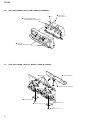
1
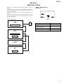
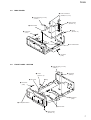
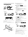
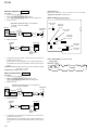
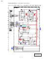
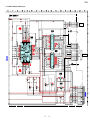
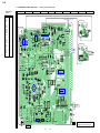
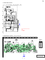
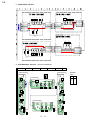
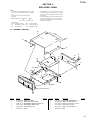
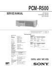
TC-S3 SERVICE MANUAL AEP Model UK Model E Model Australian Model Ver 1.0 2001.04 TC-S3 is the Tape deck section in MHC-S7AV/SV7AV/S3. Dolby noise reduction manufactured under license from Dolby Laboratories Licensing Corporation. “DOLBY” and the double-D symbol ; are trademarks of Dolby Laboratories Licensing Corporation. Tape deck Section Model Name Using Similar Mechanism NEW Tape Transport Mechanism Type TCM-230AWR41/ 230MWR41 SPECIFICATIONS Recording system Frequency response (DOLBY NR OFF) Wow and flutter Dimensions (w/h/d) Mass 4-track 2-channel stereo 60 – 13,000 Hz (±3 dB), using Sony TYPE I cassette, 60 – 14,000 Hz (±3 dB), using Sony TYPE II cassette ±0.15% W.Peak (IEC) 0.1% W.RMS (NAB) ±0.2% W.Peak (DIN) Approx. 280 x 128 x 330 mm Approx. 2.4 kg Design and specifications are subject to change without notice. STEREO CASSETTE DECK 9-873-837-11 Sony Corporation 2001D0500-1 C 2001.4 Home Audio Company Shinagawa Tec Service Manual Production Group TC-S3 TABLE OF CONTENTS 1. SERVICING NOTES ................................................ 3 2. GENERAL Location of Controls ....................................................... 4 3. DISASSEMBLY 3-1. 3-2. 3-3. 3-4. 3-5. Disassembly Flow ........................................................... Cover ............................................................................... MAIN Board ................................................................... Front Panel Section ......................................................... Tape Mechanism Deck (TCM-230AWR41/230MWR41) .................................... 3-6. LEAF SW Board, HEAD (A) Board, HEAD (B) Board ............................................................ 6 6 7 7 8 8 4. TEST MODE .............................................................. 9 5. MECHANICAL ADJUSTMENTS ....................... 10 6. ELECTRICAL ADJUSTMENTS ......................... 10 7. DIAGRAMS 7-1. Note for Printed Wiring Boards and Schematic Diagrams ....................................................... 7-2. Schematic Diagram – MAIN Section (1/2) – ................ 7-3. Schematic Diagram – MAIN Section (2/2) – ................ 7-4. Printed Wiring Board – MAIN Section – ...................... 7-5. Schematic Diagram – LEAF SW Section – ................. 7-6. Printed Wiring Board – LEAF SW Section – ............... 7-7. Schematic Diagram – PANEL Section – ....................... 7-8. Printed Wiring Boards – PANEL Section – .................. 7-9. IC Pin Function Description ........................................... 8. EXPLODED VIEWS 8-1. General Section ............................................................... 8-2. Front Panel Section ......................................................... 8-3. Tape Mechanism Deck Section-1 (TCM-230AWR41/230MWR41) .................................... 8-4. Tape Mechanism Deck Section-2 (TCM-230AWR41/230MWR41) .................................... 9. 2 13 14 15 16 17 17 18 18 19 21 22 23 24 ELECTRICAL PARTS LIST ............................... 25 Notes on chip component replacement • Never reuse a disconnected chip component. • Notice that the minus side of a tantalum capacitor may be damaged by heat. SAFETY-RELATED COMPONENT WARNING!! COMPONENTS IDENTIFIED BY MARK 0 OR DOTTED LINE WITH MARK 0 ON THE SCHEMATIC DIAGRAMS AND IN THE PARTS LIST ARE CRITICAL TO SAFE OPERATION. REPLACE THESE COMPONENTS WITH SONY PARTS WHOSE PART NUMBERS APPEAR AS SHOWN IN THIS MANUAL OR IN SUPPLEMENTS PUBLISHED BY SONY. TC-S3 SECTION 1 SERVICING NOTES This set is a component of the MHC-S7AV, MHC-SV7AV and MHC-S3. The MHC-S7AV/SV7AV/S3 system configuration is as shown below, and therefore it does not operate normally unless all four components are connected. In performing the repair, connect all components with the system cables. Note: The precaution to the users is described on the label stuck on the back panel (CD player) and in the troubleshooting section in the Operation Manual. • MODEL IDENTIFICATION – Rear Panel – System Configuration: TA POWER SUPPLY ST PART No. AC IN Model PART No. AEP and UK models 4-233-093-0[] Australian, Saudi Arabia and Korean models 4-233-093-1[] Sigapore model 4-233-093-2[] Thailand and Mexican models 4-233-093-3[] SYSTEM & CD µcon DISPLAY CDP TC TC µcon 3 TC-S3 SECTION 2 GENERAL This section is extracted from instruction manual. LOCATION OF CONTROLS – Front Panel – th tg tf td ts ta > . x x el r; ra rs rd A A rf M m H h AUTO REVERSEH h AUTO REVERSEH h M > m . H h t;rl rkrjrhrg CD SYNC rh (20, 21) DIRECTION t; (19, 20, 21) DOLBY NR rl (19, 20) EDIT rk (21) HI-DUB rj (20) REC PAUSE/START rg (20, 21) – Deck A – N (forward play) tf (19, 35) n (reverse play) td (19, 35) x (stop) ts (19) M/> (fast forward/go forward) th (19) m/. (rewind/go back) tg (19) Z (eject) ta (19) – Deck B – N (forward play) ra (19, 20, 35) n (reverse play) rs (19, 20, 35) x (stop) rd (19, 20) M/> (fast forward/go forward) el (19) m/. (rewind/go back) r; (19) Z (eject) rf (19) – Rear Panel – 1 SYSTEM CONTROL 5 connector (FROM CDP-S3/MCE-VS77) 2 SYSTEM CONTROL 4 connector (FROM ST-S5/S3/VS77) 1 4 2 TC-S3 Remote Control 1 2 3 es ea e; wl wk wj wh wg H hH hH . > x m M X O P p 4 5 6 7 8 9 q; qa o wf wd ws wa w; ql qk CD H es (14, 15) CHECK 5 (15) CLEAR 6 (15) CLOCK/TIMER SELECT qj (30) CLOCK/TIMER SET qk (13, 21, 29) DBFB qg (23) DISPLAY ws (13, 16, 18, 29, 35) D.SKIP 4 (14) ENTER wg (10, 12, 13, 15, 17, 18, 21, 22, 26–30) EQ qd (27) EQ ON/OFF qf (10, 28) FUNCTION wf (10, 14, 15, 20, 21, 31) GROOVE wa (23) qs qd qf qg qh qj SET UP qs (10, 12, 26, 28, 29) SLEEP 7 (29) SUR wd (25) TAPE A hH ea (19, 35) TAPE B hH e; (19, 20, 35) TUNER/BAND wl (17) TUNING + 9 (17) TUNING – wh (17) TV CH +/– ql TV VOL +/– w; TV @/1 2 TV/VIDEO 1 VOL +/– qh BUTTON DESCRIPTIONS @/1 (power) 3 X (pause) q; x (stop) 8 . (go back) wk > (go forward) wj m (rewind) wh M (fast forward) 9 O/o/P/p qa 6 5 TC-S3 SECTION 3 DISASSEMBLY • This set can be disassembled in the order shown below. 3-1. DISASSEMBLY FLOW SET 3-2. COVER (Page 6) 3-3. MAIN BOARD (Page 7) 3-4. FRONT PANEL SECTION (Page 7) 3-5. TAPE MECHANISM DECK (TCM-230AWR41/230MWR41) (Page 8) 3-6. LEAF SW BOARD, HEAD (A) BOARD, HEAD (B) BOARD (Page 8) Note: Follow the disassembly procedure in the numerical order given. 3-2. COVER 1 three screws (BVTP3 × 8) 4 Remove the cover in the direction of arrow A. 2 two screws (case 3 TP2) A 3 3 6 2 two screws (case 3 TP2) TC-S3 3-3. MAIN BOARD 2 three connectors (CN309, 310, 314) 1 wire (flat type) (17 core) (CN311) 3 three screws (BVTP3 × 8) 5 MAIN board 3 screw (BVTP3 × 8) 2 connector (CN1) 4 PC board holder 2 connector (CN2) 3-4. FRONT PANEL SECTION 1 wire (flat type) (17 core) (CN311) 2 connector (CN314) 3 screw (BVTP3 × 8) 6 two claws 4 lug 2 connector (CN1) 2 connector (CN2) 7 front panel section 6 three claws 5 three screws (BVTP3 × 8) 7 TC-S3 3-5. TAPE MECHANISM DECK (TCM-230AWR41/230MWR41) 3 lug 2 five screws (BVTP2.6 × 8) 4 tape mechanism deck (TCM-230AWR41/230MWR41) 1 Open the cassette holder (L)/(R). 3-6. LEAF SW BOARD, HEAD (A) BOARD, HEAD (B) BOARD 2 five claws 3 LEAF SW board 1 Remove the four solderings. 5 head (A) board 4 screw (+PTT 2 × 4) 7 head (B) board 6 screw (+PTT 2 × 4) 8 TC-S3 SECTION 4 TEST MODE Note: Use following buttons in the test mode. no mark : Button of Tape unit (TC-S3) *1 : Button of amplifier unit (TA-S7AV or TA-S3) *2 : Button of CD unit (CDP-S3) [MC Test Mode] Enter the MC Test Mode Procedure: 1. Press the I/1 *1 button to turn the power on. 2. While pressing the both [PLAY MODE]*2 and [x ]*2 buttons, press the [DISC 3]*2 button. 3. “GROOVE” indication blinks on the fluorescent indicator tube in the midst of MC test mode. Releasing the MC Test Mode To release from this mode, press the I/1 *1 button or disconnect the power cord. [DECK Test Mode] In the DECK test mode, it operates as follows. Cancellation of the linear mute of DOLBY IC (IC301) • It become cancellation automatically when it is possible to enter a MC test mode. AMS checking Procedure: 1. Enter the MC test mode. 2. Insert a test tape AMS-110A or AMS-120 to Deck A. 3. Set TAPE A function. 4. Press the [CD SYNC] button to enter the AMS test mode. 5. After a tape is rewound first, the FF AMS is checked, and the mechanism is shut off after detecting the ASM signal twice. 6. Then the REW AMS is checked and the mechanism is shut off after detecting the AMS signal twice. 7. When the check is complete, a message of either OK or NG appears. (To check an AMS of the B deck, select TAPE B function. After that, press [CD SYNC].) ALC checking Procedure: 1. Enter the MC test mode. 2. Insert a tape into Deck B. 3. During Recording, Keep holding down the below keys. [x ]*2 + [REC PAUSE/START] ALC could keep ON while these keys keep being pressed, ALC could keep OFF while keys are released. Double speed REC mode Procedure: 1. Enter the MC test mode 2. Insert a tape into Deck B. 3. During Recording, keep holding down the below key. [HI-DUB] Double speed recording is going on while the key keeps being pressed. REC/PLAY checking • The mode to PLAY by rewinding recording contents automatically. Procedure: 1. If recording A surface, it returns automatically at the point of the recording beginning and it replays when pressing TAPE B [M]. 2. If recording B surface, it returns automatically at the point of the recording beginning and it replays when pressing TAPE B [m]. 9 TC-S3 SECTION 5 MECHANICAL ADJUSTMENTS Precaution 1. Clean the following parts with a denatured alcohol-moistened swab: record/playback heads pinch rollers erase head rubber belts capstan idlers 2. Demagnetize the record/playback head with a head demagnetizer. 3. Do not use a magnetized screwdriver for the adjustments. 4. After the adjustments, apply suitable locking compound to the parts adjusted. 5. The adjustments should be performed with the rated power supply voltage unless otherwise noted. Torque Measurement Mode Torque meter FWD CQ-102C FWD back tension CQ-102C REV CQ-102RC REV back tension CQ-102RC FF/REW FWD tension REV tension CQ-201B CQ-403A CQ-403R Meter reading 3.06 N • m to 6.96 N • m 31 to 71 g • cm (0.43 – 0.98 oz • inch) 0.19 N • m to 0.58 N • m 2 to 6 g • cm (0.02 – 0.08 oz • inch) 3.06 N • m to 6.96 N • m 31 to 71 g • cm (0.43 – 0.98 oz • inch) 0.19 N • m to 0.58 N • m 2 to 6 g • cm (0.02 – 0.08 oz • inch) 6.96 N • m to 14.02 N • m 71 to 143 g • cm (0.98 – 1.99 oz • inch) 9.80 N • m 100 g or more (3.53 oz or more) 9.80 N • m 100 g or more (3.53 oz or more) SECTION 6 ELECTRICAL ADJUSTMENTS DECK SECTION 0 dB=0.775 V 1. Demagnetize the record/playback head with a head demagnetizer. 2. Do not use a magnetized screwdriver for the adjustments. 3. After the adjustments, apply suitable locking compound to the parts adjust. 4. The adjustments should be performed with the rated power supply voltage unless otherwise noted. 5. The adjustments should be performed in the order given in this service manual. (As a general rule, playback circuit adjustment should be completed before performing recording circuit adjustment.) 6. The adjustments should be performed for both L-CH and RCH. 7. Switches and controls should be set as follows unless otherwise specified. 8. Please refer to “SERVICING NOTES” (page 3) before adjustments. • Test Tape Tape P-4-A100 WS-48B P-4-L300J Signal 10 kHz, –10 dB 3 kHz, 0 dB 315 Hz, 0 dB Used for Azimuth Adjustment Tape Speed Adjustment Level Adjustment Record/Playback Head Azimuth Adjustment DECK A DECK B Note: Perform this adjustments for both decks Procedure: 1. Mode: Playback test tape P-4-A100 (10 kHz, –10 dB) level meter set STS3/S5/SV7 + – MD OUT jack (J601) 10 TC-S3 2. Turn the adjustment screw and check output peaks. If the peaks do not match for L-CH and R-CH, turn the adjustment screw so that outputs match within 1dB of peak. Note: Use following buttons in the test mode. no mark : Button of Tape unit (TC-S3) *1 : Button of amplifier unit (TA-S7AV or TA-S3) *2 : Button of CD unit (CDP-S3) Tape Speed Adjustment within 1dB L-CH peak within 1dB Output level Screw position R-CH peak L-CH peak Screw position R-CH peak 3. Mode: Playback DECK B Note: Start the Tape Speed adjustment as below after setting to the test mode. In the test mode, the tape speed is high during pressing the [HI-DUB] button. Procedure: 1. Turn the power switch on. 2. While pressing the both [PLAY MODE]*2 and [x]*2 buttons, press the [DISC 3]*2 button. (The “GROOVE” on the fluorescent indicator tube display while in the test mode.) To exit from the test mode, press the ?/1 *1 button. Mode: Playback test tape P-4-A100 (10 kHz, –10 dB) L-CH oscilloscope STS3/S5/SV7 set R-CH + – test tape WS-48B (3 kHz, 0 dB) frequency counter STS3/S5/SV7 set MD OUT jack (J601) MD OUT jack (J601) waveform of oscilloscope in phase 45 ° 90 ° 135 ° 180 ° wrong good 4. After the adjustments, apply suitable locking compound to the pats adjusted. Adjustment Location: Playback Head (Deck A). Record/Playback/Erase Head (Deck B). forward + – 1. Insert the WS-48B into the deck B. 2. Press the N button on the deck B. 3. Press the [HI-DUB] button in playback mode. Then at HIGH speed mode. 4. Adjust RV1001 on the LEAF SW board so that frequency counter reads 6,000 ± 30 Hz. 5. Press the [HI-DUB] button. Then back to NORMAL speed mode. 6. Adjust RV1002 on the LEAF SW board so that frequency counter reads 3,000 ± 15 Hz. Adjustment Location: LEAF SW board Playback level Adjustment Procedure: Mode: Playback DECK A test tape P-4-L300J (315 Hz, 0 dB) set DECK B level meter STS3/S5/SV7 + – MD OUT jack (J601) reverse 1. Confirm that level difference between the channels is with ± 0.5 dB. 2. After check, adjust the following RVs. Deck A is RV302 (L-CH), Deck B is RV303 (L-CH) so that adjustment within adjustment level as follows. Adjustment Level: MD OUT jack (J601) PB level: 334.4 to 748.7 mV (–6.8 ± 0.5 dB) Adjustment Location: MAIN board Sample Volue of Wow and Flutter: 0.3% or less W. RMS (WS-48B) 11 TC-S3 REC Bias Adjustment DECK B Procedure: 1. Insert a tape into Deck B. 2. After press [REC PAUSE/START] button, press [REC PAUSE/START] button, then recording start. 3. Mode: Record attenuator blank tape CN-123 600 Ω STS3/S5/SV7 [MAIN BOARD] (Component Side) REC LEVEL (R-CH) MD/VIDEO (AUDIO) IN (J601): ST-S3/S5/SV7 1) 315 Hz 50 mV (–23.8 dB) 2) 10 kHz AF OSC Adjustable level: MD OUT jack PB level: 47.2 to 53.0 mV (–27.3 to –26.3 dB) Adjustment Location: MAIN board RV351 REC LEVEL (L-CH) set DECK B PB LEVEL (L-CH) RV301 4. Mode: Playback recorded portion CN311 level meter RV302 RV303 REC BIAS (R-CH) RV354 STS3/S5/SV7 set DECK A PB LEVEL (L-CH) + – IC303 REC BIAS (L-CH) IC302 RV304 MD OUT jack (J601) REC Level Adjustment DECK B Procedure: 1. Insert a tape into Deck B. 2. After press [REC PAUSE/START] button, press [REC PAUSE/START] button, then recording start. 3. Mode: Record AF OSC MD/VIDEO (AUDIO) IN (J601) : ST-S3/S5/SV7 315 Hz, 50 mV (–23.8 dB) attenuator blank tape CS-123 600 Ω STS3/S5/SV7 set 4. Mode: Playback recorded portion level meter set STS3/S5/SV7 + – MD OUT jack (J601) 5. Confirm the play back signal recorded in step 3 becomes adjustable level as follows. If these levels are not adjustable level, adjust the RV301 (LCH) and RV351 (R-CH) on the MAIN board to repeat steps 4 and 5. 12 [LEAF SW BOARD] (Component Side) TAPE SPEED 5. Confirm the playback signal recorded in step 3 becomes adjustable level as follows. If these levels are not adjustable level, adjust the RV304 (LCH) and RV354 (R-CH) on the MAIN board to repeat steps 4 and 5. Adjustable level: Playback output of 315 Hz to playback output of 10 kHz: ±1.0 dB Adjustment Location: MAIN board (NORMAL) (HIGH) RV1002 RV1001 CN1001 TC-S3 SECTION 7 DIAGRAMS 7-1. • Circuit Boards Location NOTE FOR PRINTED WIRING BOARDS AND SCHEMATIC DIAGRAMS Note on Printed Wiring Boards: • X : parts extracted from the component side. • : Pattern from the side which enables seeing. • Indication of transistor. Q B C E These are omitted. Q B C E These are omitted. Note on Schematic Diagram: • All capacitors are in µF unless otherwise noted. pF: µµF 50 WV or less are not indicated except for electrolytics and tantalums. • All resistors are in Ω and 1/4 W or less unless otherwise specified. • 5 : fusible resistor. • C : panel designation. LEAF SW board MAIN board HEAD (A) board Note: The components identified by mark 0 or dotted line with mark 0 are critical for safety. Replace only with part number specified. TC-PANEL-A DECK board • A : B+ Line. • B : B– Line. • Voltages and waveforms are dc with respect to ground under no-signal conditions. no mark : STOP ( ) : PB 〈〈 〉〉 : REC • Voltages are taken with a VOM (Input impedance 10 MΩ). Voltage variations may be noted due to normal production tolerances. • Waveforms are taken with a oscilloscope. Voltage variations may be noted due to normal production tolerances. • Circled numbers refer to waveforms. • Signal path. E : PB a : REC TC-SUB PANEL-A board TC-SUB PANEL-B board TC-PANEL-B DECK board HEAD (B) board • Waveforms – MAIN Board – • IC Block Diagram – MAIN Board – 3 NO312 6 (L-REC), 3 (R-REC) (DECK-B REC mode) 1 T301 4 (DECK-B REC mode) µPC1330HA IC302 INVERTER 120 Vp-p 52 Vp-p COMPARATER 1 2 SW R1 GND 13 µs 13 µs 2 Q301, 303 (collector) (REC mode) 10 Vp-p 13 µs 13 13 3 4 SW P1 CONT 5 6 GND VCC 7 8 SW P2 GND 9 SW R2 TC-S3 SCHEMATIC DIAGRAM – MAIN Section (1/2) – • See page 13 for Waveforms. • See page 13 for IC Block Diagram. 1 2 R334 220 R340 220 DECK A PB AMP 3 DECK B PB AMP 8 3 8 2 C322 100p IC303(2/2) NJM4580MD-D R333 130k 2 C328 100p 1 (DECK A) 1 C330 100 16V IC304(2/2) NJM4580MD-D R335 120k T4 RV302 2.2k R339 270k RV303 2.2k HP901 (PB) NO313 3P CN1 L-CH R331 100 L-PB TP340 C321 390p L-PB +6V TP341 R332 5.6k C324 100 16V C323 0.022 R336 220 C385 100 10V R330 120k C326 390p R338 12k C327 100 10V C329 0.01 R337 22k +6V TP342 C386 100 10V R-PB R-CH R372 5.6k R371 100 C374 100 16V R402 1.5k R373 130k T5 R370 120k R376 220 R378 12k C379 0.01 R404 1.5k 4 R405 820 R379 270k (CHASSIS) 6 C372 100p TCM-230AWR41 6 4 C378 100p 5 5 7 7 /230MWR41 R374 JW IC303(1/2) NJM4580MD-D R380 JW IC304(1/2) NJM4580MD-D T3 BLOCK HRPE901 C380 100 16V R377 22k R403 820 TAPE MECHANISM DECK R375 120k C377 100 10V T6 C371 390p C373 0.022 C376 390p R-PB NO312 8P CN2 L-PB (REC/PB/ERASE) TP343 L-PB E+6V L-CH E+6V L-REC TP344 L-REC R-PB TP345 R-PB E+6V R-CH E+6V R-REC TP346 R-REC E-HOT TP347 Q304,305 SW.R2 SW.P2 GND VCC REC/PB SWITCH CONT. TP348 E-HOT GND E+6V SW.P1 ERASE SW.R1 E+6V GND REC/PB SWITCH CONTROL IC302 µPC1330HA Q304 BN1A4M (CHASSIS) Q305 BA1A4M C347 10 50V (Page 15) R348 220 C367 0.001 C332 120p T2 R341 12k L301 27mH C333 330p R349 4.7k C383 330p L351 27mH T7 C382 120p RV354 220k R321 12k L302 220µH RV304 220k 3 Q301 2SD1387 REC BIAS CONTROL Q302 2SC2001 T1 TP370 C337 0.015 R344 18k R345 18k C342 47 16V C340 0.018 C334 27p C339 0.0068 C384 27p C338 0.0068 (DECK B) R347 22k 7-2. Q310 2SC2785 R367 1k LEVEL SHIFT T301 R342 5.6 R343 5.6 Q303 2SC2001 Q302,303 C335 0.01 100V C336 2.2 50V BIAS OSC R346 5.6k C341 1 50V R369 470 L303 220µH CN314 7P C350 10 50V C349 10 50V C348 0.1 R368 1.2k 4 5 DGND B-FWD TP405 LED-B-FWD TP406 R386 270 Y6 KEY1 B-REV TP407 LED-B-REV 6 D+5V A-REV TP408 (Page 18) LED-A-REV A-FWD TP409 LED-A-FWD 7 8 The components identified by mark 0 or dotted line with mark 0 are critical for safety. Replace only with part number specified. 14 14 TC-S3 7-3. SCHEMATIC DIAGRAM – MAIN Section (2/2) – 1 T2 T1 2 CN308 5P TP308 X5 X1 TCREC-L X2 TP307 X3 TP305 PB-L R307 3.3k R304 6.8k ST-S5/S3/VS77 TCREC-R C417 0.1 R319 4.7k 1 50V FROM PB-R R318 1.2k C305 0.47 50V SYSTEM CONTROL R324 10k TP354 R317 390k C418 0.1 IC310 PT8300-S C343 0.1 C398 100p C399 100p C314 10 50V Y4 Y3 C397 100p Y5 LM (CHASSIS) C344 0.1 Y2 PB AMP, EPT300 C396 100p C394 10 50V 1 50V C318 10 50V X2 C306 R306 12k AGND TP304 X4 C309 0.47 RV301 10k C307 C304 0.1 C308 10 50V R305 10k SYSTEM CONTROL 4 TP306 R308 22k TP377 REC EQ AMP, C310 470p DOLBY B NR C301 1 50V R300 22k C303 0.1 TP378 RM BIAS C313 0.001 R301 2.2k X1 NR C315 4.7 50V IC301 HA12226F TP379 N/H PB TP371 TP381 T4 T5 R303 C319 100 2.2 50V C320 2.2 50V C369 2.2 50V R412 100 D GND TP303 AHALF Z7 BPLAY Z6 R413 100 APLAY Z5 R414 100 BHALF TP373 TP383 TP374 R316 10k LM TP375 TP385 R315 10k Y1 R415 100 TP300 REC/PB/PAS TP376 TP386 Y1 Y2 R406 100 TP309 NR R313 10k C317 100 10V RM R314 33k DATA-OUT C316 100 16V C346 0.1 Y3 R407 100 Y4 R408 100 Y5 R409 100 TP310 DATA-IN IC311 PT8300-S LED DRIVE, C345 0.1 MOTOR DRIVER TP311 CLK TP312 BIAS R311 100k C352 0.0047 T6 LAT TP313 SYSTEM CONTROL 5 19 KEY Y7 R416 100 Y8 R417 100 N/H TP315 ATRIG TP395 TP389 PB TP396 TP316 R422 220 UNREG HI B-FWD TP317 ALC C353 0.1 M GND TP390 R423 220 TP397 M GND B-REV CN310 10P TP398 (Page 14) CDP-S3/MCE-VS77 BTRIG TP356 R350 22k FROM TP314 17 C370 2.2 50V C351 1 50V TP301 ASHUT TP355 Y6 X4 TP302 BSHUT C302 0.0047 R302 100 TP318 X5 TP372 TP382 ALC TP384 T3 CN309 5P TP380 TP391 R351 2.2k TP399 R420 220 A-REV EPT302 TP400 TP392 TP401 RV351 10k TP353 TP351 TP352 R356 12k D306 11ES2-NTA2B D307 11ES2-NTA2B D308 11ES2-NTA2B D309 11ES2-NTA2B (CHASSIS) TP394 TP404 C359 0.47 C311 10 50V R357 3.3k T7 R358 33k C354 0.1 A-FWD TP393 C368 10 50V R355 10k R421 220 TP402 C356 1 50V R354 6.8k C355 0.47 50V C357 1 50V C360 470p C358 10 50V X3 C395 10 50V R309 1M C312 0.47 50V R310 160k +12V REGULATOR IC320 BA12T 3 R359 1k R361 1k Q393 2SB1116 Q391 2SB1116 C389 470 16V C388 10 50V R364 1k C362 0.0047 R360 1k Q391-394 C363 0.0047 TRIGER R362 1k DRIVE +9V REGULATOR Q395 BA1A4M Q396 2SD1387 CAPSTAN MOTOR CAPSTAN SPEED CONTROL MOTOR DRIVE CN311 17P IC321 NJM7809FA Z1 CAPM(-) TP321 CAPM(+) Z2 Q392 BA1A4M Q394 BA1A4M TP320 C391 470 16V R363 47k TP322 CAP.M H/N C390 10 50V Z3 TP323 TRG/A TP324 TRG/GND Z4 TP325 TRG/B Z5 TP326 4 A SHUT Y7 TP327 Y8 D.GND 5 Z4 Z3 Z2 Z1 R328 47k AHALF TP328 A HALF TP329 +5V Q400 2SC2001 LEVEL 6 R327 4.7k R418 560 SHIFT 17 R325 47k C414 10 50V R419 1k R323 4.7k TP331 B SHUT APLAY TP332 A PLAY.SW Z7 C415 470 10V TP330 A 120/170 Z6 TP333 B HALF 19 TP334 B 120/170 BPLAY TP335 B PLAY.SW 7 TP336 R322 47k 8 15 15 B METAL (Page 17) TC-S3 7-4. • Semiconductor Location 1 2 3 4 5 6 7 8 MAIN BOARD T301 1 JW307 5 JW303 JW305 1 4 NO313 B C326 C386 9 10 R336 C321 C371 R330 R331 R370 5 4 4 R332 8 9 C336 R348 R347 IC302 L351 L301 C340 L303 JW310 JW313 C333 R369 C367 HEAD (B) BOARD C349 C347 R349 R368 C348 C330 JW317 R367 Q310 E C350 C341 E JW312 R340 JW385 C380 R386 L302 C342 E 8 IC304 CN314 7 Q304 Q305 R334 C324 R345 R346 C384 RV354 C382 C383 IC303 C374 1 C373 C339 Q301 E JW302 C379 C329 R372 1 C332 R378 R338 R373 C323 R379 R339 C372 C322 1 5 C328 R333 C C378 R376 R337 R344 Q302 E JW301 JW304 JW308 JW306 R375 Q391 R359 E JW316 R321 R341 A JW311 JW314 JW319 R405 C363 C362 R420 CN311 R402 JW324 Q394 JW327 JW325 R303 JW330 JW326 JW328 JW337 R364 R305 C304 JW331 R328 JW335 JW333 R323 R306 R300 C310 R308 R327 JW334 R304 C320 C307 C302 C317 JW339 R350 56 29 1 28 R317 C313 C368 R355 R351 JW341 JW342 JW343 JW345 JW344 R313 JW360 C343 C315 R311 C316 JW352 RV351 R309 R408 R409 R413 R414 R416 R417 JW367 R412 JW361 JW368 JW388 C357 JW362 R310 JW364 C358 R357 JW363 C356 C395 R407 JW369 C312 G R415 C344 C314 R356 C396 C397 R406 1 CN309 5 1 10 CN310 JW371 C417 JW386 D306 D308 C391 C389 JW381 JW374 EPT302 C414 JW375 C415 H R419 1 4 1 2 CN308 JW379 (CHASSIS) JW377 IC320 JW380 JW372 JW376 C390 C388 5 SYSTEM CONTROL 5 FROM CDP-S3/MCE-VS77 JW370 C418 EPT300 IC310 JW351 JW355 R315 R314 15 C311 C359 C399 R324 JW354 JW383 C354 C355 R354 C398 JW353 R316 R358 14 JW340 R318 IC301 C353 JW346 42 C351 JW347 43 JW356 R319 JW349 C309 JW348 C305 C352 C360 C345 C308 C303 JW350 C369 C394 IC311 C346 JW332 C319 C370 JW359 R325 Q395 C306 JW322 R360 R322 E C318 R423 JW336 R363 JW338 R301 R421 R362 RV301 C301 JW323 E Q392 E Q396 E R307 R302 E JW321 R422 R403 R404 D (Page 17) JW320 Q393 R361 E JW329 F LEAF SW BOARD CN1001 JW318 RV302 RV303 IC321 3 1 R418 D309 E 3 Q400 D307 11 JW373 JW378 1-680-718- I (CHASSIS) HEAD (A) BOARD 3 C334 RV304 C338 TC-PANEL-B DECK BOARD NO304 R342 C376 R335 R371 JW382 R377 JW309 C327 Q303 E C337 R343 1 2 6 C377 3 C385 B-6 B-6 B-6 B-5 C-5 C-6 C-5 D-5 D-5 D-5 E-4 D-4 H-5 C335 NO312 8 JW365 F-3 B-4 C-1 B-3 F-6 E-6 H-3 H-4 (Page 18) B JW366 IC301 IC302 IC303 IC304 IC310 IC311 IC320 IC321 A JW357 H-2 I-6 H-2 H-5 Q301 Q302 Q303 Q304 Q305 Q310 Q391 Q392 Q393 Q394 Q395 Q396 Q400 • See page 13 for Circuit Boards Location. Location D306 D307 D308 D309 JW358 Ref. No. PRINTED WIRING BOARDS – MAIN Section – SYSTEM CONTROL 4 FROM ST-S5/S3/VS77 16 16 (11, 12) There are a few cases that the part printed on this diagram isn’t mounted in this model. TC-S3 7-5. SCHEMATIC DIAGRAM – LEAF SW Section – C1001 33 10V S1004 (A. 120/70) A MAIN BOARD (2/2) CN311 (Page 15) S1008 (B. 120/70) • Voltages are dc with respect to ground under no-signal conditions. no mark : TAPE PLAY ( ) : TAPE REC 7-6. PRINTED WIRING BOARD – LEAF SW Section – • See page 13 for Circuit Boards Location. 1 2 3 4 5 6 7 8 9 10 11 PM902 A PM901 IC1001 IC1002 B 12 • Semiconductor Location Ref. No. Location D1001 D1002 B-4 B-10 IC1001 IC1002 B-2 B-9 Q1001 B-3 C A D (Page 16) CN311 17 17 There are a few cases that the part printed on this diagram isn’t mounted in this model. TC-S3 7-7. SCHEMATIC DIAGRAM – PANEL Section – S306 S301 S302 S303 S304 S305 REC PAUSE/ S307 S308 S309 START CD SYNC HI DUB EDIT NO302 5P DGND NO304 7P NO303 5P S301 S302 S303 S304 NO303 5P D+5V S305 S306 DGND DGND S307 S308 S309 A REV DGND LED-A-REV A FWD B FWD LED-B-FWD KEY1 R387 330 KEY1 B REV R388 470 R389 560 KEY1 LED-A-FWD A FWD A FWD R390 680 LED-A-FWD R391 1k LED-A-FWD A REV A REV LED-B-REV LED-A-REV D+5V R392 1.2k R393 1.8k R394 2.7k KEY1 LED-A-REV D+5V D+5V A REV LED-A-REV D302 SEL5423E-T P15 A FWD (Page 14) B REV B FWD LED-A-FWD D303 SEL5423E-T P15 D302,303 BACK LIGHT NO301 5P R401 56k R400 27k R399 15k R398 10k NO301 5P D+5V S311 S310 DIRECTION DOLBY NR S311 R397 6.8k DGND A REV S310 R396 4.7k NO302 5P R395 3.3k LED-A-REV KEY1 LED-A-FWD LED-A-FWD LED-A-FWD KEY1 KEY1 LED-A-REV LED-A-REV A FWD D300 SEL5423E-T P15 D301 SEL5423E-T P15 S316 S315 S314 S313 S312 DGND S315 S314 S313 D+5V S312 DGND A REV A FWD S316 D+5V D300,301 BACK LIGHT 7-8. PRINTED WIRING BOARDS – PANEL Section – • See page 13 for Circuit Boards Location. 1 2 3 4 5 6 TC-PANEL-B DECK BOARD 7 TC-PANEL-A DECK BOARD A S301 TC-SUB PANEL-B BOARD M> R387 NO304 7 1 R391 (Page 16) B R389 R388 1 B MAIN BOARD CN314 R393 R392 REC PAUSE /START D300 D301 D302 D303 5 LP301 R399 R394 5 S306 NO303 S307 CD SYNC S308 HI-DUB S309 EDIT 1 R400 NO302 11 1-680-722- (11, 12) S302 .m Ref. No. S316 M> R401 D302 D300 N N S315 .m S303 S314 N N S304 D303 D301 n n n TC-SUB PANEL-A BOARD 1 C S305 x R395 S313 JW384 R397 R396 n 5 NO303 1 5 NO302 5 R390 1-680-720- S310 DOLBY NR S311 DIRECTION 11 NO301 1-680-721- 11 5 (11, 12) 1 (11, 12) S312 x NO301 1 R398 1-680-719- 18 18 • Semiconductor Location 11 (11, 12) Location B-6 C-6 B-1 C-1 TC-S3 7-9. IC PIN FUNCTION DESCRIPTION • MAIN BOARD IC310 PT8300-S (SYSTEM CONTROL) Pin No. Pin Name I/O 1 VSS — Description 2 RESET_B I Reset signal input terminal 3 CLK I Serial data transfer clock signal input from the CD player section (CDP-S3) Ground terminal Not used 4 LATCH I Serial data latch pulse signal input from the CD palyer section (CDP-S3) 5–8 P15 – P12 I Not used (fixed at “L”) 9 P11 I AMS signal input terminal 10 P10 I Detection input from the deck-A half detect switch “H”: cassette in, “L”: no cassette 11 P9 I Detection input from the deck-B play detect switch “H”: deck-B play 12 P8 I Detection input from the deck-A play detect switch “H”: deck-A play 13 LATCHO O Serial data latch pulse output to the PT8300-S (IC311) 14 CLKO O Serial data transfer clock signal output to the PT8300-S (IC311) 15 DO1 O Serial data output to the PT8300-S (IC311) 16 DI2 I Serial data input from the PT8300-S (IC311) 17 P7 O Tape deck relay on/off control signal output to the µPC1330H (IC302) 18 P6 O ALC on/off control signal output to the HA12226F (IC301) 19 P5 O Deck-A/B selection signal output to the HA12226F (IC301) 20 P4 O EQ high/normal selection signal output to the HA12226F (IC301) 21 P3 O Recording bias on/off control signal output to the HA12226F (IC301) 22 P2 O Recording muting on/off control signal output to the HA12226F (IC301) 23 P1 O Dolby NR on/off selection signal output to the HA12226F (IC301) 24 P0 O Tape deck line muting on/off control output to the HA12226F (IC301) 25 DO2 O Serial data output to the CD player section (CDP-S3) 26 DI1 I Serial data input from the CD player section (CDP-S3) 27 PULLUP I P8 to P15 Control pin for pull-up resisitor (fixed at “L”) 28 VCC — “L”: AMS in Power supply terminal (+5V) 19 TC-S3 • MAIN BOARD IC311 PT8300-S (LED DRIVE, MOTOR DRIVER) Pin No. Pin Name I/O 1 VSS — Description 2 RESET_B I Reset signal input terminal 3 CLK I Serial data transfer clock signal input from the PT8300-S (IC310) 4 LATCH I Serial data latch pulse input from the PT8300-S (IC310) 5 P15 O Not used (connected to pin 6) 6 P14 O LED drive signal output of the B-FWD indicator (D302) 7 P13 O Not used (connected to pin 8) 8 P12 O LED drive signal output of the B-REV indicator (D303) 9 P11 O Not used (connected to pin q;) 10 P10 O LED drive signal output of the A-REV indicator (D301) Ground terminal Nor used 11 P9 O Not used (connected to pin qs) 12 P8 O LED drive signal output of the A-FWD indicator (D300) 13 LATCHO O Not used (open) 14 CLKO O Not used (open) 15 DO1 O Not used (open) 16 DI2 I Not used (fixed at “L”) 17 – 21 P7 – P3 O Not used (open) 20 “L”: LED on “L”: LED on “L”: LED on “L”: LED on 22 P2 O Not used (connected to pin wd) 23 P1 O Capstan motor on/off control signal output terminal 24 P0 O High/normal speed selection signal output of the capstan motor “H”: normal speed, “L”: high speed 25 DO2 O Serial data output to the PT8300-S (IC310) 26 DI1 I Serial data input from the PT8300-S (IC310) 27 PULLUP I P8 to P15 Control pin for Pull-up resistor (fixed at “L”) 28 VCC — Power supply terminal (+5V) “H”: motor on TC-S3 SECTION 8 EXPLODED VIEWS NOTE: • -XX and -X mean standardized parts, so they may have some difference from the original one. • Color Indication of Appearance Parts Example: KNOB, BALANCE (WHITE) . . . (RED) ↑ ↑ Parts Color Cabinet's Color • Abbreviation MX : Mexican model AUS : Australian model EA : Saudi Arabia model SP : Singapore model TH : Thailand model KR : korean model • Items marked “*” are not stocked since they are seldom required for routine service. Some delay should be anticipated when ordering these items. • The mechanical parts with no reference number in the exploded views are not supplied. • Hardware (# mark) list is given in the last of the electrical parts list. 8-1. GENERAL SECTION 5 #3 4 4 #1 3 6 #1 #1 2 #1 1 not supplied 7 #1 8 not supplied Front panel section #1 Ref. No. Part No. Description * 1 2 3 3 4 4-924-098-01 1-773-048-11 A-2007-873-A A-4725-734-A 3-363-099-21 HOLDER, PC BOARD WIRE (FLAT TYPE) (17 CORE) MAIN BOARD, COMPLETE (EXCEPT TH) MAIN BOARD, COMPLETE (TH) SCREW (CASE 3 TP2) 5 4-232-336-31 COVER Remark Ref. No. Part No. Description 6 7 7 7 7 1-757-632-11 4-233-093-01 4-233-093-11 4-233-093-21 4-233-093-31 CORD (WITH CONNECTOR) 15P PANEL (TC), BACK (AEP, UK) PANEL (TC), BACK (AUS, EA, KR) PANEL (TC), BACK (SP) PANEL (TC), BACK (MX, TH) 8 4-965-822-01 FOOT Remark 21 TC-S3 8-2. FRONT PANEL SECTION 58 TCM-230AWR41/230MWR41 59 not supplied 57 61 59 #2 #2 61 59 56 62 58 60 59 55 59 63 64 59 65 66 54 51 53 Ref. No. Part No. Description 51 52 53 54 55 X-4953-607-1 X-4953-606-1 4-233-091-01 4-233-090-01 X-4953-605-1 PANEL ASSY, FRONT HOLDER (R) ASSY, CASSETTE SPRING (R), TORSION SPRING (L), TORSION HOLDER (L) ASSY, CASSETTE 56 57 58 4-233-094-01 EJECT (L), BUTTON 4-900-888-01 EJECT (LEVER-L) 3-019-456-11 SCREW, STEP 22 52 Remark Ref. No. Part No. Description 59 60 61 62 63 4-951-620-01 4-900-889-01 4-215-062-01 1-680-719-11 1-680-721-11 SCREW (2.6X8), +BVTP EJECT (LEVER-R) DAMPER TC-PANEL-A DECK BOARD TC-SUB PANEL-A BOARD 64 65 66 1-680-722-11 TC-SUB PANEL-B BOARD 1-680-720-11 TC-PANEL-B DECK BOARD 4-233-095-01 EJECT (R), BUTTON Remark TC-S3 8-3. TAPE MECHANISM DECK SECTION-1 (TCM-230AWR41/230MWR41) Note: Two different types of tape mechanism are used depending on models. They maintain compatibility as an entire mechanism even though there are some different parts are used. 706 706 713 710 PM901 704 702 HP901 705 701 703 PM902 702 713 705 HRPE901 703 704 701 708 709 707 707 Ref. No. Part No. Description 701 702 703 704 705 3-016-574-11 3-016-565-01 3-016-564-01 X-3374-156-4 X-3374-155-4 SPRING (HEAD), TENSION BASE (PINCH LEVER REV) BASE (PINCH LEVER FWD) PINCH LEVER (REV) ASSY PINCH LEVER (FWD) ASSY 706 707 708 4-229-083-01 SPRING (CASSETTE), LEAF 4-227-872-11 SCREW (+PTT 2X4), GROUND POINT 1-676-220-11 HEAD (A) BOARD Remark Ref. No. Part No. 709 1-676-221-11 710 A-2007-838-A 713 3-016-566-01 HP901 A-2004-771-A HRPE901A-2004-772-A PM901 PM902 Description Remark HEAD (B) BOARD LEAF SW BOARD, COMPLETE SLIDER, REVERSE BASE (A) ASSY, HEAD BASE (B) ASSY, HEAD 1-454-887-32 SOLENOID, PLUNGER 1-454-887-32 SOLENOID, PLUNGER 23 TC-S3 8-4. TAPE MECHANISM DECK SECTION-2 (TCM-230AWR41/230MWR41) not supplied 765 766 763 757 753 #6 #7 751 754 757 767 755 #7 764 not supplied 762 M901 751 not supplied 752 756 Ref. No. Part No. Description 751 752 753 754 755 3-041-946-01 4-227-239-01 X-3378-042-1 X-3378-043-1 X-3378-040-1 BELT (CAPSTAN B) BELT (CAPSTAN C) FLYWHEEL (B-FWD) ASSY FLYWHEEL (B-REV) ASSY FLYWHEEL (A-FWD) ASSY 756 757 X-3378-041-1 FLYWHEEL (A-REV) ASSY 3-041-947-01 BELT (FR) 24 Remark Ref. No. Part No. Description 762 763 764 765 766 3-318-203-62 3-019-208-01 3-040-580-11 4-228-450-11 A-2004-793-A SCREW (B1.7X4), TAPPING WASHER, STOPPER PULLEY (TENSION) SPRING (REVERSE SLIDER), TORSION CHASSIS (A) ASSY, SUB Remark 767 M901 A-2004-794-A CHASSIS (B) ASSY, SUB X-3378-241-1 MOTOR ASSY (CAPSTAN) SECTION 9 ELECTRICAL PARTS LIST NOTE: • Due to standardization, replacements in the parts list may be different from the parts specified in the diagrams or the components used on the set. • -XX and -X mean standardized parts, so they may have some difference from the original one. • RESISTORS All resistors are in ohms. METAL: Metal-film resistor. METAL OXIDE: Metal oxide-film resistor. F: nonflammable • Abbreviation TH : Thailand model Ref. No. Part No. HEAD (A) LEAF SW • Items marked “*” are not stocked since they are seldom required for routine service. Some delay should be anticipated when ordering these items. • SEMICONDUCTORS In each case, u: µ, for example: uA. . : µA. . uPA. . : µPA. . uPB. . : µPB. . uPC. . : µPC. . uPD. . : µPD. . • CAPACITORS uF: µF • COILS uH: µH Description Remark 1-676-220-11 HEAD (A) BOARD ************** Ref. No. R1008 Part No. TC-S3 HEAD (B) MAIN The components identified by mark 0 or dotted line with mark 0 are critical for safety. Replace only with part number specified. When indicating parts by reference number, please include the board. Description 1-249-417-11 CARBON Remark 1K 5% 1/4W < VARIABLE RESISTOR > < CONNECTOR > * CN1 1-564-719-11 PIN, CONNECTOR (SMALL TYPE) 3P ************************************************************** RV1001 1-241-785-11 RES, ADJ, CARBON 10K RV1002 1-241-785-11 RES, ADJ, CARBON 10K < SWITCH > 1-676-221-11 HEAD (B) BOARD ************** < CONNECTOR > CN2 1-564-722-11 PIN, CONNECTOR (SMALL TYPE) 6P ************************************************************** S1001 S1002 S1003 S1004 S1005 1-570-953-11 1-570-953-11 1-771-333-11 1-771-205-11 1-771-205-11 SWITCH, PUSH (1 KEY) (A PLAY) SWITCH, PUSH (1 KEY) (B PLAY) SWITCH, LEAF (A.HALF) SWITCH, LEAF (A.120/70) SWITCH, LEAF (REC.A) S1006 1-771-333-11 SWITCH, LEAF (B.HALF) S1008 1-771-205-11 SWITCH, LEAF (B.120/70) S1009 1-771-205-11 SWITCH, LEAF (REC.B) ************************************************************** A-2007-838-A LEAF SW BOARD, COMPLETE ************************ < CAPACITOR > C1001 1-107-716-11 ELECT 33uF 20% A-2007-873-A MAIN BOARD, COMPLETE (EXCEPT TH) A-4725-734-A MAIN BOARD, COMPLETE (TH) ********************* 10V < CONNECTOR > 7-685-646-79 SCREW +BVTP 3X8 TYPE2 N-S CN1001 1-568-860-21 SOCKET, CONNECTOR 17P < CAPACITOR > < DIODE > D1001 D1002 8-719-911-19 DIODE 1SS133T-72 8-719-911-19 DIODE 1SS133T-72 < PHOTO INTERRUPTER > IC1001 IC1002 8-749-014-38 PHOTO INTERRUPTER SG-264 8-749-014-38 PHOTO INTERRUPTER SG-264 < TRANSISTOR > Q1001 8-729-029-56 TRANSISTOR 1-247-879-11 1-249-409-11 1-249-409-11 1-249-414-11 1-247-834-11 CARBON CARBON CARBON CARBON CARBON R1005 R1006 R1007 1-247-818-11 CARBON 1-247-864-11 CARBON 1-247-780-00 CARBON 1-126-960-11 1-130-479-00 1-136-165-00 1-136-165-00 1-126-959-11 ELECT MYLAR FILM FILM ELECT 1uF 0.0047uF 0.1uF 0.1uF 0.47uF 20% 5% 5% 5% 20% 50V 50V 50V 50V 50V C306 C307 C308 C309 C310 1-126-960-11 1-126-960-11 1-126-964-11 1-137-194-11 1-162-290-31 ELECT ELECT ELECT FILM CERAMIC 1uF 1uF 10uF 0.47uF 470PF 20% 20% 20% 5% 10% 50V 50V 50V 50V 50V C311 C312 C313 C314 C315 1-126-964-11 1-126-959-11 1-162-294-31 1-126-964-11 1-126-963-11 ELECT ELECT CERAMIC ELECT ELECT 10uF 0.47uF 0.001uF 10uF 4.7uF 20% 20% 10% 20% 20% 50V 50V 50V 50V 50V C316 C317 C318 C319 C320 1-126-933-11 1-104-665-11 1-126-964-11 1-126-961-11 1-126-961-11 ELECT ELECT ELECT ELECT ELECT 100uF 100uF 10uF 2.2uF 2.2uF 20% 20% 20% 20% 20% 16V 10V 50V 50V 50V DTA144ESA-TP < RESISTOR > R907 R1001 R1002 R1003 R1004 C301 C302 C303 C304 C305 100K 220 220 560 1.3K 5% 5% 5% 5% 5% 1/4W 1/4W 1/4W 1/4W 1/4W 300 24K 7.5 5% 5% 5% 1/4W 1/4W 1/4W 25 TC-S3 MAIN Ref. No. Part No. Description Remark Description 1-162-289-31 1-162-282-31 1-136-157-00 1-126-933-11 1-162-289-31 CERAMIC CERAMIC FILM ELECT CERAMIC 390PF 100PF 0.022uF 100uF 390PF 10% 10% 5% 20% 10% 50V 50V 50V 16V 50V C327 C328 C329 C330 C332 1-104-665-11 1-162-282-31 1-136-153-00 1-126-933-11 1-162-283-31 ELECT CERAMIC FILM ELECT CERAMIC 100uF 100PF 0.01uF 100uF 120PF 20% 10% 5% 20% 10% 10V 50V 50V 16V 50V C333 C334 C335 C336 C337 1-162-288-31 1-162-209-31 1-137-150-11 1-126-961-11 1-136-155-00 CERAMIC CERAMIC MYLAR ELECT FILM 330PF 27PF 0.01uF 2.2uF 0.015uF 10% 5% 5% 20% 5% 50V 50V 100V 50V 50V C338 C339 C340 C341 C342 1-130-481-00 1-130-481-00 1-136-156-00 1-126-960-11 1-104-660-11 MYLAR MYLAR FILM ELECT ELECT 0.0068uF 0.0068uF 0.018uF 1uF 47uF 5% 5% 5% 20% 20% 50V 50V 50V 50V 16V * CN308 C343 C344 C345 C346 C347 1-164-159-11 1-164-159-11 1-164-159-11 1-164-159-11 1-126-964-11 CERAMIC CERAMIC CERAMIC CERAMIC ELECT 0.1uF 0.1uF 0.1uF 0.1uF 10uF * CN314 20% 50V 50V 50V 50V 50V C348 C349 C350 C351 C352 1-164-159-11 1-126-964-11 1-126-964-11 1-126-960-11 1-130-479-00 CERAMIC ELECT ELECT ELECT MYLAR 0.1uF 10uF 10uF 1uF 0.0047uF 20% 20% 20% 5% 50V 50V 50V 50V 50V D306 D306 D307 D307 D308 8-719-024-99 8-719-200-82 8-719-024-99 8-719-200-82 8-719-024-99 C353 C354 C355 C356 C357 1-136-165-00 1-136-165-00 1-126-959-11 1-126-960-11 1-126-960-11 FILM FILM ELECT ELECT ELECT 0.1uF 0.1uF 0.47uF 1uF 1uF 5% 5% 20% 20% 20% 50V 50V 50V 50V 50V D308 D309 D309 8-719-200-82 DIODE 11ES2-NTA1B (TH) 8-719-024-99 DIODE 11ES2-NTA2B (EXCEPT TH) 8-719-200-82 DIODE 11ES2-NTA1B (TH) C358 C359 C360 C362 C363 1-126-964-11 1-137-194-11 1-162-290-31 1-130-479-00 1-130-479-00 ELECT FILM CERAMIC MYLAR MYLAR 10uF 0.47uF 470PF 0.0047uF 0.0047uF 20% 5% 10% 5% 5% 50V 50V 50V 50V 50V C367 C368 C369 C370 C371 1-162-294-31 1-126-964-11 1-126-961-11 1-126-961-11 1-162-289-31 CERAMIC ELECT ELECT ELECT CERAMIC 0.001uF 10uF 2.2uF 2.2uF 390PF 10% 20% 20% 20% 10% 50V 50V 50V 50V 50V C372 C373 C374 C376 C377 1-162-282-31 1-136-157-00 1-126-933-11 1-162-289-31 1-104-665-11 CERAMIC FILM ELECT CERAMIC ELECT 100PF 0.022uF 100uF 390PF 100uF 10% 5% 20% 10% 20% 50V 50V 16V 50V 10V C378 C379 C380 C382 C383 1-162-282-31 1-136-153-00 1-126-933-11 1-162-283-31 1-162-288-31 CERAMIC FILM ELECT CERAMIC CERAMIC 100PF 0.01uF 100uF 120PF 330PF 10% 5% 20% 10% 10% 50V 50V 16V 50V 50V C384 C385 C386 1-162-209-31 CERAMIC 1-104-665-11 ELECT 1-104-665-11 ELECT 27PF 100uF 100uF 5% 20% 20% 50V 10V 10V 26 Remark Ref. No. Part No. C321 C322 C323 C324 C326 C388 C389 1-126-964-11 ELECT 1-126-935-11 ELECT 10uF 470uF 20% 20% 50V 16V C390 C391 C394 C395 C396 1-126-964-11 1-126-935-11 1-126-964-11 1-126-964-11 1-162-282-31 ELECT ELECT ELECT ELECT CERAMIC 10uF 470uF 10uF 10uF 100PF 20% 20% 20% 20% 10% 50V 16V 50V 50V 50V C397 C398 C399 C414 C415 1-162-282-31 1-162-282-31 1-162-282-31 1-126-964-11 1-126-935-11 CERAMIC CERAMIC CERAMIC ELECT ELECT 100PF 100PF 100PF 10uF 470uF 10% 10% 10% 20% 20% 50V 50V 50V 50V 10V C417 C418 1-164-159-11 CERAMIC 1-164-159-11 CERAMIC 0.1uF 0.1uF 50V 50V < CONNECTOR > CN309 CN310 CN311 1-566-856-11 SOCKET, CONNECTOR 5P (SYSTEM CONTROL 4) 1-794-569-11 PIN, CONNECTOR 5P (SYSTEM CONTROL 5) 1-580-176-11 PIN, CONNECTOR 10P (SYSTEM CONTROL 5) 1-784-778-11 CONNECTOR, FFC 17P 1-568-934-11 PIN, CONNECTOR 7P < DIODE > DIODE DIODE DIODE DIODE DIODE 11ES2-NTA2B (EXCEPT TH) 11ES2-NTA1B (TH) 11ES2-NTA2B (EXCEPT TH) 11ES2-NTA1B (TH) 11ES2-NTA2B (EXCEPT TH) < GROUND TERMINAL> * EPT300 1-537-738-21 TERMINAL, EARTH * EPT302 1-537-738-21 TERMINAL, EARTH < IC > IC301 IC302 IC303 IC304 IC310 8-759-652-02 8-759-143-54 8-759-710-59 8-759-710-59 6-800-467-01 IC IC IC IC IC HA12226F uPC1330HA NJM4580D-D NJM4580D-D PT8300-S IC311 IC320 IC321 6-800-467-01 IC PT8300-S 8-759-394-35 IC BA12T 8-759-701-59 IC NJM7809FA < COIL > L301 L302 L303 L351 1-410-780-11 1-414-193-41 1-414-193-41 1-410-780-11 INDUCTOR INDUCTOR INDUCTOR INDUCTOR 27uH 220uH 220uH 27uH < TRANSISTOR > Q301 Q302 Q303 8-729-801-93 TRANSISTOR 8-729-142-46 TRANSISTOR 8-729-142-46 TRANSISTOR 2SD1387-34-TP 2SC2001TP-LK 2SC2001TP-LK TC-S3 MAIN Ref. No. Part No. Description Remark Q304 Q305 8-729-422-57 TRANSISTOR 8-729-900-80 TRANSISTOR BN1A4M-TP BA1A4M-TP Q310 Q391 Q392 Q393 Q394 8-729-119-78 8-729-140-04 8-729-900-80 8-729-140-04 8-729-900-80 TRANSISTOR TRANSISTOR TRANSISTOR TRANSISTOR TRANSISTOR 2SC2785TP-HFE 2SB1116-TP-LK BA1A4M-TP 2SB1116-TP-LK BA1A4M-TP Q395 Q396 Q400 8-729-900-80 TRANSISTOR 8-729-801-93 TRANSISTOR 8-729-142-46 TRANSISTOR BA1A4M-TP 2SD1387-34-TP 2SC2001TP-LK < RESISTOR > R300 R301 R302 R303 R304 1-249-433-11 1-249-421-11 1-247-807-31 1-247-807-31 1-249-427-11 CARBON CARBON CARBON CARBON CARBON 22K 2.2K 100 100 6.8K 5% 5% 5% 5% 5% 1/4W 1/4W 1/4W 1/4W 1/4W R305 R306 R307 R308 R309 1-249-429-11 1-249-430-11 1-247-843-11 1-249-433-11 1-247-903-00 CARBON CARBON CARBON CARBON CARBON 10K 12K 3.3K 22K 1M 5% 5% 5% 5% 5% 1/4W 1/4W 1/4W 1/4W 1/4W R310 R311 R313 R314 R315 1-247-884-11 1-249-441-11 1-249-429-11 1-249-435-11 1-249-429-11 CARBON CARBON CARBON CARBON CARBON 160K 100K 10K 33K 10K 5% 5% 5% 5% 5% 1/4W 1/4W 1/4W 1/4W 1/4W R316 R317 R318 R319 R321 1-249-429-11 1-247-893-11 1-249-418-11 1-249-425-11 1-249-430-11 CARBON CARBON CARBON CARBON CARBON 10K 390K 1.2K 4.7K 12K 5% 5% 5% 5% 5% 1/4W 1/4W 1/4W 1/4W 1/4W R322 R323 R324 R325 R327 1-249-437-11 1-249-425-11 1-249-429-11 1-249-437-11 1-249-425-11 CARBON CARBON CARBON CARBON CARBON 47K 4.7K 10K 47K 4.7K 5% 5% 5% 5% 5% 1/4W 1/4W 1/4W 1/4W 1/4W R328 R330 R331 R332 R333 1-249-437-11 1-247-881-00 1-247-807-31 1-249-426-11 1-247-882-11 CARBON CARBON CARBON CARBON CARBON 47K 120K 100 5.6K 130K 5% 5% 5% 5% 5% 1/4W 1/4W 1/4W 1/4W 1/4W R334 R335 R336 R337 R338 1-249-409-11 1-247-881-00 1-249-409-11 1-249-433-11 1-249-430-11 CARBON CARBON CARBON CARBON CARBON 220 120K 220 22K 12K 5% 5% 5% 5% 5% 1/4W 1/4W 1/4W 1/4W 1/4W R339 R340 R341 0 R342 0 R343 1-247-889-00 1-249-409-11 1-249-430-11 1-212-851-00 1-212-851-00 CARBON CARBON CARBON FUSIBLE FUSIBLE 270K 220 12K 5.6 5.6 5% 5% 5% 5% 5% 1/4W 1/4W 1/4W 1/4W F 1/4W F R344 R345 R346 R347 R348 1-249-432-11 1-249-432-11 1-249-426-11 1-249-433-11 1-249-409-11 CARBON CARBON CARBON CARBON CARBON 18K 18K 5.6K 22K 220 5% 5% 5% 5% 5% 1/4W 1/4W 1/4W 1/4W 1/4W The components identified by mark 0 or dotted line with mark 0 are critical for safety. Replace only with part number specified. Ref. No. Part No. Description R349 R350 R351 R354 R355 1-249-425-11 1-249-433-11 1-249-421-11 1-249-427-11 1-249-429-11 CARBON CARBON CARBON CARBON CARBON 4.7K 22K 2.2K 6.8K 10K 5% 5% 5% 5% 5% 1/4W 1/4W 1/4W 1/4W 1/4W Remark R356 R357 R358 R359 R360 1-249-430-11 1-247-843-11 1-249-435-11 1-249-417-11 1-249-417-11 CARBON CARBON CARBON CARBON CARBON 12K 3.3K 33K 1K 1K 5% 5% 5% 5% 5% 1/4W 1/4W 1/4W 1/4W 1/4W R361 R362 R363 R364 R367 1-249-417-11 1-249-417-11 1-249-437-11 1-249-417-11 1-249-417-11 CARBON CARBON CARBON CARBON CARBON 1K 1K 47K 1K 1K 5% 5% 5% 5% 5% 1/4W 1/4W 1/4W 1/4W 1/4W R368 R369 R370 R371 R372 1-249-418-11 1-249-413-11 1-247-881-00 1-247-807-31 1-249-426-11 CARBON CARBON CARBON CARBON CARBON 1.2K 470 120K 100 5.6K 5% 5% 5% 5% 5% 1/4W 1/4W 1/4W 1/4W 1/4W R373 R375 R376 R377 R378 1-247-882-11 1-247-881-00 1-249-409-11 1-249-433-11 1-249-430-11 CARBON CARBON CARBON CARBON CARBON 130K 120K 220 22K 12K 5% 5% 5% 5% 5% 1/4W 1/4W 1/4W 1/4W 1/4W R379 R386 R402 R403 R404 1-247-889-00 1-249-410-11 1-249-419-11 1-249-416-11 1-249-419-11 CARBON CARBON CARBON CARBON CARBON 270K 270 1.5K 820 1.5K 5% 5% 5% 5% 5% 1/4W 1/4W 1/4W 1/4W 1/4W R405 R406 R407 R408 R409 1-249-416-11 1-247-807-31 1-247-807-31 1-247-807-31 1-247-807-31 CARBON CARBON CARBON CARBON CARBON 820 100 100 100 100 5% 5% 5% 5% 5% 1/4W 1/4W 1/4W 1/4W 1/4W R412 R413 R414 R415 R416 1-247-807-31 1-247-807-31 1-247-807-31 1-247-807-31 1-247-807-31 CARBON CARBON CARBON CARBON CARBON 100 100 100 100 100 5% 5% 5% 5% 5% 1/4W 1/4W 1/4W 1/4W 1/4W R417 R418 R419 R420 R421 1-247-807-31 1-249-414-11 1-249-417-11 1-249-409-11 1-249-409-11 CARBON CARBON CARBON CARBON CARBON 100 560 1K 220 220 5% 5% 5% 5% 5% 1/4W 1/4W 1/4W 1/4W 1/4W R422 R423 1-249-409-11 CARBON 1-249-409-11 CARBON 220 220 5% 5% 1/4W 1/4W < VARIABLE RESISTOR > RV301 RV302 RV303 RV304 RV351 1-241-764-11 1-241-762-11 1-241-762-11 1-241-768-11 1-241-764-11 RES, ADJ, CARBON 10K RES, ADJ, CARBON 2.2K RES, ADJ, CARBON 2.2K RES, ADJ, CARBON 220K RES, ADJ, CARBON 10K RV354 1-241-768-11 RES, ADJ, CARBON 220K 27 TC-S3 MAIN TC-PANEL-A DECK TC-SUB PANEL-A Ref. No. Part No. TC-PANEL-B DECK TC-SUB PANEL-B Description Remark Ref. No. < TRANSFORMER > Part No. T301 1-423-980-11 TRANSFORMER, BIAS OSCILLATION ************************************************************** 1-680-719-11 TC-PANEL-A DECK BOARD ********************* 1-249-417-11 1-249-418-11 1-249-420-11 1-249-422-11 8-719-058-03 LED SEL5423E-TP15 (N) 8-719-058-03 LED SEL5423E-TP15 (n) 1-249-429-11 1-249-431-11 1-249-434-11 1-249-438-11 CARBON CARBON CARBON CARBON 10K 15K 27K 56K CARBON CARBON CARBON CARBON 1K 1.2K 1.8K 2.7K 5% 5% 5% 5% 1/4W 1/4W 1/4W 1/4W < SWITCH > < RESISTOR > R398 R399 R400 R401 Remark < RESISTOR > R391 R392 R393 R394 < LED > D300 D301 Description 1-680-722-11 TC-SUB PANEL-B BOARD ********************* 5% 5% 5% 5% 1/4W 1/4W 1/4W 1/4W S306 1-771-410-21 SWITCH, TACTILE (REC PAUSE/START) S307 1-771-410-21 SWITCH, TACTILE (CD SYNC) S308 1-771-410-21 SWITCH, TACTILE (HI-DUB) S309 1-771-410-21 SWITCH, TACTILE (EDIT) ************************************************************** MISCELLANEOUS ************** < SWITCH > S312 1-771-410-21 SWITCH, TACTILE (x) S313 1-771-410-21 SWITCH, TACTILE (n) S314 1-771-410-21 SWITCH, TACTILE (N) S315 1-771-410-21 SWITCH, TACTILE (. m) S316 1-771-410-21 SWITCH, TACTILE (M >) ************************************************************** 1-680-720-11 TC-PANEL-B DECK BOARD ********************* 2 1-773-048-11 6 1-757-632-11 HP901 A-2004-771-A HRPE901A-2004-772-A M901 X-3378-241-1 PM901 1-454-887-32 SOLENOID, PLUNGER PM902 1-454-887-32 SOLENOID, PLUNGER ************************************************************ ************** HARDWARE LIST ************** < LED > D302 D303 8-719-058-03 LED SEL5423E-TP15 (N) 8-719-058-03 LED SEL5423E-TP15 (n) < RESISTOR > R387 R388 R389 R390 1-249-411-11 1-249-413-11 1-249-414-11 1-249-415-11 CARBON CARBON CARBON CARBON 330 470 560 680 5% 5% 5% 5% 1/4W 1/4W 1/4W 1/4W < SWITCH > S301 1-771-410-21 SWITCH, TACTILE (M >) S302 1-771-410-21 SWITCH, TACTILE (. m) S303 1-771-410-21 SWITCH, TACTILE (N) S304 1-771-410-21 SWITCH, TACTILE (n) S305 1-771-410-21 SWITCH, TACTILE (x) ************************************************************** 1-680-721-11 TC-SUB PANEL-A BOARD ******************** < RESISTOR > R395 R396 R397 1-247-843-11 CARBON 1-249-425-11 CARBON 1-249-427-11 CARBON 3.3K 4.7K 6.8K 5% 5% 5% 1/4W 1/4W 1/4W < SWITCH > S310 1-771-410-21 SWITCH, TACTILE (DOLBY NR) S311 1-771-410-21 SWITCH, TACTILE (DIRECTION) ************************************************************** 28 WIRE (FLAT TYPE) (17 CORE) CORD (WITH CONNECTOR) 15P BASE (A) ASSY, HEAD BASE (B) ASSY, HEAD MOTOR ASSY (CAPSTAN) #1 #2 #3 #6 #7 7-685-646-79 7-685-853-04 7-685-871-01 7-628-254-05 7-623-921-01 SCREW +BVTP 3X8 TYPE2 N-S SCREW +BVTT 2X6 (S) SCREW +BVTT 3X6 (S) SCREW +PS 2.6X5 RING, RETAINING, CAPSTAN TC-S3 MEMO 29 TC-S3 REVISION HISTORY Clicking the version allows you to jump to the revised page. Also, clicking the version at the upper right on the revised page allows you to jump to the next revised page. Ver. 1.0 Date 2001.04 Description of Revision New