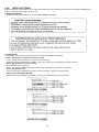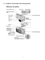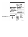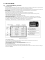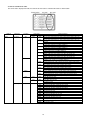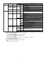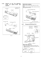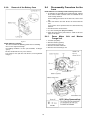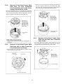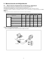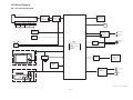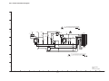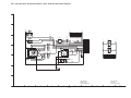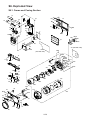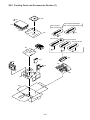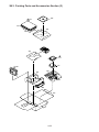
1
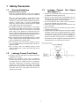
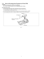
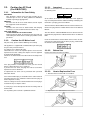
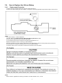
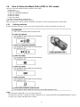
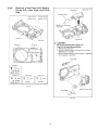
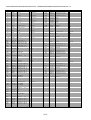
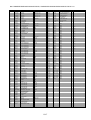
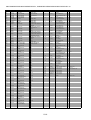
ORDER NO. DSC0703019CE B26 Digital Camera DMC-TZ3P DMC-TZ3PC DMC-TZ3PL DMC-TZ3EB DMC-TZ3EE DMC-TZ3EF DMC-TZ3EG DMC-TZ3EGM DMC-TZ3GC DMC-TZ3GD DMC-TZ3GK DMC-TZ3GN DMC-TZ3GT DMC-TZ3SG DMC-TZ2P DMC-TZ2PC DMC-TZ2PL DMC-TZ2EB DMC-TZ2EE DMC-TZ2EF DMC-TZ2EG DMC-TZ2EGM DMC-TZ2GC DMC-TZ2GD DMC-TZ2GK © 2007 Matsushita Electric Industrial Co., Ltd. All rights reserved. Unauthorized copying and distribution is a violation of law. DMC-TZ2GN DMC-TZ2GT (S)...........Silver Type (K)...........Black Type (except DMC-TZ2PL/GD/GT) (A)...........Blue Type (only DMC-TZ3P/PC/EB/EE/EF/EG/ EGM/GC/SG) Vol. 1 Colour TABLE OF CONTENTS PAGE 1 Safety Precaution -------------------------------------------------3 1.1. General Guidelines ----------------------------------------3 1.2. Leakage Current Cold Check ---------------------------3 1.3. Leakage Current Hot Check (See Figure 1.)--------3 1.4. How to Discharge the Capacitor on Flash PCB------------------------------------------------------------4 2 Warning --------------------------------------------------------------5 2.1. Prevention of Electrostatic Discharge (ESD) to ElectrostaticallySensitive (ES) Devices -----------5 2.2. How to Recycle the Lithium Ion Battery (U.S. Only)-----------------------------------------------------------5 2.3. Caution for AC Cord(For EB/GC/SG) -----------------6 2.4. How to Replace the Lithium Battery-------------------7 3 Service Navigation------------------------------------------------8 3.1. Introduction --------------------------------------------------8 3.2. General Description About Lead Free Solder (PbF) ----------------------------------------------------------8 3.3. Important Notice 1:(Other than U.S.A. and Canadian Market) ------------------------------------------8 3.4. How to Define the Model Suffix (NTSC or PAL model)---------------------------------------------------------9 4 Specifications ---------------------------------------------------- 12 5 Location of Controls and Components------------------ 13 6 Service Mode ----------------------------------------------------- 15 6.1. Error Code Memory Function ------------------------- 15 6.2. Confirmation of Firmware Version ------------------- 18 7 Service Fixture & Tools --------------------------------------- 19 7.1. Service Fixture and Tools ------------------------------ 19 7.2. When Replacing the Main PCB ---------------------- 20 7.3. Service Position ------------------------------------------ 20 8 Disassembly and Assembly Instructions --------------- 22 8.1. Disassembly Flow Chart-------------------------------- 22 8.2. PCB Location---------------------------------------------- 22 8.3. Disassembly Procedure -------------------------------- 23 8.4. Disassembly Procedure for the Lens --------------- 28 8.5. Assembly Procedure for the Lens ------------------- 31 8.6. Removal of the CCD Unit ------------------------------ 35 8.7. Removal of the Zoom Motor Unit -------------------- 35 8.8. Removal of the Focus Motor Unit -------------------- 36 8.9. The Applyment of Grease Method------------------- 36 9 Measurements and Adjustments -------------------------- 37 9.1. Matrix Chart for Replaced Part and Necessary Adjustment ------------------------------------------------- 37 10 Maintenace -------------------------------------------------------- 38 10.1. Cleaning Lens and LCD Panel ----------------------- 38 PAGE 2 1 Safety Precaution 1.1. General Guidelines 1.3. 1. IMPORTANT SAFETY NOTICE There are special components used in this equipment which are important for safety. These parts are marked by 2. 3. 4. 5. 1. Plug the AC cord directly into the AC outlet. Do not use an isolation transformer for this check. 2. Connect a 1.5 kΩ, 10 W resistor, in parallel with a 0.15 μF capacitor, between each exposed metallic part on the set and a good earth ground, as shown in Figure 1. 3. Use an AC voltmeter, with 1 kΩ/V or more sensitivity, to measure the potential across the resistor. 4. Check each exposed metallic part, and measure the voltage at each point. 5. Reverse the AC plug in the AC outlet and repeat each of the above measurements. 6. The potential at any point should not exceed 0.75 V RMS. A leakage current tester (Simpson Model 229 or equivalent) may be used to make the hot checks, leakage current must not exceed 1/2 mA. In case a measurement is outside of the limits specified, there is a possibility of a shock hazard, and the equipment should be repaired and rechecked before it is returned to the customer. in the Schematic Diagrams, Circuit Board Layout, Exploded Views and Replacement Parts List. It is essential that these critical parts should be replaced with manufacturer’s specified parts to prevent X-RADIATION, shock, fire, or other hazards. Do not modify the original design without permission of manufacturer. An Isolation Transformer should always be used during the servicing of AC Adaptor whose chassis is not isolated from the AC power line. Use a transformer of adequate power rating as this protects the technician from accidents resulting in personal injury from electrical shocks. It will also protect AC Adaptor from being damaged by accidental shorting that may occur during servicing. When servicing, observe the original lead dress. If a short circuit is found, replace all parts which have been overheated or damaged by the short circuit. After servicing, see to it that all the protective devices such as insulation barriers, insulation papers shields are properly installed. After servicing, make the following leakage current checks to prevent the customer from being exposed to shock hazards. 1.2. Leakage Current Hot Check (See Figure 1.) Leakage Current Cold Check 1. Unplug the AC cord and connect a jumper between the two prongs on the plug. 2. Measure the resistance value, with an ohmmeter, between the jumpered AC plug and each exposed metallic cabinet part on the equipment such as screwheads, connectors, control shafts, etc. When the exposed metallic part has a return path to the chassis, the reading should be between 1 MΩ and 5.2 MΩ. When the exposed metal does not have a return path to the chassis, the reading must be infinity. Figure. 1 3 1.4. How to Discharge the Capacitor on Flash PCB CAUTION: 1. Be sure to discharge the capacitor on FLASH PCB. 2. Be careful of the high voltage circuit on FLASH PCB when servicing. [Discharging Procedure] 1. Refer to the disassemble procedure and Remove the necessary parts/unit. 2. Put the insulation tube onto the lead part of Resistor (ERG5SJ102:1kΩ /5W). (an equivalent type of resistor may be used.) 3. Put the resistor between both terminals of capacitor on FLASH PCB for approx. 5 seconds. 4. After discharging confirm that the capacitor voltage is lower than 10V using a voltmeter. Fig. F1 4 2 Warning 2.1. Prevention of Electrostatic Discharge (ESD) to Electrostatically Sensitive (ES) Devices Some semiconductor (solid state) devices can be damaged easily by static electricity. Such components commonly are called Electrostatically Sensitive (ES) Devices. The following techniques should be used to help reduce the incidence of component damage caused by electrostatic discharge (ESD). 1. Immediately before handling any semiconductor component or semiconductor-equipped assembly, drain off any ESD on your body by touching a known earth ground. Alternatively, obtain and wear a commercially available discharging ESD wrist strap, which should be removed for potential shock reasons prior to applying power to the unit under test. 2. After removing an electrical assembly equipped with ES devices, place the assembly on a conductive surface such as aluminum foil, to prevent electrostatic charge buildup or exposure of the assembly. 3. Use only a grounded-tip soldering iron to solder or unsolder ES devices. 4. Use only an antistatic solder removal device. Some solder removal devices not classified as "antistatic (ESD protected)" can generate electrical charge sufficient to damage ES devices. 5. Do not use freon-propelled chemicals. These can generate electrical charges sufficient to damage ES devices. 6. Do not remove a replacement ES device from its protective package until immediately before you are ready to install it. (Most replacement ES devices are packaged with leads electrically shorted together by conductive foam, aluminum foil or comparable conductive material). 7. Immediately before removing the protective material from the leads of a replacement ES device, touch the protective material to the chassis or circuit assembly into which the device will be installed. CAUTION : Be sure no power is applied to the chassis or circuit, and observe all other safety precautions. 8. Minimize bodily motions when handling unpackaged replacement ES devices. (Otherwise harmless motion such as the brushing together of your clothes fabric or the lifting of your foot from a carpeted floor can generate static electricity (ESD) sufficient to damage an ES device). 2.2. How to Recycle the Lithium Ion Battery (U.S. Only) 5 2.3. 2.3.1. Caution for AC Cord (For EB/GC/SG) 2.3.2.1. Information for Your Safety Blue Brown IMPORTANT Your attention is drawn to the fact that recording of prerecorded tapes or discs or other published or broadcast material may infringe copyright laws. WARNING To reduce the risk of fire or shock hazard, do not expose this equipment to rain or moisture. CAUTION To reduce the risk of fire or shock hazard and annoying interference, use the recommended accessories only. FOR YOUR SAFETY DO NOT REMOVE THE OUTER COVER To prevent electric shock, do not remove the cover. No user serviceable parts inside. Refer servicing to qualified service personnel. 2.3.2. Important The wires in this mains lead are coloured in accordance with the following code: Neutral Live As the colours of the wires in the mains lead of this appliance may not correspond with the coloured markings identifying the terminals in your plug, proceed as follows: The wire which is coloured BLUE must be connected to the terminal in the plug which is marked with the letter N or coloured BLACK. The wire which is coloured BROWN must be connected to the terminal in the plug which is marked with the letter L or coloured RED. Under no circumstances should either of these wires be connected to the earth terminal of the three pin plug, marked with the letter E or the Earth Symbol. Caution for AC Mains Lead For your safety, please read the following text carefully. This appliance is supplied with a moulded three-pin mains plug for your safety and convenience. A 5-ampere fuse is fitted in this plug. Should the fuse need to be replaced please ensure that the replacement fuse has a rating of 5 amperes and it is approved by ASTA or BSI to BS1362 Check for the ASRA mark or the BSI mark on the body of the fuse. 2.3.2.2. Before Use Remove the Connector Cover as follows. If the plug contains a removable fuse cover you must ensure that it is refitted when the fuse is replaced. If you lose the fuse cover, the plug must not be used until a replacement cover is obtained. A replacement fuse cover can be purchased from your local Panasonic Dealer. 2.3.2.3. How to Replace the Fuse 1. Remove the Fuse Cover with a screwdriver. If the fitted moulded plug is unsuitable for the socket outlet in your home then the fuse should be removed and the plug cut off and disposed of safety. There is a danger of severe electrical shock if the cut off plug is inserted into any 13-ampere socket. If a new plug is to be fitted please observe the wiring code as shown below. If in any doubt, please consult a qualified electrician. 2. Replace the fuse and attach the Fuse cover. 6 2.4. 2.4.1. How to Replace the Lithium Battery Replacement Procedure 1. Remove the Top Operation PCB. (Refer to Disassembly Procedures.) 2. Remove the Lithium battery (Ref. No. “B9901” at component side of Top Operation PCB) and then replace it into new one. NOTE: This Lithium battery is a critical component. (Type No.: ML614S/ZT Manufactured by Matsushita Battery Industrial Co.,Ltd.) It must never be subjected to excessive heat or discharge. It must therefore only be fitted in requirement designed specifically for its use. Replacement batteries must be of same type and manufacture. They must be fitted in the same manner and location as the original battery, with the correct polarity contacts observed. Do not attempt to re-charge the old battery or re-use it for any other purpose. It should be disposed of in waste products destined for burial rather than incineration. NOTE: Above caution is applicable for a battery pack which is for DMC-TZ3/TZ2 series, as well. 7 3 Service Navigation 3.1. Introduction This service manual contains technical information, which allow service personnel’s to understand and service this model. Please place orders using the parts list and not the drawing reference numbers. If the circuit is changed or modified, the information will be followed by service manual to be controlled with original service manual. 3.2. General Description About Lead Free Solder (PbF) The lead free solder has been used in the mounting process of all electrical components on the printed circuit boards used for this equipment in considering the globally environmental conservation. The normal solder is the alloy of tin (Sn) and lead (Pb). On the other hand, the lead free solder is the alloy mainly consists of tin (Sn), silver (Ag) and Copper (Cu), and the melting point of the lead free solder is higher approx.30°C (86°F) more than that of the normal solder. Distinction of PCB Lead Free Solder being used Service caution for repair work using Lead Free Solder (PbF) • The lead free solder has to be used when repairing the equipment for which the lead free solder is used. (Definition: The letter of “PbF” is printed on the PCB using the lead free solder.) • To put lead free solder, it should be well molten and mixed with the original lead free solder. • Remove the remaining lead free solder on the PCB cleanly for soldering of the new IC. • Since the melting point of the lead free solder is higher than that of the normal lead solder, it takes the longer time to melt the lead free solder. • Use the soldering iron (more than 70W) equipped with the temperature control after setting the temperature at 350±30°C (662±86°F). Recommended Lead Free Solder (Service Parts Route.) • The following 3 types of lead free solder are available through the service parts route. RFKZ03D01K-----------(0.3mm 100g Reel) RFKZ06D01K-----------(0.6mm 100g Reel) RFKZ10D01K-----------(1.0mm 100g Reel) Note * Ingredient: tin (Sn) 96.5%, silver (Ag) 3.0%, Copper (Cu) 0.5%, Cobalt (Co) / Germanium (Ge) 0.1 to 0.3% 3.3. Important Notice 1:(Other than U.S.A. and Canadian Market) 1. The service manual does not contain the following information, because of the impossibility of servicing at component level without concerned equipment/facilites. a. Schematic diagram, Block Diagram and PCB layout of MAIN PCB. b. Parts list for individual parts for MAIN PCB. When a part replacement is required for repairing MAIN PCB, replace as an assembled parts. (Main PCB) 2. The following category is/are recycle module part. please send it/them to Central Repair Center. • MAIN PCB (TZ3: VEP56047A/TZ2: VEP56047B) 8 3.4. How to Define the Model Suffix (NTSC or PAL model) There are seven kinds of DMC-TZ3/TZ2, regardless of the colours. • a) DMC-TZ3S • b) DMC-TZ3, TZ2P/PC • c) DMC-TZ3, TZ2EB/EF/EG/EGM/GN • d) DMC-TZ3, TZ2EE • e) DMC-TZ3, TZ2GD • f) DMC-TZ3, TZ2GT • g) DMC-TZ3PL/GC/GK/SG, TZ2PL/GC/GK (DMC-TZ3S is exclusively Japan domestic model.) What is the difference is that the “INITIAL SETTINGS” data which is stored in Flash ROM mounted on Main PCB. 3.4.1. Defining methods: To define the model suffix to be serviced, refer to the nameplate which is putted on the bottom side of the Unit. NOTE: After replacing the MAIN PCB, be sure to achieve adjustment. The adjustment instruction is available at “software download” on the “Support Information from NWBG/VDBG-PAVC” web-site in “TSN system”, together with Maintenance software. 9 3.4.2. INITIAL SETTINGS: When you replace the Main PCB, be sure to perform the initial settings after achieving the adjustment by ordering the following procedure in accordance with model suffix of the unit. 1. IMPORTANT NOTICE: Before proceeding Initial settings, be sure to read the following CAUTIONS. 2. PROCEDURES: • Preparation. Proceed the picture back up from the unit (Refer to above "CAUTION 2") • Step 1. The temporary cancellation of factory setting: Set the mode dial to “[ Normal picture mode ] (Red camera mark)”. While keep pressing [ Optical Image Stabilizer ] and “[ UP ] of Cross key” simultaneously, turn the Power on. • Step 2. The cancellation of factory setting: Set the mode dial to “[ Playback ]”. Press [ Optical Image Stabilizer ] and “[ UP ] of Cross key” simultaneously, then turn the Power off. • Step 3. Turn the Power on: Set the mode dial to “[ Normal picture mode ] (Red camera mark)”, and then turn the Power on. • Step 4. Display the INITIAL SETTING: While keep pressing [ MENU ] and “[ RIGHT ] of Cross key” simultaneously, turn the Power off. 10 • Step 5. Set the INITIAL SETTING: (Refer to “CAUTION 1”) [Caution for before settings] Once "NONE(JAPAN)" (Area for Japan) or "P" (Area for North America) is selected with "INITIAL SETTINGS", other areas will not displayed even if "INITIAL SETTINGS" menu is displayed again, thus, the area can not be changed. Select the area carefully. Select the area with pressing “[ UP ] / [ DOWN ] of Cross key”, and then press the “[ RIGHT ] of Cross key”. The only set area is displayed, and then press the “[ RIGHT ] of Cross key” after confirmation. (The unit is powered off automatically.) Confirm the display of “PLEASE SET THE CLOCK” in English when the unit is turned on again. • Step 6. CONFIRMATION: The display shows “PLEASE SET THE CLOCK” when turn the Power on again. When the unit is connected to PC with USB cable, it is detected as removable media. (When the “GT” or “GK” model suffix is selected, the display shows “PLEASE SET THE CLOCK” in Chinese.) 1) As for your reference Default setting condition is given in the following table. • Default setting (After “INITIAL SETTINGS”) MODEL a) DMC-TZ3S b) DMC-TZ3, TZ2P/PC/PL c) DMC-TZ3EB/EG/EGM/GC/GN/SG DMC-TZ2EB/EG/EGM/GC/GN d) DMC-TZ3, TZ2EF e) DMC-TZ3, TZ2EE f) DMC-TZ3, TZ2GK g) DMC-TZ3, TZ2GT h) DMC-TZ3, TZ2GD VIDEO OUTPUT NTSC NTSC PAL LANGUAGE Japanese English English DATE Year/Month/Date Month/Date/Year Date/Month/Year PAL PAL PAL NTSC NTSC French Russian Chinese (simplified) Chinese (traditional) Korean Date/Month/Year Date/Month/Year Year/Month/Date Year/Month/Date Year/Month/Date 11 REMARKS 4 Specifications 12 5 Location of Controls and Components 13 14 6 Service Mode 6.1. Error Code Memory Function 1. General description This unit is equipped with history of error code memory function, and can be memorized 16 error codes in sequence from the latest. When the error is occurred more than 16, the oldest error is overwritten in sequence. The error code is not memorized when the power supply is shut down forcibly (when the unit is powered on by the battery, the battery is pulled out) because the error code is memorized to FLASH ROM when the unit is powered off. 2. How to display The error code can be displayed by the following procedure: Before perform the error code memory function, connect the AC adaptor or insert the battery. (Since this unit has built-in memory, this error code memory function can be performed without inserting SD card.) • 1. The temporary cancellation of factory setting: Set the mode dial to “[ Normal picture mode ] (Red camera mark)”. While keep pressing [ Optical Image Stabilizer Button ] and “[ UP ] of Cross key” simultaneously, turn the Power on. • 2. The display of error code: Press [ Optical Image Stabilizer Button ], [ MENU ] and “[ LEFT ] of Cross key” simultaneously with the step 1 condition. The display is changed as shown below when the above buttons is pressed simultaneously. Normal display → Error code display → Operation history display → Normal display → ..... Example of Error Code Display • 3. The change of display: The error code can be memorized 16 error codes in sequence, however it is displayed 5 errors on the LCD. Display can be changed by the following procedure: “[ UP ] or [ DOWN ] of Cross key” : It can be scroll up or down one. “[ LEFT ] or [ RIGHT ] of Cross key” : It can be display last 5 error or another 5 error. • 4. How to read the error date: The error date code is displayed from the left in order at the month, year, day, time. Error date information is acquired from "Clock setting" information when the error occurs. When the clock is not setting, it is displayed as “00000000”. 15 • 5. How to read the error code: One error code is displayed for 8 bit, the contents of error codes is indicated the table as shown below. Attribute LENS Main item Lens drive Sub item OIS C.B./Zoom Focus Lens Adj.History OIS Error code Contents (Upper) High 4 bits Low 4 bits Check point (Lower) 18*0 1000 PSD (X) error. Hall element (X axis) position detect error in OIS unit. OIS Unit 2000 PSD (Y) error. Hall element (Y axis) position detect error in OIS unit. OIS Unit 3000 GYRO (X) error. Gyro (IC7201: X axis) detect error on Main P.C.B.. IC7201 (Gyro element) or IC6001 (VENUS 3) 4000 GYRO (Y) error. Gyro (IC7201: Y axis) detect error on Main P.C.B.. IC7201 (Gyro element) or IC6001 (VENUS 3) 5000 MREF error (Reference voltage error). IC7001 (LENS drive) or IC6001 (VENUS 3) 6000 Drive voltage (X) error. VENUS 3 AD value error, LENS Unit, LENS flex breaks etc. 7000 Drive voltage (Y) error. VENUS 3 AD value error, LENS Unit, LENS flex breaks etc. 0100 HP Low detect error (C.B. encoder (full retract) always Low detect). FP9802-(15,16) signal line or IC6001 (VENUS 3) 0200 HP High detect error (C.B. encoder (full retract) always High detect). FP9802-(13,14) signal line or IC6001 (VENUS 3) 0300 ENC1 detect error (C.B. motor encoder detect error). FP9802-(10) signal line or IC6001 (VENUS 3) 0400 ENC2 detect error (C.B. motor encoder detect error). FP9802-(8) signal line or IC6001 (VENUS 3) 0001 HP Low detect error (Focus encoder always Low detect error). FP9802-(11) signal line or IC6001 (VENUS 3) 0002 HP High detect error (Focus encoder always High detect error). FP9802-(9) signal line or IC6001 (VENUS 3) 18*1 0000 Power ON time out error. Lens drive system 18*2 0000 Power OFF time out error. Lens drive system 19*0 2000 OIS adj. Yaw direction amplitude error (small) 3000 OIS adj. Pitch direction amplitude error (small) 4000 OIS adj. Yaw direction amplitude error (large) 5000 OIS adj. Pitch direction amplitude error (large) 6000 OIS adj. MREF error 7000 OIS adj. time out error 8000 OIS adj. Yaw direction off set error 9000 OIS adj. Pitch direction off set error A000 OIS adj. Yaw direction gain error B000 OIS adj. Pitch direction gain error C000 OIS adj. Yaw direction position sensor error D000 OIS adj. Pitch direction position sensor error E000 OIS adj. other error 16 Attribute HARD Main item VENUS A/D FLASH ROM (EEPROM Area) SYSTEM SOFT CPU Card CPU, ASIC hard Operation Zoom Sub item Error code Contents (Upper) High 4 bits Low 4 bits Check point (Lower) Flash 28*0 0000 Flash charging error. IC6001-(247) signal line or Flash charging circuit FLASH ROM 2B*0 0001 EEPROM read error (EEPROM IC6002 (FLASH ROM) Area) 0002 EEPROM write error IC6002 (FLASH ROM) RTC 2C*0 0001 SYSTEM IC initialize failure error Communication between IC6001 (VENUS 3) and IC9101 (SYSTEM) Reset 30*0 0001 NMI reset | Non Mask-able Interrupt 0007 (30000001-30000007 are caused by factors) Card 31*0 0001 Card logic error SD memory card data line or IC6001 (VENUS 3) 0002 Card physical error SD memory card data line or IC6001 (VENUS 3) 0004 Write error SD memory card data line or IC6001 (VENUS 3) 39*0 0005 Format error Stop 38*0 0001 Camera task finish process time out. Communication between Lens system and IC6001 (VENUS 3) 0002 Camera task invalid code error. IC6001 (VENUS 3) 0100 File time out error in recording motion image IC6001 (VENUS 3) 0200 File data send error in recording motion image IC6001 (VENUS 3) 0300 Single or burst recording brake time out. Power on 3B*0 0000 FLASHROM processing early period of camera during movement. Zoom 3C*0 0000 Inperfect zoom lens processing. Zoom lens 35*0 0001 Software error. | (0-7bit : command, 8-15bit : status) 0007 35*1 0000 Though record preprocessing is necessary, it is not called. 35*2 0000 Though record preprocessing is necessary, it is not completed. About "*" display in the above table: The treble of the error code is different according to the factory setting. - In case of 0 (example: 18001000) The error that occurs while factory settings completed is shown. It is guessed the error that occurs basically on the user side. - In case of 8 (example: 18801000) The error that occurs while factory settings release is shown. (example: service mode etc.) It is not an error that occurs on the user side. • 6. How to returned to Normal Display: Turn the power off and on, to exit from Error code display mode. NOTE: The error code can not be initialized. 17 6.2. Confirmation of Firmware Version The Firmware version can be confirmed by ordering the following steps:. • Step 1. The temporary cancellation of factory setting: Set the mode dial to “[ Normal picture mode ] (Red camera mark)”. Insert the SD memory card which has a few photo data. While keep pressing [ Optical Image Stabilizer ] and “[ UP ] of Cross key” simultaneously, then turn the power on. • Step 2. Confirm the version: Set the mode dial to “[ Playback ]” and then press [ DISPLAY ] to switch to LCD with indication. (Fig. A) Press [ Optical Image Stabilizer ] and “[ DOWN ] of Cross key” simultaneously. (No need to keep pressing.) (The version information is displayed on the LCD with light blue colour letters.) (Fig. B) CAUTION: The version information does not display if the LCD has switched to LCD with indication already. In this case, press [ DISPLAY ] to switch to LCD with indication. <Point> • The firmware version and EEPROM version can be confirmed with the information (1). • The information (2), (3) are just reference. 18 7 Service Fixture & Tools 7.1. Service Fixture and Tools The following Service Fixture and tools are used for checking and servicing this unit. 19 7.2. When Replacing the Main PCB After replacing the MAIN PCB, be sure to achieve adjustment. The adjustment instruction is available at “software download” on the “Support Information from NWBG/VDBG-PAVC” web-site in “TSN system”, together with Maintenance software. 7.3. Service Position This Service Position is used for checking and replacing parts. Use the following Extension cables for servicing. Table S1 Extension Cable List 1 2 3 4 5 No. Parts No. VFK1950 RFKZ0416 RFKZ0363 RFKZ0363 RFKZ0363 6 VFK1974 7 RFKZ0362 7.3.1. Connection FP9801 (MAIN) - CCD UNIT FP9802 (MAIN) - LENS UNIT FP9803 (SUB) - FP9901 (FLASH) FP9005 (MAIN) - FP8001 (TOP OPERATION) FP9001 (MAIN) - LCD UNIT (For DMC-TZ3) FP9002 (MAIN) - LCD UNIT (For DMC-TZ2) FP9003 (MAIN) - LCD UNIT (For DMC-TZ3) FP9004 (MAIN) - LCD UNIT (For DMC-TZ2) PS9801 (SUB) - PP9001 (MAIN) Extension Cable Connections for DMC-TZ3 20 Form 33PIN 0.3 FFC 41PIN 0.3 FFC 19PIN 0.5 FFC 19PIN 0.5 FFC 19PIN 0.5 FFC 4PIN 0.5 FFC 100PIN B to B 7.3.2. Extension Cable Connections for DMC-TZ2 CAUTION-1. (When servicing FLASH TOP PCB) 1. Be sure to discharge the capacitor on FLASH PCB. Refer to “HOW TO DISCHARGE THE CAPACITOR ON FLASH PCB”. The capacitor voltage is not lowered soon even if the AC Cord is unplugged or the battery is removed. 2. Be careful of the high voltage circuit on FLASH PCB. 3. DO NOT allow other parts to touch the high voltage circuit on FLASH PCB. 21 8 Disassembly and Assembly Instructions 8.1. Disassembly Flow Chart 8.2. PCB Location 22 8.3. Disassembly Procedure No. Item 1 Rear Case Unit Fig Fig. D1 (DMCTZ3) Fig. D1a (DMCTZ2) 2 LCD Unit 3 Main P.C.B. 4 Lens Unit Fig. D2 (DMCTZ3) Fig. D2a (DMCTZ2) Fig. D3 (DMCTZ3) Fig. D3a (DMCTZ2) Fig. D4 5 6 Top Operation Unit Top Operation P.C.B. AF Assist P.C.B. Speaker 7 Sub P.C.B. 8 Flash Unit Battery Frame Unit Lens Plate Front Grip Fig. D5 Fig. D6 Fig. D7 Fig. D8 Fig. D9 Fig. D10 9 Battery Case Fig. D11 8.3.1. Removal of the Rear Case Unit For DMC-TZ3 Removal Card Battery 3 Screws (A) 1 Screw (B) 1 Screw (C) FP9001(Flex) (DMC-TZ3) FP9003(Flex) (DMC-TZ3) FP9002(Flex) (DMC-TZ2) FP9004(Flex) (DMC-TZ2) Strap Holder Heat Radiation Sheet (DMC-TZ3) Lens Barrier Sheet (DMC-TZ2) Rear Case Unit 5 Locking tabs LCD Unit PP9001(Connector) FP9005(Flex) Main P.C.B. 1 Screw (D) 2 Screws (E) FP9801(Flex) FP9802(Flex) Lens Unit Top Operation Unit 2 Locking tabs 2 Screws (F) Top Operation P.C.B. AF Assist P.C.B. Speaker NOTE: (When Installing) 1 Screw (G) 1 Screw (H) Earth Plate FP9803(Flex) 1 Locking tab Sub P.C.B. 2 Screws (I) 1 Screw (J) 2 Screws (K) 2 Screws (L) 2 Locking tabs Flash Unit Battery Frame Unit Lens Plate Front Grip 3 Locking tabs Battery Case Fig. D1 23 8.3.2. For DMC-TZ2 Removal of the LCD Unit For DMC-TZ3 Fig. D2 For DMC-TZ2 Fig. D2a Fig. D1a 24 8.3.3. Removal of the Main P.C.B. 8.3.4. Removal of the Lens Unit For DMC-TZ3 Fig. D3 For DMC-TZ2 Fig. D4 8.3.5. Removal of the Top Operation Unit Fig. D5 Fig. D3a 25 8.3.6. Removal of the Top Operation P.C.B., AF Assist P.C.B. and Speaker Fig. D7 8.3.7. Removal of the Sub P.C.B. Fig. D6 Fig. D8 26 8.3.8. Removal of the Flash Unit, Battery Frame Unit, Lens Plate and Front Grip Fig. D9 Fig. D10 27 8.3.9. 8.4. Removal of the Battery Case Disassembly Procedure for the Lens NOTE: When Disassembling and Assembling for the Lens 1. To minimize the possibility of the CCD being dirt, perform disassemble and/or assemble under the condition of the CCD is being mounted. Disassembling procedures for the CCD unit, refer to item 8.6. 2. Take care that the dust and dirt are not entered into the lens. In case of the dust is putted on the lens, blow off them by airbrush. 3. Do not touch the surface of lens. 4. Use lens cleaning KIT (BK)(VFK1900BK). 5. Apply the grease to the point where is shown to" Grease apply" in the figure. 8.4.1. 1. 2. 3. 4. 5. Fig. D11 NOTE: (When Assembling) Be sure to confirm the following points when assembling. • The Screw is tightened enough. • Assembling conditions are fine. (No distortion, no illegalspace.) • No dust and/or dirt on every Lens surfaces. • LCD image is fine. (No dust and dirt on it, and no gradient images.) 28 Zoom Motor Frange Unit Unit Unsolder (16 points). Remove the libs (4 points). Unscrew the 6 screws (A). Remove the zoom motor unit. Remove the master flange unit. and Master 8.4.2. Removal of the Direct Frame, Both Side Cam, 1st Lens Frame/2nd Lens Frame/3rd Lens Frame, Penetration Cam and Drive Frame 2. Push the 1st lens frame to the indicated by arrow from lens side, and then remove the unit of direct frame, both side cam and 1st lens frame/2nd lens frame/3rd lens frame from the penetration cam and drive frame. • Push the penetration cam to the indicated by arrow from lens side, and then remove the unit of direct frame, both side cam, 1st lens frame/2nd lens frame/3rd lens frame, penetration cam and drive frame from the fixed frame unit. 8.4.4. 8.4.3. Removal of the Direct Frame, Both Side Cam and 2nd Lens Frame/3rd Lens Frame • Turn to the indicated by arrow(1) while picking the pin, and then remove the unit of direct frame, both side cam and 2nd lens frame/3rd lens frame from the 1st lens frame. Removal of the Direct Frame, Both Side Cam and 1st Lens Frame/2nd Lens Frame/3rd Lens Frame 1. Turn the drive frame, and then Align the groove of drive frame and pin of 1st lens frame. 29 8.4.5. Removal of the 3rd Lens Frame and 2nd Lens Frame 8.4.6. Removal of the Direct Frame 8.4.7. Removal of the Drive Frame 1. Turn the direct frame, and then Align the groove of direct frame and groove of both side cam. 2. Remove the 3rd lens frame and 2nd lens frame from the direct frame, both side cam. 30 8.5. Assembly Procedure for the Lens 8.5.1. Phase alignment of the Penetration Cam and Drive Frame 8.5.2. 31 Phase alignment of the Direct Frame and Both Side Cam 8.5.3. Assembly for the 2nd Lens Frame and 3rd Lens Frame 8.5.4. 32 Assembly for the Direct Frame, Both Side Cam and 2nd Lens Frame/3rd Lens Frame 8.5.5. Assembly for the Direct Frame, Both Side Cam and 1st Lens Frame/ 2nd Lens Frame/3rd Lens Frame 8.5.6. 33 Assembly for the Direct Frame, Both Side Cam, 1st Lens Frame/ 2nd Lens Frame/3rd Lens Frame, Penetration Cam and Drive Frame 8.5.7. Assembly for the Zoom Motor Unit and Master Flange Unit 34 8.6. Removal of the CCD Unit 8.7. To prevent the CCD unit from catching the dust and dirt, do not remove the CCD unit except for replacing. 35 Removal of the Zoom Motor Unit 8.8. Removal of the Focus Motor Unit 8.9. The Applyment Method of Grease The grease apply point of lens unit are as follows. Apply grease additionally in the specified position if necessary. When the grease is applied, use a toothpick and apply thinly. • Focus motor nut moving part - Grease: VFK1850 (Furoyl type) - Amount of apply: 3 - 5 mg • 4th lens frame positioning pole, guide pole - Grease: VFK1829 - Amount of apply: 0.15 - 0.35 mg 36 9 Measurements and Adjustments 9.1. Matrix Chart for Replaced Part and Necessary Adjustment The relation between Replaced part and Necessary Adjustment is shown in the following table. When concerned part is replaced, be sure to achieve the necessary adjustment(s). As for Adjustment condition/procedure, consult the “Adjustment Manual” which is available in Adjustment software. The Adjustment software is available at “TSN Website”, therefore, access to “TSN Website” at “Support Information from NWBG/ VDBG-PAVC”. NOTE: After adjustments have been terminated, make sure to achieve “INITIAL SETTINGS”. VENUS (IC6001) O O O O O O O O O O O O O O O O O O O O O O O O Adjustment Item Camera Section OIS hall element adjustment (OIS) Back focus adjustment (BF) Shutter adjustment (SHT) ISO sensitivity adjustment (ISO) AWB adjustment High brightness coloration inspection (WBL) CCD white scratch compensation (WKI) Replaced Part Flash-ROM Lens Part (IC6002) (Excluding CCD) O O Main P.C.B. NOTE: *There is no LCD adjustment in this model. *There is no CCD Black scratch compensation adjustment (BKI) in this model. 37 CCD Unit O 10 Maintenace 10.1. Cleaning Lens and LCD Panel Do not touch the surface of lens and LCD Panel with your hand. When cleaning the lens, use air-Blower to blow off the dust. When cleaning the LCD Panel, dampen the lens cleaning paper with lens cleaner, and the gently wipe the their surface. Note: The Lens Cleaning KIT ; VFK1900BK (Only supplied as 10 set/Box) is available as Service Aid. 38 DSC0703017CE/DSC0703019CE Service Manual S1.1. Important Safety Notice Diagrams and Replacement Parts List Digital Camera Model No. DMC-TZ2P DMC-TZ2PC DMC-TZ2PL DMC-TZ2EB DMC-TZ2EE DMC-TZ2EF DMC-TZ2EG DMC-TZ2EGM DMC-TZ2GC DMC-TZ2GD DMC-TZ2GK DMC-TZ2GN DMC-TZ2GT DMC-TZ3P DMC-TZ3PC DMC-TZ3PL DMC-TZ3EB DMC-TZ3EE S1. About Indication of The Schematic Diagram COMPONENTS IDENTIFIED WITH THE MARK HAVE THE SPECIAL CHARACTERISTICS FOR SAFETY. WHEN REPLACING ANY OF THESE COMPONENTS USE ONLY THE SAME TYPE. 1.Although reference number of the parts is indicated on the P.C.B. drawing and/or schematic diagrams, it is NOT mounted on the P.C.B. when it is displayed with "$" mark. 2.It is only the "Test Round" and no terminal (Pin) is available on the P.C.B. when the TP (Test Point) indicated as " " mark. 3.The voltage being indicated on the schematic diagram is measured in "Standard-Playback" mode when there is no specify mode is mentioned. DMC-TZ3EF DMC-TZ3EG DMC-TZ3EGM DMC-TZ3GC DMC-TZ3GD DMC-TZ3GK DMC-TZ3GN DMC-TZ3GT DMC-TZ3SG 4.Although the voltage and waveform available on here is measured with standard frame, it may be differ from actual measurement due to modification of circuit and so on. 5.The voltage being indicated here may be include observational-error (deviation) due to internal-resistance and/or reactance of equipment. Therefore, handle the value indicated on here as reference. 6.Use the parts number indicated on the Replacement Parts List . 7.Indication on Schematic diagrams: Circuit name being connected. Vol. 1 Colour (S)...........Silver Type (K)...........Black Type (except DMC-TZ2PL/GD/GT) (A)...........Blue Type (only DMC-TZ3P/PC/EB/EE/EF/EG/EGM/GC/SG) OFTR FEP Name of Signal Table of contents S1. About Indication of The Schematic Diagram ............................ S-1 S1.1. Important Safety Notice......................................................... S-1 S2. Block Diagram .......................................................................... S-2 S2.1. Overall Block Diagram .......................................................... S-2 S3. Schematic Diagram .................................................................. S-3 S3.1. Interconnection Diagram ....................................................... S-3 S3.2. Flash Schematic Diagram ..................................................... S-4 S3.3. Top Operation Schematic Diagram ....................................... S-5 S3.4. AF Assist Schematic Diagram ............................................... S-5 S3.5. CCD Flex Schematic Diagram (DMC-TZ2) ........................... S-6 S3.6. CCD Flex Schematic Diagram (DMC-TZ3) ........................... S-7 S3.7. Lens Flex Schematic Diagram .............................................. S-8 S4.4. CCD Flex P.C.B. (DMC-TZ2) .............................................. S-11 S4.5. CCD Flex P.C.B. (DMC-TZ3) .............................................. S-12 S4.6. Lens Flex P.C.B................................................................... S-13 S5. Replacement Parts List .......................................................... S-15 S6. Exploded View ....................................................................... S-20 S6.1. Frame and Casing Section.................................................. S-20 S6.2. Packing Parts and Accessories Section (1) ........................ S-21 S6.3. Packing Parts and Accessories Section (2) ........................ S-22 S4. Print Circuit Board .................................................................... S-9 S4.1. Flash P.C.B. .......................................................................... S-9 S4.2. Top Operation P.C.B. ........................................................... S-10 S4.3. AF Assist P.C.B. .................................................................. S-10 S-1 This signal is connected to the FEP schematic diagram. S2. Block Diagram S2.1. Overall Block Diagram (28mm ~ 280mm) IC3101 CCD 1/2.33" 7 MEGA PIX [DMC-TZ2] 1/2.35" 8 MEGA PIX [DMC-TZ3] ZOOM IRIS SHUTTER OIS UNIT IC6003 SDRAM/128Mbit IC3001 PRE PROCESS [DMC-TZ2] CDS,AGC, A/D,TG, CCD DRIVER SDRAM/256Mbit [DMC-TZ3] FOCUS SD CARD IC7001 MOTOR DRIVE, OIS DRIVE& PRE PROCESS IC5001 AUDIO AMP MICROPHONE MICROPHONE AMP SPEAKER SPEAKER CONTROL IC7201 GYRO SENSOR X/Y IC6001 VENUS3 IC9003 VIDEO OUT DIGITAL/ AV OUT TERMINAL CAMERA PROCESS J-PEG COMP/EX PANDS MEDIA I/F USB I/F MAIN MICROPROCESSOR OIS CONTROL LENS DRIVE LCD DRIVE FLASH REAR OPERATION UNIT IC9101 SYSTEM IC COLOR LCD PANEL IC4001 LCD DRIVE 2.5" PANEL 207K PIX [DMC-TZ2] 3.0" PANEL 230K PIX [DMC-TZ3] X9101 (32.768kHz) IC6002 FLASH ROM/ 128Mbit DC IN TERMINAL TOP OPERATION UNIT IC1001 POWER (POWER SUPPLY) BATTERY DMC-TZ3/TZ2 OVERALL BLOCK DIAGRAM S-2 S3. Schematic Diagram 10 9 8 7 6 AF ASSIST LED P.C.B. (FOIL SIDE) AF LED A AF LED A AF LED A AF LED A AF LED A S3.1. Interconnection Diagram AF LED K AF LED K AF LED K AF LED K AF LED K SPEAKER 1 2 3 4 5 BATTERY P9701 : (FOIL SIDE) 10 9 8 7 6 M9901 P9901 1 2 3 4 5 : (COMPONENT SIDE) 1 2 3 4 5 6 7 8 9 10 11 12 13 14 15 16 17 18 19 UNREG UNREG NC FLASH TRG A GND STB PWM OUT STB CHG LV 5V BAT THERMO UNREG GND UNREG GND NC BATT+ BATT+ BATT+ NC BATTBATTBATT- TL8903 TL8902 TL8901 TOP OPERATION P.C.B. (FOIL SIDE) 1 LI BATT+ 2 POWER ON L 3 NC 4 KEY OIS 5 WIDE 6 TELE 7 SHUTTER 0 8 SHUTTER 1 9 D GND 10 D GND 11 KEY IN3 12 KEY IN2 13 A GND 14 MIC IN 15 MIC REG 16 SP17 SP+ 18 AF LED K 19 AF LED A FP9901 FP8001 ET9901 AF LED A AF LED A AF LED A AF LED A AF LED A ET9902 AF LED K AF LED K AF LED K AF LED K AF LED K FLASH P.C.B. (COMPONENT SIDE) MICROPHONE DMC-TZ2 FP9005 19 18 17 16 15 14 13 12 11 10 9 8 7 6 5 4 3 2 1 : (COMPONENT SIDE) AF LED A AF LED K SP+ SPMIC REG MIC IN A GND KEY IN2 KEY IN3 D GND D GND SHUTTER 1 SHUTTER 0 TELE WIDE KEY OIS NC POWER ON L LI BATT+ UNREG UNREG NC FLASH TRG A GND STB PWM OUT STB CHG LV 5V BAT THERMO UNREG GND UNREG GND NC BATT+ BATT+ BATT+ NC BATTBATTBATT- SUB P.C.B. (FOIL SIDE) PP9803 FP9802 LENS UNIT CCD UNIT 1 3 5 7 9 11 13 15 17 19 21 23 25 27 29 31 33 35 37 39 41 FBN FBP FAP ZENC2 VCC ZENC2 ZENC1 ZM+ ZMFZHP VCC FZHP NC SHUT2 SHUT1 IRIS2 IRIS1 YDRV+ XDRV+ YHO+ YHOXV+ XV- FAN 2 FBP 4 FAP 6 8 ZENC2 LED K 10 ZENC1 LED K 12 ZENC1 VCC ZM+ 14 ZM16 18 FZHP LED K NC 20 SHUT2 22 SHUT1 24 IRIS2 26 IRIS1 28 YDRV30 XDRV32 YV34 YV+ 36 XHO+ 38 XHO40 FP9801 1 CCD POWER 3 V3C 5 V3A 7 V3R 9 V2 11 V1A 13 SUBSW 15 V5L 17 V5C 19 V5A 21 V6 23 VH CCD GND 25 CCD GND 27 HL 29 H1 31 33 CCD POWER SE 2 CCD THERMO V3B 4 V3L 6 CCD GND 8 V1B 10 V1S 12 VSUB 14 V5R 16 V5B 18 V4 20 VL 22 CCD GND 24 CCDOUT 26 RG 28 H2 30 CCD GND 32 PS9801 51 52 53 54 55 56 57 58 59 60 61 62 63 64 65 66 67 68 69 70 71 72 73 74 75 76 77 78 79 80 81 82 83 84 85 86 87 88 89 90 91 92 93 94 95 96 97 98 99 100 SUPER3R1V A3R1V A3R1V BL CHANGE1 D GND XPOS YPOS PWM XOIS PWM YOIS DAC LD DAC DI DAC CK D GND LENS 27MCLK D GND PWM FA PWM FB PWM IRIS PWM SHUT D1R2V D1R2V D1R8V D1R8V N.C. D GND D GND N.C. D3V D3V AFE SCK AFE SDATA AFE CS CCDHD CCDVD CCD11 CCD10 CCD9 CCD8 CCD7 CCD6 CCD5 CCD4 CCD3 CCD2 CCD1 CCD0 D GND FCK D GND CCD THERMO DMC-TZ2 19 18 17 16 15 14 13 12 11 10 9 8 7 6 5 4 3 2 1 FP9002 COM CKV STV VVDD ENB CSV VBB SC DSD DSG B R G CSH VSS STH HVDD CKH1 CKH2 MAIN P.C.B. (FOIL SIDE) : (COMPONENT SIDE) PP9001 UNREG 50 49 POWER CTL SW AF3R4V 48 AF3R4V 47 46 LCD8R5 OFF L 5V 45 44 NC (FZHP LED) A GND 43 FZHP 42 YDR AD 41 XDR AD 40 MREF 39 ZENC2 38 ZENC1 37 36 FZHP LED CNT 35 ZENC LEDCNT 34 BL CHANGE0 BL VDD 33 BL MINUS 32 ACADP IN 31 30 BATT THERMO N.C. 29 28 STB PWM OUT STB CHG LV 27 D GND 26 D GND 25 N.C. 24 SCACD 23 SCADAT1 22 SCADAT0 21 SCACMD 20 SCADAT3 19 SCADAT2 18 SCAWP 17 D GND 16 SCACLK 15 D GND 14 CABLE DET 13 VIDEO GND 12 VIDEO OUT 11 A GND 10 LINE OUT 9 A GND 8 USB7 USB CAB IN 6 USB+ 5 USB GND 4 N.C. 3 FRAME GND 2 FRAME GND 1 100 99 98 97 96 95 94 93 92 91 90 89 88 87 86 85 84 83 82 81 80 79 78 77 76 75 74 73 72 71 70 69 68 67 66 65 64 63 62 61 60 59 58 57 56 55 54 53 52 51 S-3 CCD THERMO D GND FCK D GND CCD0 CCD1 CCD2 CCD3 CCD4 CCD5 CCD6 CCD7 CCD8 CCD9 CCD10 CCD11 CCDVD CCDHD AFE CS AFE SDATA AFE SCK D3V D3V N.C. D GND D GND N.C. D1R8V D1R8V D1R2V D1R2V PWM SHUT PWM IRIS PWM FB PWM FA D GND LENS 27MCLK D GND DAC CK DAC DI DAC LD PWM YOIS PWM XOIS YPOS XPOS D GND BL CHANGE1 A3R1V A3R1V SUPER3R1V FRAME GND 1 FRAME GND 2 N.C. 3 USB GND 4 USB+ 5 USB CAB IN 6 USB7 A GND 8 LINE OUT 9 A GND 10 VIDEO OUT 11 VIDEO GND 12 CABLE DET 13 D GND 14 SCACLK 15 D GND 16 SCAWP 17 SCADAT2 18 SCADAT3 19 SCACMD 20 SCADAT0 21 SCADAT1 22 SCACD 23 N.C. 24 D GND 25 D GND 26 STB CHG LV 27 28 STB PWM OUT N.C. 29 30 BATT THERMO ACADP IN 31 BL MINUS 32 BL VDD 33 BL CHANGE0 34 35 ZENC LEDCNT 36 FZHP LED CNT ZENC1 37 ZENC2 38 MREF 39 XDR AD 40 YDR AD 41 FZHP 42 A GND 43 44 NC (FZHP LED K) 5V 45 46 LCD8R5 OFF L AF3R4V 47 AF3R4V 48 49 POWER CTL SW UNREG 50 1 2 3 4 5 6 7 8 9 10 11 12 13 14 15 16 17 18 19 LCD UNIT FP9004 D GND BL RANK BL MINUS BL PLUS 1 2 3 4 DMC-TZ3 FP9003 BL PLUS BL MINUS BL RANK D GND 1 2 3 4 DMC-TZ3 FP9001 CKH2 CKH1 HVDD STH VSS CSH G R B DSG DSD SC VBB CSV ENB VVDD STV CKV COM 1 2 3 4 5 6 7 8 9 10 11 12 13 14 15 16 17 18 19 LCD UNIT DMC-TZ3/TZ2 INTERCONNECTION DIAGRAM S3.2. Flash Schematic Diagram G F CAUTION: FOR CONTINUED PROTECTION AGAINST FIRE HAZARD, REPLACE ONLY WITH THE SAME TYPE 1.25A 32V FUSE. ATTENTION: POUR UNE PROTECTION CONTINUE LES RISQUES D' INCENDIE N' UTILISERQUE DES FUSIBLE DE MÉME TYPE 1.25A 32V. 1.25A 32V 6. & $*&%5 6. .#/2=? %. 6 )&# (2 -/0$# ( '4$5'47 % (-,# =? ) D ' 5 %. 4 /=&? =? & ) 4 5 4 -=&? % ()# 4 -=? %. 3 $&(%) %. +% %<$< 4 =? 0% %. #A)0& 56$A29/A176 56$A%*)A.8 8 $#6A6*'4/1 704')A)0& 704')A)0& 0% $#6 $#6 $#6 0% $#6 $#6 $#6 1.5A 32V 6. $#6 #A)0& C 5641$'A64) ( '4$5'47 % W=? %. 0% % (-,# =? % 704') - % (#( 8Ǵ( 64)=UV? 4 /=&? =? 4 3 $,$.2 4 /=? 704') 5 (-, =? 64)=%1/? %. % 5 5 1.25A 32V 6 )(# E 6. .#/2=? 64)=PF? 6. $#6A6*'4/1 %. 6. $#6 56$A64) 8 %. 1.5A 32V CAUTION: FOR CONTINUED PROTECTION AGAINST FIRE HAZARD, REPLACE ONLY WITH THE SAME TYPE 1.5A 32V FUSE. ATTENTION: POUR UNE PROTECTION CONTINUE LES RISQUES D' INCENDIE N' UTILISERQUE DES FUSIBLE DE MÉME TYPE 1.5A 32V. B A DMC-TZ2/TZ3 Flash Schematic Diagram 1 2 3 4 5 6 S-4 7 8 9 10 S3.3. Top Operation Schematic Diagram / S3.4. AF Assist Schematic Diagram G 1+5A59 %. #(A.'&A# #(A.'&A- #(A.'&A# #(A.'&A- #(A.'&A- .$ ,,%% 9+&' '6 '6 -$%& -$%& -';A+0 %. 8 4 /'/1 8 4 24+06 (4#/'A)0& D 8 /1&'&+#. 5*766'4A %. 5*766'4A %. &A)0& -';A+0 %. +1+5 8 4 2.#; 8 4 8 4 - %. 5*76A*#.( 4 =? 5*76A(7.. 5;/2.' (4#/'A)0& #(A.'&A- 52 52 /+%A4') /+%A+0 #A)0& -';A+0 -';A+0 &A)0& &A)0& 5*766'4A 5*766'4A 6'.' 9+&' 1+5A59 0% 219'4A10A. .+A$#66 &A)0& 1(( 5 -&$ 10 0% - # 0% $#&$ & 6.1*615*+$# 0% 0% - # 0% 0% =$#&$? & -/0$# (2 #(A.'&A- #(A.'&A# #(A.'&A- #(A.'&A# #(A.'&A- #(A.'&A# #(A.'&A- #(A.'&A- #(A.'&A# #(A.'&A# --$## 2 219'4A59 0% 0% (4#/'A)0& &142#'456'4 5%'0' #&A8%%8 5 -)# C /#%41 5 -(# 4 8 % 5*766'4 #4'% 8 4 - /18+' #&A8%%8 4 $ /.5<6 8 #(A.'&A# <$ -<< &A)0& ,,%% .$ 5%'0' 8 %. )0& )0& 176 4') %. %. %. / .%<## %. 9+&' 6'.' #(A.'&A# #(A.'&A# %. &A)0& #(A.'&A# #(A.'&A- --#$# 2 6'.' <11/A59 5 -.%$ #(A.'&A- 1+5 %. %. 1+5 %. 5 '8323$ &A)0& E %. &A)0& %. %. F 219'4A10A. %. % (4#/'A)0& 6. 6. B A DMC-TZ2/TZ3 Top Operation Schematic Diagram 1 2 3 4 5 6 S-5 7 DMC-TZ2/TZ3 AF Assist Schematic Diagram 8 9 10 S3.5. CCD Flex Schematic Diagram (DMC-TZ2) G 6157$A%0 (6 F %%&A219'4A5' %%&A)0& * * *. 4) %%&A)0& %%&A176 %%&A)0& %%&A)0& 4 E 8 8 4 8# 3 72%$. 8$ 8% 84 ' 8. % 857$ 4 $ 57$59 & 85 ) 8# 5 8$ 8 D 4 84 8. 57$59 857$ 84 8 8. 8# 8$ 8% % =? % =? '%,8$%- (,## 8* 8. 8 8 8# 8$ 8% 84 8. 857$ 57$59 85 8# 8$ 8 %%&A)0& 84 8. 8# 8$ 8% %%&A6*'4/1 %%&A219'4 6* '46,')*# )0& 81 8# 85 8. 84 0% 8$ 8&& 57$59 8$ 4) 857$ 8 26 *. 8# 8 8# 84 8$ 8$ 8. 8% * 8 8$ 8% * 0% 8$ 8# 8 8% 8% +% /02.8 8 C 84 8. 85 8# 8# B A DMC-TZ2 CCD Flex Schematic Diagram 1 2 3 4 5 6 S-6 7 8 9 10 S3.6. CCD Flex Schematic Diagram (DMC-TZ3) G 615&A%0 (6 F %%&A219'4A5' %%&A)0& * * 4 E 8 8 4 8# 3 72%$. 8$ 84 ' % $ & ) 5 8. 857$ 4 57$59 85 8# 8$ 8 D 4 84 8. 57$59 8 857$ 8# 8$ % =? % =? '%,8$%- (,## *. 4) %%&A)0& %%&A176 %%&A)0& %%&A)0& 8* 8. 8 8 8# 8$ 8% 84 8. 857$ 57$59 85 8# 8$ 8 %%&A)0& 84 8. 8# 8$ 8% %%&A6*'4/1 %%&A219'4 6* '46,')*# 26 *# *# *. )0& 8&& 8$ 8# 8. 84 8 8$ 8# 85 8&& 8$ 8# 8. 84 81 57$59 8 4) 8 857$ 84 *$ 84 *$ 8. 8# 8. 8# 8 8$ 8$ +% -#4%# )0& C 85 8# 8$ 8 B A DMC-TZ3 CCD Flex Schematic Diagram 1 2 3 4 5 6 S-7 7 8 9 10 S3.7. Lens Flex Schematic Diagram POSITIVE VOLTAGE LINE G F E D TO SUB (SUB CN) CIRCUIT (FP9802) C B FBN 1 FAN 2 FBP 3 FBP 4 FAP 5 FAP 6 ZENC2 VCC 7 ZENC2 LED K 8 ZENC2 9 ZENC1 LED K 10 ZENC1 11 ZENC1 VCC 12 ZM+ 13 ZM+ 14 ZM- 15 ZM- 16 FZHP VCC 17 FZHP LED K 18 FZHP 19 N.C. 20 N.C. 21 SHUT2 22 SHUT2 23 SHUT1 24 SHUT1 25 IRIS2 26 IRIS2 27 IRIS1 28 IRIS1 29 YDRV- 30 YDRV+ 31 XDRV- 32 XDRV+ 33 YV- 34 YHO+ 35 YV+ 36 YHO- 37 XHO+ 38 XV+ 39 XHO- 40 XV- 41 A1 A2 A3 COIL COIL STEPPING MOTOR A FOCUS MOTOR UNIT A4 B1 B2 B3 C1 PHOTO SENSOR C2 C3 B ZOOM ENCODER 1 C ZOOM ENCODER 2 D1 DC MOTOR D ZOOM MOTOR UNIT D2 E1 E2 E3 PHOTO SENSOR E FOCUS ENCODER F1 DC SOLENOID (SHUTTER) F2 F SHUTTER UNIT F3 DC SOLENOID (IRIS) F4 G1 G2 DRIVE COIL (Y ) G3 G4 DRIVE COIL (X) G5 H OIS G6 G7 HALL SENSOR (Y ) G8 G9 HALL SENSOR (X) G10 G11 G12 A DMC-TZ3/TZ2 LENS FLEX SCHEMATIC DIAGRAM 1 2 3 4 5 6 S-8 S4. Print Circuit Board S4.1. Flash P.C.B. G 6. 4 .6 3 %+ % .6 4 4 .6 F E & % ( 4 % 6. 6. % 4 (Component Side) %. %. %. 4 6 %. 6 %. (2 % ( % 3 4 4 %. C D %. %. %. B (Foil Side) A DMC-TZ2/TZ3 Flash P.C.B. 1 2 3 4 5 6 S-9 7 8 9 10 S4.2. Top Operation P.C.B. / S4.3. AF Assist P.C.B. G 5 .6 5 4 4 4 5 & & 5 .6 4 4 5 4 4 $< / 4 4 $. 6' $. 6' F (Component Side) E (Component Side) D %. %. %. %. %. C 2 %. %. %. %. %. %. %. %. %. 2 %. %. %. %. % %. (2 B (Foil Side) (Foil Side) A DMC-TZ2/TZ3 Top Operation P.C.B. 1 2 3 4 5 6 S-10 7 DMC-TZ2/TZ3 AF Assist P.C.B. 8 9 10 S4.4. CCD Flex P.C.B. (DMC-TZ2) G 6( F E D 4 4 3 6* +% % C 4 4 % B (Component Side) (Foil Side) A DMC-TZ2 CCD Flex P.C.B. 1 2 3 4 5 6 S-11 7 8 9 10 S4.5. CCD Flex P.C.B. (DMC-TZ3) G (6 F E D 4 4 (Component Side) +% 4 3 4 % 6* % C (Foil Side) B A DMC-TZ3 CCD Flex P.C.B. 1 2 3 4 5 6 S-12 7 8 9 10 S4.6. Lens Flex P.C.B. G F E FOCUS ENCODER E3 E2 E1 E A FOCUS MOTOR UNIT A1 A4 F1 F2 F3 F4 D D1 F SHUTTER UNIT C3 C2 C1 D ZOOM MOTOR UNIT Pin 1 A2 A3 D2 B1 B2 B3 Pin 41 G OIS C ZOOM G12 G11 G10 C G1 B ZOOM ENCODER1 ENCODER2 G9 G8 G7 G2 G3 G4 G5 G6 B A DMC-TZ3/TZ2 LENS FLEX P.C.B. 1 2 3 4 5 6 S-13 S-14 S5. Replacement Parts List Note: 1.* Be sure to make your orders of replacement parts according to this list. 2. IMPORTANT SAFETY NOTICE Components identified with the mark have the special characteristics for safety. When replacing any of these components, use only the same type. 3. Unless otherwise specified, All resistors are in OHMS, K=1,000 OHMS. All capacitors are in MICRO-FARADS (uf), P=uuF. 4. The marking (RTL) indicates the retention time is limited for this item. After the discontinuation of this assembly in production, it will no longer be available. E.S.D. standards for Electrostatically Sensitive Devices, refer to “PREVENTION OF ELECTROSTATIC DISCHARGE (ESD) TO ELECTROSTATICALLY SENSITIVE (ES) DEVICES” section. Definition of Parts supplier: 1. Parts marked with [MBI] in the remarks column are supplied from “Matsushita Battery Industrial Co., Ltd.” S-15 DMC-TZ2EB/EE/EF/EG/EGM/GC/GK/GN/GT/P/PC/PL, TZ3EB/EE/EF/EG/EGM/GC/GD/GK/GN/GT/P/PC/PL/SG vol.1 Ref.No. Part No. Part Name & Description Pcs Remarks ## VEP56047A MAIN P.C.B. 1 [RTL](TZ3) E.S.D. ## VEP56047B MAIN P.C.B. 1 [RTL](TZ2) E.S.D. ## VEP51013A SUB P.C.B. 1 [RTL](TZ3) E.S.D. ## VEP51013B SUB P.C.B. 1 [RTL](TZ2) E.S.D. ## VEP58039A FLASH P.C.B. 1 [RTL] E.S.D. ## VEP59041A TOP OPERATION P.C.B. 1 [RTL] E.S.D. ## VEP59042A AF ASSIST LED P.C.B. 1 [RTL] E.S.D. ## VEK0L03 CCD UNIT 1 (TZ2) E.S.D. ## VEK0L04 CCD UNIT 1 (TZ3) E.S.D. Ref.No. VEP58039A FLASH P.C.B. C8001 C8003 C8004 C8006 C8007 C8009 ECJ1VB0J105K F2A2F8800001 F1K2J102A010 F1K2J333A031 F1G1A1040006 ECJ3YB0J106K C.CAPACITOR CH 6.3V 1U E.CAPACITOR 300V 88U C.CAPACITOR 630V 1000P C.CAPACITOR 630V 0.033U C.CAPACITOR CH 10V 0.1U C.CAPACITOR CH 6.3V 10U D8002 B0HDCS000001 DIODE 1 E.S.D. ERBSE1R25U ERBSE1R50U 1 1 F8001 F8002 FUSE 32V 1.25A FUSE 32V 1.5A K0F212A00003 K0D112B00145 EVQPQ6B55 K0G199A00012 K0L1CB000003 SWITCH SWITCH SWITCH SWITCH SWITCH 1 1 1 1 1 ZB9901 B9901 K3ZZ00500014 ML614S/ZT CONNECTOR BATTERY 1 1 [MBI] VEP59042A AF ASSIST LED P.C.B. C0ZBZ0000914 IC 1 E.S.D. Q8001 Q8009 B1JBLP000012 TRANSISTOR B1DFCG000020 TRANSISTOR 1 E.S.D. 1 E.S.D. R8002 R8003 R8004 R8006 R8013 R8021 R8032 R8033 ERJ3GEYJ104 ERJ3GEYJ330 D0YAR0000007 ERJ8GEYJ105V ERJ2RHD153X ERJ2GEJ153 ERJ6RED105 ERJ6RED105 T8001 T8002 G5D1A0000061 TRANSFORMER G5F1A0000024 TRANSFORMER M.RESISTOR CH 1/10W M.RESISTOR CH 1/10W M.RESISTOR CH 1/16W M.RESISTOR CH 1/8W M.RESISTOR CH 1/16W M.RESISTOR CH 1/16W M.RESISTOR CH 1/16W M.RESISTOR CH 1/16W K4BC01D00001 EARTH TERMINAL K4BC01D00001 EARTH TERMINAL FP9901 K1MN19BA0209 CONNECTOR J0JCC0000317 J0JCC0000317 P9701 K1KB10AA0129 CONNECTOR 1 1 1 1 [RTL] E.S.D. 1 E.S.D. 10P 1 100K 33 0 1M 15K 15K 1M 1M 1 1 1 1 1 1 1 1 1 1 1 1 Q3101 UP05C8B00L TRANSISTOR 1 E.S.D. R3101 R3102 R3103 R3104 ERJ2GEJ470 ERJ2RKD330 ERJ2GEJ222 ERJ2GEJ152 M.RESISTOR CH 1/16W M.RESISTOR CH 1/16W M.RESISTOR CH 1/16W M.RESISTOR CH 1/16W TH3101 ERTJ0EG103HA THERMISTOR ## L0CZAA000007 MICROPHONE UNITS 1 P9901 K1KA10BA0190 CONNECTOR 1 R9901 R9902 R9903 R9904 R9905 ERJ2GEJ242 ERJ2GEJ432 ERJ2GEJ822 ERJ2GEJ243 ERJ2GEJ242 2.4K 4.3K 8.2K 24K 2.4K 1 1 1 1 VEK0L04 1 CCD UNIT (TZ3) E.S.D. ECJ1VB1C105K C.CAPACITOR CH 16V 1U F1J1A106A023 C.CAPACITOR CH 10V 10U 1 1 Q3101 UP05C8B00L TRANSISTOR 1 R3101 R3102 R3103 R3104 ERJ2GEJ470 ERJ2RKD330 ERJ2GEJ222 ERJ2GEJ152 M.RESISTOR CH 1/16W M.RESISTOR CH 1/16W M.RESISTOR CH 1/16W M.RESISTOR CH 1/16W TH3101 ERTJ0EG103HA THERMISTOR 1 M9901 M.RESISTOR CH 1/16W M.RESISTOR CH 1/16W M.RESISTOR CH 1/16W M.RESISTOR CH 1/16W M.RESISTOR CH 1/16W 47 33 2.2K 1.5K C3101 C3102 1 1 10P (TZ2) E.S.D. ECJ1VB1C105K C.CAPACITOR CH 16V 1U F1J1A106A023 C.CAPACITOR CH 10V 10U 1 1 FILTER FILTER CCD UNIT C3101 C3102 [RTL] E.S.D. 19P VEK0L03 1 TOP OPERATION P.C.B. ET9901 ET9902 B3ADB0000100 DIODE ## IC8001 LB9911 LB9912 19P 1 1 1 1 1 1 K1MN19BA0209 CONNECTOR VEP59041A Remarks S9901 S9902 S9903 S9904 S9905 D9701 4.3K 8.2K 24K 5.1K Pcs M.RESISTOR CH 1/16W M.RESISTOR CH 1/16W M.RESISTOR CH 1/16W M.RESISTOR CH 1/10W [RTL] E.S.D. FP8001 ## Part Name & Description ERJ2GEJ432 ERJ2GEJ822 ERJ2GEJ243 ERJ6GEYJ512 ## ## Part No. R9906 R9907 R9908 R9909 1 1 1 1 1 S-16 47 33 2.2K 1.5K 1 1 1 1 1 DMC-TZ2EB/EE/EF/EG/EGM/GC/GK/GN/GT/P/PC/PL, TZ3EB/EE/EF/EG/EGM/GC/GD/GK/GN/GT/P/PC/PL/SG vol.1 Ref.No. 1 1 2 2 3 4 5 6 7 8 9 10 11 11 12 13 14 15 16 17 19 19 19 19 23 23 23 23 24 25 26 26 26 26 27 28 28 29 30 30 31 33 35 36 37 38 39 40 41 41 41 41 41 42 43 43 44 44 44 44 44 45 46 47 48 49 50 201 202 202 203 204 205 207 Part No. VEP51013B VEP51013A VEP56047B VEP56047A L0AA01A00027 ML614S/ZT VGQ9404 VGU0B03 VGU0B04 VEP59041A VEP59042A VYF3145 VYK2C42 VYK2C41 VYQ4009 VEK0K94 VGQ9354 VMB4024 VWJ1955 VEP58039A VKF4188 VKF4189 VKF4187 VKF4190 VYQ4019 VYQ4017 VYQ4014 VYQ4018 VMS7822 VMS7823 VYF3143 VYF3140 VYF3142 VYF3141 VGK3312 VGK3321 VGK3313 VGK3315 VGQ9317 VMP8808 VGQ9356 VEK0L23 VMC2036 VMP8808 VWJ1956 VGL1230 VGQ9162 VGQ9162 VUKM7124 VUKM7101 VUKM7103 VUKM7100 VUKM7102 VGU0B02 VYK2C54 VYK2C31 VYK2C53 VYK2C52 VYK2C50 VYK2C49 VYK2C51 VGQ9316 F2A2F8800001 VEK0L24 VGQ9498 VGQ9503 VGQ9505 VDL1944 VEK0L03 VEK0L04 VMX3600 L6DABCGD0001 B3NAA0000132 VDW1412 Part Name & Description SUB P.C.B. SUB P.C.B. MAIN P.C.B. MAIN P.C.B. SPEAKER BATTERY TOP PCB SHEET POWER KNOB OIS BUTTON TOP OPERATION P.C.B. AF ASSIST LED P.C.B. TOP COVER UNIT TOP ORNAMENT UNIT TOP ORNAMENT UNIT MIC DAMPER FLASH UNIT CONDENSER COVER BATTERY SPRING FPC FLASH P.C.B. JACK DOOR JACK DOOR JACK DOOR JACK DOOR BATTERY FRAME UNIT BATTERY FRAME UNIT BATTERY FRAME UNIT BATTERY FRAME UNIT BATTERY DOOR SHAFT JACK DOOR SHAFT BATTERY DOOR UNIT BATTERY DOOR UNIT BATTERY DOOR UNIT BATTERY DOOR UNIT FRONT GRIP GRIP FIX GRIP FIX STRAP HOLDER TRIPOD LENS PLATE PCB SPACER HEAT RADIATION SHEET PCB PLATE LENS PLATE FPC REAR PANEL LIGHT CURSOL TAPE CURSOL TAPE REAR CASE UNIT REAR CASE UNIT REAR CASE UNIT REAR CASE UNIT REAR CASE UNIT CURSOR BUTTON LCD UNIT LCD UNIT FRONT CASE UNIT FRONT CASE UNIT FRONT CASE UNIT FRONT CASE UNIT FRONT CASE UNIT LENS ORNAMENT E.CAPACITOR 300V 88UF LENS BARRIER SHEET CAPACITOR SHEET SWITCH SHEET IC SHEET OPTICAL FILTER CCD UNIT CCD UNIT CCD CUSHION RUBBER ZOOM MOTOR UNIT PHOTO COUPLER 2ND/3RD DIRECT FRAME Pcs 1 1 1 1 1 1 1 1 1 1 1 1 1 1 1 1 1 1 1 1 1 1 1 1 1 1 1 1 1 1 1 1 1 1 1 1 1 1 1 1 1 1 1 1 1 1 1 1 1 1 1 1 1 1 1 1 1 1 1 1 1 1 1 1 1 1 1 1 1 1 1 1 1 1 Remarks Ref.No. (TZ2) [RTL] E.S.D. (TZ3) [RTL] E.S.D. (TZ2) [RTL] E.S.D. (TZ3) [RTL] E.S.D. [MBI](B9901) [RTL] E.S.D. [RTL] E.S.D. (TZ2) (TZ3) [RTL] E.S.D. (-K)TZ2 (-K)TZ3 (-S) (-A) (-K)TZ2 (-K)TZ3 (-S) (-A) (-K)TZ2 (-K)TZ3 (-S) (-A) (TZ2) (TZ3) (TZ3) (-K)TZ2 (-S)TZ2 (-K)TZ3 (-S)TZ3 (-A) (TZ2) (TZ3) (-K)TZ2 (-S)TZ2 (-K)TZ3 (-S)TZ3 (-A) (C8003) (TZ2) (TZ2) E.S.D. (TZ3) E.S.D. S-17 Part Name & Description Pcs 208 209 210 211 212 213 214 215 216 VXP2744 VXP2745 VXP2746 VXP2748 VXP2754 VXQ1502 VXQ1504 L6HA86ND0001 VXW0868 Part No. 1ST LENS FRAME UNIT BOTH SIDE CAM FRAME UNIT 2ND LENS FRAME UNIT 3RD LENS FRAME UNIT DRIVE FRAME UNIT FIX FRAME UNIT MASTER FLANGE UNIT FOCUS MOTOR UNIT LENS UNIT 1 1 1 1 1 1 1 1 1 B1 B2 B3 B3 B4 B4 B5 B5 B6 B6 B7 B7 B8 B8 B9 B9 B10 B10 B11 B11 B12 B12 B13 B14 B15 B16 B17 B19 B20 B21 B22 B23 B24 B25 B201 B202 B203 B204 B205 B206 B207 B208 B209 B210 B211 VHD1876 VHD1876 VHD1853 VHD1693 VHD1853 VHD1693 VHD1853 VHD1693 VHD1854 VHD1841 VHD1854 VHD1841 VHD1854 VHD1841 VHD1854 VHD1841 VHD1854 VHD1841 VHD1877 VHD1876 VHD1877 VHD1876 VHD1909 VHD1909 VHD1921 VHD1921 VHD1924 VHD1924 VHD1926 VHD1924 VHD1924 VHD1678 XQN16+BJ3FN VHD1909 VHD1871 VHD1871 VHD1871 XQN14+CJ4FJ XQN14+CJ4FJ XQN14+CJ4FJ XQN14+CJ4FJ XQN14+CJ4FJ XQN14+CJ4FJ XQN14+CJ4FJ VHD1871 SCREW SCREW SCREW SCREW SCREW SCREW SCREW SCREW SCREW SCREW SCREW SCREW SCREW SCREW SCREW SCREW SCREW SCREW SCREW SCREW SCREW SCREW SCREW SCREW SCREW SCREW SCREW SCREW SCREW SCREW SCREW SCREW SCREW SCREW SCREW SCREW SCREW SCREW SCREW SCREW SCREW SCREW SCREW SCREW SCREW 1 1 1 1 1 1 1 1 1 1 1 1 1 1 1 1 1 1 1 1 1 1 1 1 1 1 1 1 1 1 1 1 1 1 1 1 1 1 1 1 1 1 1 1 1 Remarks (-K)(-A) (-S) (-K)(-A) (-S) (-K)(-A) (-S) (-K)(-A) (-S) (-K)(-A) (-S) (-K)(-A) (-S) (-K)(-A) (-S) (-K)(-A) (-S) (-K)(-A) (-S) (-K)(-A) (-S) DMC-TZ2EB/EE/EF/EG/EGM/GC/GK/GN/GT/P/PC/PL, TZ3EB/EE/EF/EG/EGM/GC/GD/GK/GN/GT/P/PC/PL/SG vol.1 Ref.No. Part No. Part Name & Description Pcs Ref.No. Part No. 311 VQT1D48 311 VQT1D46 311 VQT1D47 311 VQT1D51 311 VQT1D53 311 VQT1D52 311 VQT1D45 311 VQT1D54 312 VQT1D77 312 VQT1D78 312 VQT1D76 312 VQT1D74 312 VQT1D75 312 VQT1D79 1 EG 312 VQT1D81 1 EG 312 VQT1D80 1 EG 312 VQT1D73 312 VQT1D82 313 314 315 316 316 317 318 320 VYQ3680 K2CT3CA00004 K2CQ2CA00006 K2CA2CA00020 K2CA2CA00027 K2CJ2DA00008 RJA0078-1X ------------ 301 302 302 302 302 303 304 305 306 307 VPF1137 DE-A46AA DE-A46BA DE-A46CA DE-A45BA K1HA08CD0013 K1HA08CD0014 VFC4090 VFF0358-S VPK3326 CAMERA BAG BATTERY CHARGER BATTERY CHARGER BATTERY CHARGER BATTERY CHARGER USB CABLE AV CABLE HAND STRAP CD-ROM PACKING CASE 1 1 1 1 1 1 1 1 1 1 307 VPK3260 PACKING CASE 1 307 307 307 VPK3327 VPK3261 VPK3320 PACKING CASE PACKING CASE PACKING CASE 1 1 1 307 VPK3257 PACKING CASE 1 307 VPK3324 PACKING CASE 1 307 307 308 309 309 310 VPK3321 VPK3258 VPN6549 VPF1100 VPF1132 VQT1B74 1 1 1 1 1 1 310 VQT1B75 310 VQT1B76 310 VQT1B67 310 VQT1B66 310 VQT1B68 310 VQT1B69 310 VQT1B70 310 VQT1B71 310 VQT1B72 310 VQT1B73 310 VQT1B77 310 VQT1B78 310 VQT1B79 310 VQT1B80 310 VQT1B82 310 VQT1B83 310 VQT1B81 310 VQT1B63 310 VQT1B64 310 VQT1B65 310 VQT1B84 311 VQT1D49 311 VQT1D50 PACKING CASE PACKING CASE CUSHION BAG, POLYETHYLENE BAG, POLYETHYLENE INSTRUCTION BOOK (ENGLISH) INSTRUCTION BOOK (RUSSIAN) INSTRUCTION BOOK (UKRAINIAN) INSTRUCTION BOOK (FRENCH) INSTRUCTION BOOK (GERMAN) INSTRUCTION BOOK (ITALIAN) INSTRUCTION BOOK (DUTCH) INSTRUCTION BOOK (SPANISH) INSTRUCTION BOOK (PORTUGUESE) INSTRUCTION BOOK (SWEDISH) INSTRUCTION BOOK (DANISH) INSTRUCTION BOOK (ENGLISH) INSTRUCTION BOOK (CHINESE(TRADITIONAL)) INSTRUCTION BOOK (ARABIC) INSTRUCTION BOOK (PERSIAN) INSTRUCTION BOOK (CHINESE(SIMPLIFIED)) INSTRUCTION BOOK (ENGLISH) INSTRUCTION BOOK (CHINESE(TRADITIONAL)) INSTRUCTION BOOK (ENGLISH) INSTRUCTION BOOK (SPANISH) INSTRUCTION BOOK (PORTUGUESE) INSTRUCTION BOOK (KOREAN) O/I PC CONNECTION (ENGLISH) O/I PC CONNECTION (RUSSIAN/UKRAINIAN) Remarks (EXCEPT P/PC) EB,EF,EG,EGM,GN EE,GC,GK,GD,SG GT PL (EXCEPT P/PC) (EXCEPT P/PC) (EXCEPT P/PC) (EXCEPT P/PC) (-K)2EB,2EE,2EF,2EG,2EGM, 2GC,2GN (-S)2EB,2EE,2EF,2EG,2EGM, 2GC,2GN,2GT,2PL 2GKK 2GKS (-K)3EB,3EE,3EF,3EG,3EGM, 3GC,3GD,3GN,3GT,3PL,3SG (-S)3EB,3EE,3EF,3EG,3EGM, 3GC,3GN,3GT,3PL,3SG (-A)3EB,3EE,3EF,3EG,3EGM, 3GC,3SG 3GKK 3GKS (EXCEPT P/PC) EB,EE,EF,GD,GK,GN,GT EG,EGM,GC,PL,SG EB 1 EE 1 EE 1 EF,EG 1 EGM 1 EGM 1 EGM 1 EGM 1 GC,SG 1 GC,SG 1 GC,SG 1 GC,SG 1 GK 1 GN 1 GT 1 PL 1 PL 1 PL 1 GD 1 EB,GN 1 EE S-18 Part Name & Description O/I PC CONNECTION (FRENCH) O/I PC CONNECTION (GERMAN/FRENCH/ITALIAN/ DUTCH) O/I PC CONNECTION (SPANISH/PORTUGUESE/ SWEDISH/DANISH) O/I PC CONNECTION (ENGLISH/ARABIC/PERSIAN/ CHINESE(TRADITIONAL)) O/I PC CONNECTION (CHINESE(SIMPLIFIED)) O/I PC CONNECTION (CHINESE(TRADITIONAL)) O/I PC CONNECTION (ENGLISH/SPANISH/ PORTUGUESE) O/I PC CONNECTION (KOREAN) O/I SOFTWARE (ENGLISH) O/I SOFTWARE (RUSSIAN/UKRAINIAN) O/I SOFTWARE (FRENCH) O/I SOFTWARE (GERMAN/FRENCH/ITALIAN/ DUTCH) O/I SOFTWARE (SPANISH/PORTUGUESE/ SWEDISH/DANISH) O/I SOFTWARE (ENGLISH/ARABIC/PERSIAN/ CHINESE(TRADITIONAL)) O/I SOFTWARE (CHINESE(SIMPLIFIED)) O/I SOFTWARE (CHINESE(TRADITIONAL)) O/I SOFTWARE (ENGLISH/SPANISH/ PORTUGUESE) O/I SOFTWARE (KOREAN) BATTERY CARRYING CASE U AC CABLE W/PLUG AC CABLE W/PLUG AC CABLE W/PLUG AC CABLE W/PLUG AC CABLE W/PLUG AC CABLE W/PLUG BATTERY Pcs Remarks 1 EF 1 EG 1 EGM 1 GC,SG 1 GK 1 GT 1 PL 1 GD 1 EB,GN 1 EE 1 EF 1 EG 1 EGM 1 GC,SG 1 GK 1 GT 1 PL 1 GD 1 1 1 1 1 1 1 1 (EXCEPT P/PC) EB,GC,SG EE,EF,EG,EGM,GC,SG GK GT GN GD (EXCEPT P/PC) DMC-TZ2EB/EE/EF/EG/EGM/GC/GK/GN/GT/P/PC/PL, TZ3EB/EE/EF/EG/EGM/GC/GD/GK/GN/GT/P/PC/PL/SG vol.1 Ref.No. Part No. 401 402 403 404 405 406 407 407 407 407 407 408 409 410 VPF1137 DE-A45BA K1HA08CD0013 K1HA08CD0014 VFC4090 VFF0357-S VPK3325 VPK3259 VPK3319 VPK3256 VPK3323 VPN6548 VPF1100 VQT1B61 410 VQT1E23 410 VQT1B62 411 VQT1D44 411 VQT1E39 412 VQT1D72 413 414 VYQ3680 ------------ Part Name & Description CAMERA BAG BATTERY CHARGER USB CABLE AV CABLE HAND STRAP CD-ROM PACKING CASE PACKING CASE PACKING CASE PACKING CASE PACKING CASE CUSHION BAG, POLYETHYLENE INSTRUCTION BOOK (ENGLISH) INSTRUCTION BOOK (SPANISH) INSTRUCTION BOOK (CANADIAN FRENCH) O/I PC CONNECTION (ENGLISH) O/I PC CONNECTION (CANADIAN FRENCH) O/I SOFTWARE (ENGLISH/CANADIAN FRENCH) BATTERY CARRYING CASE U BATTERY PACK Pcs 1 1 1 1 1 1 1 1 1 1 1 1 1 1 Remarks Ref.No. P,PC P,PC P,PC P,PC P,PC P,PC 2PK,2PCK 2PS,2PCS 3PK,3PCK 3PS,3PCS 3PA,3PCA P,PC P,PC P,PC 1P 1 PC 1 P,PC 1 PC 1 P,PC 1 P,PC 1 P,PC S-19 Part No. Part Name & Description Pcs Remarks S6. Exploded View S6.1. Frame and Casing Section 14 19 23 46 16 B8 B24 39 41 B9 17 49 42 48 25 13 B10 40 38 24 2 B12 15 26 B5 B13 31 202 B201 B202 43 B203 1 B23 50 201 203 35 47 (For DMC-TZ2) B25 33 (For DMC-TZ3) B20 11 205 7 6 B207 B204 B208 B205 B211 B209 215 10 204 B210 211 3 214 37 4 12 210 8 5 B1 B2 207 212 209 9 208 B14 B6 27 29 44 B17 213 216 B19 B7 B21 28 B22 B11 45 36 30 B3 B4 S-20 B15 B206 B16 S6.2. Packing Parts and Accessories Section (1) 306 310 312 DMC-TZ2EB/GC DMC-TZ3EB/GC/SG DMC-TZ2EE/EF/EG/EGM/GC DMC-TZ3EE/EF/EG/EGM/GC/SG 311 315 309 314 (DMC-TZ3GD) (DMC-TZ2/TZ3GK/GT) (DMC-TZ2/TZ3GN) 301 318 316 317 305 313 302 303 320 304 308 307 S-21 S6.3. Packing Parts and Accessories Section (2) 406 410 412 409 411 401 414 413 402 403 408 404 405 407 S-22