1
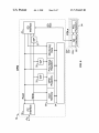
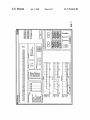
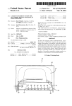
US007394445B2
(12) United States Patent
Chapuis et a1.
DIGITAL POWER MANAGER FOR
CONTROLLING AND MONITORING AN
ARRAY OF POINT-OF-LOAD REGULATORS
CN
2521825
(Continued)
OTHER PUBLICATIONS
“Synchronization of Multiple Voltage Regulator Outputs,” by M.W.
USC 154(b) by 125 days.
Mueller et a1. IBM Technical Disclosure Bulletin, Jun. 1999; (2
(21) Appl. No.: 11/048,014
Filed:
11/2002
Subject to any disclaimer, the term of this
patent is extended or adjusted under 35
This patent is subject to a terminal dis
claimer.
(22)
(65)
*Jul. 1, 2008
FOREIGN PATENT DOCUMENTS
Inventors; Alain Chapuis, Morgan Hill, CA (US);
Mikhail Guz, Daly City, CA (US)
Assignee: Power-One, Inc., Camarillo, CA (US)
Notice:
US 7,394,445 B2
(10) Patent N0.:
(45) Date of Patent:
pages).
(Continued)
Primary ExamineriVijay Shankar
(74) Attorney, Agent, or Firm4O’Melveny & Myers LLP
Jan. 31, 2005
Prior Publication Data
US 2006/0015616 A1
(57)
ABSTRACT
Jan. 19, 2006
Related US. Application Data
(63) Continuation-in-part of application No. 10/326,222,
?led on Dec. 21, 2002, noW Pat. No. 7,000,125, Which
is a continuation-in-part of application No. 10/293,
001, ?led on Nov. 13, 2002, noW Pat. No. 7,049,798,
Which is a continuation of application No. 10/293,531,
?led on Nov. 12, 2002, noW Pat. No. 6,949,916.
A poWer control system comprises a plurality of point-of-load
(POL) regulators each adapted to convey regulated poWer to
a load, a serial data bus operatively connecting the plurality of
POL regulators, and a digital poWer manager connected to the
data bus. The digital poWer manager includes a controller
adapted to execute stored instructions to program operational
Provisional application No. 60/588,594, ?led on Jul.
parameters of the plurality of POL regulators via the serial
data bus and receive monitoring data from the plurality of
POL regulators via the serial data bus. The digital poWer
16, 2004.
manager further comprises a user interface, such as an 12C
(51)
Int. Cl.
and send monitoring data thereto. The digital poWer manager
further comprises a non-volatile memory containing a plural
(52)
US. Cl. ......................... .. 345/89; 345/95; 345/204;
(60)
interface, adapted to receive programming data therefrom
G09G 3/36
(2006.01)
345/210; 345/211; 345/212
(58)
Field of Classi?cation Search ......... ..
345/89*103,
345/204i2l5; 713/300, 310, 3304340; 323/282
See application ?le for complete search history.
(56)
References Cited
U.S. PATENT DOCUMENTS
429,581 A
ity of registers, including a digital poWer manager con?gura
tion register containing data values de?ning a con?guration
of the poWer control system, a POL set-up register containing
data values re?ecting programming state of one of the POL
regulators, a POL monitor register containing data values
re?ecting status of operating conditions Within one of the
POL regulators, and a user-de?nable space. The digital poWer
manager is adapted to program voltage margining of each of
the POL regulators.
6/1890 Tan
37 Claims, 7 Drawing Sheets
(Continued)
1o
\\
Board
SD
Line OKA OKB OKC OKD
V01
Vo n
Core
V01
V0 n
l/Os
V01
Vo n
Interface 1
V01
V0 n
Interface 2
US 7,394,445 B2
Page 2
US. PATENT DOCUMENTS
3,660,672
4,194,147
4,204,249
4,328,429
4,335,445
4,350,943
4,451,773
4,538,073
4,538,101
4,616,142
4,622,627
4,630,187
4,654,769
4,677,566
4,761,725
4,940,930
4,988,942
5,004,972
5,053,920
5,073,848
5,079,498
5,117,430
5,168,208
5,229,699
5,270,904
5,272,614
5,287,055
5,349,523
5,377,090
5,426,425
5,481,140
5,489,904
5,532,577
5,627,460
5,631,550
5,646,509
5,675,480
5,727,208
5,752,047
5,815,018
5,847,950
5,870,296
5,872,984
5,874,912
5,883,797
5,889,392
5,892,933
5,905,370
5,917,719
5,929,618
5,929,620
5,935,252
5,943,227
5,946,495
5,990,669
5,994,885
6,021,059
6,055,163
6,057,607
6,079,026
6,100,676
6,111,396
6,115,441
6,121,760
6,137,280
6,150,803
6,157,093
6,157,182
6,163,143
6,163,178
6,170,062
A
A
A
A
A
A
A
A
A
A
A
A
A
A
A
A
A
A
A
A
A
A
A
A
A
A
A
A
A
A
A
A
A
A
A
A
A
A
A
A
A
A
A
A
A
A
A
A
A
A
A
A
A
A
A
A
A
A
A
A
A
A
A
A
A
A
A
A
A
A
B
5/1972
3/1980
5/1980
5/1982
6/1982
9/1982
5/1984
8/1985
8/1985
10/1986
11/1986
12/1986
3/1987
6/1987
8/1988
7/1990
1/1991
4/1991
10/1991
12/1991
1/1992
5/1992
12/1992
7/1993
12/1993
12/1993
2/1994
9/1994
12/1994
6/1995
1/1996
2/1996
7/1996
5/1997
5/1997
7/1997
10/1997
3/1998
5/1998
9/1998
12/1998
2/1999
2/1999
2/1999
3/1999
3/1999
4/1999
5/1999
6/1999
7/1999
7/1999
8/1999
8/1999
8/1999
11/1999
11/1999
2/2000
4/2000
5/2000
6/2000
8/2000
8/2000
9/2000
9/2000
10/2000
11/2000
12/2000
12/2000
12/2000
12/2000
1/2001
Berger et al.
Payne et al.
Dye et al.
Kublick et al.
Nercessian
Pritchard
Papathomas et al.
Freige et al.
Shimpo et al.
Upadhyay et al.
Rodriguez et al.
Henze
Middlebrook
Whittaker et al.
Henze
Detweiler
Ekstrand
Roth
Staf?ere et al.
Steigerwald et al.
Cleasby et al.
Berglund
Schultz et al.
Chu et al.
Gulczynski
Brunk et al.
Cini et al.
Inou et al.
Steigerwald
Conrad et al.
Maruyama et al.
Hadidi
Doluca
Bazinet et al.
Castro et al.
Berglund et al.
Stanford
Brown
Darby et al.
Soborski
Bhagwat
Schaffer
Berglund et al.
Hasegawa
Amaro et al.
Moore et al.
Voltz
Bryson
Hoffman et al.
Boylan et al.
Dobkin et al.
Berglund et al.
Bryson et al.
Scholhamer et al.
Brown
Wilcox et al.
Kennedy
Wagner et al.
Rader, III et al.
Berglund et al.
Burstein et al.
Line et al.
Douglass et al.
Marshall et al.
Ackermann
Varga
Giannopoulos et al.
Tanaka et al.
Shimamori
Stark et al.
Henrie
6,177,787
6,181,029
6,191,566
6,194,883
6,198,261
6,199,130
6,208,127
6,211,579
6,246,219
6,249,111
6,262,900
6,288,595
6,291,975
6,304,066
6,304,823
6,320,768
6,351,108
6,355,990
6,366,069
6,373,334
6,385,024
6,392,577
6,396,169
6,396,250
6,400,127
6,411,071
6,411,072
6,421,259
6,429,630
6,448,745
6,456,044
6,465,909
6,465,993
6,469,478
6,469,484
6,476,589
6,556,158
6,563,294
6,583,608
6,590,369
6,608,402
6,621,259
6,683,494
6,686,831
6,693,811
6,717,389
6,731,023
6,744,243
6,771,052
6,778,414
6,788,033
6,788,035
6,791,298
6,791,302
6,791,368
6,795,009
6,801,027
6,807,070
6,816,758
6,819,537
6,828,765
6,829,547
6,833,691
6,850,046
6,850,049
6,850,426
6,853,169
6,853,174
6,888,339
6,903,949
6,911,808
6,915,440
6,917,186
1/2001
1/2001
2/2001
2/2001
3/2001
3/2001
3/2001
4/2001
6/2001
6/2001
7/2001
9/2001
9/2001
10/2001
10/2001
11/2001
2/2002
3/2002
4/2002
4/2002
5/2002
5/2002
5/2002
5/2002
6/2002
6/2002
6/2002
7/2002
8/2002
9/2002
9/2002
10/2002
10/2002
10/2002
10/2002
11/2002
4/2003
5/2003
6/2003
7/2003
8/2003
9/2003
1/2004
2/2004
2/2004
4/2004
5/2004
6/2004
8/2004
8/2004
9/2004
9/2004
9/2004
9/2004
9/2004
9/2004
10/2004
10/2004
11/2004
11/2004
12/2004
12/2004
12/2004
2/2005
2/2005
2/2005
2/2005
2/2005
5/2005
6/2005
6/2005
7/2005
7/2005
Hobrecht
Berglund et al.
Petricek et al.
Shimamori
Schultz et al.
Berglund et al.
Doluca
Blair
Lynch et al.
Nguyen
Suntio
Hirakata et al.
Snodgrass
WilcoX et al.
Smit et al.
Pham et al.
Burstein et al.
Mitchell
Nguyen et al.
Melanson
Olson
Swanson et al.
Voegli et al.
Bridge
Giannopoulos
Schultz
Feldman
Brooks et al.
Pohlman et al.
Killat
Darmawaskita
Soo et al.
Clarkin et al.
Curtin
L’Hermite et al.
Umminger et al.
Steensgaard-Madsen
Duffy et al.
Zafarana et al.
Burstein et al.
Soo et al.
Jones et al.
Stanley
Cook
Bowman et al.
Johnson
Rothleitner et al.
Daniels et al.
Ostojic
Chang et al.
Vinciarelli
Bassett et al.
Shenai et al.
Tang et al.
Tzeng et al.
Duffy et al.
Hann et al.
Ribarich
Maxwell, Jr. et al.
Pohlman et al.
Schultz et al.
Law et al.
Chapuis
Chapuis
Kono
Koj ori et al.
Burstein et al.
Inn
Travaglini et al.
Ribarich
Shimamori
Berglund et al.
Klippel et al.
US 7,394,445 B2
Page 3
6,928,560 B1
8/2005 Fell, III et al.
6,933,709 B2
8/2005 Chapuis
6,933,711 B2
8/2005 Sutardja et a1.
6,936,999 B2
8/2005 Chapuis
6,947,273 B2
6,963,190 B2
6,965,220 B2
9/2005 Bassett et al.
11/2005 Asanuma et al.
11/2005 Kernahan et al.
6,965,502 B2
6,975,494 B2
6,977,492 B2
11/2005 Duffy et a1.
12/2005 Tang et al.
12/2005 Sutardja et a1.
7,000,125 B2 *
2/2006 Chapuis et al. ........... .. 713/300
7,007,176 B2
7,023,672 B2
2/2006 Goodfellow et al.
4/2006 Goodfellow et al.
7,049,798 B2 *
5/2006 Chapuis et al. ........... .. 323/282
7,068,021 B2
6/2006 Chapuis
7,080,265 B2
7,141,956 B2
2001/0033152
2001/0052862
2002/0070718
2002/0073347
2002/0075710
2002/0105227
2002/0144163
2003/0006650
2003/0067404
2003/0122429
2003/0142513
2003/0201761
2004/0027101
2004/0080044
2004/0090219
2004/0093533
2004/0123164
2004/0123167
2004/0135560
2004/0155640
2004/0174147
A1
A1
A1
A1
A1
A1
A1
A1
A1
A1
A1
A1
A1
A1
A1
A1
A1
A1
A1
A1
A1
2004/0178780 A1
2004/0189271 A1
7/2006 Thaker et a1.
11/2006 Chapuis
10/2001
12/2001
6/2002
6/2002
6/2002
8/ 2002
10/ 2002
Pohlman et al.
Roelofs
Rose
Zafarana et a1.
Lin et al.
Nerone et a1.
Goodfellow et al.
1/2003 Tang et al.
4/ 2003 Ruha et al.
7/2003 Zhang et a1.
7/ 2003
10/ 2003
2/ 2004
4/ 2004
Vinciarelli
Harris
Vinciarelli
Moriyama et al.
Data Sheet, Integrity-One Power SystemiRack System Power-One,
Inc. (P025580-P025583).
Data Sheet, “PCS Controller” Power-One, Inc. (P025584-P025585).
Data Sheet, “PMP 25 Recti?er Module” Power-One, Inc. (P025602
P025603).
“Presenting DALI” AG DALI, 2003, pp. 1-17.
“DALI Manual” DALI AG, Digital Addressable Lighting Interface
Activity Group, ZVEI-Division Luminaires, 2001,pp. 1-62.
“Microchip PIC 16C781/782 Data Sheet, 8-bit CMOS Microcontrol
lers with ND, D/A, OPAMP, Comparators and PSMC” Microchip
Technology Inc., 2001, pp. 1-184.
“Microchip AN811, The RS-232/DALI Bridge Interface” Microchip
Technology Inc., 2002, DS00811A, pp. 1-8.
“Microchip AN809, Digitally Addressable DALI Dimming Ballast”
Microchip Technology Inc., 2002, DS00809B, pp. 1-18.
“The Digital Addressable Lighting Interface (DALI): An Emerging
Energy-Conserving Lighting Solution” by Ronat, Odile International
Recti?er, Apr. 9, 2002, TP4/9/2002, pp. 1-6.
“Microchip AN703, Using the MCP320X 12-Bit Serial ND Con
verter with Microchip PICmicro® Devices” Microchop Technology
Inc., 2002, DS00703A, pp. 1-25.
“System Management Bus (SMBus) Speci?cation” Version 2.0
Duracell, Inc., Energizer Power Systems, Inc., Fujitsu, Ltd., Intel
Corporation, Linear Technology, Inc., Maxim Integrated Products,
Mitsubishi Electric Semiconductor Company, PowerSmart, Inc.,
Toshiba Battery Cd. Ltd., Unitrode Corporation, USAR Systems,
Inc., Aug. 3, 2000, pp. 1-59.
“Fieldbus System Engineering Guidelines” Fieldbus Foundation,
2003-2004, pp. 1-94.
“Technical Overview, FoundationTM ?eldbus, Freedom to Choose.
Power to Integrate” Fieldbus Foundation, 2003, FD-043 Rev 3.0, pp.
5/ 2004 Chapuis
1-37.
5/ 2004 Chapuis et al.
6/ 2004 Chapuis et al.
“Silicon Labs Preliminary Invalidity Contentions”, Civil Action No.
2-05-CV-463 (LED)iMay 26, 2006 (US. District Court Eastern
District of Texas).
6/ 2004 Chapuis
7/ 2004 Kernahan et al.
33702 Microprocessor Power Supply (3.0A) Analog Products
8/ 2004 Sutardja et a1.
9/ 2004 Vinciarelli
9/2004 Chapuis
MC33702 Fact Sheet; Motorola/Digital dna/ Power Management
Switching; pp. 1-4.
“Motorola Switch Mode Power Supply With Multiple Linear Regu
lators And High Speed CAN Transceiver” Motorola, Inc. 2002; digi
9/2004 Hansson et al.
Templeton ................. .. 307/11
tal dna; Analog Marketing; Rev. 2.5, Nov. 2002; 33394; Multi-Output
2004/0201279 A1*
10/2004
2004/0225811 A1
11/2004 Fosler
Power Supple Semiconductor Technical Data.
2004/0246754 A1
12/2004 Chapuis
“Power Management Solutions For Networking Aplications”; Pre
sented by Luc Darmon Smart Networks Developer Forum
2003iJun. 4-6 Euro-Disney Paris, France; Motorola digital dna;
2005/0093594 A1
2005/0117376 A1
5/2005 Kim et al.
6/2005 Wilson
2005/0146312 A1
2005/0200344 A1
2006/0022656 A1
7/2005 Kennyetal.
9/2005 Chapuis
2/2006 Leung et a1.
2006/0149396 A1 *
7/2006
Templeton ................. .. 700/22
FOREIGN PATENT DOCUMENTS
EP
EP
EP
EP
EP
JP
KR
RU
SU
WO
W0
WO
WO
WO
WO
0255258
315366
0660487
0875994
0997825
1185329
200284495
1814177 A1
1359874
WO93/19415
WO 01/22585 A1
WO02/31943
WO02/31951
WO02/50690
WO02/063688
2/1988
5/1989
6/1995
11/1998
5/2000
3/1999
8/2002
5/1993
12/1985
9/1993
3/2001
4/2002
4/2002
6/2002
8/2002
OTHER PUBLICATIONS
“Power System Controller in an Intelligent Telecom Recti?er Plant,”
by U. Roth. INTELLEC 1992, pp. 476-483.
Integrity-One: Installation, Operation and Maintenance Manual
Power-One, Inc., 1999-2003 Version 1.2 (P025374-P025559).
www.motorola.com/sndf; pp. 1-26.
Preliminary Information 1.5 A Switch-Mode Power Supply With
Linear Regulator 33701; Power Supply Integrated Circuit; Motorola
Semiconductor Technical Data; Analog Marketing MC33701/D Rev.
1.0, May 2003; Motorola digital dna; pp. 1-24.
“Electronic Products” Power Supply Special The Engineer’s Maga
zine of Product Technology, A Hearst Business Publication, vol. 37,
No. 10, Mar. 1995, 4 pages.
“KEKB Power Supply Interface Controller Module” byA. Akiyama,
T. Nakamura, M. Yoshida, T. Kubo, N. Yamamoto and T. Katoh.
KEK, High Energy Accelerator Research Organization, 1-1 Ohio,
Tsukuba 305 Japan, International Conference on Accelerator and
Large Experimental Physics and Control Systems, 1997, Beijing,
China, 4 pages.
“Magnet Power Supply Control System in KEKB Accelerators” by
T.T. Nakamura, A. Akiyama, T. Katoh, Ta. Kubo, N. Yamamoto, M.
Yoshida. KEK, Tsukuba, Japan International Conference on Accel
erator and Large Experimental Physics Control Systems, 1999,
Trieste, Italy, pp. 406-408.
“System Management Bus Speci?cation” Smart Battery System
Speci?cations, Revision 1.1, Dec. 11, 1998 Copyright 1996, 1997,
1998, Benchmarq Microelectronics Inc., Duracell Inc., Energizer
Power Systems, Intel Corporation, Linear Technology Corporation,
Maxim Integrated Products, Mitsubishi Electric Corporation,
National Semiconductor Corporation, Toshiba Battery Co., Varta
Batterie AG, All rights reserved, 39 pages.
“The I2C-Bus Speci?cation” Version 2.1, Jan. 2000, Document
Order No. 9398 393 40011, pp. 1-46.
US 7,394,445 B2
Page 4
“Quantization Resolution and Limit Cycling in Digitally Controlled
“DHP Series DC Power Supplies”, IEEE 488.2/RS-232 Options
PWM Converters” by Angel V. Peterchev andA.V. Sanders Electrical
Programming Manual, Sorensen, Division of Elgar Electronics Cor
Engineering and Computer Science; US Berkley; Power Electronics
Specialists Conference 2001.PESC, vol. 2, Jun. 17-21, 2001, pp.
poration, Document No. M550005-01 Rev B, Jul. 29, 2002, 32 pages.
“Distributed Power Hot Swap Controller” SMH4804 Summit Micro
electronics, Inc., 2050 2.3, Mar. 19, 2001, 32 pages.
“Programmer Manual”, PS2520G & PS2521G Programmable Power
465-471; XP002274573.
“Distributed Intelligence and Modular Architecture for Next Genera
tion DC Power System” by Louis Duguay and Pierre Got Astec
Advanced Power Systems, Quebec, Canada; 6 pgs.
Ron Vinsant, John DiFiore, and Richard Clarke PCIM, Jun. 1994, pp.
Supples, Tektronix, 070-9197-00, 1995, 70 pages.
“User Manual”, PS2520, PS2520G, PS2521 & PS2521G Program
mable Power Supples, Tektronix, 070-9196-00, 1995, 56 pages.
“A Power LAN for Telecommunication Power Supply Equipment”
30-37.
by Nicholas Vun C.H., Lau CT. and Lee B.S. IEEE TENCON ’93
“Operating and Service Manual”, SBC488A, Magna-Power Elec
tronics, Inc., Dec. 19, 2002, 58 pgs.
“Operating and Service Manual”, SQ Series, DC Power Supples
Magna-Power Electronics, Inc., Dec. 16, 2002, 48 pgs.
“Uniform Language for Accessing Power PlantsiHuman-Machine
Beihing, pp. 24-27.
“VXI Bus Programmable DC Power Supplies” Advanced Power
“Digitally-Controlled SMPS Extends Power System Capabilities” by
Language”, ANSI T1.317-1993 American National Standards Insti
tute, Dec. 14, 1993, 55 pages.
Designs, Inc., Irvine, CA; 4 pages.
“Operating Manual for Internal RS -232 Interface for XT 60 Watt and
HPD 300 Watt Series Programmable DC Power Supplies” Xantrex
“An Intelligent, Fault Tolerant, High Power, Distributed Power Sys
tem for Massively Parallel Processing Computers” by J. Burns, J.
Riel andT. TiBene IEEE, May 1994, 0-7803-1456-5/94, pp. 795-800.
Technology, Inc., 59 pages.
“Auto Sequence Programming Examples for GPIB-M” Xantrex
Technology, Inc., Nov. 27, 2002, 1.0a, 4 pages.
“SCPI Programming Examples for GPIB-M” Xantrex Technology,
Inc., Nov. 26,2002, 1.0, 3 pages.
“BE510 / BE510S Modules”iBipolar DC Source from 100mV to
20V and from 100nA to 4A Innovative Test Systems; BE510 Version
“Implementing a Nationwide Energy Management System” by Stig
Sj oberg, Tommy Hedberg, Lars Selberg and Rober Wikstrom.
II, Issue 9, Nov. 12, 2000, 3 pgs.
“IEEE Standard Codes, Formats, Protocols, and Common Com
mands for User with IEEE Std 488.1-1987, IEEE Standard Digital
Interface for Programmable Instrumentation”, IEEE Std 488.2-1992
IEEE, Jun. 18, 1992, ISBN 1-55937-238-9, 254 pages.
“BE52x Modules”iMulti-range bipolar DC sources from 30V to
500V, 90W Innovative Test Systems; BE52x Version A, Issue 9, Aug.
3,2001, 3 pages.
“PCX-150A 150 Amp Pulsed Current Source Operation Manual”,
Version 3.0 Directed Energy, Inc., 2001, Document No. 9100-0212
R4, 31 pages.
“New Applications Demand Programmable Power Supplies/
Sources” by Paul O’Shea http://www.evaluationengineering.com/
archiv/aIticles/0997powr.htm, Nelson Publishing, Inc., 1997, 8
pages.
“Market Trends Toward Enhanced Control of Electronic Power Sys
tems” by FM. Miles, R.K. Danak, T.G. Wilson and G.G. Suranyi
IEEE, 1993, 0-7803-0982-0/93, pp. 92-98.
“R Option, S Option DC Power Supplies”, IEEE 488.2/RS-232 Pro
gramming Manual Power Ten, Document No. M550013-01 Rev C,
Jun. 25, 2002, 56 pages.
“A Digitally Controlled Zero-Voltage-Switched Fullbridge Con
verter” by Karl-Heinz Rinne, Klaus Theml, Joseph Duigan and
Oliver McCarthy Power Conversion, Jun. 1994 Proceedings, pp.
“Agilent E3640A-E3649A Programmable dc Power Supplies” Data
Sheet Agilent Technologies, 4 pages.
“Agilent E364xA Single Output DC Power Supplies”, User’s Guide
Agilent Technologies, Part No. E3640-90001, Jan. 2000, 207 pages.
“Optimizing Power Product Usage to Speed Design Validation Test
ing” Application Note 1434 Agilent Technologies, Nov. 22, 2002, 16
pages.
“vol. 2: Command Reference” SCPI Consortium, May 1999, Version
1999.0, 565 pages.
“Why have Monitoring?” by P. Shawyer, P Hobbs and A. McLeod
Texcel Technology PLC, United Kingdom.
“IMPI Intelligent Platform Management Bus Communications Pro
tocol Speci?cation v1.0” Intel, Hewlett-Packard, NEC, Dell, Docu
ment Revision 1.0, Nov. 15, 1999, 39 pages.
“Operating and Service Manual”, MQ Series DC Power Supplies
Magna-Power Electronics, Inc., Dec. 19, 2002, 48 pages.
3 17-3 24.
“User’s Guide” Series 661xxA MPS Power Modules & Model
“vol. 1: Syntax and Style” Standard Commands for Programmable
Instruments (SCPI) Consortium, May 1997, Version 1997.0, 68
66001A MPS Keyboard Agilent Technologies, Agilent Part No.
5959-3386, Apr. 2000, 53 pages.
pages.
“Programming Guide” Series 661xxA MPS Power Modules Agilent
“Integrate Internet Solutions Into Your Energy Management Net
work” by Johan Sarkinen and Ola Lundin Jun. 1998, 7 pages.
“Automating the Design of a Generic Modular Power System for the
Technologies, Agilent Part No. 5959-3362, Sep. 1997, 114 pages.
"Accelerator-Control-System Interface for Intelligent Power Sup
Global Market” by George Pedersen, Steve Briggs, and Paul Massey
Advance Power Raynham Road, Bishops Stortford, Herts.; CM23
5PF UK.
“An Operation and Maintenance Process Model for Energy Manage
ment” by Ola Lundin Ericsson Components AB, Energy Systems
Division, S-164 81 KISTAiStockhold, Sweden; 7 pages.
“Intelligent Platform Management Interface Speci?cation v1.5”
Intel, Hewlett-Packard, NEC, Dell, Document Revision 1.1, Feb. 20,
2002, 459 pages.
“vol. 2: Command Reference” SCPI Consortium, May 1997, Version
1997.0, 506 pages.
“vol. 4: Instrument Classes” SCPI Consortium, May 1997, Version
1997.0, 58 pages.
plies” by S. Cohen Los Alamos National Laboratory, pp. 183-186.
“Testing Intelligent Power Supplies for the Los Alamos National
Laboratory Accelerator Complex” by J .C. Sturrock, S. Cohen, B.L.
Weintraub, D.J. Hayden and SF. Archuletta Los Alamos National
Laboratory, pp. 217-219.
“Intelligent Power Supply Controller” by RS. Rurnrill and DJ.
Reinagel IEEE, Aug. 1991, 0-7803-0135-8/91, PAC 1991, pp. 1537
1539.
“Magnet Power Supply as a Network Object” by S. Cohen and R.
Stuewe IEEE, Aug. 1991, 0-7803-0135-8/91, PAC 1991, pp. 929
931 .
1999.0, 67 pages.
“Non-Impact Printer Power and Motor Control System on a Chip” by
James Masson and Steven Barrow IEEE, Apr. 1995, IEEE Catalogue
No. 95TH8025, 0-7803-2423-4/95, pp. 98-103.
“Power Distribution Systems for Future Homes” by Po-Wa Lee,
Yim-Shu Lee and Bo-Tao Lin IEEE, Aug. 1999, 0-7803-5769-88/99,
“vol. 3: Data Interchange Format” SCPI Consortium, May 1997,
pp. 1140-1146.
“vol. 1: Syntax and Style” SCPI Consortium, May 1999, Version
Version 1997.0, 73 pages.
“Installation Guide” MPS Mainframe Model 66000A Agilent Tech
“vol. 3: Data Interchange Format” SCPI Consortium, May 1999,
nologies, Agilent Part No. 66000-90001, Apr. 2000, 26 pages.
Version 1999.0, 72 pages.
“vol. 4: Instrument Classes” SCPI Consortium, May 1999, Version
1999.0, 115 pages.
“Service Guide for Agilent 6610xA Power Modules” Agilent Tech
by Ueli Roth IEEE, Aug. 1992, 0-7803-0779-8/92, pp. 476-483.
“The Continuing Evolution of Intelligence for Telecommunications
Power Plants” by Jimmy Godby IEEE, Apr. 1996, 0-7803 -3 507-4/96,
nologies, Agilent Part No. 5959-3364, Dec. 2002, 101 pages.
pp. 70-75.
“Power System Controller in an Intelligent Telecom Recti?er Plant”
US 7,394,445 B2
Page 5
“Digitally Controlled Power Systems: How Much Intelligence is
Needed and Where it Should be” by Tom Lock RELTEC Corpora
tion, 5 pages.
“Controlling and Alarming DC Power Plants via the Internet” by
Anthony P. Cosentino, Michael C. Sullivan, RichardV. Baxter, Jr. and
John Loeck Power Conversion Products, LLC and Pensar Corpora
tion, 6 pages.
“Defendant’s Artesyn Technologies, Inc.’s Preliminary Invalidity
Contentions”4(PoWer- One, Inc. vs. Artesyn Technologies, Inc et al.)
Civil Action No. 2-05-CV-463 (LED), United States District Court
for the Eastern District of Texas; Apr. 26, 2006.
25 Watt DC-DC Converters Melcher The Power Partners and Power
One Group of Companies, Industrial Environment, Apr. 4, 1999,
DC-DC Converters <40 Watt, G Series, 16 Pages.
48V Programmable How Swap Sequencing Power Controller Sum
mit Microelectronics, Inc., Oct. 30, 2002, SMH4804, 41 Pages.
Advanced Con?guration and Power Interface Speci?cation Intel
Corporation, Microsoft Corporation, Toshiba Corp, Feb. 2, 1999,
Revision 1.0b, 387 Pages.
Advantages of Microcontrollers in DC-DC Converters, Galaxy
In?nite Impulse Response, Wikipedia, http://en.wikipedia.org/wiki/
IIR, May 2, 2006, pp. 1-4.
In-Situ Transfer Function Analysis, 2006 Digital Power Forum Pre
sentation; Mark Hagen, Texas Instruments Digital Power Group, Jul.
1, 2006.
In-System Network Analyzer 2006 Digital Power Forum Presenta
tion, Silicon Laboratories, Jul. 7, 2006.
Low Voltage Study Workshop Report Charles E. Mullett; Lou Pechi;
PSMA, Power Sources Manufacturers Accosiation, The Multina
tional Power Electronics Association, Jan. 1, 2001, 150 Pages.
Memorandum Opinion and Order Power One v Artesyn Technolo
gies, Inc.; Civil Action 2:05cv463, Mar. 22, 2007.
Microprocessor Core Supply Voltage Set by I2C Bus Without VID
LinesiDesign Note 279 Mark Gurries; Linear TechnologyiDesign
Notes, Jan. 7, 2002, 2 Pages.
NEBS Compliant Board Level Power System Thomas J. DeLurio,
Mikhail GuZ and John Ng; Summit Microelectronics, Power One,
Oct. 20, 2002, 7 Pages.
New Digital Power Delivery Architecture Bob Carrol, Primarion,
Power, Jan. 1, 2003 IBM Symposium, Real Solutions for Distributed
Sep. 1, 2004, 5 Pages.
Power, 8 Pages.
Power Management for Communications: Corporate Overview Sum
mit Microelectronics Inc., Oct. 1, 2002, 213 Pages.
Power Management for Communications: Product Information Sum
Architecture and IC implementation of a digital VRm controller
Jinwen, Xiao et a1, 32nd Annual IEEE Power Electronics Specialists
Conference. PESC 2001. Conference Proceedings. Vancouver,
Canada, Jun. 17-21, 2001, Annual Power Electronics Specialists
Conference, NewYork, NY: IEEE, US, vol. vol. 1 or4. Conf. 32, Jun.
17, 2001, pp. 38-47, XP010559121 ISBN: 0-7803-7067-8, ?gure 7.
Characteristics of Automated Power System Monitoring & Manage
ment Platforms Hawkins, John M.; Telepower Australia Pty Ltd, Jan.
1, 2000, [email protected], IEEE, Intelec, 5 Pages.
Chemistry-Independent Battery Chargers Maxim Integrated Prod
ucts, Dec. 1, 2002, 19-1158, Rev 1, MAX1647/MAX1648, 25 Pages.
Current-Fed Multiple-Output Power Conversion Seamus O’Driscoll;
John G. Hayes and Michael G. Egan; Artesyn Technologies; Dept. of
Electrical Engineering, University College Cork, Ireland, Dec. 3,
2003, 7 pages.
Digital Multiphase Power from Primarion and Intersil Changing the
Landscape of Processor Power Primarion, Inc., White Paper, Sep. 12,
2002, 6 pages.
Dual 550kHZ Synchronous 2-Phase Switching Regulator Controller,
Linear Technology, Jan. 1, 1998, LTC1702, 36 Pages.
Dual Smart Card Interface TDA8020HL Philips Semiconductors,
Integrated Circuits, Data Sheet, Feb. 24, 2001, I2C Bus,TDA8020JL,
Objective Speci?cation v4.2 Supersedes data of Jan. 2001 File under
Integrated Circuits, ICXX, 22 Pages.
Dual Smart Card Interface TDA8020HL/C2 Christophe Chausset,
Philips Semiconductors, May 20, 2003, Application Note,
TDA8020HL/C2, AN10232, 28 Pages.
High Ef?ciency Synchronous Step-Down Switching Regulator, Lin
mit Microelectronics, Inc., Jan. 23, 2001, 168 Pages, http://www.
summitmicro.com.
Power Semiconductors and Power SuppliesiThe Building Blocks
of the Digital Power Revolution Todd Cooper and Holman Harvey;
Stephens, Inc. Investment Bankers, Sep. 1, 2000, 132 Pages.
Programmable Four-Channel Step-Down DC/DC Converter Texas
Instruments, Oct. 1, 2001, TPS54900, 16 Pages.
Quad Tracking Power Supply Manager Summit Microelectronics,
Inc., Mar. 4, 2002, SMT4004, 35 Pages.
Simple digital hardware to control a PFC converter, A Zumel P et a1;
JECON’0 1. Proceedings of the 27th. Annual Conference of the IEEE
Industrial Electronics Society. Denver, CO, Nov. 29-Dec. 2, 2001,
Annual Conference of the IEEE Industrial Electronics Society, New
York, NY : IEEE, US, v01. vol. 1 of3. Conf. 27, Nov. 29, 2001, pp.
943-948, XP010572905 ISBN: 0-7803-7108-9, paragraph [IIIC].
Single-Inductor Multiple-Output Switching Converters Wing-Hung
Ki and Dongsheng Ma; Integrated Power Electronics Laboratory,
Department of Electrical and Electronic Engineering, The Hong
Kong University of Science and Technology, Clear Water Bay, Hong
Kong SAR, China, Jan. 1, 2001, 6 Pages.
Six-Channel Power Supply Supervisor and Cacsade Sequence Con
troller Summit Microelectronics, Inc., Jul. 16, 2003, SMS66, Pre
liminary Information, 26 Pages.
SMBus Controls CPU Voltage Regulators without VID Pins Mark
Gurries, Design Ideas, Linear Technology Magazine, Sep. 1, 2001, 2
ear Technology, Jan. 1, 1998, LTC1735, 33 Pages.
Pages.
High Ef?ciency, 2-Phase Synchronous Step-Down Switching Regu
SMBus VID Voltage Programmers Linear Technology, Jan. 1, 2001,
LTC1699 Series, 20 Pages.
SMH4804, SMP9210 and SMT4004 Telecom Reference Design,
Summit Microelectronics, Inc., Sep. 5, 2002, Application Note 25, 17
lators, Linear Technology, Jan. 1, 1998, LCT1628/LTC1628-PG, 32
Pages.
High-frequency digital controller IC for DC/DC converters Patella B
J et al; APEC 2002. 17th. Annual IEEE Applied Power Electronics
Conference and Exposition. Dallas, TX, Mar. 10-14, 2002, Annual
Applied Power Electronics Conference, New York, NY : IEEE, US,
vol. vol. 2 of2. Conf. 17, Mar. 10, 2002, pp. 374-380, XP010582947,
ISBN: 0-7803-7404-5, p. 375, right hand column; ?gure 3.
Highly Programmable Voltage Supply Controller and Supervisory
Pages.
Wide Operating Range, No Sense Step-Down Controller Linear
Technology, Jan. 1, 2001, LTC1778/LTC1778-1, 24 Pages.
Wide Operating Range, No Sense Step-Down DC-DC Controller
with SMBus Programming Linear Technology, Jan. 1, 2001,
LTC1909-8, 34 Pages.
Circuit Summit Microelectronics, Inc., Jun. 7, 2001, SMS44, Pre
liminary, 19 Pages.
* cited by examiner
US. Patent
Jul. 1, 2008
Sheet 2 of7
US 7,394,445 B2
mzmEA lmoB=orco ‘
zw.J|_<m>wH|_om.< 4E.E-P-.m.mm2z
l2
Tmz8xn:N82zFm60_To:Ewblc.ml2o9ac6s0m 0|"oh|+
0|’"
.OEN
0
W
M
Fwv=
{a
r8
aeTIYWo~_w$60mam
on
.2223a
@LIY
0m W
OH
-.Dlwmw
Mm<aw
9282%
_> <o"6m=L9ltEoYBO.<
9.0i46:.05ON¢:
HE.ma-owl 6%50:62
{NF
i.n:O6
0>2mw_
US. Patent
Jul. 1, 2008
Sheet 3 of7
62\
US 7,394,445 B2
POL32
Status POL1
Status POL2
.'
,'
'
PADS-2
'
64C
Tem
64b
Status POL32
FIG. 3A
80\
FIG. 3B
Margining
ll
82\
For each POL in the System
Is POL member of a (supported)
84M
Parallel Bus? If yes select all
those addresses too
Depending on function
86\
argument send WVOS cmd to
POL(s) with VOL, VOH or VOS
as argument
V
88\
Return
FIG. 4
A
US. Patent
Jul. 1, 2008
1003
102\
Sheet 4 of7
US 7,394,445 B2
Monitoring Process
"
Start 0.5s Clock Counter = 0
104
V
Q9“
106\
|
No
"Yes
Counter = (Counter = 1)? 0 : 1
v
For Each Group
A
110
AND Co)unter= 0
114\
Yes
Yes‘,
Retrieve status register for
POLs in Group
116\
118
it
Update STx register
STx
changed A7ND NST= 1
12o\
Yes‘,
Send ST§< to User
7
122
124\
"Yes
Retrieve parametric data for
POLs in Group
I
FIG. 5
‘
US. Patent
Jul. 1,2008
Sheet 5 of7
US 7,394,445 B2
wm
:w0L. m:aW\SN61ow\2oYmt9BmEK y.
n
l‘
u
m
m
> n_>>
momtEB
v/?5:5 r8KNu.m‘mv mON_ON_Gm
oE>>
mn_>>M
fwm
M
=>: O
3mm2%a92$.9_:mo2n:_0:52E02m:063am21 A"(m
:wnam.,
.OEw
US. Patent
Jul. 1, 2008
Sheet 6 of7
US 7,394,445 B2
US. Patent
Jul. 1, 2008
Sheet 7 0f 7
US 7,394,445 B2
Intermediate Bus Configuration
IBV Voltage
IBV nom
IV
|[ Accept ||
@
@
Undervoltage Threshold I -20.6% I 8 L=9.53V |
Overvoltage Threshold | +9.9% I g |=13.19V|
Help
FIG. 8
Monitoring Ring Buffer
Sample V0 [V] I0 [A]
Temp [C]
n
1.49
2.88
34.38
n-1
1.49
2.88
34.38
n-2
1 .49
2.88
34.38
n-3
1 .49
2.88
34.38
n-4
1.49
2.88
34.38
n-5
1.49
2.88
35.16
n-6
1.49 -
2.88
35.16
n-7
1.49
2.88
35.16
n-8
1.49
2.88
35.16
n-9
1.49
2.88
35.16
FIG. 9
US 7,394,445 B2
1
2
DIGITAL POWER MANAGER FOR
CONTROLLING AND MONITORING AN
ARRAY OF POINT-OF-LOAD REGULATORS
With a poWer supply controller that activates, programs, and
monitors the individual POL regulators. It is knoWn in the art
for the controller to use a multi-connection parallel bus to
activate and program each POL regulator. For example, the
RELATED APPLICATION DATA
parallel bus may communicate an enable/disable bit for tum
ing each POL regulator on and off, and voltage identi?cation
This patent application claims priority pursuant to 35
U.S.C. § 119(e) to provisional patent application Ser. No.
60/588,594, ?led Jul. 16, 2004, for DIGITAL POWER MAN
(VID) data bits for programming the output voltage set-point
of the POL regulators. The controller may further use addi
tional connections to monitor the voltage/ current that is deliv
ered by each POL regulator so as to detect fault conditions of
the POL regulators. A draWback With such a control system is
that it adds complexity and siZe to the overall electronic
AGER FOR CONTROLLING AND MONITORING AN
ARRAY OF POINT-OF-LOAD REGULATORS. This patent
application also claims priority pursuant to 35 U.S.C. § 120 as
a continuation-in-part of each of the following: (1) Ser. No.
10/293,531, ?led Nov. 12, 2002, for SYSTEM AND
system.
Thus, it Would be advantageous to have a system and
METHOD FOR CONTROLLING A POINT-OF-LOAD
REGULATOR, noW issued as US. Pat. No. 6,949,916 on
method for controlling and monitoring POL regulators Within
Sep. 27, 2005; (2) Ser. No. 10/293,001, ?led Nov. 13, 2002,
a distributed poWer system.
for SYSTEM AND METHOD FOR COMMUNICATING
WITH A VOLTAGE REGULATOR, noW issued as US. Pat.
No. 7,049,798 on May 23, 2006; and (3) Ser. No. 10/326,222,
SUMMARY OF THE INVENTION
20
?led Dec. 21, 2002, for METHOD AND SYSTEM FOR
The invention overcomes these and other disadvantages of
CONTROLLING AND MONITORING AN ARRAY OF
the prior art by providing a digital poWer manager adapted to
POINT-OF-LOAD REGULATORS, noW issued as US. Pat.
control and monitor a plurality of POL regulators of a poWer
No. 7,000,125 on Feb. 14, 2006.
control system.
25
BACKGROUND OF THE INVENTION
1. Field of the Invention
The present invention relates to poWer control systems, or
more particularly, to a method and system to control and
monitor an array of point-of-load regulators.
2. Description of Related Art
With the increasing complexity of electronic systems, it is
common for an electronic system to require poWer provided
at several different discrete voltage and current levels. For
example, electronic systems may include discrete circuits that
require voltages such as 3 v, 5 v, 9 v, etc. Further, many of
each adapted to convey regulated poWer to a load, a serial data
bus operatively connecting the plurality of POL regulators,
30
35
40
registers, including a digital poWer manager con?guration
register containing data values de?ning a con?guration of the
poWer control system, a POL set-up register containing data
reasons. First, the relatively long physical run of loW voltage,
congests the routing of signal lines on the circuit board.
Second, the impedance of the lines carrying the high current
eters of the plurality of POL regulators via the serial data bus
and receive monitoring data from the plurality of POL regu
lators via the serial data bus. The digital poWer manager
further comprises a user interface, such as an I2C interface,
high current lines consumes signi?cant circuit board area and
tends to dissipate a lot of poWer and complicate load regula
tion. Third, it is dif?cult to tailor the voltage/ current charac
teristics to accommodate changes in load requirements.
In order to satisfy these poWer requirements, it is knoWn to
distribute an intermediate bus voltage throughout the elec
tronic system, and include an individual point-of-load
and a digital poWer manager connected to the data bus. The
digital poWer manager includes a controller adapted to
execute stored instructions to program operational param
adapted to receive programming data therefrom and send
monitoring data thereto. The digital poWer manager further
comprises a non-volatile memory containing a plurality of
these circuits require a relatively loW voltage (e.g., 1 v), but
With relatively high current (e. g., 100 A). It is undesirable to
deliver relatively high current at loW voltages over a relatively
long distance through an electronic device for a number of
In an embodiment of the invention, the poWer control sys
tem comprises a plurality of point-of-load (POL) regulators
45
values re?ecting programming state of one of the POL regu
lators, a POL monitor register containing data values re?ect
ing status of operating conditions Within one of the POL
regulators, and a user-de?nable space. The digital poWer
manager is adapted to program voltage margining of each of
the POL regulators.
In a further embodiment of the invention, at least one host
50
user system is operatively coupled to the digital poWer man
ager. The host user system further comprises a graphical user
(“POL”) regulator, i.e., DC/DC converter, at the point of
interface providing monitoring and programming of the
poWer consumption Within the electronic system. Particu
larly, a POL regulator Would be included With each respective
poWer control system. For example, the graphical user inter
face further provides an interface for programming voltage
electronic circuit to convert the intermediate bus voltage to
55
the level required by the electronic circuit. An electronic
system may include multiple POL regulators to convert the
intermediate bus voltage into each of the multiple voltage
levels. Ideally, the POL regulator Would be physically located
margining of each of the POL regulators, for monitoring
operating conditions of the POL regulators, and/or for pro
gramming the POL regulators. The digital poWer manager is
60
further adapted to receive fault detection information from
the POL regulators via the serial data bus.
A more complete understanding of the system and method
for controlling and monitoring POL regulators Within a dis
tributed poWer system Will be afforded to those skilled in the
delivered to the multiple POL regulators using loW current
art, as Well as a realiZation of additional advantages and
lines that minimiZe loss.
With this distributed approach, there is a need to coordinate
the control and monitoring of the POL regulators of the poWer
65
objects thereof, by a consideration of the folloWing detailed
description of the preferred embodiment. Reference Will be
made to the appended sheets of draWings Which Will ?rst be
adjacent to the corresponding electronic circuit so as to mini
miZe the length of the loW voltage, high current lines through
the electronic system. The intermediate bus voltage can be
system. The POL regulators generally operate in conjunction
described brie?y.
US 7,394,445 B2
3
4
BRIEF DESCRIPTION OF THE DRAWINGS
not be grouped at all, and the POL control system 10 could
include a plurality of individual POL regulators.
The front-end regulator 14 draWs poWer from a voltage
source (e. g., 48V), and provides an intermediate voltage
(IBV) to the plurality of groups 22, 24, 26, 28 over an inter
FIG. 1 is a block diagram of an exemplary POL control
system in accordance With an embodiment of the invention;
FIG. 2 is a block diagram of an exemplary digital poWer
manager of the POL control system;
FIGS. 3a and 3b graphically depict a monitoring memory
mediate voltage bus. The front-end regulator 14 may simply
comprise another POL regulator. The digital poWer manager
in the digital poWer manager for storing POL parameters;
12 draWs its poWer from the intermediate voltage bus or from
a board bias voltage source. Although depicted as separate
FIG. 4 is a How diagram of a process for performing volt
age margining of the POL regulators;
devices, the digital poWer manager 12 and front-end regulator
14 may be integrated together in a single unit. Alternatively,
the front-end regulator 14 may provide a plurality of interme
FIG. 5 is a How diagram of a process for monitoring per
formance of the POL regulators;
FIG. 6 is a block diagram depicting exemplary partitioning
of memory for the digital poWer manager;
diate voltages to the groups of POL regulators over a plurality
of intermediate voltage buses.
The digital poWer manager 12 communicates With the plu
FIG. 7 is an exemplary screen shot depicting a graphical
user interface (GUI) for monitoring POL regulators Within a
rality of POL regulators by Writing and/ or reading digital data
POL control system;
(either synchronously or asynchronous) via a unidirectional
or bidirectional serial bus, illustrated in FIG. 1 as the synch/
data (SD) line. The SD line may comprise a tWo-Wire serial
FIG. 8 is an exemplary screen shot depicting a GUI for
monitoring intermediate bus voltage status for a POL control
system; and
20
mitted synchronously (i.e., synchronized to a clock signal).
The SD line provides synchroniZation of all POL regulators to
monitoring ring buffer status for a POL control system.
DETAILED DESCRIPTION OF THE PREFERRED
EMBODIMENT
a master clock generated by the digital poWer manager 12 and
25
The present invention provides a digital poWer manager for
controlling and monitoring POL regulators Within a distrib
uted poWer system. In the detailed description that folloWs,
like element numerals are used to describe like elements
30
illustrated in one or more ?gures.
Referring ?rst to FIG. 1, a POL poWer system 10 is shown
in accordance With an embodiment of the present invention.
The POL poWer system 10 includes a digital poWer manager
(DPM) 12, a front-end regulator (PE) 14, and a plurality of
poWer control groups 22, 24, 26, 28 (also labeled Groups A
35
through D). Each of the poWer control groups includes a
plurality of individual POL regulators (such as POL regula
tors 2211-2211). The POL regulators depicted herein include,
but are not limited to, point-of-load regulators, poWer-on
40
load regulators, DC/DC converters, voltage regulators, and
all other programmable voltage or current regulating devices
generally knoWn to those skilled in the art. Each POL regu
lator has a unique 5-bit address (ADDR) programmed by
grounding respective address pins.
simultaneously performs bi-directional data transfer betWeen
POL regulators and the digital poWer manager 12. In order to
address any speci?c POL regulator in any group, each POL
regulator is identi?ed With a unique address, Which may be
hardWired into the POL regulator or set by other methods. The
digital poWer manager 12 also communicates With each one
of the plurality of groups for fault management over respec
tive unidirectional or bidirectional serial lines, illustrated in
FIG. 1 as the OKA, OKB, OKC and OKD lines (correspond
ing to each of groups A-D, respectively) (also referred to
beloW as respective OK lines).
The digital poWer manager 12 communicates With a host
user system via a serial data bus (I2C) for programming,
setting, and monitoring the POL control system 10. The host
user system Would include a computer coupled to the I2C
interface, either directly or through a netWork, having suitable
softWare adapted to communicate With the digital poWer man
ager 12. As knoWn in the art, the host computer Would be
equipped With a graphics-based user interface (GUI) that
45
incorporates movable WindoWs, icons and a mouse, such as
based on the Microsoft WindoWsTM interface. The GUI may
50
text and graphics, as generally understood in the art. Infor
mation received from the digital poWer manager 12 is dis
played on the computer screen by the GUI, and the host user
can program and monitor the operation of the POL control
include standard preprogrammed formats for representing
Each group of POL regulators produces a plurality of out
put voltages that are supplied to corresponding loads. The
POL regulators may be grouped depending upon the charac
teristics of the loads that are supplied. For example, POL
regulators supplying loads With high dependencies could be
bus (e.g., I2C) that alloWs data to be transmitted asynchro
nously or a single-Wire serial bus that alloWs data to be trans
FIG. 9 is an exemplary screen shot depicting a GUI for
placed into one group, e.g., all POL regulators supplying CPU
core voltages are placed in Group A, and POL regulators
system 10 by making changes on the particular screens of the
GUI. The digital poWer manager 12 performs translation
supplying input/output circuits are placed Group B, etc. By
grouping plural POL regulators together, the POL regulators
betWeen the I2C interface connected to the host system or
GUI and the SD line connected to the individual POL regu
lators. The digital poWer manager 12 can be controlled via the
Within a group can exhibit the same responsive behavior in the
case of a fault condition. Grouping enables users to program
55
GUI or directly via the I2C bus by using high and loW level
advanced fault management schemes and de?ne margining
commands.
functions, monitoring, start-up behavior, and reporting con
The digital poWer manager 12 provides undervoltage and
overvoltage protections for the intermediate voltage bus, sup
ports error protection by controlling the front-end regulator
ventions. Each group of POL regulators represents a virtual,
and not physical, grouping of POL regulators. The POL regu
lators of a particular group may actually be physically sepa
rated from each other Within an electrical system. It should be
appreciated that the number of groups and POL regulators
depicted in each group in FIG. 1 are presented solely for
exemplary purposes, and that a greater or lesser number of
groups and/or POL regulators Within each group could be
advantageously utiliZed. Moreover, the POL regulators may
60
14 and a croWbar circuit 16, and performs controlled system
shutdoWn in case of the main AC line failure (re?ected by a
signal on the AC Fail_N input line). Speci?cally, the digital
65
poWer manager 12 communicates With the front-end regula
tor 14 over a separate line (FE_EN) to disable operation of the
front-end regulator 14 in the event of a system-Wide fault. If
there is a component failure in one of the POL regulators, the
US 7,394,445 B2
5
6
output of that POL regulator could experience an overvoltage
condition that could damage its respective load. It is therefore
until the next time the system is turned on, therefore alloWing
for remote diagnostics and troubleshooting. FIG. 9 illustrates
very desirable to reduce as quickly as possible the interme
a screen shot of a GUI that enables a user to monitor the status
diate bus voltage When such a fault is detected. Accordingly,
of the ring buffers. The data values for temperature, output
the POL control system may further include an optional croW
voltage and current are listed for a plurality of time samples.
Returning to FIG. 2, the controller 32 communicates With
bar circuit 16 coupled to the intermediate voltage bus, Which
drives to ground the voltage remaining on the intermediate
voltage bus and thereby cuts-off the intermediate voltage
(VIN) to the POL regulators and prevents any overvoltage
external systems through the I2C controller 38, SD interface
42, monitoring function device 44, and poWer on reset (POR)
device 46. The controller 32 communicates With the user
through the I2C controller 38, Which provides an interface
conditions.
FIG. 2 is a block diagram of an exemplary digital poWer
manager 12 of the POL control system. The digital poWer
betWeen the controller 32 and the I2C bus in accordance With
the I2C standard. The I2C controller 38 serves as an interface
betWeen the controller 32 and the serial I2C bus, and controls
all the I2C bus speci?c sequences, protocol, arbitration and
timing. The I2C controller 38 permits bidirectional commu
nication With the digital poWer manager 12, in either a master
mode in Which serial data transmitted or received through
manager 12 includes a controller 32 that executes stored
instructions to control and monitor operations of the digital
poWer manager 12 responsive to commands from the host
user, interrupts, and status data received from the POL regu
lators. A clock generator 54 and timer circuit 52 provide the
controller 32 With suitable clock signals to control the timing
of internal and external functions. It is anticipated that the
digital poWer manager 12 be included in a single integrated
circuit.
The controller 32 is coupled to tWo memory blocks, includ
ing a non-volatile memory 34 (e.g., ?ash memory) and a
random access memory (RAM) 36. Upon start up, data is
20
SDA While SCL outputs the serial clock, or a slave mode in
Which serial data is transmitted or received through SDA
While the serial clock is received through SCL. The I2C con
Written from the non-volatile memory 34 to the RAM 36, and
25
troller 38 also includes a 3-bit address (ADDR) input permit
ting programming of the digital poWer manager 12 via hard
Wiring or other signaling.
The controller 32 communicates With the POL regulators
through the SD interface 42, Which in turn is coupled to the
SD line and the OK lines. The status of the OK lines is
continuously read and saved to an internal register. Errors
from the POL regulators are propagated throughout the poWer
control system 10 through the SD line and the OK lines. An
the controller thereafter accesses the RAM to use the data.
This minimizes the number of read/Write cycles of the non
volatile memory 34 to thereby increase its operational life.
The non-volatile memory 34 is segmented into four sections,
including DPM con?guration registers, POL set-up registers,
30
exemplary method and system for monitoring and managing
ration registers contain data values re?ecting the program
fault conditions is provided inU.S. patent application Ser. No.
10/890,573, ?led Jul. 13, 2004, for SYSTEM AND
ming of the digital poWer manager 12 and de?nes the con
?guration of the POL control system. The POL set-up
TEM, the subject matter of Which is incorporated by refer
POL monitor registers, and user memory. The DPM con?gu
registers contain data values re?ecting the programming of
the individual POL regulators. The POL monitor registers
contain data values re?ecting the monitoring of operating
METHOD FOR MANAGING FAULT IN A POWER SYS
35
ence herein in its entirety.
memory is a user-de?nable space that can be used to store
user information such as system identi?cation, dates of manu 40
The monitoring function device 44 receives various inputs
re?ecting system level commands, such as intermediate volt
age bus sense (IBV_S), manual reset (RES_N), AC-Fail, and
a plurality of interrupts (IN1-IN4). The digital poWer man
ager 12 continuously monitors the intermediate bus voltage
facture, location, application code version, etc. The user can
through the IBV_S input. The monitoring function device 44
access the user memory through the I2C interface.
measures the intermediate bus voltage and compares it to
conditions Within the individual POL regulators. The user
Referring brie?y to FIGS. 3a and 3b, the POL monitor
programmable loW (undervoltage) and high (overvoltage)
registers of the non-volatile memory 34 are shoWn in greater
detail. FIG. 3a shoWs a ?rst register block 62 containing a
thresholds. FIG. 8 illustrates a GUI used to monitor the inter
45
copy of the POL set-up registers re?ecting the programming
of each respective POL regulator. The set-up registers de?ne
mediate bus voltage. The GUI shoWs the nominal intermedi
ate bus voltage (IBV nom), the undervoltage threshold, and
the overvoltage threshold. As shoWn in FIG. 8, the undervolt
static parameters such as membership in a group and group
age and overvoltage thresholds are selectable in terms of a
con?guration, fault propagation con?guration, interrupt con
?guration, intermediate bus voltage high and loW thresholds,
softWare version, I2C address, etc. Each parameter of the
static registers may be selectively Write protected, and the
percentage of the nominal intermediate bus voltage.
When the intermediate bus voltage decreases beloW the
loW threshold, the digital poWer manager 12 Will pull all OK
lines loW and thereby turn off all POL regulators. The POL
user may be selectively granted access to each parameter on a
regulators Will then execute a regular tum-off sequence. Con
read only or read/Write basis.
FIG. 3b shoWs a second registerblock 64 containing a copy
of the POL monitor registers for run-time conditions for each
50
55
recovers, the controller 32 Will ?rst reprogram all POL regu
lators and then turn them on through the SD interface 42, if the
Auto Turn On is enabled in the GUI. When the intermediate
of the POL regulators, including output voltage 64a, current
64b, and temperature 640. For each parameter, there is a ring
buffer of plural values (e.g., ?fteen). The parameter is con
tinuously sampled and stored into the ring buffer With the
60
oldest data being overWritten so that a running record of the
last samples of the parameters is maintained. In case of sys
tem failure, the ring buffer Will store data for plural monitor
bus voltage exceeds the high threshold, the controller 32 Will
pull all OK lines loW turning off all POL regulators. The POL
regulators Will execute a regular tum-off sequence. Contents
of the ring buffer Will be saved in non-volatile memory 34.
After a delay (e.g., 50 ms), the controller 32 turns off the
front-end regulator 14. If the voltage does not decrease beloW
ing cycles immediately preceding the system shutdoWn. After
the system shutdoWn, the ring buffer can be accessed either
via the GUI or directly via the I2C bus using high and loW
level commands. The data Will be stored in the ring buffer
tents of the ring buffer (discussed beloW) Will be saved in
non-volatile memory 34. When the intermediate bus voltage
65
the threshold Within the delay period, the controller 32 Will
trigger the croWbar circuit 16 to drive the intermediate bus
voltage to ground. One second after clearing the intermediate
US 7,394,445 B2
7
8
bus voltage high fault, the controller 32 Will attempt to turn on
the front-end regulator 14. If the intermediate bus voltage is
Within limits, the controller 32 Will reprogram all POL regu
margin for each POL regulator by a desired percentage. In an
embodiment of the invention, the output voltage for each POL
regulator is set by the user through the GUI. The margin can
be programmed for each POL regulator individually, or can
lators and then turn them on, if the Auto Turn On is enabled in
the GUI.
be broadcast to all POL regulators of a group, or can be
The AC-Fail input is generated by the AC/DC converter
broadcast to all POL regulators of the poWer control system
(not shoWn) that supplies the input voltage (e.g., 48V) to the
10.
front-end regulator 14. If the AC mains supplying the AC/DC
converter fail, the AC-Fail signal noti?es the controller 32. If
there is no battery back-up for the input voltage, then the input
Starting at step 82, the process enters a loop in Which the
margining is determined for each POL regulator in the poWer
control system 10.At step 84, the process determines Whether
the POL regulator has its outputs connected in parallel With
another POL regulator for the purpose of achieving current
voltage Will disappear after a predetermined period (e.g., 20
ms). When the controller 32 receives the AC-Fail signal, the
controller Will pull all OK lines loW, turning off all POL
regulators. The POL regulators Will execute a regular tum-off
sharing. When tWo or more POL regulators are connected in
this manner, then the POL regulators of the current share
group must be programmed simultaneously. The addresses
sequence. Contents of the ring buffer Will be saved in non
volatile memory 34. When the AC voltage recovers and the
AC_Fail goes high, the controller 32 Will reprogram all POL
regulators and then turn them on, if the Auto Turn On is
enabled in the GUI.
The RES_N input causes the controller 32 to turn off all
POL regulators in response to certain trigger conditions. The
for all POL regulators of the share group are identi?ed so that
the controller 32 may direct programming information to
them as Well. Then, at step 86, the controller 32 communi
cates a command to set output voltage set-point (WVOS) With
20
interrupts may be programmed to turn off particular parts of
the poWer control system 10. For example, one interrupt may
shut doWn a particular group of POL regulators in order to
permit replacement of a user level board or component. The
set-point (VOS) as an argument. The process then returns to
step 82 and repeats for the next POL regulator. After margin
ing of each of the POL regulators has been programmed, the
25
interrupts alloW temporary tum-off of POL groups by pulling
the interrupt inputs loW. The interrupts are enabled in the GUI
Interrupt Con?guration WindoW or directly via the I2C bus by
runs independently from the run status of any of the POL
30
ment of the invention, the clock counts up to 0.5 seconds and
repeats continuously. The counter has tWo states: one and
Zero. At step 104, the monitoring process checks Whether the
poWer-on reset 46 ensures that the controller 32 starts at a
grammed by the digital poWer manager 12 via the I2C com
munication bus Without replacing any components or reWir
35
clock cycle is neW. If it is not a neW clock cycle, the process
Will continue to loop through step 104 until the neW clock
40
ing printed circuit board traces. The POL programming data
can be preloaded into the digital poWer manager 12 or can be
programmed by the user via the GUI and the I2C bus. The
digital poWer manager 12 can be programmed either before or
after installation on a host board. The POL programming data
regulators. At step 102, the monitoring process begins by
starting a clock and setting a counter to Zero. In an embodi
during initial poWer up of the poWer control system 10. When
the poWer control system 10 is initially poWered up, the
knoWn state. The poWer-on reset 46 delays initialiZation of
the controller 32 until the intermediate bus voltage has stabi
liZed at an appropriate level.
Performance parameters of the POL regulators can be pro
process ends at step 88.
FIG. 5 illustrates a process 100 for monitoring perfor
mance of the POL regulators. The process 100 continuously
retrieves the monitoring data from the POL regulators, and
Writing into the DPM Con?guration registers.
The poWer-on reset (POR) 46 receives a reset signal
(HW_RES_N) that causes the controller 32 to reset, such as
either output voltage margining loW value (VOL), output
voltage margining high value (VOH), and/ or output voltage
45
cycle begins. At step 106, the counter is incremented.
The process next begins a major loop 108 that is repeated
for each group of POL regulators. At step 110, the process
checks the setting for the frequency of retrieving the moni
toring data (FRM). The FRM setting can have tWo possible
states: Zero, corresponding to a frequency of 1 Hz; and one,
corresponding to a frequency of 2 HZ. The FRM setting is
de?ned in the DPM con?guration register included in the
non-volatile memory 34. If both the FRM setting is Zero and
is stored in the POL con?guration registers of the non-volatile
the counter is Zero, the process returns to step 108 for the next
memory 34.
group of POL regulators. OtherWise, the process passes to
step 112, in Which the process checks the setting for retrieve
status monitoring data (SMON). The SMON setting can have
tWo possible states: Zero, corresponding to disabling of auto
retrieve of status monitoring data from the POL regulators;
and one, corresponding to enabling of auto-retrieve of status
The programming of the POL regulators is performed in
several steps. Upon poWer-up, When the voltage on the IBV_S
pin exceeds the undervoltage protection threshold, the con
troller 32 uploads programming data from its static registers
into RAM 36. Then, the controller 32 executes the cyclic
redundancy check (CRC) to ensure integrity of the program
ming data. If the result is correct, then the programming data
stored in the POL set up registers of non-volatile memory 34
is sent to one of the respective POL regulators via the SD line.
Every data transfer command is folloWed by an acknoWledge
ment and read back procedure. If both acknowledgement and
read back operations are successful, then the POL regulator is
considered programmed successfully, and the controller 32
continues With programming of the next POL regulator. Upon
50
monitoring data from the POL regulators. The SMON setting
is de?ned in the DPM con?guration register included in the
55
non-volatile memory 34. If the SMON setting is Zero, the
process skips doWn to step 122 (discussed beloW). OtherWise,
the process passes to the next step 114 in Which the contents
of the status register for the selected group of POL regulators
is retrieved. Then, the POL monitor registers included in the
60
non-volatile memory 34 are updated With the neW status
(STx) information.
completion of the programming cycle, programming status
At step 118, the process determines Whether the status
information is recorded in the status registers.
FIG. 4 illustrates an exemplary process 80 for program
information has changed and Whether the setting for notifying
ming voltage margining of the POL regulators. Margining is
a function performed by the host user to test the voltage at the
high and loW rail extremes, and alloWs the user to set the
65
the user When STx changes (NST) is equal to one. The NST
setting can have tWo possible states: Zero, corresponding to
disabling of auto-noti?cation; and one, corresponding to
enabling of auto-noti?cation. The NST setting is de?ned in
US 7,394,445 B2
10
the DPM con?guration register included in the non-volatile
powered up. New counter state is saved into non-volatile
memory at least once per day of continuous operation. Con
tents of the counter can be examined in the GUI or directly via
memory 34. If there has been a change to the status informa
tion and NST is set to enable auto-noti?cation, the status
information is sent to the user at step 120. Otherwise, the
the I2C bus using high and low level commands.
Having thus described a preferred embodiment of a
method and system to control and monitor an array of DC/DC
power converters, it should be apparent to those skilled in the
process skips step 120 and passes to step 122. At step 122, the
process checks the setting for retrieve parametric monitoring
data (PMON). The PMON setting can have two possible
states: Zero, corresponding to disabling of auto-retrieve of
art that certain advantages of the system have been achieved.
parametric monitoring data from the POL regulators; and
one, corresponding to enabling of auto-retrieve of parametric
monitoring data from the POL regulators. The PMON setting
is de?ned in the DPM con?guration register included in the
tations, and alternative embodiments thereof may be made
within the scope and spirit of the present invention.
non-volatile memory 34. If the PMON setting is Zero, the
proceeds to step 124 in which the process retrieves parametric
data for the POLs of the selected group. Otherwise, the pro
cess returns to step 108 and repeats the loop for the next group
a plurality of point-of-load (POL) regulators each adapted
It should also be appreciated that various modi?cations, adap
What is claimed is:
1. A power control system comprising:
to convey regulated power to a load;
a serial data bus operatively connecting said plurality of
POL regulators; and
of POL regulators. Following completion of the loop for each
group of POL regulators, the process returns to step 104 to
await the start of the next clock cycle.
FIG. 6 illustrates the communication of commands and
data through the different memory sections contained in the
20
tional parameters of said plurality of POL regulators via
said serial data bus and receive monitoring data from
said plurality of POL regulators via said serial data bus.
digital power manager 12. Write protection (WP) registers
33, 35, 37 limit the write access to the memory blocks in the
non-volatile memory 34 and the POL regulators 2211-220. The
POL regulators 22a-22c are illustrated as each having corre
25
sponding SD interface 92 and POL registers 94. As shown in
FIG. 6, the content of the non-volatile memory 34 has been
written to the RAM 36, and the controller is accessing the
RAM to use and update the data. Either the I2C interface 38 or
the SD interface 42 can access the content of the RAM 36
30
defaulted to write protect upon powering up the digital power
manager 12, thereby precluding alteration of the DPM regis
to the POL registers 94. The user can read data (via the I2C
interface 38) from any of the registers, and can freely write to
the user memory. The POL regulators can read data only from
35
40
45
write protections are automatically restored when input
power to the digital power manager 12 input power.
FIG. 7 illustrates a GUI that enables the user to monitor
performance of the POL regulators. Using the GUI, the user
can program the speci?c performance parameters of the POL
50
regulators that are desired to be monitored, as well as the
frequency of updating the monitoring data. Also, the perfor
mance monitoring programming can be different for each
POL group. At the top of the screen, each POL regulator of the
power control system is listed along with a status icon. The
status icon may include a color re?ect the operational status of
the POL regulator. For example, if the status icon for a POL
regulator is green, then the programming data was commu
nicated successfully to the POL regulators. Conversely, if the
status icon for a POL regulator is red, then the programming
3. The power control system of claim 2, wherein said user
interface further comprises an I2C interface.
4. The power control system of claim 1, wherein said
digital power manager comprises a non-volatile memory con
taining a plurality of registers.
the POL set-up registers and write data only to the monitoring
data registers. In order to change the programming of either
the POL regulators or the digital power manager 12, the user
must ?rst disable the write protection registers, such as by
checking appropriate boxes in a GUI or via the I2C bus. The
2. The power control system of claim 1, wherein said
digital power manager further comprises a user interface
adapted to receive programming data therefrom and send said
monitoring data thereto.
using read or write comments. The WP registers 33, 35, 37 are
ters or POL set-up registers. Speci?cally, WP register 33
precludes the user from writing to the DPM register, WP
register 35 precludes the user from writing to the POL set-up
registers, and WP register 37 precludes the user from writing
a digital power manager connected to said serial data bus,
said digital power manager including a controller
adapted to execute stored instructions to program opera
55
5. The power control system of claim 4, wherein said
plurality of registers includes a digital power manager con
?guration register containing data values de?ning a con?gu
ration of the power control system.
6. The power control system of claim 4, wherein said
plurality of registers includes at least one POL set-up register
containing data values re?ecting programming state of one of
said plurality of POL regulators.
7. The power control system of claim 4, wherein said
plurality of registers includes at least one POL monitor reg
ister containing data values re?ecting status of operating con
ditions within one of said plurality of POL regulators.
8. The power control system of claim 7, wherein said at
least one POL monitor register further comprises a ring
buffer.
9. The power control system of claim 4, wherein said
plurality of registers includes a user-de?nable space.
10. The power control system of claim 1, wherein said
digital power manager further comprises a power-on reset
device adapted to delay initialiZation of the controller until
input power has stabiliZed at an appropriate level.
11. The power control system of claim 1, wherein said
digital power manager further comprises a monitoring device
adapted to receive plural inputs re?ecting system level con
ditions.
12. The power control system of claim 1, wherein said
60
plurality of POL regulators further comprises plural groups of
data was not communicated successfully to the POL regula
plural POL regulators.
tor. The GUI also shows graphically the parameters of the ring
13. The power control system of claim 12, further compris
ing a plurality of OK status lines coupled to respective ones of
buffer elapsed over time. The GUI further includes buttons
that enable individual POL regulators or groups of POL regu
lators to be shut down. The digital power manager also moni
tors the duration of time that it has been in operation. The Run
Time Counter is active whenever the digital power manager is
said plural groups of POL regulators.
65
14. The power control system of claim 1, wherein said
digital power manager is adapted to program voltage margin
ing of each of said plurality of POL regulators.
US 7,394,445 B2
11
12
15. The power control system of claim 1,further compris
25. The poWer manager of claim 24, Wherein said user
interface further comprises an 12C interface.
26. The poWer manager of claim 23, further comprising a
ing at least one host user system operatively coupled to said
digital poWer manager, said at least one host user system
further comprising a graphical user interface providing moni
toring and programming of said poWer control system.
5
16. The poWer control system of claim 15, Wherein said
graphical user interface further provides an interface for pro
gramming voltage margining of each of said plurality of POL
regulators.
17. The poWer control system of claim 15, Wherein said
graphical user interface further provides an interface for
10
monitoring operating conditions of said plurality of POL
29. The poWer manager of claim 26, Wherein said plurality
18. The poWer control system of claim 15, Wherein said
graphical user interface further provides an interface for pro
of registers includes at least one POL monitor register con
taining data values re?ecting status of operating conditions
gramming said plurality of POL regulators.
19. The poWer control system of claim 1, Wherein said
plurality of POL regulators each further comprises respective
20
plurality of POL regulators each further comprises respective
DC-DC converters.
21. The poWer control system of claim 1, Wherein at least
tWo of said plurality of POL regulators are grouped to provide
current sharing.
22. The poWer control system of claim 1, Wherein said
digital poWer manager is adapted to receive fault detection
information from said plurality of POL regulators via said
serial data bus.
23. A poWer manager for use in a poWer control system
25
30
having a respective poWer conversion circuit adapted to con
vey poWer to a load, and a serial data bus operatively con
system level conditions.
34. The poWer manager of claim 23, further comprising an
interface operatively coupled to a plurality of OK status lines
coupled to respective ones of saidplurality of POL regulators.
35. The poWer manager of claim 23, Wherein said control
ler is adapted to program voltage margining of each of said
plurality of POL regulators.
necting said plurality of POL regulators, said poWer manager
35
to program operational parameters of said plurality of POL
regulators via said serial data bus and receive monitoring data
from said plurality of POL regulators via said serial data bus.
24. The poWer manager of claim 23, further comprising a
user interface adapted to receive programming data therefrom
and send said monitoring data thereto.
Within one of said plurality of POL regulators.
30. The poWer manager of claim 29, Wherein said at least
one POL monitor register further comprises a ring buffer.
31. The poWer manager of claim 26, Wherein said plurality
of registers includes a user-de?nable space.
32. The poWer manager of claim 23, further comprising a
poWer-on reset device adapted to delay initialiZation of the
controller until input poWer has stabiliZed at an appropriate
level.
33. The poWer manager of claim 23, further comprising a
monitoring device adapted to receive plural inputs re?ecting
comprising a plurality of point-of-load (POL) regulators each
comprising a controller adapted to execute stored instructions
of registers includes at least one POL set-up register contain
ing data values re?ecting programming state of one of said
plurality of POL regulators.
regulators.
voltage converters.
20. The poWer control system of claim 1, Wherein said
non-volatile memory containing a plurality of registers.
27. The poWer manager of claim 26, Wherein said plurality
of registers includes a poWer manager con?guration register
containing data values de?ning a con?guration of the poWer
control system.
28. The poWer manager of claim 26, Wherein said plurality
36. The poWer manager of claim 23, Wherein said control
ler is adapted to receive fault detection information from said
plurality of POL regulators via said serial data bus.
37. The poWer manager of claim 23, further comprising an
integrated circuit.
40