1
SERVICE MANUAL
Manual Number: 668200
MATSUI 1410R/1410T/2010R
TV
Version 1.1
This Manual is available in Electronic format.
Mastercare, Maylands Avenue, Hemel Hempstead, Hertfordshire, HP2 7TG, Telephone 01442 888104
MATSUI 1410R/1410T/2010R
TV
SERVICE MANUAL
Specifications are subject to change without notice.
COPYRIGHT © 2000 MASTERCARE LIMITED
PRODUCED BY
MASTERCARE TECHNICAL CENTRE
Contents
Technical Specifications
Page 2
Mechanical Instructions
Page 3
Overview oscillograms / testpoints
Page 4
Descriptions of microprocessor and TXT in CTN chassis
Page 5
Small signal
Page 7
Power supply
Page 9
Power supply signal
Page 10
Electrical Adjustments
Page 11
Repair Facilities
Page 12
Block Diagram Power Supply
Page 13
List of Abbreviations
Page 14
Electrical Instructions
Page 15
Safety Instructions, Maintenance Instructions, Warnings and notes Page 17
PCB layout
Page 18
Block Diagrams
Page 20
Circuit Descriptions
Page 26
Parts List
Page 33
Technical specifications
CHASSIS CTN
Mains voltage
Power cons. at 220V~
Aerial input impedance
Min. aerial input VHF
Min. aerial input UHF
Max. aerial input VHF/UHF
Pull-in range colour sync.
Pull-in range horizontal sync.
Pull-in range vertical sync.
Picture tube range
: 220 - 240 V ± 10% AC; 50 Hz (±5%)
: 35 W (stand-by 6W)
: 75Ohms - coax
: 30:V
: 40:V
: 180mV
: ± 300 Hz
: ± 600 Hz
: ± 5 Hz
: 14''
: Mono 4'' round full range 25W 1W.
TV Systems
: PAL BG
: PAL I
: PAL BG / SECAM BGDK
: PAL BGI / SECAM BGLL'
Indications
: On screen display (OSD) green and menu
: 1 LED (red in ON and blinking red in stand-by)
VCR programs
: 0 to 79
Tuning and operating system
:
UV1315AS / IEC (VST)
: VHFa: 48 - 102 MHz
: VHFb: 138 - 224 MHz
: UHF: 470 - 861 MHz
U1343AS / IEC (VST)
: UHF: 470 - 861 MHz
Local operating functions
: Vol/Prog, +, -, contrast, colour and brightness.
VST
2. Connection facilities
Euroconector:
1
2
3
4
5
6
7
8
9
10
-
Audio
Audio
Audio
Audio
Blue
Audio
Blue
CVBS status 1
Green
11 - Green
12
13
14
15
16
-
Red
Red
RGB status
R (0V5 RMS ó 1K ).
R (0V2 - 2V RMS ò 10K ).
L ( 0V5 RMS ó 1K ).
17
18
19
20
21
-
CVBS
CVBS
CVBS
CVBS
( 1Vpp 75W ).
( 1Vpp/75W ).
Earthscreen.
L (0V2 - 2V RMS ò 10K ).
(0V7pp/75W ).
(0-2V int., 10-12V ext.).
(0V7pp/75W ).
Head phone:
(0V7pp/75W ).
(0-V4 int.) (1-3V ext. 75W ).
1
8 - 600S /60mW 3,5mm ø.
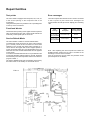
Mechanical instructions
For the main carrier two service positions are possible (3.1).
A: For faultfinding on the component side of the main carrier.
B: For (de) soldering activities on the copper side of the main carrier.
Position A can be reached by first removing the mains cord from it's fixation, then loosen the carrier lips (1) and then pulling the
carrier panel (2) for approximately 10cm.
Position B can be reached from position A after disconnecting the degaussing cable. Put the carrier on the line transformer side.
Fig. 3.1
Fig. 3.2
2
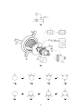
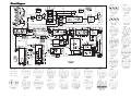
Overview oscillograms / Testpoints
3
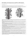
Description of microprocessor and TXT in CTN chassis
MICROPROCESSOR + TXT
The CTN model chassis is designed to accept three different microcontrollers: the TMP47C634, the SAA5288 and the SAA5290.
The three microcontrollers are mounted in the same position, by placing pin 1 at the same point. The TMP47C634 has 42 pins while the SAA52XX
models have 52 pins. The circuitry connected to the pins is practically the same. From pin 21 on the Toshiba model, the equivalent pin on the
SAA52XX unit will be 10 numbers higher (e.g., pin 33 on the TMP47C634 corresponds to pin 43 on the SAA52XX).
The difference between the TMP47C634 and the SAA52XX is an improvement in the OSD (it goes from two lines to a full screen, thus making it
possible to implement the MENU) and the addition of new functions in the software (24-h timer, child block, etc.). The SAA5290 also has a TXT
decoder.
Following is an explanation of the different functions of the microcontrollers with indications as to the pin number assigned to each integrated circuit
and the differences between the microprocessors, where applicable:
- Integrated circuit power supply: The TMP47C634 has a single +5V power supply (pin 42 VVD). The SAA52XX has several power supplies for the
microcontroller (pin 44 VDDM), the analog converter and the OSD (VDDA pin 38 and VDDT pin 39), as well as for the final phase of RGB outputs
(RGBREF pin 31).
- LED (pin 20): The LED lights up with a low current when the television set is ON and with a high current when the set is on Standby.
- RC5 (pin 35 on the TMP47C634; pin 45 on the SAA52XX): The commands transmitted by the remote control handset are received by infrared
receiver 1685 and passed to the microcontroller for decoding.
- Switching voltages of the BG/L-L/L’-BG/I systems (pins 36, 37 and 38 on the TMP47C634; pins 46, 47 and 48 on the SAA52XX). These signals are
only used on Multistandard units. These pins are used for switching the system for decoding sound and video. These signals are inverted and set at
the correct level by transistors 7672 and 7673, respectively. Once they are transformed, together with the signal from pin 48 (BG/I), they make up the
system status lines (See table).
- Oscillator: The TMP47C634 has a 4-MHz oscillator which is determined by a 4-MHz ceramic resonator on pins 31 and 32. The SAA52XX has a 12MHz oscillator which is determined by a 12-MHz crystal between pins 41 and 42.
- On-Screen Display (OSD): In order to synchronize the OSD information with the picture signal, the VERT FLYBACK signal is added in inverted
form to the integrated circuit (pins 15 and 27 on the TMP47C634 and pin 37 on the SAA52XX), as is the HOR FLYBACK signal (pin 26 on the
TMP47C634 and pin 36 on the SAA52XX). The SAA5290 also uses these signals to synchronize the TXT. On the TMP47C634 there is an LC
network on pins 28 and 29 which controls the OSD.
The TMP47C634 has only the green output activated (pin 23) and this is inverted with transistor 7658 so that the correct level is reached. The
SAA52XX models have three outputs, R, G and B (pins 32, 33 and 34) with emitter followers (7641, 7642 and 7644).
The pin for erasing the RGB picture signal for inserting OSD (pin 25 on the Toshiba and 35 on the SAA52XX) is connected with diode 6679 to pin
21 on the TDA836X.
- Tuning: The unit has a VST (Voltage Synthesized tuning) system. This system works by tuning to a station on the tuner through a linear variation
of the tuning voltage (0V2 to 5V). It is available on pin 1 of the mC and converted to an adequate level on the selector/dial (0V to 33V), using T7605
and +101.5V. The AFC signal (Automatic Frequency Control) of detector FI is added to the tuning voltage V-VARI by R3689 and R3688 to compensate for the slow variation of the tuning feature.
While searching for the station, pin 41 is set on high which means that the AFC voltage will not be added to the V-VARI. If an IDENT signal is
received on pin 16 while searching for a station, the mC will check via entry pin 9 whether the tuning is correct and whether the AFC signal can be
activated again. The SAA52XX has 3 pins (15 VHF1, 17 VHFIII AND 18 UHF) for band switching and provides voltage to the corresponding pin. The
TMP47C634 has only two pins (17, 18) for band switching which decode the 3 tuning lines using transistors 7003 and 7004.
The SAA52XX models also have pin 30, which they use to limit the CAS voltage in automatic tuning so that noise signals are not memorized.
- Picture and sound adjustments: volume control (pin 2), brightness control (pin 3), colour control (pin 4) and contrast control (pin 5); the SAA52XX
models also have sharpness control (pin 6).
4
The RC networks are used to convert the modulated pulse output to a DC voltage level. Some of these settings can be preprogrammed in the
memory for all channels as a personal preference (PP). Mute is controlled internally on the mC during automatic station search or when the signal
received is interrupted (detected via the IDENT signal on pin 16).
- Service: If pin 7 is connected to earth when the set is turned on from the IR, the unit will go into Service Default Mode (see Chapter 8).
- INT/EXT and mute on programme 0. The microcontrollers have a pin for switching to external (pin 7 on the TMP47C634 and pin 8 on the SAA5290)
via transistors 7876 and 7877. This signal is added to the signal from SCART pin 8 so that either of them can be used to switch to external.
On units without SCART, this signal is used for muting the sound and picture on programme 0.
On the SAA52XX models, this line is also an input line so that the microcontroller knows if the unit is on external. This way, the correct video signal
is switched on the TXT and the sound is not muted on external, even if there is no pilot signal.
- EEPROM bus 12C memory (pins 39 and 40 on the TMP47C634; pins 49 and 50 on the SAA52XX); The microcontroller is connected to non-volatile
memory IC7685 (EEPROM) via bus 12C. Personal preferences (PP) and channel data are stored in the memory. The system can memorize 79
channels (with the data on tuning voltage, band and system) and the personal preferences.
- Standby (pin 19); The Standby switching signal is on pin 19 of the mC. If the Standby signal is “low”, it reduces the start-up voltage of oscillator pin
36 on the TDA836X, thus cutting the line voltages.
- Control and options keypad; The decoding principle is different depending on the unit. On the TMP47C634, it decodes a matrix between pins 11,
12 and 13 while on the SAA52XX, it only checks to see if the pin is earthed. The TMP47C634 also checks for diodes 6603, 6604 and 6605 via pin
14 on the microcontroller (see options table on diagram).
The SAA52XX reads the options via pins 14 and 52, which will be “1” or “0” depending on the components (2690, 3600, 3650 and 3657).
- TXT: The SAA5290 has an internal teletext decoder. The following functions have been programmed on the software: TXT input/output, show,
freeze, temporary cancellation, clock, subcode, zoom, index, flof, page +/-, X/26 and 8/30 packet decoding (station identification and start-up page).
Synchronization is received from the HOR FLY and VERT FLY signals, as is the OSD (this means that if the video signal is lost, the TXT does not
become unsynchronized). The teletext information is extracted from the video signal inserted on pins 23 (internal video) and 24 (external video) via
condensers 2635 and 2636.
Pin 27 corresponds to the NIL control signal, which pulse switches transistor 7640 and keeps the picture from interlacing when applied to the
vertical deflector.
All remaining circuitry (oscillator, RGB output, fastblanking, etc.) is shared with the microcontroller.
L/L'
BG/L
I
BG
L
L
L
I
L
L
H
DK
L
L
L
L
L
H
L
L'
H
H
L
SYSTEM
5
Small signal
IC 7015 (TDA836X) is a single-chip video processor with built in IF- detector, luminance and chrominance separator, PAL chroma
decoder, RGB processing , horitzontal&vertical syn. processor, FM sound- decoder,
IF (INTERMEDIATE FRECUENCY) DEMODULATION (ic7015/6A)
IC 7015/6A contains the IF detector. The 38.9 MHz IF signal is a present at the output pin 11 of the tuner (33.4 MHz for a sign al
according to the SECAM L' system).
Bandpass filter; The IF bandpass characteristic is determinated by the bandpass of the SAW (Surface Acoustic Wave) filter 1015.
* For PAL BG sets a SAW filter with 5.5 MHz bandwich is used (33.4 to 38.9 MHz).
* For PAL I sets a SAW filter with a bandwinch of 6.0 MHz is used (33.4 to 39.4 MHz).
* For PAL BGI/SECAM BGLL' sets a SAW filter with 6.0 MHz bandwich is used to enable BGILL' reception.
* For LL' reception BG/L is "high", D6014 conducts and so the 33.4 MHz is tuned to a lower frecuency with C2014 (32.9 to 38.9 M Hz).
* For BGIDK reception BG/L is "low", D6014 does no conduct. With C2013 the bandpass filter is tuned at 33.4 MHz (32.4 to 38.9
MHz).
* For PAL BG/SECAM BGDK sets a SAW filter with a bandwich of 6.5 MHz is used without switching possibilities (32.4 to 38.9
MHz).
Demodulation and AGC; After the bandpass filter the IF signal is supplied to the IF-detector IC7015/6A pins 45 and 46. This IC7015
6A is suitable for a both negative (BGIDK) and positive (LL') modulation controlled by the BG/L switching signal (" high" for LL' positive
modulation, "low" for a BGDIK negative modulation) at pin 1 IC7015/6F (pin 1 IC7015/6F is at DC level input pin for positive/negative
switching of IC7015/6A). This control also determinates whether the AGC circuit controls at the top white level (positive modulation) or
at the top sync level (negative modulation).
The high-frecuency AGC voltage is available at pin 47. The take over level of the high-frecuency (delayed) AGC control can be set at
pin 49 by means of R3021. For switching to diferent IF for the SECAM L' system (33.4 MHz) the demodulation reference circuit 5040
at pins 2 and 3 IC7015/6A is switched by switching signal L/L'.
* For BGILDK reception L/L' is "low", D6042 conduct and so coil 5043 is connected in parallel to 5040. The circuit is tuned to 38.9
MHz.
* For reception L/L' is "high", D6042 does nor conduct. The circuit is tuned to 33.4 Mhz by L5040 only.
Note: For sets with LL' reception L5040 is tuned at 33.4 MHz, for sets without LL' reception L5040 is tuned at 38.9 MHz (or 39.5
MHz for PAL I only sets).
Automatic Frecuency Control (AFC) signal at pin 44 is obtained from the reference signal of the IF-detector and the control is
modified internally in IC7015/6A for positive or negative modulation. C2037 smoothes the AFC voltage.
SOURCE SELECT, LUMINANCE AND CHROMINANCE SEPARATION (IC7015/6B)
Sound trap; The baseband CVBS signal of pin 7 IC7015/6A (nominal amplitude of 2Vpp) also contains the 5.5 or 6.0 MHz FM sound
signal (FM intercarrier sound). This sound signal is filtered out with a 5.5 MHz (6.0 MHz PAL I) ceramic filter (1032 and/or 10 33).
Source select: The CVBS signal is now fed to pin 13 IC7015/6B to the source selector switch in IC7015/6B. Pin INT/EXT = 0V gives
internal CVBS (pin 13), pin 16 INT/EXT = 8V gives external CVBS (pin 15) (external signal SCART CVBS IN from the CVBS IN cinch
or pin 20 scart-connector).
Luminance and chrominance separation: chrominance signal is filtered out (-20dB) by a luminance notch filter which is internallly
calibrated at the subcarrier frecuency (4.43 or 3.58). The IDENT status signal is coming from pin 14 IC7015/6B. In case of no
horizontal sync (so no signal detected) by the sync processor IC7015/6E, pin 14 IC7015/6B is made "low", TS7651 does not conduc t
so pin 16 of the µC is "high". The IDENT signal is internally fed to ensuring stable OSD even without transmiter signal (IC7015/6D can
be switched to different time constants).
CHROMINANCE DECODING (IC7015/6C)
CVBS is extracted from the baseband CVBS signal from the IF-detector via crystals 1032. PAL (and NTSC if applicable) chroma
decoding inside IC7015/6C, SECAM chroma decoding inside IC7250.
Inside IC7015/6C the PAL (or NTSC) chroma signal is fed via amplification and a burst demodulator to the R-Y and B-Y demodulator.
(PAL or NTSC processing is determined automatically by the burst demodulator inside IC7015/6C). The 4.43 MHz reference crysta l
for chrominance demodulation in IC7015/6Cis in present at pin 35 of IC7015/6C.
Pin 27 shoud be 5V5 (via R3280) to force IC7015 in the PAL/SECAM mode; by then IC7015/6C is in the PAL decoding mode and via
pin 27 feeds throught the chroma signal to the SECAM chroma decoder IC7250 (so IC7015/6C searches for PAL and IC7250
searches for SECAM).
Via a bidirectional communication line between pin 32 of IC7015/6C and pin of IC7250 both IC7015/6C and IC7250 "know" wether
a PAL or a SECAM signal is detected:
- On AC level there is a 4,43 calibration for calibration of thr PLL and chroma cloche filter of IC7250.
- On DC level there is a SECAM or PAL switching line enabling automatic selection of IC7015/6C and IC7250 to supply R-Y and BY to the delay line IC7271.
* If IC7015/6C has detected a PAL signal, Vpin 32 is made 1V5. By then the demodulated R-Y and B-Y at output pins 30 and 31 od
IC7015 / 6C are fed to delay line IC7271.
* If IC7015/6C has detected a PAL signal, Vpin 32 is made 5V. By then the demodulated R-Y and B-Y at output pins 30 and 31 of
IC7015/6C are not fed to the delay line IC7271.
* If IC7250 has detected SECAM Vpin 1 IC7250 becomes "low", sinking typical 150 µA from the 5V from pin 32 IC7015/6C. Only in
case the sinking current at pin 32 IC7015/6C is typical 150 µA, only by then IC7015/6C "knows" IC7250 has detected SECAM
demodulated R-Y and B-Y are fed to the delay line IC7271 via output pins 9 and 10 of IC7250.
6
RGB DEMATRIXING (IC7015/6D)
RGB-dematrixing dematrixies the -(R-Y), -(B-Y) and the Y signals; the sandcastle pulse coming from the IC7015/6E synchronises
RGB dematrixing and suppresses the RGB signals during line and frame flyback.
Control by µC for contrast, brightness and saturation (0V5 to 4V5).
RGB-source select switches between internal RGB and external RGB (OSD or SACART) via pin 21 of IC7015/6D (via resp OSD
FAST BLANKING from OSD generator and FAST BLANKING from SACART or µP INT/EXT from µC).
HORIZONTAL SYNCHRONISATION (IC7015/6E) diagram B
Start up of the hor. oscillator via +11A gives start up current into pin 36 5V8 the hor. oscillator starts running approx. 25 KHz and only
when IC7015 supply pin 10 = 8V the line frecuency changes to 15625 Hz.
Hor, sync., separator separates hor pulses out of CVBS and so synchronises the free-running hor. sawtooth generator. Both the line
and frame frecuencies are internally locked to the chroma oscillator on pin 35 IC7015/6C.
Hor, oscillator sawtooth is converted in square wave voltage with variable duty cycle (pin 37). Hor, flyback pulse at pin 38 compares
phase of flyback pulse with phase of the hor. oscillator; if phase not correct the duty cycle of hor. oscillator will be adjusted. Time
connstant of the sync. circuit automacallly determinated by IC7015/6E. Pin 38 is both sandcastle output and hor. flyback input.
Selection automacally determinated by the input current (sandcastle a few µA, flyback 100-300 µA determinate by R3371).
Amplitudes of sandcastle pulse; burst 5V3, line blanking is 3V, frame blanking 2V.
At standby (STANDBY "low") TS7580 blocks and TS7581 conducts and so the line is shut down at stand by.
VERTICAL (VERT.) SYNCHRONISATION (IC7015/6E) diagram B
Vert. sync. separator separates frame sync. pulses from CVBS and so synchronises frame oscillator. IC7015/6E compares phase of
flyback pulse with phase of sawtooth at pin 42 (from external RC network); if phase not correct the duty cycle of hor. Pre-amplifier in
IC7015/6E amplifies sawtooth (pin 43 of IC7015/6). Via BCI' frame correction is realised for high beam currents; If beam current
increases (more white), EHT decreases so picture will become too big. BCI and so BCI' decrases for increasing beam current
(diagram C) and the picture will be corrected.
SOUND DETECTION (IC7015/6F) diagram D
There are two audio paths: for the BG, I and DK systems FM modulated intercarrier sound (sound extracted from baseband CVBS
from IF detector), for the LL' systems AM modulated quasi-split sound (sound extracted directly from the tunner).
FM demodulation; For FM modulated sound the sound signal is filtered throught filter 1135 or 1136 from the baseband picture signal.
For BGDK or BGILL' sets the switching signal BG/I is used to select the current crystals.
* For I (or DK) reception BG/I is "low", TS7170 does not conduct, D6170 conduct and so crystal 1136 (6.0 MHz for I and 6.5 MHz for
DK) is switched parallel to 1135.
* For BG reception BG/I is "high", TS7170 conduct, D6170 does not conduct and 1136 is not switched in parallel to 1135 (5.5 MHz
only).
* For PAL BG or PAL I only sets only 1135 is used (resp. 5.5 MHz or 6.0 Mhz). FM-mono sound demodulation takes place in
IC7015.6F. No adjustament required for BG or I demodulation as automatic PLL tuning (4.2 to 6.8 MHz).
Sound frecuency characteristic is defined by de-emphasis C2112 at pin 1. Volume control on DC level at pin 5. Selection between
FM sound or AM sound/EXT sound (from input pin 6) by pin 16 IC7015/6B.
AM demodulation; Interferences signals at 30,9 MHz are removed from IF signal coming fron tuner by SAW filter 1137 (double band
pass caracteristic) the required frequency spectrum is fed to the AM demodulation IC7125. The doble characteristic is necessary
because for the L system the sound is at 32,4 MHz and for L´at 39,9 switched by switching signal L/L´and TS 7126 TS7127
* For L´ reception (L/L´ is "high") IF signal is present in pin 2.
* For L reception (L/L´ is "low") IF signal is present in pin 1.
The demodulated signal at pin 6 of IC7125 is supplier to the source selection switch in IC7140 , C2126 and 2127 are AGC related
storage capacitos.
Source selection: INT/EXT is "low " for internal and "high" for external . This signal is made from uP INT/EXT and pin 8 of the scart. If
one of these 2 signals is "high" external is selected. BG/L is "low" for FM sound (BGIDK) and "high" for AM sound (LL').
* Top switch in IC7140 select between AM sound (pin 5) and EXT sound from SCART +AV (pin3) by pin 9 INT/EXT. The output of this
selector (pin 4 IC7150 ) is fed to input pin 6 of FM demodulator IC7015/6F .
Here selection is made between FM sound (pin 5) and EXT sound from SCART+ AV (pin 3) by pin 9 INT/EXT. The output of this
selector (pin 4 IC7150) is fed to input pin 6 of FM demodulator IC7015/6F.
* Middle switch in IC7140 selects between AM (pin 1) and FM sound (pin 2) for SCART AUDIO OUT by pin 10 (BG/L is "high" for AM
pin1, "low" for FM pin2).
* Bottom switch in IC7140 connects +8 to pin 1 IC7015/6F to switch the IF-detector and AGC (both IC7015/6A) to positive modulation
for SECAM LL´(BG/L so pin 11 IC7140 is "high" for AM LL´ positive modulation so pin 13 to +8).
Anti-plop; At switch on the set C2183 is not charged, anode C2183 is "high", TS7183 conducts and so mutes the output amplifier
IC7187. As soon as C2183 is charged anode C2183 is "low", TS7183 stops muting.
At switch off of the set the +8A drops very fast. As C2183 is still charged, the anode of C2183 becomes approx. -8V DC. By then the
DC volume control signal VOLUME is shorted via zener D6183, so IC7015/6F is muted.
7
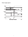
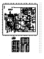
Power Supply
Mains isolated switched mode power supply (SMPS), control IC7514 (TDA4605) gives oscillation, variable frequency, variable duty
cycle, switching FET, no opto coupler, no thrystor switching windings on the secondary side, slow start circuitry and no standby
mode of the power supply. Via sense windings 4-2 frequency and duty cycle control on the primary side.
Duty cycle and frequency of the power depends on T-on of FET TS7525 which is controlled by IC7514. This IC detects variations
of the +100 (at the secondary side of 5525 at winding 5-7) via sensing windings 4-2 at the primary side of 5525. The switching
period of TS7525 is divided in three main areas T-on, T-off and T-dead:
During T-on energy is extracted from the mains into the primary winding 8-12 of transformer 5525 with a linear increasing primary
current (slope depends on voltage across C2505). Via T-on regulation the duty cycle and the frequency of the SMPS and so the
+100 can be controlled.
During T-off energy "inside" transformer is supplied to the load via secondary windings of 5525. Current through secondary side of
the transformer decreases linear with firm slope.
During T-dead no energy is extracted or supplied. During T-dead the L-prim is demagnetised (polarity L-prim and C2524 is switched).
PRIMARY SIDE
Degaussing; R3501 is a dual PTC (2 PTC's in one housing). After switch on set, PTC is cold so low-ohmic and so degaussing
current is very high. After degaussing, PTC is heated so high-ohmic, so in normal operation degaussing current very low.
Mains voltage is filtered by L5500, full wave rectified by diodes 6502-6505 and smoothed by C2505 to VIN (300 V DC for 220V AC
mains).
Start up; Via start up circuitry via R3507 the DC voltage VIN is used to start up IC7514. As soon as the supply voltage Vpin6 12V
the IC7514 starts; the internal oscillator of IC7514 drives TS7525 into conduction at the lowest frequency (during start up C2523
determines the frequency; as C2523 is uncharged at start up this gives a low start). The power supply automatically starts up.
Take over IC7514; During start up a voltage across winding 4-2 is built up. At the moment the voltage across winding 4-2 reaches
approx. +15V, D6521 starts conducting and takes over the +15 supply voltage at pin 6 IC7514.
CONTROL CIRCUITRY
+100 feedback for frequency and duty cycle control; Sense windings 4-2 has same polarity as winding 5-7. During T-off winding 57 and so winding 4-2 are positive. D6515 conducts and so charges C2515; the DC level across C2515 is a reference for the +100.
Via R3518, R3517 and R3508 this DC-voltage is brought to the required level for input pin 1 IC7514; this voltage is used for
frequency and duty cycle control of IC7514.
R3518 is a potentiometer and so +100 can be adjusted.
IC7514 controls +100 by controlling T-on and so the frequency and the duty cycle; IC7514 compares voltage at pin 1 with an internal
reference voltage.
* In a stable situation the voltage at pin 1 is the same as the internal reference voltage, so frequency and duty cycle remains the
same.
* If +100 increases the voltage at pin 1 increases, and so the frequency and duty cycle and so the +100 will be decreased (new
balance of voltage at pin 1 and the reference voltage and so new lower stable frequency and duty cycle).
* If +100 decreases, the voltage at pin 1 decreases. The frequency and duty cycle and so the +100 will be increased.
The voltage at pin 1 is in a stable situation typical 400 mV.
Undervoltage protection; If Vpin6 supply voltage drops under 7V25, the logic in IC7514 will shut the output at pin 5. The power
supply will stop running.
Overvoltage protection; The power at pin 3 IC7515 is a measure for the mains voltage and so the DC Vin across C2505. As soon
as the voltage Vpin3 6V6, the logic in IC7514 will shut the output at pin 5. The power supply will stop running.
Overload protection; If the secondary load becomes too high, the T-on becomes too long. The internal sawtooth used for oscillation
is measured over C2509 at pin 2 IC7514. If Vpin2 3V (foldback point) the IC will switch into overload mode giving protection (hickup or burst mode): IC7514 switches TS7525 and so power supply "off" as long as I-prim is too high, starts up again, if I-prim still
too high switches "off" again, etc.
SECONDARY SIDE
±100 for the line output stage ±100A for the tunning (V VARI), +11 for sound output amplifier, +11A for start up of the line circuitry,
±5 for pull up and +5A for µC and EEPROM. No secondary protections are available.
8
Power supply signals
9
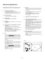
Electrical adjustments
Adjuntaments on the main panel (fig.7.2).
1.7. RF AGC.
If the picture of a strong local transmiter is reproduced
distorted, adjust potenciometer R3021 until the picture
is undistorted.
1.1. +100V power supply voltage.
Connect a voltmeter (DC) across C2530.
Adjust R3518 for a voltage of +101V5 for 14" or +106V5
for 20" sets at back picture (beam current 0 mA).
Or: Connect a pattern generator (e. g. PM5518) to the
aerial amplitude=1mV.
Connect a multimeter (DC) at pin 5 of tunner.
Adjust R3021 so that voltage at a pin 5 of tuner
is 3V7 ±0V5(DC).
1.2. Horizontal centring.
Is adjusted with potenciometer R3354.
2.
1.3. Picture height.
Is adjusted with potenciometer R3410.
Adjustaments on the CRT panel (Fig. 7.1).
2.1. Vg2 cut-off points of picture tube.
Apply a pattern generator (e. g. PM5518) and a set it
to a white raster pattern.
Adjust contrast and Vg2 at minimum (Vg2 with
potentiometer in the line output transformer to the left).
Adjust brightness until the DC voltage across
potentiometer 3213 is 0V.
Adjust R3207 (B), R3220 (G) and R3234 (R) for a
black level of 115V on the collectors of transistors 7205,
7218 and 7227.
Adjust Vg2 potentiomete until the gun that first emits
ligth is just no longer visible. Adjust the two other guns
with the respective controls (3207 3220 or 3234)
until just no light will be visible.
1.4. Focussing.
Is adjudted with potenciometer in the line output
transformer.
1.5. If filter (only for sets with SECAM LL' reception
possibility).
Connect a signal genetor (e. g. PM5326) via a
capacitor 5p6 to pin 17 of the tunner an adjust the
frequency for 33.4 MHz.
Connect an osciloscope to pin 1 of filter 1015.
Switch on the set and select a program with system
Europe (BG/L "low" for BGIDK reception).
Adjust L5040 for a minimum amplitude.
2.2. Grey sacle (white D).
Apply a test pattern signal and the set for normal
operation. Allow the set to warm up for about 10
minutes.
Adjust R3213 and R3214 until the desired grey scale
has been obtained.
1.6. AFC.
a. For a sets with SECAM LL' reception possibility:
Connect a signal generator (e. g. PM5326) as indicated
in point 1.5. Connect a volmeter to pin 44 of IC7015/6A.
Adjust the frecuency for 38.4 MHz and a select a
program with system France (L/L' is "higt" for
reception).
FIG. 7.1
Adjust L5040 for 3V5 (DC).
Next adjust the frecuency for 38.9 MHz. Select a
program Europe (L/L' is "low" for BG- ILDK reception).
Adjust L5043 for 3V5 (DC).
b. For sets without SECAM LL' reception possibility:
Connect a signal generator (e. g. PM5326) as indicated
above and adjust the frecuency for 38.9 MHz (for a
PAL I at 39.5 MHz). Connect a voltmeter to pin 44 of
IC7015/6A.
Adjust L5043 for 3V5 (DC).
10
Repair facilities
Test points
Error messages
The CTN chasis is equipped with test points, TP1, TP2, etc
in the service printing on the component side of the
monoboard.
Using these test points it is possible to set a quick diagnosis
on the top of the monoboard.
The microcomputer also detects errors in circuits connected
to the I 2C (Inter IC) bus. These error messages are
communicated via OSD (On Screen Display) and a flashing
LED.
Functional blocks
On both the service printing on the copper and the component
side, functional blocks are given. These blocks indicate the
functionaly of that specific part of the circuit.
Service Default Mode
The CTN software contains a "Service Default Mode" .
To activate this mode the service pin of the microcomputer
(pin 7-IC7600) should be short-circuited to earth while
switching on the set with the mains switch (shorting pin 7
can be done on the copper side via the 2 copper squares or
on the component side by pin 7 and the shielding of the µC)
When the set in the Service Default Mode and "S" appears
on the screen.
In the Service Default Mode the set is in a pre-defined mode
In this mode all analog settings (volume, contrast, brighness
and saturation) are in the mid position and the set is tuned to
program number 1.
The Service Default Mode is left via switching off the set by
the mains switch or via standby on the remote control.
Error
message
Error
description
Possible defecttive component
F1 en OSD y
LED parpadea
Error interno µC
IC7600
F2 en OSD y
LED parpadea
Error Eeprom
IC7685
Note: After replacing the microcomputer first solder the
shielding before testing the set. This is needed as the
shielding is used for earth connection.
If this is not done the set can switch into protection mode
(see description of the SMPS).
FIG.7.2
11
+100
+10V
+100
+100
Block diagram power supply
12
List of abbreviations
µC
µP INT/EXT
Microcomputer
Switching signal from µC to TS7876 and TS7877 (diagram C) making together with pin 8 of SCART connector the INT/EXT switching signal; "low" for
internal, "high" for external
AF
Alternating Current
AFC
Automatic Frecuency Control
AGC
Automatic Gain Control
AM
Amplitude modulation
AQUA
Aquadag on the CRT panel for spark gaps and used for making BCI signal
AV
Audio and Video cinches on the rear side of the set
BCI
Beam Current Info; if beam current increases the BCI signal decrases. BCI is used for contrast reduction if beam current is too high
BCI'
Derived from BCI; if beam current increases (more white), EHT decreases so picture will become too big. BCI and so BCI' decreases for increasing
beam current (diagram C) and the picture will be corrected.
BG/I
Switching signal from µC; "low" for I or DK reception (6.0 or 6.5 MHZ FM sound), "high" for BG reception (5.5 MHZ FM sound)
BG/I/DK/LL'
Sond system BG/I/DK/LL' indicate frecuency distance between sound and picture carriers (5.5 MHz for I, 6.5 MHz for D K and LL')
Switching signal from µC; "low" for BGIDK reception (negative modulation, FM sound), "high" for LL' reception (positive modulation, AM sound)
BG/L
BRI
Brightness control signal (same as BRIGHTNESS)
BRIGHTNESS
Control signal (from µC, but on DC level via RC network) for brightness control of the video controller IC7015/6D
BSW1
Bandswitcing signal from µC to 2 to 3 decorer IC 7002
BSW2
Bandswitching signal from µC to 2 to 3 decorer IC7002
CONTRAST
Control signal (from µC, but on DC level via RC network) for brightness control of the video controller IC7015/6D
CRT
Picture tube
CVS
Colour Video Blanking Synchronisation from pin 7 IF detector IC7015/6A
DC
Direct current
EEPROM
Electrical Eresable Programmable Read Only Memory
EHT
Extra High Tension (25 KV)
FET
Field Effect Transistor
FF
Filatement (heather voltage)
FM
Frecuency MOdulation
HOR FLYBACK
Horizontal flyback pulse (15625 Hz) used for locking the horizontal oscillator in IC7015/6E and for locking the OSD generator in the µC
HOR
Horizontal drive signal from IC7015/6E to line output stage
HUE
Tint ajustment for NTSC system
Digital Control bus of the microcomputer
I2 C
IDENT
Status signal; "low" for horizontal synchronisation, "high" in case horizantal synchronisation is detected
IF
Intermediate Frecuency
iNT/EXT
Switching signal derived fromµµP INT/EXT and pin 8 of SCART to pin 16 IC7015/6B and IC7140 (diagram D); "low" for internal, "high" for external
L/L'
Switching signal from µC; "low" for BGIDKL (picture at 38.9 MHz) reception, "high" for L' reception (picture at 33.4 MHz)
LED
Light Emitting Diode
LOT
Line Output Transformer
MUTE PROG 0
Only for sets whithout SCART + AV ; "low" for program 0 muting the sound, "high" for program 1-39
NIL
Non InterLace
NTSC
National Television System Committee
OSD
On Screen Display
OSD FAST BLANKING Fast blanking info from OSD generator in µC to video controller IC7015/6D for blanking the RGB info to enable OSD-G insertion
OSD-G
Green info from OSD generator in µC to video controller IC7015 for inserting green OSD info on screen.
PAL
Phase Alternating Lines
PLL
Phase Locked Loop
POR
Power On Reset (ensures the µC starts up it's software only if the power supply of the µC itself is high enough)
POS/NEG
Switching signal from IC7140 via BG/L; "high" for positive modulation (LL'), highihmic for negative modulation (BGIDK).
PP
Personal Preference
PROT
Prottection signal from frame IC7400; in case vertical flyback generator in IC7400 is not activted, the voltage at pin 8 IC7400 becomes 2V.
Protection circuit in IC7400 will make pin 7 "high" overrulling the HOR FLYBACK and SANDCASTLE. The constant "high" sandcastle is supplied to
the luminance circuit and so the picture will be blanked.
PTC
Positive Temperature Coefficient Resistor
RC5
Remote Control 5 system
RGB
Red Green Blue
ROM
Random Access Memory
SATURATION
Control signal (from µC, but on DC level via RC network) for saturation control of the video controller IC7015/6D
SAW
Surface Acoustic Wave; very precise bandpass filter.
SC
Sandcastle signal from IC7015/6F to delay line IC7271 and SECAM chroma decoder IC7250
SCART CVBS IN
CVBS signal from pin 2 SCART to external input pin 15 IC7015/6B
SCART CVBS OUT
CVBS signal from IF detector IC 7015/6A to pin 19 SCART
SCART AUDIO IN
Audio signal from SCART + AV cinches to source select IC7140
SCART AUDIO OUT Audio signal from IC 7140 to pin 1 and 3 SCART + AV
SCART
Euroconnector
SCL
Clock line of the I²C-bus
SDA
Data line of the I²C-bus
SDM
Service Default Mode; predefined mode for faultfinding (see chapter 8)
SECAM
SEquential Couleur A Memoire
SMPS
Switched Mode Power Suplly
STANDBY
Switching signal; "low" for standby (only line is shut), "high" for normal operation
SYNC
Synchronisation
TP-1
Tets point 1
UHF
Ultra High Frecuency band from tuning range
V-IN
The DC voltage across C2505 present at pin 11 of the primary side of the transformer
V-VARI
Tuning voltage (0-30V)
VERT FEEDBLACK
50Hz vertical flyback pulse used for locking the vertical oscillator in IC7015/6E
VERT FLYBACK
50Hz vertical flyback pulse from frame IC7400 lo lock the OSD generator in µC
VERT DRIVE
Vertical drive signal from IC7415/6E to frame amplifier IC7400
Vg2
Voltage on Grid 2 of the picture tube
VHF
Very High Frecuency band from tuning range
VOLUME
Control signal (from µC, but on DC level via RC network) for volume control of sound processing in IC7015/6F
VST
Voltage Synthesized Tuning
Y
Luminance part of video signal
13
Electrical Instructions
A. ADJUSTMENT OF MAIN PLATE
8. Turn the colour purity rings with tab “E” so that the vertical red line
coincides as closely as possible with the centre of the screen and,
at the same time, make sure the centre horizontal line is as cor
rectly aligned as possible.
9. Connect a picture white signal and make sure the red vertical line
is in the centre of the screen. If it is not in the centre, connect the
crosshatch signal again and move the red vertical line in the right
direction, making sure that the image does not stray too far from
vertical.
10.Connect a picture white signal and move the deflection coil until
the inside of the screen is uniformly red.
11.Connect the green and blue guns and make sure that no spots
appear on the white screen obtained. If spots appear, they can be
corrected by turning rings “E” and/or moving the deflection coil.
12. Tighten screw “F”.
13. Now adjust the static and dynamic convergence.
1. Supply voltage: +100V.
Connect a voltmeter (DC) between the +2530 and mass. With
potentiometer 3518, adjust voltage to 101V5 for a 14” tube and 106V5
for a 20” or 21” tube.
2. Horizontal centring
Adjust with potentiometer 3354.
3. Picture height
Adjust with potentiometer 3410.
4. Focus adjustment
Adjust with the potentiometer placed on the line transformer.
5. APC
Connect a signal generator (e.g., PM 5326) as indicated in Fig. 1 and
adjust the frequency to 38.9 MHz. (PAL I: 39.5 MHz). Connect a voltmeter to pin 44 of IC 7015:C and adjust voltage with 5040 to 3.5V
(DC).
II. Static convergence (Fig. 3).
(If CRT has a multipole unit)
1. Connect a crosshatch signal and let the TV warm up for 10
minutes.
2. Block the green gun by disconnecting 3216 and turning attachment
ring “B” anticlockwise.
3. Turn the 4-pole magnetic rings with tab “C” so that the blue and red
crosshatch pattern is superimposed in the centre of the screen.
4. Connect the green gun and disconnect the blue gun by disconnect
ing resistor 3203.
5. Turn the 6-pole magnetic rings with tab “D” so that the red and
green crosshatch pattern is superimposed in the centre of the
screen.
6. Connect the blue gun and set the multipole unit using ring ”B”.
6. AGC - RF
When the image of a powerful local TV station is distorted, adjust with
potentiometer 3021 until the problem is solved.
B. ADJUSTMENTS ON PICTURE TUBE PANEL
1. Tube cutoff (Voltage Vg 2)
Connect a picture white signal to the antenna.
Connect pin 25 of IC7015:E to mass.
Adjust the brightness until the DC voltage on potentiometer 3214 is
zero.
Using potentiometers 3234, 3207 and 3220, adjust the level of black
on the collector of transistors 7227, 7205 and 7218 to 125V for a 14”
or 21” tube, 130V for a 20” tube.
Adjust potentiometer Vg2 until the light from the gun that comes on
first is barely visible.
Adjust the other two guns with the other controls (3234, 3207 or 3220)
until the light disappears.
III. Dynamic convergence
NOTE:
Dynamic convergence is obtained by moving the deflection coil hori
zontally and vertically. In order to ensure the exact position of the
deflection yoke, three rubber wedges are placed between the glass
of the tube bulb and the deflection coil as shown in Fig. 4a or 5d.
1. First adjust colour purity and static convergence.
2. Connect a crosshatch signal and disconnect the green gun by dis
connecting resistor 3216.
3. Eliminate the central, horizontal and vertical blue and red lines by
moving the deflection coil vertically. If the position of the deflection
coil is correct, place the rubber wedge (1) either straight up (Fig.
4a) or straight down (Fig. 5a).
The placement of the wedge as in Fig. 4a is correct if the deflection
coil is facing down.
4. By moving the deflection coil horizontally, the horizontal red and
blue line is superimposed in the top and bottom of the screen and
the red and blue vertical line to the left and right. If the position of
the deflection coil is correct, place wedges (2) and (3) as shown in
Fig. 4b or 5b. Firmly press the adhesive part of the wedge against
the tube glass.
5. Now place wedge (4) as in Fig. 4c or 5c and press so that it adheres
to the tube.
6. Remove wedge (1) and place it as shown in Fig. 4d or 5d.
7. Connect the green gun.
2. Grey scale
Connect the test signal to the antenna and adjust TV controls as normal.
Let the TV warm up for at least 10 minutes. Adjust 3214 and 3213
until the desired grey scale is achieved.
PURITY AND CONVERGENCE ADJUSTMENT
NOTE:
The instructions for adjusting colour purity and convergence de
scribed below should be used only if the tube is replaced or when
full adjustment is necessary in any other cases. Even when the
deflection yoke is replaced, it is not necessary to move the rubber
wedges (“G” in Fig. 3). Small corrections can be made using the
multipole unit.
I. Colour purity. (Fig. 3)
1. Slightly loosen screw “F” (if CRT has a multipole unit).
2. Move the deflection coil and remove the three rubber wedges (“G”).
3. Slide the deflection coil as far as possible against the tube bulb and
tighten screw “F” so that the deflection coil can be moved with a
certain amount of resistance.
4. Position the multipole unit as shown in the diagram, tighten screw
“A” and turn safety ring “B” anticlockwise.
5. Place the TV facing either EAST or WEST and insert tube.
Connect a single crosshatch signal to the antenna and turn up the
brightness as high as possible. Let the TV warm up for 10 minutes.
6. Adjust the static convergence using tabs “C” and “D” (see Chapter
II if necessary).
7. Block the green and blue guns by disconnecting resistors 3216
and 3203, respectively.
14
15
Safety instructions, maintenance instructions,
warning and notes
Safety Instructions for Repairs
Warnings
1. Safety regulations require that during a repair:
- The set should be connected to the mains via an isolating
transformer.
- Safety components, indicated by the symbol ! should be
replaced by components identical to the original ones
- When replacing the CRT, safety goggles must be worn.
1.In order to prevent damage to IC's and transistors any flash-over of
the EHT should be avoided. To prevent damage to the picture tube
the method, indicated in Fig. 11.1., has to be applied to discharge
the picture tube.
Make use of an EHT probe and a universal meter is 0V (after approx
30s).
2. ESD.
All IC's and many other semi-conductors are sensitive to electrostatic
discharges (ESD). Careless handing during repair can reduce life
drastically. When repairing, make sure that you are connected with
the same potential as the mass of the set via wrist wrap with
resistance. Keep components and tools on the same potential.
2. Safety regulations require also that after a repair:
- The set should be returned in its original condition.
- The cabinet should be checked for defects to avoid touching, by
the customer, of inner parts.
- The insulation of the mains lead should be checked for external
damage.
- The mains lead strain relief should be checked onits function
- The cableform and EHT cable are routed correctly and fixed with
the mounted cable clamps in order to avoid touching of the CRT,
hot components or heat sinks
- The electrical resistance between mains plug and the secondary
side is checked. This check can be done as follows:
· Unplug the mains cord and connect a wire tween the two pins
of the mains plug.
· Switch on the TV with the main switch.
· Measure the resistance value between the pins of the mains
plug and the metal shielding of the tuner or the aerial
connection on the set. The reading should be between 4.5 M
and 12 M.
· Switch off the TV and remove the wire between the two pins of
the mains plug.
· Thermally loaded solder joints should be oldered.
-This includes components like LOT, the line utput transistor, flyback capacitor.
3. Proceed with care when testing the EHT section and the picture
tube.
4. Never replace any modules or any other parts while the set is
switched on.
5. Use plastic instead of metal alignment tools. This will prevent any
short circuits and the danger of a circuit becoming unstable.
6. Upon a repair of a transistor or an IC assembly (e.g. a transistor or
IC with heatsink and spring) remounting should be carried out in
the following order:
1. Mount transistor or IC on heatsink with spring.
2. Resolder the joints.
Notes
1. After replacing the microcomputer first solder the shielding before
testing the set. This is needed as the shielding is used for earth
connection. If this is not done the set can switch into protection
mode (see description of the SMPS).
Maintenance Instructions
It is recommended to have a maintenance inspection carried out
periodically by a qualified service employee.
The interval depends on the usage conditions.
- When the set is used in a living room the recommended interval
is 3 to 5 years. When the set is used in the kitchen or garage this
interval is 1 year.
- During the maintenance inspection the above mentioned "safety
instructions for repair" should be caried out. The power supply
and deflection circuitry on the chassis, the CRT panel and the
neck of the CRT should be cleaned.
2. Do not use heatsink as earth reference.
3. The direct voltages and waveforms should be measured relative to
the nearest earthing point on the printed circuit board.
4. The direct voltages and waveforms are measured in the Service
Default Mode (see chapter 8). Use a colour bar pattern of a pattern
generator (e.g. PM5518).
5. The DC voltages and oscillograms are where necessary measured
with (
) and without (
) aerial signal (settings as in Service
Default Mode; see chapter 8).
Voltages and oscillograms in the power supply section have been
measured for both normal operation ( ) and in the stand-by mode
( ). As an input signal a colour bar pattern has been used.
6. The picture tube PWB has printed spark gaps. Each spark gap is
connected between and electrode of the picture tube and the
Aguadog coating.
FIG. 11.1
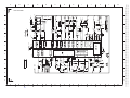
16
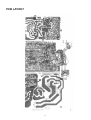
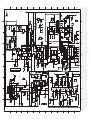
PCB LAYOUT
17
PCB LAYOUT
18
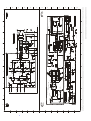
Bloc
k Dia
gram
Block
Diagram
19
C
D
E
F
B-C-D-E-F
E16
F16
AFC
1
A47
E47
A49
SCART
SCART
C48
G
H
I
J
K
L
M
S.C.
CVBS
OUT
IN
*
ONLY SECAM
2274*
100N
1
MC
3
+8B
78M08CT
2019
22U
2271*
22N
2041*
3043*
10K
2043*
IDENT
3049*
68K
R-Y
CHROMA
+8E
9124
3032*
180R
- IF -
02PH
3011*
5K6
2
3
44
100N
2050*
7
15
Y
2370
22N
22U
38
F25
HOR
FLYBACK
3372*
22K
TP10
D4
9372
2351
1U
+8V
STANDBY
3371
27K
6372*
9367
BSW1
E14
F14
6003*
K7
2041
B2
3865
L7
2043
B2
3875
L8
2044
A2
3876
M8
2045
D3
3879
J8
2050
G3
3880
J9
2053
E5
3881
K8
2080
G4
3882
K8
2081
H5
3883
K9
2082
G4
3884
M7
2084
G4
5001
G6
2261
J5
5002
F6
2262
J5
5010
B5
2265
I6
5012
B3
2267
I3
5015
G2
2268
I3
5032
E3
2271
I1
5040
C2
2272
J2
5043
B2
2273
J2
6001
F7
2274
K1
6003
F8
G
2275
L1
6014
A3
75R
B37
2279
L3
6020
C5
2280
L3
6042
B2
2285*
100P
3286
E54
F54
2284
L4
6261
M3
2285
L4
6275
L1
2286
L5
6289
L5
2291
K6
6372
D8
2292
K6
6849
J6
2293
K6
6850
J7
2297
H1
6851
J7
2340
B9
6852
J7
2350
A8
6853
J7
2351
A8
6854
K7
2354
A7
6855
K7
2366
B9
6865
L7
2370
C8
7001
F6
2371
C8
7003
F9
2850
I8
7004
F8
2852
I8
7015
D4
2860
H7
7016
F1
2871
M8
7030
E2
2876
M8
7250
H2
3001
E6
7271
L2
3002
E7
7875
M8
3003
E7
7876
J9
3004
E8
7877
K9
3007
F8
9001
H9
3008
F8
9002
H8
3009
E9
9003
F6
3010
B4
9005
F6
3011
B3
9012
A4
3012
B4
9015
G9
3013
E6
9016
G2
3014
F9
9017
D7
3015
E8
9020
G3
3016
F8
9021
G3
3017
C5
9034
F2
3018
C5
9035
M9
3019
C5
9043
A2
3020
C5
9051
E5
3021
E6
9080
G5
3022
E5
9115
A4
3023
E6
9124
G3
3029
E3
9261
M3
3030
E2
9262
K6
3031
E3
9265
G2
3875*
3032
E3
9271
J3
56R
3033
F4
9289
M5
3043
B2
9331
D7
3044
B2
9350
D7
3045
D2
9354
M1
3051
F5
9366
A8
3080
H5
9367
C8
3260
I5
9370
D7
3261
M3
9371
C7
3262
J5
9372
D8
3272
J1
9600
F6
3273
J1
9810
L9
3275
L1
9811
J9
3280
H4
9812
K9
3284
M4
3285
M4
6261*
E19
F19
LL4148
*
*
3
NO SCART
1
3006*
2V
9002
V VARI
D61
1
5
3
2
7
9
4
6
8
7004*
2850*
220P
RES
VERT
DRIVE
D1
C
20
A5
D
E
7003*
BC848
23
22
2284*
100P
3285
E53
4
TP28
2M7
TP29
1M7
B
B36
E55
5
TP30
3290
2291*
A42
A43
11
BCI
3289
8K2
A6
BCI'
CONTRAST
F10
6
A18
A49
E49
SCART
CVBS
IN
I50 SCART
+AV
AUDIO/VIDEO
6865*
LL4148
ONLY
7
75R
3865*
VIDEO
IN
13
17
15
+8A
21
19
12
14
16
18
20
V VARI
IN
470N
3850*
AUDIO
220P
3852*
12K
12K
3871
220R
8
7875*
BC848
3882*
4K7
3881*
10K
3879*
47K
7876*
BC848
+8V
ONLY
NO MENU
2876
10U
+8B
3854*
9810
7877*
3876*
9035
3K3
BC848
3883*
10K
INT/EXT
*C1
F
10
2852*
3880*
5K6
9811
S.C.
B38
75R
+8B
F17
E17
3007*
2K7
3342*
R
3884*
3014*
2340*
100N
A41
2006*
22N
2005
+8V
RES
20
3M7
AGC
3008*
4K7
+8V
10K
3284
AGC
3016*
2K7
3009*
PROT
4M7
9262
470R
A51
D4
+8E
2
RES
E4-F4
HOR
FLYBACK
TP11
B
3862
4V
8V2
43
3860*
2002*
BC848
SYNC.
E13
F13
5
VHFI
E25
UHF
BSW2
390R
4
VHFIII
2350*
4N7
2371*
3
RES
3370
3003*
100R
3004
9331
LINE DRIVE
+11A
A
E2
E8
F8
FAST
BLANKING
3002
RES
D35
10
3015*
4K7
9350
36
+8V
RES
9370
9371
H.DRIVE
BCI'
I7
2037
F18
D3
75R
2K7
TP9
RES
39
9
L7
3860
C45
IF
A50
11
M
A43
+8B
2860*
4N7
3345
1M
3858
F4
25
1K
6
A42
3858*
1001
+11A
A6
E2
2034
E18
CRO
BRIGHT
ONLY SCART + A/V
SCART
AUDIO
OUT
TP21
2001
100U
2003
100U
2N2
FEEDBACK
K7
2030
6289
1N4148
3862*
A40 TUNER
9005
9003
5V6
9017
37
*
A41
LL4148
9600
6001
+5A
FERRITE
5001 FERRITE
5002
17
E10
E9-F9
1N4148
7001
BC337
X3
SATURATION
C50
10K
2366*
4N7
3855
9289
LL4148
INT/EXT
-SYNC-
3354
3260*
8K2
SHARPNESS
E60
3013*
270R
3353*
VERT
D5
18P
9080
A52
9004
TV
+8D
4.43
100N
3001
10R
+8
+8E
15K
I9
2025
NO SCART
2262*
100N
34
3851*
75R
6
820k
3854
75R
ONLY
RES*
3291*
+8A
3080*
2081*
2080*
C12
E12
F12
1K8
3023*
2022*
35
1272
100N
2U2
+8A
IDEN
9366
D6
2286*
100P
24
14
2265*
100N
42
J7
2022
BCL
3262*
100K
2084*
2082
AGC
41
J8
3853
19
26
3.5
OSC
2292*
52
4.4
OSC
BRI
CLAMP
SWITCH
6855*
8
4.4
REF
3021
3341
3852
G1
18
PLL
32
4K7
3340*
C5
2019
R
B-Y
33
27
100N
2015
680U
3022
A80 IF/CHROMA/VIDEO
28
6854*
9
6K2
D2
I7
2018
C
O
N
T
R
O
L
G
2293*
10
2016*
100N
12K
3018
CHROMA
RES
11
6020
R-Y
AGC
HUE
+8A
48
2025
8
3851
OSD
BLANK
29
31
LL4148
SWITCH
9051
50Hz
B5
5M7
G
3292*
NO SCART
NEG
49
Y.DRIVE
I8
2017
SINC
16
+8
6K2
G1
3850
R
3051*
2018*
AGC
15K
F5
10
B
TP23
3017*
3351
8
R-Y
2261*
4 4
3019*
2017
Y
30
B-Y
2053*
100N
POS
22N
G
D8
2016
2280*
100N
SINC
13
47
560R
40
D8
3372
B39
DEMOD.
3010*
7
3371
F5
FAST
BLANKING
B
45
5
3020*
7015/6E
A4
2015
- CHROMA -
3
2354
D7
2014
+8C
+8D
3855*
75R
2
820K
4
7015/6D
47N
2011*
A51
3370
3280
10K
2034*
46
4
IF
5
B4
A18
7015/6C
1
5010
B7
2013
2
2279*
100N
1
0
3
12
7015/6B
1015
18P
2010*
3354
21
7015/6A
2014*
4N7
A50
2268
220N
6853*
4
B4
B40
1033
3012*
18P
2267*
100N
9271
6852*
RES*
B7
2011
5032
3033*
BG / L
A7
3353
12
3
8u2
2013*
33P
3351
F2
9021
TP22
9012
14
1032
F21
9115
H8
2007
(R-Y)
8
7
9020
WITH SCART
5K6
E21
D7
2006
TP27
-
LL4148
6
56P
3345
64mu
1K8
4
6014*
BA682
H8
1N
RES*
0.28uH
WITH I
B9
2005
1K
3
5012
ONLY MULTI
3342
15
2273*
10
B-Y
3029
*
F6
11
TP25
16
6
+8E
B8
2003
1
64mu
+8D
12P
B8
3341
(B-Y)
16
1N
9265
2045*
4N7
BA682
REF
+8C
2030*
22N
7030*
BC848
1K
6
9016
LL4148
3
3340
H7
TP26
-
2272*
9
4N7
6042*
RES
47N
1
3853*
75R
5043
0.7uH
RES
3045*
G5
2002
TDA4665
6849
4N7
K5
2001
7271
6851*
4
3292
H
6850*
2044*
220R
I5
9354
3272*
2007*
9034
4N7
5
TP24
3030*
K5
1272
BK
+8A
330R
2
3
5040
3291
5V1
TDA8395
SCART
+8A
10K
E4
6275
9
7250
WITH
3031*
9043
15
LL4148
3044*
K5
1033
9261
+8A
M5
3290
220R
13
3273
10K
10K
3
5015
FERRITE
F20
L/L'
2297
47U
2
2037*
220N
E20
M5
3289
E3
+8D
2275*
100N
1
+12
*
3286
C4
1032
3275*
+8D
7016
ONLY MULTI P/S BGLL'
F7
1015
A5
CVBS
CVBS
1001
1K
B
3261*
A
BSW3
E15
9015
SCART
AUDIO
IN
9001
A52
C46
G
H
9812
I
uP INT/EXT
F19
SCART CVBS
C52
OUT
E19 INT/EXT
J
K
L
A47
M
9
A
B
C
21
D
E
F
G
H
I
J
K
1135
L
BG/I
2170*
10N
3170
E22 18K
6170*
4K7
3171*
1136
7170*
BC848
3143*
1K
2143*
4N7
22K
3151
5
TP31
10U
2180
51
3152*
1
2127
2U2
13
C31
6
9114
7
2155
1N
SCART AUDIO IN /
2152
P.16
50
C33
I/E AUDIO
SWITCH
C32
FM SCART
AUDIO OUT
AM SOUND
2128
10U
9125
E11
F11
VOLUME
3184*
4K7
9143
3185
3K3
TP32
C59
FM SCART
AUDIO OUT
3125*
27K
9183
330N
2185
+11
C32
+8
9110
3181*
68K
2
D26
156
3L2
100K
3156*
100K
3155*
2189*
100NF
3
2
4
7187
TDA7052A
2R
3189
HEF4053
2184*
2N2
16
ff
D27
7140
+8
1
5
3
14
D28
4L2
VG1
6
1
8
2188*
100N
I/E AUDIO
SWITCH
6
7
8
13
11
10
15
9
4
VG2
46
VG2
2237
33N
3237
1K5
9157
+150V
6
FM SCART
AUDIO OUT
C32
WITHOUT
9191
HEADDPHONE
ONLY
2U2
2156
2M3
3M3
1M3
68R
3191*
48
2192*
10N
750R
3114*
470R
3111*
25R
1W
2
4
3
1
42
HEADPHONE
A45
10U
SCART
AUDIO
OUT
9112
2109
A52
B43 AMPLIFIER
1K5
3112*
+8
INT/EXT
C31
SCART AUDIO IN/
AM SOUND
7115*
BC858
BC848
7114*
SCART AUDIO IN
A-C
SCART +A/V
*
3115*
6K8
A46
D24
3194*
2191
100U
RES
9191
EHT
25KV
WITH HEADPHONE
BG/L
E21
F21
D23
SONEGROUND
8
5
9190
TP35
2187
100U
9192
FOCUS
C33
D30
L3
FOCUS
FOCUS
1
K
+8V
3173*
CVBS
82P
7015/6F
2112*
3N9
5
4
8K2
3126
TP34
+8
7184*
BC848C
330K
3187*
A12
E12
IDENT
2L2
1K5
3236
5
ff
9111
2169*
3
AM
6
BC848
7183*
3182*
3K3
10K
3188*
+8V
D29
ff
1L2
4
ff
J
A48
+8V
2126
4U7
- FM DETECTOR -
BC848B
7127*
1
14
9188
F19
+150
RES
+150V
5235
23
1990
I
B33 SOUND
3117*
10K
1137
OFW9453
4
6
16
3222*
2117*
4N7
2K
3
5
TDA3843
10U
C59
1U
2206
2K2
3234
CUT
OFF
R
R
G
B
9156
F20
L/L'
E20
2
1
5101
6116*
BA682
+8
TP33
2U2
7126*
BC848B
3226*
2124
22N
2125*
430R
3244*
3233
3K3
7227
BF422
7
9
3
33
H
3119*
10K
3120*
10K
3118*
10K
1K
10R
3124
+8
6227*
7125
2230*
270P
3230*
22R
1K5
3229
+8C
L4
AQUADAG
P30 DISPLAY
2
6115*
BA682
3225*
G
3121*
2101*
4N7
3K3
F
A-D-E
3212*
3224
BAS32L
7225*
560R
1K5
12K
3228
CUT
OFF
G
+8C
CUT
OFF
B
3220
BC858
3227*
1K
9201
+150V
3221*
430R
3K3
3219
3216
1K5
+150V
3208*
430R
3206*
3K3
E
- AM DETECTOR -
+8C
+8C
2217*
330P
3217*
22R
1K5
3203
+8C
D
ONLY MULTI P/S BGLL'
+8C
1K8
7212*
BC858
3232*
470R
+8C
BF422
7218
3215
12K
7205
BF422
3202
12K
+150V
2K2
A38
3L1
3214
2K2
WHITE
D
6218*
BAS32L
+8C
2204*
330P
3204*
22R
6205*
BAS32L
+8C
2K2 3207
3211*
1K8
7211*
BC858
3218*
470R
+8C
9202
WHITE
D
3213
2K2
470R
3205*
+8C
4
R
A37
G
2L1
1K8
3210*
1L1
7210*
BC858
+8C
C
IF
A50
8
*
B
22N
2202*
7
A36
5L1
4L1
C65 RGB & DISPLAY COMPONENTS
6
A40
A39
CRT PANEL
5
B
AQUA
3
VG2
A
L
M
1
9
M
42
1
2
3
4
5
6
7
15K
3144*
8
9
K1
7114
J2
1135
L8
7115
I2
1136
L8
7125
I6
1137
I7
7126
I8
1990
C3
7127
J8
2101
I9
7140
I4
2109
J1
7170
L8
2112
K7
7183
I5
2117
J8
7184
I5
2124
H6
7187
K4
2125
H6
7205
B6
2126
J7
7210
B7
2127
J7
7211
C7
2128
J6
7212
D7
2143
L8
7218
D6
2152
L6
7225
E7
2155
L6
7227
E6
2156
H2
9110
I4
2169
L9
9111
J3
2170
L8
9112
J1
2180
L7
9114
K6
2184
L4
9125
J5
2185
L4
9143
L5
2187
K3
9156
H3
2188
K3
9157
H3
2189
M4
9183
L5
2191
K2
9188
H5
2192
K2
9190
L3
2202
A7
9191
L3
2204
C6
9192
I3
2206
E5
9201
D6
2217
D6
9202
B7
2230
E6
2237
E4
3111
I2
3112
J2
3114
J2
3115
J2
3117
J8
3118
I8
3119
I8
3120
I8
3121
J8
3124
H6
3125
I5
3126
J5
3143
L8
3144
L8
3151
K8
3152
L6
3155
H4
3156
H4
3170
L9
3171
L8
3173
L8
3181
I5
3182
I5
3184
L5
3185
L5
3187
H5
3188
H5
3189
K4
3191
K2
3194
L3
3202
B6
3203
B5
3204
B6
3205
B7
3206
B5
3207
B5
3208
B6
3210
C7
3211
D7
3212
D7
3213
B7
3214
D6
3215
C6
3216
C5
3217
D6
3218
C7
3219
D5
3220
D5
3221
D6
3222
D6
3224
E6
3225
E7
3226
E7
3227
E7
3228
E6
3229
E5
3230
E6
3232
D7
3233
E5
3234
E5
3236
E4
3237
E4
3244
E6
5101
I7
5235
E4
6115
I8
6116
J8
6170
L8
6205
B6
6218
C6
6227
E6
22
22
B3
3509
B5
47
J2
3510
D5
47
J4
3512
D4
49
C3
3513
D4
1500
A2
3516
E3
2401
I1
3517
D5
2402
J2
3518
D5
2404
K2
3519
B4
2405
L2
3520
B4
2414
H2
3521
E5
2415
I2
3523
D4
2416
J2
3524
B4
2440
H5
3525
B4
2442
I5
3527
E5
2443
L5
3528
E4
2444
H5
3540
F5
2445
J5
3570
F4
2446
K5
3571
F4
2448
J3
3573
G4
2449
J3
3574
F4
2450
I4
3576
F5
2451
I4
3577
F5
2453
L6
5441
I5
2458
J3
5443
K5
2460
L4
5445
K3
2463
L5
5447
J3
2470
I3
5449
K5
2500
B3
5480
I4
2502
D3
5500
C3
2504
D3
5525
E3
2505
D4
5532
F5
2506
B6
5534
F3
2508
E5
5540
F5
2509
B4
5541
F6
2510
D5
5550
D6
2511
D5
5552
E4
2514
D6
6416
I2
2515
D5
6417
H2
2516
D3
6440
H6
2520
D5
6443
L5
2523
B5
6447
J5
2524
E4
6449
L6
2530
F3
6451
I4
2532
F5
6470
J3
2534
F2
6502
D3
2540
F6
6503
D3
2561
G4
6504
D3
2562
G4
6505
D3
3235
J5
6515
D5
3238
J5
6516
E3
3400
K1
6521
D6
3401
K2
6530
F3
3402
J1
6540
F5
3403
K2
6570
F4
3404
L2
6571
F4
3405
L2
7400
H2
3406
L2
7440
H5
3407
L2
7445
J5
3408
H2
7514
C4
3410
L2
7525
E4
3411
L2
7571
F5
3412
K2
7575
F4
3415
J2
9400
J2
3416
J2
9460
L4
3440
H5
9480
I4
3441
H6
9506
E6
3442
I6
9523
D4
3444
H5
9524
C5
3445
I5
9560
G5
3448
K5
9561
G6
3449
K5
1M1
A3
3451
I4
1M2
C2
3455
H4
1M5
J4
3456
H4
1M6
I3
3457
J3
2M1
A2
3460
L4
2M2
C2
3470
J3
2M6
J5
3480
I4
3M6
J5
3501
C3
4M5
J4
3504
A3
4M6
L4
3507
B5
5M5
K2
3508
D5
6M5
J2
B3
1679
C12
24B-24C B5
25B-26 B4
25C-26 B5
2602
G2
2610
G2
2611
H2
2622
G7
2623
H6
2624
H6
2629
H6
2630
H5
2635
C11
2636
C11
2641
F12
2648
C10
2651
F2
2656
H9
2659
G12
2660
C3
2669
B10
2677
E2
2680
C11
2681
C12
2685
C3
2691
D2
2692
G9
3600
C5
3601
H2
3602
H2
3603
G2
3604
G2
3605
G2
3606
F2
3607
F2
3608
F8
3609
G4
3610
G2
3611
H2
3612
H2
3613
H6
3614
F5
3615
H5
3616
F5
3617
H5
3618
G4
3619
F5
3620
F5
3621
F7
3622
F7
3623
G6
3624
G6
3625
F6
3626
G6
3627
G6
3628
F6
3629
G5
3630
F3
3631
F3
3632
G5
3633
H6
3636
B10
3637
B11
3638
H11
3639
F11
3640
G10
3641
G11
3642
G11
3643
F11
3644
G12
3645
F11
3646
D1
3647
G10
3648
C10
3649
F12
3650
C6
3651
F4
3652
F10
3653
F10
3654
G9
3655
G9
3656
H9
23
3657
3658
3659
3660
3661
3662
3663
3664
3665
3667
3668
3669
3670
3671
3672
3673
3674
3675
3676
3680
3681
3682
3684
3685
3686
3687
3688
3689
3690
3691
3692
3693
3694
3695
3696
3697
3698
3699
6602
6616
6641
6642
6644
6663
6691
7600
7601
7605
7638
7640
7641
7642
7644
7651
7665
7670
7672
7673
7685
7686
7691
9052
9148
9266
9609
9610
9611
9614
9616
9618
9650
9651
9652
9653
9658
9663
9665
9670
9671
9678
9679
9686
9692
C6
G12
G13
C3
C7
C4
C3
B9
B9
C9
B10
B10
C9
C6
B8
B7
B8
C3
C2
H7
C8
F7
G7
G7
H3
H3
H3
H3
C5
F1
F3
G3
C4
C6
C6
C4
G9
C5
G2
H5
H11
H11
H12
B3
E2
D2
F7
F2
G11
G11
G11
G11
G12
G10
C9
C10
B8
B7
H8
G3
E1
B8
B7
B11
H4
F1
A13
G5
F7
A14
H10
F4
G4
A13
G4
C3
B3
C10
C9
F1
C1
G3
F9
A
B
C
24
D34
D
E
F
G
H
I
9148
J
3668
47K
3664
33K
3665*
1K
K
9618
10K
3669*
3670*
10K
+5
7670*
BC848
9670
26
27
15
TP19
3666*
9653
9623
21
30
2691*
34
OSD
4MHz
23
29
28
25
32
31
7
SERVICE
RES
+5
2678*
10P
4K7
3656*
2677*
10P
RES
1679
4.0MHZ
5677
9611
330P
2669*
7665*
BC848
9671
G
SERVICE
SDA
+5V
40
6
SCL
+5V
+5STBA
3629*
LL4148
3690*
18K
3658*
2K7
270P
2658*
3627*
100K
-----
620R
3659*
--LL4148
MULTI/I
A10
A9
7685
ST24CO2
+5STB
LL4148
---
ONLY UHF
TP20
A54
OSD-G
A18
A19
INT/EXT
A25
STANDBY
A8
CONTRAST
1U
2623
SATURATION
2624
1U
6658
1N4148
7658*
PMBT2369
+8C
C11
VOLUME
A12
C12
IDENT
A13
A14
BRIGHTNESS
OSD FAST BLANKING
3
1
NO MULTI
2K7
3655*
1K8
4
7
8
6601*
2V4
2
5
3679*
3685*
3K3
6
33K
3624*
33K
3613*
22K
3633*
1U
2629
2630
2U2
6K8
3617*
+5STBA
3615
1K
3632*
3623*
+5STB
18K
3628*
6603
6605
3618*
100K
9616
270P 6679*
2676*
3684*
3K3
BC858
7601*
22K
3625*
+5STB
3616*
18K
3620*
33k
3651*
10K
RES
7651*
BC848
9652
BSW2
BSW1
3686
1K
3687
390R
J
HOR
FLYBACK
A5
VERT
FLYBACK
3667*
10K
TP18
37
BG
/
L
2
IC
9617
9650
39
19
5
4
3
2
16
+5
9658
7686*
BC848
A16
AFC
I
D7
9052
+5
7673*
BC848
3661
10K
L'
CPU
TV
18
17
1K
3692
+5B
3688*
9686
3689*
3626*
BG/L
3
1K
3673
+5
36
14
13
10
11
RC5
41
47K
3693*
+5B
H
A21
+8A
3675
7672*
BC848
10K
3681
3657*
68K
100R
2698*
820P
3698*
2696*
820P
2695*
820P
12
8
35
AFC
360K
3630*
470K
100K
L/L'
+5
1K
3662
TP17
+5A
9666
1N
2660*
100R +5STBC
20
2M2
100K
9624
V VARI
A17
G
C20
A20
3699*
4K7
ONLY MULTI
P/S BGL'I
2K7
1K
3672
+8A
3678*
6603*
UHF
6604*
LL4148
6605*
MULTI
9668
100U
2685
3663
3663*
560R
3660*
9669 9603
9663
3631
3612*
220N
2611
3611*
3610*
220N
2610
10K
10K
15K
6602
HZT33
101.5
F
P-
3695*
100R
P+
2
24
1
+5STBC
9667
6663
9
3605*
220K
3604*
24K
3603*
10K
3601
3602
E
MENU
26
9665
B4-B4534
2682*
100P
10K
3606*
7605*
PMBT2369
10U
2602
8K2
D
3696*
100R 25
1685
+5STB
10K
33
1
3607*
22K
+5STB
C
3676
42
2690*
100N
+5STBA
+5A
3
A-C-D
6
7600
SAA5541
5
9610
5640
+5C
2
3600*
+5STB
9679
4
+5B
1
B
P.O.R
7
G30 CONTROLS
A
K
L
L
M
* ONLY NO MENU
1
2
3
47UH
4
5
6
7
8
8
9
9
M
24
25
26
1679
1685
2602
2610
2611
2623
2624
2629
2630
2658
2660
2669
2676
2677
2678
2682
2685
2690
2691
2695
2696
2698
3600
3601
3602
3603
3604
3605
3606
3607
3610
3611
3612
3613
3615
3616
3617
3618
3620
3623
3624
3625
3626
3627
3628
3629
3630
3631
3632
3633
3651
3655
3656
3657
3658
3659
3660
3661
3662
3663
3664
3665
3666
3667
3668
3669
3670
3672
3673
3675
3676
3678
3679
3681
3684
3685
3686
3687
3688
3689
3690
3692
3693
3695
3696
3698
3699
5640
5677
6601
6602
6603
6604
6605
6658
6663
6679
7600
7601
7605
7651
7658
7665
7670
F7
G8
F8
J4
E8
C3
D2
D2
H2
H2
G2
G2
K3
E7
K7
J4
K4
K4
D7
E7
C5
K5
F7
G7
G7
C5
C2
C2
C3
D3
D3
D4
D4
D3
D2
D2
H2
G3
G3
F2
F3
G4
H3
H3
H4
H3
G3
H3
G3
D4
D4
F3
H2
F4
K3
K4
H6
K3
K3
E7
I7
E7
E7
J8
J7
J7
J7
K8
K7
K7
H8
I8
E7
D7
G8
J3
H7
I3
I3
E2
E2
D2
D2
J3
E3
E3
F8
G8
G7
G7
C4
K4
H2
C3
G7
G7
F7
K2
E7
J3
D6
H4
D4
F3
K3
J7
K7
7672
7673
7685
7686
9052
9148
9603
9610
9611
9616
9617
9618
9623
9624
9650
9652
9653
9658
9665
9666
9667
9668
9669
9670
9671
9679
9686
H7
I7
I2
E2
H8
I8
E7
C5
L7
G3
H4
L7
L6
D2
F4
F3
L6
F3
E8
E7
E7
E7
E7
K7
J7
C4
D2
CIRCUIT DESCRIPTION
1.- SMALL SIGNAL PROCESSING (Diagram A)
The small signal is processed by TDA8361, (TDA8360 no scart) for Pal sets and TDA8362 for Pal/Secam
sets (IC 7015), including IF detection, video processing, chroma decoder, RGB processing, sync processor
and FM sound decoder.
1.1- IF detection (IC7015/6A)
- IF input (pins 45,46): The IF signal comes from pin 11 of the tuner to the IF SAW (Surface Acoustic Wave)
filter (1015) and the IF-detector IC7015/6A (pins 45 and 46).
- IF filter (1015): The IF bandpass characteristic, determined by the SAW filter, is 33.4 to 38.9 MHz. for BG
sets, 33.5 to 39.5 MHz. for PAL I sets and 32.4 to 38.9 MHz. for DK sets.
- IF oscillator (pins 2,3): Carrier frequency, present in coil L5040, is tuned at 38.9 MHz. for BG sets or
39.5 MHz for Pal I sets
- AGC voltage (pin 47): The AGC delayed voltage is applied to pin 1 of the tuner. It should be adjusted
for 1mV. antenna signal by means of R3021 (pin 49).
- AFC signal (pin 44): The Automatic Frequency Control is obtained from the reference signal of the IFdetector. C2037 smoothes the AFC voltage.
- Identification (pin 4): The identification output is applied to pin 16 of the µC. This signal is high in case of
signal detected.
- Video output (pin 7) : This baseband CVBS signal with 2Vpp of nominal amplitude, also contains the FM
intercarrier sound signal. Sound is filtered out by a ceramic trap (1032 or 1033) which frequency can be
different depending on the system: 5.5 MHz. for BGLL’, 6.0 MHz. Pal I or 6,5 MHz. for DK.
Multistandard sets
-The IC TDA8362 changes automatically between negative (BGIDK) and positive (LL’) modulation.
The IC also determines if the AGC circuit should control at the top white level of the video (positive
modulation) or at the top sync level (negative modulation).
-Saw filter (1015) bandpass characteristic is modified by BG/L switching signal proceeding from the
microcontroller:
- For BGIDK reception BG/L is low, D6014 does no conduct and the bandpass filter is tuned by
5012 and 2013 at 32.9MHz. to 38,9 MHz.
- For LL’ reception BG/L is high, D6014 conducts and so the bandpass filter is tuned by 5012 and
C2014 at 32.4 to 38.9 MHz.
-Oscillator frequency is controlled by the L/L’ switching signal:
-For BGIL reception L/L’ is low, D6042 conduct and so coil 5043 is connected in parallel to 5040.
- The circuit is tuned to 38.9 MHz.
- For L’ reception L/L’ is high, D6042 does nor conduct and the circuit is tuned to 33.4 MHz. by L5040 only.
1.2- Source select, luminance and chroma separation (IC7015/6B)
- Source select (pin 13, 15, 16): The internal CVBS signal is now fed to pin 13 IC7015/6B. External CVBS
from the pin 20 of Euroconnector is present on pin 15. The source selector switch between internal (pin 16 = 0V.)
or external (pin 16 = 8V.).
- Luminance and chrominance separation: Chrominance signal is filtered out (-20dB) by a luminance
notch filter which is internally calibrated at the subcarrier frequency (4.43MHz).
1.3- Chroma Decoding (IC7015/6C)
Pal or Secam signals are recognized automatically by the IC. For Pal signals decoding is made in IC7015/
6C and for Secam signals in IC7250 (TDA8395).
- Pal signal: This signal is amplified and demodulated. The 4.43 MHz. reference crystal for chrominance
demodulation is present at pin 35 of IC7015/6C. The R-Y and B-Y out-puts (pins 30, 31) are applied to
chroma delay line IC7221 (TDA4665).
- Secam signal (pin 27): This signal is applied to pin 16 of Secam decoder IC7250.
25
- Secam reference (pin 32): Pal or Secam signals are recognized using a DC level by bi-directional
communication line between this pin and pin 1 of IC7250.
-If IC7015/6C has detected a Pal signal, Vpin 32 is made 1,5V. By then the demodulated R-Y and BY outputs (pins 30, 31) are applied to delay line IC7271.
-If IC7015/6C has not detected a Pal signal, Vpin 32 is made 5V. By then the demodulated R-Y and
B-Y at outputs (pins 30, 31) are not used.
-If IC7250 has detected a Secam signal, Vpin 1 IC7250 becomes low, sinking typical 150µA. current
from pin 32 (5V.) of IC7015/6C, which one detect this current to know that a Secam signal has been
detected. In this case R-Y and B-Y signals are applied to the delay line IC7271 via outputs of
IC7250 (pins 9 and 10).
This bi-directional communication line uses AC level to calibrate the 4,43MHz. between the PLL and chroma
cloche filter of IC7250.
1.4- RGB-dematrixing(IC7015/6D)
- R-Y, B-Y inputs (pins 28, 29): The R-Y and B-Y signals come from delay line (IC7271) and the Y signal
comes (internally) from IC7015/6B.
The sandcastle pulse coming (internally) from the IC7015/6E (pin 38) synchronizes RGB dematrixing and
suppresses the RGB signals during line and frame flyback.
- Video controls (pins 17, 25, 26): These inputs for contrast, brightness and saturation can be adjusted
from 0,5V to 4,5V by the µC. If beam current is limited reducing contrast with D6289 circuit.
- RGB inputs (pins 22, 23, 24): External RGB inputs come from Euroconnector and are switched by fast
blanking.
- Fast blanking (pin 21): When voltage of pin 21 is 0,4V. internal RGB is used. For a pin 21 voltage between
0,4V. and 3,5V. the set switch to external RGB.
If voltage of pin 21 is 4V. both internal and external are deleted. The up uses this status to insert RGB signals
from OSD generator directly to RGB outputs.
Fast blanking can switch signals for full screen (by a DC voltage) or for a part of the screen (by a pulse
voltage).
- RGB outputs (pins 18, 19, 20): See RGB amplifier.
1.5- Horizontal synchro (IC7015/6E)
- Start up (pin 36): When the set is switched on, voltage at pin 36 rises and when exceeds 7V. the horizontal
oscillator starts running at approx. 25 KHz. (slow start). After the line starts, main supply of IC7015 (pin 10)
comes up to 8V. and the line frequency changes to 15625 Hz.
- Standby (pin 36): This pin is used also for standby function. In this case the voltage is reduced to 3V. by
the uP and so the line is shut down.
- Hor. oscillator: This oscillator is fully integrated and internally calibrated. Frequency is obtained derived of
chroma oscillator on pin 35 of IC7015/6C.
- Hor. sync separator: This circuit (fully integrated) separates hor. pulses of CVBS proceeding from 7051/6B.
- Oscillator synchro (pin 40): Oscillator is synchronized with video signal by a first control loop circuit. The
control voltage is present at pin 39.
- Hor. phase control (pin 39): Line fly-back (pin 38) is synchronized with oscillator by a second control loop
circuit. The control voltage is present at pin 39. Phase can be adjusted by 3354.
- Hor. output (pin 37): Oscillator is converted in square wave voltage at this pin.
- Sandcastle (pin 38): This pin is used as line fly-back input and also as sandcastle output. Levels of
sandcastle pulse are 5,3V for burst detection, 3V. for line blanking and 2V. for frame blanking.
1.6- Vertical synchro (IC7015/6E)
- Vertical oscillator (pin 42): Frequency is obtained dividing frequency of chroma oscillator on pin 35
IC7015/6C. At pin 42 a sawtooth signal is present. Resistor 3342 is used to correct vertical amplitude with
beam current.
- Vert. sync. separator: It separates frame sync. pulses from CVBS and so synchronizes frame oscillator.
- Vert. drive (pin 43): This out-put is used to drive the vertical amplifier (7400)
- Vert. feedback (pin 41): this feedback is proportional to deflection current and is used to correct the vert.
drive signal.
26
2.- RGB AMPLIFIERS (diagram B)
- RGB inputs : The RGB signals available at pins 20, 19 and 18 of IC7015/6D are drived by emitter followers
(7210, 7211, 7212), to RGB amplifiers.
- Reference voltage (7225): An internal reference voltage of 2.5V. is produced on the emitter of transistor
7225 to keep the black level stable.
- RGB amplifiers (7205, 7218, 7227): Signal is inverted and drived to the CPT by RGB amplifiers. To
improve high frequency amplification there are small capacitors (2204, 2217 and 2230).
- Flash-over protections: Clamping diodes to +8V. (6203, 6216, 6229) and 1K5 series resistors (3203,
3216, 3229) are added for protect the circuit from CPT flash-over.
- White adjustment: The gain of B and G amplifiers can be adjusted by 3213 and 3214.
- Cut-off adjustment: The black level of the CPT can be adjusted by 3207, 3220, 3234 and Vg2.
3.- SOUND CIRCUIT (diagram C)
3.1- FM Sound detection (IC7015/6F)
- FM input (pin 5): FM sound is extracted from baseband video (CVBS) proceeding of IF detector and
filtered through 1136 (5.5 MHz. for BG sets, 6.0 Mhz. for Pal I sets, 6.5 Mhz. for DK sets).
- FM demodulation: FM - mono sound demodulation takes place in IC7015/6F. No adjustment is required
because demodulation is doing by an automatic PLL (4.2 to 6.8 MHz.).
- De-emphasis (pin 1): Sound frequency characteristic is defined by de-emphasis capacitor C2112 at pin 1.
- External FM audio out (pin 1): The signal at this pin is amplified by T7114 and T7115 to drive the
euroconnector sound outputs (pins 1,3).
- External FM audio in (pin 6): External audio proceeding of euroconnector (pins 2,6) is applied to this pin.
Selection between internal or external is done by pin 16 of IC7015/6B.
This output is drived to pin 3 of the final sound amplifier IC7187 (TDA7052 or TDA7056).
Multistandard sets:
-FM demodulation: This function is done in the same way that no multi sets. The only difference consist
of a second Pal I 6MHz. filter (1135) in addition to the 5,5MHz. BG filter (1136). 6MHz. filter is switched
off for BG reception by transistor 7170 depending on BG/I signal.
-AM demodulation: In Multistandard sets, also AM demodulation for LL’ systems is necessary. AM
sound is extracted directly from the tuner instead of from baseband video.
AM Sound detection (IC7125)
- AM input (pins 1,16): AM signal at 32,4MHz. for L system or 39,9MHz. for L’, is removed from IF
signal coming from tuner by SAW filter 1137 (double band pass characteristic). Sound is switched by
T7126, D6115, TS7127 and D6116 depending on L/L’ signal: For L’ reception (L/L’ is high) IF signal is
present at pin 1, and For L reception, IF signal is present at pin 2.
The required frequency spectrum is fed to pins 1 and 16 of the AM demodulation IC7125.
- AGC (pin 3,5): C2126 and 2127 are AGC related storage capacitors.
- AM Sound output (pin 6): The demodulated signal at pin 6 of IC7125 is supplied to the source selection
switch (pins 1, 5 IC 7140).
AM Sound switching (IC7140)
- External audio out (pin 15): Audio out is selected between AM sound (pin1) or FM sound (pin2) by
internal switch depending on BG/L signal (pin 10).
- Audio in (pins 3, 4, 5): Top switch in IC7140 select between internal AM sound (pin 5) and EXT sound
from SCART (pin3) by INT/EXT signal (pin 9). The output of this selector (pin 4) is fed to input pin 6 of
FM demodulator (IC7015/6F).
- Internal AM audio switching (pin 13): This pin is switched to 8V when the set is in L or L’ system (AM
sound). Then, pin 1 of IC7015/6F is 8V. and this IC switches internally its sound input from pin 5 to pin
6, where AM sound is present. (Sound proceeding from pin 4 of IC7140 can be internal AM or external).
27
3.2- Sound amplifier (IC7187)
Sound amplifier can be TDA7052 for 14" and 17" models or TDA7056 for 20" and 21" models.
Amplified sound is drived to the headphones output and loudspeakers. If headphones are connected, loudspeakers
are switched off.
Volume control on DC level is present at pin 4 for TDA7052 or pin 5 for TDA7056.
4.- POWER SUPPLY (Diagram D)
Mains isolated switched mode power supply (SMPS), controlled by IC7514 (TDA4605) in variable frequency
mode.
- Switching behaviour: The switching period is divided in on-time, when energy is extracted from the
mains into the primary winding (8-12 of 5525), off-time, when energy in the transformer is supplied to the
loads via secondary windings of 5525 and dead when no energy is extracted or supplied.
- Standby mode: Output voltages are present when the set is on stand by, due to standby is done cutting
line deflection. On-time is lower and power consumption is very low.
4.1- Primary side
- Degaussing: R3501 is a dual PTC (2 PTC’s in one housing). After switch on set, PTC is cold so lowohmic and so degaussing current is very high. After degaussing, PTC is heated so high-ohmic, so in
normal operation degaussing current is very low.
- Rectifier: Mains voltage is filtered by L5500, full wave rectified by diodes D6502-D6503-D6504-D6505
and smoothed by C2505 (300V. DC for 220V AC mains).
4.2- Control circuit (IC7514)
- Start up and supply (pin 6): When the set is switched on, a current via R3507 is applied to pin 6. When
C2514 is charged to 15V. the power supply starts and a current from pin 5 to T7525 is drived. T7525 and
starts conduction and a voltage across transformer windings is built up. The voltage across winding 4-2 is
rectified by diode D6521 and used to supply the IC on pin 6.
- Soft start (pin 7): The capacitor C2523 causes a slow increase of the duration of the output pulse during
start up.
- IC output (pin 5): This output drives T7525. R3523 is a fuse resistor to protect IC from short circuits in
T7525. D6516 limits the maximum voltage in T7525.
- Start conduction of T7525 (pin 8): A voltage proceeding from winding 4-2 is applied to this pin. The zero
crossing detector recognizes the complete discharge of the energy stored in the transformer core, in addition
to a dead time depending on C2508. This circuit guarantee that T7525 starts conduction at minimum Vds
voltage (see signals 4.5 pag 13).
- Primary current info (pin 2): Current primary winding is simulated by a pin 2 voltage.
- Output voltage info (pin 1): The voltage across winding 4-2 is rectified by diode D6515, divided by
R3527, R3518 and R3508 and applied to pin 1. Internal control voltage (Vcont) inversely proportional to V
pin 1 is generated. Tipical Vpin1 is 400 mV.
- Output regulation (pins 1, 2, 8): IC7514 stabilizes output voltage by controlling T-on and so the frequency
and the duty cycle:
Start pulse to T7525 is determined by pin 8 circuit (see signals 4.5 page 13 ).
Then a sawtood voltage Vpin 2 is generated at pin 2. Stop pulse to T7525 is produced when Vpin 2
reaches Vcont.
Output control is done by the following way:
If output is higher, Vpin 1 is higher, Vcont is lower, T-on and output will be reduced.
If output is lower, output will be increased.
Output voltage of supply can be adjusted by R3518.
Mains voltage variation is stabilized in the following way:
If mains voltage is higher, slope in the sawtood voltage Vpin 2 is higher, stop point is reached before
and T-on is reduced.
If mains voltage is lower, T-on is increased.
28
4.3- Protections
- Overload protection (pin 2): This is produced if T-on is increased till Vpin 2 voltage reaches the foldback
point (see signals 4.5). The IC will switch into overload mode (off and on continuously).
- Output voltage protections (pin 6): Limiting values of Vpin 6 voltage (7.25 and 16V.) provide under and
overvoltage protections for the circuit.
- Mains overvoltage (pin 3): The voltage at pin 3 IC7515 is a measure for the mains voltage and so the DC
voltage across C2505. As soon as the voltage Vpin 3 reaches 6.6V. the supply will stop running.
4.4- Secondary side
- Line supply: The value to adjust the supply is 101,5V. for 14" CPT’S, 102,5V. for 17" CPT’S and 107V. for
20"/21" CPT’S. This supply is also used to obtain the +33V. varicap voltage by D6602.
- Auxiliary supply (+11V.): This supply is used for sound output amplifier, for start up the line circuitry and
for the stand by of the microprocessor. +5STB is regulated by T7525 and D6575. A +5V. power on reset
signal (POR) is obtained during start up by R3573 till T7571 conducts by D6570.
4.5- Power supply signals
V cont
V pin 5 = V GS (7525)
I DS (7525)
V DS (7525)
29
5.- DEFLECTION (Diagram E)
5.1- Frame deflection
This function is performed by the integrated circuit TDA3653 (7400).
- Frame supply (pins 6, 8, 9): Pin 9 is used to supply the IC except output stage which one is supplied by
pin 6. At pin 6 there is a higher voltage during flyback time. This is produced adding the flyback signal
present at pin 8 to a +25V. supply by D6416 and C2415. Pin 8 is also used to drive vertical flyback input at
pin 37 of the up. (IC 7600)
- Vertical input (pins 1, 3): The input circuit is driven by pin 44 of IC7015/6E. Vertical signal is amplified and
inverted.
- Vertical output (pin 5): Vertical output is applied to deflection coil. DC current is suppressed by C2404. A
voltage proportional to current deflection is present in R3411/12 and a feedback of it is sent to pin 42 of
IC7015/6 by 3407, so that amplitude can be adjusted by 3410. DC feedback is present in R3406. Linearity
is corrected by the network around C2405.
- TRC protection (pin 7): When frame deflection is broken down, the tube is protected blanking all the
picture by pin 7 output.
5.2- Line deflection
The final line transistor is driven by the transformer 5441, whose primary winding is driven by the transistor
T7440 connected to the line drive output of IC7015/6E.
The horizontal deflection stage is carried out in a conventional way, with the deflection transistor (T7445)
and line transformer (5545).
Beam current info (BCI) is present at C2460.
There are the following auxiliary supply voltages obtained from line transformer (5545):
+25V.: To supply frame deflection..
+12V.: To obtain +8V. by IC7016 (diagram A) for small signal, +5V. by T7001 (diagram A) for the tuner
and for the microcontroller.
6.- MICROCONTROLLER/TEXT (Diagram E)
The CTN-BB chassis is designed to accept 2 different microcontrollers: SAA5531 and SAA5541.
Both microcontrollers are mounted in the same position (7600), and the associated circuitry is the same.
The ROM of the ICs contain an specific program that assures all the functions of the appliance, including a
MENU to control the set is (see Instructions Manual).
For no TXT sets SAA5541 is used.
For TXT sets SAA5531 is used which one also contains a teletext decoder, including the following functions:
TXT on/off, reveal, freeze, temporary cancellation, clock, subcode, zoom, index, flof, page +/-, X/26 and 8/
30 packet decoding (station identification and start-up page).
Following there is an explanation of the different functions of the microcontroller indicating pins number
assigned:
- Power supply (pins 31, 39, 44): The IC has several +3,3V power supplies, analog (pin 31), core (pin 39),
and periphery ( pin 44 ). All supplies are present during stand by.
- P.O.R. (pin 43): POR (power on reset) is activated when the set is switched on (see 4.4 pag 13 ). If the
system shows abnormal behaviour it is important to reset it switching off/on the set. Reset can be produced
also connecting pin 43 to +5V. for an instant.
- LED (pin 20): The LED (6663) lights up with a low current when the television set is ON and with a high
current when the set is on Standby. While the set is receiving a remote control signal, the led is blinking.
- RC5 (pin 45): The commands transmitted by the remote control handset are received by infrared receiver
(1685) and passed to the microcontroller for decoding.
- Control keys (pins 10, 11, 12): When a control key is activated, the correspondent pin is connected to
ground.
30
- I2C bus (pins 49 and 50): The microcontroller is connected to non-volatile memory IC7685 (EEPROM)
via bus I2C. Personal preferences (PP) and channel data are stored in the memory. The system can store
79 channels (with the data on tuning voltage and band) and personal preference.
- Service (pin 7): If this pin is connected to earth when the set is switched on, the unit will go into Service
Default Mode (see Repair Facilities in chassis CTN Service Manual).
- Options (pins 14, 21, 52): While start up, the microcontroller checks option pin voltages to know the
special features of this chassis. This one is implemented changing the associated components of these
pins. Different options (menu, multistandard, etc. ) can be seen on tables of diagram E.
- Multistandard out-puts (pins 46, 47, 48): These signals are only used on multistandard units, for
switching the system for decoding sound and video. Signals from pins 46 and 47 are inverted and
set at the correct level by transistors 7672 and 7673, respectively. After they are inverted together
with the signal from pin 48, they make up the system status lines: BG/I is high for Pal I system, BG/
L is high for L and L’ systems and L/L’ is high for L’ system.
- OSD synchronization (pins 36, 37): In order to synchronize the OSD and the TXT information with the
picture signal, the VERT FLYBACK signal (pin 37) and HOR FLYBACK signal (pin 36) are added in inverted
form to the integrated circuit. Due to this if the video signal is lost, the TXT keeps synchronism. - Video
inputs (pins 23 and 24): These inputs are only used on TXT sets. The teletext information is extracted from
the video signal inserted on pins 23 (internal video) and 24 (external video), depending on status of INT/
EXT (pin 8).
- Oscillator (pins 41 and 42): A 12-MHz. oscillator is determined by a 12-MHz. crystal between pins 41 and
42.
- Tuning (pins 1, 9, 16, 51): The unit has a VST (Voltage Synthesized Tuning) system. This system works by
tuning to a station on the tuner through a linear variation of the tuning voltage (V-VARI) from 0V. to 33V.
applied on pin 2 of the tuner. It is generated on pin 1 of the uP and converted to an adequate level for the
tuner using T7605. The AFC signal (Automatic Frequency Control) of IF detector is added to the tuning
voltage V-VARI by R3689 and R3688 to compensate for the slow variation of the tuning feature.
While searching for the station, pin 51 is set on high, which means that the AFC voltage will not be added to
the V-VARI. If an IDENT signal is received on pin 16 while searching for a station, the uP stop searching and
checks via input pin 9 if the tuning is correct and whether the AFC signal can be activated again.
- AGC auto tuning (pin 30): This pin is used to limit the AGC voltage in automatic tuning so that noise
signals are not memorized.
- Band switching (pins 15, 17, 18): There are 3 outputs for band switching pin 15 for VHFI, pin 17 for VHFIII
and pin 18 for UHF. The uP controls the channel band in the tuner by a voltage of +5V. at the correspondent
output.
- Picture and sound adjustments (pins 2, 3, 4, 5, 6): Volume control (pin 2), brightness control (pin 3),
colour control (pin 4), contrast control (pin 5), and sharpness control (pin 6).
The RC networks are used to convert the modulated pulse output to a DC voltage level. These settings can
be pre-programmed in the memory as a personal preference (PP). Mute is controlled internally on the up
during automatic station search or when the signal received is interrupted (detected via the IDENT signal on
pin 16).
- INT/EXT (pin 8): When this output is 0V. the set is switched to external via transistor (7877). This signal is
added to the signal from pin 8 of Euroconnector, so that either of them can be used to switch to external. This
line is also used by the microcontroller as an input line, to switch the adequate video input (internal or
external) used for decoding TXT.
- Standby (pin 19): When this output is high, the set is switched to stand by. The start-up voltage of the
TDA8361A (pin 36) is reduced and the line oscillator stops.
- Fast blanking (pin 35): This pin is used for delete the video picture signal while RGB insertion is produced.
- NIL (Pin 27): This control signal is used (only on TXT sets), to eliminate interlacing for TXT signals. It is
applied to the vertical deflection by switching transistor 7640.
- RGB outputs( pins 32, 33, 34): The RGB outputs are used for On-Screen Display (OSD) and also for
TXT (TXT character set is used for both functions). RGB signals are applied trough common base amplifiers
(7641, 7642, 7644) to RGB outputs of 7015 (pins 20, 19, 18).
31
PARTS LIST
A
B
C
D
E
F
G
H
I
J
2502
2504
2516
2524
2534
3203
3216
3229
3236
3237
2505
2446
3235
3001
3523
3470
3448
3449
3189
3457
3516
3202
3215
3228
3507
3444
3504
3501
1540
1500
1272
1033
1015
5500
5441
5040
42
160
5445
5525
6
3
6663
1685
6530
7600
FRONT CABINET GREY
BACKCOVER GREY
MAINS KNOB
KNOB ASSEMBLY
SENSOR COVER
OWNERS MANUEL
MAINS SWITCH E/F/G400
MICRO SWITCH E/F/G400
MAIN PCB*NON SERVICE PART
CRT PCB
CAP CERPL 2N2 1KV (MURATA
CAP CERPL 2N2 1KV (MURATA
CAP CERPL 2N2 1KV (MURATA
CAP CERPL 1N 1KV (MURATA)
CAP CERPL 1N 1KV (MURATA)
RES 1K5 1/2W (KAMAYA)
RES 1K5 1/2W (KAMAYA)
RES 1K5 1/2W (KAMAYA)
RES 1K5 1/2W (KAMAYA)
RES 1K5 1/2W (KAMAYA)
CAP ELEC 68U 385V PM20
CAP POL BN2 1KV6 PM10
RES NFR25 1R 1/3W
RES 10R 1/3W NFR25
RES 33R 1/3W
RES 4R7 1/3W NFR25
RES 1R 1/3W NFR25H
RES 1R 1/3W NFR25H
RES 2R 1/3W NFR25H
RESNFR25H 27R 1/2W PM5
RES MET FILM 100K
RES 12K 2W PR02
RES 12K 2W PR02
RES 12K 2W PR02
RES MET FILM 150K
RES FLM PRO3 5K6 3W
RES VR37 10M 1/2W PM5
RES PTC 18R 270V 2K
FUSE 630MAMP
FUSE 2AMP 250V
XTL 4.43MHZ HC-49/U
CER FILTER 6.0MHZ
SAW FILTER
MAINS FILTER
LINE DRIVER TRAFO U10 3
COIL
CON HEADPHONES E700
EHT CABLE 14"
IND LINE TRANS 14/17
IND SOPS TRANS 14"/17"
LOOP AERIAL
LOUDSPEAKER 26 OHMS
LED B4-B4534 ROJO
IR RECEIVER TSOP 1736SA1
DIODE BYV37
IC SAA5541 MICRO PAINT
A14GR
B14GR
C
D
E
F
G
H
I14
J14
202055890282
202055890282
202055890282
202055890337
202055890337
212010308152
212010308152
212010308152
212010308152
212010308152
222205758689
222237682822
230620403108
230620403109
230620403339
230620403478
230620703108
230620703108
230620703208
230620703279
232219473104
232219473123
232219473123
232219473123
232219473154
232219533562
232224213108
232266296626
242208610417
242208610536
242254300859
242254903572
242254941481
311110835001
311233830882
312212050190
312212879791
312807801731
312813820411
312813835322
313010020482
313010060191
313010070023
313010070024
313010070028
313010070310
32
2450
2506
2500
1679
1136
1679
2
5
23
1001
7525
1
7514
7685
7016
6602
6447
6516
7445
7605
7187
7400
7271
7015
CAP POL 470N 250V 5%
CAP CER Y2 3N3 250VACPM20
CAP MKTX2 470N 275V A.C.
CER CRYSTAL 12 MHZ
CER FILTER 6.0 MHZ
CER RESONATOR 12MHZ
DEGAUSING COIL 14"
REMOTE CONTROL NO TEXT
CRT SOCKET
TUNER U 1343AS/1
SW MODE TRANS STP2N80F1
TUBE**NON SERVICE PART***
TDA4605/3 IC POWER REG
IC ST24C02CB1
IC REGULATOR MC78M08CT
DIODE HZT33
DIODE BYD33M
DIODE BYD33M
TRANS BUT11AF
TRANS PMBT2369 SMD
IC TDA 7052A
TDA3653B/N2 IC
IC TDA 4665/V4
IC TDA8361 E/N5
313010080055
313010080068
313010080071
313010080076
313010080077
313010080220
313010821271
313010821361
313010861831
313914712881
823009007670
823009009280
932204988682
932206745882
933623810682
933676010673
933741030133
933741030133
933760560127
933828890215
935054410112
935084350112
935193240112
935200950112
A
B
I
I
J
1
1
2
3
5
23
23
160
160
1033
5500
6602
7015
7016
7187
7514
7525
7600
FRONT CABINET 20"
BACK COVER 20"
MAIN PANEL 14"
MAIN PANEL 20"
CRT PANEL 20"
CRT 14"
CRT 20"
DEGAUSING COIL
LOUDSPEAKER 14" 25OHMS
REMOTE CONTROL MENU TXT
CON CRT SOCKET 14"/17" MINI
CON CRT SOCKET 20/21" NARROW
EHT CABLE 14"
EHT CABLE 20"
CER TRAP 6,0 MHZ
MAINS FILTER 20"
DIO HZT33
IC TDA8361 E/NS
IC MC78M08CT (MOTO)
IC TDA 7D66/N2Z
IC TDA 4605-2
TRA FET STP2N80 FI
IC SAA5531 MICRO PAINT TXT
20/21
20
14
20
20
823009009280
823020040210
313010821262
313010060191
313010821341
313010861831
313010010131
312807801731
313010867600
242254903572
312233831732
933676010673
935200950112
933623810682
935054420112
932204988682
823009007670
313010070320
33
NOTES
NOTES
MATSUI 1410R/1410T/2010R