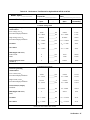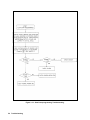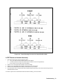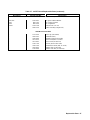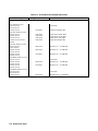
1
SERVICE MANUAL
GPIB DC Power Supplies
Series 657xA and 667xA
For instruments with Serial Numbers:
Agilent Model 6571A: US36520101 and Above *
Agilent Model 6572A: US36350101 and Above *
Agilent Model 6573A: US36330101 and Above *
Agilent Model 6574A: US36340101 and Above *
Agilent Model 6575A: US36340101 and Above *
Agilent Model 6671A: US36400101 and Above *
Agilent Model 6672A: US36390101 and Above *
Agilent Model 6673A: US36380101 and Above *
Agilent Model 6674A: US36370101 and Above *
Agilent Model 6675A: US36370101 and Above *
* For instruments with higher serial numbers, a change page may be included.
For instruments with lower serial numbers, see Appendix A.
Agilent Part No. 5961-2583
Microfiche Part No. 5961-2584
S1
Printed in USA
September 2000
CERTIFICATION
Agilent Technologies certifies that this product met its published specifications at time of shipment from the factory. Agilent
Technologies further certifies that its calibration measurements are traceable to the United States National Bureau of
Standards, to the extent allowed by the Bureau’s calibration facility, and to the calibration facilities of other International
Standards Organization members.
WARRANTY
This Agilent Technologies hardware product is warranted against defects in material and workmanship for a period of three
years from date of delivery. Agilent Technologies software and firmware products, which are designated by Agilent
Technologies for use with a hardware product and when properly installed on that hardware product, are warranted not to
fail to execute their programming instructions due to defects in material and workmanship for a period of 90 days from date
of delivery. During the warranty period Agilent Technologies will, at its option, either repair or replace products which
prove to be defective. Agilent Technologies does not warrant that the operation of the software, firmware, or hardware shall
be uninterrupted or error free.
For warranty service, with the exception of warranty options, this product must be returned to a service facility designated
by Agilent Technologies. Customer shall prepay shipping charges by (and shall pay all duty and taxes) for products returned
to Agilent Technologies for warranty service. Except for products returned to Customer from another country, Agilent
Technologies shall pay for return of products to Customer.
Warranty services outside the country of initial purchase are included in Agilent Technologies product price, only if
Customer pays Agilent Technologies international prices (defined as destination local currency price, or U.S. or Geneva
Export price).
If Agilent Technologies is unable, within a reasonable time to repair or replace any product to condition as warranted, the
Customer shall be entitled to a refund of the purchase price upon return of the product to Agilent Technologies.
LIMITATION OF WARRANTY
The foregoing warranty shall not apply to defects resulting from improper or inadequate maintenance by the Customer,
Customer-supplied software or interfacing, unauthorized modification or misuse, operation outside of the environmental
specifications for the product, or improper site preparation and maintenance. NO OTHER WARRANTY IS EXPRESSED
OR IMPLIED. AGILENT TECHNOLOGIES SPECIFICALLY DISCLAIMS THE IMPLIED WARRANTIES OF
MERCHANTABILITY AND FITNESS FOR A PARTICULAR PURPOSE.
EXCLUSIVE REMEDIES
THE REMEDIES PROVIDED HEREIN ARE THE CUSTOMER’S SOLE AND EXCLUSIVE REMEDIES. AGILENT
SHALL NOT BE LIABLE FOR ANY DIRECT, INDIRECT, SPECIAL, INCIDENTAL, OR CONSEQUENTIAL
DAMAGES, WHETHER BASED ON CONTRACT, TORT, OR ANY OTHER LEGAL THEORY.
ASSISTANCE
The above statements apply only to the standard product warranty. Warranty options, extended support contracts, product
maintenance agreements and customer assistance agreements are also available. Contact your nearest Agilent
Technologies Sales and Service office for further information on Agilent Technologies’ full line of Support Programs.
SAFETY CONSIDERATIONS
GENERAL. This is a Safety Class 1 instrument (provided with terminal for connection to protective earth ground).
OPERATION. BEFORE APPLYING POWER verify that the product is set to match the available line voltage, the correct
line fuse is installed, and all safety precautions (see following warnings) are taken. In addition, note the instrument’s external
markings described under "Safety Symbols".
WARNING.
• Servicing instructions are for use by service-trained personnel. To avoid dangerous electrical shock, do not perform any
servicing unless you are qualified to do so.
• BEFORE SWITCHING ON THE INSTRUMENT, the protective earth terminal of the instrument must be connected to
the protective conductor of the (mains) power cord. The mains plug shall be inserted only in an outlet socket that is
provided with a protective earth contact. This protective action must not be negated by the use of an extension cord
(power cable) that is without a protective conductor (grounding). Grounding one conductor of a two-conductor outlet is
not sufficient protection.
• If this instrument is to be energized via an auto-transformer (for voltage change), make sure the common terminal is
connected to the earth terminal of the power source.
• Any interruption of the protective (grounding) conductor (inside or outside the instrument), or disconnecting of the
protective earth terminal will cause a potential shock hazard that could result in personal injury.
• Whenever it is likely that the protective earth connection has been impaired, this instrument must be made inoperative
and be secured against any unintended operation.
• Only fuses with the required rated current, voltage, and specified type (normal blow, time delay, etc.) should be used.
Do not use repaired fuses or short-circuited fuseholders. To do so could cause a shock or fire hazard.
• Do not operate this instrument in the presence of flammable gases or fumes.
• Do not install substitute parts or perform any unauthorized modification to this instrument.
• Some procedures described in this manual are performed with power supplied to the instrument while its protective
covers are removed. If contacted, the energy available at many points may result in personal injury.
• Any adjustment, maintenance, and repair of this instrument while it is opened and under voltage should be avoided as
much as possible. When this is unavoidable, such adjustment, maintenance, and repair should be carried out only by a
skilled person who is aware of the hazard involved.
• Capacitors inside this instrument may hold a hazardous electrical charge even if the instrument has been disconnected
from its power source.
SAFETY SYMBOLS.
Instruction manual symbol. The instrument will be marked with this symbol when it is necessary for you to refer to the
instruction manual in order to protect against damage to the instrument.
This sign indicates hazardous voltages.
This sign indicates an earth terminal (sometimes used in the manual to indicate circuit common connected to a ground
chassis).
The WARNING sign denotes a hazard. It calls attention to a procedure, practice, or the like, which, if not correctly
performed or adhered to, could result in personal injury. Do not proceed beyond a WARNING sign until the
indicated conditions are fully understood and met.
The CAUTION sign denotes a hazard. It calls attention to an operating procedure, or the like, which, if not correctly
performed or adhered to, could result in damage to or destruction of part or all of the product. Do not proceed
beyond a CAUTION sign until the indicated conditions are fully understood and met.
.
Safety Symbol Definitions
Symbol
Description
Symbol
Description
Direct current
Terminal for Line conductor on permanently
installed equipment
Alternating current
Caution, risk of electric shock
Both direct and alternating current
Caution, hot surface
Three-phase alternating current
Caution (refer to accompanying documents)
Earth (ground) terminal
In position of a bi-stable push control
Protective earth (ground) terminal
(Intended for connection to external
protective conductor.)
Out position of a bi-stable push control
Frame or chassis terminal
On (supply)
Terminal for Neutral conductor on
permanently installed equipment
Off (supply)
Terminal is at earth potential
(Used for measurement and control
circuits designed to be operated with
one terminal at earth potential.)
Standby (supply)
Units with this symbol are not completely
disconnected from ac mains when this switch is
off. To completely disconnect the unit from ac
mains, either disconnect the power cord or have
a qualified electrician install an external switch.
Printing History
The edition and current revision of this manual are indicated below. Reprints of this manual containing minor corrections
and updates may have the same printing date. Revised editions are identified by a new printing date. A revised edition
incorporates all new or corrected material since the previous printing date. Changes to the manual occurring between
revisions are covered by change sheets shipped with the manual. Also, if the serial number prefix of your power supply is
higher than those listed on the title page of this manual, then it may or may not include a change sheet. That is because even
though the higher serial number prefix indicates a design change, the change may not affect the content of the manual.
Edition 1
Edition 2
October 1993
September, 2000
© Copyright 1993, 2000 Agilent Technologies, Inc.
This document contains proprietary information protected by copyright. All rights are reserved. No part of this document
may be photocopied, reproduced, or translated into another language without the prior consent of Agilent Technologies, Inc.
The information contained in this document is subject to change without notice.
Table of Contents
Introduction ............................................................................................................................................................................ 7
Scope .................................................................................................................................................................................. 7
Organization..................................................................................................................................................................... 7
Related Documents .......................................................................................................................................................... 7
Change Sheet................................................................................................................................................................. 7
Operating Manual.......................................................................................................................................................... 7
Instrument Identification..................................................................................................................................................... 8
Manual Revisions............................................................................................................................................................. 8
Firmware Revisions.......................................................................................................................................................... 8
Safety Considerations ......................................................................................................................................................... 8
Conventions ........................................................................................................................................................................ 9
Electrostatic Discharge ....................................................................................................................................................... 9
Verification............................................................................................................................................................................ 11
Introduction....................................................................................................................................................................... 11
Tests.................................................................................................................................................................................. 11
Test Equipment Required.................................................................................................................................................. 11
List of Equipment........................................................................................................................................................... 11
Current-Monitoring Resistor .......................................................................................................................................... 11
Electronic Load .............................................................................................................................................................. 12
Programming The Tests .................................................................................................................................................... 13
General Considerations .................................................................................................................................................. 13
Programming Parameters ............................................................................................................................................ 13
General Measurement Techniques .................................................................................................................................... 13
Performance Test Record Sheets ...................................................................................................................................... 13
Operation Verification Tests............................................................................................................................................. 14
Performance Tests............................................................................................................................................................. 15
Constant Voltage (CV) Tests ......................................................................................................................................... 15
Test Setup.................................................................................................................................................................... 15
Test Procedures ........................................................................................................................................................... 15
Constant Current (CC) Tests .......................................................................................................................................... 19
Test Setup.................................................................................................................................................................... 19
Test Procedures ........................................................................................................................................................... 19
Averaging the CC Measurements................................................................................................................................... 22
Troubleshooting .................................................................................................................................................................... 29
Introduction....................................................................................................................................................................... 29
Localizing the Problem .................................................................................................................................................. 29
Chapter Organization ..................................................................................................................................................... 29
Test Equipment Required.................................................................................................................................................. 30
Troubleshooting Procedures ............................................................................................................................................. 30
Power-On Selftest .......................................................................................................................................................... 30
Description .................................................................................................................................................................. 30
Disabling The Power-On Selftest ................................................................................................................................ 30
Using the *TST? Query (GPIB Systems Supplies Only) ............................................................................................ 30
Troubleshooting Charts.................................................................................................................................................. 32
Troubleshooting Test Points .......................................................................................................................................... 32
Bias and Reference Supplies .......................................................................................................................................... 32
CV/CC Status Annunciators Troubleshooting................................................................................................................ 53
A5 Control Board Troubleshooting Setup ..................................................................................................................... 53
A3 FET Board Troubleshooting .................................................................................................................................... 53
Signature Analysis ............................................................................................................................................................ 56
Introduction.................................................................................................................................................................... 56
Firmware Revisions........................................................................................................................................................ 56
Test Headers .................................................................................................................................................................. 56
Post-Repair Calibration..................................................................................................................................................... 63
When Required .............................................................................................................................................................. 63
Inhibit Calibration Jumper ............................................................................................................................................. 63
Calibration Password ..................................................................................................................................................... 63
Restoring Factory Calibration Constants........................................................................................................................ 63
EEPROM Initialization..................................................................................................................................................... 64
Transferring Calibration Constants To Factory Preset Locations ..................................................................................... 64
Disassembly Procedures ................................................................................................................................................... 69
Top Cover ...................................................................................................................................................................... 69
RFI Shield ...................................................................................................................................................................... 69
Front Panel Assembly .................................................................................................................................................... 70
S1 Line Switch ............................................................................................................................................................... 70
A1 Front Panel Board .................................................................................................................................................... 70
A1DSP1 LCD Display ................................................................................................................................................... 70
A1G1 and A1G2 Rotary Controls .................................................................................................................................. 70
A1KPD Keypad ............................................................................................................................................................. 71
Rear Panel and/or A2 GPIB or Isolator Board............................................................................................................... 71
Output Subchassis .......................................................................................................................................................... 71
A5 Control Board........................................................................................................................................................... 71
A6 Output Filter Board .................................................................................................................................................. 72
A7 Snubber Board and D900 Output Rectifier .............................................................................................................. 72
T900 Output Power Transformer/L900 Output Choke .................................................................................................. 72
AC Input Filter ............................................................................................................................................................... 72
A3 FET Board and Heatsink Assembly ......................................................................................................................... 73
A4 AC Input Board ........................................................................................................................................................ 74
B1 Fan............................................................................................................................................................................ 74
Principles of Operation ........................................................................................................................................................ 77
Introduction....................................................................................................................................................................... 77
INTERFACE CONTROL CIRCUITS.............................................................................................................................. 77
A2 GPIB Board (667xA Series Only)............................................................................................................................ 77
A2 Isolator Board Circuits (657xA Series Only) ........................................................................................................... 78
A1 Front Panel Assembly............................................................................................................................................... 78
A5 Control Board........................................................................................................................................................... 79
Secondary Interface..................................................................................................................................................... 79
CV/CC Control............................................................................................................................................................ 80
Switching/Downprogramming Control ....................................................................................................................... 80
Power Circuits................................................................................................................................................................... 81
A4 AC Input Board ........................................................................................................................................................ 81
Input Filter and Rectifier ............................................................................................................................................. 81
Bias Supplies and Bias Detect..................................................................................................................................... 81
Fan Speed Control....................................................................................................................................................... 82
A3 FET Board................................................................................................................................................................ 82
Output Circuits............................................................................................................................................................... 82
Replaceable Parts ................................................................................................................................................................. 85
INTRODUCTION ............................................................................................................................................................ 85
Chapter Organization ..................................................................................................................................................... 85
Reading the Tables......................................................................................................................................................... 85
How To Order Parts.......................................................................................................................................................... 86
Diagrams ............................................................................................................................................................................. 119
Introduction..................................................................................................................................................................... 119
Chapter Organization ...................................................................................................................................................... 119
General Schematic Notes ................................................................................................................................................ 125
Backdating........................................................................................................................................................................... 147
Index .................................................................................................................................................................................... 159
1
Introduction
Scope
Organization
This manual contains information for troubleshooting and repairing to the component level the following 2-kilowatt power
supplies.
•
•
Agilent Series 657xA manually programmable (bench), and
Agilent Series 667xA GPIB programmable (system) supplies.
The remaining chapters of this manual are organized as follows:
Chapter
Chapter 2
Chapter 3
Chapter 4
Chapter 5
Chapter 6
Appendix A
Description
Verification procedures to determine the performance level of the supply either before or after repair.
Troubleshooting procedures for isolating a problem, procedures for replacing the defective component
and, if required, post-repair calibration and EEPROM initialization procedures.
Principles of power supply operation on a block-diagram level.
Replaceable parts, including parts ordering information.
Diagrams, including schematics, component location drawings, and troubleshooting test points.
Backdating information for power supplies with serial numbers below those listed in the title page of
this manual.
Related Documents
Change Sheet
There may or may not be a Manual Change sheet included with this manual (see Manual Revisions). If one is included, be
sure to examine it for changes to this manual.
Operating Manual
Each power supply is shipped with an operating manual (see Replaceable Parts, Chapter 5 for part numbers) that covers the
following topics:
•
•
•
•
•
•
•
•
•
•
•
•
Options, accessories, specifications, supplementary characteristics, output characteristic curve, typical output
impedance curves.
Connecting the power cord, load, and remote sensing.
Connecting power supplies in series or autoparallel.
Connecting the remote controller and setting the GPIB address.
Configuring the digital port for remote inhibit, relay link, or digital I/O operation.
Connecting the analog port for external voltage programming control.
Turn-on tests, including selftest errors and runtime errors.
Front panel operation.
SCPI programming, an introduction to syntax, language dictionary, and status register operation.
Compatibility-language programming for operation with Agilent Series 603xA power supplies.
Replacement of line fuse and conversion of line voltage.
Calibration procedure (front panel and remote).
Introduction 7
Instrument Identification
The power supply is identified by a unique, two-part serial number, such as, US36320101. The items in this serial number
are explained as follows:
Item
Description
US
Indicates the country of manufacture, where US = USA.
3643
The year and week of manufacture or last significant design change. Add 1960 to the first two
digits to determine the year. For example, 36=1996. The last two digits specify the week of the
year.
0101
A sequential number assigned to each power supply.
Manual Revisions
This manual was written for power supplies that have the same serial prefixes (first part) as those listed on the title page and
whose serial numbers (second part) are equal to or higher than those listed in the title page.
Note
1) If the serial prefix of your supply is higher than that shown in the title page then the supply was made after
the publication of this manual and may have hardware and/or firmware differences not covered in the
manual.
2) If they are significant to the operation and/or servicing of the power supply, those differences are
documented in one or more Manual Changes sheets included with this manual.
3) If the serial prefix on the power supply is lower than that shown on the title page, then the supply was
made before the publication of this manual and can be different from that described here. Such differences
are covered in Appendix A - Manual Backdating Changes.
Firmware Revisions
The power supply’s firmware resides in the main board microprocessor chip and in ROM chips on the A2 GPIB and A1
Front Panel boards. You can obtain the firmware revision number as follows:
•
For a bench power supply, you will find the revision numbers printed on the label affixed to the integrated circuit.
•
For a GPIB system power supply, you can read the integrated circuit label as above, or query the power supply using
the GPIB *IDN query command (see Chapter 3 - Troubleshooting). Also, see Chapter 3, Firmware Revisions for the
actual Agilent BASIC program that does this.
Safety Considerations
This power supply is a Safety Class I instrument, which means it has a protective earth terminal. This terminal must be
connected to earth ground through a power source equipped with a 3-wire, ground receptacle. Refer to the "Safety
Summary" page at the beginning of this manual for general safety information. Before operation or repair, check the power
supply and review this manual for safety warnings and instructions. Safety warnings for specific procedures are located at
appropriate places in the manual.
8 Introduction
Hazardous voltage exist within the power supply chassis, at the output terminals, and at the analog
programming terminals.
Conventions
•
In diagrams, the name of a complementary signal is sometimes shown with a bar above the signal mnemonic. In other
diagrams and in the text, complementary signals are shown with an asterisk (*) after the mnemonic (such as PCLR*). A
mnemonic with a bar over it or an asterisk after it represents the same signal.
•
In this manual, all Agilent 667xA Series supplies are referred to as system supplies. All Agilent 657xA Series supplies
are referred to as bench supplies.
Electrostatic Discharge
The power supply has components that can be damaged by ESD (electrostatic discharge). Failure to
observe standard, antistatic practices can result in serious degradation of performance, even when an
actual failure does not occur.
When working on the power supply observe all standard, antistatic work practices. These include, but are not limited to:
•
•
•
•
•
Working at a static-free station such as a table covered with static-dissipative laminate or with a conductive table mat
(Agilent P/N 9300-0797, or equivalent).
Using a conductive wrist strap, such as Agilent P/N 9300-0969 or 9300-0970.
Grounding all metal equipment at the station to a single common ground.
Connecting low-impedance test equipment to static-sensitive components only when those components have power
applied to them.
Removing power from the power supply before removing or installing printed circuit boards.
Introduction 9
2
Verification
Introduction
This chapter provides test procedures for checking the operation of Agilent Series 667xA GPIB (system) and 657xA
programmable (bench) power supplies. The required test equipment is specified and sample performance test record sheets
are included. Instructions are given for performing the tests either from the front panel or from a controller over the GPIB
for system units.
Tests
Two types of procedures are provided: Operation Verification tests and Performance tests.
Type of Test
Purpose
Operation Verification
These tests do not check all parameters, but comprise a short procedure to verify that the power
supply is performing properly.
Performance
These tests verify all the Specifications (not Supplementary Characteristics) listed in Table 1-1
of the Power Supply Operating Manual.
If you encounter failures or out-of-specification test results, see Troubleshooting Procedures (Chapter 3). The procedures
will determine if repair and/or calibration is required.
Note
The power supply must pass the selftest at power-on before the following tests can be performed. If the
power supply fails selftest, go to Chapter 3.
Test Equipment Required
List of Equipment
Table 2-1 lists the equipment required to perform the tests given in this chapter. Only the equipment marked with the
superscript "1’’ is needed for the Operation Verification test.
Current-Monitoring Resistor
The four-terminal, current-monitoring resistor listed in Table 2-1 is required to eliminate output current measurement error
caused by voltage drops in leads and connections. The specified load resistors have special current-monitoring terminals
inside the load connection terminals. Connect the AC or DC voltmeter directly to these current-monitoring terminals.
Verification 11
Table 2-1. Test Equipment Required
Type
Digital Voltmeter1
Current Monitor Resistor1
DC Power Supply
Electronic Load
Required Characteristics
Recommended Model
Resolution: 10 nV @ 1V
Readout: 8 1/2 digits
Accuracy: 20 ppm
Agilent 6571A, 6671A:
0.001Ω ± 0.04%, 300A, 100W
Agilent 3458A
Agilent 6572A-6575A, 6672A6675A
0.01Ω ± 0.04%, 100A, 100W
5V @10A
Range: Voltage and current range
must exceed that of supply under test.
Power: 2KW minimum
Guildline 9230/100
Agilent 6571A-6574A, 6671A6674A
Guildline 9230/300
Agilent 6653A
(1) Agilent 6050B, mainframe with
(3) Agilent 6040A modules.
Agilent 6575A, 6675A
(2) Agilent 6050B, mainframe with
(3) Agilent 60507B modules plus
(1) Agilent 6051A mainframe with
(1) 60507B module.
Oscilloscope
Sensitivity: 1mV
Bandwidth Limit: 20MHz
Probe: 1:1 with RF tip
Agilent 54504A
RMS Voltmeter
True RMS Bandwidth: 20MHz
Sensitivity: 100 µV
Agilent 3400B
Variable-Voltage Transformer
Power: 4KVA minimum
GPIB Controller*
Range: -13% to +6% of input
Full GPIB capabilities
HP Series 300 or Vectra with and
GPIB card
1
Required for Operation Verification Tests.
*Required for remote testing of 667xA models.
Electronic Load
Many of the test procedures require the use of a variable load capable of dissipating the required power. If a variable
resistor is used, switches must be used for connecting, disconnecting, and shorting the load resistor. For most tests, an
electronic load (see Table 2-1) is easier to use than a variable resistor. However, an electronic load may not be fast enough
for testing transient recovery time or may be too noisy for testing noise (PARD). In these cases, fixed load resistors of
suitable power dissipation can be used with minor changes to the test procedures given in this chapter.
12 Verification
Programming the Tests
General Considerations
Procedures are given for programming these tests either from the front panel keypad or from a GPIB controller for a GPIB
controller for 667xA system supplies. The procedures assume you know how to use the front panel keypad or how to
program over the GPIB (see the Power Supply Operating Manual for more information). When using computer-controlled
tests, you may have to consider the relatively slow (compared to computer and system voltmeters) settling times and slew
rates of the power supply. Suitable WAIT statements can be inserted into the test program to give the power supply time to
respond to the test commands.
Hazardous voltages may be present at the power supply output during these tests. They should be performed
only by qualified electronics personnel.
Programming Parameters
Table 2-2 lists the programming voltage and current values for each model. You can enter these values either from the front
panel or from a controller over the GPIB (for system power supplies).
Table 2-2. Programming Voltage and Current Values
Agilent Model
Agilent 6571A, 6671A
Agilent 6572A, 6672A
Agilent 6573A, 6673A
Agilent 6574A, 6674A
Agilent 6575A, 6675A
Full Scale
Voltage
8V
20V
35V
60V
120V
Max. Prog.
Voltage
8.190V
20.475V
35.80V
61.425V
123.0V
Full Scale
Current
220A
100A
60A
35A
18A
Max. Prog.
Current
225.23A
102.375A
61.425A
35.83A
18.5A
Max. Prog.
Overvoltage
10V
24V
42V
72V
144V
-CC
Current
10A
10A
5A
4A
2.5A
General Measurement Techniques
Figure 2-1 shows the setup for most tests. Measure the dc output voltage directly at the sense (+S and -S) terminals. Connect
these terminals for remote sensing (to the +LS and -LS terminals). Be certain to use load leads of sufficient wire gauge to
carry the output current (see Chapter 4 of the Power Supply Operating Manual). To avoid noise pickup, use coaxial cable or
shielded pairs for the test leads. If you use more than one meter or a meter and an oscilloscope, connect separate leads for
each instrument to avoid mutual-coupling effects.
Performance Test Record Sheets
When performing the tests in this chapter, refer to the Performance Test Record sheets supplied at the end of this chapter.
Table 2-6 is for recording common information, such as, the test equipment used and the environmental conditions. Tables
2-7 through 2-11 are dedicated to specific models and contain the acceptable test values and ranges. A place is provided to
record the results of the test.
Verification 13
Figure 2-1. Constant Voltage (CV) Test Setup
Note
It is recommended that before you perform the tests in either Table 2-4 or Table 2-5, that you first locate
the appropriate Performance Test Record sheet from Tables 2-7 through Table 2-11 for your specific
model. Make a copy of this sheet, and record the actual observed values in it while performing the tests.
Use the sheets in Tables 2-7 through Table 2-11 as master reference sheets to run copies at any time.
Operation Verification Tests
Table 2-3 lists the requirements for operation verification, which is a subset of the performance tests.
Table 2-3. Operation Verification Tests
Test
Refer To
1
Turn-On Checkout
Power Supply Operating Manual
2
Voltage Programming and Readback Accuracy
Table 2-4
3
Current Programming and Readback Accuracy
Table 2-5
Record the results of Tests 2 and 3 in the appropriate Performance Test Record sheets.
14 Verification
Performance Tests
Performance tests check all the specifications of the power supply. The tests are grouped into constant-voltage mode tests
(Table 2-4) and constant-current mode tests (Table 2-5).
Constant Voltage (CV) Tests
Test Setup
Connect your dc voltmeter leads to only +S and -S (see Figure 2-1), because the power supply regulates the voltage between
these points, not between the + and - output terminals .
Test Procedures
Perform the test procedures in Table 2-4. The CV tests are:
•
•
•
•
•
Voltage Programming and Readback Accuracy.
CV Load Effect.
CV Source Effect.
CV Noise (PARD).
Transient Recovery Time.
Note
The tests are independent and may be performed in any order.
Verification 15
Table 2-4. Constant Voltage (CV) Tests
Action
Normal Result
Voltage Programming and Readback Accuracy
This test verifies that the voltage programming, GPIB readback (GPIB system power supplies only), and front panel display
functions are within specifications. With system power supplies, values read back over the GPIB should be the same as
those displayed on the front panel.
1
Turn off the power supply and connect a DVM across +LS and -LS
(see Figure 2-1A).
2
Turn on the power supply with no load and program the output for 0 volts
and maximum programmable current (see Table 2-2).
CV annunciator on. Output current near
0.
3
Record voltage readings at DVM and on front panel display.
Readings within specified Low Voltage
limits.
4
Program voltage to full scale (see Table 2-2).
5
Record voltage readings of DVM and on front panel display.
Readings within specified High Voltage
limits.
CV Load Effect
This test measures the change in output voltage resulting from a change in output current from full-load to no-load.
1
Turn off the power supply and connect a DVM across +LS and -LS
(see Figure 2-1A).
2
Turn on the power supply and program the current to its maximum
programmable value and the voltage to its full-scale value (see Table 2-2).
3
Adjust the load to produce full-scale current (see Table 2-2) as shown on
the front panel display.
4
Record voltage reading of the DVM.
5
Adjust load to draw 0 amperes (open load). Record voltage reading of the
DVM.
6
Check test result.
CV annunciator is on. If it is not, adjust
the load to slightly reduce the output
current until the annunciator comes on.
The difference between the DVM
readings in steps 4 and 5 are within the
specified Load Effect limits.
CV Source Effect
This test measures the change in output voltage resulting from a change in ac line voltage from its minimum to maximum
value within the line voltage specifications.
1
Turn off the power supply and connect the ac power input through a
variable-voltage transformer.
16 Verification
Table 2-4. Constant Voltage (CV) Tests (continued)
Action
Normal Result
CV Source Effect (cont)
2
Set the transformer to the nominal ac line voltage. Connect the DVM
across +LS and -LS (see Figure 2-1A).
3
Turn on the power supply and program the current to its maximum
programmable value and the voltage to its full-scale value (see Table 2-2).
4
Adjust the load to produce full-scale current (see Table 2-2) as shown on
the front panel display.
5
Adjust the transformer to decrease the ac input voltage to the low-line
condition (174Vac or 191Vac). Record the output voltage reading of the
DVM.
6
Adjust the transformer to increase the ac input voltage to the high-line
condition (220Vac or 250Vac). Record the output voltage reading on the
DVM.
7
Check test result.
CV annunciator is on. If it is not, adjust
the load to slightly reduce the output
current until the annunciator comes on.
The difference between the DVM
readings in steps 5 and 6 are within the
specified Source Effect limits.
CV Noise (PARD)
Periodic and random deviations (PARD) in the output (ripple and noise) combine to produce a residual ac voltage
superimposed on the dc output voltage. This test measures CV PARD, specified as the rms and peak-to-peak output voltages
over the frequency range of 20Hz to 20MHz.
1
Turn off the power supply and connect an a-c coupled oscilloscope across
the + and -output terminals (see Figure 2-1A). Set the oscilloscope
bandwidth limit to 20MHz (30MHz for the Agilent 54504A) and use an
RF tip on the oscilloscope probe.
2
Turn on the power supply and program the current to its maximum
programmable value and the voltage to its full-scale value (see Table 2-2).
3
Adjust the load to produce full-scale current (see Table 2-2) as shown on
the front panel display.
CV annunciator is on. If it is not, adjust
the load to slightly reduce the output
current until the annunciator comes on.
4
Record the amplitude of the waveform.
Amplitude is within the specified PARD
Peak-to-Peak limits.
5
Replace the oscilloscope connection with an ac rms voltmeter.
6
Record the reading obtained in Step 5.
Amplitude is within the specified PARD
rms limits.
Verification 17
Table 2-4. Constant Voltage (CV) Tests (continued)
Action
Normal Result
Transient Recovery Time
This test measures the time required for the output voltage to return to within 100mV of its final value following a 50%
change in output load current. Measurements are made on both the unloading transient (from full load to 1/2 load) and the
loading transient (from 1/2 load to full load).
1
Turn off the power supply and connect an oscilloscope across +LS and
-LS (see Figure 2-1A).
2
Turn on the power supply and program the current to its maximum
programmable value and the voltage to its full-scale value (see Table 2-2).
3
Program the Electronic Load as follows:
þ
þ
þ
þ
þ
Operating mode to constant current.
Input load current to 1/2 the supply’s full rated output current.
Transient current level to the supply’s full rated output current.
Transient generator frequency = 100Hz.
Transient generator duty cycle = 50%.
4
Turn on the transient and adjust the oscilloscope to display response
waveform.
See Figure 2-2.
5
Measure both the loading and unloading transients by triggering the
oscilloscope on both the negative and positive slopes of the transient.
Record the voltage level obtained at the 900-µs interval .
Specified voltage level is reached within
900µs.
Figure 2-2. Transient Response Waveform
18 Verification
Constant Current (CC) Tests
Test Setup
Connect the appropriate current monitoring resistor (see Table 2-l) as shown in Figure 2-1B. The accuracy of the resistor
must be as specified in the table.
Test Procedures
The test procedures are given in Table 2-5. The tests are independent and may be performed in any order. The CC tests are:
•
•
•
•
•
Current Programming and Readback Accuracy.
Current Sink (-CC) Operation.
CC Load Effect.
CC Source Effect.
CC Noise (PARD).
Table 2-5. Constant Current (CC) Tests
Action
Normal Result
Current Programming and Readback Accuracy
This test verifies that the current programming and readback are within specification.
1
Turn off the power supply and connect the current monitoring resistor as
shown in Figure 2-1B. Connect a DVM across the resistor.
2
Turn on the power supply and program the output for 5 volts and 0
amperes.
3
Short the load.
4
Observe the DVM voltage reading. Divide this by the resistance of the
current monitor resistor. Record the result as the Low Current value.
Value within specified Low Current
limits.
5
Record the front panel display readback.
Value within specified readback limits.
6
Program output current to full scale (see Table 2-2).
7
Repeat Steps 4 and 5.
Both current readings within specified
High Current and readback limits.
Current Sink (CC-) and Readback Accuracy
This test verifies current sink operation and readback accuracy.
1
Turn off the power supply. Connect the output as shown in Figure 2-1B,
except replace the Electronic Load with the external test supply specified
in Table 2-1.
2
Set the external supply to 5 volts and its current limit to the -CC value of
the power supply under test (see Table 2-2).
3
Turn on the power supply under test and program its output voltage to 0.
Verification 19
Table 2-5. Constant Current (CC) Tests (continued)
Action
Normal Result
Current Sink (CC-) and Readback Accuracy (cont)
4
Observe the DVM voltage reading. Divide this by the resistance of the
current monitor resistor to obtain the current sink value.
5
Subtract the current value obtained in Step 4 from the current reading on
Value within Current Sink Display
the power supply display. Record the difference as the Current Sink
Readback limits.
Display Readback.
CC Noise (PARD)
Periodic and random deviations (PARD) in the output (ripple and noise) combine to produce a residual ac current
superimposed on the dc output current. This test measures CC PARD, specified as the rms output current over the frequency
range of 20 Hz to 20 MHz.
1
Turn off the power supply and connect the current monitoring resistor and
rms voltmeter (see Figure 2-1). Make the test leads as short as possible to
reduce noise pickup.
2
Measure the residual noise on the RMS voltmeter with the power supply
turned off. Noise generated by other equipment may affect this
measurement and should be removed or factored out.
3
Turn on the power supply and program the current to its full scale value
and the voltage to its maximum programmable value (see Table 2-2).
4
Adjust the load in the CV mode for full-scale voltage (see Table 2-2) as
shown on the front panel display.
The power supply output current should
be at its full-scale value and the CC
annunciator on. If it is not, adjust the
load to slightly reduce the output
voltage until the annunciator comes on.
5
Observe the reading on the rms voltmeter. Divide this voltage by the
resistance of the current monitoring resistor to obtain the rms noise
current.
Current is within the specified PARD
rms limits.
CC Load Effect
This test measures the change in output current resulting from a change in load from full-load voltage to a short circuit. It is
recommended that you use averaged readings for Steps 4 and 5 of this test (see Averaging AC Measurements at the end of
this chapter).
1
Turn off the power supply and connect a DVM across the current
monitoring resistor (see Figure 2-1).
2
Turn on the power supply and program the current to its full scale value
and the voltage to its maximum programmable value (see Table 2-2).
3
Set the Electronic Load to CV mode and its voltage to full scale as
indicated on its front panel display.
20 Verification
Power supply output current is full scale
and its CC annunciator is on. If not,
reduce the Electronic Load voltage
slightly until the annunciator comes on.
Table 2-5. Constant Current (CC) Tests (continued)
Action
Normal Result
CC Load Effect (cont)
4
Observe the DVM reading. Divide this by the resistance of the current
monitoring resistor to obtain the output current. Record the result.
You may want to use an averaged
reading for this measurement.
5
Short the Electronic Load input and repeat Step 4.
You may want to use averaged reading
for this measurement.
6
Check the result.
The difference between the current
readings taken in Step 4 and Step 5 must
be within specified “Load Effect” limits.
CC Source Effect
This test measures the change in output current resulting from a change in ac line voltage from its minimum to its maximum
value within the line voltage specifications. It is recommended that you use averaged readings for Steps 6 and 8 of this test
(see "Averaging AC Measurements" at the end of this chapter).
1
Turn off the power supply and connect the ac power input through a
variable-voltage transformer.
2
Set the transformer to the nominal ac line voltage. Connect the DVM
across the current monitoring resistor (see Figure 2-1).
3
Turn on the power supply and program the current to its full-scale value
and the voltage to its maximum programmable value (see Table 2-2).
4
Set the Electronic Load to CV mode and its voltage to full scale.
5
Adjust the transformer to decrease the ac input voltage to the low-line
condition (174Vac or 191Vac).
6
Observe the DVM reading. Divide this voltage by the resistance of the
current monitoring resistor to obtain the output current. Record the result.
7
Adjust the transformer to increase the ac input voltage to the high-line
condition (220Vac or 250Vac).
8
Observe the DVM reading. Divide this voltage by the resistance of the
current monitoring resistor to obtain the output current. Record the result.
You may want to use an averaged
reading for this measurement.
9
Check the test result.
The difference between the current
readings found in Step 6 and Step 8 is
within the specified current Source
Effect limits.
The power supply output current is full
scale and its CC annunciator is on. If
not, reduce the Electronic Load voltage
slightly until the annunciator comes on.
You may want to use an averaged
reading for this measurement.
Verification 21
Averaging the CC Measurements
The CC Load Effect and CC Source Effect tests measure the dc regulation of the power supply’s output current. When doing
these tests, you must be sure that the readings taken are truly dc regulation values and not instantaneous ac peaks of the
output current ripple. You can do this by making each measurement several times and then using the average of the
measurements as your test value. Voltmeters such as the Agilent 3458A System Voltmeter can be programmed to take just
such statistical average readings as required by these tests.
The following steps show how to set up the voltmeter from its front panel to take a statistical average of l00 readings.
represents the unlabeled shift key in the FUNCTION/RANGE group.
1.
2.
3.
5.
Program 10 power line cycles per sample by pressing
Program 100 samples per trigger by pressing
Set up voltmeter to take measurements in the statistical mode as follows:
.
a. Press
until MATH function is selected, then press
.
b. Press
until STAT function is selected, then press
.
c. Press
Now set up voltmeter to read the average of the measurements as follows:
.
a. Press
until RMATH function is selected, then press
.
b. Press
until MEAN function is selected, then press
.
c. Press
Execute the average reading program by pressing
6.
Wait for 100 readings and then read the average measurement by pressing
4.
Record this as your result.
22 Verification
.
.
.
.
Table 2-6. Performance Test Record Form
Test Facility:
__________________________________________
__________________________________________
__________________________________________
__________________________________________
Model_____________________________________
Serial No.__________________________________
Options ___________________________________
Firmware Revision___________________________
Report No.__________________________________________
Date______________________________________________
Customer___________________________________________
Tested By___________________________________________
Ambient Temperature (°C)______________________________
Relative Humidity (%)_________________________________
Nominal Line Frequency (Hz)___________________________
Special Notes:
____________________________________________________________________________________________
____________________________________________________________________________________________
____________________________________________________________________________________________
____________________________________________________________________________________________
____________________________________________________________________________________________
____________________________________________________________________________________________
____________________________________________________________________________________________
____________________________________________________________________________________________
____________________________________________________________________________________________
Test Equipment Used:
Description
Model No.
Trace No.
Cal. Due Date
1. AC Source
_______________
_______________
_________________
2. DC Voltmeter
_______________
_______________
_________________
3. RMS Voltmeter
_______________
_______________
_________________
4. Oscilloscope
_______________
_______________
_________________
5. Electronic Load
_______________
_______________
_________________
6. Current Monitoring
Shunt
_______________
_______________
_________________
Verification 23
Table 2-7. Performance Test Record for Agilent Model 6571A or 6671A
MODEL Agilent_____________
Report No.______________
Test Description
Minimum
Spec.
Results
*
Date_____________________
Maximum
Spec.
Measurement
Uncertainty
Constant Voltage Tests
Voltage Programming
and Readback
Low Voltage (0V) Vout
Front Panel Display Readback
-8mV
Vout - 12mV
________mV
________mV
+8mV
Vout + 12mV
1.6µV
1.6µV
High Voltage (8V) Vout
Front Panel Display Readback
7.9888V
Vout - 16mV
_________V
_______mV
8.0012V
Vout + 16mV
88µV
88µV
Load Effect
Vout - 0.46mV
_______mV
Vout + 0.46mV
1µV
Source Effect
Vout - 0.46mV
_______mV
Vout + 0.46mV
1µV
0
0
_______mV
_______µV
7mV
650µV
872µV
50µV
0
_______mV
100mV
12mV
PARD (Ripple and Noise)
Peak-to-Peak
RMS
Transient Response Time
(at 900 µs)
Constant Current Tests
Current Programming
and Readback
Low Current (0A) Iout
Front Panel Display Readback
-125mA
Iout - 150mA
_______mA
_______mA
+125mA
Iout + 150mA
1.5µA
1.5µA
High Current (220A) Iout
Front Panel Display Readback
219.655A
Iout - 370mA
_________A
_______mA
+220.345A
Iout + 370mA
68.5mA
68.5mA
Isink - 160mA
________mA
Isink + 160mA
2.6mA
0
________mA
200mA
50mA
Load Effect
Iout - 21mA
________mA
Iout + 21mA
166µA
Source Effect
Iout - 21mA
________mA
Iout + 21mA
166µA
Current Sink (10A) Display
Readback
PARD (Ripple and Noise)
RMS
*Enter your test results in this column.
24 Verification
Table 2-8. Performance Test Record for Agilent Model 6572A or 6672A
MODEL Agilent_____________
Report No.______________
Test Description
Minimum
Spec.
Results
*
Date_____________________
Maximum
Spec.
Measurement
Uncertainty
Constant Voltage Tests
Voltage Programming
and Readback
Low Voltage (0V) Vout
Front Panel Display Readback
-20mV
Vout - 30mV
________mV
________mV
+20mV
Vout + 30mV
2µV
2µV
High Voltage (20V) Vout
Front Panel Display Readback
19.972V
Vout - 40mV
_________V
_______mV
20.028V
Vout + 40mV
335µV
335µV
Load Effect
Vout - 1.1mV
_______mV
Vout + 1.1mV
20µV
Source Effect
Vout - 1.1mV
_______mV
Vout + 1.1mV
20µV
0
0
_______mV
_______µV
9mV
750µV
904µV
50µV
0
_______mV
100mV
12mV
PARD (Ripple and Noise)
Peak-to-Peak
RMS
Transient Response Time
(at 900 µs)
Constant Current Tests
Current Programming
and Readback
Low Current (0A) Iout
Front Panel Display Readback
-60mA
Iout - 100mA
_______mA
_______mA
+60mA
Iout + 100mA
157µA
157µA
High Current (100A) Iout
Front Panel Display Readback
99.84A
Iout - 200mA
_________A
_______mA
+100.16A
Iout + 200mA
41mA
41mA
Isink -110mA
________mA
Isink +110mA
1.3mA
0
________mA
100mA
15mA
Load Effect
Iout - 12mA
________mA
Iout + 12mA
40µA
Source Effect
Iout - 12mA
________mA
Iout + 12mA
40µA
Current Sink (10A) Display
Readback
PARD (Ripple and Noise)
RMS
*Enter your test results in this column.
Verification 25
Table 2-9. Performance Test Record for Agilent Model 6573A or 6673A
MODEL Agilent_____________
Report No.______________
Test Description
Minimum
Spec.
Results
*
Date_____________________
Maximum
Spec.
Measurement
Uncertainty
Constant Voltage Tests
Voltage Programming
and Readback
Low Voltage (0V) Vout
Front Panel Display Readback
-35mV
Vout - 50mV
________mV
________mV
+35mV
Vout + 50mV
2µV
2µV
High Voltage (35V) Vout
Front Panel Display Readback
34.951V
Vout - 68mV
_________V
_______mV
35.049V
Vout + 68mV
526µV
526µV
Load Effect
Vout - 1.9mV
_______mV
Vout + 1.9mV
27µV
Source Effect
Vout - 1.9mV
_______mV
Vout + 1.9mV
27µV
0
0
_______mV
_______µV
9mV
800µV
904µV
50µV
0
_______mV
100mV
12mV
PARD (Ripple and Noise)
Peak-to-Peak
RMS
Transient Response Time
(at 900 µs)
Constant Current Tests
Current Programming
and Readback
Low Current (0A) Iout
Front Panel Display Readback
-40mA
Iout - 60mA
_______mA
_______mA
+40mA
Iout + 60mA
154µA
154µA
High Current (60A) Iout
Front Panel Display Readback
59.9A
Iout - 120mA
_________A
_______mA
+60.1A
Iout + 120mA
15mA
15mA
Isink -65mA
________mA
Isink +65mA
0.7mA
0
________mA
40mA
5mA
Load Effect
Iout - 7mA
________mA
Iout + 7mA
28µA
Source Effect
Iout - 7mA
________mA
Iout + 7mA
28µA
Current Sink (5A) Display
Readback
PARD (Ripple and Noise)
RMS
*Enter your test results in this column.
26 Verification
Table 2-10. Performance Test Record for Agilent Model 6574A or 6674A
MODEL Agilent_____________
Report No.______________
Test Description
Minimum
Spec.
Results
*
Date_____________________
Maximum
Spec.
Measurement
Uncertainty
Constant Voltage Tests
Voltage Programming
and Readback
Low Voltage (0V) Vout
Front Panel Display Readback
-60mV
Vout - 90mV
________mV
________mV
+60mV
Vout + 90mV
2.2µV
2.2µV
High Voltage (60V) Vout
Front Panel Display Readback
59.916V
Vout - 120mV
_________V
_______mV
60.084V
Vout + 120mV
0.8mV
0.8mV
Load Effect
Vout - 3.2mV
_______mV
Vout + 3.2mV
40µV
Source Effect
Vout - 3.2mV
_______mV
Vout + 3.2mV
40µV
0
0
_______mV
_______mV
11mV
1.3mV
904µV
150µV
0
_______mV
100mV
12mV
PARD (Ripple and Noise)
Peak-to-Peak
RMS
Transient Response Time
(at 900 µs)
Constant Current Tests
Current Programming
and Readback
Low Current (0A) Iout
Front Panel Display Readback
-25mA
Iout - 35mA
_______mA
_______mA
+25mA
Iout + 35mA
153µA
153µA
High Current (35A) Iout
Front Panel Display Readback
34.94A
Iout - 70mA
_________A
_______mA
+35.06A
Iout + 70mA
5.7mA
5.7mA
Isink -39mA
________mA
Isink +39mA
0.6mA
0
________mA
25mA
5mA
Load Effect
Iout - 3.75mA
________mA
Iout + 3.75mA
21µA
Source Effect
Iout - 3.75mA
________mA
Iout + 3.75mA
21µA
Current Sink (4A) Display
Readback
PARD (Ripple and Noise)
RMS
*Enter your test results in this column.
Verification 27
Table 2-11. Performance Test Record for Agilent Model 6575A or 6675A
MODEL Agilent_____________
Report No.______________
Test Description
Minimum
Spec.
Results
*
Date_____________________
Maximum
Spec.
Measurement
Uncertainty
Constant Voltage Tests
Voltage Programming
and Readback
Low Voltage (0V) Vout
Front Panel Display Readback
-120mV
Vout - 180mV
________mV
________mV
+120mV
Vout + 180mV
3µV
3µV
High Voltage (120V) Vout
Front Panel Display Readback
119.832V
Vout - 240mV
_________V
_______mV
120.168V
Vout + 240mV
1.7mV
1.7mV
Load Effect
Vout - 6.4mV
_______mV
Vout + 6.4mV
230µV
Source Effect
Vout - 6.4mV
_______mV
Vout + 6.4mV
230µV
0
0
_______mV
_______mV
16mV
1.9mV
1mV
150µV
0
_______mV
100mV
12mV
PARD (Ripple and Noise)
Peak-to-Peak
RMS
Transient Response Time
(at 900 µs)
Constant Current Tests
Current Programming
and Readback
Low Current (0A) Iout
Front Panel Display Readback
-12mA
Iout - 18mA
_______mA
_______mA
+12mA
Iout + 18mA
151µA
151µA
High Current (18A) Iout
Front Panel Display Readback
17.97A
Iout - 36mA
_________A
_______mA
+18.03A
Iout + 36mA
2.4mA
2.4mA
Isink -20.5mA
________mA
Isink +20.5mA
0
________mA
12mA
5mA
Load Effect
Iout - 1.9mA
________mA
Iout + 1.9mA
15µA
Source Effect
Iout - 1.9mA
________mA
Iout + 1.9mA
15µA
Current Sink (2.5A) Display
Readback
PARD (Ripple and Noise)
RMS
430µA
*Enter your test results in this column.
28 Verification
3
Troubleshooting
Shock Hazard: Most of the procedures in this chapter must be performed with power applied and
protective covers removed. These procedures should be done only by trained service personnel aware of
the hazard from electrical shock.
This instrument uses components that can be damaged or suffer serious performance degradation due to
ESD (electrostatic discharge). Observe standard antistatic precautions to avoid damage to the
components (see Chapter 1).
Introduction
Localizing the Problem
This chapter provides troubleshooting and repair information for the power supply. Before beginning troubleshooting
procedures, make certain the problem is in the power supply and not with an associated circuit, the GPIB controller (for
system power supplies), or ac input line. Without removing the covers, you can use the Verification tests in Chapter 2 to
determine if the power supply is operating normally.
Chapter Organization
The information in this chapter is organized as follows:
Topic
Test Equipment Required
Troubleshooting Procedures
Information Given
Equipment required for completing all the tests in this chapter.
A series of flow charts for systematic location of defective boards, circuits, and
components.
An explanation of the error codes and messages generated during the power-on
selftest.
Signature analysis techniques for troubleshooting the digital circuits on the front panel.
primary, and secondary interface circuits .
Specific paragraphs for:
•
Checking the bias and reference supplies.
•
Troubleshooting the CV/CC status annunciators.
•
Troubleshooting the A3 FET board.
Post-Repair Adjustments
Calibration and EEPROM initialization procedures required after the replacement of
certain critical components.
Disassembly Procedures
Gaining access to and/or replacing components.
Troubleshooting 29
Test Equipment Required
Table 3-1. Test Equipment Required
Equipment
Logic Probe
Test Clips
Ammeter/Current Shunt
Purpose
To check states of data lines.
To gain access to IC pins.
To measure output current.
Oscilloscope
Signature Analyzer
To check waveforms and signal levels.
To troubleshoot most of the primary
and secondary interface circuits.
To communicate with power supply via
the GPIB (for system units).
To measure output voltage and current,
bias and references.
GPIB Controller
DC Voltmeter
Recommended Model
Agilent 545A
AP Products No. LTC
Agilent 6571A & 6671A:
Guildline 9230/300
Agilent 6572A-75A & 6672A-75A:
Guildline 9230/100
Agilent 54504A
Agilent 5005A/B
Agilent BASIC Series
Agilent 3458A
Troubleshooting Procedures
Power-On Selftest
Description
The procedures in the troubleshooting charts make use of the power-on selftest. The power-on selftest tests the front panel,
GPIB interface (for GPIB system power supplies) or Isolator Board (bench supplies), and secondary interface circuits. If the
power supply fails the selftest, the output remains disabled (turned off) and the front panel normally displays an error code
or message (see Table 3-2). The message is displayed indefinitely and the power supply will not accept GPIB or front panel
commands.
Disabling The Power-On Selftest
In order to perform troubleshooting procedures that require programming of the power supply, you must disable the
power-on selftest. Do this as follows:
1.
2.
3.
4.
Turn off the power supply.
key and turn on the supply.
Hold down the
Continue holding down the
for 2 seconds and wait until the PWR ON INIT indicator goes off.
The power supply is now on without executing power-on selftest.
Using the *TST? Query (GPIB Systems Supplies Only)
You can get the power supply to execute a partial selftest by sending it the GPIB *TST? query command. Table 3-2 shows
the tests that are performed in response to this command. These tests do not interfere with normal operation or cause the
output to change. The command returns a value of "0" if all tests pass. Otherwise, the command returns the error code of the
first test that failed. No error codes are displayed on the front panel and the power supply will attempt to continue normal
operation.
30 Troubleshooting
Table 3-2. Selftest Error Codes/Messages
Code and/or
Message
El FP RAM
E2 FP ROM
E3 EE CHKSM
E4 PRI XRAM**1
E5 PRI IRAM**
E6 PRI ROM**
E7 GPIB **
E8 SEC RAM
E9 SEC ROM
E10 SEC 5V
E11 TEMP
E12 DACS
Description
Front panel RAM test failed (power-on)
Front panel ROM test failed (power-on and
*TST?)
Front panel EEPROM checksum test failed
(power-on and *TST?)
Primary interface external RAM test failed
(power-on)
Primary interface internal RAM test failed
(power-on)
Primary interface ROM test failed
(power-on and *TST?)
GPIB interface test failed (power-on)
Secondary interface RAM test failed
(power-on)
Secondary interface ROM test failed
(power-on and *TST?)
Secondary interface 5 volt readback test
failed (power-on and *TST?)
Ambient temperature readback test failed
(power-on and *TST?)
CV or CC DAC tests failed (power-on)
Probable Cause Selftest Error
Codes/Messages
Microprocessor A1U3
ROM AlU4 or address latches AlU8
Possibly due to power loss during a write operation.
See Checksum Errors in Chapter 3 of Operating
Manual. If power loss is not the problem, EEPROM
A1U6 could be defective. (If you replace AlU6, the
power supply must be reinitialized and calibrated.)
RAM A2U108
Microprocessor A2U114
ROM A2U106
Talker/listener A2U117
Microprocessor A5U504
Microprocessor A5U504
Comparators A5U513, readback DAC
A5U511/U512, or secondary bias supply (5Vs
A4U304)
Thermistor A5RT770 or comparator
A5U513
CV DAC A5U507/U508 or CC DAC
A5U509/U510 (see Figure 3-7)
NOTE: The following error messages can appear due to a failure occurring either while the power supply is operating or
during selftest.
SERIAL TIMOUT
Serial data line failure on A2 board
See Figure 3-10 (system) or Figure 3-11 (bench).
SERIAL DOWN
Serial data line failure on A2 board
See Figure 3-10 (system) or Figure 3-11 (bench).
UART PARITY**
UART failed
UART A2U112
UART FRAMING**
UART failed
UART A2U112
UART OVERRUN**
UART failed
UART A2U112
SBUF OVERRUN**
Serial buffer failure UART
SBUF FULL**
Serial buffer failure
EE WRITE ERR
EEPROM write failure
UART A2U112 defective or GPIB board is in SA
mode
UART A2U112 defective or GPIB board is in SA
mode
EEPROM AlU6 defective or calibration error
SECONDARY DN
Serial data line failure on Main board
See Figure 3-12.
1
A double asterisk indicates that the item applies only to 667xA system supplies.
Troubleshooting 31
Troubleshooting Charts
Figure 3-1 gives overall troubleshooting procedures to isolate the fault to a circuit board or particular circuit (see Figure
3-20 for the location of the circuit boards). These procedures include the use of power-on selftest (Table 3-2) and signature
analysis techniques (Table 3-5 through Table 3-7). Some results of Figure 3-1 lead to more detailed troubleshooting charts
that guide you to specific components. The troubleshooting charts are organized as follows:
Chart
Figure 3-1
Figure 3-2
Figure 3-3
Figure 3-4
Figure 3-5
Figure 3-6
Figure 3-7
Figure 3-8
Figure 3-9
Figure 3-10
Figure 3-11
Figure 3-12
Figure 3-13
Trouble or Circuit
Overall procedure checks selftest errors, calibration errors, ac input circuit, fan, readback circuits,
A5 Control Board, GPIB cable, digital port, serial link, rotary controls, current amplifier.
No display (from Figure 3-1).
OV circuit not firing (from Figure 3-1).
OV circuit is on at turn-on (from Figure 3-1).
Output level is held low (from Figure 3-1).
Output level is held high (from Figure 3-1).
DAC circuits (from Figure 3-1).
DAC test waveforms.
CV and CC DAC and amplifiers (from Figure 3-1).
Serial interface circuit (from Figure 3-1).
Isolator board circuits.
Secondary interface down (from Figure 3-1).
Slow downprogramming circuit (from Figure 3-1).
Troubleshooting Test Points
The troubleshooting charts reference test points listed in Table 6-3 of Chapter 6. Test points are identified by an encircled
number (such as ⑤ in schematic diagrams and component location drawings, also in Chapter 6).
Bias and Reference Supplies
Many of the following troubleshooting procedures begin by checking the bias and/or reference voltages. Table 6-3 lists the
test points for these voltages and gives the correct reading for each. The circuit board component location diagrams identify
these points on each board.
32 Troubleshooting
Figure 3-1. Overall Troubleshooting (Sheet 1 of 4)
Troubleshooting 33
Figure 3-1. Overall Troubleshooting (Sheet 2 of 4)
34 Troubleshooting
Figure 3-1. Overall Troubleshooting (Sheet 3 of 4)
Troubleshooting 35
Figure 3-1. Overall Troubleshooting (Sheet 4 of 4)
36 Troubleshooting
Figure 3-2. No Display Troubleshooting
Troubleshooting 37
Figure 3-3. OV Will Not Fire Troubleshooting
38 Troubleshooting
Figure 3-4. OV At Turn-On Troubleshooting (Sheet 1 of 2)
Troubleshooting 39
Figure 3-4. OV At Turn-On Troubleshooting (Sheet 2 of 2)
40 Troubleshooting
Figure 3-5. Output Held Low Troubleshooting (Sheet 1 of 2)
Troubleshooting 41
Figure 3-5. Output Held Low Troubleshooting (Sheet 2 of 2)
42 Troubleshooting
Figure 3-6. Output Held High Troubleshooting
Troubleshooting 43
Figure 3-7. DAC Circuits Troubleshooting
44 Troubleshooting
Figure 3-8. DAC Test Waveforms
Troubleshooting 45
Figure 3-9. CV/CC DAC and Amplifier Circuit Troubleshooting
46 Troubleshooting
Figure 3-10. Serial Down Troubleshooting (Sheet 1 of 2)
Troubleshooting 47
Figure 3-10. Serial Down Troubleshooting (Sheet 2 of 2)
48 Troubleshooting
Figure 3-11. Isolator Board Troubleshooting
Troubleshooting 49
Figure 3-12. Secondary Interface Down (Sheet 1 of 2)
50 Troubleshooting
Figure 3-12. Secondary Interface Down (Sheet 2 of 2)
Troubleshooting 51
Figure 3-13. Slow Downprogramming Troubleshooting
52 Troubleshooting
CV/CC Status Annunciators Troubleshooting
When troubleshooting the CV/CC status annunciators or status readback circuits, first measure the voltage drop across the
gating diodes, which are A5D615 for the CC circuit and A5D620 for the CV circuit (see A5 Control Board schematic
diagram, Sheet 2). A conducting diode indicates an active (ON) control circuit. This forward drop is applied to the input of
the associated status comparator (A5U630) and drives the output low. The low signal indicates an active status which is sent
to the secondary microprocessor A5U504 via Programmed GAL A5U502 (see schematic Sheet 1). The front panel CV
annunciator lights when the CV mode is active (CV is low) and the CC annunciator lights when the CC mode is active (CC
is low). If neither is active, the UNREGULATED (Unr) annunciator comes on.
A5 Control Board Troubleshooting Setup
Several troubleshooting procedures in this chapter require you to gain access to the components and test points on the A5
Control Board. To do this, follow the procedure given in Table 3-3.
To gain access to components and test points on the A5 Control Board, proceed as follows:
1.
2.
3.
4.
Turn off power supply and remove the top cover and RFI shield (see Disassembly Procedures).
Remove the A5 Control Board from the output subchassis (see Disassembly Procedures).
Lay the board, component side up, on a piece of insulating material adjacent and close to the supply.
Make the following connections;
a. Ribbon cable W3 from A5J509 to A4J500.
b. Phone cable W4 from A5J502 to A2J107.
c. Test cable (2-wire cable assembly Agilent P/N 5080-2169) from A5J503 to A3J200.
d. Make a 12-inch test jumper cable from two 20-pin connectors (Agilent P/N’s 1251-8666 and 1251-8667) and 20
feet of wire (24-26 AWG). Use the cable to connect A5J510 to A6J900.
You may now proceed with the specific tests for the A5 Control Board.
A3 FET Board Troubleshooting
Because test points on the FET board are not accessible when the board is installed, troubleshooting must be performed with
the board removed from the power supply. Both static (power removed) and dynamic (power applied) troubleshooting
procedures are provided. The location of different test points are shown by encircled numbers on the A3 FET Board
schematic and component location diagrams (see Chapter 6).
Note
If any power FET (Q201-204, Q211, Q222, Q233 or Q244) is defective, you must replace all eight with a
matched set.
Table 3-4. FET Troubleshooting Chart
Procedure
Result
1.
Static Troubleshooting
Turn the power supply off and remove the A3 FET board with its heatsink assembly
attached (see "Disassembly Procedures").
2.
Measure the resistance between the + Rail (E502) and the - Rail ( E501).
≥ 20 MΩ.
3.
Measure the resistance between the gate of each FET (Q201-204, Q211, Q222, Q233,
and Q244) and common (-Rail).
>15 kΩ.
Troubleshooting 53
Table 3-4. FET Troubleshooting Chart (continued)
Procedure
Result
4.
Static Troubleshooting
Measure the resistance across capacitor C201.
5.
Measure the resistance across the 15V bias input (E506 to E507).
1.
Dynamic Troubleshooting
Turn off the power supply and remove the A3 FET Board with its heat sink assembly.
≈ 150 Ω.
≈ 1 kΩ in the forward
direction and 490 Ω in the
reverse direction.
2.
Short the collectors of Q251 and Q252 by connecting the collector (case) of each
transistor to common ( E507) .
3.
Connect waveform generator to J200-1 and J200-2.
4.
Set generator to produce a 20KHz, 20V p-p triangular waveform.
5.
Connect 15V from an external supply to E506 (positive) and E507 (common).
See "Disassembly
Procedures".
See Figure 3-14A.
Note: All of the following measurements are taken with respect to E507 common, test
point
on A3 FET Board schematic diagram.
6. Check bias voltage at U203-1
.
7.
While adjusting the external 15V supply input, check the bias trip point at U204-1
8.
Set external supply input to + 15V and check drive 1 waveform at U201-10
.
drive 2 waveform at U201-12
9.
Check that pulses are present at U201-1
.
, U201-7
, U202-1
+5V
.
and
, and U202-7
Voltage goes from low (0V)
to high (5V) at an input of
approximately 12V; and
from high to low at an input
of approximately 13V.
See Figure 3-14B.
See Figure 3-14C.
10. Pulses should be present on both sides of inductors L201-204 and L213-216 as follows:
Check the pulses on the driver transistor side (Q251-Q254) of each inductor.
See Figure 3-14D.
Check the pulses on the FET regulator side (Q201-Q204, Q211, Q222, Q233, and
Q244) of each inductor.
If the waveforms do not have the fast step as shown in Figure 3-14, then the associated
FET gate input has an open circuit.
11. Measure the VREF voltage at U204-4
.
12. Check the peak current limit by connecting a 68KΩ resistor from +5V (U201-9) to
U204-5.
54 Troubleshooting
See Figure 3-14E.
≈ 1.7V
All pulses turn off.
Figure 3-14. A3 FET Board Test Waveforms
Troubleshooting 55
Signature Analysis
Introduction
The easiest and most efficient method of troubleshooting microprocessor-based instruments is with signature analysis (SA).
This technique is similar to signal tracing with an oscilloscope in linear circuits. Part of the microprocessor memory is
dedicated to SA, and a known bit stream is generated to stimulate as many nodes as possible within a circuit. Because it is
virtually impossible to analyze a bit stream with an oscilloscope, a signature analyzer is used to compress the bit stream into
a four-character signature. By comparing the signatures of the IC under test to the correct signature for each node, you can
isolate faults to one or two components .
The following general rules apply to signature analysis testing:
1.
2.
3.
4.
5.
6.
Be sure to use the correct test setup connections for the specific test.
When examining an IC, note the correct signatures for Vcc (+5V) and for common. If an incorrect signature matches
either one, it probably indicates a short to that part of the circuit.
If two IC pins have identical signatures, they are probably shorted.
If two IC signatures are similar, it is only a coincidence.
If an input pin of an IC has an incorrect signal but the signal source (output of the previous IC) is correct, then look for
an open printed circuit track or soldering problems.
If the output signature of an IC is incorrect, it could be caused by that IC. However, it could also be caused by a short at
another component that is connected to that output.
Firmware Revisions
Each signature analysis table in this chapter shows the power supply firmware revision for which the table is valid. If
needed, for a Bench Supply you can confirm the firmware revision of your power supply by checking the label on the Front
Panel ROM, AlU3, and on the Secondary microprocessor, A5U504. You can obtain the revisions on a Systems Supply with
the GPIB $IDN? query command. The following sample Agilent BASIC program does this:
10 ALLOCATE L$[52]
20 OUTPUT 705;"*IDN?"
30 ENTER 705;L$
40 DISP L$
50 END
For a typical Model 6671A, the controller will return a string with four comma-separated fields, as follows:
"Agilent Technologies,6671A,0,fA.01.05sA.01.04pA.0l.0l"
The first three fields in the string are the manufacturer, model number and 0. The last field gives the firmware information
as follows:
f= front panel firmware revision (A.01.05).
s= secondary interface firmware revision (A.01.04).
p= primary interface firmware revision (A.01.01).
Test Headers
The power supply has two test headers as shown in Figure 3-15, each with a jumper that can be moved to different positions
for SA testing and for other functions. To gain access to the headers, remove the power supply top cover.
56 Troubleshooting
Pins
Description
Primary Interface Test Connector A2J106 (Systems Supplies Only)
7 and 8 (FLT/INH)
Normal operating (and storage) position. DIG CNTL port** is configured for
fault indicator (FLT) output and remote inhibit (RI) input .
1 and 2 (SA Mode)
Install jumper here for SA mode.
3 and 4 (DIG I/O)
Install jumper here to configure DIG CNTL port** for digital I/O operation .
5 and 6 (RELAY LINK)
Install jumper here to configure DIG CNTL port** for control of external relay
accessories.
** See Appendix D in Power Supply Operating Manual for information about the
digital control port.
Front Panel Test Connector A1J3
7 and 8 (NORM)
Normal operating (and storage) position of jumper.
1 and 2 (SA Mode)
Install jumper here for SA mode.
3 and 4 (INHIBIT CAL)
Install jumper here to disable calibration commands and prohibit calibration.
5 and 6 (FACTORY PRESET CAL)
Install jumper here to restore original factory calibration constants.
Figure 3-15. Test Header Jumper Positions
Troubleshooting 57
Table 3-5. Primary Interface SA Test
Description: These signatures check some primary interface circuits on the Systems Supply A2 GPIB Board.
Valid A2U106 ROM Firmware Revision: A.01.06
Test Setup: See Figure 3-17.
1.
Turn off the power supply and remove the top cover.
2.
Connect SA jumper of connector J106 on A2 GPIB Board (see Figure 3-15).
3.
Connect signature analyzer CLOCK, START, STOP, and GROUND inputs as show in Figure 3- 16 .
4.
Turn on the power supply and use the signature analyzer probe to take the following signatures:
Power:
5V = 9FFP
Serial Link: A2U109-3 = 0104
Microprocessor: A2U114-24 = 9FFP
A2U114-25 = UF39
Digital Control Interface: A2U118-1 = 9AF1
A2U118-9 = 40A5
A2U118-10 = 1029
A2U118-15 = 0010
A2U118-16 = 040A
Gated Array Logic: A2U119-2 = 0A55
A2U119-5 = 0040
A2U119-15 = 0040
5.
After completing the tests, be sure to return the J106 jumper to its original position.
Figure 3-16. Signature Analysis Signal Inputs
58 Troubleshooting
Figure 3-17. Signature Analysis Connections for Model 657xA Only
Troubleshooting 59
Figure 3-17. Signature Analysis Connections for Model 667xA Only
60 Troubleshooting
Table 3-6. Front Panel SA Test
Description: These signatures check front panel microprocessor AlU3.
Valid A1U4 ROM Firmware Revision: A.01.07
Test Setup: See Figure 3-17.
1.
Turn off the power supply and remove the top cover.
2.
To gain access to A1 Front Panel Board, perform steps 1 and 2 of the disassembly procedure for A1 Front Panel
Assembly (see "Disassembly Procedures").
3.
Connect SA jumper of connector J3 on A1 Front Panel Board (see Figure 3-15).
4.
Connect signature analyzer CLOCK, START, STOP, and GROUND inputs and setup as shown in Figure 3-16.
5.
Turn on the power supply and use the signature analyzer probe to take the following signatures:
Power:
5V = 3395
Microprocessor:
AlU3-15 = 0000
A1U3-29 = 1029
AlU3-19 = 552U
AlU3-30 = 0295
AlU3-20 = 954C
AlU3-31 = 0000
AlU3-21 = A552
AlU3-32 = 3395
AlU3-22 = 2954
AlU3-33 = 0008
AlU3-23 = 0A55
AlU3-34 = 040A
AlU3-24 = 3395
AlU3-35 = 0102
AlU3-25 = 3395
AlU3-38 = 0002
AlU3-26 = 0000
AlU3-39 = 0020
AlU3-27 = 0000
AlU3-42 = 0000
AlU3-28 = 40A5
6.
After completing the tests, be sure to return the J3 jumper to its original position.
Troubleshooting 61
Table 3-7. Secondary Interface SA Test
Description: These signatures check the secondary microprocessor A5U504.
Valid A5U504 ROM Firmware Revision: A . 01. 04
Test Setup: See Figure 3-17.
1.
Turn off the power supply and remove the top cover.
2.
To obtain a setup that allows access to components and test points on the A5 Control Board, follow the procedure given
in Table 3-3 under "A5 Control Board Setup".
3.
Connect signature analyzer CLOCK, START, STOP, and GROUND inputs and setup as shown in Figure 3-15.
4.
To place the secondary interface in the SA mode, turn on the power supply while momentarily (for 2 seconds) shorting
A5U504-1 to A5U504-20 (common).
5.
Use the signature analyzer probe to take the following signatures:
Power:
5 V = lC4C
Microprocessor:
A5U504-1 = F77H
A5U504-21 = 0C98
A5U504-2 = C98P
A5U504-22 = 5PC7
A5U504-3 = 1573
A5U504-23 = 0000
A5U504-4 = P42A
A5U504-24 = 6CAP
A5U504-5 = UHF8
A5U504-25 = A339
A5U504-6 = F5UC
A5U504-26 = A319
A5U504-7 = UH8C
A5U504-27 = A339
A5U504-8 = 23UC
A5U504-28 = 0C98
A5U504-9 = 0000
A5U504-29 = lC4C
A5U504-10 = IC4C
A5U504-30 = 0000
A5U504-11 = lC4C
A5U504-31 = lC4C
A5U504-12 = C76F
A5U504-32 = 0000
A5U504-13 = U042
A5U504-33 = 0000
A5U504-14 = 2189
A5U504-34 = lC47
A5U504-15 = lC4C
A5U504-35 = 0000
A5U504-16 = lC45
A5U504-36 = 0UPU
A5U504-17 = 0010
A5U504-37 = UF7P
A5U504-18 = IC4C
A5U504-38 = 347F
A5U504-19 = lC4C
A5U504-39 = CP47
A5U504-20 = 0000
A5U504-40 = lC4C
6.
After completing the tests, be sure to return the J3 jumper to its original position.
Note
After completing this test, you can exit the SA mode only by performing a power-on reset.
62 Troubleshooting
Post-Repair Calibration
When Required
Calibration is required annually and also whenever certain components are replaced. If components in any of the circuits
listed below are replaced, the supply must be recalibrated.
Note
For calibration procedures, see Appendix A of the Operating Manual.
Location
A5 Control Board
Component
CV/CC DACs/operational amplifiers, CV/CC control circuit amplifiers, readback
DAC/operational amplifier, readback comparators.
A1 Front Panel Assy
A1 Front Panel Board or EEPROM AlU6.
Note: If either of these front panel components is replaced, the power supply must first be
reinitialized before calibration (see "EEPROM Initialization" ) .
Inhibit Calibration Jumper
If CAL DENIED appears on the display when front panel calibration is attempted (or error code 1 occurs when GPIB
calibration is attempted on a Systems Supply), the INHIBIT CAL jumper (see Figure 3-15) is installed. This prevents the
power supply calibration from being changed. To calibrate the power supply first move this jumper from the INHIBIT CAL
position to the NORM position.
Calibration Password
In order to enter the calibration mode, you must use the correct password as described in Appendix A of the Operating
Manual. As shipped from the factory, the supply’s model number (e.g., "6671") is the password. If you use an incorrect
password, PASSWD ERROR appears on the display during front panel calibration, or error code 2 occurs during GPIB
calibration, and the calibration mode is disabled. If you do not know the password, you can recover the calibration function
by restoring the preset factory calibration constants as described below.
Restoring Factory Calibration Constants
This procedure allows you to recover the factory calibration constants. The ability to do this allows you to operate the
power supply for troubleshooting and/or to recalibrate it as required. To restore the original factory calibration constants,
proceed as follows:
1
Turn off the supply and remove the top cover.
2
Move the jumper in test header J3 on the A1 Front Panel Board from the NORM to the FACTORY PRESET CAL
position (see Figure 3-15).
3
Turn on the power supply and note that ADDR 5 and then PWR ON INIT appear briefly on the front panel display.
4
When PWR ON INIT no longer appears, the supply’s factory calibration constants have been restored and the password
has been changed to 0. There is no longer any password protection. You can now turn off the supply and restore the
calibration jumper to the NORM position (see Figure 3-15).
5
Turn on the supply. You may now set a new password (if desired) and recalibrate the power supply.
Troubleshooting 63
EEPROM Initialization
EEPROM AlU6 on the A1 Front Panel Board stores the supply’s GPIB address, model number, and constants required to
program and calibrate the power supply. If either the front panel board or the EEPROM is replaced, the power supply must
be reinitialized with the proper constants by running the program listed in Figure 3-18.
When the program pauses and asks you to make a selection, respond as follows:
Initialization (I) or Factory Preset Replacement (F)? I
After the power supply has been initialized, it must be calibrated as described in Appendix A of the Operating Manual.
After calibration, transfer the new calibration constants to the EEPROM’s "Factory Cal" locations as described next.
Transferring Calibration Constants To Factory Preset Locations
A newly initialized and calibrated power supply has calibration constants in operating locations but does not have the new
factory calibration constants stored in EEPROM. This procedure transfers the calibration constants into the EEPROM
FACTORY PRESET CAL locations by running the program listed in Figure 3-18.
When the initialization program pauses and asks you to make a selection, respond as follows:
Initialization (I) or Factory Preset Replacement (F)? F
The new calibration constants will then be stored. Pre-initialized and tested A1 Front Panel boards are available for Analog
Programmable "bench" series supplies. (see Chapter 5, Table 5-4 for part numbers.)
A Bench Series Supply can be initialized and the new Factory Preset calibration constants loaded by temporarily replacing
the A2 Isolator board with an A2 GPIB board. Then follow the instructions above for "EEPROM INITIALIZATION" and
also "TRANSFERRING CALIBRATION CONSTANTS TO THE FACTORY PRESET LOCATIONS" described above.
After the supply has been Initialized, Calibrated, and the new Factory Presets stored, remove the GPIB board and reinstall
the original Isolator board.
10 ! Program to initialize EPROM or move factory preset data in 657xA
20 ! and 667xA power supplies.
30 ! RE-STORE " INIT_2KW"
40 ! Rev A.00.00 dated June 28, 1993
50 !
60
DIM Init_data(1:45),Model$[5],Idn$[21],Cal_data$[40]
70
INTEGER Addr(1:45),Length(1:45)
80
ASSIGN @Ps TO 705
! Supply must be at address 705
90
CLEAR SCREEN
100
!
110 Eprom_data_addr:
! Data address
120
DATA 2,6,10,14,18,19,20,24,28,32
130
DATA 36,37,38,42,46,50,54,55,56,57
140
DATA 64,68,72,76,80,150,l52,153,154,155
Figure 3-18. Initialization and Factory Preset Replacement Program Listing (Sheet 1 of 6)
64 Troubleshooting
150
DATA l56,158,160,162,163,164,165,166,167,168
160
DATA 169,170,171,172,174
170
!
180 Eprom_data_len:
! Data for word length
190
DATA 4,4,4,4,1,1,4,4,4,4
200
DATA 1,1,4,4,4,4,1,1,1,1
210
DATA 4,4,4,4,4,2,1,1,1,1
220
DATA 2,2,2,1,1,1,1,1,1,1
230
DATA 1,1,1,2,1
240
!
250 Eprom_data_6x71:
!
! EEPROM data for 6571A and 6671A
260
DATA 459,70,8.19,0,83,0,14.561,39.45,225.23,0
270
DATA 98,3,88.65,0,10,0,83,255,20,10
280
DATA 6571,455,168,13.7,163,1768,5,255,0,0
290
DATA 1296,6571,0,20,180,20,180,175,33,98
300
DATA 115,30,20,1,58
310
!
320 Eprom_data_6x72:
!
! EEPROM data for 6572A and 6672A
330
DATA 181,75.038,20.475,0,99,0,31,88.988,102.375,0
340
DATA 82,1,35.416,18,24,0,99,255,20,10
350
DATA 6572,161,500,31,500,1768,5,255,0,0
360
DATA 1296,6572,0,20,180,20,180,175,33,98
370
DATA 115,30,20,1,58
380
!
390 Eprom_data_6x73: !
! EEPROM data for 6573A and 6673A
400
DATA 111,16.35,35.8,0,99,0,53.39,100,61.5,0
410
DATA 82,1,18.68,79.5,42,0,99,255,20,10
420
DATA 6573,92,166.322,52,162.759,11768,5,255,0,0
430
DATA 1296,6573,0,20,180,20,180,175,33,98
440
DATA 115,30,20,1,58
450
!
460 Eprom_data_6x74: !
! EPROM data for 6574A and 6674A
470
DATA 60,70,61.425,0,82,0,80,70,35.83,0
480
DATA 99,1,11.4,0,72,0,82,255,20,10
490
DATA 6574,55,500,90,500,1768,5,255,0,0
500
DATA 1296,6574,0,20,180,20,180,175,33,98
510
DATA 115,30,20,1,58
520
!
530 Eprom_data_6x75: !
! EEPROM data for 6575A and 6675A
540
DATA 29,85,123,0,82,0,179,84,18.5,0
550
DATA 99,1,5.069,130.25,144,0,82,255,20,10
560
DATA 6575,27,646,170,645,1768,5,255,0,0
570
DATA 1296,6575,0,20,180,20,180,175,33,98
580
DATA 115,50,20,1,58
590
!
600
INPUT “Input Power Supply model number. Example:""6671A""",Model$
610
Model$=TRIM$(UPC$(Model$)
620
CLEAR SCREEN
630
!
640
RESTORE Eprom_data_addr
Figure 3-18. Initialization and Factory Preset Replacement Program Listing (Sheet 2 of 6)
Troubleshooting 65
650
660
670
680
690
700
710
720
730
740
750
760
770
780
790
800
810
820
830
840
850
860
870
880
890
900
910
920
930
940
950
960
970
980
990
1000
1010
1020
1030
1040
1050
1060
1070
1080
1090
1100
1110
1120
1130
1140
!
FOR I=l T0 45
READ Addr(I)
NEXT I
!
RESTORE Eprom_data_len
!
FOR I=l T0 45
READ Length(I)
NEXT I
!
SELECT Model$
!
CASE "6571A"
RESTORE Eprom_data_6x71
CASE "6572A"
RESTORE Eprom_data_6x72
CASE "6573A"
RESTORE Eprom_data_6x73
CASE "6574A"
RESTORE Eprom_data_6x74
CASE "6575A"
RESTORE Eprom_data_6x75
!
CASE "6671A"
RESTORE Eprom_data_6x71
CASE "6672A"
RESTORE Eprom_data_6x72
CASE "6673A"
RESTORE Eprom_data_6x73
CASE "6674A"
RESTORE Eprom_data_6x74
CASE "6675A"
RESTORE Eprom_data_6x75
!
CASE ELSE
PRINT "Model number not found. Program is for Agilent Models"
PRINT "6571A, 6572A, 6573A, 6574A and 6575A"
PRINT "6671A, 6672A, 6673A, 6674A and 6675A"
STOP
END SELECT
!
FOR I=1 TO 45
! Read model dependent data
READ Init_data(I)
IF I=21 OR I=32 THEN Init_data(I)=VAL(Model$)
NEXT I
!
OUTPUT @Ps;"*CLS"
!
OUTPUT @Ps;"CAL:STATE ON,"
! Turn on cal mode, "0" passcode
Figure 3-18. Initialization and Factory Preset Replacement Program Listing (Sheet 3 of 6)
66 Troubleshooting
1150
!
1160
GOSUB Ps_error
! Error if passcode is not "0" !
1170
IF Err THEN
1180
OUTPUT @Ps;"*IDN"
! Get data from # location
1190
ENTER @Ps;Idn$
1200
Model=VAL(Idn$[POS(Idn$,",")+1])
1210
ELSE
1220
GOTO START
1230
END IF
1240
!
1250
OUTPUT @Ps;"CAL:STATE ON,";Model
! Turn on cal mode, passcode =
1260
! data at model number location
1270
!
1280
GOSUB Ps_error
! Error if passcode is not same as
1290
! data at model # location
1300
IF Err THEN
1310
OUTPUT @Ps;"CAL:STATE ON,";Model$[1,4}
! Turn on cal mode, passcode =
1320
! model #
1330
GOSUB Ps_error
1340
IF Err THEN
1350
PRINT "Change pass code to the power supply model # or zero then restart the program."
1360
STOP
1370
ELSE
1380
GOTO Start
1390
END IF
1400
END IF
1410
!
1420 Start:
!
1430
!
1440
!
1450
INPUT “Select Initialization (I) or Factory preset replacement (F).”,Sel$
1460
CLEAR SCREEN
1470
SELECT (UPC$(Sel$))
1480
CASE "I"
! Select Initialization
1490
GOTO Init_eeprom
1500
CASE "F"
! Select install new factory data
1510
GOTO Fact_preset
1520
CASE ELSE
1530
BEEP
1540
GOTO Start
1550
END SELECT
1560
!
1570 Init_eeprom:
!
1580
PRINT “Initializing EEPROM”
1590
!
1600
FOR I=1 TO 45
1610
OUTPUT @Ps;"DIAG:EEPR '';Addr(I);'','';Length(I);'','';Init_data(I)
1620
NEXT I
1630
GOTO Cal_off
1640
!
Figure 3-18. Initialization and Factory Preset Replacement Program Listing (Sheet 4 of 6)
Troubleshooting 67
1650
!
1660 Fact_preset:
!
1670
CLEAR SCREEN
1680
PRINT "This program should ONLY be completed if your power supply”
1690
PRINT "EEPROM has been replaced or a component that will effect"
1700
PRINT "the calibration AND the alignment of voltage, overvoltage"
1710
PRINT "and current is complete AND unit has passed the performance"
1720
PRINT "test.
Enter C to continue, any other key to abort.”
1730
INPUT Cont_prog$
1740
IF (UPC$(Cont_prog$))< >"C" THEN GOTO Cal_off
1750
!
1760
CLEAR SCREEN
1770
PRINT "Transferring calibration data to factory preset locations."
1780
!
1790 Fact_cal_sour:
! Address of factory calibration data source
1800
DATA 2,6,68,72,20,24,76,80,150
1810
!
1820 Fact_cal_dest
: ! Address of factory calibration data destination
1830
DATA 84,88,92,96,100,104,108,112,116
1840
!
1850 Fact_cal_len:
! Length of factory calibration data
1860
DATA 4,4,4,4,4,4,4,4,2
1870
!
1880
RESTORE Fact_cal_sour
1890
FOR I=1 TO 9
1900
READ Cal_sour_addr(I)
1910
NEXT I
1920
!
1930
RESTORE Fact_cal_dest
1940
FOR I=1 T0 9
1950
READ Cal_dest_addr(I)
1960
NEXT I
1970
!
1980
RESTORE Fact_cal_len
1990
FOR I=1 T0 9
2000
READ Cal_length(I)
2010
NEXT I
2020
!
2030
FOR I=1 T0 9
! Locations of good data
2040
OUTPUT @Ps;"DIAG:EEPR? ";Cal_sour_addr(I);",";Cal_length(I)
! Read good data
2050
ENTER @Ps;Cal_data$
! Enter good data
2060
OUTPUT @Ps;"DIAG:EEPR";Cal_dest_addr(I);",";Cal_length(I);”,”;Cal_data$
! Write good data to factory preset locations
2070
NEXT I
2080
!
2090
!
2100 Cal_off
2110
CLEAR SCREEN
2120
OUTPUT @Ps;"CaL:STATE OFF"
! Turn off cal mode
2130
!
2140
GOSUB Ps_error
! Check for errors
Figure 3-18. Initialization and Factory Preset Replacement Program Listing (Sheet 5 of 6)
68 Troubleshooting
2150
IF Err THEN
2160
PRINT "An error occurred during the EEPROM read/write, Check for"
2170
PRINT "programming errors. Initialization data may be incorrect."
2180
STOP
2190
END IF
2200
!
2210
PRINT "Operation complete. Program stopped."
2220
STOP
2230
!
2240 Ps_error:
! Error handling subroutine
2250
OUTPUT @Ps;"SYST:ERR?"
! Check for errors
2260
ENTER @Ps;Err
2270
RETURN
2280
!
2290
END
Figure 3-18. Initialization and Factory Preset Replacement Program Listing (Sheet 6 of 6)
Disassembly Procedures
Shock Hazard: To avoid the possibility of personal injury, remove the power supply from service before
removing the top cover. Turn off the ac power and disconnect the line cord, GPIB cable, load leads, and
remote sense leads before attempting any disassembly.
Cable connections are shown in Figure 6-2 of Chapter 6 and component part numbers are given in Chapter 5. Reassembly
procedures are essentially the reverse of the corresponding disassembly procedures.
Most of the attaching hardware is metric. Use of other types of fasteners will damage threaded inserts.
Older power supplies use TORX screws for securing the carrying straps. When removing or installing
these screws, use TORX screwdriver size T-15 unless T-10 is specified.
Top Cover
1.
2.
3.
Remove the four screws that secure both the carrying straps and the cover to the chassis.
Spread the bottom rear of the cover and then pull back to disengage it from the front panel.
Remove the cover by sliding it back towards the rear of the power supply.
Shock Hazard: Hazardous voltage can remain inside the power supply even after it has been turned off.
Check the INPUT RAIL LED (A4CR402) under the RFI shield (see Figure 3-20). If the LED is on, there is
still hazardous voltage inside the supply. Wait until the LED goes off (approximately 7 minutes after power is removed)
before proceeding.
RFI Shield
The RFI shield covers most components on the A3 through A6 circuit boards, as well as, many of the chassis-mounted
components. Remove the shield as follows:
1.
2.
3.
Remove four screws on each side securing shield to chassis.
Lift the RF shield out of the chassis.
Connect a dc voltmeter across A4TP1 and A4TP2 (see Figure 3-19). When the reading is 42 volts or less, it is safe to
work inside the power supply.
Troubleshooting 69
Front Panel Assembly
1.
2.
3.
4.
5.
6.
Peel off vinyl trim (one strip on each side of front panel) to access the four screws that secure the front panel assembly
to the chassis.
Remove the four screws (two on each side) using a size T-10 TORX.
Disconnect phone cable W5 from J6 on the A1 Front Panel Board.
Record the color code and the location of each of the four wires connected to line switch S1.
Disconnect the wires from the switch assembly.
Remove the front panel assembly.
S1 Line Switch
1.
2.
Remove Front Panel Assembly and disconnect switch wires as described in that procedure.
Release the switch locking tabs by pressing them inward against the body of the switch and removing the switch.
A1 Front Panel Board
1.
2.
Remove the Front Panel Assembly and disconnect the switch as described under "Front Panel Assembly".
Disconnect LCD display ribbon cable W2 from J2 on the A1 Front Panel Board.
Note
3.
Use a small Allen wrench (0.050") to loosen the set screws that are inset in the knobs. (These are the AlG1 and AlG2
Voltage/Current control shafts that extend through the front panel.) Remove knobs and shaft bushings.
Note
4.
5.
When reinstalling the LCD ribbon cable, be sure to line up the "stripe" of the ribbon cable with pin 1 on
J2.
Be careful not to unscrew the knob set screws too far out as they can easily fall out of the knob and
become lost.
Remove screw (if installed) that secures board to the Front Panel Assembly. The screw is located near J4 on the Front
Panel Board.
Lift tab (near J6 on front panel board) and slide left to release board from the A1 Front Panel Assembly and remove
board.
A1DSP1 LCD Display
1.
2.
Remove the A1 Front Panel Board as described in that procedure.
Remove the nuts securing the LCD display to the front panel assembly and remove the LCD and attached ribbon cable
(see CAUTION below). (When reinstalling this cable, be sure to line up the cable stripe over the LCD connector pin
marked with a square.)
The display connector is fragile. When removing the cable from the LCD display, carefully rock the
cable connector back and forth while gently pulling it back.
A1G1 and A1G2 Rotary Controls
1.
2.
3.
Remove the A1 Front Panel Board as described in that procedure.
Remove the AlG1 and AlG2 cables from connectors A1J4 and A1J5.
Remove nuts securing the AlG1 AlG2 controls to the board and remove controls.
70 Troubleshooting
A1KPD Keypad
1.
2.
Remove the A1 Front Panel Board as described in that procedure.
With board removed. keypad can easily be lifted out of the Front Panel Assembly.
Rear Panel and/or A2 GPIB or Isolator Board
To remove these two assemblies together, proceed as follows:
1. Disconnect the cables from the following connectors on the A2 board:
a. Ac bias cable W6 from P101 (or J803 on 657xA).
b. Phone cable W4 from J107 (or J800 on 657xA).
c. Phone cable W5 from J108 (or J801 on 657xA).
2. Remove the AC input safety cover (2 screws) and line cord connections on rear panel.
3. Remove the DC output safety cover (4 screws) and the ±Output and ±LS sense connections on the rear panel.
4. Remove the "quick disconnect" plug (if present) from the analog connector (near OUT terminal) on rear panel.
5. Remove two screws securing the plastic output name plate to the ±bus bars.
6. Remove two screws securing the heatsink assembly brackets to rear panel.
7. Remove the nut securing the ground wire to the Output Signal ground terminal on the rear panel.
8. Remove two screws (one on each side) securing the rear panel to the chassis and remove the Rear Panel/A2 board.
To remove only the A2 board, proceed as follows:
1.
2.
3.
4.
Disconnect cables from the A2 board as described in Step 1.
Remove two screws securing A2 board to rear panel.
(667xA Only) Remove the two hex standoffs and washers securing the GPIB connector to the rear panel.
(667xA Only) Release GPIB board from holding bracket and remove board from the chassis.
Output Subchassis
The Output Subchassis houses the A5 Control Board, A6 Output Board, A7 Snubber Board, power output transformer,
choke and output heatsink assembly. The output power rectifier (D900) and the downprogrammer FETS (A6Q901/902) are
mounted on the output heatsink assembly. To remove the Output Subchassis, proceed as follows:
1.
2.
3.
4.
5.
6.
7.
8.
Remove Top Cover and RFI Shield as described under their respective procedures.
Remove the Rear Panel and A2 Board as described in the combined procedure.
Disconnect the two transformer T900 primary leads from the TB201 terminals (fuse clip type) on the A3 FET Board.
Disconnect cables from the following connectors on the A5 Control Board:
a. Phone cable W4 from A5J502
b. Ribbon cable W3 from A5J509
c. 2-wire cable W7 from A5J503 (position the cable away from and clear of output heatsink assembly)
Remove screw securing output heatsink bracket to the fan assembly.
Remove the screw (located between T900 and L200) securing the bottom of the Output Subchassis to the main chassis.
Remove three screws securing the side of the Output Subchassis to the side of the main chassis.
Slide Output Subchassis to rear, lift it up, and remove it from the main chassis.
A5 Control Board
Note
The A5 Control Board can be removed from the power supply without first removing the Output
Subchassis as previously described.
If the output subchassis has not been removed, disconnect cables from the A5 board as described in Step 4 of the "Output
Subchassis" and then remove the A5 board as follows:
Troubleshooting 71
1.
2.
3.
Remove two screws securing the board to the Output Subchassis.
Slide the A5 board upward and free of the two standoff mounts and the plug-in connection A5J510/A6J900 with the A6
Output Board.
Remove board from the output subchassis.
A6 Output Filter Board
1.
2.
3.
4.
Remove the A5 Control Board as described in that procedure.
On the Output Filter Board, remove the nut securing the lead from choke L900.
Remove the bolt that secures the Output Filter Board + OUT out bus bar to the heat sink.
Remove the screws that secure the Output Filter Board downprogrammer MOSFETs (Q901/Q902) to the heat sink.
(Use size T-10 TORX screwdriver.)
Note
5.
6.
Apply a thermal compound before you reconnect Q901/Q902 to the heat sink.
Remove three screws that secure the Output Filter Board to the Output Subchassis.
Slide the Output Filter Board forward to release it from stand offs (5) and lift the board out of the subchassis.
A7 Snubber Board and D900 Output Rectifier
1.
2.
3.
Remove two bolts securing the leads from the Snubber Board and transformer T900 to output rectifiers D900, mounted
on the heat sink assembly.
Remove screw securing the Snubber Board to the heat sink and remove the board.
Remove two bolts securing D900 to the heat sink and remove D900.
Note
When replacing D900, follow the procedure given in Figure 3-19.
T900 Output Power Transformer/L900 Output Choke
1.
2.
Remove the bolt and nut that connect transformer T900 and choke L900 leads together (two from T900 and one from
L900). (The bolt is accessible through a hole in the Output Subchassis).
Remove T900 or L900 by removing the four screws that secure each component to the Output Subchassis.
AC Input Filter
1.
2.
3.
4.
Remove the Top Cover and the RFI Shield as described in their respective procedures.
Remove the A2 board as described under, "Rear Panel and/or A2 GPIB or Isolator Board" earlier.
Disconnect the ac line and neutral output lines going to the A4 AC Input Board (load) side of the filter.
Remove four screws securing the Input Filter to the chassis and lift the filter out of chassis. (When you replace the
filter, connect the "load" side to the AC Input Board.
72 Troubleshooting
Figure 3-19. Proper Mounting Procedure for Output Rectifiers D900
A3 FET Board and Heatsink Assembly
1.
2.
3.
4.
5.
Disconnect cables/wires from the following points:
a. + 15VP bias cable W8 from A4J400 on the AC Input Board.
b. + (red) and -(black) rail cable W9 leads from E411 and E412 on the AC Input Board;
c. 2-wire cable W7 from A3J200 on the FET Board.
Remove screw securing the FET heatsink to the fan assembly.
Remove screw securing the FET heatsink to the bottom of the main chassis.
Slide the FET Board/Heatsink Assembly forward and lift it out of chassis.
Pry up the plastic tabs securing the FET Board and the Heatsink Assembly to the metal bracket and separate the
heatsink from the bracket.
To further separate the A3 FET Board from the Heatsink Assembly, proceed as follows:
Troubleshooting 73
Observe standard antistatic practices against ESD when working with the MOSFETs. Refer to Chapter 1
for more information on antistatic procedures.
1.
2.
3.
Remove four screws securing the FET Board to the Heat Sink Assembly.
Remove the two screws securing each of the eight MOSFET’s to the Heatsink Assembly and the sockets on the FET
Board. (Use a size T-10 TORX screwdriver to remove these screws. )
Unplug each MOSFET from the socket on the FET Board and separate the board from the Heat Sink Assembly.
Note
When you replace these MOSFETs (Q201-204, 211, 222, 233, 244), be sure to install the appropriate
mica insulator (see "Replaceable Parts") between each MOSFET and the heat sink.
A4 AC Input Board
1.
2.
3.
4.
Remove the A3 FET Board and Heatsink Subassembly as described in the combined procedure.
Disconnect the cable from A4J302.
Remove the 13 screws securing the AC Input Board to the chassis.
Note
5.
8 of these screws also fasten L400 and T300 to the board via standoffs between the board and the
chassis.
Slide board forward and remove it from chassis.
B1 Fan
1.
2.
3.
4.
5.
Remove the fan cable from A4J302.
Remove the two screws securing the heatsink brackets to the fan bracket.
Remove the two screws securing the fan bracket to the bottom of the chassis.
Remove fan assembly (fan and bracket) from supply.
Remove the screws, washers, nuts securing the fan to the bracket and separate the two. (Use size T-10 TORX
screwdriver.)
74 Troubleshooting
Figure 3-20. Component Locations (Top Cover and RFI Shield Removed)
Troubleshooting 75
4
Principles of Operation
Introduction
Figure 4-1 (at the end of this chapter) is a block diagram showing the major circuits within the power supply. The supply’s
interface and control circuits consist of circuits on the A1 Front Panel Board, A2 GPIB or Isolator Board, and A5 Control
Board. The power circuits are the A4 AC Input Board, A3 FET Board, A7 Snubber Board, A6 Output Filter Board, and a
few components mounted on the chassis.
Each block in Figure 4-1 identifies a schematic diagram in Chapter 6 where the circuits are shown in detail. You can refer to
the schematic to locate specific components mentioned in this description. Chapter 6 also has a cabling diagram (Figure 6-2)
showing the circuit board interconnections.
INTERFACE CONTROL CIRCUITS
A2 GPIB Board (667xA Series Only)
Circuits on the A2 GPIB board (see A2 GPIB Board schematic) provide the interface between the GPIB controller and the
power supply. All communications between the power supply and the GPIB controller are processed by the GPIB interface
and primary microprocessor circuits on the A2 board. The primary microprocessor circuits (microprocessor U114, ROM
U106, and RAM U108) ICs decode and execute all instructions and control all data transfers between the GPIB controller
and the Secondary Interface on the A5 Control Board. The primary microprocessor also processes measurement and status
data received from the Secondary Interface.
A UART (universal asynchronous receive/transmit) IC (U112) on the A2 board converts data between the primary
microprocessor’s 8-bit, parallel bus and the serial I/O port. The serial data is transferred between the primary interface and
the secondary interface via a programmed GAL (gated array logic) IC (U119) and optical isolator ICs (U110/U111). These
ICs isolate the primary interface circuits (referenced to earth ground) from the secondary interface circuits (referenced to
power supply common). The GAL IC also provides a serial I/O port to the A1 Front Panel Board to enable front panel
control of the power supply.
A serial link interface IC (U109) on the A2 GPIB Board allows up to sixteen supplies to be connected together and
programmed from one GPIB address. The first supply is the only supply connected directly to the GPIB controller and is set
to the primary GPIB address. The remaining supplies are set to secondary addresses and are linked (daisy chained) together
via the Jl/J2 phone jacks at the rear of each supply. The serial link configuration is described in the Power Supply Operating
Manual.
A digital control interface on the A2 GPIB Board provides the following power supply functions:
•
•
•
•
Relay link.
Digital 1/0.
Remote inhibit (INH).
Discrete fault indicator (FLT).
An optical isolator IC (U113) isolates the FLT output signal common from the external fault circuit common.
Principles Of Operation 77
The desired digital interface function is selected by placing a jumper in a header (J106) on the A2 GPIB Board. Appendix
D in the Power Supply Operating Manual describes how to select one of these functions and how to make the appropriate
external connections to the DIG CNTL connector on the supply’s rear panel. Another jumper position on the header selects
the SA (signature analysis) mode, which is used for troubleshooting (see Chapter 3).
The A2 Board has a bias supply regulator IC (U121) that provides +5V (with respect to earth ground) for the primary
interface circuits and the bias voltage for the front panel board circuits, the LCD, and the keypad. The A2 Board also has a
line or bias voltage detector IC (U101) that generates a power clear signal (PCLR). This signal initializes certain primary
interface and front panel circuits when normal ac line voltage is applied, and also shuts these circuits down when the line
voltage drops below the required minimum.
A2 Isolator Board Circuits (657xA Series Only)
The isolator board performs the following two functions:
1.
2.
Creates a +5V bias voltage.
Provides isolation between the PCLR, RxD, and TxD front panel signals and similar signals received from the A1
Main Board.
When power is turned on to the power supply, an isolated AC signal from XFMR T1 in the secondary circuits is applied to a
+5V bias supply (U805) on the isolator board. The bias supply produces a +5V BIAS output voltage that is routed to the
front panel circuits.
At the same time, a low SPCLR* level from the secondary circuits is applied to optical isolator circuit U800. It is then
routed as a low PCLR* level to the RESET* input of the front panel microprocessor. This low level keeps the
microprocessor temporarily disabled during power turn on for a short time interval. After a delay of 40 ms, SPCLR* goes
high and the microprocessor is enabled. By inhibiting microprocessor operation for 40 ms, any erroneous operation (due to
a rising but yet unstable +5V) is prevented until the +5V BIAS voltage fully settles.
When power is turned off or is removed, SPCLR* goes low immediately to disable the microprocessor in order to provide a
graceful shutdown of the power supply as the +5V falls to zero volts.
Note
PCLR* is generated in the GPIB Board for Agilent 667xA models. For Agilent 657xA models, it
originates at the main board secondary circuits and is routed to the Isolator Board.
The isolator board includes three separate optical isolator circuits that isolate the front panel signals: RxD, TxD, and PCLR*
signals from the SRx, BSTx and SPCLR* signals at the secondary interface circuits.
A1 Front Panel Assembly
The power supply Al Front Panel Assembly contains a circuit board, keypad, liquid crystal display (LCD), and the power
on/off switch. Circuit details are shown on the Al Front Panel Board schematic.
Front Panel Circuit Board A1 contains microprocessor circuits (microprocessor U3 and ROM U4) that decode and execute
all front panel keypad commands. These are transferred to the power supply output via the serial I/O port to the A2 board
GAL (gated-array logic) IC and isolators, and to the secondary interface circuits on the A5 Control Board. The front panel
microprocessor circuits also process power supply measurement and status data received from the serial I/O port. This data
is displayed on the LCD.
IC EEPROM (electrically erasable programmable read-only memory) (U6) on the A1 Front Panel Board stores data and
configuration information. This information includes calibration constants, GPIB address (667xA Series only), the present
programming language, and model-dependent data such as the minimum and maximum values of voltage and current. One
of the EEPROM storage locations holds a checksum value used to verify the integrity of this EEPROM data. Access to the
78 Principles Of Operation
calibration data in the EEPROM is controlled by the combination of a password and jumper options on a header (J3)
located on the A1 board (see "Post-Repair Calibration" in Chapter 3).
The power supply can be calibrated with front panel keys or over the GPIB (667xA Series) with SCPI (Standard Commands
for Programmable Instruments) commands. The calibration procedure is in Appendix A of the Power Supply Operating
Manual).
A5 Control Board
The A5 Control Board contains the Secondary Interface, the CV/CC (constant voltage/constant current) Control Circuits,
and the Switching/Downprogramming Control circuits. These circuits are shown schematically on Sheets 1 through 3 of the
A5 Control Board schematic.
Secondary Interface
These circuits are shown in detail in the A5 Control Board schematic, Sheet 1, and include the Secondary Microprocessor
IC (U504), the Programmed GAL IC (U502), three DAC/OP amp (digital-to-analog converter/ operational amplifier)
circuits (U507-U512), and Readback Comparator circuits (U503 and U513). The secondary microprocessor translates the
serial data received from the A2 board into a parallel 12-bit data bus. The data bus is connected directly to the three
DAC/OP amplifier circuits. Under control of the microprocessor, the selected DAC converts the data on the bus into an
analog signal. The DAC reference circuit (U505, U517) provides a +10V reference for the CV and CC DACs and a
-11.6V reference for the readback DAC.
A CV DAC/OP amplifier (U507, U508) converts the programmed value of voltage on the bus into the CVPROG signal.
CVPROG is sent to the CV control circuits to control the magnitude of the output voltage in the CV mode. The range of
CVPROG is 0 to -10V, which corresponds to the zero-to-full scale output voltage range of the power supply.
A CC DAC/OP amplifier (U509, U510) converts the programmed value of current on the bus into the CCPROG signal.
CCPROG is sent to the CC control circuits to control the magnitude of the output current in the CC mode. The range of
CCPROG is 0 to -10V, which corresponds to the zero-to-full scale output current range of the supply.
The Readback Comparator circuits (U503, U513) operate with the readback DAC/OP Amplifier (U511, U512) to return the
following signals to the microprocessor:
•
•
•
•
•
•
The monitored output voltage (VMON).
The monitored output current (IMON).
The ambient temperature (AMB_SENSE).
The programmed voltage value (CVPROG).
The programmed current value (CCPR0G).
The fan speed (FAN_SENSE).
The readback DAC circuit is controlled by the microprocessor to successively approximate (to 12-bit resolution) the value
of each signal monitored. The CVPROG and CCPROG signals are used during self test to check operation of the DAC/OP
amplifier circuits. The microprocessor monitors the fan speed (FAN_SENSE) and the supply’s ambient temperature
(AMB_SENSE) in order to generate a FAN_PWM control signal. The pulse width of FAN_PWM is varied according to the
ambient temperature. The signal is applied to the fan speed control circuit on the A4 AC Input Board to increase the fan
speed as temperature increases and decrease the fan speed as temperature decreases.
The Secondary Microprocessor generates OVPROG, a pulse-width modulated signal that represents the programmed
overvoltage protection level. OVPROG is processed by Programmed GAL U502 and U517 to produce OVREF, which is sent
to an OV Comparator circuit (U630 in A5 Control Board schematic, Sheet 3). This circuit compares the actual output
voltage level with OVREF. When the output voltage exceeds OVREF, the OV comparator circuit produces a low-level
OVCMP signal, which is applied to the Programmed GAL (A5 Control Board schematic, Sheet 1). When OVCMP goes true,
the GAL circuit produces a high-level OVSCR signal that causes the following actions to occur:
Principles Of Operation 79
•
•
•
•
The supply’s output is downprogrammed.
The pulse width modulator (described later) is disabled.
With the pulse width modulator disabled, the drive signals for the FET regulators are removed, thereby turning off the
power supply output.
When OV is reset, the secondary microprocessor generates OVCLR (output protection clear), which clears OVSCR.
During power initiation, the secondary microprocessor generates an INHIBIT signal to hold the supply’s output off for ten
seconds. After 10 seconds INHIBIT is removed and the output can be programmed.
CV/CC Control
These circuits are shown in detail on the A5 Control Board schematic, Sheet 3 and include CV (constant-voltage) and CC
(constant-current) control loops. The power supply must act as either a CV or CC supply for any value of load impedance.
Switching between CV and CC mode is done automatically by the CV/CC control circuits at a value of load impedance
equal to the ratio of the programmed voltage value to the programmed current value. A low-level CV or CC signal is
generated by the applicable Status Comparator (U630) and returned to the secondary interface to indicate that the
corresponding mode (CV or CC) is in effect.
In CV mode, an OR gate diode (D620) conducts and the CV loop regulates the output voltage. A CV Error Amplifier (P/O
U615) compares the programmed voltage signal CVPROG (0 to -10V range) to VMON, which is the output voltage monitor
output signal of V_DIF Differential Amplifier (P/0 U615). The range of VMON is 0 to +10V, which corresponds to the
zero-to-full scale output voltage of the supply. If the output voltage exceeds the programmed voltage, the OR_GATE signal
goes low, causing the output voltage to decrease to the programmed value. Conversely, if the output voltage is less than the
programmed voltage, OR_GATE goes high to cause the output voltage to increase to the programmed value. An externally
applied dc signal (VPROG) can also be used to program the output voltage. A 0 to -5V VPROG level produces a proportional
zero-to-full scale output voltage.
In CC mode, an OR gate diode (D615) conducts and the CC loop regulates the output current. A CC Error Amplifier (P/O
U612) compares the programmed current signal CCPROG (0 to -10V range) to IMON, which is the output current monitor
signal. This signal is produced by measuring the voltage across a current monitor resistor (A6R907) on the A6 Output Filter
Board.
The voltage drop across A6R907 (± ISEN) is amplified by 1st I_AMP (U617) and 2nd I_AMP (U612) to produce current
monitoring signal IMON. The range of IMON is 0 to +10V, which corresponds to the zero-to-full scale output current of the
supply. If the output current exceeds the programmed current, the OR_GATE gate signal goes low, causing the output
current to decrease to the programmed value.
Conversely, if the output current is less than the programmed value, the OR_GATE signal goes high, causing the output
current to increase to the programmed value. An externally applied differential voltage signal (± IP) can also be used to
program the output current. The IP signal is applied to the CC Error Amplifier via the IPROG Amplifier (P/O U618). A 0 to
10V differential input level produces a proportional zero-to-full scale output current.
Switching/Downprogramming Control
These circuits (A5 Control Board schematic, Sheet 3) include a Ramp Generator, Fast-Sense Differential Amplifier,
Summing Amplifier, Divider, Pulse-Width Modulator, Downprogramming Control, and Overvoltage Comparator circuits.
The OR-GATE signal (CV or CC control signal as previously described) is summed with a fixed 40-KHz triangular waveform
produced by the Ramp Generator. An input from the Fast Sense Differential Amplifier also is summed in order to
compensate for sudden transients in the rectified output.
The Ramp Generator derives its output signal from 40KHz pulses received from the Divider circuit. The Divider circuit also
generates output pulses for a Deadtime Latch and an On Latch. The Divider clock input is the 2MHz ALE_CK signal from
80 Principles Of Operation
the secondary microprocessor. The width of the output pulses from the Summing Amplifier vary as the OR_GATE control
signal decreases or increases. These pulses are applied to the Pulse-Width Modulator IC via the On Latch. The Pulse-Width
Modulator generates the square-wave pulses that are applied to the A3 FET Board to turn the FET switches on and off. The
Deadtime Latch resets the On Latch to provide a minimum dead (off) time for the FET switches .
The OV circuit compares the output voltage level with a signal (OVREF) that represents the programmed overvoltage level.
When the output voltage exceeds the programmed value, the downprogramming circuits are activated and the FET switches
are turned off.
The downprogramming control circuit generates control signal DP when an OV or INHIBIT condition has been detected, or
when the output is higher than was programmed. DP causes the downprogramming MOSFETS on the A6 Output Filter
Board to conduct current away from the load.
Power Circuits
A4 AC Input Board
The A4 AC Input Board (see A4 AC Input Board schematic) includes the following circuits:
Input Filter and Rectifier
The single-phase ac input (220/240 vac) is applied through chassis-mounted line filter FL1, a 25-ampere line fuse (A4F400)
and filter components on the A4 board to the front panel switch (S1). When the switch is turned on, filtered ac input is
applied to a bias transformer (A4T300) via a line voltage select switch (A4SW300) and through turn-on relay (A4K401)
contacts and R400/R401 to a bridge rectifier (A4D400).
The ac line voltage is rectified and filtered to provide the ±RAIL (290 volts) input lines to the A3 FET Board. Because filter
capacitors are connected directly across the rectified line (±RAILS), large inrush current surges at turn-on could blow fuses
or affect the operation of other equipment connected to the same ac line. This is prevented by the time-delay action of one
of the turn-on relays (AK400). During the turn-on period (approximately 10 seconds), relay A4K400 is deenergized and
presents a higher input resistance that limits inrush current. After the turn-on period, relay A4K400 energizes and decreases
R400/R401 input resistance.
Bias Supplies and Bias Detect
The secondary windings of the bias transformer (A4T300) provide ac inputs to the +15Vp primary bias supply (components
D313-D316, U302), the ±15Vs secondary bias supply (components D306-D309, U305, U306) and the fan voltage supply
(components D310, D317). In addition, the bias transformer applies ac power to the +5Vp Primary Interface Bias Supply on
the A2 GPIB or Isolator Board.
The +15Vp bias voltage is used to operate the turn-on relays (K400/K401), an Isolation Optoisolator (U309), and by
circuits on the A3 FET Board. The ±15Vs bias voltage is used by the fan speed control circuits and also powers the +5Vs
and ±14V bias voltages used by circuits on the A5 Control Board.
The purpose of the Bias Detect Circuit (U308) is to disable the power supply output until the bias voltages have stabilized.
When power is initially applied, the circuit generates a RESET signal to disable the supply’s output and to initialize the
secondary interface microprocessor on the A5 Control Board. When the bias circuit has stabilized, the Bias Detect Circuit
detects a BIAS_OK signal from the A5 Control Board and removes the RESET signal to enable the power supply output.
Principles Of Operation 81
Fan Speed Control
A fan speed control circuit (U304, U311) provides the dc voltage to operate the cooling fan. A pulse-width modulated
signal (FAN_PWM) from the secondary microprocessor on the A5 Control Board varies this voltage to increase or decrease
the fan speed according to the ambient temperature. The secondary microprocessor determines the level of FAN_PWM by
monitoring a fan speed signal (FAN_DETECT) and the ambient temperature, as measured by the voltage drop across a
thermistor (A4RT300). Chassis-mounted fan BI is shown on A4 AC Input Board schematic.
A3 FET Board
The A3 FET Board has 8 power FET stages and 2 bridge driver IC’s (see A3 FET Board schematic). The power FETs are
mounted on, but are electrically isolated from, a heat sink assembly. The FET stages are connected from the +RAIL and the
-RAIL to the power transformer (T900) in an H-bridge configuration.
DRIVE_A and DRIVE_B pulses, received from the A5 Control Board. are used by the bridge driver ICs (U201 and U202) to
derive control pulses (DRIVEl and DRIVE2) for the FET switches. The width of these pulses determines the ON time of the
FET switches, thereby determining the magnitude of the output voltage or current. DRIVEl pulses turn on one set of +RAIL
(Q201, Q211) and -Rail (Q203, Q233) FETS, causing current to flow through power transformer T900 in one direction.
DRIVE2 pulses turn on the other set of +RAIL (Q204, Q244) and -Rail (Q202, Q222) FETS, causing current to flow through
T900 in the opposite direction. The FET on/off periods are controlled by Duty Cycle Detect and the peak current detection
circuits. If the output attempts to change, regulation is accomplished by the CV/CC Control Circuits on the A5 Control
Board (previously described). These circuits vary the width of the drive pulses and the duration of the FET on/off periods.
Output Circuits
The output circuits consist of chassis mounted components (power transformer T900, power rectifier D900, and inductor
L900), the A6 Output Filter Board, and the A7 Snubber Circuit Board. These circuits are shown on the corresponding
model schematic (see Chapter 6). Power transformer T900 couples the output pulses from the A3 FET Board to the power
full-wave rectifier D900. Filtering is provided by L900 and the A7 Snubber Board. The A6 Output Board provides both
normal-mode and common-mode filtering as well as downprogramming circuits. When activated, the downprogramming
circuits draw current from the output terminals.
82 Principles Of Operation
Figure 4-1. Agilent Series 665xA/667xA Power Supply, Block Diagram
Principles Of Operation 83
5
Replaceable Parts
INTRODUCTION
Chapter Organization
This section lists the replaceable electrical and mechanical parts for the Agilent 657xA and Agilent 667xA Series power
supplies. (Component location diagrams are located in Chapter 6.) The lists consist of tables organized by assemblies as
follows:
.
Assembly
See
Main chassis *
Table 5-3
A1 Front Panel Board (used in all models)
Table 5-4
A2 Isolator Board (used in Agilent 657xA models)
Table 5-5
A2 GPIB Board (used in Agilent 667xA models)
Table 5-6
A3 FET Board (used in all models)
Table 5-7
A4 AC Input Board (used in all models)
Table 5-8
A5 Control Board (model-specific assembly)
Table 5-9
A6 Output Filter (model-specific assembly)
Table 5-10
A7 Snubber Board (model-specific assembly)
Table 5-11
* The locations of circuit board assemblies and chassis-mounted components are shown
in Figure 3-20.
Reading the Tables
Each table lists electrical components alphabetically by reference designator and provides the Agilent part number followed
by the part description. Mechanical parts are placed after the electrical parts and listed alphabetically by part description.
Unless otherwise specified, a listed part is used in all models of the series. Model-specific parts are tabulated by model
number under the reference designator. The reference designators are defined in Table 5-1. Abbreviations used in parts
descriptions are explained in Table 5-2.
Table 5-1. Part Reference Designators
A
B
C
CR
D
DSP
F
assembly
blower (fan)
capacitor
thyristor/SCR
diode
display (LCD)
fuse
J
K
L
P
Q
R
RT
jack
relay
inductor
plug
transistor
resistor
thermal resistor
SW
T
TB
U
VR
W
Y
switch
transformer
terminal block
integrated circuit
voltage regulator
cable or jumper
crystal oscillator
Replaceable Parts 85
Table 5-2. Part Description Abbreviations
assy
bd
blvl
gnd
lg
assembly
board
belleville
ground
long
M
mch
mm
mtg
PCB
metric
machine
millimeter
mounting
pc board
sq
submin
thk
thrd
w/
square
subminiature
thick
thread
with
w/o
xfmr
xtal
without
transformer
crystal
How To Order Parts
You can order parts from your local Agilent Technologies Sales and Support Office (see the list of offices in the back of this
manual). When ordering a part, please include the following information:
• the Agilent part number
• the desired quantity
86 Replaceable Parts
• the part description
• the model number of the power supply (for example, Agilent 6682A)
Table 5-3. Main Chassis, Replaceable Parts
Ref. Desig.
Agilent Part No.
ELECTRICAL PARTS
A1
5060-3400
A1
--
6571A
6572A
6573A
6574A
6575A
A2
A2
A3
A4
A5
6571A, 6671A
6572A, 6672A
6573A, 6673A
6574A, 6674A
6575A, 6675A
A6
6571A, 6671A
6572A, 6672A
6573A, 6673A
6574A, 6674A
6575A, 6675A
A7
6571A, 6671A
6572A, 6672A
6573A, 6673A
6574A, 6674A
6575A, 6675A
B1
C416-419
D900
6571A, 6671A
6572A, 6672A
6573A, 6673A
6574A, 6674A
6575A, 6675A
FL1
J900
L900
6571A, 6671A
6572A, 6672A
6573A, 6673A
6574A, 6674A
6575A, 6675A
06571-61001
06572-61001
06573-61001
06574-61001
06575-61001
5060-3398
5060-3592
5060-3338
5060-3341
-06671-61020
06672-61020
06673-61020
06674-61020
06675-61020
-06671-61024
06672-61024
06673-61024
06674-61024
06675-61024
-06671-61021
06672-61021
06673-61021
06674-61021
06675-61021
5060-3436
0180-4369
-1906-0396
1906-0397
1906-0398
1906-0398
1906-0404
9135-0439
1251-8667
Description
Front Panel Board, for all 667xA Models (see Table
5-4 )
Front Panel Board Tested & Initialized (see Table
5-4)
Isolator Board (see Table 5-5)
GPIB Board (see Table 5-6)
FET Board Heat Sink Assembly (see Table 5-7)
AC Input Board (see Table 5-8)
Control Board (see Table 5-9)
Output Filter Board (see Table 5-10)
Snubber Board (see Table 5-11)
Fan assembly
Capacitor 1500µF 400V
Diode rectifier
Filter RFI
Connector post test point
Choke output (Model specific)
06671-80003
06673-80003
06674-80003
06675-80003
06676-80003
Replaceable Parts 87
Table 5-3. Main Chassis, Replaceable Parts (continued)
Ref. Desig.
T900
6571A, 6671A
6572A 6672A
6573A, 6673A
6574A 6674A
6575A, 6675A
Agilent Part No.
ELECTRICAL PARTS (continued)
-9100-4909
9100-4946
9100-4945
9100-4910
9100-4944
W1
W2
W3
W4
W5
W6
W7
W8
CABLES (see Figure 6-2)
5080-2172
8120-4944
5080-2166
5080-2167
5080-2168
5080-2169
5080-2170
5080-2171
W9
5080-2178
Description
Transformer power output (Model specific)
Cable assy 4-wire (AlS1 to A4 AC Input bd)
Cable ribbon (front panel display AlDSP1)
Cable ribbon (A4 AC Input bd to A5 Control bd)
Cable phone (A2 GPIB bd to A5 Control bd)
Cable phone (A2 GPIB bd to A1 Front Panel bd)
Cable assy 2-wire (A2 GPIB bd to A4 AC Input bd)
Cable assy 2-wire (A3 FET bd to A5 Control bd)
Cable assy 2-wire (A3 FET bd to A4J400 on A4 AC
Input bd)
Cable assy 2-wire (A3 FET bd to ± rails on A4 AC
Input bd)
CHASSIS MECHANICAL
G1,G2
DSP1
Keypad
S1
--------6571A, 6671A
6572A, 6672A
6573A-6575A
6673A-6675A
-6571A, 6671A
6572A, 6672A
6573A, 6673A
6574A, 6674A
6575A, 6675A
88 Replaceable Parts
0960-0912
5063-2304
5040- 1665
3101-3088
5040-1675
1510-0107
5001-6740
5040-1673
5001-6766
5000-6554
5041-8801
-06671-00007
06671-00007
5001-6749
5001-6749
-06671-00008
06671-00008
5001-6750
5001-6750
5001-6750
Optical Encoders (Voltage and Current Controls)
LCD Display
Keypad
AC ON/OFF line switch
Bezel output
Binding post (rear panel gnd post)
Bracket GPIB
Bracket polycarb
Bracket A7 Snubber bd
Bracket strap
Bumper foot
Bus bar heat sink (Model specific)
Bus bar, minus (Model specific)
Table 5-3. Main Chassis, Replaceable Parts (continued)
Ref. Desig.
-6571A 6671A
6572A 6672A
6573A, 6673A
6574A, 6674A
6575A, 6675A
---------------6571A
6572A
6573A
6574A
6575A
6671A
6672A
6673A
6674A
6675A
Agilent Part No.
MECHANICAL PARTS (continued)
------
-06671-00009
06671-00009
5001-6751
5001-6751
5001-6751
5041-8819
5041-8820
5060-3334
1400-0611
1531-0309
9170-1138
5001-6745
5001-6758
5001-6747
5020-2741
5001-6748
5040-1664
5020-2740
0340-0458
0370-3238
06571-80001
06572-80001
06573-80001
06574-80001
06575-80001
06671-80001
06672-80001
06673-80001
06674-80001
06675-80001
0590-0534
0535-0002
0535-0031
0590-0305
0535-0031
0590-0305
---------
2550-0084
2950-0144
0905-0193
5001-6746
5080-2184
5001-6743
5040-1674
5040-1676
Description
Bus bar, plus (Model specific)
Cap strap handle
Cap strap handle
Chassis assy
Clamp cable (phone cable)
Clevis (A2 GPIB bd)
Core mtg assy
Cover
Fan bracket
FET chassis
FET heat sink
Front panel
Front panel frame
Heatsink diode
Insulator mica (FETs to heat sink)
Knob (front panel RPG control)
Nameplate
Nameplate
Nameplate
Nameplate
Nameplate
Nameplate
Nameplate
Nameplate
Nameplate
Nameplate
Nut self-threading (display to front panel)
Nut hex (shunt to PCB)
Nut hex w/lockwasher (bus bar to A6 output bd)
Nut hex w/lockwasher (L901,902 brkt)
Nut hex w/lockwasher M3X.5 2.4 mm( fan to bracket)
Nut hex w/lockwasher 6-32 thrd .094 in thk
(ground wire to rear panel)
Nut hex (bus bar)
Nut hex (rear panel gnd post)
O-ring 1.12in (input caps)
output chassis (sense term)
Rear label
Rear panel
Safety cover dc output
Safety cover ac input
Replaceable Parts 89
Table 5-3. Main Chassis, Replaceable Parts (continued)
Ref. Desig.
Agilent Part No.
MECHANICAL PARTS (continued)
---
2680-0215
2940-0103
-------
0515-1253
2940-0103
2940-0103
2680-0222
0515-0104
0515-0374
--
0515-0433
--------
0380-1524
3050-0893
2190-0586
0535-0024
5001-6775
0515-0375
0515-0382
--
0515-0433
---------------------
0515-0906
0515-1132
0515-0375
0515-0433
5001-6763
5001-0539
0380-0643
0380-1524
7144-0535
0380-1524
5062-3705
0362-0681
0362-0207
1205-0777
3050-0629
3050-1690
3050-0002
3050-0629
3050-0858
3050-0893
---
3050-0993
3050-1677
90 Replaceable Parts
Description
Screw mch 10-32 (output caps)
Screw cap 1/4-20 (power xfmr to diode block bus to
heat sink)
Screw cap M8x1.25 30 mm lg (shunt to PCB)
Screw cap 1/4-20 (diode block to heat sink)
Screw cap 1/4 x 20 ( bus bar)
Screw mch 10-32 ( caps ac input)
Screw mch M3x0.5 8 mm lg (sense term)
Screw mch M3x0.5 10 mm lg (front frame, Q901 to
heat sink)(5)
Screw mch M4x0.7 8 mm lg Qty 2 (for Isolator to
chassis mtg)
Standoff Qty 2 (for Isolator to chassis mtg)
Flatwasher Qty 2 (for Isolator to chassis mtg)
Split washer Qty 2 (for Isolator to chassis mtg)
Nut Qty 2 (for Isolator to chassis mtg)
Cover (for Isolator to chassis mtg)
Screw mch M3x0.5 16m lg (fan)
Screw mch M4x0.7 12 mm lg (line choke, busbar to
support, output choke, output xfmr, diode block)
Screw mch M4x0.7 8 mm lg (cap, RFI fan brkt, GPIB,
cover, A6 output Filter bd gnd, A5 Control bd to
subchassy, diode block and A7 Snubber bd to heat
sink)
Screw mch M4x0.7 50 mm long (bias xfrmr)
Screw mch M5x0.8 10 mm long (strap handles)
Screw mch M3x0.5 10 mm long (FETs to sockets)
Screw mch M4x0.7 8 mm long (FET bd mtg)
Shield RFI
Side trim strips
Standoff hex 0.255 in (GPIB connector)
Standoff hex 8 mm (control bd mtg)
Standoff slide (mtg A5 Control bd to chassis)
Standoff hex 8 mm (FET bd mtg)
Strap handle
Terminal crimp AC power cord
Terminal crimp AC power cord gnd
Thermal pad
Washer flat (diode block to heat sink)
Washer spring (diode block to heat sink)
Washer flat (caps to bus bars)
Washer flat (choke to bus bar)
Washer spring blvl (current shunt to A6 output bd)
Washer flat (A6 output and A5 Control bd to
subchassis)
Washer flat (current shunt to A6 output bd)
Washer (choke)
Table 5-3. Main Chassis, Replaceable Parts (continued)
Ref. Desig.
---------
Agilent Part No.
MECHANICAL PARTS (continued)
Description
3050-1690
Washer spring (choke to bus bar, choke to xfmr, bus
to heat sink, transformer to diode block)
2190-0034
Washer lock hlcl (caps ac input)
2190-0586
Washer lock hlcl (GPIB connector)
3050-0002
Washer flat (caps ac input)
3050-1690
Washer spring (bus bar)
2190-0586
Washer lockwasher hlcl (A3 FET bd mtg)
3050-0893
Washer flat (A3 FET bd mtg)
1000-0842
Window (front panel display)
MISCELLANEOUS
5080-2148
1252-1488
1252-3698
5959-3372
5959-3398
8120-5488
8120-5490
8120-5545
8120-5491
8120-5489
8120-5487
8120-5546
Chaining cable for power supply link
Quick-disconnect mating plug for DIG CNTL
connector on rear panel
Quick-disconnect mating plug for analog connector on
rear panel
Quick-Start Guide, European (see 5959-3372)
Manual, Series 667xA operating
Manual, Series 667xA operating
Option 831 12 AWG power cord w/o plug
Option 832 4 sq mm power cord w/o plug
Option 834 10 AWG cord w/o plug
Option 841 12 AWG cord with plug (NEMA 6-20P)
Option 842 4 sq mm power cord with plug (IEC
309-32A)
Option 843 12 AWG power cord with plug (JIS
C8303)
Option 844 10 AWG power cord with plug (NEMA
L6-30P)
Replaceable Parts 91
Table 5-4. A1 Front Panel Board, Replaceable Parts
Ref. Desig.
C1
C2
C4
C5
C6,7
C8
C10-12,14-16
C17
D1,2
J2
J3
J4,5
J6
L1
R1
R2
R23-25,27-30
R37
R38
R39,40
RT1
VR16
U3
U4
U6
U8
W3
W5
Y1
Agilent Part No.
ELECTRICAL PARTS
0160-5422
0160-4808
0160-4787
0180-0155
0160-5422
0160-4835
0160-5422
0180-0155
1906-0229
1251-4927
1251-4926
1252-0718
1251-8184
9140-0158
1810-0560
0698-3359
0698-3155
1810-0371
0698-3441
0698-3155
0837-0412
1902-0950
1820-6721
5080-2466
1818-4792
1820-2724
1258-0209
0811-3590
0410-2159
Capacitor 0 047µF 20%
Capacitor 470pF 5%
Capacitor 22pF 5% 100V
Capacitor 2.2µF 20V
Capacitor 0.047µF 20%
Capacitor 0.1µF 10% 50V
Capacitor 0.047µF 20%
Capacitor 2.2µF 20V
Diode array 50V
Receptacle LCD display
Receptacle test header
Receptacle (A3G1, A3G2)
Receptacle phone (GPIB board)
Inductor 1µH 10%
Resistor network DIP
Resistor 12.7K 1%
Resistor 4.64K 1%
Resistor network SIP
Resistor 215 Ω 1% 0.125W
Resistor 4.64K 1%
Thermistor
Diode zener 4.7V 5
IC MPU
ROM programmed front panel
IC memory
IC SN74ALS573BN
Jumper (J3)
Jumper
Crystal 10Mhz
MECHANICAL PARTS
----
92 Replaceable Parts
1200-1274
1200-1417
0340-1277
Description
Socket IC (U3)
Socket IC (U4)
Insulator (Y1)
Table 5-5. A2 Isolator Board Replaceable Parts for 657xA only
Ref. Desig.
C800
C801
C802
C803
C804
C805
C806
CR800
CR801
CR802
CR803
F800
J800,801
J802
J803
R800
R801
R802
R803
R804
R805
R806
R807
U800
U801
U802
U803
U804
U805
Agilent Part No.
ELECTRICAL PARTS
0160-5422
0160-4822
0160-4822
0180-3167
0180-4129
0160-5422
0160-5422
1901-0731
1901-0731
1901-0731
1901-0731
2110-0951
1251-8184
1251-4926
1251-4245
0757-0401
0698-3155
0698-3155
0698-0082
0698-0082
0698-3155
0698-3155
0698-3155
1990-0543
1990-0444
1990-0444
1820-1201
1820-1438
1826-0122
5060-2948
1205-0282
Description
Capacitor 0.047µF 20%
Capacitor 1000pF 5%
Capacitor l000pF 5%
Capacitor 1000µF 25V
Capacitor 1µF 35V
Capacitor 0.047µF 20%
Capacitor 0.047µF 20%
Diode power rectifier
Diode power rectifier
Diode power rectifier
Diode power rectifier
Fuse subminature 5 AT
Receptacle modular phone
Connector test-point header
Connector 2-pin male
Resistor 100 Ω 1% 0.125W
Resistor 4.64K 1%
Resistor 4.64K 1%
Resistor 464 Ω 1% 0.125W
Resistor 464 Ω 1% 0.125W
Resistor 4.64K 1%
Resistor 4.64K 1%
Resistor 4.64K 1%
IC Opto isolator
IC Opto isolator
IC Opto isolator
IC SN74LS08N
IC SN74LS257N
IC UA7805UC
Heat sink assembly TO-220 (U805)
Heat sink
Replaceable Parts 93
Table 5-6. A2 GPIB Board Replaceable Parts (see Note)
Ref. Desig.
Agilent Part No.
ELECTRICAL PARTS
C122
C128
F101
J101
J106
J107
J108
J114
J115
P101
U110, U111
U113
U117
U118
U121
TB101
0180-4606
0160-4281
2110-0699
1252-2320
1251-4926
1251-7330
1251-7330
1251-7330
1251-7330
1251-4245
1990-0444
1990-0543
1820-2549
1820-4185
1820-0430
0360-2312
Description
Capacitor 10,000µF
Capacitor 2,200pF
Fuse Subminature 5AM
Connector Receptacle (GPIB)
Connector Receptacle (Test Header)
Connector Receptacle
Connector Receptacle
Connector Receptacle
Connector Receptacle
Connector Plug 2-pin (AC Bias)
IC Optoisolator
IC Optoisolator
IC Optoisolator
IC Optoisolator
IC Voltage regulator
Terminal Block (Digital Control)
MECHANICAL PARTS
-----
1205-0758
0535-0031
0515-0642
0515-0911
Heatsink (U121)
Nut hex w/lockwasher (J101)
Screw (U121)
Screw M3x0 5 (J101)
Note: All other parts are surface mounted and are not field repairable
94 Replaceable Parts
Table 5-7. A3 FET Board Replaceable Parts
Ref. Desig.
C201
C202
C203
C204,205
C206
C207-209
C210,211,213,214
C215,216
C217
C218
C219
C220,222
C221
C226
C227
C228
C229
C230
C235-238
C239
C240
C242,243
C244,245
D201
D202
D203 ,204
D205
D206-210,213-217,220-223
D224
J200
L201-204
L205-212
L213-216
Q201-204,211,222,233,244
Q251-254
R207,232
R201
R202
R203
R204
R205
R206
R208
R209
R210
Agilent Part No.
ELECTRICAL PARTS
0160-7505
0180-4132
0160-4835
0160-5098
0180-4132
0160-2006
0160-6838
0160-2006
0160-5098
0160-4835
0160-2006
0180-4132
0160-5098
0160-4791
0160-4835
0160-4904
0160-4832
0160-4831
0160-4832
0160-4791
0160-4832
0160-5098
0160-6806
1901-0050
1901-1065
1901-0050
1901-1065
1901-0050
1901-0731
1252-0055
9170-1454
9170-1510
9170-1454
5080-2241
1853-0363
0683-0335
0699-3196
0699-0208
0683-8215
0698-0083
0683-1005
0683-7505
0683-3305
0683-1005
0683-1015
Description
Capacitor 7µF ±5% 200V
Capacitor 6.8µF 35V
Capacitor 0.1µF 10% 50V
Capacitor 0.22µF 10%
Capacitor 6 8µF 35V
Capacitor 100pF 10%
Capacitor 2200pF lKV
Capacitor 100pF 10%
Capacitor 0.22µF 10%
Capacitor 0.1µF 10% 50V
Capacitor 100pF 10%
Capacitor 6.8µF 35V
Capacitor 0.22µF 10%
Capacitor 10pF 5% 100V
Capacitor 0.1µF 10% 50V
Capacitor 6800pF 5%
Capacitor .01µF 10%
Capacitor 4700pF 10%
Capacitor .01µF 10%
Capacitor 10pF 5% 100V
Capacitor .01µF 10%
Capacitor 0.22µF 10%
Capacitor 0.1µF 400V
Diode switching
Diode power lN4936
Diode switching
Diode power lN4936
Diode switching
Diode power rectifier
Connector
Inductor choke
Inductor choke
Inductor choke
Transistor MOSFET (matched set of 8)
Transistor PNP D45H5/D45H8/363
Resistor 3.3 Ω 5% 0.25W
Resistor 150 Ω 5% 2W
Resistor 1 5% 0.25W CF
Resistor 820 Ω 5% 0.25W
Resistor 1.96K 1%
Resistor 10 Ω 5% 0.25W
Resistor 75 Ω 5% 0.25W
Resistor 33 Ω 5% 0.25W
Resistor 10 Ω 5% 0.25W
Resistor 100 Ω 5% 0.25W
Replaceable Parts 95
Table 5-7. A3 FET Board Replaceable Parts (continued)
Ref. Desig.
R211,212
R213,214,216,217,220,221
R222
R224,225
R226
R227
R228
R229
R230
R231
R233
R237
R238
R239
R240
R241,242
R243
R244
R245
R246
R247
R248
R249
R250
R251
R252
R253
R254
R255
R256,257
R258
R261
R262
R263-265
R266
R267
R268
R269
R270
R271
R272
R273-275
R285
R299
RV200
T202
T204
96 Replaceable Parts
Agilent Part No.
ELECTRICAL PARTS (continued)
0683-1535
0699-3196
0811-2556
0699-3196
0683-1535
0698-3159
0683-1015
0683-1005
0683-3305
0683-7505
0683-1005
0757-0437
0757-0280
0757-0437
0757-0280
0757-0437
0683-1535
0757-0417
0693-1015
0683-1555
0698-3450
0698-3159
0698-3518
0698-3499
0757-0288
0698-3225
0698-3136
0698-3279
0683-1015
0757-0316
0683-1035
0683-8205
0683-1215
0683-8205
0683-1215
0683-8205
0698-3572
0698-4121
0757-0424
0757-0200
0757-0442
0757-0437
8159-0005
0698-3646
0837-0442
9100-4350
06624-80091
Description
Resistor 15K 5% 0.25W
Resistor 150 Ω 5% 10W
Resistor 1.25 Ω 1% 4W
Resistor 150 Ω 5% 10W
Resistor 15K 5% 0.25 W
Resistor 26.1K 1%
Resistor 100 Ω 5% 0.25W
Resistor 10 Ω 5% 0.25W
Resistor 33 Ω 5% 0.25W
Resistor 75 Ω 5% 0.25W
Resistor 10 Ω 5% 0.25W
Resistor 4.75K 1%
Resistor 1K 1% 0.125W
Resistor 4.75K 1%
Resistor 1K 1% 0.125W
Resistor 4.75K 1%
Resistor 15K 5% 0.25W
Resistor 562 Ω 1% 0.125W
Resistor 100 Ω 5% 0.25W
Resistor 1.5M 5% 0.25W
Resistor 42.2K 1%
Resistor 26.1K 1%
Resistor 7.32K 1%
Resistor 40.2K 1%
Resistor 9.09K 1%
Resistor 1.43K 1%
Resistor 17.8K 1%
Resistor 4.99K 1%
Resistor 100 Ω 5% 0.25W
Resistor 42.2 Ω 1%
Resistor 10K 5% 0.25W
Resistor 82 Ω 5% 0.25W
Resistor 120 Ω 5% 0.25W
Resistor 82 Ω 5% 0.25W
Resistor 120 Ω 5% 0.25W
Resistor 82 Ω 5% 0.25W
Resistor 60.4K 1%
Resistor 11.3K 1%
Resistor 1.1K 1%
Resistor 5.62K 1%
Resistor 10K 1% 0.125W
Resistor 4.75K 1%
Resistor O Ω
Resistor 12K 5% 2W
Varistor 18V
Transformer current
Transformer pulse
Table 5-7. A3 FET Board Replaceable Parts (continued)
Ref. Desig.
U201,202
U203
U204
VR201
--
Agilent Part No.
ELECTRICAL PARTS (continued)
1820-8433
1826-1343
1826-0138
1902-1390
5080-2178
Description
IC pulse-width modulator
IC voltage regulator
IC comparator
Diode zener 6.2V 2%
Cable assembly (output rails)
MECHANICAL PARTS
----------
2110-0726
5020-2741
0340-0458
0515-0375
0515-0433
1200-1158
0380-1524
3050-0893
2190-0586
Fuse clip (for TB201)
Heatsink (FET)
Insulator (FETs to heat sink)
Screw mch (FET to socket)
Screw mch (A3 FET bd)
Socket (FETs to heat sink)
Standoff hex 8mm (FET to A3 bd)
Washer flat (A3 FET bd)
Washer lock hlcl (A3 FET bd)
Replaceable Parts 97
Table 5-8. A4 AC Input Board Replaceable Parts
Ref. Desig.
C304
C305
C306,307
C309
C310
C311
C312
C313-315,317,318
C320,322
C351
C352-354
C357
C358,359
C360,361
C420,421,423
C425,426
C427
C430
C431
C497,498
CR402
D306-310,312-317
D318,319
D400
E403,404,411,412
F304
F308
F400
F401
FL1
J301,302,40p
J500
K400,401
L402
R315
R316
R317
R326
R327
R328
R329
R330,331
R332
R333
R339
R350
98 Replaceable Parts
Agilent Part No.
ELECTRICAL PARTS
0160-4834
0180-3458
0180-4129
0180-4136
0160-4834
0180-3458
0180-3587
0180-4129
0180-4131
0180-3458
0180-0230
0160-4554
0160-4835
0180-3587
0160-7606
0160-4439
0160-4065
0160-4355
0160-4065
0160-7606
1990-0517
1901-0731
1901-1098
1906-0389
1251-5613
2110-0304
2110-0202
2110-0849
2110-0098
1252-0055
1251-8837
0490-1746
06012-80095
0698-8672
0698-0085
8159-0005
0698-8672
0757-0281
0757-0281
0698-8672
8159-0005
0764-0041
8159-0005
0698-3155
0757-0434
Description
Capacitor .047µF 10%
Capacitor 4700µF 50V
Capacitor 1µF 35V
Capacitor 10µF 20V
Capacitor .047µF 10%
Capacitor 4700µF 50V
Capacitor 1000µF 50V
Capacitor 1µF 35V
Capacitor 4.7µF 35V
Capacitor 4700µF 50V
Capacitor 1µF 50V
Capacitor .01µF 20%
Capacitor 0.1µF l0% 50V
Capacitor 1000µF 50V
Capacitor 1µF @250V
Capacitor 4700pF
Capacitor 0 1µF
Capacitor 0.01µF 10%
Capacitor 0.1µF
Capacitor 1µF 250V
LED visible
Diode, power rectifier
Diode 1N4150
Diode, full-wave bridge
CONN-SGL CONN
Fuse 1.5AT 250V
Fuse 0.5AT 250V
Fuse 25AM 250V
Fuse 20AM 250V
(see Table 5-3)
Connector-POST-TP HDR
Connector-POST-TP-HDR
Relay lC 30A @ 30Vdc, 15Vdc coil
Inductor, output choke
Resistor 243.4 Ω O 1%
Resistor 2.61K 1%
Resistor 0 Ω
Resistor 243.4 Ω 0.1%
Resistor 2.74K 1%
Resistor 2.74K 1%
Resistor 243.4 Ω 0.1%
Resistor 0 Ω
Resistor 30 Ω 5% 2W
Resistor 0 Ω
Resistor 4.64K 1%
Resistor 3.65K 1%
Table 5-8. A4 AC Input Board Replaceable Parts (continued)
Ref. Desig.
R351
R352
R361
R362
R363
R364
R367
R368
R369,370
R371,372
R373
R374
R375,376
R377
R378
R379
R380
R381
R382
R383
R384
R399
R400,401
R404
R409
R414
RT300
SW300
T300
U302
U304
U305
U306
U307
U308
U309
U310
U311
--
Agilent Part No.
ELECTRICAL PARTS (continued)
0698-3155
0757-0280
0698-5090
0698-3201
0698-5090
0764-0015
0757-0401
0757-0444
0698-8812
0757-0465
0757-0401
0698-3155
0757-0346
0698-3642
0683-6845
0698-3155
0698-3620
0698-4150
0683-3305
0757-0401
0757-0280
0699-0208
0699-3191
0764-0028
0811-1918
0811-1666
0837-0412
3101-2828
9100-4908
5060-2942
1826-0393
5060-3324
1853-0490
5060-3325
1826-0393
5060-2943
1826-0527
5060-2948
1826-0122
1826-2341
1990-1351
1858-0047
1826-0346
5080-2172
Description
Resistor 4.64K 1%
Resistor 1K 1% 0.125W
Resistor 43K 1% 0.125W
Resistor 80K 1% 0.125W
Resistor 43K 1% 0.125W
Resistor 560 Ω 5% 2W
Resistor 100 Ω 1% 0.125W
Resistor 12.1K 1%
Resistor 1 Ω 1% 0.25W F
Resistor 100K 1%
Resistor 100 Ω 1% 0.125W
Resistor 4.64K 1%
Resistor 10 Ω 1% 0.125W
Resistor 3K 5% 2W
Resistor 680K 5% 0.25W
Resistor 4.64K 1%
Resistor 100 Ω 5% 2W
Resistor 115 Ω 1% 0.25W
Resistor 33 Ω 5% 0.25W
Resistor 100 Ω 1% 0.125W
Resistor 1K 1% 0.125 W
Resistor 1 Ω 5% 0.25W
Resistor 27 Ω 5% 20W
Resistor 100K 5% 2W
Resistor 30K 5% 10W
Resistor 1 Ω 5% 2W
Thermistor
Switch DPDT, line-voltage select
Transformer, bias GPIB
Assembly (IC and heatsink)
IC LM317T (U302)
Assembly (transistor and heatsink)
Transistor PNP (U304)
Assembly (IC and heatsink)
IC LM317T (U305)
Assembly (IC and heatsink)
IC LM337T (U306)
Assembly (IC and heatsink)
IC UA7805UC (U307)
IC, voltage sense
Optoisolator
Transistor array 16P-DIP
IC op amp
Cable assembly (SW 300)
Replaceable Parts 99
Table 5-8. A4 AC Input Board Replaceable Parts (continued)
Ref. Desig.
----------
100 Replaceable Parts
Agilent Part No.
MECHANICAL PARTS
2110-0726
2110-0870
1205-0282
1205-0402
0590-1397
0515-0070
0515-0981
2190-0009
2190-0586
Description
Fuse clip (F304,308,401)
Fuse clip 13/32 (F400)
Heatsink (U302,306,307)
Heatsink (U304,305)
Nut (F400 clips)
Screw M4 x 0.7 (F400 clips)
Screw M4 x 0.7 (D400)
Washer lock internal (F400 clips)
Washer lock (F400 heatsinks)
Table 5-9. A5 Control Board Replaceable Parts
Ref. Desig.
C501
C502,503
C504
C505
C507,509
C510
C512
C513
C515
C516
C515,517,518
C519
C520,521
C523
C524
C530
C531,532
C533
C550-555
C556-558
C600
C601
C602
C603,604
C610
C620
C621
C622
C623
C624
C625
C626
C630 (Model specific)
6571A-6573A,
6671A-6673A
6574A, 6575A,
6674A, 6675A
C631
C632 (Model specific)
6571A-6573A,
6671A-6673A
6574A, 6575A,
6674A, 6675A
C655 (Model specific)
6571A-6574A,
6671A-6674A
6575A, 6675A
Agilent Part No.
ELECTRICAL PARTS
Description
0160-5422
0160-4805
0160-5422
0180-4129
0160-5422
0160-4801
0160-5422
0160-4801
0160-5422
0160-4801
0160-5422
0180-4129
0160-5469
0160-4846
0160-5422
0180-4129
0160-5422
0180-4131
0160-4835
0180-4129
0180-4131
0160-4835
0160-4805
0160-4810
0160-4807
0160-4904
0160-4791
0160-4795
0160-4904
0160-4787
0160-4795
0180-4129
Capacitor 0.047µF 20%
Capacitor 47pF 5% 100V
Capacitor 0.047µF 20%
Capacitor 1µF 35V
Capacitor 0.047µF 20%
Capacitor 100pF 5%
Capacitor 0.047µF 20%
Capacitor 100pF 5%
Capacitor 0.047µF 20%
Capacitor 100pF 5%
Capacitor 0.047µF 20%
Capacitor 1µF 35V
Capacitor 1µF 10% 50V
Capacitor 1500pF 100V
Capacitor 0.047µF 20%
Capacitor 1µF 35V
Capacitor 0.047µF 20%
Capacitor 4.7µF 35V
Capacitor 0.1µF 10% 50V
Capacitor 1µF 35V
Capacitor 4.7µF 35V
Capacitor 0.1µF 10% 50V
Capacitor 47pF 5% 100V
Capacitor 330pF 5%
Capacitor 33pF 5% 100V
Capacitor 6800pF 5%
Capacitor 10pF 5% 100V
Capacitor 4.7pF
Capacitor 6800pF 5%
Capacitor 22pF 5% 100V
Capacitor 4.7pF
Capacitor 1µF 35V
0160-4801
Capacitor 100pF 5%
0160-4787
Capacitor 22pF 5%
0160-4799
Capacitor 2.2pF
0160-4801
Capacitor 100pF 5%
0160-4787
Capacitor 22pF S%
0160-4831
Capacitor 4700pF 10%
0160-4819
Capacitor 2200pF 5%
Replaceable Parts 101
Table 5-9. A5 Control Board Replaceable Parts (continued)
Ref. Desig.
C660
C670 (Model specific)
6571A-6574A,
6671A-6674A
6575A, 6675A
C671
C672
C680 (Model specific)
6571A, 6671A
6572A, 6672A
6573A, 6673A,
6574A, 6674A
6575A, 6675A
C681 (Model specific)
6571A, 6671A,
6572A, 6672A
6573A, 6673A
6574A, 6674A
6575A, 6675A
C682
C683 (Model specific)
6571A, 6671A
6572A, 6672A
6573A, 6673A,
6574A, 6674A
6575A, 6675A
C684 (Model specific)
6571A, 6671A
6572A, 6672A
6573A-6575A,
6673A-6675A
C690 (Model specific)
6571A, 6671A,
6572A, 6672A
6573A, 6673A,
6574A,6674A
6575A, 6675A
C691,692 (Model specific)
6571A, 6671A
6572A, 6672A
6573A, 6673A
6574A,6674A,
6575A, 6675A
C695,696
C700
C701
102 Replaceable Parts
Agilent Part No.
ELECTRICAL PARTS
Description
0160-4822
Capacitor 1000pF 5%
0160-5098
Capacitor 0.22µF 10%
0160-4835
0160-5469
0160-4795
Capacitor 0.1µF 10% 50V
Capacitor 1µF 10% 50V
Capacitor 4.7pF
0160-4822
0160-4829
0160-4808
Capacitor 1000pF 5%
Capacitor 680pF 10%
Capacitor 470pF 5%
0160-4813
Capacitor 180pF 5%
0160-4832
Capacitor 0.01µF 10%
0160-4904
0160-4831
0160-5410
0160-4799
Capacitor 6800pF 5%
Capacitor 4700pF 10%
Capacitor 3300pF 5%
Capacitor 2.2pF
0160-5468
0160-5469
0160-7277
Capacitor 0.47µF 50V
Capacitor 1µF 10%
Capacitor 2.2µF 10% 50V
0160-7308
Capacitor 3.3µF 10% 50V
0160-5469
0160-7277
0160-7308
Capacitor 1µF 10% 50V
Capacitor 2.2µF 10%
Capacitor 3.3µF 10% 50V
0160-4795
Capacitor 4.7pF
0160-4799
Capacitor 2.2pF
0160-4795
Capacitor 4.7pF
0160-5469
0160-5892
0160-5579
0160-5578
Capacitor 1µF 50V
Capacitor 0.22µF
Capacitor 0.047µF
Capacitor 0.022µF
0160-4791
0160-4822
0160-4834
Capacitor 10pF 5% 100V
Capacitor 1000pF 5%
Capacitor 0.047µF 10%
Table 5-9. A5 Control Board Replaceable Parts (continued)
Ref. Desig.
C704 (Model specific)
6571A, 6671A
6572A, 6672A,
6573A, 6673A
6574A, 6674A
6575A, 6675A
C706
C710,711
C712 (Model specific)
6571A-6574A,
6671A-6674A
6575A, 6675A
C714 (Model specific)
6571A-6574A,
6671A-6674A
6575A, 6675A
C715
C716 (Model specific)
6571A, 6671A,
6572A, 6672A
6573A, 6673A
6574A, 6575A,
6674A, 6675A
C717 (Model specific)
6571A-6574A,
6671A-6674A
6575A, 6675A
C719
C720
C722 (Model specific)
6571A, 6671A, 6672A
6573A, 6673A, 6674A
6575A, 6675A
C723
C724
C731
C732
C733
C734,735
C736
C737
C738
C739
C740
C741
Agilent Part No.
ELECTRICAL PARTS
Description
0160-4808
0160-4821
Capacitor 470pF 5%
Capacitor 1200pF 5%
0160-4808
0160-4821
0160-4795
0160-4835
Capacitor 470pF 5%
Capacitor 1200pF 5%
Capacitor 4.7pF
Capacitor 0.1µF 10% 50V
0160-4808
Capacitor 470pF 5%
0160-4813
Capacitor 180pF 5%
0160-4808
Capacitor 470pF 5%
0160-4812
0160-4805
Capacitor 220pF 5%
Capacitor 47pF 5% 100V
0160-5098
Capacitor 0.22µF 10%
0160-4835
0160-4834
Capacitor 0.1µF 10% 50V
Capacitor 0.47µF 10%
0160-4808
Capacitor 470pF 5%
0160-4812
0160-4835
0160-5469
Capacitor 220pF 5%
Capacitor 0.1µF 10% 50V
Capacitor 1µF 10% 50V
0160-5892
0160-5468
0160-7277
0160-4835
0160-4832
0160-4791
0160-4787
0160-4797
0160-4835
0160-4797
0160-5098
0160-4811
0160-4799
0160-4795
0160-4835
Capacitor 0.22µF 10%
Capacitor 0.47µF 50V
Capacitor 2.2µF 50V
Capacitor 0.1µF 10% 50V
Capacitor 0.01µF 10%
Capacitor 10pF 5% 100V
Capacitor 22pF 5% 100V
Capacitor 3.3pF
Capacitor 0.1µF 10% 50V
Capacitor 3.3pF
Capacitor 0.22µF 10%
Capacitor 270pF 5%
Capacitor 2.2pF
Capacitor 4.7pF
Capacitor 0.1µF 10% 50V
Replaceable Parts 103
Table 5-9. A5 Control Board Replaceable Parts (continued)
Ref. Desig.
C750,751 (Model specific)
6571A, 6671A
6572A, 6672A
6573A, 6673A,
6574A, 6674A
6575A, 6675A
C760
C851
C852
C855
C885,894,895
C892,893
C896
C899
C900
D530
D605,610-613,615
D618
D620,621,626,627,630,631,
641
D651
D660,661
D662-665
D666-668
D676
D677
D678
D679,680
D685
D686
D687
D688,689
D690-692
D693
J501
J502
J503
J509
J510
L001
Q602
R501
R502
R504 (Model specific)
6571A, 6671A
6572A-6574A,
6672A-6674A
6575A, 6675A
104 Replaceable Parts
Agilent Part No.
ELECTRICAL PARTS
Description
0160-4829
0160-4822
(Not used)
Capacitor 680pF 10%
Capacitor 1000pF 5%
0160-0178
0160-4788
0160-4835
0160-4183
0160-5098
0160-4835
0180-4136
0160-4183
0160-4835
0160-4801
1901-1098
1901-1098
1901-0880
1901-1098
Capacitor 470pF 5%
Capacitor 18pF 5% 100V
Capacitor 0.1µF 10% 50V
Capacitor 1000pF 20%
Capacitor 0.22µF 10%
Capacitor 0.1µF 10% 50V
Capacitor 10µF 20V
Capacitor 1000pF 20%
Capacitor 0.1µF 10% 50V
Capacitor 100pF 5%
Diode 1N4150
Diode 1N4150
Diode GEN PRP
Diode 1N4150
1901-0880
1901-1098
1901-0880
1901-1098
1901-0880
1901-1098
1901-0880
1901-1098
1901-0880
1901-1098
1901-0880
1901-1098
1901-0731
1901-0880
1252-3693
1251-7330
1252-0055
1252-1992
1251-8666
9140-0158
1853-0510
0698-3456
1810-0305
Diode GEN PRP
Diode 1N4150
Diode GEN PRP
Diode 1N4150
Diode GEN PRP
Diode 1N4150
Diode GEN PRP
Diode 1N4150
Diode GEN PRP
Diode 1N4150
Diode GEN PRP
Diode 1N4150
Diode PWR RECT
Diode GEN PRP
Connector
Receptacle modular phone
Connector POST-TP HDR
Connector POST-TP-HDR
Connector POST-TP
Inductor lµH 10%
Transistor PNP
Resistor 287K 1%
Resistor network SIP
0757-0123
0698-6983
Resistor 34.8K 1%
Resistor 20.4K 0.1%
0699-1212
Resistor 19K 0.1%
Table 5-9. A5 Control Board Replaceable Parts (continued)
Ref. Desig.
R505 (Model specific)
6571A, 6671A
6572A-6574A,
6672A-6674A
6575A, 6675A
R506
R507
R508
R509-511
R512
R513,514
R515
R516,517
R520
R521
R530
R531
R532
R533,534
R535
R540
R541
R542
R543
R544
R601
R603
R604
R605,606
R608
R609
R610
R611
R612
R620
R621
R623
R624
R625
R626
R627
R630
R631
R632
R633,634
R635,636
R637
Agilent Part No.
ELECTRICAL PARTS
Description
0698-7163
0698-6631
Resistor 2.0081K 0.1%
Resistor 2.5K 0.1%
0698-6348
0699-1212
0698-6392
0757-0442
0757-0401
0698-3456
0757-0465
0757-0462
0698-4486
0757-0442
8159-0005
0757-0442
0757-0280
0698-8827
0698-3162
0757-0280
0757-0273
0698-3155
0757-0442
0757-0289
0757-0472
0757-0273
0757-0442
0757-0199
0757-0442
0757-0273
0757-0407
0757-0273
0757-0407
0757-0273
0698-3279
0698-4479
0757-0465
0757-0442
0698-3155
0698-3162
0757-0429
0757-0434
0698-3450
0757-0407
0698-4486
0757-0472
0757-0434
Resistor 3K 0.1% 0.125W
Resistor 19K 0.1%
Resistor 22K 0.1% 0.125W
Resistor 10K 1% 0.125W
Resistor 100 Ω 1% 0.125W
Resistor 287K 1%
Resistor 100K 1%
Resistor 75K 1% 0.125W
Resistor 24.9K 1%
Resistor 10K 1% 0.125W
Resistor 0 Ω
Resistor 10K 1% 0.125W
Resistor 1K 1% 0.125W
Resistor 1M 1% 0.125W
Resistor 46.4K 1%
Resistor 1K 1% 0.125W
Resistor 3.01K 1%
Resistor 4.64K 1%
Resistor 10K 1% 0.125W
Resistor 13.3K 1%
Resistor 200K 1%
Resistor 3.01K 1%
Resistor 10K 1% 0.125W
Resistor 21.5K 1%
Resistor 10K 1% 0.125W
Resistor 3.01K 1%
Resistor 200 Ω 1% 0.125W
Resistor 3.01K 1%
Resistor 200 Ω 1% 0.125W
Resistor 3.01K 1%
Resistor 4.99K 1%
Resistor 14K 1% 0.125W
Resistor 100K 1%
Resistor 10K 1% 0.125W
Resistor 4.64K 1%
Resistor 46.4K 1%
Resistor 1.82K 1%
Resistor 3.65K 1%
Resistor 42.2K 1%
Resistor 200 Ω 1% 0.125W
Resistor 24.9K 1%
Resistor 200K 1%
Resistor 3.65K 1%
Replaceable Parts 105
Table 5-9. A5 Control Board Replaceable Parts (continued)
Ref. Desig.
R638
R639
R640
R641
R642,643
R644
R645
R650
R651,652 (Model specific)
6571A, 6671A
6572A, 6672A
6573A, 6673A
6574A, 6674A
6575A, 6675A
R653
R662,663
R664
R665,666 (Model specific)
6571A, 6671A
6572A, 6672A
6573A, 6673A
6574A, 6674A
6575A, 6675A
R667
R669
R670
R671
R672
R674
R678 (Model specific)
6571A, 6671A
6572A, 6672A
6573A, 6673A,
6574A, 6674A
6575A, 6675A
R679 (Model specific)
6571A-6574A,
6671A-6674A
6575A, 6675A
R680
R682 (Model specific)
6571A, 6671A
6572A, 6672A
6573A, 6673A
6574A, 6674A
6575A, 6675A
106 Replaceable Parts
Agilent Part No.
ELECTRICAL PARTS
Description
0699-0070
0757-0407
0757-0442
0699-0070
0757-0472
0757-0280
0757-0442
0757-0453
Resistor 3.16M 1%
Resistor 200 Ω 1% 0.125W
Resistor 10K 1% 0.125W
Resistor 3.16 M 1%
Resistor 200K 1%
Resistor 1K 1% 0.125W
Resistor 10K 1% 0.125W
Resistor 30.1K 1%
0757-0453
0757-0462
0757-0468
0757-0473
0698-3260
0757-0453
0757-0410
0698-3155
Resistor 30.1K 1%
Resistor 75K 1% 0.125W
Resistor 130K 1%
Resistor 221K 1%
Resistor 464K 1%
Resistor 30.1K 1%
Resistor 301 1% 0.125W
Resistor 4.64K 1%
0757-0199
0757-0441
0757-0447
0698-3157
0698-3279
0698-0082
0757-0199
0698-3279
0757-0472
0757-0465
(Not used)
Resistor 21.5K 1%
Resistor 8.25K 1%
Resistor 16.2K 1%
Resistor 19.6K 1%
Resistor 4.99K 1%
Resistor 464 Ω 1% 0.125W
Resistor 21.5K 1%
Resistor 4.99K 1%
Resistor 200K 1%
Resistor 100K 1%
0698-3450
0757-0457
0698-3450
Resistor 42.2K 1%
Resistor 47.5K 1%
Resistor 42.2K 1%
0698-3162
Resistor 46.4K 1%
0698-3155
Resistor 4.64K 1%
0757-0442
0698-3279
Resistor 10K 1% 0.125W
Resistor 4.99K 1%
0757-0123
0698-3450
0757-0124
0698-3450
0698-3162
Resistor 34.8K 1%
Resistor 42.2K 1%
Resistor 39.2K 1%
Resistor 42.2K 1%
Resistor 46.4K 1%
Table 5-9. A5 Control Board Replaceable Parts (continued)
Ref. Desig.
R685 (Model specific)
6571A-6574A,
6671A-6674A
6575A, 6675A
R687 (Model specific)
6571A-6574A,
6671A-6674A
6575A, 6675A
R688
R689 (Model specific)
6571A, 6671A
6572A, 6672A
6573A, 6673A
6574A, 6674A
6575A, 6675A
R690 (Model specific)
6571A, 6671A
6572A, 6672A
6573A, 6673A
6574A, 6674A
6575A, 6675A
R691 (Model specific)
6571A, 6671A
6572A, 6672A
6573A, 6673A
6574A, 6674A
6575A, 6675A
R692 (Model specific)
6571A, 6671A,
6572A, 6672A
6573A, 6673A,
6574A, 6674A
6575A, 6675A
R693 (Model specific)
6571A-6574A,
6671A-6674A
6575A, 6675A
R694
R696 (Model specific)
6571A-6574A,
6671A-6674A
6575A, 6675A
R697 (Model specific)
6571A, 6671A
6572A, 6672A
6573A, 6673A
6574A, 6674A
6575A, 6675A
Agilent Part No.
ELECTRICAL PARTS
Description
0757-0410
Resistor 301 Ω 1% 0.125W
0757-0413
Resistor 392 Ω 1% 0.125W
0757-0434
Resistor 3.65K 1%
0757-0443
0757-0429
Resistor 11K 1%
Resistor 1.82K 1%
0757-0472
0698-3450
0698-3260
0698-8827
0757-0472
Resistor 200K 1%
Resistor 42.2K 1%
Resistor 464K 1%
Resistor 1 M 1% 0.125W
Resistor 200K 1%
0757-0453
0698-1254
0757-0480
0699-1254
0699-0070
Resistor 30.1K 1%
Resistor 536K 1%
Resistor 432K 1%
Resistor 536K 1% 0.125W
Resistor 3.16 M 1%
0757-0442
0757-0451
0698-3450
0757-0462
0698-3460
Resistor 10K 1% 0.125W
Resistor 24.4K 1%
Resistor 42.2K 1%
Resistor 75K 1% 0.125W
Resistor 422K 1%
0698-8827
Resistor 1M 1% 0.125W
0699-0070
Resistor 3.16M 1%
(Not used)
0698-3558
Resistor 4.02K 1% 0.125W
0757-0442
0699-0070
Resistor 10K 1%
Resistor 3.16 M 1%
0757-0468
Resistor 130K 1% 0.125W
0698-4536
Resistor 340K 1%
8159-0005
0698-8827
8159-0005
0699-0070
Resistor 0 Ω
Resistor 1 M 1% 0.125W
Resistor 0 Ω
Resistor 3.16 M 1%
(Not used)
Replaceable Parts 107
Table 5-9. A5 Control Board Replaceable Parts (continued)
Ref. Desig.
R698
R699
R702 (Model specific)
6571A, 6671A
6572A-6575A,
6672A-6675A
R703 (Model specific)
6571A, 6671A
6572A-6575A,
6672A-6675A
R710
R712 (Model specific)
6571A, 6671A
6572A, 6672A
6573A, 6673A
6574A, 6674A
6575A, 6675A
R713 (Model specific)
6571A, 6671A
6572A, 6672A
6573A, 6673A,
6574A, 6674A
6575A, 6675A
R715
R717
R718
R719 (Model specific)
6571A, 6671A
6572A-6574A,
6672A-6674A
6575A, 6675A
R720
R721.722
R723,724
R730,731 (Model specific)
6571A, 6671A,
6572A, 6672A
6573A, 6673A
6574A, 6674A
6575A, 6675A
R732,733 (Model specific)
6571A, 6671A
6572A, 6672A
6573A, 6673A
6574A, 6575A,
6674A, 6675A
108 Replaceable Parts
Agilent Part No.
ELECTRICAL PARTS
Description
0699-0070
0699-0088
Resistor 3.16 M 1%
Resistor 1.2 M 1%
0757-0429
0757-0280
Resistor 1.82K 1%
Resistor 1K 1% 0.125W
0699-1254
0698-3162
Resistor 536K
Resistor 46.4K 1%
0698-3155
Resistor 4.64K 1%
0757-0460
0757-0458
0698-3454
0757-0469
0757-0280
Resistor 61.9K 1%
Resistor 51.1K 1%
Resistor 215K 1%
Resistor 150K 1%
Resistor 1K 1% 0.125W
0698-8827
0699-0088
0683-2755
Resistor 1M 1% 0.l25W
Resistor 1.21M 1%
Resistor 2.7M 1% 0.25W
0683-6855
0698-3279
0699-0070
0699-0461
Resistor 6.8M 5% 0.25W
Resistor 4.99K 1%
Resistor 3.16M 1%
Resistor 30K 0.1% 0.1W
0699-0460
0699-1211
Resistor 85K 0.1% 0.1W
Resistor 95K 0.1%
0699-2295
0699-2247
0699-0461
0757-0468
Resistor 100K 0.1% 0.1W
Resistor 121K 0.05%
Resistor 30K 0.1% 0.1W
Resistor 130K 1%
0699-2246
Resistor 25K 0.05%
0699-1513
0699-2248
0699-1510
Resistor 40K 0.05% 0.1W
Resistor 47.5K 0.05%
Resistor 22.22K 0.05%
0698-7163
0699-0924
0698-3956
0698-6342
Resistor 2.0081K 0.1%
Resistor 11K 0.1%
Resistor 42.5K 0.1%
Resistor 90K 1%
Table 5-9. A5 Control Board Replaceable Parts (continued)
Ref. Desig.
R740,741 (Model specific)
6571A, 6671A
6572A, 6672A
6573A, 6673A
6574A, 6674A
6575A, 6675A
R750
R752
R761,762
R765
R766
R767 (Model specific)
6571A-6573A,
6671A-6673A
6574A, 6674A
6575A, 6675A
R768 (Model specific)
6571A, 6671A
6572A, 6672A,
6573A, 6673A
6574A, 6674A
6575A, 6675A
R769
R770 (Model specific)
6571A, 6671A,
6572A, 6672A
6573A, 6673A,
6574A, 6674A
6575A. 6675A
R785 (Model specific)
6571A, 6671A
6572A, 6672A
6573A, 6673A
6574A, 6674A
6575A, 6675A
R790,791
R792,793
R794,795
R801
R802
R803
R804
R805 (Model specific)
6571A, 6671A
6572A-6575A,
6672A-6675A
Agilent Part No.
ELECTRICAL PARTS
Description
0757-0280
0757-0429
0698-3279
0757-0442
0757-0447
0698-8093
0757-0199
0698-3430
8159-0005
0698-8093
Resistor 1K 1% 0.125W
Resistor 1.82K 1%
Resistor 4.99K 1%
Resistor 10K 1% 0.125W
Resistor 16.2K 1%
Resistor 40K 0.1% 0.1W
Resistor 21.5K 1%
Resistor 21.5 1%
Resistor 0 Ω
Resistor 40K 0.1% 0.1W
0699-1741
Resistor 5.657K 0.1%
0699-0055
0699-1741
Resistor 4.53K 0.1%
Resistor 5.657K 0.1%
0757-0410
0699-0083
Resistor 301 Ω 1% 0.125W
Resistor 681 Ω 0.1% 0.1W
0699-0211
0698-7163
0698-3279
Resistor 859 Ω 0.1%
Resistor 2.0081K 0.1%
Resistor 4.99K 1%
0698-3155
Resistor 4.64K 1%
0757-0429
Resistor 1.82K 1%
0757-0419
Resistor 681 Ω 0.1% 0.125W
0757-0472
0757-0473
0698-4536
0757-0471
0698-3455
0698-8093
0698-6414
0698-6323
0757-0447
0757-0468
0757-0462
0757-0468
Resistor 200K 1%
Resistor 221K 1%
Resistor 340K 1%
Resistor 182K 1%
Resistor 261K 1%
Resistor 40K 0.1% 0.1W
Resistor 1K 0.1% 0.1W F
Resistor 100 Ω 0.1%
Resistor 16.2K 1%
Resistor 130K 1%
Resistor 75K 1% 0.125W
Resistor 130K 1%
0699-3103
0699-2246
Resistor 19K 0.05%
Resistor 25K 0.05%
Replaceable Parts 109
Table 5-9. A5 Control Board Replaceable Parts (continued)
Ref. Desig.
R807
R808
R809 (Model specific)
6571A, 6671A
6572A, 6672A,
6573A, 6673A
6574A, 6674A
6575A, 6675A
R810
R820,821
R822,823
R824,825
R827
R828
R831
R832
R833
R834
R835
R836
R837
R839
R840
R851
R852
R853
R854
R855
R860
R861
R862
R870,871
R880
R885
R892
R893
R894,895 (Model specific)
6571A, 6671A
6572A, 6672A
6573A, 6673A
6574A, 6575A,
6674A, 6675A
R896
U502
U503
110 Replaceable Parts
Agilent Part No.
ELECTRICAL PARTS
Description
0698-8827
0757-0407
Resistor 1M 1% 0.125W
Resistor 200 Ω 1% 0.125W
0699-0489
0699-3103
Resistor 16.15K 0.01%
Resistor 19K 0.05%
0699-0489
0699-1510
0698-8093
0757-0460
0698-3450
0757-0442
0698-4123
0757-0453
0757-0429
0757-0273
0698-3450
0757-0280
0757-0465
0698-4479
0698-3456
0699-0088
0698-8827
0698-3155
0757-0472
0698-3279
0683-2255
0698-0082
0683-1005
0698-4123
0757-0273
0698-3430
0698-3279
0757-0283
0698-3456
0757-0440
Resistor 16.15K 0.01%
Resistor 22.2K 0.05%
Resistor 40K 0.1% 0.1W
Resistor 61.9K 1%
Resistor 42.2K 1%
Resistor 10K 1% 0.125W
Resistor 499 Ω 0.125W
Resistor 30.1K 1%
Resistor 1.82K 1%
Resistor 3.01K 1%
Resistor 42.2K 1%
Resistor 1K 1% 0.125W
Resistor 100K 1%
Resistor 14K 1% 0.125W
Resistor 287K 1%
Resistor 1.2M 1%
Resistor 1 M 1% 0.125W
Resistor 4.64K 1%
Resistor 200K 1%
Resistor 4.99K 1%
Resistor 2.2M 5% 0.25W
Resistor 464 Ω 1% 0.125W
Resistor 10 Ω 5% O.25W
Resistor 499 Ω 1% 0.125W
Resistor 3.01K 1%
Resistor 21.5 Ω 1%
Resistor 4.99K 1%
Resistor 2K 1% 0.125W
Resistor 287K 1%
Resistor 7.5K 1%
0699-3103
0699-2248
0699-2247
0699-2198
Resistor 19K 0.05%
Resistor 47.5K 0.05%
Resistor 121K 0.05%
Resistor 243K 0.05%
0698-3279
5080-2150
1826-1370
Resistor 4.99K 1%
GAL programmed, main
IC 365
Table 5-9. A5 Control Board Replaceable Parts (continued)
Ref. Desig.
U504
U505
U507
U508
U509
U510
U511
U512
U513
U517
U518
U600
U601
U602
U603
U604
U605
U606
U607
U608
U609
U612,615
U617
U618,621
U630
VR630
VR631
Y501
Agilent Part No.
ELECTRICAL PARTS
5080-2250
1826-1369
1826-2187
1826-1896
1826-2187
1826-1896
1826-2187
1826-1896
1826-1370
1826-0161
1826-1370
1820-3199
1820-2922
1820-3081
1826-2343
1820-2922
1826-0065
1858-0083
1826-0962
1826-0890
1826-1343
1826-1409
1826-1895
1826-0962
1826-1370
1902-1377
1902-0018
0410-2109
Description
IC secondary
IC voltage regulator
IC D/A converter
IC linear
IC D/A converter
IC linear
IC D/A converter
IC linear
IC 365
IC 324
IC 365
IC MC74HC4040N
IC MC74HC00N
IC MC74HC74N
IC VRGLTR,SWG
IC MC74HC00N
IC 31 1
Transistor array 14P-DIP
IC 412
IC 358A
IC voltage regulator
IC 1013
Precision op amp
IC 412
IC 365
Diode zener 6.19V
Diode zener IN941
Crystal oscillator 12.000MHz
MECHANICAL PARTS
----
0340-1277
1200-0552
1200-0639
Insulator (Y501)
Socket IC 40-pin (U504)
Socket IC 20-pin (U502)
Replaceable Parts 111
Table 5-10. A6 output Filter Board Replaceable Parts
Ref. Desig.
C901 (Model specific)
6571A, 6671A
6572A, 6672A
6573A, 6673A
6574A, 6674A
6575A, 6675A
C902 (Model specific)
6571A. 6671A
6572A-6575A,
6672A-6675A
C903 (Model specific)
6571A, 6671A
6572A, 6672A
6573A, 6673A
6574A, 6674A
6575A, 6675A
C904 (Model specific)
6571A, 6671A
6572A-6575A,
6672A-6675A
C905 (Model specific)
6571A, 6671A
6572A, 6672A
6573A, 6673A
6574A, 6674A
6575A, 6675A
C906 (Model specific)
6571A, 6671A,
6572A, 6672A
6573A, 6673A
6574A, 6674A
6575A, 6675A
C907,908 (Model specific)
6571A, 6671A,
6572A, 6672A
6573A-6575A,
6673A-6675A
C909,910
C911,912
C913,914
C930 (Model specific)
6571A, 6671A
6572A-6575A,
6672A-6675A
112 Replaceable Parts
Agilent Part No.
ELECTRICAL PARTS
Description
0180-4333
0757-0489
0180-4390
0160-4372
0180-4466
Capacitor 22,000µF 16V
(Not used)
Capacitor 12,000µF 45V
Capacitor 7,000µF 75V
Capacitor 2,100µF 150V
0180-4333
0757-0489
Capacitor 22,000µF 16V
(Not used)
0180-4333
0757-0489
0180-4390
0160-4372
0180-4466
Capacitor 22,000µF 16V
(Not used)
Capacitor 12,000pF 45V
Capacitor 7,000µF 75V
Capacitor 2,100µF 150V
0180-4333
Capacitor 22,000µF 16V
(Not used)
0180-4333
0180-4390
0160-4372
0180-4466
Capacitor 22,000µF 16V
(Not used)
Capacitor 12,000µF 45V
Capacitor 7,000µF 75V
Capacitor 2,100pF 150V
0180-4333
Capacitor 22,000µF 16V
0160-4835
0160-4834
0160-6804
Capacitor 0.17µF l0% 50V
Capacitor 0.047 l0%
Capacitor 0.047µF 250V
0160-4183
Capacitor 1000pF 20%
0160-4048
Capacitor 0.22µF 20%
0160-4413
0160-4048
0160-4183
Capacitor 0.6µF l0%
Capacitor 0.22µF 20%
Capacitor 1000pF 20%
0160-4835
(Not used)
Capacitor 0.1µF l0% 50V
Table 5-10. A6 output Filter Board Replaceable Parts (continued)
Ref. Desig.
C931 (Model Specfic)
6571A, 6671A,
6572A, 6672A
6573A-6575A,
6673A-6675A
D900 (Model Specific)
D901 (Model specific)
6571A-6574A,
6671A-6674A
6575A, 6675A
D902 (Model specific)
6571A-6574A,
6671A-6674A
6575A, 6675A
D910,911 (Model specific)
6571A, 6671A
6572A-6575A,
6672A-6675A
F901 (Model specific)
6571A-6573A,
6671A-6673A
6574A, 6674A
6575A, 6675A
F902 (Model specific)
6571A, 6571A,
6672A, 6672A
6573A, 6673A
6574A, 6674A
6575A, 6675A
L900 (Model specific)
L901,902 (Model specific)
6571A, 6572A,
6671A, 6672A
6573A, 6673A
6574A, 6674A
6575A, 6675A
L90lA (Model specific)
6571A, 6671A
6572A, 6573A,
6672A, 6673A
6574A, 6674A
6575A, 6675A
L90lB (Model specific)
6571A, 6671A
6572A, 6573A,
6672A, 6673A
6574A, 6674A
6575A, 6675A
Agilent Part No.
ELECTRICAL PARTS
Description
0160-5468
Capacitor 0.47µF 50V
0160-6825
Capacitor 0.47µF 250V
See Main Chassis, Electrical Parts
(Not used)
1906-0404
Output rectifier
(Not used)
1901-1182
Output rectifier
1901-1098
(Not used)
Out
2110-0713
Fuse submin 10AM, 125V
2110-0699
2110-0685
Fuse submin 5AM, 125V
Fuse submin 7AM, 125V
2110-0713
Fuse submin 10AM, 125V
2110-0699
(Not used)
Fuse submin 5AM, 125V
(Not used)
See Main Chassis, Electrical Parts
(Not used)
9170-0061
9170-1195
9170-0061
Coil toroid
Coil toroid
Coil toroid
9170-1040
Coil toroid
(Not used)
9170-1512
9170-0061
Coil toroid
Coil toroid
9170-1040
Coil toroid
(Not used)
9170-1512
Coil toroid
(Not used)
Replaceable Parts 113
Table 5-10. A6 output Filter Board Replaceable Parts (continued)
Ref. Desig.
L903,903 (Model specific)
6571A, 6671A,
6572A, 6672A
6573A, 6673A
6574A, 6674A
6575A, 6675A
L904A,904B (Model
specific)
6571A-6573A,
6671A-6673A
6574A, 6674A
6575A, 6675A
Q901 (Model specific)
6571A, 6671A,
6572A, 6672A
6573A-6575A,
6673A-6675A
Q902 (Model specific)
6571A, 6671A
6572A, 6672A
6573A-6575A,
6673A-6675A
Q903 (Model specific)
6571A, 6671A
6572A, 6672A,
6573A-6575A,
6673A-6675A
Q910 (Model specific)
6571A, 6671A
6572A-6575A,
6672A-6675A
R901-904
R905,906
R907 (Model specific)
6571A, 6671A
6572A, 6672A
6573A, 6673A
6574A, 6674A
6575A, 6675A
R908
R909 (Model specific)
6571A, 6671A
6572A, 6672A
6573A, 6673A
6574A, 6674A
6575A, 6675A
114 Replaceable Parts
Agilent Part No.
ELECTRICAL PARTS
Description
(Not used)
9170-1518
9170-1517
Coil toroid
(Not used)
Coil toroid
(Not used)
9170-1512
Coil toroid
(Not used)
1855-0834
MOSFET power
1855-1003
MOSFET
1855-0834
1855-1003
(Not used)
MOSFET power
MOSFET
(Not used)
1855-1003
MOSFET
1853-0510
(Not used)
Transistor PNP
0757-0489
0683-0475
Resistor 10 Ω 5% 0.25W
Resistor 4.7 Ω 5% 0.25W
06671-20001
06672-20001
06673-20001
06674-20001
06675-20001
0683-2755
Shunt current 250A
Shunt current 125A
Shunt current 75A
Shunt current 50A
Shunt current 20A
Resistor 2.7M 5% 0.25W
0698-3311
0698-3630
0764-0016
0683-2755
0698-3646
Resistor 51 Ω 5% 2W MO
Resistor 300 Ω 5% 2W Mo
Resistor 1K 5% 2W Mo
Resistor 3K 5% 2W Mo
Resistor 12K 5% 2W Mo
Table 5-10. A6 output Filter Board Replaceable Parts (continued)
Ref. Desig.
R910 ( Model specific)
6571A, 6671A,
6572A, 6672A
6573A, 6673A
6574A, 6674A
6575A, 6675A
R911 (Model specific)
6571A, 6671A,
6572A,6672A
6573A, 6673A
6574A, 6674A
6575A, 6675A
R912 (Model specific)
6571A, 6671A,
6572A, 6672A
6573A-6575A,
6673A-6675A
R915 (Model specific)
6571A-6574A,
6671A-6674A
6575A, 6675A
R916
R917 (Model specific)
6571A, 6671A,
6572A,6672A
6573A, 6673A
6574A, 6674A
6575A, 6675A
R933 (Model specific)
6571A, 6671A
6572A, 6672A
6573A-6575A.
6673A-6675A
R934 (Model specific)
6571A-6574A,
6671A-6674A
6575A, 6675A
R935 (Model specific)
6571A-6573A,
6671A-6673A
6574A, 6674A
6575A, 6675A
R936 (Model specific)
6571A, 6671A
6572A-6575A,
6672A-6675A
Agilent Part No.
ELECTRICAL PARTS
Description
0698-3311
Resistor 51 Ω 5% 2W Mo
0698-3642
0764-0034
(Not used)
Resistor 3K 5% 2W Mo
Resistor 47K 5% 2W Mo
0699-1060
Resistor 0.05 Ω 1% 3W
0699-1075
0812-0019
Resistor 0.1 Ω 1% 3W
Resistor 0.33 Ω 5% 3W PW
(Not used)
0699-1060
Resistor 0.05 Ω 1% 3W
0699-1075
Resistor 0.1 Ω 1% 3W
0757-0273
Resistor 3.01K 1%
0698-3358
0698-0082
Resistor 4.02K 1%
Resistor 464 Ω 1% 0.125W
(Not used)
0764-0016
0698-3646
Resistor 1K 5% 2W Mo
(Not used)
Resistor 12K 5% 2W Mo
0698-0082
0698-0082
(Not used)
Resistor 464 Ω 1% 0.125W
(Not used)
(Not used)
0698-0082
Resistor 464 Ω 1% 0.125W
(Not used)
0757-0290
0757-0451
Resistor 6.19K 1%
(Not used)
(Not used)
Resistor 24.3K 1%
Replaceable Parts 115
Table 5-10. A6 output Filter Board Replaceable Parts (continued)
Ref. Desig.
R937 (Model specific)
6571A, 6671A
6572A, 6672A
6573A, 6673A
6574A, 6674A
6575A, 6675A
R938 (Model specific)
6571A, 6671A
6572A-6575A,
6672A-6675A
T900 (Model specific)
6571A, 6671A
6572A, 6672A
6573A, 6673A
6574A, 6674A
6575A, 6675A
U901 (Model specific)
6571A, 6671A
6572A-6575A,
6672A-6675A
VR901
VR902 (Model specific)
6571A, 6671A
6572A, 6672A
6573A-6575A,
6673A-6675A
W900,901
W910,911 (Model specific)
6571A, 6671A,
6572A, 6672A
6573A, 6673A
6574A, 6575A,
6674A, 6675A
W912,913 (Model specific)
6571A-6574A,
6671A-6674A
6575A, 6675A
W914 (Model specific)
6571A, 6671A,
6572A, 6672A
6573A, 6673A
6574A, 6575A,
6674A, 6675A
116 Replaceable Parts
Agilent Part No.
ELECTRICAL PARTS
Description
0698-4416
(Not used)
Resistor 169 Ω 1% 0.125W
0757-0274
0698-4416
Resistor 1.21K 1%
Resistor 169 Ω 1% 0 125W
8159-0005
Resistor 0 Ω
(Not used)
9100-4909
9100-4946
9100-4945
9100-4910
9100-4944
See Main Chassis, Electrical Parts
Transformer power
Transformer power
Transformer power
Transformer power
Transformer power
1826-0890
(Not used)
IC LN358A
1902-0960
Diode zener 12V 5%
1902-0960
(Not used)
Diode zener 12V 5%
(Not used)
1251-4180
Connector (R902, ± ISEN)
(Not used)
5080-2177
(Not used)
(Not used)
5080-2177
(Not used)
5080-2177
(Not used)
Table 5-10. A6 output Filter Board Replaceable Parts (continued)
Ref. Desig.
W915 (Model specific)
6571A, 6671A,
6572A, 6672A
6573A, 6673A
6574A, 6674A
6575A, 6675A
W916,917 (Model specific)
6571A-6574A,
6671A-6674A
6575A, 6675A
W918-W921 (Model
specific)
6571A, 6671A,
6572A, 6672A
6573A, 6673A
6574A, 6674A
6575A, 6675A
Agilent Part No.
ELECTRICAL PARTS
Description
(Not used)
5080-2177
(Not used)
5080-2177
(Not used)
5080-2177
(Not used)
5080-2177
(Not used)
5080-2177
MECHANICAL PARTS
1251-4211
1340-1507
0515-1253
Connector (Q901)
Insulator (Q901, 902 and 903)
Screw cap M 8X1.25 (shunt to A6 bd)
.
Replaceable Parts 117
Table 5-11. A7 Snubber Board Replaceable Parts
.
Ref. Desig.
C901 (Model specific)
6571A-6574A,
6671A-6674A
6575A, 6675A
C990 991 (Model specific)
6571A, 6671A
6572A, 6672A
6573A, 6673A
6574A, 6575A, 6674A,
6675A
R990,991 (Model specific)
6571A, 6671A,
572A, 6672A
6572A, 6672A,
6573A, 6673A
6574A, 6575A,
6674A, 6675A
R992-R995 (Model specific)
6571A, 6671A
6572A, 6672A,
6573A, 6673A
6574A, 6575A,
6674A, 6675A
R996-R999 (Model specific)
6571A-6574A,
6671A-6674A
6575A 6675A
118 Replaceable Parts
Agilent Part No.
ELECTRICAL PARTS
Description
(Not used)
0764-0013
Capacitor 2200pF 1KV
0160-5927
0160-6896
0160-6030
0160-6838
Capacitor 0.022µF 400V
Capacitor 0.015µF 400V
Capacitor 0.01µF 400V
Capacitor 2200pF 1KV
0698-3601
Resistor 10 Ω 5% 2W MO
0698-3614
Resistor 43 Ω 5% 2W MO
0764-0013
Resistor 56 Ω 5% 2W MO
0698-3614
(Not used)
Resistor 43 Ω 5% 2W MO
0764-0013
Resistor 56 Ω 5% 2W MO
(Not used)
0698-3635
Resistor 680 Ω 5% 2W MO
6
Diagrams
Introduction
This chapter contains drawings and diagrams for troubleshooting and maintaining Series 657xA and 667xA Power Supplies.
Unless otherwise specified, a drawing or diagram applies to all models of the series. Wiring connections to external
equipment are shown in the Power Supply Operating Manual.
Chapter Organization
Table 6-1 summarizes the contents of this chapter.
Table 6-1. Summary of Chapter Contents
Function
Description
Interconnections
Drawing identifying each circuit board, the cables between boards, and schematic
diagram for each board.
Schematics
Show test points, signal mnemonics, component-location grid coordinates, and
specific notes. General notes applicable to all schematics are given in Table 6-4.
Al Front Panel Board.
A2 GPIB Board (Used in 667xA Series only.
A2 Isolator Board (Used in 657xA Series only).
A3 FET Board.
A4 Input AC Power Board.
A5 Control Board (3 sheets)
Secondary Interface and CV/CC Readback DACS.
CV/CC Control Circuits.
Switching, Down Programmer Control, OV Monitor.
Agilent 6571A/72A, 6671A/72A A6 Output Filter Board & A7 Snubber Board.
Agilent 6573A/74A, 6673A/74A A6 Output Filter Board & A7 Snubber Board.
Agilent 6575A and 6675A A6 Output Filter Board & A7 Snubber Board .
Signal Names
Table of signal name mnemonics
Parts Location
A drawing that shows the location of components on a circuit board is located
next to the above circuit board schematic diagram.
Test Points
See
Figure 6-2
Table 6-2
A drawing showing location of each circuit board in the chassis is in Chapter 3.
Figure 3-19
Description of each test point.
Location of each test point is shown on the the appropriate schematic and its
associated parts location drawing.
Table 6-3
Diagrams 119
Table 6-2. Signal Name Mnemonics
Mnemonic
A(0)-A(15)
AD (0)-AD(7)
AMB_SENSE
ANA(0)-ANA(7)
ATN
BIAS_OK
BOVPROG
BSTX
cc
CCPROG
cv
CVPROG
D(0)_D(7)
D101-D108
DAV
DFI
DFI-EN
DPS
DN_PGM
DRIVE_A/B
EOI
FAC_CAL
FAN_PWM
FPRX
FPTX
FS
HSRQ
IFC
IMON
INH_CAL
IP
Description
Address lines
Address bus
Ambient temperature sense
Analog signal readback bus
Attention (GPIB)
±15V bias supplies have stabilized
Buffered OV programming
Buffered secondary transmit
Constant current status
Constant current programming
Constant voltage status
Constant voltage programming
Data lines
Data lines (GPIB)
Data valid (GPIB)
Discrete fault indicator
Discrete fault indicator enable
Downprogramming shunt
Down programming
FET drive signals
End or identify (GPIB)
Factory calibration
Fan pulse width modulation
Front panel receive serial data
Front panel transmit serial data
Fast sense
GPIB service request
Interface clear (GPIB)
Current monitor
Inhibit calibration
External current programming
Mnemonic
MSRQ
NDAC
NEG_IMON
NRFD
OV
OV_CLR
OVCMP
OVP_BIAS
OVPROG
OVSCR
PCLR
PREF
PREF_2
PREN
PRX
PTX
PWM_EN
RAM
RDY
REN
RI
ROM
SPCLR
RX
RxD
SA
SRQ
SRX
STX
TxD
UART
IPROG
ISEN
ISRQ
KO(0)-KO(5)
KI(0)-KI(5)
Current programming
Current sense
Interface service request
Keypad output data bus
Keypad input data bus
VMON
vos
VPROG
WR
120 Diagrams
Description
Microprocessor service request
Not data accepted (GPIB)
Negative current monitor
Not ready or data (GPIB)
Overvoltage
Overvoltage clear
Overvoltage comparator
Overvoltage protection bias
Overvoltage programming
Overvoltage SCR (crowbar)
Primary power clear
Primary reference voltage (2.53V)
Primary reference voltage (1.0V)
Primary remote enable
Primary receive serial data
Primary transmit serial data
Pulse width modulator enable
Random access memory
Ready
Remote enable
Remote inhibit
Read only memory
Secondary power clear
Receive serial data
Receive serial data
Signature analysis
Service request (GPIB)
Secondary receive serial data
Secondary transmit serial data
Transmit serial data
Universal asynchronous
Receive/transmit
Voltage monitor
Voltage offset
Voltage programming
Write
Table 6-3. Troubleshooting Test Points
TEST POINT
No. & Loc.
Signal Tested
Measurement and Conditions
A2 GPIB BOARD (667xA Series Only)
J106-4
U101-1
U101-6
U101-8
U110-3
U111-6
U119-4
U119-18
Primary/chassis ground
Connect meter or scope common here. Then make measurements
at test points
through
.
+ 5V primary bias
+ 5V + 0.2V
PCLR
Goes high for approximately 40 ms at power on, then goes low.
PCLR*
Held low for approximately 40 ms at power on, then goes high.
STX
Primary transmit to secondary serial data line. Toggles between 0
and +5V.
SRX
Primary receive from secondary serial data line. Toggles between
0 and +5V.
FPRX
Primary receive from front panel serial data line. Toggles between
0 and +5V.
FPTX
Primary transmit to front panel serial data line. Toggles between 0
and +5V.
A2 Isolator BOARD (657xA Series Only)
-C803
+U805-3
J800-2
J801-2
J801-4
Primary/chassis ground
+ 5V primary bias
SPCLR
PCLR* (also called RESET*)
TxD
J801-3
RxD
J800-4
Rx
J800-3
BSTx
+ 5V + 0.2V
Held low for approximately 40 ms at power on, then goes high.
Held low for approximately 40 ms at power on, then goes high.
Primary transmit to secondary serial data line. Toggles between 0
and 5V.
Primary receive from secondary serial data line. Toggles between
0 and 5V.
Primary receive from front panel serial data line. Toggles between
0 and 5V.
Primary transmit to front panel serial data line. Toggles between 0
and 5V.
Diagrams 121
Table 6-3. Troubleshooting Test Points (continued)
TEST POINT
No. & Loc.
Signal Tested
Measurement and Conditions
A4 AC Input Board
-C307
+15 Vp primary bias common
Connect meter or scope common here. Then make
measurements at test points
through
.
R317
+C352
-C315
+15 Vp primary bias
+26V
Secondary common
+15 ± 0.9V
+24.4V to +28.6V
Move meter or scope common here. Then make
measurements at test points
through
.
R333
R331
+C353
R330
+C354
U310-6
U308-6
U308-7
U308-1
U308-5
+5V secondary bias
+15Vs secondary bias
+26V
-15Vs secondary bias
-25V
RELAY ON*
RESET
BIAS OK
PREF
RESET*
U311-7
D317
U311-2
FAN DETECT
-25V
FAN_PWN
+5 ± 0.2V
+15 ± 0.9V
+24.4V to +28.6V
-15 ± 0.9V
-22.5V to -27.5V
0V
0V
+5V
+2.5V
Held low for approximately 50 ms at power-on, then goes
high.
+3V
+3V
+0.6V
A3 FET Board
Note:
Test points
through
are on the A3 FET Board. Troubleshooting procedures at these
points are given under Dynamic Troubleshooting section of the FET Troubleshooting Chart
(Table 3-4).
122 Diagrams
Table 6-3. Troubleshooting Test Points (continued)
TEST POINT
No. & Loc.
+C558
U505-6
U517-7
U508-6
U510-6
Signal Tested
Measurement and Conditions
A5 Control Board
Secondary common (Sheet 1) Connect meter or scope common here. Then make measurements
at test points
through
through
and
CC/CC DACs reference
(Sheet 1)
Readback DAC reference
(Sheet 1)
CVPROG (Sheets 1,2)
CVPROG (Sheets 1,2)
+10 ± 0.05V
-11.6 ± 0.1V
Approximately -4.6V (with voltage programmed 1/2 of full scale)
Approximately -4.1V (with voltage programmed 1/2 of full scale)
Note:
Measurements at test points
through
where taken under the following conditions:
1. Programming
a. Programming Voltage = ½ scale
b. Current = ½ scale
c. OV = full scale
2. First measurement in CV mode with no load.
3. Second measurement in CC mode with output shorted.
U615-1
U615-7
U630-2
VMON (Sheet 2)
CV CONTROL (Sheet 2)
CV* (Sheet 2)
CV mode = +4.6V
CV mode = +2.4V
CV mode =0V
U618-1
CC CLAMP AMP output
(Sheet 2)
CV mode =+2.2V
CC mode = +2.2V
U617-6
1ST I AMP output (Sheet 2)
CV mode =0V
CC mode = -0.6V
U612-7
2ND I AMP output (Sheet 2)
CV mode =0V
CC mode = +4.5V
U612-1
CC CONTROL (Sheet 2)
CV mode =+15V
CC mode = +0.4V
U630-3
CC* (Sheet 2)
CV mode =+5V
CC mode = 0V
U621-1
CV mode = -4V
CC mode = 0V
U607-7
FAST SENSE AMP
(Sheet 3)
RAMP GEN (Sheet 3)
See Figure 6-1
U607-1
RAMP GEN (Sheet 3)
See Figure 6-1
U602-9
DIVIDER output (Sheet 3)
See Figure 6-1
U605-3
SUMMING POINT (Sheet 3)
See Figure 6-1
U602-6
DEADTIME LATCH
(Sheet 3)
See Figure 6-1
CC mode = 0V
CC mode = 12V
CC mode = 5V
Diagrams 123
Table 6-3. Troubleshooting Test Points (continued)
TEST POINT
No. & Loc.
Signal Tested
Measurement and Conditions
U605-7
SUMMING
COMPARATOR (Sheet 3)
See Figure 6-1
U600-10
DIVIDER CLOCK (Sheet 3)
See Figure 6-1
U601-6
DIVIDER RESET (Sheet 3)
See Figure 6-1
U601-3
See Figure 6-1
U604-3
ON LATCH CLOCK
(Sheet 3)
ON LATCH (Sheet 3)
U603-3
PWM_EN (Sheet 3)
U603-13
VOS (Sheet 3)
See Figure 6-1
Held high for approximately 12 seconds at power-on, then goes
low.
+5 ± 0.2V
NOTE: Temporarily move both scope leads to J503 for TP
J503-1,2
DRV A, DRV B (Sheet 3)
See Figure 6-1
U630-15
U517-14
Q602,C
OVCMP (Sheet 3)
OVREF (Sheets 1,3)
DP CONTROL (Sheet 3)
U608-7
DP CONTROL (Sheet 3)
U630-11
U630-12
D660-AN
U630-10
PREF_2 (Sheets 1,3)
DN PGM (Sheets 1,3)
DP_TST (Sheet 3)
OV COMPARATOR
(Sheet 3)
+5V
+4.2V
CV Mode
CV Mode
+13V
+1V
0V
0V
CV Mode
+1.5V
124 Diagrams
.
CC Mode
-0.14V
CC Mode
0V
CC Mode
+3.25V
General Schematic Notes
The following table lists summary information about notes appearing in schematic diagrams.
Table 6-4. General Schematic Notes
1.
2.
3.
4.
5.
All resistors are in ohms ±1%, 1/8W, unless otherwise specified.
All capacitors are in microfarads unless otherwise specified.
Signal lines that are terminated by flags continue on other sheets, and may also go to other locations on the same sheet.
Example: CVPROG (SH.2 8C); "SH.2 8C" indicates the sheet number and the coordinates on that sheet where the
CVPROG signal line goes.
Unterminated signal lines go to a least one other location on the same sheet.
Unless otherwise noted, bias connections to integrated-circuit packages are as follows:
14-pin packages
16-pin packages
20-pin packages
Common
pin 7
pin 8
pin 10
+ 5V
pin 14
pin 16
pin 20
Diagrams 125
Figure 6-1. Test Point Waveforms for Table 6-3
126 Diagrams
Figure 6-2. Circuit Board Cabling Diagram
Diagrams 127
Figure 6-3. A1 Front Panel Board, Component Location Diagram
128 Diagrams
Figure 6-4. A1 Front Panel Board Schematic Diagram
Figure 6-5. A2 GPIB Board Assembly Diagram (667xA only)
2
3
4
5
6
7
1
8
Figure 6-6. A2 GPIB Board Schematic Diagram (667xA only)
35
28
27
32
29
30
31
34
33
26
Figure 6-7. A3 FET Board Assembly Diagram and Test Point Locations
32
34
27
28
33
31
29
26
30
35
Figure 6-8. A3 FET Board Schematic Diagram
25
23
21
19
20
22
15
24
17
14
12
16
11
18
13
10
9
Figure 6-9. A4 AC Input Board Assembly Diagram and Test Point Locations
18
11
10
13
9
14
19
23
15
20
12
22
17
25
21
16
24
Figure 6-10. A4 AC Input Board Schematic Diagram
44
46
45
41
42
66
69
47
65
63
43
68
48
67
70
51
49
50
53
62
59
55
61
54
56
60
52
40
58
39
37
57
36
64
38
Figure 6-11. A5 Control Board Assembly Diagram and Test Point Locations
39
40
64
36
38
37
Figure 6-12. A5 Board Sec. & CV/CC Readback DACs Schematic sheet 1
43
48
41
39
47
42
46
45
44
40
Figure 6-12. A5 Board CV/CC Control Circuits Schematic sheet 2
58
50
54
56
52
57
51
61
59
53
60
49
55
62
69
70
68
65
67
66
63
64
Figure 6-12. A5 Board Switch/Downprog. & OV Monitor Schematic sheet 3
Figure 6-13. A6 Output Filter & A7 Snubber Boards Assembly Diagrams (65/6671A, 72A)
A7 Snubber Board
Figure 6-14. A6 Output Filter & A7 Snubber Boards Schematic Diagrams (65/6671A, 72A)
Figure 6-15. A6 Output Filter & A7 Snubber Boards Assembly Diagrams (65/6673A, 74A)
6675A only
A7 Snubber Board (6673A - 74A)
A7 Snubber Board
(6675A only)
Figure 6-16. A6 Output Filter & A7 Snubber Boards Schematic Diagrams (65/6673A - 75A)
Figure 6-17. A6 Output Filter & A7 Snubber Boards Assembly Diagrams (65/6675A)
Figure 6-8. A2 Isolator Board Assembly and Schematic Diagram for 654xA & 655xA Models Only
3
4
7
6
5
8
600V ISOLATION
REFERENCED TO
SUPPLY COMMON
REFERENCED TO
EARTH GROUND
2
PHONE CONNECTOR
PIN DESIGNATIONS
5
3
1
6
4
2
1
Figure 6-18. A2 Isolator Board Assembly and Schematic Diagram (667xA only)
A
Backdating
Manual backdating describes changes that must be made to this manual for power supplies whose serial numbers are lower
than those listed in the title page to this manual.
Look in the following table and locate your Agilent Model. Then look at each serial number listed for this group. If the
serial number of your power supply is prior to any of the serial number(s) listed, perform the change indicated in the
Change column. Note that, several changes can apply to your supply. You may also be instructed to update your power
supply if certain components are being replaced during repair.
Note:
For all Agilent Models, make changes 26 through 34 and change 36.
Serial Numbers
Change
Model 6571A
Serial Numbers
Change
Model 6575A
3206A 00103
3222A 00118
3222A 00123
All
3635A 00143
8,9
7
14
17,19,22,37
39,40
Model 6572A
3209A 00103
3220A 00108
3242A 00118
3423A 00163
3423A 00208
3622A 00238
3634A 00268
3203A 00103
3203A 00108
3216A 00123
3422A 00138
3626A 00218
3635A 00223
8
7,9,10,11
14
37
39
40
Model 6573A
8,9
6
14
37
38
39
40
Model 6671A
3204A 00103
3223A 00113
3223A 00133
3432A 00143
3620A 00208
3633A 00220
8,9
7
14
37
38
39,40
Model 6574A
3125A 00168
3129A 00183
3145A 00233
3203A 00273
3215A 00323
3236A 00388
3236A 00428
All
1
13
2,3,4
9
7
12
14,35
17,19,20,21,22,
23,24,25,36
39
40
Model 6672A
3208A 00103
3230A 00113
All
3423A 00183
3423A 00258
3620A 00303
3634A 00323
6,8,9
7,14
22
37
38
39
40
3624A 00578
3639A 00601
3138A 00101
3149A 00120
3217A 00131
3235A 00151
3235A 00201
3347A 00256
All
3621A 00561
3632A 00603
13
9
7,10
12
14
35
19,22,36
39
40
Backdating 147
Serial Numbers
3138A 00101
3151A 00116
3216A 00141
3239A 00176
3239A 00226
3345A 00356
All
3501A 00796
3620A 01006
3634A 01086
Change
Model 6673A
13
9
7
12
14
35
19,22,36
38
39
40
Model 6674A
3126A 00131
3144A 00181
3146A 00191
3208A 00103
3215A 00251
3216A 00261
3216A 00331
1,13
2
3,5,9
5
7
12
14
Serial Numbers
Change
Model 6674A (cont)
3346A 00391
All
3501A 00941
3619A 01161
3632A 01225
35
15,16, 19,20,21,
22,23,24,25,36
38
39
40
Model 6675A
3138 00101
3149A 00116
3216A 00136
3234A 00156
3242A 00191
3350A 00221
All
3502A 00551
3619A 00796
3632A00932
13
9
7
12
14
35
19,22,36
38
39
40
CHANGE 1
In Table 5-9:
CHANGE: Capacitor from 100pF 5% Agilent P/N 0160-4801 to resistor zero ohm Agilent P/N 8159-0005 (Circuit
Reference C506) NOTE The resistor will be inserted where the capacitor was. Wire Agilent P/N 8150-2408 is hand wired
from J509 pin 16 to U502 pin 12.
In Table 5-7:
DELETE: Resistor 100 ohms 0.1% 0.125 watt Agilent P/N 0757-0401 (R383)
CHANGE 2
In Table 5-3:
CHANGE: From 5060-3422 to 5060-3367
CHANGE: From 5060-3334 to 5060-3385
CHANGE 3
In Table 5-9:
ADD:
1) Resistor, R550, 4.99K 1% 1/8W Agilent P/N 0698-3279, Qty. 1 (Located in C506 position).
2) Jumper, 26ga, Agilent P/N 8150-2408 or equivalent, Qty. 1.5inch (between C741 and R550).
DELETE: Resistor, REF C506, Zero Ohm Agilent PIN 8159-0005, Qty. 1.
148 Backdating
CHANGE 4
In Table 5-9:
DELETE: IC Socket, 40 Pin, REF U504, Agilent P/N 1200-0552,Qty. 1.
ADD:
1) Resistor, R885, 2.0K 1% 1/8W Agilent P/N 0757-0283, Qty. 1.
2) Resistor, R862, 3.01K 1% 1/8W Agilent P/N 0757-0273, Qty. 1.
3) Resistor, R861, 267 Ohm 1% 1/8W Agilent P/N 0698-4446, Qty. 1.
4) Resistor, R713, 1 Meg 1% 1/8W Agilent P/N 0698-8827, Qty. 1.
5) Capacitor, C885, 0.1µF 50V Agilent P/N 0160-4835, Qty. 1.
6) Capacitor, C760, 18pF 100V Agilent P/N 0160-4788, Qty. 1.
7) Capacitor, C681, 0.01µF 100V Agilent P/N 01604832, Qty. 1.
8) Diode D618 Agilent P/N 1901-0880 Qty 1.
CHANGE:
1) Resistor, R893 from 10K 1% 1/8 Agilent PN 0757-0442 to 7.5K 1% 1/8w Agilent P/N 0757-0440 Qty 1.
2) Resistor, R805 from 20K 0.1% 1/8 Agilent PN 0699-0118 to 19K 0.05% 1/8w Agilent P/N 0699-3103 Qty 1.
3) Resistor, R809 from 16.15K 0.1% 1/8w Agilent PN 0699-0489 to 19K 0.05% 1/8w Agilent P/N 0699-3133 Qty 1.
CHANGE 5
In Table 5-9:
CHANGE: Capacitor, C684, from 2.2µF Agilent P/N 0160-7277 to 3.3µF Agilent P/N 0160-7308, Qty. 1.
DELETE: IC Socket, 40 Pin, REF U504, Agilent P/N 1200-0552 Qty 1.
ADD:
1) Resistor, R885, 2.0K 1% 1/8W Agilent P/N 0757-0283 Qty 1.
2) Resistor, R862, 3.01K 1% 1/8W Agilent P/N 0757-0273 Qty 1.
3) Resistor, R861, 257 Ohm 1% 1/8W Agilent P/N 0698-4446 Qty 1.
4) Resistor, R713. 2.7 Meg. 5% 1/4W Agilent PN 0683-2755.
5) Capacitor, C885, 0.1µF 50V Agilent P/N 0160-4835 Qty 1.
6) Capacitor, C760, 18pF 100V Agilent P/N 0160-4788 Qty 1.
7) Capacitor, C681, 4700pF 100V Agilent P/N 0160-4831 Qty 1.
8) Diode, D618, Agilent P/N 1901-0880, Qty. 1.
CHANGE: Resistor, R893, from 10K 1% 1/8W Agilent P/N 0757-0442 to 7.5K 1% 1/8W Agilent P/N 0757-0440, Qty. 1.
Backdating 149
CHANGE 6
In Table 5-10:
ADD:
1) Capacitor, C913 & C914, 1000pF Agilent P/N 0160-4183, Qty. 2. Pin-Solder, El-3, Agilent P/N 1251-0600, Qty. 3.
2) Diode, D910 & D911, Agilent P/N 1901-1098, Qty 2.
3) Resistor, R917, 3K 5% 2W Agilent P/N 0698-3642, Qty. 1.
DELETE:
1) Resistor, R935, 6.19K 1% 1/8W Agilent P/N 0757-0290, Qty 1.
2) Resistor, R910, 3K 5% 2W Agilent P/N 0698-3642, Qty. 1.
CHANGE:
Resistor, R937, from 1.21K 1% 1/8W Agilent P/N 0757-0274 to 169 Ohm 1% 1/8W Agilent P/N 0698-4416, Qty. 1.
CHANGE 7
In Table 5-9:
DELETE: Resistor, R550, 4.99K 1% 1/8W Agilent P/N 0698-3279, Qty. 1.
ADD: Resistor, R896, 4.99K 1% 1/8W Agilent P/N 0698-3279, Qty. 1.
CHANGE:
1) Zener diode VR630. from 6.2V 2% 0.4 W H/P P/N 1902-0509 to 6.19V 2% 0.4W Agilent P/N 1902-1377, Qty. 1.
2) Resistor, R861, from 267 Ohm 1% 1/8W Agilent P/N 0698-4446 to 499 Ohm 1% 1/8W Agilent P/N 0698-4123, Qty. 1.
ADD: Capacitor C900 100pF 5% 100V Agilent P/N 0160-4801 Qty 1.
CHANGE 8
In Table 5-4:
ADD: Core-Magnetic, Agilent P/N 9170-1497, Qty. REF FP Phone Cable (To Chassis).
CHANGE: Assembly-PCB, Keypad from Agilent P/N 5060-3427 to Agilent P/N 5060-3464, Qty. 1.
CHANGE 9
In Table 5-3:
DELETE:
CE SHIPPING LABEL Agilent PN 5080-2247 & CE INSTRUMENT LABEL Agilent P/N 5080-2248.
150 Backdating
CHANGE 10
In Table 5-11:
CHANGE: Capacitor, C990 C991, from 0.015µF ±10% 200V Polyester/Foil Agilent P/N 0160-0194 to 0.015µF ±5%
400V Polypropylene/Foil Agilent P/N 0160-6896, Qty. 2.
CHANGE 11
Applicable to Agilent Maintenance Personnel Only.
REFERENCE PCO 21-6348 & 21-6397 This PCO is in reference to 21-6348 & 21-6397. The start serial number for Model
Q572A should be as follows:
MODEL
6572A
RUN
57602
START SERIAL
3216-00108
CHANGE 12
In Table 5-6:
CHANGE:
1) Capacitor, C138, from 0.047µF 20% 50V Agilent P/N 0160-5422 to 0.01µF 10% 100V Agilent P/N 0160-4832, Qty. 1.
2) Resistor, R134, from 100 Ohm 5% 1/4W Agilent P/N 0683-1015 to 1K 5% 1/4W Agilent P/N 0683-1025, Qty. 1.
CHANGE 13
In Table 5-6:
The power supply unit will not operate with Agilent relay boxes 595l0A and 59511A in the relay link communications
mode.
The cover must be removed and the jumper on the GPIB assembly 50603291 must be moved as described in the operating
manual to observe this operating anomaly.
CHANGE 14
In Table 5-9:
ADD: Label Agilent P/N 5080-2249 Qty. 1 (Change to ETL label ).
CHANGE 15
In Table 5-9:
ADD: Capacitor, C900, 100pF 5%100V Agilent P/N 0160-4801, Qty, 1.
CHANGE 16
In Table 5-3:
CHANGE:
1) PC Board, Output/Snubber from Agilent PN 5020-2745 to Agilent P/N 5020-2774, Qty 1.
2) Output from Agilent P/N 5020-2744 to Agilent P/N 5020-2775, Qty. 1.
Backdating 151
CHANGE 17
In Table 5-11:
CHANGE: Capacitor, C990 & C991, from 0.022µF ±10% 200V Polyester/Foil Agilent P/N 0160-0162 to 0.022uF ±5%
400V Polypropylene/Foil Agilent P/N 0160-5927 Qty. 2
.
CHANGE 18
In Table 5-9:
CHANGE: Insulator, REF Y501, from 43300145 Bead, Qty. 2 to 0340-1277 Insulator Component, Qty 1.
CHANGE 19
In Table 5-3:
ADD:
Service Manual Agilent P/N 5959-3384, Qty. 1.
FOR MODEL/OPTION 6672A#910.
FOR MODEL/OPTION 6673A#910.
FOR MODEL/OPTION 6675A#910.
CHANGE:
For MODEL/OPTION 6672A#910.
For MODEL/OPTION 6671A#910.
For MODEL/OPTION 6674A#910.
Service Manual from Agilent P/N 5959-3337 to Agilent P/N 5959-3384, Qty. 1.
CHANGE 20
In Table 5-3:
CHANGE: Operating Manual from Agilent P/N 5959-3352 TO Agilent P/N 5959-3372, Qty. 1.
CHANGE 21
In Table 5-3:
CHANGE:
Line Cord, 12ga. WCSA without plug from Option 931 to Option 831.
Line Cord, 4mm Harmonized without plug from Option 932 to Option 832.
Line cord, 10ga. Canadian without plug from Option 934 to Option 834.
Line Cord, 12ga. UL/CSA with NEMA 6-20p plug from Option 941 to Option 841. Line Cord, 4mm Harmonized with IEC
309 plug from Option 942 to Option 842.
Line Cord, 12ga. Japanese with JIS C8303 plug from Option 943 to Option 843.
152 Backdating
Line Cord, 10ga. Canadian with NEMA 6- 30P plug from Option 944 to Option 844.
Line cord family drawing C-8120-9296-lB from Rev. B to Rev. C .
CHANGE 22
In Table 5-11:
CHANGE:
Capacitor Metalized Polyester Dielectric from 1.0µF 20% Agilent P/N 0160-4962 to 1.0µF Agilent P/N 0160-7606 Qty. 1.
(Circuit Ref."C452, C30, C33, C1, C5, C133, C137, C5, C8, C9 ,C500-C502, C420, C421, C423, C497, C498").
CHANGE 23
In Table 5-10:
CHANGE: Q201-204, 211, 222, 233, 244 from POWER FET Agilent P/N 1855-0849, Qty. 8 to FET-MACHED Set
Agilent P/N 5080-2241 QTY 1.
CHANGE 24
In Table 5-6:
CHANGE: Diode-Zener. VR102, FROM 11V 2% Agilent P/N 1902-3172 to 11V 5% Agilent P/N 1902-0959 Qty, 1.
CHANGE 25
In Table 5-9:
CHANGE: Microprocessor, U504, from Programmed Agilent P/N 5080-2155 to Masked Agilent P/N 1820-8600, Qty. 1.
CHANGE 26
In Table 5-9:
ADD: Label-Fuse warning Agilent P/N 7120-4827, Qty 1 (For 6002A only- Qty. 2).
CHANGE 27
In Table 5-9:
CHANGE: Thermistor, 10K @25C, Reference Designator 0837-0397 to Agilent P/N 0837-0412, Qty 1.
CHANGE 28
In Table 5-11:
CHANGE: Microprocessor, U504, from programmed (Fabricated) Agilent P/N 1820-5996 to Mask (Purchased) Agilent
P/N 1821-0223 Qty. 1.
Backdating 153
CHANGE 29
In Table 5-11:
CHANGE:
1 ) Microprocessor, Masked U504, from Agilent P/N 1821-0223 to Agilent P/N 1821-0943, Qty. 1.
2) Firmware, Secondary, from Rev. A101.03 to Rev. A.01.05.
3) READ-ONLY MEMORY FRONT PANEL 5080-2208.
CHANGE 30
In Table 5-11:
CHANGE: ROM, Front Panel, U4, Firmware from Rev. A.01.07 to Rev. A.01.08.
CHANGE 31
In Table 5-7:
CHANGE:
1) Heat sink, Ref D400, from Agilent P/N 12050766 to Agilent P/N 1205-0861, Qtv 1.
2) Heat sink, Ref D400, from Agilent P/N 1205-0766 to Agilent P/N 1205-0861, Qty 1.
CHANGE 32
In Table 5-3:
CHANGE: Fuseholder ’Clip Type’ from Agilent P/N 2110-0269 to Agilent P/N 2110-0726 QTY 2.
CHANGE 33
In Table 5-4:
CHANGE: IC Read-Only Memory, U4, Agilent P/N 5080-2208 from Fabricated To Purchased.
CHANGE 34
In Table 5-3:
ADD: Collar RPG P/N 5040-1700 Qty. 2.
CHANGE 35
In Table 5-3:
CHANGE: Part number of the A2 GPIB board from P/N 5060-3399 to P/N 5060-3291.
154 Backdating
In Table 5-6:
REPLACE: Table 5-6 (A2 GPIB Board Parts List) in Section 5 of this manual with the A2 GPIB Board Parts List shown
in Table A-l in the next page.
REPLACE: A2 GPIB Board Component Location diagram in Section 6 of this manual with the A2 GPIB Board
Component Location Diagram shown in Figure A-l at the end of this appendix.
CHANGE 36
In Figure 3-18, sheet 1 on page 72: Change first data value on program line 360 from 1296 to 1304.
In Table 5-3 on page 91: A2 GPIB board to 5060-3399.
In Table 5-3 on page 92: Change DSP1 to 5061-1190
In schematic, Figure 6-14: Add D910, D911, R910 and VR902 to the down programming circuit. This section of the
circuit should match Figure 6-16. These components are model dependent.
In Table 5-6 on page 98: Change the part number of U121 to 1820-0430.
CHANGE 37
In Table 5-5 on page 97: Change F800 to 5A normal blow, part number 2110-0669.
CHANGE 38
In Table 5-10 on page 118: Change Q901, 902 and 903 to part number 1855-0835.
CHANGE 39
In Table 5-3 on page 91: Change A1 Front panel board for 667xA Series to part number 5060-3400.
In Table 5-3 on page 92: Change G1 and G2 to part number 0960-0822.
In Table 5-3 on page 93: Change Knob (for G1 and G2) to part number 0370-1091.
In Table 5-4 on page 96: Change U4 to part number 5080-2208.
CHANGE 40
In Table 5-9 on page 106 and on schematic Figure 6-12: Delete C691 and 692
Backdating 155
Table A-1. A2 GPIB Parts List
Ref Desig.
C102-105
C106
C107,108
C109-111,114,115,121
C122
C123
C124
C125
C126,127
C128
C129-134
C135
C136
C138-140
D107-110
D111-114
D115,116
D119,120
F101
J101
J106
J107,108,114,115
L101
P101
Q101
R103
R104
R105
R106
R107
R108
R109
R111,114
R115-117
R118
R119
R120-122
R123
R130-133
R134
R135,136
R137
156 Backdating
Agilent Part No.
ELECTRICAL PARTS
0160-4822
0180-0155
0160-4787
0160-5422
0180-3325
0160-4822
0180-0228
0160-5422
0160-4807
0160-4281
0160-5422
0180-0228
0160-4803
0160-5422
1901-0731
1901-1098
1901-1080
1902-0766
2110-0699
1252-0268
1251-4926
1251-7330
9100-1610
1251-4245
1853-0089
0757-0442
0698-3155
0683-1065
0698-4037
0698-0082
0757-0401
0698-0082
0698-3155
0698-4037
0757-0280
0698-8827
0698-3155
0698-0082
0698-3155
0683-1015
0698-3155
0757-0401
Description
Capacitor 1000pF 5%
Capacitor 2.2µF 20V
Capacitor 22pF 5% 100V
Capacitor 0.047µF 20%
Capacitor 25V
Capacitor 1000pF 5%
Capacitor 22µF 15V
Capacitor 0.047µF 20%
Capacitor 33pF 5% 100V
Capacitor 2200pF 20%
Capacitor 0.047µF 20%
Capacitor 22µF 15V
Capacitor 68pF 5% 100V
Capacitor 0.047µF 20%
Diode power rectifier
Diode 1N4150
Diode 1N5817
Diode zener 18.2V 5%
Fuse subminature 5AM, 125V
Connector receptacle (GPIB)
Connector receptacle (test header)
Connector receptacle phone
Inductor 150nH 20%
Connector plug 2-pin (ac bias)
Transistor PNP 2N4917
Resistor 10K 1% 0.125W
Resistor 4.64K 1%
Resistor 10M 5% 0.25 W
Resistor 46.4 Ω 1%
Resistor 464 Ω 1% 0.125W
Resistor 100 Ω 1% 0.125W
Resistor 464 Ω 1% 0.125W
Resistor 4.64K 1%
Resistor 46.4 1%
Resistor 1K 1% 0.125W
Resistor 1M 1% 0.125W
Resistor 4.64K 1%
Resistor 464 Ω 1% 0.125W
Resistor 4.64K 1%
Resistor 100 Ω 5% 0.25W
Resistor 4.64K 1%
Resistor 100 Ω 1% 0.125W
Table A-1. A2 GPIB Parts List (continued)
Ref Desig.
TB101
U101
U106
U108
U109
U110,111
U112
U113
U114
U115
U116
U117
U118
U119
U120
U121
VR101
VR102
VR103,104
W101
Y101
Agilent Part No.
ELECTRICAL PARTS
0360-2312
1826-0468
5080-2152
1818-4111
1820-6789
1990-0444
1820-3210
1990-0543
1821-1479
lLH4-0001
1820-2724
1820-2549
1820-4185
5080-2153
5080-2154
1820-0430
1902-0766
1902-0959
1902-0049
1258-0209
0410-2109
Description
Terminal block (digital control)
IC MC3423PI
IC DROM GPIB
IC MCM 6164C55
IC interface
IC Opto isolator
IC 68B50
IC Opto isolator
IC MPU
IC GPIB transceiver
IC SN74ALS573BN
IC 8291A
IC interface
IC GAL programmed GPIB
IC GAL programmed IIPIB
IC LM309K
Diode zener 18.2V 5%
Diode zener 11V 5%
Diode zener 6.19V 5%
Jumper
Crystal oscillator 12.000MHz
MECHANICAL PARTS
---------
1205-0758
0340-1277
0535-0031
0515-0642
0515-0911
1200-0567
1200-0639
1200-1274
Heatsink (U121)
Insulator (Y101)
Nut hex w/lockwasher (J101)
Screw (U121)
Screw M3x0.5 (J101)
Socket IC 28-pin (U106)
Socket IC 20-pin (U119,120)
Socket IC (U114)
Backdating 157
Figure A-1. A2 GPIB Component Parts List
158 Backdating
Index
A
A1 Front Panel Board, test header ...............................................................................................................................61
A2 GPIB Board, test header ........................................................................................................................................61
A3 FET Board
dynamic troubleshooting ......................................................................................................................................58
static troubleshooting............................................................................................................................................57
test connections ....................................................................................................................................................57
test points.........................................................................................................................................................57,58
analog port ...................................................................................................................................................................11
Agilent 50504A oscilloscope.......................................................................................................................................34
Agilent 545A logic probe ............................................................................................................................................34
B
bias supply ...................................................................................................................................................................36
C
cable
W3 ribbon...................................................................................................................... .......................................75
W4 phone ....................................................................................................................... ......................................75
W5 phone ....................................................................................................................... ......................................75
W6 ac bias ..................................................................................................................... .......................................74
Cabling diagram................................................................................................................ .........................................131
calibration constants, factory ................................................................................................. ......................................67
calibration password ........................................................................................................... .........................................67
calibration, post-repair....................................................................................................... ..........................................67
calibration procedure .......................................................................................................... .........................................11
CC annunciator ............................................................................................................................................................57
CC load effect, testing ........................................................................................................ .........................................24
CC noise (PARD), testing....................................................................................................... .....................................24
CC PARD, defined ............................................................................................................... .......................................24
Circuits
isolator board........................................................................................................................................................82
conductive table mat ....................................................................................................................................................13
conductive wrist strap ..................................................................................................................................................13
configuration jumper
FACTORY PRESET CAL ...................................................................................................................................61
FLT/INH...............................................................................................................................................................61
INHIBIT CAL ......................................................................................................................................................61
RELAY LINK ......................................................................................................................................................61
SA mode ...............................................................................................................................................................61
current, maximum programmable ................................................................................................................................17
current, -CC .................................................................................................................................................................17
current programming and readback accuracy, testing..................................................................................................18
current sink and readback accuracy, testing................................................................................................................2-8
CV/CC status annunciators ..........................................................................................................................................23
CV load effect, defined................................................................................................................................................21
CV load effect, testing .................................................................................................................................................21
Index 159
CV noise (PARD), defined ..........................................................................................................................................21
CV noise (PARD), testing ...........................................................................................................................................21
CV source effect. defined ............................................................................................................................................21
CV source effect, testing..............................................................................................................................................20
CV transient response waveform .................................................................................................................................22
CV transient recovery time, defined ............................................................................................................................22
CV transient recovery time, testing..............................................................................................................................22
CV voltage programming and readback accuracy, testing...........................................................................................20
D
Diagram cabling.........................................................................................................................................................131
DIG CNTL port, configuring.......................................................................................................................................61
disassembly procedures ...............................................................................................................................................73
downprogrammer FETs, location of ............................................................................................................................75
E
electronic load .......................................................................................................................................................16, 23
error, checksum ...........................................................................................................................................................35
error code
E1 .........................................................................................................................................................................35
E10 .......................................................................................................................................................................35
E11 .......................................................................................................................................................................35
E12 .......................................................................................................................................................................35
E2 .........................................................................................................................................................................35
E3 .........................................................................................................................................................................35
E4 .........................................................................................................................................................................35
E5 .........................................................................................................................................................................35
E6 .........................................................................................................................................................................35
E7 .........................................................................................................................................................................35
E8 .........................................................................................................................................................................35
E9 .........................................................................................................................................................................35
error code, over GPIB .................................................................................................................................................34
error code, selftest .......................................................................................................................................................35
error message
CAL DENIED ......................................................................................................................................................67
DACS ...................................................................................................................................................................35
EE CHKSM..........................................................................................................................................................35
EE WRITE ERR...................................................................................................................................................35
FP RAM ...............................................................................................................................................................35
FP ROM ...............................................................................................................................................................35
FRAMING............................................................................................................................................................35
GPIB.....................................................................................................................................................................35
PASSWD ERROR................................................................................................................................................67
PRI IRAM ............................................................................................................................................................35
PRI ROM..............................................................................................................................................................35
PRI XRAM...........................................................................................................................................................35
SBUF FULL .........................................................................................................................................................35
SBUF OVERRUN................................................................................................................................................35
SEC 5V................................................................................................................................................................35
SECONDARY DWN ...........................................................................................................................................35
SEC RAM.............................................................................................................................................................35
160 Index
SEC ROM.............................................................................................................................................................35
SERIAL DOWN...................................................................................................................................................35
SERIAL TIMOUT ...............................................................................................................................................35
TEMP ...................................................................................................................................................................35
UART OVERRUN...............................................................................................................................................35
UART PARITY....................................................................................................................................................35
error message, selftest..................................................................................................................................................35
errors
calibration.............................................................................................................................................................36
selftest...................................................................................................................................................................36
ESD, 1-2, 3-1
F
factory calibration constants ........................................................................................................................................67
firmware, revisions ......................................................................................................................................................12
firmware revisions .......................................................................................................................................................60
Form, performance test record.....................................................................................................................................27
front panel EEPROM
factory cal location ...............................................................................................................................................68
initialization of......................................................................................................................................................68
transferring constants to........................................................................................................................................68
front panel operation....................................................................................................................................................11
front panel, testing .......................................................................................................................................................34
G
GPIB error 2 ................................................................................................................................................................67
GPIB interface, testing.................................................................................................................................................34
I
*IDN query ..................................................................................................................................................................60
inhibit calibration jumper ............................................................................................................................................67
Isolator board circuits ..................................................................................................................................................82
J
jumper
DIG I/O ................................................................................................................................................................61
FACTORY PRESET CAL ...................................................................................................................................61
INHIBIT CAL ......................................................................................................................................................61
NORM..................................................................................................................................................................61
K
keypad..........................................................................................................................................................................17
L
line fuse, replacing.......................................................................................................................................................11
line voltage, conversion of...........................................................................................................................................11
M
Index 161
manual backdating .......................................................................................................................................................12
manual changes sheet.............................................................................................................................................12, 13
manufacturing date, determining .................................................................................................................................12
message
PWR ON INIT ...............................................................................................................................................34, 67
Mnemonics
signal names .......................................................................................................................................................124
mutual coupling, test lead ............................................................................................................................................17
N
noise, testing, ...............................................................................................................................................................15
O
operating manual .........................................................................................................................................................11
oscilloscope, Agilent 54504A......................................................................................................................................16
output heatsink assembly .............................................................................................................................................75
output rectifiers
location of.............................................................................................................................................................75
replacing ...............................................................................................................................................................76
overvoltage, maximum programmable ........................................................................................................................17
P
Performance test record form ......................................................................................................................................27
performance tests, CC..................................................................................................................................................23
performance tests, CV .................................................................................................................................................20
power FETs, replacing.......................................................................................................................................121, 122
power-on selftest..........................................................................................................................................................34
power-on selftest, disabling .........................................................................................................................................34
protective earth ground ................................................................................................................................................13
R
record sheet, test ..........................................................................................................................................................17
reference supply...........................................................................................................................................................37
regulation, voltage ...................................................................................................................................................... 18
removing
A1 Front Panel Assembly.....................................................................................................................................74
A1 Front Panel Board...........................................................................................................................................74
A2 GPIB Board ....................................................................................................................................................75
A3 FET Board ......................................................................................................................................................77
A4 AC Input Board ..............................................................................................................................................78
A5 Control Board .................................................................................................................................................76
A6 output Filter Board..........................................................................................................................................76
A7 Snubber Board ................................................................................................................................................76
ac input filter ........................................................................................................................................................78
fan.........................................................................................................................................................................77
heatsink assembly .................................................................................................................................................75
keypad ..................................................................................................................................................................76
L900 output choke................................................................................................................................................76
line switch.............................................................................................................................................................74
output subchassis ..................................................................................................................................................75
rear panel ..............................................................................................................................................................75
162 Index
RFI shield .............................................................................................................................................................73
RPG controls ........................................................................................................................................................74
T900 output transformer.......................................................................................................................................76
top cover...............................................................................................................................................................73
Replaceable parts
for A2 isolator board ............................................................................................................................................97
resistor
current monitoring ................................................................................................................................................16
load .......................................................................................................................................................................16
resistor, current monitor...............................................................................................................................................23
resistor, current monitoring..........................................................................................................................................24
S
SA................................................................................................................................................................................60
SA secondary interface, exiting test.............................................................................................................................66
SA signals
A5 microprocessor................................................................................................................................................66
SA signals, secondary interface ...................................................................................................................................66
SA signatures, identical ...............................................................................................................................................60
SA signatures, similar ..................................................................................................................................................60
SA test header jumper..................................................................................................................................................61
Schematic notes .........................................................................................................................................................129
SCPI programming ......................................................................................................................................................11
secondary interface, testing..........................................................................................................................................34
sense terminals.............................................................................................................................................................17
serial number ...............................................................................................................................................................12
serial number prefix.....................................................................................................................................................12
settling time .................................................................................................................................................................17
Signal name
mnemonics..........................................................................................................................................................124
Signals
+5 V bias voltage.................................................................................................................................................84
BSTx ....................................................................................................................................................................84
PCLR....................................................................................................................................................................84
RESET*................................................................................................................................................................84
RxD ......................................................................................................................................................................84
SPCLR*................................................................................................................................................................84
Srx ........................................................................................................................................................................84
TxD ......................................................................................................................................................................84
XFMR T1 .............................................................................................................................................................84
slew rate.......................................................................................................................................................................17
T
test
selftest..................................................................................................................................................................15
test equipment, troubleshooting ...................................................................................................................................34
test headers ..................................................................................................................................................................60
test leads ......................................................................................................................................................................17
test measurements, cc mode.........................................................................................................................................23
test points, troubleshooting ..........................................................................................................................................61
Test point waveforms.................................................................................................................................................130
tests
constant-current mode ..........................................................................................................................................19
Index 163
constant-voltage mode ..........................................................................................................................................19
independent order of.............................................................................................................................................19
operation verification............................................................................................................................................15
performance..........................................................................................................................................................15
programming ........................................................................................................................................................15
Tests
performance test record ...............................................................................................................................................27
TORX screws ..............................................................................................................................................................72
transformer, variable-voltage.......................................................................................................................................16
transient recovery time.................................................................................................................................................16
Troubleshooting test points........................................................................................................................................125
troubleshooting chart
output held high....................................................................................................................................................47
ov at turn-on ........................................................................................................................................................43
secondary downprogramming...............................................................................................................................56
troubleshooting charts..................................................................................................................................................37
*TST? ..........................................................................................................................................................................34
*TST? query ................................................................................................................................................................34
U
UNREGULATED annunciator....................................................................................................................................57
using *IDN query............................................................................................................... ..........................................12
V
voltage, maximum programmable................................................................................................................................17
164 Index