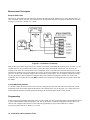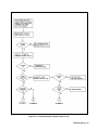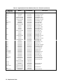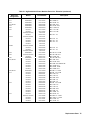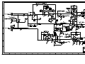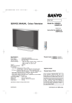
1
SERVICE GUIDE for Agilent 6610xA Power Modules Agilent Part No. 5959-3364 Microfiche Part No. 5959-3365 Printed in Malaysia Update December, 2002 CERTIFICATION Agilent Technologies certifies that this product met its published specifications at time of shipment from the factory. Agilent Technologies further certifies that its calibration measurements are traceable to the United States National Bureau of Standards, to the extent allowed by the Bureau’s calibration facility, and to the calibration facilities of other International Standards Organization members. WARRANTY This Agilent Technologies hardware product is warranted against defects in material and workmanship for a period of three years from date of delivery. Agilent software and firmware products, which are designated by Agilent Technologies for use with a hardware product and when properly installed on that hardware product, are warranted not to fail to execute their programming instructions due to defects in material and workmanship for a period of 90 days from date of delivery. During the warranty period Agilent Technologies will, at its option, either repair or replace products which prove to be defective. Agilent Technologies does not warrant that the operation of the software, firmware, or hardware shall be uninterrupted or error free. For warranty service, with the exception of warranty options, this product must be returned to a service facility designated by Agilent Technologies. Customer shall prepay shipping charges (and shall pay all duty and taxes) for products returned to Agilent Technologies for warranty service. Except for products returned to Customer from another country, Agilent Technologies shall pay for return of products to Customer. Warranty services outside the country of initial purchase are included in Agilent Technologies ’ product price, only if Customer pays Agilent Technologies international prices (defined as destination local currency price, or U.S. or Geneva Export price). If Agilent Technologies is unable, within a reasonable time to repair or replace any product to condition as warranted, the Customer shall be entitled to a refund of the purchase price upon return of the product to Agilent Technologies. LIMITATION OF WARRANTY The foregoing warranty shall not apply to defects resulting from improper or inadequate maintenance by the Customer, Customer-supplied software or interfacing, unauthorized modification or misuse, operation outside of the environmental specifications for the product, or improper site preparation and maintenance. NO OTHER WARRANTY IS EXPRESSED OR IMPLIED. AGILENT TECHNOLOGIES SPECIFICALLY DISCLAIMS THE IMPLIED WARRANTIES OF MERCHANTABILITY AND FITNESS FOR A PARTICULAR PURPOSE. EXCLUSIVE REMEDIES THE REMEDIES PROVIDED HEREIN ARE THE CUSTOMER’S SOLE AND EXCLUSIVE REMEDIES. AGILENT TECHNOLOGIES SHALL NOT BE LIABLE FOR ANY DIRECT, INDIRECT, SPECIAL, INCIDENTAL, OR CONSEQUENTIAL DAMAGES, WHETHER BASED ON CONTRACT, TORT, OR ANY OTHER LEGAL THEORY. ASSISTANCE The above statements apply only to the standard product warranty. Warranty options, extended support contracts, product maintenance agreements and customer assistance agreements are also available. Contact your nearest Agilent Technologies Sales and Service office for further information on Agilent Technologies’ full line of Support Programs. 2 SAFETY SUMMARY The following general safety precautions must be observed during all phases of operation of this power module. Failure to comply with these precautions or with specific warnings elsewhere in this guide violates safety standards of design, manufacture, and intended use of the power module. Agilent Technologies assumes no liability for the user’s failure to comply with these requirements. GROUND THE POWER MODULE. When installed in a properly wired mainframe, this product is a Safety Class 1 instrument (provided with a protective earth terminal). To minimize shock hazard, the mainframe must be connected to an electrical ground. The mainframe must be connected to the ac power supply mains through a three-conductor power cable, with the third wire firmly connected to an electrical ground (safety ground) at the power outlet. Any interruption of the protective (grounding) conductor or disconnection of the protective earth terminal will cause a potential shock hazard that could result in personal injury. DO NOT EXCEED INPUT RATINGS. The mainframe is equipped with a power line filter to reduce electromagnetic interference and must be connected to a properly grounded receptacle to minimize electric shock hazard. Operation at line voltages or frequencies in excess of those stated on the line rating label may cause leakage currents in excess of 5.0 mA peak. DO NOT OPERATE IN AN EXPLOSIVE ATMOSPHERE. Do not operate the power module in the presence of flammable gases or fumes. BEFORE APPLYING POWER. Verify that the power module line voltage switch is set to match the available line voltage. SAFETY SYMBOLS. Instruction manual symbol: the product will be marked with this symbol when it is necessary for the user to refer to the instruction manual (refer to Table of Contents) . Indicates hazardous voltages. Indicate earth (ground) terminal. The WARNING sign denotes a hazard. It calls attention to a procedure, practice, or the like, which, if not correctly performed or adhered to, could result in personal injury. Do not proceed beyond a WARNING sign until the indicated conditions are fully understood and met. The CAUTION sign denotes a hazard. It calls attention to an operating procedure, or the like, which, if not correctly performed or adhered to, could result in damage to or destruction of part or all of the product. Do not proceed beyond a CAUTION sign until the indicated conditions are fully understood and met. Power modules that appear damaged or defective should be made inoperative and secured against unintended operation until they can be repaired by qualified service personnel. 3 Printing History The current edition of this guide is indicated below. Reprints of this guide containing minor corrections and updates may have the same printing date. New editions are identified by a new printing date and, in some cases, by a new part number. A new edition incorporates all new or corrected material since the previous edition. Changes to the guide occurring between editions are covered by change sheets shipped with this guide. Edition 1 . . . . October, 1993 (Agilent Model 6610xA) Update . . . . . June 2000, December 2002 Copyright 1993, 2000 Agilent Technologies, Inc. This document contains proprietary information protected by copyright. All rights are reserved. No part of this document may be photocopied, reproduced, or translated into another language without prior consent of Agilent Technologies The information contained in this document is subject to change without notice. 4 Table of Contents Overview.................................................................................................................................................................................. 7 About This Manual ............................................................................................................................................................... 7 Related Documents ........................................................................................................................................................... 8 Revisions and Updates.......................................................................................................................................................... 8 Manual.............................................................................................................................................................................. 8 Firmware........................................................................................................................................................................... 8 Safety Considerations ........................................................................................................................................................... 9 Electrostatic Discharge ......................................................................................................................................................... 9 Service Tools and Equipment ............................................................................................................................................... 9 Verification and Performance Tests.................................................................................................................................... 11 Operation Verification Tests............................................................................................................................................... 11 Performance Tests .............................................................................................................................................................. 11 Measurement Techniques ............................................................................................................................................... 12 Setup for Most Tests................................................................................................................................................... 12 Current-Monitoring Resistor....................................................................................................................................... 12 Programming .................................................................................................................................................................. 12 Constant Voltage (CV) Tests.......................................................................................................................................... 13 CV Setup..................................................................................................................................................................... 13 Voltage Programming/Readback Accuracy ................................................................................................................ 13 CV Load Effect........................................................................................................................................................... 13 CV Source Effect........................................................................................................................................................ 14 CV Noise (PARD) ...................................................................................................................................................... 14 Transient Recovery Time............................................................................................................................................ 14 Constant Current (CC) Tests........................................................................................................................................... 15 CC Setup..................................................................................................................................................................... 15 Current Programming/Readback Accuracy................................................................................................................. 15 CC Load and Line Regulation .................................................................................................................................... 15 CC Load Effect ........................................................................................................................................................... 16 CC Source Effect ........................................................................................................................................................ 16 CC Noise (PARD) ...................................................................................................................................................... 17 Troubleshooting .................................................................................................................................................................... 25 Troubleshooting Sequence.................................................................................................................................................. 25 Accessing the Flowcharts.................................................................................................................................................... 25 If You Experienced a Selftest Failure or RunTime Error Message................................................................................. 26 If You Experienced Other Problems With the Module................................................................................................... 26 Test Points .......................................................................................................................................................................... 48 Built-In Test Functions ....................................................................................................................................................... 48 EEPROM Troubleshooting and Initialization..................................................................................................................... 51 Troubleshooting.............................................................................................................................................................. 51 Initialization.................................................................................................................................................................... 51 Disassembly Procedures ..................................................................................................................................................... 56 Removing the Module and Module Connector ............................................................................................................... 56 Removing the Cover ....................................................................................................................................................... 56 Removing the Fan........................................................................................................................................................... 56 Removing the Front Panel Assembly.............................................................................................................................. 57 Removing the Power Board ............................................................................................................................................ 57 Removing the Bias Board ............................................................................................................................................... 57 Removing the Front Panel Board.................................................................................................................................... 57 5 Installing the Power Board ............................................................................................................................................. 58 Installing the Bias Board ................................................................................................................................................ 58 Installing the Front Panel Board and Front Panel Assembly .......................................................................................... 59 Installing the Fan ............................................................................................................................................................ 59 Installing the Cover......................................................................................................................................................... 59 Theory of Operation............................................................................................................................................................. 61 AC Input and Bias Supplies................................................................................................................................................ 61 Microprocessor Circuits...................................................................................................................................................... 61 CV/CC DACs ..................................................................................................................................................................... 61 CV Amplifier ...................................................................................................................................................................... 63 CC Amplifier ...................................................................................................................................................................... 63 OR Gates ............................................................................................................................................................................ 63 Pulse-Width Modulator, FETS, and Isolation Transformer................................................................................................ 64 Downprogrammer Circuit ................................................................................................................................................... 64 Readback Multiplexer......................................................................................................................................................... 64 OV Circuit .......................................................................................................................................................................... 65 Replacement Parts ................................................................................................................................................................ 67 Diagrams ............................................................................................................................................................................... 83 Schematic Sheets ................................................................................................................................................................ 83 Component Location Diagrams .......................................................................................................................................... 83 Schematic Notes ................................................................................................................................................................. 84 Manual Backdating ............................................................................................................................................................ 97 Index .................................................................................................................................................................................... 99 6 1 Overview About This Manual This manual is a complete guide for servicing the Agilent 6610xA Power Modules. Troubleshooting information for the Agilent 66000A MPS Mainframe is provided in the mainframe service manual (see "Related Documents"), which should be used with this manual. Note Troubleshooting the Agilent 6610xA Power Modules requires the use of one working Agilent 66000A MPS Mainframe. This manual is organized into the following major sections: ■ Overview discusses safety and equipment considerations to be aware of when troubleshooting. It also lists the tools and equipment required for troubleshooting. ■ Verification and Performance consists of a series of tests that are used to verify.... ■ Troubleshooting procedures systematically verify selected circuits to isolate the cause of a problem. Suggestions for remedying the problem are also provided. The following troubleshooting procedures are provided: ❏ ❏ ❏ ❏ ❏ ❏ ❏ ❏ ❏ Overall Microprocessor Error Messages Overvoltage Circuit Output Circuit CV and CC Circuits Downprogrammer Circuits DAC Circuit Readback Circuit Disassembly procedures are provided at the end of the chapter. ■ Theory of Operation provides a brief description of the overall operation of the power module. ■ Replacement Parts lists part numbers for electrical components and miscellaneous chassis parts. ■ Schematics and component location diagrams are provided as an aid in troubleshooting and repair. Overview 7 Related Documents The following documents are related to this manual: Manual Part Number Agilent 66000A MPS Mainframe Installation Guide Agilent Series 6610xA MPS Power Modules User's Guide Agilent Series 6610xA MPS Power Modules Programming Guide Agilent Series 66000A MPS Mainframe Service Manual 66000-90001 5959-3386 5959-3362 66000-90003 Description Provides product specifications, installation, and connection information. Describes the operation of the MPS Power Modules. Describes SCPI programming commands, status reporting. Provides replaceable-parts lists, circuit diagrams, and verification procedures for the Agilent Series 66000A MPS Mainframe. Revisions and Updates Manual Agilent Technologies instruments are identified by a 10-digit serial number. The format is described as follows: first two letters indicate the country of manufacture. The next four digits are a code that identify either the date of manufacture or of a significant design change. The last four digits are a sequential number assigned to each instrument. Item US 3648 0101 Description The first two letters indicates the country of manufacture, where US = USA; MY = Malaysia; SG = Singapore. This is a code that identifies either the date of manufacture or the date of a significant design change. The last four digits are a unique number assigned to each power module. If changes have been made to your unit since the publication of this manual, a yellow Manual Change sheet may be supplied with the manual. It defines the differences between your unit and the unit described in this manual. The yellow change sheet may also contain information for correcting errors in the manual. Note that because not all changes to the product require changes to the manual, there may be no update information required for your unit. Older serial number formats used with these instruments had a two-part serial number, i.e. 2701A-00101. This manual also applies to instruments with these older serial number formats. Refer to Manual Backdating for backdating information. Firmware This manual applies to power modules that run on software revision A.00.01 through A.00.04. Firmware revision A.00.04 is backward compatible with all previous revisions. The ROM chip (U2) has a label that specifies the firmware revision. 8 Overview Safety Considerations The Agilent 6610xA Power Modules are Safety Class 1 instruments that connect to a protective earth terminal when properly installed in an Agilent 66000A MPS Mainframe. Refer to the Safety Summary page at the beginning of this manual for general safety procedures and the meaning of safety symbols appearing in the manual and on the module. Electrostatic Discharge The Modular Power System has components that can be damaged by ESD (electrostatic discharge). Failure to observe standard anti-static practices can result in serious degradation of performance even when complete failure does not occur. When working on the Modular Power System, observe all anti-static work practices. This includes, but is not limited to: ■ Working at a static-free station, such as a table covered with static-dissipative laminate or with a conductive table mat (Agilent p/n 9300-0797). ■ Using a conductive wrist strap (Agilent p/n 9300-0969 or 9300-0970). ■ Grounding all metal equipment at the station to a single, common ground. ■ Connecting low-impedance test equipment to static sensitive components only when those components have power applied to them. ■ Removing power from the Modular Power System before removing or installing printed circuit boards. Service Tools and Equipment The following tools are required to repair the Agilent 6610xA MPS Modules: ■ T10 TORX driver ■ 7mm HEX NUT drivers ■ #2 POZI driver ■ Slot-head screwdriver - medium ■ DIP component removal tool ■ Soldering iron and solder ■ De-solder removal tool ■ Needle-nose pliers ■ Anti-static work mat and wrist strap Overview 9 The following equipment is required to verify and troubleshoot the Agilent 6610xA Power Modules: Table 1-1. Service Test Equipment Equipment Required Critical Specifications Recommended Model 1 Use GPIB Controller Full GPIB capabilities HP Series 200/300 computer T Oscilloscope Sensitivity: 1mV Bandwidth Limit: 20MHz Probe: 1:1 with RF tip Agilent 54504A T Rms Voltmeter True RMS Bandwidth: 20MHz Sensitivity: 100µV Agilent 3400B T Digital Voltmeter Resolution: 10nV @ 1V (8 1/2 digit) Agilent 3458A Accuracy: 20 ppm Variable Voltage Transformer Adjustable from- 13% to + 6% of input range. 1KVA min. CC RMS Noise Resistor (RM) Agilent 66101A,102A - 100A (.01 Ω) ± 0.04%2 Agilent 66103A,106A - 15A (.01 Ω) ± 0.04%3 Guildline 9230/100 Guildline 9230/15 V,T Electronic Load Voltage and current range must exceed range of module under test. Power Range: 600W minimum V,T Load Resistor (RL) Agilent 66101A- 0.1 Ω ± 5% 300W Agilent 66102A-106A- 1.0 Ω ± 5% 300W Agilent 6050A Load mainframe and Agilent 60503A module (240V) or Agilent 60507A module (120V). Ohmite C300KR10 Ohmite C300KIR0 MPS Mainframe Agilent 66000A V,T MPS Keyboard4 Agilent 66001A V,T T 1 V = Verification; T = Troubleshooting. 2 Guildline Shunt Accuracy determined by Power Coefficient ( ± 0.01% + (0.0004%/watt)) 3 Guildline Shunt Accuracy determined by Power Coefficient ( ± 0.01% + (0.002%/watt)) 4 Use of the keyboard is recommended for displaying selftest error messages. 10 Overview V,T T 2 Verification and Performance Tests This chapter contains test procedures to check the operation of the Agilent 6610xA Power Modules. The required test equipment is specified in Chapter 1. Sample performance test record sheets are included at the end of the chapter. Instructions are given for performing the tests either from a GPIB controller or the MPS keyboard. Two types of procedures are provided: Operation Verification tests and Performance tests. Operation Verification These tests do not check all parameters, but comprise a short procedure to verify that the power module is performing properly. Performance These test all the Performance Specifications (not Supplementary Characteristics) listed in Table 1-1 of the Power Module User’s Guide. If you encounter failures or out-of-specification test results, see "Troubleshooting Procedures" in Chapter 3 of this manual. Those procedures will determine if repair and/or calibration is required. Note The power module must pass the selftest at power-on before the following tests can be performed. If the module fails selftest, refer to the overall troubleshooting procedures in Chapter 3. SHOCK HAZARD The tests should only be performed by qualified personnel. During the performance of these tests, hazardous voltages may be present at the output of the module. Operation Verification Tests To assure that the module is operating properly, without testing all specified parameters, perform the following test procedures: 1. 2. Perform the turn-on and checkout procedures given in Chapter 3 of the Power Module User’s Guide. Perform the Voltage Programming/Readback Accuracy and the Current Programming/Readback Accuracy Performance Tests in this chapter. Performance Tests The following paragraphs provide test procedures for verifying the module’s compliance with the specifications listed in Table 1-1 of the Power Module User’s Guide. All of the performance test specifications are listed in the Performance Test Records at the end of this chapter. You can record the actual measured values in the column provided. Verification and Performance Tests 11 Measurement Techniques Setup for Most Tests Most tests are performed at the rear terminals as shown in the following figure. Measure the dc voltage directly at the + S and - S terminals. Set the connector sense switch for local sensing and use adequate wire gauge for load leads as described in Chapter 2 of the Power Module User’s Guide. Figure 2-1. Performance Test Setup Many of the test procedures require the use of a variable load capable of dissipating the required power (see Table 1-1). If a variable resistor is used, switches must be used to connect, disconnect, and short the load resistor. For most tests, an electronic load can be used. The electronic load is considerably easier to use than load resistors but some may not be fast enough to test transient recovery time and may be too noisy for the noise (PARD) tests. Fixed load resistors may be used in place of a variable load, with minor changes to the test procedures in this chapter. Also, if computer controlled test setups are used, the relatively slow (compared to computers and system voltmeters) settling time and slew rates of the power module may have to be taken into account. WAIT statements can be used in the test program if the test system is faster than the module. Current-Monitoring Resistor To eliminate output current measurement error caused by voltage drops in the leads and connections, connect the current monitoring resistor between the output and the load as a four-terminal device (see RM in Figure 2-1). Connect the current monitoring leads inside the load lead connections directly at the monitoring points on the resistor element. Programming Table 2-1 lists the programming and current values for each module. You may program the module from the MPS Keyboard or from a GPIB controller when performing the tests. The test procedures are written assuming that you know how to do either or both. Complete instructions for remote and local programming are given in the module Power Module Programming Guide and Power Module User’s Guide. 12 Verification and Performance Tests Table 2-1. Power Module Voltage and Current Values Agilent Model 66101A 66102A 66103A 66104A 66105A 66106A Full-Scale Voltage 8V 20V 35V 60V 120V 200V Max. Prog. Voltage 8.190V 20.475V 35.831V 61.425V 122.85V 204.75V Full-Scale Current 16A 7.5A 4.5A 2.5A 1.25A 0.75A Max. Prog. Current 16.380A 7.678A 4.607A 2.559A 1.280A 0.768A Max. Prog. Overvoltage 10V 24V 42V 72V 144V 240V Constant Voltage (CV) Tests CV Setup If more than one meter or a meter and an oscilloscope are used, connect each to the terminals by a separate pair of leads to avoid mutual coupling effects. For constant voltage dc tests, connect only to + S and - S because the module regulates the output voltage that appears between those terminals, not between the + and - output terminals. Use coaxial cable or shielded 2-wire cable to avoid noise pickup on the test leads. Voltage Programming/Readback Accuracy This test verifies that the voltage programming, readback, and front panel display functions are within specifications. Note that the values read back over the GPIB should be identical to those displayed on the keyboard display. 1. 2. 3. 4. 5. Turn off the power module and connect a digital voltmeter between the + S and--S terminals (see Figure 2-1). Turn on the module and program it for zero volts and the maximum programmable current (see Table 2-1) with the load off. Record the output voltage readings on the DVM and the keyboard display. The readings should be within the limits specified in the Performance Test Record Tables under CV PROGRAMMING @ 0 VOLTS, for the particular model being tested. The CV annunciator should be on and the output current reading should be approximately zero. Program the output voltage to full scale (see Table 2-1). Record the output voltage readings on the DVM and the keyboard display. The readings should be within the limits specified in the Performance Test Record Tables under CV PROGRAMMING @ FULL SCALE, for the particular model being tested. CV Load Effect This test measures the change in output voltage resulting from a change in output current from full-load to no-load. 1. 2. 3. 4. 5. 6. Turn off the module and connect the output as shown in Figure 2-1 with the DVM connected between the + S and - S terminals. Turn on the module and program the current to the maximum programmable value and the voltage to the full-scale value (see Table 2-1). Adjust the load for the full-scale current (see Table 2-1) as indicated on the keyboard display. The front panel CV annunciator must be on. If it is not, adjust the load so that the output current drops slightly until the annunciator comes on. Record the output voltage reading on the DVM connected to + S and - S. Open the load and again record the DVM voltage reading. The difference between the DVM readings in steps (4) and (5) is the load effect voltage and should not exceed the value listed in the Performance Test Record Tables under CV LOAD EFFECT, for the model being tested. Verification and Performance Tests 13 CV Source Effect This test measures the change in output voltage that results from a change in ac line voltage from the minimum to maximum value within the line voltage specifications. 1. 2. 3. 4. 5. 6. 7. 8. 9. Turn off the module and connect the ac power line through a variable-voltage transformer. Connect the output as shown in Figure 2-1 with the DVM connected between the + S and - S terminals. Set the transformer to nominal line voltage (either 115Vac or 230Vac). Turn on the module and program the current to the maximum programmable value and the output voltage to the full-scale value (see Table 2-1). Adjust the load for the full-scale current value (see Table 2-1) as indicated on the keyboard display. The front panel CV annunciator must be on. If it is not, adjust the load so that the output current drops slightly until the annunciator comes on. Adjust the transformer to the LOW line voltage (e.g., 87Vac for a 115Vac nominal input, or 174Vac for a 230Vac nominal input). Record the output voltage reading on the DVM. Adjust the transformer to the HIGH line voltage (e.g., 132Vac for a 115Vac nominal input, or 250Vac for a 230Vac nominal input). Record the output voltage reading on the DVM. The difference between the DVM readings in steps (6) and (8) is the source effect voltage and should not exceed the value listed in the Performance Test Record Tables under CV SOURCE EFFECT, for the model being tested. CV Noise (PARD) Periodic and random deviations (PARD) in the output (ripple and noise) combine to produce a residual ac voltage superimposed on the dc output voltage. This test measures CV PARD, specified as the rms or peak-to-peak output voltage over the frequency range of 20Hz to 20MHz. 1. 2. 3. 4. 5. Turn off the module and connect the output as shown in Figure 2-1 to an oscilloscope (ac coupled) between the + and-terminals. Set the oscilloscope’s bandwidth limit to 20MHz (30MHz on the Agilent 54504A) and use an RF tip on the oscilloscope probe. Turn on the module and program the current to the maximum programmable value and the output voltage to the full-scale value (see Table 2-1). Adjust the load for the full-scale current value (see Table 2-1) as indicated on the keyboard display. The waveform on the oscilloscope should not exceed the peak-to-peak limits in the Performance Test Record Tables under CV NOISE (PARD), for the model being tested. Disconnect the oscilloscope and connect an ac rms voltmeter in its place. The rms voltage reading should not exceed the rms limits in the Performance Test Record Tables under CV NOISE (PARD) for the model being tested. Transient Recovery Time This test measures the time for the output voltage to recover to within the specified value following a 10% change in the load current. 1. 2. 3. 4. 5. 6. 7. Turn off the module and connect the output as shown in Figure 2-1 with the oscilloscope across the + S and -S terminals. Turn on the module and program the output voltage to the full-scale value and the current to the maximum programmable value (see Table 2-1). Set the load to the Constant Current mode and program the load current to 90% of the power module full-scale rated current. Set the electronic load’s transient generator frequency to 100Hz and its duty cycle to 50%. Program the load’s transient level to the module’s full-scale current value and turn the transient on. Adjust the oscilloscope for a waveform similar to that in Figure 2-2. The output voltage should return to within 100mV of the nominal value in less than 1ms. Check both loading and 14 Verification and Performance Tests unloading transients by triggering on the positive and negative slope. Figure 2-2. Transient Response Waveform Constant Current (CC) Tests CC Setup Follow the general setup instructions in the Measurement Techniques paragraph and the specific instructions given in the following paragraphs. Current Programming/Readback Accuracy This test verifies that the current programming and readback are within specification. The accuracy of the current monitoring resistor is determined by the power coefficient (see Table 1-1). 1. 2. 3. 4. 5. Turn off the module and connect the current monitoring resistor directly across the output and a DVM across the resistor. Refer to the "Current Monitoring Resistor" paragraph. Turn on the module and program the output voltage to 5V and the current to zero. Divide the voltage drop (DVM reading) across the current monitoring resistor by its resistance to convert to amps and record this value as (Io). The actual current (Io) and the reading on the keyboard display should be within the limits specified in the Performance Test Record Tables under CC PROGRAMMING @ 0 AMPS, for the particular model being tested. Program the output voltage to 5V and the current to full-scale (see Table 2-1). Divide the voltage drop (DVM reading) across the current monitoring resistor by its resistance to convert to amps and record this value as (Io). The actual current (Io) and the reading on the keyboard display should be within the limits specified in the Performance Test Record Tables under CC PROGRAMMING @ FULL SCALE, for the particular model being tested. CC Load and Line Regulation These tests (CC Load Effect and CC Source Effect given below) are tests of the dc regulation of the power module’s output current. To insure that the values read are not the instantaneous measurement of the ac peaks of the output current ripple, several dc measurements should be made and the average of these readings calculated. Verification and Performance Tests 15 The following steps show how to set up an Agilent 3458A System Voltmeter from its front panel to take a statistical average of 100 readings. represents the unlabeled shift key in the FUNCTION/RANGE group. . 1. Program 10 power line cycles per sample by pressing . 2. Program 100 samples per trigger by pressing 3. Set up the voltmeter to take measurements in the statistical mode as follows: . 4. a. Press until the MATH function is selected; then press . b. Press until the STAT function is selected; then press . c. Press 5. Now set up the voltmeter to read the average value of the measurements as follows: . 6. a. Press b. Press until the RMATH function is selected; then press . until the MEAN function is selected; then press . c. Press 7. Execute the average reading program by pressing . 8. Wait for 100 readings and then read the average measurement by pressing . Record this as your result. To repeat the measurement, perform steps (7) and (8). CC Load Effect This test measures the change in output current for a change in the load from full-scale output voltage to short circuit. 1. 2. 3. 4. Turn off the module and connect the output to be tested as shown in Figure 2-1 with the voltmeter connected across the current monitoring resistor. Turn on the module and program the current to the full-scale current value and the output voltage to the maximum programmable voltage value (see Table 2-1). Adjust the load in the CV mode for full-scale voltage as indicated on the keyboard display. Check that the CC annunciator is on. If it is not, adjust the load to drop the output voltage slightly until the annunciator comes on. Record the output current reading (DVM reading ÷ current monitor resistance value in ohms). Note 5. 6. You may want to use the average reading program described previously. Short the load switch and record the output current reading. The difference in the current readings in steps (4) and (5) is the load effect and should not exceed the limit specified in the Performance Test Record Tables under CC LOAD EFFECT, for the particular model being tested. CC Source Effect This test measures the change in output current that results when the ac line voltage changes from the minimum to the maximum value within the specifications. 1. 2. 3. 4. 5. 6. Turn off the module and connect the ac power line through a variable-voltage transformer. Connect the output terminals as shown in Figure 2-1 with the voltmeter connected across the current monitoring resistor. Set the transformer to the nominal line voltage. Turn on the module and program the current to the full-scale value and the output voltage to the maximum programmable value (see Table 2-1). Adjust the load in the CV mode for full-scale voltage as indicated on the front panel display. Check that the CC annunciator is on. If it is not, adjust the load to drop the output voltage slightly until the annunciator comes on. Adjust the transformer to the LOW line voltage (e.g., 87Vac for a 115Vac nominal input, or 174Vac for a 230Vac nominal input). Record the output current reading (DVM reading ÷ current monitoring resistor in ohms). 16 Verification and Performance Tests Note You may want to use the average reading program described previously. 7. 8. Adjust the transformer to the HIGH line voltage (e.g., 132Vac for a 115Vac nominal input, or 250Vac for a 230Vac nominal input), and record the output current reading. The difference in the current readings in steps (6) and (7) is the CC source effect and should not exceed the values listed in the Performance Test Record Tables under CC SOURCE EFFECT, for the particular model being tested. CC Noise (PARD) Periodic and random deviations (PARD) in the output (ripple and noise) combine to produce a residual ac current as well as an ac voltage superimposed on the dc output. Constant current (CC) PARD is specified as the rms output current in a frequency range 20Hz to 20MHz with the module in CC operation. 1. 2. 3. 4. 5. Turn off the module and connect the load resistor (RL) and rms voltmeter as shown in Figure 2-1. Use only a resistive load for this test. Keep leads as short as possible to reduce noise pickup. Check the test setup for noise with the module turned off. Other equipment (e.g. computers, DMM, etc.) may affect the reading. Turn on the module and program the current to full-scale and the output voltage to the maximum programmable value (see Table 2-1). The output current should be at the full-scale rating with the CC Mode on. Divide the reading on the rms voltmeter by the shunt resistance to obtain rms current. It should not exceed the values listed in the Performance Test Record Tables under CC NOISE (Rms) for the particular unit being tested. Verification and Performance Tests 17 Table 2-2. Performance Test Record for Model Agilent 66101A (8V, 16A) Pre Cal_____________Post Cal______________ Model Agilent 66101A Temperature___________________________Test Performed By_______________________ Serial Number_______________________Humidity________________________Date__________________________ Test Description Specification Actual 0 ± 3mV DVM ± 2mV ________ ________ 8V ± 5.4mV DVM ± 3.6mV ________ ________ 1mV ________ 0.5mV ________ 5mV 2mV ________ ________ 100mV ________ 0 ± 6mA Io ± 6mA ________ ________ 16A ± 10.8mA Io ± 9.2mA ________ ________ CC LOAD EFFECT 0.5mA ________ CC SOURCE EFFECT 0.75mA ________ 8mA ________ CV PROGRAMMING @ 0 volts Output Accuracy (DVM Reading) Display and Readback Accuracy CV PROGRAMMING @ full-scale Output Accuracy (DVM Reading) Display and Readback Accuracy CV LOAD EFFECT CV SOURCE EFFECT CV NOISE (PARD) Peak to Peak Rms TRANSIENT RECOVERY in 1 ms CC PROGRAMMING @ 0 amps Output Accuracy (Io) Display and Readback Accuracy CC PROGRAMMING @ full-scale Output Accuracy (Io) Display and Readback Accuracy CC NOISE (RMS) 18 Verification and Performance Tests Table 2-3. Performance Test Record for Model Agilent 66102A (20V, 7.5A) Pre Cal_____________Post Cal______________ Model Agilent 66102A Temperature___________________________Test Performed By______________________ Serial Number_______________________Humidity________________________Date__________________________ Test Description Specification Actual CV PROGRAMMING @ 0 volts Output Accuracy (DVM Reading) Display and Readback Accuracy 0 ± 8mV DVM ± 3mV ________ ________ CV PROGRAMMING @ full-scale Output Accuracy (DVM Reading) Display and Readback Accuracy 20V ± 14mV DVM ± 7mV ________ ________ 1mV ________ 0.5mV ________ 7mV 3mV ________ ________ 100mV ________ 0 ± 3mA Io ± 3mA ________ ________ 7.5A ± 5.3mA Io ± 4.5mA ________ ________ CC LOAD EFFECT 0.2mA ________ CC SOURCE EFFECT 0.5mA ________ 4mA ________ CV LOAD EFFECT CV SOURCE EFFECT CV NOISE (PARD) Peak to Peak Rms TRANSIENT RECOVERY in 1 ms CC PROGRAMMING @ 0 amps Output Accuracy (Io) Display and Readback Accuracy CC PROGRAMMING @ full-scale Output Accuracy (Io) Display and Readback Accuracy CC NOISE (RMS) Verification and Performance Tests 19 Table 2-4. Performance Test Record for Model Agilent 66103A (35V, 4.5A) Pre Cal_____________Post Cal______________ Model Agilent 66103A Temperature___________________________Test Performed By______________________ Serial Number_______________________Humidity________________________Date__________________________ Test Description Specification Actual 0 ± 13mV DVM ± 8mV ________ ________ 35V ± 23.5mV DVM ± 15mV ________ ________ CV LOAD EFFECT 1mV ________ CV SOURCE EFFECT 1mV ________ CV NOISE (PARD) Peak to Peak Rms 10mV 5mV ________ ________ TRANSIENT RECOVERY in 1 ms 100mV ________ 0 ± 2mA Io ± 2mA ________ ________ 4.5A ± 3.4mA Io ± 2.9mA ________ ________ CC LOAD EFFECT 0.2mA ________ CC SOURCE EFFECT 0.3mA ________ 2mA ________ CV PROGRAMMING @ 0 volts Output Accuracy (DVM Reading) Display and Readback Accuracy CV PROGRAMMING @ full-scale Output Accuracy (DVM Reading) Display and Readback Accuracy CC PROGRAMMING @ 0 amps Output Accuracy (Io) Display and Readback Accuracy CC PROGRAMMING @ full-scale Output Accuracy (Io) Display and Readback Accuracy CC NOISE (RMS) 20 Verification and Performance Tests Table 2-5. Performance Test Record for Model Agilent 66104A (60V, 2.5A) Pre Cal_____________Post Cal______________ Model Agilent 66104A Temperature___________________________Test Performed By______________________ Serial Number_______________________Humidity________________________Date__________________________ Test Description Specification Actual CV PROGRAMMING @ 0 volts Output Accuracy (DVM Reading) Display and Readback Accuracy 0 ± 27mV DVM ± 16mV ________ ________ CV PROGRAMMING @ full-scale Output Accuracy (DVM Reading) Display and Readback Accuracy 60V ± 45mV DVM ± 28mV ________ ________ CV LOAD EFFECT 2mV ________ CV SOURCE EFFECT 2mV ________ CV NOISE (PARD) Peak to Peak Rms 15mV 9mV (1) ________ ________ TRANSIENT RECOVERY in 1 ms 100mV ________ 0 ± 0.6mA Io ± 0.6mA ________ ________ 2.5A ± 1.4mA Io ± 1.1mA ________ ________ CC LOAD EFFECT 0.1mA ________ CC SOURCE EFFECT 0.1mA ________ 1mA ________ CC PROGRAMMING @ 0 amps Output Accuracy (Io) Display and Readback Accuracy CC PROGRAMMING @ full-scale Output Accuracy (Io) Display and Readback Accuracy CC NOISE (RMS) (1) 18mV Rms when the ac input is between 87 and 104Vac. Verification and Performance Tests 21 Table 2-6. Performance Test Record for Model Agilent 66105A (120V, 1.25 A) Pre Cal_____________Post Cal______________ Model Agilent 66105A Temperature___________________________Test Performed By______________________ Serial Number_______________________Humidity________________________Date__________________________ Test Description Specification Actual CV PROGRAMMING @ 0 volts Output Accuracy (DVM Reading) Display and Readback Accuracy 0 ± 54mV DVM ± 32mV ________ ________ CV PROGRAMMING @ full-scale Output Accuracy (DVM Reading) Display and Readback Accuracy 120V ± 90mV DVM ± 56mV ________ ________ CV LOAD EFFECT 4mV ________ CV SOURCE EFFECT 3mV ________ CV NOISE (PARD) Peak to Peak Rms 25mV 18mV ________ ________ TRANSIENT RECOVERY in 1 ms 100mV ________ 0 ± 0.6mA Io ± 0.6mA ________ ________ 1.25A ± 975µA Io ± 850µA ________ ________ CC LOAD EFFECT 50µA ________ CC SOURCE EFFECT 50µA ________ CC NOISE (RMS) 1mA ________ CC PROGRAMMING @ 0 amps Output Accuracy (Io) Display and Readback Accuracy CC PROGRAMMING @ full-scale Output Accuracy (Io) Display and Readback Accuracy 22 Verification and Performance Tests Table 2-7. Performance Test Record for Model Agilent 66106A (200V, 0.75A) Pre Cal_____________Post Cal______________ Model Agilent 66106A Temperature___________________________Test Performed By______________________ Serial Number_______________________Humidity________________________Date__________________________ Test Description Specification Actual 0 ± 90mV DVM ± 54mV ________ ________ 200V ± 150mV DVM ± 94mV ________ ________ CV LOAD EFFECT 7mV ________ CV SOURCE EFFECT 5mV ________ CV NOISE (PARD) Peak to Peak Rms 50mV 30mV ________ ________ TRANSIENT RECOVERY in 1 ms 100mV ________ 0 ± 0.4mA Io ± 0.3mA ________ ________ 0.75A ± 625µA Io ± 450µA ________ ________ CC LOAD EFFECT 10µA ________ CC SOURCE EFFECT 30µA ________ CC NOISE (RMS) 1mA ________ CV PROGRAMMING @ 0 volts Output Accuracy (DVM Reading) Display and Readback Accuracy CV PROGRAMMING @ full-scale Output Accuracy (DVM Reading) Display and Readback Accuracy CC PROGRAMMING @ 0 amps Output Accuracy (Io) Display and Readback Accuracy CC PROGRAMMING @ full-scale Output Accuracy (Io) Display and Readback Accuracy Verification and Performance Tests 23 3 Troubleshooting This chapter provides troubleshooting and repair information for the Agilent 6610xA Power Modules. Before attempting to troubleshoot the modules, ensure that the problem is not with an external circuit or application, the mainframe, the GPIB controller, the application program, or the input power line. SHOCK HAZARD Most of the troubleshooting procedures given in this chapter are performed with power applied and protective covers removed. Such maintenance should be performed only by trained service personnel who are aware of the hazards (for example, tire and electrical shock). Hazardous voltages are present throughout the Power and Bias board assemblies. Ac line voltage is present on some connectors even when the module is not turned on. The dc rail voltage to the module is 310 volts when the unit is turned on. Troubleshooting Sequence 1. Verify that the module is at fault. 2. Use the flowcharts to locate the functional block at fault. 3. Troubleshoot the functional block per flowchart instructions. Selftest routines built into firmware are provided to help isolate a problem to a particular circuit on the board. Once a problem has been isolated to a circuit, suggestions are given in the appropriate flowchart as to what component may be at fault. This instrument uses components that can be damaged or suffer serious performance degradation as a result of ESD (electrostatic discharge). Observe the standard anti-static precautions discussed in Chapter 1 to avoid damage to components. Accessing the Flowcharts The following troubleshooting flowcharts are provided to help you identify and isolate a problem to a specific circuit. Once a problem has been narrowed down, suggestions are provided as to the components that may be responsible for the problem. Refer to the schematic diagrams for detailed information on circuit wiring and component function. § Figure 3-1 - Overall Troubleshooting § Figure 3-2 - Troubleshooting Microprocessor Circuits § Figure 3-3 - Troubleshooting Error Messages § Figure 3-4 - Troubleshooting Overvoltage at Turn-on Troubleshooting 25 § Figure 3-5 - Troubleshooting No Output § Figure 3-6 - Troubleshooting High Output § Figure 3-7 - Troubleshooting Will Not Overvoltage § Figure 3-8 - Troubleshooting CV Accuracy § Figure 3-9 - Troubleshooting CC Accuracy § Figure 3-10 - Troubleshooting Downprogrammer § Figure 3-11 - Troubleshooting DAC Circuit § Figure 3-12 - Troubleshooting Readback Circuits Oscilloscope waveforms are provided on some flowcharts along with the settings required to generate the waveforms. Connect the module to ac mains through an isolation transformer when making measurements with an oscilloscope or any equipment that has the measuring input grounded. If You Experienced a Selftest Failure or RunTime Error Message If you experienced a selftest failure or runtime error message as described in Chapter 3 of the Power Module User's Guide, disassemble the module and proceed directly to the flowchart in Figure 3-3 "Troubleshooting Error Messages". If You Experienced Other Problems With the Module If you experienced problems other than a selftest failure or a runtime error message, disassemble the module and proceed directly to Figure 3-1 "Overall Troubleshooting". 26 Troubleshooting Figure 3-1. Overall Troubleshooting (Sheet 1 of 3) Troubleshooting 27 Figure 3-1. Overall Troubleshooting (Sheet 2 of 3) 28 Troubleshooting Figure 3-1. Overall Troubleshooting (Sheet 3 of 3) Troubleshooting 29 Figure 3-2. Troubleshooting Microprocessor Circuits (Sheet 1 of 2) 30 Troubleshooting Figure 3-2. Troubleshooting Microprocessor Circuits (Sheet 2 of 2) Troubleshooting 31 Figure 3-3. Troubleshooting Error Messages 32 Troubleshooting Figure 3-4. Troubleshooting Overvoltage at Turn-On (Sheet 1 of 2) Troubleshooting 33 Figure 3-4. Troubleshooting Overvoltage at Turn-On (Sheet 2 of 2) 34 Troubleshooting Figure 3-5. Troubleshooting No Output (Sheet 1 of 5) Troubleshooting 35 Figure 3-5. Troubleshooting No Output (Sheet 2 of 5) 36 Troubleshooting Figure 3-5. Troubleshooting No Output (Sheet 3 of 5) Troubleshooting 37 Figure 3-5. Troubleshooting No Output (Sheet 4 of 5) 38 Troubleshooting Figure 3-5. Troubleshooting No Output (Sheet 5 of 5) Troubleshooting 39 Figure 3-6. Troubleshooting High Output 40 Troubleshooting Figure 3-7. Troubleshooting Will Not Overvoltage Troubleshooting 41 Figure 3-8. Troubleshooting CV Accuracy 42 Troubleshooting Figure 3-9. Troubleshooting CC Accuracy Troubleshooting 43 Figure 3-10. Troubleshooting Downprogrammer 44 Troubleshooting Figure 3-11. Troubleshooting DAC Circuit Troubleshooting 45 Figure 3-12. Troubleshooting Readback Circuits (Sheet 1 of 2) 46 Troubleshooting Figure 3-12. Troubleshooting Readback Circuits (Sheet 2 of 2) Troubleshooting 47 Test Points The following test points are referenced in the troubleshooting flowcharts. Refer to the component locations diagram in Chapter 6 for the actual location of the test points on the pc board. Table 3-1. Test Points Test Point TP 0 TP 1 TP 2 TP 3 TP 4 TP 5 TP 6 TP 7 TP 8 TP 9 TP 10 TP 11 TP 12 TP 13 TP 14 TP 15 TP 16 TP 17 TP 18 TP 19 TP 20 TP 21 TP 22 Description Output circuit common (located on inboard side of R303) +5V (4.8 to 5.2 volts) +12V (11.4 to 12.6 volts) +7V (6.7 to 7.3 volts) +2.5V (2.4 to 2.6 volts) -12V (-11.4 to -12.6 volts) +15V (14.25 to 15.75 volts, referenced to the-rail)l +5V (4.75 to 5.25 volts, referenced to frame common) +24V (24.3 to 27.3 volts, referenced to frame common) +28V (unregulated, referenced to frame common) Frame common \ F / PCLR* (goes low for 175ms at turn-on) 6MHz (microprocessor clock out) 3MHz (A/D clock in) + output -output 0 to-6V (CVPROG) 0 to-6V (CCPROG) 0 to 2V (A/D INPUT) 0 to 2V (VMON) 0 to 2V (IMON) 0 to 4V (OVREF) -3.4 to -4V (OR GATE, output dependent) 1 Test Equipment must be isolated from ground. Built-In Test Functions To aid in troubleshooting, the module configuration switch (S3) can be set to run various test routines as described in the Overall Troubleshooting flowchart. To start the test, set all switches to 0 (down) and turn on ac power. Then set the switch to perform the selected test as shown in the following table. 48 Troubleshooting Table 3-2. S3 Test Settings S3 Setting 87654321 00000000 00010000 00000001 00010001 00000010 00010010 00000011 00010011 00000100 00010100 00000101 00010101 00000110 00010111 00001000 00001001 00011001 00001010 00001011 00001100 00001101 00001110 Test Description Start with blank front panel Front panel with all segments on VDAC minimum (TP16 = 0V) VDAC maximum (TP16 = -VREF) IDAC minimum (TP17 = 0V) IDAC maximum (TP17 = -VREF) OVPDAC minimum (TP21 = 0V) OVPDAC maximum (TP21 = 4V) VDAC ramp slow (TP16, see waveform B) VDAC ramp fast (TP16, see waveform C) IDAC ramp slow (TP17, see waveform B) IDAC ramp fast (TP17, see waveform C) OVPDAC ramp (TP21, see waveform A) MUX/AD (Toggle S3 switch 5 to select input) SRST* and OVPRST$ pulse PWMENhigh PWMEN low DOCAL pulse TRIGOUT (TOUT) pulse EEPROM read (U22 pin 4)2 Relay sequence (toggle S3 switch 5 to select relay)3 Tx pulses 1 Tests multiplexer inputs. First measure voltage at Ul5 pin 4. Toggle S3 switch 5 until voltage at Ul5 pin 8 equals the voltage at U15 pin 4. Now each time S3 switch 5 is toggled, the multiplexer will sequence through its inputs. The input of the A/D (Ul2-9) will be equal to the output of the multiplexer. Because the A/D is continually reading, its output (Ul2-20) should pulse. 2 Continuously reads the contents of location 0 of EEPROM. Check pulses at U22 pin 4. 3 Tests relays K601-K606. Toggling S3 switch 5 sequences through the relays. A relay is off when both ends of the coil are at +12V. A relay is on when one end is pulled low. A particular relay will energize every 5th toggle on S3 switch 5. Note that K607 is not tested. Troubleshooting 49 Figure 3-13. S3 Switch Setting Waveforms 50 Troubleshooting EEPROM Troubleshooting and Initialization Troubleshooting The power module can detect an EEPROM checksum error. This error is not identified by number, but causes the following symptoms: § The power module starts up with both the VOLTS and AMPS full-scale programming and metering ranges accepting values up to 1000. § Selftest error code 330 is stored in the SCPI error queue where it can be read by the controller (see Chapter 5 in the Power Module Programming Guide). § The *IDN? query returns 0A in the model field. § The calibration password is set to 0. An EEPROM checksum error can occur if there has been an excessive number of write cycles to an EEPROM. This condition is not recoverable and requires a new EEPROM. An EEPROM checksum error can also occur due to loss of ac power during a checksum calculation. This condition is very unlikely, but may be recoverable by performing the following steps from the controller: § Enable calibration mode (CAL:STAT ON,0) § Save an operating state to EEPROM. (for example, *SAV 2) Initialization EEPROM U22 on the power board stores the module's GPIB address, model number, and other operating and calibration constants. The EEPROM was initialized with the proper constants at the factory. If you need to re-initialize the module with the proper operating constants, run the following program. After you have initialized the module by running the initialization program, you must calibrate the module as described in Appendix A of the Power Module User's Guide. Troubleshooting 51 10 ! Program to initialize EEPROM or move factory preset data in 66101A, 20 ! 66102A, 66103A, 66104A, 66105A and 66106A power supply modules. 30 ! Rev A.00.00 dated May 27, 1993 40 ! 50 DIM Init_data(1:39),Model$[6],Idn$[21],Cal_data$[40] 60 INTEGER Addr(1:39),Length(1:39) 70 ASSIGN @Ps TO 70500 ! Supply must be at address 70500 80 CLEAR SCREEN 90 ! 100 Eprom_data_addr: ! Data address 110 DATA 2,6,10,14,18,19,20,24,28,32 120 DATA 36,37,38,42,46,50,55,56,57,58 130 DATA 62,66,70,74,,110,l11,112,114,118,119 140 DATA l20,121,122,124,125,126,127,128,130 150 ! 160 Eprom_data_len: ! Data for word length 170 DATA 4,4,4,4,1,1,4,4,4,4 180 DATA 1,1,4,4,4,4,1,1,1,4 190 DATA 4,4,4,4,1,1,2,4,1,1 200 DATA 1,1,2,1,1,1,1,1,2 210 ! 220 Eprom_data_101a: ! ! EEPROM data for 66101A 230 DATA 409,668,32.2818,8.19,0,66,0,221.586,33.0533,16.38,0 240 DATA 66,4,23.5,19,10,0,255,100,20,66101 250 DATA 3277.35,-1.74536,1772.04,-1.50366,0,0,4,66101,20,150 260 DATA 20,150,28321,40,20,10,83,83,0 270 ! 280 Eprom_data_102a: ! ! EEPROM data for 66102A 290 DATA 164.035,32.3969,20.475,0,66,0,440.367,30.0918,7.678,0 300 DATA 66,4,9,5.25,24.0,0,255,100,20,66102 310 DATA 1311.8,.248047,3523.12,-28.4202,0,0,4,66102,20,150 320 DATA 20,150,28321,40,20,10,83,83,0 330 ! 340 Eprom_data_103a: ! ! EEPROM data for 66103A 350 DATA 93.7474,32.2944,35.831,0,66,0,735.971,26.127,4.607,0 360 DATA 66,4,4,.93986,5.50002,42,0,255,100,20,66103 370 DATA 749.745,-.725342,5885.92,-54.0496,0,0,4,66103,20,150 380 DATA 20,150,28321,40,20,10,83,83,0 390 ! 400 Eprom_data_104a: ! ! EEPROM data for 66104A 410 DATA 54,32.3969,61.425,0,66,0,1320,30.0918,2.559,0 420 DATA 66,4,3,5.25,72.0,0,255,100,20,66104 430 DATA 437,.248047,10569,-28.4202,0,0,4,66104,20,150 440 DATA 20,150,28321,40,20,10,83,83,0 450 ! 460 Eprom_data_105a: ! ! EEPROM data for 66105A 470 DATA 27,32.3969,122.85,0,65,0,2640,30.0918,1.28,0 480 DATA 66,4,1.5,5,5.25,144,0,255,100,20,66105 490 DATA 219,.248047,21000,-28.4202,0,0,4,66105,20,150 500 DATA 20,150,28321,40,20,10,82,83,0 Figure 3-14. EEPROM Initialization Program (Sheet 1 of 5) 52 Troubleshooting 510 ! 520 Eprom_data_106a: ! ! EEPROM data for 66106A 530 DATA 16.4035,32.3969,204.75,0,65,0,4403.67,30.0918,0.768,0 540 DATA 67,4,0.9,5.25,240,0,255,100,20,66106 550 DATA 131.18,.248047,35231.2,-28.4202,0,0,4,66106,20,150 560 DATA 20,150,28321,40,20,10,82,84,0 570 ! 580 INPUT “Input Power Supply model number. Example:""66101A""",Model$ 590 Model$=TRIM$(UPC$(MODEL$)) 600 CLEAR SCREEN 610 ! 620 PRINT "The Power Supply Module must be in slot 0. Press ""Continue""" 630 PRINT "to resume program." 640 PAUSE 650 CLEAR SCREEN 660 ! 670 RESTORE Eprom_data_addr 680 ! 690 FOR I=l T0 39 700 READ Addr(I) 710 NEXT I 720 ! 730 RESTORE Eprom_data_len 740 ! 750 FOR I=l T0 39 760 READ Length(I) 770 NEXT I 780 ! 790 SELECT Model$ 800 ! 810 CASE "66101A" 820 RESTORE Eprom_data_101a 830 CASE "66102A" 840 RESTORE Eprom_data_102a 850 CASE "66103A" 860 RESTORE Eprom_data_103a 870 CASE "66104A" 880 RESTORE Eprom_data_104a 890 CASE "66105A" 900 RESTORE Eprom_data_105a 910 CASE "66106A" 920 RESTORE Eprom_data_106a 930 CASE ELSE 940 PRINT "Model number not found. Program is for Agilent models" 950 PRINT "66101A through 66106A ONLY" 960 STOP 970 END SELECT 980 ! 990 FOR I=l T0 39 ! Read model dependent data 1000 READ Init_data(I) Figure 3-14. EEPROM Initialization Program (Sheet 2 of 5) Troubleshooting 53 1010 NEXT I 1020 ! 1030 OUTPUT @Ps;"*CLS" ! Clears power supply registers 1040 ! 1050 OUTPUT @Ps;"CAL;STATE ON," ! Turn on cal mode, "0" passcode 1060 ! 1070 GOSUB Ps_error ! Error if passcode is not "0"! 1080 IF Err THEN 1090 OUTPUT @Ps;"*IDN?" ! Get data from model # location 1100 ENTER @Ps;Idn$ 1110 Model=VAL(Idn$[POS(Idn$,”,”)+1] ) 1120 ELSE 1130 GOTO Start 1140 END IF 1150 ! 1160 OUTPUT @Ps;"CAL:STATE ON,";Model ! Turn on cal mode, passcode = 1170 ! data at model number location 1180 ! 1190 GOSUB Ps_error ! Error if passcode is not same as 1200 ! data at model # location 1210 IF Err THEN 1220 OUTPUT @Ps;"CAL:STATE ON,";Model$[l,4] ! Turn on cal mode, passcode = 1230 ! model # 1240 GOSUB Ps_error 1250 IF Err THEN 1260 PRINT "Change pass code to the power supply model # or zero. Restart program." 1270 STOP 1280 ELSE 1290 GOTO Start 1300 END IF 1310 END IF 1320 ! 1330 Start: ! 1340 ! 1350 INPUT “Select Initialization (I) or Factory preset replacement (F).”,Sel$ 1360 CLEAR SCREEN 1370 SELECT (UPC$(Sel$)) 1380 CASE "I" ! Select Initialization 1390 GOTO Init_eeprom 1400 CASE "F" ! Select install new factory data 1410 GOTO Fact_preset 1420 CASE ELSE 1430 BEEP 1440 GOTO Start 1450 END SELECT 1460 ! 1470 Init_eeprom: ! 1480 PRINT “Initializing EEPROM” 1490 ! 1500 FOR I=1 TO 39 Figure 3-14. EEPROM Initialization Program (Sheet 3 of 5) 54 Troubleshooting 1510 1520 1530 1540 1550 1560 1570 1580 1590 1600 1610 1620 1630 1640 1650 1660 1670 1680 1690 1700 1710 1720 1730 1740 1750 1760 1770 1780 1790 1800 1810 1820 1830 1840 1850 1860 1870 1880 1890 1900 1910 1920 1930 1940 1950 1960 1970 1980 1990 2000 OUTPUT @Ps;"DIAG:EEPR ’’;Addr(I);’’,’’;Length(I);’’,’’;Init_data(I) NEXT I GOTO Cal_off ! Fact_preset: ! CLEAR SCREEN PRINT "This program should ONLY be completed if your power supply” PRINT "EEPROM has been replaced or a component that will effect" PRINT "the calibration AND the alignment of voltage, overvoltage" PRINT "and current is complete AND unit has passed the performance" PRINT "test. Enter C to continue, any other key to abort.” INPUT Cont_prog$ IF (UPC$(Cont_prog$))< >"C" THEN GOTO Cal_off ! CLEAR SCREEN PRINT "Transferring calibration data to factory preset locations." ! Fact_cal_sour: ! Address of factory calibration data source DATA 2,6,62,66,20,24,70,74 ! Fact_cal_dest : ! Address of factory calibration data destination DATA 78,82,86,90,94,98,102,106 ! Fact_cal_len: ! Length of factory calibration data DATA 4,4,4,4,4,4,4,4, ! RESTORE Fact_cal_sour FOR I=1 TO 8 READ Cal_sour_addr(I) NEXT I ! RESTORE Fact_cal_dest FOR I=1 T0 8 READ Cal_dest_addr(I) NEXT I ! FOR I=1 T0 8 ! Locations of good data OUTPUT @Ps;"DIAG:EEPR? ";Cal_sour_addr(I);",";4 ! Read good data ENTER @Ps;Cal_data$ ! Enter good data OUTPUT @Ps;"DIAG:EEPR";Cal_dest_addr(I);",";4;",";Cal_data$ ! Write data NEXT I ! Cal_off ! CLEAR SCREEN OUTPUT @Ps;"CaL:STATE OFF" ! Turn off cal mode ! GOSUB Ps_error ! Check for errors IF Err THEN PRINT "An error occurred during the EEPROM read/write, Check for" PRINT "programming errors. Initialization data may be incorrect." Figure 3-14. EEPROM Initialization Program (Sheet 4 of 5) Troubleshooting 55 2010 STOP 2020 END IF 2030 ! 2040 PRINT "Operation complete. Program stopped." 2050 STOP 2060 ! 2070 Ps_error: 2080 OUTPUT @Ps;"SYST:ERR?" 2090 ENTER @Ps;Err 2100 RETURN 2110 ! 2120 END ! Error handling subroutine ! Check for errors Figure 3-14. EEPROM Initialization Program (Sheet 5 of 5) Disassembly Procedures This section describes how to disassemble and reassemble the Agilent 6610xA Power Modules. Refer to Chapter 5 for the component descriptions. Refer to Chapter 1 for the tools required to disassemble and reassemble the unit. Most of the attaching hardware is metric. Using the wrong fasteners will damage threaded inserts. Observe all standard anti-static procedures when removing the pc boards from the chassis (see Chapter 1). Removing the Module and Module Connector Before you can disassemble the module, you must first remove the power modules from the mainframe. 1. Use the slot-head screwdriver and release the pull tab at the front of each module. 2. Pull the power module out of the mainframe. 3. To remove the module connector, use the Pozi driver and disconnect the module connectors from the back of the mainframe. Removing the Cover 1. Use the T10 driver and remove the seven screws that connect the chassis cover to the chassis. 2. Lift the cover off. Removing the Fan 1. Carefully unplug the fan cable from the J102 connector on the Power board. 2. Use the T10 driver and 7mm nut driver and remove the two screws that connect the fan to the fan bracket. 3. Remove the fan. 56 Troubleshooting Removing the Front Panel Assembly 1. Carefully unplug the front panel cable from the J3 connector on the Power board. 2. Spread the bottom of the chassis away from the front panel assembly and lift the assembly out of the chassis. Removing the Power Board 1. Carefully unplug the front panel cable from the J3 connector, the bias board cables from the J301 and J302 connectors, and the fan cable from the J102 connector on the Power board. 2. Use the T10 driver and remove the four screws (two toward the back and two near the center) that attach the Power board to the chassis. 3. Lift up on the top edge of the Power board and carefully remove the board from the chassis. Removing the Bias Board Removing the Front Panel assembly first makes it easier to remove the Bias board. 1. Carefully unplug the bias board cables from the J401 and J402 connectors on the Bias board. If you have not already done so, carefully unplug the front panel cable from the J3 connector on the Power board. 2. Use the T10 driver and remove the two screws at the front that attach the Bias board to the chassis. 3. Lift up on the front edge of the Bias board and carefully remove the board from the chassis. Removing the Front Panel Board You must first remove the Front Panel assembly before you can remove the Front Panel board. 1. Separate the two halves of the front panel assembly by releasing the four locking tabs with the flat-bladed screwdriver (see figure 3-15). 2. Insert the screwdriver into the areas indicated on the figure and press against the tabs to release them. 3. Once separated, you can easily remove the front panel board from the front panel assembly. 4. You can also easily remove the latching mechanism once the front panel assembly is separated. Troubleshooting 57 Figure 3-15. Front Panel Assembly Locking Tabs Installing the Power Board 1. Insert the tabs along the bottom edge of the board in the corresponding slots on the bottom of the chassis and carefully install the board in the chassis. 2. Use the T10 driver and insert the four screws (two toward the back and two near the center) that attach the Power board to the chassis. 3. Connect the front panel cable into the J3 connector, the bias board cables into the J301 and J302 connectors, and the fan cable into the J102 connector on the Power board. 4. Insert the front panel cable and the bias board cables into the appropriate cable cutout on the fan bracket. 5. To prevent the cover from pinching the cables, route the front panel cable, the longer bias board cable, and the fan cable between T201 and L201. Installing the Bias Board 1. Carefully install the Bias board so that T401 is positioned up against the fan bracket. 2. Use the T10 driver and insert the two screws at the front that attach the Bias board to the chassis. 3. Connect the bias board cables into the J401 and J402 connectors on the Bias board. 4. Insert the bias board cables into the appropriate cable cutout on the fan bracket. Route the longer bias cable in between T201 and L201. 58 Troubleshooting Installing the Front Panel Board and Front Panel Assembly 1. Install the front panel, the front panel board, and the latch assembly in one of the front assembly halves. 2. Make sure that the front panel board is positioned in the slot closest to the front panel. 3. Carefully snap the other half of the front panel assembly together. 4. Insert the tab on the top of the front panel assembly in the corresponding notch on the chassis and position the front panel assembly into the chassis. The two tabs on the side of the assembly should be positioned in the corresponding notches on the side of the chassis. 5. Connect the front panel cable into the J3 connector on the Power board. Route the cable through the cutout on the fan bracket and in between T201 and L201. Installing the Fan 1. Position the fan up against the fan bracket. Make sure that the arrow on the fan is pointing to the BACK of the module. The airflow must be from the front of the module to the back of the module. 2. Use the T10 driver and 7mm nut driver and insert the two screws and nuts that connect the fan to the fan bracket. Place the locking nuts against the fan bracket. 3. Connect the fan cable into the J102 connector on the Power board. Route the cable in between T201 and L201. Installing the Cover 1. Position the cover over the chassis so that the screw holes and the notches on the front panel assembly notches line up with the corresponding openings in the cover. Make sure that no cables are being pinched by the cover. 2. Use the T10 driver and insert the seven screws that connect the chassis cover to the chassis Troubleshooting 59 4 Theory of Operation This chapter provides a brief theory of operation for the Agilent 6610xA Power Modules. Figure 4-1 is a block diagram of the primary circuit functions of the power modules. The diagram references the schematic sheets where the circuits are located. AC Input and Bias Supplies AC input power is distributed to each module through the backplane connector board on the mainframe. A turn-on relay inside the module applies ac power from the mainframe to the power module. This relay receives its bias power from the mainframe and is opened and closed by a control signal from the mainframe. The ac input is rectified and filtered in the power module, producing the + and - dc rail. In addition to the dc rail, the ac input is also applied to a bias transformer, which provides the following bias voltages: + 15V (primary) + 5V (secondary) ± 12V (secondary) Microprocessor Circuits All communication between the modules and the controller or keyboard except for the trigger signals is processed by U44 on the mainframe. The primary function of this microprocessor is to distribute the digital signals from controller or keyboard to the correct module slot in the mainframe. Microprocessor Ul on the modules communicates with U44 through two data lines -a transmit and a receive line (Tx and Rx). Associated with Ul is ROM chip U2, RAM chip U3, and EEPROM chip U22. At turn-on, microprocessor Ul first transfers the calibration constants that are stored in the EEPROM chip of each module into RAM. It then applies the calibration correction factors in RAM to the voltage or current setting information and calculates a bit count that it sends to the DACs. The microprocessor directs the data either to the CV or the CC DAC. It is able to send sixteen data bits to each DAC by first strobing in the upper byte, and then strobing in the lower byte. CV/CC DACs Upon receiving data from the microprocessor, the CC and CV DACS output the correct analog output voltage. Both the CC and the CV DACs output an analog signal in the range of 0 to minus 6 volts (calibrated), which corresponds to the zero to full-scale output range of the power module’s voltage and current. The DACs are referenced to a regulated 7V bias. Theory Of Operation 61 Figure 4-1. Block Diagram 62 Thoery Of Operation CV Amplifier The CV amplifier controls the output of the power module when the module is operating in constant voltage mode. The CV amplifier consists of two stages: an error amplifier stage and a voltage monitor stage. The calibrated CVPROG* signal from the CV DAC pulls current out of the negative input of the error amplifier at a rate determined by the DAC’s programmed value. The error amplifier in turn, controls the output of the module. The output of the module is monitored by the voltage monitor stage. It reduces the module’s output voltage so that the 0 to full-scale output voltage of the module is represented by a range of 0 to 2 volts at the output of the voltage monitor amplifier. The voltage monitor amplifier’s output (VMON) is fed through a resistor to develop a current. This current is fed into the negative input of the error amplifier stage at the same time that current is being pulled out of this input by the CVPROG* signal from the CV DAC. When the current pulled out of the error amplifier input by the CV DAC exceeds the current fed into the input by the voltage monitor, the error amplifier turns on, which turns the output of the module on. When the current pulled out of the error amplifier input by the CV DAC is less than the current fed into the input by the voltage monitor, the error amplifier turns off, which turns off the output of the module. When the current pulled out of the error amplifier input by the CV DAC is equal to the current fed into the input by the voltage monitor, the net current into the error amplifier is zero. At this point, there is no change on the output voltage of the power module because the output voltage equals the programmed voltage value. CC Amplifier The CC amplifier controls the output of the power module when the module is operating in constant current mode. The CC amplifier also consists of two stages: an error amplifier stage, and a current monitor stage. The calibrated CCPROG* signal from the CC DAC pulls current out of the negative input of the error amplifier at a rate determined by the DAC’s programmed value. The error amplifier in turn, controls the output of the module. The current monitor stage monitors the current at the output of the module by sensing the voltage drop across current monitor resistor (RM). The current monitor amplifies this voltage (which is typically in the range of 0 to 50mV) so that the 0 to full-scale current output of the module is represented by a range of 0 to 2 volts at the output of the current monitor amplifier. The current monitor amplifier’s output (IMON) is fed through a resistor to develop a current. This current is fed into the negative input of the error amplifier stage at the same time that current is being pulled out of this input by the CCPROG* signal from the CC DAC. When the current pulled out of the error amplifier input by the CC DAC exceeds the current fed into the input by the current monitor, the error amplifier turns on, which turns on the output of the module. When the current pulled out of the error amplifier input by the CC DAC is less than the current fed into the input by the current monitor, the error amplifier turns off, which turns off the output of the module. When the current pulled out of the error amplifier input by the CC DAC is equal to the current fed into the input by the current monitor, the net current into the error amplifier is zero. At this point, there is no change on the output current of the power module because the output current equals the programmed current value. OR Gates The outputs of the CV and CC amplifiers are "or"ed through two diodes, producing a single pulse-width modulator control signal (VCNTRL). Whichever of the two signals (CC or CV) is the most negative, with respect to the output of the module, controls the pulse-width modulator. The pulse-width modulator in turn controls the FETS. The more negative that the controlling signal is with respect to the output, the harder it causes the pulse-width modulators to turn on the FETs. Theory Of Operation 63 Pulse-Width Modulator, FETS, and Isolation Transformer The pulse-width modulator controls the FETS. The FETS are arranged in an "H" bridge configuration with the + and - dc rail at the top and bottom of the H. The 4 FETS are located on each leg of the "H", and the isolation transformer is located on the horizontal bar of the H. The FETS located diagonally across from each other are alternately turned on and off (Q201 and Q204 are turned on, then off; followed by Q202 and Q203 being turned on, then off). In this way current flows from the + dc rail through the primary of T201 to the - dc rail. When Q201 and Q204 are on, current flows through the primary of T201 in one direction. When Q202 and Q203 are on, current flows through the primary of T201 in the opposite direction. This generates the positive and negative pulses on the secondary winding of T201. The output of T201 is then rectified and filtered to produce the dc output. T202, located in series with T201, is part of the peak current limit circuit, which limits the amount of current that can flow through the FETs. This protects the internal and external circuits from excessive currents that may result when the output of the module is shorted. Downprogrammer Circuit The downprogrammer circuit internally draws current through the output rectifier and filter to keep the FET circuits turned on when the module is programmed to a low or zero output. The maximum current that flows through the downprogrammer is 10% of the total output current . The downprogrammer circuit monitors the current at the output of the module and turns off when the output current reaches 1/2 of its full-scale rating. Additionally, when voltage is programmed to a low value or programmed off, the downprogrammer helps to pull down the output of the supply to speed up downprogramming time. Readback Multiplexer The readback multiplexer and the readback A to D are used to read back information from the module during normal operation and during selftest. The microprocessor selects an input on the readback multiplexer and reads back data on that input. The following signals comprise the inputs to the multiplexer: IMON VMON +12V reference +5V reference temperature reference power turn-on switch setting CV DAC output CC DAC output The multiplexer inputs are between 2.5 volts and -2.5 volts, which is the voltage range of the 16-bit readback A to D converter. The IMON and VMON signals are in the range of 0 to 2 volts, which represents the 0 to full-scale output of the supply. The readback A to D converter converts the analog signal from the multiplexer to a digital signal, which is returned to the microprocessor. The microprocessor in turn sends the corrected (calibrated) data to the display. 64 Thoery Of Operation OV Circuit The OV circuit consists of a comparator that compares the output voltage of the module with an overvoltage reference signal and shuts down the output when the output of the supply exceeds the overvoltage reference level. The microprocessor generates the overvoltage reference by putting out a pulse-width modulated signal that is filtered to produce a 0 to 4 volts reference (OVREF). This reference is proportional to an overvoltage setting of about 0 to 110% of full scale output and is applied to the + input of the overvoltage comparator. The output of the supply goes to a voltage divider which steps down the output to a proportional voltage that also ranges from 0 to 4 volts. This signal is applied to the negative input of the overvoltage comparator. When the voltage at the negative input exceeds the voltage at the positive input, the output of the comparator changes state, informing the microprocessor that an overvoltage condition has occurred. The microprocessor then turns off the pulse-width modulators, which turns off the FETs. Theory Of Operation 65 5 Replacement Parts Table 5-1 lists the electrical components of the Agilent 6610xA Power Modules' main, bias, and front panel boards. Table 5-2 lists the mechanical components of the module. Table 5-3 lists all of the components of the connector assembly. These tables provide the following information: § § § Reference designation Agilent Technologies part number Description of part You can order parts from your local Agilent Technologies sales office. A list of the regional sales offices is given at the back of this manual. When ordering parts, include the following information: § § § § Agilent Technologies part number Description of the part Quantity desired MPS model number (e.g. Agilent 66101A) Note The test point and locations diagrams in Chapter 6 identify the location of the electrical components on the circuit boards. Replacement Parts 67 Table 5-1. Agilent 6610xA Power Modules Parts List - Electrical Reference Designators Cl, C2 C3 C4-C10 C11, C12 C13, C14 C15-C17 C18 C20-C24 C27 C28 C192 C201 C202 C203, C204 C206 C207, C208 C209 C210 C211, C212 C213 C214 C215 C217-C221 C222 C223 C224 C225, C226 C227 C228 C229 C230 C232 C301 68 Replacement Parts Model Part Number 66101A 66102A 66103A 66104A 66105A 66106A All Models All Models All Models All Models All Models All Models All Models All Models All Models All Models All Models All Models All Models All Models All Models All Models All Models All Models All Models All Models All Models All Models All Models All Models All Models All Models All Models All Models All Models All Models All Models All Models All Models 66101A 66102A 66103A 66104A 66105A 66106A 66101-61022 66102-61022 66103-61022 66104-61022 66105-61022 66106-61022 5060-3358 0160-5422 0180-4136 0160-5422 0180-4136 0160-4807 0160-4822 0180-4136 0160-5422 0160-5422 0160-4281 0160-5422 0160-4830 0160-4808 0160-4183 0160-4259 0180-4393 0160-7578 0160-4814 0160-5422 0180-4136 0160-7578 0160-5422 0160-5422 0160-4803 0160-5422 0160-4801 0160-7578 0180-3680 0160-4830 0160-4833 0160-5098 0160-4439 0160-7568 0160-7522 0160-7639 0160-6838 0160-7639 0160-7640 Description ASSEMBLY-POWER BOARD ASSEMBLY-POWER BOARD ASSEMBLY-POWER BOARD ASSEMBLY-POWER BOARD ASSEMBLY-POWER BOARD ASSEMBLY-POWER BOARD ASSEMBLY-FAN (REF J102) CAP .047uF 20% CAP l0uF 20V CAP .047uF 20% CAP l0uF 20V CAP 33pF 5% l00V CAP l000pF 5% CAP l0uF 20V CAP .047uF 20% CAP .047uF 20% CAP 2200pF 20% CAP .047uF 20% CAP 2200pF 10% CAP 470pF 5% CAP l000pF 20% CAP .22uF 10% CAP 560uF 250V CAP 330pF 630VDC CAP 150pF 5% CAP .047uF 20% CAP l0uF 20V CAP 330pF 630VDC CAP .047uF 20% CAP .047uF 20% CAP 68pF 5% 100V CAP .047uF 20% CAP l00pF 5% CAP 330pF 630VDC CAP l0uF 50V CAP 2200pF 10% CAP .022uF 10% CAP .22uF 10% CAP 4700pF 20% CAP 4700pF 250V 5% CAP l000pF 630V CAP 470pF 1600V CAP 2200pF CAP 470pF 1600V CAP 330pF 1600V Table 5-1. Agilent 6610xA Power Modules Parts List - Electrical (continued) Reference Designators C303 C304 C305 C306, C307 C307 C308 C309A C309B C310 C311 C312, C313 C314, C315 C316 C317 C318 C319 C320 C321 C322 C323 C324, C325 C326, C327 C328 C329 C330 C331 Model Part Number 66101A 66102A 66103A 66104A 66105A 66106A 66101A 66102A 66103A 66104A 66105A 66106A All Models All Models All Models All Models 66101A-66103A 66104A-66106A 66101A 66102A, 66103A 66104A-66106A All Models 66101A, 66104A 66102A, 66103A 66105A 66106A All Models All Models All Models 66101A, 66102A 66103A, 66104A 66105A 66106A All Models All Models All Models 66101A 66102A-66106A All Models All Models All Models All Models All Models All Models All Models 66101A, 66102A 66103A-66106A 0180-4398 0180-4400 0180-4397 0180-3649 0180-3648 0180-3169 0180-4398 0180-4400 0180-4397 0180-3649 0180 3696 0180-3648 0160-4323 0160-4259 0160-4259 0160-4323 0160-7562 Not Used 0160-7562 Not Used 0160-5050 0160-4808 0160-4831 0160-7001 0160-4830 0160-7001 0160-4281 0160-4808 0160-4795 0160-4831 0160-6616 0160-4832 0160-5166 0160-4795 0160-5467 0160-4791 0160-5892 0160-5468 0160−4807 0160−5892 0160−4808 0160-5422 0160-4822 0160 5422 0160-4832 0160-4787 0160-4805 Description CAP 470uF 63V CAP 220uF 63V CAP l00uF 63V CAP 47uF l00VDC CAP l0uF 250V CAP 4.7uF 250VDC CAP 470uF 63V CAP 220uF 63V CAP l00uF 63V CAP 47uF 100V CAP 22uF 250V CAP l0uF 250V CAP .047uF 20% CAP .22uF 10% CAP .22uF 10% CAP .047uF 20% CAP 6.8uF 63V CAP 6.8uF 63V CAP l.0uF 250V CAP 470pF 5% CAP 4700pF 10% CAP 3300pF 100V CAP 2200pF 10% CAP 3300pF 100V CAP 2200pF 20% CAP 470pF 5% CAP 4.7pF CAP 4700pF 10% CAP 6800pF 100V CAP .0luF 10% CAP .015uF 20% CAP 4.7pF CAP 0.0luF 63V CAP l0pF 5% 100V CAP .22uF 10% CAP 0.47uF 50V CAP 33pF 5% 100V CAP .22uF 10% CAP 470pF 5% CAP .047uF 20% CAP l000pF 5% CAP .047uF 20% CAP .0luF 10% CAP 22pF 5% 100V CAP 47pF 5% 100V Replacement Parts 69 Table 5-1. Agilent 6610xA Power Modules Parts List - Electrical (continued) Reference Designators C332, C333 C334 C335 C336 C337 C338-C341 C342 C343 C346 C347 C349 C358 C395 C396 C397 C403 C404 C407 C408-C410 C411-C413 C414, C415 C416 C418 C420-C425 C427A C427B C427B C428, C429 C430 C431, C432 Model Part Number All Models All Models 66101A 66102A-66106A 66101A, 66102A 66103A-66106A All Models All Models All Models 66101A-66104A 66105A 66106A 66101A 66102A 66103A, 66104A 66105A 66106A 66101A 66102A-66104A 66105A 66106A 66101A-66105A 66106A All Models All Models All Models All Models All Models All Models All Models All Models All Models All Models All Models All Models All Models 66101A-66103A 66104A 66105A, 66106A 66101A-66103A 66104A 66105A, 66106A 66101A-66104A 66105A, 66106A 66101A-66106A All Models 0160-5422 0160-4807 0160-4831 0160-4830 0160-4787 0160-4805 0160-4830 0160-5422 0160-5892 0160-4831 0160-4833 0160-7001 0160-4832 0160-6616 0160-4832 0160-4833 0160-4832 0160-4801 0160-4803 0160-4813 0160-4803 0160-4812 0160-4808 0160-4830 0180-4129 0160-7578 0160-4835 0160-4183 0160-5422 0180-4136 0180-4129 0160-4835 0160-4822 0160-4808 0160-5422 0160-5422 0160-4835 0160-4834 Not Used Not Used 0160-4834 0160-0269 Not Used 0160-0269 Not Used 0160-5422 70 Replacement Parts Description CAP .047uF 20% CAP 33pF 5% 100V CAP 4700pF 10% CAP 2200pF 10% CAP 22pF 5% 100V CAP 47pF 5% 100V CAP 2200pF 10% CAP .047uF 20% CAP .22uF 10% CAP 4700pF 10% CAP .022uF l0% CAP 3300pF 100V CAP .0luF 10% CAP 6800pF 100V CAP .0luF 10% CAP .022uF 10% CAP .0luF 10% CAP l00pF 5% CAP 68pF 5% 100V CAP 180pF 5% CAP 68pF 5% 100V CAP 220pF 5% CAP 470pF 5% CAP 2200pF 10% CAP luF 35V CAP 330pF 630VDC CAP .luF 10% 50V CAP l000pF 20% CAP .047uF 20% CAP l0uF 20V CAP luF 35V CAP .luF 10% 50V CAP l000pF 5% CAP 470pF 5% CAP .047uF 20% CAP .047uF 20% CAP .luF 10% 50V CAP .047uF 10% CAP .047uF 10% CAP .luF 20% CAP .luF 20% CAP .047uF 20% Table 5-1. Agilent 6610xA Power Modules Parts List - Electrical (continued) Reference Designators C433 C434, C435 D201-D204 D205, D206 D207, D208 D210-D212 D215 D216, D217 D301 D301A D302 D303, D304 D303A, D304A D314-D316 D317, D318 D324, D325 D326 D326A Fl F2 F201 F202 J3 J102 J103 J301 J302 K201 Ll L201 L202 L203 L204-L211 L301 L301 Model Part Number All Models All Models All Models All Models All Models All Models All Models 66101A-66103A 66104A-66106A 66101A-66103A 66104A 66105A-66106A 66101A-66105A 66106A All Models 66101A-66103A 66104A 66105A-66106A 66101A-66105A 66106A All Models All Models All Models 66101A-66103A 66104A 66105A-66106A 66101A-66105A 66106A All Models All Models All Models All Models All Models All Models All Models All Models All Models All Models All Models All Models All Models All Models All Models 66101A 66102A 66103A 66104A 66105A 66106A 0160-4791 0160-5422 1901-1087 1901-1214 1901-1098 1901-1098 1901-1098 1901-1098 1901-1214 Not Used 1901-1383 1901-1199 Not Used 1901-1199 1901-1098 5060-3378 1901-1383 1901-1199 Not Used 1901-1199 1901-1098 1901-0880 1901-0880 Not Used 1901-1383 1901-1199 Not Used 1901-1199 2110-0671 2110-0716 2110-0056 2110-0716 1252-1152 1252-0063 1251-8410 1252-0056 1251-8676 0490-1781 9100-1610 5080-2179 5080-2180 9140-0137 5080-2251 66101-80001 66102-80001 66103-80001 66104-80001 66105-80001 66106-80001 Description CAP l0pF 5% 100V CAP .047uF 20% DIODE-PWR RECT DIODE-PWR RECT DIODE-lN4150 DIODE-lN4150 DIODE-lN4150 DIODE-lN4150 DIODE-PWR RECT DIODE-PWR RECT DIODE-PWR RECT DIODE-PWR RECT DIODE-lN4150 ASSY-HS, DIODE (1901-1383) DIODE-PWR RECT DIODE-PWR RECT DIODE-PWR RECT DIODE-lN4150 DIODE GEN PRP DIODE GEN PRP DIODE-PWR RECT DIODE-PWR RECT DIODE-PWR RECT FUSE .125A 125V FUSE-SUBMIN .5A FUSE 6A 250V, CLIPS (2110-0726) FUSE-SUBMIN .5A CONNECTOR, To FRONT PANEL CONNECTOR, To FAN CONNECTOR, To MAINFRAME AC CONNECTOR, To BIAS BOARD CONNECTOR, To BIAS BOARD RELAY 2C 24VDC COIL 150nH 20% CHOKE-LINE CHOKE-INPUT COIL lmH 5% BEAD-FERRITE CHOKE-OUTPUT CHOKE-OUTPUT CHOKE-OUTPUT CHOKE-OUTPUT CHOKE-OUTPUT CHOKE-OUTPUT Replacement Parts 71 Table 5-1. Agilent 6610xA Power Modules Parts List - Electrical (continued) Reference Designators L302, L303 L304 L305, L306 L307 L308 P301 Q201-Q204 Q208 Q301, Q302 Q303 Q305 Q401 Q403 Q404 Rl R2 R3 R4 R5, R6 R7 R8 R9 R10 R11 R12 R13 R15 R16 R18, R19 R20 R21 R22 R23 R24 R25 R26 R27 R28 Model Part Number All Models 66101A-66103A 66104A-66106A 66101A 66102A-66106A 66101A 66102A-66105A 66106A 66101A 66102A-66106A All Models All Models All Models 66101A-66104A 66105A, 66106A All Models All Models All Models All Models All Models All Models All Models All Models All Models All Models All Models All Models 66101A-66106A All Models All Models All Models All Models All Models All Models All Models All Models All Models 66101A-66103A 66104A-66106A All Models All Models All Models All Models All Models All Models 5080-2219 9140-1064 5080-2252 5080-2251 Not Used 5080-2251 Not Used 5080-2251 5080-2251 Not Used 1252-0167 5060-3457 1854-0087 5060-3382 5060-3466 1854-0828 1853-0086 5060-2942 5060-2948 5060-2942 0757-0447 0699-2246 1810-0483 0699-3414 0698-3155 1810-0355 0757-0346 0757-0346 0698-4123 0698-6619 0757-0346 0757-0442 1810-0206 0757-0280 0698-0082 0698-4202 0698-3155 0757-0346 8159-0005 0698-3155 0757-0430 1810-0279 1810-0280 0699-0486 0698-3445 72 Replacement Parts Description CHOKE-OUTPUT CHOKE-OUTPUT CHOKE-OUTPUT BEAD-FERRITE BEAD-FERRITE BEAD-FERRITE BEAD-FERRITE CONNECTOR, HOOD ASSY-FET, HS (1855-0510) TRANSISTOR NPN SI ASSY-FET, HS (1866-0670) ASSY-FET, HS (1855-0631) TRANSISTOR NPN SI TRANSISTOR PNP Sl ASSY-REGULATOR, HS (1826-0393) ASSY-REGULATOR, HS (1826-0122) ASSY-REGULATOR, HS (1826-0393) RES 16.2K 1% RES 25K .05% NETWORK-RES SIP RES 45K .lW .05% RES 4.64K 1% NETWORK-RES SIP RES 10 1% .125W RES 10 1% .125W RES 499 1% .125W RES 15K .1% RES 10 1% .125W RES l0K 1% .125W NETWORK-RES SIP RES lK 1% .125W RES 464 1% .125W RES 8.87K 1% RES 4.64K 1% RES 10 1% .125W RES-ZERO OHMS RES 4.64K 1% RES 2.21K 1% NETWORK-RES SIP NETWORK-RES SIP RES 2K .1% .lW F RES 348 1% .125W Table 5-1. Agilent 6610xA Power Modules Parts List - Electrical (continued) Reference Designators R29 R201, R202 R203 R204 R205 R206, R208 R210, R211 R212 R213 R214 R215-R217 R218, R219 R220 R221 R222 R223 R224 R225 R228, R229 R232 R234 R235 R236 R237, R238 R239 R240 R241 R244 R245, R246 R247 R249 R250 R301, R302 R303 R304 Model Part Number All Models All Models All Models All Models All Models 66101A-66103A 66104A-66106A All Models All Models All Models All Models All Models All Models All Models 66101A-66103A 66104A-66106A All Models All Models All Models All Models All Models All Models All Models All Models All Models All Models All Models All Models All Models All Models All Models All Models All Models All Models 66101A, 66102A 66103A 66104A 66105A 66106A 66101A 66102A 66103A, 66104A 66105A 66106A All Models 0698-0082 0764-0045 0698-3430 0757-0403 0683-0335 0698-3445 0757-0407 0698-3631 0698-3430 0683-0335 0757-0403 0757-0442 0698-3432 1810-0203 0698-4470 0757-0290 0757-0449 0698-3446 0757-0442 0757-0279 0757-0442 0757-0442 0757-0401 0698-3279 0757-0430 0698-3631 0757-0442 0698-4406 0757-0283 0698-3159 0698-8827 0757-0280 0757-0462 0698-4099 0811-3896 0811-3897 0811-3896 0811-3891 0811-3892 5080-2217 5080-2218 5080-2224 0811-3771 0811-3772 0698-3279 Description RES 464 1% .125W RES 22K 5% 2W Mo RES 21.5 1% .125W RES 121 1% .125W RES 3.3 5% .25W RES 348 1% .125W RES 200 1% .125W RES 330 5% 2W Mo RES 21.5 1% RES 3.3 5% .25W RES 121 1% .125W RES l0K 1% .125W RES 26.1 1% NETWORK-RES SIP RES 6.98K 1% RES 6.19K 1% RES 20K 1% .125W RES 383 1% .125W RES l0K 1% .125W RES 3.16K 1% RES l0K 1% .125W RES l0K 1% .125W RES 100 1% .125W RES 4.99K 1% RES 2.21K 1% RES 330 5% 2W Mo RES l0K 1% .125W RES 115 1% .125W RES 2K 1% .125W RES 26.1K 1% RES lM 1% .125W RES lK 1% .125W RES 75K 1% .125W RES 139 1% .125W RES 20 5% l0W RES 62 5% l0W RES 20 5% l0W RES 75 5% l0W RES 300 5% l0W SHUNT .005 OHMS SHUNT .01 OHMS SHUNT .035 OHMS RES .25 OHM 1% RES .50 OHM 1% RES 4.99K 1% Replacement Parts 73 Table 5-1. Agilent 6610xA Power Modules Parts List - Electrical (continued) Reference Designators R305 R306 R307 R308 R309 R310 R311 R312 R313 R314 R315 Model Part Number 66101A 66102A 66103A 66104A 66105A 66106A 66101A 66102A 66103A 66104A 66105A 66106A All Models 66101A-66104A 66105A 66106A 66101A-66104A 66105A 66106A 66101A 66102A 66103A 66104A 66105A 66106A 66101A 66102A 66103A 66104A 66105A 66106A All Models 66101A 66102A 66103A 66104A, 66105A 66106A 66101A 66102A 66103A 66104A 66105A 66106A 66101A 66102A 66103A 66104A, 66105A 66106A 0757-0441 0757-0449 0757-0123 0698-3572 0757-0467 0757-0472 0757-0441 0757-0449 0757-0123 0698-3572 0757-0467 0698-6358 0698-3279 0757-0472 0757-0270 0757-0472 Not Used 0811-1732 Not Used 0757-0441 0757-0446 0757-0444 0757-0946 0698-4444 0698-3498 0757-0458 0757-0462 0757-0458 0757-0349 0698-4486 0757-0449 0699-0070 0698-0085 0698-0084 0757-0279 0757-0427 0757-0279 0757-0442 0698-3162 0757-0458 0757-0449 0757-0461 0757-0469 0698-4435 0757-0439 0698-3153 0698-4435 0757-0440 74 Replacement Parts Description RES 8.25K 1% RES 20K 1% .125W RES 34.8K 1% RES 60.4K 1% RES 121K 1% RES 200K 1% RES 8.25K 1% RES 20K 1% .125W RES 34.8K 1% RES 60.4K 1% RES 121K 1% RES 100K .1% RES 4.99K 1% RES 200K 1% RES 249K 1% RES 200K 1% RES 1 3W 5% RES 8.25K 1% RES 15K 1% .125W RES 12.1K 1% RES 8.2K 2% RES 4.87K 1% RES 8.66K 1% RES 51.1K 1% RES 75K 1% .125W RES 51.1K 1% RES 22.6K 1% RES 24.9K 1% RES 20K 1% .125W RES 3.16M 1% RES 2.61K 1% RES 2.15K 1% RES 3.16K 1% RES 1.5K 1% RES 3.16K 1% RES l0K 1% .125W RES 46.4K 1% RES 51.1K 1% RES 20K 1% .125W RES 68.1K 1% RES 150K 1% RES 2.49K 1% RES 6.81K 1% RES 3.83K 1% RES 2.49K 1% RES 7.5K 1% Table 5-1. Agilent 6610xA Power Modules Parts List - Electrical (continued) Reference Designators R316 R317 R318 R319, R320 R321 R322 R323 R323A R323B R324 R325 R326 R327, R328 R329, R330 R331 R332 R333 Model Part Number All Models All Models All Models All Models All Models All Models 66101A 66102A 66103A-66105A 66106A 66101A,66102A 66103A 66104A 66105A 66106A 66101A,66102A 66103A 66104A 66105A,66106A All Models 66101A-66105A 66106A All Models 66101A 66102A 66103A 66104A 66105A 66106A All Models 66101A 66102A 66103A 66104A 66105A 66106A 66101A 66102A 66103A 66104A 66105A 66106A 66101A 66102A, 66103A 66104A 66105A 66106A 0698-8827 0757-0472 0757-0349 0699-2246 0699-2248 0699-0070 0811-2568 0811-2455 Not Used 0698-3433 Not Used 0698-8822 0698-4356 0757-0382 Not Used Not Used 0698-8822 0698-4356 Not Used 0757-0283 0699-3415 0699-3417 0699-3415 0699-3103 0699-2248 0699-2879 0699-3446 0699-3104 0699-3448 0757-0280 0698-6362 0698-6631 0698-8184 0699-2246 0698-6353 0699-3447 0698-6362 0698-6631 0698-8184 0699-2246 0698-6353 0698-6358 0698-3159 0757-0442 0757-0443 0757-0441 0757-0447 Description RES lM 1% .125W RES 200K 1% RES 22.6K 1% RES 25K .05% RES 47.5K .05% RES 3.16M 1% RES 1 1% 3W RES 2 1% 3W RES 28.7 1% RES 6.81 1% RES 12.7 1% RES 16.2 1% RES 6.81 1% RES 12.7 1% RES 2K 1% .125W RES 5K .lW .05% RES 3.85K .lW RES 5K .lW .05% RES 19K .05% RES 47.5K .05% RES 80K .05% 5PPM .lW RES 125K .05% RES 250K .125W RES 300K .05% RES lK 1% .125W RES lK .1% .125W RES 2.5K .1% RES 7.5K 1% RES 25K .05% RES 50K .1% RES 85K .1% RES lK .1% .125W RES 2.5K .1% RES 7.5K 1% RES 25K .05% RES 50K .1% RES 100K .1% RES 26.1K 1% RES l0K 1% .125W RES 11K 1% .125W RES 8.25K 1% RES 16.2K 1% Replacement Parts 75 Table 5-1. Agilent 6610xA Power Modules Parts List - Electrical (continued) Reference Designators R334 R336 R337 R338 R339 R340 R340A R340B R341 R342 R343 R344 R345 R346 R347 Model Part Number 66101A-66103A 66104A 66105A 66106A 66101A-66103A 66104A 66105A 66106A All Models 66101A, 66102A 66103A 66104A 66105A, 66106A All Models 66101A 66102A 66103A-66105A 66106A 66101A, 66102A 66103A 66104A 66105A 66106A 66101A, 66102A 66103A 66104A 66105A, 66106A All Models 66101A 66102A 66103A, 66104A 66105A 66106A 66101A 66102A 66103A 66104A 66105A 66106A 66101A 66102A-66106A All Models All Models 66101A-66105A 66106A 0698-7933 0698-8607 0698-7933 0698-8607 0699-3417 0699-3449 0699-3417 0699-3449 1810-0483 0699-3416 0699-2248 0699-3416 0699-2246 0698-3430 0811-2568 0811-2455 Not Used 0698-3433 Not Used 0698-8822 0698-4356 0757-0382 Not Used Not Used 0698-8822 0698-4356 Not Used 0698-3430 0757-0462 0698-3450 0757-0470 0757-0463 0757-0470 0757-0441 0757-0288 0757-0441 0757-0447 0757-0446 0757-0447 0698-3450 0698-4509 0757-0280 0699-2248 8159-0005 0699-3416 76 Replacement Parts Description RES 3.83K .1% RES 4.5K .1% RES 3.83K .1% RES 4.5K .1% RES 3.85K .lW RES 4.5K .05% RES 3.85K .lW RES 4.5K .05% NETWORK-RES SIP RES 100K .lW RES 47.5K .05% RES 100K .lW RES 25K .05% RES 21.5 1% RES 1 1% 3W RES 2 1% 3W RES 28.7 1% RES 6.81 1% RES 12.7 1% RES 16.2 1% RES 6.81 1% RES 12.71% RES 21.5 1% RES 75K 1% .125W RES 42.2K 1% RES 162K 1% RES 82.5K 1% RES 162K 1% RES 8.25K 1% RES 9.09K 1% RES 8.25K 1% RES 16.2K 1% RES 15K 1% .125W RES 16.2K 1% RES 42.2K 1% RES 80.6K 1% RES lK 1% .125W RES 47.5K .05% RES-ZERO OHMS RES 100K .lW Table 5-1. Agilent 6610xA Power Modules Parts List - Electrical (continued) Reference Designators R348 R349 R350 R351 R352 R353 R354 R355 R359 R360 R361 R362 R363 R364 R365 R367 R368, R369 R401 R402 R406 R407, R408 R409-R411 R416 R419 Model Part Number 66101A, 66102A 66103A, 66104A 66105A 66106A All Models 66101A-66105A 66106A All Models All Models 66101A 66102A 66103A 66104A 66105A, 66106A All Models All Models 66101A-66103A 66104A 66105A 66106A 66101A 66102A 66103A 66104A 66105A 66106A 66101A 66102A 66103A, 66104A 66105A 66106A All Models All Models All Models All Models 66101A, 66102A 66103A-66105A 66106A 66101A, 66102A 66103A-66106A All Models AU Models All Models All Models All Models All Models All Models 0757-0441 0757-0444 0698-3136 0698-3159 0757-0472 8159-0005 0698-6358 0699-2246 0683-2255 0698-4443 0757-0349 0757-0467 0698-6376 Not Used 0757-0283 0757-0442 0698-6360 0698-6320 0698-6360 0698-8061 0698-4196 8159-0005 0698-0064 8159-0005 0698-7841 0698-6376 0698-6619 0699-2248 0698-6359 0698-7841 0698-8050 0757-0465 0699-2246 0698-3279 0698-6358 0698-8812 Not Used 0757-0346 0698-8812 Not Used 0699-1069 0699-0486 0757-0437 0757-0407 0757-0280 8159-0005 0757-0449 Description RES 8.25K 1% RES 12.1K 1% RES 17.8K 1% RES 26.1K 1% RES 200K 1% RES-ZERO OHMS RES 100K .1% RES 25K .05% RES 2.2M 5% .25W RES 4.53K 1% RES 22.6K 1% RES 121K 1% RES 200K .1% RES 2K 1% .125W RES l0K 1% .125W RES l0K .1% RES 5K .1% .125W RES 10K .1% RES 8.25K .1% RES 1.07K 1% RES-ZERO OHMS RES 9.31K 1% RES-ZERO OHMS RES 164K .1% RES 200K .1% RES 15K .1% RES 47.5K .05% RES 80K 0.l% RES 164K .1% RES 256K .1% RES 100K 1% RES 25K .05% RES 4.99K 1% RES 100K .1% RES 1 1% .125W RES 10 1% .125W RES 1 1% .125W RES 229 .1% RES 2K .1% .lW F RES 4.75K 1% RES 200 1% .125W RES lK 1% .125W RES-ZERO OHMS RES 20K 1% .125W Replacement Parts 77 Table 5-1. Agilent 6610xA Power Modules Parts List - Electrical (continued) Reference Designators R420 R421 R422 R423 R424 R427 R428 R429 R430 RT301 S3 S201 T201 T202 U1 U2 U3 U4 U5 U6 U7 U11 U12 U13 U14 U15 U17-U20 U21 U22 U23 U24 U25 U26 U201, U202 Model Part Number 66101A, 66102A 66103A 66104A 66105A, 66106A All Models All Models All Models All Models 66101A-66103A 66104A-66106A 66101A-66105A 66106A 66101A-66103A 66104A, 66105A 66106A All Models All Models All Models All Models 66101A 66102A 66103A 66104A 66105A 66106A All Models All Models All Models All Models All Models AU Models All Models All Models All Models All Models All Models All Models All Models All Models All Models All Models All Models All Models All Models All Models All Models 0698-6358 0699-2248 0698-6358 0699-2246 0698-3155 0757-0346 0698-8812 0757-0280 0698-8812 Not Used 0698-8812 Not Used 0698-8812 Not Used 0757-0346 0757-0280 0837-0397 3101-2243 3101-2966 9100-5020 9100-5021 9100-5022 9100-5001 9100-5002 9100-5003 9140-0974 1821-1479 5080-2529 1818-4134 1820-2724 5080-2236 5080-2530 1826-2402 1826-2284 1826-2484 1820-3399 1826-1409 1826-1021 1990-1502 1820-2110 1818-4792 1820-2110 1826-1896 1990-1502 1826-2341 1820-8433 78 Replacement Parts Description RES 100K .1% RES 47.5K .05% RES 100K .1% RES 25K .05% RES 4.64K 1% RES 10 1% .125W RES 1 1% .125W RES lK 1% .125W RES 1 1% .125W RES 1 1% .125W RES 1 1% .125W RES 10 1% .125W RES lK 1% .125W THERMISTOR SWITCH 8-lA SWITCH DPDT TRANSFORMER-POWER TRANSFORMER-POWER TRANSFORMER-POWER TRANSFORMER-POWER TRANSFORMER-POWER TRANSFORMER-POWER INDUCTOR-FIXED MICROPROCESSOR, SOCKET (1200-1274) PROGRAMMED-ROM, SOCKET (1200-0567) IC-MEMORY, 64K IC SN74ALS573BN PROGRAMMED-GAL, SOCKET (1200-0639) PROGRAMMED-GAL, SOCKET (1200-0639) IC-CONVERTOR AD7837BN IC IC-CONVERTOR IC MC74HC273N IC 1013 ANALOG MULTIPLEXER OPTO ISOLATOR IC-INTERFACE IC-EEPROM IC-INTERFACE IC-LINEAR OPTO ISOLATOR IC-VOLTAGE SENSE IC PULSE WIDTH MODULATOR Table 5-1. Agilent 6610xA Power Modules Parts List - Electrical (continued) Reference Designators U203 U204 U205 U206 U301 Model Part Number All Models All Models All Models All Models 66101A-66103A 66104A-66106A All Models All Models All Models All Models All Models All Models All Models All Models All Models All Models 1826-2075 1990-1502 1858-0069 1826-0175 1826-0346 1826-0962 1826-1896 1826-1370 1826-1895 1826-1553 1990-1502 1826-0346 1902-0968 1902-0951 1902-0018 0410-2109 IC UC3825N OPTO ISOLATOR TRANSISTOR ARRAY 18P-DIP IC 319 IC OP-AMP IC OP-AMP IC-LINEAR IC 365 PRECISION OP-AMP IC-LINEAR OPTO ISOLATOR IC OP-AMP DIODE-ZENER 27V 5% DIODE-ZENER DIODE-ZENER lN941 11.7V CRYSTAL 12.000 MHZ C401 C402 C404 C405 C406 C408, C410 C411 D401, D402 D402 F401 J401 J402 Q402 Q404 R403 R404 R405 R406 S402 T401 U401, U402 All Models All Models All Models All Models All Models All Models All Models All Models All Models All Models All Models All Models All Models All Models All Models All Models All Models All Models All Models All Models All Models All Models 5060-3455 0180-3587 0180-4273 0160-5422 0180-3587 0180-4389 0180-4129 0160-4835 1901-0731 1901-0731 2110-0820 1252-0056 1251-8676 1826-0527 5060-2942 0699-0486 0699-1069 0698-3447 0757-0437 3101-2966 9100-4932 1906-0006 ASSEMBLY-BIAS BOARD CAP 1000uF 50V CAP 1000uF CAP .047uF 20% CAP 1000uF 50V CAP 6800uF 25V CAP luF 35V CAP .luF 10% 50V DIODE-PWR RECT DIODE-PWR RECT FUSE .5A 250V, HOLDER (2110-0714) CONNECTOR, TO POWER BOARD CONNECTOR, TO POWER BOARD IC LM337T ASSY-HS, TO-220 RES 2K .1% .lW F RES 229 .1% RES 422 1% .125W RES 4.75K 1% SWITCH DPDT TRANSFORMER-BIAS DIODE BRIDGE 400V C501, C502 C503, C504 CR501-CR503 CR504-CR506 D501-D508 D509 J501 All Models All Models All Models All Models All Models All Models All Models All Models 5060-3454 0160-5422 0160-4833 1990-1554 1990-1553 1990-1492 1902-3110 1252-3844 ASSEMBLY-FRONT PANEL BOARD CAP .047uF 20% CAP .022uF 10% LED GREEN LED YELLOW DISPLAY, LED DIODE-ZENER 5.9V 2% CONNECTOR, TO POWER BOARD U302 U303 U304 U305 U306 U307 VR201 VR302 VR304, VR305 Y1 Description Replacement Parts 79 Table 5-1. Agilent 6610xA Power Modules Parts List - Electrical (continued) Reference Designators R501 R502 R503 R504 R505 R506 R507 U501 U502 U503 U504 Model Part Number All Models All Models All Models All Models All Models All Models All Models All Models All Models All Models All Models 1810-0405 1810-0405 1810-0405 1810-0405 1810-0636 1810-0636 1810-0483 1821-0045 1821-0045 1858-0069 1820-3344 Description NETWORK RES SIP NETWORK RES SIP NETWORK RES SIP NETWORK RES SIP NETWORK RES SIP NETWORK RES SIP NETWORK RES SIP IC DISPLAY DRIVE IC DISPLAY DRIVE TRANSISTOR ARRAY 18P-DIP IC MC74HC595N Table 5-2. Agilent 6610xA Power Modules Parts List - Mechanical Model All Models All Models All Models All Models All Models All Models All Models All Models All Models All Models All Models All Models All Models All Models All Models All Models All Models All Models 66101A 66102A 66103A 66104A 66105A 66106A Part Number 0403-0086 0515-1946 0515-0430 0515-1038 0535-0031 1460-2307 5001-6759 5001-6760 5001-6761 5001-6762 5040-1677 5040-1678 5040-1680 5040-1681 5080-2193 5080-2194 5080-2195 5080-2223 66101-40001 66102-40001 66103-40001 66104-40001 66105-40001 66106-40001 80 Replacement Parts Description BUMPER FOOT PRESS-IN SCREW-MACH, M3 X 0.5 6MM LG, TORX T10 FLT, (REF COVER) SCREW-MACH, M3 X 0.5 6MM LG, TORX T10 PAN, (REF PC BD) SCREW-MACH, M3 X 0.5 35MM LG, TORX T10 PAN, (REF FAN) NUT-HEX W/LKWR, M3 X 0.5, (REF FAN) SPRING (REF LATCH) CHASSIS COVER BRACKET-FAN INSULATOR BEZEL-LEFT BEZEL-RIGHT LATCH-PLASTIC PULLER ASSEMBLY-FRONT PANEL CABLE (REF J501/J3) ASSEMBLY-BIAS BOARD CABLE (REF J402/J302) ASSEMBLY-BIAS BOARD CABLE (REF J401/J301) LABEL, AC/S3 SWITCH CONFIG PANEL-FRONT PANEL-FRONT PANEL-FRONT PANEL-FRONT PANEL-FRONT PANEL-FRONT Table 5-3. Output Connector Assembly Parts List Reference Designators Part Number Description C602, C603 C604 C605 J601 J602, J603 R601 SW1 TB601 VR601-VR603 5060-3470 0160-5422 0160-4281 1810-1379 1251-8410 1252-4311 0757-0442 3101-3133 0360-2423 1902-0968 ASSEMBLY-OUTPUT CONNECTOR BOARD CAP .047uF 20% CAP 2200pF 20% NETWORK-CAP SIP CONNECTOR, TO POWER BOARD CONNECTOR, TO CONNECTOR BOARD RES l0K 1% .125W SWITCH, SLIDE TERMINAL BLOCK DIODE-ZENER 27V 5% C601 F601, F602 K601-K604 K605-K607 P602, P603 R601-R603 5060-3351 0180-4136 2110-0757 0490-1670 0490-1405 1252-4310 0686-3305 ASSEMBLY-OUTPUT RELAY BOARD CAP l0uF 20V FUSE .062A PWR RELAY RELAY 2C 12 VDC CONNECTOR, TO CONNECTOR BOARD RES 33 5% .5W CC 5060-3386 5060-3387 1400-0307 5040-1682 5040-1683 5080-2220 OUTPUT ASSEMBLY-without relays OUTPUT ASSEMBLY-with relays Cable Tie Hood Base Hood Cover Hood Label Replacement Parts 81 6 Diagrams This chapter contains test point and component location diagrams and schematics for troubleshooting the Agilent 6610xA Power Modules. SHOCK HAZARD Hazardous voltages are present throughout the Power and Bias board assemblies. Ac line voltage is present on some connectors even when the module is not turned on. The dc rail voltage to the module is 310 volts when the unit is turned on. Schematic Sheets Foldout #1 front--Power board sheet 1 of 5 back--Power board sheet 2 of 5 Foldout #2 front--Power board sheet 3 of 5 back--Power board sheet 4 of 5 Foldout #3 front--Power board sheet 5 of 5 back--Front panel schematic and component locations Foldout #4 front--Output connector board schematic and component locations back--Relay board schematic and component locations Foldout #5 front--Bias board schematic and component locations back--Power board component locations and test points Foldout #6 front--Main board Component coordinates back--blank Component Location Diagrams Component location diagrams are provided for all of the module circuit boards. The component location diagram for the power board is located on the back of the last foldout sheet (the bias board schematic) foldout sheet. The diagram is divided into columns and rows designated "x coordinates" and "y coordinates". The table on the facing page lists all of the components on the Power board and gives the coordinate location of each component. For example, resistor R201 is located at x coordinate 3.9 and y coordinate 1.4. Refer to Chapter 5 for the part number and description of each electrical part. The test points shown on the component location diagram for the power board correspond with the test points that are used in the troubleshooting procedures of Chapter 3. The component location diagrams for the bias, front panel, connector, and relay boards are located on the same sheets as their schematic diagrams. Diagrams 83 Schematic Notes Notes that apply to all schematic sheets are as follows: § All resistors are in ohms +/-1%, 1/8 W, unless otherwise specified. § All capacitors are in microfarads unless otherwise specified. § Refer to the parts list (Table 5-1) for the values of the resistors and capacitors that are enclosed by a heavy rectangle on the schematic. Their values differ from model to model. The schematic shows only the values used by Model 66105A. § An asterisk negates a signal name. For example, WR appears on the schematic as WR*. § Signal line destinations are given inside the parentheses at the end of the signal lines. For example, PCLR* (S02C5) on Power board schematic sheet 1 of 5, indicates that the PCLR* signal continues on schematic sheet 2 of 5 at grid coordinates C, 5. Coordinates are labeled on the schematic border. § Signal lines that are terminated by flags direction. § Signal lines without flags go to another location of the same schematic sheet. § Test points on the schematic sheets (e.g. TP22) identify the location of the test points used in the troubleshooting procedures in Chapter 3. § Voltages and waveforms shown on the schematics are obtained when following the troubleshooting procedures in Chapter 3. 84 Diagrams continue onto other sheets. Note that flags do NOT indicate signal flow L305 L306 R309 L308 L307 A B C D +5V C502 13 20 33 53 74 0.1 10% 16V X7R 0160-7828 1 VCC I/O78 I/O77 I/O76 I/O75 I/O73 R507 2 R507 7 4 5 I/O72 52 J501 +5V 1 1252-3844 2 3 4 5 6 7 8 9 10 PIN SDATA 4.7K 5% I/O70 51 6 I/O69 I/O51 R507 SCLK 1 4.7K 5% 1810-1670 8 I/O67 50 CLK 1 3 44 8 I/O44 4.7K 5% 1810-1670 R508 VDISP U501 R508 4.7K 5% 1810-1670 IDISP 6 A40MX02 A40MX02 46 ADISP 10 2 I/O66 I/O65 I/O64 I/O63 2 R501 73 3 Ic 72 71 6 Id 69 1 Ie 67 66 3 Ig 63 62 I/O45 N10 N11 N12 N13 2 8 3 e c E 5 F 7 4 6 5 g e b c 8 3 g b 7 4 6 5 c E C6 2 8 3 A a F 9 B f b g 8 C G 7 4 6 5 e 7 c E DP d D 1990-1492 9 C e 10 C1 B f G HDSP-A103 1 A a F DP d D 1990-1492 2 C E C6 9 B f G DP d D a 10 C1 DP 6 d D C6 C6 1990-1492 1990-1492 7 R502 4 5 U502 I/O5 0.1 10% 16V X7R 0160-7828 9 D508 HDSP-A103 1 A 470.0 5% 1810-1979 6 470.0 5% 1810-1979 Ih 4 10 C1 C R502 R502 64 5 2 b g D507 HDSP-A103 1 B f G 8 470.0 5% 1810-1979 If 65 F 3 470.0 5% 1810-1979 R502 a 2 R501 4 10 A C1 470.0 5% 1810-1979 470.0 5% 1810-1979 D506 HDSP-A103 1 7 470.0 5% 1810-1979 I/O6 C501 75 D505 R501 470.0 5% 1810-1979 Ib 45 7 +5V 2 76 8 R508 4.7K 5% 1810-1670 RT < POST 77 I/O62 I/O46 4.7K 5% 1810-1670 1 Ia 70 R507 1810-1670 3 R501 78 I/O71 MODE 4.7K 5% 1810-1670 1 79 I/O79 57 I/O8 SDI 5 S0 1 6 S1 2 8 S2 3 9 S3 4 I/O9 58 5 DCLK 6 59 7 PRA 8 61 PRB ULN2003AD 16 1B 1C 15 2C 2B 14 3B 3C 13 4B 4C 12 5B 5C 11 6B 6C 10 7B 7C 9 E COM 1858-0104 2 N9 48 N8 49 N7 N6 80 I/O48 23 I/O24 I/O80 I/O25 I/O26 I/O28 I/O29 I/O30 I/O31 24 R503 8 Va 25 26 Vb 28 29 Vc 6 32 I/O32 I/O34 R509 16 I/O35 I/O36 I/O16 100K A 0699-3993 I/O37 I/O38 C503 21 I/O39 I/O21 I/O40 0.1 10% 16V X7R 0160-7828 R510 34 8 35 36 40 5 I/O22 I/O1 I/O10 I/O11 3 I/O12 I/O14 I/O15 GND 7 27 47 68 1 CV 2 10 CC 3 11 ADDR 4 12 UNR 5 14 DIS 6 15 PROT 7 8 5 D502 HDSP-A103 A C1 a F B f g b G C e c E DP d D C6 10 1 9 2 8 3 7 4 6 5 D503 HDSP-A103 C1 A a F B f g b C G e c E C6 1990-1492 1990-1492 DP d D 10 1 9 2 8 3 7 4 6 5 D504 HDSP-A103 C1 A a F B f g b C G e c E DP d D C6 10 1 9 2 8 3 7 4 6 5 1990-1492 HDSP-A103 C1 A a F B f g b G C e c E DP d C6 D 10 9 8 7 6 1990-1492 2 5% 470.0 1810-1979 3 R504 5% 470.0 1810-1979 1 22 4 R504 7 5 4 5% 470.0 1810-1979 U503 10K A 0699-3970 4 1 6 Vh 3 5% 470.0 1810-1979 R504 Vg 39 2 R503 5% 470.0 1810-1979 Vf 37 38 3 R504 Ve 1 2 5% 470.0 1810-1979 5% 470.0 1810-1979 Vd D501 R503 7 R503 30 31 1 5% 470.0 1810-1979 ULN2003AD 16 1B 1C 15 2C 2B 14 3B 3C 13 4B 4C 12 5B 5C 11 6B 6C 10 7B 7C 9 E COM 1858-0104 +5V CR501 R505 1 8 220.0 5% 1810-1659 2 7 220.0 5% 1810-1659 N5 3 1990-1554 CR502 R505 1990-1554 CR503 R505 3 6 220.0 5% 1810-1659 1990-1554 CR504 R505 4 5 220.0 5% 1810-1659 1990-1553 CR505 R506 1 8 220.0 5% 1810-1659 1990-1553 CR506 R506 2 7 1990-1553 D509 220.0 5% 1810-1659 1902-1424 I/O23 I/O49 4 4 MODULE FRONT PANEL D 5020-2935 04/01/99 A B C D A2 SHEET 1 OF 1 5 0 11 4 17 18 10 22 -I 20 SENSE 6 1 3 21 16 13 12 14 19 - OUT F I 15 9 7 8 + OUT Main Board Component Coordinates C1 C2 C3 C4 C5 C6 C7 C8 C9 C10 C11 C12 C13 C14 C15 C16 C17 C18 C20 C21 C22 C23 C24 C27 C28 C192 C201 C202 C203 C204 C206 C207 C208 C209 C210 C211 C212 C213 C214 C215 C217 C218 C219 X 8.1 8.1 8.1 7.3 8.5 7.9 9.1 9.1 9.7 9.1 6.5 7.4 8.5 8.5 9.3 10.7 8.5 9.8 8.0 8.0 5.9 6.9 7.3 7.4 5.6 6.7 1.1 0.5 10.6 7.1 4.1 1.6 1.6 2.3 0.5 1.6 1.1 2.9 2.3 1.5 1.5 5.0 1.1 Y 2.2 2.0 3.1 3.0 3.4 2.1 3.7 3.6 4.0 4.0 2.7 2.4 0.4 0.3 0.4 0.9 0.6 0.6 2.5 2.4 1.9 0.7 1.9 2.7 2.3 3.5 2.6 0.9 0.0 0.0 1.8 0.6 1.8 4.8 2.3 4.4 3.9 2.2 4.1 3.3 2.8 1.1 2.5 C220 C221 C222 C223 C224 C225 C226 C227 C228 C229 C230 C232 C301 C302 C303 C304 C305 C306 C307 C308 C309A C309B C310 C311 C312 C313 C314 C315 C316 C317 C318 C319 C320 C321 C322 C323 C324 C325 C326 C327 C328 C329 C330 X 0.5 1.0 0.0 1.0 0.0 2.3 3.2 11.3 0.5 0.0 5.8 4.0 5.0 3.3 5.7 10.3 5.6 5.2 6.6 8.5 15.7 15.6 13.5 8.5 15.5 15.7 7.1 6.7 7.1 12.1 13.5 12.8 13.0 12.0 15.4 12.9 15.4 15.4 15.4 14.3 11.0 14.1 11.0 Y 2.1 3.2 2.9 2.1 2.4 3.7 3.3 2.3 2.0 1.3 3.3 2.2 3.5 4.3 4.5 4.5 3.3 3.3 4.6 4.7 3.4 3.4 2.5 3.6 2.9 3.3 3.6 3.9 4.0 3.7 3.5 3.5 2.5 3.9 3.1 3.3 3.3 4.2 3.2 4.1 2.8 3.3 3.9 C331 C332 C333 C334 C335 C336 C337 C338 C339 C340 C341 C342 C343 C345 C346 C347 C349 C358 C395 C396 C397 C403 C407 C409 C412 C413 C414 C415 C416 C418 C420 C421 C422 C425 C427A C427B C428 C429 C430 C431 C432 C433 C434 X 12.7 13.7 13.4 13.2 10.9 12.2 14.2 14.9 15.4 12.2 12.7 12.2 13.6 11.0 14.1 7.2 11.6 14.7 10.9 9.6 7.3 6.l 8.5 6.4 6.4 8.0 10.2 10.2 15.4 7.9 9.1 7.5 8.2 7.1 15.8 15.8 12.0 5.7 9.8 14.7 9.8 13.5 13.1 Y 3.7 3.6 4.1 3.8 3.7 3.9 3.3 4.1 4.0 3.4 3.3 3.0 2.8 3.8 2.9 4.1 3.6 2.7 2.2 4.1 2.0 3.3 4.2 2.4 2.5 3.5 3.9 3.8 3.5 1.9 1.9 0.7 0.6 3.4 3.3 4.1 4.7 4.9 4.5 3.3 1.7 2.9 2.7 C435 C436 C437 D201 D202 D203 D204 D205 D206 D207 D208 D210 D211 D212 D215 D216 D217 D301 D302 D303 D304 D314 D315 D316 D317 D318 D324 D325 D326 Fl F2 F201 F202 J3 J102 J103 J301 J302 K201 L1 L201 L202 L203 X 9.1 15.5 15.7 3.7 3.7 2.9 2.9 1.6 1.6 2.6 0.5 2.6 2.4 2.4 7.3 1.5 2.5 3.4 14.7 4.6 4.6 11.5 7.7 11.5 10.4 14.1 12.1 12.1 3.4 10.4 10.4 5.3 15.4 5.4 11.0 11.3 0.8 6.3 8.0 9.1 2.6 4.7 2.1 Y 4.1 4.1 4.1 2.0 1.8 2.0 1.8 4.8 3.7 4.3 3.1 3.2 2.4 2.5 3.1 4.5 2.8 4.7 2.5 4.4 4.7 3.1 4.2 3.2 4.2 2.5 3.3 3.4 4.5 2.1 2.0 0.1 2.5 0.6 2.2 0.0 0.7 2.9 0.4 0.4 0.1 0.3 0.0 L301 L302 L303 L304 P301 Q201 Q202 Q203 Q204 Q208 Q301 Q302 Q303 Q305 Q401 Q403 R1 R2 R3 R4 R5 R6 R7 R8 R9 R10 R11 R12 R13 R15 R16 R18 R19 R20 R21 R22 R23 R24 R25 R26 R27 R28 R29 X 5.4 6.3 13.4 8.9 16.2 2.2 2.2 2.2 2.1 6.7 14.3 14.9 11.1 5.5 7.9 6.7 7.4 7.4 9.7 7.9 8.5 8.0 9.1 8.6 9.7 8.0 8.5 9.1 9.7 10.1 8.6 10.7 10.4 7.3 6.8 6.4 6.8 10.7 5.6 12.5 8.6 7.1 8.5 Y 3.5 4.3 4.2 4.5 4.5 4.6 3.9 3.5 2.9 3.1 3.7 4.6 1.9 2.5 3.7 2.4 3.0 2.9 0.8 2.8 2.1 1.9 2.0 3.5 4.1 2.3 2.6 3.8 3.7 2.8 3.3 0.8 1.8 2.2 2.1 2.3 3.0 1.0 0.5 2.9 3.9 4.4 0.5 R201 R202 R203 R204 R205 R206 R208 R210 R211 R212 R213 R214 R215 R216 R217 R218 R219 R220 R221 R222 R223 R224 R225 R228 R229 R232 R234 R235 R236 R237 R238 R239 R240 R241 R242 R244 R245 R246 R247 R249 R250 R301 R302 X 3.9 2.3 2.6 2.1 1.6 2.2 2.6 3.0 2.8 2.1 1.5 1.9 0.0 0.5 0.5 1.7 1.9 9.8 0.5 0.5 6.4 0.5 0.0 0.5 0.5 0.5 1.1 0.0 10.4 2.8 3.0 0.5 10.3 0.0 0.6 0.5 0.0 0.5 0.5 0.5 3.9 4.4 3.7 Y 1.4 0.6 4.2 4.2 4.3 4.4 3.3 4.8 4.8 3.1 3.2 2.7 2.5 2.6 2.7 4.0 2.6 1.8 2.2 1.6 2.2 1.9 3.0 2.8 1.5 1.8 2.7 3.2 2.3 3.8 3.1 1.7 0.7 1.2 0.6 1.0 0.7 0.5 1.4 1.1 0.5 4.0 4.0 R303 R304 R305 R306 R307 R308 R310 R311 R312 R313 R314 R315 R316 R317 R318 R319 R320 R321 R322 R323 R324 R325 R326 R327 R328 R329 R330 R331 R332 R333 R334 R336 R337 R338 R339 R340 R341 R342 R343 R344 R345 R346 R347 X 10.6 7.1 6.7 6.4 6.7 7.2 7.7 13.5 13.5 12.1 8.0 14.1 14.1 8.5 13.5 14.1 13.5 13.6 13.5 14.1 14.7 15.4 15.4 14.9 14.5 15.4 14.8 15.4 14.0 12.1 13.7 12.2 14.8 12.7 13.7 13.7 13.2 11.0 12.1 13.6 11.0 12.2 14.2 Y 4.6 3.7 4.1 4.3 3.8 4.0 3.3 2.6 3.2 3.5 3.7 2.6 2.7 4.0 2.8 3.1 3.1 3.0 3.3 4.0 2.6 2.6 2.7 3.0 3.5 2.8 4.2 2.9 3.6 3.8 3.9 4.0 2.5 3.8 3.7 4.0 4.0 3.5 3.0 3.2 3.0 3.6 3.4 R348 R349 R350 R351 R352 R353 R354 R355 R359 R360 R361 R362 R363 R364 R365 R367 R368 R369 R401 R402 R407 R408 R409 R410 R411 R416 R419 R420 R421 R422 R423 R424 R427 R428 R429 R430 RT301 S3 S201 T201 T202 U1 U2 X 11.5 11.5 6.6 12.7 16.3 11.0 14.7 8.0 11.0 13.9 14.0 10.9 13.5 12.1 7.7 9.8 9.6 9.5 8.5 8.0 10.9 10.9 9.8 5.9 5.9 11.0 12.9 14.1 13.5 10.9 10.9 9.7 9.7 9.4 9.9 5.8 8.0 12.4 0.1 4.7 3.2 8.6 6.7 Y 3.4 2.9 4.2 3.5 2.5 3.6 2.8 2.8 3.3 4.8 4.3 4.0 3.4 3.1 3.9 4.8 4.8 4.8 3.9 3.8 3.8 3.9 0.3 2.1 2.0 4.0 3.2 3.4 3.0 1.7 1.9 2.3 4.8 4.8 4.8 2.5 2.7 2.7 0.0 2.5 2.7 0.7 0.4 U3 U4 U5 U6 U7 U11 U12 U13 U14 U15 U17 U18 U19 U20 U21 U22 U23 U24 U25 U26 U201 U202 U203 U204 U205 U206 U301 U302 U303 U304 U305 U306 U307 VR201 VR302 VR304 VR305 W1 W2 W3 Y1 X 6.0 7.6 8.0 9.6 9.0 8.4 9.6 7.2 7.8 10.5 9.9 10.3 9.9 10.2 10.8 5.2 10.8 10.0 10.3 7.2 1.4 1.4 1.0 5.6 9.6 l.0 7.6 15.4 10.9 13.1 12.9 5.5 14.6 10.9 9.1 9.8 12.1 3.4 9.1 4.4 8.4 Y 0.4 0.8 0.8 0.8 2.0 2.9 3.1 0.8 2.2 2.8 2.4 1.2 2.0 0.8 1.1 0.5 1.5 3.2 0.3 2.6 4.0 2.9 2.3 1.8 2.0 1.4 3.4 3.6 2.8 3.6 2.4 1.3 2.9 2.4 3.4 2.9 3.2 3.7 0.3 3.9 0.3 Manual Backdating This section describes changes that must be made to the manual so that it applies to power modules with older serial number formats. Look for the serial number of your module on the table and make only those changes listed for that serial number. Agilent Model 66101A 66102A 66103A CHANGE 1: CHANGE 2: CHANGE 3: CHANGE 4: CHANGE 5: Prefix Number 3444A 3444A 3421A 3231A 3151A 3147A 3139A 3421A 3226A 3204A 3151A 3147A 3139A 3421A 3226A 3204A Serial Number 03900-03271 03270-01394 01393-01354 00516-00360 00359-00151 00150-00141 00140-00101 05364-04131 00597-00420 00419-00195 00194-00153 00152-00141 00140-00101 04175-03501 00444-00273 00272-00156 Make Changes 1 1,4 1,4 1,4,5 1,4-6 1,4-9 1,4-10 1 1,5 1,5,6 1,5-7 1,5-9 1,5-10 1 1,5 1,5,6 Agilent Model 66103A 66104A 66105A 66106A Prefix Number 3151A 3147A 3139A 3445A 3445A 3421A 3306A 3207A 3421A 3421A 3218A 3207A 3421A 3421A 3207A Serial Number 00155-00149 00148-00141 00140-00101 02435-01778 01777-00840 00839-00795 00421-00395 00394-00101 01030-00811 00810-00403 00215-00126 00126-00101 00927-00761 00760-00369 00222-00101 Make Changes 1,5-7 1,5-8 1,5-8,10 1 1,2 1-3 1-3,5 1-3,5,11 1 1,2 1,2,5,12 1,2,5,12,13 1 1,2 1,2,5 In the parts list on page 78 and in the table on schematic sheet 3 of 5, change the part number of U2 to 5080-2235 and U6 to 5080-2237. In the parts list on page 79, change the part number of U301 to 1826-0346. In the parts list on page 73 and in the table on schematic sheet 3 of 5,change R301 and R302 to 25 ohms , part number 0811-3890. In the parts list on page 68 and in the table on schematic sheet 3 of 5,change C301 to 1500pF, part number 0160-7638. In the parts list on page 71, change the part number of D301, 303, 304 and 326 to 1901-1199. In the parts list on page 77 and in the table on schematic sheet 3 of 5,change R360 to zero ohms, part number 8159-0005. In the parts list on page 70 and in the table on schematic sheet 3 of 5,change C335 to 2200pF, part number 0160-4830. In Table 2-1 on page 13, change the maximum programmable overvoltage to 9.6V. In the program listing on page 52, change line 240 to read: DATA 66,4,25,9.25002,9.6,0,255,100,20,66101 In the parts list on page 62, change the part number of the power boards from 6610xA-61022 to 6610xA-61020. CHANGE 6: In the parts list on page 75, change the part number of the output connector board from 5060-3470 to 5060-3350. CHANGE 7: In the parts list on page 74, delete bumper foot, part number 0403-0086. Indicate that software revision A.00.02 applies to these and earlier models. CHANGE 8: In the parts list on page 65, change L204 through L211 from part number 5080-2251 to 9170-0442. Backdating 97 CHANGE 8: In the parts list on page 65, change L204 through L211 from part number 5080-2251 to 9170-0442. CHANGE 9: On page 67, change R204, R214 to 61.8 ohms, part number 0757-0397. On page 65, delete D216, D217, part number 1901-1214. CHANGE 10: Indicate that software revision A.00.01 applies to these and earlier models. CHANGE 11: In the parts list on page 63, change C311 from 0160-4831 to 2200pF, part number 0160-4830. On page 68, change R311 from 0757-0349 to 51.1K part number 0757-0458. CHANGE 12: In the parts list on page 68, change R308 from 249K to 200K part number 0757-0472. Delete R309. CHANGE 13: In the parts list on page 63, change C303 from 0180-3648 to 0180-4497. On page 71, change R348 from 17.8K to 12.1K part number 0757-0444. Delete R333. 98 Backdating Index B backdating....................................................................................................................................................................89 C component locator .......................................................................................................................................................83 constant current (cc) tests ............................................................................................................................................15 constant voltage tests ...................................................................................................................................................13 current monitoring .......................................................................................................................................................12 D disassembly bias board .............................................................................................................................................................57 cover .....................................................................................................................................................................56 fan.........................................................................................................................................................................56 front panel.............................................................................................................................................................57 front panel board ..................................................................................................................................................57 modules ................................................................................................................................................................56 power board..........................................................................................................................................................57 documents - related........................................................................................................................................................8 E electrostatic discharge....................................................................................................................................................9 equipment ......................................................................................................................................................................9 I initialization .................................................................................................................................................................51 installing bias board .............................................................................................................................................................59 cover .....................................................................................................................................................................59 fan.........................................................................................................................................................................59 front panel board ..................................................................................................................................................59 power board..........................................................................................................................................................58 M mainframe ......................................................................................................................................................................7 P parts Bias board - electrical...........................................................................................................................................79 Front Panel board - electrical ...............................................................................................................................79 mechanical............................................................................................................................................................80 output connector ...................................................................................................................................................81 Power board - electrical...............................................................................................................................................68 Index 99 performance tests .........................................................................................................................................................11 programming values - modules....................................................................................................................................12 R revision number .............................................................................................................................................................8 run-time error message ................................................................................................................................................26 S S3 switch settings.........................................................................................................................................................49 schematic notes .....................................................................................................................................................................84 schematics....................................................................................................................................................................83 bias board .............................................................................................................................................................83 connector board ....................................................................................................................................................83 front panel board ..................................................................................................................................................83 power board..........................................................................................................................................................83 relay board............................................................................................................................................................83 selftest failure ..............................................................................................................................................................26 serial number .................................................................................................................................................................8 service manual ...............................................................................................................................................................8 shock hazard ................................................................................................................................................................25 switch setting waveforms.............................................................................................................................................50 T test points.....................................................................................................................................................................48 test record - 66101A ....................................................................................................................................................18 test record - 66102A ....................................................................................................................................................19 test record - 66103A ....................................................................................................................................................20 test record - 66104A ....................................................................................................................................................21 test record - 66105A ....................................................................................................................................................22 test record - 66106A ....................................................................................................................................................23 theory...........................................................................................................................................................................61 ac input .................................................................................................................................................................61 bias supplies .........................................................................................................................................................61 CC DAC ...............................................................................................................................................................61 CCPROG* ............................................................................................................................................................62 CV DAC ...............................................................................................................................................................61 CVPROG*............................................................................................................................................................62 downprogrammer..................................................................................................................................................64 FETS ....................................................................................................................................................................64 IMON .............................................................................................................................................................63, 64 isolation transformer.............................................................................................................................................64 microprocessor .....................................................................................................................................................61 OR Gates ..............................................................................................................................................................63 OV comparator .....................................................................................................................................................65 readback multiplexer ............................................................................................................................................64 turn-on ..................................................................................................................................................................61 VCNTRL ..............................................................................................................................................................63 VMON............................................................................................................................................................63, 64 tools ...............................................................................................................................................................................9 troubleshooting ............................................................................................................................................................25 cc accuracy ...........................................................................................................................................................43 100 Index cv accuracy ...........................................................................................................................................................42 DAC .....................................................................................................................................................................45 downprogrammer..................................................................................................................................................44 error messages ......................................................................................................................................................32 flowcharts .............................................................................................................................................................25 high output............................................................................................................................................................40 microprocessor .....................................................................................................................................................30 no output...............................................................................................................................................................35 no overvoltage ......................................................................................................................................................27 overall...................................................................................................................................................................27 overvoltage ...........................................................................................................................................................33 readback ...............................................................................................................................................................46 Troubleshooting EEPROM..............................................................................................................................................................51 V verification tests...........................................................................................................................................................11 Index 101