1
Models 172,173
Instruction Manual
Contains Operating and Servicing/Calibration
Information for Models 172,173,1722, and 1728
Publication Date: October, 1977
Keithley Instruments, Inc.
Instrument Division
Cleveland, Ohio, U.S.A.
Document Number: 28262
INSTRUCTION
MANUAL
Dlgltat Multlmeter
Models 172,173
[Contalnr Operating and SafuWno/~bmtlon
In!omuNon For Moddr 172,173,1722, and 1728.1
‘1
KEITHLEY
INSTRUMENTS
m
INSTRUCTION
Digital
Multimeter
Models
@COPYRIGHT
THIRD
1976,
MANUAL
172,
KEITHLEY
173
INSTRUMENTS,
INC.
OCT. 1977, CLEVELAND, OHIO U.S.A.
PRINTING,
DOCUMENT NO. 28262,
REVISION CODE CC
INSTRUCTION
MANUAL
Dlgltal hlultlmeler
Models 172,173
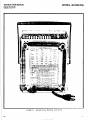
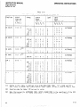
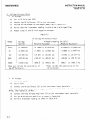
CONTENTS
I Section
I
I
CONTENTS .........................
ILLUSTRATIONS.
: : : : : :
SPECIFICATIONS
............
I.
GENERAL INFORMATION.
: : : : :
.......
l-l.
INTRODUCTION . . . . . . . . . . . . .
l-2.
FEATURES . . . . . . . . .
QARRANTY INFORMATION . . . : : : : : :
l-3.
1-4.
CHANGE NOTICE.
. . . . . . . .
OPTIONAL MODEL 1728 RECHARGEABL; ;A;T;R;
l-5.
OPTIONAL MODEL 1722 DIGITAL
INTERFACE.
l-6.
I
,
I
4.
I:5.
I
i
I
ii
Page
: :
: : : : : : : : : :
: : : : : : : : : : : : :
. . . . . . .
. .
.
. .
.
: : : : : : :
.
.
PACK: : : :
. . . . . . .
OPERATING INSTRUCTIONS ...................
3-l.
GENERAL ........................
3-2.
HOW TO SELECT POWER. .................
;I;.
HOW TO SELECT FUNCTION................................
HOW TO SELECT RANGE.
HOW TO MEASURE VOLTAGE ........
HOW TO MEASURE CURRENT (MODEL 172 ONLY):
:
HOW TO MEASURE CURRENT (MODEL 173 ONLY).
HOW TO MEASURE RESISTANCE.
..
..
...
:
FURTHER MEASUREMENT CONSIDERATIONS
;I?;.
HOW TO USE MODEL 172/173
OFF-GROUND:
: : :
3-11.
HOW TO USE OPTIONAL PROBES AND SHUNTS. ........
3-12.
HOW TO USE THE MODEL 1722 DIGITAL
INTERFACE.
ACCESSORIES ....................
GENERAL..................::::
4-l.
POWER OPTIONS. ....................
ISOLATED DIGITAL
OUTPUT. ........
:
4-4.
RACK MOUNTING. .............
4-5.
PROBE AND SHUNTS ...................
4-6.
CABLES AND CONNECTORS. ................
4-7.
MISCELLANEOUS.
....................
THEORY OF OPERATION.
....................
5-l.
GENERAL ........................
INPUT SIGNAL CONDITIONING.
..............
POWER SUPPLY, SCHEMATIC NO. 28067D ..........
DISPLAY BOARD PC-403 SCHEMATIC NO. 274780.
CURRENT BOARD, SCHEMATIC NO. 27478D.
.........
MODEL 1728 RECHARGEABLE BATTERY PACK .........
ANALOG-TO-DIGITAL
CONVERTER. .............
MODEL 1722 DIGITAL
INTERFACE ....
DETAILED II-WIRE OHMS OPERATION ...
: : :
5-9.
.
.
.
.
.
.
.
.
.
.
.
.
.
.
.
.
.
.
.
.
.
.
.
.
.
.
.
.
.
.
.
.
: : : : : :
: :
: : : :
: :
: : : :
. . .
. .
. . .
.....
::
: : : :
: :
......
: :
: : : :
.
*
.
.
.
.
.
.
.
.
.
.
.
.
.
.
.. ii
iii
"
: : : : I-I
.
. I-l
.
. l-1
.
l-l
. l-l
. .
1-I
. .
. 1-l
. .
. 2-l
. .
. 2-l
. .
. 2-l
2-l
: : : :
.
.
.
*
.
.
.
.
.
.
.
.
.
.
.
.
.
.
.
.
.
.
.
*
.
.
.
.
.
.
.
.
.
.
.
.
. . . 3-l
. . , 3-l
.
. 3-l
.
3-2
. . 3-3
. 3-4
. . . 3-5
. . . 3-6
. . . 3-7
. . . 3-8
. . . 3-11
. . . 3-12
. 3-13
. . . 4-l
* . . 4- 1
. . . 4-l
. . . 4-l
* . . 4-l
. . . 4-4
. . . 4-5
. . . 4-5
. . . 5-l
. . . 5-1
. . . 5-2
. . . 5-9
. . . 5-10
. . . 5-12
. . . S-13
. . . 5-13
. . . 5-22
. . . 5-26
AA
I
INSTRUCTION
MANUAL
Digllel Mulllmeter
Model8 172. 173
CONTENTS (continued)
I
/section
6.
Page
>_I
MAINTENANCE.
................
GENERAL. ...............
6-2.
REQUIRED TEST EQUIPMENT. ........................
6-3. PERFORMANCE VERIFICATION
6-4.
ADJUSTMENT/CALIBRATION
PR&D;R;
:
TROUBLESHOOTING AND REPAIR , .
6-5.
REPLACEABLE PARTS. . . . . . . . . . : :
7-1. GENERAL. . .
ORDERING INFORMATiON : : : : : : :
7-2.
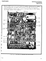
J-3. SCHEMATICS . . . . . . . . . . . .
6-1.
7.
:
:
: :
: :
:
: :
: : :
: : : : : : : : : : : :
: : :
: : : : : : : : :
6-1
6-1
6-I
6-3
6-15
:
: :
: : :
:
.
: :
. .
: :
. .
:
: :
: : :
: : : : : :
:
J-1
1
: : : : : : : : : : : : : :
. . . . . . . . . . . . .
;:;
J-1
j
)
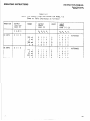
ILLUSTRATIONS
Fi g ure
No.
I
:
4
2
z
9
IO
II
12
13
I4
I5
16
17
18
19
20
21
22
23
24
25
26
27
28
29
30
;:
nb
;:a.
34b.
Title
/
6-19,
Page
iv
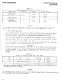
Dimensional
Data.
..........................
vi
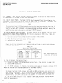
Tilt
Bail
Positions
.........................
t-2
Front
Panel
.............................
l-3
Bottom
View Showing
Line Cord ....................
2-2
Rear Panel
Showing
Current
Fuse and Check Points.
..........
2-4
Model
1728 Rechargeable
Battery
Pack.
................
2-5
Installation
of Battery
Pack.
....................
3-3
Front
Panel
Pushbutton
Selection.
..................
3-5
Typical
Model
172 Current
Display
..................
3-6
Typical
Model
I73 Current
Display
..................
3-J
Typical
2 WIRE Resistance
Measurement
................
3-9
Typical
4 WIRE Resistance
Measurement
................
3-10
Semiconductor
Diode and Transistor
Testing.
.............
3-11
Illustration
of Floating
Operation.
.................
3-14
Model
1722 Digital
Output
Interface
.................
3-15
Installation
of Model 1722. .....................
3-17
Connector
Pin Identification.
....................
3-17
Card-Edge
Connectors.
........................
3-18
1722. ...........
Location
of Jumpers
and Pull-Ups
on Model
Model
1010 Single
Rack Mounting
Kit.
..............
.4-Z
: : .4-4
Model
1017 Dual Rack Mounting
Kit.
...............
: . .5-l
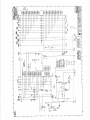
Overall
Block
Diagram
of Model
lJ2/173 .............
.5-4
DC Volts
Input
Circuit
.......................
Simplified
AC Attenuator
Circuit
.5-6
.......
1 : ‘.‘.‘:
: : : : : : . .5-6
AC Converter
Circuit
............
.5-II
Digital
Display
Multiplex
Scheme ..................
.5-14
Basic
Functional
Blocks
of A/D Converter
..............
.5-15
Basic
Charge-Balance
Converter
...................
.5-16
Operating
Waveforms
of A/D Converter
................
Simplified
Schematic
of A/D Converter.
.5-18
...............
Detailed
Schematic
of A/D Converter.
................
.5-20
A/D Converter
System Timing.
....................
.5-21
Model
1722 Block Diagram
......................
.5-24
Simplified
Ohms Diagram
(Shown in Z-WIRE Configuration).
......
.5-25
Four-Wire
Ohms Measuring
Technique
.................
.5-25
I
INSTRUCTION
MANUAL
Digltal Multimeter
Models
172,
173
12.75
(324)
I
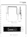
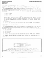
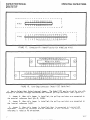
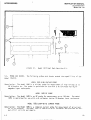
DIMENSIONS
FIGURE
1.
IN
INCHES
Dimensional
(MM)
Data.
na
I
INSTRUCTION
MANUAL
Digllal Multimeter
Model, 172, 173
SPECIFICATIONS
AA
INSTRUCTION
MANUAL
Digital
Mullimeler
Models
172.173
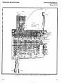
LEVEL
POSITION
- TILTBAIL
AT FRONT
r
HANGING
POSITIOI;
SHELF POSITION
45'
LEVEL POSITION
POSITION
FIGURE
vi
2.
Tilt
Bail
- TILTBAIL
AT REAR
Positions.
AA
INSTRUCTION
MANUAL
Digital Multimeter
GENERAL
Models 172. 173
I
~
INFORMATION
SECTION
GENERAL INFORMATION
172 and
l-l.
INTRODUCTION.
The Models
purpose
measuring
instruments,
resistance.
l-2.
I.
capable
173 Digital
of
measuring
Multimeters
are wide-range,
ac/dc
voltage,
ac/dc
current,
generaland
FEATURES
a.
Automatic
Ranging
and
b.
Manual
Range
C.
HI and
LO Otxns Capability
d.
Line
e.
Optional
Battery
f.
Floating
Capability
9.
Optional
Isolated
Selection
Polarity
and
Range
Hold
Operation
Operation,
to
Model
?lbOOV
Digital
1728.
peak
Interface,
Model
1722
The warranty
is stated
on the inside
front
cover
WARRANTY INFORMATION.
l-3.
If there
is a need for
service,
contact
your Keithley
representative
manual.
ized repair
facility
as given
in OUT catalog.
of
or
Improvements
or changes
to the instrument
l-4.
CHANGE NOTICE.
manual will
be explained
on a change
notice
sheet attached
to
the manual.
into
the
cover
of
not incorporated
the inside
back
the
author-
OPTIONAL MODEL 1728 RECHARGEABLE BATTERY PACK.
The Model
1728 is an accessory
l-5.
batterY
pack which
enables
either
line
or battery
operation.
The Model
1728 has builtin recharging
circuitry.
The Model
1728 is field-installed
on the Model
172/173
chasis.
l-6.
~~~~digital
OPTIONAL MODEL 1722 DIGITAL
output
option.
It provides
INTERFACE.
isolated
The model
open-collector
1722
is a field-installable
BCD outputs
and control
lines.
IMPORTANT
The A
symbol
can be found
in various
read the associated
CAUTION statements
instrument.
Damage to the instrument
Carefully
places
in this
Instruction
Manual.
with
regard
to proper
use and handling
of
may occur
if these
precautions
are ignored.
the
This
symbol
The t
symbol can be found
in various
places
in this
Instruction
Manual.
Carefully
indicates
those areas
on the instrument
which
are potential
shock hazards.
read the associated
WARNING statements
with
regard
to proper
use and handling
of the
instrument.
Serious
personal
injury
may result
if these
precautions
are ignored.
cc
l-l
GENERAL
INSTRUCTION
INFORMATION
MANUAL
Digital
Multimeter
Models
172.173
FUNCTION
AND UNITS
DISPLAY
(my)
INPUT HI AND LO, UPPER PAlR
(OHMS SOURCE. LOWER PAIR)
\\
VOLTAGE
AHPERES
DC FUNCTION
AUTORANG, NG (OUT)
MANUAL RANGING (IN)
FUNCTION
FUNCTION
LINE POWER
(LINE
AND EAT MUST BE OUT FOR BATTERY
FIGURE 3.
I
l-2
Model 173 Front
(OUT)
(IN)
CHARGE)
Panel
CC
INSTRUCTION
MANUAL
Dlgllal Multlmeler
Modelr
GENERAL
INFORMATION
172,173
I
-3
I
GENERAL
INFORMATION
INSTRUCTION
MANUAL
Digllal Mullimeter
Models 172.173
I
1
172. 173 CONDENSED OPERATING INSTRUCTIONS
II
FUNCTION
SELECTION
ME&RE
,
II
, 3,
(SE%%f,
101.9999A
LP'..
.I....
'"".q
/
1 ( HlllOD
OVERRANGE:FIRST DIGIT 3. REMAINING IIICITS
LINE
IRICKLECHARGES
OUl.CHARGES DISCHARGED 1728 IN I6 HOURS,
IN.OPERATESlNSTRUMENTfOR6HOUASFROM 1728BAT PACK,
RAT.
IfINSTAtLEO.FRON7PANELLOBAT LlGHTCIIMFSflNIf RdTTlAY
1
OPERATlONWOULOCAUSEfAULTYREAOlNGS
SELFTEST(REARPANEL))
CONNECT~NG~NPUTHITODCTERMINALW~~~CAIJSE~NSTRUMENT
DC
~~~~~~~f'PROX.5VINOCVOLTSANOImAINOCAMPS.
CONNECTlNGlNPUTHITOACTERMINALWlttCAUSElNSTRUMENT
IIAC
1
T""'*"""PROX.6VINACVOLTSANDl.2mAINACAMPS.
)
CONNECTlNGlNPUTHITOQlERMINAtWIttCAUSElNSTRUMENT
II
n
l‘
1
TIJREADAPPROX.10kIN2TERMlNALOHMS.
I
TO OPEN INSTRUMENT:CAUTION-DISCONNECTLINE CORD.LOOSEN (4) SCREWS (THIS
SIOE). HOLD INSTRUMENT TOGETHER AND TURN OVER.TltT TOP COVER BACK AND UP,
DISCONNECT (2) CONNECTORS (CURRENT FUSE LINE AND SELF CHECK).
I
l-4
AB
INSTRUCTION
INITIAL
MANUAL
PREPARATION
Digital Mulllmeler
Models
172.
173
I
SECTION
2-l.
GENERAL.
preparation
for
2-2.
trically
which
verify
This
use.
section
INITIAL
2.
provides
PREPARATION
information
needed
for
incoming
inspection
and
INSPECTION.
The Model
172/173
was carefully
inspected
both mechanically
and elecUpon receiving
the instrument,
check for any obvious
damages
before
shipment.
Report
any damages to the shipping
agent.
To
may have occurred
during
transit.
follow
the procedures
given
in Section
6.
the electrical
specifications,
2-3.
PREPARATION FOR USE.
The
can be powered
from line
voltage
optional
Model
1728 Rechargeable
Model
172/173
is shipped
ready-to-use.
or from rechargeable
nickel-cadmium
Battery
Pack is installed).
The Model 172/173
has an attached
receptacles
(NEMA 5-l5P).
The
the cord around
the base of the
Line Power.
a.
third-wire
grounded
stored
by wrapping
three-wire
permanently
instrument
The
batteries
instrument
(when
the
line
cord which
mates with
installed
line
cord
is
as shown in Figure
4.
CAUT I ON
This
234V
instrument
position
for
has an internal
line
power
operation
above
125 volts
selector
switch
rms, 50-60 HZ.
that
must
be set
to
The Model
172/173
has a
1. How to Set the Internal
Line
Voltage
Switch
(~601).
To set the switch
for
two position
slide
switch
located
on the main circuit
board.
The top cover
must be
operation
above I.25 volts
the switch
setting
must be changed.
removed
to gain access
to the circuit
board
as described
in MAINTENANCE section.
WARNING
t
Disconnect
voltage
is
HAZARD.
the line
cord before
removing
present
at various
points
on
Other
line
transformer
voltage
ranges
T601 as shown
Summary
of
are available
on schematic
Standard
to
125 V rms
210
to
250 v rms
NOTE
when wiring
28067~1.
TABLE
and
2-l.
Optional
the
and
instrument.
represents
modifications
Line
are
Line
a SHOCK
made
to
Voltages
Optional
Standard
I05
the top cover
of
the circuit
board
90 195
-
105 v rills
210 v
rms >
Transformer
wiring
must be modified
2-l
.INITIAL
PREPARATION
INSTRUCTION
MANUAL
Digital Mullimeler
Models
SELF
FIGURE
2-2
5.
Rear
Panel
Showing
172.173
FUSE
Current
Fuse
and
Check
Points
AA
STRUCTION MANUAL
.gllel MultImeter
INITIAL
PREPARATION
~~Modelr 172, 173
2.
Line
line-operated
l/4 ampere
A
Replace
The Model 172/173
use a single
line
Fuse Requirement.
The fuse
is a 3 AB or 3 AG, slow-blow
power supply.
for
117 volts
operation
or l/8 ampere for 234 volts.
IMPORTANT
fuse
with
correct
otherwise
rating
damage
to
the
fuse
to
type.
instrument
protect
the
with
Replace
could
result.
the Line Fuse.
3. How to Replace
The fuse
is installed
on the main circuit
board
as shown in Figure
36 (page 6-10).
The top cover
must be removed
to gain access
to the
circuit
board as described
in Section
6. Use Keithley
FU-17 for
117 V; FU-20 for 234V.
WARNING
t
Disconnect
voltage
is
HAZARD.
the line
present
cord before
removing
at various
points
on
the top cover
of
the circuit
board
the
and
instrument.
represent
Line
a SHOCK
CAUTION
A
The fuse
installed
range protection.
b.
Battery
Rechargeable
factory-installed
on the rear
panel
of the Model
This
fuse
is -not a line
voltage
172/173
is
protection
To operate
the Model
172/173
from batteries,
Power.
The Model
1728 can
Battery
Pack must be installed.
(at the time the Model
172/173
is purchased).
used only
fuse.
for
current
the Model
1728
be either
field
or
NOTE
The Model
1728 Rechargeable
Battery
Pack can be installed
However,
if the Model
1722
Model
172/173
at any time.
the Model
1728 cannot
be used simultaneously.
installed,
1.
How to Install
the Model
with
the Model
1728 are already
cludes
7 rechargeable
“C” cells
cells
per pack).
See Figure
6.
a)
3AB or
Check the fuses
3 AG, Slo-Blo
1728 Rechargeable
installed
(l.ZV,
on the Battery
types,
Keithley
b)
Check for proper
installation
battery
cells
are to be installed,
individual
cells
as shown in Figure
in the
2 AMP Hr)
Battery
battery
and two
Three
fuses
Pack.
Part
No. FU-IO.
of batteries
be certain
6.
to
in the
observe
by
Digital
the user
Output
within
the
is already
The batteries
furnished
Pack.
pack.
The battery
pack in19.2 volt
packs
(sixteen
l.ZVare
used.
All
are
If
Battery
Pack.
the proper
polarity
I ampere,
replacement
of the
turn
the instrument
over so that
the bottom
cover
c)
To install
the Battery
Pack,
The
Loosen
four
slotted
screws
on the bottom
cover
as shown in Figure
4.
faces
up.
Turn over
the instruthat
is they cannot
be removed
completely.
screws
are captive,
care
to hold
the top and bottom
covers
toment with
the top cover
facing
up, taking
Carefully
remove
the top cover
to gain
access
to the printed
circuit
board.
gether.
There are 2 connections
between
the top cover
and the main circuit
board which
must
Check
to
see
that
the
four
be temporarily
removed
in order
to free
the top cover.
insulating
spacers
are in position
on the circuit
board
as shown in Figure
7. Plug
into
the
mating
receptacles
(~602,
P606)
takthe two S-wire
connectors
(J401,
J402)
Place
the
Model
1728
in
position
on
the
ing care to orient
the connectors
as shown.
Replace
the connectors
from the
spacers
with
the pack oriented
as shown in Figure
7.
Turn over
the instrument
with
Replace
the top cover.
top cover
to the circuit
board.
the bottom
cover
facing
up and tighten
down the four
slotted-head
screws.
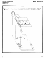
I B
2-3
INITIAL
PREPARATION
INSTRUCTION
MANUAL
Digilal
Mullimeler
Models
172. 173
J402
a..-- .~
FIGURE 6.
Model
1728
Rechargeable
Battery
Pack.
I
INSTRUCTION
Digital Multimeter
Models
MANUAL
INITIAL
PREPARATION
172.173
WARNI NG
t
Disconnect
Line voltage
HAZARD.
the
is
line
cord on the instrument
present
at various
places
FIGURE
CB
7.
Installation
before
on the
of
the Battery
Pack
circuit
board and
Battery
is installed,
is a SHOCK
Pack.
2-5
INITIAL
PREPARATION
INSTRUCTION
MANUAL
Digilal Multimeler
Models 172.173
Summary
TABLE 2-2.
Batteries
Used
of
Description
7
+19.2V
(l6-l.2V
pack
cells)
1
-19.2V
(16-l.2V
pack
cells)
I
the
Model
1728
Keithley
Voltage
Quantity
I 2V “C” ccl I
(; AMP-HR)
in
8.4v
I
+19.2v
Part
No.
BA- 30
I
BA-31
I
-19.2v
BA-3 I
CAUTION
A
The
the
Model
1728
pack should
2.
How to
Check
is shipped
be installed
from
in
the factory
the Model
in an uncharged
condition.
172/173
and charged
prior
Therefore
use.
to
Batteries.
LO BAT indicator
to permit
easy determination
a) The Model 172/173 has a built-in
of battery
condition.
The Model
172/173
also
has an individual
test
point
on the
bottom
panel usually
needed only
for
troubleshooting
purposes
(see Figure
4.).
b)
The LO BAT indicator
will
be lighted
when the
operating
voltage.
When the indicator
turns
on the
to LINE or OFF to permit
recharging
of the Pack.
C)
suring
The test
point
instrument.
may be checked
at any time
Then voltages
are summarized
Battery
Model
Pack
172/173
using
the Model
in Table
2-3.
goes belag
normal
should
be s,+jitched
172/173
or
other
mea-
IMPORTANT
The instrument
must be operated
in BAT mode in order
to obtain
a valid
battery
condition
at test
point
“A”.
This will
ensure
that
the batteries
are supplying
power
to the instrument.
If the voltage
is measured
when the Model
172/173
is operated
in the LINE mode a different
reading
may be observed
since
the batteries
are being
charged.
Summary
Test
Point
I’A”
of
Acceptable
Battery
TABLE 2-3.
Voltage
Battery
Levels
Range
)
ITV + t20.5V
Levels
(BAT mode)
Recharge
if Below
Normal
+19.2
Battery
Tested
BT402
ITV
The Model
1728 provides
built-in
recharging
cir3. How to Charge the Batteries.
Recharging
occurs
at
cui try.
The Model
172/173
must be connected
to line
voltage.
the recharge
time
Typically,
most rapid
rate when the Model
172/173
is set to OFF.
2.5 hours
per hour of discharge.
the
is
CAUT I ON
A
2-6
Overcharging
may shorten
the batteries
the life
of
the
will
raise
batteries.
the
internal
temperature
of
the
battery
pack
and
CB
INSTRUCTION
MANUAL
OPERATING
Digital Multimeter
Models
172.
INSTRUCTIONS
173
SECTION
3- 1.
GENERAL.
for measurement
This
section
of voltage,
3.
provides
current
OPERATING
INSTRUCTIONS
information
and resistance.
needed
to
operate
HOW TO SELECT POWER. The Model
172/173
may be powered
3-2.
chargeable
nickel-cadmium
batteries
(when the Model 1728 is
173 has a built-in
line-voltage
power supply
and power cord.
the
from line
installed).
Model
172/173
voltage
or reThe Model
l72/
NOTE
The accessory
llodel
1726 Rechargeable
Battery
Pack may be ordered
purchase
of the Model
172/173
or may be purchased
and field-installed
time
if so desired.
The Model
1728 features
plug-in
wiring
and,
modifications
need to be made to the Model 172/173
chassis.
a.
How to Operate
from Line Power.
age over
four
ranges
from a minimum
of
summarizes
the line
voltages
permitted.
I .
Set
the
2.
Plug
3.
Depress
internal
the
line
line
cord
The Model 172/173
can
90 V rms to a maximum
voltage
into
switch
source
of
to
line
either
ll7V
at
the time of
at a later
as a result,
no
be powered
from line
of 250 V rms.
Table
or
volt3-l
234V.
power.
LINE pushbutton.
NOTE
Power on will
surement
unit
be indicated
showing.
by
a lighted
How to
How to
Operate
from
Model
Battery
I.
Install
the
2.
Depress
BAT pushbutton.
hoz;s
If
to
1728
one
or
more
and
mea-
-;
<<For these
ranges
the
leads
must be rewired
NO
Yes
digits
_.
Transformer
Modification:‘:
yes ;‘;
ll7V
117v
234V
234V
go- 105V
lO5-125V
195-2lOV
210-25ov
with
TABLE 3-1.
Set Line Voltage
Switch
5601
Range
Desired
b.
display
7:
NO
Power.
Rechargeable
Battery
Pack.
(See
Section
2,
the battery
pack must be charged
LO BAT indicator
is lighted
provide
fully
charged
opera;ion
of the Model
172/173.
page
Z-3.)
a minimum
of
16
NOTE
To charge
the Model
1728, release
both LINE and BAT pushbuttons
and connect
the
line
cord to line
power.
If it is desired
to use the Model
172/173
immediately,
depress
LINE.
The Model
172/173
will
be useable
for measurements
although
the
battery
charging
rate
is decreased
considerably.
4.
used
CB
If
for
the LO BAT indicator
measurements.
is
not
lighted
in
BAT mode,the
model
172/173
may be
3-l
3PERATING
INSTRUCTIONS
lNSTRUCTlON
MANUAL
Digital Mullimeler
Models
172,
173
NOTE
The Model
1728 is shipped
from the
Model
1728 should
be installed
and
been charged
for at least
16 hours,
for at least
6 hours.
Summary
of
factory
in uncharged
condition.
Therefore
the
charged
prior
to use.
After
the Model 1728 has
the Model 172/173
can be powered
continuously
TABLE 3-2.
Ooeration
in LINE
Condition
Line
Button
Power
Connected
installed
1728 not
Depressed
LINE
Line
ON
trickle
Battery
OFF
OFF
OFF
Battery
charged
imum rate.
I
HOW TO SELECT FUNCTION.
3-3.
V/A, and R
d.
rent
DC.
fu#lct
This
ions.
pushbutton
Function
must
be used
is
with
1.
DC Voltage.
Depress
DC
Release
2.
DC Current.
Depress
DC
Uepress
AC.
This
fe Ict ions.
b.
rent
pushbutton
Instrument
Line
Power Not Connected
1728 installed
OFF
charged.
ON
Batteryslowly
NE I THER
LINE NOR BAT
BAT Modes
Power Connected
1728 installed
ON
BAT
of
and
must
be used
with
selected
ON
discharged.
OFF
at
max-
by means
V/A to select
of
four
pushbuttons
AC,
DC,
either
DC voltage
or
DC cur-
either
AC voltage
or
AC cur-
V/A
V/A
V/A to select
I.
AC Voltage.
Depress
AC
Release
V/A
2.
AC Current.
Depress
AC
Depress
V/A
t.
V/A.
This
pushbutton
selects
either
voltage
resistor
is connected
along
with
DC or AC, a shunt
vide current
sensing.
d.
{I.
Depress0
to measure
resistance.
NOTE
V or
across
current
the
HI
A.
When V/A is
and LO terminals
are interlocked
so that
only
one pushbutton
is
DC. AC, and Sl pushbuttons
depressed
at a time.
However,
it is possible
to have all
pushbuttons
out
disconnects
the input
HI and LO terminals
and no measurement
can be made.
R indicator
will
be lighted
in this
instance.)
depressed,
to
pro-
which
(The
AA
I
INSTRUCTION
I
Dlgllal
MANUAL
OPERATING
Models
8.
FIGURE
Front
Panel
Pushbutton
The Model
172/173
provides
3-4.
HOW TO SELECT RANGE.
AmO/M4N
pushbutton
determines
the ranging
mode, where
AUTO.
When released
, the
in accord
with
the following
a.
range
I.
to
to
b.
INSTRUCTIONS
Mulllmeler
172. 173
less
Model
172/173
rules.
When the display
exceeds
29999 the
sensitivity
and the decimal
point
When the display
2.
greater
sensitivity
MAN.
reaches
and the
When depressed
the
or downrange
172/173 to uprange
Selection.
automatic
or
AUTO = fully
automatically
manual
ranging.
automatic
ranging.
selects
Model 172/173
upranges
moves appropriately).
the
(that
02599 the Model
172/173
downranges
decimal
point
moves appropriately).
range
is
by using
appropriate
is,
(that
The
it
is
placed
in hold.
The user can cause the
the UP RANGE and DN RANGE pushbuttons.
changes
it
changes
Model
1.
When DN RANGE is momentarily
depressed
the Model
172/173 will
downrange
one
decade of sensitivity.
Each time the pushbutton
is depressed
and released,
one
downrange
will
occur
until
most sensitive
range
is obtained.
2.
When UP RANGE is momentarily
depressed
of sensitivity.
Each time the pushbutton
is
,occur until
least
sensitive
range
is obtained.
I
AA
the model
depressed
172/173
will
and released,
uprange
one
one uprange
decade
will
3-3
OPERATING
INSTRUCTIONS
INSTRUCTION
MANUAL
Digital
Multimeter
Models 172.173
3-S.
HOW TO MEASURE VOLTAGE.
172/173 measures
The Model
ranges:
0.3V,
3V, 3OV, 300V and 12OOV DC (1000VAC).
CAUTION
input
voltage
depends
on the range selected.
continous
input
for each range on AC and
damage to the instrument
will
occur.
TABLE 3-3.
Maximum Allowable
Continuous
Maximum
allowable
aqes or
I.
Set
to
DC Volts.
2.
Set
to
AUTO.
3.
4.
Observe
the displayed
digits,
unit
(mV or V).
If no polarity
b.
AC Voltage.
The Model
volts
(1000.0
display).
The
a 3 remains
lighted,
but all
volts
on the highest
range.
I.
Set to AC Volts.
2.
Set
3.
Table
3-3 gives
Do not exceed
to
(The
polarity
sign
l72/173
detects
ac voltages
maximum display
is 29999.
other
digits
are blanked.
AC indicator
should
Observe
five
the maximum
these volt-
+I0 microvolts/digit
to
When the display
exceeds
The display
blinks
above
sign,
decimal
point
indicated,
a positive
is
in
Input
(The terminals
BG-5 or accessory
location,
polarity
and measureis implied.
from IO microvolts
rms to 1000
When the display
exceeds
29933,
The display
blinks
above 999.9
be lighted.)
AUTO.
to be measured
between
HI and LO terminals.
Connect the signals
designed
to accept
banana
style
plugs,
such as Keithley
part
no.
leads
such as t+odel
1681 Clip-On
Test Leads.)
4.
or
dc voltage
Connect
the Signal
to be measured
between
HI and LO terminals.
designed
to accept
banana style
plugs.
Such as Keithley
part
no.
leads
such as Model
I681 Clip-On
Test Leads.)
ment
are
test
DC.
172/173 detects
dc voltages
from
The Model
display).
The maximum display
is 29999.
but all
other
digits
are blanked.
a 3 remains
lighted,
volts
on the highest
range.
,law.O
29999,
1199.9
are
test
ac and
the
displayed
digits,
decimal
point
location,
and
(The terminals
BG-5 or accessory
measurement
unit
(mV
V).
CB
INSTRUCTION
Dlgltal
OPERATING
MANUAL
INSTRUCTIONS
MultImeter
Models 172.173
3-6.
in two
DMM is
How TO MEASURE CURRENT. (MODEL 172 ONLY).
The
ranges:
0.3A, and ZA. The current
is limited
capable
of displaying
2.9999A.
CAUTION
Model
172 measures ac and
by the current
fuse even
The Model
172 is protected
by a 2 ampere fuse on all
ranges.
be installed
in
a replacement
Keithley
Part No. FU-13 should
holder.
(See Figure
5.)
A
If
the
dc current
though
the
the fuse
is blown,
rear
panel
fuse
The Model
172 detects
dc currents
from ?I0 microamperes/digit
to 22
DC Current.
When the input
exceeds
2 amperes,
the current
fuse will
blow.
When using
the
MAN mode it is possible
to select
30A, 300A & 3000A Ranges,but
2A Max is sti))
the limit.
a.
.3”pZl-l?S.
I .
Set
to
DC Amperes.
2.
Set
to
AUTO.
3.
Connect
the
signal
to
Observe
the displayed
4.
ment unit
(LIA, mA, or A).
implied.
be measured
at
the
HI
digits,
polarity
sign,
If no polarity
sign
is
terminal.
decimal
indicated,
point
location,
a positive
and measurepolarity
is
ac currents
from 10 nanoamperes
rms/digit
The Model 173 DMM detects
AC Current.
When the display
exceeds
29999,
a 3
tobj
amperes
rms.
The maximum display
is 29999.
remains
lighted,
but all
other
digits
are blanked.
I .
Set
to AC Amperes.
2.
Set
to Auto.
3.
Connect
Observe
4.
PA, AC ma, or
the
signal
(The
to
the displayed
AC A).
:I
-
be measured
digits,
/Ill
at
decimal
‘ql
L
FIGURE 9.
CB
AC indicator
1:;
should
be
the
terminal.
HI
point
lighted.)
location,
lq
and measurement
unit
(AC
mV
OAC
.,,,A
on
okn
0,”
OWU-I
.
Typical
Model
172 Current
Display
(DCmAJ.
3-5
OPERATING
INSTRUCTIONS
INSTRUCTION
MANUAL
Digital Multimeter
Models
3-7.
HOW TO MEASURE CURRENT. (MODEL 173 ONLY.)
The Model
dc current
in five
ranges:
0.3mA,
3mA, 30mA, 0.3A,
173 measures
and 3A.
172.173
ac and
CAUTION
The Model
I73 DMM is protected
blown,
a replacement
Keithley
fuse
holder.
(See Figure
5.)
a.
The Model
DC Current.
The maximum display
amperes.
lighted,
but all
other
digits
1.
Set
to
2.
Set
to AUTO.
3.
Connect
by a 3 ampere fuse
Part No. FU-2 should
on all
ranges.
be installed
173 DMM detects
dc currents
When the display
is 29999.
are blanked.
from ?I0
exceeds
If
in
the
the
nanoamperes
to 13
a 3 remains
29999,
DC Amperes.
the
signal
to
be measured
4. Observe
the displayed
ment unit
( A, mA, or A).
implied,
If
at
the
HI
digits,
polarity
sign,
no polarity
sign
is
terminal.
decimal
indicated,
point
location,
a positive
and
polarity
The Model 173 DMM detects
ac currents
from
IO nanoamperes
b.
AC Current.
When the display
exceeds
3 amperes
rms.
The maximum display
is 29999.
:o
-emains
lighted,
but all
other
digits
are blanked.
I.
Set
to AC Amperes.
2.
Set
to AUTO.
3.
Connect
4.
A,
Observe
AC ma, or
the
signal
(The
to
the displayed
AC A).
FIGURE
3-6
fuse
is
rear panel
AC indicator
be measured
digits,
10.
Typical
should
at
decimal
Model
the
HI
point
be
measureis
rms/digit
29999,
a 3
lighted.)
terminal.
location,
and measurement
.AC
OmV
OV
on
0ki-i
OMa
o,M
.mA
OA
173 Current
Display
unit
(AC,
(ACmA).
CB
INSTRUCTION
MANUAL
OPERATING
INSTRUCTIONS
Dlgltal MulIimeler
Models 172. 173
HOW TO MEASURE RESISTANCE.
3-8.
The Model
172/173 measures
resistance
fro-,
10 milliohms/d iq i t to 300 megohms.
When the display
erceeds
The maximum display
is 23939.
29999,
a 3 remains
lighted,
but all
other
digits
are blanked.
a.
HI Ohms Measurement.
When the HI/LO
pushbutton
is released
(set
to HI),
the Voltage developed
~CTOSS
the resistance
under
test
at full
range
js 3 volts,
The Model
172/
173 measures
to 300 megohms in HI mode.
For the 2 wire
method
the lower
set of terminals
is not used.
I.
Set
to
HI
2.
Set
to
2 WIRE.
Ohms
NOTE
terr!iiials
When the.Ilodcl
172/173
is set to 2 WIRE, the Iov~er set of HI and LO in;,ut
set of HI il~~(l LO input
terr;i~lals
When set to 4 WIRE, the higher
are not cnnncctcd.
See Section
3-S for more detailed
inforare used as “voltage
sensing”
terminals.
mation.
Set to AUTO.
3.
4.
Connect
the
resistance
5.
Observe
MC).
the
displayed
KR, or
under
digits,
test
between
decimal
the
point
upper
location,
b.
LO Ohms Measurement.
When the HI/LO
pushbutton
age developed
across
the resistance
under
test
at full
Model
172/173
measures
to 30 megohms in LO mode.
For
terminals
is not used.
Set to LO Ohms.
I.
2.
Set
to
2 WIRE.
3.
Set
to
AUTO.
4.
Connect
the
resistance
Observe
Kc!, or MR)
the
displayed
digits,
illustration
is
5.
This
under
test
between
decimal
typical
point
of
the
For
When measuring
use the 4-wire
a pair
of IOft
FIGURE
iB
of
and
is released
range
is
the 2 wire
upper
location,
a Z-terminal
ifF-~/--qiy=j
to
example
set
set
HI
and
LO terminals.
meaSurement
unit
(c,
(set
to LO), the volt300 millivolts.
The
method
the lower
set of
of
and
ohmmeter
HI
and
LO terminals
measurement
unit
(:.,
design.
OHMMETER
resistance
less
than 1OOOohms it may be necessary
mode to eliminate
the measuring
error
of the test
leads.
leads made from I8 AWG copper
wire
has 0.14 ohms resistance.
11.
Typical
2 WIRE Resistance
Measurement.
3-7
I
OPERATING
INSTRUCTION
INSTRUCTIONS
MANUAL
Dlgilal
Multimeler
Models
172.
173
FURTHER MEASUREHENT CONS I OERATI ONS.
3-Y.
a.
DC Voltage
Measurements.
1.
Overloads.
When the
an overload
condition.
display
exceeds
?lZOO.OV
DC all
digits
blink
to
indicate
2.
The input
resistance
is
1,000 HR on the 0.3V and 3V ranges;
Input
Resistance.
The effects
of circuit
loading
should
be
IO MC?on the 3OV, 3OOV, and 3000V ranges.
considered
when evaluating
total
accuracy
of measurement.
(See Accuracy.)
The Model
172/i73
accuracy
is specified
in terms of 4 of reading
and
Accuracy.
3.
For a full
range
reading
of 299.99
mV DC the accuracy
of measurement
a % df range.
would
be + (0.03
mV + 0.01 mV) or +0.04
mV. Measurements
from relatively
high
source.
resistances
could
cause an additional
reading
error.
The amount of error
due to
loading
can be determined
by the following
relationship:
% error
= 100 x Rs i
(Rs + RI)
resistance
in ohms
Rs = source
RI - input
resistance
of Model
172/173
in ohms
Self-Check
Feature.
4.
The Model
172/173
has a rear
panel
Voltage
test
point
for
functional
check of the Model
172/173
in DC Volts.
To use this
feature,
connect.the
input
HI terminal
to the rear panel white
terminal.
Verify
a display
of approximately
5 volts
dc.To
check dc current,
depress
V/A andverify
a display
of 1 mA.
b.
AC Voltage
Measurements
where
1.
dicate
2.
Overloads.
an overload
Input
When the
condition.
Impedance.
The
display
input
exceeds
impedance
1000.0
is
V AC (t-m)
2 megohms
The effects
of circuit
loading
should
picofarads.
(See Accuracy.
)
total
accuracy
of measurement.
all
shunted
be considered
digits
by
when
blink
less
to
than
in-
50
evaluating
the
The Model
172/173
operates
as an average-reading
voltmeter,
AC-to-DC
Conversion.
3.
The calibration
is
calibrated
in terms of the root-mean-square
(rms)
of a sine wave.
exact
for sinusoidal
waveforms
in the specified
frequency
range.
4.
Frequency
mum and maximum
Response.
frequencies
The frequency
range
given
which
accuracy
is valid.
The Model
172/173
accuracy
is
Accuracy.
5.
Measurements
from relatively
and a % of range.
The amount of error
additional
reading
error.
the following
relationship:
% error
where
in
the
specifications
is
the
mini-
specified
in terms of a % of reading
high
source
impedance
could
cause an
due to loading
can be determined
by
= 100 x zs fsZin
Zs = source
Zin = effective
impedance
input
impedance
of
Model
172/173
The Model
172/172
has a rear
panel
Voltage
test
point
for
6.
Self-Check
Feature.
functional
check of the Model
172/173
in AC Volts.
To use this
feature,
connect
the
Connect
the line
cord to line
voltage.
HI terminal
to the rear panel
red terminal.
Verify
a display
of approximately
6 volts
ac. To check ac current,
depress
V/A and
verify
a display
of approximately
1.2 mA.
AA
1
INSTRUCTION
MANUAL
Digital MultImeter
OPERATING
INSTRUCTIONS
Models 172, 173
c.
Current
Measurements.
Overloads.
I.
Fuses
Shunt Resistance.
terminals
at full
2.
input
For example,
in a voltage
are
as
follows:
Model
172:
The Model
173 develops
range.
The 172 has 1.3
on the 300 milli-ampere
range
the
drop of 0.3 x 1.3 = 390 millivolts
2A
Model
173:
3A
approximately
300 millivolts
R on all
ranges.
shunt
resistor
at full
range.
is
1.3
ohm,
across
which
the
results
3.
Accuracy.
The Model
172/173
accuracy
is specified
in terms of a % of reading
and a pl of range.
An additional
reading
error
should
be considered
if the source
resistance
is not greater
than
1000 times
the shunt
resistor.
The amount of error
can
be determined
by the following
relationship:
where
d.
Resistance
I.
sine
HI
3.
or
resistance
resistance.
of
the
Model
172/173
Measurements.
Maximum Allowable
wave or t250V dc.
Polarity
2.
terminal.
Rin = shunt
Rs = source
of
Voltage
Ohms.
Input.
The Model
Maximum Open-Circuit
LO ohms, the maximum
The
172/173
maximum
provides
When the HI and
developed
between
Voltage.
voltage
This
illustration
is typical
using
a separate
Voltmeter
combines
these
features.
input
should
a positive
not
voltage
LO terminals
HI and LO is
exceed
at
are open
+5 volts.
250V
the
in
rms
HI
either
of a 4-terminal
measuring
technique
The Model
172/173
and Current
Source.
“HI”
“LOW”
LEADS
LEADS
RSOURCE HIGH
R SOURCE LOW
When using
the 4-WIRE method,
connect
one pair
Connect
a
“current”
leads
to n SOURCE input.
second
pair
of “voltage”
leads
to HI and LO.
Then set to 4 WIRE.
of
Care should
be taken
to connect
"current"
leads
and “voltage”
leads
properly.
The LO terminal1
and R Source
low must always
connect
to the same
side of the unknown
resistance.
FIGURE
CB
12.
Typical
4 WIRE Resistance
Measurement
3-v
OPERATING
INSTRUCTIONS
INSTRUCTION
MANUAL
Digital Multimeler
Models 172.173
Four-terminal
Measurements.
4.
The II-WIRE mode connects
the lower
set of R SOURCE
terminals
As shown in Figure
I2 the lower
terminals
to the DMM ohmmeter
source.
are the current
carrying
terminals
while
the upper
terminals
are the voltage
sensing
terminals.
This arrangementeliminatesthe
error
due to voltage
drop across
the current-carrying
leads.
Diode
and Transistor
Testing.
The Model
172/173
can be used to
5. Semiconductor
test
diodes
and transistors
to determine
the relative
condition
of the device.
For
semiconductor
diodes,
the voltage
applied
must be sufficient
to cause conduction
in the
The “HI OHMS” mode provides
a voltage
up to 3 volts
at a current
“pto
forward
direction.
I milliampere.
Since
the HI terminal
is positive
with
respect
to LO terminal,
connections
should
be made as shown in Figure
13 to cause forward
conduction
of diodes.
Since
the maximum current
is available
on the 3 K:. range,
depress
AUTO/HAN (Set to
MAN) and manually
range
to the 3 KI: range
(down-range!.
The Model
1;12/173 has a rear panel
ohms
Feature.
6. Self-Check
functional
check of the Model
172/173
in OHMS. To use this
feature,
Connect
the HI terminal
to the blue
terminal.
OHMS and 2 WIRE mode.
of approximately
IO kilohms.
test
point
for
place
the DMM in
Verify
a display
HI
i
TYPICAL
TYPICAL
DIODE
FIGURE
13.
Semiconductor
Diode
and
PNP TRANSISTOR
Transistor
Testing.
AA
INSTRUCTION
Dlgllsl
Models
MANUAL
OPERATING
INSTRUCTIONS
Multimeter
172,
173
3-10.
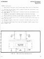
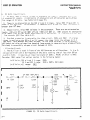
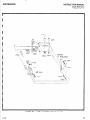
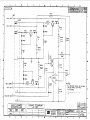
HOkl TO USE MODEL 172/173 OFF-GROUND.
The "LO" terminal
can be operated
off
ground
at potentials
of up to ?14OOV.
Isolation
from the "LO" terminal
to power line
Ty ically,
the isolation
ground
is specified
at IOOOMR, or IO'ii
(shunted
by 300pF).
resistance
from LO to CND is two decades
greater
than
10qR (10 PI n).
Because of this
excellent
isolation,
ground
results
in very
little
operating
the Model 172/173 off
loading
(from
LO to GND) of a floating
source.
At IOOOV above ground,
the Model 172/
173 will
require,
typically,
only
IOnA from the source.
The excellent
isolation
also
accounts
for
the high common-mode
rejection
ratio
of the Model
172/173.
Even with
the
"HI"
terminal
driven
and a source
resistance
of lkR,
1000 VDC (from HI to GND) will
produce
typically
only
IOuV DC error.
This error
voltage
is determined
directly
from
the ratio
of the source
resistance
to the "isolation"
resistance
(See Figure
14).
, - lOOOV
- 10-sA
V
to"n
across
Ik
=
I x Iki:
= IO-'
x IO3 = 1O;VDC
The "isol
ation"
capacitance
frwn LO to GND is important
when AC cornnon-mode
signals
are
present.
In the Model
172/173 this capacitance
is specified
at 300 pF.
At a frequency
of
60~2,
300 picofarads
has a reactance
of approximately
IOHR.
With the HI terminal
driven
and a source
impedance
of lkn,
a IOOOV p-p,
60 Hz, common-mode
signal
will
produce
a voltage
of only
IOOmV p-p across
the input
terminals.
This
IOOmV
p-p signal
will
be further
rejected
by the input
filter
and A-D converter
so that
the
total
rejection
at the digital
display
is at least
120 dB
(HI d riven,
IkT. source
impedance).
For DC voltage
measurements,
rejection
is much greater
than specified
when
the Model 1721173 LO terminal
is driven,
rather
than the HI terminal.
Where there
is
a need for even greater
isolation
from LO to power line
ground,
or where
there
is a need
to float
at potentials
greater
than 1400 volts
above power line
ground
the Model
1728
Battery
Pack should
be used.
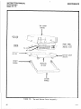
r-------------I
1
I
II:PlJl
,
I
I
l+L&
I
lKI!
SOURCI
SlSTANCL
(7ERNAL
:"IIQCF
I
I
I
I
DIGllAL MULlIMEliF.
,
10l'n
*
I
-1
-
TYPlCAL
1s~OLAllON
RESISTANCE
I
14.
Use of
L----------r
Multimeter
Off
I
I
I
GROiND
FIGURE
I
I
I
I
Ground.
I
OPERATING
INSTRUCTION
INSTRUCTIONS
MANUAL
Digital Mullimeler
Models
3-11.
172.
173
How TO USE OPTIONAL PP!IBFS AND SHUNTS.
a.
Model 1600 High Voltage
Probe.
Set the Model
172/173
to DC volts
and 30 volt
range.
The input
resistance
on the 30 volt
range
is IO megohms so that
no shunt
resistor
is needed.
The Model 1682 has a 1OOO:l division
ratio.
For maximum safety
review
the
instructions
furnished
with
the Model
1600 probeabove
30kV, switch
to the 300V range.
CAUTION
A
The alligator
clip
(ground)
age is not applied
between
occur
if the alligator
clip
b.
Model 1682 RF Probe.
Model
1682 has a IVdc output
100 MHz.
must be connected
to the source
low so that
high
voltlow and ground.
Severe
damaqe to the instrument
will
is not connected.
Set the Model
corresponding
The
172/173
to DC volts
and 30 volt
range.
to I V rms input
over
the range
100 kHz to
IMPORTANT
For use on the
should
be used
3 ‘volt
and 0.3
3 volt
range the banana
since
the Model 172/173
volt
ranges.
Model 1685 Clamp-On
AC Current
C.
volt
range.
The Model
1685 provides
rms input.
Review the instructions
sible
accuracy.
plug
input
adapter
(with
IO megohm resistor)
resistance
is >lOOO megohms on
the
Set the Model
172/173 to AC volts
and 0.3
Probe.
a 0.1 volt
rms output
corresponding
to a I ampere
furnished
with
the Hodel
1685 to achieve
best pos-
d.
Model 1651 Current
Shunt.
Set the Model 172/173
to AC or DC volts
(as appropriate)
and 0.3 volt
range.
Connect
the voltage
leads
to the Model
172/173
input
terminals.
Connect
separate
leads
(not
furnished)
between
the source
and the Model
1651 hex-head
bolts.
The Model 1651 shunt
resistance
is 0.001 ohm which
produces
a sensitivity
of I
millivolt
per ampere.
AA
INSTRUCTION
Dlgllsl
MANUAL
OPERATING
INSTRUCTIONS
Multimeter
Models
172,
3-12.
173
HOW TO USE THE MODEL 1722
DIGITAL
INTERFACE.
a.
THE Model
1722 provides
binary
coded decimal
outputs
(8421)
and range
General.
control
lines.
Outputs
are open-collector
positive
true
unless
otherwise
specified.
The
This accessory
is available
either
"factory
installed"
or "field-installable".
Model
1722 consists
of a two-layer
circuit
with
card-edge
and mating
output
connectors.
installation.
b.
I.
Disconnect
2.
Turn
the
1?2/173
over
line
cord
so that
the
from
bottom
line
voltage,
cover
faces
the instrument
with
covers
together.
the
top
cover
facing
remove the top cover
to gain
access
5. Carefully
There
are 2 connections
between
the top cover
and the
be temporarily
removed
in order
to free
the top cover
6.
Remove the Model
1728 Rechargeable
Battery
connectors
from the mother
board.
disconnect
up.
slotted
screws on the bottom
cover
as shown
that
is,
they cannot
be removed
completely.
Turn over
and bottom
4.
top
Model
instrument
Loosen
four
are captive,
3.
screws
the
the
up,
in
Figure
taking
4.
care
The
to hold
to the printed
circuit
board.
main circuit
board which
must
(see Figure
40.)
Pack.(if
installed).
Carefully
NOTE
The Models
1722 and
at the same time.
7.
board
as
8.
9.
board,
Check to see that
shown in Figure
Place
the
Model
1728 cannot
the
16.
four
1722 on the
11.
Replace
the
12.
Reinstall
13.
Turn
the
return
wire
connections
the
top
instrument
installed
insulating
spacers
Lift
up the Model
1722 slightly
and plug
in connectors
JlOO3,
Connect
ground
10.
transformer
TIOI.
be
to
the
the
as
shown
Model
top
cover.
tighten
the
Model
in
in
access
JIOOI
Figure
to
(in
1722
to
172/173
position
on
chassis
the
16.
the Model
172/173
order
given).
the
circuit
extra
lug
mother
on
cover.
over
and
four
The Model
I722 uses two
Connector
Terminations.
and PI101
(26-pin).
Ribbon cable
style
of mating
cardedge
connectors
as shown in Table
3-5.
pi:j
Sumnary
I
the
spacersare
to gain
JlOO2,
and
from
on
Manufacturer
of
screws.
card-edge
connectors
connectors
~1006
may be used with
(40these
TABLE 3-5.
Mating
Connectors
Crimped
Ribbon-Cable
PllOl
3M
3462-0000
P1006
3M
3464-0000
Style
3-13
OPERATING
INSTRUCTIONS
INSTRUCTION
MANUAL
Digital Multimeter
Models 172,173
J1002
J1003
AA
INSTRUCTION
Dlgltsl
Mode18
MANUAL
OPERATING
Mullimeler
INSTRUCTIONS
172,173
.~
1’ c
3
\,
\\
SPACER
i (4 Places)
'1 'J
3k-T
‘\
PI01
bllr”Kt
CB
IO.
Installation
of
Model
1722.
3-15
1
OPERATING
INSTRUCTIONS
INSTRUCTION
MANUAL
Digital Multimeter
Models 172,173
Sumnary
Pin
No.
I
I
Signal
1
4
10
II
I
Pin
Signal
21
104-2
103-l
104-l
103-l
lo*-8
101-8
IO’-4
101-4
27
28
R4
16
.t;
19
20
lo”-8
103-8
104-4
103-4
Summarv
of
OVERFLOW
POLARITY
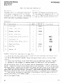
TABLE 3-7.
Remote Commands
Command
Pin
CASE GND"
COMMON
COMMON
AUTORANGED STROBE
TRIGGER MODE
AUTOMOOE STROBE
HOLD
OVERFLOW
STROBE
~___
LOAD RANGE
FLAG/FLAG STROBE
Rl
FUNCTION
R2
3-16
No.
VOLTS
I
AMPS
R2
AC
Rl
OHMS
No.
~1006
22
23
24
25
26
PRINTER HOLD
-. .-- E
T
-15
Pin
at
CASE GND
COMMON
COMMON
COMMON
:
6
TABLE 3-b.
Digital
Output
of
No.
14
15
16
17
18
I9
20
21
22
23
24
STROBE
2
at
PI101
Comnand
RANGE STROBE
R4
POLARITY STROBE
R8
IO4 STROBE
TRIGGER
I03 StROBE
FLAG RESET
IO2 STROBE
TR GGER MODE DISABLE
10 I STROBE
AUTORANGED
loo STROBE
CB
INSTRUCTION
MANUAL
OPERATING
INSTRUCTIONS
Digllal Multimeter
Models 172.173
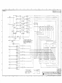
r_--__-_--------------
-I
2 4’
/
I
PIIOI
I’
I
6
61@1?14161820222426
; 1 m : ’ : : ; :
3 5 7 3 lll3151719212325
I
:
:1
I
L--------------------J
I
,
2
PI006
I’
: -----
17.
FIGURE
How to Select
d.
internal
or external
2.
the
Jumper
internal
6 e 1012i41618202~24262e303234~~384;
’ I ’
11111111111111
I
1
1-----------------3 5 7 9 111315
II11I~IIIIIIi~
1719212>252729313335373~
FIGURE
Jumper
I.
the external
4
’
Connector
18.
Pin
Card-Edge
Connectors
8.
When
reference
this
jumper
(+5V).
for
(Model
The
Jumper.
and internal
Vext Using
Internal
voltage
references
A.
When this
jumper
reference
Vext
(pin
Identification
pt006
1727
Model
pull-up
______
and
Cable
Set).
1722 may be wired
resistors.
(See
for use with
Figure
16.)
is
installed,
~1006).
the
pull-up
resistors
are
connected
to
is
installed,
the
pull-up
resistors
are
connected
to
8,
Vext
is connected
to
Jumper C.
When this
jumper
is installed,
The
pull-up
resistors
are
not
connected
in
this
instance.
reference.
reference
is rated
at 40 mA maximum.
3.
PIIOI.
internal
+5V
The +5 volt
3PERATING
INSTRUCTIONS
INSTRUCTION
MANUAL
Digital Mullimeler
Models 172. 173
FIGURE
1 3-18
13.
Location
of Jumpers
and
Pull-Ups
on Model
1722.
AA
INSTRUCTION
MANUAL
OPERATING
Digltal Multimeler
Models 172,173
Digital
r
Output
TABLE 3-8.
Lines
Grouped
INSTRUCTIONS
By Function
Name
FUNCTION
STROBE
-AUTORANGE
TRIGGER
MODE
LOAD RANGE
FLAG RESET
FLAG/FLAG
CB
STROBE
3-19
QPERATING
I
INSTRUCTIONS
INSTRUCTION
MANUAL
Digital Mullimeler
Models 172.173
I
General
Characteristics
TABLE 3-g.
of Model
1722
Digital
Interface.
I
DIGITAL
Logic:
Data:
OUTPUTS:
BCD (8421)
Open-collector
4 full
digits,
I partial
positive
digit
(0,
I,
true
2,
unless
3) and
otherwise
exponential
specified.
range
code.
1
1
Function:
4-bit
code (n, AC VOLTS, AMPS)
Polarity:
HIGH : +.
Overflow:
LOW s > 23333.
:
Autorange:
LOW s range change.
! Automode:
HIGH s autorange
mode.
FLAG (m):
HIGH (logic
“0” : no output
change
occuring.
,
Logic
Levels:
HIGH f open collector
to output
LO.
LOW 5 closure
to output
LO.
Output
/
device
(2N5134)
greater
than 20V breakdown,
<0.5V at 5mA sink
(3TTL loads).
Internal
pull-up
resistors
may be installed
on these
open collector
outputs.
4.7K minimum
5 volt
power supply.
value
is recommended
when using
internal
OUTPUT TIMING:
Data is updated
typically
every
320 msec (non-trigger
mode).
Update
I
.
is
typically
1.2 msec.
Data will
appear
at an output
only
if its
respective
time
strobe
is active.
The FLAG will
go low (Logic
“0”)
typically
2 msec before
update
and
go high
typically
100 usec after
update.
Data can be expected
to be unchanging
so
long as the flag
is high.
If FLAG RESET is activated,
the FLAG will
reset
(go to Logic
“0”)
until
the end ~of the next data update.
REMOTE CONTROLS:
1 Strobe:
Strobe
lines
permit
word serializing
in 4-bit
increments
or multiples
thereof.
HIGH inhibits
controlled
output
lines
from conduction,
LOW enables
conduction.
Range In:
4-bit
exponential
code.
L&
Range:
Low enables
remote
ranging
as set by Range code.
Hold:
LOW inhibits
display
update,
output
update
and autorange
(A/D continues
conversions)
.
( Printer
Hold:
Same as hold but grouped
with
outputs
for convenience
in interfacing
printer.
I
Trigger
Mode:
LOW enables
TRIGGER control.
, Trigger
Mode Disable:
LOW disables
TRIGGER.
Trigger:
LOW to HIGH transition
initiates
a new A/D conversion.
Flag Reset:
Low sets
FLAG (FLAG) t0 LOW (HIGH),
Control
Logic
Levels
G Source
Requirements:
HIGH 3 either
an open circuit
or a
voltage
between
+2.4V and 5V referred
to output
LO.
LOW : closure
to outcut
LO
I
within
0.8V while
sinking
+T.6 milliamperes
(ITTL
load).
When TRIGGER MODE, HE
and LOAD RANGE code bits
are all
HIGH (inactive)
the 172/173
is under
front
panel
control.
These REMOTE CONTROL inputs
have priority
and will
override
any front
I
panel
setting
once activated.
ISOLATION:
All
digital
outputs
and remote
controls
are isolated
from 172/173
analog
input
by 10’ 0 and 5OOpF, 1200 VDC, 1OOOV rms AC maximum.
All
digital
outputs
and
remote controls
are isolated
from chassis
ground
by I06 R and 0.0l~F;
250V rms maximum.
I
I
1
AA
INSTRUCTION
MANUAL
MUttbW!W
Model8 172.173
OPERATING
INSTRUCTIONS
DiQllEd
e.
Detailed
Explanation
of
TRIGGER MODE AND TRIGGER:
(See
schematic
28248E)
1722.
When TRIGGER MODE is active
(Low),
output
data
play will
not be updated.
TRIGGER MODE enables
Conversion
starts
within
1.6 milliseconds
after
Integration
starts
120 milliseconds
after
start
conversion.
and disTRIGGER.
TRIGGER.
of
HOLD:
If either
HOLD or PRINTER HOLD is low the output
data
and the display
wi 11 not be updated
and the FLAG wi I1
stay at HIGH (unless
reset
by FLAG RESET).
LOAD RANGE :
When LOAD RANGE is low the 172/173
will
go to the range
as set by the RANGE IN code
(Table
3-10)
at the beginning of the next conversion.
As long as LOAD RANGE is
held
low each instrument
will
remain
on its programed
range overriding
front
panel
UPRANGE, DOWNRANGE and
AUTORANGE.
RANGE IN codes programmed
outside
the 1 imi ts
of table3-IO
will
result
in the nearest
valid
range
to that
programmed.
LOAD RANGE will
always
cause a DMM
range change.
However,
the display
and output
data will
be held
(not updated)
during
TRIGGER MODE or HOLD.
Referring
to
timing
schematic
28249~,it
is possible
to
just
miss a REMOTE CONTROL update
prior
to data output.
This
can be misleading,especially
in the case of HOLD.
A HOLD just
missed
(unknown
to the user),
just
before
data begins
to change,could
result
in erroneous
data.
To check
if this
occurred,
it is suggested
that
the
FLAG be examined
no sooner
than 10 usec after
activation
of the HOLD bit.
If flag
is low wait
until
it goes to
HIGH before
expecting
the HOLD bit
to have been accepted.
Other
REMOTE CONTROL bits
such as TRIGGER MODE and
TRIGGER,
LOAD RANGE and the RANGE IN code can be kept
active
for
longer
than an output
data update
time,
i.e.
>3.2 msec to insure
proper
REMOTE CONTROL acceptance.
REMOTE CONTROLS :
TRIGGER MODE DISABLE:
(See Schematic
28249D)
A6
Model
When in TRIGGER MODE and triggering
into
an autoranging
condition,
normal
operation
will
give an output
for each
However,
if
range
encountered
during
the autorange.
this
is undesirable
the AUTORANGED output
bit
can be
tied
to TRIGGER MODE DISABLE and FLAG RESET.
This will
prevent
the FLAG from being
set and ignore
further
triggering
until
the final
range
is reached.
3-21
OPERATING
INSTRUCTION
MANUAL
Digital Multimeter
INSTRUCTIONS
Models
v
Internal
external
resistors
internal
internal
mended
ext:
LINE
GROUND:
172.173
jumpers
(user
installedjselect
internal
or
voltage
reference
for user-installed
pullup
for all
open-collector
outputs,
or applies
+5V to v
(maximum external
current
load on
+5v is
Minimum
pull-up
resistor
recomis 4.7K.
GiGA).
One pin
on each
GROUNDS:
4 pins
for
CONNECTORS:
One ho-pin
output
digital
card
connector.
outputs,
edge
and
2 pins
one
for
26-pin
remote
card
control.
edge.
ENVIRONMENT :
installed
in
a 172/173:
Operating
0°C
-25.
Storage:
Modifications
f.
lj’2Z
in TRIGGER
as follows:
Also
when
to Model
172/173
Specifications.
MODE, only
the accuracy
specifications
HI n 3OOMQ Range:
HI R 30tln Range:
From
LO fi 30M Range:
LO n 3H Range:
From 0.5%
From 0.1%
operating
in
TRIGGER
0.5% on 300MQ Hi
0.05% on 30Mn Hi
Accuracy
1722.when
3-22
to 55°C. humidity
to +65OC
1% of
From 0.15%
MODE, repeatability
$I and
R and
of all
other
ohms ranges
and
operating
in TRIGGER MODE.
When operating
for the top
reading
to
of reading
of
of
reading
reading
of
3OMQ Lo R ranges,
3MQ Lo n ranges.
all
other
80% @ 35’C.
functions
a 172/173
with
two ohms ranges
1.5% of
to 0.2%
reading.
of reading.
to 1% of
to 0.15%
reading.
of reading.
readings
may be up to:
a
change
and
is
not
affected
by
the
Model
AB
I
INSTRUCTION
Dlgllsl Multimeter
Models
172.
MANUAL
OPERATING
INSTRUCTIONS
173
TABLE 3-10
MODEL 1722 RANGE t
OUTPUT
FUNCTION
CODE (1)
FUNCTION
RANGE
VAACQ
100
DC VOLTS
v
3:
300
1000
I 0 0
101
4C AMPS
LOW n
I000
“v
v
v
001
R
IO
1 1
ill
0 0
0
III1
IO
IO
IO
0
I
Ill1
IO
IO
IO
0
I
IO
0
l
0 0
I
I
AUTORANGE
I
I
0
I
I
0
0
I
AUTORANGE
Ill1
0
IO
0110
I
300 mA
2 A
0
0
IO
II0
I
300 R
3 kn
30 kn
0
0
0
0
0
0
010
0 II
IO
IO
110
Ill
0
0
0
0
0
IO
0 II
I 0
IO
I
I
Ill
0
AUTORANGE
!
oC2)
1
0
I
0
I
300 kn
3 m
30 nfi
300 MR
(I)
Coding
in this
to
LOW. Refer
(2)
Function
(3)
Note that
except
PUT RANGE CODE,
AA
0
0
0
I
IO
I
300 mA
2 A
3 kn
30 ka
code
IO
110
Ill
0 0
0
oC2)
300 kfi
3 MI2
30 MC
il
0
0
0
I
IO
0
300 mv
DC AMPS
(EXP)
0
1200
101
OUTPUT
RANGE
CODE (I)
%I R4 R2 Rl
300 mv
3.ov
30 v
300 v
AC VOLTS
COOING FOR MODEL 17-i’
FUNCTION
table
output
for
0
is defined
to be HIGH (POSITIVE)
and remote
control
logic
levels
Model
for
i.e.
0
1
0
172 current
is
IO
I
0
IO
0
1
Ill
II0
I
IO
IO
I1
IO
IO
IO
0
I 0 0
Ill1
I
I
IO
IO
IO
10
0
Ill
1
1
0
AUTORANGE
1
0
AUTORANGE
0 0
II
IO
0
I
0 0
TRUE.
"I"
= HIGH and "0" =
for definitions
of HIGH & LOW.
volts.
of
AUTORANGE CODE, INPUT t RANGE CODE is the compliment
the INPUT RANGE CODE is the LOW TRUE BCO code of (EXP).
the
OUT-
3-23
OPERATING
INSTRUCTIONS
INSTRUCTION
MANUAL
Digital
Multimeter
Models
172. 173
TABLE 3-11
MODEL 1722 RANGE G FUNCTION CODING FOR MODEL I73
(Same as Table
3-loexcept
as follows)
OUTPUT
FUNCTION
CODE (I)
I
RANGE
VAACR
010
AC AMPS
'-24
011
OUTPUT
RANGE
CODE (I)
(EXP)
INPUT
RANGE
CODE (1)
(3)
R8 R4 R2 R~
R8 R4 R2 R~
I
II
1
IO
10
IO
0
I
IO
0 0
0
Ill
0 II0
AUTORANGE
Ill1
1 0
10
IO
AUTORANGE
0
300
3
30
300
3
PA
mA
mA
mA
A
0 IO
0 II0
01
I
1000
IO
0
300
3
30
300
3
VA
mA
mA
mA
A
0 I 0
0110
0
Ill
1 D 0
1001,g
I
I
ll
I
9
1
2
0
87
0
1
0
0
0
I
0
AA
INSTRUCTION
Dlgltal
Multimeter
Models
172.173
MANUAL
OPERATING
INSTRUCTIONS
COMMENTS RELATIVE TO THE MODEL 172/173 SPECIFICATIONS.
Above I ampere there
is a
3-13.
decrease
in accuracy.
This
decrease
in accuracy
is due toself
heatingand
the temperature
coefficient
of the resistors
that
are used in these currents.
This
degradation
in accuracy will
not exceed
those
values
that
are listed
in the specification
sheet.
However,
prolonged
operation
at the high currents
(for
instance,
2 amperes on the Model 172, or
3 amperes
on the Model
173) may give
temporary
zero shifts
because
of the thermals
which
are generated
due to the self
heating
of the devices.
AC voltage
specifications
are
listed
down to 1% of range.
Below
1% of range an additional
IO digits
is added to the
accuracy.
This does not occur
immediately
at the 1% level,
but gradually
as the level
is decreased,
because
the zero of the ac/dc
converter
is not very well
defined.
It has
to overcome
the threshhold
level
of various
semiconductor
devices
(a MDS FET and diode).
As a result
there
will
typically
be a IO digit
offset
at zero even with
the input
shorted
on the 300 millivolt
range and on the 30 volt
range.
The 30 volt
range offset
will
be
somewhat
smaller
because
the noise
will
be somewhat
less.
For best accuracy
use the
Model
172/173
on whatever
range gives
the largest
reading.
Autoranging
will
accomplish
this
automatically.
Although
the manufacturers
of the nickel
cadmium batt3-14.
MODEL 1728 OPERATING TIPS.
eries
used in the 1728 claim
that
their
cells
can be charged
at a C/IO rate
indefinitely,
once a cell
is fully
charged,
the energy
fed to the cell
is converted
to heat,
which
If cells
are overcharged
at C/IO rate
for extendincreases
the temperature
of the cell.
Keithley
recommends
that
ed periods
of time’(weeks),
this
may cause cell
degradation.
the 1728 not be overcharged
for extended
periods
to maximize
useful
battery
life.
Trickle
Nickel
Cadmium batteries
also
excharging
should
have no effect
on useful
battery
life.
If the 1728 is only
used to operate
the instrument
for relatively
hibit
a memory effect.
short
periods
of time
(I or 2 hours)
the 1728 may not be able
to provide
the full
operating time of 6 hours.
Do not operate
the Multimeter
in BAT mode after
the LO BAT indicator
is lighted.
The
discharge
characteristic
of Nickel
Cadmium batteries
is such that
it maintains
a fairly
At the end of the discharge
curve
constant
l.2V
through
most of its discharge
cycle.
After
a given
cell
in the battery
the cell
voltage
drops
fairly
rapidly
to zero volts.
pack drops
to zero it is reverse
charged
by the rest
of the cells
in series
with
it.
Although
the cells
used in the 1728 are guaranteed
by the manufacturer
to withstand
reit is not a good practice
to continually
verse
charge
for
10% of their
discharge
time,
reverse
charge
cells,
as more rapid
cell
degradation
may occur.
The cells
used in the 1728 should
give a minimum of 250 discharge/charge
cycles
and
Thus,
based on daily
useage
(5 day week, one per
typically
500 discharge/charge
cycles.
day)
the battery
pack should
give
a minimum of one year operation
and typically
two years.
Longer
life’should.be
expected
for
less frequent
useage.
AB
3-25
I
INSTRUCTIONS
urtHATlNG
INSTRUCTION
MANUAL
Digilal Multimeter
Models 172,113
TABLE 3-12
Summarv
of
ITEM
Fuses
and
Miscellaneous
Replaceable
-
WHERE USED
KEITHLEY
:use,
3 AB/3
AG,
l/4
A,
Slo-Blo
ll7V
Line
Volts
FU-17
:use,
3 AB/3
AG,
l/8
A,
Slo-Blo
23411 Line
Volts
FU-20
‘use,
3 AB/3
AG,
I A,
‘use,
3 AB/3
:use,
3 AB/3
.op Cover
Model
1728
FU-IO
AG, 2 A Quick
Model
172 Amperes
FU-13
AG,
Model
173 Amperes
FU-2
(less
3 A Quick
metalcal)
lottom
Cover
(less
landle
(less
insert)
+
:ubber
Slo-Blo
Parts
PART NO.
27979C
metalcal)
25727E
25729D
Insert
260YOA
Foot
FE-IO
-
-26
AA
INSTRUCTION
MANUAL
Dlgllsl Mullimeler
Models
ACCESSORIES
372.173
SECTION
4.
ACCESSORIES
This
section
describes
the various
GENERAL.
with
the Model
!72/173
Digital
Multimeter.
4-l.
use
accessories
and
options
POWER OPTIONS.
b-2.
The Model
172/173
can be powered
by line
voltage
or rechargeable
Battery
Pack (Model
1728).
Other
line
voltage
ranges
described
in Section
2.
The Model
1728 is available
factory-installed
installable.
ISOLATED DIGITAL
OUTPUT.
4-3.
The
factory-installed
or field-installable.
(paragraph
3-12.)
The Model
1722 and
options
occupy
the
4-4.
width)
1728 cannot
same location
Model
be
1722 Digital
Output
Complete
specifications
IMPORTANT
installed
and used
on the Model 172/173
MODEL IO10
SINGLE
Interface
is
are given
in
a full
for
(105-125V
standard)
are available
as
or field-
at the same time
chassis.
RACK MOUNTING.
THE Model
172/173
can be rack mounted
in either
a single
or dual mounting
configuration.
available
rack
available
in Section
since
(I9
3
both
inch
RACK MOUNTING KIT
Description:
Application:
The Model 1010 is a single
rack mounting
kit
with
overall
dimensions
5-i/4
in.
(133
mm) high and 19 in.
(483 mm) wide.
The
hardware
included
in this
kit
includes
a
19 inch wide panel
and other
miscellaneous
hardware.
The Model
1010 adapts
one Keithley
Style
“K”
instrument
for Standard
5-l/4
in.
(I33 mm)
x 19 in.
(483 mm) rack mounting
with
II in.
(280 mm) depth
behind
the front
panel.
For
dual
rack mounting
of Style
“K” instruments
the Model
1017 Dual Rack Mounting
Kit must
be used.
Parts
List:
I tern
I40.
Illustration
Description
I
Front
2
Support
Plate
3
Bracket,
Left
4
Bracket,
Right
5
Slotted
6
Flat
7
Phillips
AB
-
Panel
(Shelf)
Side
Side
#b-32
Screw,
Washer,
x 2-l/4
in.
#6
Screw,
#8-32
x l/2
in.
4-I
INSTRUCTION
4CCESSORIES
MANUAL
Digital Multimeter
Models 172. 173
Assembly
Instructions:
I .
(Item
Using
I).
two
2.
Using
four
Phillips
Phillips
Panel
3 and 4) to Front
3.
port
4.
5.
dle
6.
gether
7.
holes
a.
ment
I 4-2
Using
Plate
four
(Item
Assembly
Screws
Screws
(Itw
I).
Phillips
2).
of
Screws
rack
7) attach
(Item
hardware
Support
Slotted
feet.
Position
Instrument
on Support
Plate.
Using
two
to Support
Slotted
Plate.
Screws
FIGURE
Front
Panel
left
and
right
side
Brackets
(Items
(Item
7).
secure
left
and
right
side
Brackets
to
complete
except
long)
in.
holes
(Item
20.
to
attach
(l-l/4
so that
2)
7),
is
Screws
(Item
(Item
for
“handle”
of Instrument
so that
handle
is
Rotate
can be removed completely
if desired
by separating
Remove two
near front
Plate
5)
Model
used
in bottom
and
two
1010
of
Flat
Single
mounting
of
Instrument.
toward
rear of
top and bottoto
hold
top
Instrument
Washers
Rack Hountinq
Instrument.
covers.)
and bottom
align
(Item
Sup-
with
6).
secure
(Hancovers
two
to-
front
Instru-
Kit.
AA
I
INSTRUCTION
MANUAL
ACCESSORIES
Digllal Multimeter
Model. 372. 173
MODEL I017
DUAL RACK MOUNTING KIT
Description:
Application:
The Model
1017 is a single/dual
with
overall
diwnsions
5-l/4
high and I9 in.
(483 mm) wide.
included
in this
kit
includes
panel,
and other
miscellaneous
Parts
mounting
in.
The hardware
a I9 inch wide
hardware.
The Model
1017 adapts
two Keithley
5-l/4
“K” instruments
for’standard
mn) x I9 in.
(483 mm) rack mounting
in.
(280 mm) depth behind
the front
Style
in.
!I33
with
Ii
oanel.
List:
teni
lo.
kit
(I33 mm)
Qtv
Description
Req’d
I
Front
2
Support
Plate
3
Bracket,
Left
4
Bracket,
Right
Side
5
Slotted
Screw,
i6-32
6
Flat
7
Phillips
Blank
Panel
Wasner,
I
28092D
(Shelf)
I
28OY4C
Side
I
280968
I
280978
4
-_
4
__
4
__
I
28098B
8
Hole
9
Kep Nut,
Plug
2
HP-20
,“8
5
-_
x 2-l/4
in.
;6
Screw,
Cover
Kei thley
Part No.
Plate
!8-32
x l/2
in.
-I
IlluStralion
=?
a
cs
f”TJj
a
handle.
Loosen four screws
on the bottom
cover of the instrument,
lift
off
the top cover
and remove handle.
Replace
the top cover
and tighten
the four
screws
on the bottom
cover
6. Remove two Slotted
long)
used to hold
top and bottom
covers
toScrews
(i-l/4
in.
These screws
are captive
and a needlegether
near the front
feet
on each instrument.
nose pliers
should
be used to pull
the screw out after
it is loosened
with
a screwdriver.
Position
the Instrument
so that
holes
in the bottom
of the Instrument
align
with
7.
the two front
holes
in the Support
Plate.
8. Using two Slotted
screws
(Item
5) and two Flat Washers
(Item
6) secure
the Instrument to the Support
Plate.
AB
4-3
I
ACCESSORIES
INSTRUCTION
MANUAL
Digital Mullimeler
Models
FIGURE
4-5.
Model
PROBE AND SHUNTS.
172/173.
The
21.
Model
following
1017
probes
Dual
and
Rack Mounting
shunts
extend
the
172. 173
Kit.
capabilities
of
the
MODEL 1600 HIGH VOLTAGE PROBE
Description:
The Model
1600 is
40 kilovolts
dc.
The probe
megohms input
resistance.
a divider
probe for measurement
of high
is optimized
for use with
a dc voltmeter
voltage
having
up to
10
MODEL 1682 RF PROBE
Description:
1682
is
The Model 1682 is an RF probe for
optimized
for use with
a dc voltmeter
MODEL 1685
CLAMP-ON AC CURRENT PROBE
Description:
The Model 1685 is a clamp-on
up to 200 amperes.
The Model
1685 is
p,ut of 0.1 volt
rms per ampere.
4-4
measurement
up to 100 MHz.
The Model
having
10 Megohms input
resistance.
current
used with
probe for measurement
an AC voltmeter
and
of ac current
provides
an out-
AA
INSTRUCTION
Dlgltal
MANUAL
ACCESSORIES
Multlmeler
Models172,173
MODEL 1651 CURRENT SHUNT
Description:
having
4-6.
use
of
at
The Model
1651 is
least
100 microvolts
CABLES AND CONNECTORS.
the Model 172/173.
a 0.001
ohm shunt
for use
resolution.
The shunt
The
following
MODEL 1683
The Model
1683 is
Description:
with
interchangeable
screw-on
cables
UNIVERSAL
a set of
adapters.
The Model 1681 is a set of test
plug and spring-action
clip-on
MODEL 1727
The Model
1727 is a cable
Description:
cable
terminated
by mating
card-edge
is 3 feet
long (I m), and the Model
test
leads,
48 in.
leads,
probe.
enable
effective
40
in.
(Im)
in
length,
(1,2m)
in
length,
terminated
OUTPUT CABLE SET
SHIELDED
of 26- and 40- conductor
ribbon
The Model
1727-3
the model
1722.
feet
long
(3,l
m).
CABLE
42 inches
The Model 7004 cable
is a shielded
cable,
by 2 tinned
leads
plus shield.
Two banana
Models
172/173.
when
both
plug
making
analog
O,l
adapters
low-level
INPUT and
m) long and
are furnished
voltage
OUTPUT.
is
for
connections
The shield
MISCELLANEOUS.
MODEL 1725 MAINTENANCE
Description:
ability
AP
Kits
LEAD KIT
set consisting
connectors
to
1727-10
is ten
Application:
The Model 7004 cable
is useful
to the Model 7021'7029
Low-Voltage
Scanner,
may be connected
to the GUARD terminal.
4-7.
cpnnection
TEST LEAD KIT
DIGITAL
MODEL 7004
Description:
terminated
use with
TEST
flexible
MODEL 1681 CLIP-ON
Description:
by a banana
and
with
an AC or DC voltmeter
is rated
at up to 50 amperes.
The Model
to adjustment
1725 contains
a specially
controls
on the Model
KNIT
punched
calibration
172/173
chassis.
cover
for
access-
4-5
I
INSTRUCTION
MANUAL
Digital Multimeter
ACCESSORIES
Models
MODEL 702/7029
Description:
be used
I
for
PRINTER
173
LOW-VOLTAGE SCANNER
The Model 702/7029
is a ten-channel
low-voltage
or remote
scanning
operation.
manual,
scan,
MODEL 750
172,
WITH MODEL 7501-1722
PRINTER
scanner.
The
702/7029
can
INTERFACE
AA
INSTRUCTION
MANUAL
Digllel Mullimeter
Models 172.173
THEORY OF OPERATION
SECTION
5.
THEORY OF OPERATION
5-l.
GENERAL.
This
section
contains
circuit
The description
is broken
down into
172/173.
a.
Input
Signal
b.
Power
Supply
c.
Display
Board
d.
Durrent
Board
e.
Battery
Pack
f.
A/D
4.
Digital
description
the following
information
for the
major categories.
Conditioning.
(Model
1728).
Converter
Interface
(Model
POWER
SUPPLY
(SCHEMATIC 286560)
1722).
f----c
(OPTION)
MODEL 1728
BATTERY
PACK
(SCHEMATIC 27903~)
SHEET 3 OF 3
-&CHEMATIC
28656C)
SHEET I OF 3
MODEL 173
CURRENT
BOARD
(SctiE~ATic
27478~)
FIGURE
22.
SCHEMATIC
(OPTION)
Overall
Block
Diagram
27902E
28019~
of
Model
172/173.
Model
THEORY
OF OPERATION
INSTRUCTION
MANUAL
Digital Mullimefer
Models
5-2.
switching,
INPUT SIGNAL
overload
a.
Switching.
function.
Table
CONDITIONING.
protection,
The interlocked
5-l
summarizes
(Schematic
ohms converter,
27903E).
pushbutton
the switching
switches
scheme.
Sumnary
of
Switch
Style
Line
Push-Push
I”
Push-Push
: out
Push-Push
/
Line
~
ISetting
IN
ac/dc
TABLE S-1.
Pushbutton
This circuit
consists
converter,
and filter.
set
the
DMM to
the
of
172.
173
input
appropriate
Switching
Remarks
I
1 DMM is
j pack (if
I DMM is
pack (if
if line
DMM is
powered
by ac line
power.
Battery
installed)has
a trickle
charge.
disconnected
from line
power.
Battery
installed)
is charged
at maximum rate
cord is connected
to power.
powered
by internal
Battery
Pack.
i DMM is
disconnected
I
1
I
BAT
Push-Push
j Out
i
/
1
1
I -__-~-I-~ AUTO/MAN
I
j
(
.-UP
I
L
~
Push-Push
I”
AUTO/MAN
Push-Push
Out
DN Range
Momentary
In
Range
Momentary
I”
__--__
“Interlock
I”
--__
I”
“Interlock
5-2
I”
from
Battery
Pack.
NOTE
Interlock
preveots
both pushbuttons
IN at the
same time.
Both pushbuttons
must be set to
OUT before
either
can be set to IN.
PushPush means that
a single
depression
will
place
the pushbutton
to IN, a second
depressoon
will
release
the
pushbutton
to
OUT.
-DMM is set to MAN (Manual
mode).
To change
range depress
either
DN RANGE or UP RANGE.
See also
REMOTE PROGRAMMING OPTION.
DMM is set to AUTO (Automatic
Ranging
Mode.)
DMM range
is set automatically
Momentary
depression
causes
the DHM to down
range one decade to lesser
sensitivity.
Operable
only when AUTO/MAN is IN.
__
Momentary
depression
causes
the DHM to up
range one decade to greater
sensitivity.
Operable
only when AUTO/MAW is IN.
%%Ts
set to DC mode.
Overrides
AC and n
functions
due to interlocked
pushbuttons.
Overrides
DC and R
DMM is set to AC mode.
functions
due to interlocked
pushbuttons.
DMM is set to R mode.
Overrides
AC and DC
functions
due to interlocked
pushbuttons,
also
overrides
V/A switch.
t
1
-
j
i
AB
I
lNSTRUCTlON
Dlgilal
Models
MANUAL
THEORY
Mulllmeler
172,
OF OPERATION
173
TABLE 5-1 (Continued)
Summary of Pushbutton
Switching
Switch
'7;':
Can be depressed
and held
IN
simultaneously
V/A
Push-Push
I"
V/A
Push-Push
out
Push-Push
Push-Push
I"
Out
H,,LO;::>::
” , /LO
Remarks
;'NOTE
If DC, AC, and n pushbuttons
are OUT simultaneously,
no function
will
be selected,
the
input
terminals
will
be open-circuited,
and
the DMM will
display
R.
The displayed
reading is meaningless.
Setting
i:‘l :;
DNM
DC).
DMM
DC).
DMM
DMM
Only
w , RE, 4
w , R E 5 :i i’
Push-Push
I"
Push-Push
Out
I
Gain
s set to measure
current
Not functional
when set
s set to measure
voltage
s set
IS set
(either
to :I.
(either
to low ohms range.
..,
to high
ohms range.
functional
when
set
to
AC or
AC or
:+;b
2.:
i:.
DMM is sat for 4-WIRE ohms measurements.
upper
pair
of terminals
are used for VoltLower
pair
of terminals
are
age sensing.
used for ohms source.
Lower pair
of terminals
are useable
only
in 4 WIRE r. mode
and are open circuited
for all
other
conditions.
DMM is Set for conventional
Z-WIRE ohms
measurements.
Upper pair
of Terminals
must be used.
Lower pair
of terminals
are
open-circuited.
L
Chart
TABLE 5-2.
For AC/DC
Voltage
RANGE CONTROL LINES
RANGE
AB
ATTENUATION
A/D
GAIN
RL
H
300 mV
+l
Xl0
+a v
-12
V
3v
il
Xl
+8 v
-12
v
Xl0
ov
-12
v
Xl
ov
-12
v
Xl
ov
-8
v
30
v
+I00
300
v
SIOO
1000
v
ilOO
5-3
EORY OF OPERATION
INSTRUCTION
MANUAL
Digilal
Mullimeler
Models 172.173
DC Volts
input
Circuit.
DC Volts
input
circuitry
is used to attenuate
I.
A combination
of attenuation
It unwanted
AC signals.
See Table
5-2on
page 5-3.
ive ranges
of DC Volts.
There
is no attenuation
2.
The
mown in this
position.
rester
than
109 ohms.
on the
attenuator
and
gains
filter
allows
is
of
There are two attentuation
attenuator.
C9Ol assures
AC attenuation
with
Q901 on.
is maintained.
RL line
controls
K901 and
Overload
protection
is assured
by the clamp
4.
sltage
is applied
on the 300 m V or 3 V ranges,
As
RY29 absorbs
the input
voltage.
fter
R929.
307 keeps the relay
voltage
from becoming
large
Tihe clamp
is essentially
an open circuit
between
Filtering
input
if necessary
and A/D converter
Relay
KY01 (Figure
23)
300 m V and 3 V ranges.
is bypassed
which
allows
the input
resistance
relay
KY01 switches
in the
Above 3 volts,
3.
ilO0 with
FET switch
QYOI off
and +I000
evels,
f at least
ilOO
so that
normal
mode rejection
line
controls
QYOl (See table
5-2).
.
the
circuit,
the clamp
the relay
enough
to
?5 Volts.
If a large
RY29, and C907.
limits
the voltage
to i5 V
switches
in the attenuator,
cause arcing
or plazma
effects.
Circuit.
It is a 3The DC filter
is used in front
of the A/D Converter
on all
functions.
I.
ale active
filter
with
3 db frequency
of 5Hz and a settling
time of less
than 300 ms
It requires
an input
resistance
of 200K9,
bY.YK< of which
is RYl8.
o within
0.01%.
he other
ISOK!? comes from various
sources
in the following
manner:
INPUT
In
DC Volts,
In
I"
AC Volts,
il
300
30
all
, all
m V and 3 V range:
V and 300 V range:
ranges:
R801
ranges:
RY.28
-.OluF
FIGURE
j-4
RY2Y,
RYlY + R908 + RYll+RYl0
23.
DC Volts
Input
Circuit.
AA
i
INSTRUCTION
Dlgltal Multimeter
Models
172.
MANUAL
THEORY OF OPERATION
173
This
ZOOKR is also
maintained
so that
the etfect
of A/D input
current
is autozeroed
(See A/D discussion,
section
5-7).
The DC filter
contributes
no DC offsets
to the
path.
They are blocked
by C905 & C904.
R922, R917, C902 G U901 complete
the filter
circuit.
R92lisacurrent
limiting
resistor
and C903 frequency
compensates
U901.
out
signal
AC Attenuator.
d.
1.
ered
2.
with
relay
(see
AC voltages
and passed
on
are
to
first
the
attenuated
A/D converter.
The AC attenuator
(Figure
24) is
maximum gain of unity.
Its other
K801 and FET ~804 respectively.
table
5-2).
3.
pressure
voltage
if
necessary,
converted
from
AC to
DC, then
filt-
really
a frequency
compensated
summing amplifier
gains
are ~100 and +lOOO which
are switched
by
RL line
controls
K80i and H line
controls
~804
C908 blocks
DC signals
up to +-lOOOV, so that
AC signals
of DC voltages.
The attenuator
is referenced
to -6
on ~808 and C809 (figure
25) near zero.
may be looked
Volts
to keep
at
the
in the
DC bias
-Rf (1cjwRiC~i)
-2 f
Ri (l+jwRfCf).By
making
the RC time constant
The gain of the attenuator
is TN=
of Zf equal
to the RC t im constant
of 2 IN, the gain of the attenuator
is constant
with
-.
This
is
true
in
the
midband
region.
Low
frequency
is
and
equal
to
frequency,
frequency
by ~803.
Nominal
~908 and RIN (R818) and high
limited
by RC time constan R!‘of
values
of resistance
and capacitance
are shown in Figure
24.
4.
Amplifier
~803 is powered
from +3 V and -15 V.
agz*at
the output
is -6 Volts
which
keeps DC voltage
minimizes
settling
time when autoranging.
e.
When overloaded
off
of C808 and
the average
This
C809.
volt-
AC Converter.
The AC converter
is a transconductance
amplifier.
The simplified
1.
the basic
operation.
The AC input
voltage
(Ein)
is converted
to a current
of the summing amplifier
configuration.
This
current
flows
through
the
and through
the diode
when positive.
Thus Eout is a half
wave rectified
polarity
is negative.
Eout is the input
current
flowing
through
Rout.
of the converter
amplifier
is referenced
to a negative
voltage
to allow
across
the FET (~801).
2. The ac
Q801, diode
is ~812 and
FET Q801 is
FET is driven
circuit
shows
(Iin)
because
FET when negati*
signal
if the
The + terminal
voltage
swing
converter
consists
of dual
FET Q803, operational
amplifier
~801 and HOSFET
The input
resistance
CR801, and transistor
~802,
semiconductor
elements.
R807, and the output
resistance
is ~802 in series
with
~803 adjustment
pot.
located
in the feedback
loop of the converter
amplifier
and the gate of this
from the output
of the amplifier
for one polarity.
polarity
the feedback
path for ~801 and input
FETs Q803 (a,b)
is
3. For the other
is positive
at the input
through
diode
CR801 and transistor
~802.
When the ‘ignal
side
of ~812, current
flows
into
the summing junction
of the amplifier
which
is the gate
This
turns
on
(Pin
3) of ~803 and this
current
causes
the output
of Q8Ol to go negative.
the base emitter
junction
of Q802 and pulls
current
through
diode
CR801 so that
the
connection
path is through
~812,
R807, CR801 and ~802 emitter
to collector
to -15 volt
The reason
that
Q802 is a transistor
and not a diode
is to equalize
the output
SUPPlY.
and avoid
any parasitic
oscillaload on amplifier
~801 in each of its
two polarities,
tion
which
might
occur
in ~801 because
of unequal
output
current
Loading.
AA
5-5
Tt iORY OF OPERATION
INSTRUCTION
MANUAL
Digital Mullimefer
Model* 172.173
TO AC
CONVERTER
0
I
K801
158.4 pF
\
4804
24.
FIGURE
Simplified
AC Attenuator
Circuit.
Eout
-lin
C808
Ein
t-
lin
~809
Rout
4
--l(--AANbRin
~802
~803
r
~812, R807
k”’
+lin
~802
-V
FIGURE
5-6
25.
AC Converter
Circuit.
AA
1
INSTRUCTION
Dlgilsl
MANUAL
THEORY
OF OPERATION
Mulllmeter
Models
172.
173
4.
When the input
voltage
is negative
to the input
side of R812 the current
will
flow
out ~807 and ~812 and thus the output
of Q801 will
go positive,
thus forward
biasing
the
gate of Q801.
This
turns
on Q801 pulling
current
through
resistors
R802 and ~803 from
signal
ground.
Thus Q801 only
conducts
for negative
input
signals
and the output
current
is a half
cycle
sine wave of negative
polarity.
This
output
current
flows
thru
CbO3
filters
the DC voltage.
and ~802 which
This
filtering
action
allows
the necessary
3 V
DC with
only
6 volts
available
from Q8Ol.
Without
~803, more than 9 V swing
would
be
The transfer
gain of the AC converter
is unity.
needed.
One volt
AC RHS sine
in causes
I Volt
DC out.
with
source
resistors
R805 and R806.
5. Q803 is a dual FET used as source followers
The 10 m V adjustment
feeds
a small
correction
current
to the summing junction
to adjust
for
leakage
current
errors.
The I Volt
IKHz adjust
calibrates
the system
gain on the
300 m V and 3 V ranges.
Additional
output
filtering
is provided
by the DC filter
(Section
5 C) whose input
is R801 & ~801 in this
case.
6. The only blocking
converter.
They keep
reaching
the output.
capacitors
needed are
voltage
offsets
of ~803
C808 and C805 on the input
of the
(AC attenuator)
and Q803 and ~801
7. The AC System common is the -6 Volt reference.
~802 and input divider
~811 and R810.
C807 is used
between
6V and
signal
lo
to
minimize
AC noise
to
It is composed
provide
a low
of voltage
impedance
AC
from
follower
AC path
pickup.
Ohms Circuit.
f.
A summing amplifier
configuration
is
is a current
generator.
I . The ohms circuit
The current
is generated
by applying
a reference
voltage
to the input
resistor
of
used.
the summing
amplifier
and connecting
the unknown
resistor
in the feedback
loop of U702
Refer
to Figure
34a.
Either
the
to force
the current
through
the unknown
resistor.
3.3444
V or the .33444 V reference
is connected
to buffer
amplifier
U701 thru,
switching
The output
of the buffer
drives
one of three
resistors
(3.3444K,
FETs Q702 or Q703.
334.44K,
33.444MG)
to give
six decade values
of current
from 10 “anoamperes
to I milliEach resistor
consists
of a” adjustment
potentiometer,
and thus six ohms ranges.
.3tllpere,
a fixed
resistor
and the on resistance
of a FET (no FET for 33.44&M:;).
2.
which
3.
which
High ohms puts the A/D
can turn on semiconductor
Low ohms
do
not
puts
turn
converter
on
junctions
the A/D converter
on semiconductor
the
for
on the
junctions
allowing
3 Volt
range,
on scale
readings.
300 m V range,
for on scale
allowing
readings.
6 resistance
ranges
6 resistance
ranges
See Table5-3.
drifts
associated
with
amplifiers
U701 and U702.
4. There are time and temperature
The reference
used to calibrate
These effects
are compensated
for by the A/D converter.
Therefore,
any drift
in U7Ol is
the A/D converter
in R function
is the output
of U7Ol.
The negative
input
of U702 is what
“auto”
compensated
for every
conversion
cycle.
the stability
of the ohms
Therefore,
zero”
one is calibrated
to every
conversion
cycle.
The lead drop
in the
current
is a function
of only
the stability
of the R resistor.
high
terminal
of the ohms source
amplifier
is compensated
for by connecting
it to
“Auto-zero”
2 is the zero for the input
signal.
“auto-zero”
2 when in the ohms mode.
In 2-wire
ohms the leads
connect
at the front
panel
binding
post.
Therefore
a 4-terminal
See Section
5-9.
ohms system
exists
up to the front
panel
terminals.
A6
5-7
iEORY
OF OPERATION
INSTRUCTION
MANUAL
Digital Multimeter
Models 172.173
The ohms switching
FETs (Q703,
Q702) are driven
5.
by transistor
Q701 and the C-line,
Q710 is driven
from the A-line
and Q707 is driven
from the B-line.
These
lines
are also
used and decodes
to operate
the Model 173 autoranging
current.
Amplifier
U702 is a
FET input
amplifier.
This amplifier
is overload
protected
by Q709 base emitter
junction
connected
to the signal
ground,
and Q708 base emitter
junction
connected
through
Q706
clamp transistor.
Thus the input
swing
is clamped.
Very large
voltage
excursions
on
the output
side of U702 are allowed.
This
is done by Q704, Q705, and CR703.
Under
normal
operating
conditions
Q704 is operated
in the saturated
mode,
However,
under
overload
conditions,
Q704 becomes a current
source
with
its
collector
to emitter
breakdown handling
large
voltage
excursions
when signals
are positive
with
respect
to the
ohms source
high.
However,
if signals
are negative
with
respect
to the ohms source
high,
CR703 reverse
biases,
cutting
off
that
portion
of the circuit.
All
of these high
voltages
will
cause current
to flow
through
R703 (IZOKR)
which
is connected
to the +I5
The maximum limitation
of 250 volts
rms is a function
of the power rating
volt
supply.
of R703 (a half
watt
resistor),
and Q704’s
400 volt
breakdown.
TABLE 5-3.
OHMS RANGES
I
I
RANGE
HIR
RANGE
R
LOR
300::
3;:
300K
3M
3OM
300M
REF
“I
3.3444K
3.3444K
334.44K
334.44K
33.444M
33.444M
3::
300K
3::
OHMS
I CURRENT
3.3444”
-33444”
3.3444”
.33444”
3.3444”
.33444”
RANGE LINES
I mA
IOOuA
IOuA
IvA
100 nA
IO nA
/
9.
Range
Selection.
Ranging
is accomplished
by RSA t RSB lines
going
to LSI
by the front
panel
switches
AUTO/MAN, DN & UP, according
edge sensitive,
causing
range changes
when their
levels
uprange
or one downrange
per button
push.
circuit
UlO3.
to Table
5-4.
are changed.
They are controlled
RSA & RSB are
This
causes
one
TABLE 5-4.
Range Selection
Range
AUTO/MAN
UP
Range
RSA
Lines
RSB
Action
OUT
X
X
0”
+8”
AUTORANGE
IN
OUT
OUT
0”
0”
HOLDRANGE
IN
IN
OUT
+8v
0”
DOWNRANGE
IN
OUT
IN
+8”
+8”
X E DON’T
5-8
Switches
DN
UPRANGE
CARE
AA
INSTRUCTION
Digllsl
MANGAL
THEORY
OF OPERATION
Mullimeler
Models 172, 173
h.
Function
Switching.
TABLE 5-5.
Function
Select
FUNCTION SWITCHES
AC
i:
V/A
inn
FUNCTION
AC/DC
FUNCTION
DC
DC”
IN
OUT
OUT
OUT
X
+8v
+8v
DCI
IN
OUT
IN
OUT
X
+8v
+8v
ACV
DUT
IN
OUT
OUT
X
0”
AC I
OUT
IN
IN
OUT
X
+8v
+8”
Hln
OUT
OUT
X
IN
OUT
ov
0”
LOI!
OUT
OUT
X
IN
IN
0”
+8v
X s
Function
to Table
DON’T
LINES
0”
VI
+8v
+8” (172)
0”+;;73)
+8v (172)
0” (173)
+8”
+8v
CARE
selection
5-5.
c
H I /LO
is accomplished
The function
lines
by connecting
function
are level
sensitive.
lines
R, AC/DC,
& VI
according
POWER SUPPLY, SCHEMATIC 28656E.
This
schematic
contains
the voltage
regulators,
line
transformer,
line
voltage
switching
and power switching
for the Models
172/173.
There
are three
separate
regulators
used in the Model 172/173.
One is a ?15 volt
regulahas three
percent
accuracy,
typically
0.1% regulation,
and delivers
tar , VR603, which
+I5 volts
at approximately
a 65 milliampere
level
to most of the circuitry
on the l72/
VR601, which
is used as the positive
supply
to
regulator,
173. There is also an 8 volt
the LSI chip,
(UlO3 on A/D converter
schematic
27904F).
There
is also
a +5 volt
regulaThis
regulator
is used to drive
the display,
the digital
logic
circuitry
in
tar , VR602.
the A/D converter,
and all
the relays.
VR603 is a 215 volt
dual
tracking
regulator.
It
is an integrated
circuit
with
complete
regulated
circuitry
and reference
elements
built
into
the unit.
It is either
driven
by T60l transformer,
or from ?19.2
volt
batteries
in
the Model
1728 Battery
pack.
Connected
to the transformer
is a full
wave rectifier,
~~602,
supply
+ and - 30 volts
unregulated
to VR603.
then
two filter
capacitors,
C607 and ~611,
These voltages
are higher
than VR603 needs because
they are used to recharge
the battery
If the instrument
is off
but the line
cord
is powered,
unregulated
voltages
are
pack.
generated.
5-3.
If a Model 1728 battery
pack
1728 will
be charged
through
resistors,
resistors
~604, R610, and
drop the charging
is installed
in the Model
the unregulated
voltages.
~605,
feed the charge
inputs
current
down to the trickle
When the instrument
is in the 1 ine operated
mode, the
The -30
to R601, which
goes to the + input
of VR603.
These
resistors
~602 and goes to the - input
on VR603.
excess
power,
which
is not necessary
to be dissipated
AB
172/173
the batteries
of the Model
When instrument
is line
powered,
These
on the battery
pack.
charge
level.
+3D volts
unregulated
is connected
volts
unregulated,
passes
through
are used to absorb
swne of the
in the regulator.
5-9
i
‘HEORY OF OPERATION
INSTRUCTION
MANUAL
Digilal Mullimeler
Models 172, 173
The 8 volt
regulator,
VR601, gets its unregulated
input
from the unregulated
Vt input
on
This
input
goes through
a dropping
resistor,
~~603,
R606, to further
reduce
the voltage
lown to an acceptable
level
for ~~601.
The input
for VR602
(5V regulator)
is derived
irom transformer
secondary
7 and 8, full
wave rectifier
CR601 and R603.
This voltage
also
changes
the 8.4V batteries.
In BAT mode, the t19.2
volt
batteries
and the +8.4 volt
regulator,
latteries
connect
to the input
terminals
of VR603 and VR602.
VR6Ol ( the 8 volt
‘s fed through
the 270 ohm resistor.
The line
switch
applies
ac voltage
from the
transformer
to the Model
1722 for
its
regulated
5 volt
supply.
Thus,
when the 172 or I73
are turned
off
the 1722 turns
off.
Transformer
T601 has two internal
shields,
one secondary
shield
tied
to pin IO, and one
qrimary
shield
tied
to power ground.
This
shielding
provides
line
isolation.
When the
dual primary
of T6Ol are tied
in parallel
by switch
5601,
the Model
172/173
is connected
Switch
~601 also
puts
these
primaries
in series,
for 230 volt
for
117 volt
operation.
as indicated
on the schematic.
Provision
for
100 volt
line
is interchanging
operation,
connections
5 and 6 and connections
2 and 3 on the primaries.
This
is a physical
wire
change
that
must be made on the printed
circuit
board,
and is a factory
option.
rhere
are two connectors
for the Model
I728 battery
pack,
~602 and P606.
The self-check
terminals
are on the rear
panel.
There
is an “a?
self-check,
“dc”
self-check,
and an
“ohms”
self-check.
Connect
from the appropriate
self-check
terminal
to the input
high
terminal
to exercise
the instrument.
The self-check
is not accurate,
the voltages
and
~:urrents
are only
apptoximate.
A battery
test
point
on the bottom
of the instrument
alIars
checking
of the +19.2
volt
battery
in the Model
1728.
Normally
the low battery
light
will
indicate
when the batteries
have become low and need recharging.
However,
it could
be
Jsed to troubleshoot
for a defective
cell.
5-4.
DISPLAY
BOARD, SCHEMATIC
27404D.
This
schematic
shows the display
digits,
a.
the LED function
indicators,
all
display
drivers
and timing
mux generator.
The entire
display,
including
minus
sign and function
indicators
are fully
multiplexed.
This
is accomplished
with
six
time slots
(timing
mux).
times
are generated
by shift
register
U3Ol whose inputs
come from the LSI chip
The mux
(UlO3,
Schematic
27904F).
These time slots
are referred
to as to,
t,,
~2, r3, t4,
t5.
The common anodes of each digit
and the common anodes of the function
indicators
are
driven
from the appropriate
mux line,
See fiqure
26.
These mux times
are also
used in
operating
digital
interfaces
(See Section5-8,
1722).
The mux times
occur
in the
sequence
to thru
t5,
tg and t, are 383 microseconds
each,
and t2 thru
t5 are 191 microseconds
each.
One complete
mux cycle
is 1.53 milliseconds.
b.
The data mux lines,
a, b, c, d,
segments
and the function
indicators.
the LSI chip
(UlO3,
Schematic
27904F).
e, f, g. and dp drive
the cathodes
See Table 5-6.
The data mu lines
of the display
are generated
c.
The 10,000 digit
only
indicates
1, 2, or 3 in overrange.
If the 10,000 digit
is
zero,
it is blanked
by the data mux lines.
It is necessary
to operate
the function
indicator
and minus sign
twice
as long as the digits.
Since
“AC” and I’-”
are activated
the 10,000 digit
time,
tl
is as long as to.
juring
tl,
To keep the 10,000
digit
the
same brightness
as the other
digits,
a,b,c,d,e
and f data mux lines
for
this
digit
are
for half
of tl time.
in
on
d.
The anode driver
transistors
are saturating
switches
(Q301 thru
Q306).
The segment
driver
transistors
are emitter
followers
(Q307 thru
Q314).
R302A thru
R302H are current
limiting
resistors.
Segment
current
is approximately
30 milliamperes
peak.
17303 &
C3Ol decouple
current
spikes
from the 5 volt
power supply.
C302 decouples
U301 from
CR301 and R304 prevent
parasitic
oscillation
of segment
driver
transistors.
power supply.
5-10
1
AB
INSTRUCTION
MANUAL
Dlgltsl MultImeter
THEORY
OF OPERATION
Models 372, 173
TABLE 5-6.
Data MUX Lines.
Display
8 LINESt5
DISPLAY
t4
‘3
t2
a
a
a
I
a
a
DRIVES
SEGMENT OF INDICATOR LIGHT
-_
~~~
_~-.
tl
a for
Off
b
b
I
ic
‘,
d
(b
I
b
ic
c
d
e
e
f
f
d
d
b
9
dp
g
dp
/
b for
I
Off
id
last
other
/
C
other
mV/mA
‘, of
tl ,
half.
V indicator-173
V/A
indicator-172
d
Same as above.
mA indicator-173
not used-172
f
f
j
/
AC indicator
all
of t,
g
g
g
/
g for
e
Same as above.
other
“-”
All
indicator
of t,
I
C indicator
last
Off
:
A indicator-173
not used-172
5 of
ti
k::
indicator
half
MT? indicator
ov I
OMSl’
POLARITY--
OA
---
FIGURE
CB
indicator-172
uA indicator-173
not used-172
f
dp
half
mV indicator-173
Same as above.
e
dp
t,,
c
e
dp
t0
L! of
last
e
/
DURING
26.
Digital
Display
Multiplex
!
Scheme.
5- I I
’ iEORY
OF OPERATION
INSTRUCTION
MANUAL
Digilal Multimeter
Models 172, 173
5-5.
CURRENT BOARD.
Schematic
27478D contains
all
of the current
circuitry
which
is
( Nntained
in the Model 173 and also
in the 172.
The current
circuitry
for
the Model
172,
I mown at the bottom
of the schematic
consists
of a 2 ampere fuse and a one ohm resistor.
it allows
It is switched
in front
of the ac voltmeter
or dc voltmeter
for ac or dc amps.
200 milliamperes
on the 300 millivolt
range,
and up to 2 amperes
on the 3 volt
range.
/ limit
of 2 amperes
limits
the power
in the I ohm resistor.
The input
impedance
is
Above I
approximately
I.3 ohms on both the 300 milliampere
and the 2 ampere
range.
ampere the self-heating
effect
and TC of the resistor
causes
the reading
error
to
ICreaSE!.
rur Model
173 the voltmeter
is held on the 300 millivolt
range and resistors
are switched
by means of relays
K501, 502, 503, 504, or 505.
KS01 connects
the input
on the 300
I croampere
range,
K502 on the 3 milliamp
range,
K503 on 30 milliamps,
K504 on 300 milli,ps, and K505 on the 3 ampere ranqe.
The current
resistors
are connected
in series.
ix502 is connected
to the high
of the voltmeter
(high
sense).
R510 goes to signal
low (low
The measurement
is thus done four
terminal.
The 3 ampere
range
is adjusted
with
me).
>tentiometer
R512, the 300 milliampere
range by R509, and the 30 milliampere
range with
Input
protection
is provided
by diode
bridge
CR501, which
limits
the voltage
to
R506.
Unity
gain
amplifier
US01 guards
7 diode
drops
in either
positive
or negative
polarity.
‘me center
connection
of these
diodes.
This
assures
good performance
on the 300 microA 3 amp medium acting
fuse
ampere range which
nas IO nanoampere
sensitivity.
limits
the maximum current.
The fuse
is rear panel
accessible.
The relay
drive
tranistors
are driven
by U502.
Spike
suppression
diodes
across
the relay
coils
prevent
Jmage to the transistor
drivers.
Range lines
from the LSI chip,
lines
A, B, and C
autorange
the ohms function,
They are decoded
in
and the Model
173 current
function.
-:O to decimal
decoder
U502.
See Table 5-7.
There
is a possibility
of a small
period
of
This will
not present
an open circuit
;me during
ranging
where all
relays
may be open.
to the source
because
the diode
bridge
will
conduct.
DiodesCR507,
508, 509 block
the
Resistors
“gnal
lines,
A, B, and C from reverse
biasing
the inputs
of U502 when at -12V.
;l5, 516, 517, 513G, 513H and 513F are input dividers
to drop +8 volts
to 5 volts
to
Resistors
R513D,C,
A, B and E limit
base current
to the transistor
drivers.
protect
U502.
Resistors
for
the top three
current
ranges
are adjusted
in shunt
rather
than
in series.
lthough
adjustment
ranges
are equal
plus and minus from the nominal
value,
the adjustdnts
are non1 inear.
Resistors
R5l 1, R508, and R505 limit
the range of the adjustment
The pots plus
these
resistors
limit
the adjustment
range
in the
in one direction.
U5Ol hasamaximum
input
current
of 7 nanoamperes
(less
than
1 digit
2posite
direction.
3 the 300uA current
range).
TABLE 5-7.
173 Current
Rangina
RANGE
ACA t DCA
I
300~A
3mA
I
3A
300mA
I
3A
5-12
RANGE
RESISTANCE
UGE LINE
.EVELS
B
RELAY
OPERATED
A
IKR
KS01
+8v
-12v
+8v
1OOR
KS02
+8v
-12v
-12v
IOR
KS03
-12v
+8v
+8v
IO
KS04
-12v
+8v
- 12v
0.1n
-12v
-12v
+8v
INSTRUCTION
MANUAL
THEORY
Dlgltsl MultImeter
Models 172. 173
5-6.
MODEL 1728 RECHARGEABLE BATTERY PACK.
The
volts
from nickel-cadimum
batteries.
ET401 and
cadmimum packs which
are fused
by lA, 3AG Slo-Blo
of seven
1.2 volt
“C” cells
and is also
fused
by
has a built-in
recharging
circuit
which
operated
DMH I ine-power
supply.
OF OPERATION
hodel
1728 provides
tl9.2
“OILS and +8.4
BT402 are 19.2 volt,
.45 AH nickel
fuses.
ET403 is an 8.4~ pack composed
a IA, 3AG, Slo-Blo
fuse.
The Model 1728
from iZ9.5V
unregulated
supplied
by the
BT40l
Charging.
a.
BT401 is charged
via a constant
current
from Q4Ol.
Diodes
CR401
and ~~402 and resistor
R402 place
a diode
drop across
R401.
The resulting
current
is the
maximum charging
current.
Diode CR403 prevents
the battery
from supplying
current
through
The maximum charging
current
occurs
only
when the DWM is set to OFF.
A trickle
Q4Ol.
charge
is maintained
when the DMM is line
operated,
The reduced
current
is obtained
by.
inserting
a limiting
resistor
in series
with
the charging
circuit
(not shown on Schematic
26758~).
ln full
charge,
the batteries
are charged
at a C/IO rate
(45 mA for ET401 t
BT402,
& 200mA for BT403).
When trickle
charged,
the charge
rate
varies
according
to
line
voltage
G battery
condition
from a minimum of C/l00
rate
to a maximum of C/20 rate.
Thus I trickle
charge
may never
fully
charge
the batteries,
but is intended
to put
sufficient
charge
into
them for
short
intermittent
use.
ET402 & ET403
b.
BT402 & ET403 &argi
ng.
or Q40l
respectively.
These circuits
operate
they are powered
byunregulated
+29.5V.
5-7.
a.
ANALOG-TO-DIGITAL
CONVERTER.
(Schematic
are charged
similarly
via a constant
current
from
to the above circuit,
except
Q402
that
28656E).
Introduction.
as its
name implies,
performs
the function
of generating
a
I.
The A/D converter,
The basic
funcdigital
representation
of an analog
voltage
applied
to its
input.
This A/D converter
tional
blocks
involved
in this
process
are shown in Figure
27.
has several
distinct
modes of operation,
broadly
grouped
as “signal-measurement
The signal
flow
in the signal-measurement
mode
mode” and “error-correct
ion mode”.
the transformation
from
is shown in heavy
lines
in Figure
27. It can be seen that
The first
block
(V/F
voltage
input
to display
output
occurs
in two major
blocks.
Converter)
generates
a digital
pulse
train
whose frequency
is proportional
to the
The second
block
(digital
chip)
contains
circuitry
which
counts
the
input
voltage.
incoming
pulses
for a fixed
time period,
producing
a total
count which
is proportional
to the average
of the input
voltage
over
that
time period.
The digital
chip
(a custom
HOS LSI circuit)
which
performs
the pulse
counting
2.
function
also performs
a number of other
functions
necessary
for the analog-toDetails
of the operation
digital
converter,
and for other
portions
of the DMH.
Howof this
digital
subsystem
will
not be given
in the following
discussion.
various
of its outputs
which
are necessary
for
the operation
of the remaindever,
er of the A/D converter
will
be referred
to when necessary.
AB
S-13
THEORY
OF OPERATION
INSTRUCTION
MANUAL
Digital Multimeter
Models 172, 173
3. The first
step of the A/D conversion
process,
the Voltage-to-Frequency
conversion,
is performed
using
a principal
known as charge
balancing.
The resulting
output
pulse
train
has the property
that
its average
frequency
over a given
time
period
is proportional
to the average
of the input
voltage
over
the same time period.
the charge
balance
technique
has the property
that
the digital
output
is a
Thus,
representation
of the trueintegral
of the analog
input
over any specified
sampling
time.
The circuitry
which
performs
the V/F~function
is explained
in detail
in
Section
b.
4.
The charge-balance
circuitry
described
in Section
b, although
highly
linear,
has certain
intrinsic
scale
factor
and zero offset
errors.
In the complete
A/D
converter
these errors
are corrected
for by the use of additional
circuitry.
This
so-called
Auto-Zero
and Auto-Calibrate
circuitry
is described
in Section
c.
Section
d contains
a description
of overall
A/D converter
system
operation,
combining the circuit
functions
described
in sections
b and c into
a complete
A/D conversion
cycle.
FIGURE
j-14
27.
Basic
Functional
Blocks
of
A/D
Converter.
AB
INSTRUCTION
MANUAL
THEORY OF OPERATlbN
Dlgllal hlullimeler
Models 172.173
b.
Voltage-to-Frequency
Converter.
illustrates
the basic
simplified
circuit
shown in Figure
28
1 . The greatly
principles
Its operating
waveforms
are shown
of the charge-balance
V/F converter.
in Figure
29.
Assume the integrating
capacitor
voltage,
Vi,
to be initally
negative.
As the input
signal
current
Ix is integrated
by the capacitor,
Vi rises
and eventually
becomes more positive
than the threshhold
of the comparator
(time
t1 in
is a logical
variable,
then
Figure
29.).
The comparator
output
voltage
V,, which
rises
to a logic
‘one’.
At the next positive-going
edge of the clock
CID (time
t2
in Figure
29),
this
‘one’
is latched
by the flip
flop
and appears
as the latched
output
QR. A quarter
of a clock
period
after
that
event,
(at tj),
the out-of-phase
clock,
Cl, goes high and enables
the output
of the AND gate,thereby
turning
on the
For the next half
clock
period,
from t
current
switch.
Ji :;,&
ii’;
;e;~;e;Y”;;;;ent
I
is forced
to flow
out of the integrating
capacitor,
Sometime
(t,)
during
this
reference
current
pulse,
Vi
VT to a negative
value.
c:osses
the comparator
threshhold
in a negative
direction
and Vc goes to a loglcal
(t,),
the comparator
voltage
At the next positive-going
edge of clock
CID,
‘zer0l.
The
is still
a zero and therefore
the flip
flop
output
also
becomes a zero.
current
consequently
is not turned
on during
that
clock
period,
and in
2r ference
fact
stays
off
until
the next
time the integrator
voltage
once again
rises
above
the comparator
threshhold.
Ix
m”,,
h
COMPARATOR
FIGURE
AB
28.
Basic
Charge-Balance
Converter.
5- IS
THEORY
OF OPERATION
INSTRUCTION
Digital
Models
MANUAL
Multimeter
172.
173
2.
For relatively
large
values
of the input,
the time required
for
the integrating
capacitor
to be recharged
above the comparator
threshhold
is relatively
small,
and
the charging-discharging
cycle
described
will
occur
at a high
frequency.
For lower
values
of input
current,
the recharging
time of the integrator
will
be correspondingly
longer
and the events
described
will
occur
at a lower
rate.
Thus the repetition
rate of reference
current
pulses
(and digital
output
pulses)
is a function
of
the input
curre,,t.
Notice
that
the amount of charge
removed
from the integrating
capacitor
during.
3.
each discharge
cycle
is equal
to the product
of the reference
current,
I , and onehalf
the clock
period.
Through
appropriate
circuit
design
these
two parLmeters
can
be made very stable,
with
the result
that,
whether
the frequency
of the discharge
cycle
is high or low, each increment
of charqe
removed
(i.e.,
each reference
current
pulse)
is precisely
the same size.
Since
the total
charge
removed
from the capacitor
in any given
time period
is equal
to the total
charge
that
flowed
in during
the
same time period
(within
a resolution
of one discharge
increment)
the uniformity
of
size
of the reference
current
pulse
guarantees
that
the total
number of such pulses
is precisely
proportional
to the time-integral
of the input
current.
FIGURE
5-16
29.
Operating
Waveforms
of
A/D
Converter.
AB
INSTRUCTION
MANUAL
-
THEORY OF OPERATION
Dlgital Multimeter
Models 172, 173
4.
Figure
30 is .~ a simplified
to perform
the V/F conversion.
already
discussed,
Figure
30
mentioned.
a)
high
gain
line
schematic
diagram
of the c,ircuitry
In addition
to some added details
shows three
major
circuit
elements
The input
buffer
amplifier,
U202, serves
two
impedance
input
to the A/D converter.
Second,
of 10, giving
the A/D converter
in effect
two
labeled
GIO (an output
from the LSI chip).
b)
The transconductance
MOS FET (QlO4)
and resistors,
buffer
amplifier
LIZ02 into
integrating
capacitor.
amplifier,
converts
a proportional
actually
employed
of the circuitry
not previously
functions.
First
it provides
a
it provides
a selectable
voltage
voltage
ranges,
selected
by the
consisting
of op amp UlOl
the voltage
which
appears
is
current,
Ix, which
and its associated
at the output
of
used to charge
the
The reference
diode
and the resistor
connected
from it to the summing junction
c)
of op amp UIOI provide
a fixed
current
component
of I
in addition
to the variable
component
I
(which
is proportional
to the input
voltsge).
This
fixed
offset
current,
labeled
I
allows
the overall
A/D converter
to handle
both positive
and
With
this
arrangement,
the output
pulse
frequency
is one
negative
input
vol?iges.
half
of its maximum possible
value
when the input
voltage
to the entire
converter
is zero.
subtracting
This
transposi.~tion
a fixed
number
is
from
accounted
for
the accumulated
in
the digital
count
before
d)
The remaining
circuitry
in Figure
30 is functionally
details)
to the basic
charge-balance
loop shown in Figure
signals
QR and CLK are used by the digital
subsystem,
in
pulse
train
discussed
in connection
with
Figure
28.
Auto-Zero
C.
and
Auto-Calibrate
subsystem
displaying
(LSI
it.
chip)
by
equivalent
(with
some added
The digital
output
28.
effect,
to reconstitute
the
Circuitry.
1 . The charge
balance
system
shown in Figure
30. is inherently
highly
linear,
but
both
its zero and full-scale
calibration
(scale
factor)
are susceptible
to drift
with
time and temperature,
due to a variety
of effects.
Through
the use of a pair
of related
circuit
functions,
referred
to as Auto-Zero
and Auto-Calibrate,
these
intrinsic
errors
can be cancelled,
resulting
in a system whose scale
factor
is
essentially
as stable
as the voltage
of a reference
zener
diode
and whose zero
The techniques
used to
stability
is limited
principally
by thermo-electric
offsets.
achieve
this
performance
are described
in this
section.
2. It
as offset
lifier
summing
lent
to
can
be shown that
all
zero-error
sources
in the charge
balance
system
(such
voltage
drift
of amplifiers
U202 and UIOI,
input
current
drift
of ampUIOI,
etc.)
can be represented
as a total
effective
error
current
at the
gain
errors
are equivajunction
of amplifier
UlOl.
In a similar
way, all
an error
current
at the emitter
of the reference
current
output
transistor,
Ql02B.
It is thus possible
to correct
for all
such errors
by introducing
an
The
approprrate
correction
current
at each of these
two locations
in the circuit.
function
of the Auto-Cal
and Auto-Zero
circuitry,
then,
is to discover
the proper
values
of these
two currents
and to supply
them during
the measurement
of the input
signal.
” the proper
value
of the correction
signals
is as
The method used to “discover
In an error-free
system,
a zeroConsider
first
the Auto-Zero
operation.
follows:
volt
input
would
cause the charge-balance
loop to deliver
reference-current
pulses
In the Auto-Zero
mode, the
fo the integrator
at exactly
l/2
the clock
frequency.
and the current
switch
is digitally
buffer
input
is supplied
with
zero volts,
forced
to deliver
reference-current
pulses
at precisely
l/2
the clock
frequency.
In
the current
being
delivered
to the integrata real
system with
finite
offset
errors,
3.
I
THEORY
INSTRUCTION
OF OPERATION
MANUAL
Digilal
Mullimrler
Models
172.173
FIGURE
5-18
30.
Simplifiea
bcnematbc
or
V/F
Converter.
AB
5
INSTRUCTION
DiglIal
MANUAL
THEORY
OF OPERATION
Mulllmeler
Models 172,173
or through
the transconductance
amplifier
(I ) does not exactly
match this
forced
reference
current;
the difference
exactly
eq:als
the correction
current
required
to
cancel
the offset
errors.
Thus the integrator
voltage,
V., exhibits
a charge
balance
sawtooth
waveform
like
that
shown in Figure
29.,
Superimposed
on a much
slower
ramp whos.e slope
is proportional
to this
difference
current.
The auto-zero
feedback
system adjusts
a correction
current
which
flows
into
the sumning
junction
of amplifier
UIOI so that
the slope
of the ramp is equal
to zero.
In this
way, all
zero errors
are oreciselv
cancelled.
4.
of
The Auto-Calibrate
detail:
system
a)
The voltage
supplied
amount voltage
which
the
switch
half
of
works
in
an analogous
to the input
charge
balance
b)
rather
The current
than one
is
it.
forced
to
C)
current
The feedback
correction
current
output
transistor
(QIOZB).
manner,
of buffer
amplifier
system
can measure.
a frequency
is
delivered
equal
to
to
the
with
three
U202
is
the
emitter
‘;
The circuitry
which
performs
the operations
described
above
is
Figure
31,
together
with
most of the charge
balance
system
redrawn
The added circuitry
is grouped
in five
major blocks:
6.
Input
b)
Reference
C)
Comparator
d)
Auto-Zero
e)
Auto-Cal
This
description
the
clock
5.
a)
differences
exact
frequency
of
the
shown
from
reference
in
Figure
30.
Multiplexer,
current
forcing
circuitry,
filter,
feedback
feedback
circuitry
of its
will
basic
and
and
storage
storage
circuitry,
circuitry.
be described
block
mode of operation.
by block
with
reference
to
the
above
“known” voltages
to the input
of
The input
multiplexer
supplies
the necessary
=I
and connects
the buffer
amplifier
to the
the buffer
amplifier
at appropriate
times,
The multiplexer
consists
of JFET
signal
source
when that
signal
is to be measured.
(the
two adjustable
capacitors
switches
controlled
by signals
from the LSI chip.
to neutralize
the JFET switching
charge
in
shown in Figure
31. are used primarily
order
to minimize
the A/D input
current.)
b)
The reference
current
forcing
circuitry
controls
the input
of the comparator
the output
of this
flip
flop
to
In the Auto-Zero
mode, it forces
latch
flip
flop.
The resulting
reference
alternate
between
one and zero on successive
clock
periods.
current
pulse
rate
is equivalent
to an output
frequency
from the charge
balance
In the Auto-Calibrate
mode QR is forced
to a one
system
of l/2 the clock
frequency.
constantly
with
the result
that
the reference
current
is on at every
opportunity;
Two chip outreference-current
pulse
frequency
thus equals
the clock
frequency.
FON is oneduring
FON
and
COFF,
are
used
to
control
these
two
operating
modes:
puts,
and COFF is zero during
Auto-Zero
and one otherboth Auto-Zero
and Auto-Calibrate,
wise.
AB
5-19
rHEORY
INSTRUCTION
MANUAL
Digital Multimeter
OF OPERATION
Models
FIGURE
31.
Simplified
Schematic
of
Complete
A/D
172,
173
Converter.
AB
INSTRUCTION
MANUAL
THEORY
OF OPERATION
Dlgltal Mulllmeler
Model8 172, 173
labeled
“Comparator
Filter”,
not previously
mentioned,
serves
an
C) The block
important
function
in the Auto-Zero
and Auto-Calibrate
feedback
loops.
As discussed
above,
the component
of the integrator
voltage
which
is of interest
for Auto-Zero
and Auto-Cal
purposes
is the slow ramp arising
from the effective
error
currents.
Because
this
ramp has superimposed
on it a relatively
high frequency
triangle
waveform,
the combination
of comparator
and comparator-filter
functionsas
a switchingmode (class
D) amplifier
for
the ramp voltage,
with
gain equal
to the ratio
of the V,
The comparator-filter’s
function
is to smooth
switch
to the triangle
amplitude.
the switching
output
of the comparator
so that
only
the low-frequency
amplified
ramp signal
is passed on to the remainder
of the Auto-Zero
(or Acal)
feedback
loop.
d)
The Auto-Zero
feedback
and storage
block
completes
the control
loop used to.
generate
the Auto-Zero
correction
current.
Ignore
for the mcment the two storage
capacitors
and consider
only
the direct
signal
path via
the Auto-Zero
loop switch
and the JFET source
follower.
Consider
the following
circuit
elements:
Transconductance
amplifier,
switching
mode amplifier
(comparator
and
integrating
capacitor,
comparator
f i 1 ter) , auto-zero
loop switch,
source
follower
and the resistor
between
FET source
and UlOl summing junction.
Examination
shows that
these circuit
elements
constitute
a simple
low-frequency
and dc feedback
loop which will
strive
to adjust
the voltage
across
the integrating
capacitor
to a value
near zero.
Once this
condition
has been achieved,
then the Auto-Zero
correction
current
I
must have taken
on the desired
value,
since
the total
current
being
fed to the %tegrating
capacitor
must now be exactly
balanced
by the switched
reference
current.
The remainder
of the auto-zero
system
operation
is quite
simple.
Once the stable
closed
loop condition
has been achieved,
one of the two capacitor
switches
is then
closed
and the gate voltage
on the source
follower
(which
has the value
necessary
to
produce
the correct
value
of I
When the loop
IS stored
on that
capacitor.
gz’
switch
finally
opens at the en
of the Auto-Zero
phase,
the value
of I
which
AZ
was established
during
the Auto-Zero
phase thus remains
in effect
until
the next
Auto-Zero
operation.
ONE A/D
CONVERSION
P
4
S I GNAL I NTEGRATE
*
200ms
J
\
SIGNAL
MEASUREMENT
ERROR
CORRECTION
FIGURE
AB
32.
A/D
Converter
System
Timing.
5-21
THEORY
OF OPERATION
INSTRUCTION
Digital
MANUAL
Multimeler
Models
172.173
e)
The Auto-Cal
feedback
and storage
block
works
in a manner
identical
to that
of
the Auto-Zero
feedback
and storage
block,
with
the exception
that
its output
current
is fed to the emitter
of QlO2B instead
of the summing junction
of UIOI.
Although
the Auto-Zero
and Auto-Cal
correction
operations
interact
to some degree,
a few
sequential
iterations
of these
operations
suffice
to establish
the correct
values
of
the two correction
currents.
d.
Overall
A/D
System
In the preceeding
1.
circuit
block
has been
in which
these
elements
is based on Figure
32,
conversion.
Operation.
two sections
the structure
and
explained.
This
section
contains
are combined
in a complete
A/D
an overall
A/D converter
timing
function
of each major
analog
a description
of the manner
conversion.
The description
diagram
showing
one complete
The first
major
division
of the conversion
period
is into
an error-correction
2.
During
the
segment
(120 ms long)
and a signal-measurement
segment
(200 ms long).
the input
multiplexer
supplies
known reference
voltages
to the V/F block,
former,
are established.
and (as described
in Section
c ) the correction
currents
I
and I
the now error-corrected
V/F converter
hatZthe
un tl %%n signal
voltage
During
the latter,
(As the
applied
to its
input,
and its output
pulses
are counted
by the digital
chip.
the chip processes
the resulting
pulse-count
and disnext conversion
period
begins,
plays
the result.)
The error-coirection
segment
of the conversion
3.
three
40-msec.
phases.
During
the first
two of these
gain
is held constant
at either
IX or IOX (depending
the input
multiplexer
supplies
During
the AZ1 phase,
voltage,
and the Auto-Zero
feedback
loop is closed.
correct
any
(see Figure
to be stored
cycle
is further
divided
into
phases,
the buffer
amplifier
on DMM range and function).
the buffer
with
a zero-reference
The value
of IAZ required
to
system
zero-err-ors
is established,
and the closure
31) causes
the source-follower
gate voltage
which
on the corresponding
Auto-Zero
storage
capacitor.
During
the ACAL phase,
4.
the multiplexer
connects
reference
voltage
(either
3.34 or 0.334
V, depending
process
results
in a scale-factor
correction
voltage
storage
capacitor.
of the
produces
AZCI
this
switch
current
the buffer
input
to a full-scale
on buffer
gain),
and a similar
being
stored
in the Auto-Cal
Buffer
gain during
the AZ2 phase is always
the same as it is during
the signal5.
measurement
phase;
it may differ
from its value
during
AZI and ACAL.
Because
of the
(possibly)
changed
buffer
gain,
the effective
system
offsets
may have changed
so the
second Auto-Zero
operation
is required
to prepare
the V/F converter
for an errorcorrected
signal
measurement.
This
new value
of the Auto-Zero
correction
voltage
is
stored
on the capacitor
controlled
by the AZC2 switch
(Figure
31.).
5-a.
MODEL 1722
DIGITAL
INTERFACE.
a.
Overall
Block
Diagram.
As shown in Figure
33
Serial
data from the DMM and its
associated
clock
lines
are first
isolated.
Bidirect\onal
data
line
SERDAT is then split.
Output
data DOWNDAT goes to the output
register
block
where
it is converted
to parallel
form and then to the output
buffers.
The clock
lines
go to the control
block
which
decides
where
the data
is going,
out or in, and also
generates
the flag.
i-22
AA
INSTRUCTION
Digltal
Models
MANUAL
THEORY OF OPERATION
Mulllmeler
172,
173
Control
input
data and strobes
are first
buffered
by the input
buffer
block.
The
strobes
go to the output
buffer
to gate the outputs.
The control
data
inputs
go to the
input
register
and control
block
where they are converted
from parallel
to serial
form
and sent to the isolation
block.
The input
register
and control
block
also decides,
based on control
data
input,
whether
there
is to be an output
update.
Power isolation
for
the 1722 is provided
by transformer
TIOOI which
is powered
by a secondary
winding
of the DMN power transformer.
b.
Signal
Isolation.
The bidirectional
data
line
SERDAT and the
SERCLK and INCLK each drive
an emitter
follower
made up of transistors
and QlO37 whose loads are LED’s
in the opto-isolators
are pulled
up
RI009 and ~1018,
which
is driven
by QlO34 similar
to the three
just
put pullup
on ~1018 is on the DMM mainframe.
Power for the DMM side
is taken
directly
from the DMM +5 volts
through
~1016 and ~1018 and
the coupling.
plF;d
Power Supply.
via pins B and
Low voltage
C on JIOIA.
ac
from
the
secondary
of
the
two
clock
lines
41036,
QlO35,
by resistors
RIOIO,
mentioned.
The outof the isolatidn
ClOl7,
which
provide
DMM transformer
is
sup-
Switching
for the power for TIOOI provided
at J1003 Pins A and B and comes via the Dtlti
mainframe
through
its
Power On switch.
The secondary
of TlOOl
is rectified,
filtered
and rub through
an integrated
circuit
+SJregulator
TRlOOl,
where
it is again
filtered
by ClOl5,
Cl002,
ClOO3, ClOO4, ClOl4.
The core of TIOOI
is connected
to chassis
ground
by a green wire
to a screw on the DHM mainframe
or transformer.
Also common mode
filtering
is performed
by RI008 and cl006
between
output
low and chassis
ground.
Control
Block.
d.
UPCLK, the isolated
form of INCLK, is run to the trigger
input
of
El017
timer.
A buffered
version
of UPCLK is also
run via diode
gate CR1002 to the
threshhold
input
of UlOl7.
UlOl7
is such that
its output
will
go high when a falling
edge goes into
trigger.
A filter
made up of RI007 and ~1008 will
try
to charge,
however,
since
this
threshhold
is clamped
low through
diode
CRIOOZ.
It will
not be able
to time
out in the time period
of the clock
pulses
on INCLK until
the last
rising
edge of INCLK.
at which
time
it will
clock
out at 30 microseconds,
therefore
UPTIME,
the output
of
will
be length
of the INCLK pulse
stream
plus approximately
30 microseconds,
UlOl7,
which
is the time in which
data will
be flowing
from the 172 to the DMM. The beginning
conversion
(See Schematic
27902E).
This
is done by clocking
DOWNCLK with
UPTIME in
flip-flop
UlOl5A.
The beginning
of downtime
also defines
the time when the flag
is set
that
is when data has finished
being
updated.
Setting
the flag
lo,,; during
data
high,
change
time,
or resetting
the flag,
is accomplished
in two ways:
FR or UPDATE.
Downtime
also gates
DOWNCLK thru
UlOl4C
& UlO14D where
it is called
GATECLK and goes to
the output
register.
The output
regi’ster
is made up of shift
registers
UlOO8A & 8,
Output
Register.
IO;,,
& B, IOIOA & B, 1011 A & 8.
It is a 32-bit
shift
register,
of which
only
30 are
Serial
data enters
U1008B and is clocked
through
all
of the shift
registers
by
used.
At
the
end
of
the
clocking
time
all
30
bits
have
been
the parallel
clock,
GATECLK.
shifted
in and are presented
in parallel
to the output
buffer.
Parallel
data on the output
registers
Output
Drive
and Buffer.
f.
Here they are gated
with
gates
UIOOI thru
1007 and UlOl2
and 1013.
and drive
transistors
QIOOI thru
1030 to output
connector
Rl006.
Strobelines
are buffered
Input
Buffers.
9.
Remote control
output
drive
and buffer
block.
UllO4
is a Schmitt
trigger
and is put
u1105.
triggering.
by UIIOI
and UllO2
inputs
are buffered
on certain
control
goes to output
the output
strobes
and go out to the
by UllO4.
Ullll,
lines
to prevent
false
IORY OF OPERATION
INSTRUCTION
Olgltal
MANUAL
Multimeter
Models 172.173
-
:
b
FIGURE
33.
Model
1722
Block
Diagram
7 IEORY OF OPERATION
INSTRUCTION
MANUAL
Olgltal Multimeter
Models 172, 173
DETAILED
5-9.
4 WIRE OHMS OPERATION.
a.
The circuit
u ing the voltage
a summing amplifier
t’ rough an input
measures
a resistor
by putting
a constant
current
through
Rx and measdrop across
Rx.
This
is accomplished
by putting
Rx in the feedback
of
(G AMP) the input
to this
amplifier
being
a reference
(0 Vref)
voltqe
resistor
(RR).
a.
AZ-I,
ACAL, AZ-2,
& A/D
for
time & temperature
variation
r sistance.
The A/D looks
at
IT 2ner.
I)
AZ-I
looks
at
Signal
are the 4 A/D inputs.
This A/D operation
compensates
of n VRef and R Amp, as well
as compensating
for
lead
each of these
inputs
in time sequence
in the following
!? AMP input
for
40 ms and
stores
2)
ACAL looks
at :: VREF for 40 ms and calibrates
AZ-l
and ACAL.
Thus, it is calibrated
to the voltage
stable
resistor
the value
of I is now known.
Since
is fixed.
3)
zero
AZ-2
level
this
zero
itself
across
I flus
to the difference
between
RG . Since
Rc! is a fixed
through
Rx the calibration
looks
at the voltage
at the top of Rx for 40 ms.
for signal
measurement
and is stored
in A/D.
4)
A/D Signal
looks
the difference
between
Rx is displayed.
c.
The measurement
and the voltage
across
level.
This
defined
at the bottom
of Rx for
200 m seconds.
The A/D
A/D signal
and AZ-2 without
polarity
sign.
The
i’s essentially
RR.
a ratio
measurement
between
the
Note that
the voltage
at the top of Rx is essentially
at signal
d.
ment (2 nAMP offset
and lead resistance
drop)
and the voltage
at the
negative.
Thus,
the high
impedance
terminal
is guarded
and relative
i ilieved
at high
resistance
values.
,-26
is
as the
thus measures
voltage
across
voltage
across
Rx
LO of the instrubottom
of Rx is
fast
response
is
AA
INSTRUCTION
MANUAL
MAINTENANCE
Digilal Mullimeler
Models 172.173
SECTION
6-1.
GENERAL.
This
section
contains
Included
are procedures
for Electrical
shooting,
and Battery
Replacement
and
6.
MAINTENANCE.
information
Performance
Charging.
necessary
Verification,
to maintain
the
Calibration,
b-2.
REQUIRED TEST EQUIPMENT.
Recommended test
equipment
for
the instrument
is given
in Table
b-l.
Alternate
test
equipment
specifications
equal
or exceed
the stated
characteristics.
TABLE
List
of
Test
Eat lip Nment For
T
Performance
Verification.
DESCRIPTION
A
DC Calibrator
+0.2
AC Calibrator
0.2 through
20 v rms
?0.022% + touv
Voltage
Decade
Current
Resistor
Source
Amplifier
checking
and maintaining
may be substituted
if
6-l.
TEM
High
SPECIFICATION
HFR
V through
+0.002%
or
200V through
10.04%
+lOOO Vdc
2ouv
1000.0
2Kci through
10.01%
200Mr. +O.l%
200uA
1OMR
through
20 mA
v rmr,
j
200mA and
2A 20.02%
1070 21% 109n
NOTE
The equipment
listed
here
in many cases will
uncertainty
in the Performance
Verification.
should
be used when evaluating
the displayed
cc
25%
I
FLUKE
HP
I
HFR MODEL I
343A
,
~
74bA
ESI
DBb2
CADDOCK 1
MG75C
FLUKE
33306
FLUKE
382A
KI
616
i 0.006%
Ohmmeter
instrument.
Trouble-
introduce
an additional
The Absolute
Acc~lracy
reading
on the DHH.
b-l
INSTRUCTION
MANUAL
MAINTENANCE
Dlgltsl Mulllmeler
Models 172. 173
6-3.
PERFORMANCE VERIFjCATION.
Use the following
procedures
to verify
basic
operation
of the instrument.
All
measurements
should
be made at ambient
temperature
of 25°C.
and
relative
humidity
less
than 80%.
If the instrument
is out of specification
at any point,
perform
a complete
calibration
as given
in paragraph
6-4.
For each function
that
is
checked,
an additional
uncertainty
due to temperature
coefficient
should
be considered
if the ambient
temperature
is different
from 25” C.
Example:
If calibrated
at 3O”C,
add 5°C of temperature
coefficient
specification.
NOTE
This
procedure
is intended
to verify
in voltage,
current,
and resistance
Xl0 better
than measurement
accuracy.
Xl0 better
than
instrument
accuracy
available.
a.
in
Battery
Check.
1.
Check for
Figure
7
2.
Depress
3.
Verify
b.
How to
sufficiently
I.
Set
2.
(With
proper
the
Model
only
the basic
accuracy
of the Model
172/173
Test equipment
accuracy
should
be
modes.
In many cases
the equipment
listed
is not
because
such equipment
is not commercially
1728
installation
of
Rechargeable
individual
that
the
“LO BAT”
Charge
the
charged.)
the
indicator
is
switch
5601
Connect
the
cord
to
the
appropriate
3.
Release
LINE
4.
Recharge
for
I6
hours
line
at
Resistance
Depress
MAN.
2.
Depress
BAT.
3.
Select
4.
Measure
Input
6.
Select
7.
Measure
8.
Input
in
the
installed.)
battery
pack
as shown
the
the
least
the
DC range
input
resistance
the
30 volt
input
resistance
If
this
procedure
the
appropriate
line
lighted,
only
line
if
recharge
the
batteries.’
batteries
voltage
are
not
range.
voltage.
should
using
fully
charge.
resistance
be
UP RANGE or
between
be >I
DC range
should
to
(DC VOLTS)
3 volt
resistance
to
lighted.
BAT.
Check.
I.
5.
scale).
and
-not
(Perform
Batteries.
line
Input
cells
Pack
BAT pushbutton.
internal
C.
Battery
HI
and
LO using
(Make
x IO3 ohms.
using
DN RANGE pushbutton.
DMH (F).
sure
that
173 does
not
read
off
UP RANGE pushbutton.
between
HI
IO megohms
and
LO using
DMM (F).
?Zti%.
“NOTE
Battery
pack may be discharged
to the
will
not operate.
If in doubt,recharge
AB
point
the
where
battery
the
LO BAT indicator
pack at least
I6
circuit
hours.
6-3
I
MAINTENANCE
INSTRUCTION
Voltage
d.
1.
Accuracy
Check.
DC Voltage.
=)
Set
to
DC Volts
b)
Connect
the
C)
Set
DC Calibrator
d)
Verify
that
e)
Repeat
steps
the
and
AUTO.
DC Calibrator
the
(A)
to
the
instrument
c)
and
d)
to
the
output
reading
with
negative
DC Voltage
instrument.
specified
in
Table
is within
the
limits
6-3.
specified.
voltages.
6-3.
TABLE
Performance
Check
Reading
Voltage
Applied
Relative
Allowable
Accuracy"
+0.20000Vdc
kO.l9997
to
+0.20003Vdc
~0.19995to
3v
+2.0000
Vdc
k1.9997
t0
k2.0003
vdc
?1.9996
to
i2.0064
Vdc
3ov
+20.000
Vdc
i19.997
to
+20.003
Vdc
119.996
to
t20.004
Vdc
3oov
~200.00
Vdc
~199.97
to
t200.03
Vdc
+199.96
to
i200.04
Vdc
1ooov
+lOOO.O
Vdc
399.8
to
?1000.2
Vdc
?999.7
to
t1000.3
Vdc
Range
1
300mV
:tDoes not include
the DCCalibrator.
2.
the
uncertainty
+*Does
include
DC Calibrator,
of
(at 25'C)
Absolute
the
=)
Set
to AC Volts.
b)
Set
to AUTO.
cl
Connect
the
AC Calibrator
(8)
d)
Set the AC Calibrator
to
Hz, then repeat
at 20 KHz.
6-4
Accuracy:'"
*0.20005
uncertainty
of
vdc
the
AC Voltaqe.
the
to
the
output
instrument
specified
input
in
Table
50
I
MANUAL
Digital Mulhmeler
Models 172,173
4
Connect
the
f)
Set
High
9)
Verify
the
High
Voltage
Voltage
a displayed
Amplifier
Amplifier
reading
(C)
as shown
as shown
in
to
the
in
Table
instrument
Table
6-4.
6-4.
terminals.
6-4.
input
Set
frequency
terminals.
to
INSTRUCTION
MANUAL
MAINTENANCE
Digltal MultImeter
Models 172.173
AC Voltage
Rangu
I
Voltage
Applied
i-
300 mv
Check
Allowable
Reading
(at
25°C)
0.20000
Vrms
0.19964
to
0.20036
Vrms
0.19959
to 0.20041
3V
2.0000
Vrms
1.9964
to
2.0036
Vrms
1.9960
to
2.0040
Vrms
3OV
20.000
Vrms
19.964
to
20.036
Vrms
19.960
to
20.040
Vrms
3oov
200.00
Vrms
199.64
to
200.36
Vrms
199.56
to
200.44
Vrms
IOOOV
1000.00
Vrms
997.4
to
1002.6
Vrms
to
1003.0
Vrms
*Does not include
DC Calibrator.
e.
Resistance
I.
High
uncertainty
of
the
(D)
to
**Does
include
Calibrator
the
uncertainty
of
to
b)
Set
to HI.
C)
Set
to
d)
Set
to AUTO.
e)
Connect
2 WIRE.
the
Decade
Resistor
Resistor
to
the
the
instrument
resistance
TABLE 6-5.
Performance
input
specified
Check
Allowable
Accuracy"
(HI
Re<
in
terminals.
Table
6-5.
Verify
OHMS)
ng
(at 25'C)
Absolute
Accuracy""
Resistance
Setting
Relative
2.00DOKn
1.9993
to
2.0007K
1.9991.
to
2.0009KR
30Kn
20.000Ka
19.993
to
2D.OD7K
19.991
to
i'O.Oo9KQ
3ODKn
200.00Kn
199.93
to
200.07K
199.91
to
200.09Kn
3Mo
2.0000Mn
1.9991
to
20.009K
I.9989
to
2.0011~~
20.000MR
lg.969
to
2.003lK
19.967
to
20.033Mn
200.00MR
197.99
to
202.01K
197.79
to
202.2lMCl
Range
3KQ
*Does nqt
Resistance
DC
Check.
Resistance
3DOMn
the
?(OHMS).
Set the Decade
readings
given.
30MR
Vrms
Ohms.
Set
f)
the
Accuracy
a)
the
cc
TABLE 6-4.
Performance
I
include
the
Source.
uncertainty
of
the
**Does
include
the uncertainty
Resistance
Source.
of
the
6-5
,
INSTRUCTIONMANUAL
Dlgllelhl”mmetcr
MAINTENANCE
Models172,173
IMPORTANT
Measure
the resistance
the Model
172/173.
of
the
leads
and
subtract
from
the
resistance
reading
on
Low Ohms.
2.
=)
Set
to
cl (OHMS,I
b)
Set
to
LO.
c)
set
to
2 WIRE.
d)
Set
to
AUTO.
e)
Connect
the
Df !C ade
f)
Set the Decade
the readings
given.
Resistor
Resistor
I/
(D)
to
Resistance
Setting
the
the
instrument
resistance
TABLE
Performance
Resistance
Range
to
specified
R source
in
Table
terminals.
6-6.
Verify
6-6.
Check
Allowable
Accuracy"
Relative
and
(LO OHMS)
Reading
(at 25.C)
Absolute
Accuracy""
200.00
199.93
to
2DD.07Q
199.91
to
200.09
2.0000K~
I.9993
to
2.0007KQ
I.9991
to
z.ooogKn
30Kn
20.000KR
lg.993
to
20.007KR
lg.991
to
20.DO9Kn
300KR
ZOO.OOKI!
199.91
to
200.09KQ
lgg.89
to
200.llKD
3MT:
2.0000MR
I.9979
to
2.002lMn
1.9977
to
2.0023M1,
lg.899
to
20,lOlMS!
19.897
to
20.103Mfi
3oon
3KQ
20.000M!:
3OM:i
*Does not
Resistance
include
the
Source.
1
uncertainty
of
""Does
include
the uncertainty
Resistance
Source.
the
of
the
IMPORTANT
Measure
on the
the resistance
Model
172/173.
of
the
leads
and
subtract
from
the
resistance
reading
INSTRUCTION
Dlgllal
Models
f.
MANUAL
MAINTENANCE
Mulllmeter
172.
173
Current
1.
Accuracy
Check.
(Model
173
DC Current.
a)
Set
to
DC Amperes.,
b)
Set
to AUTO.
C)
Connect
Current
Source
(E)
d)
Set the Current
readings
given.
Source
to
instrument
current
input
specified
Allowable
Accuracy>?
terminals.
in
(Model
6-7.
Table
Verify
the
173 only)
Reading
(at 25'C)
Absolute
Relative
;tZOO.OOuA
199.78
to
200.22uA
199.77
to
200.23uA
*2.0000mA
I.9978
to
2.0022mA
1.9977
to
2.0023mA
+-20,OOOmA
19.978 to 20.022mA
19.977
to
20.023mA
0.19978
to
0.20022A
1.9958
to
2.0042A
+2.0000A
"Does not include
CurrentSource.
I.
the
the
Current
Applied
i-200.00mA
Current
to
TABLE 6-7.
Performance
Check
DC Current
9.
only)
the
Accuracy
uncertainty
Check
of
(Model
the
0.19858
1.9838
""Does
include
the
Current
Source.
Accuracy**
to 0.20142A
to
2.0162A
uncertainty
of
the
172 only)
DC Current
a)
Set
to
DC Amperes
b)
Set
to
AUTO.
C)
Connect
Current
Source
(E)
d)
Set
the
Current
Source
to
200mA.
d
Set
the
Current
Source
to
the
to
the
IA.
instrument
Verify
Verify
input
a reading
a reading
terminals.
of
of
199.48
0.9973
to
to
200.52mA.e
1.0027A."
*NOTE
Readings
Current
cc
do not account
for
Source
(E) is used.
source
inaccuracy.
Add 0.02%
uncertainty
if
6-7
MAINTENANCE
INSTRUCTION
MANUAL
Digllal Multimeter
Models
Surrmary
of
TABLE 6-8.
Adjustment
Controls
T
Circuit
Desig
C203
C82l
INPUT Current
OHMS Zero
lOOV @ 20kHz
IV @ 20 kHz
IKV @ 20 kHz
IKV @ 20 kHz
RI03
R201
Auto Zero
c205
c817
~819
~820
R208
R209
I-
Description
Auto
T
Paragraph
ADJ
ADJ
ADJ
ADJ
ADJ
Cal
R213
RZl7
0.3V Ref
Xl0 Gain
2.9V Cal
Buffer
Zero
R704 L
R705
R707
R709
R803
R809
R816
R817
290KQ ADJ
1OMR ADJ
R Bias
'2.9Kn ADJ
IV I&' IkHz ADJ
lOmV @ IkHz ADJ
1OOV @ 1kHz ADJ
lKV@lkHz
ADJ
R901
R904
R9ll
IKV DC ADJ
300mV Zero
290V DC ADJ
R913
3ov Zero
R506 (173 only)
R509 (173 only)
R512 (173 only)
IOmA DC ADJ
IOOmA DC ADJ
IA DC ADJ
172,173
6-4
6-4
6-4
6-4
6-4
6-4
6-4
6-4
6-4
6-4
6-4
6-4
6-4
6-4
6-4
6-4
6-4
6-4
c2 (el
c2 (i)
e7
e7
e7
.e7
cl
cl
(h)
(i)
fig
d2 (d)
d2 (d)
cl (j)
f24
f7
f9,
tzg
13
e7
e7
27904F
27904F
27903E
27903E
27903E
27903E
27904F
27904F
27904F
27904F
27904F
27904F
27903E
27903E
27903E
27903E
27903E
27903E
b-4 e7
d2
dl
d2
dl
Shown
27903E
27903E
6-4~~7
6-4
6-4
6-4
6-4
Schematic
(d)
(d)
(d)
(g)
27903E
27903E
27903E
27903E
b-4 96
b-4 glo
274780
27478D
6-4 912
27478D
-i
AE
INSTRUCTION
MANUAL
MAINTENANCE
Dlgllal Mulllmeter
Models 172,173
TOP COVER
27979c
FRONT PANEL
27958A (173)
2802YA (172)
SPACER
257628
COVER
INSERT
26090A
i
257290
HANDLE
rlbunr
AA
,3.
lop
and
Bottom
Cover
Assembly.
6-9
MAINTENANCE
INSTRUCTION
MANUAL
Dlgltal Mullimeler
Models 172.173
;;;;ECTS
NOTE:
DRESS WIRES
BETWEEN SHELI
AND POSTS
BEFORE TOP
COVER IS
PLACED IN
POSITION.
TO-
LINE
FUSE
F601
LINE
VOLTAGE
SWITCH
5601
MODEL I73
SHOWN WITH
CURRENT
BOARD
INSTALLED.
FIGURE 36.
c-10
Location
of
Line
Fuse
and
Line
Switch.
AB
INSTRUCTION
MANUAL
MAINTENANCE
Dlgilsl Mulllmelar
Models 172.113
TABLE 6-9.
List
ITEM
of
Test
Equipment
Required
DESCRIPTION
MINIMUM
DC Calibrator
+0.290005v,
For
Adjustment/Calibration
SPECIFICATION
+290.005\1,
NEEDED
+2.90005v,
+lOOO.O5V.
+29.0005v,
HFR
HFR MODEL
Fluke
343A
HP
745A
HP
746~
ESI
RS725
TEK
465
to within
20 rw
AC Calibrator
High
Voltage
Decade
IOmV, IV,
IV, IOOV,
Amplifier
IOOV, IOOOV @ IkHz
IOOOV @ 20kHz
See B above
2KR through
Resistor
20MR +O.Ol%
Oscilloscope
Current
IA.
Source+
DHM
Test
IOOmA,
1.0000v
Circuit
IOmA f 0.02%
1 0.001%
Resistor,
Capaci tar,
2MG
IuF
1
Paralleled
FLUKE
382~
KI
5900
KI
KI
.-253-2t1
-215-1uF
“NOTE
An alternate
Current
Source
may be assembled
using
a precision
Ii resistor
and a Keithley
Model 227 wiich
has been
stabilized
at constant
temperature,
Use DMM (H)
adjusted
to obtain
a 1.0000
V reading
across
the IR resistor.
to accurately
monitor
the voltage
drop.
The following
adjustments
should
be performed
ADJUSTMENT/CALIBRATION
PROCEDURE.
6-4.
For checking
the inwhen a specification
has been determined
to be out of tolerance.
strument
to its maximum published
specifications,
the Performance
Verification
procedure
The “tolerance
on reading”
should
be used.
is adjusted
to allow
for time drift
of critical
components.
Ambient
temperature
should
be maintained
at 25-C +I*C.
Turn
the instrument
over
so that
the bottom
cover
is
a.
How to Open the Instrument.
facing
up.
Loosen
the four
slotted
screws
in the bottom
panel
(the
screws
are captive
Turn
and will
only
unscrew
until
the screw head is flush
with
the top of the holes).
and disconnect
the wires
going
over
the instrument.
Carefully
lift
off
the top cover,
to the rear panel.
CAUTION
Disconnect
the
should
be taken
board when the
disconnect
the
cc
line
to
line
line
Care
cord from the line
voltage
before
opening
the instrument.
avoid
contact
with
line
voltages
at various
points
on the pc
voltage
cord
is connected.
To discharge
voltage
on capacitors
cord and depress
LINE.
6-11
IV~H,N I LNANCE
INSTRUCTION
MANUAL
Digital Mullimeler
Models 172. 173
in
b.
Power Supply
Check.
Llt3E or BAT modes (if
1.
Set
the
2.
Using
The following
measurements
the Model
1728 is installed).
internal
Line
Switch
DMM ( H ) measure
5601
the
can
appropriately
voltages
be made using
for
listed
in
Table
the
line
the
voltage
instrument
being
used.
6-10.
6-10.
TABLE
5V to +5.25V
+14.5
to +15.5
NOTE
To achieve
calibration
to published
specifications
the instrument
should
be calibrated
using
the Model
1725 Calibration
Cover.
The instrument
should
be allowed
to stabilize
for approximately
1 hour after
the Calibration
Cover
is put in place.
It is important
that
the calibration
sequence
be followed
exactly,
because
the adjustments
are interrelated
and dependent
on prior
calibration
steps.
c.
A/D
This
that
1.
Calibration.
Capture
Range
a)
Set
the
b)
Set
to
c)
Place
d)
Connect
TPlOl
and
at
9)
DMM to
a short
between
input
Oscilloscope
(G)
2.
Oscilloscope
VERTICAL
3.
Oscilloscope
GND to
the
1.
Trigger:
2.
Vertical
3.
Time
the
HI and
a Berg-type
Z-pin
housing
TPl02 on PC-407 (See Figure
Ext.
For
ensure
MAN.
Oscilloscope
Set
to
Adjustments.
I.
f)
calibration
300mV DC.
Connect
4
NOTE
precede
the regular
analog
section
will
meet all
rated
specifications.
procedure
must
the instrument
TRIGGER
Oscilloscope
+,
:
to
INPUT
signal
(Keithley
38).
the
to
as
~~-266)
following
TPlOl
with
approx.
30 inch
leads
points.
(FON).
TPIOZ
ground
controls
(Prefilter).
test
point
~1001~
(lo,.,).
follows:
DC coupled.
DC, 0.5
Base:
between
LO.
V/division
20 ms/division
following
h)
Adjust
potentimeter
AUTO CAL time period.
adjustments
RI03
refer
to
trace
(AUTO CAL ACAL)
for
shown
a level
in
Figure
39.
of
+O.ZV
+lV
during
AB
INSTRUCTION
MANUAL
Digltal Mulllmeler
Models 172,173
MAINTENANCE
IMPORTANT
When adjusting
trimmer
capacitors
C203, C205, C817, C819, &20
and ~821 use an
insulated
screwdriver
to avoid
shorting
to the metal
shield.
In addition
the
screwdriver
should
be rigid
so that
adjustments
can be made with
minimum backlash.
~803
ii
R8og
R9Oi
.
Ii
c
R8l6
~817
ii
.51. R91
I
!I!
h’
._ I
C8,7
~819
R913
c82
I
Model
Model
metal
173 is shown above
(with
172 has a In, Low Resistor
shield
(Not shown).
FIGURE
AB
37.
Location
of
C820
Current
Board
Installed.)
(R514) mounted
on the
Calibration
Adjustments.
6-13
hlAlNTENANCE
INSTRUCTION
MANUAL
Digital Mullimeler
Models
172.
173
Regulator
VRb03 requires
the use of heat sink
assembly,
Keithley
part
no. 28203~.
If the regulator
must be removed,
bend the tabs on the heat sink
to provide
clearance.
After
a new regulator
is installed,
bend the heat sink
tabs to their
original
condition
to avoid
a short
circuit
to the metal
shield
or other
conducting surfaces
adjacent
to the reaulator.
,P603
t’601
P604
TPIOI
red
_ green
wire
TPIOi
black
J2Ol
Pi01
P605
PYOI
P606
P902
FIGURE
14
38.
Locations
of
Connectors
and
Test
Points.
AA
INSTRUCTION
MANUAL
=
MAINTENANCE
Dlgllal Multimeler
Models 172,173
I AZi
I
,
PREFILTER
OUTPUT
I
SIGNAL
I
I
ACAL ;
I
I
A22
INTEGRATION
I
I
I~/yI
I
I
I
I
I_
FON j-----i
,I--120
i)
j)
ms-
Adjust
period.'
potentiometer
R20l
(AUTO ZERO AZ,)
for
a level
of
Adjust
Period.
potentiometer
R217
(AUTO
for
a level
of
are
within
AZ1
A22
ms~~*~200
k)
Repeat
steps
I)
Depress
HI/LO
m)
Release
2 WIRE/4
")
Set
range
h,i,
to
and
ohms
j
until
(Set
to
WIRE (Set
Adjust
period.
potentiometer
3.
Repeat
steps
and
to
Current
a)
Set
b)
Place
DMM to
c)
Record
the
reading
d)
Remove
the
short
a short
Adjust
variable
e)
in step c) to within
f)
Remove
9)
Set
the
the
R208
I and
Offset
the
levels
+lV
during
?O.ZV
IV ?0.2V
during
simultaneously.
2 WIRE).
3K ii.
(A:AL)
Zero
all
?0,2V
LO).
I.
Adjust
potentiometer
R707
AZ1 and AUTO ZERO A22 periods.
2.
ZERO AZ2)
+lV
2 until
($2 BIAS)
(0.3V
both
for
Ref)
a level
fora
conditions
of
level
are
of
met
+IV
+IV
+O.ZV
during
10.2V
AUTO ZERO
during
AUTO CAL
HI
LO.
simultaneously.
Adjustments.
300 mV DC range.
across
INPUT HI and
on
and
the
Test
Circuit
DMM to
2-WIRE
DMM.
connect
capacitor
+ 2 digits.
the
C203
and
and
LO.
Test
(Input
replace
Circuit
Current)
the
(H)
across
to obtain
input
the
and
same reading
as
short.
LO ohms.
6-15
MAINTENANCE
INSTRUCTION
MANUAL
Digital Multimeter
Modelo172.173
h)
Set
range
i)
Adjust
j)
Set
k)
Adjust
the
Zero
capacitor
DMM to
that
than
C205
(OHMS zero)
for
a zero
reading
the
on
DMM.
300mV DC.
potentiwneter
DC Voltage
1.
3 KQ.,
variable
1)
Verify
has no more
d.
to
RYO4 (300
during
the
10 transitions
Calibration.
mV Zero)
for
a zero
200 ms INTEGRATION period
from positive
slope
to
(Depress
DC, release
V/A,
reading
on
the
the output
at
negative
slope
depress
DMM.
TP102
(and
(Prefilter)
vice-versa).
AUTO/MAN.)
Adjustments.
a)
Connect
the
b)
Set
instrument
the
DC Calibrator
to
on the
the
input
terminals.
300 mV range
by using
DOWN RANGE.
NOTE
It may be necessary
to compensate
for dc offset
of the DC Calibrator.
if the dc offset
is -2 uV dc then the DC Calibrator
should
be adjusted
compensate
for the offset.
Use a Keithley
Model
155.
Set
C)
d)
“+I”.
the
DC Calibrator
Adjust
the
“300
Set
the
instrument
f)
Set
the
DC Calibrator
g)
Adjust
2.
Full
Range
“30
output
mV ZERO” (RV04)
e)
the
for’an
on the
for
V ZERO”
of
f or
+5 PV (see
a display
note
which
For example,
+2 uV to
above).
flashes
between
“-0”
and
30 V range.
an output
(R913)
of
for
+.5
mV.
a display
which
flashes
between
“-0”
and “+I”.
Calibration.
a)
Connect
the
b)
Set
the
instrument
C)
Set
the
DC Calibrator
d)
Adjust
the
DC Calibrator
to
control
to
the
to
given
the
range
the
in
input
termillals.
given
in
output
Table
given
6-11to
Table
in
6-11
Table
achieve
6-11
the
display
specified.
NOTE
Perform
the
calibration
Full
rnge
*The
Setting
Applied
in
I
exact
order
given.
TABLE 6-11
Range DC Calibration
input
Control
Display
Required”*
3
v
+2.90005
v
2.9
V ADJ (R213)
+2.9000
to
+2.9001
v
300
v
+290.005
v
290 V ADJ (R911)
+290.00
to +290.01
v
30
v
+2g.o005
v
X10 GAIN
(R209)
+29.000
to
+29.001
v
1200
v
+Tooo.o5
v
1 KV ADJ (RYOI)
+1000.0
to
+1000.1
v
DC Calibrator
output
should
be adjusted
;+-L Display
6-‘6
the
to
compensate
should
flash
for
dc offset
alternately
voltage.
between
readings.
cc
INSTRUCTION
MANUAL
MAINTENANCE
Dlgllal Multlmeler
Modela 172.173
e.
AC Voltage
Calibration.
1.
Depress
AC.
2.
Release
V/A.
3.
Depress
AUTO/MAN.
4.
Connect
the
5.
Set
the
instrument
6.
Set
the
AC Calibrator
7.
Adjust
the
AC Calibrator
to
Control
to
the
the
range
for
the
given
in
input
given
voltage
Table
6-12
terminals.
in
Table
and
to
6-12.
frequency
achieve
given
the
in
display
Table
6-12.
specified.
TABLE 6- 12.
Lange Setting
zii 300 mv
Applied
Input
Frequency
Control
Display
Required
010.00
mv
I KHz
1 KHz ADJ (R8og)
009.99
to
010.01
mv
v
1.0000
v
I KHz
I KHZ ADJ (~803)
0.9999
to
1.0001
V
300
v
100.00
v
1 KHZ
1 KHz ADJ (R816)
099.99
to
100.01
v
1000
v
1000.0
v
1 KH.;
1 KHZ ADJ (11817)
999.9
to
1000.1
v
,ooo
”
1000.0
v
20
KHz
20 KHz ADJ
(C820,
999.9
to
1000.1
v
3
v
1.0000
v
20
KHz
20 KHz ADJ
(C819)
0.9999
to
1.0001
v
?;A 300
v
100.00
v
20
KHz
20 KHz ADJ
(C817)
99.99
to
100.01
v
*
;t;t
3
;L;>t
C821)
The “green”
wire
14.
Connect
the Oscilloscope
to the test
points
shown in Figure
38.
The “black”
wire
should
be connected
between
power supply
low and Oscilloscope
low.
The
should
be connected
between
pre-filter
output
and Oscilloscope
vertical
input.
“red”
wire
should
be connected
between
FON and the Oscilloscope
trigger.
AB
6-17
INSTRUCTION
1 f I\INTENANCE
MANUAL
Digital Mullimeler
Models
15.
Set
the
Oscilloscope
16.
Set
the
instrument
17.
Depress
HI/LO
18.
Connect
a short
13.
AdjustO.PVREF
20.
until
Verify
that
level
is +lV kO.PV
all
conditions
are satisfied.
21.
Set
22.
to
lV/div.
Ohms and
release
across
for
+lV
to
Connect
the
Resistor
23.
Set
Decade
24.
Adjust
25.
Set
26.
Depress
2 WIRE/4
27.
Connect
the
28.
Set
Decade
29.
Adjust
the
the
the
the
the
Current
Depress
V/A.
3.
Depress
AUTO/MAN.
4.
Set
Model
5.
Connect
6.
Adjust
7.
Set
8.
Connect
9.
Set
II.
Set
12.
Adjust
Current
which
173 to
Current
to
173 to
the Current
the Current
Zero.
the
upper
a reading
Repeat
steps
e.2
through
e.20
set
of
terminals.
of
230.00
fl
diqit.
HIR.
between-the
for
terminals
and
Decade
Resistor
of
2.3OOOKn
il
digit.
173 only).
3 ampere
Source
(G)
the
input
a reading
the
range.
to
for
the
Model
a reading
173.
of
1.0000
A.
300 mA range.
Sourceto
Sourcefor
the
(A)
for
Sourcefor
10 mA ADJ (R506)
Calibration
determines
Auto
Cal.
(HIQ)
to
for
(R709)
100 mA ADJ (R509)
the Current
Auto
2.9000KR.
I A ADJ (R512)
Model
during
cable
(Model
2.
Adjust
test
ADJ
DC.
IO.
h.
Z.PKn
Depress
the
WlRC.
during
3KQ range,
Resistor
I.
the
20 ms/cm.
WIRE.
4-WIRE
the
of
290.000Kfi.
(R704)
to
Calibration
the
base
LO.
tO.lV
(0)
to
ADJ
instrument
and
3OOKn range.
Resistor
290Kn
and a time
2 WIRE/4
INPUT HI
(R208)
Decade
sensitivity
3Kf1 range.
instrument
9.
I
the
to
172,
for
173.
lOO.00
a reading
10.00
for
Model
mA.
of
100.00
mA.
mA.
a reading
of
10.000
No adjustments
For Model
172.
accuracy
is resistor
R514 (In,
mA.
can
0.1X,
Primary
be made.
IOU. Ww).
component
173
2
INSTRUCTION
MANUAL
Dlgllel Mulllmeler
Models
MAINTENANCE
172,173
6-5.
TROUBLESHOOTING AND REPAIR.
An understanding
of basic
analog
and digital
circuit
fundamentals
is needed to troubleshoot
and repair
the Model
172/173.
It i5 strongly
recommended
that
the user review
the Theory
of Operation
(Section
5) and the Adjustment/
Calibration
procedure
(paragraph
6-4)
before
any attempt
is made to repair
the Model
172/173.
a.
Troubleshooting
Hints.
6-13 describes
the Symptoms and Probable
Faulty
Table
Component
for a variety
of possible
malfunctions.
It is beyond
the scope of this
Instruction
Manual
to list
all
possible
symptoms.
Therefore,
the Keithley
represenative
in your area should
be contacted
in the event
repair
is needed.
For In-Warranty
repairs
within
the continental
U.S.A.
contact
the factory
for shipping
instructions.
SYMPTOM
a)
No display
(LINE mode)
TABLE 6-13
Troubleshooting
PROBABLE CAUSE
No display.
(BAT mode)
Line switch
incorrectly.
2)
Fuse FlOl
is missing
or open.
Line voltage
connector
J601 improperly
connected to pc board
at ~601.
Batteries
need recharging.
(Check for
LO BAT
indication.)
Battery
fuses
blown.
Batteries
improperly
installed
on battery
pack.
Battery
cables
improperly
installed.
Display
cable
P3Ol not
properly
connected.
4)
2)
3)
4.
c)
d)
AA
No display
(Al I modes)
Display
is blank.
or some segment
on.
CORRECTIVE
I)
3)
b)
Hints
1)
set
2)
LSI module
installed.
improperly
3)
Power
supply
1)
Clock
ing.
waveform
malfunction
is
miss-
ACTION
Check connection
to line
power.
Check LINE switch
setting
to
conform
to line
voltage
36.
available.
See Figure
Check fuse.
Reptace
with
proper rating.
Check connection
to DC board
as shown in Figure
39,
Connect
power.
instrument
to
Release
LINE.
I ine
Check F401, F402, and F 403.
Check battery
pack for proper
polarity
on all
batteries,
See Figure
7 .
Check battery
connections
at
~602 and R606. as in Figure 7.
Check plug P3Ol and mating
Make certain
connector
J2Ol.
al 1 pins
are making
proper
contact
(pins
should
not be
bent).
Check for proper
orientation
of the connector
Check UlO3 for proper
installMake certain
all
pins
ation.
are making
contact
(pins
should
not be bent).
Check power supply
voltages
as described
in Section
6-4b.
Check pin 4 of LSI (UlO3)
for
a clock
waveform
of approx.
between
+4V
334 kHz, swinging
If waveform
is present
and 0V.
LSI U103 is probably
faulty.
If waveform
is not present,
integrated
circuits
UOO3, UO04.
transistor
QO03, or ceramic
resonator
CR003 may be faulty.
6-19
,lAlNTENANCE
INSTRUCTION
MANUAL
Digital Multimeter
Models 172. $73
JIOOI
FIGURE 40.
6-20
Plug-In
Connections
on PC-407
CB
INSTRUCTION
MiNUAL
MAINTENANCE
DIgItsI Multimeter
Models 172,173
TABLE 6-13
Troubleshooting
SYMPTOM
e)
f)
One display
bar
missing
on all
digits.
One digit
f
PROBABLE CAUSE
CORRECTIVE
1)
Check plus P3Ol and matins
connecior-J201.
t4ake cergain
all
pins are making
contact.
“a” bar:
Check R3O2 pin 14
for signal.
When "ON",
voltage
should
be approx.
+l.8~.
"b" bar:
Check R3O2 pin 16
"c" bar:
Check R3O2 pin ,l5
"d" bar:
Check R3O2 pin
9
'e" bar:
Check R302 pin I2
"f"
bar:
Check R302 pin 10
"g" bar:
Check R302 pin 13
decimal
point:
Check R302
pin II
Check plug P3Ol and mating
connector
JZOI.
If units
digit
missing,
check
collector
of Q305 for signal.
When "ON"
voltage
should
be
approx.
418~.
If tens digit
missing,
check
collector
of 4304.
If hundreds
digit
missing,
check collector
Q303.
If thousands
digit,
minus sign
and function
indicator
missing,
check collector
Q302.
On 10,000 digit,
check collector Q301.
If no signals
are
present
problem
could
be transistor
or integrated
circuit
u301.
2)
I)
missing.
2)
Faulty
connection
between
P3Ol and
JZOI.
Cathode
driver
cirsee
cuitry
faulty.
schematic
27404D
Faulty
connection
between
R30l and J2Ol.
Anode driver
circuitry
faulty.
See schematic
27404D.
9)
10,000
digit
missing.
(except
if reading
is
less than
10,000
counts)
Q301
h)
Function
off.
Faulty
function.
Transistor
i)
indicator
reading
on R
1)
2)
j)
AA
Faulty
Current
reading
function.
on
(Con’t)
Hinl ts
Q306
DMM set for 4 WIRE
ohms and R SOURCE
terminals
are not
connected.
DMM set for 4 WIRE
ohms, but leads are
reversed.
Current
fuse
is blown.
f
ACTION
F5Ol
Set
to
2 WIRE.
Connect
HI input
to the same
side of unknown as the + R
SOURCE lead.
Replace
fuse on rear panel.
6-21
INSTRUCTION
MANUAL
Digilal Multimeter
Models 172,173
b.
How to Repair
Circuits
and/or
Components
Which Have a “Conformal
Coat”.
The
172/173
circuit
board has a conformal
coat which
protects
the circuit
from moisture,
lables
the 172/173
to function
over a range of environmental
conditions.
The circuits
and/or
components
are covered
I.
Dow Corning@
QR4-3117
Dow Corning
Corporation.
one-part
silicone
elastoplastic
resin.
2.
Parts
coated
with
QR4-3117
coating
can
by either
a)
Apply
a small
amount of solvent
(see below)
and allow
make the repair
(unsolder
component,
etc.).
After
cleaning,
Coating.
Cleaning
may be accomplished
using
a small
3.
as FREON-TE,
TOLUENE, XYLENE OR CHLOROTHENE.
and
by a Conformal
Coating
manufactured
Conformal
Coating
is a transparent,
be repaired
b)
For minor
repairs,
a soldering
iron can
After
unsolder
or resolder
a component
lead.
with
Conformal
Coating.
Model
be used
cleaning
brush
of
two
the coating
Recoat with
methods.
to dissolve.
Conformal
to melt
through
the
the soldered
area,
or
cotton
swab
and
by
coating
recoat
to
solvent,
such
CAUTION
Use solvent
4.
5.
coating
Recoat
on circuit
with
Shelf
life
material
undiluted
tape-side
only.
Conformal
Solvent
Coating
may adversely
using
a small
of the coating
material
is approximately
in order
to maintain
the properties
of
affect
brush
or
I2 months.
the material.
components.
other
Always
applicator.
use
fresh
WARNI NG
Keep away from heat
and open flame.
The Conformal
Coating
is combustible.
Avoid
prolonged
breathing
of
vapor.
Avoid
prolonged
adequate
ventilation.
Take necessary
precautions
when using
cleaning
solvents.
ed skin
contact.
cable
manufacturers
data
sheets.
I
--22
Use with
or repeatSee appli-
AA
INSTRUCTION
REPLACEABLE
MANUAL
PA&S
Digital MultImeter
Models 172, 173
I
SECTION
7-l.
parts
GENERAL.
This
section
contains
list
is arranged
in alphabetical
7.
REPLACEABLE
information
order
of
PARTS
for
their
ordering
Circuit
replacement
Designations.
ORDERING INFORMATION.
To place
an order
or to obtain
information
7-2.
contact
your Keithley
representative
or the factory.
replacement
parts,
front
cover
of the catalog
for addresses.
When ordering,
include
the
mat ion.
a.
Instrument
Model
b.
Instrument
Serial
t.
Part
d.
Circuit
e.
Keithley
7-3.
Number
Designation
Part
(if
applicable)
Number
SCHEMATICS.
her
supply
d.
Circuit
designation
Battery
Pack.)
This
schematic
Sheet
3).
(28656E,
series
This
circuitry.
describes
This
schematic
designation
AB
schematic
describes
ohms source.
Circuit
describes
the
designation
display
Battery
Pack(26758C).
Digital
Interface,
Upper (28019E).
Circuit
designation
series
is
This
1100.
Timing
(28247E,
for
Model
1722.
schematic
driver
the
analog-toseries
is
circuitry.
000,
Circuit
describes
the line
power supply.
the Model
1728 Rechargeable
26758~ for
describes
series
is
This
Digital
Interface,
Bottom
(27902E).
9.
Circuit
designation
series
is 1000.
cui try.
I
This
and
schematic
Circuit
the
Sheet 3 of 3).
This
is 600.
(See schematic
1728 Rechargeable
Diagrams
I of 3).
attenuating,
300.
e.
Current
Board
(27478D).
Circuit
the Models
I72 and 173.
Model
(28656E,
filtering,
and 900.
(28656E,
Sheet
2 of
and the range selection
c.
Display
(274040).
designation
series
is
i.
concerning
See the inside
following
infor-
Description
b.
A/D Converter
digital
converter
100, and 200.
h.
cuitry.
The
Number
a.
Input
Signal
Conditioning.
input
switching,
ac/dc
conversion,
designation
series
is 700, 800,
f.
parts.
the
500.
Circuit
schematic
schematic
28248E,
current
circuitry
designation
describes
describes
28249D)
series
the
the
.
for
Model
Model
both
is
400.
1722 cir-
1722 cir-
(
REPLACEABLE PARTS
INSTRUCTION
Cross-Reference
MFR.
ICODE
1
,A-B
I
;A-D
AMP
APH
APX
BEC
BLD
BRG
BRN
BUS
C-l
c-w
CAD
CAN
CLB
-
TABLE 7-1
of Manufacturers
NAME AND ADDRESS
FEDERAL
jUPPLY
ZODE
Allen-Bradley
Milwaukee,
II 121
WI
T
Corp.
53204
Analog
Devices
Cambridge,
MA
Amp Inc.
Harrisburg,
IL,
AlllperC%
Elkgrove
Vlg,
Beckman
Fullerton,
CTS
24355
I7105
Inst.
CA
Mfg.
IL
DO779
60153
IL
60007
Inc.
9'2634
EFJ
70903
ERI
22526
F- I
92507
30294
Bussman Mfg. Div.
St.
Louis,
MO 63017
71400
Components,
Biddeford,
Continental-Wirt
Warminster,
CA
Inc.
ME 04005
PA
Elec.
18974
G-E
36751
Corp.
G-I
79727
GLD
Caddock
Riverside,
CA
ITT Cannon
Santa Ana,
Electric
CA 92702
Centralab
Milwaukee,
FUS
92507
Division
WI
53201
I9647
H-P
DLE
71590
--
-.+-
Inc.
12697
46514
71450
Dickson
Electronics
Corp.
Scottsdale,
A2 85252
Electra
Cube
San Gabriel,
EDI
Inc.
CTS Corporation
Elkhart,
IN
ECI
73138
Inc.
PA 17070
Clarostat
Mfg.
Co..
Dover,
NH 03820
Dielettron
New York
73445
FEDERA
SUPPLY
CODE
NAME AND ADDRESS
DTN
02660
Co.
60644
Berg Electronics
New Cumberland,
Bourns,
Riverside,
MFR.
CODE
C
DIC
PA
Amphenol
Broadview,
Belden
Chicago,
1
CLR
Inc.
02142
MANUAL
Electronic
Yonkers,
(Consolidated)
City,
NY IO013
NY
Inc.
CA VI776
Devices
10710
E F Johnson
Waseca, MN
Erie
Erie,
14752
Inc.
Co.
56093
Technological
PA 16512
Fairchild
Yountain
12954
74970
Prod.
72982
lnst
Corp.
VieW,CA
94043
07263
Bussman Mfg.
(Fusetron)
St. Louis,
MO 63107
71400
General
Syracuse,
Electric
NY
03508
General
Newark,
Instrument
NJ 07104
Gould,
Inc.
St. Paul,
MN
Hewlett-Packard
Palo Alto,
CA
Dale Electronics
Columbys,
NE
Company
13201
Corp.
55165
726%
52431
94304
50434
Inc.
68601
91637
.
INSTRUCTION
Dlgllal
MANUAL
AEPLACEbLE
PARTS
Mulllmeler
Model8 172. 173
TABLE
MFR.
CODE
INT
I RC
<- I
.-F
$OL
10T
IAT
'68
'AK
'OM
UN
IAY
{CA
AB
7-l
NAME AND ADDRESS
FEDERAL
SUPPLY
CODE
lntersil
Cupertino,
32293
Inc.
CA
IRC Division
Burlington,
Keithley
Cleveland,
MFR.
CODE
RCL
95014
SIE
IA
52601
07716
Instruments,
Inc.
Ohio
44139
Littlefuse,
Des Plaines,
Holex
Downers
(Cont'd)
Inc.
IL
SIG
80164
SIL
60016
75915
SPG
Grove,
Motorola
Phoenix,
IL
60515
Semi Prod.
AZ 85008
27264
Inc.
National
Semi Corp.
Santa Clara,
CA 95051
T-l
04713
TEP
27014
Potter
& Brumfield
Princeton,
IN
47670
TPL
Paktron
Vienna,
TRW
VA
22180
Pomona Electric
Pomona, CA 91766
Q-Tron
Santa Ana,
Raytheon
Quincy,
VIS
05276
VRN
CA
92705
WAB
Company
MA
RCA Corporation
tloorestown,
NJ
94144
08050
FEDERAL
SUPPLY
CODE
NAME AND ADDRESS
RCL Electronics,
Manchester,
NH
Siemens
Iselin,
Inc.
03102
Corporation
NJ 08830
Signetics
Sunnyvale,
Sprague
Visalia,
Texas
Dallas,
CA
TRW Capacitor
Ogallala,
NB
Vishay
Malvern,
Vernitron
Laconia,
95054
Instruments,
TX
75231
Corp.
14606
92080
Div.
69153
03246
Wabash-Magnetics
Wabash,
IN
46992
17856
14659
Inc.
Resistor
Products
PA
19355
NH
25088
18324
Electric
Co.
CA 93278
Tepro
Electric
Rochester,
NY
Temple
Tecate,
j
Corp.
CA 94086
Siliconix
Inc.
Santa Clara,
CA
01686
01295
02985
29505
844 II
18612
13150
01101
02734
7-3
IEPLACEABLE
PARTS
INSTRUCTION
MANUAL
Digital M”ltime‘er
Models 172.173
BATTERIES
"400"
rircuit
esig.
Description
BT40l
-T402
T403
lP.ZV,
Multicell.
Multicell~
lP.ZV,
set of Seven "C"
:i
SERIES
Nickel-Cadmium
NickE !I -Cadmium
cells,
8.4 volts
(ET)
(Schematic
Mfr.
Code
Mfr.
Desig.
Keithley
Part
No.
GLD
GLD
403041
403041
BA-31
BA-jl
--
--
Nickel-Cadmium,
"C" ccl I , 1.2
volts
(used for BT403;
seven
required)
. . . .
.
. . . . . GLD
CAPACITORS
irccit
esig.
"000"
COOI
002
003
coo4
-005
006
coo7
~008
009
LO10
0.1 IIF, l6V,
0.1 "F, 16V,
0.1 PF, 16v,
0.1 PF, 16V,
0.1 uF, 16V,
33pF,
IOOOV,
O.oluF,
16v,
0.01 uF, 16v,
2.2 uF, 2OV,
0.47pF,
SW,
CerD.
........
CerD.
........
CerD.
........
CerD.
........
CerD.
........
Cero
........
CerD.
........
CerD ........
ETT .........
Cer Film
"100"
Cl01
102
-103
Cl04
105
106
Cl07
'108
109
Cl10
Clll
:I I2
cll3
Cl14
:\I5
7-4
SERIES
0.1 "F,
l6v,
CerD.
0.1 ,,F, 16~. CerD.
0.1 pF, 16v, CerD.
0.1 uF, 16v, CerD.
0.1 uF, I~v,
CerD.
0.022
pF, 5OV, MPC
.0022 ,,F, ZOOV, My,
0.01 pF, loov,
My!
33 pF, IOOOV, CerD
0.1 uF, 16v, CerD.
0.1 "F,
l6v,
CerD.
0.22 PF, 5OV, MPC.
0.22 uF, 5OV, MPC.
0.22 "F, 5OV, MPC.
8.2 pF. 50~. Ce,-
........
........
........
........
........
........
10% ......
lo% ......
........
........
........
........
........
........
........
(Schematic
CLB
CLB
CLB
CLB
CLB
CLB
CLB
CLB
C-l
ERI
SERIES
(Schematic
CLB
CLB
CLB
CLB
CLB
ECI
E-C
PAK
CLB
CLB
CLB
ECI
ECI
ECI
CLB
:’
2.OSCB
BA-30
Mfr.
Desig.
Keithley
Part
Nc.
(C)
Mfr.
Code
Description'
26758C)
28656E)
~~16-104
~~16-104
~~16-104
~~16-104
U~l6-104
DD-330
UKl6-103
UKl6-103
TDl-20-225-20
813l050651474~
C-238-.lh
C-238-.IM
C-238-.lM
C-238-.IM
C-238-.ln
C-64-33~
c-238-.01"
C-238-.OIM
C-179-2.2"
C-237-0.47t'
28656E)
~~16-104
~~16-104
~~16-104
U~l6-104
uKl6-lo4
625BlA223-J
6258l~222
PT420
DD-330
~~16-104
~~16-104
625BlA224J
625BlA224J
625BlA224J
C40c8R2~
C-238-.IH
C-238-.ltl
C-238-.IH
C-238-.ltI
C-238-.IH
C-ZOI-.022M
C-ZZI-.0022M
C-38-.OlM
C-64-33P
C-238-.ln
C-238-.ln
C-20l-.22H
C-ZOI-.22M
c-ZOI-.22t4
C-282-8.2~
AB
i
INSTRUCTION
Digital
Models
MANUAL
REPLACEABLE
172.173
CAPACITORS
Circuit
Desig.
15 pF, IOOOV, CerD .
2.2 uF, 2OV, ETT . .
.8-11
pF, IOOOV. HI-K,
3.3pF,
50~. Cer
. .
.8-11
pF. IOOOV, HI-K,
O.O022pF,
2OOV, MPC.
100 pF, IOOOV, CerD.
100 pF, IOOOV, CerD.
100 pF, IOOOV, CerD.
1500 pF, IPOOV, CerD.
,
.
.
.
.
.
.
.
SERIES
. .
. .
Glass
. *
Glass
. .
.
. .
. .
. .
"300'a
C3Ol
C302
180~F,
O.OluF,
20%. 6v . . . . .
'16v, CerD.
. . .
"500"
C5Ol
47 pF,
IOOOV,
CerD
. .
"600"
~601
~602
~603
~604
~605
C606
C607
C608
~609
~610
~611
~612
BA
100 pF, IOOOV,
1500 pF, 5OOV,
CerD.
Poly.
(Schematic
. .
. .
.
. *
.
. .
. .
.
. .
. .
.
.
.
.
.
.
.
.
.
.
SERI'ES
. . .
. . .
CLB
C-l
SPG
CLB
SPG
E-C
CLB
CLB
CLB
CLB
(Schematic
SERIES
. . .
.
.
.
.
.
.
.
.
.
.
. . DIG
. . CLB
(Schematic
. . . CLB
SERIES
(Schematic
C-l
C-l
C-l
C-l
RIC
C-l
TPL
C-l
C-l
EDI
TPL
EDI
270 uF, 6v, ETT. .........
IO uF, 2OV, ETT. .........
IO uF, ZOV, ETT. .........
IO uF, 2OV, ETT. .........
2000 uF, 25V ...........
0.47 IIF, 2OV, ETT. ........
470 uF, 5Ov, EAL .........
IO pF, 2OV, ETT. .........
IO pF, 2OV, ETT. .........
O.iuF,
5OV, CerF ........
470 uF, 5OV, EAL. ........
O.luF,
5OV, CerF.
........
"700"
C7Ol
C702
(C)
Mfr.
Code
Description
"200"
c201
c202
C203
C204
C205
C206
C207
C208
c209
c210
PARTS
MultImeter
SERIES
(Schematic
. . . . . . . CLB
. . . . . . . CLB
Mfr.
Desig.
Keithley
Part No.
28656E)
DD-150
TDl-20-225-20
GHCIIOOO
c40C3R3D
GHCIIOOO
625BlC222
DD-IOI
DD-IO1
DD-IOI
DD-152
C-64-l5P
C-l79-2.2H
C-202-.8-llP
C-282-3.3P
C-202-.8-IIP
C-22l-.0022H
C-64-100P
C-64-100~
C-64-100~
C-64-l500P
27404D)
Dl80EC6M
UKl6-I03
I
c-270-l80M
C-238-.OlM
2747GD)
DD-470
~-64-47~
28067D)
TD5-506277-20
TD2-20-106-20
TD2-20-106-20
TD2-20-106-20
JC-~-2000-25-8~
TDI-20-474-20
411-47OpF
TD2-20-106-20
TD2-20-106-20
8l210506l-104~
411-47OuF
812105061-104~
C-194-270ti
c-l79-IOM
C-179-IOM
C-179-IOM
C-255.2000M
c-17g-.47M
C-246~470l4
c-17g-lon
C-179-IOM
C-237-O.ln
C-246-470~
C-237-O.lH
28656~)
DD-IOI
CPR-l500J
7-5
1
REPLACEABLEPARTS
INSTRUCTION
MANUAL
DigItal Mullimeter
Models 172.173
INTEGRATED
Circuit
Desig.
Ul105
ut 106
u1107
Ul108
u1109
ulllo
Ullll
(U)
Mfr.
Code
Description
"1100"
UllOl
UllO2
u1103
UllO4
CIRCUITS
SERIES
(Schematic
Hex Inverters,
Open Collector
Output..
Hex Inverters,
Open Collector
Output..
Hex Inverters,
Open Collector
Output..
Positive-NAND
Gates and Inverters/
Totem-pole
outputs
, . . . . , . .
Hex Inverters,
Open Collector
Output
Dual D-Type
Flip-Flop,
14-pin
DIP.
Quad 2-Input
NOR, 14-pin
DIP
. . :
COS/HOS a-Stage
Static
Shift
Register
. . . . . . . . . . . . .
Quad 2-Input
AND, 14-pin
DIP . . , .
COShIOS Dual 4 Input
NAND Gates.
. .
Six COS/MOS Hex lnvertec
. . . . . .
. . TEXAS
. . TEXAS
. . TEXAS
.
. .
.
: .
.
.
.
,
VRlOl
VR102
Zener,
Zener,
9.1V,
6.2V,
400mW . .
1/4W. . .
SERIES
. .
. .
Zener,
Zener,
Zener,
6.2'~.
I/~w - Part
of
gV - Part of matched
12V, 400mV .
. .
"600"
VR601
VR602
'JR603
Voltage
Regulator,
Regulator,
--7c
Zener,
matched
set
set 280406
.
.
SERIES
12V,
400mW . . .
SERIES
. . . .
.
c-137
c- 14.1
c-103
c-108
CO402lAE
CD4081BE
CD4012AE
CD4069BE
c-130
c-138
c-140
c-139
MFR.
Desig.
Keithley
Part
No.
lN96OB
I N827A
DZ-55
DZ-48
lN963B
DZ-54
LM340LA2-8.0
UGH7805393
RC4195TK
IC-164
28515A
IC-128
lN963B
DZ-54
28656E)
DIC
28656E)
. . NAT
. . F-l
. . RAY
(Schematic
. .
SN74LSl4N
SN74LSOSN
CD4013AE
CD400lAE
280408
(Schematic
. .
c-141
c-141
c-141
28656E)
(Schematic
Regulator,
+Bv, Case TO-92
. .
(IC-93).
. .
5v, Case TO-220
?15V, TO-66 Case . . . . . .
"800"
VR801
(Schematic
, , , . . , . . DIC
. . . . . . . . DIC
SERIES
SN74LSOSN
SN74LSOSN
SN74LSO5N
(VR)
Mfr.
Code
"200"
VRZOI
VR202
VR203
TEXAS
TEXAS
RCA
RCA
. . . RCA
. . . RCA
. . , RCA
. , . RCA
Description
"100"
Keithley
Part
No.
28019E)
VOLTAGE REGULATORS
Circuit
Desig.
Mfr.
Desig.
.
28656E)
. DIC
INSTRUCTION
REPLACEABLEPARTS
MANUAL
Dlgltal Multlmeler
Models 172,173
JUMPERS (W)
Circuit
Desig.
Mfr.
Code
Description
"200"
SERIES
"500"
SERIES
"600"
SERIES
w601
--_
(Schematic
SERIES
J-3
(SCHEMATIC
28656~)
J-3
(SCHEMATIC
28656~)
K-l
~801
"900"
(Used
only
on Model
173)
SERIES
--
(Schematic
K-l
J-3
28656E)
K-l
"800'~
Keithley
Part No.
28656E)
K-l
w501
AB
(Schematic
K-1
w201
w901
Mfr.
Desig.
J-3
28656E)
--
WIRE
7-27
REPLACEABLEPARTS’
INSTRUCTIONMANUAL
Digital
Mullimelcr
Models
172.
173
MISCELLANEOUS
I
KE ITHLEY
PART NO.
DESCRIPTION
Top
Cover
(less
metalcal)
: : Metalcal
for
Bottom
(less
. .
.
Cover
Metalcal,
. .
Insert
(4
Rubber
foot
Front
Front
“p”
instructions
MC-239
panel
MC-2j5
25729D
req’d)
26090A
req’d)
Panel
Panel
Ring
25727E
insert)
(2
Spacer
MC-236
metalcals)
rear
(less
cover
operating
. Metalcal,
Handle
top
27979c
(4
257628
req’d)
- Model
- Model
(Used
to
FE-IO
172
28029A
.
173
hold
display
board)
279 58A
~A-18
J
INSTRUCTION
MANUAL
REPLACEABLE
PARTS
Dlgltal Multlmeter
Models 172.173
TABLE
7-2
COMPONENT DESIGNATIONS
(See
FOR PC-407
Figure
(MODEL 173)
43.)
I
Circuit
Desig.
AB
COOI
coo2
COO3
coo4
coo5
Co06
coo7
co08
coo9
G-27
~-27
K-26
M-26
M-25
s-29
u-29
T-26
U-27
Cl01
Cl02
Cl03
Cl04
Cl05
cl06
Cl07
cl08
Cl09
Cl10
Cl11
Cl12
Cl13
Cl)4
Cl15
G-26
H-22
F-18
G-18
H-18
K-23
'K-22
L-21
K-19
M-24
P-26
Q-22
Q-22
Q-20
T-20
C2Ol
c202
czo3
C204
c205
~206
C207
~208
c209
c210
Y- 19
a-23
a-20
a-21
a-18
a-17
c-18
d-17
e-21
f-24
~601
C602
C603
c604
c605
C606
C607
C608
C609
II610
B-28
B-26
D-25
L-15
F-13
J-13
J-11
L-IO
L-IO
~-8
-
-
Location
Code
Circuit
Desig.
I ---~- -~
~611
~612
C7Ol
C702
J-2
I-14
T-14
z-15
~801
~802
~803
~804
~805
C806
C807
C808
CEO9
~810
~811
C812
c813
~814
C815
C816
C817
C818
c819
C820
~821
P-10
N-8
Q-9
R-Y
N-7
N-5
R-8
R-5
S-5
P-2
u-7
v-8
v-7
T-3
X-IO
x-5
Y-5
x-3
Z-6
f-5
f-4
CR207
~~208
CR209
CR210
CR211
CR212
CR213
C~214
cgo1
cgo2
c903
cyo4
c905
cgo6
c907
cgo8
C909 (NS)
C910 (NS)
V-II
D-19
f-14
g-14
g-12
g-7
h-6
g-3
k-26
h-24
CR00 1
CR002
CR003
CR201
CR202
CR203
CR204
CR205
cR206
J-26
L-26
w-30
u-19
v-17
v-19
v-18
w-21
Y-17
I
I
I
Location
Code
Y-23
b-23
c-23
c-23
d-23
d-23
H-33
w- 18
CR601
~~602
J-8
J-5
CR701
CR702
CR703
CR704
CR705
P-14
P-13
s-13
Y-13
e-16
CR801
~~802
CR803
~~804
Q-5
v-5
a-2
b-2
CR301
CR902
CR903
CRY04
CR905
~
~
(NS)!
(NS)'
w-9
g-9
h-19
m-23
m-24
DS601
p-30
FbOl
c-16
J2Ol
b-30
K801
u-6
Kg01
PI01
~601
P602
P603
~604
P605
P606
K-9
e-25
H-31
B-16
K-7
K-4
g-31
k-31
P9Ol
P902
k-l
p-1
-
I
7-29
EPLACEABLE
PARTS
INSTRUCTION
MANUAL
Digilal Mullimeler
Models 172. 173
TABLE 7-2 (continued)
Component
Designations
For
r
:ircuit
lesig.
200 1
2002
2003
r
Location
Code
Circuit
Oesig.
H-25
R-25
v-29
Q801
Q802
Q8o3
P-9
N-6
P-4
F-19
H-21
J-22
J-21
~-24
L-23
L-21
M-22
M-21
$2
b-3
Q901
Q902
QV03
V-IO
ROOI
S-23
s-22
s-21
s-20
R004
H-27
J-27
Q-27
~-27
PC-407
rI
I
Location
Code
Iircuit
Iesig.
___-
t=
f1209
I(210
f?211
1\212
f\213
I\214
F\215
Ft216
f<217
ft218
f\219
1(220
Q-V
p201
p202
Q203
~204
Q2O5
~206
Q207
L-20
s-18
s-17
T-18
T-17
x-19
x-17
Y-19
b-22
b-20
d-21
d-20
d-19
f-22
f-21
h-22
~208
Q209
Q210
4211
Q212
:;1:
Q215
Q216
R002
R003
R005
R006
R007
R008
ROOV
ROIO
Roll
R012
R013
S-26
s-30
RIOI
RI02
RI03
R104
RI05
RlO6
RI07
R108
RlOV
RI10
Rlll
H-27
F-25
F-23
F-21
F-18
H-20
G-19
H-18
H-17
T-23
RI12
Q701
4702
4703
Q704
Q705
Q706
Q707
Q7O8
p-16
P-15
Q709
4710
a-14
~205
b-15
R206
R207
R113
RI14
:I;;
i
e-9
f-10
P-12
R201
Q-12
x-14
2-14
R202
R203
~204
R208
fI221
ft222
f3223
f3224
f7225
f%226
f1227 (NS)
ft228
fI229
II230
II231
T-30
s-29
u-30
v-29
x-30
Y-29
T-27
I%60l
I7602
I~603
Ix604
1605
1606
1607
R608
?609
R610(NS)
~611
~612
R613
R701
R702
R703
R704
R705
~706
R707
R708
R709
R710
X-26
X-27
2-26
2-27
K-17
L-19
~-18
M-18
M-18
N-18
p-18
P-IV
-
I
Location
Code
R-19
Q-18
U-24
u-21
u-23
u-18
W-24
v-21
v-20
w-18
Y-21
x-18
2-23
2-18
b-24
b-22
b-18
d-18
d-20
e-17
g-24
g-22
e-28
B-30
B-31
c-30
D-31
E-30
D-27
L-4
L-4
M-4
k-28
p-26
H-IO
M-V
N-15
P-13
R-13
u-16
v-16
u-15
u-13
V-15
w-14
v-16
__-AB
INSTRUCTION
MANUAL
REPLACEABLEPARTS
Dlgltsl Multlmelar
Models 172.173
TABLE 7-2 (continued)
Component
Designations
For
PC-407
r-
Circuit
Desia.
Location
Code
Circuit
Desig.
Location
Code
Circuit
Desig.
/
Location
Code
j
'
3
R801
R802
R803
R804
~805
R806
R807
R808
R809
R810
R811
R812
R813
R814
R8\5
R816
R817
R818
R819
R820
RYOI
R902
R903
R904
R905
RY06
R907
R908
609
RYIO
RYII
R912
R913
RYl4
R915
RY16
R917
RY18
RYl9
R920
R921
R922
R923
RY24
R925
~926
-
AB
N-IO
P-9
R927 (NS)
R928 (NS)
R929 (NS)
k-17
W603
w604
R931
265
p-20
p-20
W605
W606
w607
5601
B-20
W801
T601
TPlOl
TP102
D-7
n-23
U-24
WY01
UOOI
uoo2
uoo3
uoo4
uoo5
~-28
N-27
Q-29
U-28
U-26
UlOl
UlO2
u103
H-20
P-24
a-26
u201
u202
W-23
x-20
u701
~702
s-15
b-13
U9Ol
VROOI
VRlOl
VRl0.7
d-14
x-29
F-26
G-21
VR201
VR202
VR203
L-19
N-18
2-23
VR601
~~602
VR603
B-25
F-16
L-13
VREOI
Y-9
g-5
w201
P-18
e-18
f-19
f-18
~601
,W602
D-29
D-29
S-II
p-6
N-4
R930
;I::
R-3
R-2
T-6
T-6
T-5
x-9
y-8
w-5
v-4
w-2
b-4
2-2
c-2
u-12
T-11
U-l I
T-V
u-10
u-9
NOT USED
NOT USED
x-12
W-II
Y-12
2-12
a-12
NOT USED
b-8
c-7
d-12
e-12
e-11
e-10
f-12
f-11
::
~-28
E-28
D-27
D-27
L-9
_:
7-31
t
I
t p===-
ir
I I I I I
R408
1001
-
-29.5”
21
““REG. > ,
I I
;
I
~!,
’
!
I
E
-
.
c
c
-
c
-
~R~PLACEABLE
PARTS
INSTRUCTION
MANbAL
Digital Multimeter
Models 172.173
CAPACITORS
Circuit
! sig.
Mfr.
Code
Description
"800"
L"Ol
C802
( 03
I 04
c805
r"06
[ 07
~808
rRo9
I IO
Loll
C812
1 iI3
iI4
~815
.",I6
:I7
C818
'919
i20
Ld2l
CPW
310
7-6
SERIES
0.1 IJF, 200V.
.........
IO uF, 2OV, ETT. .......
4.7pF,
2OV, ETT. .......
150 pF, IOOOV, CerD.
.....
IO pF, ZOV, ETT. .......
IO vF, 2OV, ETT. .......
220~F,
IOV, ETT. .......
120 LIF, IOV, ETT .......
I20 ~.IF, IOV, ETT .......
10 pF, 2OV, ETT. .......
33 pF, IOOOV, CerD ......
IO uF, 2OV, ETT. .......
IO uF, ZOV, ETT. .......
22OOpF,5OOV,
Mica*
* * * * * *
0.01 uF. lb'/,
CerD ......
145pF,
SOOV, Mica.
......
1.9-15.7
pF,'25OV,
Trimmer
. .
144OpF, 500V. Mica
......
.25-I.5
pF, Variable
.....
.25-1.5
pF, Variable
.....
.25-I.5
pF, Variable
.....
"900"
301
c902
'903
304
‘-305
~906
307
308
(C)
SERIES
(Schematic
.
.
.
.
.
.
.
.
.
.
.
.
.
.
.
'
'
.
ECI
C-l
ITT
CLB
C-l
C-l
SIE
C-l
C-l
C-l
CLB
C-l
C-l
G-l
CLB
G-l
EFJ
G-l
EFJ
: EFJ
. EFJ
(Schematic
0.01 uF, 5OV, MPC. ........
ECI
0.1 PF, IO%, 200VDC. .......
TRW
33 pF, IOOOV, CerD ........
CLB
0.15 liF, IO%, 200VDC .......
TRW
0.15 uF, IO%, 200VDC .......
TRW
. CLB
1000 PF, 5OOV, poly
O.OluF.
1200~
. . . : : : : : : . STD
.I ui. 'IOOOV 20% . . . . . . . . . STD
uF; IbVDC ...........
CLB
PF, I6VDC ...........
CLB
Mfr.
Desig.
Keithley
Part No.
28656E)
625~lcl04
TD2-20-106-20
TAP4X7E200
DD-I51
TD2-20-106-20
TD2-20-106-20
D220EDlOMl
TD5-010127-20
TD5-010127-20
TD2-20-106-20
DD-330
TD2-20-106-20
TD2-20-106-20
ROMISFD
UKl6-103
145PF,l%
187-0109-005
273-l-l
c-221-.IH
C-l79-IOM
c-l79-4.7n
~-64-150~
C-179-IOH
C-l79-IOH
C-78-220M
C-180-12OH
C-l60-l20H
c-l79-lon
C-64-33P
C-l79-IOM
c-179-10H
~-278-2200~
C-238-.OIH
C-278-l45P
C-284-l.v-15.7P
C-278-l44OP
C-l84-.25-1.5P
C-l84-.25-l.5P
C-184-.25-1.5P
28656E)
625BlAl03-J
I-200-IO-X363UW
DD-330
15-200-IO-~363~~
15-200-IO-~363~~
CPR-1000
PYW-R-.01
M2WF-O.luF
~~16-104
~~16-104
C-201-.OlM
c-269-.
IM
C-64-33P
C-269-.l5M
C-269-.l5M
~-138-1000~
C-286-0.01~
C-285-.lM
C-238-.lM
C-238-.lM
AB
I
INSTRUCTION
MANUAL
REPLACEABLE
PARTS
Digital MultImeter
Modeis172.I73
CAPACITORS
Circuit
Desig.
Mfr.
Code
Description
"1000"
Cl001
"1100"
CIIOI
Cl102
Cl103
Cl104
Cl105
cl106
Cl107
AB
SERIES
(Schematic
0.01 uF, 5OOV, CerD .........
0.01 IJF, l6v,
CerD.
.........
0.01 pF, lbv,
CerD.
.........
0.01 uF, 16v, CerD.
.........
1550 uF, 25V, EAL ..........
0.01 uF, 5OOV, CerD .........
0.01 pF, l6v,
CerD.
.........
1000 pF, IOOOV, CerD.
........
0.01 pF, l6v,
CerD.
.........
39 pF, l5V,
ETT ...........
0.01 uF, 16v, CerD.
.........
0.01 pF, 16v, CerD.
.........
0.01 uF, l6v,
CerD.
.........
0.01 pF, l6v,
CerD.
.........
10 uF, 2OV, ETT ...........
0.01 uF., l6v,
CerD.
.........
CerD.
.........
0.01 uF, l6v,
100 uF, l5V,
ETT. ..........
Cl002
Cl003
Cl004
Cl005
cl006
Cl007
Cl008
Cl009
CIOIO
ClOll
Cl012
Cl013
Cl014
Cl015
cl016
Cl017
cl018
I
0.01
0.01
I.2
0.01
0.01
220
1000
(C)
SERIES
UF, 16~. CerD.
.........
PF, Ibv,
CerD.
.........
uF, 20%, 20V. ..........
uF, l6v,
CerD.
.........
uF, l6v,
CerD.
.........
pF, IOOOV, CerD .........
pF, \ooOV,
CerD.
........
27902E,
ERI
CLB
CLB
CLB
RIG
ERI
CLB
ERI
CLB
C-l
CLB
CL6
CLB
CLB
ITT
CLB
CLB
C-l
(Schematic
28019E,
CLB
CLB
C-,
CLB
CLB
CLB
ER,
Mfr.
Desig.
Keithley
Part No.
PC-415)
871-25~0-103~
~~16-103
U~l6-103
UKl6-IO3
MDl6C1550258P
871-Z5~0-103~
UKl6-103
808-OOO-Z5RO-IOZK
UK16-103
TD4015396lD
U~l6-103
UKl6-103
~~16-103
UKl6-103
TAP/FOlOF200
UKl6-103
U~l6-103
T0501510710
C-22-.OlM
c-238-.011.1
C-238-.OIM
C-238-.Olfl
C-272-l59OH
c-22-.OlM
C-238-.OlH
C-64-1000~
C-238-.Oln
C-228-39tI
C-238-.OIH
C-238-.011
C-238-.Oltl
C-238-.Olfl
C-179-10n
C-238-.OlM
C-238-.OlM
C-228-100~
PC-416)
UK16-103
~~16-103
TDI-20-125-20
UKl6-103
UKl6-103
DD-221
608-OOO-ZSRO-102K
C-238-0.01~
C-238-0.01~
C-179-l.2H
C-238-0.01~
C-238-0.01~
C-64-220P
~-64-1000~
l-7
1 PFPLACEABLE
PARTS
INSTRUCTION
MANUAL
Digital Mullimeter
MC&Is 172.173
DIODES
'ircuit
esig.
Mfr.
Code
Description
"000"
CROOl
CR002
1003
Rectifier,
Rectifier,
Resonator.
SERIES
Rectifier,
Rectifier,
75 mA, 75V.
75 mA, 75V.
SERIES
. .
. .
"200"
rU201
?202
LA203
CR204
3205
~'1206
CR207
.7208
1209
CR210
'Q211
1212
~~213
rR214
Rectifier,
Rectifier,
Rectifier,
Rectifier,
Rectifier,
Diode,
Dual,
Rect ifier,
Rect ifier,
Rect ifier,
Rect ifier,
Rectifier,
Rectifier,
Rectifier,
Rectifier,
75
7.5
75
75
75
mA,
mA,
mA,
mA,
mA,
Low
75 mA,
75 mA,
75 mA,
75 mA,
75 mA,
75 mA,
75 mA,
75 mA,
75V.
75V.
75V.
75V.
75V.
Leakage
75v.
75V.
75V.
75V.
75V.
75V.
75V.
75V.
'-8
Rectifier,
Rectifier,
Rectifier,
Rectifier,
Rectifier,
Rectifier,
Rectifier,
Rectifier,
Rectifier,
Rectifier,
(Schematic
. . . T-l
. . . T-l
SERIES
.
.
.
.
.
. , T-1
. . T-1
. . T-1
.
.
.
. .
.
. .
.
, .
. .
. .
. .
75 mA, 75V. .....
75 mA, 75V.
.....
I A, 800~ ......
75 mA, 75V. .....
75 mA, 75V. .....
I A, 800~ ......
75 mA, 75V. .....
75 mA, 75V. . .
1 A, 800~ . . .
75 mA, 75V. . .
(Schematic
. . T-1
.
.
. . T- I
,
,
.
.
.
,
,
.
.
Gb400" SERIES
R401
R402
CR403
'R404
R405
~~406
CR407
R408
,R409
CR410
(Schematic
75 mA;75V.
. . . . . . T-l
75 mA, 75V. . . . . . . T-l
Ceramic,
669 kliz.
. . . VER
"100"
CR101
RIO2
(CR)
.
.
.
.
.
.
.
IN T
T-l
T-l
T-1
T-l
T-l
T-l
. T-l
. T-l
(Schematic
T-l
T-l
MOT
T-l
T-l
MOT
T-i
T-l
. . .
* . . MO7
. . . T- I
Mfr.
Desig.
Keithley
Part No.
28656~)
lN914
IN914
TF-01-669
RF-28
RF-28
CR-7
28656E)
IN914
IN914
RF-28
RF-28
28656E)
lN914
IN914
IN914
IN914
IN914
ID101
IN914
IN914
IN914
IN914
IN914
lN914
RF-28
RF-28
RF-28
RF-28
RF-28
DN-3
RF-28
RF-28
RF-28
RF-28
RF-28
RF-28
IN914
IN914
RF-28
RF-28
2675GC)
IN914
lN914
1~4006
IN914
IN914
I N4006
I NY14
I N914
I ~4006
I N914
RF-28
RF-28
RF-38
RF-28
RF-28
RF-38
RF-28
RF-28
RF-38
RF-28
A0
INSTRUCTION
REPLACEABLE
MANUAL
PARTS
Dlgllel Mulllmeter
Models 172.173
DIODES
Circuit
Desig.
Mfr.
Code
Description
"500"
CR501
CR502
CR503
CR504
CR505
CR506
CR507
CR508
CR509
Bridge
Rectifier,
BridgyRectifier,
IOOV,
IOOV,
"700"
CR701
CR702
CR703
CR704
CR705
Rectifier,
Rectifier,
Rectifier,
Rectifier,
Rectifier,
75
75
IA,
75
75
Rectifier,
Rectifier,
Rectifier,
Rectifier,
75 mA, 75V
75 mA, 75V
75 mA, 75V
75 mA, 75V
"900"
CR901
CR902
CR903
CR904
CR905
AE
Rectifier,
Rectifier,
Rectifier,
Rectifier,
Rectifier,
75
75
75
75
75
SERIES
2 A.
2 A.
mA,
WI,
mA,
mA,
mA,
75V.
75V.
75V.
75V.
75V.
(Schematic
. . . EDI
.
. EDI
SERIES
SERIES
......
......
......
......
SERIES
......
......
......
......
......
(Schematic
50~ ED I
T- I
T- I
T- I
. T- I
T-l
.
. . T-l
. . T-l
. . T-l
mA, 75V
......
mA, 75V. ......
.......
800~.
mA, 75V. ......
mA, 75V. ......
"800"
CR801
~~802
CR803
CR804
SERIES
Bridge
Rectifier,
4 d Dde, 5A,
Rectifier,
75 mA, 75~
......
Rectifier,
75 mA, 75V
......
Rectifier,
75 mA, 75V
......
Rectifier,
75 mA, 75V. . .
.
Rectifier,
75 mA, 75V
.
. .
Rectifier,
75 mA, 75V
. . . .
Rectifier,
75 mA, 75V
. . .
Rectifier,
75 mA, 75V
. . . .
"600"
CR601
~~602
(CR)
(Schematic
T-l
T-l
MOT
T-l
T-l
(Schematic
Mfr.
Desig.
27478D)
PE05
IN914
IN914
lN914
IN914
IN914
IN914
lN914
IN914
RF-48
RF-28
RF-28
RF-28
RF-28
RF-28
RF-28
RF-28
RF-28
28656E)
PDIO
PDIO
RF-36
RF-36
28656~)
lN914
lN914
IN4006
IN914
IN914
RF-28
RF-28
RF-38
RF-28
RF-28
28656E)
T-l
T-l
T-l
T-l
IN914
IN914
IN914
IN914
(Schematic
28656~)
T-l
T-l
T-l
T-l
T-l
Keithley
Part No.
IN914
IN914
IN914
lN914
IN914
RF-28
RF-28
RF-28
RF-28
RF-28
RF-28
RF-28
RF-28
RF-28
7-9
:
,
.EPLACEABLE
PARTS
INSTRUCTION
MANUAL
Digllal Mullimeter
Models 172,173
(CR)
DIODES
Circuit
Desig.
Mfr.
Code
Description
"1000"
CRIOOI
CR1002
SERIES
(Schematic
Rectifier,
75 mA, 75V . . . . . .
Bridge
Rectifier,
lOOV, 2A. . . .
"1100"
Rectifier,
CR1101
75 mA, 75V
.
. . . .
"300"
DS311
DS312
OS313
DS314
DS315
Digital
Digital
Digital
Digital
Digital
Light,
Light,
Light,
Light,
Light,
Light,
Light,
Light,
Light,
Light,
7-10
Pilot
Display,
Display,
Display,
Display,
Display,
Light,
(Schematic
Red, LEO. . . . . . . H-P
Light-Emitting
Diode.
H-P
Light-Emitting
Diode.
H-P
Light-Emitting
Diode.
H-P
Light-Emitting
Diode.
H-P
Light-Emitting
Diode.
H-P
Light-Emitting
Diode.
H-P
Light
Emitting
Diode.
H-P
Light
Emitting
Diode.
H-P
Light
Emitting
Diode.
H-P
T-segment
T-segment
T-segment
T-segment
7-segment
"600"
0~601
SERIES
Light
. . .
.
. .
. , . .
. . . .
. . . .
SERIES
Emitting
H-P
H-P
H-P
H-P
H-P
(Schematic
Diode.
Keithley
Part No.
PC-415)
IN914
PDIO
RF-28
RF-36
28019E)
IN914
RF-28
Mfr.
Desig.
Keithley
Part No.
(DS)
Mfr.
Code
Description
Pilot
Pilot
Pi lot
Pi lot
Pilot
Pilot
Pilot
Pilot
Pilot
Pilot
T-l
E-D
T-l
i
OS30 I
DS302
OS303
DS304
OS305
DS306
OS307
DS308
DS309
DS310
27902E,
SERIES (Schematic
DISPLAYS
Circuit
Desig.
Mfr.
Desig.
H-P
274040)
B-031075-2501-1
HP5082-4494
HP5082-4494
HP5082-4494
~~5082-4494
HP5082-4494
HP5082-4494
HP5082-4494
~~5082-4494
~~5082-4494
~~-64
PL-63
u-63
PL-63
~~-63
PL-63
PL-63
PL-63
PL-63
PL-63
5082-7650
5082-7650
5082-7650
5082-7650
5082-7650
DD-13
DD-13
DD-13
DD-13
DD-13
28656E)
HP5082-4494
PL-63
AB
:
INSTRUCTION
MANUAL
REPLACEABLE
PARTS
Digital Multimeter
Models 172.173
FUSES (F)
Circuit
Desig.
Description
"400"
F401
F402
F403
lA,
lA,
IA,
3AG,
3AG,
3AG,
25OV,
25OV,
25OV,
SERIES
Slo-Blo
Slo-Blo
Slo-Blo
(Model
(Model
173)
172)
3A,
2A,
25OV,
25OV,
3AG,
3AG,
SERIES
Quick.
Quick.
"600"
F6Ol
Slo-Blo,
Slo-Blo,
1/4A,
1/8A,
Mfr.
Desig.
(Schematic
26758C)
. . . . . . FUS
. . . . . . FUS
. . . . . . FUS
"500"
F501
Mfr.
Code
(Schematic
.
.
SERIES
3AG (117V).
3AG (22OV).
. .
. .
.
L-F
. . L-F
(Schematic
. . L-F
. . BUS
MDL-IAMP
MDL-IAMP
MDL-IAMP
Keithley
Part No.
FU-IO
FU-IO
FU-IO
27478D)
312003
312002
FU-2
FU-13
28656~)
313.250
MDL-l/8
FU-17
FU-20
Mfr.
Desig.
Keithley
Part No.
CONNECTORS (J)
Circuit
Desig.
Mfr.
Code
Description
"200"
J201
Socket,
l4-pin
DIP
. . . .
"400"
J401
J402
5-pins
5-pins
J502
J503
--
AB
(Schematic
.
C931402
26758C)
. . . . . . . . . . ..MOL
. . .
. . . . . , . . . . MOL
2139-5
2139-5
5-pin
Housing.
. . . . .
8-pin
Housing.
. . . . .
2-pin
Housing.(Model
173
Female Contacts
(2 req'd
SERIES
. T-l
28656~)
(Schematic
"500"
J5Ol
SERIES
SERIES
(Schematic
. . . . . BRG
. . . . . BRG
only)
MOL
for J503j
MOL
so-70
CS-287-5
CS-287-5
27478D)
20370
65039c
03-06-1023
02-06-5103
cs-251
cs-310
~~-326-2
~5-328
7-11
I
REPLACEABLE
INSTRUCTION
PARTS,
MANUAL
Dipllsl
Multimeter
Models 172.113
CONNECTORS (J)
Circuit
Desig.
Mfr.
Code
Description
"600"
J60 I
5602
J603
J604
---J605
J606
J607
J608
J609
Housing,
Housing,
Housing,
S-pins
6-pins.
2-pins,
(Schematic
Not Used
Not Used
Not Used
Card-edge
Card-edge
SERIES
.................
.................
.................
connector.
connector.
...........
...........
SERIES
(Schematic
...
(Schematic
2139-2
-----
CS-275
65039-034
75691-005
___
---
CS-270
CS-236
105-0602-001
105-0610-001
BJ-IO-2
BJ-IO-9
BJ-IO-6
105-0601-001
---
-----
28656E)
----POM
POM
POM
POM
(mates
with
~~-236).
.............
MINI-PV
.........
"1100"
JllOl
JllO2
J1103
JllO4
J1105
SERIES
Keithley
Part No.
28067D)
HOL
----BRG
BRG
----EFJ
EFJ
EFJ
Not Used .................
Not Used .................
Banana Jack,
Red .............
Banana Jack,
Black
............
Banana Jack,
Red .............
Banana Jack,
Black
............
"1000"
JlOOl
JIOOZ
JlOO3
(Schematic
2-pins
..................
Not Used .................
Not Used .................
3-pin
Housing.
..............
Female pin (3 req'd
for ~604).
......
Not Used .................
Not Used .................
Tip Jack,
Recessed,
Red.
.........
Tip Jack,
Recessed,
White.
........
Tip Jack,
Recessed,
Blue .........
"900"
J901
J90.7
J903
J904
J905
J906
SERIES
Mfr.
Desig.
-----
2854
2854
2854
2854
----_
BJ-9-2
BJ-9-C
BJ-9-2
BJ-9-O
20370
65043-093
65039-035
CS-251
cs-335
CS-266
27902E)
BERG
BERG
BERG
28019E)
------MOL
HOL
___
___
---
09-52-3102
09-52-3122
___
--_
___
CS-332-10
CS-332-12
i
INSTRUCTION
Digital MultImeter
REPLACEABLE
MANUAL
PARTS
Models 172,173
RELAYS
Circuit
Desig.
Mfr.
Code
Description
"500"
KS01
KS02
K503
K504
KS05
Relay,
Relay,
Relay,
Relay,
Relay,
Reed,
Reed,
Reed,
Reed,
Reed,
0.5A,
0.5A,
O.SA,
1.5A,
3A. .
Kg01
Relay,
Relay.
Form
Form
Form
Form
. ,
SERIES
A.
A.
A.
A.
. .
& “900”
"800"
K801
(K)
(Schematic
. . .
. . .
. . .
. . .
. .
.
.
.
.
.
SERIES
WAB
WAB
WAB
QTN
WA6
(Schematic
reed,
form 1 A, 20V . . . . WAB
. . . . . . . . . . . . . . P&B
Mfr.
Desig.
Keithley
Part No.
274780)
1170-3-I
1170-3-I
1170-3-I
H5AlM-S20
1170-2-I
RL-44
RL-44
RL-44
RL-50
RL-49
27903E)
1170-s-2
RIO-E3738-1
RL-53
RL-51
CONNECTORS (P)
Circuit
Desig.
Mfr.
Code
uescrlptl0n
"100"
PI01
j-pin
Housing.
SERIES
. . . . .
"300"
P301
Cable
p503
Not Used
Not Used
Connector
AB
SERIES
(Schematic
27404D)
K- I
__
(Model
Receptacle,
Receptacle.
Receptacle,
Receptacle,
Receptacle,
Receptacle,
Not Used
Not Used
Not Used
Line Cord.
5-pin.
2-pin.
4-pin.
3-pin.
2-pin.
5-pin.
(Schematic
_-__
172 only)
"600"
p601
~602
P603
~604
~605
P606
~607
P608
~609
~610
65507-136
SERIES
.
.
.
.
.
.
. . . . .
.
.
.
.
.
.
SERIES
.
.
.
.
.
.
.
.
.
.
.
.
. . .
.
.
.
.
.
.
.
.
.
.
.
.
(Schematic
.
.
.
.
.
.
. . .
.
.
.
.
.
.
MOL
MOL
BRG
BRG
BRG
MOL
_---
. BLD
Keithley
Part No.
28656~)
. . . . . BRG
Assembly
"500"
P501
P502
(Schematic
Mfr.
Desig.
CS-3B-3
2796lA
28656E)
-_
-__
28656E)
A-2391-5A
--
~~-288-5
~~-288-2
(35-339-4
CS-339-3
CS-339-2
CS-288-5
_-
17237
-co-g
A-2391-5A
A-2391-2A
65507-136
65507-136
65507-136
7-13
IF’PLACEABLE
PARTS
INSTRUCTION
MANUiL
Digital Multimeter
Models 172.173
CONNECTORS (P)
Circuit
esig.
Mfr.
Code
Description
"900"
901
P902
Connector
Connector
PI003
'1004
'1005
b1006
. . .
8-pin
. .
. . . . . . . . . . . . . . ERG
SERIES
. . . . . . . . ERG
(Schematic
Not Used. . . . . . . .
. . . .
Not Used. . . .
.
. . . . .
NotUsed..................--Connector,
10 pins.
. . . . . . ,
Connector,
12 pins.
. . . . . . .
Card-edge,
40 pins
(part
of Model
"1100"
'1101
.
Card-edge,
26-pin
(part
SERIES
of
. . . , . MOL
. . . . . t4OL
1727.
. . MMM
1727).
100 I
JO02
Qoo3
Transistor,
Dual,
NPN, Case TO-106.
NPN, Case TO-106.
Monolithic
.............
.............
"100"
1101
12102
Ql03
1104
J105
Q106
2107
1108
QlOT
2110
21 11
4112
Q113
.-I4
. . MMM
(Schematic
PNP.
SERIES
------og-67-1104
09-67-1124
___
-----
3464-0000
cs-331-10
(35-331-12
cs-294-J
3462-0000
CS-294- 1
Mfr.
Desig.
Keithley
Part
No.
AD820
TG-121
TG-65
TG-65
(Q)
Mfr.
Code
SERIES
cs-339-8
(35-339-4
28019E)
Description
"000"
65507-136
65507-136
PC-415)
. . . . . --. . . . . ---
TRANSISTORS
Circuit
bsig.
27902E,
(Schematic
Model
Keithley
Part No.
28656E)
(Schematic
4-pin
"1000"
1001
rl002
SERIES
Mfr.
Desig.
.....
(Schematic
28656E)
A-D
F-l
F-l
2N5134
2N5134
28656E)
PNP Silicon,
TO-92 Case ......
. . . . MOT
Differential
Amp. .........
. . . . INT
NPN, Case TO-106
("Selected
TG-39).
. . . . F-l
P-Chan HOS FET. ..........
* . . . INT
Differential
AMP. .........
. . . . INT
Dual FET. . . . . . . . . . . . . . . . . . SIL
N-Chan,
J-FET ', Case TO-18 . . . . . . . . . INT
. . . . . . . . . . . . . . INT
N-Ghan,
J-FE7 '.
N-than,
J-FE1 ., Case TO-18 . . , . , . . . . INT
N-Chan,
J-FE1
Case TO-18 . . . . . . . . . INT
N-Ghan,
J-FET : Case TO-18 . . . . . . . . . INT
N-Ghan,
J-FET , Case TO-18 . . . . . . . . . INT
N-Ghan,
J-FET,
Case TO-18 . . . . . . . . . INT
2N3905
IT122
2N3565"
3N163
IT122
E411
ITS3538
ITE4392
rTs3%8
ITS3538
ITS3538
I::::;:
TG-53
TG-73
28234A+
TG-126
TG-73
TG-118
TG-88
TG-77
TG-88
TG-88
TG-88
TG-88
TG-88
AB
INSTRUCTION
Digttel
MANUAL
REPLACEABLE
PARTS
Multimeter
Models172,173
TRANSISTORS
Circuit
Desig.
Mfr.
Code
Description
"200"
SERIES
Q208
Q209
4210
Q211
Q212
N-Char,,
J-FET,
Case To-929 .
N-Ghan,
J-FET,
Case TO-18.
.
N-Ghan,
J-FET,
Case TO-92.
.
N-Ghan,
J-FET . . . . . . . .
N-ChaE,
J-FET,
Case TO-92.
.
Transistor,
NPN, Case TO-106
PNP, TO-92 Case
. .
PNP, Case to TO-92 . . : : :
N-Ghan,
J-FET,
Case TO-92
,
N-Ghan,
J-FET,
Case TO-92
.
N-Ghan,
J-FET,
Case TO-92
.
Transistor,
h]PN, Case TO-106
4213
Q214
Q215
Q216
Transistor,
Transistor,
Transistor,
PNP, TO-92,
"Selected
TG-39
Q201
Q202
Q203
Q204
QX'5
Q206
Q207
NPN, Case TO-106
NPN, Case TO-106
NPN, Case TO-106
Case TO-106.
. .
"300"
Q3Ol
4302
:;z
::z
Q307
Q308
Q3W
4310
Q311
4312
AB
PNP,
PNP,
PNP,
PNP,
PNP,
PNP,
PNP,
PNP,
PNP,
PNP,
PNP,
PNP,
PNP,
PNP,
Case
Case
Case
Case
Case
Case
Case
Case
Case
Case
Case
Case
Case
Case
TO-106
TO-106
TO-106
TO-106
TO-106
TO-106
R-110.
R-110.
R-110.
R-110.
R-110.
R-110.
R-110.
R-110.
.......
.......
.......
.......
.......
.......
.......
.......
.......
.......
.......
.......
.......
.......
SERIES
(Schematic
.
.
.
.
.
.
.
.
.
.
.
.
.
.
.
.
.
.
.
.
.
.
.
.
.
.
.
.
.
.
.
NAT
INT
NAT
INT
NAT
F-l
MOT
MOT
NAT
NAT
NAT
F-l
INT
INT
INT
MOT
(Q)
Mfr.
Desig.
Keithley
Part No.
28656E)
PN4392
ITS3538
PN4393
ITE4392
PN4392
2N3565
2N3905
ITS3538
PN4392
~~4392
PN4392
2N3565
2N3565
2N3565
2N3565
2N3905
(Schematic
27404D)
F-l
F-l
F-l
F-l
F-l
F-l
F-l
F-l
F-l
F-l
F-l
F-l
F-l
F-l
2N4355
2N4355
2N4355
2N4355
2N4355
2N4355
517638
S17638
517638
517638
Sl7638
517638
Sl7638
~17638
TG-129
TG-88
TG-130
K-77
TG-130
TG-39
X-53
TG-53
TG-128
TG-128
TG-128
TG-39
28234A
28234A
28234A
TG-53
f
*
-'
TG-90
TG-90
TG-90
TG-90
TG-90
TG-90
TG-33
TG-33
TG-33
TG-33
TG-33
TG-33
TG-33
TG-33
7-15
i
I IPLACEABLE
PARTS
INSTRUCTION
Digilal
MANUAL
Mullimeter
Models 172,173
TRANSISTORS
lrcuit
Desig.
Mfr.
Code
Description
"400"
Q4Ol
Q402
:“4::
Q405
Q50 1
2701
1702
Q703
Q704
1705
J706
Q707
1708
1709
Q710
PNP, Case TO-5 . . . . . . .
NPN, Case TO-39.
. . . . . .
PNP, Case TO-5 . . . . . . .
NPN, Case TO-106
.
. . .
PNP, Case TO-92
"500" SERIES
Transistor
Array,
4805
**selected
Q303
7-16
.
.
.
.
DIP
"700"
SERIES
NPN, Case TO-106
. . . .
N-Chan,
J-FET.
. . . . .
N-Ghan,
J-FET,
Case TO-18.
PNP Silicon,
Case TO-92.
NPN, Case TO-106
. . . .
Silicon,
PNP TO-92Case
.
N-Chan,
J-FET,
Case TO-18.
NPN. Case TO-106 ("Selected
NPN, Case TO-106
("Selected
FET, Case TO-18
("Selected
.
.
.
.
RCA
MOT
RCA
F-l
MOT
(Schematic
.
.
.
.
. .
SERIES
SERIES
. RCA
(Schematic
. . . .
. . . .
. . .
. . . .
. . . .
. . . .
. . .
TG-39)
TG-39)
TG-88)
FET, Case TO-72 . . . . . . . .
PNP Silicon,
TO-92 Case . . . .
Dual FET. . . . . . . . . . . .
FET, Case TO-18 ("Selected
TG-88)
Transistor
Array,
I4-pin
DIP.
.
IC-53
"900"
Q9Ol
4902
(Schematic
l4-pin
"800"
Q801
4802
SERIES
.
.
.
.
.
.
.
F-l
INT
INT
MOT
F-l
MOT
INT
F-l
F-l
INT
(Q)
Mfr.
Desig.
26758C)
2N4032
2N3300S
2N4032
2N3565
2N5087
C~3086
TG-39
TG-61
IC-53
28656E)
2N3565
ITE4392
ITS3538
MPS'tO'tA
2N3565
2115087
ITS3538
2N3565"
2N3565"
ITS35385
28656E)
.
.
.
SIG
MOT
SIL
INT
RCA
2D2lO
2N3905
E411
ITS3538"
c~3086+*
(Schematic
28656E)
N-Chan,
J-FET,
Case TO-18.
. . . . INT
NPN, Case R-110.
. . . . . . . . . F-l
PNP Silicon,
TO-92 Case.
. . . . . MOT
TG-92
TG-II7
TG-92
274780)
(Schematic
.
Keithley
Part
No.
TG-39
TG-77
TG-88
TG-99
TG-39
TG-61
TG-88
28234At'
28234A:'
28250~::
TG-119
TG-53
TG-II8
28229A"
28228~""
ITS3538
TG-88
2N3643
TG-123
K-53
2N3905
BA
I
INSTRUCTION
MANUAL
Digital
Mullimeler
Mod&
REPLACEABLE
172,173
TRANSISTORS
Circuit
Desig.
QIOOI
41002
Q1003
Ql004
Q1005
Q1006
QlOO7
41008
QIOOV
QIOIV
PI020
Ql02l
Q1022
Q1023
41024
Ql025
~I026
QiO27
~1028
al029
Q1030
QlO3l
QlO32
Q1033
Q1034
Qlo35
41036
41037
Mfr.
Code
NPN,
NPN,
NPN,
NPN,
NPN,
NPN,
NPN,
NPN,
NPN,
NPN,
NPN.
NPN;
NPN,
NPN,
NPN,
NPN,
NPN,
NPN,
NPN,
NPN,
NPN,
NPN,
NPN,
NPN,
NPN,
NPN,
NPN,
NPN,
NPN,
NPN,
NPN,
NPN,
NPN,
PNP,
PNP,
PNP,
PNP,
Case
Case
Case
Case
Case
Case
Case
Case
Case
Case
Case
Case
Case
Case
Case
Case
Case
Case
Case
Case
Case
Case
Case
Case
Case
Case
Case
Case
Case
Case
Case
Case
Case
Case
Case
Case
Case
TO-106.
TO-106.
TO-106.
TO-106.
TO-106.
TO-106.
TO-106.
TO-106.
TO-106.
TO-106.
TO-106.
TO-106.
TO-106.
TO-106.
TO-106.
TO-106.
TO-106.
TO-106.
TO-106.
TO-106.
TO-106.
TO-106.
TO-106.
TO-106.
TO-106.
TO-106.
TO-106.
TO-106.
TO-106.
TO-106.
TO-106.
TO-106.
TO-106.
R-110
R-110
R-110
R-110
.
.
.
.
.
.
.
.
.
.
.
. .
.
. *
. *
. .
.
.
.
.
AB
NPN, Case
TO-106.
SERIES
.
.
.
.
.
.
I
.
.
.
.
.
.
.
.
.
.
.
.
.
.
.
.
.
.
.
.
.
.
.
.
.
.
.
.
.
.
.
.
.
.
.
. . .
.
.
.
.
.
.
.
.
.
.
.
.
.
.
.
. . .
. . .
.
.
.
.
.
.
.
.
.
.
.
.
.
.
.
.
.
.
.
.
.
.
.
.
.
.
.
.
.
.
.
.
.
.
.
.
.
.
.
.
.‘.
SERIES
. .
Mfr.
Desig.
27902E,
.
.
.
.
. .
.
. .
. .
. .
. .
. .
.
.
.
.
.
.
.
(Schematic
.
.
.
.
.
.
.
.
.
.
.
.
.
.
. . .
. . .
.
.
.
.
.
"1100"
QllOl
(Q)
Description
"1000"
QIOIO
QIOII
QIOIZ
QlOl3
41014
QlOl5
QlOl6
QlOl7
41018
PARTS
.
F-l
F-l
F-l
F-l
F-l
F-l
F-l
F-l
F-l
F-l
F-l
FFFFFFF- I
F- I
F-l
F-l
F-l
F-l
F-l
F-l
F-l
F-l
F-l
F-l
F-l
F-l
F-l
F-l
F-l
F-l
F-l
F-l
(Schematic
. . . . .
Keithley
Part No.
PC-415)
2N5134
2N5134
2N5134
2N5134
2N5134
2N5134
2N5134
2N5134
2N5134
2N5134
2N5134
2N5134
2N5134
2N5134
2N5134
2N5134
2N5134
2N5134
2N5134
2N5134
2N5134
2N5134
2N5134
2N5134
2N5134
2N5134
2N5134
2N5134
2N5134
2N5134
2N5134
2N5134
2N5134
517638
S17638
Sl7638
Sl7638
TG-65
TG-6j
TG-65
TG-65
TG-65
TG-65
TG-65
TG-65
TG-65
TG-65
TG-65
TG-65
TG-65
TG-65
TG-65
TG-65
TG-65
TG-65
TG-65
TG-65
TG-65
TG-65
TG-65
TG-65
TG-65
TG-65
TG-6$
TG-65
TG-65
TG-65
TG-65
TG-65
TG-65
TG-33
TG-33
TG-33
TG-33
28019E)
F-l
2N5134
TG-65
7-17
REPLACEABLE
INSTRUCTION MANUAL
DiglmlMultimeler
PARTS
Models
RFSISTORS
ircuit
Desig.
Mfr.
Code
Descriptioq
"000"
4001
1002
II003
R004
ioo5
.3006
ROO7
x008
1009
ROlO
TOI1
3012
R013
RO14
Rlll
Rll.2
Rll3
R114
~206
R207
R208
R209
R210
R211
R212
(Schematic
IRC
K-1
A-B
A-B
A-B
IRC
IRC
.A-8
IRC
IRC
IRC
IRC
IRC
A-B
SERIES
(Schematic
280 :., I:,
1/8w,
MtF .......
280 12, 12, 1/8W, MtF .......
I kR, Potentiometer,
0.5W. ....
6.336
kti, O.l%,
1/8W, MtF.
....
150 kg, 15, 1/8W, MtF.
......
470 G, IO?,
1/4W, Comp ......
470 Sl, 102,
1/4W, Comp ......
200 kc, I'/., 1/8W, MtF.
......
Thick
Filr
Resistor
Network.
...
Thick
FilResistor
Netviork.
...
22ki.,
IO:,
5&,
43k:.,
22Kli , 1Oi *
22~:!,
IO?,
1/4W,
1/4W,
l/4W,
1/4W,
Comp ......
Camp.
.....
Camp.
.
'
Comp '
. '
"200"
R201
R202
R203
R204
R205
SERIES
6.04 k;., It, 1/8w, HtF ......
Thick
Film
Resistor
Network.
...
10 k!:, IO:,
1/4W, Camp ......
18 kc, 105, 1/4W, Comp ......
6.8kr.,
lOI:,
l/4W,
Camp.
.....
5.49k:.,
l;,
1/8w,
MtF ......
12, 1/8W, MtF ......
7.6&:.,
IOM::, IO 4. 1/4W, Comp ......
looii,
IS, 1/8W, MtF .......
I.5Kn,
1%. 1/8W, Mtf.
......
4.22KT.,
IZ,
1/8w,
MtF ......
I.l5Kn,
I%, 1/8w,
MtF ......
49.gK,‘l%,
1/8w,
HtF.
......
I/~w,
Comp.
......
15::. 102,
"100"
RIOI
RI02
RI03
R104
RI05
RIO6
RI07
RI08
RlOY
RI10
(R)
5 kR, 0.5W, Var. .........
374 R, l$,
1/8W, MtF .......
7.50 kR, O.l%,
1/8w.
.......
7.50 kR, 0.8%,
1/8w.
.......
28.0 kn, 0.5%,
1/8w.
.......
Part of 280408
Part of 280408
20 kR, Potentiometer,
0.5W ....
500 R, Potentiometer,
0.5W ....
Thin
Film
Resistor
Network
....
23.2 kn, I%, 1/8w, MtF ......
332 kR, O.l%,
1/8W, MtF.
.....
Keithley
Part
No.
28656E)
CEA-TO-6.04K
-CB-IOO-10%
CB-loo-IO%
CB-682-10:
CEA-TO-5.49K
CEA-TO-7.68K
ca-106-10%
CEA-TO-100
CEA-TO-1.5K
CEA-TO-4.22K
CEA-TO-1.15K
CEA-TO-49.9K
CB-150-104
R-88-6.04K
TF-47
R-76-1OK
R-76-t8K
R-76-6.8~
R-88-5.49~
R-88-7.68~
R-76-10~
R-88-100
R-88-1.5K
R-88-4.22~
R-88-l.lSK
R-88-49.9~
R-16-.15
28656E)
IRC
IRC
BEC
DLE
IRC
A-B
A-B
IRC
K-l
K-l
CEA-TO-280
CEA-TO-280
72PMR
MFF-l/8-6.336~
CEA-TO-I5OK
CB-121-104
CB-121-IO%
CEA-TO-2OOK
-__
A-B
MEP
A-B
A-B
CB-223-102
CR-25-43K
CB-223-102
cB-223-tot
(Schematic
28656E)
. .
' '
SERIES
Mfr.
Desig.
R-88--280
~-88-280
RP-97-IK
R-168-6.336K
R-88-1501(
R-76-470
R-76-470
R-88-200K
TF-49
TF-46
R-76-22K
R-248-43~
R-76-221;
R-7b-z2kc
BEC
IRC
DLE
DLE
DLE
72PMR-5K
CEA-TO-374
MFF-l/8-7.50K
MFF-l/8-7.50K
HFF-l/8-28.OK
RP-97-5K
R-88-374
R-168-7.50K
R-168-7.50K
R-246-28.OK
BEC
BEC
K-l
IRC
DLE
72PMR-20K
72PMR-500
-CEA-TO-23.2K
HFF-l/8-332K
RP-97-20K
RP-97-500
TF-56
R-88-23.2K
R-168-332K
172.173
i
INSTRUCTION
Digllal
Models
MANUAL
REPLACEABLE
RESISTORS
Circuit
Desig.
(R)
Mfr.
Code
Description
"200"
SERIES
Mfr.
Desig.
Keithley
Part No.
(Cont'd)
R213
R214
R215
R216
R217
R218
R219
100 k", 5%, 0.5W . . . . . . . . . BRN
Thick
Film Resistor
Network.
. . . K-l
Thick
Film Resistor
Network.
. . . K-l
909 2, I%, 1/8w,
MtF . . . . . . . IRC
10 kT., Potentiometer,
0.5W . . . . BEC
Thick
Film Resistor
Network.
. . . K-l
1.8 kc, I%, 1/8w,
MtF.
. . . . . . IRC
32ggw-11-104-51
--CEA-TO-909
72PMR
_CEA-TO-1.8K
RP-ll4-IOOK
TF-51
TF-45
R-88-909
RP-97-IOK
TF-50
R-88-l.8K
R220
R22l
R222
R223
R224
R225
R226
IO kc, I%, 1/8w,
MtF . . .
200 r., I%, 1/8w,
MtF . . .
200 kR, I%, 1/8w,
MtF.
. .
39 kR, IO%, l/4W,
Comp . .
Thick
Film Resistor
Network.
10 kR, I%, 1/8w,
MtF . . .
2lOkn,
I%, 1/8w,
MtF . . .
22 R, IO%, l/4W,
Comp. . .
22 R, IO%, l/4W,
Comp. . .
15 kC, IO%, 1/4W, Comp . .
Thick
Film Resistor
Network.
8.2 k.l, IO%, 1/4W, Camp. .
R22J
~228
R229
R230
R231
"300"
R301
R302
R303
R304
Thick
Thick
I R,
Film Resistor
Film Resistor
12, 1/2w.
. .
R40J
~408
R409
R4lO
R4ll
R412
R413
R414
AB
.
.
.
.
.
.
.
.
.
.
.
.
.
.
.
.
.
.
.
.
.
+
SERIES
2.2::, 5%,1/4W . . . . . . .
I%, 1./8w, MtF . .
IO%, 1/2w, Comp .
IO%, 1/2W, Comp .
13.Jn, I%, 1,/8w, MtF . .
3.3 0, IO%, 1/2W, Comp .
1.5 kI?, IO%, 1/2W, Comp.
71.5 kn, I%, 1/8w,
MtF .
100 kc, 10%. 1/4W, Comp.
2.2 kn, IO%, 1/4W, Comp.
76.8 kR, l%, l/Ew,
MtF .
499 kR, I%, l/Ew,
MtF.
.
100 kR, 14, ~/SW, MtF.
.
II0 kR, I%, 1/8w,
MtF.
.
499 k.'., I%, 1/8w,
MtF
.
13.711,
12 kn,
12 kn,
.
.
.
.
.
.
.
.
.
.
.
.
Network.
. .
Network.
.
. . . . . . .
"400"
R401
R402
R403
R404
R405
~406
PARTS
Mulllmeter
172,173
.
SERIES
. .
.
.
.
.
.
.
.
.
.
.
.
.
.
.
.
.
.
.
.
.
IRC
IRC
IRC
A-B
K-l
IRC
IRC
A-B
A-B
A-B
K-l
A-B
CEA-TO-IOK
CEA-TO-200
CEA-TO-2OOK
CB-393-10%
-CEA-TO-IOK
CEA-TO-21OK
CB-loo-lo%
CB-IOO-IO%
CB-IOO-IO?
_ _
R-88-10K
~-88-200
R-88-200K
R-76-39K
TF-48
R-88-IOK
R-88-210K
R-76-22K
R-76-22K
R-76-l5K
TF-60
~~-822-108
R-J6-8.2K
(Schematic
27404D)
K-l
BEC
IRC
__
DLE
898-3-R62
DCC-IT:
588-2.21.
(Schematic
26758C)
IRC
A-B
. *
A-B
. .
IRC
. .
. . . A-B
A-B
. .
IRC
. .
. .
A-B
A-B
. .
IRC
. .
IRC
. .
IRC
. .
IRC
. .
IRC
. .
. . . .
. .
. .
.
.
.
.
.
.
.
.
.
.
.
.
CEA-TO-\3.7<:
EB-123-10:;
EB-l23-10%
CEA-TO-l3.7fi
EB-3R3-10%
EB-152-10%
CEA-TO-71.5K
cB-io4-io%CB-222-10%
CEA-TO-76.8K
CEA-TO-499K
CEA-TO-IOOK
CEA-TO-IIOK
CEA-TO-499K
TF-42
TF-43
R-12-1
R-248-2.2
R-88-13.7
R-I-l2K
R-I-l2K
R-88-13.7
R-l-3.3
R-I-l.5K
R-88-71.5K
R-76-IOOK
R-76-2.2K
R-88-76.8K
R-88-ig9K
R-88-IOOK
R-88-IIOK
R-88-49pK
7-19
i
I ZPLACEABLE
PARTS
INSTRUCTION
MANUAL
Digital Mullimeler
Models 172.173
RESISTORS
Circuit
Desig.
Mfr.
Code
Description
"500"
R501
R502
R503
R504
R505
R506
R507
R508
R509
R510
R51 I
R512
R513
R514
Not Used
900 n, 0.05%. 1/2W ........
i/Ew. ........
90 n, 0.059,
9.1 c', 0.5:;.
1/2W. ........
499 R, I?,
1/8w, MtF .......
IO k!:, 0.5W, Var .........
0.91 r!, 0.52,
5w .........
40.2 n, I%, 1/8w,
MtF.
......
I k.rl, O.SW, Var.
.........
0.102
R, 0.5%,
IOW ........
2.7 R, IO%, 1/4W, Comp ......
IO R, O.SW, Var.
.........
Thick
Film Resistor
Network.
I R, O.l%,
IOW, WW ........
r
R502-R513
2514
used
R515
R516
R517
SERIES
JO.IKR,
50. KR,
30. KR,
SERIES
R60 1
120 R, 5%,
R602
R603
120 Cl 5%, IW, Comp.
................
ISQ, 5%. SW, ww.
680 n, IO%, 1/2W, Comp ......
R609
R610
R611
R612
7-20
100 R,
...
used on Model
173 only.
dn Model
172 only.
7
I%, l/Ew,
MtF
I%, 1/8w,
MtF
I%, 1/8w,
MtF
"600"
R604
R605
R606
R607
R608
(Schematic
IW,
Comp.
.......
IO%, IW, Comp .......
2709, lo%, 1/2W, Comp. ......
6.65 kR 12, i/Ew,
MtF.
......
4.9 ks7, 1% 1/8w,
MtF.
......
IO kR, l%, i/Ew,
MtF .......
680 R, 10% 1/2W, Comp ......
10 kR, 10% 1/4W, Comp ......
ion. 10%. 1,14W. Camp. .......
(R)
Mfr.
Desig.
28067D)
IRC
IRC
TEP
IRC
BEC
TEP
IRC
BEC
TEP
A-B
BEC
K-l
TEP
HARb-900R
MAR6-90R
TS.SS-9.lC
CEA-TO-499
72PMR-IOK
TSS-0.91
CEA-TO-40.2
72PHR-IK
TSIO-0.102R
CB-2R7-10%
72PMR-IO
IRC
IRC
IRC
CEA-30.lK-I%
CEA-30. IK-I%
CEA-30. IK-I%
(Schematic
A-B
A-B
OHM
A-B
A-B
A-B
IRC
IRC
IRC
A-B
A-B
A-B
Keithley
Part No.
TS-IOW-III
R-236-900
R-236-90
R-237-9.1
~-88-499
RP-97-10K
R-238-.91
~-88-40.2
RP-97-IK
R-239-.102
R-76-2.7
RP-97-10
TF-44
R-221-l
28656E)
GB-121-s%
ca-121-s%
4565
EB-681-IO%
GB-IOI-IO%
EB-27l-10%
cEA-TO-6.65K
CEA-TO-4.99K
CEA-TO-IOK
EB-681-10%
CB-103-10%
CB-100:10%
R-102-120
R-102-120
R-257-15
R-l-680
R-2-100
R-l-270
R-88-6.65~
R-88-4.99K
R-88-IOK
R-I-680
R-76-IOK
R-76-10
AB
I
INSTRUCTION
MANUAL
Dioilal Mulllmeter
REPLACEABLE
PARTS
M;dela172,173
RESISTORS
Circuit
Desig.
Mfr.
Code
Description
"700"
R701
R702
R703
R704
R705
R706
R707
R708
R709
R710
Thick
Thick
StRltS
Film
Film
Resistor
Network.
Resistor
Network.
62n,,lO%, 1/2W, Comp . . . .
5 kR, 0.5W, Var. . . . . . .
500 kR, Potentiometer,
0.5W.
335.3 kR, 0.1%.
1/8w . . . .
l ki!, Potentiometer,
0.5W.
.
3.280 kn, O.l%,
1/8w,
MtF.
,
50 Ti, Potentiometer,
0.5W.
,
33.2 MR, O-25%, 2W . . . . .
"800"
R801
R802
R803
~804
R805
R806
R807
R806
R809
R810
R811
R812
R813
R814
~815
R816
R817
R818
R81Y
R820
1
Part of matched
2.15kR
1 MR, lo%, 1/4W, Comp.
"900"
RYOI
R902
R903
R904
R905
R906
R907
RY08
RYO9
RYIO
BA
.
.
.
.
.
.
.
.
.
.
.
.
.
,
.
. .
. .
SERIES
set,
.
.
.
.
.
.
.
.
.
.
EB-620-10%
72PMR-5K
72PMR-500K
MAR-6-TlO-0.1%
72PHR-IK
MAR6
72PMR-50
MG72l
(Schematic
BEC
BEC
no:
.
.
.
.
.
.
(Schematic
.
.
.
.
.
.
.
.
,
.
.
.
BEC
A-B
IRC
BEC
A-B
A-B
72PMR-500
72PMR-100
RP-97-500
RP-97-100
CB-105-10%
R-76-IH
R-243
A-B
SERIES
R-88-l50K
R-241-2.196K
RP-97-50
R-76-IOK
R-88-68.IK
R-88-68.IK
R-241-500
R-76-IOM
RP-97-IOOK
R-88-24.3K
R-88-15.8K
R-241-500
R-76-3.3K
R-243
no:
part
TF-61
TF-62
R-l-62
RP-97-5K
RP-97-500K
R-241-335.3K
RP-97-IK
R-240-3.280K
RP-97-50
R-242-33.2H
28656~)
CEA-TO-ISOK
MAR-6
72PMR-50
CB-IOj-IO%
CEA-TO-68.lK
CEA-TO-68.lK
MAR-6
cB-106-10%
72PMR-IOOK
CEA-TO-24.3
CEA-TO-l5.8K
MAR-6
CB-332-10%
IRC
IRC
BEC
A-B
IRC
IRC
IRC
A-B
BEC
IRC
IRC
IRC
A-B
Keithley
Part No.
28656~)
KI
KI
A-B
BEC
BEC
TRW
BEC
IRC
BEC
CAD
......
100 R, Potentiometer,
0.5W .
IO%, 1/4W, Comp . . .
I MR, I%, l/8W,
MtF.
. . . .
200 kR, Potentiometer,
0.5W.
2.7 0, lo%, 1/4W, Comp . . .
I MO, 10%. 1/4W, Comp. . . .
NOT USED
NOT USED
lO.YlKR
Part of matched
set
99.75Kn
Part of matched
set
2.7 0,
Mfr.
Desig.
(Schematic
I50 kR, I%, 1/8W, MtF.
......
2.196 kR, O.l%,
l/8W,
MtF.
....
50 R, Potentiometer,
0.5W.
....
IO kR, IO%, l/4W,
Comp ......
68.1 kn, I%, l/EW,
MtF ......
68.1 kR, I%, 1/8w,
MtF ......
SOOn, 0.1%.
1/8w,
MtF.
......
IOMR, 10%, 1/4W, Comp. ......
100 kn, Potentiometer,
0.5W. ...
24.3 k0, O.l%,1/8W,
MtF.
.....
15.8 KR, I%, 1/8w, MtF. .....
1/8w, MtF. .....
500 0,
I%
3.3k.Q, 10%,'1/4W,
Camp ......
2Mn
Part of matched
set,
part
19.95kZ 7
500 R, Potentiometer,
0.5W ....
....
100 R, Potentiometer,
0.5W.
2MR,
(R)
28656~)
CB-2~7-10%
RP-97-100
R-76-2.7
CEA-TO-1M
72PHR-200K
CB-2R7-10%
CB-105-10%
R-88-IH
RP-Y7-200K
R-76-2.7
R-76-1~
72PMR-100
R-259
R-259
7-21
1 REPLACEABLEPARTS
INSTRUCTION
MANUAL
Digital Multimeler
Models 172,173
RESISTORS
Circuit
%sig.
Mfr.
Code
Description
"900"
Ryll
R912
R913
R914
RY15
R916
R917
RPl8
R919
R920
R921
R322
R923
R924
R925
~326
RY27
R928
R929
R930
R931
500 0, Potentiometer,
I MR. 1%. l/8W. MtF.
200 in,
0.5W
. . .
Potentiometer.
NOT USED
9.75Mn
Part
of matched
IR, I%, 1/2w . . . . .
133k!l,
I%, 1/8W, MtF .
49.9 ki,, IS, 1/8w,
MtF
49.9 kR, 12, l/8W, MtF
470 R, IO%, 1/4W, Comp
.
IOkR, I%, l/i 8W. MtF.
MtF .
133kn,
l%, I. /a;,
27k0,
IO%, I, 12W, Comp.
3.3kR, IO%, 1/4W, Comp
3.3k%,
IO%, 1/4w, Comp
3.3kG,
IO%, 1/4W, Comp
I kR, 10%.
150kri,
I%,
150k':,
I%, 8 w , . . . *
3.3ka,
105, 1/4w,
Comp
3.3kn,
IO%, 1/4w, Comp
1.
SERIES
. .
. .
0.5w.
. .
set
.
.
.
.
.
.
.
.
.
.
.
R-259
. .
. .
. .
. .
.
.
.
.
.
.
.
.
.
.
.
.
.
,
.
.
.
.
.
.
*
.
.
. .
. .
. .
.
.
.
.
.
.
.
.
.
.
.
.
"1000"
RIOOI
R1002
RI003
RI004
RI005
RI006
RI007
RI008
R1009
~a1010
RlOll
a1012
51013
RI014
RIO15
51016
1-22
(R)
Resistor
Network,
Thick
Resistor
Network,
Thick
Resistor
Network,
Thick
Resistor
Network,
Thick
Resistor
Network,
Thick
I kR, IO%, 1/4W, Comp. .
32.4 kR, I%, 1/8W, MtF .
1 MI?, lo%, 1/4W, Comp. .
3.9 kR, 102, 1/4W, Comp.
3.9 kR, iOX, 1/4W, Camp.
I54 R, I%, l/8W,
MtF . .
3.9 kR, IO%, 1/4W, Comp.
I54 R, I%, 1/8W, Mtf . .
154 R, I%, 1/8w,
MtF..
.
154 R, I%, l/8w,
MtF . .
IO R, IO%, l/4W,
Comp. .
Film
Film
Film
Film
Film
. .
.
.
.
.
.
.
.
.
,
.
.
.
.
.
.
.
.
,
.
.
.
.
.
.
.
.
.
.
.
.
.
.
.
.
.
.
.
.
.
.
.
.
.
.
.
Mfr.
Desig.
Keithley
Part No.
(Cont'd)
BEC
IRC
BEC
72PMR-500
CEA-TO-IM
72PMR-200K
RP-97-500
R-88-IM
RP-97-200K
IRC
IRC
IRC
I RC
A-B
IRC
IRC
A-B
A-B
A-B
A-B
DCC-I-I%
CEA-TO-133K
CEA-TO-49.9K
CEA-TO-49.9K
CB-IZI-10%
CEA-TO-IOK
CEA-TO-133K
EB-273-10%
CB-332-10%
CB-332-10%
(38-332-104,
CB-102-10%
CEA-TO-l50K
R-12-I
R-88-133~
R-88-49.9K
R-88-49.9K
R-76-470
R-88-IOK
R-88-133K
R-I-27K
R-76-3.3K
R-76-3.3K
R-76-3.3K
R-76-IK
R-88-l50K
R-247-150K
R-76-3.3K
f,c"
CAD
A-B
A-B
SERIES
.
K-I
. . K-l
. . K-l
K-l
. K-l
. . A-B
. . IRC
. . A-B
. . A-B
. . A-B
. , IRC
. . A-B
. . IRC
. . IRC
. . IRC
. . A-B
~~-281.
150K
CB-332-10;
CB-332-10%
(Schematic
CB-lO2-10%
CEA-TO-32.4K
CB-lO5-10%
CB-392-10%
CB-392-10%
CEA-TO-154
CB-392-10%
CEA-TO-154
CEA-TO-154
CEA-TO-154
CB-IOO-10%
R-76-3.3K
27902E)
TF-53
TF-53
TF-53
TF-53
TF-53
R-76-IK
R-88-32.4K
R-76-IM
R-76-3.9K
R-76-3.9K
R-88-154
R-76-3.9K
R-88-154
~-88-154
~-88-154
R-76-10
BA
INSTRUCTION
Dlgllsl
MANUAL
REPLACEABLE
Multimeter
PARTS
Models 172,173
RESISTORS
Circuit
Desig.
Mfr.
Code
Description
"1100"
RI101
RI102
RI103
RI104
RI105
RI106
RI107
SERIES
(Schematic
11 kR, I%, 25OV, 1/8W . . . . . .
Resistor
Newwork,
Thick
Film.
. .
Resistor
Network,
Thick
Film.
. .
Resistor
Network,
Thick
Film.
. .
Resistor
Network,
Thick
Film.
. .
6.5 kR, I%, 1/8w.
. . . . . . . .
10 kR, I%, l/8W . . . . . . . . .
.
.
.
.
.
.
.
.
.
.
.
.
.
.
SWITCHES
Circuit
Desig.
Switch,
Slide,
(Modified
SERIES
DPDT . . . . . .
"900"
S9Ol
.
.
.
.
.
.
.
.
.
.
.
.
.
SW-393)
(Schematic
. . .
SERIES
. . . . . .
. .
T60l
Power
Transformer
AB
Transformer
IRC
K-l
K-l
K-l
K-l
IRC
IRC
CEA-TO-6.5KL
CEA-TO-IOKG
R-88-llK
TF-54
TF-54
TF-54
TF-54
R-88-6.5K
R-88-IOK'
Mfr.
Code
Mfr.
Desig.
Keithley
Part No.
GF326-0006
SW-397
. C-W
. K-l
Mfr.
Code
. . .
"1000"
TIOOI
.
.
.
.
.
.
.
SERIES
.
(Schematic
. .
SERIES
. . . . . . . .
. . .
.
280048
Mfr.
Desig.
Keithley
Part No.
28656E)
. . . K-l
(Schematic
. . .
-
(T)
Description
"600"
CEA-TO-IIKG
28019E)
27903E)
. . .
TRANSFORKERS
Circuit
Desig.
Keithley
Part
No.
28656~)
(Schematic
. . .
Mfr.
Desig.
(5)
Description
"600"
5601
(R)
TR-163
27902E)
. . K-l
TR-164
7-23
I
REPLACEABLE
:
PARTS
uoo5
Description
SERIES
Transistor
array,
I4-pin
Flip-Flop,
Ill-pin
DIP.
.
Flio-Flop.
14-pin
DIP.
.
Hex Inverter,
l6-pin
DIP
Timing
Logic,
8-pin
DIP.
"100"
JIOI
0102
UlO3
Linear
Op-Amp,8-Pin
Large-Scale
Integrated
Large-Scale
Integrated
DIP
"Selected
. .
Circuit
Circuit
8-Bit
Parallel-Out
l4-pin
Register,
U502
Operational
Amplifier,
7-24
28656E)
CA3086
9LS74
9LS74
CD404VAE
NE555V
(Schematic
28656E)
IC-53
IC-144
IC-144
IC-106
IC-71
I c-99
LM308PA
_--
LSI-5
LSI-4
(Schematic
28656E)
. .
. RCA
~~3086
. .
. NAT
LH0042CH
SERIES
SERIES
8-pin
DIP
SERIES
(Schematic
. T-l
(Schematic
. F-l
(Schematic
Operational
Amplifier,
8-pin
DIP . INT
COS/MOS BCD-TO-DECIMAL
decoder,
16-pin
DIP . . . . . . . . . . . RCA
"700"
U7Ol
U702
Keithley
Part
No.
Mfr.
Desig.
RCA
F-l
F-l
RCA
SIG
.
.
.
.
.
. . INT
. . K-l
. K-l
Serial
Shift
DIP . . . . .
"500"
u50 I
.
(U)
+
280VOA"
IC-132
IC-57
"400"
u401
.
.
.
.
.
SERIES
Ill-pin
DIP
Transistor
array
Operational
Ampl fier,
a-pin,
TO-5 Case.
. . . . . . . .
"300"
u301
DIP .
. . .
. . .
.
.
.
(Schematic
SERIES
"200"
u201
u202
CIRCUITS
Mfr.
Code
"000"
UOOI
uoo2
1003
JO04
MANUAL
Digilal Mullimeler
Models 172.173
INTEGRATED
Circuit
%sig.
INSTRUCTION
SERIES
(Schematic
Operational
Amplifier,
E-pin
DIP : :ii
Op-Amp, a-pin,
TO-5CaSe
* * * .
27404D)
~~74~Sl64
IC-127
26758~)
UVT7741393
IC-42
27478D)
LM~o~PA
I c-93
CD4028AE
IC-135
28656E)
LM308PA
LH0042CH
IC-99
JC-132
CB
INSTRUCTION
Diollal
MANUAL
REPLACEABLE
~~
INTEGRATED CIRCUITS
Circuit
Desig.
Mfr.
Code
Operational
Amplifier,
Operational
Amplifier,
Analog
Amplifier,
8-pin
SERIES
8-pin
8-pin
DIP
"900"
ugo I
Linear
Op-Amp,
a-pin
DIP.
"1000"
UlOOl
uioo2
UlOO3
UlOO4
UlOO5
I~1006
u1007
1~1008
uioog
ulolo
UiOll
u1012
UlO13
UlOl4
u1015
~1016
UlOl7
~1018
u1019
u1020
u1021
AB
(U)
Description
"800"
~802
~803
PARTS
Multlmeler
Quad 2-Input
Quad Z-Input
Quad Z-Input
Quad 2-Input
Quad t-Input
Quad Z-lriput
Quad Z-Input
COS/MOS Dual
Register.
COS/MOS Dual
Register.
COS/MOS Dual
Register.
COS/MOS Dual
Register.
Quad 2-Input
Quad 2-Input
Quad 2-Input
Dual D-Type
COS/MOS Hex
Timing
Logic,
Optically-coupled
Optically-coupled
Optically-coupled
Optically-coupled
(Schematic
(Schematic
(Schematic
AND, 14-pin
DIP.
. .
AND, 14-pin
DIP.
. .
AND, Ill-pin
DIP.
. .
AND, 14-pin
DIP.
. .
AND, 14-pin
DIP.
. .
AND, 14-pin
DIP. . .
AND, 14-pin
DIP.
. ,
4-Stage
Static
Shift
. . . . . . . . . . .
4-Stage
Static
Shift
. . . . . . . . . . .
4-Stage
Static
Shift
. , . . . , . . . . .
4-Stage
Static
Shift
. . . . . . . . . . .
AND, 14-pin
DIP.
. .
AND, 14-pin
DIP.
, .
NOR, 14-pin
DIP.
.
Flip-Flop,
14-pin
DIP
Inverter,
14-pin
DIP.
8-pin
DIP . .
Isolator,
i-bin
Isolator,
8-pin
Isolator,
E-pin
Isolator,
8-pin
.
.
.
.
.
.
.
LH30lAN
LH301AN
LF356H
It-24
IC-24
IC-152
LM308PA
I c-39
IC-138
IC-138
28656E)
. . . . . . . . . NAT
SERIES
Keithley
Part
No.
28656E)
DIP.
.
. . NAT
DIP.
. : : . . NAT
. . . . . . . . NAT
SERIES
Mfr.
Desig.
27902E)
,
.
.
.
.
.
.
.
.
.
.
.
,
.
.
.
.
.
.
.
.
RCA
RCA
RCA
RCA
RCA
RCA
RCA
CD408lBE
CD408lBE
c04081B~
CD4081BE
CD408lBE
CD408lBE
CD4081BE
;;I;;;
. .
.
. RCA
CD4015AE
IC-136
. .
.
. RCA
CD4015AE
IC-136
, .
. . RCA
CD4015AE
It-136
.
.
,
.
.
.
.
.
.
.
.
.
.
.
.
.
.
CD408lBE
CD4081BE
CD4081BE
CD400lAE
CD4013AE
CD4069BE
NE555'J
HP5082-4351
HP5082-4351
HP5082-4351
HP5082-4351
IC-136
IC-138
IC-138
IC-I08
IC-103
IC-139
IC-71
IC-142
IC-142
IC-142
IC-142
.
,
,
.
.
.
bib
DIP
DIP
DIP
.
.
.
.
.
.
.
*
.
.
.
RCA
RCA
RCA
RCA
RCA
RCA
SIG
H-P
H-P
H-P
H-P
IC-138
It- I38
IC-138
7-25
I
REPLACEABLE
PARTS
INSTRUCTION
MANUAL
Digllal Mullimeler
Models 172.173
INTEGRATED
Circuit
Desig.
u1105
UllO6
u1107
U1108
ulloy
Ull IO
Ullll
(U)
Mfr.
Code
Description
"1100"
UllOl
u1102
UllO3
u1104
CIRCUITS
SERIES
(Schematic
Hex Inverters,
Open Collector
Output..
Hex Inverters,
Open Collector
Output..
Hex Inverters,
Open Collector
Output..
Positive-NAND
Gates and Inverters/
Totem-pole
outputs
. .
. . .
Hex Inverters,
Open Collector
Output
Dual D-Type
Flip-Flop,
14-pin
DIP.
Quad Z-Input
NOR, lb-pin
DIP . . . .
COS/MOS 8-Stage
Static
Shift
Register
. . . . . . . . . . . . .
Quad 2-Input
AND, 14-pin
DIP . . , .
COS/tlOS Dual 4 Input
NAND Gates.
. .
Six COS/MOS Hex lnvertec
. . . . . .
.
.
.
nrr.
Desig.
Keithley
Part
No.
28019~)
. . TEXAS
. . TEXAS
. . TEXAS
SN74LS05N
SN74LS05N
SN74LSOSN
IC-141
IC-141
IC-141
.
SN74LSl'iN
SN74LS05N
CD4013AE
CD4001AE
IC-137
IC-ikl
IC-103
IC-I08
CD402lAE
CD408lBE
CD4012AE
CD4069BE
IC-I30
It-138
IC-I40
IC-139
MFR.
Desig.
Keithley
Part
No.
IN960B
IN827A
DZ-55
Dz-48
IN963B
DZ-54
LM340LAZ-8.0
UGH7805393
RC4195TK
IC-164
28515A
It-128
lN963B
02-54
TEXAS
. TEXAS
. . RCA
.
RCA
, . . RCA
. . . RCA
.
. RCA
. . . RCA
VOLTAGE REGULATORS ('JR)
Circuit
Desig.
rlfr.
Code
Description
"100"
VRlOl
VRl02
Zener,
Zener,
9.1V.
6.2V,
400mW . .
1/4W.
. .
SERIES
.
.
.
"200"
VR201
VR202
VR203
Zener,
Zener,
Zener,
VR601
VR602
'JR603
Voltage
Regulator,
Regulator,
SERIES
'.-IL
Zener,
28656~)
280408
.
(Schematic
DIG
28656E)
Regulator,
+8~, Case TO-92
. . . . NAT
5v, Case TO-220
(IC-93).
. . . . F-l
+15V, TO-66 Case . . . . . . . . RAY
"800"
VR80 1
(Schematic
matched
set
set 280406
.
"600"
28656E)
. . .
. .
DIC
. . . . . . . DIC
SERIES
6.2V,
1/4W - Part
of
3V - Part
of matched
l2V,
400mV .
.
(Schematic
12V,
400mW .
. .
.
SERIES
.
(Schematic
. . . . . .
28656E)
. . DIC
.
INSTRUCTION
Dlgltal
Models
REPLACEABLE
MANUAL
PARTS
Multimeter
172,173
JUMPERS (W)
Circuit
Desig.
Mfr.
Code
Description
"200"
SERIES
"500"
SERIES
1'600io SERIES
w601
~801
(Schematic
(SCHEMATIC
(Used
only
on Model
173)
SERIES
(Schematic
K-1
J-3
28656~)
J-3
(SCHEMATIC
K-l
"900"
AB
---
28656~)
K-i
1180011SERIES
Keithley
Part No.
28656~)
K-l
w501
WPOI
(Schematic
K-,
w201
Mfr.
Desig.
J-3
28656~)
__
J-3
28656E)
Y-
WIRE
7-27
~REPLACEABLEPARTS’
INSTRUCTION
MANUAL
Digital Multimeter
Models 172.173
MISCELLANEOUS
KEITHLEY
PART NO.
DESCRIPTION
Top
Cover
(less
metalcal)
1 1 Hetalcal
for
Bottom
(less
.
.
Cover
Metalcal,
.
.
NC-236
25727E
metalcals)
rear
(less
Insert
cover
operating
. Metalcal,
Handle
top
27979c
instruction5
panel
MC-2j5
insert)
25729D
(2 req'd)
Spacer
(1( req'd)
Rubber
foot
(4
MC-239
260POA
257628
req'd)
FE-IO
Front
Panel
- Model
I72
2802PA
Front
Panel
- Model
173
27958A
"C"
Ring
(Used
to
hold
display
board)
~A-18
.
INSTRUCTION
MANUAL
REPLACEABLEPARTS
Digltel Mullimeler
Models 172. I73
TABLE 7-2
COMPONENT DESIGNATIONS
(See
/
I
1 Circuit
/ Desig.
Figure
(MODEL 173)
43.)
I
Location
Code
COOI
I coo2
coo3
coo4
coo5
co06
coo7
co08
G-27
G-27
K-26
M-26
~-25
s-29
u-29
T-26
U-27
COOP
AB
FOR PC-407
Cl01
Cl02
Cl03
Cl04
Cl05
cl06
Cl07
Cl08
Cl09
Cl10
Clll
Cl12
Cl13
Cl14
Cl15
G-26
H-22
F-18
G-18
H-18
~-23
'K-22
L-21
K-19
M-24
P-26
Q-22
o-22
a-20
T-20
c201
c202
C203
C204
c205
C206
C207
~208
c209
c210
Y-19
a-23
a-20
a-21
a-18
a-17
c-18
d-17
e-21
f-24
~601
C602
C603
c604
C605
C606
C607
C608
C609
C610
B-28
B-26
D-25
L-15
F-13
J-13
J-II
L-IO
L-10
~-8
-
Circuit
Desig.
Location
Code
Circuit
Desig.
,
Location
Code
~611
~612
C7Ol
C702
J-2
l-14
T-14
z-15
I
!
~801
~802
~803
~804
C805
~806
~807
c808
~809
~810
~811
C812
C813
C814
C815
C816
C817
C818
~819
C820
C82l
P-10
N-8
Q-9
CR207
CR208
CR209
CR210
CR211
CR212
CR213
CR214
y-23
b-23
c-23
c-23
d-23
d-23
H-33
W-18
_.~~
C9Ol
$02
c903
c904
c905
~306
c907
~908
C903 (NS)
R-P
N-7
N-5
R-8
R-5
S-5
P-2
u-7
v-8
v-7
T-3
X-IO
x-5
Y-5
x-3
Z-6
f-5
f-4
V-II
D-19
f-14
g-14
g-12
CR601
CR602
J-8
J-5
CR701
CR702
CR703
CR704
CR705
P-14
P-13
s-13
Y-13
e-16
~~801
~~802
CR803
~~804
Q-5
v-5
a-2
b-2
CR301
CR902
CR903
CR904
CRY05
DS601
w-9
I
g-9
h-19
m-23
m-24
p-30
F6Ol
c-16
J2Ol
b-30
9-J
I~801
u-6
9-3
IK90l
I'101
I~601
I3602
I'603
I~604
I'605
I3606
K-9
e-25
H-31
B-16
K-7
K-4
g-31
k-31
Ip901
IP902
k-l
p-1
h-6
CVIO (NS)
k-26
h-24
CR001
CR002
CR003
CR201
CR202
CR203
CR204
CR205
~~206
J-26
L-26
w-30
u-19
v-17
v-19
v-18
w-21
Y-17
-
i
I
7-29
REPLACEABLE
PARTS
INSTRUCTION
MANUAL
Digital
Multimeler
Models
172.173
Component
Circuit
Desig.
!
;
H-25
R-25
v-29
QIOI
QlO.2
Q103
QlO4
Q105
QlO6
Q107
QlO8
PI09
QllO
Qll I
Q112
Ql I3
F-19
H-21
J-22
J-21
~-24
L-23
L-21
M-22
M-21
S-23
s-22
s-21
s-20
QZOI
Q202
Q203
Q204
Q205
Q206
Q207
~208
Q209
Q210
Q-211
Q212
4213
~214
L-20
s-18
s-17
T-18
T-17
x-19
x-17
Y-19
b-22
b-20
d-21
d-20
d-19
f-22
f-21
h-22
Q70l
4702
Q703
Q704
::2
Q707
Q7o8
Q709
Q710
PC-407
ILocation
Code
QOOI
QOOZ
Qoo3
$6'
TABLE 7-2 (continued)
Designations
For
p-16
P-15
i
Circuit
Desig.
Q80l
P-9
N-6
P-4
r$:;
~804
Q805
Q-V
Q90l
Q902
o303
V-IO
e-9
f-10
ROOI
R002
R003
R004
R005
R006
R007
R008
ROOY
ROIO
ROII
ROl2
ROl3
H-27
J-27
51-27
~-27
S-26
s-30
T-30
s-29
u-30
v-29
x-30
Y-29
T-27
RIOI
RI02
R103
RI04
RI05
RI06
RI07
RI08
RIO9
RI10
Rlll
R112
RI13
RI14
H-27
~-25
F-23
F-21
F-18
H-20
G-19
H-18
H-17
T-23
x-26
X-27
2-26
Z-27
R201
R202
R203
R204
R205
~206
R207
~208
K-17
L-19
~-18
M-18
M-18
N-18
p-18
P-19
;r;;
P-12
Q-12
x-14
2-14
a-14
b-15
Location
Code
b-3
Circuit
Desig.
Location
Code
R209
R2lO
R2ll
R212
R213
R214
R215
R216
R217
~218
R2lY
R220
R22l
R222
R223
R224
R225
R226
R227 (NS)
~228
R229
R230
R23l
R-19
Q-18
U-24
u-21
U-23
u-18
W-24
v-21
v-20
w-18
Y-21
x-18
2-23
z-18
b-24
b-22
b-18
d-18
d-20
e-17
g-24
g-22
e-28
R60l
~602
R603
~604
R605
R606
R607
R608
R609
R6IO(NS)
Rbll
R612
R613
R701
R702
R703
R704
R705
R706
R7o7
R708
R709
R7lO
B-30
B-31
c-30
D-31
E-30
D-27
L-4
L-4
M-4
k-28
p-26
M-IO
M-Y
N-15
P-13
R-13
u-16
v-16
u-15
u-13
v-15
w-14
y-16
AB
I
INSTRUCTION
REPLACEABLEPARTS
MANUAL
Dlgllal MultImeter
Models 172, 173
TABLE 7-2 (continued)
For
Component
Designations
Circuit
Desig.
R807
R808
R809
R810
R81l
R812
R813
R814
R815
R816
R817
R818
R819
~820
R90l
R902
R903
Rg04
R905
R906
R907
R908
1
R-4
R-3
R-2
T-6
T-6
T-5
x-9
v-8
W-5
v-4
w-2
b-4
z-2
c-2
u-12
T-II
u-11
T-9
U-IO
u-9
NOT USED
NOT USED
RVOV
R9lO
RYII
RVl2
RYl3
R914
R915
R916
R917
R9l8
R919
R920
R92l
R922
R923
R924
R925
R926
AB
NOT USED
b-8
c-7
d-12
e-12
e-11
e-10
f-12
f-II
9-5
&I 8
f-19
f-18
Location
Code
Circuit
Desig.
R927 (NS)
k-17
R928 (NS)
R929 (NS)
g-15
E-28
E-28
D-27
D-27
L-9
c-5
R930
R93l
n-16
p-20
p-20
iJ603
w604
W605
4606
W607
~601
B-20
ti801
T601
TPlOl
TP102
D-7
M-23
~-24
UOOI
uoo2
uoo3
uoo4
uoo5
~-28
N-27
Q-29
U-28
U-26
UlOl
H-20
P-24
a-26
Iu102
Iill03
IJ2Ol
ILIZ02
IJ701
IJ702
(
Location
Code
f-19
W-23
x-20
s-15
b-13
JVOI
d-14
x-29
F-26
G-21
‘:/ROOl
1JR101
,JR102
1JR201
,JR202
IilR203
-
PC-407
L-IV
N-18
Z-23
1JR601
\1~602
\/R603
B-25
F-16
L-13
\IR80l
Y-9
\J201
p-18
I~601
\~602
D-29
D-29
i
J
-
1
7-31
I
I
I
I
3
I
I
I
t
I
.
r
I
-
I
I -15”j 1
I
I
I! CR410
r
I
I
I
I
:
I
i I
i
-
I I
I
-
-
-
K
-
I
I-
L
3
-
I\
m
-
0
cl
-
m
n
0
I
I
-
c
-
L
-
-
TI
L
5
J
Y
-J
c
-
-I
-
Y
-
-2
-
~
-
D
- m
- n
- Q
- m
- n
- G)
- I
- x
- r
- 3
- Z
- -u
- 0
- x
- v)
- -4
- c
<
--s
- x
- <
N
(u
- m
- 0
- a
m
-