1
Instruction Manual
Model 160B
Digital Multimeter
Contains Operating and Servicing Information
for Model 160B Digital Multimeter and
Model 1602B Digital Output
01975, Fourth Printing, December
Keithley Instruments, Inc.
Instrument Division
Cleveland, Ohio, U.S.A.
1977
INSTRUCTION MANUAL
MODEL 1606
DIGITAL MULTIMETER
(AND MODEL 16028
@COPYRIGHT
FOURTH
PRINTING,
1975,
DIGITAL OUTPUT)
KEITHLEY
DECEMBER
INSTRUMENTS,
1977,
CLEVELAND,
INC.
OHIO,
U.S.A.
CONTENTS
:,OOEL ibOJ
CONTENTS
SECTION
PAGE
SPECIFICATIONS.
.
......
I.
GENERAL INFORMATION.
........
I-l,
,NTROD"CT,ON
..
i-2.
FEATURES
............
l-3.
WARRANTY lNFORHATlON.
................
l-4.
CHANGE NOTlCE
l-5.
OPTIONAL MODEL 16028 D,G,TAL
o"TP" T. .....
1-6.
OPTIONAL MODEL 1688~ RECHARGEABLE BATTERY PACK
................
2.
INITIAL
PREPARATlON
2-l.
GENERAL ...................
.................
2-2.
INSPECTlON.
Z-1.
PREPARATION FOR "SE
3.
OPERATlNG INSTRUCTIONS
.
.
.
3-l.
GENERAL
3-2.
HOW TO SELECT POWER.
.
3-3.
HOW TO MAKE INPUT CONNECTION!
.
3-4.
HOW TO SELECT FUNCTlON
HOW TO MEASURE VOLTAGE
3-5.
3-b.
HOW TO MEASURE RESISTANCE.
.
3-7.
HOW TO MEASURE CURRENT
.
.
.
3-8.
NOISE CONSIOERATIONS
3-9.
THER"AL EHFS
.
.
.
3-10.
MAGNETIC FlELDS
.
*
3-11.
AC ELECTRlC FIELDS
.
3-12.
SHIELDING.
.
3-13.
HOW TO "SE THE ANALOG OUTPUT
3-14.
HOW TO USE MODEL 1608 OFF-GROUND .
.
OUTPUT.
3-15.
HOW TO USE MODEL 16028 DlGlTAL
3-16.
HOW TO RACK MOUNT THE MODEL 1608
4
THEORY OF OPERATION. . . .
. .
. . .
: :
.
4-l.
GENERAL
.
4-2.
ANALOG AMPLIFIER ClRC",TRY
: : : : : :
4-3.
ANALOG-TO-DIGITAL
CONVERTER.
.
4-4.
POWER SUPPLY . .
.
.
4-S.
MODEL 16028 DIGITAL OVTPUT
. : :
ACCESSORIES.
.
5.
MODEL 1601 AC DC PROBE
MODEL 1688A RECHARGEABLE BATTERY bAiK:
:
MODEL 1683 UNIVERSAL TEST LEA0 KIT
., .
MODEL 1600 HIGH VOLTAGE PROBE.
MODEL 1682 RF PROBE...
.
MODEL 1609 CALlBRATlON
COVER
.
MODEL 1681 CLIP-ON TEST LEAD SET
6.. "AINTENANCE.
6-1.
GENERAL.
6-2.
REQUIRED TEST EQUIPHENT.
t
.
6-3.
PERFORMANCE VERIFICATION
.
b-4.
ADJUSTMENT/CALIBRATION
PROCEDURE
7.
REPLACEABLE PARTS. ...........
7-l.
GENERAL. .............
7-2.
ORDERING INFORMATION .......
7-3.
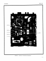
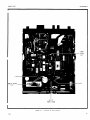
SCHEMATlCS
"
I
I
I
\
I
I
k
..
2
6
8"
8
I
.
.
.
.
.
ii
.
. .
.
8"
9
IO
Ii
12
12
12
12
12
14
14
16
22
23
23
23
26
,'P
32
32
.
.
.
::
::
34
2
::
35
37
45
45
15
45
ILLUSTRATIONS
rzg.
NO.
1
2
3
4
5
6
7
8
9
10
11
12
13
14
15
16
17
1.8
19
20
21
22
23
24
25
26
27
28
29
30
31
32
33
34
35
36
37
38
39
40
41
42
43
0976
IIcLe
“fme”sio”al
Data.
--___--____-____-_____________________
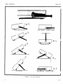
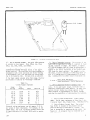
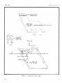
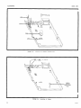
Tilt
Bail
Positions.
-----------------------*pant
panel.
-------------------------------------------
*ottcm View Showing Line Cord. -------------------------------__--_____--_____
Rear View Showing Line Switches.
Mode11688A Rechargeable
Pack. -----------------Batrery
Exploded View of Model 160B/1688A.---------------------Installatio"
of Battery
Pack. -----------------------------------_----___------------Battery
Test Location.
Front Panel Controls.
-------------------_-------------Imcarion
of Protection
Fuse. _---____-_________-________
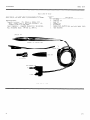
Voleage Measurements "sing Model 1601 AC/DC Probe. ----Current Measurements Using Made1 1651 Shunt. ---------Floating
operation.
--_---__-__-_______________________
O”f,,“t.
_____-____-___-____-________
Model 16028 ,,+&tal
Exploded View of Model 16011602B. __-_-----__--____--__
lnstallati,,,,
of &,&I
1602~. _---_______-____-__________
output Connector.
Rear Panel Digital
------------------Timing Diagram for Model 1602~. -----------------------Rack M,,unti,,g of Model 1.3,~. __--_______--______________
Overall
Block Diagram. _---____-___-____--_____________
DC Voltage Operation.
-------------_----__------------Resistance
operation.
__-____-_________--______________
current
Operaelan.
------------------------------------Absolute
Value Deeector.
---__--_-________-_____________
LSI Block Diagram. ----_---___----___--_________________
A/D Converter
Diagram. _--___-_________--_______________
Identification
af Se~,ent.s and Mulriplex
lines.
-------Tap and Bottom Cover Assembly.
------------------------Locarion
of Calibration
Ad,ustmenfs.
-----------------Location
of Test mints.
Location
of Chassis Connections.
---------------------Location
of Fuses. ------------------------------------case Outline
- Integrated
CirCUitS.
-------------------case Outline
- Integrated
circuits.
_---_______________Case Outline
- Integraeed
Circuits.
_--____--_____--__case Outline
- Inregrated
circuits.
-------------------case ourline
- Transistors.
Case Outline
- Thick Film Networks.
_---__-_____-_______
Case Outline
- Thick Film Networks.
-------------------Case O"tline
- Custom LSI. ---_----_---_-_------------Component Layout* pc-349. --_-_--______________________
pc-352. ----_---_-----____--_______I_
component Layout,
rage
iv
vi
1
3
4
4
;
9
11
13
13
14
15
16
17
18
*"
22
23
25
25
25
27
28
28
29
38
40
41
44
44
54
55
56
57
58
59
60
61
63
64
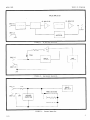
MODEL 1608
SPECIFICATIONS
I
10.7 5
(27:
i
I
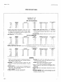
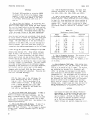
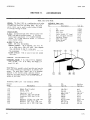
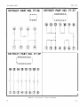
DIMENSIONS IN INCHES (MM)
I
FIGURE
1. Dimensional
Data.
1174
SPECIFICATIONS
Calibrated at 25” *ST
war,mte* to, 1 year
AS A DC VOLTMETER
AS AN OHMMETER
Liz2
m
NORMAL BENCH POSITION
LEVEL POSITION - TILTEAIL
J
&
45" POSITION
LEVEL POSITION - TILTBAIL%
AT FRONT
MODEL 160B
SECTION
1.
GENERAL
l-l.
INTROD”CTION.
The Model 1608 is a wide-range
digital
multimeter
capable of measuring voltage,
current, and resistance.
me Model 1608 offers
SeYen
ranges of voltage
from lrn" to 1000 volts,
nine ranges
of current
from 1O"A to 1ooomA, and ten ranges Of resistance
from 1n to lOOOM12. The Model 1608 display
is 3 digifs
plus 100% overrange.
1-2.
FEATURES.
a.
Voltage
sensitivity
to 1 micravole
b.
current
.se"Giti"ity
to O.OlnA per digit.
C.
Resistance
d.
Floating
capabilify
e.
Built-in
analog
f.
Optional
Made1 1602R Digital
s.
Optional
Model1688ARrchargeable
sensitivity
to 0.001n
per digit.
per digit.
LO _+1*00 "OlC.5 above case.
output.
Output
"attery
Pack.
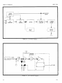
INFORMATION
HANDLE AND
TILT BAIL
I
LINE
COW
STORAGE
~
S
S
BAT TEST A
BAT TEST B
I
CONDENSEDOPERATING INSTRUCTIONS
2
S = SCREW
LOOSEN FOR
DISASSEMBLY
1174
MODEL 1608
INITIAL
5112 J113
!520 I
ANALOG OUTPUT
PREPARATION
DiGi :TAL
OUTF'UT
J302
SWITCHES SHOWNFOR
OPERATION FROM 105-125V LINE
3
L‘IG”RE 7.
4
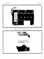
Exploded
view
Of Model
1600,16881\
0976
I
I
I
BATTERi FUSES
F203, F204
MODEL 1608 CHASSIS
\\
SPACER
(4 PLACES)
CAUTION
DISCONNECT LINE CORD BEFORE OPENING
THE TOP AND BOTTDM COVER,
LINE VOLTAGE ON THE CHASSIS
REPRESENTS A SHOCK HAZARD.
I
FIGURE
8.
Installation
0976
"f
Battery
Pack.
5
INITIAL
MODEL 160B
PREPARATION
SECTION
2.
INITIAL
b. Row
the Model
chargeable
1688A can
batteries
fare their
provides
information
GENERAL. This section
2-l.
needed for incoming inspecrian
and preparation
for
use.
INSPECTION. The Model 1603 was carefully
in2-2.
spected both mechanically
and electrically
before
shipment.
"pm receiving
the instrument,
check for
any obvious damage which may have occurred during
Report any damages to tne shipping
agent.
f*El"Sit.
TO verify
the electrical
specifications,
follow
the
procedures
given in Section 6.
The Model 1688A Rechargeable
Battery
Pack can
be insralled
within
the Model 1608 chassis at
However, if the Model 16028 Digital
any time.
Output is already
installed,
the Model 1688A
cannot be used simultaneously.
The Model 16OB
a. How to operate From IdlIe Power.
provides
a three-wire
cord which mates with third-wire
;rounded receptacles
(see Figure 4 for ~1% configura-the permanently
installed
line cord is stored
tion,.
by wrapping
the card around the base of the i"str"ment as shown in Figure 4.
The Made1 1608 has
1. wow to Set Line Switches.
two rear panel Line Switches which enable selection
of line voltages
over ranges from x0-llO",
105125v,
195-235",
or 210-250".
TO operate from line power.
determine
the appropriate
line voltage
range to be
used and set the Line Swirches as fallows:
Settings.
I
I
105-125”
NORM,
117
195-235”
1
‘Jo-110”
I
210-250"
I
LOW. 117
LO", 234
NORM. 234
For example,
if the line voltage
ea be used is
approximately
115 volts,
select
NORM and 117 which
permits B range of operarion
from 105 to 125v.
hfter
line Switches are set, connect the line cord
and set the Power Switch to LINE.
The Model 1608 uses
2. ,.ine Fuse Requirements.
~VO line fuses to protect
the line-operated
power
ne fuse types are l/8 ampere, MB, slowSWPlY.
blow.
Replace with Keithley
Part No. F"-20.
3. How to Replace Fuses in Model 1688A.
The
!Jodel, 1688H uses 1 ampere fuses to protect
the
power supply regulators
in case of malfunction.
Fuses F203 and F204 are plug-in
types and are located on pc board PC-349 as shown in Figure 8.
Keplace with 1 ampere, 3AB, slo-blo,
Keithley
Part
NO. FU-28.
6
to operate From Battery
Power.
TO operate
16OB from batteries,
the Model 1688A Rebattery
Pack must be installed.
The Model
(The
be either
field
or factory
installed.
in the Model 1688A may need recharging
befirst
usage to power the Model 1600.)
NOTE
The Model 160~ is shipped
PREPAR**ION FOR "SE.
2-3.
The instrument
can be powered from
ready-to-use.
line voltage
or from rechargeable
nickel-cadmium
batteries
(when the oprional
Model 1688A Rechargeable
Battery
Pack is installed).
TABLE 2-1.
Summary of Line Switch
PREPARATION
I
1. HOW to Install
Model 168% Rechargeable
BatThe batteries
furnished
with the Model
tery Pack.
1688A come already
installed
in the battery
pack.
the battery
pack includes
7 rechargeable
"C" cells
(1.2",
3 AMP HR) and 1 rechargeable
pack (16.8V).
If baeeeries
need to be replaced
or re-installed,
be certain
to observe the proper polarity
of individual
cells as shown in Figure 6. To install
the
Model 1688A Battery
Pack, turn the instrument
over
so that the bottom cover faces up.
Loosen four
slotted
screws on the batrom cover as shown in
Figure 4.
(A chisel-blade
screwdriver
is requires'
to loosen the slotted
screws.)
Turn over the instrument with tap cover facing up, taking care to
hold the top and bottom covers together.
Carefully
remove the top cover to gain access fo the printed
circuit
board.
(Two "ires
that connect to the
Analog Oufput must be disconnected
at the PC board
before the top cover can be set aside.)
Check to
see that the four insulating
spacers are in yasition on the printed
circuit
board.
Place the Model
1688A Battery
Pack in position
an the spacers with
the cable oriented
as sham in Figure 8. Plug the
4-wire Conneceor (5205) into the mating receptacle
(P205) taking care to orient
the connector
as
shown in Figure 8. After
the Battery
Pack is installed.
replace
the top cover.
Turn over the instrumen; wiih bottom co&r facing up and tighten
down the four slotted-head
screws.
TABLE 2-2.
Sumnary of nateerie
Used in Model
1688A
Rechargeable
"C" cell,
1.2". 2 AMP-FIR
Rechargeable
battery
pack, 16.8V, .225
Am-m
1
TM-32
0976
The instrument
must he operated
in the BAT
mode in order t” obtain a valid battery
condition
at test points A and 8. This3 Will
enstire that tile batteries
are supplying
power to the instrument.
If the voltages
are measured when the Model 1608 is operated in the LINE mode a different
reading
may be observed since the batteries
are not
connected and rherefore
do not supply power
to the instrumenr.
0976
OPERATING INSTR”CTIONS
MODEL 160B
SECTION
OPERATING
3.
information
GENERAL. This sec~ian provides
3-l.
needed to operate
the Model 160B for measU*eme"f
voltage,
cuirent,
and resistance.
Of
HOW TO SELECT POWER. The Model 160B may be
3-2.
powered from line voltage
or rechargeable
nickel-cadmium batteries
("hen the Model 1688A is installed).
The Model XOB has a built-in
line-voltage
power supIf the accessory Model 1604 Reply and line cord.
chargeable
Battery
Set is ordered and installed,
then
the user has the oprion of selecting
line or bateery
operation
via the front panel rotary
power switch.
NOTE
The accessory Model 1688A Rechargeable
Battery See may be ordered at ebe time of purchase of the Model 160B or may be purchased
and field
installed
at a later
time if so
me Model 1688A features
plug-in
desired.
Wi*i"g.
As a result,
no modifications
need
to be made to the Model 160B chassis.
a. "m, to Operate from Line Power.
The Model 160B
can be powered from Line voltage
over four ranges
from a minimum of 90" to a maximum of 25OV. see
Table 2-1.
1. Set rear panel Line Switches
positions
as show" in Figure 5.
3.
b.
Set front
panel
"cm to Operate
I.
Install
to appropriate
Power Switch
from Battery
to LINE.
Power.
Mode11688ARechargeable
Battery
Pack.
2. Check battery
voltages
at Teat Points A and
B to ensure thaL batteries
are charged sufficiently.
1. If necessary,
plug line cord info ac power
and set Power Switch to CHG to bring battery
"altage up to useable levels.
4. When bartery
line cord and set
switch
POSition
OFF
LINE
CHG
BAT
8
level is sufficient,
Power Swifch LO BAT.
disconnect
Line Connected
1688A not installed
OFF
ON
OFF
OFF
INSTRUCTIONS
HOWTO MAKE INPUT CONNECTIONS. The Model 1608
3-3.
has two front panel terminals
identified
as "HI"
(red) and '3.0" (black).
These terminals
accomodate
banana plugs. alligator
clips,
spade lugs, bare
wirea,
and other similar
input connections.
Leads
may be fabricated
using a good quality
capper wire
terminated
by single
banana plugs such as Keichley
Part No. K-5 or dual banana plug such as Keithley
Part NO. m-7.
Ready-made test leads are also available from Keithley.
Accessory Model 1681 Clip-o"
Test Lead Set includes
two 40 inch long leads terminated by a banana plug and spring-loaded
clip which
easily
attaches
co wires and terminals
on pc boards,
Model 1683 Universal
Test Lead Kit features
inetc.
terchangeable
probe tips for various
applications.
'I%e Kit includes
regular
probes, alligator
clips,
banana plugs.
spade lugs, and phone tips.
All-cow==
leads and teminarions
are best for measurements on
the lm" and ln ranges.
3-4.
HO" TO SELECT FUNCTION. Function
is selected
by means of a single
front panel Range Switch.
llie
Range dial is marked in "en&wring"
units for meas"remenf Of voltage
(rn", V), C"r*e"t
("‘4, LL4, n!A), and
For each function,
rotating
resistance
(‘2, kn, M0).
the knob clockwise
causes the Model 160B to switch
to a less sensitive
range.
a. DC “catage.
The voltage
sectors
of the Range
Switch are designated
in millivolts
("IV) and volts
I", for full
ranees from lm" to 1000".
A full stop
it'the
1000 "&range
prevents
inadverranr
switching to the nanoampere ranges by clockwise
rotation.
The resistance
sectors
of the
b, Resistance.
Lange Switch are designared
in ohms (n), kilohms
(kn), and megohms (MO) for full
ranges from 1 ohm
to 1000 megohms.
The current
sectors
of the Range
C. CU**e"t.
Switch are designafed
in nanoamperes ("A), microamperes (,,A), and milliamperes
(mA) for full
ranges
franI 10 nanoamperes to 1000 milliamperes.
Condition
of Instrument
Line connected
16888 installed
Line not connected
1688~ installed
OFF
ON
ON
ON
0976
-ZERO
R114
POWER
S203
-
FIGURE 10.
3-5.
HO” TO ME‘“LS”RE“OLTIICE.
The Model 1608 measures dc “aleage
in seven ranges:
Im”, lOnl”, loom”,
lV, lOV, LOO”, and 1ooov.
Maximum dc input is 1200”
dc + peak ac.
a. How to Select Ra”E,e. Function
and range is
selected
by rotating
the Range Switch to the appropriate
position.
Three positions
are direct-reading
in millivolts
CmV); four positions
are direct-reading in voles (VI.
Decimal point is selected
by the
Kan,qe Switch.
Polarity
is automatically
displayed.
If the input signal
exceeds twice full
range, the
display
blanks (3 least significant
digits)
to indicate an “overran&
condition.
TABLE 3-2.
“01 1tage Ranges Displ;
Range
SeCti”
,
1000
100
10
1
100
10
1
v
v
v
v
mv
mv
In”
Panel
Controls.
b. How to Determine Accuracy.
The xodel 16011 nccuracy is iO.I% of readina
f 1 dirit.
For enarno1e.
a display
reading
of 1.005 volt dc will
have a” ,a,,certainty
of 10.1% f 1 digit
or r.002 volts.
The input resisrance
in the dc m”de is 10 o,c~“,,cs.
!,eaiurements from relatively
high source resistnnccs
could cause an additional
reading error.
The dln”“,:i
of error due to loading
can bc determined
by rhc
following
relatiansbip:
% error
= 100 x RS i (R, + 10’)
where R, = Source resistance
in ohms
For example, a so”rcc resistance
“f 10,000 ohms Viii
result
in a loading
error of approximately
0.1% ai
reading.
d
Max. Display
1999 *
199.9
19.99
1.999
199.9
19.99
1.999
*Maximum allowable
input is 1200” dc plus
peak ac even though display
can be read
beyond 1.200”.
1174
Front
RANGE
SlOl
The input current
of the 1608 Cal” also cause
reading errors on the nlOSL sensitive
vo1cage
ranges when high source resistances
are present.
For example, an input CUrrent of lOpA
and a so”rce resistvnce
of MI! produce a”
error voltage
of loll”.
c. Maximum Allowable
Input.
The maximum L”P”L to
the Model 1608 is 1200” dc + peak ac.
On lrn”, lOn,V,
and lOOn,” ranges,
the maximum conti”uox,s
input is
6OOV (12OOV momentary) dc + peak ac.
‘,‘hc ?,odel ,,SO”
can display
dc voltages
greater
tba” r120O” but dnmage to the input is possible.
0
OPERATING INSTR”CTIONS
MODEL L6OB
IMPORTANT
The Model 1608 provides
ac rejection
(NMRR)
of greater
than 60 dB on the highesf
range.
However, a large ac signal
superimposed
on
a dc level could cause damage if the input
CO the Model 160" exceeds 1200 volts
dc +
peak UC.
d. How to Zero the Display.
To accurately
zero
the instrument,
place a low-thermal
short (such as a
piece Of clean copper wire) across the input rerminals, set Lhe Range Switch to the lm" range, and adjust the front panel Zero conerol
for a flashing
"i"
sign at the display.
The display
should then read
t.OOO, with some flicker
of the least significant
digit
due to noise and A-D converter
uncertainfy.
Once the zero has been set accurately,
there should
be little
reason to rezero the instrumenf
again soon
when making measurements on the 10~1" through 1000"
ranges.
The time stability
of rhe zero setring
is
excellent,
and in applications
requiring
continuous
operation
of the Model 160B, the zero setting
will
hold for months.
The front panel Zero control
is
convenienf
when making measurements on fhe 11"" Range.
A test set-up and cables when connected to the 160B
may cause offset
voltages
because of thermoelectric
effects
(see section
3-9).
These offset
voltages
might be only a few microvolts
or several
tens of
microvolts.
In such situations,
the Zero control
can be used to buck out any initial
offsefs.
I.""
thermal cabling
and connections
should be used whenever possible.
The instrument
zero can also be check
ed, and adjusted,
by shorring
the input on any range
(voltage,
current,
or resistance).
me zero c**t*01
will
have varying
effects
on the differenr
ranges
depending on the sensitivity
of the input amplifier,
but the zero control
can be used in this manner.
Again, it should be emphasized,
that for most meas"remene~ with the Model 160B, the Zero control
can
be set once and then left
untouched.
(See also ?ection 3-6c "LO" Ohms Zeroing").
NOTE
With the input open 0" the lm" Range, the
Model 160~3 display
may show a reading as
high as i.100.
This 19 equ*va1ent
to an
offset
currene of lo.opA.
If the display
shows a reading grearer
than t.100,
then
the internal
potentiometer,
R121, should
be readjusted.
Typically,
ehe offset
current will
be less than 5p~.
e. 80" to "se Model 1601 AC/DC Probe.
TO make ac
measuremenfs,
connect the Model 1601 accessory
K/DC
Probe to the Model 1608 inpur terminals.
Set the
Range to desired voltage
range.
Set switch on probe
to AC. "se the probe tip plus ground clip to make
connections
to circuit
under eesc.
see section
5 for
complete specifications.
HOWTO MEASURE RESISTANCE. The Model 1608
1-6.
measures resistance
in 10 ranges:
lsr, 1on, 10011,
Ikn, IOk&?, lOOk0, IM,,, lOMn, lOOK,, and 100011!2.
Function
and range is
a. HO" to Select Range.
selected
by rotafinf:
the Ranae Swifch LO rhe BPPTOpriate
position.
Three posi;ions
are direct-reading
in ohms (n): three positions
are direct-reading
in
kilohms (kn); four positions
are direct-reading
in
megohms (MQ)
Decimal point is selected
by Range
Switch.
If the input signal
exceeds twice full
range,
the display
blanks to indicate
an "overra"&
condlti**.
TABLE 3-3.
Resistance
current
Range
setting
1. n
10 n
1
10
100
1000
MI1
Mn
Mr!
M*
Max.
LIiF3play
Ranges
units
Impressed
current
1.999
19.99
ii
n
I InA
lti
1.999
19.99
199.9
1999
Mn
MO
Mn
MO
100 “A
10 "A
I"‘4
0.1 "A
b. How to Determine Accuracy.
The accuracy of cbe
Model 1608 is specified
in terms of a nercen~ of
reading and a p¢
of range.
For example, a display of 1.000 kilohID (kn.1 will
haw an uncertainty
of ~0.004kQ.
C. HO” to Measure “LOW” ohms. when making measurements on the ln, lOn, and 1OOn ranges,
rhe Model
160B is to be zeroed on the IQ range.
The zeroing
is accomplished
by shorting
the test leads together.
and adjusting
the display
for a flashing
+ and .ooon.
By zeroing
the instrument
in this manner,
lead resistance
of 200 mill.iohms
(minimum) can be
compensated for.
The instrument
must be rezeroed on
the lil range each time a different
set of iese leads
is used.
Before making meaS"reme"tS
right *t the input rerminals
(no test leads used), rhe instrumene
should be zeroed on the iii Range after placing
a
short,
such as a piece of copper wire, across the
binding
posts.
Copper leads and clips are best for
making measurements on the ln Range, because the
voltage
drop across a In resistor
is only Im".
CAUTION
Care should be taken when making resistance
measurements in circuits
which may have voltages on capacitors,
etc. or "here line voltage is present.
Although the Model 1608 is
fully
protected
against
accidental
voltages
up to 250" rms in resistance
function,
if
higher voltages
are applied,
damage may occur.
f.
How to "se Model 1682 RF Probe.
To make rf ac
measurements,
connect the Model 1682 Probe to the
Model 160B input terminals.
Set the Range to desired
voltage
range.
Maximum allowable
input is 30" *Ins
ac, 200” dc.
10
1174
-FUSEFUSE SHOWN
TWICE ACTUAL SI
Range
setting
I,0 nA
100 nA
1 LB.4
LO ,lh
100 UA
1. InA
10 rnA
100 lx.4
1000 mi\
Max.
IDisplay
Units
19.99
199.9
1.999
19.99
199.9
1.999
19.99
199.9
1.999
Il.4
IL4
II‘4
irA
UA
n!A
In.4
mA
ti
s,,une R*
1060
10%
1040
10311
10%
10 il
I. 0
0.1 !1
0.1 G
MODEL 160B
OPERATING INSTR”CTIONS
d. HOW to "se the Model 1651 Current Shunt (for
meaS"remenfS to SOA). current
measuremenf capability
Of the Model 160B may be extended to 50 amperes
through ctle use Of accessory Model 1651 SO-Ampere
The Model 1651 permits
4-terminal
connections
shunt.
to minimize meaeuremene error.ciue
to lead resistance.
To use the Model 1651, connect the voltage
sensing
leads eo the Model 160B input terminals.
Connect
separate
current
leads (not furnished)
beuveen xhe
source and the large hex-head bolts on the Model 1651.
The current
leads should be rated for currents
up to
50 amperes.
me Shunt resistance
is 0.001 ohm, vhich
produces a sensitivity
of lmV/Amp.
As examples,
10
amps current
results
in a lOIn" drop on 1Oln" RANGE,
and 30 amps yields
a voltage
drop Of 3Oln" which can
be read on the loom" RANGE. Power diss*paCed
in the
shunt is 2.5 watts at 50 amperes.
3-8.
NOISE CONSIDERATIONS. The 1imic of resolution
in voltage
and current
measurements is determined
largely
by rhe noise generated
in the source.
stray
low-level
noise is present
in some form in nearly al1
electrical
circuits.
The instrument
does not distinguish between stray and signal
voltages
since it measwhen using the lnl" and 1omv
ures the net "olfage.
ranges,
consider
the presence of low-level
e1ectrical phenomena such as thermocouples
(thermoelectric
effect),
flexing
of coaxial
cables (triboelectric
effect),
apparent
residual
charges on capacitors
(dielectric
absorption),
and battery
action Of t"O
terminals
(galvanic
action).
3-9.
THERMAL EMFS. Thermal emfs (thermoelectric
potentials)
are generated
by thermal differences
between two junctions
of dissimilar
metals.
To minimize the drift
caused by thermal emfs, "se copper
leads to connect the circuie
to the instrument.
The
front panel ZERO control
can be used to buck out a
cmstant
thermal offset
"aleage
if necessary.
The
Keithley
accessory
Model 1483 La" Thermal. Connecrio"
Kit contains
all necessary materials
for making very
low thermal copper crimp connections
far minimizing
thermal effects.
3-10.
MAGNETIC FIELDS.
The presence of strong magnetic
fields
can be a potential
sw.,rce of ac noise.
Magnetic flux lines which CUt a conductor
can produce
large a-c noise especially
at power line frequencies.
The voltage
induced due to magnetic flux is proportional
fO the area enclosed by the circuit
as well
as the rate of change of magnetic flux.
For example,
the motion of a 3-inch diameter
loop in the earth's
magnetic field
Will induce a signal
of several
tenths
of a microvolt.
one way to minimize magnetic pickup
is to arrange all wiring
so that rhe loop area enclosed is as small as possible
(such as twisting
inpur leads).
A second way co minimize magnetic pickup
is to use shielding
as described
in Section 3-12.
12
3-11.
AC ELECTRIC FIELDS.
The presence of electric
fields
generated
by power lines or other sources can
have an effect
on instrument
operation.
AC voltages
which are very large with respect
to the full-range
sensitivity
could drive the input amplifier
into saturarion,
thus producing
an errOneo"S DC OUtpUt.
At
line frequency
or twice line frequency,
the insLrument is capable of rejecting
AC voltages
whose peakto-peak amplitude
is equal to the full-range
DC sellsftivity
on the loom" through 1OOOV ranges.
This
level of interfering
AC signal will
produce no more
On the lm" and 1OmV Ranges, the
than 1 digit
error.
instrumenf
can reject
line frequency
and twice line
frequency
signals
whose p-p amplitude
is equal CD 10
eimes the full-range
sensitivity.
Far example, on
rhe ID," Range, a 1OmV p-p, 50 Hz signal will
produce
Peak-to-peak
AC
no more than 1~" (1 digit)
DC erroi-.
voltages
greater
than 1x the full-range
sensitivity
o,, the 1OOm" through 1000" ranges,
the 10X the fullrange sensitivity
on the lln" and 1omv ranges will
cause clipping
in the AC section
of the Model 160B
For this reason, shielding
is reinput amplifier.
com,,,ended when making sensieive
DC voltage
measuremenrs, or when making measurements from high so"rce
(See Shielding,
Section 3-12.)
The inimpedances.
serunlent is also capable of rejecting
frequencies
There is one proother than power line frequencies.
blem to consider;
however, the input amplifier
of the
Model l6OB uses a modulator
to convert DC signals
LO
AC signals
before amplification.
The drive frequency
of this modulator
is 220 HZ nominally,
f approx.
5%.
Interfering
AC signals
with frequencies
equal to the
modulator
drive frequency,
or mu1tipl.e~ fhereof,
will
appear 8.3 modulated DC, and produce large DC errors.
3-12.
SHIELDING.
a. Electric
Fields.
Shielding
is usually
necea8arv when the insrrument
is in the eresence of verv
l&e
a-c fields
or when very sensi;ive
measuremen;s
are being made. The shields
of rhe measurement circuit and leads should be connecee* together
to ground
at only one point.
This provides
a "tree"
configuration, which minimizes
ground loops.
b. Magnetic Fields.
Magnetic shielding
19 useful
where very large magnetic fields
are present.
Shielding, which is available
in ehe form of plates,
foil
or cables,
can be used to shield
the measuring circuit,
the lead wires,
or the instrument
itself.
C.
Other
Considerations.
1. Voltmeter
Measurements.
Use shielded
input
leads when source resiseances
are greater
than 1
kilohm or when long input cables are used.
2. Current Measurements.
On the mA and PA current ranges, no special
shielding
precautions
need
be taken.
However, an the 100 and 10 nanoampcre
ranges, shielded
input leads are recommended.
3. llesiatance
Measurements.
Shielding
of input
leads and source are recommended for measurements
on the 10 megohm through 1000 megohm ranges to prevent errOneO"S readings.
1174
FIGURE 12.
Voltage
Measurements
Using Model 1601 AC/DC Probe.
CURRENT TERMINALS
VOLTAGE TERMINALS
VOLTAGE LEADS FURNISHED
;*
1
1174
MODEL 1608
OPERATING lNSTR"CTlONS
I
i+
--~
MODEL 1608
EXTERNAL
E%'
DC
I
CASE
>lO"n
8'
TYPICAL
ISOLATION
RESISTANCE
GROUND
FIGURE 14.
3-13. HOWTO
has an analog
inverting)
at
for recording
analog output
a la"-noise,
Operation
USE THE ANALOC OUTPUT.
The Model 16OB
output of il volt at full-range
(nonup to 1 milliampere
(2mA at 2 volts)
or monitoring
purposes.
Also, the
enables the Model 1608 to be used as
low drift
DC amplifier.
hi"
Range
1 In"
1.0 rn"
100 In"
TABLE 3-5.
at liNALOG OUTPUT
Gain
Full Range
OUtpUt
x1000
x100
x10
1"
1"
1"
For off-ground
operarim,
the analog output should
be connected only to equipment capable of operating
off-ground
also.
The low side of the analog output
is at the same poeential
as the "LO" input terminal
of the Model 160".
3-14. HOW TO USE MODEL 1608 OFF-GROUND. The "LO"
terminal
can be operated
off ground at potentials
Of up tLl 11200".
Isolation
franI ehe "LO" terminal
to power line ground is specified
at lOOOMn, or 10'0
(shunted by 300@).
Ty,,ically,
the isolation
resistance from I.0 to GNE is two decades greater
than
log!? (lO"O).
Because of this excellent
isolation,
operating
the Model 1608 off ground results
in very
1.itr1e loading
(from LO to GNU) of a floating
source.
AC 1000" above ground, the Model 1608 will
require,
typically,
only 1Onh from the source.
The excellent
i.solation
also accounts for the high common-mode re14
Floating
"across
lk = I x lkn = 10-a x 103 = lOll"DC
The "isolation"
capacitance
from LO to GNC is important when AC common-mode signals
are present.
in
the Model 1608, rhis capacitance
is specified
at 300
of 60 HZ, 300 picofarads
pF maximum. At a frequency
has a reactance
of approximately
10Mli. With the HI
terminal
driven and a source impedance of lkll, R
1OOOV p-p, 60 Hz, common-mode signal
will
produce a
voltage
of only loom" p-p across the Model 1608 input terminals.
This lOOmV p-p signal
will
be lurtbcr
rejected
by the input amplifier
and A-1) converrer
SC
that the total
rejection
at the digital
display
is
at 1easL 140 LIB. At lower levels
of *C common-mode
signals,
the total
rejection
at the display
is even
greater.
For example, a 60 Hz, 100" p-p signal
should produce only about 1 digit
errur on the lh"
Range for a total
rejection
of approx.
160 dR. (IiT
driven,
IkQ source impedance.1
WiCh both AC and IDC
common-mode signals,
rejecti,,
is lnuch greater
than
specified
when the Model 160B LO terminal
is driven,
rather
than the HI rerminal.
Where there is a need
for even greater
isolation
from LO (0 power Line
ground, or where there is a need fo float
at porcntials
greater
than UOO volts above power Line ground
the Model 1688A Battery
Pack should bc used.
MODEL 160B
OPERATINC INSTRUCTIONS
out&t
IO&
“0” s &Sure
f0 0~tp~f LO.
OUtput Device:
2N5089 or equivalent
(greater
than
25volt
breakdown,
less than 0.5 volt while sinking f15 milliamperes).
REMOTE CONTROLS:
Strobe:
6 lines
for serializing
in multiples
Of 4
bits.
Logic "1" inhibits
controlled
OUtpUt lines.
i’
I.oeic "0" retains
data from last readO"t"UC Hold:
ing af DigitLOutput.
Logic “0” retains
data from last
Display
Hold:
reading
(escept far polarity
and decimal)
at
“igital
output and Display.
0976
15
CwmATING
MODEL 160B
INSTR”CTIONS
FIGURE
3-15.
HOW TO USE MODEL 16028
DIGITAL
16.
Exploded
View of Model 1608/1602B
To install
OUTPUT.
so mar:
The Model 16028 Digital
Output
provides
a. General.
binary-coded
decimal
(BCD) ouepufs and several
control
2his accessory
is available
either
"fsctaryinputs.
The Model 1602B
installed"
or "field-i"srallable".
consists
of a single
printed
circuit
baard (K-352)
with input and integrally
mounted "u~pue ca""ecfar,
and an ouf,,"t mating cm,ne~tc,r with hoad.
The Model 16028
b.
Installation
of Model 1602B.
ia installed
inrernal
to the Model 160B and is DOW~Ied by the Model 1608 line operated power supply:
NOTE
It is not ineended
that the Model 16028 be
used simulta"eously
with the Model 1688A
Battery
Pack.
To use the Model 1602B. the
Model 1688A muse be remaved and set aside.
It is possible,
however, for the u8er eo
make his own wiring
modifications
8" that
the Model 1688.4 Battery
Pack can power rhe
Model 160B while lacated
outside
the Made1
160B.
the Model
me
DOttOm
16028.
cover
turn
races
up.
the Model 160B "ver
.
Locate
and
loose”
four slotred
scre"s as shown in Figure 4. The 8cre"B
are "captive"
and should "at be completely
removed.
Once the screws are loosened,
hold
top and bott"m
covers
ragether
and turn Wodel 1608 so chat the top
CO"Br- is up.
Carefully
lift
off rhe top c"ver and
Locate
16disconnect
the wires to the Analog Output.
pin receptacle
5201 o" the ma,." circuit
board W-349).
Plug the mating c""necLor
(P301) from the Model 1602B
into 5201, after
checking
that pin numbers are corresponding.
Locate Spin plug P208 on the main circuit
b"ard (PC-349).
Connect
5303 from the Model 1602B to
P208.
Be sure that the “A” of PZOE lines up with the
"A" af 5303.
Place Model 1602B board o" four spacers
with cables positioned
as shown in Figure 17. Rem"ve
digital-output
c"ver plate fram Model 160B fop c"ver.
Place t"p c"ver back on instrument,
after
reconnecting
Amlog output wires.
Turn instrument
0"e-L and tighten
four slotted
screws.
C.
Pi" Idenrif*cae*on
of FleaI? Panel Digital
OutpUt
connector.
The Model 1602B uses a 37-pin connector
(5302)
Co provide
all input and output connections
to
external
equipment.
Pins are identified
as shown in
Table 3-7.
CAUTION
DISCONNECT LINE COBB BEFORE OPENING
THE TOP AND BOTTOM CO"ER.
LINE VOLTAGE ON THE CHASSIS
REPRESENTS A SHOCK HAZARD.
16
0976
DIGITAL OUTPUT
CONNECTOR5302
,J303
FROM PC-352
A
DE
PZO8
(PC-3491
5303
P301
(FROM ~~-352)
FIGURE 17.
1174
Installatian
of Model
1602B.
17
OPERATING
MODEL 1608
1NSTR”CTIONS
19
FIGmw. 18.
d. OUtpUt Data Lines.
positive
logic represents
digit,
""erload,
decimal
1
Rear Panel
BCD (l-2-4-8)
open-collector
each of 3 dv&a,
OVerrange
position,
and polarity.
1.
open-collector
output.
The output data buffers
of the Model 1602B consist
of CMOS NOR gates driving
individual
"open-callector"
transistors.
A main
fearure
of open-collector
outputs
is the ability
to
interface
with a variety
of data processing
equipment types including
printers
and campucers.
The
open-collector
output operates
in eirher
a saturated
(low-impedance)
state or an open (high-impedance)
state.
It is compaCible with many Lypes of lagic
including
TTL, DTL, RTL, and CMOS. The Model 16028
OUtpUt lines can operate at voltage
levels
up to
+ZOV, and hence can interface
directly
with CMOS
circuits
operating
with +15V supplies.
I" most cases,
a pull-up
resist"=
is needed to define
the "open"
or logic "1" state.
The value will
depend on the
capacitive
caupling
among wires in the cable and to
other circuitry
external
to the Model 160B/1602B.
For operation
with S-volt
power supplies,
a value
of Sk to 1Okn is usually
sufficient,
and the minim"!" value is about 3OOn. The Model 1602~ printed
circuit
board is designed so that pull-up
resisto=8 can be mounted on the board itself
(rather
than added externally).
One end of the pull-up
resistors
can then be connected to an excerna,.
power supply at pin 18 of the 37-pin output conneceor (5302).
The PC board spacing is designed
for l/4 watt carbon resistors.
18
Digital
OUtpUt Connector.
The open-collector
configurafian
can be
4.
used to connect multiple
"utputs
to one input of
a data-processing
system.
For example, if the
16028 is ineerfaced
to a 16-bit
compute=, ehe 3
BCD digits
may be presented
to a lh-bit
data =e@seer in the computer by setting
lines
25, 5,
and 24 t" logic "0" at a given time.
If the DP,
overload,
polarity,
and 1 x lo3 outputs
are wired
TABLE 3-7.
Model 1602B Connector
1
2
3
4
5
6
7
8
9
10
11
12
13
14
15
16
17
18
19
Not
Used
Not Used
DISPLAY HOLD
STROBE, ST-6
STROBE, ST-2
STROBE, ST-5
LO
DP-3 (100.0~
m-1 coooj
FLAG
OVERLOAD
DATA. 8 x
DATA; 2 x
DATA, 8 x
DATA, 2 Y
DATA. 8 x
DATA; 2 x
EXT VOLTS
Not Used
10'
10'
lOI
10'
10'
10'
Pin Ideneification.
20
21
22
23
24
25
26
27
28
29
30
31
32
33
34
35
36
37
_-
Not
Not
USed
Used
FLAG RESET
BCD HOLD
STROBE. ST-3
STROBE; ST-l
STROBE, ST-4
w-2
(10.00)
m
POLARITY
DATA,
DATA,
DATA,
DATA,
DATA,
1 x LO3
4 x LO2
1 x lo2
4 x 10'
1 x IO'
DATA, 4 x 10'
DATA, 1 x lOa
Not USed
__-__-_--___
1174
"PERATINC INSTRUCTIONS
MODEL 1608
Pi”
25
36
17
35
16
I
I-
NO.
STROBE1
26
I x in0
30
11
2 x 100
4 x 100
8 x 100
5
34
15
33
14
STROBE 2
1 x 101
2 x 101
4 x 101
8 x 101
24
32
13
31
12
STROBE 3
1 x 10²
2 x 10²
4 x 10²
8 x 10²
18
EXT.
VOLTS
b).
When a particular
16”B/16028 is being operaied,
line 6 may be set to logic “O”, enabling
FLAG and FLZG. when the data from this particular 160BI1602R is not of interest,
line 6 may be
set to Logic “1”. which disables
FLAG ant, FnE.
men, ametIer device may use the same line for
interrupt
or polling.
Since the dafa is in 4-bLr or smaller
cl.
groups, all output dafa from the 1602B may be
sequentially
connected to a 4-bit
bus using the
same technique
described
above.
This is useful
when interfacing
to progralmnable
calculators
and
logic systems where bit-parallel,
character-serial data tranSmiSSi0”
is used.
3. nverrange
Digit,
Overload,
and Polarity.
These three lines are controlled
by the same strobe.
me presence of the overrange
digit
is indicated
by
a “high”
output.
An overload
condition
is hdiC.9
ted by a “low” output.
For polarity,
“+” is represented by a “high”
ourput.
Name
!
29
6
10
28
STROBE 4
1 Y 103 (““ERRANCE)
OVERLOAD
POLAKI'TY
!
1
STROBE 5
FLAC
Fix
i
OPEBATlNG
niSTR”CTI”NS
MODEL 1608
EVENT*
3*
4*
I
FLAG
DIGITAL OUTPUT
LATCHES UPDATED
5*
I
/
DIGITAL OUTPUT
LATCHES UPDATED
I
I
BCD-----------HOLD
-f----
;;:;T-- - - - - - ~-- --- - - - - - - -~..-- - ~~.
__~~I...,,
EXPLANATION OF EVENTS*
Conversion
cycle #1 complete.
Latches in LSI circuit
(in Model 1608) updated.
1).
2).
Digital
Output latches
updated with data from conversion
#l.
"Flag"
line goes
from "0" to "1".
"BCD Hold" goes low (after
"Flag"
line has gone high).
31.
"Flag"
line goes high.
Digital
Output latches
still
contain
data from cower4).
sion #2, because "BCD Hold" line is low.
"BCD Hold" released
(after
"Flag"
line has gone high).
5).
"Flag"
line goes high.
Digital
Output latches
now contain data from conversion
61.
Flag Reset" goes from "1" to "0". causing the "Flag"
to go from "1" to "0".
"Flog" line goes high even though "Flag Reset" line is still
low.
Digital
Outcontain data from conversion
#5.
put latches
FIGURE 19.
2”
Timing
Diagram
for
Model 1602B.
MODEL 1608
f.
Output Control Lines.
The Model 16028 has six
Strobe lines,
a Flag Reset line,
a BCD Hold, and a
Display
Hold.
1. Strobe Lines.
All data outputs are grouped
into 3- and 4-line
groups. .Eachgroup
is controlled
Flag and Flag are also controlby a "Strobe"
line.
led by a Strobe line.
Logic "1" on a Strobe line
turns all the transistor
"open-collector"
outputs
off in a particular
group.
A logic
"0" o" a Strobe
line enables the data to determine
the logic states
'rhe groupings
are indicated
in Table
Of the group.
3-s.
Section d (above) gives additional
information
on open-collector
outputs.
Flag may be reset at any
2. Flag Reset Line.
time by setting
Flag Reset to logic "0".
The Flag
is reset by the transition
of the Flag Reset line
from logic "1" to logic "0".
The signal
at the
Flag Reset line may be either
a pulse or a level.
When a pulse is used, the pulse width should be at
If a level is used, a logic "0" on
least l"&C.
the Flag Reset line will
not prevent
the Flag from
going high when the next "good data" is available.
BCD Hold.
If this line is set to logic "0".
3.
the data at the Digital
Output will
"at be updated
as conversions
are completed.
Flag will
operate
When BCD Hold is returned
to logic "1".
normally.
the Digital
Output will
be updated normally.
New
data will
be available
beginning
with the next
logic "0" to logic "1" transition
of the Flag.
1
me BCD Hold is not synchronized
with a particular
point in the conversion
cycle.
when the BCD Hold
line is set to logic "O", the "updating"
pulses
to the Digital
Output latches
are blocked.
If
the BCD Hold is activated
during the time when
Flag is normally
low, either
"one of or some of
the Di@tal
Output latches
will
be updated.
If
the BCD Hold is released
during the time when
slag is normally
Low, only some of the Digital
Output latches
may be updated at the next Flag
For these reasons.
the SCD Hold should
high.
be acrivated
and released
only during the time
when the Flag is normally
high (this
is approximately
200mS regardless
of whether Flag Reset
is used).
The BCD Hold should be activated
after
Flag has gone from low to high; the BCD hold
should be released
after
the Flag has gone first
from high to law and then from low to high.
1174
NOTE
The SCD Hold has no control
over the "DP"
(decimal point)
lines.
The logic states
of the data on these lines is determined
by the setting
of the Model 160~ ~a"Se
Switch.
The Range Switch setting
should
not be changed while the Digital
OUtpUt
is in a "Hold mode".
4.
Display
Hold.
This "Hold" line affects
the
Model 160B LSI circuit
directly.
When this ""aid"
is applied,
the numerical
data present at the Model
160~. display
and at the Digital
Output is "at updated as conversi~na
are completed.
Tne Display
Hold line is activated
by a logic "0".
When Display Hold is returned
to logic "I",
numerical
data at the display
and Digital
Output will
be
updated normally.
The Display
Hold is not synchronized
with a parcycle.
If the
ticular
point in the conversion
Display
Hold is activated
during the time that
the Flag is normally
low, numerical
data from
either
the moot recent conversion
or the co"version previous
to it may be retained.
A similar
situation
can occur if the Display
Hold is released during the time when Flag is normally
law.
The Display
"old should be activated
after
Flag
has gone from low to high:
the Display
Hold
should be released
after
the Flag has gone first
from high co law and the" from low to high.
Llnit is very unlikely
that aclike the SCD Hold,
tivating
or releasing
the Display
Hold during
Flag low time would produce mixed data at Cbe
display
and Digital
Output.
If it does not
matter whether the retained
data is from the
most recent Conversion
or the co""ersio"
immediately
preceeding
it,
the Display
Hold can be
applied
arbitrarily.
I" any operating
system
however. the Display
Hold should be synchronized
in some way "ith
the Flag.
FIGURE 20.
tick
Mounting
af Model 160B
now TO RACK MOUNT THE MODEL 160B. The Model
3-16.
1010 Rack Mounting Kit adapts the Model 1608 for
standard
S-114 in x 19 in. rack mounting,
with 11 in.
depth behind the front panel.
a. “sing two Phillips
screws (Item 7) attach
port Plate (Item 2) to Front Panel (Item 1).
sup-
b. “sing four Phillips
screws (Item 7). attact,
left
and right
side Brackets
(Items 3 and 4) to Front
Panel (Item 1).
d. Assembly of rack hardware
for mounting of IrlStrune”t.
22
ia complete
except
0875
MODEL 1608
T,,E”RY
SECTION
4.
THEORY
OF
OPEKnTI”N
OPERATION
OPTIONAL
DIGITAL
OUTPUT
CURRENT
SHUNT
RESISTORS
IlV
1174
OF
OUTPUT
.‘i
MODEL 160B
TABLE 4-1.
summary of Voltage sensitivity.
Range
lrn"
1" In"
100 m"
1
”
10
100
1000
v
"
"
Attenuator
setting
Amplifier
Full-Range
SenSitiYity
--__l/l"0
l/l""
1/10,0""
1/1",""0
1
1"
1""
1"
100
1"
100
3. Filfer
Network.
Basically,
the filter
is a
l-section
RC low-pass filter
made up of R116, R117,
and C104. Rl16 and R117 in series have a nominal
resistance
value of 112kn.
At 5" Hz, Cl04 (.S$F)
has a reactance
of approx.
6k0, and with the 112kn
produces an attenuation
of apprax.
20 co 1. This
attenuation
gives the Model 160B a normal-mode rejection
spec of 60 dB above 1 digit
on the 1OOmV
range, as an example.
"6" dB above 1 digit"
means
that the Model 16"B can re,ect
a 1OOm" p-p, 50 Hz
signal
an the 1O"mV range with no more than a 1
digit
error.
1""mV p-p at 5" Hz would be reduced
This 5mv
to 5mV p-p at the output of the filter.
p-p, after
"chopping"
and amplifying
is enough to
cause amplifier
"104 to reach its maximum allowed
A signal
greater
than 5m" at the
OUtpUt level.
oUtpUt of the filter
causes "104 to saturate.
when
Saturation
0cc"r-s) significant
DC error signals
can
he produced at the output af ehe overall
amplifier.
4. Modulator
Circuit.
This circuit
converts
an
input dc signal
to an ac signal with a fundamental
frequency
component of approx.
22" HZ. The frequency of 220 Hz was chosen because this frequency
is not harmonically
related
to either
50 Hz or 60
HZ. The circuit
utilizes
a dual MOS-FET (Ql"2A
and Ql"2B) connected in a series-shunt
configuration.
This type of eeries-shunt
modulator
maintains high input impedance.
5. AC Amplifier.
The ac amplifier
uses a lownoise integrated
circuit,
"104.
The amplifier
feedback network provides
a gain of approx.
2000 at the
modulating
frequency
of 220 Hz, while maintaining
a gain of 1 far amplifier
("104) dc offset
voltages.
6. Demodularor
Circuit.
The demodulator
is synchronized
with the input modulator.
A JFET, 4103,
with low on-resistance
is used to alrernately
attenuate or pass ehe signal
present
at the output of ac
amplifier
"104.
The negaeive portions
of the 22"
Hz ac signal
are allowed to pass which produces a
"half-wave-rectified"
negative
dc signal
at the input to dc amplifier,
"105.
7. DC Amplifier.
This amplifier
is composed of
resistors
R128 and R129, capacieors
Cl13 and Cl14,
and integrated
circuit
"105.
The integrated
circuit provides
sufficient
gain to bring the foral
open-loop
dc gain of the overall
amplifier
to a
minimum of about 20 million.
The feedback capacitor. Cl13 and Cl14 in series,
was selected
to give
a noise bandwidth
of apprax.
0.5 Hz fo rhe overall
amplifier
when it is used at a closed-loop
gain of
10"".
The integrated
circuit,
UlOS, must be capa24
Amplifier
Gain
m"
In"
lnv
In"
In"
mV
mv
F"ll-Ra"ge
DC output
Xl000
Xl""
Xl"
X10"
x10
X10"
x10
1
1
1
1
1
1
1
Volt
volt
volt
volt
volt
Volt
volt
ble of driving
the feedback network (R160.4, B, C,
and ehe Analog Output
and D), ehe A-to-D convereer,
to t2 VDC.
8. Modulator-DemodulaCar
"rive
Circuit.
CMOS
inverters,
U103A and "1038, provide
oppoatte phase
square .,,aves used to drive MS-PET modulator
transiseors
Ql"2A and QlOZB. Inverter
U103B also provides a drive signal
for demodulator
JFET Ql"3.
Resistors
Rl21, P.122, and R123, and capacitors
Cl08
and Cl"9 effect
the rise and fall
times of the
square-wave
drive signals.
R121 adjusts
the rise
and fall
time of Ql"2A only, 80 that the total
charge, both posifiva
and negative,
transferred
to
the input can be minimized.
Any net charge at the
input creates
a current,
which in the Model 160B
is specified
to be less than il"pA.
The frequency
of the drive signal
is determined
by the clock circuit and LSI "201.
Circuitry
in LSI "201 divides
down a nominal clock frequency
of 9680 Hz to produce 22" Hz.
9.
4-Z&.
OffseE
Current
Zero Circuit.
See section
1".
Front Panel Zero.
The voltages
across potentiometer
R114 are set-up by a seable zener reference diode, VRl"1. and an IC op-amp. "102.
These voltages
are approximately
+2 "DC, which give
RI14 an adjustment
range of approximately
45"uVolcs.
A typical
Model 1608 has an internal
offset
of about
-l""uValts
in the chopper amplifier.
Hence. adjuscing the Front Panel Zero from end to end "ill
typically produce aboue +lZS,,"olrs
and -325v"olts.
This
"extra"
adjustment
a~ ehe negative
end of the range
allows sizeable
positive
offsets
to be compensated
for, as is the case when the Zero is used for tese
lead compensation
on the law-ohms Ranges.
200~ of
test lead resistance
will
produce +ZOO,,"oles of zero
offset,
which can be "bucked o"t" by the Zero conti-"1.
(See also Section 3-5d).
Zeroing of the
chopper amplifier
output is actually
accomplished
by having the "Zero" circuit
either
source or sink
whatever current
is present
in feedback resistor
R160".
For example, an Offset voltage
of -1llu"
on
the feedback line produces a c"rrenf
of -1,A in resiseor R16"" (111.135n).
A voltage
of -1u"olt
at
the wiper of Zero poteneiometer
RI14 will
produce
an equal current
Of -1uA in resistor
R115 (M").
With fhts zeroing
scheme. for the chopper amplifier
output to be at zero, the voltage
at the feedback
line will
always be offset
from the voltage
at the
input by a constant,
say for example. -1llu"olts.
(The feedback line connects to the junction
of R16"C
and R160D).
1174
ANALOG AMPLIFIER
DC AMPLIFIER
AC AMPLIFIER
INPUT HI
ATTENUATOR -
MODULATOR -
A,
-
DEMODULATOR
w
I ',
OUTPUT
INPUT LO
RANGE
SWITCHING
?I7
FIGURE 22.
DC Voltage
operation.
FIGURE 23.
Resistance
operation.
INPUT HI
INPUT LO
0
f-i+7
FUSE
INPUT HI
ANALOG
AMPLIFIER
ox0
Lr
RANGE SWITCHING
1
'I
INPUT LO
1174
OVERLOAD
PROTECTION
I
I
I
1
C. “hnmlecer circuitry.
This circuitry
provides
a
number Of fixed currents
by using a Stable voltage
reference,
a differential
voltage
amplifier,
and a series resistor.
The circuit
is also proLecte*
against
voltage
overloads
Of 25” volts
at the Model 1608 input terminals.
1. “oltane
Reference.
An adjustable
divider
made
up of resistors
R1.05, 11106, and RI’“7 provides
an
output of approximately
-1”“nl” from a stable
zener
reference,
“Rl”1.
This divider
is cannected tcl the
inverting
input of the differential
voltage
amplifier.
(The divider
is actually
adjusted
so that the
amplifier
ourput is 311 accurate
+l”“m” when the input terminals
of the Model 1608 are shorted.)
2. Differential
Voltage Amplifier.
This amplifier circuit
includen
UlOl, resistors
F.102, R104,
K108, R109, Kll”,
and prorection
circuitry.
me
resistors
and 1C op-amp are connected as a unity
gain differential
amplifier;
resistor
~11” adjusts
the gain accuracy.
l‘he inverting
input of the circuit is connected
to a reference
voltage.
me *cl”inverting
input is connected to the feedback voltage of the analog amplifier.
Because the feedback
voltage
is esual to the innur voltaee
of the analoe
4. OverLoad Protection.
when a positiw
overload voltage
up CO f25O “DC is applied
to the Model
1608 input terminals,
CR101 is reverse biased and
prevents
damays to IC amplifier,
“101.
current
flow
from the +250 “DC source is ttmxgh
a current
setting resistor
and R102. K102 has a value of 49wn
which prevents
excessive
currents
in the low-value
current-setting
resistors.
when a negative
overload voltage
up to -250 VDC is applied
to the input
terminals,
Ql.O1 is biased to limit
the current
to
appvaximate1y
2mA. Maximum current
possible
from
“101 and Rl”2 at -250 “DC is approximately
Z.Sti,
which is low enough to protecf
the low-value
current
seccing resistors.
Q106 has a normal diode drop for
positive
overloads,
and an approximate
-6V zener
drop for negative
overloads.
It protects
the input
of U1”l.
4-3.
ANALOG-TO-DIGITAL CONVERTER. me analog-codigital
converter
includes
the following
circuits:
an “absolute-value”
circuit,
a polarity
detector,
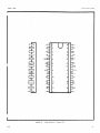
integrator
and threshold
detector,
a,, ISI circuit,
clock,
an LED display,
and display
drive circuitry.
a. Absolute-value
Circuit.
‘This circuit
produces
a positive
DC output voltage
regardless
of the polarity of the input voltage.
The relationship
is defined
by:
“0”f
26
an
a
= k lhnl
where k = +1
1174
R16ZA,R134
ANALOG SIGNAL
TO POLARITY INDICATOR LOGIC
1V = FULL RANGE
1
J
R162F,G
1
Actual operation
is as follows:
A positive
dc voltage
at p*n 12 of K162 produces an equal dc voltage
at the
output of Ul”7, and also causes the output of U106 to
go negative.
When this happens, CR105 is reverse
biased,
and “107 is effectively
isolated
from the action of “106.
A negative
dc voltage
at pin 12 of RI62
causes the autput of “106 to 80 positive;
the output
of U106 must go sufficiently
posirive
to forward bias
CR105 and drive the input of “107.
In this situation,
U107 and Ul”6 together
function
as a two-stage
inverting amplifier.
The gain of this inverting
amplifier
is accurately
set to -1 by internal
adfustmenf
R134
(“-DC CAL”) and rcsisrors
R162A, R, and H. K135 (“RECT
ZERO”) sets the zero offset
voltage
of “106 equal f0
-l/Z the zero Offset voltage
Of “107.
rfhus, the zexo
offset
is the same for hot-h positive
and negative
dc
signals,
and this zero offset
can be compensated far
with the “DISPLAY ZERO”, R136.1
capacitors
~115, C116.
C117, and cl18 provide
filtering
of AC components present in the input signal.
The polarity
detection
cirb. Polaricy
Defector.
cuit uses TWO transistors,
“108C and U1”8D, of an IC
rransistor
array.
These transi~rors
are used as a
simple differential-voltage
amplifier
with one,output
connected LO y~~wer supply common. A positive-going
output “f “106 callses the collector
of transistor
“1081~ to go negative.
When this happens, Q206 is
shut off, and the “+” segments of display
DS201 ~r’e
A negative-going
OUCPUC of U206 CRUSTS
aha shut off.
:he base of transistor
u108D to be clamped at appraximately
-0.7”.
which shuts off the collector
current
of “108D.
AS a result,
the voltage
at the collector
of 11108” gaes to a level of approximately
+“.,“,
which
is sufficient
to drive Q206 into saturation
and turn
on the “+” segments of “S201.
0976
TO A/D CONVERTER
CS
7 SEGMENT
DECODER
TH
I
1
DISPLAY
OUTPUTS
i
TO
DISPLAY
Cl 20
LSI CIRCUITRY
DETECTOR
OCLOCK
28
1174
a
f
1 +TL;f.;./y i
b
,,I
e
dp .
IDENTIFICATION
Identification
curacy.
Once the reference
current
is set, a” input
of 250m" is represented
as 250 counts out of 2016,
and 1.999" is represented
as 1999 counts out of 2016.
An input of 2v or greater
causes the 3 least-significant
digits
to blank.
NOTI:
one comp1ere con"ersio"
cycle is 2048 CO"rLfS.
The six counter is able to count to 2016 beDuring the remaining
32
fore it is stopped.
CO"*ltS, the information
in the BDC counter is
transferred
into latches,
and then the "CD
counter is reset to Zl?TO. 2048 CO""tS at a
clock frequency
of 9680 Hz results
in a total
conversion
time of approximately
0.21 seconds
(which is equivalent
to about 5 readingslsec.).
The clock circuit
makes use Of an IC
d. Clock.
timer,
Ll202, hooked up far astable
operation.
Rexist,,rs ,I205 and R206, together
with capacitor
C201, set
up a non-symmetrical
square-wave
with a nominal frequency of 9680 HZ and a duty cycle of about 5%. 4201,
along with R202, R203, and R204 is used to invert
the
output of uzm.
The Model 1608 digital
readout is
e. "isplay.
,nade up of three LED seven segment displays
(DS202,
~203,
and uS204) and one LED "21" display
(DS201).
1. Display Multiplexing.
The LED displays
are
znultiplexed
to minimize
the number of interconnections,
simplify
the drive circuitry,
and reduce
power consumption.
The timing for the multiplexing
0976
I
d
IDENTIFICATION
OF MULTIPLEX LINES
PIGURE 28.
c
I
of segments
and Multiplex
OF SEGMENTS
Lines.
is determined
by the LSI circuit,
L201. and is see
up such that each mu1cip1ex line is hi&
for 8
clock pulses (;~pproximately
825uSec.1 and low for
24 clock pulses.
The four mulriplex
lines are designated
as TO, Tl, T2, and T3, and each line cuntrols
an LED display
(See Figure 28). Circuit
operation during a particular
multiplexing
interval.
say
TO, is as follows:
when TO is high, the oucpuc Of
"20% is 10".
This produces a CUrrelIt in R218B Of
approximately
lOmA which is sufficient
to drive
Q202 into saturation,
and effectively
c"nnect 1~5201
to the f5" power line.
Simultaneously,
the LSI
circuit
supplies
the correct
digital
information
for DS201 to the display
segment ciriuers.
The aan,e
circuit
action
the" occurs during the oe,,er multiplexing
intervals
--- 'i‘l, T2, and T3.
The display
drivers
are de2. Display
Drive.
signed to handle a variety
of LED common-anode displays.
Because 't~~nstant--current"
drivers
are used.
displays
with different
voltage
drops per sewent
can be drive"
without
changing the circuit
power
conaumptian.
The driver*
take the same current
from ehe C5" power supply regardless
of whether
the display
segment drop is 1" or 3.5".
Actam
operarion
of a particular
segment, segment h for
example, is as follows:
when the "A" 1inc of LSI
circuit
"201 is high. the" the open-collector
DUtAS a result,
LhC
put of buffer
U204A is shut off.
voltage
at pin 5 of resistor
network R211 is spproximarely
11.3".
which is also the voltage
at pin 9
of transistor
array "205.
nssuming a base-to-emitter
voltage
of 0.7".
Lhen the voltage
at pin 10
Of "205 is approximately
i4.6";
this voltage
generates a 15,nA c,,rrent
in the 400 emitter
resistor.
29
MODEL 1608
THEORY OF OPERATION
When the “A” line of U201 is low, then the output
of "204,, is also low, and the transistor
current
source (pins 9, 10, and 11 of 11205) controlled
by
Transistor
4207, and ifs assoc"204A is shut off.
iaCed circuitry
duplicates
the operation
of the other
The “decimal
point”
six transisror
current
sourcgs.
lines of 115202, DS203, and OS204 are controlled
by
the Range Switch,
and the currents
for the decimal
points are determined
by R209, R210, and R211.
line
4-4.
POWERSUPPLY. the Model 1608 uses either
power or battery
power (when the Model 1668A is installed).
Transformer
I’201 has two tapped
a. Line Power.
primary windings which are connected in series
or in
parallel
depending on the position
of line switches
Fuse F201 is in series with winding
5201 and 5202.
Fuse ~202 is connected only
4-5-6 for all settings.
when winding l-2-3 is connected in parallel
with winding 4-5-6.
The secondary of I’201 has two tapped windings.
T,,C lower caps (11 and LO; 8 and 7) are used
in line mode. 'The upper taps (12 and 10; 9 and 7) are
used in charge mode.
In LINE operation,
the ac “olt1. +5v Supply.
age between transformer
leads 10 and 11 is full-wave
rectified
by CK203. The filtered
full-wave
dc voltage (approximately
10”) is regulated
by integrated
The outpur regulated
voltage
is 5”
circuit
u207.
15%.
2.. -12” Supply.
I” LINE operation,
the voltage
between transformer
leads 7 and 8 is full-wave
rectified
by CR204. The filtered
full-wave
dc voltqe
(approximately
18") is regulated
by integrated
circuit U208. The regulated
output voltage
is -12”
i5%.
b. Battery
Power.
When “ATTERY mode is selected,
the Mode11668ABattery
Pack is connected into the inputs of u207 and U208 while the line voltage
is disconnected at the secondary.
The 8.4” batteries
provide input power for the l 5” supply.
The 16.8" battales
provide
input power for the -12” supply.
Battery test point h provides
a measurement of the 16.8”
battery
supply with respecr
to power supply low.
Therefore,
the voltage
measured is the difference
bctween the battery
supply and the -12 vole uurput which
is approximately
+4.8 volts.
nartery
LCSC point R
provides
a measurement of the 8.4” battery
supply.
Battery
Char&q.
In the Charge mode, rbe 8.4”
ba;;er*eS
are connected between the output of CR203
and the input of U207.
‘TO accommodate the barteries
in series with the regulator
(U2071, one AC input oI
CR203 is switched
to a higher voltage
rap (pin 121 on
eransformer
T201.
‘The 16.8” batteries
are connected
between CR204 and “208. and CR204 is switched
to pin
9 af T201.
Actual charging
of the 8.4” batteries
is
accomplished
by the current
pulses in filter
capaciior C203; charging
of ehe 16.8” batteries
is by current pulses in C206.
TABLE 4-4.
Pin Identification
Pi”
NO.
“Wig.
1
f
“altape
FU”CLiO”
/
I Segment drive
l.C”ClS
l 5” = ON, 0”
= OFF
for
LSI.
Pi”
lie.
Ilesig.
15
dp
1 Decimal
I
I
point
) Segment drive
+5v = ON, 0” = OFF
16
:44
~ Multiplex
line
f5”
= ON, 0” = OFF
17
‘TO
Multiplex
Line
+5v = ON, 0" = OFF
18
Fl
~ Multiplex
I
Not Used
19
i F4
) Not Used
20
1 +5v
Power,
21
I -12"
,~Power,
22
C”M
2
8
3
4
iT1
I
, T3
5
: HOLD i
,
____
6
MR
Not "se*
7
TH
1 Threshold
8
1 CM
9
b
10
a
Se,qent
11
d
Segment drive
12
e
13
14
input
____
+5” or -12”
Clock
Approx.
: Se,,q”ent drive
lOk”Z,
+5v LO -12”
~
+5v = ON, 0" = OFF
24
i ~2
~ ?utip1ex
= ON, 0” = OFF
25
IR4
i Nat Used
Se~tnent drive
+5v = ON, 0” = OFF
26
8.1
Not Used
c
Segment drive
f5"
27
/ R2
Not Used
cs
Current
Switch
I+5”
= ON, 0" = OFF
= integrate
mode
Not “SCd
- ON, 0”
= OFF
+5v - ON, 0” = OFF
! ----
-12"
~ common or “LO”
~ CN
~ +5v
Le”els
: +5v
-12"
23
.+5”
line
f5"
+5v = ON, 0" = OFF
drive
Voltage
FunCtion
line
0”
i +5v = ON, 0" = OFF
_---
_---
I
30
0976
a.
uses
SeVerI segmell-to-BCD
canvercer.
three
one Hex Inverter
n!301).
‘This
converter
"uad 2-InnuT
NOR
The dara buffers
consist
C. OUtpUt Data Buffers.
basically
of five Quad 2sInput NOR gates (U314 thraugb
SECTION
5.
ACCESSORIES
MODEL 1601 AC-DC PROBE
GENERAL. The Model 1601 is a combination
ac-dc probe
MECHANICAL PARTS LIST:
that enables the user fo measure "oltqes
from 45 Hz
Item
to 45kHz when used with the Model 160B. The slide
NO.
Description
switch (SlOl) can be used to select
either
AC mode
or straight-through
DC Mode.
1
TiP
2
Bady, Front
SPECIFICATIONS:
3
Body, Rear
4
Strain Relief
DC:
straight-through
probe does not alter
any
5
Cable, Ground (13" long)
1) 150 picoModel 1608 specifications
except:
6
Clip,
Alligator
(Ground)
farads input capacitance
2) 0.5 atqere maximum
7
Insulator
(Black)
current
3) 0.3 ohms resistive
offset
4) i20 micro8
Cable (40" lo"=)
volts
rhermal offset.
9
strain
Relief
Can Shield
w
(Voltage
only):
RANGE: 250 volts
nns maximum.
TRANSFER ACCURACY: f3% of reading,
10.1 volt,
45
Hz to 45kHz into a LOWi 110% load.
Peak responding, calibrated
in rms of a sine wave.
INPUT IMPEDANCE: 0.5 megohm, shunted by less than
20 picofarads.
MAXIMUM OVERLOAD: Peak ac plus dc must "of exceed
400 "OltS.
CONNECTOR: Shielded
246548
24656C
24655C
186768
SC-33
*C-lo
AC-11
SC-30
18676~
25128‘4
Banana Plug.
DIMENSIONS, WEIGHT: 6 in. long x 314 in. diameters
(150 x 20 "In), 3 ft. (1 m) cable, "et weight l/4
pound (0,l kg).
MAINTENANCE:
Since the probe assembly should provide
goad service
with normal handling
"o maintenance
is usually
"ecWSClry.
The probe body (Items 2 and 3) is fastened
rogether
at the factory
using a special
salvent.
Therefore
ebe probe should not be disassembled.
If
repair
is necessary,
contact
the Keiebley
Representative
in your area.
ELECTRICAL PARTS LIST:
JlOl
SlOl
Cl01
Cl02
DlOl
0102
D103
RlOL
R102
KL03
8104
32
(See schemaeic
24669C)
Banana Plug (2 req'd)
Switch, AC-DC
capacitor,
0.047pF
capacitor,
0.1 pF
Tra"SistOr,
ieN, case TO-106
NPN, case TO-106
Tra"SiSfOr,
Diode
Resistor,
3.92 MR, 1%. 1/4w, CbF
Resi6tor,
Selected
in Test*
Resistor,
1 MI, o.l%, l/El.?, MtF
Resistor,
100 0, lO%, 1/4W, Camp
Mfr.
Code
Mfr.
Part
JOHN
RI
STAND
POT
FAIR
FAIR
MOT
DALE
IRC
DALE
OHM
108-750-Z
speckI
MZW-F-0.047uF
MWLA-O.~UF
2N3565
2N3565
IN4006
DC-l/4-3.92M
CEA-TO-"
MFF-L/8-LM
CB-101-10%
NO.
w-3
SW-334
C197-.047M
C86-.1M
TG39
TG-39
RF- 38
R178-3.92M
R88-*
RL79-1M
R16-100
1174
operate
Time:
continuous
from full
charge
is
Recharge
Time:
l-112
operation
of Mode1 16OB
6 hours minimum.
hours
per hour of
discharge
(fully
charged witbin
12 hours),
Added Weight:
2 pounds (1 kg).
Added Fowcr When Charging:
4 watts.
Fused for I, ampere.
stora,qe
Temperature:
-25’C
to +45°c
Description:
The Model 1683 is a set of flexible
leads,
40 in. (1 m) in length,
with interchangeable
screw-on adapters.
contents
c .
:
nescripeion
2
Test
4
4
2
2
Alligator
Banana
Probe.
2
test
Leads,
40 in.
(lm)
1 red,
I black
clip
adapter
plug adapter
1 red,
1 black
Spade lug adapter
Phone tip adapter
Model
1600 High Voltage
Probe
The Model 1600 High Voltage Probe may be used with a
voltmeter
havinga
nominal input resistance
of 10 megohms
in the dc volts
function.
The division
ratio
is 1000
to 1. The maximum voltage
which can be measured is
40 kilovolts.
“O,.TAGE RANGE: 0 to 40,000
volts
INPUT RESISTANCE:
1000 megohms.
DIVISION
RATIO:
1000:1.
RATIO ACC”RACY (WITH 10Mi LOAD):
cl=.*
!1.5%
*2.0%
at
at
25k”,
20k”
decreasing
amI 30k”,
C”
~3.0% at lOk” and 40k”, and
at Ik”.
0.01% per “C, rO.l% par year.
Self-heacing
due to application
or high “oltagc
for periods
in excess
cause a maximum of 0.2% additional
error at 40kV (error
is less at
14.0%
RATIO STABTLITY:
HEAATINGEFFECTS:
of 1 minute will
lower ““ltages).
ENVIRONMENT: o*c to 50°C. 0% to 80% relative
70°C.
DIMENSIONS,
WEIGHT:
3 in.
(1.4 m) cable and ground
*AC resnonse
1277
UC Ik”
is
maximum
diameter
humidity
x 15-l/4
clip lead to banana ,‘l,u~.
float withii,
110% from 20 HZ t”
up to 35*c.
in.
long
(76
SfOragC:
x 387 mm).
-25°C
4-l/2
to
it.
12 OZ.
(341 g).
Net Weight:
ratio
is dcpen
120 NE. division
33
Model
34
1.6K2 RF Probe
127,
SECTION
Item
kscri_Frion
A
“altmerer,
K
Voltage
Digital
source
MAINTENANCE
6.
Minim”“,
lO.“O”
Specification
e 0.2%
1,10,100,1000”
0.005%
Voltage
Divider
100:1 @ 0.01%
1000:1 @ 0.025%
”
current
source
ImA, lOmA, loom*,
@ 0.02%
Resistance
F
Ohmmeter
G
Resistance
H
Resistance
Keirhlcy
168
Fluke
343A
ESI
622:\11~0K
Fluke
382A
tic @
c
E
Node i
Manufvciurcr
1A
Radio
1433-H
1G @ 0.1%
1OII @ 0.04%
loon, xa,
1OKIi
loom,
lMrl, 1OMIi e 0.02%
General
loon @ 0.4%
1om @ 0.3%
Keirhley
168
source*
lo*!> e 0.25%
i4elhyn
N14-l”b.25%
smrce*
10911 @ 1%
*(resistor
in shielded
enclosure)
wzlwyn
ml-109-l%
source
I
MODEL 1608
MAINTENANCE
TABLE 6-2.
Voltage Levels
summary of Battery
Test
Point
Range
2.5"
to 9"
4.8V
B
7"
to 10.5"
8.4"
Input
b.
Kesistaoce
1.
Select
2.
Measure
3.
Resistance
c.
Voltage
1.
2.
input
select
Recharge
If Below
Normal
A
at Test
-
Batteries
Tested
6.
connect
2.5"
L-29
7.
Verify
7"
BA-30
8.
connect
9.
Verify
resistance
should
using
1n
10 $1
100 n
Iki2
lOkn
loo!4
lMn
1Ol.K
lOOM0
1ooom
*
(low-thermal
copper)
to the
(R114) as
Remo"e short.
Select
range, verify
the tolerance
Accuracy
(H).
lOOOlG range.
TABLE 6-4.
Check for ResFstance
that rhe Model
stated.
20.1%
10.04%
iO.OZ%
iO.O2%
20.02%
?0.02%
?0.02%
iO.O2%
?0.5%
22%
1.000 n
10.00 12
100.0 II
1. OOOkG
10 . OOki>
lOO.Okn
1, OOOMn
10.00MO
100. OMQ
1000 Mri
for
e.
Check.
Current
Accuracy
temperature
15 digits
'4 digits
24 digits
14 digits
?4 digits
+4 digits
'4 digits
?4 digits
ilO
digits
t301 digits
coefficient
Fuse Check.
1.
Select
lOOOn!A range.
Check.
b).
using
the 10 range.
2. connect Resistance
Source (El
adjust Model 1608 zero for a i.0000
3. Verify
the tolerance
loon ranges.
source
**See Specificarlona
for resistance.
a).
1.
Resistance
Ohmmeter (F).
lrn" range.
Apply a short
terminals.
Resistance
CC).
be 10 megohms ? 1%.
Accuracy 3.
6. For each voltage
160s reading is within
d.
source
1ooMs range.
Accuracy
1000" range.
input
Resistance
Check.
3. Adjust frone panel Zero Control
necessary
to achieve a +.OOO display.
4.
5. Verify
that the Model 1608 reading is within
tolerance
stated in Table 6-4 for Ikn, lOk:i, 100k:i,
UW, and LOW ranges.
Points
to input
reading.
Measure
ohmmeter
resistance
(F).
between
input
terminals,
and
that the Model 160B reading is within
stated in Table 6-4 for 10, IOP, and
4. With Resistance
Source (E) connected and set
to On, select
the 1mV range and adjust
the Model
16OB zero for a ~.OOOmV reading.
Accuracv
36
TABLE 6-3.
Check for DC "oltaee
1.000000
”
0.001
1 mv
1.000000
10.00000
1.000000
10.00000
100.0000
1000.0000
"
v
"
"
"
"
0.01
0.01
___
__
-_
10 In"
100 In"
I "
10 "
100 "
1000 "
20.03%
1.000
?0.015%
?0.015%
10.005%
?0.005%
F0.005%
?0.005%
10.00 mv
100.0 In"
1.000 "
10.00
"
100.0
"
1000
"
In”
t2
i2
t2
12
i2
F2
~2
digits
digits
digits
digits
digits
digits
digits
1174
1.01
1.01
1.01
1.01
10
1
100
10
”
v
v
v
MO
MO
ul
KG
100
1
10
100
n.4
UA
"A
!A
iO.O25%
?0.025%
iO.,O25%
10.025%
100.0
1.000
10.00
100.0
XIA
u*
UA
UA
?0.02%
?0.02%
?0.02%
?0.02%
1.000
10.00
100.0
1000
mA
mA
InA
ti
SO”rce (D)
settinp
1mA
10 InA
100 mA
1000 mA
**see
2.
Accuracy
lrl!A
10 mA
100 *
1000 mA
Specifications
for
temperature
coefficient
Verification.
connect Resismnce
source (E) in series
a).
wirh Voltage source (B) to farm a current
Bo”r’c‘3
(for lO”A, loo”*,
l&4, lO!lA, an* 100u. ranges).
b).
set Voltage
Resistance
source
c).
input.
d).
Connect
Select
e).
Adjust
display.
f).
Select
source (8)
(E) to on.
"Current
Im" range
to 0.000000”
Source"
and
to Model 160B
on rhe Model 160B.
zero
on the Model
lOti
range
160B for
on the Model
a i.OOOm"
160B.
6).
Verify
the lOllA, lOOnA, lpA, lO"A, and
lOO"A ranges using tile source settings
given in
Table 6-5.
NOTE
Voltage source
compensaee for
at full-range.
(8) must be set lam" high to
the Model 1608 "input
drop"
Verify
that the ImA, lomA, lOOmA, and 1000
1).
m&t ranges are within
the eokxances
given in Table
6-5.
0875
for *c currelIt.
6-4.
.4D.NSmENT/CALIBRATION PR”CE”“KE.
The following adjustments
should be performed when any specification
has been determined
to be out of tolcrancc.
For checking
the Model 1608 to its maximum publislied
specificaclms,
the Performance Verification
pracrdures given in Section 6-3 should he used.
For maintaining
the Model 160B on a six-month
recalibration
cycle,
Tables 6-8, 6-9, and 6-K should be used.
The
"Tolerance
an Reading" given in Tables 6-8, 6-9, and
6-10 is adjusted
to allow for time drift- of critical
components,
and also fhe effects
of humidiry.
Tables
6-8, 6-9, and 6-10 also give the probable
component
to be investigated
if a range does not meet spccifications
after
the Adjustment
Procedure has been con>pleted.
IMPORTANT
The Model 16OB factory-calibration
is at a
level
that will
aSSUre all specifications
are
met for a period of 12 months after
shipment
For subsequent
recalibrnfrom the factory.
tion,
a six-month
re-cd
cycle is recommended
since component tolerance
drift
may prevent recalibration
to stringent
factory-cnlibraci""
me fallevels
witbut
component replacement.
lawfng calibrarion
procedure
uses levels
that
will
.¶ssure that the instrument
meets puhlishcd
specifications
for a six month period wichouc
Adjusrmenrs
requiring
componenC changes.
should be performed under laboratory
candicions of approximately
25-C and lees than 50%
relative
humidity.
a. HO" to open Instrument.
over so that the bottom cover
Turn the Hodcl l6OB
is facing up.
Loose"
TOP COVER
26545C
METALCAL
MC-212 -
FRONT PANEL
262WC
METALCAL
MC-213 MOOIF;;KE;OTTOM
24446
as717
INSERT 26090A
2 REQUIRED
HAiDLE
257290
FIGURE 29.
Top and Boccam Cover Assembly.
38
1277
Kecommended Test
I
““ltmrter,
.J
Voltage
K
Voltage
for
Calibration
Minimum Specification
Description
Item
Equiment
Manufacturer
Model
10omv @ 0.015%
1v @ 0.01%
nata
source
1” @ 0.005%
Fluke
345,
Divider
1O:l @ 0.005%
100”:1 @ 0.025%
ISI
bZLA,lOK
oigita1
Precision
he power supply voltages
b. Power Supply Check.
can be checked with Voltmeter
(I) from Table 6-6.
2540Rl
NOTE
Check the Line Voltage
1. +5” Regulated
Supply.
Switches
(at rear of instrument)
to see if they are
Measure
the voltage
set correctly.
The voltage
respect
to IDput LO.
at
TP202 with
should be +5”,
55% ii, the “LINE” mode of operation,
and also in
the “CHG” and “B,W modes of operation
if batteries
are installed.
Check the Line “olt2. -1ZV Regulated
Supply.
age Switches
(at rear Of instrument)
eo see if they
are set correctly.
Measure the voltage
at TP201
“it,,
respect
to Input LO. me vo1cage should be
-12”,
25% in the “LINE”
mode of operation,
and also
in the “CBG” and “BAT” modes of operation
if batteries
are installed.
3.
Baecery
Check.
See Section
d).
e).
+Ol.”
Apply
a +lm”
signal
to
the
Node1
Adjust Display
Zero (K136)
at the Model 1608 display.
for
lb”13
inpii~.
a rcadin~
UL
6-3a.
f).
For best acHow To Calibrate
the msrrumenr.
curacy,
the Model 1608 should be calibrated
with the
Model 1609 Cal. Cover Accessory or an equivalent.
‘The instrument
should be allowed to stabilize
for
approximately
l/2 hour after
the Cal. Cover is put
It is important
that the calibration
sein place.
quence be followed
exactly,
because the ad,uatments
are interrelated
and dependent on prior
calibration
SCepS.
Apply
a -Irn”
signal.
C.
d.
DC “oitage
1.
ment.
Voltage
Calibration.
3.
Zero and Offset
Current
Select
h”
+OC Cal.
c:).
Analog
ccmnect
Output.
f).
reading
AdJustment.
copper)
Change Divider
t,pply
(K) setting
a +lOOm” signal
(I)
to the Model
the short
acrosis
Adjust Offset Current
af A20m” at Voltmeter
lb”,,
across
a reading
of
a readini:
of
160B
d).
panel Zero Control
at Voltmeter
(I).
to 0.1 ratio.
to the Yodel
Adjust CDC Cal. (R137) for
cl.
+lOO.O at the Yodel 16011 display.
“oltmeter
d).
Adjust front
a reading of t”.?m”
e).
remove
put terminals.
b).
input.
(low-thermal
and -DC Cal.
Zero Adjust-
range.
b).
Place a dmrr
the input terminals.
ii rending
NOTE
a).
a).
1174
Adjust Recrifier
Zero CR1351 for
d,
of -01.0 at the Model 160” display.
(R114)
for
e).
-100.0
Apply
a -1oomv signal.
Adjust -DC Cal. (R134) for
at the Model 1608 display.
the Model 1608 in-
Zero
(R121)
for
a
(I).
39
MODEL 1608
MAINTENANCE
RllW
R136R135RlZl-
R137-
FIGURE 3".
40
Location
of Calibration
Adjuetmenrs.
1174
MAINTENANCE
MODEL 1608
"OHMS"
,+lOOmV
REF
-1 2V-
JTPUT-
+5V‘TO
MODEL 16028
I
FIGURE 31.
1174
Location
of Test
Points.
41
MODEL 1608
MAINTENANCE
e.
2.
Ohms Calibration.
lOOmV Reference
1.
Cl.
See Voltage
Source
(K) to "0" output.
connect
Voltmeter
(J)
(I)
co 0",
and set
to TPlOl
(loom"
Adjust the "1OOmV Adj."
d).
+1oornv, i2OjJ" at Voltmeter
(I).
trimpot
Adjustment.
open
_-
+hlv
5%
b).
cl.
(KllO)
Apply
a +200m" to the Model
1608 input.
AdJust the "Ohms Ref. Accuracy"
for +300mV, i6Ou" at Voltmeter
trimpot
(I).
Rd),
(R105)
for
Test
AdJustment Name and
circuit
Ilesig.
Display
Reading
oesig.
1 In"
--
(I)
Analog output
set ea 0 + .h"
Front
I""
--
(1)
Analog outpue
set to 0 i 2om"
Offset
100 In"
to1.0
__
Range
Equipmene
Reading
Panel zero
(R114)
current
(R121)
Display
Zero (RI361
2.5%
100 In"
-01.0
__
+I~oom"
i.Ol%
100 ln"
+100.0
__
-LOOWl"
i.Ol%
100 rn"
-100.0
__
__
-_
100 Ill"
--
(1)
TPlOl see to
+loom" k 2011"
lOOmV adj.
?.Ol%
100 rn”
--
(1)
TPlOl
Ohms Ref. Accuracy
CR1101
fZOOnl”
_-
zero
-Ill!"
short
set
Rectifier
to
l 3OOm" t 60~"
42
Accuracy
Adjustment.
a).
Leave the Model 1608 set 0" the loom"
Range;;leave
Voltage source (3 and DiYider
(0
connected to the Model 1608 input.
b).
"ivider
Ohms Reference
Zero (RI351
+Ilc Cd.
(R137)
-DC Cal.
(R134)
(R105)
_. - __ _, . .._.. ___ . . ._..__ “.
Range
1
LO
100
I,
10
10”
1000
mv
m”
Ill”
”
”
”
”
‘Tolerance
on Reading
Principle
Component Involved
ResI.sLor
ReSFSCOr
Resistor
Resistor
Resistor
Resistor
Resistor
21-112 digits
tl-l/2
digits
il-l/2
digits
kl-l/2
digits
il-l/2
digits
11-l/2 digits
:!.l-l/2
digit.5
Network
Network
Network
Network
Network
Network
Network
RI60
11160
KlbO
RI59
R159
R159
RL59
*This rable is to be considered
as an extension
of Table 6-3.
The
modified
“Tolerance
on Reading” column shown here allows the user
to verify
that tire instrument
will
meet published
specs lor il period ai 6 months.
TABLE 6-9”.
Check for Resistance
Accuracy
*This table Ls to be considered
modified
“Tolerance
on Reading”
verify
that the instrument
will
6 months.
Accuracy
K-l/Z
12-112
i2-112
12-112
22-112
?2-112
13-l/2
t3-l/2
TABLE 6-lo*.
Check ior
digits
digits
digifs
digits
digits
digits
digits
digits
“This table is to be considered
modified
“Tolerance
on Reading”
verify
that the insrrumenr
will
6 months.
**R163 may or may not be installed.
1174
as an extension
of Table
column shown here allows
meet published
specs for
6-4.
‘The
the user to
a period oi
Current
RI45
K146
11139
K140
R141
RI42
Rl43
R144
R144
(IMn)
(look.21
(IOk<:) and CR108
(1!4)
(1000)
(100)
(0.9970)
(0.0987Q) and R163**
(0.0987Q2) and R163**
as an extension
of Table
column shown here allows
meet published
specs for
See schematic
(201.)
(2OU)
6-5.
me
the user to
a period of
26590E.
MAINTENANCE
MODEL 160B
c
e
1‘5114
5203
III
P203
FlOl
CURRENT
PROTECTION
FUSE
FIGURE 33.
44
Location
Of Fuses.
1174
SECTION
a.
Instrument
Model Number
b.
~~strurnenr
Serial
C.
Part
d.
CirC"*t
e.
Keirhlev
1174
7.
REPLACEABLE
PARTS
This
C. Model 1602B Digiml
"utpuc - (26654E).
schematic describes
the digital
outp"t
for Model
1608.
Circuit
designation
series
is "300".
Number
Description
Designation
Stock
Parf
(if
applicable)
Number.
45
REPI.ACEABI.E
i’
PARTS
Allen-Bradley
Milwaukee,
hperex
Elkgrove
WI.
carp.
53204
Village,
II,.
Amp 1°C.
Elizabethtown,
PA.
Analog
Devices,
Cambridge,
MA.
Beckman
Fullerton,
Farichild
Mountain
60007
17022
1°C.
02142
instruments,
IIIC.
CA.
92634
InStrNmenrS
Curp.
View,
CA.
94040
General
Syracuse,
Electric
NY.
General
Newark,
Insrrument
NJ.
0,104
94304
1ntersi1,
Cupertino,
95014
1°C.
CA.
Inc.
PA.
17070
IKC Division
Burlington,
Bourns,
Riverside,
92507
ITT cannon
Santa Ana,
CA.
Eussmann Mfg. Div.
St. Louis,
MO.
Kdthley
Cle"eland,
Ccntralab
Milwaukee,
Littlefuse
Des Plaines,
Division
WI.
53201
Clarostat
Mfg. co.,
Dover,
NH.
03820
components,
Biddeford,
1°C
M"l‘2X
Ihurlers
1°C.
ME.
04005
Corp.
Hewlett-Packard
Palo Al,ea, CA.
Berg Electronics,
New Cumberland,
1°C.
company
13201
IA.
,aeceric
92701
CA.
instruments,
OH.
44139
Inc.
IL.
Grove,
Motorola
Phoenix,
52601
~nc.
60016
I,..
6051.5
Semiconductor
AZ.
ti5008
ProduCLs,
National
Serniconductar
Corp.
Santa Clara,
CA.
95051
RCA Carporatian
Comer"ille,
NJ.
08876
RCL Electronics,
Manchester,
NH.
1°C.
03102
signetics
Sunnyvale,
Erie
Erie,
'Technological
PA.
16512
Products,
Inc.
Corp.
CA.
94086
siemens
Isdin,
corporaeion
NJ.
08830
Temple
cecate,
CA.
‘rexas
Dalhs,
Vfshay
Malver")
92080
Instruments,
TX.
75231
Resistor
PA.
Inc.
Products
19355
Inc
CAPACITORS
Cl01
CSO2
Cl03
Cl04
CSO5
2200
100
0.1
0.56
0.01
pF, 5oov,
cerll
..........
pF, lOOOV, cerr!.
.........
!JF, 250". Wm. ..........
UF, 50", MFC ...........
UF, 250".
MtF.
..........
Cl06
cso7
Cl08
Cl09
ClSO
Clll
Cl12
cs13
CL14
Cl15
Cl16
Cl17
Cl18
cu9
Cl20
0.0022uF, ZOO", HPCb. .........
0.1 UF, 250", MTF. ..........
C201
c202
C2"3
C204
C205
C206
c207
0.01 ,iF, zoov,
My ...........
0.01 !lF, 500",
cerL3 ..........
2000 VF, 25", I?* I. ...........
UF, 15", Epoxy ..........
39
NOf Used.
...............
470
“F, 50”,
EAL ...........
10
VP, mv,
ETT ...........
CRSOl
CR102
CF.103
CR104
CR105
ml06
CR107
CR108
Rectifier,
LA, 800”
..........
cotnpurer
Type,
75*,
75v. .......
Rectifier,
Ih, aoov ..........
Rectifier,
IA, 800” ..........
Rectifier,
BOrnA, 125”.
........
Computer
Type,
7id.,
75v.
.......
Not Used.
...............
Bridge
Keceifler,
4-diode,
50”.
CR201
CR202
CR203
CR204
computer
Computer
Rectifier,
Rectifier,
Circuit
1277
100
100
pF,
pF,
630",
630".
Poly
Poly
83125"022?>i
D&SOS
C280AEjP100K
62581A474
Cl78-.OlPl
625BlC
C280AE/P100K
831360‘%1101H
B31360AllOlH
6258X222
62581A205
D&100
TSD220106
TSD220106
TD4-015-396-10
TD4-015-396-10
TUi-20-226-20
TD1-20-226-20
TD4-015-396-10
..........
..........
O.OOZZpF, ZOO", MPCb. .........
2
"F, 50", MIT ...........
SO
SO
10
39
39
22
22
39
0.1
pF,
UF,
“F,
)lF,
“F,
,,F.
UF,
pF,
“F,
moo”,
ZO”,
20”,
15",
15".
ZO”,
20”.
15",
25ov,
C64-lOOI'
C128-O.lPI
~201-0.56N
CerD.
.........
ETT ...........
ETT ...........
Epoxy ..........
Epoxy ..........
ETT ...........
CTT ...........
Epoxy ..........
MTF. ..........
c221-.002*EL
c178-".I?,
C252-1O"P
C252-1OOF
c221-.0022!,
C215-2Y
C64-101
C179-IW
C179-10'1
C228-39X
C228-39s
C179-22n
Cl,')-22?,
C228-39x
C28OAElPlOOK
IN4006
lN914
IN4006
lN4006
lii3595
IN914
5A.
Type,
75mA, 75v. .......
‘Type, 75mb., 15v.
.......
Bridge
Type,
1.5A,
4oov.
Bridge
Type,
1.5*,
4oov.
..
FE05
..
..
1N914
lN9S4
PF40
PF40
RF-28
RF-28
RF-46
RF-46
FSOl
Fuse,
3.4, Microfuse
P201
Fuse,
Fuse,
l/8*,
250",
l/BA.
25OV, 3.0,
FUBB,
Fuse,
IA,
SA,
F202
F203
F204
250".
250".
:
MB,
.
.
.
.
.
Slo-Blo.
.
.
.
Slo-Blo.
.
. .
,
.
.
.
. .
. .
.
.
,
,
.
.
.
273003
. . .
MDL-l/B.4
MDL-l/8*
MD,.-1A
MDL-1A
.
.
.
CONNECTORS
.JS”l
5102
J103
5104
5105
J106
5107
3108
J109
JllO
.Jlll
.J112
5113
5114
.I115
5116
5206
.I207
3208
PlOl
PSO2
P103
PLO4
P105
PI06
PI07
PSO8
PI09
PllO
Pill
PI12
PSS3
PI14
P201
P202
P203
P204
P205
P206
P207
P208
48
Housing,
Housing,
musing.
Housing,
Housing,
Rousing,
Housing,
Female,
Female,
Female,
Fanale,
Female,
Female,
Female,
3 pin .
2 pin
1 pin
5 pin
10 pi".
5 pin
5 pin .
Housing,
Housing,
Female,
Female,
5 pin
5 pin
Housing,
Housing,
Binding
Binding
Housing,
Binding
Binding
Housing,
Housing,
Housing,
Male,
Male
Female,
Female,
Female,
. .
. .
. .
,
.
.
.
(1)
(3)
Male,
so-pins.
blase, 4-pins
Male,
5-pins
Male,
5-pins
Male Pi”
(3)
Male,
3-pins
Male, It-pins
Nat Used
.
Not Used
Male Pi" (2)
.
.
.
.
.
I
.
.
.
. .
.
.
. .
.
. .
65039-034
65039-035
.
.
.
. .
.
.
47439
20370
20052
20370
20370
20370
65039-034
20370
.
.
.
.
.
.
.
.
.
.
.
.
.
.
.
.
.
.
.
.
.
.
.
. .
.
. .
.. ..
.....
.
.
. .
.
. .
.
.
20052
20052
65039-035
CS-237
CS-237
CS-266
.
.....
.....
.....
.....
.....
.....
.....
.....
.....
.....
.....
.....
....
.....
CS-339-3
24249.4
24249A
24249A
CS-339-10
cs-339-4
CS-339-5
CS-339-5
X249*
CS-339-3
cs-339-4
....
....
24249A
.....
..,..
26424A-2
26424A-1
CS288-3
CO-9
CS288-4
CS-339-8
CS-239-8
24249A
.
.
.
.
.
.
.
. .
.
.
.
Cable Assembly to Model 16028. . .
Cable Assembly LO Display
Board. .
Keceptacle*
Male, 3 pins . .
. ,
Line Cord, 3 conductor,
5 FT, 9 IN
Receptacle,
Male, 4 pins
.
.
Male, a-pins
. . .
.
.
Male, B-pins .
. . . . . . . . .
Male Pi" (2) . .
. .
. .
.
.
.
.
.
.
.
.
. .
.
.
. .
.
.
. .
. .
.
.
. .
.
. .
.
.
.
.
.
.
.
.
.
.
cs-270
~~-266
G-236
CS-251
CS-237
CS-251
CS-251
CS-251
CS-270
CS-251
85-60
BJ-6R
CS-270
25537A
25539A
.
.
65039-034
.
.
.
.
.
.
.
. .
.
.
.
so pin.
.....
10 pin.
.....
2 pin ......
.
. .
.
.
Female, 3 pin
Female, 5 pin
Pmt. Black.
Post, Red.
Female, 3 pin
Post, Ked.
.
Post, Black.
3-pins
Pi”
(2)
Male Pi"
Male Pi"
.
-
-
.
. .
. .
.
.
.
.
. .
.
.
.
.
.
. .
.
.
.
. .
. .
. .
.
.
. .
. *
. *
,
.
.
.
.
.
*239-3A
.....
*2391-4A
.....
.....
.. . ..
0976
MODEL 160B
Code
4101
Q102
Q103
Q104
Q105
Q106
PNP, lbwer Type, loW,-TO-5 case .
Dual “P” man, MOS FIST, TO-77 case.
“N” Ctm, JFCT, R-110 case.
. .
PNP, TO-106 case.
.
.
. .
,
.
PIP, TO-106 case. . .
NPN, TO-106 Case.
. .
Q201
q202
((203
4204
Q205
Q206
q207
PNP,
PNP,
PNP,
PNP,
PNP,
NPN,
NPN,
TO-106 Case.
TO-106 case.
TO-106 Case.
TO-106 Case.
TO-106 case.
TO-92 case
TO-92 case
KlOl
RlO2
11103
Kl"4
RI05
Kl"6
1107
RL08
R109
RllO
Rlll
K112
P.113
Rl14
R115
~116
R117
R118
It119
R120
R121
RI22
R123
R124
R125
RI26
R127
RI28
K129
R130
K131
11132
R133
R134
R135
11136
R137
K138
R139
R14"
R141
RI42
K143
IklZ,
10x,
1277
o.zsw,
. .
.
.
.
.
. .
.
.
.
.
. . .
.
.
.
.
.
. .
.
.
. .
5
~
.
.
. .
. .
camp
.
499kQ, ".5%, ".SW, MtF.
1,8kn, lo%, ".25%, Camp
499kn, I%, 0.12W. MCF
1!in. 0.5w. Var.
. .
5.8!&,
l%, 0.12w, MtF .
loon, 1%. O.lZW, MtF.
499kn, 1%, ".12W, MtF
475k", I%, O.lZW, MtF .
50kQ, ".5W, "ar
56.2kn,
1%. O.l2W, MrF.
l"okn,
I%, ".12W, MC?
32.4kl1, 1%, ".12W, MtF.
5"k0, 2w, var . .
IM", l%, ".12W, MtF
56k0, lo%, 2W, Camp .
56ki2, lO%, ZW, Cow . .
22kn, IO%, 0.25W, C.mp.
3300, IO%, o.*sw, camp.
3300, lo%, 0.25W, Camp.
2k0, ".5W, Var.
. . .
9.0kQ, 0.1%. 0.12W, MtF
10kn, 1%. 0.12W, MtF.
2.2Mn, lo%, 0.25W, Camp
lkrl, I"%, 0.25W, Camp
2.2M", l"%, 0.25W, Camp
5.6k",
lo%, 0.25W, Camp
22kn, IO%, 0.25W. Coq.
22ki2, l"%, ".25W, Camp.
4.99kIi.
1%. 0.12W. McF.
12.lkn,
I%, ".12W, MC.
Ikn, l"%, ".25W, Camp
3.3kR, 10%. O.ZSW, Cow
5000, ".SW, "ar
.
l"kn,
O.SW, Var
.
L"kn, ".5W, "ar
.
Ikn, ".SW, Var.
.
Zkn, I%, ".12W, MtF
.
I"kn, 0.02%. ".3W, MtF.
IkS,, ".I%,
".5W, MtF
100". 0.1%. 0.12w. MeF.
1o.on, O.l%, 5w
.
0.99712, 0.1%. SW.
.
.
.
.
‘
.
.
,
.
.
.
.
.
I
.
.
.
.
.
.
.
DALE
DALE
IMLE
BECK
IRC
IRC
IRC
CLARO
IRC
A-”
A-8
A-B
A-B
A-B
.
.
.
.
.
.
.
.
.
.
.
.
.
.
.
.
.
.
. .
.
.
.
.
.
.
.
. .
.
.
.
.
.
.
.
.
.
.
.
.
.
.
.
.
.
.
.
. .
. .
.
.
.
.
. .
.
.
, .
.
.
. .
.
.
.
.
.
.
.
.
.
.
.
.
.
.
.
.
.
.
.
.
.
.
.
*
.
.
.
.
.
.
.
.
.
.
.
.
.
.
.
.
.
.
.
.
.
.
.
.
.
.
. .
.
.
.
.
.
.
.
FAIR
FAIR
FAIR
FAIR
FAIR
MOT
MOT
.
.
I
.
KC*
GENI
INTER
FAIR
FAIR
FAIR
.
.
.
“hl.E
IRC
A-B
ii-”
A-B
A-B
A-B
A-B
IRC
IRC
A-B
II-B
BECK
BECK
BECK
BECK
IRC
“IS”
“ALE
DALE
RCL
RCI.
2N5416
955-004
ITE4392
2135139
2N514"
2N3565
TG-94
'TG-76
'E-66
2N5139
2N4355
2N4355
2N4355
2N4155
2215089
2N5089
Z-66
K-90
TG-90
TG-90
X-9"
'X-62
V-62
C&102-1"%
VHF-1,2-T9-499K
CB-182-10%
MFF-1/8-m-499X
72Prn-1K
MFF-l/8-T9-5.8K
MFF-l/8-T9-1""
MFF-l/8-T9-499K
MFI-l/8-T9-475K
72PMR-50K
CD,-TO-56.2K
CEh-TO-100K
CEA-TO-32.4K
73J*-s"Kn
CEA-TO- 1N!>
H&563-1"%
m-563-1"%
C-223-1"%
CB-331-10%
CB-331-10%
32991-2K
MFF-l/8-9."KC
CEA-TO-l"K<Z
m-222-10%
CB-102-10%
CB-225-l"%
C"-562-l"%
a-223-l"%
CB-223-10%
CEA-TO-4.99K
CEA-TO-12.1K
CB-1"2-10%
CD-332-l”%
72PNX-5""
72PMK-10K
72PMx-1°K
72PMR-1K
Cm.--TO-2K
V53-l"k0
MFP-1/2-u
MFF-l/8-10"
T5-10.0
T5-0.997
R76-IK
K171-499K
K76-1.8K
R177-499R
KP97-IK
R177-5.8K
RI,,-1""
R177-499K
R177-475K
Km-5°K
R88-56.2K
WR-1"OK
R88-32.4K
RPlOB-5OK
RBIJ-1M
K3-56K
K3-56X
R76-22K
R76-1330
K76-33"
RF104-2K
R-lb&9.OK
K88-1°K
R76-2.2X
R76-1K
R76-2.2?(
R76-5.6K
R76-22K
R76-22K
H88-4.99K
R88-12.1K
R76-iK
K16-3.3K
KP97-5""
RPYI-LOK
RF'),-IOK
RP97-IK
m&l-2K
R183-1°K
K-169-N
K168-1""
R185-10."
11185-0.997
1
1
4
MODEL 1608
REPLACEABLE PARTS
RESISTORS (Cont'd)
R144
RI45
K146
Rl47
R148
RI49
Rl3"
R151
R152
R153
R154
RI55
R156
R157
Ii158
RI59
Rl6"
R161
RI62
R163
R201
R202
R203
R204
R205
R206
K201
R208
P.209
K210
R211
II212
R213
II214
R215
R.216
R217
R218
0.098711, 0.1%, 5W .-.
.
Ma, O.l%, 0.5W, MtF. .
l"OkR, 0.1%, O.SW, XtP.
99.9c. 0.1%. O.lZW. MtF .
Ik", o.l%, 0.12W, t&F . .
10kn, ".l%, 0.12W, MLF. .
lO"kn, O.l%, 0.5W, MU. .
Pm, O.l%, ".5W, Mm. .
l"Mn, ".l%,
0.5W. . . . .
99m, l%, lW, amp.
. . .
910m, I"%, ".SW, camp. .
1.74!&,
12, O.l2W, M?F. .
Not Used.
. . .
. ,
27kn, I"%, 0.25W, Camp.
47kn, l"%, ".25W, Camp. .
Thick Film Network, 4-pins.
Thick Film Network, 5-pins.
Thick Film Network. Goin
Thick Film Network; 14&n
1on, l%, O.l2W, MtF .
.
4.7kn, lo%, 0.25W, Camp
2.2kn. 10%. 0.25W. Cams
Ikn,~iO%,
b.25W, &mp :
3.3kn, lo%, 0<25W, Camp .
12.7k",
l%, O.l2W, MLF. .
Ikn, l%, O.lZW, i.feF
.
15on, 10%. 0.25w, camp.
Ison, 10%. 0.25w, Camp.
1800, lO%, 0.7.5w, camp. .
18Ol2, IO%, ".25W, camp. .
18Os1, l"%, ".25W, Camp. .
6."4kn,
l%, O.lZW, MU. .
4.02lcn,l%,
O.l2W, MtF .
lOk0, 10%. 0.25W, Camp. .
l"kR, 10%. 0.25W, Camp. ,
40.2 ~2, 12, o.m,
MCF. .
Thick Film Network,
Ih-pin
'Thick Film Network,
16-pin
.
.
.
.
.
.
.
.
.
"I
DIP.
.
. .
. .
.
.
.
. .
.
. .
.
.
. .
.
.
.
.
. .
, .
.
, .
, .
.
.
.
.
.
.
. .
.
.
.
. .
. .
.
.
. .
.
.
. .
.
.
.
.
.
.
.
.
. . .
. . .
.
.
. .
.
.
. . . . .
DIP. . .
DIP. . .
.
.
. .
.
.
. .
.
.
. .
. .
.
.
.
.
.
.
. .
. .
. .
. .
. .
. .
. ~
. .
. .
.
.
.
.
.
.
.
. .
.
. .
. .
. .
Mfr.
Code
Mfr.
Lksig.
Keithley
Part NO.
RCL
DALE
DALE
DALE
DALE
DALE
DALE
DALE
DALE
HIMEC
IRC
IRC
.....
A-B
A-B
IRC
IRC
CTS
CTS
IRC
A-B
A-B
A-B
A-8
1RC
IX
A-B
A-B
A-B
A-B
t+B
IRC
IRC
A-B
A-B
IRC
CTS
CTS
TS-0.0987
MFF-l/L-T9-1M
Mm-l/2-Y-100K
MFF-118-99.9
MFF-l/R-1K
MFF-l/8-1OK
MFF-l/Z-10°K
MFF-l/2-lM
HMF-1OM
A-6"-99M
CBT-l/2-910
CEA-TO-1.74K
. ...
m-273-1"%
m-473-10%
KS"05
moo3
Special
QlXb.1
CEA-TO-10
m-4,2-10%
C&222-1"%
CB-102-IO%
C&332-10%
CEA-TO-12.7K
CEA-TO-1K
CB-151-10%
CB-151-10%
CB-ml-10%
CB-181-10%
CB-181-10%
CEA-TO-6.04K
CEA-TO-4.02x
CB-103-l"%
CB-10%10%
CEA-TO-40.2
900-6
900-7
R185-0.0987
K169-1M
R169-10°K
R168-99.9
R168-1K
R168-lOK
R169-10°K
R169-IM
R174-10M
R-235-99M
R230-91"M
R88-1.74K
. ...
K16-27K
R76-47K
TF-34
TF-35
TF-36
TF-37
R88-1"
R76-4.X
R76-2.2K
R76-IK
K,6-3.3K
RBB-12.7K
R88-1K
R76-15"
R76-15"
R76-18"
K76-18"
K76-180
R88-6.04K
R88-4.0X
R76-1°K
R76-10K
R88-40.2
m-30
TF-31
SWlTCHES
Mfr.
SlOl
_-5201
S202
5203
___
Rotary
Knob,
Slide
Slide
Rotary
Knob,
Knob,
T201
TPlOl
TP201
TP202
Transformer,
Tese Paint.
Test Point.
Tesr Point.
50
Switch,
RANGE .
Switch,
Switch,
Switch,
Power .
ZERO. .
RANGE. .
. . .
. .
. . . I . .
"PDT, Line Voltage.
"PDT, Line Voltage.
dower Selector
.
. . . . . .
. .
. .
. , . . . .
Power Type . .
. . , . . . ,
.
.
.
. . . . .
.
.
. .
.
. .
.
. .
. . . .
.
. .
. . .
. . . . . . .
. . .
.
.
.
. .
.*.....
.
.
. .
MISCELLANEO"S
KI
KI
c-w
c-w
KI
KI
KI
.....
.....
GG35"PCDPDT
CG350PCDP"T
.....
I....
,....
SW-373
w-33
SW-318
SW-318
SW-374
m-37
KN-36
1
1
2
.I
1
1
1
.......
.......
.......
.......
KI
KI
KI
KI
.....
.....
.....
.....
TR-156
24249.4
24249A
242491,
1
3
..
..
0875
REPLACEABLE PARTS
“103
“104
“105
GLO6
Ul.10
Operational
Operaeionel
Operational
Operational
Transistor
operatj.ona1
Operational
Amplifier.
hplifier,
.bnplifier,
Amplifier,
Array,
lit-pin
Amplifier,
Amplifier,
8-pin
8%pin,
8-pin
8-pin
DIP.
&pin
8-pin
OIP.
~0-99
IDTF.
IJIP.
DIP.
UIP.
case.
.
.
. .
.
.
NO1
“202
"203
"204
.
.
"206
0207
"208
0875
Special
NE555”
SN7401N
SN7417X
CA,086
CA’3086
REPLACEABLE PARTS
MODEL 1602B
MODEL 16028 DIGITAL OUTPUT
"300" SERIES. PC-352.
C301
C302
c303
c304
c305
O.l,F,
470@,
470pF,
470pF,
470p,
250", MF. .
lOOOV, CerD.
1000", CerD.
lOOO", cerll.
lOOOV, &i-D.
. .
.
. .
. .
. .
.
.
.
.
.
.
.
.
.
.
. .
. . . .
. . . .
.
.
. . .
.
.
.
,
.
. .
.
. . . .
. . .
.
.
. . .
.
. .
.
.
.
.
.
. .
. .
.
.
. .
AMPRX
CENLB
CENLB
CENIL!
CENLB
C280AE/P100K
DD-471
m-471
m-471
DD-471
C178-O.lM
C64-470P
C64-470P
C64-47OP
C64-470P
1
4
..
DIODES
WY.
CR301
CR302
CR303
CR304
CR305
CR306
CR307
CR308
CR309
CR310
Rectifier,
Rectifier,
Rectifier,
Rectifier,
*ecruier,
Rectifier,
Rectifier,
Rectifier.
Rectifier,
Rectifier,
75mA,
75mA,
75mA,
75mA,
75mA.
75mA,
75mA,
75mA,
75mA.
75mA,
75v.
75v.
75".
75".
75v.
75".
7%.
75v.
75v.
75v.
.
.
.
.
.
.
.
.
..............
..............
..............
..............
TEXAS
TEXAS
TEXAS
TEXAS
TmAS
TEXAS
TEXAS
TEXAS
TEXAS
TEXAS
lN914
lN914
IN914
IN914
1N914
lN914
IN914
lN914
lN914
lN914
RF-28
RF-28
RF-28
RF-28
RF-28
RF-28
RF-28
RF-28
RF-28
RF-28
.. .
Am
BERG
KI
CAN
CAN
. .. ..
205209-1
65039-040
... .
DC-37B
DC-51x-1
.....
c-301
CS-251
26424A-2
CS-302
cs-300
Mfr.
Code
Mfr.
lksip.
Keithley
Part NO.
MOT
MOT
MOT
MOT
MOT
MOT
MOT
MOT
MOT
MOT
MOT
MOT
MOT
MOT
MOT
MOT
MOT
MOT
MOT
MOT
2N5087
2N5087
2N5087
2N5087
2N5087
2N5087
2N5087
2N5087
2N5087
2N5087
2N5087
2N5087
2N5087
2N5087
2N5087
2N5087
2N5087
2N5087
2N5087
2N5087
'X-62
TG-62
TG-62
TG-62
Z-62
TG-62
TG-62
TG-62
TG-62
'K-62
TG-62
TG-62
m-62
TG-62
TG-62
T-62
TG-62
TG-62
TG-62
TG-62
10
..
..
..
.
..
..
.
..
CO!wECTORS
5301
5302
5303
P301
P302
-_
Q301
0302
6303
Q304
Q305
0306
cj307
Q308
Q309
c310
c311
C312
C313
c314
CL315
C316
c317
C318
c319
C320
52
Not Used. . .
Digital
outpur,
Female, 5-pins.
Cable Assembly
Mating connector,
Connector Cover
NPN,
NPN,
NPN,
NPN,
NPN.
NPN,
NPN,
NPN,
NPN,
NPN,
NPN,
NW,
NEW,
NPN,
NPN,
NPN,
NPN,
NPN,
NPN,
Net?,
Case
case
Case
Case
Case
Case
Case
Case
Case
Case
case
Caee
case
Case
Case
Case
Case
Case
Case
case
TO-92
To-92
TO-92
TO-92
TO-92
TO-92
TO-92
TO-92
TO-92
TO-92
TO-92
TO-92
TO-92
TO-92
TO-92
TO-92
TO-92
TO-92
TO-92
TO-92
. .
37-pina .
. . . . .
(Custom)
Digital
(Hood for
.
.
.
.
.
,
,
,
.
,
.
.
.
.
.
.
.
.
.
.
*
.
.
.
.
.
.
.
.
.
.
.
.
.
.
.
.
.
.
.
.
.
.
.
.
.
.
. .
.
.
* .
. .
. .
.
. . .
. . . . . . . . . . . . .
.
. .
. . . . . .
. . . .
.
. . . .
output,
37-pins
.
. . .
P302)
. . . . . .
TRANsIsTaks'
.
.
.
.
.
.
.
.
.
*
.
.
.
.
.
.
.
.
.
.
.
.
.
.
.
.
*
.
.
.
.
.
.
.
.
.
.
.
.
.
.
.
.
.
.
.
.
.
.
.
.
.
.
.
.
.
.
.
.
.
.
.
.
.
.
.
.
.
.
.
.
.
.
.
.
.
.
.
1
1
1
1
1
-WA
20
..
..
..
..
..
.
..
..
.
.
.
.
..
..
..
1174
REPL4CEABLE
MODEL 1602B
PARTS
RESISTORS
CiL-C"it
Lksig.
R301
R302
R303
R304
R305
R306
R307
R308
R309
R310
Deecription
lOOkn,
lOkn,
Thick
Thick
Thick
Thick
lOkn,
LOkn,
lOkR,
10k0,
1%.
10%.
Film
Film
Film
Film
lo%,
10%.
10%.
10%.
O.lZW, MtP .
0.25W, Camp.
Network.
. .
Network.
. .
Network.
. .
Network.
. .
0.25W, Coy,.
0.25W, Camp.
0.25W, Camp.
0.25W, Corn,,.
.
.
.
.
.
.
.
.
.
.
.
.
.
.
.
.
.
,
.
.
.
.
.
.
.
.
.
.
.
.
.
.
.
.
.
.
.
.
.
,
.
.
.
.
.
.
.
.
.
.
.
.
.
.
. .
.
. .
. .
. .
. .
. .
. ,
. ,
. .
.
.
.
.
.
.
.
.
.
.
.
.
.
.
.
. .
.
.
,
.
.
.
.
.
.
.
.
.
.
.
.
.
.
.
.
.
.
.
.
.
.
.
. .
.
.
.
. .
.
. .
.
. .
. .
circuit
"301~
Ino2
"303
u304
II305
U306
u307
U308
"309
u310
"311
"312
"313
II314
"315
"316
u317
U318
u319
"320
1174
Hex Inverter.
16-pin DIP. .
.
.
Quad &input
NOR, 14-pin DIP. . . . .
Quad 2-inpue NOR, 14-pin DIP. . . . .
Quad Z-input
NOR, 14-pin DIP. . . . ,
Dual 4-Input
NOR, 14-pin DIP. . . .
Thing
circuit,
8-pin DIP . . .
, .
Quad Z-input
NAND, 14-pin DIP . . . .
Dual 'TV Type, Flip-Flop,
14-pin DIP.
Dual "D" Type, Flip-Flop,
Ill-pin
DIP.
Quad Clacked "D" Latch, 16-pin DIP. ,
Quad Clocked "D" Latch. 16-pin DIP.
Quad Clocked "D" Latch, L6-pin DIP. .
Hex Buffer,
16-pin DIP. . . . . . . .
Quad 2-inpue NOR, 14-pin DIP. . . . .
Quad Z-input
NOR, 14-pin DIP. . . . .
Quad 2-input
NOR. 14-pin DIP. . . . .
Quad t-input
NOR, 14-pin DIP. . . .
quad z-input
NOR, 14-pin DIP. I .
.
Quad Z-input
NAND, 14-pin DIP .
. .
Quad Z-input
NAND, 14-pin DIP . . . .
.
.
.
.
.
.
.
.
.
.
.
.
,
.
.
.
.
.
.
.
.
.
.
.
.
.
.
.
.
.
.
.
.
.
.
.
.
.
.
.
.
.
.
.
.
*
.
.
.
. .
.
. .
.
.
.
.
.
.
.
.
.
.
.
Mfr.
&sip,.
Keichley
Part No.
IRC
A-B
KI
KI
KI
KI
A-B
A-B
A-B
A-B
CEA-TO-LOOkn
CB-103-10%
.....
... .
. ...
...
CB-103-la%
CB-103-10%
CB-103-10%
CB-LO3-10%
RBB-LOOK
R76-LOK
TF-39
w-39
w-39
v-39
R76-LOK
k76-LOK
R76-LOK
K76-LOK
Mfr.
Code
Mfr.
i(eithley
oesig.
Part
RCA
RCA
RCA
RCA
RCA
SIG
CD4049.u
CD400LAE
CD4001AE
CD4001AE
CD4002AE
NE555"
CD401LA.C
CD4013.a
CD4013AE
CD4042AE
CD4042.w
CD4042AE
CD405OAF
CD4001AE
CD4001AE
CD4001AE
CD4001AE
CD4001AE
CD401u.E
CD401u.E
IC-106
IC-108
IC-108
IC-108
LIZ-105
IC-71
K-102
IC-103
IC-103
IC-104
IC-104
IC-LO4
IC-107
IC-108
IC-108
IC-108
IC-108
IC-108
IC-LO2
IC-102
.
.
.
I
.
.
.
I
.
.
.
,
.
Mfr.
Code
.
<
.
.
.
.
.
.
.
.
.
.
RCA
RCA
RCA
RCA
RCA
RCA
RCA
RCA
RCA
RCA
RCA
RCA
RCA
No.
LlLYA
1
5
4
.
.
MODEL 1608
KEITHLEY
PART NO. IC- 24
KEITHLEY
13
PART NO.
IC-47
2
9
11
10
8
w u
KEITHLEY
PART NO.
IC - 53
FIGURE 34.
54
Case Ourline
KEITHLEY
- Integrated
PART NO.
IC -60
-93
Circuits
1174
KEITHLEY
PART NO. IC-71
.
lilxl
KEITHLEY
PART NO. IC-77
1234
)i’:i.
05
04
KEITHLEY
PART NO. IC-97
FIGURE 35.
case Outline
KEITHLEY
- Integrated
Circuits
PART NO. IC-99
KEITHLEY
PART NO.
IC-100
KEITHLEY
PART NO.
JEDEC
KEITHLEY
PART NO.
FIGURE 36.
56
IC-102
Case Outline
KEITHLEY
- Integrated
IC-101
TO-116
PART NO.
IC-103
Circuita.
1174
KEITHLEY
PART NO.
IC-104
KEITHLEY
KEITHLEY
PART NO.
IC-106
KEITHLEY
1174
PART NO.
PART NO.
IC-105
IC-107
57
REPLACEABLE PARTS
KEITHLEY
PART NO.
IC-108
KEITHLEY
TO-
LEAD
DESIG.
LEAD
TO-5
PART NO. TG-94
77
DESIG.
TO-92
&) fpj$
C
TO-5
LEAD
DESIG.
TO-106
FIGURE
58
38.
case
KEITHLEY
Outline
PART NO.
TG-77
- Transistors.
1174
TF-30
TF-3 1
TF-35
FIGURE
1174
39.
Case
Outline
- TXick
Film
Networks.
59
KEITHLEY
PART NO. TF-36
P’“rmrq
KEITHLEY
PART NO.
TF-39
KEITHLEY
PART NO.
mlmm
TF-37
F2
R2
Rl
RY
T2
CN
GND
-12v
+5v
FY
Fl
TO
i44
OP
COMPONENTSl.OC.4TED ON PC-349
c*rcuit
oesig.
Location
Code
Cl01
Cl02
Cl03
Cl04
a05
Cl06
Cl07
cm8
Cl09
Cl10
Cl11
Cl12
Cl13
Cl14
Cl15
Cl16
Cl17
Cl18
Cl19
Cl20
F-5
F-4
6-l
G-2
G-l
H-2
F-l
E-l
E-l
E-2
F-2
F-3
E-3
E-4
c-3
C-4
C-4
C-4
c-4
E-5
C201
C202
c203
C204
C206
C207
8-6
c-7
B-4
B-2
B-1
C-3
CR101
CR102
CR103
CR104
CR105
CR106
CR108
F-5
F-5
G-2
F-2
E-3
C-3
5-6
CR201
CR202
CR203
CR204
o-7
C-7
B-3
c-2
FL01
J-5
F201
F202
A-7
A-7
5201
5202
O-8
H-7
PlOl
G-2
62
Location
CC’&
P102
i-103
P104
P105
I'106
P107
P108
P109
PllO
Pill
P114
J-4
5-3
H-2
ii-5
J-5
C-2
G-4
G-4
F-3
F-3
B-4
P203
P205
P206
P207
P208
A-8
h-8
G-8
G-8
c-4
dlO2
q103
Q104
Q105
qlO6
E-4
E-2
E-2
o-2
F-6
E-5
i202
Q203
q204
q205
(1206
Q207
B-6
G-6
G-6
G-6
G-6
C-6
c-7
RlOl
RIO2
RI03
RI04
R106
R107
RI08
RI09
RllO
Rlll
K112
R113
R114
R115
R116
Rlll
F-4
E-5
F-5
o-5
D-5
E-5
D-5
F-3
F-4
F-4
F-3
E-5
E-5
J-1
F-3
H-2
G-2
CirC”it
tlesig.
Location
Code
RI18
R119
P.120
R121
R.122
R123
R124
R125
R126
R127
R128
R129
RI30
R131
R132
R133
RI34
RI35
R136
RI37
RI38
RI39
R140
R141
R142
RI43
R144
R145
P.146
RI47
R148
R149
R150
RI51
RI52
R153
R154
R155
RI57
R158
R159
R160
RI61
R162
R163
F-2
F-l
E-2
"-1
D-1
E-l
F-3
F-3
E-3
E-2
E-3
E-3
o-2
D-2
C-6
E-6
D-4
D-2
E-4
o-4
E-6
H-4
"-5
J-5
H-5
H-5
H-5
5-4
5-4
G-4
G-4
F-4
G-5
G-5
G-5
G-5
F-5
C-5
D-6
C-5
5-Z
F-2
D-3
o-3
H-6
R201
R202
It203
R204
o-7
C-6
C-7
C-7
R205
R206
R208
R209
K210
R211
R212
R213
R214
R215
R216
K217
F.218
C-8
o-7
H-7
J-7
J-7
J-6
B-6
C-6
C-8
11-8
C-6
E-7
F-6
SlOl
S201
s202
5203
A-5
A-6
H-8
T201
B-4
TPlOl
F-6
TP201
TP202
c-3
8-6
"101
"102
"103
"104
"105
"106
UlO7
"108
"109
UllO
E-5
E-4
"-2
E-3
E-4
L-l-3
o-3
o-5
D-5
c-5
"201
lJ202
U203
u204
0205
U206
U207
"208
"-7
C-7
E-6
D-7
G-7
F-7
B-5
c-2
VP.101
"RI02
c-5
c-3
0875
L
J
I
I
I
I
I
I
I
i
I
/
UI
I
“7
I
c
I
m
I
P
v
m
a
n
nl
n
I
t
I
I
t
I
r
+
I
I
I
I
L
I
I
I
I
I
I
I
I
I
I
I
I
T
L
-t
I
I
I
I
I
f
,