1
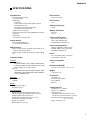
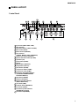
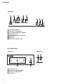
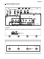
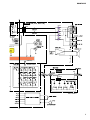
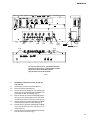
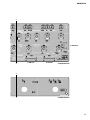
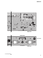
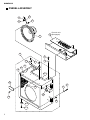
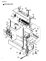
DG60FX-112
GUITAR AMPLIFIER
SERVICE MANUAL
CONTENTS
This document is printed on chlorine free (ECF) paper with soy ink.
SPECIFICATIONS
................................................ 3/4
PANEL LAYOUT
.................................... 5
CIRCUIT BOARD LAYOUT
................. 7
BLOCK DIAGRAM
............................ 8
WIRING
................................................................... 10
DISASSEMBLY PROCEDURE
............................ 11
LSI PIN DESCRIPTION
.............................. 15
IC BLOCK DIAGRAM
................................... 18
CIRCUIT BOARDS
........................................ 20
TEST PROGRAM
................................. 30
ERROR MESSAGES
............................. 33
IDLING ADJUSTMENT
........................ 33
MIDI IMPLEMENTATION CHART ......................................... 34
PARTS LIST
OVERALL CIRCUIT DIAGRAM
GA 011540
20001101-75000
HAMAMATSU, JAPAN
1.552K-448 I.T
Printed in Japan 2000.11
1
DG60FX-112
IMPOR TANT NOTICE
This manual has been provided for the use of authorized Yamaha Retailers and their service personnel. It has been assumed
that basic service procedures inherent to the industry, and more specifically Yamaha Products, are already known and understood by the users, and have therefore not been restated.
WARNING :
Failure to follow appropriate service and safety procedures when servicing this product may result in personal injury, destruction of expensive components and failure of the product to perform as specified. For
these reasons, we advise all Yamaha product owners that all service required should be performed by an
authorized Yamaha Retailer or the appointed service representative.
IMPORTANT :
This presentation or sale of this manual to any individual or firm does not constitute authorization certification, recognition of any applicable technical capabilities, or establish a principal-agent relationship of
any form.
The data provided is belived to be accurate and applicable to the unit(s) indicated on the cover. The research engineering, and
service departments of Yamaha are continually striving to improve Yamaha products. Modifications are, therefore, inevitable
and changes in specification are subject to change without notice or obligation to retrofit. Should any discrepancy appear to
exist, please contact the distributor’s Service Division.
WARNING :
Static discharges can destroy expensive components. Discharge any static electricity your body may have
accumulated by grounding yourself to the ground bus in the unit (heavy gauge black wires connect to
this bus.)
IMPORTANT :
Turn the unit OFF during disassembly and parts replacement. Recheck all work before you apply power
to the unit.
LITHIUM BATTERY HANDLING
This product uses a lithium battery for memory back-up.
WARNING :
Lithium batteries are dangerous because they can be exploded by improper handling. Observe the following precautions when handling or replacing lithium batteries.
Leave lithium battery replacement to qualified service personnel.
Always replace with batteries of the same type.
When installing on the PC board by soldering, solder using the connection terminals provided on the battery cells.
Never solder directly to the cells. Perform the soldering as quickly as possible.
Never reverse the battery polarities when installing.
Do not short the batteries.
Do not attempt to recharge these batteries.
Do not disasemble the batteries.
Never heat batteries or throw them into fire.
ADVARSEL!
Lithiumbatteri-Eksplosionsfare ved fejlagtig handtering. Udskiftning ma kun ske med batteri af samme fabrikat og type. lever det brugte
batteri tilbage til leverandren.
VARNING
Explosionsfara vid felaktigt batteribyte.
Anvand samma batterityp eller en ekvivalent typ som rekommenderas av apparattillverkaren.
Kassera anvant batteri enligt fabrikantens instruktion.
VAROITUS
Paristo voi rajahtaa, jos se on virheellisesti asennettu.
Vaihda paristo ainoastaan laitevalmistajan suosittelemaan tyyppiiin.
Havita kaytetty paristo valmistajan ohjeiden mukaisesti.
The following information complies with Dutch official Gazette 1995. 45; ESSENTIALS OF ORDER ON THE COLLECTION OF BATTERIES.
• Please refer to the diassembly procedure for the removal of Back-up Battery.
• Leest u voor het verwijderen van de backup batterij deze beschrijving.
WARNING: CHEMICAL CONTENT NOTICE!
The solder used in the production of this product contains LEAD. In addition, other electrical/electronic and/or plastic (Where
applicable) components may also contain traces of chemicals found by the California Health and Welfare Agency (and possibly
other entities) to cause cancer and/or birth defects or other reproductive harm.
DO NOT PLACE SOLDER, ELECTRICAL/ELECTRONIC OR PLASTIC COMPONENTS IN YOUR MOUTH FOR ANY REASON WHAT
SO EVER!
Avoid prolonged, unprotected contact between solder and your skin! When soldering, do not inhale solder fumes or expose
eyes to solder/flux vapor!
If you come in contact with solder or components located inside the enclosure of this product, wash your hands before handling
food.
WARNING
Components having special characteristics are marked
originally installed.
2
and must be replaced with parts having specification equal to those
DG60FX-112
SPECIFICATIONS
Digital Section
• Full Digital Signal Processing
• 8 Channel Preamp
• Digital Effects
• Compressor
• Chorus, Flanger, Phaser, Rotary Speaker, Tremolo
• Digital Delay, Tape Echo
• Spring Reverb, Hall Reverb, Plate Reverb
• Tap Tempo Function (Delay Time)
• Speaker Simulator (16 Types)
• External Controller Function (EXP Pedal/MIDI):8 Controllers/
Parameters
• Wah Function
• Tuner Function (Chromatic, Auto)
Analog Section
• 60 W Solid State Power Amp
• 30 cm Speaker (EMINENCE) x 1
A/D Converter
20 bit + 3 bit Floating
D/A Converter
20 bit
Sampling Frequency
48 kHz
Memory Allocations
Preset: 90
User: 90
Input Level/Impedance
INPUT HIGH: -25dBm/1M ohm
INPUT LOW: -15dBm/1M ohm
POWER AMP IN: 0 dBm/100k ohm
Output Level/Impedance
MIDI Functions
Receive: Program Change (Program Change Table can be
created), Control Change, Bulk In
Transmit: Program Change, Control Change, Bulk Out, Merge
Out
Controller Switch
Top Panel
Push Switch x17
UP, DOWN, MANUAL, UTILITY, STORE, COMP, CHORUS,
FLANGER, PHASER, ROTARY, TREMOLO, DELAY, TAPE
ECHO, SPRING, HALL, PLATE, SP. SIM
Knob x15
AMP SELECT, GAIN, MASTER, TREBLE, MIDDLE, BASS,
PRESENCE, COMP, SPEED, DEPTH, TIME, FEEDBACK,
LEVEL, REVERB, OUTPUT
LINE OUT L/MONO, R: -3dBm/2.3k ohm
PHONES: 0dBm/47 ohm (47ohm load)
SPEAKER: 60W RMS/8 ohm
Power
U.S. and Canadian models : 120V, 60Hz
General model : 230V, 50Hz
Power Consumption
70 W
Dimensions (WxHxD)
513 x 491 x 291 mm (20.2” x 19.3” x 11.5”)
Weight
17 kg (37 lbs 8 oz)
Accessories
Rear Panel
Push Switch x1
POWER
Display
7 Segment LED (3 digit) x1
Push Switch LED x17
Connections/Jacks
INPUT HIGH, LOW: Standard Monaural Phone Jack
LINE OUT L/MONO, R: Standard Monaural Phone Jack
PHONES: Standard Stereo Phone Jack
POWER AMP IN: Standard Monaural Phone Jack
Foot Switch Unit Terminal: 13 pin DIN
DIGITAL OUT: COAXIAL
MIDI IN, MIDI OUT: 5 pin DIN
Foot Switch Unit
Foot Switch Special Cable
Owner’s Manual
Patch List
Foot Switch Unit
Footswitch x4 (1, 2, 3, BANK)
LED x6 (1, 2, 3, BANK x3)
Connections/Jacks
EXP. PEDAL: Standard Stereo Phone Jack
Connects main unit and foot switch: 13 pin DIN
Dimensions (WxHxD) : 280 x55 x108 mm
(11.0” x 2.2” x 4.3”)
Weight : 930 g (2 lbs 1 oz)
3
DG60FX-112
4
DG60FX-112
PANEL LAYOUT
Control Panel
14
11 12 13 15
9 10
17
20
24
8
7
1
1
2
3
4
5
6
7
8
9
10
11
12
13
14
15
16
17
18
19
20
21
22
23
24
25
2
3
4
5
6
Input Jacks (INPUT HIGH, LOW)
Peak Indicator
Amp Select Switch (LEAD1-CLEAN2)
Gain Control (GAIN)
Master Volume (MASTER)
Tone Controls
(TREBLE, MIDDLE, BASS, PRESENCE)
Output Level Control (OUTPUT)
Speaker Simulator Button (SP. SIM)
Up Button (UP)
Down Button (DOWN)
Display
Manual Button (MANUAL)
Utility Button (UTILITY)
Store Button (STORE)
Compressor Button (COMP)
Compressor Knob (COMP)
Modulation Group Effect Buttons
(CHORUS/FLANGER/PHASER
/ROTARY/TREMOLO)
Speed Knob (SPEED)
Depth Knob (DEPTH)
Delay Group Effect Buttons
(DELAY/TAPE ECHO)
Time Knob (TIME)
Feedback Knob (FEEDBACK)
Level Knob (LEVEL)
Reverb Group Effect Buttons
(SPRING/HALL/PLATE)
Reverb Knob (REVERB)
5
DG60FX-112
Rear Panel
26
27
28
29
30
31
26
27
28
29
30
31
32
33
32
33
Power Switch (POWER)
Headphones Jack (PHONES)
Line Out Jacks (LINE OUT R, L/MONO)
POWER AMP IN Jack
Foot Switch Unit Terminal (FOOT SW)
MIDI OUT Jack
MIDI IN Jack
Digital Out Jack (DIGITAL OUT)
Foot Switch Unit
Top Panel
Rear panel
36
34
34
35
36
37
6
Foot Switches 1, 2, 3
Bank Switch (TAP/BANK/TUNER)
EXP Pedal Jack (EXP. PEDAL)
Unit Terminal
35
37
DG60FX-112
CIRCUIT BOARD LAYOUT
MAIN 4/8
MAIN 7/8
MAIN 6/8
MAIN 5/8
DM
MAIN 1/8
FRONT (PN1/2)
MAIN 3/8
MAIN
2/8
Foot Switch
REAR (ANALOG8/8)
SW, LED (PN2/2)
7
DG60FX-112
BLOCK DIAGRAM
A
MAIN 3/8
IC401
+
5
7
W401
IC401
+
3
1
FRONT
CN101
IC402
5
7
IC102
2
1
IC103
2
1
IC102
6
7
6
-
CN103
IC103
7
CN103
IC104
CN102
DM
IC2,IC3
IC1
IC10,IC11
IC9
IC8
IC12
(DM-CN1)
FRONT (PN1/2)
(DM-CN2)
(FRONT-CN303)
(FRONT-CN304)
A'
8
DG60FX-112
A
MAIN (1/8, 2/8, 4/8~7/8)
FRONT
IC501
+
5
7
IC501
+
3
1
IC502
+
1
3
IC502
+
5
7
W502
CN103
CN102
C10,IC11
(DM-CN3)
(FRONT-CN302)
REAR
W701
SW, LED
CN306
KEC-54207
A'
9
DG60FX-112
WIRING
POWER
TRANSFORMER
MAIN
4/8
MAIN
7/8
MAIN
6/8
MAIN
5/8
W602
W609
W607
W605
SPEAKER
CN4
CN603
CN602
CN1
CN2
CN3
CN607
W608
W606
CN102
W604
MAIN 1/8
AC
DM
CN103
CN104
CN101
W603
W601
CN601
W612
W502
MAIN 2/8
W611
W610
W501
W503
CN304
CN303
CN302
CN305
FRONT (PN1/2)
FOOT SWITCH OVERALL ASSEMBLY
CN306
W701
REAR
(ANALOG8/8)
10
W401
MAIN 3/8
CN301
SW, LED (PN2/2)
CN401
DG60FX-112
DISASSEMBLY PROCEDURE
A.
1.
1-1.
External components
Handle Assembly
Remove the two (2) screws marked [70]. The handle
assembly can then be removed. (Fig. 1)
2.
2-1.
Corner fitting
Remove the two (2) screws marked [50]. The corner
fitting can then be removed. (Fig. 1)
3.
3-1.
Leg
Remove the screw marked [110]. The leg can then
be removed. (Fig. 1)
[50]
[50]
[70]
[110]
[50]: Oval Head Tapping Screw 3.5X16 MFNI33 (V383360)
[70]: Oval Head Screw 0X25 FNM3-2B (V374370)
[110]: Truss Head Tapping Screw-1 4.0X20 MFZN2BL (O374729)
Fig.1
11
DG60FX-112
4. Removal of stereo amplifier unit
4-1. Remove the four (4) screws marked [80] and the
four (4) washers marked [90] from the back plate
and then remove the back plate. (Fig. 2)
4-2. Remove the six (6) screws marked [30] and the six
(6) washers marked [40] from the top of the main
unit. The pre main unit can then be removed. (Fig. 2)
5.
5-1.
5-2.
Removal of speaker
Remove the pre main unit. (See Procedure 4.)
Remove the four (4) screws marked [70]. The
speaker can then be removed. (Fig. 2)
[70]
[80]
[90]
[80]
[90]
[70]
[30]
[40]
[30]: Oval Head Screw 5.0X35 MFC2BL (V374938)
[40]: Washer 5S MFC2BL (EW30002)
[70]: Hexagonal Nut 4.0 MFZN2Y (O376090)
[80]: Oval Head Tapping Screw 4.0X30 MFC2BL (V374940)
[90]: Washer 4S MFC2BL (V389020)
Fig.2
B.
6.
6-1.
6-2.
6-3.
6-4.
12
Pre main unit
FRONT circuit board (PN 1/2), MAIN circuit board (3/8)
Remove the pre main unit. (See Procedure 4.)
Remove the five (5) screws marked [110] and then
remove the panel. (Fig. 3)
Remove the seven (7) screws marked [290], eight
(8) knobs marked [310], fifteen (15) hexagonal nuts,
three (3) screws marked [50]. The FRONT circuit
board (PN 1/2) can then be removed. (Fig. 3)
Remove the two (2) hexagonal nuts marked [210]
and the two (2) flat washers marked [220]. The MAIN
circuit board (3/8) can then be removed. (Fig. 3)
[30]
[40]
DG60FX-112
MAIN 4/8
MAIN 7/8
MAIN 6/8
MAIN 5/8
DM
MAIN 1/8
[290]
[290]
[310]
[290]
[210]
[220]
MAIN 3/8
[50]
FRONT (PN1/2)
[110]
[110]
[50]: Bind Head Tapping Screw-B 3.0X8 MFZN2BL (EP600190)
[110]: Bind Head Tapping Screw-C A4.0X8 MFZN2BL (VC688900)
[210]: Hexagonal Nut 9.0 12X2 MFNI33 (LX200060)
[220]: Flat Washer 9X14 0.5 FNM3 (VL802300)
Fig.3
7.
7-1.
7-2.
7-3.
7-4.
7-5.
7-6.
7-7.
DM, MAIN circuit boards (1/8, 2/8, 4/8, 5/8, 6/8,
7/8), heat sink
Remove the pre main unit. (See Procedure 4.)
Remove the panel. (See Step 6-2.)
Remove the four (4) hexagonal nuts marked [140]
and four (4) screws marked [50A]. The MAIN circuit
board (2/8) can then be removed. (Fig. 4)
Remove the five (5) screws marked [50B] and the
three (3) screws marked [55] from the rear panel.
The DM circuit board can then be removed. (Fig. 4)
Remove the four (4) screws marked [50C]. The MAIN
circuit board (1/8) can then be removed. (Fig. 4)
Remove the four (4) screws marked [130]. The MAIN
circuit boards (4/8, 5/8, 6/8, 7/8) can then be
removed. (Fig. 4)
Remove the four (4) screws marked [110A]. The heat
sink can then be removed. (Fig. 4)
13
DG60FX-112
8.
8-1.
8-2.
8-3.
Power transformer
Remove the pre main unit. (See Procedure 4.)
Remove the panel. (See Step 6-2.)
Remove the four (4) screws marked [110B]. The
transformer can then be removed. (Fig. 4)
[110B]
[110A] [130] [110A] [130] [110A] [130] [110A] [130] [50B]
Power
Transformer
MAIN 1/8
[50B]
[50C]
DM
[50C]
MAIN 2/8
[50C]
Rear panel
[140]
[50A]
[50B]
[140]
[50A]
[50]: Bind Head Tapping Screw-B 3.0X8 MFZN2BL (EP600190)
[55]: Bind Head Tapping Screw-P 3.0X12 MFZN2BL (VC161100)
[110]: Bind Head Tapping Screw-C A4.0X8 MFZN2BL (VC688900)
[130]: Bind Head Screw SP 3.0X12 MFZN2Y (VB763800)
[140]: Hexagonal Nut 12.0 14X2 MFC2BL (VD794100)
Fig.4
Battery VN103500
VN103600(Battery holder for VN103500)
• Notice for back-up battery removal
Push the battery as shows in figure,
then the battery will pop up.
14
[55]
DG60FX-112
C.
9.
9-1.
9-2.
9-3.
Foot switch
Foot switch
Remove the six (6) screws marked [110A] and then
remove the bottom plate. (Fig. 5)
Remove the two (2) screws marked [110B] and
hexagonal nuts marked [90] and then remove the
REAR circuit board (MAIN 8/8). (Fig. 5)
Remove the four (4) hexagonal nuts from the foot
switch. The SW, LED circuit board (PN2/2) can then
be removed. (Fig. 5)
[110A]
[110A]
[110A]
[90]
[110A]
View A
REAR (MAIN 8/8)
[110B]
SW, LED
(PN2/2)
Foot switch
Hexagonal nut
Hexagonal nut
[90]: Hexagonal Nut 9.0 12X2 MFNI33 (LX200060)
[110]: Bind Head Tapping Screw-B 3.0X8 MFZN2BL (EP600190)
Fig.5
15
DG60FX-112
LSI PIN DESCRIPTION
HD6413002FP16 (XQ375A00) CPU <H8/3002>
PIN
NO.
1
2
3
4
5
6
7
8
9
10
11
12
13
14
15
16
17
18
19
20
21
22
23
24
25
26
27
28
29
30
31
32
33
34
35
36
37
38
39
40
41
42
43
44
45
46
47
48
49
50
NAME
I/O
PA6
PA7
VCC
PB0
PB1
PB2
PB3
PB4
PB5
O
O
PB6//DREQ0
PB7//DREQ1
/RESO
VSS
P90/TXD0
P91/TXD1
P92/RXD0
P93/RXD1
P94/SCK0
P95/SCK1
P40/D0
P41/D1
P42/D2
P43/D3
VSS
P44/D4
P45/D5
P46/D6
P47/D7
D8
D9
D10
D11
D12
D13
D14
D15
VCC
A0
A1
A2
A3
A4
A5
A6
A7
VSS
A8
A9
A10
A11
I
I
I
I
I
I
I
I
O
O
O
I
I
O
I
I/O
I/O
I/O
I/O
FUNCTION
Port A
Address bus
Power supply
Port B
Reset
Ground
Transmit data (MIDI OUT)
KSN-ACK
Receive data (MIDI IN)
KSN-RX
Port 9
Port 9
(Ground)
I/O
I/O
I/O
I/O
I/O
I/O
I/O
I/O
I/O
I/O
I/O
I/O
Data bus
Power supply
O
O
O
O
O
O
O
O
Address bus
(Ground)
O
O
O
O
DM: IC12
PIN
NO.
NAME
I/O
51
52
53
54
55
56
57
58
59
60
61
62
63
64
65
66
67
68
69
70
71
72
73
74
75
76
77
78
79
80
81
82
83
84
85
86
87
88
89
90
91
92
93
94
95
96
97
98
99
100
A12
A13
A14
A15
A16
A17
A18
A19
VSS
P60//WAIT
P61//BREQ
P62//BACK
Ø
/STBY
/RES
NMI
VSS
EXTAL
XTAL
VCC
/AS
/RD
/HWR
/LWR
MD0
MD1
MD2
AVCC
VREF
P70/AN0
P71/AN1
P72/AN2
P73/AN3
P74/AN4
P75/AN5
P76/AN6
P77/AN7
AVSS
P80
P81//CS3
P82//CS2
P83//CS1
P84//CS0
VSS
PA0
PA1
PA2
PA3
PA4
PA5
O
O
O
O
O
O
O
O
FUNCTION
Address bus
Ground
I
I
I
O
I
I
I
I
O
O
O
O
O
I
I
I
I
I
I
I
I
I
I
I
I
O
O
O
O
O
Port 6
Øout
Stand-by mode signal
Reset
Non-maskable interrupt
Ground
Clock
Clock
Power supply
Address strobe
Read strobe
Write strobe (High)
Write strobe (Low)
Mode select
Analog power supply
Reference voltage
Analog data input (EQ)
Analog input (EQ)
Analog data input
Analog input (CS)
Analog data input (BEND)
Analog input (MOD)
Analog input (FC)
Analog input (BAT)
Analog ground
Port 8
Chip select
Ground
I
I
I
O
O
O
Port A
YM3437C-F (XM530A00) DIT2 (Digital Format Interface Transmitter)
PIN
NO.
1
2
3
4
16
NAME
I/O
Vss
MCLK
DM0
DM1
I
I
I
5
6
7
RES
WCIN
DIN
I
I
I
8
VDD
PIN
NO.
Ground
9
10
Master clock input
11
DIN/BCLK/WCLK format select
DM1,DM0=0,0 DSP,LDSP (64 bit,LSB first) 12
DM1,DM0=0,1stereo,DSP (64 bit,MSB first)
DM1,DM0=1,0 DSP2 (128 bit,MSB first)
DM1,DM0=1,1 BB (64 bit,MSB first)
13
System reset
14
Word clock input
15
Digital audio serial data input
FUNCTION
Power supply (+5 V)
16
DM: IC17
NAME
I/O
FUNCTION
MUTE
VFL
CCK
CIN
I
I
I
I
Mute
Validity flag
C,U bit clock input/C bit data input
C,U bit data input/U bit data input
CLD
CNTR
CSM
I
I
I
DOUT
O
End of C,U bit input/16,20 bit/24 bit select
32 bit counter reset/Top of block
Channel status input mode select
CSM=0 Asynchronous mode
CSM=1 Synchronous mode
Digital interface formatted data output
DG60FX-112
YSS910-S (XV988A00) DSP6 (Digital Signal Processor)
PIN
NO.
NAME
1
2
3
4
5
6
7
8
9
10
11
12
13
14
15
16
17
18
19
20
21
22
23
24
25
26
27
28
29
30
31
32
33
34
35
36
37
38
39
40
41
42
43
44
45
46
47
48
49
50
51
52
53
54
55
56
57
58
59
60
61
62
63
64
65
66
67
68
69
70
71
72
73
74
75
76
77
78
79
80
81
82
83
84
85
86
87
88
Vdd
Vss
XI
XO
Vdd
/SYNCI
/SYNCO
Vdd
CKI
CKO
CKSEL
Vss
MCKS
/SSYNC
/IC
/TEST
BTYP
/IRQ
TRIG
Vdd
Vss
/CS
/WR
/RD
CA7
CA6
CA5
CA4
CA3
CA2
CA1
Vss
Vdd
CD15
CD14
CD13
CD12
CD11
CD10
CD09
CD08
CD07
CD06
Vss
Vdd
Vdd
CD05
CD04
CD03
CD02
CD01
CD00
/WAIT
Vss
SI0
SI1
SI2
SI3
SI4
SI5
SI6
SI7
Vss
Vdd
SO0
SO1
SO2
SO3
SO4
SO5
SO6
SO7
Vss
DB00
DB01
DB02
DB03
DB04
DB05
DB06
DB07
DB08
DB09
DB10
DB11
DB12
Vdd
Vdd
I/O
I
O
I
O
I
O
I
I
I
I
I
I
O
I/O
I
I
I
I/O
I/O
I/O
I/O
I/O
I/O
I/O
FUNCTION
Power supply (3.3 V)
Ground
System master clock input (60 MHz or 30 MHz)
System master clock output (High or 30 MHz)
Power supply (5 V)
Sync. signal input
Sync. signal output
Power supply (5 V)
System clock input (30 MHz)
System clock output (30 MHz)
System master clock select (0: 60 MHz, 1: 30 MHz)
Ground
Serial I/O master clock input (128 x Fs)
Serial I/O Sync. signal output
Initial clear
Test mode setting (0: Test, 1: Normal)
Data bus type select (0: 8 bit, 1: 16 bit)
IRQ output
Trigger signal input/output
Power supply (5 V)
Ground
chip select signal input
Write signal input
Read signal input
Address bus of internal register
Ground
Power supply (3.3 V)
I/O
I/O
I/O
I/O
I/O
I/O
I/O
I/O
I/O
I/O
Data bus of internal register
Ground
Power supply (3.3 V)
Power supply (5 V)
I/O
I/O
I/O
I/O
I/O
I/O
O
I
I
I
I
I
I
I
I
Data bus of internal register
WAIT output
Ground
Serial data input
Ground
Power supply (5 V)
O
O
O
O
O
O
O
O
Serial data output
Ground
I/O
I/O
I/O
I/O
I/O
I/O
I/O
I/O
I/O
I/O
I/O
I/O
I/O
Parallel data bus
Power supply (5 V)
Power supply (3.3 V)
PIN
NO.
NAME
DM: IC8, IC9
I/O
Vss
89
DB13
I/O
90
DB14
I/O
91
DB15
I/O
92
DB16
I/O
93
DB17
I/O
94
DB18
I/O
95
DB19
I/O
96
DB20
I/O
97
DB21
I/O
98
DB22
I/O
99
Vss
100
Vdd
101
DB23
I/O
102
DB24
I/O
103
DB25
I/O
104
DB26
I/O
105
DB27
I/O
106
DB28
I/O
107
DB29
I/O
108
DB30
I/O
109
DB31
I/O
110
111 TIMO/DBOB I/O
Vss
112
Vdd
113
I/O
DA00
114
I/O
DA01
115
I/O
DA02
116
I/O
DA03
117
I/O
DA04
118
I/O
119
DA05
I/O
120
DA06
I/O
121
DA07
122
Vss
I/O
123
DA08
I/O
124
DA09
I/O
125
DA10
I/O
126
DA11
I/O
127
DA12
I/O
128
DA13
I/O
129
DA14
I/O
130
DA15
131
Vss
132
Vdd
133
(n.c)
134
Vdd
I/O
135
DA16
I/O
136
DA17
I/O
137
DA18
I/O
138
DA19
I/O
139
DA20
I/O
140
DA21
I/O
141
DA22
I/O
142
DA23
143
Vss
I/O
144
DA24
I/O
145
DA25
I/O
146
DA26
I/O
147
DA27
I/O
148
DA28
I/O
149
DA29
I/O
150
DA30
I/O
151
DA31
152
Vdd
153
Vss
O
154
A00
O
155
A01
O
156
A02
O
157
A03
O
158
A04
O
159
A05
O
160
A06
O
161
A07
O
162
A08
O
A09
163
164
Vss
Vdd
165
O
166
A10
O
A11
167
O
168
A12
O
A13
169
O
170
A14
O
171 A15/RAS
O
172 A16/CAS
O
173 A17/CE
O
174
/WE
O
/OE
175
176
Vdd
FUNCTION
Ground
Parallel data bus
Ground
Power supply (3.3 V)
Parallel data bus
Timing signal output/ Parallel data bus output/ input
Ground
Power supply (5 V)
Memory data bus
Ground
Memory data bus
Ground
Power supply (3.3 V)
Not used
Power supply (5 V)
Memory data bus
Ground
Memory data bus
Power supply (5 V)
Ground
Memory address (SRAM, PSRAM, DRAM)
Ground
Power supply (3.3 V)
Memory address (SRAM, PSRAM, DRAM)
Memory address (SRAM, PSRAM)
Memory address (SRAM, PSRAM), /RAS (DRAM)
Memory address (SRAM, PSRAM), /CAS (DRAM)
Memory address (SRAM), /CE (PSRAM)
Memory write enable signal
Memory output enable signal
Power supply (5 V)
17
DG60FX-112
AK4520A-VF-E2 (XT802A00) DAC & ADC
PIN
NO.
NAME
I/O
1 VREFH
2 VREFL
3 AINR+
4 AINR5 AINL+
6 AINL7
VA
8 AGND
9
DIF0
10
DIF1
11 LRCK
12 SCLK
13
SDTI
14 SDTO
I
I
I
I
I
I
I
I
I
I
I
O
DM: IC104
PIN
NO.
FUNCTION
Positive Voltage Reference Input, VA
Negative Voltage Reference Input, AGND
Rch Analog Positive Input
Rch analog Negative Input
Lch Analog Positive Input
Lch analog Negative Input
Analog Power Supply
Analog Ground
Audio Data Interface Format
Audio Data Interface Format
Input/Output Channel Clock
Audio Serial Data Clock
Audio Serial Data Input
Audio Serial Data Output
NAME
15 MCLK
16 DEM0
17 DEM1
18 TST3
19 TST2
20 TST1
21
VD
22 DGND
23 /PWDA
24 /PWAD
25 CMODE
26 AOUTL
27 AOUTR
28 VCOM
I/O
FUNCTION
I
I
I
I/O
I/O
I
I
I
I
O
O
O
Master Clock Input
De-emphasis Frequency Select
De-emphasis Frequency Select
Test Pins (Pull Down Pins)
Digital Power Supply
Digital Ground
DAC power-Down Mode
ADC power-Down Mode
Master Clock Select (“H”:384 fs,“L”:256 fs)
Lch Analog Output
Rch Analog Output
Common Voltage Output, VA/2
IC BLOCK DIAGRAM
74AHC32DT(XZ103A00)
74HC08DT(XZ108A00)
74HC164DT(XZ112A00)
DM: IC5, IC6
DM: IC7
DM: IC109
OR
AND
SHIFT REGISTANT
1A
1
14
VCC
1A
1
14
VDD
SIRIAL
INPUT
A
1
B
2
14
VCC
13
QH
A
B
QH
1B
2
13
4B
1B
2
13
4B
1Y
3
12
4A
1Y
3
12
4A
QA
3
QA
QG
12
QG
2A
4
11
4Y
2Y
4
11
4Y
QB
4
QB
QF
11
QF
2B
5
10
3B
2A
5
10
3Y
QC
5
QC
QE
10
QE
2Y
6
9
3A
2B
6
9
3A
QD
6
QD
CLEAR
CK A
9
CLEAR
8
3Y
8
3B
GND
7
8
CLOCK
OUTPUTS
OUTPUTS
7
GND
7
74HC175DT(XZ113A00)
74HC244DT(XZ109A00)
NJM072M(XC458A00)
DM: IC110
DM: IC14, IC15, IC16
DM: IC101
D-FF
Bus Buffer
OP AMP
1G
CL
1
16
VDD
1A1
1Q
2
1Q
3
Q CL
CK
Q D
C LQ
CK
D Q
15
4Q
14
4Q
1D
4
13
4Q
2D
5
12
3D
2Q
6
11
3Q
2Q
Vss
18
Vss
7
8
Q D
CK
Q CL
D
Q
CK
CL Q
10
9
1
20
VDD(Vcc)
2
19
2G
2Y4
3
18
1Y1
1A2
4
17
2A4
2Y3
5
16
1Y2
1A3
6
15
2A3
2Y2
7
14
1Y3
1A4
8
13
2A2
2Y1
9
12
1Y4
(GND)Vss
10
11
2A1
3Q
CK
Output A
1
Inverting
Input A
2
Non-Inverting
Input A
3
–DC Voltage
Supply
4
8
+DC Voltage
Supply
7
Output B
–+
+–
–V
6
Inverting
Input B
5
Non-Inverting
Input B
DG60FX-112
NJM4556AD (XQ824A00)
NJM5532M (XC011A00)
NE5532P (IG102500)
MAIN: IC501
DM: IC102, IC103, IC106
DM: IC502
OP AMP
OP AMP
NJM4556AMT1 (XQ138A00)
OP AMP
DM: IC105
Output A
1
Inverting
Input A
2
Non-Inverting
Input A
-
+
3
+
4
-DC Voltage Supply
8
+V
-
-V
7
Output B
6
Inverting
Input B
5
OP AMP
+DC Voltage
Supply
1
8
V+
2
7
B OUT
A+IN
3
6
V
4
5
A OUT
A IN
Non-Inverting
Input B
Output A
1
Inverting
Input A
2
Non-Inverting
Input A
3
-DC Voltage Supply
4
+V
-
+
+
-
-V
8
+DC Voltage
Supply
7
Output B
6
Inverting
Input B
5
Non-Inverting
Input B
B IN
B+IN
74HCU04DT (XZ110A00)
TC74HC4040F(XR684A00)
74HC374DT(XZ102A00)
DM: IC107
DM: IC108
DM: IC301~IC307
INVERTER
B. COUNTER
TC74HC4040DT(XZ111A00)
D-FF
1A
1
14
VDD
DM: IC108
1Y
2
13
6A
12-Stage Binary Ripple Counter
2A
3
12
2Y
4
11
20
VCC
Q
19
8Q
D CK
CK D
18
8D
D CK
OE
CK D
17
7D
Q
16
7Q
Q
15
6Q
CK D
14
6D
CK D
OE
13
5D
Q
12
5Q
11
CLOCK
OUT PUT
CONTROL
1
1Q
2
Q
6Y
1D
3
5A
2D
4
5Y
2Q
5
Q
3Q
6
Q
7
OE
D CK
OE
3D
OE
3A
5
3Y
10
6
7
4A
9
VSS
Q12
Q6
4Y
8
1
2
16
Q12
Q11
Q6
15
VDD
Q11
Q5
3
Q5
Q10
14
Q10
Q7
4
Q7
Q8
13
Q8
Q4
5
Q4
Q9
12
Q3
6
Q2
7
Vss
8
CL
11
Q2
CK
10 Input Pulses
Q1
9
(
MB3790PF(XR967A00)
DM: IC4
Multiplexer
ASSP
1
2
R CN 0.5Ω
16
VDD
15
2X
1X
1.24V
3Y
4
3Y
X-COM
13
X-COM
1Y
5
1Y
0X
12
OX
INH
6
7
VSS
8
B
VEE
INH
3X
11
A
10
9
Reference
Voltage
Power Supply
Circuit
V OUT
V OUT
6
ALARM1
7
ALARM2
V IN
2.65V
500Ω
V IN
S
3µA
Q
2.37V
V SENSE 12
3X
R
A
V OUT
9
240kΩ
B
RESET
V th:3V
V OUT
10
V th:1.5V
GND 8
11
5
2
V BAT1
14
4
SBD
590kΩ
V BAT2
Y-COM 1X
10
3
100Ω
CT
3
0Y
Y-COM
2X
GND
)
CONTROL 16
2Y
Q
Q1
DM: IC308, IC309
2Y
D CK
OE
9
OE
CLR
74HC4052DT(XZ101A00)
OY
8
Q9
Q3
V IN 14
V IN 13
4D
4Q
OE
RESET
N.C. 1
16 CONTROL
V BAT1 2
15 N.C.
V OUT 3
14 V IN
V OUT 4
13 V IN
V BAT2 5
12 V SENSE
ALARM1 6
11 C T
ALARM1 7
10 RESET
GND 8
9 RESET
19
DG60FX-112
CIRCUIT BOARDS
DM Circuit Board
A
CN101:
to MAIN3/8-W401
CN103:
to PN1/2-CN301
CN102:
to MAIN2/8-W502
to PN
A'
Battery VN103500
VN103600(Battery holder for VN103500)
• Notice for back-up battery removal
Push the battery as shows in figure,
then the battery will pop up.
20
DG60FX-112
A
CN104:
to MAIN1/8-W601
to PN1/2-CN302
A'
to PN1/2-CN303
to PN1/2-CN304
to MAIN1/8-W603
Component side
DM: CNA-V620530
0
21
DG60FX-112
DM Circuit Board
A
A'
22
DG60FX-112
A
A'
Pattern side
23
DG60FX-112
FRONT (PN1/2)
A
to MAIN2/8-W503
to DM-CN3
A'
A
SW, LED (PN2/2)
A'
LD302, LD303, LD304 and LD306 installation
Anode
PN: CNA-V620230
24
1
DG60FX-112
A
to DM-CN103
to DM-CN2
A'
to DM-CN1
Component side
A
A'
Component side
25
DG60FX-112
A
FRONT (PN1/2)
A'
A
SW, LED (PN2/2)
to Push Switch
26
to Push Switch
A'
DG60FX-112
A
Pattern side
A'
A
to MAIN8/8-W701
to Push Switch
SW
PN: CNA-V620230
A'
to Push Switch
Pattern side
1
27
DG60FX-112
MAIN (ANALOG)1/8 Circuit Board
to POWER TRANSFORMER
W608: to MAIN 7/8-W609
CN607: N.C
W606:
to MAIN6/8-W607
to POWER
TRANSFORMER
W604:
to MAIN5/8-W605
to POWER CORD
W601:
to MAIN4/8-W602
W603:
to DM-CN4
W610:
to DM-CN104
W611:
to MAIN3/8-CN401
W612:
to MAIN2/8-W501
Component side
DESTINATION MAIN Circuit Board No.
28
J, U, C
V610580
H, B, S
V610590
FZ601
2A
250V
T1A L
250V
FZ602
FZ603
2A
250V
T2A L
250V
FZ604
1A
250V
T1A L
250V
DG60FX-112
MAIN (ANALOG)2/8 Circuit Board
to DM-CN102
to MAIN1/8-W612
to PN1/2-CN305
Component side
MAIN (ANALOG)3/8 Circuit Board
MAIN (ANALOG)4/8
Circuit Board
MAIN (ANALOG)5/8
Circuit Board
to MIAN1/8-W601
Component side
to MIAN1/8-W604
Component side
MAIN (ANALOG)6/8
Circuit Board
to DM-CN101 to MAIN1/8-W611
MAIN (ANALOG)7/8
Circuit Board
to MIAN1/8-W606
to MIAN1/8-W608
Component side
REAR (ANALOG)8/8 Circuit Board
to PN2/2-CN306
Component side
Component side
Component side
MAIN(ANALOG): CNA-V610580 (J, U, C)
: CNA-V610590 (H, B, S)
29
DG60FX-112
TEST PROGRAM
A. PREPARATION
• EXP. PEDAL
Connect the B50KVR.
• DIGITAL OUT
Connect the DA converter.
• MIDI IN
Connect IN and OUT, using the DIN
• MIDI IN
5P cable.
• The input signal is a 1kHz sine wave.
• Set all rotary VR’s and switches near their center
position.
• Set the OUTPUT VR to the MAX position.
• Set the input impedance of the measuring instrument
to 1Mohm or more.
B. CONTENTS OF TEST PROGRAM
0: LED Check
1: SW Check
2: VR Check
3: Battery Check
4: MIDI Check
5: SRAM Check
6: DSP Check
C. STARTING THE TEST PROGRAM
While pressing the MANUAL, STORE and HALL
switches, turn on the POWER switch. The TEST
program will then be started.
D. SELECTING THE TEST NUMBER
Using the UP and DOWN switches, select the test
number and press the STORE switch to confirm
selection.
E. TEST PROCEDURE
0: LED Check
• Using the UP and DOWN switches, select “0” and
then press the STORE switch.
• LED segments light up one after another starting with
“UP”. When “SP.SIM” is reached, “BANK3”, “BANK2”,
“BANK1”,”3", “2” and “1” light up followed by 7
segments in the following order from the left end. After
that, all LED segments light up and go out.
1
2
1
6
5
7
2
3
4
1:
30
SW Check
• Using the UP and DOWN switches, select “1” and
then press the STORE switch.
• Starting with the UP switch, press the switches whose
LED lights up one after another. After “SP.SIM”,
“BANK”, “3”, “2” and “1”, all LED segments light up
and then go out.
• Numbers (0 to 20) are indicated at the right end of the
7 segment LED.
• If “E” representing an error appears at the left end,
press the UTILITY switch for resetting.
8
3
DG60FX-112
2:
VR Check
• Using the UP and DOWN switches, select “2” and
then press the STORE switch.
• Press switches in the order of “AMP SELECT”, “GAIN”
until “PRESENCE, then from “COMP” to “REVERB”
and finally until “EXP.PEDAL” is reached.
• Turn the control fully in the direction toward the left 7
segment LED which is turned on. If the test result is
OK, the right 7 segment LED lights up. Then turn the
control to that direction. If the test result is OK, proceed
to the next VR. After completing this check, return the
control to the center position.
• If an error exists outside of the control being checked,
“E” meaning an error appears at the left end OF LED.
In such case, press the UTILITY switch for resetting.
• At the end of all VR checks, all LED segments light up
and go out. Then checking advances to the next step.
3:
Battery Check
• Using the UP and DOWN switches, select “3” and
then press the STORE switch.
• If the check result is OK, all LED segments light up
and go out. Then checking advances to the next step.
• In case of an error, “E” is indicated by LED.
4:
MIDI Check
• Using the UP and DOWN switches, select “4” and
then press the STORE switch.
• If the check result is OK, all LED segments light up
and go out. Then checking advances to the next step.
• In case of an error, “E” is indicated by LED.
• The numeric figure at the right end of LEF represents,
0: transmission and 1: reception.
5:
SRAM Check
• Using the UP and DOWN switches, select “5” and
then press the STORE switch.
• If the check result is OK, all LED segments light up
and go out. Then checking advances to the next step.
• The numeric figure at the right end of LEF represents,
0: IC2 and 1: IC3.
31
DG60FX-112
6:
DSP Electric Characteristic
• Using the UP and DOWN switches, select “6” and
then press the STORE switch. The same output level
is obtained when No. at the right end is “0” and when
it is “1”.
• To check the output level, noise level and distortion
factor, enter the signal to be measured (short the input
with GND for the noise level check).
• Initial setting: HIGH/LOW SW(SW101) ••• OFF(LOW),
VR ••• Center, OUTPUT VR ••• MAX
ITEM
1. INPUT sensitivity
2. INPUT sensitivity
3. INPUT sensitivity
4. INPUT sensitivity
5. INPUT sensitivity
6. INPUT sensitivity
7. INPUT sensitivity
32
INPUT
OUTPUT
CN101(INPUT) -20dBm(1kHz)
CN101(INPUT) -20dBm(10kHz)
CN101(INPUT) -20dBm(100Hz)
CN101(INPUT) -20dBm(100Hz)
CN101(INPUT) -20dBm(10kHz)
CN101(INPUT) -20dBm(1kHz)
CN101(INPUT) -20dBm(1kHz)
CN102 1pin(OUT R) -6.0dBm+/-3dB
CN102 1pin(OUT R) -6.0dBm+/-3dB
CN102 1pin(OUT R) -6.0dBm+/-3dB
CN102 3pin(OUT L) -24.0dBm+/-3dB
CN102 3pin(OUT L) -24.0dBm+/-3dB
CN102 3pin(OUT L) -24.0dBm+/-3dB
JK2(Digital out) Lch -18dBm+/-3dB Rch 0dBm+/-3dB
DG60FX-112
ERROR MESSAGES
If an error occurs during operation, one of the following error message numbers will appear on the display.
E1:MIDI Receive Buffer Full
CAUSE:
SOLUTION:
Too much MIDI data is being received by the DG amplifier at one time.
Try reducing the amount of data being sent or, break the data into smaller blocks.
E2:Communication Error.
CAUSE:
SOLUTION:
An abnormality is detected during MIDI communications.
Check all connections, etc. and try again.
E3:Bulk Receive Check Sum Error.
CAUSE:
SOLUTION:
The check sum does not match the received MIDI bulk data.
Check all connections and data, and try again.
E4:Bulk Receive Data Abnormality.
CAUSE:
SOLUTION:
An abnormality is detected in the received MIDI bulk data.
Check all connections and data, and try again.
E5:Backup Battery Error.
CAUSE:
SOLUTION:
Backup battery power is depleted.
Continued use of the device will result in the loss of data. Return the device to the music dealer where
you purchased it or, the nearest Yamaha Service center and have the battery replaced.
IDLING ADJUSTMENT
1. Tu r n t h e i d l i n g a d j u s t m e n t vo l u m e ( V R 6 0 1 )
counterclockwise fully.
2. Adjust the VR601 so that the DC voltage between the
terminals of the CN607 is 3mV.
33
DG60FX-112
YAMAHA
[ Guitar Amplifier]
Date:30-Jun-2000
Model DG60FX-112
MIDI Implementation Chart
Version : 1.0
+----------------------------------------------------------------------+
:
: Transmitted
:
Recognized
:
Remarks
:
:
Function ... :
:
:
:
:-------------------+----------------+----------------+----------------:
:Basic
Default
: 1 - 16
: 1 - 16, off
: memorized
:
:Channel Changed
: 1 - 16
: 1 - 16, off
:
:
:-------------------+----------------+----------------+----------------:
:
Default
: 1,3
: 1,3
: memorized
:
:Mode
Messages : x
: x
:
:
:
Altered
: ************** : x
:
:
:-------------------+----------------+----------------+----------------:
:Note
: x
: x
:
:
:Number : True voice: ************** : x
:
:
:-------------------+----------------+----------------+----------------:
:Velocity Note ON
: x
: x
:
:
:
Note OFF : x
: x
:
:
:-------------------+----------------+----------------+----------------:
:After
Key's
: x
: x
:
:
:Touch
Ch's
: x
: x
:
:
:-------------------+----------------+----------------+----------------:
:Pitch Bender
: x
: x
:
:
:-------------------+----------------+----------------+----------------:
:
0 : x
: x
:
:
:
1 - 31 : o
: o
:
:
:
32 - 63 : x
: x
:
:
:
64 - 95 : o
: o
:
:
: Control 95 -127 : x
: x
:
:
:
:
:
:
:
: Change
:
:
:
:
:
:
:
:
:
:
:
:
:
:
:
:
:
:
:
:
:
:
:
:
:
:
:
:
:
:
:
:
:
:
:-------------------+----------------+----------------+----------------:
:Prog
: o 0 - 127
: o 0 - 127
:
:
:Change : True #
: ************** :
:
:
:-------------------+----------------+----------------+----------------:
:System Exclusive
: o
: o
: Bulk Dump
:
:-------------------+----------------+----------------+----------------:
:System : Song Pos. : x
: x
:
:
:
: Song Sel. : x
: x
:
:
:common : Tune
: x
: x
:
:
:-------------------+----------------+----------------+----------------:
:System
:Clock
: x
: x
:
:
:Real Time :Commands: x
: x
:
:
:-------------------+----------------+----------------+----------------:
:Aux :All Sound OFF: x
: x
:
:
:
:Reset All Cntrls : x
: x
:
:
:
:Local ON/OFF : x
: x
:
:
:
:All Notes OFF: x
: x
:
:
:Mes- :Active Sense : o
: x
:
:
:sages:Reset
: x
: x
:
:
:-------------------+----------------+----------------+----------------:
:
:
:
:
+-------------------+----------------+----------------+----------------+
Mode 1 : OMNI ON, POLY
Mode 2 : OMNI ON, MONO
o : Yes
Mode 3 : OMNI OFF, POLY
Mode 4 : OMNI OFF, MONO
x : No
34
GUITAR AMPLIFIER
PARTS LIST
CONTENTS
OVERALL ASSEMBLY
PRE MAIN UNIT
FOOT SWITCH
ELECTRICAL PARTS
Notes : DESTINATION ABBREVIATIONS
A : Australian model
B : British model
C : Canadian model
D : German model
E : European model
F : French model
H : North European model
I : Indonesian model
J : Japanese model
.............................................. 2
.................................. 4
............................................ 6
............................................. 7
M : South African model
O : Chinese model
Q : South-east Asia model
T : Taiwan model
U : U.S.A. model
V : General export model (110V)
W: General export model (220)
N,X : General export model
Y : Export model
WARNING
Components having special characteristics are marked
specification equal to those originally installed.
and must be replaced with parts having
The numbers “QTY” show quantities for each unit.
The parts with “--” in “PART NO.” are not available as spare parts.
This mark “ } ” in the REMARKS column means these parts are interchangeable.
) part number is O, not zero.
The second letter of the shaded (
) part number is I, not one.
The second letter of the shaded (
DG60FX-112
OVERALL ASSEMBLY
130
150
70
140
Pre main unit
10 (See page4)
50
20
30
G60
G70
40
G10
G20
G30
G120
100
80
90
G80
G50
G40
110
G90
G100
G110
2
DG60FX-112
REF NO.
PART NO.
DESCRIPTION
OVERALL ASSEMBLY
Overall Assembly
Overall Assembly
Overall Assembly
Overall Assembly
Pre Main Unit
Pre Main Unit
Pre Main Unit
Pre Main Unit
Overall Assembly
Cabinet Assembly
Vinyl Leather
Saran Net
Corner Protector
Oval Head Tapping Screw-1
Handle Assembly
Oval Head Screw
Screw
Truss Head Tapping Screw-1
Leg
Truss Head Tapping Screw-1
Oval Head Screw
Washer
Speaker
Hexagonal Nut
Oval Head Tapping Screw-1
Washer
Name Plate
Truss Head Tapping Screw-1
Connector Assembly
Bind Head Tapping Screw-C
Toothed Lock Washer-B
10
10
10
10
20
G10
G20
G30
G40
G50
G60
G70
G80
G90
G100
G110
*
30
40
50
70
*
80
90
* 100
110
130
140
150
------------V3694400
V3833600
V3630300
V3743700
V3749500
03747250
VV085600
03747290
V3749300
EW300020
XW018A00
03760900
V3749400
VB890200
V3624100
V3623800
-VC688900
ET900050
*
ACCESORIES
V 6 1 7 7 4 0 0 DIN Cable
: New Parts
REMARKS
DG60FX
J
C, U
H
B, S
J
C, U
H
B, S
PVC#507
#1059
RANK
8
16
03
01
06
01
(V632160)
(V632170)
(V632180)
(V632190)
(V632220)
(V632230)
(V632240)
(V632250)
(V611080)
(V612620)
(V369430)
(V369860)
3.5X16 MFNI33
5.0X25 FNM3-2B
4.0X40 MFC2BL
4.0X25 MFZN2Y
4.0X20 MFZN2BL
5.0X35 MFC2BL
5S MFC2BL
JA3253 EMINENCE
4.0 MFZN2Y
4.0X30 MFC2BL
4S MFC2BL
GA/BA
3.0X10 FCM3-BL
CUL #18CSA
A4.0X8 MFZN2BL
4.0 MFZN2BL
QTY
2
4
6
4
4
6
6
4
8
8
01
01
01
01
19
01
01
2
(V374010)
2
01
01
RANK: Japan only
3
DG60FX-112
PRE MAIN UNIT
210
220
290
180
310
230
110
20
(3)
300
170
50
200
30
260
190
250
40
240
270
130
50
130
20 (1)
160
280
120
60
20 (2)
110
55
110
100
50
140
50
10
10
150
75
90
50
80
76
155
70
4
DG60FX-112
REF NO.
*
*
*
*
*
*
*
*
*
*
*
*
*
10
10
10
20
20
30
40
50
55
60
60
60
70
70
70
70
75
76
80
90
95
100
110
120
130
140
150
155
160
170
180
190
200
210
220
230
240
250
260
270
280
290
300
310
PART NO.
----V6125400
V6125500
V6125600
V6105800
V6105900
V6205300
VS246400
EP600190
VC161100
XZ082A00
XZ083A00
XZ084A00
VV058200
VV058300
VV205600
VZ461100
EL200020
ET900050
VV103000
CB072750
--VC688900
V3637600
VB763800
VD794100
V6206500
V4491100
VU859000
V6125100
V5734500
V6337500
V5852100
LX200060
VL802300
ET800150
----VV104600
V3694100
V5851800
V5852300
: New Parts
DESCRIPTION
Pre Main Unit
Pre Main Unit
Pre Main Unit
Pre Main Unit
Chassis
Chassis
Chassis
Circuit Board
Circuit Board
Circuit Board
Lithium Battery
Bind Head Tapping Screw-B
Bind Head Tapping Screw-P
Power Transformer
Power Transformer
Power Transformer
AC Cord
AC Cord
AC Cord
AC Cord
Pan Head Screw
Toothed Lock Washer-B
Cord Strain Relief
Cord Strain Relief
Glass Tube
Heat Sink
Bind Head Tapping Screw-C
Insulation Sheet
Bind Head Screw
Hexagonal Nut
Insulation Sheet
Insulation Sheet (S)
Power Switch Knob
Panel
Meter Cover
Circuit Board
Button
Hexagonal Nut
Flat Washer
Toothed Lock Washer-A
Connector Assembly
Connector Assembly
Connector Assembly
Connector Assembly
Cord Holder
Knob (CH)
Spacer
Knob (FX)
Main
Main
DM
CR2450
3.0X8 MFZN2BL
3.0X12 MFZN2BL
J
UC
H,BS
E H05VV-F3X0.75 6A
BS H05VV-F3X0.75
UC SJT 3X#18 10A
J VCTF 2X0.75 7A
SP 4.0X8 MFZN2Y
4.0 MFZN2BL
SR-5R1
SR-4N-4
J
C, U
H
B, S
J
C, U
H, B
J, U
E
REMARKS
(V632220)
(V632230)
(V632240)
(V632250)
QTY
RANK
18
3
03
01
01
E
B, S
U, C
J
J
06
08
06
05
01
01
01
01
(V704260)
(V612570)
A4.0X8 MFZN2BL
UNISHEET T=0.15
SP 3.0X12 MFZN2Y
12.0 14X2 MFC2BL
13
2
4
4
01
01
01
01
Front
9.0 12X2 MFNI33
9X14 0.5 FNM3
9.0 MFZN2Y
C&C #28 12P L200
C&C #28 11P L200
C&C #28 9P L200
C&C #28 6P L400
17
2
2
2
01
01
01
6
7
01
02
(V621630)
(V621640)
(V621650)
(V621660)
8
RANK: Japan only
5
DG60FX-112
FOOT SWITCH OVERALL ASSEMBLY
110
100
90
10
80
20
130
120
110
REF NO.
*
*
*
*
*
10
20
80
80
90
100
110
120
130
PART NO.
--V6145800
V6337600
V6337700
V6337800
LX200060
VL802300
EP600190
V6145900
VU859300
: New Parts
6
DESCRIPTION
Foot SW Overall Assembly
Foot SW Overall Assembly
SW Top Cover
LED Sheet
Rear Sheet Assembly
Rear Sheet Assembly
Hexagonal Nut
Flat Washer
Bind Head Tapping Screw-B
SW Bottom Case
Leg
J, U
H
REMARKS
(V632200)
(V632210)
QTY
RANK
8
01
01
01
4
01
J, U
H
9.0 12X2 MFNI33
9X14 0.5 FNM3
3.0X8 MFZN2BL
RANK: Japan only
DG60FX-112
ELECTRICAL PARTS
REF NO.
*
*
*
*
*
*
*
*
*
*
*
*
BT1
C1
-9
C10
C11
-18
C19
C20
-29
C30
C31
C32
C33
C34
C35
C36
C37
C38
-47
C48
C49
-56
C57
C58
C59
-71
C72
C73
C74
C75
C76
C77
C78
C79
C105
C106
C107
C108
C109
C110
C111
C112
C113
C114
C115
C116
C119
-122
C123
C124
C125
C126
C127
C128
C129
C130
C131
C156
C157
PART NO.
V6205300
V6105800
V6105900
V6337700
V6337800
V6337500
V6337600
DESCRIPTION
ELECTRICAL PARTS
Circuit Board
Circuit Board
Circuit Board
Circuit Board
Circuit Board
Circuit Board
Circuit Board
DM
MAIN(1/8-7/8)
MAIN(1/8-7/8)
REAR
REAR
FRONT
SW,LED
V6205300
VK863100
VS246300
UX145100
UX145100
UR838100
UX145100
UX145100
UR838100
UX145100
UX145100
UR857100
UX145100
UX145100
UR857100
UX145100
UX061120
UX061120
UR838100
UX145100
UX145100
UR838100
UX145100
UX145100
UX064100
UX064100
UX145100
UX145100
UR848220
UX145100
UX062220
UX064100
UX064100
UX145100
UX145100
UX064100
V6197100
UX061100
UX145100
UX145100
UX061220
UX063100
V6197100
UX061680
UX061220
UX063100
UR857100
UX145100
UR857100
UR857100
UX145100
UX145100
UR857100
UR857100
UX145100
UX145100
UR857100
V6197100
V6197100
UR848100
UX145100
Circuit Board
IC Socket
Battery Holder
Ceramic Cap. (chip)
Ceramic Cap. (chip)
Electrolytic Cap.
Ceramic Cap. (chip)
Ceramic Cap. (chip)
Electrolytic Cap.
Ceramic Cap. (chip)
Ceramic Cap. (chip)
Electrolytic Cap.
Ceramic Cap. (chip)
Ceramic Cap. (chip)
Electrolytic Cap.
Ceramic Cap. (chip)
Ceramic Cap. (chip)
Ceramic Cap. (chip)
Electrolytic Cap.
Ceramic Cap. (chip)
Ceramic Cap. (chip)
Electrolytic Cap.
Ceramic Cap. (chip)
Ceramic Cap. (chip)
Ceramic Cap. (chip)
Ceramic Cap. (chip)
Ceramic Cap. (chip)
Ceramic Cap. (chip)
Electrolytic Cap.
Ceramic Cap. (chip)
Ceramic Cap. (chip)
Ceramic Cap. (chip)
Ceramic Cap. (chip)
Ceramic Cap. (chip)
Ceramic Cap. (chip)
Ceramic Cap. (chip)
Electrolytic Cap.-BP
Ceramic Cap. (chip)
Ceramic Cap. (chip)
Ceramic Cap. (chip)
Ceramic Cap. (chip)
Ceramic Cap. (chip)
Electrolytic Cap.-BP
Ceramic Cap. (chip)
Ceramic Cap. (chip)
Ceramic Cap. (chip)
Electrolytic Cap.
Ceramic Cap. (chip)
Electrolytic Cap.
Electrolytic Cap.
Ceramic Cap. (chip)
Ceramic Cap. (chip)
Electrolytic Cap.
Electrolytic Cap.
Ceramic Cap. (chip)
Ceramic Cap. (chip)
Electrolytic Cap.
Electrolytic Cap.-BP
Electrolytic Cap.-BP
Electrolytic Cap.
Ceramic Cap. (chip)
DM
DICF-42CS-E
CR2450BH
0.1000 25V Z
0.1000 25V Z
100.00 16.0V
0.1000 25V Z
0.1000 25V Z
100.00 16.0V
0.1000 25V Z
0.1000 25V Z
10.00 35.0V
0.1000 25V Z
0.1000 25V Z
10.00 35.0V
0.1000 25V Z
12P 50V J
12P 50V J
100.00 16.0V
0.1000 25V Z
0.1000 25V Z
100.00 16.0V
0.1000 25V Z
0.1000 25V Z
0.0100 50V K
0.0100 50V K
0.1000 25V Z
0.1000 25V Z
220.00 25.0V
0.1000 25V Z
220P 50V J
0.0100 50V K
0.0100 50V K
0.1000 25V Z
0.1000 25V Z
0.0100 50V K
10.00 35.0V
10P 50V D
0.1000 25V Z
0.1000 25V Z
22P 50V J
1000P 50V K
10.00 35.0V
68P 50V J
22P 50V J
1000P 50V K
10.00 35.0V
0.1000 25V Z
10.00 35.0V
10.00 35.0V
0.1000 25V Z
0.1000 25V Z
10.00 35.0V
10.00 35.0V
0.1000 25V Z
0.1000 25V Z
10.00 35.0V
10.00 35.0V
10.00 35.0V
100.00 25.0V
0.1000 25V Z
: New Parts
REMARKS
QTY
RANK
J, U
H
MAIN(8/8) J, U
MAIN(8/8) H
PN 1/2
PN 2/2
03
03
01
01
01
01
01
01
01
01
01
01
01
01
01
01
RANK: Japan only
7
DG60FX-112
REF NO.
*
*
*
*
*
*
C158
C159
C160
-188
C189
C190
C191
C192
C193
-197
C200
-209
CN1
CN2
CN3
CN4
CN101
CN102
CN103
CN104
D1
D103
D104
IC1
IC2
IC2
IC3
IC3
IC4
IC5
IC6
IC7
IC8
IC9
IC10
IC10
IC11
IC11
IC12
IC13
IC13
IC14
-16
IC17
IC18
IC102
IC103
IC104
IC107
IC108
IC109
IC110
IC111
JK1
JK2
J1
J2
J3
L1
-4
L7
L8
L9
R1
R2
-8
R9
R10
R11
R12
PART NO.
UX145100
UR848100
UX145100
UX145100
UR848100
UR848100
UX060500
UX060500
UX145100
UX145100
UX145100
UX145100
VV067200
VV067100
VV066900
V3764200
VV066200
VV066300
VV066600
V3764100
VT332900
VT332900
VT332900
XZ198100
XV411A00
XW433A00
XV411A00
XW433A00
XR967A00
XZ103A00
XZ103A00
XZ108A00
XV988A00
XV988A00
XV077A00
XV839A00
XV077A00
XV839A00
XQ375A00
VN686000
VR903700
XZ109A00
XZ109A00
XM530A00
XU965A00
XC011A00
XC011A00
XT802A00
XZ110A00
XR684A00
XZ112A00
XZ113A00
XZ162A00
V6177500
V6178000
---VS740100
VS740100
VC548200
V6178900
VS740100
RG007100
RG005100
RG005100
RG005270
RG007100
RG007100
RG006100
: New Parts
8
DESCRIPTION
Ceramic Cap. (chip)
Electrolytic Cap.
Ceramic Cap. (chip)
Ceramic Cap. (chip)
Electrolytic Cap.
Electrolytic Cap.
Ceramic Cap. (chip)
Ceramic Cap. (chip)
Ceramic Cap. (chip)
Ceramic Cap. (chip)
Ceramic Cap. (chip)
Ceramic Cap. (chip)
Connector Base Post
Connector Base Post
Connector Base Post
Connector Base Post
Connector Base Post
Connector Base Post
Connector Base Post
Connector Base Post
Diode
Diode
Diode
IC
IC
IC
IC
IC
IC
IC
IC
IC
IC
IC
IC
IC
IC
IC
IC
Photo Coupler
Photo Coupler
IC
IC
IC
IC
IC
IC
IC
IC
IC
IC
IC
IC
DIN Connector
Pin Connector
Jumper Wire
Jumper Wire
Jumper Wire
Chip Inductance
Chip Inductance
Pulse Transformer
Noise Filter
Chip Inductance
Carbon Resistor (chip)
Carbon Resistor (chip)
Carbon Resistor (chip)
Carbon Resistor (chip)
Carbon Resistor (chip)
Carbon Resistor (chip)
Carbon Resistor (chip)
REMARKS
0.1000 25V Z
100.00 25.0V
0.1000 25V Z
0.1000 25V Z
100.00 25.0V
100.00 25.0V
5P 50V C
5P 50V C
0.1000 25V Z
0.1000 25V Z
0.1000 25V Z
0.1000 25V Z
M2426XX 12P TE
M2426XX 11P TE
M2426XX
9P TE
M24185XX 4P TE
M2426XX
2P TE
M2426XX
3P TE
M2426XX
6P TE
M24185XX 3P TE
1SS355 TE-17
1SS355 TE-17
1SS355 TE-17
MX23C8100PC-10
W24258S-70LE-EL10
CY62256LL-70SNCT
W24258S-70LE-EL10
CY62256LL-70SNCT
MB3790PF
74AHC32DT
74AHC32DT
74HC08DT
YSS910-S
YSS910-S
MSM514260C-60JS
SDM4260CLU-6S
MSM514260C-60JS
SDM4260CLU-6S
HD6413002FP16
PC410T
HCPL-M600
74HC244DT
74HC244DT
YM3437C-F
UPC29M33T-E1
NJM5532M
NJM5532M
AK4520A-VF-E2
74HCU04DT
TC74HC4040F
74HC164DT
74HC175DT
NJM78M05DLA
5P3 HDC-052A
HSP-241V1B
0.55
0.55
0.55
BLM21B751S
BLM21B751S
TC-1019-06
ZJYS51R5-2PT
BLM21B751S
10K 0.1 J
100 0.1 J
100 0.1 J
270 0.1 J
10K 0.1 J
10K 0.1 J
1.0K 0.1 J
QTY
RANK
01
01
01
01
01
01
01
01
01
01
01
01
8M ROM
256K
256K
256K
256K
ASSP
OR
OR
AND
DSP6
DSP6
4M
4M
4M
4M
CPU
07
05
07
05
05
10
10
07
08
07
08
09
04
04
BUS BUF
BUS BUF
DIT2
3.3V
OP AMP
OP AMP
ADC & DAC
INVERTOR
B. COUNTER
SHIFT RESIST
D-FF
5.0V REGULATOR
07
03
03
03
07
03
(VA07890)
(VA07890)
(VA07890)
03
03
04
03
RANK: Japan only
DG60FX-112
REF NO.
*
*
*
*
*
*
*
*
*
*
*
*
*
*
*
*
*
*
*
*
*
*
*
*
R13
R14
-16
R17
R18
R19
R22
R23
R24
R26
R27
R29
R107
R108
R109
R110
R111
R112
R113
R114
R115
R116
R117
R118
R119
R120
R121
R122
R123
R124
R125
R126
R127
R128
R130
R163
R164
R165
RA1
-18
TR1
TR2
X1
X2
X101
ZD101
ZD102
PART NO.
RG005220
RG007100
RG007100
RG006220
RG005220
RG005220
RG009100
RG004470
RG004750
RG007100
RG000000
RG006100
RG008100
RG107100
RG107220
RG106330
RG007100
RG007100
RG006560
RG006560
RG005470
RG005470
RG107100
RG105470
RG106270
RG006560
RG006560
RG005470
RG005470
RG006470
RG004330
RG006470
RG203470
RG006100
RG006100
RG009100
RG005680
RG005220
RH047100
RH047100
VV556400
VV556400
VU682100
VE463500
VN277000
VU170900
VU170900
--V6105800
V6105900
V6337700
V6337800
-VV319600
BT601 V 3 6 3 2 4 0 0
C401 VV321100
C402 VZ353500
C403 UR847100
C404 VV321100
C406 VZ353500
C407 UR847100
C408 UR847100
C409 VZ353500
C410 UR866470
C411 VV062800
C412 UR847100
C413 UR847100
C501 UR847100
: New Parts
DESCRIPTION
Carbon Resistor (chip)
Carbon Resistor (chip)
Carbon Resistor (chip)
Carbon Resistor (chip)
Carbon Resistor (chip)
Carbon Resistor (chip)
Carbon Resistor (chip)
Carbon Resistor (chip)
Carbon Resistor (chip)
Carbon Resistor (chip)
Carbon Resistor (chip)
Carbon Resistor (chip)
Carbon Resistor (chip)
Carbon Resistor (chip)
Carbon Resistor (chip)
Carbon Resistor (chip)
Carbon Resistor (chip)
Carbon Resistor (chip)
Carbon Resistor (chip)
Carbon Resistor (chip)
Carbon Resistor (chip)
Carbon Resistor (chip)
Carbon Resistor (chip)
Carbon Resistor (chip)
Carbon Resistor (chip)
Carbon Resistor (chip)
Carbon Resistor (chip)
Carbon Resistor (chip)
Carbon Resistor (chip)
Carbon Resistor (chip)
Carbon Resistor (chip)
Carbon Resistor (chip)
Carbon Resistor (chip)
Carbon Resistor (chip)
Carbon Resistor (chip)
Carbon Resistor (chip)
Carbon Resistor (chip)
Carbon Resistor (chip)
Resistor Array
Resistor Array
Transistor
Transistor
Quartz Crystal Unit
Quartz Crystal Unit
Quartz Crystal Unit
Zener Diode
Zener Diode
220 0.1 J
10K 0.1 J
10K 0.1 J
2.2K 0.1 J
220 0.1 J
220 0.1 J
1.0M 0.1 J
47 0.1 J
75 0.1 J
10K 0.1 J
0 0.1 J
1.0K 0.1 J
100K 0.1 J
10K 0.1 F
22K 0.1 F
3.3K 0.1 F
10K 0.1 J
10K 0.1 J
5.6K 0.1 J
5.6K 0.1 J
470 0.1 J
470 0.1 J
10K 0.1 F
470 0.1 F
2.7K 0.1 F
5.6K 0.1 J
5.6K 0.1 J
470 0.1 J
470 0.1 J
4.7K 0.1 J
33 0.1 J
4.7K 0.1 J
4.7 1/4 J
1.0K 0.1 J
1.0K 0.1 J
1.0M 0.1 J
680 0.1 J
220 0.1 J
10KX4
10KX4
2SC2412K Q,R,S
2SC2412K Q,R,S
30.00M HZ DOC-49S2
AT-49/12.0000MHZ
24.576M AF3817CQA
UDZ 2.0BTE-17 2.0V
UDZ 2.0BTE-17 2.0V
REMARKS
Circuit Board
Circuit Board
Circuit Board
Circuit Board
Circuit Board
Circuit Board
Jumper Wire
Fuse Holder
Connector Assembly
Monolithic Mylar Capacitor
Ceramic Capacitor-SL
Electrolytic Cap.
Monolithic Mylar Capacitor
Ceramic Capacitor-SL
Electrolytic Cap.
Electrolytic Cap.
Ceramic Capacitor-SL
Electrolytic Cap.
Mylar Capacitor
Electrolytic Cap.
Electrolytic Cap.
Electrolytic Cap.
ANALOG
ANALOG
MAIN(1/8-7/8)
MAIN(1/8-7/8)
REAR
REAR
0.60
CQ-05CT
#18 2P L 300
0.22 50V J
100P 50V J
10.00 25.0V
0.22 50V J
100P 50V J
10.00 25.0V
10.00 25.0V
100P 50V J
4.70 50.0V
0.1 50V J
10.00 25.0V
10.00 25.0V
10.00 25.0V
QTY
RANK
01
01
06
03
03
J, U
E
J, U
H
MAIN8/8 J, U
MAIN8/8 H
(V633730)
(V633740)
(VV29140)
20
8
01
01
01
01
01
01
01
01
01
01
01
01
01
01
01
RANK: Japan only
9
DG60FX-112
REF NO.
*
*
*
*
*
C502
C503
C504
C505
C506
C507
C508
C509
C510
-512
C513
C514
-516
C517
C518
C519
C520
-525
C601
C602
C603
C604
C605
C606
C607
C608
C609
C610
C611
C612
C613
C614
C615
C616
C617
C618
C619
C620
-622
C623
C624
C625
C626
C627
C628
C629
C630
C701
C702
CN401
CN601
CN602
CN603
CN607
D401
-405
D601
D602
DB601
DB602
FT601
FZ601
-603
FZ604
IC401
IC402
IC501
IC502
IC601
JK401
PART NO.
UR847100
VZ353500
UR847470
UR847100
UR847100
VZ353500
UR847470
VZ353900
UR847100
UR847100
VZ353900
UR847100
UR847100
VZ353500
UR847100
UR847100
VZ354600
VZ354600
VV520600
UR866100
UR866470
V3632700
V3632700
V3632800
V3632800
UR847100
UR847100
VZ354000
VZ354000
VZ354600
UR639220
UR639220
VZ354000
VZ354000
UR847100
UR866100
VZ353900
UR867470
UR867470
VZ353500
VZ353600
VZ353600
UR858100
VV062800
VV062800
VZ354600
VZ354600
VZ354600
VZ354600
V3764100
VG879900
LB932040
LB932050
VV066200
VD631600
VD631600
IF005560
VD631600
VV518200
VQ379300
IE000010
VV070600
VV070600
VV070300
IG107000
IG107000
XQ824A00
IG102500
XJ607A00
V3633400
: New Parts
10
DESCRIPTION
Electrolytic Cap.
Ceramic Capacitor-SL
Electrolytic Cap.
Electrolytic Cap.
Electrolytic Cap.
Ceramic Capacitor-SL
Electrolytic Cap.
Ceramic Cap.-B
Electrolytic Cap.
Electrolytic Cap.
Ceramic Cap.-B
Electrolytic Cap.
Electrolytic Cap.
Ceramic Capacitor-SL
Electrolytic Cap.
Electrolytic Cap.
Monolithic Ceramic Cap.
Monolithic Ceramic Cap.
Capacitor
Electrolytic Cap.
Electrolytic Cap.
Polypropylene Capacitor
Polypropylene Capacitor
Electrolytic Cap. -LP
Electrolytic Cap. -LP
Electrolytic Cap.
Electrolytic Cap.
Ceramic Capacitor-F
Ceramic Capacitor-F
Monolithic Ceramic Cap.
Electrolytic Cap.
Electrolytic Cap.
Ceramic Capacitor-F
Ceramic Capacitor-F
Electrolytic Cap.
Electrolytic Cap.
Ceramic Cap.-B
Electrolytic Cap.
Electrolytic Cap.
Ceramic Capacitor-SL
Ceramic Cap.-B
Ceramic Cap.-B
Electrolytic Cap.
Mylar Capacitor
Mylar Capacitor
Monolithic Ceramic Cap.
Monolithic Ceramic Cap.
Monolithic Ceramic Cap.
Monolithic Ceramic Cap.
Connector Base Post
Base Post Connector
Base Post Connector
Base Post Connector
Connector Base Post
Diode
Diode
Diode
Diode
Diode Stack
Diode Stack
FET
Fuse
Fuse
Fuse
IC
IC
IC
IC
IC
Phone Jack
REMARKS
10.00 25.0V
100P 50V J
47.00 25.0V
10.00 25.0V
10.00 25.0V
100P 50V J
47.00 25.0V
1000P 50V K
10.00 25.0V
10.00 25.0V
1000P 50V K
10.00 25.0V
10.00 25.0V
100P 50V J
10.00 25.0V
10.00 25.0V
0.10 50V Z
0.10 50V Z
0.01 400V J.U.C.S
1.00 50.0V
4.70 50.0V
0.022U/250V
0.022U/250V
3300U 50V SNAP IN
3300U 50V SNAP IN
10.00 25.0V
10.00 25.0V
0.0100 50V Z
0.0100 50V Z
0.10 50V Z
2200 16.0V
2200 16.0V
0.0100 50V Z
0.0100 50V Z
10.00 25.0V
1.00 50.0V
1000P 50V K
47.00 50.0V
47.00 50.0V
100P 50V J
220P 50V K
220P 50V K
100.00 35.0V
0.1 50V J
0.1 50V J
0.10 50V Z
0.10 50V Z
0.10 50V Z
0.10 50V Z
M24185XX 3P TE
VA- 2P TE
VH- 4P TE
VH- 5P TE
M2426XX
2P TE
1SS133,176,HSS104
1SS133,176,HSS104
1SS82TD
1SS133,176,HSS104
PBU403 4.0A 200V
S1VB20 1.0A 200V
2SK30ATM Y
TDS 2A 250V J/U/C
TDS 2A 250V J/U/C
TDS 1A 250V J/U/C
NJM072D
NJM072D
NJM4556AD
NE5532P
NJM7805FA
HTJ-064-12I
QTY
RANK
01
01
01
01
01
01
01
01
01
01
01
01
01
01
01
01
01
01
02
01
01
01
01
01
01
01
01
01
01
01
01
01
01
01
01
01
01
01
01
01
01
01
01
OP AMP
OP AMP
OP AMP
OP AMP
5V REGULATOR
01
01
01
01
01
01
01
01
03
02
03
01
01
01
04
04
02
06
02
RANK: Japan only
DG60FX-112
REF NO.
JK402
JK501
-503
* JK504
JK505
JK701
JK702
K501
K502
LD401
R401
R402
R403
R404
R405
R406
R407
R408
R409
R410
R411
R412
R413
R414
R415
-418
R419
R420
R421
R501
R502
R503
R504
R505
R506
R507
R508
R509
R510
R511
R512
R513
R514
-516
R517
R518
R519
R520
R521
R522
R523
R524
R525
R526
R527
R601
R602
R603
R604
R605
R606
R607
R608
R609
R610
R611
-614
R615
R616
R617
PART NO.
V3633400
VV278300
VV278300
V6176500
VR309600
V6177700
VR309600
VV075700
VV075700
VV620800
HF457100
HF459100
HF456470
HF457270
HF457100
HF457100
HF459100
HF456470
HF456470
HF457100
HF457100
HF456470
HF455100
HF456100
HF457100
HF457100
HF456120
HF458100
HF456100
HF456100
HF456100
HF458220
HF456100
HF457100
HF456470
HF456470
HF458100
HF456100
HF457100
HF456470
HF456470
HF455100
HF455100
HF457100
HF458220
HF456680
HF457220
HF455100
HF455100
HF458100
HF456220
HF458100
HF455100
HF457100
HF458100
HF457100
HF458100
HF457220
HF458100
HF456220
HF458100
HF458100
HF456470
HF456470
V3633200
V3751900
V3751900
HF456220
HF457100
HF457560
: New Parts
DESCRIPTION
Phone Jack
Phone Jack
Phone Jack
Phone Jack
DIN Connector
Phone Jack
DIN Connector
Terminal Plate
Terminal Plate
LED
RED
Carbon Resistor
Carbon Resistor
Carbon Resistor
Carbon Resistor
Carbon Resistor
Carbon Resistor
Carbon Resistor
Carbon Resistor
Carbon Resistor
Carbon Resistor
Carbon Resistor
Carbon Resistor
Carbon Resistor
Carbon Resistor
Carbon Resistor
Carbon Resistor
Carbon Resistor
Carbon Resistor
Carbon Resistor
Carbon Resistor
Carbon Resistor
Carbon Resistor
Carbon Resistor
Carbon Resistor
Carbon Resistor
Carbon Resistor
Carbon Resistor
Carbon Resistor
Carbon Resistor
Carbon Resistor
Carbon Resistor
Carbon Resistor
Carbon Resistor
Carbon Resistor
Carbon Resistor
Carbon Resistor
Carbon Resistor
Carbon Resistor
Carbon Resistor
Carbon Resistor
Carbon Resistor
Carbon Resistor
Carbon Resistor
Carbon Resistor
Carbon Resistor
Carbon Resistor
Carbon Resistor
Carbon Resistor
Carbon Resistor
Carbon Resistor
Carbon Resistor
Carbon Resistor
Carbon Resistor
Carbon Resistor
Metal Oxide Film Resistor
Metal Oxide Film Resistor
Metal Oxide Film Resistor
Carbon Resistor
Carbon Resistor
Carbon Resistor
REMARKS
HTJ-064-12I
HTJ-064
HTJ-064
HTJ-064-05B
TCS5094-10-4151
STEREO HTJ-064-12D
TCS5094-10-4151
LT311G-41-C13
10.0K 1/4 J
1.0M 1/4 J
4.7K 1/4 J
27.0K 1/4 J
10.0K 1/4 J
10.0K 1/4 J
1.0M 1/4 J
4.7K 1/4 J
4.7K 1/4 J
10.0K 1/4 J
10.0K 1/4 J
4.7K 1/4 J
100.0 1/4 J
1.0K 1/4 J
10.0K 1/4 J
10.0K 1/4 J
1.2K 1/4 J
100.0K 1/4 J
1.0K 1/4 J
1.0K 1/4 J
1.0K 1/4 J
220.0K 1/4 J
1.0K 1/4 J
10.0K 1/4 J
4.7K 1/4 J
4.7K 1/4 J
100.0K 1/4 J
1.0K 1/4 J
10.0K 1/4 J
4.7K 1/4 J
4.7K 1/4 J
100.0 1/4 J
100.0 1/4 J
10.0K 1/4 J
220.0K 1/4 J
6.8K 1/4 J
22.0K 1/4 J
100.0 1/4 J
100.0 1/4 J
100.0K 1/4 J
2.2K 1/4 J
100.0K 1/4 J
100.0 1/4 J
10.0K 1/4 J
100.0K 1/4 J
10.0K 1/4 J
100.0K 1/4 J
22.0K 1/4 J
100.0K 1/4 J
2.2K 1/4 J
100.0K 1/4 J
100.0K 1/4 J
4.7K 1/4 J
4.7K 1/4 J
2.2K 3W J
180 5W J
180 5W J
2.2K 1/4 J
10.0K 1/4 J
56.0K 1/4 J
QTY
RANK
02
02
04
04
01
01
01
01
01
01
01
01
01
01
01
01
01
01
01
01
01
01
01
01
01
01
01
01
01
01
01
01
01
01
01
01
01
01
01
01
01
01
01
01
01
01
01
01
01
01
01
01
01
01
01
01
01
01
01
01
01
01
01
01
RANK: Japan only
11
DG60FX-112
REF NO.
R618
R619
R620
R621
R622
R623
R624
R625
R626
R627
R628
-630
R631
R632
R633
R634
R635
* R636
R637
R701
SW601
TR401
TR501
TR502
TR601
TR602
TR603
TR604
TR605
TR606
TR607
TR608
* TR609
TR610
* VR601
W401
W501
W502
W503
W601
W603
W604
W606
W608
W610
W611
W701
ZD601
ZD602
ZD603
ZD604
*
*
*
C301
-315
CN301
CN302
CN303
CN304
CN305
CN306
CN307
-310
D301
PART NO.
HF455470
HF457120
HF456100
HF456150
HF457560
HF456100
HF456330
HF456560
HF456330
HF456100
HF456220
HF455220
HF455330
HF455330
VV276800
V4480100
V4480100
V3632900
V4480100
HF456100
VV059400
IC1815M0
IC287820
IC287820
IC1815M0
IA101590
IC287820
IA097030
IA097030
VE198800
IC342100
IA135800
VV597200
IC342100
V3633500
------------VG440800
VG440800
V3752000
V3752000
DESCRIPTION
Carbon Resistor
Carbon Resistor
Carbon Resistor
Carbon Resistor
Carbon Resistor
Carbon Resistor
Carbon Resistor
Carbon Resistor
Carbon Resistor
Carbon Resistor
Carbon Resistor
Carbon Resistor
Carbon Resistor
Carbon Resistor
Flame Proof C. Resistor
Wire Wound Resistor
Wire Wound Resistor
Metal Oxide Film Resistor
Wire Wound Resistor
Carbon Resistor
Push Switch
Transistor
Transistor
Transistor
Transistor
Transistor
Transistor
Transistor
Transistor
Transistor
Transistor
Transistor
Pair Transistor
Transistor
Trimmer Potentiometer
Connector Assembly
Connector Assembly
Connector Assembly
Connector Assembly
Connector Assembly
Connector Assembly
Connector Assembly
Connector Assembly
Connector Assembly
Connector Assembly
Connector Assembly
Connector Assembly
Zener Diode
Zener Diode
Zener Diode
Zener Diode
-V6337500
V6337600
V6220800
V6624600
-V6124500
UX145100
UX145100
VV068000
VV068300
VV068500
VV068600
VV068800
VV067400
VV066200
VV066200
VT332900
Circuit Board
Circuit Board
Circuit Board
SW Spacer
LED Holder
Connector Assembly
Push Switch
Ceramic Cap. (chip)
Ceramic Cap. (chip)
Connector Base Post
Connector Base Post
Connector Base Post
Connector Base Post
Connector Base Post
Connector Base Post
Connector Base Post
Connector Base Post
Diode
: New Parts
12
REMARKS
470.0 1/4 J
12.0K 1/4 J
1.0K 1/4 J
1.5K 1/4 J
56.0K 1/4 J
1.0K 1/4 J
3.3K 1/4 J
5.6K 1/4 J
3.3K 1/4 J
1.0K 1/4 J
2.2K 1/4 J
220.0 1/4 J
330.0 1/4 J
330.0 1/4 J
100 1/4 J
0.33 5W J
0.33 5W J
4.7 1W J
0.33 5W J
1.0K 1/4 J
SDDLB11874-YL
2SC1815 Y,GR
2SC2878 A,B
2SC2878 A,B
2SC1815 Y,GR
2SA1015 O,Y
2SC2878 A,B
2SA970 GR,BL
2SA970 GR,BL
2SC2705 O,Y
2SC3421 O,Y
2SA1358 O,Y
A1492(Z)/C3856(Z)
2SC3421 O,Y
B 1K TB655MC
B&C #28 2P L 150
B&B #24 5P L 150
B&C #26 3P L 350
B&C #28 14P L 200
B&B #24 3P L 200
B&C #24 4P L 150
B&B #24 3P L 200
B&B #26 3P L 150
B&B #24 3P L 200
B&C #24 3P L 130
B&C #24 3P L 300
B&C #28 14P L 100
MTZ J 15.0B 15.0V
MTZ J 15.0B 15.0V
3Z15 15V 3W
3Z15 15V 3W
PN
FRONT
SW,LED
LED3-1A
#24 2P L60
ADS-003-A10
0.1000 25V Z
0.1000 25V Z
M2426XXR 6P SE
M2426XXR 9P SE
M2426XXR 11P SE
M2426XXR 12P SE
M2426XXR 14P SE
M2426XX 14P TE
M2426XX
2P TE
M2426XX
2P TE
1SS355 TE-17
QTY
RANK
01
01
01
01
01
01
01
01
01
01
01
01
01
01
01
01
03
01
01
01
01
01
01
01
01
01
02
02
02
(V620350)
(V620380)
(V620340)
(V621760)
(V363250)
(V620370)
(V363250)
(V620410)
(V363250)
(V363210)
(V620360)
(V620390)
01
01
(V620230)
PN 1/2
PN 2/2
(V654510)
8
6
4
4
01
01
01
01
01
01
01
RANK: Japan only
DG60FX-112
REF NO.
-322
IC301
-307
IC308
IC309
LD301
LD302
-307
L301
-312
R301
-304
R305
-321
R322
-345
R346
-360
R361
-367
R368
R369
R370
-375
SW301
-317
SW318
VR301
-313
VR314
PART NO.
VT332900
XZ102A00
XZ102A00
XZ101A00
XZ101A00
V5801000
VV620800
VV620800
VS740100
VS740100
RG007100
RG007100
RG005560
RG005560
RG005820
RG005820
RG007100
RG007100
RG006100
RG006100
RG007100
RG007100
RG005560
RG005560
VK701100
VK701100
V3633800
V5264800
V5264800
V5265100
: New Parts
DESCRIPTION
Diode
IC
IC
IC
IC
LED Display
LED
RED
LED
RED
Chip Inductance
Chip Inductance
Carbon Resistor (chip)
Carbon Resistor (chip)
Carbon Resistor (chip)
Carbon Resistor (chip)
Carbon Resistor (chip)
Carbon Resistor (chip)
Carbon Resistor (chip)
Carbon Resistor (chip)
Carbon Resistor (chip)
Carbon Resistor (chip)
Carbon Resistor (chip)
Carbon Resistor (chip)
Carbon Resistor (chip)
Carbon Resistor (chip)
Push Switch
Push Switch
Rotary Switch
Rotary Variable Resistor
Rotary Variable Resistor
Rotary Variable Resistor
REMARKS
1SS355 TE-17
74HC374DT
74HC374DT
74HC4052DT
74HC4052DT
LTC-5836E
LT311G-41-C13
LT311G-41-C13
BLM21B751S
BLM21B751S
10K 0.1 J
10K 0.1 J
560 0.1 J
560 0.1 J
820 0.1 J
820 0.1 J
10K 0.1 J
10K 0.1 J
1.0K 0.1 J
1.0K 0.1 J
10K 0.1 J
10K 0.1 J
560 0.1 J
560 0.1 J
SKHQFN GREEN
SKHQFN GREEN
SRBV18 1C-8S
RK09L1140 10KB
RK09L1140 10KB
RK09L12D0 20KA X2
QTY
RANK
01
D-FF
D-FF
MULTIPLEXER
MULTIPLEXER
01
01
03
03
02
02
07
RANK: Japan only
13
1
2
3
4
5
6
7
8
9
10
11
DG60FX-112 OVERALL CIRCUIT DIAGRAM 1/2(DM)
A
12
DG60FX-112
A
DM
PHOTO COUPLER
MX23C8100PC-10
ASSP
B
B
256K RAM
AND
256K RAM
8M ROM
BUFFER
C
C
CPU
OR
OR
OR
OR
to FRONT
-CN304
BUFFER
D
D
OR
OR
OR
AND
BUFFER
to FRONT
-CN303
E
E
to FRONT
-CN302
F
F
DSP6
DSP6
4M DRAM
G
G
to MAIN 1/8
-W603
INVERTER
PULSE TRANSFORMER
DIGITAL
OUT
DIT2
H
H
4M DRAM
3.3V REGULATOR
I
I
KEC-54205 2
to MAIN 2/8 -W502
to MAIN 3/8 -W401
J
OP AMP
J
to FRONT-CN301
ADC & DAC
OP AMP
K
K
OP AMP
OP AMP
INVERTER
L
L
5.0V REGULATOR
to MAIN 1/8-W610
SHIFT
REGIST
M
D-FF
M
B. COUNTER
N
N
NJM7805FA (XJ607A00)
UPC29M33T-E1 (XU965A00)
NJM78M05DLA (XZ162A00)
DM: IC18
DM: IC111
DM: IC112
REGULATOR +3.3V
REGULATOR +5V
REGULATOR +5V
2
2
1
1
O
1
3
3
1: INPUT
2: GND
3: OUTPUT
1: V IN
2: GND
3: OUTPUT
2
3
O
1: INPUT
2: GND
3: OUTPUT
KEC-54205
:
:
:
:
P
Mylar Capacitor
Ceramic Capacitor
Flame Proof C.
Wire Wound Resistor
P
: Metal Oxide Film Resistor
Note : See parts list for details of circuit board component parts.
DG60FX-112
Q
1
DG60FX-112
2
3
4
5
6
7
8
9
10
11
Q
12
1
2
3
4
5
6
7
8
9
10
11
DG60FX-112 OVERALL CIRCUIT DIAGRAM 2/2(FRONT, MAIN 1/8, 2/8, 3/8, 4/8, 5/8, 6/8, 7/8, REAR)
A
12
DG60FX-112
A
UTILITY
MANUAL
B
DOWN
UP
FRONT (PN 1/2)
B
D-FF
FLANGER
CHORUS
COMP
STORE
D-FF
C
C
DELAY
TREMOLO
ROTARY
PHASER
D-FF
D-FF
D
PLATE
HALL
SPRING
TAPE ECHO
D
D-FF
D-FF
E
to DM-CN103
SP. SIM
E
to DM-CN1
to DM-CN2
F
F
D-FF
AMP SELECT
GAIN
MASTER
TREBLE
MIDDLE
BASS
PRESENCE
COMP
SPEED
DEPTH
TIME
FEEDBACK
LEVEL
REVERB
G
G
to MAIN2/8-W503
MULTIPLEXER
H
H
MULTIPLEXER
KEC-54204 1
to DM-CN3
I
I
REAR (ANALOG 8/8)
MAIN 2/8
W503
to DM-CN101
to SW, LED
-CN306
to PN1/2
-CN305
J
J
MAIN 3/8
EXP. PEDAL
OP AMP
OP AMP
OP AMP
W502
to DM
-CN102
K
K
OP AMP
DESTINATION
POWER
TRANSFORMER
POWER
CODE
CODE
BUSH
OP AMP
OP AMP
OP AMP
HTJ-064-05B
KEC-54206 1
22K
6.8K
L
DESTINATION
L
Foot Switch Unit
OP AMP
C520
SW, LED
(PN 2/2)
C521
C522
100K
100
C523
C525
W610
MAIN 1/8
BL
to REAR-W701
C524
to DM-CN104
W611
W612
W501
WH
M
FOOT SW1
FOOT SW2
FOOT SW3
FOOT SW BANK
M
BL
GR
WH
BR
GR/YE
BU
KEC-54206 1
DIODE STACK
KEC-54206 1
BR
GR/YE
BU
N
N
MAIN 5/8
DIODE BRIDGE
KEC-54206 1
N.C
POWER TRANSFORMER
O
O
SPEAKER
MAIN 6/8
KEC-54206 1
MAIN 7/8
to DM-CN4
KEC-54206 1
MAIN 4/8
P
P
5V REGULATOR
KEC-54206 1
KEC-54206 1
DG60FX-112
Q
1
DG60FX-112
2
3
4
5
6
7
8
9
10
11
Q
12