1
View Safety Info
SVM203-A
October, 2010
POWER WAVE ® S350
For use with machine code number:
11589
Return to Master TOC
View Safety Info
View Safety Info
Safety Depends on You
Return to Master TOC
Return to Master TOC
RETURN TO MAIN MENU
Lincoln arc welding and cutting
equipment is designed and built
with safety in mind. However, your
overall safety can be increased by
proper
installation
. . . and thoughtful operation on
your part. DO NOT INSTALL,
OPERATE OR REPAIR THIS
EQUIPMENT WITHOUT READING THIS MANUAL AND THE
SAFETY PRECAUTIONS CONTAINED THROUGHOUT. And,
most importantly, think before you
act and be careful.
View Safety Info
Return to Master TOC
SERVICE MANUAL
Copyright © Lincoln Global Inc.
• World's Leader in Welding and Cutting Products •
• Sales and Service through Subsidiaries and Distributors Worldwide •
Cleveland, Ohio 44117-1199 U.S.A. TEL: 1.888.935.3877 FAX: 216.486.1751 WEB SITE: www.lincolnelectric.com
SAFETY
Return to Master TOC
i
i
WARNING
CALIFORNIA PROPOSITION 65 WARNINGS
Diesel engine exhaust and some of its constituents
The engine exhaust from this product contains chemare known to the State of California to cause cancer,
icals known to the State of California to cause cancer,
birth defects, and other reproductive harm.
birth defects, or other reproductive harm.
The Above For Gasoline Engines
The Above For Diesel Engines
ARC WELDING can be hazardous. PROTECT YOURSELF AND OTHERS FROM POSSIBLE SERIOUS INJURY OR DEATH.
KEEP CHILDREN AWAY. PACEMAKER WEARERS SHOULD CONSULT WITH THEIR DOCTOR BEFORE OPERATING.
Return to Master TOC
Return to Master TOC
Read and understand the following safety highlights. For additional safety information, it is strongly recommended that you purchase a copy of “Safety in Welding & Cutting - ANSI Standard Z49.1” from the American Welding Society, P.O. Box 351040,
Miami, Florida 33135 or CSA Standard W117.2-1974. A Free copy of “Arc Welding Safety” booklet E205 is available from the
Lincoln Electric Company, 22801 St. Clair Avenue, Cleveland, Ohio 44117-1199.
BE SURE THAT ALL INSTALLATION, OPERATION, MAINTENANCE AND REPAIR PROCEDURES ARE PERFORMED ONLY BY QUALIFIED INDIVIDUALS.
FOR ENGINE
powered equipment.
1.h. To avoid scalding, do not remove the
radiator pressure cap when the engine is
hot.
1.a. Turn the engine off before troubleshooting and maintenance
work unless the maintenance work requires it to be running.
____________________________________________________
1.b.Operate engines in open, well-ventilated
areas or vent the engine exhaust fumes
outdoors.
____________________________________________________
1.c. Do not add the fuel near an open flame welding arc or when the engine is running. Stop
the engine and allow it to cool before refueling
to prevent spilled fuel from vaporizing on contact with hot engine parts and igniting. Do not
spill fuel when filling tank. If fuel is spilled,
wipe it up and do not start engine until fumes
have been eliminated.
____________________________________________________
1.d. Keep all equipment safety guards, covers and devices in position and in good repair.Keep hands, hair, clothing and tools
away from V-belts, gears, fans and all other moving parts when
starting, operating or repairing equipment.
____________________________________________________
Return to Master TOC
1.e. In some cases it may be necessary to remove safety
guards to perform required maintenance. Remove
guards only when necessary and replace them when the
maintenance requiring their removal is complete.
Always use the greatest care when working near moving
parts.
___________________________________________________
1.f. Do not put your hands near the engine fan. Do
not attempt to override the governor or idler by
pushing on the throttle control rods while the
engine is running.
___________________________________________________
1.g. To prevent accidentally starting gasoline engines while
turning the engine or welding generator during maintenance
work, disconnect the spark plug wires, distributor cap or
magneto wire as appropriate.
ELECTRIC AND
MAGNETIC FIELDS
may be dangerous
2.a. Electric current flowing through any conductor causes
localized Electric and Magnetic Fields (EMF). Welding
current creates EMF fields around welding cables and
welding machines
2.b. EMF fields may interfere with some pacemakers, and
welders having a pacemaker should consult their physician
before welding.
2.c. Exposure to EMF fields in welding may have other health
effects which are now not known.
2.d. All welders should use the following procedures in order to
minimize exposure to EMF fields from the welding circuit:
2.d.1. Route the electrode and work cables together - Secure
them with tape when possible.
2.d.2. Never coil the electrode lead around your body.
2.d.3. Do not place your body between the electrode and
work cables. If the electrode cable is on your right
side, the work cable should also be on your right side.
2.d.4. Connect the work cable to the workpiece as close as
possible to the area being welded.
2.d.5. Do not work next to welding power source.
POWER WAVE ® S350
SAFETY
Return to Master TOC
Return to Master TOC
ii
ELECTRIC SHOCK can kill.
ARC RAYS can burn.
3.a. The electrode and work (or ground) circuits
are electrically “hot” when the welder is on.
Do not touch these “hot” parts with your bare
skin or wet clothing. Wear dry, hole-free
gloves to insulate hands.
4.a.
Use a shield with the proper filter and cover
plates to protect your eyes from sparks and
the rays of the arc when welding or observing
open arc welding. Headshield and filter lens
should conform to ANSI Z87. I standards.
3.b. Insulate yourself from work and ground using dry insulation.
Make certain the insulation is large enough to cover your full
area of physical contact with work and ground.
4.b. Use suitable clothing made from durable flame-resistant
material to protect your skin and that of your helpers from
the arc rays.
In addition to the normal safety precautions, if welding
must be performed under electrically hazardous
conditions (in damp locations or while wearing wet
clothing; on metal structures such as floors, gratings or
scaffolds; when in cramped positions such as sitting,
kneeling or lying, if there is a high risk of unavoidable or
accidental contact with the workpiece or ground) use
the following equipment:
• Semiautomatic DC Constant Voltage (Wire) Welder.
• DC Manual (Stick) Welder.
• AC Welder with Reduced Voltage Control.
4.c. Protect other nearby personnel with suitable, non-flammable
screening and/or warn them not to watch the arc nor expose
themselves to the arc rays or to hot spatter or metal.
3.c. In semiautomatic or automatic wire welding, the electrode,
electrode reel, welding head, nozzle or semiautomatic
welding gun are also electrically “hot”.
3.d. Always be sure the work cable makes a good electrical
connection with the metal being welded. The connection
should be as close as possible to the area being welded.
3.e. Ground the work or metal to be welded to a good electrical
(earth) ground.
3.f. Maintain the electrode holder, work clamp, welding cable and
welding machine in good, safe operating condition. Replace
damaged insulation.
3.g. Never dip the electrode in water for cooling.
Return to Master TOC
ii
3.h. Never simultaneously touch electrically “hot” parts of
electrode holders connected to two welders because voltage
between the two can be the total of the open circuit voltage
of both welders.
3.i. When working above floor level, use a safety belt to protect
yourself from a fall should you get a shock.
3.j. Also see Items 6.c. and 8.
FUMES AND GASES
can be dangerous.
5.a. Welding may produce fumes and gases
hazardous to health. Avoid breathing these
fumes and gases.When welding, keep
your head out of the fume. Use enough
ventilation and/or exhaust at the arc to keep
fumes and gases away from the breathing zone. When
welding with electrodes which require special
ventilation such as stainless or hard facing (see
instructions on container or MSDS) or on lead or
cadmium plated steel and other metals or coatings
which produce highly toxic fumes, keep exposure as
low as possible and within applicable OSHA PEL and
ACGIH TLV limits using local exhaust or mechanical ventilation. In confined spaces or in some circumstances,
outdoors, a respirator may be required. Additional precautions are also required when welding on galvanized steel.
5. b. The operation of welding fume control equipment is affected
by various factors including proper use and positioning of the
equipment, maintenance of the equipment and the specific
welding procedure and application involved. Worker exposure level should be checked upon installation and periodically thereafter to be certain it is within applicable OSHA PEL
and ACGIH TLV limits.
5.c. Do not weld in locations near chlorinated hydrocarbon vapors
coming from degreasing, cleaning or spraying operations. The
heat and rays of the arc can react with solvent vapors to form
phosgene, a highly toxic gas, and other irritating products.
5.d. Shielding gases used for arc welding can displace air and
cause injury or death. Always use enough ventilation,
especially in confined areas, to insure breathing air is safe.
Return to Master TOC
5.e. Read and understand the manufacturer’s instructions for this
equipment and the consumables to be used, including the
material safety data sheet (MSDS) and follow your
employer’s safety practices. MSDS forms are available from
your welding distributor or from the manufacturer.
5.f. Also see item 1.b.
POWER WAVE ® S350
SAFETY
Return to Master TOC
iii
WELDING and CUTTING
SPARKS can cause fire or
explosion.
6.a. Remove fire hazards from the welding area.If
this is not possible, cover them to prevent the welding sparks
from starting a fire. Remember that welding sparks and hot
materials from welding can easily go through small cracks and
openings to adjacent areas. Avoid welding near hydraulic lines.
Have a fire extinguisher readily available.
6.b. Where compressed gases are to be used at the job site,
special precautions should be used to prevent hazardous
situations. Refer to “Safety in Welding and Cutting” (ANSI
Standard Z49.1) and the operating information for the
equipment being used.
Return to Master TOC
6.c. When not welding, make certain no part of the electrode
circuit is touching the work or ground. Accidental contact can
cause overheating and create a fire hazard.
6.d. Do not heat, cut or weld tanks, drums or containers until the
proper steps have been taken to insure that such procedures
will not cause flammable or toxic vapors from substances
inside. They can cause an explosion even though they have
been “cleaned”. For information, purchase “Recommended
Safe Practices for the Preparation for Welding and Cutting of
Containers and Piping That Have Held Hazardous
Substances”, AWS F4.1 from the American Welding Society
(see address above).
6.e. Vent hollow castings or containers before heating, cutting or
welding. They may explode.
iii
CYLINDER may explode
if damaged.
7.a. Use only compressed gas cylinders
containing the correct shielding gas for the
process used and properly operating
regulators designed for the gas and
pressure used. All hoses, fittings, etc. should be suitable for
the application and maintained in good condition.
7.b. Always keep cylinders in an upright position securely
chained to an undercarriage or fixed support.
7.c. Cylinders should be located:
• Away from areas where they may be struck or subjected to
physical damage.
• A safe distance from arc welding or cutting operations and
any other source of heat, sparks, or flame.
7.d. Never allow the electrode, electrode holder or any other
electrically “hot” parts to touch a cylinder.
7.e. Keep your head and face away from the cylinder valve outlet
when opening the cylinder valve.
7.f. Valve protection caps should always be in place and hand
tight except when the cylinder is in use or connected for
use.
7.g. Read and follow the instructions on compressed gas
cylinders, associated equipment, and CGA publication P-l,
“Precautions for Safe Handling of Compressed Gases in
Cylinders,” available from the Compressed Gas Association
1235 Jefferson Davis Highway, Arlington, VA 22202.
Return to Master TOC
6.f. Sparks and spatter are thrown from the welding arc. Wear oil
free protective garments such as leather gloves, heavy shirt,
cuffless trousers, high shoes and a cap over your hair. Wear
ear plugs when welding out of position or in confined places.
Always wear safety glasses with side shields when in a
welding area.
6.g. Connect the work cable to the work as close to the welding
area as practical. Work cables connected to the building
framework or other locations away from the welding area
increase the possibility of the welding current passing through
lifting chains, crane cables or other alternate circuits. This can
create fire hazards or overheat lifting chains or cables until
they fail.
FOR ELECTRICALLY
powered equipment.
8.a. Turn off input power using the disconnect
switch at the fuse box before working on
the equipment.
8.b. Install equipment in accordance with the U.S. National
Electrical Code, all local codes and the manufacturer’s
recommendations.
8.c. Ground the equipment in accordance with the U.S. National
Electrical Code and the manufacturer’s recommendations.
6.h. Also see item 1.c.
6.I. Read and follow NFPA 51B “ Standard for Fire Prevention During Welding, Cutting and Other Hot Work”, available from
NFPA, 1 Batterymarch Park,PO box 9101, Quincy, Ma
022690-9101.
Return to Master TOC
6.j. Do not use a welding power source for pipe thawing.
Refer to http://www.lincolnelectric.com/safety for additional safety information.
POWER WAVE ® S350
SAFETY
Return to Master TOC
Return to Master TOC
Return to Master TOC
Return to Master TOC
iv
iv
PRÉCAUTIONS DE SÛRETÉ
6. Eloigner les matériaux inflammables ou les recouvrir afin de
prévenir tout risque d’incendie dû aux étincelles.
Pour votre propre protection lire et observer toutes les instructions
et les précautions de sûreté specifiques qui parraissent dans ce
manuel aussi bien que les précautions de sûreté générales suivantes:
7. Quand on ne soude pas, poser la pince à une endroit isolé de
la masse. Un court-circuit accidental peut provoquer un échauffement et un risque d’incendie.
Sûreté Pour Soudage A L’Arc
1. Protegez-vous contre la secousse électrique:
a. Les circuits à l’électrode et à la piéce sont sous tension
quand la machine à souder est en marche. Eviter toujours
tout contact entre les parties sous tension et la peau nue ou
les vétements mouillés. Porter des gants secs et sans trous
pour isoler les mains.
b. Faire trés attention de bien s’isoler de la masse quand on
soude dans des endroits humides, ou sur un plancher metallique ou des grilles metalliques, principalement dans
les positions assis ou couché pour lesquelles une grande
partie du corps peut être en contact avec la masse.
c. Maintenir le porte-électrode, la pince de masse, le câble de
soudage et la machine à souder en bon et sûr état defonctionnement.
d.Ne jamais plonger le porte-électrode dans l’eau pour le refroidir.
e. Ne jamais toucher simultanément les parties sous tension
des porte-électrodes connectés à deux machines à souder
parce que la tension entre les deux pinces peut être le total
de la tension à vide des deux machines.
f. Si on utilise la machine à souder comme une source de
courant pour soudage semi-automatique, ces precautions
pour le porte-électrode s’applicuent aussi au pistolet de
soudage.
2. Dans le cas de travail au dessus du niveau du sol, se protéger
contre les chutes dans le cas ou on recoit un choc. Ne jamais
enrouler le câble-électrode autour de n’importe quelle partie du
corps.
8. S’assurer que la masse est connectée le plus prés possible de
la zone de travail qu’il est pratique de le faire. Si on place la
masse sur la charpente de la construction ou d’autres endroits
éloignés de la zone de travail, on augmente le risque de voir
passer le courant de soudage par les chaines de levage, câbles
de grue, ou autres circuits. Cela peut provoquer des risques
d’incendie ou d’echauffement des chaines et des câbles jusqu’à
ce qu’ils se rompent.
9. Assurer une ventilation suffisante dans la zone de soudage.
Ceci est particuliérement important pour le soudage de tôles
galvanisées plombées, ou cadmiées ou tout autre métal qui produit des fumeés toxiques.
10. Ne pas souder en présence de vapeurs de chlore provenant
d’opérations de dégraissage, nettoyage ou pistolage. La chaleur
ou les rayons de l’arc peuvent réagir avec les vapeurs du
solvant pour produire du phosgéne (gas fortement toxique) ou
autres produits irritants.
11. Pour obtenir de plus amples renseignements sur la sûreté, voir
le code “Code for safety in welding and cutting” CSA Standard
W 117.2-1974.
PRÉCAUTIONS DE SÛRETÉ POUR
LES MACHINES À SOUDER À
TRANSFORMATEUR ET À
REDRESSEUR
3. Un coup d’arc peut être plus sévère qu’un coup de soliel, donc:
a. Utiliser un bon masque avec un verre filtrant approprié ainsi
qu’un verre blanc afin de se protéger les yeux du rayonnement de l’arc et des projections quand on soude ou quand
on regarde l’arc.
b. Porter des vêtements convenables afin de protéger la peau
de soudeur et des aides contre le rayonnement de l‘arc.
c. Protéger l’autre personnel travaillant à proximité au soudage
à l’aide d’écrans appropriés et non-inflammables.
4. Des gouttes de laitier en fusion sont émises de l’arc de
soudage. Se protéger avec des vêtements de protection libres
de l’huile, tels que les gants en cuir, chemise épaisse, pantalons
sans revers, et chaussures montantes.
1. Relier à la terre le chassis du poste conformement au code de
l’électricité et aux recommendations du fabricant. Le dispositif
de montage ou la piece à souder doit être branché à une bonne
mise à la terre.
2. Autant que possible, I’installation et l’entretien du poste seront
effectués par un électricien qualifié.
3. Avant de faires des travaux à l’interieur de poste, la debrancher
à l’interrupteur à la boite de fusibles.
4. Garder tous les couvercles et dispositifs de sûreté à leur place.
5. Toujours porter des lunettes de sécurité dans la zone de
soudage. Utiliser des lunettes avec écrans lateraux dans les
zones où l’on pique le laitier.
POWER WAVE ® S350
Return to Master TOC
Return to Master TOC
v
SAFETY
Electromagnetic Compatibility (EMC)
Conformance
Products displaying the CE mark are in conformity with European Community Council Directive of 15 Dec
2004 on the approximation of the laws of the Member States relating to electromagnetic compatibility,
2004/108/EC. It was manufactured in conformity with a national standard that implements a harmonized
standard: EN 60974-10 Electromagnetic Compatibility (EMC) Product Standard for Arc Welding Equipment.
It is for use with other Lincoln Electric equipment. It is designed for industrial and professional use.
Introduction
All electrical equipment generates small amounts of electromagnetic emission. Electrical emission may be
transmitted through power lines or radiated through space, similar to a radio transmitter. When emissions are
received by other equipment, electrical interference may result. Electrical emissions may affect many kinds of
electrical equipment; other nearby welding equipment, radio and TV reception, numerical controlled machines, telephone systems, computers, etc. Be aware that interference may result and extra precautions may
be required when a welding power source is used in a domestic establishment.
Installation and Use
The user is responsible for installing and using the welding equipment according to the manufacturer’s instructions. If electromagnetic disturbances are detected then it shall be the responsibility of the user of the
welding equipment to resolve the situation with the technical assistance of the manufacturer. In some cases
this remedial action may be as simple as earthing (grounding) the welding circuit, see Note. In other cases it
could involve construction of an electromagnetic screen enclosing the power source and the work complete
with associated input filters. In all cases electromagnetic disturbances must be reduced to the point where
they are no longer troublesome.
Return to Master TOC
Note: The welding circuit may or may not be earthed for safety reasons according to national codes.
Changing the earthing arrangements should only be authorized by a person who is competent
to access whether the changes will increase the risk of injury, e.g., by allowing parallel welding
current return paths which may damage the earth circuits of other equipment.
Assessment of Area
Before installing welding equipment the user shall make an assessment of potential electromagnetic problems in the surrounding area. The following shall be taken into account:
a) other supply cables, control cables, signaling and telephone cables; above, below and adjacent to the
welding equipment;
b) radio and television transmitters and receivers;
c) computer and other control equipment;
d) safety critical equipment, e.g., guarding of industrial equipment;
e) the health of the people around, e.g., the use of pacemakers and hearing aids;
Return to Master TOC
f) equipment used for calibration or measurement
g) the immunity of other equipment in the environment. The user shall ensure that other equipment being
used in the environment is compatible. This may require additional protection measures;
h) the time of day that welding or other activities are to be carried out.
POWER WAVE ® S350
v
Return to Master TOC
vi
SAFETY
Electromagnetic Compatibility (EMC)
The size of the surrounding area to be considered will depend on the structure of the building and other activities that are taking place. The surrounding area may extend beyond the boundaries of the premises.
Methods of Reducing Emissions
Return to Master TOC
Return to Master TOC
Mains Supply
Welding equipment should be connected to the mains supply according to the manufacturer’s recommendations. If interference occurs, it may be necessary to take additional precautions such as filtering of the mains
supply. Consideration should be given to shielding the supply cable of permanently installed welding equipment, in metallic conduit or equivalent. Shielding should be electrically continuous throughout its length. The
shielding should be connected to the welding power source so that good electrical contact is maintained between the conduit and the welding power source enclosure.
Maintenance of the Welding Equipment
The welding equipment should be routinely maintained according to the manufacturer’s recommendations.
All access and service doors and covers should be closed and properly fastened when the welding equipment is in operation. The welding equipment should not be modified in any way except for those changes
and adjustments covered in the manufacturers instructions. In particular, the spark gaps of arc striking and
stabilizing devices should be adjusted and maintained according to the manufacturer’s recommendations.
Welding Cables
The welding cables should be kept as short as possible and should be positioned close together, running at
or close to floor level.
Equipotential Bonding
Bonding of all metallic components in the welding installation and adjacent to it should be considered. However, metallic components bonded to the work piece will increase the risk that the operator could receive a
shock by touching these metallic components and the electrode at the same time. The operator should be insulated from all such bonded metallic components.
Earthing of the Workpiece
Where the workpiece is not bonded to earth for electrical safety, not connected to earth because of its size
and position, e.g., ships hull or building steelwork, a connection bonding the workpiece to earth may reduce
emissions in some, but not all instances. Care should be taken to prevent the earthing of the workpiece increasing the risk of injury to users, or damage to other electrical equipment. Where necessary, the connection of the workpiece to earth should be made by a direct connection to the workpiece, but in some countries
where direct connection is not permitted, the bonding should be achieved by suitable capacitance, selected
according to national regulations.
Screening and Shielding
Selective screening and shielding of other cables and equipment in the surrounding area may alleviate problems of interference. Screening of the entire welding installation may be considered for special applications. 1
Return to Master TOC
_________________________
1
Portions of the preceding text are contained in EN 60974-10: “Electromagnetic Compatibility (EMC) product standard for arc welding equipment.”
POWER WAVE ® S350
vi
I
- MASTER TABLE OF CONTENTS FOR ALL SECTIONS RETURN TO MAIN MENU
Page
Safety . . . . . . . . . . . . . . . . . . . . . . . . . . . . . . . . . . . . . . . . . . . . . . . . . . . . . . . . . . . . . . . . . . . . . . . . . . .i-vi
Installation . . . . . . . . . . . . . . . . . . . . . . . . . . . . . . . . . . . . . . . . . . . . . . . . . . . . . . . . . . . . . . . . . .Section A
Operation . . . . . . . . . . . . . . . . . . . . . . . . . . . . . . . . . . . . . . . . . . . . . . . . . . . . . . . . . . . . . . . . . . .Section B
Accessories . . . . . . . . . . . . . . . . . . . . . . . . . . . . . . . . . . . . . . . . . . . . . . . . . . . . . . . . . . . . . . . .Section C
Maintenance . . . . . . . . . . . . . . . . . . . . . . . . . . . . . . . . . . . . . . . . . . . . . . . . . . . . . . . . . . . . . . . .Section D
Theory of Operation . . . . . . . . . . . . . . . . . . . . . . . . . . . . . . . . . . . . . . . . . . . . . . . . . . . . . . . . . .Section E
Troubleshooting and Repair . . . . . . . . . . . . . . . . . . . . . . . . . . . . . . . . . . . . . . . . . . . . . . . . . . .Section F
Electrical Diagrams . . . . . . . . . . . . . . . . . . . . . . . . . . . . . . . . . . . . . . . . . . . . . . . . . . . . . . . . . .Section G
Parts Manual . . . . . . . . . . . . . . . . . . . . . . . . . . . . . . . . . . . . . . . . . . . . . . . . . . . . . . . . . . . . . . . . . . .P-609
POWER WAVE ® S350
I
TABLE OF CONTENTS - INSTALLATION SECTION
Return to Master TOC
A-1
A-1
Installation . . . . . . . . . . . . . . . . . . . . . . . . . . . . . . . . . . . . . . . . . . . . . . . . . . . . . . . . . . . . . . . . . . . . . . . . . . . . .A-1
Technical Specifications
Safety Precautions
. . . . . . . . . . . . . . . . . . . . . . . . . . . . . . . . . . . . . . . . . . . . . . . . . . . . . . . . . . . . . . .A-2
. . . . . . . . . . . . . . . . . . . . . . . . . . . . . . . . . . . . . . . . . . . . . . . . . . . . . . . . . . . . . . . . . . .A-4
Location, Lifting . . . . . . . . . . . . . . . . . . . . . . . . . . . . . . . . . . . . . . . . . . . . . . . . . . . . . . . . . . . . . . . . . . .A-4
Stacking
Return to Master TOC
Tilting
. . . . . . . . . . . . . . . . . . . . . . . . . . . . . . . . . . . . . . . . . . . . . . . . . . . . . . . . . . . . . . . . . . . . . . . .A-4
. . . . . . . . . . . . . . . . . . . . . . . . . . . . . . . . . . . . . . . . . . . . . . . . . . . . . . . . . . . . . . . . . . . . . . . . . .A-4
Input and Ground Connections . . . . . . . . . . . . . . . . . . . . . . . . . . . . . . . . . . . . . . . . . . . . . . . . . . . . . . .A-4
Machine Grounding . . . . . . . . . . . . . . . . . . . . . . . . . . . . . . . . . . . . . . . . . . . . . . . . . . . . . . . . . . . . . . . .A-4
High Frequency Protection . . . . . . . . . . . . . . . . . . . . . . . . . . . . . . . . . . . . . . . . . . . . . . . . . . . . . . . . . .A-4
Input Connection . . . . . . . . . . . . . . . . . . . . . . . . . . . . . . . . . . . . . . . . . . . . . . . . . . . . . . . . . . . . . . . . . . . . .A-5
Input Fuse and Supply Wire . . . . . . . . . . . . . . . . . . . . . . . . . . . . . . . . . . . . . . . . . . . . . . . . . . . . . . . . .A-5
Input Voltage Selection . . . . . . . . . . . . . . . . . . . . . . . . . . . . . . . . . . . . . . . . . . . . . . . . . . . . . . . . . . . . .A-5
Power Cord Replacement . . . . . . . . . . . . . . . . . . . . . . . . . . . . . . . . . . . . . . . . . . . . . . . . . . . . . . . . . . .A-5
Connection Diagram . . . . . . . . . . . . . . . . . . . . . . . . . . . . . . . . . . . . . . . . . . . . . . . . . . . . . . . . . . . . . . .A-6
Cable Inductance and its Effects on Welding . . . . . . . . . . . . . . . . . . . . . . . . . . . . . . . . . . . . . . . . . . . .A-9
Remote Sense Lead Specifications . . . . . . . . . . . . . . . . . . . . . . . . . . . . . . . . . . . . . . . . . . . . . . . . . . .A-9
Voltage Sensing Considerations for Multiple Arc Systems . . . . . . . . . . . . . . . . . . . . . . . . . . . . . . . . .A-11
Control Cable Connections . . . . . . . . . . . . . . . . . . . . . . . . . . . . . . . . . . . . . . . . . . . . . . . . . . . . . . . . . . . .A-13
Return to Master TOC
Return to Master TOC
Recommended Work Cable Sizes . . . . . . . . . . . . . . . . . . . . . . . . . . . . . . . . . . . . . . . . . . . . . . . . . . . .A-8
POWER WAVE ® S350
INSTALLATION
Return to Master TOC
Return to Section TOC
A-2
A-2
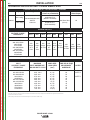
TECHNICAL SPECIFICATIONS - POWER WAVE® S350
POWER SOURCE-INPUT VOLTAGE AND CURRENT
Model
Input Voltage ± 10%
Duty Cycle
200-208/230/380-415/
460/575
50/60 Hz
100% rating
Power Factor @
Rated Output
300 Watts Max.
(fan on)
.95
39/35/20/17/14
(NA/65***/37/32/25)
40% rating
K2823-1
Idle Power
Input Amperes
(1 Phase in parenthesis)
30/28/16/14/11
(56/51/29/25/20)
RATED OUTPUT
Return to Master TOC
Return to Section TOC
INPUT
VOLTAGE / PHASE /
FREQUENCY
GMAW
40%***
60%
100%
300 Amps / 29 Volts
200-208/1/50/60
230/1/50/60
380-415/1/50/60
460/1/50/60
575/1/50/60
200-208/3/50/60
230/3/50/60
380-415/3/50/60
460/3/50/60
575/3/50/60
350
Amps
31.5
Volts
GTAW-DC
SMAW
40%***
60%
100%
40%
60%
100%
250 Amps / 30 Volts
320
325
300
Amps Amps Amps
30
33
29 Volts
Volts
Volts
250
275
350
Amps Amps
Amps
30 Volts
31
24 Volts
Volts
300
325
Amps
Amps
23Volts 22 Volts
*** On 230 Volt / 1 phase inputs the max. rating is at a duty cycle of 30%, except for GTAW processes.
Return to Master TOC
Return to Section TOC
RECOMMENDED INPUT WIRE AND FUSE SIZES
INPUT
VOLTAGE / PHASE/
FREQUENCY
MAXIMUM
INPUT AMPERE RATING AND DUTY CYCLE
CORD SIZE 3
AWG SIZES
(mm2)
TIME DELAY FUSE
OR BREAKER 2
AMPERAGE
200-208/1/50/60
200-208/3/50/60
230/1/50/60
230/3/50/60
380-415/1/50/60
380-415/3/50/60
460/1/50/60
460/3/50/60
575/1/50/60
575/3/50/60
60A, 100%
39A, 40%
67A, 30%
35A, 40%
38A, 40%
19A, 40%
34A, 40%
17A, 40%
27A, 40%
14A, 40%
6 (13)
8 (10)
4 (16)
8 (10)
8 (10)
12 (4)
8 (10)
12 (4)
10 (6)
14 (2.5)
80
50
80
45
50
30
45
25
35
20
1. Based on U.S. National electrical Code
2. Also called " inverse time" or "thermal / magnetic" circuit breakers; circuit breakers that have a delay in tripping action that decreases as the magnitude of the current increases
3. Type SO cord or similar in 30° C ambient
Return to Master TOC
4. When operating on these inputs, the line cord should be changed to an input conductor of 6 AWG or larger.
Return to Section TOC
1
POWER WAVE ® S350
NOTES
NOTE 4
NOTE 4
INSTALLATION
A-3
WELDING PROCESS
Return to Master TOC
Return to Section TOC
A-3
PROCESS
OUTPUT RANGE (AMPERES)
GMAW
GMAW-Pulse
FCAW
GTAW-DC
SMAW
5-350
OCV (Uo)
Mean
Peak
40-70
40-70
40-70
100V
24
60
PHYSICAL DIMENSIONS
MODEL
HEIGHT
WIDTH
DEPTH
WEIGHT
K2823-1
20.40 in ( 518 mm)
14.00in ( 356 mm)
24.80in ( 630mm)
85 lbs (39 kg)*
Return to Master TOC
Return to Master TOC
Return to Master TOC
Return to Section TOC
Return to Section TOC
Return to Section TOC
TEMPERATURE RANGES
OPERATING TEMPERATURE RANGE
Environmentally Hardened: -4°F to 104°F (-20C to 40C)
STORAGE TEMPERATURE RANGE
Environmentally Hardened: -40°F to 185°F (-40C to 85C)
IP23
155º(F) Insulation Class
* Weight does not include input cord.
POWER WAVE ® S350
INSTALLATION
Return to Master TOC
Return to Master TOC
Return to Master TOC
Return to Section TOC
Return to Section TOC
Return to Section TOC
A-4
LIftING
SAfEtY PREcAUtIONS
Read this entire installation section before you start
installation.
Return to Master TOC
Both handles should be used when lifting POWER WAVE® S350.
When using a crane or overhead device a lifting strap should be
connected to both handles. Do not attempt to lift the POWER
WAVE® S350 with accessories attached to it.
WARNING
WARNING
ELECTRIC SHOCK can kill.
• Only qualified personnel should perform this installation.
• turn the input power Off at the
disconnect switch or fuse box before working on
this equipment. turn off the input power to any
other equipment connected to the welding system
at the disconnect switch or fuse box before working on the equipment.
• Do not touch electrically hot parts.
• Always connect the POWER WAVE® S350
grounding lug to a proper safety (Earth) ground.
-------------------------------------------------------------
• Lift only with equipment of adequate lifting capacity.
• Be sure machine is stable when
lifting.
• Do not operate machine while
suspended when lifting.
FALLING
EQUIPMENT can
cause injury.
-------------------------------------------------------------
StAckING
The POWER WAVE® S350 cannot be stacked.
SELEct SUItABLE LOcAtION
tILtING
The POWER WAVE® S350 will operate in harsh environments. Even so, it is important that simple preventative measures are followed in order to assure long life
and reliable operation.
Place the machine directly on a secure, level surface or on a recommended undercarriage. The machine may topple over if this
procedure is not followed.
• The machine must be located where there is free circulation of clean air such that air movement in the
back, out the sides and bottom will not be restricted.
Only a qualified electrician should connect the POWER WAVE®
S350. Installation should be made in accordance with the appropriate National Electrical Code, all local codes and the information in this manual.
• Dirt and dust that can be drawn into the machine
should be kept to a minimum. The use of air filters
on the air intake is not recommended because normal air flow may be restricted. Failure to observe
these precautions can result in excessive operating
temperatures and nuisance shutdown.
MAchINE GROUNDING
• Keep machine dry. Shelter from rain and snow. Do
not place on wet ground or in puddles.
Return to Section TOC
A-4
• Do not mount the POWER WAVE® S350 over combustible surfaces. Where there is a combustible surface directly under stationary or fixed electrical
equipment, that surface shall be covered with a steel
plate at least .060” (1.6mm) thick, which shall extend
not less than 5.90” (150mm) beyond the equipment
on all sides.
INPUt AND GROUND cONNEctIONS
The frame of the welder must be grounded. A ground terminal
marked with a ground symbol is located next to the input power
connection block.
See your local and national electrical codes for proper grounding
methods.
hIGh fREQUENcY PROtEctION
The EMC classification of the POWER WAVE® S350 is Industrial,
Scientific and Medical (ISM) group 2, class A. The POWER
WAVE® S350 is for industrial use only. (See print L10093 for further details).
Locate the POWER WAVE® S350 away from radio controlled
machinery. The normal operation of the POWER WAVE® S350
may adversely affect the operation of RF controlled equipment,
which may result in bodily injury or damage to the equipment.
POWER WAVE ® S350
INSTALLATION
Return to Master TOC
Return to Section TOC
A-5
INPUT CONNECTION
WARNING
WARNING
Only a qualified electrician should
connect the input leads to the
POWER WAVE® S350. connections
should be made in accordance with
all local and national electrical codes
and the connection diagrams. failure to do so may
result in bodily injury or death.
-------------------------------------------------------------
Return to Master TOC
Return to Section TOC
A 10 ft. (3.0m) power cord is provided and wired into the
machine.
for Single Phase Input
Connect green lead to ground per National Electrical
Code.
Connect black and white leads to power.
Wrap red lead with tape to provide 600V insulation.
for three Phase Input
Connect green lead to ground per National Electric
Code.
Connect black, red and white leads to power.
Return to Master TOC
Return to Section TOC
INPUT FUSE AND SUPPLY WIRE
CONSIDERATIONS
Refer to Specification Section for recommended fuse,
wire sizes and type of the copper wires. Fuse the input
circuit with the recommended super lag fuse or delay
type breakers (also called "inverse time" or
"thermal/magnetic" circuit breakers). Choose input and
grounding wire size according to local or national electrical codes. Using input wire sizes, fuses or circuit
breakers smaller than recommended may result in "nuisance" shut-offs from welder inrush currents, even if the
machine is not being used at high currents.
Return to Master TOC
The POWER WAVE® S350 ON/OFF
switch is not intended as a service
disconnect for this equipment. Only
a qualified electrician should connect the input leads to the POWER WAVE® S350.
Connections should be made in accordance with all
local and national electrical codes and the connection diagram located on the inside of the reconnect
access door of the machine. Failure to do so may
result in bodily injury or death.
------------------------------------------------------------------------
POWER CORD REPLACEMENT
WARNING
Only a qualified electrician should
connect the input leads to the
POWER WAVE® S350. Connections
should be made in accordance with
all local and national electrical codes
and the connection diagrams. Failure to do so may result in bodily injury or death.
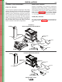
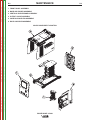
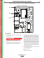
-----------------------------------------------------------------------If the input power cord is damaged or needs to be replaced an input power connection block is located in
the back of the machine with the access panel removed
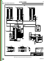
as shown Figure A.1.
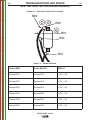
ALWAYS CONNECT THE POWER WAVE GROUNDING LUG (LOCATED AS SHOWN IN FIGURE A.1) TO
A PROPER SAFETY (EARTH) GROUND.
FIGURE A.1
CONNECTION
BLOCK
INPUT VOLTAGE SELECTION
Return to Section TOC
A-5
GROUND
LUG
The POWER WAVE® S350 automatically adjusts to
work with different input voltages. No reconnect
switches settings are required.
INPUT
POWER
CORD
POWER WAVE ® S350
INSTALLATION
Return to Master TOC
A-6
SMAW (STICK) WELDING
CONNECTION DIAGRAMS
GTAW (TIG) WELDING
A user interface is required for adjusting the TIG welding
settings. A Power Feed wire feeder can be used as the
user interface (Figure A.2), or a S-series user interface
(K2828-1) can be installed into the power source (Figure A.3). Refer to the connection diagrams based on the
user interface that is being used. For either set-up the
K2825-1 solenoid kit is recommended for controlling the
gas. Alternate configurations are possible depending on
the wire feeder that is being used. Refer to the wire
feeder’s manual for alternative configurations.
Similar to TIG welding a user interface is required for
adjusting the Stick welding settings. A Power Feed wire
feeder can be used as the user interface, or a K2828-1
(user interface control panel) can be installed into the
power source (Figure A.4). The connection diagram
shown is based on the S-Series user interface (K28281). In this diagram the remote control box is optional.
GMAW (MIG) WELDING
An arclink compatible wire feeder is recommended for
Mig welding. Refer to Figure A.5 for the connection details.
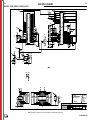
FIGURE A.2
Return to Master TOC
Return to Section TOC
Return to Section TOC
A-6
TIG WITH POWER FEED USER INTERFACE
REGULATOR
FLOWMETER
GAS SOLENOID KIT
(INSIDE MACHINE)
K2825-1
TO REMOTE CONTROL
RECEPTACLE
GAS HOSE
FOOT AMPTROL
K87
870
0
Return to Master TOC
Return to Section TOC
ARCLINK CABLE
K1543-[XX]
TO NEGATIVE
(-) STUD
Return to Master TOC
WORK CLAMP
WORK PIECE
TIG TORCH
K2266-1 KIT
(INCLUDES WORK CLAMP,
ADAPTER, AND REGULATOR)
PF10-M
WIRE FEEDER
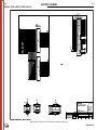
FIGURE A.3
REGULATOR
FLOWMETER
TIG WITH S-SERIES USER INTERFACE
GAS SOLENOID KIT
(INSIDE MACHINE)
K2825-1
Return to Section TOC
TO POSITIVE
(+) STUD
USER INTERFACE
CONTROL PANEL
K2828-1
TO REMOTE CONTROL
RECEPTACLE
FOOT AMPTROL
K870
GAS HOSE
TO NEGATIVE
(-) STUD
TO POSITIVE
(+) STUD
WORK CLAMP
WORK PIECE
TIG TORCH
K2266-1 KIT
(INCLUDES WORK CLAMP,
ADAPTER, AND REGULATOR)
POWER WAVE ® S350
INSTALLATION
A-7
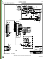
FIGURE A.4 - STICK WITH S-SERIES USER INTERFACE
STICK WITH S-SERIES USER INTERFACE
Return to Master TOC
Return to Master TOC
Return to Section TOC
Return to Section TOC
A-7
USER INTERFACE
CONTROL PANEL
K2828-1
TO NEGATIVE
(-) STUD
TO POSITIVE
(+) STUD
REMOTE CONTROL BOX
K857
ELECTRODE HOLDER KIT
K2394-1 KIT
(INICLUDES GROUND CLAMP)
WORK CLAMP
WORK PIECE
Return to Master TOC
Return to Section TOC
FIGURE A.5 - MIG PROCESS
REGULATOR
FLOWMETER
GAS HOSE
ARCLINK CABLE
K1543-[XX]
Return to Master TOC
Return to Section TOC
TO POSITIVE
(+) STUD
PF10-M
WIRE FEEDER
POWER WAVE ® S350
TO NEGATIVE (-) STUD
WORK CLAMP
WORK PIECE
INSTALLATION
Return to Master TOC
Return to Master TOC
Return to Section TOC
Return to Section TOC
A-8
A-8
GENERAL GUIDELINES
RECOMMENDED WORK CABLE
SIZES FOR ARC WELDING
Connect the electrode and work cables between the appropriate output studs of the Power Wave S350 per the
following guidelines:
• Most welding applications run with the electrode being
positive (+). For those applications, connect the electrode cable between the wire drive feed plate and the
positive (+) output stud on the power source. Connect
a work lead from the negative (-) power source output
stud to the work piece
• When negative electrode polarity is required, such as
in some Innershield applications, reverse the output
connections at the power source (electrode cable to
the negative (-) stud, and work cable to the positive
(+) stud).
• Select the appropriate size cables per the “Output
Cable Guidelines” below. Excessive voltage drops
caused by undersized welding cables and poor connections often result in unsatisfactory welding performance. Always use the largest welding cables
(electrode and work) that are practical, and be sure all
connections are clean and tight.
Note: Excessive heat in the weld circuit indicates undersized cables and/or bad connections.
• Route all cables directly to the work and wire feeder,
avoid excessive lengths and do not coil excess cable.
Route the electrode and work cables in close proximity
to one another to minimize the loop area and therefore
the inductance of the weld circuit.
• Always weld in a direction away from the work
(ground) connection.
CAUTION
Negative electrode polarity operation WITHOUT use
of a remote work sense lead (21) requires the Negative Electrode Polarity attribute to be set. See the
Remote Sense Lead Specification section of this
document for further details.
----------------------------------------------------------------------For additional Safety information regarding the electrode and work cable set-up, See the standard
“SAFETY INFORMATION” located in the front of the Instruction Manuals.
Table A.1 shows copper cable sizes recommended for
different currents and duty cycles. Lengths stipulated
are the distance from the welder to work and back to
the welder again. Cable sizes are increased for greater
lengths primarily for the purpose of minimizing cable
drop.
Return to Master TOC
Return to Master TOC
Return to Section TOC
Return to Section TOC
TABLE A.1
OUTPUT CABLE GUIDELINES
Amperes
Percent Duty
Cycle
CABLE SIZES FOR COMBINED LENGTHS OF ELECTRODE AND WORK CABLES [RUBBER COVERED COPPER - RATED 167°F (75°C)]**
200 to 250 Ft.
150 to 200 Ft.
0 to 50 Ft. 50 to 100 Ft. 100 to 150 Ft.
200
60
2
2
2
1
1/0
200
100
2
2
2
1
1/0
250
30
3
3
2
1
1/0
250
40
2
2
1
1
1/0
250
60
1
1
1
1
1/0
250
100
1
1
1
1
1/0
300
60
1
1
1
1/0
2/0
300
100
2/0
2/0
2/0
2/0
3/0
350
40
1/0
1/0
2/0
2/0
3/0
** Tabled values are for operation at ambient temperatures of 104°F (40°C) and below. Applications above 104°F (40°C) may
require cables larger than recommended, or cables rated higher than 167°F (75°C).
POWER WAVE ® S350
INSTALLATION
Return to Master TOC
Return to Master TOC
Return to Section TOC
Return to Section TOC
A-9
A-9
electrode and work cables can influence the voltage apparent at the studs of the welder, and have a dramatic
effect on performance. Remote voltage sense leads are
used to improve the accuracy of the arc voltage information supplied to the control pc board. Sense Lead
Kits (K940-xx) are available for this purpose.
CABLE INDUCTANCE AND ITS
EFFECTS ON WELDING
Excessive cable inductance will cause the welding performance to degrade. There are several factors that
contribute to the overall inductance of the cabling system including cable size, and loop area. The loop area
is defined by the separation distance between the electrode and work cables, and the overall welding loop
length. The welding loop length is defined as the total
of length of the electrode cable (A) + work cable (B) +
work path (C) (See Figure A.6).
The Power Wave S350 has the ability to automatically
sense when remote sense leads are connected. With
this feature there are no requirements for setting-up the
machine to use remote sense leads. This feature can
be disabled through the Weld Manager Utility (available
at www.powerwavesoftware.com) or through the set up
menu (if a user interface is installed into the power
source).
To minimize inductance always use the appropriate size
cables, and whenever possible, run the electrode and
work cables in close proximity to one another to minimize the loop area. Since the most significant factor in
cable inductance is the welding loop length, avoid excessive lengths and do not coil excess cable. For long
work piece lengths, a sliding ground should be considered to keep the total welding loop length as short as
possible.
CAUTION
If the auto sense lead feature is disabled and remote
voltage sensing is enabled but the sense leads are
missing or improperly connected, extremely high
welding outputs may occur.
-----------------------------------------------------------------------General Guidelines for Voltage Sense Leads
Sense leads should be attached as close to the weld as
practical, and out of the weld current path when possible. In extremely sensitive applications it may be necessary to route cables that contain the sense leads
away from the electrode and work welding cables.
REMOTE SENSE LEAD
SPECIFICATIONS
Voltage Sensing Overview
Voltage sense leads requirements are based on the
weld process (See Table A.2)
TABLE A.2
Return to Master TOC
Return to Section TOC
The best arc performance occurs when the Power
Wave S350 has accurate data about the arc conditions.
Depending upon the process, inductance within the
(1)
(2)
Process
Electrode Voltage Sensing (1)
67 lead
Work Voltage Sensing (2)
21 lead
GMAW
GMAW-P
FCAW
GTAW
SMAW
67 lead required
67 lead required
67 lead required
Voltage sense at studs
Voltage sense at studs
21 lead optional
21 lead optional
21 lead optional
Voltage sense at studs
Voltage sense at studs
The electrode voltage sense lead (67) is automatically enabled by the weld process, and integral to the 5 pin arclink control cable (K1543xx).
When a work voltage sense lead (21) is connected the power source will automatically switch over to using this feedback (if the auto sense
feature is enable).
Return to Master TOC
Return to Section TOC
FIGURE A.6
POWER
WAVE
S350
A
C
WORK
B
POWER WAVE ® S350
INSTALLATION
Electrode Voltage Sensing
Return to Master TOC
Return to Section TOC
A-10
The remote ELECTRODE sense lead (67) is built into
the 5-pin arclink control cable (K1543-xx) and is always
connected to the wire drive feed plate when a wire
feeder is present. Enabling or disabling electrode voltage sensing is application specific, and automatically
configured by the active weld mode.
Work Voltage Sensing
Return to Master TOC
Return to Section TOC
The Power Wave S350 is configured at the factory to
sense work voltage at the negative output stud (positive
output polarity with remote Work Voltage Sensing disabled).
Negative Electrode Polarity
The Power Wave S350 has the ability to automatically
sense the polarity of the sense leads. With this feature
there are no set-up requirements for welding with negative electrode polarity. This feature can be disabled
through the Weld Manager Utility (available at
www.powerwavesoftware.com) or through the set up
menu (if a user interface is installed into the power
source).
CAUTION
Return to Section TOC
Return to Master TOC
Return to Section TOC
Return to Master TOC
If the auto sense lead feature is disabled and the
weld polarity attribute is improperly configured extremely high welding outputs may occur.
-----------------------------------------------------------------------While most applications perform adequately by sensing
the work voltage directly at the output stud, the use of a
remote work voltage sense lead is recommended for
optimal performance. The remote WORK sense lead
(21) can be accessed through the four-pin voltage
sense connector located on the control panel by using
the K940 Sense Lead Kit. It must be attached to the
work as close to the weld as practical, but out of the
weld current path. For more information regarding the
placement of remote work voltage sense leads, see the
section entitled "Voltage Sensing Considerations for
Multiple Arc Systems."
POWER WAVE ® S350
A-10
Return to Master TOC
Return to Section TOC
A-11
INSTALLATION
VOLTAGE SENSING CONSIDERATIONS
FOR MULTIPLE ARC SYSTEMS
Special care must be taken when more than one arc is
welding simultaneously on a single part. Multiple arc applications do not necessarily dictate the use of remote
work voltage sense leads, but they are strongly recommended.
If Sense Leads ARE NOT Used:
Return to Section TOC
Return to Master TOC
Return to Section TOC
Return to Master TOC
• Avoid common current paths. Current from adjacent
arcs can induce voltage into each others current
paths that can be misinterpreted by the power
sources, and result in arc interference.
A-11
If Sense Leads ARE Used:
• Position the sense leads out of the path of the weld
current. Especially any current paths common to adjacent arcs. Current from adjacent arcs can induce
voltage into each others current paths that can be
misinterpreted by the power sources, and result in
arc interference.
• For longitudinal applications, connect all work leads
at one end of the weldment, and all of the work voltage sense leads at the opposite end of the weldment.
Perform welding in the direction away from the work
leads and toward the sense leads.
(See Figure A.7)
FIGURE A.7
CONNECT ALL SENSE
LEADS AT THE END
OF THE WELD.
DIRECTION
OF TRAVEL
Return to Master TOC
Return to Section TOC
CONNECT ALL
WORK LEADS AT
THE BEGINNING
OF THE WELD.
POWER WAVE ® S350
INSTALLATION
• For circumferential applications, connect all work
leads on one side of the weld joint, and all of the work
voltage sense leads on the opposite side, such that
they are out of the current path. (See Figure A.8)
Return to Master TOC
Return to Section TOC
A-12
FIGURE A.8
POWER
SOURCE
#2
Return to Master TOC
Return to Section TOC
POWER
SOURCE
#1
Return to Master TOC
Return to Master TOC
Return to Section TOC
Return to Section TOC
POWER
SOURCE
#1
POWER
SOURCE
#2
POWER
SOURCE
#1
POWER
SOURCE
#2
POWER WAVE ® S350
A-12
Return to Section TOC
Return to Master TOC
Return to Section TOC
Return to Master TOC
A-13
INSTALLATION
CONTROL CABLE CONNECTIONS
General Guidelines
Genuine Lincoln control cables should be used at all
times (except where noted otherwise). Lincoln cables
are specifically designed for the communication and
power needs of the Power Wave / Power Feed systems.
Most are designed to be connected end to end for ease
of extension. Generally, it is recommended that the total
length not exceed 100ft. (30.5m). The use of non-standard cables, especially in lengths greater than 25 feet,
can lead to communication problems (system shutdowns), poor motor acceleration (poor arc starting), and
low wire driving force (wire feeding problems). Always
use the shortest length of control cable possible, and
DO NOT coil excess cable.
Connection Between Power Source and Ethernet
Networks
The Power Wave S350 is equipped with an IP67 rated
ODVA compliant RJ-45 Ethernet connector, which is located on the rear panel. All external Ethernet equipment
(cables, switches, etc.), as defined by the connection
diagrams, must be supplied by the customer. It is critical
that all Ethernet cables external to either a conduit or
an enclosure are solid conductor, shielded cat 5e cable,
with a drain. The drain should be grounded at the
source of transmission. For best results, route Ethernet
cables away from weld cables, wire drive control cables,
or any other current carrying device that can create a
fluctuating magnetic field. For additional guidelines refer
to ISO/IEC 11801. Failure to follow these recommendations can result in an Ethernet connection failure during
welding.
Regarding cable placement, best results will be obtained when control cables are routed separate from the
weld cables. This minimizes the possibility of interference between the high currents flowing through the
weld cables, and the low level signals in the control cables. These recommendations apply to all communication cables including ArcLink® and Ethernet
connections.
Product specific Installation Instructions
Return to Section TOC
Return to Master TOC
Return to Master TOC
Connection Between Power Source and ArcLink® Compatible Wirefeeders (K1543 – ArcLink Control Cable)
Return to Section TOC
A-13
The 5-pin ArcLink control cable connects the power
source to the wire feeder. The control cable consists of
two power leads, one twisted pair for digital communication, and one lead for voltage sensing. The 5-pin ArcLink connection on the Power Wave S350 is located
on the rear panel above the power cord. The control
cable is keyed and polarized to prevent improper connection. Best results will be obtained when control cables are routed separate from the weld cables,
especially in long distance applications. The recommended combined length of the ArcLink control cable
network should not exceed 200ft. (61.0m).
POWER WAVE ® S350
Return to Section TOC
Return to Master TOC
Return to Section TOC
Return to Master TOC
Return to Master TOC
Return to Section TOC
Return to Master TOC
Return to Section TOC
A-14
NOTES
POWER WAVE ® S350
A-14
Return to Master TOC
B-1
TABLE OF CONTENTS - OPERATION SECTION
B-1
Operation . . . . . . . . . . . . . . . . . . . . . . . . . . . . . . . . . . . . . . . . . . . . . . . . . . . . . . . . . . . . . . . . . . . . . . . . . . . . . .B-1
Safety Precautions . . . . . . . . . . . . . . . . . . . . . . . . . . . . . . . . . . . . . . . . . . . . . . . . . . . . . . . . . . . . . . . . . . . .B-2
Graphic Symbols . . . . . . . . . . . . . . . . . . . . . . . . . . . . . . . . . . . . . . . . . . . . . . . . . . . . . . . . . . . . . . . . . . . . .B-2
Power-Up Sequence . . . . . . . . . . . . . . . . . . . . . . . . . . . . . . . . . . . . . . . . . . . . . . . . . . . . . . . . . . . . . . . . . .B-2
Duty Cycle . . . . . . . . . . . . . . . . . . . . . . . . . . . . . . . . . . . . . . . . . . . . . . . . . . . . . . . . . . . . . . . . . . . . . . . . . .B-2
Return to Master TOC
Product Description . . . . . . . . . . . . . . . . . . . . . . . . . . . . . . . . . . . . . . . . . . . . . . . . . . . . . . . . . . . . . . . . . . .B-3
Recommended Processes and Equipment . . . . . . . . . . . . . . . . . . . . . . . . . . . . . . . . . . . . . . . . . . . . . . . . .B-3
Equipment Limitations . . . . . . . . . . . . . . . . . . . . . . . . . . . . . . . . . . . . . . . . . . . . . . . . . . . . . . . . . . . . . . . . .B-3
Design Features . . . . . . . . . . . . . . . . . . . . . . . . . . . . . . . . . . . . . . . . . . . . . . . . . . . . . . . . . . . . . . . . . . . . . .B-4
Case Front Controls . . . . . . . . . . . . . . . . . . . . . . . . . . . . . . . . . . . . . . . . . . . . . . . . . . . . . . . . . . . . . . . . . . .B-5
Case Back Controls . . . . . . . . . . . . . . . . . . . . . . . . . . . . . . . . . . . . . . . . . . . . . . . . . . . . . . . . . . . . . . . . . . .B-5
. . . . . . . . . . . . . . . . . . . . . . . . . . . . . . . . . . . . . . . . . . . . . . . . . . . . . . .B-6/B-8
Return to Master TOC
Return to Master TOC
Common Welding Procedures
POWER WAVE ® S350
OPERATION
Return to Master TOC
Return to Master TOC
Return to Section TOC
Return to Section TOC
B-2
SAFETY PRECAUTIONS
READ AND UNDERSTAND ENTIRE
BEFORE OPERATING MACHINE.
SECTION
GRAPHIC SYMBOLS THAT APPEAR ON
THIS MACHINE OR IN THIS MANUAL
WARNING OR
CAUTION
WARNING
• ELECTRIC SHOCK CAN KILL.
• Do not touch electrically live part
or electrode with skin or wet
clothing.
• Insulate yourself from work and
ground.
• Always wear dry insulating gloves.
• Do not operate with covers, panels or guards removed or open.
--------------------------------------------------------------------• FUMES AND GASSES can be
dangerous.
• Keep your head out of fumes.
• Use ventilation or exhaust to remove fumes from breathing zone.
---------------------------------------------------------------------
DANGEROUS
VOLTAGE
POSITIVE OUTPUT
NEGATIVE OUTPUT
HIGH TEMPERATURE
• WELDING SPARKS can cause fire
or explosion.
• Keep flammable material away.
STATUS
Return to Master TOC
Return to Section TOC
--------------------------------------------------------------------ARC RAYS can burn.
• Wear eye, ear and body protection.
--------------------------------------------------------------------SEE ADDITIONAL WARNING INFORMATION
UNDER ARC WELDING SAFETY PRECAUTIONS
AND IN THE FRONT OF THIS OPERATING MANUAL.
---------------------------------------------------------------------
B-2
PROTECTIVE
GROUND
EXPLOSION
POWER-UP SEQUENCE
When the POWER WAVE® S350 is powered up, it can
take as long as 30 seconds for the machine to be ready
to weld. During this time period the user interface will
not be active.
Return to Master TOC
Return to Section TOC
DUTY CYCLE
The duty cycle is based on a ten-minute period. A 40%
duty cycle represents 4 minutes of welding and 6 minutes of idling in a ten-minute period. Refer to the technical specification section for the Power Wave S350’s
duty cycle ratings.
POWER WAVE ® S350
Return to Master TOC
Return to Master TOC
Return to Master TOC
OPERATION
B-3
PRODUCT DESCRIPTION
PROCESS LIMITATIONS
PRODUCT SUMMARY
The Power Wave® S350 is a portable multi-process
power source with high-end functionality capable of
Stick, DC TIG, MIG, Pulsed MIG and Flux-Cored welding. It is ideal for a wide variety of materials including
aluminum, stainless, and nickel — where arc performance is critical.
The software based weld tables of the Power Wave
S350 limit the process capability within the output range
and the safe limits of the machine. In general the
processes will be limited to .030-.052 solid steel wire,
.030-.045 stainless wire, .035-1/16 cored wire, and .035
and 1/16 Aluminum wire.
The Power Wave® S350 is designed to be a very flexible welding system. Like existing POWER WAVEs, the
software based architecture allows for future upgradeability. One significant change from the current range
of Power Wave units is that the Ethernet communication feature is standard on the Power Wave® S350
which allows for effortless software upgrades through
Powerwavesoftware.com. The Ethernet communication
also gives the Power Wave® S350 the ability to run
Production Monitoring™ 2. Also a Devicenet option
which will allow the Power Wave® S350 to be used in
a wide range of configurations. Also, the Power Wave®
S350 is designed to be compatible with future advanced welding modules like STT.
EQUIPMENT LIMITATIONS
Only ArcLink compatible semiautomatic wire feeders
and users interfaces may be used. If other Lincoln wire
feeders or non-Lincoln wire feeders are used there will
be limited process capability and performance and features will be limited.
RECOMMENDED PROCESSES AND
EQUIPMENT
The Power Wave® S350 is recommended for semiautomatic
welding, and may also be suitable for basic hard automation
applications. The Power Wave® S350 can be set up in a
number of configurations, some requiring optional equipment
or welding programs.
RECOMMENDED EQUIPMENT
The Power Wave® S350 is designed to be compatible
with the current range of Power Feed™ systems including future versions of ArcLink® feeders.
RECOMMENDED PROCESSES
Return to Master TOC
Return to Section TOC
Return to Section TOC
Return to Section TOC
Return to Section TOC
B-3
The Power Wave S350 is a high speed, multi-process
power source capable of regulating the current, voltage,
or power of the welding arc. With an output range of 5
to 350 amperes, it supports a number of standard
processes including synergic GMAW, GMAW-P,
FCAW, FCAW-SS, SMAW, GTAW and GTAW-P on various materials especially steel, aluminum and stainless.
POWER WAVE ® S350
Return to Master TOC
Return to Section TOC
B-4
OPERATION
DESIGN FEATURES
Loaded with Standard Features
• Multiple process DC output range: 5 - 350 Amps
• 200 – 600 VAC, 1/3 phase, 50-60Hz input power
• New and Improved Line Voltage Compensation holds
the output constant over wide input voltage fluctuations.
• State of the art power electronics technology yields
superior welding capability.
Return to Master TOC
Return to Section TOC
• Utilizes next generation microprocessor control,
based on the ArcLink® platform.
• Electronic over current protection
• Input over voltage protection.
• F.A.N. (fan as needed). Cooling fan only runs when
needed.
• Thermostatically protected for safety and reliability.
• Recessed connection panel for protection against accidental impact.
Return to Master TOC
Return to Section TOC
• Ethernet connectivity via IP-67 rated ODVA compliant
RJ-45 connector.
• Panel mounted Status and Thermal LED indicators
facilitate quick and easy troubleshooting.
• Potted PC boards for enhanced ruggedness/reliability.
• Enclosure reinforced with heavy duty aluminum extrusions for mechanical toughness
• Remote control/Foot amptrol ready.
Return to Master TOC
Return to Section TOC
• Waveform Control Technology™ for good weld appearance and low spatter, even when welding nickel
alloys.
POWER WAVE ® S350
B-4
OPERATION
Return to Master TOC
Return to Section TOC
B-5
B-5
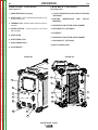
CASE FRONT CONTROLS
CASE BACK CONTROLS
(See Figure B.1)
(See Figure B.2)
1. USER INTERFACE (optional)
1. 115 VAC RECEPTACLE AND CIRCUIT BEAKER
(OPTIONAL)
2. STATUS LED - (See Troubleshooting Section for operational functions)
3. THERMAL LED - Indicates when machine has thermal fault.
4. POWER SWITCH - Controls power to the Power
Wave® S350.
2. ARCLINK
(RECEPTACLE
BREAKER)
AND
CIRCUIT
3. RESERVED FOR FUTURE DEVELOPMENT
4. DEVICENET KIT (OPTIONAL)
5. ETHERNET
5. WORK STUD
6. RESERVED FOR FUTURE DEVELOPMENT
Return to Master TOC
7. SOLENOID KIT (OPTIONAL)
7. WORK SENSE LEAD
8. INPUT POWER CORD
8. 6-PIN REMOTE
Return to Master TOC
FIGURE B.1
Return to Master TOC
Return to Section TOC
Return to Section TOC
Return to Section TOC
6. ELECTRODE STUD
FIGURE B.2
5
1
1
2
2
3
3
4
4
5
8
6
7
8
POWER WAVE ® S350
6
7
OPERATION
Return to Master TOC
Return to Master TOC
Return to Master TOC
Return to Master TOC
Return to Section TOC
Return to Section TOC
Return to Section TOC
Return to Section TOC
B-6
COMMON WELDING PROCEDURES
WARNING
MAKING A WELD
The serviceability of a product or structure utilizing
the welding programs is and must be the sole responsibility of the builder/user. Many variables beyond the control of The Lincoln Electric Company
affect the results obtained in applying these programs. These variables include, but are not limited
to, welding procedure, plate chemistry and temperature, weldment design, fabrication methods and
service requirements. The available range of a
welding program may not be suitable for all applications, and the build/user is and must be solely responsible for welding program selection.
Choose the electrode material, electrode size, shielding
gas, and process (GMAW, GMAW-P etc.) appropriate
for the material to be welded.
Select the weld mode that best matches the desired
welding process. The standard weld set shipped with
the Power Wave S350 encompasses a wide range of
common processes that will meet most needs. If a special weld mode is desired, contact the local Lincoln
Electric sales representative.
All adjustments are made through the user interface.
Because of the different configuration options your system may not have all of the following adjustments.
See Accessories Section for Kits and Options available
to use with the Power Wave® S350.
Definition of Welding Modes
B-6
Basic Welding Controls
Weld Mode
Selecting a weld mode determines the output characteristics of the Power Wave power source. Weld modes
are developed with a specific electrode material, electrode size, and shielding gas. For a more complete description of the weld modes programmed into the Power
Wave® S350 at the factory, refer to the Weld Set Reference Guide supplied with the machine or available at
www.powerwavesoftware.com.
Wire Feed Speed (WFS)
In synergic welding modes (synergic CV, GMAW-P),
WFS is the dominant control parameter. The user adjusts WFS according to factors such as wire size, penetration requirements, heat input, etc. The Power
Wave® S350 then uses the WFS setting to adjust the
voltage and current according to settings contained in
the Power Wave.
In non-synergic modes, the WFS control behaves like
a conventional power source where WFS and voltage
are independent adjustments. Therefore, to maintain
proper arc characteristics, the operator must adjust the
voltage to compensate for any changes made to the
WFS.
Amps
In constant current modes, this control adjusts the welding amperage.
Volts
In constant voltage modes, this control adjusts the welding voltage.
NON-SYNERGIC WELDING MODES
• A Non-synergic welding mode requires all welding
process variables to be set by the operator.
Trim
In pulse synergic welding modes, the Trim setting adjusts the arc length. Trim is adjustable from 0.50 to
1.50. 1.00 is the nominal setting and is a good starting
point for most conditions.
SYNERGIC WELDING MODES
• A Synergic welding mode offers the simplicity of single knob control. The machine will select the correct
voltage and amperage based on the Wire Feed
Speed (WFS) set by the operator.
UltimArc™ Control
UltimArc™ Control allows the operator to vary the arc
characteristics. UltimArc™ Control is adjustable from –
10.0 to +10.0 with a nominal setting of 0.0.
POWER WAVE ® S350
OPERATION
Return to Master TOC
Return to Master TOC
Return to Section TOC
Return to Section TOC
B-7
SMAW (STICK) WELDING
The welding current and Arc Force settings can be set
through a Power Feed 10M or Power Feed 25M wire
feeder. Alternatively an optional Stick / TIG UI (K28281) can be installed into the power source to control
these settings locally.
The nominal preprogrammed voltage is the best average voltage for a given wire feed speed, but may be adjusted to preference. When the wire feed speed
changes, the Power Wave® S350 automatically adjusts
the voltage level correspondingly to maintain similar arc
characteristics throughout the WFS range.
In a SMAW (STICK mode), Arc Force can be adjusted.
It can be set to the lower range for a soft and less penetrating arc characteristic (negative numeric values) or
to the higher range (positive numeric values) for a crisp
and more penetrating arc. Normally, when welding with
cellulosic types of electrodes (E6010, E7010, E6011),
a higher energy arc is required to maintain arc stability.
This is usually indicated when the electrode sticks to the
work-piece or when the arc becomes unstable during
manipulative technique. For low hydrogen types of electrodes (E7018, E8018, E9018, etc.) a softer arc is usually desirable and the lower end of the Arc Control suits
these types of electrodes. In either case the arc control
is available to increase or decrease the energy level delivered to the arc.
Non Synergic CV
In non-synergic modes, the WFS control behaves more
like a conventional CV power source where WFS and
voltage are independent adjustments. Therefore to
maintain the arc characteristics, the operator must adjust the voltage to compensate for any changes made
to the WFS.
GTAW (TIG) WELDING
The welding current can be set through a Power Feed
10M or Power Feed 25M wire feeder. Alternatively an
optional Stick / TIG UI (K2828-1) can be installed into
the power source to control these settings locally.
PULSE WELDING
Pulse welding procedures are set by controlling an overall “arc length” variable. When pulse welding, the arc
voltage is highly dependent upon the waveform. The
peak current, back ground current, rise time, fall time
and pulse frequency all affect the voltage. The exact
voltage for a given wire feed speed can only be predicted when all the pulsing waveform parameters are
known. Using a preset voltage becomes impractical
and instead the arc length is set by adjusting “trim”.
Return to Section TOC
Return to Master TOC
Return to Master TOC
The TIG mode features continuous control from 5 to 350
amps with the use of an optional foot amptrol (K870).
The Power Wave® S350 can be run in either a Touch
Start TIG mode or Scratch start TIG mode.
Return to Section TOC
B-7
CONSTANT VOLTAGE WELDING
Synergic CV
For each wire feed speed, a corresponding voltage is
preprogrammed into the machine through special software at the factory.
All CV Modes
Pinch adjusts the apparent inductance of the wave
shape. The “pinch” function is inversely proportional to
inductance. Therefore, increasing Pinch Control greater
than 0.0 results in a crisper arc (more spatter) while decreasing the Pinch Control to less than 0.0 provides a
softer arc (less spatter).
Trim adjusts the arc length and ranges from 0.50 to 1.50
with a nominal value of 1.00. Trim values greater than
1.00 increase the arc length, while values less than 1.00
decrease the arc length. (See figure B.3)
FIGURE B.3
Trim .50
Arc Length Short
Trim 1.00
Arc Length Medium
POWER WAVE ® S350
Trim 1.50
Arc L ength Long
OPERATION
Return to Master TOC
Return to Master TOC
Return to Master TOC
Return to Section TOC
Return to Section TOC
Return to Section TOC
B-8
Most pulse welding programs are synergic. As the wire
feed speed is adjusted, the Power Wave® S350 will automatically recalculate the waveform parameters to
maintain similar arc properties.
The Power Wave® S350 utilizes “adaptive control” to
compensate for changes in the electrical stick-out while
welding. (Electrical stick-out is the distance from the
contact tip to the work piece.) The Power Wave® S350
waveforms are optimized for a 0.75” stick-out. The
adaptive behavior supports a range of stick-outs from
0.50 to 1.25”. At very low or high wire feed speeds, the
adaptive range may be less due to reaching physical
limitations of the welding process.
UltimArc™ Control adjusts the focus or shape of the
arc. UltimArc™ Control is adjustable from -10.0 to
+10.0 with a nominal setting of 0.0. Increasing the UltimArc™ Control increases the pulse frequency and
background current while decreasing the peak current.
This results in a tight, stiff arc used for high speed sheet
metal welding. Decreasing the UltimArc™ Control decreases the pulse frequency and background current
while increasing the peak current. This results in a soft
arc good for out of position welding. (See Figure B.4)
FIGURE B.4
UltimArc™ Control OFF
Med ium Fr equency and Wi dth
Return to Master TOC
UltimArc™ Control -10.0
Low Frequency, Wi de
Return to Section TOC
B-8
POWER WAVE ® S350
UltimArc™ Control +10.0
Hi gh Frequency , Fo cu sed
Return to Master TOC
C-1
TABLE OF CONTENTS - ACCESSORIES SECTION
C-1
Accessories . . . . . . . . . . . . . . . . . . . . . . . . . . . . . . . . . . . . . . . . . . . . . . . . . . . . . . . . . . . . . . . . . . . . . . . . . . . .C-1
Kits, Options / Accessories . . . . . . . . . . . . . . . . . . . . . . . . . . . . . . . . . . . . . . . . . . . . . . . . . . . . . . . . . . . . . .C-2
Field Installed Options . . . . . . . . . . . . . . . . . . . . . . . . . . . . . . . . . . . . . . . . . . . . . . . . . . . . . . . . . . . . . .C-2/C-3
Return to Master TOC
Return to Master TOC
Return to Master TOC
Stick Options . . . . . . . . . . . . . . . . . . . . . . . . . . . . . . . . . . . . . . . . . . . . . . . . . . . . . . . . . . . . . . . . . . . . .C-3/C-4
POWER WAVE ® S350
Return to Master TOC
Return to Section TOC
C-2
ACCESSORIES
KITS, OPTIONS AND ACCESSORIES
All Kits Options and Accessories are found on the Web
site: (www.lincolnelectric.com)
FACTORY INSTALLED
None Available
FIELD INSTALLED OPTIONS
Return to Master TOC
Return to Master TOC
Return to Master TOC
Return to Section TOC
Stick / Tig User Interface Kit
Mounts inside the front panel of the Power Wave S350.
Allows stick and Tig operation without having a wire
feeder.
Order K2828-1
Return to Section TOC
Twist-Mate™ Cable Receptacle
For connecting welding cable to Twist-Mate™ Cable
Plug.
Order K1759-70 for 1/0-2/0 (50-70 mm2) cable
Order K1759-95 for 2/0-3/0 (70-95mm2) cable
Twist-Mate™ to Lug Adapter
For connection of lugged cable to Twist-Mate™ connectors. 18" (457 mm) long.
Order K2176-1
GENERAL OPTIONS
Return to Section TOC
C-2
115 VAC Auxiliary Power Kit
Mounts inside the back of the Power Wave S350. Adds
115 VAC / 60 Hz auxiliary power capability to the Power
Wave S350 ( only compatible with the K2823-1 power
source)
Order K2829-1
DeviceNet Kit
Mounts inside the back of the Power Wave S350. Allows Devicenet objects to communicate with the Power
Wave S350.
Order K2827-1
Work Voltage Sense Lead Kit
Required to accurately monitor voltage at the arc.
Order K940-25 for 25 ft. (7.6 m)
Order K1811-75 for 75 ft. (22.9 m)
Deluxe Adjustable Gas Regulator & Hose Kit
Accommodates CO2, Argon, or Argon-blend gas cylinders. Includes a cylinder pressure gauge, dual scale
flow gauge and 4.3 ft. (1.3 m) gas hose.
Order K586-1
Work and Wire Feeder 2/0 Weld Cable Package
Includes Twist-Mate™ connectors, work clamps, 15 ft.
(4.5 m) work cable and 10 ft. (3.0 m) electrode cable.
Rated 350 amps, 60% duty cycle.
Order K1803-1
Inverter and Wire Feeder Cart
Rear-wheeled cart includes front casters and no-lift gas
bottle platform. Convenient handles allow for easy cable
storage while full length side trays store parts and tools.
Shipped fully assembled. Small footprint fits through 30"
(762 mm) door.
Order K1764-1 Dual Cylinder Kit
Dual Cylinder Kit
Permits side-by-side mounting of two full size gas cylinders, with easy loading. For use with K1764-1 cart.
Order K1702-1
Coaxial Welding Cable
Optimum weld cables for minimizing cable inductance
and optimizing welding performance.
Order K1796-25 for 25 feet 25 ft. (7.6 m) cable length.
Order K1796-50 for 50 feet 50 ft. (15.2 m) cable
length.
Order K1796-75 for 75 feet 75 ft. (22.9 m) cable
length.
Order K1796-100 for 100 feet 100 ft. (30.5 m) cable
length.
Welding Fume Extractors
Lincoln offers a wide range of fume extraction environmental system solutions, ranging from portable systems
easily wheeled around a shop to shop-wide central systems servicing many dedicated welding stations.
Request Lincoln publication E13.40
(See www.lincolnelectric.com)
Twist-Mate™ Cable Plug
For connecting welding cable to output terminal receptacles. For 1/0-2/0 (50-70 mm2) cable.
Order K852-70
Twist-Mate™ Cable Plug
For connecting welding cable to output terminal receptacles. For 2/0-3/0 (70-95 mm2) cable.
Order K852-95
POWER WAVE ® S350
C-3
ACCESSORIES
Return to Master TOC
Return to Master TOC
Return to Master TOC
Return to Section TOC
Return to Section TOC
Return to Section TOC
STICK OPTIONS
Hand Amptrol®
Provides 25 ft. (7.6 m) of remote current control for TIG welding. (6-pin
plug connection)
Order K963-3
ACCESSORY KIT - 150 Amp
For stick welding. Includes 20 ft.
(6.1m) #6 electrode cable with lug,
15 ft. (4.6m) #6 work cable with lugs,
headshield, filter plate, work clamp,
electrode holder and sample pack of
mild steel electrode. For use with
K2176-1 (Twist-Mate™ to Lug Adapter)
ORDER K875
Foot Amptrol®
Provides 25 ft. (7.6 m) of remote
current control for TIG welding. (6pin plug connection).
Order K870
ACCESSORY KIT - 400 AMP
For stick welding. Includes 35 ft.
(10.7m) 2/0 electrode cable with lug,
30 ft. (9.1m) 2/0 work cable with lugs,
headshield, filter plate, work clamp
and electrode holder. For use with
K2176-1 (Twist-Mate™ to Lug Adapter)
ORDER K704
Arc Start Switch
May be used in place of the Foot or
Hand Amptrol®. Comes with a 25 ft.
(7.6 m) cable. Attaches to the TIG
torch for convenient finger control to
start and stop the weld cycle at the
current set on the machine.
Order K814
REMOTE OUTPUT CONTROL
Portable current control provides the same
dial range as the current control on the
welder. Consists of a 6-pin Amphenol connector which plugs into the remote control
Amphenol. 25 foot cable length.
ORDER K857
ORDER K857-1 for 100 ft. (30 m)
Twist-Mate™ Torch Adapter
For connection of Pro-Torch™ TIG torches (1 piece
cable) to power sources with gas passing through the
Twist-Mate™ connection. For use with K2825-1.
Order K1622-1 For air-cooled PTA-9 or PTA-17
torches.
Order K1622-3 For air-cooled PTA-26 torches.
Order K1622-2 For water-cooled torches.
STICK ELECTRODE HOLDER AND CABLE ASSEMBLY
Includes 200A stick electrode holder and Twist-Mate
connector. 12.5 ft. cable length.
ORDER K2374-1
Twist-Mate™ Torch Adapter
For connection of PTA-9 or PTA-17V torches (1 piece
cable) to power sources without gas passing through
the Twist-Mate™ connection.
Order K960-1
STICK ELECTRODE HOLDER CABLE AND WORK
CABLE ASSEMBLY
Includes 200A stick electrode holder, welding cable,
work clamp and Twist-Mate adapter.
ORDER K2394-1
Return to Master TOC
TIG OPTIONS
Return to Section TOC
C-3
Power Wave S350 Solenoid Kit
Mounts inside the back of the Power Wave
S350. Switches gas flow in the Power
Wave S350 through the Twist-Mate™ connector. Includes gas hose and solenoid (
only compatible with the K2823-1 power
source).
Order K2825-1
Pro-Torch™ TIG Torches
A full line of air-cooled and water-cooled torches available.
Request Lincoln publication E12.150
(See www.lincolnelectric.com)
POWER WAVE ® S350
Return to Master TOC
Return to Master TOC
Return to Section TOC
Return to Section TOC
C-4
ACCESSORIES
TIG-Mate™ 17V Air-Cooled TIG Torch Starter Pack
Get everything you need for TIG welding in one complete easy-to-order kit packaged in its own portable carrying case. Includes: PTA-17V torch, parts kit, Harris®
flowmeter/regulator, 10 ft. (3.0 m) gas hose, and work
clamp and cable.
Order K2265-1
TIG-Mate™ 17 Air-Cooled TIG Torch Starter Pack
Get everything you need for TIG welding in one complete easy-to-order kit packaged in its own portable carrying case. Includes: PTA-17 torch, parts kit, Harris®
flowmeter/regulator, 10 ft. (3.0 m) gas hose, Twistmate™ adapter, and work clamp and cable.
Order K2266-1
TIG-Mate™ 20 Water-Cooled TIG Torch Starter Pack
Get everything you need for TIG welding in one complete easy-to-order kit packaged in its own portable carrying case. Includes: PTW-20 torch, parts kit, Harris®
flowmeter/regulator, 10 ft. (3.0 m) gas hose, TwistMate™ adapter, work clamp and cable and 10 ft. (3.0
m) water hose.
Order K2267-1
MIG OPTIONS
Work and Feeder Welding Cables
350 amps, 60% duty cycle with Twist-Mate connectors
and Ground Clamp.
Order K1803-1
Return to Section TOC
Return to Master TOC
Return to Section TOC
Return to Master TOC
COMPATIBLE LINCOLN EQUIPMENT
Any Arclink compatible wire feeding equipment
(See www.lincolnelectric.com)
POWER WAVE ® S350
C-4
Return to Master TOC
D-1
TABLE OF CONTENTS - MAINTENANCE SECTION
D-1
Maintenance . . . . . . . . . . . . . . . . . . . . . . . . . . . . . . . . . . . . . . . . . . . . . . . . . . . . . . . . . . . . . . . . . . . . . . . . . . .D-1
Safety Precautions . . . . . . . . . . . . . . . . . . . . . . . . . . . . . . . . . . . . . . . . . . . . . . . . . . . . . . . . . . . . . . . . . . . .D-2
Routine Maintenance . . . . . . . . . . . . . . . . . . . . . . . . . . . . . . . . . . . . . . . . . . . . . . . . . . . . . . . . . . . . . . . . . .D-2
Periodic Maintenance . . . . . . . . . . . . . . . . . . . . . . . . . . . . . . . . . . . . . . . . . . . . . . . . . . . . . . . . . . . . . . . . . .D-2
Calibration Specification . . . . . . . . . . . . . . . . . . . . . . . . . . . . . . . . . . . . . . . . . . . . . . . . . . . . . . . . . . . . . . . .D-2
Return to Master TOC
Return to Master TOC
Return to Master TOC
Major Component Location . . . . . . . . . . . . . . . . . . . . . . . . . . . . . . . . . . . . . . . . . . . . . . . . . . . . . . . . . . . . .D-3
POWER WAVE ® S350
MAINTENANCE
Return to Master TOC
Return to Master TOC
Return to Master TOC
Return to Master TOC
Return to Section TOC
Return to Section TOC
Return to Section TOC
Return to Section TOC
D-2
SAFETY PRECAUTIONS
WARNING
ELECTRIC SHOCK can kill.
• Do not operate with covers removed.
• Turn off power source before installing or servicing.
• Do not touch electrically hot parts.
• Turn the input power to the welding power source
off at the fuse box before working in the terminal
strip.
• Only qualified personnel should install, use or
service this equipment.
------------------------------------------------------------------------
ROUTINE MAINTENANCE
Routine maintenance consists of periodically blowing
out the machine, using a low-pressure air stream, to remove accumulated dust and dirt from the intake and
outlet louvers, and the cooling channels in the machine.
PERIODIC MAINTENANCE
Calibration of the Power Wave® S350 is critical to its
operation. Generally speaking the calibration will not
need adjustment. However, neglected or improperly calibrated machines may not yield satisfactory weld performance. To ensure optimal performance, the
calibration of output Voltage and Current should be
checked yearly.
CALIBRATION SPECIFICATION
Output Voltage and Current are calibrated at the factory.
Generally the machine calibration will not need adjustment. However, if the weld performance changes, or the
yearly calibration check reveals a problem, use the calibration section of the Diagnostics Utility to make the
appropriate adjustments.
The calibration procedure itself requires the use of a
grid, and certified actual meters for voltage and current.
The accuracy of the calibration will be directly affected
by the accuracy of the measuring equipment you use.
The Diagnostics Utility includes detailed instructions,
it is refered to on the Service Navigator DVD or is
available at www.powerwavesoftware.com.
POWER WAVE ® S350
D-2
MAINTENANCE
Return to Master TOC
Return to Section TOC
D-3
D-3
1. FRONT PANEL ASSEMBLY
2. BASE AND POWER ASSEMBLY
3. VERTICAL DIVIDER PANEL ASSEMBLY
4. OUTPUT CHOKE ASSEMBLY
5. CASE BACK AND FAN ASSEMBLY
6. ROOF AND SIDES ASSEMBLY
MAJOR COMPONENT LOCATION
Return to Section TOC
Return to Master TOC
Return to Section TOC
Return to Master TOC
6
5
1
2
Return to Master TOC
Return to Section TOC
3
4
POWER WAVE ® S350
Return to Section TOC
Return to Master TOC
Return to Section TOC
Return to Master TOC
Return to Master TOC
Return to Section TOC
Return to Master TOC
Return to Section TOC
D-4
NOTES
POWER WAVE ® S350
D-4
Return to Master TOC
E-1
TABLE OF CONTENTS-THEORY OF OPERATION SECTION
E-1
Theory of Operation . . . . . . . . . . . . . . . . . . . . . . . . . . . . . . . . . . . . . . . . . . . . . . . . . . . . . . . . . . . . . . . . . . . . .E-1
General Description . . . . . . . . . . . . . . . . . . . . . . . . . . . . . . . . . . . . . . . . . . . . . . . . . . . . . . . . . . . . . . . . . . .E-2
Main Input Switch, Input Rectifier, Soft Start/Input Relay, DC Link Capacitor, Buck-Boost and Power Factor Correction Board . . . .E-3
Planar Transformer, Output Rectification and Filtering . . . . . . . . . . . . . . . . . . . . . . . . . . . . . . . . . . . . . . . . .E-4
Multi-Phase Chopper, Chopper Control Board, Current Transducer and Control Board . . . . . . . . . . . . . . .E-5
Return to Master TOC
DC Bus Board and Optional User Interface Board . . . . . . . . . . . . . . . . . . . . . . . . . . . . . . . . . . . . . . . . . . . .E-6
Machine Protection . . . . . . . . . . . . . . . . . . . . . . . . . . . . . . . . . . . . . . . . . . . . . . . . . . . . . . . . . . . . . . . . . . . .E-7
Pulse Width Modulation . . . . . . . . . . . . . . . . . . . . . . . . . . . . . . . . . . . . . . . . . . . . . . . . . . . . . . . . . . . . . . . .E-8
Minimum / Maximum Output . . . . . . . . . . . . . . . . . . . . . . . . . . . . . . . . . . . . . . . . . . . . . . . . . . . . . . . . . . . .E-8
Insulated Gate Bipolar Transistor (IGBT) Operation . . . . . . . . . . . . . . . . . . . . . . . . . . . . . . . . . . . . . . . . . .E-9
FIGURE E.1 BLOCK LOGIC DIAGRAM
Return to Master TOC
SWITCH BOARD
INPUT
CHOKE
(SECOND STAGE)
HIGH FRQUENCY INVERTER
OUTPUT
WITH PLANER TRANSFORMER RECTIFIER
100V
60KHZ
INPUT
RELAY
MAIN
SWITCH
INPUT
RECTIFIER
100 Ohm
DC LINK FIRST STAGE
CAPACITOR BUCK-BOOST
POSITIVE
TERMINAL
OUTPUT
CAPACITORS
400V
IGBT
FULL WAVE
BRIDGE
(THIRD STAGE)
MULTI-PHASE BUCK
CONVERTER
CURRENT
TRANSDUCER NEGATIVE
TERMINAL
120KHz
CR
CURRENT
TRANSDUCER
CHOPPER
CONTROL
BOARD
INPUT
POWER
Return to Master TOC
48 VDC
FAN
FAN CONTROL
TO SWITCH
BOARD
48 VDC
FAN
FIRST &
SECOND
STAGE
SIGNALS
IGBT
DRIVES
48 VDC
FAN
40 VDC
POWER
ON LED
THERMAL LED
PFC CONTROL
BOARD
PRECHARGE
RELAY
CONTROL
VOLTAGE
FEEDBACK
CHOPPER
COMMUNICATION
48 VDC
FAN
CONTROL
CURRENT
FEEDBACK
BUZZER
USER INTERFACE
BOARD
(OPTIONAL)
DC BUS
BOARD
THERMOSTATS
CONTROL
BOARD
ETHERNET
ARCLINK COMMUNICATION
ARCLINK COMMUNICATION
ERROR
COMMUNICATION
REMOTE CONTROL
BOARD
ARC LINK
RECEPTACLE
STATUS
LIGHT
POWER WAVE ® S350
STATUS
“ERROR”
LIGHT
REMOTE
CONTROL
RECEPTACLE
THEORY OF OPERATION
E-2
FIGURE E.2 - GENERAL DESCRIPTION
Return to Master TOC
Return to Section TOC
E-2
SWITCH BOARD
INPUT
CHOKE
(SECOND STAGE)
HIGH FRQUENCY INVERTER
OUTPUT
WITH PLANER TRANSFORMER RECTIFIER
100V
60KHZ
INPUT
RELAY
MAIN
SWITCH
INPUT
RECTIFIER
100 Ohm
DC LINK FIRST STAGE
CAPACITOR BUCK-BOOST
POSITIVE
TERMINAL
OUTPUT
CAPACITORS
400V
IGBT
FULL WAVE
BRIDGE
(THIRD STAGE)
MULTI-PHASE BUCK
CONVERTER
CURRENT
TRANSDUCER NEGATIVE
TERMINAL
120KHz
CR
CURRENT
TRANSDUCER
CHOPPER
CONTROL
BOARD
Return to Master TOC
Return to Section TOC
48 VDC
FAN
FAN CONTROL
TO SWITCH
BOARD
48 VDC
FAN
FIRST &
SECOND
STAGE
SIGNALS
IGBT
DRIVES
48 VDC
FAN
40 VDC
POWER
ON LED
THERMAL LED
PFC CONTROL
BOARD
PRECHARGE
RELAY
CONTROL
VOLTAGE
FEEDBACK
CHOPPER
COMMUNICATION
48 VDC
FAN
CONTROL
INPUT
POWER
CURRENT
FEEDBACK
BUZZER
USER INTERFACE
BOARD
(OPTIONAL)
DC BUS
BOARD
THERMOSTATS
CONTROL
BOARD
ETHERNET
ARCLINK COMMUNICATION
ARCLINK COMMUNICATION
ERROR
COMMUNICATION
REMOTE CONTROL
BOARD
ARC LINK
RECEPTACLE
STATUS
LIGHT
REMOTE
CONTROL
RECEPTACLE
STATUS
“ERROR”
LIGHT
Return to Section TOC
Return to Master TOC
Return to Section TOC
Return to Master TOC
GENERAL DESCRIPTION
The POWER WAVE S350 is a welder featuring an
inverter type power source with Tribrid Converter
Technology and Automatic PowerConnect Technology
with high-end functionality. The POWER WAVE S350
machine is a high performance multi-process machine
with GMAW, FCAW, MMA, DC TIG and pulse
capability. The S350 is capable of regulating the
current, voltage and power of the welding arc. It offers
premier welding performance solutions for specific
areas such as aluminum, stainless and nickel
especially where machine size and weight are
considerations.
One significant improvement is that the Ethernet
communication feature is standard on the Power
Wave S350 machine. This allows for effortless
software upgrades through PowerWavesoftware.com.
The Ethernet communication also gives the POWER
WAVE S350 the ability to run Production Monitoring
2. The POWER WAVE S350 is designed to be
compatible with future advanced welding modules
such as STT. The POWER WAVE S350 is capable of
producing a welding output from 5 to 350 amperes. It
will operate on single and / or three phase input power
from 208VAC to 575VAC. It is environmentally
hardened to an IP23 rating for operating in difficult
environments.
NOTE: Unshaded areas of Block Logic
Diagram are the subject of discussion
POWER WAVE ® S350
THEORY OF OPERATION
Return to Master TOC
Return to Section TOC
E-3
E-3
FIGURE E.3 - MAIN INPUT SWITCH, INPUT RECTIFIER, SOFT START/INPUT RELAY, ETC.
SWITCH BOARD
INPUT
CHOKE
(SECOND STAGE)
HIGH FRQUENCY INVERTER
OUTPUT
WITH PLANER TRANSFORMER RECTIFIER
100V
60KHZ
INPUT
RELAY
MAIN
SWITCH
INPUT
RECTIFIER
100 Ohm
DC LINK FIRST STAGE
CAPACITOR BUCK-BOOST
IGBT
FULL WAVE
BRIDGE
POSITIVE
TERMINAL
OUTPUT
CAPACITORS
400V
(THIRD STAGE)
MULTI-PHASE BUCK
CONVERTER
CURRENT
TRANSDUCER NEGATIVE
TERMINAL
120KHz
CR
CURRENT
TRANSDUCER
CHOPPER
CONTROL
BOARD
Return to Master TOC
Return to Master TOC
Return to Master TOC
Return to Section TOC
Return to Section TOC
Return to Section TOC
48 VDC
FAN
FAN CONTROL
TO SWITCH
BOARD
48 VDC
FAN
FIRST &
SECOND
STAGE
SIGNALS
IGBT
DRIVES
48 VDC
FAN
40 VDC
POWER
ON LED
THERMAL LED
PFC CONTROL
BOARD
PRECHARGE
RELAY
CONTROL
VOLTAGE
FEEDBACK
CHOPPER
COMMUNICATION
48 VDC
FAN
CONTROL
INPUT
POWER
CURRENT
FEEDBACK
BUZZER
USER INTERFACE
BOARD
(OPTIONAL)
DC BUS
BOARD
THERMOSTATS
CONTROL
BOARD
ETHERNET
ARCLINK COMMUNICATION
ARCLINK COMMUNICATION
ERROR
COMMUNICATION
REMOTE CONTROL
BOARD
ARC LINK
RECEPTACLE
STATUS
LIGHT
REMOTE
CONTROL
RECEPTACLE
STATUS
“ERROR”
LIGHT
MAIN INPUT SWITCH, INPUT
RECTIFIER, SOFT START/INPUT
RELAY, DC LINK CAPACITOR,
BUCK-BOOST AND POWER
FACTOR CORRECTION BOARD
Under normal operating conditions the PFC board activates the soft start relay 50ms after input power is applied to the machine. The 100 ohm resistor will be
“shorted out” by the relay’s contacts and the full input
potential will be applied to the DC Link Capacitor. The
DC Link Capacitor also functions as a voltage clamp for
the Buck-Boost circuit.
The Power Wave S350 can be connected to a variety
of both three-phase or single phase input voltages. The
Power Wave S350 automatically adjusts to operate with
different AC input voltages. No reconnect switch settings are required. The initial input power is applied
through a line switch located on the lower front panel of
the machine. This AC input voltage is applied to an
input rectifier where it is rectified to a DC voltage. The
DC voltage is then applied to a soft-start circuit consisting of a 100 ohm resistor and a DC relay. The rectified
input power is also connected, through a blocking diode,
to the Power Factor Correction Board.
The Buck-Boost circuit, located on the switch board,
consists of a buck converter followed by a boost converter. The boost switch is active when the input voltage
is at 230VAC input or less. Under this condition the
Buck switch is held on the entire time. The Buck switch
is active when the input voltage is at 325VAC or more.
Under this condition the Boost switch is not active for
most of the time. The Buck-Boost circuit operates at
25kHz. The Buck-Boost circuit’s output is a 400 volt
regulated bus.
Initially the DC relay is not activated and the incoming
DC voltage is applied to the DC Link Capacitor via the
100 ohm resistor. This resistor functions as a current
limiting device allowing the DC Link Capacitor to charge
slowly. The PFC board uses the incoming DC voltage
to create three separate 15VDC supplies. These auxiliary voltages are used to power the circuitry for the control circuits as well as the +15 volts for the Buck-Boost
IGBTs and the soft start relay.
The output of the Buck Boost circuit is filtered and applied to an IGBT controlled full wave bridge inverter that
is located on the switch board. The resultant 400 volt
output is coupled to the primary winding of a Planar
Transformer that is also located on the switch board.
The full wave bridge operates at 60kHz. switching frequency with a 99% on time.
The PFC board controls the “firing” of the Buck Boost
circuit and the IGBT full wave bridge circuit. This permits the PFC board to monitor and control the wave
shape of the applied input current to provide a optimal
power factor correction for the Power Wave S350.
NOTE: Unshaded areas of Block Logic
Diagram are the subject of discussion
POWER WAVE ® S350
THEORY OF OPERATION
E-4
FIGURE E.4 - PLANAR TRANSFORMER, OUTPUT RECTIFICATION AND FILTERING
Return to Master TOC
Return to Section TOC
E-4
SWITCH BOARD
INPUT
CHOKE
(SECOND STAGE)
HIGH FRQUENCY INVERTER
OUTPUT
WITH PLANER TRANSFORMER RECTIFIER
INPUT
RELAY
MAIN
SWITCH
INPUT
RECTIFIER
100 Ohm
DC LINK FIRST STAGE
CAPACITOR BUCK-BOOST
IGBT
FULL WAVE
BRIDGE
POSITIVE
TERMINAL
OUTPUT
CAPACITORS
100V
60KHZ
400V
(THIRD STAGE)
MULTI-PHASE BUCK
CONVERTER
CURRENT
TRANSDUCER NEGATIVE
TERMINAL
120KHz
CR
CURRENT
TRANSDUCER
CHOPPER
CONTROL
BOARD
Return to Master TOC
Return to Section TOC
INPUT
POWER
48 VDC
FAN
FAN CONTROL
TO SWITCH
BOARD
48 VDC
FAN
FIRST &
SECOND
STAGE
SIGNALS
IGBT
DRIVES
48 VDC
FAN
40 VDC
POWER
ON LED
THERMAL LED
PFC CONTROL
BOARD
PRECHARGE
RELAY
CONTROL
VOLTAGE
FEEDBACK
CHOPPER
COMMUNICATION
48 VDC
FAN
CONTROL
CURRENT
FEEDBACK
BUZZER
USER INTERFACE
BOARD
(OPTIONAL)
DC BUS
BOARD
THERMOSTATS
CONTROL
BOARD
ETHERNET
ARCLINK COMMUNICATION
ARCLINK COMMUNICATION
ERROR
COMMUNICATION
REMOTE CONTROL
BOARD
ARC LINK
RECEPTACLE
STATUS
LIGHT
REMOTE
CONTROL
RECEPTACLE
STATUS
“ERROR”
LIGHT
Return to Section TOC
Return to Master TOC
Return to Section TOC
Return to Master TOC
PLANAR TRANSFORMER, OUTPUT
RECTIFICATION AND FILTERING
The Planar Transformer has two secondary windings.
The 100 volt weld winding is center tapped and rectified.
The 48 volt auxiliary winding is also center tapped and
rectified. The term “Planar” refers to the design and
construction of the transformer. The windings are created on printed circuit boards and stacked up to create
a transformer.
The primary and secondary connections are oriented at
opposite ends of the transformer. This type of assembly
provides for tighter magnetic coupling between the primary and secondary windings resulting in lower leakage
inductance, higher efficiency, cooler operation and reduced size.
The 100 volt output of the weld winding is rectified and
filtered by three capacitors and an inductor. This filtered
DC voltage is applied to the multi-phase output chopper
circuit.
The 48 volt output from the Planar Transformer’s auxiliary winding is also rectified and filtered and is used to
provide power for the Fans, the Control Board, the DC
Bus Board and the optional User Interface Board.
NOTE: Unshaded areas of Block Logic
Diagram are the subject of discussion
POWER WAVE ® S350
THEORY OF OPERATION
E-5
FIGURE E.5 - CHOPPER, CURRENT TRANSDUCER AND CONTROL BOARDS
Return to Master TOC
Return to Section TOC
E-5
SWITCH BOARD
INPUT
CHOKE
(SECOND STAGE)
HIGH FRQUENCY INVERTER
OUTPUT
WITH PLANER TRANSFORMER RECTIFIER
INPUT
RELAY
MAIN
SWITCH
INPUT
RECTIFIER
100 Ohm
DC LINK FIRST STAGE
CAPACITOR BUCK-BOOST
POSITIVE
TERMINAL
OUTPUT
CAPACITORS
100V
60KHZ
400V
IGBT
FULL WAVE
BRIDGE
(THIRD STAGE)
MULTI-PHASE BUCK
CONVERTER
CURRENT
TRANSDUCER NEGATIVE
TERMINAL
120KHz
CR
CURRENT
TRANSDUCER
CHOPPER
CONTROL
BOARD
Return to Master TOC
Return to Section TOC
48 VDC
FAN
FAN CONTROL
TO SWITCH
BOARD
48 VDC
FAN
FIRST &
SECOND
STAGE
SIGNALS
IGBT
DRIVES
48 VDC
FAN
40 VDC
POWER
ON LED
THERMAL LED
PFC CONTROL
BOARD
PRECHARGE
RELAY
CONTROL
VOLTAGE
FEEDBACK
CHOPPER
COMMUNICATION
48 VDC
FAN
CONTROL
INPUT
POWER
CURRENT
FEEDBACK
BUZZER
USER INTERFACE
BOARD
(OPTIONAL)
DC BUS
BOARD
THERMOSTATS
CONTROL
BOARD
ETHERNET
ARCLINK COMMUNICATION
ARCLINK COMMUNICATION
ERROR
COMMUNICATION
REMOTE CONTROL
BOARD
ARC LINK
RECEPTACLE
STATUS
LIGHT
REMOTE
CONTROL
RECEPTACLE
STATUS
“ERROR”
LIGHT
Return to Master TOC
Return to Section TOC
MULTI-PHASE CHOPPER, CHOPPER CONTROL BOARD, CURRENT
TRANSDUCER AND CONTROL
BOARD
The Multi-Phase Chopper is used to control the welding
voltage and current output. It receives the 100 volt DC
from the Planar transformer and produces a regulated
output for welding purposes. It contains six chopper
phases in parallel that turn on 60 degrees out of phase.
Two, or complimentary, phases each conduct 180 degrees out of phase through the same output choke assembly.
Return to Master TOC
Return to Section TOC
The Chopper Control Board, located on the Switch
Board, receives welding output commands from the
Control Board. The Chopper Control Board then determines the on-time of the six chopper IGBTs to meet the
requirements set forth from the Control Board.
The Control Board receives commands and feedback
information, via Arc-Link communication, from the optional User Interface Board, the Arc Link Receptacle, the
Remote Control Board and the Chopper Control Board.
It also receives output current and voltage information
from the Current Transducer and via leads 202 and 206
from the output terminals.
The Current Transducer monitors the output current and
converts that information into a low voltage signal that
is sent to the Control Board. (500 Amps = 4.0VDC). The
Control Board uses this current feedback information
along with the output voltage feedback to monitor and
control the output of the machine. The control board
also houses the software welding tables.
In addition, the Control Board monitors the thermostat
circuitry, the shutdown circuitry and controls the two
speed fans.
NOTE: Unshaded areas of Block Logic
Diagram are the subject of discussion
POWER WAVE ® S350
THEORY OF OPERATION
E-6
FIGURE E.6 - DC BUS BOARD AND OPTIONAL USER INTERFACE BOARD
Return to Master TOC
Return to Section TOC
E-6
SWITCH BOARD
INPUT
CHOKE
(SECOND STAGE)
HIGH FRQUENCY INVERTER
OUTPUT
WITH PLANER TRANSFORMER RECTIFIER
INPUT
RELAY
MAIN
SWITCH
INPUT
RECTIFIER
100 Ohm
DC LINK FIRST STAGE
CAPACITOR BUCK-BOOST
POSITIVE
TERMINAL
OUTPUT
CAPACITORS
100V
60KHZ
400V
IGBT
FULL WAVE
BRIDGE
(THIRD STAGE)
MULTI-PHASE BUCK
CONVERTER
CURRENT
TRANSDUCER NEGATIVE
TERMINAL
120KHz
CR
CURRENT
TRANSDUCER
CHOPPER
CONTROL
BOARD
Return to Master TOC
Return to Section TOC
INPUT
POWER
48 VDC
FAN
FAN CONTROL
TO SWITCH
BOARD
48 VDC
FAN
FIRST &
SECOND
STAGE
SIGNALS
IGBT
DRIVES
48 VDC
FAN
40 VDC
POWER
ON LED
THERMAL LED
PFC CONTROL
BOARD
PRECHARGE
RELAY
CONTROL
BUZZER
USER INTERFACE
BOARD
(OPTIONAL)
DC BUS
BOARD
THERMOSTATS
CONTROL
BOARD
ERROR
COMMUNICATION
REMOTE CONTROL
BOARD
ARC LINK
RECEPTACLE
Return to Master TOC
Return to Master TOC
DC BUS BOARD AND OPTIONAL
USER INTERFACE BOARD
Return to Section TOC
ETHERNET
ARCLINK COMMUNICATION
ARCLINK COMMUNICATION
STATUS
LIGHT
Return to Section TOC
VOLTAGE
FEEDBACK
CHOPPER
COMMUNICATION
48 VDC
FAN
CONTROL
CURRENT
FEEDBACK
The DC Bus Board receives 48VDC supply voltage from
the Planar Transformer circuitry. This voltage is regulated to 40VDC and is applied to the ArcLink Receptacle
for wire feeder operation.
The optional User Interface Board receives the operator
commands, and via ArcLink communications, sends the
appropriate signals to the Control Board.
NOTE: Unshaded areas of Block Logic
Diagram are the subject of discussion
POWER WAVE ® S350
STATUS
“ERROR”
LIGHT
REMOTE
CONTROL
RECEPTACLE
Return to Section TOC
Return to Master TOC
Return to Section TOC
Return to Master TOC
E-7
THEORY OF OPERATION
Machine Protection
THERMAL PROTECTION
Two normally closed (NC) thermostats protect the machine from excessive operating temperatures. One is connected to the control board. It is located on top of the secondary heat sink. The other thermostat is located and
integrated into the switch board and is monitored by the Power Factor Correction Board. Excessive temperatures
may be caused by a lack of cooling air or by operating the machine beyond its duty cycle or output rating. If excessive operating temperatures should occur, the thermostats will prevent output from the machine. The yellow
thermal light, located on the front of the machine, will be illuminated. The thermostats are self-resetting once the
machine cools sufficiently. If the thermostat shutdown was caused by excessive output or duty cycle and the fans
are operating normally, the power switch may be left on and the reset should occur within a 15-minute period. If
the fans are not turning or the intake air louvers are obstructed, the power must be removed from the machine
and the fan condition or air obstruction corrected.
PROTECTIVE CIRCUITS
Protective circuits are designed into the Power Wave S350 to sense trouble and shut down the machine before
damage occurs to the machine’s internal components. Error Codes will be flashed out by the light on the Control
Board and will help identify the reason for the shutdown. They should all be steady green. See the Troubleshooting Section for more information regarding Error Codes. Fault codes can also be seen by using the Diagnostic Software.
OVER CURRENT PROTECTION
Return to Section TOC
Return to Master TOC
Return to Master TOC
If the average weld current exceeds 400 amps the machine’s output will be disabled.
Return to Section TOC
E-7
POWER WAVE ® S350
THEORY OF OPERATION
E-8
FIGURE E.7 - IGBT OPERATION
Return to Master TOC
Return to Section TOC
E-8
MINIMUM OUTPUT
7.3 sec
1 sec
1 sec
16.6
1 sec
sec
Return to Master TOC
Return to Section TOC
MAXIMUM OUTPUT
7.3 sec
-
7.3 sec
1 sec
Return to Master TOC
Return to Section TOC
16.6
sec
PULSE WIDTH MODULATION
MAXIMUM OUTPUT
The term PULSE WIDTH MODULATION (PWM) is used
to describe how much time is devoted to conduction in
the positive and negative portions of the cycle. Changing the pulse width is known as MODULATION. Pulse
Width Modulation is the varying of the pulse width over
the allowed range of a cycle to affect the output of the
machine.
By holding the gate signals on for 7.3 microseconds
each and allowing only 2 microseconds of dwell or off
time (one microsecond during each half cycle) during
the 16.6 microsecond cycle, the output is maximized.
The darkened area under the minimum output curve can
be compared to the area under the maximum output
curve. The more darkened area, the more power is
present.
Return to Master TOC
MINIMUM OUTPUT
Return to Section TOC
1 sec
By controlling the duration of the gate signal, the IGBT
is turned on and off for different durations during a cycle.
The top drawing shows the minimum output signal possible over a 16.6-microsecond time period. The shaded
portion of the signal represents one IGBT group1, conducting for 1 microsecond. The negative portion is the
other IGBT group. The dwell time (off time) is 14.6 microseconds (both IGBT groups off). Since only 2 microseconds of the 16.6-microsecond time period are
devoted to conducting, the output power is minimized.
POWER WAVE ® S350
THEORY OF OPERATION
FIGURE E.8 - IGBT OPERATION
POSITIVE
VOLTAGE
APPLIED
SOURCE
Return to Section TOC
Return to Master TOC
Return to Section TOC
Return to Master TOC
Return to Master TOC
n+
Return to Section TOC
E-9
Return to Master TOC
Return to Section TOC
E-9
GATE
SOURCE
n+
n+
GATE
n+
p
BODY REGION
p
BODY REGION
n-
DRAIN DRIFT REGION
n-
DRAIN DRIFT REGION
n+
BUFFER LAYER
n+
BUFFER LAYER
p+
INJECTING LAYER
p+
INJECTING LAYER
DRAIN
DRAIN
B. ACTIVE
A. PASSIVE
INSULATED GATE BIPOLAR
TRANSISTOR (IGBT) OPERATION
An IGBT is a type of transistor. IGBTs are semiconductors well suited for high frequency switching and high
current applications.
Drawing A shows an IGBT in a passive mode. There is
no gate signal, (zero volts relative to the source), and
therefore, no current flow. The drain terminal of the IGBT
may be connected to a voltage supply; but since there
is no conduction, the circuit will not supply current to
components connected to the source. The circuit is
turned off like a light switch in the OFF position.
Drawing B shows the IGBT in an active mode. When the
gate signal, a positive DC voltage relative to the source,
is applied to the gate terminal of the IGBT, it is capable
of conducting current. A voltage supply connected to the
drain terminal will allow the IGBT to conduct and supply
current to circuit components coupled to the source.
Current will flow through the conducting IGBT to downstream components as long as the positive gate signal
is present. This is similar to
turning ON a light switch.
POWER WAVE ® S350
Return to Section TOC
Return to Master TOC
Return to Section TOC
Return to Master TOC
Return to Master TOC
Return to Section TOC
Return to Master TOC
Return to Section TOC
E-10
NOTES
POWER WAVE ® S350
E-10
Return to Master TOC
F-1
TABLE OF CONTENTS - TROUBLESHOOTING AND REPAIR
F-1
Troubleshooting and Repair . . . . . . . . . . . . . . . . . . . . . . . . . . . . . . . . . . . . . . . . . . . . . . . . . . . . . . . . . . . . . .F-1
How to Use Troubleshooting Guide . . . . . . . . . . . . . . . . . . . . . . . . . . . . . . . . . . . . . . . . . . . . . . . . . . . . . . .F-2
PC Board Troubleshooting Procedures . . . . . . . . . . . . . . . . . . . . . . . . . . . . . . . . . . . . . . . . . . . . . . . . . . . .F-3
Troubleshooting Guide . . . . . . . . . . . . . . . . . . . . . . . . . . . . . . . . . . . . . . . . . . . . . . . . . . . . . . . . . . . . .F-4/F-12
Test Procedures . . . . . . . . . . . . . . . . . . . . . . . . . . . . . . . . . . . . . . . . . . . . . . . . . . . . . . . . . . . . . . . . . . . . .F-13
Return to Master TOC
Case Cover Removal and DC Link Capacitor Discharge Procedure . . . . . . . . . . . . . . . . . . . . . . . . . .F-13
Control Board Test . . . . . . . . . . . . . . . . . . . . . . . . . . . . . . . . . . . . . . . . . . . . . . . . . . . . . . . . . . . . . . . .F-17
Switch Board Test . . . . . . . . . . . . . . . . . . . . . . . . . . . . . . . . . . . . . . . . . . . . . . . . . . . . . . . . . . . . . . . .F-23
Power Factor Control Board Test . . . . . . . . . . . . . . . . . . . . . . . . . . . . . . . . . . . . . . . . . . . . . . . . . . . . .F-31
Current & Voltage Calibration . . . . . . . . . . . . . . . . . . . . . . . . . . . . . . . . . . . . . . . . . . . . . . . . . . . . . . . .F-39
Optional User Interface Board . . . . . . . . . . . . . . . . . . . . . . . . . . . . . . . . . . . . . . . . . . . . . . . . . . . . . . .F-43
Input Rectifier Test . . . . . . . . . . . . . . . . . . . . . . . . . . . . . . . . . . . . . . . . . . . . . . . . . . . . . . . . . . . . . . . .F-49
Planar Transformer Resistance Test . . . . . . . . . . . . . . . . . . . . . . . . . . . . . . . . . . . . . . . . . . . . . . . . . .F-53
Output Rectifier Test . . . . . . . . . . . . . . . . . . . . . . . . . . . . . . . . . . . . . . . . . . . . . . . . . . . . . . . . . . . . . . .F-57
Return to Master TOC
Current Transducer Test . . . . . . . . . . . . . . . . . . . . . . . . . . . . . . . . . . . . . . . . . . . . . . . . . . . . . . . . . . . .F-59
DC Bus Board Test . . . . . . . . . . . . . . . . . . . . . . . . . . . . . . . . . . . . . . . . . . . . . . . . . . . . . . . . . . . . . . . .F-65
Removal and Replacement Procedures . . . . . . . . . . . . . . . . . . . . . . . . . . . . . . . . . . . . . . . . . . . . . . . . . . .F-69
Power Factor Correction Control Board . . . . . . . . . . . . . . . . . . . . . . . . . . . . . . . . . . . . . . . . . . . . . . .F-69
Current Transducer (LEM) . . . . . . . . . . . . . . . . . . . . . . . . . . . . . . . . . . . . . . . . . . . . . . . . . . . . . . . . . .F-71
Control Board . . . . . . . . . . . . . . . . . . . . . . . . . . . . . . . . . . . . . . . . . . . . . . . . . . . . . . . . . . . . . . . . . . . .F-73
Switch Board Assembly . . . . . . . . . . . . . . . . . . . . . . . . . . . . . . . . . . . . . . . . . . . . . . . . . . . . . . . . . . . .F-77
DC Bus Board . . . . . . . . . . . . . . . . . . . . . . . . . . . . . . . . . . . . . . . . . . . . . . . . . . . . . . . . . . . . . . . . . . .F-81
Return to Master TOC
Remote PC Board . . . . . . . . . . . . . . . . . . . . . . . . . . . . . . . . . . . . . . . . . . . . . . . . . . . . . . . . . . . . . . . .F-85
Retest After Repair . . . . . . . . . . . . . . . . . . . . . . . . . . . . . . . . . . . . . . . . . . . . . . . . . . . . . . . . . . . . . . . . . . .F-89
POWER WAVE ® S350
Return to Master TOC
Return to Section TOC
F-2
TROUBLESHOOTING AND REPAIR
HOW TO USE TROUBLESHOOTING GUIDE
WARNING
Service and Repair should only be performed by Lincoln Electric Factory Trained Personnel. Unauthorized repairs performed on this equipment may result in danger to the
technician and machine operator and will invalidate your factory warranty. For your
safety and to avoid Electrical Shock, please observe all safety notes and precautions
detailed throughout this manual.
---------------------------------------------------------------------------------------------------------------------------
Return to Master TOC
Return to Master TOC
Return to Master TOC
Return to Section TOC
Return to Section TOC
Return to Section TOC
This Troubleshooting Guide is provided to
help you locate and repair possible machine
malfunctions. Simply follow the three-step
procedure listed below.
Step 1. LOCATE PROBLEM (SYMPTOM).
Look under the column labeled “PROBLEM
(SYMPTOMS)”. This column describes possible symptoms that the machine may exhibit.
Find the listing that best describes the symptom that the machine is exhibiting. Symptoms
are grouped into the following categories:
output problems, welding problems and ethernet problems.
Step 2. PERFORM EXTERNAL TESTS.
The second column labeled “POSSIBLE
AREAS OF MISADJUSTMENT(S)” lists the
obvious external possibilities that may contribute to the machine symptom. Perform
these tests/checks in the order listed. In general, these tests can be conducted without removing the case wrap-around cover.
Step 3. RECOMMENDED
COURSE OF ACTION
The last column labeled “Recommended
Course of Action” lists the most likely components that may have failed in your machine.
It also specifies the appropriate test procedure to verify that the subject component is
either good or bad. If there are a number of
possible components, check the components
in the order listed to eliminate one possibility
at a time until you locate the cause of your
problem.
All of the referenced test procedures referred
to in the Troubleshooting Guide are described in detail at the end of this chapter.
Refer to the Troubleshooting and Repair
Table of Contents to locate each specific Test
Procedure. All of the specified test points,
components, terminal strips, etc. can be
found on the referenced electrical wiring diagrams and schematics. Refer to the Electrical
Diagrams Section Table of Contents to locate
the appropriate diagram.
CAUTION
If for any reason you do not understand the test procedures or are unable to perform the tests/repairs
safely, contact the Lincoln Electric Service Department for technical troubleshooting assistance before
you proceed. Call 1-888-935-3877.
-----------------------------------------------------------------------------------------------------------------------------------
POWER WAVE ® S350
F-2
TROUBLESHOOTING AND REPAIR
Return to Master TOC
Return to Section TOC
F-3
PC BOARD TROUBLESHOOTING PROCEDURES
- Remove the PC board from the static-shielding bag
and place it directly into the equipment. Don’t set the
PC board on or near paper, plastic or cloth which could
have a static charge. If the PC board can’t be installed
immediately, put it back in the static-shielding bag.
WARNING
ELECTRIC SHOCK
can kill.
• Have an electrician install and
service this equipment. Turn the
input power OFF at the fuse box
before working on equipment. Do
not touch electrically hot parts.
Return to Master TOC
Return to Section TOC
CAUTION
Return to Master TOC
Return to Master TOC
Return to Section TOC
- If the PC board uses protective shorting jumpers, don’t
remove them until installation is complete.
- If you return a PC board to The Lincoln Electric Company for credit, it must be in the static-shielding bag.
This will prevent further damage and allow proper failure analysis.
4. Test the machine to determine if the failure
symptom has been corrected by the
replacement PC board.
Sometimes machine failures appear to be due to PC
board failures. These problems can sometimes be
traced to poor electrical connections. To avoid problems
when troubleshooting and replacing PC boards, please
use the following procedure:
NOTE: It is desirable to have a spare (known good)
PC board available for PC board troubleshooting.
1. Determine to the best of your technical ability
that the PC board is the most likely component
causing the failure symptom.
NOTE: Allow the machine to heat up so that all
electrical components can reach their operating
temperature.
2. Check for loose connections at the PC board to
assure that the PC board is properly connected.
5. Remove the replacement PC board and
substitute it with the original PC board to
recreate the original problem.
3. If the problem persists, replace the suspect PC
board using standard practices to avoid static
electrical damage and electrical shock. Read
the warning inside the static resistant bag and
perform the following procedures:
Return to Section TOC
F-3
PC board can be damaged by static electricity.
ATTENTION
Static-Sensitive
Devices
Handle only at
Static-Safe
Workstations
- Remove your body’s static
charge before opening the staticshielding bag. Wear an anti-static
wrist strap. For safety, use a 1
Meg ohm resistive cord connected
to a grounded part of the
equipment frame.
- If you don’t have a wrist strap,
touch an un-painted, grounded,
part of the equipment frame. Keep
touching the frame to prevent
static build-up. Be sure not to
touch any electrically live parts at
the same time.
a. If the original problem does not reappear by
substituting the original board, then the PC
board was not the problem. Continue to look
for bad connections in the control wiring
harness, junction blocks, and terminal strips.
b. If the original problem is recreated by the
substitution of the original board, then the PC
board was the problem. Reinstall the
replacement PC board and test the machine.
6. Always indicate that this procedure was
followed when warranty reports are to be
submitted.
NOTE: Following this procedure and writing on the warranty report, “INSTALLED AND SWITCHED PC
BOARDS TO VERIFY PROBLEM,” will help avoid denial of legitimate PC board warranty claims.
- Tools which come in contact with the PC board must
be either conductive, anti-static or static-dissipative.
POWER WAVE ® S350
TROUBLESHOOTING AND REPAIR
F-4
Return to Master TOC
Observe Safety Guidelines detailed in the beginning of this manual.
Return to Master TOC
Return to Section TOC
Return to Section TOC
F-4
PROBLEMS
(SYMPTOMS)
POSSIBLE AREAS OF
MISADJUSTMENT(S)
OUTPUT PROBLEMS
Major physical or electrical
damage is evident when the S350
case is removed.
Contact your local authorized
Lincoln Electric Service Facility.
Contact the Lincoln Electric
Service Department at 1-888935-3877.
The input fuses repeatedly fail or
the input circuit breakers keep
tripping.
Make certain the fuses or
breakers are properly sized.
Perform the Input Rectifier
Test.
The welding procedure may be
drawing too much input current
or the duty cycle may be too
high.
Reduce the welding
current and/or reduce the duty
cycle.
Perform the Switch Board
Test.
Return to Section TOC
Return to Master TOC
Return to Master TOC
Perform the
Board Test.
PFC
Control
Check for error codes. See
Status LED Troubleshooting
in this section.
The machine will not power up. –
no lights or displays-.
The
machine appears to be off.
Make sure the proper input
voltage is being applied to the
machine.(check
fuses
or
breakers)
Make sure the input supply
disconnect has been turned ON.
Return to Section TOC
RECOMMENDED
COURSE OF ACTION
Make certain the input power
switch (SW1) is in the ON
position.
Check for error codes. See
Status LED Troubleshooting
in this section.
Check the input switch SW1 for
proper operation. Also check
the associated leads for loose
or faulty connections. See the
Wiring Diagram.
Check to make sure that 40VDC
is being applied to the optional
User Interface Board at leads
52D(+) to lead 51D(-). See the
wiring diagram.
Perform the DC Bus Board
Test.
Perform the Input Rectifier
Test.
Perform the
Board Test.
PFC
Control
CAUTION
If for any reason you do not understand the test procedures or are unable to perform the tests/repairs safely,
contact the Lincoln Electric Service Department for technical troubleshooting assistance before you proceed.
Call 1-888-935-3877.
POWER WAVE ® S350
TROUBLESHOOTING AND REPAIR
F-5
Return to Master TOC
Observe Safety Guidelines detailed in the beginning of this manual.
PROBLEMS
(SYMPTOMS)
POSSIBLE AREAS OF
MISADJUSTMENT(S)
The POWER WAVE S350 does
not have welding output.
Return to Master TOC
Return to Master TOC
RECOMMENDED
COURSE OF ACTION
OUTPUT PROBLEMS
Make sure the input voltage is
correct.
Perform the Input Rectifier
Test.
If the symptom is accompanied
by an error code see the Status
LED Troubleshooting section.
Perform the Switch Board
Test.
There may be an external
“short” in the external output
circuitry. Remove all loads from
the output terminals and restart
the machine.
Return to Master TOC
Return to Section TOC
Return to Section TOC
Return to Section TOC
Return to Section TOC
F-5
Make sure the wire feeder gun
trigger circuit is functioning
properly. When the gun trigger
is activated the fans should go
to high speed.
If the thermal LED is lit the unit
may be overheated. Adjust the
welding load and /or duty cycle
to coincide with the output limits
of the PW S350. Also see the
symptom “The Thermal LED is
ON” in this section.
The Thermal LED is ON. The
machine regularly overheats.
There is no welding output.
Perform the Planar
Transformer Resistance
Test.
Perform the Control Board
Test.
Perform the Optional User
Interface Board Test.
Perform the Output Rectifier
Test.
Perform the DC Bus Board
Test.
The welding application may be
exceeding the recommended
duty cycle and/or current limits
of the machine.
Check the thermostats and
associated wiring for loose or
faulty connections. See the
wiring diagram.
Dirt and dust may have clogged
the cooling channels inside the
machine.
Refer to the
Maintenance Section of this
manual.
Check the DC voltages being
applied to the fans at lead 351
(-) to lead 353 (+). At the low
speed setting the voltage
should be 24VDC. At the high
speed setting the voltage
should be 48VDC. See the
wiring diagram.
The air intake and exhaust
louvers may be blocked due to
inadequate clearance around
the machine.
Make sure the fans are
functioning correctly. The fans
should run in a low speed setting
when the machine is at idle and
in a high speed when welding
output is activated. The fans
should also run if a thermostat
has tripped.
CAUTION
If for any reason you do not understand the test procedures or are unable to perform the tests/repairs safely,
contact the Lincoln Electric Service Department for technical troubleshooting assistance before you proceed.
Call 1-888-935-3877.
POWER WAVE ® S350
TROUBLESHOOTING AND REPAIR
F-6
Return to Section TOC
Return to Master TOC
Return to Master TOC
Return to Master TOC
Return to Master TOC
Observe Safety Guidelines detailed in the beginning of this manual.
Return to Section TOC
Return to Section TOC
Return to Section TOC
F-6
PROBLEMS
(SYMPTOMS)
POSSIBLE AREAS OF
MISADJUSTMENT(S)
RECOMMENDED
COURSE OF ACTION
OUTPUT PROBLEMS
The “Real Time Clock” no longer
functions.
The Control Board Battery may
be faulty. Replace if necessary.
(Type BS2032)
The Control Board may be
faulty.
The S350 will not produce full
output.
The input voltage may be too
low. See the Check for error
codes.
See Status LED
Troubleshooting in this section.
Perform the Current
Transducer Test.
Make certain the input voltage is
correct for the machine.
Perform the Current and
Voltage Calibration
Procedure.
The Control Board may be
faulty. Perform the Control
Board Test.
CAUTION
If for any reason you do not understand the test procedures or are unable to perform the tests/repairs safely,
contact the Lincoln Electric Service Department for technical troubleshooting assistance before you proceed.
Call 1-888-935-3877.
POWER WAVE ® S350
TROUBLESHOOTING AND REPAIR
F-7
Observe Safety Guidelines detailed in the beginning of this manual.
Return to Master TOC
Return to Section TOC
F-7
PROBLEMS
(SYMPTOMS)
POSSIBLE AREAS OF
MISADJUSTMENT(S)
RECOMMENDED
COURSE OF ACTION
WELDING PROBLEMS
General degradation
welding performance.
of
the
Check for proper wire feeding.
Make certain that the actual
speed is the same as the preset.
Perform the Current and
Voltage Calibration
Procedure.
Verify that the correct wire drive
and gear ratio have been
selected.
Return to Master TOC
Return to Master TOC
Return to Master TOC
Return to Section TOC
Return to Section TOC
Return to Section TOC
Check the welding cables for
loose or faulty connections.
Check for
shielding.
adequate
gas
Make sure the welding process
is correct for the wire feed and
voltage settings.
N/A
The wire burns back to the tip at
the end of the weld.
Reduce the burnback time.
During a weld the machine shuts
down.
The secondary current limit has
been exceeded and the machine
shuts down to protect itself.
Adjust the procedure to reduce
the load and lower the output
current draw.
A non-recoverable internal fault
will interrupt the welding
output. This condition will also
result in a status light blinking.
Check for error codes. See
Status LED Troubleshooting
in this section.
The arc is excessively long and
erratic.
In the wire feeder, make certain
the correct wire drive and gear
ratio have been selected for the
welding process being used.
Perform the Current and
Voltage Calibration
Procedure.
Reduce the workpoint.
Make sure the shielding gas is
correct for the welding process
being used. Also make sure the
flow rate is correct.
CAUTION
If for any reason you do not understand the test procedures or are unable to perform the tests/repairs safely,
contact the Lincoln Electric Service Department for technical troubleshooting assistance before you proceed.
Call 1-888-935-3877.
POWER WAVE ® S350
TROUBLESHOOTING AND REPAIR
F-8
PROBLEMS
(SYMPTOMS)
POSSIBLE AREAS OF
MISADJUSTMENT(S)
RECOMMENDED
COURSE OF ACTION
WELDING PROBLEMS
The welding starting is poor.
Make sure the driver roll tension
on the wire feeder is adjusted
correctly. Also the welding wire
should travel freely through wire
feeding path.
Check the
welding tip for blockage.
Return to Section TOC
Return to Master TOC
Return to Master TOC
Return to Master TOC
Return to Master TOC
Observe Safety Guidelines detailed in the beginning of this manual.
Return to Section TOC
Return to Section TOC
Return to Section TOC
F-8
CAUTION
If for any reason you do not understand the test procedures or are unable to perform the tests/repairs safely,
contact the Lincoln Electric Service Department for technical troubleshooting assistance before you proceed.
Call 1-888-935-3877.
POWER WAVE ® S350
TROUBLESHOOTING AND REPAIR
PROBLEMS
(SYMPTOMS)
POSSIBLE AREAS OF
MISADJUSTMENT(S)
The system will not connect.
Make sure that the correct patch
cable or cross over cable is
being used.
Verify that the cables are fully
inserted into the bulk head
connector.
Return to Master TOC
Verify that the network device
connected to the Power Wave is
either a 10-baseT device or a
10/100-baseT device.
Return to Section TOC
Return to Master TOC
Return to Master TOC
Use Weld Manager (included
on the Power Wave Utilities
and Service Navigator CD’s
or available at
www.powerwavesoftware.co
m) to verify the correct IP
address information has been
entered.
Verify that no duplicate IP
addresses exist on the
network.
The LED located under the PC
board Ethernet connector will be
lit when the machine is
connected to another network
device.
The Ethernet connection drops out
while welding.
Return to Section TOC
RECOMMENDED
COURSE OF ACTION
ETHERNET PROBLEMS
Make sure the software is not
blocking the connection. See
the on line Diagnostic Utility.
Return to Section TOC
F-9
Observe Safety Guidelines detailed in the beginning of this manual.
Return to Master TOC
Return to Section TOC
F-9
Make sure all of the connections
are tight and secure.
Make certain that the network
cable is not located next to any
heavy
current
carrying
conductors. This would include
input power cables and welding
output cables.
CAUTION
If for any reason you do not understand the test procedures or are unable to perform the tests/repairs safely,
contact the Lincoln Electric Service Department for technical troubleshooting assistance before you proceed.
Call 1-888-935-3877.
POWER WAVE ® S350
TROUBLESHOOTING AND REPAIR
Return to Master TOC
Return to Section TOC
F-10
USING THE STATUS LED TO TROUBLESHOOT SYSTEM PROBLEMS
Not all of the Power Wave® S350CE errors will be displayed
on the user interface (if it is installed). There are two status
lights that display error codes. If a problem occurs it is important to note the condition of the status lights. Therefore, prior
to cycling power to the system, check the power source
status light for error sequences as noted below.
Return to Master TOC
There is an audible beeper associated with this input control
board’s status light. So the error codes on the input board can
be detected through either the status light or the status
beeper.
Included in this section is information about the Status Lights
and some basic troubleshooting charts for both machine and
weld performance.
The status lights for the main control board is a dual-color
LED’s. Normal operation for each is steady green. Where as
the status light on the input control board is one color. Normal
operation is for the status light to be off ( and the buzzer to be
off).
Error conditions are indicated in the following chart Table F.1.
TABLE F.1
Light
Condition
Meaning
Main control board status light
Input control board
Steady Green
System OK. Power source is operational, and is communicating normally with
all healthy peripheral equipment connected to its ArcLink network.
Not applicable.
Blinking Green
Occurs during power up or a system reset, and indicates the POWER
WAVE® S350 is mapping (identifying) each component in the system.
Normal for first 1-10 seconds after power is turned on, or if the system
configuration is changed during operation.
Not applicable.
Fast Blinking Green
Indicates Auto-mapping has failed
Not applicable.
Alternating Green and Red
Non-recoverable system fault. If the Status lights are flashing any combination of red and green, errors are present. Read the error code(s)
before the machine is turned off.
Not applicable.
Error Code interpretation through the Status light is detailed in the
Service Manual. Individual code digits are flashed in red with a long
pause between digits. If more than one code is present, the codes will
be separated by a green light. Only active error conditions will be accessible through the Status Light.
Return to Master TOC
Return to Master TOC
Return to Section TOC
Return to Section TOC
Return to Section TOC
There is one externally mounted status lights located on the
case front of the machine. This status light corresponds to the
main control board’s status. A second status light is internal
and is located on the input control board and can be seen by
looking through the left case side louvers.
F-10
Error codes can also be retrieved with the Diagnostics Utility (refered
to on the Service Navigator DVD or available at www.powerwavesoftware.com). This is the preferred method, since it can access
historical information contained in the error logs.
To clear the active error(s), turn power source off, and back on to reset.
Steady Red
Not applicable.
Not applicable.
Blinking Red
Not applicable.
Error Code interpretation - Individual code digits are flashed in red
with a long pause between digits.
These error codes are three digit
codes that all start with a number
three.
Status LED off
Not applicable.
System OK
CAUTION
If for any reason you do not understand the test procedures or are unable to perform the tests/repairs safely,
contact the Lincoln Electric Service Department for technical troubleshooting assistance before you proceed.
Call 1-888-935-3877.
POWER WAVE ® S350
TROUBLESHOOTING AND REPAIR
ERROR CODES FOR THE POWER WAVE® S350
The following is a list of possible error codes for the POWER WAVE® S350.
MAIN cONtROL BOARD ( “StAtUS” LIGht)
Return to Section TOC
Return to Master TOC
Return to Section TOC
Return to Master TOC
Return to Master TOC
36
Return to Section TOC
F-11
Observe Safety Guidelines detailed in the beginning of this manual.
Return to Master TOC
Return to Section TOC
F-11
Error Code #
Indication
Thermal error
Indicates over temperature. Usually accompanied by Thermal LED.
Check fan operation. Be sure process does not exceed duty cycle
limit of the machine
54 Secondary (Output) over current error
The long term average secondary (weld) current limit has been exceeded. NOTE: The long term average secondary current limit is 325
amps.
56 Chopper communication error
Indicates communication link between main control board and chopper has errors. If cycling the input power on the machine does not
clear the error, contact the Service Department.
58 Primary Fault error
Review error code from input board status light or status beeper. Most
likely caused by an over power condition which caused an under voltage on the primary bus. If cycling the input power on the machine
does not clear the error, contact the Service Department.
Other
Error codes that contain three or four digits are defined as fatal errors.
These codes generally indicate internal errors on the Power Source
Control Board. If cycling the input power on the machine does not
clear the error, contact the Service Department.
CAUTION
If for any reason you do not understand the test procedures or are unable to perform the tests/repairs safely,
contact the Lincoln Electric Service Department for technical troubleshooting assistance before you proceed.
Call 1-888-935-3877.
POWER WAVE ® S350
TROUBLESHOOTING AND REPAIR
F-12
Return to Section TOC
Return to Master TOC
Return to Master TOC
Return to Master TOC
Return to Master TOC
Observe Safety Guidelines detailed in the beginning of this manual.
Return to Section TOC
Return to Section TOC
Return to Section TOC
F-12
INPUt cONtROL BOARD
Indication
Error Code #
Input current limit has been exceeded. Typically indicates short term
power overload. If problem persists contact Service Department.
331
Peak input current limit
333
Under-voltage lockout
336
Thermal Fault
Thermostat on primary module tripped. Typically caused by bottom
fan not working.
337
Pre-charge timeout
Problem with start-up sequence. If problem persists contact Service
Department.
346
Transformer primary over current
Transformer current too high. Typically indicates short term power
overload. If problem persists contact service department.
+15 VDC supply on Input control board too low. Verify input voltage
is within the acceptable range. If problem persists contact service department.
Contact the Service Department.
Other
CAUTION
If for any reason you do not understand the test procedures or are unable to perform the tests/repairs safely,
contact the Lincoln Electric Service Department for technical troubleshooting assistance before you proceed.
Call 1-888-935-3877.
POWER WAVE ® S350
Return to Master TOC
Return to Section TOC
F-13
TROUBLESHOOTING AND REPAIR
CASE COVER REMOVAL AND DC LINK CAPACITOR
DISCHARGE PROCEDURE
WARNING
Service and repair should be performed only by Lincoln Electric factory trained personnel.
Unauthorized repairs performed on this equipment may result in danger to the technician
or machine operator and will invalidate your factory warranty. For your safety and to avoid
electrical shock, please observe all safety notes and precautions detailed throughout this
manual.
Return to Master TOC
Return to Section TOC
If for any reason you do not understand the test procedures or are unable to perform the
test/repairs safely, contact the Lincoln Electric Service Department for electrical troubleshooting assistance before you proceed. Call 1-888-935-3877.
TEST DESCRIPTION
This procedure will aid the technician in the removal and replacement of the case sheet
metal cover and discharging the DC link capacitor making it safe for the technician to work
on the machine.
MATERIALS NEEDED
Return to Section TOC
Return to Master TOC
Return to Section TOC
Return to Master TOC
5/16 Inch Nut Driver
25-1000 Ohm resistor (25 Watts minimum)
POWER WAVE ® S350
F-13
TROUBLESHOOTING AND REPAIR
Return to Master TOC
Return to Master TOC
Return to Master TOC
Return to Section TOC
Return to Section TOC
Return to Section TOC
F-14
CASE COVER REMOVAL AND DC LINK CAPACITOR
DISCHARGE PROCEDURE (continued)
FIGURE F.1 – CASE COVER SCREW LOCATION
PROCEDURE
1. Disconnect the input power to the Power Wave
S350 machine.
2. Using the 5/16 inch nut driver remove the four
(top) corner end caps as shown in Figure F.1.
Keep the screws and flat washers for reassembly.
Return to Master TOC
3. To gain access to the left side internal components use the 5/16 inch nut driver to remove the
six remaining screws from the left side. See
Figure F.1.
Return to Section TOC
F-14
4. Locate the DC Link Capacitor and carefully
check the voltage across it. See Figure F.2. If
any voltage is present discharge the capacitor
using the high wattage resistor (25-1000 ohms
@ 25 watts minimum), electrically insulated
gloves and pliers. Hold on the resistor terminals
on the capacitor terminals for 10 seconds.
5. Recheck the voltage across the capacitor terminals. The voltage should be zero. If any voltage remains repeat the procedure. Note. Any
voltage present after discharge has been performed is an abnormal condition and may indicate a switch board problem.
6. To gain access to the right side portion of the
unit remove the six remaining screws from the
right cover.
7. When replacing the case side and/or top be
sure to secure all screws.
8. When replacing the corner end caps be certain
to replace the flats washers previously removed.
POWER WAVE ® S350
Return to Master TOC
Return to Master TOC
Return to Section TOC
Return to Section TOC
F-15
TROUBLESHOOTING AND REPAIR
F-15
CASE COVER REMOVAL AND DC LINK CAPACITOR
DISCHARGE PROCEDURE (continued)
FIGURE F.2 – CAPACITOR LOCATION
CHOPPER
CONTROL
BOARD
PLANAR
TRANSFORMER
DC LINK CAPACITOR
CURRENT TRANSDUCER
Return to Master TOC
Return to Section TOC
INPUT CHOKE
CAPACITOR DISCHARGE PROCEDURE
High voltage is present when input
power is applied to the machine.
2. Be careful not to make contact with capacitor terminals located on the left side of chassis as
shown in Figure F.2.
4. If the capacitor voltage is present discharge the
capacitor as follows.
Return to Master TOC
ELECTRIC SHOCK can kill.
1. Disconnect the input power to the Power Wave
S350 machine.
3. Carefully check for DC voltage at the capacitor
terminals. See Figure F.3.
Return to Section TOC
WARNING
5. Using a high wattage resistor (25-1000 ohms @
25 watts (minimum), electrically insulated gloves
and pliers hold the resistor terminals across the
capacitor terminals for 10 seconds
DO NOT TOUCH THE CAPACITOR TERMINALS
WITH YOUR BARE HANDS.
NEVER USE A SHORTING STRAP FOR THIS
PROCEDURE.
6. Recheck the voltage across the capacitor terminals. The voltage should be zero. If any voltage
remains, repeat the procedure. NOTE: Any voltage present after discharge has been performed
is an abnormal condition and may indicate a
switch board problem.
POWER WAVE ® S350
Return to Master TOC
Return to Section TOC
F-16
TROUBLESHOOTING AND REPAIR
CASE COVER REMOVAL AND DC LINK CAPACITOR
DISCHARGE PROCEDURE (continued)
WARNING
ELECTRIC SHOCK can kill.
High voltage is present when input
power is applied to the machine.
Return to Master TOC
Return to Section TOC
7. Also carefully check for a DC Voltage at B48
- B49. See Figure F.9. If a voltage is present
wait for it to decay before proceeding.
Return to Master TOC
Return to Section TOC
FIGURE F.3 – CAPACITOR TERMINALS AND ASSOCIATED LEADS
CAPACITOR
TERMINALS
Return to Master TOC
Return to Section TOC
DC LINK
CAPACITOR
POWER WAVE ® S350
F-16
Return to Master TOC
Return to Section TOC
F-17
TROUBLESHOOTING AND REPAIR
CONTROL BOARD TEST PROCEDURE
WARNING
Service and repair should be performed only by Lincoln Electric factory trained personnel.
Unauthorized repairs performed on this equipment may result in danger to the technician
or machine operator and will invalidate your factory warranty. For your safety and to avoid
electrical shock, please observe all safety notes and precautions detailed throughout this
manual.
Return to Master TOC
Return to Section TOC
If for any reason you do not understand the test procedures or are unable to perform the
test/repairs safely, contact the Lincoln Electric Service Department for electrical troubleshooting assistance before you proceed. Call 1-888-935-3877.
TEST DESCRIPTION
This test will help determine if the Control Board is receiving the correct supply voltages
and creating the correct output voltages to various circuits. Also the LED’s status chart
will provide information as to the Control Board’s functionality.
MATERIALS NEEDED
Return to Section TOC
Return to Master TOC
Return to Section TOC
Return to Master TOC
Voltmeter/Ohmmeter (Multimeter)
POWER WAVE ® S350
F-17
TROUBLESHOOTING AND REPAIR
Return to Master TOC
Return to Master TOC
Return to Master TOC
Return to Section TOC
Return to Section TOC
Return to Section TOC
F-18
CONTROL BOARD TEST PROCEDURE (continued)
TABLE F.2 – CONTROL BOARD VOLTAGE TESTS
Description
Test Points
Leads
Numbers
Expected
Reading
Conditions
Input Supply to
Board
J4 pin 2
To
J4 pin 1
Lead 356 (-)
To
Lead 358 (+)
48 VDC
Input power applied to
machine
Power from
control board to
chopper board
J12 pin 12
To
J12 pin 3
Lead 342 (-)
To
Lead 341 (+)
5 VDC
Input power applied to
machine
Secondary
voltage from
PFC board
J6 pin 10
To
J7 pin 14
Lead 404 (-)
To
Lead 406 (+)
15 VDC
Input power applied to
machine
Fan control
signal
J7 pin 16
To
J7 pin 6
Lead 350 (-)
To
Lead 355 (+)
0 VDC (Low
Speed)
10 VDC (High
Speed)
Input power applied.
Output enabled for
high fan speed signal
Power supply
to Current
Transducer
J8 pin 6
To
J8 pin 2
Lead 214 (-)
To
Lead 212 (+)
+15 VDC
Input power applied to
machine
Power supply
to Current
Transducer
J8 pin 6
To
J8 pin 3
Lead 214 (-)
To
Lead 213 (+)
-15 VDC
Input power applied to
machine
PROCEDURE
1. Disconnect the input power to the Power Wave
S350 machine.
2. Perform the Case Cover and DC Link Capacitor Discharge Procedure.
3. Locate the control board on the right side of the
machine.
Return to Master TOC
4. Carefully apply the correct input voltage to the
Power Wave S350 machine.
Return to Section TOC
F-18
6. If further testing is required proceed to Step #7.
7. Using the Voltmeter carefully check the voltages per Table F.2. See Figure F.5 for test
point locations and Figure F.6 for lead locations.
8. Using the Ohmmeter check the resistances per
Table F.3. See Figure F.5 for test point locations and Figure F.6 for lead locations.
5. See Figure F.4 for LEDs status and functions.
If Led #9 is green the proper input voltage is
being applied to the control board. If LED #1
is green the control board’s functioning status
is “OK”.
POWER WAVE ® S350
TROUBLESHOOTING AND REPAIR
Return to Master TOC
Return to Master TOC
Return to Master TOC
Return to Master TOC
Return to Section TOC
Return to Section TOC
Return to Section TOC
Return to Section TOC
F-19
F-19
CONTROL BOARD TEST PROCEDURE (continued)
TABLE F.3 - CONTROL BOARD ASSOCIATED RESISTANCE
Description
Test Points
Leads
Numbers
Expected
Reading
Conditions
Connection to
Output
Terminals
J9 pin 3
To
Negative
Output
Terminal
Lead 202
To
Negative
Output
Terminal
Zero Ohms
No Input power
applied to machine
J9 pin 1
To
Positive Output
Terminal
Lead 206
To
Positive Output
Terminal
Zero Ohms
J5 pin 2
To
J5 pin 3
Lead 410
To
Lead 409
Zero Ohms
Connections to
Normally
Closed
Thermostats
POWER WAVE ® S350
No Input power
applied to machine
TROUBLESHOOTING AND REPAIR
CONTROL BOARD TEST PROCEDURE (continued)
Return to Master TOC
Return to Section TOC
F-20
FIGURE F.4 – LED LOCATIONS
3
1
2
7
8
Return to Master TOC
Return to Section TOC
10
4
5
6
Return to Master TOC
Return to Master TOC
Return to Section TOC
Return to Section TOC
9
G 48 0 0 C O N T R OL P .C . B OA R D
LE D #
COLO R
F U N C T IO N
1
G RE E N
S TATU S "O K "
2
R ED
S T A T U S " E R R O R " (C H E C K C O D E F O R S P E C IF IC E R R O R )
3
G RE E N
O UTP U T E N A B L E
4
G RE E N
S IN G L E P H A S E D E T E C T
5
G RE E N
67 S E N SE
6
G RE E N
21 S E N SE
7
G RE E N
E T H E R N E T S TA T U S
8
G RE E N
E T H E R N E T S TA T U S
9
G RE E N
IN P U T S U P P LY 3 0 V D C TO 5 5 V D C
10
G RE E N
D E V IC E N E T
POWER WAVE ® S350
F-20
TROUBLESHOOTING AND REPAIR
Return to Master TOC
Return to Section TOC
F-21
F-21
CONTROL BOARD TEST PROCEDURE (continued)
FIGURE F.5 – TEST POINT LOCATIONS
Switch
Bank 2
J15
J12 - Chopper Control Board Communication
J3
CAN Communication - J11
J5 - Secondary Thermostat Connection
Switch Bank 1
J6 - Primary Error Communications
J2
Return to Master TOC
Return to Section TOC
J13
+48 Volt DC Connection - J4
J7 - Inverter Shutdown Command
Fan Control
Status LED
J8 - Current Feedback
J9 - Voltage Feedback
Return to Section TOC
Return to Master TOC
Return to Section TOC
Return to Master TOC
J10A
J10B
POWER WAVE ® S350
TROUBLESHOOTING AND REPAIR
Return to Section TOC
Return to Master TOC
Return to Section TOC
Return to Master TOC
F-22
CONTROL BOARD TEST PROCEDURE (continued)
FIGURE F.6 – PLUGS & LEAD LOCATIONS
358
PLUG J4
PLUG J5
356
410
Return to Master TOC
Return to Section TOC
409
PLUG J7
PLUG J6
355
404
406
PLUG J9
PLUG J8
212
206
213
214
PLUG J12
Return to Master TOC
341
Return to Section TOC
F-22
342
POWER WAVE ® S350
202
350
Return to Master TOC
Return to Section TOC
F-23
TROUBLESHOOTING AND REPAIR
SWITCH BOARD TEST PROCEDURE
WARNING
Service and repair should be performed only by Lincoln Electric factory trained personnel.
Unauthorized repairs performed on this equipment may result in danger to the technician
or machine operator and will invalidate your factory warranty. For your safety and to avoid
electrical shock, please observe all safety notes and precautions detailed throughout this
manual.
Return to Master TOC
Return to Section TOC
If for any reason you do not understand the test procedures or are unable to perform the
test/repairs safely, contact the Lincoln Electric Service Department for electrical troubleshooting assistance before you proceed. Call 1-888-935-3877.
TEST DESCRIPTION
This test will help determine if the Switch Board is receiving the correct voltages and also
if the Switch Board is functioning properly. The Switch Board has many functions and components. Testing of the Planar Transformer, the Input Rectifier and the Output Diodes are
addressed with individual testing procedures. See the “F”Section Table of Contents.
MATERIALS NEEDED
Return to Section TOC
Return to Master TOC
Return to Section TOC
Return to Master TOC
Voltmeter/Ohmmeter (Multimeter)
7/16 Inch Wrench
POWER WAVE ® S350
F-23
TROUBLESHOOTING AND REPAIR
Return to Master TOC
Return to Master TOC
Return to Master TOC
Return to Section TOC
Return to Section TOC
Return to Section TOC
F-24
SWITCH BOARD TEST PROCEDURE (continued)
TABLE F.4 - SWITCH BOARD LED’s
Description
LED 1
Indicates
+48VDC Supply
Light
ON
LED 4
+15VDC Supply
ON
LED 3
Boost Circuit
Active
ON*
*When high input
voltage is applied
(460 and higher)
LED3 may be very
dim or off
LED11
Buck Circuit
Active
ON**
** Brilliance may
vary with load
LEDs 5 thru 10
Chopper IGBTs
activated
Return to Master TOC
ON***
Conditions
Power applied to
PW C300
Power applied to
PW C300
*** Brilliance will
vary with load and
output
PROCEDURE
1. Disconnect the input power to the Power Wave
S350 machine.
2. Perform the Case Cover and DC Link Capacitor Discharge Procedure.
WARNING
High voltages are present on and
around the switch board. Take the
appropriated safety precautions
when performing the following
procedures.
Return to Section TOC
F-24
3. Locate the switch board on the left side of the
machine. See Figure F.7.
5. If the LEDs are not indicating a properly functioning switch board (per Table F.4.) proceed
with the following steps.
6. Check the voltages per Table F.5. See Figure
F.9 for test point locations.
7. Check the switch board resistances per Table
F.6. See Figure F.9 for test point locations.
8. If any of the above tests are not correct the
Switch should be replaced.
9. Replace all plugs and leads that were previously disconnected.
10. Replace the case covers.
4. Carefully apply the correct input power to the
Power Wave S350. Check the LEDs per Table
F.4. See Figure F.8 for LED locations.
POWER WAVE ® S350
TROUBLESHOOTING AND REPAIR
Return to Master TOC
Return to Section TOC
F-25
F-25
SWITCH BOARD TEST PROCEDURE (continued)
FIGURE F.7 - SWITCH BOARD LOCATION
INVERTER
CHOKE
Return to Master TOC
Return to Section TOC
CHOPPER
CONTROL PCB
PLANAR
TRANSFORMER
INPUT CHOKE
PRE-CHARGE
RELAY
Return to Section TOC
Return to Master TOC
Return to Section TOC
Return to Master TOC
SWITCHBOARD PCB
POWER WAVE ® S350
DC LINK CAPACITOR
TROUBLESHOOTING AND REPAIR
Return to Master TOC
Return to Section TOC
F-26
SWITCH BOARD TEST PROCEDURE (continued)
FIGURE F.8 – SWITCH BOARD LED’s
LED 1
LED 4
Return to Master TOC
Return to Section TOC
LED’S 5 THRU 10
LED 3
Return to Master TOC
Return to Section TOC
LED 11
LED’S 5 Thru 10
These six LED’s are used to indicate a turn-on of
a chopper phase. Intensity of each LED is related
to the on-time of each of the IGBT’s
LED 4
+15 Volt DC power supply for secondary control
circuits.
LED 1
+48 Volt DC auxiliary power supply indicator
Return to Master TOC
Return to Section TOC
LED 3
Boost IGBT drive.
LED 11
Buck IGBT drive.
POWER WAVE ® S350
F-26
TROUBLESHOOTING AND REPAIR
Return to Master TOC
Return to Master TOC
Return to Master TOC
SWITCH BOARD TEST PROCEDURE (continued)
TABLE F.5 – SWITCH BOARD VOLTAGE MEASUREMENTS
Description
Pre-charge relay
coil voltage
Test Points
Plug J41 Pin 6(-)
To
Plug J41 Pin5(+)
Expected Reading
15VDC
Conditions
Correct input power
applied to machine
and pre-charge
completed. If not
correct the Perform
the Power Factor
Control Board Test.
See wiring diagam
400VDC from
Buck/Boost and DC
Link Capacitor
B48(+)
To
B49(-)
400VDC
Correct input power
applied to machine
and pre-charge
completed. If not
correct Perform the
Input Rectifier Test
48 VAC from the
Planar Transformer
Winding
B7 To B9
Also
B7 to B8
50VA C
Correct input power
applied to machine
and pre-charge
completed. If not
correct Perform the
Planar
Transformer Test
100VAC from
Planar Transformer
Winding
B38
To
B40
100V AC
Correct input power
applied to machine
and pre-charge
completed. If not
correct Perform the
Planar
Transformer Test
100VDC from
Output Rectifier
B52(-)
To
B51(+)
100VDC
Correct input power
applied to machine
and pre-charge
completed. If not
correct Perform the
Outpur
Rectifier Test
Return to Master TOC
Return to Section TOC
Return to Section TOC
Return to Section TOC
Return to Section TOC
F-27
POWER WAVE ® S350
F-27
TROUBLESHOOTING AND REPAIR
Return to Master TOC
Return to Master TOC
Return to Master TOC
F-28
SWITCH BOARD TEST PROCEDURE (continued)
TABLE F.6 – SWITCH BOARD RESISTANCE MEASUREMENTS
Description
Meter Test Points
and Polarity
100 Ohm Pre-Charge
Resistor
Expected Readings
Conditions
B10(+)
To
B12(-)
100 Ohm
Machine “off” no
input power applied
Pre-Charge Relay
Coil Resistance
J41 Pin 5 (+)
Receptacle on Switch
Board
To
J41 Pin 6(-)
Receptacle on Switch
Board
15,000 to 30,000
ohms dependant on
meter being used.
Two diodes are in the
circuit path to the
relay coil.
Machine “off” no
input power applied.
Plug J41 removed
from the Switch
Board.
“Buck” Converter
IGBTs
B12(+)
To
B28(-)
High Resistance
Greater than 100,000
ohms
Typical failure is a
“short”
Machine “off” no
input power applied.
The Input Choke
disconnected from the
Switch Board B28.
“Buck” Converter
Diode
B28(+)
To
B49(-)
High Resistance
Greater than 100,000
ohms
Typical failure is a
“short”
Machine “off” no
input power applied.
The Input Choke
disconnected from the
Switch Board B28.
“Boost” Converter
IGBTs
B29(+)
To
B49(-)
High Resistance
Greater than 10,000
ohms
Typical failure is a
“short”
Machine “off” no
input power applied.
The Input Choke
disconnected from the
Switch Board B28.
“Boost” Converter
Diode
B48(+)
To
B29(-)
High Resistance
Greater than 10,000
ohms
Typical failure is a
“short”
Machine “off” no
input power applied.
The Input Choke
disconnected from the
Switch Board B28.
Full Bridge High Side
IGBTs
B48(+) To
B37(-)
Also
B48(+) To
B41(-)
High Resistance
Greater than 10,000
ohms
Typical failure is a
“short”
Machine “off” no
input power applied.
The Planar
Transformer
electrically isolated from
the Swithc Board
at test points B37 and
B41.
Return to Master TOC
Return to Section TOC
Return to Section TOC
Return to Section TOC
Return to Section TOC
F-28
POWER WAVE ® S350
Return to Master TOC
TROUBLESHOOTING AND REPAIR
Return to Master TOC
Return to Master TOC
F-29
SWITCH BOARD TEST PROCEDURE (continued)
TABLE F.7 – SWITCH BOARD RESISTANCE MEASUREMENTS (continued)
Full Bridge Low Side
IGBTs
B37(+) To
B49(-)
Also
B41(+) To
B49(-)
High Resistance
Greater than
10,000 ohms
Typical failure is a
“short”
Return to Master TOC
Return to Section TOC
Return to Section TOC
Return to Section TOC
Return to Section TOC
F-29
POWER WAVE ® S350
Machine “off” no
input power applied.
The Planar
Transformer
electrically isolated
from the Switch Board
at test points B37 and
B41
Return to Master TOC
Return to Section TOC
F-30
TROUBLESHOOTING AND REPAIR
F-30
SWITCH BOARD TEST PROCEDURE (continued)
FIGURE F.9 – SWITCH BOARD TEST POINTS
B51
INVERTER
CHOKE
B40
B53
Return to Master TOC
Return to Section TOC
B52
B9
B7
B8
B39
B38
B28
B49
B29
B10
Return to Master TOC
B12
B48
B41
PLUG J41
16
9
8
1
Return to Master TOC
Return to Section TOC
Return to Section TOC
B37
POWER WAVE ® S350
Return to Master TOC
Return to Section TOC
F-31
TROUBLESHOOTING AND REPAIR
POWER FACTOR CONTROL BOARD TEST PROCEDURE
WARNING
Service and repair should be performed only by Lincoln Electric factory trained personnel.
Unauthorized repairs performed on this equipment may result in danger to the technician
or machine operator and will invalidate your factory warranty. For your safety and to avoid
electrical shock, please observe all safety notes and precautions detailed throughout this
manual.
Return to Master TOC
Return to Section TOC
If for any reason you do not understand the test procedures or are unable to perform the
test/repairs safely, contact the Lincoln Electric Service Department for electrical troubleshooting assistance before you proceed. Call 1-888-935-3877.
TEST DESCRIPTION
This test will help determine if the Power Factor Correction Control Board is functioning
correctly. There are very high voltages present on the PFC Control Board. This test will be
limited to LED and audio error codes and also resistance checks with the input power removed from the machine.
MATERIALS NEEDED
Return to Section TOC
Return to Master TOC
Return to Section TOC
Return to Master TOC
Voltmeter/Ohmmeter (Multimeter)
POWER WAVE ® S350
F-31
TROUBLESHOOTING AND REPAIR
Return to Master TOC
Return to Section TOC
F-32
POWER FACTOR CONTROL BOARD TEST PROCEDURE (continued)
PROCEDURE
1. Disconnect the input power to the Power Wave
S350 machine.
2. Perform the Case Cover and DC Link Capacitor Discharge Procedure.
3. Locate the PFC Control Board. See Figure
F.10.
4. Apply the correct input power to the Power
Wave S350 machine.
Return to Master TOC
Return to Master TOC
Return to Master TOC
Return to Section TOC
Return to Section TOC
Return to Section TOC
5. Locate LED 2 on the PFC Control Board. See
Figure F.11.
6.
LED 2 should be on and green during proper
operation of the PFC Control Board.
7. Locate LED 1 and the audio buzzer on the PFC
Control Board. See Figure F.11.
8. If there is a problem with the PFC Control Board
LED 1 and the buzzer will provide an error
code. See Figure F.11 for error codes. LED 2
will also be OFF or blinking.
9. If further testing is required remove the input
power to the machine and perform the resistance checks in Table F.8 and Table F.9. See
Figure F.11 and Figure F.12 for test point locations. To access some of the test points the
PFC Control Board may have to be removed
from its mounting studs. See the Power Factor
Correction Control Board Removal and Replacement Procedure.
10. When testing is complete replace all plugs previously remove, the PFC Board and the case
covers.
POWER WAVE ® S350
F-32
TROUBLESHOOTING AND REPAIR
Return to Master TOC
Return to Master TOC
Return to Section TOC
Return to Section TOC
F-33
POWER FACTOR CONTROL BOARD TEST PROCEDURE (continued)
FIGURE F.10 – PFC CONTROL BOARD LOCATION
ETHERNET CONNECTOR
PFC CONTROL BOARD
DC LINK CAPACITOR
ARCLINK CONNECTION
PRE-CHARGE RELAY
Return to Section TOC
Return to Master TOC
Return to Master TOC
INPUT CORD GRIP
CONNECTOR
Return to Section TOC
F-33
POWER WAVE ® S350
TROUBLESHOOTING AND REPAIR
Return to Master TOC
Return to Section TOC
F-34
F-34
POWER FACTOR CONTROL BOARD TEST PROCEDURE (continued)
FIGURE F.11 – PFC CONTROL BOARD PLUGS
J23
J24
J26
J25
Return to Master TOC
Return to Section TOC
LED 1
BUZZER
J27
LED 2
G5915 PFC CONTROL BOARD P.C. BOARD
LED # COLOR
Return to Master TOC
Return to Section TOC
2
1
FUNCTION
GREEN 15 VDC POWER SUPPLY FUNCTION PROPERLY WHEN ON
RED
ERROR CODE (LED WILL FLASH ERROR AND BUZZER WILL SOUND)
SEE TABLE BELOW FOR DETAILS
• Pause before repeating the code: 3.5 seconds
• Pause between digits of the code: 1.5 seconds
• Pause between sounds/flashes indicating a specific digit: 0.5 seconds
ERROR CODE
Return to Master TOC
Return to Section TOC
ERROR
EXPLANATION
331
PEAK INPUT CURRENT LIMIT
334
START UP CURRENT CHECK FAILURE
335
START UP VOLTAGE CHECK FAILURE
336
THERMAL FAULT (NO FIRST STAGE FAN)
337
PRECHARGE TIMEOUT
346
TRANSFORMER PRIMARY OVERCURRENT
POWER WAVE ® S350
TROUBLESHOOTING AND REPAIR
Return to Master TOC
Return to Master TOC
Return to Master TOC
F-35
POWER FACTOR CONTROL BOARD TEST PROCEDURE (continued)
TABLE F.8 - POWER FACTOR CORRECTION CONTROL BOARD RESISTANCE CHECKS
Description
Auxiliary Power
Input Circuit
Meter Test Points
and Polarity
Expected Readings
Very High
resistance. Greater
than 50,000 ohms
Conditions
Auxiliary Power
DIode Circuit on
Switch Board
Receptacle J27 Pin
3 (-)
To
Receptacle J27 Pin
4 (+)
B48 (-)
To
Plug J27 Pin 4 (+)
Very High
resistance. Greater
than 50,000 ohms
Auxiliary Power
DIode Circuit on
Switch Board
B12 (-)
To
Plug J27 Pin 4 (+)
Very High
resistance. Greater
than 50,000 ohms
Pre-Charge Relay
Drive Circuit
Plug J23 Pin 3 (-)
To
Plug J23 Pin 4 (+)
High resistance.
Greater than 30,000
ohms
Full Bridge Gate
Drive Circuit
Plug J23 Pin 6 (+)
To
Plug J23 Pin 5 (-)
High resistance.
Greater than 30,000
ohms
Input power
removed. Remove
Plug J41 from the
Switch Board.
Typical failure is a
short
Main Buck Gate
Drive Circuit
Plug J23 Pin 11 (-)
To
Plug J23 Pin 12 (+)
Resistance should
be greater than 500
ohms
Input power
removed. Remove
Plug J41 from the
Switch Board.
Typical failure is a
short
Auxiliary Buck
Gate Drive
Plug J23 Pin 2 (-)
To
Plug J23 Pin 1 (+)
Resistance should
be greater than 500
ohms
Return to Master TOC
Return to Section TOC
Return to Section TOC
Return to Section TOC
Return to Section TOC
F-35
POWER WAVE ® S350
Input power
removed. Remove
Plug J27 from the
PFC Board. Typical
failure is a short
Input power
removed. Typical
failure is a short. If
shorted replace the
Switch Board
Input power
removed. Typical
failure is a short. If
shorted replace the
Switch Board
Input power
removed. Remove
Plug J41 from the
Switch Board.
Typical failure is a
short
Input power
removed. Remove
Plug J41 from the
Switch Board.
Typical failure is a
short
TROUBLESHOOTING AND REPAIR
Return to Master TOC
Return to Master TOC
Return to Master TOC
Return to Master TOC
Return to Section TOC
Return to Section TOC
Return to Section TOC
Return to Section TOC
F-36
F-36
POWER FACTOR CONTROL BOARD TEST PROCEDURE (continued)
TABLE F9 - POWER FACTOR CORRECTION CONTROL BOARD RESISTANCE CHECKS (continued)
Main Boost Gate
Drive
Auxiliary Boost
Gate Drive
Plug J23 Pin 8 (-)
To
Plug J23 Pin 7 (+)
Plug J23 Pin 9 (-)
To
Plug J23 Pin 10 (+)
Resistance should
be greater than 500
ohms
Resistance should
be greater than 500
ohms
POWER WAVE ® S350
Input power
removed. Remove
Plug J43 from the
Switch Board.
Typical failure is a
short
Input power
removed. Remove
Plug J43 from the
Switch Board.
Typical failure is a
short
Return to Master TOC
Return to Section TOC
F-37
TROUBLESHOOTING AND REPAIR
F-37
POWER FACTOR CONTROL BOARD TEST PROCEDURE (continued)
FIGURE F.12 – PLUG J23
12
11
10
9
8
7
6
5
4
3
2
1
Return to Section TOC
Return to Master TOC
Return to Section TOC
Return to Master TOC
PLUG J27
6
5
4
3
2
1
FIGURE F.13 – SWITCH BOARD TEST POINTS
Return to Master TOC
Return to Section TOC
B12
B48
POWER WAVE ® S350
Return to Section TOC
Return to Master TOC
Return to Section TOC
Return to Master TOC
Return to Master TOC
Return to Section TOC
Return to Master TOC
Return to Section TOC
F-38
NOTES
POWER WAVE ® S350
F-38
Return to Master TOC
Return to Section TOC
F-39
TROUBLESHOOTING AND REPAIR
CURRENT AND VOLTAGE CALIBRATION PROCEDURE
WARNING
Service and repair should be performed only by Lincoln Electric factory trained personnel.
Unauthorized repairs performed on this equipment may result in danger to the technician
or machine operator and will invalidate your factory warranty. For your safety and to avoid
electrical shock, please observe all safety notes and precautions detailed throughout this
manual.
Return to Master TOC
Return to Section TOC
If for any reason you do not understand the test procedures or are unable to perform the
test/repairs safely, contact the Lincoln Electric Service Department for electrical troubleshooting assistance before you proceed. Call 1-888-935-3877.
TEST DESCRIPTION
This procedure will aid the technician in checking and, if necessary, adjusting the calibration
of the POWER WAVE S350.
Calibration should be checked as part of the Test After Repair.
MATERIALS NEEDED
Return to Section TOC
Return to Master TOC
Return to Section TOC
Return to Master TOC
Diagnostic Utilities Software (www.powerwavemanager.com or Service Navigator)
Laptop or other Suitable Computer
Ethernet Cross Connect Cable (LECO #M19969-7)
Resistive Load Bank
Two (2) Welding Cables - 20ft. -4/0
Calibrated Ammeter and Voltmeter *
* Calibration inaccuracies due to external metering can and will effect weld performance. Use good quality digital meters that are calibrated and traceable to National Standards.
POWER WAVE ® S350
F-39
Return to Master TOC
TROUBLESHOOTING AND REPAIR
Return to Master TOC
Return to Master TOC
Return to Master TOC
Return to Section TOC
F-40
CURRENT AND VOLTAGE CALIBRATION PROCEDURE (continued)
CALIBRATION SET-UP:
CALIBRATION PROCEDURE:
1. Load the Diagnostic Utility Software into the
computer.
1. Once in the “Calibration” screen, make sure that
the machine output is OFF (light is BLACK) and
connect a resistive load bank to the output studs.
2. Use the Ethernet cable to connect the computer
to the Power wave S350.
2. Set the load bank for 200 Amps.
3. Connect a resistive load bank to the output
studs.
3. On the Calibration screen, select the 200 Amps
Current Set Point.
4. Energize the Power wave S350.
NOTE: If the meters on the load bank are not certified, connect calibrated and traceable meters to the machine output. (See Materials
Needed at the beginning of this Section).
5. Launch the Diagnostic Utility and establish communication with the Power wave S350 (Refer to
the Software Documentation to determine
proper connection)
Return to Section TOC
Return to Section TOC
Return to Section TOC
F-40
6. Click on the “Calibration” Tab. A screen similar
to Figure F.14 should appear and you are ready
to begin the calibration check.
NOTE: The Calibration Screen may look
slightly different depending on the Software version.
Calibration can only be done under
“Static Load” conditions. Do not attempt to calibrate while welding.
NOTE: Incorrect calibration can and will affect welding performance. It is strongly recommended to use the “Diagnostics” screen to
run and save a “Snapshot” before making
any calibration adjustments. This will allow
returning to original settings if necessary.
(Refer to the Software Documentation for instructions on using the Snapshot feature).
WARNING
The Output Studs of the Machine will be
Electrically “HOT” during Steps 4 thru 7
4. Click on the “Turn Output ON” button. The
BLACK light on the screen will flash RED indicating that the weld output is turned ON. See
Figure F.14.
5. Adjust the load bank to 200 Amps at approximately 24 Volts as read on the external calibrated meters.
6. Using the “Calibration Adjustment” buttons: Adjust the current so that the external ammeter
reads 200 Amps +/-2A. Adjust the voltage so
that the “Output Voltage” display window reads
the same as the external voltmeter +/-.25volts.
7. Click on the “Turn Output OFF” button. Calibration is complete. (Also check at 300 Amps + 50
Amps)
POWER WAVE ® S350
Return to Section TOC
Return to Master TOC
Return to Section TOC
Return to Master TOC
Return to Master TOC
Return to Section TOC
Return to Master TOC
Return to Section TOC
F-41
TROUBLESHOOTING AND REPAIR
CURRENT AND VOLTAGE CALIBRATION PROCEDURE (continued)
FIGURE F.14 – CALIBRATION SCREEN
POWER WAVE ® S350
F-41
Return to Section TOC
Return to Master TOC
Return to Section TOC
Return to Master TOC
Return to Master TOC
Return to Section TOC
Return to Master TOC
Return to Section TOC
F-42
NOTES
POWER WAVE ® S350
F-42
Return to Master TOC
Return to Section TOC
F-43
TROUBLESHOOTING AND REPAIR
OPTIONAL USER INTERFACE BOARD TEST PROCEDURE
WARNING
Service and repair should be performed only by Lincoln Electric factory trained personnel.
Unauthorized repairs performed on this equipment may result in danger to the technician
or machine operator and will invalidate your factory warranty. For your safety and to avoid
electrical shock, please observe all safety notes and precautions detailed throughout this
manual.
Return to Master TOC
Return to Master TOC
Return to Master TOC
Return to Section TOC
Return to Section TOC
Return to Section TOC
If for any reason you do not understand the test procedures or are unable to perform the
test/repairs safely, contact the Lincoln Electric Service Department for electrical troubleshooting assistance before you proceed. Call 1-888-935-3877.
TEST DESCRIPTION
This test will determine if the User Interface Board is functional.
MATERIALS NEEDED
Voltmeter/Ohmmeter (Multimeter)
POWER WAVE ® S350
F-43
Return to Master TOC
Return to Section TOC
F-44
TROUBLESHOOTING AND REPAIR
OPTIONAL USER INTERFACE BOARD TEST PROCEDURE (continued)
PROCEDURE
1. Disconnect the input power to the Power Wave
S350 machine.
2. To gain access to the User Interface Board test
points remove the four screws from the front
display panel. Carefully remove the optional
user interface board leaving the four pin connector in place.
Return to Master TOC
Return to Master TOC
Return to Section TOC
Return to Section TOC
3. Carefully apply the correct input power to the
Power Wave S350 machine.
4. If the displays light on the front of the machine
the User Interface is receiving the correct input
voltage. (40VDC)
5. See Table F.10. and Figure F.15. for the description of the LED functions on the User Interface Board.
6. If the displays do not light carefully check to
make sure the User Interface Board is receiving
the correct input supply voltage. See Figure
F.16. and the wiring diagram. If the supply voltage (40VDC) is present and the user interface
board does not light up the board may be faulty.
If the correct supply voltage is not present proceed to the next step.
7. Remove the input power to the Power Wave
S350 machine and discharge the DC Link Capacitor. Check the continuity of the supply
leads (51D and 52D) between Plug J31 on the
User Interface Board and Plug J47 on the DC
Bus Board. Also check the continuity of the
CAN communication leads (153D and 154D)
between Plug J31 and Plug J11 on the PFC
Board. See the wiring diagram.
8. Make sure the green ground lead is securely
connected to the user interface board.
Return to Master TOC
9. Replace the case covers, plugs and P.C.
Boards previously removed.
Return to Section TOC
F-44
POWER WAVE ® S350
TROUBLESHOOTING AND REPAIR
Return to Master TOC
Return to Master TOC
Return to Master TOC
Return to Master TOC
Return to Section TOC
Return to Section TOC
Return to Section TOC
Return to Section TOC
F-45
F-45
OPTIONAL USER INTERFACE BOARD TEST PROCEDURE (continued)
Table F.10 - Description of LED Functions
Optional User Interface Board
LED # COLOR FUNCTION
2
RED
PROCESS SELECT
3
RED
WAVE COTROL SELECT
6
RED
PRE-WELD CONTROL SELECT
7
RED
POST-WELD CONTROL SELECT
9
RED
SETUP MENU ENABLED
10
RED
THERMAL FAULT MEASURED
11
RED
WIRE FEED SPEED SELECT
12
RED
AMPS SELECT
13
RED
VOLTS SELECT
14
RED
TRIM SELECT
POWER WAVE ® S350
Return to Section TOC
Return to Master TOC
Return to Section TOC
Return to Master TOC
F-46
TROUBLESHOOTING AND REPAIR
OPTIONAL USER INTERFACE BOARD TEST PROCEDURE (continued)
FIGURE F.15 – U.I. FRONT VIEW (G4760 Series)
LED 11
LED 12
+
80
+
Return to Section TOC
Return to Master TOC
Return to Master TOC
OFF
LED 13
LED 14
LED 10
2
S T I CK
Return to Section TOC
F-46
LED 9
LED 2
LED 6
LED 3
LED 7
POWER WAVE ® S350
Return to Master TOC
Return to Master TOC
Return to Section TOC
Return to Section TOC
F-47
TROUBLESHOOTING AND REPAIR
OPTIONAL USER INTERFACE BOARD TEST PROCEDURE (continued)
FIGURE F.16 – PLUG J31 LOCATION ON USER INTERFACE BOARD (rear view)
51D
Return to Section TOC
Return to Master TOC
Return to Master TOC
153D
PLUG J 31
40 VDC
52D
Return to Section TOC
F-47
154D
NOTE: Leads connect to
user interface
harness. (4 pin
connection to 6
pin connection)
POWER WAVE ® S350
Return to Section TOC
Return to Master TOC
Return to Section TOC
Return to Master TOC
Return to Master TOC
Return to Section TOC
Return to Master TOC
Return to Section TOC
F-48
NOTES
POWER WAVE ® S350
F-48
Return to Master TOC
Return to Section TOC
F-49
TROUBLESHOOTING AND REPAIR
INPUT RECTIFIER TEST PROCEDURE
WARNING
Service and repair should be performed only by Lincoln Electric factory trained personnel.
Unauthorized repairs performed on this equipment may result in danger to the technician
or machine operator and will invalidate your factory warranty. For your safety and to avoid
electrical shock, please observe all safety notes and precautions detailed throughout this
manual.
Return to Master TOC
Return to Section TOC
If for any reason you do not understand the test procedures or are unable to perform the
test/repairs safely, contact the Lincoln Electric Service Department for electrical troubleshooting assistance before you proceed. Call 1-888-935-3877.
TEST DESCRIPTION
This test will help determine if the input rectifier has “shorted” or “open” diodes.
MATERIALS NEEDED
Return to Section TOC
Return to Master TOC
Return to Section TOC
Return to Master TOC
Digital Volt-Ohmmeter (DVM)
Misc. Hand Tools
Wiring Diagram
POWER WAVE ® S350
F-49
TROUBLESHOOTING AND REPAIR
Return to Master TOC
Return to Master TOC
Return to Section TOC
Return to Section TOC
F-50
INPUT RECTIFIER TEST PROCEDURE (continued)
FIGURE F.17 – INPUT RECTIFIER LOCATION
CHOPPER CONTROL
BOARD
PLANAR
TRANSFORMER
INPUT RECTIFIER
TEST POINTS
Return to Master TOC
Return to Section TOC
CURRENT TRANSDUCER
ON/OFF SWITCH
INPUT CHOKE
PROCEDURE
1. Remove the input power to the machine.
2. Perform the Case Cover Removal and DC Link
Capacitor Discharge Procedure.
3. Locate the Input Rectifier and associated leads.
See Figure F.17 and Figure F.18.
4. Use the digital voltmeter (DVM) set to the diode
test mode to perform the tests detailed in Table
F.11.
Return to Master TOC
5. If the Input Rectifier does not meet the expected
readings replace the Switch Board.
Return to Section TOC
F-50
POWER WAVE ® S350
TROUBLESHOOTING AND REPAIR
INPUT RECTIFIER TEST PROCEDURE (continued)
Return to Master TOC
Return to Section TOC
F-51
FIGURE F.18 – INPUT RECTIFIER LEAD LOCATIONS
B49
B32
B30
Return to Master TOC
Return to Section TOC
B10
B31
Return to Master TOC
Return to Master TOC
Return to Section TOC
Return to Section TOC
TABLE F.11 – PROBE READINGS
+Probe (RED)
-Probe (BLACK)
RESULT
Terminal B32
Terminal B10
0.3V - 1.0V
Terminal B31
Terminal B10
0.3V - 1.0V
Terminal B30
Terminal B10
0.3V - 1.0V
Terminal B49
Terminal B32
0.3V - 1.0V
Terminal B49
Terminal B31
0.3V - 1.0V
Terminal B49
Terminal B30
0.3V - 1.0V
POWER WAVE ® S350
F-51
Return to Section TOC
Return to Master TOC
Return to Section TOC
Return to Master TOC
Return to Master TOC
Return to Section TOC
Return to Master TOC
Return to Section TOC
F-52
NOTES
POWER WAVE ® S350
F-52
Return to Master TOC
Return to Section TOC
F-53
TROUBLESHOOTING AND REPAIR
PLANAR TRANSFORMER RESISTANCE TEST PROCEDURE
WARNING
Service and repair should be performed only by Lincoln Electric factory trained personnel.
Unauthorized repairs performed on this equipment may result in danger to the technician
or machine operator and will invalidate your factory warranty. For your safety and to avoid
electrical shock, please observe all safety notes and precautions detailed throughout this
manual.
Return to Master TOC
Return to Master TOC
Return to Master TOC
Return to Section TOC
Return to Section TOC
Return to Section TOC
If for any reason you do not understand the test procedures or are unable to perform the
test/repairs safely, contact the Lincoln Electric Service Department for electrical troubleshooting assistance before you proceed. Call 1-888-935-3877.
TEST DESCRIPTION
This test will help determine if the Planar Transformer windings are good and not shorted
to each other or to ground.
MATERIALS NEEDED
Voltmeter/Ohmmeter (Multimeter)
POWER WAVE ® S350
F-53
TROUBLESHOOTING AND REPAIR
Return to Master TOC
Return to Section TOC
F-54
PLANAR TRANSFORMER RESISTANCE TEST PROCEDURE (continued)
FIGURE F.21 - TEST POINTS
B51
B53
INVERTER
CHOKE
B39
B9
B7
B8
Return to Master TOC
Return to Master TOC
Return to Section TOC
Return to Section TOC
B40
B38
B28
B29
B37
B41
PROCEDURE
1. Disconnect the input power to the Power Wave
S350 machine.
2. To gain access to the Planar Transformer test
points first perform the Case Cover and DC
Link Capacitor Discharge Procedure.
3. See Figure F.21 for test point locations.
4. Using the Ohmmeter check the resistances per
Table F.12.
5. If the resistances are correct per Table F.12
then the Planar Transformer is OK.
Return to Master TOC
6. Replace the Case Cover.
Return to Section TOC
F-54
POWER WAVE ® S350
TROUBLESHOOTING AND REPAIR
Return to Master TOC
Return to Master TOC
Return to Master TOC
Return to Master TOC
Return to Section TOC
Return to Section TOC
Return to Section TOC
Return to Section TOC
F-55
F-55
PLANAR TRANSFORMER RESISTANCE TEST PROCEDURE (continued)
TABLE F.12 – RESISTANCE CHECKS
Test
Points
E xpected
B37 to B 41
Zero ohms
B39 to B 40
Zero ohms
B40 to B 38
Zero ohms
B8 to B 7
Zero ohms
B7 to B 9
Zero ohms
B37 to B 40
Infinity
B37 to B 7
Infinity
B40 to B 7
Infinity
A ll Test Points to Chassis
G r ound
Infinity
Resistance
POWER WAVE ® S350
Comments
Continuity of Primary
Winding
Continuity of 1/2 of
Secondary Winding
Continuity of 1/2 of
Secondary Winding
Continuity of 1/2 of 48V
Winding
Continuity of 1/2 of 48V
Winding
Isolation between Primary
and Secondary Winding
Isolation between Pr im ar y
and 48V Winding
Isolation between
Seconda r y and 48V
Windings
Isolation fr om all
windings to chassis
gr ound
Return to Section TOC
Return to Master TOC
Return to Section TOC
Return to Master TOC
Return to Master TOC
Return to Section TOC
Return to Master TOC
Return to Section TOC
F-56
NOTES
POWER WAVE ® S350
F-56
Return to Master TOC
Return to Section TOC
F-57
TROUBLESHOOTING AND REPAIR
OUTPUT RECTIFIER TEST PROCEDURE
WARNING
Service and repair should be performed only by Lincoln Electric factory trained personnel.
Unauthorized repairs performed on this equipment may result in danger to the technician
or machine operator and will invalidate your factory warranty. For your safety and to avoid
electrical shock, please observe all safety notes and precautions detailed throughout this
manual.
Return to Master TOC
Return to Master TOC
Return to Master TOC
Return to Section TOC
Return to Section TOC
Return to Section TOC
If for any reason you do not understand the test procedures or are unable to perform the
test/repairs safely, contact the Lincoln Electric Service Department for electrical troubleshooting assistance before you proceed. Call 1-888-935-3877.
TEST DESCRIPTION
This test will determine if the Output Rectifier is “open” or “shorted”.
MATERIALS NEEDED
Voltmeter/Ohmmeter (Multimeter)
POWER WAVE ® S350
F-57
TROUBLESHOOTING AND REPAIR
Return to Master TOC
Return to Section TOC
F-58
F-58
OUTPUT RECTIFIER TEST PROCEDURE (continued)
FIGURE F.22 – TEST POINTS
B51
Return to Section TOC
Return to Master TOC
Return to Section TOC
Return to Master TOC
B39
B38
PROCEDURE
1. Disconnect the input power to the Power Wave
S350 machine.
2. To gain access to the Output Rectifier test
points first perform the Case Cover and DC
Link Capacitor Discharge Procedure.
3. Locate test points B51, B38 and B39. See Figure F.22.
Return to Master TOC
Return to Section TOC
4. Disconnect lead #207 from the 200 ohm 100
watt output resistor. See wiring diagram.
5. Using the ohmmeter check the resistances from
B51 to B38/ B39. Polarity of the ohmmeter is
important. With the positive meter probe on
B51 and the negative meter probe on B38/B39
the resistance reading should be very high.
With the positive meter probe on B38/B39 and
the negative probe on B51 the resistance reading should be very low. Thus a forward diode
drop. If the meter readings indicate a very low
resistance is both directions the output rectifier
may be shorted. If the meter readings indicate
a very high resistance in both directions the output rectifier may be open.
6. If the Output Rectifier is faulty the entire Switch
Board must be replaced.
7. Replace lead #207.
6. Replace the case covers.
POWER WAVE ® S350
Return to Master TOC
Return to Section TOC
F-59
TROUBLESHOOTING AND REPAIR
CURRENT TRANSDUCER TEST PROCEDURE
WARNING
Service and repair should be performed only by Lincoln Electric factory trained personnel.
Unauthorized repairs performed on this equipment may result in danger to the technician
or machine operator and will invalidate your factory warranty. For your safety and to avoid
electrical shock, please observe all safety notes and precautions detailed throughout this
manual.
Return to Master TOC
Return to Master TOC
Return to Master TOC
Return to Section TOC
Return to Section TOC
Return to Section TOC
If for any reason you do not understand the test procedures or are unable to perform the
test/repairs safely, contact the Lincoln Electric Service Department for electrical troubleshooting assistance before you proceed. Call 1-888-935-3877.
TEST DESCRIPTION
This test will help determine if the Current Transducer and associated wiring is functioning
correctly.
MATERIALS NEEDED
Misc. Hand Tools
Lap-top computer
Diagnostic Utilities Software
Ethernet Cross Connect Cable (LE Co.#M19969-7)
Resistive Load Bank (Optional 50 ft. 4/0 weld cable)
Calibrated Ammeter
Volt-Ohmmeter
Note: The Diagnostic Utility Software is on the Utilities Disc that was shipped with the
machine. It can also be accessed from the Lincoln Service Navigator or downloaded from the “web” at Powerwavemanager.com
POWER WAVE ® S350
F-59
TROUBLESHOOTING AND REPAIR
Return to Master TOC
Return to Section TOC
F-60
CURRENT TRANSDUCER TEST PROCEDURE (continued)
PROCEDURE
1. Disconnect the input power to the Power Wave
S350 machine.
2. To gain access to the Current Transducer first
perform the Case Cover and DC Link Capacitor Discharge Procedure.
3. Locate plug J8 on the Control Board. See Figure F.23. To gain access to the Control Board
remove the right case side.
Return to Master TOC
Return to Section TOC
4. Locate the Current Transducer. See Figure
F.24.
5. Carefully apply the correct input power to the
Power Wave S350.
6. Check for the correct DC supply voltage to the
current transducer. See Figure F.23 for Plug
J8.
A. Pin 2 (lead 212+) to Pin 6 (lead 214- or 216)
should read +15VDC.
B. Pin 3 (lead 213-) to pin 6 (lead 214+ or 216)
should read -15VDC.
Return to Master TOC
Return to Section TOC
Note: Do not attempt to check the voltages at the
current transducer connector. The terminals
are small and delicate and may be damaged
if probed with meter leads.
If the DC supply voltages are not present the
Control Board may be faulty. If the supply
voltages are correct, proceed to Step 7.
For Steps 7 through 13 refer to the information
in the Diagnostic Utility found on the Lincoln
Service Navigator or at
Powerwavemanager.com
7. Using the Ethernet Cross Connect cable, connect a laptop computer to the Power Wave
S350 via the Ethernet port located at the top
rear of the machine. See Figure F.25.
9. Using the “Diagnostic Utility Software”:
a. Establish Communication with the PW
S350
b. Select the “Calibrate” tab
c.
Select the “50 amp” current set point
d. Select “Turn Output On”
e. Use an external calibrated ammeter that is
not affected by inverter noise to read the
actual current.
10. Check the current transducer’s feedback voltage at the Control Board plug J8 per Table
F.13. Pin 1 (lead 211+) to pin 6 (lead 214-).
See Figure F.23. for pin locations.
11. Repeat the test at several other current levels.
If the transducer feedback voltage is correct for
the actual current, the current transducer is
functioning properly. If there is no feedback
voltage, check the wiring from the control board
to the current transducer. See the wiring diagram.
CAUTION
If using a weld cable across the output terminals
instead of a load bank, do not exceed the current rating of the cable.
12. If the supply voltages are correct but the current
transducer feedback voltages are incorrect the
current transducer or wiring from the current
transducer to the control board may be defective. See the wiring diagram.
13. Click on “Turn Output Off”
14. Disconnect the laptop computer.
15. Remove the input power to the PW S350 machine.
16. Replace the case covers.
Return to Master TOC
8. Connect a load bank (or 50 Ft. weld cable) to
the Positive and Negative output terminals on
the Power Wave S350.
Return to Section TOC
F-60
POWER WAVE ® S350
TROUBLESHOOTING AND REPAIR
Return to Master TOC
Return to Section TOC
F-61
F-61
CURRENT TRANSDUCER TEST PROCEDURE (continued)
FIGURE F.23 – PLUG LOCATIONS ON CONTROL BOARD
J12 - Chopper Control Board Communication
J3
Return to Master TOC
Return to Section TOC
J5 - Secondary Thermostat Connection
Switch Bank 1
J6 - Primary Error Communications
J7 - Inverter Shutdown Command
Fan Control
Status LED
Return to Master TOC
Return to Section TOC
J8 - Current Feedback
J9 - Voltage Feedback
216
212
211
Return to Master TOC
Return to Section TOC
213
POWER WAVE ® S350
Return to Section TOC
Return to Master TOC
Return to Section TOC
Return to Master TOC
F-62
TROUBLESHOOTING AND REPAIR
F-62
CURRENT TRANSDUCER TEST PROCEDURE (continued)
FIGURE F.24 – CURRENT TRANSDUCER LOCATION
Return to Section TOC
Return to Master TOC
Return to Section TOC
Return to Master TOC
CURRENT TRANSDUCER
TABLE F.13
OUTPUT CURRENT (ACTUAL)
500
450
400
350
300
250
200
150
100
50
TRANSDUCER FEEDBACK VOLTAGE
4.0
3.6
3.2
2.8
2.4
2.0
1.6
1.2
0.8
0.4
POWER WAVE ® S350
Return to Section TOC
Return to Master TOC
Return to Section TOC
Return to Master TOC
Return to Master TOC
Return to Section TOC
Return to Master TOC
Return to Section TOC
F-63
TROUBLESHOOTING AND REPAIR
CURRENT TRANSDUCER TEST PROCEDURE (continued)
FIGURE F.25 – ETHERNET RECEPTACLE
ETHERNET RECEPTACLE
POWER WAVE ® S350
F-63
Return to Section TOC
Return to Master TOC
Return to Section TOC
Return to Master TOC
Return to Master TOC
Return to Section TOC
Return to Master TOC
Return to Section TOC
F-64
NOTES
POWER WAVE ® S350
F-64
Return to Master TOC
Return to Section TOC
F-65
TROUBLESHOOTING AND REPAIR
DC BUS BOARD TEST
WARNING
Service and repair should be performed only by Lincoln Electric factory trained personnel.
Unauthorized repairs performed on this equipment may result in danger to the technician
or machine operator and will invalidate your factory warranty. For your safety and to avoid
electrical shock, please observe all safety notes and precautions detailed throughout this
manual.
Return to Master TOC
Return to Master TOC
Return to Master TOC
Return to Section TOC
Return to Section TOC
Return to Section TOC
If for any reason you do not understand the test procedures or are unable to perform the
test/repairs safely, contact the Lincoln Electric Service Department for electrical troubleshooting assistance before you proceed. Call 1-888-935-3877.
TEST DESCRIPTION
The procedure will aid the technician in determining if the DC Bus Board is functional.
MATERIALS NEEDED
Volt-Ohmmeter
POWER WAVE ® S350
F-65
Return to Section TOC
Return to Master TOC
Return to Section TOC
Return to Master TOC
F-66
TROUBLESHOOTING AND REPAIR
F-66
DC BUS BOARD TEST (continued)
FIGURE F.26 – DC BUS BOARD LOCATIONS
Return to Master TOC
Return to Section TOC
DC BUS BOARD
PROCEDURE
1. Disconnect the input power to the Power Wave
S350 machine.
2. To gain access to the DC Bus Board see the
Case Cover Removal and DC Link Capacitor
Discharge Procedure. Remove the right case
side cover.
3. Locate the DC Bus Board. See Figure F.26.
Return to Master TOC
Return to Section TOC
4. Carefully apply the correct input voltage to the
Power wave S350 machine.
5. Locate LED1 on the DC Bus Board. See Figure
F.27. If LED1 is bright red and steady the DC
Bus Board is OK. If the LED1 is dim or not
steady remove the input power and disconnect
Plug J47. See Figure F.27. When power is
reapplied if the LED1 is bright and steady check
for a heavy load or short on leads 51-52 and
check the resistor at leads 474 and 475. The resistance should be 250 ohms. See wiring diagram.
6. If LED1 is not ON proceed to the next steps.
7. Carefully check to ensure that the correct input
voltage (48VDC) is being applied to the DC Bus
Board. Plug J46 Pin 1 (lead 65+) to Plug J46
(lead 66-). See Figure F.27.
8. If the correct input voltage is not present
(48VDC) check the circuit breaker and associated wiring between the DC Bus Board and the
Switch Board. See the wiring diagram.
9. If the correct input voltage is being applied to the
DC Bus Board check for the correct output voltages.
10. Check for the presence of 40VDC at Plug J47
Pin1 (Lead 51-) to Plug J47 Pin 8 (Lead 52+).
See Figure F.27.
11. Check for the presence of 40VDC at Plug J47
Pin5 (Lead 475-) to Plug J47 Pin4 (Lead 474+).
See Figure F.27.
12. If the correct input voltage is being applied to
the DC Bus Board and the output voltages are
not correct or missing the DC Bus Board may
be faulty.
POWER WAVE ® S350
TROUBLESHOOTING AND REPAIR
F-67
DC BUS BOARD TEST (continued)
Return to Master TOC
FIGURE F.27 – DC BUS BOARD LOCATIONS
LEAD
475
J47
LEAD
51
+
Return to Section TOC
F-67
Return to Master TOC
Return to Section TOC
+
LEAD
474
LEAD
52
LED 1
+
INDICATES OUTPUT
Return to Section TOC
Return to Master TOC
Return to Section TOC
Return to Master TOC
+
LEAD
65
J46
POWER WAVE ® S350
LEAD
66
Return to Section TOC
Return to Master TOC
Return to Section TOC
Return to Master TOC
Return to Master TOC
Return to Section TOC
Return to Master TOC
Return to Section TOC
F-68
NOTES
POWER WAVE ® S350
F-68
Return to Master TOC
Return to Section TOC
F-69
TROUBLESHOOTING AND REPAIR
POWER FACTOR CORRECTION CONTROL BOARD REMOVAL AND
REPLACEMENT PROCEDURE
WARNING
Service and repair should be performed only by Lincoln Electric factory trained personnel.
Unauthorized repairs performed on this equipment may result in danger to the technician
or machine operator and will invalidate your factory warranty. For your safety and to avoid
electrical shock, please observe all safety notes and precautions detailed throughout this
manual.
Return to Master TOC
Return to Master TOC
Return to Master TOC
Return to Section TOC
Return to Section TOC
Return to Section TOC
If for any reason you do not understand the test procedures or are unable to perform the
test/repairs safely, contact the Lincoln Electric Service Department for electrical troubleshooting assistance before you proceed. Call 1-888-935-3877.
TEST DESCRIPTION
This procedure will aid in the removal and replacement of the Power Factor Correction
Control Board.
MATERIALS NEEDED
3/8" Nutdriver
POWER WAVE ® S350
F-69
TROUBLESHOOTING AND REPAIR
Return to Section TOC
Return to Master TOC
Return to Section TOC
Return to Master TOC
F-70
F-70
POWER FACTOR CORRECTION CONTROL BOARD REMOVAL AND
REPLACEMENT PROCEDURE (continued)
FIGURE F.28 – CAPACITOR & PFC CONTROL BOARD LOCATION
PFC CONTROL BOARD
Return to Master TOC
Return to Section TOC
DC LINK CAPACITOR
PROCEDURE
1. Disconnect the input power to the Power Wave
S350 machine.
5. Remove the five molex type plugs from the
board. Label locations for reassembly.
2. To gain access to the PFC Control Board see
the Case Cover Removal and DC Link Capacitor Discharge Procedure.
6. Install the new board and replace the molex
type plugs previously removed.
3. Locate the PFC Control Board and using the
3/8 inch nutdriver remove the three nuts securing the PFC Control Board. See Figure F28.
8. Replace the left case side. See the Case
Cover Removal and DC Link Capacitor Discharge Procedure.
7. Replace the three nuts previously removed.
Return to Master TOC
Return to Section TOC
4. Carefully slide the PFC Control Board from the
mounting studs.
POWER WAVE ® S350
Return to Master TOC
Return to Section TOC
F-71
TROUBLESHOOTING AND REPAIR
CURRENT TRANSDUCER (LEM)
REMOVAL AND REPLACEMENT PROCEDURE
WARNING
Service and repair should be performed only by Lincoln Electric factory trained personnel.
Unauthorized repairs performed on this equipment may result in danger to the technician
or machine operator and will invalidate your factory warranty. For your safety and to avoid
electrical shock, please observe all safety notes and precautions detailed throughout this
manual.
Return to Master TOC
Return to Master TOC
Return to Master TOC
Return to Section TOC
Return to Section TOC
Return to Section TOC
If for any reason you do not understand the test procedures or are unable to perform the
test/repairs safely, contact the Lincoln Electric Service Department for electrical troubleshooting assistance before you proceed. Call 1-888-935-3877.
TEST DESCRIPTION
This procedure will aid in the removal and replacement of the Current Transducer (LEM)
Module.
MATERIALS NEEDED
11/32 Inch Wrench
7/16 Inch Wrench
Flat Head Screwdriver
POWER WAVE ® S350
F-71
TROUBLESHOOTING AND REPAIR
Return to Section TOC
Return to Master TOC
Return to Section TOC
Return to Master TOC
F-72
F-72
CURRENT TRANSDUCER (LEM)
REMOVAL AND REPLACEMENT PROCEDURE (continued)
FIGURE F.29 – CURRENT TRANSDUCER LOCATION
OUTPUT CHOKE
CURRENT TRANSDUCER
ON/OFF SWITCH
Return to Master TOC
Return to Section TOC
INPUT CHOKE
PROCEDURE
1. Disconnect the input power to the Power Wave
S350 machine.
2. To gain access to the Current Transducer see
the Case Cover Removal and DC Link Capacitor Discharge Procedure.
3. Locate the Current Transducer Module on the
left side of the machine. See Figure F.29.
Return to Master TOC
Return to Section TOC
4. Locate and carefully unplug the four pin molex
type plug from the Current Transducer. It is located on the underneath side of the module.
5. Using the flat head screwdriver and the 11/32
inch wrench remove the two machine screws,
flat washers, lock washers and nuts mounting
the Current Transducer Module to the output
choke bracket.
6. Using the 7/16 inch wrench remove the negative output flex cable from the output choke aluminum strap.
7. Take note of the arrow direction on Current
Transducer Module. The new Module must be
installed with the arrow pointing in the same direction.
8. Carefully remove the Current Transducer Module from the aluminum strap. This may require
some gentle twisting.
9. Carefully place the new Current Transducer
Module into the proper position taking note of
the arrow direction discussed in Step 7.
10. Mount the new Current Transducer Module to
the output choke bracket using the machine
screws, washers and nuts previously remove.
11. Attach the negative output flex cable to the output choke aluminum strap.
12. Replace the four pin molex type plug into the
new Current Transducer Module.
13. Replace the left case side. See the Case
Cover Removal and DC Link Capacitor Discharge Procedure.
POWER WAVE ® S350
Return to Master TOC
Return to Section TOC
F-73
TROUBLESHOOTING AND REPAIR
CONTROL BOARD REMOVAL AND REPLACEMENT PROCEDURE
WARNING
Service and repair should be performed only by Lincoln Electric factory trained personnel.
Unauthorized repairs performed on this equipment may result in danger to the technician
or machine operator and will invalidate your factory warranty. For your safety and to avoid
electrical shock, please observe all safety notes and precautions detailed throughout this
manual.
Return to Master TOC
Return to Master TOC
Return to Master TOC
Return to Section TOC
Return to Section TOC
Return to Section TOC
If for any reason you do not understand the test procedures or are unable to perform the
test/repairs safely, contact the Lincoln Electric Service Department for electrical troubleshooting assistance before you proceed. Call 1-888-935-3877.
TEST DESCRIPTION
This procedure will aid in the removal and replacement of the Control Board.
MATERIALS NEEDED
3/8 Inch Nutdriver
POWER WAVE ® S350
F-73
TROUBLESHOOTING AND REPAIR
Return to Section TOC
Return to Master TOC
Return to Section TOC
Return to Master TOC
F-74
F-74
CONTROL BOARD REMOVAL AND REPLACEMENT PROCEDURE
(continued)
FIGURE F.30 – CONTROL BOARD LOCATION
Return to Master TOC
Return to Section TOC
CONTROL PC BOARD
PROCEDURE
1. Disconnect the input power to the Power Wave
S350 machine.
2. To gain access to the Control Board see the
Case Cover Removal and DC Link Capacitor
Discharge Procedure. Remove the right side
case cover.
3. Locate the Control Board. See Figure F.30.
Return to Master TOC
Return to Section TOC
4. Remove the eight molex type plugs and the
Ethernet cable from the board. Label locations
for reassembly. See Figure F.31.
6. Install the new board and replace the molex
type plugs and Ethernet cable previously removed.
7. Check the settings of the dip switch making
sure they are the same as the old board
8. Replace the four nuts previously removed.
9. Replace the right case side cover. See the
Case Cover Removal and DC Link Capacitor
Discharge Procedure.
5. Using the 3/8” wrench remove the four nuts securing the control board to the vertical baffle.
POWER WAVE ® S350
TROUBLESHOOTING AND REPAIR
Return to Master TOC
Return to Section TOC
F-75
F-75
CONTROL BOARD REMOVAL AND REPLACEMENT PROCEDURE
(continued)
FIGURE F.31 – BOARD PLUG REMOVAL
Switch
Bank 2
J15
J12 - Chopper Control Board Communication
J3
CAN Communication - J11
J5 - Secondary Thermostat Connection
Return to Master TOC
Return to Section TOC
J13
Switch Bank 1
J6 - Primary Error Communications
J2
+48 Volt DC Connection - J4
J7 - Inverter Shutdown Command
Fan Control
Status LED
J8 - Current Feedback
Return to Section TOC
Return to Master TOC
Return to Section TOC
Return to Master TOC
J9 - Voltage Feedback
J10A
J10B
POWER WAVE ® S350
Return to Section TOC
Return to Master TOC
Return to Section TOC
Return to Master TOC
Return to Master TOC
Return to Section TOC
Return to Master TOC
Return to Section TOC
F-76
NOTES
POWER WAVE ® S350
F-76
Return to Master TOC
Return to Section TOC
F-77
TROUBLESHOOTING AND REPAIR
SWITCH BOARD ASSEMBLY
REMOVAL AND REPLACEMENT PROCEDURE
WARNING
Service and repair should be performed only by Lincoln Electric factory trained personnel.
Unauthorized repairs performed on this equipment may result in danger to the technician
or machine operator and will invalidate your factory warranty. For your safety and to avoid
electrical shock, please observe all safety notes and precautions detailed throughout this
manual.
Return to Master TOC
Return to Section TOC
If for any reason you do not understand the test procedures or are unable to perform the
test/repairs safely, contact the Lincoln Electric Service Department for electrical troubleshooting assistance before you proceed. Call 1-888-935-3877.
TEST DESCRIPTION
This procedure will aid the technician in the removal and replacement of the Switch Board.
It is very important to make sure the Power Factor Control Board is not damaged
before replacing the Switch Board. Perform the Power Factor Control Board Test.
MATERIALS NEEDED
Return to Section TOC
Return to Master TOC
Return to Section TOC
Return to Master TOC
5/16” Nutdriver
7/16” Wrench
3/8” Nutdriver
POWER WAVE ® S350
F-77
TROUBLESHOOTING AND REPAIR
Return to Section TOC
Return to Master TOC
Return to Section TOC
Return to Master TOC
F-78
F-78
SWITCH BOARD ASSEMBLY
REMOVAL AND REPLACEMENT PROCEDURE (continued)
FIGURE F.32 – SWITCH BOARD LOCATION & MOUNTING SCREWS
MOUNTING SCREWS (4)
INPUT CHOKE
Return to Master TOC
Return to Section TOC
SWITCH BOARD ASSEMBLY
PROCEDURE
1. Disconnect the input power to the Power Wave
S350 machine.
2. To gain access to the Switch Board Assembly
see the Case Cover Removal and DC Link
Capacitor Discharge Procedure.
3. Locate the Switch Board. See Figure F.32.
Return to Master TOC
Return to Section TOC
4. Locate, label and remove the five molex plugs
from the switch board. J41, J42, J43, J45 and
J28. See Figure F.33.
5. Using the 7/16” wrench, remove the six output
choke leads from the terminals labeled BL1 thru
BL6. Be sure to label the leads for reassembly.
See Figure F.33.
6. Using the 7/16” wrench, remove the positive output cable from the switch board. See Figure
F.33. Note washer and lead placement for reassembly.
7. Using the 7/16” wrench, remove the two input
choke leads from terminals B28 and B29. See
Figure F.33.
8. Using the 7/16” wrench, remove the three input
power leads from terminals B30 Lead 2A, B31
Lead 1A and B32 Lead 3A. See Figure F33.
9. Remove the two thermostat leads (410 and 409)
from the heat sink thermostat. See Figure F.33.
10. Using the 5/16” nutdriver, remove the four
screws and washers securing the switch board
assembly to the chassis frame. See Figure
F.32.
NOTE: To gain access to the rear mounting screws
remove the air baffle.
11. Carefully remove the Switch Board Assembly.
POWER WAVE ® S350
TROUBLESHOOTING AND REPAIR
Return to Master TOC
Return to Master TOC
Return to Section TOC
Return to Section TOC
F-79
F-79
SWITCH BOARD ASSEMBLY
REMOVAL AND REPLACEMENT PROCEDURE (continued)
FIGURE F.33 – SWITCH BOARD LEADS
POSITIVE OUTPUT
CABLE CONNECTION
HEAT SINK
THERMOSTAT
CHOPPER
BOARD
PLUG J45
CONNECTOR
J28
OUTPUT CHOKE
CONNECTIONS
BL1
BL2
BL3
BL4
BL5
BL6
LEAD A
LEAD A2
LEAD A3
LEAD A4
LEAD A5
LEAD A6
PLUG J43
INPUT
CHOKE
CONNECTIONS
INPUT PHASE
CONNECTIONS
B28
B32
B30
B31
B29
LEAD 3A
LEAD 2A
LEAD 1A
Return to Master TOC
Return to Section TOC
PLUG J42
PLUG J41
12. Carefully place the new Switch Board Assembly
into position in the chassis.
17. Reconnect all of the leads previously removed.
See Figure F.33.
13. Secure the Switch Board Assembly to the chassis with the four screws and washers previously
removed.
18. Replace the five molex plugs previously removed. See Figure F.33.
Return to Master TOC
Return to Section TOC
14. Replace the air baffle.
19. Clear and position all leads.
15. Connect leads 410 and 409 to the heat sink
thermostat.
20. Replace the case cover. See the Case Cover
Removal and DC Link Capacitor Discharge
Procedure.
16. Reconnect the positive output cable.
21. Perform the Retest After Repair Procedure.
POWER WAVE ® S350
Return to Section TOC
Return to Master TOC
Return to Section TOC
Return to Master TOC
Return to Master TOC
Return to Section TOC
Return to Master TOC
Return to Section TOC
F-80
NOTES
POWER WAVE ® S350
F-80
Return to Master TOC
Return to Section TOC
F-81
TROUBLESHOOTING AND REPAIR
DC BUS BOARD REMOVAL AND REPLACEMENT
WARNING
Service and repair should be performed only by Lincoln Electric factory trained personnel.
Unauthorized repairs performed on this equipment may result in danger to the technician
or machine operator and will invalidate your factory warranty. For your safety and to avoid
electrical shock, please observe all safety notes and precautions detailed throughout this
manual.
Return to Master TOC
Return to Master TOC
Return to Master TOC
Return to Section TOC
Return to Section TOC
Return to Section TOC
If for any reason you do not understand the test procedures or are unable to perform the
test/repairs safely, contact the Lincoln Electric Service Department for electrical troubleshooting assistance before you proceed. Call 1-888-935-3877.
TEST DESCRIPTION
This procedure will aid the technician in the removal and replacement of the DC Bus Board.
MATERIALS NEEDED
3/8" wrench
POWER WAVE ® S350
F-81
TROUBLESHOOTING AND REPAIR
Return to Section TOC
Return to Master TOC
Return to Section TOC
Return to Master TOC
F-82
F-82
DC BUS BOARD REMOVAL AND REPLACEMENT (continued)
FIGURE F.34 – DC BUS BOARD LOCATIONS
Return to Master TOC
Return to Section TOC
DC BUS BOARD
PROCEDURE
1. Disconnect the input power to the Power Wave
S350 machine.
6. Carefully remove the DC Bus Board from the
four mounting studs.
2. To gain access to the DC Bus Board see the
Case Cover Removal and DC Link Capacitor
Discharge Procedure. Remove the right case
cover.
7. Install the new DC Bus Board onto the mounting
studs.
3. Locate the DC Bus Board. See Figure F.34.
8. Secure with the four nuts previously removed.
9. Install the two molex plugs.
Return to Master TOC
Return to Section TOC
4. Label and remove the two molex plugs from the
DC Bus Board. See Figure F.35.
5. Using the 3/8” wrench remove the four nuts securing the DC Bus Board to the vertical divider
panel.
POWER WAVE ® S350
TROUBLESHOOTING AND REPAIR
F-83
DC BUS BOARD REMOVAL AND REPLACEMENT (continued)
FIGURE F.35 – DC BUS BOARD LOCATIONS
J47
OUTPUT
+
Return to Master TOC
Return to Section TOC
F-83
Return to Master TOC
Return to Section TOC
+
LED 1
+
INDICATES OUTPUT
Return to Section TOC
Return to Master TOC
Return to Section TOC
Return to Master TOC
+
INPUT
J46
POWER WAVE ® S350
Return to Section TOC
Return to Master TOC
Return to Section TOC
Return to Master TOC
Return to Master TOC
Return to Section TOC
Return to Master TOC
Return to Section TOC
F-84
NOTES
POWER WAVE ® S350
F-84
Return to Master TOC
Return to Section TOC
F-85
TROUBLESHOOTING AND REPAIR
REMOTE PC BOARD REMOVAL AND REPLACEMENT PROCEDURE
WARNING
Service and repair should be performed only by Lincoln Electric factory trained personnel.
Unauthorized repairs performed on this equipment may result in danger to the technician
or machine operator and will invalidate your factory warranty. For your safety and to avoid
electrical shock, please observe all safety notes and precautions detailed throughout this
manual.
Return to Master TOC
Return to Master TOC
Return to Master TOC
Return to Section TOC
Return to Section TOC
Return to Section TOC
If for any reason you do not understand the test procedures or are unable to perform the
test/repairs safely, contact the Lincoln Electric Service Department for electrical troubleshooting assistance before you proceed. Call 1-888-935-3877.
TEST DESCRIPTION
This procedure will aid the technician in the removal and replacement of the Remote PC
Board.
MATERIALS NEEDED
Phillips Head Screwdriver
POWER WAVE ® S350
F-85
TROUBLESHOOTING AND REPAIR
Return to Master TOC
Return to Master TOC
Return to Master TOC
Return to Section TOC
Return to Section TOC
Return to Section TOC
F-86
REMOTE PC BOARD REMOVAL AND REPLACEMENT PROCEDURE
(continued)
FIGURE F.36 – REMOTE PC BOARD LOCATIONS
REMOTE PC BOARD
PROCEDURE
1. Disconnect the input power to the Power Wave
S350 machine.
2. To gain access to the Remote PC Board see the
Case Cover Removal and DC Link Capacitor
Discharge Procedure. Remove the right case
cover.
3. Locate the Remote PC Board. See Figure F.36.
4. Label and remove the two molex plugs from the
Remote PC Board. See Figure F.37.
5. Using the phillips head screwdriver remove the
three screws securing the Remote PC Board to
the vertical divider panel.
6. Carefully remove the Remote PC Board.
7. Install the new DC Board onto the mounting
studs.
8. Using the three screws previously removed
mount the Remote PC Board to the vertical divider panel.
Return to Master TOC
9. Install the two molex plugs.
Return to Section TOC
F-86
POWER WAVE ® S350
Return to Section TOC
Return to Master TOC
Return to Section TOC
Return to Master TOC
Return to Master TOC
Return to Section TOC
Return to Master TOC
Return to Section TOC
F-87
TROUBLESHOOTING AND REPAIR
REMOTE PC BOARD REMOVAL AND REPLACEMENT PROCEDURE
(continued)
FIGURE F.37 – REMOTE PC BOARD LOCATIONS
J111
J112
POWER WAVE ® S350
J113
F-87
Return to Section TOC
Return to Master TOC
Return to Section TOC
Return to Master TOC
Return to Master TOC
Return to Section TOC
Return to Master TOC
Return to Section TOC
F-88
NOTES
POWER WAVE ® S350
F-88
Return to Master TOC
Return to Section TOC
F-89
TROUBLESHOOTING AND REPAIR
RETEST AFTER REPAIR
WARNING
Service and repair should be performed by only Lincoln Electric factory trained personnel.
Unauthorized repairs performed on this equipment may result in danger to the technician
or machine operator and will invalidate your factory warranty. For your safety and to avoid
electrical shock, please observe all safety notes and precautions detailed throughout this
manual.
Return to Master TOC
Return to Master TOC
Return to Master TOC
Return to Section TOC
Return to Section TOC
Return to Section TOC
If for any reason you do not understand the test procedures or are unable to perform the
test/repairs safely, contact the Lincoln Electric Service Department for electrical troubleshooting assistance before you proceed. Call 1-888-935-3877.
TEST DESCRIPTION
This procedure will aid the technician in testing the Power wave S350 output after the repair
or replacement of a part or PC board.
MATERIALS NEEDED
Diagnostic Utilities Software
Laptop or other Suitable Computer
Ethernet Cross Connect Cable (LE Co. #M19969-7)
Resistive Load Bank
Two (2) Welding Cables - 20ft. -4/0
Calibrated Ammeter and Voltmeter
POWER WAVE ® S350
F-89
Return to Master TOC
Return to Section TOC
F-90
TROUBLESHOOTING AND REPAIR
RETEST AFTER REPAIR (continued)
PROCEDURE
1. Be certain that the machine is properly connected for the input voltage being applied.
2. Turn the Power Switch ON and see that it goes
through the Start-up routine and the Status
Light is steady Green.
Return to Master TOC
Return to Master TOC
Return to Master TOC
Return to Section TOC
Return to Section TOC
Return to Section TOC
3. Turn the Power Switch OFF and connect a resistive load across the Output Studs and a computer to the Ethernet. Perform the Calibration
Procedure to be sure that the machine will produce proper weld output.
POWER WAVE ® S350
F-90
TABLE OF CONTENTS - DIAGRAM SECTION
Return to Master TOC
G-1
G-1
Electrical Diagrams . . . . . . . . . . . . . . . . . . . . . . . . . . . . . . . . . . . . . . . . . . . . . . . . . . . . . . . . . . . . . . . . . . . . .G-1
Wiring Diagram - Complete Machine (G6536) . . . . . . . . . . . . . . . . . . . . . . . . . . . . . . . . . . . . . . . . . . . . . . .G-2
Schematic – Complete Machine (G6535) . . . . . . . . . . . . . . . . . . . . . . . . . . . . . . . . . . . . . . . . . . . . . .G-3, G-4
Schematic – Digital Control PC Board (G4799) . . . . . . . . . . . . . . . . . . . . . . . . . . . . . . . . . . . . . .G-5 thru G-17
Schematic - 3 Stage Inverter PC Board (G4769) . . . . . . . . . . . . . . . . . . . . . . . . . . . . . . . . . . . . . . .G-18, G-19
Schematic – 40 VDC Buss Power Supply PC Board (M19330) . . . . . . . . . . . . . . . . . . . . . . . . . . . . . . . .G-23
* NOTE:
Many PC Board Assemblies are now totally encapsulated, surface mounted and or multi-layered
and are therefore considered to be unserviceable. Assembly drawings of these boards are no
longer provided.
Return to Master TOC
Return to Master TOC
Return to Master TOC
Schematic – Control and Power Supply PC Board (G5914) . . . . . . . . . . . . . . . . . . . . . . . . . . .G-20 thru G-22
POWER WAVE ® S350
WiriNG DiaGram - cOmplETE machiNE (G6536)
POWER WAVE S350
TB
J61
32A
GND5
33
32
1
2
3
4
5
6
7
8
LEAD COLOR CODING
B - BLACK
R - RED
N- BROWN
V - VIOLET
G - GREEN
317
317A
318
318A
B1
115 VAC
INVERTER PCB
B2
(VIEWED FROM COMPONENT SIDE OF P.C. BOARD)
OPTIONAL
(ASSEMBLY G6571)
J10A1,
J10B1,
J811
1
J2, J5, J11,
J31, J46,
J51, J111
2
J8, J24, J28,
J29, J43, J47,
J63
345
346
341
357
349
352
343
344
348
347
354
342
1
2
3
4
5
6
1
2
3
4
1
2
3
4
G4800
16
15
14
13
12
11
10
9
8
7
6
5
4
3
2
1
4
3
2
1
J5
J6
J7
16
15
14
13
12
11
10
9
8
7
6
5
4
3
2
1
409
410
359
403
402
401
371
370
C
D
BL6
B29
B28
B32
S4
DEVICENET
CONNECTOR
(OPTIONAL)
B37
B41
554
553A
553
BASE
D
A
C
B
L2
T2
L3
T3
1A
MOV
2A
MOV
MOV
3A
INPUT CONTROL
BOARD
311
316
315
337
333
332
336
307
308
306
305
313
314
12
11
10
9
8
7
6
5
4
3
2
1
A6
303
301
3 STAGE INVERTER
G4770
8
7
6
5
4
3
2
1
338
337
336
335
334
333
332
331
12
11
10
9
8
7
6
5
4
3
2
1
322
G5915
J26
328
W
LEM
+
S3 REMOTE RECEPTACLE
77
A
76
B
75
2
J111
REMOTE CONTROL PCB
6
5
4
3
2
1
J27
THERMAL LED
52
A5
6
5
4
3
2
1
321
322
4
(ASSEMBLY G6572)
321
C
+15V
D
TRIGGER
E
F
J112
21
S2
VOLTAGE
SENSE
RECEPTACLE
J23
206
326
324
B
250 OHM
25 W
903B
S25304-5
901B
202
-
WORK
301
554A
316
315
314
313
GROUND BOND CIRCUIT
B31
J42
GAS
SOLENOID
(OPTIONAL)
GND1 VERTICAL PANEL
GND2 CASEBACK
GND3 CASEFRONT
1A
317
317A
318
318A
303
5 CAN _L
J41
4 CAN_H
2A
309
308
307
306
305
892
891
B30
311
3 +24 GND
16
15
14
13
12
11
10
9
8
7
6
5
4
3
2
1
893
J43
4
3
2
1
CURRENT
TRANSDUCER
INPUT
CHOKE
3A
2 +24 VDC
214
211
213
212
309
S5
SYNCRONIZED
CONNECTOR
(OPTIONAL)
894
L11832
51
474
475
1
GRN
BLK/GRN
T1
2
1
4
3
J51
2
GRN
BLK/GRN
L1
250 OHM 25 W
A
B
8
16
S5
250 OHM 25 W
WHT
BLK/WHT
A4
BL5
B
WHT
BLK/WHT
BL4
371
370
373
372
2
1
351D
BL3
A3
1
2
3
4
5
6
7
8
J47
2
3J54
A2
DCBUS
BOARD
4
FAN
353D
BL2
351
3
2
R
1J54
1
9
W
J46
76
B
A
1
2
3
4
353
OUTPUT
CHOKE
B52
BL1
66
6
B38
348
347
346
345
344
343
342
341
65
207
4
B39
3
J31
5
351C
2
4
3
S1 ARCLINK
RECEPTACLE
3J55
J28
FAN
E 0 VDC
353C
1
USER
INTERFACE
PCB
360
D +40VDC
1J55
5
OPTIONAL
(ASSEMBLY G5663)
362
353B
R
10
INPUT
SWITCH
52D
328
351B
B
4
1
S3
J25
410
409
B40
J45
326
334
331
353
351
5
6
STATUS
RED/GREEN LED
324
353A
351A
2
200 OHM
100 W
350
65A
358
66
356
355
338
335
C ELECTRODE SENSE
1J56
3J56
10
9
8
7
6
5
4
3
2
1
J24
67
FAN
J6, J7,
J41
6
1
S12021-65 (INSERTION SIDE)
8
7
6
5
4
3
2
1
12
11
10
9
8
7
6
5
4
3
2
1
A ARCLINK B ARCLINK +
J29
53
51
6
12
3
S12021-68 (INSERTION SIDE)
77
405
418
415
372
373
355
406
350
213
212
211
408
554
360
404
8
7
6
5
4
3
2
1
8
7
6
5
4
3
2
1
B53
R
54
52
1
1
4
B
CHOPPER
CONTROL BOARD
406
405
404
403
402
401
ETHERNET
CABLE
53A
L6
RJ 45
TYPE
8
S4
153D 1
154D 2
51D 3
52D 4
408
L7
HEAT
SINK
B
S2
75
8
7
6
5
4
3
2
1
417
214
206
67
202
65
A
153D
154D
51D
1
3
4
5
6
J16
206A
52A 54A
Return to Master TOC
53A
54A
51A
67A
52A
65A
ETHERNET
CONNECTOR
5
J3, J4,
J45, J61
3
E
D
C
S18657 (INSERTION END)
S1
CB2
51A
Return to Master TOC
C
S12
)
ND
021
- 73 (SOLDERING E
CAPACITOR NOT
PRESENT ON
EARLIER MODELS
357
354
352
349
10A
4
J9, J13, J16,
J26, J27, J62,
J112
4
3
4
5
1
2
3
4
J50
1
2
1
WHT
BLK/WHT
GRN
BLK/GRN
67A
Return to Section TOC
J8
J9
6
5
4
3
2
1
(Neutral Bonded)
(OPTIONAL)
L5
Return to Section TOC
J3
115V
RECEPTACLE
21
Return to Master TOC
Return to Section TOC
J15
GND5
A
B
8
7
6
32A
1
2
3
4
5
6
7
8
9
10
361
359
363
32
34
J12
10A
D
J13
J2
J11
CONTROL BOARD
1
6
F
CB1
2
3
E
33
J4
33A
J12, J23,
J25, J42
1
2
3
4
5
6
7
8
9
10
11
12
54
53
416
363
553
1
2
3
4
5
6
7
8
9
10
358
356
361
362
N.A. PIN NEAREST THE FLAT EDGE OF LED LENS (ANODE)
ALIGNS WITH WHITE LEAD OF LED SOCKET.
1
4
xxxxxxx
414 7
413 2
412 6
411 1
CAVITY NUMBERING SEQUENCE
ELECTRICAL SYMBOLS PER E1537.
3
1
J63
INPUT
POWER
2
W
L3
1 415
2 416
3 GND4
4 417
5 418
6
V
J62
TO
SUPPLY L2
3
33A
GENERAL INFORMATION
U
L1
+
Return to Master TOC
G-2
ElEcTrical DiaGramS
xxxxxxx
Return to Section TOC
G-2
G
TO EARTH GROUND PER THE
NATIONAL ELECTRIC CODE
C
G6536PRINT
NOTE: This diagram is for reference only. It may not be accurate for all machines covered by this manual. The wiring diagram specific to your code is pasted inside one of the enclosure panels of your machine.
pOWEr WaVE® S350
ENGINEERING CONTROLLED
MANUFACTURER: No
CHANGE DETAIL: ADDED 10J3 TO CONTROL P.C. BOARD
STUD+
STUD -
F
E
D
TRIGGER
67
21
67
READY_L
READY_H
KILL_L
KILL_H
6J12
11J12
4J12
9J12
10J12
2J12
5J12
COM
+15V
1J12
8J12
7J12
12J12
3J12
2J4
1J4
6J7
16J7
3J7
4J7
7J7
8J7
10J3
2J5
3J5
14J7
11J7
13J6
4J6
10J6
3J6
8J6
10J4
12J6
892
893
891
894
2 +24 VDC
893
3 +24 GND
892
4 4 CAN_H
356
358
350
355
6J53
52D
348
5 5 CAN _L
S4
DEVICENET
CONNECTOR
(OPTIONAL)
357
354
352
349
348
347
J50-1
J50-2
WHT
BLK/WHT
WHT
BLK/WHT
A
B
J50-3
J50-4
GRN
BLK/GRN
GRN
BLK/GRN
C
D
S5
SYNC - TANDEM
CONNECTOR
(OPTIONAL)
8J28
7J28
347
CLOCK INPUT B
346
CLOCK INPUT A
346
6J28
345
345
5J28
DATA INPUT B
344
DATA INPUT A
344
4J28
342
343
DATA OUTPUT B
DATA OUTPUT A
343
342
341
2J28
+48 VDC POSITIVE
+48 VDC COMMON
3J28
341
+5V ISOLATED
SUPPLY
+5V ISOLATED
COMMON
356
358
350
355
FAN CONTROL POSITIVE
1J28
353
52D
(SCHEMATIC G4747)
6J45
36 PIN IN LINE CONNECTOR
8J45
353D
351D
5J45
1J54
3J54
51D
52D
(Top Front
center)
894
CHOPPER CONTROL BOARD
10J45
FAN
FAN STAYS ON
HIGH SPEED FOR
8 MIN. AFTER LAST
TRIGGER THEN
RETURNS TO LOW
SPEED
4J45
B
351
353C
351C
3J45
1J55
3J55
1J45
FAN
FAN CONTROL NEGATIVE
351B
353B
R
LOCATED REAR
FAN POS.
FAN NEG.
48 VDC FAN HIGH
24 VDC FAN LOW
353A
351A
2J45
1J56
3J56
B
6J24
5J24
8J24
4J24
3J24
2J24
J51-1
J51-2
W
FAN
STATUS
RED/GREEN LED
R
1J24
10 VDC FAN
HIGH SPEED
B
B
W
J51-3
J51-4
410
409
THERMOSTAT
LOCATED ON
TOP OF
SECONDARY
HEAT SINK
406
405
408
404
406
SECONDARY +15V THRU 475 OHM
INVERTER SHUTDOWN
405
408
INPUT BOARD ERROR
SECONDARY COMMON
404
403
402
THERMOSTAT
AC LOSS
403
402
554
553
401
THERMOSTAT
401
THERMAL LED
R
154D
4J53
54
J13-1
J13-2
J13-4
J13-5
371 370
0 VDC FAN
LOW SPEED
3J53
51D
51D
OUTPUT ON
DNET_H
+24 GND
DNET_L
+24 VDC
TYPICAL FEEDBACK
4 VDC = 500 A
372
154D
153D
418
1J11
891
373
154D
153D
1J53
53
2J11
10J7
417
7J8
416
415
8J4
9J7
213
211
212
2J8
3J8
214
1J8
6J8
67
3J9
4J9
21
202
206
1J9
6J9
4J4
9J4
362
363
+15V
FAN ON
6J112
4J112
TRIGGER
8J112
3J4
361
ARC ESTABLISHED
1J31
2J31
3J31
4J31
CAPACITOR NOT
PRESENT ON
EARLIER MODELS
150V
.0047uF
153D
USER
INTERFACE
PCB
(SCHEMATIC G4799)
LOCATED ON VERTICAL
DIVIDER PANEL
J53
OPTIONAL
(ASSEMBLY G5663)
2J111
3J111
6J111
4
2
75
5J111
76
5J112
7J112
CONTROL
P.C. BOARD
11J6
FREQUENCY
359
COM
360
GAS SOLENOID
(OPTIONAL)
5J6
ETHERNET
CABLE
21
(ASSEMBLY G6572)
LOCATED TOP
LEFT
REAR PANEL
J15
LEM COMMON
LEM FEEDBACK
-15VDC LEM SUPPLY
+15VDC LEM SUPPLY
REMOTE CONTROL PCB
RJ 45
TYPE
Return to Master TOC
4J111
554
1J111
77
+15V
B
A
LOCATED ON
CASE FRONT
C
S3 REMOTE RECEPTACLE
553
Return to Master TOC
SchEmaTic - cOmplETE machiNE (G6535 pG 1)
USED FOR PRODUCTION MONITORING,
DOWNLOADING SOFTWARE, OR
UPLOADING MACHINE INFORMATION
ETHERNET
CONNECTOR
Return to Section TOC
G-3
ElEcTrical DiaGramS
G6535
Return to Section TOC
G-3
on
CB2 located
case back
10A
200 OHM 100 W 206A
THERMOSTAT PULL DOWN
1J25
328
AC INPUT VOLTAGE (RECTIFIED)
9J25
324
400V BUS SIGNAL
4J25
331
SHUNT SIGNAL-AC SIDE
11J25
335
5J25
334
CT SIGNAL
12J25
338
CT SIGNAL
SHUNT SIGNAL -CONTRL GND
326
6J42
328
8J42
324
4J42
331
1J43
LED8
335
5J43
LED9
334
4J43
338
8J43
REGULATES PRIMARY VOLTAGE
AND CONTROLS DEVICE
SWITCHING
AUX. BUCK +15V SUPPLY
301
6J26
309
AUX. BUCK +15V COMMON
4J26
303
MAIN BUCK +15V COMMON
1J26
311
MAIN BUCK +15V SUPPLY
301
1J41
309
9J41
303
3J41
311
11J41
100 VDC
B52
B40
B39
BL4
LED4
9J23
333
AUX. BOOST NEGATIVE
EACH PHASE CONNECTED
TO SECONDARY COMMON
48V
SWITCHBOARD
P.C. BOARD
336
3J23
305
MAIN RELAY POSITIVE
4J23
306
MAIN RELAY NEGATIVE
6J23
307
FULL BRIDGE PULSE XFRMR
5J23
308
FULL BRIDGE PULSE XFRMR
2J23
313
AUX. BUCK NEGATIVE
1J23
314
AUX. BUCK POSITIVE
11J23
315
MAIN BUCK NEGATIVE
12J23
316
MAIN BUCK POSITIVE
337
7J43
332
2J43
336
6J43
305
5J41
306
6J41
307
7J41
308
8J41
313
13J41
314
14J41
315
15J41
316
16J41
LOCATED LEFT
REAR
B37
FULL
BRIDGE
B41
317
318
RECTIFIES INPUT LINE
CONTROLS PRIMARY,
AUX. AND WELDING OUTPUT
LED3
51A
+40VDC J47-8
FEEDER
52
COMMON J47-1
51
L5
317A
317
318
318A
B1
B2 115 VAC
INVERTER PCB
OPTIONAL
(ASSEMBLY G6571)
L7
67A
53A
52A
54A
51A
67
S1 ARCLINK
RECEPTACLE
3J63
7J63
1J63
5J63
8J63
1J61
6J61
2J61
7J61
32
32A
33
33A
GND5
411
412
413
414
OPTIONAL
located on
case back
CB1
10A
34
L6
21
A ARCLINK -
53
54
B ARCLINK +
67
C ELECTRODE SENSE
52
D +40VDC
51
E 0 VDC
S2
VOLTAGE
SENSE
RECEPTACLE
( Front lower right)
115V
RECEPTACLE
MOUNTED ON
BOTTOM OF
OUTPUT CHOKE
(Neutral Bonded)
INPUT
CHOKE
LED11
B12
B29 B28
CR
400 VDC
B13
SWITCHBOARD P.C. BOARD LED LEGEND
LED1: +48V AUXILIARY
LED3: BOOST IGBT DRIVE
LED4: +15V SUPPLY
LED5-LED10: CHOPPER IGBT DRIVES
LED11: BUCK IGBT DRIVE
B10
B32
L1A
L1
R
B30
L2A
L2
W
B31
_
LEM
BOTTOM
LEFT
MIDWAY
100
Ohms
BUCK /
BOOST
B48
B49
4J16
4
3
2
1
7J23
MAIN BOOST POSITIVE
52A
51D
213
MAIN BOOST NEGATIVE
6J16
214
AUX. BOOST POSITIVE
332
67A
52D
211
337
8J23
(See page 2
for LED
information)
(SCHEMATIC G4769)
3J43
53A
5J16
212
10J23
333
LEFT
CENTER
LED1
B7
474
475
54A
1J16
250 OHM
25 W
B38
B9
0 VDC
COMMON J47-5
BL6
6-PHASE CHOPPER
153D
+40VDC
+40VDC POWER J47-4
BL5
LED10
MAIN
TRANSFORMER
J46-3 Schematic: M19330
J46-4 Assembly: L11832
66
BL3
LED7
DC BUS
BOARD
J46-2
BL2
LED6
B8
!!! HIGH VOLTAGE !!!
FLOATING VOLTAGE
POTENTIAL TO GROUND
EN-170
BL1
LED5
(SCHEMATIC G5914)
3J26
Located behind front
door panel.
3J16
L3A
+
RIGHT REAR DIVIDER PANEL
INPUT VOLTAGE RANGE
200VAC-600VAC
SINGLE PHASE &
THREE PHASE
903B
901B
250 OHM 25 W
250 OHM 25 W
L3
B
FRONT RIGHT MIDDLE LINE
SWITCH
G
BASE
GND1 VERTICAL PANEL
GND2 CASEBACK
GND3 CASEFRONT
DOCUMENT CONTAINS PROPRIETARY INFORMATION OWNED BY LINCOLN GLOBAL, INC. AND MAY NOT BE DUPLICATED, COMMUNICATED
PROPRIETARY & CONFIDENTIAL: THIS
TO OTHER PARTIES OR USED FOR ANY PURPOSE WITHOUT THE EXPRESS WRITTEN PERMISSION OF LINCOLN GLOBAL, INC.
MANUFACTURING TOLERANCE PER E2056
UNLESS OTHERWISE SPECIFIED TOLERANCE: CONTROL: CLEVELAND
ON 2 PLACE DECIMALS IS ± .02 in. (± 0.5 mm)
fivory
ON 3 PLACE DECIMALS IS ± .002 in. (± 0.05 mm) DRAWN BY:
ON ALL ANGLES IS ± .5 OF A DEGREE
ENGINEER:
MATERIAL TOLERANCE (" t ") TO AGREE
bburkhart
WITH PUBLISHED STANDARDS.
APPROVED:
DRS
DO NOT SCALE THIS DRAWING
SCALE:
NONE
IF PRINTED
@ A1 SIZE
UNITS:
INCH
POWERWAVE S350
MACHINE SCHEMATIC
EQUIPMENT TYPE:
SUBJECT:
MATERIAL
DISPOSITION:
UF
APPROVAL
DATE:
12-4-2009
PROJECT
NUMBER:
CRM41671
2
1 OF ___
PAGE ___
DOCUMENT
NUMBER:
REFERENCE:
G6128
G6535
DOCUMENT
REVISION:
C
SOLID EDGE
PFC CONTROL
P.C. BOARD
326
ARCLINK -
J46-1
65
MULTI-PHASE
OUTPUT CHOKE
FAN ON
P.F.C. CONTROL BOARD LED LEGEND
LED1: ERROR CODE
LED2:+15V POWER SUPPLY FUNCTIONING
6J25
(On Vertical
Divider Panel)
4
1J42
ARCLINK + 154D
3
321
P16
B51
12J42
1
FILTERED AC
322
65
2
321
PRIMARY GND
66
207
LED1
Return to Master TOC
322
7J45
xxxxxxx
4J27
LOCATED LEFT SIDE
INNER CASE FRONT
Return to Section TOC
3J27
65A
xxxxxxx
LED2
9J45
1J62
415
416 +15V
2J62
4J62
417 COM
418 OUTPUT ON
5J62
3J62 GND4
Return to Master TOC
OUTPUT
RECTIFIER
xxxxxxx
Return to Section TOC
B
Insight
NOTE: This diagram is for reference only. It may not be accurate for all machines covered by this manual.
pOWEr WaVE® S350
CHANGE DETAIL: ADDED 10J3 TO CONTROL P.C. BOARD
ENGINEERING CONTROLLED
MANUFACTURER: No
SWITCHBOARD
P.C. BOARD
CONTROL
P.C. BOARD
PFC CONTROL
P.C. BOARD
J23
J26
J5
J3
J7
J6
LED 1
J8
LED1
O
N
J1
G4800 CONTROL P.C. BOARD
LED 4
J12
LED 3
LED 6
LED 5
J27
BUZZER
J1C1
J14
J1A1
LED2
BT1
J10B1
J1B1
LED 8
LED 7
For reference only
S2
G5915 PFC CONTROL P.C. BOARD
LED #
2
O
N
COLOR FUNCTION
GREEN 15 VDC POW ER SUPPLY FUNCTIONING PROPERLY W HEN ON
1
RED
LED 9
ERROR CODE (LED W ILL FLASH ERROR AND BUZZER W ILL SOUND)
SEE TABLE BELOW FOR DETAILS
J11
LED 10
J2
J13
J4
LED #
COLOR
FUNCTION
1
GREEN
STATUS "OK"
2
RED
STATUS "ERROR" (CHECK CODE FOR SPECIFIC ERROR)
3
GREEN
OUTPUT ENABLE
4
GREEN
SINGLE PHASE DETECT
5
GREEN
67 SENSE
6
GREEN
21 SENSE
7
GREEN
ETHERNET STATUS
8
GREEN
ETHERNET STATUS
9
GREEN
INPUT SUPPLY 30 VDC TO 55 VDC
10
GREEN
DEVICENET
COLOR FUNCTION
1
GREEN 48 VDC AUXILIARY POW ER FUNCTIONING W HEN ON
3
GREEN BOOST IGBT DRIVE FUNCTIONING W HEN ON
4
GREEN 15 VDC POW ER FUNCTIONING PROPERLY W HEN ON
5
GREEN CHOPPER IGBT 1 DRIVE FUNCTIONING W HEN ON
6
GREEN CHOPPER IGBT 2 DRIVE FUNCTIONING W HEN ON
7
GREEN CHOPPER IGBT 3 DRIVE FUNCTIONING W HEN ON
8
GREEN CHOPPER IGBT 4 DRIVE FUNCTIONING W HEN ON
9
GREEN CHOPPER IGBT 5 DRIVE FUNCTIONING W HEN ON
10
GREEN CHOPPER IGBT 6 DRIVE FUNCTIONING W HEN ON
11
GREEN BUCK IGBT DRIVE FUNCTIONING W HEN ON
B51
J10A1
LED5
G4 8 00- 2
Return to Master TOC
J15
Description of LED functions on Power Wave S350
For reference only
G4770 SWITCHBOARD P.C. BOARD
LED #
J9
LED 2
S1
J25
Description of LED functions on Power Wave S350
Description of LED functions
on Power Wave S350 For reference only
INPUT CONTROL & PWR
G5915-1
DI GI TAL CONTROL
Return to Master TOC
SchEmaTic - cOmplETE machiNE (G6535 pG 2)
J24
Return to Section TOC
G-4
ElEcTrical DiaGramS
G6535
Return to Section TOC
G-4
J45
BL1
B40
B53
LED6
BL2
ERROR CODE
ERROR
LED7
EXPLANATION
B39
331
PEAK INPUT CURRENT LIMIT
334
START UP CURRENT CHECK FAILURE
335
START UP VOLTAGE CHECK FAILURE
336
THERMAL FAULT (NO FIRST STAGE FAN)
337
PRECHARGE TIMEOUT
346
TRANSFORMER PRIMARY OVERCURRENT
LED8
B9
B7
B8
B52
BL3
J44
B38
BL4
LED9
BL5
LED10
LED4
LED1
BL6
REMOTE BOARD
ASSEMBLY G5672-1
J112
J113
J43
B49
Return to Master TOC
Return to Section TOC
J111
LED3
B32
B13
B28
B29
J42
B10
B30
B37
B41
NO P.C. BOARD
MOUNTED LED's
LED2
B11
B31
B12
G4770-1
INVERTER
J41
B48
DC BUS BOARD
J47
CHOPPER CONTROL
DAUGHTER BOARD
OUTPUT
L12741-1
J28
CONTROL
INDICATES OUTPUT
L11832-2
NO P.C. BOARD
MOUNTED LED's
J46
INPUT
MANUFACTURING TOLERANCE PER E2056
UNLESS OTHERWISE SPECIFIED TOLERANCE: CONTROL: CLEVELAND
ON 2 PLACE DECIMALS IS ± .02 in. (± 0.5 mm)
fivory
ON 3 PLACE DECIMALS IS ± .002 in. (± 0.05 mm) DRAWN BY:
ON ALL ANGLES IS ± .5 OF A DEGREE
ENGINEER:
MATERIAL TOLERANCE (" t ") TO AGREE
bburkhart
WITH PUBLISHED STANDARDS.
APPROVED:
DRS
DO NOT SCALE THIS DRAWING
SCALE:
NONE
IF PRINTED
@ A1 SIZE
UNITS:
INCH
POWERWAVE S350
MACHINE SCHEMATIC
EQUIPMENT TYPE:
SUBJECT:
MATERIAL
DISPOSITION:
UF
APPROVAL
DATE:
12-4-2009
PROJECT
NUMBER:
CRM41671
2
2 OF ___
PAGE ___
DOCUMENT
NUMBER:
REFERENCE:
G6128
G6535
DOCUMENT
REVISION:
C
SOLID EDGE
DOCUMENT CONTAINS PROPRIETARY INFORMATION OWNED BY LINCOLN GLOBAL, INC. AND MAY NOT BE DUPLICATED, COMMUNICATED
PROPRIETARY & CONFIDENTIAL: THIS
TO OTHER PARTIES OR USED FOR ANY PURPOSE WITHOUT THE EXPRESS WRITTEN PERMISSION OF LINCOLN GLOBAL, INC.
EN-170
Return to Master TOC
LED1
DC BUS
Return to Section TOC
J20
Insight
NOTE: This diagram is for reference only. It may not be accurate for all machines covered by this manual.
pOWEr WaVE® S350
+STUD
-STUD
67
21
CLUSTER 4
V+1.5BUS
1 J10A1
2 J10A1
PRI_CUR_A2
1 J10B1
2 J10B1
PRI_CUR_B2
V+15
V+5BUS
PRI_CUR_A1
PRI_CUR_B1
21
V+1.5BUS
PRI_CUR_A1
V+3.3BUS
DSP_DIGITAL
FPGA
DSP_FPGA
DSP_MEM
V+5BUS
V-15
V+15
FPGA_ANALOG
C
CPLD_ANALOG
FPGA_ANALOG
V+15
FPGA_ANALOG
FDSP_MEM
FDSP_MEM
FDSP_FPGA
FDSP_FPGA
FETC_DRIVE
+15V_RELAYS
SSOUT
FETB_DRIVE
FETD_DRIVE
CAP1
CAPBOV
V+3.3BUS
FETA_DRIVE
FETC_DRIVE
CAPAOV
FETB_DRIVE
CPLD_DIGITAL
MISC0
C
ANODE_OF_GRN
MISC1
FAN_CONTROL
ESPI_CS2
J3
ESPI_CS3
J3
ESPI_MISO
J3
ESPI_CLK
J3
ESPI_MOSI
ESPI_MOSI
J3
DSP_CPLD
RS232_RXD
RS232_RXD
J2
FDSP_CPLD
RS232_TXD
RS232_TXD
J2
CF_CPLD
ESPI_SS
ESPI_CS1
ESPI_CS2
V+1.5BUS
ESPI_CS3
C:\Jobs\G4800-4L1\G4799.sbk(01;17)
SYSTEM
CF_COMM
V+5BUS
V+5SPI
ISOV+C
7
J7
6
J7
1
J7
14
J7
15
J6 J6 J6
8 10 11
J4 J4
1
2
CAN_BUS_H
J2
7
8
9
3
4
1
J11 1
J11 2
CAN_BUS_H
CAN_BUS_L
CAN_BUS_L
FPGA_COMM
IBUTTON_DATA
IBUTTON_DATA
IBUTTON_COM
IBUTTON_COM
CPLD_COMM
SYSTEM
V+5SPI
ISOV+P
SYSTEM
3.32K
0.063W
3.32K
0.063W
C265
22pF
50V
CLKD 7 CPLD_CLK_077MHZ
DSP_CLK_50MHZ
CLKC 1
16 SHTDWN/OE
FDSP_CLK_50MHZ
CLKB
S2/SUSPND
15
9 ENET_CLK_25MHZ
X49
CLKA 10
13 S1
CF_CLK_50MHZ
CPUCLK 8
12 S0
XBUF 6 NC
4 XTALIN
XTALOUT 5
CY2292I
Y3
C263
22pF
12MHz
V+3.3BUS
50V
ISORC ISO5C
ISO5PC
V+1.2R
2
14
X49
CY2292I
3
C220
0.22uF
10V
MOSI_B
C
MISO_A
J12 8
J12 3
J12 12
MISO_B
C
CHOP_+5V
C
ASSEMBLY
G4800-4L1
J13 6
J15 4
J15 5
J15 7
J15 8
J2 2
J5
11
J12 1
J12 2
J12 7
MOSI_A
C
3.32K
0.063W
J12 10
J12 9
CLK_B
ISO5PC
ISORC ISO5C ISO5PC
J11 4
J11 3
CLK_A
ISO5C
C
C
6
ISORC
ISOV+P
V+3.3BUS
V+5BUS
POWER_SUPPLIES
ISO5PC
R592
475
221
R81
R83
221
221
R85
R591
221
R87
475
R86
475
9 10
J7
+15V THRU 475OHMS
J4 J4 J4
5
J3 10
CF_CPLD
ISORC
V+3.3BUS
V+1.2R
V+15
8
V-15
V+15
3
4
C
FPGA_COMM
R377
V+5SPI
1
2
SYSTEM
C
+15VOLTS
V-15
CF_COMM
CF_MEM
CF_COMM
ISOV+R
C
R57
100
CF_FPGA
ESPI_CLK
CHOP_BUS
V+5SPI
C36
0.1uF
50V
C35
0.1uF
50V
ESPI_MISO
C
CHOP_BUS
ACTIVE_SNUBBER
J12 11
J12 4
READY_L
READY_H
J3
V+1.5BUS
V+3.3BUS
+15VOLTS
4 J8
V+15
SYSTEM
HF_ENABLE
J12 5
J12 6
J3
SUPERPOSITION_ENABLE
+15VOLTS
LEM SUPPLIES
3 J8
COLDFIREV+15
LEVEL_IN
100
R58
C
PCAN_L
PCAN_H
READY_L
CPLD_COMM
V+15
7 J8
PCAN_L
READY_H
J13 4
J13 5
DEVNET_BUSS_l
DEVNET_SUPPLY
V+5SPI V+15
C
THERMAL_LED
STT_ON
DEVNET_COM
PCAN_H
ANODE_OF_RED
V-15
V+3.3BUS
6 J8
SYSTEM
C
V+5BUS
V+3.3BUS
V+15
8 J8
DEVNET_BUSS_l
DEVNET_SUPPLY
J13 1
J13 2
DEVNET_BUSS_H
J3
CPLD_COMM
CPLD_DIGITAL
ISO5C
ACTIVE_SNUBBER
2 J8
DEVNET_COM
FETD_DRIVE
ISOV+C
HF_ENABLE
RX0-
ESPI_SS
CF_CPLD
CPLD_DIGITAL
C
STT_ON
FAN_CONTROL
J15 3
J15 6
RX0+
ESPI_CS1
CPLD
CPLD_ANALOG
15V_RELAYS
ISORC
LEVEL_IN
SUPERPOSITION_ENABLE
TX0-
J3
FPGA_CPLD
V+15
MISC1
THERMAL_LED
HF ENABLE
10 J7
OUTPUT A
3 J4
ACTIVE SNUBBER
OUTPUT D
V+5BUS
V+5BUS
ISOV+R
ANODE_OF_RED
16 J7
RX0-
V+3.3BUS
V+3.3BUS
VDC_IN+
11 J7
13 J7
RX0+
J15 1
J15 2
TX0+
C
V+5BUS
VDC_IN-
8 J7
9 J7
TX0-
DSP_CF
VDC_IN-
MISC0
4
CF_MEM
CAP1
ANODE_OF_GRN
4 J7
5 J7
FPGA_COMM
SSOUT
CAPAOV
2 J7
3 J7
CF_MEM
DSP_DIGITAL
DSP_FDSP
FDSP_MEM
V+1.2R
VDC_IN+
FAN_CONTROL
CAPBOV
2
CF_MEM
DSP_DIGITAL
THERMO1
CAPBUV
FETA_DRIVE
3
C
C
CAPAUV
CAPBUV
1
2 -DATA J14
4 GND
440206-1
SHEILD
5
6
FDSP_CPLD
CF_FPGA
ARC_ESTABLISHED
VDC_IN-
AC SWITCH
CONTROL #1
ANODE OF GRN
STATUS LED
ANODE OF RED
STATUS LED
AC SWITCH
CONTROL #2
THERMAL LED
(MISC2)
LEVEL_IN
SUPERPOSITION ENABLE
OUTPUT C
STT_ON
FPGA_DIGITAL
DSP_FPGA
V+1.2R V+3.3BUS
MNOUT
CAPAUV
15 J6
16 J6
TX0+
FAST_DSP
INT1_3PH
MNOUT
13 J6
14 J6
V+15
DSP_FDSP
THERMO2
INT1_3PH
USB_DATA-
C
FDSP_FPGA
FPGA_CPLD
ENC2B
THERMO2
USB_DATA+
1 VBUS
3 +DATA
C
VDC_IN+
FETB DRIVE
FETD DRIVE
CAP1
9 J6
12 J6
FPGA_CPLD
FPGA_DIGITAL
FPGA_DIGITAL
COMMON
FETC DRIVE
+15V_RELAYS
SOFT START/CAP
PRE-CHARGE (SSOUT)
CAPAOV
DSP_CF
DSP_CF
V+15
SYSTEM
ENC2A
1 J5 ARC_ESTABLISHED
THERMO1
2 J5
6 J6
7 J6
V+15
SYSTEM
V+3.3BUS
CPLD_ANALOG
COMMON
CAPBOV
FETA DRIVE
V+3.3BUS
CF_CPLD
CF_CPLD
ENC1B
ENC2B
3 J6
4 J6
5 J6
USB_DATA-
CLUSTER 2
V+USB
C
DIGITAL_IO
ENC1A
ENC2A
1 J6
2 J6
USB_DATA+
V+3.3BUS
C
FDSP_CPLD
ENC1B
3 J5
DSP_MEM
ISOV+P
ISOV+R
PRI_CUR_B2
COMMON
ENC2B
ARC ESTABLISHED
OUTPUT B
THERMO1
DSP_FPGA
DSP_MEM
V+USB
DEVNET_BUSS_H
ENC1A
6 J4
7 J4
DSP_CPLD
DSP_FPGA
COMMUNICATION
V+5BUS
ISOV+C
PRI_CUR_B1
+15V THRU 475OHMS
ENC1B
ENC2A
4 J4
5 J4
V+15
V+1.2R
V+5BUS
PRI_CUR_A2
+15V THRU 475OHMS
ENC1A
DSP_DIGITAL
DSP_CPLD
CF_FPGA
CAPBUV
Return to Master TOC
V+3.3BUS
SYSTEM
INT1_3PH
INPUT CONTACTOR
CONTROL (MNOUT)
CAPAUV
Return to Master TOC
V+5BUS
67
21
ISOV+R ISOV+C V+3.3BUS ISOV+P V+5BUS
V+15 V+1.2R
FPGA_DIGITAL
STUD-
67
V-15
DSP_FDSP
STUD+
STUD-
4 J9
6 J9
DSP_ANALOG
DSP_FDSP
C
THERMO2
Return to Section TOC
MAIN_LEM
STUD+
DSP_ANALOG
DSP_ANALOG
2ND_LEM
MAIN_LEM
1 J9
3 J9
V+3.3BUS
VBUS-
2ND_LEM
+15V THRU 475OHMS
Return to Master TOC
Return to Section TOC
PRI_CUR_B
VBUS-
DSP
PARALLEL DEVICENET ETHERNET0
MAIN_LEM
VBUS+
V+3.3BUS
EXTERNAL SPI
2ND_LEM
VBUS+
5 J8
1 J8
CLUSTER 1
RS-232
VBUS-
ANALOG_IO
V+3.3BUS
R376
R375
VBUS+
2 J9
5 J9
CHOPPER I/O I-BUTTON ARCLINK
V+3.3BUS
USB 2.0
SchEmaTic - DiGiTal cONTrOl pc BOarD (G4799 pG 1)
PRI_CUR_A
Return to Section TOC
G-5
ElEcTrical DiaGramS
+15V THRU 110OHMS
Return to Master TOC
Return to Section TOC
G-5
4
J7 12
J13 3
G6682-1L0
DEVELOPMENT
NC
NC
NC
KEYING PLUG
KEYING PLUG
KEYING PLUG
KEYING PLUG
1
1, 4, & 5
* CLUSTERS 2 & 3 NOT USED
NC
NC
CLUSTER *
1&4
GENERAL INFORMATION
ELECTRICAL SYMBOLS PER E1537
CAPACITORS = MFD ( .022/50V UNLESS OTHERWISE SPECIFIED)
RESISTORS = Ohms ( 1/4W UNLESS OTHERWISE SPECIFIED)
DIODES = 1A,400V (UNLESS OTHERWISE SPECIFIED)
LABELS
R-
613
C-
368
D-
65
LAST NO. USED
DZ-32
L-14
LED-10
OCI-12
Q-31
S-3
X-100
Y-3
SUPPLY VOLTAGE NET
POWER SUPPLY SOURCE POINT
MAIN SHEET SHEET 01 OF 01
COMMON CONNECTION
FRAME CONNECTION
EARTH GROUND CONNECTION
DOCUMENT CONTAINS PROPRIETARY INFORMATION OWNED BY LINCOLN GLOBAL, INC. AND MAY NOT BE DUPLICATED, COMMUNICATED
PROPRIETARY & CONFIDENTIAL: THIS
TO OTHER PARTIES, OR USED FOR ANY PURPOSE WITHOUT THE EXPRESS WRITTEN PERMISSION OF LINCOLN GLOBAL, INC.
SINCE COMPONENTS OR CIRCUITRY ON A
DESIGN
INFORMATION
PAGE 01 OF 13
EQUIPMENT TYPE:
POWER WAVE
PRINTED CIRCUIT BOARD MAY CHANGE
WITHOUT AFFECTING THE INTERCHANGE- DRAWN BY: EF
8-17-2009
DOCUMENT
DOCUMENT
ABILITY OF A COMPLETE BOARD, THIS
SCHEMATIC,
DIGITAL
CONTROL
PCB
SUBJECT:
REVISION:
NUMBER:
DIAGRAM MAY NOT SHOW THE EXACT
ENGINEER: EF
REFERENCE:
MATERIAL
APPROVAL
PROJECT
COMPONENTS OR CIRCUITRY OF CONTROLS
-------4799-4L1
A.01
G
APPROVED:
5011992
NA
DISPOSITION:
DATE:
NUMBER:
HAVING A COMMON CODE NUMBER.
Mon Aug 17 11:25:33 2009
NOTE: This diagram is for reference only. It may not be accurate for all machines covered by this manual.
pOWEr WaVE® S350
SchEmaTic - DiGiTal cONTrOl pc BOarD (G4799 pG 2)
7
5.11K
0.063W
R290
100K
0.063W
R293
100K
0.063W
6
CLR_CAP1
4
1
C8 D53
0.1uF 0.2A
50V 70V
2
5
Q31
3A
50V
3
B 24
8
33074ADT
W 20K
20k
22
X38
10
13
255
3
100
0.063W
B 24
X21
AD5263
W 20K
20k
22
R310
6.81K
0.1W
C
R305
100K
0.063W
C129
10uF
10V
AV_INTG
A 5
X21
0
AD5263
6
20K
20k W
R38
150K
0.063W
VOLTAGE FEEDBACK
LOW ADJUST
C
D52
0.2A
30V
3
1
C
FPGA_ANALOG
FPGA_ANALOG
I_INTG
FPGA_ANALOG
C132
150pF
100V
C
+2.5V
C7
0.022uF
50V
255
4 B
R204
23 A
100K
0.063W
VPOLARITY
100K
0.063W
255
19
W
0
AUTO
67_SENSING
CURRENT FEEDBACK
LOW ADJUST
R200
33.2K
0.063W
6
C
R67
2K
0.063W
13
6
X10
5
R52
100K
0.063W
7
33074ADT
X10
14
33074ADT
12
C30
0.1uF
50V
C
C131
10uF
6.3V
R60
6.81K
0.063W
2
3
+5VA
CF_SPI_MOSI
CF_SPI_CLK
POT_/CS
CLR_CAP
CPLD_ANALOG
R207
16 SDO X36 VLOG 10
11 SDI
SHDN 15
12 CLK
RES 14
13 CS
DIS 9
17 NC/O2
20k
AD5263
16 SDO X21 VLOG 10
11 SDI
SHDN 15
12 CLK
RES 14
13 CS
DIS 9
17 NC/O2
20k
AD5263
1
16 SDO X37 VLOG 10
11 SDI
SHDN 15
12 CLK
RES 14
13 CS
DIS 9
17 NC/O2
20k
AD5263
3
X10
33074ADT
11
V-15
C33
0.1uF
50V
X9
33074ADT
11
C38
0.1uF
50V
C37
0.1uF
50V
2K
0.063W
C328
0.1uF
50V
11
C
2
R21
C
9
X10
3
R55
100K
0.063W
1
33074ADT
X10
8
33074ADT
10
C31
0.1uF
50V
1
33074ADT
3
11
10K
0.063W
10
1
D16
3
0.2A
70V
2 10K
0.063W
C
R63
6.81K
0.063W
13
12
2901D
9
8
67_POS
13
X22
X22
67_NEG
14
2901D
C
R59
33.2K
0.063W
1
8
D17
33074ADT 0.2A
3
70V
2
R62
150K
0.063W
10K
X9
0.063W
14
X9
7
6
X22
21_SENSE
1
2901D
33074ADT
C
C
CLR_CAP3
4
X26
33074ADT
11
V-15
V-15
C:\Jobs\G4800-4L1\ANALOG_IO.sbk(02;17)
C79
0.1uF
50V
C81
0.1uF
50V
4
X12
33074ADT
11
C23
0.1uF
50V
C24
0.1uF
50V
4
X23
33074ADT
11
C86
0.1uF
50V
C87
0.1uF
50V
8
+5VA
L14
10uH
1.02A
CLUSTER 4
4
X9
+2.5V
C
V-15
V+15
C34
0.1uF
50V
4
X79
10
C329
0.1uF
50V
X80
33074ADT
C343
0.1uF
50V
11
CLR_CAP2
4
C344
0.1uF
50V
X85
33074ADT
CLR_CAP1
4
X40
3
C
V+15
4
6
X40
SYS_/RESET
SYSTEM
V+15
9
4
R56
CF_CPLD
FPGA_ANALOG
FSX1F
CLKX1F
DX1F
R64
150K
0.063W
1
D50
0.2A
70V
2
AUTO
21_SENSING
+5VA
4.75K
0.063W
7
33074ADT
C
C
4.75K
0.063W
X9
5
+2.5V
1
X41 8
431ID
6
CPLD_ANALOG
Return to Master TOC
33074ADT
C316
22pF
50V
2
10K
0.063W
R587
R312
+2.5V
26.7
R291
14
X85
10K
0.063W
CLUSTER 1
R206
Return to Master TOC
Return to Section TOC
R36
100K
0.063W
CURRENT FEEDBACK
HIGH ADJUST
V+3.3BUS
12
I_INTG
C
R158
R159
R302
10K
0.063W
1K
0.063W
0
150K
0.063W
+5VA
L6
R33
W
3
R294
562
0.1W
33074ADT
8
33074ADT
V_INTG
C77
150pF
100V
VOLTAGE FEEDBACK
HIGH ADJUST
DSP_D/A_/CS
FPGA_ANALOG
X38
6
9
X85
10
AD5263
5
R303
100K
0.063W
C
R289
3.92K
0.1W
7
33074ADT
5
C
+2.5V
C4
0.022uF
50V
C
X85
26.7
R156
R196
1
33074ADT
R299
100K
0.063W
R320
562
0.1W
X38
14
33074ADT
12
475
0.063W
R288
R34
R192
A 2
1 B
20K
20k
X21
AD5263
R212
7
CURRENT
INTEGRATOR
9
13
600 OHMS
100
0.063W
R35
3.32K
0.063W
6
13
X12
14
33074ADT
12
C
V+5BUS
3
TURN_OFF_N
POS_LEM
+5VA
255
10K
0.063W
C
C
V-15
3
8
33074ADT
0
1
D49
0.2A
30V
3
R65
0
X38
3
4
1
C6 D48
0.1uF 0.2A
50V 70V
2
5
Q14
3A
50V
1K
0.063W
2
C317
R61
1.5K
6
CLR_CAP2
X12
10
1
33074ADT
DSP_ANALOG
R203
3
100K
0.063W
C
8
R180
R162
1
D23
0.2A
70V
2
6
C82
0.1uF
50V
4
C
R30
10K
0.063W
21 B X36 A 20
AD5263
3
7
R147
562
0.1W
20K
20k
X25
7
33074ADT
R31
150K
0.063W
R32
100K
0.063W
C
X85
3
V+3.3BUS
22pF
50V
R309
2
X12
6
R160
3.92K
0.1W
R201
562
0.1W
9
3.92K
0.1W
VOLTAGE FEEDBACK
ADJUST
R173
10K
0.1W
0.1%
5
R152
100K
0.063W
1
33074ADT
6
14
33074ADT
R300
3.92K
0.1W
2
X12
3
R150
150K
0.063W
23 A X36
R175
100K
0.063W
C
X26
INVERTING CURRENT FEEDBACK
GAIN
ADJUST
255
R155
3.74K
0.1W
R319
R584
221
V+15
OP-27GS8
1
8
2
2
R307
R182
200
R174
100K
0.063W
VOLTAGE
INTEGRATOR
3.32K
0.063W
0
FPGA_ANALOG
R585
221
C83
0.022uF
50V
1.5K
C
10K
0.1W
0.1%
13
C
255
DG201ADY
10K
0.063W
R586
1
D19
0.2A
30V
3
3
VPOLARITY
R191
475
0.063W
R313
2.21K
8
33074ADT
12
R171
10K
0.1W
0.1%
W
3
C26
0.0027uF
50V
1
X26
R21
10
10K
0.1W
0.1%
1
D22
0.2A
70V
2
2
R298
C29
0.0027uF
50V
10K
0.1W
0.1%
R164
R170
2.67K
0.063W
R178
R179
200
2
C
33074ADT
3
R67
100K
0.063W
R172
MAIN_LEM
1M
0.063W
R46
6.19K
0.063W
X26
X24
R165
DB 9
R48
56.2K
R183
Return to Master TOC
R45
56.2K
4.75K
0.1W
C80
560pF
50V
X11
DG409
9
R176
10K
0.1W
0.1%
X36 A 2
C
5
1M
0.063W
20K
20k
R49
56.2K
4.75K
0.1W
MSEL0
MSEL1
R167
6.19K
0.063W
7
33074ADT
AD5263
R50
56.2K
21
R54
R39
56.2K
FPGA_ANALOG
DA 8
X26
15K
0.063W
R189
10K
0.1W
0.1%
R177
10K
0.1W
0.1%
R181
1 B
R44
56.2K
C25
0.0027uF
50V
6
R42
STUD-
4.75K
0.1W
4 S1A
5 S2A
6 S3A
7 S4A
13 S1B
12 S2B
11 S3B
10 S4B
1 A0
16 A1
2 EN
2.67K
0.063W
R169
R168
C
INPUT
MULTIPLEXER
C32
0.0027uF
50V
R41
R51
56.2K
4.75K
0.1W
R53
56.2K
R47
STUD+
67
Return to Section TOC
V+3.3BUS
ABSOLUTE VALUE AMPLIFIER
AND POLARITY DETECTION V+3.3BUS
V+3.3BUS
Return to Section TOC
G-6
ElEcTrical DiaGramS
R43
Return to Master TOC
Return to Section TOC
G-6
CLUSTER 4
2
5
4
X38
33074ADT
11
C134
0.1uF
50V
C135
0.1uF
50V
13
V+
C85
0.1uF
50V
5
X24
DG201ADY GND
VC84
4
0.1uF
50V
C28
0.1uF
50V
14
V+
X11
DG409
V3
15
GND
7
20k
C89
0.1uF
50V
X21
AD5263
C27
0.1uF
50V
18
C
8
C
C
7
20k
X36
AD5263
18
8
C138
0.1uF
50V
3
7
20k
X37
AD5263
18
C133
0.22uF
10V
8
C139
0.1uF
50V
C325
10uF
25V
X22
2901D
12
C88
0.1uF
50V
5
4
X22
2
X40
LVC2G14GW
2
5
C327
0.22uF
10V
2901D
X79
LVC2G14GW
2
1
8
2
1
7
Q14
3A
50V
7
Q17
3A
50V
CLUSTER 4
8
2
11
1
7
Q31
3A
50V
DG201ADY
X24
10
GENERAL INFORMATION
ELECTRICAL SYMBOLS PER E1537
CAPACITORS = MFD ( .022/50V UNLESS OTHERWISE SPECIFIED)
RESISTORS = Ohms ( 1/4W UNLESS OTHERWISE SPECIFIED)
DIODES = 1A,400V (UNLESS OTHERWISE SPECIFIED)
_
C-
_
D-
_
LAST NO. USED
SEE PAGE 1
SUPPLY VOLTAGE NET
POWER SUPPLY SOURCE POINT
9
C
LABELS
R-
COMMON CONNECTION
ANALOG I/OSHEET 01 OF 02
FRAME CONNECTION
EARTH GROUND CONNECTION
DOCUMENT CONTAINS PROPRIETARY INFORMATION OWNED BY LINCOLN GLOBAL, INC. AND MAY NOT BE DUPLICATED, COMMUNICATED
PROPRIETARY & CONFIDENTIAL: THIS
TO OTHER PARTIES, OR USED FOR ANY PURPOSE WITHOUT THE EXPRESS WRITTEN PERMISSION OF LINCOLN GLOBAL, INC.
SINCE COMPONENTS OR CIRCUITRY ON A
DESIGN INFORMATION
PAGE 02 OF 13
EQUIPMENT TYPE:
POWER WAVE
PRINTED CIRCUIT BOARD MAY CHANGE
WITHOUT AFFECTING THE INTERCHANGE- DRAWN BY: EF
8-17-2009
DOCUMENT
ABILITY OF A COMPLETE BOARD, THIS
SUBJECT: SCHEMATIC, DIGITAL CONTROL PCB DOCUMENT
REVISION:
NUMBER:
DIAGRAM MAY NOT SHOW THE EXACT
ENGINEER: EF
REFERENCE:
APPROVAL
PROJECT
COMPONENTS OR CIRCUITRY OF CONTROLS
-------- MATERIAL
G 4799-4L1 A.01
APPROVED:
NUMBER: 5011992
DISPOSITION: NA DATE:
HAVING A COMMON CODE NUMBER.
Mon Aug 17 11:25:33 2009
NOTE: This diagram is for reference only. It may not be accurate for all machines covered by this manual.
pOWEr WaVE® S350
SchEmaTic - DiGiTal cONTrOl pc BOarD (G4799 pG 3)
0.5W
0.5W
0.5W
0.5W
0.5W
0.5W
0.5W
10
R362
100
10
C199
0.1uF
50V
DZ22
5.1V
0.5W
0.5W
0.5W
3
C368
0.0047uF
50V
DG201ADY
X24
HIGH = INVERTER
1
X79
3
1
D20
0.2A
70V
7
X80
B 4
AD5263
8
FHP3430
X84
5
100K
0.063W
R153
W 20K
22
B 24
AD5263
W
19
R279
10K
0.1W
0.1%
9
10
R282
+5VA
2
8
33074ADT
1.5K
C75
0.1uF
50V
C
C123
0.1uF
50V
FTP3
R276
100
0.063W
221
R273
7
FHP3430
1
2
3
4
R275
100
C122
820pF
50V
V+
+IN
-IN
V-
X45
Q_OUT
Q_OUT
GND
LE
TL3016ID
C121
0.1uF
50V
8
7
6
5
OVR_CUR
C
+2.5V
100K
0.063W
R149
X27
PRI_OC
C126
0.1uF
50V
V-5
V-5
C
0
23 A X37
X37 A 20
20K
20k
AD5263
21 B
3
8
7
6
5
D24
0.2A
70V
3
1
100K
0.063W
R151
C
SAWTOOTH
GENERATOR
FTP1
C
14
R541
562
0.1W
R590
10K
0.063W
6
CLR_CAP3
4
3
R536
10K
0.063W
1
C334 D60
0.1uF 0.2A
50V 70V
2
5
Q17
3A
50V
5
10K
0.063W
3
R531
10K
0.063W
100
0.063W
C
C
7
33074ADT
B 21
1K
0.063W
0
BUS FEEDBACK
ADJUST
W 20K
20k
19
X23
10
X21
6
33074ADT
R537
100K
0.063W
R555
3.92K
0.1W
8
33074ADT
255
+2.5V
CLUSTER 1
3
2
X80
1
33074ADT
22pF 50V
C326
R588
10K
0.063W
26.7
R548
6
CPLD_ANALOG
5
RESET_RAMP
V+3.3BUS
2
D61
0.2A
30V
3
1
Q30
0.115A
60V
X27
R161
1K
0.063W
R154
1K
0.063W
C136
0.022uF
50V
100pF
100V
FTP2
+5VA
C318
C
13
C
AV_INTG
R157
1K
0.063W
C330
150pF
100V
C
7
33074ADT
DSP_D/A_/CS
12
C78
22pF
50V
+5VA
DSP_FDSP
C
DSP_DX
DSP_CLKX
DSP_FSX
1 DIN
VDD
2SCLK
OUT
3CS X44 REF
4FS
AGND
TLV5636IDGK
8
7
6
5
X27
R284
221
14
33074ADT
10K
0.063W
3
R280
X23
C
R589
10K
0.063W
R556
562
0.1W
X80
R286
13
R538
100K
0.063W
9
AD5263
12
R553
100K
0.063W
R551
100K
0.063W
33074ADT
1
33074ADT
100K
0.063W
R146
2
20 A
R547
14
33074ADT
0
X27
3
1
D28
0.2A
70V
2
255
R540
X80
2
STT CURRENT FLOW
I > 56A = HI
I < 56A = LO
BUS VOLTAGE
INTEGRATOR
C333
0.0047uF
50V
5
R546
Q13
0.5A
40V
R187
10K
0.063W
1K
0.063W
C332
0.0047uF
50V
6
1
33074ADT
C
12
R542
56.2K
X23
R535
C
255
FPGA_ANALOG
R532
R543
56.2K
4.75K
0.1W
R301
C137
0.1uF
50V
13
C
VBUS-
2
R306
1K
R316
1K
R544
56.2K
4.75K
0.1W
I_FLOW_STT
3
INPUT FROM
2ND LEM
R545
56.2K
100K
0.063W
47.5K
0.063W
2ND_LEM
VBUS+
SLOPE
COMPENSATION
LIMITER
R193
R308
R304
R311
47.5K
0.063W
R283
SLOPE
COMPENSATION
INPUT CURRENT
10K
0.1W
0.1%
R281
+2.5V
10K
0.063W
X84
FPGA_ANALOG
X43
Q_OUT
Q_OUT
GND
LE
TL3016ID
C
+2.5V
V+15
9
10
6
SEL_I_ON
V+3.3BUS
6
R163
1K
C
V+15
C
V+
+IN
-IN
V-
C
R274
332
0.1W
2
1
1K
0.063W
1
2
3
4
R285
475
0.063W
255
10K
0.063W
R278
475
C 0.063W
1K
0
1.21K
0.063W
C124
330pF
100V
W 20K
20k
6
W
6
C
R166
10
8
33074ADT
PWM
FEEDBACK
BIAS
20K
4 B
10
R360
10
R357
10
X23
10
C140
150pF
100V
C128
0.1uF
50V
+5VA
R148
0.5W
10
R361
4
10
9
5 A X37
255
R593
AD5263
X36 A 5
R604
DG201ADY 16
LOW = CHOPPER
1.5K
0.063W
R549
100K
0.063W
R552
100K
0.063W
0
20k
R359
10
R363
10
R358
Return to Master TOC
1
D33
6A
200V
3
4
R356
DZ20
3.3V
5W
D34
3A
200V
1
FHP3430
15
PRIMARY CURRENT SENSE
R366
1
D31
6A
200V
3
PRI_CUR_B1
DZ19
22V
5W
3.74K
0.1W
X24
14
PRIMARY
OVER CURRENT
TRIP ADJUST
+2.5V
C331
0.022uF
50V
+2.5V
C
DZ18
3.3V
5W
PRI_CUR_A1
PRI_CUR_B2
R197
C5
0.0047uF
50V
4
R364
DZ17
22V
5W
Return to Master TOC
X84
3
D36
3A
200V
Return to Section TOC
2
R287
10K
0.063W
+5VA
R605
5.11K
0.063W
R199
39.2K
0.1W
1
D32
6A
200V
3
CLUSTER 1
MAIN
LEM CURRENT
POS_LEM
PRI_CUR_A2
Return to Section TOC
G-7
ElEcTrical DiaGramS
R365
Return to Master TOC
Return to Section TOC
G-7
221
D29 2
0.2A
30V
1
C
C125
150pF
100V
C
C
C
13
12
11
C76
0.1uF
50V
C
V-15
C:\Jobs\G4800-4L1\ANALOG_IO.sbk(03;17)
7
6
3
2
5
GND
IN X42
79L05A
1
OUT
C127
1uF
25V
C341
0.1uF
50V
C342
0.1uF
50V
4
X84
FHP3430
11
B 1
V-5
C74
0.1uF
50V
0
GENERAL INFORMATION
W 20k
3
X27
33074ADT
+5VA
AD5263
4
Return to Master TOC
C
14
FHP3430
-5V SUPPLY
V+15
Return to Section TOC
X84
2 A X37
V+15
255
ELECTRICAL SYMBOLS PER E1537
CAPACITORS = MFD ( .022/50V UNLESS OTHERWISE SPECIFIED)
RESISTORS = Ohms ( 1/4W
UNLESS OTHERWISE SPECIFIED)
(UNLESS OTHERWISE SPECIFIED)
DIODES = 1A,400V
CLUSTER 4
LABELS
R-
_
C-
_
D-
_
LAST NO. USED
SEE PAGE 1
SUPPLY VOLTAGE NET
POWER SUPPLY SOURCE POINT
COMMON CONNECTION
D25
1A
400V
ANALOG I/O SHEET 02 OF 02
FRAME CONNECTION
EARTH GROUND CONNECTION
EFDOCUMENT CONTAINS PROPRIETARY INFORMATION OWNED BY LINCOLN GLOBAL, INC. AND MAY NOT BE DUPLICATED, COMMUNICATED
PROPRIETARY & CONFIDENTIAL: THIS
TO OTHER PARTIES, OR USED FOR ANY PURPOSE WITHOUT THE EXPRESS WRITTEN PERMISSION OF LINCOLN GLOBAL, INC.
SINCE COMPONENTS OR CIRCUITRY ON A
DESIGN INFORMATION
PAGE 03 OF 13
EQUIPMENT TYPE:
POWER WAVE
PRINTED CIRCUIT BOARD MAY CHANGE
WITHOUT AFFECTING THE INTERCHANGE- DRAWN BY:
8-17-2009
DOCUMENT
ABILITY OF A COMPLETE BOARD, THIS
SUBJECT: SCHEMATIC, DIGITAL CONTROL PCB DOCUMENT
REVISION:
NUMBER:
DIAGRAM MAY NOT SHOW THE EXACT
ENGINEER: EF
REFERENCE:
APPROVAL
PROJECT
COMPONENTS OR CIRCUITRY OF CONTROLS
-------- MATERIAL
G 4799-4L1 A.01
APPROVED:
DISPOSITION: NA DATE:
NUMBER: 5011992
HAVING A COMMON CODE NUMBER.
Mon Aug 17 11:25:33 2009
NOTE: This diagram is for reference only. It may not be accurate for all machines covered by this manual.
pOWEr WaVE® S350
SchEmaTic - DiGiTal cONTrOl pc BOarD (G4799 pG 4)
CLUSTER 1
8
C70
0.022uF
50V
475K
0.1W
X97
INT_1_3PH_F
AHC1G08
MNOUT_C
SSOUT_C
HF_EN_C
ARC_EST_F
SUPERP_EN_F
ACTIVE_SNUB_F
22.1K
0.063W
1K 0.063W
R120
1K 0.063W
R115
C62
820pF
50V
DZ5
5.1V
0.5W
C
2
3
4
5
6
7
8
9
1
DZ1
5.1V
0.5W
1
2
V+15
1
2
R111
22.1K
0.063W
22.1K
0.063W
CAPBOV
1K 0.063W
R116
1K 0.063W
R109
CAPBUV
C63
820pF
50V
C58
820pF
50V
DZ6
5.1V
0.5W
1
C54
820pF
50V
DZ2
5.1V
0.5W
CAP1
3
X95
4
X94
4
R598
1.3K 0.063W
R601
1.3K 0.063W
R603
1.3K 0.063W
R599
1.3K 0.063W
R602
1.3K 0.063W
R600
1.3K 0.063W
V+5SPI
3
CHOP_BUS
2 RE
RO 1
3 DE X83 B 7
4 DI 1485 A 6
D45
1A
400V
4
3.32K
0.063W
LEVEL_IN_F
V+15
SUPERPOSITION_ENABLE
5
3
Q6
3A
50V
8
ACTIVE_SNUBBER
7
1
FETC_C
Q6
3A
50V
1.3K
0.063W
FETD_C
C352
0.1uF
50V
1.3K
0.063W
R573
26.7
FETC_DRIVE
C358
4.7uF
35V
1 VS1
2 IN
4 GND4
D65
1A
30V
VS8 8
OUT7 7
X90
OUT6 6
MIC4452YM GND5 5
C357
1uF
63V
C355
0.1uF
50V
FETD_DRIVE
D64
1A
30V
C
V+15
R575
26.7
R572
26.7
R571
26.7
1.21K
1.21K
2.21K
2.21K
ANODE_OF_RED
R565
1.3K 0.063W
R567
1.3K 0.063W
R568
1.3K 0.063W
R566
1.3K 0.063W
R564
1.3K 0.063W
12
D38
0.2A
70V
3
12
D39
0.2A
70V
3
681
0.063W
R469
681
0.063W
5
Vcc
X99
AHC1G08
GND
3
5
Vcc
C362
0.22uF
10V
X98
AHC1G08
GND
3
5
Vcc
X97
AHC1G08
GND
3
681
0.063W
R470
0.063W
R473
0.063W
R464
0.063W
R467
0.063W
5
Vcc
C360
0.22uF
10V
X96
AHC1G08
GND
3
C366
0.22uF
10V
ENC_1A_F
ENC_1B_F
ENC_2A_F
ENC_2B_F
C367
0.22uF
10V
X95
AHC1G08
GND
3
C365
0.22uF
10V
5
Vcc
X94
AHC1G08
GND
3
C364
0.22uF
10V
RED_LED
GRN_LED
RED
LED2
C
1
2
3
4
5
6
7
I0
I1
I2
I3
I4
I5
I6
X5
MC1413BD
GREEN
LED1
O0 16
O1 15
O2 14
O3 13
O4 12
O5 11
O6 10
CPLD_DIGITAL
5
Vcc
X93
AHC1G08
GND
3
C
ANODE_OF_GRN
R100
221
R98
221
MISC0
R93
221
R96
221
MISC1
R90
475
THERMAL_LED
R88
475
STT_ON
R84
475
FAN_CONTROL
GENERAL INFORMATION
ELECTRICAL SYMBOLS PER E1537
CAPACITORS = MFD ( .022/50V UNLESS OTHERWISE SPECIFIED)
RESISTORS = Ohms ( 1/4W UNLESS OTHERWISE SPECIFIED)
DIODES = 1A,400V (UNLESS OTHERWISE SPECIFIED)
V+5SPI
V+3.3BUS
V+5BUS
V+5BUS
5
Vcc
V+5SPI
V+3.3BUS
C
LABELS
R-
_
C-
_
D-
_
LAST NO. USED
SEE PAGE 1
SUPPLY VOLTAGE NET
POWER SUPPLY SOURCE POINT
20
Vcc
X100
ACT541
GND
10
C
C
C:\Jobs\G4800-4L1\DIGITAL_IO.sbk(04;17)
C361
0.22uF
10V
1
100
100
100
100
R472
681
0.063W
D41
0.2A
70V
3
R463
ENC2B
R466
ENC1B
ENC2A
D62
1A
30V
V+15
V+15
FPGA_DIGITAL
V+3.3BUS
12
C353
0.1uF
50V
C
C363
0.22uF
10V
D40
0.2A
70V
2.67K 3
R471
2.67K
R474
2.67K
R465
2.67K
R468
C356
1uF
63V
CHOP_BUS
MISC0_F
MISC1_F
THERMAL_LED_F
STT_ON_F
FAN_CONTROL_F
2
D63
1A
30V
VS8 8
OUT7 7
X91
OUT6 6
MIC4452YM GND5 5
C
C
ENC1A
C354
0.1uF
50V
1 VS1
2 IN
4 GND4
MISO_B
MISO_A
AHC1G08
26.7K
0.1W
FETB_DRIVE
D14
1A
30V
V+15
V+15
D44
1A
400V
CLK_B
CLK_A
R576
26.7
2 RE
RO 1
3 DE X81 B 7
4 DI 1485 A 6
C55
0.1uF
50V
C
MOSI_B
MOSI_A
2.67K
0.063W
R570
C3
1uF
63V
V+15
C
R574
26.7
D15
1A
30V
VS8 8
OUT7 7
X3
OUT6 6
MIC4452YM GND5 5
V+15
CHOP_+5V
2 RE
RO 1
3 DE X82 B 7
4 DI 1485 A 6
CHOP_MOSI
2
1.3K
0.063W
C320
0.22uF
10V
FPGA_DIGITAL
Return to Master TOC
L13
600 OHMS
CHOP_MISO
DZ8
5.1V
0.5W
ARC_ESTABLISHED
5
Q3
3A
50V
C59
0.1uF
50V
1 VS1
2 IN
4 GND4
C
6
CHOP_CLK
X99
1
4
C61
0.0047uF
50V
1
7
Q3
3A
50V
6
FETB_C
HF_ENABLE
2
CAP1_D
475
0.063W
R101
8
D46
1A
400V
CAPB_OV_C
C56
0.0047uF
50V
475
R102
D47
1A
400V
C
6
C
LEVEL_IN
V+15
AHC1G08
X39
D12
1A
30V
FETA_DRIVE
C1
4.7uF
35V
V+15
V+15
4
4
C64
0.1uF
50V
C
CLUSTER 4
V+15
CAPB_UV_C
V+5SPI
X39
3
AHC1G08
DSP_DIGITAL
1K 0.063W
R108
4
SSOUT
5
Q1
3A
50V
C
CAP0_D
R103
Return to Master TOC
Return to Section TOC
C16
820pF
50V
DZ7
5.1V
0.5W
7
Q1
3A
50V
6
1
AHC1G08
R569
R112
22.1K
0.063W
2
C
4 CAPA_UV_C
C
V+15
X100
ACT541
O0 18
O1 17
O2 16
O3 15
O4 14
O5 13
O6 12
O7 11
OE2 19
2
X96
2
C66
820pF
50V
C60
820pF
50V
I0
I1
I2
I3
I4
I5
I6
I7
OE1
AHC1G08
1
C
R118
Return to Master TOC
Return to Section TOC
CAPAUV
4 CAPA_OV_C
X93
2
R117
R121
1
C67
820pF
50V
1.3K
0.063W
C2
1uF
63V
R97
1
2
4
C
CAPAOV
C65
0.1uF
50V
D13
1A
30V
VS8 8
OUT7 7
X2
OUT6 6
MIC4452YM GND5 5
R99
C72
1uF
25V
DZ4
5.1V
0.5W
1
V+15
22.1K
0.063W
D11
1A
400V
1 VS1
2 IN
4 GND4
R91
10K
0.063W
R125
R124
10K
0.063W
FETA_C
MNOUT
C
D8
0.2A
70V
3
D10
1A
400V
AHC1G08
15V_RELAYS
R95
R136
47.5
THERMAL_C
4
X98
2
C69
820pF
50V
D9
1A
400V
R596
THERMO2
DZ3
5.1V
0.5W
D7
1A
400V
R113
C71
1uF
25V
1
R126
THERMO1
1K
0.063W
R127
V+15
R597
47.5
R130
R129
2.21K
0.1W
V+15
V+15
V+15
R119
V+15
V+15
INT1_3PH
Return to Section TOC
G-8
ElEcTrical DiaGramS
2
Return to Master TOC
Return to Section TOC
G-8
5
C130
0.22uF
10V
X39
LVC2G14GW
2
C
8
Vcc
X5
9
MC1413BD
8
X82
1485
GND
5
C336
0.22uF
10V
8
Vcc
X83
1485
GND
5
C337
0.22uF
10V
8
Vcc
X81
1485
GND
5
C335
0.22uF
10V
DIGITAL I/OSHEET 01 OF 01
COMMON CONNECTION
FRAME CONNECTION
EARTH GROUND CONNECTION
DOCUMENT CONTAINS PROPRIETARY INFORMATION OWNED BY LINCOLN GLOBAL, INC. AND MAY NOT BE DUPLICATED, COMMUNICATED
PROPRIETARY & CONFIDENTIAL: THIS
TO OTHER PARTIES, OR USED FOR ANY PURPOSE WITHOUT THE EXPRESS WRITTEN PERMISSION OF LINCOLN GLOBAL, INC.
SINCE COMPONENTS OR CIRCUITRY ON A
DESIGN INFORMATION
PAGE 04 OF 13
EQUIPMENT TYPE:
POWER WAVE
PRINTED CIRCUIT BOARD MAY CHANGE
WITHOUT AFFECTING THE INTERCHANGE- DRAWN BY: EF
8-17-2009
DOCUMENT
ABILITY OF A COMPLETE BOARD, THIS
SUBJECT: SCHEMATIC, DIGITAL CONTROL PCB DOCUMENT
REVISION:
NUMBER:
DIAGRAM MAY NOT SHOW THE EXACT
ENGINEER: EF
REFERENCE:
APPROVAL
PROJECT
COMPONENTS OR CIRCUITRY OF CONTROLS
-------- MATERIAL
G 4799-4L1 A.01
APPROVED:
NUMBER: 5011992
DISPOSITION: NA DATE:
HAVING A COMMON CODE NUMBER.
Mon Aug 17 11:25:33 2009
NOTE: This diagram is for reference only. It may not be accurate for all machines covered by this manual.
pOWEr WaVE® S350
CLUSTER 1
I/O13
X19
C3 I/O1 EP1C6F256I8 I/O14
BANK1
B1 I/O2
I/O15
G5 I/O3
I/O16
F4 I/O4
I/O17
D3 DQ0L0
I/O18
E4 DQ0L1
I/O19
E3 DQ0L2
DQ0L4
D2 DQ0L3
DQ0L5
E2 I/O5
DQ0L6
D1 I/O6
DQ0L7
F3 I/O7
I/O20
G3 I/O8
I/O21
F2 I/O9
I/O22
E1 I/O10
I/O23
G2 I/O11
I/O24
F1 DM0L
I/O25
H5 I/O12
VCCA_PLL1
G1 CLK0
GNDA_PLL1
DSP_SCITXB H1 CLK1
GNDG_PLL1
DSP_SCIRXB L5 DPCLK0
PLL1_OUTp
THERMAL_LED_F F5 DPCLK1
PLL1_OUTn
CF_DATA31
CF_DATA30
CF_DATA29
CF_DATA28
CF_DATA27
CF_DATA26
CF_DATA25
CF_DATA24
CF_DATA23
CF_DATA22
CF_DATA21
CF_DATA20
CF_DATA19
CF_DATA18
CF_DATA17
CF_DATA16
CF_ADDR10
CF_ADDR9
CF_ADDR8
CF_ADDR7
CF_ADDR6
CF_ADDR5
CF_ADDR4
CF_ADDR3
CF_ADDR2
CF_ADDR1
CF_/OE
CF_/TA
CF_/TS
CF_R/W
TPM_CF_/INT
CF_/CS_TPM
CF_/CS_HPI
V+1.5BUS
L3
K1
L1
L2
M1
N1
M2
N2
M3
M4
N3
K5
L4
R1
P2
P3
N4
H6
J6
J5
J1
K2
SYSTEM
HPI_/HRDY
SYS_/RESET
C
CF_CLK_50MHZ
FDSP_DATA15
FDSP_DATA14
FDSP_DATA13
FDSP_DATA12
FDSP_DATA11
FDSP_DATA10
FDSP_DATA9
FDSP_DATA8
FDSP_DATA7
FDSP_DATA6
FDSP_DATA5
FDSP_DATA4
FDSP_DATA3
FDSP_DATA2
FDSP_DATA1
FDSP_DATA0
ENC_1A_F
ENC_1B_F
ENC_2A_F
ENC_2B_F
ARC_EST_F
THERMAL_C
INT_1_3PH_F
B15 I/O93
X19
I/O109 C9
A15 I/O94 EP1C6F256I8 I/O110 E10
BANK2
B14 I/O95
I/O111 E8
C13 I/O96
I/O112 C8
B13 DQ0T0
I/O113 D8
A13 DQ0T1
I/O114 A8
B12 DQ0T2
I/O115B8
C12 DQ0T3
I/O116D7
E12 DQS0T
I/O117C7
E11 I/O97
I/O118B7
E9 I/O98
I/O119A6
D12 I/O99
I/O120E7
D11 I/O100
I/O121B6
C11 I/O101
I/O122C6
B11 I/O102
I/O123D6
A11 I/O103
I/O124D5
B10 I/O104
I/O125E6
C10 I/O105
DQ0T4C5
D10 I/O106
DQ0T5B5
A9 I/O107
DQ0T6A4
B9 I/O108
DQ0T7B4
E5 DPCLK2
I/O126C4
D9 DM0T
I/O127B3
V+1.5BUS
DSP_DATA15
N13 I/O63
X19
I/O78
DSP_DATA14
P14 I/O64 EP1C6F256I8
BANK3 I/O79
DSP_DATA13
P15 I/O65
I/O80
DSP_DATA12
R16 I/O66
I/O81
DSP_DATA11
N15 DQ1R7
I/O82
DSP_DATA10
N16 I/O67
I/O83
DSP_DATA9
K12 I/O68
I/O84
DSP_DATA8
K14 DQ1R6
I/O85
DSP_DATA7
N14 DQ1R5
I/O86
DSP_DATA6
M13 DQ1R4
I/O87
DSP_DATA5
M14 I/O69
DQ1R3
DSP_DATA4
L13 I/O70
DQ1R2
DSP_DATA3
M15 I/O71
DQ1R1
DSP_DATA2
M16 I/O72
DQ1R0
DSP_DATA1
L14 I/O73
I/O88
DSP_DATA0
L15 I/O74
I/O89
MISC0_F
L16 I/O75
I/O90
MISC1_F
K16 I/O76
I/O91
FAN_CONTROL_F H12 I/O77
I/O92
HF_EN_C
G14 DM1R
VCCA_PLL2
GNDA_PLL2
NC G16 CLK2
LEVEL_IN_F
H16 CLK3
GNDG_PLL2
SUPERP_EN_F F12 DPCLK4
PLL2_OUTp
STT_ON_F
L12 DPCLK5
PLL2_OUTn
DSP_PWM10
FDSP_ADDR12
FDSP_ADDR11
FDSP_ADDR10
FDSP_ADDR9
FDSP_ADDR8
FDSP_ADDR7
FDSP_ADDR6
FDSP_ADDR5
FDSP_ADDR4
FDSP_ADDR3
FDSP_/AWE_/SDWE
FDSP_/CS_TPM
TPM_FDSP_/INT
FDSP_/ARE_/SDCAS
CAPA_UV_C
CAPB_UV_C
CAPB_OV_C
FETA_C
FETB_C
SSOUT_C
CAPA_OV_C
FPGA_DIGITAL
DSP_ADDR9
DSP_ADDR8
DSP_ADDR7
DSP_ADDR6
DSP_ADDR5
DSP_ADDR4
DSP_ADDR3
DSP_ADDR2
DSP_ADDR1
DSP_ADDR0
DSP_/CS_TPM
TPM_DSP_/INT
DSP_/WE
DSP_/RD
G13
G15
F16
F14
F13
F15
E16
E15
D16
D15
E14
E13
D14
H13
G12
B16
C15
C14
D13
H11
J11
J12
J16
K15
FDSP_GP0
FDSP_GP3
FDSP_GP7_/INT7
MNOUT_C
FETD_C
DSP_DIGITAL
CAP1_D
ACTIVE_SNUB_F
FDSP_FPGA
C
CHOP_CLK
CHOP_MOSI
CHOP_MISO
FPGA_DIGITAL
DSP_MEM
DSP_MEM
FDSP_FPGA
FDSP_MEM
FDSP_MEM
FETC_C
CF_MEM
CF_MEM
SYSTEM
FPGA_COMM
READY_SW
I0
I1
I2
I3
I4
I5
I6
I7
OE1
X92
ACT541
C
CLUSTER 5
V+3.3BUS
14 J1C1
V+1.5BUS
20 J1C1
15 J1C1
FPGA_TDI
RESET_RAMP_IN
CLR_CAP_IN
FPGA_TDO
FPGA_TMS
FPGA_TCK
FPGA_CPLD
C
V+3.3BUS
V+1.5BUS
H14
H15
J15
J14
K4
H2
H3
J4
J3
J2
16 J1C1
17 J1C1
18 J1C1
19 J1C1
C
R94
3.32K 0.063W
R92
3.32K 0.063W
R514
3.32K 0.063W
R513
3.32K 0.063W
R515
3.32K 0.063W
MSEL0
MSEL1
TURN_OFF_N
SEL_I_ON
I_FLOW_STT
21_SENSE
67_POS
67_NEG
VPOLARITY
CLKX1F
DX1F
FSX1F
O0 18
O1 17
O2 16
O3 15
O4 14
O5 13
O6 12
O7 11
OE2 19
R594
100 0.063W
R595
100 0.063W
2
3
4
5
6
7
8
9
1
R222
3.32K 0.063W
R220
3.32K 0.063W
R224
3.32K 0.063W
SINGLE
PHASE
DETECT
ARCLINK_SW
READY_IN
READY_OUT
PCAN_TX
PCAN_RX
PRI_OC
OVR_CUR
CF_CPLD
LED4
475
0.1W
V+3.3BUS
FPGA_ANALOG
R327
475
0.1W
LED3
LED6
21 SENSE
67 SENSE
LED5
475
0.1W
R328
R325
475
0.1W
OUTPUT ENABLE
R326
Return to Master TOC
V+3.3BUS
PCAN_SW
R216
3.32K 0.063W
R89
3.32K 0.063W
R218
3.32K 0.063W
R2 I/O26
I/O44 M8
T2 I/O27
I/O45 M10
X19
R3 I/O28 EP1C6F256I8 DM1B R9
P4 I/O29 BANK4 I/O46 T9
R4 I/O30
I/O47 P9
CF_TIN1
T4 I/O31
I/O48 N9
CF_TOUT1
R5 DQ1B7
I/O49 R10
CF_TOUT0
P5 DQ1B6
I/O50 T11
RTC_CALIB
M6 I/O32
I/O51 N10
DSP_CMP0
N5 I/O33
I/O52 P10
DSP_CMP2
N6 DQ1B5
I/O53 R11
DSP_CMP4
P6 DQ1B4
I/O54 P11
DSP_TMR1_OUT R6 I/O34
I/O55 N11
DSP_TMR2_OUT M7 I/O35
I/O56 N12
DSP_IC3
T6 I/O36
I/O57 M9
DSP_PWM7
R7 I/O37
I/O58 M11
P7 I/O38
DQ1B3 P12
DSP_IC6
N7 I/O39
DQ1B2 R12
DSP_TMR3_OUT
R8 I/O40
DQ1B1 T13
DSP_TMR4_OUT
T8 I/O41
DQ1B0 R13
DSP_CANTX
N8 I/O42
I/O59 R14
DSP_CANRX
P8 I/O43
I/O60 P13
M12 DPCLK6
I/O61 T15
M5 DPCLK7
I/O62 R15
CF_FPGA
DSP_FPGA
CF_TOUT3
CF_TIN3
CF_TIN2
P_/FAULT
CLKX1FD
DX1FD
FSX1FD
FPGA_ANALOG
DEVICENET_EN
FPGA_COMM
CF_FPGA
CF_FPGA
FDSP_HPI_/CS
CF_SPI_CLK
CF_SPI_MOSI
R221
3.32K 0.063W
CF_CPLD
R225
3.32K 0.063W
Return to Master TOC
SchEmaTic - DiGiTal cONTrOl pc BOarD (G4799 pG 5)
DSP_FPGA
Return to Section TOC
G-9
ElEcTrical DiaGramS
Return to Master TOC
Return to Section TOC
Return to Section TOC
G-9
TDI
INIT_DONE
TDO
CLKUSR
TMS
nCSO
X19
TCK
nCEO
DCLK
ASDO
DATA0
CONF_DONE
nCONFIG
nSTATUS
DEV_OE
nCE
DEV_CLRn
MSEL0
MSEL1
EP1C6F256I8
D4
C2
G4
H4 NC
K3
K13
J13
A2
B2
CF_FPGA
FPGA_INIT_DONE
CF_PCIBR1
CF_PCIBR0
CF_PPSCL2
FPGA_CONF_DONE
FPGA_RDY_/FAULT
FPGA_PROG_/RST
C
V+3.3BUS
V+1.5BUS
V+3.3BUS
Return to Master TOC
Return to Section TOC
V+1.5BUS
V+5BUS
C99
10uF
6.3V
C104
0.22uF
10V
C106
0.22uF
10V
C102
0.22uF
10V
A7 A10 G8 G10 H7 H9 J8 J10 K7 K9 T7 T10
VCCINT
X19
EP1C6F256I8
GND
A1 A16 A5 A12 F6 F8 F9 F11 G7 G9 G11 H8
C100
0.22uF
10V
C157
0.22uF
10V
C101
0.22uF
10V
C53
0.22uF
10V
C50
0.22uF
10V
C105
0.22uF
10V
C161
0.22uF
10V
C1 G6 P1 A14 F10 F7 A3 P16 K11 C16 T3 L7 L10 T14
VCCIO1
VCCIO2
VCCIO3
VCCIO4
X19
EP1C6F256I8
GND
H10 J7 J9 K6 K8 K10 L6 L8 L9 L11 T1 T5 T12 T16
C
C103
0.22uF
10V
C51
0.22uF
10V
C52
0.22uF
10V
C359
0.22uF
10V
20
Vcc
GENERAL INFORMATION
ELECTRICAL SYMBOLS PER E1537
CAPACITORS = MFD ( .022/50V UNLESS OTHERWISE SPECIFIED)
RESISTORS = Ohms ( 1/4W UNLESS OTHERWISE SPECIFIED)
DIODES = 1A,400V (UNLESS OTHERWISE SPECIFIED)
X92
ACT541
GND
10
Mon Aug 17 11:25:33 2009
LABELS
R-
_
C-
_
D-
_
LAST NO. USED
SEE PAGE 1
SUPPLY VOLTAGE NET
POWER SUPPLY SOURCE POINT
COMMON CONNECTION
C
C
C:\Jobs\G4800-4L1\FPGA.sbk(05;17)
C164
0.22uF
10V
C
FPGA
SHEET 01 OF 01
FRAME CONNECTION
EARTH GROUND CONNECTION
DOCUMENT CONTAINS PROPRIETARY INFORMATION OWNED BY LINCOLN GLOBAL, INC. AND MAY NOT BE DUPLICATED, COMMUNICATED
PROPRIETARY & CONFIDENTIAL: THIS
TO OTHER PARTIES, OR USED FOR ANY PURPOSE WITHOUT THE EXPRESS WRITTEN PERMISSION OF LINCOLN GLOBAL, INC.
SINCE COMPONENTS OR CIRCUITRY ON A
DESIGN
INFORMATION
PAGE 05 OF 13
EQUIPMENT TYPE:
POWER WAVE
PRINTED CIRCUIT BOARD MAY CHANGE
WITHOUT AFFECTING THE INTERCHANGE- DRAWN BY: EF
8-17-2009
DOCUMENT
DOCUMENT
ABILITY OF A COMPLETE BOARD, THIS
SCHEMATIC,
DIGITAL
CONTROL
PCB
SUBJECT:
REVISION:
NUMBER:
DIAGRAM MAY NOT SHOW THE EXACT
ENGINEER: EF
REFERENCE:
MATERIAL
APPROVAL
PROJECT
COMPONENTS OR CIRCUITRY OF CONTROLS
-------4799-4L1
A.01
G
APPROVED:
5011992
NA
DISPOSITION:
DATE:
NUMBER:
HAVING A COMMON CODE NUMBER.
NOTE: This diagram is for reference only. It may not be accurate for all machines covered by this manual.
pOWEr WaVE® S350
SchEmaTic - DiGiTal cONTrOl pc BOarD (G4799 pG 6)
CLUSTER 1
CF_CPLD
3.32K
0.063W
IN_PWR_/INT
CF_CPLD
CF_SPI_CLK
POT_/CS
C
RESET_RAMP
CLR_CAP
CPLD_COMM
Return to Master TOC
CPLD_ANALOG
CPLD_ANALOG
CPLD_COMM
SPI5_SCLK
SPI5_MOSI
SPI5_CS3
SPI5_CS2
SPI5_CS1
SPI5_SS
19 OE2
11 O7
12 O6
13 O5
14 O4
15 O3
16 O2
17 O1
18 O0
ACT541
X4
OE1
I7
I6
I5
I4
I3
I2
I1
I0
1
9
8
7
6
5
4
3
2
RESET_DSP
RESET_FDSP
SPI5_MISO
D7
D4
D6
C7
C6
A6
C5
B5
C4
A4
B4
A3
D3
B2
B1
C2
D2
C3
B7
B6
NC
NC A7
NC E6
F6
G7
CF_SPI_MOSI
CF_SPI_MISO
CF_SPI_CLK
CF_SPI_CS5
CF_SPI_CS3
CF_SPI_CS2
CF_SPI_CS0
RESET_DSP
RESET_FDSP
CF_KILL_STOP
CPLD_RUN_/TEST
SPI_CS3
SPI_CS2
SPI_CS1
SPI_CS0
FDSP_KILL_STOP
FDSP_/RESET
FDSP_CPLD
RED_LED
GRN_LED
R110
3.32K 0.063W
CPLD_DIGITAL
I/O1A
I/O2A
I/O3A
I/O4A BLOCK 1
I/O5A
I/O1B F4
I/O6A
I/O2B G5
I/O7A
I/O3B F5
BLOCK 2 I/O4B G6
I/O1C
I/O2C
I/O5B E7
I/O3C
I/O6B E5
I/O4C
I/O1D E1
I/O5C
I/O2D E2
I/O6C
X18
I/O3D E4
I/O7C
I/O4D F1
I/O8C BLOCK3
I/O5D G1
I/O9C
I/O6D F2
BLOCK4 I/O7D E3
I/O10C
I/O11C
I/O8D G4
I/O/GCK1
TCK A1
I/O/GCK2
TDI B3
XC9572XL
I/O/GCK3
TDO G2
I/O/GTS1
TMS A2
SYSTEM
PWR_/RESET
SYS_/RESET
FDSP_CLK_50MHZ
CPLD_CLK_077MHZ
VDSP_GOOD
VSPI_GOOD
IN_PWR_GOOD
SPI_ENABLE
VIO_GOOD
SYS_/KILL
DSP_KILL_STOP
DSP_/RESET
DSP_CPLD
V+3.3BUS
CLUSTER 5
J1B1 19
J1B1 15
J1B1 16
J1B1 17
J1B1 20
J1B1 18
I/O/GTS2
I/O/GSR
R107
3.32K 0.063W
CF_SPI_MOSI
SYSTEM
RESET_RAMP_IN
R231
CLR_CAP_IN
R233
3.32K 0.063W
R232
3.32K 0.063W
R227
3.32K 0.063W
R230
3.32K 0.063W
V+3.3BUS
R106
FPGA_CPLD
FPGA_CPLD
Return to Section TOC
G-10
ElEcTrical DiaGramS
R497
3.32K 0.063W
R498
3.32K 0.063W
Return to Master TOC
Return to Section TOC
G-10
V+3.3BUS
CPLD_TCK
CPLD_TDI
CPLD_TDO
CPLD_TMS
C
C
3.32K
0.063W
Return to Master TOC
Return to Section TOC
C
V+3.3BUS
V+3.3BUS
V+5BUS
Return to Master TOC
Return to Section TOC
C57
0.22uF
10V
20
Vcc
X4
ACT541
GND
10
C107
0.22uF
10V
C1 F7 G3
VCCINT VCCIO C109
0.22uF
X18
10V
XC9572XL
A5 D1 F3
C108
0.22uF
10V
GENERAL INFORMATION
ELECTRICAL SYMBOLS PER E1537
CAPACITORS = MFD ( .022/50V UNLESS OTHERWISE SPECIFIED)
RESISTORS = Ohms ( 1/4W UNLESS OTHERWISE SPECIFIED)
DIODES = 1A,400V (UNLESS OTHERWISE SPECIFIED)
C
Mon Aug 17 11:25:34 2009
_
C-
_
D-
_
LAST NO. USED
SEE PAGE 1
SUPPLY VOLTAGE NET
POWER SUPPLY SOURCE POINT
C
C:\Jobs\G4800-4L1\CPLD.sbk(06;17)
LABELS
R-
CPLD
COMMON CONNECTION
SHEET 01 OF 01
FRAME CONNECTION
EARTH GROUND CONNECTION
DOCUMENT CONTAINS PROPRIETARY INFORMATION OWNED BY LINCOLN GLOBAL, INC. AND MAY NOT BE DUPLICATED, COMMUNICATED
PROPRIETARY & CONFIDENTIAL: THIS
TO OTHER PARTIES, OR USED FOR ANY PURPOSE WITHOUT THE EXPRESS WRITTEN PERMISSION OF LINCOLN GLOBAL, INC.
SINCE COMPONENTS OR CIRCUITRY ON A
DESIGN INFORMATION
PAGE 06 OF 13
EQUIPMENT TYPE:
POWER WAVE
PRINTED CIRCUIT BOARD MAY CHANGE
WITHOUT AFFECTING THE INTERCHANGE- DRAWN BY: EF
8-17-2009
DOCUMENT
ABILITY OF A COMPLETE BOARD, THIS
SUBJECT: SCHEMATIC, DIGITAL CONTROL PCB DOCUMENT
REVISION:
NUMBER:
DIAGRAM MAY NOT SHOW THE EXACT
ENGINEER: EF
REFERENCE:
MATERIAL
APPROVAL
PROJECT
COMPONENTS OR CIRCUITRY OF CONTROLS
-------G 4799-4L1 A.01
APPROVED:
DISPOSITION: NA DATE:
NUMBER: 5011992
HAVING A COMMON CODE NUMBER.
NOTE: This diagram is for reference only. It may not be accurate for all machines covered by this manual.
pOWEr WaVE® S350
SchEmaTic - DiGiTal cONTrOl pc BOarD (G4799 pG 7)
R213
R211
R214
R210
Return to Master TOC
3.32K
0.063W
3.32K
0.063W
SYS_/KILL
1K
R579
+1.9DANLG
NC
NC
1K
0.063W
NC
1K
1K
R581
R578
R580
1K
0.063W
C346
0.0047uF
50V
DSP_TCK
C345
0.0047uF
50V
0.063W
0.063W
DSP_/TRST
0.063W
I_INTG
C347
0.0047uF
50V
2 A
R215
200
0.063W
5
VCC
AUC1G04
X75
DSP_TDI
DSP_TDO
DSP_EMU0
DSP_EMU1
Y 4
DSP_D/A_/CS
12 J1C1
13 J1C1
1 J1C1
2 J1C1
3 J1C1
4 J1C1
5 J1C1
6 J1C1
7 J1C1
V+1.9DSP
NC GND
1 3
DSP_ANALOG
C
DSP_TMS
V+1.9DSP
9 J1C1
11 J1C1
V+1.9DSP
C
C
SYSTEM
3.32K
0.063W
X34
1
VDSP_GOOD
VIO_GOOD
2901D
1.5K
0.1W
68.1K
0.1W
R73
V+3.3BUS
R71
R323
3.32K
0.063W
DSP_CF
DSP_CF
DSP_SCITXA
DSP_SCIRXA
DSP_CLKX
DSP_CLKR
DSP_FSX
DSP_FSR
DSP_DX
DSP_DR
3.32K
0.063W
DSP_FDSP
C
V+3.3BUS
562
0.1W
6
R324
3.32K
0.063W
DSP_CLK_50MHZ
7
C147
0.22uF
10V
V+3.3BUS
C
C
V+1.9DSP
C148
0.22uF
10V
DSP_DIGITAL
3.32K
0.063W
SYSTEM
V+1.2R
3.32K
0.063W
8 J1C1
10 J1C1
N2 DSP_PWM7
P2 NC
N3 NC
P3 DSP_PWM10
L4 NC
M4 NC
K5 DSP_TMR3_OUT
N5 DSP_TMR4_OUT
CAP0_D
M5
CAP1_D
M6
DSP_IC6
P6
L8 NC
K8 NC
N6 NC
L6 NC
K7 NC
3.32K
0.063W
P10 NC
P11 NC
M1 NC
N1 NC
K2
K4
C7
A7
DSP_SCITXB
P14
DSP_SCIRXB
M13
J1
H2
H4
J2
G1
G2
N12 DSP_CANTX
N13 DSP_CANRX
R322
V+3.3BUS
0.063W
0.063W
V+3.3BUS
CLUSTER 5
+3.3DANLG
PWM7
PWM8
PWM9
PWM10
PWM11
PWM12
T3OUT
T4OUT
IC4
IC5
IC6
TDIRB
TCLKINB
CMP4
CMP5
CMP6
T3CMP
T4CMP
MOSI
MISO
SPCLK
SS
SCATX
SCARX
SCBTX
SCBRX
MCLK
MCLKR
MFS
MFSR
MDX
MDR
CANTX
CANRX
R501
DSP_CPLD
AV_INTG
V_INTG
1K
DSP_TMR1_OUT
DSP_TMR2_OUT
FETA_C
FETB_C
DSP_IC3
DSP_KILL_STOP
FPGA_DIGITAL
FPGA_DIGITAL
PWM1
PWM2
PWM3
PWM4
PWM5
PWM6
T1OUT
T2OUT
IC1
IC2
IC3
TDIRA
TCLKINA
CMP1
CMP2
CMP3
T1CMP X20
T2CMP F2812
READY
PLLDIS
TESTSEL
TEST1
TEST2
TRST
TCK
TMS
TDI
TDO
EMU0
EMU1
X2
CLKIN
CLKOUT
R499
DSP_CMP4
3.32K 0.063W
R522
3.32K 0.063W
R521
3.32K 0.063W
R524
3.32K 0.063W
R525
3.32K 0.063W
R523
1K
R577
M12
M14
L12
NC L13
K11
NC K14
J11
J13
H10
H11
H12
F14
NC F13
NC E13
NC E11
NC F10
NC H14
NC G10
NC B6
NC A11
A13
NC M7
NC N7
B12
A12
D13
C13
D12
D11
C9
NC M9
K9
NC F11
DSP_CMP2
R496
DSP_/CS_TPM
TPM_DSP_/INT
Return to Section TOC
DSP_FPGA
R321
V+3.3BUS
3.32K
0.063W
FTP6
DSP_CMP0
DSP_DATA15
DSP_DATA14
DSP_DATA13
DSP_DATA12
DSP_DATA11
DSP_DATA10
DSP_DATA9
DSP_DATA8
DSP_DATA7
DSP_DATA6
DSP_DATA5
DSP_DATA4
DSP_DATA3
DSP_DATA2
DSP_DATA1
DSP_DATA0
A9
B11
J10
L14
N9
L9
M8
P7
L5
L3
J5
K3
J3
H5
H3
G3
B5
D5
E5
A4
B4
C4
D4
A3
F5
D1
D2
D3
C1
B1
C3
C2
R582
DSP_CPLD
D15
D14
D13
D12
D11
D10
D9
D8
D7
D6
D5
D4
D3
D2
D1
D0
ANA7
ANA6
ANA5
ANA4
ANA3
ANA2
ANA1
ANA0
ANB7
ANB6
ANB5
ANB4
ANB3
ANB2
ANB1
ANB0
A18
A17
A16
A15
A14
A13
A12
A11
A10
A9
A8
A7
A6
A5
A4
A3
X20
A2
F2812
A1
A0
WE
RD
R/W
CS0
CS2
CS6
MP/MC
HOLD
HOLDA
RESET
INT1
INT2
NMI
R583
NC D7
NC B7
NC A8
NC B9
NC A10
NC E10
NC C11
NC A14
NC C12
D14
E12
F12
G14
H13
J12
M11
N10
M2
G5
N11
M3
NC N4
P1
NC P13
B13
NC
F1
NC E7
NC K10
D6
D9
D8
E8
DSP_ADDR9
DSP_ADDR8
DSP_ADDR7
DSP_ADDR6
DSP_ADDR5
DSP_ADDR4
DSP_ADDR3
DSP_ADDR2
DSP_ADDR1
DSP_ADDR0
DSP_/WE
DSP_/RD
DSP_/RESET
10K
0.063W
FTP7
R500
FTP8
DSP_MEM
DSP_MEM
DSP_CPLD
TPS72501
2 IN
X8 OUT 4
1 ENABLE RST/FB 5
GND
100K
3
C43
22.1K 0.1W
1uF
0.1W
25V
R78
V+1.9DSP
+1.9DANLG
600 OHMS
C39
10uF
6.3V
C
L2
C41
1uF
25V
C
CLUSTER 1
Return to Master TOC
Return to Section TOC
G-11
ElEcTrical DiaGramS
R75
Return to Master TOC
Return to Section TOC
G-11
+3.3DANLG
L1
600 OHMS
V+3.3BUS
C44
1uF
25V
C
+3.3DANLG
V+3.3BUS
V+1.9DSP
+1.9DANLG
R209
C90
10uF
6.3V
E1 F4 A5 B2 A6
E4
ANA VDD
E2
X20
E6
F2
F2812
B3
ANA VSS
E3 F3 C5 A2 C6
22.1K
0.063W
NC
C40
0.22uF
10V
C47
0.22uF
10V
C45
0.22uF
10V
C46
0.22uF
10V
C48
0.22uF
10V
C91
0.22uF
10V
C95
0.22uF
10V
C97
0.22uF
10V
C93
0.22uF
10V
H1 L1 P5 P9 P12 K12 G12 C14 B10 C8 J4 L7 L10 N14 G11 E9 N8
VDD
C96
X20
0.22uF
F2812
10V
VSS
G4 K1 L2 P4 K6 P8 M10 L11 K13 J14 G13 E14 B14D10 C10 B8
GENERAL INFORMATION
3
C144
0.22uF
10V
C94
0.22uF
10V
C98
0.22uF
10V
C143
0.22uF
10V
X34
2901D
12
C149
0.1uF
50V
9
8
2.67K
0.063W
C
C92
10uF
6.3V
C
C
C:\Jobs\G4800-4L1\DSP.sbk(07;17)
Mon Aug 17 11:25:34 2009
X34
5
4
R208
Return to Master TOC
Return to Section TOC
V+15
ELECTRICAL SYMBOLS PER E1537
CAPACITORS = MFD ( .022/50V UNLESS OTHERWISE SPECIFIED)
RESISTORS = Ohms ( 1/4W UNLESS OTHERWISE SPECIFIED)
DIODES = 1A,400V (UNLESS OTHERWISE SPECIFIED)
14
2901D
LABELS
R-
_
C-
_
D-
_
LAST NO. USED
SEE PAGE 1
SUPPLY VOLTAGE NET
POWER SUPPLY SOURCE POINT
COMMON CONNECTION
X34
2
2901D
DSP
SHEET 01 OF 01
FRAME CONNECTION
EARTH GROUND CONNECTION
THIS DOCUMENT CONTAINS PROPRIETARY INFORMATION OWNED BY LINCOLN GLOBAL, INC. AND MAY NOT BE DUPLICATED, COMMUNICATED
PROPRIETARY & CONFIDENTIAL: TO
OTHER PARTIES, OR USED FOR ANY PURPOSE WITHOUT THE EXPRESS WRITTEN PERMISSION OF LINCOLN GLOBAL, INC.
SINCE COMPONENTS OR CIRCUITRY ON A
DESIGN INFORMATION
PAGE 07 OF 13
EQUIPMENT TYPE:
POWER WAVE
PRINTED CIRCUIT BOARD MAY CHANGE
WITHOUT AFFECTING THE INTERCHANGE- DRAWN BY: EF
8-17-2009
DOCUMENT
ABILITY OF A COMPLETE BOARD, THIS
SUBJECT: SCHEMATIC, DIGITAL CONTROL PCB DOCUMENT
REVISION:
NUMBER:
DIAGRAM MAY NOT SHOW THE EXACT
ENGINEER: EF
REFERENCE:
MATERIAL
APPROVAL
PROJECT
COMPONENTS OR CIRCUITRY OF CONTROLS
-------4799-4L1
A.01
G
APPROVED:
5011992
DISPOSITION: NA DATE:
NUMBER:
HAVING A COMMON CODE NUMBER.
NOTE: This diagram is for reference only. It may not be accurate for all machines covered by this manual.
pOWEr WaVE® S350
SchEmaTic - DiGiTal cONTrOl pc BOarD (G4799 pG 8)
FDSP_FPGA
C
UVLO
PWRGD
RT
SYNC
ENA
COMP
BOOT 16
X62
PH15 15
PH14 14
LSG 13
VBIAS 12
VSENSE 9
TPS5435O
DSP_FDSP
L10
27uH
1.75A
0.1uF
50V
Q20
7.3A
30V
C257
1uF
25V
V+1.2FDSP
C254
0.0047uF
50V
R407
28K
0.1W
C258
100uF
6.3V
36
35
22
34
33
32
31
30
29
26
25
24
23
38
37
19
16
17
18
39
15
20
21
1
2
R21 4
3 0.063W
5 22 6
7 X 4 8
1
2
R6 4
3 0.063W
5 22 6
7 X 4 8
1
2
R510 4
3 0.063W
5 22 6
7 X 4 8
21
20
15
39
18
17
16
19
37
38
23
24
25
26
29
30
31
32
33
34
22
35
36
V+3.3BUS
15
1W
10K
0.063W
FDSP_ADDR15
FDSP_ADDR14
FDSP_ADDR13
FDSP_ADDR12
FDSP_ADDR11
FDSP_ADDR10
FDSP_ADDR9
FDSP_ADDR8
FDSP_ADDR7
FDSP_ADDR6
FDSP_ADDR5
FDSP_ADDR4
FDSP_ADDR3
FDSP_CLK
FDSP_ASDCKE
FDSP_/CS_SDRAM
FDSP_/AWE_/SDWE
FDSP_/ARE_/SDCAS
FDSP_/AOE_/SDRAS
FDSP_/BE3
FDSP_/BE2
FDSP_ADDR16
FDSP_ADDR17
FDSP_/BE0
FDSP_/BE1
C
BOOTMODE [A22:A21]
01 - HPI BOOT
(BASED ON TOUT0 PIN)
FDSP_ADDR21
FDSP_ADDR19
FDSP_ADDR22
FDSP_ADDR20
C260
0.01uF
200V
CLOCK MODE SELECT FOR
EMIFA (AECLKIN_SEL[A20:A19])
01 - CPU/4 CLOCK RATE
500MHZ/4 = 125MHZ
0.063W
R506
1K 0.063W
R509
CLUSTER 1
DSP_FPGA
FDSP_CPLD
R406
100
C259
330pF
100V
TPM_FDSP_/INT
DSP_CLKR
DSP_FSR
DSP_DR
DSP_CLKX
DSP_FSX
DSP_DX
R408
5.62K
0.1W
C261
0.022uF
50V
FDSP_CLK_50MHZ
FDSP_DATA31
M21 AEA22
AED31 W21
FDSP_DATA30
N21 AEA21
AED30 W22
FDSP_DATA29
P22 AEA20
V20
AED29
FDSP_DATA28
N22 AEA19
AED28 W20
FDSP_DATA27
AED27 AA22
NC H22 AEA18
FDSP_ADDR17
FDSP_DATA26
H21 AEA17
AED26 Y20
FDSP_ADDR16
FDSP_DATA25
J20 AEA16
AA21
AED25
FDSP_ADDR15
FDSP_DATA24
H20 AEA15
AED24 AB22
FDSP_ADDR14
FDSP_DATA23
G20 AEA14
P20
AED23
FDSP_ADDR13
FDSP_DATA22
K20 AEA13
AED22 R22
FDSP_ADDR12
FDSP_DATA21
B21 AEA12
R21
AED21
FDSP_ADDR11
FDSP_DATA20
B22 AEA11
AED20 U21
FDSP_ADDR10
FDSP_DATA19
D21 AEA10
V21
AED19
FDSP_ADDR9
FDSP_DATA18
D22 AEA9
AED18 T20
FDSP_ADDR8
FDSP_DATA17
E21 AEA8
V22
AED17
FDSP_ADDR7
FDSP_DATA16
E22 AEA7
AED16 U20
FDSP_ADDR6
FDSP_DATA15
F21 AEA6
A18
AED15
FDSP_ADDR5
FDSP_DATA14
M20 AEA5
AED14 D17
FDSP_ADDR4
FDSP_DATA13
J19 AEA4
X50 AED13 B18
FDSP_ADDR3
FDSP_DATA12
L20 AEA3
AED12 C18
FDSP_/BE3
FDSP_DATA11
A19
AB21 ABE3
AED11
FDSP_/BE2
FDSP_DATA10
P21 ABE2
AED10 C19
FDSP_/BE1
FDSP_DATA9
A22 ABE1
AED9 B19
FDSP_/BE0
FDSP_DATA8
D16 ABE0
AED8 A21
FDSP_DATA7
FDSP_CLK_50MHZ
K22 AECLKIN
AED7 D15
FDSP_CLK
FDSP_DATA6
A15
F22 AECLKOUT1
ADE6
FDSP_DATA5
AED5 B15
NC U22 AECLKOUT2
FDSP_ASDCKE
FDSP_DATA4
C15
K21 ASDCKE
AED4
FDSP_/ARE_/SDCAS D20 AARE
FDSP_DATA3
AED3 A16
FDSP_/AOE_/SDRAS E20 AAOE
FDSP_DATA2
AED2 C16
FDSP_/AWE_/SDWE C20 AAWE
FDSP_DATA1
AED1 B16
FDSP_DATA0
L21
C17
AARDY
AED0
NC
ACE3 H19 NC
NC P19 ASOE3
ACE2 N20 NC
NC T19 APDT
FDSP_/CS_TPM
ACE1 R20
NC J22 AHOLD
J21
AHOLDA
ACE0 F20 FDSP_/CS_SDRAM
NC
NC R19 ABUSREQ
TMS320C6413
0.063W
R504
1K 0.063W
R503
10K
0.063W
NC 3
4
5
6
7
8
SYSTEM
DSP_CMP0
FDSP_/RESET
FDSP_KILL_STOP
+1.2V BUSC256SUPPLY
R529
TOUT1
0 = SYSTEM OPERATES
IN BIG ENDIAN MODE
TOUT2
0 = HPI IS
ENABLED
FDSP_ADDR22
FDSP_ADDR21
FDSP_ADDR20
FDSP_ADDR19
1K
CLKX1FD
FSX1FD
DX1FD
CF_/SOFTRST
SYS_/KILL
VFDSP_GOOD
FTP4
SYSTEM
A11 CLKINSEL
A12 CLKIN
RESET C9
C11 CLKMODE3
NMI B9
B10 CLKMODE2
GP0[7] Y1
A13 CLKMODE1
GP0[6] C4
C13 CLKMODE0
GP0[5] B4
C12 PLLV
GP0[4] A4
A6 OSCIN
GP0[3] B13
CLKOUT6 B3
NC A7 OSCOUT
CLKOUT4 A2 NC
NC B6 OSCVDD
GP0[0] D13
NC C6 OSCVSS
B7 OSC_DIS X50 CLKX0 E3
H1 CLKX1
FSX0 E4
H3 FSX1
DX0 E2
H2 DX1
CLKR0 C2
FSR0 D1
NC G3 CLKR1
DR0 D2
NC G2 FSR1
CLKS0 D3 NC
NC F1 DR1
G1
AA2
TOUT0
CLKS1
NC
AA1 TOUT1
TINP0 AB2NC
AB1
AB18
SCL0
TINP1
NC
AA18 SCL1
SDA0 AB19
AA19 SDA1
TMS320C6413
+3.3FANLG
FDSP_MEM
FTP5
FDSP_MEM
Return to Master TOC
FDSP_HPI_/CS
C
FDSP_CLK_50MHZ
R405
CF_R/W
X50
CF_DATA0
CF_DATA1
CF_DATA2
CF_DATA3
CF_DATA4
CF_DATA5
CF_DATA6
CF_DATA7
CF_DATA8
CF_DATA9
CF_DATA10
CF_DATA11
CF_DATA12
CF_DATA13
CF_DATA14
CF_DATA15
CF_DATA16
CF_DATA17
CF_DATA18
CF_DATA19
CF_DATA20
CF_DATA21
CF_DATA22
CF_DATA23
CF_DATA24
CF_DATA25
CF_DATA26
CF_DATA27
CF_DATA28
CF_DATA29
CF_DATA30
CF_DATA31
R409
Y6 HCNTL0
W7 HCNTL1
Y7 HHWIL
AA8 HINT
Y10 HRDY
AB12 HDS2
AB11 HDS1
AA11 HCS
AA5 HR/W
Y5 HAS
HD0 W15
HD1 Y15
HD2 AA16
HD3 AB15
HD4 AA14
HD5 Y13
HD6 AA13
HD7 W12
HD8 AB16
HD9 Y16
HD10 AA15
HD11 AB14
HD12 Y14
HD13 AB13
HD14 AA12
HD15 Y12
HD16 AB6
HD17 AA7
HD18 AB7
HD19 AA6
HD20 AB8
HD21 Y9
HD22 AB5
HD23 AB9
HD24 AA4
HD25 AA9
HD26 AB4
HD27 Y4
HD28 W10
HD29 W11
HD30 Y11
HD31 Y8
0.063W
R507
0.063W
R502
1K 0.063W
R329
1K 0.063W
R505
TMS320C6413
R508
1K 0.063W
R367
1K 0.063W
R368
1K 0.063W
R369
1K 0.063W
R370
1K 0.063W
CF_MEM
CF_MEM
FDSP_FPGA
FDSP_GP7_/INT7
FDSP_GP3
FDSP_GP0
FDSP_HPI_/CS
V+3.3BUS
R371
1K 0.063W
R332
1K 0.063W
R333
1K 0.063W
3.32K
0.063W SETS HPI TO 32-BIT WIDTH
R527
1K
V+3.3BUS
V+3.3BUS
CF_ADDR2
CF_ADDR3
CF_ADDR1
HPI_/INT
HPI_/HRDY
Return to Section TOC
G-12
ElEcTrical DiaGramS
1K
Return to Master TOC
Return to Section TOC
G-12
1K
C
C
A12
A11
A10
A9
A8
A7
A6
A5
A4
A3
A2
X51
A1
A0 MT48LC4M16
CLK
CKE
CS#
WE#
CAS#
RAS#
DQMH
DQML
BA0
BA1
DQ15
DQ14
DQ13
DQ12
DQ11
DQ10
DQ9
DQ8
DQ7
DQ6
DQ5
DQ4
DQ3
DQ2
DQ1
DQ0
NC
BA1
BA0
DQML
DQMH
RAS#
CAS#
WE#
CS#
CKE
CLK
A0 MT48LC4M16
A1
X35
A2
A3
A4
A5
A6
A7
A8
A9
A10
A11
A12
NC
DQ0
DQ1
DQ2
DQ3
DQ4
DQ5
DQ6
DQ7
DQ8
DQ9
DQ10
DQ11
DQ12
DQ13
DQ14
DQ15
53
51
50
48
47
45
44
42
13
11
10
8
7
5
4
2
40
FDSP_DATA31
FDSP_DATA30
FDSP_DATA29
FDSP_DATA28
FDSP_DATA27
FDSP_DATA26
FDSP_DATA25
FDSP_DATA24
FDSP_DATA23
FDSP_DATA22
FDSP_DATA21
FDSP_DATA20
FDSP_DATA19
FDSP_DATA18
FDSP_DATA17
FDSP_DATA16
40
2
4
5
7
8
10
11
13
42
44
45
47
48
50
51
53
FDSP_DATA0
FDSP_DATA1
FDSP_DATA2
FDSP_DATA3
FDSP_DATA4
FDSP_DATA5
FDSP_DATA6
FDSP_DATA7
FDSP_DATA8
FDSP_DATA9
FDSP_DATA10
FDSP_DATA11
FDSP_DATA12
FDSP_DATA13
FDSP_DATA14
FDSP_DATA15
Return to Master TOC
Return to Section TOC
C
AXR0[4] N3 NC
NC L2 AXR0[0]
AXR0[5] P3 NC
NC K3 AXR0[1]
L3
ACLKX0 M1 NC
NC AXR0[2]
NC M3 AXR0[3] X50 AHCLKX0 N1 NC
K1
AFSX0 M2 NC
NC ACLKR0
AMUTE0 K4 NC
NC L1 AHCLKR0
K2
J4 NC
AMUTEIN0
AFSR0
NC
TMS320C6413
V+1.2FDSP
V+3.3BUS
C155 C158 C166 C212 C156 C159 C163 C160
0.22uF 0.22uF 0.22uF 0.22uF 0.22uF 0.22uF 0.22uF 0.22uF
10V 10V 10V 10V 10V 10V 10V 10V
F3 A3 A5 A8 A9 A14 A17 A20 B1 C22 E1 G22 J1 M22 P1 T22 W1 Y2 Y17 Y19 Y22 AB3AB10AB17AB20
DVDD
X50
TMS320C6413
VSS
C8 A1 A10 B2 B5 B8 B14 B17 B20C1 C3 C5 C7 C14C21 D4 D10D19 F2 F4 G19G21 J2 J3 K19L4L22 N2 N19 P4T21 Y3
C152 C209 C151 C150 C213 C205 C206
0.22uF 0.22uF 0.22uF 0.22uF 0.22uF 0.22uF 0.22uF
10V 10V 10V 10V 10V 10V 10V
C165 C162 C215 C167 C219 C218 C217 C207
0.22uF 0.22uF 0.22uF 0.22uF 0.22uF 0.22uF 0.22uF 0.22uF
10V 10V 10V 10V 10V 10V 10V 10V
U4 D5 D6 D9 D11 D12 D14 D18 E19 F19 G4 H4 L19 M4 M19 N4 V4 V19 W5 W9 W13 W16 W18
CVDD
X50
TMS320C6413
VSS
U19 W4 W6 W8 W14 W17 W19 Y18 Y21 AA3 AA10 AA17 AA20
C153 C210 C211 C204 C208 C154
0.22uF 0.22uF 0.22uF 0.22uF 0.22uF 0.22uF
10V 10V 10V 10V 10V 10V
C
C
Return to Master TOC
Return to Section TOC
V+3.3BUS
+3.3FANLG
V+15
CLUSTER 5
600 OHMS
V+3.3BUS
L8
C203 C202
0.22uF 0.22uF
10V 10V
1 3 9 14 27 43 49 C201 C200
Vdd
0.22uF 0.22uF
10V 10V
X51
MT48LC4M16
Vss
6 12 28 41 46 52 54
C145 C146
0.22uF 0.22uF
10V 10V
C
C:\Jobs\G4800-4L1\FAST_DSP.sbk(08;17)
1 3 9 14 27 43 49 C142 C141
Vdd
0.22uF 0.22uF
10V 10V
X35
MT48LC4M16
Vss
6 12 28 41 46 52 54
C
C216
1uF
25V
C255
10uF
25V
C
1 2
X62
TPS5435O
10 11 17
FDSP_TMS
FDSP_TDO
FDSP_TDI
FDSP_TCK
FDSP_/TRST
V+3.3BUS
13 J1B1
7 J1B1
8 J1B1
9 J1B1
10 J1B1
11 J1B1
1K
0.063W
R557
V+3.3BUS
V+1.2FDSP
EMU0 R1
U3 TMS
EMU1 T3
T4 TDO
EMU2 R2 NC
T1 TDI
EMU3 U2 NC
T2 TCK
EMU4 R3 NC
U1 TRST
EMU5 P2 NC
X50
EMU6 R4 NC
NCB11 RSV1
B12
EMU7 V2 NC
NC RSV2
EMU8 V1 NC
NCC10 RSV3
D7
EMU9 V3 NC
NC RSV4
EMU10 W3 NC
NC D8 RSV5
EMU11 W2 NC
C
TMS320C6413
CLUSTER 5
J1B1 12
J1B1 6
J1B1 5
C
J1B1 14
J1B1 1
J1B1 2
J1B1 3
J1B1 4
GENERAL INFORMATION
ELECTRICAL SYMBOLS PER E1537
CAPACITORS = MFD ( .022/50V UNLESS OTHERWISE SPECIFIED)
RESISTORS = Ohms ( 1/4W UNLESS OTHERWISE SPECIFIED)
DIODES = 1A,400V (UNLESS OTHERWISE SPECIFIED)
V+1.2FDSP
FDSP_EMU0
FDSP_EMU1
_
D-
_
LAST NO. USED
SEE PAGE 1
SUPPLY VOLTAGE NET
COMMON CONNECTION
NC
NC
_
C-
POWER SUPPLY SOURCE POINT
C
NC
NC
LABELS
R-
FAST_DSP
SHEET 01 OF 01
FRAME CONNECTION
EARTH GROUND CONNECTION
DOCUMENT CONTAINS PROPRIETARY INFORMATION OWNED BY LINCOLN GLOBAL, INC. AND MAY NOT BE DUPLICATED, COMMUNICATED
PROPRIETARY & CONFIDENTIAL: THIS
TO OTHER PARTIES, OR USED FOR ANY PURPOSE WITHOUT THE EXPRESS WRITTEN PERMISSION OF LINCOLN GLOBAL, INC.
SINCE COMPONENTS OR CIRCUITRY ON A
DESIGN INFORMATION
PAGE 08 OF 13
EQUIPMENT TYPE:
POWER WAVE
PRINTED CIRCUIT BOARD MAY CHANGE
WITHOUT AFFECTING THE INTERCHANGE- DRAWN BY: EF
8-17-2009
DOCUMENT
ABILITY OF A COMPLETE BOARD, THIS
SUBJECT: SCHEMATIC, DIGITAL CONTROL PCB DOCUMENT
REVISION:
NUMBER:
DIAGRAM MAY NOT SHOW THE EXACT
ENGINEER: EF
REFERENCE:
MATERIAL
APPROVAL
PROJECT
COMPONENTS OR CIRCUITRY OF CONTROLS
-------G 4799-4L1 A.01
APPROVED:
DISPOSITION: NA DATE:
NUMBER: 5011992
HAVING A COMMON CODE NUMBER.
Mon Aug 17 11:25:33 2009
NOTE: This diagram is for reference only. It may not be accurate for all machines covered by this manual.
pOWEr WaVE® S350
G-13
ElEcTrical DiaGramS
SchEmaTic - DiGiTal cONTrOl pc BOarD (G4799 pG 9)
NC
NC
NC V+3.3BUS
NC
NC
NC
3.32K
0.063W
NC
NC
P_/FAULT
CF_TIN1
FPGA_RDY_/FAULT
RTC_CALIB
CF_FPGA
CF_FPGA
SYSTEM
SYS_/KILL
PWR_/RESET
SYS_/RESET
CF_CLK_50MHZ
SYSTEM
V+3.3BUS
SYS_/RESET
C
V+1.2R
3.32K
0.063W
V+3.3BUS
10
SYSTEM
11
X34
SYS_/RESET
C
NVRAM/RTC
32KBYTE
CPLD_RUN_/TEST
CF_I2C_DATA
CF_I2C_CLK
CF_COMM
CF_SC0_TXD
CF_SC0_RXD
DSP_SCIRXA
DSP_SCITXA
C198
0.22uF
10V
DSP_CF
DSP_CF
1 CNT1 X29
2 CNT2
X1 10
3 A0
X2 11
4 A1
CAL/PFO 5
13 SCL
PFI 9
12 SDA
VBAK 8
6 RST
FM31256S
CF_SC2_TXD
CF_SC2_RXD
CF_CAN_RX0
CF_CAN_TX0
Y1 32.768kHz
RTC_CALIB
BT1
3V
C
CF_COMM
FPGA_PROG_/RST
FPGA_CONF_DONE
FPGA_INIT_DONE
CF_PPSCL2
CF_FPGA
V+3.3BUS
C
V+3.3BUS
C
13
2901D
C236 C231 C234 C233
0.22uF 0.22uF 0.22uF 0.22uF
10V
10V
10V
10V
CF_FPGA
C230 C195 C196
0.22uF 0.22uF 0.22uF
10V
10V
10V
C16 C22 E24 H24 M24 R3 U24 Y3 AA24 AB3 AD7 AD10AD18
EVDD
X47
MCF5484
VSS
D16 L15 M11 C3 C17 C19 C21 D6 D9 D13 D23E23 F4 M14 L4 L11 L12 L13 L14A2 L16 L24 B2 M12 M13 J4 M15
C
V+3.3BUS
Q16
7.3A
30V
16 J1A1
C171
1uF
25V
R337
5.62K
0.1W
C175
0.022uF
50V
R335
C173
330pF
100V
13.7K
0.1W
R336
100
C170
100uF
6.3V
C168
0.0047uF
50V
C174
1uF
25V
15
1W
10K
0.063W
CF_DSI
17 J1A1
CF_DSO
18 J1A1
CF_TCK
19 J1A1
13 J1A1
NC
R517
0.063W
0.063W
R518
R520
3.32K
CF_BKPT
X33
3.32K
15 J1A1
3.32K
V+3.3BUS
CF_DSCLK
V+1.5BUS
COLDFIRE
JTAG / BDM
X47
C15 DSCLK/TRST PSTCLK
PSTDDATA7
B15 BKPT/TMS PSTDDATA6
PSTDDATA5
A15 DSI/TDI
PSTDDATA4
PSTDDATA3
D17 DS0/TD0 PSTDDATA2
PSTDDATA1
A16 TCK
PSTDDATA0
MCF5484
C
C172
0.01uF
200V
J1A1 2
J1A1 3
D20
A23
B21
D18
C20
A22
B20
A21
B19
J1A1 4
J1A1 5
J1A1 6
J1A1 7
J1A1 8
J1A1 9
J1A1 10
R338
C
1K
0.063W
CLUSTER 51
C
CLUSTER 5
J1A1 12
J1A1 1
V+1.5BUS
CF_PSTCLK
CF_PSTDDATA7
CF_PSTDDATA6
CF_PSTDDATA5
CF_PSTDDATA4
CF_PSTDDATA3
+1.5CANLG
CF_PSTDDATA2
CF_PSTDDATA1
CF_PSTDDATA0
R346
BOOT 16
PH15 15
PH14 14
LSG 13
VBIAS 12
VSENSE 9
TPS5435O
L4
600 OHMS
11 J1A1
0.063W
C
R519
3.32K
0.063W
V+1.5_ENABLE
UVLO
PWRGD
RT
SYNC
ENA
COMP
+1.5CANLG
L5
27uH
1.75A
R334
SYSTEM
3
4
5
6
7
8
14 J1A1
20 J1A1
CF_/TA
V+1.5BUS
C169
0.1uF
50V
R340
C339
330pF
100V
PWR_/RESET
V+1.5BUS
+1.5V BUS SUPPLY
R530
Return to Master TOC
Return to Section TOC
CF_SPI_MOSI
CF_SPI_MISO
CF_SPI_CLK
CF_SPI_CS5
CF_SPI_CS3
CF_SPI_CS2
CF_SPI_CS0
CF_I2C_CLK
CF_I2C_DATA
CF_CPLD
3.32K
0.063W
CLUSTER 5
10K
0.063W
CF_CPLD
IN_PWR_/INT
1 A0 X28
2 A1
VCC 8
7 WP
NC 3
6 SCL
GND 4
5 SDA
AT24C512
CF_CPLD
R350
0.063W
R355
0.063W
R354
0.063W
D14 IRQ7
DSPISOUT Y24
B14 IRQ6
DSPISIN AC24
A14 IRQ5
DSPISCK AD22
D21 IRQ4
DSPICS5 W23
CF_CAN_RX1 AD19 IRQ3
DSPICS3 V23
AF21 IRQ2
DSPICS2 AA26
AF19 IRQ1
DSPICS0 Y25
AF20
PDMA0
SDA C24
NC
SCL C25
NC AC25 PDMA3
AB24
PSC0TXD AA25
PDMA2
NC
CF_TIN3
B24 TIN3
PSC0RXD AC21
CF_CAN_TX1 AD23 TOUT3
PPSCL2 AE23
CF_TIN2
A25 TIN2
AB26
X47 PPSCL3 AB25 NC
AC22
TOUT2
PSC1TXD
NC
AE20 TIN1
PSCIRXD AE22
CF_TOUT1
AC23 TOUT1
PPSCL6 AF25 NC
AF22 TIN0
PPSCL7 Y23 NC
CF_TOUT0
AF26 TOUT0
PPSCH0 AC26
B17 MTMOD3
PPSCH1 AD21
C14 MTMOD2
CANRX0 AC19
A18 MTMOD1
CANTX0 AD26
B16 MTMOD0
PPSCH4 AE26
B13 RSTI
PPSCH5 AE21
A20 RSTO
PPSCH6 AF23
A17 CLKIN
PPSCH7 AB23
D15
NC2
NC
MCF5484
EEPROM
64KBYTE
CF_COMM
CF_FPGA
CF_COMM
3.32K
3.32K
10K
R389
0.063W
R348
0.063W
R349
0.063W
3.32K
3.32K
3.32K
CF_ENET0_/INT
COLDFIRE
INTERRUPTS &
SERIAL BUSSES
CF_CPLD
CF_FPGA
TPM_CF_/INT
HPI_/INT
CF_DATA31
CF_DATA30
CF_DATA29
CF_DATA28
CF_DATA27
CF_DATA26
CF_DATA25
CF_DATA24
CF_DATA23
CF_DATA22
CF_DATA21
CF_DATA20
CF_DATA19
CF_DATA18
CF_DATA17
CF_DATA16
CF_COMM
E7
G7
H5
F5
F4
F3
E3
E1
H7
G6
G5
E5
E4
G3
E2
F2
B6
C6
D5
D6
E6
F6
F7
H2
E8
R352
CF_R/W
CF_/OE
V+3.3BUS
D15
D14
D13
D12
D11
D10
D9
D8
D7
D6
D5
D4
D3
D2
D1
D0
RFU1
RFU2
RFU3
RFU4
RFU5
RFU6
RFU7
RFU8
STS
SYSTEM
CF_/CS_FLASH
A23
A22
A21
A20
A19
A18
A17
A16
A15
A14
A13
A12
A11
A10
A9
A8
X32
A7
A6
A5
A4
A3
A2
A1
A0
BYTE#
CE0
CE1
CE2
WE#
OE#
RP#
VPEN
28F128J3
R223
3.32K 0.063W
3.32K 0.063W
R353
C
X77
CX541
O0 18
O1 17
O2 16
O3 15
O4 14
O5 13
O6 12
O7 11
OE2 19
0.063W
I0
I1
I2
I3
I4
I5
I6
I7
OE1
X78
CX541
O0 18
O1 17
O2 16
O3 15
O4 14
O5 13
O6 12
O7 11
OE2 19
G1
A8
C8
C7
B7
A7
D8
D7
C5
B5
A5
C4
D3
C3
B3
A3
C2
A2
D2
D1
C1
B1
A1
G2
F1
B4
B8
H1
G8
F8
D4
A4
R516
2
3
4
5
6
7
8
9
1
I0
I1
I2
I3
I4
I5
I6
I7
OE1
CF_ADDR23
CF_ADDR22
CF_ADDR21
CF_ADDR20
CF_ADDR19
CF_ADDR18
CF_ADDR17
CF_ADDR16
CF_ADDR15
CF_ADDR14
CF_ADDR13
CF_ADDR12
CF_ADDR11
CF_ADDR10
CF_ADDR9
CF_ADDR8
CF_ADDR7
CF_ADDR6
CF_ADDR5
CF_ADDR4
CF_ADDR3
CF_ADDR2
CF_ADDR1
CF_ADDR0
3.32K
V+3.3BUS
AE2 D31
ADDR31 V25 NC
AF3 D30
ADDR30 V26 NC
AF1 D29
ADDR29 U25 NC
AE3 D28
ADDR28 U26 NC
AE4 D27
ADDR27 T24 NC
AD5 D26
ADDR26 T25 NC
AF2 D25
ADDR25 T26 NC
AD4 D24
ADDR24 R24 NC
CF_ADDR23
AD3 D23
ADDR23 R25
CF_ADDR22
AC3 D22
ADDR22 R26
CF_ADDR21
AD2 D21
P26
CF_DATA12
ADDR21
CF_ADDR20
AC2 D20
CF_DATA11
ADDR20 P24
CF_ADDR19
CF_DATA10
AA4 D19
P23
ADDR19
CF_ADDR18
AE1 D18
CF_DATA5
ADDR18 P25
CF_ADDR17
AC1 D17
N25
CF_DATA4
ADDR17
CF_ADDR16
AD1 D16
CF_DATA3
ADDR16 N23
CF_ADDR15
AB2 D15
N26
ADDR15
CF_ADDR14
AA3 D14
ADDR14 N24
CF_ADDR13
W4 D13
M26
ADDR13
CF_ADDR12
AB1 D12
ADDR12 M25
CF_ADDR11
AA2 D11
L26
ADDR11
CF_ADDR10
AA1 D10
CF_DATA9
ADDR10 L25
CF_ADDR9
Y1 D9
K26
CF_DATA8
ADDR9
CF_ADDR8
Y2 D8
CF_DATA2
ADDR8 K25
CF_ADDR7
W3 D7
CF_DATA1
J26
ADDR7
CF_ADDR6
W1 D6
ADDR6 K24
CF_ADDR5
W2 D5
X47 ADDR5 J25
CF_ADDR4
V3 D4
ADDR4 H26
CF_ADDR3
V1 D3
J24
ADDR3
CF_ADDR2
V2 D2
ADDR2 G26
CF_ADDR1
T4 D1
H25
ADDR1
CF_ADDR0
U3 D0
ADDR0 K23
F26
R1
PCICXBE3
FBCS5
NC
NC
FBCS4 T2 NC
NC G25 PCICXBE2
FBCS3 T3 NC
NC E26 PCICXBE1
CF_/CS_TPM
FBCS2 T1
NC G24 PCICXBE0
CF_/CS_HPI
FBCS1 U2
NC J23 PCIDEVSEL
CF_/CS_FLASH
U1
FBCS0
NC F25 PCIFRM
CF_/TS
TS AD6
NC C23 PCIIDSEL
CF_/TA
TA AF6
NC D24 PCIIRDY
CF_R/W
R/W AE5
NC F23 PCIPAR
CF_/OE
OE AE6
NC D26 PCIPERR
BE/BWE3 AF4 NC
NC G23 PCIRESET
SYSTEM
AF5
F24
BE/BWE2
NC
NC
PCISERR
BE/BWE1 AC4 NC
NC E25 PCISTOP
BE/BWE0 AE7 NC
NC C26 PCITRDY
CF_/SOFTRST
W24 PPCIBG4
CF_TOUT3 Y26 PPCIBG3
CF_KILL_STOP
W25 PPCIBG2
RESET_DSP
CF_PCIBR1
V24 PPCIBG1
PPCIBR1 B23
RESET_FDSP
CF_PCIBR0
W26 PPCIBG0
PPCIBR0 A24
MCF5484
CF_CPLD
V+3.3BUS
V+3.3BUS
CF_MEM
FLASH
4 - 16MBYTES
R219
CF_DATA31
CF_DATA30
CF_DATA29
CF_DATA28
CF_DATA27
CF_DATA26
CF_DATA25
CF_DATA24
CF_DATA23
CF_DATA22
CF_DATA21
CF_DATA20
CF_DATA19
CF_DATA18
CF_DATA17
CF_DATA16
CF_DATA15
CF_DATA14
CF_DATA13
CF_DATA12
CF_DATA11
CF_DATA10
CF_DATA9
CF_DATA8
CF_DATA7
CF_DATA6
CF_DATA5
CF_DATA4
CF_DATA3
CF_DATA2
CF_DATA1
CF_DATA0
CONFIGURATION
2
3
4
5
6
7
8
9
1
CF_MEM
R343
COLDFIRE FLEXBUS
PWR_/RESET
Return to Master TOC
Return to Master TOC
Return to Section TOC
Return to Section TOC
G-13
V+3.3BUS
C
C183
10uF
6.3V
C182
0.22uF
10V
C228
10uF
6.3V
C229
0.22uF
10V
10
0.1W
AC13 AC16 AD15 AD16 AE18
USBVDD
X47
MCF5484
VSS
AD17 AE16 R16 AE17 AD20
C193
0.22uF
10V
C185
10uF
6.3V
C180
10uF
6.3V
C179
0.22uF
10V
C
+1.5CANLG
C
V+15
R347
V+3.3BUS
V+3.3BUS
Return to Master TOC
Return to Section TOC
V+1.5BUS
GENERAL INFORMATION
10
0.1W
ELECTRICAL SYMBOLS PER E1537
CAPACITORS = MFD ( .022/50V UNLESS OTHERWISE SPECIFIED)
RESISTORS = Ohms ( 1/4W UNLESS OTHERWISE SPECIFIED)
DIODES = 1A,400V (UNLESS OTHERWISE SPECIFIED)
PLL SUPPLY
C239 C238 C237 C235
0.22uF 0.22uF 0.22uF 0.22uF
10V
10V
10V
10V
C18 D11 D12 AC12 D22 H4 H23 L23 D19 R23 V4 AA23 P4 AC20
IVDD
X47
MCF5484
VSS
M16M23 N11N12N13N14N15N16P11P12P13P14P15P16 T11T12T13T14T15T16T23 U4U23 Y4 AB4 R4
C191 C190 C189 C187
0.22uF 0.22uF 0.22uF 0.22uF
10V
10V
10V
10V
14
Vdd
X29
FM31256S
Vss
7
C
C:\Jobs\G4800-4L1\COLDFIRE.sbk(09;17)
C
Mon Aug 17 11:25:34 2009
C197 C178
0.22uF 0.22uF A6 G4 H3
VCC
10V 10V
X32
28F128J3
VSS
B2 H4 H6
C177
0.22uF
10V
20
Vcc
X78
CX541
GND
10
C322
0.22uF
10V
20
Vcc
X77
CX541
GND
10
C321
0.22uF
10V
A19
Vdd
X47
MCF5484
Vss
B18
C188
10uF
6.3V
C186
0.22uF
10V
C110
10uF
25V
C
1 2
LABELS
R-
_
C-
_
D-
_
LAST NO. USED
SEE PAGE 1
SUPPLY VOLTAGE NET
POWER SUPPLY SOURCE POINT
COMMON CONNECTION
X33
TPS5435O
10 11 17
COLDFIRE
SHEET 1 OF 2
FRAME CONNECTION
EARTH GROUND CONNECTION
DOCUMENT CONTAINS PROPRIETARY INFORMATION OWNED BY LINCOLN GLOBAL, INC. AND MAY NOT BE DUPLICATED, COMMUNICATED
PROPRIETARY & CONFIDENTIAL: THIS
TO OTHER PARTIES, OR USED FOR ANY PURPOSE WITHOUT THE EXPRESS WRITTEN PERMISSION OF LINCOLN GLOBAL, INC.
SINCE COMPONENTS OR CIRCUITRY ON A
DESIGN INFORMATION
PAGE 09 OF 13
EQUIPMENT TYPE:
POWER WAVE
PRINTED CIRCUIT BOARD MAY CHANGE
WITHOUT AFFECTING THE INTERCHANGE- DRAWN BY: EF
8-17-2009
DOCUMENT
ABILITY OF A COMPLETE BOARD, THIS
SUBJECT: SCHEMATIC, DIGITAL CONTROL PCB DOCUMENT
REVISION:
NUMBER:
DIAGRAM MAY NOT SHOW THE EXACT
ENGINEER: EF
REFERENCE:
MATERIAL
APPROVAL
PROJECT
COMPONENTS OR CIRCUITRY OF CONTROLS
-------G 4799-4L1 A.01
APPROVED:
DISPOSITION: NA DATE:
NUMBER: 5011992
HAVING A COMMON CODE NUMBER.
NOTE: This diagram is for reference only. It may not be accurate for all machines covered by this manual.
pOWEr WaVE® S350
Return to Master TOC
Return to Master TOC
G-14
ElEcTrical DiaGramS
SchEmaTic - DiGiTal cONTrOl pc BOarD (G4799 pG 10)
CF_SDRAM
CF_DADDR12
CF_DADDR11
CF_DADDR10
CF_DADDR9
CF_DADDR8
CF_DADDR7
CF_DADDR6
CF_DADDR5
CF_DADDR4
CF_DADDR3
CF_DADDR2
CF_DADDR1
CF_DADDR0
CF_SDCLK0
CF_SDCKE
CF_/SDCS0
CF_SDWE
CF_/CAS
CF_/RAS
CF_SDDM3
CF_SDDM2
CF_SDBA0
CF_SDBA1
CF_SDDM0
CF_SDDM1
SDRAM
16-64MBYTES
36
35
22
34
33
32
31
30
29
26
25
24
23
38
37
19
16
17
18
39
15
20
21
1
2
R24 4
3 0.063W
5 22 6
7 X 4 8
1
2
R12 4
3 0.063W
5 22 6
7 X 4 8
1
2
R15 4
3 0.063W
5 22 6
7 X 4 8
21
20
15
39
18
17
16
19
37
38
23
24
25
26
29
30
31
32
33
34
22
35
36
Return to Master TOC
Return to Section TOC
Return to Section TOC
Return to Section TOC
G-14
A12
A11
A10
A9
A8
A7
A6
A5
A4
A3
A2
A1
X46
A0 MT48LC4M16
CLK
CKE
CS#
WE#
CAS#
RAS#
DQMH
DQML
BA0
BA1
DQ15
DQ14
DQ13
DQ12
DQ11
DQ10
DQ9
DQ8
DQ7
DQ6
DQ5
DQ4
DQ3
DQ2
DQ1
DQ0
NC
BA1
BA0
DQML
DQMH
RAS#
CAS#
WE#
CS#
CKE
CLK
A0 MT48LC4M16
A1
X53
A2
A3
A4
A5
A6
A7
A8
A9
A10
A11
A12
NC
DQ0
DQ1
DQ2
DQ3
DQ4
DQ5
DQ6
DQ7
DQ8
DQ9
DQ10
DQ11
DQ12
DQ13
DQ14
DQ15
53
51
50
48
47
45
44
42
13
11
10
8
7
5
4
2
40 NC
40 NC
2
4
5
7
8
10
11
13
42
44
45
47
48
50
51
53
CF_DDATA31
CF_DDATA30
CF_DDATA29
CF_DDATA28
CF_DDATA27
CF_DDATA26
CF_DDATA25
CF_DDATA24
CF_DDATA23
CF_DDATA22
CF_DDATA21
CF_DDATA20
CF_DDATA19
CF_DDATA18
CF_DDATA17
CF_DDATA16
V+3.3BUS
CF_DDATA0
CF_DDATA1
CF_DDATA2
CF_DDATA3
CF_DDATA4
CF_DDATA5
CF_DDATA6
CF_DDATA7
CF_DDATA8
CF_DDATA9
CF_DDATA10
CF_DDATA11
CF_DDATA12
CF_DDATA13
CF_DDATA14
CF_DDATA15
CF_DDATA31
CF_DDATA30
CF_DDATA29
CF_DDATA28
CF_DDATA27
CF_DDATA26
CF_DDATA25
CF_DDATA24
CF_DDATA23
CF_DDATA22
CF_DDATA21
CF_DDATA20
CF_DDATA19
CF_DDATA18
CF_DDATA17
CF_DDATA16
CF_DDATA15
CF_DDATA14
CF_DDATA13
CF_DDATA12
CF_DDATA11
CF_DDATA10
CF_DDATA9
CF_DDATA8
CF_DDATA7
CF_DDATA6
CF_DDATA5
CF_DDATA4
CF_DDATA3
CF_DDATA2
CF_DDATA1
CF_DDATA0
COLDFIRE
SDRAM CONTROLLER
C10
B9
A8
D5
A6
C8
B7
A5
A4
C7
B6
B4
C5
B3
C4
D4
E2
D1
G4
E1
K4
F1
G2
H3
N4
G1
H2
J3
J1
M4
K3
K2
D2
SDDATA31 SDADDR12 A13
SDDATA30 SDADDR11 A12
SDDATA29 SDADDR10 D10
SDDATA28
SDADDR9 B12
SDDATA27
SDADDR8 C12
SDDATA26
SDADDR7 A11
SDADDR6 D8
SDDATA25
SDADDR5 B11
SDDATA24
SDDATA23
SDADDR4 C11
SDDATA22
SDADDR3 A10
SDDATA21
SDADDR2 D7
SDDATA20
SDADDR1 B10
SDDATA19
SDADDR0 A9
SDDATA18
SDBA1 M2
SDDATA17
SDBA0 M3
SDDATA16
RAS E3
CAS C2
SDDATA15
SDCS3 R2 NC
SDDATA14
SDDATA13X47 SDCS2 P2 NC
SDCS1 P1 NC
SDDATA12
SDCS0 N3
SDDATA11
SDDM3 B8
SDDATA10
SDDM2 A3
SDDATA9
SDDM1 G3
SDDATA8
SDDM0 J2
SDDATA7
SDDQS3 A7
SDDATA6
SDDQS2 B5
SDDATA5
SDDQS1 F2
SDDATA4
SDDQS0 H1
SDDATA3
SDCLK1 L1 NC
SDDATA2
SDCLK0 N1
SDDATA1
SDCLK1 M1 NC
SDDATA0
SDCLK0 N2 NC
VREF
SDWE K1
SDCKE E4
SDRDQS L2
MCF5484
CF_DADDR12
CF_DADDR11
CF_DADDR10
CF_DADDR9
CF_DADDR8
CF_DADDR7
CF_DADDR6
CF_DADDR5
CF_DADDR4
CF_DADDR3
CF_DADDR2
CF_DADDR1
CF_DADDR0
CF_SDBA1
CF_SDBA0
CF_/RAS
CF_/CAS
CF_/SDCS0
CF_SDDM3
CF_SDDM2
CF_SDDM1
CF_SDDM0
CF_SDCLK0
CF_SDWE
CF_SDCKE
CLUSTER 1
V+3.3BUS
V+3.3BUS
V+3.3BUS
Return to Master TOC
Return to Section TOC
V+3.3BUS
GENERAL INFORMATION
C242 C240
0.22uF 0.22uF
10V 10V
1 3 9 14 27 43 49 C241 C243
Vdd
0.22uF 0.22uF
10V 10V
X46
MT48LC4M16
Vss
6 12 28 41 46 52 54
C
1 3 9 14 27 43 49 C279 C281
Vdd
0.22uF 0.22uF
10V 10V
X53
MT48LC4M16
Vss
6 12 28 41 46 52 54
C270 C274 C273
0.22uF 0.22uF 0.22uF
10V
10V
10V
C272 C232
A1 B1 C1 C6 C9 C13 D3 F3 L3 P3
0.22uF 0.22uF
SDVDD
10V
10V
X47
MCF5484
VSS
R11 AC10 R12 AC7 R13 AD12 R14 AE15 R15 AC18
C
C
C:\Jobs\G4800-4L1\COLDFIRE.sbk(10;17)
C280 C278
0.22uF 0.22uF
10V 10V
ELECTRICAL SYMBOLS PER E1537
CAPACITORS = MFD ( .022/50V UNLESS OTHERWISE SPECIFIED)
RESISTORS = Ohms ( 1/4W UNLESS OTHERWISE SPECIFIED)
DIODES = 1A,400V (UNLESS OTHERWISE SPECIFIED)
C
LABELS
R-
_
C-
_
D-
_
LAST NO. USED
SEE PAGE 1
SUPPLY VOLTAGE NET
POWER SUPPLY SOURCE POINT
COMMON CONNECTION
COLDFIRE
SHEET 2 OF 2
FRAME CONNECTION
EARTH GROUND CONNECTION
DOCUMENT CONTAINS PROPRIETARY INFORMATION OWNED BY LINCOLN GLOBAL, INC. AND MAY NOT BE DUPLICATED, COMMUNICATED
PROPRIETARY & CONFIDENTIAL: THIS
TO OTHER PARTIES, OR USED FOR ANY PURPOSE WITHOUT THE EXPRESS WRITTEN PERMISSION OF LINCOLN GLOBAL, INC.
SINCE COMPONENTS OR CIRCUITRY ON A
DESIGN INFORMATION
PAGE 10 OF 13
EQUIPMENT TYPE:
POWER WAVE
PRINTED CIRCUIT BOARD MAY CHANGE
WITHOUT AFFECTING THE INTERCHANGE- DRAWN BY: EF
8-17-2009
DOCUMENT
ABILITY OF A COMPLETE BOARD, THIS
SUBJECT: SCHEMATIC, DIGITAL CONTROL PCB DOCUMENT
REVISION:
NUMBER:
DIAGRAM MAY NOT SHOW THE EXACT
ENGINEER: EF
REFERENCE:
MATERIAL
APPROVAL
PROJECT
COMPONENTS OR CIRCUITRY OF CONTROLS
-------G 4799-4L1 A.01
APPROVED:
DISPOSITION: NA DATE:
NUMBER: 5011992
HAVING A COMMON CODE NUMBER.
Mon Aug 17 11:25:34 2009
NOTE: This diagram is for reference only. It may not be accurate for all machines covered by this manual.
pOWEr WaVE® S350
G-15
ElEcTrical DiaGramS
SchEmaTic - DiGiTal cONTrOl pc BOarD (G4799 pG 11)
6
HCPL-0601
5
2
Q18
0.5A
40V
3 HCPL-060L 3.3V
C262
0.22uF
10V
SPI5_MOSI
SPI5_SCLK
SPI5_MISO
100
100
100
100
R140
R138
R144
R134
R139
R133
12
D3
0.2A
70V
3
12
D2
0.2A
70V
3
332
332
0.1W
332
0.1W
332
0.1W
332
0.1W
332
R143
ESPI_SS
R141
ESPI_CS1
R145
ESPI_CS2
R137
ESPI_CS3
R142
ESPI_MOSI
R135
ESPI_CLK
CF_CAN_RX1
R131
4.75K
475
R132
DZ21
5.1V
0.5W
C
X65
ESPI_MISO
C
3
6
X65
8 Vdd2
Vdd1 1
6 Vo OCI10 Vin 2
5 GND2
GND1 4
HCPL-0720
1
C311
0.22uF
10V
4.75K
0.063W
HCT1G126DCK
2
X1
V+3.3BUS
5
5
Vcc
1.3K
0.063W
C304
10uF
6.3V
357
0.1W
15
Vcc
ROUT 9
DOUT 13
X68 INVALID 10 NC
FORCEON 12
FORCEOFF 16
MAX3221
R475
3.32K
0.063W
DZ28
18V
0.5W
C303
150pF
100V
DZ27
18V
0.5W
C299
150pF
100V
Return to Master TOC
RS232_RXD
R476
200
1W
R477
200
DZ30 1W
18V
0.5W
RS232_TXD
DZ29
18V
0.5W
X1
HCT1G126DCK
GND
3
C42
0.22uF
10V
C310
0.22uF
10V
X65
LVC2G14GW
2
1 TXD
RS 8
4 RXD X64 CANH 7
5 VREFUC5350DCANL 6
DEVNET_BUSS_H
DEVNET_BUSS_l
C312
0.22uF
10V
DEVNET_SUPPLY
DEVNET_COM
DEV+5
DEV_COM
D37
1A
400V
D35
3A
40V
C15
82uF
35V
IN
X54
7805
GND
OUT
C313
10uF
10V
750
0.1W
LED10
3
Vcc
X64
UC5350D
GND
2
C315
0.22uF
10V
DEV_COM
C
GENERAL INFORMATION
Return to Section TOC
C264
0.22uF
10V
X68
MAX3221
GND
14
ISORC
ISOV+3.3
8 RIN
11 DIN
6 C25 C2+
7 V3 V+
4 C12 C1+
1 EN
C314
0.22uF
10V
1 Vdd1
Vdd2 8
2 Vin OCI9 Vo 6
4 GND1
GND2 5
HCPL-0720
C309
0.22uF
10V
4
1
475
R128
C73
22pF
50V
4
221
0.1W
ADJ
DEVICENET
DEV+5
V+5BUS
CF_CAN_TX1
C
Q19
0.5A
3 40V
OUT
X59
LM1117I
ISORC
C
0.1W
V+5BUS
C301
0.1uF
50V C300 C302
0.1uF 0.1uF
50V 50V
1
0.1W
IN
R485
SPI5_CS3
100
D1
0.2A
70V
3
ISOV+3.3
RS-232
C298
0.1uF
50V
2
5 HCPL-060L 3.3V
R1
SPI5_CS2
100
12
8 OCI8
C
R2
SPI5_CS1
D5
0.2A
70V
3
150
C267
0.1uF
50V
ISOV+3.3
200
0.1W
1K
0.063W
6
7
A 2
221
R610
100
0.063W
ISOV+R
NC GND
1 3
5
V+5BUS
V+5BUS
3.32K
0.063W
ARCLINK_SW
5
VCC
LVC1G14GW
Y 4
X60
2 A
ISORC
GND NC
3 1
V+5BUS
6
1
R415
R413
8 7
OCI7
C
5
VCC
LVC1G14GW
4 Y
X61
CF_SC0_RXD
1K
0.063W
6
V+3.3BUS
ISOV+3.3
C266
0.22uF
10V
3
2
C
ISO5C
R410
SUP2
24V
200
0.1W
6.81K
0.063W
CF_SC0_TXD
EXTERNAL SPI
DZ31
6.2V
3W
ISO5C
R412
SUP1
24V
C
SPI5_SS
DZ32
6.2V
3W
ISO5C
V+3.3BUS
R414
C176
0.22uF
10V
CPLD_COMM
CAN_BUS_H
4
5
R416
8 7
V+3.3BUS
CF_COMM
USB_DATA-
USB_DATA-
12
S2
2 RE
RO 1
3 DE X67 B 7
4 DI 485 A 6
R411
Return to Master TOC
CF_COMM
V+3.3BUS
Return to Master TOC
1K
0.063W
DEVICENET_EN
V+USB
150
CAN_BUS_L
FPGA_COMM
USB_DATA+
D4
0.2A
70V
3
CAN BUS
ISO5C
USB 2.0
L3
600 OHMS
ISOV+5
R480
Q28
0.5A
40V 3
ISO5C
R479
OCI5
1.5K
0.063W
ISO5C
C306
0.22uF
10V
X67
485
GND
5
Q29
0.5A
3 40V
ISOV+5
C
USB_DATA+
12
2
ISO5C
2
475
0.1W
8
Vcc
511
0.1W
C307
10uF
10V
R607
200
0.1W
C305
0.22uF
10V
R419
V+3.3BUS
C
V+USB
D6
0.2A
70V
3
8 OCI6
7
5 HCPL-060L 3.3V
CLUSTER 2
2
R481
R417
6
GND NC
3 1
V+3.3BUS
C
A 2
C271
0.1uF
50V
R421
CF_CAN_RX0
C269
0.22uF
10V
1K
0.063W
X57
LM1117I
ADJ
R483
CLUSTER 1
5
VCC
LVC1G14GW
4 Y
X58
OUT
R478
ISOV+5
V+3.3BUS
CF_CAN_TX0
Return to Section TOC
IN
ISOV+C
R420
V+3.3BUS
6.81K
0.063W
Return to Section TOC
ISOV+5
CF_COMM
R418
Return to Master TOC
Return to Section TOC
G-15
ELECTRICAL SYMBOLS PER E1537
CAPACITORS = MFD ( .022/50V UNLESS OTHERWISE SPECIFIED)
RESISTORS = Ohms ( 1/4W UNLESS OTHERWISE SPECIFIED)
DIODES = 1A,400V (UNLESS OTHERWISE SPECIFIED)
LABELS
R-
_
C-
_
D-
_
LAST NO. USED
SEE PAGE 1
SUPPLY VOLTAGE NET
POWER SUPPLY SOURCE POINT
COMMON CONNECTION
COMMUNICATION
C:\Jobs\G4800-4L1\COMMUNICATION.sbk(11;17)
SHEET 1 OF 2
FRAME CONNECTION
EARTH GROUND CONNECTION
DOCUMENT CONTAINS PROPRIETARY INFORMATION OWNED BY LINCOLN GLOBAL, INC. AND MAY NOT BE DUPLICATED, COMMUNICATED
PROPRIETARY & CONFIDENTIAL: THIS
TO OTHER PARTIES, OR USED FOR ANY PURPOSE WITHOUT THE EXPRESS WRITTEN PERMISSION OF LINCOLN GLOBAL, INC.
SINCE COMPONENTS OR CIRCUITRY ON A
DESIGN INFORMATION
PAGE 11 OF 13
EQUIPMENT TYPE:
POWER WAVE
PRINTED CIRCUIT BOARD MAY CHANGE
WITHOUT AFFECTING THE INTERCHANGE- DRAWN BY: EF
8-17-2009
DOCUMENT
ABILITY OF A COMPLETE BOARD, THIS
SUBJECT: SCHEMATIC, DIGITAL CONTROL PCB DOCUMENT
REVISION:
NUMBER:
DIAGRAM MAY NOT SHOW THE EXACT
ENGINEER: EF
REFERENCE:
APPROVAL
PROJECT
MATERIAL
COMPONENTS OR CIRCUITRY OF CONTROLS
-------G 4799-4L1 A.01
APPROVED:
NUMBER: 5011992
DISPOSITION: NA DATE:
HAVING A COMMON CODE NUMBER.
Mon Aug 17 11:25:34 2009
NOTE: This diagram is for reference only. It may not be accurate for all machines covered by this manual.
pOWEr WaVE® S350
G-16
ElEcTrical DiaGramS
SchEmaTic - DiGiTal cONTrOl pc BOarD (G4799 pG 12)
8
7
6
5
C
*INVERT PCAN_RX IN FPGA
PCAN_RX
READY_IN
C111
0.22uF
10V
FPGA_COMM
*INVERT READY_IN IN FPGA
VCC
ANODE1
VO1
K1
VO2 OCI2 K2
GND
ANODE2
HCPL-0631
RO LOW
VO HIGH
RO HIGH
VO LOW
OUTPUT HIGH
1
2
3
4
Q25
0.5A
40V
Q24
0.5A
40V
R344
9.09K
0.1W
Y2
C184
22pF
50V
12MHz
R345
C181 2.67K
22pF 0.063W
50V
FPGA_COMM
LED7
DZ12
6.2V
3W
R258
150
R260
221
R262
150
R263
150
R266
221
R264
150
ISOV+P
CLOSED = MASTER
OPEN = SLAVE
S1
3
4
5
2
1
6
S3
4
5
3
2
6
1
R613
3.32K 0.063W
R378
100 0.063W
R379
100 0.063W
LED8
600 OHMS
9 TD-
TX- 8
L9
10 TDCT
TXCT 7
11 TD+
TX+ 6
V+E
NC
C224
270pF
100V
R380
100 0.063W
R382
100 0.063W
22.1K
0.063W
14 RD-
RX- 3
15 RDCT
RXCT 2
16 RD+
C225
270pF
100V C221
0.01uF
200V
TX0-
TX0+
RX0-
RX0+
RX+ 1
T1
C268
0.1uF
50V
C
CLUSTER 3
C
+12V
1WR_5V
C
V+E
L7
C348
10uF
6.3V
C226
0.01uF
200V
C223
10uF
6.3V
D5 E5 A6 G3 G4
VCCIO VCCD VCCA
C222
X48
0.01uF
LXT971AB
200V
GND
C3 C6 D4 E3 E4 F3 F4 G7 G8
CF_ENET0_/INT
2.8K
0.1W
C
CF_COMM
CF_SC2_TXD
CF_SC2_RXD
+12V
511
0.1W
ADJ
C277
1uF
25V
1.5K
0.1W
5 VPP
7 TXD
8 RXD
X66
DS2480B
VDD
POL
1-W
GND
4
6
2
1
C:\Jobs\G4800-4L1\COMMUNICATION.sbk(12;17)
+12V
3
C308
0.22uF
10V
100
R484
D59
0.2A
70V
2
1
C
IBUTTON_DATA
IBUTTON_COM
R482
100
GENERAL INFORMATION
C
ELECTRICAL SYMBOLS PER E1537
CAPACITORS = MFD ( .022/50V UNLESS OTHERWISE SPECIFIED)
RESISTORS = Ohms ( 1/4W UNLESS OTHERWISE SPECIFIED)
DIODES = 1A,400V (UNLESS OTHERWISE SPECIFIED)
C349
0.01uF
200V
LABELS
R-
_
C-
_
D-
_
LAST NO. USED
SEE PAGE 1
SUPPLY VOLTAGE NET
POWER SUPPLY SOURCE POINT
CLUSTER 1
C
C275
0.22uF
10V
1WR_5V
I-BUTTON READER
C227
10uF
6.3V
OUT
X56
LM1117I
R423
332
0.1W
IN
R422
ADJ
C276
0.1uF
50V
OUT
R425
X55
LM1117I
R424
IN
V+15
600 OHMS
Return to Master TOC
NC
NC
NC
NC
NC
NC
NC
NC
R383
3.32K 0.063W
R386
3.32K 0.063W
C2 RESET
D6 RXD3
C8 RXD2
NCB7 B7
B8 RXD1
NCC7 C7
A8 RXD0
NCD7 D7
A7 RX_DV
TDI F5
B6 RX_CLK
TDO G5
R381
0.1W A5
TMS F6
RX_ER
B5 TX_ER X48
TCK G6
C5
TRST H6
TX_CLK
R384
0.1W B4
TPFOP H2
TX_EN
A4 TXD0
TPFON H3
C4 TXD1
TPFIP H4
B3 TXD2
TPFIN H5
A3 TXD3
REFCLK/XI B1
B2 COL
REFCLK/XO C1
A2 CRS
LED/CFG1 E6
D8 MDIO
LED/CFG2 F7
E7 MDC
LED/CFG3 F8
A1 MDINT
RBIAS H1
D3 MDDIS
PAUSE H8
G1 ADDR4
SLEEP H7
F1 ADDR3
SD/TP G2
F2 ADDR2
TXSLEW0 D1
E2 ADDR1
TXSLEW1 D2
E1 ADDR0
E8 PWRDWN
LXT971AB
V+3.3BUS
Return to Section TOC
3.32K
0.063W
R609
100
0.063W
R387
100 0.063W
R385
100 0.063W
USB_DATA-
DZ11
6.2V
3W
V+3.3BUS
SYS_/RESET
R388
USB_DATA+
DZ10
6.2V
3W
C
ENET_CLK_25MHZ
CF_ETHERNET0
CF_ETHERNET0
Return to Master TOC
Return to Section TOC
V+USB
READY_H
ETHERNET PORT 0
SYSTEM
CF_E0RXD3
CF_E0RXD2
CF_E0RXD1
CF_E0RXD0
CF_E0RXDV
CF_E0RXCLK
CF_E0RXER 47.5
CF_E0TXER
CF_E0TXCLK
CF_E0TXEN 47.5
CF_E0TXD0
CF_E0TXD1
CF_E0TXD2
CF_E0TXD3
CF_E0COL
CF_E0CRS
CF_E0MDIO
CF_E0MDC
R608
R606
Return to Master TOC
Return to Section TOC
READY_SW
NC
NC
NC
NC
NC
NC
NC
NC
NC
NC
NC
NC
NC
NC
NC
NC
NC
NC
READY_L
100
0.063W
R611
PCAN_SW
AF10 E0MDIO
E1MDIO AE25
AD11 E0MDC
E1MDC AD24
AF9 E0TXCLK
E1TXCLK AE13
AE10 E0TXEN
E1TXEN AD25
AD9 E0TXD0
E1TXD0 AE12
AC9 E0COL
E1COL AF8
AD14 E0RXCLK
E1RXCLK B22
AE14 E0RXDV
E1RXDV B25
AD13 E0RXD0
E1RXD0 AF24
AE19 E0CRS
E1CRS AC5
AD8 E0TXD3
E1TXD3 AC8
AC6 E0TXD2 X47 E1TXD2 AC11
AF7 E0TXD1
E1TXD1 AE11
AE9 E0TXER
E1TXER AE24
AF11 E0RXD3
E1RXD3 D25
AF12 E0RXD2
E1RXD2 B26
AF13 E0RXD1
E1RXD1 A26
AC14 E0RXER
E1RXER AE8
AC17 USBVBUS
USBD+ AF16
USBD- AF17
NC AC15 NC1
AF18 USBRBIAS USBCLKOUT AF14
AF15 USBCLKIN
MCF5484
4 DI
A6
3 DE X15 B 7
2 RE 485 RO 1
PCAN_H
ISO5PC
3.32K
0.063W
CF_E0MDIO
CF_E0MDC
CF_E0TXCLK
CF_E0TXEN
CF_E0TXD0
CF_E0COL
CF_E0RXCLK
CF_E0RXDV
CF_E0RXD0
CF_E0CRS
CF_E0TXD3
CF_E0TXD2
CF_E0TXD1
CF_E0TXER
CF_E0RXD3
CF_E0RXD2
CF_E0RXD1
CF_E0RXER
PCAN_L
V+3.3BUS
C
COLDFIRE
ETHERNET - USB
4 DI
A6
3 DE X14 B 7
2 RE 485 RO 1
DE HIGH
DZ9
RO LOW
6.2V
DE LOW
RO BUS LEVEL 3W
ISO5PC
C
FPGA_COMM
PARALLEL
DE HIGH
B HIGH, A LOW
DE LOW
B & A HIGH Z
READY_L
Q11
0.5A
40V
C114
0.22uF
10V
8
7
6
5
READY_H
READY_OUT
ISO5PC
R526
Q10
0.5A
40V
ISO5PC
ANODE1
VCC
K1
VO1
OCI1 VO2
K2
ANODE2
GND
HCPL-0631
PCAN_L
PCAN_TX
1
2
3
4
PCAN_H
X14
485
GND
5
1K
0.063W
R248
6.81K 0.063W
X15
485
GND
5
C113
0.22uF
10V
ISOV+P
LED ON
OUTPUT LOW
LED OFF
OUTPUT HIGH
R237
6.81K 0.063W
R252
200 0.1W
C112
0.22uF
10V
3.32K 0.063W
R234
8
Vcc
8
Vcc
C120
10uF
10V
V+5BUS
R236
6.81K 0.063W
200 0.1W
R241
V+3.3BUS
R238
3.32K 0.063W
R239
3.32K 0.063W
R243
200 0.1W
V+3.3BUS
ISOV+P
ISOV+P
R235
6.81K 0.063W
200 0.1W
R240
Return to Master TOC
Return to Section TOC
G-16
COMMUNICATION
COMMON CONNECTION
SHEET 2 OF 2
FRAME CONNECTION
EARTH GROUND CONNECTION
DOCUMENT CONTAINS PROPRIETARY INFORMATION OWNED BY LINCOLN GLOBAL, INC. AND MAY NOT BE DUPLICATED, COMMUNICATED
PROPRIETARY & CONFIDENTIAL: THIS
TO OTHER PARTIES, OR USED FOR ANY PURPOSE WITHOUT THE EXPRESS WRITTEN PERMISSION OF LINCOLN GLOBAL, INC.
SINCE COMPONENTS OR CIRCUITRY ON A
DESIGN INFORMATION
PAGE 12 OF 13
EQUIPMENT TYPE:
POWER WAVE
PRINTED CIRCUIT BOARD MAY CHANGE
WITHOUT AFFECTING THE INTERCHANGE- DRAWN BY: EF
8-17-2009
DOCUMENT
ABILITY OF A COMPLETE BOARD, THIS
SUBJECT: SCHEMATIC, DIGITAL CONTROL PCB DOCUMENT
REVISION:
NUMBER:
DIAGRAM MAY NOT SHOW THE EXACT
ENGINEER: EF
REFERENCE:
MATERIAL
APPROVAL
PROJECT
COMPONENTS OR CIRCUITRY OF CONTROLS
-------G 4799-4L1 A.01
APPROVED:
DISPOSITION: NA DATE:
NUMBER: 5011992
HAVING A COMMON CODE NUMBER.
Mon Aug 17 11:25:34 2009
NOTE: This diagram is for reference only. It may not be accurate for all machines covered by this manual.
pOWEr WaVE® S350
SchEmaTic - DiGiTal cONTrOl pc BOarD (G4799 pG 13)
C18
82uF
35V
3.32K
0.1W
C251
1uF
25V
VDC_IN-
D42
3 0.2A
70V
GRN
LED9
DZ24
3.3V
3W
VREF
RT/CT
VFB
COMP
2842AD8
CS
X69
8
4
2
1
3
R453
100K
0.063W
C296
150pF
100V
2
R454
1.5K
0.063W
C297
100pF
100V
1
243
0.1W
5
1
R439
R441
2.67K
1
0.063W
X71
431ID 8
6
X70
LM1117I
ADJ
2K
0.063W
OUT
C20
82uF
35V
V+5BUS
R445
2
IN
C293
0.0027uF
50V
7
C10
82uF
35V
IN
D55
1A
600V
X52
79M15
1.5K
0.063W
C
OUT
T2
V-15
0.1
1W
0.1
1W
C295
0.0047uF
50V
0.1
1W
0.1
1W
D56
1A
600V
BULK SUPPLY FOR
+5V ISOLATED
ARCLINK CAN
ISOV+C
10
9
C19
82uF
35V
D54
1A
400V
5.11K
0.063W
ISORC
C294
10uF
10V
C
C9
82uF
35V
1.82K
511
0.1W
GND
DZ26
18V
0.5W
R461
3
7 VCC
6 OUT
5 GND
2.21K
0.063W
R459
2
3
C13
0.001F
35V
T2 12
Q21
56A
200V
R403
T2
D57
1A
600V
R451
D58
1A
600V
4
C22
0.001F
35V
ISOV+R
8
V+5BUS
10K
0.063W
11
6
OCI12
HMA124
31.6K
0.063W
R449
R456
10
0.1W
3.32K
C252
4.7uF
16V
C17
0.0033uF
630V
R450
3.32K
4
ICA-1513
1.5K
R446
10
0.1W
R455
T2
R404
C12
330uF
100V
R462
20 1W
R460
20 1W
R458
20 1W
R457
20 1W
R395
47.5K
R401
47.5K
R402
47.5K
R397
47.5K
C11
330uF
100V
R452
R396
R398
C253
0.01uF
200V
TRACE
OCI12
1 HMA124
R394
15
1W
BULK SUPPLY FOR
+3.3V ISOLATED
D43
RS-232
1A
600V
T2
V+15
COSMETIC
R447
VDC_IN+
1.5K
C14
0.0033uF
630V
CT1
R440
15
1W
R393
R444
D30
8A
100V
R443
+15V SUPPLY
30-55VDC
OPERATION
Return to Master TOC
V+15
R442
CLUSTER 1
DZ23
56V
3W
Return to Section TOC
G-17
ElEcTrical DiaGramS
R400
Return to Master TOC
Return to Section TOC
G-17
1.82K
-15V SUPPLY
ISO5C
VDC_IN-
V+5SPI
SUPPLY FOR
+5V ISOLATED
PARALLEL
ISOV+P
V+5BUS
R448
R426
2
2901D
UVLO
PWRGD
RT
SYNC
ENA
COMP
3.32K
0.063W
BOOT 16
X72
PH15 15
PH14 14
LSG 13
VBIAS 12
VSENSE 9
TPS5435O
C
C289
0.0047uF
50V
SYSTEM
C338
330pF
100V
C290
1uF
25V
R434
22.1K
0.063W
100K
0.063W
15
1W
R435
2.21K
0.063W
R437
15
C248
0.056uF
50V
475
0.063W
10K
0.063W
C284
0.0047uF
50V
C
C:\Jobs\G4800-4L1\POWER_SUPPLIES.sbk(13;17)
V+15
2.67K
1
X63 3
1.2V
SYSTEM
C
9
8
X74
14
2
+1.225V
REFERENCE
SUPPLY
V+1.2R
C249
0.1uF
50V
C
V+1.5_ENABLE
2901D
V+1.2R
10
C340
330pF
100V
C285
1uF
25V
R428
1.3K
0.063W
R430
15
C245
0.056uF
50V
475
0.063W
22.1K
0.063W
C246
0.0047uF
50V
R390
Q23
7.3A
30V
11
X74
13
2901D
R427
L12
18uH
3.9A
C286
0.1uF
50V
R429
100
0.063W
C283
0.1uF
50V
V+5SPI
V+3.3BUS
VIO_GOOD
V+15
C244
10uF
6.3V
15
1W
C21
82uF
35V
C
C
C292
10uF
25V
1 2
X72
TPS5435O
10 11 17
C287
10uF
25V
1 2
X73
TPS5435O
10 11 17
GENERAL INFORMATION
3
C282
0.1uF
50V
ELECTRICAL SYMBOLS PER E1537
CAPACITORS = MFD ( .022/50V UNLESS OTHERWISE SPECIFIED)
RESISTORS = Ohms ( 1/4W UNLESS OTHERWISE SPECIFIED)
DIODES = 1A,400V (UNLESS OTHERWISE SPECIFIED)
X74
2901D
LABELS
C
R-
_
C-
_
D-
_
LAST NO. USED
SEE PAGE 1
SUPPLY VOLTAGE NET
POWER SUPPLY SOURCE POINT
12
COMMON CONNECTION
SHEET 1OF 1
MAIN POWER SUPPLIES
R431
R433
SYSTEM
R432
Return to Master TOC
Return to Section TOC
VFDSP_GOOD
UVLO
BOOT 16
X73
PWRGD
PH15 15
RT
PH14 14
SYNC
LSG 13
ENA
VBIAS 12
COMP
VSENSE 9
TPS5435O
V+5SPI
V+1.2R
+3.3V USB SUPPLY
3
4
5
6
7
8
VSPI_GOOD
1
2901D
C247
10uF
10V
C
SYSTEM
X74
7
C250
0.0047uF
50V
Q22
7.3A
30V
R436
100
0.063W
C288
0.1uF
50V
L11
18uH
3.9A
C291
0.1uF
50V
R392
X74
3
4
5
6
7
8
6
R438
Return to Master TOC
Return to Section TOC
V+1.2R
5
C119
0.1uF
50V
C
V+1.2R
+5V SPI SUPPLY
SPI_ENABLE
C324
10uF
10V
ISO5PC
IN_PWR_GOOD
4
1 Vi(+)
Vo(+) 6
2 Vi(-) X13 Vo(-) 4
VIBLSD1
R391
4.75K
0.063W
C323
10uF
10V
FRAME CONNECTION
EARTH GROUND CONNECTION
DOCUMENT CONTAINS PROPRIETARY INFORMATION OWNED BY LINCOLN GLOBAL, INC. AND MAY NOT BE DUPLICATED, COMMUNICATED
PROPRIETARY & CONFIDENTIAL: THIS
TO OTHER PARTIES, OR USED FOR ANY PURPOSE WITHOUT THE EXPRESS WRITTEN PERMISSION OF LINCOLN GLOBAL, INC.
SINCE COMPONENTS OR CIRCUITRY ON A
DESIGN
INFORMATION
PAGE 13 OF 13
EQUIPMENT TYPE:
POWER WAVE
PRINTED CIRCUIT BOARD MAY CHANGE
WITHOUT AFFECTING THE INTERCHANGE- DRAWN BY: EF
8-17-2009
DOCUMENT
ABILITY OF A COMPLETE BOARD, THIS
SUBJECT: SCHEMATIC, DIGITAL CONTROL PCB DOCUMENT
REVISION:
NUMBER:
DIAGRAM MAY NOT SHOW THE EXACT
ENGINEER: EF
REFERENCE:
MATERIAL
APPROVAL
PROJECT
COMPONENTS OR CIRCUITRY OF CONTROLS
-------A.01
4799-4L1
G
APPROVED:
5011992
DISPOSITION: NA DATE:
NUMBER:
HAVING A COMMON CODE NUMBER.
Mon Aug 17 11:25:33 2009
NOTE: This diagram is for reference only. It may not be accurate for all machines covered by this manual.
pOWEr WaVE® S350
SchEmaTic - 3 STaGE iNVErTEr pc BOarD (G4769 pG 1)
8 J41
R17
15
T2 2
4
10 T2
D7
1A
30V
9
2
CR1
12VDC
6
1
T1
7 J41
7
2
4
DZ8
16V
1W
T1
R16
15
10 T1
9
R15
10
DZ5
16V
1W
11
R11
D12
1A
1500V
R6
D17
1A
1500V
D11
1A
1500V
D14
1A
1500V
2
6
A4
A4
A4
1
5
9
C97
0.1uF
50V
C99
0.1uF
50V
DZ22
5.1V
1W
VS2
OUTPUT1
X21 OUTPUT2
4451BN GND2
C98
0.1uF
50V
8 7
3
6
5
R160
C121
0.1uF
50V
DZ24
5.1V
1W
1 VS1
2 INPUT
4 GND1
C123
1uF
63V
13 J41
2
3
8 7
6
5
6 J42
LED2
.025A
1.5K
VS2
OUTPUT1
X22 OUTPUT2
4451BN GND2
511
475
R171
10
D138
1A/FR
400V
14
23
21
13
15
12
4
1
20
6
25
26
24
5
10
11
22
19
8
42
27
2
B11
3
T3
4
C9
1
T3
2
GND_SEC
OCI8
HCPL2601
R20
DZ2
18V
1W
B9
L2
1.94uH
AUXILLARY WINDINGS
D135
1A
30V
7 J43
DZ1
18V
1W
D5
60A
400V
D137
1A/FR
400V
6
5 J44
R112
1.21K
D121
1A
400V
2
10 J44
Q1
18A
200V
LED1
.025A
12.1K
12.1K
12.1K
C10
0.0033F
63V
C118
0.0033F
63V
DZ21
12V
1W
10K
R108
160
10W
R110
160
10W
2 J44
1
B48
J42 4
6
7
C82
0.0011F
500V
C81
0.0011F
500V
27K
2W
27K
2W
27K
2W
27K
2W
C14
0.0011F
500V
GENERAL INFORMATION
R172
10
ELECTRICAL SYMBOLS PER E1537
CAPACITORS = MFD ( .022/50V UNLESS OTHERWISE SPECIFIED)
RESISTORS = Ohms ( 1/4W UNLESS OTHERWISE SPECIFIED)
DIODES = 1A,400V (UNLESS OTHERWISE SPECIFIED)
B49
J42 12
GND_PRI
2 J42
3 J42
5 J42
7 J42
Fri Oct 16 11:56:28 2009
4
D9
60A
400V
R1
26.7
1.5K
J43 4
R70
10
C8
0.47uF
630V
C1
0.0027uF
50V
OCI6
5 CNY17-3V 1
B7
2 J43
C122
0.1uF
50V
J43 8
C86
150pF
100V
R4
10
C2
0.0027uF
50V
3 J44
10K
D19
3A
600V
1000V
0.022uF
B8
1.5K
LED3
.025A
D136
1A
30V
8
7
6
5
3 J43
C:\Jobs\G4770-3J0\G4769.sbk(01;17)
B52
B40
R97
221K
6 J43
R159
R156
R157
1.5K
D134
1A/FR
400V
R158
14 J41
5 J43
1 J43
R137
475
C119
0.0027uF
50V
OCI7
HCPL2601
9 J41
10K
C75
0.01uF
2000V
B14
B23
B21
C89
B13
0.0047uF
1000V B15
B12
B4
C90
0.0047uF B1
B20
1000V
B6
B25
B26
B24
B5
B10
B11
B22
B19
B8
B42
B27
B2
ELECTRONIC MODULE
A2
R71
26.7
562
C120
0.1uF
50V
2
5.4uH
L10
1
B29
B28
B35
B9
B36
B34
B30
B39
B31
B32
B33
B37
B40
B38
B3
B41
B43
B17
B18
B16
B7
GND_PRI
1 J41
Return to Master TOC
D131
1A
30V
1.5K
B28
R164
15 J41
2
29
28
35
9
36
34
30
39
31
32
33
37
40
38
3
41
43
17
18
16
7
D18
3A
600V
D132
1A
30V
8
7
6
5
R155
D130
1A/FR
400V
R119
10K
R174
511
R136
1.5K
2
8 J44
3 J41
16 J41
1
4 J44
R173
R138
11 J41
1 VS1
2 INPUT
4 GND1
TO TRANSFORMER
CENTER TAP
9 J44
B29
C113
1uF
63V
8.2uH
C12
10uF
400V
DZ10
16V
1W
R68
10
R69
10
C79
0.0027uF
50V
562
C83
0.0082F
160V
B53
TO TRANSFORMER
CENTER TAP
R30
10
C84
0.0082F
160V
BUS_SEC
10
GND_PRI
8
C6
0.0027uF
50V
1.5K
C13
0.0082F
160V
R77
R10
D10
1A
1500V
R140
10
5W
R75
D16
1A
1500V
GND_PRI
J42
D8
1A
30V
C124
5uF
1200V
B13
100K
R25
10
R2
R9
B12
C115
180uF
450V
B51
C109
0.0015uF
2000V
R18
15
DZ11
16V
1W
A3
R26
7
C7
0.0027uF
50V
1.5K
D139
60A
400V
2
4
6
8
10
12
R27
3
B39
DZ14
16V
1W
A4
B31
100K
Return to Master TOC
A4
B30
C116
180uF
450V
Return to Section TOC
A4
D6
1A
30V
12
1
3
5
7
9
11
1
R8
B32
8
B41
2
C114
180uF
450V
4
DZ13
16V
1W
R24
R7
Return to Master TOC
Return to Section TOC
100K
B38
R19
10
R31
10
R141
10
5W
C110
0.0015uF
2000V
PRIMARY AND SECONDARY
R21
15
R161
100
10W
D133
3A
1000V
100K
C4
0.0027uF
50V
DZ4
16V
1W
B37
6 CR1 5
B10
100K
1.5K
4 CR1 3
1 J42
100K
R32
10
R28
D140
1A
1500V
R33
10
R12
6 J41
C5
0.0027uF
50V
1.5K
R13
D2
1A
400V
DZ7
16V
1W
R153
D3
1A
400V
R22
10
R154
D4
1A
400V
6
R23
T2
7
+15V_PRI
5 J41
D1
1A
30V
Return to Section TOC
G-18
ElEcTrical DiaGramS
R14
Return to Master TOC
Return to Section TOC
G-18
9 J42
10 J42
11 J42
2 J41
10 J41
4 J41
12 J41
J44
J44
J44
174
LAST NO. USED
A-5 LED-111 T-3
X-22
124 DZ-24 OCI-8
Q-1
D- 140 L-10
R-
C-
LABELS
SUPPLY VOLTAGE NET
POWER SUPPLY SOURCE POINT
COMMON CONNECTION
FRAME CONNECTION
EARTH GROUND CONNECTION
DOCUMENT CONTAINS PROPRIETARY INFORMATION OWNED BY LINCOLN GLOBAL, INC. AND MAY NOT BE DUPLICATED, COMMUNICATED
PROPRIETARY & CONFIDENTIAL: THIS
TO OTHER PARTIES, OR USED FOR ANY PURPOSE WITHOUT THE EXPRESS WRITTEN PERMISSION OF LINCOLN GLOBAL, INC.
SINCE COMPONENTS OR CIRCUITRY ON A
DESIGN
INFORMATION
PAGE 01 OF 02
EQUIPMENT TYPE:
INVERTERS
PRINTED CIRCUIT BOARD MAY CHANGE
WITHOUT AFFECTING THE INTERCHANGE- DRAWN BY: MJH
10-16-2009
DOCUMENT
ABILITY OF A COMPLETE BOARD, THIS
SUBJECT: SCHEMATIC, 3-STAGE INVERTER PCB DOCUMENT
REVISION:
NUMBER:
DIAGRAM MAY NOT SHOW THE EXACT
ENGINEER: LL
REFERENCE:
MATERIAL
APPROVAL
PROJECT
COMPONENTS OR CIRCUITRY OF CONTROLS
G4769-1J0
4769-3J0
A.01
G
APPROVED:
------5038040
DISPOSITION: NA DATE:
NUMBER:
HAVING A COMMON CODE NUMBER.
NOTE: This diagram is for reference only. It may not be accurate for all machines covered by this manual.
pOWEr WaVE® S350
G-19
ElEcTrical DiaGramS
SchEmaTic - 3 STaGE iNVErTEr pc BOarD (G4769 pG 2)
+15V_SEC
FTP15V
1
12
J47
9
J47
11
8
J46
J46
30
24
J46
J46
GND_SEC
BL2
CHOKE2
3.3K
5W
OCI5
CNY17-3
6
4
C16
0.022uF
50V
22
21
20
J45
J45
J46
J45
J46
J46
J45
J45
5
1
2
18
17
J46
J45
J46
J45
J46
J45
C17
0.1uF
50V
C25
82uF
35V
2
R34
10K
DZ16
C27
0.022uF
50V
1
X16 8
431I
6
17V
5W
12.1K
R46
0.002
C26
150pF
100V
31
GND_SEC
25
GND_SEC
J46
J46
GND_SEC
2
GND_SEC
BL3
3
CHOKE3
4
5
J47
6
1.5K
21
23
20
J47
R115
10
+15V_SEC
-5V DIFFERENTIAL AMPLIFIER SUPPLY
D114
3A
600V
LED7
.025A
D120
1A/FR
400V
A5
14
20
R124
10K
7
8
3
8
19
19
D111
1A
400V
LED4
.025A
475K
R29
+15V_SEC
32
+15V_SEC
556N
26
9 OUT
13 DISCHG
J47
J47
X17
GND_SEC
BL4
CHOKE4
R65
23
J46
J46
LED6
.025A
OCI5
1 CNY17-3
A5
13
19
D113
3A
600V
1.5K
C3
0.001F
35V
0.002
24
J46
R116
10
R45
61.9K
R44
301
R5
301
2
R122
10K
R166
Return to Master TOC
Return to Section TOC
1.5K
R165
J46
D13
3A
600V
L1
1mH
0.8A
D15
3A
600V
7
3
C24
82uF
35V
5
GND_SEC
1
DZ18C15
17V0.1uF
5W 50V
DRAIN
VSTR
IPK
VFB X15
VCC
FSDM0365RNB
GND
1
D112
3A
600V
R121
10K
LED5
.025A
A5
12
18
5
4
3
2
1.5K
J46
R113
10
R163
6
J46
R64
4
7
0.002
10
+15V_SEC -5V
6 7 8
6
+3.3V
BUS_SEC
+15V SUPPLY
R43
1.82K
BL1
CHOKE1
R169
Return to Master TOC
Return to Section TOC
G-19
RESET
TRIG
CNTVOLT
THRESH
10
8
11
12
3.01K
+15V_SEC
C59
22uF
63V
-5V
D119
1A/FR
400V
D118
1A/FR
400V
14
Vcc
FTP-5V
C60
820pF
50V
R67
243
C58
22uF
63V
C57
0.1uF
50V
C74
0.1uF
50V
X17
556N
GND
7
R66
243
DZ17
5.1V
1W
RESET
TRIG
CNTVOLT
THRESH
556N
OUT 5
DISCHG 1
X17
GND_SEC
GND_SEC
4
4
6
3
2
9
GND_SEC
15
17
14
J47
R114
10
D115
3A
600V
R125
10K
LED8
.025A
A5
15
21
0.002
R167
1.5K
Return to Master TOC
33
+ 3.3V SUPPLY
27
+3.3V
+15V_SEC
J47
R36
301
5
11
8
J47
R120
10K
LED9
.025A
A5
16
22
D116
3A
600V
0.002
1.5K
R117
10
C64
22uF
63V
C63
0.1uF
50V
C65
22uF
63V
10
J47
R35
301
GND_SEC
CHOKE5
9
OUTPUT 1
8 INPUT
SENSE 2
3 SHUTDOWN
VTAP 6
4 GND
FEEDBACK 7
ERROR5
LP2951CN-3.3
X19
BL5
7
FTP3.3V
J47
R168
Return to Section TOC
13
J47
34
GND_SEC
28
J47
J47
GND_SEC
BL6
CHOKE6
16
5
15
J47
1.5K
3
5
2
J47
LED10
.025A
R118
10
R123
10K
D117
3A
600V
14
A5
17
23
35
6
4
J46
J46
J46
J46
J46
24
22
18
16
12
10
J47
J47
J47
J47
J47
LAST NO. USED
GENERAL INFORMATION
ELECTRICAL SYMBOLS PER E1537
CAPACITORS = MFD ( .022/50V UNLESS OTHERWISE SPECIFIED)
RESISTORS = Ohms ( 1/4W UNLESS OTHERWISE SPECIFIED)
DIODES = 1A,400V (UNLESS OTHERWISE SPECIFIED)
R- _
C- _
SEE PAGE 1
D- _
LABELS
SUPPLY VOLTAGE NET
POWER SUPPLY SOURCE POINT
J47
COMMON CONNECTION
FRAME CONNECTION
29
EARTH GROUND CONNECTION
THIS DOCUMENT CONTAINS PROPRIETARY INFORMATION OWNED BY LINCOLN GLOBAL, INC. AND MAY NOT BE DUPLICATED, COMMUNICATED
TO OTHER PARTIES, OR USED FOR ANY PURPOSE WITHOUT THE EXPRESS WRITTEN PERMISSION OF LINCOLN GLOBAL, INC.
SINCE COMPONENTS OR CIRCUITRY ON A
DESIGN
INFORMATION
PAGE 02 OF 02
INVERTERS
PRINTED CIRCUIT BOARD MAY CHANGE
WITHOUT AFFECTING THE INTERCHANGE- DRAWN BY: MJH
10-16-2009
DOCUMENT
DOCUMENT
ABILITY OF A COMPLETE BOARD, THIS
SCHEMATIC,
3-STAGE
INVERTER
PCB
REVISION:
NUMBER:
DIAGRAM MAY NOT SHOW THE EXACT
ENGINEER: LL
REFERENCE:
MATERIAL
APPROVAL
PROJECT
COMPONENTS OR CIRCUITRY OF CONTROLS
G4769-1J0
4769-3J0
A.01
APPROVED:
------5038040
DISPOSITION:
DATE:
NUMBER:
HAVING A COMMON CODE NUMBER.
PROPRIETARY & CONFIDENTIAL:
J47
J47
GND_SEC
C:\Jobs\G4770-3J0\G4769.sbk(02;17)
13
0.002
1
R170
Return to Master TOC
Return to Section TOC
11
J46
EQUIPMENT TYPE:
SUBJECT:
NA
G
Fri Oct 16 11:56:28 2009
NOTE: This diagram is for reference only. It may not be accurate for all machines covered by this manual.
pOWEr WaVE® S350
SchEmaTic - 3 STaGE iNVErTEr pc BOarD (G5914 pG 1)
VCAP_SIGNAL
150K
0.063W
GND
1
2
8
7
X12
3
4
SIMULATED DISCONTINUOUS
INPUT CURRENT
5
R87
7
221
X11
6
33074ADT
6
OP-27GS8
2
GND
+15V
Q5
0.115A
60V
R88
100
0.063W
-15V
R117
47.5K
0.063W
GND
1
X11
33074ADT
D26
0.5A
30V
CURRENT SOURCE
1V = 0.99mA
X6
2901D
R33
15K
0.063W
GND
R42
200
0.063W
121K
0.063W
R49
-15V
4
R244
PRIMARY CAP VOLTAGE
C39
150pF
100V
R253
150K
121K
0.063W
R193
R190
121K
0.063W
X11
10
8
33074ADT
+15V
121K
0.063W
33.2K
0.063W
R109
R194
221K
0.1W
R197
221K
0.1W
R196
221K
0.1W
4.75K
0.063W
R108
121K
0.063W
R94
GND
R74
2.21K
0.063W
R240
150K
R200
221K
0.1W
1
R241
150K
X9
33074ADT
R93
10K
0.063W
+15V
START UP SYSTEMS CHECK - VOLTAGE
121K
0.063W
R52
2.67K
0.063W
GND
26.7
15
R67
15
R66
15
R59
15
R58
15
R57
15
R56
15
C33
0.022uF
50V
D19
1A/FR
400V
J25
C5
0.33uF
200V
D21
1A/FR
400V
GND
C34
100pF
100V
X6
+3.3V
+15V
2901D
12.1K
0.063W
2K
0.063W
4.75K
0.063W
R29
12.1K
0.063W
R32
AC DROPOUT DETECT
+3.3V
R75
5.11K
0.063W
R1
5.11K
0.063W
R76
121K
0.063W
C(7)
AC_DROPOUT
C(2)
208VAC
C(3)
14
X6
R41
6.19K
0.063W
12
13
15V_UVLO
C(5)
R30
221K
0.1W
X9
14
33074ADT
15V UNDER VOLTAGE
LOCK OUT
R15
10K
0.063W
2.67K
0.063W
GND
1.5K
0.063W
9
8
GND
2901D
208VAC DETECT
R96
121K
0.063W
R97
+15V
R55
D22
1A/FR
400V
R95
4.75K
0.063W
1
10K
0.063W
R77
R64
4.75K
0.063W
R98
R37
R40
12
R38
26.7
6
4.75K
0.063W
R65
C50
0.1uF
50V
R79
1K
0.063W
1.5K
0.063W
7
R53
5.11K
0.063W
GND
GND
D20
1A/FR
400V
SECOND STAGE CT INPUT
C:\Jobs\G5915-2F0\G5914.sbk(01;17)
R46
100K
0.063W
3.29V @ 250V
R242
150K
J25
26.7
START_CHECK_V
+3.3V
GND
R39
26.7
C(6)
13
2901D
3
R202
100K
0.1W
R243
R239
150K
R201
221K
0.1W
10K
0.063W
5
CAP_UV
R89
1K
0.063W
R90
121K
0.063W
+15V
R238
150K
C(4)
CAP UNDER VOLTAGE
J25
R198
221K
0.1W
X6
11
R91
3.74K
0.1W
GND
R199
221K
0.1W
IAC
8
10
R195
221K
0.1W
PK_LIMIT
GND
2
J25
10
C29
0.68uF
100V
+15V
1K
0.063W
1
C(10)
2.67K
0.063W
VCAP_SIGNAL
J25
RECTIFIED AC
GND
START_CHECK_A
R63
121K
0.063W
7.45V @ 400V
9
R182
15K
0.063W
J25
R250
475K
0.1W
8
33074ADT
R192
121K
0.063W
J25
J25
2.67K
0.063W
10K
0.063W
R34
121K
0.063W
R43
GND
7
C57
330pF
100V
R151
3.32K
0.1W
C(8)
PFC_DRV
C59
0.68uF
100V
GND
FTP8
2
C(1..15)
PG. 2
10K
0.063W
2901D
R191
GND
R254
150K
GND
START UP SYSTEMS CHECK - CURRENT
R110
Return to Master TOC
C72
150pF
100V
DZ8
12V
0.5W
10K
0.063W
X6
R6
1.21K
0.1W
C8
4.7uF
35V
+3.3V
R183
15K
0.063W
GND
10
R48
1K
0.063W
2
GND
R62
1K
0.063W
GND
3
C(13)
C49
0.1uF
50V
PK INPUT CURRENT LIMIT
R50
15K
0.063W
R255
150K
CURRENT_SENSE_CTRL
X9
+3.3V
5
R51
1K
0.063W
+15V
9
C(12)
R47
11
J25
C(11)
INTEGRATOR_B
GND
R44
1K
0.063W
X11
33074ADT
R140
5.11K
0.1W
+3.3V
9
4
C65
47pF
50V
330pF
100V
C9
+15V
12
R124
249
C(1)
PRIM_OC
GENERAL INFORMATION
ELECTRICAL SYMBOLS PER E1537
CAPACITORS = MFD ( .022/50V UNLESS OTHERWISE SPECIFIED)
RESISTORS = Ohms ( 1/4W UNLESS OTHERWISE SPECIFIED)
DIODES = 1A,400V (UNLESS OTHERWISE SPECIFIED)
R- 255
LABELS
C- 101
D- 47
LAST NO. USED
Q- 15
FTP- 8
Y- 1
X- 19
LED- 2
T- 1
DZ- 14
OCI-4
SUPPLY VOLTAGE NET
POWER SUPPLY SOURCE POINT
COMMON CONNECTION
FRAME CONNECTION
5
6
EARTH GROUND CONNECTION
X9
7
33074ADT
PRIMARY OVER CURRENT
R80
10K
0.063W
R81
11
33.2K
0.063W
15
3
5
7
16
1
R139
3.32K
0.1W
GND
INTEGRATOR_A
GND
R5
1.21K
0.1W
+15V
R21
X9
33074ADT
C44
0.1uF
50V
Return to Master TOC
C38
680pF
50V
C37
0.1uF
50V
+15V
Return to Section TOC
R133
47.5K
0.063W
C42
0.022uF
50V
R78
C41
0.1uF
50V
C28
0.1uF
50V
9 VREF
2 PKLMT
10 ENA
VCC
11 VSENSE
CAOUT
6 IAC
MULTOUT
8 VRMS
X10
VAOUT
13 SS
GTDRV
4 ISENSE
GND
14 CT
12 RSET
UCC2818PW
33074ADT
C(14)
3
GND
FIRST STAGE PWM CONTROLLER
14
X11
13
GND
4
4.75K
0.063W
R138
INVERTED AVERAGE
CURRENT SIGNAL
12
GND
INTEGRATOR OUTPUT
R102
47.5K
0.063W
D25
0.5A
30V
Q8
0.115A
60V
R100
100
0.063W
R84
47.5K
0.063W
C40
0.1uF
50V
GND
GND
GND
1K
0.063W
R83
3
C43
0.022uF
50V
33.2K
0.063W
GND
R85
47.5K
0.063W
47.5K
0.063W
R86
C55
0.1uF
50V
C70
330pF
100V
Q7
0.115A
60V
R101
100
0.063W
+15V
C7
2.2uF
20V
D23
0.5A
30V
R125
12.1K
0.063W
R107
R146
1K
0.063W
D24
0.5A
30V
C46
100pF
100V
R16
R145
47.5K
0.063W
C45
100pF
100V
C48
2.2uF
20V
R73
C69
0.022uF
50V
J25
R147
1K
0.063W
R106
681K
0.1W
GND
R150
47.5K
0.063W
C47
0.0027uF
50V
+15V
R92
11
R156
47.5K
0.063W
R155
249
R157
FIRST STAGE
SHUNT SIGNAL
Return to Master TOC
C101
0.022uF
50V
R122
3.32K
0.063W
330pF
100V
C54
J25
R104
82.5K
0.1W
R111
10K
0.063W
IAC
D47
0.5A
30V
4
Return to Section TOC
D42
0.5A
30V
R126
+3.3V
R135
150K
0.063W
Return to Section TOC
G-20
ElEcTrical DiaGramS
R119
Return to Master TOC
Return to Section TOC
G-20
2.67K
0.063W
THIS DOCUMENT CONTAINS PROPRIETARY INFORMATION OWNED BY LINCOLN GLOBAL, INC. AND MAY NOT BE DUPLICATED, COMMUNICATED
TO OTHER PARTIES, OR USED FOR ANY PURPOSE WITHOUT THE EXPRESS WRITTEN PERMISSION OF LINCOLN GLOBAL, INC.
SINCE COMPONENTS OR CIRCUITRY ON A
DESIGN INFORMATION
PAGE 01 OF 03
POWER WAVE S350
PRINTED CIRCUIT BOARD MAY CHANGE
WITHOUT AFFECTING THE INTERCHANGE- DRAWN BY: MK
3-30-2009
DOCUMENT
DOCUMENT
ABILITY OF A COMPLETE BOARD, THIS
SCHEMATIC, CTRL & PWR SPLY PCB NUMBER:
REVISION:
DIAGRAM MAY NOT SHOW THE EXACT
ENGINEER: MK
REFERENCE:
MATERIAL
APPROVAL
PROJECT
COMPONENTS OR CIRCUITRY OF CONTROLS
--------5914-2F0
A.01
APPROVED:
------5038040
DISPOSITION:
DATE:
NUMBER:
HAVING A COMMON CODE NUMBER.
PROPRIETARY & CONFIDENTIAL:
EQUIPMENT TYPE:
SUBJECT:
NA
G
Thu Apr 02 12:57:24 2009
NOTE: This diagram is for reference only. It may not be accurate for all machines covered by this manual.
pOWEr WaVE® S350
G-21
ElEcTrical DiaGramS
SchEmaTic - 3 STaGE iNVErTEr pc BOarD (G5914 pG 2)
+15V
R2
2.21K
R220
2.21K
+3.3V
D43
1A
30V
0.1uF
C95
50V
D44
1A
30V
3.32K
0.063W
J23 12
MAIN BUCK DRIVE
J23 11
C98
0.1uF
50V
1 VS1
VS2
2 INPUT
OUTPUT1
4 GND1
X19 OUTPUT2
C99
1uF
4451BM GND2
63V
DZ1
18V
3W
D45
1A
30V
8
7
6
5
0.1uF
C97
50V
J23 1
D46
1A
30V
AUX BUCK DRIVE
J23 2
GND
Q11
0.115A
60V
R31
100
0.063W
C11
100pF
100V
221K
J24 4
GND
GND2
GND
INVERTER SHUTDOWN INPUT
OCI3
5 CNY1733SD 1
R7
2.21K
R227
2.21K
R233
+15V
TDI
Return to Master TOC
GCLK0 12
GCLK1 14
GCLK2 62
GCLK3 64
TDO 25
C(7)
C(1)
C(5)
C(10)
START_CHECK_V
PRIM_OC
15V_UVLO
START_CHECK_A
C(8)
+3.3V
C26
0.22uF
10V
C32
0.22uF
10V
C36
0.22uF
10V
C27
0.22uF
10V
C20
0.1uF
50V
LOW_PWR_TEST
AUDIBLE INDICATOR
C1
1uF
63V
0.1uF
C19
50V
+3.3V
D2
1A
30V
3.32K
0.063W
C(11)
C(12)
C(13)
INTEGRATOR_A
INTEGRATOR_B
CURRENT_SENSE_CTRL
1 VS1
2 INPUT
4 GND1
C2
1uF
63V
VS2
OUTPUT1
X2 OUTPUT2
4451BM GND2
DZ14
3.3V
0.5W
D8
1A
30V
8
7
6
5
0.1uF
C17
50V
D3
1A
30V
J23 10
AUX BOOST IGBT DRIVE
3.32K
0.063W
+3.3V
R25
22.1K
0.063W
VS2
OUTPUT1
X4 OUTPUT2
4451BM GND2
D10
1A
30V
8
7
6
5
C13
0.1uF
50V
GND
6 J25
J23 6
D5
1A
30V
3.32K
0.063W
C16
0.1uF
50V
C3
1uF
63V
VS2
OUTPUT1
X3 OUTPUT2
4451BM GND2
D9
1A
30V
8
7
6
5
C15
0.1uF
50V
R12
GND2
R249
100
0.063W
C23
1uF
25V
1
OCI4
4
5
S
2
J24 2
R27
100
DZ5
18V
3W
6
J24 1
THERMOSTAT OUTPUT
+15V
TO THERMOSTAT
REFERENCED TO GROUND
AUDIBLE INDICATOR
+
C63
0.1uF
50V X15 ASI401
GND
J23 5
J24 7
GND
GND
D4
1A
30V
PRIMARY FAULT
4
C12
100pF
100V
221K
FULL-BRIDGE PULSE TRANSFORMER
1 VS1
2 INPUT
4 GND1
GND
6
GND
R26
1.21K
D13
1A
400V
1 VS1
2 INPUT
4 GND1
C4
1uF
63V
C14
0.1uF
50V
+15V
+15V
C21
0.1uF
50V
GND
+15V
39 88 13 63 9 31 45 59 80 94
VCCINT VCCIO(1) VCCIO(2)
X7
EPM570
GNDINT
GNDIO
37 90 11 65 10 32 46 60 79 93
6.19K
0.063W
J23 9
+3.3V
Q12
0.115A
60V
R45
100
0.063W
GND
+15V
C18
0.1uF
50V
J23 7
MAIN BOOST IGBT DRIVE
J23 8
2
J24 8
R9
100
OCI2
1 CNY1733SD 5
DZ3
18V
3W
R234
C31
0.22uF
10V
PFC_DRV
I/O69 1
I/O68 100
I/O67 99
I/O66 98
I/O65 97
I/O64 96
I/O63 95
I/O62 92
I/O61 91
I/O60 89
I/O59 87
I/O58 86
I/O57 85
I/O56 84
I/O55 83
I/O54 82
I/O53 81
I/O52 78
I/O51 77
D7
1A
30V
8
7
6
5
R11
GND
52 I/O32 BANK2
53 I/O33
54 I/O34
55 I/O35
56 I/O36
57 I/O37
58 I/O38
61 I/O39
66 I/O40
67 I/O41
68 I/O42
X7
69 I/O43
70 I/O44 EPM570
71 I/O45
72 I/O46
73 I/O47
74 I/O48
75 I/O49
76 I/O50
VS2
OUTPUT1
X1 OUTPUT2
4451BM GND2
R230
R71
44 DEV_CLRN
43 DEV_OE
24 TCK
X7
23 TDI
EPM570
22 TMS
6 J1
7 J1
TMS
3.32K
0.063W
C(2)
C(4)
C(6)
C(3)
INVERTER SHUTDOWN
THERMAL FAULT
AC_DROPOUT
PK_LIMIT
CAP_UV
208VAC
1 VS1
2 INPUT
4 GND1
D6
1A
400V
+15V
D28
1A
400V
2.21K
Q10
0.5A
40V
R99
2.21K
0.063W
10K
0.063W
2.21K
C51
100pF
100V
R131
GND2
4 J1
5 J1
LOW_PWR_TEST
PG. 3
R235
VCC_3.3
3.32K
0.063W
R61
TDO
GND
3.32K
0.063W
4
Vdd
OUT 3
Y1 E/D 1
20.000MHz
GND
2
R60
1 J1
2 J1
3 J1
TCK
3.32K
0.063W
R72
C30
0.022uF
50V
3.32K
0.063W
221K
R8
+3.3V
+3.3V
J24 5
GND
+15V
C(1..15)
PG. 1
GND1
Return to Section TOC
2
6
C22
100pF
100V
Return to Master TOC
Return to Section TOC
4
J24 6
R13
1K
D11
1A
400V
R23
8
7
6
5
R248
VS2
OUTPUT1
X18 OUTPUT2
4451BM GND2
AC_LOSS
4
R22
C100
1uF
63V
1 VS1
2 INPUT
4 GND1
6
R3
C96
0.1uF
50V
2
+15V
3.32K
0.063W
J24 3
R4
100
OCI1
1 CNY1733SD 5
D1
1A
400V
+3.3V
+15V
R247
Return to Master TOC
Return to Section TOC
G-21
GND
LED1
J1
IAC_LOW_PWR
8
9
Return to Master TOC
Return to Section TOC
J1 10
FTP6
FTP4
2 I/O0
3 I/O1
4 I/O2
5 I/O3
6 I/O4
7 I/O5
8 I/O6
15 I/O7
16 I/O8
17 I/O9
18 I/O10
19 I/O11
20 I/O12
21 I/O13
26 I/O14
27 I/O15
BANK1
X7
EPM570
I/O31 51
I/O30 50
I/O29 49
I/O28 48
I/O27 47
I/O26 42
I/O25 41
I/O24 40
I/O23 38
I/O22 36
I/O21 35
I/O20 34
I/O19 33
I/O18 30
I/O17 29
I/O16 28
LED INDICATOR
R35
2.21K
0.063W
PRIMARY READY
AC_LOSS
+15V
AUX BUCK DRIVE
MAIN BOOST IGBT DRIVE
AUX BOOST IGBT DRIVE
FULL-BRIDGE DRIVE-B
FULL-BRIDGE DRIVE-A
MAIN BUCK DRIVE
MAIN RELAY
FTP3
+3.3V
FTP2
FTP1
MAIN RELAY
D17
0.5A
30V
R28
1K
0.063W
FTP5
D18
0.5A
30V
GND
C:\Jobs\G5915-2F0\G5914.sbk(02;17)
Thu Apr 02 12:57:25 2009
10K
0.063W
J23 3
R252
C(14)
J1
Q3
0.5A
40V
C25
100pF
100V
GND
GENERAL INFORMATION
47.5K
0.063W
ELECTRICAL SYMBOLS PER E1537
CAPACITORS = MFD ( .022/50V UNLESS OTHERWISE SPECIFIED)
RESISTORS = Ohms ( 1/4W UNLESS OTHERWISE SPECIFIED)
DIODES = 1A,400V (UNLESS OTHERWISE SPECIFIED)
J23 4
Q4
10A
100V
R36
GND
LABELS
R-
_
C-
_
D-
_
LAST NO. USED
SEE PAGE 1
SUPPLY VOLTAGE NET
POWER SUPPLY SOURCE POINT
COMMON CONNECTION
DZ6
18V
3W
FRAME CONNECTION
EARTH GROUND CONNECTION
DOCUMENT CONTAINS PROPRIETARY INFORMATION OWNED BY LINCOLN GLOBAL, INC. AND MAY NOT BE DUPLICATED, COMMUNICATED
PROPRIETARY & CONFIDENTIAL: THIS
TO OTHER PARTIES, OR USED FOR ANY PURPOSE WITHOUT THE EXPRESS WRITTEN PERMISSION OF LINCOLN GLOBAL, INC.
SINCE COMPONENTS OR CIRCUITRY ON A
DESIGN INFORMATION
PAGE 02 OF 03
EQUIPMENT TYPE:
POWER WAVE S350
PRINTED CIRCUIT BOARD MAY CHANGE
WITHOUT AFFECTING THE INTERCHANGE- DRAWN BY: PW/MK
3-30-2009
DOCUMENT
ABILITY OF A COMPLETE BOARD, THIS
SUBJECT: SCHEMATIC, CTRL & PWR SPLY PCB DOCUMENT
REVISION:
NUMBER:
DIAGRAM MAY NOT SHOW THE EXACT
ENGINEER: PW/MK
REFERENCE:
APPROVAL
PROJECT
COMPONENTS OR CIRCUITRY OF CONTROLS
--------- MATERIAL
G 5914-2F0 A.01
APPROVED:
------DISPOSITION: NA DATE:
NUMBER: 5038040
HAVING A COMMON CODE NUMBER.
NOTE: This diagram is for reference only. It may not be accurate for all machines covered by this manual.
pOWEr WaVE® S350
SchEmaTic - 3 STaGE iNVErTEr pc BOarD (G5914 pG 3)
R179
R177
R174
R172
R175
R173
R160
R158
R161
R159
221K
221K
C84
0.1uF
50V
X16
2213S
Vss
15
221K
D40
1A
1300V
C83
0.1uF
50V
3
Vcc
X16
2213S
GND
2
C77
0.1uF
50V
12 HIN
13 SD
14 LIN
Q14
5A
1200V
R205
10
0.5W
C80
0.1uF
50V
7
Vb
HO 8
X16
2213S
D39
1A
1300V
4.75K
0.1W
Vs 6
LO 1
1
T1
2
GND
221K
221K
221K
221K
D41
1A
1300V
R209
5.11K
0.1W
D29
0.5A
30V
D30
0.5A
30V
1K
R214
C71
150pF
100V
R188
R219
3.32K
2K
T1
3
D38
3A
600V
C94
0.001F
35V
4
3
J27
C82
0.1uF
50V
X17
C81
0.1uF
50V
DZ10
18V
3W
CS
COMP
VFB
RT/CT
VREF
3
1
2
4
8
R208
6.81K
0.1W
C92
0.0047uF
50V
C79
0.1uF
50V
C85
47pF
50V
C91
1uF
35V
R207
1.3K
4.75K
0.1W
GND
5
J26
T1
8
7
D36
1A/FR
400V
C88
82uF
35V
C76
0.1uF
50V
2K
LOW_PWR_TEST
3
Aux. Buck Supply
+15 Volts
0.5 Amp
DZ12
18V
0.5W
J26
6
J26
T1
10
9
D33
1A/FR
400V
C87
82uF
35V
C75
0.1uF
50V
2K
DZ11
18V
0.5W
Negative Supply
-15 Volts
0.66 Amp
1
Buck Supply
+15 Volts
0.5 Amp
J26
4
T1
12
400V
11 1A/FR
GND
C86
82uF
35V
C78
0.1uF
50V
FTP7
2K
DZ13
18V
0.5W
J27
D32
2
LOW_PWR_TEST
PG. 2
-15V
J27
R115
15K
0.063W
R116
LOW POWER TEST
SUPPLY VOLTAGE
(15.5V - 16.5V DC)
4.75K
0.063W
+15V
IN
C35
0.1uF
50V
MIC2937A
X8
+3.3V
OUT
2.21K
R237
GND
+15V
R236
6
Q9
0.115A
60V
D27
1A
400V
2.21K
C6
22uF
35V
GND
Return to Master TOC
GND
LAST NO. USED
GENERAL INFORMATION
LED2
Return to Section TOC
0.1
5W
R206
39.2K
0.1W
J27
1
Q15
5A
1200V
R204
10
0.5W
Q13
0.5A
40V
C93
330pF
100V
R210
5.11K
0.1W
26.7K
0.1W
R215
5
J27
C90
82uF
35V
UCC28C44D
1A/FR
400V
C73
150pF
100V
R203
475K
0.1W
R216
J26
2
D37
1A/FR
400V
R217
J26
5 GND
6 OUT
7 VCC
D31
R218
221K
221K
R211
221K
R189
221K
C74
0.1uF
1000V
+15V
Return to Master TOC
C89
82uF
35V
D35
1A/FR
2K 400V
R212
R171
R180
R181
R164
R165
221K
11
Vdd
221K
R167
221K
R162
221K
6
221K
R163
221K
221K
D34
1A/FR
400V
R213
R169
221K
Bootstrap Sup.
+15 Volts
0.5 Amps
T1
5
221K
R166
221K
B_4
R178
221K
221K
Return to Master TOC
Return to Section TOC
221K
R176
J27
R168
4
Return to Section TOC
G-22
ElEcTrical DiaGramS
R170
Return to Master TOC
Return to Section TOC
G-22
ELECTRICAL SYMBOLS PER E1537
CAPACITORS = MFD ( .022/50V UNLESS OTHERWISE SPECIFIED)
RESISTORS = Ohms ( 1/4W UNLESS OTHERWISE SPECIFIED)
DIODES = 1A,400V (UNLESS OTHERWISE SPECIFIED)
GND
GND
R- _
C- _
SEE PAGE 1
D- _
LABELS
SUPPLY VOLTAGE NET
POWER SUPPLY SOURCE POINT
COMMON CONNECTION
FRAME CONNECTION
EARTH GROUND CONNECTION
THIS DOCUMENT CONTAINS PROPRIETARY INFORMATION OWNED BY LINCOLN GLOBAL, INC. AND MAY NOT BE DUPLICATED, COMMUNICATED
TO OTHER PARTIES, OR USED FOR ANY PURPOSE WITHOUT THE EXPRESS WRITTEN PERMISSION OF LINCOLN GLOBAL, INC.
SINCE COMPONENTS OR CIRCUITRY ON A
DESIGN INFORMATION
PAGE 03 OF 03
POWER WAVE S350
PRINTED CIRCUIT BOARD MAY CHANGE
WITHOUT AFFECTING THE INTERCHANGE- DRAWN BY: PW/MK
3-30-2009
DOCUMENT
DOCUMENT
ABILITY OF A COMPLETE BOARD, THIS
SCHEMATIC, CTRL & PWR SPLY PCB NUMBER:
REVISION:
DIAGRAM MAY NOT SHOW THE EXACT
ENGINEER: PW/MK
REFERENCE:
MATERIAL
APPROVAL
PROJECT
COMPONENTS OR CIRCUITRY OF CONTROLS
--------5914-2F0 A.01
APPROVED:
------DISPOSITION:
DATE:
NUMBER: 5038040
HAVING A COMMON CODE NUMBER.
PROPRIETARY & CONFIDENTIAL:
EQUIPMENT TYPE:
SUBJECT:
NA
C:\Jobs\G5915-2F0\G5914.sbk(03;17)
G
Thu Apr 02 12:57:25 2009
NOTE: This diagram is for reference only. It may not be accurate for all machines covered by this manual.
pOWEr WaVE® S350
SchEmaTic - 40 VDc BUSS pOWEr SUpplY pc BOarD (m19330)
CLUSTER 2
Work Lead
Disconnect
Protection
Circuitry
270
5W
18V
20A
500V
D2
1A
400V
18V
R22
1.82K
100
R19
56.2K
R12
A1
DZ5
1W
DZ6
L1
100uH
10A
8
R15
47.5
J47 3
.05A
C15
470uF
100V
MOV1
50V
15J
7
1W
J47 6
J47 5
0.05
3W
R26
J47 2
J47
1
D5
1A/FR
400V
C8
0.1uF
50V
C2
4.7uF
35V
C3
4.7uF
35V
C16
1uF
35V
R28
47.5K
C6
47uF
35V
R23
221K
DZ4
20V
5W
8
4
2
1
3
R14
1.82K
R3
10K
3 J46
VREF
RT/CT
VFB
X1
COMP
2842A
CS
2110
VCC 7
OUT 6
GND 5
R13
100
90 Khz
C14
100pF
100V
C17
C11
0.0047uF 0.0047uF
50V
50V
X2
10 HIN
11 SD
12 LIN
R21
26.7K
R29
332K
Return to Master TOC
LED1
A1
R27
0.05
3W
4 J46
J47 4
R16
47.5
8.25K
R10
MOV2
175V
120J
D1
1A
1000V
R20
26.7K
8.25K
R11
2 J46
R25
A1
J47 7
R5
10K
R8
10K
R4
10K
R7
10K
45 - 120 VDC
1 J46
Return to Master TOC
Return to Section TOC
+ 40 VDC
J47 8
20A
500V
C13
0.47uF
630V
Return to Section TOC
G-23
ElEcTrical DiaGramS
8.25K
R9
Return to Master TOC
Return to Section TOC
G-23
C7
0.1uF
50V
Vs 5
LO 1
9
Vdd
X2
2110
Vss
13
D4
1A
30V
Vb 6
HO 7
C1 D3
27uF 3A
35V 600V
3
Vcc
C10
0.1uF
50V
C9
0.1uF
50V
X2
2110
GND
2
GENERAL INFORMATION
CLUSTER 1
ELECTRICAL SYMBOLS PER E1537
CAPACITORS = MFD ( .022/50V UNLESS OTHERWISE SPECIFIED)
RESISTORS = Ohms ( 1/4W UNLESS OTHERWISE SPECIFIED)
DIODES = 1A,400V (UNLESS OTHERWISE SPECIFIED)
LABELS
R-
29
C-
17
D-
5
C5
4.7uF
35V
LAST NO. USED
MOV- 2
LED- 1
DZ- 6
X- 2
L-1
A- 1
SUPPLY VOLTAGE NET
L11078-2
1
L11832-2
1 & 2
FRAME CONNECTION
EARTH GROUND CONNECTION
ASSEMBLY NO.
CLUSTER NO.
THIS DOCUMENT CONTAINS PROPRIETARY INFORMATION OWNED BY LINCOLN GLOBAL, INC. AND MAY NOT BE DUPLICATED, COMMUNICATED
TO OTHER PARTIES, OR USED FOR ANY PURPOSE WITHOUT THE EXPRESS WRITTEN PERMISSION OF LINCOLN GLOBAL, INC.
Return to Master TOC
Return to Section TOC
POWER SUPPLY SOURCE POINT
COMMON CONNECTION
PROPRIETARY & CONFIDENTIAL:
SINCE COMPONENTS OR CIRCUITRY ON A
PRINTED CIRCUIT BOARD MAY CHANGE
WITHOUT AFFECTING THE INTERCHANGEABILITY OF A COMPLETE BOARD, THIS
DIAGRAM MAY NOT SHOW THE EXACT
COMPONENTS OR CIRCUITRY OF CONTROLS
HAVING A COMMON CODE NUMBER.
PLOTTING DELIMITER - DON’T DELETE
DESIGN INFORMATION REFERENCE:
--------DRAWN BY: TEK
DO NOT
ENGINEER:
TN
SCALE THIS
APPROVED:
DRAWING
PAGE 01 OF 01
EQUIPMENT TYPE: MULTI-SYSTEMS 40 VDC BUSS
DOCUMENT
DOCUMENT
SUBJECT: SCHEMATIC, POWER SUPPLY PCB NUMBER:
REVISION:
MATERIAL
APPROVAL
PROJECT
A
9/8/2006 NUMBER: CRM38151-A M 19330-2C0
DISPOSITION: NA DATE:
NOTE: This diagram is for reference only. It may not be accurate for all machines covered by this manual.
pOWEr WaVE® S350