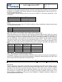
1
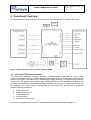
USER’S GUIDE
Date
: 12 April 2006
Doc. no. :C641xCPU_ml_bm_ug
Iss./Rev : 1.0
Page
:1
User’s Guide
micro-line® busmaster BSP
for the C6410CPU / C6413CPU / C6418CPU
Orsys Orth System GmbH, Am Stadtgraben 25, 88677 Markdorf, Germany
http://www.orsys.de
USER’S GUIDE
®
MICRO-LINE BUSMASTER BSP
Date
: 12 April 2006
Doc. no. : C641xCPU_ml_bm_ug
Iss./Rev : 1.0
Page
:2
Contents
1 PREFACE...................................................................................................................... 5
1.1
Document Organization ......................................................................................................... 6
1.2
Documentation Overview ...................................................................................................... 6
1.3
Notational conventions.......................................................................................................... 6
1.4
Trademarks ............................................................................................................................. 7
1.5
Revision History ..................................................................................................................... 8
2 FUNCTIONAL OVERVIEW ........................................................................................... 9
2.1 micro-line® Peripheral Interface ............................................................................................ 9
2.1.1 Interrupt Routing.................................................................................................................. 11
2.1.2 RDY Input............................................................................................................................ 12
2.2
Clock Outputs....................................................................................................................... 12
2.3 Main UART and Auxiliary UART.......................................................................................... 12
2.3.1 UART Software Support ...................................................................................................... 14
3 ADDRESS MAP .......................................................................................................... 15
3.1
C641xCPU Address Map...................................................................................................... 15
3.2 Address Map of the micro-line® Busmaster BSP .............................................................. 15
3.2.1 Bus Width Configuration...................................................................................................... 15
3.3 Address Mapping of the micro-line® Peripheral Interface ................................................ 16
3.3.1 Address Mapping Between the Processor and the micro-line® Bus.................................... 18
3.3.2 8-bit EMIF Configuration ..................................................................................................... 19
3.3.3 16 Bit EMIF Configuration ................................................................................................... 19
3.3.4 32 Bit EMIF Configuration ................................................................................................... 19
3.3.5 Default EMIF Bus Width Configuration................................................................................ 20
3.4 FPGA Register Description ................................................................................................. 21
3.4.1 FPGA Version Register (VER) ............................................................................................ 21
3.4.2 LED Control Register (LED) ................................................................................................ 21
3.4.3 Clock Control Register (CLK) .............................................................................................. 22
3.4.4 FPGA Interrupt Control and Status Register (INT) .............................................................. 23
3.4.5 RDY Polarity and Status Register (RDY) ............................................................................ 24
3.4.6 Auxiliary UART Enable Register (AUX_UART_EN) ............................................................ 25
3.4.7 UART Registers .................................................................................................................. 25
4 SETTING UP EMIF TIMINGS ...................................................................................... 26
5 SIGNALS ON THE MICRO-LINE® CONNECTOR....................................................... 27
USER’S GUIDE
®
MICRO-LINE BUSMASTER BSP
Date
: 12 April 2006
Doc. no. : C641xCPU_ml_bm_ug
Iss./Rev : 1.0
Page
:3
6 INDIVIDUAL SIGNAL DESCRIPTION......................................................................... 29
6.1 micro-line® Peripheral Interface .......................................................................................... 29
6.1.1 Connector A ........................................................................................................................ 29
6.1.2 Connector B ........................................................................................................................ 29
6.1.3 Connector D ........................................................................................................................ 29
6.2 Clock Outputs....................................................................................................................... 30
6.2.1 Connector E ........................................................................................................................ 30
6.3 RS-232 ................................................................................................................................... 31
6.3.1 Connector D ........................................................................................................................ 31
6.4 Auxiliary UART ..................................................................................................................... 31
6.4.1 Connector B ........................................................................................................................ 31
6.5 Other Signals ........................................................................................................................ 32
6.5.1 Connector BB ...................................................................................................................... 32
6.5.2 Connector C ........................................................................................................................ 32
6.5.3 Connector D ........................................................................................................................ 32
6.5.4 Connector E ........................................................................................................................ 32
7 INTERFACE CHARACTERISTICS ............................................................................. 33
7.1
Signal Levels ........................................................................................................................ 33
7.2
Signal Timings...................................................................................................................... 33
7.3
micro-line® Peripheral Interface Signal Timing ................................................................. 33
8 CONNECTION EXAMPLES ........................................................................................ 36
8.1
Peripheral Interface.............................................................................................................. 36
8.2
Auxiliary UART / RS-232 Connection Example.................................................................. 37
9 DEVELOPMENT SUPPORT ....................................................................................... 38
9.1
Software Development......................................................................................................... 38
9.2
FPGA Development.............................................................................................................. 38
10
LIST OF ABBREVIATIONS USED IN THIS DOCUMENT ........................................ 39
11
LITERATURE REFERENCES................................................................................... 40
USER’S GUIDE
®
MICRO-LINE BUSMASTER BSP
Date
: 12 April 2006
Doc. no. : C641xCPU_ml_bm_ug
Iss./Rev : 1.0
Page
:4
List of Tables
Table 1: Supported EMIF Settings for CE2 and CE3 address spaces............................................ 10
Table 2: UART_DIV settings for commonly used baud rates.......................................................... 14
Table 3: C641xCPU address map................................................................................................... 15
Table 4: Default address map of the micro-line® busmaster BSP ................................................... 15
Table 5: Usable chip select address space sizes for each bus width ............................................. 16
Table 6: Base addresses for each bus width .................................................................................. 16
Table 7: Allowed CE bus width configurations ................................................................................ 17
Table 8: Supported access types in 8-bit configuration................................................................... 19
Table 9: Supported access types in 16-bit configuration................................................................. 19
Table 10: supported access types in 32-bit configuration ............................................................... 20
Table 11: Default memory types for CE2 and CE3 ......................................................................... 20
Table 12: FPGA registers overview................................................................................................. 21
Table 13: Possible sources for the yellow LED ............................................................................... 22
Table 14: Timings for the CE2 and CE3 address spaces ............................................................... 26
Table 15: Pinout of connectors A, B and BB ................................................................................... 27
Table 16: Pinout of connectors C, D and E ..................................................................................... 28
Table 17: micro-line® bus timing...................................................................................................... 35
Table 18: Required cable connection to a host PC ......................................................................... 37
List of Figures
Figure 1: Block diagram of the micro-line® busmaster BSP .............................................................. 9
Figure 2: micro-line® peripheral interface ........................................................................................ 10
Figure 3: Interrupt routing by the micro-line® busmaster BSP......................................................... 12
Figure 4: UART block diagram ........................................................................................................ 13
Figure 5: Address mapping in 8-bit EMIF configuration .................................................................. 18
Figure 6: Address mapping in 16-bit EMIF configuration ................................................................ 18
Figure 7: Address mapping in 32-bit EMIF configuration ................................................................ 18
Figure 8: Recommended signal levels ............................................................................................ 33
Figure 9: micro-line® peripheral read cycle...................................................................................... 34
Figure 10: micro-line® peripheral write cycle ................................................................................... 34
Figure 11: Connecting a TL16C550 UART to the peripheral interface............................................ 36
Figure 12: Level converter schematic example............................................................................... 37
USER’S GUIDE
®
MICRO-LINE BUSMASTER BSP
Date
: 12 April 2006
Doc. no. : C641xCPU_ml_bm_ug
Iss./Rev : 1.0
Page
:5
1 Preface
This document describes the micro-line® busmaster board support package (BSP) for the
C6410CPU, C6413CPU and C6418CPU board family, which are referred to as C641xCPU
throughout this document. This BSP adds the following features to the C641xCPU (additional to
those described in [17]):
• micro-line® peripheral interface, including programmable interrupt inputs and clock outputs
• a main UART / RS-232 interface
• an auxiliary UART
• control of the yellow LED.
Most of the above listed features are similar to those of other micro-line® CPU modules, such as
the micro-line® C6211CPU board, providing an easy to use peripheral interface. The table below
lists which interfaces are always available on the C641xCPU and which features require usage of
this BSP.
Function
Provided by
DSP on-chip peripherals (HPI, McASP, McBSP, I2C,
GPIO, timers)
C641xCPU board hardware [17]
Reset inputs and outputs
External flags (XF pins)
micro-line® peripheral interface
RS-232 interface (main UART)
micro-line® busmaster BSP
Auxiliary UART
External DSP interrupts
Programmable clock outputs
With the micro-line® peripheral interface, peripherals can be easily connected to the C641xCPU,
using no or only minimal glue logic.
The RS-232 interface and the auxiliary UART support programmable baud rates, interrupts and
FIFO buffered receive and transmit operation for general-purpose serial communication. The RS232 interface has a level converter integrated on the C641xCPU and uses RS-232 signal levels,
whereas the auxiliary UART uses 3.3 V LVTTL signal levels.
This BSP is typically used for:
• migration from previous micro-line® CPU modules to the C641xCPU
• accessing micro-line® peripheral modules
• using the micro-line® peripheral interface to connect custom hardware
• using the RS-232 interface or the auxiliary UART for debug input/output during software
development
This document describes the features of the micro-line® busmaster BSP solely. The basic (FPGA
independent) features of the C641xCPU board are documented in [17].
Please note: To use this BSP, the FPGA must first be loaded with the appropriate code. How to do
this is shown in [18] and in the programming examples that are shipped together with the C641x
DSP Development Kit.
USER’S GUIDE
®
MICRO-LINE BUSMASTER BSP
1.1
Date
: 12 April 2006
Doc. no. : C641xCPU_ml_bm_ug
Iss./Rev : 1.0
Page
:6
Document Organization
This document is organized as follows:
• Chapter 2 gives an overview of the whole system and each function block
• Chapter 3 describes the available FPGA registers and their address mapping
• Chapter 4 shows how to set up the EMIF for use with this BSP
• Chapter 5 lists all signals available at the micro-line® connectors
• Chapter 6 describes each signal in detail
• Chapter 7 lists DC and switching characteristics of the signals
• Chapter 8 shows some connection examples
• Chapter 9 explains what is necessary for software development with this BSP
• Chapter 10 explains the abbreviations that are used throughout this document
• Chapter 11 lists documents that contain further information
1.2
Documentation Overview
This chapter lists the documentation from ORSYS that is shipped together with the C641xCPU.
Further documents from other vendors are listed in chapter 11 and are referenced throughout the
document in square brackets.
C641xCPU Hardware Reference Guide [17] (C641xCPU_hrg.pdf):
Describes the hardware of the C641xCPU board. It is intended to get an overview of the board and
the features provided by it. Detailed information about programming, usage of the FPGA and the
DSP is contained in other documents that will be referenced throughout this document.
C641xCPU DSP Development Kit User's Guide [18] (C641xCPU_DSP_DevKit_ug.pdf):
Describes software development for the C641xCPU board with DSP/BIOS and the micro-line®
board library. The micro-line® board library is a collection of low level drivers that allow the access
of hardware components on the C641xCPU, such as the RS-232 interface, the temperature sensor
etc. This makes the programming of the C641xCPU board easier.
User’s Guide micro-line® Power Supply Kit [19] (Power_Supply.pdf):
Describes the power supply board that is used for the DSP development kit.
UART IP Core, Type 01 [21] (UART_t01_ug.pdf):
Describes the UART that is used in this BSP. Only the BSP-specific details are described in this
document.
1.3
Notational conventions
Names of registers, bit fields and single bits are written in capital letters.
Example: HWCFG
Names of signals are also given in capital letters, active low signals are marked with a '/' at the
beginning of the name.
Example: /RESETIN
Signal names are given in capital letters. Signals that are active low (negated signals) are denoted
by a lowercase 'n' suffix. Example:
CPU_D0
(this is an active-high signal)
CPU_BE0n
(this is an active-low signal)
Configuration parameters, function names, path names and file names are written in italic typeface.
Example: dev_id
Date
: 12 April 2006
Doc. no. : C641xCPU_ml_bm_ug
Iss./Rev : 1.0
Page
:7
USER’S GUIDE
®
MICRO-LINE BUSMASTER BSP
Source code examples are given in a small, fixed-width typeface.
Example: int a = 10;
Menus and commands from menus and submenus are enclosed in double-quotes. Example:
Create a new project using the "Create Project..." command from the "File" menu.
The members of a bit field or a group of signals are numbered starting at zero, which is the least
significant bit.
Example: CFG[4:0] identifies a group of five signals, where CFG0 is the least significant bit and
CFG4 is the most significant bit.
If necessary, numbers are represented with a suffix that specifies their base.
Example: 12AB16 is a hexadecimal number (base 16 = hexadecimal) and is equal to 477910.
The bit fields of a register are displayed with the most significant bit to the left. Below each bit field
is a description of its read / write accessibility and its default value:
bit number
bit name
15
14
13
12
11
10
6
5
4
3
2
1
0
A
B
C
D
E
F
9
G
8
7
H
I
J
K
L
N
O
r,w,0
r,w,0
r,w,0
r,w,0
r,w,0
r,w,0
r,w,0102
r,0
r,wc,0
w
r,w,0
rc,0
r,w,0
r,w,0
accessibility and default value
legend:
r
bit is readable
rc
this bit is cleared after a read
r,w bit is readable and writeable, reading yields the previously written value unless otherwise
specified.
w
bit is writeable, read value is undefined
wc writing a 1 to this bit clears it
w,0 bit is write-only, reading always yields 0.
0
default value
1.4
Trademarks
TI, Code Composer, DSP/BIOS and TMS320C6000 are registered trademarks of Texas
Instruments.
Microsoft® and Windows® are either registered trademarks or
trademarks of Microsoft Corporation in the United States and/or other
countries.
Hyperterminal is a trademark of Hilgraeve Inc.
All other brand or product names are trademarks or registered trademarks of
their respective companies or organizations.
USER’S GUIDE
®
MICRO-LINE BUSMASTER BSP
1.5
Revision History
Revision
0.5
1.0
Changes
First preliminary version / January 2006
First release / April 2006
FPGA register addresses have changed
Date
: 12 April 2006
Doc. no. : C641xCPU_ml_bm_ug
Iss./Rev : 1.0
Page
:8
USER’S GUIDE
®
MICRO-LINE BUSMASTER BSP
Date
: 12 April 2006
Doc. no. : C641xCPU_ml_bm_ug
Iss./Rev : 1.0
Page
:9
2 Functional Overview
The block diagram below gives an overview of the FPGA connections on a C641xCPU board.
Figure 1: Block diagram of the micro-line® busmaster BSP
micro-line® Peripheral Interface
2.1
The micro-line® peripheral interface provides a straightforward connection to up to seven
peripheral boards or custom hardware devices without glue-logic. Its functionality is basically the
same as the direct connection to the TMS320C641x EMIF interface (in asynchronous operation
mode), or to the parallel bus of many other standard DSPs or micro-controllers. Based on the
powerful and comfortable TMS320C641x EMIF interface, the micro-line® peripheral interface can
be configured for a wide range of peripherals. On the C641xCPU, the micro-line® peripheral
interface basically consists of
•
•
•
•
•
32 data bus lines
24 address bus lines
7 chip select lines
5 interrupt lines
a number of control lines
Connection examples for the micro-line® peripheral interface can be found in chapter 8.1.
USER’S GUIDE
®
MICRO-LINE BUSMASTER BSP
Date
: 12 April 2006
Doc. no. : C641xCPU_ml_bm_ug
Iss./Rev : 1.0
Page
: 10
Figure 2: micro-line® peripheral interface
Figure 2 gives an overview of the available signals and their direction. For a detailed description of
the individual signals, please refer to chapter 6.
The C641xCPU allows different timings and different bus widths for EMIF CE2 and EMIF CE3
address spaces of the TMS320C641x DSP which reflect the chip select lines /CS1…/CS3 and
/CS4…/CS7 of the micro-line® peripheral interface. Therefore the bus access timing to connected
peripheral devices can be individually optimized within these two CE spaces without affecting other
components connected to other CE spaces. The timings for external micro-line® peripheral
interface accesses are based on the processor's external memory interface clock (EMIF clock).
which is 100 MHz by default. Several speed settings can be performed using the TMS320C641x
control registers for EMIF CE2 and EMIF CE3 address spaces which allow a wide range of microline® peripheral interface timings. The possible EMIF settings are shown in the table below.
EMIF Setting
Write Setup Time
Write Strobe Time
Write Hold Time
Read Setup Time
Read Strobe Time
Read Hold Time
Allowed range
1 to 15 clocks
1 to 63 clocks
0 to 3 clocks
1 to 15 clocks
1 to 63 clocks
0 to 7 clocks
Description
Address is valid and chip is enabled before write strobe is asserted
Write strobe is active
Address is valid and chip is enabled after write strobe is de-asserted
Address is valid and chip is enabled before read strobe is asserted
Time read strobe is active
Address is valid and chip is enabled after read strobe is de-asserted
Table 1: Supported EMIF Settings for CE2 and CE3 address spaces
The best values for micro-line® peripheral interface timings depend on:
• the minimum timing requirements for the FPGA
USER’S GUIDE
®
MICRO-LINE BUSMASTER BSP
•
Date
: 12 April 2006
Doc. no. : C641xCPU_ml_bm_ug
Iss./Rev : 1.0
Page
: 11
the fastest possible speeds which are allowed for the connected peripheral device(s).
The default timing (minimum timing required by the FPGA) is listed in chapter 4. The signal timing
of the micro-line® peripheral interface is described in chapter 7.
The board internal EMIF CE0 and EMIF CE1 space control registers should not be modified by
application software. These registers are set up to the correct values for the on-board peripherals
by the Flash File System. Modifying them may lead to an unstable or non-operating board status.
The EMIF control registers that control the micro-line® peripheral interface address space (EMIF
CE2 and EMIF CE3) are also set up by the Flash File System. They are set up for a slow and safe
timing, so that most peripherals can be connected without modification of the EMIF settings. These
two registers may be reprogrammed with a different timing and/or other bus width when needed,
see chapter 4 for details and default timings. Further information about the EMIF can be found in
[7].
How to access peripherals by application software is described in [18].
The bus width of the micro-line® peripheral interface is programmable and can be set to 8, 16 or
32 bit. The two separate chip select areas /CS1…/CS3 and /CS4…/CS7 can be programmed
independently. By this way one 32-bit bank with up to 3 peripheral devices and one 16-bit bank
with up to 4 peripheral devices can be realized, for example. Any other bus width combinations of
the two banks are possible. Normally the hardware bus width of an I/O device fits to the
corresponding data type, used by the software. If the software uses larger data types than the I/O
interface provides (e.g. 32-bit integer channeled through a 16-bit initialized I/O bank), the
processor will automatically perform several sequential I/O accesses at consecutive I/O addresses
in order to build the requested data value. Smaller software data types than corresponding I/O
bank settings are not always possible and may lead to invalid data. If, for example a 16-bit write
access is made to a 32-bit peripheral, data bits D[15:0] will be written correctly, but data bits
D[31:16] will be invalid. For a detailed description of allowed accesses, please refer to chapter
3.3.1.
2.1.1 Interrupt Routing
The TMS320C641x DSP has 5 dedicated external interrupt sources, the maskable interrupts
EXT_INT[7:4] and the non-maskable interrupt NMI. These interrupts are routed from micro-line®
connector D through the FPGA to the DSP. Within the FPGA, interrupt polarity can be configured
by the interrupt control register (see chapter 3.4.4). When changing the interrupt polarity, it is
recommended to use the interrupt control register and to leave the DSP's EXTPOL register at its
default value (rising edge triggered interrupts). The default setting of the interrupt control register is
to invert the interrupts, so that /INT[3:0] and /NMI are falling edge triggered.
Further, two additional interrupt sources exist within the FPGA:
• UART interrupts (RS-232 interface and auxiliary UART)
• Flash memory ready interrupts
These additional interrupt sources can be enabled / disabled through FPGA registers. The status
of all five interrupts can also be polled by application software. Please refer to 3.4.4 and [21] for
details.
USER’S GUIDE
®
MICRO-LINE BUSMASTER BSP
Date
: 12 April 2006
Doc. no. : C641xCPU_ml_bm_ug
Iss./Rev : 1.0
Page
: 12
Figure 3: Interrupt routing by the micro-line® busmaster BSP
2.1.2 RDY Input
Peripheral devices may expand the micro-line® peripheral interface access by hardware using the
RDY input. This allows
•
•
to access very slow peripherals, that require even slower timings than the EMIF supports
to access slow peripherals with the correct timing, while faster peripherals are accessed
with unexpanded bus cycles.
The polarity of the RDY input is programmable and the current state of the RDY input can be
polled, see chapter 3.4.5 for details.
De-asserting the ready (RDY) input line of the micro-line® peripheral interface during an I/O access
will keep the processor in a permanent wait-state as long as the RDY input line will remain inactive.
Only the assertion of the RDY input line will finalize the pending I/O bus cycle and allow the
processor to continue operation. If external hardware controlled I/O access timings are not
required, the RDY input line of the micro-line® peripheral interface should be left unconnected.
During development it is a good idea to configure the yellow LED to display non-ready conditions
(see chapter 3.4.2). This gives visual feedback. If the yellow LED is permanently on, then the
system is locked up by an access that is in a permanent non-ready condition.
2.2
Clock Outputs
The micro-line® busmaster BSP provides two clock outputs. Both clock outputs are programmable,
so that a wide range of clock frequencies can be generated. How to program the clock outputs is
described in chapter 3.4.3.
2.3
Main UART and Auxiliary UART
The FPGA design for the micro-line busmaster BSP uses an UART IP core. It is described in a
separate user guide [21]. The UART IP core is instantiated twice by the busmaster BSP: once as
main UART for the RS-232 interface and once for an auxiliary UART. The signals of the main
USER’S GUIDE
®
MICRO-LINE BUSMASTER BSP
Date
: 12 April 2006
Doc. no. : C641xCPU_ml_bm_ug
Iss./Rev : 1.0
Page
: 13
UART are routed over a RS-232 level converter to micro-line® connector D, whereas the signals of
the auxiliary UART are connected directly to micro-line® connector B.
Figure 4: UART block diagram
The auxiliary UART can be enabled and disabled in the FPGA'S auxiliary UART enable register
(see chapter 3.4.6). By default, the auxiliary UART is disabled and the signals AUX_RXD,
AUX_TXD, /AUX_CTS, /AUX_RTS on micro-line® connector B25 through B28 are in highimpedance state.
CAUTION:
The auxiliary UART signals are used as additional ground pins on a number of other micro-line®
boards. Therefore it must be ensured that no such ground connection exists in the system before
the auxiliary UART is enabled. Otherwise the board may be damaged.
CAUTION:
The auxiliary UART uses 3.3 V low-voltage TTL (LVTTL) signal levels. To connect a RS-232
device to the auxiliary UART an external RS-232 level converter must be used or the board will be
damaged.
Since the main UART signals are routed over an on-board RS-232 level converter to the microline® connector, external RS-232 devices like a PC can be connected directly. To use the auxiliary
UART as a RS-232 interface refer to the connection example in chapter 8.2.
The addresses of the UART registers are listed in Table 12. The interrupt outputs of the UARTs
are logically OR-combined with micro-line® interrupt /EXT_INT7 for the main UART and with microline® interrupt /EXT_INT5 for the auxiliary UART, therefore these interrupts are shared between the
micro-line® bus and the UARTs. To disable UART interrupts, simply clear all interrupt enable bits in
the corresponding UART_INT register. Both UARTs are clocked with an external 44.2368MHz
clock source. In contrast to the UART_CLK output on the micro-line bus, this clock source is not
programmable and therefore independent of the setting of the UART_DIV bit field in the CLK
register (see chapter 3.4.3).
USER’S GUIDE
®
MICRO-LINE BUSMASTER BSP
Date
: 12 April 2006
Doc. no. : C641xCPU_ml_bm_ug
Iss./Rev : 1.0
Page
: 14
The baud rate of the RS-232 interface is limited to 1Mbaud. Minimum baud rate is 42.2baud. Table
2 shows settings of the UART_DIV register for some commonly used baud rates and the maximum
baud rates.
baud rate
1200
2400
4800
9600
19200
38400
57600
76800
115200
230400
460800
921600
13824000
27648000
UART_DIV register setting
2303
1151
575
287
143
71
47
35
23
11
5
2
11
01
Table 2: UART_DIV settings for commonly used baud rates
2.3.1 UART Software Support
For the RS-232 interface, low level and high level drivers are included in development kits, such as
[18]. Application software can use these drivers to address the RS-232 interface as generalpurpose communication interface and use functions like fprintf(), and fgetc(), etc. for example to
transfer measurement results to a host system or to control a connected peripheral device. Another
common usage of the RS-232 interface is to output debugging information during testing.
Please note: When using the RS-232 interface in conjunction with a PC that runs Windows 2000 or
XP, the transmit buffer settings of the PC's COM port must be changed on the PC as described for
the Flash File System installation in [20].
Low-level drivers for the auxiliary UART are also included in the development kits.
1
Only supported by the auxiliary UART (without level converter).
USER’S GUIDE
®
MICRO-LINE BUSMASTER BSP
Date
: 12 April 2006
Doc. no. : C641xCPU_ml_bm_ug
Iss./Rev : 1.0
Page
: 15
3 Address Map
3.1
C641xCPU Address Map
The table below shows how the 4Gbyte address space of the C641xCPU is used. The CE spaces
CE1, CE2 and CE3 are used by the micro-line® busmaster BSP.
address range (hex)
0000 0000 – 7FFF FFFF
8000 0000 – 8FFF FFFF
9000 0000 – 900F FFFF
9010 0000 – 9015 7FFF
9015 8000 – 901F FFFF
9020 0000 – 9FFF FFFF
A000 0000 – AFFF FFFF
B000 0000 – BFFF FFFF
C000 0000 – FFFF FFFF
CE space
none
CE0
CE1
CE2
CE3
reserved
size (bytes)
2GB
256MB
1MB
352KB
672KB
254MB
256MB
256MB
1GB
description
internal memory and on-chip peripherals
external memory (SDRAM)
Flash memory segment
PLD register set
FPGA register set
Reserved (mirrored flash & registers)
FPGA registers and micro-line® peripheral
interface
Reserved
Table 3: C641xCPU address map
3.2
Address Map of the micro-line® Busmaster BSP
The table below shows, how the CE1, CE2 and CE3 address spaces are used by this BSP. Please
note, that the addresses refer to the default EMIF configuration, where CE2 is configured for 32-bit
accesses and CE1 and CE3 are configured for 16-bit accesses. The addressable address range
for each chip enable is limited to 20-bit addresses, thus 4MB within CE2 and 2MB within CE1 and
CE3 can be addressed. The address space CE2 is divided up in CS1 to CS3 with an addressable
address range of 1MB each. The address space CE3 is divided into CS4 to CS7 with an
addressable address range of 512KB each.
Address range (hex)
9015 8000 – 901F FFFF
A000 0000 – A00F FFFF
A010 0000 – A01F FFFF
A020 0000 – A02F FFFF
A030 0000 – AFFF FFFF
B000 0000 – B007 FFFF
B008 0000 – B00F FFFF
B010 0000 – B017 FFFF
B018 0000 – B01F FFFF
B020 0000 – BFFF FFFF
CE space
CE1
CE2
CE3
Size (bytes)
672KB
1MB
1MB
1MB
253MB
512KB
512KB
512KB
512KB
254MB
Description
FPGA registers (16-bit)
micro-line® CS1 (32-bit)
micro-line® CS2 (32-bit)
micro-line® CS3 (32-bit)
Reserved
micro-line® CS4 (16-bit)
micro-line® CS5 (16-bit)
micro-line® CS6 (16-bit)
micro-line® CS7 (16-bit)
Reserved
Table 4: Default address map of the micro-line® busmaster BSP
3.2.1 Bus Width Configuration
By default, the CE2 address space is configured for 32-bit bus width and CE3 is configured for 16bit bus width. This configuration allows a wide range of peripherals to be connected and can be
used in almost any cases.
However, in some special situations, it may be necessary to change the bus width, e.g. when
• more than three 32-bit chip select lines are needed (then CE3 must be configured to 32-bit,
so that /CS[7:4] are also available for 32-bit peripherals).
USER’S GUIDE
®
MICRO-LINE BUSMASTER BSP
•
•
Date
: 12 April 2006
Doc. no. : C641xCPU_ml_bm_ug
Iss./Rev : 1.0
Page
: 16
two peripherals with the same bus width must be operated with optimal timing and the RDY
input can't be used for some reason (then both, CE2 and CE3 must be configured to the
same bus width, but to different timings).
8-bit peripherals are used and their registers must be accessible as a contiguous address
space (then one of the CE spaces must be configured for 8-bit width).
When the bus width is changed, the address map (base addresses and size of the address range)
changes. The resulting changes are listed in the following tables.
For details on configuring the EMIF address spaces CE2 and CE3, please refer to [18] and [7].
Bus width
8-bit
16-bit
32-bit
Address space size
256KB
(256KB x 8 bit)
512KB
(256KB x 16 bit)
1024KB
(256KB x 32 bit)
Table 5: Usable chip select address space sizes for each bus width
Chip select
CS1
CS2
CS3
CS4
CS5
CS6
CS7
Base address (hex) for a bus width of
8-bit
16-bit
32-bit
A000 0000
A000 0000
A000 0000
A004 0000
A008 0000
A010 0000
A008 0000
A010 0000
A020 0000
B000 0000
B000 0000
B000 0000
B004 0000
B010 0000
B008 0000
B008 0000
B020 0000
B010 0000
B00C 0000
B030 0000
B018 0000
Table 6: Base addresses for each bus width
3.3
Address Mapping of the micro-line® Peripheral Interface
Up to seven peripheral boards can be connected to the micro-line® bus and can be accessed by
the CPU board independently. In order to distinguish the peripheral boards, the CPU board
generates seven different chip select signals. The chip select signals are decoded from the
processor's address bits A[22:21] and each chip select has an associated address range. All lower
18 processor address bits A[20:3] (which are connected to the micro-line® bus pins A[17:0]) can be
used to address specific locations within the peripheral boards. Thus each chip select space
provides 262144 (256K) different locations for accessing registers or memory on each peripheral
board. Each register or memory can be 8, 16 or 32-bit wide, depending on the EMIF configuration.
The chip select signals are assigned to two different address spaces of the processor (CE2 and
CE3) which can be individually configured for bus width and access timing. By default, CE2 is
configured for 32-bit operation (affects /CS1, /CS2, /CS3) and CE3 is configured for 16-bit
operation (affects /CS4, /CS5, /CS6, /CS7). This is done by the Flash File System, which is already
installed on the C641xCPU and the GEL files that are part of software development kits. The
configuration can be changed by modifying processor registers EMIF CE2 space control and EMIF CE3
space control, or by modifying the DSP/BIOS configuration file. For details please refer to [18] and
[7].
The base addresses for all three configurations are already shown in Table 6. The default
configuration is printed in bold format.
The CE space configuration must match the bus width (8/16/32-bit) of the widest peripheral that is
connected to this CE space (e.g. a combination of an 8-bit peripheral on CS4 and a 16-bit
peripheral on CS5 requires CE3 to be configured for at least 16-bit (32-bit configuration is also
allowed). Table 7 shows the possible combinations:
USER’S GUIDE
®
MICRO-LINE BUSMASTER BSP
EMIF configuration
8-bit
16-bit
32-bit
peripheral bus width
8-bit
16-bit
Ok (preferred) not allowed
Ok
Ok (preferred)
Ok
Ok
Date
: 12 April 2006
Doc. no. : C641xCPU_ml_bm_ug
Iss./Rev : 1.0
Page
: 17
32-bit
not allowed
not allowed
Ok (preferred)
Table 7: Allowed CE bus width configurations
The following rules must be obeyed when a user program accesses connected peripherals:
• Read accesses of a smaller size (compared to EMIF configuration) will read the correct
data. Example: EMIF is configured for 32-bit; address A004 0000 contains 7115 38A016.
reading 8-bit at address A004 0001 yields 3816 (C- notation: *(char *)0xA0040001 == 0x38).
• Write accesses of a smaller size (compared to EMIF configuration) are not allowed and will
corrupt peripheral data.
• Read and write accesses of a larger size (compared to EMIF configuration) will split the
access into two or four sequential hardware accesses. Example: EMIF is configured for 16bit, address A002 000016 contains 123416, address A002 000216 contains 567816, a 32-bit
read access ((int *)0xA002000) will cause two sequential accesses and will have a result of
5678123416.
• In 16-bit configuration, 16-bit and 32-bit accesses must use even addresses.
• In 32-bit configuration, 16-bit accesses must use even addresses.
• In 32-bit configuration, 32-bit accesses must use addresses that are multiples of four.
• In 8-bit configuration, each address on the micro-line® bus occupies 1 address (1 byte) of
the processor.
• In 16-bit configuration, one address on the micro-line® bus occupies 2 addresses (2 byte) of
the processor.
• In 32-bit configuration, one address location on the micro-line® bus occupies 4 addresses
(4 byte) of the processor.
USER’S GUIDE
®
MICRO-LINE BUSMASTER BSP
Date
: 12 April 2006
Doc. no. : C641xCPU_ml_bm_ug
Iss./Rev : 1.0
Page
: 18
3.3.1 Address Mapping Between the Processor and the micro-line® Bus
The examples below show accesses to the micro-line® /CS1 address space in different
configurations.
8-bit EMIF configuration
DSP address space
micro-line® address space
(A[19:0])
D0-7
A000 0000
A000 0001
A000 0002
A000 0003
A000 0004
A000 0005
D815
D16- D2423
31
0 0000
0 0001
0 0002
0 0003
0 0004
0 0005
Figure 5: Address mapping in 8-bit EMIF configuration
16-bit EMIF configuration
DSP address space
micro-line® address space
D0-7
A000 0000
A000 0001
A000 0002
A000 0003
A000 0004
A000 0005
A000 0006
A000 0007
LSB
0 0000
0 0001
0 0002
0 0003
MSB
LSB
MSB
D8-15
D16- D2423
31
LSB MSB
LSB MSB
LSB MSB
LSB
MSB
Figure 6: Address mapping in 16-bit EMIF configuration
32-bit EMIF configuration
DSP address space
micro-line® address space
D0-7
A000 0000
A000 0001
A000 0002
A000 0003
A000 0004
A000 0005
A000 0006
A000 0007
A000 0008
A000 0009
A000 000A
A000 000B
LSB
MSB
LSB
MSB
Figure 7: Address mapping in 32-bit EMIF configuration
0 0000
0 0001
0 0002
D8-15
LSB
D16- D2423
31
MSB
LSB
MSB
USER’S GUIDE
®
MICRO-LINE BUSMASTER BSP
3.3.2
•
•
•
Date
: 12 April 2006
Doc. no. : C641xCPU_ml_bm_ug
Iss./Rev : 1.0
Page
: 19
8-bit EMIF Configuration
Each location on the micro-line® bus represents 8-bit of data.
Data appears on D7 (MSB) to D0 (LSB)
Addresses appear unshifted on the micro-line® bus.
Access type
Width
direction
8-bit
read
8-bit
write
16-bit
read
16-bit
write
32-bit
read
32-bit
write
access to a peripheral of
8-bit
16-bit
32-bit
OK
n/a
n/a
OK
n/a
n/a
OK 2
n/a
n/a
OK 2
n/a
n/a
3
OK
n/a
n/a
OK 3
n/a
n/a
Table 8: Supported access types in 8-bit configuration
3.3.3
•
•
•
•
16 Bit EMIF Configuration
Each location on the micro-line® bus represents 16 bit of data.
Each location on the micro-line® bus starts on an even address.
Data appears on D15 (MSB) to D0 (LSB)
Addresses appear right-shifted by one bit on the micro-line® bus.
Access type
Width
direction
8-bit
read
8-bit
write
16-bit
read
16-bit
write
32-bit
read
32-bit
write
access to a peripheral of
8-bit
16-bit
32-bit
OK
OK 4
n/a
OK
n/a
n/a
n/a
OK
n/a
n/a
OK
n/a
n/a
OK 5
n/a
n/a
OK 5
n/a
Table 9: Supported access types in 16-bit configuration
3.3.4
•
•
•
•
2
3
4
5
32 Bit EMIF Configuration
Each location on the micro-line® bus represents 32 bit of data.
Each location on the micro-line® bus starts on an address that is a multiple of 4.
Data appears on D31 (MSB) to D0 (LSB)
Addresses appear right-shifted by two bit on the micro-line® bus.
Access will be split into two sequential accesses
Access will be split into four sequential accesses
reads only partial data: D[7:0] on address + 0, D[15:0] on address + 1
Access will be split into two sequential accesses
USER’S GUIDE
®
MICRO-LINE BUSMASTER BSP
Access type
Width
direction
8-bit
read
8-bit
write
16-bit
read
16-bit
write
32-bit
read
32-bit
write
Date
: 12 April 2006
Doc. no. : C641xCPU_ml_bm_ug
Iss./Rev : 1.0
Page
: 20
access to a peripheral of
8-bit
16-bit
32-bit
OK
OK6
OK7
OK
n/a
n/a
n/a
OK
OK8
n/a
OK
n/a
n/a
n/a
OK
n/a
n/a
OK
Table 10: supported access types in 32-bit configuration
3.3.5 Default EMIF Bus Width Configuration
The Flash File System (and the GEL file(s) on the distribution media) set up the EMIF to a default
configuration. Memory type and bus width of this default configuration is shown below. The default
timings are listed in chapter 4.
CE space
Memory type
CE2
CE3
asynchronous, 32-bit
asynchronous, 16-bit
Table 11: Default memory types for CE2 and CE3
Allowed memory types are:
• 8-bit asynchronous memory
• 16-bit asynchronous memory (default for CE3)
• 32-bit asynchronous memory (default for CE2)
6
reads only partial data: D[7:0] on address + 0, D[15:0] on address + 1
reads only partial data: D[7:0] on address + 0, D[15:0] on address + 1, D[23:16] on address + 2 and
D[31:24] on address + 3
8
reads only partial data: D[15:0] on address + 0, D[31:16] on address + 2
7
Date
: 12 April 2006
Doc. no. : C641xCPU_ml_bm_ug
Iss./Rev : 1.0
Page
: 21
USER’S GUIDE
®
MICRO-LINE BUSMASTER BSP
3.4
FPGA Register Description
This chapter describes each FPGA register in detail, with exception of the UART registers, which
are described in [21]. Below is an overview of the available FPGA registers.
Address
9018 000016
9018 000216
9018 000416
9018 000616
9018 000816
9018 000A16
9018 002016
9018 002216
9018 002416
9018 002616
9018 003016
9018 003216
9018 003416
9018 003616
Mnemonic
VER
LED
CLK
INT
RDY
AUX_UART_EN
UART_CSR
UART_DATA
UART_INT
UART_DIV
AUX_UART_CSR
AUX_UART_DATA
AUX_UART_INT
AUX_UART_DIV
Description
FPGA version register
LED control register
EMIF and UART clock control register
Interrupt status and control register
RDY polarity and status register
Auxiliary UART enable register
Main UART control and status register
Main UART receive and transmit data register
Main UART interrupt enable and flag register
Main UART baud rate divider register
Auxiliary UART control and status register
Auxiliary UART receive and transmit data register
Auxiliary UART interrupt enable and flag register
Auxiliary UART baud rate divider register
Table 12: FPGA registers overview
3.4.1 FPGA Version Register (VER)
This register describes version and revision of the currently loaded FPGA design. Application can
use this register to check that the correct FPGA code is loaded. This register is read-only.
15
14
13
12
11
10
9
8
7
6
5
4
3
VERSION
REVISION
r, 2
r, 0
2
1
0
VERSION
This bit field describes the FPGA version. Each BSP has a unique version. This BSP uses version
number 2. The version field can be used by application software to verify that the correct BSP is
loaded.
REVISION
This bit field describes BSP revision. The revision can change due to product improvement.
3.4.2 LED Control Register (LED)
This register controls the yellow LED that is connected to the FPGA.
15
5
4
3
0
RESERVED
LED_CTL
LED_SRC
r, 0
r, w, 0
r, w, 0000
LED_CTL
This bit controls the yellow LED when LED_SRC is set to 0. Setting this bit to 1 will cause the
yellow LED to light. By default, the yellow LED is off.
LED_SRC
This bit field selects the source that controls the yellow LED. By default the LED is controlled
manually by LED_CTL.
USER’S GUIDE
®
MICRO-LINE BUSMASTER BSP
LED_SRC
0
1
2
3
4
5
6
7
8
9
10
11
12
13
14
15
Date
: 12 April 2006
Doc. no. : C641xCPU_ml_bm_ug
Iss./Rev : 1.0
Page
: 22
Yellow LED controlled by
manual control by LED_CTL
SDRAM access (CE0)
PLD, flash or FPGA register access (CE1)
Chip select 1 access
Chip select 2 access
Chip select 3 access
Chip select 4 access
Chip select 5 access
Chip select 6 access
Chip select 7 access
DSP external interrupt 4 pending
DSP external interrupt 5 pending
DSP external interrupt 6 pending
DSP external interrupt 7 pending
Micro-line bus access (bus not ready)
Reserved
Table 13: Possible sources for the yellow LED
3.4.3 Clock Control Register (CLK)
This register controls the EMIF_CLK and UART_CLK outputs. EMIF_CLK is generated from the
DSP's EMIF clock. Possible EMIF clock frequencies are listed in chapter 4. Please note that
changing the EMIF_CLK on the micro-line® connector does not change the EMIF clock of the
DSP. All timings based on the EMIF clock (such as SDRAM timings or the asynchronous timings of
the seven micro-line® chip select lines) remain unchanged. UART_CLK is generated from an
independent 44.2368 MHz clock source. Both clock outputs can be completely disabled, switched
to permanent low state or programmed to different clock frequencies.
15
3
2
RESERVED
7
UART_EN
6
5
UART_DIV
4
RESERVED
EMIF_EN
1
EMIF_DIV
0
r, 0
r, w, 1
r, w, 10
r, 0
r, w, 1
r, w, 01
UART_EN:
This bit controls the UART clock output. If this bit is set to 1, the UART_CLK output is driven. If this
bit is set to 0, the UART_CLK line is in high impedance state. This bit can be used to reduce EMI
when UART_CLK if it is not used. Please note that changes to this bit immediately control the
UART_CLK output without synchronization. Therefore, glitches may occur when UART_EN is
modified while UART_DIV is set to a value different from zero.
UART_DIV:
This bit field controls the frequency of the UART_CLK output. By default, UART_DIV is set to 2,
which selects a frequency of 11.0592 MHz. Please note that changes to this bit field are
synchronized, so that UART_CLK always finishes the current clock period before the frequency is
changed. Together with UART_EN, the following selections are possible:
USER’S GUIDE
®
MICRO-LINE BUSMASTER BSP
UART_EN
0
1
UART_DIV
(don't care)
0
1
2
3
Date
: 12 April 2006
Doc. no. : C641xCPU_ml_bm_ug
Iss./Rev : 1.0
Page
: 23
UART clock output
Z
0
3.6864 MHz
11.0592 MHz
44.2368 MHz
EMIF_EN
This bit controls the EMIF clock output. If this bit is set to 1, the EMIF_CLK output is driven. If this
bit is set to 0, the EMIF_CLK line is in high impedance state. This bit can be used to reduce EMI
when EMIF_CLK if it is not used. Please note that changes to this bit immediately control the
EMIF_CLK output without synchronization. Therefore, glitches may occur when EMIF_EN is
modified while EMIF_DIV is set to a value different from zero.
EMIF_DIV
This bit field controls the frequency of the EMIF_CLK output. By default, EMIF_DIV is set to 1,
which selects a frequency of a quarter of the EMIF clock (25 MHz when a default EMIF clock of
100 MHz is used). Please note that changes to this bit field are synchronized by using the FPGA's
BUFGMUX primitives, so that EMIF_CLK always finishes the current clock period before the
frequency is changed. During changes, EMIF_CLK may stay low for some clock periods. Together
with EMIF_EN, the following selections are possible:
EMIF_EN
EMIF_DIV
EMIF clock output
0
(don't care)
Z
0
0
EMIF clock
1
4
1
EMIF clock
2
2
3
EMIF clock
3.4.4 FPGA Interrupt Control and Status Register (INT)
This register controls the polarity of external interrupt sources and represents the state of all
interrupt sources. Please note that the DSP is configured for rising edge triggered interrupts by
default. An application can also change the interrupt polarity to falling edge triggered by writing to
the DSP’s EXTPOL register. But when changing the interrupt polarity, it is recommended to use
the interrupt control register instead and leave the EXTPOL register at its default value.
15
14
RESERVED
r, 0
7
6
13
12
11
10
9
8
FRIE
NMI_POL
EINT7_POL
EINT6_POL
EINT5_POL
EINT4_POL
r, w, 0
r, w, 0
r, w, 0
r, w, 0
r, w, 0
r, w, 0
5
4
RESERVED
FRDY
NMI_STAT
r, 0
r, 1
r, 0
3
2
1
0
EINT7_STAT EINT6_STAT EINT5_STAT EINT4_STAT
r, 0
r, 0
r, 0
r, 0
FRIE:
Flash memory ready interrupt enable. If this bit is set and the flash memory changes its state from
busy to ready, an interrupt on EXT_INT6 is triggered. FRIE is disabled (set to 0) by default.
Application software does usually not need to access this bit.
NMI_POL, EINT7_POL, EINT6_POL,, EINT5_POL, EINT4_POL:
These bits control the polarity of the interrupt lines /NMI and /EXT_INT[7:4] on the micro-line® bus.
By default, these interrupts are falling edge triggered on the micro-line® bus and the DSP is
Date
: 12 April 2006
Doc. no. : C641xCPU_ml_bm_ug
Iss./Rev : 1.0
Page
: 24
USER’S GUIDE
®
MICRO-LINE BUSMASTER BSP
configured to rising edge triggered interrupts. Therefore the NMI_POL and EINTx_POL are set to 0
by default. To configure one of these interrupts to be rising edge triggered on the micro-line® bus,
set the corresponding bit to 1.
Programmable interrupt polarity gives the user more flexibility in connecting peripherals to the
C641xCPU.
NMI_POL, EINTx_POL
0
1
micro-line® interrupts
falling edge triggered
rising edge triggered
FRDY:
This bit reflects the current state of the flash ready/busy output. Application software does usually
not need to access this bit.
FRDY
0
1
micro-line® interrupts
flash memory is busy with programming or erasing
flash memory is ready
NMI_STAT, EINT7_STAT, EINT6_STAT, EINT5_STAT, EINT4_STAT:
These bits reflect the current state of the external interrupt inputs /NMI and /EXT_INT[7:4]. A set bit
means that an interrupt is currently pending, independent of its polarity. Application software can
use this register to check for external interrupts. This is especially necessary for /EXT_INT[7:5],
when the additional, internal interrupt sources (flash memory, UARTs) are also enabled. Pending
interrupts from flash or the UARTs are not indicated by EINT5_STAT .. EINT7_STAT, thus these
register bits reflect only the external interrupt state. Flash memory interrupts are indicated by the
FRDY bit (see description above) and UART interrupts are indicated in the UART_INT register, see
[21].
/NMI,
NMI_POL,
NMI_STAT,
Meaning
/EXT_INTx
EINTx_POL
EINTx_STAT
0
0
1
interrupt is pending
0
1
0
no interrupt
1
0
0
no interrupt
1
1
1
interrupt is pending
3.4.5 RDY Polarity and Status Register (RDY)
This register allows to control the polarity of the RDY input as well as to query the current state of
the RDY line. Application software uses this register to change the default polarity of the RDY input
and to check the current (idle) state of the RDY input.
15
2
RESERVED
r, 0
1
0
RDY_STAT
RDY_POL
r, 1
r, w, 0
RDY_STAT
This bit reflects the current state of the RDY input, independent of the RDY_POL setting. It can be
used by application software to check the idle state of the RDY input in order to avoid lock-ups.
However, if the externally connected hardware drives the RDY input only on access, checking
RDY_STAT can not guarantee that the external hardware uses the correct polarity. It is also a
good practice to configure the yellow LED to display non-ready conditions (see chapter 3.4.2)
during software development. This gives visual feedback of deadlock situations caused by a
permanently inactive RDY input.
USER’S GUIDE
®
MICRO-LINE BUSMASTER BSP
RDY input
0
0
1
1
RDY_POL
0
1
0
1
RDY_STAT
0
1
1
0
Date
: 12 April 2006
Doc. no. : C641xCPU_ml_bm_ug
Iss./Rev : 1.0
Page
: 25
Meaning
not ready
ready
ready
not ready
RDY_POL
This bit controls the polarity of the RDY input. By default, it is set to 0 which means that RDY is
active high, thus a logic 1 indicates a ready condition. For externally connected hardware that has
an active-low RDY output, such as the C641xCPU host port interface, RDY_POL must be set to 1.
See also the table above for encoding of RDY_POL.
3.4.6 Auxiliary UART Enable Register (AUX_UART_EN)
The auxiliary UART enable register controls wheter athe auxiliary UART is enabled or not. This
avoids porblems with systems whre the auxiliary UART signals are used as additional ground pins,
such as previous micro-line boards.
15
1
RESERVED
r, 0
0
AUART_EN
r, w, 0
AUART_EN
Auxiliary UART enable bit. If this bit is set the auxiliary UART’s outputs are enabled. Otherwise the
signals AUX_TXD, and /AUX_RTS on micro-line® connector pins B25 and B26 are in highimpedance state. The auxiliary UART is directly routed to the micro-line® connector, without a level
converter.
The auxiliary UART must not be enabled in systems that use B25..B28 as ground pins. See also
2.3.
3.4.7 UART Registers
The C641xCPU-specific address mapping of the UART registers is in Table 4. For a detailed
description of the UART registers, please refer to [21].
USER’S GUIDE
®
MICRO-LINE BUSMASTER BSP
Date
: 12 April 2006
Doc. no. : C641xCPU_ml_bm_ug
Iss./Rev : 1.0
Page
: 26
4 Setting up EMIF Timings
This chapter shows, which timings can be used for accesses to
• the FPGA registers
• the micro-line® peripheral interface
By default, the Flash File System sets up the EMIF timings for the CE2 and CE3 address space to
a slow and safe default. This default work with the FPGA as well as with most peripherals.
However, using these defaults does not give optimum performance, so the user may want to
modify the EMIF settings. This is typically done in the DSP/BIOS configuration file (see [18]), but
can also be done by modifying the CE space control registers at application start (see [7] and [14]).
The actual timings depend on:
• The timing requirements for the FPGA. These are the minimum timings. They give optimum
performance for high speed data transfers.
• The timing requirements of connected peripherals. These timings depend on the connected
hardware. If they are compliant with the timings listed in chapter 7.3, the minimum settings
can be used.
Table 14 lists the minimum required timings, the default timings set up by the Flash File System
and the maximum timings for CE2 and CE3 (micro-line® peripheral interface).
parameter
read setup
read strobe
read hold
turnaround
write setup
write strobe
write hold
EMIF clocks
min
default
max
2
3
15
9
4
10
63
2
3
3
0
2
3
2
3
15
49
10
63
2
3
7
time in ns at 100MHz EMIF clock
min
default
Max
20
30
150
40
100
630
20
30
30
0
20
30
20
30
150
40
100
630
20
30
70
Table 14: Timings for the CE2 and CE3 address spaces
9
When ML_RDY is used the minimum read and write strobe are 5 EMIF clocks (50ns)
Date
: 12 April 2006
Doc. no. : C641xCPU_ml_bm_ug
Iss./Rev : 1.0
Page
: 27
USER’S GUIDE
®
MICRO-LINE BUSMASTER BSP
5 Signals on the micro-line® Connector
This chapter lists the signals on the micro-line® connectors that are defined by this BSP. For a
description of the remaining signals and connector locations, please refer to [17].
Pin
No.
1
2
3
4
5
6
7
8
9
10
11
12
13
14
15
16
17
18
19
20
21
22
23
24
25
26
27
28
A
D0 (I/O/Z)
D1 (I/O/Z)
D2 (I/O/Z)
D3 (I/O/Z)
D4 (I/O/Z)
D5 (I/O/Z)
D6 (I/O/Z)
D7 (I/O/Z)
D8 (I/O/Z)
D9 (I/O/Z)
D10 (I/O/Z)
D11 (I/O/Z)
D12 (I/O/Z)
D13 (I/O/Z)
D14 (I/O/Z)
D15 (I/O/Z)
D16 (I/O/Z)
D17 (I/O/Z)
D18 (I/O/Z)
D19 (I/O/Z)
D20 (I/O/Z)
D21 (I/O/Z)
D22 (I/O/Z)
D23 (I/O/Z)
D24 (I/O/Z)
D25 (I/O/Z)
D26 (I/O/Z)
D27 (I/O/Z)
B
A0 (O/Z)
A1 (O/Z)
A2 (O/Z)
A3 (O/Z)
A4 (O/Z)
A5 (O/Z)
A6 (O/Z)
A7 (O/Z)
A8 (O/Z)
A9 (O/Z)
A10 (O/Z)
A11 (O/Z)
A12 (O/Z)
A13 (O/Z)
A14 (O/Z)
A15 (O/Z)
A16 (O/Z)
A17 (O/Z)
A18 (O/Z)
A19 (O/Z)
A20 (O/Z)
A21 (O/Z)
A22 (O/Z)
A23 (O/Z)
AUX_TXD
/AUX_RTS
AUX_RXD
/AUX_CTS
Connector
29
D28 (I/O/Z)
Signal GND
30
D29 (I/O/Z)
Signal GND
31
D30 (I/O/Z)
Signal GND
32
D31 (I/O/Z)
Signal GND
BB
HD0 (I/O/Z)
HD1 (I/O/Z)
HD2 (I/O/Z)
HD3 (I/O/Z)
HD4 (I/O/Z)
HD5 (I/O/Z)
HD6 (I/O/Z)
HD7 (I/O/Z)
HD8 (I/O/Z)
GPO[8] (I/O/Z)
HD9 (I/O/Z)
GPO[9] (I/O/Z)
HD10 (I/O/Z)
GPO[10] (I/O/Z)
HD11 (I/O/Z)
GPO[11] (I/O/Z)
HD12 (I/O/Z)
GPO[12] (I/O/Z)
HD13 (I/O/Z)
GPO[13] (I/O/Z)
HD14 (I/O/Z)
GPO[14] (I/O/Z)
HD15 (I/O/Z)
GPO[15] (I/O/Z)
HHWIL (I)
AFSR1[2] (I)
HCNTL0 (I)
AFSR1[1] (I)
HCNTL1 (I)
/HAS (I) 10
ACLKR1[1] (I)
HR/W (I)
AFSR1[3] (I)
/HCS (I)
ACLKR1[2] (I)
/HRD_HSTRB (I)
ACLKR1[3] (I)
/HWR_HSTRB (I)
/HRDY (O)
/HINT (O)
Reserved 11
11
Reserved
11
SCL1 (I/O/Z)
Reserved
Pin
No.
1
2
3
4
5
6
7
8
9
10
11
12
13
14
15
16
17
18
19
20
21
22
23
24
25
26
27
28
29
Reserved
11
SDA1 (I/O/Z)
30
Reserved
11
SCL0 (I/O/Z)
31
Reserved
11
SDA0 (I/O/Z)
32
Table 15: Pinout of connectors A, B and BB
This function is always provided by the C641xCPU Hardware, independent of this BSP
10
11
This signal should not be used and this pin should be left open.
Connected to the FPGA, but not used by the micro-line® busmaster BSP
USER’S GUIDE
®
MICRO-LINE BUSMASTER BSP
Date
: 12 April 2006
Doc. no. : C641xCPU_ml_bm_ug
Iss./Rev : 1.0
Page
: 28
Pin
No.
1
C
AXR0[0] (I/O/Z)
Connector
D
Power GND (I)
Reserved
11
2
AXR0[1] (I/O/Z)
Power GND (I)
Reserved
11
2
Reserved
11
3
Reserved
11
4
Reserved
11
5
Reserved
11
6
Reserved
11
7
Reserved
11
8
11
9
3
AXR0[2] (I/O/Z)
Power GND (I)
4
AXR0[3] (I/O/Z)
Power GND (I)
5
AXR0[4] (I/O/Z)
+3.3V (I)
6
AXR0[5] (I/O/Z)
+3.3V (I)
7
ACLKR0 (I/O/Z)
/RESETIN (I)
E
Pin
No.
1
8
AHCLKR0 (I/O/Z)
/RESETOUT (O)
9
AFSR0 (I/O/Z)
RESETOUT (O)
10
11
12
13
14
15
ACLKX0 (I/O/Z)
AHCLKX0 (I/O/Z)
AFSX0 (I/O/Z)
AMUTEIN0 (I)
AMUTE0 (I/O/Z)
11
Reserved
/CS1 (O)
/CS2 (O)
/CS3 (O)
/CS4 (O)
/CS5 (O)
/CS6 (O)
Reserved
DR1 (I)
DX1 (O/Z)
CLKR1 (I/O/Z)
CLKX1 (I/O/Z)
FSR1 (I/O/Z)
FSX1 (I/O/Z)
/CS7 (O)
CLKS1 (I)
16
/EXT_INT4 (I)
/EXT_INT5 (I)
/EXT_INT6 (I)
/EXT_INT7 (I)
/NMI (I)
/RD (O)
/WR (O)
R/W (O)
/STRB (O)
TXD (O)
RTS (O)
RXD (I)
CTS (I)
RDY (I)
11
Reserved
TINP1 (I)
TINP0 (I)
CLKS0 (I)
DR0 (I)
DX0 (O/Z)
CLKR0 (I/O/Z)
CLKX0 (I/O/Z)
FSR0 (I/O/Z)
FSX0 (I/O/Z)
XF0 (I/O/Z)
XF1 (I/O/Z)
TOUT0 (O/Z)
TOUT1 (O/Z)
UART_CLK (O/Z)
EMIF_CLK (O/Z)
17
18
19
20
21
22
23
24
25
26
27
28
29
30
31
Signal GND
32
16
11
17
18
19
20
21
22
23
24
25
26
27
28
29
30
31
Reserved
AXR1[0] (I/O/Z)
HD16 (I/O/Z)
AXR1[1] (I/O/Z)
HD17 (I/O/Z)
AXR1[2] (I/O/Z)
HD18 (I/O/Z)
AXR1[3] (I/O/Z)
HD19 (I/O/Z)
AXR1[4] (I/O/Z)
HD20 (I/O/Z)
AXR1[5] (I/O/Z)
HD21 (I/O/Z)
AFSX1 (I/O/Z)
HD22 (I/O/Z)
AFSR1 (I/O/Z)
HD23 (I/O/Z)
ACLKX1 (I/O/Z)
HD24 (I/O/Z)
ACLKR1 (I/O/Z)
HD25 (I/O/Z)
AHCLKR1 (I/O/Z)
HD26 (I/O/Z)
AHCLKX1 (I/O/Z)
HD27 (I/O/Z)
AMUTE1 (I/O/Z)
HD28 (I/O/Z)
AMUTEIN1 (I)
HD29 (I/O/Z)
HD30 (I/O/Z)
32
HD31 (I/O/Z)
Reserved
11
Table 16: Pinout of connectors C, D and E
This function is always provided by the C641xCPU Hardware, independent of this BSP
10
11
12
13
14
15
USER’S GUIDE
®
MICRO-LINE BUSMASTER BSP
Date
: 12 April 2006
Doc. no. : C641xCPU_ml_bm_ug
Iss./Rev : 1.0
Page
: 29
6 Individual Signal Description
This chapter describes each signal that is defined by this BSP. The remaining signals (shadowed
entries in the pinout tables) are described in [17]. The signals are listed sorted by the respective
interface, connector and then by their importance.
6.1
micro-line® Peripheral Interface
6.1.1 Connector A
D[31:0]:
These are the bi-directional data bus lines of the micro-line® peripheral interface. They are driven
during the strobe phase (DSP signal /AWE active) of a write access to the micro-line® peripheral
interface. When inactive, the data bus is held in its previous state by a bus holder to avoid floating
inputs.
6.1.2 Connector B
A[23:0]:
These are the address bus output lines of the micro-line® peripheral interface. They are activated
during the entire micro-line® peripheral interface access (while CE2 or CE3 are active), otherwise
they are held in their previous state by a bus holder to avoid floating inputs. A[19:0] are
addressable by application software, whereas A[23:20] are always driven low. These address lines
can only be used by a customized FPGA design.
6.1.3 Connector D
/CS[7:1]:
These are the seven active low chip select output lines of the micro-line® peripheral interface. They
pre-select, which external peripheral component has to be accessed during a micro-line®
peripheral access. They are activated (driven low) during the entire micro-line® peripheral interface
access (while CE2 or CE3 are active). The seven peripheral address spaces are located in the
processor's CE2 and CE3 address spaces. The chip select lines /CS1…/CS3 refer to the EMIF
CE2 area of the processor and /CS4…/CS7 refer to the EMIF CE3 area of the processor. This
allows two different I/O areas, each with three or four possible peripheral devices which have an
optimized connection to the processor regarding bus timing and bus width. The locations of the
seven peripheral address spaces are shown in chapter 3.2.
/RD, /WR:
These are the active low read strobe (/RD) and write strobe (/WR) output lines of the micro-line®
peripheral interface. They indicate a read cycle (/RD) or a write cycle (/WR) of the micro-line®
peripheral interface and are activated (driven low) during the strobe phase of an access. In case of
a read cycle, data is latched at the rising edge of /RD. Write data is valid prior the rising edge of
/WR. These signals should be used when separate read and write strobes are required (classic
INTEL peripherals). Peripherals with a common strobe and a direction select signal (classic
Motorola peripherals) should be used with R/W and /STRB instead. These signals have a 10kΩ
pull-up resistor to guarantee inactive signals when the FPGA is not loaded.
R/W, /STRB:
These are the read/write (R/W) and the active low strobe (/STRB) output lines of the micro-line®
peripheral interface. They indicate a dedicated read cycle (R/W = high and /STRB = low) or a
dedicated write cycle (R/W = low and /STRB = low) of the micro-line® peripheral interface and are
activated (driven low) during the strobe phase of an access. These signals should be used to
connect peripherals that require a common strobe signal and a direction select signal (classic
Motorola peripherals). Peripherals with separate read and write strobes (classic Intel peripherals)
USER’S GUIDE
®
MICRO-LINE BUSMASTER BSP
Date
: 12 April 2006
Doc. no. : C641xCPU_ml_bm_ug
Iss./Rev : 1.0
Page
: 30
should be used with /RD and /WR instead. /STREB has a 10kΩ pull-up resistor to guarantee an
inactive signal when the FPGA is not loaded.
RDY:
This pin is the active high ready input of the micro-line® peripheral interface. During the
programmed strobe period, the RDY input is sampled by the DSP. If RDY is sampled low, the
strobe period is extended by one EMIF clock and RDY is sampled again. If RDY is sampled high,
the strobe period ends. If no peripheral interface hardware bus cycle extensions are required, RDY
should be left unconnected. The necessary 4.7kΩ pull up resistor is provided on the C641xCPU.
This input can be used by
• very slow hardware, whose timing exceeds the maximum EMIF timing
• a mixture of fast and slow peripherals, where the EMIF timing is configured for the fast
peripherals, but the slow peripherals can extend the access for their timing requirements.
This way, the slow peripherals don't slow down accesses to the fast ones.
RDY can also be programmed to be active low. In this case, the board hardware must be modified
from a pull-up resistor to a pull-down resistor. Please refer to chapter 3.4.5 and to [17] for details.
/EXT_INT[7:4]:
These are the four maskable interrupt input lines of the micro-line® peripheral interface. They can
be used as interrupts or for DMA synchronization. In default configuration, all interrupts are
triggered on the falling edge of the interrupt signal (in contrast to the default polarity of the DSP
interrupt lines). /EXT_INT[7:4] can be individually configured to be either falling edge triggered or
rising edge triggered. This is described in chapter 3.4.4. Level triggering is not possible at the
TMS320C641x DSP. The line status of the interrupt lines can be individually polled by software
(also described in chapter 3.4.4). To enable interrupts from the micro-line® peripheral interface, the
interrupts must be enabled by the DSP.
Please note, that other interrupt sources exist on the C641xCPU for /EXT_INT5, /EXT_INT6 and
/EXT_INT7. Before designing peripheral hardware to use a specific micro-line® interrupt, please
check which on-board interrupt sources of the C641xCPU are used. Shared interrupts can be
used, but avoiding them makes the system easier and faster. See chapter 2.1.1 for the other
interrupt sources. /EXT_INT[7:4] have 10kΩ pull-up resistors to avoid false interrupt triggering
when the FPGA is not loaded.
/NMI:
This is the non-maskable interrupt input line of the micro-line® peripheral interface. Activation of
/NMI causes an interrupt at a high priority level which can not be masked by software. In default
configuration, /NMI is triggered on the falling edge of the interrupt signal (in contrast to the DSP's
NMI signal, which is rising edge triggered). It can be configured to be either falling edge triggered
or rising edge triggered. This is described in chapter 3.4.4. Level triggering is not possible. /NMI
has a10kΩ pull-up resistors to avoid false interrupt triggering when the FPGA is not loaded.
6.2
Clock Outputs
6.2.1 Connector E
UART_CLK:
This output provides a programmable clock source for external hardware, which is suitable to
supply UART devices. It can be programmed to 3 different frequencies and also be switched off.
Frequency switching (with exception of switching to / from high impedance state) is done glitchfree. Please refer to chapter 3.4.3 for details on clock control. In order to reduce EMI it is
recommended to switch off this signal if it is not used. UART_CLK is connected through a 22R
series resistor to reduce EMI.
USER’S GUIDE
®
MICRO-LINE BUSMASTER BSP
Date
: 12 April 2006
Doc. no. : C641xCPU_ml_bm_ug
Iss./Rev : 1.0
Page
: 31
EMIF_CLK:
This pin is the clock output for the micro-line® peripheral interface. This clock is generated from the
external memory interface clock. The clock output on this pin is software programmable to 3
different frequencies. By default, the DSP EMIF clock divided by 4 is available on this signal. See
chapter 3.4.3 for details. Frequency switching (with exception of switching to / from high
impedance state) is done glitch-free. In order to reduce EMI it is recommended to switch off this
signal if it is not used. There is a typical delay of 8 ns between the EMIF clock output of the
processor and the EMIF_CLK signal on the micro-line® connector, however, this timing is not
guaranteed. Please note, that the frequency of this signal does not affect any timing of the
TMS320C641x EMIF. EMIF_CLK is connected through a 22Ω series resistor to reduce EMI.
6.3
RS-232
Please note: A more detailed functional description of the RS-232 signals can be found in [21].
6.3.1 Connector D
TXD
This pin is the transmit data output of the RS-232 interface. Output voltage is either -5.5 V (typical)
or +5.5 V (typical). This output can be disabled by putting the RS-232 level converter in shut down
mode, see [17] for details.
RTS
This pin is the ready to send output of the RS-232 interface. Output voltage is either -5.5 V (typical)
or +5.5 V (typical). This output can be disabled by putting the RS-232 level converter in shut down
mode, see [17] for details.
RXD
This pin is the receive data input of the RS-232 interface. This pin accepts RS-232 signal levels
from –10 V to +10 V. An internal 5kΩ pull down resistor to GND is integrated in the line receiver.
CTS
This pin is the clear to send input of the RS-232 interface. This pin accepts RS-232 signal levels
from –10 V to +10 V. An internal 5kΩ pull down resistor to GND is integrated in the line receiver.
The CTS pin can also be used as a reset input. The reset generation is controlled by the PLD, see
[17] for details
6.4
Auxiliary UART
Please note: A more detailed functional description of the auxiliary UART signals can be found in
[21].
6.4.1 Connector B
AUX_TXD:
This pin is the transmit data output of the auxiliary UART. Output voltage is 0 V or +3.3 V. This
output can be disabled by disabling the auxiliary UART, see chapter 3.4.6.
/AUX_RTS:
This pin is the ready to send output of the auxiliary UART. Output voltage is 0 V or +3.3 V. This
output can be disabled by disabling the auxiliary UART, see chapter 3.4.6.
AUX_RXD:
This pin is the receive data input of the auxiliary UART. Allowed input voltage is 0 V .. 3.3 V.
/AUX_CTS:
This pin is the clear to send input of the auxiliary UART. Allowed input voltage is 0 V .. 3.3 V.
USER’S GUIDE
®
MICRO-LINE BUSMASTER BSP
6.5
Date
: 12 April 2006
Doc. no. : C641xCPU_ml_bm_ug
Iss./Rev : 1.0
Page
: 32
Other Signals
6.5.1 Connector BB
BB[32..27]:
These pins are routed to the FPGA but are not used by the busmaster BSP.
6.5.2 Connector C
C[16..15]:
These pins are routed to the FPGA but are not used by the busmaster BSP.
6.5.3 Connector D
D[32:31]:
These pins are routed to the FPGA but are not used by the busmaster BSP. These signals have a
10k Ω pull-up resistor.
6.5.4 Connector E
EE[9:1]:
These pins are routed to the FPGA but are not used by the busmaster BSP.
USER’S GUIDE
®
MICRO-LINE BUSMASTER BSP
Date
: 12 April 2006
Doc. no. : C641xCPU_ml_bm_ug
Iss./Rev : 1.0
Page
: 33
7 Interface Characteristics
7.1
Signal Levels
All signals described in this document, with exception of the RS-232 interface, use LVTTL signal
levels. The recommended voltage levels are listed below:
parameter
logic low input voltage
logic high input voltage
logic low output voltage 12
logic high output voltage 12
value
min
max
-0.5 V 0.8 V
2.0 V
3.6 V
0.4 V
2.4 V
Figure 8: Recommended signal levels
All outputs that are driven by the FPGA are configured for a drive capability of 12mA.
For signals driven by the DSP, such as /HRD, please refer to [4].
7.2
Signal Timings
All timing specifications in this chapter apply to FPGA V1.0, using the minimal EMIF settings as
listed in Table 14.
7.3
micro-line® Peripheral Interface Signal Timing
The timings of the micro-line® peripheral interface are basically the same as for the EMIF of the
TMS320C641x DSP. However, the FPGA adds some delays to them. If any of the timing
requirements listed in Table 17 can't be met, the EMIF settings for the respective CE space need
to be increased.
12
at 12mA load
USER’S GUIDE
®
MICRO-LINE BUSMASTER BSP
A0 .. A15
/CSx
R/W
/RD, /STRB
D0 .. D31
RDY
th2
th1
ts3
ts1
ts2
th3
Figure 9: micro-line® peripheral read cycle
A0 .. A15
/CSx
R/W
/WR, /STRB
D0 .. D31
RDY
th2
ts4 th1
ts1
ts2
Figure 10: micro-line® peripheral write cycle
td1
Date
: 12 April 2006
Doc. no. : C641xCPU_ml_bm_ug
Iss./Rev : 1.0
Page
: 34
USER’S GUIDE
®
MICRO-LINE BUSMASTER BSP
Parameter
Setup time A[23:0], /CS[7:1], R/W valid before /RD, /WR, /STRB low
Hold time A[23:0], /CS[7:1], R/W valid after /RD, /WR, /STRB high
Setup time RDY valid before rising edge of /RD, /WR, /STRB
Hold time RDY valid after rising edge of /RD, /WR, /STRB
Setup time D[31:0] valid before rising edge of /RD, /STRB (read)
Hold time D[31:0] valid after rising edge of /RD, /STRB (read)
Setup time D[31:0] valid before rising edge of /WR, /STRB (write)
Delay time D[31:0] high impedance after /WR, /STRB high (write)
Table 17: micro-line® bus timing
Date
: 12 April 2006
Doc. no. : C641xCPU_ml_bm_ug
Iss./Rev : 1.0
Page
: 35
name
ts1
th1
ts2
th2
ts3
th3
ts4
td1
min
Max
5 ns
5 ns
35 ns
0 ns
35 ns
0 ns
20 ns
15 ns
USER’S GUIDE
®
MICRO-LINE BUSMASTER BSP
Date
: 12 April 2006
Doc. no. : C641xCPU_ml_bm_ug
Iss./Rev : 1.0
Page
: 36
8 Connection Examples
8.1
Peripheral Interface
Peripheral devices can be easily connected to the micro-line® peripheral interface of the
C641xCPU. An example of connecting a TL16C550 UART to the C641xCPU board is shown
below. The reset input of the TL16C550 is active high. Thus the active high reset output
RESETOUT is used. The active low address strobe (/ADS) is connected to DGND. That is, the
internal select logic is driven directly by the address pins (A0..A2) and the chip select pins (CS0,
CS1 and /CS2). Since CS0 and CS1 are always active the TL16C550 is selected by /CS2.
The EMIF timings need to be modified to a slower timing, depending on the speed grade of the
TL16C550 device.
Figure 11: Connecting a TL16C550 UART to the peripheral interface
Note 1:
The TL16C550 interrupt INTRPT is high active. Since the interrupts EXT_INTn of the C641xCPU
are negative edge triggered by default the used interrupt must be set to rising edge triggered in the
FPGA Interrupt Control Register (see 3.4.4).
USER’S GUIDE
®
MICRO-LINE BUSMASTER BSP
8.2
Date
: 12 April 2006
Doc. no. : C641xCPU_ml_bm_ug
Iss./Rev : 1.0
Page
: 37
Auxiliary UART / RS-232 Connection Example
As opposed to the main UART, the auxiliary UART is not connected to an on-board RS-232 level
converter. The auxiliary UART signals AUX_TXD, AUX_RXD, /AUX_RTS and /AUX_CTS are
routed directly from the FPGA to the micro-line® connector B. The output standard of these pins is
3.3 V low-voltage TTL (LVTTL). To connect an RS-232 device an external RS-232 level converter
(3.3V type recommended) must be connected.
Figure 12 shows an example schematic for a suitable level converter and Table 18 shows the
required cable wiring for a connection to a PC.
Figure 12: Level converter schematic example
Signal
RXD
TXD
RTS
CTS
GND
Level converter
Sub-D 9 pin Sub-D 25 pin
2
3
3
2
7
4
8
5
5
7
Host PC
Sub-D 9 pin
3
2
8
7
5
Table 18: Required cable connection to a host PC
Sub-D 25 pin
2
3
5
4
7
USER’S GUIDE
®
MICRO-LINE BUSMASTER BSP
Date
: 12 April 2006
Doc. no. : C641xCPU_ml_bm_ug
Iss./Rev : 1.0
Page
: 38
9 Development Support
9.1
Software Development
The micro-line® busmaster BSP is supported by the DSP Development Kit (documented in [18]),
which contains
• a description of the BSP features as a C-header file
• low level access functions for the board hardware
• drivers for the UART and the temperature sensor
• documentation and example code for accessing the BSP features
• documentation and example code for loading the FPGA
• application examples that use the TI chip support library and DSP/BIOS
Together with the DSP development kit, Code Composer Studio from Texas Instruments is
required. Further, the use of an emulator, such as the XDS510 is required.
9.2
FPGA Development
FPGA Development is supported by a separate FPGA development package. This package
contains the FPGA design of the micro-line busmaster BSP as a project with most parts of the
design provided as VHDL source code. Together with the FPGA development package,
development tools from Xilinx [2] are required. For the C641xCPU, the free WebPack is sufficient.
USER’S GUIDE
®
MICRO-LINE BUSMASTER BSP
Date
: 12 April 2006
Doc. no. : C641xCPU_ml_bm_ug
Iss./Rev : 1.0
Page
: 39
10 List of abbreviations used in this document
BSP
CCS
CPU
DMA
DSP
EMI
EMIF
FPGA
HPI
I2C
KB
LED
LSB
MB
MSB
McASP
McBSP
N.A.
N.C.
Phy
PLD
RAM
ROM
SDRAM
TBC
TBD
TI
UART
board support package: a combination of software and FPGA design that provides
further functionality to the C641xCPU
Code Composer Studio –TI's development environment
Central Processing Unit = processor
direct memory access – a fast data transfer method
Digital Signal Processor
electromagnetic interference
external memory interface – a peripheral of the TMS320C641x DSP
field programmable gate array
host port interface – a peripheral of the TMS320C641x DSP
inter integrated circuit – a low speed interface between integrated circuits
1024 byte
light emitting diode
least significant bit
1204 KB = 1048576 byte
most significant bit
multi-channel audio serial port – a peripheral of the TMS320C641x DSP
multi-channel buffered serial port – a peripheral of the TMS320C641x DSP
not available / not applicable
not connected
IEEE1394 physical layer transceiver
programmable logic device
random access memory
read only memory
synchronous dynamic random access memory
to be changed = value not 100% tested and may change in future
to be defined = value is not yet specified
Texas Instruments
universal asynchronous receiver transmitter
Date
: 12 April 2006
Doc. no. : C641xCPU_ml_bm_ug
Iss./Rev : 1.0
Page
: 40
USER’S GUIDE
®
MICRO-LINE BUSMASTER BSP
11 Literature references
Further information that is not covered in this user's guide can be found in the documents listed
below. References to this list are given in square brackets throughout this document
[1]
Texas Instruments website at www.ti.com
[2]
Xilinx website at www.xilinx.com
[3]
TMS320C6000 Technical Brief, TI,
[4]
TMS320C6413, TMS320C6410 Fixed-Point Digital Signal Processors Data Manual, TI,
[5]
TMS320C6418 Fixed-Point Digital Signal Processors Data Manual, TI,
[6]
TMS320C6000 CPU and instruction set reference, TI,
[7]
TMS320C6000 peripherals reference guide, TI,
[8]
TMS320C6000 DSP Software-Programmable Phase-Locked Loop (PLL) Controller Reference
Guide, TI,
SPRU197
SPRS247
SPRS241
SPRU189
SPRU190
SPRU233
[9]
TMS320C6000 DSP Inter-Integrated Circuit (I2C) Module Reference Guide, TI,
[10]
Manual Update Sheet for TMS320C6000 Peripherals Reference Guide (SPRU190), TI,
[11]
Applications Using the TMS320C6000 Enhanced DMA, TI,
[12]
Optimizing C-Compiler user's guide, TI, SPRU187
[13]
TMS320C6000 Assembly Language Tools User’s Guide, TI,
[14]
TMS320C6000 Chip Support Library API Reference Guide, TI,
[15]
TMS320 DSP/BIOS User’s Guide, TI,
[16]
TMS320 DSP/BIOS API Reference Guide, TI,
[17]
C641xCPU Hardware Reference Guide, Orsys,
[18]
C641xCPU DSP Development Kit User’s Guide, Orsys,
[19]
Power Supply Board, Orsys,
[20]
Flash File System User's Guide, Orsys,
[21]
UART IP core type 01 User's guide, Orsys,
SPRU175
SPRA636
SPRU186
SPRU 401
SPRU 423
SPRU 403
C641xCPU_hrg
power_supply
FFS_ug
UART_t01_ug
C641xCPU_DSP_DevKit_ug
SPRZ122