1
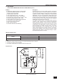
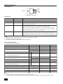
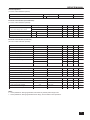
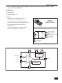
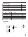
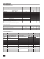
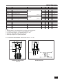
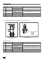
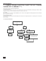
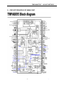
service manual
CONTENTS
1. Safety Precautions……………………………………………………………………………….2
2. Exploded View And Final Assembly Details………………………………………………....3
3. Block Diagram…………………………………………………………………………................4
4. Drawing Site Of Main Parts................................................................................................5
5. List Of Replacement Parts……..........................................................................................6
6. Replacement of Memory IC……………………………………………………………...........11
7. Service Adjustment…………………………………………………………………………......11
8. IC’s Functional Description…………………………………………………………………....18
9. Test Point Waveform……………………………………………………………………………40
10. IC And Transistor’s Voltages.…….................................................................................41
11. Common Trouble Shooting Chart For Uoc Toshiba Chassis CRT TV
(TMPA889*-****)...............................................................................................................41
12. 290 Stereo PAL Secam Schematic Circuit Diagram.....................................................45
1
service manual
1. SAFETY RECAUTIONS
1. The design of this product contains special hardware, many
circuits and components specially for safety purposes. For
continued protection, no changes should be made to the
original design unless authorized in writing by the manufacturer.
Replacement parts must be identical to those used in the
iginal circuits. Service should be performed by qualified
personnel only.
9. Isolation Check (Safety for Electrical Shock Hazard)
After re-assembling the product, always perform an isolation
check on the exposed metal parts of the cabinet (antenna
terminals, video/audio input and output terminals, Control
knobs, metal cabinet, screwheads, earphone jack, control
shafts, etc.) to be sure the product is safe to operate without
danger of electrical shock.
2. Alterations of the design or circuitry of the products should
not be made. Any design alterations or additions will void
the manufacturer’s warranty and will further relieve the
damage resulting therefrom.
10. The surface of the TV screen is coated with a thin film which
can easily be damaged. Be very careful with it when handle
the TV. Should the TV screen become soiled, wipe it with a
soft dry cloth. Never rub it forcefully. Never use any cleaner
or detergent on it.
3. Many electrical and mechanical parts in the products have
special safety-related characteristics. These characteristics
are often not evident from visual inspection nor can the
protection afforded by them necessarily be obtained by using
replacement components rated for higher voltage, wattage,
etc. Replacement parts which have these special safety
characteristics are identified in the parts list of service manual.
Electrical components having such features are identified
by shading on the schematics and by (!) on the parts list
ervie manual. The use of a substitute replacent which
does not have the same safety characteristics as the
recommended replacement part shown in the parts list of
service manual may cause shock, fire, or other hazards.
4. Don’t short between the LIVE side ground and ISOLATED
(NEUTRAL) side ground or EARTH side ground when
repairing. Some model’s power circuit is partly different in
the GND. The difference of the GND is shown by the LIVE:
( ) side GND, ISOLATED (NEUTRAL) : ( ) side GND and
EARTH : ( ) side GND. Don’t short between the LIVEide
GND and ISOLATED (NEUTRAL) side GND or EARTH side
GND and never measure with a measuring apparatus
(oscilloscope etc.) the LIVE side GND and ISOLATED
(NEUTRAL) side GND or EARTH side GND at the same time.
If above note will not be kept, a fuse or any parts will be broken.
5. If any repair has been made to the chassis, it is recommended
that the B1 setting should be checked or adjusted (See
ADJUSTMENT OF B1 POWER SUPPLY).
6. The high voltage applied to the picture tube must conform
with that specified in Service manual. Excessive high voltage
can cause an increase in X-Ray emission, arcing and
possible component damage, therefore operation under
excessive high voltage conditions should be kept to a
minimum, or should be prevented. If severe arcing occurs,
remove the AC power immediatelyt and determine the cause
by visual inspection (incorrect installation, cracked or melted
high voltage harness, poor soldering, etc.). To maintain the
proper minimum level of soft X-Ray emission, components
in the high voltage circuitry including the picture tube must
be the exact replacements or alternatives approved by the
manufacturer of the complete product.
7. Do not check high voltage by drawing an arc. Use a high
voltage meter or a high voltage probe with a VTVM. Discharge
the picture tube before attempting meter connect on, by
connecting a clip lead to the ground frame and connecting
the other end of the lead through a 10kΩ 2W resitor to the
anode button.
8. When service is required, observe the original lead dress.
Extra precaution should be given to assure correct lead
dress in the high voltage circuit area. Where a short circuit
has occurred, those components that indicate evidence of
overheating should be replaced. Always use the manufacturer’s
replacement components.
2
(1) Dielectric Strength Test
㩷
The isolation between the AC primary circuit and all metal
parts exposed to the user, particularly any exposed metal
part having a return path to the chassis shuld withstand a
voltage of 3000V AC (r.m.s.) for a period of one second
(…Withstand a voltage of 1100V AC (r.m.s.) to an appliance.
rated up to 120V, and 3000V AC (r.m.s.) to an appliance
rated 200V or more, for a periode of one second.) This
method of test requires a test equipment not generally found
in the service trade.
(2) Leakage Current Check
Plug the AC line cord directly into the AC outlet (do not use
a line isolation transformer during this check.). Using a
“Leakage Current Tester”, measure the leakage current from
each exposed metal part of the cabinet, particularly any
exposed metal part having a return path to the chassis, to
a known good earth ground (water pipe, etc.). Any leakage
current must not exceed 0.5mA AC (r.m.s.). However, in
tropical area, this must not exceed 0.2mA AC (r.m.s.).
● Alternate Check Method
Plug the AC line cord directly into the AC outlet ( do not use
a line isolation transformer during this check.). Use an AC
voltmeter having 1000 ohms per volt or more sensitivity in
the following manner. Connect a 1500Ω 10W resistor
paralleled by a 0.15μF AC-type capacitor between an
exposed metal part and a known good earth ground (water
pipe, etc.). Measure the AC voltage across the resistor with
the AC voltmeter. Move the resistor connection to each
exposed metal part, particularly any exposed metal part
having a return path to the chassis, and measure the AC
voltage across the resistor. Now, reverse the plug in the AC
outlet and repeat each measurement. Any voltage measured
must not exceed 0.75V AC (r.m.s.). This corresponds to 0.5mA
AC (r.m.s.). However, in tropical area, this must not exceed
0.3V AC (r.m.s.). This corresponds to 0.2mA AC (r.m.s.).
AC VOLTMETER
(HAVING 1000Ω/V
OR MORE SENSITIVITY)
0.15μF AC-TYPE
1500Ω/V 10W
GOOD EARTH GROUND
PLACE THIS PROBE
ON EACH EXPOSED
METAL PART
Power cord holder
FBT holder
Main board holder
4-Screw ST6*30F
6-Screw ST4*16F(Black)
Rear cabinet
2-Screw ST3*12F(Black)
Screw ST4*10F
Screw ST3*12F
6-Screw ST3*12F
2-Speakers
4-Screw ST4*12F
Power cord clame
2-Screw ST3*12F
2-Screw ST3*12F
NOTE: Inserted Parts Is Different According To The Cabinet, Just For Reference.
CRT
4-CRT washer
CRT support
Plastic decorated psrts with lens
Decorated part
Lens
Logo
2-Plastic oriented bar for holding main
Front cabinet
2-Screw ST4*16F
4-Screw ST3*12F
4-Screw ST3*12F
Function button
2-Screw M3*8
Power switch button
service manual
2. exploded view and final assembly details
3
service manual
3 Block Diagram
TUNER A101
ET-5KIE-CV100K / ET-5TIE-EF109
SAW Z101 IF389AIM
TC4053BP
AV SW
AV1
AV2
CD17821CS
TA/1304/1343
A1
Video
Audio
Y Cb
A2
VERIVE3
CD78040 / STV9302
Cr
2 in Chip
HOUT
CRT
TMPA8897CSCNG****
N204
EEPROM
N901 24C08
SC6122
KEY
MATRIX
4
RECEIVEERMP
service manual
4. Drawing Site Of Main Parts
AGC TP
TUNER
+B Adjust
FOCUS
SCREEN
5
service manual
5. List Of Replacement Parts
PCB NO.
DESCRIPTION
TUNER
A101
TUNE ET-5T1E-EF109
CAPACITOR
6
PCB NO.
DESCRIPTION
CAPACITOR
C310
CAP CERAMIC 50V 0.01UF +80%-20%
C311
CAP ELECTROLYTIC 50V 0.47UF 20%
C104
CAP ELECTROLYTIC 50V 4.7UF 20%
C312
CAP ELECTROLYTIC 50V 1UF 20%
C107
CAP ELECTROLYTIC 16V 100UF 20%
C402
CAP CERAMIC 500V 1000P 10%
C112
CAP CERAMIC 50V 0.01UF +80%-20%
C403
CAP CERAMIC 500V 3900P 10%
C113
CAP CERAMIC 50V 0.01UF +80%-20%
C412
CAP METAL FLIM 250V 0.27UF 5% D=20MM
C114
CAP CERAMIC 50V 0.01UF +80%-20%
C413
CAP POLY 100V 0.1UF 10%
C201
CAP ELECTROLYTIC 16V 10UF 20%
C414
CAP ELECTROLYTIC 160V 1UF 20%
C202
CAP CERAMIC 50V 20P 5%
C418
CAP ELECTROLYTIC 250V 22UF 20%
C203
CAP CERAMIC 50V 1000P 10%
C421
CAP POLY 100V 0.1UF 10%
C204
CAP ELECTROLYTIC 50V 0.47UF 20%
C430
CAP ELECTROLYTIC 35V 47UF 20%
C205
CAP ELECTROLYTIC 50V 2.2UF 20%
C433
CAP ELECTROLYTIC 25V 1000UF 20%
C206
CAP ELECTROLYTIC 50V 2.2UF 20%
C443
CAP ELECTROLYTIC 50V 2.2UF 20%
C207
CAP ELECTROLYTIC 50V 1UF 20%
C444
CAP POLY 100V 0.1UF 10%
C208
CAP CERAMIC 50V 0.01UF +80%-20%
C446
CAP POLY 100V 2200P 10%
C209
CAP ELECTROLYTIC 16V 470UF 20%
C447
CAP POLY 100V 0.056UF 10%
C210
CAP CERAMIC 50V 0.01UF +80%-20%
C449
CAP ELECTROLYTIC 50V 100UF 20%
C212
CAP CERAMIC 50V 0.01UF +80%-20%
C456
CAP METAL FLIM 1.6KV 7.2N 5% D=22.5MM
C216
CAP ELECTROLYTIC 50V 1UF 20%
C463
CAP CERAMIC 500V 3900P 10%
C217
CAP ELECTROLYTIC 50V 1UF 20%
C500
CAP CERAMIC 2KV 680P 10%
C218
CAP ELECTROLYTIC 50V 1UF 20%
C501
CAP METAL FLIM AC280V 0.1UF 10%
C222
CAP ELECTROLYTIC 16V 470UF 20%
C504
CAP CERAMIC 1KV 1000P 10%
C227
CAP ELECTROLYTIC 16V 22UF 20%
C506
CAP CERAMIC 1KV 1000P 10%
C228
CAP ELECTROLYTIC 16V 22UF 20%
C507
CAP ELECTROLYTIC 400V 100UF 20%
C229
CAP ELECTROLYTIC 50V 4.7UF 20%
C513
CAP ELECTROLYTIC 35V 10UF 20%
C230
CAP ELECTROLYTIC 16V 220UF 20%
C514
CAP POLY 100V 0.033UF 10%
C231
CAP POLY 100V 2200P 10%
C515
CAP POLY 63V 0.1UF 5%
C235
CAP ELECTROLYTIC 16V 100UF 20%
C516
CAP ELECTROLYTIC 35V 10UF 20%
C236
CAP ELECTROLYTIC 50V 1UF 20%
C517
CAP CERAMIC 50V 560P 10%
C237
CAP ELECTROLYTIC 50V 0.22UF 20%
C535
CAP CERAMIC AC400V 2200P 20%
C238
CAP ELECTROLYTIC 16V 47UF 20%
C536
CAP CERAMIC AC400V 1000P 10%
C243
CAP ELECTROLYTIC 16V 100UF 20%
C552
CAP CERAMIC 1KV 220P 10%
C289
CAP ELECTROLYTIC 50V 4.7UF 20%
C556
CAP CERAMIC 1KV 220P 10%
C290
CAP ELECTROLYTIC 50V 4.7UF 20%
C557
CAP ELECTROLYTIC 25V 470UF 20%
C293
CAP ELECTROLYTIC 50V 4.7UF 20%
C559
CAP ELECTROLYTIC 35V 100UF 20%
C294
CAP ELECTROLYTIC 50V 4.7UF 20%
C561
CAP ELECTROLYTIC 160V 10UF 20% D=5MM
C296
CAP ELECTROLYTIC 16V 47UF 20%
C563
CAP ELECTROLYTIC 160V 220UF 20%
C298
CAP ELECTROLYTIC 50V 1UF 20%
C565
CAP ELECTROLYTIC 35V 470UF 20%
C301
CAP ELECTROLYTIC 50V 1UF 20%
C571
CAP ELECTROLYTIC 16V 470UF 20%
C302
CAP ELECTROLYTIC 16V 47UF 20%
C573
CAP ELECTROLYTIC 35V 47UF 20%
C303
CAP POLY 100V 0.1UF 10%
C574
CAP CERAMIC 50V 0.01UF +80%-20%
C305
CAP POLY 100V 8200P 10%
C602
CAP CERAMIC 50V 390P 10%
C306
CAP ELECTROLYTIC 16V 10UF 20%
C612
CAP CERAMIC 50V 390P 10%
C308
CAP ELECTROLYTIC 16V 100UF 20%
C622
CAP CERAMIC 50V 390P 10%
C309
CAP ELECTROLYTIC 50V 4.7UF 20%
C630
CAP CERAMIC 2KV 2200P 10%
service manual
PCB NO.
DESCRIPTION
CAPACITOR
DESCRIPTION
PCB NO.
IC
C632
CAP ELECTROLYTIC 16V 47UF 20%
C635
CAP CERAMIC 50V 0.01UF +80%-20%
VD515
C701
CAP ELECTROLYTIC 25V 1000UF 20%
N550
IC 78L05
C702
CAP POLY 100V 0.1UF 10%
N701
IC CD17821CS
C705
CAP ELECTROLYTIC 50V 4.7UF 20%
N701
HEAT SINK SOUND HXXX0151-30
C710
CAP ELECTROLYTIC 50V 1UF 20%
N901
IC FM24C08A
C711
CAP POLY 100V 6800P 10%
N902
IC CW7808
C713
CAP ELECTROLYTIC 50V 1UF 20%
N902
HEAT SINK 8V HXX0050-30
C720
CAP ELECTROLYTIC 50V 1UF 20%
N904
IC KA33V/CW574CS
C721
CAP POLY 100V 6800P 10%
C722
CAP ELECTROLYTIC 50V 1UF 20%
R101
RESISTOR CARBON 1/6W 100KOHM 5%
C723
CAP ELECTROLYTIC 50V 1UF 20%
R106
RESISTOR CARBON 1/6W 220OHM 5%
C730
CAP ELECTROLYTIC 16V 10UF 20%
R107
RESISTOR CARBON 1/6W 220OHM 5%
C901
CAP CERAMIC 50V 33P 5%
R108
RESISTOR CARBON 1/6W 100OHM 5%
C902
CAP CERAMIC 50V 20P 5%
R108
RESISTOR CARBON 1/6W 3.3KOHM 5%
C903
CAP CERAMIC 50V 0.01UF +80%-20%
R111
RESISTOR CARBON 1/6W 150OHM 5%
C910
CAP CERAMIC 50V 33P 5%
R112
RESISTOR CARBON 1/6W 100OHM 5%
C911
CAP CERAMIC 50V 33P 5%
R113
RESISTOR CARBON 1/6W 33OHM 5%
C913
CAP CERAMIC 50V 0.01UF +80%-20%
R115
RESISTOR CARBON 1/6W 1.5KOHM 5%
C914
CAP ELECTROLYTIC 16V 47UF 20%
R121
RESISTOR CARBON 1/6W 100OHM 5%
C916
CAP ELECTROLYTIC 16V 47UF 20%
R201
RESISTOR CARBON 1/6W 560OHM 5%
C917
CAP ELECTROLYTIC 50V 0.47UF 20%
R203
RESISTOR CARBON 1/6W 3.3KOHM 5%
C924
CAP CERAMIC 50V 0.01UF +80%-20%
R205
RESISTOR CARBON 1/6W 100OHM 5%
C926
CAP ELECTROLYTIC 50V 2.2UF 20%
R206
RESISTOR CARBON 1/6W 100OHM 5%
C927
CAP ELECTROLYTIC 16V 100UF 20%
R207
RESISTOR CARBON 1/6W 100OHM 5%
C928
CAP ELECTROLYTIC 16V 100UF 20%
R208
RESISTOR CARBON 1/6W 100OHM 5%
C929
CAP CERAMIC 50V 0.01UF +80%-20%
R211
RESISTOR CARBON 1/6W 1MOHM 5%
C930
CAP CERAMIC 50V 0.01UF +80%-20%
R213
RESISTOR CARBON 1/6W 15KOHM 5%
C934
CAP CERAMIC 50V 1000P 10%
R215
RESISTOR CARBON 1/6W 68OHM 5%
C981
CAP ELECTROLYTIC 50V 4.7UF 20%
R217
RESISTOR CARBON 1/6W 100OHM 5%
INDUCTANCE
V501
IC FSCQ0765RT
IC LTV817C
RESISTOR
R219
RESISTOR CARBON 1/6W 100OHM 5%
L101
FILTER COIL 15UH-K
R220
RESISTOR CARBON 1/6W 100OHM 5%
L103
FILTER COIL 1UH-K
R221
RESISTOR CARBON 1/6W 15KOHM 5%
L201
FILTER COIL 15UH-K
R222
RESISTOR CARBON 1/6W 15KOHM 5%
L202
FILTER COIL 15UH-K
R225
RESISTOR CARBON 1/6W 100OHM 5%
L305
FILTER COIL 15UH-K
R228
RESISTOR CARBON 1/6W 1KOHM 5%
L414
LINEARITY COIL LX-036 D=10MM
R229
RESISTOR CARBON 1/6W 100OHM 5%
L451
RESISTOR CEMENT 3W 3.9OHM 10% D=10MM
R230
RESISTOR CARBON 1/6W 100OHM 5%
L501
FILTER COIL 15-LB6×1.0×6
R232
RESISTOR CARBON 1/6W 33KOHM 5%
L502
LINE FILTER LG-031-NLG
R233
RESISTOR CARBON 1/6W 220KOHM 5%
L901
FILTER COIL 15UH-K
R236
RESISTOR CARBON 1/6W 270OHM 5%
IC
R237
RESISTOR CARBON 1/6W 270OHM 5%
N203
IC HEF4053
R238
RESISTOR CARBON 1/6W 270OHM 5%
N204
IC 8891-****
R239
RESISTOR CARBON 1/2W 220OHM 5%
N402
IC CD78040
R243
RESISTOR CARBON 1/6W 10KOHM 5%
N402
HEAT SINK V HXXX0063-40
R244
RESISTOR CARBON 1/6W 5.6KOHM 5%
7
service manual
PCB NO.
DESCRIPTION
RESISTOR
8
PCB NO.
DESCRIPTION
RESISTOR
R245
RESISTOR CARBON 1/6W 100KOHM 5%
R480
RESISTOR CARBON 1/6W 33KOHM 5%
R250
RESISTOR CARBON 1/6W 15KOHM 5%
R480
RESISTOR CARBON 1/6W 33KOHM 5%
R253
RESISTOR CARBON 1/6W 15KOHM 5%
R515
RESISTOR CARBON 1/6W 2.7KOHM 5%
R254
RESISTOR CARBON 1/6W 15KOHM 5%
R517
RESISTOR CARBON 1/6W 2.4KOHM 5%
R256
RESISTOR CARBON 1/6W 15KOHM 5%
R520
RESISTOR CARBON 1/2W 120KOHM 5%
R279
RESISTOR CARBON 1/6W 22KOHM 5%
R521
RESISTOR CARBON 1/2W 120KOHM 5%
R280
RESISTOR CARBON 1/6W 100OHM 5%
R522
RESISTOR CARBON 1/4W 8.2OHM 5%
R283
RESISTOR CARBON 1/6W 1KOHM 5%
R523
RESISTOR CARBON 1/6W 560OHM 5%
R290
RESISTOR CARBON 1/6W 10KOHM 5%
R531
RESISTOR GLASS GLAZE 1/2W 24MOHM +80%-20%
R291
RESISTOR CARBON 1/6W 15KOHM 5%
R552
RESISTOR CARBON 1/4W 5.6KOHM 5%
R292
RESISTOR CARBON 1/6W 100OHM 5%
R553
RESISTOR METAL 2W 12KOHM 5% D=15MM
R294
RESISTOR CARBON 1/6W 100OHM 5%
R555
RESISTOR CARBON 1/4W 150KOHM 5%
R295
RESISTOR CARBON 1/6W 15KOHM 5%
R556
RESISTOR CARBON 1/4W 47KOHM 5%
R301
RESISTOR CARBON 1/6W 270OHM 5%
R557
RESISTOR CARBON 1/6W 22KOHM 5%
R306
RESISTOR CARBON 1/6W 4.7OHM 5%
R558
RESISTOR FUSE 1/2W 0.47OHM 5% D=15MM
R310
RESISTOR CARBON 1/6W 100OHM 5%
R560
RESISTOR CARBON 1/2W 3.3KOHM 5%
R312
RESISTOR CARBON 1/6W 100OHM 5%
R564
RESISTOR CARBON 1/2W 47KOHM 5%
R320
RESISTOR CARBON 1/6W 560OHM 5%
R565
RESISTOR METAL 2W 22KOHM 5% D=10MM
R321
RESISTOR CARBON 1/6W 10KOHM 5%
R566
RESISTOR CARBON 1/2W 3.3KOHM 5%
R322
RESISTOR CARBON 1/6W 8.2KOHM 5%
R572
RESISTOR CARBON 1/4W 47KOHM 5%
R326
RESISTOR CARBON 1/6W 270OHM 5%
R573
RESISTOR FUSE 1W 0.47OHM 5% D=15MM
R328
RESISTOR CARBON 1/6W 15KOHM 5%
R580
RESISTOR METAL 2W 68OHM 5% D=15MM
R330
RESISTOR CARBON 1/6W 220OHM 5%
R605
RESISTOR CARBON 1/2W 3.3KOHM 5%
R331
RESISTOR CARBON 1/6W 3.9KOHM 5%
R606
RESISTOR METAL 2W 12KOHM 5% D=15MM
R404
RESISTOR CARBON 1/6W 150OHM 5%
R607
RESISTOR CARBON 1/6W 470OHM 5%
R407
RESISTOR CARBON 1/2W 1.0KOHM 5%
R608
RESISTOR CARBON 1/6W 3.9KOHM 5%
R410
RESISTOR METAL 2W 2.0OHM 5% D=12.5MM
R615
RESISTOR CARBON 1/2W 3.3KOHM 5%
R413
RESISTOR METAL 1WS 4.7KOHM 5% D=12.5MM
R616
RESISTOR METAL 2W 12KOHM 5% D=15MM
R418
RESISTOR FUSE 1/2W 3.3OHM 5% D=15MM
R617
RESISTOR CARBON 1/6W 470OHM 5%
R420
RESISTOR CARBON 1/2W 220KOHM 5%
R618
RESISTOR CARBON 1/6W 3.9KOHM 5%
R423
RESISTOR CARBON 1/6W 10KOHM 5%
R626
RESISTOR METAL 2W 12KOHM 5% D=15MM
R424
RESISTOR CARBON 1/6W 15KOHM 5%
R627
RESISTOR CARBON 1/6W 470OHM 5%
R435
RESISTOR CARBON 1/6W 330KOHM 5%
R628
RESISTOR CARBON 1/6W 3.9KOHM 5%
R437
RESISTOR METAL 2W 270OHM 5% D=15MM
R629
RESISTOR CARBON 1/2W 3.3KOHM 5%
R442
RESISTOR CARBON 1/2W 330OHM 6%
R635
RESISTOR CARBON 1/6W 47KOHM 5%
R443
RESISTOR CARBON 1/6W 5.6KOHM 5%
R640
RESISTOR CARBON 1/6W 10KOHM 5%
R444
RESISTOR CARBON 1/6W 4.7OHM 5%
R641
RESISTOR CARBON 1/4W 2.2OHM 5%
R446
RESISTOR CARBON 1/6W 3.9KOHM 5%
R702
RESISTOR CARBON 1/6W 4.7KOHM 5%
R448
RESISTOR CARBON 1/6W 10KOHM 5%
R704
RESISTOR CARBON 1/6W 15KOHM 5%
R449
RESISTOR CARBON 1/6W 15KOHM 5%
R710
RESISTOR CARBON 1/6W 1KOHM 5%
R450
RESISTOR CARBON 1/6W 47KOHM 5%
R710
RESISTOR CARBON 1/6W 8.2KOHM 5%
R463
RESISTOR CARBON 1/2W 12KOHM 5%
R711
RESISTOR CARBON 1/6W 4.7KOHM 5%
R464
RESISTOR CARBON 1/2W 1.5OHM 5%
R713
RESISTOR CARBON 1/6W 1KOHM 5%
R467
RESISTOR FUSE 1W 0.47OHM 5% D=15MM
R715
RESISTOR CARBON 1/6W 2.2KOHM 5%
R473
RESISTOR CARBON 1/6W 100KOHM 5%
R718
RESISTOR CARBON 1/6W 4.7KOHM 5%
R480
RESISTOR CARBON 1/6W 18KOHM 5%
R720
RESISTOR CARBON 1/6W 8.2KOHM 5%
service manual
PCB NO.
DESCRIPTION
RESISTOR
DESCRIPTION
PCB NO.
TRANSISTOR
R721
RESISTOR CARBON 1/6W 4.7KOHM 5%
V301
TRANSISTOR 2SC1815Y
R722
RESISTOR CARBON 1/6W 8.2KOHM 5%
V411
TRANSISTOR 3DD5023
R723
RESISTOR CARBON 1/6W 8.2KOHM 5%
V444
TRANSISTOR 2SC2383-O
R725
RESISTOR CARBON 1/6W 33KOHM 5%
V551
TRANSISTOR 2SC1815Y
R726
RESISTOR CARBON 1/6W 47KOHM 5%
V601
TRANSISTOR 2SC2482Y
R727
RESISTOR CARBON 1/6W 15KOHM 5%
V611
TRANSISTOR 2SC2482Y
R728
RESISTOR CARBON 1/6W 4.7KOHM 5%
V621
TRANSISTOR 2SC2482Y
R730
RESISTOR CARBON 1/6W 1KOHM 5%
V630
TRANSISTOR 2SC1815Y
R900
RESISTOR CARBON 1/6W 100OHM 5%
V721
TRANSISTOR 2SC1815Y
R901
RESISTOR CARBON 1/6W 100OHM 5%
V722
TRANSISTOR 2SC1815Y
R904
RESISTOR CARBON 1/6W 1KOHM 5%
V900
TRANSISTOR 2SC1815Y
R905
RESISTOR CARBON 1/6W 5.6KOHM 5%
V902
TRANSISTOR 2SA1015Y
R909
RESISTOR CARBON 1/6W 47OHM 5%
V904
TRANSISTOR HSB892/KTB772
R910
RESISTOR CARBON 1/6W 47OHM 5%
V905
TRANSISTOR 2SD400D
R916
RESISTOR CARBON 1/6W 3.9KOHM 5%
V980
TRANSISTOR 2SC1815Y
R918
RESISTOR CARBON 1/6W 4.7KOHM 5%
DIODE
R919
RESISTOR CARBON 1/6W 4.7KOHM 5%
VD230
DIODE IN4148
R920
RESISTOR CARBON 1/6W 5.6KOHM 5%
VD232
DIODE IN4148
R922
RESISTOR CARBON 1/6W 10KOHM 5%
VD233
DIODE IN4148
R925
RESISTOR CARBON 1/6W 1KOHM 5%
VD234
DIODE IN4148
R927
RESISTOR CARBON 1/6W 22KOHM 5%
VD292
DIODE HZ4A2
R928
RESISTOR CARBON 1/6W 4.7KOHM 5%
VD401
DIODE IN4148
R929
RESISTOR CARBON 1/6W 22KOHM 5%
VD403
DIODE RF107
R930
RESISTOR CARBON 1/6W 1.2KOHM 5%
VD414
DIODE RF107
R935
RESISTOR CARBON 1/6W 10KOHM 5%
VD434
DIODE 1N4004
R939
RESISTOR CARBON 1/6W 22KOHM 5%
VD435
DIODE RF107
R941
RESISTOR CARBON 1/6W 4.7KOHM 5%
VD436
DIODE HZ11C1
R943
RESISTOR CARBON 1/6W 12KOHM 5%
VD503
DIODE TVR4N
R945
RESISTOR CARBON 1/6W 560OHM 5%
VD504
DIODE TVR4N
R946
RESISTOR CARBON 1/6W 1.5KOHM 5%
VD505
DIODE TVR4N
R947
RESISTOR CARBON 1/6W 8.2KOHM 5%
VD506
DIODE TVR4N
R960
RESISTOR CARBON 1/4W 470HM 5%
VD514
DIODE RF107
R961
RESISTOR CARBON 1/2W 47OHM 5%
VD516
DIODE IN4148
R980
RESISTOR CARBON 1/6W 10KOHM 5%
VD517
DIODE RF107
R981
RESISTOR CARBON 1/6W 10KOHM 5%
VD518
DIODE HZ4A2
R988
RESISTOR CARBON 1/6W 4.7OHM 5%
VD519
DIODE HZ18C2
R989
RESISTOR CARBON 1/6W 10KOHM 5%
VD551
DIODE HZ7A3
VARISTOR 1/2W 2KOHM 20%
VD552
DIODE RGP15D
RP551
TRANSFORMER
VD553
DIODE RF105
T401
H.DRIVER TRANS TD-0004-OL
VD554
DIODE RF105
T402
TRANS FLY BACK T9XX0124E-X
VD556
DIODE RGP15J D=15MM
T501
TRANS POWER TM-0105-ON
VD574
DIODE HZ4A2
TRANSISTOR
VD601
DIODE IN4148
V203
TRANSISTOR 2SA1015Y
VD611
DIODE IN4148
V230
TRANSISTOR 2SA1015Y
VD621
DIODE IN4148
V290
TRANSISTOR 2SC1815Y
VD901
DIODE IN4148
9
service manual
PCB NO.
DESCRIPTION
TRANSISTOR
VD902
DIODE HZ4A2
VD921
DIODE HZ6B1
CRT SOCKET,SAW FILTER ,CRYSTAL
XZ601
CRT SOCKET GZS8-6-FD
Z101
SAW FILTER IF389A1M
Z304
FILTER F10.7MHZ
Z901
CRYSTAL 8MHZ(18.5PF)
OTHERS
R502A
PTC MF72 4.7OHM D=11MM
PS501
PTC MZ72B 9OHM AC270V
F501
FUSE 3.15A 250V
F501A
FUSE SOCKET
F501B
FUSE SOCKET
XZ201
AV SOCKET AV9-01K-D
XZ207
4S SOCKET TJC3-4A(S)
XZ411
DY SOCKET TJC2-5A(M)
XZ501
2S SOCKET TJC1-2A-10MM(L)
XZ504
2S SOCKET TJC2-2A-7.5MM(M)
XZ602
4P LINE 400MM
XZ603
6P LINE 400MM
XZ711
4S SOCKET TJC3-4A(S)
XZ901
3S SOCKET TJC3-3A(S)
XZ903
3S SOCKET TJC3-3A(S)
XZ905
2S SOCKET TJC3-2A(S)
Z902
MAIN PCB BSC7.820.290-C(247×247MM)
ZN402
SCREW GB845F SF3×10MM
ZN701
SCREW GB845F SF3×8MM
ZN902
SCREW GB845F SF3×8MM
ZV411
SCREW GB845F SF3×10MM
ZV501
SCREW GB845F SF3×10MM
TP602
1S SOCKET TJC1-1A(L)
V411
HEAT SINK H HXXX0156-40
V501
HEAT SINK POWER HXXX0146-40
V600
CRT
REMOTE CONTROL YKQ8891-***
Note:
10
Security Parts.
service manual
6. REPLACEMENT OF MEMORY IC
6.1 MEMORY IC.
This TV uses memory IC. In the memory IC are memorized data for correctly operating the video and deflection circuits.
When replacing memory IC, be sure to use IC written with the initial value of data.
6.2 PROCEDURE FOR REPLACING MEMORY IC
(1) Power off
Switch the power off and unplug the power cord from AC outlet.
(2) Replace IC
Be sure to use memory IC written with the initial data values.
(3) Power On
Plug the power cord into the AC outlet and switch the power On.
7. SERVICE ADJUSTMENT
Descriptions for the operation of factory mode
AGING MODE
1. With factory remote controller to press “D-mode” directly enter AGING mode, screen will display “factory”. Press “DISP” key to
exit “factory” to enter “WHITE BALANCE”.
2. With user remote controller to press “MENU” key to turn to “TUNING” menu, press “CH-” key to Select “TARGET POS” bar,
Input“2483”, “6483”, “6568”, then enter AGING mode.
3. At “factory” mode or “AGING” mode, press “SYS”, “SOUND”, “SLEEP” key to adjust data, screen will display relevant
menu+factory. Press “MENU” to display main Menu to adjust all data. Press “DISP” to exit, screen only display “factory”.
WHITE BALANCE MODE
1. At AGING mode, press “D-mode” exit “factory” to enter WHITE BALANCE mode.
2. Press “D-mode” key two time (factory key) to enter WHITE BALANCE mode.
3. At “factory” mode, press figure key “0” enter WHITE BALANCE mode.
4. At WHITE BALANCE mode, press “MUTE”, one horizontal bright line appear on screen, use “1,4” key to adjust RCUT,
“2,5” key to adjust GCUT, “3,6” key to adjust BCUT.
ENTER FACTORY MODE
A. USER REMOTE CONTROLLER
1. At first enter AGING mode, at AGING mode, press “DISP” to exit “factory”, enter WHITE BALANCE mode.
2. At WHITE BALANCE mode, press figure 1,2,3,4,5,6, DISP to enter “factory” mode.
B. Press “D-mode” key three time (factory key) to enter factory’s adjustment menu.
ENTER FACTORY MODE F8~F15
Press “2483”,”6483”,”6568” enter F8, and also open F8-F15. Press “Mute” Key to turn Page Up and “RETURN” key to turn
Page Down for factory mode menu. Press figure Key 1, 2, 3, 4, 5, 6, 7, 8, 9 to enter “factory” mode F1~F9.
EXIT FACTORY MODE
1. Press “DISP” to exit from “factory” menu.
2. Press power switch, exit “factory’s mode.
EXPLANATION FOR ADJUSTMENT SPEED KEY
After entering factory mode, some remote controller key function will change to suit for the production adjustment.
1. Press “MUTE” key to turn page up, press “RETURN” key to turn page down.
2. Press “CH+” and “CH-“ key to select item, and press “VOL+” and “VOL-” key to change data value.
3. Press “SLEEP” key to display CHIP inner 6 kinds test signal.
11
service manual
White Balance adjustment
OSD
Descriptions
Recommend Data
Max
RC
R-CUT
110
255
GC
G-CUT
110
255
BC
B-CUT
110
255
GD
G-Diver
60
127
BD
B-Driver
72
127
U.BLK
U signal black level adjust
8
15
V.BLK
V signal black level adjust
8
15
S.RY
SECAM, R signal black level adjust
8
15
S.BY
SECAM, B signal black level adjust
8
15
Notes:
press “MUTE”, one horizontal bright line appear on screen, use “1,4” key to adjust RCUT, “2,5” key to adjust GCUT,
“3,6” key to adjust BCUT.
Geometry parameter adjustment for PAL (Not available for NTSC)
Recommend Data
Max
H.PHASE
OSD
Horizontal Phase for 50Hz
Descriptions
18
31
V.SIZE
Vertical Amplitude for 50Hz
20
63
V.POS
Vertical Phase for 50Hz
02
15
V.LIN
Vertical Linearity for 50Hz
15
31
V.SC
V-S correction for 50Hz
15
31
HBOW
H Bow correction for 50Hz
4
7
HPARA
H Para correction for 50Hz
4
7
0
07
0
07
H.BLK.RIGHT H.Right Blanking
H.BLK.LEFT
H.Left Blanking
Geometry parameter adjustment for NTSC (offset for PAL system, NTSC only)
Recommend Data
Max
NT.H.PHASE
OSD
Horizontal Phase for 60Hz
Descriptions
10
20
NT.V.SISE
Vertical Amplitude for 60Hz
10
20
NT.V.POS
Vertical Phase for 60Hz
11
20
NT.V.LIN
Vertical Linearity for 60Hz
10
20
NT.V.SC
V-S correction for 60Hz
10
31
NT.HBOW
H Bow correction for 60Hz
4
7
NT.HPARA
H Para correction for 60Hz
4
7
V.BLK.TOP
V.Top Blanking
0
3
V.BLK.BTM
V.Bottom Blanking
0
3
Recommend Data
Max
Brightness, Contrast, Color adjustment
OSD
SUB.CONT
15
15
SUB.BRIGHT
Brightness
0
-63~63
SUB.COLOR
Sub Color
10
-128~—+127
Sub Color for SECAM
64
127
IF Gain
30
63
Background 0:OFF 1:ON
1
1
BACK COLOR, 0:blue 1:black
0
1
Brightness boost speed for “POWER ON”
5
15
Child lock
0
1
LOGO MOVE 0:OFF 1:ON
0
1
S.SUB.COLOR
RF.AGC
BACKGROUND
BACK.COLOR
POW.CONT
LOCK
LOGO MOVE
12
Descriptions
Sub Contrast
service manual
OSD1 adjustment
OSD
Descriptions
Remark
Recommend Data
MENU BACK
MENU translucent background selection
0:OFF
1:ON
1
MENU ICON
MNEU icon display selection
0:OFF
1:ON
1
OPEN CURT.
Curtain style when switch on
0:OFF
1:ON
1
CLOSE CURT.
Curtain style when switch off
0:OFF
1: ON
1
CALENDER
Calendar switch
0:OFF
1: ON
1
P.ON.LOGO
LOGO display when power on
0:OFF 1:SET
0
LOGO display without signal
0:OFF 1:SET
0
OSD contrast
0:95IRE 1:60IRE
2:70IRE 3: 80IRE
1
Adjust main MENU simulation value,
Whether make main MENU disappear
0:No disappear
1:disappear
0
NO.SG.LOGO
OSD.CONT
ANALOG ADJ
Function control adjustment
OSD
TV
AV2
DVD
Descriptions
TV SWITCH 0:OFF
1:ON
AV2 SWITCH 0: OFF 1: ON
1
1
Recommend Data
Recommend Data
1
1
DVD SWITCH 0: OFF
1: ON
1
1
FM
FM SWITCH
0: OFF
1: ON
0
1
BG
BG
0: OFF
1: ON
1
1
I SWITCH
0: OFF
1: ON
1
1
DK
DK SWITCH
0: OFF
1: ON
1
1
M
M SWITCH
0: OFF 1: ON
SOUND IF MODULATE WIDTH,
0: BG\DK\I division 1: no division
1
1
0
1
I
FM-BAND
Screen Protection OSD position and H.V. compensation
OSD
LEFT
RIGHT
Recommend Data
16
125
Max
255
255
Top position limit for Screen protection OSD moving
24
255
Bottom position limit for Screen protection OSD moving
180
255
Wait time for pulling curtain
10
188
CURT.CENT
Center position for pulling curtain
160
255
TOP
BOTTOM
CURT.WAIT.TIME
Descriptions
Left position limit for Screen protection OSD moving
Right position limit for Screen protection OSD moving
CURT.STEP
Speed for pulling curtain
3
16
OSD.H.POSI.
Horizontal position for Screen protection OSD
40
127
OSD.V.POSI
Vertical position for Screen protection OSD
18
47
ZOOM
0
15
Recommend Data
Max
32
255
ZOOM
OSD2 adjustment
OSD
CH DARK
Descriptions
Black screen time adjustment for exchange channels,
8MS time for data “1”
Black screen for exchange channels 0:OFF 1:ON
0
1
FRANCE
France
0:OFF
1:ON
1
1
RUSSIAN
Russian
0:OFF
1:ON
1
1
T.VIET
Vietnam
0:OFF
1:ON
0
1
POS.TIMER
TURKEY
Turkey
0:OFF
1:ON
0
1
ARABIA
Arabia
0:OFF
1:ON
0
1
PERSIA
Persia
0:OFF
1:ON
0
1
German
0:OFF
1:ON
0
1
0
1
GERMAN
ITALIAN
Italian
0:OFF
1:ON
13
service manual
OSD3 Main MENU Color adjustment
OSD
UP BOX
BACKGROUND
Descriptions
Background color selection for up window
of main menu
Color selection to pitch on picture in up window
UP BOX MOVE
of main MENU
UP ICON ACKGROUND UP ICON color selection in main MENU
Recommend Data
Max
15
15
2
15
1
07
4
07
15
15
15
15
UP ICON MOVE
Color selection to pitch on UP ICON in main MENU
Background color selection for down window of
DOWN BOX KGROUND
main menu
Color selection to pitch on menu item bar in down
DOWN BOX MOVE
window of main MENU
DOWN TEXT GROUND
Character color selection for down
window in main MENU
2
07
DOWN TEXT MOVE
Color selection to pitch on character in down
window of main MENU
4
07
Notes:
Press “MENU” key on this page, blue screen MENU appear, and also display “FACTORY”,
directly use P+,P-,V+,V- key to adjust all items color in MENU, after adjustment then press “DISP” to exit.
VOLUME Parameters adjustment 1
OSD
Recommend Data
Max
0
1
AUDIO IN
Descriptions
When video input, sound input from AV1 or AV2,
0:AV1 1:AV2
Sound input combination, 0: Stereo 1: 32PIN 2: 22PIN
0
2
TV.MUTE
MUTE control without TV signal, 0:TV no MUTE 1:MUTE
1
1
AV.MUTE
MUTE control without AV signal, 0:AV no MUTE 1:MUTE
Volume automatic control grade,
0:off ,1:1.1Vp-p, 2:1.6Vp-p, 3:2.3Vp-p
Sound IC selection,
0: OFF 1: Balance 2:TA1343 3:TA1304
Woofer switch 0: OFF 1: ON
S. AUDIO
ALC GAIN
Sound IC
S.WOOFER
BALC
1
Sound Balance center value
Remote control code selection: 0:9028-0E0E
1:6122-BF40 2:7461-611C 3:7461-1AA1 4: AUTO
REMOTE
1
3
0
3
0
1
64
114
4
4
High, Middle, Low simulation curve adjustment
OSD
Descriptions
Minimum
Middle
Recommend Data
Max
CONTRAST
Contrast
00
95
127
127
BRIGHT
Brightness
64
69
53
127
COLOR
Color
15
64
69
127
TINT
Tint
40
58
66
127
SHARP
Sharpness
32
32
X
63
VOLUME
Volume
64
96
127
127
BASS
Bass
24
72
X
127
TREBLE
Treble
40
X
X
127
WOOFER
Woofer
114
X
X
127
Register control to Color
OSD
Descriptions
Recommend Data
TV/PAL
TV/NTSC
AV
DVD
Max
Y.DELAY
Brightness delay
5
3
3
3
7
DEMO.PHASE
Color modulate amplitude & phase
0
1
1
3
2
P/N ID
Color sensitivity
0
0
1
1
1
KILLER.OFF
Brightness Killer switch
0
0
0
0
1
SYS.SHARP
Different status SHARP value
37
37
37
37
63
Notes:
Y DELAY TIME
0:0ns 1:40ns 2:80ns 3:120ns 4:160ns 5:200ns 6:240ns 7:280ns
14
service manual
Chip pins status control
OSD
VIF
Descriptions
Recommend Data
Whether “POWER ON” to test voltage level for
0
control key PCB, 0: 1:default TOSHIBA
Whether remote control key has “FAVOURITE”
function: 0:as Up,Down,Left,Right key
1
1:as Favorite, Scan, Music key
TMPA889X Chip Tint signal input or CVBS input
0
0:Tint signal 1:CVBS
0:50/60HZ
1:High level When UHF
0
TMPA8891 Chip 31pins function
0
0:SIF OUT 1: AU OUT 2. 3:NO USE
56pins function, 3 status ?
0:High & Low two level
0
1:High, Middle, Low three level
56pins function,TV/AV1/AV2 three status voltage selection
0
0:0V 2.5V 5V 1:0V 5V 2.5V
64pins function, “POWER ON” level selection:
0
0:Low level “ON”, 1:High level “ON”
mage IF 0:38M 1:38.9M 2:45.75M
VIDEO DSP USB
AV2 DISPLAY USB
PANEL KEY DETECT
REMOTE KEY LOVE
23PIN
59PIN 50/60HZ-UHF
31PIN
56PIN 3 STATUS
56PIN V.CHG
64PIN
Max
1
1
1
1
2
1
1
1
2
1
Function control
OSD
V.AGC.DC
PIF.LEVER
CVBS.PASS
POS.NO.
TUNING.MODE
TUNER.TYPE
POWER.TIME
Recommend Data
Max
V. AGC power source selection, 0: external 1: inner
CVBS output amplitude control,
00:1.1V
3:2.4V
Whether CVBS output pass band filter,
0: PASS 1: NO PASS
Channels quantity selection, 0:248
1:256
Descriptions
1
1
3
3
0
1
0
1
Tuning mode, 0:VS
1:FS
Frequency Synthesize Tuner selection
0:38M 1:38A 2:38.9M 3:38.9A
Cold “POWER ON” power pin wait time:
0:0 second, 1:1 second, 2:2 seconds, 3:3 seconds
0
1
0
3
0
3
STANBY.MODE
“POWER ON” power pin memory status, 0:Remember status
1:Stand-by status, remote control to “POWER ON”
2:Do not remember last time “POWER ON” status
automatic “POWER ON”
0
2
U.BAND
Tuner U band level selection, 0:00
1
1
Descriptions
Start point for automatic brightness control
0:0V,1:-0.2V,2:-0.3V,3:-0.4V
Start point for automatic contrast control,
0:0V,1:-0.2V,2:-0.3V,3:-1V(OFF)
Start point for automatic brightness control gain
0:-0.2V,1:-0.35V,2:-0.5V,3:-0.65V;
Brightness peak value, 0:OFF
1:105IRE
Recommend Data
Max
2
3
1
3
3
3
0
1
Black level delay switch, 0:OFF
1:105IRE
Start point for black level delay
0:30IRE, 1:40IRE, 2:50IRE, 3:75IRE
Brightness Gamma correction
0:OFF, 1:78IRE, 2:68IRE, 3:58IRE
“POWER OFF” brightness vanish, 0:OFF
1: Brightness vanish : RGB/Cut as 0
2: Brightness vanish, RGB/Cut as FF
Balance adjustment for Vertical line roll
1
1
3
3
0
3
0
2
4
7
1:11
Register control to ABCL, Brightness
OSD
ABL.POINT
ACL.ST
ABL.GAIN
YPL
BS.SW
BS.START
Y.GAMMA
P.OFF.RGB
SHARP.BLANCE
15
service manual
Register control to Sound trap
OSD
Descriptions
S.TRAP F0
S.TRAP Q
Recommend Data
Max
BG
DK
I
M
Sound trap center frequency width
08
08
08
03
15
Sound trap Q value
0
0
0
0
3
S.TRAP GD
Sound trap GD value
2
2
2
2
3
S.TRAP HP/LP
Sound trap HP/LP value
0
0
0
3
3
STANDARD
Standard status contrast, brightness, color, sharpness
50
50
50
50
100
MILD
Lild status contrast, brightness, color, sharpness
30
30
40
30
100
VIVID
Vivid status contrast, brightness, color, sharpness
70
70
60
60
100
DYNAMIC
Dynamic status contrast, brightness, color, sharpness
80
80
50
40
100
H. Synchronization parameters adjustment
OSD
SYNC.SEARCH
Descriptions
H.Sync. test mode, 0: inner sync.,
1: external sync.
Inner sync. searching, Sync. signal test mode
SYNC.BB
Inner sync. blue screen, Sync. signal test mode
14
15
BB.COUNT
Inner sync. Blue screen, Sync. Signal counting quantity
04
255
PYNX
External sync. Status H.Sync. pulse counting maximum
46
63
PYNN
External sync. Status H.Sync. pulse counting minimum
External sync. Searching status H.Sync.
pulse counting maximum
External sync. Searching status H.Sync.
pulse counting minimum
24
63
34
63
30
63
SYNC.DET
PYXS
PYNS
Recommend Data
Max
0
1
14
15
Seldom used adjustment items 1
Recommend Data
Max
HAFC
OSD
AFC gain
Descriptions
0
255
VCEN
V. center value, valid for “+,-” power source
0
3F
NOISE.SW
Noise test switch
0
1
NOISE.COUNT
Test and confirm the noise counting value
31
255
SEARCH1
Automatic searching calculation 1, 0:quick 1:slow
0
1
SEARCH2
Automatic searching calculation 2, 0:quick 1:slow
0
1
NOISE
Test the noise comparison value
F
15
UCOM
Select input mode for test pattern from U-COM
0
7
CH SHADE
Fade in when change
0:OFF
1:ON
0
1
DSP POSITION
TV Station display position
0:right
1:left
0
1
Recommend Data
Max
0
1
0:OFF 1:ON
Seldom used adjustment items 2
OSD
Descriptions
HVBSW
H/V Blanking on/OFF switch, 0:OFF
C.TRP.Q
0
1
1
1
0
1
0
1
0
1
0
3
YUV.DIS
C-Trap Q, 0:low
1:high
AFT check, 0:check AFT for TV or AV,
1: only check AFT for TV
Automatic tuning, whether search signal downwards
0:search downwards 1:no
Black screen switch Y/RGB option
0:off Y 1:off RGB
UV SW
0:Cb/Cr
1:U/V
C trap mode selection, 00:01 interlocking “video sw”
10 :off
11:on
YUV display status 0:YUV 1:DVB
0
1
TINTP
TINT polarity
1
1
AFTCH
SEAUD
BYRGB
UV.SW
C.TRAP
16
0: Plus 1:Minus
1:ON
service manual
Seldom used adjustment items 3
OSD
Descriptions
Recommend Data
Max
VFREQ
V.frequency setting without signal, 0:automatic, 1:313
1
1
OVMO
Over modulation switch 0:normal set 1:ON
0
1
AFT SENS.
AFT sensatory 0:wide(250hz ) 1:normal(83hz)
0
1
NYBUSW
1
1
0
1
0
1
HSTOP
Nyquist Buzz reducer Switch, 0:ON, 1: OFF
Select sharpness center frequency,
0:2.75MHz, 1:4MHz
Whether adjust VC0 when change channel,
0:adjust VCO, 1:no
power on H STOP 0:H STOP=0, 1:H STOP=1
0
1
SYNC.SEP.
H. Sync. division degree,
0:40%
1
1
SYNC.SLI.
Weak signal sync. Level,
0:standard 1:low
0
1
SYNC.SKEW
Test H.Sync. incline mode, 0:30%
0
1
Recommend Data
Max
0
1
SHARPF0
VCOADJ
1:50%
1:50%
SECAM adjustment items
OSD
Descriptions
SECAM.GP
00:normal 01:+200ns 10:center
SECAM.INT
secam inhibit swich 0:detecting
1:inhibit
0
1
SECAM.ID
SECAM sensatory
1:low
1
1
SECAM.BEL.SW
sel secam bell filter bandwith 0: bell filter 1:boost mode
0
1
SECAM.ID.MOD
select secam ident mode 0:H ID 1:H+V ID
select YS-SW mode 0:normal operation
1:secam black level alignment mode
select secam bell filter Q 0:low 1:high
0
1
0
1
1
1
SECAM.BLACK.SW
SECAM.BELL
0:normal
11:-200ns
LOGO seting:
At AV mode, press remote figure key “2 4 8 3”, “6483”, “6568” to enter LOGO setting MENU, according to MENU to
select item, press P+, P-, V+, V- key to set LOGO Parameters, after setting, press DISP key to exit.
17
service manual
8. IC’s functional description
32 31 30 29 28 27 26 25 24 23 22 21 20 19 18 17 16 15 14 13 12 11 10 9 8 7 6 5 4 3 2 1
TMPA8891-XXXX
33 34 35 36 37 38 39 40 41 42 43 44 45 46 47 48 49 50 51 52 53 54 55 56 57 58 59 60 61 62 63 64
8.1 tMPA889* function: main ic
PIN
18
DESCRIPTION
PIN
DESCRIPTION
1
U/V
22
EXT-AU1
2
L/H
23
C-in
3
KEY
24
Sin
4
GND
25
ACL
5
REST
26
TV-in
6/7
X-TAC
27
ABC-in
8
TEST
28
Audio-out1
9
5V
29
Audio-out2
10
Vss
30
TV-out
54
GND
31
SIF OUT
55
5V
32
EXT-AU2
56
AV SW
33
SIF in
57
SDA
34
DC NF
58
SOL
35
PIF•PLL
59
50/60HZ
36
IF-5V
60
VT
37
S-Reg
61
MUTE
38
AU OUT1
62
TVSYNC
39
IF AGC
63
RMT IN
40
IF GND
64
Power
11
TV GND
43
RF AGC
12
FBP-IN
44
Black Det
13
H-out
45
Monitor out
14
H-AFC
46
APC fil
15
V-SAW
47
YC VCC5V1
16
V-out
48
SYNC OUT
17
H-Vcc
49
DVCC—3.3V
18
TV GND
50
R out
19
Cb
51
G out
20
Y-IN
52
B out
21
Cr
53
GND
41/42
IF in
service manual
8.2 FSCQ-Series
FSCQ0765RT Green Mode Fairchild Power Switch (FPS™)
Features
Description
● Optimized for Quasi-Resonant Converter (QRC)
● Advanced Burst-Mode Operation for under 1W
Standby Power Consumption
● Pulse-by-Pulse Current Limit
● Over Load Protection (OLP) – Auto estart
● Over Voltage Protection (OVP) – Auto Restart
● Abnormal Over Current Protection (AOCP) – Latch
● Internal Thermal Shutdown (TSD) – Latch
● Under Voltage Lock Out (UVLO) with Hysteresis
● Low Startup Current (typical: 25µA)
● Internal High Voltage SenseFET
● Built-in Soft Start (20ms)
● Extended Quasi-Resonant Switching
A Quasi-Resonant Converter (QRC) typically showslower
EMI and higher power conversion efficiency com-pared to
conventional hard-switched converter with afixed switching
frequency. Therefore, a QRC is wellsuited for noise-sensitive
applications, such as color TVand audio. Each product in the
FSCQ-Series contains anintegrated Pulse Width Modulation
(PWM) controller anda SenseFET, and is specifically designed
for quasi-resonant off-line Switch Mode Power Supplies
(SMPS)with minimal external components.
The PWM controllerincludes an integrated fixed frequency
oscillator, under voltage lockout, leading edge blanking
(LEB), optimized gatedriver, internal soft start, temperaturecompensated precise current sources for a loop
compensation, and selfprotection circuitry. Compared with a
discrete MOSFET and PWM controller solution, the FSCQSeries canreducetota l cost, component count, size, and
weight, whilesimultaneously increasing efficiency, productivity,
and sys-tem reliability. These devices provide a basic
platform thatis well suited for cost-effective designs of quasiresonantswitching flyback converters.
Maximum Output Power
Output Power Table3
Product
230 VAC±15%2
85–265 VAC
Open Frame1
Open Frame1
100W
85W
FSCQ0765RT
Notes:
1. Maximum practical continuous power in an open frame design at 50°C ambient.
2. 230 VAC or 100/115 VAC with doubler.
3. The junction temperature can limit the maximum output power.
TYpical Circuit
VO
AC
IN
FSCQ-Series
Drain
PWM
Sync
GND
VFB
VCC
Typical Flyback Application
19
service manual
Pin Configuration
5. Sync
4. Vfb
3. Vcc
2. GND
1. Drain
TO-220F-5L
Pin Configuration (Top View)
Pin Definitions
Pin Number
Pin Name
1
Drain
High voltage power SenseFET drain connection.
Pin Fuction Description
2
GND
This pin is the control ground and the SenseFET source.
3
VCC
This pin is the positive supply input. This pin provides internal operating current for both
4
Vfb
start-up and steady-state operation.
This pin is internally connected to the inverting input of the PWM comparator.
The collector of an optocoupler is typically tied to this pin. For stable operation, a capacitor
should be placed between this pin and GND. If the voltage of this pin reaches 7.5V, the over
load protection triggers, which results in the FPS shutting down.
Sync
5
This pin is internally connected to the sync detect comparator for quasi-resonant switching.
In normal quasi-resonant operation, the threshold of the sync comparator is 4.6V/2.6V.
Whereas, the sync threshold is changed to 3.0V/1.8V in an extended quasi-resonant operation.
Notes:
1. Maximum practical continuous power in an open frame design at 50°C ambient.
2. 230 VAC or 100/115 VAC with doubler.
3. The junction temperature can limit the maximum output power.
Absolute Maximum Ratings
(TA= 25°C, unless otherwise specified)
Symbol
Value
Unit
Drain Pin Voltage
VDS
650
V
Supply Voltage
VCC
20
V
Analog Input Voltage Range
Vsync
-0.3 to 13V
V
VFB
-0.3 to VCC
V
15.2
A
3.8
A(rms)
7
A(rms)
Parameter
Drain Current Pulsed4
Continuous Drain Current (TC = 25°C)
(TC: Case Back Surface Temperature)
Continuous Drain Current* (TDL= 25°C)
(TDL: Drain Lead Temperature)
IDM
ID
ID*
Continuous Drain Current (TC= 100°C)
ID
2.4
A(rms)
Single-Pulsed Avalanche Energy5
EAS
570
mJ
45
W
Total Power Dissipation
(Tc = 25°C with In nite Heat Sink)
PD
TerutarepmeT noitcnuJ gnitarep
TJ
+150
°C
TerutarepmeT tneibmA gnitarep
TA
-25 to +185
°C
TSTG
-55 to +150
°C
ESD Capability, HBM Model (All pins except Vfb)
-
(GND -Vfb =1.7KV)
KV
ESD Capability, Machine Model (All pins except Vfb)
-
(GND -Vfb =170V)
V
TegnaR erutarepmeT egarot
Notes:
4. Repetitive rating: pulse width limited by maximum junction temperature.
5. L = 15mH, starting Tj = 25°C, These parameters, although guaranteed at the design, are not tested in mass production.
20
service manual
Thermal Impedance
(TA= 25°C, unless otherwise specied)
Symbol
Parameter
Junction to Case Thermal Impedance
θJC
FSCQ0765RT
Value
Unit
2.60
°C/W
Electrical Characteristics (SenseFET Part)
(TA= 25°C, unless otherwise specified)
Parameter
Condition
Min.
Typ.
Max.
Unit
VGS= 0V, ID= 250μA
650
-
-
V
VDS= 650V,VGS= 0V
-
-
250
μA
VGS= 10V, ID=1A
-
1.4
1.6
Ω
FSCQ0765RT
VGS= 0V, VDS= 25V,
-
1415
-
pF
FSCQ0765RT
VGS= 0V, VDS= 25V,
-
100
-
pF
Condition
Min.
Typ.
Max.
Unit
18
20
22
KHz
Symbol
Drain-Source Breakdown Voltage
BVDSS
Zero Gate Voltage Drain Current
IDSS
Drain-Source ON-State Resistance
RDS(ON)
FSCQ0765RT
Input Capacitance
CISS
Output Capacitance
COSS
Electrical Characteristics (Continued)
(TA= 25°C unless otherwise specified)
Parameter
Symbol
Control Section
FOSC
Switching Frequency
Switching Frequency
Variation7
Feedback Source Current
∆FOSC
IFB
VFB= 5V, VCC= 18V
-25°C≤ TA≤ 85°C
0
±5
±10
%
VFB= 0.8V, VCC= 18V
0.5
0.65
0.8
mA
Maximum Duty Cycle
DMAX
VFB= 5V, VCC= 18V
92
95
98
%
Minimum Duty Cycle
DMIN
VFB= 0V, VCC= 18V
-
0
-
%
V
UVLO Threshold Voltage
Soft Start Time6
VSTART
VFB =1V
14
15
16
VSTOP
8
9
10
TSS
18
20
22
ms
Burst Mode Section
Burst Mode Enable Feedback Voltage
VBEN
0.25
0.40
0.55
V
VBurst Mode Feedback Source Current
IBFB
VFB =0V
60
100
140
μA
Burst Mode Switching Time
TBS
VFB= 0.9V, Duty=50%
1.2
1.4
1.6
ms
Burst Mode Hold Time
TBH
VFB =0.9V → 0V
1.2
1.4
1.6
ms
VSD
VCC= 18V
70
7.5
8.0
V
4
5
6
μA
Protection Section
Shutdown Feedback Voltage
Shutdown Delay CurrentI
IDELAY
VFB= 5V, VCC= 18V
Over Voltage Protection
VOVP
VFB= 3V
11
12
1.3
V
Over Current Latch Voltage6
VOCL
VCC= 18V
0.9
1.0
1.1
V
140
-
-
°C
Thermal Shutdown
Temp7
TSD
Notes:
6. These parameters, although guaranteed, are tested only in EDS (wafer test) process.
7. These parameters, although guaranteed at the design, are not tested in mass production.
21
service manual
Electrical Characteristics (Continued)
(TA= 25°C, unless otherwise specified)
Symbol
Parameter
Condition
Min.
Typ.
Max.
Unit
Sync Section
Sync Threshold in Normal QR (H)
VSH1
4.2
4.6
5.0
V
Sync Threshold in Normal QR (L)
VSL1
2.3
2.6
2.9
V
Sync Threshold in Extended QR (H)
VSH2
2.7
3.0
3.3
V
Sync Threshold in Extended QR (L)
VSL2
1.6
1.8
2.0
V
Extended QR Enable Frequency
FSYH
-
90
-
KHz
Extended QR Disable Frequency
FSYL
-
45
-
KHz
VFB = 5V
-
4
6
mA
VCC= 18V, VFB= 5V
Total Device Section
Operating Supply Current9
- In Normal Operation
IOP
- In Burst Mode (Non-switching)
IOB
VFB =GND
-
0.25
0.50
mA
Startup Current
ISTART
VCC=VSTART - 0.1V
-
25
50
μA
ISN
VCC=VSTOP - 0.1V
-
50
100
μA
Sustain Latch
Current11
FSCQ0765RT
Current Sense Section
Maximum Current Limit10
ILIM
Burst Peak Current
IBUR(pk)
FSCQ0765RT
VCC= 18V, VFB= 5V
4.4
5
5.6
A
FSCQ0765RT
VCC= 18V, VFB= Pulse
0.65
0.9
1.15
A
8.3 CD7522CS dual 5w btl audio power amplifier (Only for Av stereo)
Overview
CD7522CS is an audio power amplifier IC for the stereo system. In the BTL (balanced
transformerless) method, fewer external parts and easier design for applications are required.
Features
● 5W output (8Ω) with supply voltage of 12 V
● On-chip standby function
● On-chip volume function
● Package: FSIP12
Block Diagram and Pin Descriptions
Block Diagram
1B+
1
22
2
1B-
3
4
1A
5
6
2B-
2A
7
8
9
10
2B+
11
12
service manual
Pin Descriptions
Pin Number
Pin Name
Pin Fuction Description
1
Drain
High voltage power SenseFET drain connection.
2
GND
This pin is the control ground and the SenseFET source.
3
VCC
This pin is the positive supply input. This pin provides internal operating current for both
4
Vfb
start-up and steady-state operation.
This pin is internally connected to the inverting input of the PWM comparator.
The collector of an optocoupler is typically tied to this pin. For stable operation, a capacitor
should be placed between this pin and GND. If the voltage of this pin reaches 7.5V, the over
load protection triggers, which results in the FPS shutting down.
Sync
5
This pin is internally connected to the sync detect comparator for quasi-resonant switching.
In normal quasi-resonant operation, the threshold of the sync comparator is 4.6V/2.6V.
Whereas, the sync threshold is changed to 3.0V/1.8V in an extended quasi-resonant operation.
Electrical Characteristics
Absolute Maximum Ratings: Except for the operating ambient temperature and storage temperature,
all ratings are for Tamb = 25°C.
Symbol
Condition
Ratings
Unit
Supply voltage
Vcc
Vin = 0
14
V
Supply Current
Icc
2
A
Parameter
Ta = 70°C
PD
Power Dissipation
1.92
W
Operating Ambient Temperature
Tamb
-25 ~ 70
°C
Storage Temperature
Tstg
-55 ~ 150
°C
Recommended Operating Range
Parameter
Symbol
Range
Unit
Supply voltage
Vcc
3.5 ~ 13.5
V
Electrical Characteristics at Vcc= 8.0 V, RL = 8Ω, f = 1 KHz, Tamb = 25°C ± 2°C
Parameter
Symbol
Condition
Quiescent Current
ICCQ
Standby Current
ISTB
Output Noise Voltage
VNO
Rg = 10KΩ, VVOL = 0V
AV
PO = 0.5W, VVOL = 1.25V
Voltage Gain
Total Harmonic Distortion
Maximum Output Power
THD
PO
Ratings
Min
Unit
Typ.
Max.
Vin = 0mV, VVOL = 0V
45
100
mA
Vin = 0mV, VVOL = 0V
1
10
μA
0.10
0.4
mVrms
33
35
dB
0.10
0.5
%
31
PO = 0.5W, VVOL = 1.25V
THD = 10%, VVOL = 1.25V
2.4
3.0
THD = 10%, VVOL = 9.5V
3.2
4.0
THD = 10%, VVOL = 12V
4.9
6.1
30
50
Rg = 10KΩ, VVOL = 0V
W
Ripple Rejection Ratio
RR
Output Offset Voltage
VOF
Rg = 10KΩ, VVOL = 0V
-250
0
Volume Attenuation Ratio
Att
PO = 0.5W, VVOL = 0V
70
85
Channel Balance 1
CB1
PO = 0.5W, VVOL = 1.25V
-1
0
1
dB
Channel Balance 2
CB2
PO = 0.5W, VVOL = 0.6V
-3
0
3
dB
Middle Voltage Gain
GVM
PO = 0.5W, VVOL = 0.6V
20.5
23.5
26.5
dB
40
55
25
μA
VR = 0.5Vrms, fR = 120Hz
CT
PO = 0.5W, VVOL = 1.25V
Standby Pin Current
ISTB2
Vin = 0mV, VSTB = 3V
Volume Pin Current
IVOL
Vin = 0mV, VVOL = 3V
Channel Crosstalk
-12
dB
250
mV
dB
dB
μA
23
service manual
8.4 CD7523cs 3w btl audio power amplifier (only for av mono)
Overview
CD7523CS is an audio power amplifier IC. In the BTL (balanced transformerless) method, fewer external parts and easier
design for applications are required.
Features
● 3W output (8Ω) with supply voltage of 8V
● On-chip standby function
● On-chip volume function
● Package: FSIP9
Block Diagram and Pin Descriptions
Block Diagram
B+
1
B-
2
3
4
A
5
6
7
8
9
Pin Descriptions
Pin No.
Symbol
Pin No.
Symbol
1
Vcc
Supply voltage
6
IN1
2
OUT 1+
Ch.1 + output
7
GND
3
GND 1
Ground (output ch.1)
8
NC
NC.
4
OUT 1-
Ch.1 - output
9
VOL
Volume (max. volume if this pin is open)
5
ST-BY
standby (standby state if this pin is open)
Descriptions
Descriptions
Ch.1 - input
Ground (input)
Electrical Characteristics
Absolute Maximum Ratings: Except for the operating ambient temperature and storage temperature, all ratings are for
Tamb = 25°C.
Parameter
Supply voltage
Symbol
Condition
Ratings
Unit
Vcc
Vin = 0
14
V
1
A
Ta = 70°C
1.22
W
Supply Current
Icc
Power Dissipation
PD
Operating Ambient Temperature
Tamb
-25 ~ 70
°C
Storage Temperature
Tstg
-55 ~ 150
°C
Recommended Operating Range
Parameter
Symbol
Range
Unit
Supply voltage
Vcc
3.5 ~ 13.5
V
24
service manual
Electrical Characteristics at Vcc= 8.0 V, RL = 8Ω, f = 1 KHz, Tamb = 25°C ± 2°C
Parameter
Symbol
Condition
Ratings
Min
Typ.
Max.
Unit
Quiescent Current
ICCQ
Vin = 0mV, VVOL = 0V
25
60
mA
Standby Current
ISTB
Vin = 0mV, VVOL = 0V
1
10
μA
Output Noise Voltage
VNO
Rg = 10KΩ, VVOL = 0V
0.10
0.4
mVrms
AV
PO = 0.5W, VVOL = 1.25V
33
35
dB
0.10
0.5
%
Voltage Gain
THD
Total Harmonic Distortion
PO
Maximum Output Power
Ripple Rejection Ratio
RR
Output Offset Voltage
VOF
31
PO = 0.5W, VVOL = 1.25V
THD = 10%, VVOL = 1.25V
2.4
3.0
THD = 10%, VVOL = 9.5V
3.2
4.0
THD = 10%, VVOL = 12V
4.9
6.1
30
50
-250
0
Rg = 10KΩ, VVOL = 0V
VR = 0.5Vrms, fR = 120Hz
Rg = 10KΩ, VVOL = 0V
Att
PO = 0.5W, VVOL = 0V
70
85
Middle Voltage Gain
GVM
PO = 0.5W, VVOL = 0.6V
20.5
23.5
Standby Pin Current
ISTB2
Vin = 0mV, VSTB = 3V
Volume Pin Current
IVOL
Vin = 0mV, VVOL = 3V
Volume Attenuation Ratio
W
dB
250
mV
dB
26.5
dB
25
μA
-12
μA
8.5 LA78040 - TV and CRT Display Vertical Output IC with Bus Control Support (only for 14”-21” PF)
Overview
The LA78040 is a vertical deflection output IC for high image quality TV and CRT displays that supports the use of a bus control
system signal-processing IC. The sawtooth waveform from the bus control system signal-processing IC can directly drive the
deflection yoke (including the DC component).
Functions
● Built-in pump-up circuit for low power dissipation.
● Vertical output circuit.
● Thermal protection circuit.
Specifications
Maximum Ratings at Ta = 25°C
Parameter
Symbol
Pump-up block supply voltage
Output block supply voltage
Allowable power dissipation
Pd max
Deflection output current
I5 max
Ratings
Unit
+B2 max
34
V
+B6 max
70
V
Thermal resistance
Conditions
Mounted on an arbitrarily large heat sink.
9
W
-1.5 to +1.5
Ap-o
θj-c
3
°C/W
Operating temperature
Topr
-20 to +85
°C
Stroage temperature
Tstg
-40 to +150
°C
Ratings
Unit
Operating Conditions at Ta = 25°C
Parameter
Symbol
Conditions
Recommended supply voltage
+B2
24
V
Operating supply voltage range
+B2op
-16 to 33
V
To 1.8
Ap-p
Deflection output current
I5p-p
Mounted on an arbitrarily large heat sink.
25
service manual
Operating Characteristicsat Ta = 25°C, +B2 = 24V
Parameter
Deflection output saturation
Symbol
Ratings
Condition
Min
Typ.
Max.
Unit
+Vsat5-4
I5 = 0.9A
1.3
V
+Vsat6-5
I5 = -0.9A
3.2
V
+Vsat3-4
I3 = 20mA
1.8
V
+Vsat2-3
I3 = 0.9A
3.0
V
50
mA
13.0
V
voltage (lower)
Deflection output saturation
voltage (upper)
Pump-up charge saturation
voltage
Pump-up discharge saturation
voltage
ldI current
Midpoint voltage
ldI
20
Vmid
11.0
Notes:
Current flowing into the IC is positive (+) and current flowing out is negative (-).
4.5
1.3
14.5
17.0
21.5
22.3
15.0
8.8
Φ3.6
10.4 max
10.0
2.7
Package Dimensions
unit : mm
0.7
1.27
0.6
0.45
3.15
8.23
Block Diagram
THERMAL
PROTECTION
AMP
+
26
1
2
3
4
5
6
7
INVERTING INPUT
VCC
PUMP UP OUT
GND
Ver. OUTPUT
OUTPUT STAGE VCC
NON INV. INPUT
PUMP UP
12.0
service manual
8.6 STV 8172A Vertical Deflection Boosterfor 3-APPTV/Monitor Applications (only for 21” slim)
with 70-V Flyback Generator
Main Features
● Power Amplifier
● Flyback Generator
● Stand-by Control
● Output Current up to 3App
● Thermal Protection
Description
The STV8172A is a vertical deflection booster
designed for TV and monitor applications.
HEPTAWATT
(Plastic Package)
ORDER CODE: STV8172A
This device, supplied with up to 35V, provides up to
3App output current to drive the vertical deflection yoke.
The internal flyback generator delivers flyback
voltages up to 75V.
In double-supply applications, a stand-by state will
be reached by stopping the (+) supply alone.
Input (Non Inverting)
Output Stage Supply
Output
Ground Or Negative Supply
Flyback Generator
Supply Voltage
Input (Inverting)
7
6
5
4
3
2
1
Tab connected
to pin 4
Output Stage
Supply
Flyback
Generator
Input
Inverting
Input
2
3
6
Non-Inverting
Supply
Voltage
Flyback
Generator
7
+
Power
Amplifier
1
5
Output
-
Thermal
Protection
4
Ground or Negative Supply
27
service manual
Absolute Maximum Ratings
Symbol
Parameter
Value
Unit
Supply Voltage (pin 2) - Note 1 and Note 2
40
V
Flyback Peak Voltage - Note2
75
V
Voltage
VS
V5, V6
V3
V1, V7
Voltage at Pin 3 - Note2, Note3 and Note6
Amplifier Input Voltage - Note2, Note6 and Note7
-0.4 to (VS + 3)
V
-0.4 to (VS + 2) + 40
V
Current
I0(1)
Output Peak Current at f = 50 to 200 Hz, t ≤ 10µs - Note4
±5
A
I0(2)
Output Peak Current non-repetitive - Note5
±2
A
Sink Current, t<1ms - Note3
2
A
Source Current, t <1ms
2
A
Flyback pulse current at f=50 to 200Hz, t≤10µs - Note4
±5
A
I3 Sink
I3 Source
I3
ESD Susceptibility
ESD1
Human body model (100pF discharged through 1.5k)
ESD2
ESD2EIAJ Standard (200pF discharged through 0)
2
KV
300
V
Temperature
TS
Storage Temperature
-40 to 150
°C
TJ
Junction Temperature
+150
°C
Note:
1. Usually the flyback voltage is slightly more than 2 x VS. This must be taken into consideration when settingVS.
2. Versus pin 4.
3. V3 is higher than VS during the first half of the flyback pulse.
4. Such repetitive output peak currents are usually observed just before and after the flyback pulse.
5. This non-repetitive output peak current can be observed, for example, during the Switch-On/Switch-Off phases. This
peak current is acceptable providing the SOA is respected (Figure8 and Figure9).
6. All pins have a reverse diode towards pin 4, these diodes should never be forward-biased.
7. Input voltages must not exceed the lower value of either VS + 2 or 40 volts.
Thermal Data
Symbol
Rthjc
28
Parameter
Junction-to-Case Thermal Resistance
Value
Unit
3
°C/W
TT
Temperature for Thermal Shotdown
150
°C
TJ
Recommended Max. Junction Temperature
120
°C
service manual
Electrical Characteristics
(VS = 34 V, TAMB = 25°C, unless otherwise specified)
Symbol
Parameter
Text Conditions
Typ.
Min.
Max.
Unit
Fig.
Supply
10
VS
Operating Supply Voltage Range (V2-V4)
Note 8
I2
Pin 2 Quiescent Current
I3 = 0, I5 = 0
I6
Pin 6 Quiescent Current
I3 = 0, I5 = 0, V6 = 35v
I1
Input Bias Current
V1 = 1V, V7 = 22V
I7
Input Bias Current
V1 = 2.2V, V7 = 1V
8
35
V
5
20
mA
1
19
50
mA
1
-0.6
1.5
µA
1
-1.5
µA
VS-2
V
Input
-0.6
0
VIR
Operating Input Voltage Range
VI0
Offset Voltage
2
mA
Offset Drift Versus Temperature
10
µV/°C
VI0/dt
Output
I0
0°<Tcase <125°C
Operating Peak Output Current
±1.5
A
V5L
Output Saturation Voltage to pin 4
I5 = 1.5A
1
1.7
V
3
V5H
Output Saturation Voltage to pin 6
I5 = 1.5A
1.8
2.3
V
2
Output Voltage in Stand-by
V1 = V7 = VS = 0
Stand-by
V5STBY
VS - 2
V
80
dB
See Note 9
Miscellaneous
G
Voltage Gain
VD5-6
Diode Forward Voltage Between pins 5-6
I5 = 1.5A
1.8
2.3
V
VD3-2
Diode Forward Voltage Between pins 3-2
I3 = 1.5A
1.6
2.2
V
V3SL
Saturation Voltage on pin 3
I3 = 20mA
0.4
1
V
V3SH
Ssturation Voltage to pin 2 (2nd part of flyback)
I3 = -1.5A
2.1
2.8
V
3
Note:
8. In normal applications, the peak flyback voltage is slightly greater than 2 x (VS - V4). Therefore,
(VS- V4) = 35V is not allowed without special circuitry.
9. Refer to Figure 4, Stand-by condition.
8.7 2SD2499 HORIZONTAL DEFLECTION OUTPUT FOR COLOR TV (ONLY FOR 14”-21” PF)
High Voltage : VCBO = 1500 V
Low Saturation Voltage : VCE (sat) = 5 V (Max.)
High Speed : tf = 0.3 µs (Typ.)
Bult-in Damper Type
Collector Metal (Fin) is Fully Covered with Mold Resin.
16.0
5.6
3.5
Φ3.4
5.0
8.0
3.1
5.45
5.45
22.0
4.0
2.0
21.0
2.8
2.0
1.0
1
2
3
2.0
20.4
Package Dimensions
unit:mm
0.6
1 : Base
2 : Collector
3 : Emitter
29
service manual
Equivalent Circuit
Collector
Base
40Ω(Typ.)
Emitter
Maximum Ratings (Tc = 25°C)
Symbol
Rating
Unit
Collector-Base Voltage
Characterstic
VCBO
1500
V
Collector-Emitter Voltage
VCEO
600
V
Emitter-Base Voltage
VEBO
5
V
Ic
6
A
ICP
12
DC
Collector Current
Pulse
Base Current
IB
3
A
Collector Power Dissipation
PC
50
W
Junction Temperature
Tj
150
°C
Tstg
-55 ~ 150
°C
Storage Temerature Range
Electrical Characteristics (Tc = 25°C)
Parameter
Condition
Min.
Typ.
Max.
Unit
VGS= 0V, ID= 250μA
650
-
-
V
VDS= 650V,VGS= 0V
-
-
250
μA
VGS= 10V, ID=1A
-
1.4
1.6
Ω
FSCQ0765RT
VGS= 0V, VDS= 25V,
-
1415
-
pF
FSCQ0765RT
VGS= 0V, VDS= 25V,
-
100
-
pF
Symbol
Drain-Source Breakdown Voltage
BVDSS
Zero Gate Voltage Drain Current
IDSS
Drain-Source ON-State Resistance
RDS(ON)
FSCQ0765RT
Input Capacitance
CISS
Output Capacitance
COSS
8.8 2SC5299 Ultrahigh-Definition CRT Display Horizontal Deflection Output Applications
(only for 21” slim, 29” sf/pf/ slim)
Features
● High speed : tf=100ns typ.
● High breakdown voltage : VCBO=1500V.
● High reliability (Adoption of HVP process).
● Adoption of MBIT process.
Package Dimensions
unit:mm
16.0
5.6
3.1
5.0
8.0
Equivalent Circuit
5.45
2.0
4.0
Base
2.8
2.0
1.0
1
30
2
3
2.0
20.4
Emitter
5.45
22.0
21.0
Collector
3.5
Φ3.4
0.6
1 : Base
2 : Collector
3 : Emitter
service manual
Specifications
Absolute Maximum Ratings at Ta = 25˚C
Parameter
Symbol
Ratings
Unit
Collector-to-Base Voltage
VCBO
Conditions
1500
V
Collector-to-Emitter Voltage
VCEO
800
V
Emitter-to-Base Voltage
VEBO
6
V
Collector Current
IC
10
A
Collector current (Pulse)
ICP
25
A
Collector Dissipation
PC
3.0
W
70
W
Tc=25˚C
Junction Temperature
Tj
150
˚C
Storage Temperature
Tstg
-55 to +150
˚C
Electrical Characteristics at Ta = 25˚C
Parameter
Symbol
Collector Cutoff Current
Collector-to-Emitter Sastain Voltage
Min
Typ.
Unit
Max.
ICBO
VCB = 800V, IE = 0
1.0
µA
ICES
VCE = 1500V, RBE = 0
1.0
mA
1.0
mA
VCEO(sus)
Emitter Cutoff Current
Ratings
Condition
800
IC = 100mA, IB = 0
V
IEBO
VEB = 4V, IC = 0
Collector-to-Emitter Saturation Voltage
VCE(sat)
IC = 8A, IB = 2A
5
V
Base-to-Emitter Saturation Voltage
VBE(sat)
IC = 8A, IB = 2A
1.5
V
DC Current Gain
hFE1
VCE = 5V, IC = 1A
20
30
hFE2
VCE = 5V, IC = 8A
4
7
tstg
Storage Time
IC = 6A, IB1 = 1.2A, IB2 = 2.4A
tf
Fall Times
0.1
IC = 6A, IB1 = 1.2A, IB2 = 2.4A
3.0
µS
0.2
µS
8.9 FQPF10N20C (only for 21” slim, 29” sf/pf/ slim)
200V N-Channel mosfet
Package Dimensions
unit:mm
Equivalent Circuit
D
2.54 f0.20
ø3.18 f0.10
(7.00)
(0.70)
15.87 f0.20
(1.00x45e
)
G
S
MAX1.47
0.80 f0.10
)
0e
(3
9.75 f0.30
15.80 f0.20
6.68 f0.20
9.40 f0.20
4.70 f0.20
3.30 f0.10
10.16 f0.20
0.35 f0.10
#1
+0.10
0.50 –0.05
2.54TYP
[2.54 f0.20]
2.76 f0.20
2.54TYP
[2.54 f0.20]
G D S
31
service manual
Absolute Maximum Ratings
Tc = 25°C unless otherwise noted
Characterstic
Symbol
Drain-Source Voltage
-Continuous (Tc = 25°C)
Drain Current
FQPF10N20C
Unit
VDSS
200
V
ID
9.5*
A
6.0*
A
38*
A
-Continuous (Tc = 25°C)
Drain Current
-Pulsed
IDM
(Note 1)
Gate-Source Voltage
Single Pulsed Avalanche Energy
(Note 2)
VGSS
±30
V
EAS
210
mJ
Avalanche Current
(Note 1)
IAR
9.5
A
Repeltitive Avalanche Energy
(Note 1)
EAR
7.2
mJ
Peak Diode Recovery dv/dt
(Note 3)
dv/dt
5.5
V/ns
PD
38
W
0.3
W/°C
TJ, TSTG
-55 to 150
°C
TL
300
°C
Symbol
FQPF10N20C
Unit
Thermal Resistance, Junction-to-Case
RθJC
3.33
°C/W
Thermal Resistance, Case-to-Sink Typ.
RθJS
-
°C/W
Thermal Resistance, Junction-to-Ambient
RθJA
62.5
°C/W
Power Dissipation (Tc = 25°C)
-Derate above 25°C
Operating and Storage Temperature Range
Maximum lead temperature for soldering purposes,
1/8” from case for 5 seconds
* Drain current limited by maximum junction temperature.
Thermal Characteristics
Characterstic
Electrical Characteristics
Tc = 25°C unless otherwise noted
Symbol
Parameter
Test Conditions
Min
Typ
Max
200
Unit
Off Characteristice
BVDSS
Drain-Source Breakdown Voltage
VGS = 0V, ID = 250µA
--
--
V
ΔBVDSS
Breakdown Voltage Temperature
ID = 250 µA, Referenced to 25°C
--
0.28
--
V/°C
/ ΔTJ
Coefficient
IDSS
Zero Gate Voltage Drain Current
VDS = 200 V, VGS = 0 V
--
--
10
µA
VDS = 160 V, TC = 125°C
--
--
100
µA
IGSSF
Gate-Body Leakage Current, Forward
VGS = 30 V, VDS = 0 V
--
--
100
nA
IGSSR
Gate-Body Leakage Current, Reverse
VGS = -30 V, VDS = 0 V
--
--
-100
nA
On Characteristics
VGS(th)
Gate Threshold Voltage
VDS = VGS, ID = 250µA
2.0
--
4.0
V
RDS(on)
Static Drain-Source
VGS = 10 V, ID = 4.75 V
--
0.29
0.36
Ω
VGS = 40 V, ID = 4.75 V (Note 4)
--
5.5
--
S
395
510
pF
On-Resistance
gFS
Forward Transconductance
Dynamic Characteristics
Cjss
Input Capacitance
VDS = 25 V, VGS = 0 V,
--
Coss
Output Capacitance
f = 1.0 MHz
--
97
125
pF
Crss
Reverse Transfer Capacitance
--
40.5
53
pF
32
service manual
Symbol
Parameter
Test Conditions
Min
Typ
Max
Unit
Switching Characteristics
td(on)
Turn-On Delay Time
VDD = 100 V, ID = 9.5 V,
--
11
30
ns
tr
Turn-On Rise Time
RG = 25 Ω
--
92
190
ns
td(off)
Turn-Off Delay Time
--
70
150
ns
tf
Turn-Off Fall Time
--
72
160
ns
Qg
Total Gate Charge
VDS = 160 V, ID = 9.5 V,
--
20
26
nC
Qgs
Gate-Source Charge
VGS = 10 V
--
3.1
--
nC
Qgd
Gate-Drain Charge
--
10.25
--
nC
(Note 4, 5)
(Note 4, 5)
Drain-Source Diode Characteristics and Maximum Ratings
ISM
Maximum Continuous Drain-Source Diode Forward Current
--
--
9.5
A
ISM
Maximum Pulsed Drain-Source Diode Forward Current
--
--
38
A
VSD
Drain-Source Diode Forward Voltage
VGS = 0 V, IS = 9.5 A
--
--
1.5
V
trr
Reverse Recovery Time
VGS = 0 V, IS = 9.5 V,
--
158
--
ns
Qrr
Reverse Recovery Charge
dlF / dt = 100A/μs
--
0.97
--
μC
(Note 4)
Note:
1. Repetitive Rating : Pulse width limited by maximum junction temperature
2. L = 3.5mH, IAS = 9.5A, VDD = 50V, RG = 25 Ω, Starting TJ = 25°C
3. ISD ≤ 9.5A, di/dt ≤ 300A/μs, VDD ≤ BVDSS, Starting TJ = 25°C
4. Pulse Test : Pulse width ≤ 300μs, Duty cycle ≤ 2%
5. Essentially independent of operating temperature
8.10 LINE DRIVE TRANSFORMER TD0004 (only for 14” - 21” pf)
19max
17max
20max
4.0±0.5
12.5±0.3
1
6
1
Ф0.8×5
L1
5±0.5
3
4
Configuration & Dimensions
(Unit:mm)
4
3
L2
6
Electric Schematic
33
service manual
Electrical Sharacterstics
Paraminal
1
Specification
Inductance
Test Condition
L1-3 = 64.1mH ± 20%
WK4225 LCR f = 1KHz
L4-6 = 410μH ± 20%
2
Leakage Inductance
LS4-6 = 9.6μH ± 30%
WK4225 LCR f = 1KHz Test Pin4.6, short Pin1.3
3
DC Resistance
R1-3 ≤ 35Ω
CH301A or Equivalent T=20°C
4
Hi-pot
No Abnormality
L1-L2, L1.L2-Core: AC0.5KV/1min 1mA
5
Insulation Resistance
≥100MΩ
L1-L2, L1.L2-Core: DC500V
6
Polarity
Correct
According to Electric Schematic
R4-6 ≤ 0.2Ω
8.11 LINE DRIVE TRANSFORMER TD0042 (only for 21" slim, 29” sf / pf / slim)
22max
19max
25max
4.5±0.5
12.5±0.3
1
1
Ф0.8×5
6
L1
5±0.5
3
4
L2
3
4
Configuration & Dimensions
(Unit:mm)
6
Electric Schematic
Electrical Sharacterstics
Paraminal
1
Inductance
Specification
L1-3 = 30mH ± 20%
Test Condition
WK4225 LCR f = 1KHz
L4-6 = 210μH ± 20%
2
Leakage Inductance
LS4-6 = 5.0μH ± 30%
WK4225 LCR f = 1KHz Test Pin4.6, short Pin1.3
3
DC Resistance
R1-3 ≤ 10.2Ω
CH301A or Equivalent T=20°C
4
Hi-pot
No Abnormality
L1-L2, L1.L2-Core: AC0.5KV/1min 1mA
5
Insulation Resistance
≥100MΩ
L1-L2, L1.L2-Core: DC500V
6
Polarity
Correct
According to Electric Schematic
R4-6 ≤ 0.2Ω
34
service manual
8.12 fly back transformer bst9xx0124e-x / t9xx0040j-r
High Voltage
①
⑨
GND5
②
⑩
Fous
⑥
Screen
④
⑤
⑦
③
Performance Characteristics JT9XX0124-X
High Voltage
Regulation
Std.Value
Unit
Pin Layout (Botton View)
Std ± 0.5 (At Ia = 0.9ma)
20.0
KVdc
Std ± 0.5 (At Ia = 0~0.9ma)
≤ 1.6
KVdc
⑤ ⑥ ⑦
④
Focus Voltage
Vf Max. :≥ 6.6
Screen Volatge
Vs Max. :≥ 800
KVdc
Vf Min. :≤ 3.6
Vdc
Vs Min. :≤ 250
Collector
Std ± 5%
+B
Input Current
950 + 50max
Vp-p
Std ± 0.5
110
Vdc
Std + 50
400 Max
mA
Retrace Time
STD ± 0.3
11.60
us
Heater Line
Std ± 0.3
6.3
Vrms
Video Line
Std ± 5%
185
Vdc
Afc
Std ± 5%
150
Vp-p
Std ± 0.5
-13.5
Vdc
Std ± 0.5
13.5
Vdc
≤ 5or Less
4or Less
%
Line
E-13v
E13v
Line
Line
Ringing Ratio
⑨ ⑩
Tolerance
②
① ③
Items
① Collector
② +B
③ E13.5V
④ E -13.5V
⑤ GND
⑥ Heater Voltage
⑦ ABL
⑨ Video AMP Voltage
⑩ AFC Voltage
35
service manual
Performance Characteristics T9XX0040J-R
Tolerance
Std.Value
Unit
Std ± 0.5 (At Ia = 1.0ma)
26 ± 0.5
KVdc
Std ± 0.5 (At Ia = 0~1.0ma)
≤ 1.96
KVdc
High Voltage
Regulation
KVdc
Vf Max. :≥ 9.0
Vf Min. :≤ 5.5
Screen Volatge
Vdc
Vs Max. :≥ 900
Vs Min. :≤ 300
Collector
Std ± 5%
1050 + 50max
Vp-p
+B
Std ± 0.5
110
Vdc
Input Current
Std + 50
550 Max
mA
Retrace Time
STD ± 0.3
11.1
us
Heater Line
Std ± 0.3
6.3
Vrms
Video Line
Std ± 5%
185
Vdc
Afc
Std ± 5%
150
Vp-p
Line
E-13v
E13v
Line
Line
Ringing Ratio
Std ± 0.5
-16.0
Vdc
Std ± 0.5
16.0
Vdc
≤ 5or Less
4or Less
%
① Collector
② +B
③ E13.5V
④ E -13.5V
⑤ GND
⑥ Heater Voltage
⑦ ABL
⑨ Video AMP Voltage
⑩ AFC Voltage
8.13 Switch moder power transformer tm-0105-ON
Schematic Diagram
8
10
7
11
12
5
13
3
14
2
15
16
1
Configuartion & Dimesions
50
43
1
36
2 3
4 5
6
7 8
⑤ ⑥ ⑦
④
35,5
⑨ ⑩
Focus Voltage
Pin Layout (Botton View)
②
① ③
Items
service manual
Electric Characteristics
Order
Item
1
Inductance
2
Dcresistencg
3
6
Terminac
Specifition
Test Condition
7-3
620μH ± 6%
F=1KHz
7-3
0.26 max
12-10
0.25 max
Insulation
P---S,
≥ 100MΩ
REsistance
PS---C
Output Voltage
12 Pin(+B)
110V
13 Pin
27.5V ± 0.5V
14Pin
12.3V ± 0.5V
15Pin
16.3V ± 0.5V
16Pin
12.5V ± 0.5V
T=20°C±5°C
+Dc 500V
8.14 remote control
Schematic Diagram
37
service manual
Description Of Remote Control
IC
CX6122-001
Key Name
Cleent Code
Code
Key Name
Code
10
MENU
OC
12
P+
1B
1
01
P-
1F
2
02
V+
1A
3
03
V-
1E
4
04
MIX
49
5
05
TEXT
11
6
06
SUB.C
OA
7
07
PICTURE
41
8
08
9
09
45
TIME
OD
0
00
SOUND
43
-/--
OB
REVEAL
5B
OE
SIZE(ZOOM)
4C
14
HOLD
4D
56
CANCEL
55
16
P
OF
S
5C
TV/AV
CALL
Note: For Refernce Only
9. Test point Waveforms
2.0Vpp
1.3Vpp
H
TMPA889X PIN45
95Vpp
H
CRT KR
1Vpp
V
TMPA889X PIN16
38
1.2Vpp
H
TMPA889X PIN7
TMPA889X PIN52
95Vpp
95Vpp
H
CRT KG
H
CRT KB
22Vpp
H
HEATER
1.2Vpp
H
1.2Vpp
H
TMPA889X PIN50
0.9Vpp
H
TDA111XX PIN56
2.7Vpp
TMPA889X PIN50
5Vpp
H
TMPA889X PIN13
1000Vpp
H
H
V411 B
V411 C
08
service manual
10. IC and transistor’s voltages
TMPA889*
PIN
1
2
3
4
5
6
7
8
9
10
11
12
13
14
15
16
V
0
0
5
0
5
2.2
2
0
5
0
0
1.1
2.1
5.5
4.0
4.37
PIN
17
18
19
20
21
22
23
24
25
26
27
28
29
30
31
32
V
7.95
0
2.6
2.2
2.6
3.8
2.4
2.4
-
2.7
0
3
3
3.1
3
3.8
PIN
33
34
35
36
37
3.8
39
40
41
42
43
4.4
45
46
47
48
V
2.9
3.8
2.4
5
2
3
2.9
0
1.9
1.9
2.3
1.8
3
3
5
2.2
PIN
49
50
51
52
53
54
55
56
57
58
59
60
61
62
63
64
V
3.3
2.7
2.6
2.7
0
0
5
0
5
5
0
0
0
0
5
4.1
FSCQ0765RT
PIN
1
2
3
4
5
V
3.9
1.38
16.5
0
327
PIN
1
2
3
4
5
6
7
V
0.7
13.5
-11
-13.5
0.14
13.8
0.7
PIN
1
2
3
4
5
6
7
V
0.6
15
-12.8
-14.8
0.25
15.7
0.6
LA78040
STV8172A
CD7522CS
PIN
1
2
3
4
5
6
7
8
9
10
11
12
V
12
5.8
0
6
3.7
1.3
0
1.3
1.0
6
0
5.8
PIN
1
2
3
4
5
6
7
8
9
V
12
5.8
0
6
3.7
1.3
0
1.3
1.0
CD7523CS
TRANSISTOR
V101
V900
V444
V411
Ve
0.5
0
0
-0.06
Vc
4.65
0
0.16
112(+B)
Vb
1.29
0.7
0.3
0
39
service manual
11. COMMON TROUBLE SHOOTING CHART FOR UOC Toshiba
CHASSIS CRT TV (tmpa889*-****)
This flow chart is used for main board of BS7820.290.
1. Working Environment
The +5V of power is supplied to IR receive circuit, keyboard circuit, reset circuit, RAM N901 pin N204(9) pin, N204 pin, 8MHz
crystalloid connected to 7 pin. Pin N204(5) is reset pin of the remote control circuit.
2. I2C Control
There’s one group of I2C interface inside TMPA88XX, which is used to control registers and small signal process circuit, transport
data, control picture, sound of TV.
3. Power standby/on Control
Pin N204(64) is the control pin of the power standby on/off. When pin 64 is of high level power is on, and when pin 64 is of low leval
power is standby
11.1 Electrical Sharacterstics
Check the power supply
220 V
Yes
No
Check the power
cord and switch
replace
C507;300V (Yes)
C507;300V (No)
VD519 (No)
R502(No)
F501, L502 (open), check
replace
replace
40
service manual
11.2 Indicator Sight Flash
C507(OK)
C563+B (No)
C563+B (OK)
T402(open)
N501, VD515
VD551, RP551
(damage)
replace
replace
11.3 No Sound
C701 +12V (ok)
C701+12V(ok)
+12V(no)
T501or VD552 damage
R573(damage)
N701, V712, V722 (damage)
replace
replace
replace
11.4 Standby
C563+B (OK)
N557+12V (OK)
C557+12V (No)
T501, VD553 (damage)
VD904 (damage)
VD904
OK
replace
replace
V900 (damage)
replace
L305, N901 (damage)
replace
41
service manual
11.5 No Picture
Check Tuner BM Voltage
IF output voltage ok
IF output voltage problem
Z101 or C104 damage
A101 or C101
damage
replace
replace
11.6 Frame Light Line
VERTICAL Vcc
C565+25V OK
C565+25V problem
R467, VD435 above one damage
N402, VD434, N204, R328, VD921
damage
replace
replace
11.7 No Brightness
C563+B
V444 b pole
0.3V (No)
V431 bpole
0.3V(OK)
V444 or R404 damage
T401 have
AC output
T401 no
AC output
replace
R410, XZ412
CRT damage
replace
42
T401 damage
replace
TMPA88957FU7
ADJUST METHOD
TMPA8895-7FU7
(ADJUST MANUAL.)
1:IC FUNCTION INTRODUCTION
2:CIRCUIT PRINCIPLE OF MAIN CHIP
3:CONTROL ADJUSTMENT
4:LOGO EDIT
5:IIC BUS ADDRESS
1.IC Function Introduction
1) Consists of two pieces of IC chip in one package using Multi-Chip-Package(MCU)
technology. One is a micro controller (MCU) and the other one is a signal processor (SP) for a
color TV.
-1-
.
TMPA88957FU7
ADJUST METHOD
2) Function: MCU and SP
NO.
Icon
Description
1
SCL
Tuner Band selection output
2
SDA
Tuner Band selection output
3
KEY
Key on wake up input
4
UP DVSS
Power Supply GND
5
RESET
Reset signal input
6
XOUT
8 MHz oscillator connecting pins
7
XIN
8 MHz oscillator connecting pins
8
TEST
GND connection
9
UP DVDD(5V)
Power supply 5V
10
UP VVSS
GND connection
11
TV AGND
GND terminal for Analog block
12
FBP IN
Input terminal for FBP
13
H.OUT
Output terminal for Horizontal driving pulse
14
H.AFC1
H AFC filter connection
15
V.SAW
Terminal to be connected capacitor to generate V saw signal
16
V.OUT
Output terminal for Vertical driving pulse
17
H.Vcc
Vcc terminal for DEF circuit
18
TV GND
GND connection
19
Cb in
Input terminal for Cb signal
20
Y in
Input terminal for Y signal
21
Cr in
Input terminal for Cr signal
22
EXT-AUDIO1
Input terminal for external audio signal
23
C in
Input terminal for Chroma signal
24
V2 in
Input terminal for ext Video signal
25
ACL
Automatic volume leveling
26
TV IN
Input terminal for video signal
27
ABCL in
Input terminal for ABL/ACL control
28
AUDIO OUT1
Output terminal for Audio signal
29
AUDIO OUT2
Output terminal for Audio signal
30
MONITOR OUT
Output terminal for detected CVBS signal
31
SIF OUT
Output terminal for detected SIF signal
32
EXT AUDIO1
Input terminal for external audio signal
33
SIF IN
Input terminal for 2nd SIF
34
DC NF
Terminal to be connected capacitor for DC Negative Feedback
35
PIF PLL
Terminal to be connected with loop filter for PIF PLL
36
IF VCC(5V)
Vcc terminal for IF circuit
37
REG FIL
Terminal to be connected capacitor for stabilizing internal bias
38
AUDIO OUT
Audio output
39
IF AGC
Terminal to be connected IF AGC filter
-2-
.
TMPA88957FU7
ADJUST METHOD
40
IF GND
GND terminal for IF circuit
41
IF IN
Input terminal for IF signals
42
IF IN
Input terminal for IF signals
43
RF AGC
Output terminal for RF AGC control level output
44
BLACK DET
Terminal to be connected with Black Det filter for black stretch
45
EXT AUDIO2
Input terminal for external audio signal
46
APC FIL
Terminal to be connected
demodulation
47
YC VCC(5V)
Vcc terminal for YC
48
EXT AUDIO2
Input terminal for external audio signal
49
R.G.B. VCC(3.3V)
Vcc terminal for RGB circuit
50
R OUT
Output terminal for R signal
51
G OUT
Output terminal for G signal
52
B OUT
Output terminal for B signal
53
TV AGND
GND terminal for Analog block
54
UP A GND
GND for Oscillator circuit
55
UP A VDD(5V)
VDD for Oscillator circuit
56
AV SW(STEREO)
AV1/AV2 switch and S-video Check
57
SDA
IIC bus serial data input/output
58
SCL
IIC bus serial clock input/output
59
50HZ/60HZ
50HA/60HZ Check out (60Hz=Hi. 50Hz=L)/Tuner U
60
VT
Tuning Voltage (Vt) PWM output
61
MUTE(STEREO)
Output terminal for Mute
62
LED/DVD
LED
63
REMOTE
Remote control signal preprocessor input
64
POWER SW
Power control (On=Hi. Off=L)
-3-
with APC filter for Chroma
.
TMPA88957FU7
ADJUST METHOD
2.CIRCUIT PRINCIPLE OF MAIN CHIP
-4-
.
TMPA88957FU7
ADJUST METHOD
3.Descriptions for the operation of factory mode
FACTORY MODE
1) IN AV mode with user remote controller to press “MENU” key to turn to “PICTURE” menu,
Input “6483”,then enter “LOGO EDIT” mode.
2) In “LOGO EDIT” mode. Press “0” enter “B/W BALANCE”,
3) In “LOGO EDIT” mode. Press “1” enrter “F1”
4) In “F1” press “TV/AV switch to TV mode ,TV will enter “factory” mode, screen only
display “factory”.
WHITE BALANCE MODE
1) At TV mode ,when display “factory” , please wait more 10 seconds,press “display” key
enter WHITE BALANCE mode.
2) At WHITE BALANCE mode, press “MUTE”, one horizontal bright line appear on screen,
Press “1,4” key to adjust RCUT, “2,5” key to adjust GCUT, “3,6” key to adjust BCUT
ENTER FACTORY MODE
A. USER REMOTE CONTROLLER
1) At WHITE BALANCE mode, press “display” to enter factory’s adjustment menu
2) At WHITE BALANCE mode, press figure 1,2,3,4,5,6, display to enter “factory” mode.
B. Press “D-mode” key three time (factory key) to enter factory’s adjustment menu.
EXIT FACTORY MODE
Press “display” to exit from “factory” menu.
EXPLANATION FOR ADJUSTMENT SPEED KEY
After entering factory mode, some remote controller key function will change to suit for the
production
Adjustment.
1) Press “MUTE” key to turn page up
2) Press “CH+” and “CH-“ key to select item, and press “VOL+” and “VOL-” key to change
data value.
-5-
.
TMPA88957FU7
ADJUST METHOD
4.IIC BUS ADDRESS
EEPROM ADDRESS
TMPA8895 ADDRESS
R-CUT
20H
08H
00-FFH
G-CUT
21H
09H
00-FFH
B-CUT
22H
0AH
00-FFH
G-DRIVE
23H
0BH
00-7FH
B-DRIVE
24H
0CH
00-7FH
A0
88
Slave
-6-
.
A900
XZ701
+ 8V
D382-29-NM Schematic Circuit Diagram
7805
N550
2010_05_06
8V
8V
+ 200V