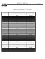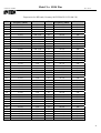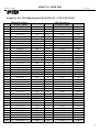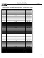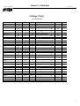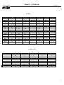
1
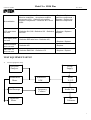
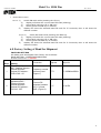
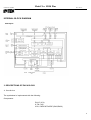
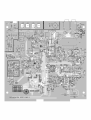
Model No: M150 Plus
Customer: INTEK
Rev No: A
M-150 Plus
Service Manual
.
1
Model No: M150 Plus
Customer: INTEK
Table of Contents
Rev No: A
Page
Specifications …………………………………………………………….……3
Test and Alignment Procedure ……………………………………….….…….4
Block Diagram ………………………………………………………….……13
Schematic Diagram ……………………………………………….………. 14
Printed Circuit Board ……………………………………………………… 20
Channel Frequency Charts ……………………………………….…………22
Parts List ……………………………………………………………………31
Semiconductor Voltage Chart ………………………………………………...37
2
Model No: M150 Plus
Customer: INTEK
Rev No: A
SPECIFICATIONS
1. GENERAL
Channels………………………...…………………………….................. …….400 Ch AM/FM 4W
Frequency Range………………………………...……………… …. …..…25.615 to 30.105 MHz
FrequencyControl……………………………………………………..…………..……………..…PLL
Operating Temperature Range……………………..……………………………….…-10° / +55°C
DC Input Voltage…………………………...……………………………………....13.2 V DC ±15%
Size………………………………………….……………..……….…180(L) X 35(H) X 140(D) mm
Weight……………………………………………………..………………..……...…………0.850 kg
2. RECEIVER
Receiving System……………………………..Dual Conversion Super Heterodyne Intermediate
st
nd
Frequency…………………………………………………….…1 IF: 10.695 MHz, 2 IF: 455 MHZ
Sensitivity……………………………………….....….0.5 µV for 20 db SINAD in FM mode Audio
Distortion……………………………………..………..……..…………….Less Than 8% @ 1 KHz
ImageRejection………………………………………………………………………..………...65 dB
Adjacent ChannelRejection…………………………………………….……………………...65 dB
Signal/ Noise Ratio………………………………………………………………………….….45 dB
Current Drain at standby……………………………………………………………………..325 mA
3.
TRANSMITTER
Output Power……………………………………………………..……….....….4W @ 13.2 V DC
Modulation……………………………………………………...…….……FM: 1.8 KHz ±0.2 KHz
Frequency response…………………………………………………....From 400 Hz to 2.5 KHz
Output impedance…………………………………..…………………………………RF 50 ohm
Unbalance Signal/ Noise Ratio……………………………………………………………..40 dB
MIN Current Drain…………………………………………………………………….….1300 mA
3
Model No: M150 Plus
Customer: INTEK
Rev No: A
OPERATION INSTRUCTIONS
Having properly installed your batteries and hooked-up the antenna, you are now ready to operate your radio for
optimum reception and voice transmission.
Turn the power “ON” with ON/OFF switch.
Set the desired channel.
Adjust the squelch control knob to reduce any undesirable background noise when no signal is being received.
To do this, select a channel where no signal are present, or wait until signals cease on your channel. Then, rotate
the squelch control knob clockwise to a point where the background noise disappears.
Note: When the squelch is set properly, the speaker will remain quiet until a signal is
order to receive weak signals, do not set the squelch too high.
received. In
Adjust the volume to the desired listening level.
To Transmit
Press and hold the push-to-talk button. Speak slowly and clearly in a normal voice two to three inches from the
microphone. A buit-in modulation control circuit will automatically adjust the microphone input level. There is no
need to speak loudly.
To Receive
Release the push-to-talk button.
4
Model No: M150 Plus
Customer: INTEK
Rev No: A
THEORY OF OPERATIONS
TRANSMITTER
A. RF Amplification
The output of double AMP Q14 is fed through tuning IFT L8 to the base of pre driver AMP Q15. The output is
then supplied through tuning circuit L9 to RF driver AMP Q16. The output of Q16 is supplied with tuning circuit
L10 and C116,C67,C95 and goes to the base of final RF AMP Q17. The output of Q17 is supplied to the antenna
through L-C tuning circuit.
B. Circuit for Suppression of Spurious Radiation
The tuning circuit between the output of final AMP Q17 and antenna, 4-stage “PHI” network L13,
C142,C71,C72,L14,C74,C75,L15,C77,C78,L16,C79,C80,L24 serves as a spurious radiation suppressor . This
network also serves to match the impedance between TX power AMP Q17 and the antenna.
C. Circuit for Limiting Power
After finished all alignment, the constant voltage supply circuit limits the available power 4 W or slightly less.
RV4 and corresponding three transistors control supply voltage of RF amplifier and other circuits.
Tune all the trimmer parts for maximum indication of RF power meter and adjust RV4 to make 4 w indication of
RF power meter.
The tuning is adjusted so that the actual power is from 3.5 to 4.0 W. There are no other additional controls for
adjusting the TX output power.
D. Modulation Control
a. FM
The mic input is fed to mic audio amplifier IC KIA324 which drives modulation varicap diode D403 in the VCO
circuit. RV1 limits the incoming modulation audio levels to inhibit over modulation. While reading the modulation
factor on the modulation analyzing equipment, adjust RV1 shall not exceed +-1.7 KHz/Dev. After 20 dB up from
1.25 KHz/1.2 KHz/Dev. Audio level
b. AM
Modulation signals are filtered with RC network and goes to the audio power AMP IC IC103 to make nominal
signal level to achieve wanted modulation. To control incoming audio signal, diode D7 and corresponding ALC
circuit limits the modulation shall not exceed +/-90% adjust RV3 +/-90% modulation under 1.0 KHz AF 60%
mod plus 20 dB of audio signal.
5
Model No: M150 Plus
Customer: INTEK
Rev No: A
E. Receiver
CB receiver is dual conversion supper-heterodyne
type
with the first IF 10.695 MHz and second IF 455 KHz.
st
nd
Receiver is separated two blocks, 1 IF section and 2 IF section. The PLL synthesizer supplies first local
frequency 16.270 ~ 16.710 MHz.(for EU) and 16.90625 MHz ~ 17.29625 MHz (for UK) With the provided first
local frequencies to Q2,Q3 mixes the incoming RF signal to generate first IF signal. Mixed signals were filtered
with the XF1 (10.695 MHz) crystal filter and other tuning
circuits. Output signal of mixer is filtered with CF1(455
nd
KHz ceramic filter). The 455 KHz signal from the 2 IF filter was amplified and limits internaly. After amplification
the signals fed the quadrature detector loop L20. Then we can see the recovered audio signals on Pin 9 for FM
of IC7. With the amplitude of recovered signals, Q10 serves as an audio amplifier. For AM signal Will be pass
filter CF1 and induced to Q6, Q7 respective and detected to voice signal by D5.
TROUBLESHOOTING HINTS
Symptom
Unit does not
work at all
No output from
speaker at all
No noise on
speaker
Probable Cause
Remedy
• Defective power switch VR1. • Blown fuse. •
Broken DC power cord. • Defective IC5.
• Replace • Replace •
Replace • Replace
• Defective external speaker jack. • Poor connection
on microphone connector • Defective push
switch on microphone. • Defective internal
speaker. • Defective VR1, IC8 other
components.
• Repair or replace •
Repair or replace •
Repair or replace •
Replace • Replace the
defective components.
• Measure all the voltage of IC7 with voltage
chart • Defective squelch circuit components
(RV5,RV7,VR2 IC7)
• Replace • Replace
• Defective VR2, RV5,RV7, IC3-D.
Squelch does not
work
• Replace the defective
components. • Re-adjust
6
Model No: M150 Plus
Customer: INTEK
Rev No: A
• Defective microphone. • Poor audio output and
defective modulation microphone amplifier
components (IC3). • Defective microphone
connector components. • Defective ALC circuit
D8,D9
• Replace • Replace the
defective components. •
Replace • Replace the
defective components.
LCD meter does
not work
• Defective D11,D22 • Defective IC5. • Defective
RV2.RV6
• Replace • Replace •
Replace
LCD display does
not work
• Defective RED wire fuse. • Defective IC5, .
Channel selector
does not work
• Defective IC5.
• Replace
EMG CH9.19
does not work
• Defective EMG SW. • Defective IC5.
• Replace • Replace
No modulation
• Replace • Replace
TEST EQUIPMENT SETUP
A.
TX test equipment setup:
Spectrum
Analyzer
Modulation
Meter
Oscilloscope
Distortion
Meter
Power
Supply
Wattmeter
10W
Frequency
Counter
Radio
U.U.T.
Audio Gen.
AC
Voltmeter
7
Model No: M150 Plus
Customer: INTEK
Rev No: A
B. RX test equipment setup:
SINAD Meter
Distortion
Meter
RF Signal
Generator
Power
Supply
8 ohm
loading
Radio
U.U.T.
Oscilloscope
Note: U.U.T. = device under test
Alignment Procedure.
4.1
VCO Adjust.
4.1.1 VCO Voltage Adjust:
Test point TP1 connect to the multi-meter,set UUT enter test mode. Press channel “UP” key to select CH01A of Poland
Band in FM mode.
1. Adjust IFT L17 for 1.0 ± 0.1V on the Multi-meter read,and then checking CH40L of RU Band should be less than
3.8V, and then check AM mode CH01A ≥ 0.8V,CH40L ≤ 3.8 V
2. Set UUT for TX MODE:Check CH01A ≥ 0.8V,CH14D ≤ 3.8V; CH15D ≥ 0.8V, CH21G ≤ 3.8V; CH22G ≥ 0.8V,
CH40L ≤ 3.8V.
3. Turn to AM mode and repeat above item 2.
4.2
RX Section Alignment . ( FM and AM )
4.2.1
Audio Distortion Adjust:
1. UUT set to FM mode CH19,output of RF signal generator connect to TP2. Audio dummy load connect to EXT.
Speaker. (@8Ω load)
2. Set RF S.S.G Freq.: 10.695MHz,Mod.: ±1.2KHz,Fmod.: 1KHz, Output level:1mV.
3. Squelch Volume set to minimum position, volume control set to around middle position.
4. Adjust IFT L20 for maximum audio output and minimum distortion at the distortion meter. ( distortion less than 5%).
5. Set volume control to maximum position, audio output power shall be more than 3 Watts.
6. UUT set to AM mode CH19,output of RF signal generator connect to TP2. Audio dummy load connect to EXT.
Speaker. (@8Ω load)
8
Model No: M150 Plus
Customer: INTEK
Rev No: A
7. Set RF S.S.G Freq.: 10.695MHz,Mod.: 60%,Fmod.: 1KHz, Output level:1mV.
8. Squelch Volume set to minimum position, volume control set to around middle position.
9. Adjust IFT L5 for maximum audio output and minimum distortion at the distortion meter. ( distortion less than 5%).
10. Set volume control to maximum position, audio output power shall be more than 3 Watts.
4.2.2 Sensitivity Adjust:
1.
RX RF bandwidth alignment: Apply Spectrum analyzer’s Track Gen. Output connect to the UUT antenna terminal and
input connect to the UUT TP3 (Q26 Emitter), center frequency set 27MHz, span set 30MHz, adjust IFT L4, L21 & L22
refer to attached table curve, then short TP3 & TP4.
2.
UUT set to FM mode CH22,output of RF signal generator connect to TP5 (Antenna).
3.
Set RF S.S.G Freq.: 27.225MHz,Mod.: ±1.2KHz,Fmod.: 1KHz, Output level:0.5uV.
4.
Adjust the volume control for 2V output on distortion meter read.
5.
Adjust L2 & L3 for more than 12dB at SINAD meter.
6.
Repeat as needed. Check all channels sensitivity must met the D.T.S. specifications.
7.
UUT set to AM mode CH22,output of RF signal generator connect to TP5 (Antenna).
8.
Set RF S.S.G Freq.: 27.185MHz,Mod.: 60%,Fmod.: 1KHz, Output level:0.5uV.
9.
Adjust the volume control for 2V output on distortion meter read.
10. Adjust L2 & L3 for more than 12dB at SINAD meter.
11. Repeat as needed. Check all channels sensitivity must met the D.T.S. specifications.
4.2.3 T- Squelch Sensitivity Adjust:
1. UUT set to AM CH22,output of RF signal generator to the antenna input terminal.
2. Set RF S.S.G Freq.: 27.225MHz,Mod.: 60%,Fmod.: 1KHz, Output level: -47dBm.
3. Volume control and Squelch control set to maximum position,(Full C.W)
4. Adjust the RV5 to mute the speaker, then turn the RF S.S.G. output level to –47dBm.
5. Slowly turn RV5 to a position that the audio output on the speaker just appears from no output. Turn the RF S.S.G.
output level to -57dBm, the audio must be off from the speaker.
Auto Squelch Adjust:
6. UUT set to AM CH22,output of RF signal generator to the antenna input terminal.
7. Set RF S.S.G Freq.: 27.225MHz,Mod.: 60%,Fmod.: 1KHz, Output level: -104dBm.
8. Squelch volume control set to minimum and Off position (Full C.C.W).
9. Adjust the RV7 to mute the speaker, Slowly turn RV7 to a position that the audio output on the speaker just appears
from no output. Turn the RF S.S.G. output level to -107dBm, the audio must be off from the speaker.
4.2.4
RX Signal Meter Display Adjust: (For M-760 Only)
1. UUT set to AM CH22,output of RF signal generator to antenna input terminal. RF Gain volume at maximum. Power
switch turn on.
9
Model No: M150 Plus
Customer: INTEK
Rev No: A
2. Turn the RF S.S.G output for 100uV without modulation.
3. Adjust RV6 for 9 characters displayed at the RX signal strength of the LCD.
4. Turn the RF S.S.G level output increase 30dB, the RX signal strength should up to +30 position.
4.2.5 Maximum S/N Detector & ANL detection:
1.
UUT set to FM CH22,output of RF signal generator to antenna input terminal. RF Gain set to maximum, Squelch set
to minimum, compander set off. (M-150 W/O Compander)
2. Set RF S.S.G Freq.: 27.225MHz,Mod.: ±1.2KHz,Fmod.: 1KHz, Output level: 1mV.
3. The Volume control turn to 0.5 watts audio output for reference A dB.
4. Then off the Modulation, here the audio output for reference B dB. A-B for S/N ≥ 35dB.
5. Compander set to On, repeat above item 3 and 4, A-B for S/N ≥ 50dB. (M-760 only)
6. UUT set to AM CH22, set RF S.S.G Mod. for 60%. Compander set Off. Repeat above item 3 and 4, A-B for S/N ≥
35dB; Compander set to On, repeat above item 3 and 4, A-B for S/N ≥ 50dB. (M-760 only)
7. UUT set to AM CH22, set RF S.S.G mod for 30%. RF level set 5.0uV. ESP set off. RF Gain set to maximum, Squelch
set to minimum. ANL set off, Noise generater (pulse 1us; width 100ms; output level 1.0Vrms) set to on and connect to
the antenna socket with network combinator.
8. Set audio output level for 0.8Vrms for 0dB reference, RF S.S.G MOD. turn off, set ANL to ON, the audio output
should be drop 6dB or below.
4.3 TX Section Alignment.
4.3.1
TX output power and Frequency Alignment:
1.
UUT set to FM EU CH19,Antenna connect to the RF power-meter input terminal.
2.
Set UUT to TX mode, adjust the IFT L8 and L9 for TX power output maximum, and then adjust the RV4 check the
output TX power for 4.0W.
3.
Set UUT turn to AM mode, check the TX power output for 0.7 to 1.3W.
4.
Change to channel to UK band “U40” (27.99125MHz), Adjust the trimmer capacitor CT1 to 27.99125MHz ± 50Hz
on frequency counter. The UUT turn to EU CH19, check the TX carrier frequency should 27.185000 +/- 300Hz.
5.
TX harmonics adjust and checking, turn to FM CH19, adjust L24 for 2nd harmonic -36dBm below.
4.3.2 TX Signal Meter Indicator Alignment.
1. UUT set to AM CH19,input of power-meter to antenna input terminal.
2. Set UUT to TX mode, adjust the RV2 for “4” characters displayed at the TX signal strength of the LCD display.
4.3.3 TX modulation Deviation Alignment:
10
Model No: M150 Plus
Customer: INTEK
Rev No: A
1. UUT set to FM I2 CH19, input of power-meter to antenna input terminal. Input of MIC socket to the audio frequency
signal generator output terminal. Mic Gain set to maximum. Compander set to Off.
2. Set audio frequency signal generator @ FREQ.: 1000Hz
Output level: 50mVrms.
Note: Should be add one
10uF capacitor in series between the AF signal O/P and UUT input.
3. Set UUT to TX mode, adjust RV1 for 1.6KHz deviation on modulation meter.
4. Decrease the AF output level. Check the 1.2KHz deviation modulation sensitivity should be between 8 -15 mV;
Compander set On, Check the 1.2KHz deviation modulation sensitivity should be between 3-8 mV.
5. Turn the AF output level for 1.2KHz deviation on modulation meter, check the modulation distortion must be less than
5.0% on the audio distortion meter for Compander On and Off..
6. Set UUT to AM mode; Set audio frequency signal generator @ FREQ.: 1000Hz
Output level: 50mVrms.
7. Set UUT to TX mode, adjust RV3 for 90% deviation on modulation meter.
8. Decrease the AF output level. Check the 50% deviation modulation sensitivity should be between 8-15 mV;
Compander set On, Check the 50% deviation modulation sensitivity should be between 3-8 mV.
9. Turn the AF output level for 60% deviation on modulation meter, check the modulation distortion must be less than
5.0% on the audio distortion meter for Compander On and Off..
4.3.4 PA audio output checking:
1. The UUT enter PA mode after long press the “ANL” key, Volume set maximum position for M-150, and the MIC gain
set maximum position for M-760. 1KHz audio input.
2. Turn to TX mode, the PA output must meet the DTS.
5.0 TEST MODE DESCRIPTION,Model Selection and International Band Select:
1. For M-760, Press both keys of
“ANL” & “Scan” synchronously, then turn on the DC power enter test mode. Press
the “ENG” key for Software version checking, press the Channel “Down” key for LCD segments scanning checking.
2. For M-150, Press both keys of
“ANL” & “DN” synchronously, then turn on the DC power enter test mode. Press the
“ENG” key for Software version checking, press the Channel “Down” key for LED segments scanning checking.
3. RX & TX parameter test: Press the “channel up” key can select Germany CH41 (26.565MHz),
CH19(27.185MHz),
EU CH22(27.225MHz) and UK CHU40(27.99125MHz), PO CH01A and RU CH40L.
4. EEPROM control for VCO alignment for Channel RU 14D, RU 15D, RU 21G and RU 22G.
5. VCO Alignment Channel: PO band CH01A(25.610MHz) ---- Low channel; RU band channel CH40L(30.105MHz)
---- High channel.
6. Model selection and European band and International band selection.
Model select: M-150 R146 = N/A and R145 = 10K; M-760 R146 = 47K and R145 = N/A. (CPU PIN64 pull high for M-150;
CPU PIN64 pull low for M-760)
International Band select: “IB” pad open for European band only, International band disable; “IB” PAD shorting that the
International band enable and the European band enable also. (CPU pin 21 pull high for International Band)
11
Model No: M150 Plus
Customer: INTEK
Rev No: A
7. BAND SELECTION:
M-150: 1)
5)
2)
3)
4)
switch ON radio while pressing the UP key
display will show the current band ID code (blinking)
select band using the UP or DN keys
shortly press the DN key to confirm
display will show the selected band ID code for 2-3 seconds, then it will show the
channel number
switch ON radio while pressing the EMG key
M-760: 1)
2)
display will show the current band ID code (blinking)
3)
select band using the UP or DN keys
4)
shortly press the EMG key to confirm
5)
display will show the selected band ID code for 2-3 seconds, then it will show the
channel number
6.0 Factory Setting of Band for Shipment
FACTORY SETTING
All radios must be shipped from factory set as follows :
BAND SETTING : EUROPEAN BANDS ONLY
RADIO SWITCH ON : CE BAND
Step
1
2
Setting
Frequency adjustment
MIC : Receive Volume :
optional Squelch :
optional CH selector :
19 EU CH9 : off
Connection
Adjuster
Adjust for
Frequency counter
to dummy load
(Figure 1).
CT1
27.185MHz±300Hz
VCO Voltage
adjustment MIC :
Receive Volume :
optional Squelch :
optional CH selector :
1A CH9 : OFF
Connect DC
voltmeter between
R97, C112and
GND. (Figure 2).
L17
1V at RX.
12
Model No: M150 Plus
Customer: INTEK
Rev No: A
PLL CIRCUIT BLOCK DIAGRAM
1. INTRODUCTION
The frequencies for transmitter and receiver first local frequencies are all derived from a single 4.0 MHz crystal
by means of a phase locked loop. The first local oscillator frequencies are 26.965 MHz (CH 1) to
27.405MHz (CH 40) for EU and 27.60125 MHz (CH 1) to 27.99125 MHz (CH 40) for UK . The second local
frequency is fixed at 10.240 MHz to generate second IF 455 KHz.
The VCO operating frequency for the receiver is 37.660 MHz (CH 1) to 37.560 MHz (CH 40) as the first local
oscillator, injected through the buffer AMP Q411 into the first fed balanced mixer Q2 and Q3.
2. BASIC SYNTHESIZER SCHEME
The crystal frequency (4.000 MHz) is divided by 800 times to make 5 KHz which is fed to one side of the phase
detector. The VCO output is divided by a programmable divider, and fed to other side of the phase detector of
IC4. The feedback loop is closed by passing the phase detector output through an active low pass filter and using
the output to control the VCO frequency through varicap diode D402,D403
Under locked conditions, both of phase detector input signal must be indential at 5 KHz. The VCO frequency is
then given by:
FVCO / N
= 0.005 MHz or FVCO = 0.005 x N MHz
Since “N” is an integer, the VCO frequency can be stepped up with 5 KHz increments. By suitable choice of “N”
the desired output frequency can be obtained.
Channel 1
Channel 40
Transmit
Receive
N
5393
7532
FVCO
26.965
37.660
N
5481
7620
FVCO
27.405
38.100
Transmit
5520.25
27.60125
5598.25
27.99125
Receive
7659.2
38.296
7737.25
38.68625
FUNCTION
EU
UK
Since all frequencies are obtained from the crystal controlled PLL oscillator, all outputs are coherent with the
crystal oscillator frequency and maintaining the same percentage accuracy.
13
Model No: M150 Plus
Customer: INTEK
Rev No: A
INTERNAL BLOCK DIAGRAM
3. DESCRIPTIONS OF EACH BLOCK
A. Introduction
The synthesizer is implemented with the following
Components:
PLL IC (IC4)
X-TAL (X2)
VCO, VARICAP DOIDE (D402,D403)
14
Model No: M150 Plus
Customer: INTEK
Rev No: A
IC5 is a cmos LSI that includes most of PLL block and driver, the Q403-Q406,Q408, C412, C421, C416, C417
and L17, Varicap diode D402,D403 are clapp oscillator circuit to operate as a VCO. Q406 is a switching
transistor to connect or disconnect the tuning capacitor in the VCO oscillator tank circuit for transmitter or
receiver. Q411 works as a buffer AMP for RX local frequencies (38MHz) and TX generating frequencies (26
MHz).
B. Reference frequency
The crystal, X2 (4.000 MHz) and other components at IC4 can make a reference frequency oscillator with internal
amplifier.
C. VCO
Q408 and surrounding parts are consisting a clapp oscillator works as a VCO . the VCO can be oscillate over the
required of 25.610MHz to 41.115 MHz
D. Phase detector and VCO control
The detector is a digital phase comparator which compares the phase of the reference signal with programmable
divider output square waves and develops a series of pulses whose DC level depends on the phase error of each
signal.
E. Transmitter/Receiver buffer AMP
Output signal of Q408 is fed into buffer AMP Q411,
F. Switching of tuning capacitor in VCO
The VCO circuit must tune with a wide rang of frequencies 25.610MHz to 30.15MHz for transmitter and
36.305~41.115 MHz for receiver. To comply above rang of VCO, the tuning capacitance should switched for
transmission or reception.
G. Receiver local oscillator outputs
First Mixer:
st
st
The secondary output signals is injected to the sources of 1 mixer Q2,Q3 in the 1 IF mixer
section
Second Mixer:
The output of 10.24 MHz oscillator circuit with XF1 is injected into the IF IC internally. Incoming IF
nd
signal and 10.24 MHz are mixed inside the IF IC to extract 2 IF signal 455 KHz. FM,AM audio
signals are recovered with the way of quadrature detector, AM signals are recovered with envelope
detector.
15
Model No: M150 Plus
Customer: INTEK
Rev No: A
4. FREQUENCY STABILITY
LET :
Fo = Crystal oscillator frequency
Fr = Phase detector reference frequency
Fvco = VCO frequency
Ft = Transmit frequency
Then : Fr = Fo/800
And under locked conditions : Fr = Fvco / N
WHERE, “N” is the programmable divider divide ratio.
THEN : Fvco = N X Fr
From which it can be seen, the percentage error in Ft is the same as the percentage error in Fo. The stability of the
crystal oscillator is determined primarily by the crystal itself and having lesser deviation by the active and passive
components of the oscillator. The choice of crystal and component is such that the required frequency stability is
maintained over the required voltage and temperature rang.
16
Model No: M150 Plus
Customer: INTEK
Rev No: A
Frequencies Tables for M-760 Plus
Specification
Legal Bands
Italy 40CH AM / FM 4W
Italy 36CH AM / FM 4W
Germany 80CH FM 4W 12CH AM 1W
Germany 40CH FM 4W 12CH AM 1W
Europe 40CH FM 4W 40CH AM 1W
CEPT 40CH FM 4W
England 40CH FM 4W English Frequencies + EC 40CH FM 4W CEPT
Poland 40CH AM / FM 4W Polish Frequencies –5kHz
LCD Display
EI
I2
DE
D2
EU
CE
U
PL
Illegal Bands
Russia 400CH AM / FM 4W
Poland 400CH AM / FM 4W Polish Frequencies –5kHz
Private Channels AM / FM 4W
RU
PO
PC
17
Model No: M150 Plus
Customer: INTEK
Rev No: A
Frequencies for EI band (Italy 40CH AM / FM 4W)
CH
1
2
3
4
5
6
7
8
9
10
11
12
13
14
15
16
17
18
19
20
21
22
23
24
25
26
27
28
29
30
31
32
33
34
35
36
37
38
39
40
Frequency (MHz)
26.965
26.975
26.985
27.005
27.015
27.025
27.035
27.055
27.065
27.075
27.085
27.105
27.115
27.125
27.135
27.155
27.165
27.175
27.185
27.205
27.215
27.225
27.255
27.235
27.245
27.265
27.275
27.285
27.295
27.305
27.315
27.325
27.335
27.345
27.355
27.365
27.375
27.385
27.395
27.405
Modulation
AM / FM
AM / FM
AM / FM
AM / FM
AM / FM
AM / FM
AM / FM
AM / FM
AM / FM
AM / FM
AM / FM
AM / FM
AM / FM
AM / FM
AM / FM
AM / FM
AM / FM
AM / FM
AM / FM
AM / FM
AM / FM
AM / FM
AM / FM
AM / FM
AM / FM
AM / FM
AM / FM
AM / FM
AM / FM
AM / FM
AM / FM
AM / FM
AM / FM
AM / FM
AM / FM
AM / FM
AM / FM
AM / FM
AM / FM
AM / FM
18
Model No: M150 Plus
Customer: INTEK
Rev No: A
Frequencies for I2 band (Italy 34CH AM / FM 4W)
CH
1
2
3
4
5
6
7
8
9
10
11
12
13
14
15
16
17
18
19
20
21
22
23
24
25
26
27
28
29
30
31
32
33
34
35
36
Frequency (MHz)
26.965
26.975
26.985
27.005
27.015
27.025
27.035
27.055
27.065
27.075
27.085
27.105
27.115
27.125
27.135
27.155
27.165
27.175
27.185
27.205
27.215
27.225
27.255
27.245
27.265
26.875
26.885
26.895
26.905
26.915
26.925
26.935
26.945
26.955
26.855
26.865
Modulation
AM / FM
AM / FM
AM / FM
AM / FM
AM / FM
AM / FM
AM / FM
AM / FM
AM / FM
AM / FM
AM / FM
AM / FM
AM / FM
AM / FM
AM / FM
AM / FM
AM / FM
AM / FM
AM / FM
AM / FM
AM / FM
AM / FM
AM / FM
AM / FM
AM / FM
AM / FM
AM / FM
AM / FM
AM / FM
AM / FM
AM / FM
AM / FM
AM / FM
AM / FM
AM / FM
AM / FM
19
Model No: M150 Plus
Customer: INTEK
Rev No: A
Frequencies for DE band (Germany 80CH FM 4W 12CH AM 1W)
CH
1
2
3
4
5
6
7
8
9
10
11
12
13
14
15
16
17
18
19
20
21
22
23
24
25
26
27
28
29
30
31
32
33
34
35
36
37
38
39
40
Frequency (MHz)
26.965
26.975
26.985
27.005
27.015
27.025
27.035
27.055
27.065
27.075
27.085
27.105
27.115
27.125
27.135
27.155
27.165
27.175
27.185
27.205
27.215
27.225
27.255
27.235
27.245
27.265
27.275
27.285
27.295
27.305
27.315
27.325
27.335
27.345
27.355
27.365
27.375
27.385
27.395
27.405
Modulation
CH
FM
FM
FM
AM / FM
AM / FM
AM / FM
AM / FM
AM / FM
AM / FM
AM / FM
AM / FM
AM / FM
AM / FM
AM / FM
AM / FM
FM
FM
FM
FM
FM
FM
FM
FM
FM
FM
FM
FM
FM
FM
FM
FM
FM
FM
FM
FM
FM
FM
FM
FM
FM
41
42
43
44
45
46
47
48
49
50
51
52
53
54
55
56
57
58
59
60
61
62
63
64
65
66
67
68
69
70
71
72
73
74
75
76
77
78
79
80
Frequency (MHz)
26.565
26.575
26.585
26.595
26.605
26.615
26.625
26.635
26.645
26.655
26.665
26.675
26.685
26.695
26.705
26.715
26.725
26.735
26.745
26.755
26.765
26.775
26.785
26.795
26.805
26.815
26.825
26.835
26.845
26.855
26.865
26.875
26.885
26.895
26.905
26.915
26.925
26.935
26.945
26.955
Modulation
FM
FM
FM
FM
FM
FM
FM
FM
FM
FM
FM
FM
FM
FM
FM
FM
FM
FM
FM
FM
FM
FM
FM
FM
FM
FM
FM
FM
FM
FM
FM
FM
FM
FM
FM
FM
FM
FM
FM
FM
20
Model No: M150 Plus
Customer: INTEK
Rev No: A
Frequencies for D2 band (Germany 40CH FM 4W 12CH AM 1W)
CH
1
2
3
4
5
6
7
8
9
10
11
12
13
14
15
16
17
18
19
20
21
22
23
24
25
26
27
28
29
30
31
32
33
34
35
36
37
38
39
40
Frequency (MHz)
26.965
26.975
26.985
27.005
27.015
27.025
27.035
27.055
27.065
27.075
27.085
27.105
27.115
27.125
27.135
27.155
27.165
27.175
27.185
27.205
27.215
27.225
27.255
27.235
27.245
27.265
27.275
27.285
27.295
27.305
27.315
27.325
27.335
27.345
27.355
27.365
27.375
27.385
27.395
27.405
Modulation
FM
FM
FM
AM / FM
AM / FM
AM / FM
AM / FM
AM / FM
AM / FM
AM / FM
AM / FM
AM / FM
AM / FM
AM / FM
AM / FM
FM
FM
FM
FM
FM
FM
FM
FM
FM
FM
FM
FM
FM
FM
FM
FM
FM
FM
FM
FM
FM
FM
FM
FM
FM
21
Model No: M150 Plus
Customer: INTEK
Rev No: A
Frequencies for EU band (Europe 40CH FM 4W 40CH AM 1W)
CH
1
2
3
4
5
6
7
8
9
10
11
12
13
14
15
16
17
18
19
20
21
22
23
24
25
26
27
28
29
30
31
32
33
34
35
36
37
38
39
40
Frequency (MHz)
26.965
26.975
26.985
27.005
27.015
27.025
27.035
27.055
27.065
27.075
27.085
27.105
27.115
27.125
27.135
27.155
27.165
27.175
27.185
27.205
27.215
27.225
27.255
27.235
27.245
27.265
27.275
27.285
27.295
27.305
27.315
27.325
27.335
27.345
27.355
27.365
27.375
27.385
27.395
27.405
Modulation
AM / FM
AM / FM
AM / FM
AM / FM
AM / FM
AM / FM
AM / FM
AM / FM
AM / FM
AM / FM
AM / FM
AM / FM
AM / FM
AM / FM
AM / FM
AM / FM
AM / FM
AM / FM
AM / FM
AM / FM
AM / FM
AM / FM
AM / FM
AM / FM
AM / FM
AM / FM
AM / FM
AM / FM
AM / FM
AM / FM
AM / FM
AM / FM
AM / FM
AM / FM
AM / FM
AM / FM
AM / FM
AM / FM
AM / FM
AM / FM
22
Model No: M150 Plus
Customer: INTEK
Rev No: A
Frequencies for CE band (CEPT 40CH FM 4W)
CH
1
2
3
4
5
6
7
8
9
10
11
12
13
14
15
16
17
18
19
20
21
22
23
24
25
26
27
28
29
30
31
32
33
34
35
36
37
38
39
40
Frequency (MHz)
26.965
26.975
26.985
27.005
27.015
27.025
27.035
27.055
27.065
27.075
27.085
27.105
27.115
27.125
27.135
27.155
27.165
27.175
27.185
27.205
27.215
27.225
27.255
27.235
27.245
27.265
27.275
27.285
27.295
27.305
27.315
27.325
27.335
27.345
27.355
27.365
27.375
27.385
27.395
27.405
Modulation
FM
FM
FM
FM
FM
FM
FM
FM
FM
FM
FM
FM
FM
FM
FM
FM
FM
FM
FM
FM
FM
FM
FM
FM
FM
FM
FM
FM
FM
FM
FM
FM
FM
FM
FM
FM
FM
FM
FM
FM
23
Model No: M150 Plus
Customer: INTEK
Rev No: A
Frequency For UK Band(England 40CH FM 4W + CEPT 40CH 4W)
England Frequency
CH
1
2
3
4
5
6
7
8
9
10
11
12
13
14
15
16
17
18
19
20
21
22
23
24
25
26
27
28
29
30
31
32
33
34
35
36
37
38
39
40
Frequency (MHz)
27.60125
27.61125
27.62125
27.63125
27.64125
27.65125
27.66125
27.67125
27.68125
27.69125
27.70125
27.71125
27.72125
27.73125
27.74125
27.75125
27.76125
27.77125
27.78125
27.79125
27.80125
27.81125
27.82125
27.83125
27.84125
27.85125
27.86125
27.87125
27.88125
27.89125
27.90125
27.91125
27.92125
27.93125
27.94125
27.95125
27.96125
27.97125
27.98125
27.99125
CEPT Frequency
Modulation
CH
FM
FM
FM
FM
FM
FM
FM
FM
FM
FM
FM
FM
FM
FM
FM
FM
FM
FM
FM
FM
FM
FM
FM
FM
FM
FM
FM
FM
FM
FM
FM
FM
FM
FM
FM
FM
FM
FM
FM
FM
1
2
3
4
5
6
7
8
9
10
11
12
13
14
15
16
17
18
19
20
21
22
23
24
25
26
27
28
29
30
31
32
33
34
35
36
37
38
39
40
Frequency (MHz)
26.965
26.975
26.985
27.005
27.015
27.025
27.035
27.055
27.065
27.075
27.085
27.105
27.115
27.125
27.135
27.155
27.165
27.175
27.185
27.205
27.215
27.225
27.255
27.235
27.245
27.265
27.275
27.285
27.295
27.305
27.315
27.325
27.335
27.345
27.355
27.365
27.375
27.385
27.395
27.405
Modulation
FM
FM
FM
FM
FM
FM
FM
FM
FM
FM
FM
FM
FM
FM
FM
FM
FM
FM
FM
FM
FM
FM
FM
FM
FM
FM
FM
FM
FM
FM
FM
FM
FM
FM
FM
FM
FM
FM
FM
FM
24
Model No: M150 Plus
Customer: INTEK
Rev No: A
Frequencies for PL band (Poland 40CH AM / FM 4W Polish Frequencies –5kHz)
CH
1
2
3
4
5
6
7
8
9
10
11
12
13
14
15
16
17
18
19
20
21
22
23
24
25
26
27
28
29
30
31
32
33
34
35
36
37
38
39
40
Frequency (MHz)
26.960
26.970
26.980
27.000
27.010
27.020
27.030
27.050
27.060
27.070
27.080
27.100
27.110
27.120
27.130
27.150
27.160
27.170
27.180
27.200
27.210
27.220
27.250
27.230
27.240
27.260
27.270
27.280
27.290
27.300
27.310
27.320
27.330
27.340
27.350
27.360
27.370
27.380
27.390
27.400
Modulation
AM / FM
AM / FM
AM / FM
AM / FM
AM / FM
AM / FM
AM / FM
AM / FM
AM / FM
AM / FM
AM / FM
AM / FM
AM / FM
AM / FM
AM / FM
AM / FM
AM / FM
AM / FM
AM / FM
AM / FM
AM / FM
AM / FM
AM / FM
AM / FM
AM / FM
AM / FM
AM / FM
AM / FM
AM / FM
AM / FM
AM / FM
AM / FM
AM / FM
AM / FM
AM / FM
AM / FM
AM / FM
AM / FM
AM / FM
AM / FM
25
Model No: M150 Plus
Customer: INTEK
Rev No: A
PART LIST
Item
Part Number
Description
1 KEJ-010
2 KEJ-512
3 KEJW-TA24BK
ANTENNA RECEPTACLE
MIC SOCKET 6PIN NTINNED WIRE UL1007
89713-0013
16-6R QIINGXI NG
#24 BLACK
4 KEJW-TA24BL
5 KEJW-TA24GR
TINNED WIRE UL1007
TINNED WIRE UL1007
#24 BLUE
#24 GREEN
TINNED WIRE UL1007
TINNED WIRE UL1007
DC POWER CORD UL10
8OHM 2W L3050AE-8TRANSISTOR NPN 2SC
CAP. ELECT. 50V M
CAP. ELECT. 50V M%
CAP. ELECT. 16V M%
CAP. ELECT. 16V M%
CAP. ELECT. 25V M%
CAP. ELECT. 16V M%
CAP. ELECT. 16V M%
CAP. ELECT. 25V M%
CAP. ELECT. 16V M%
CAP. ELECT. 16V M%
CAP. ELECT. 16V M%
CAP. TRIMMER JTC06
CRYSTAL FILTER 10.
CERAMIC FILTER LT4
8V2BSCST SEMTECH Z
DIODE GERMANIUM
DIODE IN4004
IFT 7X7MM 27MHZ KS
5840 LAIHENG IFT
KS2641 LIKHANG LH
2762 CAIHENG IFT
320-5763 LAIHENG
73C-359 LAIHENG IFT
321-0952 LAIHENG I
320-5774 LAIHENG I
3205851Z LAIHENG I
IC TDA2003 10W AUD
SPEAKER JACK JC-30
0.8X6.0X5.5 TS-P
0.8*2.5*7TS-P-B AI
#24 RED
#24 WHITE
15 20AWG
7B05R ASAHI
2078(D)
0.1UF
1UF
10UF
100UF
1000UF
22UF
220UF
220UF
47UF
47UF
470UF
E300 30PF
695MHZ QUARTZ
55HTW FRONTER
ENER DIODE
1K261
6
7
8
9
10
11
12
13
14
15
16
17
18
19
20
21
22
23
24
25
26
27
28
29
30
31
32
33
34
35
36
37
38
39
40
KEJW-TA24RD
KEJW-TA24WE
KEOE-OT513
KESP-253
KET-C2078D
KEC-E104HRMU
KEC-E105HRMU
KEC-E106ERMU
KEC-E107ERMU
KEC-E108FRMU
KEC-E226ERMU
KEC-E227ERMU
KEC-E227FRMU
KEC-E476ERMKS
KEC-E476ERMU
KEC-E477ERMU
KEC-TR031-A
KECF-0070-A
KECF-0216
KED-ZS8V2BSCST
KED-1K261
KED-4004-A
KEI-061LH
KEI-265LH
KEI-266LH
KEI-267LH
KEI-268LH
KEI-269LH
KEI-270LH
KEI-271LH
KEI-272LH
KEIC-TDA2003
KEJ-012
KEL-S147
KEL-S148
41 KEL-S149
0.6*5.0*13.5TS-P-B
2295R
IFT
FT
ET
FT
IO AMP YD
4B
R CORE COIL
AIR CORE COIL
WFD
QTY
Ref
1
1
1 SPMIC(L=0.11),VR1,VR2
VR3,VR4SW
0.2 MIC(L=0.16),VR1(L=0.08)
0.5 MIC,VR1,VR2,VR3
VR4(L=0.1),SW(L=0.03)
0.4 VR1,VR2,VR4,MIC
0.5 MIC,VR1,VR2,VR3
1
1 SPEAKER1
1 Q17
3 C107,C141,C168
3 C29,C50,C51
3 C16,C90,C152
3 C35,C85,C181
4 C31,C113,C154,C11A
2 C134,C158
3 C120,C155,C60
1 C102
1 C157
2 C59,C144
2 C94,C185
1 CT1
1 XF1
1 CF1
1 DZ1
1 D5
2 D6,D10
2 L22,L21
1 L5
1 L17
1 L20
1 L3
1 L8
1 L2
1 L9
1 L4
1 IC8
2 J1,J6
4 L13,L14,L15,L16
1 L10
1 L12
26
Model No: M150 Plus
Customer: INTEK
Rev No: A
42
43
44
45
46
47
48
49
50
51
52
53
54
55
56
57
58
59
60
61
62
63
64
65
66
67
68
69
70
71
72
KEL-V208AD
KEL-V308WFD
KEL-101MA-1
KEL-102K-LF
KEL-159CL-4
KEL-689CL-4
KEL-689MA-2
KEL-752WF
KER-MX120FBB
KER-MX471EBB
KER-100DBB
KER-102KVSF637A
KER-103KVSF637A
KER-104KVSF637A
KER-223KVSF637A
KER-229CBB
KER-302CBB
KER-471CFB
KER-473KVSF637A
KER-479DBB
KER-751DBB
KERY-039
KET-2SC2314F
KETR-011-A
KETR-067
KEX-0318
KEX-0474
M-760B1S
M-760B1SB
KCC-102FRJNPOB
KCC-103FRKBB
COIL VARIABLE 0.20
COIL VARIABLE 0.3U
COIL FIXED 100UH
FIXED COIL 1MH 10%
COIL FIXED 1.5UH A
COIL FIXED 6.8UH
COIL FIXED 6.8UH
INDUCTOR LGA0415#7
RES MX-FILM 2W 5%
RES.MX-FILM 1W 5%
RES. C-FILM 1/2W 5
RES. SEMI KVSF637A
RES. SEMI. KVSF637
RES. SEMI. KVSF637
RES. SEMI. KVSF637
RES. C-FILM 1/4W 5
RES. C-FILM 1/4W 5
RES. C-FILM 1/4W 5
RES. SEMI. KVSF637
RES. C-FILM 1/2W 5
RES C-FILM 1/2W 5%
RELAY TRKM(78F) DTRANSISTOR 2SL2314
TRANSFORMER CHOKE
BW-0903 BAN WO TRA
CRYSTAL 10.24DMHZ
CRTAL 4MZ-20PPM-HC
BASE MAIN PCB SMT
BASE MAIN PCB SMT
CAP. CER CHIP 50V
CAP. CER. CHIP 50V
73
74
75
76
77
78
79
80
81
82
83
84
85
86
87
88
89
90
KCC-104DRKBB
KCC-120FRJNPOB
KCC-122FRKBB
KCC-150FRJNPOB
KCC-151FRJNPOB
KCC-200FRJNPOB
KCC-201FRJNPOB
KCC-271FRJNPOB
KCC-333DRKBB
KCC-390FRJNPOB
KCC-409FRCNPOB
KCC-470FRJNPOB
KCC-473DRKBB
KCC-473FRKBB
KCC-509FRCNPOB
KCC-680FRJNPOB
KCD-KDS160
KCR-000B
CAP. CER. CHIP 16V
CAP. CER. CHIP 50V
CAP. CER. CHIP 50V
CAP. CER. CHIP 50V
CAP. CER. CHIP 50V
CAP. CER. CHIP 50V
CAP. CER. CHIP 50V
CAP. CER. CHIP 50V
CAP. CER. CHIP 16V
CAP. CER. CHIP 50V
CAP. CER. CHIP 50V
CAP. CER. CHIP 50V
CAP. CER. CHIP 16V
CAP. CER. CHIP 50V
CAP. CER. CHIP 50V
CAP. CER. CHIP 50V
DIODE CHIP KDS160
RES. CHIP 1/16W 0
UH 20%
H 20%
10%
AL0307-102K-LF
70704029
BOTTOM
CH J 0.001UF
B K% 0.01UF
1
1
1
1
1
1
1
2
1
1
1
1
2
1
1
1
1
1
2
1
1
2
1
1
1
1
1
1
1
1
11
B K% 0.1uF
CH J% 12PF
B K% 0.0012UF
CH J% 15PF
CH J% 150PF
CH J% 20PF
NPO J% 200P
CH J% 270PF
B K% 0.033UF
CH J% 39PF
CH C% 4PF
CH J% 47PF
B K% 0.047uF
B K% 0.047uF
CH C 5PF
CH J% 68PF
KEC
OHM
2
2
1
2
3
1
1
2
1
2
1
7
1
2
1
3
8
1
R5M-B 7.5UH
12 OHM
S 470 OHM
% S 10 OHM
1KOHM
A 10K
A 100K
A 22KOHM
% S 2.2 OHM
% S 3K
% F 470 OHM
A 47K
% S 4.7 OHM
750 OHM
12VDC-S-Z
(F) NPN
EI19KY-226
NSFORMER
CL=30PF
L24
L24
L23
L19
L1
L25
L11
L6,L18
R75
R138
R70
RV3
RV1,RV4
RV2
RV7
R107
R71
R8
RV6,RV5
R64
R66
K12,K13
Q16
CH1
T1
X1
X2
C67
C3,C61,C83,C99,C126,C140,
C8,C32,C82,C100,C132
C114,C156
C164,C163
C73
C165,C183
C124,C116,C75
C43
C77
C79,C78
C159
C92,C122
C101
C44,C142,C80,C76,C66,C95,C71
C88
C69,C70
C143
C1,C2,C74
D3,D4,D11,D12,D13,D22,D23,D24
R149
27
Model No: M150 Plus
Customer: INTEK
91
92
93
94
95
96
97
98
99
100
101
102
103
104
105
106
107
108
109
110
111
112
113
114
KCR-101B
KCR-102B
KCR-103B
KCR-151B
KCR-152B
KCR-154B
KCR-183B
KCR-221B
KCR-222B
KCR-273B
KCR-471B
KCR-474B
KCR-563B
KCT-KTC3875S
KCT-KTC3880S
KCT-MMBTSC3265Y
M-760B1ST
KCC-T105EAM
KCC-T335DK3216
KCC-100FRJNPOB
KCC-101FRJNPOB
KCC-102FRJNPOB
KCC-102FRKBB
KCC-103FRKBB
Rev No: A
RES. CHIP 1/16W 100
RES. CHIP 1/16W 1K
RES. CHIP 1/16W 10K
RES. CHIP 1/16W 150
RES. CHIP 1/16W
RES. CHIP 1/16W
RES. CHIP 1/16W 18K
RES. CHIP 1/16W 220
RES. CHIP 1/16W 2.2K
RES. CHIP 1/16W 27K
RES. CHIP 1/16W 470
RES. CHIP 1/16W
RES. CHIP 1/16W 56K
TR. CHIP NPN KTC38
TR. CHIP NPN KTC38
TRANSISTOR MMBTSC3
BASE MAIN PCB SMT
CAP. TANT. CHIP 16
CAP TANTALUM 3.3U
CAP. CER. CHIP 50V
CAP. CER. CHIP 50V
CAP. CER CHIP 50V
CAP. CER. CHIP 50V
CAP. CER. CHIP 50V
75S(GR)
80S SOT-23
265Y SOT23
TOP
V M% 1uF
10V 10% A
CH J% 10PF
CH J% 100PF
CH J 0.001UF
B K% 0.001UF
B K% 0.01UF
2
1
5
1
1
1
1
1
3
1
1
1
1
3
2
2
1
1
2
2
7
3
8
27
115 KCC-104DRKBB
CAP. CER. CHIP 16V
B K% 0.1uF
24
116 KCC-105BRZFB
117 KCC-106BRZFF
CAP. CER. CHIP 10V
CAP CER CHIP 10V F
Y5V Z% 1UF
Z 10UF
6
16
118
119
120
121
122
123
124
125
126
127
128
129
130
131
CAP. CER. CHIP 50V
CAP. CER. CHIP 50V
CAP. CER. CHIP 50V
CAP. CER. CHIP 50V
CAP. CER. CHIP 16V
CAP. CER. CHIP 50V
CAP. CER. CHIP 50V
CAP. CER. CHIP 16V
CAP. CER. CHIP 50V
CAP.CHIP 10V +/-10
CAP. CER. CHIP 50V
CAP. CER. CHIP 50V
CAP. CER. CHIP 50V
CAP. CER. CHIP 50V
CH J% 12PF
CH J% 120PF
CH J% 15PF
CH J% 150PF
B K 0.015UF
CH J% 18PF
B K% 0.0022UF
B K% 0.022uF
B K% 0.022UF
% X7R 2.2UF
CH J% 27PF
CH J% 270PF
CH J% 39PF
CH C% 4PF
KCC-120FRJNPOB
KCC-121FRJNPOB
KCC-150FRJNPOB
KCC-151FRJNPOB
KCC-153DRKBB
KCC-180FRJNPOB
KCC-222FRKBB
KCC-223DRKBB
KCC-223FRKBB
KCC-225BKBMUM
KCC-270FRJNPOB
KCC-271FRJNPOB
KCC-390FRJNPOB
KCC-409FRCNPOB
1.5K
150K
470K
1
2
1
1
1
1
1
1
1
3
1
1
2
1
R88,R5
R1
R72,R147,R153,R155,R161
R62
R94
R55
R6
R56
R73,R151,R160
R2
R104
R135
R87
Q44,Q45,Q46
Q14,Q26
Q29,Q34
C112
C6,C7
C9,C425
C40,C41,C42,C133,C171,C38,C81
C10,C182,C121
C25,C45,C47,C91,C106,C167C170,
C19,C20,C24,C27,C34,C36,C58,
C110,C135,C145,C146,C120A
C173,C203,C212, C39,C149
C503,C175,C119,C86,C89,C97
C63,,C424,C174,C427,C84,
C15,C21,C26,C28,C49,C55,C57,
C136,C147,C153,C166,C169,C148
C172,C180,C192,C127,C130
C118,C207,C21,C131,C208,C209
C93,C161,C200,C201,C202,C210
C87,C103,C104,C109,C138,C139,
C466,C467,C468,C502,C213
C150,C151,C125,C56,C214
C417
C13,C62
C416
C65
C14
C413
C160
C46
C64
C215,C204,C216
C176
C412
C428,C421
C429
28
Model No: M150 Plus
Customer: INTEK
Rev No: A
132
133
134
135
136
137
138
139
140
141
142
KCC-470FRJNPOB
KCC-472FRKBB
KCC-473DRKBB
KCC-473FRKBB
KCC-561FRJNPOB
KCC-609FRDNPOB
KCC-680FRJNPOB
KCC-682FRKBB
KCC-683FRKBB
KCC-820FRJNPOB
KCD-KDS160
CAP. CER. CHIP 50V
CAP. CER. CHIP 50V
CAP. CER. CHIP 16V
CAP. CER. CHIP 50V
CAP. CER. CHIP 50V
CAP CER CHIP 50V C
CAP. CER. CHIP 50V
CAP. CER. CHIP 50V
CAP. CER. CHIP 50V
CAP. CER. CHIP 50V
DIODE CHIP KDS160
CH J% 47PF
B K% 0.0047UF
B K% 0.047uF
B K% 0.047uF
CH J% 560PF
H D 6PF
CH J% 68PF
B K% 0.0068UF
B K% 0.068UF
CH J% 82PF
KEC
3
1
6
4
1
2
2
1
1
2
13
143
144
145
146
147
148
149
150
KCD-KDV251S
KCL-478TD
KCR-T018
KCR-T019
KCR-000B
KCR-101B
KCR-101D
KCR-102B
DIODE VARICAP CHIP
TND CHIP 0.47uH
NTC THERMISTORS NC
NTC THERMISTOR NCP
RES. CHIP 1/16W 0
RES. CHIP 1/16W 100
RES. CHIP 1/4W 100
RES. CHIP 1/16W 1K
KDV251S 12V
2
1
1
3
4
5
4
16
P18X471J03RB
18X221J03 RB
OHM
151 KCR-103B
RES. CHIP 1/16W 10K
22
152 KCR-104B
RES. CHIP 1/16W
100K
153
154
155
156
157
158
159
160
161
162
163
164
165
166
167
168
KCR-106B
KCR-122B
KCR-123B
KCR-124B
KCR-151B
KCR-152B
KCR-153B
KCR-156B
KCR-181B
KCR-182B
KCR-183B
KCR-184B
KCR-202B
KCR-203B
KCR-221B
KCR-222B
RES. CHIP 1/16W 10
RES. CHIP 1/16W 1K2
RES. CHIP 1/16W 12K
RES. CHIP 1/16W 12
RES. CHIP 1/16W 150
RES. CHIP 1/16W 1.5K
RES. CHIP 1/16W 15
RES CHIP 1/16W 15M
RES. CHIP 1/16W 180
RES. CHIP 1/16W 1.8K
RES. CHIP 1/16W 18
RES. CHIP 1/16W 18
RES. CHIP 1/16W 2K
RES. CHIP 1/16W 20
RES. CHIP 1/16W 220
RES. CHIP 1/16W 2.2K
M
169
170
171
172
KCR-223B
KCR-225B
KCR-229B
KCR-272B
RES. CHIP 1/16W 22
RES.CHIP 1/16W 2M2
RES. CHIP 1/16W 2R
RES. CHIP 1/16W 2.
K
0K
K
K
0K
K
2 0603
7K
15
1
1
1
1
1
4
5
1
1
1
5
1
3
2
2
7
6
1
1
3
C256,C39,C12
C23
C17,C18,C22,C30,C105,C129
C33,C54,C96,C108
C53
C422,C426
C414,C423
C52
C411
C48,C115
D1,D2,D7,D8,D9,D14,D15,D16,
D17,D18,D19,D20,D25
D402,D403
L109
TH2
TH1,TH3,TH4
D21,R128,R203,C205
R19,R54,R205,R213,R178
R171,R172,R175,R176
R3,R4,R35,R69,R80,R99,R114,
R412,R416,R207,R91,R163
R156,R157,R197,R129
R9,R23,R53,R82,R124,R134,
R211,R182,R184,R185,R193
R187,R165,R166,R41,R192,R191
R137,R173,R208,R132,R177
R46,R77,R78,R79,R90,R96,R118
R148,R32,R103,R210,R409,R411
R406,R415
R121
R206
R188
R112
R68
R36,R81,R92,R101
R18,R37,R51,R130,R164
R123
R142
R113
R26,R83,R84,R85,R86
R119
R199,R200,R152
R52,R125
R20,R169
R33,R67,R93,R102,R168,R28A1
R408
R21,R27,R38,R39,R158,R140
R11
R159
R12,R16,R117
29
Model No: M150 Plus
Customer: INTEK
173
174
175
176
177
178
179
180
181
182
183
KCR-273B
KCR-303B
KCR-332B
KCR-333B
KCR-334B
KCR-391B
KCR-392B
KCR-393B
KCR-470B
KCR-471B
KCR-472B
Rev No: A
RES.
RES.
RES.
RES.
RES.
RES.
RES.
RES.
RES.
RES.
RES.
CHIP
CHIP
CHIP
CHIP
CHIP
CHIP
CHIP
CHIP
CHIP
CHIP
CHIP
1/16W 27
1/16W 30
1/16W 3.
1/16W 33
1/16W 33
1/16W 390
1/16W 3.
1/16W 39
1/16W 47
1/16W 470
1/16W 4.
K
K
3K
K
0K
7K
2
1
3
4
1
1
5
4
3
5
8
9K
K
R
184 KCR-473B
RES. CHIP 1/16W 47
K
12
185
186
187
188
189
190
191
192
193
194
195
196
197
198
199
200
201
202
RES. CHIP 1/16W 47
RES. CHIP 1/16W 4.7
RES. CHIP 1/16W 560
RES. CHIP 1/16W 5K6
RES. CHIP 1/16W 56
RES. CHIP 1/16W 680
RES. CHIP 1/16W 6.
RES. CHIP 1/16W 68
RES. CHIP 1/16W 820
RES. CHIP 1/16W 8.
RES. CHIP 1/16W 82
RES. CHIP 1/16W 82
TR. CHIP PNP KTA15
TR. CHIP NPN KTC38
TR. CHIP NPN KTC38
TRANSISTOR MMBTRC1
TRANSISTOR MMBTRC1
TRANSISTOR MMBTRC1
0K
2K
K
0K
04S SOT-23
75S(GR)
80S SOT-23
01SS SOT23
02SS SOT23
04SS SOT23
6
1
2
1
3
1
3
1
1
2
2
1
6
5
7
3
2
9
203 KCT-MMBTRC111SS TRANSISTOR MMBTRC1
204 KCT-MMBTRC112SS TRANSISTOR MMBTRC1
205 KCT-MMBTSC3265Y TRANSISTOR MMBTSC3
11SS SOT23
12SS SOT23
265Y SOT23 SE
1
1
9
206
207
208
209
210
211
212
213
214
215
216
217
218
BA
NER DIODE
.7 EEPROM 4K
UAD OP AMP
DOR SOP
E DETECTOR
ATOR SOT-89
M
2
2
1
1
1
1
1
1
1
1
1
1
1
KCR-474B
KCR-479B
KCR-561B
KCR-562B
KCR-563B
KCR-681B
KCR-682B
KCR-683B
KCR-821B
KCR-822B
KCR-823B
KCR-824B
KCT-KTA1504S
KCT-KTC3875S
KCT-KTC3880S
KCT-MMBTRC101SS
KCT-MMBTRC102SS
KCT-MMBTRC104SS
KCT-2SK211-Y
KED-ZSMM5Z6V8
KEIC-AT24C04
KEIC-AZ324M
KEIC-DBL5020V
KEIC-KIA7042F
KEIC-KIA78L05F
KEIC-SL5019
KEIC-TB31202FN
KEIC-TC4066BF
KEIC-385
KEPC-1062-A1
KED-LC124
FET 2SK211-Y TOSHI
MM5Z6V8 SEMTECH ZE
IC AT24C04N-10SI-2
IC AZ324 SOIC-14 Q
IC DBL5020V COMPAN
IC KIA7042F VOLTAG
IC KIA78L05F REGUL
IC SL5019 IF SYSTE
IC TB31202FN PLL
IC TC4066BF-EL ANA
MCU TMP86CH21AUG-6
PCB 151.5*145.5*1.
LCD SDM8B4359B-HPB
K
8K
K
SW
UK2
6MM DS FR-4
R13,R44
R45
R34,R133,R97
R15,R141,R414,R30
R170
R111
R40,R116,R65,R179,R174
R29,R47,R48,R407
R59,R198,R27A1
R7,R74,R95,R143,R24
R10,R17,R22,R58,R60,R106,
R122,R127
R49,R50,R89,R139,R98,R189,
R194,R195,R196,R146,R190,
R43,R201,R212,R105,R26A1,R28
R61
R14,R214
R126
R100,R120,R413
R202
R57,R405,R433
R144
R136
R76,R209
R31,R167
R25
Q8,Q11,Q13,Q19,Q22,Q40
Q1,Q54,Q55,Q56,Q47
Q6,Q7,Q15,Q43,Q408,Q411,Q412
Q404,Q405,Q406
Q12,Q23
Q9,Q31,Q32,Q37,Q38,Q39,Q52,
Q53,Q25
Q30
Q36
Q10,Q18,Q20,Q24,Q27,Q28,Q35,
Q41,Q42
Q2,Q3
DZ4,DZ5
IC1
IC3
IC9
IC2
IC6
IC7
IC4
U1
IC5
30
Model No: M150 Plus
Customer: INTEK
219
220
221
222
223
224
225
226
227
228
229
230
231
232
233
234
235
236
237
238
239
240
241
242
243
244
245
KED-L111A
KED-L204R
KESW-015
M-760B2S
KCD-L23A-LT
KCR-101B
KCR-102B
KCR-201B
KCR-202B
KCR-512B
KCR-561B
KEPC-1050-A
KEPC-1054-A
KER-D103B502A
KER-103RD123SF
KER-503RD123SF
KEJ-513
KESP-041-C
KESW-018-1
KETC-159
KEPC-1058-A
KER-101JBB
KER-102JBB
KER-201DBB
KER-202JBB
KER-512JBB
KESW-015
Rev No: A
CTTL-0201A-48X21-L
DIODE LED EL204HD
SWITCH TACT EVQ-JA
FRONT PCB SMT
LED CHIP AMBER LT8
RES. CHIP 1/16W 100
RES. CHIP 1/16W 1K
RES. CHIP 1/16W 200
RES. CHIP 1/16W 2K
RES. CHIP 1/16W 5.
RES. CHIP 1/16W 560
PCB 149*44*1.6MM D
PCB 65*25*1.6MM SS
RD12BF-20C2-38.5KRD123SF-20BC-29K-B
RD123SF-20BC-29K-A
MIC PLUG 6PIN N-16
MIC ELEC CI034
SWITCH PUSH 2P2T P
PVC 6C ROUND COIL
PCB 35*17*1.6MM SS
RES. C-FILM 1/8W 5
RES. C-FILM 1/8W 5
RES. C-FILM 1/2W 5
RES. C-FILM 1/8W 5
RES. C-FILM 1/8W 5
SWITCH TACT EVQ-JA
D CTT AMBER
RED
C-04M
AA2-54-UR91-T5
1K
S FR-4
94V-0
042-1 ALPHA
10K-1002 ALP
50K-1002 ALPH
-6P QIINGXING
S-22I01-RP
000 BLK 50R
94V-0
% S 100
% S 1K
% S 200
% S 2K
% S 5.1K
C-04M
1
1
8
1
3
4
2
2
2
2
3
1
1
1
1
1
1
1
1
1
1
2
1
1
1
1
3
LED4
K1,K2,K3,K4,K8,K9,K10,K11
LED1,LED2,LED3
R335,R336,R342,R343
R345,R338
R337,R344
R339,R346
R340,R347
R333,R334,R341
SW1
R357,R356
R359
R354
R358
R355
K18,K19,K20
31
Model No: M150 Plus
Customer: INTEK
Rev No: A
Voltage Chart
TRANSISTOR
Ref.
Q2
2SK211-Y
Pin
E
C
B
TX
0
0
0
RX
0
0.8
6.7
Ref.
Pin
E
C
B
TX
0
0
3.5
RX
0
6.0
0
Q2
2SK211-Y
E
C
B
0
0
0
0
0.8
6.7
Q37
MMBTRC104SS
G
S
D
0
0.5
2.8
0
7.9
0
Q14
KCT3880S
E
C
B
1.2
8.0
2.0
0
0
0
Q40
KTA1504S
G
S
D
0.7
0
0
0.9
0
6.1
Q16
2SC2314F
E
C
B
0
8.5
1.0
0
3.0
0
E
C
B
Q17
C2078
E
C
B
0
13.2
13.0
0
2.0
0
E
C
B
Q18
MMBTSC3265Y
E
C
B
0
0
0.5
7.3
0
7.9
E
C
B
Q19
KTA1504S
E
C
B
8.1
7.9
7.3
8.10
0
7.9
E
C
B
Q28
MMBTSC3265Y
E
C
B
6.1
8.1
6.8
6.1
8.1
6.8
E
C
B
Q32
MMBTRC104SS
32
Model No: M150 Plus
Customer: INTEK
Rev No: A
DIODE
Ref.
D1
KDS160
D2
KDS160
D5
1K261
D6
1N4004
D10
1N4004
D14
KDS160
D16
KDS160
D19
KDS160
Pin
A
K
A
K
A
K
A
K
A
K
A
K
A
K
A
K
TX
0.5
0
0.5
0
0
0
10.6
9.7
0
12.8
7.9
7.2
2.5
2.2
7.9
7.3
RX
7.1
6.1
7.1
6.1
0
0
2.8
2.8
0
13.2
0
0.6
0
2.2
0
0
Ref.
DZ1
8V2BSCST
Pin
A
K
A
K
A
K
A
K
A
K
A
K
A
K
A
K
TX
0.4
8.7
RX
0.4
8.7
IC4 TB31202F
PIN
1
2
3
4
5
6
7
8
TX
4.2
4.7
1.0
0
5.0
0
0
0
RX
4.2
4.7
1.7
0
5.0
0
0
0
PIN
9
10
11
12
13
14
15
16
TX
3.6
4.0
4.5
0.7
0
0
4.7
4.1
RX
3.6
4.0
4.5
0.7
0
0
4.7
4.1
33
Model No: M150 Plus
Customer: INTEK
Rev No: A
IC3 AZ324M
PIN
1
2
3
4
5
6
7
TX
3.2
3.2
3.2
7.9
3.7
3.9
3.9
RX
3.2
3.2
3.2
7.9
3.7
3.9
3.9
PIN
8
9
10
11
12
13
14
TX
0
0
0
0
0
0
0
RX
1.8
1.8
1.8
0
0
1.7
0
TX
6.3
13.2
RX
6.3
13.2
TX
13.2
-
RX
13.2
-
TX
0
0
0
0
0
0
0
0
RX
1.6
0
5.0
0
1.8
0
0
1.8
IC8 TDA2003
PIN
1
2
3
TX
1.0
0.8
0
RX
1.0
0.8
0
PIN
4
5
IC6 KIA78L05F
PIN
1
2
TX
5
0
RX
5
0
PIN
3
-
IC7 SL5019
PIN
1
2
3
4
5
6
7
8
TX
0
0
0
0
0
0
0
0
RX
5.0
4.5
4.5
4.5
4.0
4.0
4.0
5.0
PIN
9
10
11
12
13
14
15
16
34
Model No: M150 Plus
Customer: INTEK
Rev No: A
IC5 TMP86CH21
PIN
1
2
3
4
5
6
7
8
9
10
11
12
13
14
15
16
17
18
19
20
21
22
23
24
25
26
27
28
29
30
31
32
TX
0
1.4
2.3
0
4.9
0.1
0
4.2
3.2
5.00
0
0
0
4.9
0
5.0
5.0
5.0
5.0
0
0
5.0
2.0
0
0
4.8
0.3
0.4
0
0
3.5
3.5
RX
0
1.4
2.3
0
4.9
0.1
0
4.2
3.2
5.0
0
0
0
0
0
5.0
5.0
5.0
5.0
0
0
5.0
0
0
0
4.8
4.8
0
0
0
0
3.5
PIN
33
34
35
36
37
38
39
40
41
42
43
44
45
46
47
48
49
50
51
52
53
54
55
56
57
58
59
60
61
62
63
64
TX
3.0
3.5
3.5
0
1.2
1.2
0
1.2
1.5
1.5
1.5
2.6
2.6
2.6
2.6
2.6
2.6
2.6
2.6
2.6
2.6
2.6
2.6
4.5
3.2
1.8
1.8
2.6
0.1
0
0
0
RX
3.0
3.5
3.5
0
1.2
1.2
0
1.2
1.5
1.5
1.5
2.6
2.6
2.6
2.6
2.6
2.6
2.6
2.6
2.6
2.6
2.6
2.6
4.5
3.2
1.8
1.8
2.6
0.1
0
0
0
35