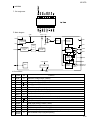
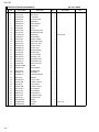
1
UX-V30
UX-V30
SERVICE MANUAL
MICRO COMPONENT SYSTEM
UX-V30
AUT
O
T A PE
SELECT
O R
AUTO REVERSE
T APE
REMOTE CONTROL RM-RXUV5R
DIMMER
SLEEP
DISPLAY
FM MODE
AHB PRO
AUTO
PRESET
COMPACT
PROGRAM RANDOM
BASS
TREBLE
DIGITAL AUDIO
MD/AUX
VERTICAL DISC
LOADING MECHANISM
CD
REPEAT
CANCEL
UP
MICRO COMPONENT SYSTEM
UX-V30
SET
DOWN
STANDBY/ON
MD/
AUX
AHB
PRO
VOLUME
TA PE
TUNER
BAND
CD
REC
TIMER
REV.
MODE
CLOCK
CD
OPEN/CLOSE
TAPE
VOLUME
FM/AM
CD
PHONES
DOWN
MULTI CONTROL
UP
Area Suffix
UF
China
Contents
Safety precautions
Important for laser products
Disassembly method
Main adjustment
Flow of functional operation
until TOC read
1-2
1-3
1-4
1-14
Maintenance of laser pickup
Replacement of laser pickup
Description of major ICs
1-19
1-19
1-20
1-18
This service manual is printed on 100% recycled paper.
COPYRIGHT 2000 VICTOR COMPANY OF JAPAN, LTD.
No.20888
1-1
Dec. 2000
UX-V30
Safety Precautions
1. This design of this product contains special hardware and many circuits and components specially
for safety purposes. For continued protection, no changes should be made to the original design
unless authorized in writing by the manufacturer. Replacement parts must be identical to those
used in the original circuits. Services should be performed by qualified personnel only.
2. Alterations of the design or circuitry of the product should not be made. Any design alterations of
the product should not be made. Any design alterations or additions will void the manufacturer`s
warranty and will further relieve the manufacture of responsibility for personal injury or property
damage resulting therefrom.
3. Many electrical and mechanical parts in the products have special safety-related characteristics.
These characteristics are often not evident from visual inspection nor can the protection afforded
by them necessarily be obtained by using replacement components rated for higher voltage,
wattage, etc. Replacement parts which have these special safety characteristics are identified in
the Parts List of Service Manual. Electrical components having such features are identified by
shading on the schematics and by ( ) on the Parts List in the Service Manual. The use of a
substitute replacement which does not have the same safety characteristics as the recommended
replacement parts shown in the Parts List of Service Manual may create shock, fire, or other
hazards.
4. The leads in the products are routed and dressed with ties, clamps, tubings, barriers and the
like to be separated from live parts, high temperature parts, moving parts and/or sharp edges
for the prevention of electric shock and fire hazard. When service is required, the original lead
routing and dress should be observed, and it should be confirmed that they have been returned
to normal, after re-assembling.
5. Leakage currnet check (Electrical shock hazard testing)
After re-assembling the product, always perform an isolation check on the exposed metal parts
of the product (antenna terminals, knobs, metal cabinet, screw heads, headphone jack, control
shafts, etc.) to be sure the product is safe to operate without danger of electrical shock.
Do not use a line isolation transformer during this check.
Plug the AC line cord directly into the AC outlet. Using a "Leakage Current Tester", measure
the leakage current from each exposed metal parts of the cabinet , particularly any exposed
metal part having a return path to the chassis, to a known good earth ground. Any leakage
current must not exceed 0.5mA AC (r.m.s.)
Alternate check method
Plug the AC line cord directly into the AC outlet. Use an AC voltmeter having, 1,000 ohms
per volt or more sensitivity in the following manner. Connect a 1,500 10W resistor paralleled by
a 0.15 F AC-type capacitor between an exposed
AC VOLTMETER
metal part and a known good earth ground.
(Having 1000
Measure the AC voltage across the resistor with the
ohms/volts,
or more sensitivity)
AC voltmeter.
Move the resistor connection to eachexposed metal
part, particularly any exposed metal part having a
0.15 F AC TYPE
return path to the chassis, and meausre the AC
Place this
voltage across the resistor. Now, reverse the plug in
probe on
the AC outlet and repeat each measurement. voltage
each exposed
1500 10W
metal part.
measured Any must not exceed 0.75 V AC (r.m.s.).
This corresponds to 0.5 mA AC (r.m.s.).
Good earth ground
Warning
1. This equipment has been designed and manufactured to meet international safety standards.
2. It is the legal responsibility of the repairer to ensure that these safety standards are maintained.
3. Repairs must be made in accordance with the relevant safety standards.
4. It is essential that safety critical components are replaced by approved parts.
5. If mains voltage selector is provided, check setting for local voltage.
! CAUTION Burrs formed during molding may be left over on some parts of the chassis. Therefore,
pay attention to such burrs in the case of preforming repair of this system.
1-2
UX-V30
Important for laser products
5.CAUTION : If safety switches malfunction, the laser is able
1.CLASS 1 LASER PRODUCT
2.DANGER : Invisible laser radiation when open and inter
lock failed or defeated. Avoid direct exposure to beam.
3.CAUTION : There are no serviceable parts inside the
Laser Unit. Do not disassemble the Laser Unit. Replace
to function.
6.CAUTION : Use of controls, adjustments or performance of
procedures other than those specified herein may result in
hazardous radiation exposure.
the complete Laser Unit if it malfunctions.
4.CAUTION : The compact disc player uses invisible
laserradiation and is equipped with safety switches
whichprevent emission of radiation when the drawer is
open and the safety interlocks have failed or are de
! CAUTION Please use enough caution not to
see the beam directly or touch it
in case of an adjustment or operation
check.
feated. It is dangerous to defeat the safety switches.
VARNING : Osynlig laserstrålning är denna del är öppnad
ADVARSEL : Usynlig laserstråling ved åbning , når
och spårren är urkopplad. Betrakta ej strålen.
VARO
sikkerhedsafbrydere er ude af funktion. Undgå
: Avattaessa ja suojalukitus ohitettaessa olet
alttiina näkymättömälle lasersäteilylle.Älä katso
udsættelse for stråling.
ADVARSEL : Usynlig laserstråling ved åpning,når
säteeseen.
sikkerhetsbryteren er avslott. unngå utsettelse
for stråling.
REPRODUCTION AND POSITION OF LABELS
WARNING LABEL
1-3
UX-V30
Disassembly method
A
<Main body>
Removing the rear cover
(See Fig.1 and 2)
1. Remove the eight screws A attaching the rear cover
on the back of the body.
A
A
A
2. Remove the two screws B attaching the rear cover
on the bottom of the body.
3. Unlock the speaker terminal and the antenna
terminal, then remove the rear cover backward with
releasing the hooks.
A
Rear cover
Fig.1
Removing the side panels
(See Fig.3 and 4)
B
Prior to performing the following procedure, remove
the rear cover.
Rear cover
1. Move the side panels in the direction of the arrow
and remove them backward.
B
Fig.2
Side panel (R)
Fig.4
1-4
Side panel (L)
Fig.3
UX-V30
Removing the cassette
assembly (See Fig.5 and 6)
mechanism
Cassette mechanism assembly
Joint a
Prior to performing the following procedure, remove
the rear cover and the side panels.
C
CN304
1. Disconnect the card wires from connector CN304
and CN305 on the main board on the left side of the
body.
2. Disconnect the harness from connector CN309 on
the Opt, Dig.out board on the right side of the body.
Cut off the band fixing the harness.
3. Remove the two screws C attaching the cassette
mechanism assembly on both sides of the body and
release the two joints a.
4. Remove the cassette mechanism assembly in the
direction of the arrow.
CN305
Main board
Fig.5
Cassette mechanism assembly
Joint a
Opt, Dig.out board
C
Band
CN309
Removing the main board / the heat sink
(See Fig.7 to 9)
Fig.6
Prior to performing the following procedure, remove
the rear cover, the side panels and the cassette
mechanism assembly.
board
CN303 Transformer
CN902
CN307
1. Disconnect the card wire from connector CN303 and
the harness from CN306 and CN307 on the main
board respectively.
Main board
2. Disconnect the harness from connector CN902 on
the power transformer.
3. Remove the screw E attaching the main board on
the right side of the body.
Heat sink
CN306
4. Remove the screw F and the two screws G
attaching the heat sink on the back of the body.
Fig.7
Main board
ATTENTION: The heat sink can be removed even if
the main board is attached to the body.
5. Disconnect connector CN301 and CN302 on the
main board from the main body. Remove the main
board upward by releasing the two joints b in the
lower part of the main board.
CN301
CN302
Joint b
E
Joint b
Fig.8
1-5
UX-V30
Heat sink
G
Main board
G
F
Removing the front panel assembly
(See Fig.10 to 12)
Prior to performing the following procedure, remove
the rear cover, the side panels, the cassette
mechanism assembly and the main board.
Fig.9
Front panel assembly
1. Disconnect the card wire from connector CN732 on
the LCD board.
Tuner & function board
2. Remove the two screws D attaching the front panel
assembly on the bottom of the body.
3. Release the two joints c on the lower right and left
sides of the body. Pull out the front panel assembly
toward the front.
LCD board
CN732
Joint c
Removing the head phone board
(See Fig.13)
Fig.10
Front panel assembly
D
Prior to performing the following procedure, remove
the rear cover, the side panels, the cassette
mechanism assembly, the main board and the front
panel assembly.
1. Remove the plastic rivet attaching the head phone
board and release the joint d.
D
Fig.11
Front panel assembly
Plastic rivet
Joint d
Fig.13
1-6
Fig.12
Joint c
UX-V30
Removing the tuner & function board
(See Fig.14)
Prior to performing the following procedure, remove
the rear cover, the side panels and the cassette
mechanism assembly.
1. Disconnect the card wire from connector CN1 on the
tuner & function board.
2. Remove the screw H attaching the tuner & function
board.
3. Release the two joints e and the joint f of the tuner &
function board.
CN1
Fig.14
1. Disconnect the harness from connector CN902 on
the power transformer.
3. Remove the four screws I attaching the power
transformer.
Joint f
Joint e
Prior to performing the following procedure, remove
the rear cover, the side panels and the cassette
mechanism assembly.
2. Disconnect the harness from connector CN901 on
the AC supply board.
Tuner
& function board
H
Removing the power transformer
(See Fig.15)
Heat sink
AC supply board
Main board
J
J
CN902
I
CN901
I
Removing the AC supply board
(See Fig.15)
*Prior to performing the following procedure, remove
the rear cover, the side panels and the cassette
mechanism assembly.
Power transformer board
Fig.15
1. Disconnect the harness from connector CN901 on
the AC supply board.
2. Remove the screw F attaching the heat sink on the
back of the body (Refer to Fig.9).
3. Remove the two screws J attaching the AC supply
board.
ATTENTION: To remove the AC supply board
efficiently, remove the main board in
advance.
1-7
UX-V30
<Cassette mechanism assembly>
Prior to performing the following procedure, remove
the rear cover, the side panels and the cassette
mechanism assembly.
Cassette door
Removing the Opt.Dig.out board
(See Fig.16)
K
1. Remove the two screws K attaching the Opt.Dig.out
board on the side of the cassette mechanism
assembly.
Eject button
Opt, Dig.out board
Fig.16
Cassette mechanism
Removing the cassette mechanism
assembly (See Fig.16 and 17)
Prior to performing the following procedure, remove
the Opt.Dig.out board.
L
L
1. Press the eject button on the front side of the
cassette mechanism assembly to open the cassette
door.
2. Remove the four screws L attaching the cassette
mechanism assembly on the back of the assembly.
L
L
Fig.17
1-8
UX-V30
<Front panel assembly>
CD mechanism cover
(CD mechanism assembly)
M
Prior to performing the following procedure, remove
the rear cover, the side panels, the cassette
mechanism assembly, the main board and the front
panel assembly.
Removing the CD mechanism assembly
(See Fig.18 to 21)
1. Disconnect the harness from connector CN721 and
CN722, and the card wire from CN766 on the LCD
board on the back of the front panel assembly.
R
Belt
M
Loading motor
M
CN766
2. Remove the five screws M attaching the CD
mechanism cover to the front panel. Remove the CD
mechanism cover together with the CD mechanism
assembly.
CN721
CN722
LCD board
Fig.18
3. Release the harness from each hook on the CD
mechanism cover.
4. Remove the five screws N attaching the CD
mechanism cover and the CD mechanism case.
Release the three joints g of the CD mechanism
cover and the CD mechanism case by pushing the
joint hooks inward.
N
Joint g
N
CD mechanism cover
5. Disconnect the card wire from connector CN603 and
the harness from CN605 on the CD servo control
board.
Loading motor
CD mechanism
case
6. Remove the CD mechanism assembly from the CD
mechanism cover by pulling out it from the three
bosses h.
N
Joint g
Joint g
N
Removing the LED board (A)
(See Fig.21)
Fig.19
1. Remove the screw O attaching the LED board (A).
CD mechanism cover
CD servo control board
LCD board (A) CD mechanism case
Joint g
CN605
CN603
Fig.21
CD mechanism cover
Fig.20
1-9
UX-V30
Removing the LED board (B) (See Fig.22)
Prior to performing the following procedure, remove
the CD mechanism assembly.
1. Remove the screw P attaching the LED board (B).
CD door switch board
Q
Q
Hook i
P
O
Removing the CD door switch board
(See Fig.22)
1. Release the hook i fixing the CD door switch board
to the CD mechanism cover.
CD servo control
board
LCD board (A)
LCD board (B)
Joint j
Fig.22
Removing the CD servo control board
(See Fig.22)
M
CD mechanism cover
(CD mechanism assembly)
Prior to performing the following procedure, remove
the CD mechanism assembly and the LED board (A)
/ (B).
1. Remove the two screws Q attaching the CD servo
control board.
2. Pull out the CD servo control board in the direction of
the arrow by releasing the two joints j.
R
Belt
Loading motor
M
M
CN766
Removing the loading motor
CN721
(See Fig.18)
LCD board
1. Remove the belt and the two screws R attaching the
loading motor on the back of the front panel
assembly.
Fig.18
Operation switch board
CN722
S
Removing the LCD board assembly
(See Fig.23)
Prior to performing the following procedure, remove
the CD mechanism cover (CD mechanism
assembly).
CN781
1. Remove the two screws S attaching the LCD board
assembly.
LCD board assembly
Fig.23
2. Disconnect connector CN781 on the LCD board
assembly from the operation switch board.
T
Operation switch board
Removing the operation switch board
(See Fig.24)
T
Prior to performing the following procedure, remove
the LCD board assembly.
1. Remove the eight screws T attaching the operation
switch board.
T
1-10
Fig.24
UX-V30
<<Cassette Mechanism Section>>
Cassette mechanism
Removing the Playback/Recording & Eraser
Head ( See Figs. 1 and 2 )
1. While shifting the trigger arms seen on the right
side of the head mount in the arrow direction,
turn the flywheel R in counterclockwise direction
Flywheel R
until the head mount has gone out with a click
(See Fig. 1).
2. When the flywheel R is rotated in counterclockwise
direction, the Playback/Recording & Eraser head
will be turned in counterclockwise direction from the
position in Fig. 2 to that in Fig. 3.
3. At this position, disconnect the flexible P.C. board
Head mount
Trigger arm
(outgoing from the Playback/Recording & Eraser head)
Fig. 1
from the connector CN31 on the head amplifier &
mechanism control P.C. board.
4. After dismounting the FPC holder, remove the flexible
Playback/Recording &
P.C. board.
eraser hyead
Spring "a"
5. Remove the flexible P.C. board from the chassis base.
Frexible
Trigger arm
6. Remove the spring Afro behind the Playback/Recording
board
& Eraser head.
7. Loosen the reversing azimuth screw retaining the Playback
/Recording & Eraser head.
8. Take out the Playback/Recording & Eraser head from the
front of the head mount.
9. The Playback/Recoring & Eraser head should also be
removed similarly according to Steps 1 ~ 8 above.
Head amplifier & mechanism
control P.C. board
Reassembling the Playback/Recording & Eraser
Head
1. Reassemble the playback head from the front of the head
mount to the position as shown in Fig. 3.
2. Fix the reversing azimuth screw.
3. Set the spring "a" from behind the Playback/Recording &
Eraser head.
4. Attach the flexible P.C. board to the chassis base, and fix
it with the FPC holder as shown in Fig. 3.
5. The Playback/Recording & Eraser head should also be
reassembled similarly to Step 1 ~ 4 above.
Flywheel R
Fig. 2
Playback/Recording &
eraser head
Reversing azimuth
screw
Head
mount
Spring "a"
Frexible
board
Head amplifier &
mechanis control
P.C. board
FPC holder
Fig. 3
1-11
UX-V30
Removing the Head amplifier & Mechanism
control P.C. board
(See Fig. 4)
Belt
Main motor
assembly
1. Remove the cassette mechanism assembly.
2. After turning over th cassette mechanism assembly,
remove the three screws "1" retaining the head
amplifier & mechanism control P.C. board.
3. Disconnect the connector CN32 on the P.C. board
including the connector CN 1 on the reel pulse P.C.
board.
4. When necessary, remove the 4 pin parallel wire
soldered to the main motor.
Head amplifier &
mechanism control
P.C. board
4pin parallel wire
Flexible P.C. board
Removing the Main Motor Assembly
(See Fig. 4~6)
1. Remove the two screws "2" retaining the main
motor assembly (See Fig. 4, 4a).
2. While raising the main motor, remove the capstan
belt from the motor pulley (See Fig. 4a).
Caution 1: Be sure to handle the capstan belt so
carefully that this belt will not be
stained by grease and other foreign
matter. Moreover, this belt should be
hanged while referring to the capstan
belt hanging method in Fig. 5, 6.
Main
moteor
assembly
Fig. 4
Main motor
assembly
Capstan belt
Motor
pulley
Fig. 4a
Mechanism motor
assembly
Main motor
assembly
Capstan
belt
Motor
pulley
Flywheel
Capstan belt
Fig. 5
1-12
Fig. 6
Motor pulley
UX-V30
Removing the Flywheel
(See Figs. 7 and 8)
Flywheel R
Flywheel L
1. Remove the head amplifier & mechanism control
P.C. board.
2. Remove the main motor assembly.
3. After turning over the cassette mechanism,
remove the slit washers "b" and "c" fixing the capstan
shafts R and L, and pull out the flywheel R and L
respectively from behind the cassette mechanism. Capstan shaft R
Capstan shaft L
Slit
washer
Slit
washer
Fig.7
Flywheel R
Flywheel L
Fig. 8
Removing the Reel Pulse P.C. board and Solenoid
(See Fig. 9)
1. Remove the five pails "d"~"h" reataining the reel pulse
P.C. board.
2. From the surface of the reel pulse P.C. board parts, remove
the two pawls "i" and "j" retaining the solenoid.
Reel pulse P.C. board
j
Solenoid
Fig. 9
1-13
UX-V30
Main adjustment
Measurement Instruments Required for
Adjustment
1. Low frequency oscillator
This oscillator should have a capacity to output
at an oscillation frequency of
0dBs to 600
50Hz-20kHz.
2. Attenuator impedance : 600
3. Electronic voltmeter
4. Distortion meter
5. Frequency counter
6. Wow & flutter meter
7. Test tape
VTT703L : Head azimuth
VT712 : Tape speed and running unevenness
(3kHz)
VT724 : Reference level (1kHz)
8. Blank tape
TYPE : AC-225
TYPE : AC-514
9. Torque gauge : For play and back tension
FWD(TW2111A), REV(TW2121a) and
FF/REW(TW2231A)
10. Test disc: CTS-1000
Measurement conditions
Power supply voltage
: AC230V (50Hz)----B/E/EE/EN
: AC110/127V/230V(50/60Hz)
: UB/UF/US/UX/U
Reference output : Speaker : 0.775V/4
: Headphone : 0.077V/32
Reference frequency and
input level ------------------------------ 1kHz, AUX : -8dBs
MIX MIC: -54dBs (UB/UF/US/UX/U)
Input for confirming recording and playback
characteristics ------------------------- AUX : -28dBs
Measurement output terminal ------- at Speaker J3002
Load resistance --------------------------- 4
Radio Input signal
AM frequency --------------------------------------- 400Hz
AM modulation ---------------------------------------- 30%
FM frequency --------------------------------------- 400Hz
FM frequency deviation ------------------------ 22.5kHz
1-14
Tuner section
B/E/EN version
FM Band cover: 87.5 108MHz
MW Band cover: 522 1,629kHz
LW Band cover: 144 288kHz
EE version
FM Band cover: 65 74MHz, 87.5 108MHz
MW Band cover: 522 1,629kHz
LW Band cover: 144 288kHz
UB/UF/US/UX/U version
FM Band cover: 87.5 108MHz
MW Band cover: 531 1,602kHz, 530 1,710kHz
SW Band cover: SW1 2.3 6.995MHz
: SW2 7 21.85MHz
Voltage applied to tuner
+B : DC5.7V
VT : DC 12V
Reference measurement
output
26.1mV(0.28V)/3
Input positions
AM : Standard loop antenna
FM : TP1 (hot) and TP2 (GND)
Standard measurement position of volume
Function switch
to Tape
Beat cut switch
to Cut
Super Bass/Active hyper Bass
to OFF
Bass Treble
to Center
Adjustment of main volume to reference output
VOL : 28
Precautions for measurement
to the IF sweeper output
1. Apply 30pF and 33k
side and 0.082 F and 100k in series to the
sweeper input side.
2. The IF sweeper output level should be made as
low as possible within the adjustable range.
3. Since the IF sweeper is a fixed device, there is no
need to adjust this sweeper.
4. Since a ceramic oscillator is used, there is no need
to perform any MIX adjustment.
5. Since a fixed coil is used, there is no need to adjust
the FM tracking.
6. The input and output earth systems are separated.
In case of simultaneously measuring the voltage in
both of the input and output systems with an
electronic voltmeter for two channels, therefore, the
earth should be connected particularly carefully.
7. In the case of BTL connection amp., the minus
terminal of speaker is not for earthing. Therefore, be
sure not to connect any other earth terminal to this
terminal. This system is of an BTL system.
8. For connecting a dummy resistor when measuring
the output, use the wire with a greater code size.
9. Whenever any mixed tape is used, use the band
pass filter (DV-12).
UX-V30
<<Arrangement of Adjusting Position>>
Cassette mechanism section
Cassette mechanism section (Back side)
Head azimuth
adjusting screw
(Forward side)
Head azimuth
adjusting screw
(Forward side)
Head azimuth
adjusting screw
(Reverse side)
Head azimuth
adjusting screw
(Reverse side)
Playback/Recording &
eraser head
Front panel assembly section
VR201
R ch BIAS ADJ
L301
MOTOR SPEED
VR301
VR101
L ch BIAS ADJ
1-15
UX-V30
Tape Recorder Section
Items
Measurement
conditions
Measurement method
Standard
Values
Confirmation Test tape
1 Playback the test tape VTT703L (8kHz)
Maximum
of head angle : VTT703L (8kHz)
2 With the recording & playback mechanism, output
Measurement output
adjust the head azimuth screw so that the
terminal
forward and reverse output levels become
: Speaker terminal
maximum. After adjustment, lock the head
Speaker R
azimuth at least by half turn.
(Load resistance: 4 ) 3 In either case, this adjustment should be
: Headphone terminal
performed in both the forward and reverse
directions with the head azimuth screw.
Confirmation Test tape
of tape speed : VT712 (3kHz)
Measurement output
terminal
: Headphone terminal
Adjusting
positions
Adjust the head
azimuth screw
only when the
head has been
changed.
Adjust VR37 so that the frequency counter
Tape speed VR301
reading becomes 2,940~3,090Hz when
of deck
playing back the test tape VT712 (3kHz) with : 2,940 ~
playback and recording mechanism after
3,090Hz
ending forward winding of the tape.
Reference Values for Confirmation Items
Items
Measurement
conditions
Measurement method
Standard
Values
Test tape
Difference
between the : VT712 (3kHz)
forward and Measurement output
reverse speed terminal
: Speaker terminal
Speaker R
(Load resistance: 4 )
Measurement output
terminal
: Headphone
When the test tape VT712 (3kHz) has been 6.0Hz or
played back with the recording and playback less
mechanism at the beginning of forward
winding, the frequency counter reading of the
difference between both of the mechanism
should be 6.0Hz or less.
Wow & flutter Test tape
: VT712 (3kHz)
Measurement output
terminal
: Headphone terminal
When the test tape VT712 (3kHz) has been 0.25% or
played back with the recording and playback less
mechanism at the beginning of forward
(WRMS)
winding, the frequency counter reading of
wow & flutter should be 0.25% or less
(WRMS).
1-16
Adjusting
positions
Head azimuth
screw
UX-V30
Electrical Performance
Items
Measurement
conditions
Measurement method
Adjustment of Mode: Forward or
1 With the recording and playback
recording bias reverse mode
mechanism, load the test tapes (AC-514 to
Recording mode
current
TYPE
and AC-225 to TYPE ), and set
Test tape
(Reference
the mechanism to the recording and
: AC-514 to TYPE
Value)
pausing condition in advance.
and AC-225 to
2 After connecting 100 in series to the
TYPE
recorder head, measure the bias current
Measurement output
with a valve voltmeter at both of the
terminal
terminals.
: Both recording and 3 After resetting the [PAUSE] mode, start
headphone terminals
recording. At this time, adjust VR31 for Lch
and VR32 for Rch so that the recording
bias current values become 4.0 A (TYPE
) and 4.20 A (TYPE ).
Adjustment of Reference frequency
recording and : 1kHz and 10kHz
(REF.: -20dB)
playback
frequency
Test tape
characteristics : AC-514 to TYPE
Measurement input
terminal
: OSC IN
Standard
Values
AC-225
: 4.20 A
AC-514
: 4.0 A
1 With the recording and playback
Output
mechanism, load the test tapes (AC-514 to deviation
TYPE ), and set the mechanism to the between
recording and pausing condition in
1kHz and
advance.
10kHz
2 While repetitively inputting the reference : -1dB 2dB
frequency signal of 1kHz and 10kHz from
OSC IN, record and playback the rape.
3 While recording and playback the test tape
in TYPE , adjust VR31 for Lch and VR32
for Rch so that the output deviation
between 1kHz and 10kHz becomes
-1dB 2dB.
Adjusting
positions
L ch
: VR101
R ch
: VR201
L ch
: VR101
R ch
: VR201
Reference Values for Electrical Function Confirmation Items
Items
Measurement
conditions
Measurement method
Standard
Values
Recording
bias
frequency
Forward or reverse
100 kHz
1 While changing over to and from BIAS 1
Test tape
6 kHz
and 2, confirm that the frequency is
: TYPE (AC-514)
changed.
Measurement
2 With the recording and playback
terminal : BIAS TP on
mechanism, load the test tape.
P.C. board
(AC-514 to TYPE ), and set the
mechanism to the recording and pausing
condition in advance.
3 Confirm that the BIAS TP frequency on the
P.C. board is 100kHz
6kHz.
Eraser
current
(Reference
value)
1 While recording and playback mechanism,
Forward or reverse
load the test tapes (AC-514 to TYPE
Recording mode
Test tape
and AC-225 to TYPE ), and set the
: AC-514 to TYPE
mechanism to the recording and pausing
conditions in advance.
and AC-225 to
2 After setting to the recording conditions,
TYPE
connect 1W in series to the eraser head on
Measurement
the recording and playback mechanism
terminal : Both of the
side, and measure the eraser current from
eraser head terminals
both of the eraser terminals.
Adjusting
positions
TYPE
: 120 mA
TYPE
: 75 mA
1-17
UX-V30
Flow of functional operation until TOC read
Check Point
Power Key
Power ON
Slider turns REST
SW ON.
Check that the voltage at the pin17
of CN604 is 0V (a moment)?
Automatic tuning
of TE offset
Laser ON
Check that the voltage at the
pin3 of IC601 + side is + 5V?
Detection of disc
Automatic tuning of
Foucus offset
Automatic measurement of
Focus A-curve amplitude
Disc is rotated
Tracking error waveform at TOC reading
pin 25 of
IC601(TE)
Approx.3sec
Confirm that the Focus error
S-cuve siganl at the pin27 of
IC601 is approx.2Vp-p
Confirm that the siganl from
pin24 IC603 is 0V as a
accelerated pulse during
approx.400ms.
Focus servo ON
(Tracking servo ON)
Approx
1.8V
VREF
Automatic measurement of
Tracking error amplitude
Tracking
Disc to be
servo
braked to stop
on statas
Disc statas
TOC reading
to rotate
finishes
Automatic measurement
of TE amplitude and
automatic tuning of
500mv/div
TE balance
2ms/div
Fig.1
Tracking
servo
off statas
Confirm the waveform of
the Tracking error signal
at the pin25 of IC601 (R612)
(See fig-1)
Automatic tuning of
Tracking error balance
Automatic tuning of
Focus error balance
Automatic tuning of
Focus error gain
Automatic tuning of
Tracking error gain
TOC reading
Play a disc
1-18
Confirm the eys-pattern
at the lead of TP1
UX-V30
Maintenance of laser pickup
Replacement of laser pickup
(1) Cleaning the pick up lens
Befor you replace the pick up, please try to
clean the lens with a alcohol soaked cotton
swab.
Turn off the power switch and,disconnect the
power cord from the ac outlet.
(2) Life of the laser diode (Fig.1)
When the life of the laser diode has expired,
the following symptoms wil appear.
(1) The level of RF output (EFM output:ampli
tude of eye pattern) will below.
Replace the pickup with a normal one.(Refer
to Pickup Removal on the previous page)
Is RF output
1.1 0.15Vp-p?
NO
Replace it.
Plug the power cord in,and turn the power on.
At this time,check that the laser emits for
about 3seconds and the objective lens moves
up and down.
Note: Do not observe the laser beam directly.
YES
Play a disc.
O.K
(Fig.1)
Check the eye-pattern at TP1.
(3) Semi-fixed resistor on the APC PC board
The semi-fixed resistor on the APC printed
circuit board which is attached to the pickup
is used to adjust the laser power.Since this
adjustment should be performed to match the
characteristics of the whole optical block,
do not touch the semi-fixed resistor.
If the laser power is lower than the specified
value,the laser diode is almost worn out, and
the laser pickup should be replaced.
If the semi-fixed resistor is adjusted while
the pickup is functioning normally,the laser
pickup may be damaged due to excessive current.
Finish.
1-19
UX-V30
Description of major ICs
LA6541-X(IC541) : Servo Driver
1. Pin Layout & Block Diagram
Vcc
Vref
Vin4
Vg4
24
23
22
21
Vo8
Vo7
20
19
Gnd
Vg3
Vin3
Cd
Res
17
16
15
14
13
11k
ohm
-
+
Vo5
18
Vcc
11k
ohm
-
Vo6
+
Level
shift
BTL
driver
BTL
driver
Level
shift
RESET
Level
shift
BTL
driver
BTL
driver
Level
shift
Regulator
11k
ohm
11k
ohm
1
2
3
4
Vcc
Mute
Vin1
Vg1
5
Vo1
6
Vo2
Gnd
7
8
9
10
11
12
Vo3
Vo4
Vg2
Vin2
Reg
out
Reg
In
2. Pin functions
Pin
No.
Symbol
1
Vcc
Power supply (Shorted to pin 24)
2
Mute
All BTL amplifier outputs ON/OFF
3
Vin1
BTL AMP 1 input pin
4
Vg1
BTL AMP 1 input pin (For gain adjustment)
5
Vo1
BTL AMP 1 input pin (Non inverting side)
6
Vo2
BTL AMP 1 input pin (Inverting side)
7
Vo3
BTL AMP 2 input pin (Inverting side)
8
Vo4
BTL AMP 2 input pin (Non inverting side)
9
Vg2
BTL AMP 2 input pin (For gain adjustment)
10
Vin2
BTL AMP 2 input pin
11
Reg Out
12
Reg In
13
Res
Reset output
14
Cd
Reset output delay time setting (Capacitor connected externally)
15
Vin3
BTL AMP 3 input pin
16
Vg3
BTL AMP 3 input pin (For gain adjustment)
17
Vo5
BTL AMP 3 output pin (Non inverting side)
18
Vo6
BTL AMP 3 output pin (Inverting side)
19
Vo7
BTL AMP 4 output pin (Inverting side)
20
Vo8
BTL AMP 4 output pin (Non inverting side)
21
Vg4
BTL AMP 4 output pin (For gain adjustment)
22
Vin4
BTL AMP 4 output pin
23
Vref
Level shift circuit's reference voltage application
24
Vcc
Power supply (Shorted to pin 1)
1-20
Function
External transistor collector (PNP) connection. 5V power supply output
External transistor (PNP) base connection
UX-V30
MN35510 (IC651) : DIGITAL SERVO&DIGITAL SIGNAL PROCESSER
1. Terminal Layout
20 ~
1
21
80
~
~
40
61
41 ~
60
2.Block Diagram
LRCKIN(MSEL)
BCLK(SSEL)
SRDATAIN
(PSEL)
DIGITAL
DEEMPHSIS
8TIMES
OVER SAMPUNC
DIGITAL FILTER
IOSEL
1BIT
DAC
LOGIC
S
CLVS
CRC
BLKCK
CLDCK
SBCK
SUBC
DEMPH
RESY
FLAG6(RESY)
SSEL
SQCK
SUBQ
AVDD2
PEM
(L)
EFM
DEMODULATION
DIGITAL
AUDIO
INTERFASE
16k
SRAM
SYNC
INTERPOLATION
SUBCODE
DEMODULATION
DSL.
PLL
VCO
CIRC
ERROR
CORRECTION
DEINTERLEVE
MLD
MCLK
MDATA
CK384(EFM)
VCOF
BYTCK
SMCK
FCLK
CSEL
MSEL
X2
X1
OUTL
FLAG
IPFLAG
SUB
CODE
BUFFER
AVDD2
PCK
EFM
PLLF
DSLF
IREF
DRF
ARF
RSEL
PSEL
AVSS1
AVDD1
OUTR
PEM
(R)
MICRO
COMPUTER
INTERFACE
VCO
TX
DIGITAL
AUDIO
INTERFASE
ECM
INTER POLATION
SOFT MUTING DIGITAL
ATTENUATION
PEAK DETECTIVE
AUTO CUE
LRCK
SRDATA
BCLK
DMUTE
PC
TRKV
KICK
VREF
TRVSTR
ECS
TVD
TRD
FOD
TBAL
FBAL
TOFS
TES
/TLOCK
/FLOCK
PLAY
LDON
WVEL
SENSE
CLV
SERVO
D/A
CONVERTER
ITUNING
GENERATION
PITCH
CONTROL
ÊSTAT
OUTPUT
A/D
COVERTER
V V
D S
D S
D
V
D
D
1
D / /
V R T
S S E
S T S
1
T
F
E
T
E
R
F
E
N
V
INPUT
T
R
C
R
S
V
D
E
T
PORT
SERVO
TIMING GENERATOR
B
D
O
/
R
F
D
E
O
F
T
1-21
UX-V30
3. Description
Description
1
BCLK
O Not used
2
LRCK
O
3
SRDATA O Not used
4
DVDD1
I
Power supply (Digital)
5
DVSS1
I
Not used
Connected to GND
6
TX
O Digital audio interface output
7
MCLK
I
8
MDATA
I
com command data input
9
MLD
I
com command load signal input
41
symbol
TES
42 PLAY
Not used
Not used
44
ARF
I
RF signal input
45 IREF
I
Reference current input pin
46 DRF
I
Bias pin for DSL
I
Not used
I
Power supply(Analog)
I
Connected to GND(Analog)
I
49 VCOF
Not used
I
I/O Loop filter pin for PLL
Not used
I
48 PLLF
Not used
I
I/O Loop filter pin for DSL
Not used
Connected to GND
56 SBCK
I
47 DSLF
Not used
Status signal
(CRC,CUE,CLVS,TTSTOP,ECLV,SQOK)
57
VSS
Connected to GND(for X'tal oscillation
circuit)
I
Reset signal input (L:Reset)
58
XI
I
Input of 16.9344MHz X'tal oscillation circuit
59 X2
60
VDD
BYTCK
50
11
FLOCK
O Focus lock signal output Active :Low
51
AVSS2
12
TLOCK
O Tracking lock signal output Active :Low
52
EFM
13
BLKCK
AVDD2
53
PCK
I
54
PDO
15
O Sub-code Q -code output
I
O sub-code block clock signal output
14 SQCK
17 STATUS O
55 SUBC
62 CLDCK
23
PC
Not used
Not used
Not used
Spindle motor drive signal (Enforced
mode output) 3-State
Spindle motor drive signal (Servo error
O
signal output)
O Kick pulse output
Not used
Not used
66 CLVS
Not used
27 TRD
O Tracking drive output
67
CRC
28
O Focus drive output
68
DEMPH
24 ECM
25
ECS
26
KICK
Not used
64 IPPLAG
65
FLAG
Not used
Not used
69 RESY
Not used
30
FBAL
O Focus Balance adjust signal output
70 IOSEL
pull up
31
TBAL
O Tracking Balance adjust signal output
71
TEST
I
Reference voltage input pin for D/A
output block (TVD,FOD,FBA,TBAL)
pull up
32
FE
I
Focus error signal input(Analog input)
72
AVDD1
I
I
Power supply(Digital)
33
TE
I
Tracking error signal input(Analog input)
73
OUT L
O Lch audio output
34
RF ENV
I
RF envelope signal input(Analog input)
74
AVSS1
I
29 VREF
I
O
63 FLAG
I
FOD
I
I
61
O Traverse drive output
I
O Traverse enforced output
TVD
I
TRV
22
Power supply(for X'tal cscillation circuit)
I
21
O Output of X'tal oscillation circuit
I
Not used
I
Not used
PMCK
I
SMCK
20
I
19
I
RST
Outside clock for sub-code Q resister input
I
18
O Tracking error shunt signal output(H:shunt)
WVEL
O Sence signal output
SUBQ
Description
43
10 SENSE
16 DMUTE
I/O
I
com command clock signal input
(Data is latched at signal's rising point)
Pin
No.
I
symbol I/O
I
Pin
No.
35
VDET
I
Vibration detect signal input(H:detect)
75
OUT R
O Rch audio output
36
OFT
I
Off track signal input(H:off track)
76 RSEL
I
Track cross signal input
77 CSEL
78 PSEL
79
BDO input pin(L:detect)
40
LDON
O Laser ON signal output(H:on)
1-22
MSEL
80 SSEL
I
I
I
I
BDO
I
RFDET
39
Connected to GND
Connected to GND
I
38
RF detect signal input(L:detect)
pull up
Connected to GND
I
37 TRCRS
Connected to GND
Pull up
UX-V30
AN8806SB-W(IC301) :RF&SERVO AMP
1.Pin layout
36 PDAC
35 PDBD
34 PDF
33 PDE
32 PDER
31 PDFR
30 TBAL
29 FBAL
28 EF27 EF OUT
26 TE25 TE OUT
24 CROSS
23 TE BPF
22 VDET
21 LD OFF
20 VREF
19 ENV
PD 1
LD 2
LDON 3
LDP 4
VCC 5
RF- 6
RF OUT 7
RF IN 8
C.AGC 9
ARF 10
C.ENV 11
C.EA 12
CS BDO 13
BDO 14
CS BRT 15
OFTR 16
/NRFDET 17
GND 18
2.Block diagram
6
29
7
28
+
9
8
27
10
+
-+
RF
AGC
EQ
17
11
12
19
ENV CURCUIT
DET
36
+
VCBA
-
+
13
+
BDO
14
OFTR
15
16
35
+
+
-
VCBA
31
+
VCBA
34
+
+
32
-+
-+
+
VCBA
+
20
21
33
+
2
++
30
24
25
26
23
22
1
4
3
1-23
UX-V30
3. Pin function
Pin No.
symbol
I/O
Function
1
PD
I
APC amp . Input terminal
2
LD
O
APC amp . Output terminal
3
LD ON
I
LD ON/OFF control terminal
4
LDP
--
Connect to GND
5
VCC
--
Power supply
6
RF-
I
RF amp . Reversing input terminal
7
RF OUT
O
RFamp . Output terminal
8
RF IN
I
AGC input terminal
9
C.AGC
I/O
10
ARF
11
C.ENV
I/O
RF detection capacity connection terminal
12
C.EA
I/O
HPF-amp capacity connection terminal
13
O
CS BDO I/O
AGC loop filter connection terminal
ARF output terminal
Capacity connection terminal for RF discernment side envelope detection
14
BDO
15
CS BRT I/O
Capacity connection terminal for RF discernment side envelope detection
16
OFTR
O
OFTR output terminal
17
/NRFDET
O
RFDET output terminal
18
GND
--
Connect to GND
19
20
ENV
O
3TENV output terminal
VREF
O
VREF output terminal
21
LD OFF
--
APC OFF control terminal
22
VDET
O
VDET output terminal
23
TE BPF
I
VDET input terminal
24
CROSS
O
CROSS output terminal
25
TE OUT
O
TE amp . Output terminal
I
FE amp . Reversing input terminal
O
FE amp . output terminal
26
27
TEFE OUT
O
BDO output terminal
28
FE-
I
FE amp . Reversing input terminal
29
FBAL
I
F.BAL control terminal
30
TBAL
I
T.BAL control terminal
31
PDFR
I/O
I-V amp conversion resistance adjustment terminal
32
PDER
I/O
I-V amp conversion resistance adjustment terminal
33
PDF
I
I-V amp input terminal
34
PDE
I
I-V amp input terminal
35
PD BD
I
I-V amp input terminal
36
PD AC
I
I-V amp input terminal
1-24
UX-V30
UPD78064GF-108 (IC701): System CPU
1.Pin layout
100
~
81
1
80
~
~
30
31
~
50
51
2.Pin function
Pin
No.
Symbol
I/O
1
2
3
4
5
6
7
8
9
10
11
12
13
14
15
16
17
18
19
20
21
22
23
24
25
26
27
28
USDATA
USCK
UQRIN
UNC
USQCK
ICVSS
UX2
UX1
VDD
UXT1
UXT2
URESET
UREM
URDSCK
UJOG1
UBEAT2
UBEAT1
U+BCTL
UXRESET
UMCLK
UMDATA
UMLD
UPBMUTE
ULATCH
UREEL
UFAUX
UAVSS
USAFEYCD
I/O
O
I
O
I
I
I
I
I
O
O
O
O
O
O
O
O
O
I
O
I
Function
Pin
No.
Symbol
I/O
Function
URESET/CLOSE I [RESET/CLOSE] switch
29
Serial data
USAFETY1
30
I Abnormal voltage detection 1
Serial clock
USAFETY0
CD Q code data
31
I Abnormal voltage detection 2
UKEY1
Non connect
32
I Body key input 1
UKEY0
CD Q code data synchronizing clock
33
I Body key input 0
UTAPE0
Connected to VSS
34
I Tape switch 0
UTAPE1
Main system clock
35
I Tape switch 1
AVDD
Main system clock
36
- AD converter power supply
UAVREF
Power supply
37
- AD converter reference voltage
UBUP
Sub system clock
38
I Backup power supply decision
UFTUNER
Sub system clock
39
O Function tuner
VSS
Reset
40
- GND
UMPX
Remote control
41
I FM stereo detection
UPERIOD
Non connect
42
O Tuner PLL strobe
UJOGB
Jog encoder 1
43
I JOG encoder 2
UBASS
Main clock selection 2
44
O BASS control
UTRE
Main clock selection 1
45
O TRE control
UVOL
Switched 5V control
46
O VOL.control
USBASS
CD LSI reset
47
O AHB on/off
USMUTE
CD LSI command clock
48
O System muting
UPOUT
CD LSI command data
49
O Power ON/OFF
UFCD
CD LSI command load
50
O Function CD
51~54
COM0~3
Tape playback mute
O LCD common
55
BIAS
Tape IC strobe
- LCD bias voltage
VLC0~2
Tape end detection
- LCD bias voltage
56~58
VSS
Function AUX
- GND
59
S0~39
AD converter GND
O LCD segment
60~99
USTATUS
CD abnormal voltage detection
I LCD LSI status
100
1-25
UX-V30
LA1838(IC102): FM AM IF AMP&detector, FM MPX Decoder
1. Block Diagram
30
29
27
28
25
26
24
23
22
20
21
18
19
17
16
REG
ALC
AM
MIX
AM
FM
RF.AMP
DECODER
ANIT-BIRDIE
OSC
MUTE
BUFF
STEREO
5N
SW
P-DET
AGC
DET
AM IF
SD
COMP
VCO
384KHz
FF
38k
FF
19k / 2
10
11
12
FF
19k /LS
PILOT
DET
AM
S-METER
FM
S-METER S-CLRVE
AM/FM
IF-BUFF
TUNING
DRIVE
STEREO
DRIVE
PM
DET
FM IF
GND
1
2
5
VCC
8
9
Pin
No.
Symbol
I/O
This is an input terminal of FM IF
signal.
16
R OUT
O
O This is an out put terminal for AM
mixer.
17
L OUT
O Left channel signal output.
I
18
R IN
3
4
6
7
13
14
15
2. Pin Function
Pin
No.
Symbol
I/O
1
FM IN
I
2
AM MIX
3
FM IF
Function
Bypass of FM IF
I
Function
Right channel signal output.
Input terminal of the Right channel post
AMP.
Input of AM IF Signal.
19
L IN
I
Input terminal of the Left channel
post AMP.
GND
I
This is the device ground terminal.
20
RO
O
Mpx Right channel signal output.
6
TUNED
O
When the set is tunning,this terminal
becomes "L".
21
LO
O
Mpx Left channel signal output.
7
STEREO
O
Stereo indicator output. Stereo "L",
Mono: "H"
22
IF IN
I
Mpx input terminal
8
VCC
I
This is the power supply terminal.
23
FM OUT
O
FM detection output.
9
FM DET
FM detect transformer.
24
AM DET
O
AM detection output.
10
AM SD
This is a terminal of AM ceramic filter.
25
AM AGC
I
This is an AGC voltage input terminal
for AM
11
FM VSM
O
Adjust FM SD sensitivity.
26
AFC
I
This is an output terminal of voltage
for FM-AFC.
12
AM VSM
O
Adjust AM SD sensitivity.
27
AM RF
I
AM RF signal input.
13
MUTE
28
REG
O
Register value between pin 26 and pin28
besides the frequency width of the
input signal.
14
FM/AM
29
AM OSC
I
5
I
I
AM IF
I
4
This is a terminal of AM Local
oscillation circuit.
I/O When the signal of IF REQ of IC121(
LC72131) appear, the signal of FM/AM
IF output. //Muting control input.
I
Change over the FM/AM input.
"H" :FM, "L" : AM
15
1-26
MONO/ST O Stereo : "H", Mono: "L"
30 OSC BUFFER O
AM Local oscillation Signal output.
UX-V30
LC72136N (IC121) : PLL Frequency Synthesizer
1. Pin layout
XT
FM/AM
CE
DI
CLOCK
DO
FM/ST/VCO
AM/FM
1
2
3
4
5
6
7
8
9
10
SDIN 11
22
21
20
19
18
17
16
15
14
13
12
XT
GND
LPFOUT
LPFIN
PD
VCC
FMIN
AMIN
IFCONT
IFIN
2. Block diagram
Phase
Detector
Charge Pump
Reference
Driver
1
18
22
19
20
16
Swallow Counter
1/16,1/17 4bit
1/2
Unlock
Detector
12bit
Programmable
DriverS
15
12
3
4
C2B
I/F
5
Universal
Counter
Data Shift Register & Latch
6
Power
on
Reset
17
21
7
8
2
11 13
3. Pin function
Pin
No.
Pin
No.
Symbol
I/O
X'tal oscillator connect (75kHz)
12
IFIN
I
IF counter signal input
O
LOW:FM mode
13
IFCONT
O
IF signal output
I
When data output/input for 4pin(input) and
14
-
Not use
I
AM Local OSC signal output
Symbol
I/O
1
XT
I
2
FM/AM
3
CE
Function
Function
6pin(output): H
4
DI
I
Input for receive the serial data from
15
AMIN
16
FMIN
I
FM Local OSC signal input
VCC
-
Power suplly(VDD=4.5-5.5V)
controller
5
6
CLOCK
I
Sync signal input use
DO
O
Data output for Controller
17
Output port
7
FM/ST/VCO
O
"Low": MW mode
When power ON:Reset circuit move
18
PD
O
PLL charge pump output(H: Local OSC
frequency Height than Reference frequency.
L: Low Agreement: Height impedance)
8
AM/FM
O
Open state after the power on reset
19
LPFIN
I
Input for active lowpassfilter of PLL
9
LW
I/O
Input/output port
20
LPFOUT
O
Output for active lowpassfilter of PLL
10
MW
I/O
Input/output port
21
GND
-
Connected to GND
I/O
Data input/output
22
XT
I
X'tal oscillator(75KHz)
11
SDIN
1-27
UX-V30
BA15218N (IC342/IC343/IC391/IC453IC362/IC363)
: Dual Ope. Amp.
1
1
+
-
+
-
2
OUT1 +IN1
3
4
5
2
6
+IN1 GND +IN2 -IN2
7
8
OUT2 Vcc
BU4094BCF-X(IC304,IC303):Serial to parallel port extension
1.Pin layout
STROBE
DATA
CLOCK
Q1
Q2
Q3
Q4
Vss
1
2
3
4
5
6
7
8
2.Block diagram
16
15
14
13
12
11
10
9
Vdd
OUTPUT ENABLE
Q5
Q6
Q7
Q8
Q's
Qs
DATA
CLOCK
STROBE
OUTPUT
ENABLE
2
10
8-STAGE
SHIFT REGISTER
3
1
8-BIT
LATHES
15
3-STATE
OUTPUTS
Q1
Q8
PARALLEL OUTPUT
1-28
9
Q's
SERIAL
Qs OUTPUT
UX-V30
GP1U271X (IC701) : Receiver for remote
+
–
Limiter
Amp.
B.P.F
Demodulator
Integrator
GND
Comparator
VCC
Vout
LB1641 (IC501) : DC Motor Driver
1. Pin Layout
3
4
5
GND OUT1 P1
1
2
VZ
IN1
6
7
8
9
IN2 VCC1 VCC2 P2
10
OUT2
2. Pin Functions
Input
Output
Mode
IN1
IN2
OUT1
OUT2
0
0
0
0
1
0
1
0
0
1
0
1
COUNTER-CLOCKWISE
1
1
0
0
Brake
Brake
CLOCKWISE
1-29
UX-V30
AN7345(IC302) PB/REC AMP
1
L1
L2
NF1
OUT1
EQ1
24
23
22
21
20
EQ
CTL1 RIN1 RNF1 ROUT1 CTL
19
18
Pre
Source
CTRL
Pre
AMP
16
17
15
ALC
AMP
RF
VCC
14
13
REPPLE
REJ
EQ
Pre
AMP
1
2
3
4
R1
R2
NF2
OUT2
5
ALC
ALC
AMP
CTRL
7
6
EQ2 CTL2
8
9
10
RIN2 RNF2 ROUT2 LC
11
12
LPF
GND
2. Pin Function
Pin
No.
Symbol
I/O
Function
Pin
No.
Symbol
I/O
Function
1
R1
I
Playback amplifier input
13
Vcc
I
Power supply
2
R2
I
Playback amplifier input
14
RF
I
Repple filter
3
NF2
I
Playback amplifier negative feedback
15
EQCTL
I
EQ control
4
OUT2
O
Playback amplifier output
16
ROUT
O
Recording amplifier output
5
EQ2
I
Equlaizer
17
RNF1
I
Recording amplifier negative feedback
6
CTL2
I
Pre Amplifier input swithing time
constant
18
RIN1
I
Recording amplifier input
7
RIN2
I
Recording amplifier input
19
CTL1
I
Pre amplifier input swithing control
8
RNF2
I
Recording amplifier negative feedback
20
EQ1
I
Equlayzer
9
ROUT2
O
Recording amplifier output
21
OUT1
O
Playback amplifier output
10
LC
I
ALC low cut
22
NF1
I
Playback amplifier negative feedback
11
LPF
I
ALC low pass filter
23
L2
I
Playback amplifier input
12
GND
I
24
L1
I
Playback amplifier input
1-30
UX-V30
LC75342
1-31
UX-V30
3. Pin function
Pin No.
symbol
I/O
1
I
Serial data input pin for control
2
D1
CE
I
Chip enable pin
3
Vss
--
Ground
4
TEST
I
5
LOUT
O
TEST pin for electronic volume control
Volume+equalizer output
6
LBASS2
O
Bas-band filter comprising capacitor and resistor connection
7
LBASS1
I
Bas-band filter comprising capacitor and resistor connection
8
LTRE
I
Capacitor connection pin comprising treble band filter
9
LIN
I
Volume+equalizer intput
10
LSEL0
O
Input selector output pin
11
I
Input signal pin
12
L4
L3
I
Input signal pin
13
L2
I
Input signal pin
14
L1
Input signal pin
15
NC
I
--
No connect
16
NC
--
No connect
17
R1
I
Input signal pin
18
R2
I
19
20
R3
I
Input signal pin
Input signal pin
I
Input signal pin
21
R4
RSEL0
O
Input selector output pin
22
RIN
I
Volume+equalizer intput
23
RTRE
I
Capacitor connection pin comprising treble band filter
24
RBASS1
I
Bas-band filter comprising capacitor and resistor connection
25
RBASS2
ROUT
O
Bas-band filter comprising capacitor and resistor connection
O
Volume+equalizer output
26
Function
27
NC
--
No connect
28
Vref
O
Analog ground
29
VDD
I
Poer Supply
30
CL
I
Clock input
1-32
UX-V30
LC72723
1. Pin Assignment
2. Block diagram
VREF
CIN
FLOUT
Vdda
REFERENCE
PLL
CLOCK
(57kHz)
RECOVERY
Vddd
(1187.5kHz)
VOLTAGE
Vssa
VREF
Vssd
57kHz
BPF
MPXIN
ANTIALIASING
FILTER
(SCF)
SMOOTHING
DATA
FILTER
DECODER
RDDA
RDCL
RAM
(128-bits)
RST
CLK(4.332MHz)
TEST
TEST
XIN
Pin
No.
Symbol
I/O
1
O
I
3
VREF
MPXIN
Vdda
4
Vssa
5
O
7
FLOUT
CIN
TEST
8
XOUT
O
9
XIN
Vssd
I
2
6
10
I
I
Vddd
MODE
I
13
RST
RDDA
RDCL
I
O
I/O
RDS-ID
READY
O
16
XDUT
Function
Reference voltage output (Vdda/2)
Baseband (multiplexed) signal input
Analog power supply (+5V)
Subcarrier input (filter output)
Subcarrier input (comparator input)
Test input
Crystal oscillator output (4.332MHz)
Crystal oscillator input (exeternal reference input)
Digtal ground
Digtal power supply
12
15
RDS-ID/
READY
Analog ground
11
14
RDS-ID
DETECT
OSC
3. Pin functions
MDDE
Read mode setting (0:master,1:slave)
RDS-ID/RAM reset (positive polarity)
RDS data output
RDS clock output (master mode)/RDS clock input (slave mode)
RDS-ID/READY output (negative polarity)
1-33
UX-V30
<<MEMO>>
1-34
UX-V30
Block diagram
6
5
4
3
2
1
A
B
C
D
E
F
G
H
I
2-1
UX-V30
UX-V30
Standard schematic diagrams
CPU & LCD driver circuit (UX-V30)
6
5
4
3
2
1
TUNER SIGNAL
A
B
C
D
E
2-2
F
G
H
I
UX-V30
CD servo circuit (UX-V30)
6
5
4
3
2
CD SIGNAL
1
A
B
C
D
E
F
G
H
I
2-3
UX-V30
UX-V30
Power amplifier circuit (UX-V30)
6
5
4
3
2
CD SIGNAL
TAPE P. B. SIGNAL
TUNER SIGNAL
AUX IN SIGNAL
MAIN SIGNAL
Parts are safety assurance parts.
When replacing those parts make
sure to use the specified one.
1
A
B
C
D
E
2-4
F
G
H
I
UX-V30
Tuner circuit (UX-V30)
6
5
4
3
2
1
FM/TUNER MAIN SIGNAL
AM SIGNAL
A
B
C
D
E
F
G
H
I
2-5
UX-V30
UX-V30
VGP2401-00A
SW6
QSEC001-E03
SW2
SW1
SW5
SW4
2.7K
R114
R113
4.7K
R110
22/16
C305
4.7K
22/16
C304
R109
4.7/25
C109
1.2K
100K
560P
C107
0.0022
C105
R105
CN1
EMV7159-010
0.068
C112
0.0022
C113
3.3K
R106
2.4K
R103
C106
10/16
1.8K
MSI-5U2LWA
47/16
C306
1.2K
R102
Q101
FA1A4ZX
R304
C108
4.7/25
C101
5.6K
100
C111
R112 2.2K
FW31
VWS304-06A13K
0.0012
R111 33K
5
D1
1SR139-100T
R108
220P
BA3126N
IC1 SG-10SF3
R104
C102
IC31
FA1A4ZX
Q102
0.033
C104
C103
220/6.3
820P
R101
6
22
Cassette mecha control circuit
CN32
QGB2011M1-10
R301
1K
R116
IC32
AN7317
R207
C374
100/10
R211 33K
C211
C110
0.0068
C301
100/10
VMC0163-R06
VGH0425-544
CN31
220
R212
2.2K
0.0012
C212
0.068
0.0022
C213
2.4K
3.3K
QVPA603-103AZM
R214
0.01
2.7K
4.7K
R213
FN1L4MX
Q301
Q371
C376
Q375
2SB562( C)
D375
MA3051( M) TX
C375
R372
1K
R338
100/10
R305
2.2K
2SA952( L,K)
3.9K
Q376
2SC1623( 6) X
QVPA603-503AZ
VR31
4.7/25
MA152WA-TX
L303
VQP0033-100Z
3.3K
C371
330P
Q372
FA1F4MX
4.7K
330P
C221
1K
150
R221
R337
D301
R376
1K
R375
C121
R121
R340 390
Q202
FA1A4ZX
0.01
4.7/25
39K
C209
R303
4.7K
100K
560P
R205
C207
1.2K
0.0022
R210
C307
R209
R206
VR37
R208 5.6K
C205
220/6.3
22
R201
C201
R371 12K
R204 1.2K
Q201
FA1A4ZX
820P
4
R203
C202
C204
0.033
C203
1K
R216
C210
0.0068
12K
1.8K
C302
0.039
C303
220/6.3
R202
220P
R107
C206
10/16
C208
4.7/25
12K
QVPA603-503AZ
VR32
56
12K
R341
4.7K
18K
R343
20K
2.2K
R336
FA1L4MX
Q321
R306
R342
C331 47/16
1.5K
R335
22K
C310
0.022
0.0056
10
R314
C308
BU4094BCF
R339
B199
56
R311
R310
R315
C309
10
22K
R317
R316
3.3
R313
1.5
C313 100/10
C314
2.2K
Q304
2SC2001( L,K)
1.5
68k
R351
C315
12K
C351
2
Q303
2SC2001( K)
0
0.01
C318
12K
R333
C321
0.01
12K
R334
0.01
47K
C324
R326
R332
C316 0.01
Q307
2SC1623( 6) X
9.1K
Q309
2SC1623( 6) X
Q311
2SC1623( 6) X
0.0068
Q306
2SC1623( 6) X
Q310
2SC1623( 6) X
10/16
R352
C319
Q308
2SC1623( 6) X
820P
C322
0.0015
C325
0.0039
470K
C326
560P
R327
0.0056
IC33
C311
1.5K
R319
1.5K
R325
1.5K
3
R322
Q302
2SC2001( K)
L301
QQR0620-001
Q305
2SC2001( L,K)
Q323
2SC1623( 6) X
D309
MA704AX
CN34
VMC0163-R10
CN33
VMC0163-R09
TAPE P. B. SIGNAL
1
A
B
C
D
E
2-6
F
G
H
I
UX-V30
Power supply circuit (FS-V30)
Power supply circuit (UX-V30)
6
5
4
3
2
Parts are safety assurance parts.
When replacing those parts make
sure to use the specified one.
Parts are safety assurance parts.
When replacing those parts make
sure to use the specified one.
1
A
B
C
D
E
F
G
H
I
2-7
UX-V30
UX-V30
Printed circuit boards
Main board
6
5
4
3
2
1
A
B
C
D
E
2-8
F
G
H
I
UX-V30
Micon P. C. board
6
5
4
3
2
1
A
B
C
D
E
F
G
H
I
2-9
UX-V30
UX-V30
CD board
6
5
4
3
2
1
A
B
C
D
E
2-10
F
G
H
I
UX-V30
Tuner P. W. B
6
5
4
3
2
1
A
B
C
D
E
F
G
H
I
2-11
UX-V30
UX-V30
<<MEMO>>
6
5
4
3
2
1
A
B
C
D
E
2-12
F
G
H
I
UX-V30
PARTS LIST
[ UX-V30 ]
* All printed circuit boards and its assemblies are not available as service parts.
Area suffix
UF ----------------------China
- Contents Exploded view of general assembly and parts list
Cassette mechanism and parts list
Electrical parts list
Packing materials and accessories parts list
3- 3
3- 5
3-10
3-21
3-1
UX-V30
<<MEMO>>
3-2
UX-V30
Exploded view of general assembly and parts list
47
50
Block No. M 1 M M
53
60
65
69
54
70
69
84
51
6
72
61
67
48
46
69
45
61
66
55
59
5
58
49
52
61
13
69
56
76
15
9
44
57
15
68
79
74
83
11
71
68
59
71
75
78
63
79
81
4
15
Main board
73
62
80
10
73
26
15
15
82
30 30
14
33
32
28
6
3
30
64
8
8
64
3
20
28
39
8
35
CD
8
2
Se
16
rvo
17
bo18
ard
21
30
43
7
1
77
A
B
r
ne
25
29
24
71
37
Tu
31
34
40
77
C
ard
bo
30
21
1
36
27
42
86
32
19
22
4
32
28
30
41
2
71
38
23
12
5
35
D
E
F
G
H
I
3-3
UX-V30
Parts list (General assembly)
A
6
5
Item
3
1
Parts name
Q'ty
Description
A
Area
Item
FRONT PANEL
1
49
GV40067-001A
REMOTE LENS
1
50
GV40068-001A
STANDBY LENS
1
51
GV30060-003A
FRONT BUTTON AS
1
52
GV10020-018A
2
3
4
F.BTN+FUNC.BTN
Parts number
GV40073-001A
Block No. M1MM
Parts name
Q'ty
Description
EJECT KNOB
1
GV40085-002A
DOOR SPRING
1
-----------
S.CASSETTE MECH
1
VYH3965-001
SIDE BRACKET(R)
1
VKL7850-002
EJECT SAFTY(R)
1
5
GV40116-002A
FRONT LENS ASSY
1
53
6
GV30063-001A
POWER BUTTON
1
54
VKW5258-003
TORSION SPRING
1
7
GV30064-001A
VOLUME BUTTON
1
55
VYH8146-012
EJECT ARM(R)
1
SCREW
8
56
VKW3006-230
TORSION SPRING
1
8
QYSDSF2608Z
SW.PWB+FR.PANEL
9
GV20044-012A
CD DOOR LENS
1
57
VKZ4341-004
SPECIAL SCREW
1
10
GV40077-001A
JVC BADGE
1
58
GV30071-001A
HEAD SHIELD
1
11
GV30065-001A
CD DOOR PLATE(L
1
59
QYSBSF2606Z
SCREW
2
12
GV30065-002A
CD DOOR PLATE(R
1
60
VKZ4001-110S
WIRE HOLDER
1
13
GV30066-001A
CD DOOR HOLDER
1
DOOR LEFT
61
QYSBSF3010Z
SCREW
4
GV30068-001A
HEAT SINK
1
SLC + TOP COVER
14
GV30066-002A
CD DOOR HOLDER
1
DOOR RIGHT
15
QYSDSF2006M
SCREW
8
CD DOOR ASSY
63
QYSPSF3010Z
TAP SCREW
3
H.SINK+IC HOLDE
16
GV20046-006A
CD CHASSIS
1
64
QYSSSF3008Z
SCREW
2
T.COVER+F.PANEL
65
GV20048-001A
SIDE PANEL (L)
1
17
QYSDSF2608Z
SCREW
2
18
GV40072-003A
WORM PULLEY
1
CD PWB+CD CHASI
66
GV20048-002A
SIDE PANEL (R)
1
19
GV30038-001A
BELT
1
67
GV10023-009A
REAR PANEL
1
QYSSST3010Z
SCREW
2
GV40071-002A
GEAR
1
68
21
GV40070-002A
INSULATOR
3
69
QYSBSF3010Z
TAP SCREW
7
22
KSM-770ABA
CD MECHA
1
70
GV30099-039A
NAME PLATE
1
23
QYSDSF2608Z
SCREW
1
71
GV40091-001A
FOOT
4
24
GV20045-005A
CD CASE
1
72
VND4118-004
CAUTION LABEL
1
25
MXN-13FB12F
DC MOTOR ASS'Y
1
73
QYSDSF2608Z
SCREW
2
L.CASE+F.PANEL
74
QYSBSTG3006Z
T.SCREW
1
TUNER PWB+B.CHA
75
QUQ412-1024CJ
FFC WIRE
1
SLC TO MAIN
76
QUQ412-0924CJ
FFC WIRE
1
SLC TO MAIN
77
QYSSST3010Z
SCREW
2
F.PANEL+B.CHASS
26
QYSPSP3004Z
SCREW
2
27
VYH7699-001SS
PULLEY
1
28
QYSDSF2608Z
SCREW
5
29
WJM0112-001A
MOTOR WIRE
1
30
QYSDSF2608Z
SCREW
5
31
GV10021-001A
BOTTOM CHASSIS
1
32
QYSBST4006Z
T.SCREW
4
33
GV30073-001A
JACK HOLDER
1
34
QYSBSTG3006Z
T.SCREW
1
ILM PWB L+CD CH
MOTOR+CD CHASSI
CD CHASSIS+CD C
CD CHASSIS+F.PA
78
VYH7237-002
I.C.COVER
1
79
QYSBSF3010N
TAP SCREW
4
REAR PANEL
TUNER TER+B.CHA
80
GV30070-002A
LAMP CASE
1
81
GV40084-002A
L.C.D.SHEET
1
M.BRD+B.CHASSIS
82
QYSBSFG3008Z
T.SCREW
1
M.BOARD+ IC HOL
QYSBSF2606Z
SCREW
2
DC PWB+T.COVER
TRANS+B.CHASSIS
QYSBSTG3006Z
T.SCREW
2
AC J.PWB+B.CHAS
83
36
FMYH4004-001
PLASTIC RIVET
1
H.P.PWB+B.CHASS
84
QYSBSG3008Z
T.SCREW
1
SLC+SIDE BKT.
37
QQT0284-003
POWER TRANSF.
1
86
GV40122-002A
FOOT SPACER
1
STICK AT CD MEC
38
QMF51E2-R63-J1
FUSE
1
(F901)
39
QMF51E2-6R3-J1
FUSE
1
(F902)
40
QUQ412-0908DJ
FFC WIRE
1
TU TO FMB
41
QUQ412-1022CJ
FFC WIRE
1
CD TO MAIN
42
QUQ412-1320CJ
FFC WIRE
1
CD TO FMB
43
QUQ110-1607BJ
FFC WIRE
1
PICKUP TO CD
44
GV40111-001A
PROTECT SHEET
1
45
GV10022-001A
TOP COVER
1
46
GV20047-001A
CASSETTE DOOR
1
47
GV40074-001A
CASSETTE LENS
1
48
VYH7366-001MM
GEAR
1
A
B
C
D
E
3-4
F
G
Area
H.SHIELD+SLC.ME
62
35
2A
A
Parts list (General assembly)
Block No. M1MM
Parts number
1
20
4
UX-V30
H
I
UX-V30
Cassette mechanism assembly and parts list
Block No. M 2 M M
SLC-S1YPM
C
C
63
Cassette switch board
Head amplifier &
mechanism control board
3-5
UX-V30
Parts list (Cassette mechanism)
A
3-6
Item
Parts number
Block No. M2MM
Parts name
Q'ty
Description
1
VKS1165-00G
CHASSIS B.ASS'Y
1
4
VKS2274-002
REEL GEAR
2
5
VKW5286-002
B.T. SPRING
2
6
VKS5559-001
PLAY IDLE GEAR
1
7
VKS5597-00A
BUND ASS'Y
1
8
VKW5296-001
EARTH SPRING
1
9
VKR4749-003
IDLE PULLEY
1
10
VKH5786-003
SHAFT
1
11
VKS2275-00E
HEAD MOUNT ASSY
1
12
VKS1167-003
HEAD MOUNT BASE
1
14
LV41089-001A
R/P&E HEAD
1
18
VKW5302-001
HEAD SPRING
1
19
VKZ4730-001
SPECIAL SCREW
2
20
VKS2277-005
DIRECTION LEVER
1
21
VKP4233-00A
PINCH ROL. ASSY
2
24
VKW5299-002
PIN ROL.SP.(R)
1
25
VKW5300-002
PIN ROL.SP.(L)
1
26
VKW5285-001
RETURN SPRING
1
27
VKY3149-002
CASSETTE SP.
1
28
VKM3906-002
PLAY SW LEVER
1
29
VKS1166-003
CONTROL CAM
1
30
VKW5279-001
HEAD BASE SP(R)
1
31
VKW5280-001
HEAD BASE SP(L)
1
32
VKS5603-00D
MAIN PULLEY ASY
1
33
VKS3785-001MM
FR ARM
1
34
VKW5284-002
SWING SPRING
1
35
VKS2278-003
TRIGGER ARM
1
36
VKW5301-001
FR SPRING
1
37
VKW5266-001
ELEVATOR SPRING
1
38
WDL214025
WASHER
1
39
VKS3786-00G
CLUTCH ASS'Y
1
45
VKF3205-00B
F.WHEEL ASSY(R)
1
48
WDL183425
SLIT WASHER
1
49
VKF3207-00B
F.WHEEL ASSY(L)
1
52
WDL173525-6
SLIT WASHER
1
53
VKZ3174-00A
DC SOLENOID
1
56
VKB3000-181
CAPSTAN BELT
1
57
MSI-5U2LWA
D.C.MOTOR ASS'Y
1
58
VKR4761-001
MOTOR PULLEY
1
59
QYSPSP2604Z
SCREW
2
61
QYSBSF2608Z
T.SCREW
3
63
QYSBSF2006Z
SCREW
1
VKS2275-00B
FOR P.W.B.
Area
UX-V30
Grease point 1/3
Grease
*
*
EM-30L
UD-24
LEN-320M
*
EM-30L
*
EM-30L
EM-30L
Fig.1
Fig.2
Fig.2
Fig.1
*
EM-30L
Fig.3
Fig.3
Fig.4
*
*
EM-30L
EM-30L
*
EM-30L
Fig.4
*
EM-30L
(Remove the Head mount Ass'y on the Chasis Base)
3-7
UX-V30
Grease point 2/3
*
EM-30L
*
EM-30L
Fig.1
Fig.5
Fig.5
Fig.1
*
EM-30L
Fig.2
Fig.4
Fig.2
Fig.3
LEN-320M
*
Note: It is a putting up of the control
cam to UD-24H(Hanarl) and
LEN-320M(Grease)dipping on the
Control cam
EM-30L
Fig.4
3-8
Fig.3
UX-V30
Grease point 3/3
*
EM-30L
*
*
EM-30L
Fig.1
*
EM-30L
EM-30L
Fig.2
Fig.2
Fig.1
Fig.3
Fig.5
Fig.4
Fig.6
UD-24
Fig.4
UD-24
Fig.3
*
EM-30L
*
Fig.5
EM-30L
Fig.6
3-9
UX-V30
Electrical parts list (Main board)
A
A
A
Item
Parts number
Block No. 01
Remarks
Parts name
Area
A
Item
Parts number
Parts name
Remarks
C 901
QFLK1HJ-104Z
TF CAPACITOR
.10MF 5% 50V
C3104
QETC1AM-336Z
E CAPACITOR
33MF 20% 10V
C 902
QFVF1HJ-104Z
MF CAPACITOR
.10MF 5% 50V
C3105
QETN1HM-225Z
E CAPACITOR
2.2MF 20% 50V
C 903
QFLK1HJ-104Z
TF CAPACITOR
.10MF 5% 50V
C3150
QETN1EM-106Z
E CAPACITOR
10MF 20% 25V
C 904
QFLK1HJ-104Z
MF CAPACITOR
.10MF 5% 50V
C3300
QETN1CM-476Z
E CAPACITOR
47MF 20% 16V
C 906
QFLM1HJ-104Z
MF CAPACITOR
.10MF 5% 50V
C3301
QETN1AM-476Z
E CAPACITOR
47MF 20% 10V
CN301
QGB1214J1-20S
CONNECTOR
MICON
C3400
QETN1HM-105Z
E CAPACITOR
1.0MF 20% 50V
CN302
QGB1214J1-14S
CONNECTOR
MICON
C3401
QETN1HM-105Z
E CAPACITOR
1.0MF 20% 50V
CN303
QGF1205C1-10
CONNECTOR
CD
C3402
QFLC1HJ-563Z
TF CAPACITOR
.056MF 5% 50V
CN304
QGF1205F1-09
CONNECTOR
SLC
C3403
QFLC1HJ-563Z
TF CAPACITOR
.056MF 5% 50V
CN305
QGF1205F1-10
CONNECTOR
SLC
C3404
QETN1HM-105Z
E CAPACITOR
1.0MF 20% 50V
CN306
QGA2501C1-05
5P CONNECTOR
HEADPHONE
C3405
QETN1CM-106Z
E CAPACITOR
10MF 20% 16V
CN307
QGA2501C1-02
2P CONNECTOR
CD DOOR
C3406
QETN1HM-105Z
E CAPACITOR
1.0MF 20% 50V
CN309
QGA2501F1-03
CONNECTOR
OPTICAL
C3500
QETN1CM-107Z
E.CAPACITOR
100MF 20% 16V
CN901
QGA7901C1-02
CONNECTOR
C3501
QETN1EM-106Z
E.CAPACITOR
10MF 20% 25V
CN902
QGA3901C1-03
3P CONNECTOR
C3502
QDYB1CM-103Y
C.CAPACITOR
C1101
QCBB1HK-331Y
C CAPACITOR
330PF 10% 50V
C3504
QDGB1HK-102Y
C CAPACITOR
C1102
QFLM1HJ-104Z
M CAPACITOR
.10MF 5% 50V
C3505
QDGB1HK-102Y
C CAPACITOR
C1103
QFLM1HJ-104Z
MF CAPACITOR
.10MF 5% 50V
C3506
QDGB1HK-102Y
C CAPACITOR
C1104
QTE1V06-106Z
E CAPACITOR
C3507
QDGB1HK-102Y
C CAPACITOR
C1150
QDGB1HK-102Y
C CAPACITOR
C3700
QETN1HM-684Z
E CAPACITOR
C1300
QFLM1HJ-823Z
M CAPACITOR
.082MF 5% 50V
C3800
EETC1HM-105ZJC
E.CAPA. I.M
C1301
QFLM1HJ-823Z
M CAPACITOR
.082MF 5% 50V
C9001
EETC1CM-227ZJC
E CAPACITOR
C1302
QTE1C06-226Z
E CAPACITOR
C9002
QDYB1CM-103Y
C.CAPACITOR
C1303
QFVJ1HJ-274Z
MF CAPACITOR
.33MF 5% 50V
C9003
QDXB1CM-222Y
C.CAPA IM
C1500
QETN1EM-106Z
E CAPACITOR
10MF 20% 25V
C9201
QETN1CM-476Z
E CAPACITOR
C1501
QFLM1HJ-272Z
M CAPACITOR
3900PF 5% 50V
C9202
QDYB1CM-103Y
C.CAPACITOR
C1502
EETC1HM-475ZJC
E CAPACITOR
4.7MF 20% 50V
C9203
QTE1V06-106Z
E CAPACITOR
10MF 20% 16V
C1503
QTE1V06-106Z
E CAPACITOR
C9302
QEKC1HM-475Z
E.CAPACITOR
4.7MF 20% 50V
C1504
QFVF1HJ-104Z
MF CAPACITOR
.10MF 5% 50V
C9303
QEKC1AM-107Z
E.CAPACITOR
100MF 20% 10V
C1505
QFVF1HJ-104Z
MF CAPACITOR
.10MF 5% 50V
C9401
EEKC1AM-227ZJC
E CAPACITOR
220MF 20% 10V
C1506
QFLM1HJ-272Z
M CAPACITOR
2700PF 5% 50V
C9402
EEKC1AM-107ZJC
E CAPACITOR
C1507
EETC1HM-475ZJC
E CAPACITOR
4.7MF 20% 50V
C9403
QDYB1CM-103Y
C.CAPACITOR
C1508
EETC1HM-475ZJC
E.CAPA. I.M
C9501
EETC1AM-477ZJC
E CAPACITOR
470MF 20% 10V
C1510
QETN1EM-475Z
E CAPACITOR
4.7MF 20% 25V
C9502
QEKC1AM-476Z
E.CAPACITOR
47MF 20% 10V
C1600
QCBB1HK-221Y
C CAPACITOR
220PF 10% 50V
C9600
QDYB1CM-103Y
C.CAPACITOR
C1700
QCBB1HK-221Y
C CAPACITOR
220PF 10% 50V
C9601
EETC1HM-107ZJC
E CAPACITOR
C1800
QETN1EM-475Z
E CAPACITOR
4.7MF 20% 25V
C9602
EETC1HM-106ZJC
E CAPACITOR
C2101
QCBB1HK-331Y
C CAPACITOR
330PF 10% 50V
C9603
EETC1HM-106ZJC
E.CAPA. I.M
C2102
QFLM1HJ-104Z
M CAPACITOR
.10MF 5% 50V
D 901
6A10E2
SI DIODE
C2103
QFLM1HJ-104Z
MF CAPACITOR
.10MF 5% 50V
D 902
6A10E2
SI DIODE
C2104
QTE1V06-106Z
E CAPACITOR
D 903
6A10E2
SI DIODE
C2150
QDGB1HK-102Y
C CAPACITOR
D 904
6A10E2
SI DIODE
C2300
QFLM1HJ-823Z
M CAPACITOR
.082MF 5% 50V
D 906
1SR35-400A-T5
DIODE I/M
C2301
QFLM1HJ-823Z
M CAPACITOR
.082MF 5% 50V
D3300
MTZJ4.3B-T2
ZENER DIODE
C2302
QTE1C06-226Z
E CAPACITOR
D3400
1SS133-T2
SI DIODE
C2303
QFVJ1HJ-274Z
MF CAPACITOR
.27MF 5% 50V
D3401
1SS133-T2
SI DIODE
C2500
QETN1EM-106Z
E CAPACITOR
10MF 20% 25V
D3402
1SS133-T2
SI DIODE
C2501
QFLM1HJ-272Z
M CAPACITOR
3900PF 5% 50V
D3403
1SS133-T2
SI DIODE
C2502
EETC1HM-475ZJC
E CAPACITOR
4.7MF 20% 50V
D3504
1SS133-T2
SI DIODE
C2503
QTE1V06-106Z
E CAPACITOR
D3505
1SS133-T2
SI DIODE
C2504
QFVF1HJ-104Z
MF CAPACITOR
.10MF 5% 50V
D3800
MTZJ6.8B-T2
ZENER DIODE
A
A
A
A
C2505
QFVF1HJ-104Z
MF CAPACITOR
.10MF 5% 50V
D9001
1SS133-T2
SI DIODE
C2506
QFLM1HJ-272Z
M CAPACITOR
2700PF 5% 50V
D9002
MTZJ8.2C-T2
ZENER DIODE
C2507
EETC1HM-475ZJC
E CAPACITOR
4.7MF 20% 50V
D9003
MTZJ10A-T2
ZENER DIODE
C2508
EETC1HM-475ZJC
E.CAPA. I.M
D9101
1SR35-400A-T5
SI.DIODE
C2510
QETN1EM-475Z
E CAPACITOR
4.7MF 20% 25V
D9201
MTZJ5.1C-T2
ZENER DIODE
C2600
QCBB1HK-221Y
C CAPACITOR
220PF 10% 50V
D9301
MTZJ3.9B-T2
Z DIODE IM
C2700
QCBB1HK-221Y
C CAPACITOR
220PF 10% 50V
D9302
1SS133-T2
SI DIODE
C2800
QETN1EM-475Z
E CAPACITOR
4.7MF 20% 25V
D9303
1SS133-T2
SI DIODE
C3100
QETM1EM-828
E CAPACITOR
8200MF 20% 25V
D9402
MTZJ6.2A-T2
Z.DIODE IDM
C3101
QFLM1HJ-104Z
MF CAPACITOR
.10MF 5% 50V
D9501
1SS133-T2
SI DIODE
C3102
EEKC1AM-107ZJC
E CAPACITOR
D9502
1SS133-T2
SI DIODE
C3103
QETN1CM-107Z
E CAPACITOR
D9503
MTZJ5.1B-T2
ZENER DIODE
3-10
100MF 20% 16V
.68MF 20% 50V
22MF 20% 16V
47MF 20% 16V
10MF 20% 50V
Area
UX-V30
Electrical parts list (Main board)
A
A
A
A
A
Item
Parts number
Block No. 01
Parts name
Remarks
Area
A
Item
Parts number
Parts name
Remarks
D9504
MTZJ9.1C-T2
Z DIODE I/M
R1401
QRE141J-223Y
C RESISTOR
22K 5% 1/4W
D9600
MTZJ27B-T2
Z. DIODE I/M
R1402
QRE141J-103Y
C RESISTOR
10K 5% 1/4W
EP901
QNZ0136-001Z
EARTH PLATE
R1501
QRE141J-512Y
C RESISTOR
5.1K 5% 1/4W
EP902
QNZ0136-001Z
EARTH PLATE
R1503
QRE141J-392Y
C RESISTOR
3.9K 5% 1/4W
FW900
QUM154-11Z4Z4
FLAT WIRE
R1504
QRE141J-272Y
C RESISTOR
2.7K 5% 1/4W
IC300
LA4628
IC
R1505
QRE141J-272Y
C RESISTOR
2.7K 5% 1/4W
IC301
BA15218N
IC
R1600
QRE141J-303Y
C RESISTOR
30K 5% 1/4W
IC302
LC75342
IC
R1601
QRE141J-303Y
C RESISTOR
30K 5% 1/4W
IC303
LB1641
IC
R1700
QRE141J-221Y
C RESISTOR
220 5% 1/4W
J 300
QNB0090-001
SPK TERMINAL
R1701
QRE141J-562Y
C RESISTOR
5.6K 5% 1/4W
J 301
QNN0018-001
PIN JACK
R1702
QRE141J-103Y
C RESISTOR
10K 5% 1/4W
J 302
QNS0030-001
JACK
R1800
QRE141J-912Y
C RESISTOR
9.1K 5% 1/4W
J 303
GP1FA550TZ
OPT TRANSMITTER
R1801
QRE141J-272Y
C RESISTOR
2.7K 5% 1/4W
J 901
QNC0006-001
AC SOCKET
R1802
QRE141J-222Y
C RESISTOR
2.2K 5% 1/4W
K3800
QUY150-050Y
BUS WIRE
R1803
QRE141J-622Y
C RESISTOR
6.2K 5% 1/4W
K9100
QUY150-050Y
FERRITE BEADS
R2100
QRE141J-2R2Y
C RESISTOR
2.2 5% 1/4W
K9401
QUY150-050Y
BUS WIRE
R2101
QRE141J-2R2Y
C RESISTOR
2.2 5% 1/4W
L 901
QQR1145-001
LINE FILTER
R2102
QRE141J-471Y
C RESISTOR
470 5% 1/4W
L9401
QUY150-050Y
INDUCTOR
R2150
QRE141J-472Y
C RESISTOR
4.7K 5% 1/4W
PP900
QZW0038-001
WIRE CLAMP
R2151
QRE141J-472Y
C RESISTOR
4.7K 5% 1/4W
Q1150
2SC3576-JVC-T
TRANSISTOR
R2200
QRE141J-151Y
C RESISTOR
150 5% 1/4W
Q1400
KTC3199/GL/-T
TRANSISTOR
R2300
QRE141J-224Y
C RESISTOR
220K 5% 1/4W
Q1700
2SC3576-JVC-T
TRANSISTOR I/M
R2301
QRE141J-202Y
C RESISTOR
1.8K 5% 1/4W
Q1800
KTC3199/GL/-T
TRANSISTOR
R2302
QRE141J-222Y
C RESISTOR
2.0K 5% 1/4W
Q2150
2SC3576-JVC-T
TRANSISTOR
R2303
QRE141J-153Y
C RESISTOR
15K 5% 1/4W
Q2400
KTC3199/GL/-T
TRANSISTOR
R2304
QRE141J-153Y
C RESISTOR
15K 5% 1/4W
Q2700
2SC3576-JVC-T
TRANSISTOR I/M
R2305
QRE141J-682Y
C RESISTOR
6.8K 5% 1/4W
Q2800
KTC3199/GL/-T
TRANSISTOR
R2306
QRE141J-512Y
C RESISTOR
4.7K 5% 1/4W
Q3150
KRA101M-T
TR I/M
R2307
QRE141J-182Y
C RESISTOR
3.6K 5% 1/4W
Q3700
KTC3199/GL/-T
TRANSISTOR
R2400
QRE141J-223Y
C RESISTOR
22K 5% 1/4W
Q3800
KRA101M-T
TR I/M
R2401
QRE141J-223Y
C RESISTOR
22K 5% 1/4W
Q9001
KTA1046/Y/
TRANSISTOR *
R2402
QRE141J-103Y
C RESISTOR
10K 5% 1/4W
Q9002
KTC3199/GL/-T
TRANSISTOR
R2501
QRE141J-512Y
C RESISTOR
5.1K 5% 1/4W
Q9003
KTA1267/YG/-T
TRANSISTOR
R2503
QRE141J-392Y
C RESISTOR
3.9K 5% 1/4W
Q9004
KRC114M-T
TR I.M
R2504
QRE141J-272Y
C RESISTOR
2.7K 5% 1/4W
Q9005
DTA144TS-T
D.TRANSISTOR
R2505
QRE141J-272Y
C RESISTOR
2.7K 5% 1/4W
Q9006
KTC3199/GL/-T
TRANSISTOR
R2508
QRE141J-103Y
C RESISTOR
10K 5% 1/4W
Q9007
KTC3199/GL/-T
TRANSISTOR
R2600
QRE141J-303Y
C RESISTOR
30K 5% 1/4W
Q9201
KTB772/Y/
TRANSISTOR
R2601
QRE141J-303Y
C RESISTOR
30K 5% 1/4W
Q9202
KTC3199/GL/-T
TRANSISTOR
R2700
QRE141J-221Y
C RESISTOR
220 5% 1/4W
Q9301
KTA1267/YG/-T
TRANSISTOR
R2701
QRE141J-562Y
C RESISTOR
5.6K 5% 1/4W
Q9302
KTC3199/GL/-T
TRANSISTOR
R2702
QRE141J-103Y
C RESISTOR
10K 5% 1/4W
Q9402
KTC3199/GL/-T
TRANSISTOR
R2800
QRE141J-912Y
C RESISTOR
9.1K 5% 1/4W
Q9403
DTC114YS-T
TR I.M
R2801
QRE141J-272Y
C RESISTOR
2.7K 5% 1/4W
Q9501
2SD2144S/VW/-T
TRANSISTOR
R2802
QRE141J-222Y
C RESISTOR
2.2K 5% 1/4W
Q9600
2SC2001/K/-T
TRANSISTOR
R2803
QRE141J-622Y
C RESISTOR
6.2K 5% 1/4W
R 901
QRZ9044-335
COMP.RESISTOR
3.3M 1/0W
R3100
QRE141J-103Y
C RESISTOR
10K 5% 1/4W
R 906
QRZ9006-4R7X
F RESISTOR
4.7 1/0W
R3300
QRE141J-101Y
C RESISTOR
100 5% 1/4W
R1100
QRE141J-2R2Y
C RESISTOR
2.2 5% 1/4W
R3301
QRE141J-152Y
C RESISTOR
1.5K 5% 1/4W
R1101
QRE141J-2R2Y
C RESISTOR
2.2 5% 1/4W
R3400
QRE141J-682Y
C RESISTOR
6.8K 5% 1/4W
R1102
QRE141J-471Y
C RESISTOR
470 5% 1/4W
R3401
QRE141J-682Y
C RESISTOR
4.7K 5% 1/4W
R1150
QRE141J-472Y
C RESISTOR
4.7K 5% 1/4W
R3402
QRE141J-124Y
C RESISTOR
120K 5% 1/4W
R1151
QRE141J-562Y
C RESISTOR
4.7K 5% 1/4W
R3403
QRE141J-154Y
C RESISTOR
150K 5% 1/4W
R1200
QRE141J-151Y
C RESISTOR
150 5% 1/4W
R3404
QRE141J-223Y
C RESISTOR
22K 5% 1/4W
R1300
QRE141J-224Y
C RESISTOR
220K 5% 1/4W
R3405
QRE141J-513Y
C RESISTOR
51K 5% 1/4W
R1301
QRE141J-202Y
C RESISTOR
1.8K 5% 1/4W
R3500
QRE141J-101Y
C RESISTOR
100 5% 1/4W
R1302
QRE141J-222Y
C RESISTOR
2.0K 5% 1/4W
R3501
QRE141J-222Y
C RESISTOR
2.2K 5% 1/4W
R1303
QRE141J-153Y
C RESISTOR
15K 5% 1/4W
R3502
QRE141J-222Y
C RESISTOR
2.2K 5% 1/4W
R1304
QRE141J-153Y
C RESISTOR
15K 5% 1/4W
R3503
QRE141J-222Y
C RESISTOR
2.2K 5% 1/4W
R1305
QRE141J-682Y
C RESISTOR
3.0K 5% 1/4W
R3700
QUY150-050Y
C RESISTOR
10K 5% 1/4W
R1306
QRE141J-512Y
C RESISTOR
5.1K 5% 1/4W
R9001
QRE141J-1R2Y
C RESISTOR
1.0 5% 1/4W
R1307
QRE141J-182Y
C RESISTOR
3.6K 5% 1/4W
R9002
QRE141J-1R2Y
C RESISTOR
1.2 5% 1/4W
R1400
QRE141J-223Y
C RESISTOR
22K 5% 1/4W
R9003
QRE141J-1R2Y
C RESISTOR
1.0 5% 1/4W
EMC FILTER
*
Area
3-11
UX-V30
Electrical parts list (Main board)
A
A
A
A
A
A
A
A
A
A
A
3-12
Item
Parts number
Parts name
Block No. 01
Remarks
R9004
QRE141J-471Y
C RESISTOR
470 5% 1/4W
R9005
QRE141J-152Y
C RESISTOR
1.5K 5% 1/4W
R9006
QRE141J-272Y
C RESISTOR
2.7K 5% 1/4W
R9007
QRE141J-681Y
C RESISTOR
680 5% 1/4W
R9008
QRE141J-682Y
C RESISTOR
6.8K 5% 1/4W
R9009
QRZ9005-680X
F.RES I/M
68 1/0W
R9010
QRZ9005-680X
F.RES I/M
68 1/0W
R9011
QRZ9005-680X
F.RES I/M
68 1/0W
R9012
QRE141J-472Y
C RESISTOR
4.7K 5% 1/4W
R9013
QRE141J-471Y
C RESISTOR
470 5% 1/4W
R9014
QRE141J-472Y
C RESISTOR
4.7K 5% 1/4W
R9015
QRE141J-472Y
C RESISTOR
4.7K 5% 1/4W
R9016
QRE141J-472Y
C RESISTOR
4.7K 5% 1/4W
R9017
QRE141J-103Y
C RESISTOR
10K 5% 1/4W
R9018
QRE141J-391Y
C RESISTOR
390 5% 1/4W
R9019
QRZ9005-680X
F.RES I/M
68 1/0W
R9102
QRZ9006-5R6X
F.RES I/M
5.6 1/0W
R9201
QRE141J-103Y
C RESISTOR
10K 5% 1/4W
R9202
QRE141J-103Y
C RESISTOR
10K 5% 1/4W
R9203
QRE141J-820Y
C RESISTOR
82 5% 1/4W
R9301
QUY150-050Y
C RESISTOR
4.7K 5% 1/4W
R9302
QRE141J-333Y
C RESISTOR
33K 5% 1/4W
R9303
QRE141J-101Y
C RESISTOR
1.0K 5% 1/4W
R9304
QRE141J-390Y
C RESISTOR
39 5% 1/4W
R9403
QRE141J-100Y
C RESISTOR
10 5% 1/4W
R9404
QRE141J-6R8Y
C RESISTOR
6.8 5% 1/4W
R9405
QRE141J-391Y
C RESISTOR
390 5% 1/4W
R9501
QRE141J-471Y
C RESISTOR
470 5% 1/4W
R9502
QRE141J-620Y
C RESISTOR
62 5% 1/4W
R9503
QRE141J-620Y
C RESISTOR
62 5% 1/4W
R9504
QRE141J-102Y
C RESISTOR
1.0K 5% 1/4W
R9600
QRZ9005-100X
F.RES I/M
10 1/0W
R9601
QRE141J-222Y
C RESISTOR
2.2K 5% 1/4W
R9602
QRE141J-224Y
C RESISTOR
220K 5% 1/4W
S 901
QSW0740-001
VOLTAGE SWITCH
W 300
QJK015-031102
WIRE
W 301
QJK017-051400
WIRE
W 901
WJK0070-001A
WIRE
Z 901
QNG0020-001Z
FUSE CLIP
Z 902
QNG0020-001Z
FUSE CLIP
Z 903
QNG0020-001Z
FUSE CLIP
Z 904
QNG0020-001Z
FUSE CLIP
SECONDARY
Area
UX-V30
Electrical parts list (Micon board & regurator) Block No. 02
A
Item
BL801
Parts number
Parts name
Remarks
Area
A
Item
QLL0050-002
LAMP
BLUE LAMP
D8205
BL802
QLL0050-002
LAMP
BLUE LAMP
CN711
QGB1214K1-14S
CONNECTOR
TO MAIN PWB
CN712
QGB1214K1-20S
CONNECTOR
CN721
QGA2001C1-03
CN722
Parts number
Remarks
Parts name
MTZJ10C-T2
Z.DIODE I.M
D8206
MTZJ10C-T2
Z.DIODE I.M
D8601
1SS133-T2
SI DIODE
TO MAIN PWB
D8602
1SS133-T2
SI DIODE
3P PLUG ASSY
TO CD DOOR SW P
D8603
1SS133-T2
SI DIODE
QGA2001C1-04
4P PLUG ASSY
TO ILLUMI PWB(R
IC701
UPD78064GF-172
IC
SYSTEM MICOM
CN732
QGF1205C1-09
CONNECTOR
IC703
KIA78S06P-T
IC
US6V REG
CN766
QGF1205C1-13
CONNECTOR
TO CD PWB
IC801
GP1U261X
IR DETECT UNIT
CN781
QGB1216J1-08S
CONNECTOR
TO FRONT SW PWB
K7001
NQR0006-001X
FERRITE BEAD
ICVSS
CN881
QGB1216K1-08S
CONNECTOR
K7002
NQR0006-001X
FERRITE BEAD
AVSS
C7001
NCS21HJ-180X
C CAPACITOR
CLOCK
K7004
NQR0006-001X
FERRITE BEAD
SW GND
C7002
NCS21HJ-180X
C CAPACITOR
CLOCK
K7005
NQR0006-001X
FERRITE BEAD
VSS
C7004
NCS21HJ-360X
C CAPACITOR
MAIN CLOCK SHIF
L7002
QQL231K-100Y
INDUCTOR
US5V
C7005
NCS21HJ-390X
C CAPACITOR
MAIN CLOCK SHIF
L7003
QQL231K-470Y
INDUCTOR
AVDD & VDD
C7006
NCS21HJ-200X
C CAPACITOR
MAIN CLOCK
L7005
QQL231K-4R7Y
INDUCTOR
AVREF
C7007
NCS21HJ-220X
C CAPACITOR
MAIN CLOCK
PP701
QZW0038-001
POST PIN
C7008
NCB21HK-102X
C CAPACITOR
Q7001
2SC2668/O/-T
TRANSISTOR
CLOCK SHIFT
C7009
NCB21HK-102X
C CAPACITOR
Q7002
2SC2668/O/-T
TRANSISTOR
CLOCK SHIFT
C7011
EEKC1AM-107ZJC
E.CAPACITOR
Q7031
2SA1037AK/RS/-X
TRANSISTOR
SW5V
C7012
NCB21HK-103X
C CAPACITOR
Q7051
DTC114TKA-X
TRANSISTOR
RESET SW
C7013
QFVF1HJ-104Z
MF CAPACITOR
.10MF 5% 50V
Q7061
2SC2412K/R/-X
TRANSISTOR
BACKUP CONT
C7014
EETC1CM-106ZJC
E CAPACITOR
10MF 20% 16V
Q7091
2SC2412K/R/-X
TRANSISTOR
POUT DRIVER
C7031
EETB0JM-228JC
E CAPACITOR
BACKUP CAPACITO
Q7601
DTC144TKA-X
TRANSISTOR
C7051
QETN1HM-684Z
E CAPACITOR
.68MF 20% 50V
Q7602
DTC144TKA-X
TRANSISTOR
C7052
EETC1HM-225ZJC
E CAPACITOR
2.2MF 20% 50V
Q7603
2SC2412K/R/-X
TRANSISTOR
C7081
NCB21CK-104X
C.CAPA. C.M
AM LCD NOISE
Q7604
2SA933S/RS/-T
TRANSISTOR
C7601
NCS21HJ-151X
C CAPACITOR
Q8001
DTC114TKA-X
TRANSISTOR
C7602
NCS21HJ-151X
C CAPACITOR
Q8601
DTC144EKA-X
TRANSISTOR
C7623
NCS21HJ-101X
C CAPACITOR
Q8602
2SA1037AK/RS/-X
TRANSISTOR
C7624
NCS21HJ-101X
C CAPACITOR
R7005
NRSA02J-822X
MG RESISTOR
C7633
NCB21HK-102X
C CAPACITOR
R7006
NRSA02J-822X
MG RESISTOR
C7641
NCS21HJ-151X
C CAPACITOR
R7031
NRSA02J-331X
MG RESISTOR
C7701
NCS21HJ-151X
C CAPACITOR
R7032
NRSA02J-103X
MG RESISTOR
C7702
NCS21HJ-151X
C CAPACITOR
R7033
NRSA02J-102X
MG RESISTOR
C7704
NCS21HJ-101X
C CAPACITOR
R7051
NRSA02J-103X
MG RESISTOR
C7801
NCB21HK-103X
CER.CAPACITOR-M
R7052
NRSA02J-103X
MG RESISTOR
C7802
NCB21HK-103X
C CAPACITOR
R7061
NRSA02J-333X
MG RESISTOR
C7803
NCB21HK-102X
C CAPACITOR
R7062
NRSA02J-473X
MG RESISTOR
C7804
NCB21HK-103X
C CAPACITOR
R7063
NRSA02J-104X
MG RESISTOR
C7809
NCB21HK-102X
C CAPACITOR
R7081
NRSA02J-104X
MG RESISTOR
C7810
NCB21HK-103X
C CAPACITOR
R7082
NRSA02J-104X
MG RESISTOR
C8001
NCB21HK-102X
C CAPACITOR
R7083
NRSA02J-104X
MG RESISTOR
C8002
QEK41CM-476
E.CAPACITOR
R7084
NRSA02J-273X
MG RESISTOR
C8003
NCB21HK-103X
C CAPACITOR
R7429
NRSA02J-913X
MG RESISTOR
C8004
NCB21HK-103X
C CAPACITOR
R7430
NRSA02J-102X
MG RESISTOR
C8601
QEKC1AM-107Z
E.CAPACITOR
100MF 20% 10V
R7528
NRSA02J-223X
MG RESISTOR
DI701
QLD0119-001
LCD
44 PIN LCD
R7529
NRSA02J-473X
MG RESISTOR
D7001
1SS133-T2
SI DIODE
US5V
R7530
NRSA02J-103X
MG RESISTOR
D7011
MTZJ8.2B-T2
DIODE
SHORT HOGO
R7602
NRSA02J-102X
MG RESISTOR
D7012
1SS133-T2
SI DIODE
SHORT HOGO
R7614
NRSA02J-103X
MG RESISTOR
D7013
1SS133-T2
SI DIODE
R7619
NRSA02J-122X
MG RESISTOR
D7014
MTZJ6.8B-T2
R7620
NRSA02J-102X
MG RESISTOR
D7031
1SS133-T2
SI DIODE
BACK UP
R7621
NRSA02J-122X
MG RESISTOR
D7032
1SS133-T2
SI DIODE
CLOCK
R7622
NRSA02J-102X
MG RESISTOR
D7051
1SS133-T2
SI DIODE
RESET
R7625
NRSA02J-823X
MG RESISTOR
D7061
MTZJ5.1C-T2
ZENER DIODE
BACK UP CONT.
R7628
NRSA02J-823X
MG RESISTOR
D7091
1SS133-T2
SI DIODE
US5V
R7629
NRSA02J-103X
MG RESISTOR
D7092
1SS133-T2
SI DIODE
5V-REMCON&STBLE
R7630
NRSA02J-563X
MG RESISTOR
D8001
1SS133-T2
SI DIODE
R7631
NRSA02J-104X
MG RESISTOR
D8002
SLR-342VC-T
LED
R7632
NRSA02J-103X
MG RESISTOR
D8003
SLR-342MC-T
LED
R7633
NRSA02J-103X
MG RESISTOR
D8201
SELU1E56BM
LED
R7634
NRSA02J-103X
MG RESISTOR
D8202
SELU1E56BM
LED
R7635
NRSA02J-104X
MG RESISTOR
100MF 20% 10V
MICOM NOISE
47MF 20% 16V
NER DIODE
Area
3-13
UX-V30
Electrical parts list (Micon board & regurator) Block No. 02
A
Item
Parts number
Parts name
Remarks
Area
A
Item
Parts number
Remarks
Parts name
R7639
NRSA02J-222X
MG RESISTOR
R8018
NRSA02J-562X
MG RESISTOR
R7641
NRSA02J-102X
MG RESISTOR
R8019
NRSA02J-103X
MG RESISTOR
R7642
NRSA02J-102X
MG RESISTOR
R8020
NRSA02J-183X
MG RESISTOR
R7647
NRSA02J-104X
MG RESISTOR
R8021
NRSA02J-433X
MG RESISTOR
R7648
NRSA02J-394X
MG RESISTOR
R8031
NRSA02J-681X
MG RESISTOR
R7649
NRSA02J-823X
MG RESISTOR
R8032
NRSA02J-681X
MG RESISTOR
R7651
NRSA02J-473X
MG RESISTOR
R8201
NRSA02J-471X
MG RESISTOR
R7652
NRSA02J-473X
MG RESISTOR
R8202
NRSA02J-471X
MG RESISTOR
R7653
NRSA02J-394X
MG RESISTOR
R8203
NRSA02J-471X
MG RESISTOR
R7654
NRSA02J-182X
MG RESISTOR
R8204
NRSA02J-471X
MG RESISTOR
R7655
NRSA02J-102X
MG RESISTOR
R8601
QRE141J-223Y
C RESISTOR
22K 5% 1/4W
R7701
NRSA02J-102X
MG RESISTOR
R8602
QRE141J-223Y
C RESISTOR
22K 5% 1/4W
R7702
NRSA02J-102X
MG RESISTOR
R8602
QRE141J-223Y
C RESISTOR
22K 5% 1/4W
R7703
NRSA02J-102X
MG RESISTOR
R8611
QRE141J-102Y
C RESISTOR
1.0K 5% 1/4W
R7704
NRSA02J-103X
MG RESISTOR
R8612
QRE141J-102Y
C RESISTOR
1.0K 5% 1/4W
R7705
NRSA02J-102X
MG RESISTOR
R8621
NRSA02J-104X
MG RESISTOR
R7711
NRSA02J-222X
MG RESISTOR
R8622
NRSA02J-473X
MG RESISTOR
R7712
NRSA02J-102X
MG RESISTOR
R8623
NRSA02J-473X
MG RESISTOR
R7713
NRSA02J-222X
MG RESISTOR
R8631
QRJ146J-3R9X
UNF C.RES I/M
3.9 5% 1/4W
R7715
NRSA02J-222X
MG RESISTOR
S8001
QSW0674-001Z
TACT SW
REVERSE MODE
R7716
NRSA02J-222X
MG RESISTOR
S8002
QSW0674-001Z
TACT SW
REC
R7717
NRSA02J-472X
MG RESISTOR
S8003
QSW0674-001Z
TACT SW
AUX
R7718
NRSA02J-102X
MG RESISTOR
S8004
QSW0674-001Z
TACT SW
POWER
R7719
NRSA02J-102X
MG RESISTOR
S8011
QSW0674-001Z
TACT SW
OPEN/CLOSE
R7720
NRSA02J-102X
MG RESISTOR
S8012
QSW0674-001Z
TACT SW
VOLUME -
R7721
NRSA02J-102X
MG RESISTOR
S8013
QSW0674-001Z
TACT SW
VOLUME +
R7722
NRSA02J-102X
MG RESISTOR
S8014
QSW0674-001Z
TACT SW
AHB PRO
R7723
NRSA02J-222X
MG RESISTOR
S8015
QSW0674-001Z
TACT SW
TIMER
R7724
NRSA02J-222X
MG RESISTOR
S8016
QSW0674-001Z
TACT SW
CLOCK
R7725
NRSA02J-222X
MG RESISTOR
S8017
QSW0674-001Z
TACT SW
CD
R7726
NRSA02J-222X
MG RESISTOR
S8018
QSW0674-001Z
TACT SW
TUNER
R7728
NRSA02J-222X
MG RESISTOR
S8019
QSW0674-001Z
TACT SW
TAPE
R7729
NRSA02J-222X
MG RESISTOR
S8020
QSW0674-001Z
TACT SW
DOWN
R7730
NRSA02J-222X
MG RESISTOR
S8021
QSW0674-001Z
TACT SW
STOP
R7731
NRSA02J-222X
MG RESISTOR
S8022
QSW0674-001Z
TACT SW
UP
R7732
NRSA02J-222X
MG RESISTOR
S8101
QSW0451-001
DETECT SW
OPEN DETECT
R7733
NRSA02J-222X
MG RESISTOR
S8102
QSW0451-001
DETECT SW
CLOSE DETECT
R7734
NRSA02J-222X
MG RESISTOR
W 701
QUM154-12Z4Z4
FLAT WIRE
R7735
NRSA02J-222X
MG RESISTOR
W 821
QJK018-032403
WIRE
R7738
NRSA02J-222X
MG RESISTOR
W 823
WJK0076-001A
E-SI C WIRE C-B
CN722
R7739
NRSA02J-222X
MG RESISTOR
X7001
QAX0401-001
CRYSTAL
SUB CLOCK
R7741
NRSA02J-222X
MG RESISTOR
X7002
QAX0410-001Z
CERA LOCK
MAIN CLOCK
R7742
NRSA02J-222X
MG RESISTOR
X7002
QAX0410-001Z
CERA LOCK
MAIN CLOCK
R7743
NRSA02J-222X
MG RESISTOR
R7744
NRSA02J-222X
MG RESISTOR
R7745
NRSA02J-222X
MG RESISTOR
R7746
NRSA02J-302X
MG RESISTOR
R7747
NRSA02J-222X
MG RESISTOR
R7748
NRSA02J-153X
MG RESISTOR
R7749
NRSA02J-123X
MG RESISTOR
R7750
NRSA02J-222X
MG RESISTOR
R7799
NRSA02J-102X
MG RESISTOR
R8001
NRSA02J-102X
MG RESISTOR
R8002
NRSA02J-102X
MG RESISTOR
R8003
NRSA02J-122X
MG RESISTOR
R8005
NRSA02J-473X
M.G.RESISTOR
R8011
NRSA02J-102X
MG RESISTOR
R8012
NRSA02J-102X
MG RESISTOR
R8013
NRSA02J-122X
MG RESISTOR
R8014
NRSA02J-152X
MG RESISTOR
R8015
NRSA02J-222X
MG RESISTOR
R8016
NRSA02J-272X
MG RESISTOR
R8017
NRSA02J-392X
MG RESISTOR
3-14
Area
UX-V30
Electrical parts list (CD board)
A
Item
Parts number
Parts name
Block No. 03
Remarks
Area
A
Item
Parts number
Parts name
CN601
QGF1201F3-13
CONNECTOR
D6063
1SS355-X
CN602
QGF1201F3-10
CONNECTOR
IC601
AN8806SB-W
IC
CN603
QGF1016F1-16
FFC/FPC CONNE
IC602
LA6541-X
IC
CN605
QGA2001C1-06
6P PLUG ASSY
IC603
MN35510AL
IC
C6001
QEKC0JM-107Z
E CAPACITOR
100MF 20% 6.3V
K6051
QQR0621-001Z
FERRITE BEADS
C6002
QEK41CM-106
E CAPACITOR
10MF 20% 16V
Q6001
2SA1037AK/R/-X
TRANSISTOR
C6003
NDC21HJ-3R5X
C CAPACITOR
Q6031
2SA952/LK/-T
TRANSISTOR
C6005
NCS21HJ-331X
C CAPACITOR
R6001
NRSA02J-123X
MG RESISTOR
C6007
NCB21HK-222X
C CAPACITOR
R6002
NRSA02J-225X
MG RESISTOR
C6008
QEKC1HM-105Z
E.CAPACITOR
R6003
NRSA02J-102X
MG RESISTOR
C6009
NCS21HJ-101X
C CAPACITOR
R6005
NRSA02J-274X
MG RESISTOR
C6010
NCB21HK-273X
C CAPACITOR
R6006
NRSA02J-473X
MG RESISTOR
C6011
NCB21HK-222X
C CAPACITOR
R6007
NRSA02J-273X
MG RESISTOR
C6012
NCB21HK-103X
C CAPACITOR
R6008
NRSA02J-564X
MG RESISTOR
C6014
NCB21EK-104X
C CAPACITOR
R6009
NRSA02J-563X
MG RESISTOR
C6015
NCB21HK-223X
C CAPACITOR
R6010
NRSA02J-104X
MG RESISTOR
C6016
NCB21HK-223X
C CAPACITOR
R6012
NRSA02J-103X
MG RESISTOR
C6017
NCB21HK-223X
C CAPACITOR
R6013
NRSA02J-121X
MG RESISTOR
C6018
NCB21HK-222X
C CAPACITOR
R6014
NRSA02J-100X
MG RESISTOR
C6019
NCS21HJ-271X
C CAPACITOR
R6015
NRSA02J-120X
MG RESISTOR
C6020
NCS21HJ-181X
C CAPACITOR
R6016
NRSA02J-910X
MG RESISTOR
C6021
NCS21HJ-821X
C CAPACITOR
R6021
NRSA02J-101X
MG RESISTOR
C6022
QEKC0JM-476Z
E.CAPACITOR
R6022
NRSA02J-101X
MG RESISTOR
C6023
NCB21EK-104X
C CAPACITOR
R6023
NRSA02J-101X
MG RESISTOR
C6028
NCB21EK-473X
C CAPACITOR
R6024
NRSA02J-154X
MG RESISTOR
C6029
QEKC0JM-107Z
E CAPACITOR
100MF 20% 6.3V
R6025
NRSA02J-104X
MG RESISTOR
C6031
EEKC1AM-227ZJC
E CAPACITOR
220MF 20% 10V
R6026
NRSA02J-393X
MG RESISTOR
C6032
QEKC0JM-107Z
E CAPACITOR
100MF 20% 6.3V
R6027
NRSA02J-393X
MG RESISTOR
C6051
NDC21HJ-120X
C CAPACITOR
R6028
NRSA02J-393X
MG RESISTOR
C6052
NDC21HJ-150X
C CAPACITOR
R6029
NRSA02J-393X
MG RESISTOR
C6053
NCB21HK-223X
C CAPACITOR
R6031
NRSA02J-0R0X
MG RESISTOR
C6055
NCB21EK-473X
C CAPACITOR
R6032
NRSA02J-0R0X
MG RESISTOR
C6058
NCS21HJ-6R0X
C CAPACITOR
R6041
NRSA02J-104X
MG RESISTOR
C6061
NCS21HJ-471X
C CAPACITOR
R6042
NRSA02J-472X
MG RESISTOR
C6062
NCB21HK-223X
C CAPACITOR
R6043
NRSA02J-392X
MG RESISTOR
C6063
NCB21HK-223X
C CAPACITOR
R6044
NRSA02J-623X
MG RESISTOR
C6064
NCB21HK-223X
C CAPACITOR
R6045
NRSA02J-433X
MG RESISTOR
C6065
NCB21CK-334X
C CAPACITOR
R6046
NRSA02J-0R0X
MG RESISTOR
C6071
NCB21HK-222X
C CAPACITOR
R6047
NRSA02J-332X
MG RESISTOR
C6072
NCB21HK-222X
C CAPACITOR
R6048
NRSA02J-222X
MG RESISTOR
C6073
EEKC1AM-227ZJC
E CAPACITOR
R6049
NRSA02J-152X
MG RESISTOR
C6074
EEKC1AM-227ZJC
E CAPACITOR
R6050
NRSA02J-332X
MG RESISTOR
C6075
NCB21HK-102X
C CAPACITOR
R6051
NRSA02J-102X
MG RESISTOR
C6076
NCB21HK-102X
C CAPACITOR
R6052
NRSA02J-102X
MG RESISTOR
C6077
NCB21HK-223X
C CAPACITOR
R6053
NRSA02J-102X
MG RESISTOR
C6080
EEKC1AM-227ZJC
E CAPACITOR
R6054
NRSA02J-102X
MG RESISTOR
C6081
EEKC1AM-227ZJC
E CAPACITOR
R6055
NRSA02J-102X
MG RESISTOR
C6083
NCB21HK-223X
C CAPACITOR
R6056
NRSA02J-0R0X
MG RESISTOR
C6089
NCB21HK-472X
C CAPACITOR
R6057
NRSA02J-0R0X
MG RESISTOR
C6090
NCB21HK-153X
C CAPACITOR
R6058
NRSA02J-0R0X
MG RESISTOR
C6091
QEQF1HM-105Z
NP E CAPACITOR
1.0MF 20% 50V
R6059
NRSA02J-471X
MG RESISTOR
C6092
QEQF1HM-225Z
E CAPACITOR
2.2MF 20% 50V
R6060
NRSA02J-471X
MG RESISTOR
C6094
NCB21HK-104X
C CAPACITOR
R6061
NRSA02J-104X
MG RESISTOR
C6096
NCS21HJ-391X
C CAPACITOR
R6063
NRSA02J-124X
MG RESISTOR
C6097
NCS21HJ-391X
C CAPACITOR
R6064
NRSA02J-681X
MG RESISTOR
C6098
NCS21HJ-391X
C CAPACITOR
R6066
NRSA02J-220X
MG RESISTOR
C6099
NCS21HJ-391X
C CAPACITOR
R6067
NRSA02J-220X
MG RESISTOR
C6154
NCS21HJ-151X
C CAPACITOR
R6068
NRSA02J-220X
MG RESISTOR
C6156
NCS21HJ-151X
C CAPACITOR
R6069
NRSA02J-155X
MG RESISTOR
C6157
NCS21HJ-151X
C CAPACITOR
R6071
NRSA02J-102X
MG RESISTOR
C6158
NCS21HJ-151X
C CAPACITOR
R6072
NRSA02J-102X
MG RESISTOR
D6061
1SS355-X
DIODE
R6076
NRSA02J-0R0X
MG RESISTOR
D6062
1SS355-X
DIODE
R6080
NRSA02J-0R0X
MG RESISTOR
1.0MF 20% 50V
47MF 20% 6.3V
220MF 20% 10V
220MF 20% 10V
Remarks
Area
DIODE
3-15
UX-V30
Electrical parts list (CD board)
A
3-16
Item
Parts number
Parts name
R6081
NRSA02J-0R0X
MG RESISTOR
R6082
NRSA02J-392X
MG RESISTOR
R6121
NRSA02J-101X
MG RESISTOR
R6124
NRSA02J-0R0X
MG RESISTOR
W 604
QJP001-032001
CONNECTOR
X6051
QAX0413-001Z
CRYSTAL
Block No. 03
Remarks
Area
UX-V30
Electrical parts list (Tuner board)
A
Item
C 1
Parts number
NCB21HK-223X
Parts name
Block No. 04
Remarks
Area
A
Item
Parts number
C CAPACITOR
IC 2
LC72136N
Parts name
C 2
NCB21HK-103X
C CAPACITOR
J 1
QNB0014-001
ANT TERMINAL
C 3
EETC1CM-106ZJC
E.CAPACITOR
L 1
QQR0796-002
COIL BLOCK
C 4
NCB21HK-103X
C CAPACITOR
L 2
QQL231K-330Y
INDUCTOR
C 6
NCB21HK-102X
C CAPACITOR
L 3
QQL231K-4R7Y
INDUCTOR
C 7
NCB21HK-102X
C CAPACITOR
Q 1
2SC2814/4-5/-X
TRANSISTOR
C 8
NCB21HK-102X
C CAPACITOR
Q 5
DTA114YKA-X
TRANSISTOR
C 10
NRSA02J-0R0X
MG RESISTOR
R 1
QRE141J-560Y
C RESISTOR
C 11
NCB21HK-104X
C CAPACITOR
R 2
NRSA02J-331X
MG RESISTOR
C 12
NCB21HK-473X
C CAPACITOR
R 3
NRSA02J-224X
MG RESISTOR
C 13
NCS21HJ-120X
C CAPACITOR
R 4
NRSA02J-331X
MG RESISTOR
C 14
QEKC1AM-107Z
E.CAPACITOR
R 5
NRSA02J-560X
MG RESISTOR
C 15
NCS21HJ-120X
C CAPACITOR
R 6
NRSA02J-240X
M.G.RESISTOR
C 16
NCS21HJ-120X
C CAPACITOR
R 10
NRSA02J-222X
MG RESISTOR
C 17
NCB21HK-392X
C CAPACITOR
R 13
NRSA02J-103X
MG RESISTOR
C 18
QEQ61HM-474Z
NP E.CAPACITOR
R 14
NRSA02J-104X
MG RESISTOR
C 19
NCB21HK-473X
C CAPACITOR
R 15
NRSA02J-332X
MG RESISTOR
C 20
NCB21HK-102X
C CAPACITOR
R 16
NRSA02J-472X
MG RESISTOR
C 21
NCB21HK-223X
C CAPACITOR
R 17
QRZ9005-680X
F.RES I/M
C 22
NCS21HJ-151X
C CAPACITOR
R 18
NRSA02J-102X
MG RESISTOR
C 23
NCS21HJ-151X
C CAPACITOR
R 19
NRSA02J-102X
MG RESISTOR
C 24
NCS21HJ-151X
C CAPACITOR
R 20
NRSA02J-102X
MG RESISTOR
C 25
QEKC1AM-107Z
E.CAPACITOR
R 21
NRSA02J-562X
MG RESISTOR
C 26
NCB21HK-102X
C CAPACITOR
R 22
NRSA02J-472X
MG RESISTOR
C 27
NCB21HK-102X
C CAPACITOR
R 23
NRSA02J-182X
MG RESISTOR
C 30
EETC1CM-107ZJC
E CAPACITOR
R 24
NRSA02J-103X
MG RESISTOR
C 31
QEKC1CM-226Z
E CAPACITOR
R 25
NRSA02J-331X
MG RESISTOR
C 32
NCB21HK-473X
C CAPACITOR
R 26
NRSA02J-222X
MG RESISTOR
C 33
NCB21HK-473X
C CAPACITOR
R 27
NRSA02J-103X
MG RESISTOR
C 34
NCB21HK-223X
C CAPACITOR
R 28
NRSA02J-103X
MG RESISTOR
C 35
NCB21HK-473X
C CAPACITOR
R 29
NRSA02J-103X
MG RESISTOR
C 36
EETC1HM-105ZJC
E.CAPA. I.M
R 30
NRSA02J-122X
MG RESISTOR
C 37
EETC1HM-105ZJC
E.CAPA. I.M
R 31
NRSA02J-102X
MG RESISTOR
C 38
EETC1HM-224ZJC
E.CAPA. I.M
R 32
NRSA02J-102X
MG RESISTOR
C 39
EETC1HM-105ZJC
E.CAPA. I.M
R 33
NRSA02J-331X
MG RESISTOR
C 40
QETN1CM-106Z
E CAPACITOR
10MF 20% 16V
R 34
NRSA02J-470X
MG RESISTOR
C 41
QETN1CM-106Z
E CAPACITOR
10MF 20% 16V
R 35
NRSA02J-562X
MG RESISTOR
C 42
NCB21HK-152X
C CAPACITOR
R 36
NRSA02J-332X
MG RESISTOR
C 43
NCB21HK-152X
C CAPACITOR
R 37
NRSA02J-103X
MG RESISTOR
C 44
QETN1CM-106Z
E CAPACITOR
10MF 20% 16V
R 38
NRSA02J-563X
M.G.RESISTOR
C 45
QETN1CM-106Z
E CAPACITOR
10MF 20% 16V
R 39
NRSA02J-563X
MG RESISTOR
C 46
NCB21HK-273X
C CAPACITOR
R 40
NRSA02J-243X
MG RESISTOR
C 47
EETC1HM-105ZJC
E.CAPA. I.M
R 41
NRSA02J-332X
MG RESISTOR
C 48
NCB21HK-222X
C CAPACITOR
R 60
NRSA02J-0R0X
MG RESISTOR
IFT
100MF 20% 10V
.47MF 20% 50V
100MF 20% 10V
22MF 20% 16V
Remarks
Area
IC
C 49
NCS21HJ-471X
C CAPACITOR
T 1
QQR0793-001
C 50
QEKC1CM-226Z
E CAPACITOR
22MF 20% 16V
TU 1
QAU0161-001
FRONT END
C 51
QEKC1HM-105Z
E.CAPACITOR
1.0MF 20% 50V
X 1
QAX0402-001
CRYSTAL
C 52
QFVJ1HJ-274Z
MF CAPACITOR
.27MF 5% 50V
C 53
EETC1CM-226ZJC
E.CAPA. I.M
C 54
NCB21HK-473X
C CAPACITOR
C 57
NCB21HK-102X
C CAPACITOR
C 58
NCB21HK-473X
C CAPACITOR
C 59
NCB21HK-102X
C CAPACITOR
CF 1
VCF2L3B-105Z
CERAMIC FILTER
CF 2
VCF2L3B-105Z
CERAMIC FILTER
CF 3
QAX0610-001Z
C DISCRIMINATOR
CN 1
QGF1205F1-09
CONNECTOR
D 1
1SS133-T2
SI DIODE
D 2
1SS133-T2
SI DIODE
D 3
1SS133-T2
SI DIODE
D 4
1SS133-T2
SI DIODE
D 11
1SS133-T2
SI DIODE
IC 1
LA1838
IC
56 5% 1/4W
68 1/0W
3-17
UX-V30
Electrical parts list (Head amp board)
A
Item
C 101
Parts number
NCS21HJ-821X
Parts name
Block No. 05
Remarks
Area
A
Item
Parts number
C CAPACITOR
820PF 5% 50V
IC 33
BU4094BCF-X
Parts name
Remarks
IC
C 102
NCS21HJ-221X
C CAPACITOR
220PF 5% 50V
L 301
QQR0620-001
OSC COIL(BIAS)
C 103
QEKJ0JM-227Z
E CAPACITOR
220MF 20% 6.3V
L 303
QQL01BK-100Z
INDUCTOR
C 104
NCB21HK-333X
C CAPACITOR
.033MF 10% 50V
Q 101
DTC114TKA-X
TRANSISTOR
C 105
NCB21HK-222X
C CAPACITOR
2200PF 10% 50V
Q 102
DTC114TKA-X
TRANSISTOR
C 106
QEKJ1CM-106Z
E CAPACITOR
10MF 20% 16V
Q 201
DTC114TKA-X
TRANSISTOR
C 107
NCS21HJ-561X
C CAPACITOR
560PF 5% 50V
Q 202
DTC114TKA-X
TRANSISTOR
REC EQ CONT.
C 108
QEKJ1EM-475Z
E CAPACITOR
4.7MF 20% 25V
Q 301
DTA144EKA-X
TRANSISTOR
REC EQ CONT.
C 109
QEKJ1EM-475Z
E CAPACITOR
4.7MF 20% 25V
Q 302
2SC2001/K/-T
TR I/M
C 110
NCB21HK-682X
C.CAPA. C.M
6800PF 10% 50V
Q 303
2SC2001/K/-T
TR I/M
C 111
NCB21HK-122X
C CAPACITOR
1200PF 10% 50V
Q 304
2SC2001/LK/-T
TRANSISTOR
C 112
NCB21EK-683X
C CAPACITOR
.068MF 10% 25V
Q 305
2SC2001/LK/-T
TRANSISTOR
C 113
NCB21HK-222X
C CAPACITOR
2200PF 10% 50V
Q 306
2SC2412K/RS/-X
CHIP TR.C.M
C 121
NCS21HJ-331X
C CAPACITOR
330PF 5% 50V
Q 307
2SC2412K/RS/-X
CHIP TR.C.M
C 201
NCS21HJ-821X
C CAPACITOR
820PF 5% 50V
Q 308
2SC2412K/RS/-X
CHIP TR.C.M
C 202
NCS21HJ-221X
C CAPACITOR
220PF 5% 50V
Q 309
2SC2412K/RS/-X
CHIP TR.C.M
C 203
QEKJ0JM-227Z
E CAPACITOR
220MF 20% 6.3V
Q 321
DTC144EKA-X
TRANSISTOR
C 204
NCB21HK-333X
C CAPACITOR
.033MF 10% 50V
Q 323
2SC2412K/RS/-X
CHIP TR.C.M
C 205
NCB21HK-222X
C CAPACITOR
2200PF 10% 50V
Q 371
2SA952/LK/-T
TRANSISTOR
C 206
QEKJ1CM-106Z
E CAPACITOR
10MF 20% 16V
Q 372
DTC124EKA-X
TRANSISTOR
C 207
NCS21HJ-561X
C CAPACITOR
560PF 5% 50V
Q 375
2SB562/C/-T
TRANSISTOR
C 208
QEKJ1EM-475Z
E CAPACITOR
4.7MF 20% 25V
Q 376
2SC2412K/RS/-X
CHIP TR.C.M
REC EQ CONT.
MOTER+B
SOLENOID DRIVE
C 209
QEKJ1EM-475Z
E CAPACITOR
4.7MF 20% 25V
R 101
NRSA02J-220X
MG RESISTOR
22 5% 1/10W
C 210
NCB21HK-682X
C.CAPA. C.M
6800PF 10% 50V
R 102
NRSA02J-182X
MG RESISTOR
1.8K 5% 1/10W
C 211
NCB21HK-122X
C CAPACITOR
1200PF 10% 50V
R 103
NRSA02J-242NY
MG RESISTOR
2.4K 5% 1/10W
C 212
NCB21EK-683X
C CAPACITOR
.068MF 10% 25V
R 104
NRSA02J-122X
MG RESISTOR
1.2K 5% 1/10W
C 213
NCB21HK-222X
C CAPACITOR
2200PF 10% 50V
R 105
NRSA02J-104X
MG RESISTOR
100K 5% 1/10W
C 221
NCS21HJ-331X
C CAPACITOR
330PF 5% 50V
R 106
NRSA02J-332X
MG RESISTOR
3.3K 5% 1/10W
C 301
QEKJ1AM-107Z
E CAPACITOR
100MF 20% 10V
R 107
NRSA02J-123X
RES. C.M
12K 5% 1/10W
C 302
NCB21HK-393X
C CAPACITOR
.039MF 10% 50V
R 108
NRSA02J-562X
MG RESISTOR
5.6K 5% 1/10W
C 303
QEKJ0JM-227Z
E CAPACITOR
220MF 20% 6.3V
R 109
NRSA02J-122X
MG RESISTOR
1.2K 5% 1/10W
C 304
QEKJ1CM-226Z
E CAPACITOR
22MF 20% 16V
R 110
NRSA02J-472X
RES. C.M
4.7K 5% 1/10W
C 305
QEKJ1CM-226Z
E CAPACITOR
22MF 20% 16V
R 111
NRSA02J-333X
MG RESISTOR
33K 5% 1/10W
C 306
QEKJ1CM-476Z
E CAPACITOR
47MF 20% 16V
R 112
NRSA02J-222X
MG RESISTOR
2.2K 5% 1/10W
C 307
NCB21HK-103X
C CAPACITOR
.010MF 10% 50V
R 113
NRSA02J-472X
RES. C.M
4.7K 5% 1/10W
C 308
NCB21HK-562X
C CAPACITOR
5600PF 10% 50V
R 114
NRSA02J-272X
MG RESISTOR
2.7K 5% 1/10W
C 309
NCB21HK-562X
C CAPACITOR
5600PF 10% 50V
R 116
NRSA02J-102X
RES. C.M
1.0K 5% 1/10W
C 310
NCB21HK-223X
C CAPACITOR
.022MF 10% 50V
R 121
NRSA02J-102X
RES. C.M
1.0K 5% 1/10W
C 311
NCB21HK-682X
C.CAPA. C.M
6800PF 10% 50V
R 201
NRSA02J-220X
MG RESISTOR
22 5% 1/10W
C 313
QEKJ1AM-107Z
E CAPACITOR
100MF 20% 10V
R 202
NRSA02J-182X
MG RESISTOR
1.8K 5% 1/10W
C 314
QCZ0205-155Z
ML C CAP I/M
1.5MF
R 203
NRSA02J-242NY
MG RESISTOR
2.4K 5% 1/10W
C 315
QCZ0205-155Z
ML C CAP I/M
1.5MF
R 204
NRSA02J-122X
MG RESISTOR
1.2K 5% 1/10W
C 316
QFG32AJ-103Z
PP CAPACITOR
.010MF 5% 100V
R 205
NRSA02J-104X
MG RESISTOR
100K 5% 1/10W
C 318
NCB21HK-103X
C CAPACITOR
.010MF 10% 50V
R 206
NRSA02J-332X
MG RESISTOR
3.3K 5% 1/10W
C 319
QFG32AJ-821Z
TF CAPACITOR
820PF 5% 100V
R 207
NRSA02J-123X
RES. C.M
12K 5% 1/10W
C 321
NCB21HK-103X
C CAPACITOR
.010MF 10% 50V
R 208
NRSA02J-562X
MG RESISTOR
5.6K 5% 1/10W
C 322
QFG32AJ-152Z
M CAPACITOR
1500PF 5% 100V
R 209
NRSA02J-122X
MG RESISTOR
1.2K 5% 1/10W
C 331
QEKJ1CM-476Z
E CAPACITOR
47MF 20% 16V
R 210
NRSA02J-472X
RES. C.M
4.7K 5% 1/10W
C 351
QEK41CM-106
E CAPACITOR
10MF 20% 16V
R 211
NRSA02J-333X
MG RESISTOR
33K 5% 1/10W
C 371
QEKJ1EM-475Z
E CAPACITOR
4.7MF 20% 25V
R 212
NRSA02J-222X
MG RESISTOR
2.2K 5% 1/10W
C 374
QEKJ1AM-107Z
E CAPACITOR
MOTOR +B
R 213
NRSA02J-472X
RES. C.M
4.7K 5% 1/10W
C 375
QEKJ1AM-107Z
E CAPACITOR
100MF 20% 10V
R 214
NRSA02J-272X
MG RESISTOR
2.7K 5% 1/10W
C 376
NCB21HK-103X
C CAPACITOR
.010MF 10% 50V
R 216
NRSA02J-102X
RES. C.M
1.0K 5% 1/10W
CN 31
QGF1205F1-06
CONNECTOR
PRI/HEAD
R 221
NRSA02J-102X
RES. C.M
1.0K 5% 1/10W
CN 32
QGB2011M1-10
PWB CONECTOR
PRI/MECHA
R 301
NRS181J-221X
MG RESISTOR
220 5% 1/8W
CN 33
QGF1205F1-09
CONNECTOR
PRI/MICON
R 303
NRSA02J-393X
MG RESISTOR
39K 5% 1/10W
CN 34
QGF1205F1-10
CONNECTOR
PRI/AMP
R 304
NRS181J-101X
MG RESISTOR
100 5% 1/8W
D 301
MA152WA-X
DIODE
R 305
NRSA02J-222X
MG RESISTOR
2.2K 5% 1/10W
D 309
MA704A-X
S.K.DIODE
R 306
NRSA02J-222X
MG RESISTOR
2.2K 5% 1/10W
D 375
MA3051/M/-X
ZENER DIODE
R 310
NRS181J-560X
MG RESISTOR
56 5% 1/8W
FW 31
QUM024-06A2Z3
EF FLAT
R 311
NRS181J-560X
MG RESISTOR
56 5% 1/8W
IC 31
BA3126N
IC
HEAD SW
R 313
NRSA02J-3R3NY
RES. C.M
3.3 5% 1/10W
IC 32
AN7317
IC
PB&REC
R 314
NRSA02J-223X
RES. C.M
22K 5% 1/10W
3-18
Area
UX-V30
Electrical parts list (Head amp board)
A
Item
R 315
Parts number
Block No. 05
Remarks
Parts name
NRSA02J-100X
MG RESISTOR
10 5% 1/10W
R 316
NRSA02J-223X
RES. C.M
22K 5% 1/10W
R 317
NRSA02J-100X
MG RESISTOR
10 5% 1/10W
R 319
NRSA02J-152X
MG RESISTOR
1.5K 5% 1/10W
R 322
NRSA02J-152X
MG RESISTOR
1.5K 5% 1/10W
R 327
NRSA02J-474X
MG RESISTOR
470K 5% 1/10W
R 332
NRSA02J-123X
RES. C.M
12K 5% 1/10W
R 333
NRSA02J-123X
RES. C.M
12K 5% 1/10W
R 335
NRSA02J-152X
MG RESISTOR
1.5K 5% 1/10W
R 336
NRSA02J-472X
RES. C.M
4.7K 5% 1/10W
R 337
NRSA02J-332X
MG RESISTOR
3.3K 5% 1/10W
R 338
NRSA02J-392X
MG RESISTOR
3.9K 5% 1/10W
R 339
NRSA02J-222X
MG RESISTOR
2.2K 5% 1/10W
R 340
NRS181J-391X
MG RESISTOR
390 5% 1/8W
R 341
NRSA02J-123X
RES. C.M
12K 5% 1/10W
R 342
NRSA02J-203X
MG RESISTOR
20K 5% 1/10W
R 343
NRSA02J-183X
MG RESISTOR
18K 5% 1/10W
R 351
NRSA02J-683X
MG RESISTOR
68K 5% 1/10W
R 352
NRSA02J-912X
RES. C.M
9.1K 5% 1/10W
R 371
NRSA02J-123X
RES. C.M
12K 5% 1/10W
R 372
NRSA02J-102X
RES. C.M
1.0K 5% 1/10W
R 375
NRSA02J-151X
MG RESISTOR
150 5% 1/10W
R 376
NRSA02J-472X
RES. C.M
4.7K 5% 1/10W
VR 31
QVP0008-503Z
SEMI V RESISTOR
BIAS ADJ
VR 32
QVP0008-503Z
SEMI V RESISTOR
BIAS ADJ
VR 37
QVP0008-103Z
SEMI V RESISTOR
TAPE SPEED ADJ
Electrical parts list (Switch board)
A
Item
Parts number
Area
Block No. 06
Remarks
Parts name
CN 1
QGB2011L1-10
10P PLUG ASSY
D 1
1SR139-400-T2
SI DIODE
IC 1
SG-105F3-BB,C
PHOTO SENSER
P 1
QNZ0104-001
POST PIN
SW 1
QSW0832-001
CASSETTE SWITCH
R.REC
SW 2
QSW0832-001
CASSETTE SWITCH
TAPE
SW 4
QSW0832-001
CASSETTE SWITCH
70U
SW 5
QSW0832-001
CASSETTE SWITCH
F.REC
SW 6
QSW0859-001
SWITCH
Area
3-19
UX-V30
Packing materials and accessories parts list
Block No. M 3 M M
Block No. M 4 M M
A3,A4
A1
A6
A2 A8
P3
A9
P5
P7
P9
P1
A11
P4
P8
A10
P2
3-20
UX-V30
Parts list (Packing)
A
Item
Block No. M3MM
Parts number
Parts name
Q'ty
Description
P 1
QPA02503503P
POLY BAG
1
P 2
GV20061-001A
CARTON
1
P 3
GV10038-001A
CUSHION(TOP)
1
P 4
GV10039-001A
CUSHION(BOTTOM)
1
P 5
GV30126-001A
POLYBAG
1
P 7
8000041211
PACKING CUSHION
1
FOR SPEAKER
P 8
8000041201
PACKING CUSHION
1
FOR SPEAKER
P 9
8500032741
POLY BAG
1
FOR SPEAKER
FOR INST. BOOK
Parts list (Accessories)
A
Item
A 1
A
Parts number
Area
Block No. M4MM
Parts name
Q'ty
Description
EWP503-001
ANT.WIRE
1
A 2
QAL0014-001
AM LOOP ANT
1
A 3
GVT0032-011A
INST.BOOK
1
A 4
BT-59012-1
SERVICE NETWORK
1
A 6
QMPS020-183-JC
POWER CORD
1
A 8
RM-RXUV3
REMOCON UNIT
1
A 9
------------
BATTERY
2
A 10
9908700201
SARAN BOARD
2
A 11
UXV30R-SPBOX
SPEAKER BOX
2
Area
CHI(PEKIN)
3-21
UX-V30
UX-V30
VICTOR COMPANY OF JAPAN, LIMITED
AUDIO & COMMUNICATION BUSINESS DIVISION
PERSONAL & MOBILE NETWORK BUSINESS UNIT 10-1,1Chome,Ohwatari-machi,Maebashi-city,371-8543,Japan
No.20888
Printed in Japan
200012(O)1-35