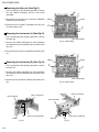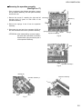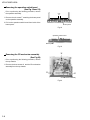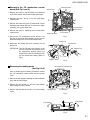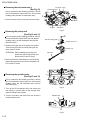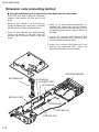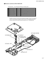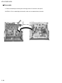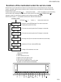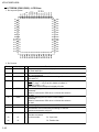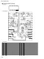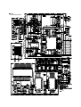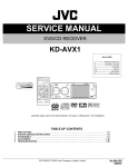
1
KD-LX10/KD-LX30
KD-LX10/KD-LX30
SERVICE MANUAL
CD RECEIVER
KD-LX10
KD-LX30
Area Suffix
J ---- Nortern America
Contents
Safety precaution
Instructions
Disassembly method
Adjustment method
Maintenance of laser pickup
Replacement of lase pickup
Extention code connecting method
VICTOR COMPANY OF JAPAN, LIMITED
MOBILE ELECTRONICS DIVISION,10-1,1Chome,Ohwatari-machi,Maebashi-city,Japan
1-2
1-3~
2-1
2-4
2-14
2-14
2-15
Functions of the mechanism under
the servise mode
Flow of functional until TOC read
Description of major ICs
Block diagrams
Standard schematic diagrams
Printed circuit board
Parts list
This service manual is made from 100% recycled paper.
(No.49537)
Printed in Japan
200002(O)
COPYRIGHT
2000 VICTOR COMPANY OF JAPAN, LTD.
2-18
2-20
2-23
2-39
2-41
2-45,46
3-1~7
No.49537
Feb. 2000
Safety precaution
! CAUTION Burrs formed during molding may be left over on some parts of the chassis. Therefore,
pay attention to such burrs in the case of preforming repair of this system.
! CAUTION Please use enough caution not to see the beam directly or touch it in case of an
adjustment or operation check.
KD-LX10/KD-LX30
Disassembly method
Bottom cover
Removing the top chassis
(See Fig.1 to 5)
1. Remove the two screws A attaching the bottom
cover to the top chassis on the bottom of the body.
2. Remove the two screws B attaching the top chassis
on both sides of the body.
A
A
3. Remove the two screws C and the two screw D
attaching the heat sink on the left side of the body.
Fig.1
4. Remove the two screws E and the screw F on the
back of the body.
5. Remove the two screws G on the upper side of the
body.
Top chassis
6. Move the top chassis upward and disconnect the CD
mechanism connector from the main board
connector by pulling it. Remove the top chassis from
the body.
Fig.2
E
C
Top chassis
F
Heat sink
Fig.4-1 (KD-LX30)
B
B
D
Fig.3
E
F
Top chassis
Fig.4-2 (KD-LX10)
G
G
Fig.5
2-1
KD-LX10/KD-LX30
Removing the main board assembly
(See Fig.6 and 7)
Prior to performing the following procedure, remove
the top chassis.
1. Disconnect the flexible harness from connector
CN701, the card wire from CN702 on the main board
and the harness from CN503 and CN504
respectively.
2. Remove the three screws H attaching the main
board assembly to the bottom cover on the upper
side of the body.
3. Remove the screw I attaching the rear panel and the
bottom cover on the back of the body. Move the
main board in the direction of the arrow and release
the two joints a. (At this point, the main board can be
removed with the rear panel and the rear heat sink.)
CN504
CN503
CN701
H
H
Joint a
Joint a
CN702
Front panel assembly
Fig.6-1 (KD-LX30)
4. Remove the screw J and the two screws K
attaching the rear heat sink on the back of the body.
5. Remove the two screws L and the screw M
attaching the rear panel. Now, the main board
assembly will be removed.
CN504
CN503
ATTENTION: when reassembling, correctly engage
the switch S561 and S562 on the main
board with the part e of the operation
assembly (Refer to Fig.6-3).
CN701
H
H
Joint a
L
Rear heat sink
M
L
J
Joint a
CN702
Front panel assembly
Fig.6-2 (KD-LX10)
Rear panel
I
K
Fig.7-1 (KD-LX30)
L
Rear panel
Rear heat sink
M
L
K
I
Fig.7-2 (KD-LX10)
2-2
e
J
Main board
S652
Fig.6-3
S651
KD-LX10/KD-LX30
Removing the front panel assembly
(See Fig.6,8 and 9)
Prior to performing the following procedure, remove
the top chassis assembly.
CN504
CN503
CN701
1. Disconnect the flexible harness from connector
CN701 on the main board assembly.
H
H
2. Remove the four screws N attaching the front panel
assembly on both sides of the body. Remove the
front panel toward the front.
Joint a
Joint a
CN702
Front panel assembly
Fig.6-1 (KD-LX30)
CN504
CN503
CN701
H
H
Joint a
Joint a
CN702
Front panel assembly
Fig.6-2 (KD-LX10)
Front panel assembly
Front panel assembly
N
N
CN701
Fig.8
Fig.9
Joints b
Removing the Front Board (See Fig.10)
Prior to performing the following procedure, remove
the top chassis assembly and the front panel
assembly.
1. Remove the four screws O attaching the front board
on the back of the front panel assembly and release
the eight joints b.
O
O
Joints b
Fig.10
2-3
KD-LX10/KD-LX30
Removing the lifter unit (See Fig.11)
Prior to performing the following procedure, remove
the top chassis assembly and the front panel
assembly.
1. Disconnect the harness from connector CN503and
CN504 on the main board.
2. Remove the four screws P and detach the lifter unit
from the bottom cover.
CN504
CN503
P
P
Removing the feed motor (L) (See Fig.12)
Prior to performing the following procedure, remove
the lifter unit.
Lifter unit assembly
Fig.11-1 (KD-LX30)
1. Remove the washer attaching the clutch assembly
and detach the clutch assembly from the shaft of the
lifter unit.
2. Remove the two screws Q attaching the feed motor
(L).
CN504
CN503
Removing the feed motor (R) (See Fig.13)
Prior to performing the following procedure, remove
the lifter unit.
P
P
1. Remove the washer attaching the clutch assembly
and detach the clutch assembly from the shaft of the
lifter unit.
Lifter unit assembly
2. Remove the two screws R attaching the feed motor
(R).
Fig.11-2 (KD-LX10)
Lifter unit assembly
Lifter unit assembly
Clutch assembly
Clutch assembly
R
Feed motor (L) assembly
Washer
Washer
Fig.13
2-4
Feed motor (R) assembly
Q
Fig.12
KD-LX10/KD-LX30
Removing the operation assembly
(See Fig.14 to 17)
Prior to performing the following procedure, remove
the top chassis assembly, the front panel assembly
and the lifer unit.
1. Remove the screws S attaching the right and left
brackets which fix gears on both sides of the
operation assembly.
2. Remove the springs 5 and 6 from the operation
assembly.
3. Disconnect the card wire from connector CN702 on
the main board and remove the operation assembly.
Bracket (R)
Bracket (L)
S
S
Spring 5
Operation assembly
ATTENTION: when reassembling, correctly engage
the switch S561 and S562 on the main
board and the right gear with the part e
of the operation assembly.
CN702
Spring 6
Fig.14
S652
S651
Operation assembly e
Fig.15
Bracket (R)
Operation assembly
Operation assembly e
e
S651
S652
Fig.17
Fig.16
2-5
KD-LX10/KD-LX30
Removing the operation switch board
(See Fig.18 and 19)
Prior to performing the following procedure, remove
the operation assembly.
TT
1. Remove the six screws T attaching the button panel
on the operation assembly.
2. Pull out the operation switch board from inside of the
button panel.
Button panel
Fig.18
Operation switch board
Button panel
Fig.19
U
Removing the CD mechanism assembly
(See Fig.20)
Prior to performing the following procedure, remove
the top chassis.
1. Remove the three screws U and the CD mechanism
assembly from the top chassis.
U
U
CD mechanism assembly
Fig.20
2-6
KD-LX10/KD-LX30
Removing the CD mechanism control
board (See Fig.1 and 2)
I
Pickup cover
N
Damper bracket
I
f
1. Remove the screw N and the pickup cover attached
to the front bracket with the two double-sided tapes.
2. Unsolder the part f and g on the CD mechanism
control board.
F
I
i
3. Remove the stator fixing the CD mechanism control
board and the damper bracket (To remove the stator
smoothly, pick up the center part).
4. Remove the screw F attaching the CD mechanism
control board.
CD mechanism
control board
Double-sided tape
5. Remove the CD mechanism control board in the
direction of the arrow while releasing it from the two
damper bracket slots i and the front bracket slot j.
Front bracket
j
Fig.1
Pickup unit
6. Disconnect the flexible wire from connector on the
pickup unit.
Flexible wire
ATTENTION: Turn the FD gear in the direction of the
arrow to move the entire pickup unit to
the appropriate position where the
flexible wire of the CD mechanism unit
can be disconnected easily (Refer to
Fig.2).
Shift the lock
FD gear
Removing the loading motor
(See Fig.3 to 5)
Fig.2
CD mechanism control board
Prior to performing the following procedure, remove
the CD mechanism control board and the pickup
cover.
1. Remove the two springs k attaching the CD mechanism
ass’y and the front bracket.
2. Remove the two screws G and the front bracket
while pulling the flame outward.
3. Remove the belt and the screw H from the loading
motor.
k
k
G
G
Loading motor
Front bracket
Fig.3
Pull outward
Front bracket
Flame
Pull outward
Fig.4
2-7
KD-LX10/KD-LX30
Loading motor
H
Belt
Fig.5
Removing the CD mechanism ass’y
(See Fig.1, 6 to 9)
Prior to performing the following procedure, remove
the CD mechanism control board and the front
bracket (loading motor).
1. Remove the three screws I and the damper bracket.
CD mechanism ass’y
Damper bracket
I
m
Flame
m
I
I
2. Raise the both sides fix arms and move the fix plates
in the direction of the arrow to place the four shafts l
as shown in Fig.8 and 9.
Fig.6
I
3. Remove the CD mechanism ass’y and the two
springs m attaching the flame.
4. Remove the two screws J and both sides rear
damper brackets from the dampers. Detach the CD
mechanism ass’y from the left side to the right side.
Fig.7
ATTENTION: The CD mechanism ass’y can be
removed if only the rear damper
bracket on the left side is removed.
Rear damper bracket
J
Fix plate (L)
Fix arm (L)
l
l
Damper
Fig.8
Fix arm (R)
J
Rear damper bracket
Fix plate(R)
l
Damper
l
Fig.9
2-8
KD-LX10/KD-LX30
Removing the feed motor ass’y
(See Fig.10)
Prior to performing the following procedure, remove
the CD mechanism control board, the front bracket
(loading motor) and the CD mechanism ass’y.
FD screw Part n
Feed motor ass’y
Part O
K
1. Remove the two screws K and the feed motor ass’y.
Pickup unit
FD gear
Fig.10
Removing the pickup unit
(See Fig.10 and 11)
Prior to performing the following procedure, remove
the CD mechanism control board, the front bracket
(loading motor), the CD mechanism ass’y and the
feed motor ass’y.
Pickup unit
L
Nut push spring plate
Pickup mount nut
1. Detach the FD gear part of the pickup unit upward.
Then remove the pickup unit while pulling out the
part n of the FD screw.
Pickup unit
FD screw
ATTENTION: When reattaching the pickup unit,
reattach the part o of the pickup unit,
then the part n of the FD screw.
2. Remove the screw L attaching the nut push spring
plate and the pickup mount nut from the pickup unit.
Pull out the FD screw.
Removing the spindle motor
(See Fig.12 and 13)
Fig.11
p
p
Prior to performing the following procedure, remove
the CD mechanism control board, the front bracket
(loading motor), the CD mechanism ass’y and the
feed motor ass’y.
1. Turn up the CD mechanism ass’y and remove the
two springs p on both sides of the clamper arms.
Open the clamper arm upward.
2. Turn the turn table and remove the two screws M
and the spindle motor.
Fig.12
Spindle motor
M
M
Fig.13
2-9
KD-LX10/KD-LX30
Removing the CD mechanism control
board(See Fig.1 and 2)
Damper bracket
D
CD mechanism ass’y D
f
m
m
Unsolder the part a and b on the CD mechanism
control board.
c
D
Remove the stator c fixing the CD mechanism
control board and the damper bracket (To remove
the stator smoothly, pick up the center part).
d
Remove the screw A attaching the CD mechanism
control board.
Front bracket
Remove the CD mechanism control board in the
direction of the arrow while releasing it from the two
damper bracket slots d and the front bracket slot e.
A
b
e
CD mechanism
control board
Fig.1
Disconnect the flexible wire from connector on the
pickup unit.
Pickup unit
Flexible wire
ATTENTION: Turn the FD gear in the direction of the
arrow to move the entire pickup unit to
the appropriate position where the
flexible wire of the CD mechanism unit
can be disconnected easily (Refer to
Fig.2).
Shift the lock
FD gear
Fig.2
CD mechanism control board
f
f
B
B
Loading motor
Front bracket
Fig.3
Front bracket Pull outward
Pull outward
Flame
2-10
Fig.4
KD-LX10/KD-LX30
Removing the loading motor
(See Fig.3 to 5)
Loading motor
C
Prior to performing the following procedure, remove
the CD mechanism control board.
Belt
1. Remove the two springs f attaching the CD mechanism
ass’y and the front bracket.
Fig.5
2. Remove the two screws B and the front bracket
while pulling the flame outward.
3. Remove the belt and the screw C from the loading
motor.
CD mechanism ass’y
Damper bracket
D
h
Flame
h
D
D
Fig.6
Removing the CD mechanism ass’y
(See Fig.1, 6 to 9)
D
Prior to performing the following procedure, remove
the CD mechanism control PWB and the front
bracket (loading motor).
1. Remove the three screws D and the damper bracket.
Fig.7
2. Raise the both sides fix arms and move the fix plates
in the direction of the arrow to place the four shafts g
as shown in Fig.8 and 9.
Rear damper bracket
3. Remove the CD mechanism ass’y and the two
springs h attaching the flame.
E
Fix plate (L)
Fix arm (L)
4. Remove the two screws E and both sides rear
damper brackets from the dampers. Detach the CD
mechanism ass’y from the left side to the right side.
g
g
ATTENTION: The CD mechanism ass’y can be
removed if only the rear damper
bracket on the left side is removed.
Damper
Fig.8
Fix arm (R)
E
Rear damper bracket
Fix plate(R)
g
Damper
g
Fig.9
2-11
KD-LX10/KD-LX30
Removing the feed motor ass’y
(See Fig.10)
Prior to performing the following procedure, remove
the CD mechanism control board, the front bracket
(loading motor) and the CD mechanism ass’y.
FD screw Part j
Feed motor ass’y
Part k
F
1. Remove the two screws F and the feed motor ass’y.
Pickup unit
FD gear
Pickup unit
Fig.10
Removing the pickup unit
(See Fig.10 and 11)
*Prior to performing the following procedure, remove
the CD mechanism control board, the front bracket
(loading motor), the CD mechanism ass’y and the
feed motor ass’y.
G
Nut push spring plate
Pickup mount nut
1. Detach the FD gear part of the pickup unit upward.
Then remove the pickup unit while pulling out the
part j of the FD screw.
Pickup unit
FD screw
ATTENTION: When reattaching the pickup unit,
reattach the part k of the pickup unit,
then the part j of the FD screw.
2. Remove the screw G attaching the nut push spring
plate and the pickup mount nut from the pickup unit.
Pull out the FD screw.
Removing the spindle motor
(See Fig.12 and 13)
Fig.11
m
m
Prior to performing the following procedure, remove
the CD mechanism control board, the front bracket
(loading motor), the CD mechanism ass’y and the
feed motor ass’y.
1. Turn up the CD mechanism ass’y and remove the
two springs m on both sides of the clamper arms.
Open the clamper arm upward.
2. Turn the turn table, and remove the two screws H
and the spindle motor.
Fig.12
H
Spindle motor
H
Fig.13
2-12
KD-LX10/KD-LX30
2-13
KD-LX10/KD-LX30
Caution : Replacing the pickup
To prevent damage to the laser diode
static electricity destroys the laser diode.
Always
take
countermeasure
to
performing repairs around the laser
pickup.
1.
Do not touch the area around the laser
2. diode or the actuator.
Do not check the laser diode with a tester
or other device (the laser diode can be
3. broken quite easily).
Short-circuit the laser pickup
Solder the land in the center of the flexible
cable of the laser diode and help prevent
damage from static electricity.
Caution :
Solder rejection or cuts a pattern with
nipper at shortstop point after short
circuiting with clip with terminal face of
flexible cable in the static electricity
countermeasure soldering iron application
that is not done.
And the rejection back inserts it in
connector immediately and do not touch
terminal side of connector either.
Recommendation
Soldering iron
HAKKO ESD countermeasures product
Soldering
Caution :
Do not forget to remove the soldered laser diode
short-circuit after finishing repair, and leave the circuit open.
2-14
KD-LX10/KD-LX30
Maintenance of laser pickup
1) Cleaning the pick up lens
Before you replace the pick up, please try to
clean the lens with a alcohol soaked cotton
swab.
(2) Life of the laser diode
When the life of the laser diode has expired,
the following symptoms will appear.
(1) The level of RF output (EFM output:ampli
tude of eye pattern) will be low.
Is RF output
1.0 0.35Vp-p?
NO
Replace it.
YES
O.K
Replacement of laser pickup
Turn off the power switch and,disconnect the
power cord from the ac outlet.
(3) Semi-fixed resistor on the APC PC board
The semi-fixed resistor on the APC printed
circuit board which is attached to the pickup
is used to adjust the laser power.Since this
adjustment should be performed to match the
characteristics of the whole optical block,
do not touch the semi-fixed resistor.
If the laser power is lower than the specified
value,the laser diode is almost worn out, and
the laser pickup should be replaced.
If the semi-fixed resistor is adjusted while
the pickup is functioning normally,the laser
pickup may be damaged due to excessive current.
Replace the pickup with a normal one.(Refer
to Pickup Removal on the previous page)
Plug the power cord in,and turn the power on.
At this time,check that the laser emits for
about 3seconds and the objective lens moves
up and down.
Note: Do not observe the laser beam directly.
Play a disc.
Check the eye-pattern at TP1.
Finish.
2-15
KD-LX10/KD-LX30
Extension code connecting method
Using the extention cords to connect the front panel with the main board
Remove the main board follwing the disassembly
methode. Then reattachi the heat sink to main
board.
1. Using the 2pin extention cord (EXTLX001-2p),
connect the harness of the feed motor (L) assembly
with the connector CN503 on the main board.
2. Using the 2pin extention cord (EXTLX001-2p),
connect the harness of the feed motor (R)
assembly with the connector CN504 on the main
board.
3. Using the jig board (EXTLX002-SWPWB), its
installing to the chassis, then using 4pin extention
cord (EXTLX002-4P) connect the harness of the
lifter detecting board with the connector CN704 on
the board.
4. Connect the connector (EXTLX001-6PC) and
extension wire (EXTLX001-6PF), connect the 6pin
connector CN702 on the main board.
5. Connect the connector (EXTLX002-16PC) and
extension wire (EXTLX002-16PF), connect the
16pin connector CN701 on the main board.
EXTLX002-SWPWB
EXTGS004-26P
EXTLX002-4P
EXTLX002-16PC
EXTLX001-2P
EXTLX001-16PF
EXTLX001-6PC
EXTLX001-2P
EXTLX001-6PF
2-16
KD-LX10/KD-LX30
Extension cord list for KD-LX10/KD-LX30
EXTLX002-JIG : Kit including the following 8 extension parts.
No.
1
2
3
4
5
6
7
Parts number
EXTLX001-2P
EXTLX001-6PF
EXTLX001-6PC
EXTLX002-16PF
EXTLX002-16PC
EXTLX002-SWPWB
EXTLX002-4P
Quantity
2
1
1
1
1
1
1
Description
2Pin, 30cm extension cord
6Pin, 30cm flat wire
6Pin x 2, interlocking connector
16Pin flat wire
16Pin, interlocking connector
3 switch PWB
4Pin, 30cm extension cord
Besides the above kit, we offer the conventional extension cord for CD mechanism
which are not essential to operation check or service. The mechanism should be
directly connected to the board using the extension wire. EXTGS004-26P
EXTLX002-SWPWB
EXTGS004-26P
EXTLX002-4P
EXTLX002-16PC
EXTLX001-2P
EXTLX001-16PF
EXTLX001-6PC
EXTLX001-2P
EXTLX001-6PF
2-17
KD-LX10/KD-LX30
Reassembly
1. Perform reassembly be reversing the removing process of "removal of main parts".
CAUTION 1: Prior to reattaching the heat sink, make sure to reattache the top chassis.
2-18
KD-LX10/KD-LX30
Functions of the mechanism under the service mode
With the three error modes stored in maximum in the internal memory of the mechanism in the body of this
system, it is posible under the service mode to call the contents of error according to the following steps when
any error has occurred.
Press the three buttons (UP button
)+(
button)+(Func button
). Then it is possible to select the follwing
service modes. After changing over to the service mode, press the UP button
and DOWN button
to
change the mode. For executing the respective service modes, press the SEL button.
With the service mode 2 , it is possible to call the error codes of the mechanism.
NORMAL MODE
(UP button
DELEEPROM
)+(
button) + (
button) at the same time.
: Deletion of entire EEPROM data. This mode is used when
shipping this system from factry.
CD-CH ERR
: This mode is used only when the CD changer is connected.
DEL CH-ERR
: This mode is used only when the CD changer is connected.
RUNNING
: Running mode (Do not use this mode under the servise mode)
DELDATA
: (Deletion of CD error code and RDS data)
CD-ERR
: Calling of CD mechanism error code
Data stored in EEPROM
1. RDS data
2. CD mechanism error cord
3. Station name (to be input by user)
4. DISC name (to be input by user)
5. AUX input name (application only to KD-LX30)
*Any data 3 to 5 above should not be deleted.
2
SEL
1
MODE
3
SOURCE
BAND
4
DISP
BBE
5
OFF/
6
2-19
KD-LX10/KD-LX30
1. Display of mechanism error
Occurrence condition
Description
Error codes
Disc loading error
1. SW4 is not turned off.
2. SW3 is not turned on.
09 0011
09 0013
Eject error
1. SW# is not turned off.
01 0021
Error during standby for loading
1. In case SW2 has been positioned to "L" before
starting loading during waiting for 15sec.
80 0031
2. Display of CD error
Occurrence condition
Pickup feeding error
1. Inner peripheral feeding error
(10sec.)
2. Outer peripheral feeding error
(10sec.)
Focus search error
In the case of focusing error after
3-way focus searching
Tracking balance adjusting error
In the case of time-over (1sec.)
of timer
TOC area searching error
In the case of time-over (10sec.)
of timer
Reading error
IN the case of time-over (30sec.)
of timer
1st tracking access error
In the case of time-over (10sec.)
of timer
Last tracking access error
In the case of time-over (10sec.)
of timer
Q code reading error
In the case of time-over (0.6sec.)
of timer
TEXT data reading error
2-20
Description
The pickup cannot returned to the inner
peripheral, and the REST switch is not turned off.
The pickup cannot be returned to the outer
peripheral, and the REST switch is not turned off.
In case the focus cannot be searched by one set
of focus searching (3-way focus searching) after
disc change and focus shock, judge that the focus
searching system is in error.
In case tracking balance cannot be adjusted even
after elapse of 1sec. following execution of the
adjusting command (TBA).
In case TOC area searching is not ended even after
elapse of 10sec.
In case reading is not ended even after elapse of 30
sec. during TOC reading action.
In case the first tracking access is not ended even
after elapse of 10sec. following completion of TOC
reading.
In case the last tracking access is not ended even
after elapse of 10sec. following completion of first
tracking under the RUNNING mode.
In case the Q code cannot be read for 0.6sec.
during playing TOC program area.
In case all TEXT data cannot be read.
Error codes
04 0051
04 0052
81 0053
82 0054
82 0055
84 0059
80 0060
80 0061
80 0062
80 0063
KD-LX10/KD-LX30
Flow of functional operation until TOC read
• When the pickup correctly moves
to the inner area of the disc
Microprocessor
commands
Power ON
Set Function to CD
• When the laser diode correctly
emits
Microprocessor
commands
Disc inserted
FMO
MN662748RPM "32"
MN662748RPM 57
Pickup feed to the inner area
FEED MOTOR
+TERMINAL
TERMINAL
IC661"26"
REST SW
YES
CN602 2
Laser emitted
• When correctly focused
"No disc"
display
Focus search
AN8806SB-W
27
YES
Focus Servo Loop ON
Disc rotates
RF signal eye-pattern
remains closed
Tracking loop closed
RF signal eye-pattern
opens
• When the disc correctly rotates
Microprocessor
commands
BCM
MN662748RPM
24
Spindle
motor (-)
IC661 "2"
TOC readout
Acceleration
Rough
Servo Servo CLV
0.5 Sec 0.5 Sec
Jump to the first track
Play
Tracking Servo Loop ON
• RF signal
Rough Servo Mode
CLV Servo Mode
(ProgramArea)
CLV Servo Mode
(Lead-In Area;
Digital: 0)
2-21
KD-LX10/KD-LX30
Feed Section
NO
Is the voltage output at
IC631 pin "26" 2.5V or
Is the wiring for IC941
(10) ~ (15) correct?
YES
Is 5V present at IC601
pin "5"?
NO
Check CD 9V
and 5V.
YES
NO
YES
Check the vicinity of
IC941.
NO
Is 4V present at both
sides of the feed motor?
Is 6V or 2V present at
IC601 "26" and "27"?
YES
Check the feed motor
connection wiring.
NO
YES
Check the feed motor.
Check IC661.
Focus Section
NO
When the lens is
moving:
Check the circuits in
the vicinity of IC661
pins "17" ~ "20".
YES
Does the S-search
waveform appear at
IC601 pins "17" and "18"?
YES
Check the pickup and
its connections.
Spindle Section
NO
Is the disk rotated?
Is 3.5V present at IC661
pins "1" and "2" ?
NO
Is 4V present at IC631
pin "25" ?
NO
Check IC601 and
IC631.
YES
YES
YES
Does the RF signal
appear at TP1?
Check the spindle motor
and its wiring.
YES
Check the vicinity of
IC661.
NO
Is the RF waveform at TP1
distorted?
NO
Check the circuits in the
vicinity of IC601 "10" ~
"18" or the pickup
YES
Proceed to the Tracking
section
Tracking Section
When the disc is rotated
at first:
YES
Approx. 1.2 V
Is the tracking error signal
output at IC631 "33"?
YES
Check IC601.
2-22
Check the circuit in the
vicinity of IC601 pins
"20" ~
.
YES
Check the pickup and
its connections.
KD-LX10/KD-LX30
FAN8037 (IC581) : CD driver
1. Pin layout & Block diagram
48 47 46 45 44 43
42
41 40 39 38 37
1
36
2
35
3
34
4
33
5
32
6
31
30
7
8
9
s
w
M
S
C
D
D
29
s
w
M
S
C
D
28
s
w
M
S
C
D
10
11
D
26
D
T.S.D
12
27
STAND BY
ALL MUTE
25
POWER SAVE
13 14 15 16 17 18
19
20 21 22
23 24
2. Pin function
Pin
No.
1
2
3
4
5
6
7
8
9
10
11
12
13
14
15
16
17
18
19
20
21
22
23
24
Symbol
IN2+
IN2OUT2
IN3+
IN3OUT3
IN4+
IN4OUT4
CTL1
FWD1
REV1
CTL2
FWD2
REV2
SGND
FWD3
REV3
CTL3
SB
PS
MUTE
PVCC2
DO7-
I/O
I
I
O
I
I
O
I
I
O
I
I
I
I
I
I
I
I
I
I
I
I
O
Function
CH2 op-amp input(+)
CH2 op-amp input(-)
CH2 op-amp output
CH3 op-amp input(+)
Ch3 op-amp input(-)
CH3 op-amp output
CH4 op-amp input(+)
CH4 op-amp input(-)
CH4 op-amp output(+)
CH5 motor speed control
CH5 forward input
CH5 reverse input
CH6 motor speed control
CH6 forward input
CH6 reverse input
Signal ground
CH7 forward input
CH7 reverse input
CH7 motor speed control
Stand by
Power save
All mute
Power supply voltage
CH7 drive output(-)
Pin
No.
25
26
27
28
29
30
31
32
33
34
35
36
37
38
39
40
41
42
43
44
45
46
47
48
Symbol
DO7+
DO6DO6+
PGND2
DO5DO5+
DO4DO4+
DO3DO3+
PGND1
DO2DO2+
DO1DO1+
PVCC1
REGOX
REGX
RESX
VREF
SVCC
IN1+
IN1OUT1
I/O
O
O
O
O
O
O
O
O
O
O
O
O
O
I
O
I
I
I
I
O
Function
CH7 drive output(+)
CH6 drive output(-)
CH6 drive output(+)
Power ground2
CH5 drive output(-)
CH5 drive output(+)
CH4 drive output(-)
CH4 drive output(+)
CH3 drive output(-)
CH3 drive output(+)
Power ground1
CH2 drive output(-)
CH2 drive output(+)
CH1 drive output(-)
CH1 drive output(+)
Power supply voltage
Regulator feedback input
Regulator output
Regulator reset input
Bias voltage input
Signal supply voltage
CH1 op-amp input(+)
CH1 op-amp input(-)
CH1 op-amp output
2-23
KD-LX10/KD-LX30
UPD784215GC-165 (IC701) : CPU
1. Pin layout
25
75
~
~
~
100
1
25
51
26
~
50
2. Pin function (1/2)
Pin
No.
Symbol
I/O
SW2
I
1
SW3
I
2
SW4
I
3
REST-SW
I
4
LM0
O
5
LM1
O
6
7 DIMMER-OUT O
LCD-PWR
8
VDD
9
X2
O
10
X1
I
11
VSS
12
XT2
O
13
XT1
I
14
RESET
I
15
SW1
I
16
BUS-INT
I
17
PS2
I
18
CRUISE
I
19
NC
20
NC
21
22 REMOCON-IN I
AVDD
23
AVREF0
24
SBAD IN
25
NC
26
KEY0
I
27
KEY1
I
28
KEY2
I
29
LEVEL
I
30
NC
31
S.METER
I
32
AVSS
33
W-VOL
O
34
O
35 DOT CONT
AVREF
36
37 BUS-SI/SO I/O
BUS-SO
O
38
BUS-SCK
I/O
39
STAGE 2
I
40
2-24
Function
CD mechanism detect switch
CD mechanism detect switch
CD mechanism detect switch
Reset signal input terminal from CD mechanism
Loading motor control signal input terminal
Loading motor control signal input terminal
DIMMER signal output terminal
Non connect
Power supply terminal
Connect to system main clock X'tal osc
Connect to system main clock X'tal osc
Connect to ground
Connect to system sub clock X'tal osc
Connect to system sub clock X'tal osc
System reset signal input terminal
CD mechanism detect switch
J-BUS signal cut in input terminal
Power save 2
CRUISE signal input terminal
Non connect
Non connect
Remote control signal input terminal
Power supply terminal
Power supply terminal
Connect to ground
Connect to ground
Key control 0 input terminal
Key control 1 input terminal
Key control 2 input terminal
Level meter signal input terminal
Non connect
S. meter level input terminal
Connect to ground
Woofer volume signal output terminal(only KD-LX30)
Dot contrast signal output terminal
Power supply terminal
J-BUS data I/O terminal
J-BUS data out put terminal
J-BUS serial clock signal I/O terminal
Initial setting (L)
KD-LX10/KD-LX30
2. Pin function (2/2)
Pin
Symbol
No.
LCD-DA
41
LCD-CL
42
LCD-CE1
43
BUZZER
44
E2PR-DA-I
45
E2PR-DA-O
46
E2PR-CLK
47
BUS-I/O
48
TM0
49
TM1
50
DM0
51
DM1
52
SD/ST
53
LOCAL
54
MONO
55
CA-SW1
56
CA-SW2
57
CA-SW3
58
CA-SW4
59
CA-SW5
60
NC
61
NC
62
SEEK/STOP
63
NC
64
FM/AM
65
PLL-CE
66
PLL-DA
67
PLL-CK
68
PLL-DI
69
NC
70
AMP KILL
71
VSS
72
DIMMER-IN
73
PS1
74
POWER
75
CD-ON
76
MUTE
77
W-LPF1
78
W-LPF2
79
W-MUTE
80
VDD
81
VOL-DATA
82
VOL-CLK
83
NC
84
NC
85
LCD RST
86
LCD-CE2
87
DMK
88
TMK
89
STAGE1
90
BUCK
91
CCE
92
RST
93
TEST
94
BUS0
95
BUS1
96
BUS2
97
BUS3
98
99 DISC SEL(8cmCD)
VOICE IN
100
I/O
O
O
O
O
I
O
I/O
I/O
O
O
O
O
I
O
O
I
I
I
I
I
O
O
O
O
O
I
O
I
I
O
O
O
O
O
O
O
O
O
I
O
O
O
I/O
]I/O
I/O
I/O
I
I
Function
Data output terminal for LCD driver
Clock output terminal for LCD driver
Chip enable 1 output terminal for LCD driver
BUZZER control signal output terminal
Data input terminal from EEPROM
Data output terminal for EEPROM
Clock signal I/O terminal with EEPROM
J-BUS I/O signal terminal
Tray motor negative signal output terminal
Tray motor positive signal output terminal
Door motor negative signal output terminal
Door motor positive signal output terminal
Station detect/Stereo signal input terminal
Local ON/OFF select signal output terminal
Monaural ON/OFF select signal output terminal
DOOR/TRAY open close detect switch signal input terminal
DOOR/TRAY open close detect switch signal input terminal
DOOR/TRAY open close detect switch signal input terminal
DOOR/TRAY open close detect switch signal input terminal
DOOR/TRAY open close detect switch signal input terminal
Non connect
Non connect
AUTO SEEK/STOP select signal output terminal
Non connect
FM/AM select signal output terminal
Chip enable signal output terminal
Data output terminal
Clock signal output terminal
Data input terminal
Non connect
Amp. cut off signal output terminal
Connect to ground
DIMMER signal input terminal
Power save 1
Power ON/OFF select signal output terminal
Power supply control terminal for CD
Mute signal output terminal
Non connect
Non connect
Non connect
Power supply terminal
Data output terminal
Clock signal output terminal
Non connect
Non connect
LCD reset signal output terminal
Chip enable 2 output terminal for LCD driver
Motor speed control signal output terminal
Tray motor control signal output terminal
Initial setting H:KD-LX30J L:KD-LX10J
Micro computer interface clock signal output terminal
Chip enable signal output terminal for micro computer interface
Reset signal input terminal
Test terminal
Micro computer interface data I/O terminal
Micro computer interface data I/O terminal
Micro computer interface data I/O terminal
Micro computer interface data I/O terminal
Initial setting (H:8cm disc uncorrespondence)
Initial setting (H:Non corespondence)
2-25
KD-LX10/KD-LX30
BA3220FV-X (IC341) : Driver
1. Pin layout & Block diagram
CL-
LGND
OUTL
OUTR
RGND
CR -
CR +
13
12
11
10
9
8
14
REFL
REFR
FILTER
1
2
3
4
5
6
7
CL+
Vcc
INL
NFL
FIL
NFR
INR
2. Pin functions
Pin
No.
1
2
3
4
5
6
7
8
9
10
11
12
13
14
2-26
Symbol
CL+
Vcc
INL
NFL
FIL
NFR
INR
CR+
CRRGND
OUTR
OUTL
LGND
CL-
Function
Powe supply terminal for amp.
power supply terminal.
input terminal.
Negative feedback terminal.
Filter terminal.
Negative feedback terminal.
Input terminal
Power supply terminal for amp.
Output terminal of internal amp.
Rch GND terminal.
Rch output terminal.
Lch output terminal.
Lch GND terminal.
Output terminal of internal amp.
KD-LX10/KD-LX30
BA4905-V3 (IC961) : Regulator
1.Terminal layout
1
2
3
4
5
6
7
8
9
10
11
12
2.Block daigram
REGULATOR
Overvoltage
protection circuit
EXT
RESET
1
2
RESET
3
4
COMP
EXT
5
6
VDD 5.7V
ACC
7
8
CD 8V
AUDIO 9V
9
37K
5K
10
VCC
CTRL
11
12
AJ
ILM 10V
GND
3.Pin function
Pin no.
Symbol
1
2
RESET
EXT output
3
COMP output
4
5
ACC
VDD output
6
AUDIO output
7
CD output
8
9
10
CTRL
VCC
ILM output
11
AJ
12
GND
Function
If VDD voltage becomes 4V or less.RESET output becomes low level.
This output voltage is approximately 0.5V lower than VCC. and max
output current is 300mA.
A voltage supply for ACC block. This output voltage is approximately
0.7V lower than VDD'S. The max output current is 100mA.
Control of the COMP output by inputting voltage.
This output voltage is 5.7V, and max output current is 100mA.
This voltage supply is for microcomputer. Whenever back up voltage
supply is connected, the output keeps on running.
This output voltage is 9.0v, and max output current is 500mA.
This voltage supply for AUDIO.
This output voltage is 8.0V, and max output current is 1A.
This voltage supply for CD.
Output selector of CD. AUDIO, ILM and EXT.
To be connected with the BACK UP of car.
This output voltage is 10V, and max output current is 500mA.
Output voltage is adjustable.
Putting a resistance between ILM and AJ or between AJ and GND
makes ILM output voltage adjustable.
Ground.
2-27
KD-LX10/KD-LX30
BD3860K (IC911) : E. volume
1. Pin layout
33
~
23
34
~
~
22
44
12
1
~
11
2. Block diagram
GND FIL VCC
6
5
9
POWER
SUPPLY
A1
41
B1
42
C1
43
D1
44
A2
1
B2
2
C2
3
D2
SEL1
VIN1
LOUD1
40
36
35
INPUT
GAIN
0 to 18 dB
MAIN
VOLUME
0 to -40 dB
LOUDNESS
HF1 LF1 DET1 VCA1 MIX1 BBOUT1
34
33
28
32
31
30
LOW(f=50Hz) 6dB
PROCESS CONTROL +3 to 12dB
(f=10kHz)
INPUT
TIN1 TNF1
29
19
BNF1
BOUT1
15
14
TREBLE
BASS
-14 to +14dB
-14 to +14dB
13 OUTF1
FADER
CH1 REAR
0 to -5 dB
12 OUTR1
LOGIC
SELECTOR
INPUT
GAIN
0 to 18 dB
4
FADER
CH1 FRONT
0 to -5 dB
MAIN
VOLUME
0 to -40 dB
LOUDNESS
39
38
37
SEL2
VIN2
LOUD2
LOW(f=50Hz) 6dB
PROCESS CONTROL +3 to 12dB
(f=10kHz)
25
24
26
23
22
21
HF2 LF2 DET2 VCA2 MIX2 BBOUT2
TREBLE
BASS
-14 to +14dB
-14 to +14dB
20
18
TIN2 TNF2
17
16
BNF2
BOUT2
7
SI
8
SC
FADER
CH2 REAR
0 to -5 dB
10 OUTR2
FADER
CH2 FRONT
0 to -5 dB
11 OUTF2
3. Pin function
Pin
No.
1
2
3
4
5
6
7
8
9
10
11
12
13
14
15
16
17
18
19
20
21
22
2-28
Symbol
A2
B2
C2
D2
FIL
GND
SI
SC
VCC
OUTR2
OUTF2
OUTR1
OUTF1
BOUT1
BNF1
BOUT2
BNF2
TNF2
TNF1
TIN2
BBOUT2
MIX2
Function
CH2 input terminal A
CH2 input terminal B
CH2 input terminal C
CH2 input terminal D
1/2 VCC terminal
Ground terminal
Serial data input terminal
Serial clock input terminal
Power supply
CH2 rear output terminal
CH2 front output terminal
CH1 rear output terminal
CH1 front output terminal
CH1 bus filter setting terminal
CH1 bus filter setting terminal
CH2 bus filter setting terminal
CH2 bus filter setting terminal
CH2 treble filter setting terminal
CH1 treble setting terminal
CH2 treble input terminal
CH2 BBE II signal output terminal
CH2 output mix amp negative input terminal
Pin
No.
Symbol
Function
23 VCA2 CH2 high frequency VCA output terminal
24 LF2 CH2 low frequency filter setting terminal
25 HF2 CH2 high frequency filter setting terminal
26 DET2 CH2 high frequency attack release time setting
Non connect
NC
27
28 DET1 CH1 high frequency attack release time setting
29 TIN1 CH1 treble input terminal
30 BBOUT1 CH1 BBE II signal output terminal
31 MIX1 CH1 output mix amp. negative input terminal
32 VCA1 CH1 high frequency VCA output terminal
33 LF1 CH1 low frequency filter setting terminal
34 HF1 CH1 high frequency filter setting terminal
35 LOUD1 CH1 loudness filter setting terminal
36 VIN1 CH1 main volume input terminal
37 LOUD2 CH2 loudness filter setting terminal
38 VIN2 CH2 main volume input terminal
39 SEL2 CH2 input gain output terminal
40 SEL1 CH1 input gain output terminal
CH1 input terminal A
A1
41
CH1 input terminal B
B1
42
CH1 input terminal C
C1
43
CH1 input terminal D
D1
44
KD-LX10/KD-LX30
BR24C16F-X (IC703) : EEPROM
1. Pin layout
2. Pin function
VCC
WP
A0
A1
SCL
SDA
A2
Symbol
VCC
GND
A0,A1,A2
SCL
SDA
WP
GND
I/O
I
I
I/O
I
Function
Power supply.
GND
No use connect to GND.
Serial clock input.
Serial data I/O of slave and ward address.
Write protect terminal.
3. Block diagram
A0
1
16kbit EEPROM allay
2
A2
3
Vcc
7
WP
6
SCL
5
SDA
8bit
11bit
A1
8
Address
decoder
11bit
START
Slave Ward
Data
Address resister
resister
STOP
Control circuit
ACK
GND
4
Power supply
voltage det.
High voltage osc circuit
BU4066BCFV-X (IC322) : Quad analog switch
1. Pin layout & Block diagram
VDD
C1
C4
I/O4
O/I4
O/I3
I/O3
14
13
12
11
10
9
8
1
2
3
4
5
6
7
I/O1
O/I1
O/I2
I/O2
C2
C3
Vss
2-29
KD-LX10/KD-LX30
HD74HC126FP-X (IC771) : Buffer
1. Pin layout
2. Function
1
2
3
4
5
6
7
Inputs
C
A
L
X
H
L
H
H
14
13
12
11
10
9
8
3. Block diagram
Vcc
Outputs
Y
Z
H
L
Vcc
1k
See Function Table
Input
1A
2A
3A
4A
1C
2C
3C
4C
Output
S1
1Y
2Y
2Y
CL
1k
Output
Sample as Load Circuit 1
Output
3Y
Sample as Load Circuit 1
Output
4Y
Sample as Load Circuit 1
NJM4565M-W (IC151,IC171,IC323,IC361,IC461) : Ope amp.
A OUTPUT
1
8
V+
A -INPUT
2
7
B OUTPUT
A
2-30
B
A +INPUT
3
6
B -INPUT
V-
4
5
B +INPUT
KD-LX10/KD-LX30
LC75811W (IC602) : LCD driver
1. Pin layout
60
~
41
~
40
~
61
80
21
COMMON
DRIVER
S1
COM8
COM1
2. Block diagram
S58
20
S59/COM10
~
S60/COM9
1
SEGMENT DRIVER
LATCH
VDD
VLCD
INSTRUCTION
DECODER
VLCD1
ADRAM
60
bits
CGRAM
5x9x16
bits
CGROM
5x9x240
bits
VLCD2
INSTRUCTION
REGISTER
VLCD3
ADDRESS
COUNTER
DCRAM
48x8
bits
VSS
ADDRESS
REGISTER
TIMING
GENERATOR
SHIFT REGISTER
RES
CE
CL
CCB INTERFACE
DI
OSCO
3. Pin function
OSCI
CLOCK
GENERATOR
Pin
No.
Symbol
Function
I/O
S3~S60
O Segment driver output terminal
1~58
COM0
O Common driver output terminal
59
60~65 COM3~COM8 O Common driver output terminal
COM1
O Common driver output terminal
66
VDD
Power supply for logic section
67
VLCD
Power supply for LCD driver section
68
LCD voltage input terminal
69~71 VLCD1~VLCD3 I
VSS
Connect to ground
72
OSCO
O Oscillation output terminal
73
OSCI
Oscillation input terminal
I
74
RES
Reset signal input terminal
I
75
CE
Chip enable input terminal
I
76
CL
Clock signal input terminal
I
77
DI
Serial data input terminal
I
78
S1~S2
O Segmrnt driver output terminal
79~80
2-31
KD-LX10/KD-LX30
LC75823W (IC601,IC602) : LCD Driver
DI
CL
CE
OSC
Vss
VDD2
VDD1
INH
VDD
COM3
COM2
COM1
S52
S51
S50
S49
1. Pin Layout & Symbol
64 63 62 61 60 59 58 57 56 55 54 53 52 51 50 49
1
48
2
47
3
46
4
45
5
44
6
43
7
42
8
41
9
40
10
39
11
38
12
37
13
36
14
35
15
34
16
33
17 18 19 20 21 22 23 24 25 26 27 28 29 30 31 32
S48
S47
S46
S45
S44
S43
S42
S41
S40
S39
S38
S37
S36
S35
S34
S33
S17
S18
S19
S20
S21
S22
S23
S24
S25
S26
S27
S28
S29
S30
S31
S32
S1
S2
S3
S4
S5
S6
S7
S8
S9
S10
S11
S12
S13
S14
S15
S16
2. Pin Function
Pin No.
1 to 52
Symbol
S1 to S52
64
DI
I/O
Function
O Segment output pins used to display data transferred
by serial data input.
53 to 55 COM1 to COM3 O Common driver output pins. The frame frequency is given
by : t0=(fosc/384)Hz.
VDD
56
-- Power supply connection. Provide a voltage of between
4.5 and 6.0V.
INH
57
I Display turning off input pin.
INT="L" (Vss) ----- off (S1 to S52, COM1 to COM3="L"
INT="H" (VDD)----- on
Serial data can be transferred in display off mode.
VDDD1
58
I Used for applying the LCD drive 2/3 bias voltage
externally.
Must be connected to VDD2 when a 1/2 bias drive scheme
is used.
VDD2
59
I Used for applying the LCD drive 1/3 bias voltage
externally.
Must be connected to VDD1 when a 1/2 bias drive scheme
is used.
Vss
60
-- Power supply connection. Connect to GND.
OSC
61
I/O Oscillator connection.
An oscillator circuit is formed by connecting an external
resistor and capacitor at this pin.
Serial data
CE : Chip enable
62
CE
interface connection
CL
CL : Sync clock
63
I to the controller.
2-32
DI : Transfer data
KD-LX10/KD-LX30
NJM2100M-W (IC821) : Dual operation amplifier
1. Pin layout
A OUTPUT
1
8
V+
A - INPUT
2
7
B OUTPUT
A + INPUT
3
6
B - INPUT
V-
4
5
B + INPUT
2. Block diagram
V+
- INPUT
OUTPUT
+ INPUT
V-
IC-PST600M/G/-W (IC702) : System reset
1 Vcc
3 Vout
Co1
OP1
2 GND
2-33
KD-LX10/KD-LX30
NJM2904M-W (IC951) : Dual operation amplifier
1. Pin layout
A OUT
1
8
V+
A - IN
2
7
B OUT
A + IN
3
6
B - IN
GND
4
5
B + IN
V+
2. Block diagram
Q5
Q2
Q6
Q3
Q4
Q1
Q7
INPUTS
OUTPUT
Q13
Q11
Q12
Q10
Q8
2-34
Q9
KD-LX10/KD-LX30
RPM6938-SV4 (IC603) : Remote control receiver
Vcc
AGC
AMP
Comp
I/V
conversion
BPF
PD
Vcc
22k
ohm
Rout
Detector
for
trimming
circuit
GND
magnetic shield
TDA7560 (IC941) : 4ch bridge amplifier
1. Pin layout
1
25
2. Block diagram
VCC1
6
ST-BY
VCC2
20
4
HSD
MUTE
25
HSD
OUT1+
OUT1P-GND1
22
IN1
11
9
7
8
IN2
12
5
3
4
OUT2+
OUT2P-GND2
IN3
15
17
19
18
OUT3+
OUT3P-GND3
IN4
14
21
23
22
OUT4+
OUT4P-GND4
16
AC-GND
10
SVR
1
TAB
13
S-GND
2-35
KD-LX10/KD-LX30
TA2109F-X (IC501) : RF amp.
1. Pin layout
24
13
1
12
2. Block diagram
15k ohm
15k ohm
13
SBAD
TEO 12
20uA
30k ohm
20pF
FEO
10k ohm
36pF
10pF
15
7.67k ohm
10k ohm
50k ohm
14
30k ohm
10k ohm
FEN
TEN
10k ohm
21k ohm 29k ohm
11
2VRO 10
7.96k ohm
10k ohm
24k ohm 24k ohm
16
TEB
VRO
17
3 STATE
DET.
21k ohm
21k ohm
50uA
RFRP 20k ohm
12k ohm
1.74k ohm
47k ohm SW1
LCD
SEL
SW2 1k ohm
680 ohm
LDO
9
8
19
20
20k ohm
RFGO
65uA
18
20k ohm
12k ohm
RFIS
SW3
PEAK
180k ohm
BOTTOM
MDI
13k ohm 2.12k ohm
20pF
RFGC
23.5k ohm
12k ohm
20pF
re=130 ohm
20k ohm
180k ohm
FPI
40pF
60k ohm
23
60k ohm
GND
1.53k ohm
180k ohm
24
40pF
3
20k ohm
20k ohm
FNI
2
20k ohm
Vcc 1
RFN
3.3k ohm
5
TPI 4
I-I
RFO
6
180k ohm
AGCI
21
22
TNI
I-I
7
3.3k ohm
3. Pin function
Pin
No.
Symbol I/O
Pin function
Vcc - Power supply input terminal
1
FNI
I Main beam I-V amp input terminal
2
FPI
I Main beam I-V amp input terminal
3
TPI
I Sub beam I-v input terminal
4
TNI
I Sub beam I-V input terminal
5
MDI I Monitor photo diode amp input terminal
6
7 LDO O Laser diode amp output terminal
SEL I Laser diode control signal input terminal
8
TEB I T. error balance adj. signal input terminal
9
10 2VRO O Reference voltage output terminal
11 TEN I TE amp negative input terminal
12 TEO O TE error signal output terminal
2-36
Pin
No.
Symbol I/O
13
14
15
16
17
18
19
20
21
22
23
24
SBAD
FEO
FEN
VRO
RFRP
RFIS
RFGO
RFGC
AGCI
RFO
GND
RFN
O
O
I
O
O
I
O
I
I
O
I
Pin function
Sub beam adder signal output terminal
Focus error signal output terminal
FE amp negative input terminal
Reference voltage (VREF) output terminal
Track count signal output terminal
RFRP detect circuit input terminal
RF gain signal output terminal
RF amplitude adj. control signal input terminal
RF signal amplitude adj. amp input terminal
RF signal output terminal
Ground terminal
RF amp negative input terminal
KD-LX10/KD-LX30
2.Block diagram
1
2
3
4
5
6
7
8
9
10
11
12
1.Terminal Layout
24
23
22
21
20
19
18
17
16
15
14
13
TB2118F-X (IC21) : PLL
Constant
power supply voltage
osc
2
XO
1
Buff.
ON/OFF
OSC circuit
AM CP.
Phase
Comparator
Reference Counter
XI 24
20
switch
AMP
AMVCO 16
AMP
IFC 13
4-bit
Swallow counter
Prescaler
12-bit
Programmable counter
AMP
+
-
FM VCO 15
REG.
22
19
20-bit BINARY COUNTER
vt
CE 3
Resistor 1
DIN
4
22-bit
40bit shift register
Resistor 2
Serial
Interface
+
-
DOUT 5
18
FM cp
I/O PORT
DIMM 6
7
SL
3.Pin Function
Pin
No.
Symbol I/O
1
2
3
4
5
6
7
8
9
10
11
12
XOUT
OSC
CE
DI
CK
DOUT
SR
I/01
I/02
OUT1
OUT2
VDD2
O
I
I
I
O
O
I/O
I/O
-
8
I/O -1
9
I/O -2
OUTPUT PORT
10
11 12
out-1 out-2 vdd2
Function
Crystal oscillator pin
Non connect
Chip enable input
Serial data input
Clock input
Serial data output
Register control pin
I/O ports
I/O ports
Non connect
Non connect
Single power supply for REF. frequency block
Pin
No.
switch
Vdd
14 17 21 23
vdd d-gnd vcc a-gnd
Symbol I/O
IFC
13
14 VDD
15 FMIN
16 AMIN
17 DGND
18 FMCP
VT
19
20 AMCP
21 VCC
RF
22
23 AGND
XIN
24
Vcc
I
I
I
O
O
I
I
Function
IF signal input
Power pins for digital block
FM band local signal input
AM band local signal input
Connect to GND (for digital circuit)
Charge pump output for FM
Tuning voltage biased to 2.5V.
Charge pump output for AM
Power pins for analog block
Ripple filter connecting pin
Connect to GND (for analog circuit)
Crystal oscillator pin
2-37
KD-LX10/KD-LX30
TC9462F (IC521) : DSP & DAC
1.Pin Layout
80
~
51
81
50
~
~
100
31
1
~
30
2.Pin Function (1/2)
Pin No.
1
2
3
4
5
6
7
8
9
10
11
12
13
14
15
16
17
18
19
20
21
22
23
24
25
26
27
28
29
30
31
32
33
34
35
36
37
38
39
2-38
Symbol
I/O
TEST0
HSO
UHSO
EMPH
LRCK
Vss
BCK
AOUT
DOUT
MBOV
IPF
SBOK
CLCK
Vdd
Vss
DATA
SFSY
SBSY
SPCK
SPDA
COFS
MONIT
Vdd
TESIO0
P2VREF
HSSW
ZDET
PDO
TMAXS
TMAX
LPFN
LPFO
PVREF
VCOREF
VCOF
AVss
SLCO
RFI
AVDD
I
O
O
O
O
O
O
O
O
O
O
I/O
O
O
O
O
O
O
O
I
O
O
O
O
O
I
O
I
O
O
I
-
Function
Test mode terminal. Normally, keep at open
Playback speed mode flag output terminal
Playback speed mode flag output terminal
Sub code Q data emphasis flag output terminal. "H"=ON "L"=OFF
Channel clock output terminal.(44.1kHz) "H"=Rch "L"=Lch
Digital GND terminal
Bit clock output terminal. (1.4122MHz)
Audio data output terminal
Digital data output terminal
Buffer memory over signal output terminal.
Correction flag output terminal
Sub code Q data CRCC check adjusting result output terminal. "H"=result OK
Sub code P~W data readout input/output terminal
Digital power supply voltage terminal
Digital GND terminal
Sub code P~W data output terminal
Play-back frame sync signal output terminal
Sub code block sync signal output terminal
Processor status signal readout clock output terminal
Processor status signal output terminal
Correction frame clock output terminal (7.35kHz)
Internal signal (DSP internal flag and PLL clock) output terminal
Digital power supply voltage terminal
Test input/output terminal. Normally, keep at "L" level
PLL double reference voltage supply terminal
2/4 times speed at "Vref" voltage
1bit DA converter zero detect flag output terminal
Phase difference signal output terminal of EFM signal and PLCK signal
TMAX detection result output terminal. Selected by command bit (TMPS)
TMAX detection result output terminal. Selected by command bit (TMPS)
LPF amplifier inverting input terminal for PLL
LPF amplifier output terminal for PLL
PLL reference voltage supply terminal
VCO center frequency reference level terminal
VCO filter terminal
Analog GND terminal
Data slice level output terminal
RF signal input terminal
Analog power supply voltage terminal
KD-LX10/KD-LX30
2.Pin Function (2/2)
Pin No.
40
41
42
43
44
45
46
47
48
49
50
51
52
53
54
55
56
57
58~61
62
63
64~67
68
69
70
71
72
73
74
75
76
77
78
79
80
81
82
83
84
85
86
87~89
90~93
94
95
96
97
98
99
100
Symbol
RFCT
RFZI
RFRP
FEI
SBAD
TSIN
TEI
TEZI
FOO
TRO
VREF
RFGC
TEBC
FMO
FVO
DMO
2VREF
SEL
FLGA~D
VDD
VSS
IO0~3
DMOUT
CKSE
DACT
TESIN
TESIO1
VSS
PXI
PXO
VDD
XVSS
XI
XO
XVDD
DVSR
RO
DVDD
DVR
LO
DVSL
TEST1~3
BUS0~3
VDD
VSS
BUCK
CCE
TEST4
TSMOD
RST
I/O
I
I
I
I
I
I
I
I
O
O
O
O
O
O
O
O
O
I/O
I
I
I
I
I
I
O
I
O
O
O
I
I/O
I
I
I
I
I
Function
RFRP signal center level input terminal
RFRP zero cross input terminal
RF ripple signal input terminal
Focus error signal input terminal
Sub-beam adder signal input terminal
Test input terminal Normally, keep at "vref" level
Tracking error signal input terminal. Take in at tracking servo ON.
Tracking error zero cross input terminal
Focus servo equalizer output terminal
Tracking servo equalizer output terminal
Analog reference voltage supply terminal
RF amplitude adjustment control signal output terminal
Tracking balance control signal output terminal
Feed equalizer output terminal
Speed error signal or feed search equalizer output terminal
Disk equalizer output terminal (PWM carrier=88.2kHz for DSP, Synchronize to PXO)
Analog double reference voltage supply terminal
APC circuit ON/OFF indication signal output terminal
External flag output terminal for internal signal
Digital power supply voltage terminal
Digital GND terminal
General I/O terminal
This terminal control IO0~IO3 terminal
Normally, keep at open
DAC test mode terminal. Normally, keep at open
Test input terminal, Normally, keep at "L" level
Test input/output terminal. Normally, keep at "L" level
Digital GND terminal
Crystal oscillator connecting input terminal for DSP
Crystal oscillator connecting output terminal for DSP
Digital power supply voltage terminal
Oscillator GND terminal for system clock
Crystal oscillator connecting input terminal for system clock
Crystal oscillator connecting output terminal for system clock
Oscillator power supply voltage terminal for system clock
Analog GND terminal for DA converter (Rch)
R channel data forward output terminal
Analog supply voltage terminal for DA converter
Reference voltage terminal for DA converter
L channel data forward output terminal
Analog GND terminal for DA converter (Lch)
Test mode terminal . Normal keep at open
Micon interface data input/output terminal
Digital power supply voltage terminal
Digital GND terminal
Micon interface clock input terminal
Command and data sending/receiving chip enable signal input terminal
Test mode terminal. Normal, keep at open
Local test mode selection terminal
Reset signal input terminal. Reset at "L" level
2-39
KD-LX10/KD-LX30
2-40
Block diagrams
KD-LX10
L-CH
R-CH
CD-L,CD-R
KEY0
KEY1
IC501 VA,VB,VC
RF AMP. MO,LD
IC581
CD&TRAY/DOOR
DRIVER
CN503
CN504
M
M
DOOR
MOTOR
TRAY
MOTOR
LOADING
REST
SPINDLE
FEED
SW1~SW4
M
IC771
JVC BUS
IC821
CRUISE
PON
ACC5V
LOADING MOTOR
REST SWITCH
M
FEED MOTOR
M
SPINDLE MOTOR
LCDRES,LCDCE2,LCDCL,LCDDF
REMOCON
IC603
REMOCON
CN
771
PICKUP
OPTIMA720
FOCUS TRACKING
COIL
COIL
CA1~CA3,SA1~SA52
IC602
LCD
DRIVER
LCDRST,LCDCE1,LCDCL,LCDDA
KEY1,KEY2,INV
A,B,C,LD
FOCUS
TRACKING
CH-L
CH-R
Line out
IC702
RESET
SW1~SW4
FEED ,SPINDLE
TRACKING ,FOCUS
LDON,LOADING
Rear speaker
IC961
REGULATOR
CRUISE
IC951
REGULATOR 14V
CN702
ACC
SI/SO,SO,I/OBUSINT,BUSSCK
RESET
SW1~SW4,REST
TRAY
IC703
EPROM
CN601
CN701
FOO,TRD
DMO,FMO
DOOR
RESET
INV
REMOCON
KEY1
KEY2
MEMORY
REAR R
CN631
IC521
DSP & DAC
INFR
INRR
OUTFL ,OUTFR
OUTRL ,OUTRR
REAR L
IC701
CPU
LCDDA
LCDCL
LCDCE1
LCDCE2
LCDRST
SEL,TEB,TE
SBAD,FE,RF
RFGC,RFAP
IC461
Rch
LINE AMP.
to CN701
BUS0
BUS1
BUS2
BUS3
BUCK
CCE
RST
LOUTF
LOUTR
to CN702
L-CH
R-CH
INFL
IC941
INRL POWER AMP.
SDA
SCL
CN501
CASW1
CASW2
CASW3
IC151
CD LPF
IC361
Lch
LINE AMP.
LEVEL
VOL-DA
VOL-CLK
IC21
PLL
PLLCE
PLLDA
PLLCL
PLLDI
CDON
LMO
LMI
DMO
DMI
DMK
TM0
TM1
TMK
IC911
E.VOLUME
LOUTF
LOUTR
CN301
TU1
TUNER PACK
J1
FM/AM
S.METER
SEEK/STOP
SD/ST
AMIN
FMIN
CN901
Front speaker
KEY0
LED
KEY1
IC601
CB1~CB3
LCD
SB1~SB52
DRIVER
LCD1
KEY
SWITCH
KD-LX30
DOOR
RESET
IC702
RESET
KEY0
KEY1
CN702
CN503
CN504
M
M
DOOR
MOTOR
TRAY
MOTOR
IC771
JVC BUS
Rear speaker
IC961
REGULATOR
IC821
CRUISE
CH-L
CH-R
SI/SO,SO,I/OBUSINT,BUSSCK
LOADING
REST
SPINDLE
FEED
SW1~SW4
W.VOL
PON
ACC5V
W-LPF1
W-LPF2
IC951
REGULATOR
IC501 VA,VB,VC
RF AMP. MO,LD
IC581
CD&TRAY/DOOR
DRIVER
TRAY
ACC
Line out
FRONT
Line out
REAR
CN
771
AU.L,AU.R
SW1~SW4,REST
FOO,TRD
DMO,FMO
MEMORY
CRUISE
M
14V
IC322
SWITCHING
LOADING MOTOR
REST SWITCH
M
FEED MOTOR
M
SPINDLE MOTOR
IC171
LINE IN
IC321
SUBWOOFER
REMOCON
IC603
REMOCON
KEY1,KEY2,INV
PICKUP
OPTIMA720
A,B,C,LD
FOCUS
TRACKING
FOCUS TRACKING
COIL
COIL
KEY0
LED
KEY1
Line IN
SUBWOOFER OUT
CA1~CA8,SA1~SA60
IC602
LCD
DRIVER
LCDRST,LCDCE1,LCDCL,LCDDA
SW1~SW4
FEED ,SPINDLE
TRACKING ,FOCUS
LDON,LOADING
AU.LI,AU.RI
IC323
SUBW
SUBWOOFER
LCDRST,LCDCE2,LCDCL,LCDDA
CN601
CN701
IC703
EPROM
CN631
IC521
DSP & DAC
RESET
INV
REMOCON
KEY1
KEY2
OUTFL ,OUTFR
OUTRL ,OUTRR
REARL,REARR
IC701
CPU
LCDDA
LCDCL
LCDCE1
LCDCE2
LCDRST
SEL,TEB,TE
SBAD,FE,RF
RFGC,RFAP
IC941
POWER AMP.
FRONTL,FRONTR
to CN701
BUS0
BUS1
BUS2
BUS3
BUCK
CCE
RST
IC461
INFR
Rch
INRR
LINE AMP.
to CN702
L-CH
R-CH
LOUTF
LOUTR
SDA
SCL
CN501
IC151
CD LPF
CDON
LMO
LMI
DMO
DMI
DMK
TM0
TM1
TMK
IC361
INFL
Lch
INRL
LINE AMP.
LEVEL
VOL-DA
VOL-CLK
IC21
PLL
PLLCE
PLLDA
PLLCL
PLLDI
CASW1
CASW2
CASW3
IC911
E.VOLUME
CD-L,CD-R
LOUTF
LOUTR
CN301
L-CH
R-CH
CN302
TU1
TUNER PACK
J1
FM/AM
S.METER
SEEK/STOP
SD/ST
AMIN
FMIN
CN901
Front speaker
IC601
CB1~CB3
LCD
SB1~SB52
DRIVER
LCD1
KEY
SWITCH
Standard schematic diagrams
KD-LX10J Main amp section
TUNER SIGNAL
CD SIGNAL
CD CHANGER SIGNAL
FRONT SIGNAL
REAR SIGNAL
KD-LX10J
CD servo & LCD control section
CD SIGNAL
KD-LX30J Main amp section
TUNER SIGNAL
CD SIGNAL
CD CHANGER SIGNAL
AUX SIGNAL
FRONT SIGNAL
REAR SIGNAL
KD-LX30J
CD servo & LCD control section
CD SIGNAL
Printed circuit boards
KD-LX10J
Main board (Forward side)
Main board (Reverse side)
LCD board (Forward side)
LCD board (Reverse side)
Switch board (Forward side)
Switch board (Reverse side)
KD-LX30J
Main board (Forward side)
Main board (Reverse side)
LCD board (Forward side)
LCD board (Reverse side)
Switch board (Forward side)
Switch board (Reverse side)
PARTS LIST
[ KD-LX10 ]
[ KD-LX30 ]
* All printed circuit boards and its assemblies are not available as service parts.
Areas suffix
J -------------- Northern America
- Contents Exploded view of general assembly and parts list
CD mechanism assembly and parts list
Electrical parts list
Packing materials and accessories parts list
3-3
3-5
3-8
3-14
[CAUTION]
Two kinds of POWER IC (IC941) are used for these models.
When you change the POWER IC (IC941), you should confirm the printed
parts number of IC.
Please change other parts listed below at the same time.
The set will break down when the undermentioned parts are mixed.
Electrical parts
IC941
LA4743B
TDA7560
R143
R243
R144
R244
C941
NRSA02J-823X
NRSA02J-823X
NRSA02J-823X
NRSA02J-823X
QERF1CM-106Z
NRSA02J-473X
NRSA02J-473X
NRSA02J-473X
NRSA02J-473X
QEKJ1HM-474Z
Parts name
MG RESISTOR
MG RESISTOR
MG RESISTOR
MG RESISTOR
E CAPACITOR
General assembly parts
IC941
6
11
12
81
104
LA4743B
LV31602-003A
LV41200-003A
LV41200-003A
LV30946-005A
LV41863-001A
TDA7560
Parts name
LV31602-001A
QYSDST2612Z
QYSDST2610Z
LV30946-003A
LV41572-001A
SIDE HEAT SINK
SCREW FOR IC
SCREW
REAR HEAT SINK
POWER IC BKT
Exploded view of general assembly and parts list
Block No. M 1 M M
11
6
10
79
3
13
11 11
13
63
99
60
Switch board
81
99
65
12
80
62
13
79
85
64
64
84
13
64
85
61
13
82
54
4
53
87
28
53
54
43
42
16
46
26
1
54
40
54
54
44
25
87
104
39 55 57
105
41
a
17
48
24
66
2
73
56
9
67
71
27
38
26
8
7
37
29
34
14
70
35
75
50
50
23 52
33
68
74
56
69
19
94
30
LCD board
93
90
21
15
22
70
107
53
32
74
103
17
36
48
31
83
Main board
46
48
9
97
17
54
27
96
106
58
55 45
87
96
83
59
64
16
5
79
79
18
91
19
13
20
76
95
92
13
77
13
77
Parts list ( General assembly )
A
Item
Parts number
Block No. M1MM
Parts name
Description
Q'ty
1
------------
CD MECHA
1
2
LV41606-001A
FFC P.MECHA
1
3
LV10189-001A
CHASSIS TOP
1
4
LV10188-002A
FRONT COVER
1
5
LV40828-002A
BLIND
1
6
LV31602-001A
SIDE HEAT SINK
1
7
LV31603-001A
INSULATOR
1
8
QYSPST2004M
SCREW
1
9
QYSDST2604Z
SCREW
3 T. CHAS+CD MECH
10
QYSDSF2610Z
TAPPING SCREW
1 T. CHAS+S HEAT
11
QYSDST2612Z
SCREW
3 T. CHAS+S HEAT
12
QYSDST2610Z
SCREW
1 T.CHASS+REAR
13
QYSDST2604Z
SCREW
8
14
LV40847-002A
SPACER
1 MOTOR L
15
LV41200-001A
SPECIAL SCREW
1 BOTTOM CHA.+REA
16
QYSPSP2003M
SCREW
4 T. CHAS+F. COVE
17
LV41200-001A
SPECIAL SCREW
3 MAIN PWB+BOTTOM
18
LV31605-001A
DOOR BASE ASS'Y
1
19
LV41452-001A
TENS SPRING BTM
2
20
LV31607-001A
PANEL COVER
1
21
LV31965-001A
BUTTON BASE BKT
1
22
LV41500-001A
BUTTON B.SUPORT
1
23
LV41545-001A
BUTTON B.GUIDE
1
24
LV31609-001A
FRONT BKT ASS'Y
1
25
LV20614-001A
LOADING BKT ASS
1
26
WDM215025
WASHER
4
27
LV41503-001A
ARM 3
2
28
LV31777-001A
FFC GUIDE
1
29
LV31610-001A
ROD GEAR
1
30
LV31604-001A
BOTTOM ASS'Y
1
31
QAR0029-001
FEED MOTOR
1 FOR BKT MOTOR L
32
PPN-13KA10C
MOTOR
1 FOR BKT MOTOR R
33
LV40847-002A
SPACER
1 MOTOR R
34
WJM0137-001A
E-SI C WIRE C-F
1 FOR MOTOR L
35
WJM0136-001A
E-SI C WIRE C-F
1 FOR MOTOR R
36
QWTA20H-030
UL VINYL TUBE
1
37
LV40783-001A
GEAR-A(WORM)
1 FOR FEED MOTER
38
LV40864-001A
GEAR-J(WORM)
1 FOR FEED MOTER
39
LV41463-001A
GEAR 1
1 R SIDE
40
LV41464-001A
GEAR 2
1 R SIDE
41
LV31611-001A
GEAR 3
1 R SIDE
42
LV41466-001A
GEAR 4
1 L SIDE
43
LV41467-001A
GEAR 5
1 L SIDE
44
LV31612-001A
GEAR 6
1 L SIDE
45
LV30981-004A
CLUTCH ASS'Y
1
46
QYSPSPT2020Z
MINI SCREW
4 F.MOTOR+B.M. L
48
LV40865-001A
MINI SCREW
4 ROD BKT(L)+LO.B
50
LV40865-001A
MINI SCREW
3 B.BASE BKT+BO.C
Area
Parts list ( General assembly )
A
Item
Parts number
Block No. M1MM
Parts name
Description
Q'ty
52
LV40865-001A
MINI SCREW
1 B.B.GUIDE+BOT.C
53
LV40865-001A
MINI SCREW
4 BKT.M.L&R+C.BOT
54
WDM215025
WASHER
6 FOR GEAR 1-6
55
WDM214540
WASHER
2 FOR CLUTCH ASS'
56
QYSPSPU1725M
SCREW
4 LO.UNIT A+DIS.P
57
LV30981-004A
CLUTCH ASS'Y
1
58
LV10317-001A
BUTTON PANEL
1 KD-LX10
LV10317-002A
BUTTON PANEL
1 KD-LX30
59
LV10318-001A
BUTTON BASE
1
60
LV20615-001A
PRESET BUTTON 1
1
61
LV20616-001A
PRESET BUTTON 2
1
62
LV31613-001A
FUNCTION BUTTON
1
63
LV41468-001A
PLATE SPRING
1
64
VKZ4777-004
MINI SCREW
6
65
WJT0030-001A
E-CARD WIRE
1
66
LV20617-001A
DISPLAY PANEL
1
67
LV32035-001A
D.P. PLATE
1
68
LV31614-002A
FINDER
1
69
LV41469-001A
UP DOWN B.ASS'Y
1
70
VYSH1R5-007
SPACER
2
71
LV41471-001A
+ - BUTTON ASSY
1
73
LV41505-001A
REMOTE LENS
1
74
VKZ4777-001
MINI SCREW
4 D.PANEL+SW.PWB
75
WJT0031-001A
E-CARD WIRE
1
76
LV31617-001A
NAME PLATE
1 KD-LX10
LV31660-001A
NAME PLATE
1 KD-LX30
77
LV41143-001A
SHEET
2
79
GE40101-001A
PIN CAP
2 KD-LX10
GE40101-001A
PIN CAP
8 KD-LX30
80
LV30943-005A-S
REAR BRACKET
1
81
LV30946-003A
REAR HEAT SINK
1
82
LV40790-001A
PIN CORD BRKT
1
83
QYSDST2604Z
SCREW
2
84
QYSDST2612Z
SCREW
2
85
QYSDSP2606Z
SCREW
2
87
QYSDST2604Z
SCREW
2 KD-LX30
QYSDST2604Z
SCREW
1 KD-LX10
90
QNZ0392-001
RUBBER CONNECTO
2
91
LV41450-001A
LCD FILTER
1
92
LV31601-001A
LCD CASE
1
93
LV31600-001A
LIGHTING CASE
1
94
LV41447-001A
LIGHTING LENS(L
1
95
LV41448-001A
LIGHTING LENS(R
1
96
QAM0178-001
PIN PLUG CORD
1 KD-LX30
QAM0177-001
PIN PLUG CORD
1 KD-LX10
97
QAM0179-001
CAR CABLE
1 KD-LX30
99
LV40848-007A
SPACER(P)
2
103
VMA4652-001SS
EARTH PLATE
1
104
LV41572-001A
POEWR IC BKT
1
105
LV40792-001A
REG.IC BRACKET
1
106
QMFZ039-150-T
FUSE
1
107
QAM0105-002
CAR PLUG CORD
1 J1
LCD 1 QLD0111-001
L.C.DISPL.PANEL
1 KD-LX10
QLD0110-001
L.C.DISPL.PANEL
1 KD-LX30
Area
CD mechanism assembly and parts list
Block No. M 2 M M
Grease
G-31SA
G-31SA(Bottom side)
RX-405
TN-CCD1001Z-138
102
23
102
49
23
1
101
14
17
12
100
10
16
70
13
5
2
4
7
6
19
3
43
18
113
86
103
134
113
80
87
102 c 54
22
78
41
47
50
115
85
46
31
116
92
117
55 131
36
49
39
32
38
56
107
22
107
89
101
112
d
108
130
107
104
135
40
51 107
a
63
57
d
93
62
42
47
84
82
81
133
61
48
83
88
67
110
49
114
79
c
72
46
30
68
62
105
20
d
66
11
8
62
65
100
7
91
64
a
b
9
71
90
101
101
15
b
101
37
54
132
34
33
106 29
106
108
35
Parts list ( CD mechanism )
A
Item
Parts number
Block No. M2MM
Parts name
Description
Q'ty
1
30310101T
FRAME
1
2
30310103T
DANPER PIN
2
3
30310107T
UPPER PLATE
1
4
30310108T
SEL STOP PLATE
1
5
30310142T
SEL ARM (L)L
1
6
30310143T
SEL ARM (R)L
1
7
30310145T
S ARM SPRING(L)
2
8
30310112T
TRIG LEVER
1
9
30310155T
TRIG PL(Z)
1
10
30310115T
TRIG PL SPRING
1
11
30310116T
TRIG ARM
1
12
30310134T
FIX ARM (L)B
1
13
30310159T
FIX ARM (R)Z
1
14
30310150T
FIX PL (L)Z
1
15
30310156T
FIX PL (R) Z
1
16
30310138T
LDG GR (6)B
1
17
30310122T
LDG GEAR (6)SP
1
18
30310148T
S.L ARM(N)
1
19
30310125T
S.L ARM SPRING
1
20
30310149T
REAR DAM BKT(Z)
1
22
30310151T
HUNG UP SP (FZ)
2
23
30310129T
HUNG UP SP (R)
2
29
30300510T
PU GEAR(B)
1
30
---------
T.T.BASE(Z)
1
31
---------
TURN TABLE(Z)
1
32
30310544T
F.M.BASE(Z)
1
33
30310547T
FD GR BLK(Z)
1
34
---------
FD GR AZ
1
35
---------
FD GR CZ
1
36
30310546T
PU GUIDE(Z)
1
37
---------
FD SCREW(Z)
1
38
30310533T
THRUST SPR(M)
1
39
30310548T
PU M NUT(Z)
1
40
30310512T
NUT PUSH SPR PL
1
41
30310558T
CLP ARM(Z)
1
42
30310514T
CLP ARM SPRING
1
43
30310552T
CLAMPER(Z)
1
46
---------
LOCK PIN(FZ)
2
47
---------
LOCK PIN(RZ)
2
48
30310557T
CLAMPER PLATE(Z
1
49
30310524T
DAMPER (J)
3
50
30310525T
CLP ARM SPR (L)
1
51
30310545T
F SCREW GUIDE(Z
1
54
---------
FEED MOTOR
1 FF030PK-09210
55
---------
SPINDLE MOTOR
1 RF300CA-11440D
56
64180405T
DET SW
1 ESE11SF4
57
QAL0230-001
C.D PICK (SONY)
1
61
30311035T
FPC HOLDER(Z)
1
Area
Parts list ( CD mechanism )
A
Item
Parts number
Block No. M2MM
Parts name
Description
Q'ty
62
19501403T
WIRE CLAMPER
3
63
30311037T
PICK UP FPC(Z)
1
64
30311036T
CONNECT.PCB(Z-J
1
65
30311038T
WIRE (5P-Z)
1
66
30311039T
WIRE (LD-Z)
1
67
30311040T
WIRE (FD-Z)
1
68
30311041T
WIRE (RS-Z)
1
70
64180402T
DET SWITCH
2 ESE22MH1
71
64180403T
DET SWITCH
2 ESE22MH3
72
68150232T
CONNECTOR
1 TKC-W26X-C1
78
---------
LDG PULLEY
1
79
30311105T
SOPPORT PLATE
1
80
30311138T
GR MT BLK(N)
1
81
30311109T
LDG GEAR (2)
1
82
30311110T
LDG GEAR (3)
1
83
---------
LDG GEAR (4)
1
84
30311112T
LDG GEAR (5)
1
85
---------
LDG GR ARM
1
86
30311136T
LDG ROLLER
2
87
---------
LDG RLR SHAFT
1
88
30311118T
L.P SPRING (L)
1
89
30311119T
L.P SPRING (R)
1
90
30311123T
SW PCB
1
91
30311124T
SW ACTUATOR
1
92
30311129T
LDG BELT
1
93
30311140T
FRONT BRKT (J)
1
100
9C0620503T
C B TAP SCREW
2 M2X5
101
9C2020401T
C SCREW TS.G
5 M2X4
102
9C4320403T
C B TAP SCREW
4 M2X4
103
9C0117223T
SCREW
2 M1.7X2.2
104
9C4217703T
C TAP SCREW S3
1 M1.7X7
105
9C0320201T
C TAP SCREW S3
1 M2X2
106
9C4920013T
C TAP SCREW S3
2 M2X10
107
9C4920603T
C TAP SCREW B3
4 M2X6
108
9P0220031T
TAMS SCREW
2 M2X3
110
9C0420253
C TAP SCREW
1 M2X2.5
112
---------
POLY WASHER
1 2.1X3.5X0.3
113
9W0330276
NW BLUE
2 2.9X5X0.3
114
----------
WAVE WASHER
1
115
----------
LUMILAR WASHER
1 2.5X6X0.1
116
9W0735080T
LUMILAR W
1 2.3X9.8X0.35
117
9W0640030T
WASHER
1 1.4X3.2X0.4
130
303105310T
FEED MO ASSY
1
131
303105311T
SPINDLE MO ASSY
1 NO.31 55 112
132
303105312T
FEED SCREW ASSY
1
133
303111301T
LDG MOTOR ASSY
1 NO.54 78
134
303111302T
RDG RLR SFT ASY
1 NO.83 85 87
303111302T
RDG RLR SFT ASY
1 NO.114 115
303105502T
T.T.BASE ASSY
1 NO.30 46 47
135
Area
Block No. 01
Electrical parts list ( Main board )
A
Item
Parts number
Parts name
C 1
NCB21EK-473X
C CAPACITOR
C 2
QERF1HM-104Z
E CAPACITOR
C 3
NCB21HK-102X
C CAPACITOR
C 4
QER41AM-227
E CAPACITOR
C 5
NCB21HK-103X
C CAPACITOR
C 7
QEKJ1CM-226Z
E CAPACITOR
C 11
NCS21HJ-331X
C CAPACITOR
C 21
QER41AM-227
E CAPACITOR
C 22
QEKJ1CM-226Z
E CAPACITOR
C 23
NCB21EK-473X
C 24
Remarks
Area
A
Item
Parts number
Parts name
Remarks
C 301
QEK41EM-475
E CAPACITOR
KD-LX30
C 302
QEK41EM-475
E CAPACITOR
KD-LX30
C 303
QEK41CM-476
E CAPACITOR
KD-LX30
C 304
QEKJ1AM-107Z
E CAPACITOR
KD-LX10
C 305
QEK41EM-475
E CAPACITOR
4.7MF 20% 25V
C 306
QEK41EM-475
E CAPACITOR
4.7MF 20% 25V
C 307
QEKJ1AM-107Z
E CAPACITOR
KD-LX30
220MF 20% 10V
C 308
QEK41EM-475
E CAPACITOR
4.7MF 20% 25V
22MF 20% 16V
C 309
QEK41EM-475
E CAPACITOR
4.7MF 20% 25V
C CAPACITOR
C 310
QEKJ1AM-107Z
E CAPACITOR
KD-LX30
NCB21EK-473X
C CAPACITOR
C 321
QEK41CM-106
E CAPACITOR
KD-LX30
C 25
NCB21EK-473X
C CAPACITOR
C 322
NCB21HK-103X
C CAPACITOR
KD-LX30
C 26
QEK41CM-106
E CAPACITOR
C 323
QER41CM-476
E CAPACITOR
KD-LX30
C 27
NDC21HJ-100X
C CAPACITOR
C 324
QEK41CM-106
E CAPACITOR
KD-LX30
C 28
NDC21HJ-7R0X
C CAPACITOR
C 325
QEKJ1HM-225Z
E CAPACITOR
KD-LX30
C 29
NDC21HJ-100X
C CAPACITOR
C 327
NCB21EK-823X
C CAPACITOR
KD-LX30
C 31
NCB21HK-103X
C CAPACITOR
C 328
NCB21HK-682X
C CAPACITOR
KD-LX30
C 32
NCB21HK-103X
C CAPACITOR
C 329
QEKJ1HM-225Z
E CAPACITOR
KD-LX30
C 33
NCB21HK-103X
C CAPACITOR
C 330
NCB21HK-123X
C CAPACITOR
KD-LX30
C 34
NCB21HK-333X
C CAPACITOR
C 331
NCB21HK-562X
C CAPACITOR
KD-LX30
C 35
QFV41HJ-473
TF CAPACITOR
C 332
NCB21HK-273X
C CAPACITOR
KD-LX30
C 36
NCB21HK-103X
C CAPACITOR
C 333
NCB21HK-273X
C CAPACITOR
KD-LX30
C 37
NCB21HK-272X
C CAPACITOR
C 334
NCB21HK-333X
C CAPACITOR
KD-LX30
C 38
NCB21HK-102X
C CAPACITOR
C 335
QEKJ1HM-225Z
E CAPACITOR
KD-LX30
C 39
NCB21HK-102X
C CAPACITOR
C 336
NCB21HK-473X
C CAPACITOR
KD-LX30
C 102
NCB21HK-561X
C CAPACITOR
C 337
NCB21HK-473X
C CAPACITOR
C 103
QEKJ1HM-105Z
E CAPACITOR
C 351
NCB21HK-104X
C CAPACITOR
C 106
NCB21HK-273X
C CAPACITOR
C 352
NCB21HK-103X
C CAPACITOR
C 112
QEKJ1HM-105Z
E CAPACITOR
C 353
NBE21AM-475X
TS E CAPACITOR
C 118
NCB21HK-472X
C CAPACITOR
C 354
NCB21HK-104X
C CAPACITOR
C 119
NBE21AM-106X
E CAPACITOR
C 355
NCB21HK-471X
C CAPACITOR
C 120
NCB21HK-471X
C CAPACITOR
C 356
QEK41CM-106
E CAPACITOR
C 125
QEKJ1EM-475Z
E CAPACITOR
KD-LX10
C 357
NCB21HK-472X
C CAPACITOR
C 141
QEKJ1HM-105Z
E CAPACITOR
1.0MF 20% 50V
C 358
NCB21CK-224X
C CAPACITOR
C 142
QEKJ1HM-105Z
E CAPACITOR
1.0MF 20% 50V
C 359
NCB21CK-224X
C CAPACITOR
C 143
NCS21HJ-331X
C CAPACITOR
C 361
NCS21HJ-101X
C CAPACITOR
KD-LX10
C 144
NCS21HJ-331X
C CAPACITOR
C 362
NCS21HJ-101X
C CAPACITOR
KD-LX10
C 151
QEK41EM-475
E CAPACITOR
C 363
QEKJ0JM-476Z
AL E.CAPACITOR
KD-LX10
C 152
NCS21HJ-821X
C CAPACITOR
C 401
QEK41EM-475
E CAPACITOR
KD-LX30
C 153
NCS21HJ-121X
C CAPACITOR
C 402
QEK41EM-475
E CAPACITOR
KD-LX30
C 155
QEKJ0JM-476Z
E CAPACITOR
47MF 20% 6.3V
C 403
QEK41CM-476
E CAPACITOR
KD-LX30
C 156
QEKJ1AM-107Z
E CAPACITOR
100MF 20% 10V
C 405
QEK41EM-475
E CAPACITOR
4.7MF 20% 25V
C 161
QEKJ1HM-105Z
E CAPACITOR
1.0MF 20% 50V
C 406
QEK41EM-475
E CAPACITOR
4.7MF 20% 25V
C 162
QEKJ1CM-226Z
E CAPACITOR
22MF 20% 16V
C 407
QEKJ1AM-107Z
E CAPACITOR
KD-LX30
C 163
NCB21HK-473X
C CAPACITOR
C 408
QEK41EM-475
E CAPACITOR
4.7MF 20% 25V
C 164
QERF1HM-224Z
E CAPACITOR
.22MF 20% 50V
C 409
QEK41EM-475
E CAPACITOR
4.7MF 20% 25V
C 172
QEK41CM-106
E CAPACITOR
KD-LX30
C 410
QEKJ1AM-107Z
E CAPACITOR
KD-LX30
C 173
QERF0JM-226Z
E CAPACITOR
KD-LX30
C 451
NCB21HK-104X
C CAPACITOR
C 174
NCB21EK-223X
C CAPACITOR
KD-LX30
C 452
NCB21HK-103X
C CAPACITOR
C 175
QEKJ0JM-476Z
E CAPACITOR
KD-LX30
C 454
NCB21HK-104X
C CAPACITOR
C 202
NCB21HK-561X
C CAPACITOR
C 455
NCB21HK-471X
C CAPACITOR
C 203
QEKJ1HM-105Z
E CAPACITOR
C 456
QEK41CM-106
E CAPACITOR
C 206
NCB21HK-273X
C CAPACITOR
C 457
NCB21HK-472X
C CAPACITOR
C 212
QEKJ1HM-105Z
E CAPACITOR
C 458
NCB21CK-224X
C CAPACITOR
C 218
NCB21HK-472X
C CAPACITOR
C 459
NCB21CK-224X
C CAPACITOR
C 219
NBE21AM-106X
E CAPACITOR
C 461
NCS21HJ-101X
C CAPACITOR
KD-LX10
C 220
NCB21HK-471X
C CAPACITOR
C 462
NCS21HJ-101X
C CAPACITOR
KD-LX10
C 225
QEKJ1EM-475Z
E CAPACITOR
KD-LX10
C 463
QEKJ0JM-476Z
AL E.CAPACITOR
KD-LX10
C 241
QEKJ1HM-105Z
E CAPACITOR
1.0MF 20% 50V
C 501
QERF0JM-107Z
E CAPACITOR
100MF 20% 6.3V
C 242
QEKJ1HM-105Z
E CAPACITOR
1.0MF 20% 50V
C 502
NCB21HK-103X
C CAPACITOR
C 243
NCS21HJ-331X
C CAPACITOR
C 503
QERF0JM-107Z
E CAPACITOR
C 244
NCS21HJ-331X
C CAPACITOR
C 504
NCB21HK-103X
C CAPACITOR
C 251
QEK41EM-475
E CAPACITOR
C 505
NCB21HK-103X
C CAPACITOR
C 252
NCS21HJ-821X
C CAPACITOR
C 506
QEKJ0JM-107Z
E CAPACITOR
C 253
NCS21HJ-121X
C CAPACITOR
C 507
NCB21HK-103X
C CAPACITOR
C 272
QEK41CM-106
E CAPACITOR
KD-LX30
C 508
NCB21EK-104X
C CAPACITOR
C 273
QERF0JM-226Z
E CAPACITOR
KD-LX30
C 509
NCB21EK-104X
C CAPACITOR
.10MF 20% 50V
220MF 20% 10V
22MF 20% 16V
10MF 20% 16V
.047MF 5% 50V
1.0MF 20% 50V
1.0MF 20% 50V
4.7MF 20% 25V
1.0MF 20% 50V
1.0MF 20% 50V
4.7MF 20% 25V
10MF 20% 16V
10MF 20% 16V
100MF 20% 6.3V
100MF 20% 6.3V
Area
Block No. 01
Electrical parts list ( Main board )
A
Item
Parts number
Parts name
C 510
NDC21HJ-560X
C CAPACITOR
C 512
QERF0JM-107Z
E CAPACITOR
C 513
NCB21HK-103X
C CAPACITOR
C 514
NCS21HJ-101X
C CAPACITOR
C 521
QEKJ0JM-107Z
E CAPACITOR
C 522
NCB21HK-103X
C CAPACITOR
C 523
QEKJ1HM-105Z
E CAPACITOR
C 525
NCB21HK-103X
C CAPACITOR
C 526
QEKJ0JM-107Z
E CAPACITOR
C 531
QEKJ0JM-107Z
E CAPACITOR
C 532
NCB21HK-103X
C 533
C 534
Remarks
Area
A
Item
Parts number
Parts name
Remarks
C 827
QEK41CM-106
E CAPACITOR
10MF 20% 16V
C 828
QEKJ1CM-226Z
E CAPACITOR
22MF 20% 16V
C 911
QEK41CM-476
E CAPACITOR
47MF 20% 16V
C 912
QEKJ1AM-107Z
E CAPACITOR
100MF 20% 10V
C 913
NCB21HK-104X
C CAPACITOR
C 931
NDC21HJ-101X
C CAPACITOR
C 932
NCB21EK-473X
C CAPACITOR
C 937
NCB21HK-104X
C CAPACITOR
100MF 20% 6.3V
C 941
QEK41HM-474
E CAPACITOR
.47MF 20% 50V
100MF 20% 6.3V
C 942
QER41CM-476
E CAPACITOR
47MF 20% 16V
C CAPACITOR
C 943
NCB21HK-103X
C CAPACITOR
NCS21HJ-470X
C CAPACITOR
C 944
QEK41CM-106
E CAPACITOR
NCB21HK-153X
C CAPACITOR
C 951
NCB21HK-104X
C CAPACITOR
C 535
NCB21HK-103X
C CAPACITOR
C 952
QEK41CM-106
E CAPACITOR
10MF 20% 16V
C 536
NCB21HK-103X
C CAPACITOR
C 961
QEZ0337-228
E CAPACITOR
2200MF
C 537
NCB21HK-272X
C CAPACITOR
C 962
QEKJ1HM-225Z
E CAPACITOR
2.2MF 20% 50V
C 538
NCB21HK-103X
C CAPACITOR
C 964
QER41AM-227
E CAPACITOR
220MF 20% 10V
C 539
NCB21HK-333X
C CAPACITOR
C 965
QERF1CM-226Z
E CAPACITOR
22MF 20% 16V
C 542
NCB21HK-182X
C CAPACITOR
C 966
NCB21HK-103X
C CAPACITOR
C 543
NCS21HJ-271X
C CAPACITOR
C 967
QEKJ1CM-226Z
E CAPACITOR
C 545
NCB21EK-473X
C CAPACITOR
C 968
NCB21EK-104X
C CAPACITOR
C 546
NCB21EK-473X
C CAPACITOR
C 969
QERF1CM-226Z
E CAPACITOR
C 547
NCB21EK-473X
C CAPACITOR
C 970
NCB21HK-473X
C CAPACITOR
C 549
NCB21EK-473X
C CAPACITOR
C 971
QER41CM-476
E CAPACITOR
47MF 20% 16V
C 550
NCB21EK-104X
C CAPACITOR
C 977
QEKJ1CM-226Z
E CAPACITOR
22MF 20% 16V
C 551
QERF0JM-476Z
E CAPACITOR
C 978
QEKJ0JM-107Z
E CAPACITOR
47MF 20% 6.3V
C 552
NCB21HK-103X
C CAPACITOR
C 982
QEKJ1CM-226Z
E CAPACITOR
22MF 20% 16V
C 553
NCB21HK-103X
C CAPACITOR
C 991
NCS21HJ-101X
C CAPACITOR
C 554
QERF0JM-476Z
E CAPACITOR
C 992
NCS21HJ-101X
C CAPACITOR
C 555
NCB21HK-103X
C CAPACITOR
C 993
NCS21HJ-101X
C CAPACITOR
C 556
NDC21HJ-100X
C CAPACITOR
C 994
NCS21HJ-101X
C CAPACITOR
C 557
NDC21HJ-100X
C CAPACITOR
C 995
NCS21HJ-101X
C CAPACITOR
C 558
NCS21HJ-101X
C CAPACITOR
C 996
NCS21HJ-101X
C CAPACITOR
C 571
QERF0JM-476Z
E CAPACITOR
47MF 20% 6.3V
C 997
NCS21HJ-101X
C CAPACITOR
C 573
QERF0JM-107Z
E CAPACITOR
100MF 20% 6.3V
C 998
NCS21HJ-101X
C CAPACITOR
C 574
NCB21HK-103X
C CAPACITOR
CN301
QGA2501C1-07
7P CONNECTOR
KD-LX30
C 581
QER41AM-107
E CAPACITOR
CN301
QGA2501C1-03
3P CONNECTOR
KD-LX10
C 582
NCB21HK-103X
C CAPACITOR
CN302
QGA2501C1-06
6P CONNECTOR
KD-LX30
C 583
QEKJ1CM-226Z
E CAPACITOR
CN501
QGB2027M2-26X
CONNECTOR
C 584
NCB21HK-473X
C CAPACITOR
CN503
QGA2501F1-02
CONNECTOR
C 701
NDC21HJ-220X
C CAPACITOR
CN504
QGA2501F1-02
CONNECTOR
C 702
NDC21HJ-270X
C CAPACITOR
CN701
QGF0503C1-16V
FPC CONNE
C 703
NDC21HJ-270X
C CAPACITOR
CN702
QGF0501F1-06X
CONNECTOR C.M
C 704
NDC21HJ-8R0X
C CAPACITOR
CN704
QGA1201C2-04X
CONNECTOR
C 705
NCS21HJ-221X
C CAPACITOR
CN771
QNZ0095-001
CONNECTOR
C 707
NCB21EK-103X
C CAPACITOR
CN901
QNZ0090-001
CAR CONNECTOR
C 708
NBE20JM-106X
TS E CAP SVB20J
D 1
1PS226-X
CHIP DIODE C.M
C 710
QER41AM-227
E CAPACITOR
D 3
MA152WK-X
SI DIODE
C 711
NCB21HK-473X
C CAPACITOR
D 111
MA152WK-X
SI DIODE
C 712
NCB21HK-473X
C CAPACITOR
D 131
MA152WA-X
DIODE
C 713
QEKJ0JM-227Z
E CAPACITOR
D 161
1PS226-X
CHIP DIODE C.M
C 719
NCS21HJ-221X
C CAPACITOR
D 231
MA152WA-X
DIODE
C 720
NCB21HK-473X
C CAPACITOR
D 332
MA152WK-X
SI DIODE
KD-LX30
C 721
NCB21HK-222X
C CAPACITOR
D 351
MA152WK-X
SI DIODE
KD-LX30
C 722
NCB21HK-222X
C CAPACITOR
D 363
UDZS5.1B-X
ZENER DIODE
KD-LX30
C 755
QCFB1HZ-473Y
C CAPACITOR
D 451
MA152WK-X
SI DIODE
KD-LX30
C 756
QDXB1CM-222Y
C CAPACITOR
D 463
UDZS5.1B-X
ZENER DIODE
KD-LX30
C 757
QCFB1HZ-104Y
C CAPACITOR
.10MF +80:-20%
D 701
CRS03-W
SB DIODE
C 758
QCBB1HK-101Y
C CAPACITOR
100PF 10% 50V
D 711
1SS355-X
DIODE C.M
C 771
NCB21EK-473X
C CAPACITOR
D 941
1SS355-X
DIODE C.M
C 791
QEKJ1HM-104Z
E CAPACITOR
D 961
1N5404-TU-15
DIODE
C 821
NCB21HK-183X
C CAPACITOR
D 962
CRS03-W
SB DIODE
C 822
NCB21EK-393X
C CAPACITOR
D 963
MA152WA-X
DIODE
C 823
NCB21EK-393X
C CAPACITOR
D 967
CRS03-W
SB DIODE
C 824
NCB21EK-393X
C CAPACITOR
D 978
UDZ11B-X
Z.DIODE
C 825
NCB21EK-393X
C CAPACITOR
D 980
1SS355-X
DIODE C.M
C 826
NCB21HK-122X
C CAPACITOR
D1001
CRS03-W
SB DIODE
100MF 20% 6.3V
100MF 20% 6.3V
1.0MF 20% 50V
47MF 20% 6.3V
47MF 20% 6.3V
100MF 20% 10V
22MF 20% 16V
220MF 20% 10V
220MF 20% 6.3V
.047MF +80:-20%
.10MF 20% 50V
10MF 20% 16V
22MF 20% 16V
22MF 20% 16V
Area
Block No. 01
Electrical parts list ( Main board )
A
Item
Parts number
Parts name
Remarks
Area
A
Item
Parts number
Parts name
Remarks
D1002
CRS03-W
SB DIODE
Q 977
UN2111-X
TRANSISTOR
D1003
CRS03-W
SB DIODE
Q 979
UN2111-X
TRANSISTOR
D1004
CRS03-W
SB DIODE
Q 981
UN2111-X
TRANSISTOR
D1005
CRS03-W
SB DIODE
Q 982
UN2211-X
TRANSISTOR
D1006
CRS03-W
SB DIODE
Q 983
2SD601A/R/-X
TRANSISTOR
D1007
CRS03-W
SB DIODE
R 1
NRSA02J-0R0X
MG RESISTOR
D1008
CRS03-W
SB DIODE
R 4
NRSA02J-473X
MG RESISTOR
D1009
CRS03-W
SB DIODE
R 5
NRSA02J-332X
MG RESISTOR
D1010
CRS03-W
SB DIODE
R 6
NRS181J-8R2X
MG RESISTOR
D1011
CRS03-W
SB DIODE
R 7
NRSA02J-473X
MG RESISTOR
D1012
CRS03-W
SB DIODE
R 8
NRSA02J-472X
MG RESISTOR
D1013
CRS03-W
SB DIODE
R 9
NRSA02J-473X
MG RESISTOR
D1014
CRS03-W
SB DIODE
R 10
NRSA02J-103X
MG RESISTOR
D1015
CRS03-W
SB DIODE
R 18
NRSA02J-223X
MG RESISTOR
D1016
CRS03-W
SB DIODE
R 21
NRSA02J-0R0X
MG RESISTOR
IC 21
TB2118F-X
IC
R 22
NRSA02J-622X
MG RESISTOR
IC151
NJM4565M-W
IC
R 23
NRSA02J-222X
MG RESISTOR
IC171
NJM4565M-W
IC
KD-LX30
R 24
NRSA02J-222X
MG RESISTOR
IC301
BA3220FV-X
IC
KD-LX30
R 25
NRSA02J-222X
MG RESISTOR
IC321
M5282FP-XE
IC
KD-LX30
R 26
NRSA02J-0R0X
MG RESISTOR
IC322
BU4066BCFV-X
IC
KD-LX30
R 27
NRSA02J-393X
MG RESISTOR
IC323
NJM4565M-W
IC
KD-LX30
R 28
NRSA02J-103X
MG RESISTOR
IC361
NJM4565M-W
I.C(MONO-ANA)
KD-LX10
R 29
NRSA02J-101X
MG RESISTOR
IC401
BA3220FV-X
IC
KD-LX30
R 31
NRSA02J-222X
MG RESISTOR
IC461
NJM4565M-W
I.C(MONO-ANA)
KD-LX10
R 32
NRSA02J-473X
MG RESISTOR
IC501
TA2109F-X
IC
R 101
NRSA02J-682X
MG RESISTOR
IC521
TC9462F
IC
R 102
NRSA02J-103X
MG RESISTOR
IC581
FAN8037
IC
R 111
NRSA02J-224X
MG RESISTOR
IC701
UPD784215GC-165
IC
R 117
NRSA02J-473X
MG RESISTOR
KD-LX10
IC702
IC-PST600M/G/-W
IC
R 118
NRSA02J-104X
MG RESISTOR
KD-LX30
IC703
BR24C16F-X
IC
R 118
NCB21HK-222X
MG RESISTOR
KD-LX10
IC771
HD74HC126FP-X
IC
R 119
NRSA02J-101X
MG RESISTOR
IC821
NJM2100M-W
IC
R 131
NRSA02J-222X
MG RESISTOR
KD-LX30
IC911
BD3860K
IC
R 132
NRSA02J-222X
MG RESISTOR
KD-LX30
IC941
TDA7560
IC
R 133
NRSA02J-681X
MG RESISTOR
KD-LX30
IC951
NJM2904M-W
IC
R 134
NRSA02J-681X
MG RESISTOR
IC961
BA4905-V3
IC
R 135
NRSA02J-101X
MG RESISTOR
L 1
QQL244K-4R7Z
INDUCTOR
R 136
NRSA02J-101X
MG RESISTOR
L 521
NQL114K-470X
INDUCTOR
R 141
NRSA02J-473X
MG RESISTOR
L 551
NQL114K-470X
INDUCTOR
R 142
NRSA02J-473X
MG RESISTOR
L 701
NQL114K-470X
INDUCTOR
R 143
NRSA02J-473X
MG RESISTOR
L 961
QQR0703-001
CHOKE COIL
R 144
NRSA02J-473X
MG RESISTOR
PP 1
QZW0010-001
STYLE PIN
R 145
NRSA02J-473X
MG RESISTOR
PP 3
QZW0010-001
STYLE PIN
R 146
NRSA02J-473X
MG RESISTOR
PP 4
QZW0010-001
STYLE PIN
R 151
NRSA02J-243X
MG RESISTOR
Q 1
UN2211-X
TRANSISTOR
R 152
NRSA02J-333X
MG RESISTOR
Q 2
2SD601A/R/-X
TRANSISTOR
R 153
NRSA02J-123X
MG RESISTOR
Q 5
2SB709A/R/-X
TRANSISTOR
R 155
NRSA02J-152X
MG RESISTOR
Q 6
2SB815/7/-X
TRANSISTOR
R 161
NRSA02J-473X
MG RESISTOR
Q 8
UN2211-X
TRANSISTOR
R 162
NRSA02J-123X
MG RESISTOR
Q 10
UN2211-X
TRANSISTOR
R 163
NRSA02J-184X
MG RESISTOR
Q 131
2SD1048/6-7/-X
TRANSISTOR
R 164
NRSA02J-223X
MG RESISTOR
Q 132
2SD1048/6-7/-X
TRANSISTOR
R 165
NRSA02J-391X
MG RESISTOR
Q 161
2SD601A/R/-X
TRANSISTOR
R 166
NRSA02J-102X
MG RESISTOR
Q 231
2SD1048/6-7/-X
TRANSISTOR
R 167
NRSA02J-274X
MG RESISTOR
Q 232
2SD1048/6-7/-X
TRANSISTOR
R 171
NRSA02J-471X
MG RESISTOR
KD-LX30
Q 321
UN2211-X
TRANSISTOR
KD-LX30
R 172
NRSA02J-104X
MG RESISTOR
KD-LX30
Q 322
UN2211-X
TRANSISTOR
KD-LX30
R 173
NRSA02J-822X
MG RESISTOR
KD-LX30
Q 323
2SD1048/6-7/-X
TRANSISTOR
KD-LX30
R 174
NRSA02J-822X
MG RESISTOR
KD-LX30
Q 501
2SB1241/QR/-T
TRANSISTOR
R 175
NRSA02J-103X
MG RESISTOR
KD-LX30
Q 581
2SB1241/QR/-T
TRANSISTOR
R 176
NRSA02J-103X
MG RESISTOR
KD-LX30
Q 791
UN2211-X
TRANSISTOR
R 177
NRSA02J-102X
MG RESISTOR
KD-LX30
Q 942
UN2211-X
TRANSISTOR
R 201
NRSA02J-682X
MG RESISTOR
Q 963
UN2213-X
TRANSISTOR
R 202
NRSA02J-103X
MG RESISTOR
Q 964
2SB709A/R/-X
TRANSISTOR
R 211
NRSA02J-224X
MG RESISTOR
Q 965
UN2211-X
TRANSISTOR
R 217
NRSA02J-473X
MG RESISTOR
KD-LX10
Q 966
2SB709A/R/-X
TRANSISTOR
R 218
NRSA02J-104X
MG RESISTOR
KD-LX30
KD-LX30
KD-LX30
KD-LX30
Area
Block No. 01
Electrical parts list ( Main board )
A
Item
Parts number
Parts name
Remarks
R 218
NCB21HK-222X
MG RESISTOR
KD-LX10
R 219
NRSA02J-101X
MG RESISTOR
R 231
NRSA02J-222X
MG RESISTOR
KD-LX30
R 232
NRSA02J-222X
MG RESISTOR
R 233
NRSA02J-681X
MG RESISTOR
R 234
NRSA02J-681X
MG RESISTOR
R 235
NRSA02J-101X
MG RESISTOR
R 236
NRSA02J-101X
MG RESISTOR
R 241
NRSA02J-473X
R 242
Area
A
Item
Parts number
Parts name
Remarks
R 403
NRSA02J-333X
MG RESISTOR
KD-LX30
R 404
NRSA02J-333X
MG RESISTOR
KD-LX30
R 405
NRSA02J-154X
MG RESISTOR
KD-LX30
KD-LX30
R 451
NRSA02J-224X
MG RESISTOR
KD-LX30
KD-LX30
R 452
NRSA02J-224X
MG RESISTOR
KD-LX30
R 454
NRSA02J-682X
MG RESISTOR
R 455
NRSA02J-224X
MG RESISTOR
R 458
NRSA02J-332X
MG RESISTOR
MG RESISTOR
R 461
NRSA02J-104X
MG RESISTOR
KD-LX10
NRSA02J-473X
MG RESISTOR
R 462
NRSA02J-153X
MG RESISTOR
KD-LX10
R 243
NRSA02J-473X
MG RESISTOR
R 463
NRSA02J-103X
MG RESISTOR
KD-LX10
R 244
NRSA02J-473X
MG RESISTOR
R 464
NRSA02J-104X
MG RESISTOR
KD-LX10
R 245
NRSA02J-473X
MG RESISTOR
R 465
NRSA02J-153X
MG RESISTOR
KD-LX10
R 246
NRSA02J-473X
MG RESISTOR
R 466
NRSA02J-103X
MG RESISTOR
KD-LX10
R 251
NRSA02J-243X
MG RESISTOR
R 467
NRSA02J-471X
MG RESISTOR
KD-LX10
R 252
NRSA02J-333X
MG RESISTOR
R 501
NRSA02J-563X
MG RESISTOR
R 253
NRSA02J-123X
MG RESISTOR
R 502
NRSA02J-563X
MG RESISTOR
R 255
NRSA02J-152X
MG RESISTOR
R 503
NRSA02J-563X
MG RESISTOR
R 272
NRSA02J-104X
MG RESISTOR
KD-LX30
R 504
NRSA02J-563X
MG RESISTOR
R 273
NRSA02J-822X
MG RESISTOR
KD-LX30
R 505
NRSA02J-124X
MG RESISTOR
R 274
NRSA02J-822X
MG RESISTOR
KD-LX30
R 506
NRSA02J-124X
MG RESISTOR
R 275
NRSA02J-103X
MG RESISTOR
KD-LX30
R 507
NRSA02J-220X
MG RESISTOR
R 276
NRSA02J-103X
MG RESISTOR
KD-LX30
R 508
NRSA02J-220X
MG RESISTOR
R 277
NRSA02J-102X
MG RESISTOR
KD-LX30
R 509
NRSA02J-273X
MG RESISTOR
R 301
NRSA02J-223X
MG RESISTOR
KD-LX30
R 510
NRSA02J-333X
MG RESISTOR
R 302
NRSA02J-223X
MG RESISTOR
KD-LX30
R 511
NRSA02J-222X
MG RESISTOR
R 303
NRSA02J-333X
MG RESISTOR
KD-LX30
R 512
NRSA02J-153X
MG RESISTOR
R 304
NRSA02J-333X
MG RESISTOR
KD-LX30
R 513
NRSA02J-682X
MG RESISTOR
R 305
NRSA02J-154X
MG RESISTOR
KD-LX30
R 514
NRSA02J-473X
MG RESISTOR
R 322
NRSA02J-103X
MG RESISTOR
KD-LX30
R 521
NRSA02J-472X
MG RESISTOR
R 323
NRSA02J-103X
MG RESISTOR
KD-LX30
R 522
NRSA02J-472X
MG RESISTOR
R 324
NRSA02J-104X
MG RESISTOR
KD-LX30
R 523
NRSA02J-472X
MG RESISTOR
R 325
NRSA02J-104X
MG RESISTOR
KD-LX30
R 524
NRSA02J-472X
MG RESISTOR
R 326
NRSA02J-103X
MG RESISTOR
KD-LX30
R 525
NRSA02J-103X
MG RESISTOR
R 327
NRSA02J-562X
MG RESISTOR
KD-LX30
R 531
NRSA02J-103X
MG RESISTOR
R 328
NRSA02J-153X
MG RESISTOR
KD-LX30
R 532
NRSA02J-473X
MG RESISTOR
R 329
NRSA02J-0R0X
MG RESISTOR
KD-LX30
R 533
NRSA02J-683X
MG RESISTOR
R 330
NRSA02J-473X
MG RESISTOR
KD-LX30
R 534
NRSA02J-474X
MG RESISTOR
R 331
NRSA02J-104X
MG RESISTOR
KD-LX30
R 536
NRSA02J-333X
MG RESISTOR
R 332
NRSA02J-104X
MG RESISTOR
KD-LX30
R 537
NRSA02J-103X
MG RESISTOR
R 333
NRSA02J-473X
MG RESISTOR
KD-LX30
R 541
NRSA02J-122X
MG RESISTOR
R 334
NRSA02J-473X
MG RESISTOR
KD-LX30
R 542
NRSA02J-103X
MG RESISTOR
R 335
NRSA02J-821X
MG RESISTOR
KD-LX30
R 543
NRSA02J-332X
MG RESISTOR
R 336
NRSA02J-473X
MG RESISTOR
KD-LX30
R 544
NRSA02J-332X
MG RESISTOR
R 337
NRSA02J-472X
MG RESISTOR
KD-LX30
R 545
NRSA02J-332X
MG RESISTOR
R 338
NRSA02J-101X
MG RESISTOR
KD-LX30
R 547
NRSA02J-332X
MG RESISTOR
R 339
NRSA02J-101X
MG RESISTOR
KD-LX30
R 571
NRSA02J-101X
MG RESISTOR
R 340
NRSA02J-474X
MG RESISTOR
KD-LX30
R 581
NRSA02J-332X
MG RESISTOR
R 341
NRSA02J-105X
MG RESISTOR
KD-LX30
R 582
NRSA02J-123X
MG RESISTOR
R 342
NRSA02J-105X
MG RESISTOR
KD-LX30
R 583
NRSA02J-102X
MG RESISTOR
R 343
NRSA02J-105X
MG RESISTOR
KD-LX30
R 584
NRSA02J-332X
MG RESISTOR
R 344
NRSA02J-105X
MG RESISTOR
KD-LX30
R 585
NRSA02J-682X
MG RESISTOR
R 351
NRSA02J-224X
MG RESISTOR
KD-LX30
R 586
NRSA02J-682X
MG RESISTOR
R 352
NRSA02J-224X
MG RESISTOR
KD-LX30
R 587
NRSA02J-682X
MG RESISTOR
R 353
NRSA02J-105X
MG RESISTOR
R 588
NRSA02J-682X
MG RESISTOR
R 354
NRSA02J-682X
MG RESISTOR
R 589
NRSA02J-332X
MG RESISTOR
R 355
NRSA02J-224X
MG RESISTOR
R 590
NRSA02J-472X
MG RESISTOR
R 358
NRSA02J-332X
MG RESISTOR
R 591
NRSA02J-392X
MG RESISTOR
R 361
NRSA02J-104X
MG RESISTOR
KD-LX10
R 592
NRSA02J-472X
MG RESISTOR
R 362
NRSA02J-153X
MG RESISTOR
KD-LX10
R 593
NRSA02J-392X
MG RESISTOR
R 363
NRSA02J-103X
MG RESISTOR
KD-LX10
R 594
NRSA02J-472X
MG RESISTOR
R 364
NRSA02J-104X
MG RESISTOR
KD-LX10
R 595
NRSA02J-103X
MG RESISTOR
R 365
NRSA02J-153X
MG RESISTOR
KD-LX10
R 596
NRSA02J-103X
MG RESISTOR
R 366
NRSA02J-103X
MG RESISTOR
KD-LX10
R 701
NRSA02J-473X
MG RESISTOR
R 367
NRSA02J-471X
MG RESISTOR
KD-LX10
R 702
NRSA02J-821X
MG RESISTOR
R 401
NRSA02J-223X
MG RESISTOR
KD-LX30
R 703
NRSA02J-473X
MG RESISTOR
R 402
NRSA02J-223X
MG RESISTOR
KD-LX30
R 704
NRSA02J-473X
MG RESISTOR
KD-LX30
Area
Block No. 01
Electrical parts list ( Main board )
A
Item
Parts number
Parts name
Remarks
Area
A
Item
Parts number
Parts name
Remarks
R 705
NRSA02J-473X
MG RESISTOR
R 912
NRSA02J-222X
MG RESISTOR
R 706
NRSA02J-103X
MG RESISTOR
R 941
NRSA02J-273X
MG RESISTOR
R 707
NRSA02J-472X
MG RESISTOR
R 942
NRSA02J-273X
MG RESISTOR
R 708
NRSA02J-472X
MG RESISTOR
R 943
NRSA02J-102X
MG RESISTOR
R 709
NRSA02J-472X
MG RESISTOR
R 951
NRSA02J-562X
MG RESISTOR
KD-LX30
R 710
NRSA02J-103X
MG RESISTOR
R 952
NRSA02J-102X
MG RESISTOR
KD-LX30
R 711
NRSA02J-103X
MG RESISTOR
R 953
NRSA02J-562X
MG RESISTOR
KD-LX30
R 712
NRSA02J-103X
MG RESISTOR
R 954
NRSA02J-103X
MG RESISTOR
R 714
NRSA02J-103X
MG RESISTOR
R 961
QRE142J-102X
C RESISTOR
R 715
NRSA02J-472X
MG RESISTOR
R 962
NRSA02J-912X
MG RESISTOR
R 716
NRSA02J-472X
MG RESISTOR
R 963
NRSA02J-472X
MG RESISTOR
R 717
NRSA02J-472X
MG RESISTOR
R 964
NRSA02J-473X
MG RESISTOR
R 718
NQL012K-1R8X
INDUCTOR
R 965
NRSA02J-222X
MG RESISTOR
R 719
NQL012K-1R8X
INDUCTOR
R 970
NRSA02J-123X
MG RESISTOR
R 720
NRSA02J-331X
MG RESISTOR
R 971
NRSA02J-393X
MG RESISTOR
R 721
NRSA02J-103X
MG RESISTOR
R 975
NRSA02J-124X
MG RESISTOR
R 722
NRSA02J-103X
MG RESISTOR
R 976
NRS181J-222X
MG RESISTOR
R 723
NRSA02J-102X
MG RESISTOR
R 977
NRS181J-222X
MG RESISTOR
R 724
NRSA02J-271X
MG RESISTOR
R 978
NRSA02J-104X
MG RESISTOR
R 725
NRSA02J-271X
MG RESISTOR
R 981
NRSA02J-473X
MG RESISTOR
R 728
NRSA02J-103X
MG RESISTOR
R 984
NRSA02J-473X
MG RESISTOR
R 729
NRSA02J-103X
MG RESISTOR
R 985
NRSA02J-472X
MG RESISTOR
R 730
NRSA02J-103X
MG RESISTOR
S 651
NSW0120-002X
PUSH SWITCH
R 731
NRSA02J-473X
MG RESISTOR
S 652
NSW0120-002X
PUSH SWITCH
R 732
NRSA02J-473X
MG RESISTOR
S 653
NSW0120-002X
PUSH SWITCH
R 733
NRSA02J-473X
MG RESISTOR
TH951
NAD0021-103X
THERMISTOR
R 734
NRSA02J-472X
MG RESISTOR
TH981
NAD0021-103X
THERMISTOR
R 735
NRSA02J-472X
MG RESISTOR
TU 1
QAU0154-001
TUNER
R 737
NRSA02J-103X
MG RESISTOR
X 21
QAX0616-001Z
CRYSTAL
R 738
NRSA02J-103X
MG RESISTOR
X 521
QAX0413-001Z
CRYSTAL
R 739
NRSA02J-473X
MG RESISTOR
X 701
QAX0617-001Z
CRYSTAL
R 740
NRSA02J-473X
MG RESISTOR
KD-LX30
X 702
QAX0445-001
CRYSTAL
R 741
NRSA02J-473X
MG RESISTOR
KD-LX10
R 742
NRSA02J-103X
MG RESISTOR
R 743
NRSA02J-473X
MG RESISTOR
R 746
NRSA02J-473X
MG RESISTOR
R 747
NRSA02J-473X
MG RESISTOR
R 748
NRSA02J-473X
MG RESISTOR
R 749
NRSA02J-473X
MG RESISTOR
R 750
NRSA02J-473X
MG RESISTOR
R 751
NRSA02J-106X
MG RESISTOR
R 752
NRSA02J-473X
MG RESISTOR
R 757
NRSA02J-473X
MG RESISTOR
R 758
NRSA02J-331X
MG RESISTOR
R 772
NRSA02J-473X
MG RESISTOR
R 773
NRSA02J-223X
MG RESISTOR
R 774
NRSA02J-101X
MG RESISTOR
R 775
NRSA02J-103X
MG RESISTOR
R 776
NRSA02J-104X
MG RESISTOR
R 777
NRSA02J-223X
MG RESISTOR
R 778
NRSA02J-101X
MG RESISTOR
R 779
NRSA02J-473X
MG RESISTOR
R 781
NRSA02J-331X
MG RESISTOR
R 782
NRSA02J-104X
MG RESISTOR
R 791
NRSA02J-102X
MG RESISTOR
R 821
QRE142J-102X
C RESISTOR
R 822
NRSA02J-822X
MG RESISTOR
R 823
NRSA02J-223X
MG RESISTOR
R 824
NRSA02J-822X
MG RESISTOR
R 825
NRSA02J-223X
MG RESISTOR
R 826
NRSA02J-153X
MG RESISTOR
R 827
NRSA02J-472X
MG RESISTOR
R 828
NRSA02J-223X
MG RESISTOR
R 829
NRSA02J-223X
MG RESISTOR
R 830
NRSA02J-103X
MG RESISTOR
R 831
NRSA02J-820X
MG RESISTOR
R 911
NRSA02J-222X
MG RESISTOR
1.0K 5% 1/4W
1.0K 5% 1/4W
KD-LX30
Area
Block No. 02
Electrical parts list ( LCD & Switch board )
A
Item
Parts number
Parts name
Remarks
Area
A
Item
Parts number
Parts name
C 601
NBE20JM-475X
TS E CAPACITOR
R 635
NRSA02J-221X
MG RESISTOR
C 602
NCB21HK-104X
C CAPACITOR
R 636
NRSA02J-821X
MG RESISTOR
C 603
NCB21HK-104X
C CAPACITOR
R 637
NRSA02J-821X
MG RESISTOR
C 604
NCB21HK-102X
C CAPACITOR
R 638
NRSA02J-122X
MG RESISTOR
C 605
NBE21AM-475X
TS E CAPACITOR
R 639
NRSA02J-182X
MG RESISTOR
C 606
NCB21HK-104X
C CAPACITOR
R 640
NRSA02J-272X
MG RESISTOR
C 607
NCB21HK-104X
C CAPACITOR
R 641
NRSA02J-392X
MG RESISTOR
C 608
NCB21HK-104X
C CAPACITOR
KD-LX30
R 642
NRSA02J-821X
MG RESISTOR
C 608
NCB21HK-102X
C CAPACITOR
KD-LX10
R 643
NRSA02J-821X
MG RESISTOR
C 609
NDC21HJ-101X
C CAPACITOR
KD-LX30
R 644
NRSA02J-122X
MG RESISTOR
C 610
NBE20JM-475X
TS E CAPACITOR
KD-LX30
R 645
NRSA02J-182X
MG RESISTOR
C 611
NBE21AM-106X
E CAPACITOR
R 646
NRSA02J-272X
MG RESISTOR
C 612
NFV41CG-393X
MPPS CAPACITOR
R 647
NRSA02J-392X
MG RESISTOR
C 613
NCZ1011-180X
C CAPACITOR
R 651
NRSA02J-221X
MG RESISTOR
C 614
NCB21EK-104X
C CAPACITOR
R 652
NRSA02J-221X
MG RESISTOR
C 615
NCB21HK-562X
C CAPACITOR
R 655
NRSA02J-391X
MG RESISTOR
C 625
NBE20JM-475X
TS E CAPACITOR
R 656
NRSA02J-391X
MG RESISTOR
CN601
QGF0501F1-16X
FPC CONNECTOR
R 671
NRSA02J-331X
MG RESISTOR
CN631
QGF0501F1-06X
CONNECTOR C.M
R 672
NRSA02J-331X
MG RESISTOR
D 621
LT1F67AF-W
LED
R 673
NRSA02J-332X
MG RESISTOR
D 622
LT1F67AF-W
LED
R 674
NRSA02J-332X
MG RESISTOR
D 623
LT1F67AF-W
LED
R 675
NRSA02J-332X
MG RESISTOR
D 624
LT1F67AF-W
LED
R 676
NRSA02J-391X
MG RESISTOR
D 625
MA3051/M/-X
ZENER DIODE
R 691
NRSA02J-104X
MG RESISTOR
D 626
MA152WK-X
SI DIODE
R 692
NRSA02J-393X
MG RESISTOR
D 627
LT1F67AF-W
LED
R 693
NRSA02J-104X
MG RESISTOR
D 655
CL-190UB-X-X
LED
R 694
NRSA02J-393X
MG RESISTOR
D 656
CL-190UB-X-X
LED
S 621
NSW0041-001X
TACT SW
IC601
LC75823W
IC
S 622
NSW0041-001X
TACT SW
IC602
LC75823W
IC
KD-LX10
S 623
NSW0041-001X
TACT SW
IC602
LC75811W
IC
KD-LX30
S 624
NSW0041-001X
TACT SW
IC603
RPM6938-SV4
IC
S 625
NSW0039-001X
TACT SW
L 611
NQLZ007-680X
INDUCTOR
S 631
QSW0856-001X
TACT SWITCH
L 612
NQR0372-001X
C FL TRANSF
S 632
NSW0041-001X
TACT SW
L 613
NQL114K-470X
INDUCTOR
S 633
QSW0856-001X
TACT SWITCH
PC601
PR-20-W
PHOTO REF.
S 634
QSW0856-001X
TACT SWITCH
PC602
PR-20-W
PHOTO REF.
S 635
QSW0856-001X
TACT SWITCH
Q 611
2SD2185/R/-X
TRANSISTOR
S 636
QSW0856-001X
TACT SWITCH
Q 612
2SD2185/R/-X
TRANSISTOR
S 637
QSW0856-001X
TACT SWITCH
Q 691
2SD601A/R/-X
TRANSISTOR
S 638
QSW0856-001X
TACT SWITCH
Q 692
2SD601A/R/-X
TRANSISTOR
S 639
QSW0856-001X
TACT SWITCH
R 601
NRSA02J-103X
MG RESISTOR
S 640
QSW0856-001X
TACT SWITCH
R 602
NRSA02J-103X
MG RESISTOR
S 641
QSW0856-001X
TACT SWITCH
R 603
NRSA02J-103X
MG RESISTOR
S 642
QSW0856-001X
TACT SWITCH
R 604
NRSA02J-473X
MG RESISTOR
S 643
QSW0856-002X
TACT SWITCH
R 605
NRSA02J-103X
MG RESISTOR
R 606
NRSA02J-103X
MG RESISTOR
R 607
NRSA02J-103X
MG RESISTOR
R 608
NRSA02J-103X
MG RESISTOR
KD-LX30
R 608
NRSA02J-473X
MG RESISTOR
KD-LX10
R 609
NRSA02J-153X
MG RESISTOR
R 611
NRSA02J-472X
MG RESISTOR
R 612
NRSA02J-472X
MG RESISTOR
R 613
NRSA02J-681X
MG RESISTOR
R 621
NRSA02J-221X
MG RESISTOR
R 622
NRSA02J-221X
MG RESISTOR
R 623
NRSA02J-821X
MG RESISTOR
R 624
NRSA02J-821X
MG RESISTOR
R 625
NRSA02J-471X
MG RESISTOR
R 626
NRSA02J-103X
MG RESISTOR
R 627
NRSA02J-221X
MG RESISTOR
R 628
NRSA02J-0R0X
MG RESISTOR
R 629
NRSA02J-102X
MG RESISTOR
R 630
NRSA02J-102X
MG RESISTOR
R 632
NRSA02J-221X
MG RESISTOR
R 633
NRSA02J-221X
MG RESISTOR
R 634
NRSA02J-221X
MG RESISTOR
Remarks
Area
Packing materials and accessories parts list
Block No. M 3 M M
Block No. M 4 M M
A1,A2,A5
A22
KIT1:A9~A13
A3,A4,A6~A8
A19~A21
A23
Front view
Packing parts list
A
Item
Block No. M3MM
Parts number
Parts name
Description
Q'ty
P 1
QPA01703505P
POLY BAG
2
P 2
QPA00801205
POLY BAG
1
P 3
QPC03004315P
POLY BAG
1 SET
P 4
LV31661-001A
PACKING CASE
1 KD-LX30
LV31619-001A
PACKING CASE
1 KD-LX10
LV10193-201A
PAPER CUSHION
2
P 5
Accessories parts list
A
Item
A 1
Area
Block No. M4MM
Parts number
Parts name
Description
Q'ty
LVT0408-001A
I.BOOK(KD-LX30)
1 (ENG SPA FRE)
LVT0393-001A
I.BOOK(KD-LX10)
1 (ENG SPA FRE)
A 2
LVT0394-001A
INST MANUAL
1
A 3
BT-20071B
SERVICE NETWORK
1 KD-LX10
BT-20071B
SERVICE NETWORK
1 KD-LX30
A 4
LVT0326-001C
TROUBLE SHOOTIN
1
A 5
LVT0436-001A
CAUTION SHEET
1
A 6
LVT0334-001A
CAUTION SHEET
1
A 7
BT-51018-2
WARRANTY CARD
1
A 8
BT-51020-2
J=REGIST CARD
1
A 9
VKZ4027-202
PLUG NUT
1
A 10
VKH4871-001
MOUNT BOLT
1
A 11
VKZ4328-001
LOCK NUT
1
A 12
WNS5000Z
WASHER
1
A 13
FSKL4010-002
HOOK
2
A 14
RM-RK31
REMOCON
1
A 15
QAB0014-001
BATTERY
1
A 16
FSKM2004-202
MOUNTING SLEEVE
1
A 17
LV10187-001A-S
TRIM PLATE
1
A 18
QAM0224-001
CAR CABLE
1
A 19
BT-52004-1
WARRANTY CARD
1
A 20
LV41155-001A
INFO. SHEET
1
A 21
LV41679-001A
INFO. SHEET
1
A 22
LV41417-001A
CAUTION SHEET
1
A 23
LV41820-001A
TRANSPORT SHEET
1
KIT 1
KDGS717K-SCREW1 SCREW PARTS KIT
1 A9-A13
Area