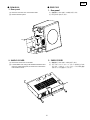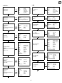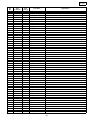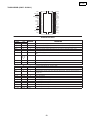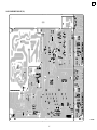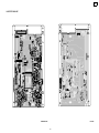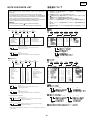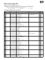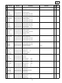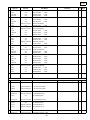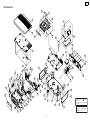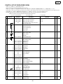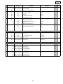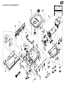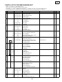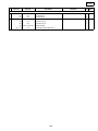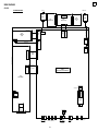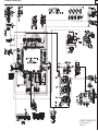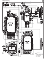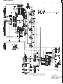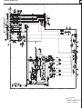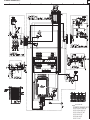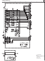
1
Ver. 2
Please refer to the
MODIFICATION NOTICE.
SERVICE MANUAL
MODEL
JP
S-102
E3
E2
EK
E2A E1C E1K EUT
3 3 3
DVD HOME ENTERTAINMENT SYSTEM
HOME ENTERTAINMENT SYSTEM (S-102) consists of DVD SURROUND RECEIVER
(ADV-S102), SUB WOOFER (DSW-S102) and SPEAKER SYSTEM (SC-S102)
注 意
サービスをおこなう前に、このサービスマニュアルを
必ずお読みください。本機は、火災、感電、けがなど
に対する安全性を確保するために、さまざまな配慮を
おこなっており、また法的には「電気用品安全法」に
もとづき、所定の許可を得て製造されております。
従ってサービスをおこなう際は、これらの安全性が維
持されるよう、このサービスマニュアルに記載されて
いる注意事項を必ずお守りください。
本機の仕様は性能改良のため、予告なく変更すること
があります。
●
補修用性能部品の保有期間は、製造打切後 8 年です。
●
For purposes of improvement, specifications and
design are subject to change without notice.
●
●
Please use this service manual with referring to the
operating instructions without fail.
●
修理の際は、必ず取扱説明書を参照の上、作業を行っ
てください。
●
Some illustrations using in this service manual are
slightly different from the actual set.
●
本文中に使用しているイラストは、説明の都合上現物
と多少異なる場合があります。
TOKYO, JAPAN
Denon Brand Company, D&M Holdings lnc.
X0341 V.02 DE/CDM 0710
S-102
SAFETY PRECAUTIONS
The following check should be performed for the continued protection of the customer and service technician.
LEAKAGE CURRENT CHECK
Before returning the unit to the customer, make sure you make either (1) a leakage current check or (2) a line to chassis
resistance check. If the leakage current exceeds 0.5 milliamps, or if the resistance from chassis to either side of the power
cord is less than 460 kohms, the unit is defective.
LASER RADIATION
Do not stare into beam or view directly with optical instruments, class 3A laser product.
CAUTION
注 意
Please heed the points listed below during servicing and inspection.
サービス、点検時にはつぎのことにご注意願います。
◎ Heed the cautions!
◎ Inspect for safety after servicing!
◎注意事項をお守りください!
◎サービス後は安全点検を!
Spots requiring particular attention when servicing, such as
the cabinet, parts, chassis, etc., have cautions indicated on
labels or seals. Be sure to heed these cautions and the cautions indicated in the handling instructions.
Check that all screws, parts and wires removed or disconnected for servicing have been put back in their original positions, inspect that no parts around the area that has been
serviced have been negatively affected, conduct an insulation
check on the external metal connectors and between the
blades of the power plug, and otherwise check that safety is
ensured.
サービスのとき特に注意を必要とする個所についてはキャ
ビネット、部品、シャーシなどにラベルや捺印で注意事項を
表示しています。これらの注意書きおよび取扱説明書などの
注意事項を必ずお守りください。
サービスのために取り外したねじ、部品、配線などが元どお
りになっているか、またサービスした個所の周辺を劣化させ
てしまったところがないかなどを点検し、外部金属端子部
と、電源プラグの刃の間の絶縁チェックをおこなうなど、安
全性が確保されていることを確認してください。
◎ Caution concerning electric shock!
(1) An AC voltage is impressed on this set, so touching internal metal parts when the set is energized could cause
electric shock. Take care to avoid electric shock, by for example using an isolating transformer and gloves when
servicing while the set is energized, unplugging the power
cord when replacing parts, etc.
(2)There are high voltage parts inside. Handle with extra care
when the set is energized.
◎感電に注意!
(1) このセットは、交流電圧が印加されていますので通電時
に内部金属部に触れると感電することがあります。従っ
て通電サービス時には、絶縁トランスの使用や手袋の着
用、部品交換には、電源プラグを抜くなどして感電にご
注意ください。
(Insulation check procedure)
Unplug the power cord from the power outlet, disconnect the
antenna, plugs, etc., and turn the power switch on. Using a
500V insulation resistance tester, check that the insulation resistance between the terminals of the power plug and the externally exposed metal parts (antenna terminal, headphones
terminal, microphone terminal, input terminal, etc.) is 1MΩ or
greater. If it is less, the set must be inspected and repaired.
(2) 内部には高電圧の部分がありますので、通電時の取扱に
は十分ご注意ください。
◎ Caution concerning disassembly and assembly!
◎分解、組み立て作業時のご注意!
Though great care is taken when manufacturing parts from
sheet metal, there may in some rare cases be burrs on the
edges of parts which could cause injury if fingers are moved
across them. Use gloves to protect your hands.
板金部品の端面の『バリ』は、部品製造時に充分管理をして
おりますが、板金端面は鋭利となっている箇所が有りますの
で、部品端面に触れたまま指を動かすとまれに怪我をする場
合がありますので十分注意して作業して下さい。手の保護の
ために手袋を着用してください。
◎ Only use designated parts!
The set's parts have specific safety properties (fire resistance, voltage resistance, etc.). For replacement parts, be
sure to use parts which have the same properties. In particular, for the important safety parts that are marked ! on wiring
diagrams and parts lists, be sure to use the designated parts.
◎ Be sure to mount parts and arrange the
wires as they were originally!
For safety reasons, some parts use tape, tubes or other insulating materials, and some parts are mounted away from the
surface of printed circuit boards. Care is also taken with the
positions of the wires inside and clamps are used to keep
wires away from heating and high voltage parts, so be sure to
set everything back as it was originally.
CAUTION
Concerning important safety parts
Many of the electric and structural parts used in the set have
special safety properties. In most cases these properties are
difficult to distinguish by sight, and using replacement parts
with higher ratings (rated power and withstand voltage) does
not necessarily guarantee that safety performance will be preserved. Parts with safety properties are indicated as shown
below on the wiring diagrams and parts lists is this service
manual. Be sure to replace them with parts with the designated part number.
◎指定部品の使用!
セットの部品は難燃性や耐電圧など安全上の特性を持った
ものとなっています。従って交換部品は、使用されていたも
のと同じ特性の部品を使用してください。特に配線図、部品
表に ! 印で指定されている安全上重要な部品は必ず指定の
ものをご使用ください。
◎部品の取付けや配線の引きまわしは、
元どおりに!
(1) Schematic diagrams ... Indicated by the ! mark.
(2) Parts lists ... Indicated by the ! mark.
安全上、テープやチューブなどの絶縁材料を使用したり、プ
リント基板から浮かして取付けた部品があります。また内部
配線は引きまわしやクランパーによって発熱部品や高圧部
品に接近しないように配慮されていますので、これらは必ず
元どおりにしてください。
Using parts other than the designated parts
could result in electric shock, fires or other
dangerous situations.
2
(絶縁チェックの方法)
電源コンセントから電源プラグを抜き、アンテナやプラグな
どを外し、電源スイッチを入れます。500V 絶縁抵抗計を用
いて、電源プラグのそれぞれの端子と外部露出金属部[アン
テナ端子、ヘッドホン端子マイク端子、入力端子など]との
間で、絶縁抵抗値が1 MΩ 以上であること、この値以下の
ときはセットの点検修理が必要です。
注 意
安全上重要な部品について
本機に使用している多くの電気部品、および機構部品は安全
上、特別な特性を持っています。この特性はほとんどの場合、
外観では判別つきにくく、またもとの部品より高い定格(定
格電力、耐圧)を持ったものを使用しても安全性が維持され
るとは、限りません。安全上の特性を持った部品は、この
サービスマニュアルの配線図、部品表につぎのように表示し
ていますので必ず指定されている部品番号のものを使用願
います。
(1) 配線図… ! マークで表示しています。
(2) 部品表… ! マークで表示しています。
指定された部品と異なるものを使用した場合に
は、感電、火災などの危険を生じる恐れがあり
ます。
S-102
DIMENSION
ADV-S102
43
294
43
149
1.5
4558
294
152
0.5 max.
122.5
10
83
135
45
380
3
S-102
41
167.5
336.5
DSW-S102
65
141
287
140
212
56
0.5
213
4
S-102
257.5
76.3
SC-S102
103.5
60
103
5
S-102
WIRE ARRANGEMENT
ワイヤー整形図
If wire bundles are untied or moved to perform adjustment or
parts replacement etc., be sure to rearrange them neatly as
they were originally bundled or placed afterward.
Otherwise, incorrect arrangement can be a cause of noise
generation.
調整や部品の交換等により、ワイヤー類の結束をはずしたり移
動させた場合には、それらの作業が完了した時点でワイヤーの
整形をおこなってください。正しく整形されてないとノイズ発
生の原因となることがあります。
1. ADV-S102
1. ADV-S102
① Fasten the CW051 5P connector cord to the front chassis
with a clamp band.
② Fasten the CW052 5P connector cord to the front chassis
with a clamp band.
③ Fasten the CX31 3P connector cord to the circuit board with
a style pin.
④ Fasten the CW52 5P connector cord to the circuit board with
a style pin.
⑤ Press the CX211 FFC in with a style pin.
⑥ Twist the CX021 2P connector cord several times and
fasten it twice with a style pin.
① CW051 5P コネクターコードをフロントシャーシにクラン
プバンドで結束する。
② CW052 5P コネクターコードをフロントシャーシにクラン
プバンドで結束する。
③ CX031 3P コネクターコードをスタイルピンで基板に固定
する。
④ CW052 5P コネクターコードをスタイルピンで基板に固定
する。
⑤ CX211 の FFC をスタイルピンで押さえこむ。
⑥ CX021 2P コネクターコードを数回捩ってスタイルピンで
2 箇所を固定する。
CX021
CX301
CX151
CX052
CX171
CX211
CX051
CX031
CX061
CX051
CW052
①
⑤
④
③
⑥ ②
⑥
⑥ CX061 6P コネクターコードをコードホルダーで固定す
る。
⑦ CX061 6P コネクターコードをスタイルピンで基板より浮
かせて固定する。
⑥ Fasten the CX061 6P connector with a cord holder.
⑦ Float the CX061 6P connector code to the circuit board with
a style pin and fasten.
Ferrite Cramp
CX061
CX061
⑦
⑧
6
⑦
S-102
2. DSW-S102
2. DSW-S102
① Fasten the CX041 4P connector cord to the chassis with a
clamp band.
② Fasten the CX041 4P connector cord and CX081 8P connector cord to the chassis with a clamp band.
③ Fasten with a clamp band.
④ Fasten the CX021 2P connector cord to the chassis with a
clamp band.
① CX041 4P コネクターコードをクランプバンドでシャーシ
に固定。
② CX041 4P コネクターコードと CX081 8P コネクターコー
ドをクランプバンドでシャーシに固定。
③ クランプバンドで結束。
④ CX021 2P コネクターコードをクランプバンドでシャーシ
に固定。
④
CX021
CX151
③
CX041
CX081
①
②
CX022
7
S-102
DISASSEMBLY
各部のはずしかた
(Follow the procedure below in reverse order when
reassembling.)
(組み立てるときは、逆の順序でおこなってください。)
● ADV-S102
1. ローダーパネルのはずしかた
● ADV-S102
1. Loader Panel
(1) Switch on, and press [
to open the Disc tray.
(1) 電源を入れ「 (OPEN/CLOSE)」ボタンを押して、
ディスクトレイを開きます。
(OPEN/CLOSE)] button
(2) ローダーパネルを持ち上げてはずします。
(2) Detach the Loader Panel by lifting.
2. サイドパネルのはずしかた
2. Side Panel
(1) 底面よりネジを 4 本はずします。
(1) Remove 4 bottom screws.
(2) 裏面よりネジを 4 本はずし、サイドパネルを矢印
の方向へはずします。
(2) Remove 4 rear screws, then detach Side Panel.
8
S-102
3. Top Cover
3. トップカバーのはずしかた
(1) Remove 9 screws, then detach Top Cover.
(1) トップカバーを止めているネジ 9 本をはずし、
トップカバーを矢印の方向へはずします。
4. DVD Mecha. Unit
4. DVD メカユニットのはずしかた
(1) Remove 4 screws fixing the DVD Mecha.
(1) メカユニットを止めているネジ 4 本をはずしま
す。
(2) Detach the DVD Mecha. to the arrow direction.
(3) Lift the DVD Mecha. and disconnect FFC and connectors.
(2) メカユニットを矢印の方向にはずします。
(3) DVD メカユニットを持ち上げ、コネクタと FFC
をはずします。
(4)
9
S-102
5. Front Panel Ass’y
5. フロントパネルのはずしかた
(1) Remove 6 Front panel screws, then detach P.W.B.
and chassis.
(1) フロントパネルからの基板とシャーシを止めてい
るネジを 6 本はずします。
(2) Remove 4 Front panel side screws, then detach the
Front Panel Ass’y.
(2) フロントパネル側面を止めているネジ 4 本(左右
各 2 本)をはずし、フロントパネルをはずしま
す。
6. Back Panel Ass’y
6. バックパネルのはずしかた
(1) Remove each terminal screws, Back Panel screws
and Chassis screws, then detach the Back Panel.
(1) 各端子を止めているネジおよびバックパネルと
シャーシを止めているネジをはずし、バックパネ
ルをはずします。
10
S-102
● DSW-S102
1. Rear panel
● DSW-S102
1. Rear panel
(1) Remove 10 screws 101 on the bottom side.
(1) 底面側から 101 のねじ 10 本をはずします。
(2) Detach the Rear panel.
(2) Rear panel をはずします。
101
2. SHIELD COVER
2. SHIELD COVER
(1) Remove 8 screws 103 on the Side.
(1) 側面側から 103 のねじ 8 本をはずします。
(2) Lift the shield cover using a flat-headed screwdriver and
remove it. When doing this, be careful not to deform the
main bracket's hook.
(2) マイナスドライバーでシールドカバーを持ち上げては
ずします。このとき、メインブラケットのつめを変形
させないように注意してください。
103
103
103
11
S-102
DIAGNOSTICS OF OPTICAL PICKUP
AND REPLACING TRAVERSE UNIT
光ピックアップの故障診断とトラバース
ユニットの交換
Make failure diagnostics of the Optical Pickup as follows.
If the laser drive current (Iop) becomes more than 1.5 times of
the initial value, the Optical Pickup should be replaced.
The laser drive current initial value is checked by "Iop checked
Method" of next page.
In case of replacing the Pickup, change the whole part of the
Traverse Unit.
No mechanical adjustment is necessary after the replacement.
次の順序で故障診断を行ってください。
レーザー駆動電流 Iop 値が初期値の 1.5 倍以上になっている
場合は光ピックアップ交換の目安となります。
レーザー駆動電流初期値は、次ページ "Iop 値の確認方法 " で
確認できます。
ピックアップ交換の場合は、トラバースユニット単位での交
換となります。メカの調整は不要です。
レーザー駆動電流初期値 :
Laser drive current initial value:
DVD:
CD:
FL Display (The display part of 13 digits)
1
2
3
4
5
6
7
8
9
10
11
12
13
T
2
2
―
m
m
m
m
―
n
n
n
n
FL Display (The display part of 13 digits)
1
2
3
4
5
6
7
8
9
10
11
12
13
T
2
1
―
m
m
m
m
―
n
n
n
n
ディスクを読み込まない
スムーズに再生しない、等
Disc no read, unsteady playback, etc.
Laser drive current (Iop) check
HF wave form check
(Refer to WAVE FORMS)
レーザー駆動電流 Iop 値の確認
HF 波形の確認
(WAVE FORMS 参照)
Present value exceeds the initial value by 1.5 times
現在値が初期値の
1.5 倍になっている
Traverse Unit replacing
トラバースユニット交換
Laser current (Iop) memorizing after replacement
交換後にレーザー電流値の記憶
12
S-102
1. Iop checked Method
1. Iop 値の確認方法
Select the laser ON/OFF (CD/DVD) mode of the test mode,
and check the lop value of DVD laser or CD laser.
(See page 13 for test mode.)
レーザー駆動電流を確認する場合は、テストモードのレー
ザー ON/OFF (CD/DVD) モードを選択して、DVD レーザー
または CD レーザーの lop 値を確認します。
(詳細は 13 ページ、テストモード参照)
FL 管の表示 (13 桁の表示部 )
FL Display (The display part of 13 digits)
1
2
T
2
3
4
5
6
7
8
9
10
11
12
13
1
2
L
a
s
e
r
O
n
O
f
f
T
2
1.1. DVD laser current check
3
4
5
6
7
8
9
10
11
12
13
L
a
s
e
r
O
n
O
f
f
1.1. DVD レーザー電流確認
(1) Press the SKIP
or
button to display the laser current value, and then select T22.
(2) Check the current value of Iop (nnnn).
FL Display (The display part of 13 digits)
(1) レーザー電流値を表示する場合は、
ボタンまたは
ボタンを押し、T22 を選択します。
(2) 現在の lop 値 (nnnn) を確認します。
FL 管の表示 (13 桁の表示部 )
1
2
3
4
5
6
7
8
9
10
11
12
13
T
2
2
―
m
m
m
m
―
n
n
n
n
( − : Off, DVD laser, Initial value: mm.mm [mA],
Current value: nn.nn [mA])
1
2
3
4
5
6
7
8
9
10
11
12
13
T
2
2
―
m
m
m
m
―
n
n
n
n
( −:消灯、DVD レーザー、初期値:mm.mm[mA],
現在値:nn.nn [mA])
1.2. CD Laser current check
1.2. CD レーザー電流確認
(1) Press the
or
button to display the laser
current value, and then select T21.
(2) Check the current value of Iop (nnnn).
(1) レーザー電流値を表示する場合は、
ボタンまたは
ボタンを押し、T21 を選択します。
(2) 現在の lop 値 (nnnn) を確認します。
FL Display (The display part of 13 digits)
1
2
3
4
5
6
7
8
9
10
11
12
13
T
2
1
―
m
m
m
m
―
n
n
n
n
FL 管の表示 (13 桁の表示部 )
( − : Off, CD laser, Initial value: mm.mm [mA],
Current value: nn.nn [mA])
1
2
3
4
5
6
7
8
9
10
11
12
13
T
2
1
―
m
m
m
m
―
n
n
n
n
( −:消灯、CD レーザー、初期値:mm.mm[mA],
現在値:nn.nn[mA])
2. Note for Handling the Laser Pick-Up
2. レーザーピックアップの取扱注意
レーザーダイオードの破壊防止。
光素子ユニットを交換するときは、以下を遵守してくださ
い。
(1) 光素子ユニットの接続ケーブルをはずすときは、静電対
策を行ったデスク上で作業してください。
(2) 作業者は、リストストラップを使用してください。
(3) レーザーダイオードの破壊防止のため、24P FFC ケーブ
ルをはずす前にランドを半田付けショートしてくださ
い。
(4) 光素子ユニットのコネクタ部に触れないでください。
The protection for the damage of laser diode.
If you want to change the optical device unit from any other
units, you must keep the following.
(1) It should be done at the desk already took measures the
static electricity in care of removing the OPU's (Optical
device unit) connector cable.
(2) Workers should be put on the "Earth Band".
(3) It should be done to add the solder to the short land to
prevent the broken Laser diode before removing the 24P
FFC cable.
(4) Don't touch OPU's connector parts carelessly.
3. Replacement of the Laser Pick-up
(Traverse Unit)
3. レーザーピックアップ ( トラバースユニッ
ト ) の交換
Iop( レーザー駆動電流)をチェックします。
現在の Iop 値が初期値の 150%を越えている場合、
トラバー
スユニット(レーザーピックアップ)を交換してください。
Check the Iop (Laser drive current)
If the present Iop (current) value exceeds.+150% of the initial value, replace the Traverse unit (Laser Pick-up) with a
new one.
13
S-102
4. Rewriting the default value of the laser
current
4. レーザー電流初期値の書き換え方法
レーザー電流の初期値を書き換えるには、CD または DVD
レーザー電流が表示されている時に
ボタンを5秒以上押
し、次に
ボタンまたは
ボタンを押して T23 を
選択します。(詳細は 22 ページ、Iop 値の確認方法参照)
To rewrite the default value of the laser current, press the
button for at least 5 seconds while the CD or DVD laser
current is displayed, then press the
or
button
to select T23. (For details, see "Iop checked Method" on
page 22.)
If the
button is pressed while T23 is displayed, the current value is displayed at "mmmm" and stored in the EEPROM.
T23 表示時に
ボタンを押と、mmmm 部に現在値を表示
し、EEPROM に保存します。
FL 管の表示 (13 桁の表示部 )
FL Display (The display part of 13 digits)
1
2
3
4
5
6
7
8
9
10
11
12
13
T
2
3
―
m
m
m
m
―
―
―
―
―
5. Resetting the accumulated laser on time
1
2
3
4
5
6
7
8
9
10
11
12
13
T
2
3
―
m
m
m
m
―
―
―
―
―
5. レーザー ON 累積時間のリセット方法
To clear the accumulated laser on time, press the
button
while the accumulated laser on time is displayed (TB1, TB2
: For details, see "Test Mode" on page 22.) until " * " appears at the fourth position, then press the
or
button to select TB3.
If the
button is pressed while TB3 is displayed, the accumulated laser on time of CD and DVD is cleared.
When TB1 or TB2 is selected with the
or
button, "nnnnnnn" is displayed as 0 so you can check.
FL Display (The display part of 13 digits)
レーザーON 累積時間をクリアするには、レーザーON 累
積時間表示 (TB1,TB2) の時(詳細は 22 ページ、テストモー
ド参照)に
ボタンを 4 桁目に ' * ' が表示されるまで押
し、
ボタンまたは
ボタンを押し TB3 を表示させ
ます。
TB3 表示時に
ボタンを押すと、CD 及び DVD レーザー
ON 累積時間をクリアします。
ボタンまたは
ボタンで TB1 または TB2 を選択
すると、nnnnnnn 部が 0 表示となり確認できます。
FL 管の表示 (13 桁の表示部 )
1
2
3
4
5
6
7
8
9
10
11
12
13
1
2
3
4
5
6
7
8
9
10
11
12
13
T
B
Y
―
―
―
n
n
n
n
n
n
n
T
B
Y
―
―
―
n
n
n
n
n
n
n
( − : Off, Y:1: CD, 2: DVD, nnnnnnn: Hour [h])
( −:消灯、Y:1: CD, 2: DVD、nnnnnnn:時間 [h])
14
S-102
HOW TO REPLACE TRAVERSE UNIT
Caution: The optical pickup can be damaged easily by
static electricity charged on human body.
Take necessary anti-static measures when
repairing around the optical pickup.
1. Guide Clamp Bracket disassembly
注意 : 光ピックアップは、人体に帯電した静電気等で静電
破壊することがあります。光ピックアップ周辺を修
理する際は、必要な静電対策を行ってください。
3. トラバースユニットのはずしかた
(1) Remove 24P FFC, 15P FFC and 5P PH WIRE connecting with from the Main P.W.B.
(1) メイン基板に接続している 24P FFC、15P FFC、5P PH
ワイヤをはずします。
(2) Remove 4 screws fixing Damper.
(2) ダンパーを固定しているねじ 4 本をはずします。
(3) Remove Traverse Unit to arrow direction.
(3) トラバースユニットを矢印方向にとりはずします。
1. ガイドクランプブラケットのはずしかた
(1) Remove 2 screws.
(1) ねじ 2 本をはずします。
(2) Remove Guide Clamp Bracket to arrow direction.
(2) ガイドクランプブラケットを矢印方向にとりはずしま
す。
2. Tray disassembly
3. Traverse Unit disassembly
トラバースユニットの交換方法
2. トレイのはずしかた
(1) Remove to arrow direction.
(1) 矢印方向にとりはずします。
(2) Solder the short-circuit (see in the frame).
(2) 半田付けショートを行います。(枠内図参照 )
半田ショート
Solder to short-circuit
Note for disassembly Traverse Unit
Short-circuit with Solder
半田ショート拡大図
15
トラバースユニット分解の注意
(1) When assembling, reverse the order of the above.
(1) 組み立てるときは、上記の逆の順序で行ってください。
(2) When inserting Tray, confirm boss on Slide Cam set to
ditch of the Tray (Compare with below drawing).
(2) トレイ組込み時、スライドカムのボスがトレイの溝に
合っているか確認してください。(下図参照)
S-102
SERVICE MODE
サービスモードについて
1. Aging Mode
1. エージングモード
1.1. preparation0
1.1. 準備
(1) Equipment used: Any one of DVD Karaoke Disc (containing more than 10 titles).
(ex : Heat run disc TDV-HR01)
(1) 使用機器:DVD カラオケディスク (10 タイトル以上のもの)
(例:ヒートランディスク TDV-HR01)
(2) Unit setting : No spec other than the following procedure.
(2) 本体設定:下記設定以外規定無。
1.2. procedure
1.2. 手順
※ Perform aging of the DVD.
※ DVD のエージングをおこなう。
(1) Pressing the
and
buttons simultaneously, plug the AC cord into a power outlet, then press the ON/STANDBY button
to turn the power on. This sets the aging mode.
(1) 本体の ボタンと
ボタンを同時に押しながら、AC コードをコンセントへ接続し、ON/STANDBY ボタンを押してセット
の電源を入れると、エージングモードが設定される。
• Once the aging mode is set, press the FUNCTION button to switch the mode.
(After the display is put out at the switch, it selects.)
(a) To select the normal aging mode ... Start from (2)
(b) To select the error rate display mode ... Start from (8)
(2) Press the
(3) Both the "
(4) When the
(5) The "
・ エージングモード設定後、FUNCTION ボタンを押して、モードを切り替える。
(切り替え時に表示を出してから選択する。)
(a) 通常のエージングモードを選択・・・(2) から開始
(b) エラーレート表示モードを選択・・・(8) から開始
button and play all the tracks recorded on the disc.
" and "
(2)
" indicators light on the fluorescent display tube.
(3) FL 管の“
button is pressed once with the tray open, titles 1 and 10 recorded on the disc are played.
" indicator flashes and the "
ボタンを押し、ディスクに収録されている全ての曲を再生する。
”インジケーターと“
(4) トレイを開いた状態で
" indicator lights on the fluorescent display tube.
(5) FL 管の“
”インジケーターが両方とも点灯する。
ボタンを 1 回押して、ディスクに収録されているタイトル 1 とタイトル 10 を再生する。
”インジケーターが点滅し、“
”インジケーターが点灯する。
(6) Once playback is completed, open and close the tray and repeat the operation in step (3) or (4).
(6) 再生終了後、トレイを開閉させ (3) または (4) の動作をする。
(7) If there is an error while in the aging mode, the error is displayed and the stop mode is set with the status at that time.
(7) エージングモード中にエラーが発生すると、エラーを表示し、その時の状態で停止する。
注 )・ エージングモード中は、本体の FUNCTION ボタンおよび、リモコンの FUNCTION 切替ボタンは動作しない。
(ファンクッションを変えると DVD が停止し、エージングモードが解除される。)
・ エージングモード中は本体およびリモコンの ON/STANDBY ボタンを動作しない。
(セットの電源を OFF にすると DVD が停止し、エージングモードが解除される。)
NOTE) ・The FUNCTION button on the main unit and the FUNCTION selector button on the remote control unit will not work
during the aging mode.
(If the function is switched, the DVD stops and the aging mode is canceled.)
・The ON/STANDBY buttons on the main unit and the remote control unit will not work during the aging mode.
(If the set's power is turned off, the DVD stops and the aging mode is canceled.
(8) When the error rate display mode is set, the final error rate information is displayed on the fluorescent display tube.
No.
Error contents
1
Bad DIsc
2
Forcus Error
3
Read Error
4
Tracking Error
5
Tray Error
6
Navigation Pack Read Error
7
Cmmunication Error
(8) エラーレート表示モードに入ると、最終エラーレート情報を FL 管に表示する。
No.
FL display
FL Display (The display part of 13 digits)
1
2
3
E
7
4
5
6
7
X
X
8
9
10
X
X
11
エラー内容
1
不良ディスク
2
フォーカスエラー
3
リードエラー
4
トラッキングエラー
12
13
5
トレイエラー
X
X
6
ナビゲーションパックエラー
7
コマンド通信エラー
16
FL 管表示
FL 管の表示 (13 桁の表示部 )
1
2
3
E
7
4
5
6
7
X
X
8
9
10
X
X
11
12
13
X
X
S-102
2. Initial Setting Mode
2. イニシャルモード
2.1. Preparation
2.1. 準備
(1) Equipment used: None
(1) 使用機器:無
(2) Unit setting: No spec other than the following procedure.
(2) 本体設定:下記手順以外規定無。
2.2. Procedure
2.2. 手順
● SYSTEM
● システム
※ This initializes the data for the function, volume, DVD mechanism, etc.
※ ファンクション、VOL 等および DVD メカのバックアップデータの初期化をおこなう。
(1) When the ON/STANDBY button is pressed to turn the set on while pressing the main unit's FUNCTION and
simultaneously, the initialization mode is set.
buttons
(1) 本体 FUNCTION ボタン と
ルモードが設定される。
ボタンを同時に押しながら、ON/STANDY ボタンを押してセットの電源を入れるとイニシャ
(2) The standby indicator lights yellow and "INITIALIZE" is displayed on the fluorescent display tube.
(2) スタンバイ LED が黄色に点灯し、FL 管に“INITIALIZE”が表示される。
(3) Once the entire initialization procedure has been completed, the set is in the normal mode with the power turned on.
(3) 全ての初期化完了後、通常モードの電源 ON の状態になる。
● DVD
● DVD
※ This initializes the data for the DVD mechanism.
(1) With the power on, set the function to DVD, and in the playback stopped mode, press the
for at least 2 seconds to set the DVD initialization mode.
※ DVD のみのバックアップデータの初期化をおこなう。
and
buttons simultaneously
(1) 電源 ON 時にファンクッションを DVD にし再生停止状態で、 ボタンと
DVD 初期化モードが設定される。
(2) "INITIALIZE" is displayed on the fluorescent display tube.
ボタンを 2 秒以上同時に押し続けると、
(2) FL 管に“INITIALIZE”が表示される。
3. µcom Firm Check Mode
3. マイコンファームチェックモード
3.1. Preparation
3.1. 準備
(1) Equipment used: None
(1) 使用機器:無
(2) Unit setting: No spec other than the following procedure.
(2) 本体設定:下記手順以外規定無。
3.2. Procedure
3.2. 手順
※ Use this to display the version information, etc.
※ バージョン表示等をおこなう。
(1) When, in the standby mode, the ON/STANDBY button is pressed to turn the set on while pressing the main unit's FUNCTION
and
buttons simultaneously, the system check mode is set.
(1) STANDBY 時に本体 FUNCTION ボタンと
ボタンを同時に押しながら、ON/STANDBY ボタンを押してセットの電源を入
れると、システムチェックモードが設定される。
(2) Press the STATUS button on the remote control unit to display the following information, in this order: System microprocessor
version → Date of system microprocessor version updating → DSP version → Date of DSP version updating → Drive microprocessor version of DVD mechanism → ESS version → Date of ESS version updating.
(2) リモコンの STATUS ボタンを押すと、システムマイコンのバージョン→システムマイコンのバージョンアップ日→ DSP の
バージョン→ DSP のバージョンアップ日→ DVD メカのドライブマイコンのバージョン→ ESS のバージョン→ ESS のバー
ジョンアップ日の順に表示される。
(3) Unplug AC cord to clear this mode.
(3) AC コードを抜くことにより、システムチェックモードを解除する。
NOTE) The DVD mechanism driver version and ESS version are not displayed un less the function is once set to DVD.
注 ) DVD メカのドライブバージョン、ESS のバージョンの表示については、一度ファンクッションを DVD にしないと表示
されない。
17
S-102
4. Test mode
4. テストモード
4.1. Entering the test mode
4.1. テストモードの設定
To enter the test mode, press the
and
buttons simultaneously while in the Aging mode. Not insert the disc.
(The Aging mode is entered by pressing the
and
buttons simultaneously to turn on the AC power.
When the Aging mode is set, the
and
indicators light.)
Press
and
テストモードの設定はエージングモード時に ボタンと
ボタンを同時に押すことでおこなう。ディスクは挿入していな
いこと。
( エージングモードの設定は ボタンと
ボタンを同時に押しながら、AC コードをコンセントへ接続し、セットの電源を入れ
る。エージングモードになると FL 管の“
”インジケーターと“ ”インジケーターが点灯する。)
buttons simultaneously
ボタンと
ボタンの同時押し
Power turns on
電源 ON
Press
and
Aging mode
buttons simultaneously
ボタンと
Test mode
エージングモード
ボタンの同時押し
button
テストモード
ボタン
Set the disc
button
ディスクを載せる
ボタン
Set the disc
button
ディスクを載せる
Aging mode start
button
TOC リード後
ボタン
Test mode start
テストモード開始
テストモード設定時の FL 管表示
FL tube display when test mode entered
FL 管の表示 (13 桁の表示部 )
FL Display (The display part of 13 digits)
2
3
4
5
6
T
E
S
T
7
8
9
10
11
M
O
D
E
12
1
13
The following modes are available.
(1) Laser on/off (CD/DVD) mode
(2) Servo adjustment value display mode
(3) Trace mode (error rate display)
(4) Accumulated laser on time
:
:
:
:
T
2
3
2
T
3
3
4
5
6
7
8
9
10
11
12
13
L
a
s
e
r
O
n
O
f
f
2
T
7
3
4
5
6
7
8
S
e
r
v
o
9
10
11
12
A
d
j
13
2
T
B
3
T
E
S
T
7
8
9
10
11
M
O
D
E
12
13
:
:
:
:
T2
T3
T7
TB
ボタンを押すと、T2,T3,T7,TB,T2…の順に表示される。
1
2
T
2
3
4
5
6
7
8
9
10
11
12
13
L
a
s
e
r
O
n
O
f
f
1
2
T
3
3
4
5
6
7
8
9
10
11
12
13
S
e
r
v
o
A
d
j
4
5
6
7
8
10
11
12
13
T
r
a
c
e
M
o
d
e
4
5
6
7
8
9
10
11
12
13
L
a
s
e
r
O
n
T
i
m
FL 管の表示 (13 桁の表示部 )
4
5
6
7
8
T
r
a
c
e
9
10
11
12
13
M
o
d
e
1
2
T
7
3
9
FL 管の表示 (13 桁の表示部 )
FL Display (The display part of 13 digits)
1
6
FL 管の表示 (13 桁の表示部 )
FL Display (The display part of 13 digits)
1
5
FL 管の表示 (13 桁の表示部 )
FL Display (The display part of 13 digits)
1
4
①テストモード中に
FL Display (The display part of 13 digits)
2
3
モードには、次のモードがある。
(1) レーザー ON/OFF(CD/DVD) モード
(2) サーボ調整値表示モード
(3) トレースモード ( エラーレート表示 )
(4) レーザー ON 累積時間
T2
T3
T7
TB
button is pressed after entering the test mode, the display switches in the order: T2, T3, T7, TB, T2 …
1
2
4.2. モードの選択
4.2. Selecting the mode
① When the
エージング開始
ボタン
After the TOC reading
button
1
ボタン
4
5
6
7
8
9
10
11
12
13
L
a
s
e
r
O
n
T
i
m
18
1
2
T
B
3
S-102
4.3. Setting the mode
4.3. モードの確定
With the mode selected, press the
button to set that mode.
モードを選択してある状態で
① In the laser on/off (CD/DVD) mode, laser on/off control is executed and the laser current is displayed.
Press the
or
button to switch the CD/DVD (T21, T22, T21. .).
To save the current laser current value, press and hold in the
button for at least 5 seconds to turn off the "mmmm" section
of the display, then press the
or
button and select T23. When the
button is pressed while T23 is displayed, the
data is displayed in the "mmmm" section.
ボタンを押すとモードを確定する。
①レーザー ON/OFF(CD/DVD) モードの場合、レーザーの ON/OFF 制御を実行し、レーザー電流を表示する。CD/DVD の切り替
えは、
ボタンまたは
ボタンを押す (T21、T22、T21. .)。
現在のレーザー電流値を保存する場合、 ボタンを 5 秒以上押し続け、mmmm 部を非表示にし、
ボタンまたは
ボタンを押して、T23 を選択する。T23 を表示時に
ボタンを押すと、mmmm 部にデータが表示される。
CD レーザーの場合
For the CD laser
FL 管の表示 (13 桁の表示部 )
FL Display (The display part of 13 digits)
1
2
3
4
5
6
7
8
9
10
11
12
13
T
2
1
―
m
m
m
m
―
n
n
n
n
1
2
3
4
5
6
7
8
9
10
11
12
13
T
2
1
―
m
m
m
m
―
n
n
n
n
( −:消灯、CD レーザー、保存データ:mm.mm[mA], 現在値:nn.nn[mA])
( − : Off, CD laser, Stored data: mm.mm [mA], Current value: nn.nn [mA])
DVD レーザーの場合
For the DVD laser
FL 管の表示 (13 桁の表示部 )
FL Display (The display part of 13 digits)
1
2
3
4
5
6
7
8
9
10
11
12
13
T
2
2
―
m
m
m
m
―
n
n
n
n
1
2
3
4
5
6
7
8
9
10
11
12
13
T
2
2
―
m
m
m
m
―
n
n
n
n
( −:消灯、DVD レーザー、保存データ:mm.mm[mA], 現在値:nn.nn [mA])
( − : Off, DVD laser, Stored data: mm.mm [mA], Current value: nn.nn [mA])
②サーボ調整値表示モードの場合 (表 1 サーボ調整値表示モード詳細 参照)
② In the servo adjustment value display mode (See "Table 1 - Servo adjustment value display mode details")
FL 管の表示 (13 桁の表示部 )
FL Display (The display part of 13 digits)
1
2
3
4
5
6
7
8
9
10
11
12
13
T
X
X
−
−
−
−
−
−
n
n
n
n
1
2
3
4
5
6
7
8
9
10
11
12
13
T
X
X
―
―
―
―
―
―
n
n
n
n
(XX: 選択モード、n: 調整値 (HEX))
(XX : Selection mode, n : Adjustment value (HEX))
③トレースモード ( エラーレート表示 ) の場合は、1層内周のトレースを選択する。
③ In the trace mode (error rate display), select the trace of the innermost circumference of 1 layer.
FL 管の表示 (13 桁の表示部 )
FL Display (The display part of 13 digits)
1
2
3
4
5
6
7
8
9
10
11
12
13
T
7
1
F
F
F
F
F
F
F
F
F
F
1
2
3
4
5
6
7
8
9
10
11
12
13
T
7
1
F
F
F
F
F
F
F
F
F
F
(F: アドレス及びエラーレートは未確定時、F を表示する。)
(F : When address and error rate not set, F is displayed.)
④レーザー ON 累積時間 (EEPROM に記憶 ) を表示する。
④ Displaying the accumulated laser on time (stored in the EEPROM)
FL 管の表示 (13 桁の表示部 )
FL Display (The display part of 13 digits)
1
2
3
4
5
6
7
8
9
10
11
12
13
T
B
Y
―
―
―
n
n
n
n
n
n
n
1
2
3
4
5
6
7
8
9
10
11
12
13
T
B
Y
―
―
―
n
n
n
n
n
n
n
(Y:1: CD、2: DVD、nnnnn : 時間 [h]) ※ 1 時間未満は切り上げて表示する。
(Y : 1:CD, 2:DVD, nnnnn: Time [h])
※ Fractions of hours are counted up one hour on the display.
19
S-102
4.4. Change within the mode
4.4. モード内での変更
Changes within modes are made by pressing the
and
buttons while the mode is set.
モードを確定してある状態で
① In the laser on/off (CD/DVD) mode, laser on/off control is executed and the laser current is displayed.
ボタンまたは
ボタンを押すとモード内での変更をおこなう。
①レーザー ON/OFF(CD/DVD) モードの場合、レーザーの ON/OFF 制御を実行し、レーザー電流を表示する。
For the CD laser
CD レーザーの場合
FL Display (The display part of 13 digits)
FL 管の表示 (13 桁の表示部 )
1
2
3
4
5
6
7
8
9
10
11
12
13
1
2
3
4
5
6
7
8
9
10
11
12
13
T
2
1
―
m
m
m
m
―
n
n
n
n
T
2
1
―
m
m
m
m
―
n
n
n
n
( − : Off, CD laser, Stored data: mm.mm [mA], Current value: nn.nn [mA])
( −:消灯、CD レーザー、保存データ:mm.mm[mA], 現在値:nn.nn[mA])
For the DVD laser
DVD レーザーの場合
FL Display (The display part of 13 digits)
FL 管の表示 (13 桁の表示部 )
1
2
3
4
5
6
7
8
9
10
11
12
13
1
2
3
4
5
6
7
8
9
10
11
12
13
T
2
2
―
m
m
m
m
―
n
n
n
n
T
2
2
―
m
m
m
m
―
n
n
n
n
( − : Off, DVD laser, mm.mm [mA], nn.nn [mA])
( −:消灯、DVD レーザー、mm.mm[mA], nn.nn[mA])
When there is no saved data (for the DVD laser)
保存データなしの場合 (DVD レーザーの場合 )
FL Display (The display part of 13 digits)
FL 管の表示 (13 桁の表示部 )
1
2
3
4
5
6
7
8
9
10
11
12
13
1
2
3
4
5
6
7
8
9
10
11
12
13
T
2
2
―
―
―
―
―
―
n
n
n
n
T
2
2
―
―
―
―
―
―
n
n
n
n
( − : Off, DVD laser, nn.nn [mA])
( −:消灯、DVD レーザー、nn.nn[mA])
To store the current value, press the
button for at least 5 seconds, then press the
or
button to select T23.
If the
button is pressed while T23 is displayed, the current value is displayed at "mmmm" and stored in the EEPROM.
現在地を保存するには、 ボタンを 5 秒以上押し、次に
ボタンまたは
ボタンを押して、T23 を選択する。T23 表
示時に、 ボタンを押すと、mmmm 部に現在値を表示し、EEPROM に保存される。
FL Display (The display part of 13 digits)
FL 管の表示 (13 桁の表示部 )
1
2
3
4
5
6
7
8
9
10
11
12
13
1
2
3
4
5
6
7
8
9
10
11
12
13
T
2
3
―
m
m
m
m
―
n
n
n
n
T
2
3
―
m
m
m
m
―
―
―
―
―
( − : Off, DVD laser, nn.nn [mA])
If the current value is over 100 mA, the 4th and 9th digit sections are used.
( −:消灯、DVD レーザー、mm.mm[mA])
電流値が 100mA 以上の場合は、4 桁、9 桁部分を使用。
② In the servo adjustment value display mode (See "Table 1 - Servo adjustment value display mode details")
②サーボ調整値表示モードの場合 (表 1 サーボ調整値表示モード詳細 参照)
FL Display (The display part of 13 digits)
FL 管の表示 (13 桁の表示部 )
1
2
3
4
5
6
7
8
9
10
11
12
13
1
2
3
4
5
6
7
8
9
10
11
12
13
T
X
X
―
―
n
n
n
n
n
n
n
n
T
X
X
―
―
n
n
n
n
n
n
n
n
(XX : Selection mode, n: Adjustment value (HEX))
For the adjustment values, 0's are added in front of the effective number of bytes.
(Ex.: If the value is 0x123 for 4-byte data, "00 00 01 23" is displayed.)
(XX: 選択モード、n: 調整値 (HEX))
調整値は、有効バイト数分先頭に 0 をつける。
(例:4 バイトデータで値が 0x123 の場合は“00 00 01 23”)
⑤ In the trace mode (error rate display) (See "Table 2 - Trace mode details")
③トレースモード ( エラーレート表示 ) の場合( 表 2 トレースモード詳細 参照)
FL Display (The display part of 13 digits)
FL 管の表示 (13 桁の表示部 )
1
2
3
4
5
6
7
8
9
10
11
12
13
1
2
3
4
5
6
7
8
9
10
11
12
13
T
Y
Y
F
F
F
F
F
F
F
F
F
F
T
Y
Y
F
F
F
F
F
F
F
F
F
F
(YY : Selection mode [71 to 94], F: When address and error rate not set, F is displayed.)
(YY: 選択モード [71 ∼ 94]、F: アドレス及びエラーレートは未確定時、F を表示する。)
⑥ In the accumulated laser on time display
⑥レーザー ON 累積時間を表示場合
FL Display (The display part of 13 digits)
FL 管の表示 (13 桁の表示部 )
1
2
3
4
5
6
7
8
9
10
11
12
13
1
2
3
4
5
6
7
8
9
10
11
12
13
T
B
Y
―
―
―
n
n
n
n
n
n
n
T
B
Y
―
―
―
n
n
n
n
n
n
n
(Y : 1: CD, 2: DVD, nnnnnnn: Time [h]) ※ If the current value is over 100 mA, the 4th and 9th digit sections are used.
To clear the accumulated laser on time, press the
button while the accumulated laser on time is displayed (TB1, TB2) until
" * " appears at the fourth position, then press the
or
button to select TB3.
If the PLAY button is pressed while TB3 is displayed, the accumulated laser on time of CD and DVD is cleared.
When TB1 or TB2 is selected with the
or
button, "nnnnnnn" is displayed as 0 so you can check.
(Y:1: CD, 2: DVD、nnnnnn: 時間 [h]) ※ 1 時間未満は切り上げて表示する。
レーザー ON 累積時間をクリアする場合、レーザー ON 累積時間表示時 (TB1、TB2) のとき、 ボタンを 4 桁目に“*”が表
示されるまで押し、
ボタンまたは
ボタンを押し、TB3 を表示させる。TB3 表示時に
ボタンを押すと CD および
DVD レーザー ON 累積時間をクリアする。
ボタンまたは
ボタンを押して、TB1 または TB2 を選択すると、
nnnnnn 部が 0 表示になり確認できる。
20
S-102
4.5. Execution of trace mode (error rate display) (See "Table 2 - Trace mode details")
Trace will be performed if the
4.5. トレースモード ( エラーレート表示 ) の実行( 表 2 トレースモード詳細 参照)
button is pushed after choosing operation.
動作を選択した後、
FL Display (The display part of 13 digits)
ボタンを押すとトレースを実行する。
FL 管の表示 (13 桁の表示部 )
1
2
3
4
5
6
7
8
9
10
11
12
13
1
2
3
4
5
6
7
8
9
10
11
12
13
T
Y
Y
m
m
m
m
m
m
l
l
l
l
T
Y
Y
m
m
m
m
m
m
l
l
l
l
(YY : selection mode [71 to 94], m : address [PBA][HEX], l : error rate [COUNT/SEC] [HEX])
Note) CD : Error rate of 75 frames is displayed (1 second).
DVD : Error rate of 8ECC block is displayed.
The mode chosen when selection mode was changed into the trace execution and the
button was pushed is performed
from the beginning.
When the
button is pushed without changing selection mode, the mode under selection is performed from the beginning.
(If the
button is pushed, the address corresponding to the chosen mode will be searched again.)
(YY: 選択モード [71 ∼ 94]、m: アドレス [PBA][HEX]、l: エラーレート [COUNT][DEC])
注 ) CD : 表示するエラーレートは、75 フレーム分の値 (1 秒 )。
DVD : 表示するエラーレートは、8ECC ブロック分の値。
トレース実行中に選択モードを変更し、 ボタンを押すと選択したモードを最初から実行する。
選択モードを変更せずに
ボタンを押した場合も、選択中のモードを最初から実行する。
(
ボタンを押すと、選択しているモードに対応したアドレスを再度サーチする。)
トレース終了時は、PAUSE 状態になります。
The pause mode is set after tracing is completed.
4.6. Other operations
① When the
4.6. その他の動作
button is pressed, the mode returns to the previously selected mode.
①
(1) Test mode detailed table
ボタンを押すと、前の選択モードに戻る。
(1) テストモード詳細一覧表
Table 1: Servo adjustment value display mode details
表 1 サーボ調整値表示モード詳細
XXX
Name
Size
Meaning
Remarks
XXX
名称
サイズ
T31
fbal0
16bits
CD/DVD L0 layer focus balance adjustment value
FBAL range: 0x8000 < FBAL < 0x7FC0(Center:0x0000)
T31
fbal0
16 ビット
T32
tbal0
16bits
CD/DVD L0 layer tracking balance adjustment value
TBAL range: 0x0000 < TBAL < 0x003F
T32
tbal0
16 ビット
CD/DVD L0 層トラッキングバランス調整値
T33
fcga0
16 ビット
CD/DVD L0 層フォーカス Loop Gain 調整値
0x100 で 1 倍 [0x200(2 倍 ) を Typ に設定する ]
(0x100 で 1 倍、0x200 で 2 倍。Y/0x100 の比率計算)
調整値 0x200 で Gain 交点が目標ターゲットになる様設定している。
T34
tkga0
16 ビット
CD/DVD L0 層トラッキング Loop Gain 調整値
0x100 で 1 倍 [0x200(2 倍 ) を Typ に設定する。]
(0x100 で 1 倍、0x200 で 2 倍。Y/0x100 の比率計算)
調整値 0x202 で Gain 交点が目標ターゲットになる様設定している。
T35
Fbal1
16 ビット
DVD L1 層フォーカスバランス調整値
意 味
CD/DVD L0 層フォーカスバランス調整値
備 考
FBAL の範囲は 0x8000< FBAL<0x7FC0。( センター : 0x0000)
TBAL の範囲は 0x0000< TBAL<0x003F。
T33
fcga0
16bits
CD/DVD L0 layer focus Loop Gain adjustment value
1x for 0x100 [0x200 (2x) set to Typ.
(1x for 0x100, 2x for 0x200. Y/0x100 ratio calculation.)
Adjustment value 0x200 sets so that gain crossover reaches target.
T34
tkga0
16bits
CD/DVD L0 layer tracking Loop Gain
adjustment value
1x for 0x100 [0x200 (2x) set to Typ.
(1x for 0x100, 2x for 0x200. Y/0x100 ratio calculation.)
Adjustment value 0x202 sets so that gain crossover reaches target.
T35
Fbal1
16bits
DVD L1 layer focus balance adjustment
value
FBAL range: 0x8000 < FBAL < 0x7FC0(Center:0x0000)
T36
Tbal1
16 ビット
DVD L1 層トラッキングバランス調整値
T36
Tbal1
16bits
DVD L1 layer tracking balance adjustment
value
TBAL range: 0x0000 < TBAL < 0x003F
T37
Fcga1
16 ビット
DVD L1 層フォーカス Loop Gain 調整値
T37
Fcga1
16bits
DVD L1 layer focus Loop Gain adjustment
value
1x for 0x100 [0x200 (2x) set to Typ.
(1x for 0x100, 2x for 0x200. Y/0x100 ratio calculation.)
Adjustment value 0x200 sets so that gain crossover reaches target.
0x100 で 1 倍 [0x200(2 倍 ) を Typ に設定する ]
(0x100 で 1 倍、0x200 で 2 倍。Y/0x100 の比率計算)
調整値 0x200 で Gain 交点が目標ターゲットになる様設定している。
T38
Tkga1
16 ビット
DVD L1 層トラッキング Loop Gain 調整値
T38
Tkga1
16bits
DVD L1 layer tracking Loop Gain adjustment value
1x for 0x100 [0x200 (2x) set to Typ.
(1x for 0x100, 2x for 0x200. Y/0x100 ratio calculation.)
Adjustment value 0x202 sets so that gain crossover reaches target.
0x100 で 1 倍 [0x200(2 倍 ) を Typ に設定する ]
(0x100 で 1 倍、0x200 で 2 倍。Y/0x100 の比率計算)
調整値 0x202 で Gain 交点が目標ターゲットになる様設定している。
T39
Asoffs
16 ビット
AS 信号の Offset 値
T40
Envoffse
16 ビット
ENV 信号の Offset 調整値
上位 10bit が有効
T41
Foffse
16 ビット
FE 信号の Offset 調整値
上位 10bit が有効
T42
Teoffse
16 ビット
TE 信号の Offset 調整値
上位 10bit が有効
T43
RFfc
8 ビット
RF 信号の周波数調整値
T44
RFbst
8 ビット
RF 信号の Boost 調整値
T45
RFgdl
8 ビット
RF 信号の低域群遅延調整値
T46
RFgdh
8 ビット
RF 信号の高域群遅延調整値
T39
Asoffs
16bits
AS signal Offset value
Upper 10 bit is valid
T40
Envoffse
16bits
ENV signal Offset adjustment value
Upper 10 bit is valid
T41
Foffse
16bits
FE signal Offset adjustment value
Upper 10 bit is valid
T42
Teoffse
16bits
TE signal Offset adjustment value
T43
RFfc
8bits
RF signal frequency adjustment value
T44
RFbst
8bits
RF signal Boost adjustment value
T45
RFgdl
8bits
RF signal low range group delay adjustment value
T46
RFgdh
8bits
RF signal high range group delay adjustment value
Upper 10 bit is valid
Adjustment range : 0x0000 ∼ 0x001F
0x0000 : 0dB
0x001F : 14dB
21
FBAL の範囲は 0x8000< FBAL<0x7FC0。( センター :0x0000)
TBAL の範囲は 0x0000< TBAL<0x003F。
上位 10bit が有効
調整範囲 :
0x0000 ∼ 0x001F
0x0000 : 0dB
0x001F : 14dB
S-102
Table 2: Trace mode details
表 2 トレースモード詳細
YY
Contents
Contents supplement
71
A display of PO error detection number of the inner circumference
of 1-layer and an address.
It is invalid at the time of CD operation.
71
1 層内周の PO 誤り検出数とアドレスの表示
CD 時は無効。
72
A display of PO uncorrectable number of the inner circumference of
1-layer and an address.
It is invalid at the time of CD operation.
72
1 層内周の PO 訂正不可数とアドレスの表示
CD 時は無効。
73
A display of PI error detection number of the inner circumference of
1-layer and an address.
CD : C1 error detection number (x3)
73
1 層内周の PI 誤り検出数とアドレスの表示
CD 時は C1 誤り検出数。(x3)
74
A display of PI uncorrectable number of the inner circumference of
1-layer and an address.
It is invalid at the time of CD operation.
74
1 層内周の PI 訂正不可数とアドレスの表示
CD 時は無効。
75
A display of PO error detection number of the central circumference of 1-layer and an address.
It is invalid at the time of CD operation.
75
1 層中周の PO 誤り検出数とアドレスの表示
CD 時は無効。
76
A display of PO uncorrectable number of the central circumference
of 1-layer and an address.
It is invalid at the time of CD operation.
76
1 層中周の PO 訂正不可数とアドレスの表示
CD 時は無効。
77
A display of PI error detection number of the central circumference
of 1-layer and an address.
CD : C1 error detection number (x3)
77
1 層中周の PI 誤り検出数とアドレスの表示
CD 時は C1 誤り検出数。(x3)
78
A display of PI uncorrectable number of the central circumference
of 1-layer and an address.
It is invalid at the time of CD operation.
78
1 層中周の PI 訂正不可数とアドレスの表示
CD 時は無効。
79
A display of PO error detection number of the outer circumference
of 1-layer and an address.
It is invalid at the time of CD operation.
79
1 層外周の PO 誤り検出数とアドレスの表示
CD 時は無効。
80
A display of PO uncorrectable number of the outer circumference
of 1-layer and an address.
It is invalid at the time of CD operation.
80
1 層外周の PO 訂正不可数とアドレスの表示
CD 時は無効。
81
A display of PI error detection number of the outer circumference of
1-layer and an address.
CD : C1 error detection number (x3)
81
1 層外周の PI 誤り検出数とアドレスの表示
CD 時は C1 誤り検出数。(x3)
82
A display of PI uncorrectable number of the outer circumference of
1-layer and an address.
It is invalid at the time of CD operation.
82
1 層外周の PI 訂正不可数とアドレスの表示
CD 時は無効。
83
A display of PO error detection number of the inner circumference
of 2-layer and an address.
In the case of 1-layer DVD and CD disc, it is invalid.
83
2 層内周の PO 誤り検出数とアドレスの表示
DVD 1 層ディスクの場合、無効。
CD 時は無効。
84
A display of PO uncorrectable number of the inner circumference of
2-layer and an address.
In the case of 1-layer DVD and CD disc, it is invalid.
84
2 層内周の PO 訂正不可数とアドレスの表示
DVD 1 層ディスクの場合、無効。
CD 時は無効。
85
A display of PI error detection number of the inner circumference of
2-layer and an address.
In the case of 1-layer DVD disc, it is invalid.
CD : C1 error detection number (x6)
85
2 層内周の PI 誤り検出数とアドレスの表示
DVD 1 層ディスクの場合、無効。
CD 時は C1 誤り検出数。(x6)
86
A display of PI uncorrectable number of the inner circumference of
2-layer and an address.
In the case of 1-layer DVD and CD disc, it is invalid.
86
2 層内周の PI 訂正不可数とアドレスの表示
DVD 1 層ディスクの場合、無効。
CD 時は無効。
87
A display of PO error detection number of the central circumference of 2-layer and an address.
In the case of 1-layer DVD and CD disc, it is invalid.
87
2 層中周の PO 誤り検出数とアドレスの表示
DVD 1 層ディスクの場合、無効。
CD 時は無効。
88
A display of PO uncorrectable number of the central circumference
of 2-layer and an address.
In the case of 1-layer DVD and CD disc, it is invalid.
88
2 層中周の PO 訂正不可数とアドレスの表示
DVD 1 層ディスクの場合、無効。
CD 時は無効。
89
A display of PI error detection number of the central circumference
of 2-layer and an address.
In the case of 1-layer DVD disc, it is invalid.
CD : C1 error detection number (x6)
89
2 層中周の PI 誤り検出数とアドレスの表示
DVD 1 層ディスクの場合、無効。
CD 時は C1 誤り検出数。(x6)
90
A display of PI uncorrectable number of the central circumference
of 2-layer and an address.
In the case of 1-layer DVD and CD disc, it is invalid.
90
2 層中周の PI 訂正不可数とアドレスの表示
DVD 1 層ディスクの場合、無効。
CD 時は無効。
91
A display of PO error detection number of the outer circumference
of 2-layer and an address.
In the case of 1-layer DVD and CD disc, it is invalid.
91
2 層外周の PO 誤り検出数とアドレスの表示
DVD 1 層ディスクの場合、無効。
CD 時は無効。
92
A display of PO uncorrectable number of the outer circumference
of 2-layer and an address.
In the case of 1-layer DVD and CD disc, it is invalid.
92
2 層外周の PO 訂正不可数とアドレスの表示
DVD 1 層ディスクの場合、無効。
CD 時は無効。
93
A display of PI error detection number of the outer circumference of
2-layer and an address.
In the case of 1-layer DVD disc, it is invalid.
CD : C1 error detection number (x6)
93
2 層外周の PI 誤り検出数とアドレスの表示
DVD 1 層ディスクの場合、無効。
CD 時は C1 誤り検出数。(x6)
94
A display of PI uncorrectable number of the outer circumference of
2-layer and an address.
In the case of 1-layer DVD and CD disc, it is invalid.
94
2 層外周の PI 訂正不可数とアドレスの表示
DVD 1 層ディスクの場合、無効。
CD 時は無効。
YY
22
内容
補足説明
S-102
TROUBLE SHOOTING
トラブルシューティング
● ADV-S102
●
ADV-S102
トラブルシューティング
1. 1U-3836 (MAIN UNIT)
1.1. FL管点灯せず
1. 1U-3836 (MAIN UNIT)
1.1. FL TUBE dosen't light
(1) Check the Set-up process of System μ-COM
Check Power Supply Voltages.
1U-3836-1(MAIN UNIT)
䊶 [IC303]:
+9V_DNS
(1) システムμ-COM 立ち上がりチェック工程
N.G
電源電圧確認
1U-3836-1(MAIN UNIT)
・ [IC303]:
+9V_DNS
Check Soldering.
䊶 CX142 on MAIN UNIT.
O.K.
Check Power Supply Voltages.
1U-3836-1(MAIN UNIT)
䊶 [IC301]:
+3.3V_DNS
N.G
電源電圧確認
1U-3836-1(MAIN UNIT)
・ [IC301]:
+3.3V_DNS
Check Soldering.
䊶 IC303 on MAIN UNIT.
N.G
発振波形確認
1U-3836-1(MAIN UNIT)
・ [IC301]:
16MHz at 18pin.
Check Soldering.
䊶 X301 on MAIN UNIT.
N.G
電源電圧確認
1U-3836-1(MAIN UNIT)
・ [IC301]:
"H"level at [ON/STBY]15pin
and "L"LEVEL at [CHOP_ON]48pin?
Check Soldering.
䊶 IC301 on MAIN UNIT.
N.G
電源電圧確認
1U-3836-1(MAIN UNIT)
・ [IC306]:
+12V_M1
Check Soldering.
䊶 IC306 on MAIN UNIT.
半田付けを確認
・ MAIN UNITのX301
N.G
半田付けを確認
・ MAIN UNITのIC301
N.G
半田付けを確認
・ MAIN UNITのIC306
N.G
半田付けを確認
・ MAIN UNITのT201
N.G
(1) MAIN UNITのCX211の半田付けを確認
(2) 1U-3831-1 の不良
O.K.
N.G
電源電圧確認
1U-3836-1(MAIN UNIT)
・ [CX211]:19pin
-HB=-35V±3V
Check Soldering.
䊶 T201 on MAIN UNIT.
O.K.
Check Data Bus between
1U-3831-1(DISPLAY CENTER UNIT)
FLD Driver(1U-3831-1[IC241])
䊶 [FL_RST]:"H"level?
N.G
O.K.
O.K.
Check Power Supply Voltages.
1U-3836-1(MAIN UNIT)
䊶 [CX211]:19pin
-HB=-35V±3䌖
半田付けを確認
・ MAIN UNITのIC303
O.K.
O.K.
Check Power Supply Voltages.
1U-3836-1(MAIN UNIT)
䊶 [IC306]:
+12V_M1
N.G
O.K.
O.K.
Check Power Supply Voltages.
1U-3836-1(MAIN UNIT)
䊶 [IC301]:
"H"level at [ON/STBY]15pin
and "L"LEVEL at [CHOP_ON]48pin?
半田付けを確認
・ MAIN UNITのCX142
O.K.
O.K.
Check Oscillation waveform.
1U-3836-1(MAIN UNIT)
䊶 [IC301]:
16MHz at 18pin.
N.G
O.K.
N.G
データバスの確認
1U-3831-1(DISPLAY CENTER UNIT)
FLD Driver(1U-3831-1[IC241])
・ [FL_RST]:"H"level?
(1) Check soldering of CX211 on MAIN UNIT.
(2) 1U-3831-1 is N.G.(No Good).
O.K.
O.K.
Continue to next step.
Check the Set-up process of B/E μ-COM.
次のステップへ
(2)B/E μ-COM 立ち上げチェック工程へ
23
S-102
(2) Check the Set-up process of B/E μ-COM
Check Power Supply Voltages.
1U-3836-1(MAIN UNIT)
・ [IC101]:
+3.3V_D2,+2.0V_ESS O.K.?
(2) B/E μ-COM 立ち上がりチェック工程
N.G
電源電圧確認
1U-3836-1(MAIN UNIT)
・ [IC101]:
+3.3V_D2,+2.0V_ESS O.K.?
Check Soldering.
・ [IC304]
・ [IC111]
N.G
Check 27MHz(3.3V)at
4pin of IC109.
N.G
O.K.
クロックの波形確認
1U-3836-1(MAIN UNIT)
・ [IC101]:49,105,116pin and
117pin.
27MHz(3.3V),O.K.?
(1) Check Soldering. of X101.
(2) Check Soldering. of IC109
Check Soldering. Of
・ R202
N.G
RESET信号の確認
1U-3836-1(MAIN UNIT)
・ [IC101]:[BE_RST]24 pin.
"H"level O.K.?
Check Soldering.
・ IC301,R112
N.G
半田付けを確認
・ IC301,R112
N.G
半田付けを確認
1U-3836-1(MAIN UNIT)
・ [IC104]
N.G
半田付けを確認
1U-3836-1(MAIN UNIT)
・ [LD0-LD7],[LCS3,LOE]
N.G
半田付けを確認
・ IC105
O.K.
N.G
1U-3836-1(MAIN UNIT)
[IC101]と[1C102]と[IC103]間の
アドレス、データバスの確認
Check Soldering at Address,Data Bus,Control Signal.
1U-3836-1(MAIN UNIT)
・ [LD0-LD7],[LCS3,LOE]
O.K.
O.K.
Check controll signal.
1U-3836-1(MAIN UNIT)
・ [IC105]:[BE_ON]19 pin.
"H"level O.K.?
N.G
I2C信号の確認
1U-3836-1(MAIN UNIT)
・ [IC101]:
"H"level at 160pin and 161pin.
Check Soldering.
1U-3836-1(MAIN UNIT)
・ [IC104]
O.K.
1U-3836-1(MAIN UNIT)
Check Address,Data Bus between
[IC101],[1C102]and[IC103]
クロックの波形確認
・ [IC109]:4pin
O.K.
O.K.
Check I䋲C Signal.
1U-3836-1(MAIN UNIT)
・ [IC101]:
"H"level at 160pin and 161pin.
N.G
O.K.
O.K.
Check Reset signal.
1U-3836-1(MAIN UNIT)
・ [IC101]:[BE_RST]24 pin.
"H"level O.K.?
半田付けを確認
・ [IC304]
・ [IC111]
O.K.
O.K.
Check Clock waveform.
1U-3836-1(MAIN UNIT)
・ [IC101]:49,105,116pin and
117pin.
27MHz(3.3V),O.K.?
N.G
N.G
制御信号の確認
1U-3836-1(MAIN UNIT)
・ [IC105]:[BE_ON]19 pin.
"H"level O.K.?
Check Soldering.
・ IC105
終了
END
24
N.G
(1) [X101]を確認
(2) 半田付けを確認
・ [IC109]
O.K.
半田付けを確認
・ R202
S-102
1.2. ディスク読めず
[No Play], [00 00] 等の表示
1.2. No Sound,Noise generated
[No Play], [00 00] displayed etc.
(1) ディスク回転せず
(1) CD,DVD PLAY
Check the Emission of Pick-up.
IU-3807(FEP UNIT)
・ Emission of P.U. laser O.K.?
・ The test mode "T2" is executed.
Laser current O.K.?
N.G
(1) Check Soldering of P.U.
・ short-circuit?
(2) Check the circumference soldering of TR603
and TR604.
(3) Check connector insertion.
・ [P.U.]-[IU-3807] FFC(CX241)
(4) Check the soldering [IC601] and circumference
soldering of [IC601]
(5) Check the soldering [IC101] ,[IC102]and
circumference soldering of [IC101] ,[IC102]
Pick-upの発光を確認
IU-3807(FEP UNIT)
・ P.U. レーザー発光 O.K.?
・ テストモード T2 実行 レーザー電流 OK?
P.U. の半田ショートランドを確認
TR603, TR604周辺の半田付けを確認
コネクタ接続を確認
[P.U.]-[IU-3807] FFC(CX241)
[IC601]とその周辺の半田付けを確認
[IC101],[IC102]とその周辺の半田付けを確認
O.K.
O.K.
Check Spindle drive.
IU-3807(FEP UNIT)
・ [SPDRV]: "H" level?
N.G
(1)
(2)
(3)
・
(4)
(5)
N.G
(1) Check soldering of [IC101]:56, 75pin
(2) Check the circumference soldering of
[SPDRV], [FG] signal.
(3) Check the soldering [IC151] and circumference
soldering of [IC151]
スピンドルドライブ信号の確認
IU-3807(FEP UNIT)
・ [SPDRV]: "H" level?
N.G
(1) [IC101] 56, 75pinの半田付けを確認
(2) [SPDRV] [FG]信号ライン周辺の半田付けを確認
(3) [IC151]とその周辺の半田付けを確認
N.G
半田付けを確認
IU-3807-1(FEP UNIT)
・ [IC101],[IC601]とその周辺の半田付けを確認
O.K.
O.K.
終了
END
(2) CD or DVD チェック工程
(2) CD or DVD check process
Check the RF signal.
IU-3807(FEP UNIT)
・ Check the voltage of Test-Point (TP)
・ TP[mAMON1] [AMON2]: differential output
about1.0Vp-p
N.G
RF信号の確認
IU-3807(FEP UNIT)
・ テストポイント (TP) の電圧確認
・ TP [AMON1] [AMON2]: 差動出力 約1.0Vp-p
Check Soldering.
㪠㪬㪄㪊㪏㪇㪎㩿㪝㪜㪧㩷㪬㪥㪠㪫㪀
・ Check the circumference soldering of [IC101],
[IC601]
O.K.
O.K.
終了
END
25
S-102
1.3. 音声出力せず、ノイズ発生
1.3. No Sound,Noise generated
(1) CD,DVD 再生時
(1) CD,DVD PLAY
Check Power Supply Voltages.
1U-3836(MAIN UNIT)
・ +12V_A1,-12V_A1
・ +7V,-7V of [IC601]
・ +1.2V_DSP of [IC401]
N.G
電源電圧確認
1U-3836(MAIN UNIT)
・ +12V_A1,-12V_A1
・ +7V,-7V of [IC601]
・ +1.2V_DSP of [IC401]
Check Soldering.
・ IC602,IC603
・ IC404
N.G
RESET信号の確認
[IC401].[IC501],[IC502]
1U-3836(MAIN UNIT)
・ [IC401]:[DSP_RST]202pin
・ [IC501]:[CODEC_RST]10 pin.
・ [IC502]:[DIR_RST]41 pin.
"H"level O.K.?
Check Soldering.
・ [IC301]:115,82,109 pin
・ IC401,RR210
・ IC501,R603
・ IC502,R661
N.G
B/EからDIRへのデジタルオーディオ
データ出力確認
1U-3836(MAIN UNIT)
・ [IC101]出力/[IC502]入力:
[BE_SPDIF]
Check Soldering.
・ [IC101]:41pin
・ R119
・ [IC502]:2pin
・ R685
N.G
DIRからPLDへのデジタルオーディオ
データ出力確認
1U-3836(MAIN UNIT)
・ [IC502]出力/ [IC503]入力:
[DIR_S_64FS],[DIR_S_FS],
[DIR_DA]
Check Soldering.
・ [IC502]:22,23,21pin
・ R670-672
・ [IC503]:71,72,70pin
・ R737-739
N.G
PLDからDSPへのデジタル
オーディオデータ出力確認
1U-3836(MAIN UNIT)
・ [IC503]出力/ [IC401]入力:
[DSPI_64FS],[DSPI_FS],
[DSPI_FDA]
Check Soldering.
・ [IC503]:60,59,55pin
・ R719,722,723
・ [IC401]:146,144,125pin
・ RR165,167
N.G
DSPからPLD/CODECへのデジタル
オーディオデータ出力確認
1U-3836(MAIN UNIT)
・ [IC401]出力/[IC503]入力:
[DSPO_64FS],[DSPO_FS]
・ [IC401]出力/[IC501]入力:
[DSPO_FDA],[DSPO_CWDA]
Check Soldering.
・ [IC401]:137,143,133,135pin
・ RR169,168,173,171
・ [IC503]:64,61pin
・ R725,724
・ [IC501]:16,15pin
・ R656,655
N.G
半田付けを確認
・ [IC502]:22,23,21pin
・ R670-672
・ [IC503]:71,72,70pin
・ R737-739
N.G
半田付けを確認
・ [IC503]:60,59,55pin
・ R719,722,723
・ [IC401]:146,144,125pin
・ RR165,167
N.G
半田付けを確認
・ [IC401]:137,143,133,135pin
・ RR169,168,173,171
・ [IC503]:64,61pin
・ R725,724
・ [IC501]:16,15pin
・ R656,655
O.K.
O.K.
Check Digital Audio Data output
from PLD to CODEC
1U-3836(MAIN UNIT)
・ [IC503]output and [IC501]input:
[DSC_64FS],[DAC_FS],
半田付けを確認
・ [IC101]:41pin
・ R119
・ [IC502]:2pin
・ R685
O.K.
O.K.
Check Digital Audio Data output
from DSP to PLD/CODEC
1U-3836(MAIN UNIT)
・ [IC401]output and [IC503]input:
[DSPO_64FS],[DSPO_FS]
・ [IC401]output and [IC501]input:
[DSPO_FDA],[DSPO_CWDA]
N.G
O.K.
O.K.
Check Digital Audio Data output
from PLD to DSP
1U-3836(MAIN UNIT)
・ [IC503]output and [IC401]input:
[DSPI_64FS],[DSPI_FS],
[DSPI_FDA]
半田付けを確認
・ [IC301]:115,82,109 pin
・ IC401,RR210
・ IC501,R603
・ IC502,R661
O.K.
O.K.
Check Digital Audio Data output
from DIR to PLD
1U-3836(MAIN UNIT)
・ [IC502]output and [IC503]input:
[DIR_S_64FS],[DIR_S_FS],
[DIR_DA]
N.G
O.K.
O.K.
Check Digital Audio Data output
from B/E to DIR
1U-3836(MAIN UNIT)
・ [IC101]output and [IC502]input:
[BE_SPDIF]
半田付けを確認
・ IC602,IC603
・ IC404
O.K.
O.K.
Check Reset signal of [IC401],
[IC501],[IC502].
1U-3836(MAIN UNIT)
・ [IC401]:[DSP_RST]202pin
・ [IC501]:[CODEC_RST]10 pin.
・ [IC502]:[DIR_RST]41 pin.
"H"level O.K.?
N.G
N.G
PLDからCODECへのデジタル
オーディオデータ出力確認
1U-3836(MAIN UNIT)
・ [IC503]出力/[IC501]入力:
[DSC_64FS],[DAC_FS],
Check Soldering.
・ [IC503]:79,80pin
・ R728,727
・ [IC501]:17,18pin
・ R657,658
O.K.
O.K.
26
N.G
半田付けを確認
・ [IC503]:79,80pin
・ R728,727
・ [IC501]:17,18pin
・ R657,658
S-102
Check Analog Audio Data output
from CODEC to AMP.
1U-3836(MAIN UNIT)
・ [IC501]output and [IC506],[IC507]
[FL],[FR],[SW]
N.G
CODECからAMPへのアナログ
オーディオデータ出力確認
1U-3836(MAIN UNIT)
・ [IC501]出力/[IC506],[IC507]入力:
[FL],[FR],[SW]
Check Soldering.
・ [IC501]:28,29,31pin
・ [IC506],[IC507]
N.G
オーディオミュート信号の確認
1U-3836(MAIN UNIT)
・ [DAC_MUTE]
"L"level O.K.?
Check Soldering.
・ [IC503]:86pin
・ TR501-505
N.G
AMPからFUNC.VR.へのアナログ
オーディオデータ出力確認
1U-3836(MAIN UNIT)
・ AMP出力/ [IC601]入力:
[DSP_FL],[DSP_FR],[DSP_LFE]
Check Soldering.
・ [IC601]:11,12,8pin
N.G
FUNC.VR.から差動AMPへのアナログ
オーディオデータ出力確認
1U-3836(MAIN UNIT)
・ [IC601]出力/差動AMP入力:
[IC601]:54,47,35pin
Check Soldering.
・ [IC601]:54,47,35pin
・ IC609,610
N.G
オーディオミュート信号の確認
1U-3836(MAIN UNIT)
・ [PRE_MUTE_MAIN],
[PRE_MUTE_SUB]
"L"level O.K.?
Check Soldering.
・ [IC301]:100,83pin
・ TR609-615
半田付けを確認
・ [IC601]:11,12,8pin
N.G
半田付けを確認
・ [IC601]:54,47,35pin
・ IC609,610
N.G
半田付けを確認
・ [IC301]:100,83pin
・ TR609-615
O.K.
O.K.
Check Analog Audio Data output
from Diff.AMP.
1U-3836(MAIN UNIT)
・ [IC609],[IC610]output:
[FL+],[FL-],[FR+],[FR-],
[SW+],[SW-]
N.G
O.K.
O.K.
Check audio mute signal.
1U-3836(MAIN UNIT)
・ [PRE_MUTE_MAIN],
[PRE_MUTE_SUB]
"L"level O.K.?
半田付けを確認
・ [IC503]:86pin
・ TR501-505
O.K.
O.K.
Check Analog Audio Data output
from FUNC.VR. to Diff.AMP.
1U-3836(MAIN UNIT)
・ [IC601]output and Diff.AMP.input:
[IC601]:54,47,35pin
N.G
O.K.
O.K.
Check Analog Audio Data output
from AMP to FUNC.VR.
1U-3836(MAIN UNIT)
・ AMPoutput and [IC601]input:
[DSP_FL],[DSP_FR],[DSP_LFE]
半田付けを確認
・ [IC501]:28,29,31pin
・ [IC506],[IC507]
O.K.
O.K.
Check audio mute signal.
1U-3836(MAIN UNIT)
・ [DAC_MUTE]
"L"level O.K.?
N.G
N.G
差動AMPのアナログオーディオ
データ出力確認
1U-3836(MAIN UNIT)
・ [IC609],[IC610]出力:
[FL+],[FL-],[FR+],[FR-],
[SW+],[SW-]
Check Soldering.
・ IC609,610
・ CX171
O.K.
O.K.
終了
END
27
N.G
半田付けを確認
・ IC609,610
・ CX171
S-102
(2) アナログオーディオ入力時(AUX1,AUX2)
AUX1-2からFUNC.VR.へのアナログ
(2) Analog audio
in(AUX1,AUX2)
Check
Analog Audio Data input
from AUX1-2 to FUNC.VR.
Check Analog Audio Data input
1U-3836(MAIN UNIT)
from AUX1-2 to FUNC.VR.
・ [AUX1-2 IN]-L/R
1U-3836(MAIN UNIT)
・ [AUX1-2 IN]-L/R
N.G
N.G
オーディオデータ入力確認
Check Soldering.
・ JK601
Check Soldering.
・ [IC601]74-77pin
AUX1-2からFUNC.VR.へのアナログ
1U-3836(MAIN UNIT)
オーディオデータ入力確認
・ [AUX1-2 IN]-L/R
1U-3836(MAIN UNIT)
・ [AUX1-2 IN]-L/R
・ JK601
・ [IC601]74-77pin
O.K.
N.G
O.K.
半田付けを確認
・ JK601
半田付けを確認
・ [IC601]74-77pin
・ JK601
・ [IC601]74-77pin
O.K.
O.K.
Check Analog Audio Data input
from FUNC.VR.
to Data
AMPinput
Check
Analog Audio
1U-3836(MAIN
from
FUNC.VR. toUNIT)
AMP
・ [IC601]output
1U-3836(MAIN
UNIT)and [IC504]
/[IC505]input:
・ [IC601]output and [IC504]
[A/D_L],[A/D_R]
/[IC505]input:
N.G
N.G
N.G
FUNC.VR.からAMPへのアナログ
オーディ
オデータ入力確認
FUNC.VR.からAMPへのアナログ
1U-3836(MAIN
UNIT)
オーディオデ
ータ入力確認
N.G
・ [IC601]
1U-3836(MAIN
UNIT) 出力/[IC504],[IC505]入力
[A/D_L],[A/D_R]
/[IC504],[IC505]入力
・ [IC601]出力
Check Soldering.
[IC601]14,17pin
Check・Soldering.
・ IC504,505
・ [IC601]14,17pin
・ IC504,505
N.G
半田付けを確認
・ [IC601]14,17pin
半田付けを確認
・ IC504,505
・ [IC601]14,17pin
・ IC504,505
[A/D_L],[A/D_R]
[A/D_L],[A/D_R]
O.K.
O.K.
O.K.
O.K.
Check Analog Audio Data input
AMPからCODECへのアナログ
オーディオデータ入力確認
オーディオデ
ータ入力確認
N.G
1U-3836(MAIN
UNIT)
1U-3836(MAIN
UNIT)
・ [IC504/505]出力/[IC501]入力
・ [IC504/505]出力/[IC501]入力
Check・Soldering.
IC504,505
・ IC504,505
・ [IC501]39-42pin
・ [IC501]39-42pin
O.K.
O.K.
O.K.
半田付けを確認
N.G
・ IC504,505
・ IC504,505・ [IC501]39-42pin
・ [IC501]39-42pin
O.K.
CODECからDIRへのデジタル
Check Digital Audio Data output
Check Digital Audio Data output
from CODEC to DIR
from CODEC to DIR
1U-3836(MAIN
UNIT)
1U-3836(MAIN UNIT)
・
[IC501]output
and
[IC502]input:
・ [IC501]output and
[IC502]input:
[AD_FDA]
[AD_FDA]
半田付けを確認
AMPからCODECへのアナログ
Check Soldering.
Check
Analog
Data input
from AMP
to Audio
CODEC
N.G
from
AMP
to
CODEC
N.G
1U-3836(MAIN UNIT)
1U-3836(MAIN
UNIT)
・ [IC504/505]output
and [IC501]input:
・ [IC504/505]output and [IC501]input:
N.G
N.G
CODECからDIRへのデジタル
オーディオデータ出力確認
オーディオデータ出力確認
N.G
1U-3836(MAIN
UNIT)
1U-3836(MAIN UNIT)
出力/力:
[IC502]入力:
[IC501]
出力
/ [IC502]入
・ [IC501]・
[AD_FDA][AD_FDA]
Check Soldering.
Check Soldering.
・ [IC501]:20pin
・ [IC501]:20pin
・
[IC502]:24pin
・ [IC502]:24pin
O.K.
O.K.
O.K.
END
END
終了
N.G
半田付けを確認
半田付けを確認
・ [IC501]:20pin
・ [IC501]:20pin
・
・ [IC502]:24pin[IC502]:24pin
O.K.
終了
(3) デジタルオーディオ入力時
(3) デジタルオーディオ入力時
(3)
(3)Digital
Digitalaudio
audioinin
Check
Audio
Data
input
CheckDigital
Digital
Audio
Data
input
from
to to
DIR
fromDig-IN
Dig-IN
DIR
1U-3836(MAIN
UNIT)
1U-3836(MAIN
UNIT)
・・[DIN]
[DIN]
N.GN.G
Dig-INからDIRへのデジタル
Dig-INからDIRへのデジタル
オーディオデ
ータ入
力確ータ入
認
オーディ
オデ
力確認
1U-3836(MAIN
UNIT)
1U-3836(MAIN
UNIT)
・ [DIN] ・ [DIN]
Check
Soldering.
Check
Soldering.
・ IC511
・ IC511
・ [IC502]9pin
・ [IC502]9pin
O.K.
O.K.
O.K.
終了
END
END
28
終了
N.G
O.K.
半田付けを確認
N.G
半田付けを確認
・ IC511
・ IC511
・ [IC502]9pin
・ [IC502]9pin
S-102
3. 1U-3836-1
(MAIN UNIT)
3. 1U-3836-1
(MAIN UNIT)
3-1.DVD
再生時
3-1.DVD 再生時
3.
3. 1U-3836-1
1U-3836-1(MAIN
(MAINUNIT)
UNIT)
3-1.DVD
PLAY
3-1.DVD PLAY
(1) インターレース映像出力せず
(1) INTERLACE output does not outputed.
(1) インターレース映像出力せず
(1) INTERLACE output does not outputed.
Check Power Supply Voltages.
Check Power Supply Voltages.
1U-3836-1(MAIN UNIT)
1U-3836-1(MAIN
UNIT)
・ +3.3V_D1,±5V_V1
N.G
N.G
電源電圧確認
電源電圧確認
1U-3836-1(MAIN UNIT)
1U-3836-1(MAIN
UNIT)
・ +3.3V_D1,±5V_V1
Check Soldering.
Check Soldering.
・ IC304
・ IC304
・ +3.3V_D1,±5V_V1
O.K.
O.K.
N.G
N.G
・ IC806,807
クロックの波形確認
1U-3836-1(MAIN
UNIT)
クロックの波形確認
・ [IC701]192pin
1U-3836-1(MAIN UNIT)
13.5MHz
OK?
・ [IC701]192pin
Check Soldering.
N.G ・ X701
Check Soldering.
・ X701
13.5MHz OK?
O.K.
O.K.
N.G
・ [IC301]12pin,RR701
・ [IC301]50pin,RR355
N.G
N.G
Check Digital Video DATA output
1U-3836-1(MAIN UNIT)
・ [IC101]output/[IC801]input
O.K.
[BE_ID0-7.],[BE_HS],[BE_VS],[PXCLK]
N.G
Check Soldering.
・ IC802
N.G
・
・
・
半田付けを確認
・
X701 半田付けを確認
N.G
・ X701
O.K.
N.G
半田付けを確認
・ [IC301]57pin,RR838
半田付けを確認
・ [IC301]12pin,RR701
N.G
・ [IC301]57pin,RR838
・ [IC301]50pin,RR355
・ [IC301]12pin,RR701
・ [IC301]50pin,RR355
ビデオミュート信号の確認
O.K.
1U-3836-1(MAIN UNIT)
・ [IC802]:[S/V_MUTE],[COMP_MUTE]
ビデオミュート信号の確認
"H"level
O.K.?
1U-3836-1(MAIN
UNIT)
N.G
半田付けを確認
・ IC802
N.G
・ [IC802]:[S/V_MUTE],[COMP_MUTE]
"H"level O.K.?O.K.
B/EからENCODERへのデジタル映像データ出力
O.K.
の確認
1U-3836-1(MAIN UNIT)
N.G
B/EからENCODERへのデジタル映像データ出力
・ [IC101]出力/[IC801]入力
の確認
[BE_ID0-7.],[BE_HS],[BE_VS],[PXCLK]
Check Soldering.
O.K.
N.G
・ [IC801]:[ENC_RST]
"H"level O.K.?O.K.
Check Soldering.
・ IC802
・ [IC802]:[S/V_MUTE],[COMP_MUTE]
O.K.
"H"level O.K.?
1U-3836-1(MAIN UNIT)
Check Digital Video DATA output
・ [IC101]output/[IC801]input
from B/E to ENCODER
[BE_ID0-7.],[BE_HS],[BE_VS],[PXCLK]
・ IC806,807
O.K.
RESET信号の確認
1U-3836-1(MAIN UNIT)
RESET信号の確認
・ [IC703]:[VPLD_RST]
1U-3836-1(MAIN UNIT)
・ [IC701]:[FLI_RST]
・ [IC703]:[VPLD_RST]
・ [IC801]:[ENC_RST]
・ O.K.?
[IC701]:[FLI_RST]
"H"level
Check Soldering.
・ [IC301]57pin,RR838
Check Soldering.
・ [IC301]12pin,RR701
N.G ・ [IC301]50pin,RR355
・ [IC301]57pin,RR838
・ [IC801]:[ENC_RST]
"H"level O.K.?
O.K.
from B/E to ENCODER
半田付けを確認
N.G
半田付けを確認
・
IC706,707
・ IC806,807・ IC706,707
O.K.
N.G
Check video mute signal.
O.K.
1U-3836-1(MAIN UNIT)
・
[IC802]:[S/V_MUTE],[COMP_MUTE]
Check
video mute signal.
"H"level O.K.? UNIT)
1U-3836-1(MAIN
N.G
O.K.
O.K.
Check Reset signal.
1U-3836-1(MAIN UNIT)
Check
Reset signal.
・
[IC703]:[VPLD_RST]
1U-3836-1(MAIN
UNIT)
・ [IC701]:[FLI_RST]
・
[IC703]:[VPLD_RST]
・ [IC801]:[ENC_RST]
・"H"level
[IC701]:[FLI_RST]
O.K.?
O.K.
・ [IC801]:+2.5V_DE,+2.5V_A
O.K.
13.5MHz OK?
・ IC304
電源電圧確認
電源電圧確認
1U-3836-1(MAIN
UNIT)
1U-3836-1(MAIN UNIT)
・ [IC701]:+1.8V
・ [IC701]:+1.8V
・ [IC801]:+2.5V_DE,+2.5V_A
Check Soldering.
Check Soldering.
・ IC706,707
・ IC706,707
・ IC806,807
・ [IC801]:+2.5V_DE,+2.5V_A
Check Clock waveform.
1U-3836-1(MAIN
UNIT)
Check Clock waveform.
・
[IC701]192pin
1U-3836-1(MAIN UNIT)
OK?
・13.5MHz
[IC701]192pin
半田付けを確認
N.G
半田付けを確認
・ IC304
・ +3.3V_D1,±5V_V1
O.K.
Check Power Supply Voltages.
Check Power Supply
1U-3836-1(MAIN
UNIT) Voltages.
1U-3836-1(MAIN
・
[IC701]:+1.8V UNIT)
[IC701]:+1.8V
・・[IC801]:+2.5V_DE,+2.5V_A
N.G
[IC101]:106-110,113-115,118,119pin
Check Soldering.
IC109,IC803
RR326-349
・ [IC101]:106-110,113-115,118,119pin
・ IC109,IC803
・ RR326-349
1U-3836-1(MAIN UNIT)
力
・ [IC101]出力/[IC801]入
O.K.
[BE_ID0-7.],[BE_HS],[BE_VS],[PXCLK]
O.K.
O.K.
29
半田付けを確認
・ IC802
半田付けを確認
・ [IC101]:106-110,113-115,118,119pin
半田付けを確認
・ IC109,IC803
・ RR326-349
N.G
・ [IC101]:106-110,113-115,118,119pin
・ IC109,IC803
・ RR326-349
S-102
Check analog signal for Video
from ENCODER to Video driver(COMPONENT)
1U-3836-1(MAIN UNIT)
・ [IC801]output and [IC802]input:
[Py],[Pb],[Pr]
N.G
Check Soldering.
・ [IC801]37-39pin
・ VR803-805
・ TR803-805
・ [IC802]11,13,15pin
ENCODERからビデオドライバーへのアナログ
映像データ出力の確認(COMPONENT)
1U-3836-1(MAIN UNIT)
・ [IC801]出力/[IC802]入力:
[Py],[Pb],[Pr]
O.K.
Check analog signal for Video
from ENCODER to Video selector(CVBS/YC)
1U-3836-1(MAIN UNIT)
・ [IC801]output and [IC804]input:
[Y],[C]
N.G
半田付けを確認
・ [IC801]43,42pin
・ VR801,802
・ TR801,802
・ [IC804]1,12pin
N.G
半田付けを確認
・ [IC804]3,13pin
・ [IC802]8,4pin
O.K.
N.G
Check Soldering.
・ [IC801]43,42pin
・ VR801,802
・ IC801,802
・ [IC804]1,12pin
ENCODERからビデオセレクタへのアナログ
映像データ出力の確認(CVBS/YC)
1U-3836-1(MAIN UNIT)
・ [IC801]出力/[IC804]入力:
[Y],[C]
O.K.
Check analog signal for Video
from selector to Video driver(CVBS/YC)
1U-3836-1(MAIN UNIT)
・ [IC804]output and [IC802]input:
N.G
半田付けを確認
・ [IC801]37-39pin
・ VR803-805
・ TR803-805
・ [IC802]11,13,15pin
O.K.
N.G
Check Soldering.
・ [IC804]3,13pin
・ [IC802]8,4pin
ビデオセレクタからビデオドライバーへのアナログ
映像データ出力の確認(CVBS/YC)
1U-3836-1(MAIN UNIT)
・ [IC804]出力/[IC802]入力:
O.K.
O.K.
END
終了
30
S-102
( )
p
p
(2) プログレッシブ映像出力せず
(2) PROGRESSIVE output does not outputed.
Check Digital signal for Video
from B/E
to signal
I/P for Video
Check
Digital
1U-3836-1(MAIN
UNIT)
from B/E to I/P
・ [IC101]output
and [IC701]input:
1U-3836-1(MAIN
UNIT)
[B/E_ID0-7],[BE_HS],[BE_VS],[PXCLK]
・ [IC101]output
and [IC701]input:
B/EからI/Pへのデジタル映像データ出力
の確認
B/EからI/Pへのデジタル映像データ出力
1U-3836-1(MAIN
UNIT)
の確認
出力/[IC701]入力:
・ [IC101]
1U-3836-1(MAIN
UNIT)
[B/E_ID0-7],[BE_HS],[BE_VS],[PXCLK]
/[IC701]入力:
・ [IC101]出力
Check Soldering.
N.G Check・
[IC101]106-119pin
Soldering.
・ RR743-765
N.G
・ [IC101]106-119pin
・ RR743-765
O.K.
O.K.
O.K.
O.K.
I/PからFPGAへのデジタル映像データ出力
Check Digital signal for Video
I/PからFPGAへのデジタル映像データ出力
の確認
の確認 1U-3836-1(MAIN UNIT)
1U-3836-1(MAIN
UNIT)
N.G
出力/[IC703]入力:
・ [IC701]
/
[IC703]入
力:
・ [IC701]出力
[IP_R6/Y0-9],[IP_BO/C0-9],[IP_HS],[IP_VS],
[IP_R6/Y0-9],[IP_BO/C0-9],[IP_HS],[IP_VS],
[IP_DE],[IP_PXCLK]
[IP_DE],[IP_PXCLK]
Check Soldering.
Soldering.
N.G Check・
[IC701]118-156pin
N.G
・ [IC701]118-156pin
・ RR803-830
・ RR803-830
O.K.
O.K.
O.K.
O.K.
O.K.
O.K.
O.K.
O.K.
O.K.
終了
END
END
31
終了
半田付けを確認
半田付けを確認
・ [IC703]105-138pin
・N.G
[IC703]105-138pin
・ RR308-349・ RR308-349
O.K.
ENCODERからビデオドライバーへのアナログ
ENCODERからビデオドライバーへのアナログ
映像データ
出力の確認出力の確認
映像データ
1U-3836-1(MAIN
UNIT)
N.G
1U-3836-1(MAIN
UNIT)
出力
/[IC802]入
・ [IC801]・
出力力:
/[IC802]入力:
[IC801]
[Py],[Pb],[Pr]
[Py],[Pb],[Pr]
Check
Soldering.
Check
Soldering.
・ [IC801]37-39pin
・ [IC801]37-39pin
N.G N.G ・ VR803-805
・ VR803-805
・ TR803-805
・ TR803-805
・ [IC802]11,13,15pin
・ [IC802]11,13,15pin
半田付けを確認
半田付けを確認
N.G
・ [IC701]118-156pin
・ [IC701]118-156pin
・ RR803-830
・ RR803-830
O.K.
FPGAからENCODERへのデジタル映像データ出力
FPGAからENCODERへのデジタル映像データ出力
の確認
の確認
1U-3836-1(MAIN
UNIT)
1U-3836-1(MAIN
UNIT)
N.G
出力力:
/[IC801]入力:
[IC703]
出力
/[IC801]入
・ [IC703]・
[ENC_Y0-9],[ENC_C0-9],[ENC_HS],[ENC_VS],
[ENC_Y0-9],[ENC_C0-9],[ENC_HS],[ENC_VS],
[ENC_DE],[ENC_CLK]
[ENC_DE],[ENC_CLK]
Check
Digital
signal
Video
Check
Digital
signal
forfor
Video
from
FPGA
to
ENCODER
Check
Soldering.
from FPGA to ENCODER
Check
Soldering.
1U-3836-1(MAIN
UNIT)
・ [IC703]105-138pin
1U-3836-1(MAIN
UNIT)
N.G N.G ・ [IC703]105-138pin
[IC703]output
and
[IC801]input:
・ RR308-349
・・[IC703]output
and
[IC801]input:
・ RR308-349
[ENC_Y0-9],[ENC_C0-9],[ENC_HS],[ENC_VS],
[ENC_Y0-9],[ENC_C0-9],[ENC_HS],[ENC_VS],
[ENC_DE],[ENC_CLK]
[ENC_DE],[ENC_CLK]
Check
analog
signal
forfor
Video
Check
analog
signal
Video
from
to to
Video
driver
fromENCODER
ENCODER
Video
driver
1U-3836-1(MAIN
UNIT)
1U-3836-1(MAIN
UNIT)
・・[IC801]output
and
[IC802]input:
[IC801]output
and
[IC802]input:
[Py],[Pb],[Pr]
[Py],[Pb],[Pr]
・ RR743-765
[B/E_ID0-7],[BE_HS],[BE_VS],[PXCLK]
[B/E_ID0-7],[BE_HS],[BE_VS],[PXCLK]
Check
Digital
signal for Video
from I/P
to FPGA
from
I/P to FPGA UNIT)
1U-3836-1(MAIN
1U-3836-1(MAIN
UNIT)
・ [IC701]output
and [IC703]input:
・ [IC701]output
and [IC703]input:
[IP_R6/Y0-9],[IP_BO/C0-9],[IP_HS],[IP_VS],
[IP_R6/Y0-9],[IP_BO/C0-9],[IP_HS],[IP_VS],
[IP_DE],[IP_PXCLK]
[IP_DE],[IP_PXCLK]
N.G
半田付けを確認
N.G
・ [IC101]106-119pin
半田付けを確認
・ RR743-765
・ [IC101]106-119pin
O.K.
半田付けを確認
半田付けを確認
・ [IC801]37-39pin
・ [IC801]37-39pin
・N.G
VR803-805・ VR803-805
・ TR803-805・ TR803-805
・ [IC802]11,13,15pin
・ [IC802]11,13,15pin
S-102
(3) HDMI映像出力せず
(3) HDMI映像出力せず
(3)HDMI
HDMIoutput
outputdoes
does
outputed.
(3)
notnot
outputed.
Check
Power
Supply
Voltages.
Check
Power
Supply
Voltages.
1U-3836-1(MAIN
UNIT)
1U-3836-1(MAIN
UNIT)
・・[IC704]:+1.8V
[IC704]:+1.8V
電源電圧確認
電源電圧確認
1U-3836-1(MAIN
UNIT)
1U-3836-1(MAIN
UNIT)
・ [IC704]:+1.8V
・ [IC704]:+1.8V
N.G N.G Check
Soldering.
Check
Soldering.
・ IC708
・ IC708
O.K.
O.K.
O.K.
Check Reset signal.
Check Reset signal.
1U-3836-1(MAIN UNIT)
1U-3836-1(MAIN UNIT)
・ [IC704]:[HDMI_RST]
・ [IC704]:[HDMI_RST]
"H"level O.K.?
N.G
・ RR853
"H"level O.K.?
O.K.
O.K.
N.G
Check Soldering.
Check Soldering.
・ RR856-886
N.G ・ [IC704]49-80,1,2pin
・ RR856-886
・ [IC704]49-80,1,2pin
END
O.K.
半田付けを確認
半田付けを確認
・ RR856-886
N.G
・ RR856-886
・ [IC704]49-80,1,2pin
・ [IC704]49-80,1,2pin
O.K.
O.K.
O.K.
O.K.
・ RR853
[HDMTVS],[HDMTDE],[HDMTCLK]
O.K.
・ [IC704]output
半田付けを確認
半田付けを確認
N.G
・ [IC105]15pin
・ [IC105]15pin
・ RR853
FPGAからTRANSMITTERへのデジタル映像
FPGAからTRANSMITTERへのデジタル映像
データ出力の確認
データ出力の確認
1U-3836-1(MAIN
UNIT)
N.G
1U-3836-1(MAIN
出力/[IC704]入力:UNIT)
・ [IC703]
・ [IC703]出力/[IC704]入力:
[HDMTY0-9],[HDMTC0-9],[HDMTHS],
[HDMTY0-9],[HDMTC0-9],[HDMTHS],
[HDMTVS],[HDMTDE],[HDMTCLK]
[HDMTVS],[HDMTDE],[HDMTCLK]
Check Digital signal for Video
from
TRANSMITTER
HDMI_CON.
Check
Digital signaltofor
Video
1U-3836-1(MAIN
UNIT) to HDMI_CON.
from TRANSMITTER
・
[IC704]output UNIT)
1U-3836-1(MAIN
N.G
"H"level O.K.?
O.K.
Check Digital signal for Video
Check
Digital
signal for Video
from
FPGA
to TRANSMITTER
from FPGA to TRANSMITTER
1U-3836-1(MAIN
UNIT)
1U-3836-1(MAIN
UNIT)
・
[IC703]output and
[IC704]input:
・[HDMTY0-9],[HDMTC0-9],[HDMTHS],
[IC703]output and [IC704]input:
[HDMTY0-9],[HDMTC0-9],[HDMTHS],
[HDMTVS],[HDMTDE],[HDMTCLK]
半田付けを確認
半田付けを確認
N.G
・ IC708
・ IC708
O.K.
RESET信号の確認
RESET信号の確認
1U-3836-1(MAIN UNIT)
1U-3836-1(MAIN UNIT)
・ [IC704]:[HDMI_RST]
・ [IC704]:[HDMI_RST]
"H"level O.K.?
Check Soldering.
N.G
Check Soldering.
・ [IC105]15pin
・ [IC105]15pin
・ RR853
N.G
TRANSMITTERからHDMIコネクタへのデジタル
映像データ
出力の確認
N.G
TRANSMITTERからHDMIコネクタへのデジタル
1U-3836-1(MAIN
UNIT)
映像データ
出力の確認
・ [IC704]出力
1U-3836-1(MAIN UNIT)
Check Soldering.
N.G
・ [IC704]26-36pin
Check Soldering.
N.G ・ TR701
・ [IC704]26-36pin
・ JK701
・ TR701
・ JK701
・ [IC704]出力
O.K.
終了
END
32
・ JK701
O.K.
終了
O.K.
半田付けを確認
・ [IC704]26-36pin
半田付けを確認
TR701
・N.G
・ [IC704]26-36pin
・ JK701
・ TR701
S-102
3-2.外部入力時
3-2.AUX IN
(1) Conposite INPUT
(1) コンポジット入力
Check Power Supply Voltages.
1U-3836-1(MAIN UNIT)
・ ±5V_V1
N.G
Check Soldering.
・ CX142
電源電圧確認
1U-3836-1(MAIN UNIT)
・ ±5V_V1
O.K.
Check analog signal for Video
from connector to Video selector
1U-3836-1(MAIN UNIT)
・ [IC805]input:
[CVBS1],[CVBS2]
N.G
Check Soldering.
・ JK301
・ RR411,413
・ [IC805]1,5pin
コネクタからビデオセレクタへのアナログ
映像出力の確認
1U-3836-1(MAIN UNIT)
・ [IC805]入力:
[CVBS1],[CVBS2]
N.G
半田付けを確認
・ JK301
・ RR411,413
・ [IC805]1,5pin
O.K.
N.G
Check Soldering.
・ [IC805]3pin
・ CC145
・ [IC802]5pin
ビデオセレクタからビデオドライバーへの
アナログ映像出力の確認
1U-3836-1(MAIN UNIT)
・ [IC805]出力/[IC802]入力:
[SEL_CVBS]
O.K.
Check analog signal for Video
from Video driver to connector
1U-3836-1(MAIN UNIT)
・ [IC802]output
半田付けを確認
・ CX142
O.K.
O.K.
Check analog signal for Video
from Video selector to Video driver
1U-3836-1(MAIN UNIT)
・ [IC805]output/[IC802]input:
[SEL_CVBS]
N.G
N.G
半田付けを確認
・ [IC805]3pin
・ CC145
・ [IC802]5pin
O.K.
N.G
Check Soldering.
・ [IC802]30pin
・ CC161
・ RR420
・ JK801
ビデオドライバーからコネクタへのアナログ
映像出力の確認
1U-3836-1(MAIN UNIT)
・ [IC802]出力
O.K.
O.K.
END
終了
33
N.G
半田付けを確認
・ [IC802]30pin
・ CC161
・ RR420
・ JK801
S-102
(2) S端子入力
(2) Y/C INPUT
Check Power Supply Voltages.
1U-3836-1(MAIN UNIT)
・ ±5V_V1
N.G
電源電圧確認
1U-3836-1(MAIN UNIT)
・ ±5V_V1
Check Soldering.
・ CX142
N.G
コネクタからビデオセレクタへのアナログ
映像出力の確認
1U-3836-1(MAIN UNIT)
・ [IC804]入力:
[Y1],[Y2],[C1],[C2]
Check Soldering.
・ JK301
・ RR402,403,408,409
・ [IC804]2,5,14,15pin
N.G
ビデオセレクタからビデオドライバーへの
アナログ映像出力の確認
1U-3836-1(MAIN UNIT)
・ [IC804]出力/[IC802]入力:
[SELY],[SELC]
Check Soldering.
・ [IC804]3,13pin
・ CC145,147
・ [IC802]4,8pin
半田付けを確認
・ JK301
・ RR402,403,408,409
・ [IC804]2,5,14,15pin
N.G
半田付けを確認
・ [IC804]3,13pin
・ CC145,147
・ [IC802]4,8pin
O.K.
O.K.
Check analog signal for Video
from Video driver to connector
1U-3836-1(MAIN UNIT)
・ [IC802]output
N.G
O.K.
O.K.
Check analog signal for Video
from Video selector to Video driver
1U-3836-1(MAIN UNIT)
・ [IC804]output/[IC802]input:
[SELY],[SELC]
半田付けを確認
・ CX142
O.K.
O.K.
Check analog signal for Video
from connector to Video selector
1U-3836-1(MAIN UNIT)
・ [IC804]input:
[Y1],[Y2],[C1],[C2]
N.G
ビデオドライバーからコネクタへのアナログ
映像出力の確認
1U-3836-1(MAIN UNIT)
・ [IC802]出力
Check Soldering.
N.G
・ [IC802]27,32pin
・ CC160,163
・ JK801
O.K.
O.K.
終了
END
34
半田付けを確認
N.G
・ [IC802]27,32pin
・ CC160,163
・ JK801
S-102
● DSW-S102
1. 1U-3811 (D.AMP/SMPS UNIT)
● DSW-S102
1. 1U-3811 (D.AMP/SMPS UNIT)
(1) AMPLIFER
(1) アンプ
Check Reset signal.
(IC208 4pin)
"H" level (About 3.3V)
N.G.
Check the following parts (and surrounding area) and
their soldering.
• [IC208] (BD4730)
• [IC201] circumference of 9pin(TAS5066PAGRG4)
Also circuits connected to this part
リセット信号の確認
・ (IC208 4pin)
"H" レベル ( 約 3.3V)
N.G.
Check the following parts (and surrounding area) and
their soldering.
• [X201]
(X-TAL)
• [IC202]
(SN74HCU04APWR)
• [IC201] circumference of 2pin(TAS5066PAGRG4)
• [IC203] circumference of 15pin(PCM1803DBR)
• [IC204] circumference of 15pin(PCM1803DBR)
Also circuits connected to this part
クロック波形の確認?
・ (IC201 2pin)
・ (IC203 15pin)
・ (IC204 15pin)
( 波形 1」を参照
N.G.
PWM 信号波形の確認
・ (IC206 4,5,6pin)
・ (IC206 14,15,16pin)
・ (IC207 2,4,17pin)
「波形2」を参照
Check the following parts (and surrounding area) and
their soldering.
• [IC201] ALL pin
(TAS5066PAGRG4)
Also circuits connected to this part
N.G.
以下部品(周辺)の状態・半田付けチェック
・ [IC201] 全てのピン
(TAS5066PAGRG4)
その他この部品につながる回路
N.G.
以下の部品の状態・半田付けチェック
・ [IC206] 全てのピン
(TAS5142DKD)
・ [IC207] 全てのピン
(TAS5121DKDR)
その他この部品につながる回路
N.G.
以下部品(周辺)の状態・半田付けチェック
・ [RL201,RL202]
(DS2SU12VDC)
・ [TR205]
(KRC102S)
・ [TR206]
(TR206)
その他この部品につながる回路
N.G.
以下の部品の状態・半田付けチェック
・ [IC203]
(PCM1803DBR)
・ [IC204]
(PCM1803DBR)
その他この部品につながる回路
N.G.
以下の部品の状態・半田付けチェック
・ [IC101]
(RC4580)
・ [IC102]
(RC4580)
・ [IC103]
(RC4580)
その他この部品につながる回路
O.K.
O.K.
Check Digital amp carrier waveform.
• (IC206 33,30pin)
• (IC206 26,22pin)
• (IC207 29,25pin)
Refer (waveform 3)
N.G.
以下部品(周辺)の状態・半田付けチェック
・ [X201]
(X-TAL)
・ [IC202]
(SN74HCU04APWR)
・ [IC201] 2pin 周辺
(TAS5066PAGRG4)
・ [IC203] 15pin 周辺
(PCM1803DBR)
・ [IC204] 15pin 周辺
(PCM1803DBR)
その他この部品につながる回路
O.K.
O.K.
Check PWM sginal waveform.
• (IC206 4,5,6pin)
• (IC206 14,15,16pin)
• (IC207 2,4,17pin)
Refer (waveform 2)
以下部品(周辺)の状態・半田付けチェック
・ [IC208]
(BD4730)
・ [IC201] 9pin 周辺
(TAS5066PAGRG4)
その他この部品につながる回路
O.K.
O.K.
Check Clock waveform.
• (IC201 2pin)
• (IC203 15pin)
• (IC204 15pin)
Refer (waveform 1)
N.G.
N.G.
デジタルアンプキャリア波形の確認
・ (IC206 33,30pin)
・ (IC206 26,22pin)
・ (IC207 29,25pin)
「波形3」を参照
Check the following parts (and surrounding area) and
their soldering.
• [IC206] ALL pin
(TAS5142DKD)
• [IC207] ALL pin
(TAS5121DKDR)
Also circuits connected to this part
O.K.
O.K.
Check Speaker relay.
• Is (RL201,RL202) switched?
N.G.
スピーカーリレーの確認
・ (RL201,RL202)
切り替わっているか?
Check the following parts (and surrounding area) and
their soldering.
• [RL201,RL202]
(DS2SU12VDC)
• [TR205]
(KRC102S)
• [TR206]
(TR206)
Also circuits connected to this part
O.K.
A / D 信号波形の確認
・ (IC201 24,23,21,19)
「波形4∼6」を参照
O.K.
Check A/D signal waveform.
• (IC201 24,23,21,19)
Refer (waveform 4-6)
N.G.
Check the following parts (and surrounding area) and
their soldering.
• [IC203]
(PCM1803DBR)
• [IC204]
(PCM1803DBR)
Also circuits connected to this part
O.K.
入力回路の確認
・ (IC101 1,7) ・ (IC102 1,7) ・ (IC103 1,7) DC が出ていない
入力信号がレベル変換されて出ている
O.K.
Check Input circuit.
• (IC101 1,7)
• (IC102 1,7)
• (IC103 1,7)
No DC produced
Input signal output with level converted
N.G.
Check the following parts (and surrounding area) and
their soldering.
• [IC101]
(RC4580)
• [IC102]
(RC4580)
• [IC103]
(RC4580)
Also circuits connected to this part
O.K.
終了
O.K.
END
35
S-102
(2) WAVEFORM
Waveform 1:Clock Waveform (24.576MHz)
(2) 波形図
波形1:クロック波形 (24.576MHz)
Waveform 4: A/D Waveform 1
CH1:IC201
CH2:IC201
CH3:IC201
CH4:IC201
CH1:IC201 24pin
CH2:IC201 23pin
CH3:IC201 21pin
CH4:IC201 19pin
Waveform 5: A/D Waveform 2(Magnification)
波形2:PWM信号 (パルス幅は入力信号により変化します。)
CH1:IC206 4pin, IC20 6 14pin, IC207 2pin
CH2:IC206 5pin, IC206 15pin, IC207 4pin
CH3:IC206 6pin, IC206 16pin, IC207 1pin
CH1:IC201 24pin
CH2:IC201 23pin
CH3:IC201 21pin
CH4:IC201 19pin
CH1:IC206 4pin, IC206 14pin, IC207 2pin
CH2:IC206 5pin, IC206 15pin, IC207 4pin
CH3:IC206 6pin, IC206 16pin, IC207 1pin
Waveform 3:Digital amp carrier Waveform
Waveform 6: A/D Waveform 3(Magnification)
波形3:デジタルアンプキャリア波形
CH1:IC206 33pin, IC206 26pin, IC206 29pin
CH2:IC206 30pin, IC206 22pin, IC206 25pin
CH1:IC201 24pin
CH2:IC201 23pin
CH3:IC201 21pin
CH4:IC201 19pin
CH1:IC206 33pin,IC206 26pin, IC206 29pin
CH2:IC206 30pin,IC206 22pin, IC206 25pin
Waveform 2:PWM Signal (Pulse width changed by input signal)
波形4: A/D波形 1
36
24pin
23pin
21pin
19pin
波形5: A/D波形 2(拡大)
CH1:IC201
CH2:IC201
CH3:IC201
CH4:IC201
24pin
23pin
21pin
19pin
波形6: A/D波形 3(拡大)
CH1:IC201
CH2:IC201
CH3:IC201
CH4:IC201
24pin
23pin
21pin
19pin
S-102
(3) 電源
(3) POWER SUPPLY
Check FUSE Condition
• FUSE (F401)OPEN?
N.G.
Check Primary Parts and Soldering
• [D405]
(GSIB660)
• [IC401]
(SW_TRANS)
• [C432]
(330/400) for E2
(1000/200) for E3/J
• [T401]
(SW_TRANS)
ヒューズは切れているか?
・ FUSE (F401)
N.G.
以下部品(周辺)の状態・半田付けチェック
・ [CX081]
(8P-PH)
ADV 側の回路のショート若しくは破損
N.G.
以下部品(周辺)の状態・半田付けチェック
・ [T402]
(POWER TRANS)
・ [D408 ∼ D410]
(RB521S)
・ [C436]
(3300/25)
その他この出力の負荷となる回路
N.G.
以下部品(周辺)の状態・半田付けチェック
・ [RL401]
(DLS9D10_M)
・ [TR401]
(KTC3199)
・ [TR402]
(KTC3875S)
その他この出力の負荷となる回路
N.G.
以下部品(周辺)の状態・半田付けチェック
・ [IC401]
(STR-F6267S) 仕向け E2
(STR-F6238S) 仕向け E3/J
・ [D405]
(GSIB660)
・ [T401]
(SW_TRANS)
・ [IC407]
(PC123-Y-22)
・ [IC405]
(SE-B2)
・ [D402]
(FMX-G22S)
・ [C447.C448]
(2200/35)
その他この出力の負荷となる回路
N.G.
以下部品(周辺)の状態・半田付けチェック
・ [IC402] 全てのピン
(SPI-8002TW)
・ [L404]
(7E10H_470M)
・ [C471]
(470/16)
・ [D426]
(SFPB-74)
その他この出力の負荷となる回路
N.G.
以下部品(周辺)の状態・半田付けチェック
・ [IC402] 全てのピン
(SPI-8002TW)
・ [L405]
(7E10H_470M)
・ [C469]
(470/10)
・ [D427]
(SFPB-74)
その他この出力の負荷となる回路
O.K.
O.K.
Check FUSE Condition
• FUSE (F402)OPEN?
N.G.
一次側の回路部品の破損
・ [D405]
(GSIB660)
・ [IC401]
(SW_TRANS)
・ [C432]
(330/400)仕向け E2
(1000/200)仕向け E3/J
・ [T401]
(SW_TRANS)
N.G.
Check the following parts (and surrounding area) and
their soldering.
• [CX081]
(8P-PH)
Short-circuit or damaged wire in ADV side circuit
ヒューズは切れているか?
・ FUSE (F402)
O.K.
O.K.
Check +9V_NSW Output
• Voltage Check
+9V_NSW DC (non-switched) Voltage is O.K.?
(CX151 14pin output)
N.G.
Check the following parts (and surrounding area) and
their soldering.
• [T402]
(POWER_TRANS)
• [D408,D410]
(RB521S)
• [C436]
(3300/25)
and Other Circuits
+9V_NSW 出力電圧は正常か?
・ (CX151 14pin 出力 )
O.K.
O.K.
Check Power relay.
• IS (RL401) switched?
N.G.
パワーリレーの確認
・ (RL401) が切り替わっているか?
Check the following parts (and surrounding area) and
their soldering.
• [RL401]
(DLS9D10_M)
• [TR401]
(KTC3199)
• [TR402]
(KTC3875S)
and Other Circuits
O.K.
O.K.
Check +HB(about 31V) Output
• Voltage Check
+HB(about 31V) DC (non-switched) Voltage is O.K.?
(CX081 6pin output)
N.G.
Check the following parts (and surrounding area) and
their soldering.
• [IC401]
(STR-F6267S) for E2
(STR-F6238S) for E3/J
• [D405]
(GSIB660)
• [T401]
(SW_TRANS)
• [IC407]
(PC123-Y-22)
• [IC405]
(SE-B2)
• [D402]
(FMX-G22S)
• [C447.C448]
(2200/35)
and Other Circuits
+HB( 約 31V) 出力電圧は正常か?
・(CX081 6pin 出力 )
O.K.
+12V_D 出力電圧は正常か?
・ (L404 C471 側 )
O.K.
Check +12V_D Output
• Voltage Check
+12V_D DC (non-switched) Voltage is O.K.?
(L404 C471 side)
N.G.
Check the following parts (and surrounding area) and
their soldering.
• [IC402] ALL pin
(SPI-8002TW)
• [L404]
(7E10H_470M)
• [C471]
(470/16)
• [D426]
(SFPB-74)
and Other Circuits
O.K.
+3.3V_D 出力電圧は正常か?
・ (L405 C469 側 )
O.K.
Check +3.3V_D Output
• Voltage Check
+3.3V_D DC (non-switched) Voltage is O.K.?
(L405 C469 side)
N.G.
Check the following parts (and surrounding area) and
their soldering.
• [IC402] ALL pin
(SPI-8002TW)
• [L405]
(7E10H_470M)
• [C469]
(470/10)
• [D427]
(SFPB-74)
and Other Circuits
O.K.
O.K.
37
S-102
Check +12V_A Output
• Voltage Check
+12V_A DC (non-switched) Voltage is O.K.?
(IC403 O Terminal (Output Terminal))
N.G.
Check the following parts (and surrounding area) and
their soldering.
• [T401]
(SW_TRANS)
• [IC403]
(KIA7812API)
• [D418]
RN-1Z
and Other Circuits
+12V_A 出力電圧は正常か?
・ (IC403 O 端子 ( 出力端子 ))
N.G.
以下部品(周辺)の状態・半田付けチェック
・ [T401]
(SW_TRANS)
・ [IC403]
(KIA7812API)
・ [D418]
RN-1Z
その他この出力の負荷となる回路
N.G.
以下部品(周辺)の状態・半田付けチェック
・ [T401]
(SW_TRANS)
・ [IC404]
(KIA7912PI)
・ [D419]
RN-1Z
その他この出力の負荷となる回路
N.G.
以下部品(周辺)の状態・半田付けチェック
・ [IC205]
(KIA7805API)
その他この出力の負荷となる回路
O.K.
O.K.
Check -12V_A Output
• Voltage Check
-12V_A DC (non-switched) Voltage is O.K.?
(IC404 O Terminal (Output Terminal))
N.G.
Check the following parts (and surrounding area) and
their soldering.
• [T401]
(SW_TRANS)
• [IC404]
(KIA7912PI)
• [D419]
RN-1Z
and Other Circuits
-12V_A 出力電圧は正常か?
・ (IC404 O 端子 ( 出力端子 ))
O.K.
O.K.
Check +5V_A Output
• Voltage Check
+5V_A DC (non-switched) Voltage is O.K.?
(IC205 O Terminal (Output Terminal))
N.G.
+5V_A 出力電圧は正常か?
・ (IC205 O 端子 ( 出力端子 ))
Check the following parts (and surrounding area) and
their soldering.
• [IC205]
(KIA7805API)
and Other Circuits
O.K.
終了
O.K.
END
38
S-102
ELECTRICAL ADJUSTMENT FOR VIDEO
ビデオ回路の調整
1. SETTING
1. セッティング手順
(1) Connect the monitor TV to the video output terminal.
(2) Connect the oscilloscope to the Y-signal and C-signal of
S-VIDEO output terminal and each terminate at 75
Ohms.
(3) Connect the oscilloscope to the Y-signal, PB-signal and
PR-signal of Component video output terminal and each
terminate at 75 Ohms.
※ Use the 75 Ohms resistance must be 1%
(4) DVD test disc : VT502
(1) セットの VIDEO OUT 端子にテレビモニターを接続する。
(2) セットの S2 VIDEO OUT 端子から Y 信号と C 信号をそ
れぞれオシロスコープ(終端抵抗:75Ω)に接続する。
(3) セットの COMPONENT VIDEO OUT の端子(Y/PB/PR)
をそれぞれオシロスコープ(終端抵抗:75Ω)に接続
する。
※ 75Ω 抵抗は 1%品を使用する事。
(4) DVD テストディスク:VT502 を用意する。
2. BEFORE ADJUSTMENT
2. 調整のまえに
2.1. Setting the Oscilloscope as below.
2.1. オシロスコープを下記に設定する。
(1) PB/PR
(a) TIME/DIV : 20μS
(b) VOLT/DIV : 100mV
(プローブ x10 使用)
(2) Y
(a) TIME/DIV : 20μS
(b) VOLT/DIV : 200mV
(プローブ x10 使用)
(3) C
(a) TIME/DIV : 20μS
(b) VOLT/DIV : 50mV
(プローブ x10 使用)
電源電圧 :100V (Japan)
:120V (U.S.A. & Canada)
:230V (Europe & Asia)
:220V (China)
(1) PB/PR
(a) TIME/DIV : 20µS
(b) VOLT/DIV : 100mV
(Use the probe : x10 )
(2) Y
(a) TIME/DIV : 20µS
(b) VOLT/DIV : 200mV
(Use the probe : x10 )
(3) C
(a) TIME/DIV : 20µS
(b) VOLT/DIV : 50mV
(Use the probe : x10 )
Power on. Power Supply
U.S.A. & Canada
:
120V
Europe & Asia
:
230V
China
:
220V
Japan
:
100V
2.2. 準備手順
2.2. Preparation
(1) Power on.
(2) Check the Component output signal is progressive.
(“PROGRESSIVE” is shown on the FL display)
(3) Check the HDMI output is off.
(“HDMI” is not shown on the FL display)
(4) Push [ ] button, then open the Disc Tray. Set DVD test
disc (VT502) on the Disc Tray, and then push [ ] button.
(5) FL display appear “STOP”, push [ ] button to playback
DVD.
(6) Press the remote control unit [CALL] button twice to display the title number.
(7) Press the remote control unit [ ] cursor button to select
the title number to be played.
(8) Push the [3] button, select title 3 of DVD.
(9) Push the [ENTER] button, playback title 3. (color bar
100%)
39
(1) セットの AC コードをコンセントへ挿入し、セットの電
源を ON する。
(2) セットの COMPONENT VIDEO OUT 端子の出力が PROGRESSIVE になっていることを確認する。
(FL 管の "PROGRESSIVE" が点灯していること )
(3) HDMI 出力が OFF になっていることを確認する。
(FL 管の "HDMI" が消灯していること )
(4) セットの「 」ボタンを押しトレイを開き、トレイ上
に DVD テストディスク(VT502)をセット後、
「 」
ボタンを押す。
(5) セット表示管上に "STOP" が表示されてから、「 」ボ
タンを押し、ディスクを再生する。
(6) リモコンの「CALL」ボタンを 2 回押し、Title ナンバー
を表示する。
(7) リモコンのカーソル「 」ボタンを押して、Title ナン
バーを選択する。
(8) 番号ボタンの [3] ボタンを押し、Title 3 を選択する。
(9) 「ENTER」ボタンを押し、Title 3 を再生する(100%カ
ラーバー信号)。
S-102
3. PROCEDURE
3. 手順
(1) Adjust the signal of S-VIDEO out by the wave of oscilloscope.
(1) セットの S2 VIDEO OUT の信号レベルをオシロスコープ
上の波高値で調整する。
(a) Target, Y-signal
Point
Adjustment Value
Waveform
:
:
(a) Y 信号レベル
調整個所
調整値
波形
VR801
1000 ± 20mV
:VR801
:1000 ± 20mV
Y
Y
Y-signal of S-VIDEO out
S2 VIDEO OUT の Y 信号レベル
(b) Target, C-signal
Point
Check Value
Waveform
:
:
(b) C 信号レベル
調整個所
確認
波形
VR802
286 ± 10mV
:VR802
:286 ± 10mV
C
C
C-signal of S-VIDEO out
S2 VIDEO OUT の C 信号レベル
(2) Adjust the signal of COMPONENT OUT (PROGRESSIVE) by the wave of oscilloscope.
(2) COMPONENT OUT (PROGRESSIVE) の信号レベルをオシ
ロスコープ上の波高値で調整する。
(a) Target, Y-signal
Point
Adjustment Value
Waveform
:
:
(a) Y 信号レベル
調整個所
調整値
波形
VR803
1000 ± 20mV
Y
Y
Y-signal
プログレッシブの Y 信号レベル
(b) Target, PB-signal
Point
Check Value
Waveform
:
:
:VR803
:1000 ± 20mV
(b) PB 信号レベル
調整個所
確認
波形
VR804
700 ± 10mV
PB
:VR804
:700 ± 10mV
PB
PB-signal
PB 信号レベル
40
S-102
(c) Target, PR-signal
Point
Check Value
Waveform
:
:
(c) PR 信号レベル
調整個所
調整値
波形
VR805
700 ± 10mV
:VR805
:700 ± 10mV
PR
PR
PR 信号レベル
PR-signal
41
S-102
BLOCK DIAGRAMS
ADV-S102
42
4580
4580
FR IN
SW IN
43
AC IN
50/60Hz
+9V_NSW
4580
FL IN
SMPS
24.576MHz
PCM1803
PCM1803
Internal PS
TAS5066
Internal SP
DSW-S102 Block Diagram
TAS5121
TAS5142
FR
FL
S-102
DSW-S102
Sub Woofer
-20dBFs
-20dBFs
200mV
44
-35dBFs
-30dBFs
-20dBFs
-10dBFs
0dBFs
-10dBFs
Front
0dBFs
Total +37.8dB
+35.0dB
+20.0dB
+17.2dB
+14.8dB
S-102
LEVEL DIAGRAM
1
2
3
4
5
6
7
8
9
10
11
12
13
14
15
16
17
18
19
20
21
22
23
24
25
26
27
28
29
30
31
32
33
34
35
36
37
38
39
40
41
42
43
44
45
46
47
48
49
50
51
52
VEE
HA2/AUX4[4]
VEE
I2CDATA/AUX0
I2C_CLK/AUX1
AUX2/IOW#
VSS
VEE
AUX3/IOR#
AUX4
AUX5
AUX6
AUX7
LOE#
VSS
VCC
LCS0#/PIXOUT_CLK
LCS1#
LCS2#
LCS3#
VSS
LD0
LD1
LD2
LD3
LD4
VEE
VSS
LD5
LD6
LD7
LD8
LD9
LD10
LD11
VSS
VEE
LD12
LD13
LD14
LD15
LWRLL#
LWRHL#
VSS
VEE
CAMIN0/PIXIN0
CAMIN1/PIXIN1
LA0
LA1
LA2
LA3
VSS
VEE
LA4
LA5
LA6
LA7
LA8
LA9
VSS
VCC
LA10
LA11
LA12
LA13
LA14
LA15
LA16
VSS
VEE
LA17
LA18
LA19
LA20
LA21
RESET#
TDMDX/RSEL
VSS
VEE
TDMDR
TDMCLK
TDMFS
TDMTSC#
TWS/SEL_PLL2
TSD0/SEL_PLL0
VSS
VCC
TSD1/SEL_PLL1
TSD2
TSD3
MCLK
TBCK
SEL_PLL3/SPDIF_OUT
SPDIF_IN
VSS
VCC
RSD
RWS
RBCK
CAMIN3/PIXIN3
XIN
XOUT
AVEE
AVSS
156
155
154
153
152
151
150
149
148
147
146
145
144
143
142
141
140
139
138
137
136
135
134
133
132
131
130
129
128
127
126
125
124
123
122
121
120
119
118
117
116
115
114
113
112
111
110
109
108
107
106
105
VSS
HA1/AUX4[3]
HA0/AUX4[2]
HCS3FX#/AUX3[6]
HCS1FX#/AUX3[7]
HIOCS16#/AUX3[4]/CAMCLK/PIXIN_CLK
HRD#/DCI_ACK#/AUX4[6]
HWR#/DCI_CLK/AUX4[5]
VEE
VSS
HIORDY/AUX3[3]
HRST#/AUX3[5]
HIRQ/DCI_ERR#/AUX4[7]
HRRQ#/AUX4[0]/CAMIN2/PIXIN2
HWRQ#/DCI_REQ#/AUX4[1]
HD15/AUX2[7]/IR
HD14/AUX2[6]
VCC
VSS
HD13/AUX2[5]/SP
HD12/AUX2[4]/C2PO
HD11/AUX2[3]//IRQ
HD10/AUX2[2]
HD9/AUX2[1]
HD8/DCI_FDS#/AUX2[0]/VFD_CLK
HD7/DCI7/AUX1[7]/VFD_DIN
VEE
VSS
HD6/DCI6/AUX1[6]/VFD_DOUT
HD5/DCI5/AUX1[5]
HD4/DCI4/AUX1[4]
HD3/DCI3/AUX1[3]
HD2/DCI2/AUX1[2]
HD1/DCI1/AUX1[1]
HD0/DCI0/AUX1[0]
VCC
VSS
HSYNC#/AUX3[0]/CAMIN7/PIXIN7
VSYNC#/AUX3[1]/CAMIN6/PIXIN6
PCLKQSCN/AUX3[2]/CAMIN5/PIXIN5
PCLK2XSCN/CAMIN4/PIXIN4
FDAC/YUV7/PIXOUT7
VDAC/YUV6/PIXOUT6
YDAC/YUV5/PIXOUT5
ADVSS
ADVEE
RSET/YUV4/PIXOUT4
COMP/YUV3/PIXOUT3
CDAC/YUV2/PIXOUT2
VREF/YUV1/PIXOUT1
UDAC/YUV0/PIXOUT0
DCLK
S-102
SEMICONDUCTORS
Only major semiconductors are shown, general semiconductors etc. are omitted to list.
主な半導体を記載しています。汎用の半導体は記載を省略しています。
1. IC’s
ES6178FF (IC101: 1U-3836)
PINOUT DIAGRAM
157
158
159
160
161
162
163
164
165
166
167
168
169
170
171
172
173
174
175
176
177
178
179
180
181
182
183
184
185
186
187
188
189
190
191
192
193
194
195
196
197
198
199
200
201
202
203
204
205
206
207
208
ES6178
45
104
103
102
101
100
99
98
97
96
95
94
93
92
91
90
89
88
87
86
85
84
83
82
81
80
79
78
77
76
75
74
73
72
71
70
69
68
67
66
65
64
63
62
61
60
59
58
57
56
55
54
53
VEE
VSS
DSCK
DQM
DCS0#
VEE
VSS
DCS1#
DB15
DB14
DB13
DB12
VEE
VSS
DB11
DB10
DB9
DB8
DB7
DB6
VSS
VCC
DB5
DB4
DB3
DB2
DB1
DB0
VSS
VEE
DMBS1
DMBS0
DRAS#
DWE#
DOE#/DSCK_EN
DCAS#
VEE
VSS
DMA11
DMA10
DMA9
DMA8
DMA7
DMA6
VSS
VEE
DMA5
DMA4
DMA3
DMA2
DMA1
DMA0
S-102
ES6178FF PIN DESCRIPTION
Name
Pin Numbers
I/O
1,18, 27, 59, 68, 75,
92, 99, 104, 130,
148, 157, 159, 164,
183, 193, 201
P
I/O power supply.
2-7, 10-16, 19-23,
204-207
O
RISC port address bus.
8, 17, 26, 34, 43,
60, 67, 76, 84, 91,
98, 103, 120, 129,
138, 147, 156, 163,
171, 177, 184, 192,
200, 208
G
Ground.
9, 35, 44, 83, 121,
139, 172
P
Core power supply.
24
I
Reset input; (5V tolerant input).
TDMDX
O
TDM transmit data output.
RSEL
I
LCS3 ROM Boot Data Width Select. Strapped to VCC or ground via 4.7-k:
resistor; read only during reset.
VEE
LA[21:0]
VSS
VCC
RESET#
Definition
RSEL
25
Selection
0
16-bit ROM
1
8-bit ROM
TDMDR
28
I
TDM receive data input; (5V tolerant input).
TDMCLK
29
I
TDM clock input; (5V tolerant input).
TDMFS
30
I
TDM frame sync input; (5V tolerant input).
TDMTSC#
31
O
TDM output enable.
TWS
O
Audio transmit frame sync output.
SEL_PLL2
I
System and DSCK output clock frequency selection is made at the rising edge of
RESET#. The matrix below lists the available clock frequencies and their
respective PLL bit settings. Strapped to VCC or ground via 4.7-k: resistor; read
only during reset.
32
SEL_PLL2
SEL_PLL1
SEL_PLL0
0
0
0
DCLK u.5
0
0
1
DCLK u 5.0
0
1
0
Bypass
0
1
1
DCLK u4.0
1
0
0
DCLK u4.25
1
0
1
DCLK u4.75
1
1
0
DCLK u 5.5
1
1
1
DCLK u6.0
46
PLL Settings
S-102
Name
Pin Numbers
TSD0
I/O
Definition
O
Audio transmit serial data output 0.
I
Refer to the description and matrix for SEL_PLL2 pin 32.
O
Audio transmit serial data output 1.
I
Refer to the description and matrix for SEL_PLL2 pin 32.
33
SEL_PLL0
TSD1
36
SEL_PLL1
TSD2
37
O
Audio transmit serial data output 2. This pin must be pulled down to VSS via a
4.7-k: resistor for proper operation.
TSD3
38
O
Audio transmit serial data output 3.
MCLK
39
I/O
Audio master clock for audio DAC.
TBCK
40
I/O
Audio transmit bit clock. TBCK is an input during reset and subsequently is
programmed as an output via the AUDIOXMT register (addr 0x2000D00Ch, bit 4).
I
Clock source select. Strapped to VCC or ground via 4.7-k: resistor; read only
during reset.
SEL_PLL3
SEL_PLL3
41
SPDIF_OUT
Clock Source
0
Crystal oscillator
1
DCLK input
O
S/PDIF output.
SPDIF_IN
42
I
S/PDIF input; (5V tolerant input).
RSD
45
I
Audio receive serial data; (5V tolerant input).
RWS
46
I
Audio receive frame sync; (5V tolerant input).
RBCK
47
I
Audio receive bit clock; (5V tolerant input).
I
Camera YUV 3.
I
CCIR656 input pixel 3.
CAMIN3
48
PIXIN3
XIN
49
I
27-MHz crystal input.
XOUT
50
O
27-MHz crystal output.
AVEE
51
P
Analog power for PLL.
AVSS
52
G
Analog ground for PLL.
53-58, 61-66
O
DRAM address bus.
69
O
DRAM column address strobe.
O
DRAM output enable.
O
DRAM clock enable.
DMA[11:0]
DCAS#
DOE#
70
DSCK_EN
DWE#
71
O
DRAM write enable.
DRAS#
72
O
DRAM row address strobe.
DMBS0
73
O
DRAM bank select 0.
DMBS1
74
O
DRAM bank select 1.
DB[15:0]
77-82, 85-90, 93-96
I/O
DRAM data bus.
97,100
O
DRAM chip select.
DQM
101
O
Data input/output mask.
DSCK
102
O
Output clock to DRAM.
DCS[1:0]#
47
S-102
Name
Pin Numbers
I/O
DCLK
105
I
Clock input to PLL; (5V tolerant input).
O
Video DAC output.
UDAC
106
Definition
Value
F DAC
(pin 115)
V DAC
(pin 114)
Y DAC
C DAC
U DAC
(pin 113) (pin 108) (pin 106)
0
CVBS/Chroma
CVBS1
Y
C
N/A
1
CVBS/Chroma
CVBS1
Y
C
CVBS2
2
CVBS/Chroma
N/A
Y
C
N/A
3
CVBS/Chroma
CVBS1
N/A
N/A
CVBS2
4
CVBS/Chroma
CVBS1
N/A
N/A
N/A
5
CVBS/Chroma
CVBS1
Y
Pb
Pr
6
CVBS/Chroma
N/A
Y
Pb
Pr
7
N/A
SYNC
G
B
R
8
CVBS/Chroma
Chroma
Y
Pb
Pr
9
CVBS
CVBS1
G
B
R
10
CVBS
CVBS1
G
R
B
11
N/A
SYNC
G
R
B
12
CVBS/Chroma
N/A
Y
Pr
Pb
13
CVBS/Chroma
CVBS1
Y
Pr
Pb
14
Chroma
Y
G
R
B
F: CVBS/chroma signal for simultaneous mode.
Y: Luma component for YUV and Y/C processing.
C: Chrominance signal for Y/C processing.
U: Chrominance component signal for YUV mode.
V: Chrominance component signal for YUV mode.
YUV0
O
YUV pixel 0 output data.
PIXOUT0
O
CCIR656 output pixel 0.
VREF
I
Internal voltage reference to video DAC. Bypass to ground with 0.1-PF capacitor.
O
YUV pixel 1 output data.
PIXOUT1
O
CCIR656 output pixel 1.
CDAC
O
Video DAC output. Refer to description and matrix for UDAC pin 106.
O
YUV pixel 2 output data.
PIXOUT2
O
CCIR656 output pixel 2.
COMP
I
Compensation input. Bypass to ADVEE with 0.1-PF capacitor.
O
YUV pixel 3 output data.
PIXOUT3
O
CCIR656 output pixel 3.
RSET
I
DAC current adjustment resistor input.
O
YUV pixel 4 output data.
O
CCIR656 output pixel 4.
YUV1
YUV2
YUV3
YUV4
PIXOUT4
107
108
109
110
48
S-102
Name
Pin Numbers
I/O
ADVEE
111
P
Analog power for video DAC.
ADVSS
112
G
Analog ground for video DAC.
O
Video DAC output. Refer to description and matrix for UDAC pin 106.
O
YUV pixel 5 output data
PIXOUT5
O
CCIR656 output pixel 5.
VDAC
O
Video DAC output. Refer to description and matrix for UDAC pin 106.
O
YUV pixel 6 output data.
PIXOUT6
O
CCIR656 output pixel 6.
FDAC
O
Video DAC output. Refer to description and matrix for UDAC pin 106.
O
YUV pixel 7 output data.
PIXOUT7
O
CCIR656 output pixel 7.
PCLK2XSCN
I/O
27-MHz video output pixel clock.
YDAC
YUV5
YUV6
YUV7
CAMIN4
113
114
115
116
Definition
I
Camera YUV 4.
PIXIN4
I
CCIR656 input pixel 4.
PCLKQSCN
O
13.5-MHz video output pixel clock.
I/O
Aux3 data I/O; (5V tolerant input).
AUX3[2]
117
CAMIN5
I
Camera YUV 5.
PIXIN5
I
CCIR656 input pixel 5.
VSYNC#
AUX3[1]
I/O
Vertical sync; (5V tolerant input).
I/O
Aux3 data I/O; (5V tolerant input).
118
CAMIN6
I
Camera YUV 6.
PIXIN6
I
CCIR656 input pixel 6.
HSYNC#
AUX3[0]
I/O
Horizontal sync; (5V tolerant input).
I/O
Aux3 data I/O; (5V tolerant input).
119
CAMIN7
I
Camera YUV 7.
PIXIN7
I
CCIR656 input pixel 7.
HD[5:0]
I/O
Host data bus lines; (5V tolerant input).
I/O
DVD channel data I/O; (5V tolerant input).
AUX1[5:0]
I/O
Aux1 data I/O; (5V tolerant input).
HD6
I/O
Host data bus line; (5V tolerant input).
I/O
DVD channel data I/O; (5V tolerant input).
I/O
Aux1 data I/O; (5V tolerant input).
DCI[5:0]
122-127
DCI6
128
AUX1[6]
VFD_DOUT
I
HD7
VFD data output.
I/O
Host data bus line; (5V tolerant input).
I/O
DVD channel data I/O; (5V tolerant input).
AUX1[7]
I/O
Aux1 data I/O; (5V tolerant input).
VFD_DIN
I
DCI7
131
VFD data input.
49
S-102
Name
Pin Numbers
HD8
DCI_FDS#
I/O
Definition
I/O
Host data bus line; (5V tolerant input).
I/O
DVD input sector start; (5V tolerant input).
I/O
Aux2 data I/O; (5V tolerant input).
132
AUX2[0]
VFD_CLK
I
HD9
VFD clock input.
I/O
Host data bus line; (5V tolerant input).
I/O
Aux2 data I/O; (5V tolerant input).
I/O
Host data bus line; (5V tolerant input).
AUX2[2]
I/O
Aux2 data I/O; (5V tolerant input).
HD11
I/O
Host data bus line; (5V tolerant input).
I/O
Aux2 data I/O; (5V tolerant input).
IRQ
O
IRQ.
HD12
I/O
Host data bus line; (5V tolerant input).
I/O
Aux2 data I/O; (5V tolerant input).
133
AUX2[1]
HD10
134
AUX2[3]
AUX2[4]
135
136
C2PO
I
HD13
I/O
Host data bus line; (5V tolerant input).
I/O
Aux2 data I/O; (5V tolerant input).
AUX2[5]
137
SP
I
HD14
C2PO error correction flag from CD-ROM; (5V tolerant input).
16550 UART serial port input.
I/O
Host data bus line; (5V tolerant input).
AUX2[6]
I/O
Aux2 data I/O; (5V tolerant input).
HD15
I/O
Host data bus line; (5V tolerant input).
I/O
Aux2 data I/O; (5V tolerant input).
140
AUX2[7]
141
IR
I
IR remote control input; (5V tolerant input).
HWRQ#
O
Host write request.
O
DVD control interface request.
AUX4[1]
I/O
Aux4 data I/O; (5V tolerant input).
HRRQ#
O
Host read request.
I/O
Aux4 data I/O; (5V tolerant input).
DCI_REQ#
142
AUX4[0]
143
CAMIN2
I
Camera YUV 2.
PIXIN2
I
CCIR656 input pixel 2.
HIRQ
DCI_ERR#
144
AUX4[7]
HRST#
I/O
Host interrupt.
I/O
DVD channel data error; (5V tolerant input).
I/O
Aux4 data I/O; (5V tolerant input).
O
Host reset.
I/O
Aux3 data I/O; (5V tolerant input).
145
AUX3[5]
HIORDY
I
Host I/O ready.
146
AUX3[3]
I/O
Aux3 data I/O; (5V tolerant input).
50
S-102
Name
Pin Numbers
I/O
Definition
I/O
Host write.
I/O
DVD channel data clock; (5V tolerant input).
AUX4[5]
I/O
Aux4 data I/O; (5V tolerant input).
HRD#
O
Host read.
I/O
DVD channel data valid; (5V tolerant input).
I/O
Aux4 data I/O; (5V tolerant input).
HWR#
DCI_CLK
DCI_ACK#
149
150
AUX4[6]
HIOCS16#
I
AUX3[4]
I/O
Device 16-bit data transfer.
Aux3 data I/O; (5V tolerant input).
151
CAMCLK
I
Camera port pixel clock input.
PIXIN_CLK
I
CCIR656 input pixel clock.
O
Host select 1.
I/O
Aux3 data I/O; (5V tolerant input).
O
Host select 3.
I/O
Aux3 data I/O; (5V tolerant input).
I/O
Host address bus.
I/O
Aux4 data I/Os; (5V tolerant input).
I/O
Auxiliary port 0 (open collector); (5V tolerant input).
I/O
I2C data I/O; (5V tolerant input).
I/O
Auxiliary port 1 (open collector); (5V tolerant input).
I/O
I2C clock I/O; (5V tolerant input).
I/O
Auxiliary port; (5V tolerant input).
O
I/O write strobe (LCS1).
I/O
Auxiliary port; (5V tolerant input).
O
I/O read strobe (LCS1).
166-169
I/O
Auxiliary ports; (5V tolerant input).
170
O
RISC port output enable.
O
RISC port chip select 0.
O
CCIR656 output pixel clock.
174-176
O
RISC port chip select [3:1].
LD[15:0]
178-182, 185-191,
194-197
I/O
RISC port data bus; (5V tolerant input).
LWRLL#
198
O
RISC port low-byte write enable.
LWRHL#
199
O
RISC port high-byte write enable.
I
Camera YUV 0.
I
CCIR656 input pixel 0.
I
Camera YUV 1.
I
CCIR656 input pixel 1.
HCS1FX#
152
AUX3[7]
HCS3FX#
153
AUX3[6]
HA[2:0]
154, 155, 158
AUX4[4:2]
AUX0
160
I2CDATA
AUX1
161
I2C_CLK
AUX2
162
IOW#
AUX3
165
IOR#
AUX4-7
LOE#
LCS0#
173
PIXOUT_CLK
LCS[3:1]#
CAMIN0
202
PIXIN0
CAMIN1
203
PIXIN1
51
S-102
DSP21367 (IC401: 1U-3836)
52
S-102
M30627FHPGP (IC301: 1U-3836)
Pin
No
Port
Function
Port
setting
Port Name
VREF
Explanation
1
VREF
-
Reference Voltage Input for A/D converter
2
AVCC
-
AVCC
Positive power
3
P97/SIN4
I
DSP_MISO
Serial Data input from DSP
4
P96/SOUT4
O
DSP_MOSI
Serial Data output to DSP
5
P95/CLK4
O
DSP_CK
Serial Clock output to DSP
6
P94
O
DSP_PWR
[DSP Power ON/OFF output]
7
P93
O
FL_CS
Chip Enable output to FLD
8
P92/SOUT3
O
FL_DOUT
Serial Data output to FLD
9
P91/SIN3
O
/FL_RST
Reset output to FLD
10
P90/CLK3
O
FL_CLK
Serial Clock output to FLD
11
P141
O
/VMONI_SELB
Select signal output of VIDEO OUTPUT(L:AUX1/2,H:DVD).
12
P140
O
/FLI_RST
Reset output to FLI2310
13
BYTE
-
BYTE
GND
Select input of Flash Memory write Mode
14
CNVCS
-
CNVSS
15
P87
O
ON/_STBY
Main POWER ON/STANDBY switching output. H:ON
16
P86
O
/VMONI_SELA
Select signal output of VIDEO OUTPUT (H:AUX1, L:AUX2)
17
RESET
I
RST
Reset input
18
XOUT
O
X1
Xtal output
19
VSS
-
VSS
GND
20
XIN
I
X2
Xtal input
21
VCC1
-
VCC1
Positive power
22
P85/NMI
I
/NMI
Positive power
23
P84/INT2
I
/DIR_INT
Interrupt input from DIR
24
P83/INT1
INT
/BE_AUDIO_RST
Audio Reset input from ESS
25
P82/INT0
INT
BE_CS
CS Interrupt input from ESS
53
S-102
Pin
No
Port
Function
Port
setting
Port Name
Explanation
26
P81
EC
27
P80
I
P_DOWN( 50/60Hz )
50Hz/60Hz AC input
PWB_CHK
Checking PWB input
28
P77
O
/SMONI_SELB
SelecteYC Video outputB
29
P76
O
/SMONI_SELA
Selecte YC Video outputA
30
P75
I
VOL_B
VOL encoder Pulse-B input
31
P74
I
VOL_A
VOL encoder Pulse-A input
32
P73/CTS2
O
NC(L:Output)
Not Used:N.C.
33
P72/CLK2
I
/TEMP_DET
Temperature Detect signal input from posister
34
P71/RXD2
I
IPOD_D_MRXD
Serial Data input from IPOD
35
P70/TXD2
O
IPOD_D_MTXD
Serial Data output to IPOD
36
P67/TXD1
O
F_TXD2
Serial Data out to Flash Memory.
37
VCC1
-
VCC1
Positive power
38
P66
O
F_RXD2
Serial Data input from Flash Memory.
39
VSS
-
VSS
GND
40
P65
O
LED_ORG
Orenge(Yellow)LED output. L:ON
41
P64
O
DC/DC_ON
Power ON/OFF output to DC/DC Converter. H: Power ON
42
TXD0
SO
BE_STXD
Serial Data output to ESS
43
RXD0
SI
BE_SRXD
Serial Data input from ESS
44
CLK0
SI
BE_CLK
Serial Clock input from ESS
45
P60/CTS0
O
NC(L:Output)
Not Used:N.C.
46
P137
O
NC(L:Output)
Not Used:N.C.
47
P136
O
HD/_SD
Select signal output of Video Encoder Clock ( L:SD, H:HD)
48
P135
O
/CHOP_ON
CHOPER REG. ON/OFF output. L:ON
49
P134
O
HDMI_DEBG6
For HDMI Debug
50
P57
O
/ENC_RST
Video Encoder Reset output
51
P56
O
NC(L:Output)
Not Used:N.C.
52
P55/EPM
O
F_EPM2
Writing Port for Flash Memory.
53
P54
I
AUX_SW
Front AUX IN insert detect signal input. H: Detected
54
P133
I
HP_SW
HEAD PHONE insert detect signal input. H: Detected
55
P132
O
NC(L:Output)
Not Used:N.C.
56
P131
O
HDMI_OE
HDMI Output Enable(Active Low)
57
P130
O
/VPLD_RST
Reset output to VPLD.
58
P53
O
NC(L:Output)
Not Used:N.C.
59
P52
O
LED_RED
Red LED output. L:ON
Blue LED output. H:ON
60
P51
O
LED_BLU
61
P50/CE
O
/F_CE2
Chip Enable output to Flash Memory.
62
P127
O
NC(L:Output)
Not Used:N.C.
63
P126
O
E2P_CS
Chip Select output to EEPROM
64
P125
O
SAN_CE
Chip Enable output to TUNER/RDS IC
65
P47
O
E2P_CLK
Serial Clock output to EEPROM
66
P46
O
E2P_MOSI
Serial Data output to EEPROM
67
P45
O
FNVL_DA
Serial Data output to FUNC/VOL IC.
68
P44
O
FNVL_CK
Serial Clock output to FUNC/VOL IC.
69
P43
O
FNVL_CE
Chip Enable output to FUNC/VOL IC.
70
P42
I
E2P_MISO
Serial Data input to EEPROM
71
P41
I
SAN_MISO
Serial Data input from TUNER/RDS IC
72
P40
I
TU_STEREO
"STEREO" indicator input from FM/AM TUNER pack
73
P37
I
TUNED
"TUNED" detect input from FM/AM TUNER pack
74
P36
O
/TU_MU
MUTE output to TUNER. L:MUTE
75
P35
O
TU_POWER
TUNER Power ON/OFF output. H: Power ON
76
P34
O
/SAN_RST
Reset output to TUNER/RDS IC
77
P33
O
SP_RL
SP RELAY ON/OFF output. H:ON
78
P32
I
CODEC_MISO
Serial Data input from CODEC
79
P31
O
NC(L:Output)
Not Used:N.C.
80
P124
O
SAN_CK
Serial Clock output to TUNER/RDS IC
54
S-102
Pin
No
Port
Function
Port
setting
Port Name
Explanation
81
P123
O
SAN_MOSI
Serial Data output to TUNER/RDS IC
82
P122
O
/CODEC_RST
Reset output to CODEC
83
P121
O
PRE_MUTE_SUB
MUTE output to PRE OUT. H:MUTE
84
P120
O
HP_MUTE_SUB
MUTE output to HEAD PHONE output. H:MUTE
85
VCC2
-
VCC2
Positive power
86
P30
O
BE/_DIR
Select audio line output.(H:ESS,L:DIR)
GND
87
VSS
-
VSS
88
P27
O
CODEC_CE
Chip Enable output to CODEC
89
P26
O
NC(L:Output)
Not Used:N.C.
90
P25
O
DSP_IO_MUTE
DSP IO MUTE output(H:Mute)
Select audio line output.(H:DIGITAL, L:ADC IN)
91
P24
O
/AD/DIG
92
P23
O
/ERR_MUTE
MUTE output at DSP Error.
93
P22
O
/BSE
Bit Stream Enable output(L:Enable)
94
P21
O
NC(L:Output)
Not Used:N.C.
95
P20
O
NC(L:Output)
Not Used:N.C.
96
INT5
INT
97
P16
98
/PROTECT
Protect Signal input.
O
NC(L:Output)
Not Used:N.C.
INT3
INT
/REMOCON
Remote Control signal input
99
P14
O
NC(L:Output)
Not Used:N.C.
100
P13
O
PRE_MUTE_MAIN
MUTE output to Output(H:Mute).
101
P12
O
/COMP_MUTE
COMPONENT VIDEO Mute output(H:Mute)
102
P11
O
/S/V_MUTE
S/COMPOSITE VIDEO Mute output(H:Mute)
Reset output to ESS
103
P10
O
/BE RST
104
P07
O
DRV_ON
DRIVE POWER ON output(H:P.ON)
105
P06
O
SYS_REQ
SYSTEM REQEST output to ESS.
106
P05
I
BE ON
Active Flag input from ESS.
107
P04
O
NC(L:Output)
Not Used:N.C.
108
P03
O
NC(L:Output)
Not Used:N.C.
109
P02
O
/DIR_RST
Reset output to DIR.
110
P01
O
DIR_CE
Chip Enable output to DIR
Serial Clock output to DIR/CODEC.
111
P00
O
DIR/CODEC_CK
112
P117
I
DIR_MISO
Serial Data input from DIR.
113
P116
O
DIR/CODEC_MOSI
Serial Data output to DIR/CODEC
114
P115
O
/DSPROM_RST
Reset output to DSP ROM.
115
P114
O
/DSP_RST
Reset output to DSP.
116
P113
O
DSP_CS
Chip Select output to DSP
117
P112
I
FLAG0
DSP FLAG0 input
118
P111
O
FAN_ON
FAN ON/OFF output.H:FAN ON
FAN SPEED Control output(H:Slow L:Fast)
119
P110
O
FAN SPEED
120
P107/AN7
I
Pull uÇê
Pull up
121
P106/AN6
AD
KEY2
Unit Operation Button input2
122
P105/AN5
AD
KEY1
Unit Operation Button input1
123
P104/AN4
AD
KEY0
Unit Operation Button input0
124
P103/AN3
AD
MODE2_S102
Initial Setting input for Region No of DVD.
125
P102/AN2
AD
MODE1_S102
Initial Setting input the destination.(E2,E3)
126
P101/AN1
O
Pull up
Pull up
127
AVSS
128
SW1_IN
AD
AVSS
GND
SW1_IN
Select signal input of Video Signal. (H:HDMI/M:PROGRE/L:INTERLACE)
[ ]:Reserved
55
S-102
W9864G2GH-7 (IC402: 1U-3836)
PIN DESCRIPTION
PIN NAME
A0−A10
FUNCTION
Address
DESCRIPTION
Multiplexed pins for row and column address.
Row address: A0−A10. Column address: A0−A7.
A10 is sampled during a precharge command to determine if
all banks are to be precharged or bank selected by BS0, BS1.
BS0, BS1
Bank Select
Select bank to activate during row address latch time, or bank
to read/write during address latch time.
DQ0−DQ31
Data Input/
Output
Multiplexed pins for data output and input.
CS
Chip Select
Disable or enable the command decoder. When command
decoder is disabled, new command is ignored and previous
operation continues.
RAS
Row Address
Strobe
Command input. When sampled at the rising edge of the
clock RAS , CAS and WE define the operation to be
executed.
CAS
Column Address
Strobe
Referred to RAS
WE
Write Enable
Referred to RAS
DQM0−
Input/output mask The output buffer is placed at Hi-Z (with latency of 2) when
DQM is sampled high in read cycle. In write cycle, sampling
DQM high will block the write operation with zero latency.
DQM3
CLK
Clock Inputs
System clock used to sample inputs on the rising edge of
clock.
CKE
Clock Enable
CKE controls the clock activation and deactivation. When
CKE is low, Power Down mode, Suspend mode, or Self
Refresh mode is entered.
VCC
Power (+3.3V)
Power for input buffers and logic circuit inside DRAM.
VSS
Ground
Ground for input buffers and logic circuit inside DRAM.
VCCQ
Power (+3.3V) for Separated power from VCC, to improve DQ noise immunity.
I/O buffer
VSSQ
Ground for I/O
buffer
Separated ground from VSS, to improve DQ noise immunity.
NC
No Connection
No connection
56
S-102
K4S641632 (IC103: 1U-3836)
( p
VDD
DQ0
VDDQ
DQ1
DQ2
VSSQ
DQ3
DQ4
VDDQ
DQ5
DQ6
VSSQ
DQ7
VDD
LDQM
WE
CAS
RAS
CS
BA0
BA1
A10/AP
A0
A1
A2
A3
V DD
)
1
2
3
4
5
6
7
8
9
10
11
12
13
14
15
16
17
18
19
20
21
22
23
24
25
26
27
54
53
52
51
50
49
48
47
46
45
44
43
42
41
40
39
38
37
36
35
34
33
32
31
30
29
28
VSS
DQ15
VSSQ
DQ14
DQ13
VDDQ
DQ12
DQ11
VSSQ
DQ10
DQ9
VDDQ
DQ8
VSS
N.C/RFU
UDQM
CLK
CKE
N.C
A11
A9
A8
A7
A6
A5
A4
VSS
54Pin TSOP (II)
(400mil x 875mil)
(0.8 mm Pin pitch)
PIN FUNCTION DESCRIPTION
Pin
Name
Input Function
CLK
System clock
Active on the positive going edge to sample all inputs.
CS
Chip select
Disables or enables device operation by masking or enabling all inputs except
CLK, CKE and L(U)DQM
CKE
Clock enable
Masks system clock to freeze operation from the next clock cycle.
CKE should be enabled at least one cycle prior to new command.
Disable input buffers for power down in standby.
A 0 ~ A11
Address
Row/column addresses are multiplexed on the same pins.
Row address : RA0 ~ RA11, Column address : CA0 ~ CA7
BA0 ~ BA1
Bank select address
Selects bank to be activated during row address latch time.
Selects bank for read/write during column address latch time.
RAS
Row address strobe
Latches row addresses on the positive going edge of the CLK with RAS low.
Enables row access & precharge.
CAS
Column address strobe
Latches column addresses on the positive going edge of the CLK with CAS low.
Enables column access.
WE
Write enable
Enables write operation and row precharge.
Latches data in starting from CAS, WE active.
L(U)DQM
Data input/output mask
Makes data output Hi-Z, tSHZ after the clock and masks the output.
Blocks data input when L(U)DQM active.
DQ0 ~ 15
Data input/output
Data inputs/outputs are multiplexed on the same pins.
V DD/VSS
Power supply/ground
Power and ground for the input buffers and the core logic.
V DDQ/VSSQ
Data output power/ground
Isolated power supply and ground for the output buffers to provide improved noise
immunity.
N.C/RFU
No connection
/reserved for future use
This pin is recommended to be left No Connection on the device.
57
S-102
TAS5142DKD (IC206: 1U-3811)
58
S-102
TAS5121DKD (IC207: 1U-3811)
GND
PWM_BP
GND
RESET
DREG_RTN
GVDD
M3
DREG
DGND
M1
M2
DVDD
SD
DGND
OTW
GND
PWM_AP
GND
1
2
3
4
5
6
7
8
9
10
11
12
13
14
15
16
17
18
GVDD_B
GVDD_B
GND
BST_B
PVDD_B
PVDD_B
OUT_B
OUT_B
GND
GND
OUT_A
OUT_A
PVDD_A
PVDD_A
BST_A
GND
GVDD_A
GVDD_A
36
35
34
33
32
31
30
29
28
27
26
25
24
23
22
21
20
19
Terminal Functions
TERMINAL
NAME
DKD
FUNCTION(1)
DESCRIPTION
BST_A
22
P
High side bootstrap supply (BST), external resistor and capacitor to OUT_A required
BST_B
33
P
High side bootstrap supply (BST), external resistor and capacitor to OUT_B required
DGND
9, 14
P
I/O reference ground
DREG
8
P
Digital supply voltage regulator decoupling pin, 1 μFcapacitor connected to DREG_RTN
DREG_RTN
5
P
Decoupling return pin
DVDD
12
P
I/O reference supply input: 100 Ω to DREG, decoupled to GND, 0.1 μF capacitor connected to
GND
1, 3, 16,
18, 21,
27, 28,
34
P
Power ground, connected to system GND
6
P
Local GVDD decoupling \pin
GVDD_A
19, 20
P
Gate drive input voltage
GVDD_B
35, 36
P
Gate drive input voltage
M1
10
I
Protection mode selection pin, connect to GND
M2
11
I
Protection mode selection pin, connect to DREG
M3
7
I
Output mode selection pin; connect to GND
OTW
15
O
Overtemperature warning output, open drain with internal pullup, active-low when temperature
exceeds 115°C
OUT_A
25, 26
O
Output, half-bridge A
OUT_B
29, 30
O
Output, half-bridge B
PVDD_A
23, 24
P
Power supply input for half-bridge A
PVDD_B
31, 32
P
Power supply input for half-bridge B
PWM_AP
17
I
PWM input signal, half-bridge A
PWM_BP
2
I
PWM input signal, half-bridge B
RESET
4
I
Reset signal, active low
GND
GVDD
SD
13
O
(1) I = input, O = Output, P = Power
Shutdown signal for half-bridges A and B (open drain with internal pullup)
59
S-102
BU2360FV (IC109: 1U-3836)
BD7820 (IC111, IC707: 1U-3836)
BLOCK DIAGRAM
FIN
1
2
3
P in No.
4
5
1
2
3
4
5
FIN
P in Nam e
GND (FIN)
Vr e f
CTL
Vcc
N.C.
OUT
A DJ
Driver
GND
TSD
CTL (1PIN)
60
Vcc
(2PIN)
OCP
N. C. (3PIN)
OUT (4PIN)
ADJ (5PIN)
S-102
2. FL DISPLAY
15-BT-102GN
98
50
1
49
Pin Connection
Grid Assignment
Anode Connection
61
S-102
PRINTED WIRING BOARDS
1U-3836 MAIN P.W.B. UNIT (1/2)
COMPONENT SIDE
62
S-102
1U-3836 MAIN P.W.B. UNIT (2/2)
FOIL SIDE
63
S-102
1U-3831 LOC/PWR-DISP P.W.B. UNIT (1/2)
COMPONENT SIDE
64
S-102
1U-3831 LOC/PWR-DISP P.W.B. UNIT (2/2)
FOIL SIDE
65
S-102
1U-3811 D.AMP/SMPS P.W.B. UNIT (1/2)
COMPONENT SIDE
66
S-102
1U-3811 D.AMP/SMPS P.W.B. UNIT (2/2)
FOIL SIDE
67
S-102
1U-3807 FEP P.W.B. UNIT
FOIL SIDE
COMPONENT SIDE
68
S-102
NOTE FOR PARTS LIST
部品表について
•
•
Parts for which "nsp" is indicated on this table cannot be supplied.
When ordering of part, clearly indicate "1" and "I" (i) to avoid missupplying.
• Ordering part without stating its part number can not be supplied.
• Part indicated with the mark " ★ " is not illustrated in the exploded view.
• Not including General-purpose Carbon Film Resistor in the P.W.Board
parts list. (Refer to the Schematic Diagram for those parts.)
• Not including General-purpose Carbon Chip Resistor in the P.W.Board
parts list. (Refer to the Schematic Diagram for those parts.)
WARNING:
Parts marked with this symbol ! have critical characteristics.
Use ONLY replacement parts recommended by the manufacturer.
1.部品表に "nsp" と記載されている部品は供給できません。
2.部品を発注する際は特に数字の " 1 " と英字の "I" との区別をはっき
り記入してください。
3.部品番号を表示していない部品は供給できません。
4. ! 印の部品は安全上重要な部品です。交換するときは、安全および性
能維持のため必ず指定の部品をご使用ください。
5.★印のついている部品は分解図中には記載していません。
6.汎用カーボン抵抗器は記載していません。定数は回路図を参照願いま
す。
7.汎用カーボンチップ抵抗器は記載していません。定数は回路図を参照
願います。
8.部品表の抵抗器、コンデンサの品名記号の読み方は表を参照してくだ
さい。
l Resistors
Ex.:
RN 14K
2E
182
G
FR
Type Shape Power Resist- Allowable Others
and perance error
formance
RD
RC
RS
RW
RN
RK
: Carbon
: Composition
: Metal oxide film
: Winding
: Metal film
: Metal mixture
] Resistance
1 8 2
⇒
s
s
2B
2E
2H
3A
3D
3F
3H
: 1/8W
: 1/4W
: 1/2W
: 1W
: 2W
: 3W
: 5W
F
G
J
K
M
: ±1%
: ±2%
: ±5%
: ±10%
: ±20%
P
NL
NB
FR
F
RN
RD
RC
RS
RW
RN
RK
: Pulse-resistant type
: Low noise type
: Non-burning type
: Fuse-resistor
: Lead wire forming
1800 ohm = 1.8 kohm
Indicates number of zeros after effective number.
2-digit effective number.
14K
:
:
:
:
:
:
2E
2B
2E
2H
3A
3D
3F
3H
∗
18
:
:
:
:
:
:
:
2
s
R
s
±1%
±2%
±5%
±10%
±20%
F :
G :
J :
K :
M:
1800
G
P
NL
NB
FR
F
FR
:
:
:
:
:
=1.8k
0
2
⇒
2
W
W
W
W
W
W
W
Ö
• Units: ohm
1
1/8
1/4
1/2
1
2
3
5
182
1R
1.2 ohm
1-digit effective number.
2-digit effective number, decimal point indicated by R.
2
1.2
Ö
1
2
• Units: ohm
R
l Capacitors
Ex.:
CE
04W
1H
2R2
M
BP
Type Shape Dielectric Capacity Allowable Others
and per- strength
error
formance
CE : Aluminum foil
electrolytic
CA : Aluminum solid
electrolytic
CS : Tantalum electrolytic
CQ : Film
CK : Ceramic
CC
CP
CM
CF
CH
: Ceramic
: Oil
: Mica
: Metallized
: Metallized
F : ±1%
HS : High stability type
1A : 10V
G : ±2%
BP : Non-polar type
1C : 16V
1E : 25V
1V : 35V
J : ±5%
K : ±10%
M : ±20%
1H
2A
2B
2C
2D
2E
2H
2J
Z : +80%
–20%
P : +100%
–0%
C : ±0.25pF
D : ±0.5pF
= : Others
HR : Ripple-resistant type
DL : For change and discharge
HF : For assuring high
requency
U : UL part
C : CSA part
W : UL-CSA type
F : Lead wire forming
0J : 6.3V
: 50V
: 100V
: 125V
: 160V
: 200V
: 250V
: 500V
: 630V
] Capacity (electrolyte only)
2 2 2
⇒
2200μF
s
s
Indicates number of zeros after effective number.
2-digit effective number.
• Units: μF.
2
s
R
2
s
⇒
CE
CE
CA
CS
CQ
CK
CC
CP
CM
CF
CH
04W
:
:
:
:
:
:
:
:
:
:
1H
6.3
10
16
25
35
50
100
125
160
200
250
500
2R2
0J
1A
1C
1E
1V
1H
2A
2B
2C
2D
2E
2H
:
:
:
:
:
:
:
:
:
:
:
:
V
V
V
V
V
V
V
V
V
V
V
V
2J
: 630 V
M
±1%
±2%
±5%
±10%
±20%
+80%
−20%
P : +100%
− 0%
C : ±0.25pF
D : ±0.5pF
= :
F
G
J
K
M
Z
:
:
:
:
:
:
BP
HS
BP
HR
DL
HF
U
C
W
F
:
:
:
:
:
:
:
:
:
UL
CSA
UL-CSA
∗
22
2
Ö
2R
2200μF
2
Ö
0
2
2.2μF
1-digit effective number.
2-digit effective number, decimal point indicated by R.
2.2μF
1
2
μF
R
μF
• Units: μF.
22
] Capacity (except electrolyte)
2
s
2
2
s
2
Ö
⇒
2200pF=0.0022μF
(More than 2) Indicates number of zeros after effective number.
2-digit effective number.
s
2
1
s
22
1
Ö
220pF
(0
0
0
(0
2
)
2
• Units: pF.
2
2200pF=0.0022μF
pF
⇒
220pF
(0 or 1)
Indicates number of zeros after effective number.
2-digit effective number.
2
pF
AC
• Units: pF.
• When the dielectric strength is indicated in AC, "AC" is included after the dieelectric
strength value.
69
0
1
)
S-102
PARTS LIST OF P.W.B. UNIT
* 本表に "nsp" と記載されている部品は供給できません。
* Parts for which "nsp" is indicated on this table cannot be supplied.
* 本表に記載されている部品は、補修用部品のため製品に使用している部品とは一部、形状、寸法などが異なる場合があります。
* The parts listed below are for maintenance only, might differ from the parts used in the unit in appearances or dimensions.
Note: The symbols in the column "Remarks" indicate the following destinations.
E3 : U.S.A. & Canada model
E2 : Europe model
JP : Japan model
1U-3836D/E/F MAIN P.W.B. UNIT ASS’Y
Ref. No.
Part No.
Part Name
Remarks
SEMICONDUCTORS GROUP
IC101
00D 262 3708 004
IC102
00D GEN 8571 -0
ES6178FF
B/E ROM SUB ASSY
IC103
00D 262 3759 008
K4S641632K-UC60
IC104
00D 262 3402 902
BR24L32F-WE2 +C
IC105
00D 262 3242 900
SN74LV273APW-EL2
IC108
00D 262 2516 909
SN74LV32APW-EL2 +C
IC109
00D 262 3751 909
BU2360FV-FE2
IC110
00D 262 3046 902
TC7WH157FU
IC111
00D 263 1282 907
BD7820FP-E2
IC202
00D 262 3707 908
BR25L640F-WE2
IC203
00D 262 3082 924
BD4730G-TR
IC205
00D 262 2953 902
SN74HCT244APW
IC210
00D 262 2813 903
SN74AHCT08PW-EL2
IC211
00D 262 2517 908
SN74LV08APW-EL2
ES29LV160EB-70TGI
+REF
+C
+C
+C
+REF
IC301
00D GEN 8570 -0
SYSTEM ROM SUB ASSY
IC303
00D 263 1240 907
BA33B00FP-E2
IC304
00D 263 1278 908
SI-8001FDE
IC305
00D 263 1279 907
SI-8008TM
IC306
00D 263 1278 908
SI-8001FDE
IC401
00D 262 3709 003
ADSP21367KSZ1A1138
IC402
00D 262 3746 008
W9864G2GH-7
IC403
00D GEN 8630 -0
DSP ROM ASSY
IC404
00D 263 1281 908
BD9130NV-E2
IC501
00D 262 3757 000
ADAU1328BSTZ1138
ES29LV160EB-70TGI
IC502
00D 262 3449 004
LC89057W-VF4A
IC503
00D 262 3750 007
LC4064V-75TN100C(S302)
IC504,505
00D 263 0934 900
BA4510F-E2
IC506,507
00D 263 0896 909
NJM2068MD-TE1
IC508
00D 262 2977 946
BA33BC0FP-E2
IC511
00D 269 0231 009
GP1FAV31RK0F
IC601
00D 263 1245 009
M61531FP
IC602
00D 263 1232 902
NJM79L07UA-TE1
IC603
00D 263 1231 903
NJM78L07UA-TE1
IC604
00D 263 0615 902
BA15218F-DXE2
IC608
00D 263 0995 004
NJM4556AD
IC609,610
00D 263 0615 902
BA15218F-DXE2
M30627FHPGP
+C
+C
+REF
+C
+T
+C
IC611-613
00D 263 1277 909
RC4580IDR
IC701
00D 262 3577 002
FLI2310-LF-CF
IC702
00D 262 3303 001
K4S643232H-UC60
IC703
00D 262 3752 005
XC2C128-7TQG144C-VSW1
IC704
00D 262 3364 011
SII9030CTU-7
IC706
00D 263 1296 906
TA48025BF(T6L1,NQ)
IC707
00D 263 1282 907
BD7820FP-E2
IC708
00D 263 1295 907
TA48018BF(T6L1,NQ)
IC801
00D 262 3478 004
ADV7320
IC802
00D 262 3365 900
BH7868FS
IC803
00D 262 3277 904
SN74LVC157APW-EL2
+REF
+C
70
Q'ty
New
S-102
Ref. No.
Part No.
Part Name
IC804,805
00D 262 3446 900
TC4052BFT
IC806,807
00D 263 1296 906
TA48025BF(T6L1,NQ)
IC901
00D 262 3360 905
LC72722PM-TLM
TR201
00D 274 0188 905
2SD1858TV2(Q/R)
Remarks
for E2
TR202
00D 269 0184 907
KRA102S-RTK/P (10K-10K)
TR203,204
00D 269 0192 902
KRC102S-RTK/P (10K-10K)
TR211,212
00D 273 0488 000
2SC4614 (HFE S/T)
TR301-307
00D 269 0192 902
KRC102S-RTK/P (10K-10K)
TR501-503
00D 273 0460 905
KTC2875-B-RTK/P
TR504
00D 269 0192 902
KRC102S-RTK/P (10K-10K)
TR505
00D 269 0184 907
KRA102S-RTK/P (10K-10K)
TR601-604
00D 273 0460 905
KTC2875-B-RTK/P
TR607
00D 269 0184 907
KRA102S-RTK/P (10K-10K)
TR608
00D 269 0192 902
KRC102S-RTK/P (10K-10K)
TR609
00D 273 0384 900
2SC2412KT96(S)
TR610,611
00D 269 0184 907
KRA102S-RTK/P (10K-10K)
+C
TR612
00D 269 0192 902
KRC102S-RTK/P (10K-10K)
TR613-615
00D 273 0460 905
KTC2875-B-RTK/P
TR616
00D 269 0192 902
KRC102S-RTK/P (10K-10K)
TR701
00D 275 0110 905
HN1K02FU-TE85L
TR801-805
00D 271 0293 901
2SA1022-B
TR810
00D 273 0384 900
2SC2412KT96(S)
TR901,902
00D 273 0486 905
KRC231S-RTK(2.2K)
TR903
00D 269 0192 902
KRC102S-RTK/P (10K-10K)
TR904
00D 269 0184 907
KRA102S-RTK/P (10K-10K)
TR905
00D 269 0192 902
KRC102S-RTK/P (10K-10K)
TR906
00D 271 0331 902
2SA2092QTL
TR907
00D 269 0184 907
KRA102S-RTK/P (10K-10K)
TR908
00D 269 0192 902
KRC102S-RTK/P (10K-10K)
TR909
00D 273 0464 901
KTC3875S-GR-RTK/P
D101
00D 276 0794 900
KDS160-RTK/P
D201,202
00D 276 0794 900
KDS160-RTK/P
D203
00D 276 0717 903
1SS355 TE-17
D210-213
00D 276 0401 905
1SS133T77 (TAPE)
D214,215
00D 276 0794 900
KDS160-RTK/P
D301
00D 276 0825 905
SFPB-74V
D302
00D 276 0824 906
SFPB-64V
D303
00D 276 0825 905
SFPB-74V
D307-310
00D 276 0750 902
RB521S-30TE61
+C
+C
for E2
+C
+REF
D401
00D 276 0750 902
RB521S-30TE61
+REF
D501,502
00D 276 0750 902
RB521S-30TE61
+REF
D601,602
00D 276 0750 902
RB521S-30TE61
+REF
D604,605
00D 276 0750 902
RB521S-30TE61
+REF
D610
00D 276 0560 901
DAN202KT146
+C
D613
00D 276 0560 901
DAN202KT146
+C
D614
00D 276 0559 909
DAP202KT146
+C
D701-703
00D 276 0794 900
KDS160-RTK/P
D704-711
00D 276 0833 900
ESD PROTECTOR(6802)
D801,802
00D 276 0794 900
KDS160-RTK/P
D901,902
00D 276 0794 900
KDS160-RTK/P
ZD201
00D 276 0683 914
UDZS9.1B-TE17
ZD205
00D 276 0760 989
MTZJ7.5B T77
ZD701
00D 276 0683 930
UDZS5.1B-TE17
+C
+C
71
Q'ty
New
S-102
Ref. No.
Part No.
Part Name
RESISTORS GROUP
R452,453
00D 241 2313 901
RD14B2E101GFRST
R845
00D 244 2051 974
RS14B3A102JNBST(S)
VR801-805
00D 211 6148 906
V03PB471MT(RH03ADCS) +REF
00D 257 2018 900
CS77B1A100MT(NOJ)
CAPACITORS GROUP
C101,102
C103-105
nsp
CK73F1C104ZT
+1005
C107
nsp
CK73F1H103ZT
+1005
C108
nsp
CK73F1C104ZT
+1005
C110
00D 254 4739 916
C111
nsp
C112
00D 254 4739 916
C113-121
C122
nsp
00D 254 4739 916
CE67W1A470MT(GV)
CK73F1C104ZT
+1005
CE67W1A470MT(GV)
CK73F1C104ZT
+1005
CE67W1A470MT(GV)
C123-133
nsp
CK73F1C104ZT
+1005
C134
nsp
CK73F1E104ZT
+1608
C137
00D 254 4739 916
CE67W1A470MT(GV)
C138
nsp
CK73B1H102KT +1005
C139
nsp
CK73F1C104ZT
+1005
C140
nsp
CK73F1H103ZT
+1005
C141
00D 254 4739 916
CE67W1A470MT(GV)
C142-148
nsp
CK73F1C104ZT
+1005
C149
nsp
CK73F1H103ZT
+1608
C150
nsp
CK73F1E104ZT
+1608
C151
nsp
CK73B1H102KT
+1608
C153
nsp
CK73F1E104ZT
+1608
C154
00D 254 4739 916
C155
nsp
CC73CH1H6R0DT
C156
nsp
CK73F1E104ZT
C157
nsp
CC73CH1H6R0DT
C158
nsp
CK73F1H103ZT
+1608
C159
nsp
CK73F1E104ZT
+1608
CE67W1A470MT(GV)
+1608
+1608
+1608
C160
nsp
CK73B1H102KT
+1608
C161
nsp
CK73F1H103ZT
+1608
C162
nsp
CK73F1E104ZT
+1608
C163
nsp
CK73B1H102KT
+1608
C166
nsp
CK73F1E104ZT
+1608
C167
nsp
CK73B1H102KT
+1608
C170
00D 254 4739 916
C171,172
nsp
CE67W1A470MT(GV)
CK73F1E104ZT
+1608
C173
00D 254 4739 916
CE67W1A470MT(GV)
C180
nsp
CK73F1E104ZT
+1608
C192
nsp
CK73F1E104ZT
+1608
C193
nsp
CK73B1H102KT
+1608
C194,195
nsp
CK73F1E104ZT
+1608
C221
00D 254 4740 976
CE67W1C100MT(GV)
C222
nsp
CK73F1E104ZT
C223
nsp
CK73B1H102KT
+1608
C224
nsp
CK73F1E104ZT
+1608
C226
nsp
CK73F1E104ZT
+1608
C241-244
nsp
CK73F1E104ZT
+1608
C245
nsp
CK73B1H102KT
+1608
C247
nsp
CK73F1E104ZT
+1608
+1608
72
Remarks
Q'ty
New
S-102
Ref. No.
Part No.
Part Name
C260
nsp
CK73F1E104ZT
+1608
C276
nsp
CK73F1E104ZT
+1608
C277
nsp
CK73B1H102KT
+1608
C278
00D 254 4740 934
C279
nsp
C281
nsp
C282
00D 254 4756 902
CE67W1C101MT(GV)
CK73F1E104ZT
+1608
CK73F1H103ZT
+1608
CE04W1H101MT HB5(KY)
C283
nsp
CK73F1E104ZT
+1608
C284,285
nsp
CK73F1H473ZT
+1608
C286
00D 255 1278 907
CQ93M2D562JT(B)
C287
00D 254 4713 916
CE04W1E470MT E11(KY)
C293
00D 254 4740 976
CE67W1C100MT(GV)
C294
nsp
CK73F1E104ZT
C298
nsp
CK73F1H103ZT
+1608
C301
nsp
CK73F1E104ZT
+1608
C302
nsp
CK73F1H103ZT
+1608
C303
nsp
CK73F1E104ZT
+1608
C304
00D 254 4740 921
C305
nsp
CK73F1E104ZT
+1608
C306
nsp
CK73B1H102KT
+1608
C307
00D 254 4740 921
C308
nsp
CK73F1E104ZT
+1608
C310
nsp
CK73F1C104ZT
+1005
C326
00D 254 4739 916
C327
nsp
C328
00D 254 4739 916
C329,330
nsp
+1608
CE67W1C470MT(GV)
CE67W1C470MT(GV)
CE67W1A470MT(GV)
CK73F1H103ZT
+1608
CE67W1A470MT(GV)
CK73F1H103ZT
+1608
C331
00D 254 4740 921
CE67W1C470MT(GV)
C361
00D 254 4709 700
CE04W1V221MC JC5(KY)
C362
00D 257 1020 915
CK73B1H225KT
C363
nsp
C365
nsp
C366
00D 254 4711 905
C367
00D 254 4709 700
CE04W1V221MC JC5(KY)
C368
00D 257 1020 915
CK73B1H225KT
CK73B1H103KT (1608) +1608
CK73F1E104ZT
+1608
CE04W1A471MT HB5(KY)
C369
nsp
CK73B1E104KT
+1608
C371
nsp
CK73F1E104ZT
+1608
C372
00D 254 4711 905
C373
00D 254 4709 700
CE04W1A471MT HB5(KY)
CE04W1V221MC JC5(KY)
C374
00D 257 1020 915
CK73B1H225KT
C375
nsp
CK73B1E104KT
+1608
CK73F1E104ZT
+1608
C377
nsp
C378
00D 254 4712 904
C379
nsp
CK73F1E104ZT
+1608
C380
nsp
CK73B1H102KT
+1608
C401
nsp
CK73F1C104ZT
+1005
C402-409
nsp
CK73F1H103ZT
+1005
C410-415
nsp
CC73CH1H101JT
C416-420
nsp
CK73B1H102KT +1005
C421
00D 257 2018 900
CS77B1A100MT(NOJ)
C422
nsp
CC73CH1H101JT
C423
nsp
CK73F1H103ZT
C424
nsp
CK73B1H102KT +1005
C425,426
nsp
CE04W1C471MT JC5(KY)
CK73F1C104ZT
+1005
+1005
+1005
+1005
C427
00D 257 2018 900
CS77B1A100MT(NOJ)
C428
nsp
CK73B1H102KT +1005
73
Remarks
Q'ty
New
S-102
Ref. No.
C429
Part No.
nsp
Part Name
CK73F1C104ZT
+1005
C430
nsp
CK73B1H102KT +1005
C431
nsp
CK73F1C104ZT
C432
00D 257 0039 910
CK73B0J226MT
C433
nsp
CK73B1H102KT
C434
nsp
CK73B1A106KT +2125
C435
nsp
CK73F1C104ZT
+1005
C436-446
nsp
CK73F1H103ZT
+1005
C447,448
nsp
CK73F1C104ZT
+1005
C449,450
nsp
CC73CH1H8R0DT
C451,452
nsp
CK73F1C104ZT
C453,454
00D 257 2018 900
+1005
+1608
+1608
+1005
CS77B1A100MT(NOJ)
C501
nsp
CK73F1E104ZT
C502
nsp
CK73B1H102KT
+1608
C503
nsp
CK73B1E223KT
+1608
C504
00D 254 4740 921
C505
nsp
CK73F1E104ZT
C506,507
nsp
CK73F1H103ZT
+1608
C508
nsp
CK73F1E104ZT
+1608
C509
00D 254 4740 976
CE67W1C100MT(GV)
C510
00D 254 4742 916
CE67W1V100MT(GV)
C511,512
C513
C514,515
nsp
00D 254 4740 976
nsp
+1608
CE67W1C470MT(GV)
CK73F1E104ZT
+1608
+1608
CE67W1C100MT(GV)
CK73F1H103ZT
+1608
C517
00D 254 4740 921
CE67W1C470MT(GV)
C518
nsp
CK73F1E104ZT
+1608
C520
nsp
CK73B1H562KT
+1608
C521
nsp
CC73CH1H391JT
C523
00D 254 4740 921
C524
nsp
CK73F1H103ZT
+1608
C525
nsp
CK73F1E104ZT
+1608
+1608
CE67W1C470MT(GV)
C526
nsp
CK73B1H102KT +1005
C527
nsp
CK73F1E104ZT
C528
nsp
C529
00D 254 4740 976
+1608
CC73CH1H121JT
+1608
CE67W1C100MT(GV)
C530
nsp
C531
00D 254 4740 921
C532
nsp
CC73CH1H101JT
C533
nsp
CK73B1H102KT +1005
C534
nsp
CK73F1E104ZT
C535
nsp
CC73CH1H121JT
C536
00D 254 4740 976
C537
nsp
C538
00D 254 4740 921
C539
nsp
C541,542
C543
nsp
00D 254 4742 916
CC73CH1H101JT
+1608
CE67W1C470MT(GV)
+1608
+1608
+1608
CE67W1C100MT(GV)
CC73CH1H101JT
+1608
CE67W1C470MT(GV)
CC73CH1H101JT
+1608
CC73CH1E681JT
+1608
CE67W1V100MT(GV)
C544
nsp
CK73B1H332KT
+1608
C545,546
nsp
CK73F1E104ZT
+1608
C547,548
00D 254 4740 934
C550,551
nsp
CE67W1C101MT(GV)
CC73CH1E681JT
+1608
C552
00D 254 4742 916
C553
nsp
CK73B1H332KT
+1608
C554
nsp
CK73F1E104ZT
+1608
C556,557
nsp
CC73CH1E681JT
C558
00D 254 4742 916
CE67W1V100MT(GV)
+1608
CE67W1V100MT(GV)
74
Remarks
Q'ty
New
S-102
Ref. No.
Part No.
Part Name
C559
nsp
CK73B1H332KT
+1608
C560
nsp
CK73F1E104ZT
+1608
C561
nsp
CK73F1H103ZT
+1608
C563
00D 254 4743 902
CE67W1H0R1MT(GV)
C564
00D 254 4740 921
CE67W1C470MT(GV)
C565
nsp
CK73F1E104ZT
C566
nsp
CK73B1H102KT
+1608
C567,568
nsp
CK73F1E104ZT
+1608
C569
C570,571
00D 256 1058 971
nsp
+1608
CF93A1H104JT (JL)
CK73F1E104ZT
+1608
C572
00D 255 1265 978
CQ93M1H223JT(B)
C573
nsp
CC73CH1H100DT
+1608
C574
nsp
CC73CH1H120JT
+1608
C575
nsp
CK73B1H102KT
+1608
C576
nsp
CK73F1E104ZT
+1608
C577
nsp
CK73F1H103ZT
+1608
C578
nsp
CK73F1E104ZT
+1608
C579
nsp
CK73F1H103ZT
+1608
C583
nsp
CK73F1E104ZT
+1608
C584
nsp
CC73CH1H220JT
C601
nsp
CK73B1H102KT
C602
nsp
CK73F1H103ZT
+1608
C603
nsp
CK73F1E104ZT
+1608
C604
00D 254 4740 921
C605-613
nsp
C702,703
00D 254 4742 916
C704,705
nsp
+1608
+1608
CE67W1C470MT(GV)
CK73F1E104ZT
+1608
CE67W1V100MT(GV)
CK73B1E473KT
+1608
C706
00D 254 4740 934
CE67W1C101MT(GV)
C707
nsp
C708
00D 254 4740 921
C709
nsp
C710
00D 254 4742 916
C711
nsp
CK73F1H103ZT
+1608
C712
nsp
CK73F1E104ZT
+1608
C714
nsp
CK73B1H222KT
+1608
C715
nsp
CK73B1E473KT
+1608
C716,717
nsp
CK73B1A224KT
+1608
C718
nsp
CK73B1E473KT
+1608
C719
nsp
CK73B1H222KT
+1608
CK73F1H103ZT
+1608
CE67W1C470MT(GV)
CK73F1H103ZT
+1608
CE67W1V100MT(GV)
C724,725
00D 254 4742 903
CE67W1V4R7MT(GV)
C726
00D 254 4740 921
CE67W1C470MT(GV)
C727,728
nsp
CK73F1H103ZT
+1608
C729
nsp
CK73F1E104ZT
+1608
C734-739
00D 254 4742 916
C740
nsp
C741
00D 254 4740 934
CE67W1V100MT(GV)
CK73F1E104ZT
+1608
CE67W1C101MT(GV)
C742,743
nsp
CC73CH1H101JT
C744
nsp
CK73F1E104ZT
C745
00D 254 4740 934
+1608
+1608
CE67W1C101MT(GV)
C746
nsp
C747
00D 254 4740 947
CE67W1C221MT(GV)
CK73F1H103ZT
+1608
C749
00D 254 4742 916
CE67W1V100MT(GV)
C751
nsp
C752
00D 254 4740 976
CC73CH1H101JT
+1608
CE67W1C100MT(GV)
C753,754
nsp
CK73F1E104ZT
+1608
C755
nsp
CK73B1H102KT
+1608
75
Remarks
Q'ty
New
S-102
Ref. No.
C758
Part No.
00D 254 4742 929
C759
nsp
C760
00D 254 4742 916
C762
nsp
C763
00D 254 4742 929
Part Name
CE67W1V220MT(GV)
CK73F1E104ZT
+1608
CE67W1V100MT(GV)
CC73CH1H470JT
+1608
CE67W1V220MT(GV)
C764
nsp
C765
00D 254 4742 916
CE67W1V100MT(GV)
C767
00D 254 4742 916
CE67W1V100MT(GV)
C769
nsp
C770
00D 254 4740 976
C771
nsp
C774
00D 254 4742 929
C775
nsp
C777
nsp
C778
00D 254 4742 929
C779
nsp
C781
00D 254 4742 916
C783
nsp
C784
00D 254 4740 976
C785,786
nsp
CK73F1E104ZT
+1608
CC73CH1H101JT
+1608
CE67W1C100MT(GV)
CK73F1H103ZT
+1608
CE67W1V220MT(GV)
CK73F1E104ZT
+1608
CC73CH1H470JT
+1608
CE67W1V220MT(GV)
CK73F1E104ZT
+1608
CE67W1V100MT(GV)
CK73B1H152KT
+1608
CE67W1C100MT(GV)
CK73F1E104ZT
C790
00D 254 4742 929
C791
nsp
CK73F1E104ZT
C793
nsp
CC73CH1H470JT
C794
00D 254 4742 929
C795
nsp
C796
00D 254 4742 916
C798
nsp
CC73CH1H470JT
C799
nsp
CK73F1E104ZT
C800
00D 254 4742 916
C802
nsp
CC73CH1H470JT
C803
nsp
CK73F1E104ZT
+1608
CE67W1V220MT(GV)
+1608
+1608
CE67W1V220MT(GV)
CK73F1E104ZT
+1608
CE67W1V100MT(GV)
+1608
+1608
CE67W1V100MT(GV)
C841-844
nsp
CC73CH1H221JT
C851,852
nsp
CK73F1C104ZT
+1608
+1608
+1608
+1005
C853
00D 257 2018 900
C854
nsp
CS77B1A100MT(NOJ)
CK73F1C104ZT
C855
nsp
CK73F1H103ZT
+1005
C856-858
nsp
CK73F1C104ZT
+1005
+1005
C859
00D 257 2018 900
C860
nsp
CS77B1A100MT(NOJ)
CK73F1C104ZT
+1005
C861
nsp
CK73F1H103ZT
+1608
C862
nsp
CK73B1H102KT +1005
C863
nsp
CK73F1H103ZT
+1005
C864-867
nsp
CK73F1C104ZT
+1005
C868
nsp
CK73B1H102KT +1005
C869
nsp
CK73F1C104ZT
C870
nsp
CK73B1H102KT +1005
C871
nsp
CK73B1H102KT
+1608
C872
nsp
CK73F1E104ZT
+1608
C901
nsp
CK73F1H103ZT
+1005
+1005
C902-905
nsp
CK73F1C104ZT
+1005
C906
nsp
CK73F1H103ZT
+1005
C907
00D 257 2018 900
CS77B1A100MT(NOJ)
C908,909
nsp
CK73F1C104ZT
+1005
C910
nsp
CK73F1H103ZT
+1005
C911
nsp
CK73F1C104ZT
+1005
C912
00D 257 2018 900
CS77B1A100MT(NOJ)
76
Remarks
Q'ty
New
S-102
Ref. No.
Part No.
Part Name
C913-928
nsp
CK73F1C104ZT
+1005
C929
nsp
CK73F1H103ZT
+1005
C930
nsp
CK73B1H102KT +1005
C931
nsp
CK73F1H103ZT
+1005
C932
nsp
CK73F1C104ZT
+1005
C933,934
nsp
CC73CH1H180JT
C935
nsp
CK73F1H103ZT
C936
00D 257 2018 900
C937-948
nsp
+1608
+1005
CS77B1A100MT(NOJ)
CK73F1C104ZT
+1005
C949
nsp
CK73B1H102KT +1005
C950,951
nsp
CK73F1C104ZT
C952,953
00D 257 5003 983
C954
nsp
+1005
CC73CH1H470JT
CK73F1C104ZT
+1005
C955
nsp
CK73B1H102KT +1005
C956
nsp
CK73F1C104ZT
C957
nsp
CK73B1H102KT +1005
C958
00D 257 2018 900
CS77B1A100MT(NOJ)
C959,960
C961
+1005
nsp
CK73B1H102KT +1005
00D 257 2018 900
CS77B1A100MT(NOJ)
C962,963
nsp
CK73F1C104ZT
C965
nsp
CK73B1H102KT +1005
+1005
C966
00D 257 2018 900
CS77B1A100MT(NOJ)
C967
nsp
CK73B1H102KT +1005
C968-970
nsp
CK73F1C104ZT
+1005
C972
nsp
CK73F1C104ZT
+1005
C974-977
nsp
CK73B1E104KT
+1608
C978
nsp
CK73F1C104ZT
+1005
C979
nsp
CK73F1H103ZT
+1005
C980,981
nsp
CK73B1H102KT +1005
00D 257 2018 900
CS77B1A100MT(NOJ)
C982
C983,984
nsp
CK73F1C104ZT
+1005
C985
00D 257 2018 900
CS77B1A100MT(NOJ)
C986
nsp
CK73F1C104ZT
+1005
C987
nsp
CK73F1H103ZT
+1005
C988
nsp
CK73B1H102KT +1005
C989
nsp
C990
00D 257 2018 900
CK73F1H103ZT
+1608
C991
nsp
CK73F1H103ZT
+1608
C992
nsp
CK73F1E104ZT
+1608
CK73B1H102KT
+1608
CS77B1A100MT(NOJ)
C993
nsp
C994
00D 257 2018 900
CS77B1A100MT(NOJ)
C996
00D 257 2018 900
CS77B1A100MT(NOJ)
C997
nsp
CK73F1C104ZT
+1005
C998
nsp
CK73F1E104ZT
+1608
CC101,102
00D 257 2018 900
CC103-105
nsp
CS77B1A100MT(NOJ)
CK73F1C104ZT
CC106
nsp
CK73B1H102KT +1005
CC107
nsp
CK73F1H103ZT
+1005
CC108,109
nsp
CK73F1E104ZT
+1608
CC113
nsp
CK73F1C104ZT
+1005
CC114
nsp
CK73B1H821KT
+1608
CC115
00D 257 2018 900
CC116
nsp
CK73F1C104ZT
CC117
nsp
CK73B1H392KT
+1608
CC118
nsp
CK73F1C104ZT
+1005
+1005
CS77B1A100MT(NOJ)
+1005
77
Remarks
Q'ty
New
S-102
Ref. No.
Part No.
Part Name
CC119,120
nsp
CK73B1H102KT +1005
CC121
nsp
CK73F1C104ZT
CC122
nsp
CK73B1H102KT +1005
CC123,124
nsp
CK73F1C104ZT
+1005
CC125-129
nsp
CK73F1E104ZT
+1608
CC139,140
nsp
CK73F1E104ZT
+1608
CC141,142
00D 254 4740 921
CC143,144
nsp
CK73F1E104ZT
+1608
CC145
nsp
CK73B1E104KT
+1608
+1005
CE67W1C470MT(GV)
CC146-150
00D 254 4740 976
CE67W1C100MT(GV)
CC151
00D 254 4740 934
CE67W1C101MT(GV)
CC152
nsp
CC153
00D 254 4740 905
CC154
nsp
CK73F1E104ZT
+1608
CC155-160
nsp
CK73B1E104KT
CK73F1E104ZT
+1608
+1608
CE67W1C220MT(GV)
CC161
00D 254 4738 946
CE67W0J102MT(GV)
CC162
00D 254 4740 905
CE67W1C220MT(GV)
CC163
00D 254 4738 946
CE67W0J102MT(GV)
CC164
00D 254 4740 905
CE67W1C220MT(GV)
CC165
00D 254 4738 946
CE67W0J102MT(GV)
CC166
00D 254 4740 905
CE67W1C220MT(GV)
CC167
00D 254 4740 934
CE67W1C101MT(GV)
CC168
00D 254 4740 905
CE67W1C220MT(GV)
CC169
00D 254 4740 934
CE67W1C101MT(GV)
CC170
00D 254 4740 905
CE67W1C220MT(GV)
CC177
00D 254 4740 934
CE67W1C101MT(GV)
CC178
nsp
CK73F1E104ZT
+1608
CC179
nsp
CK73F1H103ZT
+1608
CC180
00D 254 4740 934
CE67W1C101MT(GV)
CC181
nsp
CK73F1E104ZT
CC182,183
nsp
CK73F1H103ZT
+1608
CC184,185
nsp
CK73F1E104ZT
+1608
CC186
nsp
CK73F1H103ZT
+1608
+1608
CC187
nsp
CK73B1H102KT
+1608
CC188,189
nsp
CK73F1E104ZT
+1608
CC190
00D 254 4740 976
CE67W1C100MT(GV)
CC191
00D 257 2018 900
CS77B1A100MT(NOJ)
CC193,194
00D 257 2018 900
CS77B1A100MT(NOJ)
CC195
nsp
CC196
00D 254 4743 986
CE67W1H100MT(GV)
CC197,198
00D 254 4740 976
CE67W1C100MT(GV)
CC199,200
CC201
nsp
00D 254 4740 976
CK73B1H102KT
CK73F1E104ZT
+1608
+1608
CE67W1C100MT(GV)
CC301-304
nsp
CK73F1H103ZT
+1608
CC305,306
nsp
CK73F1E104ZT
+1608
CC307
00D 254 4740 976
CC308
nsp
CC309,310
CC311
00D 254 4740 976
nsp
Remarks
CE67W1C100MT(GV)
CK73F1H103ZT
+1608
CE67W1C100MT(GV)
CC73CH1H561JT
CK73F1H103ZT
for E2
for E2
+1608
+1608
for E2
CC312
nsp
CC313
00D 254 4739 916
CC314
nsp
CC73CH1H220JT
+1608
for E2
CC315
nsp
CC73CH1H180JT
+1608
for E2
CC316
nsp
CK73F1H103ZT
CC317
nsp
CC73CH1H331JT
CC318
nsp
CK73F1H103ZT
CE67W1A470MT(GV)
for E2
for E2
+1608
+1608
+1608
78
for E2
for E2
Q'ty
New
S-102
Ref. No.
Part No.
Part Name
CC321
nsp
CC73CH1H101JT
CC324
nsp
CC73CH1H101JT
CC325
nsp
CK73F1E104ZT
+1608
CC326
nsp
CK73F1H103ZT
+1608
CC327
nsp
CK73B1E104KT
+1608
CC328
nsp
CK73B1H103KT (1608) +1608
CC329
nsp
CC330
00D 254 4740 976
CC331
nsp
CK73B1H102KT
+1608
CC332,333
nsp
CK73F1E104ZT
+1608
CC334,335
nsp
CK73B1H102KT
+1608
CC336
nsp
CK73F1E104ZT
+1608
CC337
nsp
CK73F1H103ZT
+1608
CK73F1E104ZT
+1608
CC338
nsp
CC339
00D 254 4740 976
CK73B1E104KT
+1608
+1608
+1608
CE67W1C100MT(GV)
CE67W1C100MT(GV)
CC340
nsp
CK73B1E104KT
+1608
CC341
nsp
CK73F1H103ZT
+1608
CC342
nsp
CK73B1H102KT
+1608
CC343
nsp
CK73F1E104ZT
+1608
CC901
nsp
CK73F1E104ZT
+1608
CC902
nsp
CK73F1H103ZT
+1608
CC903
nsp
CK73B1H102KT
+1608
CC904
nsp
CK73F1E104ZT
+1608
CC905
nsp
CK73F1H103ZT
+1608
CC906
nsp
CK73B1H102KT
+1608
CC907
nsp
CK73F1E104ZT
+1608
CC908
nsp
CK73F1H103ZT
+1608
CC909
nsp
CK73B1H102KT
+1608
CC910
nsp
CK73F1E104ZT
+1608
CC911
nsp
CK73F1H103ZT
+1608
CC912
nsp
CK73B1H102KT
+1608
CC913
nsp
CK73F1E104ZT
+1608
CC914
nsp
CK73F1H103ZT
+1608
CC915
nsp
CK73B1H102KT
+1608
CC916
nsp
CK73F1E104ZT
+1608
CC917
nsp
CK73F1H103ZT
+1608
CC918
nsp
CK73B1H102KT
+1608
CC919
nsp
CK73F1E104ZT
+1608
CC920
nsp
CK73F1H103ZT
+1608
CC921
nsp
CK73B1H102KT
+1608
CC922
nsp
CK73F1E104ZT
+1608
CC923
nsp
CK73F1H103ZT
+1608
CC924
nsp
CK73B1H102KT
+1608
CC925
nsp
CK73F1E104ZT
+1608
CC926
nsp
CK73F1H103ZT
+1608
CC927
nsp
CK73B1H102KT
+1608
CC928
nsp
CK73F1E104ZT
+1608
CC929
nsp
CK73F1H103ZT
+1608
CC930
nsp
CK73B1H102KT
+1608
CC931
nsp
CK73F1E104ZT
+1608
CC932
nsp
CK73F1H103ZT
+1608
CC933
nsp
CK73B1H102KT
+1608
CC934
nsp
CK73F1E104ZT
+1608
CC935
nsp
CK73F1H103ZT
+1608
CC936
nsp
CK73B1H102KT
+1608
CC937
nsp
CK73F1E104ZT
+1608
79
Remarks
Q'ty
New
S-102
Ref. No.
Part No.
Part Name
CC938
nsp
CK73B1H102KT
+1608
CC939
nsp
CK73F1E104ZT
+1608
CC940
nsp
CK73F1H103ZT
+1608
CC941
nsp
CK73B1H102KT
+1608
CC942
nsp
CK73F1E104ZT
+1608
CC943
nsp
CK73F1H103ZT
+1608
CC944
nsp
CK73B1H102KT
+1608
CC945
nsp
CK73F1E104ZT
+1608
CC946
nsp
CK73F1H103ZT
+1608
CC947
nsp
CK73B1H102KT
+1608
CC948
nsp
CK73F1E104ZT
+1608
CC949
nsp
CK73F1H103ZT
+1608
CC950
nsp
CK73B1H102KT
+1608
CC951
nsp
CK73F1H103ZT
+1608
CC952
nsp
CK73B1H102KT
+1608
CC954
nsp
CK73F1E104ZT
+1608
CC955
nsp
CK73F1H103ZT
+1608
CC956
nsp
CK73B1H102KT
+1608
CC957
nsp
CK73F1E104ZT
+1608
CC958
nsp
CK73F1H103ZT
+1608
CC959-965
nsp
CK73B1H102KT
+1608
CC966
nsp
CK73F1E104ZT
+1608
CC967
nsp
CK73F1H103ZT
+1608
CC968
nsp
CK73B1H102KT
+1608
CC969-990
nsp
CK73F1H103ZT
+1608
CC991
nsp
CK73B1H102KT
+1608
CC992
nsp
CK73F1H103ZT
+1608
CX031
nsp
3P PH CON.BASE(TAPE) +REF
CX051
nsp
5P PH CON BASE(TAPE) +REF
CX052
00D 205 1154 958
CX061
nsp
6P PH CON.BASE
CX142
nsp
14P PIN HEADER(9120)
CX151
00D 205 0736 076
15P FFC CON.BASE
CX171
00D 205 1343 989
17P FFC BASE(9610SC)
CX211
00D 205 1343 947
21P FFC BASE(9610SC)
CX301
00D 205 1401 902
30P-FFC-BASE(9610SC)
CY021
nsp
2P VH CON BASE (White)
OTHERS PARTS GROUP
5P ZH-ZR CON.BASE-T
+REF
FB101
00D 235 0136 907
FBMJ1608HS280NT
FB201,202
00D 235 0130 903
CHIP EMIFIL(11A121) +1608
FB501
00D 235 0130 903
CHIP EMIFIL(11A121) +1608
FB701,702
00D 235 0136 907
FBMJ1608HS280NT
+1608
FB801
00D 235 0136 907
FBMJ1608HS280NT
+1608
FB901
00D 235 0147 909
E.FIL(BLM21PG221SN1)+2125
JK201
00D 204 8637 006
MINI JACK (STEREO)
JK301
00D 204 8713 001
2P/S-TERM(SYK22)
+1608
JK601
00D 204 8748 005
4P PIN JACK(FGND NI)
JK701
00D 204 8719 005
19P HDMI CONNECTOR
JK702
00D 204 8746 007
3P PIN JACK(FG GBR)
JK801
00D 204 8711 003
1P/S-TERM(SYK22)
80
Remarks
Q'ty
New
S-102
Ref. No.
Part No.
Part Name
L201
00D 235 0166 003
INDUCTOR 100UH(7208M
L301
00D 235 0186 902
INDUCTOR 47UH(7B12N)
L302
00D 235 0185 903
INDUCTOR 47UH(7E10H)
L303
00D 235 0186 902
INDUCTOR 47UH(7B12N)
L401
00D 235 0183 905
INDUCTOR 2.2UH(7E06N
L702-704
00D 235 0125 905
INDUCTOR(FLC32C220K)+3216
L803,804
00D 235 0125 905
INDUCTOR(FLC32C220K)+3216
S201
00D 279 0051 008
NTSA0WB203EE1B0
S202
00D 212 1204 000
SLIDE SW(SSAA110500)
ST101-103
nsp
STYLE PIN
ST105,106
nsp
STYLE PIN
T201
W201,202
00D 231 8087 001
D/D TRANS(060478026)
nsp
M3 SCREW TERMINAL
X101
00D 399 0619 906
XTAL(27MHZ)
X301
00D 399 0887 903
CSTCE16MOV53-R0
X401
00D 399 1113 906
X-TAL(L5030-16.660)
X501
00D 399 1116 903
X-TAL(S-24.576)
X701
00D 399 0864 900
XTAL(13.5MHZ)
X901
00D 399 1009 007
X-TAL(S-4.332-14)
Remarks
+REF
+2125
+REF
for E2
81
Q'ty
New
S-102
1U-3831D LOC/PWR-DSP P.W.B. UNIT ASS'Y
Ref. No.
Part No.
Part Name
SEMICONDUCTORS GROUP
IC102
00D 263 1259 008
BA12T
IC103
00D 263 1260 000
KIA79M12PI-U/P
IC104
00D 263 1227 001
BA50BC0T
IC105
00D 263 1268 002
KIA79M05PI-U/P
IC106
00D 263 1269 904
BA178M18CP-E2
IC107
00D 265 0130 001
STR-G7421(LF1129)
IC108
00D 263 1155 005
SE-B2(LF12)
IC241
00D 262 3228 005
M66005-0001AHP
IC242
00D 262 3602 003
GP1UE271XKVF
TR101
00D 269 0184 907
KRA102S-RTK/P (10K-10K)
TR102
00D 269 0192 902
KRC102S-RTK/P (10K-10K)
TR103
00D 273 0464 901
KTC3875S-GR-RTK/P
TR205-207
00D 269 0184 907
KRA102S-RTK/P (10K-10K)
TR244-246
00D 269 0192 902
KRC102S-RTK/P (10K-10K)
D101
00D 276 0794 900
KDS160-RTK/P
D103
00D 276 0724 912
SARS01T (V0)
D104
00D 276 0794 900
KDS160-RTK/P
D105-108
00D 276 0780 901
SFPX-62
+C
D109-112
00D 276 0773 905
RB501V-40
+2125
D113,114
00D 276 0794 900
KDS160-RTK/P
ZD101
00D 276 0848 908
UDZS22B-TE17
LD101
00D 262 3047 008
PC123Y22
LD205
00D 393 9654 003
SLI343YY3F (YEL)
LD206
00D 393 9655 002
SLI343UR3F (RED)
LD207
00D 393 9668 002
SLR343BCT3F
LD241
00D 393 9668 002
SLR343BCT3F
FL241
00D 393 8084 001
VFD (15-BT-102GN)
R113,114
00D 244 2671 927
RS14B3D0R1JNBST(S)
R115
00D 244 2043 953
RS14B3A471JNBST(S)
R116
00D 244 2051 987
RS14B3A4R7JNBST(S)
RESISTORS GROUP
CAPACITORS GROUP
C101-104
nsp
CK73F1H103ZT
+1608
C107-114
nsp
CK73F1H103ZT
+1608
C115
nsp
RM73B--0R0KT
+1608
C119-121
nsp
RM73B--0R0KT
+1608
C122-124
nsp
CK73F1H103ZT
+1608
C125
nsp
CK73F1E104ZT
+1608
C126
nsp
CK73F1H103ZT
+1608
C127
nsp
CK73B1H102KT
+1608
C128
00D 253 1210 901
C129
nsp
CK73F1H103ZT
+1608
C130
nsp
CK73B1H102KT
+1608
C131
00D 254 4709 700
CE04W1V221MC JC5(KY)
C132
00D 253 1210 901
CK45B1H104KT(RPER)
CK45B1H104KT(RPER)
82
Remarks
Q'ty
New
S-102
Ref. No.
C133
Part No.
nsp
Part Name
CK73F1H103ZT
+1608
C134
nsp
CK73B1H102KT
+1608
C135
nsp
CK73F1E104ZT
+1608
C136
nsp
CK73F1H103ZT
+1608
C137
nsp
CK73B1H102KT
+1608
C138
00D 254 4709 700
C140
nsp
C141
00D 254 4721 911
C142
nsp
CK73F1E104ZT
C143
nsp
CC73CH1H471JT
C145
nsp
CK73B1E223KT
C146
00D 253 8033 709
C147
nsp
CK73B1H103KT (1608) +1608
C148,149
nsp
CK73F1H103ZT
+1608
C150
nsp
CK73F1E104ZT
+1608
C151
00D 255 4261 704
CQ93P2J222KC(ECQP)
C152
00D 254 4807 709
CE04W1E102MC K20(KY)
C153
00D 254 4713 903
C154,155
nsp
CE04W1V221MC JC5(KY)
CK73F1E104ZT
+1608
CE04W1V100MT(GR)
+1608
+1608
+1608
CK45B3D470KC(DEA)
CE04W1E331MT JC5(KY)
CK73F1E104ZT
+1608
C156
00D 254 4718 940
C157
nsp
CK73B1H102KT
+1608
nsp
CK73F1E104ZT
+1608
C158,159
C160
00D 254 4718 940
C161
00D 254 4807 709
C162,163
nsp
CE04W1C101MT(GR)
CE04W1C101MT(GR)
CE04W1E102MC K20(KY)
CK73F1E104ZT
+1608
C164
00D 254 4718 940
CE04W1C101MT(GR)
C165
00D 254 4711 918
CE04W1A221MT F11(KY)
C166
00D 254 4713 903
C167,168
nsp
CE04W1E331MT JC5(KY)
CK73F1E104ZT
+1608
C169
00D 254 4718 940
CE04W1C101MT(GR)
C170
00D 254 4711 918
CE04W1A221MT F11(KY)
C171
nsp
CK73F1H103ZT
+1608
C173,174
nsp
CK73F1E104ZT
+1608
C175
nsp
CK73F1H103ZT
+1608
C177,178
nsp
CK73F1E104ZT
+1608
C179,180
nsp
CK73F1H103ZT
+1608
C181
nsp
CK73F1E104ZT
+1608
C182
nsp
CK73F1H103ZT
+1608
C183
nsp
CK73F1E104ZT
+1608
C184
nsp
CK73F1H103ZT
+1608
C185
nsp
CK73F1E104ZT
+1608
C186
nsp
CK73F1H103ZT
+1608
C188
nsp
CK73F1H103ZT
+1608
C189
nsp
CK73F1E104ZT
+1608
C190
nsp
CK73F1H103ZT
+1608
C191
nsp
CK73F1E104ZT
+1608
C192
nsp
CK73B1H103KT (1608) +1608
C193
nsp
CK73B1H102KT
+1608
C194
nsp
CK73F1E104ZT
+1608
C195
nsp
CK73B1H103KT (1608) +1608
C196,197
nsp
CK73B1H102KT
+1608
C198
nsp
CK73F1E104ZT
+1608
C199
nsp
CK73F1H103ZT
+1608
C200
nsp
CK73B1H102KT
+1608
C201-203
nsp
CK73F1E104ZT
+1608
C205-207
nsp
CK73B1H102KT
+1608
83
Remarks
Q'ty
New
S-102
Ref. No.
Part No.
Part Name
C208,209
nsp
CK73F1H103ZT
+1608
C212
nsp
CK73F1H103ZT
+1608
C221-224
nsp
CK73F1E104ZT
+1608
C225,226
nsp
CK73B1H222KT
+1608
C227,228
nsp
CK73F1E104ZT
+1608
C241
nsp
CK73F1H103ZT
+1608
C242,243
nsp
CK73F1E104ZT
+1608
C244
00D 254 4737 947
C245
nsp
C246
nsp
C247
00D 254 4737 947
CE04W1H010MT(SF)
CK73F1E104ZT
+1608
CC73CH1H750JT
+1608
CE04W1H010MT(SF)
C248
nsp
CK73F1E104ZT
+1608
C249,250
nsp
CK73F1H103ZT
+1608
C251
nsp
CK73F1E104ZT
+1608
C252
nsp
CK73B1H102KT
+1608
C253
nsp
CK73F1E104ZT
+1608
C254
nsp
CK73B1H102KT
+1608
C256
00D 254 4732 955
C257
nsp
CK73F1H103ZT
C264
nsp
CK73B1E104KT
+1608
C265
nsp
CK73F1H103ZT
+1608
C282
00D 257 2018 900
CE04W0J221MT(SF)
+1608
CS77B1A100MT(NOJ)
C283,284
nsp
CK73B1H102KT
+1608
C285-287
nsp
CK73F1E104ZT
+1608
C288,289
nsp
CK73F1H103ZT
+1608
C290
nsp
CK73B1H102KT
+1608
C291,292
nsp
CK73F1H103ZT
+1608
C293
nsp
CK73B1H102KT
+1608
C294-296
nsp
CK73F1H103ZT
+1608
CK73F1E104ZT
+1608
C297-300
nsp
C301
00D 254 4722 981
CE04W1H100MT(GR)
C302
nsp
CK73F1E104ZT
+1608
C303
nsp
CK73B1H102KT
+1608
C306
nsp
CK73B1E223KT
+1608
C307
nsp
CK73B1E104KT
+1608
OTHERS PARTS GROUP
AS103
AS202-204
00D 417 0476 007
RADIATOR
nsp
FL SPACER
CW051
00D 203 8582 022
5P PH-SAN CON.CORD
CW052
00D 203 8581 023
5P ZH-SAN CON.CORD
CX021
nsp
CX091,092
CX141
CY091,092
00D 205 1338 033
nsp
00D 205 1440 002
2P VH CON BASE (White)
9P CON.BASE(9117S)
14P SOCKET(9120)
9P PIN HEADER(9210B)
CY141
nsp
14P PIN HEADER(9120)
CY142
nsp
14P SOCKET(9120)
CY171
00D 205 1100 038
17P FFC BASE(P=1)
CY211
00D 205 1006 022
21P FFC BASE (P=1)
FB104
00D 235 0049 900
BEADS INDUCTOR TAPE
FB105-110
00D 235 0130 903
CHIP EMIFIL(11A121) +1608
84
Remarks
Q'ty
New
S-102
Ref. No.
Part No.
Part Name
FB111-114
00D 235 0049 900
BEADS INDUCTOR TAPE
FB221-223
00D 235 0130 903
CHIP EMIFIL(11A121) +1608
FB291-293
00D 235 0130 903
CHIP EMIFIL(11A121) +1608
JK101
nsp
25P DSUB(MALE)
JK201
00D 204 8636 010
MINI JACK(ST SW)
JK291
00D 204 8636 010
MINI JACK(ST SW)
L101,102
00D 235 0184 014
INDUCTOR 10UH(7208M)
S205-207
00D 212 5611 903
TACT SWITCH(TAPE H5)
S281
00D 212 0527 005
ROTARY ENCODER
S282-285
00D 212 5611 903
TACT SWITCH(TAPE H5)
ST101,102
nsp
T101
STYLE PIN
00D 231 8084 004
DC-DC TRANS(ST3193)
0RD 470 0051 009
3X8 CPS(SW,W) ZNP
85
Remarks
Q'ty
New
S-102
1U-3811D/E/F D.AMP/SMPS P.W.B. UNIT ASS'Y
Ref. No.
Part No.
Part Name
Remarks
SEMICONDUCTORS GROUP
!
IC101-103
00D 263 1277 909
IC201
00D 262 3502 909
RC4580IDR
TAS5066PAGRG4
IC202
00D 262 3504 907
SN74HCU04APWR
IC203,204
00D 262 3501 900
PCM1803DBR
IC205
00D 263 1100 005
KIA7805API-U/P
IC206
00D 262 3503 911
TAS5142DKD
IC207
00D 262 3503 908
TAS5121DKDR
IC208
00D 262 3082 924
BD4730G-TR
IC401
00D 265 0118 007
STR-F6267S(LF1351)
for E2
IC401
00D 265 0116 009
STR-F6238S(LF1351)
for E3, JP
IC402
00D 262 3508 903
SPI-8002TW
IC403
00D 263 1100 021
KIA7812API-U/P
IC404
00D 263 1099 022
KIA7912PI-U/P
IC405
00D 263 1155 005
SE-B2(LF12)
IC406
00D 263 1100 063
KIA7809API-U/P
IC407
00D 262 3047 008
PC123Y22
TR101,102
00D 273 0460 905
KTC2875-B-RTK/P
TR103,104
00D 269 0192 902
KRC102S-RTK/P (10K-10K)
TR105
00D 273 0460 905
KTC2875-B-RTK/P
TR110
00D 269 0184 907
KRA102S-RTK/P (10K-10K)
TR201
00D 273 0464 901
KTC3875S-GR-RTK/P
TR202,203
00D 271 0312 905
KTA1504S-GR-RTK/P
TR204
00D 273 0464 901
KTC3875S-GR-RTK/P
TR205
00D 269 0192 902
KRC102S-RTK/P (10K-10K)
TR206
00D 273 0468 907
KTC3199-GR-AT/P
TR207
00D 269 0184 907
KRA102S-RTK/P (10K-10K)
TR208
00D 269 0192 902
KRC102S-RTK/P (10K-10K)
TR401
00D 273 0468 907
KTC3199-GR-AT/P
TR402,403
00D 273 0464 901
KTC3875S-GR-RTK/P
TR404
00D 271 0320 900
KTA1517-GR-RTK/P
TR405
00D 274 0160 907
2SD2144STPU
TR406,407
00D 271 0320 900
KTA1517-GR-RTK/P
TR601,602
00D 269 0192 902
KRC102S-RTK/P (10K-10K)
D101
00D 276 0401 905
1SS133T77 (TAPE)
D102-107
00D 276 0773 905
RB501V-40
D113
00D 276 0401 905
1SS133T77 (TAPE)
D201-206
00D 276 0750 902
RB521S-30TE61
D207-212
00D 276 0401 905
1SS133T77 (TAPE)
D213,214
00D 276 0717 903
1SS355 TE-17
D215,216
00D 276 0401 905
1SS133T77 (TAPE)
D217
00D 276 0401 905
1SS133T77 (TAPE)
+2125
D401,402
00D 276 0401 905
1SS133T77 (TAPE)
D403,404
00D 276 0750 902
RB521S-30TE61
D405
00D 276 0802 009
GS1B660
D406-410
00D 276 0750 902
RB521S-30TE61
D411,412
00D 276 0727 919
AL01ZT (WK)
D413
00D 276 0758 001
SARS03
D414
00D 276 0727 919
AL01ZT (WK)
D415,416
00D 276 0772 003
1N4004
D417
00D 276 0401 905
1SS133T77 (TAPE)
D418,419
00D 276 0782 909
RN1Z
D420
00D 276 0832 008
FMX-G22S
+REF
+C
for E3, JP
+REF
+REF
86
Q'ty
New
S-102
Ref. No.
Part No.
Part Name
Remarks
D423
00D 276 0401 905
1SS133T77 (TAPE)
D424
00D 276 0773 905
RB501V-40
D425
00D 276 0401 905
1SS133T77 (TAPE)
D426,427
00D 276 0825 905
SFPB-74V
ZD201,202
00D 276 0823 907
P4SMAJ33CA
ZD401
00D 276 0761 975
MTZJ18B T77
LD601
00D 393 9666 004
LED(RED) SLI-560UT
TH401
00D 279 0045 001
NTPAJ6R0LDKB0
R261
00D 247 0059 951
RM73B--2R7FT(RL1220 1/4)
+2125
R264
00D 247 0059 951
RM73B--2R7FT(RL1220 1/4)
+2125
R401
00D 242 2009 001
RC1/2 225K B(UL)
R402
00D 242 2009 001
RC1/2 225K B(UL)
R404
00D 244 2051 961
RS14B3A101JNBST(S)
R411
00D 243 2094 019
RW99=3DR22JF
R411
00D 243 2094 035
RW99=3DR10JF
for E3, JP
R412
00D 243 2094 019
RW99=3DR22JF
for E2
R412
00D 243 2094 006
RW99=3DR12JF
for E3, JP
R414
00D 244 2682 916
RS14B3D104JNBST(S)
for E2
R414
00D 244 2682 932
RS14B3D333JNBST(S)
for E3, JP
R419
00D 241 2313 985
RD14B2E4R7JFRST
R424
00D 244 2051 990
RS14B3A472JNBST(S)
R427
00D 247 2019 902
RM73B--102FT
R428
00D 245 2385 928
RN14K2E393FT(EROS2)
R450,451
00D 243 2094 035
RW99=3DR10JF
R453
00D 244 2675 732
RS14B3D104JNBF(ERG)
for E2
R453
00D 244 2675 716
RS14B3D683JNBF (ERG)
for E3, JP
+2125
for E3, JP
RESISTORS GROUP
for E3
for E2
+1608
CAPACITORS GROUP
C101-104
00D 254 4722 981
C105,106
nsp
C107,108
00D 254 4722 981
C109,110
nsp
C111,112
00D 254 4722 981
C113
C114,115
nsp
00D 254 4722 981
CE04W1H100MT(GR)
CC73CH1H101JT
CE04W1H100MT(GR)
CK73B1E104KT
CK73B1H102KT
nsp
CK73B1H102KT
nsp
CC73CH1H101JT
C120
nsp
C121
nsp
C122
00D 254 4722 981
+1608
CE04W1H100MT(GR)
C117
00D 254 4722 981
+1608
CE04W1H100MT(GR)
C116
C118,119
+1608
+1608
+1608
CE04W1H100MT(GR)
CC73CH1H101JT
CK73B1E104KT
+1608
+1608
CE04W1H100MT(GR)
C123
nsp
CK73B1H102KT
+1608
for E3, E2
C123
nsp
RM73B--0R0KT
+1608
for JP
CK73B1E104KT
+1608
C124
nsp
C125
00D 254 4722 981
CE04W1H100MT(GR)
C126
nsp
RM73B--0R0KT
C127
nsp
CC73CH1H101JT
C128
00D 254 4722 981
C129,130
C131
nsp
00D 254 4722 981
+1608
+1608
CE04W1H100MT(GR)
CK73B1E104KT
+1608
CE04W1H100MT(GR)
87
for JP
Q'ty
New
S-102
Ref. No.
C132
Part No.
00D 254 4722 936
Part Name
Remarks
CE04W1HR47MT(GR)
C133
nsp
C134
00D 254 4722 981
CK73B1H102KT
+1608
C135
nsp
CC73CH1H101JT
+1608
C136
nsp
CC73CH1H471JT
+1608
C137
00D 254 4722 981
C138
nsp
CK73B1E104KT
C139
nsp
CK73B1E104KT
+1608
C139
nsp
RM73B--0R0KT
+1608
for JP
C201
nsp
CK73B1H102KT
+1608
for E3, E2
CE04W1H100MT(GR)
CE04W1H100MT(GR)
+1608
for E3, E2
C201
nsp
RM73B--0R0KT
+1608
for JP
C202
nsp
RM73B--0R0KT
+1608
for JP
C203
nsp
CK73B1E104KT
+1608
for E3, E2
C203
nsp
RM73B--0R0KT
+1608
for JP
C204
nsp
CC73CH1H5R0CT
C205-207
00D 254 4722 981
C208-210
nsp
C211-213
00D 254 4722 981
C214,215
nsp
C216,217
00D 254 4722 981
C218,219
nsp
C220
00D 254 4722 981
+1608
CE04W1H100MT(GR)
CK73B1H103KT (1608) +1608
CE04W1H100MT(GR)
CK73B1E104KT
+1608
CE04W1H100MT(GR)
CK73B1E104KT
+1608
CE04W1H100MT(GR)
C221
nsp
C222
00D 254 4722 981
C223
nsp
CK73B1E104KT
+1608
C224
nsp
CK73B1A224KT
+1608
C225
00D 254 4722 981
C226
nsp
C227
00D 254 4711 905
C228
nsp
C232
nsp
C233
00D 254 4759 909
C234
nsp
C235
00D 254 4759 909
C236
nsp
CK73B1A224KT
C237
nsp
CK73B1H103KT (1608) +1608
C238
00D 254 4759 909
C240
nsp
C241
00D 254 4651 900
C243
C244,245
nsp
00D 254 4759 909
C248
nsp
C249
00D 254 4718 953
C250,251
C252
C253,254
C259
C260,261
nsp
00D 254 4718 953
nsp
nsp
00D 254 4759 909
CK73B1E104KT
+1608
CE04W1H100MT(GR)
CE04W1H100MT(GR)
CK73B1E223KT
+1608
CE04W1A471MT HB5(KY)
CK73B1H103KT (1608) +1608
CK73B1E104KT
+1608
CE04W1H100MT E11(KY)
CK73B1E104KT
+1608
CE04W1H100MT E11(KY)
+1608
CE04W1H100MT E11(KY)
CK73B1H103KT (1608) +1608
CE04W0J331MT F11(KY)
CK73B1A224KT
+1608
CE04W1H100MT E11(KY)
CK73B1E104KT
+1608
CE04W1C221MT(GR)
CK73B1H103KT (1608) +1608
CE04W1C221MT(GR)
CK73B1E104KT
+1608
CK73B1E104KT
+1608
CE04W1H100MT E11(KY)
C262-266
nsp
CK73B1E104KT
+1608
C267
nsp
CK73B1E333KT
+1608
C270,271
nsp
CK73B1E333KT
+1608
C274
nsp
CK73B1E333KT
+1608
C275,276
nsp
CK73B1E104KT
+1608
C277
nsp
CK73B1H103KT (1608) +1608
C278
nsp
CK73B1E104KT
+1608
C279
nsp
CK73F1C105ZT
+2125
C280
nsp
CK73B1E333KT
+1608
88
Q'ty
New
S-102
Ref. No.
C281,282
Part No.
nsp
Part Name
CK73B1H104KT
+2125
C283
nsp
CK73B1E333KT
+1608
C284
nsp
CK73F1C105ZT
+2125
CK73B1H102KT
+1608
C285-288
nsp
C289,290
00D 254 4718 953
C299-302
nsp
C303-306
00D 254 4641 907
CE04W1C221MT(GR)
CK73B1H103KT (1608) +1608
CE04W1H470MT F11(LXZ
C307
nsp
CK73B1H104KT
C308
nsp
CC73CH1H5R0CT
C309,310
nsp
CK73B1H104KT
C311
nsp
CK73B1H103KT (1608) +1608
C312
nsp
CK73B1H104KT
C313,314
nsp
CK73B1H103KT (1608) +1608
C316
nsp
CK73B1H103KT (1608) +1608
C317,318
nsp
CK73B1H104KT
C319,320
+2125
+1608
+2125
+2125
+2125
nsp
CK73B1H103KT (1608) +1608
C323
00D 257 3013 933
CF73=1H104JT(ECHUC9) +C
C324
00D 254 4714 708
CE04W1V222MC LN3(KY)
C325
00D 257 3013 933
CF73=1H104JT(ECHUC9) +C
C326
00D 254 4714 708
CE04W1V222MC LN3(KY)
C335
nsp
C336-338
00D 256 1067 904
C339
nsp
C401
00D 253 8026 703
C402,403
nsp
Remarks
CK73B1H102KT
+1608
CF93A2A474JT(ECQV)
CK73B1E104KT
+1608
CK45E2EAC472MC
RM73B--0R0KT
+1608
for E2
!
IC405
00D 256 8039 003
CF99--2EAC104K(LEMX)
for E2, JP
!
IC405
00D 256 8039 016
CF99--2EAC224K(LEMX)
for E3
!
IC406
00D 256 8039 016
CF99--2EAC224K(LEMX)
for E3
!
IC406
00D 256 8039 029
CF99--2EAC334K(LEMX)
for JP
!
IC407
nsp
!
IC408-410
00D 253 8035 707
CK45E2EAC102MC(KY)
!
IC408-410
00D 253 8035 710
CK45E2EAC222MC(KY)
for E3, JP
!
IC411
00D 253 8030 003
CK45B3D681KC(ECKA)
for E2
CK73B1H103KT (1608) +1608
for E2
!
IC411
00D 255 4261 704
CQ93P2J222KC(ECQP)
for E3, JP
!
IC412
00D 256 8039 016
CF99--2EAC224K(LEMX)
for E3
!
IC412
00D 256 8039 003
CF99--2EAC104K(LEMX)
for JP
!
IC413,414
00D 256 8039 003
CF99--2EAC104K(LEMX)
C418,419
nsp
CK73B1E223KT
+1608
C421
nsp
CK73B1H332KT
+1608
C422
nsp
CC73CH1H221JT
C423
nsp
CK73B1H103KT (1608) +1608
C425
00D 254 4618 901
C426-429
C430
I!
nsp
00D 254 4721 995
C431
nsp
C432
00D 254 6229 000
+1608
CE04W1H101MT H12(LXZ
CK73B1H103KT (1608) +1608
CE04W1V102MT(GR)
CK73B1H103KT (1608) +1608
CE68W2G331M 35B(KMM)
for E2
for E3, JP
C432
00D 254 6228 001
CE68W2D102M 35B(KMM)
C433
00D 254 4639 906
CE04W1H4R7MT(KMG)
C434
nsp
C435
00D 255 4261 717
CQ93P2J332KC(ECQP)
for E2
C435
00D 255 4261 762
CQ93P2J103KC(ECQP)
for E3, JP
C436
00D 254 4728 707
CE04W1E332M (GR)
C437
nsp
C439
00D 254 4718 940
C440
nsp
C441
nsp
C442
00D 253 8032 700
CK73B1H102KT
CK73B1E104KT
+1608
+1608
CE04W1C101MT(GR)
CK73B1E104KT
+1608
CK73B1C473KT
+1608
CK452EAC102MC(KX)
for E2
89
Q'ty
New
S-102
Ref. No.
I!
C442
Part No.
00D 253 8029 700
Part Name
CK45F2EAC222MC (KX)
C443
nsp
C444
00D 254 2708 701
CE04W1E471MC J16(KY)
C445
00D 255 4261 720
CQ93P2J472KC(ECQP)
C446
00D 254 2708 701
CE04W1E471MC J16(KY)
C447,448
00D 254 4714 708
CE04W1V222MC LN3(KY)
C449
nsp
C451-454
nsp
C455,456
00D 254 4718 953
CK73B1E104KT
+1608
CK73B1H103KT (1608) +1608
CK73B1H103KT (1608) +1608
CE04W1C221MT(GR)
C457
nsp
CC73CH1H221JT
+1608
C458-460
nsp
RM73B--0R0KT
C461
nsp
CK73B1H105KT
C462
nsp
CK73B1H103KT (1608) +1608
C464,465
nsp
CK73B1E104KT
C466
nsp
CK73B1H103KT (1608) +1608
C467
00D 254 4722 952
C468
nsp
C469
00D 254 4711 905
C470
nsp
C471
00D 254 4712 700
+1608
+1608
CE04W1H2R2MT(GR)
CK73B1H103KT (1608) +1608
CE04W1A471MT HB5(KY)
CK73B1H103KT (1608) +1608
CE04W1C471MC JC5(KY)
C472,473
nsp
CK73B1E104KT
C474
nsp
CK73B1H103KT (1608) +1608
+1608
C475
nsp
CK73B1H102KT
C476
nsp
CK73B1H103KT (1608) +1608
+1608
C477
nsp
CK73B1H102KT
+1608
C479
nsp
CK73B1E104KT
+1608
C481
nsp
CK73B1H102KT
+1608
C482-484
nsp
RM73B--0R0KT
+1608
C485
00D 253 8029 700
CK45F2EAC222MC (KX)
C604
00D 253 1210 901
CK45B1H104KT(RPER)
C606
nsp
CK73B1H102KT
C616
nsp
CK73B1H103KT (1608) +1608
C619
nsp
CK73B1H102KT
C620
nsp
CK73B1H103KT (1608) +1608
C624
nsp
+1608
+1608
CK73B1H103KT (1608) +1608
C625,626
00D 255 1264 908
CQ93M1H102JT(B)
C627
00D 253 1210 901
CK45B1H104KT(RPER)
C630,631
00D 255 1264 908
CQ93M1H102JT(B)
OTHERS PARTS GROUP
AS401
nsp
HEAT SINK (MINI)
AS402,403
nsp
RADIATOR
AS601
nsp
LED SPACER SUPPORT A
CX021
nsp
2P VH CON BASE (White)
CX022
nsp
2P VH CON BASE (Blue)
CX041
nsp
4P VH CON.BASE
CX081
nsp
8P CONN.BASE(KR-PH)
CX151
nsp
15P CONN.BASE(KR-PH)
CX252
00D 205 1356 002
CY021
nsp
CY023
nsp
2P VH CON BASE (White)
CY042
nsp
4P VH CON.BASE
CY082
nsp
8P CONN.BASE(KR-PH)
CY152
nsp
15P CONN.BASE(KR-PH)
25P DSUB(FEMALE)
2P VH CON BASE (White)
90
Remarks
for E3, JP
Q'ty
New
S-102
Ref. No.
!
F401
!
F401
!
F402
!
F402
FB201-204
Part No.
00D 206 1094 066
Part Name
FUSE(233)T4AL125V
for E3, JP
00D 206 1099 045
FUSE(02153.15MXP/250V)
for E2
00D 206 1094 053
FUSE(233)T3.15AL125V
for E3, JP
00D 206 1096 048
FUSE(218)T3.15AL250V
for E2
00D 235 0130 903
CHIP EMIFIL(11A121) +1608
FB205,206
00D 235 0049 900
BEADS INDUCTOR TAPE
FB207
00D 235 0147 909
E.FIL(BLM21PG221SN1)+2125
FB601
00D 235 0130 903
CHIP EMIFIL(11A121) +1608
FB602,603
00D 235 0049 900
BEADS INDUCTOR TAPE
FB604
00D 235 0130 903
CHIP EMIFIL(11A121) +1608
FB606-608
00D 235 0130 903
CHIP EMIFIL(11A121) +1608
FB609
00D 235 0049 900
BEADS INDUCTOR TAPE
FB611
00D 235 0130 903
CHIP EMIFIL(11A121) +1608
FB612-615
00D 235 0049 900
BEADS INDUCTOR TAPE
FF401,402
nsp
FUSE CLIP(TAPE)
FH401,402
nsp
FUSE CLIP(TAPE)
JK601
Remarks
00D 205 1441 001
SPEAKER TERMINAL(2P)
L201
00D 235 0125 905
INDUCTOR(FLC32C220K)+3216
L202
00D 235 0192 006
INDUCTOR 7G14D-100M
L203
00D 231 0091 008
60NH(AIR COIL)
L204,205
00D 235 0192 006
INDUCTOR 7G14D-100M
L206
00D 231 0091 008
60NH(AIR COIL)
L207,208
00D 235 0192 006
INDUCTOR 7G14D-100M
L209-211
00D 231 0091 008
60NH(AIR COIL)
L212
00D 235 0192 006
INDUCTOR 7G14D-100M
L213
00D 231 0091 008
60NH(AIR COIL)
L215
00D 235 0192 006
INDUCTOR 7G14D-100M
!
L401,402
00D 239 0038 052
L.FILTER(HR28R-E123)
for E3, JP
!
L401,402
00D 239 0038 078
L.FILTER(HR28R-E333)
for E2
L404,405
00D 235 0185 903
INDUCTOR 47UH(7E10H)
RL201,202
00D 214 0217 010
RELAY(DS2SU12VDC)
!
RL401
00D 214 0242 001
RELAY(DLS9D1-O_M)
!
T401
00D 233 6604 000
SW_TRANS(E3/EJ 3590)
for E3, JP
!
T401
00D 233 6605 009
SW TRANS(E2/EK 3591)
for E2
!
T402
00D 233 6615 002
POWER TRANS(MINI/E2)
for E2
!
T402
00D 233 6614 003
POWER TRANS(MINI/E3)
for E3
!
T402
00D 233 0747 002
POWER TRANS(MINI/J)
for JP
W101
nsp
W201
nsp
LUG PLATE
W401-404
nsp
LUG PLATE
X201
00D 399 1114 905
LUG PLATE
X-TAL(L8450-24.576)
0RD 470 0012 022
3X12 CPS SW W
for IC401
0RD 470 0051 009
3X8 CPS(SW,W) ZNP
for D413,420
nsp
FUSE LABEL3.15A/125V
for E3, JP
nsp
FUSE LABEL(4A/125V)
for E3, JP
91
Q'ty
New
S-102
EXPLODED VIEW
110
44
30
104
103
31
30-1
45
35
2 -4
2 -7
27
107
103
32
24
1
106
48
104
109
101
5
4 -2
47
8
7
2 -6
101
33
103
105
2 -3
13
4 -1
15
46
23
12
46
102
25
103
26
104
14
18
101
3 -1
106
104
2 -5
101
3 -2
21
102
2 -1
2 -2
19
34
20
6
9
37
108
10
104
WARNING:
Parts marked with this symbol have critical
characteristics.
Use ONLY replacement parts recommended by
the manufacturer.
106
36
106
104
47
印の部分は安全を維持するために重要
な部品です。従って交換時は必ず指定の
部品を使用してください。
92
S-102
PARTS LIST OF EXPLODED VIEW
* 本表に "nsp" と記載されている部品は供給できません。
* Parts for which "nsp" is indicated on this table cannot be supplied.
* 本表に "nsp" と記載されている基板 ASS’Y は供給できません。基板 ASS’Y の修理の際には基板部品表を確認のうえ、交換部品を発注してください。
* P.W.B. ASS'Y for which "nsp" is indicated on this table cannot be supplied. When repairing the P.W.B. ASS'Y, check the board parts table and order replacement parts.
* 本表に記載されている部品は、補修用部品のため製品に使用している部品とは一部、形状、寸法などが異なる場合があります。
* The parts listed below are for maintenance only, might differ from the parts used in the unit in appearances or dimensions.
Note: The symbols in the column "Remarks" indicate the following destinations.
E3 : U.S.A. & Canada model
E2 : Europe model
Ref. No.
Part No.
JP : Japan mode
Part Name
Remarks
Q'ty
New
1
00D1U-3836D
MAIN P.W.B. UNIT ASS'Y(E2)
for E2
1
*
1
00D1U-3836E
MAIN P.W.B. UNIT ASS'Y(E3)
for E3
1
*
1
00D1U-3836F
MAIN P.W.B. UNIT ASS'Y(J)
for JP
1
*
2
nsp
1
*
LOC/PWR-DSP P.W.B. UNIT ASS'Y(ALL)
2-1
-
DISPLAY CENT. UNIT
1
2-2
-
DISPLAY RIGHT UNIT
1
2-3
-
DISPLAY LEFT UNIT
1
2-4
-
LOCAL POWER UNIT
1
2-5
-
HP OUT UNIT
1
2-6
-
AUX IN UNIT
1
2-7
-
IF-1 UNIT
1
3
3-1
3-2
4
4-1
4-2
00D 146 2502 103
FRONT PANEL ASSY
1
-
FRONT PANEL
1
-
WINDOW
1
POWER KNOB ASSY
1
-
POWER KNOB CAP
1
-
00D 113 2099 001
*
*
KNOB BASE(POWER)
1
5
00D 143 1292 004
LENS(POWER)
1
*
6
00D 113 2094 006
KNOB(PLAY)
1
*
7
00D 113 2095 005
KNOB(EJECT)
1
*
8
00D 113 2096 004
KNOB(FUNCTION)
1
*
9
00D 113 2098 002
KNOB(STOP)
1
*
10
00D 113 2097 003
KNOB(SKIP)
1
*
12
00D 461 1298 003
BLIND SHEET
1
*
13
00D 431 0452 001
BLIND
1
*
14
00D 463 0958 007
SPRING
2
15
nsp
FRONT BRACKET
1
*
18
nsp
MAIN CHASSIS
1
*
19
00D 104 0351 022
FOOT
4
*
20
00D 461 1066 002
FELT
4
21
00D 415 1012 008
PROTECT SHEET
1
*
1
*
23
00D 105 1691 108
REAR PANEL
24
00D 216 0125 001
AM FM TUNER(E2)
for E2
1
24
00D 216 0129 007
AM FM TUNER(E3 RDBS)
for E3
1
24
00D 216 0127 009
AM FM TUNER(J)
for JP
1
25
00D 421 0839 009
FAN F410T-12L1C
26
nsp
FAN BRACKET
1
27
nsp
SHIELD BRACKET
1
30
FG5HPS1MS
DVD MECHA UNIT
1
00D1U-3807
FEP P.W.B. UNIT
30-1
1
*
1
31
00D 146 2506 031
TOP COVER
for E2
1
31
00D 146 2506 044
TOP COVER
for E3
1
*
*
31
00D 146 2506 057
TOP COVER
for JP
1
*
32
nsp
TOP BRACKET
1
*
33
00D 146 2504 004
SIDE PANEL(L)
1
*
34
00D 146 2505 003
SIDE PANEL(R)
1
*
35
00D 146 2492 019
LOADER PANEL
1
*
93
S-102
Ref. No.
Part No.
36
Part Name
nsp
CARD SPACER
Remarks
Q'ty
New
1
37
00D 112 1000 001
VOLUME KNOB
1
★ 38
00D 342 0040 003
FERRITE CRAMP081610N
1
★ 39
nsp
★ 40
nsp
E2 LASER CAUTION
for E2
1
★ 41
nsp
LABEL(A)
for E3
1
★ 42
nsp
R.SHEET(E2) SUB ASSY
for E2
1
*
★ 42
nsp
R.SHEET(E3) SUB ASSY
for E3
1
*
★ 42
nsp
R.SHEET(J) SUB ASSY
for JP
1
*
★ 43
nsp
MANUFAC.(J)SUB ASSY
for JP
1
100mm
1
1
*
75mm
2
*
4
*
CORD HOLDER (L50)
L=50
*
1
44
nsp
EMI GASKET RFSG100100
45
nsp
FFC PAD
46
nsp
EMI GASKET RFSG010070
47
nsp
SPACER
48
nsp
EMI GASKET RFSG100100
60mm
1
for CX151
1
*
wiers
★ 51
00D 009 0236 017
15P FFC CABLE
★ 52
00D 009 0273 054
17P FFC(1.0)
for CY171
1
*
★ 53
nsp
3P VH-VH CONN CORD
for CX021
1
*
★ 54
00D 009 0273 067
21P FFC(1.0)
for CY211
1
*
★ 55
nsp
6P PH-PH CON.CORD
for MAIN-DRIVE
1
*
★ 56
00D 009 0285 026
30P FFC(1.0)
for CY302
1
*
101
0RD 473 7500 015
3X8 CBTS (P)-Z
102
0RD 473 8044 004
SPECIAL SCREW
2
103
0RD 473 7005 073
3X5 CBTS(S)Z
13
104
0RD 473 7002 034
3X6 CBTS (S)-B
15
105
00D 473 8091 002
3X16 CUP SCREW
4
106
0RD 473 7015 005
3X6 CBTS(S)-B
27
107
00D 477 0064 107
FIXING SCREW
7
108
0RD 473 7002 021
3X8 CBTS (S)-B
2
109
0RD 473 7500 002
3X6 CBTS (P)-Z
5
110
0RD 473 7031 005
2.6X10 CBTS (S)-Z
4
screws
15
94
S-102
EXPLODED VIEW OF DVD MECHANISM UNIT
WARNING:
Parts marked with this symbol have critical
characteristics.
Use ONLY replacement parts recommended by
the manufacturer.
印の部分は安全を維持するために重要
な部品です。従って交換時は必ず指定の
部品を使用してください。
95
S-102
PARTS LIST OF DVD MECHANISM UNIT
* 本表に "nsp" と記載されている部品は供給できません。
* Parts for which "nsp" is indicated on this table cannot be supplied.
* 本表に記載されている部品は、補修用部品のため製品に使用している部品とは一部、形状、寸法などが異なる場合があります。
* The parts listed below are for maintenance only, might differ from the parts used in the unit in appearances or dimensions.
Ref. No.
Part No.
Part Name
Remarks
Q'ty
1
nsp
MAIN CHASSIS ASS'Y
3
00D 9KA 2A73 8
GUIDE CLAMP ASS'Y
1
1
4
00D 9KC 2A00 3
LOADING MOTOR ASS'Y
1
5
00D 9KC 2G02 9
LOADING GEAR
1
6
00D 9KB 9G03 0
LOADING GEAR 2ND
1
7
00D 9KB 9G03 1
LOADING GEAR 3RD
1
8
nsp
SUB CHASSIS-L
1
9
nsp
SUB CHASSIS-R
1
1
10
00D 9KA 2A73 7
TRAY ASS'Y
11
00D 9KC 1G00 3
SLIDE-CAM
1
12
00D 9KC 1G00 4
TRAVERSE ARM
1
16
00D 9KB 9G01 5
LOADING BELT
1
17
nsp
SWITCH P.W.B.
1
18
nsp
5P PH WIRE
1
19
00D 9KS 01W2 04
SWITCH ESE22MH21
1
20
00D 9KS 01W2 05
SWITCH ESE22MH23
1
21
nsp
22
00D 445 8004 007
POLY.SLIT WASHER 2.6X6X0.25C
3
WIRE CLAMPER
23
1
nsp
PRECISION SCREW 1.7X2.2 TYPE3
2
24
nsp
SCREW 2.6X6 CBTS(B)-Z
6
25
nsp
PRECISION SCREW 2X3(S) TYPE3
1
26
nsp
SCREW 2X6 CBTS(P)-Z
27A
23
00D 9KA 2A69 3
-
2
TRAVERSE MECHA (FEED) ASS'Y
PRECISION SCREW 1.7X2.2 TYPE3
Assembled part
1
5
27
-
PU CHASSIS ASS'Y
1
28
-
SHAFT HOLDER L
1
29
-
SHAFT HOLDER R
1
30
-
SHAFT TILT BASE-W
1
31
-
SHAFT TILT PLATE-W
1
32
-
TILT SPRING
2
33
-
MAIN SHAFT
1
34
-
SUB SHAFT
1
35
-
PU RACK GEAR
1
36
-
FEED GEAR 2ND ASS'Y
1
37
-
PICK UP SF-HD65G
1
39
-
SHAFT SPRING
1
1
40
-
RACK GEAR SPRING
41
-
FEED MOTOR ASS'Y
1
42
-
T/T MOTOR ASS'Y
1
43
-
SCREW 2.6X6 CBTS(S)-Z
2
44
-
SCREW 2.6X4 CBTS(S)-Z
1
46
-
SCREW 2.6X15 CFTS(S)-Z
2
47
-
SCREW 3X4 BSS
2
48
-
SCREW 3X8 BSS (A)
1
50
-
POLY.SLIT WASHER 2.1X4X0.25C
2
53
-
FEED GEAR 3RD
1
49
00D 9KA 2G64 3
DAMPER
4
51
00D 9KC 1H01 2
SPECIAL SCREW
4
54
nsp
TRAY-SPRING-VXF
1
56
nsp
RUBBER CUSHION
2
59
nsp
TRAY-CUSHION
1
66
00D 009 0276 006
70
nsp
24P FFC(0.5)
1
TAPE W10X45 (NITTO NO.156)
1
96
New
S-102
POINTS OF GREASING
With Cemedine 575, glue 3 joint parts of Clamper-L
and H hooks. (0.05mg each x 3)
*As for greasing to the R rail
groove and groove's side edge,
apply grease to the outer face
"intentionally".
(Not only running a brush into
the groove, use it with pressing
to the outer face consciously.)
After attaching cushions, apply Cemedine
575 to the joint parts of the cushions and
tabs (both sides, left and right) from the tab's
back side. (0.1mg each x 4)
When greasing each rib, apply to
the rib's left, right, and top faces
properly with running a brush on both sides
of the rib.
Apply 12.5mm half-ball approx.
After applying , check especially for the front 3 ribs outer side
in order not to be insufficient greasing.
Froil KG 423
After attaching plate spring,
apply to the TRAY side of
the plate spring.
54
Main
Chassis
Main Chassis
97
S-102
DSW-S102 EXPLODED VIEW
2
18
5
6
24
102
9
101
28
27
10
1-1
103
7
102
12
1-4
13
!
105
1-2
14
17
20
19
15
16
101
11
3
101
104
4
106
107
5
WARNING:
Parts marked with this symbol have critical
characteristics.
Use ONLY replacement parts recommended by
the manufacturer.
印の部分は安全を維持するために重要
な部品です。従って交換時は必ず指定の
部品を使用してください。
98
S-102
DSW-S102 PARTS LIST OF EXPLODED VIEW
* 本表に "nsp" と記載されている部品は供給できません。
* Parts for which "nsp" is indicated on this table cannot be supplied.
* 本表に "nsp" と記載されている基板 ASS’Y は供給できません。基板 ASS’Y の修理の際には基板部品表を確認のうえ、交換部品を発注してください。
* P.W.B. ASS'Y for which "nsp" is indicated on this table cannot be supplied. When repairing the P.W.B. ASS'Y, check the board parts table and order replacement parts.
* 本表に記載されている部品は、補修用部品のため製品に使用している部品とは一部、形状、寸法などが異なる場合があります。
* The parts listed below are for maintenance only, might differ from the parts used in the unit in appearances or dimensions.
Note: The symbols in the column "Remarks" indicate the following destinations.
E3 : U.S.A. & Canada model
E2 : Europe model
Ref. No.
Part No.
JP : Japan model
Part Name
Remarks
Q'ty
New
1
nsp
D.AMP/SMPS P.W.B. UNIT ASS'Y(E2)
for E2
1
*
1
nsp
D.AMP/SMPS P.W.B. UNIT ASS'Y(E3)
for E3
1
*
1
nsp
D.AMP/SMPS P.W.B. UNIT ASS'Y(J)
for JP
1
*
1-1
SMPA/AMP UNIT
1
1-2
I/F UNIT
1
1-4
AC I/F UNIT
1
DSWS102 CABINET ASSY
1
*
2
00D 9H3 0001 728
3
00D 105 1680 232
REAR PANEL
1
*
4
00D 104 0354 003
FOOT(REAR)
2
*
5
00D 461 1300 001
FELT
4
*
6
nsp
MAIN BRACKET
1
*
1
7
nsp
P.W.B.HOLDER (H=12)
9
nsp
HEAT SINK
1
*
10
nsp
SHIELD COVER
1
*
11
nsp
CONNECTOR BRACKET
1
*
TERMINAL COVER
1
*
CORD BUSH
3
12
nsp
13
00D 445 0084 009
14
nsp
PEF SHEET(7x48)
2
*
15
nsp
PEF SHEET(7x177)
2
*
16
nsp
PEF SHEET(10x180)
2
*
17
nsp
PEF SHEET(10x233)
2
*
18
00D 104 0353 004
FOOT(FRONT)
2
*
!
I19
00D 206 2244 006
AC CORD E2withCON(V)
for E2
1
!
I19
00D 206 2245 005
AC CORD E3withCON(V)
for E3
1
!
I19
00D 206 2248 002
AC CORD JwithCON (V)
for JP
20
00D 445 0131 004
CORD BUSH(SR-5K4)
1
★ 21
00D 461 1316 008
PEF SHEET(10x10)
1
*
2
*
★ 22
nsp
★ 23
00D 342 0040 003
SPACER(CPVS-0.5F)
FERRITE CRAMP081610N
CX041
1
1
24
nsp
PWB PAD
1
*
★ 25
nsp
PEF SHEET(10x15)
5
*
★ 26
nsp
PEF SHEET(30x120)
4
*
27
nsp
CABINET PAD(70X15)
1
*
28
nsp
CABINET PAD(70X15)
1
*
★ 29
nsp
RATING SHEET(E2)
1
*
★ 29
nsp
RATING SHEET(E3)
1
*
★ 29
nsp
RATING SHEET(J)
1
*
★ 30
nsp
DATE LABEL
1
★ 51
00D 203 6644 001
4P VH-VH CON.CORD
★ 52
00D 204 3021 002
★ 53
00D 203 2447 008
★ 54
00D 204 6821 018
wires
CX04-1CY042
1
*
8P PH-PH CON.CORD
CX081-CY082
1
*
2P VA-VA CON.CORD
CX021-CY021
1
*
15P PH-PH CON.CORD
CX151-CY152
1
*
99
S-102
Ref. No.
Part No.
Part Name
Remarks
Q'ty
screws
101
0RD 473 3809 011
4X25 CBTS (1)
102
nsp
3X6 CBTS(S)-Z
7
103
nsp
3X6 CBTS(S)-B
10
104
nsp
3X8 CBTS (S)-B
9
105
nsp
3X10 CBTS (P)-Z
5
106
nsp
3X12 CBTS (P)-B
6
107
00D 477 0064 107
FIXING SCREW
1
HEXAGON HEAD SCREW SET
2
★ 108
nsp
14
100
New
S-102
SC-S102 PARTS LIST OF EXPLODED VIEW
1
SC-S102 PARTS LIST OF EXPLODED VIEW
Ref. No.
Part No.
1
00D 9H3 0001 727
Part Name
SPEAKER SYSTEM(L&R)
101
Remarks
Q'ty
New
2
*
S-102
PACKING VIEW
10
30
2
3
29
4
18 19
28
20
28
11
8
12
15
9
6
5
7
1
102
17
S-102
PARTS LIST OF PACKING & ACCESSORIES
* 本表に "nsp" と記載されている部品は供給できません。
* Parts for which "nsp" is indicated on this table cannot be supplied.
* 本表に記載されている部品は、補修用部品のため製品に使用している部品とは一部、形状、寸法などが異なる場合があります。
* The parts listed below are for maintenance only, might differ from the parts used in the unit in appearances or dimensions.
Note: The symbols in the column "Remarks" indicate the following destinations.
E3 : U.S.A. & Canada model
E2 : Europe model
Ref. No.
Part No.
JP : Japan model
Part Name
Remarks
Q'ty
New
*
1
00D 501 2374 033
MASTER CARTON
for E2
1
1
00D 501 2374 017
MASTER CARTON
for E3
1
*
1
00D 501 2374 020
MASTER CARTON
for JP
1
*
2
00D 502 1143 103
TOP SPACER
1
*
3
00D 505 0312 057
CABINET COVER
1
*
4
00D 503 1554 009
CUSHION(L)
1
*
5
00D 503 1555 008
CUSHION(R)
1
*
6
00D 505 0312 060
CABINET COVER
1
7
00D 9H3 0001 725
CUSHION DSW(BOTTOM)
1
8
00D 9H3 0001 724
CUSHION DSW(UP)
1
9
00D 9H3 0001 721
CUSHION SC(BOTTOM)
1
10
00D 9H3 0001 720
CUSHION SC(UP)
1
11
00D 104 0355 002
SP STAND(EASY)
2
12
00D 461 1236 007
PORON (HH48 F10 T1)
4
15
00D 505 0038 030
POLY COVER
1
16
00D 511 4645 000
INST. MANUAL(E2)
for E2
1
*
16
00D 511 4646 009
INST. MANUAL(E3)
for E3
1
*
16
00D 511 4647 008
INST. MANUAL(J)
for JP
1
*
17
nsp
S.S.LIST(EX)
for E3, E2
1
SERVICE STATION LIST
for JP
1
17
nsp
18
00D 399 1102 001
19
20
REMOCON(RC1073)
1
nsp
POLY COVER
1
nsp
POLY COVER
1
21
nsp
BATTERY (SUM-3) ASS
1
22
00D 203 0380 002
1P PIN CORD (VIDEO)
1
23
00D 231 1152 001
AM LOOP ANTENNA(S)
24
00D 395 0026 005
FM ANT. WIRE
for E2
for E3, JP
*
*
1
1
24
00D 395 0028 003
FM ANT ASS Y(F/WELT)
25
00D 461 1237 006
PORON (HH48 F6 T1)
1
1
26
00D 505 0343 000
ENVELOPE
1
27
0RD 471 3508 028
5X14 CBS-B
4
28
00D 203 2443 002
SP WIRE KIT(NLB193)
1
29
00D 204 6794 006
25P D-SUB CABLE
1
30
00D 511 4648 007
SETUP GUIDE
1
*
*
★ 31
nsp
WARRANTY (HOME)
for E3
1
★ 32
nsp
UPC LABEL
for E3
1
*
★ 33
nsp
E2 POS LABEL
for E2
2
*
★ 33
00D 517 1506 027
POS LABEL
for JP
1
*
★ 34
nsp
DATE LABEL
for JP
1
★ 35
nsp
CONT.CARD(L)SUB ASSY
for E3, E2
1
★ 36
nsp
GUARANTEE(S)SUB ASSY
for JP
1
103
S-102
WIRING DIAGRAMS
ADV-S102
H/P JACK
Portable IN JACK
CX092
CX092
5P SAN CW052
1U-3831
DISPLAY Right UNIT
1U-3831
DISPLAY Center UNIT
CY091
FL Display
1U-3831
HP UNIT
CX091
S102 WIRING DIAGRAM
1U-3831
AUX IN UNIT
1U-3831
DISPLAY Left
UNIT
5P SAN
CW051
CY211(21P FFC)
00D 009 0273 067 21P FFC Cable
00D 203 8581 023
+3.3V_D1
+3.3V_NSW
+9V_DNS
GND_D1
FL1
FL2
CX021(2PVH)
PARAREL
ATA
00D 203 8582 022
CX301(30P FFC)
00D 009 0285 026
㪊㪇㪧㩷㪝㪝㪚
㪚㪸㪹㫃㪼
1U-3805
FE DRIVE UNIT
(TOHEI)
CX211(21P FFC)
CY301(30P FFC)
FE DRIVE UNIT
(᧲⧷)
FL control.
LED
control.
KEY/VOL
DIMMER
REMOTE
CX051(5P PH)
FL/FR+
FL/FRC/SW+
C/SWSL/SR+
SL/SR-
1U-3831
IF1 UNIT
00D 009 0273 054
17P FFC Cable
+12V_M
GND_D
+5V_D
CX052(5P ZH)
HP out
L/R㵘out
HP_SW
CX171(17P FFC)
DSW control.
CY171(17P FFC)
00D 203 5313 016
+9V_NSW
GND_M
GNDA
-12V_A
+12V_A
GND_A
GND_V
+5V__V
CY141(14P B to B)
00D 204 0606 002
Portable in
L/R in
FRIN_SW
CY142(14P B to B)
CX061(6P PH)
CY061(6P PH)
1U-3836
MAIN UNIT
(BE/AUDIO-PLD/SYSuCOM/AVuCOM/AUDIO-DSP)
1U-3831
LOCAL POWER UNIT
CX151(15P FFC)
00D 009 0236 017 15P FFC Cable
2P VH-VH
+HB
GND_HB
CX021(2P VH)
Component IN 䌸䋱
Component OUT 䌸䋱
YC䋬CVBS IN 䌸3
YC䋬CVBS OUT 䌸1
AUX L/R IN x3
ZONE2 L/R OUT x1
SB PREOUT x1
TUNER control.
RST/MUTE
FMAM L/R
OUT
+12V_A
GND_A
15P FFC
FM/AM TUNER
+HB
GND_HB
+9V_DNS
L/R/SW Signal
DSWuCOM control.
PROT/RELAY
PDOWN/CONNECT
FM/AM ANT
CX031(3P PH)
25P SYSTEM CABLE to DSW
㪝㪘㪥
AUX1
VIDEO IN
AUX2
VIDEO OUT VIDEO OUT
HDMI OUT
S-VIDEO
COMPONENT
104
PROGRESSIVE SW
HDMI
INTERACED
PROGHRESSIVE
Audio In
AUX1 AUX12
DOCK Controlx1
AUX1Dig.IN(OPT) x 1
3811-4
AC I/F UNIT
3811-3
I/F UNIT
CY041
(VH)WHT
CX151
(PH)
CY151
(PH)
CY081
(PH)
DSUB25P
FEMALE
SP TERMINAL
105
203 2447 008
204 3021 002
CX041
(VH)WHT
204 6821 005
Shield
203 6644 001
CX021
(VH)WHT
3811-1
SMPS/AMP UNIT
CX081
(PH)
CY021
(VH)WHT
CY023
(VH)WHT
DSW-S102
Inetrnal SP
CX022
(VH)BLU
S-102
DSW-S102
S-102
MEASURING METHOD AND WAVEFORMS
各部の波形と測定方法
To check the waveforms on the FEP, the GND (-) probe of
the oscilloscope to “VHALF” point.
(Except for lnner SW, TRVSW)
FEP 基板の波形チェックを行うためにはオシロスコープの
GND(-) プローブを "VHALF" ポイントに接続します。
注 意
NOTES
Measuring Disc: DVD/VT502 or TDV-520A
CD/TCD-784
(It is better to use wires for extending between the probe and
test points.)
• When watching the HF waveform, use the extending wire
as short as possible.
• When HF waveform is noisy or cannot discriminate the
eye-pattern, replace the Traverse Unit after measuring the
lop.
• ① ~ ⑬ points have the certain test points shown below.
測定ディスク: DVD/VT502 or TDV-520A
CD/TCD-784
(テストポイントとプローブ間に延長ワイヤを使用するの
がより良い方法です。)
・ HF 波形を観測する場合、できるだけ短い延長ワイヤを
使用してください。
・ HF 波形がノイズで不明瞭、またはアイパターンが識別
不能の場合は Iop 測定後にトラバースユニットを交換し
てください。
・ ポイント①∼⑬は、下図のように特定テストポイント付
きです。
13
7
5
4
2
8
3
6
9
12
14
11 10
1
IU-3807 FEP Unit : Foil Side
* For ARF ① , use NARF ② as the reference (probe - ) for the oscilloscope, VHALF ⑭ as the reference voltage for other
points.
* ARF ①は NARF ②をオシロスコープの基準 ( プローブー ) とし、他のポイントの基準電圧は VHALF ⑭です。
106
S-302
WAVEFORMS
IU-3807 FEP Unit.
DVD PLAY
Disc : TDV-520A
CD PLAY
Disc : TCD-784
RF waveform
RF waveform
①ARF
①ARF
②NARF
②NARF
RANGE .2 v
DVD LOADING
.05 ȝsec
RANGE .2 v
CD LOADING
PLAY
③FODRV
③FODRV
④F+
④F+
⑤F-
⑤F-
③䇭.5 v
RANGE ④䇭.5 v
⑤䇭.5 v
③䇭.5 v
RANGE ④䇭.5 v
⑤䇭.5 v
0.5 sec
DVD PLAY
CD PLAY
⑥TRDRV
⑥TRDRV
⑦T+
⑦T+
⑧T-
⑧T-
⑥䇭.2 v
RANGE ⑦䇭.2 v
⑧䇭.2 v
⑥䇭.2 v
RANGE ⑦䇭.2 v
⑧䇭.2 v
100 ȝsec
.2 ȝsec
PLAY
0.5 sec
100 ȝsec
SEARCH (INNER㸢OUTER)
SEARCH (INNER㸢OUTER)
⑨TRSDRV
⑨TRSDRV
⑩FM+
⑩FM+
⑪FM-
⑪FM-
⑨䇭1 v
RANGE ⑩䇭1 v
⑪䇭1 v
⑨䇭1 v
RANGE ⑩䇭1 v
⑪䇭1 v
50 msec
DVD PLAY (INNER)
CD PLAY (INNER)
⑫SPDRV
⑫SPDRV
⑬FG
⑬FG
RANGE ⑫䇭.1 v
⑬䇭1 v
RANGE ⑫䇭.1 v
⑬䇭1 v
1 msec
107
20 msec
1 msec
S-102
NOTE FOR SCHEMATIC DIAGRAM
配線図について
WARNING:
Parts marked with this symbol ! have critical characteristics.
Use ONLY replacement parts recommended by the manufacturer.
! 印の部品は安全を維持するために重要な部品です。
従って交換時は必ず指定の部品を使用してください。
注)
CAUTION:
(1) 指定なき抵抗値は Ω、k は kΩ、M は MΩ を示す。
Before returning the unit to the customer, make sure you make
either (1) a leakage current check or (2) a line to chassis resistance check. If the leakage current exceeds 0.5 milliamps, or if
the resistance from chassis to either side of the power cord is
less than 460 kohms, the unit is defective.
(2) 指定なきコンデンサーの値は μF、p は pF を示す。
WARNING:
DO NOT return the unit to the customer until the problem is located and corrected.
NOTICE:
ALL RESISTANCE VALUES IN OHM. k=1,000 OHM
M=1,000,000 OHM
ALL CAPACITANCE VALUES IN MICRO FARAD.
P=MICRO-MICRO FARAD
EACH VOLTAGE AND CURRENT ARE MEASURED AT
NO SIGNAL INPUT CONDITION.
CIRCUIT AND PARTS ARE SUBJECT TO CHANGE
WITHOUT PRIOR NOTICE.
108
(3) 各部の電圧は無信号の値を示す。
(4) この配線図は基本配線図です。改良等のため変更する
ことがありますのでご了承ください。
SCHEMATIC DIAGRAMS (1/17)
1
S-102
2
3
4
5
6
7
8
A
5
7
4
8
B
13
14
C
1
3
2
D
6
10
11
9
E
12
SCHEMATIC DIAGRAMS (1/17)
1U-3807 FEP UNIT
F
SCHEMATIC DIAGRAMS (2/17)
1
2
S-102
3
4
5
6
7
8
A
B
C
D
E
AUDIO SIGNAL LINE
VIDEO SIGNAL LINE
SCHEMATIC DIAGRAMS (2/17)
1U-3836-1 MAIN UNIT (1/8)
(B / E BLOCK)
F
SCHEMATIC DIAGRAMS (3/17)
1
2
S-102
3
4
5
6
7
8
A
B
C
D
E
AUDIO SIGNAL LINE
SCHEMATIC DIAGRAMS (3/17)
1U-3836-1 MAIN UNIT (2/8)
(I / F BLOCK)
F
SCHEMATIC DIAGRAMS (4/17)
1
2
S-102
3
4
5
6
7
8
A
B
C
D
E
SCHEMATIC DIAGRAMS (4/17)
1U-3836-1 MAIN UNIT (3/8)
(uCOM BLOCK)
F
SCHEMATIC DIAGRAMS (5/17)
1
2
S-102
3
4
5
6
7
8
A
B
C
D
E
AUDIO SIGNAL LINE
SCHEMATIC DIAGRAMS (5/17)
1U-3836-1 MAIN UNIT (4/8)
(AUDIO DSP BLOCK)
F
SCHEMATIC DIAGRAMS (6/17)
1
2
2
S-102
3
4
5
6
7
8
A
B
C
D
E
AUDIO SIGNAL LINE
SCHEMATIC DIAGRAMS (6/17)
1U-3836-1 MAIN UNIT (5/8)
(CODEC / DIR BLOCK)
F
SCHEMATIC DIAGRAMS (7/17)
1
2
S-102
3
4
5
6
7
8
A
B
C
D
E
AUDIO SIGNAL LINE
SCHEMATIC DIAGRAMS (7/17)
1U-3836-1 MAIN UNIT (6/8)
(FUNCTION / VOLUME BLOCK)
F
SCHEMATIC DIAGRAMS (8/17)
1
2
S-102
3
4
5
6
7
8
A
B
C
D
E
VIDEO SIGNAL LINE
SCHEMATIC DIAGRAMS (8/17)
1U-3836-1 MAIN UNIT (7/8)
(IP / HDMI / PLD BLOCK)
F
SCHEMATIC DIAGRAMS (9/17)
1
2
S-102
3
4
5
6
7
8
A
B
C
D
E
VIDEO SIGNAL LINE
SCHEMATIC DIAGRAMS (9/17)
1U-3836-1 MAIN UNIT(8/8)
VIDEO ENCODER / IN-OUT BLOCK
F
SCHEMATIC DIAGRAMS (10/17)
1
2
S-102
3
4
5
6
7
8
A
B
C
D
E
AUDIO SIGNAL LINE
SCHEMATIC DIAGRAMS (10/17)
1U-3831-4 LOCAL POWER UNIT
F
SCHEMATIC DIAGRAMS (11/17)
1
2
S-102
3
4
5
6
7
8
A
B
C
D
E
AUDIO SIGNAL LINE
SCHEMATIC DIAGRAMS (11/17)
1U-3831-1 DISPLAY CENTER UNIT
1U-3831-2 DISPLAY RIGHT UNIT
1U-3831-3 DISPLAY LEFT UNIT
1U-3831-5 HP OUT UNIT
1U-3831-6 AUX IN UNIT
1U-3831-7 IF-1 UNIT
F
SCHEMATIC DIAGRAMS (12/17)
1
2
S-102
3
4
5
6
7
8
A
B
C
D
E
AUDIO SIGNAL LINE
SCHEMATIC DIAGRAMS (12/17)
1U-3811-3 I/F UNIT
1U-3811-4 AC I/F UNIT
F
SCHEMATIC DIAGRAMS (13/17)
1
2
S-102
3
4
5
6
7
8
A
B
C
D
E
AUDIO SIGNAL LINE
SCHEMATIC DIAGRAMS (13/17)
1U-3811-1 D.AMP/SMPS UNIT (1/3)
F
SCHEMATIC DIAGRAMS (14/17)
1
2
S-102
3
4
5
6
7
8
A
B
C
D
E
AUDIO SIGNAL LINE
SCHEMATIC DIAGRAMS (14/17)
1U-3811-1 D.AMP/SMPS UNIT (2/3)
F
SCHEMATIC DIAGRAMS (15/17)
1
2
S-102
3
4
5
6
7
8
A
B
C
D
E
SCHEMATIC DIAGRAMS (15/17)
1U-3811-1 D.AMP/SMPS UNIT (3/3)
(for E2 model)
F
SCHEMATIC DIAGRAMS (16/17)
1
2
S-102
3
4
5
6
7
8
A
B
C
D
E
SCHEMATIC DIAGRAMS (16/17)
1U-3811-1 D.AMP/SMPS UNIT (3/3)
(for E3 model)
F
SCHEMATIC DIAGRAMS (17/17)
1
2
S-102
3
4
5
6
7
8
A
B
C
D
E
SCHEMATIC DIAGRAMS (17/17)
1U-3811-1 D.AMP/SMPS UNIT (3/3)
(for JP model)
F