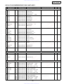
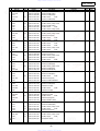
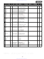
1
http://www.xiaoyu163.com
QQ 376315150 892498299
For Europe model
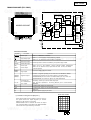
SERVICE MANUAL
MODEL
Ver. 1
DCD-1500AE
TEL
TEL
SUPER AUDIO CD PLAYER
13942296513
13942296513
サービスをおこなう前に、このサービスマニュアルを
必ずお読みください。本機は、火災、感電、けがなど
に対する安全性を確保するために、さまざまな配慮を
おこなっており、また法的には「電気用品安全法」に
もとづき、所定の許可を得て製造されております。
従ってサービスをおこなう際は、これらの安全性が維
持されるよう、このサービスマニュアルに記載されて
いる注意事項を必ずお守りください。
●
For purposes of improvement, specifications and
design are subject to change without notice.
● 本機の仕様は性能改良のため、予告なく変更すること
があります。
● 補修用性能部品の保有期間は、製造打切後8年です。
●
●
Please use this service manual with referring to the
operating instructions without fail.
● 修理の際は、必ず取扱説明書を参照の上、作業を行っ
Some illustrations using in this service manual are
slightly different from the actual set.
● 本文中に使用しているイラストは、説明の都合上現物
www
.
てください。
と多少異なる場合があります。
xiaoy u163. com
TOKYO, JAPAN
Denon Brand Company, D&M Holdings Inc.
http://www.xiaoyu163.com
X0243 V.01 DE/CDM 0508
376315150 892498299
376315150 892498299
376315150 892498299
QQ 注 意
QQ
QQ
TEL 13942296513
http://www.xiaoyu163.com
DCD-1500AE
QQ 376315150 892498299
SAFETY PRECAUTIONS
The following check should be performed for the continued protection of the customer and service technician.
LEAKAGE CURRENT CHECK
Before returning the unit to the customer, make sure you make either (1) a leakage current check or (2) a line to chassis
resistance check. If the leakage current exceeds 0.5 milliamps, or if the resistance from chassis to either side of the
power cord is less than 460 kohms, the unit is defective.
LASER RADIATION
Do not stare into beam or view directly with optical instruments, class 3A laser product.
注 意
サービス、点検時には次のことにご注意願います。
QQ 376315150 892498299
指定部品の使用!
セットの部品は難燃性や耐電圧など安全上の特性を
持ったものとなっています。従って交換部品は、使
用されていたものと同じ特性の部品を使用してくだ
さい。特に配線図、部品表に 印で指定されている
安全上重要な部品は必ず指定のものをご使用くださ
い。
注 意
部品の取付けや配線の引きまわしは、元どおりに!
安全上、テープやチューブなどの絶縁材料を使用し
たり、プリント基板から浮かして取付けた部品があ
ります。また内部配線は引きまわしやクランパーに
よって発熱部品や高圧部品に接近しないように配慮
されていますので、これらは必ず元どおりにしてく
ださい。
本機に使用している多くの電気部品、および機構部品
は安全上、特別な特性を持っています。この特性はほ
とんどの場合、外観では判別つきにくく、また、もと
の部品より高い定格(定格電力、耐圧)を持ったもの
を使用しても安全性が維持されるとは、限りません。
安全上の特性を持った部品は、このサービスマニュア
ルの配線図、部品表につぎのように表示していますの
で、必ず指定されている部品番号のものを使用願いま
す。
(1) 配線図…
マークで表示しています。
サービス後は安全点検を!
サービスのために取り外したねじ、部品、配線など
が元どおりになっているか、またサービスした個所
の周辺を劣化させてしまったところがないかなどを
点検し、外部金属端子部と、電源プラグの刃の間の
絶縁チェックをおこなうなど、安全性が確保されて
いることを確認してください。
www
.
安全上重要な部品について
xiaoy u163. com
(2) 部品表…
2
http://www.xiaoyu163.com
マークで表示しています。
指定された部品と異なるものを使用し
た場合には、感電、火災などの危険を
生じる恐れがあります。
376315150 892498299
376315150 892498299
TEL 13942296513
QQ
QQ
感電に注意!
(1)このセットは、交流電圧が印加されていますの
で、通電時に内部金属部に触れると感電するこ
とがあります。従って通電サービス時には、絶
縁トランスの使用や手袋の着用、部品交換に
は、電源プラグを抜くなどして、感電にご注意
ください。
(2)内部には、高電圧の部分がありますので、通電
時の取扱には、十分ご注意ください。
13942296513
13942296513
(絶縁チェックの方法)
電源コンセントから電源プラグを抜き、アンテナ
や、プラグなどを外し、電源スイッチを入れま
す。500V絶縁抵抗計を用いて、電源プラグのそれ
ぞれの端子と、外部露出金属部〔アンテナ端子、
ヘッドホン端子、マイク端子、入力端子など〕と
の間で、絶縁抵抗値が1MΩ以上であること、この
値以下のときは、セットの点検修理が必要です。
TEL
TEL
注意事項をお守りください!
サービスのとき特に注意を必要とする個所について
は、キャビネット、部品、シャーシなどにラベルや
捺印で、注意事項を表示しています。これらの注意
書きおよび取扱説明書などの注意事項を必ずお守り
ください。
http://www.xiaoyu163.com
DCD-1500AE
QQ 376315150 892498299
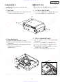
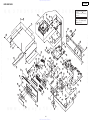
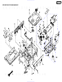
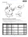
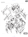
DISASSEMBLY
各部のはずしかた
(Follow the procedure below in reverse order when
reassembling.)
(組み立てるときは、逆の順序でおこなってください。)
1. Top Cover
1. トップカバーのはずしかた
(1) Remove 8 top and side screws. And remove 2 rear
screws, then detach the Top cover.
(1) トップカバーを取り付けている上部、両サイドの
ネジ 8 本およ後部のネジ 2 本をはずします。
TEL
TEL
13942296513
13942296513
(1) Detach the Loader panel Ass’y by lifting.
QQ 376315150 892498299
(1) ローダーを開き、ローダーパネルを矢印の方向に
はずします。
(2) Remove 4 top screws and 2 bottom screws of Front
Panel Ass’y.
(2) フロントパネル底部のネジ 4 本をはずします。
(3) フロントパネル上部のネジ 2 本をはずします。
(3) Remove H/P BRACKET and CHASSIS screw, then
detach the Front Panel Ass'y.
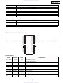
(Refer to Fig. 1)
(4) H/P BRACKET と CHASSIS を共締めしているネジ
をはずします。(Fig. 1 参照)
(5) フロントパネルを矢印の方向にはずします。
Fig. 1
www
.
xiaoy u163. com
3
http://www.xiaoyu163.com
376315150 892498299
376315150 892498299
TEL 13942296513
QQ
QQ
2. フロントパネルのはずしかた
2. Front Panel Ass’y
http://www.xiaoyu163.com
DCD-1500AE
QQ 376315150 892498299
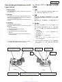
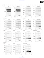
3. Mechanism
3. メカのはずしかた
(1) Remove 4 screws, then detach the Mechanism.
(1) メカを取り付けているネジ 4 本をはずします。
4. Attachment of Mechanism
4. メカの取り付けかた
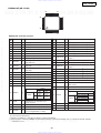
(1) Mechanism is put on MECHA BRACKET BOTTOM.
(1) MECHA BRACKET BOTTOM にメカを置く。
(2) ADJUST.COLLAR is put on 2 places of the front.
(2) ADJUST. COLLAR を前側 2ヶ所にセットする。
(3) 2 front side screws are tightened.
(3) 前側 2ヶ所をネジ止めする。
(4) 2 rear side screws are tightened.
(4) 後側 2ヶ所をネジ止めする。
TEL
TEL
ADJUST. COLLAR
13942296513
13942296513
5. Attachment of Mechanism
5. H/P ブラケットの取り付けかた
Follow the procedure below.
図のような順番にて取り付けてください。
(1) 1 screw of volume side is tightened.
(1) ボリューム横をネジ止めする。
(2) 1 screw of H/P jack side is tightened.
(2) H/P ジャック横をネジ止めする。
(3) (4) 2 screws of H/P jack top is tightened.
(3) (4) H/P ジャック上側をネジ止めする。
1
www
.
3
4
2
xiaoy u163. com
(Note) When assembling the volume pwb and the bracket,
insert thickness 1.6mm board between the bracket
and volume.
( 注 ) ボリュームを H/P ブラケットに取り付けるとき
ボリュームの上部と H/P ブラケットの曲げの間に
1.6mm 厚のスペーサを挟み込む。
4
http://www.xiaoyu163.com
376315150 892498299
376315150 892498299
TEL 13942296513
QQ
QQ
QQ 376315150 892498299
MECHA BRACKET BOTTOM
http://www.xiaoyu163.com
DCD-1500AE
QQ 376315150 892498299
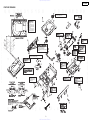
Note Handling and Replacement of the レーザーピックアップ取り扱い上の注意
Laser pick-up
と交換
1. Disassembly
1. 分解
Do not disassemble or adjust this mechanism due to precision component.
本メカニズムは、専門工場で、精密に組立て調整しており
ます。安易に分解、調整を行わないで下さい。
2. Storage
2. 保管
Do not leave this mechanism in high temperature and humidity. Be sure to prevent this mechanism from static electricity, dust and excessive forces.
Do not leave this mechanism without a unti-static cover for
the dust.
高温、あるいは高湿度下での保管は避けて下さい。静電
気、塵埃対策を行い異常な外力が加わらないように保管し
て下さい。
放置する場合は、必ず静電袋に入れて塵埃を避けて下さ
い。
3. Handling
3. 取り扱い
② CD LD 固定用プレート
Fixate plate of CD laser
①半固定抵抗 ( 2箇所 )
Trim-potentiometer
⑤対物レンズ
Objective
⑥アクチュエータ
Actuator
おさえばね
Spring
ネジ
Screw
www
xiaoy u163. com
Fig. b
③ OEIC 固定用プレート
Fixate plate of OEIC
.
Fig. c
④高周波重畳モジュール部 (DVD レーザ用 )
High frequency module and DVD laser
5
http://www.xiaoyu163.com
アクチュエ−タと FPC の接合部
Connected point actuator and PWB
376315150 892498299
376315150 892498299
※ ②及び④の LD はんだ付け部はリードカット処理を施し
ており、鋭利になっている為、危険ですので特に注意し
てください。
QQ
QQ
QQ 376315150 892498299
※ The laser diode soldering portion of ② and ④ is sharp,
be careful especially because it is dangerous.
13942296513
13942296513
TEL 13942296513
落下などの、強い衝撃がかからないように取扱って下さ
い。
次に示す個所には絶対に触れないで下さい。触れた場合
ピックアップの品質に大きく影響を及ぼす可能性があり
ます。
① 半固定抵抗
② CD LD 固定用プレート(CD レーザ及び本体について
いるプレート)
③ OEIC 固定用プレート
④ 高周波重畳モジュール部 (DVD LD)
⑤ 対物レンズ
⑥ アクチュエータ(ネジ、おさえばね、アクチュエータ
と FPC の接合部含む)
TEL
TEL
Do not shock to this mechanism.
Don't touch the parts as follows.To touch them may cause
big trouble.
① Trim-potentionmeter
② CD laser dode and Fixate of CD laser
③ Fixate plate of OEIC
④ High frequency module and DVD laser diode
⑤ Objective
⑥ Actuator (Include screw, spring, and connected point
actuator and PWB)
http://www.xiaoyu163.com
DCD-1500AE
QQ 376315150 892498299
Never touch the objective lens, actuator, laser diode, photo
detector and the trim-potentiometer.
Be sure no dust or soil on the objective lens.
If dust is on the objective lens, below it away by clean air.
If dust or soil remain on the objective lens, use the cleaning
liquid (B4) made by JCB INDUSTRY Ltd. No alternative.
Make sure that a person who handles this mechanism is
well earthed. Be sure to earth to the manufacturing equipment.
Do not approach magnetic materials.
Too much forces on the leads of laser diode, OEIC, and the
printed wiring board, may caused the pickup to damage.
Too much forces on the leads of laser diode, OEIC, and the
printed wiring board, may caused the pickup to damage.
Guide shafts in mechanism should not be forced when you
set the FFC to the connector, which may cause the guide
shafts to deform.
4. 雰囲気
6315150 892498299
QQ 5.37レーザー駆動回路
We solder the Short land on PWB before shipment to protect laser diode. Open the short landsafte you connect
pick-up your circuit by flat cable. (Refer to Fig. a)
When you unstrap the short solder for the laser diode protection in the condition which doesn't connect by a flat cable, the laser diode and PEIC may destroy by static
electricity.
レーザダイオード保護用ランドのショート部の開放は、
Fig. a の様にセットに接続されたフラットケーブルをピッ
クアップのコネクタに差込後実施して下さい。フラット
ケーブルを接続しない状態で、レーザダイオード保護用ラ
ンドを開放した場合 レーザダイオード及び OEIC が静電
破壊する可能性が大きいので十分ご注意下さい。
ピックアップコネクタ
Connector of the pick up
レーザダイオード保護用ランド
The short land for the laser diode
protection
フラットケーブル
Flat cable
セットへ接続されていること
Be connected to the circuit
Fig. a
www
.
xiaoy u163. com
6
http://www.xiaoyu163.com
376315150 892498299
376315150 892498299
5. L
Laser
drive circuit
TE
13942296513
腐食性ガス (H2S, SO2, NO2, Cl2 等 ) はもとより、有害なガ
ス雰囲気中及び、有害なガスを発生する物質(特に有機シ
リコン系、シアン系、ホルマリン系、フェノール系物質
等)が存在する場所でのご使用及び保管は避けて下さい。
特に、セット内に於いても上記物質が存在しないようにし
て下さい。モーターが回転しなくなります。
QQ
QQ
For proper operation storage and operating environment
should not contain corrosive gases. For example HS2, SO2,
NO2, Cl2 ets. In addition storage environment should not
have materials that emit corrosive gases especially from silicic, cyanic, formalin and phenol group. In the mechanism
or set, existence of corrosive gases may cause no rotation
in motor.
13942296513
13942296513
4. Surrounding atmosphere
TEL
TEL
対物レンズ、アクチュエータ、レーザーダイオード、光検
出器、及び半固定抵抗には絶対に触れないで下さい。
対物レンズに、塵埃や汚れが付かないように充分注意して
下さい。
対物レンズに埃が付いた場合、きれいな空気を吹き付けて
取り去って下さい。
取りきれない埃、汚れがある場合にはクリーニング液(日
本綿棒(株)CD レンズクリーナー液 B4)を用い、糸屑
の発生しない綿棒で軽く拭き取って下さい。尚、他のク
リーニグ液は絶対に使わないで下さい。
取り扱う作業者は、人体アースを確実に取って下さい。作
業場、治工具など、関連設備は確実にアースを取って下さ
い。
ピックアップのアクチュエータ部は強力な磁気回路を有
しているので磁性体を近づけないで下さい。
レーザーダイオードのリード部分、受光素子 (OEIC) 及び
受光素子取り付け基板に力を加えると不良となることが
ありますので、取り扱い時は絶対に力を加えないように充
分注意願います。
FFC をコネクタ部に挿入するときは、軸受け部及びガイド
シャフトに力を加えないよう挿入願います。
力を加えますと、ガイドシャフトが変形し動作不良となる
ことがありますので、充分注意願います。
http://www.xiaoyu163.com
DCD-1500AE
QQ 376315150 892498299
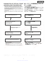
DIAGNOSTICS OF OPTICAL PICKUP 光ピックアップの故障診断とトラバース
AND REPLACING TRAVERSE UNIT
ユニットの交換
Make failure diagnostics of the Optical Pickup as follows.
If the laser drive current (Iop) becomes more than 1.5 times of
the initial value, the Optical Pickup should be replaced.
The laser drive current is registered on the seal attached to
the rear of the Mecha.Unit.
In case of replacing the Pickup, change the whole part of the
Traverse Unit.
No mechanical adjustment is necessary after the replacement.
次の順序で故障診断を行ってください。
レーザー駆動電流 Iop 値が初期値の 1.5 倍以上になっている場
合は光ピックアップ交換の目安となります。
レーザー駆動電流初期値は、メカの後部のシール上に記入さ
れています。
ピックアップ交換の場合は、トラバースユニット単位での交
換となります。メカの調整は不要です。
ディスクを読み込まない
スムーズに再生しない、等
Disc no read,unsteady playback, etc.
TEL
TEL
レーザー駆動電流 Iop 値の確認
HF 波形の確認
(73 ページ参照)
現在値が初期値の
1.5 倍になっている
Traverse Unit replacing
(See page 8 for details)
トラバースユニット交換
(詳細は 8 ページ)
Laser current registering after replacement.
交換後のレーザー電流記入
Step: Disc playback
Write the measured value on the seal attached to the
Mecha. Unit
手順 :ディスクを再生
その時の Iop 値をメカ後方のシールの上に重ねて貼る
等で更新する。
*Iop の測定方法は、8, 9 ページ参照。
*As to the measuring method, refer to page 8,9.
www
.
xiaoy u163. com
7
http://www.xiaoyu163.com
376315150 892498299
376315150 892498299
QQ 376315150 892498299
TEL 13942296513
QQ
QQ
Present value exceeds the initial value by 1.5 times
13942296513
13942296513
Laser drive current (Iop) check
HF wave form check
(Refer to page 73)
http://www.xiaoyu163.com
DCD-1500AE
QQ 376315150 892498299
1. Label Indication of SACD Mechanism.
1. SACD メカのラベル表示
Example: DVD 30mA
例: CD 30mA
TEL
TEL
2. レーザーピックアップの取扱注意
レーザーダイオードの破壊防止。
光素子ユニットを交換するときは、以下を遵守してください。
(1) 光素子ユニットの接続ケーブルをはずすときは、静電対
策を行ったデスク上で作業してください。
(2) 作業者は、リストストラップを使用してください。
(3) レーザーダイオードの破壊防止のため、24P FFC ケーブ
ルをはずす前にランドを半田付けショートしてくださ
い。
(4) 光素子ユニットのコネクタ部に触れないでください。
3. Replacement of the Laser Pick-up
(Traverse Unit)
3. レーザーピックアップ ( トラバースユニッ
ト ) の交換
Iop( レーザー駆動電流)をチェックします。
現在の Iop 値が初期値の 50%を越えている場合、トラ
バースユニット(レーザーピックアップ)を交換してくだ
さい。
Check the Iop(Laser drive current)
If the present Iop (current) value exceeds.+50% of the initial value, replace the Traverse unit(Laser Pick-up) with a
new one.
4. Iop Measurement Method
4. Iop の測定方法
レ ー ザ ー 駆 動 電 流 を 測 定 す る 場 合、下 記 の デ ィ ス ク
(CD,SACD) を再生します。
SACD 基板上のテストポイント (+5V-M2 ∼ LD(CD),LD(DVD))
にて、CD レーザーと DVD レーザーの Iop を測定してくだ
さい。
When measuring Laser drive current (Iop), playback the
discs (CD,SACD) described below, measure Iop for CD
Laser and DVD Laser by the test point (+5V-M2~
LD(CD),LD(DVD))on the SACD P.W.B.
Test Disc :SACD/Philips DAC Test Disc or commercially
available discs.
:CD/TCD-784 (manufactured by ALMEDIO INC)
or commercially available discs.
www
.
テストディスク:SACD/Philips DAC Test Disc または市販
同等ディスク
:CD/TCD-784(ALMEDIO 社製)または市
販同等ディスク
xiaoy u163. com
8
http://www.xiaoyu163.com
376315150 892498299
376315150 892498299
QQ 376315150 892498299
TEL 13942296513
QQ
QQ
the protection for the damage of laser diode.
If you want to change the optical device unit from any other
units, you must keep the following.
(1) It should be done at the desk already took measures the
static electricity in care of removing the OPU's (Optical
device unit) connector cable.
(2) Workers should be put on the "Earth Band".
(3) It should be done to add the solder to the short land to
prevent the broken Laser diode before removing the 24P
FFC cable.
(4) Don't touch OPU's connector parts carelessly.
13942296513
13942296513
2. Note for Handling the Laser Pick-Up
http://www.xiaoyu163.com
DCD-1500AE
QQ 376315150 892498299
4.1. DVD Laser current measurement
4.1. DVD レーザー電流測定
LD(DVD)
LD(DVD)
+5V-M2
+5V-M2
Oscilloscope
Oscilloscope
(1) Connect the oscilloscope to +5V-M2 of test point for GND
side and LD(DVD) of test point for signal side.
(2) Playback the stereolayer track 1 of the SACD Test Disc.
(3) Measure the voltage between +5V-M2 and LD(DVD), calculate Iop by the formula as shown below.
(1) オシロスコープをテストポイント +5V-M2(GND) と
LD(DVD)( 信号 ) へ接続します。
(2) SACD テストディスクのステレオレイヤートラック 1 を
再生します。
(3) +5V-M2 と LD(DVD) 間の電圧を測定し、次式により Iop を
算出します。
Measurement Voltage Value
Iop = ----------------------------------------------------------------------------14 (Resistance value)
(1) オシロスコープをテストポイント
+5V-M2(GND) と
LD(CD)( 信号 ) へ接続します。
(2) CD テストディスクのトラック 1 を再生します。
(3) +5V-M2 と LD(CD) 間の電圧を測定し、次式より Iop を算
出します。
(1) Connect the oscilloscope to +5V-M2 of test point for
GND side and LD(CD) of test point for signal side.
(2) Playback the track 1 of the CD Test Disc.
(3) Measure the voltage between +5V-M2 and LD(CD), calculate Iop by the formula as shown below.
LD (CD)
LD (DVD)
+5V-M2
www
.
xiaoy u163. com
1U-3624 SACD MODULE P.W.B. unit foil side
9
http://www.xiaoyu163.com
376315150 892498299
376315150 892498299
QQ 376315150 892498299
QQ
QQ
TEL 13942296513
測定電圧値
Iop = -----------------------------------11.75(抵抗値)
13942296513
13942296513
4.2. CD レーザー電流測定
4.2. CD Laser current measurement
Measurement Voltage Value
Iop = ----------------------------------------------------------------------------11.75 (Resistance value)
TEL
TEL
測定電圧値
Iop = ----------------------------14(抵抗値)
http://www.xiaoyu163.com
DCD-1500AE
QQ 376315150 892498299
HOW TO REPLACE TRAVERSE UNIT
トラバースユニットの交換方法
Caution: The optical pickup can be damaged easily by
static electricity charged on human body.
Take necessary anti-static measures when
repairing around the optical pickup.
注意 : 光ピックアップは、人体に帯電した静電気等で静電
破壊することがあります。光ピックアップ周辺を修
理する際は、必要な静電対策を行ってください。
1. Guide Clamp Bracket disassembly
1. ガイドクランプブラケットのはずしかた
(1) Remove 2 screws.
(1) ねじ 2 本をはずします。
(2) Remove Guide Clamp Bracket to arrow direction.
(2) ガイドクランプブラケットを矢印方向にとりはずしま
す。
TEL
TEL
13942296513
13942296513
2. トレイのはずしかた
(1) Remove to arrow direction.
(1) 矢印方向にとりはずします。
(2) Solder the short-circuit (see in the frame).
(2) 半田付けショートを行います。(枠内図参照 )
www
.
xiaoy u163. com
10
http://www.xiaoyu163.com
376315150 892498299
376315150 892498299
2. Tray disassembly
QQ
QQ
QQ 376315150 892498299
TEL 13942296513
http://www.xiaoyu163.com
DCD-1500AE
QQ 376315150 892498299
3. Traverse Unit disassembly
3. トラバースユニットのはずしかた
(1) Remove 24P FFC, 15P FFC and 5P PH WIRE connecting with from the Main P.W.B.
(1) メイン基板に接続している 24P FFC、15P FFC、5P PH
ワイヤをはずします。
(2) Remove 4 screws fixing Damper.
(2) ダンパーを固定しているねじ 4 本をはずします。
(3) Remove Traverse Unit to arrow direction.
(3) トラバースユニットを矢印方向にとりはずします。
TEL
TEL
13942296513
13942296513
トラバースユニット分解の注意
(1) When assembling, reverse the order of the above.
(1) 組み立てるときは、上記の逆の順序で行ってください。
(2) When inserting Tray, confirm boss on Slide Cam set to
ditch of the Tray (Compare with below drawing).
(2) トレイ組込み時、スライドカムのボスがトレイの溝に
合っているか確認してください。(下図参照)
www
.
xiaoy u163. com
11
http://www.xiaoyu163.com
376315150 892498299
376315150 892498299
Note for disassembly Traverse Unit
QQ
QQ
QQ 376315150 892498299
TEL 13942296513
http://www.xiaoyu163.com
It displats repeatedly.
TOC read → OPEN →
CLOSE → TOC read
H.R.CHACKING operation
It displats repeatedly.
TOC read → playback
title-all of the disc. →
OPEN → CLOSE →
TOC read
H.R.SHORT operation
PLAY
PLAY
PLAY
A.S.RVS
H.R.CHACKING display
A.S.FWD
A.S.RVS
A.S.RVS
A.S.FWD
STOP+A.S.RVS
STOP+A.S.RVS
A.S.RVS
A.S.FWD
The name of the inputted key and
remote control code is displayed.
Key & Remocon input mode display
A.S.FWD
The display for each grit.
(It displays at intervals
of 1 second.)
FL tube
STOP+A.S.RVS
TEST Mode
STOP+A.S.RVS
B/E µcom
Ver.display
A.S.FWD or A.S.RVS
(DCD-1500)
Model Name display
STOP+A.S.RVS
STOP+A.S.RVS
STOP+A.S.RVS
A.S.RVS
H.R.SHORT display
A.S.FWD
A.S.RVS
A.S.FWD
376315150 892498299
12
QQ
H.R.NORMAL display
QQ 376315150 892498299
13942296513
xiaoy u163. com
It displats repeatedly.
TEL 13942296513
TEL
376315150 892498299
PLAY
QQ
.
TOC read → playback
title-all of the disc. →
OPEN → CLOSE →
TOC read
13942296513
www
H.R.NORMAL operation
TEL
OPEN/CLOSE+PLAY+AC_ON
FL all light
A.S.FWD
F/E µcom
Ver.display
A.S.RVS
http://www.xiaoyu163.com
DCD-1500AE
CD TEST MODE & SERVICE MODE
QQ 376315150 892498299
http://www.xiaoyu163.com
DCD-1500AE
QQ 376315150 892498299
SETTING UP THE TEST MODE
テストモード
(1) Setting up
(1) テストモードへの投入
• In order to set up the test mode, you press STOP button
and REV button simultaneously in the heat-run mode.Fundamentaly, you can set up the test mode at the stop state
after disc loading. (Heat-run mode is set up by pressing
PLAY button,holding OPEN/CLOSE button. If it becomes
heat run mode, PLAY indicator and PAUSE indicator will
light up.)
・ テストモードへの投入はヒートランモード時に
STOP
キーと REV キーを 2 重押しすることで行う。基本的に
ディスクローディング後の停止状態でテストモードに
投入する。( ヒートランモードへの投入は OPEN/CLOSE
キーと PLAY キーを 2 重押しすることで行う。ヒートラ
ンモードになると PLAY インジケータと PAUSE インジ
ケータが点灯する。)
LOADING 表示
LOADING display
↓
FL 管の表示 (13 桁の表示部 )
FL display (The display part of 13 digits)
1
2
3
4
5
6
7
8
↓
9
10
11
12
1
13
2
3
4
5
6
7
8
9
10
11
12
13
T
T
FL 管の表示 (13 桁の表示部 )
FL display (The display part of 13 digits)
1
2
T
3
3
4
5
6
7
8
9
10
11
12
13
7
3
4
5
6
7
8
9
11
12
4
5
6
7
8
9
10
11
12
13
1
2
T
7
3
4
5
6
7
8
9
10
11
12
13
QQ 376315150 892498299
13
(3) モードの確定
(3) Mode decision
• The mode will be decided if the PLAY button is pushed in
the state where the mode is chosen.
(a) In the case of servo adjustment value display mode, a focus offset adjustment value is displayed.
FL display (The display part of 13 digits)
1
2
3
4
5
6
7
8
9
10
11
12
13
T
3
1
n
n
n
n
n
n
n
n
n
n
・ モードを選択してある状態で PLAY キーを押すとモード
を確定する。
(a) サーボ調整値表示モードの場合は、フォーカスオフ
セット調整値を表示する。
FL 管の表示 (13 桁の表示部 )
1
2
3
4
5
6
7
8
9
10
11
12
13
T
3
1
n
n
n
n
n
n
n
n
n
n
(n: 調整値 )
(b) トレースモード ( エラーレート表示 ) の場合は、1層
内周のトレースを選択する。
(n:adjustment value)
(b) In the case of trace mode (error rate display), trace of the
circumference in one layer is chosen.
FL 管の表示 (13 桁の表示部 )
FL display (The display part of 13 digits)
1
2
3
4
5
6
7
8
9
10
11
12
13
T
7
1
F
F
F
F
F
F
F
F
F
F
1
2
3
4
5
6
7
8
9
10
11
12
13
T
7
1
F
F
F
F
F
F
F
F
F
F
(F: アドレス及びエラーレートは未確定時、F を表示する。)
(F: An address and an error rate display F at the time of undecided.)
(4) モード内での変更
(4) Change within the mode
• If the REV button or the FWD button is pushed in the state
where the mode is decided, a change within the mode will
be made.
(a) In the case of servo adjustment value display mode (refer to table 1 servo adjustment value display mode details)
www
T
2
3
4
5
X
X
n
n
.
FL 管の表示 (13 桁の表示部 )
1
2
3
4
5
6
7
8
9
10
11
12
13
T
X
X
n
n
n
n
n
n
n
n
n
n
xiaoy u163. com
FL display (The display part of 13 digits)
1
・ モードを確定してある状態で REV キー又は FWD キーを
押すとモード内での変更を行う。
(a) サーボ調整値表示モードの場合( 表1サーボ調整値表
示モード詳細 参照)
(XX: 選択モード [31 ∼ 62]、n: 調整値 )
6
7
8
9
10
11
12
13
n
n
n
n
n
n
n
n
(XX:selection mode [31--62] n:adjustment value)
13
http://www.xiaoyu163.com
376315150 892498299
376315150 892498299
TEL 13942296513
10
3
QQ
QQ
2
3
FL 管の表示 (13 桁の表示部 )
FL display (The display part of 13 digits)
T
2
T
(b) 再度 REV キー又は FWD キーを押すとトレースモード
( エラーレート表示 ) になる。
(b) If the REV button or the FWD button is pushed again, it
will become the trace mode (error rate display).
1
1
13942296513
13942296513
・ モードには、サーボ調整値表示モードとトレースモード
( エラーレート表示 ) の 2 つがある。
(a) テストモード投入後に REV キー又は FWD キーを押す
と、サーボ調整値表示モードになる。
• There are two, servo adjustment value display mode and
trace mode (error rate display), in the mode.
(a) If the REV button or the FWD button is pushed in the test
mode, it will become servo adjustment value display
mode.
TEL
TEL
(2) モードの選択
(2) Mode Select
http://www.xiaoyu163.com
DCD-1500AE
QQ 376315150 892498299
(b) In the case of trace mode (error rate display) (refer to table 2 trace mode details)
(b) トレースモード ( エラーレート表示 ) の場合( 表 2 ト
レースモード詳細 参照)
FL display (The display part of 13 digits)
FL 管の表示 (13 桁の表示部 )
1
2
3
4
5
6
7
8
9
10
11
12
13
1
2
3
4
5
6
7
8
9
10
11
12
13
T
Y
Y
F
F
F
F
F
F
F
F
F
F
T
Y
Y
F
F
F
F
F
F
F
F
F
F
(YY: select mode [71--94] ,F: address and an error rate display F at the
time of undecided)
(YY: 選択モード [71 ∼ 94]、F: アドレス及びエラーレートは未確定
時、F を表示する。)
(5) Execution of trace mode (error rate display)
(refer to table 2 trace mode details)
(5) トレースモード ( エラーレート表示 ) の実行
( 表 2 トレースモード詳細 参照)
• Trace will be performed if the PLAY button is pushed after
choosing operation.
・ 動作を選択した後、PLAY キーを押すとトレースを実行
する。
FL display (The display part of 13 digits)
FL 管の表示 (13 桁の表示部 )
1
2
3
4
5
6
7
8
9
10
11
12
13
1
2
3
4
5
6
7
8
9
10
11
12
13
T
Y
Y
m
m
m
m
m
m
l
l
l
l
T
Y
Y
m
m
m
m
m
m
l
l
l
l
• The mode chosen when selection mode was changed into
the trace execution and the PLAY button was pushed is
performed from the beginning.When the PLAY button is
pushed without changing selection mode, the mode under
selection is performed from the beginning.(If the PLAY button is pushed, the address corresponding to the chosen
mode will be searched again.)
(6) Other operation
FL display (The display part of 13 digits)
1
2
3
4
5
6
7
8
9
10
11
12
13
(a) サーボ調整値表示モード、トレースモード ( エラー
レート表示 ) 中に STOP キーを押すとテストモード投
入時の状態に戻る。
QQ 376315150 892498299
FL 管の表示 (13 桁の表示部 )
1
T
2
(b) Push the OPEN/CLOSE button twice and carry out servo readjustment in OPEN operation ->CLOSE operation.
(It readjusts with test mode.)
↓
LOADING display
↓
6
7
8
9
10
11
12
13
FL 管の表示 (13 桁の表示部 )
FL display (The display part of 13 digits)
3
5
OPEN 表示
↓
CLOSE 表示
↓
LOADING 表示
↓
CLOSE display
2
4
(b) OPEN/CLOSE キーを 2 回押して、OPEN 動作→ CLOSE
動作で、サーボ再調整する。
( テストモードのまま再調整する。)
OPEN display
↓
1
3
T
4
5
6
7
8
9
1
10
11
12
T
.
3
4
5
6
7
8
9
10
11
12
13
(c) テストモード中に STOP キーと REV キーの 2 重押し
( 投入時と同じキー ) で、ヒートランモードに戻る。
(c) By pressing STOP button and REV button simultaneously in the test mode, it returns to heat-run mode.
www
2
T
13
xiaoy u163. com
14
http://www.xiaoyu163.com
376315150 892498299
376315150 892498299
TEL 13942296513
(6) その他の動作
QQ
QQ
(a) If the STOP button is pushed into servo adjustment value display mode and trace mode (error rate display), it
will return to the state at the time of a test mode injection.
(PLAY キーを押したら、選択しているモードに対
応したアドレスを再度サーチする。)
13942296513
13942296513
(YY: 選択モード [71 ∼ 94]、m: アドレス [PBA][HEX]、
l: エラーレート [COUNT/SEC][HEX])
( 注 )CD:300 フレーム ,DVD:85ECC ブロック毎にデータ
更新する。
・ トレース実行中に選択モードを変更し、PLAY キーを押
すと選択したモードを最初から実行する。選択モードを
変更せずに PLAY キーを押した場合も、選択中のモード
を最初から実行する。
TEL
TEL
(YY:select mode[71--94],m:address[PBA][HEX],
l:error rate[COUNT/SEC][HEX])
(Note) Renewal of data is carried out for every CD:300 frame and
DVD:85ECC block.
http://www.xiaoyu163.com
DCD-1500AE
QQ 376315150 892498299
(7) Test mode detailed table
(7) テストモード詳細一覧表
Table 1: servo adjustment value display mode details
XX
Contents
Contents
suppleme
nt
31
RFP FE Offset
32
RFP TE
Gain
表 1 サーボ調整値表示モード詳細
内容補足
内容説明
layer 0
PI of CXD1881AR An offset value and
FE An offset value is displayed.
Pi offset is shown in higher rank
1Byte.
FE offset is shown in low rank 1Byte.
31
RFP FE Offset
レイヤ 0
CXD1881AR の PI オフセット値と FE
オフセット値を表示。
上位 1Byte に Pi オフセットを示す。
下位 1Byte に FE オフセットを示す。
Bal
layer 0
TE balance gain value of CXD1881AR
is displayed.
32
RFP TE
Gain
Bal
レイヤ 0
CXD1881ARのTE バランスゲイン値を
表示す。
33
RFP TE Output
Gain
layer 0
TE output gain value of CXD1881AR is
displayed.
33
RFP TE Output
Gain
レイヤ 0
CXD1881ARのTE 出力ゲイン値を表示
す。
34
RFP TE Offset
layer 0
TE offset value of CXD1881AR is
displayed.
34
RFP TE Offset
レイヤ 0
CXD1881AR の TE オフセット値を表
示。
35
DSP TE Offset
layer 0
TE offset value inside CXD1885Q is
displayed.
35
DSP TE Offset
レイヤ 0
CXD1885Q 内部の TE オフセット値を
表示。
36
Fcs Bias
layer 0
The focus bias value
CXD1885Q is displayed.
inside
36
Fcs Bias
レイヤ 0
CXD1885Q 内部のフォーカスバイア
ス値を表示。
37
Fcs AGC
layer 0
The inside focus gain (setting 0x2000
to 1) value of CXD1885Q is
displayed.。
Therefore, 0x1FF2 and in the case of
0x2012, it is as follows.
0x1FF2(8178) / 0x2000(8192) =
0.998291015625(fold)
0x2012(8210) / 0x2000(8192) =
1.002197265625(fold)
Notes: The inside of ( ) is a decimal
system equivalent.
37
Fcs AGC
レイヤ 0
CXD1885Q 内 部 フ ォ ー カ ス ゲ イ ン
(0x2000 を 1 として ) 値を表示。
0x1FF2 や 0x2012 の場合、以下のよ
うになる。
0x1FF2(8178) / 0x2000(8192) =
0.998291015625( 倍 )
0x2012(8210) / 0x2000(8192) =
1.002197265625( 倍 )
注 :( ) 内は 10 進換算値
38
Trk AGC
layer 0
The inside tracking gain (setting
0x2000 to 1) value of CXD1885Q is
displayed.。
Therefore, 0x1FF2 and in the case of
0x2012, it is as follows.
0x1FF2(8178) / 0x2000(8192) =
0.998291015625(fold)
0x2012(8210) / 0x2000(8192) =
1.002197265625(fold)
Notes: The inside of ( ) is a decimal
system equivalent
38
Trk AGC
レイヤ 0
CXD1885Q内部トラッキングゲイン(0
x2000 を 1 として ) 値を表示。
0x1FF2 や 0x2012 の場合、以下のよ
うになる。
0x1FF2(8178) / 0x2000(8192) =
0.998291015625( 倍 )
0x2012(8210) / 0x2000(8192) =
1.002197265625( 倍 )
注 :( ) 内は 10 進換算値
QQ
376315150 892498299
39
Pi Offset
layer 0
It is the parameter calculated inside
CXD1885Q.
The value displayed on a set serves as
the number of complement of 2 of
2Bytes(es) doubled 256.
A voltage value is 6.25mV per bit.
39
Pi Offset
レイヤ 0
CXD1885Q 内 部 で 計 算 さ れ る パ ラ
メータ。
セットに表示される値は、256 倍され
た 2Bytes の 2 の補数となる。
電圧値は 1bit あたり 6.25mV。
40
FE Offset
layer 0
It is the parameter calculated inside
CXD1885Q.
The value displayed on a set serves as
the number of complement of 2 of
2Bytes(es) doubled 256.
A voltage value is 6.25mV per bit.
40
FE Offset
レイヤ 0
CXD1885Q 内 部 で 計 算 さ れ る パ ラ
メータ。
セットに表示される値は、256 倍され
た 2Bytes の 2 の補数となる。
電圧値は 1bit あたり 6.25mV。
41
SE Offset
layer 0
It is the parameter calculated inside
CXD1885Q.
The value displayed on a set serves as
the number of complement of 2 of
2Bytes(es) doubled 256.
A voltage value is 6.25mV per bit.
41
SE Offset
レイヤ 0
CXD1885Q 内 部 で 計 算 さ れ る パ ラ
メータ。
セットに表示される値は、256 倍され
た 2Bytes の 2 の補数となる。
電圧値は 1bit あたり 6.25mV。
42
RFP FE Offset
layer 1
PI of CXD1881AR An offset value and
FE An offset value is displayed.
Pi offset is shown in higher rank
1Byte.
FE offset is shown in low rank 1Byte.
42
RFP FE Offset
レイヤ 1
CXD1881AR の PI オフセット値と FE
オフセット値を表示。
上位 1Byte に Pi オフセットを示す。
下位 1Byte に FE オフセットを示す。
43
RFP TE
Gain
Bal
layer 1
TE balance gain value of CXD1881AR
is displayed.
43
RFP TE
Gain
Bal
レイヤ 1
CXD1881ARのTE バランスゲイン値を
表示。
44
RFP TE Output
Gain
layer 1
TE output gain value of CXD1881AR is
displayed.
44
RFP TE Output
Gain
レイヤ 1
CXD1881AR の TE 出力ゲイン値を表
示。
45
RFP TE Offset
layer 1
TE offset value of CXD1881AR is
displayed.
45
RFP TE Offset
レイヤ 1
CXD1881AR の TE オフセット値を表
示。
46
DSP TE Offset
layer 1
It is the parameter calculated inside
CXD1885Q.
The value displayed on a set serves as
the number of complement of 2 of
2Bytes(es) doubled 256.
A voltage value is 6.25mV per bit.
46
DSP TE Offset
レイヤ 1
CXD1885Q 内 部 で 計 算 さ れ る パ ラ
メータ。
セットに表示される値は、256 倍され
た 2Bytes の 2 の補数となる。
電圧値は 1bit あたり 6.25mV。
47
Fcs Bias
layer 1
It is the parameter calculated inside
CXD1885Q.
The value displayed on a set serves as
the number of complement of 2 of
2Bytes(es) doubled 256.
A voltage value is 6.25mV per bit.
47
Fcs Bias
レイヤ 1
CXD1885Q 内 部 で 計 算 さ れ る パ ラ
メータ。
セットに表示される値は、256 倍され
た 2Bytes の 2 の補数となる。
電圧値は 1bit あたり 6.25mV。
www
.
xiaoy u163. com
15
http://www.xiaoyu163.com
376315150 892498299
376315150 892498299
TEL 13942296513
QQ
QQ
内容
13942296513
13942296513
XX
TEL
TEL
Contents explanation
http://www.xiaoyu163.com
DCD-1500AE
QQ 376315150 892498299
48
Fcs AGC
レイヤ 1
CXD1885Q 内 部 フ ォ ー カ ス ゲ イ ン
(0x2000 を 1 として ) 値を表示。
0x1FF2 や 0x2012 の場合、以下のよ
うになる。
0x1FF2(8178) / 0x2000(8192) =
0.998291015625( 倍 )
0x2012(8210) / 0x2000(8192) =
1.002197265625( 倍 )
注 :( ) 内は 10 進換算値
49
Trk AGC
layer 1
The inside tracking gain (setting
0x2000 to 1) value of CXD1885Q is
displayed.
Therefore, 0x1FF2 and in the case of
0x2012, it is as follows.
0x1FF2(8178) / 0x2000(8192) =
0.998291015625(fold)
0x2012(8210) / 0x2000(8192) =
1.002197265625(fold)
Notes: The inside of ( ) is a decimal
system equivalent
49
Trk AGC
レイヤ 1
CXD1885Q 内部トラッキングゲイン
(0x2000 を 1 として ) 値を表示。
0x1FF2 や 0x2012 の場合、以下のよ
うになる。
0x1FF2(8178) / 0x2000(8192) =
0.998291015625( 倍 )
0x2012(8210) / 0x2000(8192) =
1.002197265625( 倍 )
注 :( ) 内は 10 進換算値
50
Pi Offset
layer 1
It is the parameter calculated inside
CXD1885Q.
The value displayed on a set serves as
the number of complement of 2 of
2Bytes(es) doubled 256.
A voltage value is 6.25mV per bit.
50
Pi Offset
レイヤ 1
CXD1885Q 内 部 で 計 算 さ れ る パ ラ
メータ。
セットに表示される値は、256 倍され
た 2Bytes の 2 の補数となる。
電圧値は 1bit あたり 6.25mV。
51
FE Offset
layer 1
It is the parameter calculated inside
CXD1885Q.
The value displayed on a set serves as
the number of complement of 2 of
2Bytes(es) doubled 256.
A voltage value is 6.25mV per bit.
51
FE Offset
レイヤ 1
CXD1885Q 内 部 で 計 算 さ れ る パ ラ
メータ。
セットに表示される値は、256 倍され
た 2Bytes の 2 の補数となる。
電圧値は 1bit あたり 6.25mV。
52
SE Offset
layer 1
It is the parameter calculated inside
CXD1885Q.
The value displayed on a set serves as
the number of complement of 2 of
2Bytes(es) doubled 256.
A voltage value is 6.25mV per bit.
52
SE Offset
レイヤ 1
CXD1885Q 内 部 で 計 算 さ れ る パ ラ
メータ。
セットに表示される値は、256 倍され
た 2Bytes の 2 の補数となる。
電圧値は 1bit あたり 6.25mV。
53
PO error
detection
number
Error rate
It is invalid at the time of CD
operation.
53
PO 誤り検出数
エ ラ ー
レート
CD 時は無効。
54
PO uncorrectable error
number
Error Rate
It is invalid at the time of CD
operation.
54
PO 訂正不可数
エ ラ ー
レート
CD 時は無効。
55
PI error detection number
Error Rate
CD : C1 error detection number
55
PI 誤り検出数
エ ラ ー
レート
CD 時は C1 誤り検出数。
56
PI uncorrectable
error
number
Error Rate
CD : C2 uncorrectable error number
56
PI 訂正不可数
エ ラ ー
レート
CD 時は C2 訂正不可数。
57
Mirr Count
Disc discriminant
They are the contents at the time of
disk distinction.
Please refer to "Table 3 Disc
distinction information" about the
contents of a value.
57
Mirr Count
ディスク
判別
ディスク判別時の内容。
値の内容は「表3ディスク判別情報」
を参照。
58
Mirr Width
Disc discriminant
They are the contents at the time of
disk distinction.
Please refer to "Table 3 Disc
distinction information" about the
contents of a value.
58
Mirr Width
ディスク
判別
ディスク判別時の内容。
値の内容は「表3ディスク判別情報」
参照。
59
FZC Count
Disc discriminant
They are the contents at the time of
disk distinction.
Please refer to "Table 3 Disc
distinction information" about the
contents of a value.
59
FZC Count
ディスク
判別
ディスク判別時の内容。
値の内容は「表3ディスク判別情報」
参照。
60
Pi Level
Disc discriminant
They are the contents at the time of
disk distinction.
Please refer to "Table 3 Disc
distinction information" about the
contents of a value.
60
Pi Level
ディスク
判別
ディスク判別時の内容。
値の内容は「表3ディスク判別情報」
参照。
61
Disc Type
Disc Type
They are the contents at the time of
disk type.
Please refer to "Table 4 Disc
classification information" about the
contents of a value.
61
Disc Type
ディスク
種別
ディスク種別の内容。
値の内容は「表4ディスク種別情報」
参照。
62
PO error
detection
number and
address
Error rate
PO error detection number is invalid
at the time of CD operation.
62
PO 誤り検出数
とアドレス
エラー
レート
CD 時は PO 誤り検出数は無効。
TEL 13942296513
www
.
QQ 376315150 892498299
xiaoy u163. com
16
http://www.xiaoyu163.com
376315150 892498299
376315150 892498299
The inside focus gain (setting 0x2000
to 1) value of CXD1885Q is displayed.
Therefore, 0x1FF2 and in the case of
0x2012, it is as follows.
0x1FF2(8178) / 0x2000(8192) =
0.998291015625(fold)
0x2012(8210) / 0x2000(8192) =
1.002197265625(fold)
Notes: The inside of ( ) is a decimal
system equivalent.
QQ
QQ
layer 1
13942296513
13942296513
Fcs AGC
TEL
TEL
48
http://www.xiaoyu163.com
DCD-1500AE
QQ 376315150 892498299
Table 2: trace mode details
表 2 トレースモード詳細
内容
補足説明
71
1 層内周の PO 誤り検出数とアド
レスの表示
CD 時は無効。
72
A display of PO uncorrectable
number of the inner circumference of 1-layer and an address.
It is invalid at the time of CD
operation.
72
1 層内周の PO 訂正不可数とアド
レスの表示
CD 時は無効。
73
A display of PI error detection
number of the inner circumference of 1-layer and an address.
CD : C1 error detection number
73
1 層内周の PI 誤り検出数とアドレ
スの表示
CD 時は C1 誤り検出数。
74
A display of PI uncorrectable
number of the inner circumference of 1-layer and an address.
CD : C2 uncorrectable error
number
74
1 層内周の PI 訂正不可数とアドレ
スの表示
CD 時は C2 訂正不可数。
75
A display of PO error detection
number of the central circumference of 1-layer and an address.
It is invalid at the time of CD
operation.
75
1 層中周の PO 誤り検出数とアド
レスの表示
CD 時は無効。
76
A display of PO uncorrectable
number of the central circumference of 1-layer and an address.
It is invalid at the time of CD
operation.
76
1 層中周の PO 訂正不可数とアド
レスの表示
CD 時は無効。
77
A display of PI error detection
number of the central circumference of 1-layer and an address.
CD : C1 error detection number
77
1 層中周の PI 誤り検出数とアドレ
スの表示
CD 時は C1 誤り検出数。
78
A display of PI uncorrectable
number of the central circumference of 1-layer and an address.
CD : C2 uncorrectable error
number
78
1 層中周の PI 訂正不可数とアドレ
スの表示
CD 時は C2 訂正不可数。
79
A display of PO error detection
number of the outer circumference of 1-layer and an address.
It is invalid at the time of CD
operation.
79
1 層外周の PO 誤り検出数とアド
レスの表示
CD 時は無効。
80
A display of PO uncorrectable
number of the outer circumference of 1-layer and an address.
It is invalid at the time of CD
operation.
80
1 層外周の PO 訂正不可数とアド
レスの表示
CD 時は無効。
81
A display of PI error detection
number of the outer circumference of 1-layer and an address.
CD : C1 error detection number
81
1 層外周の PI 誤り検出数とアドレ
スの表示
CD 時は C1 誤り検出数。
82
A display of PI uncorrectable
number of the outer circumference of 1-layer and an address.
CD : C2 uncorrectable error
number
82
1 層外周の PI 訂正不可数とアドレ
スの表示
CD 時は C2 訂正不可数。
83
A display of PO error detection
number of the inner circumference of 2-layer and an address.
In the case of 1-layer disc, it is
invalid.
83
2 層内周の PO 誤り検出数とアド
レスの表示
1 層ディスクの場合、無効。
84
A display of PO uncorrectable
number of the inner circumference of 2-layer and an address.
In the case of 1-layer disc, it is
invalid.
84
2 層内周の PO 訂正不可数とアド
レスの表示
1 層ディスクの場合、無効。
85
A display of PI error detection
number of the inner circumference of 2-layer and an address.
In the case of 1-layer disc, it is
invalid.
85
2 層内周の PI 誤り検出数とアドレ
スの表示
1 層ディスクの場合、無効。
86
A display of PI uncorrectable
number of the inner circumference of 2-layer and an address.
In the case of 1-layer disc, it is
invalid.
86
2 層内周の PI 訂正不可数とアドレ
スの表示
1 層ディスクの場合、無効。
87
A display of PO error detection
number of the central circumference of 2-layer and an address.
In the case of 1-layer disc, it is
invalid.
87
2 層中周の PO 誤り検出数とアド
レスの表示
1 層ディスクの場合、無効。
88
A display of PO uncorrectable
number of the central circumference of 2-layer and an address.
In the case of 1-layer disc, it is
invalid.
88
2 層中周の PO 訂正不可数とアド
レスの表示
1 層ディスクの場合、無効。
89
A display of PI error detection
number of the central circumference of 2-layer and an address.
In the case of 1-layer disc, it is
invalid.
89
2 層中周の PI 誤り検出数とアドレ
スの表示
1 層ディスクの場合、無効。
90
A display of PI uncorrectable
number of the central circumference of 2-layer and an address.
In the case of 1-layer disc, it is
invalid.
90
2 層中周の PI 訂正不可数とアドレ
スの表示
1 層ディスクの場合、無効。
91
A display of PO error detection
number of the outer circumference of 2-layer and an address.
In the case of 1-layer disc, it is
invalid.
91
2 層外周の PO 誤り検出数とアド
レスの表示
1 層ディスクの場合、無効。
92
A display of PO uncorrectable
number of the outer circumference of 2-layer and an address.
In the case of 1-layer disc, it is
invalid.
92
2 層外周の PO 訂正不可数とアド
レスの表示
1 層ディスクの場合、無効。
93
A display of PI error detection
number of the outer circumference of 2-layer and an address.
In the case of 1-layer disc, it is
invalid.
93
2 層外周の PI 誤り検出数とアドレ
スの表示
1 層ディスクの場合、無効。
94
A display of PI uncorrectable
number of the outer circumference of 2-layer and an address.
In the case of 1-layer disc, it is
invalid.
94
2 層外周の PI 訂正不可数とアドレ
スの表示
1 層ディスクの場合、無効。
TEL 13942296513
www
.
QQ 376315150 892498299
xiaoy u163. com
17
http://www.xiaoyu163.com
376315150 892498299
376315150 892498299
YY
It is invalid at the time of CD
operation.
QQ
QQ
Contents supplement
A display of PO error detection
number of the inner circumference of 1-layer and an address.
13942296513
13942296513
Contents
71
TEL
TEL
YY
http://www.xiaoyu163.com
DCD-1500AE
QQ 376315150 892498299
Table 3:Disc distinction information
Mirr Count
No Disc
Mirr Width
表3 ディスク判別情報
FZC Count
Except 2
and 3
-
CD High
reflection
2
More than
0x8ED
-
CD Low
reflection
2
More than
0x8ED
DVD High
reflection
2
DVDLow
reflection
Mirr Count
PI Level
-
No Disc
-
Mirr Width
FZC Count
PI Level
2 と 3 以外
-
-
-
2
0x8ED 以上
-
0x99 以上
CD 高反射
More than
0x99
CD 低反射
2
0x8ED 以上
-
0x98 以下
-
Less than
0x98
DVD 高反射
2
0x8ED 以下
1
0x81 以上
DVD 低反射
2
0x8ED 以下
1
0x80 以下
Less than
0x8ED
1
More than
0x81
DVD 2 層
2
0x8ED 以下
2
-
SACD Hybrid
3
-
-
-
2
Less than
0x8ED
1
Less than
0x80
DVD 2-layer
2
Less than
0x8ED
2
-
SACD Hybrid
3
-
-
-
PI level 計算式:PI level (V) = 測定値× 1.6 ÷ 256
"-" は無効
PI level Formula:PI level (V) = Measured value × 1.6 ÷ 256
"-" : Invalid
表4 ディスク種別情報
Media
Disc Type
Media
No Disc
0x00
No Disc
0x01
Unknown Disc
0x01
Unknown Disc
0x04
DVD Single High reflection
0x04
DVD Single 高反射
0x05
DVD Dual Parallel Low reflection
0x05
DVD Dual Parallel 低反射
0x06
DVD Dual Opposite Low reflection
0x06
DVD Dual Opposite 低反射
0x08
CDDA High reflection
0x08
CDDA 高反射
0x0A
VCD High reflection
0x0A
VCD 高反射
0x44
DVD Single Low reflection
0x44
DVD Single 低反射
0x48
CDDA Low reflection
0x48
CDDA 低反射
0x4A
VCD Low reflection
0x8F
SACD Hybrid Disc
Table 5: HEAT RUN ERROR CODE
No
376315150 892498299
0x4A
VCD 低反射
0x8F
SACD Hybrid Disc
表 5 ヒートランエラーコード表
Error contents
FL Display
1
Tray Error ( Back End )
E1 ****
2
Bad Disc
E2 ****
3
Focus Error
E2 ****
4
Read Error
5
6
No.
エラー内容
FL 管表示
1
トレイエラー ( Back End )
E1 ****
2
不良ディスク
E2 ****
3
フォーカスエラー
E2 ****
E2 ****
4
リードエラー
E2 ****
Tracking Error
E4 ****
5
トラッキングエラー
E4 ****
Tray Error (Front End )
E5 ****
6
トレイエラー (Front End )
E5 ****
7
Navigation Pack Read Error
E6 ****
7
ナビゲーションパックエラー
E6 ****
8
Communication Error
E7 ****
8
コマンド通信エラー
E7 ****
9
No Disc
NO DISC ****
9
ディスクが無い
NO DISC ****
(**** ; Number of times to error generating. )
www
.
(**** ; エラー発生までの回数 )
xiaoy u163. com
18
http://www.xiaoyu163.com
376315150 892498299
376315150 892498299
QQ
TEL 13942296513
QQ
QQ
0x00
13942296513
13942296513
Disc Type
TEL
TEL
Table 4: Disc classification information
http://www.xiaoyu163.com
DCD-SA11
QQ 3 7 6 3 1 5 1 5 0
8 9 2 4 9 8 2 9 9
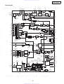
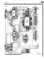
BLOCK DIAGRAM
7812
7912
CX023
(BLK)
GND_D
7805
BD9702
CX041
4P-PH
2412
CY041
4P-PH
(1)+5V_D1
(2)GND_D1
(3)+5V_DO
(4)GND_DO
CX081
7808
CX026
(WHT)
1U-3713-1
AUDIO UNIT
(1)+16V_MU
(2)GND_RL
(3)+12V_A
(4)GND_A
(5)㧙12V_A
(1)+16V_MU
(2)GND_RL
(3)+12V_A
(4)GND_A
(5)㧙12V_A
GND_A
CX024
(BLU)
CY051
5P-PH
CX051
5P-PH
CX035
BA033 +3.3V_D1
7805
(1)+5V_D1
(2)GND_D1
(3)+5V_DO
(4)GND_DO
(8)+12V_M1
(7)GND_M
(6)+8V_M1
(5)GND_M
(4)+5V_A
(3)GND_A
(2)+5V_B
(1)GND_B
CX054
CX082
BA033
1U-3714-2
POWER UNIT
+5V_D2
SO1L
(27)DIR_RST2
(26)ROM_RST
(25)VPP
(24)GND
(23)SPDIF
(22)GND
(21)MCLK
(20)GND
(19)DLINKCD
(18)DL_ON
(17)DIT_CE
(16)GND
(11)~(15)
(10)RST2
(19)DSCLK
(20)DSDI
(7)GND
(6)DSRST1
(5)DSCS1
(4)EXT/INT
(3)MUT1
(2MODE
(1)GND
(29)GND
(28)PCM_DATA
(27)PCM_LRCK
(26)GND
(25)PCM_BCK
(24)GND
(23)DSAL
(22)DSAR
(21)DSALS
(20)DSARS
(19)DSAC
(18)DSASW
(17)GND
(16)DSDBCK
(15)GND
(14) SEL4fs
(13)RST3
(12)DSD/PCM
(11)GND
(10)EXT_SEL
(9)~(7)AL_Test3
(9)~(7)AL_Test3/4/5
(6)~(1)OPEN
768FS
(1)+12V_M1
(2)GND_M
(3)+8V_M1
(4)GND_M
(5)+5V_A
(6)GND_A
(7)+5V_B
(8)GND_B
QQ
ucon
PLD
EPM3128
SPDIF
+5V_D1
Vout_+L
11A121
DBCK
DXP_RST
CX241
CX151
FAN8042
(Act Driv)
DVD DRIVE MECH
TD-5HP-D6-DE
1U-3624
SACD MODULE INIT
CY024
1U-3714-5
P.SW UNIT
CX052
11P FFC
(1)KEY2
(2)KEY1
(3)KEY0
(4)GND
(5)REMOCON
(6)GND
(7)FRRST
(8)FCS
(9)FCLK
(10)FDAT
(11)GND
AN8471
(Spi Driv)
ANALOG OUT
(24)DSDR
64fs
(1)PLRCK
Vout_+R
(2)PBCK
Vout_㧙R
3 7 6 3 1 5 1 5 0
DSD_CS
7WHCU04
DSD_RST
7WHCU04
DSD/DXP_DI
DSD/DXP_CL
33.8688MHz
Master
CLOCK
74HCT7007
COAX OUT
DIGITAL OUT
OPT OUT
74HCT7007
+5V_D1
CY111
1U-3413-4
H/P UNIT
1U-3713-3
MUT1
H/P UNIT
H/P VR
www
H/P OUT
CY042
4P-PH
(1)MUT1
(2)H/P_L
(3)GND_A
(4)H/P_R
.
(1)+5V_U
(2)GND_DISP
(3)㧙32V
(4)F+
(5)F㧙
(11)KEY2
||
(2)FDAT
(1)GND
JUMPER
x
CY052
5P-PH
CY112
<FL Display㧧15-BT-101GNK>
<KEY>
(Remocon)
+3.3V
i
CX112
(1)KEY2
(2)KEY1
(3)KEY0
(4)GND
(5)REMOCON
(6)GND
(7)FRRST
(8)FCS
(9)FCLK
(10)FDAT
(11)GND
a o y u 1 6 3
FL Driver ; M66005-0001AHP
BA330FP
(11)KEY2
(10)KEY1
(9)KEY0
(9)GND_+5V
(7)REMOTE
(6)GND_+5V
(5)FRES
(4)FCEN
(3)FCLK
(2)FDAT
(1)GND_5V
1U-3714-1
DISPLAY UNIT
19
http://www.xiaoyu163.com
MUT1
8 9 2 4 9 8 2 9 9
(4)DBCK
SCK
7SHU04
Rch
MODE
MODE
GAL_RST
(1)DIR_RST2(OPEN)
(2)ROM_RST(OPEN)
(3)VPP(OPEN)
(4)GND_D1
(5)SPDIF
(6)GND_D1
(7)MCLK
(8)GND_D1
(9)DSD_RST
(10)DL_ON(OPEN)
(11)DSD_CS
(12)GND_D1
(13)DSD/DXP_CL
(14)(DIR_INT(OPEN)
(15)DSD/DXP_DI
(16)DIR_DO(OPEN)
(17)DXP_CS
(18)RST2(OPEN)
(19)DXP_RST
(20)DIR_DI(OPEN)
(21)GND_D1
(22)DF_RST(OPEN)
(23)GAL_RST
(24)EXT/INT(OPEN)
(25)MUT1
(26)MODE
(27)GND_D1
1M
SRAM
(25)DSDL
GND_D1
Lch
Vout_㧙L
DARD
1㧛12
GAL16
CY271
27PFFC
16M
DRAM
CXD1881
(RF Amp)
157
DSAL
74HCT7007
+3.3V_D1
PURE
DIRECT
DSD1791
PBCK
M30625FGPGP
CXD1885
(F/E Prosessor)
LRCK
.
c o
m
CX042
4P-PH
376315150 892498299
376315150 892498299
1 3 9 4 2 2 9 6 5 1 3
DXP6001AF
+5V_A1
QQ
QQ
T E L
MCLK
CXD2753
(SACD Dec)
16M
SDRAM
5PZH (OPEN)
27PFFC
(1)CD_SEL
(2)DSD_NORM
(3)AL_Test3
(4)AL_Test4
(5)AL_Test5
29PFFC
+3.3V_D2
SO1R
13942296513
13942296513
CY291
29PFFC
(1)GND_D1
(2)PCM_DATA
(3)PCM_LRCK
(4)GND_D1
(5)PCM_BCK
(6)GND_D1
(7)DSAL
(8)DSAR
(9)DSALS(OPEN)
(10)DSARS(OPEN)
(11)DSAC(OPEN)
(12)DSASW(OPEN)
(13)GND_D1
(14)DSDBCK
(15)GND_D1
(16)SEL_4fs(OPEN)
(17)RST3(OPEN)
(18)DSD/PCM(OPEN)
(19)GND_D1
(20)EXTSEL(OPEN)
(21)~(23)(OPEN)
(24)~(29)(OPEN)
TEL
TEL
TRANS
(1)+5V_U
(2)GND_DISP
(3)㧙32V
(4)F+
(5)F㧙
11A121
11A121
http://www.xiaoyu163.com
DCD-1500AE
QQ 376315150 892498299
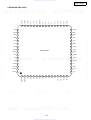
SEMICONDUCTORS
Only major semiconductors are shown, general semiconductors etc. are omitted to list.
主な半導体を記載しています。汎用の半導体は記載を省略しています。
1. IC’s
Note: Abbreviation ahead of IC No. indicates the name of P.W.B., etc.
注 ): IC No. の前の記号は、基板の名称を表します。
AD : AUDIO P.W.B.
PD : POWER/DISPLAY/HP P.W.B.
SM : SACD MODULE P.W.B.
CXD1885Q (SM: IC502)
Pin Assignment
AVDD33
DA0 (TSCON)
DA1 (SLED)
DA2 (FSCON)
DA3 (SLED2_TILT)
AVSS
FG
SPWM1
SPWM2
D/A
GPWM0
GPWM1
GPWM2
GPWM3
GPWM4
GPWM5
XLCAS
XUCAS
XMOE
RA11
RA10
DVSS
RA9
RA8
RA7
RA6
RA5
DVDD33
RA4
RA3
DVDD18
RA2
RA1
RA0
XRAS
XMWR
RD7
RD6
DVSS
RD5
RD4
RD3
RD2
RD1
RD0
RD15
RD14
RD13
RD12
RD11
RD10
DVDD18
PWM.FG
TEL
TEL
RD9
DRAM I/F
102 VREFH
101 AD9
TEST2 161
100 AD8
TEST3 162
99 AD7
TEST4 163
98 AD6
TEST5 164
97 AD5
TEST6 165
96 AD4
TEST7 166
95 AD3
TEST8 167
94 AVDD33
TEST9 168
93 AD2
TEST10 169
92 AD1
TEST11 170
91 AD0
TEST12 171
QQ 376315150 892498299
90 AVSS
TEL 13942296513
TEST13 172
89 AVSS
TEST14 173
88 RC
87 LPF2
MODSEL0 175
86 LPF1
MODSEL1 176
81 JMOUT
GIO2 181
80 JMREF
GIO3 182
79 AVDD33
DVDD33 183
78 IREF
GIO4 184
77 TLC1
GIO5 185
76 TLC0
GIO6 186
75 HF
GIO7 187
74 ATC
DVDD18 188
73 AVSS
GIO8 189
72 DTC
GIO9 190
71 MIRRORH
GIO10 191
70 HFD
GIO11 192
69 RFOKGH
GIO12 193
68 SCLKH
DVSS 194
67 SO
GIO13 195
66 SI
GIO14 196
65 CSL
GIO15 197
64 EXPLDT
GIO16 198
63 EXVCO
GIO17 199
62 BCK
GIO18 200
61 LRCK
GIO19 201
60 DOTK
TRST 202
59 DADT
TMS 203
58 C2PO
TDI 204
57 DRVRDY
TCK 205
56 DRVCLK
TDO 206
55 DRVRX
VMCHG 207
54 DRVTX
DVDD18 208
Clock
20
http://www.xiaoyu163.com
VSTEM I/F
DVDD18
DRVRST
DRVIRQ
DCK
XSHD
VEFG
XHAC
HDRQ
VDT0
VDT1
VDT2
VDT3
VDT4
VDT5
DVSS
VDT6
DVSS
VDT7
XO
XI
DVDD18
SYSCK
MINT
MRDY
xiaoy u163. com
B/E MCU I/F
.
MRD
DVDD33
MWR
MD7
MCS
MALE
MD6
DVSS
MD5
MD4
MD3
MD2
MD1
MD0
TESTSEL
MA8
MA0
9 10 11 12 13 14 15 16 17 18 19 20 21 22 23 24 25 26 27 28 29 30 31 32 33 34 35 36 37 38 39 40 41 42 43 44 45 46 47 48 49 50 51 52
MA7
MSEL1
8
MA6
MSEL0
7
MA5
ALCR
www
6
MA4
5
MA3
4
MA2
3
MA1
2
DVDD33
53 DVDD33
1
ASP S-I/O, Defect etc
82 CHG
GIO1 180
Audio D/A
General Port
83 VFBC
GIO0 179
VSTEM I/F
84 AVDD18
MODSEL2 178
Data PLL/Data Slicer
85 VCOI
DVSS 177
376315150 892498299
376315150 892498299
TEST15 174
JTAG
A/D
103 VREFL
TEST1 160
QQ
QQ
Test/Monitor Pin
104 AVDD18
RD8 158
TEST0 159
13942296513
13942296513
156 155 154 153 152 151 150 149 148 147 146 145 144 143 142 141 140 139 138 137 136 135 134 133 132 131 130 129 128 127 126 125 124 123 122 121 120 119 118 117 116 115 114 113 112 111 110 109 108 107 106 105
DVDD33 157
http://www.xiaoyu163.com
DCD-1500AE
QQ 376315150 892498299
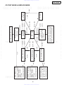
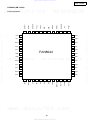
Block Diagram
16/4M DRAM
BCA
HFD
Data
Slicer
HF
ECC Core
Memory
manager
DVD
Demodulation
EDC
MPEG I/F
ASP
CD-ROM
Header Dec.
Spindle
TZC
TC
GIO
Servo
singnal
Direction
ROM/RAM
A/D
ICU
Data
RAM
Timer
Terminal Name
I/O
A/D
P
MCU I/F
MCU
ICU
Servo
control
X'tal
D/A
PWM
Peri. CLK
QQ 376315150 892498299
(A/D : Analog/Digital, PU : Pull-up, PD : Pull-down, SMT=Schumitt )
Classification
VDD & GND
Function
PU
PD
SMT
1
DVDD33
Digital 3.3V Power for I/O.
2
ALCR
I
D
MCU I/F
Chip select input. (L: Reset)
3
MSEL0
I
D
MCU I/F
MCU I/F mode select 0.
*
4
MSEL1
I
D
MCU I/F
MCU I/F mode select 1.
*
5
MA0
I/O
D
MCU I/F
MCU Address input 0 / data I/O 0 <LSB>.
*
6
MA1
I/O
D
MCU I/F
MCU Address input 1 / data I/O 1.
*
7
MA2
I/O
D
MCU I/F
MCU Address input 2 / data I/O 2.
*
8
MA3
I/O
D
MCU I/F
MCU Address input 3 / data I/O 3.
*
9
MA4
I/O
D
MCU I/F
MCU Address input 4 / data I/O 4.
*
10
MA5
I/O
D
MCU I/F
MCU Address input 5 / data I/O 5.
*
*
*
11
MA6
I/O
D
MCU I/F
MCU Address input 6 / data I/O 6.
*
12
MA7
I/O
D
MCU I/F
MCU Address input 7 / data I/O 7.
*
13
MA8
I
D
MCU I/F
MCU Address input 8 <MSB>.
*
14
TESTSEL
I
D
MCU I/F
TEST Select input.
*
15
MD0
I/O
D
MCU I/F
MCU data I/O 0 <LSB>.
*
16
MD1
I/O
D
MCU I/F
MCU data I/O 1.
*
17
MD2
I/O
D
MCU I/F
MCU data I/O 2.
*
18
MD3
I/O
D
MCU I/F
MCU data I/O 3.
*
19
MD4
I/O
D
MCU I/F
MCU data I/O 4.
*
20
MD5
I/O
D
MCU I/F
MCU data I/O 5.
*
21
DVSS
P
VDD & GND
Digital Ground.
22
MD6
I/O
D
MCU I/F
MCU data I/O 6.
*
23
MD7
I/O
D
MCU I/F
MCU data I/O 7 <MSB>.
*
24
MALE
I
D
MCU I/F
MCU Address latch signal input.
*
25
MCS
I
D
MCU I/F
MCU Chip Select signal input.
*
D
MCU I/F
MCU Write strobe signal.
*
VDD & GND
digital 3.3V Power. (for I/O )
www
26
MWR
27
DVDD33
28
MRD
29
MRDY
30
MINT
.
I
P
I
O
O
xiaoy u163. com
D
MCU I/F
MCU Read Strobe signal.
D
MCU I/F
MCU Ready signal. (L: Wait)
D
MCU I/F
MCU Interrupt signal. (L: Interrupt request)
21
http://www.xiaoyu163.com
*
376315150 892498299
376315150 892498299
TEL 13942296513
Audio
CMD/
RSP
reg.
QQ
QQ
Functions
VSTEM
DSP CLK/Mode
Audio I/F
DSP
Mecha
control
No.
Serial
Command
13942296513
13942296513
JTAG
ATC
VSTEM
Serial I/F
ASP Serial I/F
TEL
TEL
PWM
Video
CD-DSP (DDCD)
Data-PLL
http://www.xiaoyu163.com
DCD-1500AE
QQ 376315150 892498299
No.
31
Terminal Name
I/O
A/D
SYSCK
O
D
Clock
Classification
Clock Monitor output.
Function
VDD & GND
Digital 1.8V Power. (Internal logic system power)
I
D
Clock
Crystal oscillation input.
34
XO
O
D
Clock
Crystal oscillation output.
35
DVSS
P
VDD & GND
Digital Ground.
36
VDT7
O
D
VSTEM A/V
MPEG data output 7.
37
VTD6
O
D
VSTEM A/V
MPEG data output 6.
38
DVSS
P
39
VDT5
O
40
VDT4
41
VDT3
42
MPEG data output 5.
O
D
VSTEM A/V
MPEG data output 4.
O
D
VSTEM A/V
MPEG data output 3.
VDT2
O
D
VSTEM A/V
MPEG data output 2.
43
VDT1
O
D
VSTEM A/V
MPEG data output 1.
44
VDT0
O
D
VSTEM A/V
MPEG data output 0.
45
HDRQ
I
D
VSTEM A/V
MPEG data Request input.
46
XHAC
O
D
VSTEM A/V
Data Valid output.
47
VEFG
O
D
VSTEM A/V
ECC Error-sector Flag output. (L: error sector)
48
XSHD
O
D
VSTEM A/V
DVD Sector Head Flag output.
49
DCK
O
D
VSTEM A/V
Data Strobe output.
50
DRVIRQ
O
D
VSTEM Command
Interrupt Request output for Host. (L: interruption is demanded)
51
DRVRST
I
D
VSTEM Command
Drive H/W Reset input. (L: reset)
52
DVDD18
P
VDD & GND
Digital 1.8V power for Internal logic system.
53
DVDD33
P
VDD & GND
Digital 3.3V Power for I/O.
54
DRVTX
O
D
VSTEM Command
Transmitting serial data output to Host.
55
DRVRX
I
D
VSTEM Command
Reception serial data input from Host.
56
DRVCLK
I
D
VSTEM Command
Clock input from Host.
57
DRVRDY
O
D
VSTEM Command
Drive Ready signal output. (L: ready)
58
C2PO
O
D
Audio I/F
CD-DSP C2 Pointer output.
*
*
*
*
QQ
VSTEM A/V
SMT
59
DADT
O
D
Audio I/F
60
DOTX
O
D
Audio I/F
Digital audio output.
61
LRCK
O
D
Audio I/F
L/R Clock output.
62
BCK
O
D
Audio I/F
Audio Bit Clock output.
63
EXVCO
I
D
TEST/Monitor
External Channel clock input.
64
EXPLDT
I
D
TEST/Monitor
External RF data input. (Logic level)
65
CSL
O
D
ASP I/F
SIO for RF signal processing LSI control. Latch signal output.
66
SI
I
D
ASP I/F
SIO for RF signal processing LSI control. Serial data input.
67
SO
O
D
ASP I/F
SIO for RF signal processing LSI control. Serial data output.
68
SCLKH
O
D
ASP I/F
SIO for RF signal processing LSI control. Serial clock output.
69
RFOKGH
I
D
ASP I/F
RF O.K. Signal input.
*
70
HFD
I
D
ASP I/F
RF lack Signal input.
*
71
MIRRORH
I
D
ASP I/F
Mirror detected signal input.(H: Mirror detected)
*
72
DTC
I
D
ASP I/F
Track cross signal input. (Logic level input)
*
73
AVSS
P
VDD & GND
Analog Ground.
74
ATC
I
A
Data PLL
Track Cross signal input. (Analog level input)
75
HF
I
A
Data PLL
RF signal input.
76
TLC0
O
A
Data PLL
Asymmetry Charge-pump output 0.
77
TLC1
O
A
Data PLL
Asymmetry Charge-pump output 1
78
IREF
I
A
Data PLL
Reference current setting terminal for Asymmetry Circuit.
79
AVDD33
P
VDD & GND
Analog 3.3V Power.
80
JMREF
I
A
Data PLL
Reference current setting terminal for Jitter Monitor
81
JMOUT
O
A
Data PLL
Jitter Monitor output.
82
CHG
I
A
Data PLL
Reference current setting terminal for data PLL.
83
VFBC
I
A
Data PLL
VCO offset frequency setting terminal for data PLL.
84
AVDD18
P
85
VCOI
I
86
LPF1
O
87
LPF2
O
88
RC
I
89
AVSS
90
AVSS
91
AD0
www
.
P
P
I
Audio serial data output.
VDD & GND
Analog 1.8V Power.
A
Data PLL
VCO Control voltage input terminal for data PLL.
A
Data PLL
VCO Loop-filter connection terminal 1 for data PLL.
A
Data PLL
VCO Loop-filter connection terminal 2 for data PLL
A
Data PLL
VCO gain setting terminal for data PLL.
VDD & GND
Analog Ground.
VDD & GND
Analog Ground.
ADC
AD0 Input.
xiaoy u163. com
A
22
http://www.xiaoyu163.com
376315150 892498299
376315150 892498299
QQ 376315150 892498299
TEL 13942296513
13942296513
Digital Ground.
D
PD
TEL
VDD & GND
QQ
P
13942296513
DVDD18
XI
TEL
32
33
PU
http://www.xiaoyu163.com
DCD-1500AE
QQ 376315150 892498299
No.
92
Terminal Name
AD1
I/O
A/D
I
A
ADC
Classification
Function
A
ADC
AD2 Input.
VDD & GND
Analog 3.3V Power.
PU
95
AD3
I
A
ADC
AD3 Input.
96
AD4
I
A
ADC
AD4 Input.
97
AD5
I
A
ADC
AD5 Input.
98
AD6
I
A
ADC
AD6 Input.
99
AD7
I
A
ADC
AD7 Input.
100
AD8
I
A
ADC
AD8 Input.
101
AD9
I
A
ADC
AD9 Input.
102
VREFH
I/O
A
ADC
Max Reference Voltage input for ADC.
(Internal Reference Voltage mode, it will be an output state)
103
VREFL
I/O
A
ADC
Min Reference Voltage input for ADC.
(Internal Reference Voltage mode, it will be an output state)
104
AVDD18
P
VDD & GND
Analog 1.8V Power.
105
AVDD33
P
VDD & GND
Analog 3.3V Power.
106
DA0 (TSCON)
O
A
DAC
DA0 output. (Track Servo output)
107
DA1 (SLED)
O
A
DAC
DA1 output. (Sled Servo output)
108
DA2 (FSCON)
O
A
DAC
DA2 output. (Focus Servo output)
109
DA3 (SLED2_
TILT)
O
A
DAC
DA3 output. (Sled Servo / Tilt Servo output)
110
AVSS
P
VDD & GND
Analog Ground
111
FG
I
D
SPM
FG signal input.
112
SPWM1
O
D
SPM
Spindle motor PWM output 1.
113
SPWM2
O
D
SPM
Spindle motor PWM output 2.
114
GPWM0
O
D
General PWM
Multi-purpose PWM output 0.
115
GPWM1
O
D
General PWM
Multi-purpose PWM output 1.
116
GPWM2
O
D
General PWM
Multi-purpose PWM output 2.
117
GPWM3
O
D
General PWM
Multi-purpose PWM output 3.
118
GPWM4
O
D
General PWM
Multi-purpose PWM output 4.
119
GPWM5
O
D
General PWM
Multi-purpose PWM output 5.
120
XLCAS
O
D
DRAM I/F
DRAM LCAS output. (Low-Byte row address strobe output)
121
XUCAS
O
D
DRAM I/F
DRAM UCAS output. (Upper-Byte row address strobe output)
122
XMOE
O
D
DRAM I/F
DRAM output enable.
123
RA11
O
D
DRAM I/F
DRAM address output terminal 11.
124
RA10
O
D
DRAM I/F
DRAM address output terminal 10.
125
DVSS
P
VDD & GND
Digital Ground.
126
RA9
O
D
DRAM I/F
DRAM address output terminal 9.
127
RA8
O
D
DRAM I/F
DRAM address output terminal 8.
128
RA7
O
D
DRAM I/F
DRAM address output terminal 7.
129
RA6
O
D
DRAM I/F
DRAM address output terminal 6.
130
RA5
O
D
DRAM I/F
DRAM address output terminal 5.
131
DVDD33
P
VDD & GND
Digital 3.3V Power. (for I/O)
132
RA4
O
D
DRAM I/F
DRAM address output terminal 4.
133
RA3
O
D
DRAM I/F
DRAM address output terminal 3.
134
RA2
O
D
DRAM I/F
DRAM address output terminal 2.
135
RA1
O
D
DRAM I/F
DRAM address output terminal 1.
136
DVDD18
P
VDD & GND
Digital 1.8V Power. (for Internal Logic power)
137
RA0
O
D
DRAM I/F
DRAM address output terminal 0.
138
XRAS
O
D
DRAM I/F
DRAM RAS output. (Column address strobe output)
139
XMWR
O
D
DRAM I/F
DRAM Write enable.
140
RD7
I/O
D
DRAM I/F
DRAM data input/output terminal 7.
*
141
RD6
I/O
D
DRAM I/F
DRAM data input/output terminal 6.
*
142
DVSS
P
VDD & GND
Digital Ground.
143
RD5
I/O
144
RD4
I/O
145
RD3
I/O
146
RD2
I/O
147
RD1
148
RD0
149
RD15
150
RD14
TEL 13942296513
.
I/O
I/O
I/O
*
QQ 376315150 892498299
xiaoy u163. com
D
DRAM I/F
DRAM data input/output terminal 5.
*
D
DRAM I/F
DRAM data input/output terminal 4.
*
D
DRAM I/F
DRAM data input/output terminal 3.
*
D
DRAM I/F
DRAM data input/output terminal 2.
*
D
DRAM I/F
DRAM data input/output terminal 1.
*
D
DRAM I/F
DRAM data input/output terminal 0.
*
D
DRAM I/F
DRAM data input/output terminal 15.
*
D
DRAM I/F
DRAM data input/output terminal 14.
*
23
http://www.xiaoyu163.com
376315150 892498299
376315150 892498299
P
QQ
QQ
I
AVDD33
13942296513
13942296513
AD2
94
www
SMT
TEL
TEL
93
I/O
PD
AD1 Input.
http://www.xiaoyu163.com
DCD-1500AE
QQ 376315150 892498299
No.
Terminal Name
I/O
A/D
151
RD13
I/O
D
Classification
152
RD12
I/O
D
DRAM I/F
DRAM data input/output terminal 12.
*
153
RD11
I/O
D
DRAM I/F
DRAM data input/output terminal 11.
*
154
RD10
I/O
D
DRAM I/F
DRAM data input/output terminal 10.
*
155
RD9
I/O
D
DRAM I/F
DRAM data input/output terminal 9.
*
DRAM I/F
Function
DRAM data input/output terminal 13.
VDD & GND
Digital 1.8V Power. (for internal Logic system)
P
VDD & GND
Digital 3.3V power for I/O.
158
RD8
I/O
D
DRAM I/F
DRAM data input/output terminal 8.
159
TEST0
O
D
TEST/Monitor
TEST I/O 0.
160
TEST1
O
D
TEST/Monitor
TEST I/O 1.
161
TEST2
O
D
TEST/Monitor
TEST I/O 2.
162
TEST3
O
D
TEST/Monitor
TEST I/O 3.
163
TEST4
O
D
TEST/Monitor
TEST I/O 4.
164
TEST5
O
D
TEST/Monitor
TEST I/O 5.
165
TEST6
O
D
TEST/Monitor
TEST I/O 6.
TEL
166
TEST7
O
D
TEST/Monitor
TEST I/O 7.
167
TEST8
O
D
TEST/Monitor
TEST I/O 8.
168
TEST9
O
D
TEST/Monitor
TEST I/O 9.
13942296513
169
TEST10
O
D
TEST/Monitor
TEST I/O 10.
170
TEST11
O
D
TEST/Monitor
TEST I/O 11.
171
TEST12
O
D
TEST/Monitor
TEST I/O 12.
172
TEST13
O
D
TEST/Monitor
TEST I/O 13.
173
TEST14
O
D
TEST/Monitor
TEST I/O 14.
174
TEST15
O
D
TEST/Monitor
TEST I/O 15.
175
MODSEL0
I
D
TEST/Monitor
TEST mode select 0. (GND, under normal conditions)
D
TEST/Monitor
TEST mode select 1. (GND, under normal conditions)
VDD & GND
Digital Ground.
QQ
178
176
MODSEL1
I
177
DVSS
P
MODSEL2
I
D
TEST/Monitor
TEST mode select 2. (GND, under normal conditions)
QQ 376315150 892498299
179
GIO0
I/O
D
Multi-purpose
Multi-purpose port 0.
*
*
180
GIO1
I/O
D
Multi-purpose
Multi-purpose port 1.
*
*
181
GIO2
I/O
D
Multi-purpose
Multi-purpose port 2.
*
*
182
GIO3
I/O
D
Multi-purpose
Multi-purpose port 3.
*
*
183
DVDD33
VDD & GND
Digital 3.3V Power for I/O.
184
GIO4
I/O
D
General Port
Multi-purpose port 4.
*
*
185
GIO5
I/O
D
General Port
Multi-purpose port 5.
*
*
186
GIO6
I/O
D
General Port
Multi-purpose port 6.
*
*
187
GIO7
I/O
D
General Port
Multi-purpose port 7.
*
*
188
DVDD18
VDD & GND
Digital 1.8V Power for I/O. (for internal Logic system)
189
GIO8
I/O
D
General Port
Multi-purpose port 8.
190
GIO9
I/O
D
General Port
Multi-purpose port 9.
191
GIO10
I/O
D
General Port
192
GIO11
I/O
D
General Port
193
GIO12
I/O
D
General Port
Multi-purpose port 12.
194
DVSS
P
VDD & GND
Digital Ground.
195
GIO13
I/O
D
Multi-purpose
Multi-purpose port 13.
*
*
*
196
GIO14
I/O
D
General Port
Multi-purpose port 14.
*
*
*
197
GIO15
I/O
D
General Port
Multi-purpose port 15.
*
*
*
198
GIO16
I/O
D
General Port
Multi-purpose port 16.
*
*
199
GIO17
I/O
D
General Port
Multi-purpose port 17.
*
*
200
GIO18
I/O
D
General Port
Multi-purpose port 18.
*
*
201
GIO19
I/O
D
General Port
Multi-purpose port 19.
*
*
202
TRST
I
D
JTAG I/F
JTAG Reset input.
*
*
203
TMS
I
D
JTAG I/F
JTAG Mode Select input.
*
*
204
TDI
I
D
JTAG I/F
JTAG Data Input.
*
*
205
TCK
I
D
JTAG I/F
JTAG Clock input.
*
206
TDO
O
D
JTAG I/F
JTAG Data output.
207
VMCHG
I
D
MCU I/F
VSTEM / external MCU access selection terminal of system setting register for DSP. (L: VSTEM, H: external MCU)
208
DVDD18
VDD & GND
Digital 1.8V power for internal Logic system.
www
P
P
.
P
*
*
*
*
Multi-purpose port 10.
*
*
Multi-purpose port 11.
*
*
*
*
xiaoy u163. com
24
http://www.xiaoyu163.com
*
*
376315150 892498299
376315150 892498299
TEL 13942296513
*
QQ
P
SMT
13942296513
DVDD18
DVDD33
PD
*
TEL
156
157
PU
http://www.xiaoyu163.com
DCD-1500AE
QQ 376315150 892498299
CXD2753R (SM: IC401)
Pin Assignment
TEL
TEL
13942296513
13942296513
Block Diagram
www
.
xiaoy u163. com
25
http://www.xiaoyu163.com
376315150 892498299
376315150 892498299
QQ 376315150 892498299
QQ
QQ
TEL 13942296513
http://www.xiaoyu163.com
DCD-1500AE
QQ 376315150 892498299
Terminal Functions
Pin Name
I/O
Functions
1
VSC
-
It fixed to ground.( for Core)
2
XMSLAT
I
Latch input for µCOM serial communication.
3
MSCK
I
Shift clock input for µCOM serial communication.
4
MSDATI
I
Data input for µCOM serial communication.
5
VDC
-
+2.5V Power for Core.
6
MSDATO
O
Data output for µCOM serial communication. “Hi-Z” potential except the output mode.
7
MSREADY
O
Completion flag of output preparation for µCOM serial communication. “L” is outputted at the time of
completion.
8
XMSDOE
O
Output enable pin for µCOM serial communication. “L” is outputted at the time of MSDATO mode.
9
XRST
I
Reset pin. The whole IC is reset by at the time of “L” potential.
10
SMUTE
Ipd
Soft Mute. Soft mute of the audio output is carried out at the time of “H” potential.
It releases at the time of “L” potential.
I
Master Clock input.
-
It fixed to Ground. Ground for I/O.
13
EXCKO1
O
External output Clock 1.
14
EXCKO2
O
External output Clock 2.
15
LRCK
O
44.1kHz, 1Fs Clock output.
16
FRAME
O
Frame signal output.
13942296513
13942296513
MCKI
VSIO
-
+3.3V Power for I/O.
MNT0
O
Monitor output.
19
MNT1
O
Monitor output.
20
MNT2
O
Monitor output.
21
MNT3
O
Monitor output.
22
TESTO
O
Output terminal for a Test. (open)
23
TESTO
O
Output terminal for a Test.(open)
24
TESTO
O
Output terminal for a Test.(open)
25
TESTO
O
Output terminal for a Test.(open)
26
TCK
I
Clock input for a Test. It fixed to “L” potential.
27
TDI
Ipu
28
VSC
-
29
TDO
O
30
TMS
Ipu
Input pin(pull-up) for a Test.(open)
31
TRST
Ipu
Reset pin(pull-up) for a Test. Input the Power-on reset signal or fixed to “L” potential.
32
TEST1
I
Test input pin. It fixed to “L” potential.
33
TEST2
I
Test input pin. It fixed to “L” potential.
34
TEST3
I
Test input pin. It fixed to “L” potential.
35
VDC
-
+2.5V Power for CORE.
36
TESTO
O
Out put for TEST. It fixed to open.
37
XBIT
O
DST monitor.
38
SUPDT0
O
Supplementary data output. (LSB)
39
SUPDT1
O
Supplementary data output.
40
SUPDT2
O
Supplementary data output.
41
SUPDT3
O
Supplementary data output.
42
VSIO
-
Ground for I/O.
43
SUPDT4
O
Supplementary data output.
44
SUPDT5
O
Supplementary data output.
QQ 376315150 892498299
www
45
VDIO
46
SUPDT6
47
SUPDT7
48
XSUPAK
49
VSC
50
TESTO
.
Input pin(pull-up) for a Test.(open)
It fixed to Ground. Ground for CORE.
Output for a Test.(open).
xiaoy u163. com
-
+3.3V Power for I/O.
O
Supplementary data output.
O
Supplementary data output. (MSB)
O
Supplementary data Acknowledge output terminal.
-
Ground for CORE.
O
Output for TEST. (open)
26
http://www.xiaoyu163.com
376315150 892498299
376315150 892498299
VDIO
18
QQ
QQ
17
TEL 13942296513
TEL
TEL
11
12
http://www.xiaoyu163.com
DCD-1500AE
QQ 376315150 892498299
Pin Name
I/O
Functions
TESTI
I
Input for TEST. It fixed to “L” potential.
TESTO
O
Output for TEST. (open)
54
VDC
-
+2.5V Power for CORE.
55
DSADML
O
DSD Data output terminal for Lch Down Mix.
56
DSADMR
O
DSD Data output terminal for Rch Down Mix.
57
BCKASL
I
I/O selection terminal of the Bit clock for DSD data output. L=input (Slave), H=output (Master)
58
VSDSD
-
Ground terminal for DSD data output.
59
BCKAI
I
Bit clock input terminal for DSD data output.
Input a Bit clock into this terminal at the time of BCKASL=”L” potential.
60
BCKAO
O
Bit clock output terminal for DSD data output.
Bit clock output from this terminal at the time of BCKASL=”H” potential.
61
PHREFI
I
Reference phase signal input terminal for DSD output phase modulation.
62
PHREFO
O
Reference phase signal output terminal for DSD output phase modulation.
63
ZDFL
O
Lch zero-data detection flag (at the time of µcom setup).
It will be set to “H” if non-sound data continues 300 msecs.
64
DSAL
O
DSD data output terminal for Lch speaker.
65
ZDFR
O
Rch zero-data detection flag (at the time of µcom setup).
It will be set to “H” if non-sound data continues 300 msecs.
66
DSAR
O
DSD data output terminal for Rch speaker.
67
VDDSD
-
+3.3V Power for DSD data output.
68
ZDFC
O
Cch zero-data detection flag (at the time of µcom setup).
It will be set to “H” if non-sound data continues 300 msecs.
69
DSAC
O
DSD data output terminal for Cch speaker.
70
ZDFLFE
O
LFEch zero-data detection flag (at the time of µcom setup).
It will be set to “H” if non-sound data continues 300 msecs.
71
DSASW
O
DSD data output terminal for SWch speaker.
72
VSDSD
-
Ground for DSD data output.
73
ZDFLS
O
LSch zero-data detection flag (at the time of µcom setup).
It will be set to “H” if non-sound data continues 300 msecs.
74
DSALS
O
DSD data output terminal for LSch speaker.
75
ZDFRS
O
RSch zero-data detection flag (at the time of µcom setup).
It will be set to “H” if non-sound data continues 300 msecs.
76
DSARS
O
DSD data output terminal for RSch speaker.
77
VDDSD
O
+3.3V Power for DSD data output.
78
IOUT0
O
Data output terminal 0 for IEEE1394 link chip I/F.
79
IOUT1
O
Data output terminal 1 for IEEE1394 link chip I/F.
80
VSC
-
Ground for CORE.
81
IOUT2
O
Data output terminal 2 for IEEE1394 link chip I/F.
82
IOUT3
O
Data output terminal 3 for IEEE1394 link chip I/F.
83
VDC
-
+2.5V Power for CORE.
84
IOUT4
O
Data output terminal 4 for IEEE1394 link chip I/F.
85
IOUT5
O
Data output terminal 5 for IEEE1394 link chip I/F.
86
VSIO
-
Ground for I/O.
87
IANCO
O
Transmission information data output terminal for IEEE1394 link chip I/F.
88
IFULL
I
Data transmission hold request signal input terminal for IEEE1394 link chip I/F.
89
IEMPTY
I
High speed transmission request signal input terminal for IEEE1394 link chip I/F.
-
+3.3V Power for I/O.
90
VDIO
91
IFRM
www
92
IOUTE
93
IBCK
94
VSC
95
TESTI
96
TESTI
xiaoy u163. com
O
.
Frame reference signal output terminal for IEEE1394 link chip I/F.
O
Enable signal output terminal for IEEE1394 link chip I/F.
O
Data transmission clock output terminal for IEEE1394 link chip I/F.
-
Ground for CORE.
I
TEST input terminal. It fixed to “H” potential.
I
TEST input terminal. It fixed to “L” potential.
27
http://www.xiaoyu163.com
376315150 892498299
376315150 892498299
QQ 376315150 892498299
TEL 13942296513
QQ
53
QQ
Input for TEST. It fixed to “L” potential.
13942296513
52
13942296513
I
TEL
TESTI
TEL
51
http://www.xiaoyu163.com
DCD-1500AE
QQ 376315150 892498299
Pin Name
97
I/O
Functions
TEST input terminal. It fixed to “H” potential.
TESTO
O
TEST output terminal. (open)
99
VDC
-
+2.5V Power for CORE.
100
TESTI
I
TEST input terminal. It fixed to “L” potential.
101
TESTI
I
TEST input terminal. It fixed to “L” potential.
102
TESTI
I
TEST input terminal. It fixed to “L” potential.
103
TESTI
I
TEST input terminal. It fixed to “L” potential.
104
TESTI
I
TEST input terminal. It fixed to “L” potential.
105
TESTI
I
TEST input terminal. It fixed to “L” potential.
106
VSIO
-
Ground for I/O.
107
TESTI
I
TEST input terminal. It fixed to “L” potential.
108
TESTI
I
TEST input terminal. It fixed to “L” potential.
109
TESTI
I
TEST input terminal. It fixed to “L” potential.
110
VDIO
-
+3.3V Power for I/O.
111
WAD0
I
External A/D data input terminal(LSB) for PSP physical disc mark detection.
112
WAD1
I
External A/D data input terminal for PSP physical disc mark detection.
113
WAD2
I
External A/D data input terminal for PSP physical disc mark detection.
114
WAD3
I
External A/D data input terminal for PSP physical disc mark detection.
115
VSIO
-
Ground for I/O.
116
VSC
-
Ground for CORE.
117
WAD4
I
External A/D data input terminal for PSP physical disc mark detection.
118
WAD5
I
External A/D data input terminal for PSP physical disc mark detection.
119
WAD6
I
External A/D data input terminal for PSP physical disc mark detection.
120
WAD7
I
External A/D data input terminal(MSB) for PSP physical disc mark detection.
QQ 376315150 892498299
VDC
-
+2.5V Power for CORE.
122
TESTI
I
TEST input terminal. It fixed to “L” potential.
123
WCK
I
Operation clock for PSP physical disc mark detection.
124
WAVDD
-
+2.5V Power. A/D Power supply for PSP physical disc mark detection.
125
WAVDD
-
+2.5V Power. A/D Power supply for PSP physical disc mark detection.
126
WARFI
Ai
Analog RF signal input terminal for PSP physical disc mark detection.
127
WAVRB
Ai
A/D bottom reference terminal for PSP physical disc mark detection.
128
WAVSS
-
A/D Ground terminal for PSP physical disc mark detection.
129
WAVSS
-
A/D Ground terminal for PSP physical disc mark detection.
130
VSIO
-
Ground for I/O.
131
DQ7
I/O
SDRAM data input/output terminal. (MSB)
132
DQ6
I/O
SDRAM data input/output terminal.
133
DQ5
I/O
SDRAM data input/output terminal.
134
DQ4
I/O
135
VDIO
-
136
DQ3
I/O
SDRAM data input/output terminal.
137
DQ2
I/O
SDRAM data input/output terminal.
138
DQ1
I/O
SDRAM data input/output terminal.
139
DQ0
I/O
SDRAM data input/output terminal. (LSB)
140
VSIO
-
Ground for I/O.
141
DCLK
O
Clock output terminal for SDRAM.
DCKE
O
Clock enable output terminal for SDRAM.
O
Write enable output terminal for SDRAM.
O
Column address strobe output terminal for SDRAM.
O
Row address strobe output terminal for SDRAM.
142
www
143
XWE
144
XCAS
145
XRAS
146
VDIO
147
TESTO
148
A11
.
SDRAM data input/output terminal.
+3.3V Power for I/O.
xiaoy u163. com
-
+3.3V Power for I/O.
O
Output terminal for TEST. (open)
O
Address output terminal for SDRAM. (MSB)
28
http://www.xiaoyu163.com
376315150 892498299
376315150 892498299
TEL 13942296513
121
QQ
QQ
98
13942296513
13942296513
Ipu
TEL
TEL
TESTI
http://www.xiaoyu163.com
DCD-1500AE
QQ 376315150 892498299
Pin Name
149
I/O
A10
O
Functions
Address output terminal for SDRAM.
Ground for CORE.
O
Address output terminal for SDRAM.
152
A8
O
Address output terminal for SDRAM.
153
VDC
-
+2.5V Power for CORE.
154
A7
O
Address output terminal for SDRAM.
155
A6
O
Address output terminal for SDRAM.
156
A5
O
Address output terminal for SDRAM.
157
A4
O
Address output terminal for SDRAM.
158
VSIO
-
Ground for I/O.
159
A3
O
Address output terminal for SDRAM.
160
A2
O
Address output terminal for SDRAM.
161
A1
O
Address output terminal for SDRAM.
162
A0
O
Address output terminal for SDRAM. (LSB)
163
VDIO
-
+3.3V Power for I/O.
164
XSRQ
O
Output terminal of the Data Request signal inputted a front-end processor.
165
XSHD
I
Input terminal of the header Flag outputted from a front-end processor.
166
SDCK
I
Input terminal of the data conveyance Clock outputted from a front-end processor.
167
XASK
I
Input terminal of the data valid Flag outputted from a front-end processor.
168
SDEF
I
Input terminal of the error Flag outputted from a front-end processor.
169
SD0
I
Input terminal of the stream Data outputted from a front-end processor.
170
SD1
I
Input terminal of the stream Data outputted from a front-end processor.
171
SD2
I
Input terminal of the stream Data outputted from a front-end processor.
172
SD3
I
Input terminal of the stream Data outputted from a front-end processor.
QQ 376315150 892498299
SD4
I
Input terminal of the stream Data outputted from a front-end processor.
174
SD5
I
Input terminal of the stream Data outputted from a front-end processor.
175
SD6
I
Input terminal of the stream Data outputted from a front-end processor.
176
SD7
I
Input terminal of the stream Data outputted from a front-end processor.
Ipu: Pull-up input
www
Ipd: Pull-down input
.
Ai: Analog input
xiaoy u163. com
29
http://www.xiaoyu163.com
376315150 892498299
376315150 892498299
TEL 13942296513
173
QQ
QQ
-
A9
13942296513
13942296513
VSC
151
TEL
TEL
150
http://www.xiaoyu163.com
DCD-1500AE
QQ 376315150 892498299
M30625FGPGP (SM: IC739)
P11/D9
P12/D10
P13/D11
P14/D12
P15/D13/INT3
P16/D14/INT4
P17/D15/INT5
P20/A0(/D0/-)
P21/A1(/D1/D0)
P22/A2(/D2/D1)
P23/A3(/D3/D2)
P24/A4(/D4/D3)
P25/A5(/D5/D4)
P26/A6(/D6/D5)
P27/A7(/D7/D6)
VSS
P30/A8(/-/D7)
VCC
P12_0
P12_1
P12_2
P12_3
P12_4
P31/A9
P32/A10
P33/A11
P34/A12
P35/A13
P36/A14
P37/A15
P40/A16
P41/A17
P42/A18
P43/A19
P44/CS0
P45/CS1
P46/CS2
P47/CS3
Pin Assignment
M30625FGNGP Port Assignment
pin
function
I/O
Initial
mode
action
NOTE
VREF
AVCC
3
P97/ADTRG~/SIN4
P97
O
L
QQ 376315150 892498299
OPEN
DIR_RST2
4
P96/ANEX1/SOUT4
SOUT4
O
L
FDAT
DISPLAY DATA for FL DRIVER
5
P95/ANEX0/CLK4
CLK4
O
L
FCLK
DISPLAY CLOCK for FL DRIVER
6
P94/DA1/TB4IN
P94
O
L
DSRST1
RESET for DAC (DSD1791)
7
P93/DA0/TB3IN
P93
O
H
GAL_RST
RESET for GAL16V8
8
P92/TB2IN/SOUT3
P92
O
L
OPEN
OPEN
9
P91/TB1IN/SIN3
P91
I
H
USER1
MODEL SELECT 1 (10k P.U)
10
P90/TB0IN/CLK3
P90
O
L
OPEN
DL_ON
11
P14_1
O
L
OPEN
OPEN
O
H
DSCS1
CHIP SELECT for DAC (DSD1791)
12
P14_0
13
BYTE
BYTE
I
BYTE
PULL UP(8bit)
14
CNVss
CNVss
I
CNVSS
PULL DOWN (5.6k ohm)
15
P87/XCIN
P87
O
L
OPEN
CD_SEL (INTERNAL CD PLAY ONLT "H")
16
P86/XCOUT
P86
O
H
OPEN
DSD_NORM (NORMAL DSD MODE ONLY "H")
17
RESET~
RESET~
I
RESET
RESET INPUT
18
XOUT
XOUT
O
X.TAL
OSC OUT
19
VSS
VSS
-
VSS
GND
20
XIN
XIN
I
X.TAL
OSC IN
21
VCC
VCC
-
3.3V
POWER INPUT
22
P85/NMI~
P85
I
P_UP1
10K PULL UP(NON CONECT)
23
P84/INT2~
INT2~
I
IR_IN
IR INPUTSIGNAL (SHARP FORMAT)
24
P83/INT1~
INT1~
I
MINT
INT from CXD1885Q
25
P82/INT0~
INT0~
I
DRVIRQ
CXD1885Q DATA REQUEST
www
26
P81/TA4IN/U~
27
P80/TA4OUT/U
28
P77/TA3IN
29
P76/TA3OUT
30
P75/TA2IN/W~
31
P74/TA2OUT/W
.
xiaoy u163. com
P81
I
H
OPEN
DL_IDD (DL ID WRITE MODE DETECTION ("L":Write Mode)
TA4OUT
O
L
PWM
TRAY CONTROL PWM SIGNAL
P77
O
H
SELDSD
SELECT for DSD SIGNAL(PLD)
P76
O
H
SMUTE
MUTING for CXD2753R
P75
O
H
DSDRST
RESET for CXD2753R
P74
I
MSREADY
SERIAL DATA READY from CXD2753R
30
http://www.xiaoyu163.com
P.DN only
NOT USE
376315150 892498299
376315150 892498299
TEL 13942296513
2
QQ
QQ
1
port
13942296513
13942296513
VREF
AVCC
P97/ADTRG /SIN4
P96/ANEX1/SOUT4
P95/ANEX0/CLK4
P94/DA1/TB4IN
P93/DA0/TB3IN
P92/TB2IN/SOUT3
P91/TB1IN/SIN3
P90/TB0IN/CLK3
P14_1
P14_0
BYTE
CNVss
P87/XCIN
P86/XCOUT
RESET
XOUT
VSS
XIN
VCC
P85/NMI
P84/INT2
P83/INT1
P82/INT0
P81/TA4IN/U
P80/TA4OUT/U
P77/TA3IN
P76/TA3OUT
P75/TA2IN/W
P74/TA2OUT/W
P73/CTS2 /RTS2 /TA1IN/V
P72/CLK2/TA1OUT/V
P71/RXD2/SCL/TA0IN/TB5IN
P70/TXD2/SDA/TA0OUT
P67/TXD1
VCC
P66/RXD1
TEL
TEL
P12_5
P12_6
P12_7
P50/WRL /WR
P51/WRH /BHE
P52/RD
P53/BCLK
P13_0
P13_1
P13_2
P13_3
P54/HLDA
P55/HOLD
P56/ALE
P57/RDY /CLKOUT
P13_4
P13_5
P13_6
P13_7
P60/CTS0 /RTS0
P61/CLK0
P62/RXD0
P63/TXD0
P64/CTS1 /RTS1 /CTS0 /CLKS1
P65/CLK1
VSS
P10/D8
P07/D7
P06/D6
P05/D5
P04/D4
P03/D3
P02/D2
P01/D1
P00/D0
P11_7
P11_6
P11_5
P11_4
P11_3
P11_2
P11_1
P11_0
P107/AN7/KI3
P106/AN6/KI2
P105/AN5/KI1
P104/AN4/KI0
P103/AN3
P102/AN2
P101/AN1
AVSS
P100/AN0
http://www.xiaoyu163.com
DCD-1500AE
QQ 376315150 892498299
pin
port
I/O
Initial
32
P73/CTS2~/RTS2~/TA1IN/V~
P73
O
H
XMSLAT
SERIAL DATA LATCH for CXD2753R
33
34
P72/CLK2/TA1OUT/V
CLK2
O
H
MSCK
SERIAL DATA CLK for CXD2753R
P71/RXD2/SCL/TA0IN/TB5IN
RXD2
I
35
P70/TXD2/SDA/TA0OUT
TXD2
O
36
P67/TXD1
TXD1
RXD1
37
VCC
38
P66/RXD1
39
VSS
40
P65/CLK1
function
mode
action
NOTE
MSDATAO
SERIAL DATA INPUT from CXD2753R
PULL UP
H
MSDATAI
SERIAL DATA OUTPUT for CXD2753R
PULL UP
O
H
CD_LED
WRITE USE (22k P.U)
Flash(w:pull up)
I
H
WRITE USE (22k P.U)
Flash(w:pull up)
VCC
SA_LED
VSS
P65
I
H
PULL_DWN
5.1K PULL DOWN(NON CONECT)
Flash(w:pull down)
Flash(w:pull up)
41
P64/CTS1~/RTS1~/CTS0~/CLKS1
P64
O
H
DRVRST
RESET for CXD1885Q(RESET=L)
42
P63/TXD0
TXD0
O
H
DRVRX
SERIAL DATA for CXD1885Q
DRVTX
SERIAL DATA from CXD1885Q
H
DRVCLK
DATA CLOCK for CXD1885Q
RXD0
I
P61/CLK0
CLK0
O
45
P60/CTS0~/RTS0~
CTS0~
I
DRVRDY
DATA READY SIGNAL from CXD1885Q
46
P13_7
O
OPEN
New AL Test3
47
P13_6
O
OPEN
New AL Test4
48
P13_5
O
OPEN
New AL Test5
49
P13_4
CD_SEL
INTERNAL CD PLAY ONLT "H" (RESERVE)
50
P57/RDY~/CLKOUT
P57
I
MRDY
READY from CXD1885Q (NOT USE)
51
P56/ALE
P56
I
OPEN1
OPEN(anytime)
Flash(w:pull up)
52
P55/HOLD~
P55
I
P_UP2
10K PULL UP(NON CONECT)
Flash(w:GND)
53
P54/HLDA~
P54
54
P13_3
O
L
I
O
H
OPEN2
OPEN(must)
OPEN
DSPMOSI
P13_2
I
(L)
OPEN
DSPMISO
56
P13_1
O
L
OPEN
DSPSPICLK
O
H
P13_0
OPEN
DSPSPICS
58
P53/BCLK
P53
-
OPEN3
OPEN(must)
59
P52/RD~
P52
I
MRD
60
P51/WRH~/BHE~
P51
I
OPEN4
OPEN(must)
61
P50/WRL~/WR~
P50
I
MWR
WRITE STROBE for CXD1885Q(NOT USE)
62
P12_7
OPEN
BUSYEPROM
TEL 13942296513
I
(L)
QQ 376315150 892498299
READ STROBE for CXD1885Q(NOT USE)
63
P12_6
O
H
OPEN
VPP
64
P12_5
O
L
OPEN
ROMRST
65
P47/CS3~
CS3~
O
H
MCS
CHIP SELECT for CXD1885Q
66
P46/CS2~
P46
O
H
CLS_DRV
TRAY CLOSE DRIVE CONTROL
67
P45/CS1~
P45
O
H
OPN_DRV
TRAY OPEN DRIVE CONTROL
68
P44/CS0~
CS2~
O
H
MCS2
CHIP SELECT for 1M-SRAM
69
P43/A19
P43
O
L
OPEN
OPEN
70
P42/A18
P42
O
L
OPEN
OPEN
71
P41/A17
P41
O
L
OPEN
OPEN
72
P40/A16
A16
O
A16
ADRRES LINE
73
P37/A15
A15
O
A15
ADRRES LINE
74
P36/A14
A14
O
A14
ADRRES LINE
75
P35/A13
A13
O
A13
ADRRES LINE
76
P34/A12
A12
O
A12
ADRRES LINE
77
P33/A11
A11
O
A11
ADRRES LINE
78
P32/A10
A10
O
A10
ADRRES LINE
79
P31/A9
A9
O
A9
ADRRES LINE
80
P12_4
OPEN
SEL4fs
81
P12_3
82
P12_2
83
P12_1
84
P12_0
85
VCC
86
P30/A8(/-/D7)
87
VSS
www
O
.
L
xiaoy u163. com
O
L
OPEN
RST3
O
H
D_OUT
SPDIF SIGNAL LINE ON/OFF H: OUTPUT
O
L
OPEN
OPEN
O
L
OPEN
OPEN
VCC
-
---
3.3V
A8
O
A8
ADRRES LINE
VSS
-
---
GND
31
http://www.xiaoyu163.com
Flash(w:pull up)
376315150 892498299
376315150 892498299
57
QQ
QQ
55
13942296513
13942296513
P62/RXD0
44
TEL
TEL
43
http://www.xiaoyu163.com
DCD-1500AE
QQ 376315150 892498299
pin
port
function
I/O
Initial
mode
action
88
P27/A7(/D7/D6)
A7
O
A7
ADRRES LINE
89
P26/A6(/D6/D5)
A6
O
A6
ADRRES LINE
90
P25/A5(/D5/D4)
A5
O
A5
ADRRES LINE
91
P24/A4(/D4/D3)
A4
O
A4
ADRRES LINE
92
P23/A3(/D3/D2)
A3
O
A3
ADRRES LINE
93
P22/A2(/D2/D1)
A2
O
A2
ADRRES LINE
94
P21/A1(/D1/D0)
A1
O
A1
ADRRES LINE
95
P20/A0(/D0/-)
A0
O
96
P17/D15/INT5~
P17
O
97
P16/D14/INT4~
P16
98
P15/D13/INT3~
P15
A0
ADRRES LINE
L
OPEN
IIC CLK FOR EE_ROM(AT24C04N)
I/O
H
OPEN
IIC DATA FOR EE_ROM(AT24C04N)
I
(L)
OPEN
DIR_INT
NOTE
P14
I
OPN_SW
TRAY OPEN DETECT SW (P.U)
P13
I
CLS_SW
TRAY CLOSE DETECT SW (P.U)
Flash(w:pull up)
101
P12/D10
P12
I
FILTI
NOT USE(10k P/U)
(Low:384fs/Hi:192fs)
102
P11/D9
P11
O
L
OPEN
EXT/INT
103
P10/D8
P10
O
H
A_MUTE
MUTING (H:MUTE)
104
P07/D7
D7
I/O
D7
8bit DATA LINE
105
P06/D6
D6
I/O
D6
8bit DATA LINE
106
P05/D5
D5
I/O
D5
8bit DATA LINE
107
P04/D4
D4
I/O
D4
8bit DATA LINE
108
P03/D3
D3
I/O
D3
8bit DATA LINE
109
P02/D2
D2
I/O
D2
8bit DATA LINE
110
P01/D1
D1
I/O
D1
8bit DATA LINE
D0
I/O
D0
8bit DATA LINE
P11_7
I
(L)
OPEN
DIR_DO
113
P11_6
O
H
DSDI
DSD_DI
114
P11_5
O
115
P11_4
O
116
P11_3
O
117
P11_2
O
118
P11_1
O
TEL 13942296513
QQ
DXP_CS
L
DXP_RST
DXP/DSD_MDT
L
376315150 892498299
CHIP SELECT for DXP6001
RESET for DXP6001
DATA for DXP6001/DSD1791
DXP/DSD_MCK
DATA_CLOCK for DXP6001/DSD1791
OPEN
RST2
DSD/PCM
119
P11_0
O
L
OPEN
120
P107/AN7/KI3~
P107
O
H
MODE
CD/SACD SWITCHING SIGNAL(L:CD,SACD:H)
121
P106/AN6/KI2~
P106
O
L
FCS
DISPLAY CHIP SERECT for FL DRIVER
122
P105/AN5/KI1~
P105
O
H
OPEN
SM5819 INPUT SWITC (H,EXTSERECT)
123
P104/AN4/KI0~
P104
O
L
OPEN
DSD1792 RST
124
P103/AN3
P103
O
L
FRRST
DISPLAY DRIVER RESET
125
P102/AN2
AN2
I
KEY2
KEYS SENS
126
P101/AN1
AN1
I
KEY1
KEYS SENS
127
AVSS
AVSS
-
GND
AD GND
128
P100/AN0
AN0
I
KEY0
KEYS SENS
Ipu: Pull-up input
www
Ipd: Pull-down input
.
Ai: Analog input
xiaoy u163. com
32
http://www.xiaoyu163.com
376315150 892498299
376315150 892498299
P00/D0
QQ
QQ
111
112
RELAY/TR
13942296513
13942296513
P14/D12
P13/D11
TEL
TEL
99
100
http://www.xiaoyu163.com
DCD-1500AE
QQ 376315150 892.498. 299
M66005-0001AHP (PD: IC603)
BLOCK DIAGRAM
Display code RAM
CGROM
Bank 1 : 8bit x 16
Bank 2 : 8bit x 64
SEG02
SEG01
SEG00
Vcc2
SEG39
SEG38
DIG13
DIG12
DIG11
DIG10
DIG09
DIG08
DIG07
DIG06
DIG05
DIG04
49
50
51
52
53
54
55
56
57
58
59
60
61
62
63
64
M66005-0001AHP
32
31
30
29
28
27
26
25
24
23
22
21
20
19
18
17
SEG19
SEG20
SEG21
SEG22
code
write
dot data
write
SEG23
SEG24
CS 14
SEG25
SEG26
Vp
Serial
receive
circuit
SCK 15
SDATA 16
SEG27
SEG28
SEG29
SEG30
SEG31
SEG32
SEG33
XIN 21
Clock
generator
XOUT 20
timing
clock
.
33 SEG26
... 31... ...
SEG27
24 SEG34
23 SEG35
Segment/
Digit
select/
output
circuit
code
select
Display
controller
scan pulse
.
.
Digit
output
circuit
64 DIG12
63 DIG13
62 SEG38
61 SEG39
12 DIG00
.. .. ..
. . .
1 DIG11
Vcc1 19
2
Vcc2 60
18 P0
Vss 22
17 P1
Vp 32
PIN DESCRIPTIONS
Symbol
Comment
Pin name
Chip select input
SCK
Shift clock input
SDATA
Serial data input
XIN ,
Clock input
When use as a CR oscillator, connect external resistor andcapacitor.
XOUT
Clock output
When use an external clock, input external clock to XIN, and XOUT
must be opened.
DIG00~
DIG15
Digit output
Connect to digit (grid) pins of VFD.
SEG00~
SEG39
Segment output
Connect to segment (anode) pins of VFD. Pins from SEG00 to SEG39
correspond to segment pins of VFD as shown in the table below.
SEG36~SEG39 pins are common to DIG12~DIG15 pins. So, when use
SEG36~SEG39, the number of digit to be used isdecreased.
P1, P0
Universal port
P1 : bidirectional
P0 : output
Generally, use this port as the static output port.
This port also operateas s the timing IN/OUT port to control another
M66005A.
QQ 376315150 892498299
TEL 13942296513
When "L", communication with the MCU is possible.
When "H", any instruction from the MCU is neglected.
Serial input data is taken and shifted by the positive edge of SCK.
Vcc1
Positive power supply for internal logic.
Vcc2
Positive power supply for DIG and SEG outputs.
Vss
GND (0V)
Vp
Negative power supply to pull down.
Front view of VFD
( Connection of segment output pins )
00 01 02 03 04
Each square shows one-dot segment and the figure in
the square shows the output segment pin number
SEGnn (nn=00~39) to be connected.
SEG00~SEG34 are for character dot which are output
from character ROM or user RAM, and SEG35~SEG39
are the dot which is controlled by command.
www
.
05 06 07 08 09
10 11 12 13 14
xiaoy u163. com
15 16 17 18 19
20 21 22 23 24
25 26 27 28 29
30 31 32 33 34
35
38
33
http://www.xiaoyu163.com
39
376315150 892498299
376315150 892498299
CS
When "L", M66005A is initialized.
QQ
QQ
RESET
Reset input
13942296513
13942296513
..
.
.
.
CGRAM
(35bit x 16)
Code/
command
control
circuit
Segment
output
circuit
TEL
TEL
RESET 13
data
... 59... ...
SEG00
(35bit x 160)
http://www.xiaoyu163.com
DCD-1500AE
QQ 376315150 892498299
SDEN
SDATA
SCLK
V33
LCP
LCN
MNTR
CE
FE
TE
PI
V25
V125
TPH
DFT
LINK
CXD1881AR (SM: IC501)
48
47
46
45
44
43
42
41
40
39
38
37
36
35
34
33
MEV 50
31
MIN
VNA 51
30
MLPF
FNN 52
29
MB
FNP 53
28
MP
DIP 54
27
MIRR
DIN 55
26
LDON
25
VNB
24
CDPD
23
DVDPD
BYP 56
CXD1881AR
RFAC 57
VPA 58
COLD
21
DVDLD
ATON 61
20
VC
ATOP 62
19
VPB
RFSIN 63
18
CD_E
RFDC 64
17
CD_F
www
.
2
3
4
5
6
7
8
9
10
11
12
13
14
15
16
A2
B2
C2
D2
CP
CN
D
C
B
A
CD_D
CD_C
CD_B
CD_A
DVDRFP
1
DVDRFN
AIN 60
xiaoy u163. com
34
http://www.xiaoyu163.com
376315150 892498299
376315150 892498299
QQ 376315150 892498299
TEL 13942296513
22
AIP 59
QQ
QQ
MEVO
13942296513
13942296513
32
TEL
TEL
RX 49
http://www.xiaoyu163.com
DCD-1500AE
QQ 376315150 892498299
RFAC
59
DIP
AIP
60
DIN
AIN
61
FNN
ATON
62
FNP
ATOP
Block Diagram
53
52
55
54
57
FCCR b7-0
FBCR b6-0
CGR b1
OUTPUT INHIBIT
AGC
DVDRFP
1
DVDRFN
2
ATT
MUX
4
RFSIN 63
SIGR b3
INPUT
SEL
RFCR b5-4
INPUT IMP SEL
SSOUT
RFCR b7-6
INPUT IMP
SEL
56 BYP
AGCO
B
W/LPF
GCA
A 12
B+D
W/LPF
GCA
SIGR b2-0
12dB is added
@ high gain mode
(CDR b5=1)
GCA
LPF
GCA +/-4dB
4 FOCR b7-4
FS Gain
70kHz
40 FE
GCA
PIOR b4-0
5
PI offset
4
FOCR b3-0
FO Gain
Pll
Offset
cancel
LPF
38 PI
CTCR b7
BCA DET
TOPHLD
35 TPH
COMP
A+D
CD_C 14
GCA
9
GCA
CD_D 13
GCA
SEL
CBR b3-2
Buff
D
B+C
3
PDCR b3
CD/DVD
4D
SUM
SIGR b2-0
12dB is added
@ high gain mode
(CDR b5=1)
TOPHLD
RFCR b2-0
EQ
B2
4
GCA
EQ
42 MNTR
MON
SEL
CFR b2-0
CE-ATT
44 LCP
43 LCN
7 CP
8 CN
Comp.
MUX
PHASE
DETECTOR
SUB
Offset
cancel
LPF
GCA
EQ
D2
6
GCA
EQ
TRCR2 b7
CP/CN
Low lmp
PDCR b3
CD/DVD
PHASE
DETECTOR
VC
3
3
RFCR b2-0
TRCR2 b6-4
DPD EQ
CFR b7-5
TR Gain
for TE, FE & CE output ref.
V25/3 V25/2
36 V125
CDR b2
CHR b7-6
Mirr Defect
Comp ATT
AGCO
CDR b4
LD H/L
Btm Env
Dual APC
CDPD 24
2
BENV
Pll
DVDPD 23
MUX
VCI for servo input
VC
CDR b3
48 SDEN
SERIAL PORT
REGISTER
47 SDATA
46 SCLK
ATT
TOP HLD
MUX
ATT
TOP ENV
V33 for output buff
Offset
45 V33
BTM HLD
Btm clamp
& clip
Vref
BTM ENV
MUX
CGR b5-4
Gain CDR b7
LINKEN
CCR b7
DISK DET
MUX
http://www.xiaoyu163.com
27
58
19
51
25
VNB
MIN
35
33
VPB
MEVO
30
VNA
MEV
29
VPA
DVDLD
28
MIRR
31
LINK
32
MLPF
50
MB
21
MP
22
CDLD
xiaoy u163. com
26
37 V25
20 VC
CONTROL
Signals
2 To each block
MUX
MUX
.
TR offset
TRCR b6
DPD COMP HYS ON
MRCR b6-4
MRCR b7-0 Mirr Comp
droop rate ATT Level
control
CTCR b5-4
MEVO SEL
3
39 TE
3
TRCR b5-0
for PI output ref.
CCR b5
APC SEL
DVD/CD
www
CEFDB
GCA
5
TE
RST
GCA
6
C2
3
LPF
ATT
Pol sel.
buff (Ð12dB)
3
CDR b5
High Gain
TRCR2 b3-0
3B
12dB is added
@ high gain mode
(CDR b5=1)
PI
FE
TE
CE
V25
V125
V25/3
376315150 892498299
376315150 892498299
4
GCA
0-+8dB, 4bit
CFR b3
CEPOL
3
3
2
CAR b7-4
41 CE
TE MASK SEL
GCA
QQ
QQ
GCA
GCA
61 RFDC
SEL
PIOR b7-5
+3dB
+/-4dB
34 DFT
QQ 376315150 892498299
RESUM
GCA
A2
2
CBR b1-0
CGR b0
OUTPUT INHIBIT
4
CER b4-0
CE offset
TEL 13942296513
CD_F 17
Offset
cancel
TOPHLD
6dB is added
@ high gain mode
(CDR b5=1)
CD_E 18
DAC
2
CTCR b3-0 4
CO Gain
LDON
13942296513
C 10
+/-6dB, 4bit
Offset
cancel
13942296513
D
MUX
70kHz
A+C
W/LPF
GCA
CD_B 15
CCR b4-0
FE offset
5
C
B 11
Level
DAC
SUM
Amp.
AGC BTM ENV
TEL
CD_A 16
2
CAR b3-2
SIGDET
TEL
W/LPF
GCA
49 RX
Clamp
& Env
2
CAR b1-0
Env/Clamp TENV
A
AGC
CHARGE
PUMP
FULL WAVE
RECTIFIER
2
SIGR b7-4
ATT
2
PROGRAMMABLE
EQUALIZER
FILTER
DIFFERENTIATOR
INPUT
BIAS
HOLDEN
CDR b6
AGC HOLD
RFCR b3
http://www.xiaoyu163.com
DCD-1500AE
QQ 376315150 892498299
Terminal Function
Power Supply Pins
Name
I/O
Function
VPA
-
Power for RF and serial port
VPB
-
Power for servo
VNA
-
GND for RF and serial port
VNB
-
GND for servo
V33
-
Power for output buffer
V25
-
Reference Power for servo output
Input Pins
Name
I/O
Function
AIP,AIN
I
AGC amp. input
DIP,DIN
I
Analog input for RF single buffer
I
Photo detector interface input
A2,B2,C2,D2
I
Photo detector interface input
CD_A,B,C,D
I
CD photo detector interface input
CD_E,F
I
CD photo detector interface input
MIN
I
RF signal input for mirror
DVDPD
I
APC input
APC input
I
APC input ON/OFF (L:Open)
I
Link signal input (L:Open)
O
Mirror monitor output
TEL 13942296513
QQ 376315150 892498299
Output Pins
Name
I/O
ATOP,ATON
O
Function
Differential attenuator output
FNP,FNN
O
Differential normal output
RFAC
O
Single end normal output
RFDC
O
RF signal output
FE
O
Focus error signal output
TE
O
Tracking error signal output
CE
O
Center error signal output
MEVO
O
RFDDC bottom envelope output
DFT
O
Defect output
MIRR
O
Mirror detected output
PI
O
Pull-in signal output
DVDLD
O
APC output
CDLD
O
APC output
MNTR
O
Monitor output
Analog Pins
Name
www
I/O
BYP
CN
LCP
LCN
MP
xiaoy u163. com
-
CP
.
Function
RF AGC integration capacitor connecting terminal
-
Differential phase tracking LPF terminal
-
Differential phase tracking LPF terminal
-
Lens shift offset cancel LPF terminal
-
Lens shift offset cancel LPF terminal
-
MIRR top hold terminal
36
http://www.xiaoyu163.com
376315150 892498299
I
LDON
QQ
CDPD
376315150 892498299
A,B,C,D
13942296513
TEL
RF signal input
TEL
RF signal input
I
QQ
I
RFSIN
13942296513
DVDRFP,DVDRFN
http://www.xiaoyu163.com
DCD-1500AE
QQ 376315150 892498299
Name
I/O
Function
MB
-
MIRR bottom hold terminal
MEV
-
RFDC bottom envelope terminal
MLPF
-
Mirror LPF terminal
TPH
-
PI top hold terminal
VC
-
Reference voltage output
V125
-
Reference voltage output
RX
-
Reference resistor input
Serial Port Pins
Name
I/O
Function
I
SDATA
I/O
Serial data enable
Serial data
SCLK
I
Serial clock
TEL
TEL
SDEN
13942296513
13942296513
MSM51V18165F-50TSK-7 (SM: IC503)
NC
NC
WE
RAS
NC
NC
A0
A1
A2
A3
Vcc
12
13
14
15
16
17
18
19
20
21
22
TEL 13942296513
44
43
42
41
40
39
38
37
36
35
34
Vss
I/O15
I/O14
I/O13
I/O12
Vss
I/O11
I/O10
I/O9
I/O8
NC
33
32
31
30
29
28
27
26
25
24
23
NC
CASL
CASH
OE
A9
A8
A7
A6
A5
A4
Vss
QQ 376315150 892498299
Pin Descriptions
PIN NO.
PIN NAME
TYPE
18, 21, 24 ~29
A0~A9
Input
DESCRIPTION
Address Input
Row Address : A0~A9
Column Address : A0~A9
15
RAS
Input
Row Address Strobe
31
CASH
Input
Column Address Strobe/Upper Byte Control
32
CASL
Input
Column Address Strobe/Lower Byte Control
14
WE
Input
Write Enable
30
OE
Input
Output Enable
2~5, 7~10,
35~38, 40~43
xiaoy u163. com
I/O0~I/O15
Input/Output
1, 6, 22
Vcc
Supply
Power, (5V or 3.3V)
23, 39, 44
Vss
Ground
Ground
www
11~13, 16, 17,
33, 34
.
NC
-
Data Input/Output
No Connect
37
http://www.xiaoyu163.com
376315150 892498299
376315150 892498299
1
2
3
4
5
6
7
8
9
10
11
QQ
QQ
Vcc
I/O0
I/O1
I/O2
I/O3
Vcc
I/O4
I/O5
I/O6
I/O7
NC
http://www.xiaoyu163.com
DCD-1500AE
QQ 376315150 892498299
29 A6
28 A5
27 A4
26 VSS
A2 23
VDD 25
A3 24
30 A7
A1 22
31 A8
A0 21
A10/AP 20
33 N.C
32 A9
BA 19
34 CKE
CS 18
37 N.C/RFU
RAS 17
38 VDDQ
LDQM 14
36 UDQM
35 CLK
39 DQ8
VDDQ 13
CAS 16
40 DQ9
DQ6 11
DQ7 12
WE 15
41 VSSQ
VSSQ 10
44 VDDQ
43 DQ11
45 DQ12
VDDQ 7
42 DQ10
46 DQ13
DQ3 6
9
47 VSSQ
DQ2 5
DQ5
48 DQ14
4
VSSQ
49 DQ15
50 VSS
VDD 1
DQ0 2
DQ1 3
16M SDRAM (TSOP)-8 (DM: IC103, 104)
K4S161622D-TC80
W981616AH-8
DQ4 8
16M SDRAM (TSOP)-7/8 (SM: IC402)
(EM636165ST-7)
TEL
TEL
Terminal Function
Function
Power Supply/Ground
Data Input/Output
Data Input/Output
Data Output Power/Ground
Data Input/Output
Data Input/Output
Data Output Power/Ground
Data Input/Output
Data Input/Output
Data Output Power/Ground
Data Input/Output
Data Input/Output
Data Output Power/Ground
Data Input/Output Mask
Write Enable
Column Address Strobe
Row Address Strobe
TEL 13942296513
18
CS
Chip Select
19
20
21
22
23
24
25
26
27
28
29
30
31
32
33
34
35
36
37
38
39
40
41
42
43
44
45
46
47
48
49
50
BA
A10/AP
A0
A1
A2
A3
VDD
VSS
A4
A5
A6
A7
A8
A9
N. C
CKE
CLK
U DQM
N. C/RFU
VDDQ
DQ8
DQ9
VSSQ
DQ10
DQ11
VDDQ
DQ12
DQ13
VSSQ
DQ14
DQ15
VSS
Bank Select Address
Address
Address
Address
Address
Address
Power Supply/Ground
Power Supply/Ground
Address
Address
Address
Address
Address
Address
No Connection
Clock Enable
System Clock
Data Input/Output Mask
NC/Reserved
Data Output Power/Ground
Data Input/Output
Data Input/Output
Data Output Power/Ground
Data Input/Output
Data Input/Output
Data Output Power/Ground
Data Input/Output
Data Input/Output
Data Output Power/Ground
Data Input/Output
Data Input/Output
Power Supply/Ground
www
.
Power and ground for the input buffer and the core logic
Data input/output are mutiplexed on the same pin
Data input/output are mutiplexed on the same pin
Isolated power supply and ground for the output buffer
Data input/output are mutiplexed on the same pin
Data input/output are mutiplexed on the same pin
Isolated power supply and ground for the output buffer
Data input/output are mutiplexed on the same pin
Data input/output are mutiplexed on the same pin
Isolated power supply and ground for the output buffer
Data input/output are multiplexed on the same pin
Data input/output are multiplexed on the same pin
Isolated power supply and ground for the output buffer
Blocks data input when active
Enables write operation and row precharge
Latches column address on the positive going edge of the CLK at low
Latches row address on the positive going edge of the CLK at low
Disables or enables device operation by masking or enabling all
inputs except CLK, CKE, and LDQM
Selects bank to be activated during row address latch time
Row/column addresses are multiplexed on the same pin
Row/column addresses are multiplexed on the same pin
Row/column addresses are multiplexed on the same pin
Row/column addresses are multiplexed on the same pin
Row/column addresses are multiplexed on the same pin
Power and ground for the input buffer and the core logic
Power and ground for the input buffer and the core logic
Row/column addresses are multiplexed on the same pin
Row/column addresses are multiplexed on the same pin
Row/column addresses are multiplexed on the same pin
Row/column addresses are multiplexed on the same pin
Row/column addresses are multiplexed on the same pin
Row/column addresses are multiplexed on the same pin
No connect pin
Masks system clock to freeze operation from the next clock cycle
Active on the positive going edge to sample all inputs
Blocks data input when active
No connect pin
Isolated power supply and ground for the output buffer
Data input/output are multiplexed on the same pin
Data input/output are multiplexed on the same pin
Isolated power supply and ground for the output buffer
Data input/output are multiplexed on the same pin
Data input/output are multiplexed on the same pin
Isolated power supply and ground for the output buffer
Data input/output are multiplexed on the same pin
Data input/output are multiplexed on the same pin
Isolated power supply and ground for the output buffer
Data input/output are multiplexed on the same pin
Data input/output are multiplexed on the same pin
Power and ground for the input buffer and the core logic
QQ 376315150 892498299
xiaoy u163. com
38
http://www.xiaoyu163.com
376315150 892498299
376315150 892498299
VDD
DQ0
DQ1
VSSQ
DQ2
DQ3
VDDQ
DQ4
DQ5
VSSQ
DQ6
DQ7
VDDQ
L DQM
WE
CAS
RAS
Symbol
QQ
QQ
1
2
3
4
5
6
7
8
9
10
11
12
13
14
15
16
17
Pin Name
13942296513
13942296513
Pin No.
http://www.xiaoyu163.com
DCD-1500AE
QQ 376315150 892498299
DXP6001AF (AD: IC102)
23
33
34
22
44
12
1
11
DXP6001AF Terminal Function
Pin Name
I/O
Pin
No.
Description
- /Lambda-processor Lch 22nd bit Output *1, *2
O
- /Lambda-processor Lch 21st bit Output *1
27
O
- /Lambda-processor Lch 20th bit Output *1
28
VDD
-
Power Supply Terminal
29
SO2L/P19L
O
Test Setting Terminal 2 (Alpha-processor 1
30
SO1L
O
Lambda-processor Lch(+) Output
Output shifts 12-bit.)
31
SO1R
O
Lambda-processor Rch(+) Output
32
SO2R/P19R
O
33
O
37
-P20R
-P21R
-P22R
-P23R
-P24R
O
-/Lambda-processor Rch 20th bit Output *1
-/Lambda-processor Rch 21st bit Output *1, *2
-/Lambda-processor Rch 22nd bit Output *1, *2
-/Lambda-processor Rch 23rd bit Output *1, *2
-/Lambda-processor Rch 24th bit Output *1, *2
38
TEST1N
Ip
Test Terminal 1 (Alpha-processor 1 stops)
39
CKSLN
Ip
24
3
MLEN
Ip
Microcomputer Interface Latch Enable
25
4
RSTN
Ip
Reset Terminal
26
5
DLRCK
Ip
Audio Serial Input Data L/R Clock
6
VSS
-
Ground Terminal
7
DBCK
Ip
Audio Serial Input Bit Clock
QQ
Microcomputer Interface Clock
13942296513
Ip
9
TEST2N
Ip
th
Audio Serial Input Data
TEL 13942296513
10
TEST3N
Ip
Test Setting Terminal 3 (Alpha-processor 2
Output stops.)
Test Setting Terminal 4 (Lambda-processor
QQ
11
TEST4N
Ip
12
DFBCK
Ip
Lambda-processor Input Bit Clock
13
DFWCK
Ip
Lambda-processor Input Word Clock
14
DOL
Ip
Lambda-processor Input Data L-channel
15
DOR
Ip
Lambda-processor Input Data R-channel
16
LMOD
Ip
Lambda-processor Operation Mode Set
17
OMOD1
Ip
Output Mode Setting Terminal 1
Output stops.)
th
35
36
O
O
O
Ip
L
OMOD2
H
L
18bit
Alternate
20bit
Parallel
Lambda-processor Rch( ) Output/19 bit
Output *1
System Clock Select (384fs system /
256fs system)
40
CKDV1
Ip
OMOD1
OMOD2
Output *1
376315150 89249- 8299
34
Output Mode Setting Terminal 2
18
Lambda-processor Lch(-) Output /19 bit
System Clock Divider Select Terminal 1
System Clock Divider Select Terminal 2
H
24bit
Alternate
24bit
Parallel
41
CKDV2
Ip
L
CKDV2
H
19
INVIN
Ip
Lambda-processor Input Reversed
Polarity Terminal
20
BCKO
O
Lambda-processor Output Bit Clock
21
WCKO
O
Lambda-processor Output Word Clock
22
WCKO2
O
www
CKDV1
L
192fs (CKSLN=H)
256fs (CKSLN=H)
192fs (CKSLN=H)
256fs (CKSLN=H)
42
XTI
I
X-TAL Oscillator Input Terminal
43
XTO
O
X-TAL Oscillator Output Terminal
44
CKO
O
Clock Output Terminal
H
768fs
384fs
Lambda-processor Output Word Clock 2
(for Canceling OFFSET on 1DAC)
xiaoy u163. com
(Ip = Input Terminal with pull-up)
*1: Outputted on OMOD1=L (18-bit Alternate Output or 20 bit Parallel Output)
*2: Internal Signal is outputted on OMOD1=H (24-bit Alternate Output or 24 bit Parallel Output) and one of TEST1N, TEST2N, TEST3N
or TEST4N is set to L.
.
39
http://www.xiaoyu163.com
376315150 892498299
O
MCK
QQ
- /Lambda-processor Lch 23rd bit Output *1, *2
23
13942296513
O
Microcomputer Interface Data
Ip
376315150 892498299
- /Lambda-processor Lch 24th bit Output *1, *2
Ip
DDT
Description
O
MDT
8
I/O
-P24L
-P23L
-P22L
-P21L
-P20L
1
2
Pin Name
TEL
TEL
Pin
No.
http://www.xiaoyu163.com
DCD-1500AE
QQ 376315150 892498299
FAN8042 (SM: IC508)
42
41
40
39
PVCC1
43
PS
44
OPOUT2
VREF
45
OPIN2-
SVCC
46
OPIN2+
OPOUT1
47
GND
OPIN1-
48
GND
OPIN1+
Pin Assignments
38
37
IN1-
2
35
DO1-
OUT1
3
34
DO2+
IN2+
4
33
DO2-
IN2-
5
32
DO3+
GND
6
31
GND
GND
7
30
GND
OUT2
8
29
DO3-
IN3+
9
28
DO4+
IN3-
10
27
DO4-
OUT3 11
26
DO5+
12
25
DO5-
FAN8042
www
.
18
OUT4
CTL
FWD
REV
GND
19
20
21
22
23
24
PVCC2
17
TSD-M
16
MUTE4
15
MUTE123
14
SGND
13
IN4-
IN4+
GND
QQ 376315150 892498299
TEL 13942296513
xiaoy u163. com
40
http://www.xiaoyu163.com
376315150 892498299
376315150 892498299
DO1+
QQ
QQ
36
13942296513
13942296513
1
TEL
TEL
IN1+
http://www.xiaoyu163.com
DCD-1500AE
QQ 376315150 892498299
Pin Definitions
Pin Number
Pin Name
I/O
Pin Function Description
1
IN1+
I
CH1 op-amp input (+)
2
IN1-
I
CH1 op-amp input (-)
3
OUT1
O
CH1 op-amp output
4
IN2+
I
CH2 op-amp input (+)
5
IN2-
I
CH2 op-amp input (-)
6
GND
-
Ground
7
GND
-
Ground
8
OUT2
O
CH2 op-amp output
9
IN3+
I
CH3 op-amp input (+)
10
IN3-
I
CH3 op-amp input (-)
O
CH3 op-amp output
I
CH4 op-amp input (+)
13
IN4-
I
CH4 op-amp input (-)
14
OUT4
O
CH4 op-amp output
15
CTL
I
CH5 motor speed control
16
FWD
I
CH5 forward input
17
REV
I
CH5 reverse input
18
GND
-
Ground
19
GND
-
Ground
20
SGND
-
Signal Ground
21
MUTE123
I
Mute for CH1,2,3
MUTE4
I
Mute for CH4
23
TSD-M
O
TSD monitor
QQ 376315150 892498299
24
PVCC2
-
Power supply voltage 2 (For CH4,CH5)
25
DO5-
O
CH5 drive output (-)
26
DO5+
O
CH5 drive output (+)
27
DO4-
O
CH4 drive output (-)
28
DO4+
O
CH4 drive output (+)
29
DO3-
O
CH3 drive output (-)
30
GND
-
Ground
31
GND
-
Ground
32
DO3+
O
CH3 drive output (+)
33
DO2-
O
CH2 drive output (-)
34
DO2+
O
CH2 drive output (+)
35
DO1-
O
CH1 drive output (-)
36
DO1+
O
CH1 drive output (+)
37
PVCC1
-
Power supply voltage 1 (FOR CH1 CH2,CH3)
38
PS
I
Power save
39
OPOUT2
O
Normal op-amp2 output
40
OPIN2-
I
Normal op-amp2 input (-)
41
OPIN2+
I
Normal op-amp2 input (+)
42
GND
-
Ground
43
GND
-
Ground
44
VREF
I
Bias voltage input
45
SVCC
46
OPOUT1
47
OPIN1-
48
OPIN1+
www
.
-
Signal & OPAMPs supply voltage
xiaoy u163. com
O
Normal op-amp1 output
I
Normal op-amp1 input (-)
I
Normal op-amp1 input (+)
41
http://www.xiaoyu163.com
376315150 892498299
376315150 892498299
TEL 13942296513
QQ
QQ
22
13942296513
13942296513
OUT3
IN4+
TEL
TEL
11
12
http://www.xiaoyu163.com
DCD-1500AE
QQ 376315150 892498299
Block Diagram
SVCC
OPIN1OPIN1+
OPOUT1
VREF GND
48
47
46
45
44
43
GND
42
OPOUT2
OPIN2+
OPIN2PS
41
40
39
38
POWER
SAVE
IN1+ 1
10K
OUT1 3
10 K
10 K
IN2+ 4
35 DO1-
40K
40K
40K
10K
10 K
10K
33 DO2-
40K
40K
32 DO3+
5
10 K
10K
40K
6
31 GND
40K
40K
10K
40K
GND 7
30 GND
40K
10 K
IN3+ 9
10 K
10 K
IN3- 10
10 K
40K
40K
28 DO4+
27 DO4-
QQ 376315150 892498299
40K
OUT3 11
S
M
S
C
W
+
D
-
D
26 DO5+
IN4+ 12
25 DO5MUTE123
13
14
IN4- OUT4
15
16
CTL
FWD REV GND
17
18
19
20
21
MUTE4
TSD-M
22
23
24
GND SGND
MUTE4 TSD-M PVCC2
MUTE123
Note. Detailed circuit of the output power amp
40 K
10 K
Vref
DO+
+
From input opamp
10K
Pref
10K
40 K
40 K
+
DO-
10K
40K
Pref1 is almost PVCC1 / 2
Pref2 is almost PVCC2 / 2
www
.
xiaoy u163. com
42
http://www.xiaoyu163.com
376315150 892498299
376315150 892498299
TEL 13942296513
29 DO3-
QQ
QQ
OUT2 8
13942296513
13942296513
10 K
10 K
TEL
TEL
40K
GND
34 DO2+
10K
40K
IN2-
36 DO1+
40 K
2
IN1-
PVCC1
37
http://www.xiaoyu163.com
DCD-1500AE
QQ 376315150 892498299
AN8471SA (SM: IC505)
32
BC4
BC3
BC2
BC1
VPUMP
VLP
VM1
16
VDD
1
18
16 15
14
13
12
32
31
OSC
FG 10
Booster
Logic Circuit
FG2 20
Pin No.
17
Thermal
Protect
19 VM2
27 A11
Hall Amp
Matrix
H2L 4
Divider
H3H 3
24 A21
25 A22
21 A31
H3L 2
22 A32
PWMOUT
VHB 1
28 A12
Hall
Bias
23 CS2
Direction
SW
26 CS1
SRESET
EC 8
VT
Start/Stop
ECR 9
VCL
X5
CSOUT
17 GND
BMS 30
QQ 376315150 892498299
44
T14L1024N (SM: IC732)
www
.
xiaoy u163. com
43
http://www.xiaoyu163.com
376315150 892498299
376315150 892498299
TEL 13942296513
QQ
QQ
START 11
Function
Hall bias pin
Hall element 3 input (-)
Hall element 3 input (+)
Hall element 2 input (-)
Hall element 2 input (+)
Hall element 1 input (-)
Hall element 1 input (+)
Torque command input pin
Torque command ref. input pin
FG signal lout put pin (0.C)
Start/Stop switching pin
Booster pin
Booster cap. connecting pin 1
Torque command input pin 2
Torque command input pin 3
Torque command input pin 4
GND pin
Power pin
Motor power pin 2
3x FG signal output pin (0.C)
Drive output 3
Drive output 3
Current detect pin 2
Drive output 2
Drive output 2
Current detect pin 1
Drive output 1
Drive output 1
N.C.
Brake mode switching pin
Motor power pin 1
Pre-driver lower power
13942296513
13942296513
3ø Bridge
H2H 5
Pre-Driver
H1L 6
Pin Name
VHB
H3L
H3H
H2L
H2H
H1L
H1H
EC
ECR
FG1
START
VPUMP
BC1
BC2
BC3
BC4
GND
VDD
VM2
FG2
A31
A32
CS2
A21
A22
CS1
A11
A12
NC
BMS
VM1
VLP
TEL
TEL
H1H 7
1
2
3
4
5
6
7
8
9
10
11
12
13
14
15
16
17
18
19
20
21
22
23
24
25
26
27
28
29
30
31
32
http://www.xiaoyu163.com
DCD-1500AE
QQ 376315150 892498299
DSD1791DBR (AD: IC114)
PLRCK
PBCK
PDATA
DBCK
SCK
RST
VDD
DGND
AGNDF
VCCR
AGNDR
VOUTR–
VOUTR+
VCOM
MS
MC
MDI
DSDL
DSDR
ZEROL
ZEROR
VCCF
VCCL
AGNDL
VOUTL–
VOUTL+
AGNDC
VCCC
28
27
26
25
24
23
22
21
20
19
18
17
16
15
1
2
3
4
5
6
7
8
9
10
11
12
13
14
Block Diagram
PDATA
DSDL
DSDR
RST
VCOM
VOUTR+
D/S and Filter
System
Clock
Manager
VCCL
VCCR
AGNDL
VCCC
AGNDR
AGNDC
VCCF
Power Supply
VDD
SCK
ZEROR
AGNDF
Zero
Detect
DGND
ZEROL
GAL16V8 (AD: IC110)
clk
rst
www
.
xiaoy u163. com
count_out
44
http://www.xiaoyu163.com
376315150 892498299
376315150 892498299
VOUTR–
QQ
QQ
MS
Bias
and
Vref
QQ 376315150 892498299
Function
Control
I/F
MC
Advanced
Segment
DAC
Modulator
Current
Segment
DAC
and
I/V Buffer
TEL 13942296513
MDI
VOUTL+
D/S and Filter
8
Oversampling
Digital
Filter
and
Function
Control
DBCK
VOUTL–
13942296513
13942296513
Current
Segment
DAC
and
I/V Buffer
Audio
Data Input
I/F
PBCK
TEL
TEL
PLRCK
http://www.xiaoyu163.com
DCD-1500AE
QQ 376315150 892498299
BA33BC0FP-E2 (PD: IC604)
BD9702T (PD: IC905)
4
1 VCC
2 N.C
1 Vcc
3 OUT
1
2
2 OUT
3 GND
4 GND
3
4 INV
5 STBY
1 2 3 4 5
TC74VHC157FT (AD: IC111)
S-80843C (SM: IC733)
1
2
QQ 376315150 892498299
TEL 13942296513
2. TRANSISTORS
DTA114EK
DTC114EK
PNP
NPN
DTA Series
DTC Series
C
C
R1
R1
B
B
B
TOP
VIEW
DTA114EK
.
E
E
E
www
R2
R2
C
R1
10kohm
R2
10kohm
DTC114EK
R1
10kohm
xiaoy u163. com
45
http://www.xiaoyu163.com
R2
10kohm
376315150 892498299
376315150 892498299
Function
Voltage detection output terminal
Voltage input terminal
No Connect
GND Terminal
QQ
QQ
Pin Name
OUT
VDD
N.C.
VSS
13942296513
13942296513
3
TEL
TEL
No.
1
2
3
4
4
http://www.xiaoyu163.com
DCD-1500AE
QQ 376315150 892498299
3. FL DISPLAY
15-BT-101GNK (DI: FL601)
PIN CONNECTION
54 4 44 4 44 4 44
09 8 76 5 43 2 10
P P P P P P P PPPP
CONNECTION 3 2 2 2 2 2 2 2 2 1 1
6 7 6 54 3 2 1098
PIN NO.
3 3333 3 3 3 33 22 22 222 2 2211 1 11 11 11 1
9 8765 4 3 2 10 98 76 543 2 1098 7 65 43 21 09 87 6 543 2 1
PP P P P P P P
111
1 11
1 1 1 1 1 1 1 1 P P P P P P P P P N NN 5 4 3 1 2 3 4 5 6 7 8 9 0 1 2 NNN F
7 6 5 4 3 2 1 0 9 8 7 6 5 4 3 2 1 C C C G GG G G G G G G G G G G G G P P X +
1G
2G
3G
4G
5G
6G
7G
8G
[2G~14G]
3-2
11G 12G 13G 14G
5-1
4-1
4-2
15G
5-2
2-3
3-3
4-3
5-3
1-4
2-4
3-4
4-4
5-4
1-5
2-5
3-5
4-5
5-5
1-6
2-6
3-6
4-6
5-6
1-7
2-7
3-7
4-7
5-7
ANODE CONNECTION
www
.
xiaoy u163. com
46
http://www.xiaoyu163.com
376315150 892498299
376315150 892498299
QQ 376315150 892498299
1-3
QQ
QQ
2-2
10G
3-1
2-1
1-1
1-2
TEL 13942296513
9G
13942296513
13942296513
GRID ASSIGNMENT
TEL
TEL
NOTE 1) F-,F+ ---------- Filament
2) NP ------------- No pin
7) NC ------------ No connection
(NC pin should be electorically open on the PC board)
4) DL ------------ Datum line
5) 1G~15G ----- Grid
666555555555
PIN NO.
210987654321
PPPPPPPP
CONNECTION F N N N 2 2 3 3 3 3 3 3
- X PP 8 9 0 1 2 3 4 5
http://www.xiaoyu163.com
DCD-1500AE
QQ 3 7 6 3 1 5 1 5 0
8 9 2 4 9 8 2 9 9
PRINTED WIRING BOARDS
1U-3624 SACD MODULE P.W.B. UNIT
TEL
TEL
13942296513
13942296513
QQ
3 7 6 3 1 5 1 5 0
COMPONENT SIDE
www
.
x
i
8 9 2 4 9 8 2 9 9
FOIL SIDE
a o y u 1 6 3
47
http://www.xiaoyu163.com
.
c o
m
376315150 892498299
376315150 892498299
1 3 9 4 2 2 9 6 5 1 3
QQ
QQ
T E L
http://www.xiaoyu163.com
DCD-1500AE
QQ 3 7 6 3 1 5 1 5 0
8 9 2 4 9 8 2 9 9
1U-3713 AUDIO P.W.B. UNIT
TEL
TEL
13942296513
13942296513
www
.
x
i
QQ
3 7 6 3 1 5 1 5 0
a o y u 1 6 3
48
http://www.xiaoyu163.com
.
c o
m
8 9 2 4 9 8 2 9 9
COMPONENT SIDE
376315150 892498299
376315150 892498299
1 3 9 4 2 2 9 6 5 1 3
QQ
QQ
T E L
http://www.xiaoyu163.com
DCD-1500AE
QQ 3 7 6 3 1 5 1 5 0
8 9 2 4 9 8 2 9 9
TEL
TEL
13942296513
13942296513
www
.
x
i
QQ
3 7 6 3 1 5 1 5 0
a o y u 1 6 3
49
http://www.xiaoyu163.com
.
c o
m
8 9 2 4 9 8 2 9 9
FOIL SIDE
376315150 892498299
376315150 892498299
1 3 9 4 2 2 9 6 5 1 3
QQ
QQ
T E L
http://www.xiaoyu163.com
DCD-1500AE
QQ 3 7 6 3 1 5 1 5 0
8 9 2 4 9 8 2 9 9
1U-3714 POWER/DISPLAY/HP P.W.B. UNIT
TEL
TEL
13942296513
13942296513
www
.
x
i
QQ
3 7 6 3 1 5 1 5 0
a o y u 1 6 3
50
http://www.xiaoyu163.com
.
c o
m
8 9 2 4 9 8 2 9 9
COMPONENT SIDE
376315150 892498299
376315150 892498299
1 3 9 4 2 2 9 6 5 1 3
QQ
QQ
T E L
http://www.xiaoyu163.com
DCD-1500AE
QQ 3 7 6 3 1 5 1 5 0
8 9 2 4 9 8 2 9 9
TEL
TEL
13942296513
13942296513
www
.
x
i
QQ
3 7 6 3 1 5 1 5 0
a o y u 1 6 3
51
http://www.xiaoyu163.com
.
c o
m
8 9 2 4 9 8 2 9 9
FOIL SIDE
376315150 892498299
376315150 892498299
1 3 9 4 2 2 9 6 5 1 3
QQ
QQ
T E L
http://www.xiaoyu163.com
DCD-1500AE
QQ 376315150 892498299
NOTE FOR PARTS LIST
部品表について
•
Part indicated with the mark "nsp" are not always in stock and possibly to
take a long period of time for supplying, or in some case supplying of part
may be refused.
• When ordering of part, clearly indicate "1" and "I" (i) to avoid missupplying.
• Ordering part without stating its part number can not be supplied.
• Part indicated with the mark " ★ " is not illustrated in the exploded view.
• Not including Carbon Film Resister ±5%, 1/4W Type in the P.W.Board
parts list. (Refer to the Schematic Diagram for those parts.)
• Not including Carbon Chip Resister 1/16W Type in the P.W.Board parts
list. (Refer to the Schematic Diagram for those parts.)
WARNING:
Parts marked with this symbol ! have critical characteristics.
Use ONLY replacement parts recommended by the manufacturer.
1.nsp 印の部品は常時在庫していませんので供給に長時間を要すること
があります。
場合によっては、供給をお断りすることがあります。
2.部品を発注する際は特に数字の " 1 " と英字の "I" との区別をはっき
り記入してください。
3.部品番号を表示していない部品は供給できません。
4. ! 印の部品は安全上重要な部品です。交換するときは、安全および性
能維持のため必ず指定の部品をご使用ください。
5.★印のついている部品は分解図中には記載していません。
6.カーボン抵抗器± 5%、1/4W 型は記載していません。定数は回路図を
参照願います。
7.カーボンチップ抵抗器 1/16W 型は記載していません。定数は回路図を
参照願います。
8.部品表の抵抗器、コンデンサの品名記号の読み方は表を参照してくだ
さい。
l Resistors
Ex.:
: Carbon
: Composition
: Metal oxide film
: Winding
: Metal film
: Metal mixture
] Resistance
1 8 2
⇒
s
s
2B
2E
2H
3A
3D
3F
3H
: 1/8W
: 1/4W
: 1/2W
: 1W
: 2W
: 3W
: 5W
F
G
J
K
M
: ±1%
: ±2%
: ±5%
: ±10%
: ±20%
P
NL
NB
FR
F
14K
2E
RD
RC
RS
RW
RN
RK
: Pulse-resistant type
: Low noise type
: Non-burning type
: Fuse-resistor
: Lead wire forming
:
:
:
:
:
:
2B
2E
2H
3A
3D
3F
3H
∗
1800 ohm = 1.8 kohm
Indicates number of zeros after effective number.
2-digit effective number.
18
:
:
:
:
:
:
:
2
R
s
1.2 ohm
1-digit effective number.
2-digit effective number, decimal point indicated by R.
l Capacitors
1R
: Ceramic
: Oil
: Mica
: Metallized
: Metallized
s
R
2
s
1800
P
NL
NB
FR
F
:
:
:
:
:
=1.8k
F : ±1%
HS : High stability type
1A : 10V
G : ±2%
BP : Non-polar type
1C : 16V
1E : 25V
1V : 35V
J : ±5%
K : ±10%
M : ±20%
1H
2A
2B
2C
2D
2E
2H
2J
Z : +80%
–20%
P : +100%
–0%
C : ±0.25pF
D : ±0.5pF
= : Others
HR : Ripple-resistant type
DL : For change and discharge
HF : For assuring high
requency
U : UL part
C : CSA part
W : UL-CSA type
F : Lead wire forming
0J : 6.3V
: 50V
: 100V
: 125V
: 160V
: 200V
: 250V
: 500V
: 630V
⇒
2
1.2
Ö
1
2
QQ 376315150 892498299
] Capacity (electrolyte only)
2 2 2
⇒
2200µF
s
s
Indicates number of zeros after effective number.
2-digit effective number.
• Units: µF.
2
±1%
±2%
±5%
±10%
±20%
F :
G :
J :
K :
M:
0
CE
04W
1H
2R2
M
BP
Type Shape Dielectric Capacity Allowable Others
and per- strength
error
formance
CE : Aluminum foil
electrolytic
CA : Aluminum solid
electrolytic
CS : Tantalum electrolytic
CQ : Film
CK : Ceramic
CC
CP
CM
CF
CH
W
W
W
W
W
W
W
CE
CE
CA
CS
CQ
CK
CC
CP
CM
CF
CH
R
04W
:
:
:
:
:
:
:
:
:
:
1H
6.3
10
16
25
35
50
100
125
160
200
250
500
2R2
0J
1A
1C
1E
1V
1H
2A
2B
2C
2D
2E
2H
:
:
:
:
:
:
:
:
:
:
:
:
V
V
V
V
V
V
V
V
V
V
V
V
2J
: 630 V
M
±1%
±2%
±5%
±10%
±20%
+80%
−20%
P : +100%
− 0%
C : ±0.25pF
D : ±0.5pF
= :
F
G
J
K
M
Z
:
:
:
:
:
:
BP
HS
BP
HR
DL
HF
U
C
W
F
:
:
:
:
:
:
:
:
:
UL
CSA
UL-CSA
∗
22
2
Ö
2R
2200µF
2
Ö
0
2
2.2µF
1-digit effective number.
2-digit effective number, decimal point indicated by R.
2.2µF
1
2
µF
R
µF
• Units: µF.
22
] Capacity (except electrolyte)
2
s
2
2
s
www
• Units: pF.
2
s
2
1
s
• Units: pF.
2
Ö
⇒
2200pF=0.0022µF
(More than 2) Indicates number of zeros after effective number.
2-digit effective number.
22
1
Ö
220pF
(0
0
0
xiaoy u163. com
(0
2
)
2
pF
⇒
220pF
(0 or 1)
Indicates number of zeros after effective number.
2-digit effective number.
.
2200pF=0.0022µF
2
pF
AC
• When the dielectric strength is indicated in AC, "AC" is included after the dieelectric
strength value.
52
http://www.xiaoyu163.com
0
1
)
376315150 892498299
376315150 892498299
TEL 13942296513
• Units: ohm
Ex.:
FR
2
⇒
2
G
QQ
QQ
s
1/8
1/4
1/2
1
2
3
5
Ö
• Units: ohm
1
182
13942296513
13942296513
RD
RC
RS
RW
RN
RK
RN
TEL
TEL
RN 14K
2E
182
G
FR
Type Shape Power Resist- Allowable Others
and perance error
formance
http://www.xiaoyu163.com
DCD-1500AE
QQ 376315150 892498299
PARTS LIST OF P.W.B. UNIT
*本表に記載されている部品は、補修用部品のため製品に使用している部品とは一部、形状、寸法などが異なる場合があります。
* The parts listed below are for maintenance only, might differ from the parts used in the unit in appearances or dimensions.
* "nsp" 印の部品は常時在庫していませんので供給に長時間を要することがあります。場合によっては、供給をお断りする場合があります。
* Part indicated with the mark “nsp” are not always in stock and possibly to take a long period of time for supplying, or in some case supplying of part may be refused.
00D1U-3624C SACD MODULE P.W.B. UNIT ASS'Y
Ref. No.
nsp
Part No.
Part Name
Remarks
Q'ty
New
SEMICONDUCTORS GROUP
00D 262 3217 003
CXD2753R
+C
IC402
00D 262 2875 006
16M SDRAM(TSOP)-7/8 +C
IC403
00D 262 3195 905
AD8062-SO8
IC404
00D 262 3282 009
EMP3128ATC100-10(HARMONY-8LI)
IC501
00D 262 3219 001
CXD1881AR/BR
IC502
00D 262 3218 002
CXD1885Q
IC503
00D 262 3409 002
MSM51V18165F-50TSK-7
+C
+C
+C
AN8471SA
00D 262 3201 909
TC7WH08FU-TE12L
IC508
00D 262 3221 002
FAN8042
IC701,702
00D 262 2977 946
BA33BC0FP-E2
+REF
IC703
00D 262 2977 904
BA18BC0FP-E2
+C
IC704
00D 263 1182 900
NJM2391DL1-26-TE1
+REF
IC706,707
00D 262 3203 907
TC7SHU04F-TE85L
+REF
IC732
00D 262 3310 900
T14L1024N-12J(TAPE) +REF
IC733
00D 262 3206 904
S-80843CLNB-B64-T2 +C
IC739
00D 262 3529 018
M30625FGPGP-DE3112
+REF
+C
QQ 376315150 892498299
TR511,512
00D 272 0166 905
2SB798(DL/DK)-T1
+C
D501
00D 276 0778 900
1SS300-TE85L
+C
D701-704
00D 276 0717 903
1SS355 TE-17
+C
D731
00D 276 0717 903
1SS355 TE-17
+C
RESISTORS GROUP
RA401,402
00D 247 9003 908
MNR14=220JE0AB
RA501-504
00D 247 9007 917
MNR14=103JE0
+C
00D 257 0512 903
CK73F1E104ZT
00D 254 4464 964
CE67C0J470MT(MV)
+C
CAPACITORS GROUP
C403
nsp
C404
+1608
+REF
C405
nsp
00D 257 0512 903
CK73F1E104ZT
C406
nsp
00D 257 0501 901
CK73B1H103KT (1608) +1608
C407
nsp
00D 257 0512 903
CK73F1E104ZT
00D 254 4464 951
CE67C0J220MT(MV-B) +REF
C408-410
+1608
+1608
C411,412
nsp
00D 257 0512 903
CK73F1E104ZT
C413,414
nsp
00D 257 0502 942
CC73CH1H2R0CT
C415-419
nsp
00D 257 0512 903
CK73F1E104ZT
00D 254 4464 951
CE67C0J220MT(MV-B) +REF
C420
C421,422
www
C424-429
C430
C432-434
C436-438
C441
00D 257 0512 903
CK73F1E104ZT
00D 254 4464 951
CE67C0J220MT(MV-B) +REF
00D 257 0512 903
CK73F1E104ZT
00D 254 4603 958
CE67W1E101MT(P.CAP) +REF
nsp
00D 257 0512 903
CK73F1E104ZT
+1608
nsp
00D 257 0512 903
CK73F1E104ZT
+1608
00D 254 4464 951
CE67C0J220MT(MV-B) +REF
nsp
.
+1608
+1608
xiaoy u163. com
nsp
C423
+1608
+1608
+1608
53
http://www.xiaoyu163.com
*
376315150 892498299
376315150 892498299
TEL 13942296513
+C
QQ
QQ
00D 263 1109 909
IC507
13942296513
13942296513
IC505
TEL
TEL
IC401
http://www.xiaoyu163.com
DCD-1500AE
QQ 376315150 892498299
Ref. No.
nsp
Part No.
C442
nsp
00D 257 0512 903
CK73F1E104ZT
+1608
C446
nsp
00D 257 0509 929
CK73B1H102KT
+1608
C460
nsp
00D 257 0512 903
CK73F1E104ZT
+1608
00D 254 4603 958
CE67W1E101MT(P.CAP) +REF
C461
Part Name
C467
nsp
00D 257 0512 903
CK73F1E104ZT
+1608
C469
nsp
00D 257 0512 903
CK73F1E104ZT
+1608
00D 254 4464 964
CE67C0J470MT(MV)
C502
nsp
00D 257 0512 903
CK73F1E104ZT
C503
nsp
00D 257 0501 901
CK73B1H103KT (1608) +1608
C504
nsp
00D 257 0512 903
CK73F1E104ZT
+1608
C506
nsp
00D 257 0512 903
CK73F1E104ZT
+1608
00D 257 2012 906
CS77B1A475MT
+C
C501
C509
00D 257 0509 990
CK73B1H222KT +1608 CAPACITOR
C517-520
nsp
00D 257 0504 908
CC73CH1H220JT
+1608
00D 257 0516 954
CK73B1E104KT
+1608
nsp
00D 257 0510 934
CK73B1H472KT
+1608
C524
nsp
00D 257 0507 976
CC73CH1H331JT
C525,526
nsp
00D 257 0511 904
CK73F1H103ZT
C527
00D 254 4464 951
CE67C0J220MT(MV-B) +REF
C528
00D 254 4464 964
CE67C0J470MT(MV)
00D 257 0509 929
CK73B1H102KT
00D 254 4464 964
CE67C0J470MT(MV)
+1608
+1608
+REF
+1608
+REF
nsp
00D 257 0509 929
CK73B1H102KT
+1608
C532-535
nsp
00D 257 0516 954
CK73B1E104KT
+1608
C536
nsp
00D 257 0501 901
CK73B1H103KT (1608) +1608
C537
nsp
00D 257 0516 954
CK73B1E104KT
QQ 376315150 892498299
C538
nsp
00D 257 0501 901
CK73B1H103KT (1608) +1608
C539
nsp
00D 257 0506 993
CC73CH1H151JT
C540
nsp
00D 257 0509 929
CK73B1H102KT
+1608
C541
nsp
00D 257 0512 903
CK73F1E104ZT
+1608
00D 254 4464 906
CE67C0J101MT
+REF
C546,547
nsp
00D 257 0512 903
CK73F1E104ZT
+1608
C548
nsp
00D 257 0511 904
CK73F1H103ZT
+1608
00D 254 4465 918
CE67C1C470MT
C545
C549
+1608
+REF
C550
nsp
00D 257 0512 903
CK73F1E104ZT
+1608
C551
nsp
00D 257 0521 907
CK73B1A105KT
+1608
C554
nsp
00D 257 0516 954
CK73B1E104KT
+1608
C555
nsp
00D 257 0512 903
CK73F1E104ZT
+1608
00D 254 4464 951
CE67C0J220MT(MV-B) +REF
nsp
00D 257 0512 903
CK73F1E104ZT
00D 254 4464 951
CE67C0J220MT(MV-B) +REF
00D 257 0501 901
CK73B1H103KT (1608) +1608
C558
C559
C560
C561
nsp
+1608
C562
nsp
00D 257 0516 941
CK73B1E473KT
+1608
C563,564
nsp
00D 257 0511 904
CK73F1H103ZT
+1608
00D 254 4464 951
CE67C0J220MT(MV-B) +REF
nsp
00D 257 0511 904
CK73F1H103ZT
00D 254 4464 951
CE67C0J220MT(MV-B) +REF
nsp
00D 257 0512 903
CK73F1E104ZT
C569,570
00D 254 4645 903
CE67C0J221MT(MVA)
C571
00D 254 4464 951
CE67C0J220MT(MV-B) +REF
C565
C566
C567
C568
www
+1608
+1608
+REF
xiaoy u163. com
C572,573
nsp
00D 257 0511 904
CK73F1H103ZT
+1608
C575,576
nsp
00D 257 0511 904
CK73F1H103ZT
+1608
C578
nsp
00D 257 0511 904
CK73F1H103ZT
+1608
nsp
00D 257 0511 904
CK73F1H103ZT
+1608
C580
C581
C582,583
.
nsp
00D 257 0516 941
CK73B1E473KT
+1608
nsp
00D 257 0511 904
CK73F1H103ZT
+1608
54
http://www.xiaoyu163.com
376315150 892498299
376315150 892498299
TEL 13942296513
+1608
QQ
QQ
C531
13942296513
13942296513
nsp
C522,523
TEL
TEL
C521
C530
New
+REF
nsp
nsp
Q'ty
+1608
C513-516
C529
Remarks
http://www.xiaoyu163.com
DCD-1500AE
QQ 376315150 892498299
Ref. No.
nsp
Part No.
Part Name
C587
nsp
00D 257 0512 903
CK73F1E104ZT
C588
nsp
00D 257 0507 976
CC73CH1H331JT
C589
nsp
00D 257 0520 908
CK73B1A154KT
00D 254 4464 951
CE67C0J220MT(MV-B) +REF
C590
+1608
nsp
00D 257 0507 976
CC73CH1H331JT
nsp
00D 257 0508 917
CC73CH1H471JT +1608 CAPACITOR
+1608
C593
nsp
00D 257 0520 908
CK73B1A154KT
C594
nsp
00D 257 0508 917
CC73CH1H471JT +1608 CAPACITOR
+1608
nsp
00D 257 0516 954
CK73B1E104KT
+1608
C596
nsp
00D 257 0511 904
CK73F1H103ZT
+1608
C597
nsp
00D 257 0506 951
CC73CH1H101JT
C598,599
nsp
00D 257 0516 909
CK73B1E223KT
+1608
C600-602
nsp
00D 257 0511 904
CK73F1H103ZT
+1608
C604-606
nsp
00D 257 0511 904
CK73F1H103ZT
+1608
C607
nsp
00D 257 0512 903
CK73F1E104ZT
+1608
00D 254 4464 951
CE67C0J220MT(MV-B) +REF
+1608
nsp
00D 257 0512 903
CK73F1E104ZT
+1608
C615
nsp
00D 257 0509 929
CK73B1H102KT
+1608
C616
nsp
00D 257 0512 903
CK73F1E104ZT
+1608
00D 254 4575 905
CE67C1A330MT
00D 257 0511 904
CK73F1H103ZT
00D 254 4464 951
CE67C0J220MT(MV-B) +REF
00D 257 0511 904
CK73F1H103ZT
00D 254 4464 951
CE67C0J220MT(MV-B) +REF
nsp
C621
C622-625
nsp
C629,630
+REF
+1608
+1608
00D 257 0510 950
CK73B1H682KT
+1608
nsp
00D 257 0509 929
CK73B1H102KT
+1608
C634,635
nsp
00D 257 0506 951
CC73CH1H101JT
C636
nsp
00D 257 0501 901
CK73B1H103KT (1608) +1608
C637
nsp
00D 257 0511 904
CK73F1H103ZT
+1608
C639
nsp
00D 257 0510 950
CK73B1H682KT
+1608
C701-704
nsp
00D 257 0512 903
CK73F1E104ZT
+1608
00D 254 4464 906
CE67C0J101MT
+REF
00D 257 0512 903
CK73F1E104ZT
+1608
00D 254 4464 906
CE67C0J101MT
+REF
00D 257 0512 903
CK73F1E104ZT
+1608
00D 259 0015 901
NFM41CC223R2A3L
00D 257 0512 903
CK73F1E104ZT
+1608
00D 254 4464 906
CE67C0J101MT
+REF
00D 257 0512 903
CK73F1E104ZT
+1608
00D 254 4464 906
CE67C0J101MT
+REF
00D 257 0512 903
CK73F1E104ZT
+1608
00D 254 4464 906
CE67C0J101MT
+REF
00D 257 0512 903
CK73F1E104ZT
+1608
00D 254 4464 951
CE67C0J220MT(MV-B) +REF
00D 257 0512 903
CK73F1E104ZT
+1608
00D 254 4464 906
CE67C0J101MT
+REF
TEL 13942296513
C705
C706
nsp
C707
C708
nsp
C709
C710
nsp
C713
C714
nsp
C715
C716
nsp
C721-723
C724
nsp
C725
C726
nsp
C727
QQ 376315150 892498299
+1608
+C
C728
nsp
00D 257 0511 904
CK73F1H103ZT
+1608
C729,730
nsp
00D 257 0512 903
CK73F1E104ZT
+1608
C731
nsp
00D 257 0501 901
CK73B1H103KT (1608) +1608
00D 254 4464 951
CE67C0J220MT(MV-B) +REF
00D 257 0512 903
CK73F1E104ZT
00D 254 4464 951
CE67C0J220MT(MV-B) +REF
00D 257 0512 903
CK73F1E104ZT
00D 254 4464 951
CE67C0J220MT(MV-B) +REF
C732
www
C735
C739
C740
C742
C743,744
xiaoy u163. com
nsp
C736
.
nsp
nsp
+1608
+1608
00D 259 0015 901
NFM41CC223R2A3L
00D 257 0512 903
CK73F1E104ZT
+C
+1608
55
http://www.xiaoyu163.com
376315150 892498299
376315150 892498299
nsp
C633
QQ
QQ
C631,632
13942296513
13942296513
C612
TEL
TEL
C595
C619,620
New
+1608
C592
C618
Q'ty
+1608
C591
C608,609
Remarks
http://www.xiaoyu163.com
DCD-1500AE
QQ 376315150 892498299
Ref. No.
nsp
Part No.
00D 254 4464 951
CE67C0J220MT(MV-B) +REF
nsp
00D 257 0512 903
CK73F1E104ZT
00D 259 0015 901
NFM41CC223R2A3L
nsp
00D 257 0512 903
CK73F1E104ZT
00D 254 4464 951
CE67C0J220MT(MV-B) +REF
nsp
00D 257 0512 903
CK73F1E104ZT
+1608
+1608
C745
C746
C748-750
C751-753
C760
C761,762
Part Name
Remarks
Q'ty
New
+1608
+C
+1608
C769
nsp
00D 257 0512 903
CK73F1E104ZT
C770,771
nsp
00D 257 0511 904
CK73F1H103ZT
+1608
C772
nsp
00D 257 0512 903
CK73F1E104ZT
+1608
C773
nsp
00D 257 0511 904
CK73F1H103ZT
+1608
C774
nsp
00D 257 0512 903
CK73F1E104ZT
+1608
OTHERS PARTS GROUP
5P PH CON.BASE(L)
00D 205 1314 905
11P FFC.BASE(9616SAA +REF
+REF
CX112
nsp
00D 205 1257 949
11P FFC BASE (9610SD
CX151
nsp
00D 205 1224 901
15P FFC BASE(P=1.0)L +REF
CX241
nsp
00D 205 1152 905
24P FFC BASE(FLZ-SM1 +REF
CX271
nsp
00D 205 1314 918
27P FFC.BASE(9616SAA +REF
CX291
nsp
00D 205 1314 921
29P FFC.BASE(9616SAA +REF
CY082
nsp
00D 205 0863 981
8P PH CON.BASE(L)
FB501
nsp
+REF
CHIP EMIFIL(11A121) +1608
00D 235 0160 902
FB M J2125HM330-T
FB506,507
00D 235 0130 903
CHIP EMIFIL(11A121) +1608
FB703
00D 235 0136 907
FBMJ1608HS280NT
FB704,705
00D 235 0160 902
FB M J2125HM330-T
+C
FB706
00D 235 0136 907
FBMJ1608HS280NT
+1608
FB707,708
00D 235 0160 902
FB M J2125HM330-T
+C
FB711
00D 235 0136 907
FBMJ1608HS280NT
+1608
X731
00D 399 0887 903
CSTCE16MOV53-R0
+2125
TEL 13942296513
www
.
+C
QQ 376315150 892498299
+1608
xiaoy u163. com
56
http://www.xiaoyu163.com
376315150 892498299
376315150 892498299
00D 235 0130 903
FB502-505
QQ
QQ
00D 205 0863 952
nsp
13942296513
13942296513
nsp
CX111
TEL
TEL
CX052
http://www.xiaoyu163.com
DCD-1500AE
QQ 376315150 892498299
00D1U-3713 AUDIO P.W.B. UNIT ASS'Y
Ref. No.
nsp
Part No.
Part Name
Remarks
Q'ty
New
SEMICONDUCTORS GROUP
IC101
00D 262 3077 900
TC74VHCU04FT
IC102
00D 262 2531 007
DXP6001AF
+REF
IC103
00M HC0 0800 5KY
TC7WHU04FU TRIPLE INVERTER
IC104,105
00D 262 3555 901
SA5532ADR
IC106
00D 262 2376 903
TC74HCT7007AF(TP1) +C
IC107
00D 262 0864 006
UPC4570C
IC108
00D 262 3203 907
TC7SHU04F-TE85L
+C
+T
+REF
IC109
00D 262 2376 903
TC74HCT7007AF(TP1) +C
IC110
00D 262 3528 006
GAL16V8D-15LPN-DE01
IC111
00D 262 3198 902
TC74VHC157FT-EL
IC112
00D 263 1048 002
BA033T
00D 262 2376 903
TC74HCT7007AF(TP1) +C
IC114
00D 262 3299 908
DSD1791DBR
00D 262 3555 901
SA5532ADR
+C
DTA114EKT96
+C
TR103
00D 269 0082 902
DTC114EKT96
+C
TR104,105
00D 273 0460 905
KTC2875B-RTK
TR106
00D 269 0083 901
DTA114EKT96
+C
TR107
00D 269 0082 902
DTC114EKT96
+C
TR108,109
00D 273 0460 905
KTC2875B-RTK
D100
00D 276 0553 905
1SR35-200A(T93X)
TEL 13942296513
+C
QQ 376315150 892498299
+C
RESISTORS GROUP
R263,264
00D 241 2472 965
RD14B2E104JT(AMRS)
R266
00D 244 2043 953
RS14B3A471JNBST(S)
R267
00D 241 2467 941
RD14B2E681JT(AMRS)
R270
00D 244 2043 953
RS14B3A471JNBST(S)
R271
00D 241 2467 941
RD14B2E681JT(AMRS)
R276
00D 244 2043 953
RS14B3A471JNBST(S)
R281
00D 244 2055 909
RS14B3A910JNBST(S)
R994-996
00D 241 2472 965
RD14B2E104JT(AMRS)
CAPACITORS GROUP
C102
00D 255 4256 955
CQ93P2A103JT(NH2)
C103
nsp
00D 257 0516 954
CK73B1E104KT
C104
nsp
00D 257 0501 901
CK73B1H103KT (1608) +1608
C106
nsp
00D 257 0516 954
CK73B1E104KT
C107
nsp
00D 257 0501 901
CK73B1H103KT (1608) +1608
C109
nsp
00D 257 0516 954
CK73B1E104KT
00D 254 4577 945
CE04W1C101MT(RE3)
C110
www
+1608
+1608
+1608
xiaoy u163. com
C111
nsp
00D 257 0516 954
CK73B1E104KT
C112
nsp
00D 254 4577 945
CE04W1C101MT(RE3)
C113-115
nsp
00D 257 0506 951
CC73CH1H101JT
C116
nsp
00D 257 0501 901
CK73B1H103KT (1608) +1608
nsp
00D 257 0516 954
CK73B1E104KT
00D 254 4577 945
CE04W1C101MT(RE3)
00D 257 0501 901
CK73B1H103KT (1608) +1608
C117
C118
C119
.
nsp
+1608
+1608
+1608
57
http://www.xiaoyu163.com
376315150 892498299
DTC114EKT96
00D 269 0083 901
QQ
00D 269 0082 902
TR102
376315150 892498299
TR100,101
13942296513
IC117,118
QQ
NJM7805FA(S)
BA033T
13942296513
00D 263 0809 006
00D 263 1048 002
IC116
TEL
TEL
IC113
IC115
*
+REF
http://www.xiaoyu163.com
DCD-1500AE
QQ 376315150 892498299
Ref. No.
nsp
Part No.
Part Name
C120
00D 255 4256 955
CQ93P2A103JT(NH2)
C121
00D 254 4580 712
CE04W1H101MC(ROB)
00D 257 0516 954
CK73B1E104KT
00D 254 4577 945
CE04W1C101MT(RE3)
C122
nsp
C123
nsp
00D 257 0516 954
CK73B1E104KT
+1608
C126
nsp
00D 257 0509 929
CK73B1H102KT
+1608
C127
nsp
00D 257 0501 901
CK73B1H103KT (1608) +1608
C130
nsp
00D 257 0501 901
CK73B1H103KT (1608) +1608
C131
nsp
00D 257 0503 909
CC73CH1H8R0DT
00D 254 4574 922
CE04W1H101MT(RE3)
C134
CC73CH1H8R0DT
C136
nsp
00D 257 0501 901
CK73B1H103KT (1608) +1608
C137
nsp
00D 257 0509 929
CK73B1H102KT
C138
00D 254 4577 945
CE04W1C101MT(RE3)
C139
00D 255 4256 955
CQ93P2A103JT(NH2)
C140
00D 254 4694 909
CE04W1E101MT(RF0)
C141
00D 254 4574 922
CE04W1H101MT(RE3)
00D 257 0516 954
CK73B1E104KT
00D 254 4577 945
CE04W1C101MT(RE3)
nsp
C150
C151
nsp
+1608
+1608
+1608
00D 254 4693 939
CE04W1H101MT(RF0)
00D 257 0501 901
CK73B1H103KT (1608) +1608
C152
00D 255 4256 955
CQ93P2A103JT(NH2)
C153
00D 254 4693 926
CE04W1H470MT(RF0)
C155
nsp
00D 255 4256 955
CQ93P2A103JT(NH2)
00D 257 0516 954
CK73B1E104KT
QQ 376315150 892498299
C156,157
00D 255 4256 955
CQ93P2A103JT(NH2)
C158,159
00D 254 4693 926
CE04W1H470MT(RF0)
C160,161
00D 255 4256 955
CQ93P2A103JT(NH2)
C162
00D 254 4693 926
CE04W1H470MT(RF0)
C163
00D 254 4693 939
CE04W1H101MT(RF0)
C164
00D 254 4693 926
CE04W1H470MT(RF0)
00D 257 0516 954
CK73B1E104KT
00D 255 4254 973
CQ93P2A182JT(NH2)
C167,168
nsp
C169,170
C171,172
nsp
+1608
00D 257 0501 901
CK73B1H103KT (1608) +1608
C173
00D 255 4256 955
CQ93P2A103JT(NH2)
C174,175
00D 255 4255 956
CQ93P2A392JT(NH2)
C179
00D 255 4253 932
CQ93P2A471JT(NH2)
C181-183
00D 255 4253 932
CQ93P2A471JT(NH2)
C184-186
00D 255 4256 955
CQ93P2A103JT(NH2)
C187
00D 255 4255 914
CQ93P2A272JT(NH2)
C189
00D 255 4256 955
CQ93P2A103JT(NH2)
00D 257 0516 954
CK73B1E104KT
00D 254 4577 945
CE04W1C101MT(RE3)
C190
nsp
C191
C192,193
+1608
00D 255 4255 914
CQ93P2A272JT(NH2)
00D 257 0516 954
CK73B1E104KT
C195
00D 254 4577 945
CE04W1C101MT(RE3)
C196,197
00D 255 4252 975
CQ93P2A271JT(NH2)
C194
nsp
+1608
C199,200
nsp
00D 257 0516 954
CK73B1E104KT
C201
nsp
00D 257 0501 901
CK73B1H103KT (1608) +1608
00D 254 4577 945
CE04W1C101MT(RE3)
www
C202
C204
C205
C206
C208
C209
.
+1608
xiaoy u163. com
nsp
00D 209 0293 906
0.6 JUMPER WIRE(JV)
00D 254 4558 715
CE04W1H221MC(RFS)
00D 257 0516 954
CK73B1E104KT
+1608
00D 209 0293 906
0.6 JUMPER WIRE(JV)
00D 254 4577 945
CE04W1C101MT(RE3)
58
http://www.xiaoyu163.com
376315150 892498299
376315150 892498299
TEL 13942296513
+1608
QQ
QQ
C154
13942296513
13942296513
CQ93P2A103JT(NH2)
00D 257 0503 909
TEL
TEL
00D 255 4256 955
nsp
C145
New
+1608
C135
C142,143
Q'ty
+1608
C124
C133
Remarks
http://www.xiaoyu163.com
DCD-1500AE
QQ 376315150 892498299
Ref. No.
nsp
C210
Part No.
Part Name
00D 254 4558 715
CE04W1H221MC(RFS)
C211
nsp
00D 257 0516 954
CK73B1E104KT
C212
nsp
00D 257 0503 996
CC73CH1H200JT
+1608
C213
nsp
00D 257 0503 925
CC73CH1H100DT
+1608
00D 254 4569 937
CE04W1E221MT(RE3)
C214
nsp
00D 257 0503 996
CC73CH1H200JT
C216
nsp
00D 257 0516 954
CK73B1E104KT
00D 254 4574 906
CE04W1H330MT(RE3)
00D 257 0516 954
CK73B1E104KT
00D 254 4694 909
CE04W1E101MT(RF0)
00D 257 0516 954
CK73B1E104KT
00D 254 4694 909
CE04W1E101MT(RF0)
C218
nsp
C219
C220,221
nsp
C222
C223
+1608
+1608
+1608
CE04W1C101MT(RE3)
00D 257 0516 954
CK73B1E104KT
C226
nsp
00D 257 0501 901
CK73B1H103KT (1608) +1608
+1608
00D 254 4577 945
CE04W1C101MT(RE3)
nsp
00D 257 0516 954
CK73B1E104KT
C230
nsp
00D 257 0501 901
CK73B1H103KT (1608) +1608
+1608
C231
nsp
00D 257 0516 954
CK73B1E104KT
+1608
C232
nsp
00D 257 0509 929
CK73B1H102KT
+1608
00D 255 4256 955
CQ93P2A103JT(NH2)
C237
nsp
00D 257 0509 929
CK73B1H102KT
C239,240
nsp
00D 257 0506 951
CC73CH1H101JT
00D 254 4558 715
CE04W1H221MC(RFS)
C246,247
+1608
+1608
00D 257 0501 901
CK73B1H103KT (1608) +1608
nsp
00D 257 0516 954
CK73B1E104KT
00D 255 4256 955
CQ93P2A103JT(NH2)
C255
nsp
00D 257 0509 990
CK73B1H222KT +1608 CAPACITOR
C257
nsp
00D 257 0509 990
CK73B1H222KT +1608 CAPACITOR
C259
nsp
00D 257 0516 954
CK73B1E104KT
00D 255 4255 914
CQ93P2A272JT(NH2)
C261
nsp
00D 257 0501 901
CK73B1H103KT (1608) +1608
C262
nsp
00D 257 0516 954
CK73B1E104KT
C263
nsp
00D 257 0501 901
CK73B1H103KT (1608) +1608
C264
nsp
00D 257 0509 929
CK73B1H102KT
C265
nsp
00D 257 0522 906
CK73B0J475KT +1608
C266,267
nsp
00D 257 0506 951
CC73CH1H101JT
+1608
C268,269
nsp
00D 257 0504 924
CC73CH1H270JT
+1608
C277
nsp
00D 257 0516 954
CK73B1E104KT
00D 205 1034 007
M3 SCREW TERMINAL
TEL 13942296513
C250-253
C260
+1608
QQ 376315150 892498299
+1608
+1608
+1608
+1608
OTHERS PARTS GROUP
AS101-103
nsp
CX042
nsp
00D 205 0406 047
4P CON BASE(KR-PH)
CX112
nsp
00D 205 1260 017
11P FFC BASE(9610SA)
CY041
nsp
00D 205 0343 045
4P CONN.BASE(KR-PH)
CY051
nsp
00D 205 0343 058
5P CONN.BASE(KR-PH)
CY111
nsp
00D 205 1260 017
11P FFC BASE(9610SA)
CY271
nsp
00D 205 1260 033
27P FFC BASE (9610SA
CY291
nsp
00D 205 1260 046
29P FFC BASE (9610SA
nsp
00D 235 0130 903
CHIP EMIFIL(11A121) +1608
nsp
00D 235 0130 903
CHIP EMIFIL(11A121) +1608
www
FB100-103
FB106-108
.
xiaoy u163. com
59
http://www.xiaoyu163.com
376315150 892498299
376315150 892498299
nsp
C249
QQ
QQ
C248
13942296513
13942296513
C229
TEL
TEL
00D 254 4577 945
nsp
C235,236
New
+1608
C225
C227
Q'ty
+1608
C215
C217
Remarks
http://www.xiaoyu163.com
DCD-1500AE
QQ 376315150 892498299
Ref. No.
nsp
Part No.
Part Name
JK100
00D 269 0211 003
GP1FA553TZ
JK101
00D 204 8417 006
1P PIN JACK(S-GND)
JK103,104
00D 204 8517 003
1P PIN JACK(S-GND)
L100
00D 231 8063 009
PULSE TRANS
ST101-104
-
STYLE PIN
W702
-
1P SIN-SIN WIRE
X100
00D 399 0901 009
-
Remarks
Q'ty
New
W702A
XTAL(33.8688/HC-49)
*
0.6 JUMPER WIRE
TEL
TEL
13942296513
13942296513
.
xiaoy u163. com
60
http://www.xiaoyu163.com
376315150 892498299
376315150 892498299
www
QQ 376315150 892498299
QQ
QQ
TEL 13942296513
http://www.xiaoyu163.com
DCD-1500AE
QQ 376315150 892498299
00D1U-3714 POWER/DISP/HP P.W.B. UNIT ASS'Y
Ref. No.
nsp
Part No.
Part Name
Remarks
Q'ty
New
SEMICONDUCTORS GROUP
IC601
00D 262 3278 903
BD4928G-TR
IC602
00D 499 0306 001
GP1UE271XK
+C
IC603
00D 262 3228 005
M66005-0001AHP
IC604
00D 262 2977 946
BA33BC0FP-E2
IC803
00D 263 0801 004
NJM7812FA(S)
IC804
00D 263 0641 002
NJM7912FA
IC805
00D 263 0810 008
NJM7808FA(S)
IC806
00D 263 0809 006
NJM7805FA(S)
IC808
00D 263 1057 006
UPC2412AHF
IC905
00D 263 1219 006
BD9702T-V5
00D 276 0723 900
RB721Q-40
D801
00D 276 0713 703
31DQ06-FC6
D804,805
00D 276 0704 903
1SR35-400A(T93X)
D806
00D 276 0717 903
1SS355 TE-17
D807-812
00D 276 0704 903
1SR35-400A(T93X)
D813,814
00D 276 0701 003
S2L20U-4002P7.5
D815
00D 276 0714 003
21DQ06
D816,817
00D 276 0701 003
S2L20U-4002P7.5
D818-820
00D 276 0704 903
1SR35-400A(T93X)
+C
00D 276 0714 003
21DQ06
D823
00D 276 0704 903
1SR35-400A(T93X)
D824
00D 276 0714 003
21DQ06
ZD403,404
00D 276 0683 943
UDZS3.6B-TE17
ZD601
00D 276 0643 954
MTZJ3.9A T77
ZD801
00D 276 0484 906
HZS33-1TD
TEL 13942296513
RESISTORS GROUP
R402-404
00D 241 2376 922
RD14B2E330JNBST
R407
00D 241 2376 922
RD14B2E330JNBST
VR401
00D 211 0903 008
V1420Q15FC202
CAPACITORS GROUP
C401,402
nsp
00D 257 0501 901
CK73B1H103KT (1608) +1608
C403,404
nsp
00D 257 0506 951
CC73CH1H101JT
C405
nsp
00D 257 0516 954
CK73B1E104KT
C406
nsp
00D 257 0501 901
CK73B1H103KT (1608) +1608
C601
nsp
00D 257 0516 954
CK73B1E104KT
00D 254 4299 964
CE04W1C470MT(SRE)
C602,603
+1608
+1608
+1608
C604,605
nsp
00D 257 0501 901
CK73B1H103KT (1608) +1608
C606
www
nsp
00D 257 0516 954
CK73B1E104KT
C607
nsp
00D 257 0501 901
CK73B1H103KT (1608) +1608
C608
C609
C610
C611
C612
.
xiaoy u163. com
+1608
00D 254 4299 964
CE04W1C470MT(SRE)
00D 254 4196 999
CE04W1H220MT (SRA)
nsp
00D 257 0501 901
CK73B1H103KT (1608) +1608
nsp
00D 257 0506 951
CC73CH1H101JT
nsp
00D 257 0516 954
CK73B1E104KT
+1608
+1608
61
http://www.xiaoyu163.com
376315150 892498299
376315150 892498299
QQ 376315150 892498299
D821,822
QQ
D601-603
+C
13942296513
2SB562(C)TF
QQ
KTC2875B-RTK
00D 272 0025 907
13942296513
00D 273 0460 905
TR801
TEL
TEL
TR401-404
+REF
http://www.xiaoyu163.com
DCD-1500AE
QQ 376315150 892498299
Ref. No.
C613,614
nsp
Part No.
nsp
00D 257 0509 929
CK73B1H102KT
00D 254 4196 999
CE04W1H220MT (SRA)
C615,616
C617
C618,619
nsp
C620
Part Name
00D 254 4299 964
CE04W1C470MT(SRE)
00D 257 0516 954
CK73B1E104KT
00D 254 4299 964
CE04W1C470MT(SRE)
00D 257 0516 954
CK73B1E104KT
C622
nsp
00D 257 0501 901
CK73B1H103KT (1608) +1608
00D 254 4196 999
CE04W1H220MT (SRA)
nsp
00D 257 0516 954
CK73B1E104KT
C802
nsp
00D 257 0501 901
CK73B1H103KT (1608) +1608
C803
nsp
00D 257 0516 954
CK73B1E104KT
C804,805
nsp
00D 257 0501 901
CK73B1H103KT (1608) +1608
00D 255 4256 955
CQ93P2A103JT(NH2)
C808
nsp
00D 257 0516 954
CK73B1E104KT
+1608
C813-816
nsp
00D 257 0516 954
CK73B1E104KT
+1608
C821-824
nsp
00D 257 0501 901
CK73B1H103KT (1608) +1608
C825
nsp
00D 257 0516 954
CK73B1E104KT
+1608
C830
nsp
00D 257 0516 954
CK73B1E104KT
+1608
+1608
+1608
00D 257 0501 901
CK73B1H103KT (1608) +1608
nsp
00D 257 0516 954
CK73B1E104KT
C834
nsp
00D 257 0501 901
CK73B1H103KT (1608) +1608
00D 254 4585 908
CE04W0J471MT(LXV)
00D 257 0501 901
CK73B1H103KT (1608) +1608
nsp
C839
nsp
C841
00D 254 4574 922
CE04W1H101MT(RE3)
00D 257 0516 954
CK73B1E104KT
00D 254 4585 908
CE04W0J471MT(LXV)
C842
QQ 376315150 892498299
00D 254 4577 945
CE04W1C101MT(RE3)
00D 257 0501 901
CK73B1H103KT (1608) +1608
C844
00D 254 4577 945
CE04W1C101MT(RE3)
C845,846
00D 254 4580 709
CE04W1H221MC(ROB)
00D 257 0516 954
CK73B1E104KT
00D 254 4579 723
CE04W1H471MC(RE3)
C843
nsp
C847
nsp
C849
C850
nsp
C851,852
C853
+1608
00D 257 0516 954
CK73B1E104KT
00D 255 4256 955
CQ93P2A103JT(NH2)
+1608
00D 254 4539 705
CE04W1C102MC SMG/RE3
00D 257 0516 954
CK73B1E104KT
C856
00D 254 4577 945
CE04W1C101MT(RE3)
C857,858
00D 255 1265 936
CQ93M1H103JT(B)
C854,855
nsp
C859,860
nsp
+1608
00D 257 0516 954
CK73B1E104KT
C861
00D 255 1265 936
CQ93M1H103JT(B)
C862
00D 254 4611 704
CE04W1V102MC K30(LXV
C863-865
00D 255 1265 936
CQ93M1H103JT(B)
C868
nsp
+1608
00D 257 0516 954
CK73B1E104KT
C869,870
00D 255 4256 955
CQ93P2A103JT(NH2)
C871
00D 254 4442 708
CE04W1C682MC (SMG)
C872,873
00D 254 4749 702
CE04W1E472MC(RFO)
C874
+1608
00D 254 4403 734
CE04W1E472MC(SMG)
C875
nsp
00D 257 0501 901
CK73B1H103KT (1608) +1608
C876
nsp
00D 257 0516 954
CK73B1E104KT
00D 255 4256 955
CQ93P2A103JT(NH2)
C879
www
+1608
xiaoy u163. com
C880
nsp
00D 257 0516 954
CK73B1E104KT
C881,882
nsp
00D 257 0501 901
CK73B1H103KT (1608) +1608
C883
nsp
00D 257 0516 954
CK73B1E104KT
00D 253 8022 707
CK45F2EAC103MC
C901
.
+1608
+1608
62
http://www.xiaoyu163.com
376315150 892498299
376315150 892498299
TEL 13942296513
+1608
QQ
QQ
C840
+1608
13942296513
13942296513
nsp
C833
TEL
TEL
C831,832
C836-838
!
+1608
C801
C835
New
+1608
nsp
C806
Q'ty
+1608
C621
C623
Remarks
http://www.xiaoyu163.com
DCD-1500AE
QQ 376315150 892498299
Ref. No.
nsp
Part No.
Part Name
Remarks
Q'ty
New
OTHERS PARTS GROUP
AS001
nsp
00D 205 1034 007
M3 SCREW TERMINAL
CX023
nsp
00D 205 0581 056
2P VH CONNECTOR BASE
CX024
nsp
00D 205 0581 085
2P VH CONNECTOR BASE
CX026
nsp
00D 205 0581 001
2P VH CONNECTOR BASE
CX031
nsp
00D 205 0233 032
3P EH CONNECTOR BASE
CX041
nsp
00D 205 0343 045
4P CONN.BASE(KR-PH)
CX051
nsp
00D 205 0343 058
5P CONN.BASE(KR-PH)
CX052
nsp
00D 205 0321 054
5P CONNE.BASE (RED)
CX081
nsp
00D 205 0233 087
8P EH CON BASE
CX082
nsp
00D 205 0343 087
8P CONN.BASE(KR-PH)
CY024
nsp
00D 205 0581 085
2P VH CONNECTOR BASE
00D 205 0406 047
4P CON BASE(KR-PH)
nsp
00D 205 0395 051
5P CONN.BASE(RED)L
CY112
nsp
00D 205 1260 017
11P FFC BASE(9610SA)
!
F801
00D 206 1092 026
FUSE 25RF 1.0A F002
!
F802
00D 206 1092 000
FUSE 25RF 1.6A F002
00D 235 0130 903
CHIP EMIFIL(11A121) +1608
FL601
nsp
00D 393 8072 107
FL TUBE(15-BT-101GNK
00D 204 8264 000
H/P JACK (AU)
00D 235 0142 920
COIL LHL08TB100KT
JK401
TEL 13942296513
L801
nsp
QQ 376315150 892498299
L802
nsp
00D 235 0140 919
COIL LHL10TB470KT
L803
nsp
00D 239 8019 002
LINE FILTER COIL
S601-607
00D 212 5604 907
TACT SWITCH-TA(ALPS)
S901
00D 212 1030 009
POWER SWITCH (TV-5)
ST801
-
STYLE PIN
ST803-805
-
STYLE PIN
AS802
-
RADIATOR
AS803
-
RADIATOR
AS805
-
RADIATOR
nsp
00D 461 0991 026
RUBBER SHEET
nsp
00D GEN 8020
FUSE LABEL SUB ASSY
F801
nsp
00D GEN 8020 -2
FUSE LABEL SUB ASSY
F802
nsp
www
.
*
FL601
0.6 JUMPER WIRE
00D 471 3304 015
3X8 CBS-Z
xiaoy u163. com
63
http://www.xiaoyu163.com
376315150 892498299
376315150 892498299
nsp
QQ
QQ
FB801
13942296513
13942296513
nsp
CY052
TEL
TEL
CY042
*
http://www.xiaoyu163.com
DCD-1500AE
EXPLODED VIEW
QQ 3 7 6 3 1 5 1 5 0
8 9 2 4 9 8 2 9 9
WARNING:
Parts marked with this symbol have critical
characteristics.
Use ONLY replacement parts recommended by
the manufacturer.
222
21
101
26
104
印の部分は安全を維持するために重要
な部品です。従って交換時は必ず指定の
16
部品を使用してください。
106
110
27
110
110
5
TEL
TEL
104
3
201
25
201
101
107
211
104
2-4
10
103
35
2-5
101
105
13
31
17
3 7 6 3 1 5 1 5 0
102
8
36
221
201
103
110
29
33
101
18
8 9 2 4 9 8 2 9 9
29
29
37
212
101
QQ
2-2
32
211
103
211
12
201
32
22
12
2-1
14
28
20
24
101
23
.
x
15
a o y u 1 6 3
101
i
1
101
19
www
101
11
64
http://www.xiaoyu163.com
.
101
6
c o
m
376315150 892498299
376315150 892498299
1 3 9 4 2 2 9 6 5 1 3
101
9
2-3
108
109
QQ
QQ
T E L
202
4
7
13942296513
13942296513
110
101
http://www.xiaoyu163.com
DCD-1500AE
QQ 376315150 892498299
PARTS LIST OF EXPLODED VIEW
*本表に記載されている部品は、補修用部品のため製品に使用している部品とは一部、形状、寸法などが異なる場合があります。
* The parts listed below are for maintenance only, might differ from the parts used in the unit in appearances or dimensions.
* "nsp" 印の部品は常時在庫していませんので供給に長時間を要することがあります。場合によっては、供給をお断りする場合があります。
* Part indicated with the mark “nsp” are not always in stock and possibly to take a long period of time for supplying, or in some case supplying of part may be refused.
Note: The symbols in the column "Remarks" indicate the following destinations.
E2 : Europe model
JP : Japan model
Ref. No.
nsp
Remarks
Q'ty
New
nsp
00D 1U-3713
AUDIO UNIT ASS'Y
2
nsp
00D 1U-3714
POWER/DISPLAY/HP UNIT ASS'Y
for E2
1
*
2
nsp
00D 1U-3714A
POWER/DISPLAY/HP UNIT ASS'Y
for JP
1
*
-
1
DISPLAY UNIT
2-2
-
POWER UNIT
2-3
-
H/P VR UNIT
2-4
-
H/P UNIT
2-5
-
POWER SWITCH UNIT
TEL
TEL
3
nsp
00D 1U-3624C
SACD MODULE UNIT ASS'Y
4
nsp
00D 105 1653 104
REAR PANEL(E2)
for E2
1
*
4
nsp
00D 105 1653 117
REAR PANEL (J)
for JP
1
*
00D 203 3996 008
AC INLET (2P)
for E2
1
5
00D 203 3962 003
AC INLET
for JP
6
00D 104 0173 239
FOOT ASS'Y
4
5
1
1
7
nsp
00D 412 5073 002
MECHA BRACKET BOTTOM
1
8
nsp
00D 412 5074 108
TRANS BRACKET
1
*
*
9
00D 233 6518 002
POWER TRANS(E2)
for E2
1
*
!
9
00D 233 0701 006
POWER TRANS(JP)
for JP
1
*
*
QQ 376315150 892498299
10
nsp
00D 412 5264 002
H/P BRACKET
1
11
nsp
00D 409 0052 006
HOLDER (A)
1
12
nsp
00D 412 2814 073
CARD SPACER (L=18)
13
00D 144 2966 109
FRONT PANEL (SP)
for Premium Silver model
1
2
*
13
00D 144 2966 112
FRONT PANEL (BK)
for Black model
1
*
14
00D 112 0811 042
KNOB(FUJI)
for Premium Silver model
1
14
00D 112 0811 039
KNOB(FUJI)
for Black model
1
15
00D 143 1235 003
WINDOW
1
*
16
nsp
00D 443 1611 006
ADJUST. COLLAR
2
*
17
nsp
00D 431 0442 008
BLIND ASS'Y
1
18
nsp
00D 463 0958 007
SPRING
19
00D 113 2037 005
FUNCTION KNOB (SP)
for Premium Silver model
1
19
00D 113 2037 018
FUNCTION KNOB (BK)
for Black model
1
*
20
00D 113 2036 006
OP/CL/FUNC KNOB (SP)
for Premium Silver model
1
*
OP/CL/FUNC KNOB (BK)
for Black model
1
*
20
21
00D 113 2036 019
nsp
FG1500AE
2
SACD MECHA UNIT
*
1
22
00D 113 1942 010
POWER KNOB ASS'Y
for Premium Silver model
1
22
00D 113 1942 023
POWER KNOB ASS'Y
for Black model
1
*
23
00D 146 2443 000
LOADER PANEL (SP)
for Premium Silver model
1
*
23
00D 146 2443 013
LOADER PANEL (BK)
for Black model
1
*
00D 135 0068 005
SACD PLATE
24
nsp
25
25
26
www
nsp
28
nsp
29
31
32
33
00D GEN 6994
TOP COVER(SP)
for Premium Silver model
00D GEN 6996
TOP COVER (BK)
for Black model
xiaoy u163. com
00D 337 0127 102
27
nsp
.
nsp
nsp
nsp
1
1
*
1
*
DVD MECHA(TD-5HP-DE)
1
00D 412 5041 005
MECHA BRACKET TOP
1
00D 411 1371 307
CHASSIS
1
00D 445 0048 016
CORD HOLDER (L50)
1
00D 461 0501 005
RUBBER SHEET
2
00D 445 0074 006
WIRE BAND BASE
2
00D 412 2814 031
CARD SPACER(L=4)
2
65
http://www.xiaoyu163.com
376315150 892498299
376315150 892498299
TEL 13942296513
QQ
QQ
!
13942296513
13942296513
!
Part Name
1
2-1
!
Part No.
http://www.xiaoyu163.com
DCD-1500AE
QQ 376315150 892498299
Ref. No.
★ 34
nsp
Part No.
nsp
00D 513 1581 008
Part Name
Remarks
SERIAL NO. SHEET
Q'ty
New
1
35
nsp
00D 477 0231 053
4 W (S)
36
nsp
00D 461 1210 007
EMIGASKET SHSG060100
2
37
nsp
00D 441 2008 007
H/P SPACER
★ 38
nsp
00D 513 3826 004
E2 LASER CAUTION
for E2
1
★ 46
nsp
00D 204 2661 078
8P PH-PH CON.CORD
CX082-CY082 POWER<->MECHA
1
L=50
1
1
★ 47
00D 009 0252 004
11P FFC (1.0)
CX111-CY111 MECHA<->AUDIO
1
★ 48
00D 009 0252 062
27P FFC (1.0)
CX271-CY271 MECHA<->AUDIO
1
★ 49
00D 009 0252 075
29P FFC (1.0)
CX291-CY291 MECHA<->AUDIO
1
*
SCREWS
00D 473 7003 017
3X8 CFTS (S)-B
for E2
37
nsp
00D 473 7002 021
3X8 CBTS (S)-B
for JP
39
00D 473 7007 000
4X8 CBTS (S)-B
4
00D 473 7508 017
3X10 CBTS (P)-B
12
nsp
00D 477 0064 107
FIXING SCREW
4
108
nsp
00D 473 7500 015
3X8 CBTS (P)-Z
2
109
nsp
00D 473 7511 004
3X10 CFTS (P)-Z
2
110
nsp
00D 473 7015 018
3X8 CBTS (S)-B
10
nsp
00D 477 0263 018
3P.SWELLING SCREW
for Premium Silver model
8
104
nsp
00D 477 0263 005
3P.SWELLING SCREW
for Black model
8
105
nsp
00D 473 8044 017
SPECIAL SCREW
2
106
nsp
00D 473 7001 035
2.6X6 CBTS (S)-Z
4
www
.
QQ 376315150 892498299
xiaoy u163. com
66
http://www.xiaoyu163.com
376315150 892498299
376315150 892498299
TEL 13942296513
QQ
107
104
13942296513
nsp
nsp
103
QQ
102
TEL
nsp
101
13942296513
TEL
101
http://www.xiaoyu163.com
DCD-1500AE
QQ 376315150 892498299
BUTYL TAPE and NITOFLON TAPE
●
●
●
●
購入単位は 1 巻となります。使用の際は本体分解図部品表「任意事項表示欄」の指定長さにカットしてください。
Purchase unit is 1 volume. Please use it, cutting into the specification length of “Remarks” of “PARTS LIST OF EXPLODED VEW”
and a lower table.
BUTYL TAPE と NITOFLON TAPE はペア使いになります ( 一部例外あり)
。分解図中 BUTYL TAPE の番号と NITOFLON TAPE の番号
が並記してある所は、貼り付けた BUTYL TAPE の表面に NITOFLON TAPE を貼ってください。
BUTYL TAPE and NITOFLON TAPE become pair usage. (There is an exception in part.) The place as which the number of
BUTYL TAPE and NITOFLON TAPE is filled in with the exploded view should stick NITOFLON TAPE on the surface of stuck
BUTYL TAPE.
< BUTYL TAPE >
Ref. No.
nsp
Part No.
201
-
202
Part Name
Remarks
Q'ty
BUTYL TAPE (W50 T2)
L=70 (10m of 1 volume)
4
BUTYL TAPE (W50 T2)
L=220
1
New
TEL
TEL
Ref. No.
nsp
211
Part No.
-
212
Part Name
Remarks
Q'ty
NITOFLON TAPE (W50)
L=70, Sticks on No.201 (30m of 1 volume)
3
NITOFLON TAPE (W50)
L=220, Sticks on No.202
1
New
< CHUKOH TAPE >
nsp
Part No.
QQ
Remarks
Q'ty
376315150 892498299
221
-
CHUKOH TAPE (W25 T0.13)
L=100 (10m of 1 volimu)
2
222
-
CHUKOH TAPE (W13 T0.13)
L=70 (10m of 1 volimu)
1
www
.
New
xiaoy u163. com
67
http://www.xiaoyu163.com
376315150 892498299
376315150 892498299
TEL 13942296513
Part Name
QQ
QQ
Ref. No.
13942296513
13942296513
< NITOFLON TAPE >
http://www.xiaoyu163.com
DCD-1500AE
QQ 3 7 6 3 1 5 1 5 0
8 9 2 4 9 8 2 9 9
EXPLODED VIEW OF DVD MECHANISM UNIT
TEL
TEL
13942296513
13942296513
www
.
x
i
QQ
3 7 6 3 1 5 1 5 0
a o y u 1 6 3
68
http://www.xiaoyu163.com
.
c o
m
8 9 2 4 9 8 2 9 9
376315150 892498299
376315150 892498299
1 3 9 4 2 2 9 6 5 1 3
QQ
QQ
T E L
http://www.xiaoyu163.com
DCD-1500AE
QQ 376315150 892498299
PARTS LIST OF DVD MECHANISM UNIT
00D 337 0127 102 DVD MECHA. (TD-5HP-DE)
*本表に記載されている部品は、補修用部品のため製品に使用している部品とは一部、形状、寸法などが異なる場合があります。
* The parts listed below are for maintenance only, might differ from the parts used in the unit in appearances or dimensions.
* "nsp" 印の部品は常時在庫していませんので供給に長時間を要することがあります。場合によっては、供給をお断りする場合があります。
* Part indicated with the mark “nsp” are not always in stock and possibly to take a long period of time for supplying, or in some case supplying of part may be refused.
Ref. No.
Part No.
Part Name
Remarks
Q'ty
1
nsp
00D 9KC 1A01 7
MAIN CHASSIS ASS'Y
1
2
nsp
00D 9KA 7P08 5
CLAMPER BRACKET
1
3
nsp
00D 9KA 2A49 5
GUIDE CLAMP BRACKET
1
4
00D 9KC 2A00 3
LOADING MOTOR ASS'Y
1
5
00D 9KC 2G02 9
LOADING GEAR
1
6
00D 9KB 9G03 0
LOADING GEAR 2ND
1
7
00D 9KB 9G03 1
LOADING GEAR 3RD
1
nsp
00D 9KA 2G41 7
SUB CHASSIS-L
1
9
nsp
00D 9KA 2G41 8
SUB CHASSIS-R
1
10
00D 9KA 2G53 2
TRAY
1
11
00D 9KC 1G00 3
SLIDE-CAM
1
12
00D 9KC 1G00 4
TRAVERSE ARM
1
14
00D 9KA 7G20 2
CLAMPER H
1
15
00D 9KA 7G20 3
CLAMPER L
1
16
00D 9KB 9G01 5
LOADING BELT
1
nsp
00D 9KC 1P01 4
SWITCH P.W.B.
1
18
nsp
00D 9KC 2G04 3
5P PH WIRE
1
1
19
00D 9KS 01W2 04
SWITCH ESE22MH21
20
00D 9KS 01W2 05
SWITCH ESE22MH23
1
QQ 376315150 892498299
nsp
00D 9KP 26C6 25
POLY.SLIT WASHER 2.6X6X0.25C
3
22
nsp
00D 445 8004 007
WIRE CLAMPER
1
23
nsp
00D 9KS 17N0 22
PRECISION SCREW 1.7X2.2 TYPE3
2
24
nsp
00D 9KB 26BK 06
SCREW 2.6X6 CBTS(B)-Z
6
25
nsp
00D 9KS 20TK 33
PRECISION SCREW 2X3(S) TYPE3
1
26
nsp
00D 9KB 20PK 06
SCREW 2X6 CBTS(P)-Z
2
27A
00D 9KC 2A11 1C
TRAVERSE MECHA (FEED) ASS'Y
Assembled part
1
23
-
PRECISION SCREW 1.7X2.2 TYPE3
27
-
PU CHASSIS ASS'Y
1
28
-
SHAFT HOLDER L
1
29
-
SHAFT HOLDER R
1
30
-
SHAFT TILT BASE
1
31
-
SHAFT TILT PLATE
1
32
-
TILT SPRING
2
33
-
MAIN SHAFT
1
34
-
SUB SHAFT
1
35
-
PU RACK GEAR
1
37
-
PICK UP HOP-1200R
1
38
-
PU SPRING
1
39
-
SHAFT SPRING
1
40
-
RACK GEAR SPRING
1
42
-
T/T MOTOR ASS'Y
1
43
-
SCREW 2.6X6 CBTS(S)-Z
2
-
SCREW 2.6X4 CBTS(S)-Z
1
-
SCREW 2.6X15 CFTS(S)-Z
2
-
SCREW 3X4 BSS
2
-
SCREW 3X8 BSS (A)
1
-
PRECISION SCREW 1.7X5 TYPE3
1
-
PRECISION SCREW 1.7X2.2 TYPE3
2
-
FEED GEAR 2ND ASS'Y
1
www
44
46
47
48
55
23
36
.
xiaoy u163. com
69
http://www.xiaoyu163.com
3
376315150 892498299
376315150 892498299
TEL 13942296513
21
QQ
QQ
17
*
13942296513
13942296513
8
New
TEL
TEL
nsp
http://www.xiaoyu163.com
DCD-1500AE
QQ 376315150 892498299
Ref. No.
nsp
Part No.
Part Name
Remarks
Q'ty
41
-
FEED MOTOR ASS'Y
1
50
-
POLY.SLIT WASHER 2.1X4X0.25C
2
53
-
FEED GEAR 3RD
1
49
00D 9KA 2G64 3
DAMPER
4
00D 9KC 1H01 1
DAMPER SCREW
4
51
nsp
54
nsp
00D 9KB 7P02 4
TRAY-SPRING-VXF
1
56
nsp
00D 9KC 1G04 2
RUBBER CUSHION
2
57
nsp
00D 9KC 2P03 1
PLATE-RE-2HPC
2
58
nsp
00D 9KC 2P03 2
WF-PLATE-RE-2HPC
2
59
nsp
00D 9KS 20P1 04
PRECISION SCREW 2X4(P) TYPE1
2
66
00D 009 0186 015
24P FFC CABLE L=70
1
70
-
ACETATE TAPE W10X45
1
New
*
*
TEL
TEL
13942296513
13942296513
.
xiaoy u163. com
70
http://www.xiaoyu163.com
376315150 892498299
376315150 892498299
www
QQ 376315150 892498299
QQ
QQ
TEL 13942296513
http://www.xiaoyu163.com
DCD-1500AE
QQ 3 7 6 3 1 5 1 5 0
8 9 2 4 9 8 2 9 9
POINTS OF GREASING
With Cemedine 575, glue 3 joint parts of Clamper-L
and H hooks. (0.05mg each x 3)
*As for greasing to the R rail
groove and groove's side edge,
apply grease to the outer face
"intentionally".
(Not only running a brush into
the groove, use it with pressing
to the outer face consciously.)
TEL
TEL
55
59
57
57
13942296513
13942296513
58
58
When greasing each rib, apply to
the rib's left, right, and top faces
properly with running a brush on both sides
of the rib.
1 3 9 4 2 2 9 6 5 1 3
QQ
3 7 6 3 1 5 1 5 0
Froil KG 423
After attaching plate spring,
apply to the TRAY side of
the plate spring.
8 9 2 4 9 8 2 9 9
54
Main
Chassis
70
Main Chassis
56
www
.
x
i
a o y u 1 6 3
71
http://www.xiaoyu163.com
.
c o
m
376315150 892498299
376315150 892498299
T E L
QQ
QQ
After applying , check especially for the front 3 ribs outer side
in order not to be insufficient greasing.
http://www.xiaoyu163.com
DCD-1500AE
QQ 376315150 892498299
PACKING VIEW
204
210
201
202
202
TEL
TEL
213
13942296513
13942296513
214
212
211
214
203
QQ
QQ
213
*本表に記載されている部品は、補修用部品のため製品に使用している部品とは一部、形状、寸法などが異なる場合があります。
* The parts listed below are for maintenance only, might differ from the parts used in the unit in appearances or dimensions.
* "nsp" 印の部品は常時在庫していませんので供給に長時間を要することがあります。場合によっては、供給をお断りする場合があります。
* Part indicated with the mark “nsp” are not always in stock and possibly to take a long period of time for supplying, or in some case supplying of part may be refused.
Note: The symbols in the column "Remarks" indicate the following destinations.
E2 : Europe model
JP : Japan model
Ref. No.
nsp
Part No.
Part Name
Remarks
Q'ty
New
201
nsp
00D 505 0131 076
CABINET COVER
202
nsp
00D 503 1269 103
CUSHION
1
203
nsp
00D 501 2053 066
CARTON CASE
for E2
1
*
203
nsp
00D 201 2053 079
CARTON CASE
for JP
1
*
204
nsp
2
00D 505 0038 030
POLY COVER
205
00D 511 4376 007
INST.MANUAL(E2)
for E2
1
*
205
00D 511 4390 009
INST.MANUAL(J)
for JP
1
*
S.S.LIST(EX)
for E2
1
for JP
206
nsp
00D 515 0921 500
206
nsp
1
00D 515 0918 403
SERVICE STATION LIST
207
00D 399 1027 005
RC-1020
1
208
-
BATTERY (SUM-3) ASS
1
209
00D 203 2360 004
2P PIN CORD
1
!
210
!
210
www
211
212
.
213
214
xiaoy u163. com
nsp
nsp
1
00D 206 2215 006
AC CORD-E1/10A/INLET
for E2
1
00D 206 2150 103
AC CORD WITH CONN.
for JP
1
00D 515 0919 208
GUARANTEE CARD(S)
1
-
BAR CODE LABEL ASS'Y
1
00D 513 9111 030
COLOR LABEL
for Premium Silver model
2
-
CONT.CARD(L)SUB ASSY
for E2
1
72
http://www.xiaoyu163.com
*
376315150 892498299
376315150 892498299
TE
L 13942296513
QQ 376315150 892498299
PARTS LIST OF PACKING & ACCESSORIES
http://www.xiaoyu163.com
DCD-1500AE
QQ 376315150 892498299
WAVEFORMS
TEL
TEL
16
4
15
8
2
3
7
6
12
11
9
10
www
1U-3624 SACD MODULE P.W.B. unit component side
.
xiaoy u163. com
73
http://www.xiaoyu163.com
376315150 892498299
376315150 892498299
QQ 376315150 892498299
QQ
QQ
TEL 5 13942296513
13942296513
13942296513
1
http://www.xiaoyu163.com
DCD-1500AE
QQ 3 7 6 3 1 5 1 5 0
8 9 2 4 9 8 2 9 9
1. PLAY
(1) CD
(2) SACD
TCD-784
1 RFAC
(3) SACD
Hybrid DAC Test Disc
(4) SACD
Dual Layer DTS Test Disc
3 FE
3 FE
2 FSCON
2 FSCON
6 FOK
6 FOK
4 PI
4 PI
1 RFAC
GND ; 15 VC16
GND ; 15 VC16
GND ; 15 VC16
GND ; 15 VC16
(1) CD
(2) SACD
(1) CD
Single Layer DTS Test Disc
(2) SACD
TCD-784
3 FE
3 FE
3 FE
3 FE
7 TE
7 TE
4 PI
4 PI
8 DMO
8 DMO
5 MIRR
5 MIRR
1 RFAC
1 RFAC
GND ; 15 VC16
(4) SACD
Dual Layer DTS Test Disc
GND ; 15 VC16
QQ
3 7 6 3 1 5 1 5 0
(3) SACD
Hybrid DAC Test Disc
8 9 2 4 9 8 2 9 9
GND ; 15 VC16
GND ; 15 VC16
(4) SACD Layer : CD
Dual Layer DTS Test Disk
Hybrid DAC Test Disc
2 FSCON
2 FSCON
3 FE
3 FE
3 FE
3 FE
7 TE
7 TE
4 PI
4 PI
8 DMO
8 DMO
5 MIRR
5 MIRR
1 RFAC
1 RFAC
GND ; 15 VC16
GND ; 15 VC16
GND ; 15 VC16
GND ; 15 VC16
3. FOCUS inject
(1) CD
(2) SACD
TCD-784
(5) SACD Layer : SACD
Single Layer DTS Test Disc
Hybrid DAC Test Disk
3 FE
3 FE
3 FE
2 FSCON
2 FSCON
7 TE
6 FOK
8 DMO
www
6 FOK
4 PI
.
GND ; 15 VC16
x
a o y u 1 6 3
4 PI
i
1 RFAC
GND ; 15 VC16
74
http://www.xiaoyu163.com
.
c o
GND ; 15 VC16
m
376315150 892498299
376315150 892498299
1 3 9 4 2 2 9 6 5 1 3
QQ
QQ
2 FSCON
Single Layer DTS Test Disk
13942296513
13942296513
TCD-784
2 FSCON
(3) SACD
TEL
TEL
4. PLAY start
2. DISC detection
T E L
Hybrid DAC Test Disc
http://www.xiaoyu163.com
DCD-1500AE
QQ 376315150 892498299
5. LOADER open-close
OPEN
CLOSE
OPEN
9 LD+
9 LOAD+
10 LD-
10 LOAD-
11 OPN SW
11 OPN SW
12 CLS SW
12 CLS SW
GND ; 16 GND
CLOSE
GND ; 16 GND
TEL
TEL
13942296513
13942296513
.
xiaoy u163. com
75
http://www.xiaoyu163.com
376315150 892498299
376315150 892498299
www
QQ 376315150 892498299
QQ
QQ
TEL 13942296513
http://www.xiaoyu163.com
DCD-1500AE
QQ 376315150 892498299
NOTE FOR SCHEMATIC DIAGRAM
配線図について
WARNING:
Parts marked with this symbol ! have critical characteristics.
Use ONLY replacement parts recommended by the manufacturer.
! 印の部品は安全を維持するために重要な部品です。
従って交換時は必ず指定の部品を使用してください。
注)
CAUTION:
(1) 指定なき抵抗値は Ω、k は kΩ、M は MΩ を示す。
Before returning the unit to the customer, make sure you make
either (1) a leakage current check or (2) a line to chassis resistance check. If the leakage current exceeds 0.5 milliamps, or if
the resistance from chassis to either side of the power cord is
less than 460 kohms, the unit is defective.
(2) 指定なきコンデンサーの値は
µF、p は pF を示す。
(3) 各部の電圧は無信号の値を示す。
(4) この配線図は基本配線図です。改良等のため変更する
ことがありますのでご了承ください。
WARNING:
DO NOT return the unit to the customer until the problem is located and corrected.
TEL
TEL
NOTICE:
.
xiaoy u163. com
76
http://www.xiaoyu163.com
376315150 892498299
376315150 892498299
www
QQ 376315150 892498299
QQ
QQ
TEL 13942296513
13942296513
13942296513
ALL RESISTANCE VALUES IN OHM. k=1,000 OHM
M=1,000,000 OHM
ALL CAPACITANCE VALUES IN MICRO FARAD.
P=MICRO-MICRO FARAD
EACH VOLTAGE AND CURRENT ARE MEASURED AT
NO SIGNAL INPUT CONDITION.
CIRCUIT AND PARTS ARE SUBJECT TO CHANGE
WITHOUT PRIOR NOTICE.
http://www.xiaoyu163.com
DCD-1500AE
SCHEMATIC DIAGRAMS (1/6)
QQ 3 7 6 3 1 5 1 5 0
1
2
3
4
5
6
7
8
9
10
11
8 9 2 4 9 8 2 9 9
A
B
TEL
TEL
13942296513
13942296513
C
QQ
3 7 6 3 1 5 1 5 0
8 9 2 4 9 8 2 9 9
376315150 892498299
376315150 892498299
1 3 9 4 2 2 9 6 5 1 3
QQ
QQ
T E L
D
E
F
G
www
.
x
i
a o y u 1 6 3
.
c o
m
SIGNAL LINE
SCHEMATIC DIAGRAMS (1/6)
1U-3624C SACD MODULE UNIT (1/3)
H
77
http://www.xiaoyu163.com
http://www.xiaoyu163.com
DCD-1500AE
SCHEMATIC DIAGRAMS (2/6)
QQ 3 7 6 3 1 5 1 5 0
1
2
3
4
5
6
7
8
9
10
11
8 9 2 4 9 8 2 9 9
A
B
TEL
TEL
13942296513
13942296513
C
QQ
3 7 6 3 1 5 1 5 0
8 9 2 4 9 8 2 9 9
376315150 892498299
376315150 892498299
1 3 9 4 2 2 9 6 5 1 3
QQ
QQ
T E L
D
E
F
G
www
.
x
i
a o y u 1 6 3
.
c o
m
SIGNAL LINE
SCHEMATIC DIAGRAMS (2/6)
1U-3624C SACD MODULE UNIT (2/3)
H
78
http://www.xiaoyu163.com
http://www.xiaoyu163.com
DCD-1500AE
SCHEMATIC DIAGRAMS (3/6)
QQ 3 7 6 3 1 5 1 5 0
1
2
3
4
5
6
7
8
9
10
11
8 9 2 4 9 8 2 9 9
A
B
TEL
TEL
13942296513
13942296513
C
QQ
3 7 6 3 1 5 1 5 0
8 9 2 4 9 8 2 9 9
376315150 892498299
376315150 892498299
1 3 9 4 2 2 9 6 5 1 3
QQ
QQ
T E L
D
E
F
G
www
.
x
i
a o y u 1 6 3
.
c o
m
SIGNAL LINE
SCHEMATIC DIAGRAMS (3/6)
1U-3624C SACD MODULE UNIT (3/3)
H
79
http://www.xiaoyu163.com
http://www.xiaoyu163.com
DCD-1500AE
SCHEMATIC DIAGRAMS (4/6)
QQ 3 7 6 3 1 5 1 5 0
1
2
3
4
5
6
7
8
9
10
11
8 9 2 4 9 8 2 9 9
A
B
TEL
TEL
13942296513
13942296513
C
QQ
3 7 6 3 1 5 1 5 0
8 9 2 4 9 8 2 9 9
376315150 892498299
376315150 892498299
1 3 9 4 2 2 9 6 5 1 3
QQ
QQ
T E L
D
E
F
G
www
.
x
i
a o y u 1 6 3
.
c o
m
SIGNAL LINE
SCHEMATIC DIAGRAMS (4/6)
1U-3713 AUDIO UNIT
H
80
http://www.xiaoyu163.com
http://www.xiaoyu163.com
DCD-1500AE
SCHEMATIC DIAGRAMS (5/6)
QQ 3 7 6 3 1 5 1 5 0
1
2
3
4
5
6
7
8
9
10
11
8 9 2 4 9 8 2 9 9
A
B
TEL
TEL
13942296513
13942296513
C
QQ
3 7 6 3 1 5 1 5 0
8 9 2 4 9 8 2 9 9
376315150 892498299
376315150 892498299
1 3 9 4 2 2 9 6 5 1 3
QQ
QQ
T E L
D
E
F
G
www
.
x
i
a o y u 1 6 3
.
c o
m
SCHEMATIC DIAGRAMS (5/6)
1U-3714-1 DISPLAY UNIT
1U-3714-5 P.SW UNIT
H
81
http://www.xiaoyu163.com
http://www.xiaoyu163.com
DCD-1500AE
SCHEMATIC DIAGRAMS (6/6)
QQ 3 7 6 3 1 5 1 5 0
1
2
3
4
5
6
7
8
9
10
11
8 9 2 4 9 8 2 9 9
A
B
TEL
TEL
13942296513
13942296513
C
QQ
3 7 6 3 1 5 1 5 0
8 9 2 4 9 8 2 9 9
376315150 892498299
376315150 892498299
1 3 9 4 2 2 9 6 5 1 3
QQ
QQ
T E L
D
E
F
G
www
.
x
i
a o y u 1 6 3
.
c o
m
SIGNAL LINE
SCHEMATIC DIAGRAMS (6/6)
1U-3714-2 POWER UNIT
1U-3714-4 H/P UNIT
H
82
http://www.xiaoyu163.com
http://www.xiaoyu163.com
DCD-1500AE
QQ 376315150 892498299
DOCUMENTS FOR WEEE
Details of Recycle parts for Main Unit
* You have to remove the parts that marked “WEEE Mark ◆ " when the recycling processing. (Europe model only)
WEEE
Mark
Ref. No.
1
Part Name
Matrrial
Q'ty
◆
AUDIO UNIT ASS'Y
Complex
1
2-1
◆
DISPLAY UNIT
Complex
1
2-2
◆
POWER UNIT
Complex
1
2-3
◆
H/P VR UNIT
Complex
1
2-4
◆
H/P UNIT
Complex
1
2-5
◆
POWER SWITCH UNIT
Complex
1
3
◆
Complex
1
REAR PANEL(E2)
SECC
1
5
AC INLET (2P)
Complex
1
6
FOOT ASS'Y
ABS
4
MECHA BRACKET BOTTOM
SECC
1
8
TRANS BRACKET
SECC
1
POWER TRANS(E2)
Complex
1
10
9
H/P BRACKET
SECC
1
1
◆
11
HOLDER (A)
NYLON
12
CARD SPACER (L=18)
NYLON
2
13
FRONT PANEL (SP)
AL, ABS
1
14
KNOB(FUJI)
ABS
1
PMMA
1
ADJUST. COLLAR
C3604B
2
17
BLIND ASS'Y
Complex
1
18
SPRING
19
FUNCTION KNOB (SP)
20
OP/CL/FUNC KNOB (SP)
21
22
TEL 13942296513
QQ
376315150 892498299
SUS
2
ABS
1
ABS
1
SACD MECHA UNIT
Complex
1
POWER KNOB ASS'Y
AL, ABS
1
23
LOADER PANEL (SP)
ABS
1
24
SACD PLATE
Ni Electroforming
1
25
TOP COVER(SP)
PVC, STEEL
1
26
DVD MECHA(TD-5HP-DE)
Complex
1
27
MECHA BRACKET TOP
SECC
1
28
CHASSIS
SECC
1
29
CORD HOLDER (L50)
Complex
1
31
RUBBER SHEET
CR
2
32
WIRE BAND BASE
NYLON
2
33
CARD SPACER(L=4)
NYLON
2
35
4 W (S)
PC
2
SCREWS
101
3X8 CFTS (S)-B
STEEL
37
102
4X8 CBTS (S)-B
STEEL
4
103
3X10 CBTS (P)-B
STEEL
12
104
3P.SWELLING SCREW
STEEL
8
105
SPECIAL SCREW
STEEL
2
2.6X6 CBTS (S)-Z
STEEL
4
FIXING SCREW
STEEL
4
3X8 CBTS (P)-Z
STEEL
2
www
106
107
108
109
110
.
xiaoy u163. com
3X10 CFTS (P)-Z
STEEL
2
3X8 CBTS (S)-B
STEEL
10
83
http://www.xiaoyu163.com
376315150 892498299
376315150 892498299
WINDOW
16
QQ
QQ
15
13942296513
13942296513
7
TEL
TEL
SACD MODULE UNIT ASS'Y
4
http://www.xiaoyu163.com
DCD-1500AE
QQ 3 7 6 3 1 5 1 5 0
8 9 2 4 9 8 2 9 9
Exploded view of Main unit
21
101
26
104
16
106
110
27
110
110
5
104
TEL
TEL
3
13942296513
25
107
101
104
1 3 9 4 2 2 9 6 5 1 3
10
103
35
101
2-5
QQ
13
31
110
29
33
101
2-2
8
32
105
17
8 9 2 4 9 8 2 9 9
29
29
37
101
3 7 6 3 1 5 1 5 0
102
12
18
103
103
32
101
11
22
12
2-1
14
376315150 892498299
376315150 892498299
T E L
101
9
2-3
108
109
4
7
QQ
QQ
2-4
13942296513
110
101
1
101
28
19
20
24
101
www
23
.
x
15
a o y u 1 6 3
101
i
84
http://www.xiaoyu163.com
6
.
101
c o
m
You have to remove the parts that marked
"WEEE mark " when the recycling processing.
(Europe model only)
http://www.xiaoyu163.com
DCD-1500AE
QQ 376315150 892498299
Details of Recycle parts for Mechanism unit
* You have to remove the parts that marked “WEEE Mark ◆ " when the recycling processing. (Europe model only)
WEEE
Mark
Ref. No.
Part Name
Material
Q'ty
Complex
1
CLAMPER BRACKET
Steel
1
3
GUIDE CLAMP BRACKET
Steel
1
4
LOADING MOTOR ASS'Y
Complex
1
5
LOADING GEAR
POM
1
6
LOADING GEAR 2ND
POM
1
7
LOADING GEAR 3RD
POM
1
8
SUB CHASSIS-L
PC+ABS
1
9
SUB CHASSIS-R
PC+ABS
1
10
TRAY
PC+ABS
1
11
SLIDE-CAM
POM
1
12
TRAVERSE ARM
PC
1
14
CLAMPER H
POM
1
15
CLAMPER L
POM
1
16
LOADING BELT
Rubber
1
SWITCH P.W.B.
Complex
1
18
17
5P PH WIRE
Complex
1
19
SWITCH ESE22MH21
Complex
1
20
SWITCH ESE22MH23
Complex
1
21
POLY.SLIT WASHER 2.6X6X0.25C
POLY
3
22
WIRE CLAMPER
POM
1
◆
PRECISION SCREW 1.7X2.2 TYPE3
SCREW 2.6X6 CBTS(B)-Z
Steel
2
Steel
6
QQ 376315150 892498299
25
PRECISION SCREW 2X3(S) TYPE3
Steel
1
26
SCREW 2X6 CBTS(P)-Z
Steel
2
Complex
1
27A
◆
TRAVERSE MECHA (FEED) ASS'Y
23
PRECISION SCREW 1.7X2.2 TYPE3
3
27
PU CHASSIS ASS'Y
1
28
SHAFT HOLDER L
1
29
SHAFT HOLDER R
1
30
SHAFT TILT BASE
1
31
SHAFT TILT PLATE
1
32
TILT SPRING
2
33
MAIN SHAFT
1
34
SUB SHAFT
1
35
PU RACK GEAR
1
37
PICK UP HOP-1200R
1
38
PU SPRING
1
39
SHAFT SPRING
1
40
RACK GEAR SPRING
1
42
T/T MOTOR ASS'Y
1
43
SCREW 2.6X6 CBTS(S)-Z
2
44
SCREW 2.6X4 CBTS(S)-Z
1
46
SCREW 2.6X15 CFTS(S)-Z
2
47
SCREW 3X4 BSS
2
48
SCREW 3X8 BSS (A)
1
PRECISION SCREW 1.7X5 TYPE3
1
www
55
23
36
41
50
53
.
xiaoy u163. com
PRECISION SCREW 1.7X2.2 TYPE3
2
FEED GEAR 2ND ASS'Y
1
FEED MOTOR ASS'Y
1
POLY.SLIT WASHER 2.1X4X0.25C
2
FEED GEAR 3RD
1
85
http://www.xiaoyu163.com
376315150 892498299
376315150 892498299
TEL 13942296513
24
QQ
QQ
23
13942296513
13942296513
MAIN CHASSIS ASS'Y
2
TEL
TEL
1
http://www.xiaoyu163.com
DCD-1500AE
QQ 376315150 892498299
WEEE
Mark
Ref. No.
Part Name
Material
Q'ty
49
DAMPER
Silicon
51
DAMPER SCREW
Steel
4
4
54
TRAY-SPRING-VXF
SUS
1
56
RUBBER CUSHION
Rubber
2
57
PLATE-RE-2HPC
Steel
2
58
WF-PLATE-RE-2HPC
---
2
59
PRECISION SCREW 2X4(P) TYPE1
Steel
2
66
24P FFC CABLE L=70
Complex
1
TEL
TEL
13942296513
13942296513
.
xiaoy u163. com
86
http://www.xiaoyu163.com
376315150 892498299
376315150 892498299
www
QQ 376315150 892498299
QQ
QQ
TEL 13942296513
http://www.xiaoyu163.com
DCD-1500AE
QQ 3 7 6 3 1 5 1 5 0
8 9 2 4 9 8 2 9 9
Exploded view of Mechanism unit
TEL
TEL
13942296513
13942296513
www
.
x
i
QQ
3 7 6 3 1 5 1 5 0
a o y u 1 6 3
87
http://www.xiaoyu163.com
.
c o
m
8 9 2 4 9 8 2 9 9
You have to remove the parts that marked
"WEEE mark " when the recycling processing.
(Europe model only)
376315150 892498299
376315150 892498299
1 3 9 4 2 2 9 6 5 1 3
QQ
QQ
T E L
http://www.xiaoyu163.com
DCD-1500AE
QQ 376315150 892498299
Details of Recycle parts for Power transformer
TEL
TEL
13942296513
13942296513
NO.
Material
Material
1
Polyurethane Enameled Copper Wire
16
2
Polyurethane Enameled Copper Wire
17
Nylon
3
Polyurethane Enameled Copper Wire
18
Polyester Tape
4
Polyurethane Enameled Copper Wire
19
Polyester Tape
5
Polyurethane Enameled Copper Wire
20
Thermal Fuse
6
Polyurethane Enameled Copper Wire
21
Polyethylene Terephthalate
7
Polyester Tape
22
Silicon Steel
8
Polyester Sheet
23
Steel
9
Polyester Tape
24
Steel
10
Pressed Paper
25
Polyurethane Enameled Copper Wire
11
Polyester Tape
26
Polyurethane Enameled Copper Wire
12
Polyester Tape
27
Complex
13
Polyester Sheet
28
Complex
14
Polyester Sheet
29
Complex
15
Polyester Tape
www
.
Polyester Film/Polyester Non-woven Insulating Tape
xiaoy u163. com
88
http://www.xiaoyu163.com
376315150 892498299
376315150 892498299
NO.
QQ 376315150 892498299
QQ
QQ
TEL 13942296513