1
6080A/AN
SYNTHESIZED SIGNAL GENERATOR
Service Manual
P/N 868906
October 1989
©1989, John Fluke Mfg. Co. Inc. All rights reserved
PO Box C9090 Everett WA 98206
WARRANTY
The JOHN FLUKE MFG. CO., INC warrants each instrument it manufactures to be free from defects in
material and workmanship under normal use for 2 years from the date of purchase. This warranty extends
only to the original purchaser. This warranty shall not apply to fuses, disposable batteries, or any product or
parts that have been subject to misuse, neglect, accident, or abnormal conditions of operation.
In the event of failure of a product covered by this warranty, JOHN FLUKE MFG. CO., INC will repair and
calibrate an instrument returned to an authorized Service Center within 2 years of the original purchase;
provided the warrantor's examination discloses to its satisfaction that the product was defective. The
warrantor may, at its option, replace the product in lieu of repair. With regard to any instrument returned
within 2 years of the original purchase, said repairs or replacement will be made without charge. If the failure
has been caused by misuse, neglect, accident, or abnormal conditions of operation, repairs will be billed at a
nominal cost. In such case, an estimate will be submitted before work is stated if requested.
If any failure occurs, the following steps should be taken:
1.
Notify the JOHN FLUKE MFG. CO., INC or nearest Service Center, giving full details of the
difficulty. Include the model number, type number, and serial number.
On receipt of this information, service data or shipping instructions will be forwarded to you.
2.
On receipt of the shipping instructions, forward the instrument, transportation prepaid.
Repairs will be made at the Service Center and the instrument will be returned prepaid.
SHIPPING TO MANUFACTURER FOR REPAIR OR ADJUSTMENT
All shipment of JOHN FLUKE MFG. CO., INC instruments should be shipped in the original packing carton (if
available). If the original carton is not available, use any suitable container that is rigid and of adequate size. If
a substitute container is used, the instrument should be wrapped in paper and surrounded with at least four
inches of shock-absorbing material.
Table of Contents
SECTION
1
TITLE
INTRODUCTION AND SPECIFICATIONS
1-1.
1-2.
1-3.
1-4.
1-5.
2
3
INTRODUCTION
UNPACKING THE SIGNAL GENERATOR
SAFETY
ACCESSORIES
SIGNAL GENERATOR SPECIFICATIONS
PAGE
1-1
1-1
1-1
1-2
1-3
1-3
THEORY OF OPERATION
2-1
2-1.
2-2.
2-3.
2-4.
2-5.
2-6.
2-7.
2-8.
2-9.
2-10.
2-11.
2-12.
2-13.
2-14.
2-15.
2-16.
2-17.
2-18.
2-19.
2-1
2-1
2-2
2-2
2-2
2-2
2-2
2-4
2-4
2-5
2-5
2-5
2-6
2-6
2-6
2-6
2-7
2-7
2-7
INTRODUCTION
GENERAL DESCRIPTION
Front Panel Section
Upper/Lower Module Sections
Rear Panel Section
FUNCTIONAL DESCRIPTION
Frequency
Frequency Modulation
Phase Modulation
Output/Level Control
Amplitude Modulation
Pulse Modulation
Internal Modulation Oscillator
Power Supply Description
DIGITAL CONTROLLER SOFTWARE DESCRIPTION
User Interface
Calibration/Compensation Memory
Self-Test
Status Signals
CLOSED-CASE CALIBRATION
3-1
3-1.
3-2.
3-3.
3-4.
3-5.
3-6.
3-7.
3-1
3-2
3-2
3-3
3-4
3-4
3-6
INTRODUCTION
Front Panel Calibration
Remote Calibration
Calibration Data
AM CALIBRATION
Front Panel AM Calibration Procedure
Remote AM Calibration Procedure
i
(continued on page ii)
TABLE OF CONTENTS, continued
SECTION
TITLE
3-8.
3-9.
3-10.
3-11.
3-12.
3-13.
3-14.
3-15.
3-16.
4
5
FM CALIBRATION
Front Panel FM Calibration Procedure
Remote FM Calibration
RF LEVEL CALIBRATION
Front Panel Level Calibration Procedure
Remote Level Calibration Procedure
REFERENCE OSCILLATOR CALIBRATION
Front Panel Reference Oscillator Calibration Procedure
Remote Reference Oscillator Calibration Procedure
PAGE
3-7
3-8
3-9
3-10
3-11
3-13
3-14
3-15
3-16
PERFORMANCE TESTS
4-1
4-1.
4-2.
4-3.
4-4.
4-5.
4-6.
4-7.
4-8.
4-9.
4-10.
4-11.
4-12.
4-13.
4-14.
4-15.
4-16.
4-1
4-1
4-4
4-5
4-5
4-6
4-8
4-9
4-10
4-13
4-14
4-15
4-16
4-17
4-23
4-24
INTRODUCTION
TEST EQUIPMENT
POWER-ON TEST
FREQUENCY ACCURACY TEST
SYNTHESIS TEST
HIGH-LEVEL ACCURACY TEST
MID-LEVEL ACCURACY TEST
LOW-LEVEL ACCURACY TEST
ALTERNATE-LEVEL ACCURACY TEST
FLATNESS TEST
OUTPUT LEAKAGE TEST
HARMONIC AND LINE-RELATED SPURIOUS TEST
PHASE NOISE AND NON-HARMONIC SPURIOUS TESTS
MODULATION TESTS
VOLTAGE STANDING-WAVE RATIO (VSWR) TESTS
PULSE TESTS
ACCESS PROCEDURES
5-1
5-1.
5-2.
5-3.
5-4.
5-5.
5-6.
5-7.
5-8.
5-9.
5-10.
5-11.
5-12.
5-13.
5-14.
5-15.
5-16.
5-17.
5-18.
5-19.
5-1
5-3
5-3
5-3
5-3
5-4
5-4
5-5
5-5
5-5
5-5
5-6
5-6
5-6
5-7
5-7
5-8
5-8
5-8
INTRODUCTION AND SAFETY
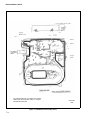
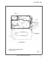
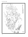
LOCATION OF MAJOR ASSEMBLIES
ACCESS INSTRUCTIONS
Removing the Front Panel Section
Removing the Rear Panel Section
Removing the A2 Coarse Loop PCA
Removing the A3 Sub-Synthesizer VCO PCA
Removing the A4 Sub-Synthesizer PCA
Removing the A5 Coarse Loop VCO PCA
Removing the A6 Mod Oscillator PCA
Removing the A8 Output PCA
Removing the A9 Sum Loop VCO PCA
Removing the A10 Premodulator PCA
Removing the A11 Modulation Control PCA
Removing the A12 Sum Loop PCA
Removing the A13 Controller PCA
Removing the A14 FM PCA
Removing the A20 Attenuator/RPP Assembly
Removing the A22 Delay Cable Assembly
ii
(continued on page iii)
TABLE OF CONTENTS, continued
SECTION
6
TITLE
CIRCUIT DESCRIPTIONS, TROUBLESHOOTING, AND ALIGNMENT
6-1.
6-2.
6-3.
6-4.
6-5.
6-6.
6-7.
6-8.
6-9.
6-10.
6-11.
6-12.
6-13.
6-14.
6-15.
6-16.
6-17.
6-18.
6-19.
6-20.
6-21.
6-22.
6-23.
6-24.
6-25.
6-26.
6-27.
6-28.
6-29.
6-30.
6-31.
6-32.
6-33.
6-34.
6-35.
6-36.
6-37.
6-38.
6-39.
6-40.
6A
PAGE
6-1
INTRODUCTION
6-1
MODULE REPLACEMENT
6-4
A1
Display PCA
6-5
A2 Coarse Loop PCA
6-5
A3 Sub-Synthesizer PCA
6-5
A4 Sub-Synthesizer PCA
6-5
A5 Coarse Loop VCO PCA
6-5
A6 Mod Oscillator PCA
6-5
A7 Relay Driver PCA
6-5
A8Output PCA
6-5
A9 Sum Loop VCO PCA
6-5
A10 Premodulator PCA
6-6
A11 Modulation Control PCA
6-6
A12 Sum Loop PCA
6-6
A13 Controller PCA
6-6
A14 FM Board PCA
6-6
A15 Power Supply PCA
6-6
A19 Switch PCA
6-6
A20 Attenuator/RPP Assembly (A7, A21, A30)
6-6
A22 Delay Line Assembly (A25+A26+Delay Cable+Trim Cable) ....... 6-6
UPDATING COMPENSATION MEMORY WITH
MODULE EXCHANGE DATA
6-7
PARTS REPLACEMENT
6-8
SELF-TEST DESCRIPTION
6-8
Digital Tests
6-8
AM Tests
6-9
FM Tests
6-9
øM Tests
6-9
DCFM Test
6-10
Coarse Loop Tests
6-11
Sub-Synthesizer Tests
6-11
Sum Loop Tests
6-11
RF Output Tests
6-12
Pulse Modulator Tests
6-12
Filter Tests
6-12
STATUS SIGNALS AND STATUS CODES
6-13
SOFTWARE DIAGNOSTIC FUNCTIONS
6-14
Digital Control Latch Test
6-14
Instrument Diagnostic State
6-14
Set Internal DACs
6-14
Display Synthesizer Loop Frequencies
6-15
POWER SUPPLY
6A-1
6A-1.
6A-2.
6A-3.
6A-4.
6A-5.
6A-1
6A-1
6A-4
6A-4
6A-5
POWER SUPPLY BLOCK DIAGRAM
POWER SUPPLY CIRCUIT DESCRIPTION
POWER SUPPLY TROUBLESHOOTING
Troubleshooting Procedure
POWER SUPPLY ADJUSTMENT PROCEDURE
iii
(continued on page iv)
TABLE OF CONTENTS, continued
SECTION
6B
TITLE
DIGITAL CONTROLLER
6B-1.
6B-2.
6B-3.
6B-4.
6B-5.
6B-6.
6B-7.
6B-8.
6B-9.
6B-10.
6B-11.
6B-12.
6B-13.
6B-14.
6B-15.
6B-16.
6B-17.
6B-18.
6B-19.
6B-20.
6B-21.
6B-22.
6B-23.
6B-24.
6B-25.
6B-26.
6B-27.
6B-28.
6B-29.
6B-30.
6B-31.
6B-32.
6B-33.
6B-34.
6B-35.
6B-36.
6B-37.
6C
PAGE
6B-1
DIGITAL CONTROLLER BLOCK DIAGRAM
6B-1
DIGITAL CONTROLLER CIRCUIT DESCRIPTION (A13)
6B-1
Microprocessor
6B-1
Memory
6B-1
Memory Control
6B-3
Front Panel Interface
6B-3
IEEE-488 Interface
6B-3
Attenuator Control Interface
6B-3
Module I/O
6B-3
Status and Control
6B-4
DIGITAL CONTROLLER TROUBLESHOOTING
6B-4
RF Control
6B-4
Microprocessor Kernel
6B-5
Clock
6B-5
Power-On Reset
6B-5
Unused Microprocessor Inputs
6B-5
Bus Error
6B-5
Interrupts
6B-5
Microprocessor Bus
6B-6
Address Decoder
6B-6
I/O Diagnostic Tests
6B-7
CALIBRATION/COMPENSATION MEMORY
6B-8
Calibration/Compensation Memory Status
6B-8
Repairing Calibration/Compensation Memory Checksum Errors .. 6B-9
Calibration/Compensation Memory Origin Status
6B-9
FRONT PANEL CIRCUIT DESCRIPTION
6B-9
Display PCA
6B-10
Data Communications
6B-10
Display Filament Voltage
6B-10
Bright-Digit Effect
6B-10
Switchboard Interface
6B-10
Remote Footswitch
6B-10
Edit Knob Interface
6B-11
Display Blanking
6B-11
Operate/Standby Selection
6B-11
FRONT PANEL TROUBLESHOOTING
6B-11
Display and Controls
6B-11
FREQUENCY SYNTHESIS
6C-1
6C-1.
6C-2.
6C-3.
6C-4.
6C-5.
6C-6.
6C-7.
6C-8.
6C-9.
6C-10.
6C-1
6C-1
6C-1
6C-9
6C-13
6C-13
6C-13
6C-14
6C-14
6C-15
FREQUENCY FAULT TREE
SUB-SYNTHESIZER BLOCK DIAGRAM
SUB-SYNTHESIZER CIRCUIT DESCRIPTION (A4)
SUB-SYNTHESIZER TROUBLESHOOTING
SUB-SYNTHESIZER ADJUSTMENTS
Steering DAC Full Scale Adjustment
Lower Clamp Adjustment, R99
Upper Clamp Adjustment, R98
SSB Mixer LO Drive Adjustment, R106
10-kHz Notch Adjustment, L56
IV
(continued on page v)
TABLE OF CONTENTS, continued
SECTION
6C-11.
6C-12.
6C-13.
6C-14.
6C-15.
6C-16.
6C-17.
6C-18.
6C-19.
6C-20.
6C-21.
6C-22.
6C-23.
6C-24.
6C-25.
6C-26.
6C-27.
6C-28.
6C-29.
6C-30.
6C-31.
6C-32.
6C-33.
6C-34.
6C-35.
6C-36.
6C-37.
6C-38.
6C-39.
6C-40.
6D
TITLE
SUB-SYNTHESIZER VCO (A3) CIRCUIT DESCRIPTION
SUB-SYNTHESIZER VCO TROUBLESHOOTING
COARSE LOOP CIRCUIT DESCRIPTION (A2)
REFERENCE SECTION BLOCK DIAGRAM
COARSE LOOP BLOCK DIAGRAM
COARSE LOOP TROUBLESHOOTING
COARSE LOOP PCA ADJUSTMENTS
Discriminator Video Amplifier Offset Adjustment, R102
Steering Gain Adjustment, R221
Acquisition Oscillator Level Adjustment, R227
40-MHz Oscillator Adjustment, L601
80-MHz Filter Tuning, L612 and L613
80-MHz Level Adjustment, R617
2-MHz Notch Adjustment, L205
Alternate Reference Frequency Selection
COARSE LOOP VCO (A5) CIRCUIT DESCRIPTION
COARSE LOOP VCO TROUBLESHOOTING
SUM LOOP BLOCK DIAGRAM
SUM LOOP (A12) CIRCUIT DESCRIPTION
RF Section
Audio Section
SUM LOOP TROUBLESHOOTING
SUM LOOP ASSEMBLY ADJUSTMENTS
Steering Level Adjustment, R112
Buffer Gain Match Adjustment, R121
FM Null Adjustment, R116
Loop Gain Adjustment, R167
Acquisition Oscillator Level Adjustment, R132
SUM LOOP VCO (A9) CIRCUIT DESCRIPTION
SUM LOOP VCO TROUBLESHOOTING
PAGE
6C-16
6C-16
6C-17
6C-17
6C-20
6C-22
6C-26
6C-26
6C-28
6C-28
6C-28
6C-29
6C-30
6C-30
6C-31
6C-31
6C-32
6C-32
6C-34
6C-34
6C-35
6C-38
6C-41
6C-41
6C-42
6C-42
6C-43
6C-44
6C-44
6C-45
RF LEVEL/AM
6D-1
6D-1.
6D-2.
6D-3.
6D-4.
6D-5.
6D-6.
6D-7.
6D-8.
6D-9.
6D-10.
6D-11.
6D-12.
6D-13.
6D-14.
6D-15.
6D-16.
6D-1
6D-1
6D-3
6D-3
6D-5
6D-6
6D-6
6D-8
6D-9
6D-10
6D-10
6D-11
6D-12
6D-13
6D-14
RF LEVEL FAULT TREE
RF LEVEL BLOCK DIAGRAM
RF LEVEL CIRCUIT DESCRIPTION
RF Path
Leveling Loop
Level Control
RF LEVEL TROUBLESHOOTING
Unleveled Condition
Output Assembly Test Point Signal Information
RF LEVEL ADJUSTMENTS
Mod Control PCA Level DAC Offset Adjustment, R23
Mod Control PCA AM DAC Offset Adjustment, R8
Mod Control PCA Detector Offset Adjustment, R28
Mod Control PCA AM Depth Adjustment,
R10
Mod Control PCA RF Level Adjustment, R20
Mod Control PCA External Modulation Level
Indicator Adjustment, R71
6D-17.
Mod Control PCA Sum Steer Gain Adjustment
v
6D-15
6D-15
(continued on page vi)
TABLE OF CONTENTS, continued
SECTION
6E
6F
PAGE
6D-18.
Output PCA Het Mixer Level Adjustment, R72
6D-19.
Output PCA Het Level Adjustment,
R10
6D-20.
Premodulator PCA Bandwidth Adjustment, R51 and C7
6D-21.
Output PCA Q16 Bias Adjustment, R96
6D-22.
Output PCA Q9 Bias Adjustment,
R1
6D-23.
Output PCA) Gain Flatness Adjustment, C201
6D-24.
FM Gain Adjustment, R82, on Mod Control PCA
6D-25.
FM Steer Gain, R101 on Mod Control PCA
6D-26.
FM INV Balance, R102 on Mod Control PCA
6D-27. ATTENUATOR/REVERSE POWER PROTECTION (RPP)
6D-28. ATTENUATOR RPP TROUBLESHOOTING
6D-16
6D-17
6D-17
6D-18
6D-19
6D-19
6D-20
6D-20
6D-20
6D-20
6D-21
FREQUENCY AND PHASE MODULATION
6E-1
6E-1.
6E-2.
6E-3.
6E-4.
6E-5.
6E-6.
6E-7.
6E-8.
6E-9.
6E-10.
6E-11.
6E-12.
6E-13.
6E-14.
6E-15.
6E-16.
6E-17.
6E-18.
6E-1
6E-2
6E-2
6E-2
6E-4
6E-4
6E-7
6E-10
6E-10
6E-10
6E-10
6E-11
6E-11
6E-12
6E-12
6E-13
6E-13
6E-14
FM/øM FAULT TREE
FM/øM BLOCK DIAGRAM
CIRCUIT DESCRIPTION
Oscillator Section
Divider Section
Phase Detectors, Loop Circuits, and Logic Section
Modulation Section
MODULATION CONTROL CIRCUIT DESCRIPTION
FM Input Voltage Processing
FM Steer Voltage Generation
FM Control Signals Generation
FM TROUBLE SHOOTING (A14)
Frequency Check
Modulation Check
Input Signals and Control Input Signals Checks
FM ADJUSTMENTS
Adjustments on the Modulation Control PCA
(A11)
Alignment of FM PCA (A14)
INTERNAL MODULATION OSCILLATOR
6F-1
6F-1.
6F-2.
6F-1
6F-3.
6F-4.
6F-5.
6F-6.
6F-7.
6F-8.
7
TITLE
MODULATION OSCILLATOR BLOCK DIAGRAM
INTERNAL MODULATION OSCILLATOR
CIRCUIT DESCRIPTION
Direct Digital Synthesized Wave Generator
Pulse Generator
Signal Routing
MOD OSCILLATOR TROUBLESHOOTING AND
ADJUSTMENTS
Direct Digital Synthesizer Troubleshooting
Pulse Generator Troubleshooting
6F-1
6F-1
6F-3
6F-3
6F-4
6F-4
6F-5
LIST OF REPLACEABLE PARTS
TABLE OF CONTENTS
7-1
7-1
7-1.
7-2.
7-3.
7-2
7-2
7-3
INTRODUCTION
HOW TO OBTAIN PARTS
SERVICE CENTERS
vi
(continued on page vii)
TABLE OF CONTENTS, continued
SECTION
8
TITLE
SCHEMATIC DIAGRAMS
TABLE OF CONTENTS
PAGE
8-1
8-1
APPENDICES
A.
B.
C.
D.
E.
F.
G.
H.
I.
INSTRUMENT PRESET STATE
SPECIAL FUNCTION TABLE
REJECTED ENTRY ERROR CODES
OVERRANGE/UNCAL STATUS CODES
SELF-TEST STATUS CODES
COMPENSATION MEMORY STATUS CODES
EXAMPLE CALIBRATION CONTROLLER PROGRAMS
COMPENSATION PROCEDURES
REAR PANEL AUX CONNECTOR PINOUT
viilviii
A-l
B-l
C-l
D-l
E-l
F-l
G-l
H-l
1-1
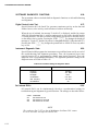
List of Tables
TABLE
TITLE
PAGE
1-1.
1-2.
1-3.
1-4.
Accessories Included with each Signal Generator
Optional Accessories
6080A/AN Specifications
Typical Signal Generator Performance
1-3
1-3
1-4
1-9
2-1.
Frequency Coverage Bands
2-3
3-1.
3-2.
3-3.
3-4.
3-5.
3-6.
3-7.
3-8.
Front Panel Controls for AM Calibration Procedure
Remote Programming Commands for AM Calibration Procedure
Front Panel Controls for FM Calibration Procedure
Remote Programming Commands for FM Calibration Procedure
Front Panel Controls for Level Calibration Procedure
Remote Programming Commands for Level Calibration Procedure
Front Panel Controls for Reference Oscillator Calibration Procedure
Remote Programming Commands for Reference Oscillator
Calibration Procedure
3-5
3-7
3-8
3-10
3-12
3-14
3-15
3-17
4-1.
4-2.
4-3.
4-4.
4-5.
Recommended Test Equipment
High-Level Accuracy Test Conditions
High-Level Accuracy Test Conditions Sample
Modulation Tests Requirements
AM Test Conditions
4-2
4-7
4-8
4-17
4-19
6-1.
6-2.
6-3.
6-4.
6-5.
6-6.
6-7.
6-8.
6-9.
6-10.
6-11.
6-12.
6-13.
6-14.
6-15.
Module Exchange Assemblies
General Self-Test Results
Digital Test Results
AM Test Conditions
FM Tests
Phase Modulation Test Conditions
DC FM Tests
Coarse Loop Tests
Sub-Synthesizer Tests
Sum Loop Tests
RF Output Tests
Pulse Modulator Tests
Filter Tests
Status Signals and Codes
Parameter Settings of Diagnostic States
6-4
6-8
6-9
6-9
6-10
6-10
6-10
6-11
6-11
6-11
6-12
6-12
6-13
6-13
6-14
ix
(continued on page x)
LIST OF TABLES, continued
TABLE
TITLE
PAGE
6A-1.
Supplies Provided by Power Supply Assembly
6A-3
6C-1.
6C-2.
6C-3.
6C-4.
6C-5.
6C-6.
6C-7.
6C-8.
6C-9.
6C-10.
6C-11.
6C-12.
Sub-Synthesizer PCA Test Points
A3 Sub-Synthesizer VCO PCA DC Voltages
Coarse Loop RF Voltage Levels
N-Divider Logic States
Discriminator RF Section Levels
A2 Coarse Loop PCA Test Points
A5 Coarse Loop VCO PCA Expected DC Voltages
Sum Loop Frequencies
A12 Sum Loop PCA RF Circuitry Test Information
A12 Sum Loop PCA RF Section DC Bias Voltages
A12 Sum Loop PCA Test Points
A9 Sum Loop VCO PCA Expected DC Voltages
6C-11
6C-17
6C-24
6C-25
6C-26
6C-27
6C-32
6C-34
6C-39
6C-40
6C-41
6C-46
6D-1. Band, Filter, and Frequency Programming Data
6D-2. Frequency Band Logic States
6D-3. Modulator - Detector Nominal Voltages
6D-4. A11 Modulation Control PCA Test Points
6D-5. Attenuator Levels
6D-6. Attenuator Level Control
6D-7
6D-8
6D-9
6D-9
6D-21
6D-22
6E-1.
6E-2.
6E-3.
6E-4.
6E-5.
6E-8
6E-9
6E-11
6E-12
6E-15
Modulation Control Table (@ 800 MHz RF Frequency)
Modulation Ranges and FM DAC Values
FM Oscillator Frequency Check Table (Normal Operation)
FM Oscillator Modulation Control (Normal Operation)
FM - Mod Rate Specifications
x
List of Illustrations
FIGURE
TITLE
PAGE
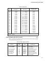
3-1.
3-2.
3-3.
3-4.
3-5.
Basic Structure of Calibration Program
Structure of the AM Calibration Program
Basic Structure of FM Calibration Program
Basic Structure of Level Calibration Program
Basic Structure of the Reference Oscillator Calibration Program
3-2
3-6
3-9
3-13
3-16
4-1.
4-2.
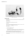
Two-Turn Loop
Alternate-Level Accuracy Test Equipment Setup
4-4
4-12
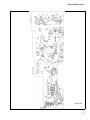
6-1.
6-2.
Instrument Block Diagram
Instrument Troubleshooting Tree
6-2
6-3
6A-1.
Power Supply Block Diagram
6A-2
6B-1.
6B-2.
Controller Block Diagram
Address Decoding
6B-2
6B-7
6C-1.
6C-2.
6C-3.
6C-4.
6C-5.
6C-6.
6C-7.
6C-8.
Frequency Synthesis Fault Tree
Sub-Synthesizer Block Diagram
Triple Modulus Prescaler
N-Divider
N-Divider Timing Diagram
Reference Section Block Diagram
Coarse Loop Block Diagram
Sum Loop Block Diagram
6C-2
6C-3
6C-5
6C-6
6C-7
6C-18
6C-21
6C-33
6D-1.
6D-2.
RF Level Fault Tree
RF Level Block Diagram
6D-1
6D-2
6E-1.
6E-2.
6E-3.
FM/øM Fault Tree
FM/øM Block Diagram
FM/øM Timing Diagram
6E-1
6E-3
6E-5
6F-1.
Modulation Oscillator Block Diagram
6F-1
xi / xii
Section 1
Introduction and Specifications
INTRODUCTION
1-1.
The 6080A/AN Synthesized RF Signal Generator (also referred to throughout as the
"signal generator") is a fully programmable, precision, synthesized signal generator.
The 6080A/AN is designed for applications that require good modulation, frequency
accuracy, and output level performance with excellent spectral purity. The signal
generator is well suited for testing a wide variety of RF components and systems
including filters, amplifiers, mixers, and radios, particularly off-channel radio testing.
Specifications of the 6080A/AN are provided at the end of this section. The salient
features of the 6080A/AN are as follows:
•
RF frequency range of 0.5 MHz to 1024 MHz in 1 Hz steps
•
RF level range of +13 to -137 dBm in 0.1 dB steps
•
Internal and External Modulation: AM, FM, and Pulse
•
Internal 10 Hz to 100 kHz Synthesized Sine Wave Modulation Oscillator
•
Fifty Storable and Recallable Memory Locations
•
Standard IEEE-488 (GPIB) Interface, complying with ANSI/IEEE Standards
488.1-1987 and 488.2-1987
•
Closed-case calibration capabilities for Frequency Reference, AM, FM, and
Level.
UNPACKING THE SIGNAL GENERATOR
1-2.
The shipping container should include a 6080A/AN Synthesized RF Signal generator,
an Operator Manual, a Service Manual, a line power cord and two BNC dust caps.
Accessories ordered for the signal generator are shipped in a separate container.
1-1
INTRODUCTION AND SPECIFICATIONS
SAFETY
1-3.
This manual contains information, warnings, and cautions that should be followed to
ensure safe operation and to maintain the generator in a safe condition.
The signal generator is designed primarily for indoor use and may be operated in
temperatures from 0 to 50° C without degradation of its safety.
WARNING
TO AVOID ELECTRIC SHOCK, USE A POWER CORD THAT HAS A
THREE-PRONG PLUG. IF THE PROPER POWER CORD IS NOT USED, THE
6080A/AN CASE CAN DEVELOP AN ELECTRICAL POTENTIAL ABOVE
EARTH GROUND.
WARNING
PIVOTING MODULE INSTRUCTIONS
IF NECESSARY DURING REPAIRS, PIVOT THE TOP (SYNTHESIZER)
MODULE UP TO ALLOW ACCESS TO ALL PARTS OF THE SIGNAL
GENERATOR THE MODULE IS HEAVY AND CARE SHOULD BE
EXERCISED. THE GAS STRUT IS PROVIDED FOR PROTECTION. CHECK
THE CORRECT OPERATION OF THE GAS STRUT BY NOTING THE
RESISTANCE TO RAPID CLOSING OF THE MODULE WHILE YOU FIRMLY
GRASP THE MODULE BY THE HANDLE.
OPENING AND CLOSING INSTRUCTIONS ARE GIVEN BELOW AND ARE
REPEATED ON THE DECAL ON THE TOP FRONT OF THE SYNTHESIZER
MODULE.
RAISING THE MODULE:
1.
REMOVE THREE HOLD-DOWN SCREWS LOCATED ON THE SIDE
RAILS.
2.
GRASP THE HANDLE AND LIFT UP.
3. LOCK IN THE UP POSITION BY INSTALLING ONE SCREW IN THE PROTRUDING
BOSS ON EACH SIDE RAIL.
LOWERING THE MODULE:
1. SUPPORT IN THE UP POSITION AND REMOVE TWO LOCK UP SCREWS.
2.
GRASP THE HANDLE AND LOWER THE MODULE KEEPING YOUR HANDS
CLEAR.
3. LOCK IN THE DOWN POSITION BY REINSTALLING THE THREE HOLD-DOWN
SCREWS.
1-2
INTRODUCTION AND SPECIFICATIONS
ACCESSORIES
1-4.
The accessories and manuals included with each signal generator are listed in Table 1-1.
The optional accessories available are listed in Table 1-2.
SIGNAL GENERATOR SPECIFICATIONS
1 -5.
Table 1-3 lists the 6080A/AN specifications. Table 1-4 lists typical performance
characteristics.
Table 1-1. Accessories Included with each Signal Generator
DESCRIPTION
PART NUMBER
QUANTITY
Operator Manual
857748
1
Service Manual
868906
1
Line Power Cord
284174
1
BNC Dust Cap
478982
2
Table 1-2. Optional Accessories
DESCRIPTION
Rack Mount Kit
Includes M05-205-600 (5 1/4-inch Rack Mount Ears)
and M00-280-610 (24-inch Rack Slides)
ACCESSORY NO.
Y6001
IEEE-488 Shielded Cable, 1 meter
Y8021
IEEE-488 Shielded Cable, 2 meters
Y8022
IEEE-488 Shielded Cable, 4 meters
Y8023
Coaxial Cable, 50 ohms, 3 feet, BNC (m) both ends
Y9111
Coaxial Cable, 50 ohms, 6 feet, BNC (m) both ends
Y9112
1-3
INTRODUCTION AND SPECIFICATIONS
Table 1-3. 6080A/AN Specifications
NOTE
Unless otherwise noted, the following performance is guaranteed over the specified
environmental and AC power line conditions two hours after turn-on.
FREQUENCY (10-DIGIT DISPLAY)
RANGE
BAND
BAND
BAND
BAND
BAND
BAND
BAND
.50-15 MHz
15-32 MHz
32-64 MHz
64-128 MHz
128-256 MHz
256-512 MHz
512-1024 MHz
0.50 to 1024 MHz in 7 bands:
0.50 to 14.999999 MHz,
15 to 31.999999 MHz,
32 to 63.999999 MHz,
64 to 127.999999 MHz,
128 to 255.999999 MHz,
256 to 511.999999 MHz,
512 to 1024 MHz.
RESOLUTION
1 Hz
ACCURACY
Same as reference (See REFERENCE).
REFERENCE (Internal)
The unit operates on an internal 10 MHz
Temperature Compensated Crystal Oscillator
(TCXO). The frequency variation will be < 10 ppm
peak to peak over the temperature range of 0 to
+50°C.
Internal reference signal (10 MHz) available at rear
panel REF OUT connector, level > 0 dBm, terminated
into 50 ohms.
Frequency stability after 2 hour warmup is < ± 0.05
ppm/hour at + 25°C ± 5°C.
REFERENCE (External)
Accepts 5 or 10 MHz signal. Level required is 0.5 to
2.0V RMS into 50 ohms termination.
AMPLITUDE (3 1/2-DIGIT DISPLAY)
1-4
RANGE
+13 to -137 dBm
RESOLUTION
0.1 dB (<1% or 1 nV in Volts).
Annunciators for dB, dBm, V, mV, μV, dB mV,
dB μV, dBf, and EMF.
ACCURACY
± 1.5 dB from +13 to -117 dBm
± 3 dB from -117 to -137 dBm
SOURCE VSWR
< 1.5:1 for levels below -10 dBm, < 2.5:1 elsewhere.
FLATNESS
±1.0dB@+10dBm.
INTRODUCTION AND SPECIFICATIONS
Table 1-3. 6080A/AN Specifications (cont)
SPECTRAL PURITY (CW ONLY)
NON-HARMONIC SPURIOUS
< -100 dBc for offsets greater than 15 kHz.
NOTE
Fixed frequency spurs are <-100 dBc or < -140 dBm, whichever is larger.
NOTE
dBc refers to decibels relative to the carrier frequency, or in this case, relative to the signal level.
HARMONICS / SUBHARMONICS
< -30 dBc for levels < +7 dBm.
POWER LINE SPURIOUS
< -40 dBc within ± 15 kHz of carrier.
RESIDUAL FM (RMS in
0.05- to 15-kHz band)
< 20 Hz
SSB PHASE NOISE
< -130 dBc/Hz @ 20 kHz offset for Frequency
< 512 MHz
< -124 dBc/Hz @ 20 kHz offset for Frequency
> 512 MHz
RESIDUAL AM (in 0.05- to 15-kHz Band)
<-80 dBc. (.01%)
AMPLITUDE MODULATION (3-DIGIT DISPLAY)
(Amplitude < 0 dBm)
INDICATED DEPTH RANGE ....................... 0 to 99.9%.
RESOLUTION
0.1%.
ACCURACY (0 to 90%)
+ 7% AM at 1 kHz rate
DISTORTION
< 5% Total Harmonic Distortion (THD)
@ 50% AM (rates = 0.1, 1, 10 kHz)
BANDWIDTH (3 dB)
10 Hz to 100 kHz
INCIDENTAL FM
< 200 Hz at 1 kHz rate, 50% AM.
FREQUENCY MODULATION (3-DIGIT DISPLAY)
DEVIATION RANGES
0 to 999 Hz
1 to 9.99 kHz
10 to 99.9 kHz
100 to 999 kHz
1 to 4 MHz
EXT RATES
DC to 100 kHz
1-5
INTRODUCTION AND SPECIFICATIONS
Table 1-3. 6080A/AN Specifications (cont)
DEVIATION
(rates = .1, 1, 50 kHz)
DEV
0 to
0 to
0 to
0 to
1 kHz min
10 kHz min
100 kHz mln
1 MHz min
RF Frequency
Frequency < 1 MHz
1 MHz < Frequency < 32 MHz
32 MHz < Frequency < 128 MHz
Frequency > 128 MHz
RESOLUTION
3 digits.
ACCURACY
(measured vs. indicated deviation,
1 kHz rate)
+(5% +10 Hz)
DISTORTION
(does not include effects
of residual FM)
< 5% THD for rates of 0.1, 1, and 50 kHz
INCIDENTAL AM
< 2% THD for deviation < 20 kHz and 1 kHz rate
< 1% AM at 1-kHz rate, for peak deviation < 100 kHz
PULSE MODULATION (RF Frequencies from 10 to 1024 MHz)
ON/OFF RATIO
35 dB minimum
RISE & FALL TIMES
< 1 μs
PULSE WIDTH
Minimum at least 5 μs
REP RATE
Minimum at least 50 Hz to 50 kHz
EXTERNAL PULSE MODULATION
NON-VOLATILE MEMORY
The pulse input is TTL compatible and 50 ohm
terminated with an internal active pull-up. It can be
modeled as 1.2V in series with 50 ohms at the pulse
modulation input connector. The signal generator
senses input terminal voltage and turns the RF off
when the terminal voltage drops below 1 ± 0.1 V. Max
allowable applied voltage, ± 10V.
50 instrument states are retained for typically 2 years,
even with the power mains disconnected.
REVERSE POWER PROTECTION
1-6
PROTECTION LEVEL
Up to 50 watts from a 50 ohm source. Up to 50V DC.
Signal generator output is AC coupled. Protection is
provided when the signal generator is off.
TRIP/RESET
Flashing RF OFF annunciator indicates a tripped
condition. Pushing RF ON/OFF button will reset
signal generator.
INTRODUCTION AND SPECIFICATIONS
Table 1-3. 6080A/AN Specifications (cont)
IEEE-488
INTERFACE FUNCTIONS
SH1, AH1, T5, TE0, L3, LEO, SR1, RL1, PRO,
DC1, DT1, C0, and E2. Complies with IEEE Std.
488.1-1987 and 488.2-1987.
INTERNAL MODULATION SOURCE
SINE WAVE
10 Hz to 100 kHz synthesized sine wave.
DISPLAY RANGES
00.1 to 99.9 Hz
100 to 999 Hz
1.00 to 9.99 kHz
10.0 to 99.9 kHz
100 to 200 kHz
FREQUENCY RESOLUTION
0.1 Hz or 3 digits
OUTPUT LEVEL RANGE
0 to 1V RMS into 600 ohms
DISTORTION
< 2% THD
OUTPUT IMPEDANCE
600 ohms ±10%
EXTERNAL MODULATION
1V peak provides indicated modulation index.
Nominal input impedance is 600 ohms. Maximum input level is ± 5 V peak.
MODULATION MODES
Any combination of AM, PULSE, and FM, internal or external, may be used.
GENERAL
TEMPERATURE
Operating
Non-Operating
0 to +50°C (+32 to +122°F).
-40 to +75°C (-40 to +167°F).
HUMIDITY RANGE
Operating
95% to +30°C, 75% to +40°C, and 45% to +50°C.
ALTITUDE
Operating
Up to 10,000ft.
VIBRATION
Non-Operating
SHOCK
Non-Operating
5 to 15 Hz at 0.06 inch, 15 to 25 Hz at 0.04 inch,
and 25 to 55 Hz at 0.02 inch, double amplitude (DA).
MIL T 28800D Class 5, Style E.
1-7
INTRODUCTION AND SPECIFICATIONS
Table 1-3. 6080A/AN Specifications (cont)
ELECTROMAGNETIC COMPATIBILITY..
The radiated emissions induce < 1 μV into a 1-inch
diameter, 2-turn loop, 1-inch from any surface as
measured into a 50-ohm receiver.
COMPLIES WITH THE FOLLOWING STANDARDS:
CE03 of MIL-STD-461B (Power and interconnecting leads), 0.015 to 50 MHz.
RE02 of MIL-STD-461B (14 kHz to 10 GHz).
FCC Part 15 (J), class A.
CISPR 11.
1-8
SIZE
Width
43 cm
17 in
Height
13.3 cm
5.25 in
Depth
59.7 cm
23.5 in
POWER
115/230 VAC, ± 10% 50, 60, and 400 Hz ±10%
250 VA maximum
WEIGHT
< 27 kg (60 Ibs).
INTRODUCTION AND SPECIFICATIONS
Table 1-4. Typical Signal Generator Performance
FREQUENCY (10-DIGIT DISPLAY)
RANGE
BAND
BAND
BAND
BAND
BAND
BAND
BAND
.01-15 MHz
15-32 MHz ..............................
32-64 MHz
64-128 MHz
128-256 MHz
256-512 MHz
512-1056 MHz
0.01 to 1056 MHz in 7 bands:
0.01 to 14.999999 MHz,
15 to 31.999999 MHz,
32 to 63.999999 MHz,
64 to 127.999999 MHz,
128 to 255.999999 MHz,
256 to 511.999999 MHz,
512 to 1056 MHz.
RESOLUTION
1 Hz
ACCURACY
Same as reference (See REFERENCE).
REFERENCE (Internal)
The unit operates on an internal 10 MHz TCXO. The
Frequency variation will be < 2 ppm peak to peak
over the temperature range of 0 to +50°C. Aging rate
of <± 1 ppm/year typical.
Internal reference signal (10 MHz) available at rear
panel REF OUT connector, level > 0 dBm, terminated
in 50 ohms.
Frequency stability after 2 hour warmup is < ± 0.05
ppm/hour at +25°C ± 5°C.
REFERENCE (External)
Accepts (1, 2, or 5) or 10 MHz signal. Level required
is 0.2 to 2.0 Vrms into 50-ohms termination.
NOTE
Choice is internal swit ch selectable (1, 2, or 5 MHz).
AMPLITUDE (3 1/2-DIGIT DISPLAY)
RANGE
+19 to -140 dBm for Frequency < 512 MHz.
+16 to -140 dBm for Frequency > 512 MHz.
RESOLUTION
0.1 dB (< 1% or 1 nV in volts). Annunciators for dB,
dBm, dBf, V, mV, μV, dB mV, dB μV, and EMF.
ACCURACY
(+23 ± 50°C)
± 1 dB from +19 to -127 dBm and for F from 0.4 to
512 MHz.
± 1 dB from +16 to -127 dBm and for F > 512 MHz.
ACCURACY
(0 to +50°C)
± 1.5 dB from +19 to -127 dBm and for from 0.4 to
512 MHz.
± 1.5 dB from +16 to -127 dBm and for F > 512 MHz.
1-9
INTRODUCTION AND SPECIFICATIONS
Table 1-4. Typical Signal Generator Performance (cont)
± 2 dB from +19 to -100 dBm and for F from 0.01 to
0.4 MHz.
± 3 dB from -100 to -127 dBm and for F from 0.01 to
0.4 MHz.
SOURCE VSWR
< 1.5:1 for levels below +1 dBm, < 2.0:1 elsewhere.
FLATNESS (+23 + 5°C)
+ 0.5 dB @ +10 dBm.
F > 0.1 MHz.
FLATNESS (0 to + 50°C)
+ 0.75 dB @ +10 dBm.
F > 0.1 MHz.
SPECTRAL PURITY (CW ONLY)
NON-HARMONIC SPURIOUS
< -100 dBc for offsets greater than 10 kHz.
NOTE
Fixed frequency spurs are < -100 dBc or < -140 dBm whichever is larger.
NOTE
dBc refers to decibels relative to the carrier frequency, or in this case, relative to the signal level.
HARMONICS
< -30 dBc for levels < +13 dBm.
< -25 dBc for levels < +16 dBm.
SUBHARMONICS
None
POWER LINE SPURIOUS
< -50 dBc within + 10 kHz of carrier.
RESIDUAL FM (RMS in 0.3to 3-kHz band)
< 0.2 Hz for .01 to 15 MHz Band
< 0.2 Hz for 15 to 32 MHz Band
< 0.2 Hz for 32 to 64 MHz Band
< 0.2 Hz for 64 to 128 MHz Band
< 0.2 Hz for 128 to 256 MHz Band
< 0.5 Hz for 256 to 512 MHz Band
< 1 Hz for 512 to 1056 MHz Band
RESIDUAL FM (RMS in 0.05to 15-kHz band)
< 0.5 Hz for .01 to 15 MHz Band
< 0.5 Hz for 15 to 32 MHz Band
< 0.5 Hz for 32 to 64 MHz Band
< 0.5 Hz for 64 to 128 MHz Band
< 0.5 Hz for 128 to 256 MHz Band
< 1 Hz for 256 to 512 MHz Band
< 2 Hz for 512 to 1056 MHz Band
SSB PHASE NOISE
1-10
< -131 dBc/Hz @ 20 kHz offset
@ Frequency = 250 MHz
INTRODUCTION AND SPECIFICATIONS
Table 1-4. Typical Signal Generator Performance (cont)
< -136 dBc/Hz @ 20 kHz offset
@ Frequency = 1 GHz
< -140 dBc/Hz @ 20 kHz offset
@ Frequency = 500 MHz
BROADBAND SSB PHASE
NOISE FLOOR
< -140 dBc/Hz @ 100 kHz offset @ +13 dBm.
RESIDUAL AM (in 0.05- to 15-kHz Band)
< -80 dBc.
AMPLITUDE MODULATION (3-DIGIT DISPLAY)
(Amplitude < +10 dBm)
INDICATED DEPTH RANGE............................ 0 to 99.9%.
RESOLUTION
0.1%.
ACCURACY (0 to 90%)
+(2% AM + 4% of setting) at 1 kHz rate
DISTORTION
(rate = 1 kHz)
< 1.5% THD to 30% AM
< 3% THD to 70% AM
< 5% THD to 90% AM
BANDWIDTH (3 dB)
10 Hz to 100 kHz
DC to 100 kHz (external only)
INCIDENTAL FM
< 200 Hz at 1 kHz rate, 50% AM.
NOTE
AM specifications apply where RF frequency - Modulation Frequency is greater than 150 kHz
FREQUENCY MODULATION (3-DIGIT DISPLAY)
DEVIATION RANGES
0 to 999 Hz
1 to 9.99 kHz
10 to 99.9 kHz
100 to 999 kHz
1 to 4 MHz
MAXIMUM DEVIATION
DEV
500 kHz
125 kHz
250 kHz
500 kHz
1 MHz
2 MHz
4 MHz
RF Frequency
.01 to 15 MHz
15 to 32 MHz
32 to 64 MHz
64 to 128 MHz
128 to 256 MHz
256 to 512 MHz
512 to 1056 MHz
1-11
INTRODUCTION AND SPECIFICATIONS
Table 1-4. Typical Signal Generator Performance (cont)
Minimum FM rate at max deviation in any band,
ACFM mode is 60 Hz.
@ 1/2 max deviation....30 Hz
@ 1/4 max deviation....15 Hz from 1/4 to 1/64 max
deviation.... 15 Hz
@ 1/64 max deviation.... 60 Hz
@ 1/128 max deviation.... 40 Hz
@ 1/256 or less max deviation.... 15 Hz
No limit in DCFM mode.
RESOLUTION
3 digits.
ACCURACY
±(5% of setting + 10 Hz) for rates of .05 to 50 kHz.
DISTORTION
(does not include effects of residual noise)
< 2% THD for rates from .05 to 50 kHz
< 1% THD at 1/2 or less max deviation and rates
from 0.1 to 50 kHz.
LOW DISTORTION MODE
(SPCL 731)
< 0.3% THD + noise @ 3.5 kHz deviation and @
rates from 0.3 to 3 kHz
BANDWIDTH (1.5 dB)
ACFM 20 Hz to 100 kHz subject to low frequency
max deviation limits
DCFM DC to 100 kHz
INCIDENTAL AM
< 1% AM at 1 kHz rate, for the maximum deviation or
100 kHz, whichever is less. Valid for RF frequency
> 0.5 MHz
DCFM CENTER FREQUENCY ERROR ..
< (0.1% of dev + 500 Hz) @ F = 1 GHz
NOTE
After DCFM Cal and without any FM range changes
LOW RATE EXTERNAL FM
(Access by SPCL 711 )
1-12
RF Band
MAX DEV @ 10 Hz Rate
sine wave square wave
MAX DEVIATION
.01 to 15 MHz
15 to 32 MHz
32 to 64 MHz
64 to 128 MHz
128 to 256 MHz
256 to 512 MHz
512 to 1056 MHz
DROOP
< 30% on a 5 Hz square wave
BANDWIDTH (3 dB)
0.5 Hz to 100 kHz (typical)
80 kHz
20 kHz
40 kHz
80 kHz
160 kHz
320 kHz
640 kHz
40 kHz
10 kHz
20 kHz
40 kHz
80 kHz
160 kHz
320 kHz
INTRODUCTION AND SPECIFICATIONS
Table 1-4. Typical Signal Generator Performance (cont)
MAX DC INPUT
±10mV
INCIDENTAL AM
< 1 % AM @ 1 kHz rate and < 10 kHz dev
NOTE
FM specifications apply where:
RF Frequency - Deviation > 150 kHz
RF Frequency - Mod Rate > 150kHz
PHASE MODULATION (3 DIGIT DISPLAY)
DEVIATION RANGES
0 to .999 rad
1 to 9.99 rad
10 to 99.9 rad
100 to 400 rad
MAXIMUM DEVIATION
DEV
RF FREQUENCY
50 rad
12.5 rad
25 rad
50 rad
100 rad
200 rad
400 rad
.01 to 15 MHz
15 to 32 MHz
32 to 64 MHz
64 to 128 MHz
128 to 256 MHz
256 to 512 MHz
512 to 1056 MHz
RESOLUTION
3 digits
ACCURACY
±(5% + 0.1 rad) at 1 kHz rate.
DISTORTION
(does not include effects of
residual Phase noise)
< 2% THD for 1 kHz rate.
< 1% THD for 1/2 or less max deviation for 1 kHz rate
BANDWIDTH (3 dB)
ACPM 20 Hz to 15 kHz
DCPM DC to 15 kHz
INCIDENTAL AM
< 1% AM at 1 kHz rate for peak dev
< 10 rad. Valid for F > 1 MHz.
HIGH RATE PHASE MODULATION
(Access by SPCL 721)
MAX DEV
5 rad
1.25 rad
2.5 rad
5 rad
10 rad
20 rad
40 rad
RF FREQUENCY
.01 to 15 MHz
15 to 32 MHz
32 to 64 MHz
64 to 128 MHz
128 to 256 MHz
256 to 512 MHz
512 to 1056 MHz
1-13
INTRODUCTION AND SPECIFICATIONS
Table 1-4. Typical Signal Generator Performance (cont)
HIGH RATE PHASE MODULATION........... ACPM 20 Hz to 100 kHz
BANDWIDTH (3 dB)
DCPM DC to 100 kHz
(Access by SPCL 721)
NOTE
Phase Modulation specs are valid where RF Frequency - Modulation Frequency > 150 kHz
PULSE MODULATION (RF FREQUENCIES FROM 10 TO 1056 MHz)
ON/OFF RATIO
40 dB minimum for frequencies from 100to 1056 MHz
60 dB minimum for frequencies less than 100 MHz
RISE & FALL TIMES
< 15 ns
LEVEL ERROR
For pulse widths > 50 ns, power in the pulse will be
within ±0.7 dB of the measured CW level.
DUTY CYCLE (ext mod)
0-100%
REP RATE (ext mod)
DC-16 MHz
INTERNAL MODULATION
Internal rates, approx 50% duty cycle.
EXTERNAL PULSE MODULATION
The pulse input is TTL compatible and 50 ohm
terminated with an internal active pull-up. It can be
modeled as 1.2V in series with 50 ohms at the pulse
modulation input connector. The signal generator
senses input terminal voltage and turns the RF off
when the terminal voltage drops below 1 ± 0.1V. Max
allowable applied voltage, ±10V.
PULSE MODULATION (RF FREQUENCIES < 10 MHz)
RISE & FALL TIMES
< 2 X period of RF Frequency.
LEVEL ERROR
For pulse widths > 10 X period of RF Frequency,
power in the pulse will be within ±0.7 dB of the
measured CW level.
Other specifications are the same as for the 10 to 1056 MHz range.
NON-VOLATILE MEMORY
50 instrument states are retained for typically 2 years, even with the power mains disconnected.
REVERSE POWER PROTECTION
PROTECTION LEVEL
1-14
Up to 50 watts from a 50 ohm source, up to 50V DC.
Signal generator output is AC coupled. Protection is
provided when the signal generator is off.
INTRODUCTION AND SPECIFICATIONS
Table 1-4. Typical Signal Generator Performance (cont)
TRIP/RESET
Flashing RF OFF annunciator indicates a tripped
condition. Pushing RF ON/OFF button will reset
signal generator.
IEEE-488
INTERFACE FUNCTIONS
SH1, AH1, T5, TE0, L3, LE0, SR1, RL1, PP0, DC1,
DT1, C0, and E2.
INTERNAL MODULATION SOURCE
SINE WAVE
0.1 Hz to 200 kHz synthesized sine wave.
FREQUENCY ACCURACY
Same as reference ±7 mHz
DISPLAY RANGES
00.1 to 99.9 Hz
100 to 999 Hz
1.00 to 9.99 kHz
10.0 to 99.9 kHz
100 to 200 kHz
FREQUENCY RESOLUTION
0.1 Hz or 3 digits
OUTPUT LEVEL RANGE
0 to 4V peak into 600 ohms
OUTPUT LEVEL RESOLUTION
3 digits or 4 mv peak, whichever is larger
DISTORTION
< 0.15% THD for output levels > 2V peak and mod
frequency < 20 kHz
OUTPUT LEVEL ACCURACY
±(4% + 15 mV) for mod frequency < 100 kHz
OUTPUT IMPEDANCE
600 ohms ±2%
OTHER WAVEFORMS AVAILABLE
BY SPECIAL FUNCTION
Square Wave (Fmod < 2 kHz)
Triangle Wave (Fmod < 5 kHz)
EXTERNAL MODULATION INPUTS
1V peak provides indicated modulation indeX.
Nominal input impedance is 600 ohms.
Maximum input level is ± 5 V peak.
MODULATION MODES
Any combination of AM, PULSE, and FM or ØM, internal or external, may be used.
DIGITAL FREQUENCY SWEEP
SWEEP MODES
Auto, single, or manual
1-15
INTRODUCTION AND SPECIFICATIONS
Table 1-4. Typical Signal Generator Performance (cont)
SWEEP FUNCTIONS
Symmetrical sweep, Asymmetrical sweep, Sweep
speed
DATA ENTRY PARAMETERS
Sweep width and sweep increment
SWEEP SPEED
Minimum 40 ms per increment selectable as (minimum + dwell time) where dwell time can be 0, 20, 50,
100, 200, or 500 ms at each increment.
SWEEP OUTPUT
0 to +10 (± 10%) V. Up to 4096 points in a stepped
ramp. Load > 2 kΩ.
PENLIFT
TTL, high for retrace. Load > 2 kΩ.
DIGITAL AMPLITUDE SWEEP
SWEEP MODES
Auto, single, or manual Linear (Volts) or Log (dB)
SWEEP FUNCTIONS
Symmetrical sweep, Asymmetrical sweep, Sweep
speed
DATA ENTRY PARAMETERS
Sweep width and sweep increment
SWEEP SPEED
Minimum 30 ms per increment selectable as (minimum + dwell time) where dwell time can be 0, 20, 50,
100, 200, or 500 ms at each increment.
SWEEP OUTPUT
0 to +10 (± 10%) V. Up to 4096 points in a stepped
ramp. Load > 2 kΩ.
PENLIFT
TTL, high for retrace. Load > 2 kΩ.
GENERAL
TEMPERATURE
Operating
Non-Operating
0 to +50°C (+32 to +122°F).
-40 to +75°C (-40 to +167°F).
HUMIDITY RANGE
Operating
95% to +30°C, 75% to +40 °C, and 45% to +50°C.
ALTITUDE
Operating
Up to 10,000 ft.
VIBRATION
Non-Operating
SHOCK
Non-Operating
1-16
5 to 15 Hz at 0.06 inch, 15 to 25 Hz at 0.04 inch, and
25 to 55 Hz at 0.02 inch, double amplitude (DA).
Per MIL T 28800D Class 5, Style E.
INTRODUCTION AND SPECIFICATIONS
Table 1-4. Typical Signal Generator Performance (cont)
ELECTROMAGNETIC COMPATIBILITY..
The radiated emissions induce < 1 μV into a 1-inch
diameter, 2-turn loop, 1-inch from any surface as
measured into a 50-ohm receiver.
COMPLIES WITH THE FOLLOWING STANDARDS:
CE03 of MIL-STD-461B (Power and interconnecting leads), 0.015 to 50 MHz.
RE02 of MIL-STD-461B (14 kHz to 10 GHz).
FCC Part 15 (J), class A.
CISPR 11.
SIZE
Width
43 cm
17 in
Height
13.3 cm
5.25 in
Depth
59.7 cm
23.5 in
POWER
115/230 VAC, ±10% 50, 60, & 400 Hz ±10% < 250 VA
WEIGHT
< 27 kg (60 Ibs).
SUPPLEMENTAL CHARACTERISTICS
The following characteristics are provided to assist in the application of the signal generator and to
describe the typical performance that can be expected.
FREQUENCY SWITCHING SPEED .......... < 100 ms to be within 100 Hz.
AMPLITUDE SWITCHING SPEED ........... < 100 ms to be within 0.1 dB.
AMPLITUDE RANGE
Programmable from +20 to -147.4 dBm. Fixed-range,
selected by special function, allows for more than 12
dB of vernier without switching the attenuator.
EXTERNAL MODULATION
Annunciators indicate when a 1V peak signal is
applied, ±2%, over a 0.02- to 100-kHz band.
IEEE
EXTERNAL REFERENCE LOCK RANGE
All controls except the power switch and the internal/
external reference switch are remotely programmable
via IEEE-488 Interface (Std 488.2-1987). All status
including the option complement are available
remotely.
± 10 ppm
PULSE MODULATION
PULSE DELAY
OFF/ON
ON/OFF
80 ns typ
65 ns typ
1-17
INTRODUCTION AND SPECIFICATIONS
Table 1-4. Typical Signal Generator Performance (cont)
DCFM DRIFT
(after 2 hour warmup and at constant
temperature)
1-18
3 ppm/hr for < 1/16 max deviation
8 ppm/hr for > 1/16 max deviation
Section 2
Theory of Operation
INTRODUCTION
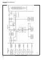
2-1.
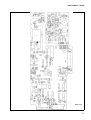
Section 2 of this manual provides a basic description of the 6080A/AN Synthesized
Signal Generator (also referred to throughout as the "signal generator"). Three major
topics are covered:
•
General Description
Briefly explains the functions and components of the four major sections of the
Generator.
•
Functional Description
Describes the functional blocks of the signal generator and their relations to the
main output parameters: amplitude, frequency, and modulation.
•
Digital Controller Software Description
Describes the software and how it affects the hardware.
GENERAL DESCRIPTION
2-2.
The 6080A/AN Synthesized Signal Generator has four major sections:
•
The front panel section includes the keyboard and display for local control.
•
The upper (synthesizer) module section includes the coarse and fine loop
synthesized signals and the synthesized modulation oscillator.
•
The lower (output) module includes the sum loop, FM oscillator, and the level,
modulation, and control circuits.
•
The rear panel section includes the power supply, cooling fan, and assorted
external connectors.
2-1
THEORY OF OPERATION
Front Panel Section
2-3.
The front panel section of the signal generator provides the operator interface,
including the primary controls, connectors, and indicators. All front panel keys and
displays (except the power switch that directly controls the power supply) are
monitored and handled by the A13 Controller PCA, which is located in the output
module section.
Upper/Lower Module Sections
2-4.
The two module sections are multi-compartmented, shielded enclosures that contain
the circuits that generate the instrument stimulus functions: frequency, modulation,
and amplitude. These enclosures provide the necessary circuit-to-circuit isolation to
prevent the generation of spurious signals. The enclosures serve to isolate the generator
circuits from the outside environment.
Rear Panel Section
2-5.
The rear panel section includes the power supply, the cooling fan, various external
connectors, and the IEEE-488 Interface connector.
FUNCTIONAL DESCRIPTION
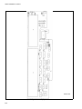
2-6.
The key functional blocks of the signal generator (described in the following
paragraphs) are:
Frequency
Frequency modulation
Phase modulation
Level
Amplitude modulation
Pulse modulation
Internal modulation oscillator
Power supply
Software.
Frequency
2-7.
The output frequency (Fo) is programmable with 1-Hz resolution from 0.01 MHz to
1056 MHz. The band controls are programmed in seven bands that are determined by
the output frequency (Fo). A coarse loop and sub-synthesizer frequency are
determined for each band.
The programming of the coarse loop steering digital-to-analog converter (DAC),
compensation DAC, and VCO control bits are determined from the coarse loop
frequency and the instrument-specific compensation data.
The programming of the sub-synthesizer compensation DAC is determined from the
sub-synthesizer frequency and the instrument-specific compensation data.
The programming of the sum loop steering and compensation DACs are derived from
the output frequency and the instrument-specific compensation data.
The 0.01- MHz to 1056-MHz frequency coverage is divided into the seven bands
shown in Table 2-1.
2-2
THEORY OF OPERATION
Table 2-1. Frequency Coverage Bands
BAND
HET
Divide-by-32
Divide-by-16
Divide-by-8
Divide-by-4
Divide-by-2
Fundamental
FREQUENCY COVERAGE
0.01 to 14.999999 MHz
15 to 31.999999 MHz
32 to 63.999999 MHz
64 to 127.999999 MHz
128 to 255.999999 MHz
256 to 511.999999 MHz
512 to 1056 MHz
Three signals are combined in the sum loop to produce a signal that ranges from 480 to
1056 MHz. This signal is divided by factors of 2 to produce the bands in Table 2-1. The
HET band is produced by mixing 80.01 to 94.999999 MHz (from the Divide-by-8 bad)
with 80 MHz to produce 0.01 to 14.999999 MHz.
The three signals that are combined in the sum loop are 576 to 960 MHz in 8-MHz
steps from the coarse loop, 8 to 16 MHz in 1-Hz steps from the sub-synthesizer, and 80
MHz from the FM circuitry. If the sum loop output frequency is below 760 MHz, the
FM signal and the sub-synthesizer signals are subtracted from the coarse loop signal. If
the sum loop output signal is above 760 MHz, the FM signal and the sub-synthesizer
signals are added to the coarse loop signal.
The A2 Coarse Loop PCA contains the reference circuits and generates a 576 to 960
MHz signal in 8-MHz steps. The main reference frequency for the signal generator is a
40-MHz crystal oscillator. This oscillator is phase locked to either an internal 10-MHz
TXCO, or an external reference. Either a 10-MHz or 5-MHz external reference may be
selected by special function. A 1-or 2-MHz reference may also substituted for the
5-MHz reference by setting a switch on the Coarse Loop PCA. The 40-MHz reference
frequency is doubled to 80 MHz. This is used as the local oscillator for the HET band
and is divided down to 20 MHz for use as the reference for the A14 FM PCA.
The coarse loop generates the 576- to 960-MHz signal using a combination of phase
lock and delay line discriminator frequency control circuitry to produce a low phase
noise signal. The delay line is a 125-ns cable contained in the module.
The sub-synthesizer generates a 16- to 32-MHz signal with 1-Hz resolution. This is
further divided on the Sum Loop PCA to 8 to 16 MHz. The sub-synthesizer generates
the fine frequency steps using a modified N-divider loop with a single-sideband mixer
(SSB) in the feedback path. The sub-synthesizer VCO runs from 160 to 320 MHz. The
reference frequency for the loop is 1 MHz, which would normally provide 1-MHz steps
in a conventional N-divider loop. However, by using pulse deletion, which is
controlled by a rate multiplier, the resolution is extended to 10 kHz. Additional
resolution is gained by introducing a 10- to 20-kHz signal in a SSB mixer. This signal is
produced by a gate array, which contains a 14-bit rate multiplier.
The A14 FM PCA also generates an 80 MHz signal that can be frequency modulated.
These signals are combined in the Sum Loop PCA. The first mixer combines the the
sum loop VCO output (the fundamental frequency, 480 to 1056 MHz) with the coarse
loop frequency (576 to 960 MHz) to produce a signal of 88 to 96 MHz. This signal is
subsequently mixed with the 80 MHz signal from the FM PCA to produce 8 to 16
MHz. This is compared with 8 to 16 MHz from the sub-synthesizer to generate a DC
control voltage that locks the loop.
2-3
THEORY OF OPERATION
Frequency Modulation
2-8.
Frequency modulation (FM) is programmable with three digits of resolution in six
ranges. The deviation is programmed using the 12-bit FM DAC and three FM range
bits. The FM DAC and range settings are dependent on the programmed deviation
and the RF output frequency. The FM DAC and FM Range settings for each
frequency band and FM deviation range are shown in Table 6E-2 in Section 6E. The
FM/øM modes are selected by the control bit PMODL.
The maximum programmable FM deviation is dependent on the RF output
frequency. FM deviations up to 4 MHz may be entered regardless of the output
frequency. However, the STATUS indicator is flashed and the FM DAC is clamped at
full scale if the entry is beyond the allowed upper limit for that frequency band. The
maximum programmable deviation in each frequency band is depicted in Section 4C,
"Modulation" in the Operators Manual.
The FM oscillator loop runs at 80 MHz with several modes of operation. In the low
deviation, low noise mode, the oscillator runs with the highest Q. As deviation is
increased, a linearizer is added to maintain low distortion, which somewhat reduces
spectral purity. At higher deviations, the tuning sensitivity of the oscillator is
increased, again causing a somewhat higher phase noise. At this deviation, the
linearizer is used to maintain low distortion.
The phase lock circuit runs off of various reference frequencies depending on the
deviation selected. To provide a large amount of deviation at low rates, a very wide
range phase detector is used in the wide deviation ACFM mode. Full deviation can be
used down to an FM rate of 100 Hz. An alternate mode of operation that uses the
lowest reference phase detector frequency and the wide range phase detector for all
deviations will allow very low modulation rates for less than maximum deviation.
In DCFM mode, full deviation can be used down to DC levels. The generator is not,
however locked to the main timebase in this mode. When DCFM is enabled, the FM
oscillator's center frequency is set to the previous locked center frequency ±1 kHz by
automatic zeroing circuitry in conjunction with the software routine.
Phase Modulation
2-9.
Phase modulation (øM) is programmable with three digits of resolution in six ranges.
Phase modulation is internally normalized to 10 kHz, then programmed as FM
deviation. The øM index is multiplied by 10 kHz (regardless of the modulation
frequency) to get the "equivalent" FM deviation. Refer to Table 6E-2 (Section 6E) to
determine the FM DAC and range settings from this "equivalent" FM deviation.
The maximum programmable phase modulation deviation is dependent on the RF
output frequency. Phase modulation deviations up to 400 radians may be entered
regardless of the output frequency. However, the STATUS indicator is flashed and the
FM DAC is clamped at full scale if the entry is beyond the allowed upper limit for that
frequency band. The maximum programmable phase modulation deviation in each
frequency band is depicted in Section 4C, "Modulation", of the Operators Manual.
Phase modulation is achieved by reconfiguring the modulation circuits to cause a true
phase modulation response for both internal and external modulation inputs. The
display is correspondingly changed to indicate deviation in radians. Two modes are
available: large deviation at a limited bandwidth and limited deviation for higher rate
bandwidth.
2-4
THEORY OF OPERATION
Output/Level Control
2-10.
Level control is provided by two separate circuits: a step attenuator and a vernier level
DAC. The A20 Attenuator/RPP Assembly provides coarse level control in 6.02-dB
steps. Fine level control is provided by a vernier level DAC that varies the leveling-loop
control voltage. The controller microprocessor automatically controls the step
attenuator and the vernier level DAC. The microprocessor also applies level correction
to compensate for the signal generator frequency response.
Each signal generator has level correction data for both the A8 Output PCA and the
A20 Attenuator/RPP Assembly. The level correction data is stored in the compensation memory located on the A13 Controller PCA. The level correction data is based on
the measurements of each assembly during level compensation of the signal generator.
The level correction data is applied only to the vernier level DAC and does not affect
the coarse level control provided by the Attenuator/RPP Assembly. In other words,
all signal generators have the same attenuator pads inserted at a selected level even
though the correction data is different for each signal generator.
To improve level accuracy in relation to temperature, the signal generator uses a
software temperature-compensation technique. This technique uses data that is the
same for all signal generators.
Amplitude Modulation
2-11.
The signal generator allows amplitude modulation depth programming from 0 to
99.9% with 0.1% resolution. Amplitude modulation depth is programmed using the
12-bit AM DAC. A nominal setting of 2997 on the AM DAC corresponds to 99.9%
AM depth.
The output of the level DAC is the leveling loop-control voltage. The signal generator
output signal is amplitude modulated by varying this control voltage with the
modulating signal. A 1V peak modulating signal from the internal modulation
oscillator or from the external MOD INPUT connector is applied to the AM DAC (a
multiplying digital-to-analog converter). The multiplying factor of this DAC,
corresponding to the programmed percentage of modulation, is calculated by the A13
Controller PCA.
The modulation signal from the AM DAC is summed with a fixed DC reference
voltage. The composite signal (DC plus modulation) is applied to the level DAC (a
level control-multiplying DAC). The multiplying factor for this DAC is also handled
by the A13 Controller PCA and corresponds to the programmed signal level. The
multipling factor also includes the level correction information stored in the
compensation memory.
The operation of the ALC loop causes the amplitude of the RF signal to conform to
this varying control voltage, thus causing amplitude modulation of the signal
generator output.
Pulse Modulation
2-12.
Pulse modulation is accomplished by a single-pole single-throw GaAs FET switch
located at the input to the output amplifier. This switch can be driven by the internal
modulation oscillator or by an external signal. The GaAs FET switch provides a very
fast and high ON/OFF ratio RF pulse.
2-5
THEORY OF OPERATION
Internal Modulation Oscillator
2-13.
The modulation oscillator is made up of two sections; a periodic wave generator and a
pulse generator. Both functions are implemented in a custom integrated circuit and are
synthesized from the main reference frequency source of the 6080A/AN.
The periodic wave generator frequency can be set from 0.1 Hz to 200 kHz with
resolution of 0.1 Hz. It is the modulation source for the internal AM, FM, øM, and
pulse functions. The oscillator is based on an algorithmic wave generation method,
which provides a very accurate and stable signal source of high purity and low
harmonic distortion level. The main function of this system is implemented in a custom
integrated circuit. The waveform data is stored in two EPROMs.
In the pulse generation mode, frequency can be set from 10 Hz to 200 kHz, which
results in a pulse period of 0.1 s through 500 us. The pulse width can be set from 100 ns
to 100 ms, with resolution of 100 ns.
Power Supply Description
2-14.
The power supply is a linear design providing + 15V, -15V, +5V, +37V, +30V, +24V,
+23.4V DC, and 6V AC to the signal generator. All the power supplies are series-pass
regulated except the 6V AC display filament supply. A fuse/filter/line-voltage selector
allows the signal generator to operate from 115 or 230V AC.
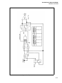
DIGITAL CONTROLLER SOFTWARE DESCRIPTION
2-15.
The signal generator software is executed on an 68HCOOO microprocessor located in
the A13 Controller PCA. The instrument program is stored in 256K bytes of ROM.
The program stack and RAM variables are stored in 16K bytes of static RAM. A
battery-backed CMOS RAM contains 4K bytes of non-volatile memory for front
panel setups, and 4K bytes of non-volatile calibration/compensation data. An 8K byte
EEPROM contains a redundant copy of the calibration/compensation data. The
software provides the following general functions:
•
Services the front panel and the IEEE-488 Interface.
•
Configures the hardware to produce the required output, then applies calibration
and compensation data to optimize the performance.
•
Implements a set of self-test and diagnostic functions.
User Interface
2-16.
The software is implemented with a simple operating system that allows several tasks
to operate in a round-robin fashion. Input and output to both the front panel and the
IEEE-488 Interface execute at a higher priority and are handled as interrupt routines.
At power-on, the software performs a self-test and initializes both the RAM and the
RF hardware. Four tasks are continuously in operation:
•
•
•
•
2-6
Diagnostic service task
Front panel Key task
Knob task
IEEE-488 task
THEORY OF OPERATION
The diagnostic service task monitors the instrument status signals. The front panel key
task, knob task and IEEE-488 task process user input. A fifth task controls the RF
output when a frequency or amplitude sweep is active. A sixth task is activated only
when needed to process certain STATUS (out-of-range or malfunction) or REJ
ENTRY (rejected entry) conditions that cause the display to flash. A seventh task is
activated when the automatic user compensation procedures have been initiated.
Calibration/Compensation Memory
2-17.
The calibration/compensation memory contains the instrument-specific compensation
data for the coarse loop compensation DAC, coarse loop steering DAC, sum loop
compensation DAC, sum loop steering DAC, sub-synthesizer compensation DAC,
the Output assembly, and the Attenuator assembly. In addition, the AM, FM, level,
and reference oscillator calibration data is stored there. Since the integrity of this data
is crucial to the performance of the signal generator, redundant copies of the data are
kept in two separate non-volatile memory ICs.
Hardware and software protection schemes guard against accidental destruction of the
data. The rear panel switch (labeled CAL|COMP) must be set to the ON position
before updating the calibration/compensation memory.
The calibration/compensation memory self test verifies the CRC checksums of each
data segment. A detailed report of the compensation memory status can be
interrogated from the front panel or the IEEE-488 interface. If errors are detected by
the self test, the signal generator uses only the valid data segments. See Appendix F for
more information on the compensation memory status codes.
Self-Test
2-18.
At power-on, the signal generator automatically tests the digital and analog circuits. If
the signal generator fails any self-test, the test results are automatically displayed as
error codes. Several special functions are available for additional tests (See
"SELF-TEST DESCRIPTION" in Section 6.) In addition, the microprocessor
continuously monitors hardware status signals.
Status Signals
2-19.
The status of the rear panel REF EXT/INT reference switch is continuously
monitored. The state of this switch is used to display the EXTREF annunciator on the
front panel and to program the reference source.
The RF output of the signal generator is considered usable, but not necessarily
calibrated unless the STATUS indicator is flashing. The STATUS indicator flashes
when the output of the instrument is considered unusable because of a severe
overrange condition or a circuit failure.
2-7/2-8
Section 3
Closed-Case Calibration
INTRODUCTION
3-1.
The closed-case calibration procedures allow the RF level, AM depth, FM deviation,
and the internal 10-MHz reference oscillator to be calibrated without removing the
instrument covers.
The calibration procedures can be performed at the specified 2-year calibration
intervals or whenever one wishes to optimize the performance of the 6080A/AN
Synthesized Signal Generator.
The procedures can be performed from the front panel or remotely under the control of
an IEEE-488 bus controller. Each procedure consists of the following steps:
1. Set the rear panel CAL|COMP switch to the 1 (on) position.
2. Initiate the calibration procedure.
3.
Connect the required measurement equipment to the signal generator's RF output.
4. Adjust the parameter of interest until the meter reading matches a predetermined
target value.
5.
Store the updated calibration factor.
Although these procedures are useful for periodic calibration, they cannot correct
hardware failures. If the required adjustment exceeds the procedure's adjustment
limits, the signal generator needs repair and "CIRCUIT DESCRIPTIONS, TROUBLESHOOTING, AND ALIGNMENT" in Section 6 should be consulted.
3-1
CLOSED-CASE CALIBRATION
Front Panel Calibration
3-2.
The bright-digit editing feature is used to perform the adjustments when performing a
front panel calibration procedure. Each calibration subsection describes the function
of the front panel controls during the procedure.
Remote Calibration
3-3.
The remote calibration procedures allow the signal generator to be calibrated in a
totally automated station. When equipped with the required measurement equipment
and controller software, the process is reduced to connecting the instrument cables and
executing the program.
The controller and signal generator work together in a tightly coupled system. The sole
function of the controller software is to obtain valid readings from the measurement
equipment and convert them into a format understood by the signal generator. The
controller software must ensure that every reading is settled and valid before sending it
to the signal generator.
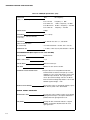
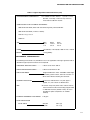
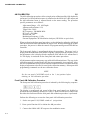
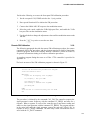
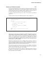
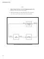
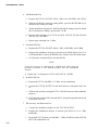
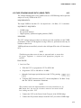
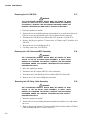
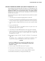
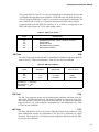
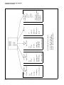
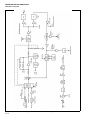
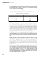
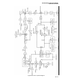
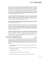
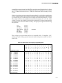
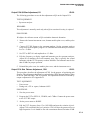
The basic structure of a calibration program is shown in Figure 3-1.
Initiate 6080A/AN calibration procedure
Initialize measurement equipment
Loop
Ask 6080A/AN for RF frequency
Exit loop if frequency is special end code "9E+09"
Get reading from measurement equipment
Send reading the 6080A/AN
End loop
Save calibration data
Exit calibration procedure
Figure 3-1. Basic Structure of Calibration Program
The controller initiates the calibration procedure and initializes the measurement
equipment. Then it requests the signal generator's RF frequency and waits for a
response. When a response is received, the controller gets a reading from the
measurement equipment and sends it to the signal generator. The program remains in
the loop until the signal generator returns the end code in response to the frequency
query. The loop is then exited and the data is saved in the calibration memory.
The controller queries the signal generator's RF frequency at each step to synchronize
its actions with the signal generator and to determine when the procedure is complete.
When the signal generator receives a reading, it updates its internal settings and does
not respond to the next frequency query until it is ready for another reading. The
controller must wait for the signal generator's output to settle before it is allowed to
take another reading.
The signal generator continues to receive readings and make adjustments until it gets
two consecutive readings within the error tolerance for the procedure, at which time
the adjustment is considered valid. The signal generator notifies the controller of this
by returning the special end code of "9E+09 Hz" in response to the next frequency
query.
3-2
CLOSED-CASE CALIBRATION
The error tolerance is defined for each procedure as a range of readings around the
target value that the signal generator expects to receive when the adjustment is correct.
The division of responsibility between the controller and signal generator allows
measurement equipment from various manufacturers to be used. Adding a different
meter to the system requires only that a new driver module be written for the
controller.
NOTE
The design of the controller software has a major impact on the accuracy
realized. One must carefully determine when the readings are settled and
average several readings before sending the result to the 6080A/AN.
Where applicable, the meter specific calibration factors should be applied
to the readings.
A sample program for each of the remote procedures is included in Appendix G. The
programs are written in Fluke BASIC and run on a Fluke 1722A controller.
Calibration Data
3-4.
The calibration data is stored along with the compensation data in non-volatile
memory. A redundant storage scheme enhances the integrity of the data. One copy of
the data is stored in the battery backed RAM and an identical copy is stored in the
EEPROM.
The rear panel slide switch labeled CAL|COMP must be set to the 1 (ON) position
before a calibration procedure can be initiated. The CAL and COMP annunciators
flash when the switch is in the 1 (ON) position. When a calibration procedure is
initiated, the CAL and COMP annunciators stop flashing, and the CAL annunciator
remains lit during the procedure. When the switch is in the 0 (OFF) position, the data is
write protected in hardware.
The calibration data can be generated in one of two ways: by the Fluke factory or by
the user. Each calibration data segment contains a data origin tag which specifies how
the data was created.
Special function 05 displays the calibration and compensation data origin codes. If no
user calibration or compensation procedures have been performed, the special
function displays origin code 00 to signify that all of the data originated at the Fluke
factory. If any user calibration procedures have been performed, the corresponding
code is displayed. For example, if the AM calibration procedure has been performed
by the user, the data origin special function will display the code 528. A complete list of
the data origin codes is given in Appendix F.
3-3
CLOSED-CASE CALIBRATION
AM CALIBRATION
3-5.
The AM calibration procedures allow a single point calibration of the AM depth to be
performed. An RF modulation meter is connected to the 6080A/AN's RF output and
the AM calibration factor is adjusted based on the meter reading. The procedure
specific parameters are as follows:
Adjustment Range: ±5% AM Depth
Adjustment Resolution: 0.1%
Target Value: 50.0%
RF Frequency: 300.000000 MHz
RF Level: +10.0 dBm
Internal AM: ON
Modulation Frequency: 1 kHz
External Equipment: RF Modulation Analyzer (HP 8901A or equivalent)
When performing the front panel procedure, use the edit knob to adjust the AM depth
until the measured AM depth matches the target value. When performing the remote
procedure, the process is under the control of a program running on an IEEE-488 bus
controller.
The front panel display is reconfigured during the procedures. The target level is
displayed in the modulation field, the RF frequency is displayed in the frequency field,
the adjustment value is displayed in the amplitude field, and the CAL annunciator is
lit. The display is consistent for the front panel and remote procedures.
All adjustments update a temporary copy of the AM calibration factor. The copy in the
calibration memory is updated only after the store command is given explicitly. After
the store command has been given, the internal calibration factor is calculated from the
displayed adjustment value and is stored in the calibration memory. Subsequent AM
programming commands use the new calibration factor.
NOTE
Set the rear panel CAL/COMP switch to the 1 (on) position before
initiating an AM calibration procedure.
Front Panel AM Calibration Procedure
3-6.
The front panel AM calibration procedure is initiated by the following key sequence:
The display is reconfigured and several of the front panel controls are disabled or
operate differently than they normally do. Table 3-1 shows all of the active controls and
describes their function while the front panel AM calibration procedure is performed.
Perform the following to execute the front panel AM calibration procedure:
1. Set the rear panel CAL|COMP switch to 1 (on) position.
2. Enter special function 991 to initiate the AM procedure.
3. Connect the 6080A/AN's RF output to the modulation meter.
3-4
CLOSED-CASE CALIBRATION
4. Select the peak+ mode, enable the 50-Hz high-pass filter, and enable the 3 kHz
low-pass filter on the modulation meter.
5. Use the edit knob to change the adjustment value until the modulation meter reads
50.0%.
6. Press
twice to store the new data.
Table 3-1. Front Panel Controls for AM Calibration Procedure
CONTROLS
FUNCTION AND DESCRIPTION
Bright-Digit Editing
KNOB
Turn the edit knob to adjust the AM calibration factor. Use the left/right
arrow keys to move the bright-digit within the adjustment field. The
bright-digit is always located in the adjustment field.
RF on/off
Toggles the RF output on/off.
Overrange/uncal or Rejected Entry Status
Normally displays the overrange/uncal status. Displays the rejected entry
status code if there is a rejected entry.
Store Measured Data
Press once; the prompt "Sto ?" is displayed.
Press again to store the data. The message "— Sto —" is displayed to
confirm the selection. The updated calibration factor is stored in the
calibration memory, and the last valid instrument state is restored.
Press any other key to cancel the store operation and resume the
procedure.
Abort the Cal Procedure
Press once; the prompt "Clr ?" is displayed.
Press again to abort the procedure. The message "— Clr —" is displayed
to confirm the selection. All measured data is discarded and the previous
instrument state is restored.
Press any other key to resume the procedure.
3-5
CLOSED-CASE CALIBRATION
Remote AM Calibration Procedure
3-7.
This following paragraphs describe the remote AM calibration procedure, the remote
commands used in the procedure, and the elements required to build a functioning
controller program. Refer to the heading "Remote Calibration" (earlier in Section 3)
for general information relating to all remote calibration procedures.
A complete program listing that runs on a Fluke 1722A controller is provided in
Appendix G.
The basic structure of the AM calibration program is shown in the program in Figure
3-2.
initiate the AM calibration procedure with "CAL_AM"
initialize modulation meter
MAIN_LOOP:
request the RF frequency with "CC_FREQ?"
if( frequency = 9e9) goto DONE
read modulation meter
send reading to 6080A/AN with "CC_RDAM"
goto MAIN_LOOP
DONE:
store new data in calibration memory with "CC_SAVE"
end
Figure 3-2. Structure of the AM Calibration Program
The procedure is initiated by the command CAL_AM. The controller requests the
signal generator's center frequency with the command CC_FREQ? and waits for a
response. When a response is received, the controller gets a mod meter reading and
sends it to the signal generator with the command CC_RDAM. The program remains
in the main loop until the signal generator returns the end code "9E+09, Hz" in
response to the CC_FREQ? command. The main loop is then exited and the data is
saved with the CC_SAVE command.
Each time the signal generator receives a reading from the controller, it adjusts its
internal settings and programs the new AM depth. When the signal generator receives
two consecutive readings within 0.1% of the target value (50.0%), it considers the
adjustment value correct and returns the end code.
The controller program must ensure that each mod meter reading is settled before
sending the reading to the 6080A/AN. The program listing in Appendix G uses a
simple but effective method to obtain valid mod meter readings.
The programming commands used in a remote AM calibration procedure are listed in
the Table 3-2. See Table 5B-3 in Section 5B of the Operator Manual for a complete
syntax description of each command.
3-6
CLOSED-CASE CALIBRATION
Table 3-2. Remote Programming Commands for AM Calibration Procedure
DESCRIPTION
COMMANDS
CAL_AM
Initiate the remote AM calibration procedure
CC_RDAM
Send the mod meter reading to the 6080A/AN
CC_FREQ?
Request the RF frequency
CC_TARGET?
Request the target value
RFOUT
Program the RF output on/off
CC_SAVE
Save the measured data
CC_EXIT
Abort the cal procedure immediately
ERROR?
Request the rejected entry status
STATUS/STATUS?
Load/Request the overrange/uncal status
FM CALIBRATION
3-8.
The FM calibration procedures allow a single point calibration of the FM deviation to
be performed. An RF modulation meter is connected to the 6080A/AN's RF output,
and the FM calibration factor is adjusted based on the meter reading. The procedure
specific parameters are as follows:
Adjustment Range: ± 10 kHz
Adjustment Resolution: 0.1 kHz
Target Value: 100 kHz
Frequency: 640.000000 MHz
RF Level: +10.0 dBm
Internal AM: ON
Modulation Frequency: 1 kHz
External Equipment: RF Modulation Analyzer (HP 8901A or equivalent)
When performing the front panel procedure, use the edit knob to adjust the FM
deviation until the measured FM deviation matches the target value. When the remote
procedure is performed, the process is under the control of a program running on an
IEEE-488 bus controller.
The front panel display is reconfigured during the procedures. The target level is
displayed in the modulation field, the RF frequency is displayed in the frequency field,
the adjustment value is displayed in the amplitude field, and the CAL annunciator is
lit. The display is consistent for the front panel and remote procedures.
All adjustments update a temporary copy of the FM calibration factor. The copy in the
calibration memory is updated only after the store command is given explicitly. After
the store command has been given, the internal calibration factor is calculated from the
displayed adjustment value and is stored in the calibration memory. Subsequent FM
programming commands use the new calibration factor.
NOTE
Set the rear panel CAL COMP switch to the 1 (on) position before
initiating an FM calibration procedure.
3-7
CLOSED-CASE CALIBRATION
Front Panel FM Calibration Procedure
3-9.
The front panel FM calibration procedure is initiated by the following key sequence:
The display is reconfigured for the procedure. Several of the front panel controls are
disabled or operate differently than they normally do. Table 3-3. shows all of the active
controls and describes their function while performing the front panel FM calibration
procedure.
Table 3-3. Front Panel Controls for FM Calibration Procedure
CONTROLS
FUNCTION AND DESCRIPTION
Bright-Digit Editing
KNOB
Turn the edit knob to adjust the FM calibration factor. Use the left/right
arrow keys to move the bright-digit within the adjustment field. The
bright-digit is always located in the adjustment field.
RF on/off
Toggles the RF output on/off.
Overrange/uncal or Rejected Entry Status
Normally displays the overrange/uncal status. Displays the rejected entry
status code if there is a rejected entry.
Store Measured Data
Press once; the prompt "Sto ?" is displayed.
Press again to store the data. The message "— Sto —" is displayed to
confirm the selection. The updated calibration factor is stored in the
calibration memory, and the last valid instrument state is restored.
Press any other key to cancel the store operation and resume the
procedure.
Abort the Cal Procedure
Press once; the prompt "Clr ?" is displayed.
Press again to abort the procedure. The message "— Clr —" is displayed
to confirm the selection. All measured data is discarded and the previous
instrument state is restored.
Press any other key to resume the procedure.
3-8
CLOSED-CASE CALIBRATION
Perform the following to execute the front panel FM calibration procedure:
1. Set the rear panel CAL|COMP switch to the 1 (on) position.
2. Enter special function 992 to initiate the FM procedure.
3. Connect the 6080A/AN's RF output to the modulation meter.
4. Select the peak+ mode, enable the 50-Hz high-pass filter, and enable the 3 kHz
low-pass filter on the modulation meter.
5. Use the edit knob to change the adjustment value until the modulation meter reads
100 kHz
6. Press the
key twice to store the new data.
Remote FM Calibration
3-10.
The following paragraphs describe the remote FM calibration procedure, the remote
commands used in the procedure, and the elements required to build a functioning
controller program. Refer to the heading "Remote Calibration" (earlier in Section 3)
for general information relating to all remote calibration procedures.
A complete program listing that runs on a Fluke 1722A controller is provided in
Appendix G.
The basic structure of the FM calibration program is shown in Figure 3-3.
initiate the FM calibration procedure with "CAL_FM"
initialize modulation meter
MAIN_LOOP:
request the RF frequency with "CC_FREQ?"
if( frequency = 9e9) goto DONE
read modulation meter
send reading to 6080A/AN with "CC_RDFM"
goto MAIN_LOOP
DONE:
store new data in calibration memory with "CC SAVE"
end
Figure 3-3. Basic Structure of FM Calibration Program
The procedure is initiated by the command CAL_FM. The controller requests the
signal generator's center frequency with the command CC_FREQ? and waits for a
response. When a response is received, the controller gets a mod meter reading and
sends it to the signal generator with the command CC_RDFM. The program remains
in the main loop until the signal generator returns the end code "9E+09, Hz" in
response to the CC_FREQ? command. The main loop is then exited and the data is
saved with the CC_SAVE command.
3-9
CLOSED-CASE CALIBRATION
Each time the signal generator receives a reading from the controller, it adjusts its
internal settings and programs the new FM deviation. When the signal generator
receives two consecutive readings within 0.1 kHz of the target value (100 kHz) it
considers the displayed adjustment value correct and returns the end code.
The controller program must ensure that each mod meter reading is settled before
sending it to the 6080A/AN. The program listing in Appendix G uses a simple but
effective method to obtain valid mod meter readings.
The programming commands used in a remote FM calibration procedure are listed in
the Table 3-4. See Table 5B-3 in Section 5B of the Operator Manual for a complete
syntax description of each command.
Table 3-4. Remote Programming Commands for FM Calibration Procedure
COMMANDS
DESCRIPTION
CAL_FM
Initiate the remote FM calibration procedure
CC_RDAM
Send the mod meter reading to the 6080A/AN
CC_FREQ?
Request the RF frequency
CC_TARGET?
Request the target value
RFOUT
Program the RF output on/off
CC_SAVE
Save the measured data
CC_EXIT
Abort the cal procedure immediately
ERROR?
Request the rejected entry status
STATUS/STATUS?
Load/Request the overrange/uncal status
RF LEVEL CALIBRATION
3-11.
The RF level calibration procedures allow a single-point calibration of the RF output
level to be performed. An RF power meter is connected to the signal generator's RF
output and the level calibration factor is adjusted based on the meter reading. The
procedure specific parameters are as follows:
Adjustment Range: ± 1.00 dB
Adjustment Resolution: 0.01 dB
Target Value: 10.0 dBm
Frequency: 300.000000 MHz
RF Level: +10.0 dBm
External Equipment: RF Power Meter (HP 436A or equivalent)
When performing the front panel procedure, use the edit knob to adjust the level until
the measured level matches the target level. When the remote procedure is performed,
the process is under the control of a program running on an IEEE-488 bus controller.
3-10
CLOSED-CASE CALIBRATION
The front panel display is reconfigured during the procedures. The target level is
displayed in the modulation field, the RF frequency is displayed in the frequency field,
the adjustment value is displayed in the amplitude field, and the CAL annunciator is
lit. The display is consistent for the front panel and remote procedures.
All adjustments update a temporary copy of the adjustment value. The copy in the
calibration memory is updated only after the store command is given explicitly. After
the store command has been given, the internal calibration factor is calculated from the
displayed adjustment value and is stored in the calibration memory. Subsequent
amplitude programming commands use the new calibration factor.
NOTE
Set the rear panel CAL/COMP switch to the 1 (on) position before
initiating the calibration procedures.
Front Panel Level Calibration Procedure
3-12.
The front panel level calibration procedure is initiated by the following key sequence:
The display is reconfigured for the procedure. Several of the front panel controls are
disabled or operate differently than they normally do. Table 3-5. shows all of the active
controls and describes their function while performing the front panel level calibration
procedure.
Perform the following to execute the front panel level calibration procedure:
1. Set the rear panel CAL|COMP switch to the 1 (on) position.
2. Enter special function 993 to initiate the procedure.
3. Connect the signal generator's RF output to the power meter.
4. Set the appropriate power meter calibration factor (if required) and zero the power
meter.
5. Use the edit knob to change the adjustment value until the power meter reads +10
dBm.
6. Press the
key twice to store the new data.
3-11
CLOSED-CASE
CALIBRATION
Table 3-5. Front Panel Controls for Level Calibration Procedure
CONTROLS
FUNCTION AND DESCRIPTION
Bright-Digit Editing
KNOB
Turn the edit knob to adjust the level calibration factor. Use the left/right
arrow keys to move the bright-digit within the adjustment field. The
bright-digit is always located in the adjustment field.
RF on/off
Toggles the RF output on/off.
Overrange/uncal or Rejected Entry Status
Normally displays the overrange/uncal status. Displays the rejected entry
status code if there is a rejected entry.
Store Measured Data
Press once; the prompt "Sto ?" is displayed.
Press again to store the data. The message "— Sto —" is displayed to
confirm the selection. The updated calibration factor is stored in the
calibration memory, and the last valid instrument state is restored.
Press any other key to cancel the store operation and resume the
procedure.
Abort the Cal Procedure
Press once; the prompt "Clr ?" is displayed.
Press again to abort the procedure. The message "— Clr —" is displayed
to confirm the selection. All measured data is discarded and the previous
instrument state is restored.
Press any other key to resume the procedure.
3-12
CLOSED-CASE CALIBRATION
Remote Level Calibration Procedure
3-13.
The following paragraphs describe the remote level calibration procedure, the remote
commands used in the procedure, and the elements required to build a functioning
controller program. Refer to the heading "Remote Calibration" (earlier in Section 3)
for general information relating to all remote calibration procedures.
A complete program listing that runs on a Fluke 1722A controller is provided in
Appendix G.
The basic structure of the level calibration program is shown in Figure 3-4.
initiate the level calibration procedure with "CAL_LEVEL"
initialize power meter
MAIN_LOOP:
request the RF frequency with "CC_FREQ?"
if( frequency = 9e9) goto DONE
read power meter
send reading to 6080A/AN with "CC_RDOWER"
goto MAIN__LOOP
DONE:
store new data in calibration memory with "CC_SAVE"
end
Figure 3-4. Basic Structure of Level Calibration Program
The procedure is initiated by the command CAL_LEVEL. The controller requests the
signal generator's center frequency with the command CC_FREQ? and waits for a
response. When a response is received, the controller gets a power meter reading and
sends it to the signal generator with the command CC_RDPOWER. The program
remains in the main loop until the signal generator returns the end code "9E+09, Hz" in
response to the CC_FREQ? command. The main loop is then exited and the data is
saved with the CC_SAVE command.
Each time the signal generator receives a reading from the controller, it adjusts its
internal settings and programs the new level. When the signal generator receives two
consecutive readings within 0.01 dB of the target value (10.00 dBm) it considers the
displayed adjustment value correct and returns the end code.
The controller program must ensure that each power meter reading is settled before
sending it to the signal generator. The program listing in Appendix G uses a simple but
effective method to obtain valid power meter readings.
The programming commands used in a remote level calibration procedure are listed in
the Table 3-6. See Table 5B-3 in Section 5B of the Operator Manual for a complete
syntax description of each command.
3-13
CLOSED-CASE CALIBRATION
Table 3-6. Remote Programming Commands for Level Calibration Procedure
COMMANDS
DESCRIPTION
CAL_LEVEL
Initiate the remote level calibration procedure
CC_RPOWER
Send the power meter reading to the 6080A/AN
CC_FREQ?
Request the RF frequency
CC_TARGET?
Request the target value
RFOUT
Program the RF output on/off
CC_SAVE
Save the measured data
CC_EXIT
Abort the cal procedure immediately
ERROR?
Request the rejected entry status
STATUS/STATUS?
Load/Request the overrange/uncal status
REFERENCE OSCILLATOR CALIBRATION
3-14.
The reference oscillator calibration procedures allow a single-point calibration of the
internal 10-MHz reference oscillator to be performed. A frequency counter is
connected to the 6080A/AN's RF output, and the reference oscillator calibration
factor is adjusted based on the counter reading. The procedure specific parameters are
as follows:
Adjustment Range: 256 counts (6 ppm minimum)
Adjustment Resolution: 1 count
Target Value: 100 MHz
RF Frequency: 100 MHz
External Equipment: Frequency Counter (Fluke 1953A or equivalent)
When performing the front panel procedure, use the edit knob to adjust the calibration
factor until the measured frequency matches the target value. When performing the
remote procedure, the process is under the control of a program running on an
IEEE-488 bus controller.
The front panel display is reconfigured during the procedures. The target level is
displayed in the modulation field, the RF frequency is displayed in the frequency field,
the adjustment value is displayed in the amplitude field, and the CAL annunciator is
lit. The display is consistent for the front panel and remote procedures and is shown
below.
All adjustments update a temporary copy of the adjustment value. The copy in the
calibration memory is only updated after the store command is given explicitly. After
the store command has been given, the internal calibration factor is calculated from the
displayed adjustment value and is stored in the calibration memory.
NOTE
This procedure can be used only to adjust the frequency of the internal
reference oscillator. It cannot be used to adjust the frequency of the
optional high-stability or medium-stability references.
3-14
CLOSED-CASE CALIBRATION
NOTE
The rear panel CAL|COMP switch must be set to the 1 (on) position
before initiating the calibration procedures.
Front Panel Reference Oscillator Calibration Procedure
3-15.
The front panel reference oscillator calibration procedure is initiated by the following
key sequence:
The display is reconfigured for the procedure. Several of the front panel controls are
disabled or operate differently than they normally do. Table 3-7. shows all of the active
controls and describes their function while performing the procedure.
Table 3-7. Front Panel Controls for Reference Oscillator Calibration Procedure
FUNCTION AND DESCRIPTION
CONTROLS
Bright-Digit Editing
KNOB
Turn the edit knob to adjust the reference oscillator calibration factor.
Use the left/right arrow keys to move the bright-digit within the adjustment field. The bright-digit is always located in the adjustment field.
RF on/off
Toggles the RF output on/off.
Overrange/uncal or Rejected Entry Status
Normally displays the overrange/uncal status. Displays the rejected entry
status code if there is a rejected entry.
Store Measured Data
Press once; the prompt "Sto ?" is displayed.
Press again to store the data. The message "— Sto —" is displayed to
confirm the selection. The updated calibration factor is stored in the
calibration memory, and the last valid instrument state is restored.
Press any other key to cancel the store operation and resume the
procedure.
Abort the Cal Procedure
Press once; the prompt "Clr ?" is displayed.
Press again to abort the procedure. The message "— Clr —" is displayed
to confirm the selection. All measured data is discarded and the previous
instrument state is restored.
Press any other key to resume the procedure.
3-15
CLOSED-CASE CALIBRATION
Perform the following to execute the front panel reference oscillator calibration
procedure:
1. Set the rear panel CAL|COMP switch to the 1 (on) position.
2. Enter special function 994 to initiate the procedure.
3. Connect the 6080A/AN's RF output to the FLUKE 1953A's FREQA input.
4. Select the FREQA input, 1 second gate time, and the continuous trigger mode.
5. Use the edit knob to change the adjustment value until the counter reads 100 MHz.
6. Press the
key twice to store the new data.
Remote Reference Oscillator Calibration Procedure
3-16.
The following paragraphs describe the remote reference oscillator calibration
procedure, the remote commands used in the procedure, and the elements required to
build a functioning controller program. Refer to the heading "Remote Calibration"
(earlier in Section 3) for general information relating to all remote calibration
procedures.
A complete program listing that runs on a Fluke 1722A controller is provided in
Appendix G.
The basic structure of the level calibration program is shown in Figure 3-5.
initiate the reference oscillator calibration procedure with "CAL_REFOSC"
initialize frequency counter
MAIN_LOOP:
request the RF frequency with "CC_FREQ?"
if( frequency = 9e9) goto DONE
read frequency counter
send reading to 6080A/AN with "CC_RDFREQ"
goto MAIN_LOOP
DONE:
store new data in calibration memory with "CC_SAVE"
end
Figure 3-5. Basic Structure of the Reference Oscillator Calibration Program
3-16
CLOSED-CASE CALIBRATION
The calibration procedure is initiated by the command CAL_REFOSC. The
controller requests the signal generator's center frequency with the command
CC_FREQ? and waits for a response. When a response is received, the controller gets a
counter reading and sends it to the signal generator with the command CC_RDFREQ.
The program remains in the main loop until the signal generator returns the end code
"9E+09, Hz" in response to the CC_FREQ? command. The main loop is then exited
and the data is saved with the CC_SAVE command.
Each time the signal generator receives a reading from the controller, it adjusts its
internal settings and programs the new reference oscillator DAC setting. When the
signal generator receives two consecutive readings within 10 Hz of the target value (100
MHz) it considers the displayed adjustment value correct and returns the end code.
The controller program must ensure that each counter reading is settled before sending
it to the signal generator. The program listing in Appendix G uses a simple but effective
method to obtain valid counter readings.
The programming commands used in a remote level calibration procedure are listed in
the Table 3-8. See Table 5B-3 in Section 5B of the Operator Manual for a complete
syntax description of each command.
Table 3-8. Remote Programming Commands for Reference Oscillator Calibration Procedure
COMMANDS
DESCRIPTION
CAL_REFOSC
Initiate the remote reference oscillator calibration procedure
CC_RDFREQ
Send the counter meter to the 6080A/AN
CC_FREQ?
Request the RF frequency
CC_TARGET?
Request the target value
RFOUT
Program the RF output on/off
CC_SAVE
Save the measured data
CC_EXIT
Abort the cal procedure immediately
ERROR?
Request the rejected entry status
STATUS/STATUS?
Load/Request the overrange/uncal status
3-17/3-18
Section 4
Performance Tests
INTRODUCTION
4-1.
The information in the Section 4 describes the performance tests for the key
parameters of the 6080A/AN Synthesized Signal Generator (also referred to
throughout as the "signal generator").
Instrument specifications are used as the performance standard. These closed-case
performance tests may be used as:
•
An acceptance test upon receipt of the instrument
•
An indication that repair and/or calibration is required
•
A performance verification after completing repairs or calibration of the
instrument.
Individual performance tests can also be used as troubleshooting aids.
The signal generator being tested (referred to as UUT — the "unit under test") must be
warmed up with all covers in place for at least 2 hours before starting the performance
tests.
Fluke recommends that calibration be performed once a year.
TEST EQUIPMENT
4-2.
Table 4-1 lists the recommended test equipment for the performance tests, adjustment
procedures, and troubleshooting the signal generator. Figure 4-1 shows a two-turn
loop.
4-1
PERFORMANCE TESTS
Table 4-1. Recommended Test Equipment
INSTRUMENT NAME
MINIMUM REQUIREMENT
MANUFACTURER
DESIGNATION
NOTES1
DVM
5 1/2-Digit, 0.3% DC-20 kHz
JF
8840A-09
DMM
RMS Voltmeter
3 1/2-Digit, 1% DC and 1 kHz
10 Hz to 20 MHz, low noise
JF
JF
8020B
8922A
Wideband Amplifier
> 25-dB gain, 0.4 to 1050 MHz
NF < 9dB
HP
8447D-010
RF-Spectrum Analyzer
0.1 to 1.7 GHz, 100 Hz BW
HP
8568A
P,T
Oscilloscope
Four-trace 300 MHz, 5-mV/Div
TEK
2465-11
T,P
FET Probe
DC-900 MHz
TEK
6201
T
500-ohm Probe
DC-3.5 GHz, 10X
TEK
P6156
T
RF Voltmeter
0.01 to 700 MHz, 0.01 to 3V ± 10%
HI
RF 801
T2
Frequency Counter
0.1-1050 MHz; 10 Hz res; 0.1V
JF
7220A
A,P,T
Modulation Analyzer
Input: 0.15 to 1300 MHz, 0 to +20 dBm HP
8901A
w/Option -003
A,P,T
A,P
A,P,T
P
AM: 10 to 90%, ±1%,
FM: 0.1 to 100 kHz dev ±1%
External LO capability
4-2
Distortion Analyzer
1 to 10% rng, ±1 dB, 0.4 and 1 kHz
HP
339B
A,P,T
Power Meter
Instrumentation accuracy < ±1%
HP
436A
A.P.T
Power Sensor
(High-level)
-30 to 20 dBm; VSWR < 1.2 for
0.4 to 1 MHz, < 1.1 for 1 to
2000 MHz, < 1.3 for > 2000 MHz
HP
8482A
Power Sensor
(Low-Level)
-67 to -20 dBm; VSWR < 1.4 for
10 to 30 MHz < 1.15 for 30 to
2100 MHz
HP
8484A
Attenuator, 50, 20 dB
0.1 to 2100 MHz VSWR < 1.15
Narda 777C
LF Synthesized Signal
Generator
10 Hz to 11 MHz, 10 Hz steps,
1V peak, Spurs and Harm < -50 dB
JF
6011A
A,P
HF Synthesized
Sig-Gen
(Low Residual)
0.5 to 1024 MHz
JF
6080A/AN
P,T
P3
PERFORMANCE TESTS
Table 4-1. Recommended Test Equipment (cont)
INSTRUMENT NAME
MINIMUM REQUIREMENT
MANUFACTURER
DESIGNATION
NOTES1
Frequency Standard
House Standard, 10 MHz
Test Cable
Dual pin to BNC
JF
732891
A,T
Adapter, Coax
50-ohm, Type-N(m) to BNC(f)
JF
Y9308
A,P,T
Adapter, Service
50-ohm, Module output to SMA
JF
744177
T
Two-Turn Loop
For Leakage test (See Figure 4-1)
Homebuilt
VSWR Bridge
10 to 2000 MHz
Wiltron 60N50
P
50-Ohm Termination
Type-N
JF
P
Coaxial Cable, 50 ohm
3 ft, BNC both ends
Y9111
A,P,T
Coaxial Cable, 50 ohm
6 ft, BNC both ends
Y9112
A,P,T
Screwdriver, electric
Set to 7 inch-pounds torque
JergensCL6500/CLT50
A,P
Y9317
P,T4
A,T
Power Supply, Variable 0 to 30V dc
Lambda
T
Measuring Receiver
Set
10 to 1300 MHz
HP
8902A
P
Sensor Module
0.1 to 2600 MHz
HP
11722A
P
Pulse Generator
50-ns pulse width,
10-MHz repetition rate
HP
8012B
P
BNC Termination
50 ohm
Midwest Microwave
2048M
P
Detector
3-GHz bandwidth, 5-ns rise time
Krytar D101
P
HP
P
Phase Noise
Measurement System
Tuning Tool
.025-inch square drive
3048A
Johanson
#4192
NOTES:
1. A = Adjustment; P = Performance Test; T = Troubleshooting.
2. Helper Instruments.
3. VSWR verified and actual attenuation calibrated to ± 0.2 dB by the operator at application
frequencies.
4. Two-Turn, 1-inch diameter loop made of #18 enamel wire soldered to a BNC connector.
4-3
PERFORMANCE TESTS
Figure 4-1. Two-Turn Loop
POWER-ON TEST
4-3.
This performance test is the built-in self-test that performs a simple functional check of
the instrument.
REQUIREMENT:
The signal generator successfully passes the self-test.
REMARKS:
The test is begun each time the signal generator is turned on. Press any of the
FUNCTION keys or the
key to abort the test.
PROCEDURE:
1. Start the test with the power off.
2. Press the POWER button on.
The signal generator automatically starts the self-tests, which include lighting all
indicators and every segment of the display. This test takes 5 seconds.
If the instrument fails any of the self-tests, the results are shown in the four display
fields. See Appendix E for the interpretation of the test failure codes.
If the signal generator passes the self-test, it is automatically returned to the default
instrument state.
4-4
PERFORMANCE TESTS
FREQUENCY ACCURACY TEST
4-4.
The internal time base is compared to that of a Frequency Standard.
REQUIREMENTS:
The frequency of the UUT time base is within the specified limits.
TEST EQUIPMENT:
•
•
Frequency standard
Frequency counter
PROCEDURE:
1. Connect the frequency standard output to the 10 MHZ REF IN connector on the
frequency counter and switch the counter to EXT REF.
2. Switch the UUT to internal reference.
3. Connect the UUT REF OUT connector to the frequency counter CHANNEL A
input connector.
4. Verify that the counter display is 10 MHz ±100 Hz.
5. Monitor the frequency for one hour to verify its stability within ±0.5 Hz.
(Operating temperature within ±5°C).
SYNTHESIS TEST
4-5.
The signal generator output frequency is measured at several programmed frequencies
using a frequency counter operating on a common reference with the signal generator.
REQUIREMENT:
The signal generator's measured and programmed frequencies agree within ±1 count.
TEST EQUIPMENT:
•
Frequency counter
REMARKS:
If the UUT fails this test, the frequency synthesis circuitry is probably at fault. See
Section 6C.
PROCEDURE:
1. Connect the UUT 10 MHz OUT to the frequency counter 10-MHz reference input,
and connect the UUT RF OUTPUT to the frequency counter input.
2. Set the UUT REF INT/EXT switch to INT.
3. Program the UUT to SPCL 909.
4-5
PERFORMANCE TESTS
4. Program the UUT frequency to 111.111111 MHz.
5. Program the UUT frequency step to 111.111111 MHz.
6. Verify that the reading on the frequency counter agrees with the UUT frequency ± 1
count as the frequency is stepped from 111.111111 to 999.999999 MHz.
HIGH-LEVEL ACCURACY TEST
4-6.
The output power is measured using a power meter at various frequencies. First the
step attenuator is set for zero attenuation; then each attenuator section is individually
programmed. Finally, the output level accuracy and attenuator section errors are
computed.
If a measuring receiver is available for level testing, proceed directly to the
"ALTERNATE-LEVEL ACCURACY TEST" procedure later in Section 4.
TEST EQUIPMENT:
•
•
Power meter
Power sensor (high-Level)
REQUIREMENT:
The output level accuracy, the attenuator section errors, and the sum of the attenuator
section errors at each test frequency are:
< ±1.5 dB from 0.5 to 1024 MHz
REMARKS:
If the UUT fails this performance test, it needs to be calibrated (Section 3) or repaired
(Section 6). Possible problem areas (if no power-on status codes are present) include
the A8 Output PCA, the A21 Attenuator PCA, or the A7 Relay Driver PCA.
The test frequencies of this procedure provide reasonable confidence of the amplitude
accuracy of the UUT. However, additional test frequencies may be included in this test.
This test verifies the high-level accuracy of the signal generator and verifies that the
amplitude correction factors for the individual attenuator sections are correct. This
test, in conjunction with the mid-level accuracy and low-level accuracy tests, verifies
the overall level performance of the UUT.
NOTE
To test attenuator sections 4 through 7, program the 6080A/AN Signal
Generator to -12 dBm, and key in
through
PROCEDURE:
1. Calibrate and zero the power meter.
4-6
, respectively.
PERFORMANCE TESTS
2. Program the UUT to SPCL 909.
3. Connect the power sensor to the UUT RF OUTPUT.
4. Program the UUT frequency to 0.5 MHz.
5. Select each attenuator section by programming the UUT amplitude to the levels
shown in Table 4-2 using SPCL 923 through SPCL 926, and record the measured
power at each level.
6. Compute the output power error for each programmed level of Table 4-2 by
subtracting the programmed power in dBm from the measured power in dBm.
These errors must not exceed the requirement stated above.
Table 4-2. High-Level Accuracy Test Conditions
OUTPUT POWER
ATTENUATION
PROGRAMMED
LEVEL
SECTION NOMINAL
(dBm)
MEASURED
POWER
(dBm)
ERROR
(dB)
SECTION
ERROR
(dB)
LIMIT
(dB)
0
0
+12
MO
M0-12
MO-12
See
1
6
+6
M1
M1-6
-MO+M1+6
test
2
12
0
M2
M2-0
-MO+M2+12
require-
3
24
-12
M3
M3-12
-MO+M3+24
4
24
-12
M4
M4-12
-MO+M4+24
ments
"
5
24
-12
M5
M5-12
-MO+M5+24
6
24
-12
M6
M6-12
-MO+M6+24
7
24
-12
M7
M7-12
-MO+M7+24
Sum of Errors
"
"
"
"
7. Subtract the measured power for section zero from the sum of the measured power
for that section plus the nominal attenuation for that section. This is done for
attenuator sections 1 through 7 only. (Example, (-M0+M1+6) for section 1.) The
eight section errors and their sum must not exceed the requirement. Table 4-3
shows the parameters of the high-level accuracy test.
NOTE
To test attenuator sections 4 through 7, program the 6080A/AN Signal
Generator to -12 dBm, and key in
through
, respectively.
4-7
PERFORMANCE TESTS
8. Repeat steps 4 through 7 with the UUT programmed to each of the following
frequencies:
14, 20, 40, 80, 160, 320, 550, 640, 700, 850, 950, 1024 MHz
Table 4-3 is an example of this procedure in which the measured power and the error
calculations are shown. This example is for one frequency, and these measurements
and calculations are repeated at other frequencies. In this case, the section errors and
the sum of the section errors are within the test limits; therefore, the unit passed the
high-level accuracy test.
Table 4-3. High-Level Accuracy Test Conditions Sample
OUTPUT POWER
ATTENUATION
PROGRAMMED
LEVEL
(dBm)
SECTION NOMINAL
MEASURED
POWER
(dBm)
ERROR
(dB)
SECTION
ERROR
(dB)
LIMIT
(dB)
0
0
+ 12
+ 12.2
+ 0.2
+ 12.2 - 12.0
= +0.2
1
6
+6
+ 05.9
-0.1
-12.2 + 5.9 + 6
= +0.3
2
12
0
-00.2
-0.2
-12.2 - 0.2 + 12
= -0.4
3
24
-12
-12.1
-0.1
-12.2 - 12.1 + 24 = -0.3
4
24
-12
-11.8
+ 0.2
-12.2 - 11.8 + 24
5
24
-12
-12.0
+ 0.0
-12.2 - 12.0 + 24 = -0.2
6
24
-12
-12.3
-0.3
-12.2 - 12.3 + 24 = -0.5
7
24
-12
-11.9
+ 0.1
-12.2 - 11.9 + 24 = -0.1
Sum of Errors
MID-LEVEL ACCURACY TEST
+0.0
= -1.0
4-7.
The level accuracy is verified using a power meter with a low-level power sensor. This
verification is done from -24 to -66 dBm at frequencies of 10, 14, 20, 40, 80, 160, 320,
550, 640, 700, 850, 950, and 1024 MHz.
REQUIREMENT:
Amplitude accuracy is:
< ±1.5 dB from 0.5 to 1024 MHz
TEST EQUIPMENT:
•
•
Power meter
Power sensor (Low-Level)
REMARKS:
This test, in conjunction with the high-level accuracy test and the low-level accuracy
test, verifies the overall level performance of the UUT.
4-8
PERFORMANCE TESTS
If the UUT fails this test after passing the high level accuracy test, problems with the
A21 Attenuator PCA or the A7 Relay Driver PCA are indicated.
It is convenient to use the UUT RF ON/OFF control when zeroing the power meter.
PROCEDURE:
1. Program the UUT to SPCL 909, 10 MHz, and -24 dBm.
2.
Calibrate the power meter.
3. Zero the power meter.
4.
Connect the power meter and power sensor to the UUT RF OUTPUT.
5. Measure the UUT output power (in dBm) with the power meter. The output
should agree with the programmed level within the requirement.
6. Repeat step 5 for levels of -30, -36, -42, -48, -54, -60, and -66 dBm.
7. Repeat steps 5 and 6 for frequencies of 14, 20, 40, 80, 160, 320, 550, 640, 700, 850,
950, and 1024 MHz.
LOW-LEVEL ACCURACY TEST
4-8.
An RF spectrum analyzer and amplifier are used to verify the UUT level accuracy at
-137 dBm and at frequencies of 10, 14, 20, 40, 80, 160, 320, 550, 640, 700, 850, 950, and
1024 MHz.
REQUIREMENT:
Amplitude accuracy is:
< ±1.5 dB from 0.5 to 1024 MHz for level between -66 dBm and -117 dBm.
< ±3.0 dB from 0.5 to 1024 MHz for level between -117 dBm and -137 dBm.
TEST EQUIPMENT:
0.1 - to 1.1-GHz amplifier
50-dB attenuator
20-dB attenuator
RF spectrum analyzer
Power meter
Power sensor (low-level)
REMARKS:
This test, in conjunction with the mid-level accuracy and high-Level accuracy test,
verifies the overall level performance of the UUT.
If the UUT fails this test after passing the "High-Level Accuracy Test and the
"Mid-Level Accuracy Test" a problem in the A21 Attenuator PCA, the A7 Relay
Driver PCA, or a leak-around problem in the attenuator assembly is indicated. Check
for a broken feed-through filter or improper mechanical assembly, i.e., loose screws
and/or damaged or misplaced gaskets.
4-9
PERFORMANCE TESTS
It is convenient to use the UUT RF ON/OFF control when zeroing the power meter.
PROCEDURE:
1. Program the UUT to SPCL 909, 10 MHz, and -67 dBm.
2.
Calibrate, then connect the power meter with a low-level power sensor to the UUT
RF OUTPUT.
3. Zero the power meter.
4.
With the power meter, measure the UUT output power (in dBm) and record the
measurement as the variable P.
5. Connect UUT RF OUTPUT through the 50-dB attenuator and the wideband
amplifier to the input of the RF spectrum analyzer. Use well shielded cables to
avoid leakage that could affect the measurement.
6. Adjust the RF spectrum analyzer to display the signal, using a resolution
bandwidth of 1 kHz and a vertical display of 1 dB/Div.
7. Adjust the reference level so that the response is at a convenient reference point on
the display (e.g., 2 dB below top scale). This signal response corresponds to a level
of (P-A) dBm, where A is the value of the 50-dB attenuator.
8. Program the UUT to a level of -117 dBm, remove the 50-dB attenuator, and note
the difference in the resulting response on the RF spectrum analyzer from the
previous response (P-A). The actual UUT output level is (P-A) plus this difference
and should agree with the programmed level to within the requirement.
9. Repeat steps 4 through 8 adding an additional 20-dB attenuator (total 70 dB) to the
UUT RF OUTPUT, and dial the signal generator level to -137 dBm. It may be
necessary to reduce spectrum analyzer resolution bandwidth.
10. Repeat steps 4 through 9 for frequencies of 14, 20, 40, 80, 160, 320, 550, 640, 700,
850, 950, and 1024 MHz.
ALTERNATE-LEVEL ACCURACY TEST
4-9.
A measuring receiver is used to verify the UUT level accuracy at various amplitude and
frequency settings that test all level ranges of the UUT on all RF bands.
REQUIREMENTS:
Amplitude accuracy is:
<±1.5 dB from 0.5 to 1024 MHz from +13 to -117 dBm
<±3.0 dB from 0.5 to 1024 MHz from -117 to -137 dBm
TEST EQUIPMENT:
•
•
4-10
Measuring receiver
Sensor module
PERFORMANCE TESTS
REMARKS:
This test is a more comprehensive test then the high-level, mid-level, and low-level
accuracy tests.
If the UUT fails this test, the UUT needs to be calibrated (Section 3) or repaired
(Section 6).
If the UUT fails this test at higher levels, problems with the A8 Output PCA, the A21
Attenuator PCA, the A7 Relay Driver PCA may be indicated.
If the UUT fails this test at lower levels, a problem with the A21 Attenuator PCA, the
A7 Relay Driver PCA, or an RF-leakage problem with the attenuator assembly is
probably indicated. Check for loose connectors, loose screws, improper gasketing, or a
broken feed-through filter.
Because of operational subtleties in measurement receivers and the intent to reduce the
risk of measurement errors, the following procedure is written around the use of the
H.P. 8902A as the receiver.
NOTE
The calibration factors for the sensor module must be stored into the
measurement receiver's "Cal Factor" table prior to performing calibrated
RF power measurements. Correctly entered cal factors can be verified on
the H.P. 8902A by using special functions 37.5 and 37.6. (Refer to the H.P
8902A Owner's Manual.)
PROCEDURE (Level Measurements):
1.
Perform the power meter "zero" and "self-calibration" for the measurement
receiver. (Refer to the H.P. 8902A Owner's Manual.)
2. Connect all instruments as shown in Figure 4-2.
3. Program the UUT to SPCL 909, 10 MHz, +13 dBm, and AMPL STEP 6.1 dB.
4. Program the Measurement receiver to RF-POWER mode, and toggle the
LOG/LIN button to display dBm. To enable the correct cal factor selection, tune
the internal LO. on the measurement receiver to that of the UUT RF output (10
MHz V for the first frequency).
5. Step the UUT level from +13 dBm to -11.4 dBm using the STEP
key.
Verify that each level measured with the measuring receiver agrees with the UUT
programmed level and is within ±1.5 dB.
6.
Select TUNED-RF LEVEL on the measuring receiver, wait for a displayed
reading, then press the CALIBRATE button. Verify that the Recal annunciator
goes out and a stable reading is displayed again.
7.
Step the UUT from -11.4 to -127.3 dBm, again observing that each stepped level is
within ±1.5 dB.
4-11
PERFORMANCE TESTS
NOTE
When the Recal annunciator on the measurement receiver lights while
stepping through UUT levels, press the CALIBRATE button on the
measuring receiver and wait for a stable reading.
8. Repeat steps 4 through 7 for each of the following UUT frequencies:
14, 20, 40, 80, 160, 320, 550, 640, 700, 850, 950, and 1024 MHz
Figure 4-2. Alternate-Level Accuracy Test Equipment Setup
4-12
PERFORMANCE TESTS
FLATNESS TEST
4-10.
A power meter and sensor are used to verify the high level flatness of the instrument.
REQUIREMENT:
Amplifier flatness is:
< ± 1 dB at +10 dBm over the frequency range of 0.5 to 1024 MHz.
TEST EQUIPMENT:
•
•
Power meter
Power sensor (high level)
REMARKS:
If the UUT fails this test, calibration (see Section 3) or repair (see Section 6) is
necessary. If no power-on status codes are present, likely problem areas needing repair
include the A8 Output PCA, the A21 Attenuator PCA, or the A7 Relay Driver PCA.
PROCEDURE:
1. Calibrate and zero the power meter.
2. Connect the power sensor to the instrument RF Output.
3. Program the instrument to SPCL 909 and then to 0.5 MHz and + 10 dBm.
4. The power meter should read + 10 ±1 dBm.
5. Repeat step 4 for the following frequencies:
a. 0.5 to 2.0 MHz in 0.1 MHz steps
b. 2.0 to 20.0 MHz in 1.0 MHz steps
c.
20.0 to 200.0 MHz in 10.0 MHz steps
d. 200.0 to 1024.0 MHz in 20.0 MHz steps
4-13
PERFORMANCE TESTS
OUTPUT LEAKAGE TEST
4-11.
The output signal leakage is verified using a 1-inch diameter, two-turn loop. The
induced signal is measured with an RF Spectrum Analyzer and compared to a l-μV
reference established at each reference frequency. The two-turn loop must be 1 inch
away from any surface of the UUT.
REQUIREMENT:
Radiated emissions induce < 1 μV of the signal generator's output signal.
TEST EQUIPMENT:
0.1- to 1050-GHz amplifier
RF spectrum analyzer
Two-turn loop
Type-N termination
A screen room may be required, depending on the RF environment.
REMARKS:
If the UUT fails this test, a feed-through filter is probably broken or an improper
mechanical assembly (i.e., loose screws and/or damaged or misplaced gaskets) is
indicated.
PROCEDURE:
1. Connect the UUT RF OUTPUT to the wideband amplifier input, and connect the
wideband amplifier output to the RF spectrum analyzer input. Use well shielded
cables to avoid leakage that could affect the measurement.
2.
Program the UUT to SPCL 909.
3.
Program the UUT to -107 dBm.
4. Adjust the RF spectrum analyzer to display the UUT signal for a convenient
reference. Make this adjustment using a vertical scale of 10 dB/division, a
resolution bandwidth of 3 kHz, and a span/division of 5 kHz/division.
5. Disconnect the wideband amplifier from the UUT and terminate UUT OUTPUT
with the type-N termination.
6. Connect the two-turn loop to the wideband amplifier input.
7. Program the UUT to +13 dBm.
8. Verify that the leakage indicated by the RF spectrum analyzer is less than -107 dBm
(1 μV) by moving the two-turn loop over the UUT surface at a distance of 1 inch.
9.
4-14
Repeat steps 3 through 8 at 14, 20, 40, 80, 160, 320, 550, 640, 700, 850, 950, and
1024 MHz.
PERFORMANCE TESTS
HARMONIC AND LINE-RELATED SPURIOUS TEST
4-12.
The Harmonic and Line-Related Spurious Test uses an RF spectrum analyzer to
compare the level of the harmonic signal and close-in spurious signals to the desired
signal at various programmed frequencies.
REQUIREMENTS:
•
•
RF harmonics: <-30 dBc for levels <= +13 dBm.
Power line spurious signals: -40 dBc (signals within 15 kHz of carrier)
TEST EQUIPMENT:
•
RF Spectrum Analyzer
PROCEDURE:
1. Connect the UUT RF OUTPUT to the RF spectrum analyzer input.
2. Program the UUT to SPCL 909.
3. Program the UUT to +13 dBm and 0.5 MHz.
4. Set the RF spectrum analyzer controls to display the UUT output signal and its
harmonics (at least three harmonics wherever possible). Be careful not to overload
the analyzer input. Overloading the RF spectrum analyzer causes it to generate
harmonics, thus invalidating the test.
5. Verify that all the harmonics are more than 30 dB below the fundamental signal.
6. Program the UUT to 7.0 dBm.
7. Verify that all the harmonics are more than 30 dB below the fundamental signal for
the following frequencies:
14, 20, 40, 80, 160, 320, 550, 640, 700, 850, 950, and 1056 MHz.
8. Set the RF spectrum analyzer to display the UUT output signal with a 2-kHz span
and 10-Hz resolution. Verify that all spurious signals are below -40 dBc for
frequencies listed in step 7.
9. Set the RF spectrum analyzer to display the UUT output signal with a 50-kHz span
and 30-Hz resolution. Verify that all spurious signals are below -40 dBc for
frequencies listed in step 7.
4-15
PERFORMANCE TESTS
PHASE NOISE AND NON-HARMONIC SPURIOUS TESTS
4-13.
The Phase Noise test uses a phase noise measurement system and a low phase noise
reference signal generator to measure the UUT phase noise. Non-harmonic spurious
signals are measured with the phase noise measurement system and low phase noise
reference signal generator and are verified with an RF spectrum analyzer. (See
REMARKS).
REQUIREMENTS:
•
•
•
Phase noise at frequency >512 MHz less than -124 dBc/Hz.
Phase noise at frequency <512 MHz less than -130 dBc/Hz.
Non-harmonic spurious signal <-100 dBc.
TEST EQUIPMENT:
•
•
•
Phase noise measurement system
RF spectrum analyzer
High-frequency synthesized signal generator (HFSSG)
REMARKS:
An RF spectrum analyzer cannot be relied upon to make -100 dBc spurious
measurements due to the analyzer's own internal spurious signal below -100 dBc, at a
variety of RF frequencies. A phase noise measurement system (using a frequency
reference with <-100 dBc spurious) can be used reliably to indicate spurious signals.
However, depending on whether the spurious signal is single sideband or double
sideband, there may be a 6-dB error in the indicated amplitude. (Double sideband
phase modulated spurious signals are indicated accurately.)
For best accuracy, to use the phase noise measurement system to locate spurious signal
frequencies that appear greater than -106 dBc, then verify the amplitude using the
spectrum analyzer in a coherent narrow scan. Typically, the spectrum analyzer is set 20
dB off scale, causing the 50-dB reference line to be -70 dBc. With sufficiently narrow
bandwidth, a -110 dBc noise floor can be obtained.
PROCEDURE:
1.
Connect the UUT RF OUTPUT to the phase noise measurement system. Connect
the HFSSG to the LO INPUT.
2. Program the UUT to +13 dBm and 640 MHz. Measure phase noise at 20 kHz
offset. Note the amplitude and offset frequency of spurious signals larger than -106
dBc for later verification.
3. Repeat step 2 at the following frequencies: 1024, 950, 850, 700, 550, 400, 320, 250,
160, 100, 80, 60, 40, 30, 20, 14 MHz.
4. Connect the UUT to the RF spectrum analyzer and verify the amplitude of the
recorded spurious signal by programming the spectrum analyzer step size to the
measured offset frequency (step 2) and stepping the analyzer plus and minus about
the carrier.
4-16
PERFORMANCE TESTS
MODULATION TESTS
4-14.
The following tests use a modulation analyzer to verify modulation accuracy and
residual and incidental modulation of the UUT. The modulation distortion is verified
by measuring the demodulated output of the modulation analyzer with a distortion
analyzer. The internal modulation oscillator frequency is measured using a frequency
counter on the demodulated output of the modulation analyzer. The internal
modulation oscillator amplitude is measured using an RMS voltmeter. Table 4-4 lists
the requirements for the modulation tests.
Table 4-4. Modulation Tests Requirements
REQUIREMENTS
PARAMETER
SPECIFICATION
MOD FREQUENCY
< ± 0.1 Hz
AM ACCURACY
< ± 7% AM (Amplitude less than 0 dBm)
AM DISTORTION
< 5% at 50% depth at .1, 1 and 10 kHz rates
RESIDUAL AM
< 0.01% RMS (-80 dBc) in a 0.04- to 15-kHz bandwidth
INCIDENTAL FM
< 200 Hz at 1 kHz rate, 50% AM
FM ACCURACY
< ± (5% + 10 Hz) for 1 kHz rate
FM DISTORTION
< 2% THD for deviation < 20 kHz, 1 kHz rate
< 5% for rates of .1, 5, and 50 kHz
RESIDUAL FM
RMS in a 0.3- to 3-kHz band: <4 Hz
RMS in a 0.05- to 15-kHz band: <8 Hz
INCIDENTAL AM
< 1% AM at 1-kHz rate and for deviation < 100 kHz
REMARKS:
If the UUT fails these performance tests, calibration and/or repair of the associated
circuitry is indicated.
Where residual noise affects the accuracy of the modulation analyzer measurements,
apply correction methods provided by the manufacturer of the modulation analyzer.
The UUT settings in this procedure are chosen to provide strong confidence in the
modulation performance of the UUT throughout its range. If desired, however,
performance may also be checked at other instrument settings.
TEST EQUIPMENT:
Modulation analyzer
Distortion analyzer
Frequency counter
Low-frequency synthesized signal generator (LFSSG)
High-frequency synthesized signal generator (HFSSG)
DVM
RMS Voltmeter
4-17
PERFORMANCE TESTS
NOTE
The following procedures must be performed in the order described
below to ensure that the proper equipment is connected and appropriate
programs are enabled.
PROCEDURE:
1. Internal Modulation Oscillator Frequency Test
a. Connect the UUT MODULATION OUTPUT to the frequency counter input.
b. Program the UUT to SPCL 909.
c. Program the UUT for 90% INT AM at a 1-kHz rate and a level of 0 dBm.
d. Verify that the counter reads 1 kHz ± 0.1 Hz.
e. Program the UUT to the following modulation frequencies and verify the
programmed frequency ± 0.1 Hz: 10, 100 Hz, 10 kHz and 100 kHz.
2. Internal Modulation Oscillator Level and Distortion Test
a.
Connect the UUT MODULATION OUTPUT to an RMS voltmeter.
b. Terminate the RMS voltmeter with a 600-ohm resistor.
c. Program the UUT to 1 volt peak modulation output and 1-kHz rate.
d. Verify the level as .707 volts ± 1% on the RMS voltmeter.
e. Repeat step d at programmed levels of .2, .5, and 1.5 volts peak (Multiply the
RMS value by 1.414 to get the peak value).
f.
Program the UUT Mod Oscillator Level to 1V RMS and the Mod Oscillator
Frequency to 10 kHz.
g. Connect the UUT Modulation Output to the input of the distortion analyzer.
The total harmonic distortion (THD) should be less than 2%.
3. AM Accuracy and Distortion Test
a. Measure the mean AM depth, (+PEAK plus -PEAK)/ 2, using the modulation
analyzer. Refer to Table 4-5 for AM test conditions.
b. Program the UUT for a frequency of 640 MHz, 0-dBm level, INT AM at 50%
AM depth and a modulation rate of 1 kHz.
c.
Connect the modulation output of the modulation analyzer to the input of the
distortion analyzer.
d. Verify that the mean AM depth (+PEAK plus -PEAK)/2 is between 43.0 and
57%.
4-18
PERFORMANCE TESTS
e.
Set the distortion analyzer to measure the total harmonic distortion (THD) of
the 1-kHz modulation signal.
f.
Verify that the THD is less than 5%.
g. Program the remaining combinations of RF frequency, level, and AM depth
listed in Table 4-5.
h. Repeat the test in step g at levels of -2 dBm and -3 dBm, which represent the
extremes of internal circuitry operation.
i.
Verify that the mean AM depth (for each combination) is between the allowed
limits and that the THD is less than the allowed limit.
Table 4-5. AM Test Conditions
FREQUENCY
(MHz)
LEVEL
(dBm)
AM
(%)
1056
0
950
0
700
0
640
0
550
0
320
0
160
0
80
0
40
0
20
0
14
0
30
50
90
30
50
90
30
50
90
30
50
90
30
50
90
30
50
90
30
50
90
30
50
90
30
50
90
30
50
90
30
50
90
4-19
PERFORMANCE TESTS
4. AM Bandwidth Test
a. Program the UUT for 50% INT AM at 1 kHz rate at 100 MHz, and -2 dBm.
b. With the modulation analyzer reading AM%, press the RATIO DB key to
normalize the reading to 0.0 dB.
c.
Set the modulation frequency to 100 kHz and read the change in level in AM in
dB. Verify that the reading is greater than -3.0 dB.
d. Repeat steps a through c at 14, 20, 30, 40, 60, 80, 160, 250, 320, 400, 550, 640,
700, 850, 950, 1056 MHz.
e. Repeat steps a through d at -3 dBm.
5. Incidental FM Test
a. Program the UUT for 50% INT AM at 1 kHz, at 640 MHz, and -2 dBm.
b. Program the modulation analyzer to measure peak FM deviation in a 0.3- to
3-kHz bandwidth. Connect the HFSSG to the external Local Oscillator input.
c. Verify that the incidental FM is less than 200 Hz.
NOTE
It may be necessary to compensate for residual noise effects using the
procedure presented in the manual provided with the Modulation
Analyzer.
d. Repeat step c at frequencies of 320, 160, 80, 40, 20, 14 MHz.
6. Residual AM Test
a. Program the UUT to 640 MHz, +13 dBm, and no modulation.
b. Connect the UUT RF OUTPUT to the diode detector to the phase noise test
set.
c. Calibrate the system by setting the UUT to 10% AM (measure with modulation
analyzer).
d. Verify that the residual AM is less than 0.01%, using the integrated noise mode
of the phase noise set.
7. FM Accuracy and Distortion Test
a.
Connect the modulation analyzer to the UUT RF OUTPUT.
b. Program the modulation analyzer to measure peak FM in a 0.3- to 3-kHz
bandwidth.
c. Program the UUT frequency to 640 MHz, +7 dBm, 20-kHz deviation, INT FM
and 1-kHz modulation rate.
4-20
PERFORMANCE TESTS
d. Set the distortion analyzer to measure distortion at 1 kHz.
e. Verify that the modulation analyzer reading is between 19 and 21 kHz, and that
the THD is less than 2%. Repeat at deviations of 5 and 10 kHz. Verify that the
modulation analyzer reading is within ± 5% of programmed value. (See the
following NOTE).
f.
Program the UUT to deviation of 50, 100, and 200 kHz.
g. Verify that the modulation analyzer reading is the deviation programmed ± 5%
and that the distortion is less than 5%.
h. Repeat steps d through g with the modulation rate set to 100 Hz. Verify
distortion only.
NOTE
Change the modulation analyzer bandwidth and distortion analyzer
frequency appropriately for modulation frequency for steps h through p.
i.
Repeat steps d through g with modulation rate set to 50 kHz. Verify distortion
only.
j.
Program UUT to 40-MHz frequency, 25-kHz deviation and 1-kHz INT
modulation frequency.
k. Verify that the Modulation Analyzer reading is between 23.75 and 26.25 and
that the distortion is less than 5%.
1.
Program the UUT to deviation of 50, 100, 200, and 250 kHz.
m. Verify that the modulation analyzer readings correspond to that programmed
± 5% and that the distortion is less than 5%.
n. Repeat steps j through m with the modulation rate set to 100 Hz. Verify
distortion only.
o. Repeat steps j through m with the modulation rate set to 50 kHz. Verify
distortion only.
p. Set the modulation rate to 100 kHz with 250 kHz deviation. Verify that
measured deviation is greater than 177 kHz (3 dB bandwidth).
NOTE
It may be necessary to compensate for residual noise effects using the
procedure presented in the manual provided with the Modulation
Analyzer.
8. øM Accuracy Test
a.
Connect the LFSSG output to the UUT MOD INPUT connector and the
DVM (use a BNC T connector).
4-21
PERFORMANCE TESTS
b. Program the UUT to SPCL 909, EXT øM, and 10 radians phase deviation.
c. Program the LFSSG for .3 kHz and .7071V RMS, as measured by the DVM.
d. Program the modulation analyzer to measure øM + peak in a 50-Hz to 15-kHz
bandwidth.
e. Verify that the modulation analyzer reading is between 9.5 and 10.5 radians.
f.
Program the LFSSG for 10 kHz and 0.7071V RMS, as measured by the DVM.
g. Verify that the modulation analyzer reading is between 8.5 and 10.0 radians. (3
dB bandwidth, 15 kHz).
NOTE
It may be necessary to compensate for residual noise effects using the
procedure presented in the manual provided with the Modulation
Analyzer.
9. Incidental AM Test
a. Program the UUT for 100-kHz deviation, INT FM on at 1 kHz, EXT FM off, a
level of +7 dBm, and a frequency of 14 MHz.
b. Program the modulation analyzer to measure peak AM in a 0.3- to 3-kHz
bandwidth.
c. Verify that the incidental AM is less than 1%.
d. Repeat steps a through cat frequencies of 20, 30, 40, 60, 80, 100, 160, 250, 320,
400, 550, 640, 700, 850, 950, 1056 MHz.
10. Residual FM Test
a. Program the UUT for a frequency of 640 MHz and no modulation.
b. Program the HFSSG to 641.5 MHz and +1.0 dBm.
c.
Connect the HFSSG output to the modulation analyzer external LO input
connector.
d. Program the modulation analyzer to measure average FM in the 50-Hz to
15-kHz band width.
e. Verify that the modulation analyzer reading is less than 8 Hz RMS.
f.
Verify that the modulation analyzer reading is less than 8 Hz average at the
following UUT frequencies: 1024, 950, 850, 700, 640, 550, 400, 320, 160, 100,
80, 60, 40, 30, 20, 14.
Program the external LO to a frequency 1.5 MHz higher than the UUT
frequency in each case.
4-22
PERFORMANCE TESTS
VOLTAGE STANDING-WAVE RATIO (VSWR) TESTS
4-15.
The Voltage Standing-Wave ratio (VSWR) tests use a VSWR bridge and a spectrum
analyzer to verify VSWR of the UUT.
REQUIREMENTS:
The output VSWR is less than 1.5:1 for output levels < -10 dBm; < 2.5:1 elsewhere.
EQUIPMENT REQUIRED:
•
•
•
VSWR bridge
RF spectrum analyzer
High-frequency synthesized signal generator (FSSG)
REMARKS:
The UUT settings in this procedure are chosen to provide confidence in the VSWR
performance of the UUT throughout its range. However, performance also may be
checked at other levels.
VSWR problems are most likely to involve the A8 Output PCA or the A21 Attenuator
PCA.
NOTE
The following procedures must be done in sequential order to ensure that
the proper equipment is connected and appropriate programs are
enabled.
PROCEDURE:
1. Low-Level Test
a. With the UUT on, program the UUT to SPCL 909.
b. Program the UUT to 640 MHz at -10 dBm.
c. Select the fixed range special function on the UUT by pressing
d. Using the EDIT function on the UUT, edit the amplitude to -30 dBm. Verify
that the UNCAL annunciator illuminates.
NOTE
This procedure leaves the output attenuators set as they would be for a -10
dBm output level, but uses the electronic control to turn down the RF
level coming out of the UUT.
e.
Connect the UUT to the Device Under Test port of the VSWR bridge.
f.
Connect the RF spectrum analyzer to the RF OUT port of the VSWR bridge.
4-23
PERFORMANCE TESTS
g. Connect the HFSSG to the RF IN port of the VSWR Bridge,
h. Program the HFSSG to 10 MHz at +13 dBm.
i.
Set the RF spectrum analyzer to display approximately 10 to 1024 MHz and
set the reference level to +10 dBm.
j.
Step the HFSSG from 10 to 1024 MHz in 10-MHz steps. Locate the frequency
at which the reflected signal (displayed by the RF spectrum analyzer) is
maximum and record this level. This is the point with worst-case VSWR.
k. Disconnect the UUT from the VSWR Bridge and record the new level.
1.
Calculate the return loss (difference) between the two recorded levels. The
difference must be at least 14 dB (14 dB of return loss = 1.5:1 VSWR).
2. High-Level Test
a. Program the UUT to +10 dBm.
b. Select the special function fixed range on the UUT by pressing
c. Using the EDIT function on the UUT, edit the amplitude to -30 dBm.
d. Connect the UUT to the Device Under Test port of the VSWR bridge.
e. Step the HFSSG from 10 to 1024 MHz in 10-MHz steps. Locate the frequency
at which the reflected signal is maximum and record this level.
f.
Disconnect the UUT from the VSWR bridge and record the new level.
g. Calculate the return loss between the two recorded levels. The difference must
be at least 7.5 dB (7.5 dB of return loss = 2.5:1 VSWR).
PULSE TESTS
The Pulse Tests check the static and dynamic operation of pulse modulation.
REQUIREMENTS:
Proper pulse operation is tested by checking that:
•
•
Static on/off ratio greater than 35 dB
Dynamic rise and fall time <1 microsecond.
TEST EQUIPMENT:
RF spectrum analyzer
Pulse generator
Power meter
Power sensor (high-level)
50-Ohm termination
Oscilloscope
Detector
4-24
4-16.
PERFORMANCE TESTS
NOTE
The following procedures must be performed in the order described
below to ensure that the proper equipment is connected and appropriate
programs are enabled.
PROCEDURE:
1. Static Test
a. Program the UUT to 1024 MHz and +10 dBm.
b. Connect a 50-ohm termination to the pulse modulation input connector.
c.
Connect the UUT RF OUTPUT to the RF spectrum analyzer input.
d. Set the RF spectrum analyzer controls to display the output of the UUT using a
span of approximately 0.5 MHz to 1024 MHz.
e. Activate pulse modulation by pressing the External Pulse key on the UUT.
f.
Observe the level change on the RF spectrum analyzer. The change should
exceed 35 dB.
g. Deactivate external pulse by pressing the External Pulse key on the UUT, and
repeat steps d through f for UUT frequencies of 950, 850, 700, 640, 550, 400,
320, 250, 160, 100, 80, 60, 40, 30, 20, 14 MHz.
2. Dynamic Test
a. Program the UUT to 640 MHz, +10 dBm, and external pulse modulation.
b. Connect the pulse generator to the UUT pulse input connector.
c. Set the pulse generator to a repetition rate of 50 kHz, +3V pulse level, and
roughly a 50% duty cycle.
d. Connect the output of the UUT to the detector.
e. Terminate the detector into 50 ohms at the oscilloscope input.
f.
Set the time base of the oscilloscope to 1.0 microsecond/division.
g. Use the oscilloscope channel to invert the detector output signal,
h. Trigger the oscilloscope on this signal.
i.
Set the variable position and gain on the oscilloscope so that the signal extends
from 0% to 100% on the graticule.
j.
Measure the rise/fall time from the 90% to the 10% coordinates,
k. Verify that the rise/fall time is < 1 microsecond.
4-25
PERFORMANCE TESTS
1.
Repeat steps f through k at 320 MHz. The time base of the oscilloscope should
also be readjusted if necessary.
m. Remove the detector and reconnect the UUT directly into the oscilloscope,
n. Change the repetition rate of the Pulse Generator to .5 MHz.
o. Verify that the rise/fall time is < 1 microsecond for RF frequencies of 100 and
50 MHz.
4-26
Some semiconductors and custom IC's can be
damaged by electrostatic discharge during
handling. This notice explains how you can
minimize the chances of destroying such devices
by:
1. Knowing that there is a problem.
2. Learning the guidelines for handling them.
3. Using the procedures, and packaging and
bench techniques that are recommended.
The Static Sensitive (S.S.) devices are identified in the Fluke technical manual parts list with the symbol
The following practices should be followed to minimize damage to S.S. devices.
3.
DISCHARGE PERSONAL STATIC BEFORE
HANDLING DEVICES. USE A HIGH RESISTANCE GROUNDING WRIST STRAP.
4.
HANDLE S.S. DEVICES BY THE BODY
1. MINIMIZE HANDLING
2. KEEP PARTS IN ORIGINAL CONTAINERS
UNTIL READY FOR USE.
Page 1 of 2
8
WHEN REMOVING PLUG-IN ASSEMBLIES,
HANDLE ONLY BY NON-CONDUCTIVE
EDGES AND NEVER TOUCH OPEN EDGE
CONNECTOR EXCEPT AT STATIC-FREE
WORK STATION. PLACING SHORTING
STRIPS ON EDGE CONNECTOR HELPS TO
PROTECT INSTALLED SS DEVICES.
9
HANDLE S S DEVICES ONLY AT A
STATIC-FREE WORK STATION
10
ONLY ANTI-STATIC TYPE SOLDERSUCKERS SHOULD BE USED
11
ONLY GROUNDED TIP SOLDERING
IRONS SHOULD BE USED
5 USE STATIC SHIELDING CONTAINERS FOR
HANDLING AND TRANSPORT
6
DO NOT SLIDE S S DEVICES OVER
ANY SURFACE
A complete line of static shielding bags and accessories is available from Fluke Parts Department,
Telephone 800-526-4731 or write to:
7. AVOID PLASTIC. VINYL AND STYROFOAM®
IN WORK AREA
JOHN FLUKE MFG CO, INC
PARTS DEPT. M/S 86
9028 EVERGREEN WAY
EVERETT, WA 98204
PORTIONS REPRINTED
WITH PERMISSION FROM TEKTRONIX, INC
AND GENERAL DYNAMICS, POMONA DIV
* Dow Chemical
Page 2 of 2
J0089D-07U8604/SE EN Litho in U S A
Rev 1 MAR 86
Section 5
Access Procedures
INTRODUCTION AND SAFETY
5-1.
Section 5 describes the general access procedures for the following major assemblies:
Front Panel Section
Rear Panel Section
A2 Coarse Loop PCA
A3 Sub-Synthesizer VCO PCA
A4 Sub-Synthesizer PCA
A5 Coarse Loop VCO PCA
A6 Mod Oscillator PCA
A8 Output PCA
A9 Sum Loop VCO PCA
A10 Premodulator PCA
A11 Modulation Control PCA
A12 Sum Loop PCA
A13 Controller PCA
A14 FM PCA
A20 Attenuator/RPP Assembly
A22 Delay Line Assembly
Access to other assemblies does not require description.
5-1
ACCESS PROCEDURES
WARNING
PIVOTING MODULE INSTRUCTIONS.
THE SYNTHESIZER MODULE, WHICH MUST BE RAISED TO GAIN
ACCESS TO MANY OF THE CIRCUIT BOARDS, IS HEAVY. WHEN RAISING
OR LOWERING THE MODULE, OBSERVE THE FOLLOWING PROCEDURES TO AVOID INJURY:
RAISING THE MODULE:
1. REMOVE THE THREE #8 PAN-HEAD SCREWS THAT SECURE THE
MODULE TO THE CHASSIS SIDES.
2.
GRASP THE HANDLE AND LIFT THE MODULE.
3.
LOCK THE MODULE IN THE UP POSITION BY INSERTING TWO OF THE
PREVIOUSLY REMOVED #8 SCREWS INTO THE BOSSES PROTRUDING FROM
THE CHASSIS SIDES NEAR THE HINGES.
LOWERING THE MODULE:
1. SUPPORT THE MODULE IN THE RAISED POSITION AND REMOVE THE TWO
LOCK-UP SCREWS.
2.
USING THE HANDLE ONLY AND KEEPING HANDS CLEAR OF ALL OTHER
PARTS OF THE SIGNAL GENERATOR, LOWER THE MODULE.
3.
LOCK THE MODULE IN THE DOWN POSITION, USING THE THREE #8 PAN-HEAD
SCREWS.
CAUTION
The gas spring can make the synthesizer module swing open when the
instrument is turned on its side. To avoid this, be certain to lock the
synthesizer module in the down position after lowering it.
5-2
ACCESS PROCEDURES
LOCATION OF MAJOR ASSEMBLIES
5-2.
The location of the major assemblies is illustrated in Section 7.
Information on exchanging modules is presented in Section 6, "CIRCUIT
DESCRIPTIONS, TROUBLESHOOTING, AND ALIGNMENT".
ACCESS INSTRUCTIONS
5-3.
Access instructions for each assembly of the 6080A/AN signal generator are provided
in the following paragraphs. Before performing any disassembly of the signal
generator, remove the power cord from the rear panel power receptacle and remove the
exterior top and bottom instrument covers.
To install the assemblies, reverse the disassembly steps. Be certain the pin connectors
and filter sockets are straight when replacing a printed circuit assembly (PCA). Take
care that the PCA pulls and RF cables are not pinched between the modules and
module covers.
Removing the Front Panel Section
1.
5-4.
Remove the two (#6) pan-head screws that attach the RF connector bracket to the
output module near the attenuator assembly A20. One screw is accessible from the
top of the instrument, the other from the bottom.
2. Disconnect the RF Output cable W1 from the type-N RF output connector J1.
3. Remove the decals from both front panel handles. (Removing the decals ruins
them. Attach new decals when reassembling to maintain proper instrument
appearance. The part number for the decal is listed in Section 7.)
4. Remove the five flat-head screws from each front panel handle, and slide the front
panel forward.
5. Disconnect the power ribbon cable W20 and the two controller ribbon cables W18
and W36 from the front panel display board Al.
6. Disconnect the inner part of the BNC connectors on the Mod Input and Mod
Output cables W2, W3, W4, and W5.
Removing the Rear Panel Section
5-5.
1. Disconnect the synthesizer and output module power cables W22 and W23, and
the front panel power cable W20 from the A15 Power Supply PCA.
2. Disconnect the controller-IEEE ribbon cable W17 from the A16 IEEE PCA.
3. Disconnect the Ref In and Ref Out RF cables W6 and W7 from the synthesizer
module.
4. Remove the decals for both rear panel handles. (Removing the decals ruins them.
Attach new decals when reassembling to maintain proper instrument appearance.
The part number for the decal is listed in Section 7.)
5. Remove the five flat-head screws from each handle. The rear panel section can now
be removed.
5-3
ACCESS PROCEDURES
Removing the A2 Coarse Loop PCA
5-6.
WARNING
THE SYNTHESIZER MODULE, WHICH MUST BE RAISED TO GAIN
ACCESS TO THE A2 COARSE LOOP PCA, IS HEAVY. WHEN RAISING OR
LOWERING THE MODULE, OBSERVE THE PROCEDURE DESCRIBED
UNDER THE HEADING "INTRODUCTION AND SAFETY" EARLIER IN
SECTION 5.
1.
Disconnect RF cables W6, W7, and W15 from the connectors at the rear of the
synthesizer module, and remove the nuts and lockwashers from the connectors.
2. Raise the synthesizer module.
3. Remove the #6 screws holding the bottom synthesizer module cover, and remove
the cover.
4. Remove the plug-in capacitor C1 and resistor R1 which are between the A22 Delay
Cable assembly and the A2 Coarse Loop PCA.
NOTE
When reinstalling Cl, be certain to put it between J1 on the A22 Delay
Cable assembly and J9 on the A2 Coarse Loop. J2 on A22 and J10 on the
A2 PCA are not used.
5. Remove the #6 screws holding the heatsinks on U305 and U310, and remove the
heatsinks.
6. Remove the #6 screws holding the PCA.
7.
Carefully remove the A2 Coarse Loop PCA.
Removing the A3 Sub-Synthesizer VCO PCA
5-7.
WARNING
THE SYNTHESIZER MODULE, WHICH MUST BE RAISED TO GAIN
ACCESS TO THE A3 SUB-SYNTHESIZER VCO PCA, IS HEAVY. WHEN
RAISING OR LOWERING THE MODULE, OBSERVE THE PROCEDURE
DESCRIBED UNDER THE HEADING "INTRODUCTION AND SAFETY"
EARLIER IN SECTION 5.
1. Disconnect RF cable W13 from the connector at the front of the synthesizer
module, and remove the nut and lockwasher from the connector.
2. Raise the synthesizer module.
3. Remove the #6 screws holding the bottom synthesizer module cover, and remove
the cover.
4. Remove the #6 screws holding the PCA.
5. Carefully remove the A3 Sub-Synthesizer VCO PCA.
5-4
ACCESS PROCEDURES
Removing the A4 Sub-Synthesizer PCA
5-8.
1. Remove the #6 screws holding the top synthesizer module cover, and remove the
cover. (The #10 screws are adjustment-access screws and need not be removed).
2. Remove the #6 screws holding the PCA.
3.
Carefully remove the A4 Sub-Synthesizer PCA.
Removing the A5 Coarse Loop VCO PCA
5-9.
WARNING
THE SYNTHESIZER MODULE, WHICH MUST BE RAISED TO GAIN
ACCESS TO THE A5 COARSE LOOP VCO PCA, IS HEAVY. WHEN RAISING
OR LOWERING THE MODULE, OBSERVE THE PROCEDURE DESCRIBED
UNDER THE HEADING "INTRODUCTION AND SAFETY" EARLIER IN
SECTION 5.
1. Raise the synthesizer module.
2. Disconnect RF cable W14 from the connector at the front of the synthesizer
module, and remove the nut and lockwasher from the connector.
3. Lower the synthesizer module.
4. Remove the #6 screws holding the top synthesizer module cover, and remove the
cover. (The #10 screws are adjustment-access screws and need not be removed).
5. Remove the #6 screws holding the PCA.
6. Carefully remove the A5 Coarse Loop VCO PCA.
Removing the A6 Mod Oscillator PCA
5-10.
1. Remove the #6 screws holding the top synthesizer module cover, and remove the
cover. (The #10 screws are adjustment-access screws and need not be removed).
2. Remove the #6 screws holding the PCA.
3. Carefully remove the A6 Mod Oscillator PCA.
Removing the A 8 Output P
C
A
5
-
1
1
.
WARNING
THE SYNTHESIZER MODULE, WHICH MUST BE RAISED TO GAIN
ACCESS TO THE A8 OUTPUT PCA, IS HEAVY. WHEN RAISING OR
LOWERING THE MODULE, OBSERVE THE PROCEDURE DESCRIBED
UNDER THE HEADING "INTRODUCTION AND SAFETY" EARLIER IN
SECTION 5.
1. Raise the synthesizer module.
2.
Disconnect RF cable W15 from the connector at the back of the output module,
and remove the nut and lockwasher from the connector.
3. Lower the synthesizer module.
5-5
ACCESS PROCEDURES
4. Remove the #6 screws holding the bottom output module cover, and remove the
cover. (The number 10 screws are adjustment-access screws and need not be
removed).
5. Disconnect the RF cable which is part of the A8 Output PCA from the A10
Premodulator PCA.
6. Disconnect the two Mod Control-Output ribbon cables W33 and W35 from the
Output PCA.
7. Remove the #6 screws holding the Output Amplifier cover, and remove the cover.
8. Remove the #6 screws holding the Output Barrier.
9. Remove the remaining #6 screws holding the PCA. Do not remove the #4 screws
that are in the output amplifier area.
10. Carefully remove the A8 Output PCA.
Removing the A9 Sum Loop VCO PCA
5-12.
1. Remove the #6 screws holding the bottom output module cover, and remove the
cover. (The number 10 screws are adjustment-access screws and need not be
removed).
2. Remove the plug-in capacitor C1 between the A10 Premodulator PCA and the A9
Sum Loop VCO PCA.
3. Remove the #6 screws holding the PCA.
4. Carefully remove the A9 Sum Loop VCO PCA.
Removing the A10 Premodulator PCA
5-13.
1. Remove the #6 screws holding the bottom output module cover, and remove the
cover. (The #10 screws are adjustment-access screws and need not be removed).
2. Disconnect the RF cable, which is part of the A8 Output PCA, from the A10
Premodulator PCA.
3. Disconnect the Mod Control-Premodulator ribbon cable W34 from the A10
Premodulator PCA.
4.
Remove the plug-in capacitor Cl between the A10 Premodulator PCA and the A9
Sum Loop VCO PCA.
5. Remove the #6 screws holding the PCA.
6. Carefully remove the A10 Premodulator PCA.
REMOVING THE A11 MODULATION CONTROL PCA
5-14.
1. Remove the #6 screws holding the bottom output module cover, and remove the
cover. (The #10 screws are adjustment-access screws and need not be removed).
2. Disconnect the Mod Control-Premodulator ribbon cable W34 from the A11 Mod
Control PCA.
3. Disconnect the two Mod Control-Output ribbon cables W33 and W35 from the
A11 Mod Control PCA.
4. Remove the #6 screws holding the PCA.
5. Carefully remove the A11 Modulation Control PCA.
5-6
ACCESS PROCEDURES
Removing the A12 Sum Loop PCA
5-15.
WARNING
THE SYNTHESIZER MODULE, WHICH MUST BE RAISED TO GAIN
ACCESS TO THE A12 SUM LOOP PCA, IS HEAVY. WHEN RAISING OR
LOWERING THE MODULE, OBSERVE THE PROCEDURE DESCRIBED
UNDER THE HEADING "INTRODUCTION AND SAFETY" EARLIER IN
SECTION 5.
1. Disconnect RF cables W13 and W14 from the connectors at the front edge of the
output module, and remove the nuts and lockwashers from the connectors.
2. Raise the synthesizer module.
3. Remove the #6 screws holding the top output module cover, and remove the cover.
(The #10 screws are adjustment-access screws and need not be removed).
4. Disconnect the FM-Sum Loop ribbon cable W32 from the A12 Sum Loop PCA.
5. Remove the plug-in capacitor C2 between the A12 Sum Loop PCA and the A14
FM PCA.
6. Remove the #6 screws holding the Sum Loop lid, and remove the lid.
7. Remove the #6 screws holding the PCA.
8. Carefully remove the A12 Sum Loop PCA.
Removing the A13 Controller PCA
5-16.
WARNING
THE SYNTHESIZER MODULE, WHICH MUST BE RAISED TO GAIN
ACCESS TO THE A13 CONTROLLER PCA, IS HEAVY. WHEN RAISING OR
LOWERING THE MODULE, OBSERVE THE PROCEDURE DESCRIBED
UNDER THE HEADING "INTRODUCTION AND SAFETY" EARLIER IN
SECTION 5.
1. Raise the synthesizer module.
2. Remove the #6 screws holding the top output module cover, and remove the cover.
(The #10 screws are adjustment-access screws and need not be removed).
3. Disconnect the front panel display ribbon cables W18 and W36 from the A13
Controller PCA.
4. Disconnect the IEEE ribbon cable W17 from the A13 Controller PCA.
5. Disconnect the Controller-Synthesizer ribbon cable W16 from the A13 Controller
PCA.
6. Disconnect the power supply cable W22 from the A13 Controller PCA.
7. Disconnect the relay driver ribbon cable W19 from the A13 Controller PCA.
8. Remove the #6 screws holding the PCA.
9. Carefully remove the A13 Controller PCA.
5-7
ACCESS PROCEDURES
Removing the A14 FM PCA
5-17.
WARNING
THE SYNTHESIZER MODULE, WHICH MUST BE RAISED TO GAIN
ACCESS TO THE A14 FM PCA, IS HEAVY. WHEN RAISING OR LOWERING
THE MODULE, OBSERVE THE PROCEDURE DESCRIBED UNDER THE
HEADING "INTRODUCTION AND SAFETY" EARLIER IN SECTION 5.
1. Raise the synthesizer module.
2. Remove the #6 screws holding the top output module cover, and remove the cover.
(The #10 screws are adjustment-access screws and need not be removed).
3. Disconnect the FM-Sum Loop ribbon cable W32 from the A14 FM PCA.
4. Remove the plug-in capacitor C2 between the A12 Sum Loop PCA and the A14
FM PCA.
5. Remove the #6 screws holding the PCA.
6. Carefully remove the A14 FM PCA.
Removing the A20 Attenuator/RPP Assembly
5-18.
WARNING
THE SYNTHESIZER MODULE, WHICH MUST BE RAISED TO GAIN
ACCESS TO THE A20 ATTENUATOR/RPP ASSEMBLY, IS HEAVY. WHEN
RAISING OR LOWERING THE MODULE, OBSERVE THE PROCEDURE
DESCRIBED UNDER THE HEADING "INTRODUCTION AND SAFETY"
EARLIER IN SECTION 5.
1. Raise the synthesizer module.
2. Disconnect the RF Output cable W1 at the Attenuator.
3. Disconnect the Controller-Relay Driver ribbon cable W19 from A20.
4. Remove the 13 #6 screws holding the Attenuator.
Removing the A22 Delay Cable Assembly
5-19.
WARNING
THE SYNTHESIZER MODULE, WHICH MUST BE RAISED TO GAIN
ACCESS TO THE A22 DELAY CABLE ASSEMBLY, IS HEAVY. WHEN
RAISING OR LOWERING THE MODULE, OBSERVE THE PROCEDURE
DESCRIBED UNDER THE HEADING "INTRODUCTION AND SAFETY"
EARLIER IN SECTION 5.
1. Raise the synthesizer module.
2. Remove the #6 screws holding the bottom synthesizer module cover, and remove
the cover.
3.
5-8
Remove the plug-in capacitor C1 and resistor Rl which are between the A22 Delay
Cable assembly and the A2 Coarse Loop PCA.
ACCESS PROCEDURES
NOTE
When reinstalling C1, be certain to put it between J1 on the A22 Delay
Cable assembly and J9 on the A2 Coarse Loop. J2 on A22 and J10 on the
A2 PCA are not used.
4. Remove the four #6 screws holding the A25 Discriminator PCA. Do not remove
the screws holding the clamp that attaches the delay line itself to the PCA.
5. Remove the two #6 screws holding the lower delay cable retainer.
6. Remove the two #6 screws holding the upper delay cable retainer, which holds the
A26 Delay Cable PCA in place. Do not remove the screws holding the clamp that
attaches the delay line itself to the PCA; do not disconnect the SMA connector on
the semi-rigid trim cable.
7. Remove the A22 Delay Line assembly.
5-9/5-10
Section 6
Circuit Descriptions, Troubleshooting,
and Alignment
INTRODUCTION
6-1.
The 6080A/AN Synthesized Signal Generator (also referred to as the "signal
generator" is usually repaired most easily by identifying the defective module and
replacing it through the Module Exchange Program (MEP). Alternatively, the
operator can troubleshoot to the component level and replace the defective part. This
section of the manual provides the necessary information for both repair methods.
After any module repair or replacement, the adjustments or actions described in the
paragraphs particular to the module should be completed, followed by the appropriate
performance tests. Signal generator problems are generally caused by operator error,
out-of-specification performance, or by catastrophic failure. The correction strategy is
different in each case.
Although most operator errors are detected and indicated, some are not and may be
mistaken for out-of-specification conditions. Rather, they may be operator errors that
are indicated by either a steady or flashing STATUS indicator or by the REJ ENTRY
indicator. The signal generators's specifications are in Table 1-3. Refer to the Operator
Manual for operating information.
Out-of-specification performance is usually corrected by performing the appropriate
calibration procedure (Refer to Section 3, CLOSED-CASE CALIBRATION.) Use
the performance tests (Section 4, PERFORMANCE TESTS) to determine which
parameters need adjustment.
If the problem is not an operator error and is not corrected by calibration, the signal
generator has had a catastrophic failure. The task is then to isolate the fault and make
appropriate repairs. The STATUS and Self-Test failure codes usually provide a good
indication of the cause of the problem. See Appendix E and Sections 6A through 6F.
In case of catastrophic failure, use the performance tests to help isolate the problem.
The Instrument Block Diagram, Figure 6-1, and the Instrument Troubleshooting Tree,
Figure 6-2, will help to isolate the problem to a specific section.
6-1
TROUBLESHOOTING AND REPAIR
Figure 6-1. Instrument Block Diagram
6-2
TROUBLESHOOTING AND REPAIR
Figure 6-2. Instrument Troubleshooting Tree
6-3
TROUBLESHOOTING AND REPAIR
MODULE REPLACEMENT
6-2.
Module replacement involves identifying and replacing the problem module. The
replacement module may be obtained through the Module Exchange Program or from
your spare module stock, which may then be restored using the Module Exchange
Program.
Use the troubleshooting tree (see Figure 6-2) to help diagnose the problem. To help
identify the problem module, call your local Fluke Technical Center for troubleshooting
assistance. Once the Fluke service technician believes the problem module is identified,
a replacement module can be shipped prepaid by an overnight air carrier.
After verifying that the replacement module corrects the problem, return the defective
module in the shipping container, and include the prepaid return shipping papers and
label.
To order a replacement module, use the part number for the assembly shown in Table
6-1 and identify the assembly as a module exchange part. For general parts
procurement, refer to Section 8 for the part number and other ordering information.
Paragraphs 6-3 through 6-20 describe the available exchange modules and any
necessary adjustments. Refer to Section 5, Access Procedures, for instructions
regarding removal and replacement of the modules. If any problems occur, refer to the
appropriate paragraph in this section for instruction on troubleshooting and
alignment. Module replacement should be followed by related performance tests
(Section 4) to ensure that the problem(s) have been fixed.
Table 6-1. Module Exchange Assemblies
6-4
ASSEMBLY NO.
MEC P/N
DESCRIPTION
A1
A2
A3
A4
A5
A6
A7
A8
A9
A10
A11
A12
A13
A14
A15
A19
A20
A22
860853
860861
860866
860874
860879
860890
860809
860817
860820
860841
860846
860825
860833
861088
860895
860858
860812
860887
Display PCA
Coarse Loop PCA
Sub-Synthesizer VCO PCA
Sub-Synthesizer PCA
Coarse Loop VCO PCA
Mod Oscillator PCA
Relay Driver PCA
Output PCA
Sum Loop VCO PCA
Premodulator PCA
Mod Control PCA
Sum Loop PCA
Controller PCA
FM Board PCA
Power Supply PCA
Switch PCA
Attenuator/RPP Assembly (A7+A21+A30)
Delay Line Assembly (A25+A26+Delay
Cable+Trim Cable)
TROUBLESHOOTING AND REPAIR
A1 Display PCA
6-3.
Adjustments: None.
A2 Coarse Loop PCA
6-4.
Adjustments: None.
Perform Reference Oscillator Calibration. See paragraph 3-14.
A3 Sub-Synthesizer VCO PCA
6-5.
Adjustments: R106 on Sub-Synthesizer PCA. See paragraph 6C-9.
A compensation data EPROM containing VCO tuning data is included. See
paragraph 6C-21 for data transfer instructions.
A4 Sub-Synthesizer PCA
6-6.
Adjustments: R106. See paragraph 6C-9.
Perform Reference Oscillator Calibration. See paragraph 3-14.
A5 Coarse Loop VCO PCA
6-7.
Adjustments: None.
Perform Coarse Loop compensation. See Appendix H.
A6 Mod Oscillator PCA
6-8.
Adjustments: None.
A7 Relay Driver PCA
6-9.
Adjustments: None.
A8 Output PCA
6-10.
Adjustments:
•
•
•
•
R28, detector offset/linearity. See paragraph 6D-13 (Mod Control PCA).
R20, RF Level adjustment. See paragraph 6D-15 (Mod Control PCA).
RIO, AM Depth adjustment. See paragraph 6D-14 (Mod Control PCA).
R96, Q16 Bias adjustment. See paragraph 6D-21 (Output PCA).
A compensation data EPROM containing Output PCA level correction data is
included. See paragraph 6-21 for data transfer instructions.
A9 Sum Loop VCO PCA
6-11.
Adjustments: R51 and C7, AM Bandwidth adjust. See paragraph 6D-20 (Premodulator
PCA).
Perform Sum Loop compensation. See Appendix H.
6-5
TROUBLESHOOTING AND REPAIR
A10 Premodulator PCA
6-12.
Adjustments: R51 and C7, AM Bandwidth adjust. See paragraph 6D-20.
A11 Modulation Control PCA
6-13.
Adjustments:
• R28, detector offset/linearity. See paragraph 6D-13.
• R20, RF Level adjust. See paragraph 6D-15.
• R10, AM Depth adjust. See paragraph 6D-14.
A12 Sum Loop PCA
6-14.
Adjustments: R116. See paragraph 6C-36.
A13 Controller PCA
6-15.
Adjustments: None.
To preserve the instrument calibration/compensation data, transfer the battery
backed RAM IC U8 and the EEPROM U9 from the old Controller PCA to the
replacement controller. If either U8 or U9 are bad, review "CALIBRATION/
COMPENSATION MEMORY" (Section 6B) then replace the faulty IC.
A14 FM Board PCA
6-16.
Adjustments:
• R107, FM deviation high-rate. See paragraph 6E-18, item 12.
• R39, HIDEV volts/steering. See paragraph 6E-20, item 8.
• R35, LOWDEV volt/steering. See paragraph 6E-20, item 9.
• R116 on Sum Loop PCA. See paragraph 6C-36.
A15 Power Supply PCA
6-17.
Adjustments: None..
A19 Switch PCA
6-18.
Adjustments: None.
A20 Attenuator/RPP Assembly (A7, A21, A30)
6-19.
Adjustments: R20, RF Level. See paragraph 6D-16 (Mod Control PCA).
A compensation data EPROM containing Attenuator/RPP level correction data is
included. See paragraph 6-21 for data transfer instruction.
A22 Delay Line Assembly (A25, A26, Delay Cable, Trim Cable)
Adjustments: None.
6-6
6-20.
TROUBLESHOOTING AND REPAIR
UPDATING COMPENSATION MEMORY WITH MODULE EXCHANGE DATA 6-21.
After installing the A20 Attenuator/RPP, A8 Output, or A3 Sub-Synthesizer VCO
module exchange assemblies, the operator must load the data in the corresponding
compensation EPROM into the compensation memory. The module exchange
EPROM is installed in a socket on the Al3 Controller PCA. The compensation data is
transferred by one of three special functions, depending on which of the three
assemblies has been replaced.
Perform the following steps to update the compensation memory with the new module
exchange data:
1. Verify that power to the 6080A/AN signal generator is turned off.
2. Access the A13 Controller PCA as described by the access procedure in Section 5.
Leave the controller in place with all cables attached since it must be operational.
3. Install the module exchange EPROM into the socket on the controller labeled
U10.
4. Power up the 6080A/AN.
5.
Remove the sticker labeled "CAL|COMP" from the rear panel and set the
CAL|COMP switch to the "1" position.
6. Verify that the CAL and COMP annunciators on the front panel are flashing.
7. Enter special function 961 to transfer the Attenuator/RPP data, special function
962 to transfer the Output data, or special function 963 to transfer the
Sub-Synthesizer VCO data.
8 . R e s p o n d to the prompt "Att Sto?", "Out Sto?" or "Sub Sto ?" by pressing the
key.
The message "—Sto—" is displayed for 12 seconds for the attenuator, and 5
seconds for the output and Sub-Synthesizer while the data is transferred.
CAUTION
Do not turn the POWER switch off or change the CAL|COMP switch until the
store operation is complete. Doing so could damage the contents of the
compensation memory.
9.
Set the rear panel CAL|COMP switch to the "0" position.
10. Verify that the CAL and COMP annunciators are no longer flashing.
11. Turn the power off and remove the module exchange EPROM, if desired.
12. Reassemble the instrument by reversing the disassembly steps.
6-7
TROUBLESHOOTING AND REPAIR
PARTS REPLACEMENT
6-22.
An experienced technician should be able to isolate the defective component and
replace it after reading "FUNCTIONAL DESCRIPTION" (in Section 2) and the
troubleshooting information contained in this section. Schematics are in Section 8.
Most parts are replaced using ordinary methods. However, chip components requiring
special attention. To replace the chip components, use a 600° F soldering iron, such as
an Ungar 50T7, with a number 76 heater, a number 88 tip, and 2% silver solder paste,
such as Electro Science Fabrication SP -37D1 or similar wire solder.
Replacement of some components may require that alignment, compensation, and/or
calibration procedures be performed. See the sections of this manual appropriate to
the circuit functions being restored. Use the performance tests in Section 4 to verify the
results of the repairs.
SELF-TEST DESCRIPTION
6-23.
The instrument self-tests are performed on power-up or when initiated by Special
Function 02. If any test fails, the message "FAIL" is displayed along with the
corresponding status code. A complete list of the test failures is displayed upon
completion. Use the
key to scroll the list if there are more than four failures.
During the tests, the RPP relay is opened to protect instruments connected to the RF
output from possible damage.
Special Function 904 runs the self-tests in a troubleshooting mode. It stops after each
test that fails leaving the hardware in the test configuration and the error code in the
display. The RF output is enabled so measurement equipment can be connected. Press
any key to continue the test.
The self-test results (see Table 6-2) can be displayed by entering Special Function 03.
Status code 00 indicates that there were no failures. Status code 301 indicates that the
tests were aborted before completion and that the reported results may be incomplete.
Table 6-2. General Self-Test Results
CODE
DESCRIPTION
00
301
No self-test Failures
Self-tests Aborted
Digital Tests
6-24.
The digital tests (see Table 6-3) perform basic checks of the circuitry on the A13
Controller PCA.
The calibration/compensation memory test verifies the CRC checksums of each of the
calibration/compensation data segments in the battery backed RAM (U8) and in the
EEPROM (U9). If any of the tests fail, status code 302 is reported. See "Calibration/
Compensation Memory Status" in Section 6B for further details.
6-8
TROUBLESHOOTING AND REPAIR
The system RAM (U6 and U7) is tested by writing data to each memory location and
verifying that the same data can be read back. The RAM test is only done at power-up.
The two program EPROMs (U2 and U3) are tested by verifying their checksums. The
non-volatile RAM is tested by verifying the checksum of each memory location.
Communication with the IEEE-488 interface IC is verified by writing data to the
IEEE-488 talker/listener IC (U28), then reading it back.
Table 6-3. Digital Test Results
CODE
DESCRIPTION
302
303
304
305
306
Calibration/Compensation memory checksum test failed
RAM test failed
EPROM test failed
Non-volatile memory test failed
IEEE interface test failed
AM Tests
6-25.
The AM Tests program normal and overmodulation conditions and then check the
state of the ALC loop-leveled indicator. Table 6-4 lists the test conditions.
Table 6-4. AM Test Conditions
CODE
AM DEPTH
AMPLITUDE
EXPECTED STATE
OF ALC LOOP
307
308
309
30.0%
0.0%
> 99.9%
+13.7 dBm
+16.0 dBm
> +20.0 dBm
Leveled
Leveled
Unleveled
RF Frequency = 1055 MHz
Mod Frequency = 1 kHz
Internal AM
= On
FM Tests
6-26.
The FM Tests program normal and overmodulation conditions and then check the
state of the FM loop-lock indicator. The locked condition is expected in four of the
FM bands and once with the Low-Rate FM mode enabled. The unlocked condition is
expected when a very wide deviation is programmed at a low modulation rate. Table
6-5 lists the test conditions.
øM Tests
6-27.
The Phase Modulation Tests verify that the FM loop remains locked when two valid
phase modulation settings are programmed. The first test is performed at a high
deviation. The second tests is performed with the High-Rate øM mode enabled. Table
6-6 lists the test conditions.
6-9
TROUBLESHOOTING AND REPAIR
Table 6-5. FM Tests
CODE
FM DEV
MOD FREQ
LOW-RATE FM
EXPECTED STATE
OF FM LOOP
310
311
312
313
314
315
100 kHz
4 MHz
4 MHz
20 kHz
10 kHz
10 kHz
1 kHz
30 Hz
63 Hz
1 kHz
1 kHz
1 kHz
Off
Off
Off
Off
Off
On
Locked
Unlocked
Locked
Locked
Locked
Locked
RF Frequency
RF Amplitude
Mod Frequency
Internal FM
= 640 MHz
= 0 dBm
= 1 kHz
= On
Table 6-6. Phase Modulation Test Conditions
CODE
PM DEV
MOD FREQ
HIGH-RATE ØM
EXPECTED STATE
OF FM LOOP
316
317
100 rad
10 rad
1 kHz
20 kHz
Off
On
Locked
Locked
RF Frequency
RF Amplitude
Mod Frequency
Internal ØM
= 640 MHz
= 0 dBm
= 1 kHz
= On
DCFM Test
6-28.
The DCFM Test (see Table 6-7) verifies the operation of the DCFM status indicator.
This low indicator reports the relative position of the DCFM DAC setting to the
corresponding ACFM control voltage. When the DCFM DAC is set to zero, the
indicator should report that it is too low.
Table 6-7. DC FM Tests
CODE
DCFM DAC
EXPECTED STATE OF
DCFM HI/LO INDICATOR
318
0
Low
RF Frequency = 640 MHz
RF Amplitude = 0 dBm
6-10
TROUBLESHOOTING AND REPAIR
Coarse Loop Tests
6-29.
The first three Coarse Loop Tests (see Table 6-8) program a frequency in each of the
three Coarse Loop VCO bands with the normal steering DAC value and expect the
loop to remain locked. The fourth test programs a valid frequency but the steering
DAC is set to zero. This should force the loop to unlock.
Table 6-8. Coarse Loop Tests
CODE
COARSE LOOP
FREQUENCY
320
321
322
323
640
768
896
640
COARSE STEER DAC
EXPECTED STATE
OF COARSE LOOP
Normal
Normal
Normal
0
Locked
Locked
Locked
Unlocked
MHz
MHz
MHz
MHz
Sub-Synthesizer Tests
6-30.
The first Sub-Synthesizer Test (see Table 6-9) programs a valid frequency near the
center of the Sub-Synthesizer range and expects the Sub-Synthesizer to remain locked.
The next two tests force the Sub-Synthesizer to frequencies outside of its normal
operating range and expect it to go unlocked.
Table 6-9. Sub-Synthesizer Tests
CODE
RF FREQUENCY
SUB-SYNTHESIZER
FREQUENCY
EXPECTED STATE
OF SUB-SYNTHESIZER
324
325
326
804.000000 MHz
800.000000 MHz
807.999999 MHz
240 MHz
120 MHz
350 MHz
Locked
Unlocked
Unlocked
Sum Loop Tests
6-31.
The first four sum loop tests (see Table 6-10) program a frequency in each of the four
Sum Loop VCO bands with the normal steering DAC value and expect that the loop
will remain locked. The fifth test programs a valid frequency but the steering DAC is
set to zero. This should force the loop to unlock.
The next two tests program 4 MHz of FM deviation at a low and a high modulation
rate and expect the sum loop to remain locked.
Table 6-10. Sum Loop Tests
CODE
FREQUENCY
SUM STEER
DAC
INT FM
327
328
329
330
331
332
333
550 MHz
700 MHz
830 MHz
975 MHz
550 MHz
800 MHz
800 MHz
Normal
Normal
Normal
Normal
0
Normal
Normal
Off
Off
Off
Off
Off
On
On
FM DEV
4 MHz
4 MHz
MOD
FREQ
50 kHz
63 Hz
EXPECTED STATE
OF SUM LOOP
Locked
Locked
Locked
Locked
Unlocked
Locked
Locked
6-11
TROUBLESHOOTING AND REPAIR
RF Output Tests
6-32.
The RF Output Tests (see Table 6-11) verify the presence of an RF signal at the output
of the Attenuator/RPP assembly. The sensitivity of the RPP detection circuitry is
increased so that it can be used as a RF signal detector. The first test programs a high
RF level at a frequency in the fundamental frequency band and expects the RPP
indicator to trip. The second test programs a high RF level at a frequency in the HET
frequency band and expects the RPP indicator to trip. The third test programs a level
below the detector threshold and expects that the indicator will not trip.
Table 6-11. RF Output Tests
CODE
RF FREQUENCY
AMPLITUDE
EXPECTED STATE
OF RPP INDICATOR
334
335
336
800 MHz
1 MHz
800 MHz
+16 dBm
+16 dBm
+7 dBm
Tripped
Tripped
Not Tripped
Pulse Modulator Tests
6-33.
The Pulse Modulator Tests (see Table 6-12) configure the RPP circuitry to its high
sensitivity mode as in the RF output tests. The first test programs a high RF level and
enables internal pulse. The internal modulation oscillator sends a steady logic "low" to
the pulse modulator; therefore, the pulse modulator will attenuate the RF output, and
the RPP indicator will not trip. The second test configures the mod oscillator to send a
steady logic "high" to the pulse modulator; therefore, the pulse modulator will not
attenuate the RF output, and the RPP indicator will trip.
Table 6-12. Pulse Modulator Tests
CODE
RF FREQUENCY
AMPLITUDE
337
338
800 MHz
800 MHz
+16 dBm
+16 dBm
Filter Tests
PULSE CONTROL
LOGIC LEVEL
EXPECTED STATE
OF RPP INDICATOR
Low
High
Not Tripped
Tripped
6-34.
The Filter Tests (see Table 6-13) verify the selection and operation of each of the output
filter and divider sections. The first 12 tests program a frequency within the band of
interest and programs the correct filter and divider settings. The ALC loop-leveled
indicator should report that the loop is leveled.
The next six tests program filter settings that do not correspond with the programmed
frequency. The ALC loop-leveled indicator should report that the loop is unleveled.
6-12
TROUBLESHOOTING AND REPAIR
Table 6-13. Filter Tests
CODE
EXPECTED STATE
OF ALC LOOP
FREQ BAND
FREQUENCY
339
20 MHz
15 - 22 MHz
Leveled
340
30 MHz
22 - 32 MHz
Leveled
341
40 MHz
32 - 47 MHz
Leveled
342
60 MHz
47 - 64 MHz
Leveled
343
100 MHz
64 - 128 MHz
Leveled
344
150 MHz
128 - 180 MHz
Leveled
345
200 MHz
180 - 256 MHz
Leveled
346
300 MHz
256 - 350 MHz
Leveled
347
400 MHz
350 - 512 MHz
Leveled
348
550 MHz
512 - 625 MHz
Leveled
349
650 MHz
625 - 730 MHz
Leveled
350
800 MHz
730 - 1056 MHz
Leveled
351
100 MHz
15 - 22 MHz
Unleveled
352
100 MHz
22 - 32 MHz
Unleveled
353
100 MHz
32 - 47 MHz
Unleveled
354
200 MHz
47 - 64 MHz
Unleveled
355
500 MHz
256 - 350 MHz
Unleveled
356
1024 MHz
512 - 730 MHz
Unleveled
Amplitude = 15.0 dBm
STATUS SIGNALS AND STATUS CODES
6-35.
Table 6-14. lists the major hardware status signals monitored by the software and the
corresponding front panel status code.
Table 6-14. Status Signals and Codes
ASSEMBLY
STATUS
CODE
SIGNAL
DESCRIPTION
A7 Attenuator/RPP
A10 Premodulator
240
241
RPTRPL
ALCUNLVL
A4 Sub-Synthesizer
A2 Coarse Loop
A12 Sum Loop
A12 Sum Loop
A2 Coarse Loop
A14 FM loop
242
243
244
245
246
247
SUBUNLKL
CORUNLKL
SUMUNLKL
SUMUNLVL
REFUNLKL
FMUNLKL
RPP Tripped
ALC Loop Unleveled or AM
Overmodulation
Sub-Synthesizer Unlocked
Coarse Loop Unlocked
Sum Loop Unlocked
Sum Loop Unleveled
Reference Loop Unlocked
FM Loop Unlocked or FM
Overmodulation
6-13
TROUBLESHOOTING AND REPAIR
SOFTWARE DIAGNOSTIC FUNCTIONS
6-36.
The instrument software includes built-in diagnostic functions to aid troubleshooting
and alignment.
Digital Control Latch Test
6-37.
Special Function 903, the Latch Test, generates continuous activity on the data and
address busses so the activity can be monitored with an oscilloscope.
When the test is initiated, the message "LAtch AA" is displayed, and the bit pattern
10101010 (Hexadecimal AA) is written continuously to each of the decoded module
I / O latch positions. The data is written to each address in sequence so that the activity
on the address bus is regular. Pressing the STEP
key changes the displayed
message to "LAtch 55", and the bit pattern is changed to 01010101 (Hexadecimal 55).
Pressing the STEP
key changes the pattern back to 10101010. Press any other
key to exit.
Instrument Diagnostic State
6-38.
Special Function 909 programs the instrument to a predefined state used by several of
the troubleshooting and alignment procedures. First, the instrument preset state
(special function 01) is programmed to disable most special functions. Then, the
diagnostic state is programmed immediately. The significant parameter settings of the
diagnostic state are listed in Table 6-15.
Table 6-15. Parameter Settings of Diagnostic States
PARAMETER
SETTINGS
Frequency
Amplitude
AM Depth
FM Deviation
Mod Frequency
All Modulation
300 MHz
-10.0 dBm
30.0%
5.00 kHz
1.00 kHz
Off
Set Internal DACs
6-39.
All internal DACs can be simultaneously forced to a predetermined setting for
troubleshooting and alignment by special function. The settings are described below:
CODE
FUNCTION
941
942
943
Set all DACs to zero
Set all DACs to mid scale
Set all DACs to full scale
NOTE
The synthesizer DA C (U7) on the A6 Modulation Oscillator PCA cannot
be set to mid scale with Special Function 942.
6-14
TROUBLESHOOTING AND REPAIR
Display Synthesizer Loop Frequencies
6-40.
The sum loop, coarse loop, and sub-synthesizer frequencies for the programmed RF
output frequency can be displayed by the Special Functions listed below:
CODE
FUNCTION
945
946
947
Display Sum Loop frequency
Display Coarse Loop frequency
Display Sub-Synthesizer frequency
6-15/6-16
Section 6A
Power Supply
POWER SUPPLY BLOCK DIAGRAM
6A-1.
Refer to the Power Supply Block Diagram, Figure 6A-1, to identify the major
functional sections and for help in following the power and current paths of the power
supply.
POWER SUPPLY CIRCUIT DESCRIPTION
6A-2.
The instrument power supply provides all the DC and AC power requirements of the
system. The DC supplies are provided to all circuitry of the system and to the DC fan.
The AC power is used for filament heat for the front panel display.
Line power passes through the line filter and fuse. The filter also provides switching for
the various power line voltages, from which the instrument is designed to operate. The
AC power is then routed to the power transformer primary winding. The transformer
includes an additional safety device, which serves as a thermal shutoff to break the
primary AC supply in case the transformer exceeds a safe operating temperature.
To accommodate the various line voltages, the case of the line fused receptacle/filter of
the 6080A/AN contains a line voltage selector card that can be plugged in two different
ways. Plugging the line voltage selector card into one of its two positions allows
selecting the line voltage of 115 or 230V AC.
The secondary windings of the transformer are connected to a linear DC power supply
assembly that provides the instrument with the supplies shown in Table 6A-1.
NOTE
The front panel power switch does not break the AC line power or the
transformer secondary. The power supply and some other parts of the
instrument, such as the display assembly, are powered while the line plug
is energized.
In the standby mode (power switch is off) the active supplies are the 23.4V and the
display filament lines. In addition, various parts of the power supply assembly are
energized, such as all transformer secondary windings, rectifiers, and filter capacitors.
The bridge rectifiers in the power supply are used in either a bridge or full-wave
center-tapped configuration with capacitor input filters. Figure 6A-1 shows the
rectifier configurations as well as the component designations for the various supplies.
6A-1
TROUBLESHOOTING AND REPAIR
POWER SUPPLY
Figure 6A-1. Power Supply Block Diagram
6A-2
TROUBLESHOOTING AND REPAIR
POWER SUPPLY
Table 6A-1. Supplies Provided by Power Supply Assembly
VOLTAGE
SUPPLY
+24V DC
+23V DC
+5V DC
+15V DC
-15V DC
+37V DC
+30V DC
+6V AC
Fan and Attenuator
Oven and Front Panel (Standby Supply)
Logic
Positive Analog
Negative Analog
Front Panel Display
High Voltage Analog
Display Filament Lines
The +24V, +23.4V, -5V, 37V and the +30V supplies use conventional three-terminal IC
regulators with internal current-limit and temperature protection.
The two highest power regulators, +5.1V and + 15V are of a very low noise, low ripple
design, that uses a high gain, low noise amplifier (U1), in a closed loop circuit with high
current Sense FET transistors (Q1 and Q2).
An over-current protection is provided to both the + 5 . V and + 15V supplies via the
Sense FET series-pass element's (Q1, Q2) internal current mirror, in conjunction with
the differential amplifiers (U2). When the load current set by R6 or R18 exceeds the the
zener diodes (CR5 or CR9) turn on, triggering the gate of the SCR (Q4). This in turn
sets pin 5 of comparator (U3) below its threshold voltage set by R19 and R22, which
sets the adjust terminal of the 37V regulator to -1.3V and turns off the 37V supply.
With the 37V supply off, the +30V and the +5V reference supplies are turned off, which
forces the +5.1V, +15V, and -15V to turn off. The 24V fan supply is not turned off on
this current limit. Q4 acts as a memory element, which requires resetting after it is
turned on. This can be done by turning off the front panel power switch.
The -15V supply is a low noise, low ripple design that utilizes a high gain, low noise
amplifier (U1) in a closed loop circuit with a conventional three-terminal IC regulator
(U6), which provides current-limit and temperature protection.
Both the +15V, and -15V regulated supplies have reverse-voltage protection diodes
(CR12 and CR14). The +5.1V supply has both reverse-voltage and over-voltage
protection (CR20).
The +5.1V, +15V, and -15V supplies are tracking and are adjustable via the +5V
reference supply adjustment (R41). It is recommended that R41 be adjusted for 5.10V
at TP6.
A +6.2V supply is developed from the +37V supply through resistor R34 and zener
diode CR15. The +6.2V supply is then applied to the center tap of the 6V AC filament
supply. This provides the necessary grid bias for the front panel displays.
All regulators have their common reference terminals brought out to an external
ground point (P2) on the module section to reduce power supply ripple. Grounding all
GND lines and the GND SENSE line at the chassis is required to prevent damage to
the power supply circuitry.
6A-3
TROUBLESHOOTING AND REPAIR
POWER SUPPLY
The -5V local supply (U5) provides negative voltage to U1 and a -1.3V for U7 and U9
shut off voltage, U3. Triac Q3 is a voltage surge protector to protect against line voltage
surges as well as overvoltage in case of a wrong setting of the line power selector card.
When the voltage across the +5.1V secondary winding of the transformer is excessive,
CR2 or CR3 conduct current which fires the gate of Q3. This sets Q3 in the conductive
mode, shorting the secondary winding and causing the power line fuse to blow.
POWER SUPPLY TROUBLESHOOTING
6A-3.
WARNING
TROUBLESHOOTING THE POWER SUPPLY SHOULD BE DONE WITH
GREAT CAUTION SINCE IT IS POWERED UP WHILE THE LINE POWER IS
CONNECTED TO THE INSTRUMENT. THE FRONT PANEL POWER SWITCH
DOES NOT BREAK EITHER THE AC LINE POWER OR THE TRANSFORMER SECONDARY. THEREFORE, THE POWER SUPPLY IS
ENERGIZED WHENEVER IT IS CONNECTED TO THE MAINS.
To troubleshoot the power supply, remove the rear panel from the instrument and
remove the Power Supply PCA from its bracket.
Since the power supply is a floating type (to reduce ground loops) both the GND lines
and the GND SENSE lines must be connected via the controller connector (J4). It is a
good practice to connect load resistors to each of the supply lines. The load values
should correspond to the load current indicated on the power supply schematic.
When operating the power supply, make sure that the fan is aimed at the power
dissipators (Q1, Q2, U6, U4, U9). Failure to provide adequate air flow could damage
the power supply.
Troubleshooting Procedure
6A-4.
Troubleshoot the power supply as described in the following procedure:
1. Set the power supply to the standby mode (front panel yellow LED on).
2. Verify that the two standby supplies are operating and are within the specified
voltage range, and verify that the rest of the supplies are turned off. The specified
ranges are as follows:
a.
b.
c.
d.
e.
f.
g.
h.
i.
6A-4
TP2, 23.4V supply = 24V (± 5%)
TP14, -5Vsupply = -5V (±5%)
TP18, 24V supply = 0V (±0.1V)
TP6, +5.1V supply = 0V (±0.1V)
TP11, + 15V supply = 0V (± 0.1V)
TP16, -15V supply = 0V (± 0.1V)
TP20, 37V supply = 0V (± 0.1V)
TP21, 30V supply = 0V (± 0.1V)
TP15, +5V reference = 0V (± 0.1V)
TROUBLESHOOTING AND REPAIR
POWER SUPPLY
3. If either of the 23.4V or -5V supplies are not at the specified voltage, check the
unregulated supply for both (TP13 and TP1, respectively).
If some of the supplies that are supposed to be off are partially or fully turned on,
check the 37V supply (TP20) voltage.
If the 37V supply is partially or fully on, check the standby switching circuit and the
comparator operation (U3, Q5, R52).
4. Next, switch the power supply on, by connecting the STANDBY line pin to GND
(J6 pin 7,8).
5. Verify all supplies are operating and are within the following specified levels:
a.
b.
c.
d.
e.
f.
g.
h.
i.
6.
TP18, 24V supply = 24V (± 5%)
TP2, 23.4V supply = 24V (± 5%)
TP6, +5.1V supply = 5.1V (± 2%)
TP11,+15V supply = 15V (± 4%)
TP16, -15V supply = -15V (± 4 %)
TP14, -5V supply = -5V (± 5%)
TP20, 37V supply = 37V (± 5%)
TP21, 30Vsupply = 30V (± 5%)
TP15, +5V reference = 5V (± 3%)
If all supplies are at the appropriate voltages when in standby, but are not at the
appropriate voltages when the power supply is on, verify that the all standby
supplies are correct.
If the fan supply (24V) is on and the rest of the supplies (with the exception of the
23.4 and -5V) are off, check the current limit circuitry (U2, CR5, CR9, Q4). A short
at either the +15 or the +5.1 could cause the current limit to trip and turn all
non-standby supplies off, with the exception of the fan supply. In this case, verify
that the voltage at TP22 is less than 1V, which indicates a current-limit trip. To
recover from a current limit shutoff, turn off the power supply (to standby
operation) for at least 5 seconds.
7. If only the +5 V reference, +5.1V, +15V, and the -15V supplies are in error, check the
+5V reference circuitry, since it is likely that the fault is with the reference supply,
U1, CR16.
POWER SUPPLY ADJUSTMENT PROCEDURE
6A-5.
A single adjustment potentiometer is provided for adjusting the voltage output of the
three discrete supplies: the +5.1, +15, and -15V. To adjust these supplies, place a
voltmeter at the +5.1V supply (TP6) and adjust R41 for 5.1V (± 0.05V). Since the
+5.1V, +15V, and 15V supplies are of tracking design, both the +15 and the -15V
supplies should be at 15V ± 0.2V.
6A-5/6A-6
Section 6B
Digital Controller
DIGITAL CONTROLLER BLOCK DIAGRAM
6B-1.
The A13 Controller PCA, under the direction of the instrument software, handles the
data interface between the front panel, remote interface, and 6080A/AN functions.
The controller is located in a top side compartment of the lower module section.
The controller consists of the following functional groups:
Microprocessor
Memory
Front Panel Interface
IEEE-488 Interface
Attenuator Control Interface
Module I/O Interface
Status and Control Latches
Refer to Figure 6B-1 to identify the major sections and trace signal paths.
DIGITAL CONTROLLER CIRCUIT DESCRIPTION (A13)
6B-2.
Microprocessor
6B-3.
The software is executed on a 68HCOOO 16-bit microprocessor. The 8-MHz digital
system clock signal is generated by an oscillator comprised of gates from U18 and
crystal Yl.
Supply voltage monitor TL7705A (U13) generates the active low reset signal to the
68HC000. The reset signal is generated on power-up or if the +5V supply drops below
+4.5V. The reset signal remains low for 200 ms.
Memory
6B-4.
The program instructions and constant data are stored in two 128-KB EPROMs, U2
and U3. The stack and program variables are stored in two 8-KB static RAMs U6 and
U7. Non-volatile front panel setups, and one half of the redundant calibration/
compensation memory are contained in the battery-backed CMOS RAM U8. The
other half of the redundant calibration/compensation memory is contained in the
EEPROM U9.
The rear panel CAL|COMP switch protects the calibration/compensation memory
from accidental destruction.
6B-1
TROUBLESHOOTING AND REPAIR
DIGITAL CONTROLLER
Figure 6B-1. 6080A/AN Controller Block Diagram
6B-2
TROUBLESHOOTING AND REPAIR
DIGITAL CONTROLLER
Memory Control
6B-5.
Decoder PAL U11 decodes the memory selects and contains additional write
protection logic for the the calibration/compensation memory and the instrument
states stored in the battery-backed RAM. Timing PAL U15 adds one wait state to each
memory read or write cycle.
Individual upper-byte and lower-byte read and write enable signals are generated from
68HCOOO control signals R / W , UDS, and LDS by U22. Signals RDU and RDL are
read enables for the upper-byte and lower-byte respectively. Signals WRU and WRL
are write enables for the upper-byte and lower-byte respectively.
Front Panel Interface
6B-6.
Data is transferred to and from the front panel circuitry through tri-state bidirectional
data buffer U31. The corresponding address signals are transferred through tri-state
buffer U32. These buffers are active when a front panel latch is addressed and the
buffer control signal from U43 is low. Otherwise, the buffer is in the high-impedance
state. To reduce RF emissions from the Generator, low-pass filters and bypass
capacitors are used on all data and select signals to the front panel.
The front panel interrupt rate is determined by the binary dividers U14 and U20. Under
normal operation, the system clock is divided by 8192 to generate a front panel
interrupt every 540 microseconds. When the display is blanked by special function, the
interrupt rate is divided by an additional factor of 32 to reduce the burden on the
microprocessor, thus reducing the software response time.
IEEE-488 Interface
6B-7.
All IEEE-488 communications are handled by U28, an NEC μPD7210 talker/listener
IC. The 7210 is connected directly to the system address and data bus and
communicates with the microprocessor as a memory mapped I/O device.
The active low interrupt signal IEINTL is connected to the level two interrupt on the
microprocessor. Tri-state bus drivers U29 and U30 interface the 7210 directly to the
IEEE-488 bus.
Attenuator Control Interface
6B-8.
The attenuator control signals are latched by U39. Darlington driver U40 provides the
level shifting necessary to control the A7 Relay Driver/RPP PCA.
Module I/O
6B-9.
Control data is transferred to the RF circuitry through two byte-wide unidirectional
data buses. Data is transferred to the upper module through J3 and to the lower
module through J6.
Select lines BSEL0L, BSEL1L, and BSEL5L, and address lines SAB2, SAB1, and
SAB0 are decoded into individual latch enables for the upper module on the A4
subsynthesizer PCA. Tri-state buffers U24 and U33 provide drive current when active
and allow these signals to float when inactive.
Select lines BSEL2L, BSEL3L, and BSEL4L and address lines BAB2, BAB1, and
BAB0 are decoded into individual latch enables for the lower module on the A11
Modulation Control PCA. Tri-state buffers U25 and U27 provide drive current when
active and allow these signals to float when inactive.
6B-3
TROUBLESHOOTING AND REPAIR
DIGITAL CONTROLLER
Timing PAL U15 adds additional wait states to each module I/O write cycle to ensure
that adequate setup and hold times are provided for every IC on the bus.
Status and Control
6B-10.
Input buffers U35, U36, U37, and U45 read the fault detector signals, hardware status
signals, the option status signals, and the status of the REF INT/EXT and
CAL|COMP switches. Control and buffer enable data is latched by output latches
U34 and U38.
DIGITAL CONTROLLER TROUBLESHOOTING
6B-11.
If the symptoms indicate a digital or control problem, the following suggestions may
help isolate the fault to a particular functional circuit. Refer to the schematic diagrams
in Section 8.
Verify that all assemblies are receiving the correct voltages from the power supply.
The most obvious symptom of failure in the A13 Controller PCA is a blank front
panel. A properly operating front panel indicates that most of the controller and
display circuitry is functional. If the front panel is totally blank or unresponsive to
keystrokes, make sure that the display blanking special function is not active by
pressing the
key or by cycling the power. If the front panel is still blank, refer
to "Microprocessor Kernel" later in Section 6B.
If the front panel is operating correctly but the RF output is incorrect, try to determine
if the fault is on the controller or on an RF circuit board by programming various
functions and checking for status codes.
RF Control
6B-12.
Communication with the RF circuitry in the upper and lower modules is through
connectors J3 and J6 respectively. The RF data and control signals to both modules
are buffered by tri-state drivers that are active only while data is being transferred and
are in the high-impedance state at all other times.
Special Function 903, the latch test, generates continuous activity on the data and
address buses so that the activity can be monitored with an oscilloscope. The latch test
is described under "SOFTWARE DIAGNOSTIC FUNCTIONS" in Section 6.
Enter Special Function 903 to initiate the latch test. Use an oscilloscope to inspect the
chip select signals at the inputs and at the outputs of buffers U24 and U25. The first
symptom to look for is totally inactive signals or invalid logic states. If there are no chip
select signals present at the inputs of U23, refer to "Address Decoding" later in Section
6B.
If all of the chip select signals are operating correctly, connect a scope probe to the
signal BSEL0L and use the high-to-low transition of the signal to trigger the scope. Use
another probe to inspect the data and address signals buffered by U24, U25, U27, and
U33 during the low period of BSEL0L. Look for inactive signals and invalid logic
states. Also compare the buffer inputs to their outputs. Press the STEP
key,
then the STEP
key to toggle each of the data signals. In addition, make sure
that the buffer control signals are low (active).
6B-4
TROUBLESHOOTING AND REPAIR
DIGITAL CONTROLLER
If the signals pass the above tests, check the data and address signals at any suspicious
latch or DAC on the suspect RF circuit board. If a DAC problem is suspected, use
special functions 941, 942, and 943, which set all DACs to zero, half scale, and full scale
respectively.
Microprocessor Kernel
6B-13.
A blank front panel is a symptom of many controller-related problems. Microprocessor-related problems are difficult to troubleshoot because of the volume of activity
at any given time. However, one can systematically verify the independent circuit
functions and quickly spot some of the most obvious problems. Read the following
paragraphs and verify the related circuitry.
Clock
6B-14.
Connect an oscilloscope probe to the clock oscillator output (U18 pin 4). There should
be a symmetrical 8-MHz square wave with adequate logic levels. If the signal appears
abnormal, determine if the problem is with the oscillator circuit or the ICs connected to
the clock output by checking the input signal at pin 3 of U18. It should be an inverted
version of the same 8-MHz square wave. (It may be slightly distorted due to its
loading.)
Power-On Reset
6B-15.
Connect an oscilloscope probe to the RESET input (pin 18) of U1. The signal should
generate a low to high transition on power-up and remain high during normal
operation. Turning the power off and on generates an active low reset pulse
approximately 200 ms wide.
If the reset pulse to U1 appears abnormal, compare it to the reset output (pin 5) of the
power supply monitor IC U13. Suspect problems with U13, and all ICs connected to
the RESETL and RESETH signals.
Also check the HALT input (pin 17) of U1; it should look like the RESET (pin 18)
input.
Unused Microprocessor Inputs
6B-16.
Input signals to U1, BR (pin 13) and BGACK (pin 12) should both be high. If either of
these signals is not high, correct the fault before continuing.
Bus Error
6B-17.
The bus error input BERR (pin 22) notifies the microprocessor when a memory cycle
cannot be completed as a result of a hardware fault. Normally, the BERR signal should
always remain high.
If the BERR signal goes low, verify that pin 1 of U14 is clocked by an 800-kHz signal
with a 60/40 duty cycle. Also verify that pin 2 of U14 is receiving continuous activity
from the address strobe signal (AS).
Interrupts
6B-18.
The front panel edit knob interrupt is generated on the A1 Display PCA when the knob
is turned. The interrupt signal from the display PCA connects to U12 pin 13. If it is low
when the knob is in the rest position, refer to "Edit Knob Interface" later in Section 6B.
6B-5
TROUBLESHOOTING AND REPAIR
DIGITAL CONTROLLER
Under normal operation, a front panel interrupt should be generated every 540 μs at
pin 6 of U21. If the display has been turned off by special function, there should be an
interrupt generated every 16.3 ms. Verify the divided outputs from U14 and U20 and
make sure that a reset signal at U21 pin 1 is generated after each interrupt.
Verify that the IEEE-488 Interface interrupt signal, IEINTL, is in the inactive (high)
state. If IEINTL is active, make sure the microprocessor kernel and buses are
operating correctly since the software must be operating before the IEEE interrupt can
be initialized properly. Next, troubleshoot communications with the IEEE-488
interface IC using the diagnostic tests under the heading "I/O Diagnostic Tests" later in
Section 6B.
Microprocessor Bus
6B-19.
The dynamic nature of the microprocessor bus makes it difficult to verify the data
transmitted at any given time. However, most common bus faults show recognizable
symptoms and can be found with the aid of the address bus diagnostic test.
To initiate the bus diagnostic test, turn off the instrument power and set DIP switches
2, 3, and 4 of S1 to the on position. Remove U11 from its socket to disable all memory
and I/O chip selects, then turn the power on. This test generates predictable activity on
the control signals and the address bus.
Look at the bus control signals (AS, R / W , UDS, LDS) with an oscilloscope. Suspect
inactive signals or signals that enter invalid logic states. Also compare the inputs and
outputs of gated signals.
All the address bus signals should have square waves of varying frequencies. The
least-significant signal (A1) has the highest frequency, and successively higher order
signals have a frequency half that of the previous line. Note that there are small glitches
on all of the address signals during the low cycle. These are normal and are not really
glitches. The address lines are momentarily tri-stated between bus cycles, and the
pull-up resistors only pull the signals part way up before the next bus cycle begins.
If the microprocessor bus test does not function as described, suspect the microprocessor kernel and the data bus. Check for data lines shorted together or shorted to
the power supply. Also look for ICs that may be driving the data bus
If the control and address signals appear normal, set the DIP switches to the off
position and install U11.
Address Decoder
6B-20.
Several levels of address decoding are used to select the memory and I/O devices.
Figure 6B-2 shows the levels of decoding.
Decoder PAL U11 generates the major memory segment selects. Verify that all of its
address and control inputs are working properly. The signal CMWRL is the
write-protection signal for the calibration/compensation memory. Signal CMWRL is
tied directly to the rear panel CAL|COMP switch. Signals NVWR and COMPWR are
software controlled write-protection signals for the non-volatile memory and the
calibration/compensation memory, respectively.
6B-6
TROUBLESHOOTING AND REPAIR
DIGITAL CONTROLLER
A chip select for the I/O circuitry is also generated by U11. Two additional levels of
decoding generate the individual device selects. If U11 is operating correctly, but the
decoded chip select is not properly generated, three internal diagnostic tests may be of
use.
I/O Diagnostic Tests
6B-21.
If the data write selects to the display latches, IEEE-488 talker/listener IC (U28), the
module I/O control circuitry, or the control outputs are not generated properly,
momentarily ground TP1 on the controller. This initiates a diagnostic routine that
continuously writes the data byte 10101010 (binary) to each decoded I/O write
location (labeled W or RW in Figure 6B-2). Momentarily grounding TP2 performs the
same action, but writes the data byte 01010101 (binary) instead.
These diagnostic tests write the data bytes very fast so that an oscilloscope can be easily
triggered. Inspect the various I/O select signals and their relationship to the data and
address signals. Normal software activity is halted so the instrument power must be
cycled to terminate the test. The display should show an odd combination of digits and
segments since it is displaying an alternating bit pattern rather than the normal display
data. Although the module I/O selects are generated by the tests, it may be easier to test
the module I/O circuitry using the latch test once the microprocessor circuitry is fully
functional.
If the data read selects to the IEEE-488 talker/listener IC (U28) or the status input
buffers are not generated properly, momentarily ground TP3. This initiates a
diagnostic routine that continuously reads data from each decoded read position
(labeled R or RW in Figure 6B-2). Cycle the instrument power to terminate this
diagnostic function.
READ SELECTS (R), WRITE SELECTS (W), READ/WRITE SELECTS (RW)
Figure 6B-2. Address Decoding
6B-7
TROUBLESHOOTING AND REPAIR
DIGITAL CONTROLLER
CALIBRATION/COMPENSATION MEMORY
6B-22.
The integrity of the calibration/compensation data is vital to the performance of the
instrument. The use of redundant data storage allows the system to recover even if
some of the data has been corrupted.
There are 11 calibration/compensation data segments:
Attenuator
Coarse Loop Compensation
Coarse Loop Steering
Output
Sub-Synthesizer
Sum Loop Compensation
Sum Loop steering
AM Calibration
FM Calibration
RF Level Calibration
Reference Oscillator calibration.
Two identical copies of each data segment are maintained in two separate ICs on the
Controller PCA. One copy is stored in the EEPROM, and the other copy is stored in
the battery-backed RAM. If the power fails while either version is being updated, the
other is still valid.
Calibration/Compensation Memory Status
6B-23.
Whenever the self-tests are performed, the checksums are verified for each data
segment in the EEPROM and in the battery-backed RAM. In addition, each
checksum is compared to the corresponding checksum in the redundant data block. If
one checksum is valid and the other is invalid, the valid copy is used. If both copies
have invalid checksums, overrange/uncal status code 250 is set, and the STATUS
annunciator is flashed.
If any of the checksums fail, self-test status code 302 is reported. Special function 04
displays a list of codes that specify which checksums failed. The list can be scrolled by
pressing the
key. If all checksums are valid, the code 00 is displayed. Refer to
Appendix E for a complete list of the checksum status codes.
The most likely failure mode would either be a defective EEPROM or battery-backed
RAM IC that would show failures of all the checksum error codes for that IC. Replace
the defective IC, and refer to "Repairing Calibration/Compensation Memory
Checksum Errors" later in Section 6B.
In addition to checksum error codes, there are codes that indicate when the checksums
are valid, but a byte-by-byte comparison of the data segments reveals that they are
different. This unusual condition is likely to occur only if one of the two calibration/
compensation memory ICs have been swapped between controller boards. Although
this situation rarely occurs, it is important to detect the condition so corrective action
can be taken. The data comparison codes are included with the checksum status codes
in Appendix E.
6B-8
TROUBLESHOOTING AND REPAIR
DIGITAL CONTROLLER
Repairing Calibration/Compensation Memory Checksum Errors
6B-24.
Special Function 907 attempts to repair all invalid data segments reported by the
calibration/compensation memory status command. Special Function 907 can be
used to repair an error in an individual data segment, or to initialize a new EEPROM
or battery-backed RAM IC following the replacement of a defective part.
NOTE
The rear panel CAL\ COMP switch must be set to the "1" position before
performing Special Function 907.
If the checksums in both ICs are valid for a given data segment, no transfers are
performed. However, if one checksum is valid and the other is invalid, the message
"—Sto—" is displayed, and the good data is copied over the bad. If both checksums are
bad, no transfers can be performed. Each redundant data segment pair is checked and
updated individually.
After all transfers are complete, the checksums are verified again and any remaining
failures are reported.
It also resolves the situation where a segment in EEPROM and in the battery backed
RAM both have valid checksums but contain different data. The EEPROM data
segment is always copied to battery backed RAM in this situation.
Calibration/Compensation Memory Origin Status
6B-25.
The data in the calibration/compensation memory can be generated by:
•
•
•
The Fluke factory
Through Module Exchange (MEC)
The user (performing the calibration or compensation procedures).
The calibration/compensation data origin code specifies how the particular data
segment was generated. A segment's data origin may have a bearing on future actions
so it is desirable to know how each was generated. Refer to Appendix H,
"Compensation Procedures".
Special Function 05 displays the data origin codes. If all data segments were generated
by the Fluke factory, the origin code 00 is displayed. If any of the data segments were
generated any other way, the corresponding status code is displayed. If there are more
than four codes, the list can be scrolled by pressing the
key. Refer to Appendix
F for a complete list of origin codes.
FRONT PANEL CIRCUIT DESCRIPTION
6B-26.
The front panel section is mounted in a sheet metal housing and consists of the A1
Display PCA, a switch circuit board, elastomeric switches, and the edit knob. The
front panel section also includes the display lens, the AM INPUT connector, the
FM/øM INPUT connector, and the PULSE INPUT connector.
All front panel control keys, except the POWER ON/OFF button, consist of an
elastomeric membrane sandwiched between the switch circuit board and the front
panel sheet metal housing. The switch circuit board consists of an 8-by-8 matrix of
open switch contact pads. When a key is pressed, a conductive pad on the back of the
elastomeric membrane connects a set of contact pads. The software senses what row
and column of the matrix are connected when a key is pressed. The two opto-interrupter
ICs for the edit knob are the only active components mounted on the switch PCA.
6B-9
TROUBLESHOOTING AND REPAIR
DIGITAL CONTROLLER
Display PCA
6B-27.
The A1 Display PCA provides a readout of the programmed modulation, frequency,
amplitude parameters, and status information. This displayed information and the
bright digit are controlled by the A13 Controller PCA under the direction of the
instrument software. The display is comprised of two vacuum fluorescent displays and
their associated control circuitry. The two displays are refreshed as four groups of nine
display fields (usually a digit) each. The four groups share the digit (grid) strobes but
have individual segment (anode) strobes.
Data Communications
6B-28.
Display data is sent through a byte-wide bidirectional data bus from the Controller
PCA and is latched by U1 through U5, and U19. The front panel latch select signals
DIG1L, DIG2L, SEG1L, SEG2L, SEG3L, and SEG9L are decoded by U20. These
latch select signals determine which latch receives the data. Level-shifting buffer
drivers U6 through U10 interface the latches directly to the +37V grids and anodes of
the vacuum fluorescent displays.
Display Filament Voltage
6B-29.
The 6.0V AC filament voltage for the display is derived from a center-tapped winding
on the Power Supply PCA transformer (T1). The AC filament voltage is biased at
+6.2V above ground by circuitry on the A14 Power Supply PCA to provide a cutoff
potential for the displays.
Bright-Digit Effect
6B-30.
The bright-digit effect is achieved by providing three extra refresh cycles (strobes) to
the specified digit. A grid current-limiting resistor (R3) ensures uniform digit
brightness by controlling electron depletion from the display cathode filaments.
Switchboard Interface
6B-31.
The digit strobe data latched by U1 is buffered by open-drain inverters (U13 and U15)
and strobes the front panel switch matrix. The switch columns are strobed in unison
with the display fields. The switch matrix status is read by the tri-state buffer (U14).
Remote Footswitch
6B-32.
The rear panel AUX connector has inputs that accept remotely generated sequence up,
sequence down, and bright digit field (frequency or amplitude) commands. The
requests are generated by momentarily grounding the signal of interest. The pinout of
this connector is provided in Appendix I.
Electromagnetic emission considerations dictate that the rear panel control inputs are
static. Gates from U12, U13, U15, and U16 convert the static rear panel inputs into
strobed key requests. The software services the requests in the same manner as all of the
strobed keys.
The front panel display can be turned off by special function. Turning off the display
also stops the switch matrix strobes, so all strobed keys become totally inactive. The
front panel
key is excluded from the switch matrix and is connected to
circuitry similar to the rear panel control signals. This allows the key to remain active
when the display is off so it can be used to enable the display.
6B-10
TROUBLESHOOTING AND REPAIR
DIGITAL CONTROLLER
Edit Knob Interface
6B-33.
The edit knob interface circuitry receives two input signals (WINDOWL and
TRIGGERL) from the opto-interrupters on the A19 switch PCA.
If the trigger signal makes a high to low transition while the window signal is low, an
edit up request is generated. This information is transmitted to the Controller PCA by
setting the knob interrupt signal KNOBINTL low and the knob direction signal
KNOBUP high.
If the trigger signal makes a low to high transition while the window signal is low, an
edit down request is generated. This information is transmitted to the Controller PCA
by setting the knob interrupt signal KNOBINTL low and the knob direction signal
KNOBUP low.
The trigger signal is ignored when the window signal is high.
After servicing the interrupt and reading the directional information, the controller
resets the knob circuitry by toggling the reset signal KNOBRSTL.
Display Blanking
6B-34.
Monostable (U11) and NOR gate (U12) clear the display if new field or segment
strobes are not received. This protects the display if the microprocessor stops
refreshing.
Operate/Standby Selection
6B-35.
The front panel POWER switch selects the operate or standby modes. When in the
standby position, the switch is closed, the STANDBY signal is set high, and LED CR1
is lit. When in the operate position, the switch is open, the STANDBY signal is pulled
low, and LED CR1 is off.
FRONT PANEL TROUBLESHOOTING
6B-36.
Display and Controls
6B-37.
If the display shows signs of activity but has missing or bright digits or segments, the
problem is most likely one of the data latches or drivers on the A1 Display PCA. If the
display is blank and the controller is operational, check the power supplies.
Use the I/O diagnostic tests described in the A13 Controller troubleshooting section to
continuously write data to the display latches. Verify that the correct data is written to
each latch and is present at the outputs of the display drivers. The display blanking
output of U11 (pin 13) should remain high while the data is written.
As the edit knob is rotated, the window and trigger signals should generate transitions
on the input signals to U18 resulting in an interrupt at U12 pin 12. If the signals do not
change as the knob is turned, suspect the opto-interrupters on the A19 switch PCA or
the interconnection with the switch PCA.
Two special-function service tests are available to test the front panel indicators and
keys. Special function 901 checks the front panel displays by lighting all segments. The
test is exited by pressing any key.
Special function 902 initiates the key check. As each key is pressed, its identifier code is
displayed in the center of the FREQUENCY display field. The key identifier codes are
assigned in order from top to bottom and from left to right. This test is exited by a clear
entry.
6B-11/6B-12
Section 6C
Frequency Synthesis
FREQUENCY FAULT TREE
6C-1.
The Frequency Synthesis Fault Tree, Figure 6C-1, is the starting point for troubleshooting frequency-related problems.
SUB-SYNTHESIZER BLOCK DIAGRAM
6C-2.
Refer to the Sub-Synthesizer Block Diagram (Figure 6C-2) to identify the major
functional blocks and follow the signal paths of the Sub-Synthesizer.
SUB-SYNTHESIZER CIRCUIT DESCRIPTION (A4)
6C-3.
The Sub-Synthesizer PCA (A4), in conjunction with the Sub-Synthesizer VCO PCA
(A3) generates a 16- to 32- MHz signal in 2-Hz steps. This board also distributes power,
control lines, and programmable DC voltages to the Coarse Loop PCA (A2). Status
lines from the Coarse Loop PCA back to the Controller PCA (A13) are also routed
through this board.
The Sub-Synthesizer phase-lock loop (PLL) is a fractional divider PLL with a
single-sideband (SSB) mixer in the feedback path. The oscillator for this loop is a
separate PCA, the A3 Sub-Synthesizer VCO PCA. The VCO frequency is 160 to 320
MHz. A 10/1 divider on the VCO PCA produces the 16- to 32-MHz signal.
The key signals to the PLL are the 1-MHz reference signal from the 40-MHz reference
circuit, the 160- to 320-MHz signal from the VCO, and the 10- to 20-kHz signal from
the low order digit generator circuit. The fractional division technique provides
provides 10-kHz frequency resolution at the VCO frequency (160 to 320 MHz).
The SSB mixer, in conjunction with the low order digit generator provides an
additional 20-Hz resolution at the VCO frequency.
6C-1
6C-2
Figure 6C-1. Frequency Synthesis Fault Tree
16-32 MHz (IN)
540-980 MHz (IN)
80 MHz (FM PCA)
PARA. 6C-28 THRU 6C-40
540-980 MHz (OUT)
80 MHz (OUT)
10 MHZ REF (OUT)
PARA. 6C-13 THRU 6C-27
16-32 MHz (OUT)
FM BOARD
SEC. 6E
80 MHz (OUT)
TO
SUM LOOP PCA
MEASURE
247
SPCL 945 - SUM LOOP FREQUENCY
SPLC 946 - COARSE LOOP FREQUENCY
SPCL 947 - SUB-SYNTHESIZER FREQUENCY
EXACT FREQUENCIES CAN BE FOUND BY:
MEASURE
MEASURE
MEASURE
PARA. 6C-3 THRU 6C-12
244
245
327-333
SUM LOOP
AND
SUM LOOP VCO
243
246
320-323
COARSE LOOP
AND
COARSE LOOP VCO
242
246
324-326
SUB-SYNTHESIZER
AND
SUB-SYNTHESIZER VCO
IMPLY A LATCH
PROBLEM OR CAL/COMP
MEMORY PROBLEM
RELATING TO
FREQUENCY
IF 302, TRY SPCL 04,
THEN CODES:
402-403
405-407
411
422-423
425-427
431
TROUBLESHOOTING AND REPAIR
FREQUENCY SYNTHESIS
TROUBLESHOOTING AND REPAIR
FREQUENCY SYNTHESIS
Figure 6C-2. Sub-Synthesizer Block Diagram
6C-3
TROUBLESHOOTING AND REPAIR
FREQUENCY SYNTHESIS
SINGLE-SIDEBAND MIXER
The 160- to 320-MHz from the VCO via J7 is filtered (C140-2, L70-1), attenuated
(R69-71), amplified (U50), attenuated again (R101-3, R106), and amplified (U51) and
connected to a quadrature (90-degree phase difference) 3-dB coupler (U52).
This signal, and two other audio quadrature signals from U59 are summed in the
double-balanced mixers U53 and U54 to produce two double-sideband suppressedcarrier signals. Because of the phase relationship of the outputs of the mixers, the
summing of the two composite signals in resistor network (R75 and R76) results in the
upper-sideband component being suppressed. The predominate remaining signal is the
lower-sideband signal.
The lower-sideband signal, spanning 160 to 320 MHz in 10-kHz steps, is amplified by
U55 and applied to the N-divider where it is divided down to 1 MHz.
N-DIVIDER
The main components of the N-Divider are: triple-modulus prescaler (divide by
16/17118) U56, U57, and U58, and the N-Divider Custom Gate Array U62.
The triple-modulus prescaler (see Figure 6C-3), consists of a divide by 8/9 U58,
divide-by-2 U57A, synchronizing flip-flop U57B, and quad NOR gates U56. If all the
inputs (El, E2, E3, E4, and E5) to 8/9 divider are low, the prescaler divides by 9, and
the total division to the output (U58 pin 7, TP33) is 18.
If inputs E1 and E3 are low, the modulus of the 8 / 9 divider is controlled by the output
of the divide-by-2 U57 A. Consequently, the prescaler divides by 8 half the time and by
9 the other half, resulting in a divide by 17. U57B synchronizes the changing of the
modulus with the clocking of the subsequent stages. The N-divider gate array is
clocked by the composite prescaler output U18A via the ECL-to-TTL converter
contained in U58.
The N-divider gate array (Figure 6C-4) contains two 5-bit binary counters (A and N), a
BCD two-decade rate multiplier, and latches to interface to the controller. The
operation of the N and A counters is described in the following paragraphs.
At the beginning of a count cycle, a number is loaded into the A and N counters. The A
counter is not at its terminal count, so the output is high, and the mode line (MODE L)
is low. This causes the prescaler to divide by 17 (or 18, TRMODL=low). The mode line
stays low for 31-A counts, where A is the programmed number. The mode line goes
high, and the prescaler divides by 16 (or 17, TRMODL=low) for 31-N counts.
The total division is:
) + P*((31-N)-(31-A))
or
P*(31-N) + (31-A).
On the 31st count, the counters are reinitialized. Figure 6C-5 shows the timing of the
A-counter programmed to 26 and the N-counter programmed to 18, a total division of
213. Only the CKNL and MODEL signals shown in Figure 6C-4 are accessible at U62
pins 6 and 22, respectively.
6C-4
TROUBLESHOOTING AND REPAIR
FREQUENCY SYNTHESIS
Figure 6C-3. Triple-Modulus Prescaler
6C-5
TROUBLESHOOTING AND REPAIR
FREQUENCY SYNTHESIS
Figure 6C-4. N-Divider
6C-6
TROUBLESHOOTING AND REPAIR
MODEL
RMOUTH
QIL=LOADL
Q0L
TCNL
N COUNTER
TCAL
A COUNTER
CKNL
FREQUENCY SYNTHESIS
Figure 6C-5. N-Divider Timing Diagram
6C-7
TROUBLESHOOTING AND REPAIR
FREQUENCY SYNTHESIS
The N-divider gate array includes a two-decade rate multiplier that produces the
fractional part of the division. The N-divider gate array rate multiplier produces a
pulse train with a programmed number of pulses for a 100-cycle frame of the 1-MHz
N-divider output.
The programmed number ranges between zero and 99, corresponding to 10-kHz steps
at the VCO frequency. The flip-flops in the rate multiplier get set up on count 29, and
on count 30 a pulse may or may not be present, depending on the programming of the
rate multiplier. This is the shaded pulse in the timing diagram (Figure 6C-5).
Irregularly spaced rate-multiplier pulses cause the mode line to go low, and the
prescaler divides by P+l at a rate equal to the rate multiplier programming.
A 16/17 dual-modulus prescaler will not allow division from 160 to 320 without holes.
For example, 170 is ten frames of 17. Consequently, there is no place to slip in the
rate-multiplier pulses. It is not possible to divide by 171.
By using a triple-modulus prescaler, these problems are solved. Continuing with the
previous example, 170 is 10 frames of 17 and 0 frames of 18. The deleter allows the
prescaler to divide by 18 at a rate equal to the rate-multiplier frequency. Number 171 is
9 frames of 17 and 1 frame of 18. A software algorithm determines whether to operate
in the 16/17 mode (TRMODL=1) or 17/18 mode (TRMODL=0).
The frequency at the output of the N-divider gate array is (Fo - Fs - Fd)/N. Since this
must be equal to reference frequency, Fr, and Fr is 1 MHz, the VCO frequency is Fo =
N + Fs + Fd, where Fs is the SSB audio frequency from the low order digit generator,
and Fd is the fractional-division frequency.
PHASE DETECTOR
The 1-MHz reference signal from divide-by-10 U37, and the 1-MHz signal from the
N-divider U62 are connected to a digital phase-frequency detector (U30, U31, U32). If
the N-divider output frequency is less than the reference frequency, TP25 is low, and
the voltage at the output of level shifter Q17 is below ground. This results in turning off
CR18 and allowing current from U63 to flow through CR18 out of the integrator. This
raises the voltage at the output of the integrator, which raises the VCO frequency.
Similarly, if the N-divider output frequency is above the reference, TP24 is high
turning on CR16 and allowing current to flow through R97 into the integrator. This
lowers the voltage at the output of the integrator, which lowers the VCO frequency. If
the phase between the reference and N-divider output slips more than two cycles in
either direction, the corresponding phase-detector output is high or low. This provides
twice the integrator current during acquisition as a conventional phase-frequency
detector.
R51 provides a small bias current to the integrator to bias the phase detector in the
linear region; consequently, the up-pump is always on.
During calibration of the VCO, the Kv, the VCO gain coefficient is measured at many
frequencies across the band, and compensation data is stored in non-volatile memory.
The instrument software uses this data along with N to control the PLL bandwidth.
The PLL bandwidth is controlled by changing the current to the up-pump via KN
DAC (U7A, U6A), and the voltage-to-current converter, U62 and Q12.
6C-8
TROUBLESHOOTING AND REPAIR
FREQUENCY SYNTHESIS
LOOP AMPLIFIER
The loop amplifier-integrator consists of operational amplifier U34, C98, and R44.
Capacitors C97 and C102 filter the 1-MHz reference. The output of the integrator is
connected to a multi-pole LC filter (R45, C104, C105, C106, C107, L56, L57, and R48)
that attenuates the delete rate (10 and 20 kHz), and reference 1-MHz spurs.
Diodes CR12, CR13, CR14, CR15, C R 2 2 and CR23 speedup the loop during
switching. Additional lead/lag compensation is provided by C114, C115, R58, and
R59. The second lead/lag network is switched by Q10 when the VCO frequency is
above 230 MHz. This is necessary to compensate for the wide Kv range of the VCO.
Amplifier U35 is a precision clamp to keep the VCO frequency within a specified range.
The photoisolator U36 detects when the clamp is active, indicating an out-of-lock
condition. This signal is sent to the controller as the SUBUNLKL status.
LOW ORDER DIGITS GENERATOR
The low order digits generator consists of the clock generator (U21, U22, Q1, Q2), the
gate array U23, the divide-by-1000 (U60, U61), the low-pass filter (L75, L76), and the
active quadrature generator, U59. Internal to the gate-array U23 is a 3 ½ decade-rate
multiplier, associated latches, and a divide-by-2.
The 40-MHz reference from the Coarse Loop is converted to ECL in U20 and then
converted to TTL in Ql and Q2. This is followed by a 20-MHz two-phase clock
generator U21, U22.
The input frequency to the rate multiplier is 20 MHz. The output frequency can be
programmed from zero to 19.995 MHz in 5-kHz steps. This signal is ORd with the
other phase of the 20-MHz clock to produce 20 to 39.995 MHz at U23 pin 1. The signal
is also divided by 2 in U23, by 10 in U60, and again by 100 in U61 to produce 10 to
19.99975 kHz in 2.5-Hz steps. Not all of this resolution is utilized. This TTL signal at
TP30 is filtered by L75, L76, C156, C157, C158, C159, and C160. Op-amp U59 forms
an active quadrature generator such that the signal at output pins 7 and 14 are offset by
90 degrees. These two signals are the 10- to 20-kHz inputs for the PLL single-sideband
mixer.
DACS AND LATCHES
The control bits for the Coarse Loop PCA are latched by U3, part of U9 and U10.
DAC U5 with op-amp U6D provides the steering voltage for the Coarse Loop VCO
and DAC U7B with op-amp U6B provides the voltage to tune the reference TXCO.
SUB-SYNTHESIZER TROUBLESHOOTING
6C-4.
NOTE
AII frequencies mentioned are synthesized; hence they are exact (coherent
with the 10-MHz reference), unless noted as approximate.
Status code 242 indicates that the Sub-Synthesizer and/or Sub-Synthesizer VCO is
not functioning properly. This status code is triggered when the Sub-Synthesizer VCO
control voltage is out of the normal operating range. A status code 244, which indicates
that the Sum Loop is out of lock, might also indicate a problem with the
Sub-Synthesizer and/or Sub-Synthesizer VCO.
6C-9
TROUBLESHOOTING AND REPAIR
FREQUENCY SYNTHESIS
Status code 244, appearing without status code 242, might indicate a marginal
break-up condition. To check the Sub-Synthesizer across the band, move the jumper
on the Sub-Synthesizer VCO (A3) from TP1-TP2 to TP1-TP3. This allows the
Sub-Synthesizer VCO frequency, not divided, to appear at A3-J2. Connect this output
to a spectrum analyzer. Program the signal generator to 800 MHz. There should be a
stable signal at 160 MHz displayed on the spectrum analyzer. Step the signal generator
in 200-kHz steps, while stepping the spectrum analyzer in 4-MHz steps. At each point,
a stable signal should be displayed on the spectrum analyzer. If the signal shows
evidence of breaking up, there is a problem with the Sub-Synthesizer and/or
Sub-Synthesizer VCO.
If there is a status code 242, check to see if the VCO control voltage is stuck high or low.
A good way to do this is to measure the DC voltage at TP27. This test point can be
accessed without removing the module cover. If the DC voltage is around 1.5V, the
problem is in the circuitry that supplies the 1-MHz reference or in the phase detector
circuit; if it is around 23V, the problem is associated with the whole phase lock loop
(VCO, SSB mixer, divider).
Table 6C-1 shows the characteristics of the signals at the various test points on the
Sub-Synthesizer PCA. The table gives the range of the signal and the expected value
for a typical instrument state. The values in the typical apply when the signal generator
is programmed to 804.001499 MHz. In this troubleshooting procedure it is useful to
have the undivided Sub-Synthesizer VCO signal available. On the Sub-Synthesizer
VCO (A3), move the jumper from TP1-TP2 to TP1-TP3.
If the voltage at TP27 is approximately 1.5 volts, check TP22. There should be a
1-MHz TTL square wave. If the signal is missing or the frequency is incorrect, work
backwards from this point. If this frequency is correct, the problem is probably in the
phase detector (U30-32) or loop amplifier (U34, etc.). At U21-9 there should be a
10-MHz TTL square wave. The input, U21-11, should be a 20-MHz TTL square wave.
At U21-3 there should be a 40-MHz TTL signal. There should be a 40-MHz ECL signal
at both U20-2 and U20-14. The frequency input, J6, from the Coarse Loop (A2),
should be approximately a 600-mV, p-p 40-MHz signal.
If the voltage at TP27 is around 23V, remove the shorting jumper connecting
TP40-TP41 and connect a variable power supply to TP41, being careful not the short
to TP40 which could destroy U34. This opens the loop and allows the frequency of the
Sub-Synthesizer VCO to be controlled directly. Use a spectrum analyzer or counter
connected to the undivided Sub-Synthesizer VCO output (A3-J3) to monitor the
frequency. Adjust the power supply so that the frequency tunes from approximately
160 to 320 MHz. If the frequency cannot be adjusted, the problem is probably in the
Sub-Synthesizer VCO (A3). Set the frequency to approximately 240 MHz with the
variable power supply.
Using a spectrum analyzer and the low impedance probe, with the 10X attenuator,
measure the level at the output of U51. A good place to measure this is at the input to
the coupler, U52. Note that the low impedance probe should be grounded as closely as
possible. PCA hold-down screws and the walls of the plate provide good grounds. The
level at this point should be approximately -10 dBm as measured on the spectrum
analyzer. Troubleshoot the RF section (U50, U51, etc.) if this level is not correct.
6C-10
TROUBLESHOOTING AND REPAIR
FREQUENCY SYNTHESIS
Table 6C-1. Sub-Synthesizer PCA Test Points
Typical:
Range:
Front panel frequency set to 804.001499 MHz
Total Sub-Synthesizer frequency range (160-320 MHz)
Front panel from 800.000000 to 807.999999 MHz
TEST
POINT
SIGNAL
TYPE
TP2
ground
TP3
RANGE
TYPICAL
TTL
20MHz, 12.5 ns (AH)
Constant
2-phase clock generator
TP4
TTL
20MHz, 12.5 ns (AH)
Constant
2-phase clock generator
TP5
TTL
10-19.98 MHz
19.98 MHz
Low order digit gate array output
TP6
DC
0-10.23V
2.2V
Coarse Loop VCO steering DAC output
TP21
TTL
1 MHz, 50 ns (AL)
1 MHz
N-Divider output
TP22
TTL
1 MHz square wave
1 MHz
Reference divider output
TP23
ground
TP24
TTL
1 MHz, 10 ns (AH)
1 MHz
Phase detector down output
TP25
TTL
1 MHz, 150 ns (AH)
1 MHz
Phase detector up output high
~2.8V, low ~-0.5V
TP26
ground
TP27
DC
2-24V
8.6V
Sub-Synthesizer VCO control voltage
TP30
TTL
10-19.98 kHz
19.98kHz
Low order digits signal
TP31
TTL
1-1.998 MHz
1.998 MHz
Intermediate low order digits signal
(divide-by-10)
TP32
ground
TP33
TTL
9-19 MHz
15MHz
Triple modulus pre-scaler output
TP34
TTL
0-1 MHz
10kHz
50 ns (AL)
Modulus select signal
TP35
DC
0-10.23V
1.6V
TP36
input
Sub-Synthesizer loop gain
compensation DAC (KN) output
For calibration of low-pass filter
TP37
audio
10-19.98 kHz
450 mV p-p
19.98kHz
Active quadrature generator output
TP38
audio
10-19.98 kHz
450 mV p-p
19.98kHz
Active quadrature generator output
TP39
DC
0-10.23V
varies
Reference oscillator voltage
DAC output
TP40
DC
2-24V
8.6V
Loop amplifier output
TP41
DC
2-24V
8.6V
Low-pass filter input TP40-TP41
normally connected together, except
when troubleshooting
FUNCTION
6C-11
TROUBLESHOOTING AND REPAIR
FREQUENCY SYNTHESIS
Next, use the low impedance probe to check the signal at the input to the divider (U58)
at pin 15. There should be a -15 dBm lower sideband signal as measured on the
spectrum analyzer. A problem at this point indicates a problem in the low order digits
generator (U21, U22, U23, U60, U61), active quadrature generator (U59), the SSB
mixer (U53, U54), or the divider input amplifier (U55).
Program the signal generator to 804.000500 MHz. The signal at the output of the triple
modulus prescaler, TP33, should be an approximately 15-MHz TTL signal. The signal
at the output of the N-divider gate array, TP34, should be approximately 1 MHz. As
the 1-MHz digit is programmed, this frequency should change, since the divide ratio is
changing.
To troubleshoot the low order digit generator, check the signal at TP3 and TP4. There
should be a 25% duty cycle, active high 20-MHz TTL signal. Program the signal
generator to 800.000000 MHz. The signal at TP5 should be 10 MHz TTL. As you
program the UUT to 1 Hz, 10 Hz, and 100 Hz digits, the frequency at TP5 should
change by 20 kHz, 200 kHz, and 2 MHz, respectively. When the UUT is programmed
to 800.000499 MHz, the frequency at TP5 should be 19.98 MHz. The outputs of the
two divide-by-10, U60, U61 should be 1.998 MHz and 19.98 kHz, respectively. The
output of the active quadrature generator, U59, at TP37 and TP38 should be
approximately 450-mV p-p 19.98-kHz sine waves.
Monitor the frequency at TP21 as you tune the power supply. If the frequency is below
240 MHz, the frequency at TP21 should be below 1 MHz. There should be a TTL
signal at TP24 that is predominantly low with very thin pulses going high. There
should be a similar signal at TP25, except the "low" voltage is approximately -0.5V and
the "high" voltage is +2.8 V. The voltage at TP40 should be about 28V. If the frequency
is above 240 MHz, the frequency at TP21 should be above 1 MHz. The signal levels at
TP24 and TP25 should be predominantly high. The voltage at TP40 should be about
-2V. If the signals at TP24 and TP25 are correct, but the voltage at TP40 does not
change from approximately -2V to +28V as the frequency at TP21 is adjusted above
and below 1 MHz, the problem is probably in the loop amplifier (U34, etc.), the current
source (U63, etc.), the switching diodes (CR18, CR19), or the KN DAC (U6, U7, etc.).
The loop should lock when you reconnect the shorting jumper between TP40 and
TP41. If the loop doesn't lock, the final circuitry to check is the low-pass filter (L56,
L57, etc.), the clamp circuit (U35, U36, etc.), and the lead-lag network. FET Q10
should be on (~+5 V on the gate) below a undivided Sub-Synthesizer frequency of 230
MHz and off (~0V on the gate) above 230 MHz. You can disable the clamp circuit by
disconnecting CR20 and CR21.
To check the various DACs, program the UUT to SPCL 943. This sets all the DACs at
full scale. The voltage at the output of the KN DAC (TP35), REFVOL DAC (TP39)
and STEERING DAC (TP6) should be approximately 10.23V. With the UUT
programmed to SPCL 942, which sets the DACs to half scale, the voltages should be
about 5.12V.
6C-12
TROUBLESHOOTING AND REPAIR
FREQUENCY SYNTHESIS
SUB-SYNTHESIZER ADJUSTMENTS
6C-5.
The following procedures cover the five adjustments on the A4 Sub-Synthesizer PCA
listed below:
R5, DAC Full Scale Adjustment
R99, Clamp Adjustment
R98, Clamp Adjustment
R106, Mixer LO Drive Adjustment
L56, 10 kHz Notch Adjustment
Note that these adjustments are not routine and are required only when associated
components have been replaced, or when the adjustment has been changed or has
shifted.
Steering DAC Full Scale Adjustment
6C-6.
TEST EQUIPMENT:
• DVM
REMARKS:
Steering DAC Full Scale adjustment is normally required only when U5, U6, or
associated components have been replaced, or when the adjustment has shifted.
PROCEDURE:
The Steering DAC voltage is adjusted to 10.23V with the Coarse Loop Steering DAC
set to full scale.
1. Program the UUT to SPCL 909.
2. Program the UUT to SPCL 943. This Special Function programs all DACs to full
scale.
3. Connect the DVM to measure voltage between TP6 and ground.
4. Adjust R5 for 10.23V ± 0.01V.
5.
Program the UUT to SPCL 00. This clears all Special Functions.
Lower Clamp Adjustment, R99
6C-7.
TEST EQUIPMENT:
•
Frequency counter
REMARKS:
The Lower Clamp Adjustment (R99) is normally required only when U35, U36 or
associated components have been replaced, when the Sub-Synthesizer VCO (A3) has
been repaired or replaced, or when the adjustment has shifted.
6C-13
TROUBLESHOOTING AND REPAIR
FREQUENCY SYNTHESIS
PROCEDURE:
The Lower Clamp frequency is adjusted to 15 MHz with the reference to the phase
detector disabled.
1. Connect output (J4) of the Sub-Synthesizer VCO (A3) to the frequency counter.
Set the frequency counter to measure with 1-kHz resolution.
2. Program the UUT to SPCL 909.
3. Program the UUT to 800 MHz. Frequency counter should read 16.000 MHz.
4. Short TP22 to ground.
5. Adjust R99 so that the frequency counter reads 15.000 MHz ± 10 kHz.
Upper Clamp Adjustment, R98
6C-8.
TEST EQUIPMENT:
•
Frequency counter
REMARKS:
The Upper Clamp Adjustment, R98 is normally required only when U35, U36 or
associated components have been replaced, when the Sub-Synthesizer VCO (A3) has
been repaired or replaced, or when the adjustment has shifted.
PROCEDURE:
The Upper Clamp frequency is adjusted to 32.5 MHz with the N-divider signal to the
phase detector disabled.
1. Connect output (J4) of the Sub-Synthesizer VCO (A3) to the frequency counter.
Set the frequency counter to measure with 1-kHz resolution.
2. Program the UUT to SPCL 909.
3. Program the UUT to 640 MHz. Frequency counter should read 32.000 MHz.
4. Short TP21 to ground.
5. Adjust R98 so that the frequency counter reads 32.500 MHz ± 10 kHz.
SSB Mixer LO Drive Adjustment, R106
6C-9.
TEST EQUIPMENT:
•
•
RF Probe (10X)
Spectrum analyzer
REMARKS:
The SSB Mixer LO Drive Adjustment (R106) is normally required only when U50,
U51 or associated components have been replaced, when the Sub-Synthesizer VCO
(A3) has been repaired or replaced, or when the adjustment has shifted.
6C-14
TROUBLESHOOTING AND REPAIR
FREQUENCY SYNTHESIS
PROCEDURE:
The SSB Mixer LO Power, as measured with a 10X RF probe using a spectrum
analyzer, is adjusted to -10 dBm as displayed on the spectrum analyzer. This
corresponds to +10 dBm at the input to the coupler.
1. Program the UUT to SPCL 909.
2. Program the UUT to 800 MHz.
3. Connect the 10X RF probe to the input of the spectrum analyzer. Set the spectrum
analyzer to -5 dBm reference level, 160 MHz, 1-MHz span, and 1 dB/div.
4. Touch the probe tip to input of the coupler, U52, that connects to C147. This is best
done on the top of the coupler with the ground connection on the coupler ground
plane.
5. Adjust R106 for -10 dBm as displayed on the spectrum analyzer.
10-kHz Notch Adjustment, L56
6C-10.
TEST EQUIPMENT:
•
Spectrum analyzer
REMARKS:
The 10-kHz Notch Adjustment is normally required only when L56, L57 and
associated components have been replaced or the adjustment has shifted.
PROCEDURE:
A signal from the internal modulation oscillator is injected into the Sub-Synthesizer
phase detector to produce a 10-kHz spur. L56 is adjusted to minimize this spur.
1. Program UUT to SPCL 909.
2.
On Sub-Synthesizer VCO (A3), move jumper (near J2) from TP1-TP2 to
TP1-TP3. Replace the cover on this side of the module.
3. Program the UUT to 800 MHz, Modulation Frequency 10 kHz, Modulation Level
to 100 mV. Connect the front panel mod out to TP36 on Sub-Synthesizer PCA.
4. Set spectrum analyzer to center 160 MHz, reference level 5 dBm, frequency span
100 kHz. The signal should be visible in the center of the screen with 10-kHz
sidebands.
5. Adjust L56 to minimize these 10-kHz sidebands.
6.
On the Sub-Synthesizer VCO (A3), move jumper (near J2) back to TP1-TP2.
6C-15
TROUBLESHOOTING AND REPAIR
FREQUENCY SYNTHESIS
SUB-SYNTHESIZER VCO (A3) CIRCUIT DESCRIPTION
6C-11.
The A3 Sub-Synthesizer VCO PCA is controlled by the A4 Sub-Synthesizer PCA and
produces a signal that is further processed in the A12 Sum Loop PCA. This assembly
includes a varactor tuned oscillator that generates frequencies from 160 to 320 MHz,
along with low-pass filters and an ECL divide-by-ten circuit.
Ql is configured as an oscillator, with a tunable resonant circuit connected between
base and collector that provides positive feedback. This circuit includes printed
transmission lines, varactor diodes CR1-CR4, and inductor L1. The frequency tuning
voltage at J1-4 is applied to the varactor diodes through RF choke L2, and tunes the
oscillator over the range of 160-320 MHz with voltages from about 2V to 22V.
The oscillator transistor output signal at Q1 emitter is next applied to Q2, configured
as a common-base stage that provides isolation. The 0 dBm output of Q2 is applied to
monolithic amplifier U1, which boosts the signal level to +13 dBm at its output.
Two switched low-pass filters, including PIN diodes CR5-CR8 and capacitors
C13-C22, follow U1 and provide harmonic suppression. Comparator U4 senses the
tuning voltage, VT, and enables the low band filter between CR5 and CR6 for VT less
than 7.5V, and enables the high band filter between CR7 and CR8 for VT greater than
7.5V. The switching voltage, 7.5V, corresponds to about 230 MHz.
The filtered signal is next applied to resistive splitter R13-R17. One output drives
monolithic amplifier U2, which provides isolation and boosts the signal to about +7
dBm. This signal connects to the A4 Sub-Synthesizer PCA by a through-the-plate
coaxial connector at P1. The other splitter output drives ECL frequency divider U3,
which is configured to divide by ten. The divided output signal from U3 is filtered by a
five-element low-pass filter (L5, L6, C27-C29), and connects to the A12 Sum Loop
PCA at J2 by a coaxial cable. This signal ranges in frequency from 16 to 32 MHz.
SUB-SYNTHESIZER VCO TROUBLESHOOTING
6C-12.
A problem in the Sub-Synthesizer VCO can cause uncal status response 242
(Sub-Synthesizer unlock) and can also cause self-test failure 324. To test the VCO
independent of the Sub-Synthesizer PCA, a voltage source, such as a lab power supply,
can be connected to the phase lock port at J1 pin 4. This will override the voltage
supplied by the Sub-Synthesizer PCA and won't cause damage. Vary the phase lock
voltage from 2 to 23V, and observe the signal at connector J2 on a spectrum analyzer.
The frequency should vary from about 16 to 32 MHz, and the level should be about +2
dBm. If the signal is not as described, the VCO is likely faulty. As a first step in
troubleshooting, remove the plug-on jumper that connects TP1 and TP2, and install it
to connect TP1 to TP3. This bypasses divider U3, and connects the fundamental
oscillator signal to J2. This signal should vary from about 160 to 320 MHz at about +3
dBm over the tuning range. If this signal is faulty, the circuit prior to U3 is faulty.
Remember to replace the plug-on jumper in its original position after troubleshooting.
DC voltages can be readily measured at various nodes in the circuit, and may help to
isolate the faulty circuit. Table 6C-2 lists expected approximate DC voltages at various
circuit nodes, as an aid to troubleshooting.
6C-16
TROUBLESHOOTING AND REPAIR
FREQUENCY SYNTHESIS
Table 6C-2. A3 Sub-Synthesizer VCO PCA DC Voltages
LOCATION
VOLT DC
Q1 collector
+8.7
Q2 collector
+7.1
U1 output
+3.9
CR5/CR7/R10 node, V(phaselock) ~< 7.5V
+2.3
CR5/CR7/R10 node, V(phaselock) ~> 7.5V
-2.3
U2 output
+4.4
U3 pin 2
+3.5
COARSE LOOP CIRCUIT DESCRIPTION (A2)
6C-13.
The Coarse Loop PCA generates frequencies from 576 to 960 MHz in 8-MHz steps. It
also provides a 40-MHz reference for the Sub-Synthesizer, a 20-MHz signal for the
modulation oscillator, and an 80-MHz signal for the output section. This 80-MHz
signal is the local oscillator signal for the heterodyne band and is the reference for the
FM circuitry.
The board can be broken down into two major blocks: the reference section and the
coarse loop itself.
REFERENCE SECTION BLOCK DIAGRAM
6C-14.
Refer to the Reference Section Block Diagram (Figure 6C-6) and the schematic
(Section 8) to identify the major functional sections and follow the signal paths of the
coarse loop reference section.
The reference section is a phase lock loop in which the VCO is a 40-MHz voltage
controlled crystal oscillator, a divide-by-4, by-8, by-20, by-40, a digital phase
frequency detector, and associated logic.
The main reference for the instrument is either a 10-MHz temperature controlled
crystal oscillator (TCXO) (U501), or an external 1-, 2-, 5-, or 10-MHz signal.
When the instrument is set to internal reference (EXTREFH=0), the TXCO is turned
on by enabling Q501 via an open-collector comparator (U509C) and associated logic
(U502, U514). The 10 MHz from the TCXO is routed through U502 to a multiplexer
(U504B). The output of the multiplexer is connected to the reference input of the phase
detector (U503A, U511D).
When the instrument is set to external reference (EXTREF=1), the TCXO is turned
off. The external signal from J6 is attenuated (R521-523), clipped (CR501-2), and
high-passed (C524-5, L502). High-speed comparator (U510) converts the external
reference signal to TTL. The output of U510 is connected to the other input of a
multiplexer (U504B). A portion of the comparator output is fed back to the input to
provide hysteresis (R524-7).
6C-17
TROUBLESHOOTING AND REPAIR
FREQUENCY SYNTHESIS
Figure 6C-6 Reference Section Block Diagram
6C-18
TROUBLESHOOTING AND REPAIR
FREQUENCY SYNTHESIS
The 40-MHz voltage-controlled crystal oscillator (VCXO) consists of the 40-MHz
third overtone crystal (Y601), a grounded base stage (Q606 and associated components), a low Q tuned circuit to ensure the crystal operates at the third overtone
(L601, C604-5, R602), and varactors (CR603-5). This oscillator can be tuned
approximately ± 1 kHz. The feedback is from the collector to the emitter. The output,
from the collector tuned circuit is lightly coupled (C607) to a buffer amplifier (U601).
The output of the buffer is connected to the 80-MHz section (R606, R617, C610) and
another pair of grounded base stages (Q607-8). The outputs of these buffers are
low-pass filtered (C616-17, L604 and C622-23, L605). One output is converted to ECL
(U602), and the other output drives the main loop phase detector buffer amplifier
(Q205).
One output of U602 provides the 40-MHz reference for the Sub-Synthesizer via J16.
The other output is divided by 2 (U506A) and buffered by U513. The 20-MHz square
wave output is band-pass filtered (R36, L510, C545) before being sent to the
modulation oscillator (J8). A second divide-by-2 (U506B) divides the 20 MHz to 10
MHz. This ECL signal is converted to TTL (Q504-05) and buffered (U507C). Two
inverters in parallel (U507A,B) drive a low pass-filter (C518-19, C550, L501) whose
output is a 10-MHz sine wave. This is the reference out for the instrument (J7).
When in internal reference, the 10-MHz signal from U507C is routed through a
multiplexer (U504A) to the R input of the phase frequency detector (U503B, U511D).
When in external reference (10 MHz), divider U505 is disabled and the signal from
U507C is routed through a multiplexer (U504C), logic (U511 A,B) to the R input of the
phase frequency detector. When Special Function 761 is enabled, the 10-MHz signal is
divided down to either 1, 2, or 5 MHz (U505), depending on how the switches are set
(S502). The output of the divider is also routed to the phase frequency detector.
The phase frequency detector (U503, U511D) compares the phase/frequency of the
divided down 40-MHz VCXO (V input) with either the 10-MHz TCXO or an external
reference. The phase detector normally operates at 10 MHz except when an external
reference of 1 ,2, or 5 MHz is used. In these cases, it operates at the reference frequency.
The output of this phase detector operates in the differential voltage mode. If the
frequency/phase of the V input (U503B-11) is greater than the R input (U503A-3),
there will be a net positive voltage from U503A-6 to U503B-8. The loop amplifier/
integrator (U508 and associated components), which drives a lead-lag network (R532,
R530, C546, Q502), integrates the phase detector voltage and causes the voltage on the
control line to the varactors (CR603-5) to drop until the two frequencies match and the
loop is locked. Consequently, if the frequency/phase of the R input is greater than the
V input, there will be a net negative voltage, and the control voltage will rise until the
loop is locked. A small phase offset is set (R512) to keep the phase detector in its linear
region. The bandwidth of this reference loop is changed by switching in various
lead-lag networks (R505, R510, R530, R532, C530, C547, C549, C546). When in
internal TCXO or external 10 or 5 MHz, Q506 and Q502 are on and the loop
bandwidth is approximately 30 Hz. When the external reference is 1 or 2 MHz, Q506 is
on and Q502 is off. By turning Q502 off, the gain is increased 5 times, but since the
division factor is 5 times greater, the overall loop gain remains approximately
constant. The loop control voltage (U508-6) is sensed by two comparators (U509A,B).
If the voltage is below approximately 1.2V and above approximately 11V or there are
pulses, this indicates the loop is unlocked. A one-shot (U512) converts these pulses into
a logic signal. This is combined with the low and high voltage detector to produce
REFUNLKL, which is sent to the controller.
The 40 MHz from the buffer (U601) is amplified (Q609) and doubled to 80 MHz in a
full wave rectifier (CR601, CR602, T601). The 80 MHz is filtered (L611, L612, C643,
6C-19
TROUBLESHOOTING AND REPAIR
FREQUENCY SYNTHESIS
C644), amplified (Q610), and filtered again (C649, C50, L613, L615). This is the
80-MHz signal to the output section (J5). When in the DCFM mode and not in the
heterodyne band, this signal is turned off (Q611) via REF80H.
COARSE LOOP BLOCK DIAGRAM
6C-15.
Refer to the Coarse Loop Block Diagram (Figure 6C-7) and the schematic (Section 8)
to identify the major functional sections and follow the signal paths of the coarse loop.
The coarse loop consists of two interlocking loops: the main phase lock loop and the
discriminator loop around the VCO. (The discriminator loop reduces the phase noise
of the VCO.)
The 576- to 960-MHz signal from the Coarse Loop VCO (A5) (P2) is attenuated
(R401-403), amplified (U401), attenuated again (R407-409) and amplified again
(U405). This signal drives a divide-by-4 pre-scaler (U301). The output of the pre-scaler
(144 to 240 MHz) is amplified (U311) to ECL levels.
The main N-divider consists of two parts: a programmable divide by 3 / 4 / 5 / 6 / 7 (U302,
U303, U308, U310), and a programmable 5-bit rate multiplier (U304, U305, U306,
U307). The divide by 3 / 4 / 5 / 6 / 7 is a ring counter with different feedback paths selected
to change the division. It is programmed with the CF0/CF1 bits to a steady-state value
of N= 3,4,5, or 6. A toggle line (TP2) allows the divider to be programmed to one more
than its steady-state value (N+l). The rate multiplier generates a sequence of 0 to 19
pulses within a 40-MHz frame. The output of the rate multiplier drives this toggle line.
Consequently, the divider divides by N part of the frame and N+1 for the remainder of
the frame. Depending on how the rate multiplier is programmed, fractional division
with a 2-MHz step size is obtained. Because of the divide by 4 pre-scaler, this
corresponds to a 8-MHz step at the Coarse Loop VCO frequency.
The output of the N-divider (U308-15,9) is connected to the mixer phase detector
(U203). The 40 MHz from the reference section is buffered in a common base stage
(Q205) and amplified (Q206) to provide the other input to the phase detector. The
output of the phase detector is low-pass filtered (C212-16, L204-5) with notches at 2
and 4 MHz to suppress the rate multiplier spurs. A lead-lag network (R210-11, C211)
provides proper high-frequency termination for the mixer. The output of the filter is
connected to a loop amplifier (U205). This amplifier provides lead-lag compensation
for the phase lock loop. The output of this stage is fed into the acquisition oscillator
state (U206). This is set up as a Wien bridge oscillator (R225-28, C228-29) at a
frequency of approximately 100 Hz. Since the phase detector is not a phase/frequency
detector, the beat frequency at the output of the phase detector must be small in order
for the loop to lock. When the loop is unlocked, the Wien bridge oscillator is
oscillating, and the VCO frequency is slowly swept about its steered frequency. This
causes the beat frequency to be slowly swept close to 0. When the loop locks, there is
enough gain around the loop so the oscillation condition for the Wien bridge is no
longer met and it stops oscillating. A one-shot (U204) is tripped when the Wien bridge
is oscillating, which indicates an out-of-lock condition. This signal (CORUNLKL) is
sent to the controller. The output of the acquisition oscillator is fed into a
programmable lead-lag network (R229-237, C231-235, Q201-204). Since the tuning
slope of the VCO, in MHz/V, is not constant, this network is programmed to reduce
the magnitude of the change. The output of this network is connected to the phaselock
port of the Coarse Loop VCO (J4). This network forms part of the compensation of the
discriminator loop. A comparator (U208) converts the TTL programming input to
0/10V to drive the FETs. Another comparator (U210) monitors the phaselock voltage.
It generates signals when the voltage exceeds -5V (CORVOLH) or +5V (CORVOLL).
This is used for the Coarse Loop VCO compensation.
6C-20
TROUBLESHOOTING AND REPAIR
FREQUENCY SYNTHESIS
Figure 6C-7. Coarse Loop Block Diagram
6C-21
TROUBLESHOOTING AND REPAIR
FREQUENCY SYNTHESIS
The steering voltage from the DAC on the Sub-Synthesizer PCA (J1-16), is amplified
and filtered (U207) before it is sent to the Coarse Loop VCO (J15). This stage is a
500-Hz active Bessel filter.
The discriminator "measures" the frequency noise of the VCO and generates a
correction signal to reduce the noise. A portion of the RF output from the Coarse
Loop VCO (P2) is amplified (U402) and fed into a two stage limiting power amplifier
(Q405-6). The output of the amplifier is filtered (C422-6, CR402-3). This filter is
switched at 712 MHz, the same point as a VCO band change. An op-amp (U209) drives
the pin diode switches (CR402-3). The output power from the filter is approximately
+20 dBm to the 90-degree power splitter on the Discriminator Board (A25). The
outputs of the power splitter are connected to the LO input of the mixer (U404) and to
the delay cable. The other end of the delay cable is connected to the RF input of the
mixer. The delay cable is trimmed so that when the coarse loop steps in 8-MHz
increments, the phase is such that the IF output is approximately at 0V DC. A filter
(C418-421, L403-4, R419-420) is connected to the IF port. This filter provides both
UHF and HF terminations for the mixer. The output of the filter is AC-coupled (C101,
R106) to a low noise amplifier (Q101-106). The output of this amplifier is resistively
summed (R123, R125) with the phaselock voltage from U206. Diodes (CR101-2) limit
the output of the discriminator amplifier while in the acquisition mode. To ensure
stability, the gain of the low noise amplifier is rolled off (C104, R119).
COARSE LOOP TROUBLESHOOTING
6C-16.
The Coarse Loop (A2) can be broken up into two sections: the reference section and
the main coarse loop. These sections can be treated independently.
REFERENCE SECTION
A status code 246 indicates a problem in the reference section. If the unit is in external
reference and there is no reference supplied, or if the reference is the wrong frequency
or is outside of the lock range specification, a status code 246 will be displayed. If the
unit is in internal reference and the high or medium stability option is installed, check
to see that the 10-MHz output from the option is correct.
Measure the voltage at TP19. If this voltage is approximately -13V, this indicates a
problem with the internal TCXO, the internal/external reference circuitry, or the
phase detector/loop amplifier. If the voltage is approximately 13V, this indicates a
problem in the 40-MHz oscillator, buffers, dividers, or phase detector/loop amplifier.
If the voltage at TP19 is approximately 13V, first check the 40-MHz oscillator. When
measuring signals with an oscilloscope all voltages are approximate. Use a 10-Meg, 8pf
probe. Make a ground connection at the probe tip with less than 1 inch of lead. There
should be a 40-MHz signal, 1.4V p-p at TP4. All frequencies are not exact because the
reference loop is not locked and will typically be slightly higher than indicated. After
the buffers at the L605, C624, C625 and L605, C617, C625 junctions, this signal should
be 630 mV p-p. After the ECL buffer, at U602 pin 2, there should be a 40-MHz ECL
signal. At TP17, which connects to the Sub-Synthesizer (A4), there should be a 700 mV
p-p signal. The output of the first divide-by-2, U506 pin 15, should be a 20-MHz ECL
square wave. Following the buffer, U513, that supplies the modulation oscillator (A6),
there should be a 20-MHz, 1.2V p-p signal at TP17. There should be a 10-MHz ECL
square wave at U506 pins 2 and 3. At the collector of Q505, there should be a 10-MHz
TTL signal. At J7, the 10-MHz Reference Out, there should be a 10-MHz 5V p-p sine
wave. When in internal or external 10-MHz reference, REFSEL should be a logic high.
There should be a 10-MHz TTL signal at the phase detector input, U503 pin 11. When
6C-22
TROUBLESHOOTING AND REPAIR
FREQUENCY SYNTHESIS
in the 1-, 2-, 5-MHz external reference mode (SPCL 761), REFSEL should be a logic
low. The signal at U503 pin 11 will be 1, 2, or 5 MHz (typically 5 MHz as configured at
the factory), depending on how SW502 is set. The setting of this switch is described in
the alignment section.
If the voltage at TP19 is approximately -13V when in internal reference, first check the
internal TCXO. There should be a 10-MHz TTL signal at U502 pin 12 and U503 pin 3.
Power to the TCXO is supplied from Q501 at TP18. To check the external reference,
connect a 10-MHz source, +4 dBm signal to the 10-MHz REF IN. There should be a 1V
p-p sine wave at J6. There should be a 10-MHz TTL signal at U510 pins 9 and 11 and
eventually at U503-5. The logic control for the reference section is summarized below:
STATE
External 10 MHz
External 5 MHz
External 2 MHz
External 1 MHz
Internal TCXO
EXTREFH
TCXOH
REFSEL
1
1
1
1
0
1
1
1
1
1
1
0
0
0
X*
Q502
Q506
on(+5V)
on
off(0V)
off
on
on(+15V)
on
on
on
on
x = 1 if normal 10 MHz external; 0 if SPCL 761 (1, 2, or 5, MHz external reference).
At this point there should be 10-MHz signals at U503 pins 3 and 11. To check the phase
detector, remove the jumper between TP20 and TP21. Connect a variable power
supply to TP21. Monitor the frequency at U503 pin 11. As you swing the power supply
from about 1 to 10V, the frequency at TP11 should move below and above 10 MHz by
about ± 200-500 Hz. The voltage at TP19 should range between -13 and +13V.
Reconnect the jumper between TP20-TP21.
The last circuitry to check is the out-of-lock circuitry (U509, U512, U515). With the
control voltage between 1 to 11V, the signal at J2-2 should be a TTL logic high.
To troubleshoot the 80-MHz doubler section, first check the bias voltages. At the
junction of R648, C652, and T601 the voltage should be about 8.8V. The voltage at the
collector of Q610 should be about 8.1V. The ac voltage on the collector of Q609 should
be 40-MHz, 2.7V p-p . There should be an 80-MHz full-wave rectified signal 1.2V p-p
at the output of the doubler (CR601, CR602). At J5, there should be a 80-MHz 0.8V
p-p sine wave.
MAIN LOOP
A status code 243 indicates the coarse loop is out of lock. A status code 244 or possibly
245, which indicates the sum loop is out of lock, could possibly be caused by a marginal
lock condition in the coarse loop.
The first thing to check is the coarse loop steering circuit. Program the UUT to 544
MHz, which programs the coarse loop to 640 MHz. Connect the output of the Coarse
Loop VCO, A2-J8, to a spectrum analyzer. Ground the phase lock port, TP7 and
disable the search oscillator by moving the jumper from TP13 to TP28-TP13. There
should be a signal at 640 MHz ± 2 MHz. If the signal is absent or is far off frequency,
either the Coarse Loop VCO or the VCO steering voltage circuit is faulty. The steering
voltage circuit can be checked by programming the UUT with SPCL 943, and
measuring the DC voltage at TP8, the VCO steering port. This special function
programs the steering DAC to full scale, and should result in a reading of 24V. If the
Coarse Loop VCO seems to function properly, the Coarse Loop PCA is probably
faulty.
6C-23
TROUBLESHOOTING AND REPAIR
FREQUENCY SYNTHESIS
With a 500-ohm, 10X probe connected to the spectrum analyzer, check the levels in the
RF section against those in Table 6C-3. These levels are as measured on the spectrum
analyzer. The actual level is 20 dB higher.
NOTE
The levels in Table 6C-3 are approximate and can vary as much as ±3 dB.
Table 6C-3. Coarse Loop RF Voltage Levels
CONNECTION POINT
LEVEL
P2
-14 dbm
U401 output
-18 dbm
U405 output
-16 dbm
U402 output
-16 dbm
At the output of the divide-by-4 amplifier, there should be a 160-MHz, -16 dBm signal
as measured with the 500-ohm, 10X probe. The N-divider programs the coarse loop in
8-MHz steps. The output of the N-divider, TP1, should be approximately 40 MHz,
ECL level. For coarse loop frequencies of 640, 800 and 960 MHz, there should not be
any signal at TP2. If the rate multiplier divider (U305, etc.) is working correctly, there
should be a 2-MHz ECL signal at U305 pin 14. The programming to the rate multiplier
(128, 64, 32, 16, 8 MHz bits) is active low. There are 20 steps in the rate multiplier
programming. The logic states for the N-divider are given in Table 6C-4.
If the N-divider is functional, check the mixer amplifier Q205 and Q206. The collector
bias at C273 is approximately 8V. At TP5 there should be a 40-MHz 1.2V p-p signal.
The output of the filter, TP11, should be a 500-mV p-p slightly triangular signal. The
frequency will be a function of how close the RF signal is to 640 MHz, but less than 125
kHz.
Reenable the search oscillator by removing the ground from TP28-TP13. Ground
TP11. There should be a 100-Hz 10V p-p sine wave (~0V DC) at TP6. Program the
UUT to SPCL 943. This programs the DACs to full scale, which turns Q201-Q204 on.
There should be a 100-Hz 650-mV p-p sine wave at TP7. Clear the UUT. Remove the
jumper between TP7 and ground. The loop should be locked. If the loop still does not
lock, ground TP9. If the loop locks, the problem is in the delay line discriminator
section. If the loop is locked and there still is a status code 243, check the unlock
detector, U204.
If the phase noise of the UUT is not within specified limits, the problem could be in the
discriminator section. First measure the DC voltage at TP1 on the Discriminator PCA
(A25). It should be ± 100 mV as the RF frequency is changed. If the voltage is nearly
zero, remove the semi-rigid cable connecting to J10 and measure the power with the
spectrum analyzer. It should be between +9 and +14 dBm depending on the RF
frequency. If there is no power, or the power is low, check the RF power amplifier
levels (Q404, Q405) against Table 6C-5 using the 500-ohm, 10x probe. The collector
bias voltages should be 10.4 and 5.1, respectively.
6C-24
TROUBLESHOOTING AND REPAIR
FREQUENCY SYNTHESIS
Table 6C-4. N-Divider Logic States
FRONT PANEL
FREQUENCY
(MHz)
COARSE LOOP
FREQUENCY
(MHz)
15.00
15.25
15.50
15.75
512
520
528
536
544
552
560
568
576
584
592
600
608
616
624
632
640
648
656
664
672
680
688
696
704
896
904
912
920
928
936
944
952
960
968
976
984
992
1000
1008
1016
1024
1032
1040
1048
576
584
592
600
608
616
624
632
640
648
656
664
672
680
688
696
704
712
720
728
736
744
752
760
768
776
784
792
800
808
816
824
832
840
848
856
864
872
880
888
896
904
912
920
928
936
944
952
960
LOGIC STATE
CF1
CF0
128
64
32
16
8
0
0
0
0
0
0
0
0
0
0
0
0
0
0
0
0
0
0
0
0
0
0
0
0
0
0
0
0
0
0
0
0
0
0
0
0
1
1
1
1
0
0
0
0
0
0
0
0
1
1
0
0
0
0
0
0
0
0
1
1
1
1
1
1
1
1
1
1
1
1
1
1
1
1
1
1
1
1
1
1
1
1
1
1
1
1
1
1
1
1
1
1
1
1
1
1
1
1
1
1
1
1
1
1
1
1
1
1
1
1
1
1
1
1
1
1
1
1
1
0
0
0
0
0
0
0
0
1
1
1
1
1
1
1
1
1
1
1
1
1
1
1
1
1
0
0
0
0
1
1
1
1
1
1
1
1
1
1
1
1
1
1
1
1
0
0
0
0
0
0
0
0
0
0
0
0
0
0
0
1
1
0
0
0
0
0
0
0
0
1
1
1
1
1
1
1
1
1
1
1
1
0
0
0
0
1
1
1
1
0
0
0
0
1
1
1
1
1
1
1
1
0
0
0
0
1
1
1
1
0
0
0
0
0
0
0
0
0
0
0
0
1
1
1
1
1
1
1
1
1
1
1
1
1
1
1
0
1
0
0
0
1
1
0
0
0
0
1
1
0
0
0
0
1
1
0
0
0
0
1
1
0
0
0
0
1
1
0
0
0
0
1
1
0
0
0
0
1
1
1
1
1
1
1
1
1
1
1
1
1
1
1
0
0
0
0
1
1
0
0
0
0
1
1
0
0
0
0
1
1
0
0
0
0
1
1
1
1
1
1
1
1
1
6C-25
TROUBLESHOOTING AND REPAIR
FREQUENCY SYNTHESIS
These levels are as measured on the spectrum analyzer. The actual levels are 20 dB
higher. The levels in Table 6C-5 are approximate and can vary as much as ± 3 dB.
Table 6C-5. Discriminator RF Section Levels
FRONT PANEL
FREQUENCY
COARSE LOOP
FREQUENCY
Q404-C
Q405-C
C421
A25-J9
544 MHz
704 MHz
1048 MHz
640 MHz
800 MHz
960 MHz
-9 dBm
-11 dBm
-9 dBm
+3 dBm
-3 dBm
-2 dBm
+3 dBm
0 dBm
-2 dBm
+3 dBm
-6 dBm
-5 dBm
If the power is correct at the collector of Q405, but low at C421, the problem is
probably in the switched low-pass filter. If the power is correct at C421, but low at the
cable connecting to J10, the problem is probably in the coupler or delay line. If the
power is correct at the output of the delay line and the DC voltage at the output of the
mixer is nearly zero, the problem is probably a defective mixer. Any problem with the
delay line assembly will necessitate replacing the whole assembly, including the cable.
To check the discriminator amplifier (Q101-105), remove the end of the resistor that
connects to the Discriminator PCA (A25-J3). Connect the resistor to the UUT front
panel MOD OUTPUT. Program the UUT to MOD FREQ 1 kHz and MOD LEVEL 4
mV. There should be a 500-mV p-p 1 kHz signal at TP9.
COARSE LOOP PCA ADJUSTMENTS
6C-17.
Refer to Table 6C-6 for information about the test points for the A2 Coarse Loop
PCA. The following procedures cover the five adjustments on the A2 Coarse Loop
PCA:
R102
R221
R227
L601
L612,3
R617
L205
SW502
Discriminator Video Amplifier Offset
Steering Gain
Acquisition Oscillator Level
40-MHz Oscillator Tuning
80-MHz Filter Tuning
80-MHz Level
2-MHz Notch Adjust
Alternate Reference Frequency Selection
These adjustments are not routine and are required only when associated components
have been replaced or when the adjustment has been changed or has shifted.
Discriminator Video Amplifier Offset Adjustment, R102
6C-18.
TEST EQUIPMENT:
• DVM
REMARKS:
Discriminator Video Amplifier Offset adjustment is normally required only when
Q102 or any associated components have been replaced or when the adjustment has
shifted.
6C-26
TROUBLESHOOTING AND REPAIR
FREQUENCY SYNTHESIS
PROCEDURE:
The output of the Discriminator Video Amplifier (TP9) is adjusted to 0V DC.
1. Program the UUT to SPCL 909.
2. Connect the DVM to measure voltage between TP9 and ground.
3.
Adjust R102 for 0V ± 10 mV.
Table 6C-6. A2 Coarse Loop PCA Test Points
TYPICAL
RANGE
TEST
POINT
SIGNAL
TYPE
TP1
ECL
40 MHz
800 mV p-p
N-divider Output
TP2
ECL
0-16 MHz
2 MHz 25 ns AH
Rate Multiplier Output
TP3
RF-ECL
120-240 MHz
162 MHz, +5 dBm* Divide-by-4 Prescaler Output
TP4
AC
40 MHz
1V p-p
40 MHz Oscillator Output
TP5
AC
40 MHz
1.2V p-p
40 MHz Reference Amplifier Output
TP6
DC
± 1V
Varies
Loop Amplifier/Acquisition Oscillator
Output
TP7
DC
± 0.1V
Varies
VCO Phase-Lock Port
TP8
DC
2-22V
11V
VCO Steering Port
TP9
DC
±50 mV
Varies
Discriminator Loop Amplifier Output
TP10
SIGNAL DESCRIPTION
Input for test
±50 mV
Varies
TP11
DC
TP12
Ground
TP13
Shorting connection to disable acquisition oscillator
TP14
Ground
TP15
TTL
10 MHz
150ns AL
Reference Loop Phase Detector Output
TP16
AC
20 MHz
1V p-p
20 MHz Reference to Modulation
Oscillator
TP17
AC
40 MHz
800 mV p-p
40 MHz Reference to Sub-Synthesizer
TP18
DC
12.7 ± 0.2V
Constant
On when internal TXCO
0.8 ± 0.2V
Constant
Off when external or high/medium
stability option
1-11V
5.6V
Reference Loop Amplifier Output
Low-Pass Filter Output
TP19
DC
TP20
Shorting connection to open reference loop for troubleshooting
TP21
* As measured with 500 ohm 10X RF probe (TEK 6156). Actual level as displayed on spectrum
analyzer will be approximately 20 dB lower.
6C-27
TROUBLESHOOTING AND REPAIR
FREQUENCY SYNTHESIS
Steering Gain Adjustment, R221
6C-19.
TEST EQUIPMENT:
• DVM
REMARKS:
The Steering Gain Adjustment is normally required only when U207 or any associated
components are replaced or when the adjustment has shifted.
PROCEDURE:
The Coarse Loop VCO steering voltage is adjusted to 24V with the Coarse Loop VCO
steering DAC set to full scale.
1. Program the UUT to SPCL 909.
2. Program the UUT to SPCL 943. This Special Function programs all DACs to full
scale.
3. Connect the DVM to measure the voltage between TP8 and ground (TP14).
4. Adjust R221 for 24.00V ± .01V.
5. Program the UUT for SPCL 00. This clears all Special Functions.
Acquisition Oscillator Level Adjustment, R227
6C-20.
TEST EQUIPMENT:
• DVM
REMARKS:
The Acquisition Oscillator Level adjustment is normally required only when U206 or
any associated components have been replaced, or when the adjustment has shifted.
PROCEDURE:
Acquisition Oscillator Level at TP6 is adjusted for 3.54V RMS with the phase locked
loop disabled.
1. Connect TP11 to ground (TP13) with a clip lead.
2. Connect the DVM to measure the AC voltage between TP6 and ground.
3. Adjust R227 for 3.54V RMS ± .1V.
40-MHz Oscillator Adjustment, L601
TEST Equipment:
• Frequency counter
• DVM
6C-28
6C-21.
TROUBLESHOOTING AND REPAIR
FREQUENCY SYNTHESIS
REMARKS:
The 40-MHz Oscillator Adjustment is normally required only when Q606 or any
associated components are replaced or when the adjustment has shifted.
PROCEDURE:
The 40-MHz Oscillator is adjusted to 40 MHz with the crystal removed from the
circuit.
1. Program the UUT to SPCL 909 and select internal reference.
2. Connect counter external reference OUT to UUT 10 MHZ IN. Set UUT to EXT
REF.
3. Move the two on-board jumpers from TP22-TP24 to TP22-TP23 and from
TP26-TP27 to TP25-TP26. This removes the crystal from the circuit.
4. Connect the frequency counter to TP4. Set for 1-kHz resolution.
5.
Adjust L601 for 40 MHz ± 10 kHz.
6. Replace the jumpers to original positions.
7. Set the frequency counter for 1-Hz resolution. Verify the frequency is 40 MHz ± 1
count on the frequency counter.
8. Measure voltage at TP19. It should be between 4.5 and 7.5V DC.
80-MHz Filter Tuning, L612 and L613
6C-22.
TEST EQUIPMENT:
•
Spectrum analyzer
REMARKS:
The 80-MHz Filter Tuning is normally required only when components in the doubler
section have been replaced (Q609, Q610 etc), or when the adjustment has shifted.
PROCEDURE:
The 80-MHz output from the coarse loop is adjusted for maximum.
1. Program the UUT to SPCL 909.
2. Remove the cable and connect the spectrum analyzer to A2-J5. Set the spectrum
analyzer to 80 MHz, 1-MHz span, and 10-dBM reference level.
3. Adjust L612 for maximum level.
4. Adjust L613 for maximum level.
5. Repeat steps 3 and 4 until the level no longer increases.
6. Reinstall the cable.
6C-29
TROUBLESHOOTING AND REPAIR
FREQUENCY SYNTHESIS
80-MHz Level Adjustment, R617
6C-23.
TEST EQUIPMENT:
•
Spectrum analyzer
REMARKS:
The 80-MHz Level Adjustment is normally required only when Q606, Q609, Q610,
U601 and associated components have been replaced, or when the adjustment has been
changed or has shifted. This adjustment should be done after L612 and L613 have been
adjusted.
PROCEDURE:
The 80-MHz Level from A2-J5 is adjusted to 4 dBm.
1. Program UUT to SPCL 909.
2. Remove the cable from A2-J15. Connect A2-J15 to the spectrum analyzer. Set the
spectrum analyzer to 80 MHz, 1 MHz-span and 10-dBm reference level.
3.
Adjust R617 for 4 dBm ±0.2.
4. Reconnect the cable to A2-J15.
2-MHz Notch Adjustment, L205
6C-24.
TEST EQUIPMENT:
•
Spectrum analyzer
REMARKS:
The 2-MHz Notch Adjustment is normally required only if L205 and associated
components have been replaced or when the adjustment has shifted.
PROCEDURE:
The 2-MHz signal, at the output of the acquisition oscillator, is minimized.
1. Program the UUT to SPCL 909.
2. Program the UUT to 15.25 MHz.
3. Connect the spectrum analyzer to TP6 with clip leads. Set the spectrum analyzer to
center 2 MHz, 100-kHz span, and ref level -20 dB.
4. As L205 is adjusted inward, a signal should be visible on the spectrum analyzer.
Adjust L205 to minimize this signal.
6C-30
TROUBLESHOOTING AND REPAIR
FREQUENCY SYNTHESIS
Alternate Reference Frequency Selection
6C-25.
REMARKS:
The unit is configured at the factory for 5-MHz external reference when in alternate
reference frequency mode, SPCL 761. These are the switch settings for 1- or 2- MHz
external reference.
PROCEDURE:
On the synthesizer module bottom cover, remove the metal hole plug labeled A2S502.
Set the switches as follows:
REFERENCE
1
2
3
4
5
6
5 MHz
2 MHz
1 MHz
on
off
off
on
off
on
off
on
off
off
on
on
on
off
off
off
off
on
COARSE LOOP VCO (A5) CIRCUIT DESCRIPTION
6C-26.
The A5 Coarse Loop VCO PCA is controlled by the A2 Coarse Loop PCA and
produces a signal that is further processed in the A12 Sum Loop PCA. This assembly
includes three varactor-tuned oscillator circuits that cover the frequency range 576 to
960 MHz, programmed by binary control signals CSVCO0H and CSVCO1H, as
follows:
BAND
FREQUENCY RANGE (MHz)
CSVCO0H
CSVCO1H
1
2
3
576 - 704
712 - 824
832 - 968
0
0
1
0
1
1
The three oscillator circuits are of similar design but have different element values and
printed transmission line lengths to cover the three bands. In the following discussion,
reference designators for the band 1 oscillator are specified. Corresponding elements
for the other oscillators are obvious from the schematic.
Each oscillator uses a common-base transistor (Q3) configured for negative resistance
at the emitter. The emitter is coupled to a resonator that consists of a printed
transmission line in series with varactor diodes (CR5, CR6) and low loss porcelain
capacitors (C5, C6). Two tuning voltage lines connect to the varactor cathodes and
anodes via RF chokes L6 and L3, respectively. The cathode lines connect to the VCO
steering port, J6. The anode lines connect to the VCO phase lock port, J5. These ports
are used by the A2 Coarse Loop PCA to control the operating frequency. The voltage
across the varactors, measured between J6 and J5, varies approximately linearly with
frequency in each band, from about 2V to 20V.
The +13 dBm nominal signal at the oscillator transistor collector is applied to an 8-dB
attenuator that provides isolation (R13-R15), and then to a low-pass filter that
attenuates harmonics to less than -20 dBc (C41, C42, and printed lines). PIN diode
CR9 has low RF resistance and passes the oscillator signal when the oscillator is on and
goes to a high impedance when the oscillator is off.
6C-31
TROUBLESHOOTING AND REPAIR
FREQUENCY SYNTHESIS
Band control signals CSVCO0H and CSVCO1H are decoded by U3 and Q4-Q8. This
circuit applies bias current only to the selected oscillator transistor. Thus, only one
oscillator is activated per band.
PIN diodes CR7-CR9 connect the active oscillator to a resistive signal splitter (R21,
R22) that drives monolithic 11 dB amplifiers U1 and U2. The +7 dBm output of U1
connects to the A2 Coarse Loop PCA at J7 by a through-the-plate coaxial connector,
and the output of U2, also at +7 dBm, connects to the A12 Sum Loop PCA at J8 by a
coaxial cable.
COARSE LOOP VCO TROUBLESHOOTING
6C-27.
The Coarse Loop VCO PCA, controlled by the Coarse Loop PCA, generates the
coarse loop signal that is further processed in the Sum Loop PCA. A problem with the
Coarse Loop VCO can cause Coarse Loop Unlock status code 243 to appear. Self-test
error codes 320 through 323 can also be triggered by a faulty Sum Loop VCO. To
determine that the Coarse Loop VCO is faulty, rather than another assembly, the
following tests can be performed. First, ground J5, the phase lock port of the VCO with
a clip lead. Next, measure the DC voltage at J6 with the UUT programmed to SPCL
943 (All DACs to full scale). The reading should be 24.00V. Next, program the UUT to
SPCL 942 (All DACs to half scale). The reading should be 12.00V. This tests the VCO
steering voltage circuit.
With J5 still grounded, examine the output at connector J8 with a spectrum analyzer as
frequency is stepped in 8-MHz increments from 512 MHz to 1056 MHz. The frequency
should always be within about 2 MHz of expected coarse loop frequency, and the level
should be approximately +5 dBm. Note that the expected coarse loop frequency can be
displayed by entering SPCL 946. If the signal is good, the problem is likely in another
PCA. If the signal is faulty only over a frequency band corresponding to one of the
VCO bands, the associated VCO circuit is likely at fault. If the VCO appears to be
faulty, DC voltages can be measured at various circuit nodes with the UUT
programmed to frequencies corresponding to the three VCO bands. UUT frequencies
of 600, 700, and 1000 MHz will enable each of the three bands. Refer to Table 6C-7 for
expected approximate voltage measurements. These measurements should help isolate
the faulty circuit.
SUM LOOP BLOCK DIAGRAM
6C-28.
Refer to the Sum Loop Block Diagram (see Figure 6C-8) for help in identifying the
major functional sections and following the signal paths of the sum loop.
Table 6C-7. A5 Coarse Loop VCO PCA Expected DC Voltages
LOCATION
ON bias transistor collector (Q4, Q5, or Q6, depends on band)
OFF bias transistor collectors
6C-32
VOLTS DC
-14.3
0
ON oscillator transistor collector (Q1, Q2 or Q3, depends on band)
+8.3
OFF oscillator transistor collectors
+9.6
U1, U2 outputs
+4.4
CR7, CR8, CR9 node
+9.9
TROUBLESHOOTING AND REPAIR
FREQUENCY SYNTHESIS
Figure 6C-8. Sum Loop Block Diagram
6C-33
TROUBLESHOOTING AND REPAIR
FREQUENCY SYNTHESIS
SUM LOOP (A12) CIRCUIT DESCRIPTION
6C-29.
The A12 Sum Loop PCA generates the fundamental frequency band, 480-1056 MHz,
by combining signal frequencies from the FM, the Sub-Synthesizer, and the Coarse
Loop PCAs. The sum loop was designed for spurious signal generation of less than
-100 dBc, and for low phase noise contribution. The relation between sum loop output
frequency and the input frequencies follows.
For f(sum) < 760 MHz:
f(sum) = f(coarse) - f(FM) - f(sub-synth)
For f(sum) >= 760 MHz:
f(sum) = f(coarse) + f(FM) + f(sub-synth)
The A12 Sum Loop PCA includes a phase locked loop circuit that steers the frequency
of the A9 Sum Loop VCO PCA to the correct value, according to the above relations.
The loop includes an RF section with two stages of heterodyne frequency down
conversion, a phase detector circuit, and an audio section containing the loop
amplifier, acquisition circuits, and VCO coarse steering circuits. These sections will be
discussed in the following paragraphs.
The output signal from the A9 Sum Loop VCO PCA is coupled into the Output
Section, where the signal is further processed to generate the instrument output signal.
RF Section
6C-30.
The RF section contains the RF amplifiers, mixers, and filters required to process the
Sum Loop VCO signal through three successive stages of frequency down-conversion.
The first stage subtracts the coarse loop frequency and the Sum Loop VCO frequency
to generate a first IF signal, referred to as the IF1 signal. The second stage subtracts the
FM PCA signal from the IF1 signal to generate a second IF signal, referred to as the
IF2 signal. The third stage includes a mixer phase detector that compares the IF2
signal to the sub-synthesizer signal and generates the audio frequency phase lock signal
that is further processed in the audio section. Frequency ranges for these signals are
given in Table 6C-8. Note that when FM is on, the programmed deviation will appear
in the Sum Loop VCO signal, the IF1 signal, and the FM PCA signal.
Table 6C-8. Sum Loop Frequencies
SIGNAL
Sum Loop VCO
480 - 1056
Coarse Loop
576 - 960
IF1
FM PCA
6C-34
FREQUENCY RANGE (MHz)
88 - 96
80
IF2
8 - 16
Sub-Synthesizer
8 - 16
TROUBLESHOOTING AND REPAIR
FREQUENCY SYNTHESIS
The Sum Loop VCO signal at J9 is applied to buffer amplifiers U7 and U8. PIN diode
CR4 follows U8 and acts as an adjustable attenuator to control the level at the RF port
of double balanced mixer U1. A low-pass filter including C81 and C82 precedes U1 RF
port and attenuates high order harmonics in the RF signal. The LO port of U1 is driven
by a two-stage amplifier that includes Q1 and Q2. This amplifier accepts the +7 dBm
signal from the Coarse Loop VCO at J11 and produces +20 dBm of drive power at the
LO port of U1.
U1 generates the IF1 signal at the IF port. This signal is filtered by a 10-element,
100-MHz low-pass filter with input at L3 and output at C27. The filter is contained
within a channel in an aluminum cover piece that improves high frequency
attenuation. This cover also shields the IF1 amplifiers and the IF2 low-pass filter. The
-14-dBm IF1 signal at the filter output is amplified by Q5, configured for 21-dB gain.
Q5 drives level detector diode CR1 at +7 dBm. CR1, U4 and associated components
form a level control loop that holds RF level constant at CR1 by adjusting modulator
PIN diode CR4 bias current. This action also holds the signal level at U1 RF port to a
constant value. Accurate RF port level control is necessary to control mixer intermod
spurs and noise floor. The leveled IF1 signal at CR1 is next applied to a 6-dB
attenuator (R25-27) and then to Q6, which is configured as a 20-dB amplifier. Q6
drives the LO port of double balanced mixer U2 with about +20 dBm. The 80-MHz
signal from the A14 FM PCA is applied to the RF port of U2. This signal is coupled via
a capacitor at J17. Q8 and associated components buffer and low-pass filter this signal,
which is then applied to U2 at a level of -8 dBm.
U2 generates the IF2 signal at the IF port. This signal is filtered by a nine-element,
20-MHz low-pass filter with input at L9 and output at L23. Like the IF1 filter, this
filter is contained within a channel in an aluminum cover piece that improves high
frequency attenuation. The -14 dBm signal at the filter output drives the IF2 amplifier,
which includes Q9 and Q10 and is configured for 21 dB gain. Q10 drives the RF port of
mixer U3 with +7 dBm, which is used as a phase detector. The IF2 low-pass filter also
provides a DC path for +15V power for the IF2 amplifier.
The LO port of phase detector U3 is driven by a signal derived from the
Sub-Synthesizer PCA, as follows. J10 is connected to the 16- to 32-MHz signal from
the A3 Sub-Synthesizer PCA. This ECL level signal is converted to TTL by Q11 and
related parts. The TTL signal then drives U5, a D type flip-flop that is configured to
halve the input frequency. The resulting 8-to 16-MHz Q and Q (compliment) outputs
of U5 drive the LO port of U3. The IF output of U3 drives the loop filter, a 13-element
low-pass type with input at R56 and output at L26. This filter allows audio frequency
components to pass with minimum phase shift while adequately attenuating RF mixer
products. The loop filter output voltage is proportional to the phase difference
between the RF and LO ports of U3. This signal drives the Audio Section, which is
described in the following paragraphs.
Audio Section
6C-31.
The Audio Section contains the circuits required to acquire and maintain phase lock.
Inputs to this section include the phase detector voltage, Sum Loop VCO coarse
steering voltage (SUMSTEER), FM modulation signal (SUMAUDIO), FM range
switching signals (SUMVCO4-6), and Sum Loop VCO Kv information
(SUMCOMPHO-7). Audio Section outputs include Sum Loop VCO steering port and
phase lock port voltages, and a phase lock status indicator for the controller. These
circuits are described in the following paragraphs.
6C-35
TROUBLESHOOTING AND REPAIR
FREQUENCY SYNTHESIS
LOOP AMPLIFIER
The loop amplifier consists of a low frequency path and a high frequency path
connected in parallel, and is driven by the phase detector voltage at the loop filter
output (L26). This configuration was chosen to minimize noise and phase shift at
frequencies around the unity loop gain frequency of 500 kHz.
The low frequency path is operative from DC to about 30 kHz, and includes OP
AMPS U104, U105, and associated components. U105 is also configured to act as a
Wien bridge type acquisition oscillator. When the sum loop is unlocked, U105
oscillates at either 800 Hz or 14 kHz, depending on switching FETs Q106-107, which
switch capacitors C127 and C131. Potentiometer R132 sets the amplitude of
oscillation. U105 stops oscillating and acts as a gain-of-3 amplifier when phase lock is
obtained, due to loop dynamics.
The high frequency path is operative for frequencies greater than about 30 kHz, and
includes Q108 and associated components. Q108 is a low noise, high ft transistor
configured as an emitter follower. An R-C circuit sums the outputs of the two paths,
with C137 and C138 providing high-pass and low-pass characteristics, respectively.
Loop gain adjustment is provided by R167.
The summing node, at TP4, is connected to the sum loop VCO phase lock port, J6. Six
switchable resistors, R138-143, also connect this node to ground. These switched
resistors are used to adjust loop amplifier gain to compensate for sum loop VCO Kv
variations. Note that Kv is the slope of the frequency vs. tuning voltage function. The
switched resistors are programmed by U110, a PROM that contains a look-up table.
SUMCOMP bits 0-7, a binary number proportional to 1 / Kv, is the input to U110. The
six-bit output of U110, functionally related to the SUMCOMP number, drives the
programmed resistors in a way to compensate for Kv variation with sum loop VCO RF
frequency.
ACQUISITION CIRCUITS
The acquisition circuit includes several parts, including a two frequency acquisition
oscillator, an unlock detecting comparator, a loop disabling circuit, and a dual
monostable multivibrator. These parts interact as described below.
When the loop is properly phase locked, the phase detector voltage at TP5 stays close
to 0V, because the loop forces equal frequency and nearly equal phase for the phase
detector inputs. If the loop was opened, for instance by shorting the VCO phase lock
port at TP4, the phase detector would generate a beat frequency triangle wave signal of
about 300 mV amplitude. Thus, the presence of a voltage above a threshold level
indicates loop unlock. High speed comparator U115 trips and activates a two-stage
acquisition sequence when the phase detector voltage exceeds 190 mV, indicating loop
unlock.
The output of U115 is applied to the 1A input of U114, a dual monostable
multivibrator, and trips the A one-shot upon unlock detection. One-shot A is
configured for a 10 ms output pulse, and drives comparators U102A and U102B, which
disable the low and high frequency paths of the loop amplifier, respectively, during the
10 ms pulse. U102A turns off Q109, and U102B turns off bias current to Q108,
effectively open circuiting the loop amplifier. This disabling action opens the loop and
allows time for all the frequency inputs to the Sum Loop PCA to settle to proper values
following a change in instrument RF frequency, prior to sum loop phase lock
6C-36
TROUBLESHOOTING AND REPAIR
FREQUENCY SYNTHESIS
acquisition. The trailing edge of the one-shot A pulse triggers one-shot B, at the 2B
input. One-shot B is configured for a 0.5 ms pulse and drives comparator U102C,
which switches acquisition oscillator U105 to the 14-kHz mode. This acquisition
frequency results in optimum lock-on behavior. During the 0.5-ms pulse, unlock
comparator U115 is disabled, to allow acquisition to occur. If Sum Loop PCA inputs
are correct, acquisition occurs during the 0.5 ms pulse, and U105 stops oscillating, due
to changes in loop dynamics. After the 0.5-ms one-shot B pulse, U105 is set to the
800-Hz mode to improve closed-loop dynamics, but doesn't oscillate if the lock was
obtained.
U102D is a zero crossing comparator that senses the polarity at TP1, the low frequency
loop amplifier output, and generates the SUMVOLH signal. The controller uses this
signal during the sum loop VCO calibration routine.
U116 is a monostable multivibrator that is triggered by the acquisition oscillation at
U105 that occurs when the sum loop is unlocked, and generates the SUMUNLKL
signal. This informs the controller that the sum loop is not locked.
SUM LOOP VCO STEERING CIRCUIT
The Sum Loop VCO has two ports for frequency tuning, the steering port at J5 and the
phase-lock-port at J6. A coarse tuning voltage, generated at the steering port, tunes the
Sum Loop VCO frequency to the desired value, within about ± 2 MHz. The phase lock
port is driven by the loop amplifier with enough voltage to compensate for the error in
the steering port and sets the Sum Loop VCO frequency to the correct phase-locked
value. The following paragraphs describe the circuit that drives the steering port.
The SUMSTEER signal at J7-14 is an RF frequency dependent DC voltage that is
proportional to the required Sum Loop VCO steering port voltage. This signal is
generated in a 12-bit DAC on the A11 Modulation Control PCA that is programmed
by data stored in the controller. Note that this data is obtained and stored during the
Sum Loop VCO compensation procedure, and is unique to a given VCO. The
SUMSTEER signal is low-pass filtered and amplified by U103 and associated
components. Gain adjustment is provided by R112. The DC voltage at the steering
port, TP3, varies from 0 to 26V, depending on RF frequency.
The source of FM in the signal generator is the 80-MHz signal from the A14 FM PCA,
an input to the sum loop. Since the Sum Loop VCO is phase locked to this signal, any
frequency modulation on the 80-MHz FM PCA signal is transferred to the Sum Loop
VCO. However, at high levels of FM deviation, the required voltage swing at the VCO
phase lock port would require a phase detector output greater than possible, and thus
the Sum Loop would lose lock. This problem is avoided by applying an AC signal at
the VCO steering port that provides nearly the correct deviation in the Sum Loop
VCO, during high deviation FM operation. Thus, the loop must only generate a small
error voltage at the VCO phase lock port to maintain lock, and the phase detector
output stays acceptably small.
The SUMAUDIO signal at J8-1 is from the A14 FM PCA and is an AC frequency
modulating signal with amplitude proportional to FM deviation. This signal is
buffered by OP AMP U106, which is configured for unity gain and can be switched via
U107 for inverting or non-inverting operation. These two modes are required to
properly phase the cancellation signal, depending on fundamental frequency band.
For f(fund) < 760 MHz, U106 inverts, while for f(fund) >= 760 MHz, U106 is
non-inverting. Gain equalization for the two modes is provided by R121. The buffered
6C-37
TROUBLESHOOTING AND REPAIR
FREQUENCY SYNTHESIS
signal at TP2 is next applied to DAC U109, which is programmed by SUMCOMP bits
0-7. These 8 bits encode a number proportional to Sum Loop VCO 1 / Kv. Note that Kv
is the slope of the frequency vs. tuning voltage function. Thus, DAC U109 scales the
signal to account for VCO tuning voltage sensitivity variations with RF frequency.
Gain adjustment for DAC U109 is provided by R116. The DAC output at U108 pin 6 is
next applied to a switched R-C network including R105-108 and related components,
that is programmed by FM range switching bits SUMVCO4-6 depending on FM
deviation range. This network scales the signal to the appropriate level. The output of
the network, at TP3, the VCO steering port, is the desired AC cancellation signal.
Noise contribution at the VCO steering port is reduced by C105, which is switched to
ground by Q101 when the cancellation circuit is not active.
SUM LOOP TROUBLESHOOTING
6C-32.
Since the primary function of the sum loop is to combine various signal frequencies
into the desired fundamental band frequency, sum loop problems will generally cause
frequency errors at the UUT output. A first step in troubleshooting is to check for sum
loop fault status codes 244 and 245. The implications and suggested troubleshooting
sequence in response to these codes are described below. Reading and understanding
the detailed circuit descriptions for the sum loop and Sum Loop VCO assemblies
(paragraphs 6C-28 through 6C-31 and 6C-39) is highly recommended prior to
troubleshooting.
Status code 244 indicates that the sum loop is not properly phase locked, and is
triggered by the free running loop acquisition oscillator. This fault condition can be
caused by either a problem with the input signals to the sum loop, or by a problem in
the A12 Sum Loop PCA or the A9 Sum Loop VCO PCA. A faulty input signal from
either the Coarse Loop, the Sub-Synthesizer, or the FM assembly could result in sum
loop unlock.
First, check for status codes that indicate faulty operation of the Sub-Synthesizer
PCA, the Coarse Loop PCA, and the FM PCA. Repair any indicated assemblies and
check whether Status Code 244 still appears. If it does, check that the following three
input signals have the correct frequency and level. The FM signal is measured using a
500-ohm probe with the spectrum analyzer, while the coarse loop and sub-synthesizer
cables are detached from the Sum Loop PCA and are connected to the spectrum
analyzer directly. Note that for any UUT frequency, the expected coarse loop and
sub-synthesizer frequencies can be displayed by entering SPCL 946 and SPCL 947,
respectively.
SIGNAL DESCRIPTION
TEST LOCATION
FREQUENCY
LEVEL
Coarse Loop
Cable W14
Use SPCL 946
+7 dBm
FM
TP14
80 Mhz
-13 dBm
Sub-Synthesizer
Cable W13
See equations below
+3 dBm
Or, use SPCL 947
For f(sum) < 760 Mhz, f in Mhz:
f(sub-synth) = 2*(f(coarse) -80 -f(sum))
For f(sum) >= 760 Mhz, f in Mhz:
f(sub-synth) = 2*(f(sum) -80 -f(coarse))
6C-38
TROUBLESHOOTING AND REPAIR
FREQUENCY SYNTHESIS
If the above signals are at the correct frequency and level, the problem is likely in the
sum loop or the Sum Loop VCO. The Sum Loop VCO can be checked for proper
operation by shorting to ground TP4, the phase lock port, and measuring the Sum
Loop VCO signal at TP12 using a 500-ohm probe with a spectrum analyzer. The
measured frequency should be within 2 MHz of the expected sum loop frequency. If
the signal is absent or is far off frequency, either the sum loop VCO or the VCO steering
voltage circuit is faulty. The steering voltage circuit can be checked by programming
the UUT with SPCL 943, and measuring the DC voltage at TP3, the VCO steering
port. This special function programs the steering DAC to full scale, and should result
in a reading of 26.00V. If the Sum Loop VCO seems to function properly, the Sum
Loop PCA is probably faulty.
With phase lock port TP4 still shorted to ground, use an oscilloscope to measure the
signal at TP5, the phase detector output. This signal should be a triangle wave of about
0.56V peak-peak amplitude. The frequency should be less than 2 MHz. An improper
signal here indicates a problem in the phase detector or the RF circuitry that precedes
it. The RF circuits can be checked and any problem isolated by measuring signal levels
and frequencies at various points with a 500-ohm probe and a spectrum analyzer. Table
6C-9 contains expected frequencies and approximate levels in a suggested test
sequence to aid in troubleshooting. Note that TP4 is assumed to be shorted to ground.
Note also that the 500-ohm probe should be grounded as closely as possible to each test
point. PCA hold down screws and the walls of the plate provide good grounds. As
another aid to troubleshooting, Table 6C-10 contains DC bias voltage information for
circuits in the RF section.
Table 6C-9. A12 Sum Loop PCA RF Circuitry Test Information
LOCATION
CIRCUIT
FREQUENCY
LEVEL†
J11
U1 LO amplifier
f(coarse)
-14 dBm
TP13
U1 LO amplifier
f(coarse)
-1 dBm
J9
U1 RF amplifier
f(sum) ± 2 MHz
-34 dBm
TP12
U1 RF amplifier
f(sum) ± 2 MHz
-24 dBm
Q5 base
IF1 amplifier
f(IF1)*
-35 dBm
R25/R26 node
IF1 amplifier
f(IF1)*
-15 dBm
Q6 collector
IF1 amplifier
f(IF1)*
-5 dBm
R17/R45 node
FM amplifier
80 MHz
-26 dBm
TP14
FM amplifier
80 MHz
-13 dBm
Q9 base
IF2 amplifier
f(sub-syn)/2 ± 2 MHz
-37 dBm
Q10 collector
IF2 amplifier
f(sub-syn)/2 ± 2 MHz
-18 dBm
J10
ECL/TTL buffer
f(sub-synth)
-18 dBm
R57/C60 node
U3 LO driver
f(sub-synth)/2
-26 dBm
* f(IF1 ) = (f(sub-synth)/2 + 80) ± 2 MHz
† Levels are approximate and are measured using a 500-ohm probe with a spectrum analyzer.
6C-39
TROUBLESHOOTING AND REPAIR
FREQUENCY SYNTHESIS
Table 6C-10. A12 Sum Loop PCA RF Section DC Bias Voltages
LOCATION
CIRCUIT
VOLTS DC
Q1 collector
U1 LO amplifier
+9.8
Q2 collector
U1 LO amplifier
+4.9
U7 output
U1 RF amplifier
+4.7
U8 output
U1 RF amplifier
+4.7
Q5 collector
IF1 amplifier
+9.5
Q6 collector
IF1 amplifier
+3.5
Q8 collector
FM amplifier
+9.8
Q9 collector
IF2 amplifier
+6.4
Q10 collector
IF2 amplifier
+8.5
Q11 collector
ECL/TTL buffer
+1.0
Table 6C-11. A12 Sum Loop PCA Test Points
TEST
POINT
SIGNAL
TYPE
TP1
DC+audio
± 4V
0V
Loop amp low frequency output
TP2
audio
0 to 3.0V RMS
0V
SUMAUDIO buffer amplifier output
TP3
DC+audio
0 to 26.0V
15V
Sum Loop VCO steering voltage
TP4
DC+audio
± .8V
0V
Sum Loop VCO phase lock voltage
TP5
DC+audio
± 150 mV
0V
Phase detector voltage
TP6
N/A
This test point is an input for sum loop test and alignment.
TP7
TTL
TTL high, low
TTL high
Loop disabling one-shot output signal
TP8
TTL
TTL high, low
TTL high
Acquisition oscillator switching signal
TP9
DC+audio
± 4V
0V
Filtered loop amp LF output
TP10
N/A
This test point is shorted to ground for sum loop test and alignment.
TP11
N/A
This test point is shorted to ground for sum loop test and alignment.
TP12
RF*
-20 to -28 dBm
480-1056 MHz
-24 dBm
600 MHz
Buffered Sum Loop VCO signal
TP13
RF*
2 to -4 dBm
576-968 MHz
+2 dBm
696 MHz
Amplified Coarse Loop VCO signal
TP14
RF*
-13 dBm
80 MHz
-13 dBm
80 MHz
Buffered FM oscillator signal
TP15
Ground
RANGE
TYPICAL
SIGNAL DESCRIPTION
* RF Levels are approximate and are measured using a 500-ohm probe with a spectrum analyzer.
6C-40
TROUBLESHOOTING AND REPAIR
FREQUENCY SYNTHESIS
A proper signal at TP5, with TP4 shorted to ground, indicates that the RF circuits are
probably not faulty, and that the problem is in the audio section. The loop
amplifier/acquisition oscillator can be checked by shorting TP5 to ground and
measuring the waveform at TP1 with an oscilloscope, which should be a sine wave of
about 800 Hz and 14V pk-pk level. Next, measure the TP1 waveform with both TP5
and TP8 shorted to ground. The waveform should be a sine wave of about 13.6 kHz
and 8V pk-pk level. Failure of this test indicates a problem somewhere between TP5
and TP1.
The programmable attenuator can be checked for proper operation as follows. First,
connect test points 7 and 9 to ground, and program the UUT to SPCL 943 (DACs set
to full scale). Measure the resistance from TP4 to ground. The reading should be about
240 ohms. Next, program the UUT to SPCL 941 (DACs set to zero). The resistance
reading should now be about 29.5 ohms. Failure of this test indicates a problem
somewhere between TP1 and TP4.
Status Code 245 indicates an unleveled condition in the leveling loop that controls the
signal amplitude at the RF input of mixer U1, and is triggered when the modulator
control voltage at Jl6 exceeds about 10V. This fault condition can be caused by either a
level problem in the RF path including the Sum Loop VCO and sum loop circuits
between J9 and CR1, or by improper signal frequencies within the sum loop.
Table 6C-11 presents the nominal characteristics of the signals at the various test points
on the A12 Sum Loop PCA. The normal range of the signals, along with specific values
for the instrument diagnostic state, SPCL 909, are listed.
SUM LOOP ASSEMBLY ADJUSTMENTS
6C-33.
The following procedures cover the five potentiometer adjustments on the A12 Sum
Loop PCA listed below:
R112, Steering Level
R121, Buffer Gain Match
R116, FM Null
R167, Loop Gain
R132, Acquisition Oscillator Level
NOTE
These adjustments are not routine and are required only when associated
components have been replaced or when the adjustment has been
changed.
Steering Level Adjustment, R112
6C-34.
TEST EQUIPMENT:
• DVM
REMARKS:
The Steering Level Adjustment is normally required only when U103 or any associated
components are replaced or when the adjustment has shifted.
6C-41
TROUBLESHOOTING AND REPAIR
FREQUENCY SYNTHESIS
PROCEDURE:
The Sum Loop VCO steering voltage is adjusted to +26V DC with the Sum Loop VCO
steering DAC set to full scale.
1. Program the UUT to SPCL 909.
2.
Program the UUT to SPCL 943. This special function programs all DACs to full
scale.
3. Connect the DVM to measure the voltage between TP3 and TP15 (ground).
4.
Adjust R112 for +26.00V ± .02V.
5. Program the UUT for SPCL 00. This clears all Special Functions.
Buffer Gain Match Adjustment, R121
6C-35.
TEST EQUIPMENT:
• DVM
REMARKS:
The buffer gain match adjustment is normally required only when U106 or any
associated components are replaced or when the adjustment has shifted.
PROCEDURE:
The SUMAUDIO buffer amplifier is adjusted for equal gain in the inverting and
non-inverting modes.
1. Program the UUT to SPCL 909, 800 MHz, 4-MHz FM deviation, and 1-kHz mod
frequency. Turn INT FM on.
2. Connect the DVM to measure the AC voltage between TP2 and TP15 (ground).
3. Note the DVM reading.
4. Program the UUT to 700 MHz.
5. Adjust R121 for a DVM reading equal to that noted in step 3, ± 5 mV.
FM Null Adjustment, R116
6C-36.
TEST EQUIPMENT:
•
Oscilloscope
REMARKS:
The FM null adjustment is required under the following conditions:
•
6C-42
The A12 Sum Loop PCA has been replaced or the A14 FM PCA has been replaced
or repaired.
TROUBLESHOOTING AND REPAIR
FREQUENCY SYNTHESIS
•
U108, U109, or any associated components are replaced or the adjustment has
been changed or has shifted.
PROCEDURE:
The AC error voltage at TP5, the phase-detector output, is adjusted for a minimum
peak-to-peak value with the UUT programmed for INT FM on, with 4-MHz FM
deviation at 168-kHz mod frequency.
1. Program the UUT to SPCL 909, 700 MHz, 4-MHz deviation, and 168-kHz mod
frequency. Turn INT FM on.
2. Set the oscilloscope for 50 mV/division vertical, 2 us/division horizontal, and AC
coupling.
3. Connect the oscilloscope probe to monitor the signal at TP5, using TP15 for the
ground connection.
4. Adjust R116 for a minimum peak-to-peak voltage. The waveform should be less
than 150 mV peak-to-peak.
Loop Gain Adjustment, R167
6C-37.
TEST EQUIPMENT:
•
Low frequency synthesized signal generator (LFSSG) Wideband AC voltmeter
(WBVM)
REMARKS:
•
The Loop Gain Adjustment is normally required only when U3, Q108, or any
associated components are replaced or when the adjustment has shifted.
•
The upper plate cover of the lower module must be installed prior to this
adjustment.
PROCEDURE:
An 800-kHz AC signal is applied to the Sum Loop VCO steering port through TP6.
Loop gain is adjusted via R167 so that the AC voltages at the Sum Loop VCO steering
and phase lock ports are equal.
1.
Access R167, TP3, TP4, and TP6 by removing the appropriate plate cover access
plugs.
2.
Program the UUT to SPCL 909, 548 MHz, 150-kHz FM deviation. Turn EXT AC
FM on.
3. Program the LFSSG to 800 kHz, 20 mV RMS.
4.
Connect the LFSSG output to TP6 via a BNC to clip lead adapter. Connect the
ground clip to the plate cover adjacent to TP6.
6C-43
TROUBLESHOOTING AND REPAIR
FREQUENCY SYNTHESIS
5. Connect the WBVM to measure the AC voltage between TP3 and the plate cover
adjacent to TP3 (ground).
6. Program the WBVM for dB relative. The reading should be 0 dB.
7. Connect the WBVM to measure the AC voltage between TP4 and the plate cover.
8. Adjust R167 for an indication of 0.0 dB ± .1 dB.
9. Replace the access plugs.
Acquisition Oscillator Level Adjustment, R132
6C-38.
TEST EQUIPMENT:
• DVM
REMARKS:
The acquisition oscillator level adjustment is normally required only when U105 or any
associated components are replaced or when the adjustment has been changed or has
shifted.
PROCEDURE:
Acquisition oscillator level at TP1 is adjusted for 2.82V RMS with the phase locked
loop disabled.
1. Connect TP5 to TP15 with a clip lead. Connect TP8 to TP15 with a clip lead.
2. Connect the DVM to measure the AC voltage between TP1 and TP15 (ground).
3. Adjust R132 for an indication of 2.83V RMS ± .05V.
SUM LOOP VCO (A9) CIRCUIT DESCRIPTION
6C-39.
The A9 Sum Loop VCO PCA is controlled by the A12 Sum Loop PCA and produces
the fundamental band signal that is further processed in the Output Section to become
the signal generator output. This assembly includes four varactor-tuned oscillator
circuits that cover the frequency range 480 MHz to 1056 MHz, programmed by binary
control signals SUMVCO0H and SUMVCO1H, as follows:
BAND
FREQUENCY RANGE (MHz)
SUMVCO0H
SUMVC01H
1
2
3
4
480-624.999999
625-759.999999
760-894.999999
895-1056
0
0
1
1
1
0
0
1
The four oscillator circuits are of similar design, but with different element values and
printed transmission line lengths to cover the four bands. In the following discussion,
reference designators for the band 1 oscillator will be specified. Corresponding
elements for the other oscillators are obvious from the schematic.
6C-44
TROUBLESHOOTING AND REPAIR
FREQUENCY SYNTHESIS
Each oscillator uses a common-base transistor (Q4) configured for negative resistance
at the emitter. The emitter is coupled to a resonator that consists of a printed
transmission line in series with varactor diodes (CR7, CR8) and low loss porcelain
capacitors (C7, C8). Two tuning voltage lines connect to the varactor cathodes and
anodes via RF chokes L8 and L4, respectively. The cathode lines connect to the VCO
steering port, J5. The anode lines connect to the VCO phase lock port, J6. These ports
are used by the A12 Sum Loop PCA to control the operating frequency. The voltage
across the varactors, measured between J6 and J5, varies approximately linearly with
frequency in each band, from about +2V to +20V.
The +13 dBm nominal signal at the oscillator transistor collector is applied to an 8-dB
attenuator that provides isolation (R18-R20), and then to a low-pass filter that
attenuates harmonics to less than -20 dBc (C51, C52 and printed lines). PIN diode
CR12 has low RF resistance and passes the oscillator signal when the oscillator is on,
and goes to a high impedance when the oscillator is off.
Band control signals SUMVCO0H and SUMVCO1H are decoded by U5 and Q5-Q10.
This circuit applies bias current only to the selected oscillator transistor. Thus, only
one oscillator is activated per band.
PIN diodes CR9-CR12 connect the active oscillator to a resistive signal splitter (R22,
R23, R50). One signal splitter output goes to series-connected monolithic 11-dB
amplifiers U1 and U2. A -12 dB pad (R26-R28) is between U1 and U2. Two amplifiers
are required for adequate isolation between the Sum Loop and the Premodulator
assemblies. The output of U2, at about +7 dBm, is connected to the A10 Premodulator
PCA by a plug in capacitor at J7.
The other signal splitter output goes to an identically configured circuit including
amplifiers U3 and U4. Following U4 is a low pass filter including C69 and C70 that
attenuates high frequency harmonics. The filtered output from U4 is connected to the
A12 Sum Loop PCA at P1 by a through-the-plate composition resistor. This
component behaves as a distributed RC lowpass filter at very high frequencies, and
improves sum loop spurious performance.
SUM LOOP VCO TROUBLESHOOTING
6C-40.
The Sum Loop VCO PCA, along with the Sum Loop PCA, generates the fundamental
frequency band. A problem with the Sum Loop VCO can cause Sum Loop Unlock
status code 244 or Sum Loop Unlevel status code 245 to appear. Self-Test error codes
327 through 333 can also be triggered by a faulty Sum Loop VCO. To determine that
the Sum Loop VCO is faulty, rather than another assembly, the following tests can be
performed.
1.
Ground the phase lock port of the VCO with a clip lead (J6, Sum Loop VCO or
TP4, Sum Loop).
2. Measure the DC voltage at J5 with the signal generator programmed to SPCL 943
(All DACs to full scale).
The reading should be +26.00V.
3.
Program the UUT to SPCL 942 (All DACs to half scale).
The reading should be +13.00V. This tests the VCO steering voltage circuit.
6C-45
TROUBLESHOOTING AND REPAIR
FREQUENCY SYNTHESIS
4. With J6 still grounded, examine the generator output with a spectrum analyzer as
frequency is stepped in the range from 512 to 1056 MHz.
The frequency should always be within about 2 MHz of programmed frequency.
Note that the output section can be bypassed by examining the signal at VCO output
J7 with a 500-ohm probe, grounding the probe nearby. The level at this point is about
-14 dBm. If the signal is good, the problem is likely in another PCA. If the signal is
faulty only over a frequency band corresponding to one of the VCO bands, the
associated VCO circuit is likely at fault. If the VCO appears to be faulty, DC voltages
can be measured at various circuit nodes with the UUT programmed to frequencies
corresponding to the four VCO bands. UUT frequencies of 600, 700, 800, and 900
MHz will enable each of the four bands. Refer to Table 6C-12 for expected
approximate voltage measurements. These measurements should help isolate the
faulty circuit.
Table 6C-12. A9 Sum Loop VCO PCA Expected DC Voltages
LOCATION
ON bias transistor collector (Q5, Q6, Q7 or Q8, depends on band)
OFF bias transistor collectors
6C-46
VOLTS DC
-14.4
0
ON oscillator transistor collector (Q1, Q2, Q3 or Q5, depends on band)
7.8
OFF oscillator transistor collectors
9.4
U1,2,3,4 outputs
4.5
CR9, CR10, CR11, CR12 node
9.7
Section 6D
RF Level/AM
RF LEVEL FAULT TREE
6D-1.
The RF Level Fault Tree (Figure 6D-1), is the starting point for troubleshooting RF
Level and AM problems.
RF LEVEL BLOCK DIAGRAM
6D-2.
Refer to the RF Level Block Diagram (Figure 6D-2) to identify the major functional
sections and to follow the signal paths of the Output PCA.
Figure 6D-1. RF Level Fault Tree
6D-1
TROUBLESHOOTING AND REPAIR
RF LEVEL/AM
Figure 6D-2. RF Level Block Diagram
6D-2
TROUBLESHOOTING AND REPAIR
RF LEVEL/AM
RF LEVEL CIRCUIT DESCRIPTION
6D-3.
The circuits on the A8 Output PCA, the A10 Premodulator PCA, and the A11
Modulation Control PCA are interrelated and are described here as a unit. The
Premodulator PCA receives a 480 to 1056-MHz RF signal from the Sum Loop VCO,
A9. The Premodulator PCA uses divide-by-two circuits and switches to develop a 15 to
1056-MHz RF signal. This signal is applied to the Output PCA. The Output PCA
contains the level/AM modulator, generates a detected voltage for the leveling loop,
develops the 0.01 to 14.999999-MHz HET BAND signal, contains the pulse modulator
circuits, and provides the final amplification of the 0.01 to 1056 MHz output signal.
The Modulation Control PCA distributes DC power and control signals to the Output
PCA, the Premodulator PCA, the FM PCA, and the Sum Loop PCA. It also controls
and distributes internal and external modulation signals for AM, FM, øM, and Pulse
modulation.
The Output Assembly provides a 0.01 to 1056-MHz RF signal to the A20
Attenuator/RPP Assembly. The Attenuator/RPP provides 0 to 138-dB of attenuation in 6-dB steps and provides protection for the output circuits.
RF Path
6D-4.
The RF path begins with the 480 to 1056-MHz signal at J5 on the Premodulator PCA.
This signal comes from the Sum Loop VCO PCA. A double-pole, double-throw
switch (CR1, CR2, CR3, CR4) sends this signal directly to amplifier U4 or through the
divide-by-two circuit, U2, and then to U4. The switch is controlled by the logic signal
MIDH. Both paths use frequency-shaping networks to flatten the frequency response.
The input frequency to U4 is then 240 to 1056 Mhz. The signal is further amplified by
U5. The output of U5 is first low-pass filtered at 1100 MHz and then filtered again by
the switched filter that is controlled by logic signals HAOCTH and MIDH. This filter
removes harmonics with low-pass filters switched at 350 MHz, 512 MHz, and 730
MHz. The particular filter in place depends on the logic state of HAOCTH and MIDH
which control CR9-19.
The 240 to 1056-MHz signal goes to the double-pole, double-throw switch (CR22,
CR23, CR31, CR32) which is controlled by the logic signal GT256H. This switch
directs the signal directly to the amplifier, Q6, or to the divider chain beginning with
U11.
The U11 output is split. One output provides 128 to 256 MHz to a switched filter for
reducing harmonics, and the other output provides an input signal to the third divider,
U58. The 128 to 256-MHz output passes through a low-pass filter (selected by logic
signal GT180H) for frequencies below 180 MHz. Above that, frequency filtering is
provided by the 260-MHz LPF between U10 and CR31. When a frequency in this band
is selected, logic signal 1HAFH2 is high, which turns on CR71. The network between
CR25,27, and CR71 provides level adjustment of the signal. U58 has two outputs. One
output provides 64 to 128 MHz to an output filter consisting of T2 and the LPF
following it. The second output provides these same frequencies to the fourth divider,
U8. U58 is activated by D1HAFL being high to provide DC bias and D2HAFH low to
activate the divider. U8 provides an output of 32 to 64 MHz. U8 and its output are
selected by logic signals D3HAF and 3HAFH. The fifth divider, U9, generates 15 to 32
MHz. U9 and its output are selected by logic signals D4HAFL and 4HAFH. Filtering
for harmonic suppression, when the frequency is in the 15 to 64-MHz range, is done on
the output board following the modulator. The appropriate band is selected by diodes
CR71, CR28, CR29, or CR30 and is amplified by U10. When a frequency from 15 to
256 MHz is selected, it passes to the amplifier Q6, through CR31. Q6 provides 6 dB of
gain and buffering for the 15 to 1056-MHz signal that is the input to the Output PCA.
6D-3
TROUBLESHOOTING AND REPAIR
RF LEVEL/AM
The amplitude modulator on the Output PCA consists of PIN diodes CR27 through
CR33 and associated components, and the modulator receives the 15 to 1056-MHz
signal from the Premodulator PCA through W1. The modulator is a voltage-controlled
variable attenuator that provides AM and output level control. Modulator control
voltage is determined by the leveling-loop circuitry. The leveling loop is described later
in this section.
Q5, U8, Q1, and associated components follow the modulator in the signal path and
form a three-stage, 17-dB gain, 15 to 1056-MHz amplifier. This gain stage is followed
by a 4-band switched filter to remove harmonics in the 15 to 27-MHz, 27 to 32-MHz,
32 to 47-MHz, and 47 to 64-MHz frequency bands. For frequencies below 64 MHz,
CR4 is on to direct these signals to the filter bank. The appropriate filter is selected by
CR6-CR13, and the result is returned to the signal path by CR16. Signals above 64
MHz proceed to this point via a high frequency, switched filter, (CR14, CR15, C38,
C39, and circuit traces). This is a LPF for frequencies below 625 MHz to further reduce
harmonics. The 64 to 1056-MHz signal is recombined with the 15 to 64-MHz signal at
C180. This signal then drives a 3-dB power splitter that consists of resistors R63, R30,
R31, and R32 and the associated transmission lines.
One power-splitter output drives the leveling loop detector diode CR20. The other
output goes to a 5.5-dB pad followed by a 7-dB amplifier, Q7 and associated
components. The HET band switch follows the buffer amp and consists of PIN diodes
CR18, CR21-24 and biasing components. In the 15 to 1056-MHz position, the signal
passes through diodes CR21 through CR24 to the pulse modulator, U5. A buffer
amplifier follows the pulse modulator and consists of Q9 and associated components.
This provides 8.5-dB of gain. This amplifier is then followed by the 6-dB final
amplifier, which is composed of Q16 and associated components. The final amplifier
provides at least +20 dBm output at low distortion.
For HET band operation (0.01 to 15 MHz), the signal from the power splitter is routed
through CR18 to the HET band circuitry. The RF signal passes through a 95-MHz
LPF, then an adjustable attenuator (R70 through R75), and then to the RF port of U3
(a double-balanced mixer). The signal frequency at the mixer RF port varies from
80.01 to 95 MHz. The 80-MHz local oscillator (LO) signal for the mixer comes from
the A2 Coarse Loop PCA through J3 and is amplified by U1. This signal is then
amplified by class C amplifier Q10, which is followed by a band-pass filter and 3-dB
pad to provide +18 dBm at the mixer LO port.
The mixer 0.01 to 15-MHz output signal is passed through a diplexing low-pass filter
(C99 through C104, R76) that suppresses unwanted mixer spurious products while
maintaining a 50-ohm load at the mixer IF port. The filtered IF signal is amplified by a
two-stage IF amplifier Q13, Q14, and associated components.
The IF amplifier gain is nominally 20 dB. The signal then is filtered to remove
remaining LO and RF signals before being recombined at CR24 with the main signal
path. The +5V power supply for the LO amplifier is switched off by Q3 so that spurious
signals are not introduced when the instrument is operating in the 15 to 1056-MHz
bands.
6D-4
TROUBLESHOOTING AND REPAIR
RF LEVEL/AM
Leveling Loop
6D-5.
The leveling loop controls the 15 to 1056-MHz signal level at the detector diode (CR20)
on the Output PCA; therefore the leveling loop also controls the signal level at the
buffer amplifier (Q7) on the Output PCA. The leveled RF signal is proportional to the
leveling loop control voltage which appears at TP7 on the Modulation Control PCA.
The Schottky detector diode (CR20) generates a temperature-dependent DC voltage.
This is a non-linear function of the applied RF voltage, thus temperature compensation
and linearization are necessary. The detector diode signal is low-pass filtered by L34
and C34, and is offset by the voltage across temperature-compensating diode CR19.
Q1, Q2, and associated components on the Modulation Control PCA form a current
source circuit that provides bias current for CR20 and CR19.
The offset detector diode voltage at U7 pin 3 on the Modulation Control PCA is
linearized by amplifier U7 and its associated feedback components. Potentiometer
R28 provides an adjustment for best detector linearity at low RF levels. Thus, the
voltage at U7 pin 6 (TP2) is proportional to the level of the RF signal incident on the
detector diode CR20 on the Output PCA.
This voltage is applied to pin 2 of the loop-integrator/summing amplifier, U41. The
leveling loop control voltage (plus any AM) is applied to pin 3 of U41. U41 drives the
leveling/AM modulator through U14 and U15 and circuits that compensate for
modulator non-linearity. R35, R36, CR5, and CR6 form an additional linearizing
network that acts on the control signal. Amplitude modulation is achieved by
summing an appropriately scaled modulation signal with the DC leveling loop control
voltage.
The amplitude modulator on the Output PCA consists of PIN diodes CR27 through
CR33 and associated components. Attenuation through the modulator is a function of
bias current through these PIN diodes. This current is provided by the modulatorlinearizer circuit on the Modulation Control PCA. U14 and associated components
provide modulator series diode current, while U15 and associated components provide
shunt diode current.
Modulator attenuation is approximately proportional to the modulator control
voltage on TP8. Proportionality is required to maintain constant leveling loop
bandwidth as modulator attenuation varies. Minimum attenuation is obtained with a
modulator control voltage of 10V, while maximum attenuation is obtained with 0V.
Comparator U10 and associated components form an unleveled indicator circuit. The
comparator senses the modulator control voltage at TP8. This voltage is normally less
than +11V, and the comparator output is high. If the modulator control voltage
exceeds +11V, the modulator attenuation is at a minimum, and the leveling loop
becomes inoperative (unleveled). This condition could be due to a fault or some
abnormal operation such as overmodulation. In this case, the comparator output
(UNLVLL) goes low. The Controller PCA senses this low and causes the front panel
STATUS indicator to flash and displays an unleveled status code (241) if interrogated.
6D-5
TROUBLESHOOTING AND REPAIR
RF LEVEL/AM
Level Control
6D-6.
The instrument output level is set by the level-control circuit. Inputs to this audio
signal processing circuit are the internal and external modulation signals, a DC
reference voltage, and the digital control commands. The circuit output is the leveling
loop control voltage that provides vernier level control and amplitude modulation
control of the signal generator output. Digitally encoded level, modulation depth, and
temperature-compensation information are provided by the A11 Controller PCA.
External AM signals are cabled to J13, pin 1 on the Modulation Control PCA. This
point is monitored by an AC peak detecting voltmeter composed of comparator U16
and U17 and associated parts. A similar circuit is present to monitor external FM
signals, and they share a common reference circuit, R70 through R74 and CR12. These
components provide voltages of 1.02 at U16 pin 8 and .98V at U16 pin 10. When these
voltages are exceeded these comparators trip and trigger monostable multivibrators
U17 A and U17B to provide indication to the controller that the peak AC voltage is not
1V.
Analog switch U5 selects the internal or external DC- or AC-coupled modulating
signal or selects no modulation. The selected modulation signal is buffered by U21 and
is applied to pin 19 of U6, a multiplying 12-bit DAC. U6, with amplifier U8-A, acts as a
digitally programmed variable attenuator and controls AM depth. The AM signal (at
TP6) is summed by op-amp U8-B with a DC-reference current provided by CR7. The
output at U8-B pin 8 is called the 1+AM signal. This signal, with additional scaling, is
the basis for level and AM depth. AM depth adjustment is provided by potentiometer
R10 and AM DAC offset by R8.
The instrument RF output amplitude is temperature compensated in a frequencydependent manner. The 1+AM signal is applied to the reference input, pin 15, of an
8-bit multiplying DAC, U11, and to one input of summing op-amp U8-D. The DAC
output, at U8-C pin 1, is the 1+AM signal scaled by a factor that is generated from
stored constants. This voltage is applied to a resistor/ thermistor network that includes
R15, R16, R18, and RT17. This signal is also applied to summing op-amp U8-D. The
voltage at U8-D pin 14 is the temperature compensated 1+AM signal.
This signal is applied to the reference input of level DAC U12. This 14-bit multiplying
DAC, with op-amp U4, generates the leveling loop control voltage (at TP7). The
leveling loop control voltage is the temperature compensated 1+AM signal multiplied
by a factor proportional to the 14-bit level control number provided by the Controller
PCA. The signal generator RF output level adjustment is provided by potentiometer
R20, and DAC offset voltage adjustment is provided by potentiometer R23.
RF LEVEL TROUBLESHOOTING
6D-7.
If the signal generator level is inaccurate or an unleveled condition exists, the Output
assembly (A8 + A10 + A11), or the A20 Attenuator/RPP Assembly is probably at
fault. If an unleveled condition exists, the problem should be in the RF circuitry prior
to the detector, the detector circuitry, or the DC part of the leveling loop circuitry. Go
to the heading "Unleveled Condition" later in Section 6D.
If there is no unleveled condition, the problem is likely in the circuitry following the
detector which includes the buffer amp Q7, the heterodyne circuit, the pulse
modulator, the output amplifiers Q9 and Q16, and the A20 Attenuator/RPP
Assembly. If the level problem exists only below 15 MHz, troubleshoot the heterodyne
circuitry. If the level problem exists only in a specific frequency band, check
6D-6
TROUBLESHOOTING AND REPAIR
RF LEVEL/AM
premodulator operation and switched filter operation controlling that band as shown
in Table 6D-1. If the problem is not frequency dependent and if the level is accurate
above +7 dBm but inaccurate below +7 dBm, the Attenuator/ RPP Assembly is likely
at fault.
If the level problem is not in a particular frequency band, it is advisable to troubleshoot
at a low frequency where an oscilloscope is useful. Put the instrument in a known state
by selecting SPCL01, set the frequency to 88 MHz, and set the amplitude to +13 dBm.
The voltage at TP8 on the modulation control PCA should be +1.3 ± .5V DC. If this
voltage is correct, the problem is localized to the Output PCA following the detector
diode CR20 or the Attenuator/RPP assembly. The appropriate signal levels following
this point are:
R121
Q7 base
Q7 collector
CR23 cathode
Q9 base
Q9 collector
Q16 collector
0.9V p-p
0.4V p-p
0.85V p-p
0.82V p-p
0.6V p-p
1.5V p-p
3.0V p-p
At 88 MHz.
These voltages are approximate and are as measured with a 10 megohms, 8 pF,
oscilloscope probe using a ground connection made at the probe tip with less than 1
inch of lead.
Table 6D-1. Band, Filter, and Frequency Programming Data
F
2
2
3
2
F
3
2
4
FREQUENCY (MHz)
F
1
5
2
2
F
4
7
6
.01-
14.999999
0
0
0
0
1
0
0
0
0
1
0
0
1
0
1
15-
21.999999
1
0
0
0
0
0
0
0
0
0
0
1
1
0
0
22-
31.999999
0
1
0
0
0
0
0
0
0
0
0
1
1
0
0
32-
46.999999
0
0
1
0
0
0
0
0
0
0
1
0
1
0
0
47-
63.999999
0
0
0
1
0
0
0
0
0
0
1
0
1
0
0
64-
127.999999
0
0
0
0
1
0
0
0
0
1
0
0
1
0
0
128- 179.999999
0
0
0
0
1
0
0
0
1
0
0
0
1
0
0
180- 255.999999
0
0
0
0
1
1
0
0
1
0
0
0
1
0
0
256- 349.999999
0
0
0
0
1
1
1
0
1
0
0
0
1
1
0
350- 511.999999
0
0
0
0
1
1
1
0
1
0
0
0
1
0
0
512- 624.999999
0
0
0
0
1
1
1
0
1
0
0
0
0
0
0
625- 729.999999
0
0
0
0
1
1
1
1
1
0
0
0
0
0
0
730-1056.000000
0
0
0
0
1
1
1
1
1
0
0
0
0
1
0
7
G G G G 1 2 3 4 M
T T T T H H H H I
6 1 2 6 A A A A D
4 8 5 2 F F F F
4
0
6
5
H
A
O
C
T
H
E
T
6D-7
TROUBLESHOOTING AND REPAIR
RF LEVEL/AM
Unleveled Condition
6D-8.
If the problem is in a specific frequency band (or bands) and other bands work
properly, check band control signals and band switches. See Table 6D-1 for band
control signal state definition and Table 6D-2 to determine pin diode states for various
frequency bands. A specific band (or bands) problem will most likely involve a divider,
a switch, a filter, or a control signal. If all of the frequency bands are affected, the
leveling loop or associated controls and inputs are probably at fault. First, check the
signal at the output connector (J16) of the Premodulator PCA. As the instrument
frequency is incremented from 15 to 1056 MHz, a corresponding signal should be seen
at J16. The levels typically range from +6 dBm at 15 MHz to +4 dBm at 1056 MHz with
a low of about 2.5 dBm at 256 Mhz. High harmonic levels will be seen in the frequencies
below 64 MHz. Lack of a proper signal here might involve U4, U5, or Q6 on the
Premodulator PCA. The input signal to the Premodulator PCA (at J5) from the Sum
Loop VCO (A9) should also be checked. The level here should be approximately +7
dBm.
If the Premodulator PCA output appears to be correct, the problem is on the
Modulation Control PCA, the Output PCA (between the input, W1, and the detector
diode, CR20), or possibly on the Controller PCA.
With the instrument programmed for SPCL 01, frequency set to 88 MHz, and level set
to 13 dBm, the voltage at TP7 (leveling loop control voltage) should be approximately
+ 1.7V DC. With the RF output programmed off, the voltage at TP7 should be 0V. If
these voltages are not correct, look at the Modulation Control PCA circuitry
associated with U21, U6, U8, U9, U11, U12, U4, or check inputs from the controller.
Table 6D-2. Frequency Band Logic States
FREQUENCY BAND
6D-8
CIRCUIT BOARD
PIN DIODES TURNED "ON"
.01 to 15-
Output, A8
CR18, CR24
15 to 22-
Output, A8
CR6, CR10, CR4, CR16
22 to 32-
Output, A8
CR7, CR11, CR4, CR16
32 to 47-
Output, A8
CR8, CR12, CR4, CR16
47 to 64-
Output, A8
CR9, CR13, CR4, CR16
64 to 128-
Premodulator, A10
CR28, CR22, CR31
128 to 180-
Premodulator, A10
CR26, CR27, CR71, CR22, CR31
180 to 256-
Premodulator, A10
CR24, CR25, CR71, CR22, CR31
256 to 350-
Premodulator, A10
CR9, CR10, CR14, CR15, CR16
350 to 512-
Premodulator, A10
CR9, CR10, CR17, CR18, CR19
512 to 730-
Premodulator, A10
CR11, CR12, CR13, CR17, CR18, CR19
730 to 1056
Premodulator, A10
CR11, CR12, CR13, CR14, CR15, CR16
.01 to 625-
Output, A8
CR15
625 to 1056
Output, A8
CR14
TROUBLESHOOTING AND REPAIR
RF LEVEL/AM
With the instrument programmed as in the preceding paragraph, the voltage at TP8
would be +1.3 ±0.5V DC. In the unleveled state, the voltage at TP8 should be greater
than +11V DC. If the instrument is working properly, signal levels between the
modulator and the detector are typically as noted in Table 6D-3.
If the voltage at TP8 is high, the AC voltages will be high unless something is wrong
with this part of the circuitry. Any DC voltage discrepancies should be investigated as
indications of the problem.
If high AC voltages are measured, the unleveled problem is now most likely with the
detector diode, CR20, on the Output PCA or with U7 or U41 and associated circuitry
on the Modulation Control PCA.
Output Assembly Test Point Signal Information
6D-9.
Table 6D-4 presents the nominal characteristics of the signals at the various test points
on the Modulation Control PCA. The table shows the range of the signal and the
expected value for the instrument preset state (SPCL 01).
Table 6D-3. Modulator - Detector Nominal Voltages
VOLTS AC @ 88 MHz
VOLTS DC
CR31
cathode
-15V
180 mV p-p
CR28 anode
-12V
Q5
collector
+7.5V
270 mV p-p
U8
output
+5.5V
600 mV p-p
Q1
collector
+9.5V
1.25V p-p
CR5
anode
+.7V
1.25V p-p
CR14
cathode
+.7V
1.2V p-p
CR17
anode
+.7V
1.15V p-p
1.2V p-p
NOTE: Measured with a 10 MΩ 8 pF oscilloscope probe with short ground.
Table 6D-4. A11 Modulation Control PCA Test Points
TEST
POINT
SIGNAL
TYPE
TYPICAL
FOR
SPCL 01
RANGE
SIGNAL DESCRIPTION
TP1
DC
.98 ± 5 mV
.980 mV
Ext. AM/FM level indicator
reference.
TP2
DC+audio
+14V to 0V
2.6V
Detector Linearizer output.
TP3*
N/A
TP4
Not Used
TP5
DC+audio
.2 to 4V
.3V (on)
Pulse Modulator to Output
PCB.
TP6
DC+audio
0 to 2.8V
.0V DC
AM input scaled by % AM.
TP7
DC+audio
0.04 to 3.0V DC nominal
1.0V DC
Leveling loop control voltage.
TP8
DC+audio
+14V dc nominal
1.0V DC
Modulator control voltage.
* This test point is an input for factory test of ALC loop.
6D-9
TROUBLESHOOTING AND REPAIR
RF LEVEL/AM
RF LEVEL ADJUSTMENTS
6D-10.
The Output Section adjustments listed below are covered in the following paragraphs:
•
Modulation Control PCA, A11
R23, Level DAC Offset Adjustment
R8, AM DAC Offset Adjustment
R28, Detector Offset/Linearity Adjustment
R10, AM Depth Adjustment
R20, RF Level Adjustment
R71, External Modulation Level Indicator Adjustment
R99, Sum Loop Steer Gain Adjustment
•
Premodulator PCA, A10
R51, C7, AM Bandwidth Adjustment
•
Output PCA, A8
R96, Q16 Bias Adjustment
R1, Q9 Bias Adjustment
R72, Het Mixer Level Adjustment
R10, Het Gain Adjustment
C201, Gain Flatness Adjustment
R82, R101, and R102 are related to FM performance and are discussed under the
heading "Alignment of FM PCA (A14)" in Section 6E.
Any adjustment can be made independently unless it is noted that it interacts with
another adjustment. Interdependent adjustments must be done in the sequence
presented. If more than one adjustment is necessary, do them in the sequence
presented.
Mod Control PCA Level DAC Offset Adjustment, R23
6D-11.
TEST EQUIPMENT:
• DVM
REMARKS:
The level DAC offset adjustment is normally required only when U4 or any associated
components are replaced.
CAUTION
This adjustment directly affects the output level and should not be made
indiscriminately.
PROCEDURE:
The level DAC offset, R23, is adjusted for 0 ±0.5 mV at TP7 with the RF OUTPUT
off.
6D-10
TROUBLESHOOTING AND REPAIR
RF LEVEL/AM
1. Access R23 by removing the bottom instrument cover and removing the bottom
module cover.
2.
Program the UUT to SPCL 01, and program the RF OUTPUT to OFF.
3.
Connect the DVM to measure the voltage between TP7 and ground on the module
plate.
4. Adjust R23 for an indication of 0 mV ±0.5 mV.
5. Program the UUT RF OUTPUT to ON.
6. Reinstall the module plate cover and instrument cover when the adjustments are
complete.
Mod Control PCA AM DAC Offset Adjustment, R8
6D-12.
TEST EQUIPMENT:
• DVM
REMARKS:
The AM DAC offset adjustment is normally required only when U8 or any associated
components are replaced.
CAUTION
This adjustment directly affects the output level and should not be made
indiscriminately.
PROCEDURE:
The AM DAC offset, R8, is adjusted for 0 ±0.5 mV at TP6 with AM off.
1. Access R8 by removing the bottom instrument cover and the bottom module plate
cover.
2. Program the UUT to SPCL 01.
3. Connect the DVM to measure the voltage between TP6 and ground on the module
plate.
4. Adjust R8 for an indication of 0 mV ±0.5 mV.
5.
Reinstall the nodule plate cover and the instrument cover when the adjustments
are complete.
6D-11
TROUBLESHOOTING AND REPAIR
RF LEVEL/AM
Mod Control PCA Detector Offset Adjustment, R28
6D-13.
The detector offset adjustment sets the detector offset voltage. The adjustment also
affects AM Depth Adjustment, R10. Repeat Section 6D-14 after this adjustment.
TEST EQUIPMENT:
•
•
Power meter
Power sensor (High-Level)
REMARKS:
The UUT must be operated at room temperature for at least one hour with the module
plate cover in place before continuing with this adjustment procedure.
This adjustment is normally required only when components in the detector or
detector linearizer circuits have been replaced. If the detector offset is adjusted,
perform the AM depth adjustment.
CAUTION
The detector offset adjustment directly affects the output level and should
not be made indiscriminately.
PROCEDURE:
The detector offset adjustment, R28, is adjusted to provide a 24-dB change in output
power for a 24-dB change in the level DAC. This is done while operating in fixed range.
1. Access R28 by removing the instrument bottom cover.
2. Program the UUT to SPCL 01, 350 MHz and +12 dBm.
3. Program the UUT to SPCL 51. This Special Function enables amplitude fixed
range.
4. Remove the detector offset adjustment access screw from the bottom module plate
cover.
5. Zero the power meter.
6. Connect the power sensor to the UUT RF OUTPUT connector.
7. Note the power meter reading.
8. Program the UUT for -12 dBm using the EDIT knob. Be certain to use the EDIT
knob to change the amplitude for this step or the special function will be
automatically cleared.
9. Adjust the detector offset adjustment, R28, for a power meter reading 23 dB ±0.1
dB below the reading obtained in step 7. Program the UUT to +12 dBm.
10. Repeat steps 7 through 9 until the difference between the power measurements is
23 ±0.1 dB. This adjustment should require three or fewer iterations.
6D-12
TROUBLESHOOTING AND REPAIR
RF LEVEL/AM
11. Use the EDIT knob to program the UUT to +17 dBm. Note the power meter
reading.
12. Use the EDIT knob to program the UUT for +2 dBm. Verify that the power meter
reading is 15 dB ±0.2 dB below the previous reading.
13. Program the UUT for SPCL 50. This disables amplitude fixed range.
14. Disconnect the power sensor from the UUT, and replace the detector offset
adjustment access screw.
Mod Control PCA AM Depth Adjustment, R10
6D-14.
TEST EQUIPMENT:
• DVM
• Modulation Analyzer
• Low-Frequency Synthesized Signal Generator (LFSSG)
REMARKS:
The UUT must be operated at room temperature for at least one hour with the module
plate covers in place before continuing with this adjustment procedure.
CAUTION
The AM depth adjustment directly affects the output level and should not be
made indiscriminately.
The AM depth adjustment is normally required only when components in the AM
signal processing circuits have been replaced. If this adjustment is made, it is then
necessary to repeat 6D-13 (Detector Offset Adjustment, R28) and perform the RF
Level Adjustment, R20.
PROCEDURE:
Adjust the AM depth adjustment, R10, for 90% AM depth as measured with the
Modulation Analyzer when the UUT is programmed to 90% AM.
1. Remove the AM depth adjustment access screw from the bottom module plate
cover.
2.
Connect the output of the LFSSG to the UUT MOD IN connector and to the
DVM using a BNC Tee.
3. Program the UUT to SPCL 01, 350 MHz, +4 dBm, and EXT AM AT 90% AM
DEPTH.
4.
Program the LFSSG for 1 KHz and a voltage of 0.7071 RMS as measured by the
DVM.
5. Connect the UUT RF OUTPUT connector to the modulation analyzer input.
6. Program the modulation analyzer to measure AM + Peak, in a 0.05- to 15-kHz
bandwidth.
6D-13
TROUBLESHOOTING AND REPAIR
RF LEVEL/AM
7. Alternately measure +PEAK and -PEAK, and adjust the AM depth adjustment,
R10, until the readings are symmetrical about 90%.
8. Reinstall the AM depth adjustment access screw.
Mod Control PCA RF Level Adjustment, R20
6D-15.
TEST EQUIPMENT:
•
•
Power meter
Power sensor (High-Level)
REMARKS:
The UUT must be operated at room temperature for at least one hour with the module
plate covers in place before continuing with this adjustment procedure.
This adjustment is required if any of the following events occur:
•
The Output PCA, the Modulation Control PCA, or the Attenuator/RPP
Assembly has been replaced.
•
The AM depth adjustment is made.
•
The level DAC or any associated components are replaced.
•
The RF level adjustment has been inadvertently changed.
CAUTION
The RF level adjustment directly affects the output level and should not be
made indiscriminately.
PROCEDURE:
With the UUT programmed to +9 dBm, adjust the RF level adjustment, R20, for +9
dBm output as measured with the Power Meter.
1. Program the UUT to SPCL 01, 350 MHz, and +9 dBm.
2. Zero the power meter.
3. Remove the RF level adjustment access screw from the bottom module plate
cover.
4.
Connect the power sensor to the UUT RF connector.
5. Adjust RF level adjustment, R20, for a reading of exactly +9 dBm on the Power
Meter.
6.
6D-14
Reinstall the RF level adjustment access screw.
TROUBLESHOOTING AND REPAIR
RF LEVEL/AM
Mod Control PCA External Modulation Level Indicator Adjustment, R71 6D-16.
TEST EQUIPMENT:
• DVM
REMARKS:
This adjustment is normally made if CR12 or R70-R74 are replaced.
PROCEDURE:
The potentiometer is adjusted to provide 0.98V DC at TP1. This adjusts both AM and
FM indicators, as the remaining levels are set by fixed resistors.
1. Remove the bottom instrument cover and remove the access screws for TP1 and
R71.
2. Connect the DVM to TP1 and ground.
3. Set the UUT to SPCL 01 and observe the DVM.
4. Adjust R71 for 0.980 volts.
5. Reinstall the access screws and bottom cover.
Mod Control PCA Sum Steer Gain Adjustment, R99
6D-17.
TEST EQUIPMENT:
• DVM
REMARKS:
The Sum Steer Gain Adjustment is normally required only when U32, U36, or any
associated components are replaced.
PROCEDURE:
The sum steer voltage is adjusted to 10.24V with the Sum Loop VCO steering DAC set
to full scale.
1. Program the UUT to SPCL 01.
2. Program the UUT to SPCL 942. This Special Function programs all DACs to full
scale.
3. Connect the DVM to measure the voltage between J2 pin 14 and module ground.
4.
Adjust R99 for 10.24V ± .01V.
5. Program the UUT for SPCL 00. This clears all Special Functions.
6D-15
TROUBLESHOOTING AND REPAIR
RF LEVEL/AM
Output PCA Het Mixer Level Adjustment, R72
6D-18.
TEST EQUIPMENT:
•
•
•
Power meter
Power sensor (High-Level)
Spectrum analyzer
REMARKS:
The UUT must be operated at room temperature for at least one hour with the module
covers in place before continuing with this adjustment procedure.
This adjustment is normally required only when mixer U4 or het band LO circuitry is
replaced. When adjusted, an interaction with R10 exists, therefore R10 adjustment is
included in this procedure.
CAUTION
This adjustment directly affects the output level and should not be made
indiscriminately.
PROCEDURE:
With the UUT programmed to +16 dBm and 14.9 MHz, the worst in band spur is
adjusted to be well within specification. A lower level of this spur degrades the
broadband noise in the het band. The het level is then appropriately readjusted.
1. Remove bottom cover and appropriate access screws on bottom module plate for
R10 and R72.
2. Program UUT to SPCL 01, 15 MHz, and +16 dBm. Connect the power meter to
the output of the UUT. Edit the level to +16 dBm. Set the power meter to dB(ref).
3. Edit the frequency to 14.9 MHz and adjust R10 for 0 dB(REL)
4. Connect the spectrum analyzer to the UUT and observe the spur at 5.5 MHz. This
spur should be observed with high spectrum analyzer attenuation (typically 30 dB)
to avoid internal analyzer spurs. The resolution bandwidth and span should be
narrow (typically a span of 1 kHz and resolution bandwidth of 10 Hz) to allow the
spur to be seen clearly.
5. Adjust the spur to a level of -89 dBm ±2 dB with R72. This has changed the
adjustment in step 3 above so steps 3 through 5 must be sequenced again until level
is 0 dB(REL)±.l dB.
6. Reinstall the access screws.
6D-16
TROUBLESHOOTING AND REPAIR
RF LEVEL/AM
Output PCA Het Level Adjustment, R10
6D-19.
TEST EQUIPMENT:
•
•
Power meter
Power sensor (High-Level)
REMARKS:
The UUT must be operated at room temperature for at least one hour with the module
plate covers in place before continuing with this adjustment procedure.
This adjustment is normally required only when components in the het band circuits
have been replaced. It is also necessary to make this adjustment if R72 is adjusted.
CAUTION
This adjustment directly affects the output level and should not be made
indiscriminately.
PROCEDURE:
With the UUT programmed to +9 dBm, adjust the het level adjustment, R10, for equal
output power at 14.9 and 15 MHz.
1. Program the UUT to SPCL 01, 15 MHz, and +9 dBm.
2. Zero the power meter.
3. Remove the het level adjustment access screw from the bottom module plate cover.
4.
Connect the Power Sensor to the UUT RF OUTPUT connector. Note the power
meter reading.
5. Program the UUT to 14.9 MHz.
6. Adjust the het level adjustment, R10, for a reading equal to that previously noted.
7. Reinstall the het level adjustment access screw.
Premodulator PCA Bandwidth Adjustment, R51 and C7
6D-20.
The following procedure covers the adjustment of R51 and C7 on the Premodulator
PCA. This adjustment optimizes the AM bandwidth in the 256 to 1056-MHz band.
TEST EQUIPMENT:
•
•
Power meter
Tuning tool, .025 in. sq., Johanson #4192
REMARKS:
This adjustment is normally made only if changes are made to the Premodulator PCA.
6D-17
TROUBLESHOOTING AND REPAIR
RF LEVEL/AM
PROCEDURE:
R51 is adjusted so that the Premodulator output is 3.5 dBm at 800 MHz. Assuming
that the shape of the control voltage versus frequency curve is typical, this minimizes
the overall variation and thereby minimizes loop gain variation and consequently
minimizes bandwidth variation. C7 is adjusted adjusted to give the optimum level out
of the Premodulator PCA at 1056 MHz.
1. Remove bottom instrument cover and bottom module plate cover.
2. Program the UUT to SPCL 01, 800 MHz, and +7 dBm. Measure the output power
of the Premodulator PCA by disconnecting the cable from J16 on the Premodulator PCA and connecting the power meter. Adjust R51 for 3.5 dBm.
3. Edit the frequency to 1056 MHz and observe the power again. Adjust C7 to obtain
4.5 dBm +.5 dB.
4. Repeat steps 2 through 4.
5. Remove the power meter and move the cable from the output board to J16 on the
Premodulator PCA.
6. Reinstall the bottom module cover and the bottom cover.
Output PCA Q16 Bias Adjustment, R96
6D-21.
The following procedure covers the adjustment of R96 on the Output PCA.
TEST EQUIPMENT:
• DVM
REMARKS:
This adjustment is required only if Q16 or any associated parts are replaced. This
adjustment sets the bias current in the output transistor for designed operating
conditions.
PROCEDURE:
R96 is adjusted for 1.355V DC between TP1 and TP2.
1.
Remove the bottom cover of the instrument, the bottom module cover, and the
pulse cover. This allows access to both the test points and R96.
2. Place the positive (+) lead of the DVM on TP2 and the negative (-) lead on TP1. Set
the DVM to VDC and the 2 volt range.
3.
Turn the signal generator on and let it operate for 15 minutes. Program the UUT
with SPCL 01.
4. Adjust R96 until the DVM reads 1.355V DC.
5. Reinstall the pulse cover, the module cover, and the instrument bottom cover.
6D-18
TROUBLESHOOTING AND REPAIR
RF LEVEL/AM
Output PCA Q9 Bias Adjustment, R1
6D-22.
The following procedure covers the bias adjustment of Q9 on the Output PCA.
TEST EQUIPMENT:
•
Spectrum analyzer
REMARKS:
This adjustment is normally made only when Q9 or associated circuitry is replaced.
PROCEDURE:
Rl adjusts the collector current of Q9 to minimize harmonic distortion.
1. Remove the bottom instrument cover, bottom module plate cover, and the pulse
cover.
2.
Connect UUT RF Output to the spectrum analyzer. Set the spectrum analyzer
sweep to cover the frequency range of 1 to 1300 MHz and set the analyzer reference
level to +13 dBm.
3. Set UUT to SPCL 01 and amplitude to +13 dBm.
4. Edit the frequency to display signal and harmonics on the spectrum analyzer.
Adjust R1 to minimize the worst harmonic seen. This is typically the second
harmonic with the UUT frequency at about 300 MHz. The harmonic must be less
than 30 dBc for proper operation.
5. Reinstall the pulse cover, the module plate cover, and the instrument cover.
Output PCA Gain Flatness Adjustment, C201
6D-23.
This procedure describes the adjustment of C201 for the purpose of optimizing gain
flatness. This adjustment should not be required unless CR20 (detector diode) or parts
in the RF path following C180 are replaced. This adjustment should be followed by
output compensation. See Appendix H.
TEST EQUIPMENT:
•
•
Power meter
Tuning tool, .025 in. square, Johanson #4192
PROCEDURE:
1. Zero the power meter
2. Program the UUT to SPCL 01, 350 MHz, and +7 dBm. Connect the power meter
to the UUT RF output.
3. Set the power meter to dB REF.
4. Edit the UUT frequency from 15 to 1056 MHz and note the variation in level.
Adjust C201 to minimize the level variation. C201 will have the greatest effect at
high frequencies. Level should be flat with a maximum allowed variation of 3dB.
6D-19
TROUBLESHOOTING AND REPAIR
RF LEVEL/AM
FM Gain Adjustment, R82, on Mod Control PCA
6D-24.
See "Alignment of FM PCA" in Section 6E.
FM steer Gain, R101 on Mod Control PCA
6D-25.
See "Alignment of FM PCA" in Section 6E.
FM INV Balance, R102 on Mod Control PCA
6D-26.
See "Alignment of FM PCA" in Section 6E.
ATTENUATOR/REVERSE POWER PROTECTION (RPP)
6D-27.
The A20 Attenuator/RPP Assembly consists of the A21 Attenuator/RPP PCA, the
A7 Relay Driver PCA, and a metal housing. The Attenuator/ RPP PCA is mounted
inside the housing and the Relay Driver is attached on top of the housing. This
assembly is mounted to the Output Module, opposite the Output PCA. The output
signal of the Output PCA (at P1) is the input to the Attenuator/RPP PCA (at J1).
The Attenuator section of the Attenuator/ RPP PCA provides an attenuation range of
0 to 138 dB in 6-dB steps. This is accomplished by seven, independently cascaded,
50-ohm attenuation sections (K1 through K7). There are one 6-dB, one 12-dB, and five
24-dB sections. Each section consists of a DPDT relay and a pi attenuator pad. One
relay position (when DC power is applied to the relay), provides a low-loss through
path for the RF signal. The other position (no DC power applied to the relay), inserts
the attenuator into the RF signal path. Control of the sections is from the Controller
PCA through the Relay Driver PCA. Attenuation correction data for each attenuator
is stored in the compensation memory on the Controller PCA. Necessary correction is
applied via the leveling loop control voltage.
The RPP section of the Attenuator/RPP PCA protects the attenuator and the output
amplifier from excess applied DC voltage or RF power. C6 and C7 provide a DC
voltage block. K8, when in the protect position (no DC power applied to the relay),
protects against long duration excess RF power. The detector diode (CR1) senses
excess RF power and trips the latching comparator circuit (U1-A) on the Relay Driver
PCA. This change of state of U1-A passes through U1-D, Q8, and Q9 to remove the
DC power from K8. This puts K8 into the protect state. Diodes CR2 through CR9 on
the Attenuator/RPP PCA form an RF limiter circuit. This provides protection against
short duration excess power events or until K8 can change state. This may take up to 4
ms. When the latching comparator (U1-A), on the Relay Driver PCA, changes to the
tripped state, the positive voltage on U1-A pin 1 is applied to the inverting input of
U1-C causing the output of U1-C to go low (approximately 0V DC). This signal
(RPTRPL) informs the Controller that the RPP has been tripped which causes the
instrument to go into the RF OFF state and flashes the STATUS light. Diodes CR8
and 9 provide bias voltage for the limiter diodes to set the limiting threshold. The
excess power detection threshold (for CR1 on the Attenuator/RPP PCA) is set by the
resistor network at the input of U1-A.
6D-20
TROUBLESHOOTING AND REPAIR
RF LEVEL/AM
ATTENUATOR/RPP TROUBLESHOOTING
6D-28.
Attenuator problems are most likely to be relay contact problems.
Connect the power meter to the UUT RF OUT connector and check the nominal levels
at 100 kHz and 1056 MHz per Table 6D-5 to isolate a faulty attenuator section.
Table 6D-6 can be used to verify proper control of the attenuator sections versus the
programmed UUT level. Errors here could indicate a problem with the Controller
PCA or the Relay Driver PCA (Q1 through Q7 and associated circuitry).
A through path problem on the Attenuator/RPP PCA may be difficult to isolate. First
verify the Output PCA signal. See paragraph 6D-8. If there is an apparent through
path problem but one of the observed levels from Table 6D-5 is correct, that associated
relay may be at fault. Another method to isolate a bad relay is to remove the
Attenuator/RPP assembly from the module leaving the control/power ribbon cable
attached. Connect a grounding lead between the Attenuator/RPP housing and the
Output Module. Program the UUT to +10 dBm and check continuity with an
ohmmeter from J1 through to C7. Be sure that the RPP is not tripped. Tracing through
the Attenuator/RPP may find a defective relay contact.
RPP trip operation can be checked using the test points provided on the Relay Driver
PCA. Connect a power meter to the UUT RF OUT connector and program the UUT
to SPCL 01 and then set level to +10 dBm. A momentary short across the terminals of
TP1 should trip the RPP causing the observed output power to drop by more than 30
dB. Failure indicates a problem with U1-A, U1-D, Q8, Q9, K8, or associated circuitry.
The RPP can be reset by pressing the RF ON button. The RPP itself can be reset by a
momentary short across TP2 but this will not reset the rest of the UUT to RF ON.
Failure indicates a problem with U1-B, U1-A, or associated circuitry. Program the
UUT to amplitude fixed range (SPCL 51) and edit the level to -10 dBm using the knob.
Place a clip lead short across TP3. This will allow the RPP to trip at low RF levels.
Now edit, with the knob, the level upwards in 1 -dB steps. The RPP should trip prior to
reaching +13 dBm. Failure indicates a problem with CR1 (on the Attenuator/RPP
PCA) or with U1-A, U1-D, Q8, Q9, K8, or associated circuitry (on the Relay Driver
PCA).
Table 6D-5. Attenuator Levels
ATTENUATOR
PROG LEVEL
6 dB
+6 dBm
+6 dBm
0 dBm
0 dBm
24 dB #1
-12 dBm
-12 dBm
24 dB #2
-12 dBm
923
-12 dBm
24 dB #3
-12 dBm
924
-12 dBm
24 dB #4
-12 dBm
925
-12 dBm
24 dB #5
-12 dBm
926
-12 dBm
12dB
SPECIAL FUNCTION
OBSERVED LEVEL
(NOMINAL)
6D-21
TROUBLESHOOTING AND REPAIR
RF LEVEL/AM
Table 6D-6. Attenuator Level Control
ATTENUATOR SECTIONS INSERTED
(INDICATED BY X)
AMPLITUDE RANGE IN DBM (CW)
A6DB
+7.0 to +20.0
+1.0 to +6.9
-5.0 to +0.9
-11.0 to -5.1
-17.0 to -11.1
-23.1 to -17.1
-29.1 to -23.2
-35.1 to -29.2
-41.1 to -35.2
-47.1 to -41.2
-53.2 to -47.2
-59.2 to -53.3
-65.2 to -59.3
-71.2 to -65.3
-77.2 to -71.3
-83.3 10-77.3
-89.3 to -83.4
-95.3 to -89.4
-101.3 to -95.4
-107.4 to -101.4
-113.4 to -107.5
-119.4 to -113.5
-125.4 to -119.5
-147.0 to -125.5
6D-22
A12DB
A241
A242
A243
A244
A245
X
X
X
X
X
X
X
X
X
X
X
X
X
X
X
X
X
X
X
X
X
X
X
X
X
X
X
X
X
X
X
X
X
X
X
X
X
X
X
X
X
X
X
X
X
X
X
X
X
X
X
X
X
X
X
X
X
X
X
X
X
X
X
X
X
X
X
X
X
X
X
X
X
X
X
X
X
X
X
X
X
X
X
X
Section 6E
Frequency and Phase Modulation
FM/øM FAULT TREE
6E-1.
The FM/øM Fault Tree, Figure 6E-1, is the starting point for troubleshooting
FM/øM problems.
Figure 6E-1. FM/øM Fault Tree
6E-1
TROUBLESHOOTING AND REPAIR
FREQUENCY AND PHASE MODULATION
FM/ØM BLOCK DIAGRAM
6E-2.
Refer to the FM/øM Block Diagram (Figure 6E-2) to identify the major functional
sections and in follow the signal paths of the FM section.
FM/ØM CIRCUIT DESCRIPTION
6E-3.
The FM PCA, (A14), has a phase-locked loop that consists of the following:
•
Voltage-controlled 80-MHz oscillator with a modulation port, a control port, and
a presteering section.
•
Programmable dividers for reference and variable frequencies.
•
Selectable phase detectors, normal and wide range, loop amplifier and filter
circuitry, and logic circuitry.
•
Modulation section with both high modulation rate path and low modulation rate
path.
Incorporated in the different sections are logic and controls for achieving frequency
modulation, normal and low rate, and phase modulation, normal and high rate. Also,
the function of DC frequency modulation is included. The FM modulation deviation is
4 MHZ maximum, which is covered in six ranges. Equivalent phase modulation ranges
exist for 400 Radians maximum (40 Radians maximum in high-rate phase modulation).
To attain such a wide deviation the oscillator has a high deviation mode in the top two
deviation ranges. A linearizer is active in the top three ranges to reduce distortion. To
achieve the wide range deviation at low rates, a wide band phase detector is used for the
top deviation ranges, and the phase detector reference frequency is appropriately
selected.
Oscillator Section
6E-4.
The voltage controlled oscillator section is composed of Q1, Q2, L1, CR1-CR8 and
associated components. The adjustable coil L1, adjustable capacitor C9, varactors
(voltage variable capacitors) CR1-CR8, and associated capacitors form the resonant
circuit. Capacitors C2 and C4 couple the resonant circuit to the input of the active
circuit and C10, C11, and C13 couple to the output of the active circuit. Parts C9,
CR15, and L4 are used to switch between the high deviation mode and normal mode.
The circuit of Q5 and Q8 drive the PIN diode CR15 between either conduction or high
impedance. Low impedance at conduction adds C9 in the resonant circuit for a normal
mode high "Q" oscillator circuit. High impedance removes C9 from the oscillator for
the high deviation mode. The varactor voltage must adjust to compensate for the
change of the capacitance of C9 in or out of the circuit. The voltage to the varactors has
both control and modulation functions. Control is applied to the center connection of
the varactors, TP11, and modulation is applied to the ends of the varactors, TP4. VCO
CONTROL, TP11, is the control voltage to keep the oscillator center frequency at 80
MHz. This voltage is about +15V DC for normal high "Q" mode and at about +7V DC
for high deviation mode. FM MODULATION, TP4, is at 0V DC and has the applied
modulation. The components in the control and modulation lines are for isolation and
filtering.
Amplifier U2 is used to buffer the oscillator output to the sum loop. Resistor R45 and
associated resistors adjust and establish the proper level. The circuit of U1 buffers the
80-MHz signal and U3 and its resistors establish ECL levels to the divide-by-four 1C,
U4. The 20-MHz signal from U4 is translated from ECL level to TTL level by the Q12
and Q13 circuit.
6E-2
TROUBLESHOOTING AND REPAIR
FREQUENCY AND PHASE MODULATION
Figure 6E-2. FM/øM Block Diagram
6E-3
TROUBLESHOOTING AND REPAIR
FREQUENCY AND PHASE MODULATION
The circuits of Q3 and Q4 provide clean power supply voltages of nominal +14V DC
and -14V DC, respectively. The circuits of quad op-amp U5 and Q6 and Q7 provide
steering for the oscillator in the DC-FM mode of operation. Diode CR14 provides a
stable voltage reference, which is translated to the required varactor control voltages as
required. One of the op-amps of U5 with Q6 along with the FM-STEER and
V-TC-COMP inputs and also variable resistors R35 and R39 and other resistors
provide the nominal voltage at Q7 for the correct programmed voltage V-PROG at
TP2. This is divided in the resistor string of R40, R41, R74, and R133, along with the
loop control voltage PH-DET at TP12 to provide the correct voltage VCO-CONTROL
for correct frequency of the oscillator. The control line HIDEVL is programmed by the
instrument control for either HI DEVIATION or not. The remaining sections of U5
provide the temperature compensation signal V-TCCOMP, TP9. RT1 is a temperature
sensitive resistor.
Divider Section
6E-5.
The divider section consists of two programmable divider sections: the reference
frequency divider and the variable frequency divider. The reference frequency divider
consists of U7, U8, U9, U10, and U13. The variable frequency divider consists of U12,
U14, U15, U16, U17, and U49. Each divider section respectively divides the referency
frequency and the variable frequency by the same division. The divider sections receive
20 MHz and divide to one of the following frequencies: 5 MHz, 200 kHz or 50 kHz,
which is a division by 4, 100, or 400 from the 20 MHz, or it is 16, 400, or 1600 from the
80-MHz FM oscillator. Both dividers are programmed to divide the same by the
control logic. Each divider consists of three parts: a divide-by-four section, a
divide-by-four section and a divide-by-25 section. Multiplexers U13 and U49 control
each divider section for the correct division. A division by 4 (5 MHz) uses just the first
divide-by-four. A division by 100 (200 kHz) uses the first divide-by-four and the
divide-by-25. A division by 400 (50 kHz) uses all three divider sections.
Each of the divider sections has different outputs. The reference divider section has two
outputs, a signal called "RSIG" and a signal called "Rck". The variable frequency
divider has three output signals: "VSIG", "Vckl", and "Vck2". The output signals are
used to control the phase detectors. The relationship of these signals is shown below
and is discussed in the the following paragraphs. The reference divider also has a
circuit, REF ON/OFF SWITCH, part of U6 and Q9, which controls the input 20 MHz
that comes from the output board. The circuit enables the 20 MHz from the output
board except when DCFM is active. The function of the different outputs from the
dividers is shown in Figure 6E-3, and discussed under the heading "Phase Detectors,
Loop Circuits, and Logic Section" that follows.
Within the signals of each divider the signal relationship is fixed, for example between
R & Rck, but the relationship between the RSIG signals and the VSIG signals can vary
in timing as shown by the first and second set of pulses. These signal drive the phase
detectors as will be discussed in the following paragraphs.
Phase Detectors, Loop Circuits, and Logic Section.
6E-6.
Only one of two phase detectors is active at any time. One of these, U21, is the normal,
standard dual D-flip-flop. The other, U11, is a wide range, N-PI phase detector which
uses U11, an up-down counter. The standard phase detector uses diode switched
resistor current sources; the other, the N-PI, uses a switched DAC. Also associated
with the dividers and phase detectors is an unlock detector, U20, which will respond if
an overmodulation or unlocked condition exists at the phase detector divider
combination.
6E-4
TROUBLESHOOTING AND REPAIR
FREQUENCY AND PHASE MODULATION
Figure 6E-3. Divider/Phase Detector Timing Diagram
The phase detectors operate at the phase detector reference frequency to produce
output signals that are related to the phase relationship of the FM-oscillator divider
combination to the phase of the reference frequency divider combination. One of the
phase detectors is programmed active. The output of the active phase detector is
selected with the analog switch, U24. This signal from the analog switch is amplified in
the integrating loop amplifier, U25. The result is filtered in the low-pass filter (L5-7)
and associated capacitors, to reduce the modulation of the 80-MHz FM oscillator by
the phase detector reference frequency. The filtered output drives the VCO-CONTROL
port of the 80-MHz FM oscillator to achieve phase lock and maintain correct center
frequency.
In the standard phase detector U21, one of two outputs is a pulse having a duty cycle
which is related to the phase relationship of the inputs. The other output becomes
active for wide phase deviation. These output signals drive the voltage level shifter
circuits, Q10, Q11, and the connected resistors, which drive diode (CR20-24) switched
resistor current sources. These currents pulses are passed through the analog switch,
p/o U24 to the loop amplifier, U25, virtual ground input. The average current, which is
proportional to the phase error between the FM oscillator and the reference, is
combined with a fixed current in the input, and the difference in current is amplified in
the integrating loop amplifier U25. The result achieves phase lock as indicated in the
previous paragraph.
For the wide deviation range N-PI phase detector, the reference and variable frequency
dividers alternately clock the up-down counter (U11) between two states with Rck and
Vck signals. Refer to Figure 6E-3. The up-down counter output four bits connect to the
four most significant bits of DAC U23, alternating the DAC between two states of its
total range of 16 states. This output is converted to a voltage output in an op amp, U50,
and into a current output with resistors R134 and R94 to drive through the analog
switch (U24) into the loop amplifier (U25). The alternating action of up down
continues smoothly as long as the up-down inputs do not coincide.
6E-5
TROUBLESHOOTING AND REPAIR
FREQUENCY AND PHASE MODULATION
To prevent coincidence problems from occurring, an approaching coincidence
condition is detected with one part of the OVERLAP PULSE AND COINCIDENCE
detector, U19, using the divider outputs "RSIG" and "VSIG". The "RSIG" input
connects to the "D" input of a first D flip-flop and "V" connects to the clock input of
the same flip-flop. This sets up the flip-flop and Vckl/Vck2 switch, U18, so that the
second flip-flop, U19 will make an overlap pulse, clocked by signal "Vck1" and reset by
signal "Vck2" to drive the DAC least significant bits. The switch U18 causes the
up-down counter to use the second "V" clock ("Vck2" instead of "Vck1") for clocking,
causing a missing portion. The overlap pulse, which occurs at the time between the
"Vck1" and "Vck2" clock signals, just fills in for the missing portion. The smoothing
adjustment R88 is used to make up for inaccuracies of timing and lower order DAC bit
substitution.
The up-down counter is prevented from wrapping around from either high to low or
low to high by end-count detectors U48, p/o U10, and p/o U16 inverters, and
four-input NAND gates that control the appropriate clock inputs. This control
information is also used to determine overmodulation or an unlocked loop condition.
This information is passed to the uncal detector.
The uncal detector U20 receives these inputs and the inputs from the other phase
detector. When the phase detectors are close enough to the edge of normal operation,
this will trigger the uncal one-shot, U20, which will stretch out the time of abnormal
indication. The output, FM UNLCK, is sent to the instrument controller.
Following the phase detectors is the loop amplifier U25, which, in combination with
the analog switch, selects the appropriate phase detector and gain resistors, R66 and
R87, to control the phase-locked bandwidth. The circuit is followed by the loop filter,
which has rejection notches at 50 kHz, 90 kHz, and 200 kHz. This filter rejection
reduces the pulses from the phase detectors to maintain minimum spurious modulation
of the FM oscillator.
Also associated with the loop amplifier and loop filter are a comparator (U27) and a
relay (K4), which are used in DCFM mode of operation of the FM PCA.
The operation to enable DCFM is under control of the instrument controller. The
controller operation is as follows:
1. Set up normal ACFM, except disconnect input modulation signals.
2.
Monitor comparator output, DCFMLO.
3. Adjust FM STEER DAC on Modulation Control PCA (All), using an
appropriate algorithm until the comparator senses nearly zero voltage at TP12.
Repeat as necessary.
4. When satisfied, assert the DCFMH control that closes the relay K4, puts TP12 at
0V DC ground, and disables dividers and phase lock, and disconnects phase
modulation path. The input modulation signals are reconnected through a DC
path.
ICs U29, U30, and U33 generate the control signals for the rest of the circuits for the
different ranges of modulation and the different modes of operation in FM, øM, and
DCFM. The inputs are the control lines from the instrument controller, and the
outputs control the divider, phase detector, oscillator, and modulation circuits. See the
Modulation Control Table (Table 6E-1) for the relationship.
6E-6
TROUBLESHOOTING AND REPAIR
FREQUENCY AND PHASE MODULATION
Modulation Section
6E-7.
The modulation section consists of a high rate modulation path and a low rate
modulation path. The modulation signal comes from the Modulation Control PCA at
J6. The signal frequency at this point can range from DC to 200 kHz. Full scale
amplitude for each range is 4V AC-peak for full deviation at the modulation
frequency. The type of modulation is determined following this point. The logic
control signals for range switching and type of modulation are generated in the two
"PAL" ICs, U29 and U33 and selector U30. This was pointed out previously under the
heading "Phase Detector, Loop Circuits, and Logic Section". See Tables 6E-1 and
6E-2.
The high rate path consists of U37, U39, U40, U41, U42, U43, U45, U46, U47, K2, and
Z6. U37, U45 and U46 are level translators from TTL (CMOS) level to the drive level
for the analog FET (or DMOS) switches which require levels for "off" of nominal -12V
DC and for "on" of +12V DC. The Mode switch for ACFM, DCFM (as well as
Low-rate FM), PHMOD (normal), and High-rate PHMOD is U39. This switch
functions as a one-of-four selector on the input of an amplifier, U40. The adjustments,
R104 and C75, are used to balance the different modes of operation. The feedback
resistors, R107 and R108, around this amplifier determine the gain of this path. The
amplifier output drives the range resistor network Z6 and range switches. The range
switches are relay switch K2 and analog switches U47 and part of U43. These are
controlled by level translators U45 and U46. The modulation signal is also amplified
by U41, which drives a analog multiplier, U42, to generate a second harmonic. The
second harmonic is added to the fundamental modulation signal for predistorting the
signal to the modulation port of the 80-MHz VCO. This predistortion cancels the
distortion of the VCO. The analog switches in U43, along with the associated resistors,
control and adjust the correct amount of predistortion for each range. The output of
the range network and switches and the output of the predistortion network are added
in the summing resistors R126 and R127. The relay K1 shorts out the large resistor,
R127, for the low deviation ranges (high "Q" mode). The 49.9 ohm resistor R126 is for
low noise performance. The ranges are labeled for FM modulation; however, there are
corresponding phase modulation ranges, i.e., 4 MHz, is 400 (40) radians, etc. The
range and predistortion paths are interactive and require interactive adjustment for
each range; range match: R139, R140, or R141, distortion match: R115, R117, or R119
respectively.
The high rate modulation signal and some of the range control logic signals are sent to
the Sum Loop PCA to maintain correct operation there. Since this causes an
interaction between the Sum Loop and the FM PCA, a lead-lag compensation is made
with R120 and C99 controlled by analog switch Q15 and translator U45. The lead-lag
compensation is controlled by the range bit FMRN2H.
The low rate modulation path consists of Z7, U32, U38, U36, Z5, and U35 and
associated components. This path operates in all modes of modulation except in the
DCFM mode and the CW mode. The modulation range is determined by a range,
network and switch, Z7 and U32, in conjunction with a range network and switch, Z5
and U35, relative to the reference frequency. The modulation signal is applied to the
range resistor network Z7, selected by analog switch U32, and applied to the virtual
ground input of a first section of dual op-amp U38. The selected feedback network
determines the gain and function. The output of the first op-amp U38 is processed by
the range network Z5 and a range switch U35. The resistors R102 and R145 determine
the gain of the low rate path for ACFM and PHASE-MOD respectively. The selected
feedback network consists of capacitors and resistors: C70 and R95 for ACFM, R98
and C71 for PHASE-MOD, and R146, R147, and C76 for high rate PHASE-MOD.
6E-7
TROUBLESHOOTING AND REPAIR
FREQUENCY AND PHASE MODULATION
Table 6E-1. Modulation Control Table (@ 800 MHz RF Frequency*)
OUTPUT
INPUT
CONTROL U
F L
3
M0DPH 0
R W c MR R
N F F OP N
G MMDM G
U29
FREQ
H
REF
p
d N I
E PHASE
s P D n N DET.
e I E
(kHz)
1
V
N/A
1.01-4.0M
251K-1.0M
62.5-250k
15.7-62.5
3.91-15.6
0.00-3.90
CW
7
6
5
4
3
2
1
0
0
0
0
0
0
0
0
0
0
0
0
0
0
0
0
0
0
0
0
0
0
0
0
0
0
0
0
0
6
5
4
4
5
4
0
DCFM
1.01-4M
251-1.0M
62.5-250
15.7-62.5
3.91-15.6
0.00-3.90
CW
6
5
4
3
2
1
0
0
0
0
0
0
1
1
1
1
1
1
0
0
0
0
0
0
0
0
0
0
0
0
6 0 0
5 0 0
4 0 0
3 0 0
2 0 0
1 0 0
SEE CW
LOW-RATE FM
1.01-4M
251-1.0M
62.5-250
15.7-62.5
3.91-15.6
0.00-3.90
CW
6
5
4
3
2
1
1
1
1
1
1
1
0
0
0
0
0
0
0
0
0
0
0
0
0
0
0
0
0
0
101-400
25.1-100
6.26-6.25
1.57-6.25
.391-1.56
0.00-.390
CW
6
5
4
3
2
1
0
0
0
0
0
0
0
0
0
0
0
0
0
0
0
1
1
1
1
1
1
1
0
0
0
0
0
0
0
6
5
4
3
2
1
0
6
5
4
3
4
3
0
0
0
0
0
0
0
0
1
1
0
0
0
0
0
2
2
2
2
2
2
1
0
0
0
0
0
0
1
200
200
200
200
200
200
5 MHz
1
1
1
1
1
1
1
1
1
1
1
1
1
1
0
0
0
0
0
0
0
1
1
1
1
1
1
1
1
1
1
1
1
1
1
1
1
1
1
1
1
1
10.1-40
2.51-10.0
.626-2.50
.157-.625
.040-.156
0.00-.039
CW
6
5
4
3
2
1
0
0
0
0
0
0
0
0
0
0
0
0
0
0
0
1
1
1
1
1
1
1
1
1
1
1
1
1
1
6
5
4
3
2
1
0
6
5
4
3
4
3
0
0
0
0
0
0
0
0
1
1
0
0
0
0
0
2
2
2
2
2
2
1
0
0
0
0
0
0
1
200
200
200
200
200
200
5 MHz
1
1
1
1
1
1
1
1
1
1
1
1
1
1
1
0
0
0
0
0
1
0
1
1
1
1
1
0
1 1
1 1
1_1
1_1
1_1
1_1
1_1
FM MODES
NORMAL ACFM
PHASE
MODULATION
HIGH-RATE
PHASE
MODULATION
FREQUENCY
DEVIATION
(kHz)
MIN - MAX
OR
RADIANS+
LOOP
p p p p R BW
AD
d d d d † (Hz)
CCP P F F P p
C C MM MM MM
PP0 1 2 1 2 1
U33
UNDEFINED FOR ALL MODES
1 1 3 1 50
0 1 1 1 0
1 1 3 1 50
0 1 1 1 0
1 0 3 1 50
0 1 1 1 0
0 0 2 1 200
0 1 1 1 0
0 1 1 1 1
0 0 2 1 200
0 0 2 1 200
0 1 1 1 1
0 0 1 1 5MHz 0 1 1 1 1
1
1
1
1
1
1
1
1
1
1
1
1
1
1
1
1
2
2
2
2
1
90
90
130
520
520
520
2.2k
1 0 0
1 0 0
0 0 0
0 0 0
0 0 0
0 0 0
UNDER
1 0 1 1 1 1 1
50
1 0 1 1 1 1 1
50
50
1 0 1 1 1 1 1
1 0 1 1 1 1 1
200
1 0 1 1 1 1 1
200
1 0 1 1 1 1 1
200
NORMAL ACFM ABOVE
1
1
1
1
1
1
X
X
X
X
X
X
X
X
X
X
X
X
6 6 1 1 3 1
5 5 1 1 3 1
4 4 1 0 3 1
3 3 1 0 3 1
2 4 1 0 3 1
1 3 1 0 3 1
SEE CW UNDER
50
1 0 1 1 0 1 1
1 0 1 1 0 1 1
50
1 0 1 1 0 1 1
50
1 0 1 1 0 1 1
50
1
50
0 1 1 1 0 1
1
50
0 1 1 1 0 1
NORMAL ACFM ABOVE
1
1
1
1
1
1
1
1
2
2
2
2
90
90
130
130
130
130
0
0
0
0
1
1
1
1
1
1
1
0
0
1
1
1
2
2
2
2
1
360
360
520
520
520
520
2.2k
0
0
0
0
1
1
1
1
1
1
1
0
0
1
1
1
2
2
2
2
1
360
360
520
520
520
520
2.2k
6
5
4
3
2
1
0
+ Radians in Phase Modulation.
* Ranges and deviation depend on dialed RF frequency. See specifications.
†For column R (under Outputs), 1 is R66, 2 is R87.
6E-8
1
1
1
1
0
0
1
TROUBLESHOOTING AND REPAIR
FREQUENCY AND PHASE MODULATION
The active feedback network consists of a second op-amp U38 and resistors R99 and
R95, and is functional for switching from ACFM to LOWRATE-FM. The selected
feedback network is controlled by the analog switch U36 for the different modes of
operation. The Z5, U35 range selection has a 16 to 1 magnitude relationship and is
selected in conjunction with the Z7, U32 combination. The Z5, U35 combination is
also selected relative to ACFM or PHASE-MOD.
Table 6E-1 shows the relationship between selected modulation ranges and functions
for inputs, controls, and outputs. Table 6E-2 shows the relationship between the
modulation ranges and the FM DAC values.
Table 6E-2. Modulation Ranges and FM DAC Values
FM DAC = (FM Deviation * Mult)/1111
512-1056
256-512
128-256
64-128
and
.01-15
32-64
15-32
6
4.00 MHz
1.01 MHz
mult= 1
2.00 MHz
501 kHz
mult= 2
1.00 MHz
251 kHz
mult 4
500 kHz
126 kHz
mult= 8
250 kHz
62.6 kHz
mult= 16
125 kHz
31.3 kHz
mult= 32
5
1.00 MHz
251 kHz
mult= 4
500 kHz
126 kHz
mult=8
250 kHz
62.6 kHz
mult= 16
125 kHz
31.3 kHz
mult= 32
62.5 kHz
15.7 kHz
mult= 64
31.2 kHz
7.82 kHz
mult= 128
4
250 kHz
62.6 kHz
mult= 16
125 kHz
31.3 kHz
mult= 32
62.5 kHz
15.7 kHz
mult= 64
31.2 kHz
7.82 kHz
mult= 128
15.6 kHz
3.91 kHz
mult= 256
7.81 kHz
1.96 kHz
mult=512
3
62.5 kHz
15.7 kHz
mult= 64
31.2 kHz
7.82 kHz
mult=128
15.6 kHz
3.91 kHz
mult= 256
7.81 kHz
1.96 kHz
mult= 512
3.90 kHz
977 Hz
mult=1024
1.95 kHz
489 Hz
mult=2048
2
15.6 kHz
3.91 kHz
mult= 256
7.81 kHz
1.96 kHz
mult=512
3.90 kHz
977 Hz
mult= 1024
1.95 kHz
489 Hz
mult=2048
976 Hz
245 Hz
mult=4096
488 Hz
123 Hz
mult=8192
1
3.90 kHz
0 Hz
mult=1024
1.95 kHz
0 Hz
mult=2048
976 Hz
0 Hz
mult=4096
488 Hz
0 Hz
mult=8192
244 Hz
0 Hz
mult=16384
122 Hz
0 Hz
mult=32768
0
CW MODE
6E-9
TROUBLESHOOTING AND REPAIR
FREQUENCY AND PHASE MODULATION
MODULATION CONTROL CIRCUIT DESCRIPTION
6E-8.
The following description applies only to the FM modulation circuitry on the
Modulation Control PCA (A11), which is covered in three parts:
•
•
•
FM input voltage processing.
FM STEER and SUN STEER voltage generation.
FM control signals generation.
FM Input Voltage Processing
6E-9.
The circuits in the list below serve to select and amplify the external FM input signal
and the internal mod oscillator signal from a level of 1V AC-peak to a level of 4V
AC-peak at the top of each FM range (4 MHz, 1 MHz, etc.), and to provide a vernier
output within each range as the multiplying DAC is programmed by the controller.
• Op Amp U27
• Associated input resistors, capacitors, and CMOS switches, U39
• DAC p/o U34 and Op Amp U9A
• Inverter/amp U9B
The selection of combinations of EXTAC FM or EXTDC FM and INT FM inputs is
made with the CMOS switches in U39 with its associated resistors and capacitors at the
input of Op-Amp U27. The resistor R82 sets the gain so that a 1 V AC-peak signal is
amplified to 4V AC-peak. The FM DEV DAC p/o U34-l,2 is set to 3600 counts (out of
4096 at full scale). The FM DEV DAC and op amp U9A produces 4V AC-peak to the
inverter/amplifier circuit U9B, which in conjunction with CMOS switch Q6 either
amplifies directly or inverts the signal to produce the proper output polarity. This
accommodates the instrument action of either over or under programming at the sum
loop. The multiplying FM DEV DAC U34 (p/o) is under controller operation to
produce a vernier output within each range, or over-range in fixed range, or variation
of nominal reference of 3600 counts (out of 4096) for closed-case calibration.
The comparators U16C and U16D with associated resistors serve to trigger one-shots
U26A and U26B to provide information that the applied external level has a peak
amplitude centered around 1V AC-peak. The controller responds to deviation from 1V
AC-peak to alert the operator with front panel indicators for a "HI" or "LO"
indication.
FM Steer Voltage Generation
6E-10.
The FM Steer signal is derived in DAC, p/o U32, and op amp U36B, and ranges
between 0 and 10.2 V DC (nominally 5.1V DC). The variable resistor R101 is used to
adjust this range. The level is under control of the controller for zeroing the frequency
offset in DCFM.
FM Control Signals Generation
6E-11.
The control signals for the FM OSC PCB (A14) are sent by the controller and latched
in U35. The signals are:
•
•
6E-10
Three Range switches: FMRN2H, FMRN1H, and FMRN0H.
Four controls: DCFMH, LOWFMH, PMODH, and HRPMH.
TROUBLESHOOTING AND REPAIR
FREQUENCY AND PHASE MODULATION
FM TROUBLE SHOOTING (A14)
6E-12.
FM troubleshooting is divided into in three parts:
•
•
•
Frequency Check
Modulation Check
Input Signals and Control Input Checks
Frequency Check
6E-13.
Use Table 6E-3 as a guide to check the performance of the FM oscillator for faults in
frequency lock. Note the relationship between the modulation frequency and the
divider frequencies.
Table 6E-3. FM Oscillator Frequency Check Table (Normal Operation)
NOTE: Set SPCL to 909, Freq to 800 MHz. Have EXT FM input equal zero.
FM DEV
EXT FM
FREQ
MHz
TP11
VOLTS DC
DIVIDER FREQUENCIES DETECTOR
TP12 TP4 TP2 TP3 TP9 TP 5,15,6,8
U21
TYPE
80
15
0
0
22
6.3
0-1
—
MHz
Std U21
50 kHz
80
15
0
0
22
6.3
0-1
200 kHz
200 kHz
Std U21
100 kHz
80
15
0
0
22
6.3
0-1
50 kHz
—
NPI U11,23
400 kHz
80
7
0
0
11
6.3
0-1
50 kHz
—
NPI U11,23
Off
*
5
* TP 5, 15 positive pulses; TP 6, 8 negative narrow pulses
Tolerances TP 2, 11, 12 = .5V; TP 4 = .01 V; TP 3 .2V
1. If the frequency is wrong, check the adjustment of oscillator frequency, L1, and
C9.
2. If the voltages are wrong, (TP11, TP2) check the steering circuit, U5.
3. If the divider frequencies are wrong check the dividers and input drive levels.
4.
If the phase detector output at TP12 is high or low check the phase detectors U11
or U21 and current sources U23 and U50 or Q10, Q11 circuits.
5. Check low rate modulation path. Op Amp U38, should have a zero volt on
junction of pin 1 and C70.
6. Check CMOS switches, U32, 35, 36, 39, 43, 47 for proper control voltages.
7.
Check associated CMOS switch drivers. Use the Modulation Control Table (Table
6E-1) for logic information. For U36, 39, 43, 47:
• V-on > +10V DC, nominally +13 Vdc.
• V-of < -12V DC.
8.
Check for CMOS switch leakage of control to the signal path.
6E-11
TROUBLESHOOTING AND REPAIR
FREQUENCY AND PHASE MODULATION
Modulation Check
6E-14.
For errors and faults in modulation, use Table 6E-4.
Table 6E-4. FM Oscillator Modulation Control (Normal Operation)
NOTE: Set SPCL 909, RF Freq 800 MHz, INTFM DEV 250 kHz @ 1 kHz (Alternate: Use EXTFM
with low frequency signal generator, JF 6011 set to 1 kHz and 383 mV RMS into EXT FM input.)
MOD FREQ
VOLTAGE AT
TP4
SIGNAL AT JUNCTION
U38-1/C70
SIGNAL
TP1
100 Hz
1 kHz
5 kHz
500 mV-peak
500 mV-peak
500 mV-peak
250 mV-peak
25 mV-peak
< 5 mV-peak
4 p-peak
4 p-peak
4 p-peak
To check modulation, proceed as follows:
1. First check FM input to FM PCA at J6 for 4V-peak. If this is not present, check
Modulation Control PCA FM circuitry and inputs.
2. For error at TP4 and TP1, check the high modulation frequency path, U40, etc.
3. For error at the U38-1/C70 junction, check the low frequency modulation path
U38, etc
4. Check all ranges for modulation correctness at output. Use the Modulation
Control Table (Table 6E-1) for the logic and the ranges for all FM DEV ranges.
Check CMOS analog switches and drivers for proper operation.
5. Check Phase Modulation for correctness at output. If the output is not correct,
check the øM circuits associated with U40 for problems at high modulation
frequencies; for errors at low modulation frequencies check the øM circuits
associated with U38.
6. For errors in Special Functions LORATE FM and HIRATE, øM check the
circuits associated with U40 and U38.
7. For errors in DCFM, check circuits associated with FM Steer and U5 and circuits
with the loop amp U25 and relay K4, and the LODCFM detector U27. Also check
the FM Steer circuits on Modulation Control PCA. The process is implemented by
the controller.
Input Signals and Control Input Signals Checks
6E-15.
Check the input signals and control input signals as follows:
1. If the modulation signal is not present at J6 FM, check the Modulation Control
PCA (A11) for the FM DAC and amplifiers and switch inverter.
2. If the 20 MHz is not present from the Output PCA (A8), check the switched +5Vsw
on J4, and the +5V DC on J7 to the Output PCA.
3. If the control signals are not correct on J1 according to the Modulation Control
Table (Table 6E-1), check the latches on the Modulation Control PCA (A11).
6E-12
TROUBLESHOOTING AND REPAIR
FREQUENCY AND PHASE MODULATION
FM ADJUSTMENTS
6E-16.
This alignment includes the following PCAs:
• A11, 6080A/AN-4048 MOD CONTROL, The FM modulation section
• A14, 6080A/AN-4045 FM Oscillator
The following equipment is recommended to make FM adjustments:
DMM (Fluke 8840A)
Modulation meter (HP 8901A)
LFSSG (Fluke 6011A)
Spectrum analyzer (HP 8586)
Oscilloscope (Tektronix)
Adjustments on the Modulation Control PCA (A11)
6E-17.
NOTE
This procedure concerns the adjustment of the modulation circuitry.
Other adjustments are covered in other procedures.
Make adjustments on the Modulation Control PCA as described in the following
procedure:
1. Make the following equipment settings:
a. Set the UUT to SPCL 909, 800 MHz, 0 dBm, 4 MHz dev, EXT ACFM.
b. Set the 8840A DMM to AC volts, autorange.
c. Set the 6011A Signal Generator to 1 kHz, 383 mV RMS.
2.
Connect the 6011A to the UUT EXT FM input and to the 8840A.
3. Set the 6011A (as measured by the 8840A) to 707 mV RMS. Set the 8840A to AC
volts, and autorange. Connect the 8840A to J16-P1 on 4048 Modulation Control
PCA. Adjust R82 for 2.828V RMS ± 2 mV.
4. Set the UUT to 700 MHz. Set the 8840A to AC volts, autorange. Connect the
8840A to J16-P1 on 4048 Modulation Control PCA. Adjust R102 for a reading of
2.828V RMS ± 2 mV on the 8840A.
5.
Set the UUT EXT ACFM off and set the UUT INT FM on. The 8840A should read
2.828V RMS ± 2 mV RMS.
Set UUT INT FM off and set UUT EXT ACFM on.
6.
Set the UUT to SPCL 943. Connect the 8840A to J2-P14. Set the 8840A to DC
volts. Adjust R99 for 10.24V DC ± 10 mV.
Connect the 8840A to J1-P3. Set the 8840A to DC volts. Adjust R101 for 10.24V
DC ± 10 mV.
Connect 8840A to J6-P24. Verify that the 8840A reads 10V DC ± .1V DC.
6E-13
TROUBLESHOOTING AND REPAIR
FREQUENCY AND PHASE MODULATION
7.
Set the UUT to SPCL 909. Connect a 50-ohm termination to UUT EXT PULSE
MOD. Connect the 8840A to J4-P5. The 8840A should read 0V DC ± .2V DC.
Press the External Pulse Modulation button on UUT front panel to on. The 8840A
should read 4.2V DC ± .2V DC.
8. Set the UUT to SPCL 909. Set the 8840A to DC volts, 2-volt range. Connect the
8840A to TP1 on the 4048 board. Adjust the modulation level sense R71 for .98V ±
.5 mV. Remove 8840A from TP1.
9. Set the UUT to EXT FM. Set the 6011A to 1 kHz and 383 mV. Connect the 6011A
and the 8840A to the UUT FM EXT input.
a. Edit the 6011A level until the 8840A reads .707V RMS. Verify on the UUT
front panel that the EXT FM LO and the FM HI annunciators are off.
b. Increase the 6011A output voltage to .728V RMS as measured on the 8840A.
Verify that the EXT FM HI annunciator is on.
c. Decrease the 6011A output voltage to .685V RMS as measured on the 8840A.
Verify that the EXT FM LO annunciator is on.
10. Set UUT to SPCL 909, EXT AM. Set the 6011A to 1 kHz and 383 mV. Connect the
6011A and the 8840A to the UUT AM EXT input.
a. Edit the 6011A level until the 8840A reads .707V RMS. Verify on the UUT
front panel that the EXT AM LO and the AM HI annunciators are off.
b. Increase the 6011A output voltage to .728V RMS as measured on the 8840A.
Verify that the EXT AM HI annunciator is on.
c. Decrease the 6011A output voltage to .685V RMS as measured on the 8840A.
Verify that the EXT AM LO annunciator is on.
Alignment of FM PCA (A14)
6E-18.
Align the FM PCA as described in the following procedure:
1. Center all pots on the FM PCA. Turn the UUT off. Set the 6011A to 50 kHz at 0
dbm. Connect the 6011A to TP12. Connect the spectrum analyzer to TP11. Adjust
L6 for a minimum 50-kHz level. Remove the 6011A and the analyzer.
2. Set the UUT to SPCL 909, 800 MHz, 62.5-kHz dev, 1-kHz mod rate, INT ACFM.
Set the 8840A to AC volts, autorange. Connect the 8840A to TP1 on the FM PCA.
Adjust R107 for 2.828V RMS ± 2 mV RMS. Turn INT ACFM off.
3. Remove the cap from J3 to J17 connecting the FM PCA to the Sum Loop PCA
(A12). Connect the counter to J3. Adjust L1 to be flush to the top of its housing.
Adjust C9 for a locked 80 MHz as read on the counter.
4. Remove the counter from J3 and connect 436A to J3. Adjust R45 for -5 dBm ± . 1
dB. Disconnect 436A from J3. Install the 1000 pF cap from J3 to J17 on the Sum
Loop PCA.
5. Connect the 8840A to TP9. Set the 8840A to DC volts. Adjust R44 for 0V DC ± 10
mV DC.
6E-14
TROUBLESHOOTING AND REPAIR
FREQUENCY AND PHASE MODULATION
6. Cover the FM oscillator (Q1, Q2 section only) with a metal cover.
7. Set the 8901A to Auto, FM, + peak, 300 Hz HP, 15 kHz LP. Connect the 8901A to
J3. Set the UUT to SPCL 909, 800 MHz, INT ACFM, 1 kHz mod rate, 400 kHz
FM Dev. Set 8840A to DC volts, autorange. Connect the 8840A to TP11. Adjust
L1 for 400-kHz FM Dev ± 2 kHz. The 8840A should read 7V DC ± 100 mV dc. Set
the UUT to 40-kHz FM Dev. Adjust C9 for 40-kHz ± .2-kHz dev. The 8840A
should read 15V DC ± 200 mV DC. Repeat these steps until both specs are met.
Remove the 8840A from TP11.
8. Set the 8840A to DC volts, autorange. Connect the 8840A to TP12. Set the UUT to
300-kHz dev, INT ACFM on, 1-kHz mod rate. Key SPCL 942 to set FM Steer
DAC to 2048. Adjust R39 for 0.0V DC ± 20 mV DC.
9. Set the UUT to 200-kHz dev ACFM, INT ACFM on, 1-kHz mod rate. Set the FM
Steer DAC to 2048. Set the 8840A to DC volts, autorange. Connect the 8840A to
TP12. Adjust R35 for 0.0V DC ± 20 mV DC.
10. Set the UUT to INT ACFM, 10-kHz mod rate. Connect oscilloscope channel 1 to
TP8 and channel 2 to TP6. Set the UUT for 200-kHz ACFM. Adjust R63 until one
pulse on channel 1 is exactly in the middle of two pulses on channel 2. This
represents a 50% alignment of the pulses on TP6 and TP8. Set the UUT to 10-kHz
dev ACFM. Check for a pulse alignment of 22/78% ± 3%. Remove scope probes.
11. Set the UUT to INT ACFM, 5-rad øM Dev, 5 kHz mod rate. Set the 8901A to FM,
AVE, 300 Hz HP, 15 kHz LP, %. Note the 8901A reads 100%. Press the kHz button
on the UUT. Adjust R104 for a reading of 102% to 102.2% on the 8901 A.
12. Set the UUT to 800 MHz, 50-kHz dev, 5-kHz mod rate, INT ACFM. Set the
8901A for +peak, % off, >20-kHz filter, and all other filters off. Adjust R107 for
equal plus and minus readings around 50 kHz. Plus and minus readings must be
within .5 kHz of each other. This is a distortion check.
13. Set the UUT to SPCL 909, 800 MHz, 50-kHz dev, 70-Hz mod rate, INT ACFM.
Set the 8901A to +peak, >20-kHz filter. Adjust R102 for a 50-kHz reading on the
8901A.
14. Set the UUT to SPCL 909, 800 MHz, 100-kHz dev, 70-Hz mod rate, INT ACFM.
Set 8901A to +peak, >20-kHz filter, all other filters off. Adjust R94 for a 100-kHz
reading on the 8901A.
15. Set the UUT to 50-kHz dev, 5-kHz mod freq, INT ACFM. Set the 8901A to %. The
8901A should read 100%. Check the mod rates in Table 6E-5 to determine if the
UUT is within specification.
Table 6E-5. FM - Mod Rate Specifications
MOD RATE (Hz)
SPECIFICATION (kHz)
1000
500
200
100
50
100 +2% -2%
100 +2% -2%
100 +2% -2%
100 +2% -2%
100 +1.5% -1.5%
6E-15
TROUBLESHOOTING AND REPAIR
FREQUENCY AND PHASE MODULATION
16. Set the UUT to SPCL 909, 800 MHz, 150-kHz dev, 25-Hz mod rate, INT ACFM.
Connect the oscilloscope to the 8901A MOD OUT. Adjust the scope for almost
full scale display with one cycle. Adjust R88 for a smooth waveform.
17. Set the UUT to 800 MHz, 5-kHz mod rate, 200-kHz dev, INT ACFM. Set the
8901A to FM, + peak, 300 Hz HP, 15 kHz LP. Adjust R141 for a 8901A reading of
200 kHz ± 1 kHz. Adjust R119 for symmetrical plus and minus readings about 200
kHz ± 1 kHz.
Repeat until both specs are met.
18. Set the UUT to 200 MHz, 5-kHz mod rate, 200-kHz dev, INT ACFM. Set the
8901A to FM, + peak, 300 Hz HP, 15 kHz LP. Adjust R140 for a 8901A reading of
200 kHz ± 1 kHz. Adjust R117 for symmetrical plus and minus readings about 200
kHz ± 1 kHz.
Repeat until both specs are met.
19. Set the UUT to 50 MHz, 5-kHz mod rate, 200-kHz dev, INT ACFM. Set the
8901A to FM, + peak, 300 Hz HP, 15 kHz LP. Adjust R139 for a 8901A reading of
200 kHz ± 1 kHz. Adjust R115 for symmetrical plus and minus readings about 200
kHz ± 1 kHz.
Repeat until both specs are met.
20. Set the UUT to 800 MHz, 70-Hz mod rate, 5-rad dev, INT ACFM. Set the 8901A
to øM, + peak, 15 kHz LP (all other filters removed), Avg and 70.7%. Adjust R145
for 5 rad.
21. Set the UUT to 800 MHz, 10-kHz mod rate, 5-rad dev, SPCL 721, INT ACFM.
Set the 8901A to øM, + peak, 300 Hz HP, >20 kHz LP. Adjust C75 for a 8901A
reading of 5 rad.
Set the UUT to 1-kHz mod rate. The 8901A reading must be 5 rad ± .05 rad.
22. Set the UUT to 800 MHz, 70-Hz mod rate, 5-rad dev, SPCL 721, INT ACFM. Set
the 8901A to øM, + peak, no filters, Avg and 70.7%. Adjust R146 for 5 rad. Set
UUT to SPCL 720.
23. Connect the 8840A to TP12 and adjust R49 to 0V DC.
Connect the 8840A to TP9. Verify that the 8840A reads between -3V DC and + 10V
DC.
24. Set the UUT to SPCL 909, 800 MHz, -5 dBm, mod freq 10 Hz, 25-kHz FM
deviation, SPCL 711, SPCL 752. Set the spectrum analyzer to IP, center freq
800.06 MHz, span 100 kHz, ref level -5 dBm, resolution bandwidth 30 kHz, video
bandwidth 30 kHz, sweep time 200 ms, log scale 6 dB, trigger free run.
Set the UUT to INT FM. Set analyzer to span 0 Hz, trigger video. Verify that the
droop of the demodulated FM is less than 10%. Set the UUT to EXT DCFM.
Verify that the droop of the demodulated DCFM is less than 2%.
6E-16
TROUBLESHOOTING AND REPAIR
FREQUENCY AND PHASE MODULATION
25. Set the UUT to 800 MHz, 300-kHz dev, 1-kHz mod rate, EXT ACFM on. Connect
the 8840A to TP12 and check that the 8840A reads 0V DC ± 200 mVdc.
Set the UUT to 200-kHz dev. Check that the 8840A reads 0V DC ± 200 mV DC.
26. Set the UUT to 800 MHz, 10-kHz dev, 1-kHz mod rate, EXT ACFM. Place a
600-ohm load on the UUT EXT FM input. Connect 1953A Counter to UUT
output and set the 1953A to read 800 MHz with 1 Hz resolution.
Set the UUT to EXT DCFM. The front panel DCFM indicator should come on
within one second. The 1953A should read within 350 Hz of the 800 MHz ACFM
frequency. Connect the 8840A to TP12. TP12 should read 0V DC. Connect the
8840A to J1-P3. The 8840A should read between 3V DC and 8V DC.
Set the UUT to ACFM. Repeat step 25 to verify performance.
Set the UUT to ACFM.
27. Set the UUT to 300-kHz dev. Set the UUT to EXT DCFM. The front panel
DCFM indicator should come on within one second. The 1953A should read
within 500 Hz of the 800 MHz ACFM frequency. Connect the 8840A to TP12.
TP12 should read 0V DC. Connect the 8840A to J1-P3. The 8840A should read
between 3V DC and 8V DC.
Set the UUT to ACFM. Repeat step 26 to verify performance.
6E-17/6E-18
Section 6F
Internal Modulation Oscillator
MODULATION OSCILLATOR BLOCK DIAGRAM
6F-1.
Refer to the Modulation Oscillator Block Diagram (Figure 6F-1) to identify the major
functional sections and follow the signal paths of the internal modulation oscillator.
INTERNAL MODULATION OSCILLATOR CIRCUIT DESCRIPTION
6F-2.
The modulation oscillator is configurable as either a direct digital synthesizer (DDS)
or as a pulse generator. Both functions are implemented in a custom integrated circuit
and are synthesized from the main reference frequency source of the instrument.
The Mod Oscillator PCA provides two outputs:
•
An internal modulation source (INT MOD)
•
A modulation output source (MOD OUT), which is available at the MODULATION OUTPUT BNC connector at the front panel.
All power, data, control and clock signals are received by the Mod Oscillator PCA via
a bus connector (J1) and clock connector (J2). The Mod Oscillator PCA has two
outputs, INT MOD and MOD OUT.
Direct Digital Synthesized Wave Generator
6F-3.
The direct digital synthesizer frequency can be set from 0.1 Hz to 200 kHz with
resolution of 0.1 Hz. It is the modulation source for the internal AM, FM, øM, and
pulse functions. The amplitude of the internal modulation source (INT MOD signal) is
a leveled 1V pk which is internally routed to the Modulation Control PCA (A11). The
amplitude of the modulation output is controlled by a level DAC. The oscillator is
based on an algorithmic wave generation method, which provides a very accurate and
stable signal source of high purity and low harmonic distortion. The main function of
this system is implemented in the custom integrated circuit U1 and it uses an external
wave lookup table (U2, U3), and a 12-bit wave reconstruction DAC (U7 and U9B).
Since a discrete time sampled method is employed in generating the various waves, a
low pass antialiasing filter, R6, R7, C13, C14, L1, is required to reject the sampling
frequency, the alias signals and the out of band spurious from the output signal.
The amplitude of oscillation at the MODULATION OUTPUT connector is controlled
by a 12-bit multiplying DAC (U8, U11A). This output level can be set between 0 to 4V
pk, with 1-mV pk steps, into a 600-ohm load.
6F-1
TROUBLESHOOTING AND REPAIR
INTERNAL MODULATION OSCILLATOR
Figure 6F-1. Mod Oscillator Block Diagram
6F-2
TROUBLESHOOTING AND REPAIR
INTERNAL MODULATION OSCILLATOR
The wave data is stored in two EPROMS (U2, U3). Three control lines from U1
control the wave-form selection, allowing up to eight waveforms to be selected via a
front panel special function. When a wave other than the sine wave is used,
consideration for the low-pass filter cutoff frequency (200 kHz) should be made. There
will be a progressive deterioration of the fidelity of waves with increased frequency,
depending on the wave shape selected. This relates to the higher frequency components
of the waves other than sine wave.
Pulse Generator
6F-4.
The pulse generation mode is selected via front panel or IEEE Special Function
commands. The frequency of the pulse generator can be set from 10 Hz to 200 kHz.
Frequency and pulse width are determined by numeric values written to the oscillator.
The built-in pulse generator can be used as a modulation source for the internal AM,
FM, øM and pulse.
The pulse generator is based on the custom IC (U1), which contains a programmable
period and pulse width sections. Both the period and the width of the pulse can be set in
increments of 100 ns. Internally, the pulse frequency is rounded and set to the nearest
100 ns period increment of the entered modulation frequency.
U4, U5, Q1, Q2, and associated components provide conditioning for the external and
internal pulse signals. When in the pulse generation mode of operation, the internal
pulse at INT MOD is preset to 1V pk via U5. U4 buffers the pulse output of the custom
IC (U1) to provide MOD OUT, which is fixed at 4.5V CMOS/TTL logic level. Both,
the frequency and the pulse width are set numerically through front panel entry or via
IEEE commands. In pulse generation mode, MOD OUT is terminated with a nominal
180 ohms.
To avoid the ambiguity of the pulse output from being set to a DC value, the software
limits the pulse width to a value that is no wider than the set period minus 100 ns, and it
prevents it from being set narrower than 100 ns.
See the Special Function list in Appendix B for selections modulation oscillator modes
of operations. The appropriate Special Functions allow the selection of direct digital
synthesis, output waveform, pulse generator and pulse width setting. In addition, by
selecting the appropriate special function code, it is possible to enable MOD OUT to
be continuously on (default) or to be turned on only during the selection of internal
modulation.
Signal Routing
6F-5.
The modulation oscillator is set up to select the active outputs by means of six analog
switches. Signals from U1 control the various switch functions to route the pulse
generator and direct digital dynthesizer output signals to the two outputs (INT MOD,
MOD OUT) of the Modulation Oscillator PCA.
The two switches associated with U9A, S1, S2, U6A, U6B, facilitate the connection of
the direct digital synthesizer to the internal modulation source (INT MOD). The two
switches associated with U11B, S3, S4, U6C, U6D, facilitate the connection of the
direct digital dynthesizer to the modulation output (MOD OUT). The two switches
associated with U4 and U5, S5, S6, U6B, and U6D facilitate the connection of the pulse
generator to both the modulation output (MOD OUT) and to the internal modulation
source (INT MOD).
6F-3
TROUBLESHOOTING AND REPAIR
INTERNAL MODULATION OSCILLATOR
MOD OSCILLATOR TROUBLESHOOTING AND ADJUSTMENTS
6F-6.
Since both the direct digital synthesizer (DDS) and the pulse generator sections are
clocked by the same clock, the first signal to verify is the input 20 MHz. In the absence
of this clock, no function on the assembly will operate. The amplitude of this wave
should be at least 300 mV p-p.
Direct Digital Synthesizer Troubleshooting
6F-7.
To troubleshoot the direct digital synthesizer, proceed as follows:
SETTING UP:
1. Put the UUT into the preset default state by selecting SPCL 909. This sets the DDS
to generate a sine wave.
2. Enable INT AM modulation.
3. Set MOD LEV to a modulation output level of 4V pk.
4. Enter MOD FREQ of 1 kHz.
5.
Connect a 600-ohm load at the MOD OUTPUT connector.
TEST PROCEDURE:
1. Check U1 output clock CLKO at TP10. This logic level signal should be at 3.33
MHz. If there is no signal at this point or the frequency is wrong, either U1 is faulty,
wrong data is written to it, or the 20 MHz signal is inadequate. With the absence of
this signal the DDS sections will not operate.
2. Using an oscilloscope, verify that the most significant bit (MSB) of the phase
accumulator (TP8) is at TTL level and is at 1 kHz (the set modulation frequency).
If the MSB is not as indicated, it is probable that the most significant lookup table
(U2) is faulty. Another possibility is that U1 phase accumulator section does not
function correctly.
3. Next use the oscilloscope to verify the presence of a 10V p-p (±5%) sine wave at the
output of the wave reconstruction DAC (TP2). If not, suspect the DAC (U7) and
the DAC output amplifier (U9A), or the wave tables (U2, U3). If the signal is not
zero centered or the amplitude is in error, check R4 and R5, also verify 10V ±2% at
pin 4 of (U7).
4. Verify that a 4.77V p-p ±5% sine wave is present at TP3. If the sine wave is not
present or is of the wrong amplitude, check the 3-pole low-pass filter components
(R6, C13, C14, L1 and R7).
5. Enter MOD FREQ of 100 kHz.
6. Repeat step 4 above.
7. Enter MOD FREQ of 1 kHz.
6F-4
TROUBLESHOOTING AND REPAIR
INTERNAL MODULATION OSCILLATOR
8. Using an oscilloscope, check for the presence of a 2V p-p sine wave at TP4 and
measure its amplitude with an AC voltmeter to verify it is 0.7071V rms within
±0.1% (±0.7 mV). If the sine wave is not present or is distorted, check S1, S2
(U10), and U9B and associated components. If amplitude is slightly off, recalibrate
(R9) using normal calibration procedures.
9. Using an oscilloscope, verify the presence of a 4.66V p-p (±5%) sine wave signal at
TP9 and check for visible distortions. If the sine wave is not present, is distorted, or
is of the wrong amplitude, check level DAC U8, and U11A. If U8 and U11A are
OK, it could be a write data error that could result from a faulty U1 or an interface
bus fault.
10. Using an oscilloscope, verify the presence of a zero centered 8V p-p sine wave at
TP5. If the signal is distorted, check U11B and associated resistors (R11, R12,
R13) and switches (S3, S4). With an AC voltmeter, check for 2.8284 V rms ±0.1 %
(±2.8mV). If the signal not within specified accuracy, recalibrate (R13) using
normal calibration procedures.
S1-S6 refer to analog switches on the Modulation Oscillator.
Pulse Generator Troubleshooting
6F-8.
To troubleshoot the pulse generator, proceed as follows:
SETTING UP:
1. Put instrument into preset default state by selecting entering SPCL 758.
2. Set up the instrument for internal pulse operation (SPCL 741).
3. Enable INT AM modulation.
4. Enter MOD FREQ of 10 kHz (100 us period).
5. Set the pulse width to 25 us (SPCL 759).
TEST PROCEDURE:
NOTE
Modulation level control has no effect in pulse mode.
1. Verify the presence of a 10.0-MHz logic signal at TP10. If no signal is present at this
point or the signal is the wrong frequency, either U1 is faulty, a data write error has
occurred, or the 20-MHz signal is inadequate.
2. Using an oscilloscope connected to TP11, verify that the TTL level PULSE signal
from U1, is at 10 kHz and that it has a positive pulse width of 25 us. If not, it is
probable that U1 is faulty.
3. Using an oscilloscope, verify that the TTL level PULSE described in step 2 above is
present at TP5.
4. Using an oscilloscope to observe TP4, verify that the same pulse shape described in
step 2 is zero centered, with an amplitude of 2V ±10% p-p. If either the amplitude
or wave shape is incorrect, check U5 and the associated resistors (R22, R23, R24,
R25).
6F-5/6F-6
Section 7
List of Replaceable Parts
TABLE OF CONTENTS
ASSEMBLY NAME
6080A/AN Final Assembly
A1 Display PCA
A2 Coarse Loop PCA
A3 Sub-Synthesizer VCO PCA
A4 Sub-Synthesizer PCA
A5 Coarse Loop VCO PCA
A6 Mod Oscillator PCA
A8 Output PCA
A9 Sum Loop VCO PCA
A10 Premodulator PCA
A11 Modulation Control PCA
A12 Sum Loop PCA
A13 Controller PCA
A14 FM PCA
A15 Power Supply PCA
A16 IEEE-488 Connector PCA
A19 Switch PCA
A20 Attenuator/RPP Assembly
A7 Relay Driver PCA
A21 Attenuator PCA
TABLE
NO.
PAGE
NO.
FIGURE
NO.
PAGE
NO.
7-1
7-2
7-3
7-4
7-5
7-6
7-7
7-8
7-9
7-10
7-11
7-12
7-13
7-14
7-15
7-16
7-17
7-18
7-19
7-20
7-4
7-19
7-21
7-26
7-28
7-32
7-34
7-36
7-40
7-42
7-46
7-50
7-54
7-57
7-62
7-65
7-67
7-68
7-69
7-71
7-1
7-2
7-3
7-4
7-5
7-6
7-7
7-8
7-9
7-10
7-11
7-12
7-13
7-14
7-15
7-16
7-7
7-20
7-25
7-27
7-31
7-33
7-35
7-39
7-41
7-45
7-49
7-53
7-56
7-61
7-64
7-66
7-17
7-18
7-70
7-72
7-1
REPLACEMENT PARTS
INTRODUCTION
7-1.
Section 7 contains an illustrated list of replaceable parts for the 6080A/AN
Synthesized Signal Generator. Parts are listed alphanumerically by assembly.
The part lists include the following information:
1. Reference Designation
2.
Description of each part
3. Fluke Stock Number
4.
Federal Supply Code for Manufacturers.
A list of part manufacturers, arranged numerically by Federal Supply Code, is
provided at the end of Section 7.
5. Manufacturer's part number.
6. Total Quantity of components per assembly.
7. Recommended Quantity.
This entry indicates the recommended number of spare parts necessary to support
one to five instruments for a period of 2 years. This list presumes an availability of
common electronic parts at the maintenance site. For maintenance for 1 year or
more at an isolated site, it is recommended that at least one of each assembly in the
instrument be stocked.
HOW TO OBTAIN PARTS
7-2.
Components may be ordered directly from the manufacturer by using the manufacturer's part number, or from John Fluke Mfg. Co. (or its authorized representative) by
using the Fluke stock number.
In the event the part you order has been replaced by a new or improved part, the
replacement will be accompanied by an explanatory note and, if necessary, installation
instructions.
To ensure prompt and efficient handling of your order, include the following
information.
1. Quantity.
2.
Fluke Stock Number.
3. Description.
4. Reference Designation.
5.
Printed Circuit Board Part Number and Revision Letter.
6. Instrument Model and Serial Number.
7-2
REPLACEMENT PARTS
A Recommended Spare Parts Kit for your basic instrument is available from the
factory. This kit contains recommended quantities of those items as listed in the REC
QTY column of the parts list.
Price information of parts is available from the John Fluke Mfg. Co., Inc. or its
representative. Prices are also available in the Fluke Replacement Parts Catalog,
which is available on request.
SERVICE CENTERS
7-3.
A list of Fluke/Philips technical service centers is provided at the end of Section 7.
CAUTION
Parts preceded by and asterisk (*) are subject to damage by static
discharge.
7-3
REPLACEMENT PARTS
Table 7-1. 6080A/AN Final Assembly
(See Figure 7-1.)
REFERENCE
DESIGNATOR
-A>-NUMERICS
-> S
A
1
A
2
A
3
A
4
A
5
A
6
A
8
A
9
A 10
A 11
A 12
A 13
A 14
A 15
A 16
A 19
A 20
H
1
H 2-21
H 22-41
H 42-57
H 58,59
H 65
H 310,311,401H 430,461-491,
H 601-629,671H 689,901-903
H 321-331
H 437-450
H 453-456,652H 660,904-911
MP 1
MP 2
MP 3
MP 5
MP 9
MP 10
MP 11
MP 12
MP 13
MP 14
MP 16,21,22,
MP 35-41
MP 17
MP 18
MP 19
MP 20
MP 25-28
MP 29,30
MP 31-34
MP 46-50
MP 60,61
MP 63
MP 64,65
MP 66,67
TM 1
TM 2
W
1
W 14
W 16
W 17
W 18
W 19
W 20
W 22
W 23
W 36
W 37
*
*
*
*
*
*
*
*
*
*
*
*
*
*
*
*
*
DESCRIPTION
A00
DISPLAY PCA
COARSE LOOP PCA
SUB-SYNTHESIZER VCO PCA
SUB-SYNTHESIZER PCA
COARSE LOOP VCO PCA
MOD OSCILLATOR PCA
OUTPUT PCA
SUM LOOP VCO PCA
PREMODULATOR PCA
MODULATION CONTROL PCA
SUM LOOP PCA
CONTROLLER PCA
FM PCA
POWER SUPPLY PCA
IEEE-488 CONNECTOR PCA
SWITCH PCA
ATTENUATOR/RPP ASSEMBLY
SCREW,MACH,TH,P,SS,6-32X.312
SCREW,MACH,FH,P,STL,8-3 2X.375
SCREW,MACH,FHU,P,SS,6-32,.250
SCREW,MACH,PH,P,STL,4-40X.187
SCREW,MACH,PH,P,MAG,SS,6-32,.281
SCREW,SHLDR,TH,SL,STL,8-32,.437
SCREW,MACH,PH,P,MAG,SS,6-32X.375
N
FLUKE MFRS MANUFACTURERS
0
STOCK SPLY PART NUMBER
TOT T
--NO-- -CODE -OR GENERIC TYPE- QTY- -E-
860853
860861
860866
860874
860879
860890
860817
860820
860841
860846
860825
860833
861088
860895
860903
860858
860812
335174
114116
320093
820779
772236
855218
783225
783225
783225
783225
SCREW,MACH,PH,P,SS,6-32X.750
376822
SCREW,MACH,PH,P,STL,10-32X.250
218941
SCREW,MACH,PH,P,SS,8-32X.375
559054
559054
CORD,LINE,5-15/IEC,3-18AWG,SVT
284174
LABEL,VINYL,.3,1.5,BAR CODE
844712
852160
SPRING,GAS,195MMX317.5MM,14.3
861158
DECAL, CAL
842786
COVER,TOP
COVER,BOTTOM
842794
842799
CHASSIS SIDE, RIGHT
842802
CHASSIS SIDE, LEFT
860580
HINGE, LEFT
860585
HINGE, RIGHT
101774
METAL PART,STAMPED,HOLE PLUG,.500
101774
860937
OUTPUT COVER, PLATED
CONTROLLER COVER, PLATED
860940
860973
COARSE LOOP COVER, PLATED
860978
SUBSYNTH COVER, PLATED
861146
DECAL, CORNER HANDLE
861042
SIDE TRIM
868786
BOTTOM FOOT, MOLDED
CABLE TIE,4.0L,.100W,.75 DIA
172080
861153
DECAL, SIDE TRIM
868799
DECAL, MODULE WARNING
478982
CONN ACC,COAX,BNC,CAP
CABLE TIE,CLAMP,8"L,1.75 DIA,#10SCREW 104638
868906
6080A/AN SERVICE MANUAL
857748
6080A/AN OPERATORS MANUAL
860924
CABLE ASSY, SR, RF OUTPUT
CABLE ASSY,RF,SEMI-SEMIRIGID
860721
CABLE ASSY, SYNTHESIZER-CTRLR
860770
860791
CABLE ASSEMBLY, CONTROLLER-IEEE
860759
CABLE ASSY,DISPLAY-CTRLR #1
860734
CABLE ASSY,RELAY DRIVER
860762
CABLE ASSY.FRONT PANEL POWER
860742
CABLE ASSY,CTRLR POWER
860775
CABLE ASSY, SYNTHESIZER POWER
860767
CABLE ASSY,DISPLAY-CTRLR #2
860726
A23,RF INTERCONNECT HARNESS
89536 860853
89536 860861
89536 860866
89536 860874
89536 860879
89536 860890
89536 860817
89536 860820
89536 860841
89536 860846
89536 860825
89536 860833
89536 861088
89536 860895
89536 860903
89536 860858
89536 860812
COMMERCIAL
COMMERCIAL
COMMERCIAL
COMMERCIAL
COMMERCIAL
COMMERCIAL
COMMERCIAL
COMMERCIAL
COMMERCIAL
COMMERCIAL
11
14
21
70903
89536
89536
89536
89536
89536
89536
89536
89536
89536
83330
17239
844712
852160
861158
842786
842794
842799
842802
860580
860585
653
1
1
1
1
1
1
1
1
1
1
10
89536
89536
89536
89536
89536
89536
89536
06383
89536
89536
02660
06383
89536
89536
89536
89536
89536
89536
89536
89536
89536
89536
89536
89536
89536
860937
860940
860973
860978
861146
861042
868786
SST-1M
861153
868799
31-006
SSC2S-S10
868906
857748
860924
860721
860770
860791
860759
860734
860762
860742
860775
860767
860726
An * in 'S' column indicates a static-sensitive part.
7-4
1
1
1
1
1
1
1
1
1
1
1
1
1
1
1
1
1
1
20
20
16
2
1
114
1
1
1
1
4
2
4
5
2
1
2
2
1
1
1
1
1
1
1
1
1
1
1
1
1
REPLACEMENT PARTS
Table 7-1. 6080A/AN Final Assembly (cont)
REFERENCE
DESIGNATOR
-A>-NUMERICS-
> S
DESCRIPTION
FLUKE
STOCK
--NO--
MFRS
MANUFACTURERS
SPLY
PART NUMBER
TOT
-CODE- -OR GENERIC TYPE----- QTY-
528539
772236
772236
772236
772236
772236
772236
772236
772236
867155
867155
571968
868930
860952
860957
541730
513606
838300
868950
868877
868880
860747
860739
860754
05397
89536
C320C102J5G5EA
772236
2
81
89536
867155
38
89536 571968
89536 868930
89536 860952
89536 860957
89536 541730
06915 CFCC-8
06915 MWSSEB-1-01A
89536 868950
89536 868877
89536 868880
89536 860747
89536 860739
89536 860754
4
1
1
1
17
2
3
1
1
1
2
1
1
772236
854658
837575
837856
516963
493551
861161
172080
563403
657718
764548
812818
861174
868794
861026
775338
812826
842849
860643
861133
860960
657601
812743
812750
812768
89536
89536
89536
55566
21845
89536
89536
06383
22526
89536
89536
89536
89536
89536
89536
89536
89536
89536
89536
89536
89536
89536
89536
89536
89536
772236
854658
837575
7229-B-A-6
SF1132-6002
493551
861161
SST-1M
65524-136
657718
764548
812818
861174
868794
861026
775338
812826
842849
860643
861133
860960
657601
812743
812750
812768
3
35
4
2
1
1
2
1
1
1
1
1
1
1
1
1
1
1
1
1
1
2
1
1
1
528539
772236
772236
772236
772236
376822
571968
541730
861047
407908
868799
05397
89536
C320C102J5G5EA
772236
1
77
N
0
T
A40
C
H
H
H
H
H
H
H
H
H
H
H
MP
MP
MP
MP
MP
MP
MP
U
U
W
W
W
1, 2
1, 6, 7,
9- 12, 1620,101-104,
201-216,301310,401,402,
501-514,601613,701,702,
801-808
901-930,937944
933-936
1
3
4
5-21
23,24
53-55
56
2
3
32,35
33
34
CAP,CER,1000PF,+-5%,50V,COG
SCREW,MACH,PH,P,MAG,SS,6-32,.281
SCREW,MACH,PH,P,MAG,SS,6-32,1.00
WASHER,SPRING,STL,.138,.281,.020
BARRIER, OUTPUT BOARD, PLATED
OUTPUT AMP COVER PLATED
SUM LOOP LID, PLATED
AIDE,PCB PULL
CLAMP,CABLE, SELF-ADHES,1.00X.88X.055
CABLE ACCESSORY,CLAMP,ADHESIVE,NYLON
* OUTPUT MODULE, FILTER ASSY
PROM, UPPER HALF
PROM, LOWER HALF
CABLE ASSY,10-CKT RIBBON JUMPER
CABLE ASSY,OUTPUT-MOD CONTROL
CABLE ASSY. PREMOD-MOD CTRL
A50
H
H
H
H
J
L
MP
MP
MP
MP
MP
MP
MP
MP
MP
MP
MP
MP
MP
MP
MP
MP
S
S
S
1, 41, 42
2-36
37-40
43,44
1
1
1, 2
3
4
5
6
7
8
9
10
13
14
15
16
17
18
19,20
1
2
3
SCREW,MACH,PH,P,MAG,SS,6-32,.281
SCREW,MACH,TH,P,STL,4-40,.187
SCREW,CAP,SCKT,SS,8-32,.375
FASTENER,SWAGED,CHASSIS,AL,6-32
ADAPTOR,COAX,SMA(M),N(M)
CORE,TOROID,FERRITE,20X14.5X7.5MM
CORNER HANDLE, FRONT 5.25 IN, GREY
CABLE TIE,4.0L,.100W,.75 DIA
HEADER,1 ROW,.100CTR,RT ANG,36 PIN
LENS DISPLAY
ENCODER WHEEL
SHIELD DISPLAY
BUSHING INSULATION R.F. OUTPUT
KNOB, ENCODER, GREY
ENCODER, MOLDED
POWER BUTTON, ON/OFF
DECAL, FRONT PANEL
FRONT PANEL
* SWITCH SHIELD
DECAL, LENS
RF OUTPUT BRACKET, PLATED
CORNER BRACKET
SWITCH,ELASTOMERIC,LEFT
SWITCH,ELASTOMERIC,CENTER
SWITCH,ELASTOMERIC,RIGHT
A60
C
H
H
H
H
H
H
MP
MP
MP
MP
1
1- 41,101,
102,201-221,
301-303,501503,701-707
42,43
903-905
1-13
19,20
57,58
62
CAP,CER,1000PF,+-5%,50V,COG
SCREW,MACH,PH,P,MAG,SS,6-32,.281
SCREW,MACH,PH,P,SS,6-32X.750
WASHER,SPRING,STL,.138,.281,.020
AIDE,PCB PULL
HEAT SINK, DIVIDER (FOR N/l IN COARSE
CABLE TIE ANCHOR,ADHSV,.160TIE
DECAL, MODULE WARNING
89536 376822
89536 571968
89536 541730
89536 861047
06383 ABMM-A-C
89536 868799
2
3
13
2
2
1
An * in 'S' column indicates a static-sensitive part.
7-5
REPLACEMENT PARTS
Table 7-1. 6080A/AN Final Assemb1y (cont)
N
REFERENCE
0
FLUKE MFRS MANUFACTURERS
DESIGNATOR
TOT
T
STOCK SPLY
PART NUMBER
-A>-NUMERICS----> S--------------DESCRIPTION-------------- --NO-- -CODE- -OR GENERIC TYPE----- QTY- -EMP 63
* FILTER SUBASSY, SYNTH MODULE
1
861109 89536 861109
1
R
1
RES,CF,0.51,+-5%,0.25W
381954 59124 CF1-4 51RO J
1
U
2
PROM, MOD OSC, MS
861112 89536 861112
U
3
PROM, MOD OSC, LS
1
861117 89536 861117
A70
B
1
F
1
H
1- 8
H 14,15
H 16-19
H 20-23
H 24-27
H 28-31
H 36-39
H 40-47
H 48-50
H 51,52
H 53,54
H 55,56
H 57,58
H 59-63
MP 2
MP 3
MP 6
MP 7
MP 8
MP 9
MP 10, 11
MP 12, 13
MP 14, 15
MP 16, 17
MP 18- 21
MP 22- 25
MP 26- 29
MP 32
MP 34
T
1
W
6
W
7
W 11
FAN ASSEMBLY
FUSE,.25X1.25,2A,250V,FAST
SCREW,MACH,PH,P,MAG,SS,6-32,.281
SCREW,MACH,TH,P,STL,4-40,.187
WASHER,FLAT,FIBER,#8,.063
NUT,ELAST STOP, HEX, STL, 8-32
SCREW,CAP,BH,SCKT,STL,6-32,.500
SCREW,MACH,PH,P,MAG,SS,8-32X2.750
SCREW,CAP,SCKT,SS,8-32,.375
WASHER,FLAT,SS,.174,.375,,.032
NUT,ELAST,STOP,HEX,STL,6-32
CONN ACC,D-SUB,FEMALE SCREWLOCK,.250
CONN ACC,MICRO-RIBBON, SCREW LOCK
WASHER,FLAT,SS,.119,.187,.010
WASHER,FLAT,BRASS,#8,0.010 THK
SCREW,MACH,PH,P,MAG,SS,6-32X.500
BUSHING,COVER,R.F. OUTPUT
FILTER,LINE,PART,PCB 115V
REAR PANEL
FAN COVER
TRANSFORMER COVER, PAINTED
AIR FILTER
CABLE ACC,CLAMP,.500 ID,SCREW MOUNT
CORNER BRACKET
CORNER HANDLE, FRONT 5.25 IN, GREY
POWER SUPPLY BRACKET
MOUNT,VIBRATION ISOLATOR,NEOPRENE
PLUG, BUTTON
MOUNT ACC,FERRULE,6-32,.365,.175
DECAL, LINE VOLTAGE/FUSE RATING
CABLE TIE,4.0L,.100W,.75 DIA
POWER TRANSFORMER, 115V,50-400HZ
CABLE ASSY, RF, W6
CABLE ASSY, RF, W7
CABLE ASSY,LINE FILTER
864967
109173
772236
854658
110353
306308
542761
800441
837575
176743
110841
854810
854737
853296
111062
853986
868781
773119
860598
860601
860606
861005
100974
657601
861161
860593
854083
861166
855036
861125
172080
860804
861067
861070
860788
89536
71400
89536
89536
73734
10059
89536
89536
89536
86928
72962
05791
05791
89536
89536
89536
89536
05245
89536
89536
89536
89536
06915
89536
89536
89536
1L965
89536
1L965
89536
06383
89536
89536
89536
89536
An * in 'S' column indicates a static-sensitive part.
7-6
864967
AGC-2
772236
854658
1472
22NTM-82
542761
800441
837575
5710-31-32
22NTM-62
ST-9531-36
LT43026
853296
111062
853986
868781
70-1495
860598
860601
860606
861005
F3NY-500NA
657601
861161
860593
J17736-21
861166
Y-31124-4-1
861125
SST-1M
860804
861067
861070
860788
1
1
8
2
4
4
4
4
4
8
3
2
2
2
2
5
1
1
1
1
1
1
2
2
2
2
4
4
4
1
1
1
1
1
1
REPLACEMENT PARTS
Figure 7-1. 6080A/AN Final Assembly
7-7
REPLACEMENT PARTS
THE ITEMS SHOWN ON THIS SHEET ARE LISTED
UNDER THE A00 DIVISION IN TABLE 7-1 UNLESS
OTHERWISE SPECIFIED.
6080A/AN
T&B
Figure 7-1. 6080A/AN Final Assembly (cont)
7-8
REPLACEMENT PARTS
OUTPUT SIDE OF OUTPUT MODULE
THE ITEMS SHOWN ON THIS SHEET ARE LISTED
UNDER THE A00 DIVISION IN TABLE 7-1 UNLESS
OTHERWISE SPECIFIED.
6080A/AN
T&B
Figure 7-1. 6080A/AN Final Assembly (cont)
7-9
REPLACEMENT PARTS
CONTROLLER SIDE OF OUTPUT MODULE
THE ITEMS SHOWN ON THIS SHEET ARE LISTED
UNDER THE A00 DIVISION IN TABLE 7-1 UNLESS
OTHERWISE SPECIFIED.
6080A/AN
T&B
Figure 7-1. 6080A/AN Final Assembly (cont)
7-10
REPLACEMENT PARTS
SUBSYNTHESIZER SIDE OF SYNTHESIZER MODULE
THE ITEMS SHOWN ON THIS SHEET ARE LISTED
UNDER THE A00 DIVISION IN TABLE 7-1 UNLESS
OTHERWISE SPECIFIED.
6080A/AN
T&B
Figure 7-1. 6080A/AN Final Assembly (cont)
7-11
REPLACEMENT PARTS
COARSE LOOP SIDE OF SYNTHESIZER MODULE
THE ITEMS SHOWN ON THIS SHEET ARE LISTED
UNDER THE A00 DIVISION IN TABLE 7-1 UNLESS
OTHERWISE SPECIFIED.
6080A/AN
T&B
Figure 7-1. 6080A/AN Final Assembly (cont)
7-12
REPLACEMENT PARTS
THE ITEMS SHOWN ON THIS SHEET ARE LISTED
UNDER THE A40 DIVISION IN TABLE 7-1 UNLESS
OTHERWISE SPECIFIED.
6080A/AN
T&B
Figure 7-1. 6080A/AN Final Assembly (cont)
7-13
REPLACEMENT PARTS
THE ITEMS SHOWN ON THIS SHEET ARE LISTED
UNDER THE A40 DIVISION IN TABLE 7-1 UNLESS
OTHERWISE SPECIFIED.
Figure 7-1. 6080A/AN Final Assembly (cont)
7-14
6080A/AN
T&B
REPLACEMENT PARTS
6080A/AN
T&B
Figure 7-1. 6080A/AN Final Assembly (cont)
7-15
REPLACEMENT PARTS
THE ITEMS SHOWN ON THIS SHEET ARE LISTED
UNDER THE A60 DIVISION IN TABLE 7-1 UNLESS
OTHERWISE SPECIFIED.
Figure 7-1. 6080A/AN Final Assembly (cont)
7-16
6080A/AN
T&B
REPLACEMENT PARTS
THE ITEMS SHOWN ON THIS SHEET ARE LISTED
UNDER THE A60 DIVISION IN TABLE 7-1 UNLESS
OTHERWISE SPECIFIED.
6080A/AN
T&B
Figure 7-1. 6080A/AN Final Assembly (cont)
7-17
THE ITEMS SHOWN ON THIS SHEET ARE LISTED
UNDER THE A70 DIVISION IN TABLE 7-1 UNLESS
OTHERWISE SPECIFIED.
REPLACEMENT PARTS
6080A/AN
T&B
Figure 7-1. 6080A/AN Final Assembly (cont)
7-18
REPLACEMENT PARTS
Tab1e 7-2. A1 Display PCA
(See Figure 7-1.)
N
FLUKE MFRS MANUFACTURERS
0
REFERENCE
STOCK SPLY
DESIGNATOR
PART NUMBER
TOT T
S--------------DESCRIPTION---------------NO-- -CODE- -OR GENERIC TYPE----- QTY- -E-A>-NUMERICS---->
C
1
C
2
C
3- 6, 8C 12,14,16C 25
C
7
CR 1
DS 1
DS 2
L
1, 2
MP 1- 8
MP 11-64
Q
1
R
1
R
2
R
3
R
4, 5
R
6, 7
R
8, 9
S
1
U
1- 4
U
5,18,19
U 6-10
U 11
U 12
U 13,15
U 14
U 16
U 17
U 20
XCR 1
Z 13
Z
4
Z
5
CAP,TA,4.7UF,+-20%,50V
CAP,TA,10UF,+-20%,10V
CAP,POLYES,0.1UF,+-20%,50V
*
*
*
*
*
*
*
*
*
*
*
832675
176214
837526
837526
837526
816181
CAP,CER,1000PF,+-20%,100V,X7R
854547
LED, YELLOW,T1,24 MCD
DISPLAY,VACUUM FLUORESCENT,FREQUENCY 812685
DISPLAY,VACUUM FLUORESCENT,AMPLITUDE 812693
320911
CHOKE,6TURN
FOOT,ADHESIVE,RUBBER,BLACK,.50X.12
543488
267500
PIN,SINGLE,PWB,0.025 SQ
698225
TRANSISTOR,SI,NPN,SMALL SIGNAL
RES,CC,1.5K,+-10%,1W
109413
573584
RES,CF,100K,+-5%,0.25W
RES,CF,620,+-5%,0.25W
641092
RES,CF,10K,+-5%,0.25W
573394
573444
RES,CF,20K,+-5%,0.25W
573048
RES,CF,180,+-5%,0.25W
836361
SWITCH,PUSHBUTTON,DPDT,PUSH-PUSH
743286
IC,CMOS,OCTAL D F/F W/RESET
IC,CMOS,DUAL D F/F,+EDG TRG,W/CLR
741702
IC,BIPLR,8CHNL FLOURESCNT DISPLY DRVR 535799
IC,CMOS,RETRG MONOSTAB MULTIVB W/CLR 741496
723320
IC, CMOS,HEX SCHMITT TRIGGER
IC,74HC05,HEX INVERTER W/OPEN DRAIN
854018
741892
IC,CMOS,OCTL LINE DRVR W/3-ST OUT
741801
IL,CMOS,QUAD 2 INPUT AND GATE
740852
IC,CMOS,QUAD 2 IN NAND W/SCHMT
773036
IC,CMOS,3-8 LINE DCDR W/ENABLE
471094
SPACER LED
461038
RES,NET,SIP,10 PIN,9 RES,100K,+-2%
500876
RES,NET,SIP,6 PIN,5 RES,10K,+-2%
494690
RES,NET,SIP,6 PIN,5 RES,4.7K,+-2%
31433 T356G475M050AS
56289 196D106X0010KA1
40402 MKT1823104056
51406
28480
89536
89536
89536
28213
00779
04713
01121
59124
59124
59124
59124
59124
31918
18324
04713
56289
12040
04713
01295
01295
04713
18324
04713
89536
91637
91637
91637
1
1
20
RPE121911X7R102M100VPT 1
1
HLMP-1440
812685
1
1
812693
320911
2
SJ5008
8
54
87623-1
2N3904RLRA2
1
1
GB1521
1
CF1-4 104 J B
CF1-4 621 J B
1
2
CF1-4 103 J B
2
CF1-4 203 J B
CF1-4 181 J B
2
1
NE182UEESP
4
N74HCT273N
3
MC74HC74N
5
UDN-6118A
1
MM74HC123AN
1
MC74HC14N
2
SN74HC05N
SN74HCT244N
1
1
MC74HC08N
74HCT132N
1
1
MC74HC138N
1
471094
3
CSC10A-01-102G
1
CSC06A-01 103 G
1
CSC06B01472G
An * in 'S' column indicates a static-sensitive part.
7-19
REPLACEMENT PARTS
6080A-1604
Figure 7-2. A1 Display PCA
7-20
REPLACEMENT PARTS
Table 7-3. A2 Coarse Loop PCA
(See Figure 7-3.)
REFERENCE
DESIGNATOR
-A>-NUMERICS----> S--------------DESCRIPTION--------------
N
FLUKE MFRS MANUFACTURERS
0
STOCK SPLY
PART NUMBER
TOT T
--NO-- -CODE- -OR GENERIC TYPE----- QTY- -E-
C
C
C
C
C
C
C
C
C
C
C
C
C
C
C
C
C
C
C
C
C
C
C
C
C
C
C
C
C
C
C
C
C
C
C
C
C
C
C
C
C
C
C
C
C
C
C
C
C
C
C
C
C
C
C
C
C
C
C
C
C
C
C
C
C
C
C
C
C
697409
837526
837526
837526
837526
837526
837526
837526
837526
837526
837526
837526
837526
837526
837526
837526
837526
837526
812131
715268
822403
822403
822403
822403
822403
822403
837609
837609
837609
816249
816249
816249
816249
816249
816249
816249
816249
358275
854505
512988
854513
820530
733089
706028
649913
854500
715037
739987
780536
161919
837542
837542
494781
812107
514133
812164
812099
512897
543256
772855
493874
193623
658898
866426
866426
364216
714709
715169
358234
101,218
102,107,206,
207,217,219,
221,222,226,
227,230,236238,245,249,
253-263,265,
266,270,305312,410,411,
415,417,424,
427,429,507512,517,520522,526-528,
531-536,539,
540,543,548,
619,630,631,
638,639,642,
651
103,605
104,231,232
105,106,239,
240,242,243,
246,247,250,
251,274,506,
541,542,601,
603,613
201,302,401,
402,404,413,
414,611,614
204,210,273,
406-409,501,
513,516,518,
544,602,606,
609,610,612,
615,620,624,
625,640,641,
646,647,652
211
212
213
214,216
215
220
223,224
225
228,229
233,267
234
235
264
301,303,304,
313,314
403
405
412
421
422
423
425,426
428
430
514
519,550
523-525,537,
538
529
530
545
546
CAP,POLYES,0.47UF,+-10%,50V
CAP,POLYES,0.1UF,+-20%,50V
CAP,CER,220PF,+-2%,100V,C0G
CAP,POLYES,0.022UF,+-10%,50V
CAP,AL,47UF,+-20%,50V,SOLV PROOF
CAP,CER,100PF,+-2%,100V,C0G
CAP,CER,0.01UF,+-20%, 50V, X7R
CAP,CER,470PF,+-20%,100V,X7R
CAP,POLYPR, 2200PF,+-5%, 100V
CAP,CER,150PF,+-2%,100V,C0G
CAP,POLYPR,4700PF,+-5%,63V
CAP,CER,390PF,+-2%,50V,C0G
CAP,POLYES,1UF,+-10%,50V
CAP,POLYES,0.22UF,+-10%,50V
CAP,POLYES,0.1UF,+-10%,50V
CAP,POLYES,2.2UF,+-10%,50V
CAP,POLYES,0.01UF,+-10%,50V
CAP,POLYES,4700PF,+-5%,50V
CAP,POLYES,2200PF,+-10%,50V
CAP,TA,1UF,+-10%,35V
CAP,CER,1000PF,+-20%,100V,X7R
CAP,CER,10PF,+-5%,50V,C0G,0805
CAP,CER,27PF,+-2%,100V,C0G
CAP,CER,100PF,+-5%,50V,C0G,0805
CAP,CER,1.5PF,+-0.25PF,100V,C0K
CAP,CER,2.2PF,+-0.25PF,100V,C0J
CAP,CER,1.8PF,+-0.25PF,100V,C0K
CAP,CER,l.2PF,+-0.25PF,100V,C0K
CAP,AL,470UF,+-20%,16V,SOLV PROOF
CAP,CER,3.9PF,+-0.25PF,50V,C0G,0805
CAP,TA,10UF,+-20%,15V
CAP,CER,270PF,+-5%,50V,C0G
CAP,CER,4700PF,+-20%,100V,X7R
CAP,TA,2.2UF,+-10%,15V
CAP,POLYES,0.047UF,+-10%,50V
CAP,CER,12PF, +-2%,100V,C0G
CAP,TA,39UF,+-20%,20V
84411 J1320R47MF10PCT50V
40402 MKT1823104056
2
75
2
72982 RPE121911COG221G100V
60935 185-2/.022/K/0050/R/C/ B 3
17
62643 KME50VB47RM6X11RP
04222 SR201A101GATR
72982 RPE121-911X7R103M50V
9
26
04222
40402
05397
40402
72982
60935
60935
60935
40402
60935
60935
96881
56289
04222
1
SR151C471KAT
1
KP1830222014
1
C315C151J1G5EA
2
KP1830472064
RPE122-901-COG-391-G-5 0V
185/1.00/K/0050/R/G/B 1
2
185-2/.22/K/0050/R/C/B
1
185-0 .1-K-0050-R-A-B
2
MKT1826225055
2
185-.01-K-0050-R
1
168-2/4700/J/50/AA
1
IR67222K
1
196D105X0035HA1
5
SR151C102MATR
05397
04222
05397
04222
72982
72982
51406
61058
04222
56289
72982
04222
1
CC805C100J5GAT
1
SR291A270GAA
1
CO805C101J5GAT
1
SR171A1R5CAA
1
RPE121911COJ2R2C100V
1
8101-100COKO189B
2
RPE110C0G1R2G100V
1
ECEA1CU471
1
08055A3R9CAT065B
195D106X0015A1
1
RPE122-901-COG-271-J-5 0V 2
5
SR151C472MATR
56289
60935
04222
31433
196D225X0015HA1
168-2/.047/K/A
SR211A126GAT
T361396M020AS
1
1
1
1
An * in 'S' column indicates a static-sensitive part.
7-21
REPLACEMENT PARTS
Table 7-3. A2 Coarse Loop PCA (cont)
REFERENCE
DESIGNATOR
-A>-NUMERICS---->
C 547,549
C 604
C 607
C 616,617,622,
C 623,643,649
C 644,650
C 653,654
CR 101,102,202,
CR 203,601,602
CR 103,204,205,
CR 501,505-507
CR 201
CR 206
CR 207
CR 402,403
CR 503
CR 508
CR 603-605
J
4, 11- 16
J
5- 8
J 9,17
L 201,202,503L 506,609,614
L 203
L 204,502
L 205
L 206-211,3^)1,
L 507,5^8,602
L 401,402,405,
L 406
L 501
L 510
L 601
L 603
L 604,605
L 606
L 611,615
L 607
L 612,613
MP 1- 30
P
2
P
3- 5
Q 101,105,106
Q 102
Q 103,104
Q 201-204,502
Q 205,206,607Q 610
Q 403,404
Q 405,406
Q 501
Q 504,505
Q 506
Q 606
Q 611
R 101
R 102
R 103,245,246
R 104
R 105,244,247,
R 252
R 106
R 107,110,115,
R 229,271,530
R 108
R 109
R 111
R 112,117
R 113
R 114,116
R 118,124
R 119
S--------------DESCRIPTION-------------CAP,TA,10UF,+-20%,10V
CAP,CER,33PF,+-2%,100V,C0G
CAP,CER,4.7PF,+-0.25PF,100V,C0H
CAP,CER,82PF,+-2%,100V,C0G
CAP,CER,10PF,+-2%,100V,C0G
CAP,CER,100PF,+-2%,100V,C0G
* DIODE,SI,SCHOTTKY BARRIER,SMALL SIGNL
* DIODE,SI,BV= 75.0V,IO=150MA,500MW
*
*
*
*
*
*
ZENER,UNCOMP,3.9V,10%,20.0MA,0.4W
ZENER,UNCOMP,5.1V,5%,20MA,0.4W
ZENER,UNCOMP,10.0V,10%,20.0MA,0.4W
DIODE,SI,PIN, RF ATTENUATING
ZENER,UNCOMP,9.1V,5%,14.0MA,0.4W
ZENER,UNCOMP,12.0V,5%,10.5MA,0.4W
DIODE,SI,VARACTOR,PIV= 28V
SOCKET,SINGLE,PWB,FOR .042-.049 PIN
CONN,COAX,SMB(M),PWB OR PANEL
SOCKET, SINGLE,PWB,FOR 0.012-0.022 PIN
INDUCTOR,0.68UH,+-10%,221MHZ,SHLD
INDUCTOR,2.2UH,+-5%,108MHZ,SHLD
INDUCTOR,10UH,+-10%,53MHZ,SHLD
INDUCTOR, VARIABLE, 14UH
CHOKE,6TURN
INDUCTOR, 10 TURNS
*
*
*
*
*
INDUCTOR,0.82UH,+-10%,200MHZ,SHLD
INDUCTOR,5.6UH,+-5%,69MHZ,SHLD
INDUCTOR,VAR,0.402UH,+-5%,SHLDED
INDUCTOR,1.5UH,+-10%,140MHZ
INDUCTOR,0.22UH,+-10%,510MHZ
INDUCTOR,0.33UH,+-5%,410MHZ
INDUCTOR,0.39UH,+-10%,365MHZ
CORE,TOROID,FERRITE,.047X.138X.118
INDUCTOR,VAR,0.070UH,+-11%
SOCKET,SINGLE,PWB,FOR .042-.049 PIN
PIN FEED THRU
JUMPER,REC,2 POS,.100CTR,.025 SQ POST
TRANSISTOR,SI,NPN,SMALL SIGNAL,TO-92
TRANSISTOR,SI,NPN,DUAL,TO-5
TRANSISTOR,SI,PNP,SMALL SIGNAL
TRANSISTOR,SI,VMOS,PWR,TO-237,VN10KM
TRANSISTOR,SI,NPN,HI-FREQ,SMALL SIGNL
* TRANSISTOR,SI,PNP,T092
* TRANSISTOR,SI,NPN,HI-FREQ,SMALL SIGNL
* TRANSISTOR,SI,PNP,T092
* TRANSISTOR,SI,PNP,HI-SPEED SWITCH
* TRANSISTOR,SI,N-DMOS FET,TO-72
* TRANSISTOR,SI,NPN,SMALL SIGNAL
* TRANSISTOR,SI,NPN,SMALL SIGNAL
RES,MF,90.9K,+-1%,0.125W,100PPM
RES,VAR,CERM,10K,+-10%,0.5W
RES,MF,4.99K,+-1%,0.125W,100PPM
RES,MF,200K,+-1%,0.125W,100PPM
RES,MF,10K,+-1%,0.125W,100PPM
RES,MF,3.32K,+-1%,0.125W,100PPM
RES,MF,499,+-1%,0.125W,100PPM
RES,MF,1.5K,+-1%,().125W,100PPM
RES,MF,3.16K,+-1%,0.125W,100PPM
RES,MF,10,+-1%,0.125W,100PPM
RES,MF,49.9,+-1%,0.125W,100PPM
RES,MF,100,+-1%,0.125W,100PPM
RES,MF,2.32K,+-1%,0.125W,100PPM
RES,MF,301,+-1%,0.125W,100PPM
RES,MF,127,+-1%,0.125W,100PPM
FLUKE
STOCK
--NO-714766
838466
816215
512350
512350
512343
837609
313247
313247
698720
698720
698654
722926
180406
508077
386557
249052
741504
866764
512095
376418
320937
320937
806547
249078
812792
320911
320911
463448
463448
320945
867056
854646
854612
854604
854992
854596
321182
854591
866764
812735
530253
832170
640656
225599
640516
535013
535013
698233
722256
698290
369629
783308
248351
698225
720581
309674
714923
719831
719476
719476
866269
816462
816462
719682
866264
719443
720318
719450
719914
720029
866199
MFRS
SPLY
-CODE56289
72982
04222
04222
51406 RPE110COG100G100V
04222 SR201A101GATR
28480 5082-6264 T25
2
2
6
65940 1N4448
7
04713
04713
04713
61804
04713
14552
25403
00779
16733
22526
24759
1N748-SR4348RL
1N751A
1N758
MA 4P523
1N960B
IN963B
BB405B
645991-3
702033
75060-012
MR-O.68
24759
24759
89536
89536
MR-2.2
MR- 10
812792
320911
1
2
1
10
89536 463448
4
24759
24759
02113
91637
91637
91637
91637
02114
02113
00779
89536
00779
04713
27014
07263
17856
04713
MRO.82
MR-5.6
142-10J08S
IM-21.5UH10%
IM-2.22UH10%
IM2-31-.33UH5%
IM-2.39UH10%
56-590-65-4B
150-02J08
645991-3
812735
530153-2
MPS652ORLRA
LM394C
2N4250
V11809
BFR91
04713
04713
27014
04713
17856
04713
04713
91637
32997
91637
91637
91637
2N3906RLRA
MRF581
MPS6562-D262
2N5771
SD215DE
MPS918
2N3904RLRA2
CMF-55 9092 FT-1
3386R-1-103
CMF-55 4991 F T-1
CMF-55 2003 F T-1
CMF-55 1002 F T-1
1
1
1
2
1
1
3
7
4
2
8
1
1
1
1
2
1
2
1
2
30
1
3
3
1
2
5
6
2
2
1
2
1
1
1
1
1
3
1
4
91637 CMF553321FT-1
91637 CMF554990FT-1
1
6
91637
91637
91637
59124
91637
91637
59124
91637
1
1
1
2
1
2
2
1
An * in 'S' column indicates a static-sensitive part.
7-22
N
0
MANUFACTURERS
TOT T
PART NUMBER
-OR GENERIC TYPE----- QTY- -E2
199D106X0010BA1
1
RPE121911COG330G100V
1
SR171A4R7CAA
6
SR291A820GATR
CMF-55 1501 F T-1
CMF553161FT-1
CMF-5S5 10R0 F T-1
MF5549R9F
CMF-55 1000 F T-1
CMF-55 2321 F T-1
MF553010F
CMF551270FT-1
REPLACEMENT PARTS
Table 7-3. A2 Coarse Loop PCA (cont)
N
REFERENCE
FLUKE MFRS MANUFACTURERS
0
STOCK SPLY
DESIGNATOR
PART NUMBER
TOT T
-A>-NUMERICS----> S--------------DESCRIPTION-------------- --NO-- -CODE- -OR GENERIC TYPE----- QTY- -ER 120,220
RES,MF,698,+-1%,0.125W,100PPM
866228 91637 CMF556980FT-1
2
R 121,122
RES,MF,30.1,+-1%,0.125W,100PPM
855242 91637 CMF5530R1FT-1
2
RES,MF,154,+-1%,0.125W,100PPM
866202 91637 CMF551540FT-1
R 123
1
RES,MF,374,+-1%,0.125W,100PPM
R 125
866335 91637 CMF553740FT-1
1
R 201,202
RES,CF,18,+-5%,0.125W
740035 80031 1-8-5P18E-B
2
RES,CF,1K,+-5%,0.25W
R 203-208,213,
573170 59124 CF1-4 102 J B
11
R 413,417,421,
573170
R 612
573170
RES,MF,196,+-1%,0.125W,100PPM
R 209,214,217
866210 91637 CMF551960FT-1
3
R 210,260,308,
RES,MF,51.1,+-1%,0.25W,100PPM
799650 71590 5063JD51R1F
6
R 408,610,618
799650
RES,MF,33.2,+-1%,0.25W,100PPM
R 211
799676 71590 5063JD33R2F
1
RES,CF,100K,+-5%,0.25W
R 212,528
573584 59124 CF1-4 104 J B
2
R 215
RES,MF,453,+-1%,0.125W,100PPM
720268 91637 CMF55 4530 F T-1
1
RES,MF,1.47K,+-1%,0.125W,100PPM
R 216
719658 91637 CMF551471FT-1
1
RES,MF,825,+-1%,0.125W,100PPM
1
R 218
866251 91637 CMF558250FT-1
RES,MF,1K,+-1%,0.125W,100PPM
R 219,223,225,
719468 91637 CMF-55 1001 F T-1
8
R 226,238,508,
719468
R 509,529
719468
R 221
RES,VAR,CERM,100,+-10%,0.5W
1
275735 32997 3386R-OT1-101
R 222
RES,MF,1.37K,+-1%,0.125W,100PPM
1
866256 91637 CMF551371FT-1
R 224
RES,MF,3.01K,+-1%,0.125W,100PPM
720037 91637 CMF553011FT-1
1
R 227
RES,VAR,CERM,500,+-10%,0.5W
1
325613 32997 3386R-1-501
R 228
1
RES,MF,249,+-1%,0.125W,100PPM
816454 91637 CMF552490FT-1
R 230
RES,CF,3,+-5%,0.25W
640961 59124 CF1-43R0JB
1
RES,MF,86.6,+-1%,0.125W,100PPM
R 231
866181 91637 CMF5586R6FT-1
1
R 232
RES,MF,178,+-1%,0.125W,100PPM
866207 91637 CMF551780FT-1
1
R 233
RES,CF,6.2,+-5%,0.25W
1
641001 59124 CF1-46R2JB
1
R 234
RES,MF,365,+-1%,0.125W,100PPM
459859 91637 CMF-55 3650 F T-1
1
R 235
RES,CF,12,+-5%,0.25W
641035 59124 CF1-4120JB
R 236
RES,MF,715,+-1%,0.125W,100PPM
866249 91637 CMF557150FT-1
1
1
R 237
RES,CF,24,+-5%,0.25W
572974 59124 CF1-4240JB
3
R 242,524,527
RES,CF,1.5K,+-5%,0.25W
573212 59124 CF1-4 152 J
R 243
RES,CF,13K,+-5%,0.25W
1
573410 65940 R25J133
3
R 248,250,301
RES,CF,4.7K,+-5%,0.25W
573311 59124 CF1-4 472 J B
2
R 249,251
RES,CF,4.7K,+-5%,0.25W
721571 59124 CF1-4472J VT
1
R 261
RES,MF,845,+-1%,0.25W,100PPM
854398 71590 5063JD8450F
R 262,636,648
RES,MF,100,+-1%,0.25W,100PPM
799668 91637 CCF-50 1000F
3
R 264,634
RES,MF,392,+-1%,0.25W,100PPM
854419 71590 5063JD3920F
2
5
R 266,270,304,
RES,MF,68.1,+-1%,0.25W,100PPM
830679 71590 5063JD68R1F
R 607,613
830679
R 268
RES,MF,40.2,+-1%,0.25W,100PPM
854393 71590 5063JD40R2F
1
1
R 302
RES,CF,510,+-5%,0.25W
573139 59124 CF1-4 511 J B
R 305
RES,MF,182,+-1%,0.25W,100PPM
799726 91637 CCF-501820F
1
R 309,310
RES,CF,180,+-5%,0.25W
2
573048 59124 CF1-4 181 J B
R 401
RES,CF,270,+-5%,0.125W
557231 59124 CF1-4271J
1
1
R 402
RES,CF,150,+-5%,0.125W
854786 59124 RDS21-8151J
1
R 403
RES,CF,68,+-5%,0.125W
830893 59124 CF1-8680J
1
R 404
RES,CF,75,+-5%,0.125W
740068 80031 1-8-5P75E-B
R 405,411
2
RES,CF,330,+-5%,0.25W
830596 59124 CF1-4VT331J
R 406
1
RES,CF,240,+-5%,0.25W
573063 59124 CF1-4 240 J B
2
R 407,409
RES,MF,121,+-1%,0.25W,100PPM
799734 91637 CCF-501210F
R 410
1
RES,CF,91,+-5%,0.125W
854380 59124 RDS21-8910J
1
R 412
RES,MF,3.65K,+-1%,0.125W,100PPM
720144 91637 CMF-55 3651 F T-1
R 414
RES,MF,31.6,+-1%,0.5W,100PPM
1
772152 91637 CMF6531R6FT-1
R 415
RES,MF,4.87K,+-1%,0.125W,100PPM
720292 91637 CMF-55 4871 F T-1
1
R 416
RES,MF,4.64K,+-1%,0.125W,100PPM
1
866272 91637 CMF554641FT-1
R 422,425
RES,MF,301,+-1%,0.25W,100PPM
799916 91637 CCF-503010F
2
R 423,424,426, * RES,CERM,12,+-5%,.125W,200PPM,1206
4
845458 59124 RM73B-2BJ120B
R 427
845458
1
R 428
RES,CF,7.5,+-5%,0.25W
641019 59124 CF1-47R5B
R 501
RES,MF,15K,+-1%,0.125W,100PPM
1
719690 91637 CMF-55 1502 F T-1
R 502
1
RES,CF,100,+-5%,0.25W
573014 59124 CF1-4 101 J B
R 503,521,523
RES,CF,270,+-5%,0.25W
573071 65940 R25J271
3
R 504
RES,CF,2K,+-5%,0.25W
1
573238 59124 CF1-4 202 J B
R 505
RES,MF,25.5K,+-1%,0.125W,25PPM
1
851212 91637 CMF552552FT-9
R 510
1
RES,MF,4.53K,+-1%,0.125W,25PPM
851238 91637 CMF-55 4531 F T-9
R 511,532
RES,MF,2K,+-1%,0.125W,100PPM
2
719815 91637 CMF-55 2001 F T-1
R 512
RES,MF,5.49K,+-1%,0.125W,100PPM
1
720383 59124 MF555491F
R 513
RES,MF,30.1K,+-1%,0.125W,100PPM
720045 91637 CMF553012FT-1
1
R 517
1
RES,CF,200,+-5%,0.25W
573055 59124 CF1-4 201 J B
R 518
RES,CF,39,+-5%,0.25W
1
641050 59124 CF1-4 390 5%
An * in 'S' column indicate a static-sensitive part.
7-23
REPLACEMENT PARTS
Table 7-3. A2 Coarse Loop PCA (cont)
REFERENCE
DESIGNATOR
-A>-NUMERICS---->
R 519,536
R 522
R 525,526
R 537
R 601,603,604
R 602
R 605
R 606,614,615
R 608
R 609
R 611,633
R 616
R 617
R 630
R 631
R 632,644
R 635
R 637
R 638
R 639
R 640
R 641
R 642
R 643
S 502
T 601
TP 1-12,14TP 19
TP 13,20-28
U 203
U 204,512
U 205-207
U 208,509
U 209,508
U 210
U 301
U 302,308,309
U 303,304
U 305,310
U 306
U 307
U 311
U 401,402,405,
U 601
U 501
U 502,511
U 503
U 504
U 505
U 506
U 507
U 510
U 513,602
U 514
U 515
W
1
Y 601
Z 201
Z 301-304
Z 501
Z 502,601,602
FLUKE
STOCK
S--------------DESCRIPTION-------------- --NO-RES,CF,30,+-5%,0.25W
866343
RES,CF,18,+-5%,0.25W
658773
RES,CF,51,+-5%,0.25W
572990
RES,MF,3.48K,+-1%,0.125W,100PPM
832071
RES,MF,3.01K,+-1%,0.25W,100PPM
854356
RES,MF,2.15K,+-1%,0.25W,100PPM
854364
RES,MF,110,+-1%,0.25W,100PPM
799809
RES,MF,82.5,+-1%,0.25,100PPM
799783
RES,MF,2.74K,+-1%,0.25W,100PPM
854427
RES,MF,1K,+-1%,0.25W,100PPM
799791
RES,CF,2.2K,+-5%,0.25W
573246
RES,MF,18.2,+-1%,0.25W,100PPM
799817
RES,VAR,CERM,100,+-20%,0.5W
193052
RES,MF,3.65K,+-1%,0.25W,100PPM
854443
RES,CF, 5.1,+-5%,0.125W
854372
RES,MF,200,+-1%,0.25W,100PPM
799759
RES,MF,2.26K,+-1%,0.25W,100PPM
854422
RES,MF,15,+-1%,0.25W,100PPM
799767
RES,MF,2.87K,+-1%,0.25W,100PPM
854430
RES,MF,221,+-1%,0.25W,100PPM
799908
RES,MF,2.94K,+-1%,0.25W,100PPM
854435
RES,MF,249,+-1%,0.25W,100PPM
854414
RES,CF,8.2,+-5%,0.125W
854377
RES,MF,150,+-1%,0.25W,100PPM
838508
SWITCH,MODULE,SPST,DIP,SEALED,6 POS
831909
TRANSFORMER,RF,70KHZ-200MHZ,2:1
851634
TERM,FASTON,TAB,.110,SOLDER
512889
512889
PIN,SINGLE,PWB,0.025 SQ
267500
MIXER, DOUBLE BALANCED,1 - 500 MHZ
733105
* IC,CMOS,RETRG MONOSTAB MULTIVB W/CLR 741496
* IC,OP AMP,LO-NOISE,8 PIN DIP
477745
* IC,COMPARATOR,QUAD,14 PIN DIP
387233
472779
* IC,OP AMP,JFET INPUT,8 PIN DIP
* IC,COMPARATOR,DUAL,LO-PWR,8 PIN DIP
478354
* IC,DIVIDE BY 4 PRESCALER
854690
* IC,ECL,QUAD 2 INPUT NOR GATE
851613
* IC,ECL,QUAD 2 INPUT AND GATE
851618
851782
* IC,ECL,HEX M/S D F/F,+EDG TRG
* IC,ECL,QUAD 2 INPUT OR/NOR GATE
851621
* IC,ECL,TRIPLE 2-3-2 INPUT OR/NOR GATE 851626
866439
* IC,BPLR,WIDEBAND AMPLIFIER, 1200 MHZ
* IC,BPLR,MONOLITHIC MICROWAVE AMP
773218
773218
OSCILLATOR,10MHZ,TCXO,1PPM
866475
854468
* IC,CMOS,QUAD 2 INPUT NAND GATE
* IC,CMOS,DUAL D F/F,+EDG TRG
854471
854455
* IC,FTTL,QUAD 2-1 LINE MUX
* IC,STTL,100MHZ DIV BY 2,DIV BY 5 CNTR 473835
454959
* IC,ECL,DUAL D M/S F/F,W/SET&RESET
634444
* IC,FTTL,HEX INVERTER
386920
* IC,COMPARATOR,HI-SPEED, 14 PIN DIP
369702
* IC,ECL,TRIPLE LINE RECEIVER
851691
* IC,CMOS,QUAD INPUT NOR GATE
* IC,CMOS,TRIPLE 3 INPUT AND
854781
CABLE ASSY, RF JUMPER
861075
855064
CRYSTAL,39.999MHZ,+-0.0005%,HC-35/U
RES,NET,SIP,6 PIN,5 RES,10K,+-2%
500876
447482
RES,NET,SIP,8 PIN,7 RES,510,+-2%
RES,NET,DIP,16 PIN,8 RES,10K,+-5%
500710
RES,NET,SIP,6 PIN,5 RES,510,+-2%
459974
MFRS
SPLY
-CODE59124
59124
59124
91637
71590
71590
91637
91637
71590
91637
59124
91637
72982
71590
59124
91637
71590
91637
71590
91637
71590
71590
59124
91637
00779
1AV65
00779
N
MANUFACTURERS
0
PART NUMBER
TOT T
-OR GENERIC TYPE----- QTY- -ECF1-4300JB
2
1
CF1-4 18R0 5%
2
CF1-4 510 J B
CMF-55 4802 F T-1
1
5063JD3011F
3
1
5063JD2151F
CCF-501100F
1
CCF-5082R5F
3
5063JD2741F
1
1
CCF-501001F
CF1-4 222 J B
2
1
CCF-5018R2F
332/H-101
1
5063JD3651F
1
RDS21-85R1J
1
2
CCF-502000F
5063JD2261F
1
CCF-5015R0F
1
5063JD2871F
1
1
CCF-502210F
5063JD2941F
1
1
5063JD2490F
RDS21-88R2J
1
CCF-501500F
1
1
5-435166-1
T2-1T-X65
1
62395-1
18
00779
16469
12040
18324
12040
12040
12040
33297
04713
04713
04713
04713
04713
33297
7E751
87623-1
SBL-1-27
MM74HC123AN
NE5534AN
LM339N
LF356N
LM393N
UPB582C
MC10H102P
MC10H104P
MC10H176L
MC10H107P
MC10H105P
UPC1651G
MSA0304
57693
07263
07263
18324
01295
04713
04713
18324
04713
18324
18324
89536
71034
91637
71450
91637
91637
5351
74ACT00PC
74ACT74PC
N74F157AN
SN74S196N
MC10131P
MC74F04N
NE529A
MC10116P
74HCT02
74HCT11N
861075
BK-1B
CSC06A-01 103 G
750-81-R510
MDP1603103J
CSC08A-01-511G
An * in 'S' column indicates a static-sensitive part.
7-24
10
1
2
3
2
2
1
1
3
2
2
1
1
1
4
1
2
1
1
1
1
1
1
2
1
1
1
1
1
4
1
3
REPLACEMENT PARTS
6080A-1660
Figure 7-3. A2 Coarse Loop PCA
7-25
REPLACEMENT PARTS
Table 7-4. A3 Sub-Synthesizer VCO PCA
(See Figure 7-4.)
N
0
REFERENCE
FLUKE MFRS MANUFACTURERS
DESIGNATOR
TOT T
STOCK SPLY
PART NUMBER
S--------------DESCRIPTION--------------A>-NUMERICS---->
--NO-- -CODE- -OR GENERIC TYPE----- QTY- -EC
1
C
2, 6
C
3, 9
C 4, 5,11,
C 26,32
C
7
C 10,12,23,
C 27,29-31
C 13,16
C 14
C 15
C 17
C 18
C 19
C 20
C 21,22
C 28
C 34,35,37
CR 1- 4
CR 5- 8
J
2
L
1
L
2
L
5, 6
L
7
MP 1- 4
MP 6- 8
P
1
P
2
Q
1, 2
R 1, 4,10
R
2, 6
R
3
R
5
R
7
R
8
R
9
R 11,12
R 13
R 14
R 15
R 16
R 17,20
R 18
R 19
R 22
R 23,24
U
1
U
2
U
3
U
4
CAP,CER,1000PF,+-20%,100V,X7R
CAP,CER,100PF,+-5%,50V,C0G,0805
CAP,CER,10PF,+-5%,50V,C0G,0805
CAP,POLYES,0.1UF,+-20%,50V
837542
514133
494781
837526
837526
CAP,CER,1.0PF,+-0.25PF,100V,C0K
512145
CAP,CER,100PF,+-2%,100V,C0G
837609
837609
CAP,CER,12PF,+-2%,100V,C0G
376871
CAP,CER,3.3PF,+-0.25PF,100V,C0J
519330
CAP,CER,18PF,+-2%,100V,C0G
512335
CAP,CER,8.2PF,+-0.25PF,100V,C0H
715359
CAP,CER,10PF,+-2%,100V,C0G
512343
CAP,CER,2.2PF,+-0.25PF,100V,C0G
362731
CAP,CER,15PF,+-2%,l00V,C0G
369074
CAP,CER,6.8PF,+-0.25PF,100V,C0H
866553
CAP,CER,180PF,+-5%,100V,C0G
603506
CAP,AL,470UF,+-20%,16V,SOLV PROOF
772855
DIODE,SI,VARACTOR,PIV= 28V
741504
* DIODE,SI,PIN,SMALL SIGNAL,UHF & VHF
402776
CONN,COAX,SMB(M),PWB OR PANEL
512095
INDUCTOR,.0825UH,+-5%,SHLD
845086
INDUCTOR,0.68UH,+-10%,221MHZ,SHLD
320937
INDUCTOR,0.33UH,+-10%,300MHZ,SHLD
261743
CHOKE,6TURN
320911
SOCKET,SINGLE,PWB,FOR .042-.049 PIN
866764
PIN,SINGLE,PWB,0.025 SQ
267500
PIN FEED THRU
812735
JUMPER,REC,2 POS,.100CTR,.025 SQ POST 530253
* TRANSISTOR,SI,NPN HI-FREQ,SMALL SIGNL 535013
RES,MF,1K,+-1%,0.25W,100PPM
799791
* RES,CERM,15,+-5%,.125W,200PPM,1206
756940
* RES,CERM,3K,+-5%,.125W,200PPM,1206
746511
RES,MF,464,+-1%,0.25W,100PPM
801282
RES,MF,357,+-1%,0.25W,100PPM
782045
RES,MF,30.1K,+-1%,0.125W,100PPM
720045
RES,MF,10K,+-1%,0.25W,100PPM
799635
RES,CF,20,+-5%,0.25W
572958
RES,MF,221,+-1%,0.25W,100PPM
799908
RES,MF,182,+-1%,0.25W,100PPM
799726
RES,MF,82.5,+-1%,0.25,100PPM
799783
RES,MF,33.2,+-1%,0.25W,100PPM
799676
RES,MF,200,+-1%,0.25W,100PPM
799759
RES,CF,300,+-5%,0.25W
643502
RES,MF,51.1,+-1%,0.25W,100PPM
799650
RES,MF,1.62M,+-1%,0.25W,100PPM
782060
RES,CF,1M,+-5%,0.125W
556829
* IC,BPLR,MONOLITHIC MICROWAVE IC AMP
836593
* IC,BPLR,MONOLITHIC MICROWAVE AMP
773218
* IC,ECL,DIV BY 10,DIV BY 11 COUNTER
454900
* IC,OP AMP,JFET IN,COMPENSTD,8 PIN DIP 418780
04222
05397
05397
40402
1
2
2
5
72982 8101-100C0K0109B
04222 SR201A101GATR
1
7
376871
8101-100COGO339C
RPE110NPO18RG100
8101-100COGO829C
RPE110COG100G100V
2222-631-09228
2222-631-10159
SR151A6R8CAA
C315C181J1G5EA
ECEA1CU471
BB405B
HP3379
702033
150-04XXX-S
MR-O.68
MR-33
320911
645991-3
87623-1
812735
530153-2
BFR91
CCF-501001F
RX3910G150JBA
RM73B-2B-J3001KB
CCF-504640F
CCF-503570F
CMF553012FT-1
5063JD1002F
R25J20B
CCF-502210F
CCF-501820F
CCF-5082R5F
5063JD33R2F
CCF-502000F
CF1-4 301 J
5063JD51R1F
5063JD1624F
CF1-4105J
MSA-0885
MSA0304
SC62844L
MC34001P(2)
2
1
1
1
1
1
1
2
1
3
4
4
1
1
1
2
1
4
3
1
1
2
3
2
1
1
1
1
1
2
1
1
1
1
2
1
1
1
2
1
1
1
1
89536
72982
51406
72982
51406
80031
80031
04222
05397
61058
25403
28480
16733
02113
24759
24759
89536
00779
00779
89536
00779
04713
91637
51406
59124
91637
91637
91637
71590
65940
91637
91637
91637
71590
91637
59124
71590
71590
59124
7E751
7E751
04713
04713
An * in 'S' column indicates a static-sensitive part.
7-26
SR151C102MATR
CO805C101J5GAT
CC805C100J5GAT
MKT1823104056
REPLACEMENT PARTS
6080A-1607
Figure 7-4. A3 Sub-Synthesizer VCO PCA
7-27
REPLACEMENT PARTS
Table 7-5. A4 Sub-Synthesizer PCA
(See Figure 7-5.)
N
REFERENCE
FLUKE MFRS MANUFACTURERS
0
DESIGNATOR
STOCK SPLY
PART NUMBER
TOT T
-A>-NUMERICS----> S--------------DESCRIPTION-------------- --NO-- -CODE- -OR GENERIC TYPE----- QTY- -EC
1, 2, 4,
C
5, 7, 8
C
3, 17, 19,
C 25,26,28,
C 29,32,36,
C 40,72-75,
C 80,90-94,
C 99,102,116,
C 117,149,151,
C 152,154,163,
C 168,172,177
C
6, 9
C 10,11,31
C 12,50
C 27,33,34,
C 70,71, 97,
C 101,148,150,
C 153
C 76-78
C 79,171,174
C 98
C 103
C 104
C 105
C 106
C 107
C 109,173,176,
C 179
C 110,111
C 112,180,181
C 114,115
C 118,119
C 120
C 140,142
C 141
C 143-147,175
C 155,158,164,
C 169
C 156
C 157
C 159,160
C 161
C 162
C 165,170
C 166
C 167
C 178
CR 1
CR 11
CR 12,13
CR 14-16,20,
CR 21
CR 18,19,22,
CR 23
J
2, 6
J
7
L
1, 3- 8,
L 13,33,74,
L 77,81-84
L 51-55,58,
L 59
L 56
L 57
L 60-62
L 70,71
L 72,73,79,
L 80
L 75
L 76
CAP,AL,10UF,+-20%,35V
*
*
*
*
*
603985
603985
CAP,POLYES,0.1UF,+-20%,50V
837526
837526
837526
837526
837526
837526
837526
837526
837526
CAP,TA,82UF,+-20%,20V
357392
CAP,AL,10UF,+-20%,16V
614859
CAP,TA,150UF,+-20%,15V
422576
CAP,CER,1000PF,+-20%,100V,X7R
837542
837542
837542
837542
CAP,CER,22PF,+-2%,100V,C0G
866421
CAP,TA,39UF,+-20%,6V
163915
697409
CAP,POLYES,0.47UF,+-10%,50V
CAP,POLYCA,0.022UF,+-5%,63V
854492
CAP,POLYPR,7500PF,+-2.5%,63V
854489
CAP,POLYPR,1500PF,+-2.5%,100V
854641
854497
CAP,POLYCA,0.056UF,+-5%,63V
720979
CAP,POLYCA,0.027UF,+-10%,63V
CAP,TA,10UF,+-20%,10V
176214
176214
CAP,CER,100PF,+-2%,100V,C0G
837609
CAP,CER,0.01UF,+-20%,100V,X7R
407361
CAP,TA,10UF,+-20%,35V
816512
822403
CAP,AL,47UF,+-20%,50V,SOLV PROOF
613984
CAP,AL,47UF,+-20%,10V
CAP,CER,10PF,+-5%,50V,C0G,0805
494781
514224
CAP,CER,18PF,+-5%,50V,C0G,0805
CAP,CER,1000PF,+-20%,50V,X7R,0805
514059
706028
CAP,POLYES,0.22UF,+-10%,50V
706028
682955
CAP,POLYES,0.15UF,+-10%,50V
696476
CAP,POLYES,0.033UF,+-10%,50V
649913
CAP,POLYES,0.1UF,+-10%,50V
CAP,POLYPR,100PF,+-1%,100V
844803
CAP,POLYPR,470PF,+-1%,100V
844811
512368
CAP,CER,47PF,+-2%,100V,C0G
844808
CAP,POLYPR,330PF,+-1%,100V
CAP,POLYPR,1000PF,+-1%,100V
844816
CAP,TA,2.2UF,+-10%,15V
364216
ZENER,COMP,6.3V,3%,10PPM,2MA
357848
ZENER,UNCOMP,10.0V,10%,20.0MA,0.4W
180406
DIODE,SI,BV= 75.0V,IO=150MA,500MW
698720
DIODE,SI,BV= 75.0V,RADIAL INSERTED
659516
659516
DIODE,SI,SCHOTTKY BARRIER,SMALL SIGNL 313247
313247
866764
SOCKET,SINGLE,PWB,FOR .042-.049 PIN
SOCKET,SINGLE,PWB,FOR 0.034-0.037 PIN 732826
CHOKE,6TURN
320911
320911
320911
320937
INDUCTOR,0.68UH,+-10%,221MHZ,SHLD
320937
INDUCTOR,ADJ 33.8MH
774299
774307
INDUCTOR,ADJ 44.2MH
INDUCTOR,100UH,+-10%,12MHZ,SHLD
249102
INDUCTOR,0.033UH,+-10%,1000MHZ
866632
INDUCTOR,10 TURNS
463448
463448
186288
INDUCTOR,390UH,+-5%,6.9MHZ,SHLD
186270
INDUCTOR,270UH,+-5%,8MHZ,SHLD
62643 LL35VB106RM5X11C3
40402 MKT1823104056
32
56289
62643
31433
04222
196D826X00200MA3
LL16VB10RM5X11CS
T362D157M015AS
SR151C102MATR
2
3
2
10
04222
56289
84411
65964
40402
68919
65964
68919
56289
SR201A220GATR
196D396X0006KA1
J1320R47MF10PCT50V
CMK5223J63L29B
KP1830752062.5%
FKP21522.5%100V
CMK5563J63L29B
MKC2-273-K-63V
196D106X0010KA1
3
3
1
1
1
1
1
1
4
04222
04222
56289
62643
62643
05397
95275
05397
60935
SR201A101GATR
3419-1000-103M
199D106X9035DA1
KME50VB47RM6X11RP
LL10VB47RM6X11C3
CC805C100J5GAT
VJ0805Q180JXAT
C0805C102M5XAT
185-2/.22/K/0050/R/C/B
2
3
2
2
1
2
1
6
4
96881
96881
60935
40402
40402
04222
40402
40402
56289
04713
04713
65940
03508
IR87154K
IR67333K
185-0.1-K-0050-R-A-B
KP1830101011%
KP1830471011%
SR15A470GAT
KP1830331011%
KP1830102011%
196D225X0015HA1
1N4578A
1N758
1N4448
1N4448
1
1
2
1
1
2
1
1
1
1
1
2
5
28480 5082-6264 T25
00779 645991-3
00779 2-332070-7
89536 320911
24759 MR-O. 68
89536
89536
24759
52763
89536
774299
774307
MR-100
5087226-323
463448
24759 MR390 5PCT
24759 WEE270
An * in 'S' column indicates a static-sensitive part.
7-28
6
4
2
1
15
7
1
1
3
2
4
1
1
REPLACEMENT PARTS
Table 7-5. A4 Sub-Synthesizer PCA (cont)
REFERENCE
DESIGNATOR
-A>-NUMERICS---->
L 78
MP
1-27,30MP 36,42-61
MP 37-40
MP 62,63
P
1
Q
1, 2
Q 10
Q 11
Q 12
R
1
R
2
R
3,45,48
R
4
R
5
R 20,74,85,
R 89,93
R 21
R 22
R 23,24,83
R 25-27, 60,
R 79,105
R 40
R 41,104
R 44
R 46,47,78
R 49,50
R 51
R 53,57
R 54
R 55
R 58
R 59
R 69
R 70,71
R 72
R 73,94
R 75,76
R 77,80
R 81
R 82
R 84
R 86
R 87
R 88,92
R 90
R 91
R 95
R 96
R 97
R 98
R 99
R 100
R 101,103
R 102
R 106
TP 2- 6,21TP 27,30-39
TP 40,41
U
1, 2
U
3, 4, 9,
U 10
U
5
U
6
U
7
U
8
U 20
U 21
U 22
U 23
U 30,31
U 32
FLUKE
STOCK
S--------------DESCRIPTION-------------- --NO-INDUCTOR,470UH,+-5%,6.5MHZ,SHLD
147827
SOCKET,SINGLE,PWB,FOR .042-.049 PIN
866764
SOCKET,SINGLE,PWB,FOR .042-.049 PIN
866764
PIN,SINGLE,PWB,0.025 SQ
267500
COMPONENT HOLDER
422865
JUMPER,REC,2 POS,.100CTR,.025 SQ POST 530253
* TRANSISTOR,SI,PNP,HI-SPEED SWITCH
369629
* TRANSISTOR,SI,VMOS,PWR,TO-237,VN10KM 640516
* TRANSISTOR,SI,NPN,SMALL SIGNAL
248351
* TRANSISTOR,SI,NPN,SMALL SIGNAL
218396
RES,MF,4.32K,+-1%,.125W,100PPM
851535
RES,MF,10K,+-1%,0.125W,100PPM
719476
RES,MF,1K,+-1%,0.125W,100PPM
719468
RES,MF,1.37K,+-1%,0.125W,100PPM
866256
RES,VAR,CERM,500,+-10%,0.5W
520783
RES,CF,51,+-5%,0.125W
740050
740050
RES,CF,100,+-5%,0.25W
573014
RES,CF,510,+-5%,0.25W
573139
RES,CF,200,+-5%,0.25W
573055
RES,CF,100,+-5%,0.125W
557223
557223
RES,CF,36,+-5%,0.25W
643817
RES,CF,270,+-5%,0.25W
810424
RES,MF,6.04K,+-1%,0.125W,100PPM
844667
RES,CF,1K,+-5%,0.25W
573170
RES,CF,220,+-5%,0.25W
574244
RES,MF,10K,+-1%,0.125W,100PPM
658914
RES,CF,10K,+-5%,0.25W
697102
RES,MF,4.12K,+-1%,0.125W,100PPM
235341
RES,MF,19.1K,+-1%,0.125W,100PPM
234963
RES,MF,49.9,+-1%,0.125W,100PPM
820266
RES,MF,47.5,+-1%,0.125W,100PPM
306076
RES,CERM,100,+-5%,.125W,200PPM,1206
746297
RES,CERM,75,+-5%,.125W,200PPM,1206
811323
RES,CERM,180,+-5%,.125W,200PPM,1206
746321
807735
RES,CERM,27,+-5%,.125W,200PPM,1206
740027
RES,CF,15,+-5%,0.125W
573071
RES,CF,270,+-5%,0.25W
RES,CF,180,+-5%,0.25W
573048
RES,CF,91,+-5%,0.25W
641076
RES,CF,56,+-5%,0.25W
641068
866298
RES,MF,21.5K,+-1%,0.125W,100PPM
RES,MF,36.5K,+-1%,0.125W,100PPM
720169
RES,MF,100,+-1%,0.125W,100PPM
719450
RES,MF,22.6K,+-1%,0.125W,100PPM
866301
RES,MF,57.6K,+-l%,0.125W,100PPM
866319
150920
RES,MF,59.0,+-1%,0.5W,100PPM
721787
RES,CF,47K,+-5%,0.25W
RES,CF,2K,+-5%,0.25W
810457
RES,VAR,CERM,5K,+-20%,0.5W
226084
RES,VAR,CERM,1K.+-30%,0.5W
193060
RES,MF,750,+-1%,0.125W,100PPM
720516
RES,CERM,62,+-5%,.125W,200PPM,l206
854674
RES,CERM,220,+-5%,.125W,200PPM,1206
746347
226068
RES VAR,CERM,500,+-20%,0.5W
TERM,FASTON,TAB,.110,SOLDER
512889
512889
PIN,SINGLE,PWB,0.025 SQ
267500
* IC,CMOS,3-8 LINE DCDR W/ENABLE
773036
* IC,CMOS,OCTAL D F/F W/RESET
743286
743286
* CMOS 7533L TESTED
802280
* IC,OP AMP,QUAD,LOW NOISE
851829
* IC,CMOS,DUAL 8-BIT MULTIPLYING DAC
854448
* IL,CMOS,QUAD 2 INPUT AND GATE
741801
* IC,ECL,TRIPLE LINE RECEIVER
369702
* IC,FTTL,DUAL D F/F,+EDG TRG,W/CL&SET 659508
* IC,FTTL,QUAD 2 INPUT NAND GATE
654640
* IC,STTL, 360 CELL GATE ARRAY
723700
* IC,STTL,DUAL D F/F,+EDG TRG,W/SET&CLR 418269
* IC,STTL,QUAD 2 INPUT NAND GATE
363580
MFRS
SPLY
-CODE72259
00779
N
MANUFACTURERS
0
PART NUMBER
TOT T
-OR GENERIC TYPE----- QTY- -E1
WEE470
645991-3
54
00779
98159
00779
04713
17856
04713
04713
91637
91637
91637
91637
32997
80031
87623-1
2829-75-2
530153-2
2N5771
V11809
MPS918
2N3904
CMF-55 4321 F T-1
CMF-55 1002 F T-1
CMF-55 1001 F T-1
CMF551371FT-1
3299W-1-501
1-8-5P51E-B
4
2
1
2
1
1
1
1
1
3
1
1
5
59124
59124
59124
59124
CF1-4 101 J B
CF1-4 511 J B
CF1-4 201 J B
CF1-4101J
1
1
3
6
65940
59124
91637
59124
59124
59124
59124
91637
91637
59124
91637
59124
59124
59124
59124
80031
65940
59124
59124
59124
91637
91637
91637
91637
91637
91637
59124
59124
80294
72982
91637
59124
59124
80294
00779
R25J360
CF1-4VT271J
CMF556041FT-1
CF1-4 102 J B
CF1-4 221 J B
MF50VTD1002F
CF1-4 VT 103J REEL
CMF4121FT-1
CMF551912FT-1
MF50VTD4992F
CMF5547R5F T-1
RM73B2BJ101B
RM73B-2BJ750B
RM73B-2BJ181B
RM73B-2BJ270B
1-8-5P15E-B
R25J271
CF1-4 181 J B
CF1-4910JB
CF1-4 560 J B
CMF552152FT-1
CMF553652FT-1
CMF-55 1000 F T-1
CMF552262FT-1
CMF555762FT-1
CMF6559R0FT-1
CF1-4473J VT
CF1-4VT202J
3329H-1-502
322/H-102
CMF-55 7500 F T-1
RM73B-2BJ620B
RM73B-2BJ221B
3329h-1-501
62395-1
1
2
1
3
2
1
2
1
1
1
1
1
2
1
2
2
2
1
1
1
1
1
2
1
1
1
1
1
1
1
1
2
1
1
22
00779 87623-1
04713 MC74HC138N
18324 N74HCT273N
2
2
4
89536
06665
24355
04713
04713
07263
04713
61271
01295
01295
1
1
1
1
1
1
1
1
2
1
802280
OP470FY
AD7628KN
MC74HC08N
MC10116P
74F74PC
MC74FOON
MB112T302
SM74S74N
SN74S00N
An * in 'S' column indicates a static-sensitive part.
7-29
REPLACEMENT PARTS
Table 7-5. A4 Sub-Synthesizer PCA (cont)
REFERENCE
DESIGNATOR
-A>-NUMERICS---->
U 34
U 35
U 36
U 37,60
U 50
U 51
U 52
U 53,54
U 55
U 56
U 57
U 58
U 59
U 61
U 62
U 63
W
1
XU 23
XU 62
Z 10
Z 20
Z 21
Z 22
FLUKE
STOCK
S--------------DESCRIPTION-------------- --NO-* IC,OP AMP,JFET INPUT,8 PIN DIP
472779
* IC,OP AMP,DUAL, JFET INPUT,8 PIN DIP
495192
* ISOLATOR,OPTO,LED TO TRANSISTOR,DUAL 454330
* IC,FTTL,SYNC PRESET DECADE COUNTER
854450
* IC,BPLR,MONOLITHIC MICROWAVE AMP
773218
* IC,BPLR,MONOLITHIC MICROWAVE IC AMP
836593
* 3DB COUPLER FOR SUBSYNTH
860648
MIXER,DOUBLE BALANCED,l - 500 MHZ
733105
* IC,BPLR,WIDEBAND AMPLIFIER,600 MHZ
854542
* IC,ECL,QUAD 2 INPUT NOR GATE
380881
* IC,ECL,DUAL D M/S F/F,W/SET&RESET
454959
* IC,ECL,TWO-MODULUS PRESCALER
722298
* IC,OP AMP,QUAD,JFET INPUT,14 PIN DIP 483438
* IC, CMOS,DUAL DECADE RIPPLE COUNTER
854349
* IC,STTL,360 CELL GATE ARRAY
723718
* IC,ARRAY,5 TRANS,5 ISO: 2-PNP,3-NPN
418954
CABLE ASSY, RF JUMPER
861083
SOCKET,IC,24 PIN
376236
SOCKET,IC,28 PIN
448217
RES,NET,SIP,8 PIN,7 RES,560,+-2%
484451
RES,NET,SIP,10 PIN,9 RES,510,+-2%
478800
RES,NET,CERM,CUSTOM
501841
RES,NET,SIP,10 PIN,5 RES,1K,+-2%
655209
MFRS
SPLY
-CODE12040
12040
50579
18324
7E751
7E751
89536
16469
18324
04713
04713
04713
01295
18324
61271
02735
89536
91506
91506
91637
91637
01121
91637
An * in 'S' column indicates a static-sensitive part.
7-30
N
0
MANUFACTURERS
TOT T
PART NUMBER
-OR GENERIC TYPE--- -- QTY- -E1
LF356N
1
LF353N
1
ILCT-6-254
74F160AN
2
1
MSA0304
1
MSA-0885
1
860648
2
SBL-1-27
NE5205N
1
1
MC10102P
1
MC10131P
MC12011L
1
1
TL084CN
1
74HCT390N
1
MB112T301
1
CA3096E
1
861083
1
224-AG39D
1
228-AG39D
1
CSC08A-01-561G
CSC10A-01-511
1
1
316B103F
1
CSC10B03102G
REPLACEMENT PARTS
6080A-1602
Figure 7-5. A4 Sub-Synthesizer PCA
7-31
REPLACEMENT PARTS
Table 7-6. A5 Coarse Loop VCO PCA
(See Figure 7-6.)
N
REFERENCE
FLUKE MFRS MANUFACTURERS
0
DESIGNATOR
STOCK SPLY
PART NUMBER
TOT T
-A>-NUMERICS----> S--------------DESCRIPTION-------------- --NO-- -CODE- -OR GENERIC TYPE----- QTY- -EC
C
C
C
C
C
C
C
C
C
C
C
C
C
C
C
C
C
CR
CR
J
J
J
L
MP
Q
Q
Q
R
R
R
R
R
R
R
R
R
R
R
R
R
U
U
1- 4
5, 6
7- 9
10- 12,14,
16, 18-20,
23, 24,28,
31, 32,35,
36, 39,40,
43- 49
21, 25,29
22, 37,41
26
27
30
33, 38,42
34
50, 51
52
1- 6
7- 9
1- 6
7
8
1- 10
1- 4
1, 2
3
4- 8
1, 3, 5
2, 4, 6,
16
7, 9,10,
12, 13,15
8, 11,14,
21, 22
17, 19
18, 20
23, 25-28
24
29, 30
31- 33
1, 2
3
CAP,PORC,1.8PF,+-0.1PF,50V,0505
CAP,PORC,2.7PF,+-0.1PF,50V,0505
CAP,CER,22PF,+-10%,50V,C0G,1206
CAP,CER,100PF,+-5%,50V,C0G,0805
800854
800862
740563
514133
514133
514133
514133
514133
514133
CAP,TA,2.2UF,+-20%,25V
697425
CAP,CER,4.7PF,+-0.25PF,50V,C0G,0805
806760
CAP,CER,5.6PF,+-0.25PF,50V,C0G,0805
806778
CAP,CER,330PF,+-20%,50V,X7R,0805
650093
CAP,CER,8.2PF,+-0.5PF,50V,C0G,0805
713982
CAP,CER,3.6PF,+-0.25PF,50V,C0G,0805
845169
CAP,CER,2.7PF,+-0.25PF,50V,C0G,0805
806752
CAP,AL,470UF,+-20%,16V,SOLV PROOF
772855
CAP,AL,10UF,+-20%,63V,SOLV PROOF
816843
866587
DIODE,SI,VARACTOR,PIV=30V,18PF,MLF
* DIODE,SI,50V,PIN,RF SWITCHING,SOT23
854588
SOCKET,SINGLE,PWB,FOR .042-.049 PIN
866764
SOCKET,SINGLE,PWB,FOR 0.034-0.037 PIN 732826
CONN,COAX,SMA(M),PWB OR PANEL
512087
INDUCTOR,0.18UH,+-10%,770MHZ
800920
PIN,SINGLE,PWB,0.025 SQ
267500
* TRANSISTOR,SI,NPN,SM SIGNAL,HI FT
535153
* TRANSISTOR,SI,NPN,SMALL SIGNAL
483156
* TRANSISTOR,SI,NPN,SMALL SIGNAL
698225
RES,CF,470,+-5%,0.25W
854567
RES,CF,200,+-5%,0.25W
810390
810390
RES,CERM,120,+-5%,.125W,200PPM,206
746305
746305
RES,CERM,47,+-5%,.125W,200PPM,1206
746263
746263
810465
RES,CF,100,+-5%,0.25W
854724
RES,CF,160,+-5%,0.25W
658914
RES,MF,10K,+-1%,0.125W,100PPM
854570
RES,CF,680,+-5%,0.25W
854562
RES,CF,15,+-5%,0.25W
* RES,CERM,150,+-5%,.125W,200PPM,1206
746313
773218
* IC,BPLR,MONOLITHIC MICROWAVE AMP
* IC,COMPARATOR,QUAD,14 PIN,SOIC
741561
51406
51406
04222
05397
MA181R8B
MA182R7B
1206FA 220 K AT050R
CO805C101J5GAT
4
2
3
24
56289
51406
51406
04222
95275
04222
51406
61058
62643
25403
25088
00779
00779
21845
52763
00779
51984
12895
04713
59124
59124
199D225X0025AA1
GRH708C0G4R7C200VPT
GRH708C0G5R6C200VPT
08055C331MAT060B
VJ0805Q8R2DXAT
08055A3R6CAT051B
GRH708C0G2R7C200VPT
ECEA1CU471
KM63VB10RM5X11RP
BB215
BA885
645991-3
2-332070-7
2985-6011
S-5087227-213
87623-1
NE21935D
NE02135-D
2N3904RLRA2
CF1-4VT471J
CF1-4VT201J
3
3
1
1
1
3
1
2
1
6
3
6
1
1
10
4
2
1
5
3
4
59124 RM73B-2BJ121B
6
59124 RM73B2BJ470B
5
59124
59124
59124
59124
59124
91637
7E751
18324
2
2
5
1
2
3
2
1
An * in 'S' column indicates a static-sensitive part.
7-32
CF1-4VT101J
CF1-4VT161J
MF50VTD1002F
CF1-4VT681J
CF1-4VT150J
CRCW-1206 1500J B02
MSA0304
LM339DT
REPLACEMENT PARTS
6080A-1605
Figure 7-6. A5 Coarse Loop VCO PCA
7-33
REPLACEMENT PARTS
Table 7-7. A6 Mod Oscillator PCA
(See Figure 7-7.)
N
REFERENCE
0
FLUKE MFRS MANUFACTURERS
DESIGNATOR
STOCK SPLY
PART NUMBER
TOT T
S--------------DESCRIPTION--------------EQTY-A>-NUMERICS---->
--NO-- -CODE- -OR GENERIC TYPE----C
C
C
C
C
C
C
C
C
C
CR
L
L
MP
Q
R
R
R
R
R
R
R
R
R
R
R
R
R
R
TP
U
U
U
U
U
U
U
XU
Z
1
2, 5- 8,
11,12
4, 9,10,
16-20,2224,28-33
13,14
15
25,26
27
1, 3- 7
1
2- 4
1- 19
1, 2
3,14,15
4, 5
6, 7,23,
25
8
9
10
11
12
13
20,26
21
22
24
1-11
1
4, 5
6
7
8
9,11
10
2, 3
1
CAP,TA,22UF,+-20%,10V
CAP,TA,10UF,+-20%,25V
*
*
*
*
*
*
*
*
*
658971
714774
714774
CAP,POLYES,0.1UF,+-20%,50V
837526
837526
837526
CAP,CER,680PF,+-5%,50V,C0G
743351
CAP,CER,15PF,+-2%,100V,C0G
369074
CAP,CER,150PF,+-2%,100V,C0G
512988
CAP,CER,10PF,+-2%,100V,C0G
512343
DIODE,SI,BV= 75.0V,IO=150MA,500MW
698720
INDUCTOR,1000UH,+-5%,4.5MHZ,SHLD
147819
CHOKE,6TURN
320911
SOCKET,SINGLE,PWB,FOR .042-.049 PIN
866764
TRANSISTOR,SI,N-JFET,TO-92
723734
RES,CF,33K,+-5%,0.25W
573485
RES,MF,49.9,+-1%,0.125W,25PPM
447177
RES,MF,1K,+-1%,0.125W,50PPM
320333
320333
RES,MF,374,+-1%,0.125W,100PPM
866335
RES,VAR,CERM,100,+-10%,0.5W
381913
RES,MF,604,+-1%,0.125W,100PPM
832030
RES,MF,8.87K,+-1%,0.125W,100PPM
658922
RES,MF,3.48K,+-1%,0.125W,100PPM
832071
RES,VAR,CERM,500,+-10%,0.5W
520783
RES,CF,10K,+-5%,0.25W
573394
RES,CF,51,+-5%,0.25W
572990
RES,MF,2.05K,+-1%,0.125W,100PPM
719849
RES,MF,5.11K,+-1%,0.125W,100PPM
720342
TERM,FASTON,TAB,.110,SOLDER
512889
IC,CMOS,CUSTOM GATE ARRAY,80PN QFP
851324
IC,OP AMP,HIGH SPEED,200V/US,35MHZ
845466
IC,COMPARATOR,QUAD, 14 PIN DIP
387233
IC,CMOS,12 BIT,1/4 LSB,ON BOARD REF
851642
IC,CMOS,12 BIT, 1/2 BIT,UP COMPATIBLE 851647
IC,OP AMP,DUAL,LO OFFST VOLT,LO-DRIFT 851704
IC,CMOS,QUAD SPST ANALOG SWITCH
680744
SOCKET,IC,28 PIN
448217
RES,NET,SIP,6 PIN,5 RES,22K,+-2%
520122
56289 199D226X0010CA1
56289 199D106X0025CA1
40402 MKT1823104056
17
72982
80031
05397
51406
65940
24759
89536
00779
17856
59124
91637
91637
RPE113-COG-681-J-50V
2222-631-10159
C315C151J1G5EA
RPE110COG100G100V
1N4448
MR-1000
320911
645991-3
J27138TR
CF1-4 333 J B
CMF5549R9FT-9
CMF551001FT-2
2
1
2
1
6
1
3
19
2
3
2
4
91637
80294
91637
59124
91637
32997
59124
59124
91637
91637
00779
33297
27014
12040
24355
06665
27014
17856
91506
91637
CMF553740FT-1
3299W-1-101
CMF556040FT-1
MF50VTD8871F
CMF-55 4802 F T-1
3299W-1-501
CF1-4 103 J B
CF1-4 510 J B
CMF-55 2051 F T-1
CMF-55 5111 F T-1
62395-1
851324
LM6361N
LM339N
AD565AJD
PM7548HP
LF412ACN
DG308ACJ
228-AG39D
CSC06A-01-223G
1
1
1
1
1
1
2
1
1
1
11
1
2
1
1
1
2
1
2
1
An * in 'S' column indicates a static-sensitive part.
7-34
1
7
REPLACEMENT PARTS
6080A-1602
Figure 7-7. A6 Mod Oscillator PCA
7-35
REPLACEMENT PARTS
Table 7-8. A8 Output PCA
(See Figure 7-8.)
N
REFERENCE
FLUKE MFRS MANUFACTURERS
0
DESIGNATOR
STOCK SPLY
PART NUMBER
TOT T
-A>-NUMERICS----> S--------------DESCRIPTION-------------- --NO-- -CODE- -OR GENERIC TYPE----- QTY- -EC
C
C
C
C
C
C
C
C
C
C
C
C
C
C
C
C
C
C
C
C
C
C
C
C
C
C
C
C
C
C
C
C
C
C
C
C
C
C
C
C
C
C
C
C
C
C
C
C
C
C
C
C
C
C
C
C
C
C
C
C
C
C
C
C
C
C
C
C
2,176
4, 7,11,
41,46-49,
58,63,64,
71,76-78,
85-87,89,
92, 108,112,
113,118,123,
125, 127-129
5, 6,12,
14-17,43,
51,53,178,
180,198,199,
206
18, 22, 67
19,21,101,
102
20
23,27,29,
31,65,100,
106
24-26
28,32
30, 50,205
33, 37, 91
34- 36, 104
38,40,57,
60-62,191,
193,202
39,184,217
44,55
45,177,211213
52
54,56,207209
66
68,69,172,
173,179
73,82,132,
134,135
74,75,84,
88
79
80
83
90
93,99
94,105
95,97,98,
124
96
103
107
109-111,114,
140
116,126,130
117,189
120
121
122
168
170,171,174,
210
188,218
194
196
200
201
CAP,CER,2700PF,+-20%,100V,X7R
CAP,POLYES,0.1UF,+-20%,50V
CAP,CER,4700PF,+-20%,100V,X7R
CAP,CER,180PF,+-5%,100V,C0G
CAP,CER,270PF,+-5%,100V,C0G
CAP,CER,330PF,+-5%,100V,C0G
CAP,CER,120PF,+-2%,100V,C0G
CAP,CER,200PF,+-5%,50V,C0G
CAP,CER,82PF,+-2%,100V,C0G
CAP,CER,150PF,+-2%,100V,C0G
CAP,CER,56PF,+-2%,100V,C0G
CAP,CER,100PF,+-2%,100V,C0G
CAP,CER,1000PF,+-10%,50V,C0G,1206
CAP,CER,3.3PF,+-0.5PF,50V,C0G,0805
CAP,CER,47PF,+-2%,100V,C0G
CAP,CER,150PF,+-5%, 50V,C0G,0805
CAP,CER,1.2PF,+-0.25PF,100V,C0K
CAP,CER,22PF,+-2%,100V,C0G
CAP,CER,27PF,+-2%,100V,C0G
CAP,CER,12PF,+-5%,50V,C0G,0805
CAP,TA,2.2UF,+-20%,20V
CAP,CER,1000PF,+-20%,100V,X7R
CAP,TA,0.47PF,+-20%,35V
CAP,CER,1.5PF,+-0.25PF,100V,C0K
CAP,CER,0.01UF,+-10%,50V,X7R,1206
CAP,TA,39UF,+-20%,6V
CAP,CER,68PF,+-2%,100V,C0G
CAP,CER,18PF,+-2%,100V,C0G
CAP,CER,6.8PF,+-0.25PF,100V,C0H
CAP,CER,33PF,+-2%,50V,C0G
CAP,CER,220PF,+-2%,100V,C0G
CAP,CER,47PF,+-2%,100V,C0G
CAP,TA,2.2UF,+-20%,20V
CAP,CER,470PF,+-20%,100V,X7R
CAP,CER,1.8PF,+-0.25PF,50V,C0G,0805
CAP,CER,8.2PF,+-0.25PF,100V,C0H
CAP,CER,22PF,+-5%,50V,C0G
CAP,CER,12PF,+-2%,100V,C0G
CAP,CER,39PF,+-2%,100V,C0G
CAP,CER,1000PF,+-10%,50V,X7R,0805
CAP,CER,10PF,+-5%,50V,C0G,0805
CAP,AL,100UF,+-20%,16V,SOLV PROOF
CAP,PORC,0.4PF,+-0.1PF,50V
CAP,CER,4.7PF,+-0.25PF,100V,C0H
CAP,VAR,0.5-1.3PF,250V,CER
362889
837526
837526
837526
837526
837526
837526
837526
837526
866426
866426
866426
866426
866426
603506
614586
614586
838474
543819
543819
543819
851266
512350
512988
512970
837609
747378
747378
747378
514208
512368
485656
485656
543256
866421
866421
812107
514232
514232
854760
854760
837542
837542
161349
529909
747261
163915
362756
512335
866553
866553
715292
812131
512368
161927
161927
358275
806745
715359
448449
376871
512962
484378
484378
494781
816850
807206
362772
783548
05397 C320C272M1R5EA
40402 MKT1823104056
2
29
04222 SR151C472MATR
15
05397 C315C181J1G5EA
05397 C320C271J1G5EA
3
4
04222 SR291A331JATR
05397 C315C121JG5EA
1
7
04222
04222
05397
05397
04222
04222
3
2
3
3
4
9
05397 CO805C339D5GAT
04222 SR15A470GAT
04222 08055A151JAT065B
3
2
5
51406 RPE110C0G1R2G100V
04222 SR201A220GATR
1
5
04222 SR291A270GAA
95275 VJ0805Q120JXAT
1
5
56289 195D225X0002S2B
5
04222 SR151C102MATR
4
56289
72982
04222
56289
89536
51406
04222
199D474X0035AE3
8101-100C0K0159C
12065C103KAT060R
196D396X0006KA1
362756
RPE110NPO18RG100
SR151A6R8CAA
1
1
1
1
2
2
4
72982
72982
04222
56289
RPE113-COG-330-G-50V
RPE121911COG221G100V
SR201A476GATR
196D224X0020HA1
1
1
1
5
04222
51406
72982
71590
89536
05397
05397
SR151C471KAT
GRH708C0G1R8C200VPT
8101-100COGO829C
R220G13COGHWFAP
376871
C315C390G1G5EA
CO805C102K5XAT
3
2
1
1
1
1
4
05397
62643
51406
72982
91293
CC805C100J5GAT
KME16VB101M6.3X11RP
MA180R4BPT
8101-100COG0479C
9401-1
2
1
1
1
1
An * in 'S' column indicates a static-sensitive part.
7-36
SR215A201JAT
SR291A820GATR
C315C151J1G5EA
C315C560G1G5EA
SR201A101GATR
12065A1001 K AT050R
REPLACEMENT PARTS
Tab1e 7-8. A8 Output PCA (cont)
REFERENCE
DESIGNATOR
-A>-NUMERICS---->
C 204
C 215
C 216
CR 4, 5,16CR 18,24
CR 6-13
CR 14,15
CR 19,20
CR 21-23
CR 26,36-40
CR 27-33
CR 35
FL 1, 21,22
FL 2- 4, 8,
FL 13, 23,25
FL 14-19
H
1, 3- 6
H
2
J
1, 2, 4
J
3
L
3, 6- 8,
L 13,16,34,
L 35,38-40,
L 50, 52, 69,
L 79-84, 93
L
4, 15, 33,
L 41, 47, 51,
L 56, 68, 72,
L 74,76
L 17,20
L 18,19
L 21,24
L 22,23
L 25,28
L 26,27
L 29,32
L 30,31
L 36,37, 58
L 42,59
L 43
L 44,62
L 45,49,73
L 46
L 48, 66, 67
L 53,54
L 55
L 57,64
L 63
L 65
L 75
L 95
MP 1
MP 2
MP 4-25
P
1
Q
1, 7, 9,
Q 10
2, 4, 6,
Q
8,11,12,
Q
Q 17
3
Q
5,13
Q
Q 14
Q 16
Q 18-21
R
1
R
2,50
R
3,15,28,
R 53, 77, 86
R
4
R
5,106,119
R
7, 8,116,
S--------------DESCRIPTION-------------CAP,CER,680PF,+-5%,50V,C0G
CAP,CER,22PF,+-5%,50V,C0G,0805
CAP,CER,1.0PF,+-0.5PF,50V,C0G,0805
* DIODE,SI,PIN,RF ATTENUATING
*
* DIODE,SI,50V,PIN,RF SWITCHING,SOT23
* DIODE,SI,PIN,EPOXY STRIPLINE
* DIODE,SI,SCHOTTKY,MATCHED SET OF 2
* DIODE,SI,PIN,SELECTED CT & RS 7402-CT
* DIODE,SI,BV= 75.0V,IO=150MA,500MW
* DIODE,SI,PI,RF CUR CONTR,EPXY STRPLN
* DIODE,SI,SCHOTTKY BARRIER,SMALL SIGNL
FILTER,RF,PIN-SLEEVE STYLE,175PF
FILTER,RF,PIN-SLEEVE STYLE,2000PF
FILTER,RF,PIN-SLEEVE STYLE,1000PF
SCREW,MACH,PH,P,SS,4-40X.250
NUT,MACH,HEX,STL,8-32
SOCKET,SINGLE,PWB,FOR .042-.049 PIN
CONN,COAX,SMB(M),PWB OR PANEL
INDUCTOR,5.6UH,+-20%,130MHZ
CHOKE, 6TURN
INDUCTOR,0.47UH,+-5%,330MHZ
INDUCTOR,0.56UH,+-5%,300MHZ
INDUCTOR,0.33UH,+-5%,410MHZ
INDUCTOR,0.39UH,+-5%,365MHZ
INDUCTOR,0.22UH, +-5%,510MHZ
INDUCTOR,0.27UH,+-5%,430MHZ
INDUCTOR,0.15UH,+-5%,600MHZ
INDUCTOR,0.18UH,+-5%,550MHZ
INDUCTOR,0.10UH,+-10%,400MHZ,SHLD
INDUCTOR,0.27UH,+-10%,400MHZ,SHLD
INDUCTOR,0.33UH,+-10%,300MHZ,SHLD
INDUCTOR,0.39UH,+-5%,290MHZ,SHLD
INDUCTOR,10 TURNS
INDUCTOR,1500UH,+-10%,2.5MHZ,SHLD
INDUCTOR,6800UH,+-10%,1.5MHZ,SHLD
INDUCTOR,0.082UH,+-10%,500MHZ,SHLD
INDUCTOR,0.044UH,+-15%,500MHZ,SHLD
INDUCTOR,0.47UH,+-5%,264MHZ,SHLD
INDUCTOR,0.68UH,+-10%,221MHZ,SHLD
INDUCTOR,0.56UH,+-5%,249MHZ,SHLD
INDUCTOR, VARIABLE, 6.8UH
INDUCTOR,0.10UH,+-5%,1000MHZ
CABLE TIE,4.0L,.100W,.75 DIA
OUTPUT AMP BASE PLATE,PLATED
PIN,SINGLE,PWB,0.025 SQ
PIN FEED THRU
* TRANSISTOR,SI,NPN,HI-FREQ,SMALL SIGNL
*
* TRANSISTOR, SI,PNP,T092
*
*
* TRANSISTOR,SI,PNP,T092
* TRANSISTOR,NPN,SI,RF,LOW NOISE
* TRANSISTOR,SI,NPN,HI-FREQ,SMALL SIGNL
* TRANSISTOR,SI,NPN,HI-FREQ,SMALL SIGNL
* TRANSISTOR,SI,PNP,HI-SPEED SWITCH
RES,VAR,CERM,50,+-10%,0.5W
RES,MF,43.2,+-1%,0.125W,100PPM
RES,CF,2K,+-5%,0.25W
RES,CC,300,+-5%,0.25W
RES,MF,182,+-1%,0.25W,100PPM
RES,MF,30.1,+-1%,0.25W,100PPM
FLUKE
STOCK
--NO-743351
855101
512129
508077
508077
854588
773176
722470
773192
698720
773234
313247
807289
807271
807271
854856
256156
281113
866764
512095
844881
844881
844881
844881
844881
320911
320911
320911
320911
855002
855007
854992
854997
854976
854989
854971
854984
257154
313031
261743
329656
463448
343863
363184
256289
249110
329664
320937
806570
860796
844923
172080
860945
267500
812735
722256
722256
698233
698233
698233
698290
845052
723379
845024
369629
447862
855267
573238
573238
348276
799726
799692
MFRS
SPLY
-CODE72982
51406
95275
61804
N
MANUFACTURERS
0
PART NUMBER
TOT T
-OR GENERIC TYPE----- QTY- -E1
RPE113-COG-681-J-50V
GRM708C0G220J200VPT
1
VJ0805Q1R0DXAT
1
6
MA 4P523
25088
59365
89536
59365
65940
59365
28480
00779
00779
BA885
MPN-7484-E26
722470
MX2636
1N4448
MX2070
5082-6264 T25
859653-1
859612-1
8
2
2
3
6
7
1
3
7
00779 859613-1
COMMERCIAL
COMMERCIAL
00779 645991-3
16733 702033
52763 5087230-723
6
5
1
3
1
21
89536 320911
11
91637
91637
91637
91637
91637
91637
91637
91637
24759
24759
24759
24759
89536
24759
24759
91637
72259
24759
24759
24759
89536
52763
06383
89536
00779
89536
04713
2
2
2
2
2
2
2
2
3
2
1
2
3
1
3
2
1
2
1
1
1
1
1
1
22
1
4
IM2-31-.47UH5%
IM2-31-.56UH5%
IM2-31-.33UH5%
IM2-31-.39H5%
IM2-31-.22UH5%
IM2-31-.27UH5%
IM2-31-.15UH5%
IM2-31-.18UH5%
MR- 10
MR-0.27
MR-33
MR- 3 9
463448
MR1500
MR6800
IMS-5.082 10%
WEEO.044
MR-0.47
MR-O.68
MR- 5 6
860796
5087226-913
SST-1M
860945
87623-1
812735
MRF581
04713 2N3906RLRA
7
27014
7E751
25403
04713
04713
80294
91637
59124
1
2
1
1
4
1
2
6
MPS6562-D262
AT-41485
BFR96
MRF-587
2N5771
3386R-1-500
CMF5543R2F T-1
CF1-4 202 J B
01121 CB3015
91637 CCF-501820F
91637 CCF-5030R1F
1
3
4
An * in 'S' column indicates a Static-sensitive part.
7-37
REPLACEMENT PARTS
Tab1e 7-8. A8 Output PCA (cont)
REFERENCE
DESIGNATOR
-A>-NUMERICS---->
R 201
R
9
R 10
R 11,37
R 12
R 13
R 14, 80- 82
R 16, 17,202
R 18, 47, 60,
R 78,79
R 20, 21, 42,
R 43, 55, 56
R 22,41
R 23, 40,103
R 24- 27,100,
R 111
R 30,32
R 31
R 33
R 38
R 39,52
R 44
R 45,46
R 48,51
R 49, 73, 76
R 54, 75,121,
R 122
R 58,71,74,
R 132
R 59,68
R 62
R 63
R 69
R 70
R 72
R 83
R 84
R 85
R 87
R 88
R 90
R 91
R 92
R 95
R 96
R 97
R 98,99
R 101,102
R 104
R 110
R 112
R 113,115
R 114
R 118
R 123
R 130,131
R 141
R 142,143
R 144,145
R 199
R 200
R 203
TP 1, 2
U
1, 9
U
2
U
3
U
4
U
5
U
7
U
8
1
W
Z
1, 2
An
7-38
FLUKE
STOCK
S--------------DESCRIPTION-------------- --NO-799692
RES,MF,5.76K,+-1%,0.125W,100PPM
720409
RES,VAR,CERM,500,+-10%,0.5W
325613
RES,MF,63.4,+-1%,0.5W,100PPM
155101
RES,MF,2.67K,+-1%,.125W,100PPM
851519
RES,MF,6.65K,+-1%,0.125W,100PPM
720474
RES,CF,15,+-5%,0.125W
740027
RES,CF,11,+-5%,0.125W
740019
RES,MF,301,+-1%,0.125W,100PPM
720029
720029
740043
RES,CF,24,+-5%,0.125W
740043
RES,CF,120,+-5%,0.125W
740084
RES,CF,2K,+-5%,0.125W
854695
RES,CF,1K,+-5%,0.25W
573170
573170
* RES,CERM,270,+-5%,.125W,200PPM,1206
746354
* RES,CERM,360,+-5%,.125W,200PPM,1206
783290
RES,CF,75,+-5%,0.125W
740068
RES,MF,1.4K,+-1%,.125W,100PPM
851563
RES,MF,2.55K,+-1%,0.125W,100PPM
719955
RES,MF,1.21K,+-1%,0.5W,100PPM
241596
RES,MF,267,+-1%,0.5W,100PPM
233163
RES,MF,1K,+-1%,0.125W,100PPM
719468
RES,CF,51,+-5%,0.125W
740050
RES,CF,160,+-5%,0.125W
740092
740092
RES,CF,18,+-5%,0.125W
740035
740035
RES,MF,267,+-1%,0.125W,100PPM
866223
RES,CF,0.51,+-5%,0.25W
631986
RES,CERM,110,+-5%,.125W,200PPM,1206
747725
RES,CF,430,+-5%,0.25W
573113
RES,CF,270,+-5%,0.125W
557231
RES,VAR,CERM,200,+-10%,0.5W
275743
RES,MF,8.87K,+-1%,.125W,100PPM
851472
RES,MF,115,+-1%,0.125W,100PPM
866186
RES,MF,11K,+-1%,0.125W,50PPM
714873
719450
RES,MF,100,+-1%,0.125W,100PPM
799817
RES,MF,18.2,+-1%,0.25W,100PPM
RES,CF,1.5K,+-5%,0.25W
573212
RES,MF,475,+-1%,0.125W,100PPM
866231
218032
RES,CC, 510,+-5%,0.25W
RES,MF,604,+-1%,0.125W,100PPM
832030
RES,VAR,CERM,100,+-10%,0.5W
275735
RES,MF,6.49K,+-1%,0.125W,100PPM
720466
855242
RES,MF,30.1,+-1%,0.125W,100PPM
RES,CERM,27,+-5%,.125W,200PPM,1206
807735
RES,CERM,10,+-5%,.125W,200PPM,1206
746214
RES,MF,1K,+-1%,0.25W,100PPM
799791
RES,CF,470,+-5%,0.25W
573121
RES,CF,39,+-5%,0.125W
844969
RES,CF,22,+-5%,0.125W
557215
799775
RES,MF,39.2,+-1%,0.25W,100PPM
RES,CF,33,+-5%,0.125W
830885
RES,CF,300,+-5%,0.125W
844972
RES,CF,1.8K,+-5%,0.25W
573220
RES,CF,20,+-5%,0.25W
572958
RES,MF,121,+-1%,0.5W,100PPM
801019
RES,MF,187,+-1%,0.5W,100PPM
845032
RES,CF,360,+-5%,0.125W
772277
RES JUMPER,0.01MAX,0.125W
867069
TERM,FASTON,TAB,.110,SOLDER
512889
* IC,BPLR,MONOLITHIC MICROWAVE AMP
773218
* IC,ECL,TRIPLE LINE RECEIVER
369702
* IC,ECL,DUAL D M/S F/F,W/SET&RESET
454959
MIXER,DOUBLE BALANCED,2-500MHZ
851282
* IC,GAAS,TRANSFER SWITCH
854831
* IC,STTL,DUAL DIFFERENTIAL LINE DRIVER 801308
* IC,BPLR,SELECT GAIN MSA 0404 @ 2GHZ
773226
CABLE ASSY RF
808568
RES,NET,SIP,6 PIN,5 RES,510,+-2%
459974
N
0
MFRS MANUFACTURERS
TOT T
PART NUMBER
SPLY
-CODE- -OR GENERIC TYPE----- QTY- -E91637
32997
01121
80031
80031
80031
80031
59124
CMF555761FT-1
3386R-1-501
MFF1-463R4
5043ED267K1
5043ED665K
1-8-5P15E-B
1-8-5P11E-B
MF553010F
1
1
2
1
1
4
3
5
80031 1-8-5P24E-B
6
80031 1-8-5P120E-B
59124 RDS1-8202J
59124 CF1-4 102 J B
2
3
6
59124
59124
80031
91637
91637
91637
91637
91637
80031
80031
RM73B-2BJ271B
RM73B-2BJ361B
1-8-5P75E-B
CMF-55 1401 F T-1
CMF552551FT-1
CMF651211FT-1
CMF652670FT-1
CMF-55 1001 F T-1
1-8-5P51E-B
1-8-5P160E-B
80031 1-8-5P18E-B
91637
59124
59124
59124
59124
32997
91637
91637
91637
91637
91637
59124
91637
01121
91637
32997
91637
91637
59124
09969
91637
59124
59124
59124
91637
59124
59124
65940
65940
91637
91637
59124
91637
00779
7E751
04713
04713
1AV65
33025
01295
7E751
89536
91637
* in 'S' column indicates a static-sensitive part.
CMF552670FT-1
CF1-4R51JB
RM73B-2BJ111B
CF1/4-431-5%
CF1-4271J
3386R-1-201
CMF558871FT-1
CMF55150FT-1
CMF551102BT-2
CMF-55 1000 F T-1
CCF-5018R2F
CF1-4 152 J
CMF554750FT-1
CB5145
CMF556040FT-1
3386R-OT1-101
CMF-55 6491 F T-1
CMF5530R1FT-1
RM73B-2BJ270B
CRCW-1206-100-J-BOZ
CCF-501001F
CF1-4 471 J B
RDS21-8390J
RDS2-1/8220J
CCF-5039R2
CF1-8330J
RDS21-8301J
R25J182
R25J20B
CMF651210FT-1
CMF651870FT-1
CF1-4361J
FRJ-50
62395-1
MSA0304
MC10116P
MC10131P
TFM-1H
MA4GM502M-2000
UA9638CP
SMA85-2025
808568
CSC08A-01-511G
2
1
1
1
2
1
2
2
3
4
4
2
1
1
1
1
1
1
1
1
1
1
1
1
1
1
1
1
2
2
1
1
1
2
1
1
1
2
1
2
2
1
1
1
2
2
1
1
1
1
1
1
1
2
REPLACEMENT PARTS
6080A-1607
Figure 7-8. A8 Output PCA
7-39
REPLACEMENT PARTS
Table 7-9. A9 Sum Loop VCO PCA
(See Figure 7-9.)
N
REFERENCE
FLUKE MFRS MANUFACTURERS
0
DESIGNATOR
STOCK SPLY
PART NUMBER
TOT T
S--------------DESCRIPTION---------------NO-- -CODE- -OR GENERIC TYPE----- QTY- -E-A>-NUMERICS---->
C
C
C
C
C
C
C
C
C
C
C
C
C
C
C
C
C
C
C
C
C
C
C
CR
CR
J
J
L
P
Q
Q
Q
R
R
R
R
R
R
R
R
R
R
R
R
R
R
R
R
R
R
R
R
R
U
U
15,
7
8
91332,
5360,
67,
33,
34
35,
36
3745
46
47,
49,
51
57,
65,
76
1917
11
1,
3,
51,
7
2,
8,
9,
18,
10,
14,
19,
23,
3324,
37
25,
36
38,
39
44,
4649
51
15
4
6
12
21,2441-44,
56,5862-64,
71-75
48
52
40
50
69,70
61
66
8
12
6
13
2
4
10
3, 5,
4, 6,
21
12,15,
22
11,13,
16,17,
20
26-28,
35,50
29,32,
30,31,
40-43
45
48
4
CAP,PORC,1.8PF,+-0.1PF,50V,0505
CAP,PORC,2.7PF,+-0.1PF,50V,0505
CAP,PORC,4.7PF,+-0.1PF,50V,0505
CAP,PORC,3.6PF,+-0.1PF,50V,0505
CAP,CER,22PF,+-10%,50V,C0G,1206
CAP,CER,100PF,+-5%,50V,C0G,0805
800854
800862
855098
806380
740563
514133
514133
514133
514133
514133
CAP,CER,3.3PF,+-0.5PF,50V,C0G,0805
514208
CAP,CER,8.2PF,+-0.5PF,50V,C0G,0805
713982
CAP,CER,5.6PF,+-0.25PF,50V,C0G,0805
806778
CAP,CER,10PF,+-5%,50V,C0G,0805
494781
CAP,TA,2.2UF,+-20%,25V
697425
CAP,CER,3.6PF,+-0.25PF,50V,C0G,0805
845169
CAP,CER,2.7PF,+-0.25PF,50V,C0G,0805
806752
CAP,CER,4.3PF,+-10%,50V,C0G,1206
844738
CAP,CER,4.7PF,+-0.25PF,50V,C0G,0805
806760
747295
CAP,CER,6.8PF,+-10%,50V,C0G,1206
CAP,CER,1.8PF,+-0.25PF,50V,C0G,0805
806745
CAP,AL,470UF,+-20%,16V,SOLV PROOF
772855
CAP,CER,1.0PF,+-0.5PF,50V,C0G,0805
512129
DIODE,SI,VARACTOR,PIV=30V,18PF,MLF
866587
854588
* DIODE,SI,50V,PIN,RF SWITCHING,SOT23
866764
SOCKET,SINGLE,PWB,FOR .042-.049 PIN
SOCKET,SINGLE,PWB,FOR 0.012-0.022 PIN 376418
800920
INDUCTOR,0.18UH,+-10%,770MHZ
PIN,SINGLE,SOLDER,0.059 DIA
255901
* TRANSISTOR,SI,NPN,SM SIGNAL,HI FT
535153
483156
* TRANSISTOR,SI,NPN,SMALL SIGNAL
* TRANSISTOR,SI,NPN,SMALL SIGNAL
698225
854567
RES,CF,470,+-5%,0.25W
854567
810390
RES,CF,200,+-5%,0.25W
810390
746263
* RES,CERM,47,+-5%,.125W,200PPM,1206
*
746263
746305
* RES,CERM,120,+-5%,.125W,200PPM,1206
*
746305
*
746305
740480
* RES,CERM,82,+-5%,.125W,200PPM,1206
*
740480
810465
RES,CF,100,+-5%,0.25W
810465
854724
RES,CF,160,+-5%,0.25W
854724
658914
RES,MF,10K,+-1%,0.125W,100PPM
RES,CF,680,+-5%,0.25W
854570
854559
RES,CF,7.5,+-5%,0.25W
746313
* RES,CERM,150,+-5%,.125W,200PPM,1206
746297
* RES,CERM,100,+-5%,.125W,200PPM,1206
186056
RES,CC,150,+-5%,0.5W
773218
* IC,BPLR,MONOLITHIC MICROWAVE AMP
741561
* IC,COMPARATOR,QUAD,14 PIN,SOIC
51406
51406
51406
51406
04222
05397
MA181R8B
MA182R7B
MA1844R7B
MA183R6B
1206FA 220 K AT050R
CO805C101J5GAT
4
2
1
1
4
38
05397
95275
51406
05397
56289
04222
51406
51406
51406
04222
51406
61058
95275
25403
25088
00779
22526
52763
55267
51984
12895
04713
59124
CO805C339D5GAT
VJ0805Q8R2DXAT
GRH708C0G5R6C200VPT
CC805C100J5GAT
199D225X0025AA1
08055A3R6CAT051B
GRH708C0G2R7C200VPT
GRM42-6COG4 .3K50VPB
GRH708C0G4R7C200VPT
12065A6R8DAT050R
GRH708C0G1R8C200VPT
ECEA1CU471
VJ0805Q1R0DXAT
BB215
BA885
645991-3
75060-012
S-5087227-213
EJ20N22C000
NE21935D
NE02135-D
2N3904RLRA2
CF1-4VT471J
2
1
2
1
4
1
1
2
3
1
2
2
1
8
4
6
1
13
1
2
2
6
4
59124 CF1-4VT201J
5
59124 RM73B2BJ470B
5
59124 RM73B-2BJ121B
8
59124 RM73B-2B-J82R0B
8
59124 CF1-4VT101J
4
59124 CF1-4VT161J
4
59124
59124
59124
91637
59124
01121
7E751
18324
An * in 'S' column indicates a static-sensitive part.
7-40
MF50VTD1002F
CF1-4VT681J
CF1-4VT7R5J
CRCW-1206 1500J B02
RM73B2BJ101B
EB1515
MSA0304
LM339DT
5
1
2
3
1
1
4
1
REPLACEMENT PARTS
Table 7-10. A10 Premodulator PCA (cont)
REFERENCE
DESIGNATOR
-A>-NUMERICS---->
L
3,18,107
L 10,39,48,
L 49,103,104
L 15-17
L 22,28
L 23
L 24,40
L 26
L 27
L 41,42
L 45
MP 1-25
Q
1, 4, 9,
Q 10
3, 7, 8
Q
5
Q
6
Q
R
1, 3
R
2
R
4, 20, 40,
R 45, 48, 53,
R 59, 64, 73,
R 78
R
5,97
R
6, 12, 14,
R 21,23
R
7, 8, 15
R 16
R 13,22
R 24,26
R 25,27
R 30- 35, 60,
R 61, 81- 84,
R 94, 276,277
R 36
R 37
R 46
R 49
R 51
R 56
R 62, 75, 76
R 65
R 66
R 67,85
R 68,100,101
R 86,87,93,
R 307,309
R 88
R 89, 90, 92
R 91
R 95
R 96
R 98
R 99
R 102
R 103
R 136,137
R 138
R 139
R 300-302,305,
R 310
R 303
R 308
T
2
U
2,11
U
4, 5,12,
U 13
U
8, 9,58
U 10
U 21,22
Z
1
Z
2
FLUKE
STOCK
S--------------DESCRIPTION-------------- --NO-INDUCTOR,0.12UH,+-10%,1000MHZ
800912
320911
CHOKE,6TURN
320911
INDUCTOR,0.68UH,+-10%,221MHZ,SHLD
320937
INDUCTOR,0.056UH,+-5%,1000MHZ
844907
844936
INDUCTOR,0.047UH, +-5%,1000MHZ
INDUCTOR,0.039UH, +-10%,1000MHZ
844931
INDUCTOR,0.082UH, +-5%,1000MHZ
844915
844910
INDUCTOR,0.068UH, +-5%,1000MHZ
INDUCTOR,0.022UH,+-20%,1000MHZ
844949
INDUCTOR,5.6UH,+-20%,130MHZ
844881
267500
PIN,SINGLE,PWB,0.025 SQ
* TRANS,SI,NPN,SELECTED IEBO,SMALL SIG 685404
*
685404
* TRANSISTOR,SI,PNP,T092
698290
698233
* TRANSISTOR,SI,PNP,T092
* TRANSISTOR,SI,NPN,HI-FREQ,SMALL SIGNL 722256
746347
* RES,CERM,220,+-5%,.125W,200PPM,1206
746230
* RES,CERM,22,+-5%,.125W,200PPM,1206
573212
RES,CF,1.5K,+-5%,0.25W
573212
573212
573212
573238
RES,CF,2K,+-5%,0.25W
816041
* RES,CERM,130,+-5%,.12 5W,200PPM,1206
*
816041
746263
* RES,CERM,47,+-5%,.125W,200PPM,1206
*
746263
746255
* RES,CERM,39,+-5%,.125W,200PPM,1206
150821
RES,MF,422,+-1%,0.5W,100PPM
167494
RES,MF,301,+-1%,0.5W,100PPM
573170
RES,CF,1K,+-5%,0.25W
573170
573170
573261
RES,CF,2.7K,+-5%,0.25W
188508
RES,CC,100,+-5%,0.5W
513952
RES,MF,210,+-1%,0.5W,100PPM
780973
* RES,CERM,11,+-1%,.125W,100PPM,1206
325613
RES,VAR,CERM,500,+-10%,0.5W
557215
RES,CF,22,+-5%,0.125W
740050
RES,CF,51,+-5%,0.125W
832063
RES,MF,200,+-1%,0.125W,100PPM
720318
RES,MF,49.9,+-1%,0.125W,100PPM
557223
RES,CF,100,+-5%,0.125W
740043
RES,CF,24,+-5%,0.125W
740076
RES,CF,110,+-5%,0.125W
740076
799783
RES,MF,82.5,+-1%,0.25,100PPM
RES,CF, 91,+-5%,0.125W
854380
855234
RES,MF,26.7,+-1%,0.125W,100PPM
851563
RES,MF,1.4K,+-1%,.125W,100PPM
719955
RES,MF,2.55K,+-1%,0.125W,100PPM
150920
RES,MF,59.0,+-1%,0.5W,100PPM
RES,CF,160,+-5%,0.125W
740092
799684
RES,MF,511,+-1%,0.25W,100PPM
772277
RES,CF,360,+-5%,0.125W
RES,CF,22,+-5%,0.25W
572966
573485
RES,CF,33K,+-5%,0.25W
RES,CF,4.7K,+-5%,0.25W
573311
RES JUMPER,0.02MAX
682575
682575
RES,CF,100,+-5%,0.25W
573014
RES,CF, 68,+-5%,0.125W
830893
TRANSFORMER,RF,50KHZ-200MHZ,1:1
844832
* IC,2.5 GHZ DIVIDE BY 2 PRESCALER,SOIC 854302
* IC,BPLR,MONOLITHIC MICROWAVE AMP
773218
*
773218
* IC,ECL,DUAL D M/S F/F,+EDGE TRIGGER
845099
* IC,BPLR,SELECT GAIN MSA 0404 @ 2GHZ
773226
* IC,OP AMP,QUAD,14 PIN DIP
402669
RES,NET,SIP,6 PIN,5 RES,510,+-2%
459974
RES,NET,SIP,10 PIN,9 RES,510,+-2%
478800
MFRS
SPLY
-CODE52763
89536
N
0
MANUFACTURERS
PART NUMBER
TOT T
-OR GENERIC TYPE----- QTY3
S-5087227-013
320911
6
24759
52763
52763
52763
52763
52763
52763
52763
00779
04713
MR-O.68
5087226-613
5087226-513
5087226-423
5087226-813
5087226-713
6087226-233
5087230-723
87623-1
SPS8763RLRA
3
2
1
2
1
1
2
1
25
4
27014
04713
04713
59124
59124
59124
MPS6562-D262
2N3906RLRA
MRF581
RM73B-2B-J2200B
RM73B-2BJ22R0B
CF1-4 152 J
3
1
1
2
1
10
59124 CF1-4 202 J B
59124 RM73B-2B-J1300OB
2
5
59124 RM73B2BJ470B
4
59124
91637
91637
59124
RM73B-2B-J39R0OB
MFF1-2422F
CMF653010FT-1
CF1-4 102 J B
2
2
2
15
59124
01121
91637
59124
32997
59124
80031
91637
59124
59124
80031
80031
CF1-4 272 J B
EB1015
CMF652100FT-1
RK73H2BF110B
3386R-1-501
RDS2-1/8220J
1-8-5P51E-B
CMF-55 2000 F T-1
MF5549R9F
CF1-4101J
1-8-5P24E-B
1-8-5P11OE-B
1
1
1
1
1
1
3
1
1
2
3
5
91637
59124
91637
91637
91637
91637
80031
71590
59124
59124
59124
59124
89536
CCF-5082R5F
RDS21-8910J
CMF5526R7F T-1
CMF-55 1401 F T-1
CMF552551FT-1
CMF6559R0FT-1
1-8-5P160E-B
5063JD5110F
CF1-4361J
CF1-4 220 J B
CF1-4 333 J B
CF1-4 472 J B
682575
1
3
1
1
1
l
1
1
1
2
1
1
5
59124
59124
1AV65
33297
7E751
CF1-4 101 J B
CF1-8680J
T1-1T-X65
UPB584G-E2
MSA0304
1
1
1
2
4
04713
7E751
27014
91637
91637
MC10H131P
SMA85-2025
LM324N
CSC08A-01-511G
CSC10A-01-511
3
1
2
1
1
An * in 'S' column indicates a static-sensitive part.
7-43
REPLACEMENT PARTS
Table 7-l0. A10 Premodulator PCA (cont)
N
0
FLUKE MFRS MANUFACTURERS
REFERENCE
PART NUMBER
TOT T
STOCK SPLY
DESIGNATOR
S--------------DESCRIPTION---------------NO-- -CODE- -OR GENERIC TYPE----- QTY- -E-A>-NUMERICS---->
2
714345 80294 4608H-101-102
RES,NET,SIP,8 PIN,4 RES,lK,+-2%
Z 3,
5
An * in 'S' column indicates a static-sensitive part.
7-44
REPLACEMENT PARTS
6080A-1602
Figure 7-10. A10 Premodulator PCA
7-45
REPLACEMENT PARTS
Table 7-11. A11 Modu1ation Control PCA
(See Figure 7-11.)
N
REFERENCE
FLUKE MFRS MANUFACTURERS
0
DESIGNATOR
PART NUMBER
TOT T
STOCK SPLY
-A>-NUMERICS----> S-------------DESCRIPTION-------------- --NO-- -CODE- -OR GENERIC TYPE----- QTY- -EC
C
C
C
C
C
C
C
C
C
C
C
C
C
C
C
C
C
C
C
C
C
C
C
C
C
C
C
C
C
C
C
C
C
C
C
C
C
C
C
C
C
CR
CR
CR
CR
CR
CR
CR
CR
J
L
L
L
MP
MP
MP
MP
MP
MP
MP
MP
MP
MP
MP
Q
Q
Q
Q
8-12, 16,1
18,20,21,1
23,24,27,1
28, 30- 32,1
36-41, 43,1
45, 46, 50,1
52- 54, 56-1
59, 72, 74,1
79, 83- 86,1
88, 89, 92,1
101,103,105,1
107,111-113,1
126,140
13,14
15
19, 73, 77
22,26
29, 62, 66,1
69,130
34
47, 51, 78,1
80
48, 49, 75,1
76
60, 61, 64,1
65
67,68
81,82
87
90
91
102
104, 106, 110, 1
137
108
109
123
124
134
135
136
139
1,13
2
3, 4
5, 6
7
8-11
12
14-16
13- 16, 20
2
10,11
12
1- 7, 917,19-30,
57-68,7074,77-81,
83-9l,l18,
119
31-37,3951,53-56,
92-103,105117
120,121
1
2
3
4
CAP,POLYES,0.1UF,+-20%,50V
CAP,AL,47UF,+-20%,50V,SOLV PROOF
CAP,CER,4.7PF,+-0.25PF,100V,C0H
CAP,TA,10UF,+-20%,10V
CAP,CER,33PF,+-2%,50V,C0G
CAP,CER,100PF,+-2%,100V,C0G
CAP,CER,820PF,+-5%,100V,C0G
CAP,TA,39UF,+-20%,6V
CAP,TA,10UF,+-20%,20V
CAP,AL,100UF,+-20%,16V,SOLV PROOF
CAP,AL,15UF,+-20%,35V
CAP,TA,10UF,+-20%,10V
CAP,CER,3.3PF,+-0.25PF,100V,C0J
CAP,AL,220UF,+-20%,25V,SOLV PROOF
CAP,AL,22UF,+50-20%,35V
CAP,AL,100UF,+50-20%,35V
CAP,POLYES,0.001UF,+-10%,50V
*
*
*
*
*
*
*
*
CAP,CER,330PF,+-5%,100V,C0G
CAP,CER,47PF,+-2%,100V,C0G
CAP,CER,5.6PF,+-0.25PF,100V,C0H
CAP,CER,2.7PF,+-0.25PF,100V,C0J
CAP,CER,560PF,+-5%, 50V,C0G
CAP,POLYES, 0.22UF,+-10%,50V
CAP,CER,56PF,+-2%,100V,C0G
CAP,TA,0.47UF,+-20%,35V
ZENER,UNCOMP,6.2V,5%,20.0MA,0.4W
ZENER,UNCOMP,4.3V,5%,20.0MA,0.4W
DIODE,SI BV= 50.0V,IO=150MA,SELCTD VF
DIODE,SI,SCHOTTKY BARRIER,SMALL SIGNL
ZENER,COMP,6.4V,5%,1 PPM TC, 2.0MA
DIODE,SI,BV= 75.0V,IO=150MA,500MW
IC,1.22V,35 PPM T.C.,BANDGAP REF
DIODE,SI,SCHOTTKY BARRIER,SMALL SIGNL
SOCKET,SINGLE,PWB,FOR .042-.049 PIN
INDUCTOR,0.22UH,+-10%,400MHZ,SHLD
INDUCTOR, 125UH
CHOKE ,6TURN
SOCKET,SINGLE,PWB,FOR .042-.049 PIN
PIN,SINGLE,PWB,0.025 SQ
*
*
*
*
COMPONENT HOLDER
TRANSISTOR, SI,PNP,T092
TRANSISTOR,SI,NPN,SMALL SIGNAL
TRANSISTOR,SI,PNP,SMALL SIGNAL
TRANSISTOR,SI,NPN,SMALL SIGNAL
837526
837526
837526
837526
837526
837526
837526
837526
837526
837526
837526
837526
837526
822403
362772
176214
715292
837609
837609
528604
163915
163915
330662
330662
816850
816850
614024
714766
519330
816793
436840
416982
720938
720938
838474
812123
512954
816231
528505
706028
512970
161349
698662
851589
234468
535195
381988
698720
634154
313247
866764
261735
738484
320911
866764
866764
866764
866764
866764
866764
267500
267500
267500
267500
422865
698233
698225
225599
330803
40402 MKT1823104056
62643
72982
56289
72982
04222
2
1
3
2
5
04222 SR151A821MAT
56289 196D396X0006KA1
1
4
56289 199D106X0020CA2
4
62643 KME16VB101M6.3X11RP
4
74840
56289
72982
62643
55680
62643
60935
156RLR035M
199D106X0010BA1
8101-100COGO339C
KME25VB221M8X11.5RP
35ULB-22
SM 35 VB 100
185/.001/K/0050/R/A/B
2
2
1
1
1
1
4
04222
72982
72982
04222
05397
60935
05397
56289
04713
14552
07263
28480
04713
65940
24355
28480
00779
24759
89536
89536
00779
SR291A331JATR
RPE121911COG470G100V
8101-100COG0569C
SR171A2R7CAA
C320C561J5G5EA
185-2/.22/K/0050/R/C/B
C315C560G1G5EA
196D474X9035HA1
1N753A-SR4348RL
1N749A
FDN9274
5082-2800
SZG20120
1N4448
AD41118
5082-6264 T25
645991-3
MR- 2 2
738484
320911
645991-3
1
1
1
1
1
1
1
1
2
1
2
2
1
4
1
3
5
1
2
1
61
00779 87623-1
98159
04713
04713
07263
04713
An * in 'S' column indicates a static-sensitive part.
7-46
KME50VB47RM6X11RP
8101-100COG0479C
196D106X0010KA1
RPE113-COG-330-G-50V
SR201A101GATR
52
2829-75-2
2N3906RLRA
2N3904RLRA2
2N4250
MPS6560
49
2
1
1
1
1
REPLACEMENT PARTS
Table 7-11. A11 Modulation Control PCA (cont)
REFERENCE
DESIGNATOR
-A>-NUMERICS----> S--------------DESCRIPTION-------------5
* TRANSISTOR,SI,PNP,T092
Q
* TRANSISTOR,SI,N-DMOS FET,TO-72
6- 8
Q
RES,CF,33K,+-5%,0.25W
R
1
RES,CF,4.7K,+-5%,0.25W
2,45,56,
R
R 110,116
RES,MF,1.37K,+-1%,0.5W,100PPM
R
3, 4,79,
R 80
RES,MF,40.2K,+-1%,0.125W,100PPM
R
5
R
RES,CF,47,+-5%,0.25W
6,21
RES,CF,56K,+-5%,0.25W
R
7,22
RES,VAR,CERM,10K,+-10%,0.5W
8,23
R
RES,MF,2.15K,+-1%,0.125W,100PPM
R
9,34,35
RES,VAR,CERM,2K,+-10%,0.5W
R 10,28
RES,MF,6.81K,+-1%,0.125W,100PPM
R 11
R 12,112
RES,MF,4.99K,+-1%,0.125W,100PPM
RES,MF,8.66K,+-1%,0.125W,100PPM
R 13
RES,MF,10K,+-1%,0.125W,100PPM
R 14
RES,MF,46.4K,+-1%,0.125W,50PPM
R 15
R 16
RES,MF,1.62K,+-1%,.125W,100PPM
RES,MF,649,+-1%,0.125W,100PPM
R 18
RES,MF,365,+-1%,0.125W,100PPM
R 19,104
RES,VAR,CERM,1K,+-10%,0.5W
R 20
RES,MF,20K,+-1%,0.125W,100PPM
R 24,26
RES,MF,66.5K,+-1%,0.125W,100PPM
R 25
RES,MF,100K,+-1%,0.125W,100PPM
R 27
RES,MF,49.9K,+-1%,0.125W,100PPM
R 29
R 30,46
RES,MF,34.8K,+-1%,0.125W,100PPM
RES,MF,16.9K,+-1%,0.125W,100PPM
R 31
R 32
RES,MF,2.55K,+-1%,0.125W,100PPM
R 33,94
RES,MF,499,+-1%,0.125W,100PPM
RES,MF,1.91K,+-1%,0.125W,100PPM
R 36
R 37
RES,MF,37.4K,+-1%,0.125W,100PPM
RES,MF,619,+-1%,0.125W,100PPM
R 38
R 39
RES,MF,1K,+-1%,0.125W,100PPM
R 40
RES,CF,100K,+-5%,0.25W
RES,CF, 1,+-5%,0.25W
R 41
R 42,52
RES,MF,24.3K,+-1%,0.125W,100PPM
RES,MF,6.04K,+-1%,0.125W,100PPM
R 43,51
R 44
RES,MF,15.4K,+-1%,0.125W,100PPM
RES,CF,10K,+-5%,0.25W
R 47,57,84,
R 114
R 48,100, 108
RES,MF,1.21K,+-1%,0.125W,100PPM
R 49,73
RES,MF,2K,+-1%,0.125W,100PPM
R 50
RES,MF,5.49K,+-1%,0.125W,100PPM
R 53
RES,MF,9.31K,+-1%,0.125W,100PPM
RES,MF,3.48K,+-1%,0.125W,100PPM
R 54
RES,MF,1.5K,+-1%,0.125W,100PPM
R 55
R 58
RES,MF,3.4K,+-1%,0.125W,100PPM
RES,MF,4.02K,+-1%,0.125W,100PPM
R 60,61
R 62
RES,MF,5.9K,+-1%,0.125W,100PPM
R 63
RES,MF,17.4K,+-1%,0.125W,100PPM
RES,MF,14.7K,+-1%,0.125W,100PPM
R 64
R 65,68,77,
RES,CF,30K,+-5%,0.25W
R 78
R 66,76
RES,MF,9.09K,+-1%,0.125W,100PPM
RES,CF,560,+-5%,0.25W
R 67,75, 95,
R 96,103
R 69
RES,CF,1K,+-5%,0.25W
R 70
RES,MF,31.6K,+-1%,0.125W,100PPM
R 71
RES,VAR,CERM,5K,+-10%,0.5W
R 72
RES,MF,8.06K,+-1%,0.125W,100PPM
R 74
RES,MF,48.7K,+-1%,0.125W,100PPM
R 81
RES,MF,845,+-1%,0.125W,100PPM
R 82
RES,VAR,CERM, 50,+-10%,0.5W
R 83
RES,MF,226,+-1%,0.125W,100PPM
R 85
RES,CF,1.5K,+-5%,0.25W
R 86
RES,CF,3.3K,+-5%,0.25W
R 87
RES,CF, 22,+-5%,0.25W
R 88,91
RES,MF,130,+-1%,0.5W,100PPM
R 89
RES,MF,205,+-1%,0.5W,100PPM
R 90
RES,CC,1K,+-5%,0.5W
R 92
RES,MF,124,+-1%,0.125W,100PPM
FLUKE
STOCK
--NO-698290
783308
573485
573311
573311
148874
148874
720227
572982
641126
309674
719880
309666
866314
714923
720557
719476
715185
851506
720458
459859
275750
719823
866322
719484
720334
866306
866293
719955
816462
866277
720177
866244
719468
573584
572883
719922
844667
719708
573394
573394
719559
719815
720383
866285
832071
719682
866280
235325
267351
719740
719666
574251
574251
720573
573147
573147
573170
720060
288282
720524
720300
344317
285122
866215
573212
573287
572966
151134
513960
108597
866194
MFRS
SPLY
-CODE27014
17856
59124
59124
N
MANUFACTURERS
O
PART NUMBER
TOT T
-OR GENERIC TYPE----- QTY- -EMPS6562-D262
1
3
SD215DE
1
CF1-4 333 J B
CF1-4 472 J B
5
91637 CMF65 1371 F T-1
4
91637
59124
59124
32997
91637
32997
91637
91637
91637
91637
91637
91637
59124
91637
32997
91637
91637
91637
91637
91637
91637
91637
91637
91637
91637
91637
91637
59124
59124
59124
91637
91637
59124
CMF-55 4022 F
CF1/4-470-5%
CF1-4 563 J B
3386R-1-103
CMF-55 2151 F
3386R-1-202
CMF556811FT-1
CMF-55 4991 F
CMF558661FT-1
CMF-55 1002 F
CMF554642BT-2
CMF-55 1621 F
MF556490F
CMF-55 3650 F
3386R-1-102
CMF-55 2012 F
CMF556652FT-1
CMF1003F
CMF-55 4992 F
CMF553482FT-1
CMF552551FT-1
CMF554990FT-1
CMF551911FT-1
CMF553742FT-1
CMF556190FT-1
CMF-55 1001 F T-1
CF1-4 104 J B
CF1/4-5R6-5%
MF552432F
CMF556041FT-1
CMF-55 1542 F T-1
CF1-4 103 J B
1
2
2
2
3
2
1
2
1
1
1
1
1
2
1
2
1
1
1
2
1
1
2
1
1
1
1
1
1
2
2
1
4
91637
91637
59124
91637
91637
91637
91637
91637
91637
91637
91637
65940
CMF-55 1211 F T-1
CMF-55 2001 F T-1
MF555491F
CMF559311FT-1
CMF-55 4802 F T-1
CMF-55 1501 F T-1
CMF553401FT-1
MFF1-84021F
CMF 5901 F T-1
CMF-55 1742 F T-1
CMF551472FT-1
R25J303
3
2
1
1
1
1
1
2
1
1
1
4
91637 CMF-55 9091 F T-1
59124 CF1-4 561 J B
2
5
59124
91637
32997
91637
91637
91637
32997
91637
59124
59124
59124
91637
91637
01121
91637
1
1
1
1
1
1
1
1
1
1
1
2
1
1
1
T-1
T-1
T-1
T-1
T-1
T-1
T-1
T-1
CF1-4 102 J B
CMF-55 3162 F T-1
3386S-1-502
CMF558061FT-1
CMF554872FT-1
CMF558450FT-1
3386S-1-502
CMF552260FT-1
CF1-4 152 J
CF1-4 332 J B
CF1-4 220 J B
CMF651300FT-1
CMF652050FT-1
EB1025
CMF551240FT-1
An * in 'S' column indicates a static-sensitive part.
7-47
REPLACEMENT PARTS
Table 7-ll. A11 Modu1ation Control PCA (cont)
REFERENCE
DESIGNATOR
-A>-NUMERICS---->
R 97
R 98,107
R 99,101,102
R 105
R 106
R 109
R 111
R 118
RT 17
TP 1-12
U
1, 2
U
3,16,28
U
4, 7, 14,
U 15
U
5,39
U
6
U
8
U
9
U 10
U 11
U 12
U 13
U 17,26
U 18-20
U 21
U 22-25, 35,
U 38, 40
U 27
U 29
U 30
U 31
U 32, 34
U 36
U 37
U 41
Z
1
Z
2, 4
Z 3, 7
FLUKE
STOCK
S--------------DESCRIPTION-------------- --NO-RES,MF,31.6,+-1%,0.125W,100PPM
855247
866236
RES,MF,590,+-1%,0.125W,100PPM
RES,VAR,CERM,200,+-10%,0.5W
285148
RES,MF, 634,+-1%,0.125W,100PPM
720441
RES,MF,604,+-1%,0.125W,100PPM
832030
RES,MF,200,+-1%,0.125W,100PPM
832063
RES,MF,1.82K,+-1%,.125W,100PPM
851527
RES,MF,3.92K,+-1%,0.125W,100PPM
844709
THERMISTOR,DISC,NEG.,10K,+-10%,25C
104596
TERM,FASTON,TAB,.110,SOLDER
512889
402669
* IC,OP AMP,QUAD,14 PIN DIP
* IC,COMPARATOR,QUAD,14 PIN DIP
387233
* IC,OP AMP,LO-NOISE,8 PIN DIP
495051
*
495051
* IC,DMOS,FET QUAD SWITCH
507228
* IC,CMOS,12 BIT,1/2 BIT,UP COMPATIBLE 851647
* IC,OP AMP,QUAD JFET INPUT,14 PIN DIP 659748
845016
* IC,OP AMP,QUAD,HIGH SPEED,LOW NOISE
* IC,COMPARATOR,DUAL,LO-PWR,8 PIN DIP
478354
* IC,CMOS,8-BIT DAC WITH AMPLIFIER
845008
* IC,CMOS,14BIT DAC,12BIT ACC,CUR OUT
773101
* IC,LSTTL,TRIPLE 3 INPUT AND GATE
393082
* IC,LSTTL,RETRG MONOSTAB MULTIVB W/CLR 404186
773036
* IC,CMOS,3-8 LINE DCDR W/ENABLE
832584
* IC,OP AMP,JFET INPUT,22V SUPPLY,DIP
* IC,CMOS,OCTAL D F/F W/RESET
743286
*
743286
816744
* IC,OP AMP,PRECISION,LOW NOISE
* IC,OP AMP,JFET IN,COMPENSTD,8 PIN DIP 418780
* IC,COMPARATOR,HI-SPEED,14 PIN DIP
647115
654640
* IC,FTTL,QUAD 2 INPUT NAND GATE
845011
* IC,CMOS,DUAL 12-BIT DAC
* IC,OP AMP,DUAL,PRECISION MATCHED
782375
407635
* IC,VOLT REG,FIXED,-8 VOLTS,1.5 AMPS
477745
* IC,OP AMP,LO-NOISE,8 PIN DIP
RES,NET,DIP,16 PIN,8 RES,1K,+-5%
358119
500710
RES,NET,DIP,16 PIN,8 RES,10K,+-5%
501841
RES,NET,CERM,CUSTOM
MFRS
SPLY
-CODE91637
91637
32997
59124
91637
91637
91637
91637
15801
00779
27014
12040
18324
N
MANUFACTURERS
0
PART NUMBER
TOT T
-OR GENERIC TYPE---- - QTY- -E1
CMF5531R6FT-1
CMF555900FT-1
2
3386S-1-201
3
1
MF556340F
CMF556040FT-1
1
1
CMF-55 2000 F T-1
CMF-55 1821 F T-1
1
1
CMF553921FT-1
1
JA41J1
62395-1
12
LM324N
2
3
LM339N
4
N35534N
17856
06665
01295
06665
12040
24355
24355
04713
01295
04713
04713
18324
SSD500203
PM7548HP
TL074CN
OP471FY
LM393N
AD7524JN
AD7534KN
SN74LS11N
SN74LS123N
MC74HC138N
LF356BN
N74HCT273N
2
1
1
1
1
1
1
1
2
3
1
7
06665
04713
18324
04713
24355
64155
04713
18324
91637
91637
01121
OP-37GP
MC34001P (2)
NE522N
MC74FOON
AD7537KN
0P227GN
MC7908CT
NE5534AN
MDP16-03-102J
MDP1603103J
316B103F
1
1
1
1
2
1
1
1
1
2
2
An * in 'S' column indicates a static-sensitive part.
7-48
REPLACEMENT PARTS
6080A-1601
Figure 7-11. A11 Modulation Control PCA
7-49
REPLACEMENT PARTS
Table 7-12. A12 Sum Loop PCA
(See Figure 7-12.)
N
REFERENCE
0
FLUKE MFRS MANUFACTURERS
DESIGNATOR
PART NUMBER
TOT T
STOCK SPLY
-A>-NUMERICS----> S--------------DESCRIPTION-------------- --NO-- -CODE- -OR GENERIC TYPE----- QTY- -EC
C
C
C
C
C
C
C
C
C
C
C
C
C
C
C
C
C
C
C
C
C
C
C
C
C
C
C
C
C
C
C
C
C
C
C
C
C
C
C
C
C
C
C
C
C
C
C
C
C
C
C
C
C
C
C
C
C
C
C
C
CR
CR
CR
CR
CR
CR
CR
CR
1, 81,82
3, 4, 6,
9, 10, 38,
65, 72, 91,
148
5
7,
11,
12,50,53,
54,62,6770,75,84,
105,lll,112,
116,119,120,
126,129,130,
132-134,150,
151
13,19
14,113
15-18
21,22
23,24
26
27,28,3436, 40, 55,
60, 61, 63,
64, 83,108,
141-146,149
33
37
41
42, 44, 76
43
45
46
47
49,89
56
57
58,59
66
71
73
74
77
78
79,80
92
101
102,131
103
104
106,107
115
121,124,125,
135
127,138
128,140
136
137
139
152
153
1, 2
3
4
102
103,104
105
106
108
CAP,CER,2.7PF,+-0.25PF,50V,C0G,0805
CAP,CER,100PF,+-2%,100V,C0G
*
*
*
*
*
*
*
*
806752
837609
837609
837609
837609
CAP,CER,3.9PF,+-0.25PF,100V,C0J
512947
CAP,POLYES,0.1UF,+-20%,50V
837526
837526
837526
837526
837526
837526
837526
837526
837526
CAP,CER,4.7PF,+-0.25PF,50V,C0G,0805
806760
CAP,CER,10PF,+-2%,100V,C0G
512343
CAP,CER,0.01UF,+-20%,50V,Z5U
614214
CAP,CER,4.7PF,+-0.25PF,100V,C0H
362772
CAP,CER,10PF,+-5%,50V,C0G,0805
494781
CAP,CER,47PF,+-5%,50V,C0G,0805
494633
CAP,CER,0.01UF,+-20%,50V,X7R
816249
816249
816249
816249
816249
CAP,CER,1000PF,+-20%,100V,X7R
837542
CAP,TA,2.2UF,+-20%,20V
161927
CAP,CER,68PF,+-5%,50V,C0G,0805
573857
CAP,CER,180PF,+-5%,50V,C0G,0805
853361
CAP,CER,100PF,+-5%,50V,C0G,0805
514133
CAP,CER,82PF,+-2%,100V,C0G
512350
CAP,CER,47PF,+-2%,100V,C0G
812123
CAP,CER,56PF,+-2%,100V,C0G
512970
CAP,CER,4700PF,+-20%,100V,X7R
866426
CAP,CER,270PF,+-5%,100V,C0G
614586
CAP,CER,750PF,+-5%,50V,C0G
528521
CAP,CER,430PF,+-5%,50V,C0G
732644
CAP,CER,0.01UF, +-10%, 100V,X7R
557587
CAP,AL,22UF,+-20%,16V,SOLV PROOF
614750
CAP,CER,39PF,+-5%,50V,C0G,0805
845102
CAP,CER,18PF,+-5%,50V,C0G,0805
514224
CAP,TA,68UF,+-20%,6.3V
821785
CAP,CER,39PF,+-2%,100V,C0G
816207
CAP,CER,220PF,+-2%,100V,C0G
812131
CAP,CER,330PF,+-5%,100V,C0G
838474
CAP,POLYES,0.27UF,+-10%,50V
733576
CAP,POLYES,0.068UF,+-10%,50V
851175
CAP,POLYES,0.015UF,+-10%,50V
714691
CAP,POLYES,1UF,+-10%,50V
733089
CAP,POLYES,0.22UF,+-10%,50V
706028
CAP,POLYES,2200PF,+-10%,50V
780536
CAP,CER,3300PF,+-5%,50V,C0G
528554
528554
CAP,POLYES,0.047UF,+-10%,50V
714709
CAP,TA,0.47UF,+-20%,35V
655035
CAP,POLYES,0.1UF,+-10%,50V
649913
CAP,POLYES,0.47UF,+-10%,50V
697409
CAP,POLYES,0.022UF,+-10%,50V
715268
CAP,AL,10UF,+-20%,63V,SOLV PROOF
816843
CAP,CER,68PF,+-2%,100V,C0G
362756
DIODE,SI,SCHOTTKY BARRIER,SMALL SIGNL 535195
ZENER,UNCOMP,4.3V,5%,20.0MA,0.4W
851589
DIODE,SI,PIN,RF CUR CONT RESIST DIODE 742296
ZENER,UNCOMP,3.3V,5%,20.0MA,0.4W
741330
DIODE,SI,SCHOTTKY BARRIER,SMALL SIGNL 313247
ZENER,UNCOMP,3.9V,10%,20.0MA,0.4W
698654
DIODE,SI,BV= 75.0V,IO=150MA,500MW
698720
ZENER,UNCOMP,10.0V,5%,12.5MA,0.4W
698696
51406 GRH708C0G2R7C200VPT
04222 SR201A101GATR
3
10
72982 8101-100COGO399C
40402 MKT1823104056
1
28
51406
51406
04222
72982
05397
04222
72982
GRH708C0G4R7C200VPT
RPE110COG100G100V
3419-050E104M
8101-100COG0479C
CC805C100J5GAT
08055A470JAT050R
RPE121-911X7R103M50V
2
2
4
2
2
1
20
04222
56289
04222
04222
05397
04222
72982
05397
04222
05397
05397
72982
04222
55680
51406
95275
31433
72982
72982
04222
96881
60935
60935
60935
60935
96881
04222
SR151C102MATR
196D224X0020HA1
08055A680JAT050R
08055A181JAT050R
CO805C101J5GAT
SR291A820GATR
RPE121911COG470G100V
C315C560G1G5EA
SR151C472MATR
C320C271J1G5EA
C320C751J5G5EA
RPE122-901COG430J50V
SR21C103MAT
16U-22
GRM708C0G390J200VPT
VJ0805Q180JXAT
T356F686L020AS
RPE121-911COG390G100V
RPE121911COG221G100V
SR291A331JATR
IR87334K
185-2/068/K/A
168-2/.015/K/A
185/1.00/K/0050/R/G/B
185-2/.22/K/0050/R/C/B
IR67222K
SR215A332JAT
1
1
1
3
1
1
1
1
2
1
1
2
1
1
1
1
1
1
2
1
1
2
1
1
2
1
4
60935
56289
60935
84411
60935
62643
89536
28480
14552
28480
04713
28480
04713
65940
04713
168-2/.047/K/A
199D474X0035AA1
185-0 .1-K-0050-R-A-B
J1320R47MF10PCT50V
185-2/.022/K/0050/R/C/B
KM63VB10RM5X11RP
362756
5082-2800
1N749A
QPND-4348
1N746A
5082-6264 T25
1N748-SR4348RL
1N4448
1N748
2
2
1
1
1
1
1
2
1
1
1
2
1
1
1
An * in 'S' column indicates a static-sensitive part.
7-50
REPLACEMENT PARTS
Tab1e 7-12. A12 Sum Loop PCA (cont)
REFERENCE
DESIGNATOR
-A>-NUMERICS---->
J
1- 6, 9,
J 12-16
J 10
J 11
J 17
K 102
L
1, 2, 8,
L 16,19
L
3
4,20
L
L
9,23
L 10,21
L 11,25
L 13- 15, 26
L 18,24
L 22
MP 1, 3 - 1 4
MP 15-17,19MP 34
Q
1, 2, 6
3, 4, 7
Q
Q
5, 8, 9,
Q 108
10
Q
Q 11
Q 101,103,105
Q 106,107,109
R
4, 52,54
R
5
R
6, 8,11,
R 24, 50,154
7, 9
R
R 10,57,58,
R 61
R 12
R 13, 21,161
R 14
R 15,28,36,
R 110,134,135
R 16
R 17
R 18,19,29,
R 31
R 20,41
R 22,117
R 23,53
R 25,27
R 26
R 30
R 32
R 33
R 34
R 35
R 37
R 38
R 39
R 40
R 42,71
R 43
R 44,169
R 45
R 47
R 48
R 49
R 51
R 55,144
R 56
R 59,60
R 68
R 69
R 70
R 72
S--------------DESCRIPTION-------------SOCKET,SINGLE,PWB,FOR .042-.049 PIN
CONN,COAX,SMB(M),PWB OR PANEL
CONN,COAX,SMA(M),PWB OR PANEL
SOCKET, SINGLE,PWB,FOR 0.012-0.022 PIN
RELAY,REED,1 FORM A,5VDC
INDUCTOR, 10 TURNS
INDUCTOR,0.022UH,+-20%,1000MHZ
INDUCTOR,0.10UH,+-5%,1000MHZ
INDUCTOR,0.33UH,+-5%,570MHZ
INDUCTOR,0.56UH,+-5%,440MHZ
INDUCTOR,0.12UH, +-10%,400MHZ,SHLD
INDUCTOR,1.8UH,+-5%,121MHZ,SHLD
INDUCTOR,10UH,+-10%,53MHZ,SHLD
INDUCTOR,0.15UH,+-5%,825MHZ
SOCKET,SINGLE,PWB,FOR .042-.049 PIN
PIN,SINGLE,PWB,0.025 SQ
*
*
*
*
*
*
*
*
TRANSISTOR,SI,NPN,HI-FREQ,SMALL SIGNL
TRANSISTOR,SI,PNP,T092
TRANSISTOR,SI,NPN,HI-FREQ,SMALL SIGNL
TRANSISTOR,SI,NPN,HI-SPEED SWITCHING
TRANSISTOR,SI,PNP,HI-SPEED SWITCH
TRANSISTOR,SI,N-JFET,LO-RDS(ON),TO-92
TRANSISTOR,SI,N-JFET,TO-92,SWITCH
RES,MF,162,+-1%,0.25W,100PPM
RES,MF,121,+-1%,0.25W,100PPM
RES,MF,200,+-1%,0.25W,100PPM
RES,MF,82.5,+-1%,0.25,100PPM
RES,MF,100,+-1%,0.25W,100PPM
RES,MF,3.01K,+-1%,0.25W,100PPM
RES,MF,1K,+-1%,0.25W,100PPM
RES,MF,5.62K,+-1%,0.125W,100PPM
RES,MF,4.99K,+-1%,0.125W,100PPM
RES,MF, 4.32K, +-1%, .125W,100PPM
RES,MF,80.6,+-1%,0.5W,100PPM
RES,CF,1K,+-5%,0.25W
* RES,CERM,51,+-5%,.125W,200PPM,1206
RES,MF,750,+-1%,0.125W,100PPM
RES,MF,182,+-1%,0.25W,100PPM
RES,MF,150,+-1%,0.125W,100PPM
RES,MF,37.4,+-1%,0.125W,100PPM
RES,MF,464,+-1%,0.25W,100PPM
RES,MF,2.94K,+-1%,0.125W,100PPM
RES,MF,12.1K,+-1%,0.125W,100PPM
RES,MF,348,+-1%,0.5W,100PPM
RES,MF,301,+-1%,0.5W,100PPM
RES,MF,6.65K,+-1%,0.125W,100PPM
RES,MF,14.3K,+-1%,0.125W,100PPM
RES,MF,590,+-1%,0.125W,100PPM
RES,CF,100,+-5%,0.25W
RES,MF,68.1,+-1%,0.125W,100PPM
RES,CF,300,+-5%,0.25W
RES,MF,392,+-1%,0.125W,100PPM
RES,MF,806,+-1%,0.125W,100PPM
RES,MF,523,+-1%,0.125W,100PPM
RES,MF,402,+-1%,0.125W,100PPM
RES,CF,4.3,+-5%,0.25W
RES,MF,11,+-1%,0.125W,100PPM
RES,MF,357,+-1%,0.25W,100PPM
RES,MF,51.1,+-1%,0.25W,100PPM
RES,CF,120,+-5%,0.25W
RES,CF, 100,+-5%,0.25W
RES,CF,4.7,+-5%,0.25W
RES,MF,154,+-1%,0.125W,100PPM
RES,CF, 5.1,+-5%,0.25W
FLUKE
STOCK
--NO-866764
866764
512095
512087
376418
461434
463448
463448
844949
844923
844886
844944
272617
806554
249078
844902
866764
267500
267500
722256
698233
535013
535013
369645
369629
507780
261578
799890
799734
799759
799759
799783
799668
799668
854356
799791
720417
714923
714923
851535
158790
573170
573170
746271
720516
799726
719674
714501
801282
261628
719542
245761
167494
720474
291617
866236
573014
855270
643502
260299
223552
820274
720201
640987
854729
782045
799650
643494
810465
816637
866202
640995
N
0
MFRS MANUFACTURERS
SPLY
PART NUMBER
TOT T
-CODE- -OR GENERIC TYPE----- QTY- -E00779 645991-3
12
16733
21845
22526
70707
89536
702033
2985-6011
75060-012
1203-0085
463448
52763
52763
52763
52763
24759
24759
24759
52763
00779
00779
6087226-233
5087226-913
5087227-513
5087227-813
MR- 12
MR-1.8
MR- 10
5087227-113
645991-3
87623-1
1
1
1
1
5
1
2
2
2
2
4
2
1
13
19
04713 MRF581
04713 2N3906RLRA
04713 BFR91
3
3
4
07263
04713
17856
89536
91637
91637
91637
1
1
3
3
3
1
6
2N4274
2N5771
J2455
261578
CCF-501620F
CCF-501210F
CCF-502000F
91637 CCF-5082R5F
91637 CCF-50 1000F
2
4
71590
91637
91637
91637
5063JD3011F
CCF-501001F
CMF-55 5621 F T-1
CMF-55 4991 F T-1
1
3
1
6
91637 CMF-55 4321 F T-1
91637 CMF6580R6FT-1
59124 CF1-4 102 J B
1
1
4
RM73B-2BJ510B
CMF-55 7500 F T-1
CCF-501820F
MF55D1500F
CMF5537R4FT-1
CCF-504640F
MFF1-82941F
CMF-55 1212 F T-1
CMF653480FT-1
CMF653010FT-1
5043ED665K
MFF1-81432F
CMF555900FT-1
CF1-4 101 J B
CMF5568R1FT-1
CF1-4 301 J
MFF1-83920F
MFF1-88060F
MF50VTD5230F
CMF-55 4020 F T-1
CF1-4 4R3 5%
MF50VTD110F
CCF-503570F
5063JD51R1F
CF1-4 121 J
CF1-4VT101J
CF1-4VT4R7J
CMF551540FT-1
CF1-4 5R1 5%
2
2
2
2
1
1
1
1
1
1
1
1
1
1
2
1
2
1
1
1
1
1
2
1
2
1
1
1
1
59124
91637
91637
59124
91637
91637
91637
91637
91637
91637
80031
91637
91637
59124
91637
59124
91637
91637
59124
91637
59124
59124
91637
71590
59124
59124
59124
91637
59124
An * in 'S' column indicates a static-sensitive part.
7-51
REPLACEMENT PARTS
Tab1e 7-12. A12 Sum Loop PCA (cont)
REFERENCE
DESIGNATOR
-A>-NUMERICS---->
R 73
R 74
R 75
R 76
R 77
R 101,123
R 102,124,155
R 103
R 105
R 106
R 107
R 108
R 109
R 111
R 112,116
R 113
R 114
R 118
R 119,120,122,
R 131,133,163
R 121
R 127
R 129
R 130
R 132
R 136
R 137
R 138
R 139
R 140
R 141
R 142
R 143
R 145
R 146,160,170,
R 171
R 148
R 149
R 156
R 157
R 158
R 159
R 162
R 165,166
R 167
R 168
R 172
R 173
R 174
R 175
TP 1- 9 , 1 5
U
1
U
2
U
3
U
4
U
5
U
7, 8
U
9
U 101,102,111
U 103-106, 108
U 107,113
U 109
U 110
U 112
U 114
U 115
U 116
Z 101
FLUKE
STOCK
S---------------DESCRIPTION-------------- --NO-RES,CF,110,+-5%,0.25W
643486
RES,MF,33.2,+-1%,0.125W,100PPM
296681
RES,CF,24,+-5%,0.25W
572974
RES,CF,130,+-5%,0.25W
573022
RES,CF,75,+-5%,0.25W
631374
RES,CF,13K,+-5%,0.25W
573410
RES,CF,1.5K,+-5%,0.25W
573212
RES,CF,20K,+-5%,0.25W
573444
RES,MF,249,+-1%,0.125W,100PPM
816454
RES,MF,1.15K,+-1%,0.125W,100PPM
293597
RES,MF,4.87K,+-1%,0.125W,100PPM
720292
RES,MF,64.9,+-1%,0.125W,100PPM
313338
RES,MF,1.54K,+-1%,0.125W,100PPM
289066
RES,MF,3.01K,+-1%,0.125W,100PPM
720037
RES,VAR,CERM,500,+-20%,0.5W
226068
RES,MF,845,+-1%,0.125W,100PPM
344317
RES,MF,2.49K,+-1%,0.125W,100PPM
719930
RES,CF,47K,+-5%,0.25W
573527
RES,MF, 2K,+-1%,0.125W,100PPM
719815
719815
RES,VAR,CERM,200,+-20%,0.5W
226050
RES,MF,1.43K,+-1%,0.125W,100PPM
719633
RES,MF,28.7K,+-1%,0.125W,100PPM
720011
RES,MF, 634,+-1%,0.125W,100PPM
720441
RES,VAR,CERM,2K,+-20%,0.5W
226076
236760
RES,MF,105,+-1%,0.125W,100PPM
RES,MF,619,+-1%,0.125W,100PPM
866244
RES,MF,60.4,+-1%,0.125W,100PPM
235366
RES,MF,127,+-1%,0.125W,100PPM
866199
RES,MF,232,+-1%,0.125W,100PPM
719906
RES,MF,499,+-1%,0.125W,100PPM
816462
RES,MF,1.02K,+-1%,0.125W,100PPM
223545
RES,MF,2.1K,+-1%,0.125W,100PPM
168237
RES,MF,7.32K,+-1%,0.125W,100PPM
853630
573584
RES,CF,100K,+-5%,0.25W
573584
721571
RES,CF,4.7K,+-5%,0.25W
573311
RES,CF,4.7K,+-5%,0.25W
RES,MF,200,+-1%,0.125W,100PPM
820282
817551
RES,MF,93.1K,+-1%,0.125W,100PPM
772038
RES,MF,15.4K,+-1%,0.125W,100PPM
RES,CF,30K,+-5%,0.25W
574251
RES,MF,1.21K,+-1%,0.125W,100PPM
719559
851563
RES,MF,1.4K,+-1%,.125W,100PPM
RES,VAR,CERM,50,+-20%,0.5W
320861
235218
RES,MF,137,+-1%,0.125W,100PPM
RES,CF,10K,+-5%,0.25W
697102
RES,MF,10K,+-1%,0.25W,100PPM
799635
757104
RES,CF,22M,+-5%,0.25W
RES MF,392,+-1%,0.125W,100PPM
854732
512889
TERM,FASTON,TAB,.110,SOLDER
MIXER,DOUBLE BALANCED,5 - 1000 MHZ
512103
MIXER,DOUBLE BALANCED,2-500MHZ
851282
MIXER,DOUBLE BALANCED,1-500MHZ
854039
418566
* IC,OP AMP,SELECTED GBW 600KHZ
* IC,STTL,DUAL D F/F,+EDG TRG,W/SET&CLR 418269
* IC,BPLR,MONOLITHIC MICROWAVE AMP
773218
429910
* IC,VOLT REG, FIXED,+5 VOLTS,0.1 AMPS
387233
* IC,COMPARATOR, QUAD,14 PIN DIP
495051
* IC,OP AMP,LO-NOISE,8 PIN DIP
* IC,DMOS,FET QUAD SWITCH
507228
* IC,CMOS,10BIT DAC,8BIT ACCUR,CUR OUT 524868
PROM, SUM LOOP
860994
478354
* IC,COMPARATOR,DUAL,LO-PWR,8 PIN DIP
* IC,LSTTL,DUAL MONOSTAB MULTIV W/SCHMT 404202
* IC,COMPARATOR,HI-SPEED,14 PIN DIP
386920
* IC,LSTTL,RETRG MONOSTAB MULTIVB W/CLR 412734
RES,NET,DIP,14 PIN,7 RES,100K,+-5%
516930
MFRS
SPLY
-CODE59124
91637
59124
59124
59124
65940
59124
59124
91637
91637
91637
91637
91637
91637
32997
91637
59124
59124
91637
N
MANUFACTURERS
0
PART NUMBER
TOT T
-OR GENERIC TYPE----- QTY- -ECF1-4111JB
1
MFF1833R2F
1
CF1-4240JB
1
CF1-4131JB
1
CF1-4 750 J B
1
R25J133
2
CF1-4 152 J
3
CF1-4 203 J B
1
CMF552490FT-1
1
CMF551151FT-1
1
1
CMF-55 4871 F T-1
CMF-55 64R9 F TL-1
1
MFF1-81541F
1
1
CMF553011FT-1
3329H-1-501
2
CMF558450FT-1
1
1
MF552491F
CF1-4 473 J B
1
6
CMF-55 2001 F T-1
80294
91637
91637
59124
32997
91637
91637
91637
91637
91637
91637
91637
91637
59124
59124
3329H-1-201
CMF-55 1431 F T-1
CMF552872FT-1
MF556340F
3329H-1-202
CMF1050FT-1
CMF556190FT-1
CMF6042FT-1
CMF551270FT-1
CMF-55 2320 F T-1
CMF554990FT-1
CMF551021FT-1
CMF552101FT-1
MF50VTD7321B
CF1-4 104 J B
1
1
1
1
1
1
1
1
1
1
1
1
1
1
4
59124
59124
59124
59124
59124
65940
91637
91637
80294
91637
59124
71590
59124
59124
00779
1AV65
1AV65
1AV65
04713
01295
7E751
04713
12040
18324
17856
32293
89536
12040
04713
18324
04713
91637
CF1-4472J VT
CF1-4 472 J B
MF50VTD2000F
MF50VTD9312F
MF50 VT D 1542J
R25J303
CMF-55 1211 F T-1
CMF-55 1401 F T-1
3329H-1-500
MFF1-81370F
CF1-4 VT 103J REEL
5063JD1002F
CF1-4VT226J
MF50VTD392F
62395-1
TFM-2H-8
TFM-1H
SBL-1-59
MLM358P
SM74S74N
MSA0304
MC78L05ACP
LM339N
N35534N
SSD500203
AD7533JN
860994
LM393N
SN74LS221N
NE529A
SN74LS122N
MDP1403104J
1
1
1
1
1
1
1
2
1
1
1
1
1
1
10
1
1
1
1
1
2
1
3
5
2
1
1
1
1
1
1
1
An * in 'S' column indicates a static-sensitive part.
7-52
REPLACEMENT PARTS
6080A-1607
Figure 7-12. A12 Sum Loop PCA
7-53
REPLACEMENT PARTS
Table 7-13. A13 Controller PCA
(See Figure 7-13.)
REFERENCE
DESIGNATOR
-A>-NUMERICS----> S--------------DESCRIPTION--------------
C
C
C
C
C
C
C
C
C
C
L
MP
MP
MP
MP
MP
MP
MP
MP
MP
MP
Q
R
R
R
R
R
R
R
R
S
TP
U
U
U
U
U
U
U
U
U
U
U
U
U
U
U
U
U
U
U
U
U
U
U
U
U
U
U
U
U
XU
XU
XU
XU
XU
Y
Z
Z
1
2, 10, 11,
15- 33, 35,
36, 52- 62
9,34
12,13
14
37
38-50,6369
4
1- 6, 812, 14- 67,
69-82,8488,90-98,
135-139,141149,151-158
99-109,111115,118-122,
124-128,130134
1
1
2
3, 5
4
6
7, 8
9,10
11-13
1
1- 3
1
6, 7
8
9
11
12
13
14
15
16
17
18
19
20
21
22
23,41,42,
44
24,25,27,
32,33
26
28
29
30
31
34, 38, 39
35- 37, 45
40
43
1
2- 5
6- 10
11,15
28
1
1- 11, 14,
17,21-23,
CAP,AL,47UF,+-20%,50V,SOLV PROOF
CAP,POLYES,0.1UF, +-10%, 50V
N
0
FLUKE MFRS MANUFACTURERS
TOT T
STOCK SPLY
PART NUMBER
--NO-- -CODE- -OR GENERIC TYPE----- QTY- -E-
822403
649913
649913
649913
CAP,TA,10UF,+-20%,25V
714774
CAP,CER, 33PF, +-2%, 100V, C0G
838466
CAP,TA,15UF,+-20%, 20V
807610
CAP,CER,0.047UF,+-20%,50V,X7R
831487
CAP,CER,220PF,+-20%,50V,C0G
740654
740654
CHOKE,6TURN
320911
PIN,SINGLE,PWB,0.025 SQ
267500
267500
267500
267500
267500
267500
SOCKET, SINGLE,PWB,FOR .042-.049 PIN
866764
866764
866764
866764
* TRANSISTOR,SI,NPN,SMALL SIGNAL
150359
RES,CF,1M,+-5%,0.25W
573691
RES,CF,2K,+-5%,0.25W
573238
RES,CF,1K,+-5%,0.25W
573170
RES,CF,100,+-5%,0.25W
573014
RES,CF,4.7K,+-5%,0.25W
573311
RES,CF,120,+-5%,0.25W
643494
RES,CF,51,+-5%,0.25W
572990
RES,CF,470,+-5%,0.25W
573121
SWITCH,DIP,SPST,4 POS
408559
TERM,FASTON,TAB,.110,SOLDER
512889
* IC,CMOS,16 BIT MPU,8 MHZ,DIP
816926
* IC,CMOS,8K X 8 STAT RAM,120 NSEC
783332
* IC,CMOS,8K X 8 STAT RAM,200 NSEC,NVM 810804
* IC,NMOS,8K X 8 EEPROM,250 NSEC
800243
* IC,16V8,LOG ARRAY,6080A-90201
855049
* IC,TTL,8-3 LINE PRIORITY ENCODER
556068
* IC,VOLT SUPERVISOR,4.55V SENSE INPUT 780577
* IC,CMOS,DUAL DIV BY 16 BINARY CNTR
741488
* IC,16V8,LOG ARRAY,6080A-90202
855051
* IC,CMOS,DUAL 4 INPUT NAND GATE
854026
* IC,CMOS,HEX INVERTERS
799924
* IC,CMOS,HEX INVERTER, UNBUFFERED
741199
* IC,74HC05,HEX INVERTER W/OPEN DRAIN
854018
* IC,CMOS,14 STAGE BINARY COUNTER
807701
* IC,CMOS,DUAL D F/F,+EDG TRG,W/CLR
741702
* IC,FTTL,QUAD 2 INPUT OR GATE
659904
* IC,CMOS,3-8 LINE DCDR W/ENABLE
773036
*
773036
* IC,CMOS,OCTL LINE DRVR W/3-ST OUT
741892
*
741892
* IC,CMOS,QUAD BUS BUFFER W/3-STATE
854021
* IC,NMOS,GPIB TALKER/LISTENER/CNTRLR
773143
* IC,LSTTL,OCTAL GPIB XCVR W/OPEN COL
585224
* IC,LSTTL,OCTAL GPIB ACTV PULL-UP XCVR 585232
* IC,CMOS, OCTAL BUS TRANSCEIVER
722017
* IC,CMOS,OCTAL D F/F W/RESET
743286
* IC,CMOS,OCTAL D TRANSPARENT LATCH
743294
* IC,ARRAY, 7 TRANS, NPN, DARLINGTON PAIRS 454116
* IC,CMOS, QUAD 2 INPUT OR GATE
817312
SOCKET,IC,64 PIN
483842
SOCKET,IC,32 PIN
807156
SOCKET,IC,28 PIN
448217
SOCKET,IC,20 PIN
454421
SOCKET,IC,40 PIN
429282
CRYSTAL,8.00MHZ QUARTZ HC-18U
707133
RES,NET,SIP,10 PIN,9 RES,4.7K,+-2%
484063
484063
62643 KME50VB47RM6X11RP
60935 185-0.1-K-0050-R-A-B
1
35
56289
72982
56289
04222
72982
2
2
1
1
20
89536 320911
00779 87623-1
1
115
00779 645991-3
31
07263
59124
59124
59124
59124
59124
59124
59124
59124
00779
00779
04713
12581
89536
66419
27014
01295
01295
04713
27014
01295
18324
04713
01295
04713
04713
04713
04713
2N3053
CF1-4 105 J B
CF1-4 202 J B
CF1-4 102 J B
CF1-4 101 J B
CF1-4 472 J B
CF1-4 121 J
CF1-4 510 J B
CF1-4 471 J B
435166-2
62395-1
MC68HC000P-8
HM6264LP-12
810804
XL2865AP-250
855049
SN74148N
TI7705ACP
MC74HC393N
855051
SN74HC20N
74HCT04N
MC74HCU04N
SN74HC05N
MC74HC4020N
MC74HC74N
MC74F32N
MC74HC138N
01295 SN74HCT244N
01295
89536
01295
01295
18324
18324
01295
01295
04713
00779
00779
91506
00779
00779
89536
91637
An * in 'S' column indicates a static-sensitive part.
7-54
199D106X0025CA1
RPE121911COG330G100V
199D156X0020DA1
SR215C473MAATR (#1A)
RPE122-901COG220M50V
74HC125N
773143
SN75160BN
SN75161BN
74HCT245N
N74HCT273N
SN74HCT373N
ULN2003AN
MC74HC32N
643575-3
2-644018-3
228-AG39D
2-640464-1
2-640379-1
707133
CSC10B01472G
1
1
1
2
1
1
2
2
3
1
3
1
2
1
1
1
1
1
1
1
1
1
1
1
1
1
1
4
5
1
1
1
1
1
3
4
1
1
1
4
5
2
1
1
17
REPLACEMENT PARTS
Table 7-13. A13 Contro11er PCA (cont)
N
FLUKE MFRS MANUFACTURERS
REFERENCE
0
STOCK SPLY
PART NUMBER
TOT T
DESIGNATOR
S--------------DESCRIPTION---------------NO-- -CODE- -OR GENERIC TYPE----- QTY- -E-A>-NUMERICS---->
484063
Z 25
3
494690 91637 CSC06B01472G
RES,NET,SIP,6 PIN,5 RES,4.7K,+-2%
Z 12,16,19
2
RES,NET,DIP,16 PIN,8 RES,120,+-5%
448423 91637 MDP16-03-121J
Z 20,24
An * in 'S' column indicates a static-sensitive part.
7-55
REPLACEMENT PARTS
6080A-1601
Figure 7-13. A13 Controller PCA
7-56
REPLACEMENT PARTS
Tab1e 7-14. A14 FM PCA
(See Figure 7-14.)
N
REFERENCE
FLUKE MFRS MANUFACTURERS
0
DESIGNATOR
STOCK SPLY
PART NUMBER
TOT T
-A>-NUMERICS----> S--------------DESCRIPTION-------------- --NO-- -CODE- -OR GENERIC TYPE----- QTY- -EC
C
C
C
C
C
C
C
C
C
C
C
C
C
C
C
C
C
C
C
C
C
C
C
C
C
C
C
C
C
C
C
C
C
C
C
C
C
C
C
C
C
C
C
C
C
C
C
C
C
C
C
C
CR
CR
CR
CR
CR
CR
CR
CR
CR
CR
CR
CR
J
J
J
K
1, 8
2, 4,10,
11
5, 7,22,
27, 29, 30,
35,37,4042, 61, 65,
66, 77- 87,
90- 92, 97
6, 12, 16,
23, 25, 26,
28, 31, 71,
76
9
13
14
17,18
19
20,24
21
32,33, 60
34
36
38
39,98
43
44
45
46
47
48
49,52,53,
64,67
50
51,88
54-56
57,58
59, 68, 69
62
63
70
72,89
73
75
93
94
95,96,101,
102
99
100
103
104
105,106
1- 8
13
14
15,17,2024
18,19,25,
26
27,28,3032
33
35
36
2, 4, 6,
7
3
1, 2
An
CAP,AL,100UF,+50-20%,35V
CAP,CER,5.6PF,+-0.25PF,63V,U2J
416982
853403
853403
CAP,POLYES,0.1UF,+-20%,50V
837526
837526
837526
837526
837526
837526
CAP,CER,1000PF,+-2%,50V,C0G
807966
807966
807966
807966
CAP,VAR,1 TO 10PF, 250V,AIR
733212
CAP,CER,56PF,+-2%,100V,C0G
512970
528505
CAP,CER,560PF,+-5%,50V,C0G
CAP,TA,82UF,+-20%,20V
357392
CAP,CER,1.2PF,+-0.25PF,100V,C0K
543256
CAP,CER,100PF,+-2%,100V,C0G
837609
CAP,CER,3.9PF,+-0.25PF,100V,C0J
812149
CAP,TA,68UF,+-20%,15V
193615
CAP,TA,10UF,+-20%,50V
800516
446450
CAP,TA,68UF,+-5%,25V
CAP,CER,270PF,+-5%, 100V,C0G
614586
CAP,CER,3300PF,+-5%,50V,C0G
528554
519686
CAP,TA,15UF,+-20%,20V
CAP,CER,2000PF,+-5%,50V,C0G
832618
CAP,POLYES,1UF,+-10%,50V
733089
715037
CAP,POLYES,0.01UF,+-10%,50V
844811
CAP,POLYPR,470PF,+-1%,100V
CAP , POLYES, 0. 02 2UF, +-10%, 50V
715268
CAP,CER,330PF,+-5%, 100V,C0G
838474
838474
866889
CAP,POLYPR,2200PF,+-1%,100V
854513
CAP,POLYPR,4700PF,+-5%,63V
519074
CAP,TA,22UF,+-20%,15V
CAP,TA,22UF,+-20%,25V
357780
CAP,TA,10UF,+-20%,35V
417683
CAP,POLYPR,7150PF,+-1%,50V
422980
CAP,CER,47PF,+-2%,100V,C0G
812123
CAP,POLYPR,0.0786UF,+-1%,50V
422998
697409
CAP,POLYES,0.47UF,+-10%,50V
CAP,POLYPR,680PF,+-1%,100V
866892
631416
CAP,VAR,10-120PF,50V,CER
161919
CAP,TA,1UF,+-10%,35V
743351
CAP,CER,680PF,+-5%,50V,C0G
CAP,TA,10UF,+-20%,20V
330662
330662
CAP,CER,6800PF,+-5%,100V,C0G
816710
CAP,CER,82PF,+-2%,100V,C0G
512350
CAP,TA,22UF,+-20%,10V
658971
CAP,CER,1800PF,+-5%,50V,C0G
528547
866897
CAP,TA,33UF,+-10%,6V
741504
DIODE,SI,VARACTOR,PIV= 28V
* DIODE,SI,PIN,RF SWITCHING
806646
* ZENER,COMP,6.3V,3%,10PPM,2MA
357848
* DIODE,SI,SCHOTTKY BARRIER,SMALL SIGNL 313247
*
313247
* DIODE,SI,BV= 75.0V,IO=150MA,500MW
698720
*
698720
* DIODE,SI,BV= 75 .0V,RADIAL INSERTED
659516
*
659516
* DIODE,SI,SCHOTTKY BARRIER,SML SGNL
313247
* ZENER,UNCOMP,5.1V,5%,20MA,0.4W
866772
* ZENER,UNCOMP,9.1V,5%,28.0MA,1.0W
459917
SOCKET,SINGLE,PWB,FOR .042-.049 PIN
866764
866764
SOCKET, SINGLE,PWB,FOR 0.012-0.022 PIN 376418
RELAY,REED,1 FORM A,5VDC
461434
62643 SM 35 VB 100
71590 R569C13U2JHWHAP
2
4
40402 MKT1823104056
29
72982 RPE122907COG102J50V
10
74974
05397
05397
56289
51406
04222
51406
56289
56289
56289
05397
04222
56289
31433
60935
60935
40402
60935
04222
8052
C315C560G1G5EA
C320C561J5G5EA
196D826X00200MA3
RPE110C0G1R2G100V
SR201A101GATR
RPE121-911COJ3R9C100V
196D686X0015LA3
199D106X0050EA3
199D686X5025EA3
C320C271J1G5EA
SR215A332JAT
196D156X0020KE4
C330C202J5G5CA
185/1.00/K/0050/R/G/B
185-.01-K-0050-R
KP1830471011%
185-2/.022/K/0050/R/C/B
SR291A331JATR
1
1
1
2
1
2
1
3
1
1
1
2
1
1
1
1
1
1
5
68919
40402
56289
31433
56289
84411
72982
84411
84411
68919
51406
56289
72982
56289
FKP2222F100V
KP1830472064
199D226X1016DA1
T361B226M025AS
196D106X0035PE4
JF86
RPE121911COG470G100V
JF86
J1320R47MF10PCT50V
FKP2681F100V
TZ03R121FR174
196D105X0035HA1
RPE113-COG-681-J-50V
199D106X0020CA2
1
2
3
2
3
1
1
1
2
1
1
1
1
4
51406
04222
56289
05397
56289
25403
25403
04713
28480
RPE122-901COG6800J100V
SR291A820GATR
199D226X0010CA1
C320C182J5G5EA
199D336X9006CE2
BB405B
BA483
1N4578A
5082-6264 T25
1
1
1
1
2
8
1
1
7
65940 1N4448
4
03508 1N4448
5
28480
04713
12969
00779
5082-6264-T25
1N751ARR1
UZ8709 TAPE/REEL
645991-3
22526 75060-012
70707 1203-0085
1
1
1
21
1
2
* in 'S' column indicates a static-sensitive part.
7-57
REPLACEMENT PARTS
Table 7-14. A14 FM PCA (cont)
REFERENCE
DESIGNATOR
-A>-NUMERICS---->
K
4
L
1
L
2, 3
L
4
L
5
L
6
7
L
L
8- 16, 18L 20,22-24
L 17,21
MP 19-21,23MP 28
Q
1, 2
3
Q
4
Q
5, 8, 9
Q
6, 7
Q
Q 10,11
Q 12,13
Q 14,15
Q 16
R
1, 7
R
2, 3
R
4
R
5, 6,31,
R 32,108,110,
R 111
R
8, 9,112,
R 113
R 10
R 11, 21, 22
R 12,15
R 13, 14, 16,
R 60,122
R 17,19
R 18,20
R 24
R 25, 67, 86
R 26,27
R 28, 29, 73
R 30,50
R 33
R 34
R 35,107
R 36
R 37
R 38
R 39
R 40,127
R 41
R 42,137
R 43
R 44,119
R 45,94
R 46
R 47
R 48
R 49
R 51
R 52
R 53
R 54
R 55
R 56
R 57
R 58,65,90,
R 93
R 59
R 61
R 62,128, 130
R 63, 88,117
R 64
FLUKE
STOCK
S--------------DESCRIPTION-------------- - --NO-RELAY,ARMATURE,2 FORM C,5V
733063
INDUCTOR,VAR,0.194UH,+-5%,SHLDED
845057
INDUCTOR,3.3UH,+-10%,88MHZ,SHLD
174714
INDUCTOR,3.9UH,+-5%,84MHZ,SHLD
413864
INDUCTOR,6800UH,+-10%,1.5MHZ,SHLD
363184
INDUCTOR,VARIABLE,4.61UH
861138
INDUCTOR,2200UH,+-10%,2.2MHZ,SHLD
147801
CHOKE,6TURN
320911
320911
INDUCTOR, 10 TURNS
463448
PIN,SINGLE,PWB,0.025 SQ
267500
267500
* TRANSISTOR,SI,N-JFET,UHF/VHF USE
403634
* TRANSISTOR,SI,NPN,SMALL SIGNAL,TO-92 832170
* TRANSISTOR,SI,PNP,SMALL SIGNAL
229898
* TRANSISTOR,SI,PNP,T092
698290
* TRANSISTOR,SI,NPN,SMALL SIGNAL
330803
* TRANSISTOR,SI,NPN,SMALL SIGNAL
248351
* TRANSISTOR, SI,PNP,HI-SPEED SWITCH
369629
477729
* TRANSISTOR,SI,N-DMOS FET,TO-72
* TRANSISTOR,SI,N-DMOS FET,TO-72
783308
RES,CF,1.8K,+-5%,0.25W
573220
RES,CF,360,+-5%,0.25W
573097
RES,CC,10K,+-10%,0.125W
246975
RES,MF,2K,+-1%,0.125W,100PPM
719815
719815
719815
RES,CF,47,+-5%,0.25W
822189
822189
RES,CC,15,+-10%,0.125W
261800
RES,CC,10,+-10%,0.125W
321125
RES,CC,68,+-10%,0.125W
261818
RES,CC,100,+-10%,0.125W
261826
261826
RES,CF,56,+-5%,0.25W
641068
RES,CC,220,+-5%,0.5W
186031
RES,CC,13K,+-5%,0.25W
221598
RES,CF,1.5K,+-5%,0.25W
810432
RES,CF,360,+-5%,0.25W
747527
RES,CF,2.2K,+-5%,0.25W
851840
RES,CF,100K,+-5%,0.25W
658963
RES,CC,33,+-10%,0.125W
272914
RES,CF,100,+-5%,0.25W
810465
RES,VAR,CERM,1K,+-10%,0.5W
393728
RES,MF,2.49K,+-1%,0.125W,100PPM
810523
RES,MF,4.99K,+-1%,0.125W,100PPM
721548
RES,MF,5.49K,+-1%,0.125W,100PPM
721795
RES,VAR,CERM,5K,+-10%,0.5W
493593
RES,MF,453,+-1%,0.125W,100PPM
866681
RES,MF,68.1,+-1%,0.125W,100PPM
855270
RES,CF,2K,+-5%,0.25W
810457
RES,CF,24K,+-5%,0.25W
697599
RES,VAR,CERM,20K,+-20%,0.5W
234443
RES,VAR,CERM,50,+-20%,0.5W
320861
RES,CF,2.4K,+-5%,0.25W
866710
RES,CF,10K,+-5%,0.25W
697102
RES,CF,1K,+-5%,0.25W
780585
RES,VAR,CERM,50K,+-20%,0.5W
225417
RES,CF,1.2K,+-5%,0.25W
573196
RES,MF,36.5,+-1%,0.125W,100PPM
855259
RES,CC,43,+-5%,0.125W
715391
RES,MF,39.2,+-1%,0.125W,100PPM
855262
RES,MF,182,+-1%,0.125W,100PPM
719757
RES,CF,47K,+-5%,0.25W
721787
RES,CF,1.5K,+-5%,0.25W
573212
RES,CF,4.7K,+-5%,0.25W
721571
721571
RES,CF,820,+-5%,0.25W
574970
RES,CF,10K,+-5%,0.25W
573394
RES,CF,1K,+-5%,0.25W
573170
RES,VAR,CERM,100K,+-30%,0.5W
193045
RES,MF,150K,+-1%,0.125W,100PPM
866327
MFRS
SPLY
-CODE51984
02113
24759
89536
24759
89536
24759
89536
89536 463448
00779 87623-1
12040
04713
07263
27014
04713
04713
04713
18324
17856
65940
65940
01121
91637
J310
MPS652ORLRA
MPS6522
MPS6562-D262
MPS6560
MPS918
2N5771
SD213EE
SD215DE
R25J182
R25K361
BB1031
CMF-55 2001 F T-1
2
11
2
1
1
3
2
2
2
2
1
2
2
1
7
59124 CF1-4VT470J
4
81349
01121
01121
01121
RCR05G150KS
BB1001
BB6801
BB1011
1
3
2
5
59124
01121
01121
59124
59124
59124
59124
011221
59124
80294
59124
59124
59124
32997
59124
91637
59124
59124
51406
80294
59124
59124
59124
80294
59124
91637
01121
91637
59124
59124
59124
59124
CF1-4 560 J B
EB2215
CB1335
CF1-4VT152
CF1-4VT361J
CF1-4VT222J
CF1-4-104J VT
BB3301
CF1-4VT101J
3299W-1-102
VF50VTD2491F
MF55D4991F
MF50VTD5491F
3299W-1-502
MF50VDT4530F
CMF5568R1FT-1
CF1-4VT202J
CF1-4-VT243J
332H/203
3329H-1-500
CF1-4VT242J
CF1-4 VT 103J REEL
CF1-4VT102J
3329H-1-503
CF1/4-122-5%
CMF5536R5FT-1
BB4305
CMF5539R2FT-1
MF55D1820F
CF1-4473J VT
CF1-4 152 J
CF1-4472J VT
2
2
1
3
2
3
2
1
1
2
1
1
1
1
2
1
2
1
2
2
1
1
1
1
1
1
1
1
1
1
1
4
59124
59124
59124
72982
91637
CF1-4 821 J B
CF1-4 103 J B
CF1-4 102 J B
3221H-104
CMF551503FT-1
1
1
3
3
1
An * in 'S' column indicates a static-sensitive part.
7-58
N
0
MANUFACTURERS
TOT T
PART NUMBER
-OR GENERIC TYPE------ QTY- -E1
MR602-5SR
142-05J08S
1
MR33
2
1
413864
1
MR6800
1
861138
1
MR-2200
15
320911
REPLACEMENT PARTS
Tab1e 7-14. A14 FM PCA (cont)
REFERENCE
DESIGNATOR
-A>-NUMERICS---->
R 66
R 74
R 75,81
R 76,82
R 77,84
R 78,83
R 79
R 80
R 85
R 87
R 89,123
R 91,92
R 95
R 96
R 97
R 98,101
R 99
R 100
R 102
R 103,144
R 104
R 105
R 106, 109,135,
R 136
R 114
R 115
R 116
R 118
R 120
R 121
R 124,142
R 126
R 129,131,132
R 133
R 134
R 138
R 139,141
R 140
R 145
R 146
R 147
RT 1
TP 1 - 1 2 , 1 5
U
1- 3
U
4
U
5
U
6
U
7,12,19
U
8,22, 51
U
9,14
U 10, 16, 17
U 11
U 13,49
U 15
U 18
U 20
U 21
U 23
U 24
U 25
U 27
U 29
U 30
U 32
U 33
U 35
U 36,39,43,
U 47
U 37, 45, 46
U 38
U 40,41
U 42
FLUKE
STOCK
S--------------DESCRIPTION-------------- --NO-RES,MF,8.45K,+-1%,0.125W,100PPM
866673
RES,MF,499,+-1%,0.125W,100PPM
866686
RES,CF,36,+-5%,0.25W
643817
RES,CC,510,+-5%,0.5W
108951
RES,MF,4.99K,+-1%,0.125W,100PPM
714923
RES,MF,10K,+-1%,0.125W,100PPM
719476
RES,MF,22.6K,+-1%,0.125W,100PPM
866301
RES,MF,44.2K,+-1%,0.125W,100PPM
271676
RES,CF,3.6K,+-5%,0.25W
866715
RES,MF,47.5K,+-1%,0.125W,100PPM
866665
RES,CF,33K,+-5%,0.25W
733667
RES,CF,3.3K,+-5%,0.25W
854554
RES,MF,442K,+-1%,0.125W,100PPM
866678
RES,CF,1M,+-5%,0.25W
649970
RES,CF,5.1K,+-5%,0.25W
866723
866660
RES,MF,7.5K,+-1%,0.125W,100PPM
RES,CF,4.7M,+-5%,0.25W
866731
866728
RES,CF,1.2M,+-5%,0.25W
RES,VAR,CERM, 200, +-20%, 0. 5W
226050
RES,MF,887,+-1%,0.125W,100PPM
866652
RES,VAR,CERM, 200, +-10%, 0. 5W
275743
RES,MF,2.15K,+-1%,0.125W,100PPM
866699
854567
RES,CF,470,+-5%,0.25W
854567
RES,MF,3.01K,+-1%,0.125W,100PPM
866694
RES,VAR,CERM, 5K,+-20%,0.5W
226084
RES,CF,82K,+-5%,0.25W
655027
RES,MF,15K,+-1%,0.125W,100PPM
866702
RES,MF,549,+-1%,0.125W,100PPM
820332
757799
RES,CF,12K,+-5%,0.25W
866707
RES,CF,330K,+-5%,0.25W
RES,MF,49.9,+-1%,0.125W,100PPM
820266
RES,CF,200,+-5%,0.25W
573055
816462
RES,MF,499,+-1%,0.125W,100PPM
RES,MF,634,+-1%,0.125W,100PPM
223560
RES,CF,3K,+-5%,0.25W
810366
RES,VAR,CERM,100,+-10%,0.5W
275735
RES,VAR,CERM,500,+-10%,0.5W
325613
RES,VAR,CERM,2K,+-20%,0.5W
226076
RES,VAR,CERM,100,+-20%,0.5W
193052
RES,MF,665,+-1%,0.125W,100PPM
866330
THERMISTOR,DISC,NEG.,10K,+-10%,25C
104596
512889
TERM,FASTON,TAB,.110,SOLDER
* IC,BPLR,MONOLITHIC MICROWAVE AMP
773218
454959
* IC,ECL,DUAL D M/S F/F,W/SET&RESET
* IC,OP AMP,QUAD,LOW NOISE
851829
* IC,ALSTTL,HEX INVERTERS
837716
* IC,LSTTL,DUAL D F/F,+EDG TRG,W/CLR
393124
* IC,LSTTL,QUAD 2 INPUT NAND GATE
393033
* IC,LSTTL,DUAL DIV BY 2,DIV BY 5 CNTR 483594
* IC,LSTTL,DUAL 4 INPUT NAND GATE
393280
* IC,LSTTL,SYNC DIVIDE BY 16 BIN CNTR
393231
* IC,FTTL,DUAL 4-INPUT MULTIPLEXER
659912
* IC,LSTTL,TRIPLE 3 INPUT NOR GATE
393090
* IC,LSTTL,QUAD 2 INPUT NOR GATE
393041
* IC,LSTTL,RETRG MONOSTAB MULTIVB W/CLR 412734
* IC,FTTL,DUAL D F/F,+EDG TRG,W/CL&SET 659508
* IC,BPLR 10BIT DAC,10BIT ACCUR,CUR OUT 477760
* IC,CMOS,DUAL SPDT ANALOG SWITCH
853598
* IC,OP AMP,LO-NOISE,PLASTIC DIP
854216
* IC,COMPARATOR,GENERAL PURPOSE,DIP
845065
* IC,16V8,LOGARRAY,6080A-90203
855056
* IC,CMOS,3-8 LINE DCDR W/ENABLE
773036
* IC,CMOS,8-1 LINE MUX/DEMUX ANALOG SW 836304
* IC,16V8,LOG ARRAY,6080A-90204
855143
* IC,CMOS,QUAD SPST ANALOG SWITCH
620948
* IC,DMOS,FET QUAD SWITCH
507228
*
507228
* IC,COMPARATOR,QUAD,14 PIN DIP
387233
* IC,OP AMP,DUAL,LOW NOISE,LOW CURRENT 855130
* IC,OP AMP,PRECISION,LOW NOISE
816744
* IC,BPLR,ANALOG MULTIPLIER
845151
MFRS
SPLY
-CODE59124
59124
65940
01121
91637
91637
91637
91637
59124
59124
59124
59124
59124
59124
59124
59124
59124
59124
80294
59124
32997
59124
59124
N
0
MANUFACTURERS
PART NUMBER
TOT T
-OR GENERIC TYPE----- QTY- -EMF50VDT8451F
1
MF50VDT4990F
1
2
R25J360
EB5115
2
CMF-55 4991 F T-1
2
CMF-55 1002 F T-1
2
1
CMF552262FT-1
CMF554422FT-1
1
CF1-4VT362J
1
1
MF50VTB4752F
CF1-4-VT333J
2
2
CF1-4VT 332J REEL
MF50VDT4423F
1
CF1-4105J VT
1
CF1-4VT512J
1
2
MF50VDT7501F
CF1-4VT475J
1
CF1-4VT125J
1
1
3329H-1-201
MF50VTD8870F
2
1
3386R-1-201
1
MF50VDT2151F
4
CF1-4VT471J
59124
80294
59124
59124
59124
59124
59124
59124
59124
91637
91637
59124
32997
32997
32997
80294
91637
15801
00779
7E751
04713
06665
01292
04713
04713
01295
04713
27014
04713
04713
04713
04713
07263
24355
34371
06665
64155
89536
04713
04713
12040
24355
17856
MF50VDT3011F
3329H-1-502
CF1-4-VT823J
MF50VDD1502F
MF50VTD549F
CF1-4VT123J
CF1-4VT334J
MF50VTD4992F
CF1-4 201 J B
CMF554990FT-1
CMF556340FT-1
CF1-4VT302J
3386R-OT1-101
3386R-1-501
3329H-1-202
3329H-1-101
CMF6650FT-1
JA41J1
62395-1
MSA0304
MC10131P
OP470FY
SN74ALS04BN
SN74LS74AN
SN74LSOON
SN74LS390N
SN74LS20N
DM74LS193N
MC74F153N
SN74LS27N
SN74LS02N
SN74LS122N
74F74PC
AD561D
HI1-0303-5
OP27GP
LT1011ACN8
855056
MC74HC138N
MM74HC4051N
855143
ADG201AKN
SSD500203
12040
06665
06665
24355
LM339N
OP270FZ
OP-37GP
AD42020-1
1
1
1
1
1
1
2
1
3
1
1
1
2
1
1
1
1
1
13
3
1
1
1
3
3
2
3
1
2
1
1
1
1
1
1
1
1
1
1
1
1
1
4
3
1
2
1
An * in 'S' column indicates a static-sensitive part.
7-59
REPLACEMENT PARTS
Tab1e 7-14. A14 FM PCA (cont)
REFERENCE
DESIGNATOR
-A>-NUMERICS----> S--------------DESCRIPTION-------------* IC,FTTL,HEX INVERTER
U 44
U 48
* IC,LSTTL,HEX INVERTER
U 50
* IC,OP AMP,JFET INPUT,8 PIN DIP
RES,NET,SIP,6 PIN,5 RES,4.7K,+-2%
Z
1
RES,NET,SIP,10 PIN,9 RES,100K,+-2%
Z
2
RES,NET,SIP,6 PIN,5 RES,100K,+-2%
Z
3
Z
4
RES,NET,SIP,6 PIN,5 RES,510,+-2%
RES NET THK FILM TESTED
Z
5
RES NET THK FILM TESTED
Z
6
Z
7
RES NET THK FILM TESTED
RES,NET,SIP,10 PIN,9 RES,4.7K,+-2%
Z
8
FLUKE
STOCK
--NO-634444
393058
472779
494690
461038
412726
459974
858378
851118
851170
484063
MFRS
SPLY
-CODE04713
04713
12040
91637
91637
71450
91637
89536
89536
89536
91637
An * in 'S' column indicates a static-sensitive part.
7-60
N
MANUFACTURERS
0
PART NUMBER
TOT T
-OR GENERIC TYPE----- QTY- -EMC74F04N
1
SN74LSO4N
1
1
LF356N
1
CSC06B01472G
1
CSC10A-01-102G
1
750-61-R100K
CSC08A-01-511G
1
1
858378
1
851118
851170
1
1
CSC10B01472G
REPLACEMENT PARTS
6080A-1606
Figure 7-14. A14 FM PCA
7-61
REPLACEMENT PARTS
Table 7-15. A15 Power Supp1y PCA
(See Figure 7-15.)
N
0
REFERENCE
FLUKE MFRS MANUFACTURERS
DESIGNATOR
STOCK SPLY
PART NUMBER
TOT T
S--------------DESCRIPTION---------------NO-- -CODE- -OR GENERIC TYPE----- QTY- -E-A>-NUMERICS---->
C
C
C
C
C
C
C
C
C
C
C
C
C
C
C
C
C
C
C
C
C
C
C
C
C
C
CR
CR
CR
CR
CR
CR
CR
CR
CR
CR
CR
CR
H
H
H
H
H
H
H
J
J
J
J
MP
MP
MP
MP
MP
MP
MP
Q
Q
Q
Q
R
R
R
R
R
R
R
R
R
1
2, 3
4, 10, 17,
22,24,29,
32,43,47
5
6
7
8, 13, 18,
21,23,30,
41,42,44,
53
9
11,12,19,
26,27
14,40
15
16,25
20,38
28
31,48
33,34
35
39
46
49
1, 13
2, 3
4, 8
5, 9,15
6, 7,12,
14
10
11
16
17
20
21
1- 4 , 1 4
5, 6,13
7, 10, 11,
15
8, 9
12
16
1
2
3, 4
7
1, 3
2
4, 5
7, 8
9
10,11
12
1, 2
3
4
5
1
2
3
4
5
6
7
8, 9,14,
15,31
CAP,AL,1000UF,+-20%,50V,SOLV PROOF
CAP,AL,22000UF,+-20%,10V,SOLV PROOF
CAP,TA,4.7UF,+-20%,50V
CAP,AL,12000UF,+-20%,25V,SOLV PROOF
CAP,AL,4700UF,+-20%,25V,SOLV PROOF
CAP,AL,470UF,+30-10%,8OV,SOLV PROOF
CAP,POLYES,0.1UF,+-20%,50V
CAP,TA,4.7UF,+-20%,25V
CAP,POLYES,0.22UF,+-10%,100V
CAP,AL,220UF,+50-20%,35V
CAP,TA,220UF,+-20%,6V
CAP,TA,22UF,+-20%,25V
CAP,CER,470PF,+-10%,1000V,Z5F
CAP,TA,4.7UF,+-20%,25V
CAP,TA,10UF,+-20%,35V
CAP,TA,2.2UF,+-10%,35V
CAP,TA,6.8UF,+-20%,35V
CAP, CER,68PF,+-10%,1000V,S3N
CAP,CER,1800PF,+-5%,50V,C0G
CAP,AL,470UF,+-20%,50V,SOLV PROOF
DIODE,SI,RECT,BRIDGE,BV=200V,IO=1.0A
* ZENER,UNCOMP,24.0V,5%,20MA,0,4W
DIODE,SI,45PIV,7.5A,DUAL SCHOTTKY
* ZENER,UNCOMP,6.2V,5%,20.0MA,0.4W
DIODE,SI,100 PIV,1.5 AMP
*
*
*
*
*
*
*
*
*
*
ZENER,UNCOMP,20.0V,5%, 6.2MA,0.4W
ZENER,UNCOMP,20.0V,5%,6.2MA,0.4W
ZENER,COMP,6.3V,2%,50 PPM,7.5MA
ZENER,UNCOMP,3.3V,5%,20.0MA,0.4W
ZENER,UNCOMP,6.8V,10%,175.0MA,5.0W
DIODE,SI,BV= 75.0V,RADIAL INSERTED
WASHER,SHLDR,NYLON,.113,.245
NUT,LOCK,SS,4-40
SCREW,MACH,PH,P,MAG,SS,6-32,.281
SCREW,MACH,PH,P,STL,4-40X.500
SCREW,MACH,PH,P,STL,4-40X.375
NUT,PRESS,BROACH,STL,6-32
HEADER,1 ROW,.156CTR,12 PIN
HEADER,1 ROW,.156CTR,5 PIN
HEADER,1 ROW,.100CTR,RT ANG,15 PIN
HEADER,1 ROW,.100CTR,2 PIN
HEAT DIS,PWB MTG,1.380,2.000,.500
HEAT DIS,VERT,1.65X1.00X1.50,TO-220
INSUL PART,TRANS,SILICONE,POWER
HEAT DIS,VERT,1.65X1.00X1.50,T0-220
HEAT DIS,HORIZ,1.860X1.062X.50,TO-3
SPACER,SWAGED,RND,BR,6-32,.187
HEADER,1 ROW,.100CTR,20 PIN
TRANSISTOR,SI,NMOS,PWR FET,TO-220
THYRISTOR,SI,TRIAC,VBO=200V,8.0A
THYRISTOR,SI,SCR,VBO=100V,0.8A
TRANSISTOR,SI,NPN,SMALL SIGNAL
RES,CF,220,+-5%,0.25W
RES,CC,6.8K,+-10%,0.5W
RES,CC,820,+-5%,0.25W
RES,CC,22K, +-5%,0.25W
RES,CC,43K,+-5%,0.25W
RES,MF,45.3,+-1%,0.125W,100PPM
RES,MF,267,+-1%,0.125W,100PPM
RES,MF,4.75K,+-1%,0.125W,100PPM
782391
844725
832675
832675
832675
844720
816827
574160
837526
837526
837526
837526
161943
436113
436113
460279
408682
357780
368613
807644
417683
697433
807602
706812
528547
747493
296509
810317
741322
698662
116111
116111
810275
832576
172148
820423
483446
659516
485417
558866
772236
772236
740761
740753
393785
512160
512186
854807
602698
386235
853759
534453
853754
740738
351882
832808
831255
413013
742643
816298
574244
108399
148015
148130
193367
296749
866223
720276
720276
00199 CEBSM1H102M
62643 KME10VR223M35X30TV4
31433 T356G475M050AS
62643
56289
62643
40402
1
1
1
10
56289 196D475X0025KA1
80031 719A1CB224PK101SA
1
5
62643
56289
31433
60705
56289
56289
31433
56289
60705
05397
62643
30800
04713
04713
04713
04713
2
1
2
2
1
2
2
1
1
1
1
2
2
2
3
4
SM35VB220
196D227X0006KE4
T361B226M025AS
562CX5FBA102 EE471
199D475X0025BA1
196D106X0035PE4
T356E225K035AS
199D685X0035DA1
561CR3LRE102EE680K
C320C182J5G5EA
KMC50VB471M16X25LLV
KBP 02M
1N970BRR1
MBR1545CT
1N753A-SR4348RL
1N5392
04713 1N968BRR1
04713 1N968B
04717 CZG20121RL
04713 1N746ARR1
04713 1N5342B
03508 1N4448
86928 5607-50
COMMERCIAL
COMMERCIAL
1
1
1
1
1
1
5
3
4
COMMERCIAL
COMMERCIAL
24347 KF2-632
27264 09-80-1123
27264 09-80-1053
00779 1-641216-5
00779 640456-2
13103 6032D
13103 6298B-2-P3-G5-1/BAG
55285 7403-09FR-54
13103 6398BP3CNE62GF1/BAG
91502 7-423BA
9W423 9533B-B-0632
00779 2-103239-0
61752 1RC530-007
02735 T2800B
04713 2N5062
04713 MPS8099RLRA
59124 CF1-4 221 J B
01121 EB6821
01121 CB8215
01121 CB2235
01121 CB4335
91637 CMF5545R3FT-1
91637 CMF552670FT-1
91637 CMF-55 4751 F T-1
2
1
1
1
1
2
1
2
1
2
2
1
2
1
2
1
1
1
1
1
1
1
1
1
1
5
An * in 'S' column indicates a static-sensitive part.
7-62
KME25VR123M35X30TV4
82D472M025KA5
KME-80VN471K23X27LLV
MKT1823104056
1
2
9
REPLACEMENT PARTS
Table 7-15. A15 Power Supply PCA (cont)
REFERENCE
DESIGNATOR
-A>-NUMERICS---->
R 10-13
R 16
R 17,25
R 18
R 19
R 20
R 21,34,44
R 22,28,42
R 24
R 26
R 27
R 29
R 30
R 32
R 33
R 35
R 36
R 37
R 38,39
R 40
R 41
R 52
TP 1- 22
U
1
U
2
U
3
U
4
U
5
U
6
7
U
8, 9
U
FLUKE
STOCK
S--------------DESCRIPTION--------------- --NO-RES,MF,221K,+-1%,0.125W,25PPM
706465
RES,MF,4.42K,+-1%,0.125W,100PPM
288514
347476
RES,MF,2.21K,+-1%,0.125W,100PPM
RES,MF,73.2,+-1%,0.125W,100PPM
306019
RES,MF,66.5K,+-1%,0.125W,100PPM
866322
108902
RES,CC,2.4K,+-5%,0.5W
RES,CF,10K,+-5%,0.25W
697102
719898
RES,MF,22.1K,+-1%,0.125W,100PPM
193508
RES,CC,3K,+-5%,0.25W
720508
RES,MF,732,+-1%,0.125W,100PPM
RES,MF,442,+-1%,0.125W,100PPM
340802
108100
RES,CC,100,+-10%,0.5W
RES,CF,1,+-5%,0.25W
572883
866186
RES,MF,115,+-1%,0.125W,100PPM
RES,MF,2.67K,+-1%,0.5W,100PPM
161430
RES,MF,127,+-1%,0.125W,100PPM
866199
RES,MF,3.65K,+-1%,0.5W,100PPM
247650
193433
RES,CC,2.4K,+-5%,0.25W
108597
RES,CC,1K,+-5%,0.5W
RES,MF,4.02K,+-1%,.125W,25PPM
851480
355503
RES,VAR,CERM,5K,+-10%,0.5W
RES,CF, 20K,+-5%,0.25W
697110
512889
TERM,FASTON,TAB .110,SOLDER
845016
* IC,OP AMP,QUAD,HIGH SPEED,LOW NOISE
* IC,OP AMP,SELECTED GBW 600KHZ
418566
* IC,COMPARATOR, QUAD, 14 PIN DIP
387233
* IC,VOLT REG,FIXED,+24 VOLTS,1.5 AMPS 604074
394551
* IC,VOLT REG,FIXED,-5 VOLTS,1.5 AMPS
* IC,VOLT REG,FIXED,-15 VOLTS,1.5 AMPS 413179
* IC,VOLT REG,HIGH VOLTAGE
723353
* IC,VOLT REG,ADJ,1.2 TO 37 V,1.5 AMPS 460410
MFRS
SPLY
-CODE91637
91637
91637
91637
91637
01121
59124
91637
01121
91637
91637
01121
59124
91637
91637
91637
91637
01121
01121
91637
80294
59124
00779
06665
04713
12040
04713
04713
04713
12040
12040
N
0
MANUFACTURERS
PART NUMBER
TOT T
-OR GENERIC TYPE----- QTY- -ECMF552213FT-9
4
1
MFF1-84421F
2
CMF552211FT-1
CMF5573R2FT-1
1
CMF556652FT-1
1
EB2425
1
3
CF1-4 VT 103J REEL
CMF552212FT-1
3
CB3025
1
CMF557320FT-1
1
1
MFF1-84420F
1
EB1011
CF1/4-5R6-5%
1
1
CMF55150FT-1
1
CMF652671FT-1
CMF551270FT-1
1
1
MFF1-223651F
1
CB2425
EB1025
2
1
CMF554021FT-9
1
3386W-W91-502
1
CF1-4VT 203 J B
62395-1
22
OP471FY
1
1
MLM358P
1
LM339N
MC7824CT
1
1
MC7905CT
MC7915CT
1
LM317HVK
1
2
LM317T
An * in 'S' column indicates a static-sensitive part.
7-63
REPLACEMENT PARTS
6080A-1604
Figure 7-15. A15 Power Supply PCA
7-64
REPLACEMENT PARTS
Table 7-l6. A16 IEEE-488 Connector PCA
(See Figure 7-16.)
N
REFERENCE
0
FLUKE MFRS MANUFACTURERS
DESIGNATOR
PART NUMBER
TOT T
STOCK SPLY
-A>-NUMERICS----> S--------------DESCRIPTION-------------- --NO-- -CODE- -OR GENERIC TYPE----- QTY- -EH
J
J
MP
S
S
3, 4
2
3
1- 34
1, 2
3
SPACER,SWAGED/BROACH,RND,BR,6-32,.187
CONN,MICRO-RIBBON,REC,PWB,24 POS
CONN,D-SUB,PWB,9 SCKT
PIN,SINGLE,PWB,0.025 SQ
SWITCH,SLIDE,SPDT,LOW PROFILE
SWITCH,SLIDE,DPDT
854666
851675
811430
267500
810887
452862
55566
52500
00779
00779
95146
79727
7332B-632-B-14
57-20240-23
747150-8
87623-1
SSB-12
GS113-(0018)-G20-32
2
1
1
34
2
1
An * in 'S' column indicates a static-sensitive part.
7-65
REPLACEMENT PARTS
6080A-1610
Figure 7-16. A16 IEEE -488 Connector PCA
7-66
REPLACEMENT PARTS
Table 7-17. A19 Switch PCA
N
FLUKE MFRS MANUFACTURERS
REFERENCE
0
STOCK SPLY
PART NUMBER
TOT T
DESIGNATOR
-A>-NUMERICS----> S--------------DESCRIPTION--------------- --NO-- -CODE- -OR GENERIC TYPE----- QTY- -EDT
MP
MP
1, 2
1
2
* ISOLATOR,OPTO,OPTICAL SWITCH,INFRARED 523530 09214 H22A1
SOCKET,1 ROW,PWB,0.100CTR,16 POS
447102 30035 SS-109-1-16
SOCKET,1 ROW,PWB,0.100CTR,7 POS
520809 30035 SS-109-1-07
2
1
1
An * in 'S' column indicates a static-sensitive part.
7-67
REPLACEMENT PARTS
Table 7-18. A20 Attentuator/RPP Assembly
N
0
FLUKE MFRS MANUFACTURERS
REFERENCE
STOCK SPLY
PART NUMBER
TOT T
DESIGNATOR
--NO-- -CODE- -OR GENERIC TYPE----- QTY- -E-A>-NUMERICS----> S--------------DESCRIPTION-------------A
7
A 21
H 301-309
MP 1
* RELAY DRIVER PCA
* ATTENUATOR PCA
SCREW,MACH,PH,P,MAG,SS,6-32X.375
* ATTENUATOR HOUSING, FILTER ASSY
860809 89536 860809
ORDER NEXT HIGHER ASSEMBLY (A20)
783225 89536 783225
868948 89536 868948
An * in 'S' column indicates a static-sensitive part.
7-68
1
1
9
1
REPLACEMENT PARTS
Tab1e 7-19. A7 Re1ay Driver PCA
(See Figure 7-17.)
N
REFERENCE
FLUKE MFRS MANUFACTURERS
0
DESIGNATOR
STOCK SPLY
TOT T
PART NUMBER
-A>-NUMERICS----> S--------------DESCRIPTION----------------NO-- -CODE- -OR GENERIC TYPE----- QTY- -EC
C
C
C
C
C
CR
CR
CR
CR
CR
CR
H
J
L
L
L
P
Q
Q
R
R
R
R
R
R
R
R
R
R
R
R
R
R
R
R
R
R
R
R
R
R
TP
U
1- 7 , 1 1
8, 9,12,
13
10,16
14
15
1- 7 , 1 5
8, 9
10
11-14,16,
17,20,21
18
1- 7
1
1- 10
11
12,13
1- 11
1- 7, 9
8,10,11
1, 4, 7,
10,13,16,
19,38
2, 5, 8,
11,14,17,
20,39,41
22,23
24
25,30,31,
37,49
27,28
29,35,36,
42,45
32
33
34
43
44,51-53
46
47
48
50
1
1
CAP, POLYES, 0.1UF, +-20%, 50V
CAP,CER,0.01UF,+-20%,50V,X7R
CAP,CER,0.22UF,+-20%,50V,Z5U
CAP,AL,22UF,+-20%,35V,SOLV PROOF
CAP,AL,4.7UF,+-20%,50V,SOLV PROOF
ZENER,UNCOMP,30.0V,10%,4.2MA,0.4W
ZENER,UNCOMP,7.5V,5%,20.0MA,0.4W
ZENER,UNCOMP,9.1V,5%,14.0MA,0.4W
DIODE,SI,BV= 75.0V,IO=150MA,500MW
*
*
*
*
*
* ZENER,UNCOMP,4.7V,5%,20.0MA,0.4W
SPACER,SWAGED,RND,BR,.150ID,.150
HEADER,2 ROW,.100CTR,RT ANG,16 PIN
CHOKE,6TURN
INDUCTOR,82UH,+-10%, 14MHZ,SHLD
INDUCTOR, 47UH, +-5%, 26 . 5MHZ, SHLD
SOCKET, SINGLE,PWB,FOR .042-.049 PIN
* TRANSISTOR,SI,PNP,T092
* TRANSISTOR, SI,NPN, SMALL SIGNAL
RES,CF,510,+-5%,0.25W
RES,CF,4.7K,+-5%,0.25W
RES,CF,750,+-5%,0.25W
RES,CF,30K,+-5%,0.25W
RES,CF,10K,+-5%,0.25W
RES,MF,422,+-1%,0.125W,100PPM
RES,CF,1K,+-5%,0.25W
RES,MF,1.5K,+-1%,0.125W,100PPM
RES,CF,56,+-5%,0.25W
RES,CF,100K,+-5%,0.25W
RES,CF,13K,+-5%,0.25W
RES,CF, 2K,+-5%,0.25W
RES,CF,470,+-5%,0.25W
RES,CF,12K,+-5%,0.25W
RES,CF,4.3K,+-5%,0.25W
RES,CF,5.1K,+-5%,0.25W
HEADER,1 ROW,.100CTR,6 PIN
* IC, OP AMP, QUAD, JFET INPUT, 14 PIN DIP
837526
816249
816249
831982
851766
851774
272633
698688
386557
698720
698720
524058
631861
417030
320911
542290
147850
866764
698290
330803
573139
573139
573139
573311
573311
573311
573162
574251
573394
573394
720235
573170
573170
719682
641068
573584
573410
573238
573121
573402
641100
573329
478669
483438
40402 MKT1823104056
72982 RPE121-911X7R103M50V
8
4
04222
62643
62643
04713
04713
04713
65940
SR295E224MAATR(A)
KRE35VB22RM6X5RP
KRE50VB4R7M5X5RP
1N972A
1N755A-SR4348RL
1N960B
1N4448
04713
9W423
00779
89536
24759
24759
00779
27014
04713
59124
1N750A
9505B-B-0256
87230-8
320911
MR82
MR47
645991-3
MPS6562-D262
MPS6560
CF1-4 511 J B
1
7
1
10
1
2
11
8
3
8
59124 CF1-4 472 J B
9
59124 CF1-4 751 J B
65940 R25J303
59124 CF1-4 103 J B
2
1
5
59124 MF554220F
59124 CF1-4 102 J B
2
5
91637
59124
59124
65940
59124
59124
59124
65940
59124
22526
01295
CMF-55 1501
CF1-4 560 J
CF1-4 104 J
R25J133
CF1-4 202 J
CF1-4 471 J
CF1-4 123 J
R25J432
CF1-4 512 J
65500-106
TL084CN
F T-1
B
B
B
B
B
B
2
1
1
8
2
1
8
1
1
1
1
4
1
1
1
1
1
1
An * in 'S' column indicates a static-sensitive part.
7-69
REPLACEMENT PARTS
6080A-1604
Figure 7-17. A7 Relay Driver PCA
7-70
REPLACEMENT PARTS
Table 7-20. A21 Attenuator PCA
(See Figure 7-18.)
N
0
FLUKE MFRS MANUFACTURERS
REFERENCE
STOCK SPLY
DESIGNATOR
PART NUMBER
TOT T
-A>-NUMERICS----> S--------------DESCRIPTION-------------- --NO-- -CODE- -OR GENERIC TYPE----- QTY- -EC
C
C
CR
CR
H
J
J
K
P
R
R
R
R
R
R
R
R
R
R
R
R
1, 2, 4
3, 5
6, 7
1
2- 9
1- 8
1
2
1- 8
1- 11
1, 4, 7,
10,19
2, 3, 5,
6, 8, 9,
11,12,20,
21
13
14,15
16
17,18
22
23
CAP,CER,1000PF,+-20%,50V,X7R,0805
CAP,TA,4.7UF,+-10%,15V
CAP,TA,3.3UF,+-20%,50V
* DIODE,SI,SCHOTTKY BARRIER,SMALL SIGNL
* DIODE,SI,BV= 70.0V,500 MW
RELAY WASHER
SOCKET,SINGLE,PWB,FOR 0.034-0.037 PIN
CONN,COAX,SMA(M),PWB OR PANEL
RELAY, SCREENED, HIGH FREQUENCY
SOCKET,SINGLE, PWB,FOR .042-.049 PIN
RES,MF,402,+-0.5%,0.125W,50PPM
RES,MF,56.9,+-0.5%,0.125W,50PPM
RES,MF,37.4,+-0.5%,0.125W,50PPM
RES,MF,150,+-0.5%,0.125W,50PPM
RES,MF,94.2,+-0.5%,0.125W,50PPM
RES,MF,83.5,+-0.5%,0.125W,50PPM
RES,MF,10K,+-1%,0.25W,100PPM
RES,CF, 51,+-5%,0.25W
514059
519363
772848
535195
454181
803247
732826
512087
812669
544056
461632
461632
461590
461590
461590
461590
461079
461624
461616
461608
799635
572990
05397 C0805C102M5XAT
33297 NSC475K15
56289 195D335X0050Z2
28480 5082-2800
03508 1N4606
COMMERCIAL
00779 2-332070-7
21845 2985-6011
89536 812669
00779 50871-1
03888 PME60-4020DP-2
3
2
2
1
8
8
1
1
8
11
5
89536 461590
10
03888
03888
89536
89536
71590
59124
PME60-37R4DP-2
PME60-1500DP-2
461616
461608
5063JD1002F
CF1-4 510 J B
1
2
1
2
1
1
An * in 'S' column indicates a static-sensitive part.
7-71
REPLACEMENT PARTS
6080A-1636
Figure 7-18. A21 Attentuator PCA
7-72
MANUFACTURER'S FEDERAL SUPPLY CODES
55680
Nichicon/America/Corp.
Schaumburg, IL
66675
Lattice Semiconductor Corp.
Hillsboro, OR
80294
Bourns Instruments Inc.
Riverside, CA
56289
Sprague Electric Co.
North Adams,MA
68919
WIMA
Harry Levinson Co.
Seattle, WA
83330
Kulka Smith Inc.
A North American Philips Co.
Manasquan, NJ
7E751
Avantek, Inc.
Santa Clara, CA
84411
American Shizuki
TRW Capacitors Div.
Ogallala, NE
57693
Oscillatek Corp.
Olathe, KS
59124
KOA-Speer Electronics Inc.
Bradford, PA
59365
Metelics Corp.
Sunnyvale, CA
60705
Cera-Mite Corp.
(formerly: Sprague)
Grafton, Wl
60935
Westlake Capacitor Inc.
Tantalum Div.
Greencastle, IN
61058
Matsushita Electric Corp.
of America
Panasonic Industrial Co. Div.
Secaucus, NJ
61271
Fujitsu Microelectronics Inc.
San Jose, CA
61752
IR-ONICS Inc.
Warwick, Rl
70903
Cooper-Belden Corp.
Geneva, IL
71034
Bliley Electric Co.
Erie, PA
86928
Seastrom Mfg. Co. Inc.
Glendale, CA
89536
John Fluke Mfg. Co., Inc.
Everett, WA
71400
Bussman Manufacturing
Div. McGraw-Edison Co.
St. Louis, MO
9W423
Amatom
El Mont, CA
71450
CTS Corp.
Elkhart, IN
91293
Johanson Mfg. Co.
Boonton, NJ
71590
Mepco/Centralab
A North American Philips Co.
Fort Dodge, IA
91502
Associated Machine
Santa Clara, CA
72259
Nytronics Inc.
New York, NY
72962
Elastic Stop Nut
Div. of Harrard Industries
Union, NJ
61804
M/A-Com, Inc.
Burlington, MA
72982
Erie Specialty Products, Inc.
(formerly: Murata Erie)
Erie, PA
62643
United Chemicon
Rosemont, IL
73734
Federal Screw Products Inc.
Chicago, IL
64155
Linear Technology
Milpitas, CA
74840
Illinois Capacitor Inc.
Lincolnwood, IL
65940
Rohm Corp. & Whatney
Irvine, CA
79727
C - W Industries
Southampton, PA
65964
Evox Inc.
Bannockburn, IL
8C798
Ken-Tronics, Inc.
Milan, IL
66419
Exel
San Jose, CA
80031
Mepco/Electra Inc.
Morristown, NJ
91506
Augat Alcoswitch
North Andover, MA
91637
Dale Electronics Inc.
Columbus, NE
95146
Alco Electronic Products Inc.
Switch Division
North Andover, MA
95275
Vitramon Inc.
Bridgeport, CT
96881
Thomson Industries Inc.
Port Washington, NY
98159
Rubber-Teck Inc.
Gardena, CA
98291
Sealectro Corp.
BICC Electronics
Trumbill, CT
MANUFACTURER'S FEDERAL SUPPLY CODES
15801
Fenwal Eletronics Inc.
Div. of Kidde Inc.
Framingham, MA
28480
Hewlett Packard Co.
Corporate HQ
Palo Alto, CA
06665
Precision Monolithics
Sub of Bourns Inc.
Santa Clara, CA
16469
MCL Inc.
LaGrange, IL
30035
Jolo Industries Inc.
Garden Grove, CA
06915
Richco Plastic Co.
Chicago, IL
16733
Cablewave Systems Inc.
North Haven, CT
30800
General Instrument Corp.
Capacitor Div.
Hicksville, NY
07263
Fairchild Semiconductor
North American Sales
Ridgeview, CT
17856
Siliconix Inc.
Santa Clara, CA
00199
Marcon Electronics Corp.
Kearny, NJ
06383
Panduit Corp.
Tinley Park, IL
00779
AMP, Inc.
Harrisburg, PA
01121
Allen Bradley Co.
Milwaukee, Wl
01295
TX Instruments Inc.
Semiconductor Group
Dallas, TX
02113
Coilcraft, Inc.
Gary, IL
02114
Amperex Electronic Corp.
Ferrox Cube Div.
Saugerties, NY
02660
Bunker Ramo-Eltra Corp.
Amphenol NA Div.
Broadview, IL
02735
RCA-Solid State Div.
Somerville, NJ
09214
General Electric Co.
Semiconductor Products
Department
Auburn, NY
09969
Dale Electronics Inc.
Yankton, SD
1AV65
Mini Circuits
c/o Robotron, Inc.
Brooklyn, NY
1L965
Lord Industrial
Cambridge Springs, PA
24347
Penn Engineering Co.
S. El Monte, CA
10059
Barker Engineering Corp.
Kenilworth, NJ
03888
KDI Electronics Inc.
Pyrofilm Div.
Whippany, NJ
12040
National Semiconductor
Corporation
Danbury, CT
04713
Motorola Inc.
Semiconductor Group
Phoenix, AZ
05245
Corcom Inc.
Libertyville, IL
05397
Union Carbide Corp.
Materials Systems Div.
Cleveland. OH
05791
LYN-TRON
Burbank, CA
21845
Solitron Devices Inc.
Semiconductor Group
Rivera Beach, FL
22526
DuPont, El DeNemours
& Co., Inc.
DuPont Connector Systems
Advanced Products Div.
New Cumberland, PA
03508
General Electric Co.
Semiconductor Products
& Batteries
Auburn, NY
04222
AVX Corp.
AVX Ceramics Div.
Myrtle Beach, SC
18324
Signetics Corp.
Sacramento, CA
12060
Diodes, lnc.
Northridge, CA
12581
Hitachi Metals Inernational
Hitachi Magna-Lock Div.
Big Rapids, MO
12895
Cleveland Electric Motor Co.
Cleveland, OH
24355
Analog Devices Inc.
Norwood, MA
24759
Lenox-Fugle Electronics Inc.
South Plainfield, NJ
25088
Siemen Corp.
Isilen, NJ
25403
Amperex Electronic Corp.
Semiconductor & Micro/
Circuit Division
Slatersville, Rl
27014
National Semiconductor
Corporation
Santa Clara, CA
13103
Thermalloy Co., Inc.
Dallas, TX
27264
Molex Inc.
Lisle, IL
14552
Microsemi Corp.
(formerly: Micro-SemiConductor Corp.)
Santa Ana, CA
28213
MN Mining & Mfg. Co.
Consumer Products Div.
3M Center
Saint Paul, MN
31433
Kemet Electonics Corp.
Simpsonville, NC
31918
ITT-Schadow
Eden Prairie, MN
32997
Bourns Inc.
Trimpot Div.
Riverside, CA
33025
M/A ComOmni Spectra, Inc.
(Replacing Omni Spectra)
Microwave Subsystems Div.
Tempe, AZ
33297
NEC Electronics USA Inc.
Electronic Arrays Inc. Div.
Mountain View, CA
40402
Roderstein Electronics Inc.
Statesville, NC
50579
Litronix Inc.
Cupertino, CA
51406
Murata Erie, No. America Inc.
(Also see 72982)
Marietta, GA
51984
NEC America Inc.
Falls Church, VA
52500
Amphenol, RF Operations
Burlington, MA
52763
Stettner-Electronics Inc.
Chattanooga, TN
55285
Bercquist Co.
Minneapolis, MN
55566
RAF Electronic Hardware
Seymour, CT
TECHNICAL SERVICE CENTERS
U.S. Service Locations
California
Fluke Technical Center
16969 Von Karman Avenue
Suite 100
Irvine, CA92714
Tel: (714) 863-9031
Fluke Technical Center
46610 Landing Parkway
Fremont, CA 94538
Tel: (415) 651-5112
Colorado
Fluke Technical Center
14180 East Evans Avenue
Aurora, CO 80014
Tel: (303) 695-1171
Florida
Fluke Technical Center
940 N. Fern Creek Avenue
Orlando, FL 32803
Tel: (407) 896-4881
Illinois
Fluke Technical Center
1150 W. Euclid Ave.
Palatine, IL 60067
Tel: (312) 705-0500
Maryland
Fluke Technical Center
5640 Fishers Lane
Rockville, MD 20852
Tel: (301) 770-1576
New Jersey
Fluke Technical Center
East 66 Midland Avenue
Paramus, NJ 07652-0930
Tel: (201) 599-9500
Texas
Fluke Technical Center
1801 Royal Lane, Suite 307
Dallas, TX 75229
Tel: (214) 869-2848
Washington
Fluke Technical Center
John Fluke Mfg. Co., Inc.
1420 75th St. S.W.
M/S 6-30
Everett, WA 98203
Tel: (206) 356-5560
International
Argentina
Coasin S.A.
Virrey del Pino 4071 DPTO E-65
1430 CAP FED
Buenos Aires
Tel: 541 522-5248
Australia
Philips Customer Support
Scientific and Industrial
23 Lakeside Drive
Tally Ho Technology Park
East Burwood
Victoria 3151
8/89
Australia
Philips Customer Support
Scientific & Industrial
25-27 Paul St. North
North Ryde N.S.W. 2113
Tel: 61 02 888 8222
Egypt
Philips Egypt
10, Abdel Rahman el Rafei st.
el. Mohandessin
P.O. Box 242
Dokki Cairo
Tel: 20-2-490922
Austria
England
Oesterreichische Philips Industrie
Unternehmensbereich Prof. Systeme Philips Scientific
Triesterstrasse 66
Test & Measuring Division
Postfach 217
Colonial Way
Watford
A-1101 Wein
Tel: 43 222-60101, x1388
Hertforshire WD2 4TT
Tel: 44923-240511
Belgium
Philips & MBLE Associated S.A.
Scientific & Industrial Equip. Div
Service Department.
80 Rue des deux Gares B-1070
Brussels
Tel: 32 2 525 6111
Finland
Oy Philips AB
Central Service
Sinikalliontie 1-3
P.O. Box 11
SF-02630 ESPOO
Tel: 358-0-52572
Brazil
Hi-Tek Electronica Ltda.
Al. Amazonas 422, Alphaville
CEP 06400 Barueri
Sao Paulo
Tel: 55 011 421-5477
France
S.A. Philips Industrielle
et Comerciale,
Science et Industry
105 Rue de Paris BP 62
93002 Bobigny, Cedex
Tel: 33-1 -4942-8040
Canada
Fluke Electronics Canada Inc.
400 Britannia Rd. East, Unit #1
Mississauga, Ontario
L4Z 1 X9
Tel: 416-890-7600
Chile
Intronsa Inc.
Casilla 16158
Santiago 9
Tel: 56 2 232-1886, 232-4308
China
Fluke International Corp.
P.O. Box 9085
Beijing
Tel: 86 01 512-3436
Colombia
Sistemas E Instrumentacion, Ltda.
Carrera 13, No. 37-43, Of. 401
Ap. Aereo 29583
Bogota
Tel: 57 232-4532
Denmark
Philips A/S
Technical Service I & E
Strandlodsveij 1A
PO Box 1919
DK-2300
Copenhagen S
Tel: 45 1 572222
Ecuador
Proteco Coasin Cia., Ltda.
P.O. Box 228-A
Ave. 12 de Octubre
2285 y Orellana
Quito
Tel: 593 2 529684
Germany (F.R.G.)
Philips GmbH
Service fuer FLUKE - Produkte
Department VSF
Oskar-Messter-Strasse 18
D-8045 Ismaning/Munich,
West Germany
Tel: 49 089 9605-239
Hindtron Services Pvt. Ltd.
15 Community Centre
Panchshila Park
New Delhi 110017
Tel: 011-6433675
Indonesia
P.T. Lamda Triguna
P.O. Box 6/JATJG
Jakarta 13001
Tel: (021) 8195365
Israel
R.D.T. Electronics Engineering, Ltd.
P.O. Box 43137
Tel Aviv 61430
Tel: 972 3 483211
Italy
Philips S.p.A.
Sezione I&E / T&M
Viale Elvezia 2
20052 Monza
Tel: 39-39-363-5342
Japan
John Fluke Mfg. Co., Inc.
Japan Branch
Sumitomo Higashi Shinbashi Bldg.
1-1-11 Hamamatsucho
Minato-ku
Tokyo 105
Tel: 81 3 434-0181
Korea
Myoung Corporation
YeoEui Do P.O. Box 14
Seoul 150
Tel: 82 2 784-9942
Greece
Philips S.A. Hellenique
15, 25th March Street
177 78 Tavros
10210 Athens
Tel: 30 1 4894911
Malaysia
Mecomb Malaysia Sdn. Bhd.
P.O. Box 24
46700 Petal ing Jaya
Selangor
Tel: 60 3 774-3422
Hong Kong
Schmidt & Co (H.K.) Ltd.
18/FL., Great Eagle Centre
23 Harbour Road
Wanchai
Tel: 852 5 8330222
Mexico
Mexel Servicios en Computacion
Instrumentacion y Perifericos
Blvd. Adolfo Lopez Mateos No. 163
Col. Mixcoac
Mexico D.F.
Tel: 52-5-563-5411
India
Hinditron Services Pvt. Ltd
1st Floor, 17-B,
Mahal Industrial Estate
Mahakali Road, Andheri East
Bombay 400 093
Tel: 91 22 6300043
Hinditron Services Pvt. Inc.
33/44A Raj Mahal Villas Extn.
8th Main Road
Bangalore 560 080
Tel: 91 812 363139
Hinditron Services Pvt. Ltd.
Field Service Center
Emerald Complex 1-7-264
5th Floor
114 Sarojini Devi Road
Secunderabad 500 003
Tel: 08 42-821117
Netherlands
Philips Nederland
Test & Meetapparaten Div.
Postbus 115
5000 AC Tilburg
Tel: 31-13-352445
New Zealand
Philips Customer Support
Scientific & Industrial Division
2 Wagener Place
Mt. Albert
Auckland
Tel: 64 9 894-160
Norway
Morgenstierne & Co. A/S
Konghellegate 3
P.O. Box 6688, Rodelokka
Oslo 5
Tel: 47 2 356110
TECHNICAL SERVICE CENTERS
Pakistan
International Operations (PAK) Ltd.
505 Muhammadi House
I.I. Chundrigar Road
P.O. Box 5323
Karachi
Tel: 92 21 221127, 239052
Peru
Importaciones & Representaciones
Electronicas S.A.
Avad Franklin D. Roosevelt 105
Lima 1
Tel: 51 14 288650
Philippines
Spark Radio & Electronics Inc.
Greenhills, P.O. Box 610
San Juan, Metro-Manila Zip 3113
Tel: 63-2-775192
Portugal
Decada Espectral
Equipmentos de Elec. e Cientificos
Av. Bomberios Voluntarios
Lote 102B, Miraflores/Alges
1495 Lisboa
Tel: 351 1 410-3420
Singapore
Rank O'Connor's Singapore Pte Ltd
98 Pasir Panjang Road
Singapore 0511
Tel: 65 4737944
South Africa
South African Philips (Pty) Ltd.
Service Department
195 Main Rd
Martindale, Johannesburg, 2092
Tel: 27 11 470-5255
Switzerland
Philips A.G.
Technischer Kundendienst
Postfach 670
Allmendstrasse 140
CH-8027 Zurich
Tel: 41 1 482211
Taiwan, R.O.C.
Schmidt Electronics Corp.
5th Floor, Cathay Min Sheng
Commercial Building,
344 Min Sheng East Road
Taipei
Tel: 886 2 501-3468
Spain
Philips Iberica Sae
Depto. Tecnico Instrumentacion
c/Martinez Villergas 2
28027 Madrid
Tel: 34 1 4042200
Thailand
Measuretronix Ltd.
2102/63 Ramkamhaeng Rd.
Bangkok 10240
Tel: 66 2 374-2516, 374-1632
Sweden
Philips Kistaindustrier Ab
I&E Technical Customer Support
Borgarfjordsgatan 16
S 164 93 Kista
Tel: 46-8-703-1000
Turkey
Turk Philips Ticaret A.S.
Inonu Caddesi 78/80
Posta Kutusu 504-Beyoglu
Istanbul
Tel: 90 1 1435891
Uruguay
Coasin Uruguaya S.A
Casilla de Correo 1400
Libertad 2525
Montevideo
Tel: 598-2-789015
Venezuela
Coasin C.A.
Calle 9 Con Calle 4, Edit. Edinurbi
Apartado de Correos Nr- 70-136
Los Ruices
Caracas 1070-A
Tel: 58 2 241-0309, 241-1248
West Germany
Philips GmbH
Service VSF
Unternehmensbereich Elektronik
fur Wissenschaft und Industrie
Oskar-Messter-Strasse 18
8045 Ismaning
Tel: 49-089-9605-260
8/89