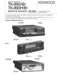
1
VHF FM TRANSCEIVER
TK-690H(B)
SERVICE MANUAL
REVISED
© 2001-7 PRINTED IN JAPAN
B51-8460-10 (N) 1031
This service manual applies to products with 30500001 or subsequent serial numbers. (KCH-10 and KCH-11 are applicable to
the productions June 2001 and after.)
In terms of the products with the serial numbers earier than 30500001, refer to the TK-690H(B) service manual as per part
No. B51-8460-00.
TK-690H(B)
Cabinet (Upper)
(A01-2163-01)
Cabinet (Lower)
(A01-2164-01)
KCH-10
Panel assy
(A62-0606-13)
Knob
(K29-4664-04) x 2
KCH-11
Panel assy
(A62-0607-13)
Knob
(K29-4664-04) x 2
TK-690H(B)
CONTENTS / GENERAL
GENERAL ......................................................................................................................... 2
SYSTEM SET-UP ............................................................................................................. 4
OPERATING FEATURES ................................................................................................. 5
INSTALLATION .............................................................................................................. 16
DISASSEMBLY FOR REPAIR ......................................................................................... 22
CIRCUIT DESCRIPTION ................................................................................................. 25
SEMICONDUCTOR DATA ............................................................................................. 31
DESCRIPTION OF COMPONENTS ............................................................................... 34
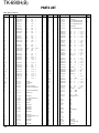
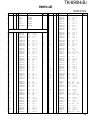
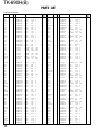
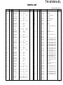
PARTS LIST .................................................................................................................... 37
EXPLODED VIEW .......................................................................................................... 48
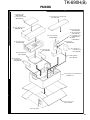
PACKING ........................................................................................................................ 51
ADJUSTMENT ............................................................................................................... 54
TERMINAL FUNCTION ................................................................................................. 62
PC BOARD VIEWS / CIRCUIT DIAGRAMS
DISPLAY UNIT (X54-3190-20) : KCH-10 .................................................................. 65
DISPLAY UNIT (X54-3200-20) : KCH-11 .................................................................. 67
TX-RX UNIT (X57-5600-XX) (A/2) ........................................................................... 73
FINAL UNIT (X45-3550-XX) ...................................................................................... 77
NB (X58-4610-10) ...................................................................................................... 85
CONTROL UNIT (X57-5600-XX) (B/2) ..................................................................... 87
WIRING .......................................................................................................................... 97
BLOCK DIAGRAM ........................................................................................................... 99
SPECIFICATIONS ......................................................................................................... 101
GENERAL
INTRODUCTION
PERSONNEL SAFETY
SCOPE OF THIS MANUAL
The following precautions are recommended for personnel safety :
• DO NOT transmit if someone is within two feet (0.6
meter) of the antenna.
• DO NOT transmit until all RF connectors are secure and
any open connectors are properly terminated.
• SHUT OFF this equipment when near electrical blasting
caps or while in an explosive atmosphere.
• All equipment should be properly grounded before
power-up for safe operation.
• This equipment should be serviced by only qualified technicians.
This manual is intended for use by experienced technicians familiar with similar types of commercial grade communications equipment. It contains all required service information for the equipment and is current as of this publication date. Changes which may occur after publication are
covered by either Service Bulletins or Manual Revisions,
which are issued as required.
ORDERING REPLACEMENT PARTS
When ordering replacement parts or equipment information, the full part identification number should be included.
This applies to all parts : components, kits, and chassis. If
the part number is not known, include the chassis or kit
number of which it is a part and a sufficient description of
the required component, for proper identification.
2
TK-690H(B)
GENERAL
PRE-INSTALLATION CONSIDERATIONS
1. UNPACKING
Unpack the radio from its shipping container and check
for accessory items. If any item is missing, please contact
KENWOOD immediately.
2. LICENSING REQUIREMENTS
Federal regulations require a station license for each radio installation (mobile or base) be obtained by the equipment owner. The licensee is responsible for ensuring transmitter power, frequency, and deviation are within the limits
permitted by the station license.
Transmitter adjustments may be performed only by a licensed technician holding an FCC first, second or general
class commercial radiotelephone operator’s license. There
is no license required to install or operate the radio.
3. PRE-INSTALLATION CHECKOUT
3-1. Introduction
Each radio is adjusted and tested before shipment. However, it is recommended that receiver and transmitter operation be checked for proper operation before installation.
3-2. Testing
The radio should be tested complete with all cabling and
accessories as they will be connected in the final installation. Transmitter frequency, deviation, and power output
should be checked, as should receiver sensitivity, squelch
operation, and audio output. QT equipment operation
should be verified.
4. PLANNING THE INSTALLATION
4-1. General
Inspect the vehicle and determine how and where the
radio antenna and accessories will be mounted.
Plan cable runs for protection against pinching or crushing wiring, and radio installation to prevent overheating.
4-2. Antenna
The favored location for an antenna is in the center of a
large, flat conductive area, usually at the roof center. The
trunk lid is preferred, bond the trunk lid and vehicle chassis
using ground straps to ensure the lid is at chassis ground.
4-3. Radio
The universal mount bracket allows the radio to be
mounted in a variety of ways. Be sure the mounting surface
is adequate to support the radio’s weight. Allow sufficient
space around the radio for air cooling. Position the radio
close enough to the vehicle operator to permit easy access
to the controls when driving.
4-4. DC Power and wiring
1. This radio may be installed in negative ground electrical
systems only. Reverse polarity will cause the cable fuse
to blow. Check the vehicle ground polarity before installation to prevent wasted time and effort.
2. Connect the positive power lead directly to the vehicle
battery positive terminal. Connecting the Positive lead to
any other positive voltage source in the vehicle is not recommended.
3. The cable provided with the radio is sufficient to handle
the maximum radio current demand. If the cable must be
extended, be sure the additional wire is sufficient for the
current to be carried and length of the added lead.
5. INSTALLATION PLANNING – CONTROL STATIONS
5-1. Antenna system
Control station. The antenna system selection depends
on many factors and is beyond the scope of this manual.
Your KENWOOD dealer can help you select an antenna system that will best serve your particular needs.
5-2. Radio location
Select a convenient location for your control station radio
which is as close as practical to the antenna cable entry
point. Secondly, use your system’s power supply (which
supplies the voltage and current required for your system).
Make sure sufficient air can flow around the radio and
power supply to allow adequate cooling.
SERVICE
This radio is designed for easy servicing. Refer to the
schematic diagrams, printed circuit board views, and alignment procedures contained in this manual.
3
TK-690H(B)
SYSTEM SET-UP
Before Reading About System Set-up
The TK-690H(B) is a transceiver main unit (without a
panel or speaker) that you complete by adding options.
The options are classified into three types according to
operation and function.
1. Install the front panel kit (controller) directly on a radio to
operate it. (Form : Radio + KCH-10/11)
2. Remotely control one radio with one controller. (Form
: Radio + KRK-5 + KCH-10/11 + KCT-22M/M2/M3)
3. Remotely control one radio with two controllers. (Form
: Radio + KRK-6DH + KCH-10/11 (two) + KCT-22M/M2/
M3 (two))
4. Remotely control two radios with one controller. (Form
: Radios (two) + KRK-7DB + KCH-10/11 + KCT-22M/M2/
M3)
5. Remotely control two radios with two controllers. (Form
: Radio (two) + KRK-8DBH + KCH-10/11 (two) + KCT22M/M2/M3 (two))
Frequency range RF power
Type
29.7~37MHz
110W TK-690H(B) F1
110W TK-690H(B) F2
35~43MHz
110W TK-690H(B) F3
40~50MHz
Merchandise received
License and frequency allocated by FCC
Choose the type of transceiver
TK-690H(B) (Radio 1)
TK-690H(B) is complete by combining options
with only the transceiver body (without panel)
Are you using two radios with two controllers?
YES
Are you using two radios with one controller?
Are you using the remote kit?
NO
See
page 16
See page 16
KCH-10 (Basic model)
Front panel kit
YES
*See Remote
kit service
manual
KCH-11 (Full featured
model) Front panel kit
YES
Are you using one radio with two controllers?
YES
Are you using one radio
with one controller?
YES
KRK-5
Single control head kit
Are you using the printed keytops?
See page 16
KRK-6DH
Dual control head kit
KRK-7DB
Dual band remote kit
KRK-8DBH
Dual band dual control head kit
NO
or
YES
KCH-10
or
KCH-11
Supplied accessory knob
KCH-10
+
KCH-10
or
or
KCH-10
+
KCH-11
KCH-11
+
KCH-11
KCH-10
or
KCH-11
KCH-10
+
KCH-10
or
KCH-10
+
KCH-11
KCH-11
+
KCH-11
KCT-22M/M2/M3 *See Remote kit
service manual
Control cable
See page 17
Are you using the voice scrambler?
YES
Modified of control unit
NO
Transceiver programming (option)
Are you using the external speaker?
See page 13
A personal computer (IBM PC or compatible), programming interface (KPG-43),
and programming software (KPG-44D) are required for programming.
(The frequency and signalling data are programmed for the transceiver.)
YES
KES-4 (EXT. SP)
See page 18
NO
KCT-23 (DC cable)
Are you using the ignition sense cable?
See Installation manual
KCT-23 M2,M4 : TK-690H(B)
YES
KCT-18
See page 18
NO
Delivery
*Service manual parts No. list
Model
Parts No.
KRK-5/6DH
B51-8445-20
KRK-7DB/8DBH
B51-8452-00
B51-8452-10
4
TK-690H(B)
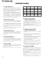
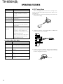
OPERATING FEATURES
(1) POWER Switch
Press to turn the power ON and OFF.
(2) TX/BUSY Indicator
The TX Indicator (Red LED) shows that you are transmitting.
The BUSY Indicator (Green LED) shows that the channel
is in use.
(3) Microphone Connector
(4) Volume Knob
To increase the volume level, turn clockwise (CW).
To decrease the volume level, turn counterclockwise
(CCW).
(5) UP/DOWN Knob
The function of this Knob can be programmed by the
FPU.
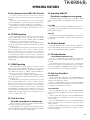
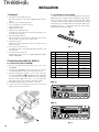
1. Controls and Functions
1-1. Basic Function Panel
(1)
(6) (7)
(19)
POWER
GRP
TX BUSY
VOL
(2) (3)
CH
(4)
(5)
(10)
(11)
(12)
(13)
(14)
Function
(31)
(29)
(24) (26) (28)
(25) (27)
(20) (21) (22)(23)
Description
Note
Channel
Channel selector.
Default
UP/DOWN
To increase the channel, turn CW.
setting.
To decrease the channel, turn CCW.
Group
Group selector.
UP/DOWN
To increase the group, turn CW.
To decrease the group, turn CCW.
(32)
(6) GR UP Key, (7) GR DW Key, (8) MON Key, (9) SCN Key,
(10)~(18) PF1-9 Key
The function of these Keys can be programmed by the
FPU.
(30)
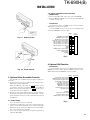
1-2. Full Function Panel
(1)
Function
(6) (7)
(19)
(9) (8)(17) (15) (16)
(18)
Description
No
No function.
Function
POWER
MON
CALL
MON
SCAN
SP
OPT
A
B
C
OST
GRP
SCN
Note
[ ] : Key top name
Default setting
of PF1~9.
Monitor
If [MON] is pressed once while
Default setting
[MON]
the RADIO is waiting for reception, of MON. (Full
TX BUSY
all signalling* squelch is canceled.
VOL
function panel)
CH
If [MON] is held down for 2 seconds, all singalling;
(2) (3)
(29) (31)
(4)
(20)
CALL
(5)
(21)
MON
(10)
(11)
(22) (23)
SCAN
SP
(12)
(13)
(14)
(26)
(24) (25) (27) (28)(30)
OPT
A
B
C
OST
noise squelch is canceled and the
QT/DQT &
audio is unmuted.
2 TONE/DTMF
Scan
Start and stop the scanning
Default setting
[SCN]
sequence.
of SCN. (Full
function panel)
Public
The RADIO works as a PUBLIC
Address [PA]
ADDRESS amplifier.
Horn Alert
When the RADIO receives a
[HA]
the optional signalling calls that
are assigned to the channel, the
HA relay turns on.
(32)
Talk Around
Use this function to communicate
[TA]
with other operators directry,
without using a repeater.
Intercom
Use this function to communicate Dual HEAD
[IC]
between the HEAD1 and HEAD2
configuration
operator without transmitting.
only.
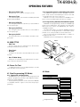
5
TK-690H(B)
OPERATING FEATURES
Function
Description
Note
[ ] : Key top name
Function
Description
Note
[ ] : Key top name
Channel
Switches the display between
Speaker 1-2 Each speaker audio can be
Dual HEAD
Name [AN]
Group-Channel No. and Group
Mute [SPM] manually disabled from the
configuration
other control head.
Channel UP If [
Internal/
Internal speaker and PA speaker.
[
>
Switch the audio output between
]
>
channel name.
Speaker
increases by one step.
If [
than 2 seconds
If [
DOWN [ ]
decreases by one step.
to toggle a
If [
Group DEL
and ADD.
<
Channel
] is pressed once, the channel
<
setting of each channel or group. [D/A] for more
] is held down for 1 second,
the channel decreases continuously.
Group UP
If [
[
increases by one step.
] is pressed once, the group
Press to enter Squelch Level Adjust
Level
Mode. The Squelch level can be
If [
[SQL]
adjusted by using the UP/DOWN
the group increases continuously.
decreases by one step.
Select signalling from the pre-
Selectable
programmed QT/DQT list.
<
If [
<
If [
DOWN [ ]
<
Group
channel Up/Down key or Group
Operator
] is pressed once, the group
] is held down for 1 second,
the group decreases continuously.
Mobile Relay The RADIO works as a repeater. Dual BAND
Tone [OST]
Station [RPT]
The optional board on and off.
[OPT]
configuration
Install the
Scrambler board.
AUX A [AUXA] Turns AUX A port on and off.
AUX B [AUXB]
] is held down for 1 second,
Knob, or the preprogrammed
Up/Down key.
Scrambler
>
Squelch
>
]
>
Add [D/A]
] is held down for 1 second,
the channel increases continuously.
<
Changes the Scan DELETE/ADD Press and hold
>
External [SP]
Delete/
only.
] is pressed once, the channel
only.
Emergency To start an Emergency Call,
This function
Call [EMG]
needs the ANI
press [EMG].
Turns AUX B port on and off.
board.
AUX C [AUXC] Turns AUX C port on and off.
Home Channel
(19) LCD Display
Switches to the pre-programmed
(Fixed) [HC] Home Channel.
Home Channel
Description
When pressed once, switches to
(20) CALL
(Toggle) [HC] the Home Channel. Press again
to returns to the previous channel.
CH1 Direct
by proper Optional Signalling
has been set
(DTMF or 2Tone).
“AND”, CALL
Switches to the GR1-CH1 directry.
lights after
[CH1]
CH2 Direct
transmitting.
Switches to the GR1-CH2 directry.
(21) MON
Switches to the GR1-CH3 directry.
(22) SCN
[CH2]
CH3 Direct
Switches to the GR1-CH4 directry.
(23) SP
6
Lights when “PA speaker” is
selected for audio output.
Switches to the GR1-CH5 directry.
(24) OPT
[CH5]
Channel
Indicates when scan mode is
enabled.
[CH4]
CH5 Direct
Lights when [MON] is pressed.
Signalling squelch is disabled.
[CH3]
CH4 Direct
Note
Flashes when the RADIO is called If Signalling
When pressed once, switches to
The [RCL] Key
Recall [RCL] the last called channel. Press again
works in Scan
(25) A
Lights when the optional board*, Optional
that is installed inside the RADIO,
Board :
is enabled.
· Scrambler
Lights when [AUXA] is pressed.
to return to the previous channel. Mode only.
The PF Port that is programmed
Dimmer
Use this function to adjust the LCD
with “AUX A” is ON.
[DIM]
backlight brightness, Key backlight,
(26) B
Lights when [AUXB] is pressed.
TX/BUSY LED, and DTMF Mic Key
The PF Port that is programmed
backlight ON/OFF.
with “AUX B” is ON.
TK-690H(B)
OPERATING FEATURES
Description
(27) C
Note
Lights when [AUXC] is pressed.
The PF Port that is programmed
with “AUX C” is ON.
(28) OST
Lights when [OST] is pressed,
Operator Selectable Tone is
enabled.
(29) ▼
If the selected group is in the
(Group
multi group scan sequence,
Add Status) the indicator appears at the
group.
(30) ▼
If the selected channel is in the
(Channel
scan sequence, the indicator
Add Status) appears at the channel.
(31)
Displays the channel status.
• BASIC
P1 : Lights when a PRIORITY 1
FUNCTION channel is shown on the display.
PANEL 7
P2 : Lights when a PRIORITY 2
SEGMENT
channel is shown on the display.
display
PP : Lights when a PRIORITY 1
• FULL
& 2 channel is shown on the display.
2. Receive
(1) To turn on the RADIO:
Press the Power Switch. The display and graphics illuminate to indicate the RADIO is ON.
(2) To adjust the volume level:
Turn the Volume Knob CW to increase the volume level.
Turn the Volume Knob CCW to decrease the volume
level.
(3) To select a Group:
Select a Group by rotating the UP/DOWN Knob which
has been programmed with “Group UP/DOWN” or by
pressing the Keys which have been programmed with
“Group UP” and “Group DOWN”.
If the “Channel Tracking Function” is enabled, the channel number will not change.
(4) To Select a Channel:
Select a Channel by rotaing the UP/DOWN Knob which
has been programmed with “Channel UP/DOWN” or by
pressing the keys which have been programmed with
“Channel UP” and “Channel DOWN”.
(5) To enter carrier squelch mode:
If you want to monitor a channel, press [MON] Key. If the
“OFF HOOK Decode” function has been disabled, you
can also enter monitor mode by taking the microphone
off HOOK.
FUNCTION HC : Lights when a Home
PANEL
Channel is selected by [HC] key.
DOT
TA : Lights when the RADIO is
MATRIX (S) in Talk Around mode.
display
RCL : Lights when recall
channel is selected by [RCL] key.
R1-R15 : Lights when remote
channel is selected by PF port.
(32)
Displays the operating Group-
• BASIC
Channel number (Channel display),
FUNCTION or name (Alphanumeric display)
PANEL 13
programmed by the FPU. Also
SEGMENT
displays the status of some
display
features.
• FULL
FUNCTION
PANEL DOT
3. Transmit
(1) Normal ON HOOK Scan Mode
First, lift the microphone from the HOOK. The scanning
stops temporarily and the OFF HOOK revert channel is
displayed. Listen for a few seconds to make certain the
channel is not being used.
OFF HOOK Scan MODE
If scanning, pressing the PTT switch will stop the RADIO
on the OFF HOOK revert channel and begin transmission immediately.
Not Scan Mode
Pressing PTT starts transmission at the selected channel.
(2) Press PTT and start speaking. For best results, hold the
microphone 1 to 1.5 inches from your mouth. Release
PTT when your message is complete. Listen for a response.
(3) When your conversation is finished, replace the microphone on its hook.
MATRIX (L)
display
4. Scan Operation
4-1. General
1-3. Microphone
Press PTT (Push To Talk) to transmit, then speak into the
microphone.
There are two “Mic HOOK” scan modes in which the
RADIO can be programmed to operate.
• ON HOOK Scan
Normal method of scanning that requires the microphone
to be ON HOOK (hanged on the Mic Hanger) to initiate
scan.
• OFF HOOK Scan
The microphone does not have to be ON HOOK to initiate
scan or to scan channels.
7
TK-690H(B)
OPERATING FEATURES
(1) The scan feature is initiated by pressing the [SCN] Key.
(2) A single confirmation tone sounds, and scanning starts. If
there is only one or no added channels, an error tone will
sound and scanning will not start.
(3) The display shows “SCN” icon, and “SCAN” or the OFF
HOOK Revert Channel Number (FPU setting).
(4) If the RADIO receives a proper signal while scanning,
scanning stops temporarily, audio is unmuted, and the
channel number or name is displayed.
If either “Priority1” or “Priority2” is programmed and
scanning stops at a Normal Channel by receiving a signal,
the RADIO watches for a signal on the Priority Channel
periodically. When a signal exists on the Priority Channel,
the channel will change from the Normal Channel to Priority Channel.
If both “Priority1” and “Priority2” are programmed and
scanning stops at the Priority2 Channel by receiving a signal, the RADIO watches a signal on the Priority1 Channel
periodically. When a signal exists on the Priority1 Channel, the channel will change from the Priority2 Channel to
the Priority1 Channel.
If there is no Priority Channel programmed, the scanning
stops at a channel and receives only that channel.
(5) If the [SCN] Key pressed again, Scan Mode ends at the
revert channel, and two confirmation tones sound.
4-2. To Delete Undesired Channels
To temporarily delete undesirable channels, press [D/A]
Key while the channel is displayed, and scanning resumes.
(To temporarily delete Priority Channel 1 or 2, set the “Priority Temporary D/A” function to “YES”.)
You can’t delete a channel in Scan Mode under the following conditions:
• Priority Scan
There is only channel beside the Priority Channel in the
scan sequence.
• Non-priority Scan
There are only 2 channels in the scan sequence. To restore the original scan sequence, either turn scan off and
on or turn the RADIO off and on.
4-3. To Enter Carrier Squelch Scan While Scan is On
If you have pressed the [MON] Key, the MON indicator is
turned on and the RADIO operates in carrier squelch scan.
5. Adding Channels and Groups to the
Scan Sequence
(1) Channels
To add the currently displayed channel to the scan sequence, press [D/A] Key. The CH ADD indicator (▼)
lights, and the channel is added to the scan sequence.
(2) Groups
To add the currently displayed group of channels to the
scan sequence, hold down the [D/A] Key for 2 seconds.
The GR ADD indicator (▼) lights, and the group is added
to the scan sequence.
8
6. Deleting Channels and Groups from the
Scan Sequence
(1) Channels
To delete a channel from the scan sequence press [D/A]
Key. The CH ADD indicator (▼) goes off, and the channel
is deleted from the scan sequence.
(2) Groups
To delete the currently displayed group of channels from
the scan sequence, hold down [D/A] Key for 2 seconds.
The GR ADD indicator (▼) goes off, and all the channels
in the group are deleted from the multi group scan sequence.
7. Operator Selectable Priority
(1) Operator Selectable Priority1
If Priority1 has been set to “Operator Selectable”, you
can set the currently displayed channel as Priority1.
To set the currently displayed channel as Priority1, hold
down the [SCN] Key and press the [MON] Key three
times.
(2) Operator Selectable Priority2
If Priority2 has been set to “Operator Selectable” you
can set the currently displayed channel as Priority2.
To set the currently displayed channel as Priority2, hold
down the [SCN] Key and press the [MON] Key twice.
8. Talk Around (TA)
Talk Around is useful when you are close to other mobiles you want to talk to, or are outside the range of your
repeater system.
Press the [TA] Key. A confirmation tone sounds, and
“TA” (BASIC Panel : 7 segment, FULL Panel : DOT MATRIX
(S)) is displayed. You can communicate without using a repeater.
To use a repeater, press [TA] again. A confirmation tone
sounds, and “TA” goes off.
9. Horn Alert (HA)
If you are called from the base station using 2Tone/DTMF
while you are away from your transceiver, you will be
alerted by the vehicle horn or some other type of external
alert. To turn the horn alert function on, press the [HA] Key.
A confirmation tone sounds, and the display shows HORN
ALERT (or HA).
If [HA] is pressed again, the horn alert function is turned
off.
TK-690H(B)
OPERATING FEATURES
10. Public Address (PA)
CASE1 : HC has been set as “HC (Fixed)”
Public Address amplifies the microphone audio, and outputs it through a PA speaker. PA is activated by pressing the
[PA] Key. A confirmation tone sounds, and the display
shows PUBLIC ADDRESS (or PA). PA can be activated at
anytime (scanning or non-scanning).
The RADIO continues to scan & receive calls while in PA
mode. Pressing PTT activates PA, and will override an incoming call at anytime ; however, no RADIO transmission
takes place. If [PA] is pressed again, a confirmation tone will
sound, the display will return to the normal channel or
SCAN display, and the PA function will turn off.
Non-Scan
12. Channel Name (AN)
This function switches the 13-segment display (BASIC
Panel) or DOT MATRIX (L) display (FULL Panel) between alphanumeric and Group-Channel number.
If you want to change from alphanumeric display to channel display, press [AN] Key. A confirmation tone sounds, and
the alphanumeric display changes to the channel display.
If [AN] is pressed again, a confirmation tone sounds, and
the channel display changes back to the alphanumeric display.
stopping
press [HC] once
Change to Home Channel
press [HC] again
No effect
CASE2 : HC has been set as “HC (Toggle)”
Non-Scan
Scanning
Scan
Mode
temporary
stopping
press [HC] once
Change to Home Channel
press [HC] again
Return to
Change to
Return to
current channel
Revert Channel
current channel
15. Squelch Level (SQL)
This function allows the radio operator to manually adjust
the squelch threshold in 16 steps (Level 0~15) via the front
panel controls. To adjust the squelch level:
(1) Press the [SQL] Key. A confirmation tone sounds, and
the RADIO enters Squelch Level Adjust Mode. In this
mode, all signallings are canceled and audio is unmuted.
The display shows SQUELCH XX (or SQL XX). (XX=
squelch level)
(2) Change the squelch level by pressing [ ] and [ ] Keys,
or rotating the UP/DOWN Knob.
(3) Press [SQL] again. A confirmation tone sounds, the display returns to the normal channel, the level setting is
memorized, and Squelch Level Adjust Mode will turn off.
<
SP amplifies the received audio from the RADIO and outputs it through a PA speaker. SP is activated by pressing the
[SP] Key. A confirmation tone sounds and the SP icon is displayed. SP can be activated at anytime (scanning or nonscanning).
The RADIO transmits and operates normally while SP is
activated, but all received calls will be output through the PA
speaker. If [SP] is pressed again, a confirmation tone
sounds, the SP icon goes off and the SP function will turn
off.
Scan
temporary
>
11. Speaker Internal/External (SP)
Scanning
Mode
* This feature can be initiated when the RADIO is not in
scanning mode.
16. Operator Selectable Tone (OST)
(1) Press the [OST] Key. A confirmation tone sounds, and
the display shows the OST Name which is memorized in
the channel for 2 seconds. The “OST” icon lights, and
OST is enabled.
Press [OST] again, and the OST icon goes off and OST is
disabled.
(2) When the [OST] Key is held down, a confirmation tone
sounds and the RADIO enters OST Select Mode.
(3) Select the Dec/Enc pair by pressing the [ ] and [ ]
Keys, or rotating the UP/DOWN Knob. The display shows
TONE XX (XX=Dec/Enc pair number) or the OST Name.
(4) Press [OST] again, a confirmation tone sounds, the display returns to the normal channel, the pair is memorized
and OST Mode will turn off.
>
Intercom (IC) allows one control head operator to talk to
the another control head operator. IC mode is activated by
pressing the [IC] Key. A confirmation tone sounds and
the display shows INTERCOM. IC can be activated at anytime (scanning or non-scanning).
The RADIO continues to scan & receive calls while in IC
mode. Pressing PTT activates IC and will override an incoming call at anytime ; however, no RADIO transmission takes
place. If [IC] is pressed again, a confirmation tone sounds,
the display returns to the normal channel or SCAN display,
and the IC function will turn off.
This function allows the radio operator to change the preset decode QT/DQT, encode QT/DQT. You can select Dec/
Enc OFF or from up to 16 decode/encode pairs (Pair No.
1~16) programmed by the FPU. To select the Dec/Enc pairs:
14. Home Channel (HC)
This feature allows the radio operator to immediately select a pre-determined “Home Channel” by pressing the [HC]
Key. HC can be activated as follows.
<
13. Intercom (IC) ; Dual Head Configuration only
* You can select a Dec/Enc pair on each channel.
9
TK-690H(B)
OPERATING FEATURES
17. Option Board (OPT)
<
>
If an optional Scrambler board has been installed in the
RADIO, Scrambler is activated by pressing the [OPT] Key. A
confirmation tone sounds, and the OPT icon is displayed. If
[OPT] is pressed again, a confirmation tone sounds, the OPT
icon goes off and the Scrambler will turn off.
If [OPT] is held down, the RADIO enters SCR Code Set
Mode. A confirmation tone sounds, and the display shows
CODE XX (XX=SCR Code). Change the SCR Code by pressing the [ ] and [ ] Keys, or rotating the UP/DOWN Knob.
Press [OPT] again, a confirmation tone sounds, the display returns to channel (SCR is ON), the SCR Code setting is
memorized, then SCR Code Set Mode will turn off.
18. AUX A, AUX B, AUX C
This function switches the accessory PF Output ports
which have been programmed with AUX A, AUX B and AUX
C.
Press [AUXA] Key. A confirmation tone sounds, the A
icon is displayed, and the AUX A Port is switched on (Low
level). If [AUXA] is pressed again, a confirmation tone
sounds, the A icon goes off and the AUX A Port is switched
off (open collector).
In the same way, [AUXB] Key controls the AUX B Port,
and [AUXC] Key controls the AUX C Port.
Display
Default
Press [DIM]
TX/BUSY
Panel Keys Microphone
backlight
LED
backlight
Keys backlight
High
High
High
High
Medium
↓
↓
↓
once
Press again
Low
↓
↓
↓
Press again
OFF
OFF
OFF
OFF
Press again
return to
return to
return to
return to
High
High
High
High
* The brightness setting is memorized.
22. Speaker 1-2 Mute (SPM)
; Dual Head Configuration only
This feature allows the radio operator to manually disable
the speaker audio of another control head.
Press the [SPM] Key, a confirmation tone sounds, and
the other head speaker is muted. Both head displays shows
X MUTE (X=Muted HEAD number).
This muted condition is canceled by both head keys without PTT and Mic HOOK which is connected to Un-muted
head.
23. Mobile Relay Station (RPT)
19. Direct Channel Access
This feature allows the radio operator to immediately select CHANNELs 1~5 which are contained in GROUP 1. To
select GR1-CH1, press [CH1]. To select GR1-CH2~5, press
[CH2] ~ [CH5],
20. Channel Recall (RCL)
This feature is enabled in scan mode.
This feature allows the radio operator to immediately access the last called (Unmuted) channel by pressing [RCL].
The 3-digit display shows “RCL”. Press [RCL] again, and the
radio returns to the previous channel.
21. Dimmer (DIM)
To adjust the brightness of the display backlight, TX/
BUSY LED, panel Keys backlight and microphone keys backlight, press the [DIM] Key.
[DIM] controls the brightness at the same time as follows.
10
; Dual Band Configuration only
This function allows the radio operator to use the RADIO
as a repeater.
(1) Both “Repeater Channel 1” and “Repeater Channel 2”
must be pre-programmed by the FPU. Each channels
must be on diferent bands.
(2) Press the [RPT] Key, then both the VHF and UHF units
move to the repeater channel, and enter Repeater mode.
Displays of both heads show “REPEATER”.
(3) If one unit receives a proper signal, the other unit will
start transmitting (repeating).
(4) If the signal stops, the repeat action will stop. If one of
the units detects another signal, the repeat action will restart.
(5) Press [RPT] again, both units return to their previous
channels, and exit the Repeater mode. However, during
the repeating mode, pressing [RPT] has no effect.
24. Emargency Call (EMG)
If the [EMG] Key is held down, the RADIO enters the
Emergency Mode. In the Emergency Mode, the channel
changes to the “Emergency Channel (set by the FPU)” internally. The display depends on “Emergency Channel Display” setting, and the Emergency Call (None, DTMF, MSK or
ANI board) is transmitted.
If “ANI Board” is selected for the Emergency Type, turn
the transceiver off, then turn it on again to recover “Normal
Mode”.
If “ANI Board” is not selected for the Emergency Type,
press and hold [EMG] key to recover “Normal Mode”.
TK-690H(B)
OPERATING FEATURES
2Tone signalling opens the squelch only when the RADIO receives a proper 2Tone code that is the same as the
pre-programmed 2Tone for the channel. When the RADIO
receives a 2Tone code, the CALL icon flashes.
If Transpond has been programmed, the RADIO will return an acknowledgment signal automatically after receiving
the 2Tone code.
If Call Alert has been programmed, an Alert Tone sounds
after receiving a 2Tone code. You can configure “Normal”
(an alert tone beeps once) or “Continuous” (an alert tone
beeps every 5 seconds) for the Call Alert. Unmute condition
is canceled and the CALL icon goes off when ; (1) pressing
the [MON] Key, (2) hanging the microphone on its hook, (3)
muting continues for 10 seconds. (If “Auto Reset” has been
programmed)
27. DTMF Signalling
29-1. AND
The audio is unmuted when the RADIO receives the correct QT/DQT and 2Tone/DTMF. After transmitting, 2Tone/
DTMF will be canceled.
29-2. OR
The audio is unmuted when the RADIO receives the correct QT/DQT. 2Tone/DTMF is used just as an individual call
or group call.
30. Off Hook Decode
If the OFF HOOK Decode function has been enabled, removing and replacing the microphone on the HOOK has no
effect for decoding QT/DQT and 2Tone/DTMF.
31. TX Audio Monitor
; Dual Head Configuration only
This function allows the radio operator to hear another
operator’s voice which is transmitted through another control head.
If the TX Audio Monitor function is set to “w/Talk Interrupt” and one operator is transmitting, the other operator’s
control head displays “INTERCOM” and he/she can speak
to the transmitting control head by pressing PTT.
32. Roll Over/Dead End
32-1. Roll Over
When [ ] (CH UP) is pressed, or the CH UP/DOWN Knob
is turned CW from the Maximum channel, the channel
changes to the Minimum channel.
When [ ] (CH DOWN) is pressed, or the CH UP/DOWN
Knob is turned CCW from the Minimum channel, the channel changes to the Maximum channel.
32-2. Dead End
When [ ] (GR UP) is pressed, or the GR UP/DOWN Knob
is turned CW from the Maximum group, the group doesn’t
change.
When [ ] (CH UP) is pressed, or the CH UP/DOWN Knob
is turned CW from the Maximum channel, the channel
doesn’t change.
When [ ] (GR DOWN) is pressed, or the GR UP/DOWN
Knob is turned CCW from the Minimum group, the group
doesn’t change.
When [ ] (CH DOWN) is pressed, or the CH UP/DOWN
Knob is turned CCW from the Minimum channel, the channel doesn’t change.
The Time Out Timer function interrupts continuous transmission after a specified time elapses.
Holding down PTT for longer than the programmed time
causes the RADIO to stop transmitting and sound a warning
tone. To stop the warning tone, release PTT.
<
28. Time Out Timer
(Possible to configure to each group)
<
>
DTMF Signalling opens the squelch only when the RADIO receives a proper DTMF code that is the same as the
pre-programmed “Primary Code (Individual ; 1~7digits)” or
“Secondary Code (Group ; 1~7digits)”. When the RADIO receives a correct code, the CALL icon flashes.
If Transpond has been programmed, the RADIO will return an acknowledgment signal automatically after receiving
the DTMF code.
If Call Alert has been programmed, an Alert Tone sounds
after receiving a DTMF code. You can configure “Normal”
(an alert tone beeps once) or “Continuous” (an alert tone
beeps every 5 seconds) for the Call Alert. Unmute condition
is canceled and the CALL icon goes off when ; (1) pressing
the [MON] Key, (2) hanging the microphone on its hook, (3)
muting continues for 10 seconds (If “Auto Reset” has been
programmed), and (4) receiving reset code. (Primary code +
“#” or secondary code + “#”)
The RADIO will be unmuted with a combination of QT/
DQT and 2Tone/DTMF. The AND/OR setting works as follows.
>
26. 2TONE Signalling
29. Signalling AND/OR
(Possible to configure to each group)
<
The Busy Channel Lockout function prevents
interferance with other stations that may be using the same
channel.
While the selected channel is in use, pressing PTT
causes the RADIO to sound a warning tone, and transmission is inhibited. To stop the warning tone, release PTT.
If BCL Override has been enabled, pressing PTT within
500msec again will cancel BCL, and transmission is enabled.
>
25. Busy Channel Lockout (BCL), BCL Override
11
TK-690H(B)
OPERATING FEATURES
36-2. PF Output Port
33. Minimum Volume
When the Volume Knob is adjusted fully counterclockwise, the audio level is set to the Minimum Volume level
which is programmed by the FPU.
AUX A
Pressing [AUXA] once → Low, Pressing [A]
AUX B
Pressing [AUXB] once → Low, Pressing [B]
34. Dead Beat Disable (DBD)
AUX C
Pressing [AUXC] once → Low, Pressing [C]
[AUXA] again → OPEN-COLLECTOR
[AUXB] again → OPEN-COLLECTOR
If the RADIO receives a DBD Code (1~7digits), the RADIO returns an acknowledgment signal automatically, and
transmission is disabled. This TX INHIBIT condition is
memorized.
If the RADIO receives a DBD Reset Code (DBD Code +
#), the RADIO returns an acknowledgment signal automatically, and transmission is Enabled.
35. ANI Board
The ANI board contains functions which you can use. To
use the function, you select that function on the ANI board.
36. Accessory Programmable Function
Port (PF Port)
The RADIO has 13 PF Ports.
HEAD (12 pin) : PF Input Port 2, PF Output Port 2
DECK (Dsub 25 pin) : PF Input Port 5, PF Output Port 4
Each Port can be programmed with a function from next
Table.
36-1. PF Input Port
External HOOK
Receiving correct QT/DQT → Low, Not receiving correct QT/DQT → OPEN-COLLECTOR
COR
BUSY → Low, Not BUSY → OPEN-COLLECTOR
37. Timed Power Off
This function works as “Automatic Power Switch Off”.
Timed Power Off timer starts from the ignition-off. After
the timer expires, the RADIO will automatically turn off. The
timer will be reset if the ignition is turned on and off.
This function requires ignition-sense. Connect the ignition-line to the 9-pin connector which is located at the rear of
the RADIO.
After the timer expires, you can turn the transceiver on
again with 2 methods below.
1) Timed power off function (Default)
Press the power switch.
2) Ignition function & Timed power off function
Turn the ignition on.
38. Emergency
• Active tome
Automatic transmission period in the emergency mode.
Open → OFF HOOK, Low → ON HOOK
1~15. If CH Select A~D are set “H” or “Open”,
CH Select C
the channel is selected by using the [
CH Select D
keys or UP/DOWN Knob. (User Channel)
• Duration of Locator Tone 1
External PTT
Open → PTT OFF, Low → PTT ON
Scan
Open → Scan OFF, Low → Scan ON
Duration of an alert tone before the automatic transmission is performed.
Home Channel
Open → Current Channel, Low → Home Channel
• Duration of Locator Tone 2
Light Sense
Open → LCD Backlight is controlled by [DIM],
Duration of an alert tone after the automatic transmission
is performed.
]/[
<
The Channel changes to Remote Channel
CH Select B
>
CH Select A
Open → Repeater inactive, Low → Repeater Active
* Dual BAND configuration only
External Monitor
Open → Monitor OFF, Low → Monitor ON
• Interval Time
Interval time between the automatic tansmissions.
]
Low → LCD Backlight is set “Low”
Repeater SW
12
[AUXC] again → OPEN-COLLECTOR
TOR
• Emergency Channel Display
Setting for the display in the emergency mode.
The transceiver can be programmed to display “EMERGENCY” channel name when it is in emergency mode.
If you set to “off” by KPG-44D the transceiver shows
selected group/channel/status before entering to the emergency mode however the transceiver is in an emergency
mode.
TK-690H(B)
OPERATING FEATURES
• Emergency Mode Type
Speaker mute on or off in the emergency mode.
41-2. Programming Interface Cable KPG-43 Description
Select an Emergency code format from DTMF, MSK, ANI
board or OFF (Disabled).
The KPG-43 is required to interface TK-690H to the computer. It has a circuit in its D-sub 25 pin connector case that
converts RS-232C logic level to TTL level.
KPG-43 is used to connect between TK-690H microphone connector and RS-232C serial port of computer.
• Emergency DTMF ID
41-3. Programming Software KPG-44D Description
The emergency DTMF ID code when you select DTMF in
the emergency type.
KPG-44D is the programming software for TK-690H supplied on a 3.5" floppy disk. This software runs under MSDOS version 3.1 or later on an IBM-PC/XT, AT, or PS2 or
compatible machine.
The data can be input to or read from TK-690H and edited
on the screen. The programmed or edited data can be
printed out. It is also possible to tune the transceiver.
We recommend that install KPG-44D for example to
harddisk first then use it.
KPG-44D instruction manual part No. : B62-1011-XX.
• Emergency Type
• Emergency Call Fleet
The emergency fleet number when you select MSK in
the emergency type.
• Emergency Call ID
The ID number when you select MSK in the above emergency type.
IBM-PC
39. MSK PTT ID
• Side Tone
A tone to notify the voice transmission is allowed after
sending the MSK PTT ID (Connect ID).
KPG-43
• Fleet (Own)
• ID (Own)
Configure the Fleet/ID of the MSK PTT ID (Fleet Sync
Format).
• Data TX Mod. Delay
Delay time of transmitting the MSK ID after the transceiver enters the transmission mode.
KPG-44D
Fig. 1
40. Power On Text
To display the Power on text for approximately 2 seconds
when the transceiver is turned on.
42. Mode
41. Data Programming (PC Mode)
41-1. Preparation and Connection
TK-690H transceiver is programmed by using a personal
computer, programming interface cable KPG-43, and programming software KPG-44D.
The programming software can be used with an IBM-PC
or compatible machine. Figure 1 shows the setup for programming.
User mode
PC mode
PC programming mode
* PC test mode
* PC tuning mode
Panel test mode
Panel tune mode
Clone mode
All clone mode
Group clone mode
Firmware programming mode
19200 bps
38400 bps
[PF4]
57600 bps
* : Single band only
115200 bps
13
TK-690H(B)
OPERATING FEATURES
Mode
Function
User mode
Customer use this mode
PC mode
Communication between the radio and
PC (IBM compatiible). It requires the
KPG-44D.
Panel test mode
Dealer uses to check the fundamental
(Refer to ADJUSTMENT)
characteristics.
Panel tune mode
Dealer uses to tune the radio.
43. PC Tuning Mode
When making adjustment while in PC tuning mode,
modify the KPG-43 programming interface cable as described below.
1. Remove the two screws from the plug cover, then lift the
cover from the plug.
(Refer to ADJUSTMENT)
Clone mode
Programmed data is transferred from
one transceiver to another by using a
cloning cable.
Firmware program-
Re-write the firmware of the flash ROM.
ming mode
Note : When programming the firmware,
it is best to copy the data from the
floppy disk to your hard disk, then from
2. Solder the lead wire onto the MIC tab on the PCB, and
the ground wire onto the ME tab.
the hard disk to the CPU.
+ +
C5
Directly copying from the floppy disk to
Q1
C4
the CPU may not work because the
MICME
access speed is too slow.
MAX232C
User mode
Power on
PC mode
Connect the PC and turn the power on.
IC1
Operation
MAXIM
Mode
C7
SB
GND
TRD
42-1. How to Enter Each Mode
+
Then the radio can be controlled by the FPU.
Panel test mode
Hold down the [PF1] key, turn the radio
Panel tune mode
Press the [GR
>
power on.
] key from the panel test
mode.
Clone mode
Hold down the [PF5] key, turn the radio
Firmware
Hold down the [PF2] key, turn the radio
programming mode
power on.
3. Create a hole in the casing (as shown in the illustration)
then fit the cable into the hole. Replace the cover and
secure it using the two screws.
power on.
Create a hole
MIC
14
Cable
ME
TK-690H(B)
OPERATING FEATURES
44-3. Group Clone
44. Clone Modes
There are two clone modes : “All Clone Mode”, in which
all data programmed in one transceiver with the “FPU” is
copied to another transceiver, and “Group Clone Mode”, in
which group data in one transceiver is copied to a group in
another transceiver.
The cloning operation is performed from the master side
transceiver.
1. Enter the group clone mode from the clone mode with
[Up/Down] knob.
2. Press the [PF5] key to enter the master group select
mode. Select the master group with [Up/Down] knob.
Master side display
A CLONE / ALL CLONE
TX LED on
[PF5] + Power on
[Up/Down]
– PC –
Busy LED on
Busy LED off
Group clone mode
[PF5]
[PF5]
[Up/Down]
Slave group selection
[UP/Down]
Cloning
Slave side display
User mode
TX LED off
Master group selection
[PF5]
[PF5]
END
All clone/Group clone selection
All clone mode
Data cloning
[PF5]
3. Press the [PF5] key to enter the slave group select mode.
Select the slave group with [Up/Down] knob.
4. Press the [PF5] key to start cloning.
Note : The transceiver does not enter the clone mode if it is
disabled with the FPU. To clone the transceiver both transceivers must be same. If the panels, frequency ranges, optional board are different, they cannot be cloned.
END
[PF5]
Power off
Master side display
Slave side display
G CLONE / GROUP CLONE
User mode
[PF5]
GRP
1M / GROUP
1M
[Up/Down]
44-1. To Enter the Clone Mode and Connect
Transceivers
GRP 160M / GROUP 160M
(1) Hold down the [PF5] key and turn on the power switch on
the master side transceiver.
Turn on the power switch on the slave side transceiver as
usual.
(2) Connect the master and slave side transceivers with a
cloning cable.
GRP
[PF5]
1S / GROUP
1S
[Up/Down]
GRP 100S / GROUP 100S
TX LED on
END
TX LED off
Data cloning
[PF5]
– PC –
Busy LED on
User mode
Busy LED off
44-2. All Clone
1. Enter the All Clone Mode from the clone mode with the
[Up/down] knob.
2. Press the [PF5] key to start cloning.
Cloning cable
(Part No. E30-3370-05)
Fig. 2
15
TK-690H(B)
INSTALLATION
2-3. Install the accessory knobs
When a function is set by the programming software
(KPG-44D), the key legend can be changed by inserting the
accessory knobs into PF1 to PF9 of the KCH-11 (PF1 to PF5
: KCH-10). The accessory contains a set of 30 knobs : AN, D/
A, DIM, HA, HC, IC, MON, OPT, OST, PA, RCL, RPT, SCN,
SP, SPM, SQ, TA, , , CH1, CH2, CH3, CH4, CH5, AUX A,
AUX B, AUX C, EMG, and blank.
<
1
2
3
4
5
6
7
8
9
10
Fig. 2
K29-5276-*3
K29-5277-*3
K29-5305-*3
1
AN
RCL
CH1
2
D/A
RPT
CH2
3
DIM
SCN
CH3
2. Front Panel Kit (KCH-10, KCH-11)
4
HA
SP
CH4
2-2. Connection with TK-690H(B)
5
HC
SPM
CH5
1. Remove the upper and lower halves of the case of the
TK-690H(B).
2. Connect the lead (W501) with a connector of the control
unit (X57-560 B/2) to CN1 of the KCH-10 or KCH-11.
3. Install the KCH-10 or KCH-11 on the radio using the
screws (N32-3006-46) ( 1 ) supplied with the front panel
kit. Take care not to get the lead between the KCH-10 or
KCH-11 and an edge of the case. (You can install the
panel upside down if necessary to install the radio.)
4. Reinstall the upper and lower halves of the case.
5. Connection the short plug for the accessory connector
(9-pins) on the rear of the radio.
6
IC
SQ
AUX A
7
MON
TA
AUX B
8
OPT
>
No.
AUX C
9
OST
<
• Front panel kit (KCH-10, KCH-11)
Description and use of the knob supplied with the KCH10/11
• Optional voice scrambler function
Voice scrambler use and connection
• Optional ANI function
ANI board connection
• Ignition sense cable (KCT-18)
Description of the ignition function and timed power off
function and connection
• External speaker (KES-4)
KES-4 connection method and modification for increasing the speaker output of the control head
• Horn alert function
Modification for changing the function of the ACC terminal for horn alert
• Accessory terminal function
Description and use of D-SUB 25-pin ACC terminals, “MI/
DI” and “SB”
• Connection with remote kit
Modification of the radio to use KRK-5, KRK-6DH, KRK7DB, or KRK-8DBH
>
1. Contents
EMG
10
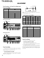
PA
No printing
KCH-10
POWER
GRP
TX BUSY
VOL
CH
PF1
PF2
PF3
PF4
PF5
KCH-11
1
PF6
PF7
PF8
PF9
POWER
MON
CALL
MON
SCAN
SP
OPT
A
B
C
OST
GRP
SCN
TX BUSY
VOL
KCH-10 or
KCH-11
CH
PF1
1
Fig. 1
16
Fig. 3
PF2
PF3
PF4
PF5
TK-690H(B)
INSTALLATION
3-2. Voice scrambler board connection
• Modification
1. Remove the upper half of the case of the TK-690H(B).
2. Remove R515 and R604 on the control unit (X57-560 B/
2) (Refer to page 21).
• Connection
The functions of pins of CN508 on the control unit (X57560 B/2) are shown in the figure.
Join the CN508 connector to the voice scrambler board
via the E37-0808-05 connector cable.
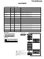
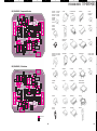
Fig. 4-1 Knob insertion
CN508
1
MCI (MIC signal input)
MCO (MIC signal output)
DEI (Detection signal input)
AC (Audio control signal output)
BC1 (Scramble code output 1)
BC2 (Scramble code output 2)
BC3 (Scramble code output 3)
BC4 (Scramble code output 4)
TXD2
RXD2
DEO (Detection signal output)
PTO (PTT signal output)
8C (8V output)
E (Earth)
14
Voice
scrambler
Fig. 5
4. Optional ANI Function
• Connection
Fig. 4-2 Knob removal
3. Optional Voice Scrambler Function
The optional voice scrambler function can be used by two
methods.
1. Assign this function to the OPT key by using the programming software (KPG-44D).
When the OPT key is pressed, the OPT indicator comes
on, and the optional (scrambler) function is enabled.
When the key is pressed again, the OPT indicator goes
off and the function is disabled.
2. Assign the optional scrambler function to each channel
by using the programming software (KPG-44D). The optional scrambler function can be used without pressing
the OPT key.
Join the CN507 connector to the ANI board via the E370809-05 connector cable, and the CN508 connector to the
ANI board via the E37-0808-05 connector cable.
CN507 ANI board
1
SQ (Squelch signal output)
EMG (Emergency signal output)
EPT (External PTT signal input)
I/O (Auxiliary input/output)
SEL (Non connection)
AS2 (Audio mute input)
MCM (MIC mute input)
TON (Side tone input)
TCN (Speaker mute input)
DTI (Data input)
10
14
E (Earth)
8C (Common 8V output)
PTO (PTT signal output)
DEO (Detection signal output)
11
CN508
3-1. Code setting
The code can be set by two methods.
1. Hold down the OPT key to enter the code setting mode.
Codes 1 to 16 will be displayed. Set a code by turning the
[Up/Down] knob. When the OPT key is pressed again,
the code setting mode terminates.
2. Set a code for each channel by using the programming
software (KPG-44D).
Fig. 6
17
TK-690H(B)
INSTALLATION
5. Ignition Sense Cable (KCT-18)
Available function when KCT-18 is
The KCT-18 is an optional cable to use the following functions:
connected
5-1. Ignition function
Horn alert function OFF during
5-2. Timed power off function
turned on.)
The timed power off function turns the transceiver’s
power off the time specified with the programming software (KPG-44D) after the ignition key is turned off. When
you are driving with the ignition key on, the horn alert function is disabled.
The ignition sense function and the timed power off function can be used at the same time.
HA function OFF during driving,
Horn alert function OFF during
Note : If the KCT-18 is used for the KRK-8DBH, use the 9-pin
plug on the back of radio 1 or the 12-pin plug on the back of
head 1. The plugs on radio 2 and head 2 cannot be used.
If the KCT-18 is used for the KRK-7DB, use the 9-pin plug on
the back of radio 1 or the 12-pin plug on the back of the
head. The plug on radio 2 cannot be used.
18
R743
Absent Present Present Absent
driving, Ignition function
None (The transceiver cannot be
Absent Absent Present Absent
Present Absent Absent Present
Ignition function & Timed power
off function
Table 1 R504, R506, R742 and R743 setup chart
(Refer to page 21)
5-3. Modification
• If the TK-690H(B) and KCH-10 or KCH-11 are used
If the accessory connector (9 pins) on the rear of the
transceiver is available, use the method described above. (If
the KRK-7DB or KRK-8DBH is used, use the accessory connector (9 pins) on the back of radio 1.)
If the accessory connector (12 pins) on the back of the
control head is used:
1. Remove the plug from the accessory connector (12 pins)
on the back of the control head.
2. Cut off the end of the rubber cap (accessory), insert the
KCT-18 into the cap, and insert it into pin 1 (IGN) of the
short plug.
3. Install the short plug and rubber cap on the connector on
the rear of the control head, then clamp the bottom of the
rubber cap with the supplied tie wrap.
4. Remove the upper half of the case of the TK-690H(B).
5. Set jumper resistors (0 ohm), R504, R506, R742 and
R743, on the control unit (X57-560 B/2) as shown in
Table 1 (Refer to page 21).
6. Reinstall the upper half of the case.
R742
driving, Timed power off function
(Default)
• When the remote kit is used
R506
Present Absent Present Absent
The ignition function allows you to turn the transceiver’s
power on and off with the ignition key of your car. When
you are driving with the ignition key on, the horn alert function is disabled.
1. Remove the short plug from the accessory connector (9
pins) on the back of the transceiver.
2. Insert the KCT-18 into pin 1 (IGN).
3. Remove the upper half of the case of the TK-690H(B).
4. Set jumper resistors (0 ohm), R504, R506, R742 and
R743, on the control unit (X57-560 B/2) as shown in
Table 1 (Refer to page 21).
5. Reinstall the upper half of the case.
R504
Accessory
connector (12P)
1
3
Rubber cap
12
10
Tie wrap
Accessory
connector (9P)
Cut
1
7
3
KCT-18
KCT-18
9
Fig. 7
6. External Speaker (KES-4)
The speaker output from the TK-690H(B) is as follows:
1. The KCH-10 has a built-in speaker (3W/8 ohms).
2. The KCH-11 does not have a built-in speaker.
3. The external speaker output from the accessory connector (9 pins) on the back of the transceiver is 13W/4 ohms.
Use the KES-4.
4. The speaker output from the accessory connector (12
pins) on the back of the control head is 2W/4 ohms. If the
remote kit (KRK-5, KRK-6DH, KRK-7DB or KRK-8DBH) is
used, use the KSP-1A or KES-4. If the KSP-1A is used, do
not attempt to modify the transceiver to increase the audio output.
Note : Since the TK-690H(B) uses a BTL audio amplifier, do
not ground the speaker output pin.
TK-690H(B)
INSTALLATION
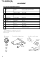
6-1. Connection for the KES-4 with the TK-690H(B)
• When taking the AF output from the accessory
connector (9-pin) on the rear of the radio
The following tools are required for changing the connector.
Extracting tool
the following extracting tool is recommended :
Molex Inc. Order No. : 11-03-0002
1. Remove the connector with jumper from the external
speaker connector on the rear panel of the radio (Fig. 81).
Note : Save the jumper, which is required when the radio
is used without the external speaker.
2. Remove the terminals with the jumper from the connector housing holes number 3 and 6 using the extracting
tool.
Removing the jumper lead (Fig. 8-2)
1) Insert the extracting tool (11-03-0002) into the connector while pushing the jumper lead in the direction
of (a).
2) Push the extracting tool into collapse the barbs of the
crimp terminal.
3) Pull out the lead while continuing to push the extracting tool in the direction (b).
3. Reinsert the terminal with the black and white stripe lead
into hole number 2, and the terminal with the black lead
into hole number 6 (Fig. 8-3).
4. Attach the connector to the external speaker connector
on the radio.
(a)
(b)
Square-type plug
(E37-0733-05)
Extracting tool
(11-03-0002)
Jumper lead
6-2. Connection for the KES-4 with the remote kit
(KRK-5, KRK-6DH, KRK-7DB, KRK-8DBH)
(When output is from the 12-pin accessory connector on the rear of the control head : remote
operation)
• Modification of plug (12-pin)
1. Remove the plug from the accessory connector (12-pins)
on the rear of the control head.
2. Cut off the end of the rubber cap, insert the KES-4
speaker cable into the cap, and insert it into pins 10 and
11.
3. Install the plug and rubber cap on the accessory connector on the rear of the control head, then clamp the bottom
of the rubber cap with the supplied tie wrap.
Plug (12P)
Rubber cap
11
Tie wrap
10
Cut
Speaker cable
(To KES-4)
Fig. 9
• If the KCH-10 is used
If the KSP-1A or KES-4 is connected to the 12-pin accessory connector, cut the internal speaker wire at the base of
the speaker.
If the internal speaker is used, cut the wire connected to
pins 10 and 11 of the 12-pins accessory connector at the
base of the connector (Fig. 10).
KCH-10
CN3
CN1
Barbs
Crimp terminal
Fig. 8-1
CN2
SP
Fig. 8-2
1
7
9
2
6
Fig. 8-3
Black lead
Black/White lead
Rear of the control head
Fig. 10
19
TK-690H(B)
INSTALLATION
6-3. Modification to increase the audio output of
the control head
The speaker output can be increased to 13W by moving
jumper resistor (0 ohm) R628 on the control unit (X57-560
B/2) to R627. In this case, the KCH-10 internal speaker cannot be used because the maximum input (3W) of the internal speaker is exceeded. Therefore, use the KES-4.
Default
Modification 1
Modification 2
R690
Present
Present
Absent
R691
Present
Absent
Absent
R692
Absent
Present
Present
State
Note : Even if the KRK-6DH is modified in this way, the audio output of head 2 cannot be increased.
To increase the audio output of head 2 of the KRK-8DBH,
modify radio 2 in the same manner.
6-4. Use as public address speaker
1. Remove the short plug from the 9-pin accessory connector on the rear of the radio. (Remove the jumpers as described in Section 5-1.)
2. Insert the KES-4 speaker leads into pins 7 and 8.
3. If you remove jumper shorting pins 3 and 6, the 20W PA
(public address) voice signal is output from pins 7 and 8.
(Only when the PA or SP switch is on.)
4. If you use the radio with pins 3 and 6 shorted, the internal
speaker is available (when the KCH-10 is used). The KCH11 does not contain a speaker.
Note : Relation ship between accessory connector (9-pins)
connection and speaker output.
When pins 3 and 6 are shorted ; The 3W internal speaker is
used (KCH-10 only).
When pins 3 and 6 are open and output is from pins 7 and 8
; The 20W external speaker is used.
7
Crimp terminal
(E23-0613-05)
HR1
HR1
HR2
HR2
HR2
Table 2 (Refer to page 21)
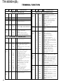
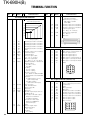
8. Accessory Terminal Function
8-1. 25-pin accessory terminal
• Pin 13
MI/DI (MIC Signal Input/Output or Data Audio Input)
This pin has one of the two functions listed in Table 3 by
setting jumper resistors (0 ohm) R640 and R641 on the
control unit (X57-560 B/2) (Refer to page 21).
1) MIC signal input/output
This pin is directly connected to the MIC input pin of the
transceiver, so it has the same function as the MIC input
pin. When the input is 5mV/3 kHz, DEV (600 ohms)
modulation is obtained. The MIC input is output from the
transceiver panel as it is.
2) Data audio input
The signal from this pin passes through the LPF (fc: about
10kHz), is summed with the MIC AMP output, and goes
to the modulator. Therefore, it is not preemphasized.
• Pin 14
SB (DC Power Output After Power Switch)
The maximum output (13.4V / 0.5A) can be obtained by
modifying the control unit as follows:
Short the land of the print pattern near CN505 of the control unit (X57-560 B/2).
Plug (9P)
8
HR1
To KES-4
Black lead
Black/White lead
Fig. 11
R640
R641
Function
Present
Absent
MIC signal input/output
Absent
Present
DATA audio input : Default
Table3 (Refer to page 21)
20
7. Horn Alert Function
9. Connection with the Remote Kit
The HR1 pin of the accessory connector (9-pin) on the
rear of the transceiver is an open collector and the maximum current is 100mA. The maximum available current can
be increased to 1A by installing a relay.
1. Remove the upper half of the case of the TK-690H(B).
2. Move jumper resistor (0 ohm) R691 on the control unit
(X57-560 B/2) to R692. To make the HR2 pin, remove
R692 (Refer to page 21).
3. Remove screws and erect the PC board. Install and solder relay K501 (Part No. : S76-0407-05).
4. Reinstall the PC board and the upper half of the case.
When the KRK-5, KRK-6DH, KRK-7DB or KRK-8DBH is
used, set chip resistors and transistors as shown in the table
below.
KRK-5
KRK-6DH
Radio 1
Radio 2
KRK-7DB
KRK-8DBH
Unnecessary
–
Remove R546 and R661
Move R602 to R705.
Table 4 (Refer to page 21)
TK-690H(B)
INSTALLATION
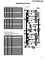
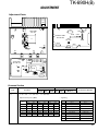
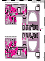
2
1
3
1
R661
CONTROL UNIT (X57 B/2)
Component side view
5
Connection with
the remote kit
(Page 20)
R743
Ignition sense
cable (KCT-18) R742
(Page 18)
4
Ignition sense R504
cable (KCT-18)
(Page 18)
R506
R546
2
3
Connection with
the remote kit
(Page 20)
R705
SB
R602
Connection with
the remote kit
(Page 20)
Accessory terminal
function (Page 20)
5
4
R604
R627 R628 External speaker
(Page 18)
Horn alert (Page 20)
R640
R690
R515 R641
R691
K501
R692
Voice Scrambler
(Page 17)
R515 : Voice Scrambler
(Page 17)
R640,641 : Accessory terminal
function (Page 20)
21
TK-690H(B)
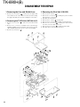
DISASSEMBLY FOR REPAIR
1. Removing the Case and Shield Cover
3. Removing the Final Unit (X45-355)
1. Remove the 12 screws ( 1 ), and remove the upper and
lower halves of the case. (Remove the 6 screws holding
the upper half and the 6 screws holding the lower half.)
1. Remove the 2 screws ( 5 ).
2. Remove the 3 screws ( 6 ) holding the power module
and transistor to the frame.
3. Desolder two transistors.
4. Remove the 1 screw ( 7 ) holding TH1.
5. Remove the 4 screws ( 7 ) holding the final transistor.
6. Remove the 2 screws ( 8 ) holding the lead terminal
from DC connector (4P) on the rear.
7. Remove the 13 screws ( 9 ) holding the PC board.
8. Desolder W3 on the antenna connector.
2. Removing the TX-RX Unit (X57-560 A/2)
1. Remove the 7 screws ( 3 ), and remove the PLL shield
case.
2. Remove the connector (CN201) and coaxial plugs
(CN104, CN203) from the final unit, and remove the flat
cable (CN202) upwards from the control unit (CN502).
3. Remove the 5 screws ( 4 ).
1
1
1
1
1
8
9 2
9
9
5
9
9
6
9
8
9
7
9
9
Final
unit
6
CN203
3
3
3
CN104
CN201
3
3
3
4
3
4
4 4
TX-RX
unit
4
Control
unit
1
1
1
1
22
TK-690H(B)
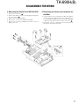
DISASSEMBLY FOR REPAIR
4. Removing the Control Unit (X57-560 B/2)
1. Remove the 8 screws ( 1 ).
2. With a screwdriver, remove the 2 leaf springs holding the
ICs to the frame ( 2 ).
3. Remove the flat cable (CN502).
4. Remove the 2 connectors CN501 and CN506.
5. Remove the connector (CN505) from D-sub connector
(25P) on the rear.
5. Removing the Accessory Connector on
the Rear
1. Confirm that the screw holding +DC cable (red) and the
screw holding –DC cable (black) of the final unit are removed, and that CN506 of the control unit (X57-560 B/2)
is disconnected. Remove the 4 screws on the rear ( 3 ).
2. Pull out the connector. (Take the connector terminals out
through the opening in the frame.)
1
3
3
1
CN501
CN506
3
CN505
CN502
2
Leaf spring
Screwdriver
IC
23
TK-690H(B)
DISASSEMBLY FOR REPAIR
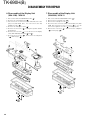
6. Disassembly of the Display Unit
(X54-3190) : KCH-10
7. Disassembly of the Display Unit
(X54-3200) : KCH-11
1. Pull out the VOL and UP/DOWN knobs ( 1 ).
2. Remove the 2 hexagnal nuts ( 2 ).
3. Disconnect the 2 connectors (CN2 and CN4) of the display unit (X54-3190 A/3). You can remove the UP/
DOWN encoder ( 3 ).
4. Remove the waterproof seal ( 4 ).
5. Remove the 4 screws ( 5 ) holding the speaker and PC
board fitting.
6. Remove the 3 screws ( 6 ). You can remove the display
units (X54-3190 A/3 and C/3) ( 7 and 8 ).
7. Remove the 3 screws ( 9 ), and remove the sub-panel
( 10 ) and keytop ( 11 ).
1.
2.
3.
4.
Pull out the VOL and UP/DOWN knobs ( 1 ).
Remove the 2 hexagnal nuts ( 2 ).
Remove the waterproof seal ( 3 ).
Disconnect the connector (CN4) of the display unit (X543200 A/2), and remove the 5 screws ( 4 ). you can
remove the up/down encoder ( 5 ) and display unit.
5. Remove the 4 screws ( 6 ), and remove the sub-panel
( 7 ) and keytop ( 8 ).
B/2
4
5
CN4
B/3
A/2
6
3
7
CN2
4
5
CN4
6
6
A/3
6
C/3
9
8
9
7
9
8
10
3
11
2
2
4
1
2
2
1
24
TK-690H(B)
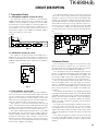
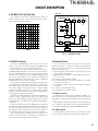
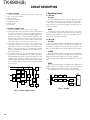
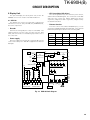
CIRCUIT DESCRIPTION
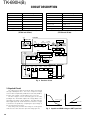
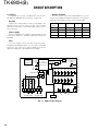
1. Transmitter Circuit
1-1. Microphone amplifier section (X57 B/2)
The audio input from the microphone is attenuated by
VR501 and passes through the active high-pass filter (preemphasis circuit) in IC505, the compressor circuit in IC504,
the IDC (limiter circuit) in IC505, the summing amplifier circuit in IC510, the active low-pass filter in IC510, the summing amplifier circuit in IC513, and the D/A converter in
IC512, and is output from the CN502 to the CN202. Q504 is
used as a microphone mute switch.
FINAL UNIT (X45)
Q1
Q5
to TX VCO
MO
IC512
DAC
If an abnormal antenna load is connected, the reflected
wave level increases. Reflected waves are detected by D6,
D5 and the output level is fed to the differential amplifier Q8,
leading to the transmitter output power being reduced in the
way already described. If an abnormal high temperature is
detected by the thermistor TH1, DC SW Q2 is made to reduce the reference voltage of the PC tuned. This also leads
to the transmitter output power being reduced. Antenna
switching is done by four diodes; D2, D3, D4 and D10 with
8T.
DO
AMP
Q9
AMP
AMP
IC510
SUM
AMP
LPF
IC505
IC504
IC505
IDC
COMP
HPF
Q504 VR501
MUTE
SW
DB
APC Q6
drive
8T
AMP
MIC
CONTROL UNIT X57 B/2
DC Q7
AMP
+B
Q8
Differential
AMP
Fig. 1
CM coupler
D5,6
REF
DET
B
PC
Q10
IC513 IC510
SUM
LPF
AMP
D2,3,4,10
ANT
SW
Q2
DC
SW
Q4
DC
AMP
D9
FWD
DET
VR1
8T
TH1
PC
1-2. Modulation section (X57 A/2)
The signal from the MO terminal of the CN202 goes to
D305 in the VCO, and the VCO is directly modulated. The
transmit signal output from the VCO passes through switch
D306, is amplified by Q203, and is output from the CN203 to
the CN1.
TX-RX UNIT X57 A/2
Q203
AMP
DO
APC
D306
SW
8T
TX-VCO
MO
Fig. 2
1-4. Final amplifier section (X45)
The signal from the DO terminal of the CN1 is applied to
drive two transistors Q1 and Q5, and the output is divided
into two signals which are amplified by Q6 and Q7. The
signals are mixed and the resulting signal is fed through
transmit/receive switching diode; D2, D3, D4 and D10, lowpass filter, and CM coupler to the antenna connector.
CM coupler is a coil for detecting traveling and reflected
waves. Traveling waves are detected by D9 and fed through
the APC control to differential amplifiers Q8, which compare
the signal level with the reference voltage of PC tuned.
The output is amplified by DC amplifier Q7 to control APC
DC amplifier Q6. Q7 controls the power supply voltage for
pre-drive amplifier Q203 on the TX-RX unit (X57-560 A/2),
keeping the transmitter output constant. To protect the
transmitter power amplifier stages, there are two protection circuits which one is against abnormal antenna loading
and the other is against overheating.
Fig. 3
2. Receiver Circuit
The incoming received signal from the antenna socket
passes through the low-pass filter, the transmit/receive
switching diodes (D2, D3, D4 and D10), and the second lowpass filter, then is fed to CN104 in the TX-RX unit.
The signal passes through the band-pass filter in the TXRX unit, is amplified by RF amplifier Q101 and Q102, then
passes through the second band-pass filter (BPF). The
tuned varactor BPF (L101, L102, L104 and L105) changes
the cut-off frequency according to the receive frequency.
After the signal has passed through the BPF, it inters RX
first mixer Q110 to Q113. The local signal (received frequency + 10.7MHz) from the PLL also enters the first mixer.
The first mixer is a double-balanced type consisting of four
FETs, which converts the receive signal to the 10.7MHz first
IF signal.
The 10.7MHz IF signal passes through NB (noise blanker)
unit A102 and IF amplifier Q103, and enters NB gate Q105
and Q106. The pulse noise in the IF signal is detected by the
NB unit, and removed by the NB gate. The IF signal passes
through the monolithic crystal filter (XF101), IF amplifier
Q301, monolithic crystal filter (XF102), and enters FM IF
system IC (IC101).
The signal is heterodyned again to 455kHz using the second local signal generated by the crystal oscillator
(11.155MHz), at the second mixer in IC101. The second IF
signal is filtered by CF101 and CF102 (ceramic filter), amplified by limiting amplifiers in IC101, and is detected as an FM
signal.
The output AF signal from IC101, then passes through
the control unit's HPF and D/A converter IC. After entering
the AF power amplifier (IC522), the signal is output from the
speaker.
25
TK-690H(B)
CIRCUIT DESCRIPTION
Item
Rating
Item
Rating
Nominal center frequency
10.7MHz
Nominal center frequency
10.7MHz
Pass bandwidth
7.5kHz or more at 3dB
Pass bandwidth
±7.5kHz or more at 3dB
Attenuation bandwidth
± 25kHz or less at 40dB
Attenuation bandwidth
±25kHz or less at 18dB
Ripple
1.0dB or less
Ripple
0.5dB or less
Insertion loss
2.5dB or less
Insertion loss
2.0dB or less
Guaranteed attenuation
80dB or more at fo± 1000kHz
Guaranteed attenuation
40dB or more at fo±1000kHz
Terminating impedance
3.0kΩ / 1.5pF
Terminating impedance
3.0kΩ / 2.5pF
Table 1
Table 2 Crystal filter (L71-0533-05)
(TX-RX unit XF102)
Crystal filter (L71-0534-05)
(TX-RX unit XF101)
TX-RX UNIT
ANT
FINAL UNIT
D2~4,10
ANT
SW
fRX+10.7MHz
1st MIX
BPF
L102,104,105 Q110~113
BPF
L101
LPF
D306
T/R
SW
RA
LPF
L11,12,14
RF AMP
Q101,102
TV
IF AMP
Q103 Q105,106
A102
TV
VCO
RX VCO
NB
10.7MHz
SW
IC101
RSSI
DET
RSSI
DET
D106
SQ NOISE
DET
FM SYSTEM IC
Q108
NOISE
AMP
MCF
XF102
Ceramic
filter
CF102 CF101
X101
11.155
MHz
IF AMP
Q107
MCF
XF101
455kHz
CONTROL UNIT
IC504
IC518
(2/2)
IC524
(1/2)
IC524
(2/2)
IC515
IC512
AMP
HPF
BEF
DE-EMP
EXP
VOL
IC516
CPU
27
ASQ
26
RSSI
BUFF
AF PA
DISPLAY UNIT
VOL
IC518
(1/2)
IC522
SP
Fig. 4 Receiver circuit
26
SQ close
SQ open
Preset
value
ANT input level
RSSI voltage
The output from IC101 enters FM IC again, then passed
through a band-pass filter. The noise component output
from IC101 is amplified by Q108 and rectified by D106 to
produce a DC voltage corresponding to the nose level.
The DC voltage is sent to the analog port of the CPU
(IC516/pin 27). And IC101 output a DC voltage (RSSI) corresponding to the input of the IF amplifier. The CPU reads the
RSSI signal via pin 26. IC101 determines whether to output
sounds from the speaker by comparing the input voltage of
pin 27 with the present value.
Only during scan, the RSSI DC voltage is used together
with the noise wave detection pin's DC voltage (pin 27).
SQ voltage
3. Squelch Circuit
Preset value
ANT input level
Fig. 5 Squelch and RSSI voltage vs ANT input level
TK-690H(B)
CIRCUIT DESCRIPTION
4. RX BPF (L101,102,104,105)
The signals are then fed into band-pass filter that uses
varactor diode tuning to reject unwanted signal components, and is fed to the 1st mixer.
TX-RX UNIT
8CL
MO
Q306
TX VCO
STR
SW Q308
Q310 SW
SW Q309
8CL
8C
8T
Q311
D306
Q313
TX
BUFF
AMP
SW
AMP
RX
8R
8CL
Q307
9CL
X301
Q312
RX VCO
AMP
VCXO
5C
5C
5C
IC301
PLL-IC
LPF
DT
CP
EP
UL
Q303,304
IC516
µ-com
Fig. 6
MB
MO
CONTROL UNIT
Fig. 7 VCO/PLL circuit
5. VCO/PLL Circuit
6. Control Circuit
The VCO of TK-690H(B) consists of two VCO circuits
which one oscillates the transmit signal with Q306 and the
other does the first local receive signal with Q307.
Each oscillators are switched by turning the source line
for Q308, Q309 and Q310 on and off. The signal output of
the VCO is amplified by the buffer amplifier Q311 and divided into two signals which one is amplified by Q313 and
the other is done by Q312. The signal from Q313 passes
through D306 which is transmit/receive switch, is amplified
by Q203, and is output from the CN203.
The signal from Q312 passes through the low-pass filter
and is applied to IC301 which is PLL frequency synthesizer
with VCXO ; X301. The VCXO of which the frequency stability is within 5.0ppm (temperature range of –30 to +60°C)
generates 16.8MHz. The PLL-IC consists of three modulus
prescaler, fractional divider, reference divider, digital phase
comparator with charge pump output.
This PLL-IC is Fractional-N type synthesizer and performs
is 25kHz reference signal which is fifth of the channel step
(5kHz). The input signal from the pins 5 and 8 of the PLL-IC
is divided down to the 25kHz and compared at digital phase
comparator.
The pulsed output signal of the digital phase comparator
is applied to the charge pump and transformed into DC signal. The DC signal from the pin 14 of the PLL-IC passes
through the active low-pass filter (loop filter), is applied to
the VCO and controls to keep the frequency of the VCO.
The serial data (DT, CP, EP) from the microprocessor
IC516 is input to the PLL-IC. And PLL lock condition is always monitored by the pin 28 (UL) of IC516.
The control unit consists of microprocessor IC and its
peripheral circuits. It controls the TX-RX unit and transfers
data to and from the control unit. The CPU (IC516) mainly
performs the following :
1) Switching between transmission and reception according to the PTT signal input.
2) Reading channel, frequency, and program data from the
memory circuit.
3) Sending frequency data to the PLL.
4) Turning the squelch on and off according to the voltage
from the squelch circuit.
5) Controlling the audio mute circuit according to input decode data.
6) Sending encode data (QT, DQT).
7) Sending data to the D/A converter.
6-1. Memory circuit
A flash memory (IC519) with a capacity of 2Mbits contains the transceiver control program for the CPU (IC516)
and data such as transceiver channels and operating features.
This program can be easily written from an external devices. Data, such as DTMF memories and operating status,
tuning data are programmed into the EEPROM (IC514).
6-2. Shift register
IC517 and IC523 are an interface IC for I/O port expansion. It is used to expand the CPU (IC516) output ports.
27
TK-690H(B)
CIRCUIT DESCRIPTION
6-3. D/A converter
IC512 is used as a conventional semi-fixed-resistor converter. It sets the following :
1) RX sensitivity
2) Transmission power
3) Modulation level
4) Audio power
5) Frequency
6-4. Power supply circuit
D507 is a protection diode for the excess voltage.
1) Turning the transceiver on/off with a power switch. Each
time you press the power switch, the IC501 output is alternated. The output is feed through Q501, Q503 to turn
Q519 on. The power source is always supplied to the
IGN terminal. If 24V DC is supplied to the transceiver by
mistake, Q502 is turned on then Q503 and Q519 are
turned off to protect the transceiver (turned off).
2) Turning the transceiver on with a power switch, then
turning the transceiver off with the Timed Power Off
(TPO) function. POF is controlled by CPU’s TPO function.
POF is to turn the transceiver off. The POF logic signal is
feed through Q507 and Q506 then 8 pin of IC501 to turn
the transceiver off.
3) Turning the transceiver on with IGN SENS, then turning
the transceiver off with TPO function. If IGN is turned on,
Q543 and Q542 are turned on then the IC501 detects the
change. IC501 outputs the signal to turn Q541 off, then
Q503 and Q519 are turned on. When POF is detected by
6 pin of IC501, Q541 is turned on then Q503 and Q519
are turned off.
IGN
+B
POF
PS
Q519
SW
D507
AVR
Q543
SW
Q507
SW
Q506
SW
Q544
SW
Q518
SW
IC501
D-FF
Q503
SW
D501
SW
Q501
SW
SB
7. Signalling Circuit
7-1. Encode
• QT, DQT
The CPU (IC516) transmits the encode data selected by
the program. The data items are output from CPU pin 34.
The signal from this pin passes though the CR low-pass
filter and goes to the summing amplifier (IC510) in the microphone amplifier.
• DTMF
The DTMF-encoder (IC511) transmits the encode data.
The encode data is passed to the D/A convertor (IC512) for
DTMF deviation adjustment, and goes to IC505 in the IDC
circuit of the microphone amplifier.
7-2. Decode
• QT, DQT
The demodulated signal from CN502 pin 5 is amplified by
IC521 and passes through a low-pass filter (IC502) to remove audio components. The signal is input to pin 25 of the
CPU. The CPU digitizes this signal, and decodes the signal.
• 2 TONE
The demodulated signal from CN502 pin 5 is amplified by
IC504 and passes through a high-pass filter (IC518) and a
band-elimination filter (IC524) to remove QT and DQT.
This signal is amplified by IC521 and inputs pin 91 of the
CPU.
• DTMF
The demodulated signal from CN502 pin 5 is amplified by
IC504 and passes through a high-pass filter (IC518) and
band-elimination filter (IC524) to remove QT and DQT.
This signal inputs pin 1 of the DTMF decoder (IC525).
CN502
DET
5
IC521
IC502
LPF
LPF
IC504
IC518
IC524
IC521
AMP
HPF
BEF
AMP
IC525
1 DTMF
decoder
Q541
SW
Fig. 9
Fig. 8 Power supply circuit
28
25
AMP
Q542
SW
Q502
SW
IC516
CPU
IC502
Decode
91
QT·DQT
2TONE
SD
TK-690H(B)
CIRCUIT DESCRIPTION
• CPU (containing LCD driver)
8. Display Unit
The on/off signals of keys other than the power switch,
and the PTT and HOOK signals, are converted to serial data
and sent to the control unit. Data is displayed on the 13segments, 8-digits LCD and 7-segments, 3-digits LCD by
the built-in LCD driver.
The optional display unit (front panel unit) for the TK690H(B) comes in two models : KCH-10 and KCH-11
8-1. KCH-10
This display unit consists of a CPU (IC4) containing the
LCD driver, a reset IC (IC2), 5V AVR (IC1), EEPROM (IC3),
and other components.
• Dimmer function
From the control of the CPU’s DM1/DM2 port, you can
switch the LCD/KEY backlight, busy/TX LED, or the optional
KMC-28 key backlight as shown in the following table.
• Encoder
Channels are changed by the rotary encoder (ENC). The
up/down pulses from the rotary encoder enter the CPU
(IC4), and converted to a serial data signal, and are sent to
the control unit.
Dimmer
• Power supply
Power is supplied to the CPU by converting SB from the
control unit to 5V by IC1. And SB is supplied to the LED for
backlight.
KEY
Busy/TX
KMC-28
H
H
ON
ON
ON
M
M
ON
ON
ON
L
L
ON
ON
ON
OFF
OFF
OFF
OFF
OFF
5V
LCD
PTT
HK
ED1
IC4
78064GCXXX8EU
D13
RX
RST
Microprocessor
AVR
SB
S1
IC1
NJM78L05UA POWER
D25
RST
PS
IC2
RH5VL42C
RST
D17
TX
S5
PF1
S6
PF2
S2
S3
S7
PF3
S8
PF4
S9
PF5
IC3
AT24C64N10SI27 EEPROM
SW
SW
SW
SW
AF VR
REF
SW
SW
MIC
1/2
TRD
RS1
RS2
SW
DM1 DM2
DM1 DM2 DM1 DM2
LCD BACK LAMP
KEY BACK LAMP
SB
HK
ME
MIC
E
TRD
DM
BLC
PTT
SB
SW
LCD
setting
ENCODER
INT SP
Fig. 10 KCH-10 block diagram
29
TK-690H(B)
CIRCUIT DESCRIPTION
8-2. KCH-11
• Dimmer function
This display unit consists of a CPU (IC4) a reset IC (IC2),
5V AVR (IC1), EEPROM (IC3), and other components.
From the control of the CPU’s DM1/DM2 port, you can
switch the LCD/KEY backlight, busy/TX LED, or the optional
KMC-28 key backlight as shown in the following table.
• Encoder
Channels are changed by the rotary encoder (ENC). The
up/down pulses from the rotary encoder enter the CPU
(IC4), and converted to a serial data signal, and are sent to
the control unit.
Dimmer
LCD
KEY
Busy/TX
KMC-28
H
H
ON
ON
ON
M
M
ON
ON
ON
setting
• Power supply
Power is supplied to the CPU by converting SB from the
control unit to 5V by IC1. And SB is supplied for the LED of
backlight.
L
L
ON
ON
ON
OFF
OFF
OFF
OFF
OFF
• CPU
The on/off signals of keys other than the power switch,
and the PTT and HOOK signals, are converted to serial data
and sent to the control unit. Data is displayed on the 14digits and 3-digits dot matrix alphanumeric display.
5V
LCD ASSY
Containing
LCD driver IC
ED1
PTT
HK
IC4
78064GCXXX8EU
D13
RX
Microprocessor
RST
PS
IC2
RH5VL42C
S5
PF1
S6
PF2
S7
PF3
S8
PF4
S9
PF5
S12
PF7
S13
SCN
S14
PF8
S15
PF9
S2
SW
SW
SW
SW
REF
AF VR
SW
DM1 DM2
LCD BACK LAMP
S3
MIC
1/2
TRD
RS1
RS2
SB
HK
ME
MIC
E
TRD
DM
BLC
PTT
SW
DM1 DM2
KEY BACK LAMP
ENCODER
Fig. 11 KCH-11 block diagram
30
S10 S11
MON PF6
IC3
AT24C64N10SI27 EEPROM
SB
SW
SB
S1
POWER
IC1
NJM78L05UA
RST
D12
TX
SW
AVR
RST D19
TK-690H(B)
SEMICONDUCTOR DATA
Microprocessor : 784214GCXXX8EU (Control Unit IC516)
• Terminal function
Pin No.
Pin name
I/O
Action
Pin No.
Pin name
I/O
Action
1
FCLR
O
Modem FCLR
40
RXD1
I
Serial interface RXD
2
CK
O
Common CLOCK
41
TXD1
O
Serial interface TXD
3
EM
O
D/A converter CS
42
STB
O
Modem STB
4
MSKE
O
Modem MSKE
43
EC1
O
Shift registerl (Control) CS
5
DIN
O
Modem DIN
44
EI
6
EP
O
PLL LE
45
SEL
7
SCL
O
DTMF encoder CLOCK
46
8
SDT
O
DTMF encoder DATA
47
9
VDD
+5V
48~71
10,11
X2, X1
X’tal
72
O
Shift register (Interface) CS
I/O
GE-STAR I/O
EPT
I
GE-STAR EPT
EMG
O
GE-STAR EMG
Flash ROM access port
VSS
GND
12
VSS
GND
73~74
Flash ROM access port
13
XT2
Open
75
Flash ROM (4Mbit) access port
14
XT1
GND
76
Not used.
15
RESET
CPU reset
77~78
Flash ROM access port
16
TEST
I
Serial interface TEST
79
17
TRD
I
Modem TRD
80
POF
18
RTM
I
Modem RTM
81
VDD
19
STD
I
DTMF decoder STD
82
EN2
20
EC2
O
Shift register 2 (Control) CS
83
21
DT
O
Common DATA
84
22
ACK
O
23
AVDD
24
AVREF0
25
TI
I
26
RSI
27
ASQ
O
Timed Power OFF.
Not used.
+5V
O
D/A converter (Interface) CS
CLK
O
EEPROM CLOCK
SDA
I/O
EEPROM DATA
DTMF decoder CLOCK
85
RSV1
O
Reserved
+5V
86
AI1
I
Acc PF Input 1
+5V
87
AI2
I
Acc PF Input 2
QT/DQT IN
88
AI4
I
Acc PF Input 4
I
RSSI IN
89
AI3
I
Acc PF Input 3
I
Analog squelch IN
90
AI5
I
Acc PF Input 5
28
UL
I
PLL UNLOCK
91
2TN
I
2tone pulse IN
29
SD
I
DTMF decoder SD
92
KEY
O
TX power SW
30
RDT
I
Modem RDT
93
SQ
O
Acc SQ OUT
31
RSV2
I
Reserved
32
IGN
I
Ignition IN
94
TEST
33
AVSS
GND
95
AO1
O
Acc PF Output 1
L : BUSY, H : Not BUSY
GND
34
TO
O
QT/DQT OUT
96
AO2
O
Acc PF Output 2
35
CP
O
PLL CLOCK
97
AO3
O
Acc PF Output 3
36
AVREF1
+5V
98
AO4
O
Acc PF Output 4
37
RXD2
I
Acc RXD
99
1/2
I
Deck 1/2
38
TXD2
O
Acc TXD
39
ES
O
Shift register (TX/RX) CS
100
SFT
O
Beat shift
L : Deck 1, H : Deck 2
31
TK-690H(B)
SEMICONDUCTOR DATA
Microprocessor : 78064GCXXX8EU (Display Unit IC4)
• Terminal function
Pin No.
1
Pin name
I/O
PTT
I
Pin No.
L : ON, H : OFF
74
Pin name
I/O
Action
Not used
2
K5
I
[MON] key
L : ON, H : OFF
75
RXD
I
Serial interface RXD
3
K6
I
[PF6] key
L : ON, H : OFF
76
TXD
O
Serial interface TXD
4
K7
I
[PF1] key
L : ON, H : OFF
77
5
K8
I
[PF2] key (Full)
L : ON, H : OFF
78
–
GND
Not used
6
K9
I
[PF3] key (Full)
L : ON, H : OFF
79
X2
–
X’tal 4.19MHz
7
K10
I
[PF7] key (Full)
L : ON, H : OFF
80
X1
–
X’tal 4.19MHz
VDD
–
8
AVDD
–
+5V
81
9
AVREF
–
+5V
82,83
10
RED
O
TX LED (Red)
11
GRN
O
BUSY LED (Green)
84
RST
–
Reset
85
END
I
Encoder data
>
L : ON, H : OFF
] Key
L : ON, H : OFF
<
L : ON, H : OFF
+5V
Not used
] Key
L : ON, H : OFF
12
E
–
GND
86
K3
I
[GR
13
DM1
O
Backlight (Dimmer)
87
K4
I
[GR
14
DM2
O
Backlight (Dimmer)
88
ENI
I
Encoder interrupt
I
Not used
89
TEST
I
Serial interface test
15
16
K11
I
[SCN] key (Full)
L : ON, H : OFF
90
AO2
O
Programable AUX output B
17
K12
I
[PF8] key (Full)
L : ON, H : OFF
91
AO1
O
Programable AUX output A
18
K13
I
[PF9] key (Full)
L : ON, H : OFF
92
AI2
I
Programable AUX input B
19
K1
I
[PF4] key
L : ON, H : OFF
93
AI1
I
Programable AUX input A
20
K2
I
[PF5] key
L : ON, H : OFF
94
BLC
O
MIC backlight ON/OFF
21
1/2
I
HEAD 1/2 jumper
22
23~26
27
28~30
31
32~67
68
B/F
COM0~3
I
O
BIAS
69
VSS
S36
O
S38
97
Not used
DM
I
DTMF MIC key pad data input
Panel type Jumper
98
HK
I
MIC hook
Basic panel : Jumper installed.
99
AVSS
–
GND
Full panel : Jumper removed
100
VOL
I
AF volume
L : ON, H : OFF
LCD drive common 0~3
LCD drive segment 0~35
Shift Register Output : BU4094BCF
LCD drive segment 36 (Basic)
• Shift register 1 on control unit (IC523)
DOT matrix driver CE (Full)
O
O
DI
71
95,96
HEAD 2 : Jumper removed
GND
O
CL
70
HEAD 1 : Jumper installed,
LCD drive power suply
S0~35
S37
L : ON, H : OFF
LCD drive bias
VLC0~2
CE
32
Action
MIC PTT
Pin No.
Port
Name
Action
LCD drive segment 37 (Basic)
4
Q1
PTO
GE-STAR/Scrambler PTO
DOT matrix driver CL (Full)
5
Q2
BC4
Scrambler BC4
LCD drive segment 38 (Basic)
6
Q3
BC3
Scrambler BC3
DOT matrix driver DI (Full)
7
Q4
BC2
Scrambler BC2
S39
O
LCD drive segment 39 (Basic)
14
Q5
AC
Scrambler AC
DO
I
DOT matrix driver DO (Full)
13
Q6
BC1
Scrambler BC1
HR
72
SCK
O
EEPROM serial clock
12
Q7
73
SDT
I/O
EEPROM serial data
11
Q8
Acc HR
Not used
TK-690H(B)
SEMICONDUCTOR DATA
• Block diagram
• Shift register 2 on control unit (IC517)
Pin No.
Port
Name
4
Q1
MM
5
Q2
AS
Action
MIC mute
VP1
5
H : Mute, L : Unmute
Audio line SW RX BPF←→DE-EMP
–INV 1
1
mute switch Cm
Q3
DS
DET line SW
7
Q4
AM1
Audio mute 1
14
Q5
RG1
Modem RG1
13
Q6
RG2
Modem RG2
12
Q7
MS
MOD line SW MIC AMP←→RX BPF
11
Q8
AM2
+
60
kΩ
DET←→RX BPF
6
_
Name
4
Q1
STR
5
Q2
Not used
6
Q3
Not used
7
Q4
Not used
14
Q5
power stage
18kΩ
mute switch Cm
+
60
kΩ
INV 2
_
3
TX/RX VCO SW
Q6
12
Q7
NB
Not used
11
Q8
Not used
power stage
18kΩ
VP
VA
PROTECTIONS
thermal
short-circuit
15kΩ
–INV 4
4
17
–INV1
Non-inverting input 1
2
GND (S)
Signal ground
3
INV 2
Inverting input 2
4
RR
Supply voltage ripple rejection
5
VP1
60
kΩ
Output 1
7
GND1
Power ground 1
8
OUT 2
Output 2
9
NC
Not connected
10
OUT 3
Output 3
11
GND2
Power ground 2
12
OUT 4
Output 4
13
VP2
Supply voltage
14
MODE
Mode select switch input
15
INV 3
Inverting input 3
16
VDIAG
Diagnostic output
17
–INV 4
Non-inverting input 4
mute
reference
voltage
_
12
OUT 4
2
kΩ
power stage
18kΩ
mute switch Cm
INV 3
OUT 1
VDIAG
+
VA
Supply voltage
6
16
+
Description
1
mute
switch
mute switch Cm
• Terminal description
Symbol
+ stand-by
reference
voltage
+
+
_
15kΩ
Audio Power Amplifier
: TDA8561Q (Control Unit IC522)
MODE
_
Noise blanker SW
RR
14
+
stand-by
switch
×1
Pin No.
OUT2
2
kΩ
8R SW
13
8
VA
Action
8R
OUT1
2
kΩ
• Shift register on TX-RX (IC201)
Port
6
VA
Audio mute 2
Pin No.
VP2
13
60
kΩ
15
+
_
10
VA
OUT 3
2
+ kΩ
power stage
18kΩ
2
GND (S)
input
reference
voltage
9
7
GND1
11
GND2
NC
33
TK-690H(B)
SEMICONDUCTOR DATA / DESCRIPTION OF COMPONENTS
Flash ROM : AT29C020-90TI (Control Unit IC519)
Final Unit (X45-3550-XX)
• Terminal description
-10 : K
Pin Name
Function
Ref. No.
-11 : K2
-12 : K3
Use/Function
Operation/Condition
A0~A17
Addresses
Q1
TX drive amplifier
CE
Chip enable
Q2
DC amplifier
OE
Output enable
Q3,4
DC switch
WE
Write enable
Q5
TX drive amplifier
I/O0~I/O7
Data inputs/outputs
Q6
APC controller
NC
No connect
Q7
DC amplifier
APC controller
Q8
APC comparator
APC controller
• Block diagram
Data inputs/outputs
I/O0~I/O7
Vcc
GND
OE
WE
CE
Address
input
Q9
Final amplifier
Q10
Final amplifier
Q11
DC switch
D1
Temperature
D2~4
Antenna switch
D5
Protector
D6
Reflected wave
APC controller
DATA LATCH
OE, CE, AND WE
LOGIC
compensation
INPUT/OUTPUT
BUFFERS
Y DECODER
Y-GATING
X DECODER
OPTIONAL BOOT
BLOCK (8K BYTES)
MAIN MEMORY
(240K BYTES)
rectification
OPTIONAL BOOT
BLOCK (8K BYTES)
D7
Surge absorption
D8
Protection of reverse
connection
D9
Forward wave
rectification
Final Amplifier : 2SC2694 (Final Unit Q9, Q10)
D10
Antenna switch
• Absolute maximum ratings
Tc= 25°C unless otherwise noted
Symbol
Parameter
Condition
Rating
VCBO
Collector-base voltage
35V
VEBO
Emitter-base voltage
4V
VCEO
Collector-emitter voltage
Ic
Collector current
Pc
Collector dissipation
140W
Tj
Junction temperature
175°C
Tstg
Storage temperature
–55 to 175°C
RBE = ∞
17V
TX-RX Unit (X57-5600-XX) (A/2)
-10 : K
Ref. No.
IC101
-11 : K2
-12 : K3
Use/Function
FM IC
20A
Operation/Condition
1, 2 : Oscillator (11.155MHz)
3 : Mixer output
4 : Vcc
5 : IF input (455kHz)
7 : Noise filter output
8 : Noise filter input
9 : DET output (AF OUT)
10 : Quad input
12 : RSSI output
16 : Input (10.7MHz)
34
IC201
Shift register
IC202
AVR
Input : 8V
Output : 5V
IC203
AVR
Input : SB
Output : 9V
TK-690H(B)
DESCRIPTION OF COMPONENTS
Ref. No.
IC301
Use/Function
PLL IC
Operation/Condition
1 : CP
LPF
IC503
AVR
8 : REFin (16.8MHz)
IC504
Audio processor
14 : Charge pump output
IC505
HPF/IDC
18 : UL ("H" when lock)
IC506
AVR
20 : VDD (5V)
IC508
Limiter/Buffer amplifier
5 : Fin
3 : EP
Use/Function
IC502
4 : Vss
2 : DT
Ref. No.
7 : Vcc
Q101,102
1st amplifier
RX frequency
IC509
Buffer amplifier
Q103
IF amplifier
10.7MHz
IC510
Summing amplifier/LPF
Q105,106
NB gate
IC511
DTMF encoder
Q107
IF amplifier
10.7MHz
IC512
D/A converter
Q108
SQL amplifier
(Noise amplifier)
IC513
LPF/Summing amplifier
Q110~113
RX 1st mixer
IC514
EEPROM
Q114
NB switch
On when NB on
IC515
Analog switch
Q115
DC switch
On when TX
IC516
CPU
Q201
8T switch
8V when TX
IC517
Shift register
Q202
8T switch
On when TX
IC518
Buffer amplifier
Q203
TX pre-drive amplifier
IC519
Flash ROM
Q204
8R switch
On when RX
IC520
NOR gate
Q205
8R switch
8V when RX
IC521
Q301
Ripple filter
8CL
Q302
Ripple filter
9CL
Q303,304
Loop filter
Operation/Condition
Input : SB, Output : 8V
Input : 8V, Output : 5V
Buffer amplifier/
Amplifier
IC522
Audio power amplifier
IC523
Shift register
Q306
OSC
TX-VCO
Q307
OSC
RX-VCO
Q308
DC switch
On when TX
IC525
DTMF decoder
Q309
DC switch
On when RX
IC526
Amplifier
Q310
DC switch
Off when RX
Q501
DC switch
Q311
Buffer amplifier
Q502
DC switch
On when 18V or more
Q312,313
Amplifier
Q503
DC switch
On when the power switch on
D102~105
BPF tuning
Q504
Muting switch
MIC mute
Vari-cap tuning
IC524
Buffer amplifier/
De-emphasis
D106
Noise detector
Q505
DC switch
D107
DC switch
On when TX
Q506,507
DC switch
Timed power off switch
D301
Frequency controller
TX-VCO
Q509
DC switch
Off when P/A
D302
Frequency controller
RX-VCO
Q510
DC switch
Off when EXT SP
D303
Frequency controller
TX-VCO
Q511
DC switch
Off when INT SP
D304
Frequency controller
RX-VCO
Q512
DC switch
Off when RX busy
D305
Modulator
Q513
DC switch
D306
RF switch
Q514
Muting switch
Q516,517
DC switch
On when on signalling code
Control Unit (X57-5600-XX) (B/2)
Q518
DC switch
On when push the power switch
-10 : K
Q519
Power switch
On when the power switch on
Q520
DC switch
On when horn alert
Q522
Beat shift switch
On when beat shift
Ref. No.
IC501
TX/RX
-11 : K2 -12 : K3
Use/Function
D FF
Operation/Condition
On when AF mute
35
TK-690H(B)
DESCRIPTION OF COMPONENTS
Ref. No.
Use/Function
Operation/Condition
Ref. No.
Use/Function
Q523
DC switch
Serial data inverter
Q11
DC switch
Q524
DC switch
Serial data transmitter
Q12,13
TRD switch
Q525
DC switch
Q14,15
DC switch
Q533~540
DC switch
On when output port on
D1,2
Surge absorption
Q541
DC switch
On when timed power off
D5
Voltage reference
Q542,543
DC switch
IGN switch
D6~11
LCD backlight
Q544
DC switch
Timed power off switch
D12
BUSY LED
D501
Voltage reference
Protection of high voltage
D13
TX LED
D502
Reverse current
D16,17
Surge absorption
prevention
D19~21
Surge absorption
D503
Surge absorption
D24
DC switch
D504
Voltage reference
D25
DC switch
D505,506
DC switch
D507
Voltage reference
D508
DCswitch
D511
DC switch
Ref. No.
D512
Reverse current
IC1
AVR
prevention
Operation/Condition
“PF4”, “PF5” key lighting : ON
On when output port on
Key lighting : ON
Display Unit (X54-3200-20) : KCH-11
Use/Function
Operation/Condition
Output : 5V
Reset
IC3
EEPROM
D519
Surge absorption
IC4
CPU
D521
Surge absorption
Q1
9V AVR
D523,524
Surge absorption
Q2
DC switch
D526,527
Surge absorption
Q3
DC switch
Dimmer “Hi”, “Low” : ON
D528,529
Reverse current
Q4
DC switch
“MON”, “PF6”, “PF7” key
prevention
,
<
IC2
D513~517 Surge absorption
>
Input : SB
key lighting : ON
lighting : ON
Q5
DC switch
“PF1”, “PF2”, “PF3” key
lighting : ON
Display Unit (X54-3190-20) : KCH-10
36
Use/Function
Operation/Condition
Input : SB
DC switch
Dimmer “Hi”, “Mid” : ON
Q7
DC switch
“SCN”, “PF8”, “PF9” key
IC1
AVR
IC2
Reset
Q8
DC switch
IC3
EEPROM
Q9,10
TRD switch
IC4
CPU/LCD driver
Q14,15
DC switch
Q1
9V AVR
D1,2
Surge absorption
Q3
DC switch
D5
Voltage reference
Q4
DC switch
>
Ref. No.
Q6
Output : 5V
D6
BUSY LED
Q5
DC switch
Dimmer “Hi”, “Mid” : ON
D7
TX LED
Q6
DC switch
Dimmer “Hi”, “Low” : ON
D11,12
Surge absorption
Q7
DC switch
Dimmer “Hi”, “Mid” : ON
D14~16
Surge absorption
Q9
DC switch
“PF1”, “PF2”, “PF3” key
D18
DC switch
lighting : ON
D19
DC switch
,
<
Dimmer “Hi”, “Low” : ON
key lighting : ON
lighting : ON
“PF4”, “PF5” key lighting : ON
On when output port on
Key lighting : ON
TK-690H(B)
PARTS LIST
✽ New Parts.
indicates safety critical components.
Parts without Parts No. are not supplied.
Les articles non mentionnes dans le Parts No. ne sont pas fournis.
Teile ohne Parts No. werden nicht geliefert.
L : Scandinavia
Y : PX (Far East, Hawaii)
Y : AAFES (Europe)
K : USA
T : England
X : Australia
P : Canada
E : Europe
M: Other Areas
TK-690H(B)
FINAL UNIT (X45-3550-XX)
Ref. No.
New
Address parts
Parts No.
Description
Destination
TK-690H(B)
Ref. No.
New
Address parts
Parts No.
Description
FINAL UNIT (X45-3550-XX) -10 : K
1
2
3
3B
1A
2B
A01-2163-01
A01-2164-01
A10-1389-01
CABINET (UPPER)
CABINET (LOWER)
CHASSIS
6
7
8
9
9
3A,3B
1G
1G
2B
2B
✽
✽
B42-2455-04
B46-0470-00
B62-0970-10
B72-1471-24
B72-1472-24
STICKER (M4X8 MAX)
WARRANTY CARD
ACSY
INSTRUCTION MANUAL
MODEL NAME PLATE
MODEL NAME PLATE
K
K2
9
2B
✽
B72-1473-24
MODEL NAME PLATE
K3
11
13
14
15
16
2B
2A
2B
2B
2B,2H
E04-0167-05
E31-3301-05
E37-0709-05
E37-0731-05
E37-0733-05
17
18
2B
3A
23
24
22
Destination
-11 : K2 -12 : K3
C1
C3-5
C6
C7,8
C9
CK73FB1H472K
CK73FB1H472K
CK73FB1E104K
CK73FB1H472K
C90-2020-05
CHIP C
CHIP C
CHIP C
CHIP C
ELECTRO
4700PF
4700PF
0.10UF
4700PF
15UF
K
K
K
K
25WV
C10
C11,12
C13
C14
C15
CK73FB1H102K
CK73FB1H472K
C92-0729-05
CK73FB1H472K
CK73FB1E104K
CHIP C
CHIP C
ELECTRO
CHIP C
CHIP C
1000PF
4700PF
330UF
4700PF
0.10UF
K
K
25WV
K
K
RF COAXIAL PECEPTACLE (M)
LEAD WIRE WITH MINIPIN PLUG (RA/DO)
LEAD WIRE WITH CONNECTOR (ACC : 9P)
LEAD WIRE WITH CONNECTOR (DC : 2P)
SHORT PLUG (SP)
ACSY
C16
C17
C17
C18
C19
CK73FB1H471K
CC73FCH1H471J
CK73FB1H331K
CC73FCH1H101J
C92-0726-05
CHIP C
CHIP C
CHIP C
CHIP C
ELECTRO
470PF
470PF
330PF
100PF
47UF
K
J
K
J
25WV
E37-0773-25
E37-0776-05
LEAD WIRE WITH CONNECTOR (D-SUB : 25P)
FLAT CABLE (CONT-TX : 18P)
2B
1B
1H
F09-0445-05
F10-1488-02
F29-0472-04
CAP (D-SUB)
SHIELDING PLATE (FINAL)
INSULATING COVER
ACSY
C20
C21
C21
C22
C23
C93-0603-05
C93-0571-05
C93-0572-05
C92-0736-05
CK73FB1H102K
CHIP C
CHIP C
CHIP C
ELECTRO
CHIP C
1000PF
82PF
100PF
10UF
1000PF
K
J
J
50WV
K
27
28
29
32
33
3A
3A
2B
3B
1A
G02-0709-04
G02-0715-04
G53-0715-03
G53-0871-03
G53-0872-03
FLAT SPRING (AUDIO AMP)
FLAT SPRING (AVR)
PACKING (DC,ACC)
PACKING (CABINET UPPER)
PACKING (CABINET LOWER)
C24
C25
C25
C26-29
C30
CK73FB1H472K
C93-0568-05
C93-0570-05
CK73FB1H472K
C93-0568-05
CHIP C
CHIP C
CHIP C
CHIP C
CHIP C
4700PF
47PF
68PF
4700PF
47PF
K
J
J
K
J
35
36
37
38
39
1G
2H
1H
2H
2G
H02-0604-03
H10-6617-11
H11-0815-04
H11-0853-04
H11-0892-04
INNER PACKING CASE
POLYSTYRENE FOAMED FIXTURE
POLYSTYRENE FOAMED BOARD
POLYSTYRENE FOAMED BOARD
POLYSTYRENE FOAMED BOARD
C30
C31
C32
C33
C34
C93-0571-05
CK73FB1E104K
C92-0726-05
CK73FB1H472K
C93-0600-05
CHIP C
CHIP C
ELECTRO
CHIP C
CHIP C
82PF
0.10UF
47UF
4700PF
560PF
J
K
25WV
K
K
40
41
42
44
45
2G
2H
2G
1H
1G
H12-1410-04
H12-1442-04
H13-1066-04
H25-0103-04
H25-0724-04
PACKING FIXTURE
PACKING FIXTURE
CARTON BOARD
PROTECTION BAG (125/250/0.07)
PROTECTION BAG (300/500/0.07)
C93-0603-05
C93-0683-05
CM73F2H121J
CM73F2H161J
CM73F2H181J
CHIP C
CERAMIC
CHIP C
CHIP C
CHIP C
1000PF
4700PF
120PF
160PF
180PF
K
K
J
J
J
43
46
1H
3H
H25-2063-04
H52-1378-02
PROTECTION BAG (80/120/0.03)
ITEM CARTON CASE
47
50
2B
1H
J21-8347-04
J61-0307-05
HARDWARE FIXTURE (DC,ACC)
BAND
ACSY
C39
C43,44
C45
C45
C46
C92-0726-05
CK73FB1H472K
CM73F2H120J
CM73F2H560J
CK73FB1H472K
ELECTRO
CHIP C
CHIP C
CHIP C
CHIP C
47UF
4700PF
12PF
56PF
4700PF
25WV
K
J
J
K
M
N
O
P
Q
2B
1A,3B
1B
2A,2B
1A,1B
N09-2292-05
N33-3006-45
N35-3006-46
N67-3008-46
N68-4006-46
HEXAGON HEAD SCREW
OVAL HEAD MACHINE SCREW
BINDING HEAD MACHINE SCREW
PAN HEAD SEMS SCREW W
PAN HEAD SEMS SCREW A
C47
C48
C49,50
C51
C52
CK73FB1E104K
C93-0684-05
CK73FB1H472K
C93-0684-05
C93-0570-05
CHIP C
CERAMIC
CHIP C
CERAMIC
CHIP C
0.10UF
6800PF
4700PF
6800PF
68PF
K
K
K
K
J
K3
R
S
T
59
2A,3B
2A
2B
2H
N87-2606-46
N87-2612-46
N87-3008-46
N99-0365-05
BRAZIER HEAD TAPTITE SCREW
BRAZIER HEAD TAPTITE SCREW
BRAZIER HEAD TAPTITE SCREW
SCREW SET
ACSY
C52
C53
C53
C54
C54
C93-0571-05
CM73F2H390J
CM73F2H820J
CM73F2H040D
CM73F2H080D
CHIP C
CHIP C
CHIP C
CHIP C
CHIP C
82PF
39PF
82PF
4.0PF
8.0PF
J
J
J
D
D
K,K2
K2,K3
K
K2
K,K3
C55
C55
C55
C56
CM73F2H101J
CM73F2H121J
CM73F2H181J
CM73F2H220J
CHIP C
CHIP C
CHIP C
CHIP C
100PF
120PF
180PF
22PF
J
J
J
J
K3
K2
K
K,K2
C34
C35,36
C37,38
C37,38
C37,38
✽
✽
K
K3
K2
K
K2,K3
K
K2,K3
K
K3
K,K2
K3
K,K2
K3
K2
K
K3
K
37
TK-690H(B)
PARTS LIST
FINAL UNIT (X45-3550-XX)
Ref. No.
Address New
parts
Parts No.
Description
Destination
Ref. No.
C56
C57
C57
C58
C58
CM73F2H270J
CC73FCH1H680J
CC73FCH1H820J
CM73F2H101J
CM73F2H121J
CHIP C
CHIP C
CHIP C
CHIP C
CHIP C
27PF
68PF
82PF
100PF
120PF
J
J
J
J
J
K3
K3
K,K2
K2
K
L14
L14
L15
L15
L16
C59
C59
C60
C60
C61
CM73F2H470J
CM73F2H820J
CC73FCH1H330J
CC73FCH1H560J
CM73F2H390J
CHIP C
CHIP C
CHIP C
CHIP C
CHIP C
47PF
82PF
33PF
56PF
39PF
J
J
J
J
J
K,K2
K3
K2
K,K3
K2
L17
L18
C61
C61
C62
C62
C62
CM73F2H470J
CM73F2H510J
CC73FCH1H121J
CC73FCH1H151J
CC73FCH1H820J
CHIP C
CHIP C
CHIP C
CHIP C
CHIP C
47PF
51PF
120PF
150PF
82PF
J
J
J
J
J
K3
K
K2
K
K3
C63
C63
C64
C65
C65
CM73F2H390J
CM73F2H820J
CE04EW1E102M
CC73FCH1H330J
CC73FCH1H560J
CHIP C
CHIP C
ELECTRO
CHIP C
CHIP C
39PF
82PF
1000UF
33PF
56PF
J
J
25WV
J
J
K3
K,K2
C66
C67
C68
C70
C71
CM73F2H020C
CC73FCH1H820J
CK73FB1H472K
CK73FB1H472K
CK73FB1H102K
CHIP C
CHIP C
CHIP C
CHIP C
CHIP C
2.0PF
82PF
4700PF
4700PF
1000PF
C
J
K
K
K
C72,73
C74
C75
C76
C77,78
CK73FB1H472K
CM73F2H020C
CC73FCH1H680J
CK73FB1H472K
CK73FB1H103K
CHIP C
CHIP C
CHIP C
CHIP C
CHIP C
4700PF
2.0PF
68PF
4700PF
0.010UF
K
C
J
K
K
C79,80
C81
C82
C83
C84,85
CK73FB1E104K
CK73FB1H103K
CK73FB1E104K
CK73FB1H103K
CM73F2H161J
CHIP C
CHIP C
CHIP C
CHIP C
CHIP C
0.10UF
0.010UF
0.10UF
0.010UF
160PF
K
K
K
K
J
CN1
CN4,5
CN6
W1
W4
E04-0154-05
E23-1116-05
E04-0154-05
E37-0783-05
E37-0706-05
PIN SOCKET
RELAY TERMINAL
PIN SOCKET
PROCESSED LEAD WIRE
LEAD WIRE WITH CONNECTOR
W5
E37-0701-05
LEAD WIRE WITH CONNECTOR
F10-2277-04
SHIELDING PLATE
L1
L2
L3
L4
L92-0125-05
L40-1095-34
L34-0908-05
L34-1039-05
L33-0666-05
TROIDAL CORE
SMALL FIXED INDUCTOR (1UH)
AIR-CORE COIL
AIR-CORE COIL
CHOKE COIL
L5
L6
L7
L7
L7
L39-1211-25
L39-1213-25
L39-1214-25
L39-1215-25
L39-1239-05
TOROIDAL COIL
TOROIDAL COIL
TOROIDAL COIL
TOROIDAL COIL
TOROIDAL COIL
L33-0625-15
L40-1001-41
L34-1150-05
L34-1241-05
L34-1151-05
L34-1241-05
A1
L8
L9
L10,11
L10,11
L12
L12
38
1B
✽
New
Address parts
Parts No.
Destination
Description
L34-1256-05
L34-1259-05
L40-5675-34
L40-6875-34
L40-2205-34
AIR-CORE COIL
AIR-CORE COIL
SMALL FIXED INDUCTOR (56NH)
SMALL FIXED INDUCTOR (68NH)
SMALL FIXED INDUCTOR (22UH)
L39-1420-15
L40-2205-34
TOROIDAL COIL
SMALL FIXED INDUCTOR (22UH)
R1
R1
R2
R2
R3
RK73FB2A151J
RK73FB2A181J
RK73FB2A270J
RK73FB2A390J
RK73FB2A151J
CHIP R
CHIP R
CHIP R
CHIP R
CHIP R
150
180
27
39
150
J
J
J
J
J
1/10W
1/10W
1/10W
1/10W
1/10W
K,K3
K2
K2
K,K3
K,K3
R3
R4
R5
R6
R7
RK73FB2A181J
R92-0699-05
R92-1261-05
RK73FB2A271J
RK73FB2A223J
CHIP R
CHIP R
CHIP R
CHIP R
CHIP R
180
10
150
270
22K
J
J
J
J
J
1/10W
1/2W
1/2W
1/10W
1/10W
K2
K
R8
R9
R10
R11
R12
R92-1245-05
RK73FB2A103J
R92-0699-05
RK73FB2A471J
RS14DB3F101J
CHIP R
CHIP R
CHIP R
CHIP R
FL-PROOF RS
47
10K
10
470
100
J
J
J
J
J
1/2W
1/10W
1/2W
1/10W
3W
R13
R14
R15
R16
R17
R92-0685-05
RK73FB2A471J
RK73FB2A222J
RK73FB2A122J
RK73FB2A101J
CHIP R
CHIP R
CHIP R
CHIP R
CHIP R
22
470
2.2K
1.2K
100
J
J
J
J
J
1/2W
1/10W
1/10W
1/10W
1/10W
R18,19
R20
R21,22
R23,24
R25,26
RS14DB3F4R7J
RK73FB2A562J
RS14DB3F221J
RS14DB3A4R7J
RS14DB3F221J
FL-PROOF RS
CHIP R
FL-PROOF RS
FL-PROOF RS
FL-PROOF RS
4.7
5.6K
220
4.7
220
J
J
J
J
J
3W
1/10W
3W
1W
3W
R27
R28
R29-31
R29-31
R32
R92-1253-05
R92-0670-05
RK73FB2A270J
RK73FB2A330J
RK73FB2A220J
CHIP R
CHIP R
CHIP R
CHIP R
CHIP R
82
0 OHM
27
33
22
J
1/2W
J
J
J
1/10W
1/10W
1/10W
R33
R34
R35
R110
R111
RK73FB2A472J
R92-1245-05
R92-1061-05
R92-0670-05
R92-0670-05
CHIP R
4.7K
J
1/10W
CHIP R
47
J
1/2W
JUMPER REST
0 OHM
CHIP R
0 OHM
CHIP R
0 OHM
R112
VR1
R92-0670-05
R12-6423-05
CHIP R
0 OHM
TRIMMING POT. (10K)
D1
D2,3
D4
D4
D5
1SS184
MA4PH633
MI809
XB15A709
1SS184
DIODE
DIODE
DIODE
DIODE
DIODE
K
K3
K2
TOROIDAL COIL
SMALL FIXED INDUCTOR (10UH)
AIR-CORE COIL
AIR-CORE COIL
AIR-CORE COIL
D6
D7
D8
D9
D10
HSM88AS
22ZR-10D
SG-5L(R)
HSM88AS
MI809
DIODE
SURGE ABSORBER
DIODE
DIODE
DIODE
K,K2
K3
K3
AIR-CORE COIL
K,K2
D10
Q1
Q2
Q3
Q4
XB15A709
2SC1971
2SC2712(Y)
DTC114EK
2SC2712(Y)
DIODE
TRANSISTOR
TRANSISTOR
DIGITAL TRANSISTOR
TRANSISTOR
K2
K,K3
K2
✽
K3
K,K2
K
K2,K3
K
K,K2
K3
K
K2
K3
TK-690H(B)
PARTS LIST
FINAL UNIT (X45-3550-XX)
TX-RX UNIT (X57-5600-XX)
Ref. No.
New
Address parts
Parts No.
Description
Destination
Ref. No.
New
Address parts
Parts No.
Description
Q5
Q6
Q7
Q8
Q9,10
2SC1972
2SD2531
2SA1162(Y)
FMW1
2SC2694
TRANSISTOR
TRANSISTOR
TRANSISTOR
TRANSISTOR
TRANSISTOR
C140
C141
C142
C143
C144
CC73GCH1H331J
CK73GB1E103K
CC73GCH1H470J
CC73GCH1H181J
CK73GB1E103K
CHIP C
CHIP C
CHIP C
CHIP C
CHIP C
330PF
0.010UF
47PF
180PF
0.010UF
J
K
J
J
K
Q11
TH1
2SC2712(Y)
PTH9M04BC471TS
TRANSISTOR
THERMISTOR
CK73GB1H102K
CC73GCH1H221J
CC73GCH1H270J
CK73GB1H103K
CC73GCH1H221J
CHIP C
CHIP C
CHIP C
CHIP C
CHIP C
1000PF
220PF
27PF
0.010UF
220PF
K
J
J
K
J
-12 : K3
C145
C146
C147
C148
C149
C101
C102
C103-106
C107
C108
CC73GCH1H180J
CK73GB1E103K
CK73GB1H103K
CC73GCH1H060D
CC73GCH1H030C
CHIP C
CHIP C
CHIP C
CHIP C
CHIP C
18PF
0.010UF
0.010UF
6.0PF
3.0PF
J
K
K
D
C
K3
K,K2
C150
C151
C152
C153
C154
CK73GB1H102K
CC73GCH1H050C
CC73GCH1H331J
CC73GCH1H101J
CK73GB1H102K
CHIP C
CHIP C
CHIP C
CHIP C
CHIP C
1000PF
5.0PF
330PF
100PF
1000PF
K
C
J
J
K
C108
C109
C109
C110
C110
CC73GCH1H040C
CC73GCH1H040C
CC73GCH1H080D
CC73GCH1H030C
CC73GCH1H040C
CHIP C
CHIP C
CHIP C
CHIP C
CHIP C
4.0PF
4.0PF
8.0PF
3.0PF
4.0PF
C
C
D
C
C
K3
K2
K,K3
K,K2
K3
C155
C156
C157
C158-160
C161
CC73GCH1H090D
CC73GCH1H390J
CC73GCH1H090D
CK73GB1H103K
CC73GCH1H560J
CHIP C
CHIP C
CHIP C
CHIP C
CHIP C
9.0PF
39PF
9.0PF
0.010UF
56PF
D
J
D
K
J
C111
C112
C112
C113
C114
CK73GB1H103K
CC73GCH1H040C
CC73GCH1H080D
CK73GB1H103K
CC73GCH1H820J
CHIP C
CHIP C
CHIP C
CHIP C
CHIP C
0.010UF
4.0PF
8.0PF
0.010UF
82PF
K
C
D
K
J
C162
C163
C164
C166
C167
CC73GCH1H820J
CK73GB1C104K
CK73GB1H103K
C92-0606-05
CK73GB1C104K
CHIP C
CHIP C
CHIP C
CHIP-TAN
CHIP C
82PF
0.10UF
0.010UF
4.7UF
0.10UF
J
K
K
10WV
K
C115
C116
C117
C118
C118
CK73GB1H152K
CK73GB1H103K
CC73GCH1H560J
CC73GCH1H220J
CC73GCH1H470J
CHIP C
CHIP C
CHIP C
CHIP C
CHIP C
1500PF
0.010UF
56PF
22PF
47PF
K
K
J
J
J
K
K2,K3
C168
C169
C170-172
C173
C174
CC73GCH1H820J
CK73FB1E104K
CK73GB1H102K
CK73GB1H472K
CK73GB1H681K
CHIP C
CHIP C
CHIP C
CHIP C
CHIP C
82PF
0.10UF
1000PF
4700PF
680PF
J
K
K
K
K
C119
C120
C120
C120
C121
CC73GCH1H390J
CC73GCH1H050C
CC73GCH1H120J
CC73GCH1H220J
CC73GCH1H470J
CHIP C
CHIP C
CHIP C
CHIP C
CHIP C
39PF
5.0PF
12PF
22PF
47PF
J
C
J
J
J
K3
K2
K
K
C175
C176
C177
C181-183
C185,186
CK73GB1H102K
CK73GB1C333K
CK73FB1C334K
CK73GB1H103K
CC73GCH1H090D
CHIP C
CHIP C
CHIP C
CHIP C
CHIP C
1000PF
0.033UF
0.33UF
0.010UF
9.0PF
K
K
K
K
D
C121
C121,122
C122
C123
C123
CC73GCH1H820J
CC73GCH1H101J
CC73GCH1H101J
CC73GCH1H100D
CC73GCH1H120J
CHIP C
CHIP C
CHIP C
CHIP C
CHIP C
82PF
100PF
100PF
10PF
12PF
J
J
J
D
J
K3
K2
K,K3
K3
K2
C189
C190
C192-194
C197,198
C201
CC73GCH1H060D
CC73GCH1H180J
CK73GB1H103K
CK73GB1H103K
CK73GB1H103K
CHIP C
CHIP C
CHIP C
CHIP C
CHIP C
6.0PF
18PF
0.010UF
0.010UF
0.010UF
D
J
K
K
K
C123
C124
C124
C124
C125
CC73GCH1H220J
CC73GCH1H101J
CC73GCH1H470J
CC73GCH1H680J
CC73GCH1H331J
CHIP C
CHIP C
CHIP C
CHIP C
CHIP C
22PF
100PF
47PF
68PF
330PF
J
J
J
J
J
K
K2
K
K3
C202
C203
C204
C205
C206
CC73GCH1H101J
C92-0044-05
C92-0578-05
CK73GB1H102K
CK73GB1H103K
CHIP C
CHIP-ELE
CHIP-ELE
CHIP C
CHIP C
100PF
47UF
22UF
1000PF
0.010UF
J
10WV
16WV
K
K
C126
C126
C126,127
C127
C127
CC73GCH1H100D
CC73GCH1H120J
CC73GCH1H220J
CC73GCH1H330J
CC73GCH1H470J
CHIP C
CHIP C
CHIP C
CHIP C
CHIP C
10PF
12PF
22PF
33PF
47PF
D
J
J
J
J
K3
K2
K
K3
K2
C206,207
C208
C209
C210
C211
CK73GB1H103K
CK73GB1H102K
CK73GB1H103K
CK73FB1E104K
C92-0008-05
CHIP C
CHIP C
CHIP C
CHIP C
CHIP-TAN
0.010UF
1000PF
0.010UF
0.10UF
3.3UF
K
K
K
K
16WV
C128,129
C130
C131
C132
C133
CC73GCH1H221J
CK73GB1H103K
CK73FB1E473K
CC73GCH1H331J
CC73GCH1H181J
CHIP C
CHIP C
CHIP C
CHIP C
CHIP C
220PF
0.010UF
0.047UF
330PF
180PF
J
K
K
J
J
C212
C213
C214
C215
C216
CK73GB1H102K
CK73GB1H103K
CC73FCH1H101J
CK73GB1H102K
C92-0044-05
CHIP C
CHIP C
CHIP C
CHIP C
CHIP-ELE
1000PF
0.010UF
100PF
1000PF
47UF
K
K
J
K
10WV
C134
C135
C136,137
C138
C139
CC73GCH1H101J
CK73GB1H103K
CC73GCH1H271J
CK73GB1H102K
CK73FB1E473K
CHIP C
CHIP C
CHIP C
CHIP C
CHIP C
100PF
0.010UF
270PF
1000PF
0.047UF
J
K
J
K
K
C217
C218
C219-222
C223
C301
CK73GB1H103K
CK73FB1E104K
CK73GB1H103K
CK73GB1H102K
C92-0560-05
CHIP C
CHIP C
CHIP C
CHIP C
CHIP-TAN
0.010UF
0.10UF
0.010UF
1000PF
10UF
K
K
K
K
6.3WV
TX-RX UNIT (X57-5600-XX) -10 : K -11 : K2
K2
K,K3
Destination
K3
K,K3
K2
39
TK-690H(B)
PARTS LIST
TX-RX UNIT (X57-5600-XX)
Ref. No.
Address New
parts
Parts No.
Destination
Description
New
Address parts
Parts No.
Description
C384
C384
C501
C524
C525
CK73GB1C473K
CK73GB1C683K
CC73GCH1H101J
CK73GB1H102K
CK73FB1E683K
CHIP C
CHIP C
CHIP C
CHIP C
CHIP C
0.047UF
0.068UF
100PF
1000PF
0.068UF
K
K
J
K
K
C526,527
C528
C529
C530
C531
CK73GB1H471K
CC73GCH1H101J
C92-0585-05
CK73GB1E123K
C92-0560-05
CHIP C
CHIP C
CHIP-TAN
CHIP C
CHIP-TAN
470PF
100PF
4.7UF
0.012UF
10UF
K
J
16WV
K
6.3WV
C532
C533
C534
C535
C536,537
CK73GB1H222K
C92-0560-05
CK73FB1E104K
C92-0560-05
CK73FB1E104K
CHIP C
CHIP-TAN
CHIP C
CHIP-TAN
CHIP C
2200PF
10UF
0.10UF
10UF
0.10UF
K
6.3WV
K
6.3WV
K
C538
C539
C540
C541
C542
CK73GB1E223K
CC73GCH1H470J
CK73FB1E104K
CK73GB1H102K
CK73FB1E104K
CHIP C
CHIP C
CHIP C
CHIP C
CHIP C
0.022UF
47PF
0.10UF
1000PF
0.10UF
K
J
K
K
K
C543
C544
C545
C546
C547
CK73GB1H102K
CC73GCH1H121J
CK73GB1H103K
CK73FB1E104K
CK73GB1E223K
CHIP C
CHIP C
CHIP C
CHIP C
CHIP C
1000PF
120PF
0.010UF
0.10UF
0.022UF
K
J
K
K
K
C548
C549
C550
C551
C552
C92-0507-05
CK73GB1H222K
CK73FB1E104K
CK73FB1E333K
CC73GCH1H470J
CHIP-TAN
CHIP C
CHIP C
CHIP C
CHIP C
4.7UF
2200PF
0.10UF
0.033UF
47PF
6.3WV
K
K
K
J
K2
K
C553,554
C555
C557
C558
C559
CK73FB1E104K
CK73GB1H102K
CK73GB1E223K
C92-0507-05
C92-0036-05
CHIP C
CHIP C
CHIP C
CHIP-TAN
CHIP-ELE
0.10UF
1000PF
0.022UF
4.7UF
4.7UF
K
K
K
6.3WV
16WV
C
D
J
J
C
K
K3
K2
K
K3
C562
C563
C565
C566
C567
CK73GB1H103K
CK73GB1H102K
C92-0003-05
CC73GCH1H100D
CK73GB1E223K
CHIP C
CHIP C
CHIP-TAN
CHIP C
CHIP C
0.010UF
1000PF
0.47UF
10PF
0.022UF
K
K
25WV
D
K
2.0PF
47PF
0.010UF
4.0PF
1000PF
C
J
K
C
K
K,K2
C568
C570
C571
C572,573
C574
CK73GB1H102K
C92-0036-05
C92-0585-05
CC73GCH1H030C
CK73GB1H472K
CHIP C
CHIP-ELE
CHIP-TAN
CHIP C
CHIP C
1000PF
4.7UF
4.7UF
3.0PF
4700PF
K
16WV
16WV
C
K
CHIP C
CHIP C
CHIP C
CHIP C
CHIP C
0.010UF
100PF
68PF
100PF
68PF
K
J
J
J
J
C575
C576
C578
C579
C580-582
C92-0628-05
CC73GCH1H470J
C92-0507-05
CK73GB1H472K
CK73GB1H102K
CHIP-TAN
CHIP C
CHIP-TAN
CHIP C
CHIP C
10UF
47PF
4.7UF
4700PF
1000PF
10WV
J
6.3WV
K
K
CK73GB1H102K
CK73GB1H103K
CK73GB1H102K
CK73GB1H103K
CK73FB1E224K
CHIP C
CHIP C
CHIP C
CHIP C
CHIP C
1000PF
0.010UF
1000PF
0.010UF
0.22UF
K
K
K
K
K
C583
C584
C585
C586
C587
C92-0546-05
CK73FB1E104K
CC73FCH1H751J
CC73GCH1H180J
CK73GB1H122K
CHIP-TAN
CHIP C
CHIP C
CHIP C
CHIP C
68UF
0.10UF
750PF
18PF
1200PF
6.3WV
K
J
J
K
CK73FB1E104K
CK73GB1H103K
CK73FB1E224K
CK73GB1H103K
CK73FB1E224K
CHIP C
CHIP C
CHIP C
CHIP C
CHIP C
0.10UF
0.010UF
0.22UF
0.010UF
0.22UF
K
K
K
K
K
C588
C589
C590
C591
C592
CC73GCH1H070D
CC73GCH1H181J
CK73GB1H332K
CC73GCH1H180J
CK73GB1H102K
CHIP C
CHIP C
CHIP C
CHIP C
CHIP C
7.0PF
180PF
3300PF
18PF
1000PF
D
J
K
J
K
C302-304
C305
C306
C307
C307
CK73GB1H102K
CK73GB1H103K
CK73GB1H102K
CC73GCH1H390J
CC73GCH1H560J
CHIP C
CHIP C
CHIP C
CHIP C
CHIP C
1000PF
0.010UF
1000PF
39PF
56PF
K
K
K
J
J
C307
C308
C309
C310
C310
CC73GCH1H820J
CC73GCH1H220J
CK73FB1E104K
CC73GCH1H121J
CC73GCH1H151J
CHIP C
CHIP C
CHIP C
CHIP C
CHIP C
82PF
22PF
0.10UF
120PF
150PF
J
J
K
J
J
K
C310
C311,312
C313
C314
C315
CC73GCH1H820J
CK73GB1H103K
CK73FB1E104K
CC73GCH1H220J
CC73GCH1H390J
CHIP C
CHIP C
CHIP C
CHIP C
CHIP C
82PF
0.010UF
0.10UF
22PF
39PF
J
K
K
J
J
K3
C315
C315
C316
C317
C318
CC73GCH1H560J
CC73GCH1H820J
C92-0633-05
C90-4016-05
C92-0555-05
CHIP C
CHIP C
CHIP-TAN
ELECTRO
CHIP-TAN
56PF
82PF
22UF
47UF
0.047UF
J
J
10WV
16WV
35WV
K2
K
C319
C320
C321,322
C323,324
C327
C92-1341-05
C90-4016-05
CK73GB1H103K
C92-0519-05
C92-0519-05
ELECTRO
ELECTRO
CHIP C
CHIP-TAN
CHIP-TAN
100UF
47UF
0.010UF
1.0UF
1.0UF
16WV
16WV
K
25WV
25WV
C328-331
C332
C332
C332
C333
CK73GB1H103K
CC73GCH1H390J
CC73GCH1H470J
CC73GCH1H820J
CC73GCH1H390J
CHIP C
CHIP C
CHIP C
CHIP C
CHIP C
0.010UF
39PF
47PF
82PF
39PF
K
J
J
J
J
C333
C333
C334
C335
C336
CC73GCH1H560J
CC73GCH1H680J
C92-0606-05
CC73GCH1H390J
CC73GCH1H101J
CHIP C
CHIP C
CHIP-TAN
CHIP C
CHIP C
56PF
68PF
4.7UF
39PF
100PF
J
J
10WV
J
J
C337
C337
C337,338
C338
C338,339
CC73GCH1H030C
CC73GCH1H060D
CC73GCH1H120J
CC73GCH1H150J
CC73GCH1H020C
CHIP C
CHIP C
CHIP C
CHIP C
CHIP C
3.0PF
6.0PF
12PF
15PF
2.0PF
C339
C340-343
C344-347
C348,349
C350,351
CC73GCH1H020C
CC73GCH1H470J
CK73GB1H103K
CC73GCH1H040C
CK73GB1H102K
CHIP C
CHIP C
CHIP C
CHIP C
CHIP C
C352
C353
C354
C355
C356
CK73GB1H103K
CC73GCH1H101J
CC73GCH1H680J
CC73GCH1H101J
CC73GCH1H680J
C357-360
C361,362
C363
C369
C373
C374
C376,377
C378
C381,382
C383
40
Ref. No.
K3
K2
K2
K
K3
K
K2
K3
K3
K
Destination
K2
K,K3
TK-690H(B)
PARTS LIST
TX-RX UNIT (X57-5600-XX)
Ref. No.
New
Address parts
Parts No.
Description
Destination
Ref. No.
New
Address parts
Parts No.
Destination
Description
C593
C594
C595-597
C598,599
C600
C92-0633-05
CK73GB1H103K
CK73GB1H102K
CK73FB1E104K
C92-0507-05
CHIP-TAN
CHIP C
CHIP C
CHIP C
CHIP-TAN
22UF
0.010UF
1000PF
0.10UF
4.7UF
10WV
K
K
K
6.3WV
CN101
CN102,103
CN104
CN201
CN202
E04-0154-05
E40-5538-05
E04-0154-05
E40-5752-05
E40-5978-05
PIN SOCKET
PIN ASSY
PIN SOCKET
PIN ASSY
FLAT CABLE CONNECTOR
C601
C602
C603
C604,605
C606
CK73GB1H102K
CK73GB1H562K
CK73GB1H102K
CK73GB1H562K
C92-0507-05
CHIP C
CHIP C
CHIP C
CHIP C
CHIP-TAN
1000PF
5600PF
1000PF
5600PF
4.7UF
K
K
K
K
6.3WV
CN203
CN501
CN502
CN504
CN505
E04-0154-05
E40-5703-05
E40-5978-05
E40-5661-05
E40-5960-05
PIN SOCKET
PIN ASSY
FLAT CABLE CONNECTOR
PIN ASSY SOCKET
PIN ASSY
C607
C608
C609
C610
C611
CK73GB1H102K
CK73GB1H332J
CK73GB1H272J
CK73FB1E104K
CK73GB1H272J
CHIP C
CHIP C
CHIP C
CHIP C
CHIP C
1000PF
3300PF
2700PF
0.10UF
2700PF
K
J
J
K
J
CN506
CN507
CN508
W501
E40-5066-05
E40-5751-05
E40-5701-05
E37-0707-05
PIN ASSY
PIN ASSY
PIN ASSY
LEAD WIRE WITH CONNECTOR
C612
C613
C614
C615
C616
C92-1341-05
C92-0040-05
CK73GB1H102K
CK73GB1H272J
CK73GB1H103K
ELECTRO
CHIP-ELE
CHIP C
CHIP C
CHIP C
100UF
47UF
1000PF
2700PF
0.010UF
16WV
16WV
K
J
K
F501
F502
F53-0128-05
F53-0108-05
FUSE (0.5A)
FUSE (1.8A)
C617
C618
C619
C620
C621
CK73FB1E104K
CK73GB1H272J
C92-0721-05
CK73GB1H103K
CK73FB1E104K
CHIP C
CHIP C
ELECTRO
CHIP C
CHIP C
0.10UF
2700PF
330UF
0.010UF
0.10UF
K
J
25WV
K
K
CD101
CF101,102
L101,102
L101,102
L103
L79-1701-05
L72-0916-05
L34-4296-05
L34-4297-05
L40-1005-34
TUNING COIL
CERAMIC FILTER (455KHZ)
COIL
COIL
SMALL FIXED INDUCTOR (10UH)
CK73GB1H102K
C92-0040-05
CK73GB1H102K
CK73GB1H103K
C92-0004-05
CHIP C
CHIP-ELE
CHIP C
CHIP C
CHIP-TAN
1000PF
47UF
1000PF
0.010UF
1.0UF
K
16WV
K
K
16WV
L34-4296-05
L34-4297-05
L40-1585-34
L40-3995-34
L40-1285-34
COIL
COIL
SMALL FIXED INDUCTOR (150NH)
SMALL FIXED INDUCTOR (3.9UH)
SMALL FIXED INDUCTOR (120NH)
K,K2
K3
C622
C623
C624
C625
C626
L104,105
L104,105
L106
L107
L108
CK73FB1E104K
CK73GB1H102K
CC73GCH1H101J
CK73GB1H102K
C92-0560-05
CHIP C
CHIP C
CHIP C
CHIP C
CHIP-TAN
0.10UF
1000PF
100PF
1000PF
10UF
K
K
J
K
6.3WV
L40-1585-34
L40-2785-34
L40-1285-34
L40-1585-34
L40-6885-34
SMALL FIXED INDUCTOR (150NH)
SMALL FIXED INDUCTOR (270NH)
SMALL FIXED INDUCTOR (120NH)
SMALL FIXED INDUCTOR (150NH)
SMALL FIXED INDUCTOR (680NH)
K,K2
C627,628
C629,630
C631
C632-639
C640
L108
L109
L110
L110
L111
CK73FB1E104K
CC73GCH1H101J
CK73GB1H102K
CC73GCH1H101J
CK73GB1H102K
CHIP C
CHIP C
CHIP C
CHIP C
CHIP C
0.10UF
100PF
1000PF
100PF
1000PF
K
J
K
J
K
L40-1285-34
L40-1585-34
L40-1095-34
L40-1295-34
L40-2205-34
SMALL FIXED INDUCTOR (120NH)
SMALL FIXED INDUCTOR (150NH)
SMALL FIXED INDUCTOR (1UH)
SMALL FIXED INDUCTOR (1.2UH)
SMALL FIXED INDUCTOR (22UH)
K3
K,K2
C641,642
C666-680
C681
C682,683
C684
L112
L112
L113
L114,115
L116
C685
C686
C687
C688
C689
CC73GCH1H101J
CK73GB1H102K
CK73GB1H103K
CC73GCH1H221J
CC73GCH1H101J
CHIP C
CHIP C
CHIP C
CHIP C
CHIP C
100PF
1000PF
0.010UF
220PF
100PF
J
K
K
J
J
L117
L118
L119
L120
L121
L40-1295-34
L40-2285-48
L40-1295-34
L40-1095-34
L40-6885-34
SMALL FIXED INDUCTOR (1.2UH)
SMALL FIXED INDUCTOR (220NH)
SMALL FIXED INDUCTOR (1.2UH)
SMALL FIXED INDUCTOR (1UH)
SMALL FIXED INDUCTOR (680NH)
C690
C691,692
C693
C694
C695
CK73FB1E104K
CC73GCH1H101J
CK73GB1H103K
C92-0633-05
CC73GCH1H101J
CHIP C
CHIP C
CHIP C
CHIP-TAN
CHIP C
0.10UF
100PF
0.010UF
22UF
100PF
K
J
K
10WV
J
L122
L123
L124
L125
L126
L40-2785-34
L39-1272-05
L34-4216-05
L40-6895-34
L39-1272-05
SMALL FIXED INDUCTOR (270NH)
TOROIDAL COIL
COIL
SMALL FIXED INDUCTOR (6.8UH)
TOROIDAL COIL
C696
C697
C698-701
C703
C704
C92-0628-05
CK73GB1H103K
C92-0560-05
CK73FB1E104K
CK73GB1H103K
CHIP-TAN
CHIP C
CHIP-TAN
CHIP C
CHIP C
10UF
0.010UF
10UF
0.10UF
0.010UF
10WV
K
6.3WV
K
K
L127
L128,129
L130
L131-133
L135
L40-4705-34
L30-0534-05
L40-6805-34
L34-4561-05
L40-2795-34
SMALL FIXED INDUCTOR (47UH)
COIL
SMALL FIXED INDUCTOR (68UH)
COIL
SMALL FIXED INDUCTOR (2.7UH)
C705
C712
C713
TC301,302
C92-0519-05
CK73GB1E473J
C92-0003-05
C05-0393-05
CHIP-TAN
1.0UF
25WV
CHIP C
0.047UF J
CHIP-TAN
0.47UF
25WV
CERAMIC TRIMMER CAP (8PF)
L201
L301,302
L301,302
L303,304
L305
L40-3905-34
L40-1285-34
L40-1585-34
L40-5605-34
L34-4290-05
SMALL FIXED INDUCTOR (39UH)
SMALL FIXED INDUCTOR (120NH)
SMALL FIXED INDUCTOR (150NH)
SMALL FIXED INDUCTOR (56UH)
COIL
L305
L305
L306
L34-4291-05
L34-4292-05
L34-4293-05
COIL
COIL
COIL
K,K2
K3
K3
K3
K,K2
K3
K2,K3
K
K
K2
K3
K2
41
TK-690H(B)
PARTS LIST
TX-RX UNIT (X57-5600-XX)
Ref. No.
Address New
parts
Parts No.
Destination
Description
Ref. No.
New
Address parts
Parts No.
Destination
Description
R167
R168
R201
R202
R203
RK73GB1J474J
RK73GB1J101J
RK73GB1J102J
RK73GB1J561J
RK73GB1J472J
CHIP R
CHIP R
CHIP R
CHIP R
CHIP R
470K
100
1.0K
560
4.7K
J
J
J
J
J
1/16W
1/16W
1/16W
1/16W
1/16W
SMALL FIXED INDUCTOR (330NH)
FERRITE CHIP
SMALL FIXED INDUCTOR (56UH)
SMALL FIXED INDUCTOR (10UH)
CRYSTAL RESONATOR (11.155MHZ)
R204
R205
R206
R207
R208
RK73GB1J101J
RK73GB1J332J
RK73GB1J473J
RK73FB2A100J
RK73GB1J473J
CHIP R
CHIP R
CHIP R
CHIP R
CHIP R
100
3.3K
47K
10
47K
J
J
J
J
J
1/16W
1/16W
1/16W
1/10W
1/16W
L77-1873-05
L77-1708-05
L77-1863-05
L71-0534-05
L71-0533-05
VCXO (16.8MHZ)
CRYSTAL RESONATOR (3.579545MHZ)
CRYSTAL RESONATOR (12.0MHZ)
CRYSTAL FILTER (10.7MHZ)
CRYSTAL FILTER (10.7MHZ)
R209
R210
R211
R212,213
R214
R92-0685-05
RK73GB1J472J
RK73FB2A821J
RK73FB2A100J
RK73FB2A821J
CHIP R
CHIP R
CHIP R
CHIP R
CHIP R
22
4.7K
820
10
820
J
J
J
J
J
1/2W
1/16W
1/10W
1/10W
1/10W
R10
R11
R12
R101
R102
R92-1252-05
R92-1252-05
R92-1252-05
RK73GB1J104J
RK73GB1J680J
CHIP R
CHIP R
CHIP R
CHIP R
CHIP R
0 OHM
0 OHM
0 OHM
100K J
68
J
R301
R302-305
R306
R307
R309,310
RK73GB1J220J
RK73GB1J103J
R92-1252-05
RK73GB1J560J
RK73GB1J220J
CHIP R
CHIP R
CHIP R
CHIP R
CHIP R
22
10K
0 OHM
56
22
J
J
1/16W
1/16W
J
J
1/16W
1/16W
R103
R104-106
R107
R108
R109
RK73GB1J104J
RK73GB1J103J
R92-1252-05
RK73GB1J821J
RK73GB1J5R6J
CHIP R
CHIP R
CHIP R
CHIP R
CHIP R
100K
10K
0 OHM
820
5.6
J
J
1/16W
1/16W
J
J
1/16W
1/16W
R311,312
R313,314
R315
R316
R317,318
RK73GB1J100J
RK73GB1J152J
RK73GB1J682J
RK73GB1J183J
RK73GB1J101J
CHIP R
CHIP R
CHIP R
CHIP R
CHIP R
10
1.5K
6.8K
18K
100
J
J
J
J
J
1/16W
1/16W
1/16W
1/16W
1/16W
R110
R111
R112
R113
R114
RK73GB1J821J
RK73GB1J470J
RK73GB1J271J
RK73GB1J180J
RK73GB1J271J
CHIP R
CHIP R
CHIP R
CHIP R
CHIP R
820
47
270
18
270
J
J
J
J
J
1/16W
1/16W
1/16W
1/16W
1/16W
R319
R320
R321,322
R323
R324
RK73GB1J222J
RK73GB1J474J
R92-1252-05
RK73FB2A392J
RK73GB1J221J
CHIP R
CHIP R
CHIP R
CHIP R
CHIP R
2.2K
470K
0 OHM
3.9K
220
J
J
1/16W
1/16W
J
J
1/10W
1/16W
R116
R117
R118
R119
R120
RK73GB1J222J
RK73GB1J151J
RK73GB1J102J
RK73GB1J103J
R92-1252-05
CHIP R
CHIP R
CHIP R
CHIP R
CHIP R
2.2K
150
1.0K
10K
0 OHM
J
J
J
J
1/16W
1/16W
1/16W
1/16W
R325,326
R327
R328
R328,329
R329
R92-1252-05
RK73GB1J102J
R92-1252-05
R92-1252-05
RK73GB1J101J
CHIP R
CHIP R
CHIP R
CHIP R
CHIP R
0 OHM
1.0K
J
0 OHM
0 OHM
100
J
R121
R122
R126
R128,129
R130
RK73GB1J103J
RK73GB1J561J
RK73GB1J822J
RK73GB1J222J
RK73GB1J103J
CHIP R
CHIP R
CHIP R
CHIP R
CHIP R
10K
560
8.2K
2.2K
10K
J
J
J
J
J
1/16W
1/16W
1/16W
1/16W
1/16W
R330-332
R333
R334
R334,335
R335
RK73GB1J103J
RK73GB1J104J
RK73GB1J561J
RK73GB1J471J
RK73GB1J471J
CHIP R
CHIP R
CHIP R
CHIP R
CHIP R
10K
100K
560
470
470
R132
R133
R134
R136
R137
RK73GB1J272J
R92-1252-05
RK73GB1J334J
RK73GB1J332J
RK73GB1J331J
CHIP R
CHIP R
CHIP R
CHIP R
CHIP R
2.7K
0 OHM
330K
3.3K
330
J
1/16W
J
J
J
1/16W
1/16W
1/16W
R336,337
R338
R339
R340
R341,342
RK73GB1J472J
RK73GB1J470J
RK73GB1J472J
RK73GB1J470J
RK73GB1J472J
CHIP R
CHIP R
CHIP R
CHIP R
CHIP R
R138
R139
R140
R141
R142
RK73GB1J152J
RK73GB1J154J
RK73GB1J332J
RK73GB1J331J
RK73GB1J332J
CHIP R
CHIP R
CHIP R
CHIP R
CHIP R
1.5K
150K
3.3K
330
3.3K
J
J
J
J
J
1/16W
1/16W
1/16W
1/16W
1/16W
R343,344
R345
R346
R347
R348,349
RK73GB1J223J
RK73GB1J330J
RK73GB1J101J
RK73GB1J221J
RK73GB1J223J
R144
R145
R146,147
R148,149
R150-153
RK73GB1J104J
RK73GB1J823J
RK73GB1J271J
RK73GB1J103J
RK73GB1J100J
CHIP R
CHIP R
CHIP R
CHIP R
CHIP R
100K
82K
270
10K
10
J
J
J
J
J
1/16W
1/16W
1/16W
1/16W
1/16W
R350
R351
R351
R352
R353
R154
R155
R162,163
R164,165
R166
RK73GB1J103J
RK73GB1J563J
RK73GB1J152J
RK73GB1J560J
RK73GB1J102J
CHIP R
CHIP R
CHIP R
CHIP R
CHIP R
10K
56K
1.5K
56
1.0K
J
J
J
J
J
1/16W
1/16W
1/16W
1/16W
1/16W
R354
R355
R356
R357
R358
L306
L306
L307
L308,309
L310
L34-4294-05
L34-4295-05
L40-3985-34
L40-2285-34
L40-4705-34
COIL
COIL
SMALL FIXED INDUCTOR (390NH)
SMALL FIXED INDUCTOR (220NH)
SMALL FIXED INDUCTOR (47UH)
L311
L312
L313,314
L501,502
X101
L40-3385-34
L92-0148-05
L40-5605-34
L40-1005-34
L77-1294-05
X301
X501
X502
XF101
XF102
42
✽
K
K3
K
K2
K3
1/16W
1/16W
K2
1/16W
1/16W
K
K2,K3
K
J
J
J
J
J
1/16W
1/16W
1/16W
1/16W
1/16W
K
K2,K3
K
4.7K
47
4.7K
47
4.7K
J
J
J
J
J
1/16W
1/16W
1/16W
1/16W
1/16W
CHIP R
CHIP R
CHIP R
CHIP R
CHIP R
22K
33
100
220
22K
J
J
J
J
J
1/16W
1/16W
1/16W
1/16W
1/16W
RK73GB1J330J
RK73GB1J122J
RK73GB1J471J
R92-1252-05
RK73GB1J101J
CHIP R
CHIP R
CHIP R
CHIP R
CHIP R
33
1.2K
470
0 OHM
100
J
J
J
1/16W
1/16W
1/16W
J
1/16W
RK73GB1J122J
RK73GB1J471J
RK73GB1J221J
RK73FB2A470J
RK73GB1J102J
CHIP R
CHIP R
CHIP R
CHIP R
CHIP R
1.2K
470
220
47
1.0K
J
J
J
J
J
1/16W
1/16W
1/16W
1/10W
1/16W
K2,K3
K
TK-690H(B)
PARTS LIST
TX-RX UNIT (X57-5600-XX)
Ref. No.
New
Address parts
Parts No.
Destination
Description
Ref. No.
New
Address parts
Parts No.
Destination
Description
R577
R578
R579,580
R581,582
R583
RK73GB1J122J
RK73GB1J102J
RK73GB1J823J
RK73GB1J683J
R92-0670-05
CHIP R
CHIP R
CHIP R
CHIP R
CHIP R
1.2K
1.0K
82K
68K
0 OHM
J
J
J
J
1/16W
1/16W
1/16W
1/16W
RK73GB1J333J
RK73GB1J104J
R92-0670-05
RK73GB1J473J
RK73GB1J223J
CHIP R
CHIP R
CHIP R
CHIP R
CHIP R
33K
100K
0 OHM
47K
22K
J
J
1/16W
1/16W
1/16W
1/16W
R584
R586
R587
R588
R589
J
J
1/16W
1/16W
J
J
J
J
J
1/16W
1/16W
1/16W
1/16W
1/16W
R591,592
R594-597
R598
R599,600
R601
RK73GB1J124J
RK73GB1J473J
RK73GB1J332J
RK73GB1J473J
RK73GB1J472J
CHIP R
CHIP R
CHIP R
CHIP R
CHIP R
120K
47K
3.3K
47K
4.7K
J
J
J
J
J
1/16W
1/16W
1/16W
1/16W
1/16W
0 OHM
100K
180
39K
150K
J
J
J
J
1/16W
1/16W
1/16W
1/16W
R602
R603
R604
R605
R606
RK73FB2A473J
RK73GB1J103J
R92-0670-05
RK73GB1J333J
RK73GB1J154J
CHIP R
CHIP R
CHIP R
CHIP R
CHIP R
47K
10K
0 OHM
33K
150K
J
J
1/10W
1/16W
J
J
1/16W
1/16W
CHIP R
CHIP R
CHIP R
CHIP R
CHIP R
1.0K
100K
470K
220K
4.7K
J
J
J
J
J
1/16W
1/16W
1/16W
1/16W
1/16W
R607
R608
R609
R611
R612
R92-1252-05
RK73GB1J123J
RK73GB1J153J
RK73GB1J474J
RK73GB1J823J
CHIP R
CHIP R
CHIP R
CHIP R
CHIP R
0 OHM
12K
15K
470K
82K
J
J
J
J
1/16W
1/16W
1/16W
1/16W
RK73GB1J104J
RK73GB1J223J
RK73GB1J104J
RK73GB1J334J
RK73GB1J154J
CHIP R
CHIP R
CHIP R
CHIP R
CHIP R
100K
22K
100K
330K
150K
J
J
J
J
J
1/16W
1/16W
1/16W
1/16W
1/16W
R613
R615
R616
R617
R618
RK73GB1J393J
RK73GB1J122J
RK73GB1J152J
RN73GH1J274D
RN73GH1J334D
CHIP R
CHIP R
CHIP R
CHIP R
CHIP R
39K
1.2K
1.5K
270K
330K
J
J
J
D
D
1/16W
1/16W
1/16W
1/16W
1/16W
R532
R533
R534
R535
R536
RK73GB1J474J
RN73GH1J473D
RN73GH1J563D
RK73GB1J103J
RK73GB1J681J
CHIP R
CHIP R
CHIP R
CHIP R
CHIP R
470K
47K
56K
10K
680
J
D
D
J
J
1/16W
1/16W
1/16W
1/16W
1/16W
R619,620
R621
R622
R623
R624
RN73GH1J274D
RK73GB1J472J
RK73GB1J473J
RN73GH1J274D
RK73GB1J103J
CHIP R
CHIP R
CHIP R
CHIP R
CHIP R
270K
4.7K
47K
270K
10K
D
J
J
D
J
1/16W
1/16W
1/16W
1/16W
1/16W
R537
R539
R541
R542
R543
RK73GB1J472J
RK73GB1J561J
R92-0670-05
RK73GB1J470J
RK73GB1J220J
CHIP R
CHIP R
CHIP R
CHIP R
CHIP R
4.7K
560
0 OHM
47
22
J
J
1/16W
1/16W
CHIP R
CHIP R
CHIP R
CHIP R
CHIP R
680K
8.2K
270K
0 OHM
56K
1/16W
1/16W
1/16W
1/16W
1/16W
RK73GB1J684J
RK73GB1J822J
RN73GH1J274D
R92-0670-05
RN73GH1J563D
J
J
D
J
J
R625
R626
R627
R628
R629
D
1/16W
R545
R546
R547
R549
R552
RK73GB1J564J
R92-0670-05
R92-1252-05
RK73GB1J153J
RK73GB1J101J
CHIP R
CHIP R
CHIP R
CHIP R
CHIP R
560K J
0 OHM
0 OHM
15K
J
100
J
1/16W
1/16W
1/16W
R630
R631
R632
R633,634
R635
RN73GH1J473D
RK73GB1J104J
RK73GB1J102J
RK73GB1J103J
R92-0670-05
CHIP R
CHIP R
CHIP R
CHIP R
CHIP R
47K
100K
1.0K
10K
0 OHM
D
J
J
J
1/16W
1/16W
1/16W
1/16W
R553
R557,558
R559
R562
R563
RK73GB1J682J
RK73GB1J104J
RK73GB1J224J
RK73GB1J274J
RK73GB1J104J
CHIP R
CHIP R
CHIP R
CHIP R
CHIP R
6.8K
100K
220K
270K
100K
J
J
J
J
J
1/16W
1/16W
1/16W
1/16W
1/16W
R636
R638
R639
R641
R642-648
RK73GB1J104J
RK73GB1J223J
RK73GB1J473J
R92-0670-05
RK73FB2A102J
CHIP R
CHIP R
CHIP R
CHIP R
CHIP R
100K
22K
47K
0 OHM
1.0K
J
J
J
1/16W
1/16W
1/16W
J
1/10W
R564
R565
R566
R567
R568
RK73GB1J474J
RK73GB1J123J
RK73GB1J153J
RK73GB1J224J
R92-1252-05
CHIP R
CHIP R
CHIP R
CHIP R
CHIP R
470K
12K
15K
220K
0 OHM
J
J
J
J
1/16W
1/16W
1/16W
1/16W
R652
R654-656
R657
R658
R659
RK73FB2A102J
RK73FB2A102J
R92-0670-05
RK73GB1J473J
RK73GB1J333J
CHIP R
CHIP R
CHIP R
CHIP R
CHIP R
1.0K
1.0K
0 OHM
47K
33K
J
J
1/10W
1/10W
J
J
1/16W
1/16W
R570
R572
R573
R574
R575,576
RK73GB1J223J
RK73GB1J104J
RK73GB1J274J
RK73GB1J102J
RK73GB1J104J
CHIP R
CHIP R
CHIP R
CHIP R
CHIP R
22K
100K
270K
1.0K
100K
J
J
J
J
J
1/16W
1/16W
1/16W
1/16W
1/16W
R661
R662
R663
R664
R665
R92-0670-05
RK73GB1J472J
RK73GB1J473J
RK73GB1J333J
RK73GB1J104J
CHIP R
CHIP R
CHIP R
CHIP R
CHIP R
0 OHM
4.7K
47K
33K
100K
J
J
J
J
1/16W
1/16W
1/16W
1/16W
R359
R359
R366
R366,367
R367
RK73GB1J820J
R92-1252-05
RK73GB1J152J
RK73GB1J102J
RK73GB1J102J
CHIP R
CHIP R
CHIP R
CHIP R
CHIP R
82
0 OHM
1.5K
1.0K
1.0K
J
1/16W
J
J
J
1/16W
1/16W
1/16W
R501
R502
R504
R505
R507
RK73GB1J333J
RK73GB1J471J
R92-0670-05
RK73GB1J103J
RK73GB1J223J
CHIP R
CHIP R
CHIP R
CHIP R
CHIP R
33K
470
0 OHM
10K
22K
J
J
1/16W
1/16W
J
J
R508
R509-511
R512
R513
R514
RK73GB1J102J
RK73GB1J473J
RK73GB1J184J
RK73GB1J223J
RK73GB1J184J
CHIP R
CHIP R
CHIP R
CHIP R
CHIP R
1.0K
47K
180K
22K
180K
R515
R516,517
R518
R519
R520
R92-0670-05
RK73GB1J104J
RK73GB1J181J
RK73GB1J393J
RK73GB1J154J
CHIP R
CHIP R
CHIP R
CHIP R
CHIP R
R521
R522
R523
R524
R525
RK73GB1J102J
RK73GB1J104J
RK73GB1J474J
RK73GB1J224J
RK73GB1J472J
R526
R527
R528
R529,530
R531
K
K2,K3
K
K2,K3
K
43
TK-690H(B)
PARTS LIST
TX-RX UNIT (X57-5600-XX)
Ref. No.
Address New
parts
Parts No.
Destination
Description
Ref. No.
New
Address parts
Parts No.
Description
1/16W
1/16W
D519
D521
D523,524
D526,527
D528,529
DA204U
DA204U
DA204U
DA204U
1SS355
DIODE
DIODE
DIODE
DIODE
DIODE
1/16W
1/16W
1/16W
1/16W
1/16W
IC101
IC201
IC202
IC203
IC301
TA31136FN
BU4094BCF
NJM78L05UA
AN8009M
SA7025DK
IC (FM IC)
IC (SHIFT REGISTER)
IC (AVR)
IC (AVR)
IC (PLL IC)
1/16W
IC501
IC502
IC503
IC504
IC505
TC4013BF(N)
NJM4558M
TA7808S
TC35453F
NJM4558M
IC (D FF)
IC (LPF)
IC (AVR)
IC (AUDIO PROCESSOR)
IC (HPF/IDC)
J
J
J
J
1/16W
1/16W
1/16W
1/16W
IC506
IC508
IC509
IC510
IC511
L78LR05B-FA
NJM4558M
MC33172D
NJM4558M
PCD3312CT
IC (AVR)
IC (LIMITER/BUFFER AMP)
IC (BUFFER AMP)
IC (SUMMING AMP/LPF)
IC (DTMF ENCODER)
0 OHM
470K
100K
470K
100K
J
J
J
J
1/16W
1/16W
1/16W
1/16W
IC512
IC513
IC514
IC515
IC516
M62364FP
NJM4558M
AT24C64N10SI27
BU4066BCF
784214GC0518EU
IC (D/A CONVERTER)
IC (LPF/SUMMING AMP)
IC (EEPROM)
IC (ANALOG SWITCH)
IC (CPU)
CHIP R
CHIP R
FL-PROOF RS
CHIP R
CHIP R
1.0K
33K
2.2
470K
220K
J
J
J
J
J
1/16W
1/16W
2W
1/16W
1/16W
IC517
IC518
IC519
IC520
IC521
BU4094BCF
NJM4558M
AT29C020-90TI
TC7S02F
NJM4558M
IC (SHIFT REGISTER)
IC (BUFFER AMP)
IC (FLASH ROM)
IC (NOR GATE)
IC (BUFFER AMP)
R92-0670-05
R92-1252-05
RK73GB1J472J
RK73GB1J824J
RK73GB1J684J
CHIP R
CHIP R
CHIP R
CHIP R
CHIP R
0 OHM
0 OHM
4.7K
J
820K J
680K J
1/16W
1/16W
1/16W
IC522
IC523
IC524
IC525
IC526
TDA8561Q
BU4094BCF
NJM4558M
LC73872M
TA75S01F
IC (AUDIO POWER AMP)
IC (SHIFT REGISTER)
IC (BUFFER AMP/DE-EMPHASIS)
IC (DTMF DECODER)
IC (AMP)
R739
R740,741
R742
R744
R745,746
R92-1252-05
RK73GB1J103J
R92-0670-05
RK73GB1J104J
R92-1252-05
CHIP R
CHIP R
CHIP R
CHIP R
CHIP R
0 OHM
10K
J
0 OHM
100K J
0 OHM
Q101,102
Q103
Q105,106
Q107
Q108
2SK520(K43)
2SK508NV(K52)
2SK508NV(K52)
2SC4215(Y)
2SC4617(S)
FET
FET
FET
TRANSISTOR
TRANSISTOR
R747
R748
VR501
R92-0670-05
R92-1252-05
R12-6417-05
CHIP R
0 OHM
CHIP R
0 OHM
TRIMMING POT. (1K)
D102-105
D106
D107
D301-304
D305
1SV228
MA716
1SS355
1SV228
1SV214
VARIABLE CAPACITANCE DIODE
DIODE
DIODE
VARIABLE CAPACITANCE DIODE
VARIABLE CAPACITANCE DIODE
Q110-113
Q114
Q115
Q201
Q202
2SK508NV(K52)
DTC144EUA
2SK1824
2SB1132(Q,R)
DTC114EUA
FET
DIGITAL TRANSISTOR
FET
TRANSISTOR
DIGITAL TRANSISTOR
D306
D501
D502,503
D504
D505
DAN235K
02CZ18(X,Y)
1SS355
02CZ5.6(X,Y)
1SS355
DIODE
ZENER DIODE
DIODE
ZENER DIODE
DIODE
Q203
Q204
Q205
Q301,302
Q303,304
2SC2954
DTC114EUA
2SB1132(Q,R)
2SC4116(GR)
2SC3722K(S)
TRANSISTOR
DIGITAL TRANSISTOR
TRANSISTOR
TRANSISTOR
TRANSISTOR
D506
D507
D508
D511
D512
1SS301
02CZ15(X,Y)
1SS355
1SS301
1SS355
DIODE
ZENER DIODE
DIODE
DIODE
DIODE
Q306,307
Q308,309
Q310
Q311,312
Q313
2SK508NV(K52)
2SC4116(Y)
DTC144EUA
2SC4215(Y)
2SC3357
FET
TRANSISTOR
DIGITAL TRANSISTOR
TRANSISTOR
TRANSISTOR
D513-517
DA204U
DIODE
Q501
Q502,503
Q504
Q505
Q506
DTA114EUA
DTC114EUA
DTC363EK
DTC144EUA
DTA114YUA
DIGITAL TRANSISTOR
DIGITAL TRANSISTOR
DIGITAL TRANSISTOR
DIGITAL TRANSISTOR
DIGITAL TRANSISTOR
R666,667
R668
R670
R671
R672
R92-0670-05
R92-1252-05
R92-0670-05
RK73GB1J683J
RK73GB1J473J
CHIP R
CHIP R
CHIP R
CHIP R
CHIP R
0 OHM
0 OHM
0 OHM
68K
J
47K
J
R674,675
R676
R677
R678,679
R680
RK73GB1J472J
RK73GB1J473J
RK73GB1J472J
RK73GB1J332J
RK73GB1J104J
CHIP R
CHIP R
CHIP R
CHIP R
CHIP R
4.7K
47K
4.7K
3.3K
100K
R690,691
R693
R695
R697
R698
R92-0670-05
RK73GB1J103J
R92-1252-05
R92-1252-05
RK73GB1J472J
CHIP R
CHIP R
CHIP R
CHIP R
CHIP R
0 OHM
10K
J
0 OHM
0 OHM
4.7K
J
R699
R700
R701
R702
R703
R92-1252-05
RK73GB1J220J
RK73GB1J103J
RK73GB1J472J
RK73GB1J473J
CHIP R
CHIP R
CHIP R
CHIP R
CHIP R
0 OHM
22
10K
4.7K
47K
R706
R707-713
R714
R715
R716
R92-0670-05
RK73GB1J474J
RK73GB1J104J
RK73GB1J474J
RK73GB1J104J
CHIP R
CHIP R
CHIP R
CHIP R
CHIP R
R717
R718
R719
R720
R721
RK73GB1J102J
RK73GB1J333J
RS14DB3D2R2J
RK73GB1J474J
RK73GB1J224J
R725
R728
R729-736
R737
R738
44
J
J
J
J
J
1/16W
1/16W
1/16W
Destination
TK-690H(B)
PARTS LIST
Ref. No.
New
Address parts
Parts No.
Destination
Description
Ref. No.
TX-RX UNIT (X57-5600-XX)
NB (X58-4610-10)
KCH-10
New
Address parts
Parts No.
Destination
Description
Q507
Q509-513
Q514
Q516
Q517
DTC114YUA
DTC144EUA
DTA144TKA
DTA114TUA
DTC144EUA
DIGITAL TRANSISTOR
DIGITAL TRANSISTOR
DIGITAL TRANSISTOR
DIGITAL TRANSISTOR
DIGITAL TRANSISTOR
R12
R13
R14
R15
R16
RK73GB1J102J
RK73GB1J104J
RK73GB1J223J
RK73GB1J103J
RK73GB1J562J
CHIP R
CHIP R
CHIP R
CHIP R
CHIP R
1.0K
100K
22K
10K
5.6K
J
J
J
J
J
1/16W
1/16W
1/16W
1/16W
1/16W
Q518
Q519
Q520
Q522
Q523,524
DTA114EUA
2SJ506(S)
DTD114EK
2SC4215(Y)
DTC114TU
DIGITAL TRANSISTOR
FET
DIGITAL TRANSISTOR
TRANSISTOR
DIGITAL TRANSISTOR
R17
R18
R19
R20
R21
RK73GB1J151J
RK73GB1J102J
RK73GB1J562J
RK73GB1J273J
RK73GB1J334J
CHIP R
CHIP R
CHIP R
CHIP R
CHIP R
150
1.0K
5.6K
27K
330K
J
J
J
J
J
1/16W
1/16W
1/16W
1/16W
1/16W
Q525
Q533-536
Q537-540
Q541
Q542
DTC144EUA
DTC144EUA
DTD114EK
DTC114EUA
DTA114EUA
DIGITAL TRANSISTOR
DIGITAL TRANSISTOR
DIGITAL TRANSISTOR
DIGITAL TRANSISTOR
DIGITAL TRANSISTOR
R22
R23
R24
R25
R26
RK73GB1J104J
RK73GB1J684J
RK73GB1J222J
RK73GB1J223J
RK73GB1J103J
CHIP R
CHIP R
CHIP R
CHIP R
CHIP R
100K
680K
2.2K
22K
10K
J
J
J
J
J
1/16W
1/16W
1/16W
1/16W
1/16W
Q543,544
TH101
DTC114EUA
157-503-53006
DIGITAL TRANSISTOR
THERMISTOR
R27
R28
R29
R30
R31,32
RK73GB1J102J
RK73GB1J101J
RK73GB1J103J
RK73GB1J101J
RK73GB1J102J
CHIP R
CHIP R
CHIP R
CHIP R
CHIP R
1.0K
100
10K
100
1.0K
J
J
J
J
J
1/16W
1/16W
1/16W
1/16W
1/16W
R33
RK73GB1J823J
CHIP R
82K
J
1/16W
C1
C2
C3
C4
C5
CK73GB1H103K
C92-0543-05
CK73FB1E104K
CC73GCH1H680J
C92-0543-05
CHIP C
CHIP-TAN
CHIP C
CHIP C
CHIP-TAN
0.010UF
3.3UF
0.10UF
68PF
3.3UF
K
10WV
K
J
10WV
D1
IC1
Q1
Q2
Q3-6
1SS184
MC1350D
3SK131(M)
2SA1162(Y)
2SC2712(Y)
DIODE
IC (IF AMP)
FET
TRANSISTOR
TRANSISTOR
C6,7
C8
C9
C10
C11
CK73GB1H103K
CC73GCH1H220J
CK73GB1H103K
CC73GCH1H470J
CK73GB1H103K
CHIP C
CHIP C
CHIP C
CHIP C
CHIP C
0.010UF
22PF
0.010UF
47PF
0.010UF
K
J
K
J
K
Q7
2SA1162(Y)
TRANSISTOR
C12
C13,14
C15
C16
C17
CK73GB1H102K
CK73FB1E104K
CK73GB1H103K
CC73GCH1H220J
CK73GB1H102K
CHIP C
CHIP C
CHIP C
CHIP C
CHIP C
1000PF
0.10UF
0.010UF
22PF
1000PF
K
K
K
J
K
C18
C19
C20
C21
C22-24
C92-0543-05
CK73GB1H102K
CC73GCH1H221J
CC73GCH1H680J
CK73GB1H103K
CHIP-TAN
CHIP C
CHIP C
CHIP C
CHIP C
3.3UF
1000PF
220PF
68PF
0.010UF
10WV
K
J
J
K
C25
CC73GCH1H221J
CHIP C
220PF
J
CN1,2
E40-6007-05
PIN ASSY
L1
L2
L3
L4
L40-1005-34
L40-5695-34
L40-1015-34
L40-5695-34
SMALL FIXED INDUCTOR (10UH)
SMALL FIXED INDUCTOR (5.6UH)
SMALL FIXED INDUCTOR (100UH)
SMALL FIXED INDUCTOR (5.6UH)
R1
R2
R3
R4
R5
R92-1252-05
RK73GB1J104J
RK73GB1J103J
RK73GB1J104J
RK73GB1J333J
CHIP R
CHIP R
CHIP R
CHIP R
CHIP R
0 OHM
100K
10K
100K
33K
J
J
J
J
1/16W
1/16W
1/16W
1/16W
R6
R7
R8
R9
R10
RK73GB1J101J
RK73GB1J102J
RK73GB1J471J
RK73GB1J330J
RK73GB1J563J
CHIP R
CHIP R
CHIP R
CHIP R
CHIP R
100
1.0K
470
33
56K
J
J
J
J
J
1/16W
1/16W
1/16W
1/16W
1/16W
R11
RK73GB1J684J
CHIP R
680K
J
1/16W
NB (X58-4610-10)
KCH-10
201
3C
A62-0606-13
PANEL ASSY
203
1D
E37-0787-05
LEAD WIRE WITH CONNECTOR (SP)
205
206
207
3D
1C
3C
G53-0838-03
G53-0839-14
G53-1523-04
PACKING (PANEL ASSY)
PACKING (SP)
PACKING (VOL)
208
209
210
211
212
2J
1I
1J
1J
2I
H10-6622-02
H11-0894-04
H13-1059-04
H25-0029-04
H25-0103-04
POLYSTYRENE FOAMED FIXTURE
POLYSTYRENE FOAMED BOARD
CARTON BOARD
PROTECTION BAG (60/110/0.07)
PROTECTION BAG (125/250/0.07)
213
214
2J
3I
H25-0117-04
H52-1271-02
PROTECTION BAG (80/250/0.07)
ITEM CARTON CASE
217
216
2C
2C
J21-8417-04
J39-0625-04
HARDWARE FIXTURE (MIC CONNECTOR)
SPACER (TX-BUSY)
218
219
220
221
222
3C
2J
2C
2J
2J
K29-4664-04
K29-4704-04
K29-5251-12
K29-5276-03
K29-5277-03
KNOB (VOL,UP/DOWN)
KNOB
KEY TOP
KNOB
KNOB
223
2J
K29-5305-03
KNOB
U
V
W
225
1C
1C,1D
2C,2D
1J
N87-2605-46
N87-2608-46
N87-3006-46
N99-0364-05
BRAZIER HEAD TAPTITE SCREW
BRAZIER HEAD TAPTITE SCREW
BRAZIER HEAD TAPTITE SCREW
SCREW SET
ACSY
227
2D
T07-0265-05
SPEAKER
ACSY
ACSY
ACSY
ACSY
45
TK-690H(B)
PARTS LIST
DISPLAY UNIT (X54-3190-20) : KCH-10
KCH-11
Ref. No.
Address New
parts
Parts No.
Destination
Description
DISPLAY UNIT (X54-3190-20) : KCH-10
Ref. No.
New
Address parts
Parts No.
R52
R54
R55
R67
VR1
RK73GB1J822J
RK73GB1J103J
RK73GB1J682J
R92-1252-05
R31-0607-05
CHIP R
8.2K
J
1/16W
CHIP R
10K
J
1/16W
CHIP R
6.8K
J
1/16W
CHIP R
0 OHM
VARIABLE RESISTOR (10K)
S1
S2,3
S5-9
S40-1420-05
S70-0410-15
S70-0410-15
TACT SWITCH
TACT SWITCH
TACT SWITCH
D6-11
D12
D13
B11-1148-14
B11-1149-04
B30-2140-05
B30-2194-05
B30-2193-05
ILLUMINATION GUIDE
FILTER
LED (YEL)
LED (GREEN)
LED (RED)
ED1
B38-0800-05
LCD
C11
C17
C20
C22
C23,24
CC73GCH1H101J
CC73GCH1H101J
CK73GB1H102K
CK73GB1E103K
CC73GCH1H101J
CHIP C
CHIP C
CHIP C
CHIP C
CHIP C
100PF
100PF
1000PF
0.010UF
100PF
J
J
K
K
J
D1,2
D5
D16,17
D19-21
D24
DA204U
02CZ9.1(X,Y)
DA204U
DA204U
1SS301
DIODE
ZENER DIODE
DIODE
DIODE
DIODE
C25
C27
C28,29
C30
C32
CK73GB1E103K
CK73GB1E223K
CK73GB1E103K
CC73GCH1H101J
CC73GCH1H101J
CHIP C
CHIP C
CHIP C
CHIP C
CHIP C
0.010UF
0.022UF
0.010UF
100PF
100PF
K
K
K
J
J
D25
IC1
IC2
IC3
IC4
MA2S111
NJM78L05UA
RH5VL42C
AT24C64N10SI27
78064GCA458EU
DIODE
IC (AVR)
IC (RESET)
IC (EEPROM)
IC (CPU/LCD DRIVER)
C35-37
C43-47
C48-50
CK73GB1E103K
CC73GCH1H101J
CK73GB1H102K
CHIP C
CHIP C
CHIP C
0.010UF
100PF
1000PF
K
J
K
CN1
CN2
CN3
CN4
E29-1192-04
E40-5953-05
E40-5704-05
E40-5952-05
E40-5738-05
INTER CONNECTOR
PIN ASSY
PIN ASSY
PIN ASSY
PIN ASSY
Q1
Q3-7
Q9
Q11
Q12,13
2SC2873(Y)
DTC144EU
DTC144EU
DTC144EU
DTC114TU
TRANSISTOR
DIGITAL TRANSISTOR
DIGITAL TRANSISTOR
DIGITAL TRANSISTOR
DIGITAL TRANSISTOR
Q14,15
DTD114EK
DIGITAL TRANSISTOR
S4
W02-0393-05
ENCODER
CN5
CN6
J1
W1
E40-5957-05
E40-5958-05
E56-0410-15
E37-0703-05
PIN ASSY SOCKET
PIN ASSY
RF COAXIAL RECEPTACLE (MIC CONNECTOR)
LEAD WIRE WITH CONNECTOR
X1
L78-0043-05
RESONATOR (4.19MHZ)
R1,2
R5
R7
R8
R9
RK73GB1J102J
RK73FB2A561J
RK73FB2A331J
R92-2023-05
RK73FB2A181J
CHIP R
CHIP R
CHIP R
CHIP R
CHIP R
1.0K
560
330
820
180
J
J
J
J
J
1/16W
1/10W
1/10W
1/2W
1/10W
R10
R11
R12
R13,14
R15
R92-0670-05
RK73FB2A331J
RK73FB2A181J
RK73GB1J102J
RK73FB2A151J
CHIP R
CHIP R
CHIP R
CHIP R
CHIP R
0 OHM
330
180
1.0K
150
J
J
J
J
1/10W
1/10W
1/16W
1/10W
R16
R17
R18
R21
R23
RK73GB1J103J
RK73GB1J331J
R92-1281-05
RK73GB1J473J
RK73GB1J473J
CHIP R
CHIP R
FUSE R
CHIP R
CHIP R
10K
330
4.7
47K
47K
J
J
J
J
J
1/16W
1/16W
1/4W
1/16W
1/16W
R24
R26
R29-33
R34,35
R36
RK73GB1J101J
RK73GB1J102J
RK73GB1J102J
RK73GB1J473J
RK73GB1J102J
CHIP R
CHIP R
CHIP R
CHIP R
CHIP R
100
1.0K
1.0K
47K
1.0K
J
J
J
J
J
1/16W
1/16W
1/16W
1/16W
1/16W
R38
R39,40
R41-43
R45
R47
R92-1252-05
RK73GB1J102J
RK73GB1J473J
R92-2063-05
R92-2023-05
CHIP R
CHIP R
CHIP R
CHIP R
CHIP R
0 OHM
1.0K
47K
680
820
J
J
J
J
1/16W
1/16W
1/2W
1/2W
R48
R49-51
RK73GB1J472J
RK73GB1J473J
CHIP R
CHIP R
4.7K
47K
J
J
1/16W
1/16W
46
Destination
Description
KCH-11
301
3E
A62-0607-13
PANEL ASSY
303
304
3F
3E
G53-0838-03
G53-1523-04
PACKING (PANEL ASSY)
PACKING (VOL)
305
306
307
308
309
2L
1K
1L
2L
2K
H10-6622-02
H11-0894-04
H13-1059-04
H25-0029-04
H25-0103-04
POLYSTYRENE FOAMED FIXTURE
POLYSTYRENE FOAMED BOARD
CARTON BOARD
PROTECTION BAG (60/110/0.07)
PROTECTION BAG (125/250/0.07)
310
311
2L
3K
H25-0117-04
H52-1271-02
PROTECTION BAG (80/250/0.07)
ITEM CARTON CASE
312
313
1E
1E
J21-8417-04
J39-0625-04
HARDWARE FIXTURE (MIC CONNECTOR)
SPACER (TX-BUSY)
315
316
317
318
319
3E
2L
2F
2L
2L
K29-4664-04
K29-4704-04
K29-5252-12
K29-5276-03
K29-5277-03
KNOB (VOL,UP/DOWN)
KNOB
KEY TOP
KNOB
KNOB
320
2L
K29-5305-03
KNOB
X
Y
Z
322
1E
1E,1F
1E,2F
1L
N87-2605-46
N87-2608-46
N87-3008-46
N99-0364-05
BRAZIER HEAD TAPTITE SCREW
BRAZIER HEAD TAPTITE SCREW
BRAZIER HEAD TAPTITE SCREW
SCREW SET
ACSY
ACSY
ACSY
ACSY
ACSY
TK-690H(B)
PARTS LIST
Ref. No.
Address New
parts
Parts No.
Destination
Description
DISPLAY UNIT (X54-3200-20) : KCH-11
Ref. No.
Address New
parts
Parts No.
DISPLAY UNIT (X54-3200-20) : KCH-11
DestiDescription
nation
VR1
R31-0607-05
VARIABLE RESISTOR (10K)
S1
S2,3
S5-15
S40-1420-05
S70-0410-15
S70-0410-15
TACT SWITCH
TACT SWITCH
TACT SWITCH
D6
D7
ED1
B30-2194-05
B30-2193-05
B38-0801-15
LED (GREEN)
LED (RED)
LCD ASSY
C9
C14
C20
C22
C23,24
CC73GCH1H101J
CC73GCH1H101J
CK73GB1H102K
CK73GB1E103K
CC73GCH1H101J
CHIP C
CHIP C
CHIP C
CHIP C
CHIP C
100PF
100PF
1000PF
0.010UF
100PF
J
J
K
K
J
D1,2
D5
D11,12
D14-16
D18
DA204U
02CZ9.1(X,Y)
DA204U
DA204U
1SS301
DIODE
ZENER DIODE
DIODE
DIODE
DIODE
C25
C27
C28,29
C30
C32
CK73GB1E103K
CK73GB1E223K
CK73GB1E103K
CC73GCH1H101J
CC73GCH1H101J
CHIP C
CHIP C
CHIP C
CHIP C
CHIP C
0.010UF
0.022UF
0.010UF
100PF
100PF
K
K
K
J
J
D19
IC1
IC2
IC3
IC4
MA2S111
NJM78L05UA
RH5VL42C
AT24C64N10SI27
78064GCA458EU
DIODE
IC (AVR)
IC (RESET)
IC (EEPROM)
IC (CPU)
C35,36
C40
C50-60
C61-67
CK73GB1E103K
CK73GB1E103K
CC73GCH1H101J
CK73GB1H102K
CHIP C
CHIP C
CHIP C
CHIP C
0.010UF
0.010UF
100PF
1000PF
K
K
J
K
Q1
Q2-8
Q9,10
Q14,15
2SC2873(Y)
DTC144EU
DTC114TU
DTD114EK
TRANSISTOR
DIGITAL TRANSISTOR
DIGITAL TRANSISTOR
DIGITAL TRANSISTOR
CN1
CN2
CN3
CN4
CN5
E40-5953-05
E40-5704-05
E40-5952-05
E40-5738-05
E40-5823-05
PIN ASSY
PIN ASSY
PIN ASSY
PIN ASSY
FLAT CABLE CONNECTOR
S4
W02-0393-05
ENCODER
J1
W1
E56-0410-15
E37-0703-05
RF COAXIAL RECEPTACLE (MIC CONNECTOR)
LEAD WIRE WITH CONNECTOR
X1
L78-0043-05
RESONATOR (4.19MHZ)
R1,2
R5
R6
R7
R8,9
RK73GB1J102J
RK73FB2A561J
R92-2023-05
R92-0670-05
RK73GB1J102J
CHIP R
CHIP R
CHIP R
CHIP R
CHIP R
1.0K
560
820
0 OHM
1.0K
J
J
J
1/16W
1/10W
1/2W
J
1/16W
R10
R11
R12
R13
R14
RK73FB2A151J
RK73GB1J103J
RK73GB1J331J
R92-1281-05
RK73GB1J473J
CHIP R
CHIP R
CHIP R
FUSE R
CHIP R
150
10K
330
4.7
47K
J
J
J
J
J
1/10W
1/16W
1/16W
1/4W
1/16W
R16
R19,20
R21
R22
R24
RK73GB1J473J
RK73GB1J473J
RK73GB1J102J
RK73GB1J101J
RK73GB1J102J
CHIP R
CHIP R
CHIP R
CHIP R
CHIP R
47K
47K
1.0K
100
1.0K
J
J
J
J
J
1/16W
1/16W
1/16W
1/16W
1/16W
R26
R28-32
R33,34
R35
R37,38
RK73GB1J472J
RK73GB1J102J
RK73GB1J473J
RK73GB1J102J
RK73GB1J102J
CHIP R
CHIP R
CHIP R
CHIP R
CHIP R
4.7K
1.0K
47K
1.0K
1.0K
J
J
J
J
J
1/16W
1/16W
1/16W
1/16W
1/16W
R39
R40,41
R42
R43
R44
RK73FB2A331J
R92-2063-05
RK73FB2A181J
R92-2063-05
R92-2023-05
CHIP R
CHIP R
CHIP R
CHIP R
CHIP R
330
680
180
680
820
J
J
J
J
J
1/10W
1/2W
1/10W
1/2W
1/2W
R45-56
R57-62
R63
R65
R66
RK73GB1J473J
RK73GB1J102J
RK73GB1J473J
RK73GB1J103J
RK73GB1J682J
CHIP R
CHIP R
CHIP R
CHIP R
CHIP R
47K
1.0K
47K
10K
6.8K
J
J
J
J
J
1/16W
1/16W
1/16W
1/16W
1/16W
R67
R92-1252-05
CHIP R
0 OHM
47
TK-690H(B)
EXPLODED VIEW
A
B
Nx2
2
1
M
N
O
P
Q
R
S
T
M3 x 6 (OC) BLK
M3 x 6 (Bi)
M3 x 8
M4 X 8
M2.6 x 6 (Br-Tap)
M2.6 x 12 (Br-Tap)
M3 x 8 (Br-Tap)
Nx2
: N09-2292-05
: N33-3006-45
: N35-3006-46
: N67-3008-46
: N68-4006-46
: N87-2606-46
: N87-2612-46
: N87-3008-46
Nx2
24
33
Q
A1
Q
Sx2
Ox2
Sx2
Px5
Sx2
701
47
Rx3
Rx6
15
Rx4
S
13
R
16
14
Final
P
2
Tx2
Px2
13
Tx2
9
Rx2
29
Tx2
TX-RX
(A/2)
Rx2
11
3
KCH-10
17
23
Mx2
Control
(B/2)
R
Rx5
28
3
27
KCH-11
32
18
R
6
1
Nx3
Nx3
48
6
Parts with the exploded numbers larger than 700 are not supplied.
TK-690H(B)
EXPLODED VIEW (KCH-10)
C
D
X54 (B/3)
Vx2
1
203
206
Vx4
X54 (A/3)
702
216
U
Wx2
X54 (C/3)
217
W
227
2
220
703
201
205
3
207
218x2
Parts with the exploded numbers larger than 700 are not supplied.
U M2.6 x 5 (Br-Tap)
V M2.6 x 8 (Br-Tap)
W M3 x 6 (Br-Tap)
: N87-2605-46
: N87-2608-46
: N87-3006-46
49
TK-690H(B)
EXPLODED VIEW (KCH-11)
E
F
X54 (B/2)
Yx2
1
Yx3
X
312
313
X54 (A/2)
Zx2
Zx2
704
2
317
301
303
3
304
315x2
50
X
Y
Z
M2.6 x 5 (Br-Tap)
M2.6 x 8 (Br-Tap)
M3 x 8 (Br-Tap)
: N87-2605-46
: N87-2608-46
: N87-3008-46
Parts with the exploded numbers larger than 700 are not supplied.
TK-690H(B)
PACKING
G
H
7 Warranty card
(B46-0470-00)
8 Instruction manual
(B62-0970-10)
1
37 Polystyrene foamed board
(H11-0815-04)
35 Inner packing case
(H02-0604-03)
44 Protection bag
(H25-0103-04)
45 Protection bag
(H25-0724-04)
43 Protection bag
(H25-2063-04)
16 Short plug (SP)
(E37-0733-05)
22 Insulating cover
(F29-0472-04)
50 Band
(J61-0307-05)
59 Screw set
(N99-0365-05)
42 Carton board
(H13-1066-04)
38 Polystyrene
foamed board
(H11-0853-04)
40 Packing fixture
(H12-1410-04)
2
41 Packing fixture
(H12-1442-04)
39 Polystyrene
foamed board
(H11-0892-04)
36 Polystyrene foamed fixture
(H10-6617-11)
3
46 Item carton case
(H52-1378-02)
UPC code label
51
TK-690H(B)
PACKING (KCH-10)
I
J
210 Carton board
(H13-1059-04)
1
209 Polystyrene foamed board
(H11-0894-04)
225 Screw set
(N99-0364-05)
212 Protection bag
(H25-0103-04)
213 Protection bag
(H25-0117-04)
221 Knob
(K29-5276-03)
222 Knob
(K29-5277-03)
223 Knob
(K29-5305-03)
211 Protection bag
(H25-0029-04)
219 Knob
(K29-4704-04) x 5
2
208 Polystyrene foamed fixture
(H10-6622-02)
214 Item carton case
(H52-1271-02)
3
52
TK-690H(B)
PACKING (KCH-11)
K
L
307 Carton board
(H13-1059-04)
1
306 Polystyrene foamed board
(H11-0894-04)
322 Screw set
(N99-0364-05)
309 Protection bag
(H25-0103-04)
310 Protection bag
(H25-0117-04)
318 Knob
(K29-5276-03)
319 Knob
(K29-5277-03)
320 Knob
(K29-5305-03)
308 Protection bag
(H25-0029-04)
316 Knob
(K29-4704-04) x 5
2
305 Polystyrene foamed fixture
(H10-6622-02)
311 Item carton case
(H52-1271-02)
3
53
TK-690H(B)
ADJUSTMENT
Test signalling CH
Key Functions in Panel Test Mode and
Panel Tune Mode
Knob/Key
Test mode
GRP UP
NB on
Test frequency CH
Tune mode
Test mode/Tune mode changeover
GRP DOWN
Monitor ON/OFF
UP/DOWN
NB ON/OFF
PF1
Frequency CH down
Tuning item down
PF2
Frequency CH up
Tuning item up
PF3
Signalling CH down
Tuning value down
PF4
Signalling CH up
Tuning value up
PF5
Not used
Tuning value backup
Basic function panel
GRP UP
GRP DOWN
POWER
Note : When a key other than GRP down is pressed, the
optional signalling is reset.
• Test frequency channel (MHz)
K
K2
K3
CH
TX
RX
TX
RX
TX
RX
1 (Center)
33.300
33.400
39.000
39.100
45.000
45.100
2 (Low)
29.700
29.800
35.000
35.100
40.000
40.100
3 (High)
37.000
36.900
43.000
42.900
50.000
49.900
4
33.300
33.300
39.000
39.000
45.000
45.000
5
33.500
33.500
39.200
39.200
45.200
45.200
6
33.700
33.700
39.400
39.400
45.400
45.400
POWER
GRP
• Test signalling channel
TX BUSY
VOL
CH No.
CH
VOL
UP/DOWN
PF1
PF2
PF3
PF4
PF5
Full function panel
GRP UP
POWER
GRP DOWN
Encode tone
Decode tone
1
None
None
2
100Hz square wave
None
3
QT 67.0Hz
QT 67.0Hz
4
QT 151.4Hz
QT 151.4Hz
5
QT 250.3Hz
QT 250.3Hz
6
DQT 023N
DQT 023N
7
Single tone 1633Hz
2 tone 321.7/928.1Hz
8
DTMF [9]
DTMF [159]
9
MSK
None
POWER
MON
CALL
MON
SCAN
SP
OPT
A
B
C
OST
GRP
SCN
Panel Tune Mode
TX BUSY
VOL
The transceiver is adjusted in this mode.
CH
• To enter the panel tune mode
Press the [GR ] key in the panel test mode.
In this mode, QT and DQT signalling is decoded, but
2tone and DTMF signalling is not decoded.
The adjustment items, the frequency and signalling,
other than the maximum deviation and sensitivity, return to
the values that were effective for the test frequency channel and test signalling channel before entering the panel
tune mode.
<
VOL
UP/DOWN
PF1
PF2
PF3
PF4
PF5
Panel Test Mode
The transceiver’s transmission output, receive sensitivity, and other items are measured and QT, DQT, 2tone and
DTMF signaling is decoded in this mode.
• To enter the panel test mode
Hold down [PF1] and turn the power switch on to enter
this mode. The test frequency channel and test signalling
channel will be displayed.
54
TK-690H(B)
ADJUSTMENT
• Tuning item and display (XXX : 0~255)
Tuning item
Basic display
Full display
FREQ_XXX
FREQUENCY_XXX_
RF power
_POW_XXX
POWER_ _ _ _ _XXX_
RF low power
LPOW_XXX
LOW_POWER_XXX_
Max. deviation
MXDV_XXX
MAX_DEV_ _ _XXX_
Max. deviation
MXDV_XXX
MAX_DEV_ _ _XXX_
Three digits on the upper left side: “_ _ L”
MXDV_XXX
MAX_DEV_ _ _XXX_
Three digits on the upper left side: “_ _ C”
MXDV_XXX
MAX_DEV_ _ _XXX_
Three digits on the upper left side: “_ _ H”
BLNC_XXX
DQT_BLNCE_XXX_
QT deviation
QTDV_XXX
QT_DEV_ _ _ _XXX_
DQT deviation
DQDV_XXX
DQT_DEV_ _ _XXX_
Frequency
(Low)
Note
Transmission and reception at the low edge
Max. deviation
(Center)
Transmission and reception at the center
Max. deviation
(High)
Transmission and reception at the high edge
DQT balance
DTMF deviation
DTDV_XXX
DTMF_DEV_ _XXX_
MSK deviation
MSDV_XXX
MSK_DEV_ _ _XXX_
Sensitivity
SENS_XXX
RX_SENSE_ _XXX_
Sensitivity
SENS_XXX
RX_SENSE_ _XXX_
Three digits on the upper left side: “_ _ L”
SENS_XXX
RX_SENSE_ _XXX_
Three digits on the upper left side: “_ _ C”
SENS_XXX
RX_SENSE_ _XXX_
Three digits on the upper left side: “_ _ H”
Squelch tight point
SQ_T_XXX
SQL_TIGHT_XXX_
Squelch open point
SQ_O_XXX
SQL_OPEN_ _XXX_
(Low)
Transmission and reception at the low edge
Sencitivity
(Center)
Transmission and reception at the center
Sensitivity
(High)
Transmission and reception at the high edge
Basic display
[PF1] + Power ON
Panel test mode
[GRP ]
Frequency
RF power
RF low power
Full display
Max. deviation
CALL
MON
SCAN
SP
OPT
A
B
C
Max. deviation (Low)
OST
Max. deviation (Center)
DQT balance
Max. deviation (High)
QT deviation
DQT deviation
DTMF deviation
MSK deviation
Sensitivity
: Use the [PF1] and [PF2] keys.
: Use the [PF5] key.
Use the [PF3] or [PF4] key to set an
adjustment value (0 to 255) for each
adjustment item.
Use the [PF5] key to move to the next
item.
Sensitivity (Low)
Sensitivity (Center)
Squelch tight
Sensitivity (High)
Squelch open
55
TK-690H(B)
ADJUSTMENT
Test Equipment Required for Alignment
No.
1
Test Equipment
Standard Signal Generator
(SSG)
2
Power Meter
3
4
Deviation Meter
Digital Volt Meter
(DVM)
Oscilloscope
High sensitivity
Frequency Counter
Ammeter
AF Volt Meter
(AF VTVM)
Audio Generator (AG)
5
6
7
8
9
10
Distortion Meter
11
Voltmeter
12
13
4Ω Dummy Load
Regulated Power Supply
Frequency Range
Modulation
Output
Input Impedance
Operation Frequency
Measurement Capability
Frequency Range
Measuring Range
Accuracy
Frequency Range
Frequency Stability
Frequency Range
Voltage Range
Frequency Range
Output
Capability
Input Level
Measuring Range
Input Impedance
Major Specifications
50kHz to 500MHz.
Frequency modulation and external modulation.
0.1µV to greater than 1mV.
50Ω.
50MHz or less.
Vicinity of 200W.
29.7 to 50.0MHz.
1 to 20V DC.
High input impedance for minimum circuit loading.
DC through 30MHz.
10Hz to 200MHz.
0.2ppm or less.
30A.
50Hz to 10kHz.
3mV to 3V.
50Hz to 5kHz or more.
0 to 1V.
3% or less at 1kHz.
50mV to 10Vrms.
10 to 1.5V DC or less.
50kΩ/V or greater.
Approx. 4Ω 30W.
(Adjustable from 9 to 17V, 30A).
Useful if ammeter equipped.
Caution
Since the RX AF output is a BTL output, there is a DC
Component. Isolate this with a capacitor or transformer as
shown in the figure.
MIC connector
(Front view)
Test cable for microphone input
E30-3313-08
1
11
2
12
3
4
10
9
Test cable for speaker output
6
8
5
7
2 : HOOK (GRY)
1 : SB
2 : HOOK
3 : MICG
4 : MIC
5 : Earth
6 : TRD
7 : NC
8 : DM
9 : BLC
10 : PTT
11 : NC
12 : NC
56
To AG
AF VTVM
4 : MIC (WHT)
3 : MICG (Shield)
Cut
10 : PTT (BLU)
PTT SW
5 : PTT (BLK)
TK-690H(B)
ADJUSTMENT
Adjustment Points
ANT
CN4
CN505
FIANL UNIT
X45-355
CN501
Q9
CN5
CN508
CONTROL UNIT
X57-560 B/2
L7
CN507
VR501
MIC SENS
CN506
Q10
CN502
TH1
CN1
CN203
Q6
CN201 L105 L104 L102
L101
CN101
CN104
L133
A
C
W5
Q1
TX-RX UNIT
X57-560 A/2
W501
CN6
W4
Q5
CN504
VR1
L124
A102 NB
L132
CV
CN103
CN102
L128 L129
L131
CN202
Common Section
Measurement
Item
1. Frequency
list
Condition
Testequipment
• Frequency range (MHz)
K : 29.7~37.0
K2 : 35.0~43.0
Unit
Adjustment
Terminal
Unit
K2
RX
33.400
29.800
36.900
33.300
33.500
33.700
Specifications/Remarks
• Signalling
K
TX
33.300
29.700
37.000
33.300
33.500
33.700
Method
K3 : 40.0~50.0
• Adjustment frequency (MHz)
CH
1 (Center)
2 (Low)
3 (High)
4
5
6
Parts
TX
39.000
35.000
43.000
39.000
39.200
39.400
RX
39.100
35.100
42.900
39.000
39.200
39.400
K3
TX
45.000
40.000
50.000
45.000
45.200
45.400
RX
45.100
40.100
49.900
45.000
45.200
45.400
CH No.
1
2
3
4
5
6
7
8
9
Encode tone
None
100Hz square wave
QT 67.0Hz
QT 151.4Hz
QT 250.3Hz
DQT 023N
Single tone 1633Hz
DTMF [9]
MSK
Decode tone
None
None
QT 67.0Hz
QT 151.4Hz
QT 250.3Hz
DQT 023N
2 tone 321.7/928.1Hz
DTMF [159]
None
57
TK-690H(B)
ADJUSTMENT
Measurement
Item
2. Setting
Condition
Testequipment
Unit
Adjustment
Terminal
• Receiver section
The indicated SSG output level are for maximum output.
Whenever there is no modulation desingnation,
standard modulation (MOD : 1kHz, DEV : 3kHz)
Unit
Parts
Specifications/Remarks
Method
• Transmitter section
Power meter
Coupler
Deviation
meter
Frequency
counter
4Ω dummy load
SSG
ANT
ANT
AF VTVM
AG
Oscilloscope
ACC
(SP)
AF VTVM
Power
supply
Ammeter
Distortion meter
MIC
DC IN
+
–
–
PTT
–
+
+
Connect the front panel (KCH-10 or KCH-11) to the transceiver's body.
3. PLL lock
voltage
1) CH-SIG : 3-1
DC VM
TX-RX
Power meter (A/2)
CV
TX-RX
(A/2)
2) CH-SIG : 3-1
PTT : ON
± 0.1V
A (TC302) 1.5V
C (TC301)
3) CH-SIG : 2-1
Check
8.0V or less
K : ± 50Hz
K2 : ± 60Hz
K3 : ± 70Hz
4) CH-SIG : 2-1
PTT : ON
4. Transmit
frequency
1) CH-SIG : 1-1
Select FREQ_XXX
in tune mode
PTT : ON
Power meter Rear
f. counter
ANT
Panel
PF3 key CH-1 frequency
PF4 key
5. BPF
1) CH-SIG : 2-1
Spectrum analyzer
Span : 50MHz
Scale : 5dB div
Tracking generator
Output : –20dBm
Spectrum TX-RX
analyzer
(A/2)
CN101
TX-RX
(A/2)
Tracking
Rear
generator
ANT
L101
L102
L104
L105
K
Adjust it so it is almost symmetrical
(± 1MHz), and so the gain is maximum.
REF 0dBm
5dB/
MAR
2MHz
MAR
4MHz
28.8MHz
ATT 10dBm
MAR
4MHz
33.1MHz
SPAN 10MHz
ATT 10dBm
38.1MHz
RBW
100kHz
VBW
100kHz
SWP
50ms
CENTER 35.1MHz
CENTER 29.8MHz
K3
Adjust it so it is almost symmetrical
(± 2MHz), and so the gain is maximum.
REF 0dBm
5dB/
RBW
100kHz
VBW
100kHz
SWP
50ms
RBW
100kHz
VBW
100kHz
SWP
50ms
58
K2
Adjust it so it is almost symmetrical
(± 2MHz), and so the gain is maximum.
REF 0dBm
5dB/
ATT 10dBm
Adjust the coils in
the following order
: L101, L102, L104,
L105
SPAN 10MHz
CENTER 40.1MHz
SPAN 10MHz
TK-690H(B)
ADJUSTMENT
Measurement
Item
6. MCF
Condition
1) CH-SIG : 1-1
Spectrum analyzer
Span : 25kHz
Scale : 2dB div
Center frequency : 10.70MHz
Tracking generator
Output : –20dBm
Testequipment
Unit
Terminal
Spectrum TX-RX
analyzer
(A/2)
CN103
Tracking
generator
CN102
Adjustment
Unit
TX-RX
(A/2)
Parts
L133
L132
L131
L129
L128
Specifications/Remarks
Method
Adjust it so it is almost symmetrical, and so the
gain is maximum.
Adjust the coils in the following order : L133, L132,
L131, L129, L128.
REF 0dBm
2dB/
ATT 10dBm
10.695MHz
10.705MHz
2dB
max.
MAR
10kHz
5kHz
5kHz
10dB or more
(±10kHz)
RBW
3kHz
VBW
1kHz
SWP
100ms
10.69MHz
10.71MHz
CENTER 10.7MHz
7. Distortion
1) CH-SIG : 1-1
SSG output : –53dBm/501µV
AF output : 1V/4Ω
8. RF power
1) CH-SIG : 1-1
(High power)
Select _POW_XXX
in tune mode
PTT : ON
SSG
Rear
Distortion
meter
AF VTVM
Oscilloscope
4Ω dummy
load
ANT
EXT.SP
Power meter Rear
Ammeter
ANT
Check
Final
10. MIC
sensitivity
1) CH-SIG : 1-1
PTT : ON
Deviation meter filter
HPF : OFF
LPF : 15kHz
De-emphasis : OFF
AG : 1kHz/5mV
Power meter Rear
Deviation
meter
AF VTVM Panel
AG
Oscilloscope
ANT
110W±5W, 20A or less
PF3 key Check
PF4 key
45W adj.
110W±1W
Panel
PF3 key ± 4.05kHz
PF4 key
± 0.05kHz
TX-RX
(B/2)
VR501 Check
2.75~3.25kHz
(Low power) 1) CH-SIG : 1-1
Select LPOW_XXX
in tune mode
PTT : ON
1) Select _ _L
MXDV_XXX
in tune mode
PTT : ON
Deviation meter filter
HPF : OFF
LPF : 15kHz
De-emphasis : OFF
AG : 1kHz/50mV
2) Select _ _C
MXDV_XXX
in tune mode
PTT : ON
3) Select _ _H
MXDV_XXX
in tune mode
PTT : ON
3% or less
If the distortion value exceeds
3%, you must adjust L129
to obtain a minimum
distortion value.
Maximum clockwise 115W or more
110W adj.
Panel
9. Maximum
deviation
VR1
SPAN 25kHz
45W±1W
MIC
59
TK-690H(B)
ADJUSTMENT
Measurement
Item
11. DQT
balance
Condition
1) CH-SIG : 1-2
Select BLNC_XXX
in tune mode
PTT : ON
Deviation meter filter
HPF : OFF
LPF : 3kHz
De-emphasis : OFF
Testequipment
Unit
Power meter Rear
Deviation
meter
AF VTVM Panel
AG
Oscilloscope
Terminal
ANT
Adjustment
Unit
Panel
Parts
Method
Specifications/Remarks
PF3 key Make the
Flat the a parts.
PF4 key demodulation waveA
form neat.
MIN
A
12. QT
deviation
1) CH-SIG : 1-4
Select QTDV_XXX
in tune mode
PTT : ON
Deviation meter filter
HPF : OFF
LPF : 3kHz
De-emphasis : OFF
± 0.75kHz
± 0.05kHz
13. DQT
deviation
1) CH-SIG : 1-6
Select DQDV_XXX
in tune mode
PTT : ON
Deviation meter filter
HPF : OFF
LPF : 3kHz
De-emphasis : OFF
± 0.75kHz
± 0.05kHz
14. DTMF
deviation
1) CH-SIG : 1-8
Select DTDV_XXX
in tune mode
PTT : ON
Deviation meter filter
HPF : OFF
LPF : 15kHz
De-emphasis : OFF
± 3.0kHz
± 0.1kHz
15. MSK
deviation
1) CH-SIG : 1-9
Select MSDV_XXX
in tune mode
PTT : ON
Deviation meter filter
HPF : OFF
LPF : 15kHz
De-emphasis : OFF
± 3.0kHz
± 0.1kHz
16. Sensitivity
1) Select _ _L
SENS_XXX
in tune mode
SSG output : –116dBm/0.35µV
AF output : 1V/4Ω
2) Select _ _C
SENS_XXX
in tune mode
3) Select _ _H
SENS_XXX
in tune mode
60
SSG
AF VTVM
Distortion
meter
Oscilloscope
4Ω dummy
load
Rear
ANT
Panel
PF3 key Low check
PF4 key
TX-RX
(A/2)
L124
EXT.SP
Center check
High check
SINAD 12dB or more
TK-690H(B)
ADJUSTMENT
Measurement
Item
17. Squelch
tight point
18. Squelch
open point
Condition
1) CH-SIG : 1-1
Select SQ_T_XXX
in tune mode
SSG output : Value when 6dB
is added from the sensitivity
value of 12dB SINAD.
Up/down knob : Set the NB on
Testequipment
SSG
Unit
Rear
AF VTVM
Distortion
meter
Oscilloscope
4Ω dummy
load
Terminal
ANT
Unit
Panel
Parts
Method
PF3 key Adjust to point of
PF4 key opening squelch
EXT.SP
Specifications/Remarks
Set the value to 255.
Adjust the SSG outut to
“Condition”. Then, decrease
the value to the point of
opening the squelch.
1) CH-SIG : 1-1
Select SQ_O_XXX
in tune mode
SSG output : Value when 3dB
is subtracted from the
sensitivity value of 12dB
SINAD.
Up/down knob : Set the NB on
2) SSG output : OFF
19. NB
Adjustment
1) Output : –109dBm/0.8µV
Pulse generator
Output : 0.5Vp-p/50Ω
Cycle : 100µsec
Pulse width : 10ns
Up/down knob : Set the NB on
SSG
Rear
Pluse
generator
ANT
Distortion
meter
Oscilloscope
AF VTVM
EXT.SP
Check
Squelch must be closed.
Check
SINAD 12dB or more.
SSG
Coupler
Radio
Pulse
generator
61
TK-690H(B)
TERMINAL FUNCTION
Connector Terminal Terminal
I/O
No.
No.
Name
Terminal Function
Connector Terminal Terminal
I/O
No.
No.
Name
FINAL UNIT (X45-3550-XX)
CN1
To
TX-RX
unit
CN4
CN5
CN6
To
TX-RX
unit
W4
To
Control
unit
W5
To
TX-RX
unit
1
DO
I
Transmission drive input.
Coaxial connector.
1
1
1
E
+B
RA
–
I
O
Earth.
Power supply input (13.4V±15%).
Receiver signal output.
Coaxial connector.
1
2
3
E
+B
+B
–
O
O
Earth.
Power supply output (13.4V±15%).
Power supply output (13.4V±15%).
1
DB
O
2
3
4
5
E
8R
8T
PC
–
I
I
I
Transmission drive control
voltage output (APC).
Earth.
8V input during reception.
8V input during transmission.
TX power control signal input.
CONTROL UNIT (X57-5600-XX) (B/2)
W501
To
Display
unit
CN501
To
Final
unit
CN502
To
TX-RX
unit
TX-RX UNIT (X57-5600-XX) (A/2)
CN104
To
Final
unit
CN201
To
Final
unit
CN202
To
Control
unit
CN203
To
Final
unit
62
1
RA
I
Receiver signal input.
Coaxial connector.
1
2
3
4
5
PC
8T
8R
E
DB
O
O
O
–
I
1
2
NC
UL
–
O
3
4
5
6
EP
CP
MO
MB
I
I
I
I
7
SB
I
8
9
10
11
12
13
14
15
16
17
18
1
DT
ES
CK
KEY
8C
E
DET
SQL
RSI
TV
PC
DO
I
I
I
I
I
–
O
O
O
I
I
O
TX power control signal output.
8V output during transmissioin.
8V output during reception.
Earth.
Tranmission drive control voltage
input (APC).
Not used.
Lock detect output for PLL.
“H” : Lock, “L” : Unlock
ENABLE input for PLL.
CLOCK input for PLL.
Modulation signal input for VCO.
Modulation and frequency control
signal input for VCXO.
Power output after power switch
(13.4V± 15%).
DATA input.
ENABLE input for shift register.
CLOCK input for shift register.
KEY signal input. “H” : TX
Common 8V (8V±5%).
Earth.
Detection signal output.
Squelch signal output.
RSSI signal output.
Tuning voltage signal input for RX BPF.
TX power control signal input.
Transmission drive output.
Coaxial connector.
Terminal Function
CN504
To
Control
cable
(Remote
kit)
CN505
To Acc
25 pin
D-sub
connector
1
2
3
RS2
RS1
SB
O
O
O
4
5
6
7
8
9
10
11
1
2
3
IGN
PS
TRD
1/2
RST
E
MIC
ME
+B
+B
E
I
I
I/O
O
O
–
I
–
I
I
–
1
2
3
4
5
6
7
8
9
10
11
12
PC
TV
RSI
SQL
DET
E
8C
KEY
CK
ES
DT
SB
O
O
I
I
I
–
O
O
O
O
O
O
13
MB
O
14
15
16
17
MO
CP
EP
UL
O
O
O
I
18
1
2
3
4
5
6
7
8
9
NC
AFO
DE3
E
EI
CK
DT
RST
5C
PSC
–
O
I/O
–
O
O
O
I/O
O
I/O
10
1
2
3
4
5
6
7
8
9
10
11
12
13
CS
RSI
NC (SB)
AI1
RSV1
AI2
RSV2
AI3
AFO
AI4
E
AI5
DEO
E
O
O
O
I
O
I
I
I
O
I
–
I
O
–
Output for remote speaker.
Output for remote speaker.
Power output after power switch
(13.4V± 15%).
Ignition input.
Power swith control signal input.
TX data output/RX data input.
Remote head 1 signal output.
RESET signal output.
Earth.
MIC signal input.
MIC earth.
Power supply input (13.4V±15%).
Power supply input (13.4V±15%).
Earth.
TX power control signal output.
Tuning voltage signal output for RX BPF.
RSSI signal input.
Squelch signal input.
Detection signal input.
Earth
Common 8V (8V±5%).
KEY signal output. “H” : TX
CLOCK output for shift register.
ENABLE output for shift register.
DATA output.
Power output after power switch
(13.4V± 15%).
Modulation and frequency control
signal output for VCXO.
Modulation signal output for VCO.
CLOCK output for PLL.
ENABLE output for PLL.
Lock detect input for PLL.
“H” : Lock, “L” : Unlock.
Not used.
RX audio signal output for head 2.
Detection signal input from Radio 2.
Earth
ENABLE output for shift register.
CLOCK output for shift register.
DATA output for shift register.
RESET signal output for Radio 2.
Common 5V (5V±5%).
Power switch control signal
input/output.
Chip select output for D/A converter.
RSSI signal output.
Non connection.
Auxiliary input 1 (FPU selectable).
Reserved
Auxiliary input 2 (FPU selectable).
Reserved.
Auxiliary input 3 (FPU selectable).
RX audio signal output.
Auxiliary input 4 (FPU selectable).
Earth.
Auxiliary input 5 (FPU selectable).
Detector signal output.
Earth.
TK-690H(B)
TERMINAL FUNCTION
Connector Terminal Terminal
I/O
No.
No.
Name
14
AO1
O
15
AO2
O
16
AO3
O
17
TXD2
O
18
AO4
O
19
RXD2
I
20
SQ
O
21
TXS
O
22
SPM
I
MCM
ME
MI/DI
–
IGN
E
HR1
HR2
OS1
OS2
ES2
ES1
RS1
I
–
I
–
I
–
O
O
O
O
O
O
I
1
SQ
O
2
3
4
5
6
EMG
EPT
IO
SEL
AS2
O
I
I/O
–
I
7
MCM
I
8
9
TON
TCN
I
I
10
1
2
3
4
DTI
MCI
MCO
DEI
AC
I
I
O
I
O
5
6
7
8
9
10
11
12
13
14
BC1
BC2
BC3
BC4
TXD2
RXD2
DEO
PTO
8C
E
O
O
O
O
O
I
O
O
O
–
23
24
25
26~30
CN506
1
To Acc
2
9 pin
3
connector
4
5
6
7
8
9
CN507
To
ANI
board
CN508
To
voice
scrambler
Terminal Function
Auxiliary output 1 (FPU selectale).
Auxiliary output 2 (FPU selectale).
Auxiliary output 3 (FPU selectale).
Serial data output.
Auxiliary output 4 (FPU selectale).
Serial data input.
Squelch signal output.
“H” : Busy, “L” : Not busy
TX sense signal output.
“H” : TX, “L” : Another
Speaker mute signal input.
“H” : Mute on
MIC mute signal input. “H” : Mute on
MIC earth.
Mic/Data signal input 1. (Default : DI)
Non connection.
Ignition sense input.
Earth.
Horn alert signal output 1.
Horn alert signal output 2.
BTL output for external speaker B (PA).
BTL output for external speaker B (PA).
BTL output for external speaker A.
BTL output for external speaker A.
Remote speaker switch.
Squelch signal output.
“H” : Busy, “L” : No signal
Emergency signal output.
External PTT signal input.
Auxiliary input/output.
Non connection.
Audio mute input.
“HiZ” : No change, “L” : Mute
MIC mute input.
“HiZ” : No change, “L” : Mute
Sidetone input.
Speaker mute input.
“HiZ” : No change, “L” : Unmute
Data input.
MIC signal input.
MIC signal output.
Detection signal input.
Audio control signal output.
“H” : OPT SW off, “L” : On
Scramble code output.
Scramble code output.
Scramble code output.
Scramble code output.
TX data output 2.
RX data input 2.
Detection signal output.
PTT signal output.
Common 8V output.
Earth.
Connector Terminal Terminal
I/O
No.
No.
Name
Terminal Function
DISPLAY UNIT (X54-3190-20) : KCH-10
(X54-3200-20) : KCH-11
CN1
To
Control
unit
CN2
To
Remote
speaker
CN3
To Acc
12 pin
connector
J1
(MIC
jack)
1
2
3
4
5
ME
MIC
E
RST
1/2
–
O
–
I
I
6
7
8
9
TRD
PS
IGN
SB
I/O
O
O
I
10
11
1
2
RS1
RS2
RS1
RS2
I
I
O
O
1
2
IGN
SB
I
O
3
4
5
6
7
8
9
1
E
MIC
ME
AI1
AI2
AO1
AO2
SB
–
I
–
I
I
O
O
O
2
HK
I
3
4
5
6
7
8
9
ME
MIC
E
TRD
NC
DM
BLC
–
I
–
I/O
–
I/O
O
10
PTT
I
11
12
NC
NC
–
–
MIC earth.
MIC signal output.
Earth.
RESET signal input.
Remote head 1/2 signal input.
“L” : Head 1, “H” : Head 2
TX data output/RX data input.
Power switch control signal output.
Ignition sense output.
Power input after power switch
(13.4V±15%).
Remote speaker input.
Remote speaker input.
Remote speaker output.
Remote speaker output.
Ignition sense input.
Power output after power switch
(13.4V±15%).
Earth.
MIC signal input.
MIC earth.
Auxiliary input 1 (FPU selectable).
Auxiliary input 2 (FPU selectable).
Auxiliary output 1 (FPU selectable).
Auxiliary output 2 (FPU selectable).
Power output after power switch
(13.4V±15%)
Hook signal input.
“L” : On hook, “H” : Off hook
MIC eearth.
MIC signal input.
Earth.
TX data output/RX data input.
Not used.
Serial data input/output for keypad MIC.
MIC backlight control signal output.
“H” : On, “L” : Off
PTT signal input.
“L” : TX, “OPEN” : RX
Not used.
Not used.
63
TK-690H(B)
TERMINAL FUNCTION
Connector Terminal Terminal
I/O
No.
No.
Name
Connector Terminal Terminal
I/O
No.
No.
Name
Terminal Function
Acc 25 pin D-sub connector
1
RSI
O
RSSI signal output.
RSSI vs ANT input (Typical value)
1.6
1.4
RSSI [V]
1.2
1.0
20
21
22
23
AO1
AO3
AO4
SQ
O
O
O
O
24
SPM
I
25
ME
–
0.8
0.6
0.4
0.2
–130
–120
–110
–100
Terminal Function
Output level : 100mVrms
(Standard modulation)
Output frequency response :
300~4.8kHz +1/–5dB
(1kHz=0dB)
Auxiliary output 1 (FPU selectable).
Auxiliary output 3 (FPU selectable).
Auxiliary output 4 (FPU selectable).
Squelch signal output.
“L” : Busy, “H” : Not busy
Speaker mute signal input.
“L” : Mute on
MIC earth.
–90
ANT input level [dBm]
2
3
4
5
6
7
8
9
10
11
AI1
AI2
AI3
AI4
AI5
E
AO2
TXD2
RXD2
TXS
I
I
I
I
I
–
O
O
I
O
12
MCM
I
13
MI/DI
I
14
64
NC (SB)
O
15
16
17
RSV1
RSV2
AFO
–
–
O
18
19
E
DEO
–
O
Auxiliary input 1 (FPU selectable).
Auxiliary input 2 (FPU selectable).
Auxiliary input 3 (FPU selectable).
Auxiliary input 4 (FPU selectable).
Auxiliary input 5 (FPU selectable).
Earth
Auxiliary output 1 (FPU selectable).
Serial data output.
Serial data input.
TX sense signal output.
“H” : TX, “L” : Another
MIC mute signal imput.
“L” : Mute on, “H” : No change
MIC/Data signal input 1. (Default : DI)
Input impedance
DI : 10kΩ or more
MI : 600Ω
Coupling
DI : DC coupling
MI : DC coupling
Frequency response
DI : ~9.6kHz +1/–3dB (1kHz=0dB)
MI : Compliance with TIA/EIA-603
Deviation
DI : 60% deviation or more.
(1kHz 2.5Vp-p input)
MI : 60% deviation
(1kHz 5mV± 1.5mV input)
Non connection.
(SB : 13.4V 0.5A max.
Refer to page 20)
Reserved.
Reserved.
RX audio signal output (Same as
CN504 pin No.1)
RX condition : RX audio output.
Output level 125mVrms.
(Standard modulation)
PA copndion : MIC output.
Output level 300mVrms.
(1kHz 5mV input)
Earth
Detector signal output.
Output impedance
1kΩ or less
Coupling
DC coupling
Acc 9 pin connector
1
2
3
4
5
6
7
8
9
IGN
ES2
RS1
HR1
HR2
ES1
OS1
OS2
E
I
O
I
O
O
O
O
O
–
Ignition sense input.
BTL output for external speaker A.
Remote speaker switch
Horn alert signal output 1.
Horn alert signal output 2.
BTL output for external speaker A.
BTL output for external speaker B (PA).
BTL output for external speaker B (PA).
Earth.
3
6
9
2
5
8
1
4
7
Acc 12 pin connector (Remote kit)
1
2
IGN
SB
I
O
3
4
5
6
7
8
9
10
11
12
E
MIC
ME
AI1
AI2
AO1
AO2
RS1
RS2
–
–
I
–
I
I
O
O
O
O
–
Ignition sense input.
Power output after power switch
(13.4V± 15%).
Earth.
MIC signal input.
MIC earth.
Auxiliary input 1 (FPU selectable).
Auxiliary input 2 (FPU selectable).
Auxiliary output 1 (FPU selectable).
Auxiliary output 2 (FPU selectable).
Remote speaker output.
Remote speaker output.
Non connection.
3
6
9
12
2
5
8
11
1
4
7
10
D
C
B
A
F
E
I
H
G
PC BOARD VIEWS
DISPLAY UNIT (X54-3190-20) Component side view : KCH-10
J
TK-690H(B)
1
E
8
5
C35
100
R12
D11
D10
R11
Q6
Q7
R39
R36
1
J72-0561-22 (C/3)
D24
R33
26 R52 R41 R42 R43 R31
R38
25
2
1
IC3
R23
R50 R49
R21
(B/3)
D9
R51
R40
4
Q13
D2 Q14
D7
IC4
X1
S4
D16
D21
R5
D20
I
G
O
CN4
C25
D5
CN5
1
8
IC1
1
C28
R48
R10
VR1
J72-0561-22 (A/3)
3
BLC
DM
TRD
D8
NC
PTT
C36
3
3
D17 R55
J1
MIC
51
50
1
C29
C22
R26
R29
NC
C20
R18
C32 MIC
C37
HK
ME
R2
R54
W1
C48
E
R30
C
B
D19
SB
C30
C24
R14
Q15
1
ME
R24
Q1
R32
RS2
R34
2
Q4
R8
R35
CN2
RS1
R1
S3
DOWN
D12
D13
1
MIC
E
RST
1/2
R15
CN1
TRD
IGN
R17
PS
RS1
SB
11
RS2
Q3
S1
POW
D25
Q12
R7
75
76
R16
C27
R67
IC2
O
I
G
D1
CN3
Q5
9
S2
UP
D6
R9
AO2
AI2
ED1
AO1
ME
C23 R13
AI1
E
MIC
SB
C17
1
IGN
C11
NC
Q9
S5
PF1
S6
PF2
C45
C46
Q11
R45
S7
PF3
S8
PF4
C47
S9
PF5
R47
C44
C43
C50
8
C49
CN6
1
Component side
Foil side
1
CN6
8
R47
R45
C45
C46
S9
PF5
C50
C43
S8
PF4
C49
DISPLAY UNIT (X54-3190-20) Foil side view : KCH-10
S7
PF3
S6
PF2
C44
S5
PF1
Q11
4
C47
5
Q9
NC
C11
C17
C28
IC1
I
G
O
CN4
C25
D16
D21
R5
1
R10
8
CN5
C29
D6
R9
Q5
R16
X1
D24
J72-0561-22 (C/3)
Q6
25
R38
26 R52 R41 R42 R43 R31
R33
R36
R40
R39
1
Q7
8
100
D9
1
4
5
6
R12
D10
R11
IC4
C36
76
75
50
51
D11
D25
C27
R67
G
I
O
IC2
R54
IC3
R21
R50 R49
R23
R51
C35
Q12
Q13
Q3
9
C23 R13
AO2
AO1
AI2
S2
UP
AI1
ME
MIC
E
SB
1
CN3
Q14 D2
1
R2
D7
E
RST
1/2
TRD
IGN
R17
PS
R15
CN1
R1
R7
IGN
RS1
SB
RS2
11
S1
POW
D8
S3
DOWN
D1
Q4
D12
C22
C48
RS1
D13
C24
R14
Q15
1
R8
ME
RS2
MIC
CN2
Q1
D5
B
C
R30
E
R24
3
C20
R18
D19
J72-0561-22 (A/3)
1
R26
R32
SB
2
R55 D17
NC
NC
VR1
D20
PTT
R29
HK
BLC
R48
J1
MIC
R34
ME
C30
DM
R35
C32 MIC
C37
TRD
E
(B/3)
S4
7
ED1
W1
1
3
66
A
C
B
TK-690H(B)
1
E
D
G
F
I
H
J
PC BOARD VIEWS
Component side
Foil side
DISPLAY UNIT (X54-3200-20) Component side view : KCH-11
C67
R40
R62 C58
C66
R20
R16
R14
C36
Q10
76
75
R19
4
S14
PF8
S13
SCN
S15
PF9
Q4
R63
D15
D12
D14
R61 C57
IC4
Q3
C62
50
51
5
R43
C63
R53
R55
R56
C65
R38 C59
R37 C60
Q8
Q5
R54
R51
R52
R41
R50
R49
R47
C55 R35
R48
R46
C54 R32
C64
S4
W1
B/2
S5
PF1
S6
PF2
S7
PF3
S8
PF4
S5
PF1
S6
PF2
S7
PF3
S8
PF4
R44
G
O
C53 R30
Q7
S9
PF5
R44
1
R7
NC
C29
3
C20
CN4
VR1
R45
8
C35
1
I
IC1 C28
NC
C25
TRD
D16
D11
R13
DM
S12
PF7
S11
PF6
R60 C56
X1
3
B
BLC
R59 C52
R65
R28
R31
R29
E
C27
R67
D5
C
PTT
100
S10
MON
25
26
1
Q9
1
Q1
E
R5
J1
MIC
R39
R34
R58 C51
IC3
R66
MIC
C30
C40
C32
ME
NC
D18
R21
SB
D19
G
Q6
R22
3
HK
CN5
R11
I
E
VCC
CE
CL
DI
DO
NC
LEDA
LEDK
NC
1
MIC
ME
R26
R24
RS2
E
RST
1/2
TRD R6
PS
OGN
2
CN2
RS1
R9
S3
DOWN
R10
R12
1
R1
R42
D6
D7
IC2
O
10
C24
ED1
1
Q2
R2
CN1
SB
RS1
11
RS2
S1
POW
D1
D2
C61
2
R33
Q14
Q15
9
S2
UP
AO2
AI2
AO1
AI1
E
MIC
SB
R57 C50
C23
R8
C14
CN3
1
IGN
C9
ME
J72-0562-12 A/2
S9
PF5
C22
4
R8
R56
Q8
R38 C59
R37 C60
C65
Q7
C63
R55
R53
R54
Q5
R41
R50
R52
R51
R48
R49
R46
R45
R47
8
I
C28 IC1
Q10
51
50
C66
S14
PF8
S15
PF9
C67
R65
IC4
Q9
D18
G
R67
C27
I
R60 C56
D19
R11
C36
10
1
CN5
Q6
S13
SCN
X1
R16
R14
R39
C62
100
1
R34
R33
26
25
S10
MON
R57 C50
R61 C57
S11
PF6
R58 C51
R40
D15
D12
D14
R19
O
IC2
D1
75
76
Q3
ED1
D2
R43
5
Q4
4
R20
R1
Q14
Q15
9
C23
AO2
AO1
AI2
AI1
ME
C14
C55 R35
C35
E
VCC
CE
CL
DI
DO
NC
LEDA
LEDK
NC
1
R2
MIC
E
3
R42
Q2
SB
1
IGN
67
D11
R26
S2
UP
C54 R32
C64
IC3
R9
C24
CN3
C9
C53 R30
R63
RST
1/2
R6 TRD
PS
OGN
RS1
SB
RS2
11
CN1
J72-0562-12 A/2
1
1
D16
S3
DOWN
C61
7
S4
R21
D6
S1
POW
W1
D5
E
Q1
ME
RS1
B/2
R22
MIC
1
R12
R31
R29
R13
C
E
RS2
CN2
2
G
B
C29
NC
R10
6
C20
3
R5
SB
D7
1
CN4
PTT
NC
HK
VR1
R24
ME
J1
MIC
BLC
R28
MIC
C30
C40
C32
5
DM
R66
TRD
E
C22
O
NC
R7
C25
DISPLAY UNIT (X54-3200-20) Foil side view : KCH-11
R62 C58
S12
PF7
R59 C52
A
B
C
Note : Components marked with a dot (·) are parts of pattern 1.
D
E
F
G
H
I
J
K
L
M
N
O
P
Q
R
CIRCUIT DIAGRAM
S
T
TK-690H(B)
1
2
3
4
5
6
7
72
A
B
TK-690H(B)
1
2
3
4
5
6
7
73
C
CIRCUIT DIAGRAM
D
E
F
G
H
I
J
K
L
M
N
O
P
Q
R
S
T
Note : Components marked with a dot (·) are parts of pattern 1.
D
C
B
A
F
E
I
H
G
J
TK-690H(B)
PC BOARD VIEW
FINAL UNIT (X45-3550-XX) -10 : K -11 : K2 -12 : K3 Component side view
1
J72-0566-02
R35 ANT
C39
CN4
GND
L8
C74
2
L17
R31
R30
E
L18
C71
R25
E
C35
D7
A1
C43
D9
C72
R21
W1
C75
C46
D8
R32
+
C76
C63
E
C67
L14
C70
D5
L7
L6
C44
C47
E
C66
3
C61
CN5
+B
C
C68
R29
Q9
B
R33
R23
W1
R28 L16
D6
C58
C59
E
+
R24
R18
E
Q10
B
L12
C56
C
4
C54
C45
D2
E B
Q5
C
E B
Q1
C10
E
C53
C1
R17
C79
C77
R9
C82
R20
Q2
5
C4
PC
8T
E
1
+
CN1
DO
Q3
C81
C33 Q4
Q11
R14
+
C26
C23
Q7
C13
C9
L15
5
VR1
APC
CN6
RA
8R
D4
R2
+
C49
C22
C7
R6
C50
D1
L1
C5
R27
C3
R5
R13
C
C19
C15
C12
L2
+
R3
R1
C16
3
B
B
L3
C21
R4
C27
1
E
C73
R8
C18 C17
C25
R10
L4
R12
C6
C20
C31
W4
R34
C62
C65
L9
R7
L5
C32 +
C24
C11
TH1
C57
C83
C60
D3
DB
R112
L1
C51
C52
C48
R111
W5
R110
R26
R22
C30
E
D10
E
R19
L10
C64
C36
C55
C28
Q8
4 3
5 1
R15 C29
R11 C80
C78
R16
C14
C8
6
Component side
Foil side
C B
Q6
7
78
A
1
C
B
D
TK-690H(B)
E
F
G
I
H
J
K
L
N
M
O
P
Q
S
R
PC BOARD VIEW
TX-RX UNIT (X57-5600-XX) (A/2) -10 : K -11 : K2 -12 : K3 Component side view
2
PC
8T
8R
E
DB
C213
R207
C209
R202
C114
C120
L112
L110
L108
R113
R149
R148
R112
R114
C118
C121
C124
C127
R146
C192
C123
C193
R147
R118
C134
C126
TV
CN101
G
R150 R152
R154
R151 R153
8T
+ C204
A102 : NB
CD101
C164
STR
R325
L303
R331
D
EP
L128
C203
C317
L131
+
L129
C216
MO
STR
8C
+ C211
CN202
ES
1
CK
DT
18
C327
PC
TV
RSSI
SQL
DET
E
8C
KEY
CK
ES
DT
SB
MB
MO
CP
EP
UL
NC
C318
+
C324
C384
+
C323
R319
R317
+
+
XF101
+
R324
R318
2
CN103
8R
+
C320
C374
C313
R316
11
R315
20
C309
R302
R304
R305
R303
1
5C
1
9C
+
UL
L312
DT
X301
9CL
STR
CP
C319
+ C316
R339
CF101
1
+
STR
L132
R168
2
TX
C337
NBS
AGC
CN102
R336
R350
8C
8CL
E
IFIN
L125
C116
C332
C341
C344 R366
C328
C377
TC301
(C)
MO
L124
R326
X101
GTS
8R
CV
XF102
C378
L305
G
R334
R344
C352
8CL
C331
D301
C376
R341
R337
Q306
C346
R138
CF102
9CL
D303
L133
C166 +
Component side
Ref No. Address Ref No. Address Ref No. Address
IC301
10D
D302
5E
Q307
6C
Q110
4I
D303
8F
Q308
9C
Q111
4I
D304
6F
Q309
7C
Q112
6I
D306
4B
Q311
8B
Q113
6I
Q312
9B
Q203
2D
Q313
6B
Q306
8C
D301
7E
79
R167
G
Q112
S
D
D
G
S
Q113
C333
RX
R10
R12
OUT
11
L103
Q110
S
D
D
G
S
Q111
C383
C343
C335
10
14
C330
R332
D
R343
L313
R338
S
C348
STR
L101
CN104
RA
C329
C382
C338
IC301
13
R329
L304
TC302
(A)
8C
8CL
5C
12
9CL
Q308
MB
10
L306
G
Q311
R347
Q312
C357 R351
R352 R348 C358
R349
R359
9
C351
R345
L307
8CL
C353 R346
8
C347
L102
R11
R328
D304
L104
Q309
C340
L308
C354
R335
L309
C355
C336
C345 R367
C359
C356
7
R353 C360
C361
L310
R355 R354
R340
L314
R356
B
L311
C
6
Q307
C349
S
E
C342
C363
C362
Q313
D302
C381
R358
L105
R107
C138
C135
8R
5
R357
1
5
L201
Q203
E
C
8T R205
CN201
DB
D306
4
C206
R201
C222
C223
3
B
C207 R204
C202
J72-0565-22 A/2
CN203
DO
C214
Pattern 1
Pattern 2
Pattern 3
Pattern 4
Foil side
80
A
B
E
D
C
F
G
H
J
I
K
L
M
O
N
P
Q
S
R
TK-690H(B)
PC BOARD VIEW
1
TX-RX UNIT (X57-5600-XX) (A/2) -10 : K -11 : K2 -12 : K3 Foil side view
2
R211
C217
C220
R213
R212
C112
R106
C109
3
R209
C110
C108
C105
C221
C113
D105
D104
R105
C147
D
G
S
Q102
C103
C107
R104
L118
D103
R103
D
G
S
Q101
R102
C111
C106
C104
R214
J72-0565-22 A/2
C101
L123
D102
C102 R101
4
5
L126
Q115
C132
C339 R333
C321
R108
R110
R313
8
C334 +
C311
C304
C303
L301
L302
C308
C314
10
C302
C305
R306
R309
R307 C306
R310
+ C301
C315
R301
R323
8
1
C373
IC201
R321
C310
Q303
Q304
C369
R320
C307
9
16
O
C210
G
C208 C205
IC202
I
9
R322
C322
R210
R208
C
Q302
C312
Q204
Q205
E
R314
R312
C219
L130
C218
O
C215 C212
G
R109
R311
Q114
B
IC203
I
R330
L106
L109
L107
C117
Q301
R117
R120
L111
C130
C131
S
G
D
Q103
C144 R163 R162
R119
C154
C145
R121
C197
C189
C190
C151
C119
D305
C194
C122
R327
C115 R111
L122
L127
Q105
D
G
S
D
G
S
Q106
C141
L135
R130
C198
R129
R126
R166
C156
R128
R165
C150
Q107 R164
C182
C142
7
C350
L113
L121
L116
C125
C139
C129
C128
R342
Q310
L114
C152
C133
6
L115
R116
L120
C149
C136
L119
Q202
R145
C161
C162
C160
R122
R132
R133
C143
C146
C155
C185
C181
C140
C137
B
C153
C183
C158
L117
R206 R203
C201
D106
C
R144
D107
R155 TH101
C177
1
C167
16
C159
C169
C173
IC101
Q201
E
Q108
R137
8
C170
9
R134
R139 C163
R136
C186
C168
C176
C172
C175
R142
C157
S
G
C171
R140
D
C148
C174
R141
11
Component side
Ref No. Address Ref No. Address Ref No. Address Ref No. Address Ref No. Address
IC101
7C
Q202
6F
D305
8P
Q105
9F
Q310
7P
IC201
10J
Q204
10J
Q106
9F
D102
4B
IC202
10H
Q205
10I
Q107
8B
D103
3D
IC203
10E
Q301
8L
Q108
6D
D104
3F
Q101
3C
Q302
9L
Q114
9I
D105
3G
Q102
3C
Q303
10N
Q115
6C
D106
6E
Q103
9H
Q304
10N
Q201
6F
D107
7E
Pattern 1
Pattern 2
Pattern 3
Pattern 4
12
Foil side
13
81
82
14
A
1
C
B
D
TK-690H(B)
E
F
G
I
H
J
K
L
N
M
O
P
Q
S
R
PC BOARD VIEW
TX-RX UNIT (X57-5600-XX) (A/2) -10 : K -11 : K2 -12 : K3 Component side view + Foil side
C147
Q102
S
G
C102 R101
D102
C148
R167
C171
C172
R134
R136
C170
C173
C175
R142
CD101
C1648
IC101 9
R138
C166 +
16
XF102
1
L133
C157
C176
C159
C155
2
1
R164
Q107
C183
R165
L135
C158
R133
C198
L131
C190
C197
R121
C154
C145
C189
L129
L128
C151
C215
+ C211
C181
R122
R126
R130
G
C141
Q106
S
R166
CN103
R132
C182
C142
8R
R129
C185
C160
C162
C161
L132
R168
CF101
C186
CF102
C174
C168
R137
C167
C177
R145
AGC
D
IC203
I
G
18
CN202
PC
TV
RSSI
SQL
DET
E
8C
KEY
CK
ES
DT
SB
MB
MO
CP
EP
UL
NC
O
1
C218
C212
O
R155 TH101
R128
ES
G
8C
R140
XF101
R119
C210
1
CK
IC202
I
R141
X101
B
C208 C205
DT
C169
NBS
S
G
D
Q105
L127
C131
L130
R120
D
C163 R139
GTS
L116
C156
C216
D106
R144
D107
C150
C144 R163 R162
Q103
D
G
S
R117
+
Q108
R116
C130
C219
C
C201
B
16
IC201
STR
8
C303
R208
R210
9
MO
Q205
E
+ C204
Q202
C149
C152
L122
L109
C119
G
8T
C
C153
L111
CN102
C203
C317
+
C146
L121
L113
C128
C143
L120
C129
Q114
Component side
Ref No. Address Ref No. Address Ref No. Address Ref No. Address Ref No. Address Ref No. Address Ref No. Address
IC101
7Q
D302
5E
Q112
6I
Q307
6C
Q103
9L
D102
4R
Q204
10J
IC201
10J
D303
8F
Q113
6I
Q308
9C
Q105
9N
D103
3P
Q205
10K
IC202
10L
D304
6F
Q114
9K
Q309
7C
Q106
9N
D104
3N
Q301
8H
IC203
10O
D305
8D
Q115
6Q
Q310
7D
Q107
8R
D105
3M
Q302
9H
IC301
10D
D306
4B
Q201
6N
Q311
8B
Q108
6P
D106
6O
Q303
10F
Q101
3Q
Q202
6N
Q312
9B
Q110
4I
D107
7O
Q304
10F
Q102
3Q
Q203
2D
Q313
6B
Q111
4I
D301
7E
Q306
8C
83
L114
L106
C115 R111
R110
C116
R108
C117
Q204
+
C320
C322
+
C132
C122
L107
C140
L119
L115
C139
C194
C312
R314
Q302
+
C327
C373
+
C324
C384
2
C133
9C
R324
R321
C323
R319
+
C318
R309
11 C304
R323
10
R317
R307
C306
R310
Q304
C313
R316
R315
C309
R318
IC301
R322
R320
Q303
C369
R302
L312
R304
R305
R303
20
1
A102 : NB
S
Q201
E
R206 R203
C137
G
C321
C332
R336
R306
C305
1
R301
C374
+
Q101
S
G
Q112
S
D
C378
C331
R331
R330
D
C302
9CL
R11
R150 R152
D
G
S
Q113
C333
L305
Q306
C301 +
R312
R10
G
R154
R151 R153
C383
C330
C376
D301
R341
R337
C308
X301
5C
R313
R109
+ C316
STR
UL
R311
IFIN
L117
C136
C125
E
L125
Q301
C311
+ C319
STR
EP
L124
8C
8CL
TX
R339
DT
5C
C328
C377
TC301
(C)
8R
CV
R326
C337
CP
L301
L303
D305
8CL
C307
9CL
R325
R327
TV
Q110
S
D
D
G
S
Q111
D302
C381
L306
D
R334
14
R332
R333
C341
L313
13
Q115
STR
D303
C346
+ C334 MO
Q308
R350
C310
12
STR
C344 R366
OUT
11
RX
C338
C350
C335
G
S
C340
C339
R344
MB
C352
C314
R335
R343
L302
10
C348
R338
R347
Q312
C357 R351 C315
R352 R348 C358
R349
R359
9
C351
R345
8C
L103
CN104
RA
R12
C329
C382
TC302
(A)
R342
Q310
R329
L304
C101
CN101
Q309
Q311
L307
8CL
C353 R346
8
L308
C354
L309
C355
D304
8CL
C345 R367
C359
C356
7
R353 C360
C361
L310
R355 R354
L126
9CL
R328
C105
L118
C103
D
R148
R112
R114
C118
C121
C124
R149
C108
L101
R102
D
R113
L102
R103
L108
C106
L110
R104
C107
L112
C347
C343
B
R340
L314
R356
6
L311
C
Q307
C349
C336
G
E
S
Q313
C342
C363
C362
C109
R106
C120
C127
R358
L104
R107
C123
R146
C192
C126
L123
C193
R147
R118
C134
C112
C213
8R
L105
J72-0565-22 A/2
C104
D103
D104
C110
DB
5
R357
D105
C114
R209
C111
R212
R105
1
PC
C220 8T
8R
C221
E
DB
R213
CN201
C217
5
CN203
DO
R214
R211
L201
C209
R207
8T R205
Q203
E
C
R202
C138
C135
D306
4
C206
R201
C222
C223
3
B
C207 R204
C202
C214
C113
2
Pattern 1
Pattern 2
Pattern 3
Pattern 4
Foil side
Connect 1 and 4
84
D
C
B
A
F
E
I
H
G
PC BOARD VIEWS
J
TK-690H(B)
1
NB (X58-4610-10) Component side view
R33
CN1
C4
R4
R3
C21
C2 R5
R2
R1
+
IF
2SC3722K
2SC4116
2SC4215
2SC4617
2SJ506
AT24C64N10SI27
NJM4558M
TDA8561Q
DA204U
DTA114YUA
HSM88AS
TA7808S
MC33172D
SA7025DK
DAN235K
1
2SB1132
2SC2873
2SC2954
2SC3357
GND
2
1
3
C7
4
3
C3
C20
Q1
2
8R
L1
R19
R6
C6
C14
FMW1
R8
R7
IC1
R18
5 R16
8
C19
R14
R17
Q2
R12
NJM78L05UA
RH5VL42C
5
C8
C13 R20
MC1350D
M62364FP
MA716
3
1
L2
3
2
1
C16
L4
C15
4
L3
R15
C12
R11
R13
C25
C23
Q4
R22
R21
R30
Q7
R10
C9
C17
Q3
R26
R23
R9
3 GTS
R24
+
R25
R27
R31
D1
R32
C1
C22
+
C5
C18
Q6
1 AGC
R28
R29
C24
CN2
NBC
Q5
DTC114EK
DTC114TU
DTC114YUA
DTC144EU
DTC363EK
DTD114EK
2SA1162
2SC2712
C11
C10
DTA114EUA
DTA114TUA
DTA144TKA
J72-0625-02
DTC114EUA
DTC144EUA
L78LR05B-FA
TC4013BF
AT29C020-90TI
02CZ15
02CZ18
02CZ5.6
02CZ9.1
4
NB (X58-4610-10) Foil side view
3SK131
AN8009M
LC73872M
TC35453F
2SK508NV
2SK520
TC7S02F
BU4066BCF
78064GCA458EU
784214GC0518EU
2SK1824
TA75S01F
1SS301
J72-0625-02
Q2
C7
1
4
L1
8R
R2
R5 C2
+
C4
R4
R1
R33
R26
R28
R29
C24
Q5
C6
Q1
2 3
C21
R24
C5
C1
R25
+
R3
R23
5
R6
C3
R27
C18
C22
C20
R9
R31
Q6
CN2
+
R11
Q4
R22
R21
R30
Q7
D1
R32
1 AGC
C8
C14
R19
C25
NBC
R10
L2
R7
R13
C9
C13 R20
R8
8
C17
3 GTS
R16 5
IC1
R12
C19
R17
Q3
1
R18
R14
C23
C15
4
C16
C11
C12
L3
R15
L4
C10
3
BU4094BCF
2SC2694
GND
IF
1
6
CN1
2SC1971
2SC1972
PCD3312CT
TA31136FN
2SD2531
Component side
Foil side
BE
85
C
7
86
A
1
C
B
D
TK-690H(B)
E
F
G
I
H
J
K
L
N
M
O
P
Q
S
R
PC BOARD VIEW
C693
R667
C526
R509
CN506
C703
C527
R504
IGN 1
E
I
+
IC503
G
C559
C570
HR1
IN2
+
10
DTI
TCN
TON
MCM
AS2
NC
IO
EPT
EMG
SQ
1
OS1
5C
ES2
C613
IC511
ES1
+
1
2
R747
RS1 9
8
5
O
RST
1
4
R546
OS2
CN507
1
8
C690
D
Q519
S
C524
R583
C591
51
50
R742
R537
CN501
25
26
R676
Q541
1
3
C594
+B
E
+B
3 4
IC520
1 5
Q522
29
30
G
Q503
IC516
MCI
MCO
DEI
AC
BC1
BC2
BC3
BC4
TXD2
RXD2
DEO
PTO
8C
E
14
7
R543
R542
C601
R674
C687
C674
C676
C678
C682
C683
C685
C673
C675
C677
C679
C680
C637
C667
C669
C681
C684
IN1
+ C558
IC504
R661
HR2
C584
R632
R714
14
C691
C553
C619
IC522
C536
R725
+ C535
VR501
R728
9
R518
R690
R536
R641
C612
16
+
17
R691
R519
R516
R515
R524
+ C531
1
+
R719
MIC SENS
+ C533
R628
12
11
C689
C598
44
R517
C688
R520
C625
R713
R522
C539
DE3
R604
R638
R639
C628
Q516
1
8
IC524
R636
R697
R718
C546
+ C626
8
23
22
R695
R668
CN508
C562
C550
+
R574
C640
33
34
76
75
100
1
C586
R552
TP
5C
C620
R658
1
IC521
5
R626
C616
R621
C617
Q517
R629
5
R634
R700
R595
IC525
C621
X501
R620
4
7
R631
R594
5
C629
1
+
C700
R630
C618
R627
R618
C624
R623
C608
C572
C573
R602
C588
R659
R625
R624
R587
C611
C630
C615 C609
8C
6
R619 R617
C604 R613 C605
F501
R635
R615 R616
1
8
5
R611
IC518
+
R608
C602
C603 R612
4
C600
R609
R716
5
RSSI 1
AI1
AI2
AI3
AI4
AI5
E
AO2
TXD2
RXD2
TXS
MCM
MI/DI
+ C606
8
R605 R606
C599
SB
R717
4
R662
X502
2 SB
SID
SIH
SIA
SIE
DEO
AO1
AO3
AO4
SQ
SPM
ME
C578
R507
R663
R607
CN505
+
4
C525
C530 C532
R514 R512
C541
C551
5
R565
4
R566
1
IC502
R531
8
R529 C544 R530
C631
C666
C668
C670
C671
C672
R657
TI
4
IC514
L501
R746
2
3
8
1
J72-0565-22 B/2
C595
CONTROL UNIT (X57-5600-XX) (B/2) -10 : K -11 : K2 -12 : K3 Component side view
C528
R508
R633
Q520
C623
R748
Q514
F502
1
ME
MIC
E
RST
1/2
TRD
PS
IGN
SB
RS1
W501
RS2
11
10
AFO
DE3
E
EI
CK
DT
RST
5C
PSC
CS
1
11
PC
TV
RSI
SQL
DET
E
8C
KEY
CK
ES
DT
SB
MB
MO
CP
EP
UL
NC
1
CN502
18
10
+
CN504
12
13
Pattern 1
Pattern 2
Pattern 3
Pattern 4
Ref No. Address Ref No. Address Ref No. Address Ref No. Address
IC518
5B
Q503
4Q
Q522
3L
IC502
3B
IC520
3O
Q514
10S
Q541
3R
IC503
5S
IC521
5D
Q516
7C
IC504
7F
IC522
8S
Q517
7C
IC511
7I
IC524
7B
Q519
4S
IC514
2M
IC525
5H
Q520
10P
IC516
4M
87
14
Component side
Foil side
88
A
B
E
D
C
F
G
H
J
I
K
L
M
O
N
P
Q
S
R
TK-690H(B)
PC BOARD VIEW
1
R646
R647
R644
R642
R643
R656
2
3
Q539
C642
16
C590
D528
R715
R597
C583
24
7
+
5
4
IC509
4
8
C582
8
R562 R558
R575 R576
R573
5
IC508
+
R577 R578
IC512
1
12
13
R745
C571
8
5 1
R737
R739
C704
C580
C694
+
R559 R572
1
8
IC513
R579
4
5
R582
R581
C592 R591
1
4
5
8
IC510
1
C587 R580 C585
IC526
R720
C705
C696 +
+ C593
C581
R553
R533
C692
R586
R706
R701
R584
R592
+ C575
C549
C547
C538
C555
1
8
IC505
4
5
C552 R532
R527
R534
Q504
C543
C548
+
C627
R567
C574
R545
C576
R564
R549
C557
R539
R671
C534
R664
R703
C566
R563
R721
4 3
+
C567
R541
C697
6
R738 + C713
D506
R568
5
R675
R525
R535
1
C622 R702
16
IC523
8
9
C701
R570
Q505
C579
Q525
C597
C638
R678
C641
1
D529
C634
R679
R599 R600
Q512
C633
R707
Q510
IC517
R698
R708
R596
D511
Q509
R709
C596
8
R711 R710
1
Q524
Q511
14
9
C614
C568
R677
R601
IC515
D526
R712
Q513
R603
D514
R652
R665
4
7
D527
8
R655
17
16
+
R680
J72-0565-22 B/2
R645
Q536
Q533
D524
D513
Q537
Q535
R732
D517
C589
R547
2
1
D519
C636
+ C565
C610
D516
R654
Q523
3
C635
C563
5
4
IC506
D505
R672
C632
D521
Q540
R693
R598
C607
IC519
C639
C686
32
1
C699 +
R731
R735
L502
Q501
D501
R505
R521
R513
D502
R666
R670
R510
Q502
R523
C537
D508
14
C542
C554
C712
R501
D504 R502
D507
C540
R526
C545
R729
R733
Q518
1
IC501
7
Q506
R528
R511
D523
R734
R736
R741
R744
8
Q507
+ C529
Q542
Q544
D515
Q538
R648
R730
+ C698
R622
R740
Q534
Q543
D512
CONTROL UNIT (X57-5600-XX) (B/2) -10 : K -11 : K2 -12 : K3 Foil side view
1
R557
9
R588 R589
C695
D503
10
C501
11
R699
Component side
Ref No. Address Ref No. Address Ref No. Address Ref No. Address Ref No. Address Ref No. Address Ref No. Address Ref No. Address Ref No. Address Ref No. Address Ref No. Address
IC512
7Q
IC526
7O
Q507
3A
Q518
3C
Q535
3I
D519
2K
IC501
3A
Q542
2B
D504
4B
D528
6Q
D512
2I
IC513
8N
Q501
4C
Q509
5N
Q523
5F
Q536
3I
D521
2K
IC505
9K
Q543
2A
D505
5B
D529
6G
D513
2L
IC515
5O
Q502
4C
Q510
6N
Q524
5F
Q537
3I
D523
2J
IC506
5C
Q544
2A
D506
7K
D514
4K
IC517
6M
Q504
9K
Q511
5N
Q525
7G
Q538
2J
D524
4I
IC508
9P
D501
4C
D507
4B
D515
2J
IC519
4F
Q505
7J
Q512
6N
Q533
3I
Q539
4J
D526
5J
IC509
8R
D502
4C
D508
4B
D516
2K
IC523
7G
Q506
3A
Q513
5M
Q534
2I
Q540
3I
D527
4J
IC510
8M
D503
10D
D511
5N
D517
2L
89
Pattern 1
Pattern 2
Pattern 3
Pattern 4
12
Foil side
13
90
14
A
1
C
B
D
TK-690H(B)
E
F
G
I
H
J
K
L
N
M
O
P
Q
S
R
PC BOARD VIEW
Q525
91
14
C634
Q507
C703
8
R528
7
Q506
R676
IC501
C540
I
C542
O
C554
C563
4
5
RST
C565 +
C613
+
1
2
C610
C614
9
+
C619
IC522
R703
R690
C627
16
+
R691
17
R633
C697
18
10
IC503
G
C559
R672
+
C623
Q520
MIC
ME
11
R699
E
RST
1/2
TRD
PS
IGN
SB
RS1
RS2
W501
+
Q514
R680
Q504
R742
Q542
Q541
1
D507
R513
D505
ES1
D
Q519
14
R509
D508
R521
C526
R523
C537
R510
Q502
3
1
2
C633
5C
R718
S
R508
1
13
C636
ES2
C701
IC523
C528
AFO
DE3
E
EI
CK
DT
RST
5C
PSC
CS
12
G
R744
R546
C568
OS1
C635
R741
R719
F502
CN504
C524
R670
OS2
+
IC506
C632
R628
+
R748
1
11
R505
D501
HR2
C570
C686
8
1
C622 R702
R641
PC
TV
RSI
SQL
DET
E
8C
KEY
CK
ES
DT
SB
MB
MO
CP
EP
UL
NC
1
CN502
Q501 +B
1
+B
3
R598
R693
10
D529 DTI
TCN
TON
MCM
AS2
NC
IO
EPT
EMG
SQ
1
R698
HR1
C529 +
R526
C527
R502 D504
R504
D502
IGN 1C639
D503
10
R537
R501
C612
R515
C548
C543
MIC
SENS R534
4
R725
VR501
5
R527
C538
CN506
R511
E
R535
16
C579
D506
R664
C534
R671
R570
R568
R661
C545
Q503
RS1 9C638
R536
R518
L502
E
3 4
C607
R583
C693
CN507
MCI
MCO
DEI
AC
BC1
BC2
BC3
BC4
TXD2
RXD2
DEO
PTO
8C
E
14
Q505
8
R525
R747
IC511
R539
IC505
C547
C549
16
51
50
IN2
1
4
C557
5
R549
1
8
C555
C581
C595
17
25
26
C712
Q518
CN501
+ C699
IC519
R667
C675
C677
C591
R541
R532 C552
C695
R666
1
IC516
+
C585 R580 C587
IC520
1 5
Q522
32
Q523
R735
R731
R697
R668
C594
Q533
Q535
C588
R695
C601
R674
L501
R730
C687
R733 R732
R729
Q536
29
30
D524
C679
C680
C673
X502
76
75
100
1
1
C584
C574
R545
R533
4
+ C535
R662
R607
Q524
8
C536
C566
R553
C576
Q544
R595
R547
C620
R574
R543
R563
C553
R564
R581
R579
C589
5
R516
C689
4
R519
Q534
R622
R648
C674
C676
C678
C682 Q538
C683
C685
R656
2 SB
SID
SIH
SIA R645
SIE
DEO
AO1
AO3
AO4
SQ
SPM
ME
C637
C667
C669
C681
C684
R603
R632
R542
C690
12 R567
11
5
1
R586
IC513 R520
+
C575 +
R594
5
C586
D527
IN1
8
+ C558
IC504
R592
44
7
C691
R701
C692
C590
R589 R588
Q513
23
22
14
R602
CN508
1
8
C705
R706 R584
R524
C539
R604
+
C597
C567
C592 R591
R517
1
8
C688
1
R728
C694
C580
C598
C593
+ C533
+ C531
9
R552
R663
IC514
4
Q543
R740
IC525
C621
16
1
C698 +
D526
C629
1
IC510
7
IC515
R714
DE3
R572 R559
8
4 3
R720
R737
5 1
IC526
R739
C704
+
C546
C696
+
R522
R652
9
IC517
X501
R654
D514
R631
R675
33
34
C562
R721 +
C550
F501
R635
Q512
C713 + R738
R745
C700
+
Q510
R601
8
C572
C573
Q509
R582
R712
Q511
TP
5C
R677 D511
R658
1
14
C640
R597 IC521
4
R709
R700
C571
R621
8 R596 1
C596 R707
R615 R616
5
R626
12
C630
13
8
C582
+
R713
4
1
R557
R710 R711
C617
IC508
IC509
R573
+ C626
C642
R600 R599
5
R639
C628 IC512
Q517
5
R659 R708
R679
R625
R624
R620
R629
4
RSSI 1
AI1
AI2
AI3
AI4
AI5
E
AO2
TXD2
RXD2
TXS
MCM
MI/DI
C541
C578
R715
R618
R636
R562 R558
8
5
R634
+
C608
IC524
R577 R578
1
8
24
C624
Q516
R638
4
7
C602
C641
1
R630
C618
C583
R627
+ C606
R716
R575
R576
R623
SB
R717
R587
C611
C625
C615 C609
8C
R619 R617
C604 R613 C605
6
R507
D528
R611
Q539
8
1
R736
CN505
C616
1
5
R608
8
IC518
+
C603 R612
4
C600
R609
5
R678
R734
Q540
+
R605 R606
C599
D515
D523
Q537
R665
R514 R512
D521
R655
C525
C530 C532
4
C551
5
R565
4
R566
1
IC502
R531
3
8
R529 C544 R530
D516
C631 R647
C666
C668
C670 R646
C671
C672
R643
TI
R644
R657
2
D519
D517
R642
D513
R746
J72-0565-22 B/2
D512
CONTROL UNIT (X57-5600-XX) (B/2) -10 : K -11 : K2 -12 : K3 Component side view + Foil side
C501
Ref No. Address Ref No. Address Ref No. Address Ref No. Address Ref No. Address Ref No. Address Ref No. Address Ref No. Address Ref No. Address Ref No. Address Ref No. Address Ref No. Address
IC509
8B
IC516
4M
IC523
7M
Q504
9I
Q512
6F
D505
5R
D524
4K
IC501
3S
Q520
10P
Q535
3K
D514
4I
Q542
2R
IC510
8G
IC517
6G
IC524
7B
Q505
7J
Q513
5G
D506
7I
D526
5J
IC502
3B
Q522
3L
Q536
3K
D515
2J
Q543
2S
IC511
7I
IC518
5B
IC525
5H
Q506
3S
Q514
10S
D507
4R
D527
4J
IC503
5S
Q523
5N
Q537
3K
D516
2I
Q544
2S
IC512
7C
IC519
4N
IC526
7E
Q507
3S
Q516
7C
D508
4R
D528
6C
IC504
7F
Q524
5N
Q538
2J
D517
2H
D501
4Q
IC513
8F
IC520
3O
Q501
4Q
Q509
5F
Q517
7C
D511
5F
D529
6M
IC505
9I
Q525
7M
Q539
4J
D519
2I
D502
4Q
IC514
2M
IC521
5D
Q502
4Q
Q510
6F
Q518
3Q
D512
2K
IC506
5Q
Q533
3K
Q540
3K
D521
2I
D503
10P
IC515
5E
IC522
8S
Q503
4Q
Q511
5F
Q519
4S
D513
2H
IC508
9D
Q534
2K
Q541
3R
D523
2J
D504
4R
Component side
Pattern 1
Pattern 2
Pattern 3
Pattern 4
Foil side
Connect 1 and 4
A
B
C
Note : Components marked with a dot (·) are parts of pattern 1.
D
E
F
G
H
I
J
K
L
M
N
O
P
Q
R
CIRCUIT DIAGRAM
S
T
TK-690H(B)
1
2
3
4
5
6
7
96
TK-690H(B)
TK-690H(B)
WIRING
97
TK-690H(B)
TK-690H(B)
BLOCK DIAGRAM
100
TK-690H(B)
SPECIFICATIONS
GENERAL
Frequency Range ...............................................
Number of Channels .........................................
Channel Spacing ................................................
Operating Voltage ..............................................
Current Drain .....................................................
K : 29.7~37.0MHz
K2 : 35.0~43.0MHz
K3 : 40.0~50.0MHz
160 channels
20kHz (PLL channel step : 5kHz)
13.4V DC± 15% negative ground
0.6A on standby
2.2A on receive
25A on transmit
Duty Cycle ......................................................... Transmit 20%
Frequency Stability ............................................ ± 0.0005% (–30°C to +60°C)
Operating Temperature Range .......................... –30°C to +60°C (–22°F to +140°F)
Dimensions & Weight ....................................... 7.01" (178mm) W x 2.36" (60mm) H x 12.88" (327mm) D, 7.92lbs (3.6kg)
RECEIVER (Measurements made per EIA standard EIA/TIA-240-D)
Antenna Impedance ..........................................
Sensitivity ..........................................................
Selectivity ..........................................................
Intermodulation .................................................
Spurious and Image Rejection ..........................
Audio Output .....................................................
Band Spread ......................................................
50Ω
12dB SINAD : 0.25µV, 20dB Quieting : 0.35µV
85dB
80dB
90dB
13W at 4Ω less than 5% distortion (12W at 4Ω less than 3% distortion)
K : 7.3MHz
K2 : 8.0MHz
K3 : 10.0MHz
TRANSMITTER (Measurements made per EIA standard EIA-152-C)
RF Power Output ............................................... 110W adjustable to 45W
Antenna Impedance .......................................... 50Ω
Spurious Response ........................................... 80dB
Type of Emission ............................................... 16K0F3E
FM Hum and Noise ........................................... 55dB
Microphone Impedance .................................... 600Ω
Audio Distortion ................................................. Less than 2% at 1000Hz
Band Spread ...................................................... K : 7.3MHz
K2 : 8.0MHz
K3 : 10.0MHz
KENWOOD follows a policy of continous advancement in development. For this reason, specifications may be changed without notice.
APPLICABLE (MIL-STD)
Military Standard
Low Pressure
High temperature
810C
500.1/Procedure I
501.1/Procedure I, II
Low Temperature
502.1/Procedure I
Temperature Shock
503.1/Procedure I
Solar Radiation
Rain (Procedure I : Control head only)
Humidity
Salt Fog
Dust
Vibration
505.1/Procedure I
506.1/Procedure I, II
507.1/Procedure II
509.1/Procedure I
510.1/Procedure I
514.2/Procedure VIII, X
Shock
516.2/Procedure I, II, V
Method/Procedures
810D
500.2/Procedure I, II
501.2/Procedure I, II
Cat, A1
502.2/Procedure I, II
Cat, C1
503.2/Procedure I
Cat, A1,C1
505.2/Procedure I
506.2/Procedure I, II
507.2/Procedure II
509.2/Procedure I
510.2/Procedure I
514.3/Procedure I
Cat, 8
516.3/Procedure I, IV
810E
500.3/Procedure I, II
501.3/Procedure I, II
Cat, A1
502.3/Procedure I, II
Cat, C1
503.3/Procedure I
Cat, A1,C1
505.3/Procedure I
506.3/Procedure I, II
507.3/Procedure II
509.3/Procedure I
510.3/Procedure I
514.4/Procedure I
Cat, 8
516.4/Procedure I, IV
101
TK-690H(B)
KENWOOD CORPORATION
14-6, Dogenzaka 1-chome, Shibuya-ku, Tokyo 150-8501, Japan
KENWOOD SERVICE CORPORATION
P.O. BOX 22745, 2201 East Dominguez Street, Long Beach, CA 90801-5745, U.S.A.
KENWOOD ELECTRONICS CANADA INC.
6070 Kestrel Road, Mississauga, Ontario, Canada L5T 1S8
KENWOOD ELECTRONICS DEUTSCHLAND GMBH
Rembrücker Str. 15, 63150 Heusenstamm, Germany
KENWOOD ELECTRONICS BELGIUM N.V.
Mechelsesteenweg 418 B-1930 Zaventem, Belgium
KENWOOD ELECTRONICS FRANCE S.A.
13, Boulevard Ney, 75018 Paris, France
KENWOOD ELECTRONICS U.K. LIMITED
KENWOOD House, Dwight Road, Watford, Herts., WD1 8EB United Kingdom
KENWOOD ELECTRONICS EUROPE B.V.
Amsterdamseweg 37, 1422 AC Uithoorn, The Netherlands
KENWOOD ELECTRONICS ITALIA S.p.A.
Via G. Sirtori, 7/9 20129 Milano, Italy
KENWOOD IBERICA S.A.
Bolivia, 239-08020 Barcelona, Spain
KENWOOD ELECTRONICS AUSTRALIA PTY. LTD.
(A.C.N. 001 499 074)
16 Giffnock Avenue, Centrecourt Estate, North Ryde, N.S.W. 2113 Australia
KENWOOD ELECTRONICS (HONG KONG) LTD.
Unit 3712-3724, Level 37, Tower one Metroplaza, 223 Hing Fong Road, Kwai Fong, N.T., Hong Kong
KENWOOD ELECTRONICS TECHNOLOGIES(S) PTE LTD.
Sales Marketing Division
1 Ang Mo Kio Street 63, Singapore 569110
102