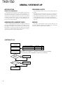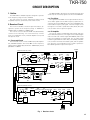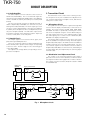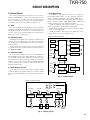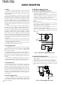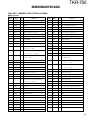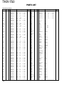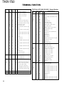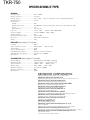
1
VHF FM REPEATER
TKR-750
SERVICE MANUAL
© 2001-1 PRINTED IN JAPAN
B51-8556-00 (N) 1435
Knob (DC source)
(K29-9106-04)
Knob (VOL)
(K29-5389-03)
Panel (Outer)
(A62-0840-03)
Panel assy
(A62-0934-03)
Key top
(K29-5460-02)
Modular jack
(E08-0543-05)
CONTENTS
GENERAL .................................................. 2
SYSTEM SET-UP ...................................... 2
OPERATING FEATURES .......................... 3
REALIGNMENT ....................................... 11
INSTALLATION ....................................... 13
MODIFICATION ....................................... 15
DISASSEMBLY FOR REPAIR ................. 16
CIRCUIT DESCRIPTION .......................... 17
SEMICONDUCTOR DATA ...................... 23
DESCRIPTION OF COMPONENTS ........ 25
PARTS LIST ............................................. 27
EXPLODED VIEW .................................... 37
PACKING ................................................. 39
ADJUSTMENT ........................................ 40
TERMINAL FUNCTION ...........................
WIRING ....................................................
PC BOARD VIEWS
RX PLL/VCO (X58-4780-10) ................
TX PLL/VCO (X58-4790-10) ................
DISPLAY UNIT (X54-3330-20) ............
FINAL UNIT (X45-3620-XX) ................
TX-RX UNIT (X57-6260-XX) (A/2) ......
TX-RX UNIT (X57-6260-XX) (B/2) ......
SCHEMATIC DIAGRAM ..........................
BLOCK DIAGRAM ...................................
KES-4 (EXTERNAL SPEAKER) ...............
SPECIFICATIONS ....................................
47
51
53
54
55
59
65
71
77
89
92
93
TKR-750
GENERAL / SYSTEM SET-UP
INTRODUCTION
PERSONNEL SAFETY
SCOPE OF THIS MANUAL
This manual is intended for use by experienced technicians familiar with similar types of commercial grade communications equipment. It contains all required service information for the equipment and is current as of the publication date. Changes which may occur after publication are
covered by either Service Bulletins or Manual Revisions.
These are issued as required.
The following precautions are recommended for personnel safety :
• DO NOT transmit until all RF connectors are verified secure and any open connectors are properly terminated.
• SHUT OFF and DO NOT operate this equipment near
electrical blasting caps or in an explosive atmosphere.
• This equipment should be serviced by a qualified technician only.
ORDERING REPLACEMENT PARTS
SERVICE
When ordering replacement parts or equipment information, the full part identification number should be included.
This applies to all parts : components, kits, or chassis. If the
part number is not known, include the chassis or kit number
of which it is a part, and a sufficient description of the required component for proper identification.
This radio is designed for easy servicing. Refer to the
schematic diagrams, printed circuit board views, and alignment procedures contained in this manual.
SYSTEM SET-UP
Merchandise
received
Frequency range (MHz)
TX/RX 146~174
TX/RX 136~150
Choose the type
of transceiver
RF power
50W
50W
Type
K,E
K2
See page 11.
Repeater
A personal computer (IBM PC or compatible), programming interface (KPG-46),
programming & setup
and programming software (KPG-66D) are required for programming.
DC power
supply or
duplexer?
YES
Installation in the
optional space
NO
External speaker?
NO
Delivery
2
YES
KES-4 installation
TKR-750
OPERATING FEATURES
1. Controls and Functions
1
1-1. Front Panel
2
9
1 Speaker
3
8
4
7
5
6
7 Programmable Function keys
2 CH/STATUS Display
Two, 7-segment digits display the channel number or status.
3 VOLUME control
Rotate to adjust the volume.
4 DC source switch
5 Dc source indicator
Lights green when DC source is applied from the DC
13.6V jack (DC 13.2V jack on E type versions). Lights red
when DC source is applied from the BACK UP battery
terminal.
Press these keys to activate their programmable functions.
PF1 key (left side)
Default : None (No function)
PF2 key
Default : Repeat disable/enable
PF3 key
Default : TX disable/enable
PF4 key
Default : Take over
PF5 key
Default : Monitor on/off
PF6 key (right side)
Default : Channel up
8 BUSY indicator
Lights green while a signal is being received.
6 MIC jack
9 TX indicator
Connect a microphone to this 8-pin modular jack.
Lights red while transmitting.
1-2. Rear Panel
1
2
8
7
3
4
6
9
5
1 TX OUT jack
Connect a TX antenna or a duplexer to this receptacle.
2 CONTROL I/O jack
Connect an external programming device or repeater
controller to this DB-25 interface.
3 FUSE
Insert 15 A blade fuses into these fuse holders.
4 RX IN jack
Connect a RX antenna or a duplexer to this BNC receptacle.
5 DC 13.6V (K type) / DC 13.2V (E type) jack
Connect a 13.6 V (K type) or 13.2 V (E type) DC power
supply to this jack.
6 BACKUP battery terminal
7 TEST/SPKR jack
Test input/output jack. Connect an external speaker to
this jack.
8 Cooling fan
9 Optional space
For external DC power supply, or duplexer, etc.
3
TKR-750
OPERATING FEATURES
2. Two 7-segment LED displays
• “E2” is displayed when the channel data is not written.
• Channel display (1~16) : While operating normally in user
mode.
• When the displayed channel is contained in scan sequence, the right side decimal point is displayed.
• When the displayed channel is the priority channel, the
left side decimal point is displayed.
• “E3” is displayed when PLL is unlocked.
Receiver PLL unlocked = flashing BUSY LED.
Transmitter PLL unlocked = flashing TX LED.
• “E4” is displayed when PTT is attempted on a channel
number that has no frequency data programmed.
• “SC” is displayed while in scan mode.
• “PC” is displayed while in PC mode.
• “PG” is displayed while in firmware programming mode.
2 decimal points displayed = 115,200bps
1 decimal point displayed = 57,600bps
No decimal = 38,400bps
• “E1” is displayed when FPU data is not written.
4
TKR-750
OPERATING FEATURES
3. Programmable Functions
TKR-750 contains many Programmable Functions tabled below.
Programmable Function
Description
AUX Out 1~5 Off
AUX Out 1 to 5 ports become deactivated, respectively.
AUX I/O 1~6 Off
AUX I/O 1 to 6 ports become deactivated, respectively.
AUX Out 1~5 On
AUX Out 1 to 5 ports become activated, respectively.
AUX I/O 1~6 On
AUX I/O 1 to 6 ports become activated, respectively.
AUX Out 1~5 On/Off
AUX Out 1 to 5 ports are toggled between its active and inactive states, respectively.
AUX I/O 1~6 On/Off
AUX I/O 1 to 6 ports are toggled between its active and inactive states, respectively.
Channel 1~16
Directly select Channel 1 to 16, respectively.
Channel Down
The channel decrements by one.
Channel Up
The channel increments by one.
CW ID On
The CW ID is transmitted.
CW Message 1~8 On
The CW Message 1 to 8 is transmitted, respectively.
Display Off
All panel LEDs are turned off except the Power LED.
Display On
All panel LEDs become active as normal status indicators on the repeater.
Display On/Off
All panel LEDs, with the exception of the Power LED, are toggled between off and their normal status on
the repeater.
Hold Time Enable
The Parameter of Repeat Hold Time is enabled.
Hold Time Disable
The Parameter of Repeat Hold Time is disabled.
Hold Time Disable/Enable
The Parameter of Repeat Hold Time is toggled between disabled and enabled.
Local Tx Disable
The local mic’s PTT is disabled.
Local Tx Enable
The local mic’s PTT is enabled.
Local Tx Disable/Enable
The local mic’s PTT is toggled between disabled and enabled.
Monitor Off
The QT/DQT decoder is disabled.
Monitor On
The QT/DQT decoder is enabled.
Monitor On/Off
The QT/DQT decoder is toggled between disabled and enabled.
Monitor Momentary
The QT/DQT decoder is momentarily disabled.
Multi Table Sub
Multi Table No. Select Signalling changes to the Multi Table Sub.
Multi Table Main
Multi Table No. Select Signalling changes to the Multi Table Main.
Multi Table Main/Sub
Multi Table No. Select Signalling changes between Multi Table Sub and Multi Table Main.
QT/DQT Dec Disable
Disables the QT/DQT decode operation.
QT/DQT Dec Enable
Enables the QT/DQT decode operation.
QT/DQT Dec Disable/Enable
Toggles between disabling and enabling the QT/DQT decode operation.
QT/DQT Enc Disable
Disables the QT/DQT encode operation.
QT/DQT Enc Enable
Enables the QT/DQT encode operation.
QT/DQT Enc Disable/Enable
Toggles between disabling and enabling the QT/DQT encode operation.
Repeat Disable
Disables repeater operation.
Repeat Enable
Enables repeater operation.
Repeat Disable/Enable
Toggles between disabling and enabling repeater operation.
Reset
Resets to default condition set up by FPU.
DC Power Save Off
Activates DC Power Save Mode Off.
DC Power Save On
Activates DC Power Save Mode On.
DC Power Save On/Off
Toggles between DC Power Save Mode On and Off.
5
TKR-750
OPERATING FEATURES
Programmable Function
Description
Scan Off
Inhibits scanning.
Scan On
Starts scanning.
Scan On/Off
Scanning is toggled between being enabled or inhibited.
Scrambler Off
Disables an installed optional voice scrambler board.
Scrambler On
Enables an installed optional voice scrambler board.
Scrambler On/Off
Toggles between enabling and disabling an installed optional voice scrambler board.
Squelch Off
The Squelch unmutes.
Squelch On
The Squelch mutes.
Squelch On/Off
The receiver’s squelch toggles between muted and unmuted.
Squelch Momentary
The Squelch momentarily unmutes.
Take Over On/Off
Toggles between disabling and enabling remote wireline control.
Test Tone Off
The Test Tone is inhibited.
Test Tone On
The Test Tone is enabled.
Test Tone On/Off
Toggles between enabling and inhibiting the Test Tone.
TOT Disable
The Time Out Timer is disabled.
TOT Enable
The Time Out Timer is enabled.
TOT Disable/Enable
The Time Out Timer is toggled between disabled and enabled.
TX Disable
The transmitter is inhibited.
TX Enable
The transmitter is enabled (normal).
TX Disable/Enable
Toggles between transmitter inhibited and transmitter enabled (normal).
The following Programmable Functions are output functions used to tell the condition of the TKR-750 to an external device.
The output functions can be assigned to only AUX Outputs as follows.
Programmable Function
COR (Carrier Operate Relay)
Description
This function becomes valid if an RF carrier is present.
TOR (Tone Operate Relay)
This function becomes valid if an RF carrier and the specified QT/DQT are present.
RX Unlock
This alarm function becomes valid if the RX PLL circuitry becomes unlocked.
TX Unlock
This alarm function becomes valid if the TX PLL circuitry become unlocked.
Power Supply Lower Limit
This alarm function becomes valid if the DC power supply voltage becomes less than the preset point.
The preset point is selected in the range of 10.6V to 13.6V.
TXS (TX Sense)
This function becomes valid when the transmitter is keyed.
Selectable
AUX Outputs which are set up as Selectable appear in the available Function List for the AUX Input
Functions and Key Assignment.
This allows AUX Inputs and PF Keys to be used to control AUX Outputs.
RX Signal Detect
This function becomes valid if the RX signal level becomes less than the preset point. The preset point is
selected in the range of –120dBm to –95dBm.
RF Power Down Detect
Fan Status
This alarm function becomes valid if the RF Power becomes less than about 10W.
This alarm function becomes valid when the Fan is turned on, either by sensing a high temperature
condition or by its operating mode being set to Continuous.
6
TKR-750
OPERATING FEATURES
4. Trigger Assignment
The Programmable Functions described above can be assigned to PF keys, AUX input, Save on/off, Start up, and Power supply
according to following table.
In the last column of the table, when the Programmable Functions is assigned to any PF keys, it expresses that the LED in the
PF key turns on either conditions. “Yes” expresses that the trigger is available the Programmable Function. “No” expresses
that the trigger is not availabale the Programmable Function.
Trigger
PF keys
Function
AUX
Save
input
on/off
Start up
Power
Condition of LED in he PF key on
supply
AUX Out 1~5 (I/O 1~6) Off
No
Yes
Yes
Yes
Yes
–
AUX Out 1~5 (I/O 1~6) On
No
Yes
Yes
Yes
Yes
–
AUX Out 1~5 (I/O 1~6) On/Off
Yes
Yes
No
No
No
Turns on in ON status.
Channel 1~16, Up/Down
Yes
Yes
Yes
Yes
Yes
Do not turn on.
CW ID On
Yes
Yes
Yes
Yes
Yes
Turns on while transmitting.
CW Message 1~8 On
Yes
Yes
Yes
Yes
Yes
Turns on while transmitting.
Display Off
No
Yes
Yes
Yes
Yes
–
Display On
No
Yes
Yes
Yes
Yes
–
Display On/Off
Yes
Yes
No
No
No
Turns on in ON status.
Hold Time Enable
No
Yes
Yes
Yes
Yes
–
Hold Time Disable
No
Yes
Yes
Yes
Yes
–
Hold Time Disable/Enable
Yes
Yes
No
No
No
Turns on in Disable status.
Local Tx Disable
No
Yes
Yes
Yes
Yes
–
Local Tx Enable
No
Yes
Yes
Yes
Yes
–
Local Tx Disable/Enable
Yes
Yes
No
No
No
Turns on in Disable status.
Monitor Off
No
Yes
Yes
Yes
Yes
–
Monitor On
No
Yes
Yes
Yes
Yes
–
Monitor On/Off
Yes
Yes
No
No
No
Turns on in ON status.
Monitor Momentary
Yes
No
No
No
No
Turns on in ON status.
Multi Table Sub
No
Yes
Yes
Yes
Yes
–
Multi Table Main
No
Yes
Yes
Yes
Yes
–
Multi Table Main/Sub
Yes
Yes
No
No
No
Turns on in Sub status.
QT/DQT Dec Disable
No
Yes
Yes
Yes
Yes
–
QT/DQT Dec Enable
No
Yes
Yes
Yes
Yes
–
QT/DQT Dec Disable/Enable
Yes
Yes
No
No
No
Turns on in Disable status.
QT/DQT Enc Disable
No
Yes
Yes
Yes
Yes
–
QT/DQT Enc Enable
No
Yes
Yes
Yes
Yes
–
QT/DQT Enc Disable/Enable
Yes
Yes
No
No
No
Turns on in Disable status.
Repeat Disable
No
Yes
Yes
Yes
Yes
–
Repeat Enable
No
Yes
Yes
Yes
Yes
–
Repeat Disable/Enable
Yes
Yes
No
No
No
Turns on in Disable status.
Reset
Yes
Yes
No
No
No
Do not turn on.
DC Power Save Off
No
Yes
No
Yes
Yes
–
DC Power Save On
No
Yes
No
Yes
Yes
–
DC Power Save On/Off
Yes
Yes
No
No
No
Do not turn on.
Scan Off
No
Yes
Yes
Yes
Yes
–
7
TKR-750
OPERATING FEATURES
Trigger
PF keys
Function
AUX
Save
input
on/off
Yes
Scan On
No
Yes
Scan On/Off
Yes
Yes
No
Scrambler Off
No
Yes
Yes
Scrambler On
No
Yes
Yes
Scrambler On/Off
Yes
Yes
No
Power
Condition of LED in he PF key on
supply
Yes
Yes
–
No
No
Turns on in ON status.
Yes
Yes
–
Yes
Yes
–
No
No
Turns on in ON status.
Squelch Off
No
Yes
Yes
Yes
Yes
–
Squelch On
No
Yes
Yes
Yes
Yes
–
Squelch On/Off
Yes
Yes
No
No
No
Turns on in OFF status.
Squelch Momentary
Yes
No
No
No
No
Turns on in OFF status.
Take Over On/Off
Yes
No
No
No
No
Turns on in ON status.
Test Tone Off
No
Yes
Yes
Yes
Yes
–
Test Tone On
No
Yes
Yes
Yes
Yes
–
Test Tone On/Off
Yes
Yes
No
No
No
Turns on in ON status.
TOT Disable
No
Yes
Yes
Yes
Yes
–
TOT Enable
No
Yes
Yes
Yes
Yes
–
TOT Disable/Enable
Yes
Yes
No
No
No
Turns on in Disable status.
TX Disable
No
Yes
Yes
Yes
Yes
–
TX Enable
No
Yes
Yes
Yes
Yes
–
TX Disable/Enable
Yes
Yes
No
No
No
Turns on in Disable status.
None
Yes
Yes
Yes
Yes
Yes
Do not turn on.
5. Simplex/Duplex Operation
The Simplex/Duplex function is used to specify whether
the channel is used as simplex (receiver muted during transmit) or duplex (receiver unmuted during transmit). If the
channel has same TX/RX frequency, it can operate only in
Simplex mode.
6. Repeater/Base Station Operation
The Repeat function is used to specify whether the channel is used as a repeater or as a base station. A repeater
simultaneously and automatically re-transmits its received
audio, a duplex base station has independent simultaneous
transmit and receive paths, a simplex base station are mutually exclusive transmit and receive paths.
7. Signalling Feature
8
Start up
The Multi Table function enables the TKR-750 to decode
any one of the 16 QT/DQTs pre-programmed into the Multi
Table. When receiving a signal (repeater operation), the repeater uses the QT/DQT encode which corresponds to the
decoded QT/DQT as set in the Multi Table. In the Multi
Table, signalling pair of “No.1” (first column) is defined as
“Primary”. A receiving signalling (if it is contained within
No.1 to No.16) is defined “Current”.
From No.2 to No.16, signalling pairs that can be changed
between “Main Table” and “Sub Table” using AUX I/O
Ports 1-4 are assigned as “Multi Table Select” and the Multi
Table Main, the Multi Table Sub or the Multi Table Main/Sub
function is executed. When AUX I/O Ports 1~4 are set for
“Multi Table Select”, these are 4 bit Binary Coded Decimal
(BCD) inputs .AUX I/O 1 is a least significant bit (LSB), and
“1101” input (LSB on the right side) signifies the Table No.2
and “1100” input signifies the Table No.3.
7-1. Multiple QT/DQT
7-2. Encode Tone in Multiple
The TKR-750 can function as a multiple-QT/DQT decode/
encode unit for operation as a community repeater or multiple-QT/DQT base station. Two Multi Tables, called Main
and Sub, can be created, each consisting of 16 decode/encode combinations.
When Local Microphone PTT or External PTT is active
while the repeater is in use or the duplex-base station is receiving, the encode signalling is determined according to
Encode Tone in Multiple function. The simplex-base station
always transmits the “Primary” encode QT/DQT.
TKR-750
OPERATING FEATURES
Current : When any PTT as described above is active
while the repeater is in use or the duplex-base station is receiving, the “paired” encode QT/DQT associated with receiving QT/DQT is transmitted. When any PTT is active
while the repeater or the duplex-base station is in idle period, the “Primary” encode QT/DQT is transmitted.
Primary : When any PTT (provided that the Priority of any
PTT is higher than the Priority of Repeat PTT) is active while
the repeater is in use, the encode QT/DQT changes
“paired” encode QT/DQT to “Primary” while continuing to
transmit. When any PTT is active while the repeater is in
idle period, the “Primary” encode QT/DQT is transmitted.
In the base station, the “Primary” encode QT/DQT is always
transmitted regardless of the receiver status.
7-3. QT Reverse Burst Time
During repeat with QT tones, the repeater re-transmits a
phase-shifted burst of the QT tone (“reverse burst”) when it
detects the radio using the repeater has un-keyed and also
sent a reverse QT burst (squelch-tail elimination). This
mutes a receiving radio’s speaker audio before its receiver
circuit shuts off causing squelch tail noise in the speaker
audio. The TKR-750 can select the time between 140 to 200
ms that the QT reverse burst is sent. Typically this time
should not have to be adjusted from the default value. The
transmission of the QT reverse burst can be also inhibited if
the QT Reverse Burst function is set to “No”.
7-4. DQT Turn Off Code Time
During repeat with DQT tones, the repeater re-transmits
a specific turn-off code when it detects the radio using the
repeater has un-keyed and also sent the turn-off code
(squelch-tail elimination). This mutes a receiving radio’s
speaker audio before its receiver circuit shuts off causing
squelch tail noise in the speaker audio.
The TKR-750 can select the time between 140 to 200ms
that the DQT turn-off code is sent. Typically this time should
not have to be adjusted from the default value.
7-5. Off Hook Decode
The TKR-750 is able to decode QT/DQT regardless
whether the local microphone is in the on- or off-hook condition. When the Off Hook Decode function is enabled, the
TKR-750 is capable of QT/DQT decode even though the microphone is in the off-hook condition (or a local microphone
is not installed).
8. Scan Feature
8-1. Scan Operation
Providing that the TKR-750 contains two or more non-priority ADD channel or one or more non-priority ADD channel
and Priority channel, it starts scanning once the Scan On
function is executed and displays “SC” on the 7-seg LED.
Scanning stops temporarily if any following conditions be
come valid.
1) if a RF carrier and a valid QT/DQT is present. The receiving channel number is displayed and the received audio is
heard from a speaker.
2) if a RF carrier is present, providing that the Monitor On
function is executed.
3) if the Squelch Off function is executed. Scanning stops
on the channel being scanned when Squelch Off is executed, the channel number is displayed and the received audio is heard from a speaker.
4) if a local microphone’s hook is in off hook status, providing that the Off Hook Scan function is set to Disable.
Scanning stops on the Revert channel, but the audio is
not heard until a valid signal is received.
When the received call is ended, scanning automatically
resumes after the period set in Dropout Delay Time function
has expired. When the Scan Off function is executed, the
TKR-750 inhibits scanning and displays the selected channel.
8-2. Scan Sequence
1) Normal Scan : When no Priority channel is set, scanning
of ADD channels is done in ascending order.
2) Single Priority Scan : The Priority channel is set as either
a fixed channel or a selected channel. When Priority
channel is set, Priority channel and non Priority channel
are scanned by turns. When scanning stops on the non
Priority channel, calls from the Priority channel are still
checked at set intervals while scanning is stopped. This
operation is called Look Back and the interval period is
selected by the Look Back Time function.
8-3. Revert Channel
The Revert channel is a channel that is used to transmit
during scanning. The time from the end of transmission on
Revert channel to the time scanning automatically resumes
is set in Dwell Time function. The Revert channel types are
Last Called, Last Used, Selected, Selected + TalkBack, Priority, and Priority + TalkBack.
1) Last Called : The TKR-750 reverts to the channel upon
which a call was last received even if scanning has resumed (power on default = selected channel).
2) Last Used (with TalkBack) : The TKR-750 reverts to the
channel that was last transmitted on (power on default =
selected channel). However, if a call is received on a
channel other than the last transmit channel and PTT is
pressed before scanning resumes, the transceiver “talks
back” on the current receive channel.
3) Selected : The transceiver reverts to the channel set by
the function prior to scan initiation.
4) Selected+TalkBack : The TKR-750 reverts to the channel
set by the Channel ‘X’ functions or Channel Select function prior to scan initiation. However, if a call is received
on a channel other than the selected channel and PTT is
pressed before scanning resumes, the transceiver “talks
back” on the current receive channel.
5) Priority : The TKR-750 always reverts to the Priority channel.
9
TKR-750
OPERATING FEATURES
6) Priority+TalkBack : The TKR-750 always reverts to the
Priority channel. However, if a call is received on a channel other than the Priority channel and PTT is pressed
before scanning resumes, the transceiver “talks back”
on the current receive channel.
9. CW ID and Message
The TKR-750 contains internal automatic station identifiers. The CW ID (Morse code) is set and transmitted on a
per-channel basis. The CW ID is transmitted when the interval period is reached (TX Interval Time function), the
channel is changed (CW ID on Channel Change function) or
CW ID Onfunction is executed. When CW ID is activated by
any functions described above, it is actually sent after the
total time of TX Delay Time (not applied to CW ID On function) and CW Modulation Delay Time has expired. TX Delay
Time is a period from CW ID is activated to the transmitter is
keyed.
CW Modulation Delay is a period from the transmitter is
keyed to the CW ID tone is sent. The CW ID tone is routed
to the Receive Audio (RA) port and a speaker if the Send CW
ID to RA function is set to Yes. The TKR-750 contains 8
message banks for CW Message. CW Message 1 to 8 is
transmitted on the current channel when the CW Message
1 to 8 On function is activated, respectively.
10. PTT Priority
A number of keying sources can be used to cause the
TKR-750 to transmit.
The transmit audio path is switched according to their
keying sources and when PTTs is simultaneously activated,
the transmit audio path related to the PTT with higher priority is given priority. These are Local Microphone PTT, External PTT, and Repeat PTT.
11. Time Out Timer
The Time Out Timer function determines the period of
time users can continuously transmit. When the selected
period expires, the transmission is inhibited.
12. Repeat Hold Time
The Repeat Hold Time (hang timer) function is used to
prevent the repeater from being repeatedly keyed and
unkeyed in response to short message traffic. When a mobile transceiver unkeys, the repeater’s Hold Timer allows
the repeater to continue transmitting for a brief period while
waiting for a responding end user. If no valid QT/DQT is
detected within the Hold Timer period, the transmitter is allowed to unkey. This function determines the period of time
that the transmitter is allowed to remain keyed after the loss
of a valid QT/DQT received signal.
10
13. Take Over
The Take Over function is used to disable the external
wireline control of the repeater. When Take over function is
enabled, the external AUX inputs and Outputs, transmit audio inputs and receive audio outputs, External PTT and External Monitor lines are disabled. All AUX Input functions
assigned to any AUX Input stay in their current state. However External PTT and External Monitor switch to the “Off”
state.
14. Test Tone
The Test Tone is a single-frequency audio sine wave and
is turned On and Off by toggling Test Tone On/Off functions.
The transmitter can be modulated without a local microphone by using the test tone. When Test Tone On function
is executed and any PTT is activated, the TKR-750 transmits
the test tone with mic mute and also routes the test tone to
RA port.
15. RF Power
The TKR-750 is able to switch transmission output on a
per-channel basis. When the TX High Power function is enabled, the transmission output is set to high power.
16. Fan Action
The TKR-750 has a cooling fan. The Fan Action function
determines whether the fan is continuously operated or operates in response to high temperatures only.
17. AUX Input and Output
There are 6 programmable AUX I/O Ports 1~6 (pins
20~25) and 3 programmable AUX Input Ports 1~3 (pins 4~6)
on the rear 25 pin D-Sub connector (CONTROL I/O) and 5
programmable AUX Output Ports 1~5 (pins 10, 11, 13~15)
on the rear 15 pin TEST/SPKR connector.
The 6 programmable AUX I/O pins are primarily intended
for remote control interfaces. Each AUX I/O Port can be set
for AUX Input, AUX Output, remote Channel Select or Multi
Table Select types. The AUX Input Port can be set execute
a single input function or a set of up to three functions when
the port is activated. If the port type for an AUX I/O Ports
1~6 is set for “AUX Input”, it will also appear AUX Input
window for function programming. The input logic is fixed
as active Low.
The AUX Output Port can be set execute a single output
function. If the port type for an AUX I/O Ports 1~6 is set for
“AUX Output”, it will also appear AUX Output window for
function programming. The output logic of AUX Output can
be set as either active High or active Low by the Logic Type
function. Active High outputs a High (5V) when the programmed condition becomes valid, active Low outputs a
Low (0V) when the condition becomes valid.
TKR-750
OPERATING FEATURES / REALIGNMENT
18. Channel Select
AUX I/O Ports 1~4 (1 or all 4) can each be set for “Channel Select” providing up to 16 channel selection capability.
These are 1 to 4 bit Binary Coded Decimal (BCD) inputs.
AUX I/O 1 is a least significant bit (LSB). When all of AUX I/
O Ports 1~4 set to Channel Select, “1110” input (LSB on
the right side) signifies the Channel 1 and “1101” input signifies the Channel 2.When the Channel Select function is
set to any AUX I/O ports, the Channel ‘X’ function (Channel
Up, Channel Down, Channel 1, etc.)can not be set to the
AUX Input ports, but can be set to the PF Keys. Normally
the channel control is controlled by the Channel Select function. If the Take Over function is executed, the channel control is disabled to be controlled by the Channel Select and
enabled to be controlled by the PF Keys.
19. DC Power Save
The TKR-750 has the DC Power Save feature. The DC
Power Save Mode is activated when the DC Power Save On
function is executed. When the DC Power Save Mode is
activated, all panel LEDs except the Power LED are turned
off, and the audio amplifier and the DSP becomes inactive.
When the Display On function is executed while the repeater is in the DC Power Save Mode, all panel LEDs become active as normal status indicators on the repeater, and
the audio amplifier and the DSP becomes active. However,
when the Save Delay Timer A period expires, all panel LEDs
except the Power LED are turned off and the audio amplifier
becomes inactive again, and when the Save Delay Timer B
period expires, the DSP becomes inactive. When the DC
Power Save Mode is turned on or off, up to 3 functions preprogrammed into the Save On function or Save Off function
are executed in sequence.
20. Power Supply
The TKR-750 is able to use two Power sources that are
called Main and Backup. When the Power source changes
from Main to Backup or from Backup to Main, up to 3 functions pre-programmed into the Backup Power function or
the Main Power function are executed in sequence.
21. Start Up
When the TKR-750 is first turned on or is reset, up to 3
functions pre-programmed into the Start Up function are
executed in sequence.
22. Optional Board
An optional scrambler board can be installed in the TKR750. Scrambler codes between 1 and 16 are available per
channel. If the scrambler board is not to be used (although it
is installed), set the parameter to “Off”. When any Scrambler code is set up and the Scrambler On function is executed, the scrambler board is activated.
REALIGNMENT
1. Modes
User mode
PC mode
PC programming mode
PC test mode
PC tuning mode
Firmware Programming mode
Mode
Function
User mode
Use this mode for normal operation.
PC mode
Use this mode to make various settings by
means of the FPU through the RS-232C port.
PC programming
Use to read and write frequency data and
mode
other features to and from the repeater.
PC test mode
Use to check the repeater using the PC.
This feature is included in the FPU.
Firmware pro-
Use when changing the firmware program
gramming mode
of the flash memory.
2. How to Enter Each Mode
Mode
Operation
User mode
Power on.
PC mode
Received commands from PC.
Firmware Pro-
[PF1] key + Power on (one second).
gramming mode
3. PC Mode
3-1. Preface
The TKR-750 repeater is programmed by using a personal
computer, programming interface and KPG-66D software.
3-2. Connection Procedure
1. Connect the TKR-750 to the personal computer with the
interface cable.
2. When power is applied, the user mode is entered immediately. When the PC sends a command, the repeater
enters the PC mode and displays “PC” on the 7-segment
LED. When data is being transmitted to the PC from the
repeater, the TX LED flashes. The BUSY LED flashes
when data from the PC is being received by the repeater.
Note :
• The data stored in the personal computer must match
the model type, when it is written into the flash memory.
• Change the TKR-750 to PC mode, then attach the interface cable.
11
TKR-750
REALIGNMENT
3-3. KPG-46 Description (PC Programming Interface Cable : Option)
The KPG-46 is required to interface the TKR-750 to the
computer. It has a circuit in its D-sub connector (25-pin)
case that converts the RS-232C logic level to the TTL level.
The KPG-46 connects the microphone connector of the
TKR-750 to the computer’s RS-232C serial port.
3-4. Programming Software Description
The KPG-66D programming disk is supplied in 3-1/2" disk
format. The software on the disk allows a user to program
TKR-750 repeater via the programming interface cable (KPG46).
3-5. Programming With IBM PC
Data can be programmed into the flash memory in RS232C format via the microphone connector.
IBM PC
KPG-46
KPG-66D
TKR-750
Fig. 1
4. Firmware Programming Mode
4-1. Preface
The TKR-750 uses flash memory to allow it to be easily
upgraded when new features are released in the future.
4-2. Connection Procedure
Connect the TKR-750 to the personal computer (IBM PC
or compatible) with the interface cable (KPG-46). (Connection is the same as in the PC mode.)
Notes :
You can only program firmware from the 8-pin microphone connector on the front panel. Using the 25-pin logic
interface on the rear panel will not work.
4-3. Programming
1. Start up the programming software (Fpro. exe).
2. Set the communications speed (normally, 115200 bps)
and communications port in the configuration item.
3. Set the firmware to be updated by file name item.
4. Turn the TKR-750 power on with the [PF1] key held
down. Hold the key down for one second until the 7segment display changes to “P.G.”. When “P.G.” appears, release your finger from the key.
5. Check the connection between the TKR-750 and the personal computer, and make sure that the TKR-750 is in the
program mode.
6. Press write button in the window. A window opens on
the display to indicate progress of writing.
7. If writing ends successfully, the TX LED on the TKR-750
lights.
8. If you want to continue programming other TKR-750s,
repeat steps 3 to 6.
Notes :
This mode cannot entered if the firmware program mode
is set to disable in the programming software (KPG-66D).
4-4. Function
If you press the [PF1] key (front panel), both decimal
point on the 7-segment display will disappear. The writing
speed is 38400 bps (low-speed mode). If you press the
[PF1] key again, the right hand decimal points will light. The
writing speed is 57600 bps (middle-speed mode).
Note :
Normally, write in the high-speed mode (115200 bps).
12
TKR-750
INSTALLATION
R742
R653
1
CN604
CN606
CN601
This unit has two external power supply connectors :
Main DC and Backup.
If an external DC power supply is connected to the main
DC connector and a backup battery is connected to the
Backup connector at the same time, the DC power supply
switches to the battery automatically if power failure occurs.
Therefore, the operation of the repeater can be continued.
If the battery is used, but both the battery and power supply need not be connected (if an external switch is used or if
only a solar battery is used), connect it to the Backup connector, not the Main DC connector. Current consumption
can be reduced by approx. 120mA because the relay is not
used.
If it is installed when the temperature at the repeater site
is below freezing, check whether the switch (relay) works
properly after installation.
TX-RX unit (B/2) control section
Component side
CN605
14
1. External Power Supply Connection
(Rear Connectors) : See Page 3
2. Voice Scrambler
It operates only during base operation. The voice is not
scrambled when it is repeated.
2-1. Modification
1) Remove R742 and R653 on the TX-RX unit (B/2) : control
section.
2-2. Connection
1) The functions of pins of CN601 on the TX-RX unit (B/2) :
control section are shown in the figure.
2) Join the CN601 connector to the voice scrambler board
via the E37-0808-05 connector cable.
When the operation is checked in PC test mode after the
modification, and the maximum deviation is adjusted, the
voice from the local microphone is not modulated. In this
case, remove the CN601 12-pin (PTO) cable and connect it
to the land of the display unit (X54-333) from the voice
scrambler. The voice from the local microphone can be
modulated in PC test mode.
Fig. 1
CN601
1
TXI (MIC signal input)
TXO (MIC signal output)
RXI (RX audio signal input)
AC (Audio control signal output)
BC1 (Scramble code output 1)
BC2 (Scramble code output 2)
BC3 (Scramble code output 3)
BC4 (Scramble code output 4)
PTI (PTT signal input)
CLRC (Clear code for scrambler)
DEO (Detection signal output)
PTO (PTT signal output)
5C (5V output)
GND
14
Voice
scrambler
Display
unit
Fig. 2
Display unit
Foil side
PTO
Fig. 3
13
TKR-750
INSTALLATION
3. External Speaker (KES-4)
The TKR-750 has a internal built-in speaker (5W/8Ω), and
the external speaker output from the TEST/SPKR connector
(15-pin) on the rear of the radio is 4W/4Ω. Use external
speaker KES-4.
3-1. Connection for the KES-4 With the TKR-750
■ When taking the AF output from the TEST/
SPKR connector (15-pin) on the rear of the radio
Fig. 4-1
The following tools are required for changing the connector.
• Extracting tool
The following extracting tool is recommended :
Molex Inc. Order No. : 11-03-0002
1. Remove the connector with jumper from the external
speaker connector on the rear panel of the radio. (Fig. 41)
Note : Save the jumper, which is required when the radio
is used without the external speaker.
2. Remove the terminals with the jumper from the connector housing holes number 9 and 12 using the extracting
tool.
Removing the jumper lead (Fig. 4-2)
1) Insert the extracting tool (11-03-0002) into the connector while pushing the jumper lead in the direction
of (a).
2) Push the extracting tool into collapse the barbs of the
crimp terminal.
3) Pull out the lead while continuing to push the extracting tool in the direction (b).
3. Reinsert the terminal with the black and white stripe lead
into hole number 12, and the terminal with the black lead
into hole number 6. (Fig. 4-3)
4. Attach the connector to the external speaker connector
on the radio.
Fig. 4-2
Note :
Relationship between TEST/SPKR connector (15-pin)
connection and speaker output.
When pins 9 and 12 are shorted : Built-in internal speaker
is used.
When pins 9 and 12 are open and output is from pins 6
and 12 : KES-4 is used.
14
Fig. 4-3
TKR-750
MODIFICATION
1. Modification for Sinking the Collector Current Up
2. DC Source Switch
Auxiliary output 1 and 2 can each be modified to sink up
600mA of the collector current. The following modification
should be installed when Auxiliary output 1 or 2 is used to
control external equipment.
1. Remove D625, R755, and R769 for Auxiliary output 1
(D624, R756, and R770 for Auxiliary output 2) on the
component side of the control section for TX-RX unit
PCB.
2. Install $Q608, $Q612, and $R761 for Auxiliary output 1
($Q607, $Q611, and $R759 for Auxiliary output 2) on the
component side of the control section for TX-RX unit
PCB.
$Q607, $Q608, $Q611, $Q612 : DTD114EKA
$R759, $R761 : 3.9kΩ (RK73GB1J392J) chip resistor.
3. Change R801 for Auxiliary output 1 (R797 for Auxiliary
output 2) from 1kΩ (RK73GB1J102J) to 0Ω (R92-125205).
To prevent the power supply from turning off due to
misoperation of the DC source switch on the front panel or
accidents (tampering) after installation, the main unit can be
kept on regardless of the on/off of the DC source switch on
the front panel.
Short the PSW land near K1 relay by soldering.
TX-RX unit (A/2)
Component side
By making this modification, Auxiliary output 1 and 2 can
now sink up to 600mA each.
TX-RX unit (B/2)
Component side
CF1
WIDE
CF2
NARROW
PSW
K1
IC602
R756
$Q607
IC623
$R759
R755
Fig. 3
R770
$Q611
CN605
$R769
R769
C681
$Q608 $Q612
Fig. 1
5V
5V
Add $R761
($R759)
3.9kΩ
Remove
D625 (D624)
DA204U
Shift
register
IC623
Add $Q608
($Q607)
DTD114EKA
Remove
R755 (R756)
0Ω
Add $Q612
($Q611)
DTD114EKA
Remove
R769 (R770)
0Ω
Fig. 2
TEST/
SPKR
15
TKR-750
MODIFICATION / DISASSEMBLY FOR REPAIR
3. Trickle Charge for Backup Battery
If the external DC power supply is connected to the Main
DC connector and a backup battery (12V rechargeable type)
is connected to the Backup connector at the same time, the
battery can be trickle-charged from the external DC power
supply with a maximum current of 0.5A.
Short the CHARGE land near R61.
Notes :
1. Make this modification after removing the DC power supply and battery for safety.
2. When the DC power supply is connected after the modification, DC voltage is output to the Backup connector.
Be careful during setup.
3. When the backup battery is used for a long time, remove
the battery from the repeater and recharge it because the
trickle charge is not sufficient for recharging a completely
discharged battery.
Final unit (A/2)
Component side
CN7 BACKUP
(ORANGE)
K1
R61
CHARGE
Fig. 4
16
DISASSEMBLY FOR REPAIR
How to Remove the Panel Assy (ABS)
Note : You can remove the panel assembly (ABS) without
removing the top panel (A62-0840-03).
1. To remove panel (TX-RX, 2 ), loose 6 screws ( 1 ).
2. To remove panel assembly (Front, 4 ), loose 6 screws
( 3 ).
3. The panel assembly (ABS) is security fastened by 4 tabs
( 5 ) on top and bottom. You can remove the panel assembly by pulling to front while you are pulling up the
tabs.
TKR-750
CIRCUIT DESCRIPTION
The BPF L5/L6/L7 attenuates the unwanted signals, and
sends only the necessary signal to the first mixer DBM A1.
1. Outline
The TKR-750 is a VHF/FM repeater designed to operate
in the frequency range of 136 to 174MHz.
The unit consists of receiver, transmitter, phase-locked
loop (PLL) frequency synthesizer, and control circuits.
2-2. First Mixer
The signal from the BPF is heterodyned with the first local oscillator signal from the PLL frequency synthesizer circuit at the first mixer DBM (A1) to become a 44.85MHz first
intermediate frequency (IF) signal. The first IF signal is fed
through two monolithic crystal filters (XF2; Wide, XF1; Narrow) to further remove spurious signals.
2. Receiver Circuit
The receiver is double conversion super-heterodyne, designed to operate in the frequency range of 146MHz to
174MHz (K,E) or 136MHz to 150MHz (K2).
The receiver circuit located in TX-RX unit (X57-626 A/2)
consists of the following : 2-1 front-end circuit, 2-2 first
mixer, 2-3 IF amplifier circuit, 2-4 audio amplifier circuit, and
2-5 squelch circuit.
2-3. IF Amplifier
The first IF signal is amplified by Q2 and Q3, and then
enters IC9 (FM system IC). The signal is heterodyned again
with a second local oscillator signal (44.395MHz) with in IC9
to become a 455kHz second IF signal. The second IF signal
is fed through a 455kHz ceramic filter, CF1 (Wide), CF2 (Narrow) to further eliminate unwanted signal, and the quadrature detection circuit FM-detects the signal to produce a
base-band signal and output it from pin 11.
2-1. Front-end Circuit
The front-end circuit consists of BPF L2/L3, RF amplifier
Q1, and BPF L5/L6/L7. The helical BPF covers frequency
ranges 146 to 174MHz (K,E) and 136 to 150MHz (K2), with a
passband of 3.0MHz.
RX ANT
TX-RX unit (X57 A/2): TX-RX
MCF (Wide)
XF2
IF AMP
Q3
D2
SW
D1
MCF (Narrow)
XF1
W/N
44.850MHz
BPF
L5,L6,L7
1st MIX
DBM A1
RF AMP
Q1
BPF
L2,L3
SW
W/N
IF AMP IF AMP
Q9
Q8
LPF
FM SYSTEM IC
IC9
RSSI
Q4
44.85MHz
IF AMP
Q2
RX VCO
A3 (X58-478)
VCO A
VCO B
QUD
SW
fRX+44.85MHz
DET
CF1 (Wide)
W/N
SW
D4
NOISE DET
D5
SQL
DET
X1
44.395MHz
SW
D3
CF2 (Narrow)
NOISE AMP
Q7
455kHz
W/N
TX-RX unit (X57 B/2): Control
AMP
DEI DEO IC608
AINR
RD
IC614
CODEC
LPF
AMP
IC619 (B/2) IC619 (A/2) RXI RXO
IC622
Q606
IC629
DAC
SW
MUTE
AF
AMP
AOUTR
IC604
RA
CPU
AM
SPM
ASQ
IC615
IC621
INV Q605
RSSI
INT SP
Fig. 1 Receiver circuit
17
TKR-750
CIRCUIT DESCRIPTION
2-4. Audio Amplifier
The audio amplifier circuit is located in control section of
TX-RX unit (X57-626 B/2). The recovered audio signal obtained from IC9 is amplified by IC608, input to the AINR terminal of CODEC IC (IC614), and audio processed by DSP
(IC618).
The processed audio signal from AOUTR terminal of
IC614 is amplified by IC619 (B/2) to a sufficient level, antialiasing filtered by IC619 (A/2). The audio signal goes to an
electronic volume (IC615) V3/V4, to the input of multiplexer
IC (IC622), and is amplified to drive a loudspeaker by an audio power amplifier (IC629). The 4W audio output can be
provided to external 4 ohms speaker through the 15-pin test
connector “SPO, SPG” on the rear panel.
2-5. Squelch Circuit
The output signal from IC9 enters FM IC again, then
passed through a band-pass filter.
The noise component output from IC9 is amplified by Q7
and rectified by D5 to produce a DC Voltage corresponding
to the noise level. The DC voltage is sent to the analog port
of the CPU (IC604).
IC9 outputs a DC voltage (RSSI) corresponding to the input of the IF amplifier.
3. Transmitter Circuit
The transmitter circuit consists of the following circuits :
3-1 microphone circuit, 3-2 modulation level adjustment circuit, 3-3 driver and final power amplifier circuit, and 3-4 automatic power control circuit.
3-1. Microphone Circuit
The signal from the microphone is passed through AGC
circuit located in display unit (X54-333), so that it does not
saturate. This circuit consists of IC501, D501, D502, Q501,
and Q502. The AGC is operated by controlling the + and –
side levels of amplitude using the current obtained by positive and negative detection of the amplified audio signal.
The audio signal goes to control section of TX-RX unit (X57626 B/2) from display unit (X54-333).
The transmit audio signal goes to the input of the multiplexer IC (IC605) for microphone muting. The audio signal is
amplified by IC610, input to the AINL terminal of CODEC IC
(IC614), and audio processed by DSP (IC618). The processed audio signal from the AOUTL terminal of IC614 is
amplified by IC616 (B/2) to a sufficient level, anti-aliasing filtered by IC616 (A/2), and amplified by the summing amplifier IC611 (A/2).
3-2. Modulation Level Adjustment Circuit
The output of the summing amplifier IC611 (A/2) is
passed to an electronic volume (IC615) for maximum deviation adjustment before being applied to a varactor diode in
the voltage controlled oscillator (VCO) A2 located in TX-RX
unit (X57-626 A/2).
Display unit
(X54 B/2)
Display unit (X54 A/2)
VR501
MIC JACK
IC501(A/2)
Q501,502
AMP
ATT
MI
J601
DET
D501,502
TXRX unit (X57 B/2): CONTROL
MIC
IC605 (A/2)
IC610
SW
AMP
IC614
CODEC IC
AINL
MIS
TA
TAS
IC616
(B/2)
IC616
(A/2)
IC611
(A/2)
AMP
LPF
AMP
AOUTL
IC605 (B/2)
TXI TXO
SW
D-SUB
TD
TDS
Fig. 2 Microphone circuit
18
IC615
MO
DAC
MB
SW
TKR-750
CIRCUIT DESCRIPTION
3-3. Driver and Final Power Amplifier Circuit
The transmit signal is generated by the TX VCO (A2),
amplified by Q11, and sent to final unit (X45-362). This amplified signal is amplified by Q2, Q3, and Q4, and is passed
to the FINAL stage. The RF power amplifier consists of
MOS FET.
Final unit (X45-362 A/2)
TX-RX unit (X57-626 A/2)
TX ANT
Q2
Drive AMP
STT
Q11
MO
ATT
TX VCO
A2
(X58-479)
CM COUPLER
TEMP
Q3
Drive AMP
IC1
FCT
MB
BUFF
TCXO
IC1
X3
16.8MHz
Q5
Final AMP
Q4
Drive AMP
Vcont
D4
DC
AMP
FWD
DET
REF
DET
D5
SW Q8
POWER ADJ
PC
Fig. 3
REF
AMP
IC1
VR1
Driver and final power amplifier circuit
3-4. Automatic Power Control, Circuit and Transmitter
The automatic power control (APC) circuit stabilizes the
transmitter output power at a pre-determined level, and consists of forward/reflected power detector circuits, and
switching transistor Q8. The forward/reflected power detector circuits detects forward RF power and reflected RF
power to DC voltage, and consists of a CM coupling type
detection circuit formed by a strip line, RF detector D4/D5,
and DC amplifier IC1 (A/2).
The voltage comparator (IC1 B/2) compares the above
detected voltage with a reference voltage, set using the microprocessor and IC6 located in the TX-RX unit. An APC
voltage proportional to the difference between the sensed
voltage and the reference voltage appears at the output of
IC1. This output voltage controls the gate voltage for the
drive amplifier Q4 and final amplifier Q5, which keeps the
transmitter output power constant.
FAN
X45 A/2
CN4
FAB
X57 A/2
IC7
BU4094BCF
+B
IC604
Q9
FAG
FAS
13
CPU
Q6
CK,
DT,
STB
IC2
TK11050M
6
OUT
TEMP
17
VTH
Q602
[Fan operation]
ON
3-5. Fan Action Control Circuit
If fan action is set to “Temperature”, the cooling fan is
turned ON or OFF according to temperature.
If the ambient temperature of the final unit exceeds
approx. 40°C, the output from pin 6 of the temperature detection IC2 changes from L to H. This signal is sent to the
CPU (IC604) by Q602 in the TX-RX unit B/2 (control section),
and the output from pin 13 (FAS) of IC7 in the TX-RX unit A/
2 controlled by the CPU goes H.
This signal turns Q9 in the final unit ON to run the cooling
fan. It has a hysteresis of approx. 5°C by IC2. If fan action is
set to “Continuous”, the fan operates continuously, but Q9
stays ON.
X57 B/2
OFF
+20°C
+30°C
+40°C
+50°C
Fig. 4 Fan action control circuit
19
TKR-750
CIRCUIT DESCRIPTION
4-2. Transmitter PLL
4. PLL Frequency Synthesizer
The PLL frequency synthesizer circuit consists of the following circuits : 4-1 receiver PLL circuit, 4-2 transmitter PLL
circuit, and 4-3 unlocked detector circuit.
4-1. Receiver PLL
The receiver PLL circuit is located in VCO unit A3 (X58478) on TX-RX unit (X57-626 A/2), and consists of VCXO X2,
VCO’s (Q350 and Q351), a single-chip PLL IC IC300, buffer
amplifier Q355, and high-frequency amplifier Q302.
The VCXO generates 16.8MHz. The frequency stability is
within ± 2.0ppm (Temperature range of –30 to +60°C). The
frequency tuning of the VCXO is done to apply a voltage to
pin 1 of the VCXO. The output of the VCXO is applied to pin
8 of the PLL IC through the pin 7 of the VCO.
The first local oscillator is an upper heterodyne local oscillator, and the VCO oscillator frequency is 180.850 to
218.850MHz. Two VCOs cover the two bands : Q350 covers the lower band and Q351 VCO covers the upper band.
The oscillator frequency is controlled by applying the
VCO control voltage, obtained from the phase comparator to
the varactor diodes.
TX-RX unit
VCO unit (X58-478)
The transmitter PLL circuit is located in VCO unit A2 (X58479) on TX-RX unit (X57-626 A/2), and consists of VCXO X3,
VCO’s (Q350 and Q351), a single-chip PLL IC IC300, buffer
amplifier Q355, and high-frequency amplifier Q302.
The VCXO generates 16.8MHz. The frequency stability is
within ± 2.0ppm (Temperature range of –30 to +60°C). The
frequency tuning and modulation of the VCXO are done to
apply a voltage to pin 1 of the VCXO. The output of the
VCXO is applied to pin 8 of the PLL IC through the pin 15 of
the VCO.
The VCO oscillator frequency is 136.00 to 174.00MHz.
Two VCOs cover the two bands : Q350 covers the lower
band and Q351 VCO covers the upper band.
The oscillator frequency is controlled by applying the
VCO control voltage, obtained from the phase comparator to
the varactor diodes.
4-3. Unlock Detector Circuit
If a pulse signal appears at the LD pin of IC300, an unlock
condition occurs, causing the voltage applied to the pin of
the microprocessor to go low. The names of this pin are
LDT for TX PLL and LDR for RX PLL. When the microprocessor detects this condition, the transmitter is disabled.
Q355
Q350
Q355
VCO A
AMP
VCO A
AMP
Q354
SW
TX-RX unit
VCO unit (X58-479)
Q350
Q354
SW Q352
SW
MO
SW
Q352
MO
MO
Q353
SW Q353
SW
SRR
VCO B
VCO B
Q351
Q351
Q300
IC300
Q302
X2
Q300
IC300
Q302
X3
LPF
PLL-IC
AMP
VCXO
LPF
PLL-IC
AMP
VCXO
CP,DP
EPR,LDR
CP,DP
EPT,LDT
µ-com
µ-com
IC604
IC604
Fig. 5 Receiver PLL
20
MO
STT
Fig. 6 Transmitter PLL
TKR-750
CIRCUIT DESCRIPTION
5-5. Display Circuit
5. Control Circuit
The display circuit (X54-333) contains two 7-segment
LEDs D506, D507 (orange : see the operation manual for
details of display), D503 (red : transmission), D504 (green :
busy), two-color LED D505 (red : backup, green : main DC),
LEDs in switches S501 to S506, IC502, IC503, IC504, and
IC505 to display this model channels and states.
IC502 to IC505 are shift registers which convert serial
data from the CPU to parallel data and light LEDs.
Q507, Q510, and Q511 are switching transistors which
control two-color LED D505.
IC506, and IC507 are three-pin power supply ICs which
produce power used for the display circuit.
The control circuit mainly located in the control section of
TX-RX unit (X57-626 B/2) consists of the following : 5-1 CPU,
5-2 memory circuit, 5-3 CPU clock shift, 5-4 shift register
circuit, 5-5 display circuit, 5-6 DSP circuit, 5-7 base-band circuit, 5-8 RS-232C circuit, and 5-9 power supply circuit.
5-1. CPU
The CPU (IC604) is a 16bit single-chip microcomputer
containing a 32k ROM and 3k RAM. This CPU controls the
flash ROM, the DSP, the receiver circuit, the transmitter circuit, the control circuit, and the display circuit and transfers
data to or from an external device.
TX-RX unit (X57 B/2): CONTROL
5-2. Memory Circuit
IC600
IC609 has a flash ROM with a capacity of 2M bits that
contains the control program for the CPU, the signal processing program for DSP and data such as channels and operating features.
This program can be easily written from an external device. Data such as the operating status are programmed into
the EEPROM (IC600).
IC604
EEPROM
FLASH ROM
IC601
IC620
Reset IC
232C DRIVER
CPU
X600
IC602/623
Q600 SW
There are the 14.754MHz clock for the CPU (IC604) and
the 16.515MHz clock for the DSP (IC618) at the control section of TX-RX unit (X57-626). When these clocks are multiplexed with the reception frequency, they become an internal beat signal. To prevent this, by tuning Q600 and Q604
on the clock frequency is shifted. (Shift on/off can be set
through programming.)
IC615
D/A IC
14.754
MHz
5-3. CPU Clock Shift
IC609
Shift Register IC
BEAT
SHIFT
IC603/606 INTERFACE IC
IC618
X601
16.515
MHz
DSP
IC613
5-4. Shift Register Circuit
Q600 SW
DIVIDER
IC614
Serial data is sent to the shift register (IC502 to IC505
located in display unit, IC602, IC623, IC7 located in TX-RX
unit) from the CPU (IC604) to control various functions in the
unit.
BEAT
SHIFT
CODEC IC
Fig. 7 Control circuit
Display unit (X54-333-20 A/2)
PF1~6
CLK,SOE,
STB1
CLK,SOE,
STB1
SI SO
Shift Reg. 1
BU4094BCFV
CLK,SOE,
STB1
SI SO
Shift Reg. 2
BU4094BCFV
SW
KEY1~5
CLK,SOE,
STB1
SI
Shift Reg. 3
BU4094BCFV
DAT
SO
Shift Reg. 4
BU4094BCFV
SW
SW
SW
KEY LAMP
1~6
TX
SW
SW
BUSY Main DC/
BACKUP
Fig. 8 Display circuit
21
TKR-750
CIRCUIT DESCRIPTION
5-6. DSP
The DSP circuit filters transmit/receive audio signal and
encode/decodes signaling (QT, DQT). This circuit consists
of IC618, IC612, IC613, IC614, IC603, IC606, IC608, IC610,
IC616, and IC619.
The receive signal DET is converted from analog to digital
by IC614 with a sampling frequency of 16.128kHz. The digitized audio signal is sent to DSP IC618 to process the signaling signal and audio signal. The processed digital audio signal is fed to CODEC IC614, converted from digital to analog,
and the analog signal is output from pin 16 (AOUTR). Then,
the audio signal is amplified by IC619 (B/2), passes through
the IC619 (A/2) low-pass filter, and goes to an electronic volume IC615.
The transmit audio signal coming from IC605 is amplified
by IC610, fed to pin 3 (AINL) of CODEC IC614, and converted from analog to digital at a sampling frequency of
16.128kHz. The digitized transmit audio signal is AGC-processed, pre-emphasized and filtered at 300Hz to 3kHz by
DSP IC618, and the resulting signal is fed back to CODEC
IC614, and converted from digital to analog, and the analog
signal is output from pin 15 (AOUTL). The transmit signal
from AOUTL is amplified by IC616 (B/2), passes through the
IC616 (A/2) low-pass filter, and goes to the IC611 (A/2) summing amplifier.
IC613 is a counter IC and the clock required for the
CODEC and DSP is generated by dividing the 16.515MHz
clock signal produced by DSP IC618.
IC603 and IC606 are interface IC between the CPU operated at 5.0V and the DSP operated at 3.3V.
6. DC Power Supply Circuit
6-1. DC Source Switching Relay Circuit
1. The final unit contains a relay (K1) for switching between
the Main DC and Backup Battery.
If an external power source is connected to the Main DC
terminal, the Backup terminal is isolated by the relay. If
the Main DC turns OFF due to power failure, it is
switched to the Backup terminal by the relay.
The CPU monitors which is used, Main DC or Backup
Battery.
2. Trickle charge circuit
If both Main DC and Backup Battery are connected,
trickle charging of 0.5 A max. can be performed from the
Main DC power supply to the Battery.
(The default is OFF. See the Modification section for information on the modification method.)
The battery is charged from the Main DC with D8, D9 and
R61. If it exceeds 0.5 A, the charging circuit is turned
OFF by D9.
Main
DC
R54
D8
D9
+B
R61
K1
(Relay)
120mA
Land
Backup
battery
Final unit (A/2)
TX-RX unit (A/2)
TX-RX unit (B/2)
5-7. Base-Band Circuit
The base-band circuit switches between the modulation
signal to the transmitter circuit, and remote audio and adjusts their levels. This circuit consists of IC605, IC607,
IC611, IC615, and IC617.
Modulation inputs include local microphone input, lowspeed data (LSD), high-speed data (HSD), external audio input (TA), and external data input (TD), and demodulation outputs include receive audio output (RA), and receive data output (RD).
The multiplexer (IC605) changes signals, the electronic
volume (IC615) adjusts the level, and the operational amplifier (IC607, IC611, IC617) amplifiers and sums signals.
5-8. RS-232C Circuit
The RS-232C circuit connects the RS-232C serial port of a
personal computer directly to this model to perform FPU
operation. The FPU operation can also be performed by connecting a programming cable (KPG-46) to the local microphone on the front panel. But, if the D-sub connector on the
rear panel is used, the programming cable is not required.
The 232C driver IC (IC620) changes the TTL-232C level. The
firmware can only be rewritten with the local microphone on
the front panel.
5-9. Power Supply Circuit
22
The power supply circuit generates power to operate the
CPU, DSP, flash ROM, bi-directional buffer, and base-band
circuit. This circuit consists of IC624, IC625, IC626, IC627,
IC628, and IC630.
BUP
16
IC604
CPU
Q601
Fig. 9 DC source switching relay circuit
6-2. SB Switching Relay Circuit
1. SB (Switched +B) is supplied through the relay (K1) in the
TX-RX unit A/2.
When S507 (DC source switch) in the display unit is
turned ON, the relay (K1) is turned ON to output SB.
2. If +B exceeds 18V, the relay is forcibly turned OFF by
D12 and Q25 to interrupt the power and protect the main
unit.
K1
+B
R165
D12
SB
R166
Q25
Q24
S507
Land
(PSW)
Display unit
(Front panel)
Fig. 10 SB switching relay circuit
TKR-750
SEMICONDUCTOR DATA
Main CPU : 30622M4-113GP (TX-RX unit IC604)
■ Pin Function
Pin No.
Name
I/O
Function
1~5
IO5~IO1
I/O
Aux I/O No.5~No.1 (Acc D-sub 25 pin)
40
HLDA
–
Not used
6
BYTE
5V
41
BCLK
O
Not used
–
Pin No.
Name
I/O
Function
7
CNVss
–
GND
42
RD
O
Flash ROM WR/DSP HDS1
8
ENT
O
TX PLL IC enable
43
BHE
–
Not used
9
ENR
O
RX PLL IC enable
44
WR
O
Flash ROM WR/DSP HDS2
10
Reset
I
Microcomputer reset input
45
STB2
O
Control shift register STB
11
Xout
–
14.7456MHz
46
INTx
O
DSP interrupt
12
Vss
–
GND
47
HCS
O
DSP HCS
13
Xin
–
14.7456MHz
48
CS0
O
Flash ROM CS
14
Vcc
–
5V
49
A19
O
Not used
15
NMI
–
Not used
50~59
A18~A9
O
Flash ROM address bus
16
BUP
I
Backup battery detect
60
Vcc
–
5V
H : Backup, L : Main
61
A8
O
Flash ROM address bus
Temperature detect for fan action
62
Vss
–
GND
H : Temp high, L : Temp low
63~70
A7~A0
O
Flash ROM address bus
Acc PTT (Acc D-sub 25 pin)
71
EMON
I
Acc monitor (Acc D-sub 25 pin)
17
18
TEMP
EPTT
I
I
H : Off, L : On
19
CLK
O
H : Off, L : On
H : Off, L : On
Common clock
72
LDR
I
RX VCO lock detect
73
LDT
I
TX VCO lock detect
20
DAT
O
Common data
21
SFT
O
Beat shift
H : Lock, L : Unlock
22
LD1
O
Control D/A converter LD
23
STB3
O
Control shift register STB
74,75
KEY5,KEY4
O
Key matrix output
24
LD2
O
TX/RX D/A converter LD
76~78
KEY3~KEY1
I
Key matrix input
25
STB4
O
TX/RX shift register STB
79~86
D7~D0
26
RS
O
DSP reset
87
FWD
I
RF power down level input
27
SC
O
Squelch control (Acc D-sub 25 pin)
88
RSSI
I
RSSI level input
H : Inactive, L : Active
89
ASQ
I
Squelch level input
28
PTT
I
Mic PTT
90
VLI
I
Volume level input
29
TXD1
O
Mic TXD
91
BATT
I
Power supply voltage level input
30
RXD1
I
Mic HOOK/RXD
92
AI1
I
Aux input No.1 (Acc D-sub 25 pin)
31
SCLK
O
EEPROM clock
93
AI2
I
Aux input No.2 (Acc D-sub 25 pin)
32
SDAT
I/O
EEPROM data
94
AVss
–
GND
33
TXD0
O
Acc TXD (Acc D-sub 25 pin)
95
AI3
I
Aux input No.3 (Acc D-sub 25 pin)
34
RXD0
I
Acc RXD (Acc D-sub 25 pin)
96
Vref
–
5V
35
CP
O
PLL IC clock
97
AVcc
–
5V
36
DP
O
PLL IC data
98
STB1
O
Display shift register STB
37
RDY
I
CPU ready input
99
SOE
O
Shift register common OE
38
ALE
–
Not used
100
IO6
I/O
Aux I/O No.6 (Acc D-sub 25 pin)
39
HOLD
–
Not used
H : On, L : Off
H : Off, L : On
H : Off, L : On
H : Lock, L : Unlock
I/O
Flash ROM data bus
23
TKR-750
SEMICONDUCTOR DATA
DSP : 320VC5402PGE (TX-RX unit IC618)
■ Pin Function
Pin No.
24
Name
I/O
1,2
NC1,NC2
–
Not used (No connection)
3
Vss
–
GND
4
DVDD
–
VDD for I/O pins (+3.3V)
45
BDR0
I
Serial data receive input
5
A0
O
Not used (No connection)
46
HCNTL1
I
HPI control 1
6
HD0
HPI data bus
47
BDR1
–
Not used (No connection)
7~11
A1~A5
O
Not used (No connection)
48
BCLKX0
I
Transmit clock input
12
NC3
–
Not used (No connection)
13
HAS
I
HPI address strobe (Pull up)
14
Vss
–
GND
15
NC4
–
Not used (No connection)
50
Vss
–
GND
16
CVDD
–
VDD for core CPU (+1.8V)
51
HINT/TOUT1
O
Boot mode select (Pull up)
17
HCS
I
HPI chip select
52
CVDD
–
VDD for core CPU (+1.8V)
18
HR/W
I
HPI read/write
53
BFSX0
I
Frame sync. for transmitter input
19
READY
I
Data ready (Pull up)
20
PS
O
Not used (No connection)
21
DS
O
Not used (No connection)
22
IS
O
Not used (No connection)
55
HRDY
–
Not used (No connection)
23
R/W
O
Not used (No connection)
56
DVDD
–
VDD for I/O pins (+3.3V)
24
MSTRB
O
Not used (No connection)
57
Vss
–
25
IOSTRB
O
Not used (No connection)
58
HD1
I/O
HPI data bus
26
MSC
O
Not used (No connection)
59
BDX0
O
Serial data transmit output
27
XF
O
CODEC control
60
BDX1
–
Not used (No connection)
H : Power down, L : Active
61
IACK
–
Not used (No connection)
I/O
Function
Pin No.
44
Name
BFSR1
I/O
I
Function
Frame sync. for receiver input
(LRCK : 16.128kHz)
(SCLK : 516.09375kHz)
49
BCLKX1
O
Master clock output
(MCLK : 4.12875MHz)
(LRCK : 16.128kHz)
54
BFSX1
I
Frame sync. for transmitter input
(LRCK : 16.128kHz)
GND
28
HOLDA
–
Not used (No connection)
62
HBIL
I
Byte identification (HPI)
29
IAQ
–
Not used (No connection)
63
NMI
I
Not used (Pull up)
30
HOLD
I
Hold (Pull up)
64
INT0
I
Command interrupt from host CPU
31
BIO
I
Serial data syncronize input
65
INT1
I
Not used (Pull up)
32
MP/MC
I
Not used (Pull down)
66
INT2
I
Boot mode select (Pull up)
33
DVDD
–
VDD for I/O pins (+3.3V)
67
INT3
I
Not used (Pull up)
34
Vss
–
GND
68
CVDD
–
VDD for core CPU (+1.8V)
35~38
NC5~NC8
–
Not used (No connection)
69
HD2
I/O
39
HCNTL0
I
HPI control 0
70
Vss
–
GND
40
Vss
–
GND
71~74
NC9~NC12
–
Not used (No connection)
41
BCLKR0
I
Receive clock input
75
DVDD
–
VDD for I/O pins (+3.3V)
(SCLK : 516.09375kHz)
76
Vss
–
GND
42
BCLKR1
–
Not used (No connection)
77
CLKMD1
I
Clock mode select (Pull down)
43
BFSR0
I
Frame sync. for receiver input
78
CLKMD2
I
Clock mode select (Pull up)
(LRCK : 16.128kHz)
79
CLKMD3
I
Clock mode select (Pull down)
HPI data bus
TKR-750
SEMICONDUCTOR DATA / DESCRIPTION OF COMPONENTS
Pin No.
Name
I/O
80
NC13
–
81
HD3
I/O
82
TOUT0
–
83
EMU0
84
EMU1/OFF
85
TDO
86
TDI
Function
Not used (No connection)
Final Unit (X45-3620-XX)
Ref No.
Part name
Description
HPI data bus
IC1
IC
DC amplifier
Not used (No connection)
IC2
IC
Thermostat
I/O
Emulator 0 (to JTAG connector)
IC3
IC
Voltage regulator
I/O
Emulator 1 (to JTAG connector)
Q2,3
Transistor
RF amplifier
O
Test data output (to JTAG connector)
Q4
FET
TX drive amplifier
I
Test data input (to JTAG connector)
Q5
FET
Final amplifier
87
TRST
I
Test reset (to JTAG connector)
Q7
FET
RF switch
88
TCK
I
Test clock (to JTAG connector)
Q8,9
Transistor
DC switch
89
TMS
I
Test mode select (to JTAG connector)
D1
Diode
Thermal sensor
90
NC14
–
Not used (No connection)
D2
Zener diode
Voltage reference
91
CVDD
–
VDD for core CPU (+1.8V)
D3
Diode
Surge absorption
92
HPIENA
I
Not used (Pull up)
D4,5
Diode
RF detector
93
Vss
–
GND
D6
Diode
Surge absorption
94
CLKOUT
O
Not used (No connection)
D7
Zener diode
Surge protector
95
HD4
HPI data bus
D8
Diode
Reverse current protection
96
X1
I/O
–
16.515MHz (System clock)
D9
Varistor
Current protector
97
X2/CLKIN
–
16.515MHz (System clock)
D51,52
Diode
Reverse connection protection
98
RS
I
DSP reset input
99~104
D0~D5
–
Not used (No connection)
105
A6
O
Not used (No connection)
106
Vss
–
GND
107~109
A7~A9
O
Not used (No connection)
110
NC15
–
Not used (No connection)
111
Vss
–
GND
112
DVDD
–
VDD for I/O pins (+3.3V)
113~119
D6~D12
–
Not used (No connection)
120
HD5
121~123
D13~D15
124
HD6
125
CVDD
–
VDD for core CPU (+1.8V)
126
NC16
–
Not used (No connection)
127
HDS1
I
HPI data strobe 1 (Pull up)
128
Vss
–
GND
129
HDS2
I
HPI data strobe 2 (Pull down)
130
DVDD
–
VDD for I/O pins (+3.3V)
131~134
A10~A13
O
Not used (No connection)
135
HD7
136~141
A14~A19
O
Not used (No connection)
142
CVDD
–
VDD for core CPU (+1.8V)
143,144
NC17,NC18
–
Not used (No connection)
I/O
–
I/O
I/O
HPI data bus
Not used (No connection)
HPI data bus
HPI data bus
Display Unit (X54-3330-20)
Ref No.
Part name
Description
IC501
MOS IC
MIC amplifier
IC502~505
MOS IC
Shift registers
IC506,507
MOS IC
Voltage regulator
Q501,502
Transistor
Level controller
Q504
FET
DC switch
Q506
Transistor
DC switch
Q507
FET
DC switch
Q508
Transistor
DC switch
Q510,511
Transistor
DC switch
Q512~514
FET
DC switch
Q516~519
FET
DC switch
Q521~525
FET
DC switch
D501,502
Diode
AF detector
D503~505
LED
LED
D506,507
LED
7 segment
D508~514
Diode
Surge absorption
D601,602
Diode
Surge absorption
D603
Varistor
Current protector
25
TKR-750
DESCRIPTION OF COMPONENTS
TX-RX Unit (X57-6260-XX)
Ref No.
26
Part name
Ref No.
Description
Part name
Description
Q600
FET
DC switch
IC1,2
IC
Buffer amplifier
Q601
Transistor
DC switch
IC3~5
IC
Voltage regulator
Q602
FET
DC switch
IC6
IC
D/A converter
Q603
Transistor
Inverter
IC7
IC
Shift register
Q604
FET
DC switch
IC9
IC
FM IF system
Q605
Transistor
Inverter
IC10,11
IC
Voltage regulator
Q606
Transistor
AF mute switch
IC600
IC
EEPROM
Q609
Transistor
DC switch
FET
DC switch
IC601
IC
Voltage detector
Q610
IC602
IC
Shift register
Q611
Transistor
DC switch
IC603
IC
Bus transceiver
D1~4
Diode
Wide/Narrow switch
IC604
MPU
CPU
D5
Diode
Noise detection
IC605
IC
Multiplexer
D7
Diode
DC switch
IC606
IC
Bus transceiver
D8
Diode
TX switch
IC607,608
IC
AF amplifier
D11
Zener diode
Surge protector
IC609
IC
Flash ROM
D12
Zener diode
Voltage reference
Diode
Surge protector
IC610,611
IC
AF amplifier
D600
IC612
IC
Inverter
D601
Diode
Voltage reduction
IC613
IC
Counter
D606~625
Diode
Surge protector
IC614
IC
CODEC
D626
Varistor
Current protector
IC615
IC
D/A converter
D627,628
Diode
Reverse current protector
IC616,617
IC
AF amplifier
D629
Diode
Surge protector
IC618
MPU
DSP
IC619
IC
AF amplifier
IC620
IC
RS-232C transceiver
IC621
IC
NAND gate
IC300
IC
PLL
IC622
IC
Multiplexer
Q300~302
Transistor
Buffer amplifier
IC623
IC
Shift register
Q350,351
FET
VCO OSC
IC624~628
IC
Voltage regulator
Q352~354
Transistor
DC switch
IC629
IC
Audio amplifier
Q355
Transistor
Buffer amplifier
IC630
IC
Voltage regulator
D350~353
Varicap
Frequency control
Q1~3
Transistor
RF amplifier
Q4
Transistor
Wide/Narrow switch
Q5,6
Transistor
DC switch
Q7
Transistor
Noise amplifier
IC300
IC
PLL
RX PLL/VCO Unit (X58-4780-10)
Ref No.
Part name
Description
TX PLL/VCO Unit (X58-4790-10)
Ref No.
Part name
Description
Q8,9
Transistor
RF amplifier
Q300,301
Transistor
Active filter
Q10
Transistor
Current control
Q302
Transistor
Buffer amplifier
Q11
Transistor
RF amplifier
Q350,351
FET
VCO OSC
Q12~15
Transistor
Ripple filter
Q352~354
Transistor
DC switch
Q16~19
Transistor
DC switch
Q355
Transistor
Buffer amplifier
Q20
Transistor
Inverter
D350~353
Varicap
Frequency control
Q23~25
Transistor
DC switch
D354,355
Varicap
Modulation
TKR-750
PARTS LIST
New Parts.
indicates safety critical components.
*
Parts without Parts No. are not supplied.
L : Scandinavia
Y : PX (Far East, Hawaii)
Y : AAFES (Europe)
Les articles non mentionnes dans le Parts No. ne sont pas fournis.
Teile ohne Parts No. werden nicht geliefert.
K : USA
T : England
X : Australia
P : Canada
E : Europe
M: Other Areas
TKR-750
FINAL UNIT (X45-3620-XX)
Ref. No.
New
Address parts
Parts No.
Destination
Description
TKR-750
1
2
3
4
5
2B
1B
1B
1D
3A
✽
✽
✽
✽
✽
A10-4037-01
A62-0836-04
A62-0837-04
A62-0840-03
A62-0933-13
CHASSIS
PANEL
PANEL
PANEL
PANEL ASSY
6
3C
✽
A62-0934-03
PANEL ASSY
8
10
11
12
1F
1F
1F
2C,3D
✽
✽
✽
✽
✽
B10-2635-04
B10-2636-04
B11-1259-04
B62-1327-10
B72-1797-04
FRONT GLASS
F-KEY
FRONT GLASS
PC SHEET
FILTER
F-KEY
INSTRUCTION MANUAL
MODEL NAME PLATE
K
12
12
2C,3D
2C,3D
✽
✽
B72-1900-14
B72-1932-04
MODEL NAME PLATE
MODEL NAME PLATE
K2
E
14
15
16
17
18
2C
1C
2C
1E
1E
✽
✽
✽
✽
E30-3414-05
E30-3418-05
E30-3419-05
E30-3427-15
E31-3228-05
DC CORD
ANTENNA CABLE (BNC)
ANTENNA CABLE (N)
DC CORD (ACC)
LEAD WIRE WITH CONNECTOR (15P)
LEAD WIRE WITH CONNECTOR
LEAD WIRE WITH TERMINAL (DC +)
LEAD WIRE WITH TERMINAL (DC -)
LEAD WIRE WITH CONNECTOR (D-SUB)
LEAD WIRE WITH CONNECTOR (SP)
ADC12
TX-RX
FINAL
OUTER
20
21
22
23
1B
1B
2C
3B
✽
✽
✽
✽
E37-0808-05
E37-0902-05
E37-0903-05
E37-0904-05
E37-0905-05
24
25
26
27
28
3A
3A
1B
1B
1B
✽
✽
✽
✽
✽
E37-0906-05
E37-0908-05
E37-0909-05
E37-0911-05
E37-0912-05
LEAD WIRE WITH CONNECTOR (CONT-DISP)
LEAD WIRE WITH CONNECTOR (11P)
LEAD WIRE WITH CONNECTOR (8P)
LEAD WIRE WITH CONNECTOR (3P)
LEAD WIRE WITH MINIPIN PLUG
29
30
33
2C
1B
2B
✽
✽
✽
✽
✽
E37-0913-05
E37-0934-05
E37-0964-05
E37-0965-05
E37-0967-05
LEAD WIRE WITH CONNECTOR (15P)
LEAD WIRE WITH TERMINAL (ORANGE)
LEAD WIRE WITH TERMINAL (BLACK)
LEAD WIRE WITH TERMINAL (RED)
FLAT CABLE (36P)
34
2C
✽
E70-0402-05
TERMINAL BOARD
36
37
38
-
1C,1E
2C
1C
✽
✽
F05-1537-05
F09-0445-05
F09-0471-05
F10-2374-04
F10-2379-04
FUSE (BLADE)
(15A/32V)
CAP (D-SUB)
FANMOTOR
SHIELDING PLATE (TX-RX)
SHIELDING CASE (TX-RX COP)
F10-2409-04
F20-3322-04
SHIELDING CASE (TX-RX FOIL)
INSULATING SHEET
Ref. No.
New
Address parts
Parts No.
Description
57
3F
✽
H52-1621-02
ITEM CARTON CASE
59
60
61
62
1E
1E
1F
1E
✽
✽
✽
J02-0475-05
J02-0492-04
J21-8402-04
J59-0302-05
FOOT (ACC)
FOOT
HARDWARE FIXTURE (ACC)
GROMMET
64
65
66
67
1E
3A
3A
3A
✽
✽
K01-0418-05
K29-5389-03
K29-5460-02
K29-9106-04
HANDLE (ACC)
KNOB (VOL)
KEY TOP
KNOB (DC SOURCE)
A
B
C
D
E
2C
2C
1C,2C
2A,1E
2B,2C
N09-2292-05
N15-1030-46
N30-2606-46
N30-4006-46
N30-4014-46
HEXAGON HEAD SCREW
FLAT WASHER
PAN HEAD MACHINE SCREW
PAN HEAD MACHINE SCREW
PAN HEAD MACHINE SCREW
F
G
H
J
K
1C
2C
3B
1B
1E
N30-4020-45
N32-3006-46
N32-4008-45
N33-3006-45
N35-3006-45
PAN HEAD MACHINE SCREW
FLAT HEAD MACHINE SCREW
FLAT HEAD MACHINE SCREW
OVAL HEAD MACHINE SCREW
BINDING HEAD MACHINE SCREW
L
M
N
O
P
2C
1C
1B,3B
1C,2C
3A
N35-3014-46
N35-4006-45
N67-3008-46
N87-2606-46
N87-3005-45
BINDING HEAD MACHINE SCREW
BINDING HEAD MACHINE SCREW
PAN HEAD SEMS SCREW W
BRAZIER HEAD TAPTITE SCREW
BRAZIER HEAD TAPTITE SCREW
Q
2A,2B
N87-3006-46
BRAZIER HEAD TAPTITE SCREW
69
3A
T07-0247-05
SPEAKER
✽
✽
✽
✽
FINAL UNIT (X45-3620-XX)
Destination
-10 : K,E -11 : K2
C1,2
C3
C7
C9,10
C11
CK73GB1H102K
C90-2146-05
CK73GB1H102K
CK73GB1H102K
CC73GCH1H470J
CHIP C
ELECTRO
CHIP C
CHIP C
CHIP C
1000PF
100UF
1000PF
1000PF
47PF
K
25WV
K
K
J
C11
C12
C13
C14,15
C16
CC73GCH1H680J
CK73GB1H102K
CK73FB1E104K
CK73GB1H102K
CK73FB1H102K
CHIP C
CHIP C
CHIP C
CHIP C
CHIP C
68PF
1000PF
0.10UF
1000PF
1000PF
J
K
K
K
K
K2
C17
C19
C21
C21
C22
CC73GCH1H330J
C93-0601-05
C93-0565-05
C93-0566-05
C93-0570-05
CHIP C
CHIP C
CHIP C
CHIP C
CHIP C
33PF
680PF
27PF
33PF
68PF
J
K
J
J
J
K,E
CK73FB1H102K
CK73GB1H102K
C93-0603-05
C93-0600-05
C93-0603-05
CHIP C
CHIP C
CHIP C
CHIP C
CHIP C
1000PF
1000PF
1000PF
560PF
1000PF
K
K
K
K
K
CK73FB1C105K
CK73GB1H102K
CK73FB1E474K
CK73GB1H102K
CHIP C
CHIP C
CHIP C
CHIP C
1.0UF
1000PF
0.47UF
1000PF
K
K
K
K
42
1C
✽
✽
44
46
47
48
49
1B
3B
2B,3B
3C,2D
1F
✽
✽
✽
✽
G02-0576-14
G02-0885-13
G10-1263-04
G10-1264-04
G13-1801-04
FLAT SPRING
EARTH SPRING
FIBROUS SHEET (CHASSIS)
FIBROUS SHEET (PANEL)
CUSHION (ACC)
50
1F
✽
G13-1802-04
CUSHION (ACC)
C27
C28
C29
C30,31
C32
53
54
55
56
1E
1F
1E
1F
✽
H25-0029-04
H25-0747-04
H25-0762-04
H25-2328-04
PROTECTION BAG (60/110/0.07)
PROTECTION BAG (250X350)
PROTECTION BAG (120X300)
PROTECTION BAG (80/250/0.07)
C33
C35
C37
C39
K,E
K2
K,E
27
TKR-750
PARTS LIST
FINAL UNIT (X45-3620-XX)
Ref. No.
Address New
parts
Parts No.
Description
C42
C43,44
C46
C47
C48,49
CK73FB1H103K
CK73GB1H102K
C93-0603-05
CM73F2H121J
C93-0563-05
CHIP C
CHIP C
CHIP C
CHIP C
CHIP C
0.010UF
1000PF
1000PF
120PF
18PF
K
K
K
J
J
C50,51
C54
C55
C57
C59,60
C93-0565-05
C93-0601-05
CK73GB1H103K
C90-2143-05
CK73GB1H102K
CHIP C
CHIP C
CHIP C
ELECTRO
CHIP C
27PF
680PF
0.010UF
47UF
1000PF
J
K
K
25WV
K
C62
C64
C68
C69
C71,72
CK73FB1H102K
CK73GB1H102K
CK73GB1H102K
C93-0564-05
C93-0564-05
CHIP C
CHIP C
CHIP C
CHIP C
CHIP C
1000PF
1000PF
1000PF
22PF
22PF
K
K
K
J
J
C71,72
C74
C77
C80-87
C90
C93-0565-05
C93-0567-05
C93-0565-05
CK73GB1H102K
CK73GB1H102K
CHIP C
CHIP C
CHIP C
CHIP C
CHIP C
27PF
39PF
27PF
1000PF
1000PF
J
J
J
K
K
C91
C92
C94
C96
C97
C92-0777-05
C93-0601-05
CC73GCH1H100D
CC73FCH1H270J
CC73FCH1H040C
ELECTROLYTIC CAP
CHIP C
680PF
CHIP C
10PF
CHIP C
27PF
CHIP C
4.0PF
K
D
J
C
C98
C99
C106-109
C110
C112
CK73GB1H102K
C90-2143-05
CK73GB1H102K
C92-0628-05
CM73F2H181J
CHIP C
ELECTRO
CHIP C
CHIP-TAN
CHIP C
1000PF
47UF
1000PF
10UF
180PF
K
25WV
K
10WV
J
C112
C113
C116
C116
C118
CM73F2H271J
CM73F2H121J
CM73F2H181J
CM73F2H241J
CK73FB1E474K
CHIP C
CHIP C
CHIP C
CHIP C
CHIP C
270PF
120PF
180PF
240PF
0.47UF
J
J
J
J
K
C136,137
C138
C138,139
C139
C140
CK73GB1H102K
CM73F2H221J
CM73F2H181J
CM73F2H241J
CC73FCH1H100D
CHIP C
CHIP C
CHIP C
CHIP C
CHIP C
1000PF
220PF
180PF
240PF
10PF
K
J
J
J
D
C141
C142
C151,152
C151,152
C93-0601-05
CC73FCH1H020C
CM73F2H390J
CM73F2H680J
CHIP C
CHIP C
CHIP C
CHIP C
680PF
2.0PF
39PF
68PF
K
C
J
J
CN1,2
CN3
CN4
CN5
CN6-8
E04-0154-05
E40-5632-05
E40-3246-05
E40-5703-05
E23-0462-05
PIN SOCKET
PIN ASSY
PIN ASSY
PIN ASSY
TERMINAL
F1
F53-0217-05
FUSE
CN51,52
J13-0071-05
FUSE HOLDER
L2
L3
L4
L5
L6
L40-4775-34
L40-6875-34
L34-4519-05
L34-4518-05
L34-4519-05
SMALL FIXED INDUCTOR (47NH)
SMALL FIXED INDUCTOR (68NH)
AIR-CORE COIL
AIR-CORE COIL
AIR-CORE COIL
L7
L8
L34-4523-05
L34-4517-05
AIR-CORE COIL
AIR-CORE COIL
Destination
Ref. No.
Parts No.
Destination
Description
K,E
K,E
L9-11
L12
L13
L15
L15
L34-4520-05
L34-4523-05
L40-3375-34
L40-4785-34
L40-8285-34
AIR-CORE COIL
AIR-CORE COIL
SMALL FIXED INDUCTOR (33NH)
SMALL FIXED INDUCTOR (470NH)
SMALL FIXED INDUCTOR (820NH)
K,E
K2
K2
L16,17
L40-8275-92
SMALL FIXED INDUCTOR (82NH)
K,E
R1
R6
R7
R8
R9
RK73FB2A100J
RK73GB1J220J
RK73GB1J472J
RK73FB2A100J
RK73FB2A470J
CHIP R
CHIP R
CHIP R
CHIP R
CHIP R
10
22
4.7K
10
47
J
J
J
J
J
1/10W
1/16W
1/16W
1/10W
1/10W
R10
R11
R13
R15
R17
RK73FB2A101J
RK73GB1J472J
RK73GB1J471J
R92-1217-05
RK73FB2A183J
CHIP R
CHIP R
CHIP R
CHIP R
CHIP R
100
4.7K
470
0 OHM
18K
J
J
J
1/10W
1/16W
1/16W
J
1/10W
R18
R18
R19
R20,21
R22
RK73EB2B180J
RK73EB2B330J
RK73FB2A473J
R92-1252-05
R92-1215-05
CHIP R
CHIP R
CHIP R
CHIP R
CHIP R
18
33
47K
0 OHM
470
J
J
J
1/8W
1/8W
1/10W
J
1/2W
R23
R24
R25
R26
R27
RK73FB2A473J
RK73FB2A563J
RK73GB1J473J
RK73GB1J101J
RK73GB1J471J
CHIP R
CHIP R
CHIP R
CHIP R
CHIP R
47K
56K
47K
100
470
J
J
J
J
J
1/10W
1/10W
1/16W
1/16W
1/16W
R28
R29
R30
R31
R32
RK73GB1J105J
RK73GB1J471J
RK73GB1J222J
RK73GB1J471J
RK73GB1J104J
CHIP R
CHIP R
CHIP R
CHIP R
CHIP R
1.0M
470
2.2K
470
100K
J
J
J
J
J
1/16W
1/16W
1/16W
1/16W
1/16W
R34,35
R36
R37
R38
R40
RK73GB1J393J
R92-1252-05
R92-0670-05
RK73GB1J103J
RK73FB2A101J
CHIP R
CHIP R
CHIP R
CHIP R
CHIP R
39K
J
0 OHM
0 OHM
10K
J
100
J
1/16W
R40
R41
R43
R45
R48
RK73FB2A121J
R92-1252-05
RK73FB2A101J
RK73GB1J102J
RK73GB1J471J
CHIP R
CHIP R
CHIP R
CHIP R
CHIP R
120
0 OHM
100
1.0K
470
R49
R50
R52,53
R55
R56
R92-1217-05
RK73EB2B222J
RK73GB1J102J
RK73GB1J102J
R92-1317-05
CHIP R
CHIP R
CHIP R
CHIP R
CHIP R
R57
R58
R59
R60
R61
RK73GB1J224J
RK73GB1J104J
RK73GB1J393J
RK73GB1J154J
R92-2687-05
CHIP R
CHIP R
CHIP R
CHIP R
RESISTOR
K,E
K2
K,E
K2
K2
K,E
K2
K2
K,E
K2
K2
K,E
K2
✽
R62,63
R64
R65,66
R68
VR1
K1
28
New
Address parts
D1
✽
K2
K,E
1/16W
1/10W
K2
J
1/10W
K,E
J
J
J
1/10W
1/16W
1/16W
0 OHM
2.2K
1.0K
1.0K
18
J
J
J
J
1/8W
1/16W
1/16W
1W
220K
100K
39K
150K
J
J
J
J
1/16W
1/16W
1/16W
1/16W
R92-0670-05
RK73GB1J5R6J
RK73GB1J821J
RK73EB2B331J
R12-6427-05
CHIP R
0 OHM
CHIP R
5.6
J
CHIP R
820
J
CHIP R
330
J
TRIMMING POT. (47K)
1/16W
1/16W
1/8W
S76-0426-05
RELAY
1SS226
DIODE
K2
K2
TKR-750
PARTS LIST
Ref. No.
New
Address parts
Parts No.
Destination
Description
Ref. No.
FINAL UNIT (X45-3620-XX)
DISPLAY UNIT (X54-3330-20)
TX-RX UNIT (X57-6260-XX)
New
Address parts
Parts No.
Destination
Description
D2
D3
D4,5
D6
D7
02DZ5.1(Y)
1SS355
HSM88AS
1SS355
ZSA5A27
ZENER DIODE
DIODE
DIODE
DIODE
ZENER DIODE
R511,512
R513
R514
R516
R517
RK73GB1J103J
RK73GB1J104J
RK73GB1J154J
R92-2565-05
R92-2023-05
CHIP R
CHIP R
CHIP R
RESISTOR
CHIP R
10K
100K
150K
J
J
J
1/16W
1/16W
1/16W
820
J
1/2W
D8
D9
D51,52
IC1
IC2
✽
RB051L-40
MINISMDC050-02
DSA3A1
TA75W01FU
TK11050M
DIODE
VARISTOR
DIODE
MOS IC
ANALOG IC
R519
R520-526
R529-540
R541-544
R601
R92-2565-05
R92-2023-05
RK73GB1J102J
RK73GB1J103J
RK73GB1J681J
RESISTOR
CHIP R
CHIP R
CHIP R
CHIP R
820
1.0K
10K
680
J
J
J
J
1/2W
1/16W
1/16W
1/16W
BI-POLAR IC
TRANSISTOR
TRANSISTOR
FET
FET
R604,605
R606
VR501
VR601
RK73GB1J102J
RK73GB1J473J
R32-0643-05
R31-0630-05
CHIP R
1.0K
J
1/16W
CHIP R
47K
J
1/16W
SEMI FIXED VARIABLE RESISTOR
VARIABLE RESISTOR
✽
NJM78L05UA
2SC3356(R24)
2SC3357
2SK3075
2SK3478-22
FET
TRANSISTOR
DIGITAL TRANSISTOR
THERMISTOR
S501-506
S507
S70-0410-15
S68-0410-05
TACT SWITCH
PUSH SWITCH
✽
2SK1824
2SC4116(Y)
DTD123EK
PTH9M04BE471TS
HSM88AS
LA-501DD
DA204U
DA204U
MINISMD020
DIODE
LED
DIODE
DIODE
VARISTOR
IC501
IC502-505
IC506,507
Q501
Q502
NJM4558E
BU4094BCFV
TA78L05F
2SC4116(Y)
2SA1586(Y,GR)
MOS IC
MOS IC
MOS IC
TRANSISTOR
TRANSISTOR
Q504
Q506
Q507
Q508
Q510,511
UPA672T
DTA114EUA
UPA672T
DTA114EUA
DTA114EUA
FET
DIGITAL TRANSISTOR
FET
DIGITAL TRANSISTOR
DIGITAL TRANSISTOR
Q512-514
Q516-519
Q521-524
Q525
UPA672T
UPA672T
UPA672T
2SK1824
FET
FET
FET
FET
IC3
Q2
Q3
Q4
Q5
Q7
Q8
Q9
TH1
D501,502
D506,507
D508-514
D601,602
D603
DISPLAY UNIT (X54-3330-20)
D503-505
B30-2151-05
LED (RED/GREEN)
C501
C502,503
C504,505
C506
C507,508
C92-0628-05
C92-0501-05
CK73GB1C104K
CC73GCH1H470J
CK73GB1C104K
CHIP-TAN
CHIP-TAN
CHIP C
CHIP C
CHIP C
10UF
1.5UF
0.10UF
47PF
0.10UF
10WV
10WV
K
J
K
C509
C510
C511,512
C513-518
C519,520
CK73GB1H103K
C92-0628-05
CK73GB1E103K
CC73GCH1H101J
CK73GB1E103K
CHIP C
CHIP-TAN
CHIP C
CHIP C
CHIP C
0.010UF
10UF
0.010UF
100PF
0.010UF
K
10WV
K
J
K
C521
C522
C523
C524
C525
C92-0628-05
CK73GB1C104K
CK73FB1E334K
C92-0628-05
CK73GB1C104K
CHIP-TAN
CHIP C
CHIP C
CHIP-TAN
CHIP C
10UF
0.10UF
0.33UF
10UF
0.10UF
10WV
K
K
10WV
K
CK73FB1E334K
CC73GCH1H101J
CK73GB1H102K
CC73GCH1H101J
CC73GCH1H101J
CHIP C
CHIP C
CHIP C
CHIP C
CHIP C
0.33UF
100PF
1000PF
100PF
100PF
K
J
K
J
J
CK73GB1C104K
CHIP C
0.10UF
K
E40-6140-05
E40-6102-05
E40-6141-05
E08-0877-05
PIN ASSY
PIN ASSY
PIN ASSY
MODULAR JACK
-
J31-0543-05
COLLAR (LH-5-1.5)
CP501-504
R502,503
R505
R506
R507
RK75GB1J471J
R92-1252-05
RK73GB1J683J
RK73GB1J103J
RK73GB1J682J
CHIP-COM
CHIP R
CHIP R
CHIP R
CHIP R
470
0 OHM
68K
10K
6.8K
J
1/16W
J
J
J
1/16W
1/16W
1/16W
R508
R509
R510
RK73GB1J102J
RK73GB1J103J
RK73GB1J224J
CHIP R
CHIP R
CHIP R
1.0K
10K
220K
J
J
J
1/16W
1/16W
1/16W
C526
C601
C602
C603
C606
✽
✽
C607
CN501
CN502
CN601
J601
✽
✽
✽
✽
✽
TX-RX UNIT (X57-6260-XX)
-10 : K,E -11 : K2
C1
C2
C3
C4
C5
CC73GCH1H060D
CC73GCH1H390J
CC73GCH1H020C
CC73GCH1H0R5C
CC73GCH1H060D
CHIP C
CHIP C
CHIP C
CHIP C
CHIP C
6.0PF
39PF
2.0PF
0.5PF
6.0PF
D
J
C
C
D
C5
C6
C7
C8,9
C10
CC73GCH1H080D
CC73GCH1H390J
CK73GB1H103K
CK73GB1H102K
CC73GCH1H101J
CHIP C
CHIP C
CHIP C
CHIP C
CHIP C
8.0PF
39PF
0.010UF
1000PF
100PF
D
J
K
K
J
K2
C11
C11
C12
C13
C14
CC73GCH1H060D
CC73GCH1H080D
CC73GCH1H390J
CC73GCH1H020C
CC73GCH1H0R5C
CHIP C
CHIP C
CHIP C
CHIP C
CHIP C
6.0PF
8.0PF
39PF
2.0PF
0.5PF
D
D
J
C
C
K,E
K2
C15
C16
C17
C18
C18
CC73GCH1H050C
CC73GCH1H020C
CC73GCH1H010C
CC73GCH1H060D
CC73GCH1H090D
CHIP C
CHIP C
CHIP C
CHIP C
CHIP C
5.0PF
2.0PF
1.0PF
6.0PF
9.0PF
C
C
C
D
D
K,E
K,E
K2
29
TKR-750
PARTS LIST
TX-RX UNIT (X57-6260-XX)
Ref. No.
Address New
parts
Parts No.
Description
Destination
Ref. No.
New
Address parts
Parts No.
Description
C109
C110
C111
C113
C120,121
CC73GCH1H270J
CC73GCH1H030C
CC73GCH1H270J
CC73GCH1H150J
CK73GB1H102K
CHIP C
CHIP C
CHIP C
CHIP C
CHIP C
27PF
3.0PF
27PF
15PF
1000PF
J
C
J
J
K
25WV
10WV
J
J
K
C122,123
C124,125
C126,127
C128,129
C130-133
CK73GB1H103K
C92-1341-05
C92-0633-05
CK73GB1H103K
CK73GB1H102K
CHIP C
ELECTRO
CHIP-TAN
CHIP C
CHIP C
0.010UF
100UF
22UF
0.010UF
1000PF
K
16WV
10WV
K
K
33PF
0.010UF
1000PF
0.010UF
68PF
J
K
K
K
J
C134,135
C136-139
C140,141
C142-144
C145
CK73GB1H103K
C90-4016-05
CK73GB1H103K
CK73GB1H102K
C92-0606-05
CHIP C
0.010UF
ELECTROLYTIC CAP
CHIP C
0.010UF
CHIP C
1000PF
CHIP-TAN
4.7UF
K
K
10WV
CHIP C
CHIP C
CHIP C
CHIP C
CHIP C
0.010UF
3.0PF
4.0PF
3.0PF
0.010UF
K
C
C
C
K
C146
C147
C148
C149
C150
CK73GB1H102K
C92-0633-05
CK73GB1H102K
CK73GB1H103K
C92-0633-05
CHIP C
CHIP-TAN
CHIP C
CHIP C
CHIP-TAN
1000PF
22UF
1000PF
0.010UF
22UF
K
10WV
K
K
10WV
CC73GCH1H680J
CK73GB1H103K
CK73GB1H103J
CK73GB1H102K
CK73GB1H103J
CHIP C
CHIP C
CHIP C
CHIP C
CHIP C
68PF
0.010UF
0.010UF
1000PF
0.010UF
J
K
J
K
J
C151
C152
C153
C154
C155
C92-0008-05
CK73GB1H103K
CK73GB1H102K
C92-0560-05
CK73GB1H103K
CHIP-TAN
CHIP C
CHIP C
CHIP-TAN
CHIP C
3.3UF
0.010UF
1000PF
10UF
0.010UF
16WV
K
K
6.3WV
K
C55,56
C57
C58
C59
C60
CK73GB1H103K
CK73GB1H103J
CC73GCH1H180J
CC73GCH1H150J
CK73GB1H103J
CHIP C
CHIP C
CHIP C
CHIP C
CHIP C
0.010UF
0.010UF
18PF
15PF
0.010UF
K
J
J
J
J
C156
C157
C158
C159,160
C161-163
CK73GB1H102K
CK73GB1H103K
C92-0008-05
CK73GB1H102K
CK73GB1H103K
CHIP C
CHIP C
CHIP-TAN
CHIP C
CHIP C
1000PF
0.010UF
3.3UF
1000PF
0.010UF
K
K
16WV
K
K
C61
C62,63
C64
C65
C66,67
CC73GCH1H080D
CK73GB1H103K
CK73GB1C104K
C92-0628-05
CC73GCH1H221J
CHIP C
CHIP C
CHIP C
CHIP-TAN
CHIP C
8.0PF
0.010UF
0.10UF
10UF
220PF
D
K
K
10WV
J
C164
C166,167
C171,172
C173
C174
CC73GCH1H471J
CK73GB1H102K
CK73GB1H102K
CK73GB1H103K
C92-0008-05
CHIP C
CHIP C
CHIP C
CHIP C
CHIP-TAN
470PF
1000PF
1000PF
0.010UF
3.3UF
J
K
K
K
16WV
C68-70
C71
C72
C73,74
C75
CK73GB1C104K
CK73GB1H103K
C92-0628-05
CK73GB1H102K
CK73GB1C223K
CHIP C
CHIP C
CHIP-TAN
CHIP C
CHIP C
0.10UF
0.010UF
10UF
1000PF
0.022UF
K
K
10WV
K
K
C175
C176
C177
C178
C179
CK73GB1H102K
CK73GB1H103K
CK73GB1H102K
C92-0606-05
CK73GB1H103K
CHIP C
CHIP C
CHIP C
CHIP-TAN
CHIP C
1000PF
0.010UF
1000PF
4.7UF
0.010UF
K
K
K
10WV
K
C76
C77
C78
C79
C80,81
C92-0628-05
CK73GB1H102K
CK73GB1C223K
CK73FB1C334K
C92-0628-05
CHIP-TAN
CHIP C
CHIP C
CHIP C
CHIP-TAN
10UF
1000PF
0.022UF
0.33UF
10UF
10WV
K
K
K
10WV
C184,185
C189,190
C191-195
C196
C197
CK73GB1H102K
CK73GB1H102K
CK73GB1H103K
CK73GB1H472K
CK73FB1H333K
CHIP C
CHIP C
CHIP C
CHIP C
CHIP C
1000PF
1000PF
0.010UF
4700PF
0.033UF
K
K
K
K
K
C82-84
C85
C86
C87
C88
CK73GB1H103K
C92-0628-05
CK73GB1H102K
C92-0628-05
CK73GB1H102K
CHIP C
CHIP-TAN
CHIP C
CHIP-TAN
CHIP C
0.010UF
10UF
1000PF
10UF
1000PF
K
10WV
K
10WV
K
C198
C199
C204-208
C209-211
C212,213
CK73GB1C104K
CK73GB1H103K
CC73GCH1H101J
CK73GB1H103K
CC73GCH1H050C
CHIP C
CHIP C
CHIP C
CHIP C
CHIP C
0.10UF
0.010UF
100PF
0.010UF
5.0PF
K
K
J
K
C
C89,90
C91
C92,93
C95
C96-99
CK73GB1H103J
CC73GCH1H100D
CK73GB1H102K
CC73GCH1H150J
CK73GB1H102K
CHIP C
CHIP C
CHIP C
CHIP C
CHIP C
0.010UF
10PF
1000PF
15PF
1000PF
J
D
K
J
K
C212,213
C600
C602
C605
C613,614
CC73GCH1H060D
CK73GB1C104K
CK73GB1C104K
CK73GB1C104K
CK73GB1E103K
CHIP C
CHIP C
CHIP C
CHIP C
CHIP C
6.0PF
0.10UF
0.10UF
0.10UF
0.010UF
D
K
K
K
K
C100
C102-105
C106
C107
C108
CC73GCH1H270J
CC73GCH1H100D
CK73GB1H102K
CC73GCH1H150J
CC73GCH1H030C
CHIP C
CHIP C
CHIP C
CHIP C
CHIP C
27PF
10PF
1000PF
15PF
3.0PF
J
D
K
J
C
C616
C623
C629
C634,635
C638
CK73GB1E103K
CK73GB1C104K
CC73GCH1H101J
CC73GCH1H220J
CK73GB1C104K
CHIP C
CHIP C
CHIP C
CHIP C
CHIP C
0.010UF
0.10UF
100PF
22PF
0.10UF
K
K
J
J
K
C19
C19
C20
C22
C23
CC73GCH1H180J
CC73GCH1H220J
CC73GCH1H101J
CC73GCH1H100D
CC73GCH1H180J
CHIP C
CHIP C
CHIP C
CHIP C
CHIP C
18PF
22PF
100PF
10PF
18PF
J
J
J
D
J
C24
C25
C30
C31
C32
C92-0519-05
C92-0628-05
CC73GCH1H680J
CC73GCH1H331J
CK73GB1H103K
CHIP-TAN
CHIP-TAN
CHIP C
CHIP C
CHIP C
1.0UF
10UF
68PF
330PF
0.010UF
C33
C34
C36
C37
C38,39
CC73GCH1H330J
CK73GB1H103K
CK73GB1H102K
CK73GB1H103K
CC73GCH1H680J
CHIP C
CHIP C
CHIP C
CHIP C
CHIP C
C40,41
C42,43
C44,45
C46,47
C48
CK73GB1H103K
CC73GCH1H030C
CC73GCH1H040C
CC73GCH1H030C
CK73GB1H103K
C49,50
C51
C52
C53
C54
30
K,E
K2
Destination
K
K,E
K2
TKR-750
PARTS LIST
TX-RX UNIT (X57-6260-XX)
Ref. No.
New
Address parts
Parts No.
Description
Destination
Ref. No.
New
Address parts
Parts No.
Description
C639
C640
C641
C642
C643
CK73GB1E103K
C92-0628-05
CK73GB1C104K
CK73GB1E103K
C92-0628-05
CHIP C
CHIP-TAN
CHIP C
CHIP C
CHIP-TAN
0.010UF
10UF
0.10UF
0.010UF
10UF
K
10WV
K
K
10WV
C753,754
C755
C756,757
C758
C759
C92-0628-05
CK73GB1H471K
C92-0628-05
CK73FB1C105K
CK73GB1H471K
CHIP-TAN
CHIP C
CHIP-TAN
CHIP C
CHIP C
10UF
470PF
10UF
1.0UF
470PF
10WV
K
10WV
K
K
C644
C645,646
C647
C648
C649
CK73GB1E103K
C92-0628-05
CC73GCH1H101J
CK73GB1E103K
CC73GCH1H330J
CHIP C
CHIP-TAN
CHIP C
CHIP C
CHIP C
0.010UF
10UF
100PF
0.010UF
33PF
K
10WV
J
K
J
C760
C761
C762,763
C764,765
C766-768
CK73GB1H102K
CK73GB1C104K
CK73GB1H102K
CK73GB1E103K
CC73GCH1H101J
CHIP C
CHIP C
CHIP C
CHIP C
CHIP C
1000PF
0.10UF
1000PF
0.010UF
100PF
K
K
K
K
J
C652
C657
C662
C663
C670
CC73GCH1H101J
CK73GB1E103K
C92-0628-05
C92-0519-05
C92-0003-05
CHIP C
CHIP C
CHIP-TAN
CHIP-TAN
CHIP-TAN
100PF
0.010UF
10UF
1.0UF
0.47UF
J
K
10WV
25WV
25WV
C769-771
C772
C773
C774
C775-779
C92-0560-05
C92-0633-05
C92-0514-05
CK73FB1C105K
C92-0519-05
CHIP-TAN
CHIP-TAN
CHIP-TAN
CHIP C
CHIP-TAN
10UF
22UF
2.2UF
1.0UF
1.0UF
6.3WV
10WV
10WV
K
25WV
C679,680
C681
C684
C685
C690
C92-0628-05
C92-0546-05
CC73GCH1H101J
CK73GB1E103K
CC73GCH1H101J
CHIP-TAN
CHIP-TAN
CHIP C
CHIP C
CHIP C
10UF
68UF
100PF
0.010UF
100PF
10WV
6.3WV
J
K
J
C780-782
C783
C784
C785,786
C787
CK73FB1C105K
CK73GB1H471K
CK73FB1C105K
CK73GB1C104K
CK73FB1C105K
CHIP C
CHIP C
CHIP C
CHIP C
CHIP C
1.0UF
470PF
1.0UF
0.10UF
1.0UF
K
K
K
K
K
C691,692
C693,694
C695,696
C697-702
C703,704
CK73GB1E103K
C92-0628-05
CK73GB1H471K
C92-0628-05
CK73GB1C104K
CHIP C
CHIP-TAN
CHIP C
CHIP-TAN
CHIP C
0.010UF
10UF
470PF
10UF
0.10UF
K
10WV
K
10WV
K
C788
C789
C790
C791
C792-794
CC73GCH1H101J
CE04EW1E331M
CC73GCH1H101J
CK73GB1H471K
CK73GB1H102K
CHIP C
ELECTRO
CHIP C
CHIP C
CHIP C
100PF
330UF
100PF
470PF
1000PF
J
25WV
J
K
K
C705
C706
C707-709
C710
C711
CK73GB1E103K
C92-0628-05
CK73GB1E103K
C92-0628-05
CK73GB1H471K
CHIP C
CHIP-TAN
CHIP C
CHIP-TAN
CHIP C
0.010UF
10UF
0.010UF
10UF
470PF
K
10WV
K
10WV
K
C795
C796,797
C798
C799
C800
CC73GCH1H101J
CK73GB1H102K
CE04EW1E470M
CK73GB1H102K
CE04EW1E470M
CHIP C
CHIP C
ELECTRO
CHIP C
ELECTRO
100PF
1000PF
47UF
1000PF
47UF
J
K
25WV
K
25WV
C712
C713,714
C715
C716,717
C718,719
CK73GB1E103K
C92-0628-05
CK73GB1E103K
CK73GB1H471K
CK73GB1E103K
CHIP C
CHIP-TAN
CHIP C
CHIP C
CHIP C
0.010UF
10UF
0.010UF
470PF
0.010UF
K
10WV
K
K
K
C801
C802-805
C806
C807-810
C811
C92-0560-05
CK73GB1H102K
CE04EW1E470M
CK73GB1H102K
CE04EW1E470M
CHIP-TAN
CHIP C
ELECTRO
CHIP C
ELECTRO
10UF
1000PF
47UF
1000PF
47UF
6.3WV
K
25WV
K
25WV
C720-722
C723
C724
C725
C726
C92-0628-05
CK73FB1C105K
CK73GB1H182K
CC73GCH1H470J
CC73GCH1H181J
CHIP-TAN
CHIP C
CHIP C
CHIP C
CHIP C
10UF
1.0UF
1800PF
47PF
180PF
10WV
K
K
J
J
C812,813
C814
C815
C816
C817
CK73GB1H102K
C92-0777-05
CK73FB1E104K
CK73GB1H102K
CE04EW1E470M
CHIP C
1000PF
ELECTROLYTIC CAP
CHIP C
0.10UF
CHIP C
1000PF
ELECTRO
47UF
K
C727,728
C729
C730,731
C732
C733
CK73GB1E103K
C92-0628-05
CK73GB1E103K
CK73GB1H471K
C92-0628-05
CHIP C
CHIP-TAN
CHIP C
CHIP C
CHIP-TAN
0.010UF
10UF
0.010UF
470PF
10UF
K
10WV
K
K
10WV
C818-820
C821,822
C823
C824
C825
CK73GB1H102K
CC73GCH1H101J
C92-0619-05
CK73GB1H472K
CK73GB1C104K
CHIP C
CHIP C
CHIP-TAN
CHIP C
CHIP C
1000PF
100PF
47UF
4700PF
0.10UF
K
J
4WV
K
K
C734
C735
C736
C737
C738
CC73GCH1H270J
CC73GCH1H150J
CK73GB1H182K
CC73GCH1H270J
CK73GB1E103K
CHIP C
CHIP C
CHIP C
CHIP C
CHIP C
27PF
15PF
1800PF
27PF
0.010UF
J
J
K
J
K
C826
C827
C828
C92-0560-05
C92-0633-05
C92-0514-05
CHIP-TAN
CHIP-TAN
CHIP-TAN
10UF
22UF
2.2UF
6.3WV
10WV
10WV
C739
C740
C741
C742
C743
CC73GCH1H181J
CC73GCH1H101J
CK73GB1E103K
CK73GB1H471K
CK73GB1E103K
CHIP C
CHIP C
CHIP C
CHIP C
CHIP C
180PF
100PF
0.010UF
470PF
0.010UF
J
J
K
K
K
CN1
CN2
CN3
CN4
CN14
E04-0154-05
E40-5538-05
E04-0154-05
E40-5538-05
E40-6009-05
PIN SOCKET
PIN ASSY
PIN SOCKET
PIN ASSY
FLAT CABLE CONNECTOR
C744-746
C747,748
C749
C750,751
C752
C92-0628-05
CK73GB1E103K
CK73GB1H471K
CK73GB1E103K
CK73GB1H471K
CHIP-TAN
CHIP C
CHIP C
CHIP C
CHIP C
10UF
0.010UF
470PF
0.010UF
470PF
10WV
K
K
K
K
CN15
CN16
CN18,19
CN600
CN601
E40-5703-05
E40-5632-05
E04-0154-05
E40-6102-05
E40-5701-05
PIN ASSY
PIN ASSY
PIN SOCKET
PIN ASSY
PIN ASSY
E40-6009-05
FLAT CABLE CONNECTOR
CN602
✽
Destination
K
K
25WV
31
TKR-750
PARTS LIST
TX-RX UNIT (X57-6260-XX)
Ref. No.
Address New
parts
Parts No.
Destination
Description
1.0K
10K
33K
100
47K
J
J
J
J
J
1/16W
1/16W
1/16W
1/16W
1/16W
R11
R13
R14,15
R16
R17
RK73GB1J223J
RK73GB1J470J
RK73GB1J271J
RK73GB1J180J
R92-0670-05
CHIP R
CHIP R
CHIP R
CHIP R
CHIP R
22K
47
270
18
0 OHM
J
J
J
J
1/16W
1/16W
1/16W
1/16W
R18
R19
R20
R21
R22
RK73GB1J474J
RK73GB1J224J
RK73GB1J824J
RK73GB1J684J
RK73GB1J471J
CHIP R
CHIP R
CHIP R
CHIP R
CHIP R
470K
220K
820K
680K
470
J
J
J
J
J
1/16W
1/16W
1/16W
1/16W
1/16W
R30
R31
R32
R33
R34
RK73GB1J821J
RK73GB1J5R6J
RK73GB1J821J
RK73GB1J470J
RK73GB1J102J
CHIP R
CHIP R
CHIP R
CHIP R
CHIP R
820
5.6
820
47
1.0K
J
J
J
J
J
1/16W
1/16W
1/16W
1/16W
1/16W
R35
R36
R37
R38
R39
RK73GB1J182J
RK73GB1J102J
RK73GB1J682J
R92-1252-05
RK73GB1J560J
CHIP R
CHIP R
CHIP R
CHIP R
CHIP R
1.8K
1.0K
6.8K
0 OHM
56
J
J
J
1/16W
1/16W
1/16W
J
1/16W
R40
R41
R42-45
R46
R47
RK73GB1J270J
RK73GB1J222J
RK73GB1J223J
RK73GB1J222J
RK73GB1J153J
CHIP R
CHIP R
CHIP R
CHIP R
CHIP R
27
2.2K
22K
2.2K
15K
J
J
J
J
J
1/16W
1/16W
1/16W
1/16W
1/16W
R48
R49
R50
R51
R52
RK73GB1J473J
RK73GB1J221J
RK73GB1J153J
R92-1252-05
RK73GB1J223J
CHIP R
CHIP R
CHIP R
CHIP R
CHIP R
47K
220
15K
0 OHM
22K
J
J
J
1/16W
1/16W
1/16W
J
1/16W
R53
R54
R55
R56
R57
RK73GB1J682J
RK73GB1J102J
RK73GB1J223J
RK73GB1J682J
RK73GB1J182J
CHIP R
CHIP R
CHIP R
CHIP R
CHIP R
6.8K
1.0K
22K
6.8K
1.8K
J
J
J
J
J
1/16W
1/16W
1/16W
1/16W
1/16W
R58
R59
R60
R61
R62
RK73GB1J153J
RK73GB1J223J
RK73GB1J103J
RK73GB1J274J
RK73GB1J222J
CHIP R
CHIP R
CHIP R
CHIP R
CHIP R
15K
22K
10K
270K
2.2K
J
J
J
J
J
1/16W
1/16W
1/16W
1/16W
1/16W
R63
R64
R65
R66
R67
RK73GB1J183J
RK73GB1J220J
RK73GB1J472J
RK73GB1J334J
RK73GB1J102J
CHIP R
CHIP R
CHIP R
CHIP R
CHIP R
18K
22
4.7K
330K
1.0K
J
J
J
J
J
1/16W
1/16W
1/16W
1/16W
1/16W
1K X2
R68
R69
R71
R72
R73
RK73GB1J332J
RK73GB1J392J
RK73GB1J104J
RK73GB1J393J
RK73GB1J474J
CHIP R
CHIP R
CHIP R
CHIP R
CHIP R
3.3K
3.9K
100K
39K
470K
J
J
J
J
J
1/16W
1/16W
1/16W
1/16W
1/16W
1/16W
1/16W
1/16W
1/16W
R74,75
R76
R77,78
R79
R82
RK73GB1J220J
RK73GB1J104J
RK73GB1J473J
RK73GB1J104J
RK73GB1J474J
CHIP R
CHIP R
CHIP R
CHIP R
CHIP R
22
100K
47K
100K
470K
J
J
J
J
J
1/16W
1/16W
1/16W
1/16W
1/16W
A4-8
F1
F11-0844-05
F53-0217-05
SHIELDING CASE
FUSE
CF1
CF2
L1
L2,3
L4
L72-0366-05
L72-0376-05
L34-4616-05
L34-4666-05
L40-1295-34
CERAMIC FILTER
CERAMIC FILTER
AIR-CORE COIL
COIL
SMALL FIXED INDUCTOR (1.2UH)
L34-4666-05
L40-2275-34
L40-5675-34
L40-1581-37
L40-1885-34
COIL
SMALL FIXED INDUCTOR (22NH)
SMALL FIXED INDUCTOR (56NH)
SMALL FIXED INDUCTOR (0.150UH)
SMALL FIXED INDUCTOR (180NH)
L12
L13
L14
L15
L16
L40-3381-37
L40-1005-34
L34-4527-05
L34-4526-05
L34-4527-05
SMALL FIXED INDUCTOR (0.330UH)
SMALL FIXED INDUCTOR (10UH)
COIL
COIL
COIL
L17,18
L19
L20
L21
L22
L34-4526-05
L34-4527-05
L40-1095-34
L40-1005-34
L40-8271-34
COIL
COIL
SMALL FIXED INDUCTOR (1UH)
SMALL FIXED INDUCTOR (10UH)
SMALL FIXED INDUCTOR (82NH)
L23
L24
L25
L26
L27,28
L40-1095-34
L34-4530-05
L40-5675-34
L40-4775-34
L40-1005-34
SMALL FIXED INDUCTOR (1UH)
COIL
SMALL FIXED INDUCTOR (56NH)
SMALL FIXED INDUCTOR (47NH)
SMALL FIXED INDUCTOR (10UH)
L29-31
L32
L33
L34-38
L39
L40-3375-34
L40-1085-45
L40-1005-34
L92-0140-05
L92-0158-05
SMALL FIXED INDUCTOR (33NH)
SMALL FIXED INDUCTOR (0.10UH)
SMALL FIXED INDUCTOR (10UH)
FERRITE CHIP
FERRITE CHIP
L40
L41
L600-613
X1
X2,3
L92-0140-05
L40-1085-92
L92-0140-05
L77-1762-05
L77-1848-05
FERRITE CHIP
SMALL FIXED INDUCTOR (100NH)
FERRITE CHIP
CRYSTAL RESONATOR (44.395MHZ)
VCXO (16.8MHZ)
X600
X601
XF1
XF2
L78-0431-05
L77-1799-05
L71-0513-05
L71-0512-05
RESONATOR (14.7456M)
CRYSTAL RESONATOR (16.515MHZ)
MCF (44.85MHZ NARR)
MCF (44.85MHZ WIDE)
CP600,601
CP602
CP603
CP604,605
CP606
R90-0725-05
R90-0724-05
R90-1019-05
R90-0725-05
R90-0719-05
MULTI-COMP
MULTI-COMP
MULTI-COMP
MULTI-COMP
MULTI-COMP
1K X2
1K X4
100 X2
1K X2
4.7K X2
CP607,608
CP609
CP610,611
CP612-614
CP615-619
R90-0725-05
R90-1019-05
R90-0750-05
R90-0725-05
R90-0750-05
MULTI-COMP
MULTI-COMP
MULTIPLE RESISTOR
MULTI-COMP
MULTIPLE RESISTOR
1K X2
100 X2
R1
R3
R4
R5
RK73GB1J272J
RK73GB1J681J
RK73GB1J100J
RK73GB1J680J
CHIP R
CHIP R
CHIP R
CHIP R
32
✽
2.7K
680
10
68
J
J
J
J
Destination
Description
CHIP R
CHIP R
CHIP R
CHIP R
CHIP R
PIN ASSY
PIN ASSY
PIN ASSY
PIN ASSY
✽
Parts No.
RK73GB1J102J
RK73GB1J103J
RK73GB1J333J
RK73GB1J101J
RK73GB1J473J
E40-5887-05
E40-5702-05
E40-5704-05
E40-5960-05
L5-7
L8
L9
L10
L11
New
Address parts
R6
R7
R8
R9
R10
CN603
CN604
CN605
CN606
✽
Ref. No.
TKR-750
PARTS LIST
TX-RX UNIT (X57-6260-XX)
Ref. No.
New
Address parts
Parts No.
Destination
Description
Ref. No.
New
Address parts
Parts No.
Destination
Description
RK73GB1J102J
R92-1252-05
RK73GB1J102J
R92-1252-05
RK73GB1J102J
CHIP R
CHIP R
CHIP R
CHIP R
CHIP R
1.0K
J
0 OHM
1.0K
J
0 OHM
1.0K
J
1/16W
1/16W
1/16W
R638
R639
R640
R641
R642
J
J
J
J
J
1/16W
1/16W
1/16W
1/16W
1/16W
R643
R644
R645,646
R647-652
R653,654
RK73GB1J473J
RK73GB1J102J
RK73GB1J473J
RK73GB1J102J
R92-0670-05
CHIP R
CHIP R
CHIP R
CHIP R
CHIP R
47K
1.0K
47K
1.0K
0 OHM
J
J
J
J
1/16W
1/16W
1/16W
1/16W
CHIP R
CHIP R
CHIP R
CHIP R
CHIP R
1.8K
J
100
J
22
J
0 OHM
0 OHM
1/16W
1/16W
1/16W
R655
R656
R657-661
R662
R663-667
RK73GB1J473J
RK73GB1J102J
RK73GB1J473J
RK73GB1J102J
RK73GB1J473J
CHIP R
CHIP R
CHIP R
CHIP R
CHIP R
47K
1.0K
47K
1.0K
47K
J
J
J
J
J
1/16W
1/16W
1/16W
1/16W
1/16W
RK73GB1J101J
RK73GB1J821J
RK73GB1J5R6J
RK73GB1J821J
RK73GB1J152J
CHIP R
CHIP R
CHIP R
CHIP R
CHIP R
100
820
5.6
820
1.5K
J
J
J
J
J
1/16W
1/16W
1/16W
1/16W
1/16W
R668
R669-671
R672-674
R675
R676
RK73GB1J183J
RK73GB1J223J
RK73GB1J104J
RK73GB1J333J
RK73GB1J823J
CHIP R
CHIP R
CHIP R
CHIP R
CHIP R
18K
22K
100K
33K
82K
J
J
J
J
J
1/16W
1/16W
1/16W
1/16W
1/16W
R122,123
R124,125
R126,127
R128
R129,130
RK73GB1J100J
RK73GB1J152J
RK73GB1J100J
RK73GB1J472J
RK73GB1J473J
CHIP R
CHIP R
CHIP R
CHIP R
CHIP R
10
1.5K
10
4.7K
47K
J
J
J
J
J
1/16W
1/16W
1/16W
1/16W
1/16W
R678
R679,680
R681
R682
R683
RK73GB1J104J
RK73GB1J223J
RK73GB1J183J
RK73GB1J153J
RK73GB1J124J
CHIP R
CHIP R
CHIP R
CHIP R
CHIP R
100K
22K
18K
15K
120K
J
J
J
J
J
1/16W
1/16W
1/16W
1/16W
1/16W
R133
R137,138
R139-142
R143
R144
RK73GB1J103J
RK73GB1J102J
R92-1252-05
RK73GB1J102J
RK73GB1J223J
CHIP R
CHIP R
CHIP R
CHIP R
CHIP R
10K
1.0K
0 OHM
1.0K
22K
J
J
1/16W
1/16W
J
J
1/16W
1/16W
R684
R685,686
R687
R688-690
R691-693
RK73GB1J473J
RK73GB1J104J
RK73GB1J223J
RK73GB1J473J
R92-1252-05
CHIP R
CHIP R
CHIP R
CHIP R
CHIP R
47K
100K
22K
47K
0 OHM
J
J
J
J
1/16W
1/16W
1/16W
1/16W
R148
R150
R151-158
R159
R160
RK73GB1J223J
RK73GB1J180J
RK73GB1J102J
RK73GB1J221J
RK73GB1J271J
CHIP R
CHIP R
CHIP R
CHIP R
CHIP R
22K
18
1.0K
220
270
J
J
J
J
J
1/16W
1/16W
1/16W
1/16W
1/16W
R694,695
R696
R697
R698
R699
RK73GB1J101J
RK73GB1J103J
RK73GB1J101J
RK73GB1J103J
R92-1252-05
CHIP R
CHIP R
CHIP R
CHIP R
CHIP R
100
10K
100
10K
0 OHM
J
J
J
J
1/16W
1/16W
1/16W
1/16W
R161,162
R163,164
R165
R166
R600
RK73GB1J471J
RK73GB1J271J
RK73GB1J471J
RK73GB1J223J
RK73GB1J473J
CHIP R
CHIP R
CHIP R
CHIP R
CHIP R
470
270
470
22K
47K
J
J
J
J
J
1/16W
1/16W
1/16W
1/16W
1/16W
R700
R701
R702
R703
R704-706
RK73GB1J101J
R92-1252-05
RK73GB1J473J
R92-1252-05
RK73GB1J473J
CHIP R
CHIP R
CHIP R
CHIP R
CHIP R
100
J
0 OHM
47K
J
0 OHM
47K
J
1/16W
1/16W
R601
R602
R603
R604
R605
R92-0670-05
RK73GB1J472J
RK73GB1J102J
RK73GB1J333J
RK73GB1J104J
CHIP R
CHIP R
CHIP R
CHIP R
CHIP R
0 OHM
4.7K
1.0K
33K
100K
J
J
J
J
1/16W
1/16W
1/16W
1/16W
R707-709
R710
R712
R713
R714
RK73GB1J223J
RK73GB1J473J
RK73GB1J473J
RK73GB1J273J
RK73GB1J223J
CHIP R
CHIP R
CHIP R
CHIP R
CHIP R
22K
47K
47K
27K
22K
J
J
J
J
J
1/16W
1/16W
1/16W
1/16W
1/16W
R606
R607-613
R614
R615
R616
RK73GB1J473J
R92-1252-05
RK73GB1J473J
R92-1252-05
RK73GB1J473J
CHIP R
CHIP R
CHIP R
CHIP R
CHIP R
47K
J
0 OHM
47K
J
0 OHM
47K
J
1/16W
R715
R717,718
R719
R720
R721
RK73GB1J103J
RK73GB1J473J
RK73GB1J104J
RK73GB1J473J
RK73GB1J223J
CHIP R
CHIP R
CHIP R
CHIP R
CHIP R
10K
47K
100K
47K
22K
J
J
J
J
J
1/16W
1/16W
1/16W
1/16W
1/16W
R618
R619
R620-622
R623,624
R625-628
R92-1252-05
RK73GB1J473J
RK73GB1J102J
R92-1252-05
RK73GB1J102J
CHIP R
CHIP R
CHIP R
CHIP R
CHIP R
0 OHM
47K
J
1.0K
J
0 OHM
1.0K
J
R722
R723,724
R726
R727
R728,729
RK73GB1J334J
R92-1252-05
RK73GB1J473J
R92-1252-05
RK73GB1J223J
CHIP R
CHIP R
CHIP R
CHIP R
CHIP R
330K J
0 OHM
47K
J
0 OHM
22K
J
1/16W
R629
R630,631
R633,634
R635,636
R637
R92-1252-05
RK73GB1J473J
RK73GB1J473J
RK73GB1J102J
R92-1252-05
CHIP R
CHIP R
CHIP R
CHIP R
CHIP R
0 OHM
47K
J
47K
J
1.0K
J
0 OHM
R730
R731
R732
R733
R734
RK73GB1J101J
RK73GB1J472J
RK73GB1J473J
R92-1252-05
RK73GB1J473J
CHIP R
CHIP R
CHIP R
CHIP R
CHIP R
100
4.7K
47K
0 OHM
47K
R83
R87,88
R90
R91
R92
R92-1252-05
RK73GB1J102J
R92-1252-05
RK73GB1J472J
RK73GB1J182J
CHIP R
CHIP R
CHIP R
CHIP R
CHIP R
0 OHM
1.0K
J
0 OHM
4.7K
J
1.8K
J
R93
R94
R95
R96
R97
RK73GB1J101J
RK73GB1J470J
RK73GB1J472J
RK73GB1J182J
RK73GB1J472J
CHIP R
CHIP R
CHIP R
CHIP R
CHIP R
100
47
4.7K
1.8K
4.7K
R98
R99
R100
R104
R106
RK73GB1J182J
RK73GB1J101J
RK73GB1J220J
R92-0670-05
R92-1252-05
R109
R110
R111
R112
R120,121
1/16W
1/16W
1/16W
1/16W
1/16W
1/16W
1/16W
1/16W
1/16W
1/16W
1/16W
1/16W
1/16W
1/16W
J
J
J
1/16W
1/16W
1/16W
J
1/16W
33
TKR-750
PARTS LIST
TX-RX UNIT (X57-6260-XX)
Ref. No.
Address New
parts
Parts No.
Destination
Description
Ref. No.
New
Address parts
Parts No.
Destination
Description
R735
R736,737
R738
R739
R740
RK73GB1J333J
RK73GB1J473J
RK73GB1J274J
RK73GB1J103J
RK73GB1J104J
CHIP R
CHIP R
CHIP R
CHIP R
CHIP R
33K
47K
270K
10K
100K
J
J
J
J
J
1/16W
1/16W
1/16W
1/16W
1/16W
R808
R809
R810
R811
R812
RK73GB1J102J
RK73GB1J473J
RK73GB1J102J
RK73GB1J473J
RK73GB1J223J
CHIP R
CHIP R
CHIP R
CHIP R
CHIP R
1.0K
47K
1.0K
47K
22K
J
J
J
J
J
1/16W
1/16W
1/16W
1/16W
1/16W
R741
R742
R743
R744
R745
RK73GB1J154J
R92-0670-05
RK73GB1J473J
RK73GB1J393J
RK73GB1J473J
CHIP R
CHIP R
CHIP R
CHIP R
CHIP R
150K
0 OHM
47K
39K
47K
J
1/16W
R813,814
R815
RK73GB1J473J
RK73GB1J104J
CHIP R
CHIP R
47K
100K
J
J
1/16W
1/16W
J
J
J
1/16W
1/16W
1/16W
K1
S76-0401-05
RELAY
R747
R749-752
R753,754
R755,756
R758
RK73GB1J103J
R92-1252-05
RK73GB1J473J
R92-0670-05
RK73GB1J103J
CHIP R
CHIP R
CHIP R
CHIP R
CHIP R
10K
J
0 OHM
47K
J
0 OHM
10K
J
1/16W
D1-4
D5
D7
D8
D11
DAN235K
MA742
1SS355
DAN235K
02DZ5.1(Y)
DIODE
DIODE
DIODE
DIODE
ZENER DIODE
R760
R762
R763
R764,765
R766
RK73GB1J122J
RK73GB1J472J
RK73GB1J103J
RK73GB1J102J
RK73GB1J122J
CHIP R
CHIP R
CHIP R
CHIP R
CHIP R
1.2K
4.7K
10K
1.0K
1.2K
J
J
J
J
J
1/16W
1/16W
1/16W
1/16W
1/16W
D12
D600
D601
D606-625
D626
02DZ18(X,Y)
DA204U
MA2S111
DA204U
MINISMDE190
ZENER DIODE
DIODE
DIODE
DIODE
VARISTOR
R767
R768
R769,770
R771
R772
RK73GB1J473J
RK73GB1J122J
R92-0670-05
RK73GB1J122J
RK73GB1J473J
CHIP R
CHIP R
CHIP R
CHIP R
CHIP R
47K
1.2K
0 OHM
1.2K
47K
J
J
1/16W
1/16W
J
J
1/16W
1/16W
D627,628
D629
IC1
IC2
IC3
1SS355
DA204U
NJM2904E
NJM4558E
NJM78L05UA
DIODE
DIODE
MOS IC
MOS IC
BI-POLAR IC
R773
R774
R775
R776
R777
RK73GB1J102J
RK73GB1J105J
RK73GB1J473J
RK73GB1J102J
RK73GB1J473J
CHIP R
CHIP R
CHIP R
CHIP R
CHIP R
1.0K
1.0M
47K
1.0K
47K
J
J
J
J
J
1/16W
1/16W
1/16W
1/16W
1/16W
IC4
IC5
IC6
IC7
IC9
NJM7808FA
AN8009M
M62354GP
BU4094BCF
TK14489V
BI-POLAR IC
MOS IC
MOS IC
MOS IC
BI-POLAR IC
R778
R779
R780
R781
R782
RK73GB1J102J
RK73GB1J473J
RK73GB1J102J
RK73GB1J471J
RK73GB1J473J
CHIP R
CHIP R
CHIP R
CHIP R
CHIP R
1.0K
47K
1.0K
470
47K
J
J
J
J
J
1/16W
1/16W
1/16W
1/16W
1/16W
TA7808F
NJM78L05UA
AT2408N10SI2.5
RH5VL42C
BU4094BCFV
ANALOG IC
BI-POLAR IC
ROM IC
MOS IC
MOS IC
R783
R784
R785
R786
R787
RK73GB1J102J
RK73GB1J473J
RK73GB1J102J
RK73GB1J473J
RK73GB1J102J
CHIP R
CHIP R
CHIP R
CHIP R
CHIP R
1.0K
47K
1.0K
47K
1.0K
J
J
J
J
J
1/16W
1/16W
1/16W
1/16W
1/16W
TC74LVX4245FS
30622M4-113GP
BU4053BCF
TC74LVX4245FS
NJM4558E
MOS IC
MPU
MOS IC
MOS IC
MOS IC
R788
R789
R790
R791
R792
RK73GB1J473J
RK73GB1J102J
RK73GB1J473J
RK73GB1J102J
RK73GB1J473J
CHIP R
CHIP R
CHIP R
CHIP R
CHIP R
47K
1.0K
47K
1.0K
47K
J
J
J
J
J
1/16W
1/16W
1/16W
1/16W
1/16W
IC608
IC609
IC610
IC611
IC612
TA75S01F
AT29C020-90TI
TA75S01F
NJM4558E
TC7S04FU
MOS IC
ROM IC
MOS IC
MOS IC
MOS IC
R793
R794
R795
R796
R797
RK73GB1J102J
RK73GB1J473J
RK73GB1J102J
RK73GB1J473J
RK73GB1J102J
CHIP R
CHIP R
CHIP R
CHIP R
CHIP R
1.0K
47K
1.0K
47K
1.0K
J
J
J
J
J
1/16W
1/16W
1/16W
1/16W
1/16W
IC613
IC614
IC615
IC616,617
IC618
TC74VHC4040FT
AK4550VT
M62364FP
NJM4558E
320VC5402PGE
MOS IC
MOS IC
MOS IC
MOS IC
MPU
R798
R799
R800
R801
R802
RK73GB1J473J
RK73GB1J102J
RK73GB1J473J
RK73GB1J102J
RK73FB2A2R2J
CHIP R
CHIP R
CHIP R
CHIP R
CHIP R
47K
1.0K
47K
1.0K
2.2
J
J
J
J
J
1/16W
1/16W
1/16W
1/16W
1/10W
TC75W51FU
ADM202EARN
TC7S00FU
TC7S66FU
BU4094BCFV
MOS IC
MOS IC
MOS IC
MOS IC
MOS IC
R803
R804
R805
R806
R807
RK73GB1J473J
RK73GB1J102J
RK73GB1J473J
RK73GB1J102J
RK73GB1J473J
CHIP R
CHIP R
CHIP R
CHIP R
CHIP R
47K
1.0K
47K
1.0K
47K
J
J
J
J
J
1/16W
1/16W
1/16W
1/16W
1/16W
XC62FP1802P
XC62FP3302P
TA78L05F
LA4422
TA78L05F
MOS IC
MOS IC
MOS IC
BI-POLAR IC
MOS IC
34
1/16W
1/16W
✽
IC10
IC11
IC600
IC601
IC602
IC603
IC604
IC605
IC606
IC607
✽
IC619
IC620
IC621
IC622
IC623
IC624
IC625,626
IC627,628
IC629
IC630
✽
3B
TKR-750
PARTS LIST
TX-RX UNIT (X57-6260-XX)
RX PLL/VCO (X58-4780-10)
Ref. No.
New
Address parts
Parts No.
Description
Destination
Ref. No.
New
Address parts
Parts No.
Destination
Description
Q1,2
Q3
Q4
Q5
Q6
2SC3357
2SC3356(R24)
DTC144EUA
DTA144EUA
DTC144EUA
TRANSISTOR
TRANSISTOR
DIGITAL TRANSISTOR
DIGITAL TRANSISTOR
DIGITAL TRANSISTOR
C359
C360,361
C362,363
C364,365
C366
CC73GCH1H080B
CK73FB1C474K
CC73GCH1H470J
CK73GB1H102K
CC73GCH1H180G
CHIP C
CHIP C
CHIP C
CHIP C
CHIP C
8.0PF
0.47UF
47PF
1000PF
18PF
B
K
J
K
G
Q7
Q8
Q9
Q10
Q11
2SC4617(S)
2SC3120
2SC3357
2SA1586(Y,GR)
2SC3120
TRANSISTOR
TRANSISTOR
TRANSISTOR
TRANSISTOR
TRANSISTOR
C367
C368
C369
C370
C371
CC73GCH1H150G
CC73GCH1H180G
CC73GCH1H150G
CC73GCH1H180G
CC73GCH1H150G
CHIP C
CHIP C
CHIP C
CHIP C
CHIP C
15PF
18PF
15PF
18PF
15PF
G
G
G
G
G
Q12-15
Q16
Q17
Q18
Q19,20
2SC4116(GR)
2SB1132(Q,R)
DTC114EUA
2SB1386(R)
DTC114EUA
TRANSISTOR
TRANSISTOR
DIGITAL TRANSISTOR
TRANSISTOR
DIGITAL TRANSISTOR
C372,373
C374,375
C376-378
C379
C383
CK73GB1H102K
CC73GCH1H010B
CK73GB1H102K
CC73GCH1H100C
CK73GB1H102K
CHIP C
CHIP C
CHIP C
CHIP C
CHIP C
1000PF
1.0PF
1000PF
10PF
1000PF
K
B
K
C
K
Q23
Q24
Q25
Q600
Q601
DTC114EUA
DTD114EK
DTC114EUA
2SK1824
DTC114EUA
DIGITAL TRANSISTOR
DIGITAL TRANSISTOR
DIGITAL TRANSISTOR
FET
DIGITAL TRANSISTOR
TC350,351
✽
C05-0396-05
CERAMIC TRIMMER CAP (8P)
CN300
CN350
CN351
✽
E40-5699-05
E40-5755-05
E40-6098-05
PIN ASSY
PIN ASSY
PIN ASSY
Q602
Q603
Q604
Q605
Q606
2SK1824
DTC114EUA
2SK1824
DTC114EUA
DTC363EK
FET
DIGITAL TRANSISTOR
FET
DIGITAL TRANSISTOR
DIGITAL TRANSISTOR
-
✽
F10-2377-04
SHIELDING CASE
Q609
Q610
Q611
TH1
DTC114EUA
2SJ506(S)
DTC114EUA
157-503-53006
DIGITAL TRANSISTOR
FET
DIGITAL TRANSISTOR
THERMISTOR
✽
L92-0148-05
L40-3975-34
L40-1085-34
L33-1268-15
L34-4612-05
FERRITE CHIP
SMALL FIXED INDUCTOR (39NH)
SMALL FIXED INDUCTOR (100NH)
SMALL FIXED INDUCTOR
AIR-CORE COIL
L358-361
L362
L33-1268-15
L40-8271-34
SMALL FIXED INDUCTOR
SMALL FIXED INDUCTOR (82NH)
A1
W02-1939-05
DBM
R300
R301-304
R305
R306
R308
RK73GB1J100J
RK73GB1J101J
R92-1252-05
RK73GB1J220J
RK73GB1J560J
CHIP R
CHIP R
CHIP R
CHIP R
CHIP R
10
100
0 OHM
22
56
J
J
1/16W
1/16W
J
J
1/16W
1/16W
L300
L301,302
L303
L350-355
L356,357
RX PLL/VCO (X58-4780-10)
C304,305
C306
C307
C308-310
C311
CK73GB1H102K
CK73GB1H103K
CK73GB1H102K
CK73FB1E104K
C92-0001-05
CHIP C
CHIP C
CHIP C
CHIP C
CHIP C
1000PF
0.010UF
1000PF
0.10UF
0.1UF
K
K
K
K
35WV
R309
R310
R311
R312
R313
RK73GB1J221J
RK73GB1J682J
RK73GB1J223J
RK73GB1J221J
RK73GB1J222J
CHIP R
CHIP R
CHIP R
CHIP R
CHIP R
220
6.8K
22K
220
2.2K
J
J
J
J
J
1/16W
1/16W
1/16W
1/16W
1/16W
C312
C313
C314
C315
C316
CC73GCH1H150J
CC73GCH1H030C
CC73GCH1H270J
CK73FB1H473K
CC73GCH1H030C
CHIP C
CHIP C
CHIP C
CHIP C
CHIP C
15PF
3.0PF
27PF
0.047UF
3.0PF
J
C
J
K
C
R314
R315
R316
R317,318
R319
RK73GB1J474J
RK73GB1J331J
RK73FB2A152J
R92-1252-05
RK73GB1J330J
CHIP R
CHIP R
CHIP R
CHIP R
CHIP R
470K
330
1.5K
0 OHM
33
J
J
J
1/16W
1/16W
1/10W
J
1/16W
C317
C318
C319
C320
C321
CC73GCH1H150J
C92-0514-05
CK73GB1H102K
C92-0514-05
CC73GCH1H470J
CHIP C
CHIP-TAN
CHIP C
CHIP-TAN
CHIP C
15PF
2.2UF
1000PF
2.2UF
47PF
J
10WV
K
10WV
J
R320
R321
R322
R350-353
R354,355
RK73GB1J102J
RK73GB1J223J
RK73GB1J103J
R92-1252-05
RK73GB1J330J
CHIP R
CHIP R
CHIP R
CHIP R
CHIP R
1.0K
22K
10K
0 OHM
33
J
J
J
1/16W
1/16W
1/16W
J
1/16W
C322
C323
C324
C325
C327
CK73GB1H102K
CK73FB1E224K
C92-0003-05
CC73GCH1H050C
C92-0514-05
CHIP C
CHIP C
CHIP-TAN
CHIP C
CHIP-TAN
1000PF
0.22UF
0.47UF
5.0PF
2.2UF
K
K
25WV
C
10WV
R356,357
R358,359
R360-363
R364
R365
RK73GB1J271J
RK73GB1J470J
RK73GB1J472J
RK73GB1J103J
RK73GB1J473J
CHIP R
CHIP R
CHIP R
CHIP R
CHIP R
270
47
4.7K
10K
47K
J
J
J
J
J
1/16W
1/16W
1/16W
1/16W
1/16W
C354
C355
C356
C357
C358
CK73GB1H102K
CC73GCH1H390J
CC73GCH1H330J
CK73GB1H102K
CC73GCH1H040B
CHIP C
CHIP C
CHIP C
CHIP C
CHIP C
1000PF
39PF
33PF
1000PF
4.0PF
K
J
J
K
B
R366
R367
R368
RK73GB1J103J
RK73GB1J221J
RK73GB1J330J
CHIP R
CHIP R
CHIP R
10K
220
33
J
J
J
1/16W
1/16W
1/16W
D350-353
IC300
1SV282
SA7025DK
VARIABLE CAPACITANCE DIODE
MOS IC
35
TKR-750
PARTS LIST
RX PLL/VCO (X58-4780-10)
TX PLL/VCO (X58-4790-10)
Ref. No.
Address New
parts
Parts No.
Description
Q300,301
Q302
Q350,351
Q352,353
Q354
2SC4116(GR)
2SC4215(Y)
2SK508NV(K52)
2SC4116(Y)
DTC114EUA
TRANSISTOR
TRANSISTOR
FET
TRANSISTOR
DIGITAL TRANSISTOR
Q355
2SC4215(Y)
TRANSISTOR
TX PLL/VCO (X58-4790-10)
C304,305
C306
C307
C308-310
C311
CK73GB1H102K
CK73GB1H103K
CK73GB1H102K
CK73FB1E104K
C92-0001-05
CHIP C
CHIP C
CHIP C
CHIP C
CHIP C
1000PF
0.010UF
1000PF
0.10UF
0.1UF
K
K
K
K
35WV
C312
C313
C314
C315
C316
CC73GCH1H220J
CC73GCH1H040C
CC73GCH1H390J
CK73FB1H473K
CC73GCH1H040C
CHIP C
CHIP C
CHIP C
CHIP C
CHIP C
22PF
4.0PF
39PF
0.047UF
4.0PF
J
C
J
K
C
C317
C318
C319
C320
C321
CC73GCH1H220J
C92-0514-05
CK73GB1H102K
C92-0514-05
CC73GCH1H470J
CHIP C
CHIP-TAN
CHIP C
CHIP-TAN
CHIP C
22PF
2.2UF
1000PF
2.2UF
47PF
J
10WV
K
10WV
J
C322
C323
C324
C325
C354
CK73GB1H102K
CK73FB1E224K
C92-0003-05
CC73GCH1H050C
CK73GB1H102K
CHIP C
CHIP C
CHIP-TAN
CHIP C
CHIP C
1000PF
0.22UF
0.47UF
5.0PF
1000PF
K
K
25WV
C
K
C355
C356
C357
C360,361
C362
CC73GCH1H180G
CC73GCH1H270G
CK73GB1H102K
CK73FB1C474K
CC73GCH1H220G
CHIP C
CHIP C
CHIP C
CHIP C
CHIP C
18PF
27PF
1000PF
0.47UF
22PF
G
G
K
K
G
C363
C364,365
C366
C367
C368
CC73GCH1H180G
CK73GB1H102K
CC73GCH1H270G
CC73GCH1H180G
CC73GCH1H150G
CHIP C
CHIP C
CHIP C
CHIP C
CHIP C
18PF
1000PF
27PF
18PF
15PF
G
K
G
G
G
C369
C370
C371
C372,373
C374,375
CC73GCH1H090B
CC73GCH1H150G
CC73GCH1H090B
CK73GB1H102K
CC73GCH1H010B
CHIP C
CHIP C
CHIP C
CHIP C
CHIP C
9.0PF
15PF
9.0PF
1000PF
1.0PF
B
G
B
K
B
C376-378
C379
C380,381
C382,383
TC350,351
✽
CK73GB1H102K
CC73GCH1H100C
CC73GCH1HR75B
CK73GB1H102K
C05-0396-05
CHIP C
1000PF K
CHIP C
10PF
C
CHIP C
0.75PF
B
CHIP C
1000PF K
CERAMIC TRIMMER CAP (8P)
CN300
CN350
CN351
✽
E40-5699-05
E40-5755-05
E40-6098-05
PIN ASSY
PIN ASSY
PIN ASSY
-
✽
F10-2377-04
SHIELDING CASE
✽
L92-0148-05
L40-3975-34
L40-1085-34
L33-1268-15
L34-4612-05
FERRITE CHIP
SMALL FIXED INDUCTOR (39NH)
SMALL FIXED INDUCTOR (100NH)
SMALL FIXED INDUCTOR
AIR-CORE COIL
L300
L301,302
L303
L350-355
L356,357
36
Destination
Ref. No.
New
Address parts
Parts No.
Destination
Description
L360,361
L362
L33-1268-15
L40-8271-34
SMALL FIXED INDUCTOR
SMALL FIXED INDUCTOR (82NH)
R300
R301-304
R305
R306
R308
RK73GB1J100J
RK73GB1J101J
R92-1252-05
RK73GB1J220J
RK73GB1J560J
CHIP R
CHIP R
CHIP R
CHIP R
CHIP R
10
100
0 OHM
22
56
J
J
1/16W
1/16W
J
J
1/16W
1/16W
R309
R310
R311
R312
R313
RK73GB1J221J
RK73GB1J682J
RK73GB1J223J
RK73GB1J221J
RK73GB1J222J
CHIP R
CHIP R
CHIP R
CHIP R
CHIP R
220
6.8K
22K
220
2.2K
J
J
J
J
J
1/16W
1/16W
1/16W
1/16W
1/16W
R314
R315
R316
R317,318
R319
RK73GB1J474J
RK73GB1J331J
RK73FB2A152J
R92-1252-05
RK73GB1J330J
CHIP R
CHIP R
CHIP R
CHIP R
CHIP R
470K
330
1.5K
0 OHM
33
J
J
J
1/16W
1/16W
1/10W
J
1/16W
R320
R321
R322
R350-353
R354,355
RK73GB1J102J
RK73GB1J223J
RK73GB1J103J
R92-1252-05
RK73GB1J330J
CHIP R
CHIP R
CHIP R
CHIP R
CHIP R
1.0K
22K
10K
0 OHM
33
J
J
J
1/16W
1/16W
1/16W
J
1/16W
R356,357
R358,359
R360-363
R364
R365
RK73GB1J471J
RK73GB1J470J
RK73GB1J472J
RK73GB1J103J
RK73GB1J473J
CHIP R
CHIP R
CHIP R
CHIP R
CHIP R
470
47
4.7K
10K
47K
J
J
J
J
J
1/16W
1/16W
1/16W
1/16W
1/16W
R366
R367
R368
R370,371
R372
RK73GB1J103J
RK73GB1J221J
RK73GB1J330J
RK73GB1J103J
RK73GB1J223J
CHIP R
CHIP R
CHIP R
CHIP R
CHIP R
10K
220
33
10K
22K
J
J
J
J
J
1/16W
1/16W
1/16W
1/16W
1/16W
R373
R374
R375
RK73GB1J104J
RK73GB1J223J
RK73GB1J104J
CHIP R
CHIP R
CHIP R
100K
22K
100K
J
J
J
1/16W
1/16W
1/16W
D350-353
D354,355
IC300
Q300,301
Q302
1SV282
1SV214
SA7025DK
2SC4116(GR)
2SC4215(Y)
VARIABLE CAPACITANCE DIODE
VARIABLE CAPACITANCE DIODE
MOS IC
TRANSISTOR
TRANSISTOR
Q350,351
Q352,353
Q354
Q355
2SK508NV(K52)
2SC4116(Y)
DTC114EUA
2SC4215(Y)
FET
TRANSISTOR
DIGITAL TRANSISTOR
TRANSISTOR
TKR-750
TKR-750
EXPLODED VIEW
A
1
A
B
C
D
E
F
G
H
J
L
N
M
O
P
Q
C
B
ø3 (FW)
M2.6 x 6
M4 x 6
M4 x 14
M4 x 20 BLK
M3 x 6 (F)
M4 x 8 (F) BLK
M3 x 6 (OC) BLK
M3 x 14 (Bi)
M3 x 8
M4 x 6 (Bi) BLK
M2.6 x 6 (Br-Tap)
M3 x 5 (Br-Tap) BLK
M3 x 6 (Br-Tap) BLK
: N09-2292-05
: N15-1030-46
: N30-2606-46
: N30-4006-46
: N30-4014-46
: N30-4020-45
: N32-3006-46
: N32-4008-45
: N33-3006-45
: N35-3014-46
: N67-3008-46
: N35-4006-45
: N87-2606-46
: N87-3005-45
: N87-3006-45
D
3
Mx14
2
4
Jx6
Jx6
30
702
21
27
44
42
20 26
28
701
Gx2
Nx3
Qx11
15 Cx2
38
Ox4
Fx4
G
Qx10
Ax2
700
36x2
Final
(A/2)
TX-RX
(A/2)
Dx3
48
Ox2
Cx2
14
1
37
Final
(B/2)
Lx2
22
Bx2 34
G
2
12
Ex3
Ex3
47
29
16
705
703
Gx2
704
Qx6
Dx3
TX-RX
(B/2)
33
47
24
IC629
23
Px4
69
Nx2
12
Hx3
Qx3
Hx3
704
Qx5
3
46
67
Display
(A/2)
706
Display
(B/2)
48x2
66
65
5
Parts with the exploded numbers larger than 700 are not supplied.
6
38
TKR-750
PACKING
E
53
59
60
62
D
K
F
Protection bag (H25-0029-04)
Foot (J02-0475-05) x 2
Foot (J02-0492-04) x 2
Grommet (J59-0302-05) x 2
Binding head machine screw (N30-4006-46) x 2
Binding head machine screw (N35-3006-45) x 5
49 Cushion (G13-1801-04)
50 Cushion (G13-1802-04)
54 Protetion bag (H25-0747-04)
61 Hardware fixture (J21-8402-04)
707 Pamphlet : E
708 Warranty card : K,K2
11 Instruction manual
(B62-1327-10)
1
64 Handle
(K01-0418-15)
17 DC cord
(E30-3427-15)
55 Protection bag
(H25-0762-04)
8 Front glass
(B10-2635-04)
10 Filter
(B11-1259-04)
56 Protection bag
(H25-2328-04)
18 Lead wire with connector
(E31-3228-05)
36 Fuse (Blade, 15A/32V)
(F05-1537-05)
53 Protection bag
(H25-0029-04)
710
Packing fixture
709
Carton board
712
Protection bag
2
BA
CK
UP
713
Packing fixture
711
Packing fixture
3
Parts with the exploded numbers larger than 700 are not supplied.
57 Item carton case
(H52-1621-02)
39
TKR-750
ADJUSTMENT
Test Equipment Required for Alignment
Test Equipment
1. Standard Signal Generator
(SSG)
2. Power Meter
3. Deviation Meter
4. Digital Volt Meter
(DVM)
5. Oscilloscope
6. High Sensitivity
Frequency Counter
7. Ammeter
8. AF Volt Meter
(AF VTVM)
9. Audio Generator (AG)
Frequency Range
Modulation
Output
Input Impedance
Operation Frequency
Measurement Capability
Frequency Range
Measuring Range
Accuracy
Frequency Range
Frequency Stability
Frequency Range
Voltage Range
Frequency Range
Output
Capability
Input Level
Measuring Range
Input Impedance
10. Distortion Meter
11. Voltmeter
12. 4Ω Dummy Load
Major Specifications
136 to 174MHz
Frequency modulation and external modulation
0.1µV to greater than 1mV
50Ω
136 to 174MHz or more
Vicinity of 50W
136 to 174MHz
1 to 20V DC
High input impedance for minimum circuit loading
DC through 30MHz
10Hz to 600MHz
0.2ppm or less
13A or more
50Hz to 10kHz
3mV to 3V
50Hz to 5kHz
0 to 1V
3% or less at 1kHz
50mV to 10Vrms
10 to 1.5V DC or less
50kΩ/V or greater
Approx. 4Ω, 5W
The following parts are required for adjustment
• Test cable for local microphone
1
8
• The following test cables are recommended.
1 : NC
2 : +B
3 : GND
4 : PTT/TXD1 (PC serial data from radio)
5 : MIC GND
6 : MIC
7 : HOOK/RXD1 (PC serial data to radio)
8 : NC
Plug cord
Part No. E30-3360-08
8pin
HOOK
(BRN)
MIC connector (Front panel view)
To AG
AF VTVM
MIC
(WHT)
MICG
PTT
(YEL)
PTT SW
Cut
Test Channel (Default)
No.
1
2
3
4
5
6
7
8
9
10
11
12
40
K,E
RX
146.10
160.10
173.90
150.10
155.10
165.10
170.10
158.50
161.50
136.10
151.90
152.10
K2
TX
146.00
160.00
174.00
150.00
155.00
165.00
170.00
161.50
158.50
136.00
151.95
152.00
RX
136.10
143.10
149.90
146.10
155.90
140.10
148.10
147.50
149.00
151.10
152.10
173.90
PTT
(RED)
8pin
TX
136.00
143.00
150.00
146.00
156.00
140.00
148.00
149.00
147.50
151.95
152.00
174.00
Test cable for microphone input
To connect the TX-RX unit A/2 (CN14) to the TX-RX unit
B/2 (CN602) while in servicing, you can use the 36-pin flat
cable, E37-0979-05, which is available from the KENWOOD
parts center.
Flat cable (36-pin) about 256mm
TKR-750
ADJUSTMENT
Measurement
Item
Condition
Testequipment
Unit
Terminal
Adjustment
Unit
Parts
Method
Specifications/Remarks
1. Setting &
Firmware
writing
1) Connect the unit to a suitable DC power supply.
2) Turn the DC source switch on after connecting a PC and FPU cable to the radio. → “P.G.” appears on LED display
3) Write the firmware to radio. After the end of firmware writing.
→ Red (TX) LED lights up
2. Write test
frequency
1) Connect the unit to a suitable DC power supply.
2) Turn the DC source switch on after connecting a PC and FPU cable to the radio. → “E1” appears on LED display
3) Write the test frequency to the radio.
→ Green (BUSY) LED lights up
4) End of test frequency writing.
3. Setting
1) Connect the unit to a suitable DC power supply.
2) Turn the power switch on after connecting a PC and FPU cable to the radio.
3) Start up the program for the adjustment.
4. RX PLL lock
voltage
1) RX VCO A high
CH : 11 K,E
CH : 10 K2
5. TX PLL lock
voltage
DVM
TX-RX
(A/2)
RX-CV
RX VCO TC350 1.50V
(A3)
2) RX VCO A low
CH : 10 K,E
CH : 1 K2
Check
3) RX VCO B high
CH : 3 K,E
CH : 12 K2
RX VCO TC351 1.50V
(A3)
4) RX VCO B low
CH : 12 K,E
CH : 11 K2
Check
1) TX VCO A high
CH : 11 K,E
CH : 10 K2
TX-CV
TX VCO TC350 1.50V
(A2)
2) TX VCO A low
CH : 10 K,E
CH : 1 K2
Check
3) TX VCO B high
CH : 3 K,E
CH : 12 K2
TX VCO TC351 1.50V
(A2)
4) TX VCO B low
CH : 12 K,E
CH : 11 K2
Check
± 0.1V
8V or less
± 0.1V
8V or less
± 0.1V
8V or less
± 0.1V
8V or less
6. RX
frequency
1) Connect the frequency
f. counter
CN3
PC adj.
50Hz or less
counter to CN3, then
Test CH+44.85MHz
measure the frequency
CH : 2
Note : RX frequency means the local frequency of the RX VCO. So its frequency is wanted frequency plus the IF frequency.
7. RX
frequency
(tune)
1) High CH (Automatically)
f. counter TX-RX
(A/2)
CN3
2) Low CH (Automatically)
PC adj.
218.8475MHz
PC adj.
180.8525MHz
8. Setting
1) Remove 8 pin cable and the coaxial cable from CN16, and CN19 on TX-RX side.
9. TX
frequency
1) Connect the frequency
counter to CN19, then
measure the frequency
CH : 2
f. counter TX-RX
(A/2)
CN19
PC adj.
50Hz or less
41
TKR-750
ADJUSTMENT
Measurement
Item
10. TX
frequency
(tune)
Condition
1) High CH (Automatically)
Testequipment
Unit
f. counter TX-RX
(A/2)
Terminal
Adjustment
Unit
Parts
CN19
Method
Specifications/Remarks
PC adj.
173.9975MHz
2) Low CH (Automatically)
PC adj.
136.0025MHz
11. Setting
1) Insert 8 pin cable and the coaxial cable to CN16, and CN19 on TX-RX side.
12. Maximum
power
limitting
1) Measure the RF power at
TX ANT.
High CH
13. TX RF
high power
1) Measure the RF power at
TX ANT.
Low CH
2) Center CH
3) High CH
PC adj.
50W
(Shipping power)
± 1W
14. TX RF
low power
1) Measure the power level at
TX ANT.
Low CH
2) Center CH
3) High CH
PC adj.
25W
(Shipping power)
± 1W
15. BPF
1) Connect the TG to RX ANT,
then connect CN1 to the
spectrum analyzer input.
Spectrum analyzer setting
Span : 50MHz
Scale : 10dB to 5dB div
Tracking generator setting
Output : –30dBm
16. MCF
(Wide)
(Narrow)
17. Discriminator
18. Threshold
squelch
(Wide)
42
Power meter Rear
1) Connect SSG to RX ANT.
CH : 2 (Wide)
SSG output : 3dB below to
12dB SINAD level
SSG MOD : 1kHz
SSG DEV : 3kHz
AF : 2V/4Ω
2) SSG : OFF
Final
Tracking
Rear
generator
RX ANT TX-RX
(A/2)
Spectrum TX-RX
analyzer
(A/2)
CN1
1) Connect the TG to CN2, then
connect CN4 to the spectrum
analyzer input.
CH : 2 (Wide)
Spectrum analyzer setting
Span : 50kHz to 25kHz
Scale : 10dB to 2dB div
Center freq‘ : 44.850MHz
Tracking generator setting
Output : –30dBm
2) CH : 2 (Narrow)
1) Connect the SSG to RX ANT.
CH : 2 (Wide)
SSG output : –53dBm/501µV
SSG MOD : 1kHz
SSG DEV : 3kHz
AF : 2V/4Ω
TX ANT
CN2
CN4
SSG
Rear
AF VM
Distortion
meter
SSG
Audio
analyzer
VTVM
Oscilloscope
RX ANT
VR1
Adjust the RF power ± 1W
to 53W.
L2
L3
L5
L6
L7
Center the frequency
you are using, then
adjust it to look like
the wave Fig. 1.
(Page 46)
L14
L17
L18
Adjust it to look like
the wave Fig. 2.
(Page 46)
L15
L16
L19
Adjust it to look like
the wave Fig. 3.
(Page 46)
L24
Adjust the distortion
to minimum.
TEST/SPKR
jack SPO
(pin 12)
Rear
RX ANT
TEST/SPKR
jack SPO
(pin 12)
PC adj.
Adjust to point of
opening squelch
Check
Squelch must be closed.
TKR-750
ADJUSTMENT
Measurement
Item
(Narrow)
19. Tight
squelch
(Wide)
(Narrow)
Condition
3) CH : 2 (Narrow)
SSG output : 3dB below to
12dB SINAD level
SSG MOD : 1kHz
SSG DEV : 1.5kHz
AF : 2V/4Ω
Testequipment
SSG
Unit
Rear
Audio
analyzer
VTVM
Oscilloscope
Terminal
RX ANT
TEST/SPKR
jack SPO
(pin 12)
Adjustment
Unit
Parts
Method
PC adj.
Adjust to point of
opening squelch
4) SSG : OFF
Check
1) Connect SSG to RX ANT.
CH : 2 (Wide)
SSG output : 7dB over to
12dB SINAD level
SSG MOD : 1kHz
SSG DEV : 3kHz
AF : 2V/4Ω
PC adj.
Adjust to point of
opening squelch
2) CH : 2 (Narrow)
SSG output : 7dB over to
12dB SINAD level
SSG MOD : 1kHz
SSG DEV : 1.5kHz
AF : 2V/4Ω
PC adj.
Adjust to point of
opening squelch
20. RD outut
level
(Wide)
1) Connect SSG to RX ANT.
CH : 2 (Wide)
SSG output : –53dBm/501µV
SSG MOD : 1kHz
SSG DEV : 1.5kHz
(Narrow)
2) CH : 2 (Narrow)
SSG output : –53dBm/501µV
SSG MOD : 1kHz
SSG DEV : 1.5kHz
21. RA outut
level
(Wide)
1) Connect SSG to RX ANT.
CH : 2 (Wide)
SSG output : –53dBm/501µV
SSG MOD : 1kHz
SSG DEV : 1.5kHz
(Narrow)
2) CH : 2 (Narrow)
SSG output : –53dBm/501µV
SSG MOD : 1kHz
SSG DEV : 1.5kHz
22. Maximum
deviation
(Wide)
1) Connect AG to the MIC terminal.
A-low CH (TX VCO A low)
A-center CH (VCO A center)
A-high CH (TX VCO A high)
B-low CH (TX VCO B low)
B-center CH (VCO B center)
B-high CH (TX VCO B high)
Deviation meter filter
HPF : OFF
LPF : 15kHz
De-emphasis : OFF
AG : 1kHz/50mV (Terminal load)
Transmission
SSG
Rear
DVM
SSG
RX ANT
Specifications/Remarks
Squelch must be closed.
PC adj.
80mV
± 5mV
PC adj.
400mV
± 20mV
PC adj.
4.1kHz
± 0.1kHz
CONTROL
I/O jack
RD
(pin 10)
4.7kΩ load
Rear
RX ANT
DVM
CONTROL
I/O jack
RA
(pin 11)
4.7kΩ load
MOD ANA Rear
or
Deviation
meter
Oscilloscope
TX OUT
AG
AF VTVM
MIC
Front
43
TKR-750
ADJUSTMENT
Measurement
Item
(Narrow)
23. DQT
balance
(Wide)
(Narrow)
24. QT
deviation
(Wide)
Condition
2) A-low CH (TX VCO A low)
A-center CH (VCO A center)
A-high CH (TX VCO A high)
B-low CH (TX VCO B low)
B-center CH (VCO B center)
B-high CH (TX VCO B high)
Transmission
1) Low CH (VCO-A center)
High CH (VCO-B center)
Deviation meter filter
HPF : OFF
LPF : 3kHz
De-emphasis : OFF
Transmission
Testequipment
Unit
Terminal
MOD ANA Rear
or
Deviation
meter
Oscilloscope
TX OUT
AG
AF VTVM
MIC
Front
MOD ANA Rear
or
Deviation
meter
Oscilloscope
TX OUT
Adjustment
Unit
Parts
Method
Specifications/Remarks
PC adj.
2.05kHz
± 0.1kHz
PC adj.
Make the demodulated waves
into square waves.
Oscilloscope DC range
flat “A” part
A
A
2) Low CH (VCO-A center)
High CH (VCO-B center)
Transmission
1) VCO-A CH (TX VCO A center)
VCO-B CH (TX VCO B center)
Deviation meter filter
HPF : OFF
LPF : 3kHz
De-emphasis : OFF
Detector : p-p/2
Transmission
MOD ANA Rear
or
Deviation
meter
Oscilloscope
TX ANT
AG
AF VTVM
MIC
Front
PC adj.
0.75kHz
± 0.05kHz
(Narrow)
2) VCO-A CH (TX VCO A center)
VCO-B CH (TX VCO B center)
Transmission
PC adj.
0.35kHz
± 0.05kHz
25. DQT
deviation
(Wide)
1) VCO-A CH (TX VCO A center)
VCO-B CH (TX VCO B center)
Deviation meter filter
HPF : OFF
LPF : 3kHz
De-emphasis : OFF
Detector : Peak hold
Transmission
PC adj.
0.75kHz
± 0.05kHz
(Narrow)
2) VCO-A CH (TX VCO A center)
VCO-B CH (TX VCO B center)
Transmission
PC adj.
0.35kHz
± 0.05kHz
26. CW ID
deviation
(Wide)
1) VCO-A CH (TX VCO A center)
VCO-B CH (TX VCO B center)
Deviation meter filter
HPF : OFF
LPF : 15kHz
De-emphasis : OFF
Transmission
PC adj.
2kHz
± 0.1kHz
(Narrow)
2) VCO-A CH (TX VCO A center)
VCO-B CH (TX VCO B center)
Transmission
PC adj.
1kHz
± 0.05kHz
44
TKR-750
ADJUSTMENT
Measurement
Item
27. Test tone
deviation
(Wide)
Condition
1) VCO-A CH (TX VCO A center)
VCO-B CH (TX VCO B center)
Deviation meter filter
HPF : OFF
LPF : 15kHz
De-emphasis : OFF
Transmission
(Narrow)
2) VCO-A CH (TX VCO A center)
VCO-B CH (TX VCO B center)
Transmission
28. TA (TX
audio input)
deviation
(Wide)
1) Insert AG output into the
control I/O TA terminal (pin 9).
VCO-A CH (TX VCO A center)
VCO-B CH (TX VCO B center)
Deviation meter filter
HPF : OFF
LPF : 15kHz
De-emphasis : OFF
AG freq‘ : 1kHz (Sine wave)
AG level : 280mV
Transmission
(Narrow)
29. TD
deviation
(Wide)
(Narrow)
30. Repeat
gain level
(Wide)
(Narrow)
Testequipment
Unit
Terminal
MOD ANA Rear
or
Deviation
meter
Oscilloscope
TX ANT
AG
AF VTVM
MIC
Front
MOD ANA Rear
or
Deviation
meter
Oscilloscope
TX ANT
AG
AF VTVM
CONTROL
I/O jack
TA (pin 9)
2) VCO-A CH (TX VCO A center)
VCO-B CH (TX VCO B center)
Transmission
1) Insert AG output into the
control I/O TD terminal (pin 8).
VCO-A CH (TX VCO A center)
VCO-B CH (TX VCO B center)
Deviation meter filter
HPF : OFF
LPF : 3kHz
De-emphasis : OFF
AG freq‘ : 100Hz (Sine wave)
AG level : 0.5Vp-p (177mVrms)
Transmission
MOD ANA Rear
or
Deviation
meter
Oscilloscope
TX ANT
AG
AF VTVM
CONTROL
I/O jack
TD (pin 8)
2) VCO-A CH (TX VCO A center)
VCO-B CH (TX VCO B center)
Transmission
1) VCO-A CH (TX VCO A center)
VCO-B CH (TX VCO B center)
SSG output : –53dBm
SSG MOD : 1kHz
SSG DEV : 1kHz
Deviation meter filter
HPF : OFF
LPF : 15kHz
De-emphasis : OFF
Transmission
SSG
MOD ANA
or
Deviation
meter
Oscilloscope
Rear
RX ANT
Adjustment
Unit
Parts
Method
Specifications/Remarks
PC adj.
3kHz
± 0.1kHz
PC adj.
1.5kHz
± 0.05kHz
PC adj.
3.0kHz
± 0.1kHz
PC adj.
1.5kHz
± 0.05kHz
PC adj.
0.75kHz
± 0.1kHz
PC adj.
0.35kHz
± 0.05kHz
PC adj.
1kHz
± 0.1kHz
TX ANT
1) VCO-A CH (TX VCO A center)
VCO-B CH (TX VCO B center)
Transmission
45
TKR-750
ADJUSTMENT
ATTEN 20dB
RL 10.0dBm
ATTEN 10dB
RL –32.0dBm
MKR –13.50dBm
10dB/
ATTEN 10dB
RL –32.0dBm
10dB/
MKR –46.000dB
15.00kHz
More than More than
3dB Max. 3.75kHz 3.75kHz
1.5MHz 1.5MHz
3dB Max. 5.5~7.5kHz 5.5~7.5kHz
MKR
D 25.00kHz
–42.17dB
3dB Max.
MODULE
MKR –42.17dB
25.00kHz
10dB/
D NOT FOUND
MKR
15.00kHz
–46.000dB
D
More than
40dB
More than
40dB
15kHz
15kHz
G
G
CENTER
RBW 300kHz
SPAN 50.00MHz
SWP 50ms
*VBW 300kHz
G
CENTER 44.85000MHz
RBW 300Hz
*VBW 1.0kHz
Fig. 1
SPAN 50.00kHz
SWP 2.0sec
CENTER 44.85000MHz
RBW 300Hz
*VBW 1.0kHz
Fig. 2
SPAN 50.00kHz
SWP 2.0sec
Fig. 3
Adjustment Points
FINAL UNIT (X45-362) (A/2)
Component side view
CN6 MAIN DC
(RED)
Q5
CN7 BACKUP
(ORANGE)
CN2
RX
VR1
CN1
TX IN
CN3
1
CN5
CN16
CN18
TP102
TX CV
2
1
3
1
CN15
L6
L5
L3
L19
L16
L15
CN4
2
1
L2
L7
8
CN8 GND
(BLACK)
CN19
TC350 (VCO A)
A2 : TX VCO (X58-479)
TC351 (VCO B)
CN1
CN2
NARROW
L24
WIDE
L18
L17
L14
CN3
TC350 (VCO A)
A3 : RX VCO (X58-478)
TX-RX UNIT (X57-626) (A/2)
Component side view
46
TP101
RX CV
TC351 (VCO B)
TKR-750
TERMINAL FUNCTION
Connector Terminal Terminal I/O
Final Unit (X45-3620-XX)
Connector Terminal Terminal I/O
No.
No.
Terminal function
Name
CN1
DRV
I
TX driver input signal (Coaxial)
CN2
–
–
Reserved
VTH
O High temperature detector signal
CN3
1
No.
output
To X57
2
BAT
O Main DC/BACKUP status output
(A/2)
3
PDT
O RF power down signal output
TX-RX
4
FAS
I
unit
5
PC
I
TX power control signal input
6
8T
I
8V input during transmission
7
RSW
–
Reserved
8
E
–
Ground
B
O Power supply output for cooling fan
FAG
O Fan ground
1
E
–
2
+B
3
1
CN4
CN5
CN6
CN7
CN8
Fan control signal input
1
1
CN501
To X54
(B/2)
1
STB1
I
Strobe data for shift register
14
CLK
I
Clock data input
15
DAT
I
Serial data input
16
PSW
O
Power switch output
17
GND
–
Ground
18
NC
–
No connection
19
SB
I
Power supply input after power switch
20
SB
I
Power supply input after power switch
Display Unit (X54-3330-20) (B/2)
Connector Terminal Terminal I/O
Terminal function
CN601
1
VLI
O
Volume control output for AF signal
2
5M
I
Common 5V input
To X54
3
GND
–
Ground
O Power supply output
(A/2)
4
NC
–
No connection
+B
O Power supply output
display
5
SB
I
Power supply input after power switch
Main DC
I
unit
6
NC
–
No connection
terminal)
7
GND
–
Ground
Power supply input (from BACKUP
8
PTT
terminal)
9
MIG
–
10
MIC
O
MIC signal output
11
HOOK
O
Hook detection output/RXD output
BACKUP
GND
I
–
Ground
Power supply input (from Main DC
Ground
Terminal function
Name
I/O PTT output/TXD input
HOOK
1
NC
–
No connection
(Mic jack)
2
SB
O
Power supply output after power
3
E
–
4
PTT/TXD I/O PTT input/TXD output
5
ME
–
6
MIC
I
MIC signal input
7
HOOK/RXD
I
Hook detection input/RXD input
8
NC
–
No connection
switch
I
Hook detection input/RXD input
2
MIC
I
MIC signal input
MIG
–
MIC ground
PTT
MIC ground
J601
Name
3
4
13
No.
Connector Terminal Terminal I/O
No.
Terminal function
Name
No.
Display Unit (X54-3330-20) (A/2)
No.
No.
I/O PTT input/TXD output
Ground
MIC ground
display
5
GND
–
Ground
unit
6
NC
–
No connection
7
SB
O Power supply output after power
8
NC
–
No connection
9
GND
–
Ground
10
5M
O Common 5V output
CN1
–
–
O
11
VLI
I
Volume control input for AF signal
CN2
–
–
I
Use for RX MCF tuning
CN502
1
MIG
–
MIC ground
CN3
–
–
O
Use for RX frequency adjustment
2
MIC
O MIC signal output
To X57
3
VLI
O Volume control output for AF signal
CN4
–
–
O
Use for RX MCF tuning
(B/2)
4
5C
I
Common 5V input
CN14
1
NC
–
No connection
TX-RX
5
K4
I
KEY input 4
2
DET
O
Detection signal output
unit
6
K5
I
KEY input 5
3
NC
–
No connection
control
7
K2
O KEY output 2
(B/2)
4
GND
–
Ground
section
8
K3
O KEY output 3
control
5
ASQ
O
Squelch signal output
9
K1
O KEY output 1
section
6
RSSI
O
RSSI signal output
10
HOOK/RXD O Hook detection output/RXD output
of TX-RX
7
NC
–
No connection
11
SOE
unit
12
PTT/TXD I/O PTT output/TXD input
switch
I
Output enable for shift register
TX-RX Unit (X57-6260-XX) (A/2) : TX-RX Section
Connector Terminal Terminal I/O
No.
No.
Terminal function
Name
Use for RX helical BPF tuning (Coaxial)
(Coaxial)
To X57
8
DP
I
Data input for PLL
9
CP
I
Clock input for PLL
47
TKR-750
TERMINAL FUNCTION
Connector Terminal Terminal I/O
No.
No.
Terminal function
Name
10
EPR
I
Enable input for RX PLL
11
EPT
I
Enable input for TX PLL
12
LDR
O
Lock detector for RX PLL
13
LDT
O
Lock detector for TX PLL
14
DT
I
Data input
15
CK
I
Clock input
16
STB4
I
Strobe input for shift register
17
FWD
O
RF power down signal output
18
LD2
I
Latch data input for DA converter
19
BUP
O
Backup signal output
20
PSW
I
Power switch input
21
TEMP
O
TX-RX Unit (X57-6260-XX) (B/2) : Control Section
Connector Terminal Terminal I/O
No.
No.
CN600
1
To X54
SOE
I
Output enable for shift register
GND
–
Ground
24
MB
I
Modulation signal input for VCXO
25
MO
I
Modulation signal input for VCO
26
GND
–
Ground
27
GND
–
Ground
28
NC
–
No connection
29
NC
–
No connection
30
SB
O
Power supply output after power
31
SB
O
display
unit
32
SB
O
switch
Power supply output after power
CN601
switch
Power supply output after power
switch
33
SB
O
Power supply output after power
NC
–
No connection
35
8C
O
Common 8V output
36
8C
O
Common 8V output
1
E
–
Earth
2
B
I
Power supply input
3
B
I
Power supply input
CN16
1
E
–
Earth
2
RSW
–
Reserved
To X45
3
8T
O
8V output during transmission
final
4
PC
O
TX power control signal output
CN15
unit
5
FAS
O
Fan control signal output
6
PDT
I
RF power down signal input
7
BAT
I
Main DC/BACKUP status input
8
VTH
I
High temperature detector signal
input
48
CN18
1
RX IN
I
Receive signal input (Coaxial)
CN19
1
DO
O
Transmission signal output (Coaxial)
Power supply output after power
2
SB
O
Power supply output after power
3
GND
–
Ground
switch
4
NC
–
No Connection
5
DAT
O
Serial data output
6
PSW
I
Power switch input
7
STB1
O
Strobe data for shift register
8
CLK
O
Clock data output
9
SOE
O
Output enable for shift register
10
TXD1
I/O PTT input/TXD output
11
K1
I
KEY input 1
12
RXD1
I
Hook detection input/RXD input
13
K2
I
KEY input 2
14
K3
I
KEY input 3
15
K4
O
KEY output 4
16
K5
O
KEY output 5
17
VLI
I
Volume control input for AF signal.
18
5C
O
Common 5V output
19
MIG
–
Mic ground
20
MIC
I
MIC signal input
1
TXI
I
MIC signal input
MIC signal output
2
TXO
O
To
3
RXI
I
RX audio signal input
optional
4
AC
O
Audio control signal output
board
switch
34
O
(B/2)
High temperature detector signal
23
Name
SB
switch
output
22
Terminal function
5
BC1
O
Scramble code output.
6
BC2
O
Scramble code output.
7
BC3
O
Scramble code output.
8
BC4
O
Scramble code output.
9
PTI
I
PTT signal input
10
CLRC
O
Clear code for scramble
11
RXO
O
RX audio signal output
12
PTO
O
PTT signal output
13
5C
O
Common 5V output
Ground
14
CN602
To X57
GND
–
1
8C
I
Common 8V input
2
8C
I
Common 8V input
3
NC
–
No connection
(A/2)
4
SB
I
Power supply input after power switch
TX-RX
5
SB
I
Power supply input after power switch
unit
6
SB
I
Power supply input after power switch
7
SB
I
Power supply input after power switch
8
NC
–
No connection
9
NC
–
No connection
10
GND
–
Ground
11
GND
–
Ground
12
MO
O
Modulation signal output for VCO
13
MB
O
Modulation signal output for VCXO
TKR-750
TERMINAL FUNCTION
Connector Terminal Terminal I/O
No.
CN603
No.
Terminal function
Name
No.
GND
–
Ground
9
RD
SOE
O
Output enable for shift register
10
IO3
16
TEMP
I
High temperature detector signal input
11
TA
17
PSW
O
Power switch output
12
IO2
18
BUP
I
Backup signal input
13
TD
19
LD2
O
Latch data output for DA converter
14
IO1
20
FWD
I
RF power down signal input
15
DG
–
Control line ground
21
STB4
O
Strobe output for shift register
16
TXG
–
TX signal ground
22
CK
O
Clock output
17
AI3
I
Auxiliary input 3 (FPU selectable)
23
DT
O
Data output
18
NC
–
No connection
24
LDT
I
Lock detector for TX PLL
19
AI2
I
Auxiliary input 2 (FPU selectable)
Squelch control output
I
TX audio input (voice)
I/O Programable I/O 2
I
TX data input (data or signaling)
I/O Programable I/O 1
LDR
I
Lock detector for RX PLL
20
SC
O
EPT
O
Enable output for TX PLL
21
AI1
I
Auxiliary input 1 (FPU selectable)
27
EPR
O
Enable output for RX PLL
22
EPTT
I
External press-to-talk switch input
28
CP
O
Clock output for PLL
23
TXD2
O
RS-232C output signal (for FPU)
29
DP
O
Data output for PLL
24
EMON
I
External monitor switch input
30
NC
–
No connection
25
RXD2
I
RS-232C input signal (for FPU)
31
RSSI
I
RSSI signal input
26
NC
–
No connection
32
ASQ
I
Squelch signal input
27
NC
–
No connection
33
GND
–
Ground
28
NC
–
No connection
34
NC
–
No connection
29
NC
–
No connection
35
DET
I
Detection signal input
30
NC
–
No connection
36
NC
–
No connection
1
SB
O
Power supply output after power
Power supply output after power
3
GND
–
Ground
4
GND
–
Ground
1
AO5
O
Auxiliary output 5 (FPU selectable)
2
AO4
O
Auxiliary output 4 (FPU selectable)
To ACC
3
AO3
O
Auxiliary output 3 (FPU selectable)
15 pin
4
SPO
O
External speaker output
connector
5
SPO
O
External speaker output
6
AO2
O
Auxiliary output 2 (FPU selectable)
7
AO1
O
Auxiliary output 1 (FPU selectable)
8
SPI
I
Internal speaker input
9
RSSI
O
RSSI signal output
10
RD
O
RX data output
11
SPG
–
External speaker ground
12
SPG
–
External speaker ground
1
SP
O
Internal speaker AF output
2
SPG
–
Internal speaker ground
1
NC
–
No connection
2
NC
–
No connection
To ACC
3
SPM
I
Speaker mute signal input
25 pin
4
IO6
D-sub
5
RXG
connector
6
IO5
7
RA
15 pin
CN606
RX data output (voice & data)
26
O
CN605
O
I/O Programable I/O 3
25
SB
CN604
Terminal function
Name
15
2
connector
No.
14
switch
To ACC
Connector Terminal Terminal I/O
switch
8
IO4
VCO (RX) Unit (X58-4780-10)
Connector Terminal Terminal I/O
No.
CN300
CN350
CN351
No.
Terminal function
Name
1
FIN
I
Prescaler RF signal input
2
5C
I
Common 5V input
3
LDR
O
Lock detector for RX PLL
4
EPR
I
Enable input for RX PLL
5
DP
I
Data input for PLL
6
CP
I
Clock input for PLL
7
REF
I
Reference frequency signal input
1
GND
–
Ground
2
SRR
I
Switching signal input for RX VCO
3
8CL
I
8V input through the ripple filter
4
CV
I
RX PLL lock voltage
5
9CL
I
9V input through the ripple filter
6
NC
–
No connection
1
VO
O
RX VCO output
2
GND
–
Ground
VCO (TX) Unit (X58-4790-10)
Connector Terminal Terminal I/O
Terminal function
No.
No.
CN300
1
FIN
I
Prescaler RF signal input
2
5C
I
Common 5V input
I/O Programable I/O 5
3
LDT
O
Lock detector for TX PLL
O
4
EPT
I
Enable input for TX PLL
5
DP
I
Data input for PLL
I/O Programable I/O 6
–
RX signal ground
RX audio output (voice)
I/O Programable I/O 4
Name
49
TKR-750
TERMINAL FUNCTION
Connector Terminal Terminal I/O
No.
CN350
CN351
No.
Terminal function
Name
Connector Terminal Terminal I/O
No.
CP
I
Clock input for PLL
7
REF
I
Reference frequency signal input
1
GND
–
Ground
2
STT
I
Switching signal input for TX VCO
3
8CL
I
8V input through the ripple filter
4
CV
I
RX PLL lock voltage
5
9CL
I
9V input through the ripple filter
18
NC
-
6
MO
I
Modulation signal input
19
TXG
-
1
VO
O
TX VCO output
2
GND
–
Ground
Connector Terminal Terminal I/O
No.
–
No connection
2
RXD2
I
Serial data to radio
3
TXD2
O
Serial data from radio
4
AI1
I
Programmable function input 1
5
AI2
I
Programmable function input 2
6
AI3
I
Programmable function input 3
7
DG
–
Control line ground
8
TD
I
TX data input (data or signalling)
Input impedance: 600Ω
Coupling: AC coupling
Deviation: 0.75kHz (wide)/
0.35kHz (Narrow)
(100Hz 0.5Vp-p input)
9
TA
I
TX audio input (voice)
Input impedance: 600Ω
Coupling: AC coupling
Deviation: 60% deviation
(1kHz 280mVrms ± 25mV input)
10
RD
O
RX data output (voice & data)
Output impedance: 1kΩ or less
Coupling: AC coupling
Frequency response: ± 2.5dB at
10~3000Hz
Output level: 70~90mVrms
(standard modulation)
11
RA
O
RX audio output (voice)
Output impedance: 1kΩ or less
Coupling: AC coupling
EMON
I
16
EPTT
I
17
SC
O
External monitor switch input
External press-to-talk switch input
“L”: PTT on, “H”: PTT off
Squelch control output
“L”: Busy, “H”: Not busy
No connection
TX signal ground
(for TA,TD ground only)
Name
NC
15
“L”: Monitor on, “H”: Monitor off
Terminal function
1
Terminal function
Name
6
ACC 25 pin D-sub Connector
No.
No.
20
AIO1
I/O Programmable function input/output 1
21
AIO2
I/O Programmable function input/output 2
22
AIO3
I/O Programmable function input/output 3
23
AIO4
I/O Programmable function input/output 4
24
AIO5
I/O Programmable function input/output 5
25
AIO6
I/O Programmable function input/output 6
13 12 11 10 9 8 7 6 5 4 3 2 1
25 24 23 22 21 20 19 18 17 16 15 14
ACC 15 pin Connector
Connector Terminal Terminal I/O
No.
No.
Terminal function
Name
1
SB
O
Power supply output after power
2
SB
O
3
NC
–
No connection
4
GND
–
Ground
5
GND
–
Ground
6
SPG
–
Speaker ground
7
RD
O
RX data output
8
RSSI
O
RSSI output
9
SPI
I
Internal speaker input
10
AO1
O
Auxiliary output 1
11
AO2
O
Auxiliary output 2
12
SPO
O
External speaker output
13
AO3
O
Auxiliary output 3
14
AO4
O
Auxiliary output 4
15
AO5
O
Auxiliary output 5
switch; 1A maximum
Power supply output after power
switch; 1A maximum
Output level: 360~440mVrms
(standard modulation)
12
RXG
–
RX signal ground
(for RA,RD ground only)
13
SPM
I
14
NC
-
Speaker mute signal input
“L”: Mute on
50
No connection
13 10 7
4
1
14 11 8
5
2
15 12 9
6
3
TKR-750
TKR-750
WIRING
51
52
D
C
B
A
F
E
I
H
G
J
TKR-750
PC BOARD VIEWS
RX PLL/VCO (X58-4780-10)
Foil side view
RX PLL/VCO (X58-4780-10)
Component side view
J72-0749-02 A/2
J72-0749-02 A/2
J72-0750-02 A/2
1
CN351
VO
C379
R368
R360
Q353
2
C373
C371
S
R375
D355
G
R374 D
Q351
C381 R371
C365
C367
C366
R372
L360
C374
C370 D354 C368 R359 R358
R373
S
C369
R354
G
R355
R370 D
C380
C364 Q350
L356
R361
R363
R367 R357
R364
C375 L361
Q354
Q352
R366
C378
Q355
C376
R356
C377
R365
L362
R362
C372
L357
L356
L356
L357
L357
2 GND
L360
C374
R358 R359 C368
D354 C370
R373
S
R354
C369
G
R355
D R370
C380
Q350 C364
C373
C371
S R375
D355
G
D R374
Q351
R371 C381
C365
C372
D
C367
R356
Q352
C366
L359
Q351
G
VO
S
2 GND
1
C371
R357
R360
R372
L358
C373
C378
R367
R364
L361 C375
Q353
CN351
C375
R363
C367
D
L361
R358
Q350
C364 R354 R355 C365
G
C366
Q353
R357
C369
C368
S
R367
R364
R366
R362
C376
Q355
R359
R361
R363
R361
L362
Q354
C374
C370
C377
R366
Q354
L360
C370
R365
Q352
C377
C378
C376
R356
Q355
R362
C372
R360
C379
R368
R368
L362
R365
CN351
VO
C379
1
J72-0750-02 A/2
1
C367
2 GND
L360
C374
C368
D
R356
Q352
Q350
S
G
C365 R355 R354 C364
D
L358
L359
C366
C369
G
S
R359
C372
C371
Q351
R358
C375
VO
L361
C373
Q354
R367
R364
R357
2 GND
1
C378
C376
Q353
R360
R362
R363
L362
Q355
R361
C379
R365
R366
CN351
R368
C377
TX PLL/VCO (X58-4790-10)
Foil side view
TX PLL/VCO (X58-4790-10)
Component side view
L357
L356
3
C355
L355
C382
C383
D353
R352
L350
R353
9CL
MO 6
LDT
EPT
DT
REF
C306
R302
R303
R304
R301
R305
C305
C304
1
IC300
R310
C309
10
C308
L300
20
11
C307
C310
C312
C321
C312
R311 R308
C313
C314
C316
C314
L301
L301
C313
R311 R308
C317
L302
L302
C316
C310
C317
CP
R300
R319
5
L303
C321
C307
C325
R322
C319
FIN
C322
R322
C319
Q302 R321
Q302 R321
R319
R300
R315
C322
7
CV
5C
4
1
CN300
CN300
C325
6
C323
C324 +
C318 +
Q300
J72-0750-02 B/2
C311 +
R312
R314
C315
+ C324
R309
R320
C323
R318
R313 Q301
R316
R318
+ C311
R320
+ C318
8CL
STT
GND 1
CN350
CN350
GND 1
5C
FIN
11
R309
R313 Q301
C315
Q300
Q300
C315
J72-0749-02 B/2
C357
R306
R314
R317 + C320
10
C309
R312
R316
R305
R310
IC300
20
R312
R315
L303
R301
1
R306
R317
C320 +
D351 C361
L351
L353
D352
R351
C363
C356
C362
C354
L354
D350
L352
L352
L353
C354
C360
1
LDT
8CL
CV
EPT
R304
R303
R302
L300
L300
C327 +
20
C324 +
C308
R306
C318 +
STT
9CL
C306
1
C308
R314
C362
C356
C383
L351
REF
C306
CP
7
REF
DT
7
R302
R303
J72-0749-02 B/2
C323
R320
C323
+ C324
R309
R318
C311 +
R313 Q301
R316
+ C311
R320
R317 + C320
R313 Q301
C315
Q300
+ C318
R318
CP
R304
IC300
R310
11
R309
R314
C305
C304
C305
C304
R306
R312
DT
R301
C309
10
C310
C307
MO 6
EPR
6
LDR
R305
C321
C312
C313
C312
C360
TC351
R350
R300
R319
C314
R311 R308
C314
C316
C317
L301
L301
C313
11
20
R311 R308
C310
10
C309
C317
L302
L302
C316
R305
R310
IC300
1
L300
C327 +
C307
Q302
L303
C321
R301
R304
R303
R302
L303
R321
R321
Q302
R322
C319
C325
C325
R319
R300
R322
C319
FIN
CN300
CN300
FIN
C306
C322
D350
TC350
R350
NC
CV
9CL
5C
1
1
DT
CP
REF
C308
8CL
SRR
GND 1
CN350
CN350
5C
GND 1
8CL
LDR
SRR
CV
EPR
6
9CL
NC
7
C305
C304
R315
C322
R353
R352
TC350
L354
D352
R351
D353
C357
R350
R315
L355
L350
R352
L350
R353
R350
C357
C361 D351
C382
D353
TC351
C355
C358
D351
C361
L351
D352
R351
TC351
C363
C363
C354
L355
C383
L354
C355
C356
C359
D350
C360
L353
C354
TC350
L352
R353
L352
D352
R351
R352
C359
D350
C360
L354
L353
L351
L350
C357
D353
TC350
C362
C361
C362
L355
C356
C358
D351
C383
C363
C355
TC351
C320 + R317
R316
7
J72-0750-02 B/2
54
Component side
Foil side
Component side
Foil side
B
A
TKR-750
C
E
D
G
F
H
I
J
PC BOARD VIEWS
1
DISPLAY UNIT (X54-3330-20) Component side view
J72-0756-02 A/2
J72-0756-02 B/2
VLI
1
5M
GND
NC
SB
NC
GND
PTT
MIG
MIC
HK
11
CN601
S507
Q523
34
1 6
61
43
CP504
34
1 6
Q521
61
43
Q517
CP501
34
1 6
R605
61
43
Q516
D601
Q518
61
43
CP502
34
1 6
D602
D507
Q524
D506
C602
Q522
C606
D603
C603
VR601
Q519
2
CP503
3
BACKUP
RED
MAIN DC
GRN
R601
4
C507
D501
Q501
Q502
C503 +
R507
VR501
1
R544
8
IC502
9
1
R534 R537
D509
C518
R526
Q514
16
34
Component side
Foil side
DTA144EUA
DTC363EK
DTD114EK
DTD123EK
2SA1586
2SC3120
2SC3356
6
MA742
7
55
2SC4116
2SC4215
2SC4617
2SB1132
2SC3357
DTA114EUA
DTC114EUA
DTC144EUA
LA4422
NJM2904E
NJM4558E
DAN235K
TA78L05F
DA204U
HSM88AS
1SS226
VREF
GND
VIN
2SK508NV
UPA672T
2SJ506
2SK1824
BU4094BCF
TC7S00F
TC7S04FU
TC7S66FU
AN8009M
TK11050M
R519
Q510
Q511
R520
D514
D510
D511
D513
R535
R536
Q507
C511
C526
S506
R539
R540
D512
C525
IC507
I
G
O
VLI
5M
GND
NC
SB
NC
GND
PTT
MIG
MIC
HK
6 1
43
R538
D508
C523
C522
C521
O
G
I
S505
R505
5
D502
R510
C506
C504
1
IC501
C517
C501 +
16
34
8
C505
BUSY
Q504
RED
11
R525
R506
Q513
R511
R509
+
C509
R514
R512
R513
C510
R533
C516
S504 C508
S503 R529
D504
IC506
CN502
R508
R524
1
2
MIG
MIC
VLI
5C
K4
K5
K2
K3
K1
HK/RXD
SOE PTT/TXD
STB1
CLK
DAT
PSW
GND
NC
SB
SB
19
20
R523
C515
R531
R530
R532
C514
16
IC503
8
Q512
6 1
43
1
9
S502
S501
5
R522
C512
R521
C513
GRN
+
Q508
TX
4
+ C502
D503
R516
GRN
34
16
R543
+ C524
Q506
RED
R606
16
R517
DG
S
9
R541
8
R542
9
Q525
IC505
R502
8
SB
16
1
IC504
C520
16
1
J601
R503
GND
PTT
CN501
MIG
R604
C607
MIC
C519
NC
HOOK
NC
C605
D505
D
C
B
A
F
E
I
H
G
J
TKR-750
PC BOARD VIEWS
1
DISPLAY UNIT (X54-3330-20) Foil side view
J72-0756-02 A/2
J72-0756-02 B/2
11
HK
MIC
MIG
PTT
GND
NC
SB
NC
GND
5M
VLI
1
CN601
VR601
D506
Q519
D603
43
61
D602
D601
43
61
Q516
1 6
34
1 6
34
CP503
CP501
2
C603
R605
MAIN DC
GRN
Q522
43
61
1 6
34
Q521
BACKUP
RED
C602
CP502
Q518
43
61
1 6
34
Q523
CP504
Q517
Q524
D507
S507
C606
R601
3
1
Component side
R604
MIC
PTT
SB
HOOK
MIG
GND
C607
C605
8
R516
NC
GRN
TX
Q513
R521
IC503
9
C512
R523
C514
R532
1 6
34
S501
8
R533
S502
16
R514
+
R522
1
5
R529 S503
C510
IC501
4
C509
C508 S504
R511
R512
R513
1
8
C513
R530
R531
CN502
C515
19
20
SB
SB
GND
NC
DAT
PSW
STB1
CLK
SOE PTT/TXD
K1
HK/RXD
K2
K3
K4
K5
VLI
5C
MIG
MIC
1
2
4
R524
C521
D501
R509
R507
Q501
C505
C504
C506
R510
+ C503
+ C502
VR501
+
Q508
C522
I
G
O
C523
IC506
D502
S505
D503
C516
R525
C517
Q502
VLI
5M
GND
NC
SB
NC
GND
PTT
MIG
MIC
HK
R508
61
43
9
GRN
R506
Q514
BUSY
R505
R503
R526
J601
RED
D504
C501 +
S506
R502
C518
CN501
C526
NC
1
IC504
8
11
O
G
I
IC507
C525
C511
C519
C520
R541
R542
Q504
D508
D509
16
Q506
43
61
RED
+ C524
1
R534 R537
16
IC502
9
8
R538
1
9
R517
R606
D512
R540
R539
R536
Q507
R535
R544
1 6
34
S
DG
R543
16
IC505
Q525
D511
D510
D514
D513
R520
Q511
Q510
R519
D505
5
Q512
61
43
C507
Foil side
30622M4-113GP
320VC5402PGE
AT29C020-90TI
TA75W01FU
TC75W51FU
AT2408N10SI2.5
TA75S01F
SA7025DK
BU4053BCF
NJM7808FA
TA7808F
ADM202EARN
NJM78L05UA
RH5VL42C
TK14489V
AK4550VT
BU4094BCFV
M62354GP
TC74VHC4040FT
M62364FP
TC74LVX4245FS
6
2SK3075
7
58
A
E
F
G
I
H
J
K
L
N
M
O
P
Q
S
R
PC BOARD VIEWS
FINAL UNIT (X45-3620-XX) -10 : K,E -11 : K2 Component side view
CN8 GND
(BLACK)
J72-0754-12 A/2
CN6 MAIN DC
(RED)
C113
C91
+
3
ANT
C57
+
2
TKR-750
D
D7
1
C
B
L12
C55
C77
C47
C138
C29
C141
C112
C139
R24
C42
D4
R36
R35
R31
R41
DET
TH1
R25
8T
CN2
RX
D5
C68
R63
L15
CN3
1
GND
RSW
8T
PC
FAS
PDT
BAT
VTH
8
C17
C1 R64
CN1
TX IN
R45
Component side
Ref No. Address Ref No. Address Ref No. Address
IC1
8K
Q5
5M
D7
3K
Q2
10H
D2
8J
D51
7B
Q3
10G
D4
7Q
D52
8B
Q4
6I
D5
10R
Pattern 1
Pattern 2
Pattern 3
Pattern 4
Foil side
13
59
VR1
1
IC1
R34
4
8
R57
5
R28
R27
R20
R21
R30
R29
R65
L16
R6
C94
L13
C33
D2
C28
Q2
R7
R66
L17
C7
C13
R52
+
C136
R48
R26
R32
C64
R38
R19
C99
C14
C10
R9
L2
R10
C9
C12
C11
R8
R11
R53
R62
C140
12
14
R43
R37
C16
C137
C2
R13
E
1
B
B
3
10
CN5
Q3
E
C
B
C69
C142
VTH
C15
R1
C106
L10
C92
R23
L4
C32
R15
C3
+
R49
L3
9
11
C97
R50
FAB 1
C48
PC
C96
FAG 2
C49
C74
R40
S
R17
C19
CN52
CN4
D52
8
C50
D
Q5
S
C31
C27
C21
D51
CN51
7
C30
G Q4 D
S
R18
R61
C22
R22
L6
R68
S
L5
6
G
C116
CHARGE
C51
C54
5
S
C71
S
C37
C72
C118
L7
L8
F1
L9
K1
L11
C46
C151
J72-0754-12 B/2
C152
4
CN7 BACKUP
(ORANGE)
60
A
B
C
E
D
F
G
H
J
I
K
L
M
O
N
P
Q
S
R
TKR-750
PC BOARD VIEWS
1
2
FINAL UNIT (X45-3620-XX) -10 : K,E -11 : K2 Foil side view
J72-0754-12 A/2
C90
3
GND
BLK
GND
BLK
+B1
RED
4
5
D8
R55
C87
+B2
RED
J72-0754-12 B/2
6
D9
R60
R59
4 3
IC2
7
C59
Q9
8
R56
G
D
S
C62
R58
Q7
C60
D3
6 1
IC3
I
G
O
C81
C80
C84
C83
C82
C86
C85
C98
D6
C44
C107
Q8
D1
C35
C39
C43
9
C108
C109
+ C110
+B2
ORG
GND
BLK
+B1
RED
10
Component side
Ref No. Address Ref No. Address Ref No. Address
IC2
7J
Q9
8O
D8
6O
IC3
9O
D1
9K
D9
7O
Q7
8E
D3
7B
Q8
9I
D6
9O
Pattern 1
Pattern 2
Pattern 3
Pattern 4
11
Foil side
12
13
61
62
14
A
E
F
G
I
H
J
K
L
N
M
O
P
Q
S
R
PC BOARD VIEWS
FINAL UNIT (X45-3620-XX) -10 : K,E -11 : K2 Component side view + Foil side
CN8 GND
(BLACK)
CN6 MAIN DC
(RED)
J72-0754-12 A/2
C113
C91
+
3
ANT
C57
+
2
TKR-750
D
D7
1
C
B
L12
C90
C55
R31
R41
DET
C60
S
D
G
Q7
VR1
R35
TH1
R25
1
CN3
L15
CN2
RX
D5
C68
R63
C85
C86
C80
C81
GND
RSW
8T
PC
FAS
PDT
BAT
VTH
C17
C1 R64
CN1
TX IN
C82
C83
C84
8T
8
C94
L13
Q8
C62
C35
C44
C43
R34
C42
IC1
R57
R27
1
R28
4
8
C39
R20
R21
5
R65
L16
R66
L17
C7
C13
R7
R52
C98
Q2
R48
R26
C71
C72
C92
R36
C140
R32
R30
R29
R6
D1
+
R8
C10
R9
L2
C11
R10
R53
C9
C12
R11
C137
R13
C28
C99
C14
C15
C2
R62
D3
R19
L9
C54
C116
C139
R43
VTH
R45
Component side
Ref No. Address Ref No. Address Ref No. Address
IC1
8K
Q7
8O
D5
10R
IC2
7J
Q8
8K
D6
9E
IC3
9E
Q9
8E
D7
3K
Q2
10H
D1
9I
D8
6E
Q3
10G
D2
8J
D9
7E
Q4
6I
D3
7R
D51
7B
Q5
5M
D4
7Q
D52
8B
63
R24
R37
Pattern 1
Pattern 2
Pattern 3
Pattern 4
Foil side
Connect 1 and 4
13
14
C69
C142
IC2
R15
E
Q3
E
C
B
L10
R40
S
3 4
C16
10
CN5
1
C110 +
R49
R1
B
C109
C97
L3
C106
B
+B2
ORG
IC3
I
G
O
C48
PC
R50
FAB 1
C49
C74
1 6
R58
C96
FAG 2
3
C107
D6
+
C3
D52
+B1
RED
GND
BLK
CN4
C50
D4
C112
R18
R60
R17
C19
CN52
D51
CN51
C108
C32
R59
C51
D
Q5
S
C31
C27
C21
R56
9
12
C30
G Q4 D
S
R23
D9
L4
C22
Q9
11
S
R22
R68
D8
R61
6
G
L6
C87
R55
C141
L5
S
C138
C29
CHARGE
8
S
C37
C33
D2
5
+B2
RED
L7
C118
GND
BLK
7
L8
F1
C64
R38 C59
K1
L11
C46
C151
+B1
RED
GND
BLK
C152
J72-0754-12 B/2
C136
4
C77
C47
CN7 BACKUP
(ORANGE)
64
A
B
E
D
C
F
G
H
J
I
K
L
M
O
N
P
Q
PC BOARD VIEW
S
R
TKR-750
1
TX-RX UNIT (X57-6260-XX) (A/2) -10 : K,E -11 : K2 Component side view
2
8
CN16
GND
RSW
8T
PC
FAS
PDT
BUP
VTM
1
J72-0757-01 A/2
CN19
3
L3
L5
L6
C125
GND2
L2
L7
VO
+
8CLT
CN18
A4
A5
A6
A7
GND1
TP102
TX CV
A8
8CL
CV
C137
+
CN1
4
STT
FIN
5C
A2 : TX VCO (X58-479)
LDT
9CL
EPT
MO
DP
5
2
1
L15
R46
FC
DP
CP
EP
LD
R110
XF2
C48
A10
GND2
WIDE
R44
L17
PSW
R112
R111
C67
7
A9
R60
L24
6
R32
R30
A1
L14
C74
R41
C37
D1
XF1
D2
R31
NARROW
L41
L16
C213
L19
C196
C66
L18
R62
R63
C51
C212
C211
CF2
NARROW
CF1
WIDE
11
R57
10
R61
IC9
R59
C64
R54
+
CN2
R45
C210
20
1
R65
L20
CN4
C60
C58
C59
CN15
X1
R50
C53
2
1
B
B
C139
1
3
B
CP
REF
CN3
FCT
SRR STT SOE 5CR
+
R129
G
FIN
9
5C
A3 : RX VCO (X58-478)
LDR
9CL
EPR
NC
DP
10
CP
C144
+
C147
B
C
E
R128
Q16
9V
Q17
C158
I
G
O
IC5
C161
C160
+
C159
STB4
REF
C138
+
11
+
LD
EP
DP
CP
O
C171
I
C174
R137
MO
C173
C172
I
8CL
IC10
R139
G
SRR
CV
C136
36
F1
TP101
RX CV
LD2
35
Q4
NC
NC DET
ASQ GND
NC RSSI R142
DP
CP
R140
EPT EPR
LDT LDR
DT
R138
CK
FWD STB4
BUP LD2
TEMP PSW
GND SOE
MO MB
GND GND
NC
NC
SB
SB
SB
SB
NC
8C
8C
2
CK
DT
GND1
+
8CR
SB
R141
O
TX
1
IC4
CN4
R69
8CR
C76
+
C124
FCR
K1
8
VO
12
Component side
Ref No. Address Ref No. Address Ref No. Address
IC4
11A
IC10
11I
Q17
10J
IC5
10I
Q4
10E
D1
7I
IC9
7D
Q16
10K
D2
7E
Pattern 1
Pattern 2
Pattern 3
Pattern 4
13
Foil side
65
66
14
A
1
C
B
TKR-750
D
E
F
G
I
H
J
K
L
N
M
O
P
Q
S
R
PC BOARD VIEW
TX-RX UNIT (X57-6260-XX) (A/2) -10 : K,E -11 : K2 Foil side view
L1
C7
R3
C2
C6
C8
R83
R52
C55
R47
D3
C54
L21
C62
R55
D4
R58
C68
R56
R162
R163
R164
C49
C46
C43
C38
R53 C56
Q3 C57
R49
R48
C50
C47
C45
C42
Q2
Q7
C78
D5
R64
R68
+
C72 +
C71
C153
C79
C77
C156
C185
R71
C189
C148
C149
11
C75
R66
C151
R67
12
13
14
Component side
Ref No. Address Ref No. Address Ref No. Address Ref No. Address Ref No. Address Ref No. Address Ref No. Address
IC1
4C
IC11
6E
Q6
9N
Q11
3C
Q18
5E
Q25
9R
D8
3D
IC2
10E
Q1
3N
Q7
11P
Q12
9G
Q19
5F
D3
7R
D11
10N
IC3
10E
Q2
7K
Q8
8C
Q13
4G
Q20
2F
D4
8R
D12
9R
IC6
9K
Q3
7O
Q9
8D
Q14
10G
Q23
3D
D5
11O
IC7
9L
Q5
9N
Q10
3N
Q15
5G
Q24
9S
D7
9S
67
Pattern 1
Pattern 2
Pattern 3
Pattern 4
Foil side
68
D7
Q24
C73
TH1
C190
D11
C154 +
C162
Q25
R165
Q5
Q6
8
R166
D12
9
IC7
16
C155
C142 Q14
C157
L12
R36
B
C
E
C130
C132
C134
R126 R124 C140
IC3
C145
C146
R123
R72
1
R161
C163
Q12
C184
NC
IC2
+
C88
R88
R120
9CL
4
O
G
I
R76 R73
R77
+
R75 C83
L28
X2
CV
8
C84
C81
C90
REF
C105
C104
R158
R42
1
8CL
R157
C197
C40
1
5C
C122
C121
CP
L13
16
SRR
C69
C70
R8
R150
IC6
C128
FIN
DP
R39
R38
C198
C65 +
C126 +
GND1
5
R40
C36
C106
EPR R156
C34
C61
C63
L26
LDR R155
10
C108
R22
L32
9
C110
R51
C52
C44
C113
C32
R35
L29
C39
C31
8
L25
R93
C97
R100
C98
R99
L33
L23
C41
R43
9
VO
R98
R11
R34
L10
C30 R33
L11
R94
C93
GND2
8
Q9
B
C
E
R97
L30
C107
Q8
L31
C109
R91
Q10
R10
R9
C20
C133
C135
R125 C141
R37
+
C143
R127
R90
C87
Q15
C111
R92
R160 C91
C92
R104
C1
C3
9CL
C33
C100
C4
R122
7
C95
C5
C131
C209
+
R1
C120
MO
C175
C176
IC11
+
C152
Q19
R6
O
G
I
L27
6
C178
X3
C80
C89
REF
R130
C177
R154
R74 C82
CP
+ C85
L8
R5
C199
Q13
8CL C86
CV R87
+
R78
C103
C102
DP
+ C24
C11
C13
R121
STT
C150
C179
EPT R152
R153
1
+ C25
Q18
8
LDT R151
5
4
IC1
GND1
B
C
E
5C
5
R20
FIN
R18
R19
4
R21
R79 R82
C167
C14
L4
L9
C129
C123
C16
C15
C195
C127 +
R17
C17
R12
C9
C208
C207
C194
C193
C206
C192
C205
C204
C191
C18
C19
C99
R109
R148
D8
Q23
L22
C23
R143
Q11
C22 R95
VO R159
R106
R96
C96
R13
GND2
Q1
E
C
B
C10
Q20
R15 R16
3
J72-0757-01 A/2
R4
R133
L38
L37
L36
L35
L39
C164
R14
R144
C166
L34
L40
R7
2
A
B
E
D
C
F
G
H
J
I
K
L
M
O
N
P
Q
S
R
TKR-750
PC BOARD VIEW
1
TX-RX UNIT (X57-6260-XX) (A/2) -10 : K,E -11 : K2 Component side view + Foil side
VTML34 8
C166
R144
R14
C164
Q11
C22 R95
R79 R82
R20
R19
R18
Q18
E
C
B
LDT
R152
EPT
R153
DP
C89
C102
C103
C80
C178
R74 C82
C177
5
CP
REF
L27
+
6
FC
DP
CP
EP
LD
+
C111
C109
C124
C113
C91 R160
C92
L25
R94
C93
GND2
+
C84
X2
+
LDR
R156
EPR
R157
DP
R158
CP
C90
8
1
R155
C104
C105
IC2
R77
5
C146
+
NC
I
G
O
C142
C132
C134
Q14
C140 R124 R126
4
C81
CV
9CL
9
5C
A3 : RX VCO (X58-478)
C145
C88
R88
8
VO
R93
FIN
RX CV 8CL
8CR
C138
C97
R100
C98
R99
R92
L32
IC3
C144
C147
Q16
B
C
E
R128
Q17
R129
G
+
R91
Q8
C122
SRR
C121 TP101
+
9V
R98
GND1
C128
+
R97
L26
C149
C148
R120
C95
Q9
B
C
E
R76 R73
C107
C100
R75 C83
R111
R104
C106
C136
C159
R151
R154
C110
C130
C158
I
G
O
IC5
C85 +
R78
X3
R22
8
IC6
1
1
C161
C160
5C
8
1
IC11
R127
C143
R31
C30 R33
A10
L31
L30
C108
R123
+
IC1
4
FIN
L11
L41
C209
L10
L12
R36
R37
R112
L29
FCT
+ C154
35
R6
I
G
O
C20
2
1
R110
C34
Q12
C155
A2 : TX VCO
(X58-479)
5
7
CN3
LD2
C24 +
4
R130
+ C126
36
F1
+
C36
16
IC7
8
Q4
10
REF
L28
11
I
O
+
C171
MO
LD
EP
DP
CP
IC10
C174
2
1
Q2
E
C
B
C38
L14
C43
16
9
C71
D5
DT
Q19
C25 +
A1
C32
R35
STB4
CK
C173
C172
C157
I
C156
G
SB
C78
+ C72
NC TH1
D11
NC DET
R71
ASQ GND
RSSI
NC
DP R142
R141
CP
R140
EPT EPR
R139
LDT LDR C184
C185
DT
R138
CK
R137
FWD STB4
BUP LD2
C190
C189 TEMP PSW
GND SOE
MB
MO
GND GND
NC
NC
SB
SB
SB
SB
NC
8C
8C
C151
C153
O
+
C75
C77
SRR STT SOE 5CR
MO
C139
R32
R30
FCR
R72
IC4
R64
R68
C79
8CR
R67
CN4
R66
Q15
C133
C135
C141 R125
R42
TX
C73
Q7
Q6
Q5
C76
R69
R165
R166
D12
Q25
Q24
+
R39
R38
C40
WIDE
C213
C33
L13
C163
K1
CN1
9
L17
R44
C44
C46
C48
L24
XF2
D1
R40
R150
C212
C31
R41
C37
L15
C39
L16
C42
C50
L19
R46
R48
C45
C57
C210
C67 Q3
C47
A9
D2
C63
R56
R58
C62
PSW
C68
R55
D4
R162
C74
C41
R43
NARROW
XF1
L18
C197
R60
R34
C52
C211
R163
C196
L21 R49
C54
R61
C66
C49
X1
R62
R63
11
R57
CF2
NARROW
R8
R51
R164
CF1
WIDE
IC9
10
C51
9CL
+
+
CN2
R45
C60 R54
20
1
+ C65
R59
R161
L23
C61
C198
R65
C69
C70
CN4
R83
C64
D3
R52
C55
R47
R53 C56
L20
CN15
C58
C59
R50
C53
2
1
B
1
B
3
B
R9
R10
C137
+
CV
C150
R87
C176
C175
A8
C152
A7
GND2
R159 VO
C179
C120
GND1
R122 8CLT TP102
STT
TX CV
C131
C86 8CL
R90
A6
3
C167
C87
A5
L22
R143
C23
BUPL35
PDTL36
C205
C191
FAS L37
C206
C192
PC L38
C207
C193
L39
R17
C129
C123
+
D8
R13
C96
R96
R121
R106
R148
Q13
A4
C162
8T
C208
+ C127
R109
C99
L7
R16 R15
R21
R5
C199
L6
CN19
Q23
L5
C18
C17
C194
C16
C195
C14
C19
C13
CN18
D7
GNDR133 1
L9
C11
C125
R11
L33
Q20
C15
L4
Q10
L3
R7
L2
R1
C8
C5
C4
C2
C3
C6
C1
L8
C10
C9
R12
L1
R3
C7
Q1
E
C
B
2
CN16
C204
L40
R4
RSW
J72-0757-01 A/2
12
Ref No. Address Ref No. Address Ref No. Address Ref No. Address Ref No. Address Ref No. Address Ref No. Address
IC1
4Q
IC7
9H
Q3
7E
Q9
8P
Q15
5M
Q23
3P
D4
8B
IC2
10O
IC9
7D
Q4
10E
Q10
3F
Q16
10K
Q24
9A
D5
11E
IC3
10O
IC10
11I
Q5
9F
Q11
3Q
Q17
10J
Q25
9B
D7
9A
IC4
11A
IC11
6O
Q6
9F
Q12
9M
Q18
5O
D1
7I
D8
3P
IC5
10I
Q1
3F
Q7
11D
Q13
4M
Q19
5N
D2
7E
D11
10F
IC6
9I
Q2
7I
Q8
8Q
Q14
10M
Q20
2N
D3
7B
D12
9B
Component side
Pattern 1
Pattern 2
Pattern 3
Pattern 4
13
Foil side
69
Connect 1 and 4
70
14
A
1
C
B
TKR-750
2
D
E
F
G
I
H
J
K
L
N
M
O
P
Q
S
R
PC BOARD VIEW
TX-RX UNIT (X57-6260-XX) (B/2) -10 : K,E -11 : K2 Component side view
CN600
19
20
MIG
MIC
VLI
5C
K4
K5
K2
K3
K1
HK/RXD1
SOE PTT/TXD1
STB1
CLK
DAT
PSW
GND
NC
SB
SB
1
2
CP601
4
D629
C805
C794
C799
C802
C804
C807
C820
C796
C774
R749
R752
R760
R766
R768
R771
C809
C762
+
C812
C816
C790
C827
R765
R764
+
R750
+
+
C828
R676 R669 R671
C772
6
R812
+
C819
C818
1
C788
R742
C681
C663 +
C792
C773
R769
SPG
R755
SPO
R655
R657
1
C691
9
8
1
16
+ C823
CN605
C760 R675
IC623
CN606
29
30
NC
NC
NC
NC
RXD2
NC
TXD2 EMON
AI1
EPTT
AI2
SC
AI3
NC
DG
TXG
TD
IO1
TA
IO2
RD
IO3
RA
IO4
RXG
IO5
SPM
IO6
NC
NC
1
2
12
D625
R800
L610
L611
R793
L609
C813
R801
C657 R674
R770
4
R756
C649
R796
IC607
8
C702 +
2
9
C810
D624
R797
9
8
C808
D621
IC602
R751
R788
AO5
AO4
AO3
SPO
SPO
AO2
AO1
SPI
RSI
RD
SPG
SPG
1
CN604
16
R658
14
+ C646
9
8
1
R792
TXI
TXO
RXI
AC
BC1
BC2
BC3
BC4
PTI
CLRC
RXO
PTO
5C
GND
C765
CN601
C645
C644
1
8
L608
R785
10
C811
+
R789
C803
IC605
+
+
D618
L612
D614
L613
16
R653
6
IC629
C798
+
C814
CN603
1
IC601
SB
SB
GND
GND
1
DEO
R784
VDD
+
SB
C795
DEI
OUT
C789
C817
+
C801 +
R654
GND
7
IC630
I
G
O
D626
R612
R613
R609
R611
R607
C770
C767
C781
IC625
G
I
O
R601
C600
C769
C766
C780
C786
IC624
G
I
O
C623
5
L607
D600
L604
R603
+
C642
L601
ANI
R781
8C
3.3D
C785
C613
L606
C800
+
CP600
4
+
R605
+ C826
C825
IC627
I
G
O
R604
3
O
G
I
IC628
1
C806
+
C652 R672
J72-0757-01 B/2
Component side
Ref No. Address Ref No. Address Ref No. Address Ref No. Address
IC601
5B
IC624
3G
IC630
4N
D624
7M
IC602
7L
IC625
3K
D600
4B
D625
7N
IC605
6L
IC627
3B
D614
6M
D626
4N
IC607
8P
IC628
3G
D618
6N
D629
6O
IC623
8L
IC629
4S
D621
7M
10
11
Pattern 1
Pattern 2
Pattern 3
Pattern 4
Foil side
12
13
14
71
72
A
B
E
D
C
F
G
H
J
I
K
L
M
O
N
P
Q
S
R
TKR-750
PC BOARD VIEW
2
8C 2
NC
SB
SB
SB
SB
NC
NC
GND
GND
MO
MB
GND
SOE
TEMP
PSW
BUP
LD2
FWD
STB4
CK
DT
LDT
LDR
EPT
EPR
CP
DP
NC
RSSI
ASQ
GND
NC
35 DET NC 36
C821
+ C722
C692
1
8
R710
C724
5
C710
34
109
108
R645
R648
+ C753
R646
R649
R667
R650
CP602
R615
R814
R634
C638
R619
CP605 CP604
R633
R620
R621
R623
R624
R625
+ C640
R639
IC604
50
51
76
75
R661
CP614
R660
R651
R662
R665
CP619
CP617
CP615
C751 R687
CP618
6
7
R659
CP613
R730 C824
R727
R731
Q604
C735
C737
C716
C727
C738
R712
C719
R704
C714 +
C712
IC613
+
5
C641
L602
R647
R638
CP612
R643
1
100
CP608
+ C757
25
26
R618
CP610
R641
C755 R688
R600 R602
4
CP611
R637
+ C756
72
73
CP607
C747
R652
C711
CP606
R631
CP609
R630
+ C754
C752
Q600
R635
C750
R636
S
DG
C614
R664
C662
C693
C694
+
R629
R626
R628
R663
R693
C709
C635 C634 C629
L603
C749
C748
R622
CP603
R627
R642
R666
C745
R726
R724
R723
R720
R640
C759
R705
IC616
4
C696
1
8
C616
R614
IC618
X600
R656
CP616
8
S
GD
C734
R733
R679
13
12
1
IC603
24
32
L600
R718
8
144
X601
+
1
1
R701
IC611
C726
4
R694
IC612
9
C728
R707
R717
5
1
4
IC600
1
8
+
15
R708
+ C680
24
R698
C721
13
C679
12
+
36
37
+
C708
R696
16
IC614
C704
C690 R684
R713
C705
+
C695
16
C720
C758
+
R681
C670
5
4
IC617
R714
1
C700 +
+ C733
R813
R689
8
C699
R804
C822
1
8
R709
R719
C715
IC615
C742
R697
C707
D601
IC626
R690 C768
C706 +
R695
9
C701
24
C782
C771
C744
G
I
O
R692
C725
+
C639
R691
+
R722
+
+
C698
+
C723
5 1
R680
C697
+
1
R715
4 3
L605
5 1
IC610
R678
C685
C648
C740
4 3
+
C732
IC606
R644
R735
5
R738
C743 R739
R729 R740
R728 R741
R737 C739
R732 R736
D611
D609
4
R686 R685
C761
C729 +
8
+ C643
C703
R721
D617
D613
R805
R807
R799
1
C741
R606
R683
R670
IC619
C736
R806
R682
C763
D615
R743
D619
D607
R803
D606
R795
C730
+
R808
R798
D622
C776
+
R810
1
C775
+
C746 +
IC608
C731
12
C684
R668
R673
R706
C713 +
R700 R702
C718
C815 R802
C647
R809
D608
R790
R786
R794
D616
R783 R787 R791
R773
IC620
C777
9
8
+
R780
R779
R777
D610
R778
16
D620
R772
R776
C779
R775
D612
R782
D623
Q603
C717
R767
R747
51
R610
R608
D627
R811
R745 C764
IC621
13
R703
Q609 C791
5
R616
R734
C783
Q605
4 3
3
R699
Q611
R815
R744
51
4 3
IC622
+
R753
D628
C778
R762
C602
C605
S
R754
Q606
S
DG
1 8C
Q610
G
C797
C793
R774
R758
C787
Q602 Q601
CN602
D
R763
TX-RX UNIT (X57-6260-XX) (B/2) -10 : K,E -11 : K2 Foil side view
C784
1
IC609
1
16
9
17
J72-0757-01 B/2
Component side
Ref No. Address Ref No. Address Ref No. Address Ref No. Address Ref No. Address Ref No. Address Ref No. Address
IC600
4O
IC611
9E
IC618
6L
Q601
3J
Q610
3D
D610
6B
D619
6C
IC603
9M
IC612
7I
IC619
6E
Q602
3J
Q611
4C
D611
6D
D620
6A
IC604
6P
IC613
8I
IC620
8A
Q603
4K
D601
6I
D612
6A
D622
7B
IC606
4M
IC614
7G
IC621
5B
Q604
8L
D606
7B
D613
8B
D623
6A
IC608
5G
IC615
7E
IC622
4B
Q605
5B
D607
7C
D615
6C
D627
4G
IC609
9P
IC616
9G
IC626
7H
Q606
4B
D608
6B
D616
7A
D628
4C
IC610
5H
IC617
8D
Q600
4Q
Q609
4D
D609
7C
D617
8B
10
Pattern 1
Pattern 2
Pattern 3
Pattern 4
Foil side
11
12
13
73
74
14
A
TKR-750
2
D
E
F
G
I
H
J
K
L
O
P
Q
S
R
PC BOARD VIEW
TX-RX UNIT (X57-6260-XX) (B/2) -10 : K,E -11 : K2 Component side view + Foil side
11
12
13
75
76
R758
R774
C778
D628
IC622
51
4 3
R744
R815
R786
C794
C796
R783
D623
R775
R776
D620
NC
NC
R804
RXD2
NC
C790 TXD2
EMON
R803
C816 AI1
EPTT
SC
C812 AI2
D607
NC
C809 AI3
R798 TXG
DG
TD
IO1
TA D606
IO2
RD
IO3
R794
RA
IO4
IO5
C776 RXG
D622
SPM
IO6
NC
R772 NC
R780 R778
R7792
R713
R676 R669 R671 R719
C722 + C821
1
C774
16
D613
C763
C761
D616
+
IC620
R749
R752
R760
R766
R768
R771
R751
C730
+
+ C729
+
+
+
+
8
+
R750
9
C792
C775
D617
C779 1
R773
R795
R765
+
C822
R715
R777
C777
R790
C802
C804
D612
R782
D608
C807
C820R809
C799
R743
C819
D610
C762
4
R799
+
C692 C652 R672
15
IC621
R810 R791 R 787
C827
6
R709
10
3 4
D619
C818
R807
D615
R805
D611
CN606
29
30
NC
D609 NC
C723
R714
R681
SPG
2
5C663 +
SPO
C649
C657 R674
IC611 R812
R808
4 C7605 R675
C788
IC617 R721
R764
C772
8
1
IC615
1
8
+
C681 R679
C793
C797
G
C758
C702 +
4
R710
R732 R736
R737 C739
C744
R742
12
C701
1
D625
R801
L609
R800
C813
C705
R763
D
Q610
R728 R741
R739
R738
D629
C743
R735
L608
R789
R729 R740
4
C805
C740
R788
C648
L612
L610
C715
R806
1
8
C670
IC607
SB
SB
GND
GND
1
L613
AO5
C697
AO4
AO3
SPO
SPO
AO2
AO1
SPI
C720 RSI
RD
SPG
C699 SPG
C724
Q605
R747
+
+12C823
+
C764 R745
C811
+
C736
+
CN605 13
C680 +
Ref No. Address Ref No. Address Ref No. Address Ref No. Address Ref No. Address Ref No. Address Ref No. Address Ref No. Address Ref No. Address Ref No. Address
IC600
4E
IC607
8P
IC614
7M
IC621
5R
IC628
3G
Q604
8H
D601
6K
D612
6S
D619
6Q
D626
4N
IC601
5B
IC608
5M
IC615
7O
IC622
4R
IC629
4S
Q605
5R
D606
7R
D613
8R
D620
6S
D627
4M
IC602
7L
IC609
9D
IC616
9M
IC623
8L
IC630
4N
Q606
4R
D607
7Q
D614
6M
D621
7M
D628
4Q
IC603
9G
IC610
5L
IC617
8P
IC624
3G
Q600
4C
Q609
4P
D608
6R
D615
6Q
D622
7R
D629
6O
IC604
6D
IC611
9O
IC618
6H
IC625
3K
Q601
3J
Q610
3P
D609
7Q
D616
7S
D623
6S
IC605
6L
IC612
7K
IC619
6O
IC626
6M
Q602
3J
Q611
4Q
D610
6R
D617
8R
D624
7M
IC606
4G
IC613
8K
IC620
8S
IC627
3B
Q603
4I
D600
4B
D611
6P
D618
6N
D625
7N
10
4
+
C828
4
R769
R718
C798
+
IC629
Q606
C773
5
5
+
C704
R707
1
8
IC616
R755
C810
C685
C642
R784
R770
R708
C728
1
24
1
+
R796
R753
C605
C602
D626
R612
R613
R609
R611
R607
R712
1
S
NC 36
NC
GND
ASQ
RSSI
NC
DP
CP
EPR
EPT
LDR
LDT
DT
CK
STB4
FWD
LD2
BUP
PSW
TEMP
SOE
GND
MB
MO
GND
GND
NC
NC
SB
SB
SB
SB
NC
8C 2
1 8C
35 DET
R610
C770
R678
IC613
14
R733
16
+ C700
C679
C716
16
C719
C712
R701
+ C714
R699
R704
R727
R705
R703
R734
C738
C735
C734
R731
IC623
IC614
D624
8
9
R756
Q611
+ C746
R682
24
S
DG
8
+
C706
1
R686 R685
1
Q604
L605
C691
C737
IC603
+ C646
16
13
9
9
8
CN604
C690 R684
17
9
12
C727
8
+
L611
C711
R767
IC619
R797
C709
16
SB C791 Q609
C703
D621
C768 R690
D618
+
R793
+
IC626
+
C808
72
73
109
108
IC602
C639
R717
C756 +
R688 C755
+
16
1
R670
C803
R785
G
I
O
9
1 5
C726
C748
8
D614
C698
1
C696
TXI
TXO
R694
RXI
AC
R696
R698 BC1
BC2
IC612 BC3
5 1 BC4
43
PTI
CLRC
RXO
PTO
5C
GND
R689
3 4
IC608
R754
R762
R802 C815
C814
+
CN603
C787
+
C783
1
C784
C789
C817
+
R811 C801 +
CP601
C708
R673
C643 +
R792
R662
+
1
D601
IC605
C782
C721
C752
C695
R695
C771
C693
C753 +
C707
R655
R667
IC618
8C
IC630
I
G
O
ANI
R781
C647
R668
R680
R657
R650
+
16
+
R653
C662
R646
C757 +
1 5
1
C725 R658
R649
R692
R813
C759
DEO
IC610 3 4
R691
R697
C747
R683
DEI
C765
R645
36
37
C800
+
C795
C684
CN601
8
R648
144
1
X601
L600
IC609
C767
R608
C781
IC625
G
I
O
+ C713
R693
R636
D627
C718
C824 R730
1
32
CP600
R700 R702
R706
R720
R723
R724
R601
C766
C769
R726
C745
C733 +
C717
C694
CP606
CP609
C732
3.3D
1
8
C754 +
R687 C751
CP618
C742
Q603
9
CP616
C731
L607
C710
CP613
C750
R631
R643
R663
CP619
C749
R630
R647
R651
CP617
+
24
C741
+
R654
R614
R641
R665
13
IC606
1
L606
C600
O
G
I
IC628
C786
R626
50
51
+
12
+
CN602
S
GD
R644
R637
R666
CP615
R659
CP603
R622
R625
R624
R623
R642
R664
C644
CP612
CP614
R660
R656
R628
R639
C645
76
75
IC624
G
I
O
R814
R633
R621
R620
R634
25
26
IC604
R661
7
R640
L603
1
100
CP611
6
R627
R635
CP610
L602
IC601
C614
C640 +
VDD
OUT
8
C616
R652
GND
R616
R606
CP607
C641
1
R629
R602 R600
R638
5
CP608
R603
5
C623
L604
C613
R615
R618
S
GD
CP605
L601
C629 C634 C635
Q600
D600
4
IC600
C638
C785
R605
R604
4
CP604
+ C826
X600
R619
C825
IC627
I
G
O
CP602
3
C780
C806
+
CN600
19
20
MIG
MIC
VLI
5C
K4
K5
K2
K3
K1
HK/RXD1
SOE PTT/TXD1
STB1
CLK
DAT
PSW
GND
NC
SB
SB
1
2
Q601 Q602
14
N
M
R722
1
C
B
J72-0757-01 B/2
Component side
Pattern 1
Pattern 2
Pattern 3
Pattern 4
Foil side
Connect 1 and 4
A
B
C
Note : Components marked with a dot (·) are parts of pattern 1.
D
E
F
G
H
I
J
K
L
M
N
O
P
Q
R
S
CIRCUIT DIAGRAM
T
TKR-750
1
2
3
4
5
6
7
80
A
TKR-750
1
2
3
4
5
6
7
81
B
C
CIRCUIT DIAGRAM
D
E
F
G
H
I
J
K
L
M
N
O
P
Q
R
S
Note : Components marked with a dot (·) are parts of pattern 1.
T
A
B
C
Note : Components marked with a dot (·) are parts of pattern 1.
D
E
F
G
H
I
J
K
L
M
N
O
P
Q
R
S
CIRCUIT DIAGRAM
T
TKR-750
1
2
3
4
5
6
7
88
TKR-750
TKR-750
BLOCK DIAGRAM
89
TKR-750
TKR-750
KES-4 (EXTERNAL SPEAKER)
When Using an External Speaker
1. Make sure the unit‘s power is tuned off.
2. When using the external speaker, remove the jumper
lead from the connector, and attach the speaker cable.
3. When not using the external speaker, replace the jumper
lead and insert the connector into the speaker jack (pin9
and 12).
KES-4
UP
CK
BA
Jumper lead
Connector
15
12
6
13
1
3
Crimp terminal
(E23-0613-05)
Speaker cable
Black lead
Black/White lead
Specifications
Speaker size ........................................... 120mm
Maximum input power .......................... 20W
Impedance ............................................. 4Ω
Frequency response .............................. 100 to 5000Hz
Dimensions (W x H x D) ........................ 127 x 127 x 65 mm
projection not included
5 x 5 x 2-9/16 inch
Weight ................................................... 780g / 1.72 lbs
92
TKR-750
SPECIFICATIONS (K,K2 TYPE)
GENERAL
Frequency Range ................................ K : 146 to 174MHz
K2 : 136 to 150MHz
Number of Channels ........................... 16 channel
Channel Spacing ................................. Wide : 30kHz, 25kHz
Narrow : 15kHz, 12.5kHz
(PLL channel stepping 2.5kHz/5kHz/6.25kHz/7.5kHz)
Operating Voltage ............................... 13.6V DC± 15%
Current Drain
Standby .......................................... 0.8A
Standby w/power save .................. 0.3A (Operationg mode DC-IN : Backup, FAN : Temp, SAVE : ON, DISP : OFF)
Receive .......................................... 1.2A
Transmit/Receive ........................... Less than 13A
Duty Cycle
Receive .......................................... 100%
Transmit ......................................... 100% (100% @25W)
Frequency Stability ............................. Less than ± 0.0002% –30°C to +60°C (–22°F to +140°F)
Antenna Impedance ........................... 50Ω
Operating Temperature Range ........... –30°C to +60°C (–22°F to +140°F)
Dimensions ......................................... 483 (19) W x 88 (3-1/2) H x 340 (13-1/3) D mm (inch)
Weight ................................................ 9.7kg (21.4 lbs.)
RECEIVER (Measured by TIA/EIA-603)
Sensitivity
12dB SINAD ................................... 0.35µV
20dB Quieting ................................ 0.45µV
Selectivity ........................................... Wide : 85dB (± 30kHz)
Narrow : 80dB (15kHz), 77dB (12.5kHz)
Intermodulation ................................... Wide : 80dB (± 30kHz/± 60kHz)
Hum and Noise ................................... Wide : 50dB
Narrow : 75dB (± 15kHz/± 30kHz)
Narrow : 45dB
Spurious & Image Rejection ............... 90dB
Audio Output (Ext. Speaker) ............... 4W at 4Ω less than 5% distortion
Audio Distortion (Ext. Speaker) .......... Less than 2.5% at 1000Hz
Band Spread ....................................... 3MHz
TRANSMITTER (Measured by TIA/EIA-603)
RF Power Output ................................ 50W adjustable to 25W (100% duty @25W)
Type of Emission ................................ Wide : 16K0F3E
Narrow : 11K0F3E
Spurious Response ............................. 80dB
FM Hum and Noise ............................ Wide : 50dB
Narrow : 45dB
Audio Distortion .................................. Less than 3% at 1000Hz
Microphone Impedance ...................... 600Ω
Band Spread ....................................... K : 28MHz
K2 : 14MHz
93
TKR-750
SPECIFICATIONS (E TYPE)
GENERAL
Frequency Range ........................................
Number of Channels ..................................
Channel Spacing .........................................
Operating Voltage .......................................
Current Drain
Standby ...................................................
Standby w/power save ...........................
Receive ...................................................
Transmit/Receive ....................................
Duty Cycle ..................................................
Frequency Stability .....................................
Antenna Impedance ...................................
Operating Temperature Range ...................
Dimensions .................................................
Weight ........................................................
146 to 174MHz
16 channel
Wide : 25kHz
13.2V DC
Narrow : 12.5kHz (PLL channel stepping 5kHz/6.25kHz)
0.8A
0.3A (Operationg mode DC-IN : Backup, FAN : Temp, SAVE : ON, DISP : OFF)
1.2A
Less than 13A
Receive : 100%
Transmit : 100% (100% @25W)
Less than ± 0.0002% –30°C to +60°C
50Ω
–30°C to +60°C
483 W x 88 H x 340 D mm
9.7kg
RECEIVER (Measured by ETS 300 086)
Sensitivity ...................................................
Adjucent Channel Selectivity .....................
Intermodulation ..........................................
Spurious & Image Rejection .......................
Audio Output (Ext. Speaker).......................
Audio Distortion (Ext. Speaker) ..................
Band Spread ...............................................
0.45µV
85dB (± 25kHz)
77dB (± 12.5kHz)
72dB
90dB
4W at 4Ω less than 5% distortion
Less than 2.5% at 1000Hz
3MHz
TRANSMITTER (Measured by ETS 300 086)
RF Power Output ........................................
Modulation Limiting ....................................
Spurious Emission ......................................
FM Noise (EIA) ...........................................
Modulation Distortion .................................
Microphone Impedance .............................
Band Spread ...............................................
50W adjustable to 25W (100% duty @25W)
± 5kHz at ± 25kHz
±2.5kHz at ± 12.5kHz
–36dBm ≤ 1GHz
–30dBm > 1GHz
25kHz : 50dB
12.5kHz : 45dB
Less than 3% at 1000Hz
600Ω
28MHz
KENWOOD CORPORATION
14-6, Dogenzaka 1-chome, Shibuya-ku, Tokyo 150-8501, Japan
KENWOOD SERVICE CORPORATION
P.O. BOX 22745, 2201 East Dominguez Street, Long Beach, CA 90801-5745, U.S.A.
KENWOOD ELECTRONICS CANADA INC.
6070 Kestrel Road, Mississauga, Ontario, Canada L5T 1S8
KENWOOD ELECTRONICS DEUTSCHLAND GMBH
Rembrücker Str. 15, 63150 Heusenstamm, Germany
KENWOOD ELECTRONICS BELGIUM N.V.
Mechelsesteenweg 418 B-1930 Zaventem, Belgium
KENWOOD ELECTRONICS FRANCE S.A.
13, Boulevard Ney, 75018 Paris, France
KENWOOD ELECTRONICS U.K. LIMITED
KENWOOD House, Dwight Road, Watford, Herts., WD1 8EB United Kingdom
KENWOOD ELECTRONICS EUROPE B.V.
Amsterdamseweg 37, 1422 AC Uithoorn, The Netherlands
KENWOOD ELECTRONICS ITALIA S.p.A.
Via G. Sirtori, 7/9 20129 Milano, Italy
KENWOOD IBERICA S.A.
Bolivia, 239-08020 Barcelona, Spain
KENWOOD ELECTRONICS AUSTRALIA PTY. LTD.
(A.C.N. 001 499 074)
16 Giffnock Avenue, Centrecourt Estate, North Ryde, N.S.W. 2113 Australia
KENWOOD ELECTRONICS (HONG KONG) LTD.
Unit 3712-3724, Level 37, Tower one Metroplaza, 223 Hing Fong Road, Kwai Fong, N.T., Hong Kong
KENWOOD ELECTRONICS TECHNOLOGIES(S) PTE LTD.
Sales Marketing Division
1 Ang Mo Kio Street 63, Singapore 569110