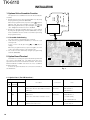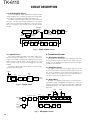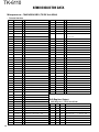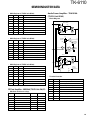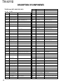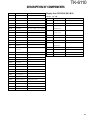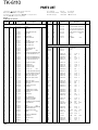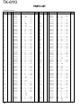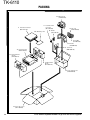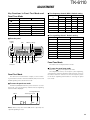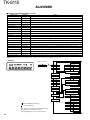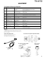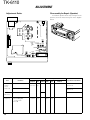
1
VHF FM TRANSCEIVER TK-6110 SERVICE MANUAL © 2000-6 PRINTED IN JAPAN B51-8519-00 (N) 1113 Microphone (T91-0621-05) Cabinet (A01-2170-03) Key top (K29-5388-02) Knob (VOL) (K29-5389-03) Panel assy (A62-0761-13) CONTENTS GENERAL ................................................................. 2 PACKING ................................................................ 32 SYSTEM SET-UP ..................................................... 3 ADJUSTMENT ....................................................... 33 OPERATING FEATURES ......................................... 4 TERMINAL FUNCTION ......................................... 40 REALIGNMENT ........................................................ 8 PC BOARD VIEWS INSTALLATION ...................................................... 10 TX-RX UNIT (X57-6100-XX) (A/3, C/3) ........... 41 CIRCUIT DESCRIPTION ......................................... 13 TX-RX UNIT (X57-6100-XX) (B/3) .................... 47 SEMICONDUCTOR DATA ..................................... 18 SCHEMATIC DIAGRAM ........................................ 51 DESCRIPTION OF COMPONENTS ....................... 20 BLOCK DIAGRAM................................................... 57 PARTS LIST ............................................................ 22 SPECIFICATIONS................................................... 59 EXPLODED VIEW .................................................. 31 TK-6110 GENERAL INTRODUCTION SCOPE OF THIS MANUAL This manual is intended for use by experienced technicians familiar with similar types of commercial grade communications equipment. It contains all required service information for the equipment and is current as of the publication data. Changes which may occur after publication are covered by either Service Bulletins or Manual Revisions. These are issued as required. ORDERING REPLACEMENT PARTS When ordering replacement parts or equipment information, the full part identification number should be included. This applies to all parts : components, kits, or chassis. If the part number is not known, include the chassis or kit number of which it is a part, and a sufficient description of the required component for proper identification. PERSONNEL SAFETY The following precautions are recommended for personnel safety : • DO NOT transmit if someone is within two feet (0.6 meter) of the antenna. • DO NOT transmit until all RF connectors are verified secure and any open connectors are properly terminated. • SHUT OFF and DO NOT operate this equipment near electrical blasting caps or in an explosive atmosphere. • All equipment should be properly grounded before power-up for safe operation. • This equipment should be serviced by a qualified technician only. PRE-INSTALLATION CONSIDERATIONS 1. UNPACKING Unpack the radio from its shipping container and check for accessory items. If any item is missing, please contact KENWOOD immediately. 2. LICENSING REQUIREMENTS Federal regulations require a station license for each radio installation (mobile or base) be obtained by the equipment owner. The licensee is responsible for ensuring transmitter power, frequency, and deviation are within the limits permitted by the station license. Transmitter adjustments may be performed only by a licensed technician holding an FCC first, second or general class commercial radiotelephone operator’s license. There is no license required to install or operate the radio. 2 3. PRE-INSTALLATION CHECKOUT 3-1. Introduction Each radio is adjusted and tested before shipment. However, it is recommended that receiver and transmitter operation be checked for proper operation before installation. 3-2. Testing The radio should be tested complete with all cabling and accessories as they will be connected in the final installation. Transmitter frequency, deviation, and power output should be checked, as should receiver sensitivity, squelch operation, and audio output. Signalling equipment operation should be verified. 4. PLANNING THE INSTALLATION 4-1. General Inspect the vehicle and determine how and where the radio antenna and accessories will be mounted. Plan cable runs for protection against pinching or crushing wiring, and radio installation to prevent overheating. 4-2. Antenna The favored location for an antenna is in the center of a large, flat conductive area, usually at the roof center. The trunk lid is preferred, bond the trunk lid and vehicle chassis using ground straps to ensure the lid is at chassis ground. 4-3. Radio The universal mount bracket allows the radio to be mounted in a variety of ways. Be sure the mounting surface is adequate to support the radio’s weight. Allow sufficient space around the radio for air cooling. Position the radio close enough to the vehicle operator to permit easy access to the controls when driving. 4-4. DC Power and wiring 1. This radio may be installed in negative ground electrical systems only. Reverse polarity will cause the cable fuse to blow. Check the vehicle ground polarity before installation to prevent wasted time and effort. 2. Connect the positive power lead directly to the vehicle battery positive terminal. Connecting the Positive lead to any other positive voltage source in the vehicle is not recommended. 3. The cable provided with the radio is sufficient to handle the maximum radio current demand. If the cable must be extended, be sure the additional wire is sufficient for the current to be carried and length of the added lead. TK-6110 GENERAL / SYSTEM SET-UP 5. INSTALLATION PLANNING – CONTROL STATIONS 5-1. Antenna system Control station. The antenna system selection depends on many factors and is beyond the scope of this manual. Your KENWOOD dealer can help you select an antenna system that will best serve your particular needs. SERVICE This radio is designed for easy servicing. Refer to the schematic diagrams, printed circuit board views, and alignment procedures contained in this manual. 5-2. Radio location Select a convenient location for your control station radio which is as close as practical to the antenna cable entry point. Secondly, use your system’s power supply (which supplies the voltage and current required for your system). Make sure sufficient air can flow around the radio and power supply to allow adequate cooling. SYSTEM SET-UP Frequency range RF power Type 29.7~37MHz 70W TK-6110 K 70W 35~50MHz TK-6110 K2 Merchandise received License and frequency allocated by FCC Choose the type of transceiver Transceiver programming Are you using the external speaker? See page 8 A personal computer (IBM PC or compatible), programming interface (KPG-46), and programming software (KPG-59D) are required for programming. (The frequency and signalling data are programmed for the transceiver.) YES KES-4 (EXT. SP) See page 12 KCT-18 See page 12 NO Are you using the ignition sense cable? YES NO Delivery 3 TK-6110 OPERATING FEATURES Displays the operating Channel number, the Channel name, and the transceiver status. Displays the operating channel number and the channel status: P indicates a Priority channel HC indicates a Home Channel tA indicates Talk Around mode Flashes when a call is received by DTMF or 2-Tone signaling. Appears during and after transmitting if set by the dealer. Appears when signaling squelch is turned OFF. Appears while scanning is in progress. 1. Controls and Functions 1-1. Front Panel Display 1 3 MON A 5 6 4 Speaker 2 B 7 C 8 SCN 9 10 Appears when the optional scrambler board is enabled. Appears when the selected channel is in the scanning sequence. Appears when Aux is ON. 1 Volume control Turn clockwise to increase the volume. Turn counterclockwise to decrease the volume. 2 / keys Press these keys to activate their programmable functions. The default settings of these keys are “Channel Up” ( ) and “Channel Down” ( ). 3 Microphone jack Insert the microphone plug into this jack. Appears when Operator Selectable Tone is enabled. 1-3. Rear Panel 4 IO (Power) switch Press to switch the power ON. Press and hold for approximately 1 second to switch the power OFF. TK-6110 5 MON key Press MON to activate its programmable function. The default setting of this key is “Monitor”. 6 A key 7 B▼ key 8 C▲ key Press these PF (programmable function) keys to activate their programmable functions. The default setting of these keys is “No Function”. 9 SCN key Press SCN to activate its programmable function. The default setting of this key is “Scan”. 10 LED Lights red while transmitting. Lights green while the selected channel is busy. Blinks orange when you receive a call by 2-Tone or DTMF. 15 pin connector (for accessories) Antenna connector Power input connector 1-4. Microphone 1-2. Display PTT (Push To Talk) switch Press and hold to transmit, then speak into the microphone. Release to receive. 4 TK-6110 OPERATING FEATURES 2. Scanning 2-1. Start Scanning You can start scanning when 1 priority channel and at least 1 ADD channel, or 2 or more ADD channels are selected. The transceiver must be in the normal receiving mode (releasing PTT). Press the key programmed to the scan, the scan starts. The “SCN” (scan) icon appears on the main display and “SCAN” or revert channel appears on the 8-digit alphanumeric display. 2-2. Stop Scanning The scan stops temporarily if the following conditions are satisfied. 1) A carrier is detected, then signalling matches on channel for which receive the signalling is set by the programming software. 2) A carrier is detected on the channel for which receiving signalling is not set by the programming software or when the monitor (signalling cancel) function is activated. 2-3. Types of Scan Channel 1) Priority channel is the most important channel for the scan, and always detects a signal during scan and when the scan stops temporarily. 2) Non-priority channels detects a signal during scan and when scan stops temporarily. 2-4. Setting Priority Channel Priority channel can be set as follows with the programming software (KPG-59D). 1) Specify priority channel as fixed priority channel. 2) Make selected channels, priority channels. 2-5. Scan Type Depending on the Priority Channel 1) When no priority channels are set : Only the non-priority channels are scanned. If the transceiver stops on a non-priority channel, priority channel is still checked for signals at the specified time intervals. If the transceiver detects a signal on a priority channel, it pauses at the priority channel and starts receiving the calls. 2) When priority channel is set : Either priority channel is scanned. If a priority channel stops temporarily, it stops until there is no signal on the priority channel. 2-6. Revert Channel The revert channel is used to transmit during scanning and set by the programming software (KPG-59D). 1) Last called channel The transceiver reverts to the last called channel during the scan. 2) Last used channel The transceiver reverts to the last used (transmitted) channel during scan. “Last used” revert channel includes talkback function. 3) Selected with talkback The transceiver reverts to the channel before scanning or the channel that you changed during scan. 4) Selected channel The transceiver reverts to the channel before scanning or the channel that you changed during scan. While the transceiver pauses scanning, the revert channel becomes the channel you selected with [CH UP], [CH DW], [CH1] to [CH5] in the last step. 5) Priority with talkback The transceiver reverts to the priority channel. If you press PTT during a resume timer (dropout delay time, TX dwell time) or calling, you can transmit on current channel to answer to the call however revert channel is set to priority channel. After resume time, scan re-starts and transmission channel is return to priority channel. 6) Priority The transceiver reverts to the priority channel. 2-7. Scan End When you press the key once again, programmed to the scan function during scan mode, the scan ends. The scan icon “SCN” and “SCAN” or revert channel (programmable) display goes off. 2-8. Temporarily Delete/Add It is possible to delete or add channel temporarily during scan. When scan stops on unnecessary channel for example by interference of the other party, activate the delete/ add function (for example press the key), then that channel is deleted temporarily and scan re-start immediately. When you would like to add the deleted channel temporarily to scan sequence, select the desired (deleted) channel during scan, activate the delete/add function (for example press the key) before scan re-start. That channel is added temporarily to scan sequence. The temporary deleted or added channels are returns to pre-set delete/add, when the transceiver exits from scan mode. 3. Optional Features You can use these features using the programming software (KPG-59D). 3-1. Beep Tones The beep tones (power on tone, control tone, warning tone, alert tone) are individually programmable to the fixed level 0 to 31 or follow the mechanical volume position. 3-2. Minimum Volume The minimum volume is programmable (0 to 31). The transceiver remains the minimum volume level however the mechanical volume position is set to zero. 3-3. BCL (Busy Channel Lockout) Override You can transmit in spite of Busy Channel Lockout situation. For example : To make an emergency voice call. To transmit under busy channel lockout situation, press PTT once more within approx. 500ms after the PTT release. 5 TK-6110 OPERATING FEATURES 3-4. Sub LCD Display 3-11. “TOT” Pre-Alert You can use 3-digit 7-segment the display to display the channel number. It is useful when the main (8-digit 13-segment) display indicates channel name. The transceiver has “TOT” pre-alert timer. This parameter selects the time at which the transceiver generates “TOT” pre-alert tone before “TOT” is expired. “TOT” will be expired when the selected time passes from a TOT pre-alert tone. 3-5. Emergency Channel Display The transceiver can be programmed to display “EMERGENCY” channel name when it is in emergency mode. If you set to “off” by KPG-59D the transceiver shows selected group/channel/status before entering to the emergency mode however the transceiver is in an emergency mode. 3-12. “TOT” Re-Key Time The transceiver has “TOT” re-key timer. This timer is the time you can not transmit after “TOT” exceeded. After “TOT” re-key time expired you can transmit again. 3-13. “TOT” Reset Time 3-6. Clear to Transpond The transceiver waits the transpond of 2-Tone/DTMF if channel is busy until channel open. This feature replies to the transpond signal when the caller returns to receive. 3-7. Mode (Enable/Disable) The transceiver has many special modes mainly for maintenance. · Panel Test mode · Clone mode · Main programming mode It is possible to set enable/disable for each mode. We recommend to set these mode to Disable after set up to save contents. 3-8. ID The transceiver is capable to have ID. The format is DTMF. The timing that the transceiver sends ID is programmable. Begin of TX : Connect ID is send on beginning of transmission. End of TX : Disconnect ID is send on end of transmission. Both : Connect ID is send on beginning of transmission and disconnect ID is send on end of transmission. Off : Sending ID function is disabled. There is also “PTT ID” setting for each channel. Refer “PTT ID” of channel feature. 3-9. OST (Operator Selectable Tone) The transceiver has “TOT” reset timer. This timer is the minimum wait time allowed during a transmission that will reset the “TOT” count. “TOT” reset time causes the “TOT” to continue even after PTT is released unless the “TOT” reset timer has expired. 3-14. Signalling Signalling “AND/OR” sets the audio unmute condition for any channel programmed with the option signalling (2Tone/ DTMF). AND : “AND” requires both the valid option signalling and the programmed QT/DQT to be received for audio to unmute (and initiate an option signalling decode alert). OR : “OR” requires either the valid option signalling or the programmed QT/DQT to be received for audio to unmute (an option signalling decode alert is only initiated if the proper option signalling is decoded). 4. Channel Features You can use these features using the programming software (KPG-59D). 4-1. Alphanumeric Display (Channel Name) The programming software (KPG-59D) enables you to set the alphanumeric display for channel name. The total text size of channel name are 8-digits. The characters can be used as shown in Figure 1. The transceiver is capable to have “OST” function and 16 tone pair (QT/DQT) with max 8-digit name for each tone pair. • “OST” Back Up The transceiver is programmable the selected “OST” code is memorized or not. If you set to Disable (no memorized), the “OST” function always starts at “off”. 3-10. “TOT” (Time-Out Timer) The transceiver has the “TOT”. This parameter selects the period of time users can continuously transmit. When the selected period passes, the transceiver generates an warning tone and stops the transmission. A B C D E F G H J K L M N O P Q R S T U V W X Y Z 1 2 3 4 5 6 7 8 9 All on 0 - Fig. 1 6 I TK-6110 OPERATING FEATURES 4-2. Option Signalling 5-6. Delete/Add The transceiver is programmable to the option signalling (2-Tone decode program 1, 2-Tone decode program 2, 2Tone decode program 3, DTMF decode) to each channel. It is useful to receive an individual call. Receive format is selectable “AND” or “OR” with QT/ DQT. The radio response of option signalling is programmable call Alert and “Transpond” for each option signalling (2-Tone decode program 1, 2-Tone decode program 2, 2Tone decode program 3, DTMF). This key switches the currently displayed channel between “Delete” and “Add”. The “Add” channel contained in the scan sequence, and “Delete” channel is not contained. In the scan mode, this key switches the channel delete or add temporarily. 5-7. Home Channel Press this key once, the channel switches to the pre-programmed home channel. Press this key again, the channel goes back to the previous channel. 4-3. PTT ID PTT ID provides a DTMF ANI to be sent with every time PTT (connect ID at beginning of transmission, disconnect ID at end of transmission, or both). You can program PTT ID “on” or “off” for each channel. The contents of ID are programmed for each transceiver. 4-4. Busy Channel Lockout Transmission is inhibited when the channel is busy. It is able to set this feature “Yes” or “No” for each channel. 4-5. Scan Delete/Add Scanning “delete/add” is programmable for each channel. Set the currently selected channel required to include in the scan sequence to “add”. The operator can change the “delete/add” information using the key programmed to “delete/add” function. 5. Key Functions 5-1. No Function Sounds error operation beep, and no action will occur. Use this function when the transceiver is required to be more simple operated. 5-2. AUX. 5-8. Monitor Monitor the channel before a transmission. Press this key once, “MON” appears and unmutes speaker if a carrier is present, regardless of the specified signalling (including option signalling). Press this key again, “MON” disappears and mutes speaker. Press this key after the Option Signalling is matched, the Option Signaling is reset. DBD (Dead Beat Disable) mode is not reset by this operation. Press and hold the Monitor key for 2 seconds to disable the squelch. 5-9. Operator Selectable Tone When this key is pressed, the “OST” icon lights and Encode/Decode QT/DQT is switched to the OST Tone pair. If pressed again, the “OST” icon goes off and Encode/Decode QT/DQT returns to KPG-59D pre-set. When this key is held down for 1 second, the transceiver enters “OST Select Mode”. In this mode, the display shows OST No. or OST Name which is set to the channel and operator can select one of OST Tone pair using UP key and DW key. If pressed this key again, the displayed OST code is memorized to the channel, the transceiver exits from the OST Select Mode, returns to normal channel display and “OST” icon lights. 16 kinds of tone pair for OST can be programmed by KPG-59D. OST is useful to access the repeater with same radio frequency and different tone (QT/DQT). The AUX function can be programmed for push key. If this key is pressed, the “A” icon lights on the LCD and the AUX port which is contained in 15-pin connector located at the rear of the transceiver goes to low level. If pressed again, the “A” icon goes off and the AUX port goes to Open-collector. 5-10. Scan 5-3. Channel Down Press this key starts scanning. Pressing this key stops scanning. If this key is pressed once, the channel number decreases by one step. If this key is hold down, the channel number decreases continuously. 5-11. Squelch Level If this key is pressed once, the channel number increases by one step. If this key is hold down, channel number increases continuously. The preset squelch level is varied in user mode (0 to 15). Press the key programmed to “squelch level”, the transceiver enters to “squelch level adjust mode”. The squelch level can be adjusted by / . Press the key programmed to “squelch level” again, the adjusted level is memorized and returns to the normal user mode. 5-5. Channel Name 5-12. Talk Around This key switches the LCD display between the current channel number and programmed channel name. Press this key, the transceiver uses the receive frequency and the tone for transmission. The operator can call the other party directory (without repeater). Press this key again, the talk around function goes off. 5-4. Channel Up 7 TK-6110 OPERATING FEATURES / REALIGNMENT 5-13. Emergency Call 8-3. Programming Software KPG-59D Description When the Emergency function (key) is activated, the radio enters the “Emergency Mode”. In this mode, the radio automatically switches to the programmed “Emergency Channel” and starts transmission with the Emergency ID Code programmed in an installed ANI Board (dependent on ANI board capabilities and programming). The LCD display (Emergency Text) and the TX LED operation are dependent on the “Emergency CH Display” settings. KPG-59D is the programming software for TK-6110 supplied on two 3.5" floppy disks. This software runs under MSDOS version 3.1 or later, and Windows MS-DOS prompt on an IBM-PC or compatible machine. The data can be input to or read from TK-6110 and edited on the screen. The programmed or edited data can be printed out. It is also possible to tune the transceiver. We recommend that install KPG-59D for example to harddisk first then use it. 6. 2-Tone 2-Tone signalling opens the squelch only when the RADIO receives a proper 2-Tone code that is the same as the pre-programmed 2-Tone for the channel. When the RADIO receives a 2-Tone code, the CALL icon flashes. If Transpond has been programmed, the RADIO will return an acknowledgment signal automatically after receiving the 2-Tone code. If Alert Tone has been programmed, an Alert Tone sounds after receiving a 2-Tone code. Unmute condition is canceled and the CALL icon goes off when ; (1) pressing the [MON] Key, (2) hanging the microphone on its hook, (3) muting continues for 10 seconds. (If “Auto Reset” has been programmed) KPG-46 IBM-PC KPG-59D TK-6110 Fig. 2 7. DTMF DTMF Signalling opens the squelch only when the RADIO receives a proper DTMF code that is the same as the pre-programmed “Primary Code (Individual ; 1~7digits)” or “Secondary Code (Group ; 1~7digits)”. When the RADIO receives a correct code, the CALL icon flashes. If Transpond has been programmed, the RADIO will return an acknowledgment signal automatically after receiving the DTMF code. If Alert Tone has been programmed, an Alert Tone sounds after receiving a DTMF code. Unmute condition is canceled and the CALL icon goes off when ; (1) pressing the [MON] Key, (2) hanging the microphone on its hook, (3) muting continues for 10 seconds (If “Auto Reset” has been programmed), and (4) receiving reset code. (Primary code + “#” or secondary code + “#”) 8. Data Programming (PC Mode) 8-1. Preparation and Connection The TK-6110 transceiver is programmed by using a personal computer, programming interface cable KPG-46, and programming software KPG-59D. The programming software can be used with an IBM-PC or compatible machine. Figure 2 shows the setup for programming. 8 REALIGNMENT 1. Mode User mode PC programming mode PC mode PC test mode PC tuning mode Clone mode Panel test mode Panel tuning mode Main programming mode Mode User mode PC mode 8-2. Programming Interface Cable KPG-46 Description PC programming mode PC test mode The KPG-46 is required to interface the transceiver with the computer. It has a circuit in its D-sub 25pin connector case that converts RS-232C logic level to TTL level. KPG-46 is used to connect between transceiver microphone connector and RS-232C serial port of computer. Panel test mode (Refer to ADJUSTMENT) Main programming mode Function Customer use this mode Communication between the radio and PC (IBM compatible). It requires the KPG-59D. Frequency, signalling and features write to the radio and read from the radio. Check the radio using the PC. This feature is included in the FPU. Dealer uses to check the fundamental characteristics. Re-write to firmware of the flash ROM. TK-6110 REALIGNMENT 4-3. Programming 2. How to Enter Each Mode Mode User mode PC mode Panel test mode Main programming mode Operation Power on Turn on the transceiver. Then, set the transceiver to PC mode from the menu in KPG-59D. Hold down the [MON] key, turn the radio power on. Hold down the [A] key, turn the radio power on. 3. Clone Mode 1. Turn the master side transceiver power on with the [SCN] key held down. The master side transceiver displays “CLONE”. 2. Set the power switch on the slave side transceiver to ON. 3. Connect the cloning cable (E30-3382-05) between the master side transceiver (source) and slave side transceiver (clone). 4. Press the [SCN] key on the master side transceiver to start cloning. 5. The TX LED on the master side transceiver flashes when cloning starts and an “END” message appears when cloning ends. 6. The BUSY LED on the slave side transceiver flashes. 7. When a problem occurs during cloning, an “ERROR” message appears on the slave side transceiver. 8. Pressing the [SCN] key sets clone mode again. CLONE Set the transceiver to Main Programming Mode. Connect the KPG-46 to the transceiver. Start up the programming software (KPG-59D), select “firmware program” in the “Program” item, and press the Return key on the personal computer. This starts up the firmware programmer. 4. The top screen is displayed. Press any key to advance to the next screen. 5. Set the communications speed (normally, 115,200bps) and communications port in the Setup item. 6. Set the firmware to be updated by File select. 7. Held down the [A] key. Turn the transceiver power on. Until the display change to “PROG1152” 8. Check the connection between the transceiver and the personal computer, and make sure that the transceiver is in the Main Programming Mode. 9. Press F10 on the personal computer. A window opens on the display to indicate progress of writing. When the transceiver starts to receive data, “PG” is appeared on 2 digit sub display. 10. If writing ends successfully, the TX LED on the transceiver lights and the checksum is displayed. 11. If you want to continue programming other transceivers, repeat steps 5 to 8. Notes : • To start the Firmware Programmer from KPG-59D, the Fpro path must be set up by KPG-59D setup. • This mode cannot be entered if the Main Programming mode is set to Disable in the Programming software (KPG-59D). 4-4. Function [SCN] [SCN] 1. 2. 3. [SCN] START END 4. Main Programming Mode 4-1. Preface Flash memory is mounted on the transceiver. This allows the transceiver to be upgraded when new features are released in the future. (For details on how to obtain the firmware, contact Customer Service.) 4-2. Connection Procedure Connect the transceiver to the personal computer (IBM PC or compatible) with the interface cable (KPG-46). (Connection is the same as in the PC Mode.) 1. If you press the [SCN] key while “PROG1152” is displayed, the checksum is displayed. If you press the [C] key while the checksum is displayed, “PROG1152” is redisplayed. 2. A transmission speed can be selected by pressing the [C] key while “PROG1152” is displayed. 115200bps : PROG1152 19200bps : PROG 192 38400bps : PROG 384 57600bps : PROG 576 Note : Normally, write in the high-speed mode. 5. Panel Test Mode Setting method refer to ADJUSTMENT. 9 TK-6110 INSTALLATION 1. Optional Voice Scrambler Function The optional voice scrambler function can be used by two methods. 1. Assign this function to any programmable keys by using the programming software (KPG-59D). When the programmed key is pressed, the indicator appears and optional scrambler function is enabled. When the programmed key is pressed again, the indicator disappears and the function is disabled. 2. Assign the optional scrambler function to each channel by using the programming software (KPG-59D). The optional scrambler function can be used without pressing the programmed key. TX-RX unit Component side 1-1. Scrambler Code Setting The code can be configured by two methods. 1. Hold down the programmed OPT key to enter the code setting mode. Select a new code by pressing [ ] or [ ] key to change. When the programmed key is pressed again, the new code is stored and exit the code setting mode. 2. Set a code for each channel by using the programming software (KPG-59D). 2. Option Board Terminal A B C D E F K L M G H J N P R R725 R778 Terminals for mounting the option board are provided at the center of the TX-RX unit. The table shows the correspondence between the board and terminals. Disconnect R725 and R778 in TX-RX unit when the voice scrambler board is attached. Connect the option board to the connection terminals of the TX-RX unit. Fig. 1 2-1. Option Port 1 (For ANI board etc.) Port name Abbreviation Abbreviation Name Description Connection Note (PCB) (Schematic diagram) B RX IN Data in Board data input. Connected to Reference Transceiver (Receiver demodulaion circuit) → the circuit 1kHz STD DEV → Board data output. Connected to Reference ANI board → the circuit ANI board T DATA Data out OUT 250~350mVrms Transceiver (Transmitter modulation circuit) 1kHz/150mVrms → 2.5~3.5kHz (Wide), 1.25~1.75kHz (Narrow) Z TCONT T control Audio amplifier power control → TX-RX unit microprocessor 10 CPU input L : Audio amp on H : Audio amp off S T W X Y Z TK-6110 INSTALLATION Port name Abbreviation Abbreviation Name Description Connection Note (PCB) (Schematic diagram) X STONE Side tone Beep during PTT ID Connected to the circuit R AUDI IH Audio inhibit Microphone muting during PTT ID Connected to the circuit K GND Ground Ground Ground W AUX Aux Emergency channel request → CPU input J PTTO PTT Microprocessor PTT logic → ANI board CPU output L : TX, H : RX P EMERG Emergency Microprocessor emergency channel logic → CPU output L : Emergency operation request TX-RX unit microprocessor L : EMG CH request H : No EMG CH request ANI board H : No emergency operation request N BUSY Channel busy Microprocessor busy logic → ANI board CPU output L : Busy, H : Not busy Y KEY (Transmission) Transmission start control GE-star → CPU input L : Transmission request Key TX-RX unit microprocessor L +8V Board power Switched B H : No transmission request Power supply supply 2-2. Option Port 2 (For voice scrambler etc.) Port name Abbreviation Abbreviation Name Description Connection Note (PCB) (Schematic diagram) G CODE 1 Scrambler code 1 First of four bits of scrambler code CPU output D CODE 2 Scrambler code 2 Second of four bits of scrambler code E CODE 3 Scrambler code 3 Third of four bits of scrambler code F CODE 4 Scrambler code 4 Fourth of four bits of scrambler code A TXOUT TX out Board → Connected to Transceiver (Transmitter modulation circuit) the circuit Board code selection (Logic by binary code) Reference 1kHz/15mVrms → 2.5~3.5kHz (Wide), 1.25~1.75kHz (Narrow) M RXOUT RX out Board → Transceiver (Audio amp) Connected to K GND Ground Ground Ground the ciircuit J PTTO Scrambler modulation/demodulation control CPU output L : TX, H : RX H CLRC Clear/Code Specifies whether to scramble CPU output L : Scramble, H : Normal B RXIN RX in Transceiver (Microphone circuit) → Board Connected to Reference the circuit 1kHz STD DEV → 250~350mVrms C TXIN TX in transceiver (Microphone circuit) → Board L +8V Board power Switched B Connected to the circuit Power supply supply 11 TK-6110 INSTALLATION 3. Ignition Sense Cable (KCT-18) The KCT-18 is an optional cable to use the following functions: 3-1. Ignition function The ignition function allows you to turn the transceiver’s power on and off with the ignition key of your car. When you are driving with the ignition key on, the horn alert function is disabled. 3-2. Timed power off function The timed power off function turns the transceiver’s power off the time specified with the programming software (KPG-59D) after the ignition key is turned off. When you are driving with the ignition key on, the horn alert function is disabled. The ignition sense function and the timed power off function can be used at the same time. 2. Remove the terminals with the jumper from the connector housing holes number 9 and 12 using the extracting tool. Removing the jumper lead (Fig. 3-2) 1) Insert the extracting tool (11-03-0002) into the connector while pushing the jumper lead in the direction of (a). 2) Push the extracting tool into collapse the barbs of the crimp terminal. 3) Pull out the lead while continuing to push the extracting tool in the direction (b). 3. Reinsert the terminal with the black and white stripe lead into hole number 6, and the terminal with the black lead into hole number 12 (Fig. 3-3). 4. Attach the connector to the external speaker connector on the radio. 3-3. Modification 1. Remove the short plug from the accessory connector (15 pins) on the back of the transceiver. 2. Insert the KCT-18 into pin 3 (IGN). 13 15 1 3 Contact KCT-18 Fig. 2 Fig. 3-1 Fig. 3-2 4. External Speaker (KES-4) 1. The external speaker output from the accessory connector (15 pins) on the back of the transceiver is 10W/4 ohms. Use the KES-4. 4-1. Connection for the KES-4 with the TK-6110 • When taking the AF output from the accessory connector (15-pin) on the rear of the radio The following tools are required for changing the connector. Extracting tool the following extracting tool is recommended : Molex Inc. Order No. : 11-03-0002 1. Remove the connector with jumper from the external speaker connector on the rear panel of the radio (Fig. 31). Note : Save the jumper, which is required when the radio is used without the external speaker. 1 3 13 15 6 12 Black lead Black/White lead Fig. 3-3 5. Horn Alert Function The HR pin of the accessory connector (15-pin) on the rear of the transceiver is an open collector and the maximum current is 100mA. The maximum available current can be increased to 1A by installing a relay. Program the Horn Alert Function, using KPG-59D. HR (Pin 10) Fig. 4 12 TK-6110 CIRCUIT DESCRIPTION 1. Overview 3. Receiver System The KENWOOD model TK-6110 is a VHF/FM transceiver designed to operate in the frequency range of 29.7 to 37MHz (K), 35.0 to 50.0MHz (K2), the unit consists of a receiver, a transmitter, a phase-locked loop (PLL) frequency synthesizer, power supply circuits, a control unit. 3-1. Front-End RF Amplifier An incoming signal from the antenna is applied to a bandpass filter (L202) after going through a low-pass filter and an antenna switch (K1). The signal is then amplified by the RF amplifier (Q201) and again filtered by another band-pass filter (L203, L206 and L207). 2. Circuit Configuration by Frequency 3-2. First Mixer The receiver is a double-conversion superheterodyne with a first intermediate frequency (IF) of 128.55MHz and a second IF of 455kHz. Incoming a signals from the antenna are mixed with the local signal from the PLL1 to produce the first IF of 128.55MHz. This is then mixed with the 129.005MHz seconds local oscillator output to produce the 455kHz second IF. This is detected to give the demodulated signal. The transmit signal is modulated PLL2-VCO2 (129.005 MHz) from the microphone. The transmit signal frequency is down-conversion with PLL2 and PLL1. It is then amplified and sent to the antenna. ANT 1st MIX PA AMP FM IF SYSTEM 29.7~ 37.0MHz : K 35.0~ 50.0MHz : K2 AF AMP SP 129.005 MHz PLL2 VCO2 MIC AMP 129.005 MHz 158.705~166.005MHz : K 164.005~179.005MHz : K2 Frequency configuration BPF Q201 RF AMP BPF BPF LPF IC201 1st MIX D502 T/R SW Q202 Q205 MCF IF AMP 128.55MHz IF AMP TX MIX 158.25~165.55MHz : K 163.55~178.55MHz : K2 Fig. 1 The first IF signal is amplified by Q202 and Q205, and then enters IC202 (FM processing IC). The signal is heterodyned again with a second local oscillator signal (129.005MHz) with in IC202 to become a 455kHz second IF signal. The second IF signal is fed through a 455kHz ceramic filter, CF201 and CF202 to further eliminate unwanted signals before it is amplified and FM detected in IC202. MCF 128.55MHz ANT SW TX AMP 3-3. IF Amplifier CF 455kHz TX/RX 29.7~37.0MHz : K 35.0~50.0MHz : K2 LPF The signal from the band-pass filter is heterodyned with the first local oscillator signal from the PLL frequency synthesizer circuit at the first mixer (IC201) to become a 128.55MHz first intermediate frequency (IF) signal. The first IF signal is fed through two monolithic crystal filters (XF201) to further remove spurious signals. IC202 FM IF SYSTEM MIC XF201 129.005MHz PLL1 VCO1 CF201,202 455kHz Fig. 2 Receiver section Item Nominal center frequency Pass bandwidth Attenuation bandwidth Ripple Insertion loss Guaranteed attenuation Terminating impedance Table 1 Rating 128.55MHz ± 7.5kHz or more at 3dB ± 35kHz or less at 40dB 1.0dB or less 5dB or less 70dB or more at fo± 910kHz 1000Ω Crystal filter (L71-0560-05) (TX-RX unit XF201) 13 TK-6110 CIRCUIT DESCRIPTION 3-4. Audio Amplifier Circuit The recovered audio signal obtained from IC202 is amplified by IC709, IC713, low-pass filtered by IC713 high-pass filtered by IC713 and band-eliminate filtered by IC713. The audio signals then passed through a de-emphasized by IC713. The processed audio signal passes through an audio volume control and is amplified to a sufficient level to drive a loudspeaker by an audio power amplifier BTL (IC102). IC709 (2/2) IC203 AF AMP IC202 FM IF SYSTEM SW IC710 IC710 IC105 VOL VOL MUTE IC711 (2/2) AF AMP CF201,202 455kHz 129.005 MHz IC102 AF AMP ES2 AM1 IC713 HPF 2 LPF HPF 1 BEF 5 DEEMP EXP MUTE 41 Fig. 3 Audio amplifier circuit 3-5. Squelch Circuit The output signal from IC202 enters FM IC again, then passed through a band-pass filter. The noise component output from IC202 is amplified by Q206 and rectified by D205 to produce a DC 0 voltage corresponding to the noise level. The DC voltage is sent to the analog port of the CPU (IC604). And IC202 outputs a DC voltage (RSSI) corresponding to the input of the IF amplifier. AF OUT IC604 CPU IC202 9 DET OUT 8 Noise amp 7 Q206 D206 Noise amp DET 31 SQL Output expander Mute circuit 4. Transmitter System 4-1. Microphone Amplifier The signal from the microphone is high-pass filtered by IC713, passed through microphone mute and microphone amplifier circuit (Q703 and IC714), limited and pre-emphasized by IC713 and D711. 4-2. Modulator Circuit The output of Audio-processor (IC703) is passed to the D/ A converter (IC710) for maximum deviation adjustment and the summing amplifier (IC711) before being applied to a varactor diode in the voltage controlled oscillator (VCO) located in the frequency synthesizer section. 4-3. Down-Mixer At Q503, a modulated VCO2 signal is mixed with 2nd local oscillator signal, 129.005MHz. The difference of the two signals is used for the transmission signal 29.7~37MHz (K), 35.0~50.0MHz (K2). The output was filtered through a lowpass filter. Fig. 4 squelch circuit MM Q708 SW IC713 IC714 (2/2) D711 MIC1 SW AMP LIMIT 12 15 16 18 TONE 9 8 HPF PRE EMP 19 LPF HPF ALC COMP IC712 IC710 D/A O4 I4 IC711 (1/2) L517 MC1 MIC2 (External input) SW MC2 SW SUM AMP LSD Fig. 5 Microphone circuit 14 VCO IDC 6 TK-6110 CIRCUIT DESCRIPTION 4-4. Driver and Final Power amplifier Circuits 5. PLL Frequency Synthesizer The transmit signal is generated by the TX mixer (Q503). The transmit signal obtained from the buffer amplifier Q1 and Q2, is amplified by Q3 to approximately 30dBm. This amplified signal is amplified by Q4 and Q5 to approximately 8W, and this signal is passed to the final stage. The RF power amplifier consists of transistor (Q6 and Q7) and is capable of roducing up to 70W of RF power. The frequency synthesizer consists of the VCXO (X501), VCO (L517), PLL IC (IC501) and buffer amplifiers. The VCXO generates 16.8MHz reference frequency. The frequency stability is within ± 5.0ppm (temperature range of –30 to +60°C). The output of the VCXO is applied to pin 8 of the PLL IC. VCO (L517) has 2 internal VCOs. One for the 1st local oscillator (K : 158.25~166.005MHz, K2 : 163.55~179.005 MHz) and another one for the 2nd local oscillator (129.005MHz). Each output is connected to a dual PLL IC (IC501). VCO1 oscillates at K : 158.705~166.005MHz, K2 : 164.005~179.005MHz during transmission and it oscillates at K : 158.25~165.55MHz, K2 : 163.55~178.55MHz during reception. VCO2 oscillates at 129.005MHz during both reception and transmission. However, the oscillated signal is modulated during transmission. Each PLL circuit has LPFs and buffer amplifiers. The output of VCO1 goes through the buffer amplifier, then the output is switched either for the 1st local oscillator circuit of the receiver or TX mixer. The output of VCO2 goes through the buffer amplifier, then the output is switched either for the 2nd local oscillator circuit of the receiver or TX mixer. 4-5. Transmit/Receive Switching Circuit The final output signal is passed through a transmit/receive switching circuit (K1) before it is passed to the antenna terminal. 4-6. Automatic Power Control, Circuit and Transmitter The APC circuit consists of an RF level detector, an exciter control section and a temperature sensing circuit. The RF level detector senses the forward and reflected power. The transmitter output power is kept constant by the exciter control circuit which monitors the forward power and regulates the supply voltage applied to the exciter section. If the antenna load becomes abnormal, the reflected power increases, causing the exciter control circuit to reduce the supply voltage to the exciter. In case of an abnormal temperature rise in the power amplifier section, the temperature sensing circuit detects this condition and send the information to the APC circuit. These actions reduce the transmitter output power to a safe operating level. ANT Q503 Q1 Q2 Q3 Q4 Q6 K1 TX mixer RF amp RF amp Predrive amp Drive amp RF power amp TX/RX ANT SW Q5 Q7 Drive amp RF power amp LPF Fig. 6 Drive and final amplifier TCXO VCO1 BUFF SW LPF BUFF 8TB/8R TX local 1 RX local 1 16.8MHz Dual PLL UL CPU PDAT,PCLK,LE MOD/TONE LPF BUFF 8TB/8R VCO2 BUFF SW TX local 2 RX local 2 Fig. 7 PLL block diagram 15 TK-6110 CIRCUIT DESCRIPTION IC605 6. Power Supply Circuit EEPROM The power (+B), which is suplied via a power connector, is routed to the TX drive amplifier (Q4 and Q5), the TX final amplifier (Q6 and Q7), and the audio power amplifier (IC102). The power switch (Q110) converts the power (+B) to SB. The 8V REG (IC103) converts SB to 8C. The two, 5V REGs (IC104 and IC602) converts 8C to 5C and 5CM respectively. The 5CM is the power supplied to the CPU. 8C is distributed between the TX circuit power (8T and 8TB) and the RX circuit power (8R). +B IC606 IC604 CPU Address decode Flash ROM IC607 Fig. 9 Memory circuit +B Q110 SB SW Power control circuit IC103 IC104 8V REG 5V REG 5C IC602 5V REG 5CM 7-2. CPU Clock The CPU clock is generated by VCXO (16.8MHz) and it is fed through an inverter, IC603. This clock was divided into a half cycle (1/2 frequency) at the internal CPU. The CPU further divides this clock to utilize it as the various clocks. 8C Q117 SW 8T 8TC X1 IC604 CPU X2 IC603 X501 INV VCXO IC603 to PLL INV Q118 SW 8TB Fig. 10 8TBC CPU clock circuit Q119 SW 8R 8RC Fig. 8 Power supply circuit 7. Control Circuit The control unit circuit consists of microprocessor IC604 and flash memory IC607. It controls the TX-RX unit and transfers data to and from the Display unit. The CPU (IC604) mainly performs the following : 1) Switching between transmission and reception by PTT signal input. 2) Reading channel, frequency, and program data from the memory circuit. 3) Sending frequency program data to the PLL. 4) Controlling squelch on/off from the squelch circuit. 5) Controlling the audio mute circuit by decode data input. 6) Transmitting encode data (QT, DQT). 7) Sending serial data to output expander (IC704, IC701, IC702 and IC703) to control various function in the unit. 7-1. Memory Circuit IC607 has a flash memory with a capacity of 2M bits that contains the transceiver control program for the CPU and data such as transceiver channels and operating features. This program can be easily written from an external devices. Data, such as DTMF memories and operating status, are programmed into the EEPROM (IC605). 16 7-3. Shift Register IC704, IC701, IC702 and IC703 is an interface IC for output port expansion. It is used to expand the CPU (IC604) output ports. 7-4. D/A Converter IC715 and IC710 is used as a conventional semi-fixedresistor converter. It sets the following : 1) RX filter tuning 2) Transmission power tuning 3) Modulation level tuning 4) Audio power tuning 7-5. Key Input (Display unit) K1 or K2 becomes High when any key is pressed (or enable signal on the optional circuit). When K1 or K2 becomes High, to trigger the interrupt to IC604 in order to start the key scan. When the key scan starts, the output terminals IC901 (Q1~Q5) become Low. Only the key sensing circuit remains High. When a key is pressed, the signal is routed through K1 or K2 to the microprocessor. Then, the microprocessor determines which key is pressed using this signals. TK-6110 CIRCUIT DESCRIPTION CLK,DAT,LCDCS IC901 IC604 CPU Q1 Q3 Q4 Q5 D912 D913 D914 8-2. Decode • Low-speed data (QT, DQT) The demodulated signal from the FM IC (IC202) is amplified by IC709 (2/2) and passes through a low-pass filter (IC705) to remove audio components. The signal is input to pin 28 of the CPU. The CPU digitizes this signal, performs processing such as DC restoration, and decodes the signal. D915 • High-speed data (DTMF) CH UP MON SCN B K1 CH DN A C The DTMF input signal from the FM IC (IC202) is amplified by IC709 (2/2) and goes to IC708, the DTMF decoder. The decoded information is then processed by the CPU. During transmission and standby, the PD terminal is High. When the line is busy, the PD terminal becomes Low, the power down mode is canceled and decoding is carried out. K2 • High-speed data (2-tone) Fig. 11 Key input The demodulated signal from the FM IC (IC202) is amplified by IC709 (2/2) and passes through an audio processor (IC713) and low-pass filter (IC709 1/2) to remove a lowspeed data. The CPU digitizes this signal, performs processing such as DC restoration, and decodes the signal. 8. Signalling Circuit 8-1. Encode The CPU (IC604) transmits the encode data selected by the program. • Low-speed data (QT, DQT) Low-speed data is output from pin 34 of the CPU. The signal passes through a low-pass filter consisting of IC706 (2/2), and goes to the summing amplifier (IC711 1/2). The signal is mixed with the audio signal and goes to the VCO (L517). IC713 AF from IC202 FM IC IC709 (2/2) AMP IC709 (1/2) LPF 2TON IC604 CPU IC705 LPF IC708 DTMF DECODE LSD IN STD DCK SD Fig. 13 Decode • High-speed data (DTMF) High-speed data is output from pin 35 of the CPU. The signal passes through a low-pass filter consisting of IC706 (1/2), and provides a TX DTMF tone and a RX DTMF tone including a beep tone. The TX DTMF tone is passed to the D/A convertor (IC710) for DTMF deviation adjustment, and then applied to the audio processor (IC713). The signal is mixed with the audio signal and goes to the VCO. The RX DTMF tone is passed the D/A convertor (IC710) for audio control summing amplifier (IC711 2/2), audio power amplifier and then to the speaker. RX AUDIO HSDO LPF SUM to AF AMP SUM IC710 DAC (ADJ) IC604 CPU LSDO LPF SUM MOD TX AUDIO VCO2 Fig. 12 Encode 17 TK-6110 SEMICONDUCTOR DATA Microprocessor : 784214GC0618EU (TX-RX Unit IC604) • Terminal function Pin No. 18 Pin name I/O Action Pin No. Pin name I/O Action 1 FCLR O Modem FCLR 46 STB1 O Shift register 1 STB 2 POF O Power off 47 STB2 O Shift register 2 STB 3 LD O D/A converter CS (M62364FP) 48~71 4 MSKE O Modem MSK enable 72 VSS – 5 MDAT O Modem Data/TX Data 73~74 Cannot use. Flash ROM access port. 6 MD1 I Model select 1 75 Cannot use. Flash ROM (4Mbit) 7 MD2 I Model select 2 8 NC 9 VDD – +5V 77~78 10 X2 – Ext. clock 79 Cannot use. Flash ROM access port. GND access port. 76 Cannot use open Cannot use. Flash ROM access port. KEY I GE-STAR KEY – +5V 11 X1 – Ext. clock 80 NC 12 VSS – GND 81 VDD 13 XT2 – Open 82 SCL O EEPROM clock 14 XT1 – GND 83 SDA I/O EEPROM data 15 RESET – CPU reset 84 CLK O Common clock 16 SENSB I GE-STAR SENS B 85 DATA O Common data 17 TRD I Modem TRD 86 CM I DTMF MIC key pad data 18 RTM I Modem RTM 87 K1 I Key scan counter return 1 19 STD I DTMF decoder STD 88 K2 I Key scan counter return 2 20 NC 89 PCLK O PLL clock 21 PSW I Power SW detect 90 KES O Key scan counter enable 22 HK1 I MIC hook 1 (RXD1) 91 2TON I 2-Tone 23 AVDD – +5V 92 SOE O Shift register output enable 24 AVREF0 – +5V 93 LE O PLL latch enable 25 AUXGE I GE-STAR AUX 94 TEST - GND 26 VOL I AF volume 95 TCNT I GE-STAR TCONT 27 TMP I Temperature 96 PTT2 I EXT PTT 28 LSD IN I QT/DQT input 97 HK2 I EXT hook 29 IGN I Ignition sense 98 FSW I Foot SW 30 UL I PLL unlock detect 99 LD2 O D/A converter CS (M62354GP) 31 SQL I SQL level 100 RDT I Modem RDT 32 RSSI I RSSI level L : ON, H : OFF Cannot use open 33 AVSS – GND 34 LSDO O QT/DQT output Shift Register Output 35 HSDO O DTMF/BEEP output • Shift Register 1 (TX-RX unit IC704) 36 AVREF1 – +5V 37,38 NC 39 PDAT O PLL data 40 RXD1 I Serial interface RXD 41 PTT1/TXD1 MIC PTT/ Serial interface TXD I/O Pin No. Port Name 4 Q1 8RBC 5 Q2 8RC 6 Q3 7 Q4 Action 8RB control SW L : OFF, H : ON 8R control SW L : OFF, H : ON 8TBC 8TB control SW L : OFF, H : ON 8TC 8R control SW L : OFF, H : ON 42 MSTB O Modem STB 14 Q5 – Reserved 43 DCK O DTMF decoder clock 13 Q6 – Not used 44 SD I DTMF SD 12 Q7 – 45 LCDCS O LCD CS 11 Q8 NBS Reserved NB control SW L : OFF, H : ON TK-6110 SEMICONDUCTOR DATA • Shift Register 2 (TX-RX unit IC701) Pin No. Port Name Action 4 Q1 AM1 Audio mute 1 5 Q2 REG1 Modem REG1 6 Q3 REG2 Modem REG2 7 Q4 PD DTMF PD 14 Q5 AUX ACC AUX 13 Q6 – Not used 12 Q7 AM2 11 Q8 – L : Mute, H : Unmute Audio Power Amplifier : TDA1519A (TX-RX Unit IC102) • Block Diagram mute switch 1 Cm 60kΩ VA Audio mute 2 4 183 Ω L : Unmute, H : Mute Not used power stage 18.1kΩ Vp • Shift Register 3 (TX-RX unit IC702) Pin No. Port Name 4 Q1 BLC Action 5 Q2 RXLED Busy LED SW L : ON, H : OFF 6 Q3 TXLED TX LED SW L : ON, H : OFF 8 + – stand-by switch stand-by reference voltage VA LCD, KEY back light SW L : OFF, H : ON 7 Q4 MM Modem, GE-STAR 14 Q5 HRC Horn alert control SW 13 Q6 MC1 Internal MIC SW L : Mute, H : Unmute 12 Q7 MC2 External MIC SW L : Mute, H : Unmute 11 Q8 – + + – x1 3 L : Mute, H : Unmute 15kΩ L : OFF, H : ON mute switch mute reference voltage 18.1kΩ Not used power stage 183 Ω 6 VA 9 Cm 60kΩ • Shift Register 4 (TX-RX unit IC703) Pin No. Port Name input reference voltage Action 4 Q1 PTTO GE-STAR, Scrambler PTT 5 Q2 CLRC Scrambler CLR code 6 Q3 CHBS GE-STAR Channel Busy + mute switch signal ground 2 L : ON, H : OFF Vp 7 power ground (substrate) 5 7 Q4 EMRG GE-STAR EMRG 14 Q5 COD1 Scrambler code set 13 Q6 COD2 Scrambler code set Pin No. 12 Q7 COD3 Scrambler code set 1 NINV 11 Q8 COD4 Scrambler code set 2 GND1 Ground (signal) 3 RR Supply voltage ripple rejection • Terminal function Symbol Description Non-inverting input 4 OUT1 Output 1 RF Final Amplifier : 2SC2540 (TX-RX Unit Q6,Q7) 5 GND2 Ground (substrate) • Absolute maximum ratings Symbol Parameter Condition 6 OUT2 Output 2 Rating 7 Vp Positive supply voltage 35V 8 M/SS Mute/stand-by switch 4V 9 INV Inverting input VCBO Collector to base voltage VEBO Emitter to base voltage VCEO Collector to emitter voltage IC Collector current PC Collector dissipation Tj Junction temperature +175°C Tstg Storage temperature –55~+175°C RBE=∞ 17V 10A 75W 19 TK-6110 DESCRIPTION OF COMPONENTS TX-RX Unit (X57-6100-XX) (A/3) Ref. No. -10 : K Q11 DC switch APC control Q12 DC amplifier APC controller Ref. No. -11 : K2 Use/Function Operation/Condition Operation/Condition IC2 APC comparator APC control Q13 DC switch APC control IC101 D Flip-Flop Power supply control Q101 DC switch On when push the power switch IC102 Audio power amplifier 10W/4Ω, BTL method Q102 DC switch On when power off IC103 Voltage regulator Input : SB, Output : 8V Q103 DC switch On when power on IC104 Voltage regulator Input : 8V, Output : 5V Q104 DC switch On when power off IC105 Analog switch Audio mute switch Q105 Mute switch On when power on and AM2 “L” IC201 Active DBM RX 1st mixer Q106 DC switch On when 18V or more IC202 FM IF system 2nd mixer, Detector, IF amp, Q107 DC switch On when power on and AM2 “L” Noise amp Q108 DC switch On when power on Audio mute switch Q109 DC switch On when AM2 “H” IC203 Analog switch IC401 AGC amplifier Q110 Power switch On when power on IC501 Dual-PLL Q111 DC switch On when ignition sense “H” IC601 Voltage detector Microprocessor reset Q112 DC switch On when ignition sense “H” IC602 Voltage regulator Input : 8V, Output : 5V Q113 8T switch On when 8TC “H” IC603 Buffer amplifier Microprocessor clock Q114 8TB switch On when 8TBC “H” IC604 Microprocessor Q115 8R switch On when 8RC “H” IC605 EEPROM Q117 Current driver, 8T switch On when 8TC “H” IC606 NOR gate Q118 Current driver, 8TB switch On when 8TBC “H” IC607 Flash ROM Q119 Current driver, 8R switch On when 8RC “H” IC701~704 Shift register Output expander Q121 DC switch IC705 Active low pass filter LPF for LSD input Q122 Mute switch AM1 “L” : Mute, “H” : Unmute IC706 Active low pass filter LPF for HSD, LSD output Q201 RF front amplifier RX frequency IC707 Buffer amplifier 1/2V Ref, Ext. DET amplifier Q202 If amplifier 128.55 MHz IC708 DTMF decoder Q203,204 NB gate IC709 Buffer amplifier/ Q205 If amplifier 128.55 MHz Q206 SQL amplifier Noise amplifier Address decode latch DET amplifier/LPF for 2-tone Active filter 20 Use/Function IC710 D/A converter Audio adjustment Q401 RF amplifier IC711 Summing/Buffer amplifier For MOD/For AF Q402,403 Detector IC712 Analog switch Audio switch Q404~406 Amplifier IC713 Audio processor Q407,408 DC switch IC714 AF/ Buffer amplifier Q501 Ripple filter IC715 D/A converter Q503 TX mixer Q1~3 TX pre-drive amplifier Q504 RF amplifier Sub VCO Q4,5 TX drive amplifier Q505 RF amplifier Main VCO Q6,7 TX final amplifier Q506 RF buffer amplifier Main VCO Q8 DC switch Q507 RF buffer amplifier Sub VCO Q9 DC amplifier APC controller Q601 DC switch On when push the power switch Q10 DC switch TX/RX switch Q602 DC switch On when ignition sense “H” For MOD/For DI TK-6110 DESCRIPTION OF COMPONENTS Ref. No. Use/Function Operation/Condition Display Unit (X57-6100-XX) (B/3) -10 : K -11 : K2 Q701 DC switch On when AUX Q702 DC switch On when horn alert Ref. No. Q703 Internal MIC switch MC1 “L” : Mute, “H” : Unmute IC901 Shift register Q704 DC switch MC1 “L” : Mute, “H” : Unmute IC902 LCD driver Q705 External MIC switch MC2 “L” : Mute, “H” : Unmute Q901 Current driver, Q706 DC switch MC2 “L” : Mute, “H” : Unmute Q707 DC switch Q708 MIC mute switch Q709 DC switch Q903 LCD back light switch BLC “L” : Off, “H” : On D1 Reflected wave rectification Q904 LCD back light switch BLC “L” : Off, “H” : On D3 Forward wave rectification Q905 KEY back light switch BLC “L” : Off, “H” : On D4 Surge absorption D901 LED for TX, D5 Protector D101 Protection of reverse D902~907 LED for LCD back light connection D908~911 LED for KEY back light D102 Surge absorption D912~915 Protection of reverse current D103 Voltage reference D916 Speed up D104 DC switch D105 Voltage reference D106 DC switch D107 Surge absorption D108 DC switch D109 Voltage reference Protection of high voltage D202~205 B.P.F. tuning Vari-cap tuning D206 Noise detector D207 DC switch On when TX D208 Voltage reference Voltage protection D401 DC switch D501~504 RF switch D701~710 Surge absorption D711 Voltage clamp Use/Function Operation/Condition Output expander TXLED “L” : On, “H” : Off TX LED switch Q902 MM “L” : Mute, “H” : Unmute Current driver, RXLED “L” : On, “H” : Off RX LED switch RX LED light Voltage protection Voltage protection TX/RX 21 TK-6110 PARTS LIST New Parts. indicates safety critical components. * Parts without Parts No. are not supplied. L : Scandinavia Y : PX (Far East, Hawaii) Y : AAFES (Europe) Les articles non mentionnes dans le Parts No. ne sont pas fournis. Teile ohne Parts No. werden nicht geliefert. K : USA T : England X : Australia P : Canada E : Europe M: Other Areas TK-6110 TX-RX UNIT (X57-6100-XX) Ref. No. New Address parts Parts No. Description Destination TK-6110 1 2 1B 3A 4 5 6 7 8 3B 3B 3B 7B 2B 9 11 12 12 2B 1C 2B 2B 14 15 16 17 18 3B 2B 1D 1D 3A 19 20 21 * * A01-2170-03 A62-0761-13 CABINET PANEL ASSY B11-1148-14 B11-1149-04 B38-0800-05 B41-1837-04 B42-2455-04 ILLUMINATION GUIDE (LCD) FILTER (LCD) LCD CAUTION LABEL STICKER (M4X8 MAX) B42-5650-04 B62-1216-10 B72-1633-04 B72-1729-04 S/NO. LABEL INSTRUCTION MANUAL ACSY MODEL NAME PLATE MODEL NAME PLATE * E29-1192-04 E30-2145-15 E30-3339-05 E31-3228-05 E37-0831-05 INTER CONNECTOR (LCD) ANTENNA CABLE DC CORD ACSY LEAD WIRE WITH CONNECTOR ACSY FLAT CABLE (MIC&VOL UNIT:13P) 2A 2B 3A * * * E37-0833-15 E37-0838-05 E37-0899-05 23 24 25 26 27 2A 1A 1A 2A 1D * * * * 29 30 31 32 33 1A 1A 2A 3B 2A,2B 34 35 36 37 38 1B 3B 2B 2B 2B * * * 39 40 41 42 * * * * * Ref. No. New Address parts 60 3A A B C D 62 64 65 K K2 * Parts No. Destination Description K29-5389-03 KNOB (VOL) 1B 1A 2B 1A,1B,2B 2D N33-2606-45 N67-3008-46 N87-2606-45 N87-2606-46 N99-0395-05 OVAL HEAD MACHINE SCREW (CASE) PAN HEAD SEMS SCREW W (FINAL AMP) BRAZIER HEAD TAPTITE SCREW (ANT,15P) BRAZIER HEAD TAPTITE SCREW (PCB) SCREW SET ACSY 3B 1D T07-0265-05 T91-0621-05 SPEAKER MICROPHONE ACSY TX-RX UNIT (X57-6100-XX) -10 : K -11 : K2 D901 D902-907 D908-911 B30-2151-05 B30-2140-05 B30-2050-05 LED (RED/GREEN) LED (Y/8) LED LEAD WIRE WITH CONNECTOR (SP) LEAD WIRE WITH CONNECTOR (15P) FLAT CABLE (DISPLAY UNIT:17P) C1 C3 C3 C4 C5 CK73GB1H103K CC73GCH1H270J CC73GCH1H470J CK73GB1H103K CC73GCH1H101J CHIP C CHIP C CHIP C CHIP C CHIP C 0.010UF 27PF 47PF 0.010UF 100PF K J J K J F10-2326-13 F10-2370-04 F10-2380-04 F10-2386-04 F51-0018-05 SHIELDING PLATE (FINAL) SHIELDING PLATE SHIELDING PLATE (LPF) SHIELDING PLATE (NB) FUSE (6*30 20A) ACSY C6 C7 C8 C9 C9 CK73GB1H103K CK73GB1H102K CK73GB1H103K CC73GCH1H101J CC73GCH1H680J CHIP C CHIP C CHIP C CHIP C CHIP C 0.010UF 1000PF 0.010UF 100PF 68PF K K K J J G02-0715-04 G02-0861-04 G10-1242-04 G10-1245-04 G10-1253-04 FLAT SPRING (VOLTAGE REGULATOR:IC103) FLAT SPRING (AUDIO POWER AMP:IC102) FIBROUS SHEET (CHASSIS UPPER) FIBROUS SHEET (CHASSIS SP) FIBROUS SHEET (CHASSIS SIDE) C11 C11 C13 C14 C15,16 CC73GCH1H101J CK73GB1H103K CK73GB1H472K CK73GB1H103K CK73GB1H472K CHIP C CHIP C CHIP C CHIP C CHIP C 100PF 0.010UF 4700PF 0.010UF 4700PF J K K K K * G10-1270-04 G10-1271-04 G11-2613-04 G13-1468-04 G13-1752-04 FIBROUS SHEET (CASE) FIBROUS SHEET (CHASSIS LOWER) RUBBER SHEET CUSHION (CHASSIS REAR) CUSHION (SP) C17-19 C20 C20 C21,22 C21,22 CK73GB1H103K CC73GCH1H470J CC73GCH1H560J CC73GCH1H101J CC73GCH1H121J CHIP C CHIP C CHIP C CHIP C CHIP C 0.010UF 47PF 56PF 100PF 120PF K J J J J 2B 3B 3B 1B * * * * G13-1788-04 G13-1799-04 G53-0893-03 G53-1509-03 CUSHION (CHASSIS SP UPPER) CUSHION (CHASSIS SP LOWER) PACKING (SP) PACKING (CASE) C23 C23 C24 C24 C25 CC73GCH1H470J CC73GCH1H560J CC73GCH1H390J CC73GCH1H680J CK73GB1H103K CHIP C CHIP C CHIP C CHIP C CHIP C 47PF 56PF 39PF 68PF 0.010UF J J J J K 44 45 46 47 48 2D 2C 2C 2C 3C * * * * H02-0616-03 H12-3083-12 H12-3084-12 H25-0723-04 H52-1504-02 INNER PACKING CASE PACKING FIXTURE (FRONT) PACKING FIXTURE (REAR) PROTECTION BAG (230X400:MAIN BODY) ITEM CARTON CASE CK73GB1H103K C93-0596-05 C93-0600-05 CE04EW1E470M CK73GB1H103K CHIP C CHIP C CHIP C ELECTRO CHIP C 0.010UF 270PF 560PF 47UF 0.010UF K K K 25WV K 50 51 52 53 54 1D 2B 2B 3B 1D * * * * J19-1584-05 J21-8387-04 J21-8388-04 J21-8413-04 J29-0662-03 HOLDER ACSY HARDWARE FIXTURE (15P CONNECTOR) HARDWARE FIXTURE (SP) HARDWARE FIXTURE (LCD) BRACKET ACSY CK73GB1H472K CK73GB1H103K C92-0633-05 CK73GB1H103K C93-0684-05 CHIP C CHIP C CHIP-TAN CHIP C CERAMIC 4700PF 0.010UF 22UF 0.010UF 6800PF K K 10WV K K 55 56 57 1B 1A 2B * * * J42-0515-05 J42-0702-05 J99-0356-04 BUSHING (15P CONNECTOR) BUSHING (W1) ADHESIVE TAPE (SP) 59 3A * K29-5388-02 KEY TOP C90-4085-05 CK73FB1E104K CK73GB1H472K CC73GCH1H101J ELECTRO CHIP C CHIP C CHIP C 47UF 0.10UF 4700PF 100PF 20WV K K J 22 * * * * C28,29 C30 C30 C31 C32 C33 C34 C35 C36 C39,40 C45 C46 C47 C48 * * * K2 K K2 K K2 K K2 K2 K K2 K K2 K K2 K K2 K TK-6110 PARTS LIST TX-RX UNIT (X57-6100-XX) Ref. No. New Address parts Parts No. Destination Description Ref. No. New Address parts Parts No. Description Destination C49 C50 C51 C52 C54 CK73FB1E104K CK73GB1H103K CK73FB1E103K CK73GB1H103K CC73GCH1H020B CHIP C CHIP C CHIP C CHIP C CHIP C 0.10UF 0.010UF 0.010UF 0.010UF 2.0PF K K K K B C111 C112 C113 C114,115 C116,117 CE04EW1E101M CE04EW1E470M C92-0560-05 CK73FB1E224K CK73GB1H102K ELECTRO ELECTRO CHIP-TAN CHIP C CHIP C 100UF 47UF 10UF 0.22UF 1000PF 25WV 25WV 6.3WV K K C55 C56 C58 C59-61 C62 CC73GCH1H820J CK73GB1H103K CK73FB1E104K CK73GB1H103K CC73GCH1H680J CHIP C CHIP C CHIP C CHIP C CHIP C 82PF 0.010UF 0.10UF 0.010UF 68PF J K K K J C118,119 C120 C121 C122 C123-126 CK73FB1E104K CE04EW1E470M CK73FF1C105Z CK73GB1H471K CK73GB1H103K CHIP C ELECTRO CHIP C CHIP C CHIP C 0.10UF 47UF 1.0UF 470PF 0.010UF K 25WV Z K K C63 C64 C65,66 C65,66 C68,69 CK73GB1H103K CC73GCH1H020B CC73GCH1H220J CC73GCH1H390J CK73GB1C473K CHIP C CHIP C CHIP C CHIP C CHIP C 0.010UF 2.0PF 22PF 39PF 0.047UF K B J J K C128 C129 C130 C131 C132,133 CK73FF1C105Z CK73GB1H471K C92-0589-05 CK73GB1H102K CK73GB1H103K CHIP C CHIP C CHIP-TAN CHIP C CHIP C 1.0UF 470PF 47UF 1000PF 0.010UF Z K 6.3WV K K C70 C70 C71 C71 C72 CM73F2H470J CM73F2H820J CM73F2H080D CM73F2H090D CM73F2H101J CHIP C CHIP C CHIP C CHIP C CHIP C 47PF 82PF 8.0PF 9.0PF 100PF J J D D J K2 K K K2 K2 C134 C135,136 C137,138 C139 C140 CK73FB1E104K C92-0560-05 CK73FB1E224K CK73GB1C104K CK73FB1E224K CHIP C CHIP-TAN CHIP C CHIP C CHIP C 0.10UF 10UF 0.22UF 0.10UF 0.22UF K 6.3WV K K K C72 C73 C75 C75 C76 CM73F2H181J CK73GB1H103K CM73F2H180J CM73F2H220J CM73F2H470J CHIP C CHIP C CHIP C CHIP C CHIP C 180PF 0.010UF 18PF 22PF 47PF J K J J J K C141 C142 C197,198 C196,199 C196,199 CK73GB1C104K CK73GB1H471K CM73F2H121J CM73F2H181J CM73F2H330J CHIP C CHIP C CHIP C CHIP C CHIP C 0.10UF 470PF 120PF 180PF 33PF K K J J J C76,77 C77 C78 C79 C79 CM73F2H820J CM73F2H390J CM73F2H510J CM73F2H390J CM73F2H820J CHIP C CHIP C CHIP C CHIP C CHIP C 82PF 39PF 51PF 39PF 82PF J J J J J K K2 K2 K C197,198 C203 C204 C205 C205 CM73F2H331J CC73GCH1H101J CC73GCH1H050C CC73GCH1H390J CC73GCH1H470J CHIP C CHIP C CHIP C CHIP C CHIP C 330PF 100PF 5.0PF 39PF 47PF J J C J J K2 K K2 C80 C81 C81 C82 C82 CK73GB1H103K CC73GCH1H470J CC73GCH1H560J CC73GCH1H101J CC73GCH1H121J CHIP C CHIP C CHIP C CHIP C CHIP C 0.010UF 47PF 56PF 100PF 120PF K J J J J K2 K K2 K C206 C208 C209 C210-212 C213 CK73GB1H103K CK73GB1H102K C92-0628-05 CK73GB1H103K CC73GCH1H050C CHIP C CHIP C CHIP-TAN CHIP C CHIP C 0.010UF 1000PF 10UF 0.010UF 5.0PF K K 10WV K C K2 C83 C83 C84,85 C84,85 C86 CC73GCH1H470J CC73GCH1H560J CC73GCH1H220J CC73GCH1H390J CC73GCH1H270J CHIP C CHIP C CHIP C CHIP C CHIP C 47PF 56PF 22PF 39PF 27PF J J J J J K2 K K2 K K2 C214 C215 C215 C217-219 C221 CK73GB1H103K CC73GCH1H390J CC73GCH1H470J CK73GB1H103K CC73GCH1H050C CHIP C CHIP C CHIP C CHIP C CHIP C 0.010UF 39PF 47PF 0.010UF 5.0PF K J J K C C86 C87,88 C87,88 C89 C89 CC73GCH1H560J CC73GCH1H220J CC73GCH1H390J CC73GCH1H470J CC73GCH1H560J CHIP C CHIP C CHIP C CHIP C CHIP C 56PF 22PF 39PF 47PF 56PF J J J J J K K2 K K2 K C222 C225 C226 C227 C228 CC73GCH1H101J CC73GCH1H270J CK73GB1H102K CC73GCH1H100D CC73GCH1H180J CHIP C CHIP C CHIP C CHIP C CHIP C 100PF 27PF 1000PF 10PF 18PF J J K D J C90 C90 C91 C91 C92-96 CC73GCH1H101J CC73GCH1H121J CC73GCH1H470J CC73GCH1H560J CK73GB1H103K CHIP C CHIP C CHIP C CHIP C CHIP C 100PF 120PF 47PF 56PF 0.010UF J J J J K K2 K K2 K C229 C230 C231,232 C233 C235 CC73GCH1H040C CC73GCH1H680J CK73GB1H103K CK73GB1H471K CK73GB1H471K CHIP C CHIP C CHIP C CHIP C CHIP C 4.0PF 68PF 0.010UF 470PF 470PF C J K K K C99 C100 C101 C102 C103 C93-0601-05 CM73F2H561J CE04EW1E471M CK73GB1H472K C92-0777-05 CHIP C CHIP C ELECTRO CHIP C ELECTRO 680PF 560PF 470UF 4700PF 1000UF K J 25WV K 25WV C236-238 C239 C240 C241 C242 CK73GB1H102K CC73GCH1H030C CC73GCH1H180J CK73GB1H102K CK73GB1C473K CHIP C CHIP C CHIP C CHIP C CHIP C 1000PF 3.0PF 18PF 1000PF 0.047UF K C J K K C104 C105,106 C107 C108 C109,110 CE04NW1E4R7M CK73FB1E104K CK73FB1E224K CE04EW1E470M CK73FB1E104K ELECTRO CHIP C CHIP C ELECTRO CHIP C 4.7UF 0.10UF 0.22UF 47UF 0.10UF 25WV K K 25WV K C243 C245 C246 C247,248 C249 CK73GB1H102K CC73GCH1H1R5B CK73GB1H102K CK73GB1H103K CC73GCH1H010B CHIP C CHIP C CHIP C CHIP C CHIP C 1000PF 1.5PF 1000PF 0.010UF 1.0PF K B K K B K2 K K K2 K2 K K2 K K2 K K2 K2 23 TK-6110 PARTS LIST TX-RX UNIT (X57-6100-XX) Ref. No. Address New parts Parts No. Description Destination Ref. No. New Address parts Parts No. Description C250 C251 C252 C253 C255 CC73GCH1H020B CC73GCH1H010B CK73GB1H102K CK73GB1H103K CK73GB1H102K CHIP C CHIP C CHIP C CHIP C CHIP C 2.0PF 1.0PF 1000PF 0.010UF 1000PF B B K K K C416 C417 C418 C419-421 C422 CK73GB1H102K CC73GCH1H221J CC73GCH1H680J CK73GB1H103K CC73GCH1H221J CHIP C CHIP C CHIP C CHIP C CHIP C 1000PF 220PF 68PF 0.010UF 220PF K J J K J C256 C257-259 C260 C262 C263 CK73GB1C104K CK73GB1H102K CC73GCH1H030C CK73GB1C104K CK73GB1H102K CHIP C CHIP C CHIP C CHIP C CHIP C 0.10UF 1000PF 3.0PF 0.10UF 1000PF K K C K K C423 C424 C425 C501 C502 C92-0543-05 CK73GB1H102K CK73GB1H103K C92-0560-05 CC73GCH1H100D CHIP-TAN CHIP C CHIP C CHIP-TAN CHIP C 3.3UF 1000PF 0.010UF 10UF 10PF 10WV K K 6.3WV D C264 C266 C267,268 C269 C270 C92-0004-05 CC73GCH1H270J CK73GB1C104K CK73GB1H102K CC73GCH1H221J CHIP-TAN CHIP C CHIP C CHIP C CHIP C 1.0UF 27PF 0.10UF 1000PF 220PF 16WV J K K J C503 C504,505 C507 C510 C511,512 CK73GB1H103K CK73GB1H102K C92-0560-05 C92-0589-05 CK73GB1H103K CHIP C CHIP C CHIP-TAN CHIP-TAN CHIP C 0.010UF 1000PF 10UF 47UF 0.010UF K K 6.3WV 6.3WV K C271 C272 C273 C274 C275,276 CK73GB1H103K CC73GCH1H221J CK73GB1E223K CK73GB1H472K CK73GB1H102K CHIP C CHIP C CHIP C CHIP C CHIP C 0.010UF 220PF 0.022UF 4700PF 1000PF K J K K K C513 C514 C516 C517,518 C519 CC73GCH1H100D CK73GB1H102K CC73GCH1H100D CK73GB1H102K CK73GB1H103K CHIP C CHIP C CHIP C CHIP C CHIP C 10PF 1000PF 10PF 1000PF 0.010UF D K D K K C277 C278 C279 C280 C281 CK73FB1H223K C92-0560-05 CK73FB1C334K CK73GB1H103K C92-0560-05 CHIP C CHIP-TAN CHIP C CHIP C CHIP-TAN 0.022UF 10UF 0.33UF 0.010UF 10UF K 6.3WV K K 6.3WV C521 C522 C523,524 C525 C526 CK73GB1H103K C92-0507-05 CK73GB1H102K CK73GB1H222K CC73GCH1H101J CHIP C CHIP-TAN CHIP C CHIP C CHIP C 0.010UF 4.7UF 1000PF 2200PF 100PF K 6.3WV K K J C282 C284 C284 C285,286 C287 CK73GB1H103K CC73GCH1H390J CC73GCH1H470J CC73GCH1H150J CC73GCH1H020B CHIP C CHIP C CHIP C CHIP C CHIP C 0.010UF 39PF 47PF 15PF 2.0PF K J J J B C527 C528 C529 C530 C531-533 C92-0507-05 CC73GCH1H120J CC73GCH1H470J CK73GB1H102K CC73GCH1H101J CHIP-TAN CHIP C CHIP C CHIP C CHIP C 4.7UF 12PF 47PF 1000PF 100PF 6.3WV J J K J C288 C290 C291 C293 C294 CC73GCH1H150J CC73GCH1H020B CC73GCH1H101J CC73GCH1H020B CC73GCH1H150J CHIP C CHIP C CHIP C CHIP C CHIP C 15PF 2.0PF 100PF 2.0PF 15PF J B J B J C534,535 C536 C537 C538 C539 CK73GB1H102K CC73GCH1H101J CK73GB1H102K CC73GCH1H180J CK73GB1H103K CHIP C CHIP C CHIP C CHIP C CHIP C 1000PF 100PF 1000PF 18PF 0.010UF K J K J K C296 C297 C299 C300 C301 CC73GCH1H020B CC73GCH1H180J CC73GCH1H020B CC73GCH1H270J CC73GCH1H040C CHIP C CHIP C CHIP C CHIP C CHIP C 2.0PF 18PF 2.0PF 27PF 4.0PF B J B J C C540 C541 C542 C543 C544 CK73GB1H102K CC73GCH1H101J C92-0001-05 C92-0560-05 C92-0004-05 CHIP C CHIP C CHIP C CHIP-TAN CHIP-TAN 1000PF 100PF 0.1UF 10UF 1.0UF K J 35WV 6.3WV 16WV C302 C303 C304 C305 C306 CC73GCH1H020B CC73GCH1H220J CC73GCH1H040C CC73GCH1H020B CC73GCH1H330J CHIP C CHIP C CHIP C CHIP C CHIP C 2.0PF 22PF 4.0PF 2.0PF 33PF B J C B J C545,546 C547 C548 C548,549 C549 C92-0589-05 CK73GB1C473K CK73GB1H102K CK73GB1H102K CC73GCH1H101J CHIP-TAN CHIP C CHIP C CHIP C CHIP C 47UF 0.047UF 1000PF 1000PF 100PF 6.3WV K K K J C307,308 C309 C401 C402 C403 CK73GB1H102K CC73GCH1H010B C92-0543-05 CC73GCH1H680J CK73GB1H103K CHIP C CHIP C CHIP-TAN CHIP C CHIP C 1000PF 1.0PF 3.3UF 68PF 0.010UF K B 10WV J K C550 C550 C551 C552 C553 CC73GCH1H070D CC73GCH1H100D C92-0004-05 CK73GB1H103K C92-0560-05 CHIP C CHIP C CHIP-TAN CHIP C CHIP-TAN 7.0PF 10PF 1.0UF 0.010UF 10UF D D 16WV K 6.3WV C404 C405 C406 C407 C408 CK73GB1C104K C92-0543-05 CK73GB1H103K CC73GCH1H220J CC73GCH1H470J CHIP C CHIP-TAN CHIP C CHIP C CHIP C 0.10UF 3.3UF 0.010UF 22PF 47PF K 10WV K J J C554 C555 C557 C559 C560,561 CK73GB1H102K CC73GCH1H060D CK73GB1H102K CC73GCH1H220J CK73GB1H102K CHIP C CHIP C CHIP C CHIP C CHIP C 1000PF 6.0PF 1000PF 22PF 1000PF K D K J K C409,410 C411 C412,413 C414 C415 CK73GB1H103K CK73GB1H102K CK73GB1C104K CK73GB1H103K CC73GCH1H220J CHIP C CHIP C CHIP C CHIP C CHIP C 0.010UF 1000PF 0.10UF 0.010UF 22PF K K K K J C564 C565 C568 C569 C570 CC73GCH1H180J CC73GCH1H470J CK73GB1H102K CC73GCH1H390J CC73GCH1H220J CHIP C CHIP C CHIP C CHIP C CHIP C 18PF 47PF 1000PF 39PF 22PF J J K J J 24 K K2 Destination K2 K K2 K2 K TK-6110 PARTS LIST TX-RX UNIT (X57-6100-XX) Ref. No. New Address parts Parts No. Destination Description Ref. No. New Address parts Parts No. Description C571 C573 C574 C575,576 C577 CK73GB1H102K CC73GCH1H090D CC73GCH1H180J CK73GB1H102K CC73GCH1H270J CHIP C CHIP C CHIP C CHIP C CHIP C 1000PF 9.0PF 18PF 1000PF 27PF K D J K J C768 C770 C771 C772 C773 CK73GB1C333K CC73GCH1H121J CK73GB1H103K CK73GB1C273K CK73GB1H103K CHIP C CHIP C CHIP C CHIP C CHIP C 0.033UF 120PF 0.010UF 0.027UF 0.010UF K J K K K C578 C579 C580 C581 C582 CC73GCH1H150J CC73GCH1H070D CC73GCH1H060D CC73GCH1H040C CK73GB1H102K CHIP C CHIP C CHIP C CHIP C CHIP C 15PF 7.0PF 6.0PF 4.0PF 1000PF J D D C K C774 C775 C776 C777 C778 CK73GB1H222K CC73GCH1H271J CK73GB1H103K CK73GB1H472K CK73GB1E123K CHIP C CHIP C CHIP C CHIP C CHIP C 2200PF 270PF 0.010UF 4700PF 0.012UF K J K K K C583 C584 C585 C586 C587 CC73GCH1H270J CC73GCH1H150J CK73GB1H102K CC73GCH1H100D CC73GCH1H090D CHIP C CHIP C CHIP C CHIP C CHIP C 27PF 15PF 1000PF 10PF 9.0PF J J K D D C779 C780 C781 C782 C783 CK73GB1C683K CK73GB1H103K CC73GCH1H101J C92-0003-05 CK73GB1H103K CHIP C CHIP C CHIP C CHIP-TAN CHIP C 0.068UF 0.010UF 100PF 0.47UF 0.010UF K K J 25WV K C588-594 C595 C596 C598 C599 CK73GB1H102K CC73GCH1H220J CK73GB1H103K CK73GB1H103K CC73GCH1H470J CHIP C CHIP C CHIP C CHIP C CHIP C 1000PF 22PF 0.010UF 0.010UF 47PF K J K K J C784 C785 C786-788 C789 C791 CK73GB1C473K CK73GB1C104K CK73GB1H103K C92-0507-05 CK73GB1C104K CHIP C CHIP C CHIP C CHIP-TAN CHIP C 0.047UF 0.10UF 0.010UF 4.7UF 0.10UF K K K 6.3WV K C601 C602 C603 C604 C605 CK73GB1H102K CK73FF1C105Z CK73GB1H471K CK73GB1H103K CK73GB1H222K CHIP C CHIP C CHIP C CHIP C CHIP C 1000PF 1.0UF 470PF 0.010UF 2200PF K Z K K K C792,793 C794 C795 C796 C797 CK73GB1H103K C92-0560-05 CK73GB1C104K CC73GCH1H471J CK73GB1H103K CHIP C CHIP-TAN CHIP C CHIP C CHIP C 0.010UF 10UF 0.10UF 470PF 0.010UF K 6.3WV K J K C606 C607 C608 C609 C610 CK73FF1C105Z CK73GB1H222K CK73GB1H471K C92-0589-05 CK73GB1H102K CHIP C CHIP C CHIP C CHIP-TAN CHIP C 1.0UF 2200PF 470PF 47UF 1000PF Z K K 6.3WV K C798 C800 C801 C802 C803-805 CK73GB1H102K CK73GB1H103K CK73GB1H122J CK73GB1C104K CK73GB1H103K CHIP C CHIP C CHIP C CHIP C CHIP C 1000PF 0.010UF 1200PF 0.10UF 0.010UF K K J K K C611-639 C640 C641 C642 C643 CC73HCH1H101J CK73GB1H102K C92-0560-05 CK73GB1H102K CK73GB1C104K CHIP C CHIP C CHIP-TAN CHIP C CHIP C 100PF 1000PF 10UF 1000PF 0.10UF J K 6.3WV K K C806,807 C808 C809 C810-812 C813 CK73GB1C104K CK73GB1H103K CK73GB1C104K CK73GB1H562J CK73GB1H272J CHIP C CHIP C CHIP C CHIP C CHIP C 0.10UF 0.010UF 0.10UF 5600PF 2700PF K K K J J C703 C704 C707 C711 C715 CK73GB1C104K C92-0560-05 CC73GCH1H151J CK73GB1C104K CK73GB1C104K CHIP C CHIP-TAN CHIP C CHIP C CHIP C 0.10UF 10UF 150PF 0.10UF 0.10UF K 6.3WV J K K C814 C815 C816,817 C818 C819 CC73GCH1H470J CK73GB1C333K CK73GB1H272J CC73GCH1H090D C92-0560-05 CHIP C CHIP C CHIP C CHIP C CHIP-TAN 47PF 0.033UF 2700PF 9.0PF 10UF J K J D 6.3WV C716 C720 C723 C725,726 C728 CK73GB1H471K CK73GB1H103K CK73GB1H103K CC73GCH1H101J CK73GB1H471K CHIP C CHIP C CHIP C CHIP C CHIP C 470PF 0.010UF 0.010UF 100PF 470PF K K K J K C820 C821 C822 C823 C824 CC73GCH1H151J CC73GCH1H090D CK73GB1H122J CK73GB1H102K C92-0560-05 CHIP C CHIP C CHIP C CHIP C CHIP-TAN 150PF 9.0PF 1200PF 1000PF 10UF J D J K 6.3WV C730,731 C733 C734,735 C737 C738,739 CC73GCH1H101J CK73GB1C104K CC73GCH1H101J CK73GB1C104K CC73GCH1H101J CHIP C CHIP C CHIP C CHIP C CHIP C 100PF 0.10UF 100PF 0.10UF 100PF J K J K J C825 C826 C827-830 C831 C832 CK73GB1C104K CC73GCH1H101J CK73GB1C104K CK73GB1H103K C92-0560-05 CHIP C CHIP C CHIP C CHIP C CHIP-TAN 0.10UF 100PF 0.10UF 0.010UF 10UF K J K K 6.3WV C741,742 C744,745 C747,748 C750,751 C753,754 CC73GCH1H101J CC73GCH1H101J CC73GCH1H101J CC73GCH1H101J CC73GCH1H101J CHIP C CHIP C CHIP C CHIP C CHIP C 100PF 100PF 100PF 100PF 100PF J J J J J C833 C834 C836 C837 C838 CK73GB1H472K CK73GB1H103K CK73GB1H472K C92-0507-05 CK73GB1E153K CHIP C CHIP C CHIP C CHIP-TAN CHIP C 4700PF 0.010UF 4700PF 4.7UF 0.015UF K K K 6.3WV K C756 C757 C759 C760 C764-767 CC73GCH1H101J CK73GB1H102K CC73GCH1H101J C92-0560-05 CK73GB1H102K CHIP C CHIP C CHIP C CHIP-TAN CHIP C 100PF 1000PF 100PF 10UF 1000PF J K J 6.3WV K C839 C840 C841 C843 C844 CC73GCH1H101J CK73FB1H563K C92-0507-05 CK73GB1H102K CK73GB1H272K CHIP C CHIP C CHIP-TAN CHIP C CHIP C 100PF 0.056UF 4.7UF 1000PF 2700PF J K 6.3WV K K K Destination 25 TK-6110 PARTS LIST TX-RX UNIT (X57-6100-XX) Ref. No. Address New parts Parts No. Description Destination Ref. No. C845 C902,903 C906 C907 C908 CK73GB1C104K CK73GB1H102K CK73GB1H102K C92-0004-05 CC73GCH1H101J CHIP C CHIP C CHIP C CHIP-TAN CHIP C K K K 16WV J L216 L217 L218 L219 L220 TC202 TC204 C05-0384-05 C05-0384-05 CERAMIC TRIMMER CAP (10PF) CERAMIC TRIMMER CAP (10PF) E40-6053-05 E40-5737-05 E40-6050-05 E40-3242-05 E40-3246-05 FLAT CABLE CONNECTOR (17P) PIN ASSY (8P) FLAT CABLE CONNECTOR (13P) PIN ASSY (7P) PIN ASSY (2P) L221 L222 L223 L224 L225 E40-5538-05 E40-6050-05 E40-6053-05 E08-0877-05 E37-0900-05 PIN ASSY (2P) FLAT CABLE CONNECTOR (13P) FLAT CABLE CONNECTOR (17P) MODULAR JACK PROCESSED LEAD WIRE E30-3340-05 DC CORD F1 F701 F53-0130-05 F53-0108-05 FUSE (3.0A) FUSE (1.8A) CF201 CF202 L1 L2 L2 L72-0916-05 L72-0924-05 L40-4705-34 L40-2285-34 L40-3385-34 CERAMIC FILTER (455KHZ) CERAMIC FILTER (455KHZ) SMALL FIXED INDUCTOR (47UH) SMALL FIXED INDUCTOR (220NH) SMALL FIXED INDUCTOR (330NH) L3,4 L5 L5 L6-8 L9 L92-0148-05 L40-1095-48 L40-2285-48 L40-1585-34 L39-1439-05 FERRITE CHIP SMALL FIXED INDUCTOR (1UH) SMALL FIXED INDUCTOR (220NH) SMALL FIXED INDUCTOR (150NH) TOROIDAL COIL L33-0666-05 L39-1433-15 L33-0625-15 L39-1432-05 L40-2205-34 CHOKE COIL TOROIDAL COIL TOROIDAL COIL TOROIDAL COIL SMALL FIXED INDUCTOR (22UH) L15 L16 L18 L18,19 L19 L39-1420-15 L40-2205-34 L34-1150-05 L34-1151-05 L34-1241-05 TOROIDAL COIL SMALL FIXED INDUCTOR (22UH) AIR-CORE COIL AIR-CORE COIL AIR-CORE COIL L20 L20 L21 L22,23 L24,25 L34-1256-05 L34-1259-05 L40-4785-34 L40-1585-92 L40-1585-34 AIR-CORE COIL AIR-CORE COIL SMALL FIXED INDUCTOR (470NH) SMALL FIXED INDUCTOR (150NH) SMALL FIXED INDUCTOR (150NH) K2 K L40-6875-92 L34-4639-05 L34-4646-05 L40-4775-92 L40-1005-34 SMALL FIXED INDUCTOR (68NH) COIL COIL SMALL FIXED INDUCTOR (47NH) SMALL FIXED INDUCTOR (10UH) K2 K2 K L34-4639-05 L34-4646-05 L40-6875-92 L40-8275-92 L40-1285-92 COIL COIL SMALL FIXED INDUCTOR (68NH) SMALL FIXED INDUCTOR (82NH) SMALL FIXED INDUCTOR (120NH) K2 K L40-2785-92 L39-1272-05 L92-0138-05 SMALL FIXED INDUCTOR (270NH) TOROIDAL COIL FERRITE CHIP CN1 CN2 CN3 CN4 CN5 * * CN201-204 CN902 CN904 J901 3A W1 W2 L10 L11 L12 L13 L14 L26 L202,203 L202,203 L204 L205 L206,207 L206,207 L208 L209,210 L211 L212 L213,214 L215 26 * * * 2B * * * * * * 0.10UF 1000PF 1000PF 1.0UF 100PF K2 K K K2 K K2 K New Address parts Parts No. Destination Description L39-1272-05 L40-1885-92 L40-1295-34 L34-4616-05 L40-1295-34 TOROIDAL COIL SMALL FIXED INDUCTOR (180NH) SMALL FIXED INDUCTOR (1.2UH) AIR-CORE COIL SMALL FIXED INDUCTOR (1.2UH) L40-2205-34 L34-4648-05 L34-4625-05 L34-4648-05 L34-4625-05 SMALL FIXED INDUCTOR (22UH) COIL COIL COIL COIL L226,227 L228 L229-236 L237 L401 L40-1885-92 L40-1585-92 L34-4520-05 L34-4530-05 L40-1005-34 SMALL FIXED INDUCTOR (180NH) SMALL FIXED INDUCTOR (150NH) AIR-CORE COIL COIL SMALL FIXED INDUCTOR (10UH) L402 L403 L404 L501,502 L503 L40-5695-34 L40-1015-34 L40-5695-34 L92-0138-05 L40-4795-34 SMALL FIXED INDUCTOR (5.6UH) SMALL FIXED INDUCTOR (100UH) SMALL FIXED INDUCTOR (5.6UH) FERRITE CHIP SMALL FIXED INDUCTOR (4.7UH) L504-510 L511 L512 L513 L514 L92-0138-05 L40-1285-92 L40-2785-34 L92-0138-05 L40-5675-92 FERRITE CHIP SMALL FIXED INDUCTOR (120NH) SMALL FIXED INDUCTOR (270NH) FERRITE CHIP SMALL FIXED INDUCTOR (56NH) L515 L516 L517 L518 L519-522 L92-0138-05 L40-2285-92 L78-0481-05 L40-2285-92 L92-0138-05 FERRITE CHIP SMALL FIXED INDUCTOR (220NH) VCO SMALL FIXED INDUCTOR (220NH) FERRITE CHIP L523 L524 L525 L526 L527 L40-5675-92 L40-4775-92 L40-5675-92 L40-4775-92 L40-1285-92 SMALL FIXED INDUCTOR (56NH) SMALL FIXED INDUCTOR (47NH) SMALL FIXED INDUCTOR (56NH) SMALL FIXED INDUCTOR (47NH) SMALL FIXED INDUCTOR (120NH) L528 L529 L530 L531,532 L533 L40-4775-92 L40-3975-92 L40-8275-92 L40-1085-92 L40-1285-92 SMALL FIXED INDUCTOR (47NH) SMALL FIXED INDUCTOR (39NH) SMALL FIXED INDUCTOR (82NH) SMALL FIXED INDUCTOR (100NH) SMALL FIXED INDUCTOR (120NH) L534 L535 L536 L537 L538 L40-3375-92 L40-8275-92 L40-3375-92 L40-1085-92 L40-1585-92 SMALL FIXED INDUCTOR (33NH) SMALL FIXED INDUCTOR (82NH) SMALL FIXED INDUCTOR (33NH) SMALL FIXED INDUCTOR (100NH) SMALL FIXED INDUCTOR (150NH) L602 L604 L701-703 L704-706 L901 L92-0138-05 L40-1005-34 L92-0138-05 L92-0140-05 L92-0138-05 FERRITE CHIP SMALL FIXED INDUCTOR (10UH) FERRITE CHIP FERRITE CHIP FERRITE CHIP X501 X701 XF201 L77-1832-05 L77-1708-05 L71-0560-05 VCXO (16.8MHZ) CRYSTAL RESONATOR (3.579545MHZ) MCF (128.55MHZ) CP601-609 CP610-624 CP625 CP626,627 R1 R90-0741-05 R90-0740-05 R90-0743-05 R90-0741-05 RK73GB1J333J MULTIPLE RESISTOR MULTIPLE RESISTOR MULTIPLE RESISTOR MULTIPLE RESISTOR CHIP R 33K J 1K X2 100 X2 47K X2 1K X2 1/16W K2 R1 RK73GB1J473J CHIP R 1/16W K * * * 47K J TK-6110 PARTS LIST TX-RX UNIT (X57-6100-XX) Ref. No. Address New parts Parts No. Destination Description Ref. No. Address New parts Parts No. Destination Description R118 R119-121 R123 R124,125 R127 RK73GB1J472J RK73GB1J473J RK73GB1J152J RK73GB1J472J RK73GB1J102J CHIP R CHIP R CHIP R CHIP R CHIP R 4.7K 47K 1.5K 4.7K 1.0K J J J J J 1/16W 1/16W 1/16W 1/16W 1/16W R128 R129-132 R133 R134 R135 RK73GB1J104J RK73GB1J103J RK73GB1J100J RK73GB1J473J RK73GB1J103J CHIP R CHIP R CHIP R CHIP R CHIP R 100K 10K 10 47K 10K J J J J J 1/16W 1/16W 1/16W 1/16W 1/16W 1/16W 1/16W 1/16W 1/10W 1W R136 R137 R138,139 R140,141 R142 RK73GB1J394J RK73GB1J104J RK73GB1J394J RK73GB1J104J RK73GB1J473J CHIP R CHIP R CHIP R CHIP R CHIP R 390K 100K 390K 100K 47K J J J J J 1/16W 1/16W 1/16W 1/16W 1/16W J J J J J 3W 1/16W 1/16W 1/16W 1/16W R143,144 R145 R201 R202,203 R204 RK73GB1J103J RK73GB1J102J RK73GB1J473J RK73GB1J103J RK73GB1J393J CHIP R CHIP R CHIP R CHIP R CHIP R 10K 1.0K 47K 10K 39K J J J J J 1/16W 1/16W 1/16W 1/16W 1/16W J J J J J 1/16W 1/16W 1/16W 1/16W 1/16W R205 R206-208 R211 R212 R215 RK73GB1J102J RK73GB1J103J RK73GB1J560J RK73GB1J330J R92-1252-05 CHIP R CHIP R CHIP R CHIP R CHIP R 1.0K 10K 56 33 0 OHM J J J J 1/16W 1/16W 1/16W 1/16W CHIP R CHIP R CHIP R CHIP R CHIP R 47K J 0 OHM 470 J 1.0K J 0 OHM 1/16W R216 R218 R221 R223 R225 RK73GB1J103J R92-1252-05 R92-1252-05 R92-1252-05 R92-1252-05 CHIP R CHIP R CHIP R CHIP R CHIP R 10K J 0 OHM 0 OHM 0 OHM 0 OHM 1/16W R92-1252-05 RK73GB1J153J R92-1252-05 RK73GB1J103J RK73GB1J472J CHIP R CHIP R CHIP R CHIP R CHIP R 0 OHM 15K J 0 OHM 10K J 4.7K J R226 R227 R228 R229 R230 RK73GB1J151J RK73GB1J222J RK73GB1J101J R92-1252-05 RK73GB1J680J CHIP R CHIP R CHIP R CHIP R CHIP R 150 2.2K 100 0 OHM 68 J J J 1/16W 1/16W 1/16W J 1/16W R50 R52 R53 R54 R55 RK73GB1J104J R92-1252-05 RK73GB1J681J RK73GB1J391J RK73GB1J104J CHIP R CHIP R CHIP R CHIP R CHIP R 100K 0 OHM 680 390 100K J 1/16W CHIP R CHIP R CHIP R CHIP R CHIP R 1.0K 100K 0 OHM 10K 8.2K 1/16W 1/16W 1/16W 1/16W 1/16W RK73GB1J102J RK73GB1J104J R92-1252-05 RK73GB1J103J RK73GB1J822J J J J J J R231 R232 R233 R234 R235 J J 1/16W 1/16W R56-59 R60 R61 R62 R63 RK73GB1J562J RK73GB1J153J RK73GB1J103J RK73GB1J473J RK73GB1J152J CHIP R CHIP R CHIP R CHIP R CHIP R 5.6K 15K 10K 47K 1.5K J J J J J 1/16W 1/16W 1/16W 1/16W 1/16W R236 R237,238 R239,240 R241 R242 RK73GB1J102J RK73GB1J222J RK73GB1J103J RK73GB1J222J RK73GB1J100J CHIP R CHIP R CHIP R CHIP R CHIP R 1.0K 2.2K 10K 2.2K 10 J J J J J 1/16W 1/16W 1/16W 1/16W 1/16W R101 R102 R103 R104 R105 RS14DB3D2R2J RK73GB1J102J RK73GB1J104J RK73GB1J473J RK73GB1J104J FL-PROOF RS CHIP R CHIP R CHIP R CHIP R 2.2 1.0K 100K 47K 100K J J J J J 2W 1/16W 1/16W 1/16W 1/16W R243,244 R245 R246 R249 R251 R92-1252-05 RK73GB1J100J RK73GB1J102J R92-1252-05 RK73GB1J223J CHIP R CHIP R CHIP R CHIP R CHIP R 0 OHM 10 J 1.0K J 0 OHM 22K J R106 R107 R108 R109 R110 RK73GB1J102J RK73GB1J473J RK73GB1J333J RK73GB1J103J R92-0670-05 CHIP R CHIP R CHIP R CHIP R CHIP R 1.0K 47K 33K 10K 0 OHM J J J J 1/16W 1/16W 1/16W 1/16W R252 R253 R254 R255 R256 RK73GB1J274J RK73GB1J334J R92-1252-05 RK73GB1J182J RK73GB1J332J CHIP R CHIP R CHIP R CHIP R CHIP R 270K 330K 0 OHM 1.8K 3.3K J J 1/16W 1/16W J J 1/16W 1/16W R111 R112 R113 R114 R115-117 RK73GB1J103J RK73GB1J471J RK73GB1J104J RK73GB1J333J RK73GB1J473J CHIP R CHIP R CHIP R CHIP R CHIP R 10K 470 100K 33K 47K J J J J J 1/16W 1/16W 1/16W 1/16W 1/16W R257 R258,259 R260 R261 R262 RK73GB1J153J RK73GB1J102J RK73GB1J223J RK73GB1J474J RK73GB1J104J CHIP R CHIP R CHIP R CHIP R CHIP R 15K 1.0K 22K 470K 100K J J J J J 1/16W 1/16W 1/16W 1/16W 1/16W R2 R3 R4 R5 R6 RK73GB1J471J RK73GB1J100J RK73GB1J122J RK73GB1J220J RK73GB1J181J CHIP R CHIP R CHIP R CHIP R CHIP R 470 10 1.2K 22 180 J J J J J 1/16W 1/16W 1/16W 1/16W 1/16W R8 R8 R10 R11 R11 RK73GB1J100J R92-1252-05 RK73GB1J560J RK73GB1J123J RK73GB1J183J CHIP R CHIP R CHIP R CHIP R CHIP R 10 0 OHM 56 12K 18K J 1/16W J J J 1/16W 1/16W 1/16W R12 R13 R14 R15-18 R19-22 RK73GB1J683J RK73GB1J223J RK73GB1J472J RK73FB2A101J R92-1264-05 CHIP R CHIP R CHIP R CHIP R CHIP R 68K 22K 4.7K 100 5.6 J J J J J R23,24 R25 R26 R27 R28 RS14DB3F101J RK73GB1J104J RK73GB1J123J RK73GB1J105J RK73GB1J330J FL-PROOF RS CHIP R CHIP R CHIP R CHIP R 100 100K 12K 1.0M 33 R29 R30,31 R32 R33 R35 RK73GB1J103J RK73GB1J270J RK73GB1J220J RK73GB1J183J RK73GB1J223J CHIP R CHIP R CHIP R CHIP R CHIP R 10K 27 22 18K 22K R36 R37 R38 R39 R42 RK73GB1J473J R92-1252-05 RK73GB1J471J RK73GB1J102J R92-1252-05 R44,45 R46 R47 R48 R49 1/16W 1/16W 1/16W 1/16W 1/16W K2 K K2 K 1/16W 1/16W 1/16W 27 TK-6110 PARTS LIST TX-RX UNIT (X57-6100-XX) Ref. No. Address New parts Parts No. Destination Description Ref. No. New Address parts Parts No. Destination Description R524 R525 R526 R527 R528 R92-1252-05 RK73GB1J102J RK73GB1J182J R92-1252-05 RK73GB1J154J CHIP R CHIP R CHIP R CHIP R CHIP R 0 OHM 1.0K J 1.8K J 0 OHM 150K J 1/16W R529 R529 R530,531 R532 R533,534 RK73GB1J104J RK73GB1J124J RK73GB1J102J RK73GB1J104J RK73GB1J223J CHIP R CHIP R CHIP R CHIP R CHIP R 100K 120K 1.0K 100K 22K J J J J J 1/16W 1/16W 1/16W 1/16W 1/16W J J J J J 1/16W 1/16W 1/16W 1/16W 1/16W R535 R536 R537 R538 R539 RK73GB1J222J RK73GB1J223J RK73GB1J102J RK73GB1J222J RK73GB1J560J CHIP R CHIP R CHIP R CHIP R CHIP R 2.2K 22K 1.0K 2.2K 56 J J J J J 1/16W 1/16W 1/16W 1/16W 1/16W 100 470 33 56K 680K J J J J J 1/16W 1/16W 1/16W 1/16W 1/16W R541 R541 R542-545 R546 R547 RK73GB1J331J RK73GB1J391J RK73GB1J222J R92-1252-05 RK73GB1J101J CHIP R CHIP R CHIP R CHIP R CHIP R 330 390 2.2K 0 OHM 100 J J J 1/16W 1/16W 1/16W J 1/16W CHIP R CHIP R CHIP R CHIP R CHIP R 100K 1.0K 22K 5.6K 10K J J J J J 1/16W 1/16W 1/16W 1/16W 1/16W R548 R549 R550 R552 R553 RK73GB1J561J RK73GB1J102J RK73GB1J224J RK73GB1J331J RK73GB1J223J CHIP R CHIP R CHIP R CHIP R CHIP R 560 1.0K 220K 330 22K J J J J J 1/16W 1/16W 1/16W 1/16W 1/16W RK73GB1J562J RK73GB1J273J RK73GB1J102J RK73GB1J334J RK73GB1J104J CHIP R CHIP R CHIP R CHIP R CHIP R 5.6K 27K 1.0K 330K 100K J J J J J 1/16W 1/16W 1/16W 1/16W 1/16W R555 R556,557 R558 R559 R560 RK73GB1J470J RK73GB1J100J RK73GB1J473J RK73GB1J334J RK73GB1J470J CHIP R CHIP R CHIP R CHIP R CHIP R 47 10 47K 330K 47 J J J J J 1/16W 1/16W 1/16W 1/16W 1/16W R423 R424 R425 R426 R427 RK73GB1J684J RK73GB1J222J RK73GB1J103J RK73GB1J223J RK73GB1J101J CHIP R CHIP R CHIP R CHIP R CHIP R 680K 2.2K 10K 22K 100 J J J J J 1/16W 1/16W 1/16W 1/16W 1/16W R561 R562,563 R564 R565,566 R567 R92-1252-05 RK73GB1J470J RK73GB1J101J RK73GB1J102J R92-1252-05 CHIP R CHIP R CHIP R CHIP R CHIP R 0 OHM 47 J 100 J 1.0K J 0 OHM 1/16W 1/16W 1/16W R428 R429 R430 R431 R432,433 RK73GB1J102J RK73GB1J103J RK73GB1J101J RK73GB1J473J RK73GB1J102J CHIP R CHIP R CHIP R CHIP R CHIP R 1.0K 10K 100 47K 1.0K J J J J J 1/16W 1/16W 1/16W 1/16W 1/16W R570 R572 R572 R601 R602 R92-1252-05 RK73GB1J101J R92-1252-05 RK73GB1J103J RK73GB1J474J CHIP R CHIP R CHIP R CHIP R CHIP R 0 OHM 100 J 0 OHM 10K J 470K J 1/16W 1/16W R434 R503 R504 R505 R506 RK73GB1J151J RK73GB1J473J RK73GB1J220J R92-1252-05 RK73GB1J392J CHIP R CHIP R CHIP R CHIP R CHIP R 150 47K 22 0 OHM 3.9K J J J 1/16W 1/16W 1/16W J 1/16W R603 R604 R605 R606 R607 RK73GB1J473J RK73GB1J103J RK73GB1J473J RK73GB1J102J RK73GB1J100J CHIP R CHIP R CHIP R CHIP R CHIP R 47K 10K 47K 1.0K 10 J J J J J 1/16W 1/16W 1/16W 1/16W 1/16W R507 R511 R512 R513,514 R515 R92-1252-05 RK73GB1J560J RK73GB1J103J RK73GB1J100J RK73GB1J102J CHIP R CHIP R CHIP R CHIP R CHIP R 0 OHM 56 10K 10 1.0K J J J J 1/16W 1/16W 1/16W 1/16W R608 R609 R610 R611-617 R618 RK73GB1J473J RK73GB1J103J RK73GB1J100J RK73GB1J473J RK73GB1J472J CHIP R CHIP R CHIP R CHIP R CHIP R 47K 10K 10 47K 4.7K J J J J J 1/16W 1/16W 1/16W 1/16W 1/16W R516,517 R518 R519 R520 R521 RK73GB1J100J RK73GB1J102J RK73GB1J103J RK73GB1J471J R92-1252-05 CHIP R CHIP R CHIP R CHIP R CHIP R 10 1.0K 10K 470 0 OHM J J J J 1/16W 1/16W 1/16W 1/16W RK73GB1J473J R92-1252-05 RK73GB1J103J RK73GB1J473J RK73GB1J102J CHIP R CHIP R CHIP R CHIP R CHIP R 47K 0 OHM 10K 47K 1.0K J 1/16W K2 R619 R620 R621 R622 R623-627 J J J 1/16W 1/16W 1/16W R521,522 R522 R523 R523 R524 R92-1252-05 RK73GB1J100J RK73GB1J101J RK73GB1J331J RK73GB1J100J CHIP R CHIP R CHIP R CHIP R CHIP R 0 OHM 10 100 330 10 K K2 K2 K K R628 R629 R630,631 R632 R634,635 RK73GB1J473J RK73GB1J102J RK73GB1J473J R92-1252-05 R92-1252-05 CHIP R CHIP R CHIP R CHIP R CHIP R 47K J 1.0K J 47K J 0 OHM 0 OHM 1/16W 1/16W 1/16W R263 R264 R265 R266 R267 RK73GB1J823J RK73GB1J104J R92-1252-05 RK73GB1J271J RK73GB1J180J CHIP R CHIP R CHIP R CHIP R CHIP R 82K 100K 0 OHM 270 18 J J 1/16W 1/16W J J 1/16W 1/16W R268 R269 R270 R401 R402 RK73GB1J271J RK73GB1J563J R92-1252-05 R92-1252-05 RK73GB1J104J CHIP R CHIP R CHIP R CHIP R CHIP R 270 J 56K J 0 OHM 0 OHM 100K J 1/16W 1/16W R403 R404 R405 R406 R407 RK73GB1J333J RK73GB1J104J RK73GB1J823J RK73GB1J103J RK73GB1J102J CHIP R CHIP R CHIP R CHIP R CHIP R 33K 100K 82K 10K 1.0K R408 R409 R410 R411 R412 RK73GB1J101J RK73GB1J471J RK73GB1J330J RK73GB1J563J RK73GB1J684J CHIP R CHIP R CHIP R CHIP R CHIP R R413 R414 R415 R416 R417 RK73GB1J104J RK73GB1J102J RK73GB1J223J RK73GB1J562J RK73GB1J103J R418 R419 R420 R421 R422 28 J J J J 1/16W 1/16W 1/16W 1/16W K2 1/16W 1/16W 1/16W 1/16W K K2 K K2 K K2 TK-6110 PARTS LIST TX-RX UNIT (X57-6100-XX) Ref. No. New Address parts Parts No. Destination Description Ref. No. New Address parts Parts No. Destination Description 1/16W R780 R781 R782 R783 R784,785 RK73GB1J104J RN73GH1J682D RK73GB1J472J RK73GB1J155J RK73GB1J472J CHIP R CHIP R CHIP R CHIP R CHIP R 100K 6.8K 4.7K 1.5M 4.7K J D J J J 1/16W 1/16W 1/16W 1/16W 1/16W 1/16W 1/16W 1/16W R786 R787 R788 R789 R790 RN73GH1J683D RK73GB1J474J RK73GB1J472J RN73GH1J682D RK73GB1J101J CHIP R CHIP R CHIP R CHIP R CHIP R 68K 470K 4.7K 6.8K 100 D J J D J 1/16W 1/16W 1/16W 1/16W 1/16W R791,792 R793 R794 R795 R797 RK73GB1J104J RK73GB1J224J RK73GB1J103J RK73GB1J223J RK73GB1J104J CHIP R CHIP R CHIP R CHIP R CHIP R 100K 220K 10K 22K 100K J J J J J 1/16W 1/16W 1/16W 1/16W 1/16W 1/16W R798 R799 R800 R801 R802 RK73GB1J224J RK73GB1J393J RK73GB1J563J RK73GB1J473J RK73GB1J394J CHIP R CHIP R CHIP R CHIP R CHIP R 220K 39K 56K 47K 390K J J J J J 1/16W 1/16W 1/16W 1/16W 1/16W J J J J 1/16W 1/16W 1/16W 1/16W R803,804 R805 R806 R807 R808 RK73GB1J271J RK73GB1J470J RK73GB1J220J RK73GB1J333J R92-1252-05 CHIP R CHIP R CHIP R CHIP R CHIP R 270 47 22 33K 0 OHM J J J J 1/16W 1/16W 1/16W 1/16W 180K 22K 15K 10K 390K J J J J J 1/16W 1/16W 1/16W 1/16W 1/16W R809 R810 R811 R812 R814 RK73GB1J473J RK73GB1J184J RK73GB1J224J RK73GB1J104J RK73GB1J103J CHIP R CHIP R CHIP R CHIP R CHIP R 47K 180K 220K 100K 10K J J J J J 1/16W 1/16W 1/16W 1/16W 1/16W CHIP R CHIP R CHIP R CHIP R CHIP R 100 100K 15K 0 OHM 56K J J J 1/16W 1/16W 1/16W J 1/16W R815 R901,902 R903,904 R905-907 R908 R92-1252-05 RK73GB1J473J R92-2572-05 R92-1252-05 R92-2572-05 CHIP R CHIP R RESISTOR CHIP R RESISTOR 0 OHM 47K J 330 0 OHM 330 RK73GB1J154J R92-1252-05 RK73GB1J562J RK73GB1J474J RK73GB1J562J CHIP R CHIP R CHIP R CHIP R CHIP R 150K 0 OHM 5.6K 470K 5.6K J 1/16W J J J 1/16W 1/16W 1/16W R909,910 R911 R912 R913 R914,915 R92-1201-05 R92-2572-05 RK73GB1J100J RK73GB1J473J R92-1201-05 CHIP R RESISTOR CHIP R CHIP R CHIP R 220 330 10 47K 220 R760 R761 R762 R763 R764 RK73GB1J472J RK73GB1J333J R92-1252-05 RK73GB1J472J RK73GB1J223J CHIP R CHIP R CHIP R CHIP R CHIP R 4.7K 33K 0 OHM 4.7K 22K J J 1/16W 1/16W J J 1/16W 1/16W R916-923 R924 R925 R926-928 R929 RK73GB1J102J RK73GB1J104J RK73GB1J274J RK73GB1J103J RK73GB1J100J CHIP R CHIP R CHIP R CHIP R CHIP R 1.0K 100K 270K 10K 10 R765 R766 R767 R768 R769 RK73GB1J334J RK73GB1J104J RK73GB1J124J RK73GB1J223J R92-1252-05 CHIP R CHIP R CHIP R CHIP R CHIP R 330K 100K 120K 22K 0 OHM J J J J 1/16W 1/16W 1/16W 1/16W R930 VR701 VR901 * R92-1281-05 R32-0635-05 R31-0630-05 RESISTOR 4.7 1/4W SEMI FIXED VARIABLE RESISTOR (470) VARIABLE RESISTOR (10K) * S76-0425-05 RELAY R770 R771 R772 R773 R774 RN73GH1J913D RN73GH1J683D RK73GB1J103J RN73GH1J333D RN73GH1J913D CHIP R CHIP R CHIP R CHIP R CHIP R 91K 68K 10K 33K 91K D D J D D 1/16W 1/16W 1/16W 1/16W 1/16W D1 D3 D4,5 D101 D102 HSM88AS HSM88AS 1SS355 DSA3A1-FK ZSA5A27 DIODE DIODE DIODE DIODE ZENER DIODE R775 R776 R777 R778 R779 RN73GH1J274D RK73GB1J564J RN73GH1J913D R92-0670-05 R92-1252-05 CHIP R CHIP R CHIP R CHIP R CHIP R 270K D 560K J 91K D 0 OHM 0 OHM 1/16W 1/16W 1/16W D103 D104 D105 D106 D107 02DZ15(X,Y) 1SS355 02DZ15(X,Y) 1SS355 DA204U ZENER DIODE DIODE ZENER DIODE DIODE DIODE R637,638 R700 R701-705 R706 R707 R92-1252-05 RK73GB1J393J RK73GB1J102J R92-1252-05 RK73GB1J104J CHIP R CHIP R CHIP R CHIP R CHIP R 0 OHM 39K J 1.0K J 0 OHM 100K J R708 R710 R711 R712 R713 R92-0670-05 R92-1252-05 RK73GB1J473J RK73GB1J104J RK73GB1J473J CHIP R CHIP R CHIP R CHIP R CHIP R 0 OHM 0 OHM 47K J 100K J 47K J R714 R715-720 R722 R723 R725 RK73GB1J104J RK73GB1J473J R92-0670-05 RK73GB1J473J R92-0670-05 CHIP R CHIP R CHIP R CHIP R CHIP R 100K J 47K J 0 OHM 47K J 0 OHM 1/16W 1/16W R726-728 R729 R730,731 R732,733 R734,735 RK73GB1J473J RK73GB1J154J RK73GB1J334J R92-1252-05 RK73GB1J103J CHIP R CHIP R CHIP R CHIP R CHIP R 47K 150K 330K 0 OHM 10K J J J 1/16W 1/16W 1/16W J R737 R738 R739 R740 R741 R92-1252-05 RK73GB1J473J RK73GB1J103J RK73GB1J473J RK73GB1J223J CHIP R CHIP R CHIP R CHIP R CHIP R 0 OHM 47K 10K 47K 22K R742,743 R744 R745 R746 R747 RK73GB1J184J RK73GB1J223J RK73GB1J153J RK73GB1J103J RK73GB1J394J CHIP R CHIP R CHIP R CHIP R CHIP R R748 R749 R751 R752 R754 RK73GB1J101J RK73GB1J104J RK73GB1J153J R92-1252-05 RK73GB1J563J R755 R756 R757 R758 R759 1/16W 1/16W 1/16W K1 3A J J J J J J J 1/16W 1/2W 1/2W 1/2W 1/2W 1/16W 1/16W 1/2W 1/16W 1/16W 1/16W 1/16W 1/16W 29 TK-6110 PARTS LIST TX-RX UNIT (X57-6100-XX) Ref. No. Address New parts Parts No. Description Destination Ref. No. New Address parts Parts No. Description 1SS355 02DZ18(X,Y) KV1470 MA742 MA2S111 DIODE ZENER DIODE VARIABLE CAPACITANCE DIODE DIODE DIODE Q107 Q108 Q109 Q110 Q111 2SK1824 DTC114EE 2SK1824 2SJ506(S) DTA114YE FET DIGITAL TRANSISTOR FET FET DIGITAL TRANSISTOR D208 D401 D501-504 D701-710 D711 02DZ5.1(Y) 1SS301 MA2S077 DA204U MA742 ZENER DIODE DIODE DIODE DIODE DIODE Q112 Q113-115 Q117 Q118,119 Q121,122 DTC114TE 2SK1824 2SB1132(Q,R) 2SA1362(Y) 2SK1824 DIGITAL TRANSISTOR FET TRANSISTOR TRANSISTOR FET D912-915 D916 IC2 IC101 IC102 DAP202U 1SS373 TA75S01F TC4013BF(N) TDA1519A DIODE DIODE IC (APC COMPARATOR) IC (D FLIP-FLOP) IC (AUDIO POWER AMP) Q201 Q202-204 Q205 Q206 Q401 2SK2596 2SK508NV(K52) 2SC4215(Y) 2SC4617(S) 3SK131(L) FET FET TRANSISTOR TRANSISTOR FET IC103 IC104 IC105 IC201 IC202 TA7808S TK11250BM BU4066BCFV GN2011(Q) TA31136FN IC (VOLTAGE REGULATOR) IC (VOLTAGE REGULATOR) IC (ANALOG SWITCH) IC (ACTIVE DBM) IC (FM IF SYSTEM) Q402 Q403-406 Q407 Q408 Q501 2SA1832(GR) 2SC4738(GR) 2SK1824 2SA1832(GR) 2SC4617(S) TRANSISTOR TRANSISTOR FET TRANSISTOR TRANSISTOR IC203 IC401 IC501 IC601 IC602 TC7S66FU MC1350D LMX2332LTMX PST9132NR TK11250BM IC (ANALOG SWITCH) IC (AGC AMP) IC (DUAL-PLL) IC (VOLTAGE DETECTOR) IC (VOLTAGE REGULATOR) Q503 Q504 Q505,506 Q507 Q601,602 3SK131(L) 2SC4617(S) 2SC4649(N,P) 2SC4617(S) 2SK1824 FET TRANSISTOR TRANSISTOR TRANSISTOR FET IC603 IC604 IC605 IC606 IC607 TC7WU04FU 784214GC0618EU AT2408N10SI2.5 TC7S02FU AT29C020-90TI IC (BUFFER AMP) IC (MICROPROCESSOR) IC (EEPROM) IC (NOR GATE) IC (FLASH ROM) Q701,702 Q703 Q704 Q705 Q706-709 DTD114EK 2SJ243 2SK1824 2SJ243 2SK1824 DIGITAL TRANSISTOR FET FET FET FET IC701-704 IC705 IC706,707 IC708 IC709 BU4094BCFV TA75W01FU TC75W51FU LC73872M TC75W51FU IC (SHIFT REGISTER) IC (ACTIVE LOW PASS FILTER) IC (ACTIVE LOW PASS FILTER) IC (DTMF DECODER) IC (BUFFER AMP/ACTIVE FILTER) Q901,902 Q903-905 TH1 TH2,3 TH201 2SC4617(S) 2SK1824 157-503-65001 157-104-53001 157-503-65001 TRANSISTOR FET THERMISTOR THERMISTOR THERMISTOR IC710 IC711 IC712 IC713 IC714 M62364FP TC75W51FU BU4066BCFV TC35453F TA75W01FU IC (D/A CONVERTER) IC (SUMMING/BUFFER AMP) IC (ANALOG SWITCH) IC (AUDIO PROCESSOR) IC (AF/BUFFER AMP) IC715 IC901 IC902 Q1 Q2 M62354GP BU4094BCF LC75824W 2SC4649(N,P) 2SC3357 IC (D/A CONVERTER) IC (SHIFT REGISTER) IC (LCD DRIVER) TRANSISTOR TRANSISTOR Q3 Q4,5 Q6,7 Q8 Q9 2SK2596 2SK3075 2SC2540 2SK1824 2SA1362(Y) FET FET TRANSISTOR FET TRANSISTOR Q10 Q11 Q12 Q13 Q101 2SK1824 DTC114TE 2SB1132(Q,R) 2SK1824 DTA114EE FET DIGITAL TRANSISTOR TRANSISTOR FET DIGITAL TRANSISTOR Q102 Q103 Q104 Q105 Q106 DTA114YE DTA114EE DTC114YE DTA144TE DTC114EE DIGITAL TRANSISTOR DIGITAL TRANSISTOR DIGITAL TRANSISTOR DIGITAL TRANSISTOR DIGITAL TRANSISTOR D108 D109 D202-205 D206 D207 30 * * * Destination TK-6110 EXPLODED VIEW A B Ax2 The FFC (Flexible Flat Cable) could be inserted to the connector at an angle. Make sure that the cable is inserted into the connector firmly to the end. A B C D M2.6 x 6 (OC) BLK : N33-2606-45 : N67-3008-46 M2.6 x 6 (Br-Tap) BLK : N87-2606-45 M2.6 x 6 (Br-Tap) : N87-2606-46 1 Dx2 1 Bx4 24 42 29 56 25 30 Dx17 34 55 36 51 X57 (A/3) 23 Cx2 W2 20 26 8 37 9 12 C 15 33 C 2 D 52 D 8 33 31 X57 (C/3) 57 19 38 701 39 (Chassis) 40 21 18 32 VR901 7 64 41 X57 (B/3) J901 35 4 Dx4 3 59 5 14 6 53 60 2 Parts with the exploded numbers larger than 700 are not supplied. 31 TK-6110 PACKING C D 65 Microphone (T91-0621-05) 1 11 Instruction manual (B62-1216-10) 17 Lead wire with connector (E31-3228-05) 702 Warranty card 16 DC cord (E30-3339-05) 50 Holder (J19-1584-05) 27 Fuse (20A) (F51-0018-05) 54 Bracket (J29-0662-03) 62 Screw set (N99-0395-05) 47 Protection bag (H25-0723-04) 45 Packing fixture (Front) (H12-3083-12) 2 46 Packing fixture (Rear) (H12-3084-12) 44 Inner packing case (H02-0616-03) 3 48 Item carton case (H52-1504-02) 32 Parts with the exploded numbers larger than 700 are not supplied. TK-6110 ADJUSTMENT Key Functions in Panel Test Mode and Panel Tune Mode Knob/Key Test mode Tune mode Test mode/Tune mode changeover Monitor ON/OFF SCN NB ON/OFF Tuning value back up MON Frequency CH down Tuning item down A Frequency CH up Tuning item up B Signalling CH down Tuning value down C Signalling CH up Tuning value up ■ Test frequency channel (MHz) : Default setting K K2 CH TX RX TX RX 1 (Center) 33.300 33.400 42.500 42.600 2 (Low) 29.700 29.800 35.000 35.100 3 (High) 37.000 36.900 50.000 49.900 4 33.300 33.300 42.500 42.500 5 33.500 33.500 42.700 42.700 6 33.700 33.700 42.900 42.900 ■ Test signalling channel : Default setting ■ Function panel Volume control DW key UP key LCD MON A B C SCN TX/BUSY C key A key Power switch LED MIC MON key B key SCN key connector CH No. Encode tone Decode tone 1 None None 2 100Hz square wave None 3 QT 67.0Hz QT 67.0Hz 4 QT 151.4Hz QT 151.4Hz 5 QT 210.7Hz QT 210.7Hz 6 DQT 023N DQT 023N 7 Single tone 1633Hz 2-tone 321.7/928.1Hz 8 DTMF [9] DTMF [159] 9 MSK None Panel Tune Mode The transceiver is adjusted in this mode. ■ To enter the panel tune mode Panel Test Mode The transceiver's transmission output, receive sensitivity, and other items are measured and QT, DQT, 2-tone and DTMF signaling is decoded in this mode. Press the [ ] key in the panel test mode. The adjustment items, the frequency and signalling, other than the maximum deviation and sensitivity, return to the values that were effective for the test frequency channel and test signalling channel before entering the panel tune mode. ■ To enter the panel test mode Hold down [MON] and turn the power switch on to enter this mode. The test frequency channel and test signalling channel will be displayed. Test signalling CH NB on Test frequency CH Note : When a key other than GRP down is pressed, the optional signalling is reset. 33 TK-6110 ADJUSTMENT ■ Tuning item and display (XXX : 0~255) Tuning item Frequency RF power RF power (Low) Display FREQ_XXX _POW_XXX _POW_XXX RF power (Center) RF power (High) Max. deviation QT deviation DQT deviation DTMF deviation MSK deviation Sensitivity Sensitivity (Low) Sencitivity (Center) Sensitivity (High) Squelch tight point Squelch tight (Low) Squelch tight (Center) Squelch tight (High) Squelch open point Squelch open (Low) Squelch open (Center) Squelch open (High) _POW_XXX _POW_XXX MXDV_XXX QTDV_XXX DQDV_XXX DTDV_XXX MSDV_XXX SENS_XXX SENS_XXX SENS_XXX SENS_XXX SQ_T_XXX SQ_T_XXX SQ_T_XXX SQ_T_XXX SQ_O_XXX SQ_O_XXX SQ_O_XXX SQ_O_XXX Note Three digits on the upper left side: “_ _ L”. Transmission and reception at the low edge. Three digits on the upper left side: “_ _ C”. Transmission and reception at the center. Three digits on the upper left side: “_ _ H”. Transmission and reception at the high edge. Three digits on the upper left side: “_ _ L”. Transmission and reception at the low edge. Three digits on the upper left side: “_ _ C”. Transmission and reception at the center. Three digits on the upper left side: “_ _ H”. Transmission and reception at the high edge. Three digits on the upper left side: “_ _ L”. Transmission and reception at the low edge. Three digits on the upper left side: “_ _ C”. Transmission and reception at the center. Three digits on the upper left side: “_ _ H”. Transmission and reception at the high edge. Three digits on the upper left side: “_ _ L”. Transmission and reception at the low edge. Three digits on the upper left side: “_ _ C”. Transmission and reception at the center. Three digits on the upper left side: “_ _ H”. Transmission and reception at the high edge. Caution : When squelch open level data is memorized, RSSI level data is memorized at the same time. • Display [MON] + Power ON Panel test mode [ ] Frequency RF power (Low) RF power RF power (Center) RF power (High) Max. deviation QT deviation DQT deviation DTMF deviation Sensitivity (Low) Sensitivity (Center) Sensitivity (High) MSK deviation Sensitivity Squelch tight (Low) Squelch tight (Center) Squelch tight Squelch tight (High) Squelch open Squelch open (Low) : Use the [MON] and [A] keys. : Use the [SCN] key. Use the [B] or [C] key to set an adjustment value (0 to 255) for each adjustment item. Use the [SCN] key to move to the next item. 34 Squelch open (Center) Squelch open (High) TK-6110 ADJUSTMENT Test Equipment Required for Alignment No. 1 Test Equipment Standard Signal Generator (SSG) 2 Power Meter 3 4 9 Deviation Meter Digital Volt Meter (DVM) Oscilloscope High sensitivity Frequency Counter Ammeter AF Volt Meter (AFVTVM) Audio Generator (AG) 10 Distortion Meter 11 Voltmeter 12 13 4Ω Dummy Load Regulated Power Supply 5 6 7 8 Frequency Range Modulation Output Input Impedance Operation Frequency Measurement Capability Frequency Range Measuring Range Accuracy Frequency Range Frequency Stability Frequency Range Voltage Range Frequency Range Output Capability Input Level Measuring Range Input Impedance Major Specifications 50kHz to 1000MHz. Frequency modulation and external modulation. 0.1µV to greater than 1mV. 50Ω. 50MHz or less. Vicinity of 100W. 29.7 to 50.0MHz. 1 to 20V DC. High input impedance for minimum circuit loading. DC through 30MHz. 10Hz to 200MHz. 0.2ppm or less. 30A. 50Hz to 10kHz. 3mV to 3V. 50Hz to 5kHz or more. 0 to 1V. 3% or less at 1kHz. 50mV to 10Vrms. 10 to 1.5V DC or less. 50kΩ/V or greater. Approx. 4Ω 30W. (Adjustable from 9 to 17V, 30A). Useful if ammeter equipped. Caution Since the RX AF output is a BTL output, there is a DC Component. Isolate this with a capacitor or transformer as shown in the figure. Tuning cable (E30-3383-05) Test cable for microphone input (E30-3360-08) Adapter cable (E30-3383-05) is required for injecting an audio if PC tuning is used. See “PC Mode” section for the connection. Test cable for speaker output MIC connector (Front view) 8 1 Lead wire + MIC Shiel wire – 1 : BLC 2 : PSB 3:E 4 : PTT 5 : ME 6 : MIC 7 : HOOK 8 : CM 35 TK-6110 ADJUSTMENT Adjustment Points Disassembly for Repair (Speaker) To install the speaker and to style wiring from the speaker, follow the instructions given in the diagram below. ANT L202 CN201 L207 L206 L203 CN202 CN204 L237 TP1 L225 L224 VR701 TC202 TC204 L222 TP2 CN203 L223 Measurement Item 1. PLL lock voltage check Main VCO Sub RX-center 2. Transmit frequency 36 Condition 1) CH-SIG : 2-1 Testequipment Unit DC VM TX-RX Power meter (A/3) Terminal Adjustment Unit Parts TP1 Method Check 2) CH-SIG : 3-1 1.0~1.6V : K 1.5~2.3V : K2 1.7~2.6V : K 3.0~4.3V : K2 3) CH-SIG : 1-1 1) CH-SIG : 1-1 Select FREQ_XXX in tune mode PTT : ON Specifications/Remarks TP2 Power meter Rear f. counter panel ANT 1.7~3.3V Front panel B key C key CH1 frequency ± 100Hz TK-6110 ADJUSTMENT Measurement Item 3. BPF Condition 1) CH-SIG : 2-1 Select _ _L SENS_ _75 : K SENS_ _50 : K2 in tune mode Spectrum analyzer Span : 50MHz Scale : 10dB/div Tracking generator Output : –20dBm Testequipment Unit Adjustment Terminal Spectrum TX-RX analyzer (A/3) CN201 Tracking Rear generator panel ANT TX-RX (A/3) 1) CH-SIG : 1-1 Spectrum analyzer Span : 25kHz Scale : 10dB/div Center frequency : 128.55MHz Tracking generator Output : –20dBm Parts L202 L203 L206 L207 Specifications/Remarks Method Adjust the coils in the following order : L202, L203, L206, L207 K Adjust it so it is almost symmetrical, and so the gain is maximum. K2 CH2 S21 log MAG 10dB / REF 0dB 1 : 15.40dB CH2 S21 log MAG 10dB / REF 0dB Marker 1 : 35MHz Marker 1 : 29.7MHz Spectrum TX-RX analyzer (A/3) CN203 Tracking generator CN204 STOP 60.000,000MHz TX-RX (A/3) L222 L223 L224 L225 START 20.000,000MHz 1) CH-SIG : 1-1 Spectrum analyzer Span : 20MHz Scale : 10dB/div Center frequency : 128.55MHz Tracking generator Output : –20dBm CH2 S21 log MAG 10dB / REF –20dB Spectrum TX-RX analyzer (A/3) CN204 Tracking generator CN202 TX-RX (A/3) 1) CH-SIG : 1-1 SSG output : –53dBm/501µV AF output : 1V/4Ω SPAN 0.100,000MHz TC202 Adjust it so it is almost symmetrical, and so the TC204 gain is maximum. CH2 S21 log MAG 10dB / REF 0dB Marker 1 : 128.55MHz SSG Distortion meter AF VTVM Oscilloscope 4Ω dummy load Rear panel ANT EXT.SP TX-RX (A/3) 1 : –13.306dB 1 Marker 1 : 128.550MHz Center frequency 128.550,000MHz 6. Distortion STOP 70.000,000MHz Adjust it so it is almost symmetrical, and so the gain is maximum. Adjust the coils in the following order : L222, L223, L224, L225. Center frequency 128.550,000MHz 5. Delay line NB 1 : 16.288dB 1 1 START 10.000,000MHz 4. MCF Unit L237 Adjust it, and so the distortion is minimum. 1 : –23.286dB 1 SPAN 20.000,000MHz Distortion is minimum. 37 TK-6110 ADJUSTMENT Measurement Item 7. RF power 8. Maximum deviation 9. MIC sensitivity 10. QT deviation 11. DQT deviation 12. DTMF deviation 13. MSK deviation 38 Condition 1) RF power _POW_XXX Adjust the RF power. All values in Low, Center and High frequencies changes one time. 2) Select _ _L _POW_XXX in tune mode PTT : ON 3) Select _ _C _POW_XXX in tune mode PTT : ON 4) Select _ _H _POW_XXX in tune mode PTT : ON 1) CH-SIG : 1-1 Select MXDV_XXX in tune mode PTT : ON Deviation meter filter HPF : OFF, LPF : 15kHz De-emphasis : OFF AG : 1kHz/50mV 1) CH-SIG : 1-1 PTT : ON Deviation meter filter HPF : OFF LPF : 15kHz De-emphasis : OFF AG : 1kHz/5mV 1) CH-SIG : 1-4 Select QTDV_XXX in tune mode PTT : ON Deviation meter filter HPF : OFF LPF : 3kHz De-emphasis : OFF 1) CH-SIG : 1-6 Select DQDV_XXX in tune mode PTT : ON Deviation meter filter HPF : OFF, LPF : 3kHz De-emphasis : OFF 1) CH-SIG : 1-8 Select DTDV_XXX in tune mode PTT : ON Deviation meter filter HPF : OFF, LPF : 15kHz De-emphasis : OFF 1) CH-SIG : 1-9 Select MSDV_XXX in tune mode PTT : ON Deviation meter filter HPF : OFF, LPF : 15kHz De-emphasis : OFF Testequipment Unit Terminal Adjustment Unit Parts Method Specifications/Remarks Power meter Rear Ammeter panel ANT Front panel B key C key 70W 15A or less 70w ±1.0W 15A or less Power meter Rear Deviation panel meter ANT Front panel B key C key ± 4.05kHz ± 0.1kHz AF VTVM Front AG panel Oscilloscope MIC TX-RX (A/3) VR701 Check Front panel B key C key 2.2~3.8kHz ± 0.75kHz ± 0.05kHz ± 0.75kHz ± 0.05kHz ± 3.0kHz ± 0.1kHz ± 3.0kHz ± 0.1kHz TK-6110 ADJUSTMENT Measurement Item Condition 14. Sensitivity 1) Sensitivity SENS_XXX Adjust the sensitivity. All values in Low, Center and High frequencies changes one time. 2) Select _ _L SENS_ _75 : K SENS_ _50 : K2 in tune mode SSG output : –116dBm/0.35µV AF output : 0.25µV/4Ω 3) Select _ _C SENS_130 in tune mode Testequipment SSG Unit Rear panel AF VTVM Distortion meter Oscilloscope 4Ω dummy load Terminal Adjustment Unit Parts ANT Front panel B key C key EXT.SP TX-RX (A/3) L237 SINAD 12dB or more Low check Center check 4) Select _ _H SENS_230 in tune mode 15. Squelch tight point Specifications/Remarks Method High check 1) Squelch tight point SQ_T_XXX Adjust the squelch tight point. All values in Low, Center and High frequencies changes one time. 2) Select _ _L SQ_T_XXX in tune mode SSG output : Value when 7dB is added from the sensitivity value of 12dB SINAD. NB : ON 3) Select _ _C SQ_T_XXX in tune mode Front panel B key C key Adjust to point of opening squelch B key C key Check Adjust to point of opening squelch Squelch must be closed. Front panel Check Squelch must be closed. Front panel B key C key 4) Select _ _H SQ_T_XXX in tune mode 16. Squelch open point 1) Squelch open point SQ_O_XXX Adjust the squelch open point. All values in Low, Center and High frequencies changes one time. 2) Select _ _L SQ_O_XXX in tune mode SSG output : Value when 3dB is subtracted from the sensitivity value of 12dB SINAD. NB : ON 3) SSG output : OFF 4) Select _ _C SQ_O_XXX in tune mode 5) SSG output : OFF 6) Select _ _H SQ_O_XXX in tune mode 7) SSG output : OFF 17. NB 1) CH-SIG : 1-1 SSG output : –109dBm/0.8µV Pulse generator Output : 0.5Vp-p/50Ω Cycle : 100µsec Pulse width : 10ns NB : ON SSG Rear Pulse panel generator ANT Distortion meter Oscilloscope AF VTVM EXT.SP Adjust to point of opening squelch Check Squelch must be closed. Check SINAD 12dB or more SSG Coupler Radio 4Ω load Pulse generator Oscilloscope AF VTVM Distortion meter 39 TK-6110 TERMINAL FUNCTION TX-RX Unit (X57-6100-XX) (A/3) to Display Unit (X57-6100-XX) (B/3) CN1 CN904 Pin Name TX-RX Unit (X57-6100-XX) (A/3) to ACC15 pin (1/2) Function ACC15 Pin Name Function 1 13 SPG Speaker ground 2 9 ISP Internal speaker 1 17 NC (SB) 2 16 PSW Power SW control 3 15 GND GND 3 6 ES1 External speaker 4 14 K1 Key scan 1 4 12 ES2 External speaker 5 13 K2 Key scan 2 5 15 GND GND 6 12 KES BU4094BCF STRB 6 7 SB SB 7 11 DAT Data 7 3 IGN Ignition sense input 8 10 CLK Clock 9 9 GND GND 10 8 LCDCS LC75824W CS 11 7 GND GND 12 6 5CM 5CM 13 5 8C 8C 14 4 8C 8C “L” : On/Off Note : Pin 9 and pin 12 of the 15-pin connector are connected with a jumper. TX-RX Unit (X57-6100-XX) (A/3) to ACC15 pin (2/2) 15 3 TXLED TXLED “L” : On, “H” : Off 16 2 RXLED RXLED “L” : On, “H” : Off 17 1 BLC Back light control “L” : Off, “H” : On TX-RX Unit (X57-6100-XX) (A/3) to MIC & VOL Unit (X57-6100-XX) (C/3) 40 CN4 CN3 CN902 1 13 Pin Name BLC Back light control Function 2 12 SB SB 3 11 GND GND 4 10 5 9 PTT/TXD PTT 1 / TXD ME ME 6 8 MIC MIC1 7 7 HK/RXD Hook 1 / RXD 1 8 6 GND GND 9 5 CM DTMF Key Scan 10 4 GND GND 11 3 GND GND 12 2 VOL Volume level det 13 1 5CM 5V CN2 ACC15 1 4 Pin Name DEO Function Detect signal output 2 1 HK2 Hook 2 3 10 HR Hone alert control 4 5 MI2 Mic input 2 5 2 FSW Foot SW 6 11 AUX Accessory port 7 8 PTT2 PTT input 2 8 14 SQ Squelch signal output “H” : On TX-RX Unit (X57-6100-XX) (A/3) to Internal SP On hook : “L” CN5 SP 1 + Pin Name ISP Internal speaker Function 2 – SPGR Speaker ground through R 1 C B TK-6110 D E F G I H J K L N M O P Q R TX-RX UNIT (X57-6100-XX) (A/3, C/3) -10 : K -11 : K2 Component side view PC BOARD VIEW D102 C46 A W1 Ref. No. Address Ref. No. Address R23 11N 16 1 IC715 Q705 9 R792 R791 R725 C135 + + C704 1 8 IC714 4 R799 + C760 R814 L702 R132 R722 1 2 BLC SB GND PTT/TXD ME MIC HK/RXD GND CM GND GND VOL 5CM 12 13 CN3 12 C757 R130 R129 L701 R131 + C136 Q703 S DG R712 Component side GD S DGS R714 GD S Q704 Q706 11 Pattern 1 Pattern 2 Pattern 3 Pattern 4 Pattern 5 Pattern 6 5 R804 R803 VR701 33 34 23 22 IC713 1 R32 R33 R31 D1 C95 C54 R28 C75 C71 R249 R262 R265 CF202 Q206 C272 R255 R257 C280 C268 CN203 R244 C252 2 8 1 C779 R749 R747 IC705 R730 R729 R731 C768 R737 R742 C778 R743 R744 C770 C771 R732 5 R754 4 R755 C792 R760 C791 R758 R779 C793 R763 R759 R757 8 IC709 4 Q203 S G D R233 R237 R235 R239 S G R238 D C247 Q204 C243 C246 R240 TP1 L222 C242 C308 4 IC707 8 R748 C783 R745 1 C781 R746 + C782 R203 R204 C213 R206 R216 C219 C287 1 2 R205 L205 C215 C290 C293 C296 CN204 L218 J72-0720-02 A/3 TP2 BLC L224 L223 C250 C249 XF201 GND 1 2 5 C221 L227 C241 R231 R229 C238 L217 C240 PSB C248 1 C251 1 L216 L219 C774 5 L214 C267 R246 C266 C262 R254 C271 C309 L226 R242 R241 C253 C256 C255 L237 C233 R227 R226 L212 R251 + C209 C208 C214 C210 L232 CF201 R253 C823 R733 C204 C203 C80 C279 L225 C788 41 D5 C199 G SD C836 R809 12 C833 R810 11 C840 C838 R807 C843 R808 R783 R787 C806 C825 R769 C814 L705 R793 D711 Q707 C820 R815 DGS R811 44 D208 R269 C827 Q708 C828 C829 C830 13 14 C100 C79 R770 C802 C803 CLK DAT R771 R773 C804 C807 + C832 C809 SQL R790 C821 R772 C800 R789 Foil side R26 C78 R735 C818 L704 L706 R263 X701 5 L203 TC204 9Q 4 L213 L206 C294 Q201 R739 R741 8 IC711 R212 L207 L231 12J 1 R215 R218 C291 D711 R801 2 1 NC C703 C834 IC710 R798 R762 GND PSW K1 K2 R800 C845 DAT KES GND CLK R767 12 13 GND LCDCS R812 R766 8C 5CM C844 C796 TXLED 8C BLC RXLED C797 C776 1 8 17 16 R774 IC706 C777 C775 C801 4 5 R740 R776 R775 C808 R738 C772 C773 C795 C805 R780 R777 R734 14 1 R782 R778 IC712 R784 R781 C810 R785 7 8 C812 C811 R788 R786 C813 C815 C817 C816 7I R761 R765 R764 R768 Q119 C794 + 9H 24 D710 C831 C798 7H CN1 Q118 + 1 9J 8 D208 C101 R110 10 7H 2 1 CN5 C780 Q117 CN201 Z L230 10J W R TC202 D207 D710 D202 C217 R208 C212 R207 C205 R201 Q201 G R211 S C282 D203 C211 D D204 VR901 R930 7I 8 M J F C288 Q115 2 SPG C L209 L210 C228 L211 C226 C230 C232 C284 10J D205 Y P L229 9O D206 R752 L202 8R X T E Q701 R708 C285 D205 7H S C285 6H Q114 H N B 2 Q113 1 ISP R101 K L C222 9P G D CN202 D204 A 1 9 5F + L703 R710 C206 C218 R202 C237 Q112 SPG 1 C108 8TB C239 9Q + C789 Q202 D G S R230 C307 R270 8Q D203 DEO HK2 HR MI2 FSW AUX PTT2 SQ R236 D202 5F Q11 Q702 1 ISP C227 5E Q111 CN2 ES1 4 3 Q110 + L215 R228 C236 C235 4G R234 D109 TV L220 4F R63 L221 Q108 R24 R223 4G K1 6 1 D108 IC102 5F 8C Q118 F701 ES2 1 8 Q106 C196 C197 GND C111 C70 8RBC Q115 R125 DGS C126 IC201 5F Q119 R225 C231 D106 C40 5F C122 C245 Q103 SB C229 C225 R221 L208 5F Q117 R124 C260 R268 R266 L228 C259 R267 D105 L18 PC E 1 7H E 16 Q13 IGN 7 E C264 + C263 4E B C Q205 D104 R46 R243 7I 5 1 C50 8T 8 Q11 C112 + DGS IC202 4E Q113 DG D103 C124 R119 6H 9 7 Q8 C198 C93 R123 CN4 C72 C745 C739 C726 1J R29 C59 C69 IC2 9 D102 4 3 C258 L204 R232 C257 6L G SD C742 C731 C735 Q7 + R259 C274 C276 R260 R252 3G C748 C751 C754 D101 C Q7 C269 C270 3L R47 Q8 + C278 Q6 B C120 C741 R706 C759 3P D207 D5 R53 R52 10F R45 IC715 E R44 SB C118 L13 L19 C839 3P L20 C76 E R802 D3 C55 – R795 R794 C822 11G + D105 C58 R27 IC714 D106 C51 3P C744 C750 C747 C725 C730 C734 C756 C753 C738 D1 + C819 11I C47 E C77 R50 R49 R48 IC713 + 8 11J 7 Q709 GD 13H L11 S Q114 R61 R60 R121 IC712 R111 R145 R144 IC708 11I C786 R756 C787 Q708 14 9G 1 IC711 R118 R108 C785 12H R751 C784 Q707 C92 10G L15 L14 D108 D109 TH2 IC710 Q108 R38 11E R120 R56 R57 R58 R59 Q13 S C125 Q706 C60 R30 R112 13H Q111 IC709 Q103 Q106 11E C116 R117 Q705 C107 Q112 8H C56 C49 R128 IC708 R36 C68 C Q6 E G 11E S Q704 Q110 13K D IC707 E B O 11E R102 8H Q703 D104 Q702 10H C117 13J IC706 D103 IC705 C105 8H I 6 Q701 IC103 G 5 11K C104 4 IC203 E C31 C69 D3 C39 L10 C64 L16 + C99 10K 43 51 Q206 C277 11L + 3 GND ANT C45 R256 C275 D206 R258 TH201 C273 IC202 W1 R261 IC203 R245 12L + C281 Q205 R264 10N L12 R805 IC201 + + C837 11M DGS 11M Q204 Q709 Q203 6E W2– C824 + 8E IC103 + C841 IC102 W2+ C103 R806 Q202 R797 C826 6H D101 IC2 2 J901 PTT ME MIC HK CM 3 J72-0720-02 C/3 S B E D C F G H J I K L M O N TX-RX UNIT (X57-6100-XX) (A/3, C/3) -10 : K -11 : K2 Foil side view P Q PC BOARD VIEW R S TK-6110 1 Ref. No. Address Ref. No. Address C32 R20 C102 R19 R4 1 D107 R107 R104 C109 Q101 8 R105 C132 C119 C134 C73 C16 C18 GD S R113 R116 R109 L4 R55 C36 C7 L1 CM R521 C524 C519 C767 R717 R728 C617 9 9D Q404 9E IC501 12I Q405 9E IC601 10K Q406 9E IC602 9M Q407 10E IC603 9L Q408 9E IC604 11L Q501 10J IC605 10M Q503 8H IC606 12N Q504 10F IC607 12L Q505 10I IC701 8L Q506 9H IC702 8K Q507 8F IC703 8J Q601 10K IC704 8L Q602 10K 7E D107 5O Q3 6L D401 10E Q4 5L D501 8H Q5 4L D502 8H Q9 7L D503 8G Q10 7F D504 8G D704 8M D706 Q105 7O D705 12O Q107 7N D706 9M Q109 7N D707 12N Q121 11O D708 8M Q122 10O D709 8M 2 3 IC607 1 C615 C618 C630 R635 C636 R634 C628 C640 C611 C629 C631 R135 C139 1 C137 8 9 S DG 10 C121 C141 11 Component side + C130 D701 R704 D703 C711 D707 7 R143 Q121 6 1 C123 4 3 R707 C128 6 C115 14 R703 D702 C624 C623 C616 C614 C138 R701 C715 C720 C728 C733 16 4 3 5 1 C627 5 R134 C114 7 IC105 C129 C131 CP610 R632 CP 618 IC606 C642 C637 GD S C142 L604 + C641 4 Q122 8 R136 R133 IC104 R142 C609 + 1 C140 8 IC605 R141 R139 R138 R140 R137 R700 C610 4 5 C608 C602 C606 C603 3 4 R630 R631 C604 CP603 1 6 R611 R619 R623 R612 R624 R613 R625 R614 R615 C613 CP 611 CP612 D4 7K 5O 76 75 CP613 9J Q2 Q104 R620 R626 R616 R627 R617 R618 17 Q1 D709 IC602 CP601 CP625 1 R603 R602 CP614 IC401 12N 8 C601 4 CP 623 CP 622 CP 621 CP 620 CP 619 CP 624 10D D703 R629 R628 R610 32 Q403 5O R723 R720 R719 R713 8 CP626 3 4 CP602 R607 C605 C607 R715 R711 IC601 1 5 C643 C639 C622 C621 C620 C619 10O Q102 1 100 CP 616 CP615 C501 + C502 5 IC603 R621 C638 IC105 12N D708 IC704 9 16 IC701 8 8 1 1 C766 R727 R726 9 16 C764 IC702 9 16 8 16 IC703 C612 CP617 C525 + C522 C517 L505 C48 TH1 R39 C625 C626 C635 C634 C633 C632 10D 12O IC604 50 51 Q402 D702 R609 CP607 CP608 CP609 1 L602 CP605 CP606 11O D701 D705 20 + C527 R605 R604 Q601 R606 25 R622 26 GD S CP Q602 604 GD S IC104 5O R637 C542 + C544 + C547 R526 R534 R527 C534 C535 C539 L504 R516 R507 C598 OUT C596 CP627 9D 7M R702 C707 C716 C723 R705 C737 MIC HK R530 ME X501 R567 C512 R512 C513 R515 L508 11 10 C521 L503 L507 C523 C516 IC501 L506 R531 R525 R520 L510 C530 L509 + C543 PTT + C551 + C545 GND 1 2 BLC SB GND PTT/TXD ME HK/RXD MIC CM GND GND GND 5CM VOL 12 13 + C546 PSB R536 R533 CN902 R608 VDC GND R566 C532 R519 R565 R518 C533 C531 R601 R638 R539 C557 VC R514 R513 L517 J72-0720-02 A/3 BLC C505 R506 L501 R505 C504 C514 Q501 C511 C510 + L524 C564 R511 C518 + C553 C305 C306 L236 L235 C303 C304 L233 L234 C300 C301 C302 C507 + R718 R716 Q401 Q12 D704 R1 L530 C576 Q505 R549 C574 C579 C503 R503 L502 C569 R504 L526 Q504 1 R538 R529 L514 L515 C582 R548 C575 C570 C299 L21 R552 R561 L534 C588 C589 R553 R563 R560 L519 C765 1 R523 C554 L512 C540 C599 C541 L537 C526 C536 C595 C538 L511 C529 R570 L538 C4 C528 C83 R3 C81 C85 C1 R35 C84 C82 L22 L23 R37 C3 Q1 R537 C555 L516 R535 C548 C581 L529 C578 R545 R558 R546 R562 L531 R555 L520 R517 D401 R431 R410 L533 C590 Q408 C422 C585 C418 R424 R426 R425 R428 C420 Q406 R550 R547 L525 C573 L523 L527 C559 C565 C423 + 5 Q407 4 Q405 R430 R432 C419 R433 GD S IC401 G2 D C416 Q404 C417 R427 C412 R429 C413 C421 R419 R412 R411 R413 R414 C409 Q402 R434 C415 R420 1 8 R421 R423 C424 L404 R417 C414 Q403 R418 R416 R415 C411 L401 C405 C425 R408 R404 L402 R406 R407 C407 C408 + G1 S Q401 R422 R402 R403 C406 C403 R409 C410 R405 C404 R401 C402 Q507 C583 C587 L403 R532 R524 C552 D503 L518 G1 S C550 Q503 R541 G2 D C537 R542 L521 C560 D501 D502 R572 C549 R528 R522 C571 C561 L522 R543 L513 R559 R557 C568 C592 R556 L532 C594 R564 C591 C586 C584 L535 L536 C593 Q506 C52 C401 + L528 C580 C577 R544 D504 4O Q101 L3 C61 GD S C110 Q9 L2 Q109 Q107 Q105 C E R62 C8 DGS R5 C6 R6 R2 C5 Q2 E C B L26 C86 Q10 Q12 B C9 D4 R106 R114 R115 C133 R127 L5 R10 R42 C11 R8 + C113 C20 Q3 G S D R11 C19 + C35 C90 C89 C96 R12 C14 C13 L25 C91 L24 R54 C94 C15 C17 R22 R21 TH3 L7 C66 C65 C21 C28 L6 C25 R17 R15 S R14 R13 Q104 Q102 C22 S D Q4 G C88 R103 C106 R25 L9 L8 C30 C23 14 C24 S C87 IC101 R16 R18 D Q5 G 7 C29 C33 C34 IC101 F1 S C297 A Pattern 1 Pattern 2 Pattern 3 Pattern 4 Pattern 5 Pattern 6 12 Foil side J72-0720-02 C/3 13 44 14 E F G I H J K L N M R32 R31 D1 C54 C78 C79 5 4 IC705 8 1 R730 R729 R731 C768 5 4 IC707 8 R748 C783 R745 1 C781 R746 + C782 C75 TP1 R533 L222 C551 + R536 C248 L223 R216 C219 C418 C221 R424 R203 C204 C410 C215 R409 C406 C403 C408 R403 C407 R402 C213 R407 R206 R406 C402 L402 R404 C404 R401 C425 R408 R205 R405 R204 L401 C405 L205 L218 L232 L231 C299 C296 TC204 C294 L233 C293 C297 C291 L234 C302 C301 C300 L235 C288 C305 CN204 C290 TC202 L229 C306 L236 C285 C285 2 C287 C304 C303 G C411 R415 CN202 2 SD Q407 1 1 R416 Q403 R418 R417 C414 L230 C423 R434 C222 C284 C424 R422 L404 Q408 L525 C237 C308 Q202 D G S R230 C307 R270 C241 R231 R229 C238 L217 C240 J72-0720-02 A/3 CN902 TP2 2 1 2 C249 XF201 C217 R208 C212 R207 C205 R201 Q201 D204 G R211 L403 + C401 S R215 D203 C282 D R218 C415 C416 C211 Q405 R420 Q404 R212 + C209 R430 C417 S G1 1 8 L206 Q401 R432 L207 R427 C208 D G2 IC401 + R433 C419 R429 C412 C214 L203 C421 C413 4 C210 5 Q406 R412 R419 R411 C422 + D401 R413 R431 R414 R410 C409 Q402 D205 R421 R423 3 VR901 1 BLC SB PTT/TXD GND ME MIC GND HK/RXD GND CM VOL GND 5CM 12 13 J72-0720-02 C/3 BLC PSB GND R930 R240 R539 C557 L216 R236 C246 D202 C218 R202 L227 C590 C227 R547 4 3 R233 R237 R235 R239 S G R238 D C247 Q204 L221 Q203 S G D C243 C250 L215 R228 C236 C235 R550 L527 C242 L517 R527 Q504 C575 C570 C573 6 1 C582 R548 C559 R234C565 L523 L220 L219 L202 Q507 L533 R223 R225 C231 R546 L214 C206 C203 C80 L3 C779 R749 R747 5 R737 R742 C778 R743 R744 4 R754 8 IC709 R755 C792 R760 C791 R758 R779 C793 R763 R759 R757 1 R544 C577 C580 L528 C548 R535 L516 C555 R537 L512 R523 C251 L213 L212 C774 R733 C233 R227 R226 L520 + + C837 DGS Q709 R638 C824 + R513 R514 R517 R805 R621 C839 + C841 R806 R802 R795 R794 C822CP617 R797 C826 R775 C808 16 CP 611 CN1 CP612 17 C613 R632 CP610 R798 R762 R800 C643 1 5 R607 3 4 C776 C775 R740 R738 R734 R782 CP626 R784 R785 C607 C605 R788 CP602 R601 X701 12 4 IC710 L602 IC601 R739 4 5 R741 IC603 R562 R555 R1 R C245 M + C546 P C52 C239 L23 C82 C85 C83 C529 C536 N R558 J F R718 R716 R711 R715 K LL21 C229 C225 R221 L208 C R752 D504 C552 S G1 L518 D503 C583 Q503 C550 R541 C587 S D G2 C537 8R D501 C560 L521 R542 X C571 TR522 R528 C549 R572 D502 R543 L522 C561 L513 R557 R559 Y L209 L210 C228 C568 W R556 2 C592 L532 L211 C226 C594 CN201 Z R564 C591 1 C230 C232 C584 C586 L535 C593 L536 Q506 R534 E R524 R532 + C545 H C71 TV C61 G D D710 5 R801 C703 C834 2 1 C70 K1 8RBC R24 C3 L22 C84 C81 C528 L511 C526 A Q701 R708 13 C608 C606 R764 R768 C794 + 24C609 + IC605 C831 R631 C798 R630 R792 R791 C610 8 1 1 1 R70716 R33 C40 Q115 L26 C86 R263 C505D208 R561 L519 + C507 L501 R506 C101 C603 1 8 4 5 CF201 R505 + R269 C602 4 3 CP627 R602 R603 L530 R608 C504 R761 CF202 C279 Q122 C576 Q505 Q601 R604 R605 R141 R611 DG DG R735 C818 R790 C821 R549 S S R619 SQL C114 R134 R139 R606 R772 1 25 C579 C574 R612 R623 R622 8 R138 7 L502 R503 C503 100 C138 26C800 G C569 R613 R624 R140 DS R504 CP IC105 R614 L526 R625 C115 R137 Q602 604 L524 Q206 33 23 C827 L704 R615 14 1 R700 34 22 C137 C267 R246 Q708 VC VDC L706 CP605 Q121 C140 C 564 C272 R620 R253 R249 G S CP606 SD GD IC604 R255 R616 R626 R770 C802 R257 X501 R 511 C828 R507 C141 C803 R617 R627 R771 R714 CLK DAT IC713 CP607 C829 R609 C757 C598 R262 C518 R618 R773 C804 GND OUT C596 CP608 R722 1 8 C807 C830 + IC714 Q703 C809 R628 R629C832 C142 5 4 R610 R725 R251 C280 C268R566 C836 R809 CP609 R712 76 50 12 44 C266 C262 C532 R799 L604 R804 C833 R810 1 VR701 75 51 11 R567 + C136 + + C704 C128 R254 C271 C309 R519 L237 C135 R265 R807 C838 R803 C840 C130 + C512 + C760 R518 R565 3 4 L226 R242 R808 C513 C641 + C843 C48 R512 R783 R787 C806 C533 C531 5 1 IC606 R241 C253 C825TH1 L508 R515 C642 C256 C627 R769 C814 R704 L503 11 L705 10 L510 R520 R525 R531 C521 C637 R793 C638 R39 C624 D701 D711 Q707 C255 R635 16 17 C530 L507 C625 C820 C623 D703 S C639 C636 R815 DG C626 IC501 R244 L509 C616 R811C622 C516 C523 C252 R634 C635 L506 C614 2 C621 IC607 C711 C534 C634 C640 C628 CN203 C620 20 R789 C522 + D707 11 C611 C633 C535 C823 C615 C619 R703 C517 C632 C629 C631 R521 C539 C524 + C618 C527 L224 L505 32 R516 L504 C612 C519 C630 1 C617 L225 R142 Q705 R133 IC104 8 9 R136 IC715 C123 C95 C199 R53 R52 C9 DGS B L18 D4 S GD C765 8TB R710 C780 IC6021 8 6 1 IC711 C96 Q10 R530 R765 8 B R125 C126 L703 C845 R767 C604 R812 R766 C844 C796 CP603 C797 1 8 CP601 IC706 C777 R751 R719 4 5 C601 R720 CP625 C784 C772 C773 R723 2 SPG Q2 E C + C789 PTT2 D706 SQ 1 ISP E Q11 R713 + E C89 R264 D207 C501 + C502 D206 Q1 C277 R37 + C281 C511 C741 C514 C275 R256 Q501 R706 R261 IC203 R35 R245 R258 C759 TH201 43 R3 C1 C510 + C273 51 C748 R570 L538 C4 C269 C751 C595 C538 + C278 C525 C270 C754 C599 C541 L537 R552 R259 C742 C540 + C553 R553 C274 C731 C554 C589 C276 R260 R252 C735 R232 C258 L515 C588 8 9 C745 L204 L514 L534 C257 C739 R529 IC202 R560 C726 R538 R563 Q205 16 1 R545 C542 + R243 C578 + C264 C263 L529 C544 + C260 R268 R266 C581 L228 C259 R267 R526 C543 C547 Q702 C785 SPG 1 R4 L1 C72 R63 DEO D704 HK2 HRD708 MI2 FSW D709 AUX C108 C36 C7 C Q7 C420 R428 R426 R425 R55Q118 C17 C15 CN2 C87 R29 L24 C59 C69 R50 C91 R49 R48 C90 C51 R11 4 3 C19 5IC21 L25 Q113 C93 DS R10 R8 C50 R46 R123 G C11 R42 B 8T PC R5 C C6 E Q117R62 R6 R124 C122 L2 Q119 G SD 8C ISP C139 R135 R28 L19 R21 C58 R27 C13 R12 C14 R47 C88 R56 8 9 R57 R756 IC704 C786 R728 R58 C787 R717 R59 14 C125 16 11 C767 DS Q13 G GDQ9 8 9 S Q114 R61 IC708 R60 R121 C8 R726 IC701 R727 8 7 16 1 C766 C5 C744 8 9 R2 C750 IC702 C747 R45 C725 16 1 C730 C764 C734 8 9 C756 C753 IC703 C738 16 1 C73 Q8 1 IC102 R26 C100 E C198 TH3 C124 C18 D R119C16 R38 S G Q3 + C35 L5 L4 SB ES1 1 D5 C196 C197 C99 C30 R54 C94 Q12 E C B R120 C110 C134 C132 C119 R109 R116 R113 IGN 7 CN5 L13 C76 E O IC103 G I 9 C133 R127 F701 R101 L20 S C28 R44 C788 14 R20 C32 R19 R18 C92 TH2 R17 R15 C25 – ES2 + C55 C77 R22 L6 + GND C111 D3 C39 D101 R16 R112 C116 R128 L7C107 L8 R117 Q112 C65 C66 Q103 Q106 R25 Q111 1 R102 D104 R104 IC101 S D107 R107 C106 D R105 Q110 7 8 G Q104 Q102 D103 C105 14 C109 DG S DG S C47 E G Q4 D Connect 1 and 6 45 C33 C34 L11 C770 C771 R732 13 CN4 L14 C49 CP 618 R774 CPC801 619R776 C795 C805 R780 CP R777 620 14 1 CP CP613 R778 621 IC712 CP R781 C810 CP614 622 7 8 C812 C811 CP R786 C813CP615 623 CP C815 C817 C816 616 CP 624 + C819 Foil side + L15 S D105 R106 R114 R115 C60 R30 C56 G Q5 D R144 R637 12 C Q6 B C112 + Q105 Q107 Q109 D702 D705 CN3 Pattern 1 Pattern 2 Pattern 3 Pattern 4 Pattern 5 Pattern 6 L9 R111 R145 C20 C120 R36 S R14 D106 C21 R13 DG GD 6 1G S SD 4 3 Component side C22 + C118C113 SB Q704 Q706 R143 C121 S 11 R108 R103 S DG 10 + R118 C23 C69 C68 S Q108 C24 D108 D109 C64 L16 + E E C29 C733 R130 C728 R129 C720 L701 C715 R131 R701 C131 12 C129 R814 L702 9 E B R705 C737 C723 C716 C707 R702 13 8 F1 GND ANT C45 C31 + R132 7 L12 L10 2 6 W2– C102 W1 1 5 W1 + Q101 C117 4 R R23 W2+ C104 3 Q C103 R110 2 P C46 D102 Ref. No. Address Ref. No. Address Ref. No. Address Q13 7H Q703 11E IC2 6H Q101 5E Q704 11E IC101 4E Q102 5E Q705 11E IC102 8E Q103 5F Q706 11E IC103 6E 5E Q707 12H IC104 11E Q104 7E Q708 11I IC105 10E Q105 5F Q709 11J IC201 10N Q106 7F D1 3P IC202 11L Q107 4F D3 3P IC203 11K Q108 Q109 7F D4 7O IC401 9P 5E D5 3P IC501 12K Q110 Q111 5F D101 3G IC601 10I Q112 5F D102 1J IC602 9G Q113 6H D103 4E IC603 9H 7H D104 4E IC604 11H Q114 7I D105 5F IC605 10G Q115 7H D106 5F IC606 12F Q117 7H D107 5E IC607 12H Q118 Q119 7I D108 4G IC701 8H Q121 11E D109 4G IC702 8I Q122 10E D202 8Q IC703 8J Q201 9Q D203 9Q IC704 8H 9P IC705 13J Q202 11N D204 9O IC706 10H Q203 11M D205 10J IC707 13K Q204 11M D206 Q205 12L D207 10J IC708 8H 9J IC709 13H Q206 10K D208 9P D401 10O IC710 10G Q401 Q402 10P D501 8L IC711 9G 8L IC712 13H Q403 10P D502 Q404 9O D503 8M IC713 11I 9O D504 8M IC714 11G Q405 9O D701 12F IC715 10F Q406 Q407 10O D702 12E Q1 9J Q408 9O D703 12F Q2 7I Q501 10J D704 8G Q3 6H Q503 8L D705 12E Q4 5H Q504 10N D706 9G Q5 4H Q505 10K D707 12F Q6 3L Q506 9L D708 8G Q7 6L Q507 8N D709 8G Q8 6H Q601 10I D710 9H Q9 7H Q602 10I D711 12J Q10 7N Q701 9H Q11 7I Q702 8H Q12 7G O TX-RX UNIT (X57-6100-XX) (A/3, C/3) -10 : K -11 : K2 Component side view + Foil side PC BOARD VIEW L531 TK-6110 D C585 1 C B IC201 A J901 PTT ME MIC HK CM S A B E D C F G H J I K L M N O P Q PC BOARD VIEWS TX-RX UNIT (X57-6100-XX) (B/3) -10 : K -11 : K2 Component side view Ref. No. Address IC902 4F D901 6N D902 4C D903 3C D904 4C D905 4K D906 3K D907 4K D908 6F D909 6J D910 2M D911 5M D916 5G R S TK-6110 D910 1 17 33 CH UP D906 D903 2 42 ED901 32 1 16 3 D907 D902 IC902 48 4 1 D905 C907 + R925 C908 R928 R926 R927 64 R929 D904 49 D916 CH DN R924 5 D911 Component side Pattern 1 Pattern 2 Pattern 3 Pattern 4 Pattern 5 Pattern 6 D901 PWR MON A B C SCN 6 D909 D908 J72-0720-02 B/3 Foil side 7 TX-RX UNIT (X57-6100-XX) (B/3) -10 : K -11 : K2 Foil side view 8 Component side C903 J72-0720-02 B/3 R904 R902 9 R903 Q901 R901 Q904 R913 Q905 Q903 R915 R910 R911 R905 R907 R906 1 10 C906 16 9 IC901 Foil side R916 R917 R918 8 D914 D915 D913 D912 R919 R920 R921 R922 R923 R914 R908 R909 Q902 C902 Pattern 1 Pattern 2 Pattern 3 Pattern 4 Pattern 5 Pattern 6 R912 11 1 12 2 17 NC PSW GND K1 K2 KES DAT CLK GND LCDCS GND 5CM 8C 8C TXLED RXLED BLC 16 CN904 NC Ref. No. Address IC901 10F Q901 9L Q902 9L Q903 10K Q904 10K Q905 9K D912 9F D913 9F D914 9E D915 9E L901 5CM 13 48 14 A 1 C B TK-6110 D E F G I H J K L N M O P Q R PC BOARD VIEW TX-RX UNIT (X57-6100-XX) (B/3) -10 : K -11 : K2 Component side view + Foil side 2 D910 1 ED901 5CM 32 17 33 CH UP D906 17 16 NC PSW GND K1 K2 KES DAT CLK GND LCDCS GND 5CM 8C 8C TXLED BLC RXLED 1 2 L901 CN904 D903 3 42 16 D907 NC 48 1 D905 R912 R913 R901 Q901 Q905 D901 R903 SCN R902 C903 C D911 C902 Q903 R915 R910 B R911 R905 R906 R907 A R916 D913 D912 R917 R918 R919 R920 R921 R922 CH DN R924 1 IC901 8 D914 D915 MON R923 R914 PWR R908 R909 6 D916 C906 C908 R928 16 C907 + R925 9 5 R926 R927 64 R929 D904 49 Q904 D902 IC902 4 R904 Q902 D908 J72-0720-02 B/3 D909 7 Component side Ref. No. Address Ref. No. Address Ref. No. Address Ref. No. Address Ref. No. Address Q904 6K D904 5B IC901 5F D909 7J D914 6E Q905 6K D905 5K IC902 4F D910 2L D915 6E D901 6N D906 3K Q901 6K D911 5L D916 5G D902 4B D907 4K Q902 7K D912 6F D903 3B D908 7F Q903 6K D913 6E 8 Pattern 1 Pattern 2 Pattern 3 Pattern 4 Pattern 5 Pattern 6 Foil side 9 DTA114EE DTA114YE DTA144TE DTC114EE DTC114TE DTC114YE DTD114EK 2SA1362 10 TC4013BF 2SA1832 2SC4215 2SC4617 2SC4738 2SB1132 2SC3357 BU4066BCFV 2SC4649 TC7S66FU DAP202U DA204U HSM88AS MC1350D MA742 1SS301 TK11250BM 2SK508NV 784214GC0618EU 3SK131 2SK2596 BU4094BCF 2SJ243 2SK1824 AT29C020-90TI AT2408N10SI2.5 PST9132NR TDA1519A Connect 1 and 6 TC35453F GN2011 LC75824W 11 BU4094BCFV M62354GP 12 M62364FP 13 49 14 TA75W01FU TC7WU04FU TC75W51FU TA75S01F TC7S02FU TA31136FN LC73872M LMX2332LTMX 2SJ506 2SK3075 2SC2540 TA7808S S A B C Note : Components marked with a dot (·) are parts of patterun 1. D E F G H I J K L M N O P Q R S SCHEMATIC DIAGRAM T TK-6110 1 2 3 4 5 6 7 54 A TK-6110 1 2 3 4 5 6 7 55 B C SCHEMATIC DIAGRAM D E F G H I J Note : Components marked with a dot (·) are parts of patterun 1. TK-6110 TK-6110 BLOCK DIAGRAM TX-RX UNIT (X57-610X-XX) (A/3) K:29.7~37MHz K2: 35~50MHz +BATT Protect SB SW D101 DSA3A1-FK Buff Amp Mixer SB Q110 2SJ506 Dual PLL IGN 16.8MHz POF D102 ZSA5A27 IC101 TC4013BF Buff Amp L517 L78-0481-05 Buff Amp Regulate DISPLAY UNIT (X57-610X-XX) (B/3) Reg 8V Power SW Q505 2SC4649 8C IC103 TA7808 Reg 5V LCD Driver SW LCD LPF Q4,5 2SK3075 L18,19,20 D503,504 MA2S077 ANT SW Buff Amp Lo SW PC IC2 TA75S01F D501,502 MA2S077 Q506 2SC4649 Q6,7 2SC2540 APC 129.005MHz 158.705~179.005MHz Mixer 158.25~178.55MHz IF Amp FM System IC BPF MCF RF Amp BPF Q201 2SK2596 L202 128.55MHz Q205 2SK1215 8T Q117 2SB1132 Q3 2SK2596 Q2 2SC3357 IC201 GN2011 XF201 L203 206,207 455KHz SQL RSSI 8TC KEY x 7 IC902 LC73824W TX,BUSY LED IC901 BU4094BCF SW SW 8R Q119 2SA1362 8RC CD201 CF201,202 DET RL Q118 2SA1362 RLC LAMP Audio Processor SUM Amp DTMF MIC MIC Amp MIC 1 Q703 2SJ243 MC1 MIC 2 AF Regulate Q705 2SJ243 8C MC2 AF Amp SW HSD IC706 1/2 TC75W51FU DTMF Decoder LPF IC706 1/2 TC75W51FU INV 2Tone SP (INT) IC603 TC7WU04FU Latch IC105 BU4066BCFV LSD Buff(INV) 16.8MHz X501 TCXO IC102 TDA7053AT LPF RESET IC602 TK11250BM Flash-ROM IC604 Microprocessor upc784214GC0618EU AM2 CLK IC605 AT2408N10SI2.5 DATA STD LPF IC705 TC75W01FU EERROM AM1 IC708 LC73872M IC709 1/2 TC75W51FU Data IC607 AT29C020-90TI LPF LSD IC606 TC7S02FU Adress SP (EXT) AF Amp 3.58MHz IC601 PST9132NR IC701,702,703,704 BU4094BCFV MM Shift Register SW AF DTMF IC711 1/2 TC75W51FU SW IC713 TC35453F MOD A/D IC710 M62364FP SUM Amp IC714 1/2 TA75W01FU Mute SW Q709 2SK1824 D/A convertor MOD IC711 1/2 TC75W51FU SW 57 Power Amp K1 Q507 2SC4617 IC202 TA31136FN 5C IC104 TK11250BM Q1 2SC2649 Q503 3SK131(L) VCO IC501 LM2332L Drive Amp Lo SW Q504 2SC4617 Protect RF Amp RF Amp Pre-Drive Amp IC709 1/2 TC75W51FU IC203 TC7S66FU 8RC ANT TK-6110 SPECIFICATIONS GENERAL Frequency Range ................................................. 29.7 to 37.0MHz (K) 35.0 to 50.0MHz (K2) Number of Channels ............................................ Maximum 32 channels Channel Spacing .................................................. 20kHz / 25kHz PLL Channel Stepping ......................................... 5kHz Operating Voltage ................................................ 13.6V DC Current Drain Standby ............................................................ 0.6A Receive ............................................................. 2.4A Transmit ........................................................... 15.0A Frequency Stability (–22°F to +140°F) ................ ± 0.0005% Operating Temperature Range ............................ –30°C to +60°C (–22°F to +140°F) Antenna Impedance ............................................ 50Ω Dimensions (Not Including Protrusions) .............. 6-1/4 in (160mm) W x 2 in (50mm) H x 6-1/4 in (160mm) D Weight (Body only) .............................................. 3.5 lbs (1.6kg) RECEIVER (Measurements made per TIA/EIA-603) Sensitivity (EIA 12dB SINAD) .............................. 0.25µV Selectivity ............................................................ 75dB Intermodulation .................................................... 70dB Spurious Response .............................................. 70dB Audio Power Output ............................................ 10W at 4Ω less than 5% distortion Channel Frequency Spread ................................. 7.3MHz (K) 15MHz (K2) TRANSMITTER (Measurements made per TIA/EIA-603) RF Power Output ................................................. 70W Harmonics ............................................................ 62dB Modulation ........................................................... 16K0F3E FM Noise ............................................................. 50dB Microphone Impedance ....................................... 600Ω Audio Distortion ................................................... Less than 3% Channel Frequency Spread ................................. 7.3MHz (K) 15MHz (K2) KENWOOD follows a policy of continuous advancement in development. For this reason specifications may be changed without notice. 59 TK-6110 KENWOOD CORPORATION 14-6, Dogenzaka 1-chome, Shibuya-ku, Tokyo 150-8501, Japan KENWOOD SERVICE CORPORATION P.O. BOX 22745, 2201 East Dominguez Street, Long Beach, CA 90801-5745, U.S.A. KENWOOD ELECTRONICS CANADA INC. 6070 Kestrel Road, Mississauga, Ontario, Canada L5T 1S8 KENWOOD ELECTRONICS DEUTSCHLAND GMBH Rembrücker Str. 15, 63150 Heusenstamm, Germany KENWOOD ELECTRONICS BELGIUM N.V. Mechelsesteenweg 418 B-1930 Zaventem, Belgium KENWOOD ELECTRONICS FRANCE S.A. 13, Boulevard Ney, 75018 Paris, France KENWOOD ELECTRONICS U.K. LIMITED KENWOOD House, Dwight Road, Watford, Herts., WD1 8EB United Kingdom KENWOOD ELECTRONICS EUROPE B.V. Amsterdamseweg 37, 1422 AC Uithoorn, The Netherlands KENWOOD ELECTRONICS ITALIA S.p.A. Via G. Sirtori, 7/9 20129 Milano, Italy KENWOOD IBERICA S.A. Bolivia, 239-08020 Barcelona, Spain KENWOOD ELECTRONICS AUSTRALIA PTY. LTD. (A.C.N. 001 499 074) 16 Giffnock Avenue, North Ryde, N.S.W. 2113 Australia KENWOOD ELECTRONICS (HONG KONG) LTD. Unit 3712-3724, Level 37, Tower one Metroplaza, 223 Hing Fong Road, Kwai Fong, N.T., Hong Kong KENWOOD ELECTRONICS TECHNOLOGIES(S) PTE LTD. Sales Marketing Division 1 Ang Mo Kio Street 63, Singapore 569110