1
2640A/2645A
NetDAQ Data Acquisition Tools
Service Manual
PN 942615
March 1995
© 1995 Fluke Corporation, Inc. All rights reserved. Printed in U.S.A.
All product names are trademarks of their respective companies.
®
LIMITED WARRANTY & LIMITATION OF LIABILITY
Each Fluke product is warranted to be free from defects in material and workmanship under
normal use and service. The warranty period is one year and begins on the date of shipment.
Parts, product repairs and services are warranted for 90 days. This warranty extends only to the
original buyer or end-user customer of a Fluke authorized reseller, and does not apply to fuses,
disposable batteries or to any product which, in Fluke’s opinion, has been misused, altered,
neglected or damaged by accident or abnormal conditions of operation or handling. Fluke
warrants that software will operate substantially in accordance with its functional specifications for
90 days and that it has been properly recorded on non-defective media. Fluke does not warrant
that software will be error free or operate without interruption.
Fluke authorized resellers shall extend this warranty on new and unused products to end-user
customers only but have no authority to extend a greater or different warranty on behalf of Fluke.
Warranty support is available if product is purchased through a Fluke authorized sales outlet or
Buyer has paid the applicable international price. Fluke reserves the right to invoice Buyer for
importation costs of repair/replacement parts when product purchased in one country is submitted
for repair in another country.
Fluke’s warranty obligation is limited, at Fluke’s option, to refund of the purchase price, free of
charge repair, or replacement of a defective product which is returned to a Fluke authorized
service center within the warranty period.
To obtain warranty service, contact your nearest Fluke authorized service center or send the
product, with a description of the difficulty, postage and insurance prepaid (FOB Destination), to
the nearest Fluke authorized service center. Fluke assumes no risk for damage in transit.
Following warranty repair, the product will be returned to Buyer, transportation prepaid (FOB
Destination). If Fluke determines that the failure was caused by misuse, alteration, accident or
abnormal condition of operation or handling, Fluke will provide an estimate of repair costs and
obtain authorization before commencing the work. Following repair, the product will be returned to
the Buyer transportation prepaid and the Buyer will be billed for the repair and return
transportation charges (FOB Shipping Point).
THIS WARRANTY IS BUYER’S SOLE AND EXCLUSIVE REMEDY AND IS IN LIEU OF ALL
OTHER WARRANTIES, EXPRESS OR IMPLIED, INCLUDING BUT NOT LIMITED TO ANY
IMPLIED WARRANTY OF MERCHANTABILITY OR FITNESS FOR A PARTICULAR PURPOSE.
FLUKE SHALL NOT BE LIABLE FOR ANY SPECIAL, INDIRECT, INCIDENTAL OR
CONSEQUENTIAL DAMAGES OR LOSSES, INCLUDING LOSS OF DATA, WHETHER
ARISING FROM BREACH OF WARRANTY OR BASED ON CONTRACT, TORT, RELIANCE OR
ANY OTHER THEORY.
Since some countries or states do not allow limitation of the term of an implied warranty, or
exclusion or limitation of incidental or consequential damages, the limitations and exclusions of
this warranty may not apply to every buyer. If any provision of this Warranty is held invalid or
unenforceable by a court of competent jurisdiction, such holding will not affect the validity or
enforceability of any other provision.
Fluke Corporation
P.O. Box 9090
Everett WA
98206-9090
5/94
Fluke Europe B.V.
P.O. Box 1186
5602 B.D. Eindhoven
The Netherlands
SAFETY TERMS IN THIS MANUAL
This instrument has been designed and tested in accordance with IEC publication
1010-1 (1992-1), Safety Requirements for Electrical Measuring, Control and Laboratory
Equipment, and ANSI/ISA-582.01-1994, and CAN/CSA-C22.2 No. 1010.1-92. This User
Manual contains information, warning, and cautions that must be followed to ensure
safe operation and to maintain the instrument in a safe condition. Use of this equipment
in a manner not specified herein may impair the protection provided by the equipment.
This instrument is designed for IEC 1010-1 Installation Category II use. It is not
designed for connection to circuits rated over 4800 VA.
WARNING statements identify conditions or practices that could result in personal injury
or loss of life.
CAUTION statements identify conditions or practices that could result in damage to
equipment.
SYMBOLS MARKED ON EQUIPMENT
WARNING Risk of electric shock. Refer to the manual.
GROUND Ground terminal to chassis (earth).
Attention Refer to the manual. This symbol indicates that information
about usage of a feature is contained in the manual. This symbol
appears on the rear panel ground post and by the fuse compartment.
AC POWER SOURCE
The instrument is intended to operate from an ac power source that will not apply more
than 264V ac rms between the supply conductors or between either supply conductor
and ground. A protective ground connection by way of the grounding conductor in the
power cord is required for safe operation.
USE THE PROPER FUSE
To avoid fire hazard, for fuse replacement use only the specified unit: 15/100 ampere,
250V, time delay.
GROUNDING THE INSTRUMENT
The instrument utilizes controlled overvoltage techniques that require the instrument to
be grounded whenever normal mode or common mode ac voltages or transient voltages
may occur. The enclosure must be grounded through the grounding conductor of the
power cord, or through the rear panel ground binding post.
USE THE PROPER POWER CORD
Use only the power cord and connector appropriate for the voltage and plug
configuration in your country.
Use only a power cord that is in good condition.
Refer power cord and connector changes to qualified service personnel.
DO NOT OPERATE IN EXPLOSIVE ATMOSPHERES
To avoid explosion, do not operate the instrument in an atmosphere of explosive gas.
DO NOT REMOVE COVER DURING OPERATION
To avoid personal injury or death, do not remove the instrument cover without first
removing the power source connected to the rear panel. Do not operate the instrument
without the cover properly installed. Normal calibration is accomplished with the cover
closed. Access procedures and the warnings for such procedures are contained in this
manual. Service procedures are for qualified service personnel only.
DO NOT ATTEMPT TO OPERATE IF PROTECTION MAY BE IMPAIRED
If the instrument appears damaged or operates abnormally, protection may be impaired.
Do not attempt to operate the instrument under these conditions. Refer all questions of
proper instrument operation to qualified service personnel.
Table of Contents
Chapter
1
Title
Page
Introduction and Specification............................................................ 1-1
1-1.
1-2.
1-3.
1-4.
1-5.
1-6.
1-7.
1-8.
1-9.
1-10.
1-11.
1-12.
1-13.
1-18.
1-19.
1-20.
1-21.
1-22.
1-23.
1-24.
1-25.
1-26.
1-27.
1-28.
1-29.
1-30.
1-31.
1-32.
1-33.
Introduction ............................................................................................ 1-3
Options and Accessories ........................................................................ 1-6
Instrument Connector Set, 2620A-100 .............................................. 1-6
Host Computer Ethernet Interfaces.................................................... 1-6
Interconnection Cables and Components........................................... 1-6
Operating Instructions ............................................................................ 1-7
Organization of the Service Manual....................................................... 1-7
Conventions............................................................................................ 1-8
Specifications ......................................................................................... 1-8
2640A/2645A Combined Specifications ........................................... 1-8
2640A/2645A General Specifications. .......................................... 1-9
2640A/2645A Environmental Specifications ................................ 1-10
2640A/2645A Input/Output Capabilities....................................... 1-10
2640A/2645A Totalizer ................................................................. 1-12
2640A/2645A Real-Time Clock and Calendar.............................. 1-12
2640A Specifications ......................................................................... 1-13
2640A DC Voltage Measurement Specifications.......................... 1-13
2640A AC Voltage Measurement Specifications.......................... 1-14
2640A Four-Wire Resistance Measurement Specifications.......... 1-16
2640A Two-Wire Resistance Measurement Specifications .......... 1-16
2640A Four-Wire RTD per ITS-1990 Measurement
Specifications.............................................. .................................. 1-17
2640A Two-Wire RTD per ITS-1990 Measurement
Specifications.............................................. .................................. 1-17
2640A Thermocouple per ITS-1990 Measurement
Specifications.............................................. .................................. 1-18
2640A Frequency Measurement Specifications ............................ 1-19
2645A Specifications ......................................................................... 1-20
2645A DC Voltage Measurement Specifications.......................... 1-20
2645A AC Voltage Measurement Specifications.......................... 1-21
2645A Four-Wire Resistance Measurement Specifications.......... 1-23
2645A Two-Wire Resistance Measurement Specifications .......... 1-23
i
NetDAQ
Service Manual
1-34.
1-35.
1-36.
2
2645A Four-Wire RTD per ITS-1990 Measurement
Specifications................................................................................. 1-24
2645A Thermocouple per ITS-1990 Measurement
Specifications................................................................................. 1-24
2645A Frequency Measurement Specifications. ........................... 1-26
Theory of Operation............................................................................. 2-1
2-1.
2-2.
2-3.
2-4.
2-5.
2-6.
2-7.
2-8.
2-9.
2-10.
2-11.
2-12.
2-13.
2-14.
2-15.
2-16.
2-17.
2-18.
2-19.
2-20.
2-21.
2-22.
2-23.
2-31.
2-42.
2-48.
2-49.
2-50.
2-51.
2-52.
2-53.
2-54.
2-55.
2-56.
2-57.
2-58.
2-59.
2-60.
2-61.
2-62.
2-63.
2-64.
2-65.
2-66.
2-67.
2-73.
2-74.
Introduction ............................................................................................ 2-5
Functional Block Description................................................................. 2-5
A1 Main PCA Block Description ...................................................... 2-7
Power Supply................................................................................. 2-7
Digital Kernel ................................................................................ 2-7
Serial Communication (Guard Crossing) ...................................... 2-8
Digital Inputs and Outputs............................................................. 2-8
Ethernet Interface .......................................................................... 2-8
A2 Display PCA Block Description .................................................. 2-8
A3 A/D Converter PCA Block Description....................................... 2-8
Analog Measurement Processor .................................................... 2-9
Input Protection ............................................................................. 2-9
Input Signal Conditioning.............................................................. 2-9
Analog-to-Digital (a/d) Converter ................................................. 2-9
Inguard Microcontroller ................................................................ 2-9
Channel Selection. ......................................................................... 2-9
Open Thermocouple Check ........................................................... 2-10
A4 Analog Input PCA Block Description.......................................... 2-10
20-Channel Terminals ................................................................... 2-10
Reference Junction Temperature................................................... 2-10
Detailed Circuit Description .................................................................. 2-10
A1 Main PCA Circuit Description..................................................... 2-10
Power Supply Circuit Description................................................. 2-10
Digital Kernel ................................................................................ 2-13
Digital Inputs and Outputs............................................................. 2-24
A2 Display PCA Circuit Description................................................. 2-26
Main PCA Connector .................................................................... 2-26
Front Panel Switches ..................................................................... 2-27
Display........................................................................................... 2-28
Beeper Drive Circuit...................................................................... 2-28
Watchdog Timer and Reset Circuit ............................................... 2-29
Display Controller ......................................................................... 2-29
A3 A/D Converter PCA Circuit Description ..................................... 2-31
Stallion Chip .................................................................................. 2-33
Input Protection ............................................................................. 2-33
Input Signal Conditioning.............................................................. 2-33
Function Relays ............................................................................. 2-33
Channel Selection Circuitry........................................................... 2-34
DC Volts and Thermocouples Measurement Circuitry ................. 2-34
Ohms and RTD Measurement Circuitry........................................ 2-36
AC Volts Measurement Circuitry.................................................. 2-37
Frequency Measurements .............................................................. 2-37
Active Filter (ACV Filter) ............................................................. 2-37
Voltage Reference Circuit ............................................................. 2-38
Analog/Digital Converter Circuit .................................................. 2-39
Inguard Digital Kernel Circuitry ................................................... 2-42
Open Thermocouple Detect Circuitry............................................. 2-43
ii
Contents (continued)
2-75.
A4 Analog Input PCA Circuit Description ........................................ 2-43
2-76. A1 Main to A3 A/D Converter Communications................................... 2-44
2-77.
Special Codes..................................................................................... 2-44
2-78.
Resets ................................................................................................. 2-44
2-79.
Commands.......................................................................................... 2-45
2-80.
Perform Scan ................................................................................. 2-45
2-81.
Perform Self-Test........................................................................... 2-46
2-82.
Return Main Firmware Version..................................................... 2-46
2-83.
Return Boot Firmware Version ..................................................... 2-47
2-84.
Set Global Configuration............................................................... 2-47
2-85.
Set Channel Configuration ............................................................ 2-47
2-86.
Do Housekeeping........................................................................... 2-48
2-87.
Checksums ......................................................................................... 2-48
2-88.
Errors.................................................................................................. 2-48
2-89.
Power-Up Protocol............................................................................. 2-49
2-90.
Inguard Unresponsive ........................................................................ 2-49
2-91. Inguard Software Description ................................................................ 2-49
2-92.
Hardware Elements ............................................................................ 2-49
2-93.
Channel MUX.... ........................................................................... 2-49
2-94.
Function Relays . ........................................................................... 2-51
2-95.
Stallion Chip and Signal Conditioning.......................................... 2-51
2-96.
A/D ................................................................................................ 2-53
2-101.
DISCHARGE Signal. .................................................................... 2-57
2-102.
Open-Thermocouple Detector. ...................................................... 2-57
2-103.
Channel Measurements ...................................................................... 2-57
2-104.
Reading Rates. ............................................................................... 2-57
2-105.
Measurement Types....................................................................... 2-58
2-112.
Autoranging. .................................................................................. 2-60
2-113.
Overload ........................................................................................ 2-61
2-114.
Housekeeping Readings ..................................................................... 2-61
2-115.
Reading Types ............................................................................... 2-61
2-118.
Housekeeping Schedule................................................................. 2-62
2-119.
Self-Tests ........................................................................................... 2-62
2-120.
Power-Up Self-Tests...................................................................... 2-62
2-121.
Self-Test Command ....................................................................... 2-63
3
General Maintenance ........................................................................... 3-1
3-1.
3-2.
3-3.
3-4.
3-5.
3-6.
3-7.
3-8.
3-9.
3-10.
3-11.
3-12.
3-13.
3-14.
3-15.
3-16.
3-17.
Introduction ............................................................................................ 3-3
Warranty Repairs and Shipping ............................................................. 3-3
General Maintenance.............................................................................. 3-3
Required Equipment .......................................................................... 3-3
Power Requirements .......................................................................... 3-3
Static-Safe Handling .......................................................................... 3-3
Servicing Surface-Mount Assemblies................................................ 3-4
Cleaning.................................................................................................. 3-4
Replacing the Line Fuse ......................................................................... 3-5
Disassembly Procedures......................................................................... 3-7
Removing the Instrument Case .......................................................... 3-7
Removing the Front Panel Assembly................................................. 3-7
Disassembling the Front Panel Assembly.......................................... 3-11
Removing the A1 Main PCA ............................................................. 3-11
Removing the A2 Display PCA ......................................................... 3-12
Removing the A3 A/D Converter PCA.............................................. 3-12
Removing the A4 Analog Input PCA ................................................ 3-12
iii
NetDAQ
Service Manual
3-18.
3-19.
3-20.
3-21.
3-22.
3-23.
3-24.
3-25.
3-26.
3-27.
3-28.
3-29.
3-30.
3-31.
3-32.
3-33.
4
Removing Miscellaneous Chassis Components ................................ 3-12
Removing the Power Switch/Input Connector .............................. 3-12
Removing the Fuseholder .............................................................. 3-13
Removing the Power Transformer................................................. 3-13
Assembly Procedures ............................................................................. 3-13
Installing Miscellaneous Chassis Components .................................. 3-13
Installing the Power Transformer .................................................. 3-13
Installing the Fuseholder ............................................................... 3-14
Installing the Power Switch/Input Connector................................ 3-14
Installing the A1 Main PCA............................................................... 3-15
Installing the A2 Display PCA........................................................... 3-15
Installing the A3 A/D Converter PCA ............................................... 3-15
Installing the A4 Analog Input PCA.................................................. 3-15
Assembling the Front Panel Assembly .............................................. 3-16
Installing the Front Panel Assembly .................................................. 3-16
Installing the Instrument Case............................................................ 3-16
Performance Testing and Calibration................................................. 4-1
4-1.
4-2.
4-3.
4-4.
4-5.
4-6.
4-7.
4-8.
4-9.
4-10.
4-11.
4-12.
4-13.
4-14.
4-15.
4-16.
4-17.
4-18.
4-19.
4-20.
4-21.
4-22.
4-23.
4-24.
4-25.
4-26.
4-27.
4-28.
4-29.
4-30.
4-31.
4-32.
4-33.
4-34.
4-35.
4-36.
Introduction ............................................................................................ 4-3
Performance Test ................................................................................... 4-3
Configuring the Performance Test Setup........................................... 4-3
Initializing the Performance Test Setup............................................. 4-6
Accuracy Performance Tests ............................................................. 4-7
Volts DC Accuracy Test (2640A) ................................................. 4-8
Volts DC Accuracy Test (2645A) ................................................. 4-9
Volts AC Accuracy Test................................................................ 4-10
Frequency Accuracy Test .............................................................. 4-10
Analog Channel Integrity Test....................................................... 4-11
Computed Channel Integrity Test.................................................. 4-11
Thermocouple Temperature Accuracy Test .................................. 4-12
Open Thermocouple Response Test .............................................. 4-12
Two-Terminal Resistance Accuracy Test (2640A) ....................... 4-13
Two-Terminal Resistance Accuracy Test (2645A) ....................... 4-14
Four-Terminal Resistance Accuracy Test (2640A)....................... 4-15
Four-Terminal Resistance Accuracy Test (2645A)....................... 4-17
RTD Temperature Accuracy Test (Resistance) (2640A) .............. 4-18
RTD Temperature Accuracy Test (Resistance) (2645A) .............. 4-19
RTD Temperature Accuracy Test (DIN/IEC 751 RTD) ............... 4-19
Digital Input/Output Tests ................................................................. 4-20
Digital I/O Output Test.................................................................. 4-20
Digital Input Test........................................................................... 4-21
Totalizer Tests ........................................................................................ 4-22
Totalizer Count Test ...................................................................... 4-22
Totalizer Sensitivity Test............................................................... 4-23
Master Alarm Output Test ................................................................. 4-23
Trigger Input Test .............................................................................. 4-24
Trigger Output Test............................................................................ 4-24
Calibration.............................................................................................. 4-25
Methods of Calibration ...................................................................... 4-25
Preparing for Calibration ................................................................... 4-26
Ending Calibration ............................................................................. 4-28
RS-232 Instrument Configuration Parameters ................................... 4-28
Calibration Procedure (Automatic).................................................... 4-28
Calibration Procedure (Semiautomatic)............................................. 4-28
iv
Contents (continued)
4-37.
4-38.
4-39.
4-40.
4-41.
4-42.
4-43.
4-44.
4-45.
4-46.
5
VDC Calibration Procedure........................................................... 4-31
VAC Calibration Procedure........................................................... 4-32
Resistance Calibration Procedure.................................................. 4-33
Frequency Calibration Procedure .................................................. 4-34
Calibration Procedure (Manual) ........................................................ 4-34
Manual Calibration Commands..................................................... 4-36
Manual VDC Calibration Procedure ............................................. 4-37
Manual VAC Calibration Procedure ............................................. 4-38
Manual Resistance Calibration Procedure..................................... 4-39
Manual Frequency Calibration Procedure..................................... 4-41
Diagnostic Testing and Troubleshooting........................................... 5-1
5-1.
5-2.
5-3.
5-4.
5-5.
5-6.
5-7.
5-8.
5-9.
5-10.
5-11.
5-12.
5-13.
5-14.
5-15.
5-16.
5-17.
5-18.
5-19.
5-20.
5-21.
5-22.
5-23.
5-24.
5-25.
5-26.
5-27.
5-28.
5-29.
5-30.
5-31
5-32.
5-33.
5-34.
5-35.
5-36.
5-37.
5-38.
5-39.
5-40.
5-41.
Introduction ............................................................................................ 5-3
Servicing Surface-Mount Assemblies .................................................... 5-3
Error Detection....................................................................................... 5-4
FLASH ROM Parameter Defaults ..................................................... 5-5
Background Testing ........................................................................... 5-5
Internal Software Errors..................................................................... 5-6
Retrieving Error Codes using RS-232................................................ 5-6
Retrieving Error Codes using the Network........................................ 5-6
Selecting the Diagnostic Tools............................................................... 5-6
Diagnostic Tool dio............................................................................ 5-7
Diagnostic Tool idS ........................................................................... 5-7
Diagnostic Tool conF......................................................................... 5-8
Diagnostic Display Test ..................................................................... 5-9
COMM Parameter Reset.................................................................... 5-9
Using the RS-232 Interface .................................................................... 5-9
Command Processing......................................................................... 5-10
Instrument Configuration................................................................... 5-11
Command Set ......................................................................................... 5-12
Troubleshooting the Instrument ............................................................. 5-19
General Troubleshooting ................................................................... 5-19
A1 Main PCA Troubleshooting ......................................................... 5-27
Troubleshooting the A1 Main PCA Digital Kernel....................... 5-27
Troubleshooting the RS-232 Interface........................................... 5-28
Troubleshooting the Ethernet Interface ......................................... 5-28
Troubleshooting the Digital I/O Lines and Trigger Out Lines...... 5-28
Troubleshooting the Totalizer and Trigger In Lines ..................... 5-28
Troubleshooting the Power Supply ............................................... 5-29
A2 Display PCA Troubleshooting ..................................................... 5-29
Variations in the Display ............................................................... 5-31
A3 A/D Converter PCA Troubleshooting.......................................... 5-31
A3 Kernel. ..................................................................................... 5-32
Break/Reset Circuit........................................................................ 5-32
Out of Tolerance Readings ............................................................ 5-32
Troubleshooting Relay Problems .................................................. 5-33
A4 Analog Input PCA Troubleshooting ............................................ 5-33
Troubleshooting Calibration Failures .................................................... 5-34
Retrieving Calibration Constants....................................................... 5-34
Loading Embedded Instrument Firmware.............................................. 5-36
Firmware Diskette.............................................................................. 5-36
Loading the Main Firmware .............................................................. 5-37
Loading the A/D Firmware ................................................................ 5-38
v
NetDAQ
Service Manual
6
List of Replaceable Parts .................................................................... 6-1
6-1.
6-2.
6-3.
6-4.
6-5.
7
Introduction ............................................................................................ 6-3
How To Obtain Parts.............................................................................. 6-3
Manual Status Information..................................................................... 6-3
Newer Instruments.................................................................................. 6-4
Service Centers....................................................................................... 6-4
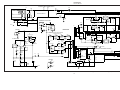
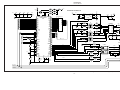
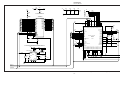
Schematic Diagrams............................................................................ 7-1
vi
List of Tables
Table
Title
1-1.
1-2.
1-3.
1-4.
1-5.
1-6.
1-7.
1-8.
1-9.
1-10.
1-11.
1-12.
1-13.
1-14.
1-15.
1-16.
1-17.
1-18.
1-19.
1-20.
1-21.
1-22.
1-23.
1-24.
1-25.
1-26.
1-27.
1-28.
1-29.
1-30.
1-31.
1-32.
1-33.
1-34.
1-35.
Summary of 2640A/2645A Specifications............................................. 1-4
Summary of 2640A/2645A Measurement Capabilities ......................... 1-4
Summary of 2640A/2645A Features...................................................... 1-5
Models, Options and Accessories .......................................................... 1-6
2640A/2645A General Specifications.................................................... 1-9
Environmental Specifications ................................................................ 1-10
2640A/2645A DIGITAL I/O Specification............................................ 1-10
2640A/2645A Trigger In (TI) Specification .......................................... 1-11
2640A/2645A Trigger Out (TO) Specification...................................... 1-11
2640A/2645A Master Alarm (MA) Specification ................................. 1-11
2640A/2645A Totalizer Specification ................................................... 1-12
2640A/2645A Real-Time Clock and Calendar ...................................... 1-12
2640A DC Voltage General Specifications ........................................... 1-13
2640A DC Voltage Range and Resolution Specifications..................... 1-13
2640A DC Voltage Accuracy Specifications......................................... 1-14
2640A AC Voltage General Specifications ........................................... 1-14
2640A AC Voltage Range and Resolution Specifications..................... 1-15
2640A AC Voltage Accuracy Specifications......................................... 1-15
2640A Four-Wire Resistance Temperature Coefficient......................... 1-16
640A Four-Wire Resistance Range and Resolution Specifications ....... 1-16
2640A Four-Wire Resistance Accuracy Specifications ......................... 1-16
2640A Four-Wire RTD Temperature Coefficient.................................. 1-17
2640A Four-Wire RTD Specifications .................................................. 1-17
2640A Thermocouple General Specifications ....................................... 1-18
2640A Thermocouple Specifications ..................................................... 1-18
2640A Frequency Accuracy Specifications ........................................... 1-19
2640A Frequency Sensitivity Specifications ......................................... 1-20
2645A DC Voltage General Specifications ........................................... 1-20
2645A DC Voltage Resolution and Repeatability Specifications.......... 1-21
2645A DC Voltage Accuracy Specifications......................................... 1-21
2645A AC Voltage General Specifications ........................................... 1-21
2645A AC Voltage Range and Resolution Specifications..................... 1-22
2645A AC Voltage Accuracy Specifications......................................... 1-22
2645A Four-Wire Resistance Temperature Coefficient......................... 1-23
2645A Four-Wire Resistance Range and Resolution Specifications ..... 1-23
vii
Page
NetDAQ
Service Manual
1-36.
1-37.
1-38.
1-39.
1-40.
1-41.
1-42.
2-1.
2-2.
2-3.
2-4.
2-5.
2-6.
2-7.
2-8.
2-9.
2-10.
2-11.
2-12.
2-13.
2-14.
2-15.
2-16.
2-17.
2-18.
2-19.
2-20.
2-21.
2-22.
4-1.
4-2.
4-3.
4-4.
4-5.
4-6.
4-7.
4-8.
5-1.
5-2.
5-3.
5-4.
5-5.
5-6.
5-7.
5-8.
5-9.
5-10.
5-10.
5-10.
5-10.
5-10.
5-10.
5-11.
5-12.
2645A Four-Wire Resistance Accuracy Specifications ......................... 1-23
2645A Four-Wire RTD Temperature Coefficient.................................. 1-24
2645A Four-Wire RTD Specifications .................................................. 1-24
2645A Thermocouple General Specifications ....................................... 1-24
2645A Thermocouple Specifications ..................................................... 1-25
2645A Frequency Accuracy Specifications ........................................... 1-26
2645A Frequency Sensitivity Specifications ......................................... 1-26
Microprocessor Interrupt Sources .......................................................... 2-16
Booting Microprocessor Memory Map.................................................. 2-17
nstrument Microprocessor Memory Map............................................... 2-17
A2 Display Power Supply Connections ................................................. 2-27
Front Panel Switch Scanning ................................................................. 2-28
Display Initialization Modes .................................................................. 2-30
Range of Buffer Amplifier ..................................................................... 2-34
Measurement Matrix for DC Volts ........................................................ 2-35
Measurement Matrix for Ohms .............................................................. 2-36
Measurement Matrix for AC Volts ........................................................ 2-37
Analog/Digital Converter Measurement Cycle...................................... 2-39
Tree Bits ................................................................................................. 2-50
Channel Bits ........................................................................................... 2-50
Tree and Channel Switch Settling Times............................................... 2-50
Function Relays...................................................................................... 2-51
Function Relay Settling Time................................................................. 2-51
Stallion Switch Settings ......................................................................... 2-52
Signal Conditioning Settling Time......................................................... 2-53
A/D Command Codes............................................................................. 2-55
A/D Readings to Average to Obtain a Measurement ............................. 2-58
Frequency Sensitivity ............................................................................. 2-60
A/D Readings to Average to Obtain a Reference
Balance Measurement ............................................................................ 2-61
Recommended Test Equipment.............................................................. 4-4
RS-232 Instrument Configuration for Calibration Procedures............... 4-28
Calibration Commands........................................................................... 4-36
Manual Calibration Command Responses ............................................. 4-37
Manual VDC Calibration ....................................................................... 4-37
Manual VAC Calibration ....................................................................... 4-39
Manual Resistance Calibration .............................................................. 4-40
Manual Frequency Calibration............................................................... 4-41
Selftest Error Codes ............................................................................... 5-4
FLASH ROM Parameter Defaults ......................................................... 5-5
Corrective Action for Background Error Checking ............................... 5-6
Instrument Firmware Descriptions ......................................................... 5-8
Instrument Default COMM Parameters ................................................. 5-9
Instrument Configuration ....................................................................... 5-11
RS232 Command Set ............................................................................. 5-12
Power-on/Reset Instrument State ........................................................... 5-14
Range Settings ........................................................................................ 5-18
Selftest Error Codes ............................................................................... 5-20
Relating Selftest Errors to Instrument Problems.................................... 5-21
Relating Selftest Errors to Instrument Problems.................................... 5-22
Relating Selftest Errors to Instrument Problems.................................... 5-23
Relating Selftest Errors to Instrument Problems.................................... 5-24
Relating Selftest Errors to Instrument Problems.................................... 5-25
Hints for Troubleshooting ...................................................................... 5-26
A1 Main PCA Jumper Positions ............................................................ 5-27
viii
Tables (continued)
5-13.
5-14.
5-15.
5-16.
6-1.
6-2.
6-3.
6-4.
6-5.
6-6.
A2 Display PCA Initialization Routines ................................................ 5-29
A3 A/D Converter PCA Jumper Positions ............................................. 5-32
Calibration Constants ............................................................................. 5-35
Files on the Firmware Diskette .............................................................. 5-37
2640A/2645A Final Assembly............................................................... 6-5
A1 Main PCA Assembly ........................................................................ 6-10
A2 Display PCA Assembly .................................................................... 6-15
2640A A3 A/D Converter PCA Assembly............................................. 6-17
2645A A3 A/D Converter PCA Assembly............................................. 6-22
A4 Analog Input PCA Assembly ........................................................... 6-27
ix
NetDAQ
Service Manual
x
List of Figures
Figure
1-1.
2-1.
2-2.
2-3.
2-4.
2-5.
2-6.
2-7.
2-8.
2-9.
2-10.
2-11.
2-12.
2-13.
2-14.
2-15.
2-16.
3-1.
3-2.
3-3.
4-1.
4-2.
4-3.
4-4.
4-5.
4-6.
4-7.
4-8.
5-1.
5-2.
5-3.
6-1.
6-1.
6-2.
Title
Page
2640A/2645A NetDAQ Networked Data Acquisition Units ................. 1-3
Interconnection Diagram........................................................................ 2-5
Overall Functional Block Diagram ........................................................ 2-6
Power Supply Block Diagram ................................................................ 2-7
Command Byte Transfer Waveforms..................................................... 2-29
Grid Control Signal Timing ................................................................... 2-30
Grid-Anode Timing Relationships ......................................................... 2-31
A3 A/D Converter Block Diagram......................................................... 2-32
DC Volts 300V Range Simplified Schematic ........................................ 2-35
RTD Measurement Simplified Schematic.............................................. 2-36
AC Volts 3V Range Simplified Schematic ............................................ 2-38
Integrator Output Waveform for Input Near 0 ....................................... 2-40
Integrator Output Waveform for Input Near + Full Scale...................... 2-41
Integrator Output Waveform for Input Near - Full Scale....................... 2-41
A/D Timing (2645A Normal Reading) .................................................. 2-54
A/D Timing (2640A Normal Reading, 2640A and
2645A Reference Balance)..................................................................... 2-54
A/D Status Signals.................................................................................. 2-55
Replacing the Fuse ................................................................................. 3-6
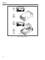
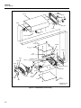
2640A and 2645A Assembly Details ..................................................... 3-8
Power Input Connections at the Power Switch ...................................... 3-14
Performance Test Setup ......................................................................... 4-5
Two-Terminal Connections to 5700A.................................................... 4-5
Four-Terminal Connections to the Universal Input Module (Resistor) . 4-15
Four-Terminal Connections to the Universal Input Module (5700A) ... 4-16
Instrument and Host Computer Calibration Setup ................................. 4-27
Universal Input Module Calibration Connections ................................. 4-27
Two-Wire Calibration Connection......................................................... 4-29
Four-Wire Calibration Connection......................................................... 4-29
Display Test Pattern #1 .......................................................................... 5-29
Display Test Pattern #2 .......................................................................... 5-30
Connection to A3P1 for Loading A/D Firmware................................... 5-39
2640A/264A5 Final Assembly............................................................... 6-9
701/702 Final Assembly......................................................................... 6-9
A1 Main PCA Assembly ........................................................................ 6-14
xi
NetDAQ
Service Manual
6-2.
6-3.
6-4.
6-5.
6-6.
A1 Power Supply PCA........................................................................... 6-14
A2 Display PCA Assembly .................................................................... 6-16
2640A A3 A/D Converter PCA Assembly............................................. 6-21
2645A A3 A/D Converter PCA Assembly............................................. 6-26
A4 Analog Input PCA Assembly ........................................................... 6-28
xii
Chapter 1
Introduction and Specification
Title
1-1.
1-2.
1-3.
1-4.
1-5.
1-6.
1-7
1-8.
1-9.
1-10.
1-11.
1-12.
1-13.
1-14.
1-15.
1-16.
1-17.
1-18.
1-19.
1-20.
1-21.
1-22.
1-23.
1-24.
1-25.
1-26.
1-27.
1-28.
Page
Introduction ............................................................................................ 1-3
Options and Accessories ........................................................................ 1-6
Instrument Connector Set, 2620A-100.............................................. 1-6
Host Computer Ethernet Interfaces ................................................... 1-6
Interconnection Cables and Components .......................................... 1-6
Operating Instructions ............................................................................ 1-7
Organization of the Service Manual ...................................................... 1-7
Conventions............................................................................................ 1-8
Specifications ......................................................................................... 1-8
2640A/2645A Combined Specifications........................................... 1-8
2640A/2645A General Specifications.......................................... 1-9
2640A/2645A Environmental Specifications............................... 1-10
2640A/2645A Input/Output Capabilities ..................................... 1-10
Digital I/O.................................................................................1-10
Trigger In..................................................................................1-11
Trigger Out ...............................................................................1-11
Master Alarm............................................................................1-11
2640A/2645A Totalizer................................................................ 1-12
2640A/2645A Real-Time Clock and Calendar ............................ 1-12
2640A Specifications ........................................................................ 1-13
2640A DC Voltage Measurement Specifications ........................ 1-13
2640A AC Voltage Measurement Specifications ........................ 1-14
2640A Four-Wire Resistance Measurement Specifications......... 1-16
2640A Two-Wire Resistance Measurement Specifications......... 1-16
2640A Four-Wire RTD per ITS-1990 Measurement
Specifications ............................................................................... 1-17
2640A Two-Wire RTD per ITS-1990 Measurement
Specifications ............................................................................... 1-17
2640A Thermocouple per ITS-1990 Measurement
Specifications. .............................................................................. 1-18
2640A Frequency Measurement Specifications........................... 1-19
1-1
NetDAQ
Service Manual
1-29.
1-30.
1-31.
1-32.
1-33.
1-34.
1-35.
1-36.
1-2
2645A Specifications ........................................................................ 1-20
2645A DC Voltage Measurement Specifications ........................ 1-20
2645A AC Voltage Measurement Specifications ........................ 1-21
2645A Four-Wire Resistance Measurement Specifications......... 1-23
2645A Two-Wire Resistance Measurement Specifications......... 1-23
2645A Four-Wire RTD per ITS-1990 Measurement
Specifications ............................................................................... 1-24
2645A Thermocouple per ITS-1990 Measurement
Specifications. .............................................................................. 1-24
2645A Frequency Measurement Specifications........................... 1-26
Introduction and Specification
Introduction
Introduction
1
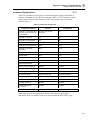
1-1.
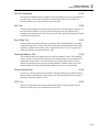
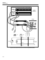
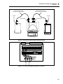
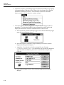
This Service Manual supports performance testing, calibration, servicing, and
maintenance of the 2640A NetDAQ™ and 2645A NetDAQ networked data acquisition
units (Figure 1-1). NetDAQ networked data acquisition units are 20-channel front ends
that operate in conjunction with a host computer to form a networked data acquisition
system. The host computer and instruments are interconnected using an Ethernet
network, and the host computer runs the NetDAQ Logger for Windows application to
provide an operating environment for the instruments, including testing and calibration.
The 2640A and 2645A networked data acquisition units are identical in operation and
appearance, and vary only in emphasis: The 2640A emphasizes precision and supports
up to 100 measurements per second, with 5 ½ digits of resolution, .02% accuracy, and
150-volt common mode voltage (300 volts on channels 1 and 11), while the 2645A
emphasizes increased measurement speed supporting up to 1000 measurements per
second, with 4 ½ digits of resolution, .04% accuracy, and 50-volt common mode voltage.
Refer to Table 1-1 for a summary of instrument specifications. For complete instrument
specifications, see “Specifications” later in this chapter.
The instruments measure dc volts, ac volts, ohms, temperature, frequency, and dc
current. Temperature measurements use thermocouples or resistance-temperature
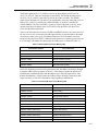
detectors (RTDs). Refer to Table 1-2 for a summary of instrument measurement
capabilities. In addition, there are eight digital input/output lines, one totalizing input,
one external trigger input, one trigger output, and one master alarm output. The
instruments can be ac or dc powered. An RS-232 serial port is supplied for servicing and
maintenance procedures.
The term "instrument" is used in this manual to refer to both units. The model number
(2640A or 2645A) is used when discussing characteristics unique to one instrument.
Instrument assemblies are identical except for the A3 Analog/Digital Converter printed
circuit assembly (pca), which is specific to the 2640A (mechanical switching for
measurement signals) and 2645A (solid-state switching for measurement signals).
The instrument is designed for bench-top, field service, and system applications. A dual
vacuum-fluorescent display uses combinations of alphanumeric characters and
descriptive annunciators to provide prompting and measurement information during
setup and operation modes. Some features provided by the instrument are listed in Table
1-3. For additional information regarding instrument features and capabilities, refer to
the NetDAQ Users Manual (PN 942623).
NetDAQ
NETWORKED DATA ACQUISITION UNIT
REM SCAN
MON
V
CH
DC
CAL
ENABLE
COMM
DIO
MON
ENTER
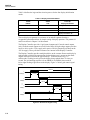
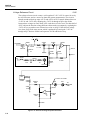
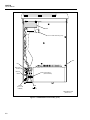
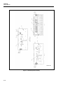
Figure 1-1. 2640A/2645A NetDAQ Networked Data Acquisition Units
1-3
NetDAQ
Service Manual
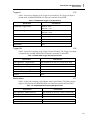
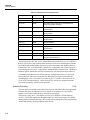
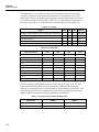
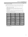
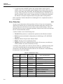
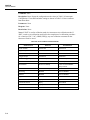
Table 1-1. Summary of 2640A/2645A Specifications
Specification
2640A
2645A
Maximum Normal Mode Voltage
150/300V [1]
50V
Maximum Common Mode
Voltage
150/300V [1]
50V
Input (Overload) Protection
1600V
300V
Maximum Reading Rates
143 readings/second
1000 readings/second
(Volts DC Only)
(scanning 20 channels)
(scanning 20 channels)
Maximum Single Channel Scan
80 readings/second
250 readings/second
Reading Rates [2]
(Drift Correction enabled)
(Drift Correction enabled)
120 readings/second
400 readings/second
(Drift Correction disabled)
(Drift Correction disabled)
0.02%
0.04%
0.3°C
0.6°C
Resistance-Temperature
Detectors (RTDs) Resolution
0.003°C
0.03°C
Resistance-Temperature
Detectors (RTDs) Accuracy
0.12°C
0.2°C
Time to Change Functions
6 ms
6 ms
Volts DC Accuracy (90 day),
1V dc input
Thermocouple Accuracy
(90 day)
(Between V dc, V ac,
Frequency, and Ohms)
[1] The 300V value is for channels 1 and 11 only; the 150V value is for all other channels.
[2] Drift Correction refers to an automatic internal measurement step performed with each
scan to correct for drift due to changes in ambient temperature and humidity.
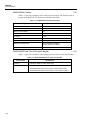
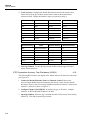
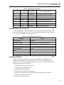
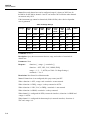
Table 1-2. Summary of 2640A/2645A Measurement Capabilities
Capability
1-4
2640A
2645A
Volts DC Measurements
Ranges: 90 mV
300 mV
3V
30V
150/300V [1]
Autorange
Ranges: 90 mV
300 mV
3V
30V
50V
Autorange
Volts AC Measurements
Ranges: 300 mV
3V
30V
150/300V [1]
Autorange
Ranges: 300 mV
3V
30V
Autorange
Resistance Measurements
Ranges: 300 Ω
3 kΩ
30 kΩ
300 kΩ
3 MΩ
Autorange
Ranges: 30 kΩ
300 kΩ
3 MΩ
Autorange
Introduction and Specification
Introduction
1
Table 1-2. Summary of 2640A/2645A Measurement Capabilities (cont)
Capability
2640A
Temperature Measurements
(Thermocouple) [2]
Thermocouples:
J
2645A
Thermocouples:
J
K R S E
T B C N
T B C N
Temperature Measurements
K R S E
RTD R0: 10 to 1010
(None)
RTD R0: 10 to 1010
RTD R0: 10 to 1010
Frequency Measurements [3]
Ranges:
Autorange
Ranges:
Autorange
Amperes DC Measurements [4]
Ranges:
4 to 20 mA
Ranges:
4 to 20 mA
(RTD) (Two-wire)
Temperature Measurements
(RTD) (Four-wire)
0 to 100 mA
0 to 100 mA
[1] 300V range available only on channels 1 and 11.
[2] Open thermocouple detection is supported on a per-channel basis.
[3] Minimum frequency is 20 Hz. Signal strength must be at least 50 mV ac rms.
[4] Shunt resistor required (enter value; default is 10 ohms). The 4 to 20 mA scale displayed as
0% (4 mA) to 100% (20 mA).
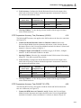
Table 1-3. Summary of 2640A/2645A Features
Feature
Description
Analog Channels
20 (channels 1 to 20)
Computed Channels
10 (channels 21 to 30)
Alarm Limits
Two per channel
Mx+B Scaling
Any configured channel (1 to 30)
Scan Triggering
Interval/External/Alarm Trigger
Channel Monitoring
Any configured channel, scanning or not scanning
Setup and Operation
Via host computer
Communications Ports
Ethernet 10BASE2 and 10BASE-T
Primary Power
AC - 107 to 264V ac, 50/60 Hz
DC - 9 to 16V dc
Nonvolatile Memory (unaffected by cycling
instrument power)
Instrument parameters: Base Channel Number,
Line Frequency, Network Type, Socket Port, IP
Address, Baud Rate. (See Chapter 2.)
Permanent Data Storage
Via host computer
Real-Time Trend Plotting
Via host computer
1-5
NetDAQ
Service Manual
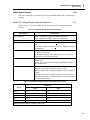
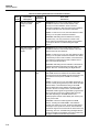
Options and Accessories
1-2.
Table 1-4 summarizes the available models, options and accessories, including
measurement transducers, software, connector sets, Ethernet interfaces, cables, and
components.
Table 1-4. Models, Options and Accessories
Model
Description
2640A
NetDAQ Instrument
2645A
NetDAQ Instrument
264XA-901
NetDAQ Logger for Windows (Isolated Network)
264XA-902
NetDAQ Logger for Windows (General Network)
264XA-902U
NetDAQ Logger for Windows Network (Upgrade Kit)
264XA-801
Ethernet Card
264XA-802
Parallel-to-LAN Adapter (10BASE2)
80i-410
Clamp-On DC/AC Current Probe
80i-1010
Clamp-On DC/AC Current Probe
2620A-100
I/O connector set, including Universal Input Module, DIGITAL I/O
and ALARM/TRIGGER I/O connectors.
2620A-101
4-20 mA Current Shunt Strip
942615
NetDAQ Service Manual
Y2641
19-inch Rackmount Kit
Y2643
4-meter Cable Kit
Instrument Connector Set, 2620A-100
1-3.
The 2620A-100 is a complete set of input connectors: one Universal Input Module, one
ALARM/TRIGGER I/O connector, and one DIGITAL I/O connector. Each instrument
comes with a 2620A-100 Instrument Connector Set. The use of additional connector sets
allows quick equipment interface to several wiring setups.
Host Computer Ethernet Interfaces
1-4.
The 264XA-801 is the recommended Ethernet card and the 264XA-802 is the
recommended Parallel-to-LAN Adapter for host computer installations.
Interconnection Cables and Components
Cables for equipment interconnection can be purchased as an option or fabricated.
Ethernet interconnection components such as BNC "T" and 50-ohm terminations are
available from any components supplier.
1-6
1-5.
Introduction and Specification
Operating Instructions
Operating Instructions
1
1-6.
Full operating instructions are provided in the NetDAQ User Manual (PN 942623). Refer
to the User Manual as necessary during the maintenance and repair procedures presented
in this Service Manual.
Organization of the Service Manual
1-7.
This manual focuses on performance tests, calibration procedures, and component-level
repair of the 2640A and 2645A networked data acquisition units. To that end, manual
chapters are often interdependent; effective troubleshooting may require not only
reference to the troubleshooting procedures in Chapter 5, but also some understanding of
the detailed Theory of Operation in Chapter 2 and some tracing of circuit operation in
the Schematic Diagrams presented in Chapter 7.
Often, scanning the table of contents yields an appropriate place to start using the
manual. A comprehensive table of contents is presented at the front of the manual; local
tables of contents are also presented at the beginning of each chapter for ease of
reference. If you know the topic name, the index at the end of the manual is probably a
good place to start.
The following descriptions introduce the manual:
Chapter 1 - Introduction and Specifications Introduces the instrument, describing its
features, options, and accessories. This chapter also discusses use of the Service Manual
and the various conventions used in describing the circuitry. Finally, a complete set of
specifications is presented.
Chapter 2 - Theory of Operation This chapter first categorizes the instrument’s
circuitry into functional blocks, with a description of each block’s role in overall
operation. A detailed circuit description is then given for each block. These descriptions
explore operation to the component level and fully support troubleshooting procedures
defined in Chapter 5.
Chapter 3 - General Maintenance Provides maintenance information covering
handling, cleaning, and fuse replacement. Access and reassembly procedures are also
explained in this chapter.
Chapter 4 - Performance Testing and Calibration This chapter provides performance
verification procedures, which relate to the specifications presented in Chapter 1. To
maintain these specifications, a full calibration procedure is also presented.
Chapter 5 - Diagnostic Testing and Troubleshooting The troubleshooting procedures
presented in this chapter rely closely on both the Theory of Operation presented in
Chapter 2, the Schematic Diagrams shown in Chapter 7, and the access information
provided in Chapter 3.
Chapter 6 - List of Replaceable Parts Includes parts lists for all standard assemblies.
Information on how and where to order parts is also provided.
Chapter 7 - Schematic Diagrams Includes schematic Diagrams for all standard and
optional assemblies. A list of mnemonic definitions is also included to aid in identifying
signal name abbreviations.
1-7
NetDAQ
Service Manual
Conventions
1-8.
Throughout the manual set, certain notational conventions are used. A summary of these
conventions follows:
•
Instrument Reference The term "instrument" is used in this manual to refer to both
the 2640A NetDAQ and 2645A NetDAQ networked data acquisition units. The
model number (2640A or 2645A) is used when discussing characteristics unique to
one instrument.
•
Printed Circuit Assembly The term "pca" is used to represent a printed circuit
board and its attached parts.
•
Signal Logic Polarity On schematic Diagrams, a signal name followed by a "*"
character is active (or asserted) low. Signals not so marked are active high.
•
Circuit Nodes Individual pins or connections on a component are specified with a
dash (-) following the assembly and component reference designators. For example,
pin 19 of U30 on assembly A1 would be A1U30-19.
•
Front Panel Interface User Notation For front panel operation, XXX, an
uppercase word or symbol without parentheses indicates a button to be pressed by
the user. Buttons can be pressed in four ways:
1. Press a single button to select a function or operation.
2. Press a combination of buttons, one after the other.
3. Press and hold down a button; then press another button.
4. Press multiple buttons simultaneously.
Computer Interface User Notation For computer interface operation:
XXX An uppercase word without parentheses identifies a command by name.
<XXX> Angle brackets around all uppercase letters mean press the <XXX> key.
(xxx) A lowercase word in parentheses indicates a keyboard input.
•
Specifications
1-9.
Specifications are divided into three sections. The first section contains the combined
specifications that apply equally to both the 2640A and 2645A instruments. The second
section contains specifications that apply only to the 2640A instrument. The third section
contains specifications that apply only to the 2645A instrument.
2640A/2645A Combined Specifications
1-10.
The following specifications apply equally to both the 2640A and 2645A instruments.
The topics include:
1-8
•
•
2640A/2645A General Specifications
2640A/2645A Environmental Specifications
•
2640A/2645A Digital I/O and Totalizer Interface
Introduction and Specification
Specifications
2640A/2645A General Specifications
1
1-11.
Table 1-5 provides the general specifications for the 2640A and 2645A instruments.
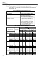
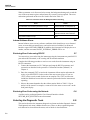
Table 1-5. 2640A/2645A General Specifications
Specification
Characteristic
Channel Capacity
20
I/O Lines Total
12
Size
9.3 cm (3.67 in) high, 21.6 cm (8.5 in) wide, 36.2 cm (14.28 in) deep
Weight
Net, 4 kg (8.8 lb.) Shipping, 6.0 kg (13.2 lb.)
Power
107 to 264V ac (no switching required), 45 to 65 Hz, 15 VA maximum
9V dc to 16V dc, 6W maximum. Specifications are for 50 or 60 Hz operation.
If both sources are applied simultaneously, ac voltage is used if it exceeds
approximately 8 times the dc voltage. Automatic switchover occurs between ac
and dc without interruption.
Standards
Both instruments comply with:
IEC 1010-1
UL 1244
CSA Bulletin 556B
ANSI/ISA-S8201-1988
CSA C22.2 No. 101.1-92
Vfg. 243/1991 (when shielded cables are used)
FCC-15B, Class B level (when shielded cables are used)
Serial Interface
(RS-232C)
Connector: 9 pin male (DB-9P)
Signals: TX, RX, DTR, RTS, GND
Modem Control: full duplex
Baud rates: 4800, 9600, 19200, 38400
Data format: 8 data bits, no parity bit, one stop bit
Flow control: XON/XOFF
Echo: Off
Common Mode
Voltage
2640A 150V (300V on channels 1 and 11)
2645A 50V dc or 30V ac rms.
Measurement Speed
(Scanning Rates)
2640A
Slow - 6 readings per second
Medium - 48 readings per second (60 Hz)
Fast - 143 readings per second (20 configured channels)
Single Channel - 120 readings per second
2645A
Slow - 54 readings per second (60 Hz)
Medium - 200 readings per second
Fast - 1000 readings per second (20 configured channels)
Single Channel - 400 readings per second
Accuracy of Medium
Scanning Rate
Equal to (Fast Accuracy Rate + Slow Accuracy Rate)/2
Additional error if
“Automatic drift
correction” is turned
off.
If the instrument is fully warmed-up at the time drift correction was disabled, i.e.,
turned on at least 1 hour earlier: 1/10 of the 90-day specification per °C change
in ambient temperature from the temperature when drift correction was disabled.
If the instrument was not fully warmed up at the time of drift correction was
disabled: add an error equal to the 90-day specification for instrument warmup
+1/10 of the 90-day specification per °C change in ambient temperature from the
temperature when drift correction was disabled.
1-9
NetDAQ
Service Manual
2640A/2645A Environmental Specifications
1-12.
Table 1-6 provides a summary of the environmental specifications for the 2640A/2645A.
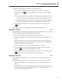
Table 1-6. Environmental Specifications
Specification
Characteristic
Warmup Time
1 hour to rated specifications -or- 15 minutes if relative humidity
(noncondensing) is 50% or less.
Operating Temperature
-10°C to 60°C (14°F to 140°F)
Storage Temperature
-40°C to +70°C (-40°F to +158F)
Relative Humidity
90% maximum for -10°C to 28°C (14°F to 82.4°F)
75% maximum for 28°C to 35°C (82.4°F to 95°F)
50% maximum for 35°C to 60°C (95°F to 140°F)
(3 MΩ range, reduce humidity rating by 25% for 1 hour warmup.
The 3 MΩ range meets full humidity ratings with 2-hour warmup.)
Altitude
Operating: 2,000m (6,561 ft) maximum
Non-operating: 12,200m (40,000 ft) maximum
Vibration
0.7g at 15 Hz
1.3g at 25 Hz
3g at 55 Hz
Shock
30g half-sine per Mil-T-28800
Bench handling per Mil-T-28800
2640A/2645A Input/Output Capabilities
1-13.
The following specifications include the input/output functions, including the Digital
I/O, Trigger Out, Trigger In, and Master Alarm output.
Digital I/O
1-14.
Table 1-7 provides a summary of the Digital I/O specifications for the 8 Digital I/O lines
(0 to 7). Digital I/O is located on the DIGITAL I/O connector, terminals 0 to 7, and
GND.
Table 1-7. 2640A/2645A DIGITAL I/O Specification
Specification
1-10
Characteristic
Maximum Input Voltage
30V
Minimum Input Voltage
-4V
Isolation
None (dc coupled)
Threshold
1.4V
Hysteresis
500 mV
Specification
Characteristic
Output Voltage - TTL Logical Zero
0.8V maximum for an Iout of -1.0 mA (1 LSTTL load)
Output Voltage - TTL Logical One
3.8V minimum for an Iout of 0.05 mA (1 LSTTL load)
Output Voltage - Non-TTL Load Zero
1.8V maximum for an Iout of -20 mA
Output Voltage - Non-TTL Load One
3.25V maximum for an Iout of -50 mA
Introduction and Specification
Specifications
Trigger In
1
1-15.
Table 1-8 provides a summary of the Trigger In specifications. The Trigger In input is
located on the ALARM/TRIGGER I/O connector, terminals TI and GND.
Table 1-8. 2640A/2645A Trigger In (TI) Specification
Specification
Characteristic
Logical High - Trigger not set
Minimum: 2.0V
Maximum: 7.0V
Logical Low - Trigger set
Minimum: -0.6V
Maximum: +0.8V
Compatibility
TTL or Contact Closure
Isolation
None (dc coupled)
Minimum Pulse Width
5 µs
Maximum Frequency
Nominal 400 Hz
Repeatability
3 ms
Trigger Out
1-16.
Table 1-9 provides a summary of the Trigger Out specifications. The Trigger Out output
is located on the ALARM/TRIGGER I/O connector, terminals TO and GND.
Table 1-9. 2640A/2645A Trigger Out (TO) Specification
Specification
Characteristic
TTL Logical Zero - Trigger Out Set
0.8V maximum for an Iout of -1.0 mA (1 LSTTL load)
TTL Logical One - Trigger Out Not Set
3.8V minimum for an Iout of 0.05 mA (1 LSTTL load)
Non-TTL Logical Zero - Trigger Out Set
1.8V maximum for an Iout of -20 mA
Non-TTL Logical One - Trigger Out Not Set
3.25V maximum for an Iout of -50 mA
Pulse Duration (Logic Low)
125 µs
Isolation
None
Master Alarm
1-17.
Table 1-10 provides a summary of the Master Alarm specifications. The Master Alarm
output is located on the ALARM/TRIGGER I/O connector, terminals MA and GND.
Table 1-10. 2640A/2645A Master Alarm (MA) Specification
Specification
Characteristic
TTL Logical Zero - Master Alarm Set
0.8V maximum for an Iout of -1.0 mA (1 LSTTL load)
TTL Logical One - Master Alarm Not Set
3.8V minimum for an Iout of 0.05 mA (1 LSTTL load)
Non-TTL Logical Zero - Master Alarm Set
1.8V maximum for an Iout of -20 mA
Non-TTL Logical One - Master Alarm Not Set
3.25V maximum for an Iout of -50 mA
Isolation
None
1-11
NetDAQ
Service Manual
2640A/2645A Totalizer
1-18.
Table 1-11 provides a summary of the Totalizer specifications. The Totalizer input is
located on the DIGITAL I/O connector, terminals Σ and GND.
Table 1-11. 2640A/2645A Totalizer Specification
Specification
Characteristic
Maximum Input Voltage
30V
Minimum Input Voltage
-4V
Minimum Peak Voltage
2V
Isolation
None (dc coupled)
Threshold
1.4V
Hysteresis
500 mV
Input Debouncing
None or 1.75 ms (selectable)
Maximum Transition Rate
5 kHz (Debounce disabled)
500 Hz (Debounce enabled)
Maximum Count
4,294,967,295
2640A/2645A Real-Time Clock and Calendar
1-19.
Table 1-12 provides a summary of the battery powered real-time clock and calendar.
Table 1-12. 2640A/2645A Real-Time Clock and Calendar
Specification
Accuracy
Battery Life
Characteristic
1 minute per month for 0°C to 50°C range
>15 unpowered instrument years for 0°C to 28°C (32°F to 82.4°F).
>6 unpowered instrument years for 0°C to 50°C (32°F to 122°F).
>4 unpowered instrument years for 50°C to 70°C (122°F to 158°F).
1-12
Introduction and Specification
Specifications
2640A Specifications
1
1-20.
This section includes specifications specific to the 2640A instrument by measurement
function.
2640A DC Voltage Measurement Specifications
1-21.
Tables 1-13 to 1-15 provide 2640A specifications for the dc voltage measurement
function.
Table 1-13. 2640A DC Voltage General Specifications
Specification
Characteristic
Input Impedance
100 MΩ in parallel with 300 pF maximum for ranges <=3V
10 MΩ in parallel with 100 pF maximum for ranges >3V
Normal Mode Rejection
50 dB minimum at 50 Hz/60 Hz +0.1%, Slow Rate
Common Mode Rejection
120 dB minimum at dc, 50 Hz/60 Hz +0.1%, 1 kΩ imbalance, Slow
Rate
80 dB minimum at dc, 50 Hz/60 Hz +0.1%, 1 kΩ imbalance, Medium
and Fast Rates
Channel-to-Channel Crosstalk
120 dB minimum Slow Rate (e.g., 30V dc on channel 1 may cause a
30 µV error on channel 2)
100 dB minimum Medium and Fast Rates (e.g., 1V dc on channel 1
may cause a 10 µV error on channel 2)
Temperature Coefficient
For % input: Add 1/10th the 90-day specification per °C above 28 °C
or below 18 °C
For floor error (V): Add 1/20th the 90-day specification per °C above
28 °C or below 18 °C
Maximum Input Voltage
The lesser voltage of:
300V from any terminal on channels 1 and 11 to earth;
150V from any terminal on channels 2 through 10, and 12 through 20
to earth;
300V from any terminal on channels 1 and 11 to any other terminal;
150V from any terminal on channels 2 through 10, and 12 through 20
to any other input terminal
Table 1-14. 2640A DC Voltage Range and Resolution Specifications
Resolution
Range
Slow
Fast
90 mV
0.3 µV
1 µV
300 mV
1 µV
3 µV
3V
10 µV
30 µV
30V
100 µV
300 µV
150V/300V
1 mV
3 mV
Note 300V range applies to channels 1 and 11 only.
1-13
NetDAQ
Service Manual
Table 1-15. 2640A DC Voltage Accuracy Specifications
Accuracy, 3σ + (% input + V)
18°C to 28°C
Range
90 Day
Slow
-10°C to 60°C
1 Year
Fast
1 Year
Slow
Fast
Slow
Fast
90 mV
.01%+7 µV
.01%+17 µV
.013%+8 µV
.013%+18 µV
.042%+18.2 µV
.042%+44.2 µV
300 mV
.01%+15 µV
.01%+30 µV
.013%+17 µV
.013%+35 µV
.042%+39 µV
.042%+78 µV
750 mV*
.01%+40 µV
.01%+70 µV
.013%+50 µV
.013%+80 µV
.042%+104 µV
.042%+182 µV
3V
.01%+0.1 mV
.01%+0.2 mV
.013%+0.15 mV
.013%+0.2 mV
.042%+0.26 mV
.042%+0.52 mV
30V
.01%+1.5 mV
.02%+3 mV
.013%+1.7 mV
.026%+3.5 mV
.042%+3.9 mV
.084%+7.8 mV
150/300V**
.01%+15 mV
.04%+30 mV
.013%+17 mV
.052%+35 mV
.042%+39 mV
.168%+78 mV
* The 750 mV range is used internally to the instrument and not user selectable.
** 300V range applies to channels 1 and 11 only.
2640A AC Voltage Measurement Specifications
1-22.
Tables 1-16 to 1-18 provide 2640A specifications for the ac voltage measurement
function.
Table 1-16. 2640A AC Voltage General Specifications
Specification
Characteristic
Input Impedance
1 MΩ in parallel with 100 pF
Maximum Crest Factor
3.0 Maximum
2.0 for rated accuracy
Crest Factor Error
For nonsinusoidal input signals with crest factors between 2 and 3 and
pulse widths >=100 µs, add 0.2% to the accuracy specifications.
Common Mode Rejection
80 dB minimum at dc, 50 Hz/60 Hz +0.1%, 1 kΩ imbalance, Slow Rate
Maximum Input Voltage
The lesser voltage of:
300V ac rms from any terminal on channels 1 and 11 to earth.
150V ac rms from any terminal on channels 2 through 10, and 12
through 20 to earth.
300V ac rms from any terminal on channels 1 and 11 to any other
terminal.
150V ac rms from any terminal on channels 2 through 10 and 12
through 20 to any other input terminal.
Maximum Volt-Hertz Product
2x10⁶ Volt-Hertz product on any range, normal mode input.
1x10⁶ Volt-Hertz product on any range, common mode input.
1-14
Temperature Coefficient
Linear interpolation between 2 applicable points for temperatures
between 28°C and 60°C, or -10°C and 18°C, e.g., if the applicable
specification at 28°C is 2% and the specification at 60°C is 3%, then the
specification at 40°C is (3%-2%)x(40-28)/(60-28)+2%=2.375%.
DC Component Error
The presence of a dc voltage will cause an indeterminate error in the
reading of the ac voltage on the input.
Introduction and Specification
Specifications
1
Table 1-17. 2640A AC Voltage Range and Resolution Specifications
Resolution
Range
Slow
Minimum Input for
Rate Accuracy
Fast
Full Scale
+30,000
+3,000
300 mV
10 µV
100 µV
20 mV
3V
100 µV
1 mV
200 mV
30V
1 mV
10 mV
2V
150/300V
10 mV
100 mV
20V
Note 300V range applies to channels 1 and 11 only.
Table 1-18. 2640A AC Voltage Accuracy Specifications
1 Year Accuracy + (%input + V) [1]
Range
Frequency
18°C to 28°C
Slow
300 mV
3V
30V
150/300V
Fast
-10°C to 60°C
Slow
Fast
20 to 50 Hz
3%+.25 mV
6%+.5 mV
3.5%+.25 mV
7%+.5 mV
50 to 150 Hz
0.4%+.25 mV
1%+.5 mV
0.5%+.25 mV
1.5%+.5 mV
150 Hz to 10 kHz
0.3%+.25 mV
1%+.5 mV
0.4%+.25 mV
1.5%+.5 mV
10 kHz to 20 kHz
0.4%+.25 mV
1%+.5 mV
0.7%+.25 mV
1.5%+.5 mV
20 kHz to 50 kHz
2%+.3 mV
3%+.5 mV
3%+.3 mV
4%+.5 mV
50 kHz to 100 kHz
5%+.5 mV
5%+1 mV
7%+.5 mV
8%+1 mV
20 to 50 Hz
3%+2.5 mV
6%+5 mV
3.5%+2.5 mV
7%+5 mV
50 to 150 Hz
0.4%+2.5 mV
1%+5 mV
0.5%+2.5 mV
1.2%+5 mV
150 Hz to 10 kHz
0.3%+2.5 mV
1%+5 mV
0.4%+2.5 mV
1.2%+5 mV
10 kHz to 20 kHz
0.4%+2.5 mV
1%+5 mV
0.5%+2.5 mV
1.2%+5 mV
20 kHz to 50 kHz
1%+3 mV
1.5%+6 mV
1.5%+3 mV
2%+6 mV
50 kHz to 100 kHz
2%+5 mV
3%+10 mV
3%+5 mV
4%+10 mV
20 to 50 Hz
3%+25 mV
6%+50 mV
3.5%+25 mV
7%+50 mV
50 to 150 Hz
0.4%+25 mV
1%+50 mV
0.5%+25 mV
1.2%+40 mV
150 Hz to 10 kHz
0.3%+25 mV
1%+50 mV
0.5%+25 mV
1.2%+40 mV
10 kHz to 20 kHz
0.4%+25 mV
1%+50 mV
0.5%+25 mV
1.2%+40 mV
20 kHz to 50 kHz
1%+30 mV
1.5%+60 mV
1%+30 mV
2%+50 mV
50 kHz to 100 kHz, V<20V
2%+50 mV
3%+100 mV
2.5%+50 mV
4%+100 mV
20 to 50 Hz
3%+.25V
6%+.5V
3.5%+.25V
7%+.5V
50 to 150 Hz
0.4%+.25V
1%+.5V
0.5%+.25V
1.2%+.4V
150 Hz to 2 kHz
Vx Hz<2 x10⁶
0.3%+.25V
1.2%+.5V
0.5%+.25V
1.4%+.4V
2 kHz to 20 kHz, V<100V
0.4%+.25V
1.6%+.5V
0.5%+.25V
1.8%+.4V
20 kHz to 50 kHz, V<40V
1%+.30V
2.0%+.6V
1.2%+.30V
2.5%+.5V
[1] Sinewave inputs>6% of scale and signals with crest factors <2.
1-15
NetDAQ
Service Manual
2640A Four-Wire Resistance Measurement Specifications
1-23.
Tables 1-19 to 1-21 provide 2640A specifications for the four-wire resistance
measurement function. The four-wire measurements use 2 input channels a decade apart,
e.g., channels 4 and 14.
Table 1-19. 2640A Four-Wire Resistance Temperature Coefficient
Specification
Characteristic
Add 1/10th the 90 day specification per °C
above 28°C or below 18°C.
Temperature Coefficient
Table 1-20. 2640A Four-Wire Resistance Range and Resolution Specifications
Resolution
Range
Slow
Current
Applied
Fast
Full Scale
Voltage
Maximum Voltage
Applied by Instrument
300Ω
1 mΩ
3mΩ
1 mA
300 mV
3.5V
3 kΩ
10 mΩ
30 mΩ
100 µA
300 mV
3.5V
30 kΩ
100 mΩ
300 mΩ
10 µA
300 mV
3.5V
300 kΩ
1Ω
3Ω
10 µA
3.0V
3.5V
3 MΩ
10Ω
30Ω
1 µA
3.0V
3.5V
Table 1-21. 2640A Four-Wire Resistance Accuracy Specifications
Accuracy, 3σ + (% input + V)
18°C to 28°C
Range
90 Day
-10°C to 60°C
1 Year
Slow
Fast
300Ω
.015%+20 mΩ
.02%+80 mΩ
3 kΩ
.02%+.3Ω
30 kΩ
300 kΩ
3 MΩ [1]
Slow
1 Year
Fast
Slow
Fast
.02%+50 mΩ
.02%+120 mΩ
.084%+126 mΩ
.084%+336 mΩ
.02%+.8Ω
.02%+.5Ω
.02%+1.2Ω
.084%+1.26Ω
.084%+3.36Ω
.03%+3Ω
.04%+10Ω
.03%+5Ω
.04%+15Ω
.126%+12.6Ω
.168%+42Ω
.1%+40Ω
.2%+100Ω
.1%+60Ω
.2%+150Ω
.42%+168Ω
.84%+420Ω
.25%+800Ω
.5%+10 kΩ
.25%+1 kΩ
.5%+1.5 kΩ
1.05%+3.36 kΩ
2.1%+4.2 kΩ
[1] The 3 MΩ range is susceptible to the absorption of humidity under extreme conditions. If the instrument is
operated normally within its specified temperature-humidity range, the 3 MΩ range meets its accuracy specifications.
However, if the instrument is “soaked” at 50°C, 90% relative humidity, the 3 MΩ range may require 1 hour of “dry-out”
time at 25°C, <40% relative humidity for each hour of soak time in order to achieve its specified accuracy.
2640A Two-Wire Resistance Measurement Specifications
1-24.
The 2640A specifications for the two-wire resistance measurement function is based on
the four-wire resistance measurement specification (above) except you add a nominal
5-ohm (10-ohm maximum) positive offset. This value varies for each channel and with
temperature
(nominal +1%/ºC).
1-16
Introduction and Specification
Specifications
2640A Four-Wire RTD per ITS-1990 Measurement Specifications
1
1-25.
Tables 1-22 and 1-23 provide 2640A specifications for the four-wire ResistanceTemperature Detector (RTD) measurement function. The four-wire measurements use 2
input channels a decade apart, e.g., channels 4 and 14.
Table 1-22. 2640A Four-Wire RTD Temperature Coefficient
Specification
Temperature Coefficient
Characteristic
To calculate RTD accuracy for temperatures between 28°C and 60°C, or
-10°C and 18°C, use a linear interpolation between the two applicable
points. For example, if the applicable specification at 28°C is 0.2 and the
specification at 60°C is 0.75, then the specification at 40°C is =(.75.2)x(40-28)/(60-28)+.2=0.406.
Table 1-23. 2640A Four-Wire RTD Specifications
Accuracy, 3σ
Resolution
Temperature
Slow
Fast
-200°C
0.003°C
0°C
90 Day
18°C to 28°C
Slow
Fast
0.007°C
0.06°C
0.16°C
0.003°C
0.007°C
0.09°C
100°C
0.003°C
0.007°C
300°C
0.003°C
600°C
0.003°C
1 Year
18°C to 28°C
Slow
1 Year
-10°C to 60°C
Slow
Fast
0.09°C
0.33°C
0.63°C
0.20°C
0.13°C
0.53°C
0.86°C
0.10°C
0.23°C
0.16°C
0.63°C
0.97°C
0.007°C
0.14°C
0.30°C
0.21°C
0.83°C
1.20°C
0.007°C
0.19°C
0.53°C
0.30°C
1.20°C
1.60°C
2640A Two-Wire RTD per ITS-1990 Measurement Specifications
1-26.
The 2640A specifications for the two-wire Resistance-Temperature Detector (RTD)
measurement function is based on the four-wire RTD measurement specification (above)
except you add a nominal 5-ohm (approximately 13°C) positive offset. This value varies
for each channel and temperature gradient (nominal +1%/ºC). Also note that the
resistance of the RTD wiring adds directly to the error. After 100 million operations of a
measurement channel, the offset will increase at an indeterminate rate.
1-17
NetDAQ
Service Manual
2640A Thermocouple per ITS-1990 Measurement Specifications
1-27.
Tables 1-24 to 1-25 provide 2640A specifications for the thermocouple measurement
function per ITS-1990.
Table 1-24. 2640A Thermocouple General Specifications
Specification
Characteristic
Input Impedance
100 MΩ minimum in parallel with 300 pF
Open Thermocouple Detect
Operates by injecting a small ac signal into the
input after each measurement. A
thermocouple resistance greater than 1k to
10k is detected as an open input.
Temperature Coefficient
To calculate Thermocouple accuracy for
temperatures between 28°C and 60°C, or
-10°C and 18°C, use a linear interpolation
between the two applicable points. For
example, if the applicable specification at
28°C is 0.6 and the specification at 60°C is
1.1, then the specification at 40°C is =(1.10.6)x(40-28)/(60-28)+0.6=0.7875.
Table 1-25. 2640A Thermocouple Specifications
Accuracy + °C
Thermocouple
Resolution
18°C to 28°C
90 Day
1 Year
1 Year
Type
Temperature °C
J
-100 to 80
.03
0.45
0.50
0.80
0.60
0.80
80 to 230
.02
0.35
0.50
0.70
0.60
0.80
230 to 760
.02
0.40
0.50
0.70
0.80
0.90
-100 to -25
.04
0.55
0.60
0.90
0.70
1.00
-25 to 120
.03
0.40
0.50
0.80
0.60
0.90
120 to 800
.03
0.50
0.65
0.90
1.00
1.20
800 to 1372
.03
0.70
1.00
1.30
1.60
1.90
-100 to -25
.05
0.65
0.75
1.20
0.80
1.30
-25 to 120
.05
0.55
0.60
1.00
0.70
1.10
120 to 1000
.04
0.45
0.60
0.90
1.00
1.20
1000 to 1300
.03
0.55
0.75
1.00
1.20
1.50
-100 to -25
.03
0.45
0.50
0.80
0.60
0.80
-25 to 20
.02
0.35
0.40
0.60
0.50
0.70
20 to 600
.02
0.30
0.40
0.60
0.50
0.80
600 to 1000
.02
0.40
0.50
0.70
0.90
1.00
-100 to 0
.04
0.60
0.65
1.00
0.70
1.10
0 to 150
.03
0.40
0.50
0.80
0.60
0.90
150 to 400
.02
0.30
0.40
0.60
0.60
0.80
K
N
E
T
1-18
-10°C to 60°C
Slow
Slow
Fast
Slow
Fast
Introduction and Specification
Specifications
1
Table 1-25. 2640A Thermocouple Specifications (cont)
Accuracy + °C
Thermocouple
Resolution
18°C to 28°C
90 Day
-10°C to 60°C
1 Year
1 Year
Type
Temperature °C
R
250 to 600
0.1
0.90
1.00
2.10
1.20
2.20
600 to 1500
0.1
0.80
0.90
1.80
1.30
2.00
1500 to 1767
0.1
0.85
0.85
1.90
1.70
2.50
250 to 1000
0.1
0.95
1.10
2.30
1.30
2.40
1000 to 1400
0.1
0.80
1.00
1.90
1.40
2.30
1400 to 1767
0.1
1.00
1.30
2.20
1.80
2.80
600 to 900
0.2
1.20
1.40
3.10
1.50
3.20
900 to 1200
0.2
0.90
1.00
2.20
1.20
2.40
1200 to 1820
0.1
0.75
1.00
1.90
1.30
2.20
0 to 150
0.2
0.80
0.90
1.60
1.00
1.70
150 to 650
0.1
0.65
0.75
1.40
1.00
1.50
650 to 1000
.05
0.65
0.85
1.40
1.20
1.80
1000 to 1800
.05
1.00
1.30
2.10
2.10
2.80
1800 to 2316
.05
1.60
2.10
3.20
3.40
4.60
S
B
C
Slow
Slow
Fast
Slow
Fast
2640A Frequency Measurement Specifications
1-28.
Tables 1-26 to 1-27 provide 2640A specifications for the frequency measurement
function.
Table 1-26. 2640A Frequency Accuracy Specifications
Frequency Measurement Accuracy, 1 Year, -10°C to 60°C
Range
Resolution
Slow
Accuracy + (% input + Hz)
Fast
Slow
Fast
15 Hz to 900 Hz
0.01 Hz
0.1 Hz
0.05%+0.02 Hz
0.05%+0.2 Hz
900 Hz to 9 kHz
0.1 Hz
1 Hz
0.05%+0.1 Hz
0.05%+1 Hz
9 kHz to 90 kHz
1 Hz
10 Hz
0.05%+1 Hz
0.05%+10 Hz
90 kHz to 900 kHz
10 Hz
100 Hz
0.05%+10 Hz
0.05%+100 Hz
1 MHz
100 Hz
1 kHz
0.05%+100 Hz
0.05%+1 kHz
1-19
NetDAQ
Service Manual
Table 1-27. 2640A Frequency Sensitivity Specifications
Frequency Measurement Sensitivity (Sinewave)
Frequency Range
Minimum Signal
Maximum Signal
15 Hz to 70 kHz
100 mV ac rms
V<150/300Vrms [1] and Vx Hz<2x10 6)
70 kHz to 100 kHz
100 mV ac rms
20V ac rms
100 kHz to 200 kHz
150 mV ac rms
10V ac rms
200 kHz to 300 kHz
150 mV ac rms
7V ac rms
300 kHz to 1 MHz
Linearly increasing from 150 mV ac
rms at 300 kHz to 2 V ac rms at 1 MHz
Linearly decreasing from 7 V ac rms
at 300 kHz to 2 V ac rms at 1 MHz
[1] 300V range applies to channels 1 and 11 only.
2645A Specifications
1-29.
This section includes specifications specific to the 2645A instrument by measurement
function.
2645A DC Voltage Measurement Specifications
1-30.
Tables 1-28 to 1-30 provide 2645A specifications for the dc voltage measurement
function.
Table 1-28. 2645A DC Voltage General Specifications
Specification
Input Impedance
Characteristic
100 MΩ in parallel with 300 pF maximum for ranges <=3V
10 MΩ in parallel with 100 pF maximum for ranges >3V
Normal Mode Rejection
50 dB minimum at 50 Hz/60 Hz +0.1%, Slow Rate
Common Mode Rejection
120 dB minimum at dc, 50 Hz/60 Hz +0.1%, 1 kΩ imbalance, Slow Rate
80 dB minimum at dc, 60 dB at 50 Hz/60 Hz +0.1%, 1 kΩ imbalance,
Medium and Fast Rates
Channel-to-Channel
Crosstalk
120 dB minimum Slow Rate (e.g., 30V dc on channel 1 may cause a 30 µV
error on channel 2)
80 dB minimum Medium and Fast Rates (e.g., 1V dc on channel 1 may
cause a 10 µV error on channel 2)
Temperature Coefficient
For % input: Add 1/10th the 90-day specification per °C above 28°C or
below 18°C.
For floor error (V): Add 1/20th the 90-day specification per °C above 28°C
or below 18°C.
Maximum Input Voltage
The lesser voltage of:
50V dc or 30V ac rms from any input terminal to earth
-or50V dc or 30V ac rms from any input terminal to any other input terminal
1-20
Introduction and Specification
Specifications
1
Table 1-29. 2645A DC Voltage Resolution and Repeatability Specifications
Resolution
Range
Slow
Fast
90 mV
3 µV
6 µV
300 mV
1 µV
3 µV
3V
10 µV
30 µV
30V
100 µV
300 µV
50V
1 mV
3 mV
Table 1-30. 2645A DC Voltage Accuracy Specifications
Accuracy, 3σ + (% input + V)
18°C to 28°C
Range
90 Day
Slow
-10°C to 60°C
1 Year
Fast
Slow
1 Year
Fast
Slow
Fast
90 mV
.01%+20 µV
.01%+50 µV
.013%+23 µV
.013%+50 µV
.042%+52 µV
.042%+130 µV
300 mV
.01%+40 µV
.01%+90 µV
.013%+49 µV
.013%+93 µV
.042%+104 µV
.042%+234 µV
750 mV*
.01%+90 µV
.01%+200 µV
.013%+105 µV
.013%+220 µV
.042%+273 µV
.042%+520 µV
3V
.01%+.3 mV
.01%+.6 mV
.013%+.38 mV
.013%+.64 mV
.042%+.78 mV
.042%+1.56 mV
30V
.01%+4 mV
.02%+8 mV
.013%+4.9 mV
.026%+9.5 mV
.042%+10.6 mV
.084%+20.3 mV
50V
.01%+30 mV
.04%+60 mV
.013%+40 mV
.052%+64 mV
.042%+78 mV
.168%+156 mV
*
The 750 mV range is used internally to the instrument and not user selectable.
2645A AC Voltage Measurement Specifications
1-31.
Tables 1-31 to 1-33 provide 2645A specifications for the ac voltage function.
Table 1-31. 2645A AC Voltage General Specifications
Specification
Characteristic
Input Impedance
1 MΩ in parallel with 100 pF
Maximum Crest Factor
3.0 maximum; 2.0 for rated accuracy
Crest Factor Error
For nonsinusoidal input signals with crest factors between 2 and 3 and
pulse widths >=100 µs, add 0.2% to the accuracy specifications.
Common Mode Rejection
80 dB minimum at dc, 50 Hz/60 Hz +0.1%, 1 kΩ imbalance, Slow Rate
Maximum Input Voltage
The lesser voltage of:
30V ac rms from any input terminal to earth.
30V ac rms from any terminal input to any other input terminal.
Maximum Volt-Hertz Product
2x10⁶ Volt-Hertz product on any range, normal mode input.
1x10⁶ Volt-Hertz product on any range, common mode input.
Temperature Coefficient
Linear interpolation between 2 applicable points for temperatures
between 28°C and 60°C, or -10°C and 18°C, e.g., if the applicable
specification at 28°C is 2% and the specification at 60°C is 3%, then the
specification at 40°C is (3%-2%)x(40-28)/(60-28)+2%=2.375%.
DC Component Error
The presence of a dc voltage will cause an indeterminate error in the
reading of the ac voltage on the input.
1-21
NetDAQ
Service Manual
Table 1-32. 2645A AC Voltage Range and Resolution Specifications
Resolution
Range
Slow
Fast
Minimum Input for
Rate Accuracy
Full Scale
+30,000
+3,000
300 mV
10 µV
100 µV
20 mV
3V
100 µV
1 mV
200 mV
30V
1 mV
10 mV
2V
Table 1-33. 2645A AC Voltage Accuracy Specifications
1 Year Accuracy + (%input + V) [1]
Range
Frequency
18°C to 28°C
Slow
300 mV
3V
30V
Fast
Slow
Fast
20 to 50 Hz
3%+.25 mV
6%+.5 mV
3.5%+.25 mV
7%+.5 mV
50 to 150 Hz
0.4%+.25 mV
0.8%+.5 mV
0.5%+.25 mV
1%+.5 mV
150 Hz to 10 kHz
0.3%+.25 mV
0.8%+.5 mV
0.4%+.25 mV
1%+.5 mV
10 kHz to 20 kHz
0.4%+.25 mV
1%+.5 mV
0.7%+.25 mV
1.5%+.5 mV
20 kHz to 50 kHz
2%+.3 mV
3%+.5 mV
3%+.3 mV
4%+.5 mV
50 kHz to 100 kHz
5%+.5 mV
5%+1 mV
7%+.5 mV
8%+1 mV
20 to 50 Hz
3%+2.5 mV
6%+5 mV
3.5%+2.5 mV
7%+5 mV
50 to 150 Hz
0.4%+2.5 mV
0.8%+5 mV
0.5%+2.5 mV
1%+5 mV
150 Hz to 10 kHz
0.3%+2.5 mV
0.6%+5 mV
0.4%+2.5 mV
1%+5 mV
10 kHz to 20 kHz
0.4%+2.5 mV
0.8%+5 mV
0.5%+2.5 mV
1%+5 mV
20 kHz to 50 kHz
1%+3 mV
1.5%+6 mV
1.5%+3 mV
2%+6 mV
50 kHz to 100 kHz
2%+5 mV
3%+10 mV
3%+5 mV
4%+10 mV
20 to 50 Hz
3%+25 mV
6%+50 mV
3.5%+25 mV
7%+50 mV
50 to 150 Hz
0.4%+25 mV
0.8%+50 mV
1.2%+25 mV
1.3%+40 mV
150 Hz to 10 kHz
0.4%+25 mV
0.8%+50 mV
1.2%+25 mV
1.3%+40 mV
10 kHz to 20 kHz
0.4%+25 mV
0.8%+50 mV
1.2%+25 mV
1.3%+40 mV
20 kHz to 50 kHz
1%+30 mV
1.5%+60 mV
1.2%+30 mV
2%+50 mV
50 kHz to 100 kHz, V<20V
2%+50 mV
3%+100 mV
2.5%+50 mV
4%+100 mV
[1] Sinewave inputs>6% of scale and signals with crest factors <2.
1-22
-10°C to 60°C
Introduction and Specification
Specifications
2645A Four-Wire Resistance Measurement Specifications
1
1-32.
Tables 1-34 to 1-36 provide 2645A specifications for the four-wire resistance
measurement function. The four-wire measurements use 2 input channels a decade apart,
e.g., channels 4 and 14.
Table 1-34. 2645A Four-Wire Resistance Temperature Coefficient
Specification
Characteristic
Add 1/10th the 90 day specification per °C above 28°C or below 18°C.
Temperature
Coefficient
Table 1-35. 2645A Four-Wire Resistance Range and Resolution Specifications
Resolution
Range
Slow
Current
Applied
Fast
Full Scale
Voltage
Maximum Voltage
Applied by Instrument
300Ω
10 mΩ
30 mΩ
1 mA
300 mV
3.5V
3 kΩ
100 mΩ
300 mΩ
100 µA
300 mV
3.5V
30 kΩ
1Ω
3Ω
10 µA
300 mV
3.5V
300 kΩ
10Ω
30Ω
10 µA
3.0V
3.5V
3 MΩ
100Ω
300Ω
1 µA
3.0V
3.5V
Table 1-36. 2645A Four-Wire Resistance Accuracy Specifications
Accuracy, 3σ + (% input + Ω)
18°C to 28°C
Range
90 Day
Slow
-10°C to 60°C
1 Year
Fast
Slow
1 Year
Fast
Slow
Fast
300Ω
.02%+60 mΩ
.02%+.1Ω
.02%+.1Ω
.02%+.2Ω
.084%+.25Ω
.084%+.42Ω
3 kΩ
.02%+.6Ω
.02%+2Ω
.02%+1Ω
.02%+3Ω
.084%+2.5Ω
.084%+8.4Ω
30 kΩ
.02%+6Ω
.2%+200Ω
.02%+10Ω
.2%+300Ω
.084%+25Ω
.84%+840Ω
300 kΩ
.5%+80Ω
1%+2 kΩ
.5%+150Ω
1%+3 kΩ
2.1%+336Ω
4.2%+8.4 kΩ
3 MΩ
1.3%+1 kΩ
2%+120 kΩ
1.3%+2 kΩ
2%+200 kΩ
5.46%+4.2 kΩ
8.4%+200 kΩ
2645A Two-Wire Resistance Measurement Specifications
1-33.
The 2645A specifications for the two-wire resistance measurement function is based on
the four-wire resistance measurement specification (above) except you add a 700 to 1000
ohm positive offset. This value varies for each channel and temperature gradient
(nominal +1%/ºC).
1-23
NetDAQ
Service Manual
2645A Four-Wire RTD per ITS-1990 Measurement Specifications
1-34.
Tables 1-37 and 1-38 provide 2645A specifications for the four-wire ResistanceTemperature Detector (RTD) measurement function. The four-wire measurements use 2
input channels a decade apart, e.g., channels 4 and 14. There is no two-wire RTD
capability for the 2645A.
Table 1-37. 2645A Four-Wire RTD Temperature Coefficient
Specification
Characteristic
Temperature Coefficient
To calculate RTD accuracy for temperatures between 28°C and
60°C, or -10°C and 18°C, use a linear interpolation between the two
applicable points. For example, if the applicable specification at
28°C is 0.2 and the specifications at 60°C is 0.75, then the
specification at 40°C =(.75-.2)x(40-28)/(60-28)+.2=.406.
Table 1-38. 2645A Four-Wire RTD Specifications
Accuracy, 3σ
Temperature
Resolution
Slow
Fast
90 Day
18°C to 28°C
Slow
Fast
1 Year
18°C to 28°C
Slow
1 Year
-10°C to 60°C
Slow
Fast
-200°C
0.03°C
0.06°C
0.16°C
0.25°C
0.25°C
0.62°C
1.10°C
0°C
0.03°C
0.06°C
0.20°C
0.31°C
0.31°C
0.85°C
1.30°C
100°C
0.03°C
0.06°C
0.23°C
0.34°C
0.34°C
0.95°C
1.40°C
300°C
0.03°C
0.06°C
0.30°C
0.41°C
0.41°C
1.18°C
1.70°C
600°C
0.03°C
0.06°C
0.53°C
0.63°C
0.63°C
1.62°C
2.12°C
2645A Thermocouple per ITS-1990 Measurement Specifications
1-35.
Tables 1-39 to 1-40 provide 2645A specifications for the thermocouple measurement
function per ITS-1990.
Table 1-39. 2645A Thermocouple General Specifications
Specification
1-24
Characteristic
Input Impedance
100 MΩ minimum in parallel with 300 pF
Open Thermocouple Detect
Operates by injecting a small ac signal into the input after each
measurement. A thermocouple resistance greater than 1 k to 10k is
detected as an open input.
Temperature Coefficient
To calculate Thermocouple accuracy for temperatures between 28°C
and 60°C, or -10°C and 18°C, use a linear interpolation between the
two applicable points. For example, if the applicable specification at
28°C is 0.6 and the specification at 60°C is 1.1, then the specification
at 40°C is =(1.1-0.6)x(40-28)/(60-28)+0.6=0.7875.
Introduction and Specification
Specifications
1
Table 1-40. 2645A Thermocouple Specifications
Accuracy + °C
Thermocouple
18°C to 28°C
Resolution
90 Day
-10°C to 60°C
1 Year
1 Year
Type
Temperature °C
J
-100 to 80
.3
0.8
0.9
1.6
0.9
1.7
80 to 230
.2
0.7
0.8
1.4
0.9
1.5
230 to 760
.2
0.7
0.8
1.3
1.0
1.5
-100 to -25
.4
1.0
1.1
2.0
1.2
2.1
-25 to 120
.3
0.8
0.9
1.7
1.0
1.8
120 to 1000
.3
0.9
1.1
1.8
1.5
2.2
1000 to 1372
.3
1.2
1.5
2.3
2.0
2.9
-100 to -25
.5
1.4
1.5
2.8
1.5
2.9
-25 to 120
.5
1.1
1.3
2.3
1.3
2.4
120 to 1000
.4
1.0
1.1
2.0
1.2
2.1
1000 to 1300
.3
1.0
1.2
1.9
1.6
2.4
-100 to -25
.3
0.8
0.9
1.5
1.0
1.6
-25 to 20
.2
0.7
0.7
1.2
0.8
1.3
20 to 600
.2
0.6
0.7
1.1
0.8
1.2
600 to 1000
.2
0.6
0.8
1.2
1.1
1.5
-100 to 0
.4
1.1
1.2
2.2
1.3
2.3
0 to 150
.3
0.9
1.0
1.7
1.0
1.8
150 to 400
.2
0.7
0.8
1.4
0.8
1.5
250 to 600
1
2.4
2.7
5.6
2.8
5.7
600 to 1500
1
2.0
2.3
4.6
2.4
4.8
1500 to 1767
1
2.0
2.3
4.5
2.8
5.1
250 to 1000
1
2.6
2.8
5.9
2.9
6.0
1000 to 1400
1
2.0
2.3
4.6
2.6
5.0
1400 to 1767
1
2.3
2.7
5.3
3.3
5.9
600 to 1200
2
3.6
3.9
8.5
4.0
8.6
1200 to 1550
2
2.1
2.4
5.0
2.6
5.2
1550 to 1820
1
2.0
2.3
4.7
2.7
5.0
0 to 150
2
1.9
2.0
4.0
2.1
4.2
150 to 650
1
1.6
1.7
3.5
1.8
3.6
650 to 1000
.5
1.4
1.7
3.2
2.0
3.5
1000 to 1800
.5
2.0
2.5
4.5
3.2
5.3
1800 to 2316
.5
3.1
3.8
6.8
5.1
8.1
K
N
E
T
R
S
B
C
Slow
Slow
Fast
Slow
Fast
1-25
NetDAQ
Service Manual
2645A Frequency Measurement Specifications
1-36.
Tables 1-41 to 1-42 provide 2645A specifications for the frequency measurement
function.
Table 1-41. 2645A Frequency Accuracy Specifications
Frequency Measurement Accuracy, 1 Year, -10°C to 60°C
Range
Resolution
Slow
Accuracy + (% input + Hz)
Fast
Slow
Fast
15 Hz to 900 Hz
0.01 Hz
0.1 Hz
0.05%+0.02 Hz
0.05%+0.2 Hz
900 Hz to 9 kHz
0.1 Hz
1 Hz
0.05%+0.1 Hz
0.05%+1 Hz
9 kHz to 90 kHz
1 Hz
10 Hz
0.05%+1 Hz
0.05%+10 Hz
90 kHz to 900 kHz
10 Hz
100 Hz
0.05%+10 Hz
0.05%+100 Hz
1 MHz
100 Hz
1 kHz
0.05%+100 Hz
0.05%+1 kHz
Table 1-42. 2645A Frequency Sensitivity Specifications
Frequency Range
1-26
Minimum Signal
Maximum Signal
15 Hz to 70 kHz
100 mV ac rms
30V ac rms
70 kHz to 100 kHz
100 mV ac rms
20V ac rms
100 kHz to 200 kHz
150 mV ac rms
10V ac rms
200 kHz to 300 kHz
150 mV ac rms
7V ac rms
300 kHz to 1 MHz
Linearly increasing from 150 mV ac
rms at 300 kHz to 2V ac rms at 1 MHz
Linearly decreasing from 7V ac rms
at 300 kHz to 2V ac rms at 1 MHz
Chapter 2
Theory of Operation
Title
2-1.
2-2.
2-3.
2-4.
2-5.
2-6.
2-7.
2-8.
2-9.
2-10.
2-11.
2-12.
2-13.
2-14.
2-15.
2-16.
2-17.
2-18.
2-19.
2-20.
2-21.
2-22.
2-23.
2-24.
2-25.
2-26.
2-27.
2-28.
2-29.
2-30.
Page
Introduction ............................................................................................
Functional Block Description.................................................................
A1 Main PCA Block Description ......................................................
Power Supply................................................................................
Digital Kernel ...............................................................................
Serial Communication (Guard Crossing) .....................................
Digital Inputs and Outputs............................................................
Ethernet Interface .........................................................................
A2 Display PCA Block Description ..................................................
A3 A/D Converter PCA Block Description.......................................
Analog Measurement Processor ...................................................
Input Protection ............................................................................
Input Signal Conditioning ............................................................
Analog-to-Digital (a/d) Converter................................................
Inguard Microcontroller ...............................................................
Channel Selection.........................................................................
Open Thermocouple Check ..........................................................
A4 Analog Input PCA Block Description .........................................
20-Channel Terminals ..................................................................
Reference Junction Temperature..................................................
Detailed Circuit Description ..................................................................
A1 Main PCA Circuit Description.....................................................
Power Supply Circuit Description................................................
Raw DC Supply ........................................................................
Auxiliary 6V Supply.................................................................
5V Switcher ..............................................................................
Inverter......................................................................................
Inverter Outguard Supply .........................................................
Inverter Inguard Supply............................................................
Power Fail Detection ................................................................
2-5
2-5
2-7
2-7
2-7
2-8
2-8
2-8
2-8
2-8
2-9
2-9
2-9
2-9
2-9
2-9
2-10
2-10
2-10
2-10
2-10
2-10
2-10
2-11
2-11
2-11
2-12
2-12
2-13
2-13
2-1
NetDAQ
Service Manual
2-31.
2-32.
2-33.
2-34.
2-35.
2-36.
2-37.
2-38.
2-39.
2-40.
2-41.
2-42.
2-43.
2-44.
2-45.
2-46.
2-47.
2-48.
2-49.
2-50.
2-51.
2-52.
2-53.
2-54.
2-55.
2-56.
2-57.
2-58.
2-59.
2-60.
2-61.
2-62.
2-63.
2-64.
2-65.
2-66.
2-67.
2-68.
2-69.
2-70.
2-71.
2-72.
2-73.
2-74.
2-75.
2-76.
2-77.
2-78.
2-2
Digital Kernel ...............................................................................
Reset Circuits............................................................................
Microprocessor .........................................................................
Address Decoding.....................................................................
Flash Memory...........................................................................
Static RAM ...............................................................................
Real-Time Clock.......................................................................
FPGA (Field Programmable Gate Array).................................
Serial Communication (Guard Crossing) .................................
RS-232 Interface.......................................................................
Ethernet Interface .....................................................................
Digital Inputs and Outputs............................................................
Digital Input Threshold ............................................................
Digital Input Buffers.................................................................
Digital and Alarm Output Drivers ............................................
Totalizer Input ..........................................................................
External Trigger Circuits ..........................................................
A2 Display PCA Circuit Description.................................................
Main PCA Connector ...................................................................
Front Panel Switches ....................................................................
Display..........................................................................................
Beeper Drive Circuit.....................................................................
Watchdog Timer and Reset Circuit ..............................................
Display Controller ........................................................................
A3 A/D Converter PCA Circuit Description .....................................
Stallion Chip.................................................................................
Input Protection ............................................................................
Input Signal Conditioning ............................................................
Function Relays ............................................................................
Channel Selection Circuitry .........................................................
DC Volts and Thermocouples Measurement Circuitry................
Ohms and RTD Measurement Circuitry.......................................
AC Volts Measurement Circuitry.................................................
Frequency Measurements.............................................................
Active Filter (ACV Filter) ............................................................
Voltage Reference Circuit ............................................................
Analog/Digital Converter Circuit .................................................
Autozero ...................................................................................
Integrate ....................................................................................
Deintegrate1..............................................................................
Deintegrate2..............................................................................
Overhead...................................................................................
Inguard Digital Kernel Circuitry ..................................................
Open Thermocouple Detect Circuitry............................................
A4 Analog Input PCA Circuit Description........................................
A1 Main to A3 A/D Converter Communications ..................................
Special Codes.....................................................................................
Resets .................................................................................................
2-13
2-14
2-14
2-16
2-18
2-18
2-19
2-19
2-21
2-21
2-22
2-24
2-24
2-24
2-25
2-25
2-25
2-26
2-26
2-27
2-28
2-28
2-29
2-29
2-31
2-33
2-33
2-33
2-33
2-34
2-34
2-36
2-37
2-37
2-37
2-38
2-39
2-39
2-40
2-42
2-42
2-42
2-42
2-43
2-43
2-44
2-44
2-44
Theory of Operation
Introduction
2
2-79.
Commands ......................................................................................... 2-45
2-80.
Perform Scan ................................................................................ 2-45
2-81.
Perform Self-Test ......................................................................... 2-46
2-82.
Return Main Firmware Version.................................................... 2-46
2-83.
Return Boot Firmware Version .................................................... 2-47
2-84.
Set Global Configuration.............................................................. 2-47
2-85.
Set Channel Configuration ........................................................... 2-47
2-86.
Do Housekeeping ......................................................................... 2-48
2-87.
Checksums ......................................................................................... 2-48
2-88.
Errors.................................................................................................. 2-48
2-89.
Power-Up Protocol............................................................................. 2-49
2-90.
Inguard Unresponsive ........................................................................ 2-49
2-91. Inguard Software Description ................................................................ 2-49
2-92.
Hardware Elements............................................................................ 2-49
2-93.
Channel MUX............................................................................... 2-49
2-94.
Function Relays ............................................................................ 2-51
2-95.
Stallion Chip and Signal Conditioning......................................... 2-51
2-96.
A/D ............................................................................................... 2-53
2-97.
Timing ...................................................................................... 2-54
2-98.
Control Signals ......................................................................... 2-54
2-99.
Counters.................................................................................... 2-56
2-100.
Converting Counts to Volts ...................................................... 2-56
2-101.
DISCHARGE Signal .................................................................... 2-57
2-102.
Open-Thermocouple Detector ...................................................... 2-57
2-103.
Channel Measurements...................................................................... 2-57
2-104.
Reading Rates ............................................................................... 2-57
2-105.
Measurement Types...................................................................... 2-58
2-106.
VDC, VAC, Ohms .................................................................... 2-58
2-107.
VDC Fast Rate, 2645A ............................................................. 2-58
2-108.
Thermocouples ......................................................................... 2-59
2-109.
Reference Junction ................................................................... 2-59
2-110.
Frequency ................................................................................. 2-59
2-111.
VAC Discharge Mode .............................................................. 2-60
2-112.
Autoranging .................................................................................. 2-60
2-113.
Overload ....................................................................................... 2-61
2-114.
Housekeeping Readings..................................................................... 2-61
2-115.
Reading Types .............................................................................. 2-61
2-116.
Reference Balance Readings .................................................... 2-61
2-117.
Zero Offset Readings................................................................ 2-62
2-118.
Housekeeping Schedule................................................................ 2-62
2-119.
Self-Tests ........................................................................................... 2-62
2-120.
Power-Up Self-Tests .................................................................... 2-62
2-121.
Self-Test Command...................................................................... 2-63
2-122.
A/D Test.................................................................................... 2-63
2-123.
Zero Offset Test........................................................................ 2-63
2-124.
Reference Balance Test ............................................................ 2-63
2-125.
Ohms Overload Test ................................................................. 2-63
2-126.
OTC Test .................................................................................. 2-63
2-3
NetDAQ
Service Manual
2-4
Theory of Operation
Introduction
Introduction
2
2-1.
The theory of operation begins with a general overview of the instrument and progresses
to a detailed description of the circuits of each pca.
The instrument is first described in general terms with a Functional Block Description.
Then, each block is detailed further with Detailed Circuit Descriptions. Refer to
Chapter 7 of this manual for full schematic diagrams. The Interconnection Diagram
(Figure 2-1) illustrates the physical connections between each pca.
In all discussions, signal names followed by a ’*’ character are active (asserted) low. All
other signals are active high.
Functional Block Description
2-2.
Refer to Figure 2-2, Overall Functional Block Diagram, during the following functional
block descriptions.
A2 Display
Digital I/O
Alarm/Trigger I/O
J5
J6
J2
J1
A1 Main
AC Power
RS-232
P1
10BASE-T
P2
10BASE2
P3
Debug
J3
J4
P10
Channels 11... 20
TB1
P1
J1
A4 Analog Input
TB2
Channels 1... 10
J10
A3 A/D Converter
P2
J2
J3
Program Power
Figure 2-1. Interconnection Diagram
2-5
NetDAQ
Service Manual
Terminal Strips
Reference Junction
Input Multiplexing
A4 Analog Input
Input Protection
Input Signal Conditioning
Analog Measurement Processor
A/D Converter
EPLD
Microprocessor, RAM, and Flash
A3 A/D Converter
Inguard
Serial
Guard Crossing
Communications
Outguard
RS-232
µP
Vacuum Fluorescent
Display
Flash
Memory
RAM and
Real-Time
Clock
Address
Decoding
Ethernet
Interface
Reset
Circuits
Buffer
RAM
10BASE2
10BASE-T
Display Controller
Front-Panel Switches
FPGA
Digital I/O
A2 Display
+5.6V dc (Vddr)
Power
Supply
+5.2V dc (Vdd)
-5.2V dc (Vss)
Inguard
+4.9V dc (Vcc)
-5.0V dc (Vee)
Outguard
-30V dc (display)
5.4V ac (display)
A1 Main
Figure 2-2. Overall Functional Block Diagram
2-6
Theory of Operation
Functional Block Description
A1 Main PCA Block Description
2
2-3.
The A1 Main pca description is divided into sections for each primary pca function as
described below.
Power Supply
2-4.
The Power Supply functional block (Figure 2-3) provides voltages required by the
outguard digital circuitry: +4.9V dc (Vcc); the vacuum-fluorescent display: -30V dc and
filament voltage of 5.4V ac; the inguard circuitry: +5.2V dc (Vdd), +5.6V dc (Vddr), and
-5.2V dc; and RS-232 interface voltage: -5.0V dc (Vee).
Within the power supply, the raw dc supply converts 107 to 264V ac line voltage into a
dc level and applies it to the power switch, and/or the 9 to 16V dc input is applied to the
power switch. The 5V Switcher (A1U9, A1U28) converts the dc from the power switch
into 4.9V +/-0.05V dc, which is used by the Inverter (A1U22, A1U23) in generating the
above-mentioned outputs. A Power Fail Detector provides a power supply status signal
to the Microprocessor in the Digital Kernel.
Within the Ethernet interface (A1U16, A1U32) there is an inverter module that provides
an isolated -9V dc supply for the 10BASE2 transceiver. The inverter module is powered
from the 4.9V dc (Vcc) supply. There is also a small power supply that provides a
programming voltage (Vpp) for the FLASH EPROM device on the outguard digital
kernel.
Power
Switch
107 to 264
V ac In
+4.9V dc (Vcc)
5V Switcher
9 to 16
V dc In
5.4V ac (display)
Inverter
-30V dc (display)
Regulator
+5.2V dc (Vdd)
Regulator
+5.6V dc (Vddr)
Regulator
-5.2V dc (Vss)
Regulator
-5.0V dc (Vee)
Regulator
Figure 2-3. Power Supply Block Diagram
Digital Kernel
2-5.
The Digital Kernel functional block is responsible for the coordination of all activities
within the instrument. This block requires voltages from the Power Supply and signals
from the Power-on Reset circuit.
Specifically, the Digital Kernel microprocessor (A1U1) performs the following
functions:
•
Executes the instructions stored in FLASH EPROM (A1U21).
•
Stores instrument calibration data in FLASH EPROM.
2-7
NetDAQ
Service Manual
•
Communicates with the microprocessor on the A/D Converter PCA via the Serial
Communication (Guard Crossing) block (A1U5, A1U7).
•
Communicates with the Display Controller to display readings and user interface
information (A1U1, A1U31).
•
Communicates with the Field Programmable Gate Array (A1U31), which scans the
user interface keyboard found on the Display Assembly and interfaces with the
Digital I/O hardware.
•
Communicates with a host computer via the Ethernet interface (A1U32).
•
Communicates with a host computer via the RS-232 interface (A1U1, A1U13).
•
Reads the digital inputs and changes digital, alarm, and trigger outputs.
Serial Communication (Guard Crossing)
2-6.
This functional block provides a high isolation voltage communication path between the
Digital Kernel of the Main PCA and the microprocessor on the A/D Converter PCA.
This bidirectional communication circuit (A1U5, A1U7) requires power supply voltages
from the Power Supply block.
Digital Inputs and Outputs
2-7.
This functional block contains the Totalizer and Trigger Input buffers, eight bidirectional
Digital I/O channels (A1U3, A1U4, A1U17, A1U27), Master Alarm output, and a
Trigger Output (A1U17). These circuits require power supply voltages from the Power
Supply and signals from the Digital Kernel.
Ethernet Interface
2-8.
This functional block contains the Ethernet Controller (A1U32), used for both 10BASE2
and 10BASE-T. When 10BASE2 is selected by the Ethernet interface, an additional
Ethernet Transceiver device (A1U32) is used. These circuits require power supply
voltages from the Power Supply and signals from the Digital Kernel.
A2 Display PCA Block Description
2-9.
The Display Assembly controller communicates with the A1 Main PCA microprocessor
(A1U1) over a three-wire communication channel. Commands from the microprocessor
inform the Display Controller how to modify its internal display memory. The Display
Controller (A2U1) then drives the grid and anode signals to illuminate the required
segments on the Display. The A2 Display PCA requires power supply voltages from the
A1 Main PCA power supply voltages and a clock signal from the A1U4 microprocessor.
A3 A/D Converter PCA Block Description
2-10.
The following paragraphs describe the major blocks of circuitry on the A/D Converter
PCA.
2-8
Theory of Operation
Functional Block Description
Analog Measurement Processor
2
2-11.
The Analog Measurement Processor (A3U30) provides input signal conditioning,
ranging, and frequency measurement. This custom chip is controlled by the A/D
Microprocessor (A3U5). The A/D Microprocessor communicates with the Main PCA
Microprocessor (A1U1) over a serial interface.
Input Protection
2-12.
This circuitry protects the instrument measurement circuits during overvoltage
conditions.
Input Signal Conditioning
2-13.
Here, each input is conditioned and/or scaled to a dc voltage for measurement by the a/d
converter. DC voltage levels greater than 3V are attenuated. To measure resistance, a dc
current is applied across a series connection of the input resistance and a reference
resistance to develop dc voltages that can be ratioed. DC volts and ohms measurements
are filtered by a passive filter. AC voltages are first scaled by an ac buffer, converted to a
representative dc voltage by an rms converter, and then filtered by an active filter.
Analog-to-Digital (a/d) Converter
2-14.
The dc voltage output from the signal conditioning circuits is applied to a multi-slope
A/D converter.
The input voltage is applied to a buffer/integrator that charges a capacitor for an exact
amount of time. During this time, positive and negative reference voltages are alternately
applied to the integrator. The references are switched in a sequence controlled by the
A/D Electrically Programmed Logic Device (EPLD) (A3U18), which prevents the
integrator from saturating.
The amount of time that each reference is applied to the integrator, and the amount of
time required to discharge the capacitor, are measured by digital counter circuits in the
A/D EPLD (A3U18). These times are used by the inguard microprocessor (A3U5) to
calculate the level of the unknown input signal.
Inguard Microcontroller
2-15.
This microprocessor (A3U5) and associated circuitry controls all functions on the A/D
Converter PCA and communicates with the digital kernel on the Main PCA. Upon
request by the Main PCA, the inguard microprocessor selects the input channel to be
measured through the channel selection circuitry, sets up the input signal conditioning,
commands the A/D EPLD (A3U18) to begin a conversion, stops the measurement, and
then fetches the measurement result. The inguard microprocessor manipulates the result
mathematically and transmits the reading to the digital kernel.
Channel Selection
2-16.
This circuitry consists of a set of relays and relay-control drivers. The relays form a tree
that routes the input channels to the measurement circuitry. Two of the relays are also
used to switch between two-wire and four-wire operation. For signal switching and
selection, the 2640A uses reed relays, while the 2645A uses solid-state relays.
2-9
NetDAQ
Service Manual
Open Thermocouple Check
2-17.
Under control of the Inguard Microprocessor, the open thermocouple check circuit
applies a small ac signal to a thermocouple input before each measurement. If an
excessive resistance is encountered, an open thermocouple input condition is reported.
A4 Analog Input PCA Block Description
2-18.
The following paragraphs briefly describe the major sections of the Input Connector
PCA, which is the “Universal Input Module” used for connecting the analog inputs to the
instrument.
20-Channel Terminals
2-19.
Twenty HI and LO terminal blocks are provided in two rows, one for channels 1 through
10 and one for channels 11 through 20. The terminals can accommodate a wide range of
wire sizes, starting with 12 gauge as the largest size. The two rows of terminal blocks are
maintained very close to the same temperature for accurate thermocouple measurements.
Reference Junction Temperature
2-20.
A semiconductor junction is used to sense the temperature of the thermocouple input
terminals. The resulting dc output voltage is proportional to the block temperature and is
sent to the A/D Converter PCA for measurement.
Detailed Circuit Description
2-21.
The following circuit descriptions describe the theory of operation for each Instrument
pca. For these descriptions, refer to the associated schematic diagram in Chapter 7.
A1 Main PCA Circuit Description
2-22.
The following paragraphs describe the operation of the circuits on the A1 Main PCA.
The schematic for this pca is located in Chapter 7.
Power Supply Circuit Description
2-23.
The power supply portion of the A1 Main pca consists of three major sections:
2-10
•
Raw DC Supply The raw dc supply converts line voltage (107V to 264V ac) into a
dc output of 8V to 35V.
•
5V Switcher Supply The 5V switcher supply regulates the 8V to 35V dc input into
the 4.9V +/-0.05V dc (Vcc) source.
•
Inverter Using the 5V switching supply output, the inverter generates the -30V dc
and 5.4V ac supply levels needed for the vacuum-fluorescent display and the -5V dc
supply for the RS-232 Interface. The inverter also provides isolated +5.6V (Vddr),
+5.2V (Vdd), and -5.2V (Vss) outputs for the inguard circuitry.
Theory of Operation
Detailed Circuit Description
Raw DC Supply
2
2-24.
The raw dc supply circuitry receives input from power transformer T401, which operates
from an ac source of 107V to 264V ac. The power transformer is energized whenever the
power cord is plugged into the ac line; there is no on/off switch on the primary side of
the transformer. The transformer has an internal 275V ac metal-oxide varistor (MOV) to
clamp line transients. The MOV normally acts as an open circuit. When the peak voltage
exceeds approximately 400V, the line impedance in series with the line fuse limits
transients to approximately 450V. All line voltages use a time-delay 0.15 A, 250V fuse.
On the secondary side of the transformer, rectifiers A1CR2, A1CR3, and capacitor A1C7
rectify and filter the output. When ON, switch A1S1 (the rear panel POWER switch)
connects the output of the rectifiers to the filter capacitor and the rest of the instrument.
Depending on line voltage, the output of the rectifiers is between 8.0 and 35V dc.
Capacitor A1C2 is used for electromagnetic interference (EMI) and electromagnetic
compatibility (EMC) requirements. Capacitor A1C1 helps supply the high frequency
ripple current drawn by the switching regulator (described below).
When external dc power is used, the power switch connects the external dc source to
power the instrument. The external dc input uses thermistor A1RT1 for overcurrent
protection and diode A1CR1 for reverse input voltage protection. Capacitor A1C59 is
used for EMI/EMC requirements. Resistor A1R48, and capacitors A1C102 and A1C39
are also used for EMI/EMC performance requirements. If both ac power and dc power
are connected to the instrument, the instrument uses ac power when it exceeds
approximately eight times the value of the dc voltage. Automatic switchover occurs
between ac and dc power without interrupting instrument operation.
Auxiliary 6V Supply
2-25.
Three-terminal regulator A1U19, voltage-setting resistors A1R44 and A1R46, and
capacitor A1C34, make up the auxiliary 6-volt supply. This supply is used to power the
inverter oscillator and inverter driver.
5V Switcher
2-26.
The 5V switcher supply uses a controller/switch device A1U9 and related circuitry to
produce the 4.9V dc (Vcc) output.
4.9V dc (Vcc) The 8V to 35V dc input is regulated to 4.9V dc (Vcc) through
pulse-width modulation at a nominal switching frequency of 100 kHz. The output
voltage of the switcher supply is controlled by varying the duty cycle (ON time) of the
switching transistor in the controller/switch device A1U9. A1U9 contains the supply
reference, oscillator, switch transistor, pulse-width modulator comparator, switch drive
circuit, current-limit comparator, current-limit reference, and thermal limit. Dual
inductor A1T2 regulates the current that flows from the raw supply to the load as the
switching transistor in A1U9 is turned on and off. Complementary switch A1CR10
conducts when switching is turned off.
2-11
NetDAQ
Service Manual
The pulse-width modulator comparator in A1U9 compares the output to an internal
reference and sets the ON-time/OFF-time ratio to regulate the output to 4.9V dc. A1C1
is the input filter capacitor, and A1C14 and A1C18 are the output filter capacitors.
Proper inductor and capacitor values set the filter frequency response to ensure best
overall system stability. A1R26 and A1C21 ensure that the switcher supply remains
stable and operating in the continuous mode. The power supply current is internally
limited by A1U9 to 5 amps.
Resistors A1R5, A1R6, A1R27, A1R29, A1R30 and A1R31 form a voltage divider that
operates in conjunction with amplifier A1U28, which is configured as a voltage
follower. A1U28-3 samples the 4.9V dc output, while A1U28-2 is the voltage divider
input. The effect is to maintain the junction of R30 and R31 at 4.9V dc, resulting in an
A1U28-1 output level of 6.14V dc, or 1.24V dc above the output This feedback voltage
is applied to A1U9-2, which A1U9 interprets as 1.24V dc because A1U9-3 (ground) is
connected to the 4.9V dc output. A1U9 maintains the feedback and reference voltages at
1.24V dc and thus regulates the 4.9V dc source.
Inverter
2-27.
The inverter supply uses a two transistor-driven push-pull configuration. The center tap
of transformer A1T1 primary is connected to the 4.9V dc Vcc supply, and each side is
alternately connected to common through transistors A1Q7 and A1Q8. A1R38 may be
removed to disable the inverter supply for troubleshooting purposes. A1Q7 and A1Q8
are driven by the outputs of D flip-flop A1U22. Resistors A1R34 and A1R28, and diodes
A1CR11 and A1CR12 shape the input drive signals to properly drive the gate of the
transistors. D flip-flop A1U22 is wired as a divide-by-two counter driven by a 110-kHz
square wave. The 110-kHz square wave is generated by hex inverter A1U23, which is
connected as an oscillator with a frequency determined by the values of resistors A1R40
and A1R47, and capacitor A1C35. The resulting ac voltage produced across the
secondary of A1T1 is rectified to provide the input to the inverter inguard and outguard
supplies.
Inverter Outguard Supply
2-28.
The inverter outguard supply provides three outputs: -30V dc and 5.4V ac for the
display, and -5.0V dc (Vee) for the RS-232 drivers and receiver.
-30V dc Dual diodes A1CR8 and A1CR9 provide full-wave rectification of A1T1
outputs (pins 4, 5, and 8), creating the -30V dc supply. Output filtering for the -30V dc
supply is provided by capacitor A1C17.
5.4V ac The 5.4V ac supply is sourced from a secondary winding on transformer T1
(pins 6 and 7), and is biased at -24V dc with zener diode A1VR3 and resistor A1R22.
-5.0V dc (Vee) Dual-diode A1CR13 rectifies an input from the inverter circuit, with the
diode and capacitors A1C30 and A1C31 configured as a voltage doubler, generating
-12V dc. This voltage is applied to the three-terminal regulator A1U18, which regulates
the output for the -5.0V dc (Vee) source. Capacitor A1C32 is used for transient response
performance of the three-terminal regulator.
2-12
Theory of Operation
Detailed Circuit Description
Inverter Inguard Supply
2
2-29.
The inverter inguard supply provides three outputs: +5.2V dc (Vdd) and -5.2V dc (Vss)
for the inguard analog and digital circuitry, and +5.6V dc (Vddr) for the relays. Diodes
A1CR5 and A1CR6, and capacitor A1C12 create a +6.8V dc source, while diodes
A1CR7 and capacitor A1C13 create a -9.5V dc source.
+5.2V dc (Vdd) The +5.2V dc (Vdd) source is regulated from a +6.8V dc input to
A1U24 with resistors A1R9 and A1R10 setting the output voltage, and A1C4 handling
transient loads. Resistors A1R4, A1R130, A1R128 and A1R13, along with transistor
A1Q1, comprise a current-limiting circuit, which prevents A1U24 from supplying more
than 60 mA of load current.
-5.2V dc (Vss) The -5.2V dc (Vss) source is regulated from a -9.5V dc input to A1U25
with resistors A1R11 and A1R12 setting the output voltage, and A1C5 handling transient
loads. Resistors A1R14, A1R15, A1R129, A1R122, along with transistors A1Q5 and
A1Q6, comprise a current-limiting circuit, which prevents A1U25 from supplying more
than 40 mA of load current. Capacitor A1C9 enables the regulator to start up.
+5.6V dc (Vddr) The +5.6V dc (Vddr) source is regulated from a +6.8V dc input to
A1U6 with resistors A1R131 and A1R132 setting the output voltage, and A1C6 handling
transient loads.
Power Fail Detection
2-30.
The power fail detection circuit generates a signal to warn the Microprocessor that the
power supply is going down. Microprocessor supervisor A1U10 compares the
divided-down raw supply voltage, via voltage divider A1R19 and A1R20. When the raw
supply voltage falls below approximately 8V dc, A1U10-5 output is low. Resistor
A1R99 is a pull up resistor for the A1U10-7 reset line, and A1C81 provides filtering of
high frequency noise. The reference voltage internal to the A1U10 is nominally 1.3V dc.
Digital Kernel
2-31.
The Digital Kernel is composed of the following 10 functional circuit blocks:
•
•
Reset Circuits
Microprocessor
•
•
Address Decoding
Flash Memory
•
•
•
Static RAM
Real-Time Clock
FPGA (Field Programmable Gate Array)
•
Serial Communication (Guard Crossing)
•
•
RS-232 Interface
Ethernet Interface
Each of the 10 topics is discussed below.
2-13
NetDAQ
Service Manual
Reset Circuits
2-32.
The Power-On Reset signal (POR*, A1U10-7) is generated by the Microprocessor
Supervisor, which monitors the voltage of Vcc at A1U10-2. If Vcc is less than +4.65
volts, then A1U10-7 is driven low. POR* drives the enable inputs of the four tri-state
buffers in A1U2, causing the HALT*, RESET*, and DRST* signals to be driven low
when POR* is low. When POR* goes high, the tri-state buffer outputs (A1U2) go to
their high-impedance state and the pull-up resistors pull the outputs to a high level.
When HALT* and RESET* are both driven low, the Microprocessor (A1U1) is reset and
is in execution when they both go high. The Microprocessor may execute a "reset"
instruction during normal operation to drive A1U1-92 low for approximately 10
microseconds to reset all system hardware connected to the RESET* signal.
The Display Reset signal (DRST*) is driven low by A1U2-6 when POR* is low, or it
may be driven low by the Microprocessor (A1U1-56) if the instrument firmware needs to
reset only the display hardware. For example, the firmware resets the display hardware
after the FPGA is loaded at power-up and the Display Clock (DCLK) signal from the
FPGA begins normal operation. This ensures that the Display Processor is properly reset
while DCLK is active.
Microprocessor
2-33.
The Microprocessor uses a 16-bit data bus and a 20-bit address bus to access locations in
the Flash Memory (A1U21), the Static RAM (A1U20, A1U30, A1U34 and A1U35), the
Real-Time Clock (A1U11), the FPGA (A1U31), and the Ethernet Interface (A1U32). All
of the data bus lines and the lowest 12 address lines have series termination resistors
located near the Microprocessor (A1U1) to ensure that the instrument meets EMI/EMC
performance requirements. When a memory access is done to the upper half of the data
bus (D15 through D8), the upper data strobe (UDS*) goes low. When a memory access
is done to the lower half of the data bus (D7 through D0), the lower data strobe (LDS*)
goes low. When a memory access is a read cycle, R/W* must be high. Conversely for
any write cycle, R/W* must be low.
The Microprocessor is a variant of the popular Motorola 68000 processor and is
enhanced by including hardware support for clock generation, address decoding, timers,
parallel ports, synchronous and asynchronous serial communications, interrupt
controller, DMA (Direct Memory Access) controllers, and a watchdog timer.
The 15.36-MHz system clock signal (A1TP11) is generated by the oscillator circuit
composed of A1U1, A1Y1, A1R2, A1C3, and A1C8. This clock goes through a series
termination resistor (A1R17) to the FPGA (A1U31). This resistor is necessary to ensure
that the instrument meets EMI/EMC performance requirements.
The Microprocessor has four software programmed address decoders that include wait
state control logic. These four outputs are used to enable external memory and I/O
components during read and write bus cycles. See "Address Decoding" for a complete
description.
2-14
Theory of Operation
Detailed Circuit Description
2
One sixteen-bit timer in the Microprocessor is used to keep track of the time to the
nearest millisecond. The timer counter runs off the 15.36 MHz clock at a rate of 1/64th
millisecond. The CINT* signal from the Real Time Clock chip (A1U11) causes the timer
counter to be sampled every 1/64th of a second. The CINT* signal also interrupts the
Microprocessor to provide a timing reference for the software. The combination of the
counter and the interrupt are used by the software to keep track of the time to the nearest
millisecond, referenced to the Real Time Clock Chip.
A second sixteen-bit timer in the Microprocessor is used for an interval timer. It is also
clocked at a rate of 1/64th millisecond. This timer interrupts the Microprocessor at a rate
determined by the application.
The Microprocessor has two parallel ports. Many of the parallel port pins are either used
as software controlled signals or as inputs or outputs of timers and serial communication
channels. Port A has 16 bits and Port B has 12 bits.
The Microprocessor communicates to the Display Controller using a synchronous,
three-wire communication interface controlled by hardware in the Microprocessor.
Information is communicated to the Display Controller to display user interface menus
and measurement data. Details of this communication are described in the Display
Controller Theory of Operation in this chapter.
The Microprocessor communicates to the A/D Microprocessor on the A/D Converter
PCA (via the Serial Communication circuit) using an asynchronous communication
channel at 120,000 baud. Communication to the A/D Microprocessor (A3U5) originates
at A1U1-80. Communication from the A/D’s Microprocessor to the Microprocessor
appears at A1U1-52. When there is no communication in progress between the
Microprocessor and the A/D Microprocessor, both of these signals are high.
The Microprocessor uses another asynchronous communication channel to communicate
to external computing or modem equipment through the RS-232 interface. This interface
is described in detail in the RS-232 Interface Theory of Operation in this chapter.
The third asynchronous communication channel in the Microprocessor is connected to
the Debug Interface (P3). This connector is not installed in production assemblies.
The interrupt controller in the Microprocessor prioritizes interrupts received from
hardware devices both internal and external to the Microprocessor. Table 2-1 lists
interrupt sources from highest to lowest priority.
2-15
NetDAQ
Service Manual
Table 2-1. Microprocessor Interrupt Sources
Microprocessor Pin
Signal Name
Description
A1U1-96
CINT*
Real-Time Clock Interrupt; 64 per second.
A1U1-121
XTINT*
External Trigger Interrupt.
A1U1-120
KINT*
Keyboard Interrupt; interrupts on each debounced
change of keyboard conditions.
n/a
n/a
A/D Communication Interrupt; internal to the
microprocessor.
n/a
n/a
RS-232 Interface Interrupt; internal to the
microprocessor.
n/a
n/a
Timer Interrupt; internal to the microprocessor.
n/a
n/a
Debug Serial Interface Interrupt; internal to the
microprocessor.
A1U1-119
EINT*
Ethernet Interface.
n/a
n/a
Timer Interrupt; internal to the microprocessor.
n/a
n/a
Display Serial Interface Interrupt; internal to the
microprocessor.
n/a
n/a
Watchdog Timer; internal to the microprocessor.
A1U1-118
DISRX
Display Interrupt..
A1U1-97
TOTINT*
Totalizer Interrupt; interrupts on totalizer overflow from a
count of 4,294,967,295 to 0.
The Microprocessor also has several internal DMA (Direct Memory Access) controllers
that are used by the serial communication channels. Each serial communication channel
has a DMA channel that handles character reception and another that handles character
transmission. The use of these DMA controllers is transparent to the external operation
of the Microprocessor, but it is important to understand that communication is handled at
hardware speeds without the need for an interrupt for each character being transferred.
A watchdog timer internal to the Microprocessor is programmed to have a 10-second
timeout interval. If the code executed by the Microprocessor fails to reinitialize the
watchdog timer every 10 seconds or less, then A1U1-117 (POR*) is driven low for 16
cycles of SCLK (approximately 1 microsecond). This results in a complete hardware
reset of the instrument, which restarts operation.
Address Decoding
2-34.
The four chip-select outputs on the Microprocessor are individual software programmed
elements that allow the Microprocessor to select the base address, the size, and the
number of wait states for the memory accessed by each output.
The FLSH* signal (A1U1-128) enables accesses to 512 kilobytes of Flash Memory
(A1U21). The FLSH* signal goes through jumper W3, which must always be installed
during normal instrument operation. W3 is removed only during the initial programming
of the Flash Memory during production at the factory.
2-16
Theory of Operation
Detailed Circuit Description
2
The RAM* signal (A1U1-127) enables access to the Static RAM (A1U20, A1U30,
A1U34, or A1U35). There are two banks of static RAM. The SRAM decoding circuit
(A1U14, A1U15, A1R125, and A1R126) selects one of the two banks. The RAM1*
signal selects one bank (A1U20 and A1U30) and RAM2* selects the other bank (A1U34
and A1U35). A1R125 is installed for 128Kx8 SRAMs, or A1R126 is installed for
512Kx8 SRAMs. The I/O* and ENET* signals go to the I/O Decoder (A1U29), which
decodes small areas of address space for I/O devices like the FPGA, the Real-Time
Clock, and the Ethernet Interface.
There are no wait states for accesses to FLSH* and SRAM*, but two wait states are used
for any access to I/O*. Each wait state adds approximately 65 nanoseconds to the length
of a memory read or write cycle. The Ethernet Interface (A1U32) handles wait state
timing for any accesses to ENET*. When the Microprocessor is starting up (also referred
to as "booting"), the address decoding maps the address space as shown in Table 2-2.
Table 2-2. Booting Microprocessor Memory Map
Hexadecimal Address
Device Selected
000000 - 07FFFF
Flash (A1U21)
200000 - 27FFFF
SRAM (A1U20, A1U30, A1U34, and A1U35)
400000 - 401000
Microprocessor Internal
500000 - 50000F
Ethernet Interface (A1U32)
600000 - 60007F
FPGA Configuration (A1U31)
600080 - 6000FF
Real-Time Clock (A1U11)
Just before beginning execution of the instrument code, the address decoding is changed
to map the address space as shown in Table 2-3. This change switches the positions of
Flash Memory and Static RAM within the address space of the Microprocessor. Note
that the Flash Memory is duplicated at two address ranges. When the instrument code
begins executing, it runs out of the address range beginning at 088000 Hex.
Table 2-3. Instrument Microprocessor Memory Map
Hexadecimal Address
Device Selected
000000 - 07FFFF
SRAM (A1U20, A1U30, A1U34, and A1U35)
080000 - 87FFFF
Flash (A1U21)
088000 - 8FFFFF
Flash (A1U21)
400000 - 401000
Microprocessor Internal
500000 - 50000F
Ethernet Interface (A1U32)
600000 - 600007
FPGA Control / Status (A1U31)
600008 - 60000F
Alarm Outputs (A1U31)
600010 - 600017
Digital Outputs (A1U31)
600018 - 60001F (Read Only)
Digital Inputs (A1U31)
600020 - 600027 (Read Only)
Keyboard Input (A1U31)
600028 - 60002F (Read Only)
Totalizer LSB Input (A1U31)
600030 - 600037 (Read Only)
Totalizer MSB Input (A1U31)
600080 - 6000FF
Real-Time Clock (A1U11)
2-17
NetDAQ
Service Manual
Flash Memory
2-35.
The Flash EPROM is an electrically erasable and programmable memory that provides
storage of instructions for the Microprocessor and measurement calibration data.
A switching power supply composed of A1U12, A1L3, A1CR16, A1C11, A1C15,
A1C86, and A1C97 generates a nominal +12 volt programming power supply (Vpp)
when the Microprocessor drives VPPEN high (A1U12-2). Resistor A1R119 pulls
A1U12-2 to near ground during power-up to ensure that A1U12 is not enabled while the
Microprocessor is being reset. When the power supply is not enabled, the output voltage
(Vpp) should be about 0.1 volt less than the input voltage of the power supply (Vcc).
The only time that the programming power supply is active is when new firmware is
being loaded or new calibration constants are being stored into the Flash EPROM. The
code executed immediately after power-up is stored in an area of the Flash EPROM
(known as the Boot Block) that is only erasable and reprogrammable if BBVPP
(A1U21-44) is at a nominal +12 volts. This may be accomplished by installing jumper
A1W2, but this should only be done by a trained technician, and A1W2 should never be
installed unless it is necessary to update the Boot firmware. In normal operation, resistor
A1R124 and diode A1CR20 pull BBVPP up to about 0.25 volts less than Vcc.
The FLSH* chip select (A1U1-128) for this device goes low for any memory access to
A1U21. The FLSH* signal goes through jumper W3, which must always be installed
during normal instrument operation. W3 is removed only during the initial programming
of the Flash Memory during production at the factory.
Static RAM
2-36.
The Static RAM (SRAM) provides 512K bytes of data storage for the instrument using
128Kx8 SRAM devices. The board may also be configured for 2M bytes of data storage
using 512Kx8 SRAM devices.
The RAM* address decode output (A1U1-127) for the SRAM goes low for any memory
access to A1U20, A1U30, A1U34, or A1U35. Two OR gates in A1U15 are used to select
two of the memory chips. RAM1* selects A1U20 and A1U30, and RAM2* selects
A1U34 and A1U35. A1R125 or A1R126 is installed depending on the size of the
memory chips. A1R125 is installed for 128Kx8 SRAMs, or A1R126 is installed for
512Kx8 SRAMS. Address bit 18 (A18) is inverted to A1U20-30 and A1U30-30 to
provide an active high chip select when 128Kx8 SRAM chips are used.
A1U30 and A1U35 are connected to the high 8 bits of the data bus, so read accesses are
enabled by the Read Upper (RD1*;A1U30-24;A1U35-24) signal going low, and write
accesses are enabled by the Write Upper (WRU*;A1U30-29;A1U35-29) signal going
low. A1U20 and A1U34 are connected to the low 8 bits of the data bus, so read accesses
are enabled by the Read Lower (RD2*;A1U20-24;A1U34-24) signal going low, and
write accesses are enabled by the Write Lower (WRL*;A1U20-29;A1U34-29) signal
going low.
2-18
Theory of Operation
Detailed Circuit Description
Real-Time Clock
2
2-37.
The Real-Time Clock maintains time and calendar date information for use by the
instrument.
A nonvolatile power supply (Vbb) biases A1U11. The Microprocessor Supervisor
(A1U10) monitors the voltage on Vcc (A1U10-2). If Vcc is greater than the voltage of
the lithium battery (A1U10-8), A1U10 switches Vcc from A1U10-2 to A1U10-1 (Vbb).
If Vcc drops below the voltage of the lithium battery (A1U10-8), A1U10 switches
voltage from lithium battery A1BT1 through current-limiting resistor A1R84 to
A1U10-1 (Vbb). The nominal current required from the lithium battery (A1BT1) at room
temperature with the instrument powered down is approximately 2 microamperes. This
can be easily measured by checking the voltage across A1R98.
Memory accesses to the Real-Time Clock (A1U11) are enabled by the RTC address
decode output (A1U29-16). This signal must go through a NAND gate in A1U36 to the
Real-Time Clock chip select input (A1U11-18). This ensures that when the instrument is
powered down and A1U10-7 is driven low, A1U11-18 is driven high so that the contents
of the Real-Time Clock cannot be changed, and the power dissipated by the Real-Time
Clock is minimized. A1U11 is connected to the high 8 bits of the data bus, so read
accesses are enabled by the Read Lower (RD1*;A1U11-19) signal going low, and write
accesses are enabled by the Write Upper (WRU*;A1U11-20) signal going low. When
the instrument is powered up, the accuracy of the timebase generated by the internal
crystal may be tested by measuring the frequency of the 1-Hz square wave output
(A1U11-4). The Real-Time Clock also has an interrupt output (A1U11-3) that is used by
the Microprocessor to synchronize its internal millisecond timer to the real-time clock.
There should be 64 interrupts per second from the real-time clock.
FPGA (Field Programmable Gate Array)
2-38.
When the instrument is powered up, the FPGA, a complex programmable logic device,
clears its configuration memory and waits until RESET* (A1U31-78) goes high. The
FPGA then tests its mode pins and should determine that it is in "peripheral"
configuration mode (A1U31-54 high; A1U31-52 low; A1U31-56 high). In this mode the
Microprocessor must load the configuration information into the FPGA before the FPGA
logic can begin operation.
The Microprocessor first makes sure that the FPGA is ready to be configured by driving
XD/P* (A1U31-80) low and then pulsing the RESET* (A1U31-78) input low for about
10 microseconds. The Microprocessor then waits until the XINIT* (A1U31-65) output
goes high, indicating that the FPGA has been initialized and is ready for configuration.
The Microprocessor then writes a byte of configuration data to the FPGA by driving
PGA* (A1U31-88) low and latching the data on the data inputs (D<0> through D<7>) by
pulsing WRL* (A1U31-5) low and then back high. The XRDY (A1U31-99) output then
goes low to indicate that the FPGA is busy loading that configuration byte. The
Microprocessor then waits until XRDY goes high again before loading the next
configuration byte, and the sequence is repeated until the last byte is loaded. While the
configuration data is being loaded, the FPGA drives the XD/P* signal (A1U31-80) low.
When the FPGA has been completely configured, the XD/P* signal is released and
pulled high by resistor A1R64. The Microprocessor repeats the configuration sequence if
XD/P* (A1U31-80) does not go high when it is expected to.
2-19
NetDAQ
Service Manual
The FPGA contains the following eight functional elements after the Microprocessor has
loaded the configuration into the FPGA:
•
•
Clock Dividers
Internal Register Address Decoding
•
•
Keyboard Scanner
Digital I/O Buffers
•
•
•
Latches
Totalizer Debouncing and Mode Selection
Totalizer Counter
•
External Trigger Logic
Clock Dividers The 15.36-MHz system clock (A1U31-30) is divided down by the
Clock Dividers to create the 1.024-MHz Display Clock (DCLK; A1U31-19). The
Display Clock is not a square wave; it is low for 2/3 of a cycle and high for the other 1/3.
The Display Clock is also used internal to the FPGA to create the 128-kHz Totalizer
Debouncer Clock and the 4-kHz Keyboard Scanner Clock.
Internal Register Address Decoding The FPGA logic decodes four bits of the address
bus (A<3> through A<6>), the PGA* chip select signal (A1U31-88), RD2* (A1U31-95),
and WRL* (A1U31-5) to allow the Microprocessor to read five registers and write to
three registers implemented in the FPGA logic. The absolute addresses are listed in
Table 2-3.
Keyboard Scanner The Keyboard Scanner sequences through the array of switches on
the Display Assembly to detect and debounce switch closures. After a switch closure is
detected, it must remain closed for at least 16 milliseconds before the Microprocessor is
interrupted and the Keyboard Input register is read from the FPGA. When the keyboard
interrupt (KINT*, A1U31-62) goes low, the Keyboard Scanner stops scanning until the
Microprocessor reads the Keyboard Input register, which automatically clears the
interrupt by driving KINT* high again. The FPGA interrupts the Microprocessor again
when the switch on the Display Assembly is detected as open again. Actually the
Microprocessor is interrupted once for each debounced change in the contents of the
Keyboard Input register. See also the information on "Front Panel Switches" in the
"Display PCA" section for this instrument.
The Microprocessor can enable or disable the Keyboard Scanner by changing the state of
a bit in the Control/Status register that is in the FPGA. The Keyboard Scanner is disabled
if the instrument is in either the RWLS or LWLS state (see Users Manual; RWLS, and
LWLS Computer Interface Commands).
Digital I/O Buffers and Latches The FPGA logic implements internal registers for the
eight Digital Outputs (DO<0> through DO<7>), Master Alarm Output (AO<2>), and
Trigger Output (AO<3>). The two Alarm Outputs (AO<0> and ADO<1>) are not
supported. These registers are both written and read by the Microprocessor. The FPGA
logic also implements an eight-bit input buffer so that the Microprocessor can read the
eight Digital Input lines (DI<0> through DI<7>). See also "Digital Input Buffers" and
"Digital and Alarm Output Drivers."
2-20
Theory of Operation
Detailed Circuit Description
2
Totalizer Debouncing and Mode Selection Logic internal to the FPGA lets the
Microprocessor enable a debouncer in the Totalizer input signal path. You can find the
detailed description of the Totalizer Debouncer and Mode Selection later in this chapter
under the heading "Totalizer Input."
Totalizer Counter There is a 16 bit counter internal to the FPGA to count the totalizer
inputs. When the 16 bit counter overflows, the microprocessor is interrupted and a
software counter is incremented.
External Trigger Logic Logic internal to the FPGA allows the Microprocessor to set
up the External Trigger Logic to interrupt on rising or falling edges of the XTI input to
the FPGA. The FPGA also allows the Microprocessor to pulse an external trigger output
from the FPGA. The detailed description of the External Trigger operation may be found
later in this chapter in the "External Trigger Circuits" section.
Serial Communication (Guard Crossing)
2-39.
The transmission of information from the Microprocessor (A1U1) to the A/D
Microprocessor (A3U5) is accomplished via the circuit made up of A1U5, A1R8,
A1R16, and A1CR22. The transmit output from the Microprocessor (A1U1-80) switches
current through optocoupler LED (A1U5-3). Resistor A1R8 limits the current through
the LED.
The photodiode in A1U5 responds to the light emitted by the LED when A1U1-80 is
driven low. The open collector output (A1U5-6) is pulled high by A1R16 and A1CR22.
This output is connected to a serial port input on the A/D Microprocessor (A3U5-53).
The transmission of data from the A/D Microprocessor (A3U5) to the Microprocessor
(A1U1) is accomplished via the circuit made up of A1U7, A1R7, and A1R3. The
transmit output from the A/D Microprocessor (A3U5-54) drives the optocoupler LED
(A1U7-3). The current through the LED is limited by resistor A1R7. The photodiode in
A1U7 responds to the light emitted by the LED when A1U7-3 is driven low.
The photodiode in A1U7 responds to the light emitted by the LED when A3U5-54 is
driven low. The open collector output (A1U7-6) is pulled high by A1R3. This output is
connected to a serial port input on the Microprocessor (A1U1-52).
RS-232 Interface
2-40.
The RS-232 interface is composed of connector A1J4, RS-232 Driver/Receiver A1U13,
and the serial communication hardware in Microprocessor A1U1.
The serial communication transmit signal (A1U1-54) goes to the RS-232 driver
(A1U13-14), where it is inverted and level shifted so that the RS-232 transmit signal
transitions between approximately +5.0 and -5.0V dc. When the instrument is not
transmitting, the driver output (TP13;A1U13-3) is approximately -5.0V dc. The RS-232
receive signal from A1J4 goes to the RS-232 receiver A1U13-4, which inverts and level
shifts the signal so that the input to the serial communication hardware transitions
between 0 and +5.0V dc. When nothing is being transmitted to the instrument, the
receiver output (TP12;A1U13-13) is +5.0V dc.
2-21
NetDAQ
Service Manual
Data Terminal Ready (DTR) and Request To Send (RTS) are modem control signals
controlled by the Microprocessor. When the instrument is powered up, the
Microprocessor initially sets DTR and RTS false by setting A1U1-61 and A1U1-59 high,
which results in the RS-232 driver outputs (A1U13-7 and A1U13-5 respectively) going
to -5.0V dc. When the instrument has initialized the RS-232 interface and is ready to
receive and transmit, A1U1-61 and A1U1-59 goes low, resulting in the RS-232 DTR and
RTS signals going to +5.0V dc. The RS-232 DTR and RTS signals remain at +5.0V dc
until the instrument is powered down except for a short period of time when the user
changes RS-232 communication parameters from the front panel of the instrument.
Clear To Send (CTS) and Data Set Ready (DSR) are modem control inputs from the
connected RS-232 equipment. Of these signals, only CTS is used when CTS flow control
is enabled via the RS-232 communication setup menu. The CTS modem control signal
from A1J4 goes to the RS-232 receiver A1U13-6, which inverts and level shifts the
signal so that the input to the Microprocessor (A1U1-58) transitions between 0 and
+5.0V dc. When the instrument is cleared to send characters to the RS-232 interface, the
receiver output (A1U13-11) is +5.0V dc. If the RS-232 CTS signal is not driven by the
attached RS-232 equipment, the receiver output (A1U13-11) is near 0V dc.
Ethernet Interface
2-41.
The Ethernet Interface is the primary means the instrument uses to communicate with a
host computer. The interface is comprised of an Ethernet chip, a buffer memory, two
physical connectors, and electrically isolated interfaces between the Ethernet chip and
the connectors. Only one of the two connectors are used at a time.
Ethernet Chip and Buffer Memory The Ethernet chip (A1U32) is directly connected
to the Microprocessor’s address and data bus. Three address lines are used to select
registers within the Ethernet Chip, and data is transferred over 16 data lines. The chip
select is performed by read and write strobe signals EIOR* and EIOW* (A1U32-154 and
A1U32-155). EIOR* is driven low when the Microprocessor is reading from the
Ethernet Chip, and EIOW* is driven low when the Microprocessor is writing to the
Ethernet Chip. The Ethernet chip signals the end of a read or write cycle by driving its
RDY output (A1U32-151) low. This enables the output of tri-state buffer A1U2-3,
driving the DTACK* signal low to the Microprocessor (A1U1-85). When the
Microprocessor sees DTACK* go low, it ends the read or write cycle to the Ethernet
chip. The Ethernet Chip may also interrupt the Microprocessor by driving EINT* low
(A1U32-133.) A1R133 is used to pull EINT* high.
Unlike RS-232 and other serial interfaces, Ethernet transfers data as packets of several K
bytes of data, instead of as single bytes. The buffer memory is used to store packets
while they are being received, or while being transmitted. The Ethernet Chip (A1U32) is
connected directly to the buffer memory (A1U33). Packets being received or transmitted
are stored to or retrieved from the buffer memory by the Ethernet Chip. The buffer
memory (A1U33) provides 32K bytes of storage for data packets.
Packets stored in the buffer memory (A1U33) are transferred to or from the Static RAM
(A1U20, A1U30, A1U34, or A1U35) by a DMA controller in the Microprocessor
(A1U1). This transfer is done with read or write cycles to the Ethernet Chip (A1U32).
2-22
Theory of Operation
Detailed Circuit Description
2
The clock for the Ethernet Chip is provided by A1Y2, A1C38, and A1C89, which are
connected directly to A1U32-17 and A1U32-18. This provides a 20 MHz clock to the
Ethernet Chip. The clock allows the Ethernet Interface to send and receive data at
10 M-bits per second.
A1R107 sets internal bias currents in the Ethernet Chip (A1U32). The voltage drop
across this resistor is normally around 1.25 volts.
The Ethernet Chip also drives three LEDs. A1DS2 indicates that a packet is being
received. A1DS3 indicates that the Ethernet Chip is transmitting a packet. A1DS1
indicates two different things depending on the type of physical interface being used. If
10BASE-2 (Coax) is being used, A1DS1 indicates when collisions were detected on the
Ethernet. If 10BASE-T (Twisted Pair) is being used, A1DS1 indicates whether the link
to the host computer is intact. A1DS1 is driven by the Ethernet Chip (A1U32) through a
dual diode (A1CR4), which ORs together two outputs (A1U32-59 and A1U32-60).
A1DS2 and A1DS3 are driven directly by A1U32-57 and A1U32-58. Resistors A1R37,
A1R122, and A1R121 limit current to LEDs A1DS1, A1DS2, and A1DS3.
Ethernet Connectors The instrument is connected to the Ethernet by either a
10BASE-2 interface (A1P2) or a 10BASE-T interface (A1P1). 10BASE-2 uses coaxial
cable to attach instrument to a host computer. Other instruments and possibly other
equipment may be attached to the same coaxial cable when a 10BASE-2 interface is
used. 10BASE-T uses twisted pair cable to attach instrument to some kind of hub. A host
computer, other instruments, and other equipment are connected to a 10BASE-T hub
using separate twisted pair cables.
10BASE-T Ethernet Connector Pulse transformer A1T4 provides electrical isolation
between the Ethernet Chip (A1U32) and the 10BASE-T connector (A1P1). Two twisted
pairs are used in a 10BASE-T cable. One pair is used to transmit data (A1P1-1 and
A1P1-2), and the other is used to receive data (A1P1-3 and A1P1-6). Resistors A1R86,
A1R95, and capacitor A1C60 provide a termination network for data received through
the pulse transformer (A1T4). Resistors A1R32, A1R76, A1R92, A1R100, and A1R120
provide a termination network for data transmitted through the pulse transformer
(A1T4). Connector A1P1 provides chassis potential on pins 9 and 10 to shield the cable
and provide a system ground. Capacitor A1C28 helps the instrument meet EMI
requirements.
10BASE2 Ethernet Connector Ethernet transceiver chip A1U16 drives and receives data
on the 10BASE-2 (Coaxial) interface connector (A1P2). In addition, A1U16 detects
collisions on the Ethernet. Data and collision detect signals are transferred between the
transceiver chip (A1U16) and the Ethernet Interface (A1U32) through pulse transformer
A1T3. Power supply module A1U38 provides a -9V isolated power supply to the
10BASE-2 transceiver chip A1U16. The power supply module can be powered down by
a signal from the Ethernet Chip (A1U32-64) when the 10BASE-2 interface is not being
used. The transceiver chip (A1U16) is protected from electrostatic discharge (ESD) by
resistors A1R136, A1R77, capacitors A1C23, A1C61, and MOV A1RV2. A1R18 sets
internal bias currents in A1U16.
2-23
NetDAQ
Service Manual
Pulse transformer A1T3 provides electrical isolation between the Ethernet Chip (A1U32)
and the 10BASE-2 transceiver chip (A1U16). Data is transmitted from the Ethernet Chip
(A1U32) to the transceiver chip (A1U16) through pins 1, 2, 15, and 16 of pulse
transformer A1T3. Resistor A1R24 terminates the outputs from the Ethernet Chip
(A1U32). Data is received from the transceiver chip (A1U16) through pins 4, 5, 12, and
13 of pulse transformer A1T3. Resistors A1R42, A1R65, and capacitor A1C33 provide a
termination network for data received through the pulse transformer (A1T4). The
transceiver chip indicates a collision was detected on the Ethernet through pins 7, 8, 9,
and 10 of pulse transformer A1T3. Resistors A1R85, A1R87, and capacitor A1C69
provide a termination network for the collision detected signal received through the
pulse transformer (A1T4).
Digital Inputs and Outputs
2-42.
The following paragraphs describe the digital input/output as follows:
•
•
•
•
Digital Input Threshold
Digital Input Buffers
Digital and Alarm Output Drivers
Totalizer Input
•
External Trigger Circuits
Digital Input Threshold
2-43.
The Digital Input Threshold circuit sets the input threshold level for the Digital Input
Buffers and the Totalizer Input. A fixed value voltage divider (A1R36, A1R37) and a
unity gain buffer amplifier (A1U8) are the main components in this circuit. The voltage
from the divider (approximately +1.4V dc) is then buffered by A1U8, which sets the
input threshold. Capacitor A1C29 filters the divider voltage at the input of A1U8.
Digital Input Buffers
2-44.
Since the eight Digital Input Buffers are identical in design, only components used for
Digital Input 0 are referenced in this description. If the Digital Output Driver
(A1U17-12) is off, the input to the Digital Input Buffer is determined by the voltage
level at A1J5-10. If the Digital Output Driver is on, the input of the Digital Input Buffer
is the voltage at the output of the Digital Output Driver.
The Digital Input Threshold circuit and resistor network A1Z1 determine the input
threshold voltage and Hysteresis for inverting comparator A1U3. The inverting input of
the comparator (A1U3-2) is protected by a series resistor (A1Z3) and diode A1CR14. A
negative input clamp circuit (A1Q9, A1Z2, and A1CR17) sets a clamp voltage of
approximately +0.7V dc for the protection diodes of all Digital Input Buffers. A negative
input voltage at A1J5-10 causes A1CR14 to conduct current, clamping the comparator
input A1U3-2 at approximately 0V dc.
The input threshold of +1.4V dc and a hysteresis of +0.5V dc are used for all Digital
Input Buffers. When the input of the Digital Input Buffer is greater than approximately
+1.65V dc, the output of the inverting comparator is low. When the input then drops
below about +1.15V dc, the output of the inverting comparator goes high.
2-24
Theory of Operation
Detailed Circuit Description
Digital and Alarm Output Drivers
2
2-45.
Since the 11 Digital Output and Alarm Output Drivers are identical in design, the
following example description references only the components that are used for the
Master Alarm Output (AO<2>).
The Microprocessor controls the state of the Master Alarm Output Driver by writing to
the Alarm Output register in the FPGA (A1U31) to set the level of output A1U31-61.
When A1U31-61 is set high, the output of the open-collector Darlington driver
(A1U17-14) sinks current through current-limiting resistor A1R60. When A1U31-61 is
set low, the driver output turns off and is pulled up by A1Z2 and/or the voltage of the
external device that the output is driving. If the driver output is driving an external
inductive load, the internal flyback diode (A1U17-9) conducts the energy into MOV
A1RV1 to keep the driver output from being damaged by excessive voltage. Capacitor
A1C56 ensures that the instrument meets electromagnetic interference (EMI) and
electromagnetic compatibility (EMC) performance requirements.
Totalizer Input
2-46.
The Totalizer Input circuit consists of Input Protection, a Digital Input Buffer circuit,
and a Totalizer Debouncing circuit. The Digital Input Buffer for the totalizer is protected
from electrostatic discharge (ESD) damage by A1R49 and A1C43. Refer to the detailed
description of the Digital Input Buffer circuit for more information.
The Totalizer Debounce circuit in the FPGA (A1U31) allows the Microprocessor to
select totalizing of either the input signal or the debounced input signal. The buffered
Totalizer Input signal (TOTI*) goes into the FPGA at A1U31-12. Inside the FPGA, the
totalizer signal is routed to a 16-bit counter in the FPGA. The counter can be read at any
time by the microprocessor. When the 16-bit counter overflows, the microprocessor is
interrupted by the Totalizer Interrupt signal (TOTINT*) that comes from A1U31-8. The
microprocessor uses this interrupt (A1U1-97) to increment a software counter.
The actual debouncing of the input signal is accomplished by A1U31. Counters divide
the 15.36-MHz system clock down to 128 kHz for the debouncing circuit. An EXOR
gate compares the input signal (TOTI*) and the latched output of the debouncer. If these
signals differ, the EXOR gate output goes high, enabling the debouncer. If the input
remains stable for 1.75 milliseconds, the debouncer output changes state. If the input
does not remain stable for 1.75 milliseconds, the debouncer output does not change state.
If the Microprocessor selected totalizing of the debounced input signal, the debouncer
output is connected to the 16-bit counter inside the FPGA.
External Trigger Circuits
2-47.
The External Trigger Input circuit can be configured by the Microprocessor to interrupt
on a rising or falling edge of the TGIN* input (A1J6-2) or to not interrupt on any
transitions of the TGIN* input. The falling edge of the TGIN* input is used by the
instrument firmware as an indication to start scanning, and the rising edge is used as an
indication to stop scanning.
The External Trigger Input is pulled up to +5V dc by A1Z2 and is protected from
electrostatic discharge (ESD) damage by A1R58, A1C54, A1Z3, and A1CR15. Capacitor
A1C54 helps ensure that the instrument meets EMI/EMC performance requirements.
2-25
NetDAQ
Service Manual
The input (XTI) is then routed to the FPGA (A1U31), that contains the External Trigger
control circuitry. The Microprocessor sets control register bits in the FPGA (A1U31) to
control the external trigger circuit. The External Trigger control circuit output
(A1U31-9) drives an interrupt input on the Microprocessor (A1U1-121).
If External Triggering is enabled (see User Manual), the Microprocessor sets FPGA
control register bits to allow a low level on the TGIN* input to cause the External
Trigger Interrupt (XTINT*; A1U31-9) to go low. The Microprocessor then changes the
FPGA control register bits to allow a high level on the TGIN* input to cause XTINT*
(A1U31-9) to go low. Thus the Microprocessor can detect both rising and falling edges
on the TGIN* input. Normally, the XTINT* output of the FPGA (A1U31-9) should be
low only for a few microseconds at any time. If it is held low constantly, the instrument
does not operate. Resistor A1R39 pulls the XTINT* output high to ensure that it is high
during power-up.
The instrument has a trigger output line that is pulsed low when the Microprocessor
writes a bit to a register in the FPGA (A1U31). The trigger output line (TGOUT*
A1J6-3) is pulsed low for 250 to 500 microseconds at the beginning of the first
measurement of each acquisition scan. The pulse width is set by circuitry within the
FPGA. The output circuitry for the trigger output is the same as for the digital and alarm
output buffers, except for transistor A1Q10. This transistor is used to increase the
amount of current the trigger output can sink. This allows the trigger output to drive the
trigger inputs of up to 19 instruments.
A2 Display PCA Circuit Description
2-48.
Display Assembly operation is classified into six functional circuit blocks as follows:
•
•
•
•
Main PCA Connector
Front Panel Switches
Display
Beeper Drive Circuit
•
•
Watchdog Timer/Reset Circuit
Display Controller
Each circuit block is described in the following paragraphs.
Main PCA Connector
2-49.
The 20-pin Main PCA Connector (A2J1) provides the interface between the Main PCA
and the other functional blocks on the Display PCA. Seven of the connector pins provide
the necessary connections to the four power supply voltages: -30V dc, -5V dc (Vee),
+4.9V dc (Vcc), and 5.4V ac filament voltage (see Table 2-4). Six pins are used to
provide the interface to the Front Panel Switches (A2SWR1 through A2SWR6). The
other seven signals interface the Microprocessor (A1U4) to the Display Controller
(A2U1) and pass the reset signals between the assemblies.
2-26
Theory of Operation
Detailed Circuit Description
2
Table 2-4. A2 Display Power Supply Connections
Power Supply
A2J1 Pins
Nominal Voltage
Vcc
8
+4.9V dc
Vee
6
-5.0V dc
Vload
7
-30V dc
FIL1/FIL2
2/3
5.4V ac
Front Panel Switches
2-50.
The FPGA monitors the front panel switches (see below) using six interface signals
SWR1 through SWR6. The ground connection is already available from the power
supply.
Switch Designation
Switch Function
S11
COMM
S12
Left Arrow
S13
DIO
S14
Right Arrow
S15
MON
S16
ENTER
S17
Up Arrow
S18
Down Arrow
S21
CAL Enable
The six Switch Interface Signals (SWR1 though SWR6) are connected to bidirectional
I/O pins on the FPGA. Each successive column has one less switch. This arrangement
allows the unused interface signals to function as strobe signals when their respective
column is driven by the FPGA. The FPGA cycles through six steps to scan the complete
front panel switch matrix. Table 2-5 shows the interface signal state and, if the signal
state is an output, the switches that may be detected as closed.
In step 1, six I/O pins are set to input, and the interface signal values are read. In steps 2
through 6, the pin listed as O is set to output zero, the other pins are read, and pins
indicated by a Z are ignored.
Each of the interface signals is pulled up to the +5V dc supply by a 10 kΩ resistor in
network A2Z1. Normally, the resistance between any two of the interface signals is
approximately 20 kΩ. Checking resistances between any two signals (SWR1 through
SWR6) verifies proper termination by resistor network A2Z1.
2-27
NetDAQ
Service Manual
Table 2-5. Front Panel Switch Scanning
Interface Signal States or Key Sensed
Step
SWR6
1
SWR5
A2S17
SWR4
A2S10
SWR3
A2S12
2
3
SWR2
SWR1
A2S18
A2S13
A2S11
0
0
Z
4
A2S14
A2S15
A2S16
0
Z
Z
5
n/a
n/a
0
Z
Z
Z
6
A2S21
0
Z
Z
Z
Z
A2Sn indicates switch closure sensed.
0 indicates strobe driven to logic 0.
Z indicates high impedance input state ignored.
Display
2-51.
The custom vacuum-fluorescent display (A2DS1) consists of a filament, 11 grids
(numbered 0 through 10 from right to left on the display), and up to 14 anodes under
each grid. The anodes make up the digits and annunciators for their respective area of the
display. The grids are positioned between the filament and the anodes.
A 5.4V ac signal, biased at a -24V dc level, drives the filament. When a grid is driven to
+5V dc, the electrons from the filament are accelerated toward the anodes that are under
that grid. Anodes under that grid that are also driven to +5V dc are illuminated, but the
anodes that are driven to -30V dc are not. Grids are driven to +5V dc one at a time,
sequencing from GRID(10) to GRID(0) (left to right, as the display is viewed.)
Beeper Drive Circuit
2-52.
The Beeper Drive circuit drives the speaker (A2LS1) to provide an audible response to a
button press. A valid entry yields a short beep; an incorrect entry yields a longer beep.
The circuitry consists of a dual four-bit binary counter (A2U4) and a NAND gate
(A2U6) used as an inverter. One four-bit free-running counter (A2U4) divides the
1.024-MHz clock signal (E) from the FPGA (DSCLK) by 2 to generate the 512-kHz
clock (CLK1) used by the Display Controller. This counter also divides the 1.024-MHz
clock by 16, generating the 64-kHz clock that drives the second four-bit binary counter
(A2U4).
The second four-bit counter is controlled by an open-drain output on the Display
Controller (A2U1-17) and pull-down resistor A2R1. When the beeper (A2LS1) is off,
A2U1-17 is pulled to ground by A2R1. This signal is then inverted by A2U6, with
A2U6-6 driving the CLR input high to hold the four-bit counter reset. Output A2U4-8 of
the four-bit counter drives the parallel combination of the beeper (A2LS1) and A2R10 to
ground to keep the beeper silent. When commanded by the Microprocessor, the Display
Controller drives A2U1-17 high, enabling the beeper and driving the CLR input of the
four-bit counter (A2U4-12) low. A 4-kHz square wave then appears at counter output
A2U4-8 and across the parallel combination of A2LS1 and A2R10, causing the beeper to
resonate.
2-28
Theory of Operation
Detailed Circuit Description
Watchdog Timer and Reset Circuit
2
2-53.
The Watchdog Timer and Reset circuit has been defeated by the insertion of the jumper
between TP1 and TP3 on the Display Assembly. In this instrument, the reset circuitry is
on the Main Assembly and the Watchdog Timer is part of the Microprocessor (A1U1).
The Display Reset signal (DRST*) drives the RESET2* signal on the Display Assembly
low when the instrument is being reset. This discharges capacitor A2C3, and NAND gate
output A2U6-11 provides an active high reset signal to the Display Processor. The
Watchdog Timer on the Display Assembly (A2U5, A2U6 and various resistive and
capacitive timing components) is held "cleared" by TP1 being held at 0V dc by a jumper,
and output A2U5-12 is high.
Display Controller
2-54.
The Display Controller is a four-bit, single-chip microcomputer with high-voltage
outputs that are capable of driving a vacuum-fluorescent display directly. The controller
receives commands over a three-wire communication channel from the Microprocessor
on the Main Assembly. Each command is transferred serially to the Display Controller
on the display transmit (DISTX) signal, with bits being clocked into the Display
Controller on the rising edges of the display clock signal (DSCLK). Responses from the
Display Controller are sent to the Microprocessor on the display receive signal (DISRX)
and are clocked out of the Display Controller on the falling edge of DSCLK.
Series resistor A2R11 isolates DSCLK from A2U1-40, preventing this output from
trying to drive A1U4-16 directly. Figure 2-4 shows the waveforms during a single
command byte transfer. Note that a high DISRX signal is used to hold off further
transfers until the Display Controller has processed the previously received byte of the
command.
DSCLK
BIT 7
DISTX
BIT 7
DISRX
CLEAR TO
RECEIVE
BIT 6
BIT 6
BIT 5
BIT 5
BIT 4
BIT 4
BIT 3
BIT 3
BIT 2
BIT 2
BIT 1
BIT 1
BIT 0
BIT 0
HOLD OFF
31.5 µs
CLEAR TO
RECEIVE
31.5 µs
Figure 2-4. Command Byte Transfer Waveforms
Once reset, the Display Controller performs a series of self-tests, initializing display
memory and holding the DISRX signal high. After DISRX goes low, the Display
Controller is ready for communication; on the first command byte from the
Microprocessor, the Display Controller responds with a self-test results response. If all
self-tests pass, a response of 00000001 (binary) is returned. If any self-test fails, a
response of 01010101 (binary) is returned. The Display Controller initializes its display
memory to one of four display patterns depending on the states of the DTEST*
(A2U1-41) and LTE* (A2U1-13) inputs. The DTEST* input is pulled up by A2Z1, but
may be pulled down by jumpering A2TP4 to A2TP3 (GND). The LTE* input is pulled
down by A2R12, but may be pulled up by jumpering A2TP5 to A2TP6 (Vcc). The
default conditions of DTEST* and LTE* cause the Display Controller to turn all
segments on bright at power-up.
2-29
NetDAQ
Service Manual
Table 2-6 defines the logic and the selection process for the four display initialization
modes.
Table 2-6. Display Initialization Modes
A2TP4
DTEST*
A2TP5
LTE*
Power-Up
Display Initialization
1
1
All Segments OFF
1
0
All Segments ON (default)
0
1
Display Test Pattern #1
0
0
Display Test Pattern #2
The two display test patterns are a mixture of on and off segments forming a
recognizable pattern that allows for simple testing of display operation. Test patterns #1
and #2 are shown in Chapter 5 of this manual.
The Display Controller provides 11 grid control outputs and 15 anode control outputs
(only 14 anode control outputs are used). Each of these 26 high-voltage outputs provides
an active driver to the +5V dc supply and a passive 220-k\Q (nominal) pull-down to the
-30V dc supply. These pull-down resistances are internal to the Display Controller.
The Display Controller provides multiplexed drive to the vacuum-fluorescent display by
strobing each grid while the segment data for that display area is present on the anode
outputs. Each grid is strobed for approximately 1.14 milliseconds every 13.8
milliseconds, resulting in each grid on the display being strobed about 72 times per
second. The grid strobing sequence is from GRID(10) to GRID(0), that results in
left-to-right strobing of grid areas on the display. Figure 2-5 shows grid control signal
timing.
GRID TIMING
16.56 ms
0V
GRID(10)
1.37 ms
0V
GRID(9)
…
…
1.37 ms
0V
GRID(1)
1.37 ms
0V
GRID(0)
1.37 ms
140 µs
Figure 2-5. Grid Control Signal Timing
2-30
Theory of Operation
Detailed Circuit Description
2
The single grid strobing process involves turning off the previously enabled grid,
outputting the anode data for the next grid, and then enabling the next grid. This
procedure ensures that there is some time between grid strobes so that no shadowing
occurs on the display. A grid is enabled only if one or more anodes are also enabled.
Thus, if all anodes under a grid are to be off, the grid is not turned on. Figure 2-6
describes the timing relationship between an individual grid control signal and the anode
control signals.
GRID/ANODE TIMING
5V
0V
1.37 ms
GRID(X)
-30V
140 µs
5V
0V
ANODE(14..0)
-30V
22.5 µs
72 µs
67.5 µs
117 µs
5V
0V
GRID(X-1)
-30V
Figure 2-6. Grid-Anode Timing Relationships
A3 A/D Converter PCA Circuit Description
2-55.
The following paragraphs describe the operation of the circuits on the A3 A/D Converter
PCA. See Figure 2-7 for a block diagram and Chapter 7 for a schematic diagram. The
2640A and 2645A A/D Converter PCAs are identical, except for signal switching, and
both use the following:
•
•
Motorola 68302 microprocessor.
Flash ROM
•
RAM
•
Serial Interface to the Main Board.
•
A Fluke manufactured Stallion IC (U30) for range selection and frequency
measurements.
•
Muli-Slope A/D converter comprised of discrete components and an FPGA (Field
Programmable Gate Array) (U18).
The difference between the A/D boards is that the 2640A uses reed relays, while the
2645A uses optically coupled solid state relays.
2-31
NetDAQ
Service Manual
A4 Analog Input
EMI Filters
Ch1 to 10
Scanner Relays
Ch11 to 20
Scanner Relays
Relay
Drivers
Treeing Relays
Ohms Current Source
Voltage Input
Input Protection
Signal Conditioning
Selectable Gains
DC Buffer Amplifier
+3.45V dc
References
x1
x10
x4.021
x32.168
A/D Converter
BR4
BR3
BR2
BR1
FPGA
RAM
Serial Bus
A/D
Microprocessor
Latches
Flash
Vdd=+5.2V dc
Vss=-5.2V dc
Vddr=+5.6V dc
Serial Digital Output
(Guard Crossing)
Reg
Figure 2-7. A3 A/D Converter Block Diagram
2-32
Vcc=+5.0V dc
Theory of Operation
Detailed Circuit Description
Stallion Chip
2
2-56.
The Stallion IC (A3U30) is a Fluke-designed 100-pin CMOS device that performs the
following functions under control of the A/D Microprocessor (A3U5):
•
•
Input signal routing
Input signal conditioning
•
•
A/D buffer amplifier range switching
Frequency measurements
•
Active filtering of ac voltage measurements
The Stallion IC design is based on the Mercury A/D Chip used in Fluke 45 and Hydra,
except it does not contain the A/D conversion function, that is now done using discrete
components using a multi-slope technique.
Two separate signal paths are used. One path is for the functions dcv/ohms/temperature,
and other path is used for ac voltages/frequency.
Input Protection
2-57.
Input protection is provided by series hold-off resistors A3R111, A3R110, A3R138 and
A3R132, and related transistor switches used as clamp devices. Excessive voltages
develop a current through the resistors that is sensed by the corresponding transistor,
which turns on to provide a signal path to ground. For example, an excessive input on
the LO SENSE line is sensed by A3R132 (100 kΩ, 3w) and clamped to ground by
A3Q17.
Input Signal Conditioning
2-58.
Each analog input is conditioned and/or scaled to a dc voltage (3 volts or less) for input
to the buffer amplifier (A3U27, A3U28 and related devices), which scales the voltage to
approximately 3V Full Scale for measurement by the multi-slope A/D converter
circuitry. The scalings of the buffer amplifier are x1, x4.021, x10, and x32.168.
Accuracy is derived by software calibration constants.
AC volts signal conditioning consists of conversion of an ac level to a scaled and
corresponding dc level. The ac level is scaled by resistor network A3Z6 and switches
A3Q10 to A3Q16, and is processed by A3U29. Input protection is via A3Z6 and A3CR5.
DC voltages below 3V can be applied directly to the Stallion IC, while higher dc input
voltages are scaled by A3Z7. Ohms inputs are converted to a dc voltage, and ac inputs
are first scaled then converted to a dc voltage. Noise rejection is provided by the A/D for
dc inputs and an active filter for ac inputs.
Function Relays
2-59.
For both the 2640A and 2645A, the function relays A3K25, A3K26, and A3K27 route
the input signal to the correct measurement path. They are latching relays and switched
when a 6 ms pulse is applied to the set or reset coils. The A/D Microprocessor (A3U5)
controls the relay drive pulses by putting a data word on the bus and latching it into F/F
A3U10. The drive pulses are sent by A3U10 to the appropriate coils.
2-33
NetDAQ
Service Manual
Channel Selection Circuitry
2-60.
Channel selection is done using reed relays on the 2640A and by optically coupled
solid-state relay on the 2645A. Channel selection is done by a set of 24 relays organized
in a tree structure. Relays A3K1 through K20 select the specific channel 1-20. The
selection of relays A3K21 through K24 (Treeing Relays) depends on which bank of 10
channels is being used (both banks are selected for four-wire ohms) and the channel
function and range being used.
DC Volts and Thermocouples Measurement Circuitry
2-61.
For 3 volts and lower ranges, the input to Stallion (A3U30) are as follows for signal HI
and signal LO inputs:
•
HI is a direct input via the HI SENSE line A3R11, A3K26, A3R130, and pin 50
(HI1) input of A3U30.
•
LO is an input to LO SENSE via A3R132 to pin 80 (LO2) of A3U30.
For the 30 and 300 volt range, the input to Stallion (A3U30) are as follows for the HI
and LO signal inputs:
•
The HI signal is scaled by A3Z7. The input is applied to pin 1 of A3Z7 and a 101:1
divider is formed by the 10 MΩ 100 kΩ resistors when switches S3 and S13 are
closed. The attenuated HI input is then sent via S24, S64, and S44 to the Buffer
Amplifier and then to A/D Converter.
•
The LO signal is sensed through A3L52, A3R146, A3K27, A3R119, and S33 and
S37.
The outputs from Stallion (A3U30) are as follows:
•
HI (pin 20) is to Buffer Amplifier circuitry (A3U27 and A3U28).
•
LO (pin 100) is to Buffer Amplifier circuitry (A3U27 and A3U28).
The ranges for the buffer amplifier are shown in Table 2-7 and measurement matrix in
Table 2-8. Figure 2-8 shows a simplified signal path for the 300V dc range.
Table 2-7. Range of Buffer Amplifier
Range
2-34
Buffer Range Control Signals (Gain)
90mV Range
BR1 (x32.168 gain)
300mV Range
BR3 (x10 gain)
750mV Range
BR2 (x4.021 gain)
3V Range
BR4 (x1 gain)
30V Range
BR3 (x10 gain)
300V Range
BR4 (x1 gain)
Theory of Operation
Detailed Circuit Description
2
Table 2-8. Measurement Matrix for DC Volts
DC Volt
Range
Input to
Stallion
Full-Scale
Output of
Stallion
Gain of DC
Buffer Amplifier
Full-Scale DC
Volts Input to
Multislope A/D
Buffer Range
Control Signal
90 mV
Direct
90 mV
32.168
3V
BR1
300 mV
Direct
300 mV
10.00
3V
BR3
750 mV
Direct
750 mV
4.021
3V
BR2
3V
Direct
3V
1.000
3V
BR4
30V
Divide by 101
300 mV
10.000
3V
BR3
150/300V
Divide by 101
3V
1.000
3V
BR4
CHANNEL 1
INPUT HI
A3K1
A3K23
HI
A3R110
1K
Fusible
A3K27 (Reset)
A3Z7
10M
S1
S3
S13
S24
S64
S44
A3U27
+
_
A3Z7
100K
A3U28
_
A3K27 (Reset)
CHANNEL 1
INPUT LO
A3R119
1K
LO A3L52
S33
+
S37
A3U27
+
_
AD HI
AD LO
A3K1 A3K23
Figure 2-8. DC Volts 300V Range Simplified Schematic
2-35
NetDAQ
Service Manual
Ohms and RTD Measurement Circuitry
2-62.
Resistance measurements are made by sourcing dc current through the unknown resistor
and measuring the resultant dc voltage (see Table 2-9). The current source consists of
operational amplifier A1U31, FET A3Q19, and switches internal to the Stallion.
four-wire measurements use separate source and sense signal paths to the point of the
unknown resistance. This technique eliminates lead wire resistance errors. Figure 2-9
shows a simplified signal path for an RTD four-wire measurement.
Table 2-9. Measurement Matrix for Ohms
Ohms
Range
Current
Used
Full-Scale
Input to
Stallion
(dc volts)
Full-Scale
Output of
Stallion
(dc volts)
Gain of DC
Buffer
Amplifier
Full-Scale DC
Volts input to
Multislope A/D
Buffer
Range
Control
Signal
300 Ohm
1 mA
300 mV
300 mV
10
3V
BR3
3k Ohm
100 µA
300 mV
300 mV
10
3V
BR3
30k Ohm
10 µA
300 mV
300 mV
10
3V
BR3
300k Ohm
10 µA
3V
3V
1
3V
BR3
3M Ohm
1 µA
3V
3V
1
3V
BR3
CHANNEL 1
HI
A3R111
HI
A3K1 A3K21 Sense 1K Fusible A3K26 A3R130
S23
S64
S44
to A/D
Buffer
A3R110
CHANNEL II A3K11 A3K24 HI 1K Fusible A3K27
HI
VDD
A3R138
1K
A3Z7
1K
+3.45V Ref
A3U31 A3Q19
+
7
_
RESISTOR
BEING
MEASURED
3KΩ Range
IOUT
300Ω Range
-30K & 300K Range
A3U31
+
1
_
I
-3MΩ Range
S9
S10
S8
S7
A3Z7
10K
A3Z7
1K
A3Z7
100K
A3Z7
1M
S
S19
A3R128
3.45K
S14
S15
CHANNEL 1
LO
S13
CHANNEL II
LO
S12
A3K27
VDD
Figure 2-9. RTD Measurement Simplified Schematic
2-36
Theory of Operation
Detailed Circuit Description
AC Volts Measurement Circuitry
2
2-63.
AC-coupled voltage inputs are scaled by an ac buffer (A3U29), converted to dc by a true
rms ac-to-dc converter (A3U26), filtered by an active ac volt filter, then sent to the
Stallion IC, the Buffer Amplifier, and the A/D Conversion Circuitry (see Table 2-10).
The HI input is switched to the ac buffer through dc blocking capacitor A3C80. The LO
input is sensed through A3L52, A3R146, A3K27, A3R119, and S33 and S37. The gain
or attenuation of the ac buffer is selected by A3U30’s ACR1-ACR4 outputs. 0V turns
JFETS A3Q10 to A3Q16 ON, while -5V (VAC) turns the JFETS OFF. Only one line at a
time is set at 0V.
The ac voltage input signal is routed through and scaled by the buffer to obtain a full
scale buffer output of 0.75V RMS at A3U29-6. A3R120 and A3C76 provides high
frequency compensation on the 300 mV range. The output of the buffer is ac coupled to
the input of the ac-to-dc rms converter. The output of the rms converter (0.75VDC) is
divided by 2.5 by A3Z2 and sent to the acv filter. The filtered output is sent to pin 31
(ACFO) of the Stallion chip via S41. Full scale input to Stallion is 300 mV dc.
Figure 2-10 shows a simplified signal path for the 3V ac range.
Table 2-10. Measurement Matrix for AC Volts
AC Volt
Range
Gain of
AC Volts
Buffer
Amplifier
Full-Scale
Output of
AC Volts
Buffer
Amplifier
Full-Scale
Output of
RMS
Converter
Full-Scale
Input to
Stallion
(dc volts)
Full-Scale
Output of
Stallion
(dc volts)
Gain of DC
Buffer
Amplifier
Full-Scale
DC Volts
Input to
Multislope
A/D
Buffer
Range
Control
Signal
300 mV
2.5
0.75V rms
0.75V
300 mV
300 mV
10
3V
BR3
3V
0.25
0.75V rms
0.75V
300 mV
300 mV
10
3V
BR3
30V
0.025
0.75V rms
0.75V
300 mV
300 mV
10
3V
BR3
150/300V
0.0025
0.75V rms
0.75V
300 mV
300 mV
10
3V
BR3
Frequency Measurements
2-64.
The ac input follows the same path as ac volt measurements except the output of the
buffer (A3U29) is sent to the Stallion Chip pin 35 (C+). Internal to the Stallion Chip
switch S38 sends the C+ input to a frequency comparator and counter.
Active Filter (ACV Filter)
2-65.
The active filter is used only for ac volt measurements to filter out the ac ripple and
noise present on the output of the rms converter. The filter uses an op-amp internal to the
Stallion Chip, resistors A3R102, A3R103, and A3R104, capacitors A3C57, A3C58, and
A3C59. A3Q6 turns on to discharge the capacitors between measurements.
2-37
NetDAQ
Service Manual
Voltage Reference Circuit
2-66.
The voltage reference circuit creates a well-regulated +3.45/-3.45V dc source for use by
the A/D converter, and as a source for ohms and current measurements. The circuit is
formed around two dual op-amps A3U12 and A3U20. A3U12 controls balance between
+3.45V dc and -3.45V dc by adjusting the +3.45V dc through A3Q2 as the divider
between these voltages in zener diode A3Z1 reads above or below zero. The other half of
A3U12 adjusts the absolute voltage difference between the two outputs by regulating the
-3.45V dc so as to produce zero collector-base volts on A3Q5. If the collector voltage
rises, then A3Q5 needs more current, which is produced by lowering the -3.45V dc
through A3Q3. Resistor A3R101 and capacitor A3C48 stabilize the loop.
A3K25
S
R
A3Q15
A3K25
HI SENSE
A3R11
1K
2W FUS
R
A3C80
A3Z6
1.111M
A3U29
_
+
A3C72
A3R127
1K
A3CR2
LO
A3Q12
S
A3Z6
12.25K
A3Z6
111.1K
A3C71
S33
A3L52
A3K27
A3R146
270
R
A3R119
1K
A3Z6
2.776K
A3Z6
115.7
AD LOW
VIN
RMSOUT
A3U26
A3Z2
4.95K
To Pin 31 of A3U30
A3R103
100K
A3Z2
3.3K
S41
A3C57
S44
A3C58
+
_
A3R104
100K
A3R102
100K
A3C59
Figure 2-10. AC Volts 3V Range Simplified Schematic
2-38
TO
BUFFER
AMP
Theory of Operation
Detailed Circuit Description
2
A3U20 is also a dual op-amp. One half provides the regulated 3 mA required to flow
into the cathode of the zener diode within A3Q5 by forming a current source with A3Q4.
If not supplied from a current source, the current would change with the emitter base
voltage of A3Q5. The current source is best visualized as a differential amp sensing both
sides of A3R83 and nulling this against the reference voltage. The other side of A3Q20
establishes a reference voltage of 0.493V dc above the collector of A3Q5 so that the
selected resistors A3R64 and A3R65 provide the required current. When A3Q5 is tested,
it has a collector current specified for zero tc. This current is converted into resistor
values, but requires a known voltage differential to operate properly.
Analog/Digital Converter Circuit
2-67.
The A/D converter consists of a gate array for control, switches for directing currents,
and a reference circuit and reference resistors for providing the currents. The various
currents are integrated across capacitor A3C44, and the zero crossing is detected by
comparator A3U11 and a logic signal returned to the FPGA (Field Programmable Gate
Array). The FPGA contains counters that count the amount of time that the reference
currents are applied to the integrator. The input voltage is proportional to the difference
in the time required of positive and negative reference currents to null the applied input.
The a/d produces about +35,000 counts for +3V dc. It has linear behavior up to 3.4V dc.
This gives a resolution of about 88 µV in the fast measurement mode.
The measurement cycle consists of four basic periods as shown in Table 2-11. This gives
a total measurement time of 833.533 µs. A brief explanation of each state follows. For
additional information, refer to “A1 Main to A3 A/D Converter Communications” later
in this chapter.
Table 2-11. Analog/Digital Converter Measurement Cycle
State
Counts
Time
Autozero
125
200.0 µs
Integrate
307
491.4 µs
Deintegrate1
64
102.4 µs
Deintegrate2
24
38.4 µs
Overhead
n/a
1.333 µs
Total
Autozero
833.533 µs
2-68.
Autozero is the state the a/d idles in when not in use. In this state, the signals PREF,
NREF, DREF, and INT are all low. The purpose of the state is to remove any remaining
charge on A3C44, to charge A3C60 to a voltage so that pin 6 of A3U19 is at zero, and to
provide time to return data to the microprocessor. In this state, the input is not
connected, A3R94 and A3R95 ground the input, A3U19 produces an error signal, which
is amplified by the other halve of A3U19, providing feedback to produce a nulling
voltage at A3C60. A3C60 stays charged to this voltage until another cycle is initiated.
2-39
NetDAQ
Service Manual
Integrate
2-69.
The integrate state is when the input voltage is actually connected to the integrator.
PREF and NREF are each switched off and on 10 to 20 times during this state and DREF
is still off, INT is on, AZ is off, and the CMP signal is switching off and on. The primary
signal is pin 7 of A3U19, which looks approximately like a triangular wave with 51.2 µs
slope when the input voltage is zero. The triangular wave is very irregular at other
voltages, moving on an upward or downward slope and reversing direction within the
integrate time period. The actual behavior is determined by the algorithm in the FPGA.
This tests the CMP signal at defined times spaced 51.2 µs apart. If the CMP signal is
turned off, then NREF is turned on. PREF and NREF are never on at the same time
during integrate. First, the existing reference is turned off and a 1-count (1.6 us) period is
entered where only the input signal is integrated. Next, a reference of a polarity such as
to keep the total number of NREF pulses so far equal to the number of PREF pulses is
turned on for 1-count (1.6 µs).
Finally, the reference with a polarity determined by the comparator (CMP) test at the
very first of the interval is turned on for the remaining 30 counts (48 µs) of the interval.
The beginning first interval is only 16 counts instead of 32 counts. The last state is 35
counts to allow for completing the PREF and NREF pulse count equalization. There are
8 normal intervals of 32 counts. The purpose is to bound the waveform to prevent
amplifier saturation, prevent charge injection from being a variable with waveform
changes and prevent logic signals themselves from injecting unwanted signals into the
summing node.
The integrate state is the primary measuring interval, and during this time the FPGA
accumulates counts of how long PREF and NREF have been applied. The count is
completed during deintegrate. Typical integrator output waveforms for different inputs
are shown in Figure 2-11, Figure 2-12, and Figure 2-13.
0V dc
0.5V/Div.
125 µs/Div.
Figure 2-11. Integrator Output Waveform for Input Near 0
2-40
Theory of Operation
Detailed Circuit Description
2
0.5V/Div.
0V dc
125 µs/Div.
Figure 2-12. Integrator Output Waveform for Input Near + Full Scale
0v dc
0.5V/Div.
125 µs/Div.
Figure 2-13. Integrator Output Waveform for Input Near - Full Scale
2-41
NetDAQ
Service Manual
Deintegrate1
2-70.
Deintegrate1 is when the remaining charge of the capacitor is removed and the major
count is completed. The input is turned off and no longer affects the reading. INT is off,
PREF, and NREF continue to switch a few more times, and the signal is brought very
close to zero. The previous integrate state ended in a hold (both references off) and this
state begins with the PREF signal on. The comparator is examined after each count and
as soon as CMP goes low, a hold state begins with both references off. Depending of the
level of the signal at the beginning of deintegrate, this can result in PREF being on from
1 to 60 counts. At the end of the hold count NREF, is turned on until CMP drops low.
This can also be anywhere from 1 to 60 counts, but at this point, the output should be
within 1 count of reaching zero volts. Next, another hold state is entered into for 1 count,
followed by PREF until CMP goes high. This sets up the final DREF to always approach
zero from the same direction. A hold state with both references off begins until a total of
64 counts have occurred since deintegrate began. If the magnitude of the signal as it ends
integrate is large, this final hold is short. If the signal at the end of integrate is small, the
hold is as long as 60 counts.
Deintegrate2
2-71.
Deintegrate begins with the turning on of DREF. This reference applies 1/16th of the
current of NREF so the approach to zero is slower and more accurate. Correspondingly,
the internal FPGA counter counts this time at 1/16th the value of NREF time. The count
ends as the final state of the comparator (CMP) goes low, indicating that the charge has
been removed from the capacitor. This also ends the count accumulation in the FPGA
counters. The deintegrate2 state always takes 24 counts even though the data has already
been accumulated. This guarantees the entire measurement cycle is of fixed length so
that line cycle rejection is maintained. The data is sent to the microprocessor during the
following autozero state. It is sent with 20 bits each for the PREF and NREF times. In
the microprocessor, the voltage is computed based on the difference between p-counts
and n-counts.
Overhead
2-72.
Overhead is a fixed amount of time required for signal settling and processing.
Inguard Digital Kernel Circuitry
2-73.
The inguard digital kernel circuitry consists of devices A3U2, A3U5, A3U6, A3U7, and
A3U10. The memory consists of Flash ROM (A3U6) that contains the internal A/D
program and RAM (A3U2) . The 68302 Microprocessor is A3U5, which communicates
with the main processor A1U1, and the Stallion device via the serial lines SB CLK, SB
XMIT, and SB RECV. Kernel communications are via the A/D State Machine (FPGA
IC, A3U18) using serial lines SB CLK, SB XMIT, and SB RECV (sends measurement
commands and reads measurement data).
To start a measurement, A/D TRIGGER* is asserted by the A/D microprocessor
A3U5-113. Communication is with Stallion if the processor sets STAL SELECT* low
(A3U5 pin 115). The DISCHARGE signal at A3U5-59 is asserted to discharge the filter
capacitors, and a data word sent out on the D0-D7 bus controls channel, treeing, and
function relays.
2-42
Theory of Operation
Detailed Circuit Description
2
Communication with the main processor is done using the IGDR line to receive and the
IGDS line to send serial data. On the A/D side, these signals are called RECV DATA
and XMIT DATA (pins A3U5-53 and A3U5-54 respectively). The RESET* signal is
asserted on power-up for reset and during operation when a break signal is received from
A1U4.
The A/D microprocessor guard crossing is bidirectional. When the user finishes defining
the channels and intervals and starts scanning, the A1 Main PCA downloads all the
channel information to the A3 A/D Converter PCA. The A1 Main PCA uses the guard
crossing to advise the A3 A/D Converter PCA when to start scans, and then return the
readings to the A1 Main PCA. The arrangement keeps the guard-crossing traffic to a
minimum when scanning is taking place allowing peak performance during short scan
intervals.
Open Thermocouple Detect Circuitry
2-74.
The open thermocouple detect circuitry uses devices A3U23 and A3U32. Before every
thermocouple measurement the open T/C check is done by sending a small ac-coupled
signal to the thermocouple input. The A/D Microcomputer (A3U5) initiates the open T/C
test by asserting OTC_EN and turning ON A3Q20. A 19.2 kHz square wave is sent out the
OTCCLK line through A3Q20 and A3C82 to the thermocouple.
The resulting waveform is detected by A3U32 pin 3 and a proportional level is stored on
A3C79. If the level is above a threshold level of about 2.7V (Vth) the resistance at the input
is too large (greater than 4 kohm to 10 kohm) and open T/C check is asserted by A3U32
pin 7. After a short delay the A/D Microcontroller reads the signal and determines if the
thermocouple should be reported to the main processor as open.
A4 Analog Input PCA Circuit Description
2-75.
The Input Connector assembly, which plugs into the A/D Converter PCA from the rear
of the instrument, provides 20 pairs of channel terminals for connecting measurement
sensors. This assembly also provides the reference junction temperature sensor circuitry
used when making thermocouple measurements.
Circuit connections between the Input Connector and A/D Converter PCAs are made via
connectors A4P1 and A4P2. Input channel and earth ground connections are made via
A4P1, while temperature sensor connections are made through A4P2.
Input connections to channels 1 through 20 are made through terminal blocks TB1 and
TB2. Channel 1 and 11 HI and LO terminals incorporate larger creepage and clearance
distances and each have a metal oxide varistor (MOV) to earth ground to clamp voltage
transients. MOVs A4RV1 through A4RV4 limit transient impulses to the more
reasonable level of approximately 1800V peak instead of the 2500V peak that can be
expected on 240V ac, IEC 664 Installation Category II, ac mains. In this way, higher
voltage ratings can be applied to channels 1 and 11 than can be applied to the other rear
channels.
Strain relief for the user’s sensor wiring is provided both by the Connector PCA housing
and the two round pin headers. Each pin of the strain relief headers is electrically
isolated from all other pins and circuitry.
2-43
NetDAQ
Service Manual
Temperature sensor transistor A4Q1 outputs a voltage inversely proportional to the
temperature of the input channel terminals. This voltage is 0.6V dc at 25 °C, increasing
2 mV with each degree decrease in temperature, or decreasing 2 mV with each degree
increase in temperature. For high accuracy, A4Q1 is physically centered within and
thermally linked to the 20 input terminals. Local voltage reference A4VR1 and resistors
A4R1 through A4R3 set the calibrated operating current of the temperature sensor.
Capacitor A4C1 shunts noise and EMI to ground.
A1 Main to A3 A/D Converter Communications
2-76.
The exclusive means of communication between the inguard and outguard is a
bidirectional, asynchronous, optically-isolated serial link. This link operates at a rate of
120,000 baud. The individual bytes are transmitted with eight data bits, one stop bit, and
one even parity bit.
The outguard can send either a reset or a command to the inguard. A reset consists of a
number of consecutive break characters, and causes a complete reset of the inguard
hardware and software. The inguard returns no response to a reset. A command is a
six-byte packet (hereafter referred to as a ’command packet’) that causes the inguard to
perform some action and return one or more six-byte response packets. Transactions
between the outguard and inguard are always initiated by the outguard. The inguard
never sends data across the guard without being asked to do so.
There are two modes of communication between the inguard and outguard:
non-pipelined and pipelined. In the non-pipelined mode, commands and responses are
synchronous, i.e., the outguard waits for the response to a command before sending
another command. In the pipelined mode, the outguard may send a second command
before the first command has completed. The outguard must wait for the response from
the first command before sending a third command.
Special Codes
2-77.
An ACK response packet is arbitrarily defined as the sequence of bytes (42,0,0,0,0,x)
where x is the checksum byte. A NAK response packet is defined as
(255,255,255,255,255,x) where x is the checksum byte. A break is an all-zeros character
without stop bits.
Resets
2-78.
A reset consists of 5 ms of consecutive break characters sent to the inguard. A hardware
circuit on the inguard detects this condition and causes a complete reset of the inguard
subsystem. The inguard sends no response to a reset. After sending a reset, the outguard
must wait a predefined amount of time before attempting further communication with
the inguard. This is the same amount of time it waits after a power-up, approximately 3.5
seconds.
2-44
Theory of Operation
A1 Main to A3 A/D Converter Communications
Commands
2
2-79.
A command consists of a six-byte packet sent from the outguard to the inguard. The
most-significant four bits of the first bytes define the following command types:
•
•
Perform Scan.
Perform a Self-Test.
•
•
Return A/D Main Firmware Version.
Return A/D Boot Firmware Version.
•
•
Set Global Configuration.
Set Channel Configuration.
•
Do Houskeeping.
The sixth byte is a checksum. The meanings of the remainder of the bits in the command
packet vary depending on the command type. The response to all commands is one or
more six-byte response packets. The sixth byte in a packet is always the checksum byte;
the meaning of the remainder of the bits depends on the command. The only restriction
is that a response packet should always be distinguishable from a NAK, i.e., it should
never have all bits 1.
Perform Scan
2-80.
The Perform Command Packet tells the A/D Converter Assembly to do the following:
•
•
•
•
•
•
•
•
•
Measure Channel Number if set.
Return BR1 Zero Offset if set.
Return BR2 Zero Offset if set.
Return BR3 Zero Offset if set.
Return BR4 Zero Offset if set.
Return Reference Junction Reading if set.
Return Reference Balance (both references off) reading if set.
Return Reference Balance (both references on) reading if set.
Return Checksum.
Action Performed The Perform Scan command causes the inguard to measure each
channel indicated. These channels must have been previously defined using the Set
Channel Configuration command. One response packet is sent to the outguard for each
channel measured. If any thermocouple channels are requested in this scan, the first
response packet is the reference junction reading. If a requested channel has not been
defined, its value is returned as NaN.
There are several bits in the command that exist for debugging purposes only. These bits
indicate that the current stored value for the corresponding housekeeping reading should
be returned. The actual value returned for these bits depend on the current measurement
rate, since a different value is stored for each measurement rate. Note that these bits do
not cause any physical measurement to take place, they simply cause the latest values to
be returned.
2-45
NetDAQ
Service Manual
Response Packets Returned The inguard returns one response packet for the reference
junction reading if any of the measured channels is a thermocouple channel, followed by
a response packet for each channel measured, returned in ascending channel order,
followed by a response packet for each housekeeping reading specified by the scan
command.
Response Packet Format Each response packet for a Perform Scan command consists
of a floating-point number representing the measurement value, the range used to take
the measurement, the channel number, and the checksum. The floating-point format used
is ANSI/IEEE Std 754-1975 single-precision. Positive and negative overload conditions
cause a value of PLUS_OVLD_VAL (0x7f800000) and MINUS_OVLD_VAL
(0xff800000), respectively, to be returned. A frequency channel whose input frequency
is too low to measure returns 0 Hz. A channel with an open-thermocouple condition
causes the value of OTC_VAL (0x7fc00000) to be returned. The inguard waits until it
has completed all measurement activity associated with a particular scan before
beginning the transmission of the response packets for that scan to the outguard.
The floating-point value returned has a nominal range of -3.0 to +3.0. The outguard must
scale this according to the channel function and range to produce the correct volts or
ohms. For most ranges, a full-range value is returned as +3.0. For example, on the 300
ohm range, +3.0 represents 300 ohms. For the 90 mV and 750 mV ranges, however, +3.0
represents 93.26 mV and 0.746083V, respectively. Also, frequency readings always
return the actual frequency measured and do not require range-scaling by the outguard.
Perform Self-Test
2-81.
The Command Packet tells the A/D to perform all self tests. Response Packets Returned
always returns a single response packet. The Response Packet Format provides the
following:
•
•
•
•
•
A/D self-test result, pass or fail.
Zero Offset self-test result, pass or fail.
Reference Balance self-test result, pass or fail.
Ohms Overload self-test result, pass or fail.
Open Thermocouple self-test result, pass or fail.
•
Checksum
Return Main Firmware Version
2-82.
This Command Packet requests version number of the inguard main firmware and
always returns a single response packet.
Response Packet Format The response consists of five ASCII characters (plus the
checksum byte), in the form txxyy, where t is “F” for FFE (2645A) software and “P” for
the PFE (2640A); xx are the two digits of the major version number, and yy are the two
digits of the minor version number (there is an implicit decimal point between the two).
Note that constraining the bytes to be ASCII characters causes the most significant bit of
each character to be a 0, making the response packet always distinguishable from a
NAK.
2-46
Theory of Operation
A1 Main to A3 A/D Converter Communications
Return Boot Firmware Version
2
2-83.
This Command Packet Format requests version number of the inguard boot firmware
and always returns a single response packet.
Response Packet Format The response consists of five ASCII characters (plus the
checksum byte), in the form Bxxyy, where B indicates boot software, xx are the two
digits of the major version number, and yy are the two digits of the minor version
number (there is an implicit decimal point between the two). Note that constraining the
bytes to be ASCII characters causes the most significant bit of each character to be a 0,
making the response packet always distinguishable from a NAK.
Set Global Configuration
2-84.
The Command Packet tells the A/D the following:
•
Measurement Rate, fast, medium, or slow
•
Power Line Frequency, 50 Hz or 60 Hz
•
Scheduled Housekeeping Measurements, Enable or Disable
Action Performed Sets global configuration parameters (instrument measurement rate,
AC power line frequency, and enable or disable housekeeping measurements). The
default state for the inguard is to measure on the fast rate, assuming 60 Hz, and with
scheduled housekeeping measurements enabled. The meaning of “scheduled
housekeeping measurements” depends on the current measurement rate.
Response Packets Returned Always returns a single response packet.
Response Packet Format Returns either an ACK packet or a NAK if the command
arguments are not recognized.
Set Channel Configuration
2-85.
The Command Packet tells the A/D the following:
Measurement Function VDC, VAC, 2-Wire Ohms, 4-Wire Ohms, Frequency,
Thermocouple, OFF.
Range 90 mV or 300 ohm, 300 mV or 3 kΩ, 3V or 30 kohm, 30V or 300 kΩ, 50V
(2645A), 150/300V (2640A), or 3 MΩ, 750 mV (reference junction calibration).
The range field is ignored for frequency and thermocouple channels.
Channel Number 0 to 19 (though user sees channel 1 to 20)
Enable Autorange if bit set (ignored for frequency and thermocouple).
Enable Open Thermocouple Detect if bit set.
Checksum Action Performed is configuration of a single channel to the parameters
given. The Response Packets Returned always returns a single response packet. The
Response Packet Format returns an ACK response packet if the channel was successfully
configured; otherwise, it returns a NAK.
2-47
NetDAQ
Service Manual
Do Housekeeping
2-86.
The Command Packet tells the A/D to do the following:
•
•
Do all housekeeping readings if bit set.
Do the next housekeeping reading in the schedule if bit set.
•
Prescan: preset the function relays.
Checksum Action Performed is as follows:
•
•
•
•
If the Housekeeping bit is 1, the inguard takes a complete set of housekeeping
readings for the current measurement rate (there is one set for each rate).
If the Next bit is 1, the inguard does the next housekeeping reading indicated by its
internal schedule. This is the same schedule used for a housekeeping timeout.
If the Do2 bit is 1, the inguard does the two reference balance readings.
If the PS bit is 1, the inguard presets the function relays for the first defined channel.
These bits may be set or cleared independently. Note that the actions described above are
carried out regardless of whether scheduled housekeeping is “enabled” by the global
configuration command.
Response Packets Returned Always returns a single response packet. This packet is
not returned until the inguard completes all indicated housekeeping measurements.
Response Packet Format Returns a single ACK packet.
Checksums
2-87.
The last byte of each command and response packet is its checksum.
Any time a packet that fails its checksum test is received, it is treated as a
communication error. The inguard transmits a break and waits to be reset. The outguard
resets the inguard.
Errors
2-88.
Whenever the inguard encounters an unrecoverable error or a guard-crossing
communications error (e.g., parity error, overrun), it attempts to send a break character
to the outguard and then goes into a loop, ignoring all subsequent commands from the
outguard, and waits to be reset by the outguard. This insures that all measurement
hardware is properly reset. This type of error could be caused by a glitch in the inguard
hardware, which is conceivable but rare.
The inguard returns a NAK whenever it receives an illegal command or a command with
illegal parameters. Such an error should never occur and probably indicates a software
defect. The exception to this is that an error in a scan command returns a break (instead
of a NAK).
2-48
Theory of Operation
Inguard Software Description
Power-Up Protocol
2
2-89.
The inguard powers up silently, without sending any kind of unsolicited information to
the outguard. The outguard, after powering up, waits 3.5 seconds before attempting to
communicate with the inguard, to allow it to complete its initialization procedure and
power-on self-tests. The inguard performs only limited self-tests automatically on
power-up. The full set of self-tests is performed only in response to a self-test command
from the outguard.
Inguard Unresponsive
2-90.
The inguard does not contain any kind of watchdog timer. If, for whatever reason, the
inguard fails to respond after the expected length of time, the outguard should reset the
inguard by sending a series of break characters. The “expected length of time” for a scan
command is variable depending on the number and types of channels defined, and is
calculated by the outguard at run-time.
Inguard Software Description
2-91.
The major functional blocks of the inguard are given in Figure 2-7. The arrows show the
flow of measurement information. There is a control interface (not shown) between the
A3U5 A/D microprocessor and every other functional block.
The channel scanner relays select the desired channel to be measured and route it to the
function relays. The function relays route the signal to the appropriate portion of the
Signal Conditioning circuitry, depending on the function being measured (VAC, VDC,
ohms, etc.). The Signal Conditioning circuitry converts the signal into a form that can be
measured by the A/D (i.e., a DC voltage with a range of -3 to 3V).
The A/D converts the analog voltage to a digital value, which is then read by the A3U5
A/D microprocessor. The box labeled A/D microprocessor represents the microcontroller
and its associated memory and glue logic, upon which the inguard software runs. It
controls all of the other hardware elements on the inguard and handles communication
with the outguard.
The primary task of the inguard software is to interpret configuration information and
scan requests from the outguard, manipulate the hardware in the appropriate way to
obtain the requested measurements, and return the measurement data to the outguard.
Hardware Elements
2-92.
This section contains information about the various hardware subsystems on the inguard
board.
Channel MUX
2-93.
The channel multiplexing consists of treeing and channel switches, implemented with
either FET switches (2645A) or reed relays (2640A). There are two sets of bits
associated with these switches. The tree bits must be set to indicate which bank of
channels is being used where bank 0 is channels 1 to 10, and bank 1 is channels 11-20.
For four-wire ohms measurements, both banks are selected. The position of the tree
switches is also a function of the channel function and range being measured.
2-49
NetDAQ
Service Manual
The channel bits are set to indicate which of the 10 channels within a bank is being
selected. To deselect a channel (so that no channels are selected), write 1111 to the
channel bits. The tree bits should not be deselected, since this would result in excessive
wear of these switches (for the 2640A). Table 2-12: Tree Bits gives the bit patterns for
the tree bits and Table 2-13: Channel Bits gives the bit patterns for the channel bits.
Table 2-12. Tree Bits
Signal
TR2
TR1
TR0
Switches
2W Ohms, VAC, Frequency, VDC, <=3V, OTC, TC (CH1-10)
1
0
1
K21, K23
2W Ohms, VAC, Frequency, VDC, <=3V, OTC, TC (CH11-20)
1
1
0
K22, K24
VDC >3V (CH1-10)
0
0
1
K23
VDC >3V (CH11-20)
0
1
0
K24
4W Ohms
1
1
1
K21, K24
Table 2-13. Channel Bits
Channels Enabled
CH3
CH2
CH1
CH0
1, 11
0
0
0
0
2, 12
0
0
0
1
3, 13
0
0
1
0
4, 14
0
0
1
1
5, 15
0
1
0
0
6, 16
0
1
0
1
7, 17
0
1
1
0
8, 18
0
1
1
1
9, 19
1
0
0
0
10, 20
1
0
0
1
The time required for the channel switches to settle is given in Table 2-14: Tree and
Channel Switch Settling Times. Note that for both the 2645A and the 2640A, the
switches are guaranteed to have a select time that is longer than their deselect time. This
means that you can select a new channel at the same time as you deselect the previous
channel, without worrying about shorting together the two channels.
Table 2-14. Tree and Channel Switch Settling Times
Description
2-50
2640A
2645A
Select
1 ms
150 µs
Deselect
1 ms
120 µs
Theory of Operation
Inguard Software Description
Function Relays
2
2-94.
There are three relays (K25, K26, and K27) that route the signal to different portions of
signal-conditioning circuitry on the A/D board. These are relatively slow relays,
requiring 6 ms to change position. Each relay has a SET and RESET position, which are
configured by pulsing the SET and RESET coils, respectively. Each change of state of
the function relays requires two writes by the A3U5 A/D microprocessor: one to set the
appropriate bits and energize the relays and another to reset all the bits and de-energize
the coils once the relays have switched (after 6 ms).
Table 2-15: Function Relays gives the required relay states and bit patterns for the
various measurement functions. Note that after the indicated bit pattern is written and 6
ms have elapsed, a pattern of 000000 should be written. Also note that the two bits
associated with any given relay, corresponding to SET and RST, are never set to 1 at the
same time. Table 2-16: Function Relay Settling Time gives the required time for the
relays to settle for a given function.
Table 2-15. Function Relays
Function
K26
K25
K27
F0
F1
F2
F3
F4
F5
VDC, TC, OTC
S
R
R
0
1
1
0
1
0
Ohms
S
R
S
0
1
1
0
0
1
VAC, Frequency
R
S
R
1
0
0
1
1
0
Table 2-16. Function Relay Settling Time
2640A
6 ms
Stallion Chip and Signal Conditioning
2645A
6 ms
2-95.
The Stallion Chip (A3U30) is a Fluke-custom IC that contains assorted switches,
amplifiers, and the frequency counter. The chip contains registers that the A3U5 A/D
microprocessor may read and write to configure the chip and obtain frequency readings.
Its interface to the A3U5 A/D microprocessor consists of a synchronous serial port. The
SCP port of the A3U5 A/D microprocessor is used to program the Stallion, with a clock
rate of 3.072 MHz. When reading information from the Stallion (the only time this needs
to be done is for frequency readings), the clock rate is reduced to 960 kHz. Due to a
limitation of the Stallion chip, the fastest that data may be reliably read from the chip is
1 MHz.
The Stallion switch settings for the various function/range combinations are given in
Table 2-17: Stallion Switch Settings.
2-51
NetDAQ
Service Manual
Table 2-17. Stallion Switch Settings
Stallion Settings
Function
S Switches
VDC 90 mV
17 23 35 37 39 44 50 64
BR1
ACR4
FPWR
RPCTL
VDC 300 mV
17 23 35 37 39 44 50 64
BR3
ACR4
FPWR
RPCTL
VDC 750 mV
17 23 35 37 39 44 50 64
BR2
ACR4
FPWR
RPCTL
VDC 3V
17 23 35 37 39 44 50 64
BR4
ACR4
FPWR
RPCTL
VDC 30V
1
3
13 17 24 33 37 39 44 50 64 BR3
ACR4
FPWR
RPCTL
VDC HIV
1
3
13 17 24 33 37 39 44 50 64 BR4
ACR4
FPWR
RPCTL
VAC 300 mV
1
17 18 34 37 39 41 44
BR3
ACR1
FPWR
RPCTL
VAC 3V
1
17 18 34 37 39 41 44
BR3
ACR2
FPWR
RPCTL
VAC 30V
1
17 18 34 37 39 41 44
BR3
ACR3
FPWR
RPCTL
VAC HIV
1
17 18 34 37 39 41 44
BR3
ACR4
FPWR
RPCTL
2W 300Ω
10 15 19 23 35 37 39 44 64
BR3
ACR4
FPWR
RPCTL
2W 3 kΩ
9
14 19 23 35 37 39 44 64
BR3
ACR4
FPWR
RPCTL
2W 30 kΩ
8
13 19 23 35 37 39 44 64
BR3
ACR4
FPWR
RPCTL
2W 300 kΩ
8
12 19 23 35 37 39 44 64
BR3
ACR4
FPWR
RPCTL
2W 3 MΩ
7
11 19 23 35 37 39 44 64
BR3
ACR4
FPWR
RPCTL
4W 300Ω
10 15 19 23 35 37 39 44 64
BR3
ACR4
FPWR
RPCTL
4W 3 kΩ
9
14 19 23 35 37 39 44 64
BR3
ACR4
FPWR
RPCTL
4W 30 kΩ
8
13 19 23 35 37 39 44 64
BR3
ACR4
FPWR
RPCTL
4W 300 kΩ
8
12 19 23 35 37 39 44 64
BR3
ACR4
FPWR
RPCTL
4W 3 MΩ
7
11 19 23 35 37 39 44 64
BR3
ACR4
FPWR
RPCTL
Freq. 300 mV 1
17 18 26 32 34 38 44 64
ACR1 FPWR FHYST0 FHYST1 RPCTL
Freq. 3V
1
17 18 26 32 34 38 44 64
ACR2 FPWR FHYST0 FHYST1 RPCTL
Freq. 30V
1
17 18 26 32 34 38 44 64
ACR3 FPWR FHYST0 FHYST1 RPCTL
Freq. HIV
1
17 18 26 32 34 38 44 64
ACR4 FPWR FHYST0 FHYST1 RPCTL
TC
2-52
Other Switches
(same as VDC 90 mV)
Zero BR1
23 35 37 39 44 64
BR1
ACR4
ACR5
FPWR
RPCTL
Zero BR2
23 35 37 39 44 64
BR2
ACR4
ACR5
FPWR
RPCTL
Zero BR3
23 35 37 39 44 64
BR3
ACR4
ACR5
FPWR
RPCTL
Zero BR4
23 35 37 39 44 64
BR4
ACR4
ACR5
FPWR
RPCTL
REFBAL2
26 34 37 39 44 64
BR4
ACR4
FPWR
RPCTL
REFBAL0
26 34 37 39 44 64
BR4
ACR4
FPWR
RPCTL
REFJUNC
17 21 34 37 39 44 64
BR2
ACR4
FPWR
RPCTL
OTC Dischg
17 23 34 37 42 43 44 46 64 65
BR1
ACR4
FPWR
RPCTL
Theory of Operation
Inguard Software Description
2
After the input channel has been selected and the Stallion chip programmed
appropriately, there is a minimum time required for the signal conditioning circuitry to
settle. This settling time varies depending on the function and range being measured, and
is given in Table 2-18: Signal Conditioning Settling Time.
Table 2-18. Signal Conditioning Settling Time
Function
A/D
Time
VDC
30 µs
VAC, fast
100 ms
VAC, medium
150 ms
VAC, slow
200 ms
300Ω
20 µs
3 kΩ
100 µs
30 kΩ
400 µs
300 kΩ
2 ms
3 MΩ
10 ms
Frequency, fast
100 ms
Frequency, medium
150 ms
Frequency, slow
200 µs
Zero, BR1
30 µs
Zero, BR2
30 µs
Zero, BR3
30 µs
Zero, BR4
30 µs
Reference Balance, both references on
30 µs
Reference Balance, both references off
30 µs
Reference Junction
30 µs
2-96.
The multi-slope A/D converter in the instrument uses a hardware state machine (A3U18)
to control the switching of the voltage references during the A/D conversion. This state
machine also contains the counters that measure how long each reference is switched in,
and provides the A3U5 A/D microprocessor with its interface to the A/D. A synchronous
serial port is used to transfer the counter contents from the state machine to the A3U5
A/D microprocessor. These counter values can then be manipulated to form an A/D
reading. There are two counters, NCOUNT and PCOUNT, which measure how long the
negative and positive references, respectively, are switched in.
2-53
NetDAQ
Service Manual
Timing
2-97.
The timing for the 2645A and 2640A A/Ds is shown in Figures 2-14 and 2-15. These
figures apply to normal readings. For Reference Balance readings, the timing for both
2645A and 2640A is given by Figure 2-15.
AZ
Autozero
I
Integrate
DE
Deintegrate
200.0 us
491.2 us
140.8 us
UAZ
Untimed Autozero
Trigger
Figure 2-14. A/D Timing (2645A Normal Reading)
AZ
Autozero
I
Integrate
DE
Deintegrate
244.8 us
2948.8 us
140.8 us
UAZ
Untimed Autozero
Trigger
Figure 2-15. A/D Timing (2640A Normal Reading, 2640A and 2645A Reference Balance)
After the Trigger signal from the A3U5 A/D microprocessor is recognized, the A/D goes
into the Autozero period. Immediately following this are the Integrate and Deintegrate
periods. The only time that the input signal is actually being measured by the A/D is
during the Integrate period. Therefore, the channel can be deselected and the Stallion
programming for the next channel begun during the Deintegrate period. Also, the signal
conditioning does not need to be settled until the beginning of integrate. At the end of
Deintegrate, if the Trigger signal is still asserted, the A/D immediately begins the
Autozero period for the next reading. Otherwise, it enters the Untimed Autozero period,
which lasts until the Trigger signal is once again asserted. To take higher resolution
measurements, the Trigger signal is left asserted until the required number of readings
are obtained. This is also done for VDC readings on the fast rate (2645A only).
Control Signals
2-98.
Several signals are used by the A3U5 A/D microprocessor to control and receive state
information from the A/D state machine (A3U18). The Trigger line, used to indicate to
the A/D when to begin a reading, was discussed previously.
2-54
Theory of Operation
Inguard Software Description
2
The A/D state machine has several modes of operation: perform conversion (measure
input); do a reference balance reading with both references on; or do a reference balance
reading with both references off. These modes are selected by the A3U5 A/D
microprocessor through a two-bit parallel port, which consists of two data lines and a
strobe line. The codes for the commands are given in Table 2-19: A/D Command Codes.
To send a command to the A/D state machine, the data lines are set to the values shown,
and then latched with a rising edge on the strobe line.
Table 2-19. A/D Command Codes
Command
C1
C0
Measure Signal
0
0
Reference Balance Reading, Both References
0
1
Reference Balance Reading, Neither Reference
1
0
There are two lines from the A/D state machine (A3U18) that indicate its state. These are
connected as interrupt request signals to the A3U5 A/D microprocessor. The falling edge
of the A/D Interrupt* signal indicates that a reading is complete and the counters are
ready to be read. The A/D Interrupt* signal goes high at the beginning of the Integrate
period, when the counters are cleared, and the signal is read by the A3U5 A/D
microprocessor reads the counters to make sure that they were read in time. The
DE_INT* signal indicates the beginning of the Deintegrate period. See Figure 2-16 A/D
Status Signals.
AZ
Autozero
I
Integrate
DE
Deintegrate
UAZ
Untimed Autozero
DE_INT*
A/D Interrupt*
Figure 2-16. A/D Status Signals
2-55
NetDAQ
Service Manual
Counters
2-99.
The counters in the A/D state machine (A3U18) are accessed through a synchronous
serial interface. This interface is connected to the SCP port of the A3U5 A/D
microprocessor, which is also connected to the Stallion chip. Chip-select lines are used
to indicate the device the A3U5 A/D microprocessor is communicating. The counter
values from the A/D are transmitted in five bytes. The hardware state machine transmits
bytes most-significant bit first. There is no hardware detection of overload. An overload
condition is detected by a software check of the PCOUNT and NCOUNT values. The
hardware is designed so that there are sufficient guard bits on the A/D counters to avoid
overflow.
The counters are cleared at the beginning of the Integrate period. This means that when
taking continuous readings, the A3U5 A/D microprocessor has only the length of the
Autozero period to read the counters.
Converting Counts to Volts
2-100.
If we assume perfect voltage references and no offsets, the basic formula for obtaining
volts from N and P counts is as follows:
V = (16P - N)K
where
V = volts
P = P counts
N = N counts
K = (0.1)(2)(3.45) / (16) / (307) / (1.6)
(2645A)
K = (0.1)(2)(3.45) / (16) / (1843) / (1.6) (2640A)
For higher resolution measurements, P and N counts are accumulated for the total
number of A/D readings in the measurement and then used in the above formula. We call
these Ptot and Ntot. The final voltage is then divided by the number of A/D readings in
the measurement.
In reality, we do not have perfect references, so we must apply a scale factor. The scale
factor is applied to P counts in the above formula, giving:
V = (16PS - N)K
where
S = scale factor
The scale factor is derived from the reference balance readings. See Reference Balance
Readings. The scale factor has a nominal value of 1.0, and a typical value between 0.99
and 1.01.
2-56
Theory of Operation
Inguard Software Description
2
We also must subtract the correct zero offset from the measurement. There are four zero
offsets, one for each DC buffer amplifier gain setting (BR1, BR2, BR3, or BR4). The
gain setting used for a particular function and range can be determined from the Stallion
switch settings (Table 2-17: Stallion Switch Settings). The final formula is therefore
V = (16PtotS - Ntot)K - Z
where
Ptot = P counts (total)
Ntot = N counts (total)
Z = zero offset.
Zero offsets are also covered in “Zero Offset Readings” later in this chapter.
DISCHARGE Signal
2-101.
The signal DISCHARGE is driven by the A3U5 A/D microprocessor (pin 59) through
one of its parallel port pins and controls the discharge of certain filter capacitors. This
line is normally left low. It is driven high during the VAC discharge mode. See “VAC
Discharge Mode” later in this chapter for more information.
Open-Thermocouple Detector
2-102.
To check for an open thermocouple input, the appropriate channel is selected with the
function relays also set to the appropriate position, and the OTC circuitry is enabled.
This is done by setting the OTC_EN bit high and turning on the OTC_CLK signal, with
a frequency of 19.2 kHz. OTC_CLK is supplied by the A3U5 A/D microprocessor in the
form of the SCC3 baud rate generator (BRG3 pin). After 1.7 ms, the OTC bit is read to
determine the status of the channel. A 1 represents an open thermocouple.
After the reading, the OTC_CLK signal is turned off by setting it high. Then the
OTC_EN bit is set low.
After deselecting the channel, the measurement circuitry that has been charged by the
OTC test must be discharged. This is done by programming Stallion to apply a short
between its HI1 pin and ground, setting OTC_CLK low, and setting OTC_EN high. This
short is maintained for 500 us. After this, OTC_CLK is set high again, and OTC_EN is
set low.
Channel Measurements
2-103.
The following paragraphs describe the Channel Measurement characteristics.
Reading Rates
2-104.
The instrument has three reading rates: fast, medium, and slow. These measurement
rates allow you to obtain higher resolution and accuracy at the expense of slower
measurements. The instrument obtains higher resolution measurements by averaging
multiple A/D readings and/or waiting longer for signal conditioning to settle. The
number of A/D readings averaged together to obtain a single measurement is given
below in Table 2-20: A/D Readings to Average to Obtain a Measurement. Multiple A/D
readings taken to average to obtain a measurement must be taken back-to-back, without
interruption, in order to obtain AC line-frequency rejection.
2-57
NetDAQ
Service Manual
Note that these numbers do not apply to measurement types that do not use the A/D
converter. They also do not apply to reference balance readings (see Reference Balance
Readings).
Table 2-20. A/D Readings to Average to Obtain a Measurement
Instrument
Reading Rate Fast
Reading Rate Medium
Reading Rate Slow
2640A
1
5 (60 Hz)
6 (50 Hz)
45 (60 Hz)
48 (50 Hz)
2645A
1
4
20 (60 Hz)
24 (50 Hz)
Measurement Types
2-105.
There are several steps that you must perform at the beginning of any channel
measurement:
•
•
•
•
•
Set function relays. See “Function Relays” earlier in this chapter. This is a relatively
slow operation and should be done only if the relay positions actually need to
change.
Set tree and channel switches. See “Channel MUX” earlier in this chapter.
Program Stallion. See “Stallion Chip and Signal Conditioning” earlier in this
chapter.
Wait for channel switches to settle. See Table 2-14: Tree and Channel Switch
Settling Times.
Wait for signal conditioning circuitry to settle. See Table2-18: Signal Conditioning
Settling Time.
After these steps have been carried out, the sequence of operations depends on the
measurement function.
VDC, VAC, Ohms
2-106.
These types of measurements all use the A/D converter. After selecting the channel and
configuring the signal conditioning circuitry, the A/D is triggered and, depending on the
reading rate, one or more readings taken. The A/D counts are converted to a
floating-point value and stored in a buffer for later transmission to the outguard. The
channel and tree switches are then deselected.
VDC Fast Rate, 2645A
2-107.
Volts DC on the 2645A, fast rate represent a special case. To attain the required
throughput, you cannot perform the sequence of steps given above for each channel.
Instead, certain characteristics of VDC readings are exploited in order to allow the A/D
to be triggered continuously for all the channels in a VDC block. A VDC block consists
of a series of channels that are all defined as VDC, with “similar” ranges. Similar range
means either the low ranges (90 mV, 300 mV, 750 mV, and 3V) or the high ranges (30V
and HIV).
2-58
Theory of Operation
Inguard Software Description
2
For the channels within such a block, we can assume the following:
•
•
No function relay switches are required.
There is only one Stallion register, that must be written to between channels.
•
A channel can be selected at the beginning of the deintegrate period of the previous
channel, at the same time that the previous channel is deselected.
There is sufficient time during the deintegrate period to configure the Stallion for the
next channel.
•
•
•
There is sufficient time during the autozero period of a channel for signal
conditioning settling.
The N and P counters for a channel can be read during the autozero period of the
next channel.
Thermocouples
2-108.
A thermocouple channel is measured in the same way as a volts DC channel, on the
90 mV range. However, before deselecting the channel at the end of the measurement, an
open-thermocouple check may be done, if the channel is so configured. An “open”
indication from this check causes a value of OTC_VAL to be returned for the channel
measurement, regardless of the voltage measured. See Open-Thermocouple Detector.
Thermocouple readings also require an isothermal block reference junction reading to be
taken. If any thermocouple channels are measured in a scan, a reference junction
measurement is taken first, before any channel measurements.
Reference Junction
2-109.
The reference junction reading is similar to a VDC reading. However, no channel
selection or function relay switching is required; however, the Stallion must be
configured. The reference junction reading is converted to a floating-point value and
returned to the outguard.
Frequency
2-110.
There are actually two parts to a frequency measurement. First, a normal VAC
measurement is taken using the highest range. You must do this to determine the
amplitude of the input signal, and thus the most appropriate gain setting to use for the
actual frequency measurement. The frequency measurement circuitry works best with a
large amplitude input signal.
Therefore, the gain setting used is one higher than would be used for a normal VAC
measurement. For example, if the autosensitivity reading indicates that the input
amplitude is 3V, you take the frequency measurement is taken with the AC buffer
amplifier set to the 300 mV range. See Table 2-21: Frequency Sensitivity. For input
signals whose measured amplitude is very low, a frequency reading is still attempted,
since the frequency response of the VAC measurement circuitry rolls off more quickly at
higher frequencies than that of the frequency measurement circuitry.
2-59
NetDAQ
Service Manual
Table 2-21. Frequency Sensitivity
Measured Amplitude
Range Used for Frequency Measurement
Less than 3V
ACR1 (300 mV)
Between 3V and 30V
ACR2 (3V)
Greater than 30V (2640A only)
ACR3 (30V)
The frequency measurement itself does not use the A/D. Frequency measurements are
taken using the Stallion chip. To reduce noise in frequency measurements, the
instrument takes eight frequency readings and averages them together to obtain a single
frequency measurement.
There is only one frequency range (this is different from sensitivity), and therefore the
range field of the channel configuration is ignored for a frequency channel.
The only difference between the three measurement rates for a frequency reading is the
length of time allowed for settling. See Table 2-18: Signal Conditioning Settling Time.
If the status bits returned by Stallion indicate a low frequency (PEROVER bit set), a
value of 0 Hz is returned. If they indicate a high frequency (PEROVER bit clear and
FREQOVER bit set), a value of PLUS_OVLD_VAL (defined in Perform Scan) is
returned.
If the FRDY interrupt is not received within 500 ms of starting a frequency
measurement, the input signal is assumed to be too low in amplitude or frequency to
measure, and a value of 0 Hz is returned.
VAC Discharge Mode
2-111.
After a frequency or VAC reading, the hardware is configured to discharge certain signal
conditioning capacitors, charged during the measurement. This is done to avoid
disturbing the measurement of a subsequent VAC or frequency measurement. The
function relays are set to the VAC discharge position, as given in Table 2-15: Function
Relays, and the DISCHARGE signal is set high. After 6 ms, the DISCHARGE signal is
once again set low.
Autoranging
2-112.
The configuration of each channel includes the state of autoranging for that channel,
either enabled or disabled. When performing a measurement on a channel that has
autoranging enabled, the instrument first attempts a measurement on the range that was
used on that channel for the previous scan. If this results in an overrange or underrange,
the instrument up-ranges or down-ranges accordingly. Channels that are configured with
autorange enabled, but have not yet been measured start on the highest legal range for
the channel’s function type.
Autoranging may decrease the measurement rate, since readings on multiple ranges may
be required for a single channel. On the slow and medium rates, only the first A/D
reading of a measurement is used to determine whether a range change is required.
2-60
Theory of Operation
Inguard Software Description
2
The actual points where a channel up-ranges or down-ranges varies, depending on the
outguard calibration constants. This happens because the overrange/underrange
determination is made by the inguard, which is comparing uncalibrated, raw A/D counts.
These points are selected so that some overlap exists between ranges, to ensure a certain
amount of hysteresis when changing ranges. Also, when autoranging, on a given scan for
a given channel, the instrument only up-ranges or down-ranges, not both. This avoids
“infinite autoranging,” where a channel measurement could hypothetically take forever
as the instrument up-ranges and down-ranges continuously on a noisy input.
Overload
2-113.
A channel can be in either positive or negative overload, depending on the polarity of the
input signal. Overload limits are similar to autorange limits in that their actual values can
vary, depending on the outguard calibration constants.
Housekeeping Readings
2-114.
The following paragraphs describe the housekeeping functions, which are called Drift
Correction in the NetDAQ Logger for Windows software.
Reading Types
2-115.
There are two types of housekeeping readings: reference balance and zero offset
readings. There are two different reference balance readings and four different zero
offset readings.
Reference Balance Readings
2-116.
Reference balance readings are similar to VDC readings, except that no channel
selection is required, and no function relay switching is required. The A/D itself,
however, must be configured to operate in a different mode. See Control Signals. After
the Stallion chip is configured (to provide an input of zero volts to the A/D), the A/D can
be triggered and then read as normal. Note that a reference balance reading has different
timing than a normal reading on the 2645A; see “Timing” earlier in this chapter. The
number of readings to take and average for the different reading rates are given in Table
2-22.
Table 2-22. A/D Readings to Average to Obtain a Reference Balance Measurement
Instrument
Reading Rate Fast
Reading Rate Medium
Reading Rate Slow
2640A
1
5 (60 Hz)
6 (50 Hz)
45 (60 Hz)
48 (50 Hz)
2645A
1
1
5 (60 Hz)
6 (50 Hz)
There are two reference balance readings: one with both references on, and one with
both references off. These readings are intended to compensate for unequal voltage
references in the A/D. They are used to obtain a scale factor, which is then applied to the
P counter for normal measurements.
2-61
NetDAQ
Service Manual
The scale factor is derived as follows:
S = 1 - {[(16P2 - N2) - (16P0 - N0)]K2}
where
S = scale factor
P2 = P counts (both references on)
N2 = N counts (both references on)
P0 = P counts (both references off)
N0 = N counts (both references off)
K2 = (0.1) / (16) / (1843) / (1.6)
Zero Offset Readings
2-117.
There are four zero readings: one for each gain setting of the DC buffer amplifier. Zero
offset readings are similar to VDC readings, except that no channel selection is required
and no function relay switching is required. The Stallion chip must be configured. The
A/D is placed in normal measurement mode. The number of readings to average is the
same as for a normal reading (see Table 2-20: A/D Readings to Average to Obtain a
Measurement). Zero offset measurements are converted to volts in the same way as
normal channel measurements, except, of course, that no zero offset is subtracted. The
reference balance scale factor is used.
Housekeeping Schedule
2-118.
Housekeeping readings are always taken in response to a “Do Housekeeping” command
from the outguard, as described in “Do Housekeeping” earlier in this chapter.
Setting the HK bit in a configuration command causes the inguard to schedule
housekeeping readings on a rotating basis, taking one at the end of each channel scan. It
also enables a timer, which is started at the end of a scan or after a configuration
command. Whenever the timer expires, the next housekeeping reading in the schedule is
measured, and the timer is restarted. The timer is set to expire after 17.476 seconds.
On the medium and slow rate, all six housekeeping readings are scheduled as described
in the preceding paragraph. On the fast rate, however, only zero offset readings are
scheduled. This is because a single reference balance reading is longer than a normal
reading on the fast rate, which would cause scans containing them to take longer.
Self-Tests
2-119.
There are two series of self-tests performed by the inguard: those done automatically at
power-up, and those done in response to a self-test command from the outguard.
Power-Up Self-Tests
2-120.
On power-up the inguard performs a ROM checksum test and a destructive RAM test. If
either of these tests fail, the inguard treats it as a fatal error and enters the boot monitor.
No explicit indication of either of these tests failing is given to the outguard.
2-62
Theory of Operation
Inguard Software Description
Self-Test Command
2
2-121.
The self-test command from the outguard causes the following tests to be performed, in
the order given. If the A/D test fails, the tests that require the A/D (zero offset test,
reference balance test, ohms overload test) are not done.
A/D Test
2-122.
This test simply triggers the A/D and waits for either the A/D interrupt or a timeout. If
the timeout occurs before receiving an A/D interrupt, the test fails and the A/D is
assumed to be non-functional. The timeout is set to 10 ms, greater than either the 2640A
or 2645A A/D reading time.
Zero Offset Test
2-123.
The zero offset test measures the four zero offsets, and ascertains that they are within
reasonable limits. The test fails if any of the offsets measures greater than 2000 counts
(2645A) or 12000 counts (2640A). This is approximately 0.175 volts. A typical zero
offset measurement is approximately 0.1 volts.
Reference Balance Test
2-124.
The reference balance test measures the two reference balance values. The individual
counter values (N counts and P counts) are tested against limits, as are the differences
between the counter values. For both references on, each counter must be less than
0x8000, and their difference must be less than 0x6000. For both references off, each
counter must be less than 0x2000, and their difference must be less than 0x200.
Ohms Overload Test
2-125.
For this test, a two-wire ohms measurement is attempted without any channel selected
(however the tree and function relays must be set). This should result in an overload.
Any other value causes the test to fail.
OTC Test
2-126.
The OTC test attempts to do an open-thermocouple check with no channel selected.
Unless this results in an “open” indication, the test fails.
2-63
NetDAQ
Service Manual
2-64
Chapter 3
General Maintenance
Title
3-1.
3-2.
3-3.
3-4.
3-5.
3-6.
3-7.
3-8.
3-9.
3-10.
3-11.
3-12.
3-13.
3-14.
3-15.
3-16.
3-17.
3-18.
3-19.
3-20.
3-21.
3-22.
3-23.
3-24.
3-25.
3-26.
3-27.
3-28.
3-29.
3-30.
3-31.
3-32.
3-33.
Introduction ............................................................................................
Warranty Repairs and Shipping .............................................................
General Maintenance..............................................................................
Required Equipment ..........................................................................
Power Requirements ..........................................................................
Static-Safe Handling ..........................................................................
Servicing Surface-Mount Assemblies ...............................................
Cleaning..................................................................................................
Replacing the Line Fuse.........................................................................
Disassembly Procedures.........................................................................
Removing the Instrument Case..........................................................
Removing the Front Panel Assembly ................................................
Disassembling the Front Panel Assembly .........................................
Removing the A1 Main PCA .............................................................
Removing the A2 Display PCA .........................................................
Removing the A3 A/D Converter PCA..............................................
Removing the A4 Analog Input PCA ................................................
Removing Miscellaneous Chassis Components ................................
Removing the Power Switch/Input Connector ..............................
Removing the Fuseholder..............................................................
Removing the Power Transformer ................................................
Assembly Procedures .............................................................................
Installing Miscellaneous Chassis Components..................................
Installing the Power Transformer..................................................
Installing the Fuseholder ...............................................................
Installing the Power Switch/Input Connector................................
Installing the A1 Main PCA ..............................................................
Installing the A2 Display PCA ..........................................................
Installing the A3 A/D Converter PCA ...............................................
Installing the A4 Analog Input PCA..................................................
Assembling the Front Panel Assembly..............................................
Installing the Front Panel Assembly..................................................
Installing the Instrument Case ...........................................................
Page
3-3
3-3
3-3
3-3
3-3
3-3
3-4
3-4
3-5
3-7
3-7
3-7
3-11
3-11
3-12
3-12
3-12
3-12
3-12
3-13
3-13
3-13
3-13
3-13
3-14
3-14
3-15
3-15
3-15
3-15
3-16
3-16
3-16
3-1
NetDAQ
Service Manual
3-2
General Maintenance
Introduction
Introduction
3
3-1.
This chapter provides handling, cleaning, fuse replacement, disassembly, and assembly
instructions. For replacement part information, refer to Chapter 6.
Warranty Repairs and Shipping
3-2.
If your instrument is under warranty, see the warranty information at the front of the
Users Manual for instructions on returning the unit. The list of authorized service
facilities is included in Appendix I of the Users Manual.
General Maintenance
3-3.
General maintenance includes information on the general aspects of instrument
servicing, including required test equipment, power requirements, static-safe handling,
and servicing surface-mount assemblies.
Required Equipment
3-4.
Equipment required for calibration, troubleshooting, and repair of the instrument is listed
in Chapter 4, Table 4-1. Refer to the Fluke "Surface-Mount Device Soldering Kit" for a
list of special tools required to perform circuit assembly repair. (In the USA, call
1-800-526-4731 to order this kit.)
Power Requirements
3-5.
WARNING
To avoid shock hazard, connect the instrument power
cord to a power receptacle with earth ground.
The instrument operates on any line voltage between 107V ac and 264V ac and at any
frequency between 45 and 65 Hz. However, the instrument is warranted to meet
published specifications only at 50/60 Hz. The instrument also operates from dc power
(9 to 16V dc). DC input power is connected to the rear input connector
ALARM/TRIGGER I/O (J6), pin 8 (DCH), and pin 7 (DCL). If both ac and dc power
sources are connected to the instrument, the ac power source is used if the ac line voltage
exceeds approximately 8.3 times the dc voltage. Automatic switchover between ac and
dc occurs without interrupting instrument operation. The instrument draws a maximum
of 15 VA on ac line power or 6W on dc power.
Static-Safe Handling
3-6.
All integrated circuits, including surface mounted ICs, are susceptible to damage from
electrostatic discharge (ESD). Modern integrated circuit assemblies are more susceptible
to damage from ESD than ever before. Integrated circuits today can be built with circuit
lines less than one micron thick, allowing more than a million transistors on a 1/4-inch
square chip. These submicron structures are sensitive to static voltages under 100 volts.
This much voltage can be generated on a dry day by simply moving your arm. A person
can develop a charge of 2,000 volts by walking across a vinyl tile floor, and polyester
clothing can easily generate 5,000 to 15,000 volts during movement against the wearer.
These low voltage static problems are often undetected because a static charge must be
in the 30,000 to 40,000 volt range before a person feels a shock.
3-3
NetDAQ
Service Manual
Most electronic components manufactured today can be degraded or destroyed by ESD.
While protection networks are used in CMOS devices, they merely reduce, not eliminate
component susceptibility to ESD.
ESD may not cause an immediate failure in a component; a delayed failure or wounding
effect is caused when the semiconductor’s insulation layers or junctions are punctured.
The static problem is thus complicated in that failure may occur anywhere from two
hours to six months after the initial damage.
Two failure modes are associated with ESD. First, a person who has acquired a static
charge can touch a component or assembly and cause a transient discharge to pass
through the device. The resulting current ruptures the junctions of a semiconductor. The
second failure mode does not require contact with another object. Simply exposing a
device to the electric field surrounding a charged object can destroy or degrade a
component. MOS devices can fail when exposed to static fields as low as 30 volts.
Observe the rules for handling static-sensitive devices as follows:
1. Handle all static-sensitive components at a static-safe work area Use grounded
static control table mats on all repair benches, and always wear a grounded wrist
strap. Handle boards by their nonconductive edges only. Store plastic, vinyl, and
Styrofoam objects outside the work area.
2. Store and transport all static-sensitive components and assemblies in static
shielding bags or containers Static shielding bags and containers protect
components and assemblies from direct static discharge and external static fields.
Store components in their original packages until they are ready for use.
Servicing Surface-Mount Assemblies
3-7.
NetDAQ incorporates Surface-Mount Technology (SMT) for printed circuit assemblies
(pca’s). Surface-mount components are much smaller than their predecessors, with leads
soldered directly to the surface of a circuit board; no plated through-holes are used.
Unique servicing, troubleshooting, and repair techniques are required to support this
technology.
Refer to Chapter 5 for additional information. Also, refer to the Fluke "Surface-Mount
Device Soldering Kit" for a complete discussion of these techniques (in the USA, call
1-800-526-4731 to order this kit).
Cleaning
3-8.
WARNING
To avoid electrical shock or damage to the instrument,
never allow water inside the case. To avoid damaging the
instrument’s housing, never apply solvents to the
instrument.
If the instrument requires cleaning, wipe it down with a cloth that is lightly dampened
with water or a mild detergent. Do not use aromatic hydrocarbons, chlorinated solvents,
or methanol-based fluids when wiping the instrument. Dry the instrument thoroughly
after cleaning.
3-4
General Maintenance
Line Fuse
Replacing the Line Fuse
3
3-9.
The line fuse (15/100 ampere, 250V, time delay, PN 944629) is in series with the power
supply and located inside the instrument. To replace the fuse, refer to Figure 3-1 and the
following procedure:
WARNING
Do not operate the instrument without the cover properly
installed.
1. Disconnect all rear panel cables to the instrument power, Universal Input Module,
and I/O connectors.
2. Invert the instrument on a protective surface and remove the four 1/4-inch 6-32
Phillips-head screws on the bottom of the case.
3. Turn the instrument upright and remove the two 1/2-inch 6-32 Phillips-head screws
from the rear panel bezel.
4. Remove the rear panel bezel and case assembly. Do not touch any internal parts of
the instrument!
5. Locate the fuse holder at the back of the chassis near the power input connector.
Using a non-metallic tool, carefully pry the fuse from the holder.
6. Insert the new fuse into the holder. (You must use a 15/100 ampere, 250V, time
delay line fuse replacement, PN 944629.)
7. Reinstall the case to its original position (the rubber feet are towards the front of the
instrument).
8. Reinstall the rear panel bezel (rubber feet towards the bottom) and attach it with the
two 1/2-inch 6-32 Phillips-head screws.
9. Invert the instrument on the protective surface and reinstall the four 1/4-inch 6-32
screws on the bottom securing the case.
10. Reinstall the cables removed in Step 1.
3-5
NetDAQ
Service Manual
1
Remove
all
Cables
2
Bottom
Remove
Bottom
Screws
(4 places)
3
Remove
Rear Bezel
Screws
(2 places)
4
Remove
Rear Bezel
and
Case for
Fuse
Access
Top
Fuse (15/100, 250V
Time Delay)
Figure 3-1. Replacing the Fuse
3-6
General Maintenance
Disassembly Procedures
Disassembly Procedures
3
3-10.
The following paragraphs describe disassembly of the instrument in sequence from the
fully assembled instrument to the chassis level. Start and end your disassembly at the
appropriate heading levels. For disassembly procedures, refer to Figure 3-2.
WARNING
Opening the case may expose hazardous voltages.
Always disconnect the power cord and other inputs
before opening the case. Repairs or servicing should be
performed only by qualified personnel.
NOTE
In the disassembly procedures, parts referenced by a letter in
brackets, e.g. [A], are shown in Figure 3-2.
Removing the Instrument Case
3-11.
Complete the following procedure to remove the instrument case [A]. (Refer to
Figure 3-2.)
WARNING
Do not operate the instrument without the cover properly
installed.
1. Disconnect all rear panel cables to the instrument power, Universal Input Module,
and I/O connectors.
2. Invert the instrument on a protective surface and remove the four 1/4-inch 6-32
Phillips-head screws [B] on the bottom of the case.
3. Turn the instrument upright and remove the two 1/2-inch 6-32 Phillips-head screws
[C] from the rear panel bezel [Z].
4. Remove the rear panel bezel and case assembly. Do not touch any internal parts of
the instrument!
Removing the Front Panel Assembly
3-12.
Complete the following procedure to remove the Front Panel Assembly [D].
1. Complete the procedure “Removing the Instrument Case” to gain access to the
instrument assemblies. Verify the instrument is not powered from any ac or dc
source.
2. Using a needle-nose pliers or nonmetallic prying device, gently disconnect the
display ribbon cable [E] from the J1 connector on A2 Display PCA.
3. Grasp the Front Panel Assembly and gently push one end free of the mounting post
hardware; then remove the assembly.
3-7
NetDAQ
Service Manual
A
C
L
Z
4 Places B
O
P
6 Places
W
A3 A/D Converter PCA
N
V
2 Places
F
U
A2 Display PCA
T
R
Y
4 Places
I
E
G
H
D
4 Places X
A1 Main PCA
M 2 Places
Figure 3-2. 2640A and 2645A Overall Assembly Details (Sheet 1 of 3)
3-8
General Maintenance
Disassembly Procedures
3
U
E
J
K
I
A1 MAIN PCA
Figure 3-2. 2640A and 2645A Overall Assembly Details (Sheet 2 of 3)
3-9
NetDAQ
Service Manual
U
J
A3 A/D CONVERTER PCA
S
R
T
S
Q
3 Places
L
Figure 3-2. 2640A and 2645A Overall Assembly Details (Sheet 3 of 3)
3-10
General Maintenance
Disassembly Procedures
Disassembling the Front Panel Assembly
3
3-13.
Complete the following procedure to disassemble the Front Panel Assembly [D].
1. Place the Front Panel Assembly on a protective surface to prevent any scratching or
damage to the assembly.
2. Release the tabs at the sides and top that hold the A2 Display PCA [F] on the back of
the Front Panel Assembly; then lift the pca out of its securing slots.
NOTE
The Display PCA provides space for securing screws, which are
used only if one or more tabs are broken. If the pca has one or more
securing screws, remove these as well.
3. To remove the elastomeric keypad [G], grasp the keypad and with a gentle motion
pull the keypad free of the assembly.
4. To remove the display window [H], release the two snaps along the bottom edge and
push the window free of the assembly.
CAUTION
Avoid using ammonia or methyl-alcohol cleaning agents
on either the Front Panel or the display window. These
types of cleaners can damage surface features and
markings. Use an isopropyl-based cleaning agent or
water to clean the Front Panel and the display window.
Removing the A1 Main PCA
3-14.
Complete the following procedure to remove the A1 Main PCA [I] from the chassis.
1. Complete the procedure “Removing the Instrument Case” to gain access to the
instrument assemblies. Verify the instrument is not powered from any ac or dc
source.
2. Using a needle-nose pliers or nonmetallic prying device, gently disconnect the
display ribbon cable [E] from the connector A1J2.
3. Disconnect the pendant A/D ribbon cable [J] at the A3 A/D Converter PCA
connector A3J10 and gently pull the cable and connector through the chassis
opening.
4. Disconnect the transformer cable at A1J3 [K].
5. Using a needle-nose pliers or nonmetallic prying device, remove the two terminals
with red wires from the instrument power switch [L] and gently pull the wires and
terminals through the pca opening. (At the power switch, you may find it necessary
to remove the power input terminals to gain access to the red wires. Note the color
and routing of the power input terminals for the reconnection procedure.)
6. Remove the two screws [M] that secure the pca to the chassis.
7. Remove the RS-232 connector hardware [N] using a 3/16-inch nut driver.
8. Slide the pca towards the front of the instrument so that the pca edge indentations
match the guide tabs on each side of the chassis, tilt slightly upwards and remove.
3-11
NetDAQ
Service Manual
Removing the A2 Display PCA
3-15.
To remove the A2 Display PCA [F], see the procedure “Disassembling the Front Panel
Assembly.”
Removing the A3 A/D Converter PCA
3-16.
Complete the following procedure to remove the A3 A/D Converter PCA [O] from the
chassis.
1. Complete the procedure “Removing the Instrument Case” to gain access to the
instrument assemblies. Verify the instrument is not powered from any ac or dc
source.
2. Disconnect the ribbon cable [J] at connector A3J10 that leads to the A1 Main PCA.
3. Remove the six screws [P] that secure the pca to the chassis.
4. Slide the pca towards the front of the instrument so that the pca edge indentations
match the guide tabs on each side of the chassis, tilt slightly upwards and remove.
(Be sure the Universal Input Module is not connected at the rear panel.)
Removing the A4 Analog Input PCA
3-17.
Complete the following procedure to remove the A4 Analog Input PCA from the
Universal Input Module.
1. Remove the Universal Input Module from the instrument. Open the module and
disconnect all inputs to the terminal strips.
2. Using a nonmetallic prying device, widen the side of the module next to one of the
securing tabs (located near the ends of the terminal strips), and pry one edge of the
pca free of the module. Lift the free edge of the pca upwards and remove from the
module.
Removing Miscellaneous Chassis Components
3-18.
Complete the following procedure to remove miscellaneous chassis components,
including the power switch/input connector, fuseholder, and power transformer.
Removing the Power Switch/Input Connector
3-19.
Complete the following procedure to remove the power switch/input connector [L].
1. Complete the procedure “Removing the Instrument Case” to gain access to the
instrument assemblies. Verify the instrument is not powered from any ac or dc
source.
2. Disconnect all five terminals [Q] from the power switch/input connector.
3. Compress the tab at one side of the power switch/input connector and partially
remove the switch from the chassis. Repeat for the other tab and remove the switch
from the chassis.
3-12
General Maintenance
Assembly Procedures
Removing the Fuseholder
3
3-20.
Complete the following procedure to remove the fuseholder [R].
1. Complete the procedure “Removing the Instrument Case” to gain access to the
instrument assemblies. Verify the instrument is not ac or dc powered.
2. Remove the fuse from the fuseholder.
3. Disconnect the two terminals [S] from the fuseholder.
4. Remove the single screw [T] securing the fuseholder.
Removing the Power Transformer
3-21.
Complete the following procedure to remove the power transformer [U].
1. Remove the A3 A/D Converter PCA. (See the procedure “Removing the A3 A/D
Converter PCA.”)
2. Disconnect the white wire (blue wire on early production units) that leads to the
transformer at the input connector.
3. Disconnect the black wire (brown wire on early production units) that leads to the
transformer at the fuseholder.
4. Disconnect the transformer connection at A1J3 [K] on the A1 Main PCA.
5. Remove the two screws [V] that secure the transformer wire cover plate [W] and
side the plate free from the chassis and remove.
6. Remove the four nuts [X] that secure the transformer to the chassis mounting plate.
Assembly Procedures
3-22.
The following paragraphs describe assembly of the instrument in sequence from the fully
unassembled instrument. Start and end your disassembly at the appropriate heading
levels. For assembly procedures, refer to Figure 3-2 as required.
NOTE
In the assembly procedures, parts referenced by a letter in brackets,
e.g. [A], are shown in Figure 3-2.
Installing Miscellaneous Chassis Components
3-23.
Complete the following procedure to install miscellaneous chassis components,
including the power switch/input connector, fuseholder, and power transformer. Refer to
Figure 3-2 and 3-3 as required.
Installing the Power Transformer
3-24.
Complete the following procedure to install the power transformer [U].
1. Install the four nuts [X] that secure the transformer to the chassis mounting plate.
2. Route the twisted white and brown wires to the fuseholder area; then install the two
screws [V] that secure the transformer wire cover plate [W].
3-13
NetDAQ
Service Manual
3. Reconnect the transformer connection at J3 [K] on the A1 Main PCA [I].
Top of Switch
Red (to A1 Main PCA)
Red (to A1 Main PCA)
Black (to fuseholder)
White (to transformer)
Green (to chassis)
Figure 3-3. Power Input Connections at the Power Switch
4. Reconnect the brown wire that leads to the transformer at the fuseholder [R]. Refer
to Figure 3-2 as required.
5. Reconnect the white wire that leads to the transformer at the input connector [L].
Refer to Figure 3-3 as required.
Installing the Fuseholder
3-25.
Complete the following procedure to install the fuseholder [R].
1. Install the single screw [T] securing the fuseholder.
2. Install a 15/100 amp, 250V, time delay fuse in the fuseholder (PN 944629).
3. Reconnect the two terminals (brown wires) [S] to the fuseholder.
Installing the Power Switch/Input Connector
3-26.
Complete the following procedure to install the power switch/input connector [L].
WARNING
Make sure you correctly connect the switch and power
terminals at the power switch! There is a risk of electric
shock if the connection is incorrect. Refer to Figure 3-3
for the input power terminal connections.
1. Position the power switch/input connector so the input connector portion is towards
the top and the switch portion is towards the bottom of the instrument; then snap it
into place.
2. Reconnect the five terminals to the power switch/input connector [Q]. Refer to
Figure 3-3 as required. Note that either red wire can be connected to either switch
terminal. The power input connections must be exactly as shown in Figure 3-3.
3-14
General Maintenance
Assembly Procedures
Installing the A1 Main PCA
3
3-27.
Complete the following procedure to install the A1 Main PCA [I].
1. Tilt the rear portion of the pca slightly downwards and position the pca in the
chassis. Slide the pca towards the rear and into position.
2. Install the RS-232 connector hardware [N] at the rear panel using a 3/16-inch nut
driver.
3. Install the two screws [M] that secure the pca to the chassis.
WARNING
Make sure you correctly connect the switch and power
terminals at the power switch! There is a risk of electric
shock if the connection is incorrect. Refer to Figure 3-3
for the input power terminal connections.
4. Thread the two red wires through the pca and connect to the power switch. Either red
wire can be connected to either switch terminal. Do not accidentally connect the red
wires to any input power terminal! (If you removed the power input terminals,
reconnect them as shown in Figure 3-3.)
5. Reconnect the transformer cable at A1J3.
6. Route the pendant A/D ribbon cable [J] (from A1P10) through the chassis opening
and reconnect it to the A3 A/D Converter PCA connector A3J10.
7. Gently reconnect the display ribbon cable [E] to the connector A1J2.
8. Complete the procedure “Installing the Instrument Case,” as required.
Installing the A2 Display PCA
3-28.
To install the A2 Display PCA, see “Assembling the Front Panel Assembly.”
Installing the A3 A/D Converter PCA
3-29.
Complete the following procedure to install the A3 A/D Converter PCA [O].
1. Tilt the rear portion of the pca slightly downwards and position the pca in the
chassis. Slide the pca towards the rear and into position.
2. Install the six screws [P] that secure the pca to the chassis.
3. Reconnect the ribbon cable [J] at connector A3J10 that leads to A1P10 on the A1
Main PCA.
4. Complete the procedure “Installing the Instrument Case,” as required.
Installing the A4 Analog Input PCA
3-30.
Complete the following procedure to install the A4 Analog Input PCA.
1. Place the pca in position in the module.
2. Widen a side of the module next to one of the securing tabs (located near the ends of
the terminal strips), and press the pca firmly into place. Repeat for the other tab.
3. Reconnect the input measurement wires, as required.
3-15
NetDAQ
Service Manual
Assembling the Front Panel Assembly
3-31.
Complete the following procedure to assemble the Front Panel Assembly [D].
1. Place the Front Panel Assembly on a protective surface to prevent any scratching or
damage to the assembly.
2. Position the display window [H] in place; then push it firmly to snap it into position
in the assembly.
3. Position the elastomeric keypad [G] in place; then gently press it into position in the
assembly.
4. Position the A2 Display PCA [F] in place; then push it firmly to snap it into position
in the assembly. It may be necessary to slightly distend the top of the bezel to allow
the pca to snap into position.
NOTE
The Display PCA provides space for securing screws, which are
used only if one or more tabs are broken. If the pca uses one or
more securing screws, install these as well.
CAUTION
Avoid using ammonia or methyl-alcohol cleaning agents
on either the Front Panel or the display window. These
types of cleaners can damage surface features and
markings. Use an isopropyl-based cleaning agent or
water to clean the Front Panel and the display window.
Installing the Front Panel Assembly
3-32.
Complete the following procedure to install the Front Panel Assembly [D]:
1. Gently connect the display ribbon cable [E] to the connector on A2 Display PCA.
2. Position the Front Panel Assembly on the chassis mounting post hardware [Y].
3. Complete the procedure “Installing the Instrument Case,” as required.
Installing the Instrument Case
3-33.
Complete the following procedure to install the instrument case [A]. (Refer to
Figure 3-2.)
WARNING
Do not operate the instrument without the cover properly installed.
1. Reinstall the case to its original position (the rubber feet are towards the front of the
instrument).
2. Reinstall the rear panel bezel (rubber feet towards the bottom) [Z] and attach it with
the two 1/2-inch 6-32 Phillips-head screws [C].
3. Invert the instrument on the protective surface and reinstall the four 1/4-inch 6-32
screws [B] on the bottom securing the case.
4. Reinstall the measurement connection cables and power cord, as required.
3-16
Chapter 4
Performance Testing and Calibration
Title
4-1.
4-2.
4-3.
4-4.
4-5.
4-6.
4-7.
4-8.
4-9.
4-10.
4-11.
4-12.
4-13.
4-14.
4-15.
4-16.
4-17.
4-18.
4-19.
4-20.
4-21.
4-22.
4-23.
4-24.
4-25.
4-26.
4-27.
4-28.
4-29.
Introduction ............................................................................................
Performance Test....................................................................................
Configuring the Performance Test Setup...........................................
Initializing the Performance Test Setup ............................................
Accuracy Performance Tests .............................................................
Volts DC Accuracy Test (2640A) .................................................
Volts DC Accuracy Test (2645A) .................................................
Volts AC Accuracy Test................................................................
Frequency Accuracy Test ..............................................................
Analog Channel Integrity Test ......................................................
Computed Channel Integrity Test .................................................
Thermocouple Temperature Accuracy Test ..................................
Open Thermocouple Response Test ..............................................
Two-Terminal Resistance Accuracy Test (2640A) .......................
Two-Terminal Resistance Accuracy Test (2645A) .......................
Four-Terminal Resistance Accuracy Test (2640A).......................
Four-Terminal Resistance Accuracy Test (2645A).......................
RTD Temperature Accuracy Test (Resistance) (2640A) ..............
RTD Temperature Accuracy Test (Resistance) (2645A) ..............
RTD Temperature Accuracy Test (DIN/IEC 751 RTD) ...............
Digital Input/Output Tests .................................................................
Digital I/O Output Test..................................................................
Digital Input Test...........................................................................
Totalizer Tests....................................................................................
Totalizer Count Test ......................................................................
Totalizer Sensitivity Test...............................................................
Master Alarm Output Test .................................................................
Trigger Input Test ..............................................................................
Trigger Output Test............................................................................
Page
4-3
4-3
4-3
4-6
4-7
4-8
4-9
4-10
4-10
4-11
4-11
4-12
4-12
4-13
4-14
4-15
4-17
4-18
4-19
4-19
4-20
4-20
4-21
4-22
4-22
4-23
4-23
4-24
4-24
4-1
NetDAQ
Service Manual
4-30.
4-31.
4-32.
4-33.
4-34.
4-35.
4-36.
4-37.
4-38.
4-39.
4-40.
4-41.
4-42.
4-43.
4-44.
4-45.
4-46.
4-2
Calibration..............................................................................................
Methods of Calibration ......................................................................
Preparing for Calibration ...................................................................
Ending Calibration .............................................................................
RS-232 Instrument Configuration Parameters...................................
Calibration Procedure (Automatic)....................................................
Calibration Procedure (Semiautomatic) ............................................
VDC Calibration Procedure...........................................................
VAC Calibration Procedure...........................................................
Resistance Calibration Procedure..................................................
Frequency Calibration Procedure ..................................................
Calibration Procedure (Manual) ........................................................
Manual Calibration Commands.....................................................
Manual VDC Calibration Procedure .............................................
Manual VAC Calibration Procedure .............................................
Manual Resistance Calibration Procedure.....................................
Manual Frequency Calibration Procedure.....................................
4-25
4-25
4-26
4-28
4-28
4-28
4-28
4-31
4-32
4-33
4-34
4-34
4-36
4-37
4-38
4-39
4-41
Performance Testing and Calibration
Introduction
Introduction
4
4-1.
This section of the Service Manual provides performance tests that are used at any time
to verify that the operation of the instrument networked data acquisition units (2640A or
2645A) is within published specifications. A complete calibration procedure is also
included. The performance test and, if necessary, the calibration procedures are
performed periodically as well as after service or repair.
Performance Test
4-2.
When received, the 2640A/2645A is calibrated and in operating condition. The
following Performance Test procedures are provided for acceptance testing upon initial
receipt or to verify correct instrument operation. The performance tests must be
performed in sequence.
If the instrument fails a performance test, the instrument requires service or repair. To
perform these tests, you will need a Fluke 5700A Multifunction Calibrator and several
other pieces of equipment that meet the minimum specifications given in Table 4-1.
Each of the measurements listed in the following steps assume the instrument is being
tested after a 1/2 hour warm-up, in an environment with an ambient temperature of 18 to
28°C, and a relative humidity of less than 70%.
WARNING
The 2640A/2645A instruments contain high voltages that are
dangerous or fatal. Only qualified personnel should attempt to
service the instruments.
Configuring the Performance Test Setup
4-3.
Configure the performance test setup as described below. The performance test requires
a complete network connection between the host computer and instrument under test,
including a host computer Ethernet interface and installation of NetDAQ Logger for
Windows software. If you have not yet configured and tested a network connection for
the host computer and instrument, complete the appropriate installation procedure for
your network configuration in the separate NetDAQ Getting Started manual before
conducting any performance testing.
1. Connect the Instrument and the Host Computer Connect the supplied 50-ohm
coaxial cable, with a BNC "T" or "Y" and 50-ohm terminator, between the host
computer BNC Ethernet port and the instrument BNC Ethernet port. The 50-ohm
terminator with the ground lead is used at the instrument with the terminator ground
lug connected to the ground terminal adjacent to the BNC port (Figure 4-1).
2. Connect the 5700A to Channel 1 Connect a cable from the Output VA HI and LO
connectors of the 5700A to the Universal Input Module terminals for channel 1
connecting the 5700A HI to terminal H and LO to terminal L. Insert the Universal
Input Module into the instrument under test (Figure 4-2).
4-3
NetDAQ
Service Manual
Table 4-1. Recommended Test Equipment
Instrument Type
Minimum Specifications
Multifunction
DC Voltage:
Calibrator
Range: 90 mV to 300V dc
Recommended Model
Fluke 5700A
Accuracy: 0.002%
AC Voltage:
Frequency
Voltage
Accuracy
1 kHz
29 mV to 300V
0.05%
100 kHz
15 mV to 300V
0.5%
1V rms
0.01%
Frequency:
10 kHz
Ohms:
Ohms
Accuracy
190Ω
0.005%
1.9 kΩ
0.005%
19 kΩ
0.005%
190 kΩ
0.005%
1.9 MΩ
0.005%
Mercury Thermometer
0.02°C Resolution
Princo ASTM-56C
Thermocouple Probe
Type T
Fluke P20T
Oil/Water Bath
Thermos bottle and cap
Digital Multimeter
General Purpose Measurement
Fluke 77
Signal Generator
Sine wave. 0.5 to 1V rms, 10 Hz to 5 kHz
Fluke 6011A
Alternative Equipment List
Instrument Type
4-4
Recommended Model
DC Voltage Calibrator
Fluke 5440B
DMM Calibrator
Fluke 5100B (AC Volts Only)
Function/Signal Generator
Philips PM5193 or Fluke 6011A
Decade Resistance Source
General Resistance RDS 66A
Performance Testing and Calibration
Performance Test
4
Ethernet Coaxial Cable (50-ohm)
Minimum cable length
is 20 inches (0.5 m).
BNC “T”
NetDAQ
NETWORKED DATA ACQUISITION UNIT
COMM
DIO
MON
ENTER
50-ohm
Terminator
50-ohm
Terminator
Host
Computer
Instrument
Terminator Ground Wire
FIGURE 4-1. Performance Test Setup
SOURCE
INPUT
MODULE
11
12 13 14 15 16 17 18 19 20
HL
HL HL HL HL HL HL HL HL HL
HL
HL HL HL HL HL HL HL HL HL
(4-WIRE)
SENSE
(4-WIRE)
1
2
3
4
5
6
7
8
9
10
5700A
OUTPUT
VΩA
SENSE
VΩ
WIDEBAND
HI
HI
LO
LO
HI
AUX
GUARD GROUND
CURRENT
Figure 4-2. Two-Terminal Connections to 5700A
4-5
NetDAQ
Service Manual
Initializing the Performance Test Setup
4-4.
Complete the following procedure to initialize the performance test setup. It is assumed
you have configured the host computer and instrument as described in "Configuring the
Performance Test Setup" (above). Testing begins with the instrument and host computer
unpowered. This assures that at power-up, self-tests are completed successfully, the
correct host computer Ethernet port is activated, the host computer configuration is
accurately reflected, and other background operations are completed. This procedure
clears the instrument of any existing BCN, Line Frequency, and Network settings.
1. Apply Instrument Power with Configuration Reset Hold down the COMM key
on the instrument front panel and apply power to the instrument. After the
instrument beeps and momentarily displays "rESEt" (Reset), release the COMM key.
If any self-test errors are reported on the front panel display, refer to "Self-Test
Diagnostics and Error Codes" in this chapter. Configuration Reset sets the
instrument to the default parameters: BCN=1, Line Frequency=60, and Isolated
Network.
2. Set the Line Frequency If the ac power applied to your instrument is 60 Hz
(default), continue to Step 3. If the ac power applied to your instrument is 50 Hz,
complete this step.
Press the COMM key for 3 seconds, until your hear a beep and the SET annunciator
in the display lights. Press the up/down arrow keys until LinE (Line Frequency) is
displayed in the primary display. Press the ENTER key. Press the up/down arrow
keys until 50 (50 Hz) is displayed in the primary display. Press the ENTER key.
3. Apply Host Computer Power Apply power to the host computer.
4. Open NetDAQ Logger for Windows Open NetDAQ Logger from the Fluke
NetDAQ Logger group in Program Manager.
5. Add Instrument Select the Communications Config command from the Setup
menu to open the Communications Configuration File dialog box. If the command is
dimmed, Configuration Lockout is checked in the Options menu. Observe the
Instruments on Network list. If the list includes instrument 01 with the correct model
number (model 2640A or model 2645A), continue to Step 6.
If instrument 01 is listed but with the wrong model number, select (highlight) the
instrument on the Instruments on Network list and click the Modify button. Select
the correct model and click OK. If instrument 01 is not listed, click the Add button
and add instrument 01 with the correct model number. Click OK.
6. Verify Communications. With the Communications Configuration File dialog box
still open, select instrument 01 on the Instruments on Network list and click the
Verify button. The message Connection Successful! is returned for a successful
communications between the instrument and host computer. If you receive an error
message, refer to "Error and Status Messages" in Chapter 4. Click OK in the
message box and then the Close button in the Communications Configuration File
dialog box to return to the Main Window.
4-6
Performance Testing and Calibration
Performance Test
4
7. Configure Icon Note the Icon Bar in the Main Window. If the Icon Bar shows
instrument 01, complete Reset Instrument Icon below. If the Icon Bar does not show
instrument 01, complete Create Instrument Icon below.
Reset Instrument Icon Select the Delete Instrument Icon form the Setup menu. If the
command is dimmed, Configuration Lockout is checked in the Options menu. Click
Yes in warning message. Complete Create Instrument Icon below. (This sequence
clears all configuration data from the instrument.)
Create Instrument Icon Select the Create Instrument Icon from the Setup menu. If
the command is dimmed, Configuration Lockout is checked in the Options menu.
Select instrument 01 on the Available Instruments List. Click OK.
8. Select Reading Rate and Trigger Out Click the Instrument Config button on the
Button Bar, opening the Instrument Configuration dialog box. Select Reading Rate =
Slow, and check the Trigger Out box. Click OK to return to the Main Window.
9. Connect DIGITAL I/O Test Leads Remove the 10-position DIGITAL I/O
connector from the instrument rear panel or from the connector kit supplied with the
instrument. Connect a test lead to each DIO line 0 to 7, plus a test lead to the Σ
(Totalizer) input and the common GND line. Reinstall the DIGITAL I/O connector.
10. Connect ALARM/TRIGGER I/O Test Leads Remove the 8-position
ALARM/TRIGGER I/O connector from the instrument rear panel or from the
connector kit supplied with the instrument. Connect a test lead to each line, MA
(Master Alarm), TO (Trigger Output), TI (Trigger Input), plus a test lead to the
common GND line.
Accuracy Performance Tests
4-5.
This accuracy performance test assumes you have completed "Initializing the
Performance Test Setup" above. Do not begin this test until the instrument has
temperature stabilized for a minimum of 30 minutes. Do not use the instrument front
panel monitor function for performance testing; use the higher resolution Spy window at
the host computer as specified in the procedures. The Accuracy Performance Tests
include the following:
•
•
•
Volts DC Accuracy Test
Volts AC Accuracy Test
Frequency Accuracy Test
•
Analog Channel Integrity Test
•
•
•
Computed Channel Integrity Test
Thermocouple Temperature Accuracy Test
Open Thermocouple Response Test
•
•
Two-Terminal Resistance Accuracy Test
Four-Terminal Resistance Accuracy Test
•
•
RTD Temperature Accuracy Test (Resistance Source)
RTD Temperature Accuracy Test (DIN/IEC 751 RTD Source)
Tests for current dc are not included since these functions are derived from volts dc.
4-7
NetDAQ
Service Manual
Volts DC Accuracy Test (2640A)
4-6.
Complete the following procedure to test the accuracy of the volts dc function for the
2640A. Measurement accuracy applies to all channels, not just the channel used for the
test.
1. Configure Channel 1 for Volts DC In NetDAQ Logger for Windows, configure
channel 1 for volts dc, 90 mV range.
2. Open Spy Window Select the Spy command from the Utilities menu. Select
channel 0101 (instrument 01, channel 01) from the Channel list. Click OK to open
the Spy window.
3. Verify Accuracy Configure the 5700A for the output values below and verify the
Spy window measurement is between the minimum and maximum values. Change
the channel 1 range as required (see Step 1).
Volts DC Range
5700A Output
Minimum Reading
Maximum Reading
90 mV
Short Circuit (Zero)
-0.000008V
+0.000008V
90 mV
+90 mV
+0.089980V
+0.090020V
90 mV
-90 mV
-0.090020V
-0.089980V
300 mV
Short Circuit (Zero)
-0.000017V
+0.000017V
300 mV
+300 mV
+0.299944V
+0.300056V
300 mV
-300 mV
-0.300056V
-0.299944V
3V
Short Circuit (Zero)
-0.00015V
+0.00015V
3V
+3V
+2.99946V
+3.00054V
3V
-3V
-3.00054V
-2.99946V
30V
Short Circuit (Zero)
-0.0017V
+0.0017V
30V
+30V
+29.9944V
+30.0056V
30V
-30V
-30.0056V
-29.9944V
300V
Short Circuit (Zero)
-0.017V
+0.017V
300V
+300V
+299.944V
+300.056V
300V
-300V
-300.056V
-299.944V
4. Close Spy Window To close the Spy window, double-click the upper left-hand
corner control-menu box.
4-8
Performance Testing and Calibration
Performance Test
Volts DC Accuracy Test (2645A)
4
4-7.
Complete the following procedure to test the accuracy of the volts dc function for the
2645A. Measurement accuracy applies to all channels, not just the channel used for the
test.
1. Configure Channel 1 for Volts DC In NetDAQ Logger for Windows, configure
channel 1 for volts dc, 90 mV range.
2. Open Spy Window Select the Spy command from the Utilities menu. Select
channel 0101 (instrument 01, channel 01) from the Channel list. Click OK to open
the Spy window.
3. Verify Accuracy Configure the 5700A for the output values below and verify the
Spy window measurement is between the minimum and maximum values. Change
the channel 1 range as required (see Step 1).
Volts DC Range
5700A Output
Minimum Reading
Maximum Reading
90 mV
Short Circuit (Zero)
-0.000023V
+0.000023V
90 mV
+90 mV
+0.089965V
+0.090035V
90 mV
-90 mV
-0.090035V
-0.089965V
300 mV
Short Circuit (Zero)
-0.00005V
+0.00005V
300 mV
+300 mV
+0.29991V
+0.30009V
300 mV
-300 mV
-0.30009V
-0.29991V
3V
Short Circuit (Zero)
-0.0004V
+0.0004V
3V
+3V
+2.9992V
+3.0008V
3V
-3V
-3.0008V
-2.9992V
30V
Short Circuit (Zero)
-0.005V
+0.005V
30V
+30V
+29.991V
+30.009V
30V
-30V
-30.009V
-29.991V
50V
Short Circuit (Zero)
-0.04V
+0.04V
50V
+50V
+49.95V
+50.05V
50V
-50V
-50.05V
-49.95V
4. Close Spy Window To close the Spy window, double-click the upper left-hand
corner control-menu box.
4-9
NetDAQ
Service Manual
Volts AC Accuracy Test
4-8.
Complete the following procedure to test the accuracy of the volts ac function for both
the 2640A and 2645A. Measurement accuracy applies to all channels, not just the
channel used for the test.
1. Configure Channel 1 for Volts AC In NetDAQ Logger for Windows, configure
channel 1 for volts ac, 300 mV range.
2. Open Spy Window Select the Spy command from the Utilities menu. Select
channel 0101 (instrument 01, channel 01) from the Channel list. Click OK to open
the Spy window.
3. Verify Accuracy Configure the 5700A for the output values below and verify the
Spy window measurement is between the minimum and maximum values. Change
the channel 1 range as required (see Step 1).
Volts AC Range
5700A Output
Minimum Reading
Maximum Reading
300 mV
20 mV@1 kHz
0.0197V
0.0203V
300 mV
20 mV@100kHZ
0.0185V
0.0215V
300 mV
300 mV@1 kHz
0.29885V
0.30115V
300 mV
300 mV@100 kHz
0.2845V
0.3155V
3V
3V@1 kHz
2.9885V
3.0115V
30V
30V@1 kHz
29.885V
30.115V
300V [2640A only]
300V@1 kHz
298.85V
301.15V
4. Close Spy Window To close the Spy window, double-click the upper left-hand
corner control-menu box.
Frequency Accuracy Test
4-9.
Complete the following procedure to test the accuracy of the frequency function for the
2640A and 2645A. Measurement accuracy applies to all channels, not just the channel
used for the test.
1. Configure Channel 1 for Frequency In NetDAQ Logger for Windows, configure
channel 1 for frequency. There is no range selection for frequency because all
frequency measurements use Autoranging.
2. Open Spy Window Select the Spy command from the Utilities menu. Select
channel 0101 (instrument 01, channel 01) from the Channel list. Click OK to open
the Spy window.
4-10
Performance Testing and Calibration
Performance Test
4
3. Verify Accuracy Configure the 5700A for the output values below and verify the
Spy window measurement is between the minimum and maximum values. Change
the channel 1 range as required (see Step 1).
Frequency Range
Autorange Only
5700A Output
1V@10 kHz
Minimum Reading
9.994 kHz
Maximum Reading
10.006 kHz
4. Close Spy Window To close the Spy window, double-click the upper left-hand
corner control-menu box.
Analog Channel Integrity Test
4-10.
Complete the following procedure to test the integrity of each analog channel (2 to 20) to
verify each analog channel is capable of making measurements.
1. Configure Channel for Ohms In NetDAQ Logger for Windows, configure
channels 2 (then 3, then 4, etc. because this step is repeated) to 20 for ohms-2T, 300
range [2640A] or 30K range [2645A].
2. Connect Test Leads Remove the Universal Input Module from the instrument,
disconnect the test leads, and connect them to the channel under test (starting with
channel 2). Reinstall the Universal Input Module in the instrument.
3. Open Spy Window Select the Spy command from the Utilities menu. Select the
analog channel under test. Click OK to open the Spy window.
4. Verify Reading Alternately open and short the test leads. Observe the measurement
for the analog channel under test in the Spy window shows Overload for opened
leads and very low resistance for shorted leads (less than 10 ohms for the 2640A, or
less than 1kΩ for the 2645A).
5. Repeat Test for each Channel Repeat steps 2 to 4 for each channels (3, 4, 5, and so
forth to channel 20).
Computed Channel Integrity Test
4-11.
Complete the following procedure to test the integrity of each computed channel (21 to
30) to verify each computed channel is capable of making measurements.
1. Configure Channels 1 and 2 for Ohms In NetDAQ Logger for Windows,
configure channels 1 and 2 for Ohms-2T, 30k range.
2. Configure Channel for Average In NetDAQ Logger for Windows, configure
channels 21 to 30 for ChanA - ChanB (Difference) with the difference channels
being analog channel 1 and analog channel 2.
3. Connect Test Leads Remove the Universal Input Module from the instrument and
connect test leads to channels 1 and 2. Reinstall the Universal Input Module in the
instrument.
4. Open Spy Window Select the Spy command from the Utilities menu. Select the
computed channels 21 to 28. Click OK to open the Spy window.
4-11
NetDAQ
Service Manual
5. Verify Reading Alternately open and short both sets of test leads. Observe the
measurement for the computed channel under test in the Spy window shows
+Overload for opened leads and very low resistance for shorted leads.
6. Repeat Test Repeat steps 4 to 5 for channels 29 and 30.
Thermocouple Temperature Accuracy Test
4-12.
Ensure that the Accuracy Tests (above) have been completed before performing this test.
1. Connect a Thermocouple Remove the Universal Input Module from the instrument
and connect the supplied type T thermocouple to the channel 1 terminals with the
blue lead to the H terminal and red lead to the L terminal. Reinstall the Universal
Input Module.
2. Configure Channel 1 for Thermocouples In NetDAQ Logger for Windows,
configure channel 1 for Thermocouples with Range (thermocouple type) T.
3. Open Spy Window Select the Spy command from the Utilities menu. Select analog
channel 01. Click OK to open the Spy window.
4. Verify Accuracy Insert the thermocouple and a mercury thermometer in a roomtemperature bath. Allow 20 minutes for thermal stabilization. The value displayed on
the mercury thermometer should equal the value in the Spy Window + 0.5°C
(2640A) or + 1.0°C (2645A) plus any sensor inaccuracies.
5. Close Spy Window To close the Spy window, double-click the upper left-hand
corner control-menu box.
Open Thermocouple Response Test
4-13.
This test checks the Open Thermocouple response.
1. Connect an 820 Ohm Test Resistor Remove the Universal Input Module from the
instrument and connect an 820 ohm resistor to the channel 1 terminals. Reinstall the
Universal Input Module.
2. Configure Channel 1 for Thermocouples In NetDAQ Logger for Windows,
configure channel 1 for Thermocouples with Range (thermocouple type) K.
3. Open Spy Window Select the Spy command from the Utilities menu. Select analog
channel 1. Click OK to open the Spy window. The value displayed should
approximate the ambient temperature.
4. Connect a 10kΩ Test Resistor Remove the Universal Input Module from the
instrument and connect a 10kΩ resistor to the channel 1 terminals to simulate an
open thermocouple condition. Reinstall the Universal Input Module.
5. Verify Open Thermocouple The Spy window indicates an open thermocouple
detect condition by displaying Open TC in place of a temperature reading.
6. Close Spy Window To close the Spy window, double-click the upper left-hand
corner control-menu box.
4-12
Performance Testing and Calibration
Performance Test
Two-Terminal Resistance Accuracy Test (2640A)
4
4-14.
Complete the following procedure to test the accuracy of the resistance function for the
2640A using two terminals. Measurement accuracy applies to all channels, not just the
channel used for the test. (The four-terminal resistance accuracy test is more rigorous
and you may wish to skip this step and continue to "Four-Terminal Resistance Accuracy
Test.")
1. Connect the Resistance Source to Channel 1 Remove the Universal Input Module
from the instrument and connect a cable from the Decade Resistance Source to the
Universal Input Module terminals for channel 1. Reinstall the Universal Input
Module. You may also use the 5700A resistance calibration output instead of the
Decade Resistance Source. Tables are provided for both connections.
2. Configure Channel 1 for Ohms In NetDAQ Logger for Windows, configure
channel 1 for Ohms-2T, 300 range [2640A] or 30K range [2645A].
3. Open Spy Window Select the Spy command from the Utilities menu. Select
channel 0101 (instrument 01, channel 01) from the Channel list. Click OK to open
the Spy window.
4. Verify Accuracy Configure the Decade Resistance Source for the output values
below and verify the Spy window measurement is between the minimum and
maximum values. Change the channel 1 range as required (see Step 2).
Resistance Range*
Decade Resistor
Minimum Reading
Maximum Reading
300Ω
Short Circuit (Zero)
0Ω
10Ω
300Ω
290Ω
289.86Ω
300.14Ω
3 kΩ
Short Circuit (Zero)
0Ω
10.5Ω
3 kΩ
2.9 kΩ
2.8986 kΩ
2.9114 kΩ
30 kΩ
29 kΩ
28.983 kΩ
29.027 kΩ
300 kΩ
290 kΩ
289.61 kΩ
290.39 kΩ
3 MΩ
2.9 MΩ
2.8914 MΩ
2.9086 MΩ
* The resistance accuracy in this table makes allowance for up to 0.1Ω of lead wire
resistance plus 0.01% decade resistance tolerance. You must add any additional lead wire
resistance present in your setup to the resistance values given in this table.
Resistance Range*
5700A
Minimum Reading
Maximum Reading
300Ω
Short Circuit (Zero)
0Ω
10Ω
300Ω
190Ω
189.91Ω
200.09Ω
3 kΩ
Short Circuit (Zero)
0Ω
10.5Ω
3 kΩ
1.9 kΩ
1.8991 kΩ
1.9109 kΩ
30 kΩ
19 kΩ
18.989 kΩ
19.021 kΩ
300 kΩ
190 kΩ
189.75 kΩ
190.26 kΩ
3 MΩ
1.9 MΩ
1.8942 MΩ
1.9058 MΩ
* The resistance accuracy in this table makes allowance for up to 0.1Ω of lead wire
resistance. You must add any additional lead wire resistance present in your setup to the
resistance values given in this table..
4-13
NetDAQ
Service Manual
5. Close Spy Window To close the Spy window, double-click the upper left-hand
corner control-menu box.
Two-Terminal Resistance Accuracy Test (2645A)
4-15.
Complete the following procedure to test the accuracy of the resistance function for the
2645A using two terminals. Measurement accuracy applies to all channels, not just the
channel used for the test. (The four-terminal resistance accuracy test is more rigorous
and you may wish to skip this step and continue to "Four-Terminal Resistance Accuracy
Test.")
1. Connect the Resistance Source to Channel 1 Remove the Universal Input Module
from the instrument and connect a cable from the Decade Resistance Source to the
Universal Input Module terminals for channel 1. Reinstall the Universal Input
Module. You may also use the 5700A resistance calibration output instead of the
Decade Resistance Source. Tables are provided for both connections.
2. Configure Channel 1 for Ohms In NetDAQ Logger for Windows, configure
channel 1 for Ohms-2T, 30k range.
3. Open Spy Window Select the Spy command from the Utilities menu. Select
channel 0101 (instrument 01, channel 01) from the Channel list. Click OK to open
the Spy window.
4. Verify Accuracy Configure the Decade Resistance Source for the output values
below and verify the Spy window measurement is between the minimum and
maximum values. Change the channel 1 range as required (see Step 2).
Resistance Range*
Decade Resistor
Minimum Reading
Maximum Reading
30 kΩ
Short Circuit (Zero)
700Ω
1 kΩ
30 kΩ
29 kΩ
29.681 kΩ
30.019 kΩ
300 kΩ
290 kΩ
289.07 kΩ
292.63 kΩ
3 MΩ
2.9 MΩ
2.8607 MΩ
2.9410 MΩ
* The resistance accuracy in this table makes allowance for up to 0.05 ohm of lead wire
resistance plus 0.01% decade resistance tolerance. You must add any additional lead wire
resistance present in your setup to the resistance values given in this table.
Resistance Range*
5700A
Minimum Reading
Maximum Reading
30 kΩ
Short Circuit (Zero)
700Ω
1 kΩ
30 kΩ
19 kΩ
19.686 kΩ
20.014 kΩ
300 kΩ
190 kΩ
189.60 kΩ
192.10 kΩ
3 MΩ
1.9 MΩ
1.8740 MΩ
1.9277 MΩ
* The resistance accuracy in this table makes allowance for up to 0.05 ohm of lead wire
resistance. You must add any additional lead wire resistance present in your setup to the
resistance values given in this table.
5. Close Spy Window To close the Spy window, double-click the upper left-hand
corner control-menu box.
4-14
Performance Testing and Calibration
Performance Test
Four-Terminal Resistance Accuracy Test (2640A)
4
4-16.
Ensure that the Accuracy Tests (above) have been completed before performing this test
on the 2640A.
1. Connect the Resistance Source to Channels 1 and 11 Remove the Universal Input
Module from the instrument and connect a cable from the Decade Resistance Source
to the Universal Input Module terminals for channel 1 (Sense) and channel 11
(Source) as shown in Figure 4-3. Reinstall the Universal Input Module. You may
also use the 5700A resistance calibration output instead of the Decade Resistance
Source. Tables are provided for both connections. Refer to Figure 4-4 for the 5700A
four-wire connections.
2. Configure Channel 1 for Resistance In NetDAQ Logger for Windows, configure
channel 1 for Ohms-4T, 300 range.
3. Open Spy Window Select the Spy command from the Utilities menu. Select analog
channel 01. Click OK to open the Spy window.
4-Wire (4T) Connection
SOURCE
11
12 13 14 15 16 17 18 19 20
HL
HL HL HL HL HL HL HL HL HL
(4-WIRE)
SENSE
Input
Module
HL
HL HL HL HL HL HL HL HL HL
(4-WIRE)
1
2
3
4
5
6
7
8
9
10
Decade Resistance Box
or
DIN/IEC75/RTD
Figure 4-3. Four-Terminal Connections to the Universal Input Module (Resistor)
4-15
NetDAQ
Service Manual
SOURCE
11
12 13 14 15 16 17 18 19 20
HL
HL HL HL HL HL HL HL HL HL
(4-WIRE)
SENSE
INPUT
MODULE
HL
HL HL HL HL HL HL HL HL HL
(4-WIRE)
1
2
3
4
5
6
7
8
9
10
5700A
OUTPUT
V ΩA
SENSE
VΩ
WIDEBAND
HI
HI
LO
LO
HI
AUX
CURRENT
GUARD
GROUND
NC
NC
EX SNS
: ON
EX GRD
: OFF
2-WIRE
COMP
OFF
Sense
Source
UUT
5700A
Source
Sense
Figure 4-4. Four-Terminal Connections to the Universal Input Module (5700A)
4-16
Performance Testing and Calibration
Performance Test
4
4. Verify Accuracy Configure the Decade Resistance Source for the output values
below and verify the Spy window measurement is between the minimum and
maximum values. Change the channel 1 range as required (see Step 2).
Resistance Range
Decade Resistor
Minimum Reading*
Maximum Reading*
300Ω
Short Circuit (Zero)
0Ω
0.050Ω
300Ω
290Ω
289.861Ω
290.139Ω
3 kΩ
Short Circuit (Zero)
0Ω
0.50Ω
3 kΩ
2.9 kΩ
2.89849 kΩ
2.90137 kΩ
30 kΩ
29 kΩ
28.9834 kΩ
29.0166 kΩ
300 kΩ
290 kΩ
289.621 kΩ
290.379 kΩ
3 MΩ
2.9 MΩ
2.89146 MΩ
2.90854 MΩ
* The resistance accuracy in this table makes allowance for up to 0.01% decade resistance
tolerance.
Resistance Range
5700A
Minimum Reading
Maximum Reading
300Ω
Short Circuit (Zero)
0Ω
0.050Ω
300Ω
190Ω
189.912Ω
190.088Ω
3 kΩ
Short Circuit (Zero)
0Ω
0.50Ω
3 kΩ
1.9 kΩ
1.89912 kΩ
1.90088 kΩ
30 kΩ
19 kΩ
18.9893 kΩ
19.0107 kΩ
300 kΩ
190 kΩ
189.750 kΩ
190.250 kΩ
3 MΩ
1.9 MΩ
1.89425 MΩ
1.90575 MΩ
5. Close Spy Window To close the Spy window, double-click the upper left-hand
corner control-menu box.
Four-Terminal Resistance Accuracy Test (2645A)
4-17.
Ensure that the Accuracy Tests (above) have been completed before performing this test
on the 2645A.
1. Connect the Resistance Source to Channels 1 and 11 Remove the Universal Input
Module from the instrument and connect a cable from the Decade Resistance Source
to the Universal Input Module terminals for channel 1 (Sense) and channel 11
(Source) as shown in Figure 4-3. Reinstall the Universal Input Module. You may
also use the 5700A resistance calibration output instead of the Decade Resistance
Source. Tables are provided for both connections. Refer to Figure 4-4 for the 5700A
four-wire connections.
2. Configure Channel 1 for Resistance In NetDAQ Logger for Windows, configure
channel 1 for Ohms-4T, 300 range.
3. Open Spy Window Select the Spy command from the Utilities menu. Select analog
channel 01. Click OK to open the Spy window.
4-17
NetDAQ
Service Manual
4. Verify Accuracy Configure the Decade Resistance Source for the output values
below and verify the Spy window measurement is between the minimum and
maximum values. Change the channel 1 range as required (see Step 2).
Resistance Range
Decade Resistor
Minimum Reading*
Maximum Reading*
300Ω
Short Circuit (Zero)
0Ω
0.1Ω
300Ω
290Ω
289.81Ω
290.19Ω
3 kΩ
Short Circuit (Zero)
0Ω
1.0Ω
3 kΩ
2.9 kΩ
2.8981 kΩ
2.9019 kΩ
30 kΩ
29 kΩ
28.981 kΩ
29.019 kΩ
300 kΩ
290 kΩ
288.37 kΩ
291.63 kΩ
3 MΩ
2.9 MΩ
2.8600 MΩ
2.9400 MΩ
* The resistance accuracy in this table makes allowance for up to 0.01% decade resistance.
Resistance Range
5700A
Minimum Reading
Maximum Reading
300Ω
Short Circuit (Zero)
0Ω
0.1Ω
300Ω
190Ω
189.86Ω
190.14Ω
3 kΩ
Short Circuit (Zero)
0Ω
1.0Ω
3 kΩ
1.9 kΩ
1.8986 kΩ
1.9014 kΩ
30 kΩ
19 kΩ
18.986 kΩ
19.014 kΩ
300 kΩ
190 kΩ
188.90 kΩ
191.10Ω
3 MΩ
1.9 MΩ
1.8733 MΩ
1.9267 MΩ
5. Close Spy Window To close the Spy window, double-click the upper left-hand
corner control-menu box.
RTD Temperature Accuracy Test (Resistance) (2640A)
4-18.
The following RTD accuracy test applies to the 2640A and uses the four-wire connection
(see Figure 4-3).
1. Connect the Decade Resistance Source to Channels 1 and 11 Remove the
Universal Input Module from the instrument and connect a cable from the Decade
Resistance Source to the Universal Input Module terminals for channel 1 (Sense) and
channel 11 (Source) as shown in Figure 4-3.
2. Configure Channel 1 for RTD-4W In NetDAQ Logger for Windows, configure
channel 1 for RTD-4W and RTD R0 for 100 ohms.
3. Open Spy Window Select the Spy command from the Utilities menu. Select analog
channel 01. Click OK to open the Spy window.
4-18
Performance Testing and Calibration
Performance Test
4
4. Verify Accuracy Configure the Decade Resistance Source for the output values
below and verify the Spy window simulated temperature measurement is between
the minimum and maximum values.
Decade Resistance
Source Value
Simulated
Temperature (°C)
Minimum Reading
Maximum Reading
100
0°C
-0.13°C
+0.13°C
200
266.34°C
266.13°C
266.55°C
300
557.70°C
557.40°C
558.00°C
5. Close Spy Window To close the Spy window, double-click the upper left-hand
corner control-menu box.
RTD Temperature Accuracy Test (Resistance) (2645A)
4-19.
The following RTD accuracy test applies to the 2645A and uses the four-wire connection
(see Figure 4-3).
1. Connect the Decade Resistance Source to Channels 1 and 11 Remove the
Universal Input Module from the instrument and connect a cable from the Decade
Resistance Source to the Universal Input Module terminals for channel 1 (Sense) and
channel 11 (Source) as shown in Figure 4-3.
2. Configure Channel 1 for RTD-4W In NetDAQ Logger for Windows, configure
channel 1 for RTD-4W and RTD R0 for 100 ohms.
3. Open Spy Window Select the Spy command from the Utilities menu. Select analog
channel 01. Click OK to open the Spy window.
4. Verify Accuracy Configure the Decade Resistance Source for the output values
below and verify the Spy window simulated temperature measurement is between
the minimum and maximum values.
Decade Resistance
Source Value
Simulated
Temperature (°C)
Minimum Reading
Maximum Reading
100
0°C
-0.31°C
+0.31°C
200
266.34°C
265.94°C
266.74°C
300
557.70°C
557.07°C
558.33°C
5. Close Spy Window To close the Spy window, double-click the upper left-hand
corner control-menu box.
RTD Temperature Accuracy Test (DIN/IEC 751 RTD)
4-20.
The following RTD accuracy test applies to both the 2640A and 2645A and uses the
four-wire connection (see Figure 4-3).
1. Connect the RTD Source to Channels 1 and 11 Remove the Universal Input
Module from the instrument and connect the RTD to the Universal Input Module
terminals for channel 1 (Sense) and channel 11 (Source) as shown in Figure 4-3.
4-19
NetDAQ
Service Manual
2. Configure Channel 1 for RTD-4W In NetDAQ Logger for Windows, configure
channel 1 for RTD-4W and RTD R0 for 100 ohms (assuming the reference R0=100;
enter the correct value for R0).
3. Open Spy Window Select the Spy command from the Utilities menu. Select analog
channel 01. Click OK to open the Spy window.
4. Verify Accuracy Insert the RTD and a mercury thermometer in a room-temperature
bath. Allow 20 minutes for thermal stabilization. The value displayed on the mercury
thermometer should equal the value in the Spy Window +0.15°C (2640A) or
+0.32°C (2645A) plus sensor inaccuracies.
5. Close Spy Window To close the Spy window, double-click the upper left-hand
corner control-menu box.
Digital Input/Output Tests
4-21.
The Digital Input/Output Tests check the eight Digital I/O lines on the DIGITAL I/O
connector for output and input functions.
Digital I/O Output Test
4-22.
This test checks the Digital I/O lines when used as outputs.
1. Open Spy Window Select the Spy command from the Utilities menu. Select
01DIO. Click OK to open the Spy window.
2. Verify Digital I/O Output for all Unset Lines The Spy window summarizes the 8
DIO binary lines as a decimal equivalent, i.e., 255 for the present condition of all
lines unset (11111111).
3. Measure DIO Lines Using a digital multimeter, measure the output of each DIO
line, referenced to the GND line, for a voltage greater than +3.8V dc.
4. Close Spy Window To close the Spy window, double-click the upper left-hand
corner control-menu box.
5. Configure Channels 1 to 8 for Volts DC In NetDAQ Logger for Windows,
configure channels 1 to 8 for Volts dc, 3V range.
6. Configure Channels 1 to 8 for Alarms In NetDAQ Logger for Windows, configure
each channel 1 to 8 for an Alarm 1 with Alarm Sense=LO, Alarm Value=1 and
Digital Outputs assigned as below.
Channel 1 - Digital Output DO0
Channel 2 - Digital Output DO1
Channel 3 - Digital Output DO2
Channel 4 - Digital Output DO3
Channel 5 - Digital Output DO4
Channel 6 - Digital Output DO5
Channel 7 - Digital Output DO6
Channel 8 - Digital Output DO7
7. Verify Channels and Alarm Configuration After Steps 5 and 6 are completed, the
portion of the Main Window for channels and alarms configuration will appear as
shown below.
4-20
Performance Testing and Calibration
Performance Test
4
8. Start Instrument Scanning Click the Start Instrument button on the Button Bar to
start the instruments scanning. The instruments must be scanning to set the DIO
lines.
9. Open Spy Window Select the Spy command from the Utilities menu. Select
01DIO. Click OK to open the Spy window.
10. Verify Digital I/O Output for all Set Lines The Spy window summarizes the 8
DIO binary lines as a decimal equivalent, i.e., 0 for the present condition of all lines
set (00000000).
11. Measure DIO Lines Using a digital multimeter, measure the output of each DIO
line, referenced to the GND line, for a voltage less than +0.8V dc.
12. Close Spy Window To close the Spy window, double-click the upper left-hand
corner control-menu box.
13. Stop Instrument Scanning Click the Stop Instrument button on the Button Bar to
stop the instruments scanning.
Digital Input Test
4-23.
This test checks the Digital I/O lines when used as inputs.
1. Connect Test Leads to DIGITAL I/O Connector Remove the 10-position
DIGITAL I/O connector from the instrument rear panel. Connect a test lead to each
DIO line 0 to 7, plus a test lead to the GND line. Also connect a test lead to the Σ
(Totalizer) output. Reinstall the connector.
2. Open Spy Window Select the Spy command from the Utilities menu. Select
01DIO. Click OK to open the Spy window.
3. Verify Digital I/O Input for all Set Lines In sequence, individually ground each
DIO line to the GND line using the DIO wires connected in Step 1. Note the change
in the DIO status reported in the Spy window as follows:
None grounded Reported DIO Status = 255
DIO0 grounded Reported DIO Status = 254
DIO1 grounded Reported DIO Status = 253
DIO2 grounded Reported DIO Status = 251
DIO3 grounded Reported DIO Status = 247
DIO4 grounded Reported DIO Status = 239
DIO5 grounded Reported DIO Status = 223
DIO6 grounded Reported DIO Status = 191
DIO7 grounded Reported DIO Status = 127
4-21
NetDAQ
Service Manual
4. Close Spy Window To close the Spy window, double-click the upper left-hand
corner control-menu box.
Totalizer Tests
4-24.
The Totalizer Tests check the Totalizer feature for counting and sensitivity.
Totalizer Count Test
4-25.
This test checks the ability of the Totalizer feature to count.
1. Configure Channel 1 for Volts DC In NetDAQ Logger for Windows, configure
channel 1 for Volts dc, 3V range.
2. Configure Channel 1 for Alarms In NetDAQ Logger for Windows, configure
channel 1 for an Alarm 1 with Alarm Sense=LO, Alarm Value=1 and Digital
Output=DO0.
3. Connect Test Leads At the DIGITAL I/O connector, connect the DIO0 test lead to
the Σ (Totalizer) test lead.
4. Start Instrument Scanning Click the Start Instrument button on the Button Bar to
start instrument scanning. Scanning is initiated to enable the return of TOTAL status
to the Spy window.
5. Open Spy Window Select the Spy command from the Utilities menu. Select
01TOTAL. Click OK to open the Spy window.
6. Verify Totalizer Count The current totalizer count is 1 since it counted the number
of times channel 1 went into alarm.
7. Close Spy Window To close the Spy window, double-click the upper left-hand
corner control-menu box.
8. Increase Totalizer Count Alternately click the Stop Instrument and Start
Instrument buttons several times, which advances the Totalizer count as channel 1
goes into alarm at the start of each scan.
9. Open Spy Window Select the Spy command from the Utilities menu. Select
01TOTAL. Click OK to open the Spy window.
10. Verify Totalizer Count The Spy window summarizes the new Totalizer count and
is equal to the number of times the instrument has started and stopped scanning since
the beginning of this test.
11. Close Spy Window To close the Spy window, double-click the upper left-hand
corner control-menu box.
12. Stop Scanning Click the Stop Instrument button on the Button Bar to stop
instrument scanning.
4-22
Performance Testing and Calibration
Performance Test
Totalizer Sensitivity Test
4
4-26.
This test checks the ability of the Totalizer feature to count voltage transition at a
particular sensitivity level.
1. Connect Test Leads At the DIGITAL I/O connector, connect the Σ (Totalizer) test
lead and GND test lead to a signal generator’s output terminals. Adjust the signal
generator for an output of 1.5V rms sine wave at 10 Hz.
2. Start Instrument Scanning Click the Start Instrument button on the Button Bar to
start instrument scanning. Scanning is initiated to enable the return of TOTAL status
to the Spy window.
3. Open Spy Window Select the Spy command from the Utilities menu. Select
01TOTAL. Click OK to open the Spy window.
4. Verify Totalizer Count The Spy window summarizes the Totalizer count. Verify
the totalizer count is advancing at approximately 10 Hz per Spy window update
(nominal 1 second intervals).
5. Close Spy Window To close the Spy window, double-click the upper left-hand
corner control-menu box.
6. Stop Scanning Click the Stop Instrument button on the Button Bar to stop
instrument scanning.
Master Alarm Output Test
4-27.
This test checks the Master Alarm output for a logic low when a channel is in alarm.
1. Connect Test Leads to ALARM/TRIGGER I/O Connector Remove the
8-position ALARM/TRIGGER I/O connector from the instrument rear panel.
Connect a test lead to each line, MA (Master Alarm), TO (Trigger Output), TI
(Trigger Input), plus a test lead to the GND line. Reinstall the connector.
2. Measure Unset MA Line Using a digital multimeter, measure the output of the
unset MA test lead, referenced to the GND test lead, for a voltage greater than +3.8V
dc.
3. Verify Configuration Channel 1 for Volts DC In NetDAQ Logger for Windows,
verify channel 1 is configured for Volts dc, 3V range.
4. Verify Configuration Channel 1 for Alarms In NetDAQ Logger for Windows,
verify channel 1 is configured for an Alarm 1 with Alarm Sense=LO, Alarm
Value=1 and Digital Output=DO0.
5. Start Instrument Scanning Click the Start Instrument button on the Button Bar to
start instrument scanning. Scanning is initiated to enable the Master Alarm output.
6. Measure Set MA Line Using a digital multimeter, measure the output of the set
MA test lead, referenced to the GND test lead, for a voltage less than +0.8V dc.
7. Stop Scanning Click the Stop Instrument button on the Button Bar to stop
instrument scanning.
4-23
NetDAQ
Service Manual
Trigger Input Test
4-28.
This test checks the ability of the Trigger Input line to trigger measurement scanning.
1. Configure Trigger Input In NetDAQ Logger for Windows, configure the scan
parameters for External Trigger with an Interval 2 of 1 second. Be sure Interval
Trigger is not enabled.
2. Verify Configuration Channel 1 for Volts DC In NetDAQ Logger for Windows,
verify channel 1 is configured for Volts dc, 3V range.
3. Start Instrument Scanning Click the Start Instrument button on the Button Bar to
enable instrument scanning, although no measurement scanning takes place because
the external Trigger Input is not set.
4. Open Logging Status Window Select the Show Logging Status command from the
Options menu to display the Logging Status window.
5. Verify Logging Status Note in the Logging Status window that the Retrieved Scans
count is zero and not incrementing.
6. Set Trigger Input While monitoring the Logging Status window, connect the TI
(Trigger Input) test lead to the GND test lead. Note in the Logging Status window,
the Retrieved Scans count increments at 1-second intervals. Disconnect the TI and
GND test lead connection.
7. Stop Scanning Click the Stop Instrument button on the Button Bar to stop
instrument scanning.
Trigger Output Test
4-29.
This test checks the Trigger Output (125µs logic low) that occurs each time the
instrument scans.
1. Configure Interval Trigger In NetDAQ Logger for Windows, configure the scan
parameters for Interval Trigger with an Interval 1 of 1 second.
2. Verify Configuration Channel 1 for Volts DC In NetDAQ Logger for Windows,
verify channel 1 is configured for Volts dc, 3V range.
3. Measure Unset Trigger Output Line Using a digital multimeter, measure the
output of the unset TO test lead, referenced to the GND test lead, for a voltage
greater than +3.8V dc.
4. Verify Trigger Output is Enabled In NetDAQ Logger for Windows, click the
Instrument Config button on the Button Bar. In the Instrument Configuration dialog
box, verify the Trigger Out box is checked. Click OK to return to the Main Window.
5. Connect Trigger Output Connect the TO test lead on the ALARM/TRIGGER IO
connector to the Σ (Totalizer) test lead on the DIGITAL I/O connector. This allows
each Trigger Output pulse to be counted by the Totalizer.
6. Start Instrument Scanning Click the Start Instrument button on the Button Bar to
enable instrument scanning.
7. Open Spy Window Select the Spy command from the Utilities menu. Select
01TOTAL. Click OK to open the Spy window.
4-24
Performance Testing and Calibration
Calibration
4
8. Verify Totalizer Count The Spy window summarizes the Totalizer count. Note the
Totalizer is incrementing at 1-second intervals as it counts the Trigger Output pulse
at the start of each scan.
9. Close Spy Window To close the Spy window, double-click the upper left-hand
corner control-menu box.
10. Stop Scanning Click the Stop Instrument button on the Button Bar to stop
instrument scanning.
Calibration
4-30.
The instrument features calibration that is completed over the NetDAQ networked data
acquisition unit RS-232 interface, and it is not necessary to open the instrument case.
Using known reference sources, closed-case calibration has many advantages. There are
no parts to disassemble, no mechanical adjustments to make, and the instrument can be
calibrated by an automated instrumentation system. The instrument should normally be
calibrated on a regular cycle, typically every 90 days to 1 year. The chosen calibration
cycle depends on the accuracy specification you wish to maintain. The instrument should
also be calibrated if it fails the performance test or has undergone repair.
The calibration procedure uses the CAL ENABLE switch under the Calibration Seal on
the instrument front panel. Do not press CAL ENABLE unless you intend to calibrate
the instrument. If you have entered calibration and wish to exit, press CAL ENABLE
until CAL is removed from the primary display, or just turn the instrument power off.
Once the instrument is in calibration mode, closed-case calibration is made for the four
calibration groups as follows:
•
•
•
•
Volts DC
Volts AC
Resistance
Frequency
Once begun, each group must be completed successfully for the results of the calibration
to be made permanent. It is not necessary to perform all calibration groups.
Methods of Calibration
4-31.
There three methods of instrument calibration as follows:
•
•
•
Automatic using Fluke MET/CAL software MET/CAL is a software package
developed by Fluke that automates the calibration of Fluke instruments and popular
instruments from other selected manufacturers.
Semiautomatic using NetDAQ Logger for Windows Calibration takes place in
conjunction with NetDAQ Logger for Windows, that is, a feature of the software is
used to calibrate the instrument. Since calibration is accomplished over an RS-232
connection between the instrument RS-232 port and a host computer serial COM
port, it is not necessary to have a network connection to accomplish calibration.
Manual using a terminal and individual commands Calibration takes place using
a host computer in a terminal mode. With this method all commands and responses
are considered individually.
4-25
NetDAQ
Service Manual
All methods use the instrument RS-232 serial interface. Procedures cannot be performed
over the network interface or from the instrument front panel.
Preparing for Calibration
4-32.
Regardless of the method you are using for calibration (automatic, semiautomatic, or
manual), the preparation for calibration is identical. Complete the following procedure to
prepare for calibration.
1. Connect the instrument RS-232 serial port to a host computer COM serial port as
shown in Figure 4-5. You can connect two instruments as shown, although only one
is calibrated at a time. The “RS” cables used are standard null-modem cables
(reversed transmit and receive lines) that may be ordered from Fluke.
2. Wire the Universal Input Module so the high and low inputs to channels 1 and 11 are
externally available. In addition, a four-wire short must be applied to channels 2 and
12. (See Figure 4-6.) Plug the module into the instrument.
3. Power the instrument and allow at least a 30-minute warmup period. The instrument
must be stabilized in an environment with an ambient temperature of 22 to 24°C and
relative humidity of less than 70%.
4. Using the buttons at the instrument front panel, set the desired baud rate for the
instrument RS-232 port (see below). This is the only selectable RS-232 parameter.
The other instrument RS-232 parameters are fixed: data bits=8; stops bits=1;
parity=none; echo=none; flow control=xon/xoff.
COMM
Press the COMM key to review the baud rate, or press and hold the COMM key
for 3 seconds to set the baud rate (the SET annunciator lights).
Press the up/down arrow keys until rS232 is shown in the primary display
(comm is displayed in the secondary display).
ENTER
Press the ENTER key. bAud is displayed in the secondary display and the
current baud rate in the primary display.
Press the up/down arrow keys to select the desired number baud rate:
4800, 9600, 19200, or 38400. The factory default value is 9600 baud.
ENTER
Press the ENTER key to exit. (Pressing any other function key will cancel set
operations.)
5. Activate the calibration mode at the instrument by pressing and holding the
instrument front panel CAL Enable button for approximately 4 seconds. Release the
button after instrument beeps and CAL is shown on the primary display.
NOTE
The CAL Enable button is located on the right side of the display beneath a
calibration seal. Press this button with a blunt-tipped object. Do not press
CAL ENABLE unless you intend to calibrate the instrument. If you have
activated Calibration and wish to exit, press CAL ENABLE momentarily a
second time, or turn the instrument off.
4-26
Performance Testing and Calibration
Calibration
RS43 Null Modem Cable
(DB-9 Female to DB-9 Female)
4
RS40 Null Modem Cable
(DB-25 Female to DB-9 Female)
RS-232
Port
RS-232
Port
COM1 (DB-9)
COM2 (DB-25)
NetDAQ 1
NetDAQ 2
Host Computer
Figure 4-5. Instrument and Host Computer Calibration Setup
11
12
13
14
15
16
17
18
19
20
H L
H L H L H L H L H L H L H L H L H L
H L
H L H L H L H L H L H L H L H L H L
1
2
H L
CH1
3
4
5
6
7
8
9
10
H L
CH11
Figure 4-6. Universal Input Module Calibration Connections
4-27
NetDAQ
Service Manual
There are two connection methods used between the leads from the instrument Universal
Input Module and the 5700A Calibrator. The volts dc, volts ac, and resistance functions
use the two-wire connection shown in Figure 4-7. The resistance function uses the fourwire connection shown in Figure 4-8.
Ending Calibration
4-33.
When you are using the manual method of calibration and have completed the
calibration of the desired functions (dc volts, ac volts, ohms, and frequency), press the
front panel CAL Enable button again to clear CAL from the primary display. When
using the calibration features of NetDAQ Logger for Windows, calibration is ended
automatically when you exit the calibration mode.
RS-232 Instrument Configuration Parameters
4-34.
When CAL is shown in the primary display indicating you are in the calibration mode,
the instrument configuration parameters are set as listed in Table 4-2.
Table 4-2. RS-232 Instrument Configuration for Calibration Procedures
Parameter
Setting
Channel Configuration
Unique to calibration step
Reading Rate
Slow
Trigger Type
All disabled
Intervals
All disabled
Drift Correction
Enabled
External Trigger Output
Disabled
Temperature Units
Celsius
Queue Overflow Mode
Discard old
Totalizer Debounce
Disabled
Autodisable Scanning
On
Calibration Procedure (Automatic)
4-35.
Automatic calibration uses Fluke MET/CAL software. All procedures are provided in
the MET/CAL Users Manual. These procedures assume you have completed the
“Preparing for Calibration” procedure above.
Calibration Procedure (Semiautomatic)
4-36.
Semiautomatic calibration uses the calibration feature built into the NetDAQ Logger for
Windows software. This procedure assumes you have completed the “Preparing for
Calibration” procedure above.
Complete the following procedure to calibrate an instrument using NetDAQ Logger for
Windows software. This procedure integrates the four calibration cycles: VDC, VAC,
ohms, and frequency. Complete only the cycle or cycles of interest.
1. If you have not already done so, complete the “Preparing for Calibration” procedure
earlier in this chapter. Note the instrument baud rate and host computer COM port
used for interconnection.
4-28
Performance Testing and Calibration
Calibration
Universal
Input
Module
SOURCE
11
12 13 14 15 16 17 18 19 20
HL
HL HL HL HL HL HL HL HL HL
HL
HL HL HL HL HL HL HL HL HL
4
(4-WIRE)
SENSE
(4-WIRE)
1
2
3
4
5
6
7
8
9
10
Channel 1
Wires
5700A Calibrator
Channel 11
Wires
OUTPUT
VΩA
SENSE
VΩ
WIDEBAND
HI
HI
LO
LO
HI
AUX
GUARD GROUND
CURRENT
Figure 4-7. Two-Wire Calibration Connection
Channel 11
Wires
SOURCE
11
12 13 14 15 16 17 18 19 20
HL
HL HL HL HL HL HL HL HL HL
HL
HL HL HL HL HL HL HL HL HL
(4-WIRE)
SENSE
Universal
Input
Module
2-WIRE
COMP
OFF
(4-WIRE)
1
2
3
4
5
6
7
8
9
10
EX SNS
: ON
EX GRD
Channel 1
Wires
: OFF
5700A Calibrator
OUTPUT
VΩA
SENSE
VΩ
WIDEBAND
HI
HI
LO
LO
HI
AUX
GUARD GROUND
CURRENT
Figure 4-8. Four-Wire Calibration Connection
4-29
NetDAQ
Service Manual
2. At the host computer, open NetDAQ Logger from the Fluke NetDAQ Logger group
in Program Manager. Under the Utilities menu, look for a listing of the command
Instrument Calibration (see below). If the Instrument Calibration command is
shown, continue to Step 4; otherwise, continue to Step 3.
3. Close the Logger for Windows application. Complete the following procedure to
append the /C switch on the NetDAQ Logger command line, which enables and
displays the Instrument Calibration command under the Utilities menu.
a. Select (but do not open) the NetDAQ Logger icon in the Fluke NetDAQ Logger
group in Program Manager (below).
b. Select the Properties command in Program Manager File menu to open the
Program Item Properties dialog box.
c. Append the /C switch at the end of the command line text. Example:
C:\NETDAQ\NETDAQ.EXE /C, as shown below. If you have also included a
setup file on the command line, place the /C switch after the setup file name.
Click OK.
d. Open NetDAQ Logger from the Fluke NetDAQ Logger group in Program
Manager.
4-30
Performance Testing and Calibration
Calibration
4
4. Select the Instrument Calibration command from the Utilities menu, opening the
Instrument Calibration dialog box (below).
5. Select the COM port and baud rate noted in Step 1. The instrument default baud rate
is 9600 baud.
VDC Calibration Procedure
4-37.
This procedure uses the calibration feature of NetDAQ Logger for Windows. Complete
the “Calibration Procedure (Semiautomatic)” before using this procedure.
1. Click the Volts DC button in the Instrument Calibration dialog box, opening the first
Calibration Steps - Volts DC dialog box (below).
If you get an error message, check the RS-232 parameter settings, and cabling, and
make sure no other application such as terminal or internal modem is using the
selected COM port. The error “Calibration Mode not enabled” means you have not
pressed the CAL enable button at the instrument front panel.
2. Connect the 5700A Calibrator as shown in Figure 4-7 and source an output of 0.09V
dc. Click the Perform Calibration Step button to calibrate the selected value. After
the calibration step completes, the next calibration appears in the Actual box.
3. In a similar manner, source the 5700A Calibrator for the values 0.3V, .75V, 3V and
so forth until the Done button is no longer dimmed.
4-31
NetDAQ
Service Manual
4. Click the Done button to exit the volts dc calibration cycle.
5. If this completes your calibration requirements, click the Close button in the
Instrument Calibration dialog box to return to the NetDAQ Logger for Windows
Main Window. Otherwise, continue to the next calibration function.
VAC Calibration Procedure
4-38.
This procedure uses the calibration feature of NetDAQ Logger for Windows. Complete
the “Calibration Procedure (Semiautomatic)” before using this procedure.
1. Click the Volts AC button in the Instrument Calibration dialog box, opening the first
Calibration Steps - Volts AC dialog box (below).
If you get an error message, check the RS-232 parameter settings, and cabling, and
make sure no other application such as terminal or internal modem is using the
selected COM port. The error “Calibration Mode not enabled” means you have not
pressed the CAL enable button at the instrument front panel.
2. Connect the 5700A Calibrator as shown in Figure 4-7 and source an output of 0.03V
ac at a frequency of 1 kHz. Click the Perform Calibration Step button to calibrate the
selected value. After the calibration step completes, the next calibration appears in
the Actual box.
3. In a similar manner, source the 5700A Calibrator for the values 0.3V, 0.3V, 3V, 3V
(values repeat) and so forth until the Done button is no longer dimmed.
4. Click the Done button to exit the volts ac calibration cycle.
5. If this completes your calibration requirements, click the Close button in the
Instrument Calibration dialog box to return to the NetDAQ Logger for Windows
Main Window. Otherwise, continue to the next calibration function.
4-32
Performance Testing and Calibration
Calibration
Resistance Calibration Procedure
4
4-39.
This procedure uses the calibration feature of NetDAQ Logger for Windows. Complete
the “Calibration Procedure (Semiautomatic)” before using this procedure.
1. Click the Resistance button in the Instrument Calibration dialog box, opening the
first Calibration Steps - Resistance dialog box (below).
If you get an error message, check the RS-232 parameter settings, and cabling, and
make sure no other application such as terminal or internal modem is using the
selected COM port. The error “Calibration Mode not enabled” means you have not
pressed the CAL enable button at the instrument front panel.
2. Connect the 5700A Calibrator as shown in Figure 4-8 and source an output of 190
ohms. Note that this must be a four-wire connection. Also verify the calibrator
output is set up for a four-wire source. Click the Perform Calibration Step button to
calibrate the selected value. After the calibration step completes, the next calibration
appears in the Actual box.
3. In a similar manner, source the 5700A Calibrator for the values 1.9k, 19k, 190k
ohms and so forth until the Done button is no longer dimmed.
4. Click the Done button to exit the resistance calibration cycle.
5. If this completes your calibration requirements, click the Close button in the
Instrument Calibration dialog box to return to the NetDAQ Logger for Windows
Main Window. Otherwise, continue to the next calibration function.
4-33
NetDAQ
Service Manual
Frequency Calibration Procedure
4-40.
This procedure uses the calibration feature of NetDAQ Logger for Windows. Complete
the “Calibration Procedure (Semiautomatic)” before using this procedure.
1. Click the Frequency button in the Instrument Calibration dialog box, opening the
Calibration Steps - Frequency dialog box (below).
If you get an error message, check the RS-232 parameter settings, and cabling, and
make sure no other application such as terminal or internal modem is using the
selected COM port. The error “Calibration Mode not enabled” means you have not
pressed the CAL enable button at the instrument front panel.
2. Connect the 5700A Calibrator as shown in Figure 4-7 and source an output of 3V ac
at 10 kHz. Click the Perform Calibration Step button. There is only a single value.
3. Click the Done button to exit the frequency cycle.
Calibration Procedure (Manual)
4-41.
Manual calibration uses a calibration command set operated over an ASCII terminal or a
computer running a terminal emulation program. The following procedure assumes you
will be using the Windows Terminal feature of your host computer. If you are using a
different terminal, adapt this procedure to suit.
Complete the following procedure to prepare the Windows Terminal feature.
1. Complete the “Preparing for Calibration” procedure earlier in this chapter. Note the
instrument baud rate and host computer COM port that you selected for use.
2. Open Windows to the Program Manager screen on your host computer.
3. Open Terminal (below) from the Accessory group of Program Manager.
4-34
Performance Testing and Calibration
Calibration
4
4. Select the Communications command from the Setting menu. Enter the same
RS-232 baud rate and host computer COM noted in Step 1. The other parameters are
selected as shown below. Click OK.
5. Select the Terminal Preferences command from the Settings menu. Check the boxes
Local Echo and Outbound (see below). Click OK.
4-35
NetDAQ
Service Manual
6. Press the <Enter> key a few times and notice the => returns, indicating a successful
connection (see below). If you do not receive these returns, the RS-232 link is not
operating. Check the communication parameter settings and cabling.
Manual Calibration Commands
4-42.
The calibration procedures are performed in the terminal mode using the commands
CAL, CAL?, CAL_REF, CAL_REF?, CAL_STEP, and CAL_CLR. Refer to Table 4-3
for information regarding these commands. After each command is entered, the terminal
returns one of three responses, as shown in Table 4-4.
Table 4-3. Calibration Commands
Command
4-36
Description
Cal Mode Only?
CAL x
Start calibration of a new function, where x = an integer from
1 to 4. For example, CAL 1 for VDC calibration.
1 = VDC
2 = VAC
3 = Resistance
4 = Frequency
Yes
CAL?
Return identifier of currently active calibration procedure. For
example, CAL? returns 2 for active calibration of the VAC
mode.
0 = No cal procedure currently active
1 = VDC
2 = VAC
3 = Resistance
4 = Frequency
Yes
CAL_REF <value>
Calibrate to <value>, rather than the default calibration
reference value.
Yes
CAL_REF?
Return the present calibration reference.
Yes
CAL_STEP?
Calibrate and return the calibrated value of the input.
Yes
CAL_CLR
Reset all calibration constants to nominal values, clearing
present calibration. Use with caution. This clears all contents
for all functions, VDC, VAC, resistance, and frequency.
Yes
Performance Testing and Calibration
Calibration
4
Table 4-4. Manual Calibration Command Responses
Response
Description
=>
indicates the command was executed correctly.
!>
indicates that a device-dependent error was generated and the calibration step could not be
executed. Verify that the input to NetDAQ channel 1 is the correct value and polarity, is
connected correctly, and the 5700A is in the Operate mode.
?>
indicates the command was entered with incorrect syntax, for example, misspelling the
command. Reenter the command using the correct syntax.
Manual VDC Calibration Procedure
4-43.
The VDC calibration procedure calculates gain and offset calibration constants for all of
the VDC ranges. The 750 mV range is not user accessible, but is used to measure the
reference junction voltage and must be calibrated.
Complete the following procedure to manually calibrate the VDC function.
1. If you have not already done so, complete the procedure “Preparing for Calibration”
earlier in this chapter.
2. Connect the instrument and 5700A Calibrator as shown in Figure 4-7.
3. Complete the sequence of manual steps shown in Table 4-5. Measuring channel 1
provides the full scale reading, and measuring the short on channel 2 determines the
zero offset error. Both readings are accomplished automatically with the
CAL_STEP? command.
Table 4-5. Manual VDC Calibration
Command
Response
Action
CAL 1
=>
Puts NetDAQ in VDC calibration.
CAL_REF?
+90.0000E-3
5700A - Source 90 mV dc.
CAL_STEP?
+90.0000E-3
NetDAQ computes the calibration constant and returns
the calibrated reading. Allow several seconds.
CAL_REF?
+300.000E-3
5700A - Source 300 mV dc.
CAL_STEP?
+300.000E-3
NetDAQ computes the calibration constant and returns
the calibrated reading. Allow several seconds.
CAL_REF?
+750.000E-3
5700A - Source 750 mV dc.
CAL_STEP?
+750.000E-3
NetDAQ computes the calibration constant and returns
the calibrated reading. Allow several seconds.
CAL_REF?
+3.00000E+0
5700A - Source 3V dc.
CAL_STEP?
+3.00000E+0
NetDAQ computes the calibration constant and returns
the calibrated reading. Allow several seconds.
CAL_REF?
+30.0000E+0
5700A - Source 30V dc.
CAL_STEP?
+30.0000E+0
NetDAQ computes the calibration constant and returns
the calibrated reading. Allow several seconds.
CAL_REF?
+300.000E+0 (2640A)
+50.0000E+0 (2645A)
5700A - Source +300V dc (2640A).
5700A - Source +50V dc (2645A).
CAL_STEP?
+300.000E+0 (2640A)
+50.0000E+0 (2645A)
NetDAQ computes the calibration constant and returns
the calibrated reading. Allow several seconds.
4-37
NetDAQ
Service Manual
4. Resolve any calibration problems based on the following:
•
•
•
•
•
An execution error !> is returned by the CAL_STEP? command if the full scale
measurement is off by more than 5% from the target or if the zero measurement
is off by more than 1% of full scale from the target. When an error is detected,
the cal constant is not updated, and the procedure remains at the same step.
When CAL_STEP? reports an execution error !> due to an out-of-range
measurement, it returns the raw measured reading to give you an indication of
what was measured. When CAL_STEP? completes successfully, it returns the
reference value.
If CAL_STEP? returns an execution error !> while measuring the short circuit
on channel 2, the procedure freezes at the internal step that measures the short.
This way, you can send a CAL_REF? command and it will return 0 V, indicating
that the problem was probably caused by a misapplied short on channel 2.
A device-dependent error is returned by the CAL_STEP? command if an internal
error such as a measurement timeout is detected. When an error is detected, the
cal constant is not updated, and the procedure remains at the same step.
An execution error !> is returned by the CAL_REF command if the specified
reference is less than 33% of full scale or greater than 100% of full scale.
Manual VAC Calibration Procedure
4-44.
The VAC calibration procedure calculates gain and offset calibration constants for all of
the VAC ranges.
Complete the following procedure to manually calibrate the VAC function.
1. If you have not already done so, complete the procedure “Preparing for Calibration”
earlier in this chapter.
2. Connect the instrument and 5700A Calibrator as shown in Figure 4-7.
3. Complete the sequence of manual steps shown in Table 4-6. Measurements are made
on channel 1 for each VAC range: one at 10% of full scale and one at 100% of full
scale. All AC voltages must be applied at 1 kHz. The VAC gain and offset
calibration constants for each range are determined from the two measurements.
4. Resolve any calibration problems based on the following:
•
•
•
4-38
An execution error !> is returned by the CAL_STEP? command if the full-scale
measurement is off by more than 10% from the target or if the low-scale
measurement is off by more than 1% of full scale (10% from the target). When
an error is detected, the cal constant is not updated, and the procedure remains at
the same step.
A device-dependent error is returned by the CAL_STEP? command if an internal
error such as a measurement timeout is detected. When an error is detected, the
cal constant is not updated, and the procedure remains at the same step.
An execution error !> is returned by the CAL_REF command for the full scale
measurement if the specified reference is less than 33% of full scale or greater
than 100% of full scale for any range. An execution error !> is returned by the
CAL_REF command for the low scale measurement if the specified reference is
less than 10% of full scale or greater than 30% of full scale for any range.
Performance Testing and Calibration
Calibration
4
Table 4-6. Manual VAC Calibration
Command
Response
Action
CAL 2
=>
Puts NetDAQ in VAC calibration.
CAL_REF?
30.0000E-3
5700A - Source 30 mV ac @ 1 kHz
CAL_STEP?
30.0000E-3
NetDAQ computes the calibration constant and returns
the calibrated reading. Allow several seconds.
CAL_REF?
300.000E-3
5700A - Source 300 mV ac @ 1 kHz
CAL_STEP?
300.000E-3
NetDAQ computes the calibration constant and returns
the calibrated reading. Allow several seconds.
CAL_REF?
300.000E-3
5700A - Source 300 mV ac @ 1 kHz
CAL_STEP?
300.000E-3
NetDAQ computes the calibration constant and returns
the calibrated reading. Allow several seconds.
CAL_REF?
3.00000E+0
5700A - Source 3V ac @ 1 kHz
CAL_STEP?
3.00000E+0
NetDAQ computes the calibration constant and returns
the calibrated reading. Allow several seconds.
CAL_REF?
3.0000E+0
5700A - Source 3V ac @ 1 kHz
CAL_STEP?
3.0000E+0
NetDAQ computes the calibration constant and returns
the calibrated reading. Allow several seconds.
CAL_REF?
30.0000E+0
5700A - Source 30V ac @ 1 kHz
CAL_STEP?
30.0000E+0
NetDAQ computes the calibration constant and returns
the calibrated reading. Allow several seconds.
[2640A only for remainder of steps]
CAL_REF?
30.0000E+0
5700A - Source 30V ac @ 1 kHz
CAL_STEP?
30.0000E+0
NetDAQ computes the calibration constant and returns
the calibrated reading. Allow several seconds.
CAL_REF?
300.0000E+0
5700A - Source 300V ac @ 1 kHz
CAL_STEP?
300.0000E+0
NetDAQ computes the calibration constant and returns
the calibrated reading. Allow several seconds.
Manual Resistance Calibration Procedure
4-45.
The resistance calibration procedure calculates gain and offset calibration constants for
all of the four-wire ohms ranges. The same calibration constants are used for the
corresponding two-wire ohms ranges.
Complete the following procedure to manually calibrate the ohms function.
1. If you have not already done so, complete the procedure “Preparing for Calibration”
earlier in this chapter.
2. Connect the instrument and 5700A Calibrator as shown in Figure 4-8.
3. Complete the sequence of manual steps shown in Table 4-7. The default values were
chosen assuming that a Fluke 5700A will be used to supply the reference resistors.
For each range, channels 1 and 2 are configured to four-wire ohms and a
measurement is made for each channel. Making a four-wire ohms measurement on
channel 1 provides the full scale reading and measuring the four-wire short on
channels 2 and 12 determines the zero offset error. The four-wire ohms gain and
offset calibration constants are determined from these two measurements.
4-39
NetDAQ
Service Manual
The 5700A provides a limited set of reference resistors where the best resistor for
each range is at 63.3% of full scale. This will give very good results, but making the
measurement closer to the full scale value using fixed resistors may give better
results. When you are using fixed resistors, you must use the CAL_REF command to
tell instrument the value of the new reference resistor. When you are using fixed
resistors, you connect the leads as they are for any four-wire ohms measurement.
4. Resolve any calibration problems based on the following:
•
•
•
•
•
An execution error !> is returned by the CAL_STEP? command if the full scale
measurement is off by more than 5% from the target or if the zero measurement
is off by more than 1% of full scale. When an error is detected, the cal constant
is not updated, and the procedure remains at the same step.
When CAL_STEP? reports an execution error !> due to an out-of-range
measurement, it returns the raw measured reading to give you an indication of
what was measured. When CAL_STEP? completes successfully, it returns the
reference value.
If CAL_STEP? returns an execution error !> while measuring the four-wire
short on channels 2 and 12, the procedure freezes at the internal step that
measures the short. This way, you can send a CAL_REF? command and it will
return 0 W, indicating that the problem was probably caused by a misapplied
short on channels 2 and 12.
A device-dependent error is returned by the CAL_STEP? command if an internal
error such as a measurement timeout is detected. When an error is detected, the
cal constant is not updated, and the procedure remains at the same step.
An execution error !> is returned by the CAL_REF command if the specified
reference is less than 33% of full scale or greater than 100% of full scale for any
range.
Table 4-7. Manual Resistance Calibration
Command
4-40
Response
Action
CAL 3
=>
Puts NetDAQ in resistance calibration.
CAL_REF?
+190.000E+0
5700A - Source 190 ohms
CAL_STEP?
+190.000E+0
NetDAQ computes the calibration constant and returns
the calibrated reading. Allow several seconds.
CAL_REF?
+1.90000E+3
5700A - Source 1.9k ohms
CAL_STEP?
+1.90000E+3
NetDAQ computes the calibration constant and returns
the calibrated reading. Allow several seconds.
CAL_REF?
+19.0000E+3
5700A - Source 19k ohms
CAL_STEP?
+19.0000E+3
NetDAQ computes the calibration constant and returns
the calibrated reading. Allow several seconds.
CAL_REF?
+190.000E+3
5700A - Source 190k ohms
CAL_STEP?
+190.000E+3
NetDAQ computes the calibration constant and returns
the calibrated reading. Allow several seconds.
CAL_REF?
+1.90000E+6
5700A - Source 1.9M ohms
CAL_STEP?
+1.90000E+6
NetDAQ computes the calibration constant and returns
the calibrated reading. Allow several seconds.
Performance Testing and Calibration
Calibration
Manual Frequency Calibration Procedure
4
4-46.
The Frequency calibration procedure calculates a calibration constant that corrects for
errors in the frequency counter crystal frequency. It is sufficiently accurate to measure a
single frequency point and calculate the scale factor assuming that the other endpoint is
0 Hz.
Complete the following procedure to manually calibrate the frequency function.
1. If you have not already done so, complete the procedure “Preparing for Calibration”
earlier in this chapter.
2. Connect the instrument and 5700A Calibrator as shown in Figure 4-7.
3. Complete the sequence of manual steps shown in Table 4-8. Channels 1 is
configured to frequency, and a single measurement is made.
Table 4-8. Manual Frequency Calibration
Command
Response
Action
CAL 4
=>
Puts NetDAQ in frequency calibration.
CAL_REF?
+10.0000E+3
5700A - Source 3V ac @ 10 kHz
CAL_STEP?
+10.0000E+3
NetDAQ computes the calibration constant
and returns the calibrated reading. Allow
several seconds.
4. Resolve any calibration problems based on the following:
•
•
•
•
An execution error !> is returned by the CAL_STEP? command if the frequency
measurement is off by more than 5% from the target. When an error is detected,
the cal constant is not updated, and the procedure remains at the same step.
When CAL_STEP? reports an execution error !> due to an out-of-range
measurement, it returns the raw measured reading to give you an indication of
what was measured. When CAL_STEP? completes successfully, it returns the
reference value.
A device-dependent error is returned by the CAL_STEP? command if an internal
error such as a measurement timeout is detected. When an error is detected, the
cal constant is not updated, and the procedure remains at the same step.
An execution error !> is returned by the CAL_REF command if the specified
reference is less than 10 kHz or greater than 100 kHz.
4-41
NetDAQ
Service Manual
4-42
Chapter 5
Diagnostic Testing and Troubleshooting
Title
5-1.
5-2.
5-3.
5-4.
5-5.
5-6.
5-7.
5-8.
5-9.
5-10.
5-11.
5-12.
5-13.
5-14.
5-15.
5-16.
5-17.
5-18.
5-19.
5-20.
5-21.
5-22.
5-23.
5-24.
5-25.
5-26.
5-27.
5-28.
5-29.
Introduction ............................................................................................
Servicing Surface-Mount Assemblies....................................................
Error Detection.......................................................................................
FLASH ROM Parameter Defaults .....................................................
Background Testing ...........................................................................
Internal Software Errors.....................................................................
Retrieving Error Codes using RS-232 ...............................................
Retrieving Error Codes using the Network........................................
Selecting the Diagnostic Tools...............................................................
Diagnostic Tool dio............................................................................
Diagnostic Tool idS ...........................................................................
Diagnostic Tool conF.........................................................................
Diagnostic Display Test.....................................................................
COMM Parameter Reset....................................................................
Using the RS-232 Interface ....................................................................
Command Processing.........................................................................
Instrument Configuration...................................................................
Command Set.....................................................................................
Troubleshooting the Instrument .............................................................
General Troubleshooting ...................................................................
A1 Main PCA Troubleshooting .........................................................
Troubleshooting the A1 Main PCA Digital Kernel.......................
Troubleshooting the RS-232 Interface ..........................................
Troubleshooting the Ethernet Interface .........................................
Troubleshooting the Digital I/O Lines and Trigger Out Lines......
Troubleshooting the Totalizer and Trigger In Lines .....................
Troubleshooting the Power Supply ...............................................
A2 Display PCA Troubleshooting .....................................................
Variations in the Display ...............................................................
Page
5-3
5-3
5-4
5-5
5-5
5-6
5-6
5-6
5-6
5-7
5-7
5-8
5-9
5-9
5-9
5-10
5-11
5-12
5-19
5-19
5-27
5-27
5-28
5-28
5-28
5-28
5-29
5-29
5-31
5-1
NetDAQ
Service Manual
5-30.
5-31.
5-32.
5-33.
5-34.
5-35.
5-36.
5-37.
5-38.
5-39.
5-40.
5-41.
5-2
A3 A/D Converter PCA Troubleshooting..........................................
A3 Kernel.......................................................................................
Break/Reset Circuit........................................................................
Out of Tolerance Readings ............................................................
Troubleshooting Relay Problems ..................................................
A4 Analog Input PCA Troubleshooting ............................................
Troubleshooting Calibration Failures ....................................................
Retrieving Calibration Constants.......................................................
Loading Embedded Instrument Firmware .............................................
Firmware Diskette..............................................................................
Loading the Main Firmware ..............................................................
Loading the A/D Firmware................................................................
5-31
5-32
5-32
5-32
5-33
5-33
5-34
5-34
5-36
5-36
5-37
5-38
Diagnostic Testing and Troubleshooting
Introduction
Introduction
5
5-1.
The instrument provides error code information and semi-modular design to aid in
troubleshooting. This section explains the error codes and describes procedures needed
to isolate a problem to a specific functional area. Finally, troubleshooting hints for each
functional area are presented.
But first, if the instrument fails, check the line voltage fuse and replace as needed. If the
problem persists, verify that you are operating the instrument correctly by reviewing the
operating instructions found in the instrument Users Manual.
WARNING
Opening the case may expose hazardous voltages. Always
disconnect the power cord and measuring inputs before
opening the case. And remember that repairs or servicing
should be performed only by qualified personnel.
Required calibration equipment is listed in Chapter 4 of this manual. Signal names
followed by a ’*’ are active (asserted) low. Signal names not so marked are active high.
Servicing Surface-Mount Assemblies
5-2.
The instrument incorporates Surface-Mount Technology (SMT) for printed circuit
assemblies (pca’s). Surface-mount components are much smaller than their predecessors,
with leads soldered directly to the surface of a circuit board; no plated through-holes are
used. Unique servicing, troubleshooting, and repair techniques are required to support
this technology. The information offered in the following paragraphs serves only as an
introduction to SMT. It is not recommended that repair be attempted based only on the
information presented here. Refer to the Fluke "Surface-Mount Device Soldering Kit"
for a complete demonstration and discussion of these techniques. (In the USA, call 1800-526-4731 to order.)
Since sockets are seldom used with SMT, "shotgun" troubleshooting cannot be used; a
fault should be isolated to the component level before a part is replaced. Surface-mount
assemblies are probed from the component side. The probes should make contact only
with the pads in front of the component leads. With the close spacing involved, ordinary
test probes can easily short two adjacent pins on an SMT IC.
This Service Manual is a vital source for component locations and values. With limited
space on the circuit board, chip component locations are seldom labeled. Figures
provided in Chapter 6 of this manual provide this information. Also, remember that chip
components are not individually labeled; keep any new or removed component in a
labeled package.
Surface-mount components are removed and replaced by reflowing all the solder
connections at the same time. Special considerations are required.
•
The solder tool uses regulated hot air to melt the solder; there is no direct contact
between the tool and the component.
•
Surface-mount assemblies require rework with wire solder rather than with solder
paste. A 0.025-inch diameter wire solder composed of 63% tin and 37% lead is
recommended. A 60/40 solder is also acceptable.
5-3
NetDAQ
Service Manual
•
A good connection with SMT requires only enough solder to make a positive
metallic contact. Too much solder causes bridging, while too little solder can cause
weak or open solder joints. With SMT, the anchoring effect of the through-holes is
missing; solder provides the only means of mechanical fastening. Therefore, the pca
must be especially clean to ensure a strong connection. An oxidized pca pad causes
the solder to wick up the component lead, leaving little solder on the pad itself.
Refer to the Fluke "Surface-Mount Device Soldering Kit" for a complete discussion of
these techniques.
Error Detection
5-3.
At power-up, the instrument software performs self-tests. If any errors in instrument
operation are detected, they are reported on the instrument front panel with Error in the
primary display and a decimal error code number in the secondary display. If there is
more than one error, they are displayed sequentially. Selftest errors can be retrieved from
RS-232 commands and the network.
A selftest includes a test of the following items:
•
FLASH ROM parameters, communication parameters and calibration constants.
•
•
RAM Instrument and channel configuration plus RAM images of FLASH ROM
parameters.
Ethernet Ethernet chip and static Ethernet RAM.
•
Display Display processor and display board
•
Inguard Specific tests for ROM checksum, RAM, A/D converter, zero offset test,
reference balance test, ohms overload test, and otc.
A summary of the possible error codes are shown in Table 5-1, including the front panel
error code (in decimal) and the corresponding network and RS-232 error code (in
hexadecimal). The faults that might cause each error are described in “Troubleshooting
the Instrument” later in this chapter.
Table 5-1. Selftest Error Codes
5-4
Front Panel
Error Codes
RS-232 Query
Error Codes
Error Codes in
hexadecimal
(None)
0
0x00000000
No selftest error.
1
1
0x00000001
Bad boot software image in FLASH ROM.
2
2
0x00000002
Bad main software image in FLASH ROM.
3
4
0x00000004
RAM test failure.
4
8
0x00000008
Display test failure.
5
16
0x00000010
Display not responding.
6
32
0x00000020
Calibration constants corrupt.
7
64
0x00000040
Inguard not responding.
8
128
0x00000080
Inguard A/D failure.
9
256
0x00000100
Inguard zero offsets test failed.
Error Code Description
Diagnostic Testing and Troubleshooting
Error Detection
5
Table 5-1. Selftest Error Codes (cont)
Front Panel
Error Codes
RS-232 Query
Error Codes
Error Codes in
hexadecimal
10
512
0x00000200
Inguard reference balance test failed.
11
1024
0x00000400
Inguard overload detection failed.
12
2048
0x00000800
Inguard open thermocouple detect failed.
13
4096
0x00001000
Communication parameters corrupt.
14
8192
0x00002000
Ethernet address parameter corrupt.
15
16384
0x00004000
RAM constants corrupt.
16
32768
0x00008000
Ethernet chip or RAM failure.
Error Code Description
FLASH ROM Parameter Defaults
5-4.
The FLASH ROM (U21 Main Board) parameters are reset to defaults following the first
power-on and following power-cycles after any FLASH ROM parameters are discovered
to be corrupt. These defaults are listed in Table 5-2.
Table 5-2. FLASH ROM Parameter Defaults
Parameter
Default
Ethernet Address
ff:ff:ff:ff:ff:ff
Calibration Constants
All gains are set to 1.0; all offsets are set to 0.0
IP Address
255.255.255.255
Port Number
4369
RS-232 Baud Rate
19200
BCN
1
Line Frequency
60 Hz
Network Type
0 (isolated network)
Background Testing
5-5.
Background testing is performed to ensure that communication, configuration, and
calibration constants do not become corrupt over time. Every 10 seconds, one of the
parameter sets is verified (verifying all parameter sets at once is too CPU intensive). The
following parameter sets are checked:
•
FLASH ROM communication parameters
•
•
FLASH ROM calibration constants
FLASH ROM Ethernet address
•
•
RAM instrument and channel configuration
RAM pre-computed range scaling and calibration constants used in evaluation
•
•
RAM copy of calibration constants
RAM copy of Ethernet address
5-5
NetDAQ
Service Manual
When a parameter set is discovered to be corrupt, the background testing task records the
error in the error/status register, and performs any corrective action required. The errors
and actions performed on the errors are listed in the below Table 5-3.
Table 5-3. Corrective Action for Background Error Checking
Error
Action
FLASH ROM communication parameters corrupt.
Reset to defaults on next power-up.
FLASH ROM calibration constants corrupt.
Reset to defaults on next power-up.
FLASH ROM Ethernet address corrupt.
Reset to defaults on next power-up.
Network interfaces will not activate.
Any RAM constants corrupt.
None.
Internal Software Errors
5-6.
Internal software errors are any software conditions which should never occur. Internal
errors are recorded in an internal store, and can be retrieved with the User Network
Interface request NETCMD_IERROR. In addition, the front panel will display the error
number, and the error/status bit EST_INTERNAL_ERROR will be set.
Retrieving Error Codes using RS-232
5-7.
You can retrieve error codes from the instrument using the instrument rear-panel RS-232
port and an ASCII terminal, or PC running ASCII terminal emulation.
Complete the following procedure to retrieve error codes from the instrument using an
RS-232 connection.
1. Connect the instrument to a PC COM port and setup the RS-232 parameters and
connection as described in the procedure “Calibration Procedure (Manual)” in
Chapter 4.
2. Enter the command *TST? to invoke the instrument selftest routine and return the
result, or just SELFTEST? for the results of the most recent self test. If you use
*TST?, allow several seconds for the tests to complete. The *TST? test does not
include the RAM test because this test cannot be performed when the instrument is
operating.
3. Observe the returned number after the selftest routine. Refer to Table 5-1 for an
analysis of the return. For example, a return of 64 is the same as error code 7 on the
front panel display.
Retrieving Error Codes using the Network
5-8.
A selftest can be performed from the User Network Interface with the
NETCMD_RUN_SELFTEST network command.
Selecting the Diagnostic Tools
5-9.
This section describes the instrument diagnostic tool menu and other diagnostic features.
The diagnostic tool menu is hidden from the user. There are three separate diagnostic
tools that can be selected from the menu, each of which is described below.
5-6
Diagnostic Testing and Troubleshooting
Selecting the Diagnostic Tools
5
Complete the following procedure to select the diagnostic tools.
1. Power the instrument and allow it to complete the normal power-on sequence.
2. Press and hold the
display.
DIO
key for 3 seconds until “tool” appears in the secondary
3. Use the up/down arrow keys to sequence you through the three diagnostic selections:
•
dio (used to set any of the instrument rear-panel dio7 to dio0 digital i/o lines)
•
•
idS (used to display the various firmware versions active within the instrument)
conF (used to configure the reading rate, and channel functions and ranges)
4. Select the desired diagnostic tool using the up/down arrow keys; then press the
ENTER
key.
Other diagnostic tools include the display test and COMM parameter reset.
Diagnostic Tool dio
5-10.
The dio diagnostic tool allows you to change the status of any eight dio lines dio7 to dio0
located on the instrument rear-panel DIGITAL I/O connector.
Complete the following procedure to change the status of any dio line.
1. Select the dio diagnostic tool using the procedure “Selecting the Diagnostic Tool
Menu.”
2. Use the left/right arrows to select the desired dio line dio7 to dio0. The format is
nnnn-nnnn, representing dio lines dio7 to dio0, respectively. The secondary display
shows the selected line, for example, dio:7.
3. Use the up/down arrow keys to select the desired dio line status, 0 or 1.
4. In a similar manner, select the desired dio status for each line dio7 to dio0; then
press the ENTER key to return to the diagnostic tool menu.
5. Select another diagnostic tool using the up/down arrow key, or exit by pressing the
DIO
key. The dio lines remain set after exiting this procedure.
Diagnostic Tool idS
5-11.
The idS diagnostic tool allows you to view the firmware versions installed in your
instrument.
Complete the following procedure to view the firmware versions in your instrument.
1. Select the idS diagnostic tool using the procedure “Selecting the Diagnostic Tool
Menu.”
2. With inStr shown in the secondary display, and the instrument model number shown
in the primary display, press the up/down arrow keys to sequence through the
firmware selections shown in Table 5-4.
5-7
NetDAQ
Service Manual
Table 5-4. Instrument Firmware Descriptions
Primary Display*
Secondary Display
2640A -or- 2645A
inStr (Instrument Model Number)
02.02
FP9A (A1 Main pca, FPGA** Version)
01.00
diSP (Display CPU Version)
00.09
Atodb (A/D Boot Version)
01.02
AtodM (A/D Software Version)
02.07
boot (Main Boot Version)
01.05
MAin (Main Software Version)
* The firmware versions shown in this table are typical. Actual firmware versions may vary.
** Field Programmable Gate Array
3. After viewing the desired information, press the
diagnostic tool menu.
ENTER
key to return to the
4. Select another diagnostic tool using the up/down arrow key, or exit by pressing the
DIO
key.
Diagnostic Tool conF
5-12.
The conF diagnostic tool allows you to configure the reading rate, and channel functions
and channel ranges for channels 1 to 20.
Complete the following procedure to configure the reading rate and channel functions.
1. Select the conF diagnostic tool using the procedure “Selecting the Diagnostic Tool
Menu.”
2. Reading Rate Use the up/down arrow keys to show rAtE in the primary display;
then press the ENTER key. Using the up/down arrow keys, sequence through the
reading rates SLO (Slow), FASt (Fast), and HALF (Medium), stopping at the desired
rate; then press ENTER .
3. Select the conF diagnostic tool using “Selecting the Diagnostic Tool Menu.”
4. Channel Functions Use the up/down arrow keys to show chAn in the primary
display; then press the ENTER key.
a. Using the left/right and up/down arrow keys, select the desired channel for
configuration (01 to 20); then press the ENTER key.
b. Using the up/down arrow keys, chose the measurement function for the selected
channel; then press the ENTER key.
c. Using the up/down arrow keys, chose the range for the measurement function
(except frequency, which has no range selection); then press the ENTER key.
5. Repeat Step 4 for each channel you wish to configure.
6. Select another diagnostic tool using the up/down arrow key, or exit by pressing the
DIO
key.
5-8
Diagnostic Testing and Troubleshooting
Using the RS-232 Interface
Diagnostic Display Test
5
5-13.
For a constant front panel display with all segments lit, turn off the instrument, then turn
the power on again while holding down the front panel
key. After the instrument
beeps, release the key. The front panel display remains on until any front panel key is
pressed. This allows you to inspect the display segments.
COMM Parameter Reset
5-14.
To reset all the communication parameters to the factory defaults (Table 5-5), turn off
the instrument, then turn the power on again while holding down the front panel COMM
key. After the instrument beeps, and the message "rESEt" is displayed for one second,
release the key.
Table 5-5. Instrument Default COMM Parameters
Parameter
Default Setting
Base Channel Number
1
Line Frequency
60 Hz
Network Selection
Isolated Network
Socket Port
4369
Internet Protocol Address
---.---.---.--- (dashes)
Baud Rate
38400
Using the RS-232 Interface
5-15.
The instrument supports calibration adjustment and verification using ASCII commands
on the RS-232 interface since Met/Cal does not have network capability, and field
calibration stations probably won’t either. The instrument also supports several
commands for factory testing and several for software testing. The RS-232 interface is
also used to download the main software to flash.
The RS-232 interface does not perform acquisition scans and does not save measured
data in the scan queue or last scan record. The user can configure the function, range,
and number of terminals for channel one only. RS-232 can be used to get a measurement
on channel one. Other configuration elements cannot be set by the user through the RS232 interface. The computed channels are not accessible. Alarms are not configurable
through the RS-232 interface. The instrument does not set master alarm output, trigger
out, or DIO output in response to an RS-232 measurement query. The user has no access
to the totalizer value or the state of the DIO lines through the RS-232 interface. When
calibration is enabled, the secondary display shows “CAL.” The instrument does not
output measurements to an RS-232 printer as Hydra did. The REM annunciator will not
be lit because the instrument does not provide commands like Databucket's REMS,
LOCS, RWLS.
5-9
NetDAQ
Service Manual
Command Processing
5-16.
The instrument RS-232 interface processes input and output in a manner similar to
Hydra. The instrument receives a command or query from the host. The instrument
returns a response to a valid query. The instrument always returns a prompt after
processing an input line (the prompt follows the response in the case of a query).
An input line to the instrument consists of one or more semicolon-separated commands
followed by an input terminator. The instrument will accept CR/LF or LF as the input
terminator. The instrument reads input into a 350-byte input queue until it finds the input
terminator. The instrument does not echo input. While processing the queued input, the
instrument parses and processes each command in sequence. Therefore, earlier
commands can execute even if a later command contains a syntax error.
The prompts have the following meanings:
=> No error. Command was parsed and executed with no errors.
?> Command error. The command contained a syntax error. For example, the command
name or an argument contained a type; the command was not a legal command; an
argument was of the wrong type; too many or too few arguments were supplied. Since
parity is always set to none, parity errors cause garbage in the input buffer, and this will
generate a syntax error (at best).
!> Execution or device-dependent error. An execution error occurs when the command
was recognized to be an instrument command but was not legal given the current state of
the instrument, or had an inappropriate parameter value. A device-dependent error
occurs when an instrument-specific limitation is exceeded (such as input queue size), or
when the instrument tries to execute the command but it fails (for example, due to a bad
CRC).
If a command cannot be recognized (i.e., syntax error), the instrument returns the ?>
error prompt and does not do any more processing on that command or the remaining
contents of the input queue. If a query had already been processed on that line, its
response would be sent before the prompt.
If the input queue size is exceeded, the instrument throws away all further input until it
receives a terminator, and generates a device-dependent error. None of the commands in
the queue are executed. The instrument returns the !> prompt when it encounters the
input terminator.
If the instrument receives an input line before its last prompt has been read out of its
output queue, the instrument will generate an execution error, return the !> error prompt
instead of whatever prompt it had planned to return, and ignore the second input line.
If an input line contains more than one query command, the responses will be returned in
one response line separated by semicolons.
When sending a response or prompt, the instrument appends an output terminator which
is the CR/LF character. The instrument output can be held off with XON/XOFF.
The string formats and general syntax rules are the same as Hydra’s.
The following settings are fixed: eight data bits, no parity, no echo, XON/XOFF flow
control, no CTS flow control. The user can set the baud rate to 4800, 9600, 19200, or
38400.
5-10
Diagnostic Testing and Troubleshooting
Using the RS-232 Interface
Instrument Configuration
5
5-17.
The FUNC command is used to select a measurement function, range, and number of
terminals on channel one only. When executing the *RST or *TST? command, or when
exiting calibration mode, the instrument sets the configuration to the values shown
below in Table 5-6:
Table 5-6. Instrument Configuration
Configuration Element
Power-on
Reset/Selftest
Channel 1 to 20 configuration:
function, range, terminals, TC
type, RTD R0
Channel 1 only is VDC,
Autorange
Off
Channel 1 to 20 OTC
Off
Off
Channel 21 to 30 Equation
Off
Off
Channel 1 to 30 Mx+B
1x+0
1x+0
Channel 1 to 30 Alarm Limits
Off/0
Off/0
Channel 1 to 30 Alarm
Association
None
None
Channel 1 to 30 Alarm Trigger
Disabled
Disabled
Reading Rate
Slow
Slow
Primary Interval
0
0
Conditional Interval
0
0
Alarm-Check Interval
0
0
Primary Interval Triggering
Disabled
Disabled
External Triggering
Disabled
Disabled
Alarm Triggering
Disabled
Disabled
Scan Queue Mode
Overwrite Old Scans
Overwrite Old Scans
Trigger Output
Disabled
Disabled
Temperature Scale (F or C)
C
C
Totalizer Debounce
Disabled
Disabled
Housekeeping (Drift
Correction)
Enabled
Disabled
Inactive Client Scan-Disable
Enabled
Enabled
The prompts provide error information. And the *TST? query provides failure
information. Power-on selftest results can be retrieved with the SELFTEST? query.
5-11
NetDAQ
Service Manual
Command Set
5-18.
The instrument RS-232 command set is shown in Table 5-7: RS-232 Command Set. The
calibration commands are described in more detail in Chapter 4. These are: CAL,
CAL_CLR, CAL_CONST, CAL_CONST?, CAL_REF, CAL_REF?, and CAL_STEP?.
The other commands are described in this chapter. The instrument does not accept the
calibration commands unless calibration mode is enabled. In calibration mode, the
instrument does not accept some non-calibration commands. It is expected that users will
make all calibration adjustments and exit calibration mode before performing calibration
verification. Calibration verification readings will be made in the slow reading rate,
which is the power-on and reset default, therefore no command is provided for setting
the rate.
Table 5-7. RS-232 Command Set
Command
Description
Cal
Not Cal
*IDN?
Identification query
*
*
*OPC?
Operation complete query
*
*
*RST
Reset
*
*
*TST?
Self test query
SELFTEST?
Return current selftest results
*
CAL
Start calibration procedure for indicated
function
*
CAL?
Return the identifier of any CAL procedure in
progress
*
CAL_CLR
Reset calibration constants to nominal value
*
CAL_CONST?
Query the value of a particular calibration
constant
*
CAL_REF
Specify value to calibrate to (in place of default
reference value)
*
CAL_REF?
Query the present calibration reference value
*
CAL_STEP?
Calibrate and query the calibrated value of the
input
*
FUNC
Configure function, range, terminals for channel
1
*
FUNC?
Query function, range, terminals for channel 1
*
MEAS?
Trigger and query a measurement on channel 1
*
*
*
*
The RS-232 commands are described in this chapter using the following format:
•
•
•
•
•
•
5-12
Command: The command name and syntax.
Description: A description of the command.
Parameters: A description of the required and optional parameters.
Response: A description of data returned.
Restrictions: When the command is allowed/disallowed.
Notes: Any additional useful information.
Diagnostic Testing and Troubleshooting
Using the RS-232 Interface
5
Command: *IDN?
Description: Identification query.
Parameters: None
Response: FLUKE, <model>, <serial-number>, <versions>
<model> = 2640A, 2645A
<serial-number> = 0
<versions> = MMx.x MBx.x F/PAx.x ABx.x D0x.0x LMxx.xx
MM is for outguard main software
MB is for outguard boot monitor software
FA is for 2645A inguard (A/D) main software
PA is for 2640A inguard (A/D) main software
BAis for inguard boot software
D is for display microprocessor software
LM is for FPGA logic
Restrictions: None
Notes: The <serial-number> field is always zero. The instrument could store the serial
number in flash, and let it be set once from the RS-232 interface. But if a replacement
board were ever sent to a customer, it would not have the serial number.
Command: *OPC?
Description: Operation complete query. *OPC? causes the instrument to output an
ASCII “1.”
Parameters: None
Response: <state> = 1
Restrictions: None
Notes: *OPC? is used in conjunction with a non-query command to get a response from
the instrument when the non-query command is finished executing. For example,
sending “CAL 1; *OPC?” will get the “1” response when the instrument is ready to
execute calibration procedure 1.
5-13
NetDAQ
Service Manual
Command: *RST
Description: Reset. Resets the configuration to the values in Table 5-6: Instrument
Configuration. Clears DIO and other settings as shown in Table 5-8: Power-on/Reset
Instrument State.
Parameters: None
Response: None
Restrictions: None.
Notes: If *RST is used in calibration mode, the instrument exits calibration mode. If
*RST is used to exit calibration mode before the completion of a calibration procedure
for a function (VDC, VAC, OHMS, FREQ), any new calibration constants for that
function will not be saved.
Table 5-8. Power-on/Reset Instrument State
State Element
5-14
Power-on
Reset/Selftest
32-bit totalizer
Cleared to 0
Cleared to 0
Digital Output
Deasserted
Deasserted
Master Alarm Output
Deasserted
Deasserted
Trigger Output
Deasserted
Deasserted
External Trigger Input
FPGA interrupt disabled
FPGA interrupt disabled
Front Panel
Quiescent
Goes to quiescent
Error/Status
Errors from startup
Errors not cleared/Status
always current
Selftest Status
Errors from startup
Not affected/Results of test
Scanning
Disabled
Goes to disabled
Monitor
Disabled
Goes to disabled
Spy
Disabled
Goes to disabled
Scan Queue
Empty
Gets flushed
Last Scan Record
Empty
Gets flushed
Latest Channel Measurements
Empty
Gets flushed
Network Connections
None
Not affected
Diagnostic Testing and Troubleshooting
Using the RS-232 Interface
5
Command: *TST?
Description: Selftest query. Initiates asynchronous selftest and then returns the selftest
results. This command resets the instrument configuration and state the same as *RST.
Parameters: None
Response: <selftest-result> = an integer which binary-encodes the selftest results as
shown in Table 5-1: Selftest Error Codes. Multiple selftest errors are indicated by the
selftest codes or’d together.
Restrictions: Not allowed in calibration mode.
Command: SELFTEST?
Description: Selftest results query. Returns the selftest results from the last selftest
performed. This command can be used to retrieve the power-on selftest results.
Parameters: None
Response: <selftest-result> = an integer which binary-encodes the selftest results as
shown in Table 5-1. Multiple selftest errors are indicated by the selftest codes or’d
together.
Restrictions: Not allowed in calibration mode.
Command: CAL
Description: Initiate calibration procedure for the specified measurement function.
Parameters:
<procedure>
<procedure> =
1 = VDC
2 = VAC
3 = Ohms
4 = Frequency
Response: None
Restrictions: Only allowed in Calibration Mode
Notes: If executed during a calibration procedure, it aborts the current procedure and
begins another.
This command returns an execution error if not in the Calibration Mode.
This command returns a device dependent error if an internal error such as a guard
crossing error is detected while attempting to determine the instrument type.
This command returns a device dependent error if it is unable to set the default cal
configuration. This could happen if scanning was enabled via the network interface after
the cal procedure was initiated.
5-15
NetDAQ
Service Manual
Command: CAL?
Description: Return the procedure identifier of any calibration procedure in progress
Parameters: none
Response:
<procedure>
where <procedure> =
0 = No calibration procedure currently active
1 = VDC
2 = VAC
3 = Ohms
4 = Frequency
Restrictions: Only allowed in Calibration Mode
Notes: This command returns an execution error if not in the Calibration Mode.
NetDAQ Logger for Windows uses this command to determine when a calibration
procedure has completed.
Command: CAL_REF
Description: Specify value to calibrate to in place of default reference
Parameters:
<new calibration reference value>
<new calibration reference value> = floating point reference value
Response: None
Restrictions: Calibration mode only
Notes: This command returns an execution error if the specified calibration reference is
invalid. The allowable limits for each reference are specified for each procedure in
Chapter 4, “Performance Testing and Calibration.” This command returns an execution
error if no cal procedure is active.
Command: CAL_REF?
Description: Query the present calibration reference value
Parameters:
None
Response:
<reference value>
<reference value> = floating point number
Restrictions: Calibration mode only
Notes: This command returns an execution error if no cal procedure is active.
5-16
Diagnostic Testing and Troubleshooting
Using the RS-232 Interface
5
Command: CAL_STEP?
Description: Calibrate and query the calibrated value of the input
Parameters:
None
Response:
<calibrated value>
<calibrated value> = floating point number
Restrictions: Calibration mode only
Notes: This command returns an execution error if the measured reading is outside of
the limits specified for each function. For vdc, resistance and frequency functions, the
calibration constant value cannot exceed +5% of the function range; for vac the
calibration constant cannot exceed +10% of the function range.
This command returns an execution error if no cal procedure is active.
This command returns a device dependent error if an internal error such as measurement
timeout is detected.
If the CAL_STEP? command completes successfully, the "calibrated value" returned is
the reference value. If the command fails because the measured reading is outside of the
specified limits, the raw measurement is returned.
A device dependent error is returned if an internal error such as a Guard Crossing error,
measurement timeout, or a configuration failure is detected. No value is returned in this
case.
This command sets the EST_BUSY bit in the error status register while changing the
instrument configuration. The scan queue is also cleared.
Command: FUNC 1, <function> [, <range> [, <terminals>] ]
Description: Configure the measurement function, range, and number of terminals for
channel one.
Parameters:
<function> = OFF, VDC, VAC, OHMS, FREQ
<range> = 1, 2, ... 5, AUTO (see Table 5-9: Range Settings )
<terminals> = 2 or 4 for OHMS
Response: None.
Restrictions: Not allowed in calibration mode.
<range> and <terminals> may not be specified with <function> = OFF.
<terminals> may not be specified with <function> = VDC, VAC, or FREQ.
<terminals> must be specified with <function> = OHMS.
<range> must be specified for VDC, VAC, and OHMS.
<range> may be specified for FREQ, but it is not used.
A <range> value which is “na” in Table 5-9: Range Settings generates an execution
error.
5-17
NetDAQ
Service Manual
Notes: Since only channel one can be configured, range 4 is shown as 300V here for
the2640A. On the 2640A, channels 1 and 11 can measure 300V while the other channels
can measure only 150V.
If the instrument type cannot be determined (2640A/2645A), then a device dependent
error is generated.
Table 5-9. Range Settings
<range>
2645A
VDC
2640A
VDC
2645A
VDC
2640A
VDC
2645A
2-W
Ohms
1
300mV
300mV
300mV
300mV
na
300Ω
300Ω
opt
2
3V
3V
3V
3V
na
3kΩ
3kΩ
opt
3
30V
30V
30V
30V
30kΩ
30kΩ
30kΩ
opt
4
50V
300V
50V
300V
300kΩ
300kΩ
300kΩ
opt
5
90mV
90mV
na
na
3MΩ
3MΩ
3MΩ
opt
6
750mV
750mV
na
na
na
na
na
opt
2640A
2-W
Ohms
4-W
Ohms
FREQ
Command: FUNC? 1
Description: Query the measurement function, range, and number of terminals for
channel one.
Parameters: None
Response:
<function> [, <range> [, <terminals>]]
<function> = OFF, VDC, VAC, OHMS, FREQ
<range> = 1, 2, ... 5, AUTO (see Table 5-9: Range Settings )
<terminals> = 2 or 4
Restrictions: Not allowed in calibration mode.
Notes: If channel one is not configured, this query returns just OFF.
When <function> is OFF, <range> and <terminals> are not returned.
When <function> is FREQ, <range> is always returned as AUTO.
When <function> is VDC, VAC, or FREQ, <terminals> is not returned.
When <function> is OHMS, <terminals> is always returned.
When channel 1 is configured for RTD (via network interface) <function> is OHMS and
<range> is AUTO.
When channel 1 is configured for thermocouple (via network interface) <function> is
VDC and <range> is 6.
5-18
Diagnostic Testing and Troubleshooting
Troubleshooting the Instrument
5
Command: MEAS?
Description: Takes a measurement on channel one and returns the measured value. This
command is new to the instrument.
Parameters: None
Response: <measurement> = IEEE-488.2 NR3 ASCII representation of a floating point
value: leading sign;
5 or 6 digits with embedded decimal point for 2645A and 2640A respectively,
padded
with leading and trailing zeroes if necessary;
“E”;
a signed exponent of -3, +0, +3, or +6.
For example +115.67E+0.
An overload condition is indicated by a value of +001.00E+9 or -001.00E+9 in the
2645A, +001.000E+9 or -001.000E+9 for the 2640A.
Restrictions: Not allowed in calibration mode. If channel one is not configured, this
command generates an execution error and does not return a value.
Notes: While processing this query, the instrument does not return a response or a
prompt until the measurement has been taken.
The instrument generates a device dependent error if the measurement does not arrive
after 30 seconds.
Open thermocouples return a +999.99[9]E+9.
Troubleshooting the Instrument
5-19.
The following paragraphs describe an organized method of instrument troubleshooting.
The overall approach is to start with power-up self-test error codes and then proceed to
more and more detailed procedures. Begin troubleshooting with “General
Troubleshooting.” These procedures locate about 90% of the instrument faults. The
remaining faults require sleuthing that is beyond the scope of this manual. For these
cases, review Chapter 2 “Theory of Operation” and approach the difficulty in a logical
manner adapting the troubleshooting procedures, as required. As a last resort, contact the
factory or Fluke Service Center (see Chapter 6) for assistance.
General Troubleshooting
5-20.
General troubleshooting uses the instrument response to self-test as a clue to the fault
location. If the instrument completes self-test and displays an error code on the front
panel, refer to Table 5-10. If the instrument appears dead and will not even self test, refer
to Table 5-11. If the instrument passes self test but is not operating correctly, then refer
to “Troubleshooting the A3 A/D Converter PCA” for analog problems, and
“Troubleshooting the A1 Main PCA” for digital problems. For assembly and
disassembly procedures, see Chapter 3, “General Maintenance.”
5-19
NetDAQ
Service Manual
Table 5-10. Relating Selftest Errors to Instrument Problems
Error
Code
1
Error Code
Description
Bad boot software
image in FLASH
ROM.
Suspect
Assembly
A1 Main
PCA
Error Code
Discussion
Background The A1U21 FLASH memory device is
divided into sections. One of these sections is the
memory for the boot software, which is used for
instrument initialization. After the instrument is initialized,
the main code takes over and runs the instrument.
Failure For this error to occur, the boot software is either
missing or is corrupted and must be reloaded.
Correction Reloading the boot software is a factory
procedure only. The only recourse is to order a new
A1U21 device programmed at the factory if the software
is corrupted. Also see “Troubleshooting the Digital
Kernel.”
2
Bad main software
image in FLASH
ROM.
A1 Main
PCA
Background The A1U21 FLASH memory device is
divided into sections. One of these sections is the main
software that runs the instrument.
Failure For this error to occur, the main software is either
missing or is corrupted and must be reloaded. This failure
is detected by a boot monitor condition, which means the
boot software completed but the main software did not
take over instrument operation.
Correction Reloading the main software is discussed in
“Updating Embedded Instrument Firmware” later in this
chapter. Also see “Troubleshooting the Digital Kernel.”
3
RAM test failure.
A1 Main
PCA
Background The A1U20, A1U30, A1U34, and A1U35
static RAM devices are divided into two banks: RAM1
(A1U20 and A1U30) and RAM2 (A1U34 and A1U35). The
boot software uses a portion of RAM1 as a memory
device.
Failure For this error to occur, the RAM1 devices did not
function correctly during the boot process. Either the RAM
devices failed, or the address decoding for the RAM
devices failed. Most of the address decoding is located
internal to the A1U1 microprocessor, while the RAM1*
and RAM2* enable signals are generated by logic devices
A1U14 and A1U15 from A1U1 address bits 18 and 20.
Note that depending on the RAM devices used,
resistor/jumpers A1R125 and A1R126 (near A1U14) may
or may not be used.
Correction Check the enable signals at the RAM
devices, including the enable RAM1* and read/write
signals. If the inputs are correct, the devices themselves
are suspect. If the inputs are incorrect, work backwards
towards the signal source and locate the device that is not
performing. Also see “Troubleshooting the Digital Kernel.”
Check the A1U29 I/O and Memory Decoder to make sure
the proper enables and strobes are produced.
5-20
Diagnostic Testing and Troubleshooting
Troubleshooting the Instrument
5
Table 5-10. Relating Selftest Errors to Instrument Problems (cont)
Error
Code
4
Error Code
Description
Display test failure.
Suspect
Assembly
A2 Display
PCA
[Note 1]
Error Code
Discussion
Background The A1U1 microprocessor requests the A2
Display PCA to run a self-test and report the results.
Failure For this error to occur, the A2 Display PCA is
able to communicate with A1U1 microprocessor but the
Display self-test is “fail.”
Correction Almost certainly the A2 Display PCA has a
problem. Refer to paragraph “A2 Display PCA
Troubleshooting.”
5
Display not
responding.
A2 Display
PCA
[Note 1]
Background The A1U1 microprocessor requests the A2
Display PCA to run a self-test and report the results.
Failure For this error to occur, the A2 Display PCA did
not respond to the A1U1 microprocessor request to run a
self-test. Neither “pass” nor “fail” was reported as if the A2
Display PCA is dead or missing.
Correction Check the ribbon-cable connection between
A1J2 and A2J1, or the power supply voltages to the A2
Display PCA. Refer to paragraph “A2 Display PCA
Troubleshooting.” The A1U1 microprocessor could be
damaged for the interface with the A2 Display PCA.
6
Calibration
constants corrupt.
A1 Main
PCA
Background The A1U21 FLASH memory device is
divided into sections. One of these sections is the
memory for the calibration constants. Although the
calibration constants are used by the A/D converter on
the outguard A3 A/D Converter PCA, they are stored on
the inguard A1 Main PCA because the Flash memory on
the A3 A/D Converter cannot be programmed while the
instrument is operating, i.e., programmed with calibration
constants.
Failure For this error to occur, the calibration constants
stored in A1U21 have become corrupted. One possibility
is that you started a calibration routine and then didn’t
complete it. When you start a calibration routine, it sets a
“start” flag; when you complete a calibration routine, it
sets a “finish” flag. If the software detects a start flag and
no finish flat, you will receive this error.
Correction If the only problem is calibration values,
complete the calibration procedures in Chapter 4. One
other possibility is a A1U21 device failure.
5-21
NetDAQ
Service Manual
Table 5-10. Relating Selftest Errors to Instrument Problems (cont)
Error
Code
7
Error Code
Description
Inguard not
responding.
Suspect
Assembly
A3 A/D
Converter
PCA
Error Code
Discussion
Background The A1U1 processor requests the inguard
A3 A/D Converter PCA to run a self-test and report the
results.
Failure For this error to occur, the A3 A/D Converter
PCA did not respond to the A1U1 microprocessor request
to run a self-test. Neither “pass” nor “fail” was reported as
if the A3 A/D Converter PCA is dead or missing.
Correction Check the ribbon-cable connection between
A1P10 and A3J10, or the power supply voltages to the A3
A/D Converter PCA. Refer to paragraph “A3 A/D
Converter PCA Troubleshooting.” The A1U1
microprocessor could be damaged for the interface with
the A3 A/D Converter PCA, or possibly the optics optoisolator devices A1U5 and A1U7 for the serial data guard
crossing. (Note that the guard crossing serial data is
similar to RS-232, except it uses normal logic levels
instead of RS-232 logic levels.) Another possibility is the
digital kernel on the A3A/D Converter PCA has failed.
See “Troubleshooting the A3 A/D Converter PCA.”
8
Inguard A/D failure.
A3 A/D
Converter
PCA
Background The A1U1 microprocessor requests the A/D
portion of the inguard A3 A/D Converter PCA to run a
self-test and report the results.
Failure For this error to occur, the A/D portion of the A3
A/D Converter PCA self-test report would be “fail.”
Correction The A/D portion of the A3 A/D Converter
PCA depends on accurate power supply levels (+50 mV).
In particular Vddr (+5.6V dc at A3U8-1), Vcc (+5.0V dc at
A3U8-3), Vdd (+5.2V dc at A3C31) and Vss (-5.2V dc at
A3C33).
See “Troubleshooting the A3 A/D Converter PCA” and
“Troubleshooting the Power Supply.”
9
Inguard zero
offsets test failed.
A3 A/D
Converter
PCA
Background Each measurement function, VDC, VAC,
resistance, and frequency is subject to some sort of signal
conditioning and if this circuitry fails, it could introduce an
expectedly large offset error.
Failure This error suggests a problem in the signal
conditioning path, rather than the A/D converter itself.
Correction Check the components for each signal
conditioning method, depending the function that has
failed. You can, for example, apply different functions,
i.e., vac, vdc, resistance or frequency, and note which
function measures incorrectly. Then look in the signal
conditioning components for the failure. Be sure A3W8
jumper is in place.
5-22
Diagnostic Testing and Troubleshooting
Troubleshooting the Instrument
5
Table 5-10. Relating Selftest Errors to Instrument Problems (cont)
Error
Code
10
Error Code
Description
Inguard reference
balance test failed.
Suspect
Assembly
A3 A/D
Converter
PCA
Error Code
Discussion
Background The A/D converter uses two very precise
voltages for operation: +3.45V dc and -3.45V dc. These
voltages are applied to resistor network A3Z1-1 and
A3Z1-3, with a balanced output at A3Z1-2. When the two
reference voltages are exact, the A3Z1-2 output is nearly
zero.
Failure This error occurs when the output of the balance
reference check at A3Z1-2 is not nearly zero.
Correction Troubleshoot the reference voltage circuitry
at A3U12 and A3U20 and related components. During
proper operation, A1U12-6 is within a few microvolts of
ground potential. Check the inputs and outputs of A3U12
and A3U20 and look for an incorrect output, indicating a
device failure.
11
Inguard overload
detection failed.
A3 A/D
Converter
PCA
Background This self-test is created by configuring for
an ohms measurement, with treeing relays pulled in, but
no channel relays are set. This creates an overload
measurement as the A/D converter tried to measure the
resistance of an open circuit.
Failure The error occurs when the A/D converter did not
detect an overload condition for measuring an open
circuit.
Correction There is a problem in the ohms conditioning
circuitry or possibly a problem in the A3U30 Stallion
device. The dc buffer might also be affected. Normally,
this error occurs in conjunction with other errors. If there
are not other errors, then the signal conditioning circuitry
is more likely at fault. Also check the ohms current source
at A3U31 and related components. When the precision 1
mA current sink is operating correctly, the voltage across
A3R128 is exactly 3.45V dc and the voltage across A3Z79 and A3Z7-11 is 1.00V dc. If all the voltages are correct,
the A3U30 Stallion device becomes more suspect.
5-23
NetDAQ
Service Manual
Table 5-10. Relating Selftest Errors to Instrument Problems (cont)
Error
Code
12
Error Code
Description
Inguard open
thermocouple
detect failed.
Suspect
Assembly
A3 A/D
Converter
PCA
Error Code
Discussion
Background The open thermocouple detect circuit
checks on the amount of a 19.2 kHz voltage developed
across a “thermocouple.” Similar to the overload
detection, the self-test does not set any channel relays
and the detection circuit should detect the “open”
thermocouple.
Failure For this error to occur, the open-thermocouple
circuit has failed to detect the simulated open
thermocouple condition.
Correction Check the circuitry formed by the open
thermocouple detect circuit formed by A3U32 peak
detector and comparator and associated components
operates by applying a 19.2 kHz clock from A3U5 via
A3C82 into the measurement line. It checks on the
amount of 19.2 kHz voltage is developed. If the
developed voltage exceeds a certain level, this is
detected as an open thermocouple with a logic output at
A3U32-7. Similar to the overload detection, the self-test
does not set any channel relays and the detection circuit
should detect the “open” thermocouple. Also check the
relays in the circuit path.
13
Communication
parameters corrupt.
A1 Main
PCA
Background The A1U11 real-time clock device has
resident RAM that stores the RS-232 communication
parameters (baud rate). A1U11 is powered by Vbb, the
source of which is either the battery BT1 or the supply
Vcc, depending if the instrument is powered or not (via
A1U10).
Failure For this error to occur, the RS-232 parameter is
no longer stored in A1U11 RAM or the addressing is
missing.
Correction This might happen if the battery BT1 is dead,
or a problem with A1U10 power supply monitor, or the
A1U11 chip itself. Also check A1U29 for I/O and memory
decoding.
14
Ethernet address
parameter corrupt.
A1 Main
PCA
Background The A1U21 FLASH memory device is
divided into sections. One of these sections is the
memory for the Ethernet address. This is a unique
address assigned at the time of manufacturer.
Failure For this error to occur, the Ethernet address is
either missing or is corrupted and must be reloaded, or
the addressing is missing.
Correction Reloading the Ethernet address is a factory
procedure only. The only recourse is to order a new
A1U21 device programmed at the factory if the Ethernet
address is corrupted. Also see “Troubleshooting the
Digital Kernel.” Also check A1U29 for I/O and memory
decoding.
5-24
Diagnostic Testing and Troubleshooting
Troubleshooting the Instrument
5
Table 5-10. Relating Selftest Errors to Instrument Problems (cont)
Error
Code
15
Error Code
Description
RAM constants
corrupt.
Suspect
Assembly
A1 Main
PCA
Error Code
Discussion
Background The A1U11 real-time clock device has
resident RAM that stores constants. A1U11 is powered by
Vbb, the source of which is either the battery BT1 or the
supply Vcc, depending if the instrument is powered or not
(via A1U10).
Failure For this error to occur, the constants are no
longer stored in A1U11 RAM.
Correction This might happen if the battery BT1 is dead,
or a problem with A1U10 power supply monitor, or the
A1U11 chip itself.
16
Ethernet chip or
RAM failure.
A1 Main
PCA
Background The Ethernet controller (A1U32) has
associated RAM (A1U33). The addition of the 10BASE2
transceiver (A1U16) completes the device complement of
the Ethernet interface.
Failure For this error to occur, the self-test that simulates
Ethernet activity using A1U32 and A1U33 has to fail.
Correction Check Ethernet operation using both
10BASE2 and 10BASE-T. If the Ethernet interface
operates over 10BASE-T but not 10BASE2, then the
Ethernet transceiver A1U16 is suspect. If Ethernet does
not operate over either interface, then A1U32 and A1U33
are suspect. Also see “Troubleshooting the Digital
Kernel.” Also check A1U29 for I/O and memory decoding.
Note 1 Obviously if the display is not operating, the display may not show an error code. You can extract
the error codes via the RS-232 interface. See “Retrieving Error Codes using RS-232.”
5-25
NetDAQ
Service Manual
Table 5-11. Hints for Troubleshooting "Dead" Instruments
Possible Fault
5-26
Discussion
Blown Fuse
If the instrument is completely dead, you may have
blown the line fuse. See “Replacing the Line Fuse”
in Chapter 3.
Power Supply
Self-test starts with the outguard A1 Main PCA. If
self-test won’t even begin, then something is wrong
either at the A1 Main PCA or with a power supply
voltage. If the A3 A/D Converter PCA has a short
circuit of some kind, it could load down a power
supply voltage such that the current limiting feature
is folding the supply back. For example, the +5.6V
dc Vddr supply might only measure 1.2V dc. This in
turn would kill the A1 Main PCA. To check this
possibility, turn the instrument power off; then
disconnect the A3 A/D Converter PCA by removing
the ribbon cable at A3J10. Power the instrument
again. If this time the instrument goes into self test,
then you need to troubleshoot the A3 A/D Converter
PCA and look for the load that is pulling the power
supply down. See “Power Supply Troubleshooting.”
[Power Supply - look for overwarm devices]
Dead A2 Display PCA
It may appear that self-test didn’t begin because the
display is dead and therefore didn’t shown anything.
To verify the display is dead, extract the error code
over the RS-232 port instead of from the front panel
display. (See “Retrieving Error Codes using RS232.”)
Dead A1U1 Microprocessor
If the A1U1 microprocessor or related component in
the kernel has failed, self-test will not initialize. See
“Troubleshooting the Digital Kernel.”
Power-On Reset
If the input line voltage is too low, the A1U10 PowerOn Reset/Power-Fail Detector might be generating a
POR* (power-on reset) or PFAIL* (power failure)
condition. Or if for some other reason the output of
the raw dc supply falls below approximately 8.25V
dc (measured at A1WP1 and A1WP2 terminals, with
the power switch on). Locate the low voltage or
missing voltage condition.
A1U1 Microprocessor Task Interrupt
Check the CINT* signal at A1U11-3 for a nominal
output of 64 Hz, which is used to switch from one
task to the next. If the A1U1 microprocessor is not
getting this signal, it won’t switch tasks and the
microprocessor will appear dead.
Diagnostic Testing and Troubleshooting
Troubleshooting the Instrument
A1 Main PCA Troubleshooting
5
5-21.
The following paragraphs provide troubleshooting hints for the A1 Main PCA. Use this
material in conjunction with Chapter 2, “Theory of Operation.”
WARNING
To avoid electric shock, disconnect all channel inputs from the
instrument before performing any troubleshooting operations.
Troubleshooting the A1 Main PCA Digital Kernel
5-22.
When the instrument is first powered, the resident RAM portion of the A1U1
microprocessor begins to initialize the digital kernel. This activity may be monitored at
one of the A1U1 microprocessor chip select outputs, for example, FLSH* at A1U1-128,
or RAM* at A1U1-127. (It might be easier to measure signals at places other than the
pins of the A1U1 microprocessor; for example, measure A1U1-128 at resistor A1R144.)
If there is brief chip-select activity and then the activity stops, this indicates that the
A1U1 microprocessor tried to start operation, but one or more of the outboard devices
did not respond and the A1U1 microprocessor was unable to continue initialization. If
there is no chip-select activity when power is first applied to the instrument, then the
A1U1 microprocessor may have been damaged by static electricity.
If the problem seems to be in the outboard devices, then probe them with a logic
analyzer or oscilloscope looking for missing signals or dc power, or by touch to find a
device that is excessively warm. (Be careful to touch only the case of the device and not
the pins.) These devices include A1U21 Flash Memory, A1U20, A1U30, A1U34,
A1U35 Static RAM, A1U11 Real-Time Clock, A1U10 Power Monitor, A1U12 Flash
Programming Power Supply, and related logic devices such as AND gates, OR gates,
and inverters.
Check the A1U1 crystal frequency at A1TP11 to make sure there is a clock input to the
A1U1 microprocessor. The crystal frequency should measure 15.36 MHz.
Check the jumper A1W3 near A1U21 Flash Memory and make sure it is in place. If this
jumper is missing, the instrument will appear completely dead. Check all the jumper
positions, as shown in Table 5-12.
Table 5-12. A1 Main PCA Jumper Positions
Jumper
If Missing
If in Place
W1
A1U1-109 enable PB1/disable
IACK6*
A1U1-109 disable PB1/enable
IACK6*
W2
A1U21 programming power via
Vpp
A1U21 programming power via
Vcc
W3
Flash disabled (dead Instrument)
Flash enabled
W4
Boot Baud rate 19.2k
Boot Baud rate 38.4k
W5
A1U1-108 enable PB0/disable
IACK7*
A1U1-108 disable PB0/enable
IACK7*
Normal jumper position is shown in bold.
5-27
NetDAQ
Service Manual
Check that no programming power is applied to A1U21-1 Flash Memory (+12V dc).
Programming power is applied only when storing (for example) calibration constants.
During normal operation, A1U21-1 should not be powered. If power is being applied to
A1U21-1 during normal operation, check to make sure jumper A1W2 is not in place (see
Table 5-12) and probe A1U12 to find the cause for the presence of Vpp.
Check A1U29 I/O and Memory Decoder. If this device is not responding correctly, a
whole host of address problems will occur, including RAM and Flash write and read
strobes. A failure of this device would result in several error code reports.
Troubleshooting the RS-232 Interface
5-23.
If the instrument RS-232 port does not seem to operate, be sure you have selected the
correct RS-232 baud rate for the interface with a terminal or PC running terminal
emulation software. If everything seems to be correct, troubleshoot the RS-232 interface
A1U13 drivers, in particular, A1TP12 for the receive (RX) input.
Troubleshooting the Ethernet Interface
5-24.
If Ethernet operates on 10BASE-T but not 10BASE2, the A1U16 transceiver is suspect.
Check pin A1U16-18 for a nominal -7V dc and A1U16-19 for a nominal -8V dc. Since
the A1U16 device is powered by power supply module A1U38, you should also check
A1U38 for the correct output of -9V dc. Also check A1U2, which processes the A1U32
Ethernet Controller interrupt output. Finally, if there still is an Ethernet problem, the
fault could be caused by the A1U32 Ethernet Controller itself or its associated RAM
device, A1U33. One check is to measure the bias voltage at A1U32-21 (at resistor
A1R107). For a normally operating A1U32 device, this voltage is a nominal +1.22V dc.
Troubleshooting the Digital I/O Lines and Trigger Out Lines
5-25.
When the instrument is powered, the A1U31 Field Programmable Gate Array is
programmed by the A1U1 microprocessor as part of the initialization routine. Thus
programmed, the FPGA interfaces with the keys portion of the A2 Display PCA and the
DIO lines such as the instrument rear panel DIGITAL I/O dio7 to dio0, as well as the
trigger output and input lines. If there are any problems in this area, check the A1U31
signal conditions, in particular, the D-clock output at A1U31-19. If all appears well,
check the associated receivers A1U3 and A1U4, and drivers A1U17 and A1U27. Often if
a receiver or driver device fails, you will lose a block of dio lines. Power supply voltage
levels are important here because of threshold levels. Check the power supply voltages.
Note that the fanout for the trigger output line is increased by A1Q10 so that this output
can be connected to 20 trigger input lines without overloading the signal. If there are
problems with loading of the trigger output line, check A1Q10.
Troubleshooting the Totalizer and Trigger In Lines
5-26.
The Totalizer and Trigger In inputs are processed by A1U8 and associated devices, and
applied to the A1U31 FPGA. If you have problems with these features, check for the
correction inputs to the FPGA. If the inputs are correct, then the FPGA is suspect or the
programming of the FPGA is suspect.
5-28
Diagnostic Testing and Troubleshooting
Troubleshooting the Instrument
Troubleshooting the Power Supply
5
5-27.
To troubleshoot the power supply circuits, check the test points for each voltage,
proceeding from the raw dc supply through the 5V switcher and subsequent regulator
circuits. If one of the supplies is folded back due to excessive current draw, unplug the
ribbon cable at A3J10 on the A3 A/D Converter PCA to see if this unloads the power
supply. If this works, then troubleshoot the A3 A/D Converter PCA. When tracking
down power supply loads, use a sensitive voltmeter and look for resistive drops across
filter chokes, low value decoupling resistors, and circuit traces. Also check for devices
that are too warm. On the A3 A/D Converter PCA, all devices run cool except A3U5
microprocessor and A3U8 FPGA, which run warm, but not hot.
A2 Display PCA Troubleshooting
5-28.
The following provides troubleshooting hints for the A2 Display PCA. Use this material
in conjunction with Chapter 2, “Theory of Operation.” A Display Extender Cable is
available from Fluke (PN 867952) for use during troubleshooting.
WARNING
To avoid electric shock, disconnect all channel inputs from the
instrument before performing any troubleshooting operations.
The Display Controller reads the DTEST* and LTE* inputs to determine how to
initialize the display memory. DTEST* and LTE* default to logic 1 and logic 0,
respectively, to cause all display segments to be initialized to "on". DTEST* is
connected to test points A2TP4, and LTE* is connected to A2TP5. Either test point can
be jumpered to VCC (A2TP6) or GND (A2TP3) to select other display initialization
patterns. Display Test Patterns #1 and #2 are a mixture of "on" and "off" segments with a
recognizable pattern to aid in troubleshooting. When either of the special display
patterns is selected, the beeper is also sounded for testing without interaction with the
Microprocessor. Table 5-13 indicates the display initialization possibilities.
Table 5-13. A2 Display PCA Initialization Routines
A2TP4 DTEST*
A2TP5 LTE*
Power-Up Display Initialization
1
1
All segments OFF
1
0
All segments ON (default)
0
1
Display Test Pattern #1
0
0
Display Test Pattern #2
Figures 5-1 and 5-2 show Display Test Patterns #1 and #2, respectively. Refer to the
Display Assembly schematic diagram in Chapter 7 for grid/anode assignments.
REVIEW
REM SCAN
SET FUNC
mV
x1 k Ω
1
EXT TR
Figure 5-1. Display Test Pattern #1
5-29
NetDAQ
Service Manual
LAST
MAX
MIN
F
AUTO MON
Mx+B ALARM
°C °F RO
AC DC
Hz
M
LIMIT HI OFF PRN CH
2 LO CAL
Figure 5-2. Display Test Pattern #2
When the instrument display is initially powered up, all display segments should come
on automatically. If this display does not appear, proceed with the following steps:
NOTE
If the display is operational but has problems when front-panel
buttons are pressed, proceed directly to step 9.
1. Check the three power supplies with respect to GND on the Display Assembly.
Vcc (A2U1-21)
Vee (A2U1-4)
Vload (A2U1-5)
+4.9V dc
-5.0V dc
-30.0V dc
2. Check the filament drive signals FIL1 and FIL2; these connect to the last two pins
on each end of A2DS1. These signals should be 5.4V ac with FIL2 biased to be
about 6.8V dc higher than the Vload supply (nominally a -23.2V dc level). FIL1 and
FIL2 should be 180 degrees out of phase. If the dc bias of FIL2 is not at about 23.2V dc, the display segments that should be "off" will show a shadowing (or
speckling) effect.
3. Check the clock signal CLK1 at A2TP2, A2U1-2, and A2U4-3. This signal should
be a 512-kHz square wave (1.953 microseconds per cycle). This signal depends on
an E clock signal (also known as DCLK) of 1.024 MHz from the Main Assembly. If
the E clock is not correct, the problem may be in the A1 Main PCA or in the ribbon
cable system connecting the two assemblies.
4. Check the state of the RESET signal (A2U1-1). This signal should be low once the
reset time is completed (after power-up). Also verify that the RESET* signal
(A2U6-3) is high after the reset time is completed.
5. Verify that the DISRX signal (A2U1-39) goes low after RESET (A2U1-1) goes low.
If this sequence does not occur, communication to the Microprocessor is held off
with the DISRX signal high. If DISRX stays high but is not shorted to VCC, A2U1
must be faulty.
6. Verify activity for both the DISTX and DSCLK signals. These signals are driven by
the Microprocessor and must be transitioning for the Display Controller to receive
commands from the Microprocessor.
7. If all segments of a particular digit do not turn on at power-up, the grid drive from
A2U1 may not be connected properly to A2DS1. Grids are numbered from 10 to 0
(left to right as the display is viewed). For a digit to be enabled, the respective grid
drive signals (GRID(10:0)) must be at approximately Vcc (+4.9V dc.) For a digit to
be disabled, the drive must be at Vload (-30.0V dc.)
5-30
Diagnostic Testing and Troubleshooting
Troubleshooting the Instrument
5
8. If a segment under each of several (or all) grids fails to be turned on (or off)
properly, one of the anode drive signals may not be connected properly from A2U1
to A2DS1. When an anode signal is at Vcc, and a grid signal is at Vcc, the
corresponding segment on the display is illuminated.
9. If the Microprocessor has difficulty recognizing front-panel button presses, the
switch scanning signals SWR1 through SWR6 should be checked. When no switch
contacts are being closed, the switch scanning lines should have about 20 kΩ of
resistance between each other (through two 10 kΩ pull-up resistors to Vcc). Unless
one of the switches is closed, none of the switch scanning lines should be shorted
directly to GND at any time.
Variations in the Display
5-29.
Under normal operation, the display presents various combinations of brightly and dimly
lit annunciators and digits. However, you may encounter other, random irregularities
across different areas of the display under the following circumstances:
•
•
After prolonged periods of displaying the same information.
If the display has not been used for a prolonged period.
This phenomenon can be cleared by activating the entire display and leaving it on
overnight (or at least for several hours). Use the following procedure to keep the display
fully lit:
1. With power OFF, press and hold the left arrow key, then press power ON.
2. Wait a moment for the instrument to beep, then release the key. The entire display
will now stay on until you are ready to deactivate it.
3. At the end of the activation period, press any button on the front panel; the
instrument resumes the mode in effect prior to the power interruption (Active or
Inactive.)
A3 A/D Converter PCA Troubleshooting
5-30.
The following paragraphs provide troubleshooting hints for the A3 A/D Converter PCA.
Use this material in conjunction with Chapter 2, “Theory of Operation.”
WARNING
To avoid electric shock, disconnect all channel inputs from the
instrument before performing any troubleshooting operations.
5-31
NetDAQ
Service Manual
A3 Kernel
5-31.
If the microprocessor detects a fault, it drives the HALT* signal low and in essence halts
itself. Monitor the HALT* line and if it is not steady and toggles between low and high,
then there is most certainly a problem with the A3 kernel. In this instance, check the
pull-up resistors for the data and addressing lines, and then signal conditions at the
kernel devices. Incorrect jumper settings (Table 5-14) can also cause kernel problems.
Table 5-14. A3 A/D Converter PCA Jumper Positions
Jumper
W5
If Missing
VBOOT enable at A3Q1
(this jumper is in place when loading
new A/D firmware. If you forgot to
remove the jumper, you would receive
this error)
If in Place
VBOOT disable at A3Q1 prevents
A3U6 from initializing (error 7 is
reported at the front panel, or
error 64 over the RS-232
interface)
W6
Flash disabled (error 7 is reported at
the front panel, or error 64 over the RS232 interface)
Flash enabled
W8
A/D HI disable, between the dc buffer
amplifier and a/d converter (A/D
converter failure)
A/D HI enable, between the dc
buffer amplifier and a/d
converter (A/D converter
operate)
Normal jumper position is shown in bold.
Break/Reset Circuit
5-32.
Check the break/reset circuit formed by A3U1 and A3U3, and related components. The
result line at A3U1-7, IG RESET* (Inguard Reset). At power up, IG RESET* should
stay low for about 250 ms and then go high for normal operation. If IG RESET* fails to
go high, then troubleshoot the reset circuit. When IG RESET* goes high, the signal
HALT* at A3U1-1 should also go high. HALT* is an I/O pin on the A3U5
microprocessor.
Out of Tolerance Readings
5-33.
Out-of-tolerance readings may occur even though self-test passed. This could be an out
of calibration problem due to too long a cycle between instrument calibrations, or due to
a failure. Clues come from the range and function where the problem occurs. If the
problem is all functions and all ranges, this points to A/D converter problems, in
particular the precision voltages used for measurements. To locate problem, complete
the Performance Test in Chapter 4 and note which parameters are out of tolerance. If all
parameters are out of tolerance, this points towards a failure in the A/D converter
circuitry, in particular, dc power supply voltages that are incorrect. If only certain
functions or ranges are out of tolerance, then the problem may be in the treeing and
channel select relays, or signal conditioning circuitry, or A3U30 Stallion device and
related circuit elements. When you have identified the functions and ranges that are not
correct, note the signal paths on the schematic and look for a common element.
5-32
Diagnostic Testing and Troubleshooting
Troubleshooting the Instrument
5
For dc volt problems that affect all channels, look for faults in the dc buffer and Stallion
device. For dc volt problems on individual channels or groups of channels, check the
channel select (2640A only) and treeing relays.
For resistance problems, check the dc volts characteristics first. If there are no problems,
then the difficulty is not in the dc buffer circuitry. This would suggest a problem in the
ohms conditioning circuit or the A3U30 Stallion device.
For ac volt problems, check the dc volts characteristics first. If there are no problems,
then the difficulty is probably in the ac-to-dc conversion circuitry.
Troubleshooting Relay Problems
5-34.
Both the 2640A and 2645A use mechanical reed relays for signal switching, although the
2645A uses solid-state relays for channel selection. The mechanical relays have a life of
100,000,000 operations. If you use your instrument in long-duration, high-speed
measurement runs at high voltages and high common mode voltages, then the relays may
start to act up after a few years. This includes failure to open, failure to close, excessive
contact resistance, and so forth. If your instrument is not subject to these extremes, then
relay failures become less likely. An example of a relay failure is when the reading on
one channel affects the readings on another channel (beyond the normal effects of crosstalk for ac measurements). This is especially true for dc volts, resistance, or
thermocouple measurements. If a group of channels is causing problems, particular for
channels 1 to 10, and 11 to 20, then it may be a bus problem (bank1 and bank2). If the
banks are interacting, the treeing relays A3K21 to A3K24 may be at fault. You may find
it easier to measure relay conditions by removing the A3 A/D Converter PCA and
measuring at the bottom of the pca. However, removing the pca could unstick a stuck
relay and complicate relay troubleshooting. Also, for relay troubleshooting, applying
+1V dc to the even channels and -1V dc to the odd channels can assist you in signal
tracing. Crossed relays, for example, might cause a 0V reading where you expected +1V.
A4 Analog Input PCA Troubleshooting
5-35.
The A4 Analog Input PCA is essentially a passive assembly of terminal blocks, with the
exception of a small active network formed around A4Q1 that provides a temperature
reference for thermocouple measurements. If thermocouple measurements are out of
tolerance, A4Q1 may be suspect.
To verify the operation of A4Q1, connect multimeter test leads across A4R2 (marked
and clearly visible in the open module) and power the instrument. At normal room
temperatures, the voltage across A4R2 is a nominal 1V dc. If the measured voltage is
0V, A4Q1 is probably open and should be replaced. For this test, you may find it easier
if you remove the cover portion of the Universal Input Module by gently lifting one of
the tabs the form the cover hinge and removing the cover.
WARNING
To avoid electric shock, disconnect all channel inputs from the
instrument before performing any troubleshooting operations.
The A4Q1 circuit is calibrated at the factory by adjusting the potentiometer A4R3. Do
not disturb this adjustment unless you have replaced A4Q1. If you have replaced A4Q1,
allow the instrument to stabilize in an ambient temperature of exactly 22*C and then
adjust A4R3 for a reading of 1.00V dc across A4R2.
5-33
NetDAQ
Service Manual
Troubleshooting Calibration Failures
5-36.
The paragraphs in this section describe troubleshooting actions when there is a
calibration failure. Calibration procedures are provided in Chapter 4.
Calibration of the instrument through the computer interface is described in Chapter 4 of
this manual. Generally, a calibration failure is indicated by a Device Dependent Error
and a "!>" prompt after a CAL_STEP? command. These indications occur if the analog
input varies from what the instrument expects to see by more than +/-5% or +/-15%,
depending on the calibration step.
Before suspecting a fault with the instrument, verify that the calibration is being
conducted properly.
•
•
•
Check the connections between the source and the instrument. Are all the
connections in place?
Check the output of the calibration source. Does it equal the value called for by this
calibration step?
Check the calibration source. Is it in operate mode? Has it reverted to standby?
If a calibration step has failed, the instrument remains on that step so that the output
from the calibration source may be corrected or the calibration reference value
(CAL_REF) being used by the instrument may be changed if it was improperly entered.
The calibration step may be repeated by sending the CAL_STEP? command to the
instrument again.
Calibration of the instrument utilizes a simple "calibration by function" approach. If you
suspect calibration errors, but the instrument does not exhibit the symptoms mentioned
above, verify that you are observing the following calibration rules:
•
•
Independent calibration of any function results in the storage of calibration constants
for that function only.
Once calibration is begun, all steps for that function must be completed before the
calibration constants are stored. If all steps are not completed and the procedure is
terminated, no constants for that function are stored; only calibration constants for
previously completed functions are stored.
Retrieving Calibration Constants
5-37.
If a calibration error is suspected, the stored constant can be retrieved and verified over
the computer interface. Acceptable calibration constants for each function and range are
listed in Table Error! Reference source not found.. The equations below specify how
to calculate the VDC, VAC, and Resistance gain and offset calibration constants:
Gain = (highTarget - lowTarget) / (highMeas - lowMeas)
Offset = -((lowMeas * Gain) - lowTarget)
Where:
highTarget = high scale target value
lowTarget = low scale (or zero) target value
highMeas = high scale measured value
lowMeas = low scale (or zero) measured value
5-34
Diagnostic Testing and Troubleshooting
Troubleshooting Calibration Failures
5
Table 5-15. Calibration Constants
CAL Constant
Number
Function
Function Range
Comment
Minimum
Allowable
Value
Maximum
allowable
Value
0
VDC
90 mV
Gain
+0.95000E+0
+1.05000E+0
2
VDC
90 mV
Offset
-0.00090E+0
+0.00090E+0
4
VDC
300 mV
Gain
+0.95000E+0
+1.05000E+0
6
VDC
300 mV
Offset
-0.00300E+0
+0.00300E+0
8
VDC
3V
Gain
+0.95000E+0
+1.05000E+0
10
VDC
3V
Offset
-0.03000E+0
+0.03000E+0
12
VDC
30V
Gain
+0.95000E+0
+1.05000E+0
14
VDC
30V
Offset
-0.30000E+0
+0.30000E+0
16
VDC
50V (2645A)
150/300V (2640A)
Gain
+0.95000E+0
+1.05000E+0
18
VDC
50V (2645A)
150/300V (2640A)
Offset
-0.50000E+0
-3.00000E+0
+0.50000E+0
+3.00000E+0
20
VDC
750 mV
Gain
+0.95000E+0
+1.05000E+0
22
VDC
750 mV
Offset
-0.00750E+0
+0.00750E+0
24
VAC
300 mV
Gain
+0.90000E+0
+1.10000E+0
26
VAC
300 mV
Offset
-0.00300E+0
+0.00300E+0
28
VAC
3V
Gain
+0.90000E+0
+1.10000E+0
30
VAC
3V
Offset
-0.03000E+0
+0.03000E+0
32
VAC
30V
Gain
+0.90000E+0
+1.10000E+0
34
VAC
30V
Offset
-0.30000E+0
+0.30000E+0
36
VAC
N/A (2645A)
150/300 V (2640A)
Gain
+0.90000E+0
+1.10000E+0
38
VAC
N/A (2645A)
150/300 V (2640A)
Offset
-3.00000E+0
+3.00000E+0
40
Resistance
300Ω
Gain
+0.95000E+0
+1.05000E+0
42
Resistance
300Ω
Offset
-3.00000E+0
+3.00000E+0
44
Resistance
3 kΩ
Gain
+0.95000E+0
+1.05000E+0
46
Resistance
3 kΩ
Offset
-3.00000E+1
+3.00000E+1
48
Resistance
30 kΩ
Gain
+0.95000E+0
+1.05000E+0
50
Resistance
30 kΩ
Offset
-3.00000E+2
+3.00000E+2
52
Resistance
300 kΩ
Gain
+0.95000E+0
+1.05000E+0
54
Resistance
300 kΩ
Offset
-3.00000E+3
+3.00000E+3
56
Resistance
3 MΩ
Gain
+0.95000E+0
+1.05000E+0
58
Resistance
3 MΩ
Offset
-3.00000E+4
+3.00000E+4
60
Frequency
All
CFC*
+0.95000E+0
+1.05000E+0
*CFC = crystal frequency correction
5-35
NetDAQ
Service Manual
The frequency counter calibration constant is simply the Gain constant calculation where
the lowTarget and lowMeas are both assumed to be zero.
FrequencyConstant = targetFreq / measFreq
To retrieve the calibration constants, set up the instrument in the manual calibration
configuration described in “Calibration Procedure (Manual)“ in Chapter 4. Then retrieve
the desired calibration constant with the CAL_CONST? xx command, where xx denotes
the calibration constant number shown in Table 5-15. Each constant reflects the
correction applied to the uncompensated measurement result as an offset or as a gain
multiplier. For example, CAL_CONST? 8 might return +998.939E-3 indicating the
uncompensated value for the 3V dc range is multiplied by 0.998939 to achieve
specification.
Loading Embedded Instrument Firmware
5-38.
Instrument firmware consists of the following components:
Main Firmware Loaded from a floppy disk on the PC to the instrument via the
instrument rear panel RS-232 port. This is a closed-case procedure and it is not
necessary to open the instrument to load the Main Firmware. The Main Firmware is
identical for both model instruments.
A/D Firmware Loaded from a floppy disk on the PC to the instrument directly to a
3-pin connection on the A3 A/D Converter PCA. This also requires a separate power
supply connection to the A3 A/D Converter PCA Flash Memory, and custom cables for
making the connections. This is not a closed-case procedure and it is necessary to open
the instrument to load the A/D Firmware. The A/D Firmware is different for each
instrument.
Firmware is stored in the instrument in electrically erasable and programmable memory
devices. A diskette containing the necessary loading software and latest release of the
firmware may be obtained from either your local Fluke authorized service center, or
from the Fluke factory. You may also contact the factory directly: Fluke Data
Acquisition Sales Support, (206) 356-5870 or FAX, (206) 356-5790.
To review which versions of the Main and A/D firmware are presently in your
instrument, see “Diagnostic Tool idS” earlier in this chapter. The listing for A/D
Firmware is identified as AtodM; the listing for Main Firmware is identified as Main.
The remaining firmware for the display, FPGA and so forth are factory procedures only.
Firmware Diskette
5-39.
The firmware diskette contains the files shown in Table 5-16. The *.bat files are used for
the standard installation of the firmware. If you wish to customize the installation, then do
not run the batch file, but refer to Table 5-16 for the switches used for the executable file
ld26xx.exe. Create a directory on your hard drive for this diskette and then copy the
contents to the hard drive. For example, create the directory on your hard drive called
firmware and copy the contents of the diskette into this directory. (Refer to your
Windows or DOS documentation if you need information on creating directories or
copying files.)
5-36
Diagnostic Testing and Troubleshooting
Loading Embedded Instrument Firmware
5
Table 5-16. Files on the Firmware Diskette
File [1]
PC COM Port
Instrument
Description
load451.bat
COM1
2640A/2645A
Loads Main Firmware via COM1
load452.bat
COM2
2640A/2645A
Loads Main Firmware via COM2
adld401.bat
COM1
2640A
Loads 2640A A/D Firmware via COM1
adld402.bat
COM2
2640A
Loads 2640 A/D Firmware via COM2
adld451.bat
COM1
2645A
Loads 2645A A/D Firmware via COM1
adld452.bat
COM2
2645A
Loads 2645 A/D Firmware via COM2
readme.txt
Loading instructions and hints
fa0102.hex [typical]
Typical A/D Firmware file loaded by
ld26xx.exe
mm0104.bin [typical]
Typical Main Firmware file loaded by
ld26xx.exe
File
Switch
ld26xx.exe
Switch Description
Executable file that loads the firmware into the
instrument
/B
Switch to run the program in the Batch mode.
If you include this switch, you must include
both the /Cn and /Fname switches
/Cn
Switch sets the PC COM port number where
/C1 is COM1 and /C2 is COM2
/Fname
Switch specifies the firmware file to load where
[name] is the file name
/H
Switch to disable the CTS/RTS handshake;
required to load the A/D Firmware
/Mn
Switch to force detection of a particular model
instrument where /M2 is for the 2640A/2645A
instruments
/Rn
Switch for baud rate where /R1 is 19200 and
/R2 38400
[1] The *.bat files contain a checklist of instructions, and then launches the ld26xx.exe file with its
appropriate switches for this loading procedure. For example, the file load451.bat might launch the file
ld26xx.exe /Fmm0104.bin /C1 /B /R2 /M2 where /Fmm0104.bin is the name of the Main
Firmware file, followed /C1 for COM1, /B for batch mode (notice the required /Cn and /Fname switches),
/R2 for baud rate 38400, and /M2 for 2640A/2645A instruments.
Loading the Main Firmware
5-40.
The instrument Main Firmware is stored in an electrically erasable and programmable
Flash memory (A1U21). The firmware is easily updated without opening the instrument
case or replacing any parts. This procedure requires the "NetDAQ Embedded Firmware
Memory Loader" diskette that contains the software loader and the latest release of Main
Firmware. The Main Firmware is identical for both the 2640A and 2645A.
5-37
NetDAQ
Service Manual
Complete the following procedure to load the Main Firmware. Use this procedure only if
the normal defaults specified for the *.bat file are acceptable. If you want to customize
this installation, refer to Table 5-16.
1. Set up the instrument for RS-232 communications as described in “Calibration
Procedure (Manual)“ in Chapter 4, only use a baud rate of 38400 instead of 19200.
Note which PC COM port was used for the RS-232 connection.
2. At the PC, obtain the DOS prompt C:\>. (Do not shell to the DOS prompt from
Windows.)
3. If you have not already done so, copy the contents of the diskette into a directory on
your hard drive, e.g., firmware, and change to this directory (C:\firmware>).
4. After the DOS prompt in the directory with the diskette files, type load451.bat if
you connected to PC COM port 1, or load452.bat if you connected to PC COM
port 2. For example, type the command C:\firmware>load451.bat; then press
<Enter>.
5. Observe the checklist for this installation, a pause (press <Cntl><C> to escape at this
point), and then press any key to the launch the executable ld26xx.exe with its
appropriate switches for this loading application (see Table 5-16).
6. While loading; the instrument display shows “boot.” Allow several minutes for the
firmware loading process to complete. The PC screen will show Loading Line as the
firmware is loaded. Do not interrupt this process by touching the PC keyboard or
removing power from the instrument. After the completion of the firmware, the screen
shows Done Loading and the DOS prompt is returned.
7. To confirm the successful loading of the new firmware, see “Diagnostic Tool idS”
earlier in this chapter and note the new version of the Main Firmware identified as
Main.
Loading the A/D Firmware
5-41.
The instrument A/D Firmware is stored in an electrically erasable and programmable Flash
memory (A3U6). The Program Power for A3U6 is from an external source at A3P2 (or
A3J3) and the firmware loads from an internal connection at A3P1. This means you must
remove the case to load the A/D firmware. The A/D Firmware is specific to the 2640A or
2645A. Be sure you are loading the correct program.
Complete the following procedure to load the A/D Firmware. Use this procedure only if the
normal defaults specified for the *.bat file are acceptable. If you want to customize this
installation, refer to Table 5-16.
1. Remove the instrument case as described in the procedure “Removing the
Instrument Case” in Chapter 3.
2. Locate contacts for A3W5 and install a jumper across these contacts. This connects
Vcc to the line VBOOT (for the A3U5 microprocessor) and prevents A3U5 from
initializing the A3 A/D Converter PCA kernel.
5-38
Diagnostic Testing and Troubleshooting
Loading Embedded Instrument Firmware
5
WARNING
To avoid electric shock, do not touch any portion of the
instrument except as described in this procedure.
3. Turn on the instrument power and observe self test reports error 7.
4. Connect the selected PC COM port to A3P1 using the connection shown in
Figure 5-3. This connection must be made when instrument power is on. Use
standard connector parts to assemble this custom cable.
NetDAQ A/D
A/D RS-232 Extender Cable
RS-232 Cable, Model RS40
PN 851712
PC (25 Pin)
P1
P1
DB-9P
DB-9S
DB-25S
1
1
2
2
2
2 TX
2
2
3
3
3
3 RX
3
3
5
5
7
7 Signal
Ground
PN 845339
Socket, 1 Row,
.100 CTR, 3 POS
NetDAQ A/D
PN 347617
Connector,
D-SUB, 9 Pin
A/D RS-232 Extender Cable
RS-232 Cable, Model RS40
PN 851712
PC (9 Pin)
P1
P1
DB-9P
DB-25S
DB-9S
1
1
2
2
2
2 RX
2
2
3
3
3
3 TX
3
3
7
7
5
5 Signal
Ground
PN 845339
Socket, 1 Row,
.100 CTR, 3 POS
PN 312587
Connector,
D-SUB, 25 Pin
Figure 5-3. Connection to A3P1 for Loading A/D Firmware
5. Apply +12V dc, 300 mA, programming power from an external source to A3J3 or
A3P2. The + voltage is connected to A3P2-1 or A3J3-2. This connection must be made
when instrument power is on.
6. At the PC, obtain the DOS prompt C:\>. (Do not shell to the DOS prompt from
Windows.)
7. If you have not already done so, copy the contents of the diskette into a directory on
your hard drive, e.g., firmware, and change to this directory (C:\firmware>).
5-39
NetDAQ
Service Manual
8. 2640A After the DOS prompt in the directory with the diskette files, type
adld401.bat if you connected to PC COM port 1, or adld402.bat if you
connected to PC COM port 2. For example, type the command
C:\firmware>adld401.bat; then press <Enter>.
-or2645A After the DOS prompt in the directory with the diskette files, type
adld451.bat if you connected to PC COM port 1, or adld452.bat if you
connected to PC COM port 2. For example, type the command
C:\firmware>adld451.bat; then press <Enter>.
9. Observe the checklist for this installation, a pause (press <Cntl><C> to escape at this
point), and then press any key to the launch the executable ld26xx.exe with its
appropriate switches for this loading application (see Table 5-16).
10. Allow several minutes for the firmware loading process to complete. The PC screen
will show Loading Line as the firmware is loaded. Do not interrupt this process by
touching the PC keyboard or removing power from the instrument. After the
completion of the firmware, the screen shows Done Loading and the DOS prompt is
returned.
11. With the instrument power still on, remove the +12V dc connection at A3J3 or A3P2.
12. Turn the instrument power off and remove the connection at A3P1.
13. IMPORTANT! Remove the jumper at A3W5.
14. Reinstall the instrument case using the procedure “Installing the Instrument Case” in
Chapter 3.
15. Turn on the instrument power and verify you do not receive self-test error code 7,
which would indicate you failed to remove the A3W5 jumper in Step 13.
16. To confirm the successful loading of the new firmware, see “Diagnostic Tool idS”
earlier in this chapter and note the new version of the A/D Firmware identified as
AtodM.
5-40
Chapter 6
List of Replaceable Parts
Title
6-1.
6-2.
6-3.
6-4.
6-5.
Introduction ............................................................................................
How To Obtain Parts..............................................................................
Manual Status Information.....................................................................
Newer Instruments .................................................................................
Service Centers.......................................................................................
Page
6-3
6-3
6-3
6-4
6-4
6-1
NetDAQ
Service Manual
6-2
List of Replaceable Parts
Introduction
Introduction
6
6-1.
This chapter contains an illustrated list of replaceable parts for models 2640A and
2645A Data Acquisition Units. Parts are listed by assembly; alphabetized by reference
designator. Each assembly is accompanied by an illustration showing the location of
each part and its reference designator. The parts lists give the following information:
•
•
•
•
•
•
Reference designator (for example, “R52”).
An indication if the part is subject to damage by static discharge.
Description.
Fluke stock number.
Total quantity.
Any special notes (i.e., factory-selected part).
CAUTION
A * symbol indicates a device that may be damaged by static
discharge.
How To Obtain Parts
6-2.
Electronic components may be ordered directly from the Fluke Corporation and its
authorized representatives by using the part number under the heading FLUKE STOCK
NO. In the U.S., order directly from the Fluke Parts Dept. by calling 1-800-526-4731.
Parts price information is available from the Fluke Corporation or its representatives.
In the event that the part ordered has been replaced by a new or improved part, the
replacement will be accompanied by an explanatory note and installation instructions, if
necessary.
To ensure prompt delivery of the correct part, include the following information when
you place an order:
•
•
•
•
•
•
Instrument model and serial number.
Part number and revision level of the pca (printed circuit assembly) containing the
part.
Reference designator.
Fluke stock number.
Description (as given under the DESCRIPTION heading).
Quantity.
Manual Status Information
6-3.
The Manual Status Information table that precedes the parts list defines the assembly
revision levels that are documented in the manual. Revision levels are printed on the
component side of each pca.
6-3
NetDAQ
Service Manual
Newer Instruments
6-4.
Changes and improvements made to the instrument are identified by incrementing the
revision letter marked on the affected pca. These changes are documented on a
supplemental change/errata sheet which, when applicable, is included with the manual.
Service Centers
6-5.
A list of service centers that may be contacted for any items on the Parts Lists is located
at the end of this chapter.
NOTE
This instrument may contain a Nickel-Cadmium battery. Do not mix with
the solid waste stream. Spent batteries should be disposed of by a qualified
recycler or hazardous materials handler. Contact your authorized Fluke
service center for recycling information.
WARNING
THIS INSTRUMENT CONTAINS A FUSIBLE RESISTOR (PN
650085). TO ENSURE SAFETY, USE EXACT REPLACMENT
ONLY.
MANUAL STATUS INFORMATION
Ref or Option number
6-4
Assembly name
Fluke Part Number
Revision Level
A1
Main PCA
938089
D
A2
Display PCA
814194
–
A3
2640A A/D Converter PCA
938100
C
A3
2645A A/D Converter PCA
932652
C
A4
Analog Input PCA
814210
C
List of Replaceable Parts
Parts Lists
6
Table 6-1. 2640A/2645A Final Assembly
Reference
Designator
Description
Fluke Stock
No
Tot Qty
Notes
A1
*
MAIN PCA ASSEMBLY
938089
1
A2
*
DISPLAY PCA ASSEMBLY
814194
1
A3
*
2640 A/D CONVERTER ASSEMBLY
938100
1
1
A3
*
2645 A/D CONVERTER ASSEMBLY
932652
1
2
A4
*
ANALOG INPUT PCA ASSEMBLY
814210
1
H51
SCREW,PH,P,LOCK,SS,6-32,.375
334458
2
H52
SCREW,PH,P,LOCK,STL,6-32,.250
152140
12
H53
SCREW,FHU,P,LOCK,SS,6-32,.250
320093
4
H54
SCREW,TH,P,SS,4-40,.187
721118
2
H65
SCREW,KNURL,SL,CAPT,STL,6-32,.500
876479
2
H70
NUT,HEX,STL,6-32
110551
4
MP1
BEZEL,REAR, GRAY #8
874081
1
M2
ISOTHERMAL CASE,BOTTOM
874107
1
MP3
ISOTHERMAL CASE,TOP
874110
1
MP4
SEAL,CALIBRATION
735274
1
MP5
DECAL, REAR PANEL
938142
1
MP10
CHASSIS ASSY
938118
1
MP11
FRONT PANEL
938134
1
MP12
ELASTOMERIC KEYPAD
935890
1
MP13
CASE FOOT, BLACK
824433
2
MP15
LENS, FRONT PANEL
784777
1
MP16
FOOT, FRONT
938126
2
MP18
OUTER CASE
938121
1
MP19
WIRE ASSY,GROUND
874099
1
MP22
PWR PLUG,PANEL,10A,250V,3 WIRE,SWITCH
928627
1
MP25
DECAL,ISOTHERMAL CASE
874131
1
MP27
CABLE ASSY,FLAT,20 COND,MMOD,FERRITE
876185
1
MP35
DECAL, CSA
864470
1
MP42
CORD,LINE,5-15/IEC,3-18AWG,SVT,5.5 FT
343723
1
MP46
HOLDER,FUSE,.25X1.25,SCREW MT,187TAB
929885
1
MP48
CONN ACC,D-SUB,FEMALE SCREWLOCK,.250
844704
2
MP59
DECAL,NAMEPLATE
938147
1
MP67
TERM STRIP,SOCKET,.197CTR,10 POS
875880
1
MP71
POWER TRANSFORMER
949602
1
MP95
JUMPER,REC,2 POS,.100CTR,.025 SQ POST
757294
4
MP97
DECAL, FUSE WARNING
939673
1
MP98
WIRE ASSY, RECEPTACLE TO FUSE
939678
1
MP99
FUSE,.25X1.25,0.15A,250V,SLOW
944629
1
MP101
LABEL,ADHES,VINYL, 1.500, .312
844712
2
MP111
LABEL,PAPER,ITS-90
928101
1
MP199
T/C CABLE,ASSY
871512
1
MP260
COVER, RELAYS
939744
1
MP399
LABEL,MYLAR,GROUND SYMBO
911388
1
MP990
AC SHIELD
949669
1
MP995
CARD,REGISTRATION,2620A DATA ACQ
896969
1
MP997
CABLE ASSY,C0AX,BNC(M),BNC(M),4M
943600
1
MP998
ADAPTER,COAX,BNC(M),BNC(F),BNC(F)
942813
1
MP999
TERMINATION,COAX,BNC(M),50 OHM
942834
1
TM1
264X SERIES USERS MANUAL
942623
1
1
1. 2640 only.
2. 2645 only.
6-5
NetDAQ
Service Manual
MP18
MP101
H51
MP13
MP22
MP1
MP35
MP16
4 Places H53
H52
6 Places
MP990
A3
MP48
MP5
H52
MP97
2 Places
MP11
MP101
VXWORKS LABEL
MP59
MP71
A2
MP15
MP99 & MP46
MP399
MP27
MP12
H70
4 Places
MP111
H52
A1
2 Places
MP4
2640A/2645A T&B
(Sheet 1 of 4)
Figure 6-1. 2640A/2645A Final Assembly
6-6
List of Replaceable Parts
Parts Lists
6
MP27
From A1 Main PCA (P10)
A1
H52
2 Places
2640A/2645A T&B
(Sheet 2 of 4)
Figure 6-1. 2640A/2645A Final Assembly (cont)
6-7
NetDAQ
Service Manual
MP71
From A1 Main PCA Assy (P10)
H52
H52
Black (Part
of MP71)
MP46 &
MP99
MP98
(From L tab
of MP22)
White (Part of MP71)
(N tab of MP22)
MP19
( tab
of MP22)
2640A/2645A T&B
(Sheet 3 of 4)
Figure 6-1. 2640A/2645A Final Assembly (cont)
6-8
List of Replaceable Parts
Parts Lists
6
Red (2) from
A1 Main PCA Assy (P10)
2640A/2645A T&B
(Sheet 4 of 4)
Figure 6-1. 2640A/2645A Final Assembly (cont)
6-9
NetDAQ
Service Manual
Table 6-2. A1 Main PCA Assembly
Reference
Designator
Description
Tot Qty
1
BT1
BATTERY,LITHIUM,3.0V,0.560AH
821439
C1, 18
CAP,AL,220UF,+-20%,35V,SOLV PROOF
929708
2
C2
CAP,CER,0.033UF,+-20%,100V,X7R,1206
886655
1
C3, 8, 38,
CAP,CER,22PF,+-10%,50V,C0G,1206
740563
4
C89
740563
C4- 6, 11,
CAP,AL,47UF,+-20%,50V,SOLV PROOF
C15, 30, 31
822403
7
822403
C7
CAP,AL,10000UF,+-20%,35V,SOLV PROOF
875203
C9, 32, 34
CAP,AL,1UF,+-20%,50V,SOLV PROOF
782805
3
C10, 35, 53,
CAP,CER,1000PF,+-5%,50V,C0G,1206
867408
4
C81
1
867408
C12, 13
CAP,AL,470UF,+-20%,16V,SOLV PROOF
772855
2
C14
CAP,AL,2200UF,+-20%,10V,SOLV PROOF
875208
1
C16, 19- 22
CAP,CER,0.1UF,+-10%,25V,X7R,1206
747287
40
C24, 25, 29,
747287
C33, 36, 40-
747287
C42, 60, 62-
747287
C65, 67- 69,
747287
C71, 73, 75-
747287
C80, 82- 84,
747287
C86- 88, 90,
747287
C92, 93, 95,
747287
C96
747287
C17
CAP,AL,2.2UF,+-20%,50V,SOLV PROOF
769687
1
C23, 28
CAP,CER,1000PF,+-20%,3000V,Z5U
832709
2
C26
CAP,AL,47UF,+-20%,100V,SOLV PROOF
837492
1
C27, 37
CAP,CER,0.01UF,+-10%,50V,X7R,1206
747261
2
C39,102
CAP,CER,0.047UF,+-10%,100V,X7R
844733
2
C43- 52, 54-
CAP,CER,180PF,+-10%,50V,C0G,1206
769778
16
C59
769778
C61
CAP,CER,0.01UF,+100-0%,1600V,Z5U
106930
1
C97
CAP,CER,4700PF,+-10%,50V,X7R,1206
832279
1
C98-101
CAP,TA,10UF,+-20%,16V,6032
867572
4
CR1, 10
DIODE,SI,60 PIV,3 AMP,SCHOTTKY
943097
2
CR2, 3
CR4, 14, 15,
*
DIODE,SI,600 PIV,1.5 AMP
112383
2
DIODE,SI,BV=70V,IO=50MA,DUAL,SOT23
742544
6
DIODE,SI,40 PIV,1 AMP,SCHOTTKY
837732
3
CR18, 19, 21
742544
CR5, 6, 16
6-10
Fluke Stock
No
CR7
*
DIODE,SI,SCHOTTKY,DUAL,30V,SOT-23
942594
1
CR8, 9, 13,
*
DIODE,SI,BV=100,IO=100MA,DUAL,SOT23
821116
4
CR17
*
CR11, 12, 20,
*
CR22
*
821116
DIODE,SI,BV=75V,IO=250MA,SOT23
830489
4
830489
DS1
LED,YELLOW,RIGHT ANGLE,3 MCD
914242
DS2, 3
LED,RED,RIGHT ANGLE,3.0 MCD
927389
1
2
J2
HEADER,1 ROW,.050CTR,20 PIN
831529
1
J3
HEADER,1 ROW,.100CTR,3 PIN
845334
1
J4
CONN,D-SUB,PWB,RT ANG,9 PIN
855221
1
J5
HEADER,1 ROW,.197CTR,RT ANG,10 PIN
875695
1
J6
HEADER,1 ROW,.197CTR,RT ANG,8 PIN
875690
1
L1
FERRITE CHIP,95 OHMS @100 MHZ,3612
867734
1
Notes
List of Replaceable Parts
Parts Lists
6
Table 6-2. A1 Main PCA Assembly (cont)
Reference
Designator
Description
Fluke Stock
No
Tot Qty
L2, 4
CHOKE,6TURN
320911
2
L3
INDUCTOR,20UH,+-20%,1.15ADC
914007
1
L5- 13
FERRITE CHIP,600 OHM @100 MHZ,1206
943704
9
P1
JACK,MODULAR,PWB,RT ANG,8 POS,8 PIN
929450
1
P2
CONN,COAX,BNC(F),PWB,RT ANG
929153
1
P10
CABLE ASSY,FLAT,10 CONDUCT,6.0"
714022
1
Q1
*
TRANSISTOR,SI,PNP,SMALL SIGNAL,SOT-23
742684
1
Q5, 6
*
TRANSISTOR,SI,NPN,SMALL SIGNAL,SOT-23
742676
2
Q7, 8
*
TRANSISTOR,SI,N-MOS,50W,D-PAK
927806
2
Q9
*
TRANSISTOR,SI,NPN,25V,SOT-23
820902
1
Q10
*
TRANSISTOR,SI,N-DMOS FET,SOT-23
927538
1
R1, 14, 22,
*
RES,CERM,47K,+-5%,.125W,200PPM,1206
746685
6
R25, 39,127
*
R2
*
RES,CERM,698K,+-1%,.125W,100PPM,1206
867296
R3, 16, 97
*
RES,CERM,360,+-5%,.125W,200PPM,1206
783290
3
R4, 15,130
*
RES,CERM,10,+-1%,.125W,100PPM,1206
867676
3
R5, 6, 29-
*
RES,CERM,12.4K,+-1%,0.1W,100PPM,0805
928804
6
R31,107
*
R7, 8, 28,
*
R34, 49, 58,
*
R121,122,136
*
R9, 12, 46,
*
R129,131
*
746685
1
928804
RES,CERM,470,+-5%,.125W,200PPM,1206
740506
9
740506
740506
RES,CERM,4.02K,+-1%,.125W,100PPM,1206
783266
5
783266
R10, 44
*
RES,CERM,1.30K,+-1%,.125W,100PPM,1206
780999
2
R11,132
*
RES,CERM,1.21K,+-1%,.125W,100PPM,1206
867189
2
R13, 18, 84,
*
RES,CERM,1K,+-1%,.125W,100PPM,1206
783241
4
R128
*
R17
*
RES,CERM,33,+-5%,.125W,200PPM,1206
746248
1
R19
*
RES,CERM,11K,+-1%,.125W,100PPM,1206
867291
1
R20
*
RES,CERM,59K,+-1%,.125W,100PPM,1206
851803
1
R21
*
RES,CERM,270,+-5%,.125W,200PPM,1206
746354
1
R23, 35, 41,
*
RES,CERM,1.5K,+-5%,.125W,200PPM,1206
746438
7
R45, 63, 73,
*
R78
*
R24
*
RES,CERM,78.7,+-1%,0.25W,100PPM,1210
929682
1
R26
*
RES,CERM,100,+-5%,.125W,200PPM,1206
746297
1
RES,CF,220K,+-5%,0.25W
851837
1
RES,CERM,75,+-1%,0.25W,100PPM,1210
929679
6
R27
R32, 68, 76,
*
R92,100,120
*
783241
746438
746438
929679
R33, 71, 83,
*
R98
*
R36
*
RES,CERM,3.6K,+-5%,.125W,200PPM,1206
746537
1
R37
*
RES,CERM,9.1K,+-5%,.125W,200PPM,1206
746602
1
RES JUMPER,0.02,0.25W
682575
2
*
RES,CERM,5.1K,+-5%,.125W,200PPM,1206
746560
1
R42, 65, 85,
*
RES,CERM,39.2,+-1%,0.25W,100PPM,1210
929666
4
R87
*
R43, 47, 64,
*
R70, 74, 75,
*
746610
R79, 81, 99,
*
746610
R123,124,134,
*
746610
R38,126
R40
Notes
RES,CERM,4.7K,+-5%,.125W,200PPM,1206
740522
4
740522
929666
RES,CERM,10K,+-5%,.125W,200PPM,1206
746610
14
6-11
NetDAQ
Service Manual
Table 6-2. A1 Main PCA Assembly (cont)
Reference
Designator
R135,137
Description
*
Tot Qty
746610
R48
RES,CF,10K,+-5%,0.25W
697102
1
R50- 57, 59-
RES,CF,47,+-5%,0.25W
822189
12
RES,CERM,47,+-5%,.0625W,200PPM,0603
927707
R62
822189
R66, 67, 69,
*
R72, 80, 82,
*
927707
R88- 91, 93,
*
927707
R94, 96,101-
*
927707
R106,108-118,
*
927707
R138-148
*
R77
*
RES,CERM,1M,+-5%,1W,200PPM
912589
R86, 95
*
RES,CERM,49.9,+-1%,0.25W,100PPM,1210
929674
2
R119
*
RES,CERM,100K,+-5%,.125W,200PPM,1206
740548
1
R133
41
*
927707
1
RES,CERM,3.32K,+-1%,.125W,100PPM,1206
810788
1
RT1
THERMISTOR,DISC,0.18,25C
875273
1
RV1
VARISTOR,41.5V,+-9%,1.0MA,1206
914114
1
RV2
VARISTOR,910,+-10%,1.0MA
876193
1
1
T1
TRANSFORMER, INVERTER
939681
T2
INDUCTOR,FXD,DUAL,EE24-25,0.4MH,1.2A
817379
1
T3
TRANSF,PULSE,3/PKG,1:1,100UH
929625
1
T4
TRANSF,PULSE,10BASE-T,RCV1:1,XMT1:1.4
929620
1
TP1, 30
JUMPER,WIRE,NONINSUL,0.200CTR
816090
2
U1
*
IC,INTEGR MLTIPROTOCOL MPU,16 MHZ,QFP
910831
1
U2
*
IC,CMOS,QUAD BUS BUFFER W/3-ST,SOIC
866801
1
U3, 4
*
IC,OP AMP,QUAD,LOW POWER,SOIC
742569
2
U5, 7
*
ISOLATOR,OPTO,HI-SPEED,LED TO GATE
504522
2
U6, 24
*
IC,VOLT REG,ADJ,POS,LO DROPOUT,TO-220
943931
2
U8, 28
*
IC,OP AMP,DUAL,LOW POWER,SOIC
867932
2
U9
*
IC,V REG,SWITCHING,100KHZ,5A,TO-220
929591
1
U10
*
IC,CMOS,MICROPROCESSOR SUPERVISOR,DIP
913975
1
U11
*
IC,CMOS,PARALLEL I/O CAL/CLCK W/CRYST
914036
1
U12
*
IC,CMOS,REGULATOR,STEP-UP,PWM,SO16
914080
1
U13
*
IC,CMOS,RS232 DRIVER/RECEIVER,SOIC
821538
1
U14
*
IC,CMOS,HEX INVERTER,SOIC
838417
1
U15
*
IC,CMOS,QUAD 2 INPUT OR GATE,SOIC
838276
1
U16
*
IC,COAXIAL TRANSCEIVER,ETHERNET,PLCC
944723
1
U17, 27
*
IC,ARRAY,7 NPN DARLINGTON PAIRS,SOIC
821009
2
U18
*
IC,VOLT REG,FIXED,-5.0 VOLTS,0.1 AMPS
454793
1
U19
*
IC,VOLT REG,ADJ,1.2 TO 32 V,0.1 A
810242
1
U20, 30, 34,
*
IC,CMOS,SRAM,128K X 8,100 NS,SO32
914101
4
U35
*
U21
*
IC,PROGRAMMED FLASH,MAIN
949677
1
U22
*
IC,CMOS,DUAL D F/F,+EDG TRG,SOIC
782995
1
1
914101
U23
*
IC,CMOS,HEX INVERTER,UNBUFFERED,SOIC
806893
U25
*
IC,VOLT REG,ADJ,NEG,LO DROPOUT,TO-220
943936
1
U29
*
IC,16V8,PROGRAMMED,2645A-90130,PLCC20
943159
1
U31
*
IC,PROG GATE ARRAY,3000 G,70 MHZ,PQFP
887138
1
U32
*
IC,ETHERCOUPLER CONTROLLER,PQFP160
929612
1
U33
*
IC,CMOS,SRAM,32K X 8,70 NS,SO28
929609
1
U36
*
IC,CMOS,QUAD INPUT NAND GATE,SOIC
830703
1
PWR SUP,5VIN,9VOUT,1.8W
929583
1
U38
6-12
Fluke Stock
No
Notes
List of Replaceable Parts
Parts Lists
6
Table 6-2. A1 Main PCA Assembly (cont)
Reference
Designator
VR3
Description
*
Fluke Stock
No
Tot Qty
ZENER,UNCOMP,6.8V,5%,20MA,0.2W,SOT-23
837195
1
W2, 3
HEADER,1 ROW,.100CTR,2 PIN
643916
2
WP1, 2
DC POWER WIRE
938139
2
Y1
CRYSTAL,15.36MHZ,50PPM,SURFACE MT
943167
1
Y2
CRYSTAL,20.00MHZ,+-30PPM,HC-49M
867051
1
Z1
RES,CERM,NET,CUSTOM
821157
1
Z2
RES,CERM,SOIC,16 PIN,15 RES,22K,+-2%
867841
1
Z3
RES,CERM,SOIC,20 PIN,10 RES,47K,+-2%
867846
1
Notes
6-13
NetDAQ
Service Manual
2645A-1601
Figure 6-2. A1 Main PCA Assembly
6-14
List of Replaceable Parts
Parts Lists
6
Table 6-3. A2 Display PCA Assembly
Reference
Designator
Description
Fluke Stock
No
Tot Qty
5
C1, 3- 6
CAP,CER,0.1UF,+-10%,25V,X7R,1206
747287
C2
CAP,TA,4.7UF,+-20%,16V,3528
745976
1
DIODE,SI,BV=75V,IO=250MA,SOT23
830489
1
CR3
*
DS1
TUBE,DISPLAY,VAC FLUOR,7 SEG,10 CHAR
783522
1
J1
HEADER,1 ROW,.050CTR,20 PIN
831529
1
LS1
AF TRANSD,PIEZO,22 MM
602490
1
MP321
WIRE,JUMPER,TEF,22AWG,WHT,.300
528257
1
R1, 10, 12
*
RES,CERM,10K,+-5%,.125W,200PPM,1206
746610
3
R2
*
RES,CERM,2.2M,+-5%,.125W,200PPM,1206
811778
1
R3
*
RES,CERM,1.2M,+-5%,.125W,200PPM,1206
806240
1
R11
*
RES,CERM,1K,+-5%,.125W,200PPM,1206
745992
1
U1
*
IC,CMOS,4-BIT MPU,FLUKE 45-90002
820993
1
U4
*
IC,CMOS,DUAL DIV BY 16 BIN CNTR,SOIC
837054
1
U5
*
IC,CMOS,DUAL MONOSTB MULTIVBRTR,SOIC
806620
1
U6
*
IC,CMOS,QUAD 2 IN NAND W/SCHMT,SOIC
837245
1
RES,CERM,SOIC,16 PIN,15 RES,10K,+-2%
836296
1
Z1
Notes
6-15
NetDAQ
Service Manual
2620A-1601
Figure 6-3. A2 Display PCA Assembly
6-16
List of Replaceable Parts
Parts Lists
6
Table 6-4. 2640A A3 A/D Converter PCA Assembly
Reference
Designator
Description
C1- 4, 6-
CAP,CER,0.1UF,+-10%,25V,X7R,1206
Fluke Stock
No
Tot Qty
747287
60
C12, 16- 24,
747287
C28- 30, 32,
747287
C34, 36- 42,
747287
C47, 49- 55,
747287
C61- 63, 69,
747287
C70, 75, 77,
747287
C78, 81, 86-
747287
C96
Notes
747287
C5, 13- 15,
CAP,TA,10UF,+-20%,16V,6032
C31, 33, 45,
867572
10
867572
C46, 67, 68
867572
C25, 48
CAP,CER,0.01UF,+-10%,50V,X7R,1206
747261
2
C26, 27
CAP,CER,27PF,+-10%,50V,C0G,1206
800508
2
C35, 56
CAP,CER,1000PF,+-10%,50V,C0G,1206
747378
2
C43
CAP,CER,3.3PF,+-0.5PF,50V,C0G,0805
514208
1
C44
CAP,POLYPR,1500PF,+-2.5%,100V
854641
1
C57- 59
CAP,POLYPR,0.1UF,+-10%,160V
446781
3
C60
CAP,POLYES,0.47UF,+-10%,50V
697409
1
C64, 65
CAP,AL,470UF,+-20%,10V,SOLV PROOF
822387
2
C66
CAP,POLYES,1UF,+-10%,50V
733089
1
C71, 72
CAP,TA,33UF,+-10%,6V
866897
2
C73
CAP,POLYPR,2200PF,+-5%,100V
854505
1
C74
CAP,CER,1000PF,+-5%,50V,C0G,1206
867408
1
C76
CAP,CER,4.3PF,+-0.5PF,50V,C0G,0805
514216
1
C79
CAP,CER,0.047UF,+-20%,50V,X7R,1206
782615
1
C80
CAP,POLYES,0.1UF,+-10%,1000V
837518
1
C82
CAP,CER,2500PF,+-20%,250V,X7R
485680
1
C83, 84
CAP,CER,15PF,+-10%,50V,C0G,1206
837393
2
C85
CAP,CER,68PF,+-2%,50V,C0G
715300
1
C97, 98
CAP,CER,180PF,+-2%,50V,C0G
820522
2
CR1- 6
*
DIODE,SI,BV=70V,IO=50MA,DUAL,SOT23
742320
6
CR7, 21
*
DIODE,SI,SCHOTTKY,DUAL,30V,SOT-23
942594
2
CR8- 14, 17-
*
DIODE,SI,DUAL,BV=50V,IO=100MA,SOT23
851659
10
CR19
*
CR15
*
851659
DIODE,SI,BV=100,IO=100MA,DUAL,SOT23
821116
1
J1
CONN,DIN41612,TYPE C,RT ANG,48 PIN
867333
1
J2
CONN,MICRO-RIBBON,PLUG,RT ANG,20 POS
876107
1
J3
JACK,PWB,RT ANG,1.3MM PIN
943113
1
J10
HEADER,2 ROW,.100CTR,10 PIN
756858
1
K1- 20, 23,
RELAY,REED,2 FORM A,5VDC,LOW THERM,HV
929711
22
K24
929711
K21, 22
RELAY,REED,2 FORM A,5VDC,LOWTHERM,1UV
944488
K25, 26
RELAY,ARMATURE,2 FORM C,5VDC,LATCH
836486
2
2
K27
RELAY,ARMATURE,4 FORM C,5V,LATCH
715078
1
L1- 49, 51
FERRITE CHIP,600 OHM @100 MHZ,1206
943704
50
L50, 53- 71
INDUCTOR,33UH,+-10%,0.115ADC
944509
20
L52
INDUCTOR,15MH,+-5%,0.021ADC
944251
1
MP200
INSUL PT,TRANSISTOR MOUNT,DAP,TO-5
152207
1
MP813,815
RIVET,S-TUB,OVAL,STL,.087,.343
838458
2
P1, 2
HEADER,1 ROW,.100CTR,3 PIN
845334
2
6-17
NetDAQ
Service Manual
Table 6-4. 2640A A3 A/D Converter PCA Assembly (cont)
Reference
Designator
Description
Tot Qty
Q1
*
TRANSISTOR,SI,N-DMOS FET,SOT-23
927538
1
Q2, 4
*
TRANSISTOR,SI,N-JFET,SOT-23
929588
2
Q3
*
TRANSISTOR,SI,P-CHAN,SOT-23
832477
1
REF AMP SET
936047
1
TRANSISTOR,SI,N-JFET,SOT-23
876263
10
Q5
Q6- 9, 19,
*
Q20, 23- 26
*
Q10- 16
*
TRANSISTOR,SI,N-JFET,SOT-23
820860
7
Q17, 18, 21,
*
TRANSISTOR,SI,NPN,SELECT IEBO,SOT-23
821637
4
Q22
*
Q33
*
TRANSISTOR,SI,PNP,SMALL SIGNAL,SOT-23
742684
1
R1, 6, 23,
*
RES,CERM,10K,+-1%,0.1W,100PPM,0805
928791
22
R38- 42, 46,
*
928791
R47, 49- 57,
*
928791
R60,144,145
*
R2, 3
*
RES,CERM,470K,+-5%,.125W,200PPM,1206
746792
2
R4, 20, 44,
*
RES,CERM,10K,+-1%,.125W,100PPM,1206
769794
11
R45, 75, 78,
*
769794
R95, 98,149,
*
769794
R150,152
*
R5, 61, 65,
*
R101,147
*
876263
821637
928791
769794
RES,CERM,1.07K,+-1%,.125W,100PPM,1206
876011
5
876011
R7- 14, 17-
*
R19, 24- 37,
*
927707
R43, 59,109,
*
927707
R115,118,153,
*
927707
R166-168
*
R15,102-104,
*
R126,134,139
*
R16,108,136,
*
R137
*
RES,CERM,47,+-5%,.0625W,200PPM,0603
927707
34
927707
RES,CERM,100K,+-1%,.125W,100PPM,1206
769802
7
769802
RES,CERM,30.1K,+-1%,.125W,100PPM,1206
801258
4
801258
R21
*
RES,CERM,1.5K,+-1%,.125W,100PPM,1206
810630
1
R22, 62,106,
*
RES,CERM,10,+-1%,.125W,100PPM,1206
867676
12
R107,129,131,
*
867676
R154,158,160,
*
867676
R164,165,184
*
R48, 85- 92,
*
R148,151
*
R58
*
RES,CERM,698K,+-1%,.125W,100PPM,1206
867296
1
R66, 68, 70,
*
RES,CERM,200,+-1%,.125W,100PPM,1206
772798
7
R72, 73, 81,
*
R84
*
R67
*
RES,CERM,7.5K,+-1%,.125W,100PPM,1206
811463
1
R69, 96
*
RES,CERM,2K,+-5%,.125W,200PPM,1206
746461
2
RES,MF,28.7K,+-1%,0.125W,50PPM
335315
1
RES,CERM,47K,+-5%,.125W,200PPM,1206
746685
10
R71
R74, 97,105,
6-18
Fluke Stock
No
*
867676
RES,CERM,47,+-5%,.125W,200PPM,1206
746263
11
746263
772798
772798
R120-124,142,
*
R143
*
746685
R76,112-114
*
RES,CERM,33,+-5%,.125W,200PPM,1206
746248
4
R77
*
RES,CERM,26.1K,+-1%,.125W,100PPM,1206
807685
1
R79
*
RES,CERM,110K,1%,.125W,100PPM,1206
887208
1
R80
*
RES,CERM,100,+-5%,.125W,200PPM,1206
746297
1
746685
Notes
List of Replaceable Parts
Parts Lists
6
Table 6-4. 2640A A3 A/D Converter PCA Assembly (cont)
Reference
Designator
Description
Fluke Stock
No
Tot Qty
R82
RES,MF,10K,+-1%,0.125W,25PPM
328120
1
R83
RES,MF,402,+-1%,0.125W,25PPM
658401
1
R93
*
RES,CERM,91K,+-5%,.125W,200PPM,1206
811828
1
R94
*
RES,CERM,45.3K,+-1%,0.1W,100PPM,0805
930201
1
RES,MF,29.4K,+-1%,0.125W,25PPM
929690
1
RES,CERM,4.02K,+-1%,.125W,100PPM,1206
783266
2
R99
R100,140
*
R110,111
RES,MF,1K,+-1%,100PPM,FLMPRF,FUSIBLE
650085
2
R116,146
RES,CF,270,+-5%,0.25W
810424
2
R117,125
*
RES,CERM,22,+-5%,.125W,200PPM,1206
746230
2
R119,127,133
*
RES,CERM,1K,+-1%,.125W,100PPM,1206
783241
3
RNET, MF, FRIT, SIP, LO V I SOURCE
926691
1
R128
R130,132
*
RES,CERM,100K,+-5%,3W
820811
2
R135
*
RES,CERM,24.9K,+-1%,.125W,100PPM,1206
867689
1
THERMISTOR,DISC,POS,1K,+-40%,25 C
820878
1
R141
*
RES,CERM,1M,+-1%,.125W,100PPM,1206
836387
1
R155
*
RES,CERM,510,+-5%,.125W,200PPM,1206
746388
1
RES,CF,6.2K,+-5%,0.25W
714337
1
*
RES,CERM,59K,+-1%,.125W,100PPM,1206
851803
1
JUMPER,WIRE,NONINSUL,0.200CTR
816090
2
U1, 3, 23
*
IC,COMPARATOR,DUAL,LOW PWR,SOIC
837211
3
U2
*
IC,CMOS,SRAM,128K X 8,100 NS,SO32
914101
1
U4
*
IC,CMOS,RS232 DRIVER/RECEIVER,SOIC
821538
1
U5
*
IC,INTEGR MLTIPROTOCOL MPU,16 MHZ,QFP
910831
1
U6
*
PROGRAMMED FLASH, PFE
949685
1
R138
R156
R183
TP1, 2
U7, 10
*
IC,CMOS,OCTAL D F/F,+EDG TRG,SOIC
838029
2
U8
*
IC,VOLT REG,5 V,LO DO/IQ,500MA,SOT223
929641
1
U9, 34
*
IC,CMOS,QUAD 2 INPUT OR GATE,SOIC
838276
2
U11
*
IC,COMPARATOR,HI-SPEED,PRECISION
822197
1
3
U12, 27, 31
*
IC,OP AMP,DUAL,PICOAMP IB,SO8
910836
U13, 15
*
IC,ARRAY,7 NPN DARLINGTON PAIRS,SOIC
821009
2
U14, 33
*
IC,LSTTL,BCD-DEC,DECODER/DRIVER,SOIC
742007
2
U16
*
IC,CMOS,QUAD 2 INPUT AND GATE,SOIC
853317
1
U17, 2
*
IC,CMOS,HEX INVERTER,UNBUFFERED,SOIC
806893
2
U18
*
IC,EPLD,PR0GRAMMED,2645A-90220,PLCC84
929695
1
U19
*
IC,OP AMP,DUAL,LO POWR,SNGL SUP,8PDIP
929604
1
U20
*
IC,OP AMP,DUAL,RAIL-RAIL VOUT,SO8
929596
1
U22, 24, 25
*
IC,CMOS,TRIPLE 2-1 LINE ANLG MUX,SOIC
929013
3
U26
*
IC,BPLR,TRUE RMS TO DC CONVERTER
707653
1
U28
*
IC,OP AMP,PRECISION,SINGLE SUPPLY,SO8
905315
1
U29
*
IC,OP AMP,JFET INPUT,DECOMP,SOIC
837237
1
IC TWIN WELL STALLION ASSEMBLY TESTED
933502
1
U30
U32
*
IC,OP AMP,DUAL,HIGH BW,SNGL SUP,SO8
929075
1
VR1
*
ZENER,UNCOMP,15V,5%,8.5MA,0.2W,SOT-23
837187
1
VR2- 4
*
ZENER,UNCOMP,6.0V,5%,20MA,0.2W,SOT-23
837161
3
W5, 6, 8
HEADER,1 ROW,.100CTR,2 PIN
643916
3
Y1
CRYSTAL,15.36MHZ,50PPM,SURFACE MT
943167
1
Y2
CRYSTAL,10MHZ,+-0.01%,HC-18/U
520239
1
Z1
RNET, MF, FRIT, SIP, A TO D CONV
926688
1
Z2
RNET,CERM,SIP,2620 LO V DIVIDER
849984
1
Z3, 4
RNET,MF,POLY,SIP,1752 LO V DIVIDER
645341
2
Z5
RNET,MF,POLY,SIP,8840 LO V DIVIDER
655811
1
Notes
1
6-19
NetDAQ
Service Manual
Table 6-4. 2640A A3 A/D Converter PCA Assembly (cont)
Reference
Designator
Description
Tot Qty
1
Z6
RNET,CERM,SIP,2620 HI V AMP GAIN
847363
Z7
RNET, MF, FRIT, SIP, HI V DIVIDER
926733
1
Z8
RNET,MF,POLY,SIP,2280 LO V DIVIDER
611186
1
1. FUSIBLE RESISTOR. USE EXACT REPLACEMENT ONLY.
6-20
Fluke Stock
No
Notes
List of Replaceable Parts
Parts Lists
6
2640A-1603
Figure 6-4. 2640A A3 A/D Converter PCA Assembly
6-21
NetDAQ
Service Manual
Table 6-5. 2645A A3 A/D Converter PCA Assembly
Reference
Designator
Description
C1- 4, 6-203
CAP,CER,0.1UF,+-10%,25V,X7R,1206
Tot Qty
747287
58
C12, 16- 24,
747287
C28- 30, 32,
747287
C34, 36- 42,
747287
C47, 49- 55,
747287
C61- 63, 69,
747287
C70, 75, 77,
747287
C78, 81, 86,
747287
C88- 91, 94-
747287
C97
747287
C5, 13- 15,
CAP,TA,10UF,+-20%,16V,6032
C31, 33, 45,
867572
10
867572
C46, 67, 68
867572
C25, 48
CAP,CER,0.01UF,+-10%,50V,X7R,1206
747261
2
C26, 27
CAP,CER,27PF,+-10%,50V,C0G,1206
800508
2
C35, 56
CAP,CER,1000PF,+-10%,50V,C0G,1206
747378
2
C43
CAP,CER,3.3PF,+-0.5PF,50V,C0G,0805
514208
1
C44
CAP,POLYPR,1500PF,+-2.5%,100V
854641
1
C57- 59
CAP,POLYPR,0.1UF,+-10%,160V
446781
3
C60
CAP,POLYES,0.47UF,+-10%,50V
697409
1
C64, 65
CAP,AL,470UF,+-20%,10V,SOLV PROOF
822387
2
C66
CAP,POLYES,1UF,+-10%,50V
733089
1
C71, 72
CAP,TA,33UF,+-10%,6V
866897
2
C73
CAP,POLYPR,1000PF,+-1%,100V
844816
1
C74, 87
CAP,CER,1000PF,+-5%,50V,C0G,1206
867408
2
C76
CAP,CER,4.3PF,+-0.5PF,50V,C0G,0805
514216
1
C79
CAP,CER,0.047UF,+-20%,50V,X7R,1206
782615
1
C80
CAP,POLYES,0.1UF,+-10%,1000V
837518
1
C82
CAP,CER,2500PF,+-20%,250V,X7R
485680
1
C83, 84
CAP,CER,15PF,+-10%,50V,C0G,1206
837393
2
C85
CAP,CER,68PF,+-2%,50V,C0G
715300
1
DIODE,SI,BV=70V,IO=50MA,DUAL,SOT23
742320
8
J1
CONN,DIN41612,TYPE C,RT ANG,48 PIN
867333
1
J2
CONN,MICRO-RIBBON,PLUG,RT ANG,20 POS
876107
1
J3
JACK,PWB,RT ANG,1.3MM PIN
943113
1
J10
HEADER,2 ROW,.100CTR,10 PIN
756858
1
K1- 24
RELAY,SOLID STATE,DUAL 1FA,400V,20MA
929703
24
K25, 26
RELAY,ARMATURE,2 FORM C,5VDC,LATCH
836486
2
K27
RELAY,ARMATURE,4 FORM C,5V,LATCH
715078
1
L1- 49, 51
FERRITE CHIP,600 OHM @100 MHZ,1206
943704
50
L50, 52
INDUCTOR,15MH,+-5%,0.021ADC
944251
2
L61-100
INDUCTOR,33UH,+-10%,0.115ADC
944509
40
CR1- 6, 8,
*
CR9
*
742320
MP200
INSUL PT,TRANSISTOR MOUNT,DAP,TO-5
152207
1
MP813,815
RIVET,S-TUB,OVAL,STL,.087,.343
838458
2
2
P1, 2
HEADER,1 ROW,.100CTR,3 PIN
845334
Q1
*
TRANSISTOR,SI,N-DMOS FET,SOT-23
927538
1
Q2, 4
*
TRANSISTOR,SI,N-JFET,SOT-23
929588
2
Q3
*
TRANSISTOR,SI,P-CHAN,SOT-23
832477
1
REF AMP SET
936047
1
TRANSISTOR,SI,N-JFET,SOT-23
876263
10
Q5
Q6- 10, 13,
6-22
Fluke Stock
No
*
Notes
List of Replaceable Parts
Parts Lists
6
Table 6-5. 2645A A3 A/D Converter PCA Assembly (cont)
Reference
Designator
Description
Fluke Stock
No
Tot Qty
Q19, 20, 23,
*
Q24
*
Q11, 12, 14-
*
Q16
*
Q17, 18, 21,
*
Q22
*
Q33
*
TRANSISTOR,SI,PNP,SMALL SIGNAL,SOT-23
742684
1
R1, 6, 23,
*
RES,CERM,10K,+-1%,0.1W,100PPM,0805
928791
22
R38- 42, 46,
*
928791
R47, 49- 57,
*
928791
R60,144,145
*
R2, 3
*
RES,CERM,470K,+-5%,.125W,200PPM,1206
746792
2
R4, 20, 44,
*
RES,CERM,10K,+-1%,.125W,100PPM,1206
769794
7
R45, 78, 95,
*
R98
*
R5, 61, 65,
*
R101,147
*
876263
876263
TRANSISTOR,SI,N-JFET,SOT-23
820860
5
820860
TRANSISTOR,SI,NPN,SELECT IEBO,SOT-23
821637
4
821637
928791
769794
769794
RES,CERM,1.07K,+-1%,.125W,100PPM,1206
876011
5
876011
R7- 14, 17-
*
R19, 24- 37,
*
927707
R43, 59,109,
*
927707
R115,118,153,
*
927707
R167-169
*
R15,102-104,
*
R126,134
*
R16,108,136,
*
R137
*
RES,CERM,47,+-5%,.0625W,200PPM,0603
927707
34
927707
RES,CERM,100K,+-1%,.125W,100PPM,1206
769802
6
769802
RES,CERM,30.1K,+-1%,.125W,100PPM,1206
801258
4
801258
R21
*
RES,CERM,1.5K,+-1%,.125W,100PPM,1206
810630
1
R22, 62,106,
*
RES,CERM,10,+-1%,.125W,100PPM,1206
867676
13
R107,129,131,
*
867676
R149,150,154,
*
867676
R158,160,164,
*
867676
R165
*
R48, 85- 92,
*
R121,148
*
R58
*
RES,CERM,698K,+-1%,.125W,100PPM,1206
867296
1
R66, 68, 70,
*
RES,CERM,200,+-1%,.125W,100PPM,1206
772798
7
R72, 73, 81,
*
R84
*
R67
*
RES,CERM,7.5K,+-1%,.125W,100PPM,1206
811463
1
R69, 96
*
RES,CERM,2K,+-5%,.125W,200PPM,1206
746461
2
RES,MF,28.7K,+-1%,0.125W,50PPM
335315
1
RES,CERM,47K,+-5%,.125W,200PPM,1206
746685
9
R71
R74, 97,105,
*
867676
RES,CERM,47,+-5%,.125W,200PPM,1206
746263
11
746263
772798
772798
R120,122-124,
*
R142,143
*
R75, 76
*
RES,CERM,33,+-5%,.125W,200PPM,1206
746248
2
R77
*
RES,CERM,26.1K,+-1%,.125W,100PPM,1206
807685
1
R79
*
RES,CERM,110K,1%,.125W,100PPM,1206
887208
1
R80
*
RES,CERM,100,+-5%,.125W,200PPM,1206
746297
1
R82
RES,MF,10K,+-1%,0.125W,25PPM
328120
1
R83
RES,MF,402,+-1%,0.125W,25PPM
658401
1
RES,CERM,91K,+-5%,.125W,200PPM,1206
811828
1
R93
*
Notes
746685
746685
6-23
NetDAQ
Service Manual
Table 6-5. 2645A A3 A/D Converter PCA Assembly (cont)
Reference
Designator
R94
*
R99
R100,140
*
R110,111
Tot Qty
RES,CERM,45.3K,+-1%,0.1W,100PPM,0805
930201
1
RES,MF,29.4K,+-1%,0.125W,25PPM
929690
1
RES,CERM,4.02K,+-1%,.125W,100PPM,1206
783266
2
RES,MF,1K,+-1%,100PPM,FLMPRF,FUSIBLE
650085
2
*
RES,CERM,150,+-5%,.125W,200PPM,1206
746313
4
RES,CF,270,+-5%,0.25W
810424
2
R117,125
*
RES,CERM,22,+-5%,.125W,200PPM,1206
746230
2
R119,127,133
*
RES,CERM,1K,+-1%,.125W,100PPM,1206
783241
3
RNET, MF, FRIT, SIP, LO V I SOURCE
926691
1
R112-114,138
R116,146
R128
R130,132
*
RES,TINOX,39K,+-5%,2W
615435
2
R135
*
RES,CERM,24.9K,+-1%,.125W,100PPM,1206
867689
1
R139
*
RES,CERM,39K,+-5%,.125W,200PPM,1206
746677
1
R141
*
RES,CERM,1M,+-1%,.125W,100PPM,1206
836387
1
R183
*
RES,CERM,43.2K,+-1%,.125W,100PPM,1206
887109
1
JUMPER,WIRE,NONINSUL,0.200CTR
816090
2
U1, 3, 23
*
IC,COMPARATOR,DUAL,LOW PWR,SOIC
837211
3
U2
*
IC,CMOS,SRAM,128K X 8,100 NS,SO32
914101
1
U4
*
IC,CMOS,RS232 DRIVER/RECEIVER,SOIC
821538
1
U5
*
IC,INTEGR MLTIPROTOCOL MPU,16 MHZ,QFP
910831
1
u6
*
PROGRAMMED FLASH, FFE
949680
1
U7, 10
*
IC,CMOS,OCTAL D F/F,+EDG TRG,SOIC
838029
2
U8
*
IC,VOLT REG,5 V,LO DO/IQ,500MA,SOT223
92964
1
U9, 34
*
IC,CMOS,QUAD 2 INPUT OR GATE,SOIC
838276
2
U11
*
IC,COMPARATOR,HI-SPEED,PRECISION
822197
1
TP1, 2
U12, 27, 31
*
IC,OP AMP,DUAL,PICOAMP IB,SO8
910836
3
U13
*
IC,ARRAY,7 NPN DARLINGTON PAIRS,SOIC
821009
1
U14, 33
*
IC,LSTTL,BCD-DEC,DECODER/DRIVER,SOIC
742007
2
U15
*
IC,CMOS,OCTAL BUFFER/LINE DRVR,SOIC
853671
1
U16
*
IC,CMOS,QUAD INPUT NAND GATE,SOIC
830703
1
U17, 21
*
IC,CMOS,HEX INVERTER,UNBUFFERED,SOIC
806893
2
U18
*
IC,EPLD,PR0GRAMMED,2645A-90220,PLCC84
929695
1
U19
*
IC,OP AMP,DUAL,LO POWR,SNGL SUP,8PDIP
929604
1
U20
*
IC,OP AMP,DUAL,RAIL-RAIL VOUT,SO8
929596
1
U22, 24, 25
*
IC,CMOS,TRIPLE 2-1 LINE ANLG MUX,SOIC
929013
3
U26
*
IC,BPLR,TRUE RMS TO DC CONVERTER
707653
1
U28
*
IC,OP AMP,PRECISION,SINGLE SUPPLY,SO8
905315
1
U29
*
IC,OP AMP,JFET INPUT,DECOMP,SOIC
837237
1
IC TWIN WELL STALLION ASSEMBLY TESTED
933502
1
IC,OP AMP,DUAL,HIGH BW,SNGL SUP,SO
929075
1
U30
U32
6-24
Fluke Stock
No
Description
*
VR1
*
ZENER,UNCOMP,15V,5%,8.5MA,0.2W,SOT-23
837187
1
VR2, 3
*
ZENER,UNCOMP,6.0V,5%,20MA,0.2W,SOT-2
837161
2
W5, 6, 8
HEADER,1 ROW,.100CTR,2 PIN
643916
3
Y1
CRYSTAL,15.36MHZ,50PPM,SURFACE MT
943167
1
Y2
CRYSTAL,10MHZ,+-0.01%,HC-18/U
520239
1
Z1
RNET, MF, FRIT, SIP, A TO D CONV
926688
1
Z2
RNET,CERM,SIP,2620 LO V DIVIDER
849984
1
Z3, 4
RNET,MF,POLY,SIP,1752 LO V DIVIDER
645341
2
Z5
RNET,MF,POLY,SIP,8840 LO V DIVIDER
655811
1
Z6
RNET,CERM,SIP,2620 HI V AMP GAIN
847363
1
Z7
RNET, MF, FRIT, SIP, HI V DIVIDER
926733
1
Notes
1
List of Replaceable Parts
Parts Lists
6
Table 6-5. 2645A A3 A/D Converter PCA Assembly (cont)
Reference
Designator
Z8
Description
RNET,MF,POLY,SIP,2280 LO V DIVIDER
Fluke Stock
No
Tot Qty
611186
1
Notes
1. FUSIBLE RESISTOR. USE EXACT REPLACEMENT ONLY.
6-25
NetDAQ
Service Manual
2645A-1603
Figure 6-5. 2645A A3 A/D Converter PCA Assembly
6-26
List of Replaceable Parts
Parts Lists
6
Table 6-6. A4 Analog Input PCA Assembly
Reference
Designator
Description
Fluke Stock
No
Tot Qty
C1
CAP,CER,1000PF,+-5%,50V,C0G,1206
867408
1
H55
RIVET,S-TUB,OVAL,STL,.087,.375
106473
2
L1
CORE,BALUN,FERRITE,.136,.079,.093
106184
1
M1, 2
HEADER,1 ROW,.156CTR,15 PIN
414458
2
MP2
ISOTHERMAL CASE,BOTTOM
874107
1
MP3
ISOTHERMAL CASE,TOP
874110
1
MP25
DECAL,ISOTHERMAL CASE
874131
1
P1
CONN,DIN41612,TYPE R,RT ANG,48 SCKT
867338
1
P2
CONN,MICRO-RIBBON,REC,RT ANG,20 POS
876102
1
Q1
TRANSISTOR,SI,NPN,TEMP SENSOR TO-92
741538
1
R1
RES,MF,5.49K,+-1%,0.125W,100PPM
334565
1
R2
RES,MF,10K,+-1%,0.125W,25PPM
328120
1
R3
RES,VAR,CERM,50K,+-10%,0.5W
876573
1
RV1- 4
VARISTOR,910,+-10%,1.0MA
876193
4
TB1, 2
TERM STRIP,PWB,45 ANG,.197CTR,20 POS
875195
2
IC, 2.5V,100 PPM T.C.,BANDGAP REF
723478
1
VR1
*
*
Notes
6-27
NetDAQ
Service Manual
2620A-1604
H
L
H
L
H
H
L
L
H
L
H
H
L
L
H
H
H
L
L
H
L
L
H
H
L
L
H
H
L
L
H
H
L
L
H
L
H
L
H
L
Figure 6-6. A4 Analog Input PCA Assembly
6-28
Chapter 7
Schematic Diagrams
Title
7-1.
7-2.
7-3.
7-4.
7-5.
Introduction ............................................................................................
A2 Display PCA Assembly....................................................................
2640A A3 A/D Converter PCA Assembly.............................................
2645A A3 A/D Converter PCA Assembly.............................................
A4 Analog Input PCA Assembly ...........................................................
Page
7-3
7-10
7-12
7-19
7-26
7-1
NetDAQ
Service Manual
7-2
Schematic Diagrams
7
NOTES: UNLESS OTHERWISE SPECIFIED
1. ALL CAPACITOR VALUES ARE IN MICROFARADS.
2. ALL RESISTOR VALUES ARE IN OHMS.
3. ALL RESISTORS ARE 1/8W, 5% UNLESS OTHERWISE NOTED.
REF DES
DO_GND
GND
GND1
7
7
7
7
7
7
10
16
16
16
16
3
16, 20, 29,
30, 37, 56,
61, 65, 80,
99, 120, 127,
140, 143,
144, 145,
146, 147,
148, 149,
150, 160
9
9
4, 13, 23, 29,
34, 44, 57,
67, 84, 102,
107, 116,
126
U36
U2
U22
U23
U14
U15
U29
U20
U30
U34
U35
U10
U32
U13
U37
U1
IBIAS
U21
U11
U17, U27
U33
U31
VBB
VCC
VCC1
VCC15
VCC20
VCC21
VCC29
VCC30
VCC34
VCC35
14
14
14
14
14
14
20
32
32
32
32
2
1, 19, 31, 32,
52, 53, 62,
81, 116, 121
16
16
18, 28, 39,
62, 83, 99,
112, 131
16, 17
U16
M9V
5, 6, 7, 8,
9, 10, 11,
20, 21, 22,
23, 24, 25
13, 32
1, 12, 21
23
24
8
14
16, 28, 53,
66, 77, 4
28
27, 41, 55
79, 91, 3
Reference Designations
Last Used
BT
C
CR
DS
J
L
P
Q
R
RT
RV
S
T
TP
U
VR
W
WP
Y
Z
2645A-1601
BT1
C102
CR22
DS3
J6
L13
P10
Q10
R148
RT1
RV2
S1
T4
TP32
U38
VR3
W5
WP2
Y2
Z3
Not Used
C66, 70, 72, 74, 85, 91, 94
J1
P4-9
Q2-4
TP16-17, 19-29
U26
VR1-2
2645A-1001
(Sheet 1 of 7)
Figure 7-1. A1 Main PCA Assembly
7-3
2640A/2645A
Service Manual
TO REAR PANEL POWER SWITCH
WP1
J3
WP2
CR3
RT1
CR1
1
L
1N5397
0.15 A
C59
MBRD360
C2
2
RAW DC SUPPLY
.033
100V
N
INVERTER INGUARD SUPPLIES
CR2
3
EG
1N5397
R20
R4
59.0K
1%
10
C7
10K
1/4W
U19
4
R44
2
1.30K
1%
3
D PR Q
12
R46
UNUSED
8
U28
U22
C34
CL Q
1.0
50V
LM358DT
T2
4
FLUKE45-6401
9
7
U23
HCU04
9
6
2
U9
5
GND
47
50V
U28
LM358DT
VSW
LT1170
FB
4
2
8
HCU04
CR10
MBRD360
3
12
D PR Q
4
1000PF
10
BAT54A
R47
13
R30
9
CR12
UNUSED
C14
12.4K
1%
11
R27
HCU04
R133
13
4
5
1
10
8
C5
47
50V
3.32K
1%
Q6
MMBT3904
4
R11
R12
1.21K
1%
4.02K
1%
TP32
VSS
GND
2
R15
2
3
ON
ADJ
LM2991T
IN
OUT
10
1
5
U25
1.0
50V
TP9
3
8
R28
7
TP5
6
TP6
5VAC
8
Q7
INVERTER OUTGUARD SUPPLIES
5
470
CR9
MMBD7000
TP10
HCU04
J2
1
2
3
4
7
6
8
FIL1
FIL2
TP4
VLOAD
VEE
4
VR3
CR8
VCC
1N5235B
MMBD7000
C30
C17
47
50V
2.2
50V
U18
TP3
R22
VEE
47K
LM79L05A
IN
OUT
10
CR13
U23
TP1
4.02K
1%
C9
MMBD7000
220K
1/4W
9
6
7
TP30
A
MMBT3904
U23
2200
10V
47K
Q8
0.02
1/4W
R29
C6
47
50V
Q5
R38
12.4K
1%
220
35V
P10
4.02K
1%
1.21K
1%
BAS16
TP2
12.4K
1%
R129
C13
10K
CR11
12.4K
1%
C18
R131
DISPLAY
100
R5
1
SMD25N05
CL Q
VCC
VDDR
5
R132
470
16V
BAS16
U22
R6
HCU04
1
CR7
C35
11
R26
0.1
25V
2
470
10
12.4K
1%
C21
HCU04
3
SMD25N05
HC74
R31
4
R34
2
1
5
TP14
1
47
50V
RCOM
SHLD
1
VC
3
3
U23
5.1K
C26
1.00K
1%
C4
R14
U23
R40
4
5V SWITCHER
1.00K
1%
R10
1.30K
1%
11
U23
8
VIN
C12
NOTE: U22 AND U23 ARE POWERED BY
THE OUTPUT OF U19.
5
R13
GND
470
16V
INVERTER
6
1
7
MBR140
IN
OUT
LM2941T
ON
ADJ
R128
A/D
4.02K
1%
2
CR6
T1
HC74
4.02K
1%
GND
U6
4
MBR140
5
TP31
R9
1
3
CR5
ADJ
.047
100V
6
MMBT3906
VDD
5
IN
OUT
LM2941T
ON
ADJ
2
10
TP7
LM317L
IN
OUT
220
35V
Q1
11.0K
1%
AUXILIARY 6V SUPPLY
C1
.047
100V
C102
MH2
10000
35V
C39
U24
4
R130
R19
R48
MH1
SHEET 7
DCH
DCL
SHEET 5
VPF
RXE135
180PF
C31
47
50V
GND
C32
1.0
50V
12
2645A-1001
(Sheet 2 of 7)
Figure 7-1. A1 Main PCA Assembly (cont)
7-4
Schematic Diagrams
U14
12
VCC
47
47
47
47
47
47
47
47
47
47
47
47
47
47
CD74AC04M
XTINT*
KINT*
EINT*
DISRX
POR*
15
14
13
12
11
10
9
8
7
6
5
4
3
2
1
FLSH*
RAM*
ENET*
I/O*
D<15..0>
A<23..1>
UNUSED
13
L7
U14
U1
U1
U1
U1
VCC1
D<15..0>
5UH
10
R144
R145
R108
R109
R66
R96
R93
R90
R101
R103
R104
R105
R106
R102
CD74AC04M
11
C36
C40
C62
C64
.1
25V
.1
25V
.1
25V
.1
25V
A<23..1>
U14
SRAM DECODING
U1
SPRXD/CTS3
L1SY1/CD1
DISRX
DISTX
DSCLK
DCLK
R25
47K
VCC
R7
A/D
2
3
IGDS
8
7
3
TP8
U13
13
6
14
U13
D
2
IGDR
U5
8
7
2
6
3
C27
RCOM
0.01
50V
HCPL2601
1
R8
R3
470
360
U13
R148
R147
R146
47
47
47
15
R
12
TP15
U13
11
R
6
U13
D
5
3
U15
2
R142
RAM2*
47
U15
VCC15
5UH
C8
.1
25V
22PF
Y1
R2
15.36 MHZ
R17
C93
698K
1%
C3
33
22PF
SCLK
TOTINT*
CINT*
NOTE: R125, W1, W4, W5 ARE NOT INSTALLED
IN PRODUCTION ASSEMBLIES.
VCC1
VCC
RESET*
HALT*
R43
B19.2K
W4 BOOT BAUD RATE
OFF 19.2K
ON 38.4K
10K
W4
R110
DTACK*
U14
CD74AC04M
RESET*
5
1
2
3
4
5
DSR
RTS
CTS
6
7
8
9
10
11
RESET
6
U29
GAL16V8B-10LJ
I1
F0
I2
F1
I3
F2
I4
F3
I5
F4
I6
F5
I7
F6
I8
F7
ENET*
I/O*
AS*
UDS*
2
3
4
5
6
7
8
9
LDS*
R/W*
11
1
10
9
8
7
12
13
14
15
16
17
18
19
R141
R140
47
47
R139
R138
47
47
L6
OE/I9
CK/I0
U29
VCC
J4
7
2
CD74AC32M
L8
UDS*
LDS*
AS*
R/W*
VCC
U13
D
4
RAM1*
47
47
RX
TX
DTR
10
3
R143
VCC
88
87
86
85
BGACK
BG
BCLR
DTACK
TP13
3
VCC
360
20
R125
6
U15
0.02
1/4W
98
97
96
95
94
93
92
91
90
R 4
BAS16
R16
5
CD74AC32M
RAM*
PGA*
WRU*
RD1*
EIOR*
RTC
EIOW*
WRL*
RD2*
VCC29
5UH
I/O AND MEMORY DECODER
RS-232 I/F
0.01
50V
5
4
0.02
1/4W
100
EXTAL
VCC1
MC145406DW
C37
HCPL2601
CR22
W1
TP12
U7
470
P10
VPPEN
XRDY
XD/P*
XINIT*
47K
DBGRX
DBGTX
PFAIL*
B19.2K
51
52
53
54
55
56
58
59
60
61
63
64
65
66
R1
VDDR
R126
TP11
CLKO
IPL0/IRQ1
IPL1/IRQ6
IPL2/IRQ7
BERR
AVEC/IOUT0
RESET
HALT
BR
270
VCC
A18*
2
U14
101
XTAL
MC68302
MICROPROCESSOR
L1GR/CTS1
L1RXD/RXD1
PA0/RXD2
PA1/TXD2
PA2/RCLK2
PA3/TCLK2
PA4/CTS2
PA5/RTS2
PA6/CD2
PA7/SDS2/BRG2
PA8/RXD3
PA9/TXD3
PA10/RCLK3
PA11/TCLK3
DRST*
10K
10K
10K
10K
10K
4.7K
4.7K
R21
5
10
11
13
12
14
9
49
50
10K
18
R79
R81
R75
R74
R71
R83
J2
D15
D14
D13
D12
D11
D10
D9
D8
D7
D6
D5
D4
D3
D2
D1
D0
BRG1
SPCLK/CD3
SPTXD/RTS3
L1RQ/RTS1/GCIDCL
L1TXD/TXD1
SDS1/L1SY0/TCLK1
L1CLK/RCLK1
30
31
32
33
35
36
37
38
40
41
42
43
45
46
47
48
DRST*
DISPLAY
47
47
47
47
47
47
47
47
47
47
47
47
47
47
47
47
R135
W5
TOUT2/PB6
TIN2/PB5
TOUT1/PB4
TIN1/PB3
IACK1/PB2
IACK6/PB1
IACK7/PB0
A0/UDS
DS/LDS
AS
R/W
DSCLK
DISTX
R114
R112
R94
R89
R82
R69
R67
R116
R115
R113
R111
R91
R88
R80
R118
R117
15
14
13
12
11
10
9
8
7
6
5
4
3
2
1
0
R134
115
114
113
111
110
109
108
106
105
104
103
76
77
78
79
80
81
82
8
U15
1
CD74AC04M
A16
A17
A18
A19
A20
A21
A22
A23
PA12/BRG3
PA13/DREQ
PA14/DACK
PA15/DONE
FRZ
DISCPU
BUSW
CD74AC32M
10
19
20
21
22
24
25
26
27
16
17
18
19
20
11
U15
68
69
70
71
72
73
74
CD74AC32M
13
9
A15
A14
A13
A12
A11
A10
A9
A8
A7
A6
A5
A4
A3
A2
A1
8
VCC
FC0
FC1
FC2
IOUT2/CS0
CS1
CS2
CS3
IOUT1/RMC
IAC
PB11
PB10
PB9
PB8
WDOG/PB7
17
16
15
14
12
11
10
9
8
7
6
5
3
2
1
CD74AC04M
12
132
130
129
128
127
125
124
123
122
121
120
119
118
117
CD74AC04M
U14
9
7
C16
.1
25V
CONTROL
U13
U14
VCC
C101
10
16V
TANT
C41
C92
.1
25V
.1
25V
C24
5
.1
25V
VEE
2645A-1001
(Sheet 3 of 7)
Figure 7-1. A1 Main PCA Assembly (cont)
7-5
2640A/2645A
Service Manual
VCC
L5
R97
R137
10K
U32
U32
U32
U32
R121
470
U33
R122
CR4
VCC
BAW56
C75
C22
C68
C63
C25
.1
25V
.1
25V
.1
25V
.1
25V
.1
25V
6
5
4
3
2
159
158
157
122
119
118
117
115
114
113
112
10
134
135
136
137
139
1
2
3
138
154
155
EIOR*
EIOW*
DTACK*
U2
3
HC125
470
60
LEDC
8
9
10
11
12
13
14
15
0
1
2
3
4
5
6
7
59
LEDL
58
LEDT
MB86965APF
SD0
SD1
SD2
SD3
SD4
SD5
SD6
SD7
SD8
SD9
SD10
SD11
SD12
SD13
SD14
SD15
U32
LEDR
BA15
BA14
BA13
BA12
BA11
BA10
BA9
BA8
BA7
BA6
BA5
BA4
BA3
BA2
BA1
BA0
156
CHRESET
EINT*
133
132
131
130
142
141
IRQA
IRQB
IRQC
IRQD
INTSEL0
INTSEL1
R33
4.7K
126
125
124
DREQ
DMACK
EOP
153
152
129
SMEMRD
AEN
ALE
83
82
79
78
77
76
75
74
73
72
71
70
69
68
67
66
RMTRST
CNTRL
63
64
CIP
CIN
DIP
DIN
DOP
DOP
DON
DON
TPIN
TPIP
TPONB
TPONA
TPOPA
TPOPB
VCC
MODE2
MODE1
MODE0
C100
10
16V
TANT
CLKI
12.4K
1%
2
IN+
54
55
42
43
45
46
48
49
39
38
36
34
28
25
UPD43256BGU-70L
A0
A1
U33
A2
A3
IO1
A4
IO2
A5
IO3
A6
IO4
A7
IO5
A8
IO6
A9
IO7
A10
IO8
A11
A12
A13
A14
10
9
8
7
6
5
4
3
25
24
21
23
2
26
1
27
20
22
10
16V
TANT
23
24
ININ-
OUTOUT-
9
10
OUT+
OUT+
11
12
U38
EPC1018H
11
12
13
15
16
17
18
19
0
1
2
3
4
5
6
7
22PF
22PF
U16
C65
C10
.1
25V
1000PF
1
1
C69
.1
/ 25V
R87
T3
1%
39.2
1/4W
R41
PE-65728T
7
R85
R45
1%
39.2
1/4W
WE
CS
OE
C33
.1
/ 25V
8
1.5K
9
R65
1%
39.2
1/4W
R78
T3
4
0
1
2
3
4
5
6
7
U16
NE83Q92A
1.5K
10
1.5K
13
R42
R73
1%
39.2
1/4W
1.5K
5
12
16
2
15
R18
2
CD+
RR+
18
3
CD-
RR-
19
4
RX+
HBE
15
12
RX-
RXI
26
13
TX+
TXO
28
14
TX-
CDS
1
1.00K
1%
10BASE2
P2
R136
470
1
T3
1
R77
RV2
C23
C61
1M
1W
910V
.001
3KV
.01
1600V
R24
BD<7..0>
78.7
1%
1/4W
C60
.1
10BASE-T
R95
49.9
1%
1/4W
/ 25V
CIP
CIN
DIP
DIN
DOP
R86
49.9
1%
1/4W
P1
T4
DON
TPIN
TPIP
TPONB
R76
75 1%
1/4W
TPONA
1
2
6
7
8
75 1%
1/4W
R32
14
TPRD+
5
4
3
11
TPTD-
2
TPTD+
1
9
10
16
1:1
15
1:
2
10
9
C28
.001
3KV
R100
75 1%
1/4W
R92
TPOPB
R68
75 1%
1/4W
R120
TPRD-
8
7
6
PE-65746
3
20.0 MHZ
C38
10
16V
TANT
ENABLE
22
TPOPA
C89
-9V
U16
C98
75 1%
1/4W
Y2
R107
1 IN+
6T
CLKO
18
21
RBIAS
L4
17
90
91
92
-9V
VCC
84
85
86
87
88
89
93
94
95
96
97
98
100
101
102
103
BD0
BD1
BD2
BD3
BD4
BD5
BD6
BD7
BD8
BD9
BD10
BD11
BD12
BD13
BD14
BD15
ECS
IOR
IOW
RESET
DS3
C99
106
105
104
107
SA0
SA1
SA2
SA3
SBHE
RDYPOL
RDY
ETHERNET INTERFACE
5UH
DS2
BWE
BCS0
BCS1
BOE
SB/SW
108
151
DS1
57
2
1
VCC
360
75 1%
1/4W
D<15..0>
A<23..1>
CONTROL
D<15..0>
A<23..1>
2640A-1001
(Sheet 4 of 7)
CONTROL
Figure 7-1. A1 Main PCA Assembly (cont)
7-6
Schematic Diagrams
U2
7
U10
VCC
C71
C76
.1
25V
.1
25V
STATIC RAM
POWER-ON
RESET AND
POWER-FAIL
DETECTION
9
R63
R99
R23
R35
1.5K
10K
1.5K
1.5K
U2
5UH
1
2
3
4
5
6
7
8
9
10
11
12
13
14
15
16
17
DRST*
6
4
NOTE:
U11 AND U36
ARE BIASED BY VBB
BT1
3.0V
R84
U10
MAX694
8
4
6
2
VBB
VBATT
1.00K
1%
VPF
SHT 2
U35
VCC35
VCC
5UH
C84
C19
.1
25V
.1
25V
M5M51008AFP
U2
HC125
L9
VCC30
M5M51008AFP
RESET*
11
HC125
U30
HALT*
8
13
5
L10
VCC
U2
HC125
10
12
VCC
1
7
5
VOUT
RESET
PFO
PFI
WDI
POR*
PFAIL*
A18*
19
4
12
11
10
9
8
7
6
5
27
26
23
25
4
28
3
31
2
30
1
A0
A1
A2
U30
A3
A4
A5
A6
A7
A8
A9
A10
A11
A12
A13
A14
A15
A16
A17 /CS
A18
29
22
24
WE
CS
OE
IO0
IO1
IO2
IO3
IO4
IO5
IO6
IO7
13
14
15
17
18
19
20
21
1
2
3
4
5
6
7
8
9
10
11
12
13
14
15
16
17
18
19
8
9
10
11
12
13
14
15
12
11
10
9
8
7
6
5
27
26
23
25
4
28
3
31
2
30
1
A0
A1
A2
A3
A4
A5
A6
A7
A8
A9
A10
A11
A12
A13
A14
A15
A16
A17 /CS
A18
29
22
24
WE
CS
OE
U35
IO0
IO1
IO2
IO3
IO4
IO5
IO6
IO7
13
14
15
17
18
19
20
21
8
9
10
11
12
13
14
15
MC145406DW
MC145406DW
U37
10
U37
7
D
6
MC145406DW
C81
WRU*
RAM1*
RD1*
S1
1000PF
1
NOTE: S1 IS NOT INSTALLED IN
PRODUCTION ASSEMBLIES.
3
U10
U11
L12
U36
12
C96
C42
C20
.1
25V
.1
25V
.1
25V
U36
RD1*
WRU*
18
19
20
2
A0
A1
A2
A3
U36
1
2
3
4
5
6
7
8
9
10
11
12
13
14
15
16
17
6
HC00
VCC
CS
OE
WE
HST/SP
1HZ
IRQ
I/O0
I/O1
I/O2
I/O3
I/O4
I/O5
I/O6
I/O7
.1
25V
4
13
R
VCC
R127
RTC*
1
2
3
4
C77
.1
25V
D
U37
5
NOTE: P3 AND U37 ARE NOT INSTALLED IN
PRODUCTION ASSEMBLIES.
VCC34
C90
M5M51008AFP
3
HC00
8
7
6
5
U34
VCC
8
HC00
5
1
REAL-TIME CLOCK
U11
RTC64613
12
9
4
U36
MC145406DW
U37
5UH
11
HC00
10
2
L11
VCC20
5UH
U36
13
RTC
U20
VCC
VBB
POR*
WRU*
RAM2*
RD1*
11
R
4
3
9
10
11
13
14
15
16
17
R70
R98
10K
4.7K
CINT*
8
9
10
11
12
13
14
15
A18*
19
WRL*
RAM1*
RD2*
12
11
10
9
8
7
6
5
27
26
23
25
4
28
3
31
2
30
1
A0
A1
A2
U20
A3
A4
A5
A6
A7
A8
A9
A10
A11
A12
A13
A14
A15
A16
A17 /CS
A18
29
22
24
WE
CS
OE
IO0
IO1
IO2
IO3
IO4
IO5
IO6
IO7
M5M51008AFP
13
14
15
17
18
19
20
21
1
2
3
4
5
6
7
8
9
10
11
12
13
14
15
16
17
18
19
0
1
2
3
4
5
6
7
WRL*
RAM2*
RD2*
12
11
10
9
8
7
6
5
27
26
23
25
4
28
3
31
2
30
1
A0
A1
A2
A3
A4
A5
A6
A7
A8
A9
A10
A11
A12
A13
A14
A15
A16
A17 /CS
A18
29
22
24
WE
CS
OE
MC145406DW
U37
47K
DBGTX
14
D
P3
3
1
U34
IO0
IO1
IO2
IO3
IO4
IO5
IO6
IO7
13
14
15
17
18
19
20
21
0
1
2
3
4
5
6
7
DEBUG
INTERFACE
MC145406DW
U37
DBGRX
15
R
2
2
3
D<15..0>
A<23..1>
CONTROL
D<15..0>
A<23..1>
CONTROL
2645A-1001
(Sheet 5 of 7)
Figure 7-1. A1 Main PCA Assembly (cont)
7-7
2640A/2645A
Service Manual
L13
U21
VCC21
VCC
U31
U31
U31
U31
VCC
C95
C79
C82
.1
25V
.1
25V
.1
25V
.1
25V
R124
FLASH MEMORY
U21
28F400BX
3
0
RD2*
VCC
PGA*
SCLK
C67
C73
.1
25V
.1
25V
VCC
XRDY
RESET*
FLASH PROGRAMMING POWER SUPPLY
R119
C86
.1
25V
3
INIT-IO
HDC-IO
LDC-IO
DOUT-IO
DONE-PG
65
57
59
1
80
VCC
R123
R64
10K
10K
R72
DCLK
47
TOTI*
XINIT*
XD/P*
0
1
2
3
4
CTX20-1
DI<7..0>
CR16
6
MBR140
DO<7..0>
C97
100K
5
CCLK
M0-RTRIG
M1-RDATA
M2-IO
RDY/BUSY-RCLK-IO
RESET
PWRDWN
TOTINT*
XTINT*
1
0
CC
2
54
52
56
99
78
29
U31
2
VREF
TCLKIN-IO
XTL1-BCLKIN-IO
XTL2-IO
7
6
U12
30
82
76
7
LX
11
12
13
FPGA
WRL*
.0047
SS
GND
7
VOUT
SW_GND
8
9
2
1
3
SHDN
4
2
V+
XC3030-70PQ100C
A0-WS-IO
A1-CS2-IO
A2-IO
A3-IO
A4-IO
A5-IO
A6-IO
A7-IO
A8-IO
A9-IO
A10-IO
A11-IO
A12-IO
A13-IO
A14-IO
A15-IO
14
VPP
AO<3..0>
KINT*
2
VPPEN
L3
16
D0-DIN-IO
D1-IO
D2-IO
D3-IO
D4-IO
D5-IO
D6-IO
D7-IO
47K
5
6
8
9
13
15
18
20
24
26
25
23
19
17
14
12
62
61
60
58
51
50
49
48
47
46
45
44
43
42
40
39
38
37
36
35
34
33
32
MAX732CWE
1
47
50V
CS0-IO
CS1-IO
R39
PAD54
PAD55
PAD56
PAD58
PAD61
PAD62
PAD63
PAD64
PAD65
PAD66
PAD67
PAD68
PAD69
PAD70
PAD71
PAD72
PAD73
PAD74
PAD75
PAD76
PAD77
PAD78
PAD79
VCC
C11
88
93
100
98
94
92
89
87
83
81
0
1
2
3
4
5
6
7
W2
XTI
3
CE
OE
WE
RP
BYTE
VPP
15
14
13
12
11
10
9
8
7
6
5
4
3
2
1
0
5
12
14
43
44
33
1
31
29
27
25
22
20
18
16
30
28
26
24
21
19
17
15
DQ15/A_1
DQ14
DQ13
DQ12
DQ11
DQ10
DQ9
DQ8
DQ7
DQ6
DQ5
DQ4
DQ3
DQ2
DQ1
DQ0
4
BBVPP
VCC
A17
A16
A15
A14
A13
A12
A11
A10
A9
A8
A7
A6
A5
A4
A3
A2
A1
A0
5
W3
FLSH*
RD1*
WRU*
3
34
35
36
37
38
39
40
41
42
4
5
6
7
8
9
10
11
5
3
18
17
16
15
14
13
12
11
10
9
8
7
6
5
4
3
2
1
22
21
11
10
97
96
95
90
86
85
84
75
74
73
72
71
70
69
68
67
64
63
BAS16
SWR1
SWR2
SWR6
SWR5
SWR3
SWR4
PAD5
PAD6
PAD15
PAD16
PAD25
PAD26
PAD27
PAD31
PAD35
PAD36
PAD37
PAD42
PAD43
PAD44
PAD45
PAD46
PAD47
PAD48
PAD49
PAD50
PAD52
PAD53
CR20
15
16
20
19
17
18
6
10K
J2
6
C87
4
C78
.1
25V
KEYBOARD I/F
5UH
VCC
C15
47
50V
D<15..0>
A<23..1>
2645A-1001
(Sheet 6 of 7)
CONTROL
Figure 7-1. A1 Main PCA Assembly (cont)
7-8
Schematic Diagrams
7
XTI
TOTI*
EXTERNAL TRIGGER
AND TOTALIZER
INPUTS
VCC
VCC
2
1
1
0
1
10
350K
19
LM324D
7
18
10
14
10
350K
9
3
Z3
13
6
14
12
10
3
13
7
14
4
10
350K
Z3
9
8
8
350K
Z3
10
6
9
5
10
55K
C83
C80
.1
25V
.1
25V
.1
25V
U17
C29
R36
.1
25V
3.6K
7
ULN2004
9
UNUSED
U17
11
6
J5
DIO0
DIO1
DIO2
DIO3
DIO4
DIO5
DIO6
DIO7
U17
9
9
1
Z2
16
R62
22K
16
ULN2004
47
1/4W
C58
180PF
R52
U17
47
1/4W
16
C46
10
9
8
7
6
5
4
3
2
1
VCC
180PF
1
9
2
180PF
10
16
J6
8
7
6
5
4
3
2
1
OUT0
OUT1
MAOUT
TGOUT*
R61
22K
15
ULN2004
Z2
SHEET 2
DCH
DCL
47
1/4W
C57
Z3
12
ULN2004
6
Z2
3
10
Z3
2
16
R60
22K
14
ULN2004
Z2
RV1
180PF
L1
6T
1T
C52
C53
180PF
1000PF
DO_GND
47
1/4W
C56
L2
41V
U17
R50
11
Z2
22K
U27
11
180PF
9
7
9
3
11
11
7
U17
C45
ULN2004
47K
3
47
1/4W
16
22K
U27
2
R51
12
9
10
ULN2004
AO<3..0>
C88
0
Z2
6
Z1
350K
9
10
C47
9
BAW56
1
2
5
CR21
11
U4 4
LM324D
7
5
TP18
U8
47
1/4W
16
13
47K
5
55K
6
U4
13
5
Z1
350K
9.1K
7
180PF
7
4
22K
6
R53
ULN2004
U27
U4 4
LM324D
6
LM358DT
180PF
22K
55K
5
R37
U8 8
16
C48
9
11
7
Z2
ULN2004
22K
47K
10
6 Z1
10
Z2
4
U4 4
LM324D
5
4
U27
55K
4
VCC
47
1/4W
16
14
BAW56
9
180PF
14
CR19
11
VCC
U3
R54
ULN2004
47K
12
8 Z1
C49
9
3
U4 4
LM324D
C43
4
47
1/4W
16
22K
U27
55K
Q9
TOT
470
MMBT5089
180PF
Z2
16
22K
MMBD7000
15
3
13
Z2
R55
ULN2004
11
11
4
15
15
47K
12
Z1
350K
Z3
R49
CR17
9
U27
180PF
17
C50
22K
2
Z3
47K
55K
ULN2004
Z2
C54
22K
180PF
1
16
TGIN*
470
47
1/4W
16
18
BAW56
13
4
2
3
Z1 10 350K 15
R56
9
CR18
11
U3 4
LM324D
3
Z2
14
Z2
BAW56
16
47K
10
55K
2
2
1
Z1
16
19
U27
LM324D
8
2
12
22K
17
U8 8
LM358DT
180PF
ULN2004
47K
R58
16
CR15
C51
1
11
U3 4
7
Z3
55K
1
DO<7..0>
2
5
Z1
350K
6
47
1/4W
16
9
5
Z3
47K
22K
U17
U3 4
1
Z2
BAW56
55K
0
8
CR14
11
5
R57
20
47K
3
Z1
Z3
DIGITAL I/O
LM324D
TRIGGER/ALARMS
U3 4
DI<7..0>
3
4
9
12
13
ULN2004
47
1/4W
16
Z2
16
R59
22K
47
1/4W
C55
180PF
C44
Q10
180PF
2N7002
2645A-1001
(Sheet 7 of 7)
Figure 7-1. A1 Main PCA Assembly (cont)
7-9
2640A/2645A
Service Manual
2620A-1602
Figure 7-2. A2 Display PCA Assembly
7-10
Schematic Diagrams
7
2620A-1002
Figure 7-2. A2 Display PCA Assembly (cont)
7-11
2640A/2645A
Service Manual
2640A-1603
Figure 7-3. 2640A A3 A/D Converter PCA Assembly
7-12
2640A-1603
Schematic Diagrams
STAL INTERRUPT*
10
U17
STAL INTERRUPT
11
HCU04
7
A/D INTERRUPT*
DE_INT*
NOTES; UNLESS OTHERWISE SPECIFIED
1. ALL RESISTORS ARE IN OHMS.
ALL CAPACITORS ARE IN MICROFARADS.
VCC
R44
10K
1%
CR1
BAV99
DATA<7..0>
N28F001BX-B150
10K 1%
10K 1%
10K 1%
R47
R42 10K 1%
R60
R46
10K
R41
1%
10K 1%
10K 1%
10K 1%
R38
R39
R40
15
14
13
12
11
10
9
8
7
6
5
4
3
2
1
R167
R168
R166
W6
47
47
47
12
11
10
9
8
7
6
5
27
26
23
25
4
28
29
3
2
0
1
2
3
4
5
6
7
8
9
10
11
12
13
14
15
16
VCC
47
47
47
47
47
47
47
47
47
47
47
47
47
47
47
VCC
R18
R19
R26
R27
R28
R29
R30
R31
R32
R33
R34
R35
R36
R37
R43
16
ADDRESS<16..0>
RAM*
LATCH ENABLE*
1
31
22
24
FLASH*
A0
A1
A2
A3
A4
A5
A6
A7
A8
A9
A10
A11
A12
A13
A14
A15
A16
U6
RP
30
DQ0
DQ1
DQ2
DQ3
DQ4
DQ5
DQ6
DQ7
13
14
15
17
18
19
20
21
PWR DOWN
P2
1
C10
0.1
25V
0
1
2
3
4
5
6
7
J3
1
3
2
VPP
WE
CE
OE
PROG PWR
P2
3
132
130
129
128
127
125
124
123
122
121
120
119
118
117
R59 47
R109 47
101
XTAL
EXTAL
100
EXTAL
WE*
74AC32M
8
U9
R153
OE*
47
13
U17
HCU04
0
WRITE
12
12
11
10
9
8
7
6
5
27
26
23
25
4
28
3
31
2
0
1
2
3
4
5
6
7
8
9
10
11
12
13
14
15
16
29
22
30
24
R58
698K 1%
Y1
15.36 MHZ
98
97
96
95
94
93
92
91
90
R1
VCC
HM628128LFP-10
A0
A1
A2
A3
A4
IO0
A5
IO1
A6
IO2
A7
IO3
A8
IO4
A9
IO5
A10
IO6
A11
IO7
A12
A13
A14
U2
A15
A16
13
14
15
17
18
19
20
21
0
1
2
3
4
5
6
7
P2
R45 VR1 C11
10K 15V 0.1
1%
25V
2
WE
CS1
CS2
OE
MEM_IMAGE
10K
1%
LATCH ENABLE*
DATA STROBE*
WRITE
C26
27PF
50V
C27
27PF
50V
R57 10K 1%
R56 10K 1%
R55 10K 1%
R54 10K 1%
88
87
86
85
R53 10K 1%
BGACK
BG
BCLR
DTACK
R115
47
ADDRESS<0>
DATA STROBE*
READ/WRITE*
R52 10K 1%
51
52
53
54
55
56
58
59
60
61
63
64
65
66
VCC
C1
C0
A<0>
R51 10K 1%
SPRXD/CTS3
L1SY1/CD1
11
U9
STAL SELECT*
XTAL
CLKO
IPL0/IRQ1
IPL1/IRQ6
IPL2/IRQ7
BERR
AVEC/IOUT0
RESET
HALT
BR
74AC32M
A/D TRIGGER*
CMND STROBE
R50 10K 1%
D15
D14
D13
D12
D11
D10
D9
D8
D7
D6
D5
D4
D3
D2
D1
D0
L1GR/CTS1
L1RXD/RXD1
PA0/RXD2
PA1/TXD2
PA2/RCLK2
PA3/TCLK2
PA4/CTS2
PA5/RTS2
PA6/CD2
PA7/SDS2/BRG2
PA8/RXD3
PA9/TXD3
PA10/RCLK3
PA11/TCLK3
49
50
MC68302
U5
115
114
113
111
110
109
108
106
105
104
103
R49 10K 1%
47
47
47
47
47
47
47
47
9
TOUT2/PB6
TIN2/PB5
TOUT1/PB4
TIN1/PB3
IACK1/PB2
IACK6/PB1
IACK7/PB0
A0/UDS
DS/LDS
AS
R/W
BRG1
SPCLK/CD3
SPTXD/RTS3
L1RQ/RTS1/GCIDCL
L1TXD/TXD1
SDS1/L1SY0/TCLK1
L1CLK/RCLK1
R14
R13
R12
R11
R10
R9
R8
R7
7
6
5
4
3
2
1
0
30
31
32
33
35
36
37
38
40
41
42
43
45
46
47
48
A16
A17
A18
A19
A20
A21
A22
A23
76
77
78
79
80
81
82
47
13
10
PA12/BRG3
PA13/DREQ
PA14/DACK
PA15/DONE
FRZ
DISCPU
BUSW
19
20
21
22
24
25
26
27
68
69
70
71
72
73
74
R17
12
FC0
FC1
FC2
IOUT2/CS0
CS1
CS2
CS3
IOUT1/RMC
IAC
PB11
PB10
PB9
PB8
WDOG/PB7
A15
A14
A13
A12
A11
A10
A9
A8
A7
A6
A5
A4
A3
A2
A1
17
16
15
14
12
11
10
9
8
7
6
5
3
2
1
A/D SM SELECT*
IG RESET*
HALT*
CONTROL BUS
SERIAL BUS
47
R25
VCC5
R23
10K
1%
47
R6
10K
1%
VCC
VCC
SB CLK
SB XMIT
SB RECV
R20
10K
1%
R24
VCC
NOT INSTALLED
ON PRODUCTION UNITS
P4
1
VCC
P4
2
TO MAIN PWB
J10
1
SHLD
1
2
3
4
5
6
7
8
9
10
RECV DATA
XMIT DATA
RCOM
LT-1129-5
VDDR
4
VSS
VDD
C31
10
16V
C33
10
16V
C87
0.1
25V
C13
C86
A
10
16V
0.1
25V
C74
1000PF
U8
TAB
1
IN
OUT
14
8
OTCCLK
VCC
TEST PORT XMIT
3
U4
TEST PORT RECV
MC145406DW
15
R
2
P1
1
P1
2
P1
3
OTC_EN
3
OTC
GND
DISCHARGE
2
C14
10
16V
U4
+ MC145406DW
D
VSSR
C15
10
16V
VBOOT
(FROM SHEET 4)
VCC
C37
0.1
25V
C38
0.1
25V
C77
0.1
25V
C89
0.1
25V
C88
0.1
25V
2640A-1003
(Sheet 1 of 6)
Figure 7-3. 2640A A3 A/D Converter PCA Assembly (cont)
7-13
2640A/2645A
Service Manual
DATA<7..0>
U7
DATA<7..0>
LATCH ENABLE*
1
9
0
ADDRESS<16..0>
U17
HCU04
8
2
74AC32M
U9
18
17
14
13
8
7
4
3
7
6
5
4
3
2
1
0
3
LS<1>*
HC273
D7
Q7
D6
Q6
D5
Q5
D4
Q4
D3
Q3
D2
Q2
D1
Q1
D0
Q0
19
16
15
12
9
6
5
2
VCC
TR3
CH3
CH2
CH1
CH0
TR2
TR1
TR0
R184
VCC16
10
C40
0.1
25V
11
CL
1
VCC
U10
4
5
74AC32M
U9
18
17
14
13
8
7
4
3
7
6
5
4
3
2
1
0
6
LS<0>*
11
VCC
19
16
15
12
9
6
5
2
R164
F5
F4
F3
F2
F1
F0
VCC14
10
L49
5U
R165
VCC33
VCC5
10
C91
0.1
25V
CL
1
SERIAL BUS
12
R141
1M
C83
15PF
50V
11
U21
HCU04
10
9
U21
HCU04
R85
8
Y2
10.0 MHZ
4.02K
1%
R148
47
R91
47
AZ
R90
47
3
DE
R92
VCC
47
R151
47
C2
R144
10K
1%
CMND STROBE
A/D TRIGGER*
84
2
1
83
IG RESET*
INT*
A/D SM SELECT*
HCU04
35
34
33
44
45
46
48
49
50
51
52
54
55
56
57
58
60
61
62
63
64
65
67
68
69
70
71
73
74
75
76
77
79
80
81
C94
0.1
25V
C95
0.1
25V
C96
0.1
25V
VCC10
R154
VCC9
5U
C17
0.1
25V
C28
0.1
25V
VCC
VCC17
10
L48
C9
0.1
25V
L42
VCC7
10
C12
0.1
25V
C39
0.1
25V
C29
0.1
25V
L41
VCC18
5U
VCCX
5U
C21
0.1
25V
C18
0.1
25V
C19
0.1
25V
C41
0.1
25V
C51
0.1
25V
C52
0.1
25V
C30
0.1
25V
C20
0.1
25V
C42
0.1
25V
C50
0.1
25V
VCC
IG RESET*
47
INT
C16
0.1
25V
R158
VCC6
5U
1
12
(2.5MHZ)
R86
47
VSSR
FOUT
1
HALT*
10
CONTROL BUS
U4
U4
+ MC145406DW
5
D
8
MC145406DW
6
RS232
11
R
RS232
VCC
STAL SELECT*
C1
12
11
10
9
8
6
5
4
22
21
20
18
17
16
15
14
31
30
29
28
27
25
24
23
41
40
39
37
36
47
R87 47
U17
4
C8
0.1
25V
10
L47
EPM7128LC84-4
IO_MC3
IO_MC59
IO_MC5
IO_MC61
IO_MC6
IO_MC64
IO_MC8
IO_MC65
IO_MC11
IO_MC67
IO_MC13
IO_MC69
IO_MC14
IO_MC72
IO_MC16
IO_MC73
IO_MC17
IO_MC75
IO_MC19
IO_MC77
IO_MC21
IO_MC80
IO_MC24
IO_MC83
IO_MC25
IO_MC85
IO_MC27
IO_MC86
IO_MC29
IO_MC88
IO_MC32
IO_MC91
IO_MC35
IO_MC93
IO_MC37
IO_MC94
IO_MC38
IO_MC96
IO_MC40
IO_MC97
IO_MC43
IO_MC99
IO_MC45
IO_MC101
IO_MC46
IO_MC104
IO_MC48
IO_MC105
IO_MC49
IO_MC107
IO_MC51
IO_MC109
IO_MC53
IO_MC112
IO_MC56
IO_MC115
IO_MC57
IO_MC117
IO_MC118
IN/OE1
IO_MC120
IN/OE2
IO_MC123
IO_MC125
IN/GCLR
IO_MC126
IN/GCLK
IO_MC128
MAX
SCF_IMAGE
C0
R88
CMP
C7
0.1
25V
R160
VCC2
5U
R48
47
R89
C6
0.1
25V
VCC
L46
C84
15PF
50V
NREF
PREF
DREF
A/D INTERRUPT*
C4
0.1
25V
VCC
U18
DE_INT*
C90
0.1
25V
FIN
47
R140
SB CLK
U21
HCU04
SB RECV
13
HC273
D7
Q7
Q6
D6
Q5
D5
Q4
D4
Q3
D3
Q2
D2
Q1
D1
Q0
D0
RS232
U4
U4
+ MC145406DW
D
7
4
8
R22
VSSR
RS232
MC145406DW
R
13
1
U21
HCU04
2
3
U21
HCU04
4
5
U21
HCU04
6
VSS
10
C5
10
16V
2640A-1003
(Sheet 2 of 6)
Figure 7-3. 2640A A3 A/D Converter PCA Assembly (cont)
7-14
Schematic Diagrams
7
VAC+
1 1.111M
0.1
1000V
4
SSTH17
3
2
SSTH17
Q16
Z6
Q12
SSTH17
Q11
Q10
4
6
SSTH17
7
2.776K 9
7
VAC+
1
A
Q13
ACR5
A
SB90041
VSS
47K
47K
MMBD7000
47K
Q25
VDD
47K
VAC-
R131
VR3
6.0V
4
6
R
CH24
V3
55
VDD
V4
6
9
58
4
62
1K
5
63
7
8
64
67
3
AD706
R122
VSS
ACR4
ACR5
ACR+
VDD
C+
ACFI
ACR3
C-
ACR1
ACR2
HGRD
ACR-
STALLION
8
3
10
VDD
+3.45V
5
8
79
AGND
Q19
U31
Q22
82
MPS6560
83
84
85
86
87
NBC
8
4
VSSB
TP1
RI
AD LO
VDD
Q33
1.00K
1%
R134
100K
1%
8
7
MC34072D
4
R183
59.0K
1%
C79
.047
R136
30.1K
1%
LGRD
LO
BRS
SCK
RCV
CS*
SND
XOUT
DGND
XIN
VSS
RP7
88
89
90
91
92
93
94
95
96
97
98
99
VDDB
100
SB CLK
VR2
U32
5
R107
10
8
2
U27
1
1
VDD
24.9K
1%
6
MC34072D
4
AD HI
VDD
2
VDD
3
R118
47
0.1
25V
TP6
VIA
OTC
A
4
SB RECV
STAL INTERRUPT
(FRDY)
14K
3
Z3
54-4111T
AD706
C67
C68
10
16V
VSSB
STAL SELECT*
10
16V
FOUT
VSS
14K
2
SB XMIT
6.0V
A
R133
2
W8
LT1006
4
RESET
C75
VDD
1
3
SB90041
3
HRESET
BRS
SCK
U28
6
1
4
DGND
7
3
Z8
Q23
VSS
2
MMBT3906
R128
3.45K
1%
VSS
RP6
RP5
RP4
RP3
RP1
SB90041
RP2
AD706
TP7
VIA
CR6
BAV99
S54A
1
81
MPS6560
U32
S55A
1
5
2
SB90041
6
LGRD
A
8
3
BR2
BR-
S56A
LO2
R135
3
Q24
7
S57A
CS
SND
RCV
A
TP5
VIA
Q9
8
BR3
80
LM393DT
VSS
2
BR4
5
S37
SERIAL COMM
OSCILLATOR
RP7
RP6
RP5
RP4
SB90041
9
S54B
Z5
7
6
Q21
2
RP0
RP1
RP2
RP3
LO1
1
BR1
RELAY/STATUS PORT
VDDB
SB90041
A
BR+
S56B
LGRD
S35
C73
2200PF
100V
11
S36
78
R137
30.1K
1%
U23
1
4
76
12
DCA+
DCLO
LGRD
C82
2500PF
250V
Q8
13
S55B
S34
LOV
4
VDD
S26
S27
77
Q20
SB90041
R108
IG
LGRD
2
Q7
DCAO
S33
AGND
A
S18
AD706
14K
VSSB
DCA-
G_AMP
S32
S25
S16
3
14K
R143
47K
14
S57B
RI
1
4
VCLAMP
15
S53
TP2
Z4
54-4111T
7
DCFI
VDD
C1
189PF
MRST
S65
RP0
A
MPS6560
6
DCFO
S52
RESET
75
VSS
C97
180PF
50V
2%
Q17
HGRD
74
VSS
U27
8
16
HRESET
73
1
4
OTC_EN
U31
19
17
S46
S17
IOUT
TP4
VIA
VDD
8
5
HGRD
72
2
A
18
F_AMP
HGRD
A
A
20
DCF2
S51
S49
S20
SGRD
DISCHARGE
4
R74
47K
VDDB
HGRD
S50
S48
S15
71
6
5
HGRD
70
U23
7
LM393DT
23
G_AMP
S31
1.2V, 3V
SOURCE
8
100K
1%
HI
DCHI
S19
R97
47K
R126
1%
C59
0.1
160V
21
S64
IS
VDD
R102
100K
1%
ACA+
S47
69
10
R104
HGRD
SGRD
R129
A
AGND
S45
68
C65
470
10V
C57
0.1
160V
24
FREQ_COMP
S30
S10
VSS
4.95K 2
ACAO
S9
S5
R117
Z2
25
S43
S4
SGRD
V7
VAC-
22
HRESET
S24
1.0
50V
26
S44
S14
C66
10
3 3
1
ACA-
S23
66
9
10
MPS6560
R132
3.3K
AGND
NBIAS
S13
V6S
8
BIAS
FIN
CTRI
9
CAV
22
4
100K
27
AGND
NBIAS
S41
S62B
RMSOUT
VSM
C58
0.1
160V
AGND
S29
V7S
30.1K
1%
TR
S28
S8
65
Z7
11
R119
1.00K
1%
DB
R103
100K
1%
28
BIAS_AMP
F_AMP
S22
V6
10K
S42
S39
HGRD
S3
61
S40
S21
SGRD
100K
1K
OTCCLK
31
S38
S60B
S12
V5S
1M
6.2K
1/4W
100K
3W
(.3VDC, 3VDC, OHMS-LO-SENSE)
32
BIAS
S62A
S2
SGRD
V5
3
Q18
LO SENSE
33
S63
S61B
S61A
S7
60
LOW
(30VDC, 300VDC-LO-SENSE, OHMS-LO-SOURCE)
34
S59B
S60A
V4S
Z7
S58B
S59A
S11
59
6
1/4W
35
S1
57
R138
1K
R146
36
TCO
SGRD
R
270
37
S58A
V3S
12
15M
38
S6
56
11
10
L52
39
29
54
13
A
40
VDD
14
R156
41
30
4
1K
FUSIBLE
(30VDC, 300VDC HI-SENSE, OHMS-HI-SOURCE)
42
HGRD
SGRD
2
5
8
R110
43
53
Z7
3
HI
44
HGRD
10M
7
45
52
A
1
S
CHPSEL
DENIN
A
A
51
VDD
A
46
13
OFFNUL
Z2
A
HGRD
1.07K
1%
47
HI2
RGRD
CH24
K27
R147
48
HGRD
C85
68PF
50V
2%
11
8
1K
FUSIBLE
C98
180PF
50V
2%
49
14
VIN
ACOM
U30
50
HI1
9
13
510
R111
(OHMS, .3VDC & 3VDC)
S
100K
3W
HGRD
R155
SB90041
R123
VCLAMP
CR15
HI SENSE
R124
Q26
R130
K26
R105
47K
R121
VAC-
BUFIN
VSP
BUFOUT
AD637KD
SB90041
C78
0.1
25V
ACFO
A
3
4
5
6
7
Q6
1%
C64
470
10V
U26
11
Z6
10
LO
0.1
25V
VAC7
VDD
22
R139
100K
R125
C69
SSTH17
Q14
33
6V
8
115.7
Z6
CR5
BAV99
RJ SENSE
Z6
Z6
6 1.013K
33
6V
4
7
5 12.25K
SSTH17
Q15
C72 C71
LF357M
7
111.1K
VAC+
A
0.1
25V
U29
6
2
Z6
R
3
SSTH17
48.336K
1.00K
1%
11
8
CH24
14.0K
R127
C80
CH24
13
SB90041
S
9
54-4098T
K25
CH24
C70
7
2.0K
4.3PF
50V
18K
47K
54-4118TT
C76
2K
R120
R145
10K
1%
A
R106
10
A
VSS
IG RESET*
C81
0.1
25V
A
2640A-1003
(Sheet 3 of 6)
Figure 7-3. 2640A A3 A/D Converter PCA Assembly (cont)
7-15
2640A/2645A
Service Manual
C63
INT*
0.1
25V
U25
R93
91K
1%
U24
74HC4053
16
VCC
10
A
1
4
6
INH
VEE GND
7
4
2
6
INH
7
A
8
6
7
C44
1500PF
100V
VEE GND
8
7
8
C32
0.1
25V
C45
10
16V
INH
VEE GND
A
A
5
INH
VEE GND
8
VDD
3
15
5
2
74HC4053
16
VCC
9
3
15
U22
74HC4053
16
VCC
10
1
6
U22
74HC4053
16
VCC
9
A
AD HI
Z1
7
11
A
1
A
89.97K
R94
45.3K
1%
LEADED
6
74HC4053
5
16
VCC
11
AD LO
U22
C55
13
0.1
25V
14
4
6.6K
INH
100K
7
0.1
25V
0.1
25V
3.3PF
50V
R77
26.1K
1%
A
A
C46
10
16V
C43
A
1.07K
1%
6
4
C22
0.1
25V
A
VSS
R79
110K
A
VDD
A
U25
44.97K
CA
C62
6
16
12
10
U25
74HC4053
U24
74HC4053
VCC
0.1
25V
16
VCC
1
R142
47K
11
13
15
2
6
14
12
INH
C60
0.47
50V
VEE GND
7
8
Z1
INH
GND VEE
8
74HC4053
16
VCC
9
3
CR3
BAV99
4
5
6
C
A
VEE GND
7
8
AZ
R80
INH
100
6
7
VSS
16
A
U24
74HC4053
VCC
11
8
AD822
R62
10
A
8
AD822
CMP
R61
7
4
C53
C54
VEE GND
Z1
A
10K
1%
8
LT1016C
3
A
12
6
2
LEADED
3
R78
7
4
8
1
5
14
A
2
8
13
Z1
38.27K
5
U11
R95
10K
1%
13
14
10
C61
12
44.97K
6
INH
0.1
25V
VEE GND
7
Z1
8
A
A
2
1
14K
14K
PREF
NREF
3
DREF
INT
BREAK-RESET CIRCUIT
R66
200
R73
200
C47
0.1
C36
25V
A
A
+3.45V
0.1
25V
D
Q2
C23
0.1
25V
S
SST109
C56
0.001
50V
R96
2K
R64
SEL1
CA
D
A
Q4
G
R67
CR4
BAV99 A
S
SST109
R100
4.02K
1%
R63
SEL2
A
7.5K
1%
2
8
8
6
R98
10K
1%
6
5
OP295
R101
1.07K
1%
4
8
U12
VBOOT
6
8
U1
IG RESET*
7
D
C3
0.1
25V
4
LM393DT
3
470K
8
U1
1
HALT*
2
R3
470K
4
LM393DT
2N7002
(FROM SHEET 1)
R72
200
Q3
A
D
C49
A
LM393DT
G
A
-3.45V
C35
0.001
50V
4
AD706
4
C25
0.01
50V
Q1
S
W5
BAV99
1
3
R4
10K
1%
G
A
CA
2
A
R99
29.4K
R71
28.7K
50PPM/C
U3
R2
CR2
C48
0.01
50V
R21
1.5K
1%
1
LM393DT
AD706
VCC
2640A-4501
4
8
3
4
OP295
C
Q5
2
7
5
A
E
8
U3
R5
1.07K
1%
C2
0.1
25V
5
B
U20
8
7
C
7
C1
0.1
25V
R15
100K
1%
5
R70
200
U12
U20
1
4
6
RECV DATA
R65
1.07K
1%
3
R83
402
25PPM/C
R82
10K
25PPM/C
R81
200
R69
2K
R16
30.1K
1%
A
G
C
VCC
0.1
25V
C34
0.1
25V
A
R68
200
S
SST175
R84
200
C24
0.1
25V
2640A-1003
(Sheet 4 of 6)
A
A
Figure 7-3. 2640A A3 A/D Converter PCA Assembly (cont)
7-16
Schematic Diagrams
SHLD
L51
L45
7
5U
5U
J2
A1
B1
A2
B2
A3
B3
A4
B4
A5
B5
A6
B6
A7
B7
A8
B8
A9
B9
A10
B10
L44
REF RTRN
R116
RJ RTRN
A
(SHEET 3)
RGRD
(SHEET 3)
5U
LO
L31
HI
CH11
LO
CH2
HI
CH2
LO
5U
L22
5U
L32
CH12
HI
CH12
LO
5U
L23
HI
5U
LO
L33
CH13
HI
CH13
LO
CH4
HI
CH4
LO
CH14
5U
L24
5U
L34
HI
CH14
5U
LO
CH5
HI
CH5
LO
L25
5U
CH15
HI
CH15
LO
CH6
CH6
CH16
CH16
CH7
HI
CH7
LO
CH17
CH17
HI
LO
CH8
HI
CH8
LO
HI
LO
HI
LO
L35
5U
L26
5U
L36
5U
L27
5U
L37
5U
L28
5U
CH18
HI
L38
CH18
LO
5U
CH9
CH9
CH19
CH19
HI
LO
HI
LO
L29
5U
L39
5U
CHASSIS
WP1
WP2
WP5
CH10
HI
CH10
LO
CH20
CH20
HI
LO
K1
L21
HI
CH11
CH3
WP3
VDD
RJ SENSE
CH3
WP4
LOW (SHEET 3)
5U
CH1
A27
C27
A29
C29
A23
C23
A25
C25
A21
A19
C21
B20
B18
A17
C19
C17
C15
A15
B16
B14
B12
A11
A13
C13
B10
C9
C11
A9
B8
B6
C7
A7
C5
C3
B4
A5
C1
B2
A3
A1
B22
B24
B26
B28
B30
B32
A31
C31
270
1/4W
L43
CH1
J1
A
5U
L30
5U
L40
5U
CH1A
L1
CH1
5U
L50
K21
5
6
CH21
5
6
3
4
CH21
3
4
CH1
33U
CH11A
L11
CH11
L53
K2
CH2A
L2
CH2
5U
L54
5
6
CH12
3
4
L55
K3
CH3A
L3
CH3
5U
L56
CH13
L57
CH4
5U
L58
5U
L59
CH5
L60
L61
CH6
L62
5U
4
5
6
3
4
K5
5
6
5U
L63
3
4
K6
5
6
3
4
CH7
L64
K7
5
6
CH17
5U
L65
3
4
33U
CH8
5U
L66
K8
5
6
CH18
5U
L67
3
4
33U
CH9
5U
L68
K9
5
6
CH19
5U
L69
3
4
33U
CH10
5U
L70
K10
5U
L71
33U
6
3
4
(SHEET 3)
3
4
LO
(SHEET 3)
K15
5
6
3
4
K16
5
6
3
4
K17
5
6
3
4
K18
5
6
3
4
K19
5
6
3
5
6
4
3
4
CH10
33U
CH20A
L20 CH20
6
CH19
CH10A
L10
5
CH9
33U
CH19
L19
CH22
K14
5
HI
CH18
CH9
L9
CH24
K24
CH8
33U
CH18A
L18
4
CH17
CH8A
L8
3
CH7
33U
CH17A
L17
6
CH16
33U
5U
K13
5
CH6
CH7A
L7
(SHEET 3)
CH15
33U
CH16
LO SENSE
CH5
CH16A
L16
CH23
(SHEET 3)
K23
6
33U
5U
1U
HI SENSE
CH14
CH6A
L6
4
CH4
33U
CH15
3
3
CH15A
L15
4
4
33U
5U
3
3
K4
CH5A
L5
6
CH13
33U
CH14
K12
5
5
CH14A
L14
6
6
33U
CH4A
L4
5
CH3
33U
5U
CH23
K22
CH22
5
CH13A
L13
4
1U
CH12
33U
5U
3
CH2
33U
CH12A
L12
6
CH11
33U
5U
K11
5
K20
5
6
3
4
CH20
2640A-1003
(Sheet 5 of 6)
Figure 7-3. 2640A A3 A/D Converter PCA Assembly (cont)
7-17
2640A/2645A
Service Manual
U16
12
VDDR
11
13
HC08
VZ
9
U15
13
4
U13
9
VDDR
2
16
1
1
2
1
2
K26
ULN2004
1
K25
K27
ULN2004
SET
16
U13
ULN2004
5
9
RST
SET
15
16
12
RST
SET
15
16
ULN2004
9
7
F3
VDDR
VZ
6.0V
15
2
ULN2004
U13
9
U13
11
6
ULN2004
F2
9
U13
14
3
F1
RST
15
VR4
9
U13
FROM SHEET 2
F0
9
U13
4
10
1
1
13
ULN2004
K22
1U
ULN2004
F4
1
K24
1
F5
2
R152
10K
1%
TR3
R75
10K
1%
2
R114
VDDR
U15
VCC
1
K10
U17
5
HCU04
6
R149
10K
1%
TR0*
4
U16
6
5
9
6
1
(BANK_0)
FROM SHEET 2
K23
2
33
C92
.1
25V
TR0
2
K21
1U
1
1
K9
K8
1
1
K7
1
K6
K5
1
K4
1
K3
1
K2
VZ
11
ULN2004
K1
CR7
BAT54A
U15
9
VZ
16
1
ULN2004
R150
10K
1%
2
2
2
2
2
2
2
2
2
2
CR21
BAT54A
K21
U15
9
2
VZ
15
K21*
R112
33
HC08
ULN2004
1
U15
U16
3
TR2
2
K22
9
R76
33
VZ
14
3
K22*
HC08
ULN2004
(OHMS/NOT_OHMS*)
FROM SHEET 2
9
U15
U16
8
10
K23
9
5
VZ
12
K23*
HC08
ULN2004
U15
7
9
VZ
10
K24*
ULN2004
R113
1
33
TR1
1
U17
HCU04
2
C93
.1
25V
TR1*
1
1
K20
K19
1
K18
1
1
K17
1
K16
K15
1
K14
1
K13
1
K12
K11
(BANK_1)
FROM SHEET 2
2
CR14
BAV74
2
2
CR11
BAV74
CR10
BAV74
2
2
CR8
BAV74
2
CR19
BAV74
CR18
BAV74
2
2
CR17
BAV74
CR13
BAV74
2
2
CR9
BAV74
CR12
BAV74
VZ
VZ
CH0
CH1
CH2
CH3
0
0
0
0
1,11
1
0
0
0
2,12
0
1
0
0
3,13
1
1
0
0
4,14
0
0
1
0
5,15
1
0
1
0
6,16
0
1
1
0
7,17
1
1
1
0
8,18
0
0
0
1
9,19
1
0
0
1
10,20
0
1
0
1
NONE
1
1
0
1
NONE
VZ
VZ
VZ
VZ
VZ
VZ
VZ
VZ
TR0*
1
2
0
0
1
1
NONE
1
0
1
1
NONE
0
1
1
1
NONE
FROM SHEET 2
CH3
1
1
1
1
NONE
CH2
Y9
Y8
Y7
Y6
Y5
Y4
Y3
Y2
Y1
Y0
12
I3
13
I2
14
I1
15
I0
LS145
DECODER
U14
12
I3
13
I2
14
I1
15
I0
TR1*
Y9
Y8
Y7
Y6
Y5
Y4
Y3
Y2
Y1
Y0
LS145
U33
DECODER
11
10
9
7
6
5
4
3
2
1
11
10
9
7
6
5
4
3
2
1
CHANNELS
ENABLED
74AC32M
U34
3
4
5
9
U34
6
74AC32M
10
74AC32M
8
U34
12
13
CH1
U34
11
2640A-1003
(Sheet 6 of 6)
74AC32M
CH0
Figure 7-3. 2640A A3 A/D Converter PCA Assembly (cont)
7-18
Schematic Diagrams
7
2645A-1603
2645A-1603
Figure 7-4. 2645A A3 A/D Converter PCA Assembly
7-19
2640A/2645A
Service Manual
STAL INTERRUPT*
NOTES; UNLESS OTHERWISE SPECIFIED
4
U17
STAL INTERRUPT
3
HCU04
A/D INTERRUPT*
DE_INT*
1. ALL RESISTORS ARE IN OHMS.
ALL CAPACITORS ARE IN MICROFARADS.
VCC
R44
10K
1%
CR1
BAV99
DATA<7..0>
N28F001BX-B150
1%
1%
1%
1%
10K
10K
10K
10K
R42
R60
R46
R47
1%
R41 10K
A<16>
R17
47
47
47
RAM*
R169
47
LATCH ENABLE*
FLASH*
132
130
129
128
127
125
124
123
122
121
120
119
118
117
13
9
101
XTAL
EXTAL
100
EXTAL
U17
11
HCU04
98
97
96
95
94
93
92
91
90
8
U9
10
R153 OE*
47
0
WRITE
R1
10K
1%
10K 1%
10K 1%
R57
10K 1%
R54
10K 1%
10K 1%
R53
10K 1%
10K 1%
R52
R55
10K 1%
VCC5
10 16V
C86
0.1 25V
C74
A
NOT INSTALLED
ON PRODUCTION UNITS
P4
SB CLK
SB XMIT
1
VCC
P4
2
14
U4
+ MC145406DW
TEST PORT XMIT
3
D
VSSR
15
OTCCLK
VCC
OTC_EN
U4
R
P1
2
RS232
TEST PORT RECV
1
P1
2
P1
3
3
OTC
DISCHARGE
2
C14
10
16V
LATCH ENABLE*
CONTROL BUS
VCC
GND
C87
1000PF
2
WRITE
MC145406DW
OUT
P2
R45 VR1 C11
10K 15V 0.1
1%
25V
0
1
2
3
4
5
6
7
WE
CS1
CS2
OE
MEM_IMAGE
8
U8
13
14
15
17
18
19
20
21
IG RESET*
HALT*
LT-1129-5
IN
P2
SERIAL BUS
TAB
1
C13
HM628128LFP-10
A0
A1
A2
A3
A4
IO0
A5
IO1
A6
IO2
A7
IO3
A8
IO4
A9
IO5
A10
IO6
A11
IO7
A12
A13
A14
A15
A16 U2
R24 47
R25 47
VDD
J3
1
3
2
DATA STROBE*
RS232
VSS
1
C26
27PF
50V
RECV DATA
XMIT DATA
RCOM
4
P2
C10
0.1
25V
VCC
R23
10K
1%
SB RECV
R6
10K
1%
VDDR
PWR DOWN
0
1
2
3
4
5
6
7
VPP
WE
CE
OE
Y1
C27
27PF
50V
SHLD
C33
10
16V
29
22
30
24
VCC
1
C31
10
16V
12
11
10
9
8
7
6
5
27
26
23
25
4
28
3
31
2
0
1
2
3
4
5
6
7
8
9
10
11
12
13
14
15
16
15.36 MHZ
R51
88
87
86
85
WE*
47
74AC32M
R58
698K 1%
10K 1%
PA12/BRG3
PA13/DREQ
PA14/DACK
PA15/DONE
FRZ
DISCPU
BUSW
BRG1
SPCLK/CD3
SPTXD/RTS3
L1RQ/RTS1/GCIDCL
L1TXD/TXD1
SDS1/L1SY0/TCLK1
L1CLK/RCLK1
76
77
78
79
80
81
82
51
52
53
54
55
56
58
59
60
61
63
64
65
66
BGACK
BG
BCLR
DTACK
R115
ADDRESS<0>
DATA STROBE*
R59 47
R109
47
READ/WRITE*
XTAL
CLKO
IPL0/IRQ1
IPL1/IRQ6
IPL2/IRQ7
BERR
AVEC/IOUT0
RESET
HALT
BR
SPRXD/CTS3
L1SY1/CD1
C1
C0
A<0>
R50
D15
D14
D13
D12
D11
D10
D9
D8
D7
D6
D5
D4
D3
D2
D1
D0
11
U9
A/D TRIGGER*
CMND STROBE
VCC
1
2
3
4
5
6
7
8
9
10
13
14
15
17
18
19
20
21
74AC32M
STAL SELECT*
115
114
113
111
110
109
108
106
105
104
103
R56
TOUT2/PB6
TIN2/PB5
TOUT1/PB4
TIN1/PB3
IACK1/PB2
IACK6/PB1
IACK7/PB0
A0/UDS
DS/LDS
AS
R/W
MC68302
U5
VCC
R20
10K
1%
30
3
12
R49
A16
A17
A18
A19
A20
A21
A22
A23
L1GR/CTS1
L1RXD/RXD1
PA0/RXD2
PA1/TXD2
PA2/RCLK2
PA3/TCLK2
PA4/CTS2
PA5/RTS2
PA6/CD2
PA7/SDS2/BRG2
PA8/RXD3
PA9/TXD3
PA10/RCLK3
PA11/TCLK3
49
50
TO MAIN PWB
J10
1
31
22
24
U6
RP
DQ0
DQ1
DQ2
DQ3
DQ4
DQ5
DQ6
DQ7
PROG PWR
10
68
69
70
71
72
73
74
30
31
32
33
35
36
37
38
40
41
42
43
45
46
47
48
47
47
47
47
47
47
47
47
R167
R168
FC0
FC1
FC2
IOUT2/CS0
CS1
CS2
CS3
IOUT1/RMC
IAC
PB11
PB10
PB9
PB8
WDOG/PB7
17
16
15
14
12
11
10
9
8
7
6
5
3
2
1
A15
A14
A13
A12
A11
A10
A9
A8
A7
A6
A5
A4
A3
A2
A1
R14
R13
R12
R11
R10
R9
R8
R7
W6
A0
A1
A2
A3
A4
A5
A6
A7
A8
A9
A10
A11
A12
A13
A14
A15
A16
A/D SM SELECT*
19
20
21
22
24
25
26
27
7
6
5
4
3
2
1
0
12
11
10
9
8
7
6
5
27
26
23
25
4
28
29
3
2
0
1
2
3
4
5
6
7
8
9
10
11
12
13
14
15
16
VCC
1%
1%
1%
VCC
R38 10K
R39 10K
R40 10K
15
14
13
12
11
10
9
8
7
6
5
4
3
2
1
R18
R19
R26
R27
R28
R29
R30
R31
R32
R33
R34
R35
R36
R37
R43
47
47
47
47
47
47
47
47
47
47
47
47
47
47
47
16
ADDRESS<16..0>
C15
10
16V
VCC
VBOOT
(FROM SHEET 4)
C37
0.1
25V
C40
0.1
25V
C77
0.1
25V
C88
0.1
25V
C89
0.1
25V
2645A-1003
(Sheet 1 of 6)
1000PF
Figure 7-4. 2645A A3 A/D Converter PCA Assembly (cont)
7-20
Schematic Diagrams
DATA<7..0>
U7
DATA<7..0>
18
17
14
13
8
7
4
3
7
6
5
4
3
2
1
0
LATCH ENABLE*
1
U17
9
0
ADDRESS<16..0>
HCU04
8
2
U9
3
LS<1>*
11
HC273
D7
Q7
D6
Q6
D5
Q5
D4
Q4
D3
Q3
D2
Q2
D1
Q1
D0
Q0
19
16
15
12
9
6
5
2
CH3
CH2
CH1
CH0
TR2
TR1
TR0
VCC
R150
CL
74AC32M
VCC16
10
1
C38
0.1
25V
U10
18
17
14
13
8
7
4
3
7
6
5
4
3
2
1
0
4
5
U9
6
LS<0>*
11
74AC32M
SERIAL BUS
HC273
D7
Q7
D6
Q6
D5
Q5
D4
Q4
D3
Q3
D2
Q2
D1
Q1
D0
Q0
19
16
15
12
9
6
5
2
VCC
F5
F4
F3
F2
F1
F0
VCC
R164
CL
R149
10
VCC15
VCC14
C97
0.1
25V
10
R165
1
11
U21
HCU04
10
9
U21
HCU04
R85
8
FIN
47
R141
R140
1M
Y2
VCC5
C90
0.1
25V
C91
0.1
25V
C4
0.1
25V
47
DE
4
6
U16
HC00
5
R121
47
R91
47
R90
47
R92
47
A/D INTERRUPT*
R148
C2
47
A/D SM SELECT*
1
83
IG RESET*
A/D TRIGGER*
CMND STROBE
R144
10K
1%
84
2
EPM7128LC84-4
IO_MC3
IO_MC59
IO_MC5
IO_MC61
IO_MC6
IO_MC64
IO_MC8
IO_MC65
IO_MC11
IO_MC67
IO_MC13
IO_MC69
IO_MC14
IO_MC72
IO_MC16
IO_MC73
IO_MC17
IO_MC75
IO_MC19
IO_MC77
IO_MC21
IO_MC80
IO_MC24
IO_MC83
IO_MC25
IO_MC85
IO_MC27
IO_MC86
IO_MC29
IO_MC88
IO_MC32
IO_MC91
IO_MC35
IO_MC93
IO_MC37
IO_MC94
IO_MC38
IO_MC96
IO_MC40
IO_MC97
IO_MC43
IO_MC99
IO_MC45
IO_MC101
IO_MC46
IO_MC104
IO_MC48
IO_MC105
IO_MC49
IO_MC107
IO_MC51
IO_MC109
IO_MC53
IO_MC112
IO_MC56
IO_MC115
IO_MC57
IO_MC117
IO_MC118
IN/OE1
IO_MC120
IN/OE2
IO_MC123
IO_MC125
IN/GCLR
IO_MC126
IN/GCLK
IO_MC128
MAX
SCF_IMAGE
35
34
33
44
45
46
48
49
50
51
52
54
55
56
57
58
60
61
62
63
64
65
67
68
69
70
71
73
74
75
76
77
79
80
81
C94
0.1
25V
C95
0.1
25V
C96
0.1
25V
R160
10
VCC2
5U
L47
47
VCC7
10
C28
0.1
25V
R86
VCC10
10
R154
VCC9
5U
VCC
VCC17
R158
VCC6
5U
L48
IG RESET*
R87
12
11
10
9
8
6
5
4
22
21
20
18
17
16
15
14
31
30
29
28
27
25
24
23
41
40
39
37
36
L46
C17
0.1
25V
C9
0.1
25V
C12
0.1
25V
C29
0.1
25V
L42
L41
5U
C21
0.1
25V
5U
C19
0.1
25V
C18
0.1
25V
(2.5MHZ)
FOUT
C41
0.1
25V
C51
0.1
25V
C52
0.1
25V
C30
0.1
25V
C20
0.1
25V
C39
0.1
25V
VCCX
C42
0.1
25V
C50
0.1
25V
VCC
STAL SELECT*
HALT*
1
C0
C1
R89
47
CMP
INT*
C16
0.1
25V
VCC
R88
47
AZ
C8
0.1
25V
VCC
NREF
PREF
DREF
INT
C7
0.1
25V
R48
47
C84
15PF
U18
DE_INT*
C6
0.1
25V
4.02K
1%
10.0 MHZ
C83
15PF
SB CLK
12
SB RECV
U21
HCU04
L49
5U
VCC33
10
13
7
12
CONTROL BUS
+ U4
D
U4
5
4
RS232
RS232
MC145406DW
VSSR 8
VCC
MC145406DW
U4
RS232
6
1
10
+
D
13
R
U4
RS232
7
R
11
UNUSED
MC145406DW
1
MC145406DW
U21
HCU04
2
3
U21
HCU04
4
5
U21
HCU04
6
8
R22
VSSR
VSS
10
C5
10
16V
2645A-1003
(Sheet 2 of 6)
Figure 7-4. 2645A A3 A/D Converter PCA Assembly (cont)
7-21
2640A/2645A
Service Manual
VAC+
1 1.111M
0.1
1000V
4
SSTH17
3
2
SSTH17
Q16
Z6
Q12
SSTH17
Q11
2
Q10
4
6
SSTH17
2.776K 9
7
1
A
Z6
Q13
ACR5
47K
SB90041
VSS
VDD
47K
MMBD7000
47K
Q25
47K
10
VR3
6.0V
R111
4
6
R
CH24
V3
10M
55
6
9
58
ACFI
C-
ACR4
HGRD
VSS
C+
ACR3
VDD
ACR2
ACR5
ACR1
ACR+
ACR-
31
3
4
62
5
63
7
8
64
V6
1K
67
FREQ_COMP
U31
STALLION
MRST
14
3
4
AD706
10
8
3
VDD
+3.45V
5
8
1
LGRD
AGND
CS
SND
RCV
81
Q22
82
MPS6560
83
84
85
86
87
TP7
VIA
NBC
MC34072D
4
8
4
VSSB
TP1
RI
AD LO
VDD
2
VDD
Q33
1.00K
1%
R134
100K
1%
8
7
MC34072D
4
R183
59.0K
1%
C79
.047
R136
30.1K
1%
LGRD
LO
BRS
SCK
RCV
SND
CS*
XOUT
DGND
XIN
VSS
RP7
88
89
90
91
92
93
94
95
96
97
98
99
VDDB
100
SB CLK
VR2
U32
5
R107
10
8
2
U27
1
1
VDD
24.9K
1%
R133
2
AD HI
4
VDD
6.0V
R118
47
0.1
25V
TP6
VIA
OTC
4
SB RECV
STAL INTERRUPT
(FRDY)
14K
3
Z3
54-4111T
AD706
C67
C68
10
16V
VSSB
STAL SELECT*
10
16V
FOUT
VSS
A
14K
2
SB XMIT
C75
6
1
SB90041
RESET
3
A
VDD
CR6
BAV99
3
4
DGND
W8
LT1006
MMBT3906
R128
3.45K
1%
VSS
RP6
RP5
RP4
SB90041
RP3
AD706
RP1
6
MPS6560
U32
S54A
LGRD
A
8
S55A
3
HRESET
BRS
SCK
LO2
R135
3
S56A
1
A
TP5
VIA
VSS
BR-
S57A
U28
6
1
Z8
Q23
7
3
2
SB90041
6
80
LM393DT
VSS
3
BR2
5
S37
SERIAL COMM
OSCILLATOR
RP7
RP6
RP5
RP4
Q24
7
1
5
2
7
Q21
2
4
79
Q19
U31
R137
30.1K
1%
U23
RP0
RP1
RP2
RP3
LO1
Q9
8
BR3
S54B
Z5
2
BR1
RELAY/STATUS PORT
78
SB90041
BR4
S56B
S36
S35
1
9
DCLO
LGRD
4
VDD
76
VDDB
SB90041
A
BR+
S55B
S34
LOV
Q20
SB90041
R108
S26
S27
RP2
A
IG
LGRD
77
C82
2500PF
250V
11
S33
AGND
A
MPS6560
S18
C73
2200PF
100V
DCA+
G_AMP
S32
S25
S16
12
DCAO
S57B
75
VSS
C97
180PF
50V
2%
Q17
HGRD
74
Q8
13
RESET
S65
2
Q7
DCA-
S53
14K
VSSB
15
S46
14K
AD706
16
DCFI
VDD
C1
189PF
RI
3
R143
47K
DCFO
HRESET
73
1
VCLAMP
17
S52
TP2
Z4
54-4111T
1
4
18
HGRD
S49
S17
IOUT
TP4
VIA
VDD
8
6
DCF2
S51
G_AMP
S20
VSS
7
HGRD
S50
S48
F_AMP
S19
DISCHARGE
4
R74
47K
U27
8
5
19
72
2
A
HGRD
SGRD
A
A
20
S64
71
6
5
LM393DT
HI
DCHI
70
U23
7
VDDB
21
S31
1.2V, 3V
SOURCE
8
100K
1%
C59
0.1
160V
24
R97
47K
R126
1%
100K
23
S15
IS
10
R102
1%
ACA+
S47
69
VDD
C57
0.1
160V
R104
HGRD
SGRD
R129
A
22
S45
S5
C65
470
10V
Z2
ACA-
S30
68
VSS
ACAO
S44
S10
R117
4.95K 2
3 3
1
25
S23
SGRD
V7
VAC-
AGND
HRESET
S24
1.0
50V
26
S43
S9
66
9
10
MPS6560
R132
3.3K
AGND
NBIAS
S4
65
Z7
11
S41
S39
S13
S14
C66
BIAS
S29
V6S
8
10
22
4
100K
27
AGND
NBIAS
S38
S62B
9
CAV
VSM
C58
0.1
160V
AGND
BIAS
FIN
CTRI
S3
61
SGRD
100K
10K
R119
1.00K
1%
DB
R103
100K
1%
28
BIAS_AMP
F_AMP
S8
V5S
1M
S42
RMSOUT
DENIN
R122
TR
HGRD
HI2
32
S40
HGRD
S28
HGRD
OTC_EN
33
S21
S12
V7S
30.1K
1%
34
S63
S60B
S22
V5
Z7
1K
OTCCLK
35
S62A
S2
60
6.2K
1/4W
100K
3W
(.3VDC, 3VDC, OHMS-LO-SENSE)
36
S61B
S61A
S7
SGRD
Q18
LO SENSE
37
S59B
S60A
V4S
LOW
(30VDC, 300VDC-LO-SENSE, OHMS-LO-SOURCE)
38
S58B
S59A
S11
59
6
1/4W
39
S1
SGRD
V4
R138
1K
R146
40
TCO
57
12
270
41
S58A
V3S
R
L52
42
S6
56
14
15M
43
VDD
13
A
44
29
54
11
10
R156
45
30
4
1K
FUSIBLE
(30VDC, 300VDC HI-SENSE, OHMS-HI-SOURCE)
CHPSEL
A
A
HGRD
SGRD
2
5
8
R110
46
53
Z7
3
HI
A
HGRD
VDD
7
47
13
OFFNUL
Z2
52
A
1
S
R105
47K
51
VDD
A
48
HGRD
1.07K
1%
CH24
K27
R147
RGRD
HI1
C85
68PF
50V
2%
11
8
1K
FUSIBLE
(OHMS, .3VDC & 3VDC)
9
13
510
C98
180PF
50V
2%
RP0
HI SENSE
S
100K
3W
49
14
VIN
ACOM
U30
50
HGRD
R155
SB90041
R123
VCLAMP
CR15
K26
R124
Q26
BUFIN
VSP
BUFOUT
AD637KD
SB90041
R121
VAC-
R130
3
4
5
6
7
C78
0.1
25V
ACFO
A
A
VAC-
R131
LO
VAC+
Q6
1%
C64
470
10V
U26
11
R139
100K
VDD
22
0.1
25V
VAC7
SSTH17
Q14
R125
C69
115.7
7
33
6V
8
Z6
CR5
BAV99
RJ SENSE
Z6
Z6
6 1.013K
33
6V
4
7
5 12.25K
SSTH17
Q15
C72 C71
LF357M
7
111.1K
VAC+
A
0.1
25V
U29
6
Z6
R
7
3
SSTH17
48.336K
1.00K
1%
11
8
CH24
14.0K
R127
C80
CH24
13
SB90041
S
9
54-4098T
K25
CH24
C70
2.0K
4.3PF
50V
18K
47K
54-4118TT
C76
2K
R120
R145
10K
1%
A
R106
10
A
VSS
IG RESET*
C81
0.1
25V
2640A-1003
(Sheet 3 of 6)
A
Figure 7-4. 2645A A3 A/D Converter PCA Assembly (cont)
7-22
Schematic Diagrams
C63
INT*
0.1
25V
U25
R93
91K
1%
74HC4053
U24
16
VCC
10
74HC4053
9
AD HI
Z1
7
16
10
A
INH
VEE GND
7
8
4
6
INH
VEE GND
7
8
A
11
A
INH
VEE GND
7
8
A
R95
10K
1%
89.97K
A
5
2
6
VDD
3
1
15
5
6
74HC4053
16
VCC
9
VCC
3
4
INH
VEE GND
7
8
U22
74HC4053
U22
16
2
6
A
VCC
1
15
C45
10
16V
C44
R94
45.3K
1%
A
1
5
LEADED
16
VCC
11
4
5
U22
C55
13
0.1
25V
14
A
6.6K
INH
VEE GND
7
8
0.1
25V
Z1
16
U24
U25
VDD
5
INH
VEE GND
7
8
AZ
R80
14
U24
3
11
INH
GND VEE
8
7
U25
4
A
12
C60
0.47
50V
16
VCC
9
6
13
INH
VEE GND
7
8 74HC4053
16
VCC
VSS
CR3
BAV99
0.1
25V
74HC4053
16
VCC
2
R142
47K
A
74HC4053
15
6
C22
0.1
25V
R79
1
12
R61
1.07K
1%
6
4
110K
A
VCC
10
7
U19
AD822
CMP
A
C62
6
8
U11
LT1016C
3
R62
10
R77
26.1K
1%
C54
A
2
LEADED
A
3.3PF
50V
74HC4053
4
C46
10
16V
C43
A
3
A
U19
AD822
4
12
6
44.97K
100K
A
C53
0.1
25V
14
2
8
1
10K
1%
7
5
AD LO
R78
8
6
Z1
C32
0.1
25V
1500PF
100V
13
38.27K
7
100
6
VSS
A
11
13
Z1
8
10
14
C61
12
44.97K
6
Z1
INH
VEE GND
7
8 74HC4053
0.1
25V
A
A
2
1
14K
14K
PREF
3
NREF
DREF
INT
R66
200
Q2
C56
0.001
50V
R16
30.1K
SST109
R65
1.07K
1%
CR4
BAV99
R64
SEL1
A
Q4
SST109
R83
402
25PPM/C
R81
200
8
U20
R98
10K
1%
6
7
5
OP295
R63
SEL2
2640A-4501
R82
10K
25PPM/C
R99
29.4K
R67
7.5K
1%
2
A
8
R15
100K
1%
8
U3
2
C1
0.1
25V
C23
0.1
25V
U12
LM393DT
4
U3
LM393DT
6
8
U1
IG RESET*
7
5
A
VCC
7
5
4
R21
1.5K
1%
1
3
4
R5
1.07K
1%
C2
0.1
25V
8
7
5
R2
8
6
1
3
R70
200
A
A
U20
6
RECV DATA
C36
0.1
25V
C47
0.1
25V
4
AD706
R4
10K
1%
2N7002
Q1
OP295
C3
0.1
25V
4
470K
LM393DT
3
8
U1
1
HALT*
2
R3
470K
4
LM393DT
W5
A
CR2
C
VBOOT
(FROM SHEET 1)
BAV99
Q5
4
R71
28.7K
50PPM/C
R100
4.02K
VCC
R73
200
+3.45V
R96
2K
BREAK-RESET CIRCUIT
R101
A
1.07K 1%
C48
0.01
2
8
U12
1
50V
3
AD706
4
A
-3.45V
R72
200
C49
C35
0.001
50V
R69
2K
C25
0.01
50V
A
A
Q3
0.1
25V
C34
0.1
25V
R68
200
A
A
R84
200
C24
0.1
25V
SST175
A
2645A-1003
(Sheet 4 of 6)
Figure 7-4. 2645A A3 A/D Converter PCA Assembly (cont)
7-23
2640A/2645A
Service Manual
SHLD
L51
5U
L45
REF RTRN
5U
J2
A1
B1
A2
B2
A3
B3
A4
B4
A5
B5
A6
B6
A7
B7
A8
B8
A9
B9
A10
B10
L44
RJ RTRN
A
R116
5U
270
1/4W
A
VDD
L43
5U
RJ SENSE
RGRD
L1
CH1 HI
L2
CH1 LO
5U
5U
L22
5U
5U
L4
CH2 LO
CH12 LO
5U
L24
CH3 HI
L6
CH3 LO
CH13 LO
5U
L8
CH4 LO
CH14 LO
5U
33U
5U
L10
CH5 LO
L67
L68
5U
CH15 LO
5U
5U
CH6 LO
5U
5U
CH16 LO
L32
5U
L14
CH7 LO
5U
CH17 HI
CH17 LO
L34
5U
CH8 HI
L16
CH8 LO
5U
CH18 HI
CH18 LO
L36
L18
CH9 LO
5U
L33
5U
5U
5U
5U
L38
5U
CH10 HI
L20
CH10 LO
CH20 LO
5U
6
K5
7
8
5
6
K6
7
8
5
6
K7
7
8
5
6
K8
7
8
5
6
5U
L99
L100
33U
8
5
6
K15
7
8
5
6
K16
7
8
5
6
K17
7
8
5
6
K18
7
8
K9
7
8
5
6
5
6
K19
7
8
5
K10
7
8
6
5
6
33U
33U
5U
7
LO
33U
L79
L80
K14
33U
33U
L39
L40
8
5
L97
L98
L19
5U
CH20 HI
7
6
33U
33U
5U
K24
33U
L77
L78
6
6
8
33U
L17
5
5
5
L95
L96
8
8
33U
33U
L37
CH19 HI
CH19 LO
L76
K13
7
K23
7
33U
L75
L35
6
7
33U
L15
5
LO SENSE
HI
K4
L93
L94
6
33U
L73
L74
5
33U
33U
5U
CHASSIS
6
33U
L13
CH7 HI
5
L91
L92
8
33U
33U
5U
K12
7
33U
L71
L72
L31
CH16 HI
8
33U
L11
L12
K3
7
L89
L90
8
33U
L69
L70
K22
7
33U
33U
5U
CH6 HI
6
33U
L29
L30
5
L87
L88
6
33U
33U
5U
CH15 HI
8
33U
5U
5
HI SENSE
K2
7
L85
L86
L9
CH5 HI
5U
WP4
L66
8
33U
L65
5U
CH9 HI
WP3
L84
L27
L28
6
K11
7
33U
33U
5U
CH14 HI
5
L83
L7
CH4 HI
WP1
L64
L25
L26
6
33U
5U
A27
C27
A29
C29
A23
C23
A25
C25
A21
A19
C21
B20
B18
A17
C19
C17
C15
A15
B16
B14
B12
A11
A13
C13
B10
C9
C11
A9
B8
B6
C7
A7
C5
C3
B4
A5
C1
B2
A3
A1
B22
B24
B26
B28
B30
B32
A31
C31
L63
L5
5U
CH13 HI
8
5
33U
33U
5U
J1
L82
L23
CH12 HI
7
33U
5U
K21
8
L81
L3
CH2 HI
K1
7
33U
33U
L21
CH11 HI
CH11 LO
L61
L62
K20
7
8
5
6
33U
WP2
2645A-1003
(Sheet 5 of 6)
WP5
Figure 7-4. 2645A A3 A/D Converter PCA Assembly (cont)
7-24
Schematic Diagrams
7
VDDR
U15
11
AC240
U13
U15
9
8
AC240
12
1
2
1
2
16
1
2
K26
1
K25
K27
ULN2004
1
19
9
FROM SHEET 2
U13
F0
9
SET
16
RST
SET
15
16
11
6
9
U13
2
RST
SET
15
16
15
9
U13
ULN2004
9
U13
14
3
F1
RST
15
ULN2004
12
5
9
U13
ULN2004
VDDR
ULN2004
7
9
U13
4
10
13
F2
ULN2004
F3
ULN2004
F4
F5
3
1
3
K21
VDDR
R75
L52
33
15M
4
CR9
BAV99
1
K23
2
4
3
2
1
K22
3
3
TR0
FROM SHEET 2
13
U17
HCU04
12
1
3
1
3
K10
TR0*
1
3
K9
1
3
1
3
K7
K8
1
3
K6
1
3
K5
1
3
K4
3
1
K3
1
R112
150
K1
K2
K24
R114
150
4
(BANK_0)
2
4
4
12
13
U16
11
5
U17
HCU04
6
2
4
2
4
2
4
2
4
2
4
2
4
2
4
2
4
4
2
K21
4
U15
AC240
16
K21*
HC00
1
2
U16
3
17
U15
AC240
3
K22
6
U16
8
13
AC240
7
K23
2
U17
2
U15
AC240
K23*
5
K24*
1
R76
33
HCU04
18
R138
150
HC00
15
1
K22*
1
19
TR1
FROM SHEET 2
14
U15
9
10
U15
AC240
R113
150
HC00
19
(OHMS/NOT_OHMS*)
2
2
1
TR2
FROM SHEET 2
1
L50
19
15M
3
TR1*
U15
AC240
K20
1
3
K19
1
3
K18
1
3
K17
1
3
K16
1
K15
1
3
3
K14
1
3
K13
1
3
K12
1
3
K11
1
CR8
BAV99
(BANK_1)
4
2
4
2
4
2
4
2
4
2
4
2
4
2
4
2
4
2
4
2
CHANNELS
ENABLED
CH1
CH2
CH3
0
0
0
0
1,11
1
0
0
0
2,12
0
1
0
0
3,13
1
1
0
0
4,14
0
0
1
0
5,15
1
0
1
0
6,16
0
1
1
0
7,17
1
1
1
0
8,18
0
0
0
1
9,19
1
0
0
1
10,20
0
1
0
1
NONE
1
1
0
1
NONE
12
0
0
1
1
NONE
13
1
0
1
1
NONE
CH3
0
1
1
1
NONE
CH2
1
1
1
1
NONE
CH1
CH0
3
U34
I3
I2
I1
I0
Y9
Y8
Y7
Y6
Y5
Y4
Y3
Y2
Y1
Y0
LS145
DECODER
12
I3
13
I2
14
I1
15
I0
74AC32M
Y9
Y8
Y7
Y6
Y5
Y4
Y3
Y2
Y1
Y0
LS145
1
2
U14
12
13
14
15
TR0*
FROM SHEET 2
DECODER
U33
TR1*
11
10
9
7
6
5
4
3
2
1
11
10
9
7
6
5
4
3
2
1
CH0
4
U34
74AC32M
11
5
6
U34
74AC32M
9
10
U34
74AC32M
8
2645A-1003
(Sheet 6 of 6)
Figure 7-4. 2645A A3 A/D Converter PCA Assembly (cont)
7-25
2640A/2645A
Service Manual
2620A-1604
Figure 7-5. A4 Analog Input PCA Assembly
7-26
Schematic Diagrams
TB2
M1
1
2
3
6
8
4
11
10
14
13
12
15
5
9
7
M2
3
5
7
9
11
13
15
1
6
8
4
2
14
12
10
1
2
CH1_HI
CH1_LO
4
5
6
7
8
9
10
11
12
13
14
15
16
17
18
19
20
21
CH2_HI
CH2_LO
CH3_HI
CH3_LO
CH4_HI
CH4_LO
CH5_HI
CH5_LO
CH6_HI
CH6_LO
CH7_HI
CH7_LO
CH8_HI
CH8_LO
CH9_HI
CH9_LO
CH10_HI
CH10_LO
RV3
RV4
910V
910V
RV1
910V
TB1
1
2
CH11_HI
CH11_LO
4
5
6
7
8
9
10
11
12
13
14
15
16
17
18
19
20
CH12_HI
CH12_LO
CH13_HI
CH13_LO
CH14_HI
CH14_LO
CH15_HI
CH15_LO
CH16_HI
CH16_LO
CH17_HI
CH17_LO
CH18_HI
CH18_LO
CH19_HI
CH19_LO
CH20_HI
CH20_LO
P1
RV2
910V
R1
R3
50K
25PPM/C
UNLESS OTHERWISE SPECIFIED.
1. ALL CAPACITOR VALUES ARE IN MICROFARADS.
R2
10K
25PPM/C
CW
5.49K
NOTES:
7
CH1_HI
CH1_LO
CH2_HI
CH2_LO
CH3_HI
CH3_LO
CH4_HI
CH4_LO
CH5_HI
CH5_LO
CH6_HI
CH6_LO
CH7_HI
CH7_LO
CH8_HI
CH8_LO
CH9_HI
CH9_LO
CH10_HI
CH10_LO
CH11_HI
CH11_LO
CH12_HI
CH12_LO
CH13_HI
CH13_LO
CH14_HI
CH14_LO
CH15_HI
CH15_LO
CH16_HI
CH16_LO
CH17_HI
CH17_LO
CH18_HI
CH18_LO
CH19_HI
CH19_LO
CH20_HI
CH20_LO
A6
C6
A10
C10
A12
A14
B15
A16
C18
A18
B21
A22
B23
C24
B25
B27
C28
C30
C32
B31
A4
C4
A8
C8
C12
B13
C14
C16
B17
B19
A20
C20
C22
A24
C26
A26
B29
A28
A30
A32
B11
B9
B7
B5
B3
B1
A2
C2
RGRD
A10
B10
A9
B9
A8
B8
A7
B7
A6
B6
A5
B5
A4
B4
A3
B3
A2
B2
A1
B1
P2
CB2
CB1
VR1
LM385-2.5
VDD
AGND2
AGND1
Q1
STS1018
C1
1000PF
SHLD
2620A-1004
Figure 7-5. A4 Analog Input PCA Assembly (cont)
7-27
2640A/2645A
Service Manual
7-28