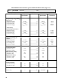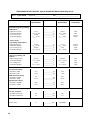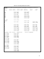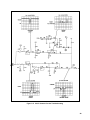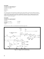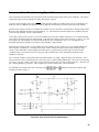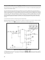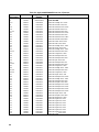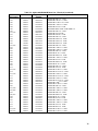
1
SERVICE MANUAL 300 WATT SINGLE INPUT ELECTRONIC LOADS Agilent Technologies Model 6060B and 6063B For instruments with serial numbers Agilent 6060B US37350101 and up Agilent 6063B US37350101 and up For instruments with higher serial numbers, a change page may be included. Agilent Part No. 5951-2828 Microfiche Part No. 5951-2829 Printed in USA Edition 2: February, 2000 CERTIFICATION Agilent Technologies certifies that this product met its published specifications at time of shipment from the factory. Agilent Technologies further certifies that its calibration measurements are traceable to the United States National Bureau of Standards, to the extent allowed by the Bureau's calibration facility, and to the calibration facilities of other International Standards Organization members. WARRANTY This Agilent Technologies hardware product is warranted against defects in material and workmanship for a period of three years from date of delivery. Agilent Technologies software and firmware products, which are designated by Agilent Technologies for use with a hardware product and when properly installed on that hardware product, are warranted not to fail to execute their programming instructions due to defects in material and workmanship for a period of 90 days from date of delivery. During the warranty period Agilent Technologies will, at its option, either repair or replace products which prove to be defective. Agilent Technologies does not warrant that the operation of the software, firmware, or hardware shall be uninterrupted or error free. For warranty service, with the exception of warranty options, this product must be returned to a service facility designated by Agilent Technologies. Customer shall prepay shipping charges by (and shall pay all duty and taxes) for products returned to Agilent Technologies for warranty service. Except for products returned to Customer from another country, Agilent Technologies shall pay for return of products to Customer. Warranty services outside the country of initial purchase are included in Agilent Technologies' product price, only if Customer pays Agilent Technologies international prices (defined as destination local currency price, or U.S. or Geneva Export price). If Agilent Technologies is unable, within a reasonable time to repair or replace any product to condition as warranted, the Customer shall be entitled to a refund of the purchase price upon return of the product to Agilent Technologies. LIMITATION OF WARRANTY The foregoing warranty shall not apply to defects resulting from improper or inadequate maintenance by the Customer, Customer-supplied software or interfacing, unauthorized modification or misuse, operation outside of the environmental specifications for the product, or improper site preparation and maintenance. NO OTHER WARRANTY IS EXPRESSED OR IMPLIED. AGILENT TECHNOLOGIES SPECIFICALLY DISCLAIMS THE IMPLIED WARRANTIES OF MERCHANTABILITY AND FITNESS FOR A PARTICULAR PURPOSE. EXCLUSIVE REMEDIES THE REMEDIES PROVIDED HEREIN ARE THE CUSTOMER'S SOLE AND EXCLUSIVE REMEDIES. AGILENT TECHNOLOGIES SHALL NOT BE LIABLE FOR ANY DIRECT, INDIRECT, SPECIAL, INCIDENTAL, OR CONSEQUENTIAL DAMAGES, WHETHER BASED ON CONTRACT, TORT, OR ANY OTHER LEGAL THEORY. ASSISTANCE The above statements apply only to the standard product warranty. Warranty options, extended support contracts, product maintenance agreements and customer assistance agreements are also available. Contact your nearest Agilent Technologies Sales and Service office for further information on Agilent Technologies' full line of Support Programs. Copyright 2000 Agilent Technologies, Inc. All rights Reserved 2 SAFETY SUMMARY The following general safety precautions must be observed during all phases of operation, service and repair of this instrument. Failure to comply with these precautions or with specific warnings elsewhere in this manual violates safety standards of design, manufacture, and intended use of the instrument. Agilent Technologies assumes no liability for the customer's failure to comply with these requirements. BEFORE APPLYING POWER. Verify that the product is set to match the available line voltage and the correct fuse is installed. GROUND THE INSTRUMENT. This product is a Safety Class 1 instrument (provided with a protective earth terminal). To minimize shock hazard, the instrument chassis and cabinet must be connected to an electrical ground. The instrument must be connected to the ac power supply mains through a threeconductor power cable, with the third wire firmly connected to an electrical ground (safety ground) at the power outlet. For instruments designed to be hard-wired to the ac power lines (supply mains), connect the protective earth terminal to a protective conductor before any other connection is made. Any interruption of the protective (grounding) conductor or disconnection of the protective earth terminal will cause a potential shock hazard that could result in personal injury. If the instrument is to be energized via an external autotransformer for voltage reduction, be certain that the autotransformer common terminal is connected to the neutral (earth pole) of the ac power lines (supply mains). FUSES. Only fuses with the required rated current, voltage and specified type (normal blow, time delay, etc.) should be used. Do not use repaired fuses or short-circuited fuseholders. To do so could cause a shock or fire hazard. DO NOT OPERATE IN AN EXPLOSIVE ATMOSPHERE. Do not operate the instrument in the presence of flammable gases or fumes. KEEP AWAY FROM LIVE CIRCUITS. Operating personnel must not remove instrument covers. Component replacement and internal adjustments must be made by qualified service personnel. Do not replace components with power cable connected. Under certain conditions, dangerous voltages may exist even with the power cable removed. To avoid injuries, always disconnect power, discharge circuits and remove external voltage sources before touching components. DO NOT SERVICE OR ADJUST ALONE. Do not attempt internal service or adjustment unless another person capable of rendering first aid and resuscitation, is present. DO NOT EXCEED INPUT RATINGS. This instrument may be equipped with a line filter to reduce electromagnetic interference and must be connected to a properly grounded receptacle to minimize electric shock hazard. Operation at line voltages or frequencies in excess of those stated on the line rating label may cause leakage currents in excess of 5.0 mA peak. SAFETY SYMBOLS. Instruction manual symbol: the product will be marked with this symbol when it is necessary for the user to refer to the instruction manual (refer to Table of Contents) . Indicates hazardous voltages. Indicate earth (ground) terminal. The WARNING sign denotes a hazard. It calls attention to a procedure, practice, or the like, which, if not correctly performed or adhered to, could result in personal injury. Do not proceed beyond a WARNING sign until the indicated conditions are fully understood and met. The CAUTION sign denotes a hazard. It calls attention to an operating procedure, or the like, which, if not correctly performed or adhered to, could result in damage to or destruction of part or all of the product. Do not proceed beyond a CAUTION sign until the indicated conditions are fully understood and met. DO NOT SUBSTITUTE PARTS OR MODIFY INSTRUMENT. Because of the danger of introducing additional hazards, do not install substitute parts or perform any unauthorized modification to the instrument. Return the instrument to an Agilent Technologies Sales and Service Office for service and repair to ensure that safety features are maintained. Instruments which appear damaged or defective should be made inoperative and secured against unintended operation until they can be repaired by qualified service personnel. 3 Table of Contents Introduction ............................................................................................................................................................................ 7 Scope ........................................................................................................................................................................................ 7 Related Documents ................................................................................................................................................................... 7 Firmware Revisions .................................................................................................................................................................. 7 Manual Revisions ..................................................................................................................................................................... 7 Safety Considerations ............................................................................................................................................................... 8 Electrostatic Discharge ............................................................................................................................................................. 8 Verification.............................................................................................................................................................................. 9 Introduction .............................................................................................................................................................................. 9 Test Equipment Required ......................................................................................................................................................... 9 CC Mode Test......................................................................................................................................................................... 10 CV Mode Test ........................................................................................................................................................................ 11 CR Mode Test......................................................................................................................................................................... 12 Transient Operation and Slew Circuit Test............................................................................................................................. 14 CC Mode PARD Test ............................................................................................................................................................. 15 CC Mode Power Limit............................................................................................................................................................ 15 Troubleshooting .................................................................................................................................................................... 21 Introduction ............................................................................................................................................................................ 21 Test Equipment Required ....................................................................................................................................................... 21 Overall Troubleshooting Procedures ...................................................................................................................................... 21 Selftest Sequence and Error Messages.................................................................................................................................... 22 Primary Interface ................................................................................................................................................................ 22 Secondary Interface ............................................................................................................................................................ 26 Test Points .......................................................................................................................................................................... 27 Signature Analysis .................................................................................................................................................................. 31 Firmware Revisions ............................................................................................................................................................ 31 Test Header Jumper Positions............................................................................................................................................. 32 Test Setup for Signature Analysis....................................................................................................................................... 33 DAC Circuits Troubleshooting (Figure 3-3)........................................................................................................................... 43 Slew Circuit Troubleshooting (Figure 3-4)............................................................................................................................. 45 CC/CV CONTROL CIRCUIT TROUBLESHOOTING (Figure 3-5) .................................................................................... 46 Input Power Stages Troubleshooting (Figure 3-6) .................................................................................................................. 50 Transient Generator Troubleshooting (Figure 3-7)................................................................................................................. 51 General Troubleshooting .................................................................................................................................................... 51 Transient Generator Frequency........................................................................................................................................... 51 Toggle or Pulse Modes ....................................................................................................................................................... 51 Trigger Circuit Troubleshooting (Figure 3-8)......................................................................................................................... 53 Overcurrent Circuit Troubleshooting (Figure 3-9).................................................................................................................. 55 Overpower Circuit Troubleshooting (Figure 3-10) ................................................................................................................. 56 Post Repair Calibration........................................................................................................................................................... 57 EEPROM Initialization........................................................................................................................................................... 57 Disassembly Procedures ......................................................................................................................................................... 58 AC Receptacle .................................................................................................................................................................... 58 Fan ...................................................................................................................................................................................... 58 Front Panel.......................................................................................................................................................................... 59 Keypad................................................................................................................................................................................ 59 LCD Display and Window.................................................................................................................................................. 59 Line Switch ......................................................................................................................................................................... 59 5 Heat Sinks........................................................................................................................................................................... 60 PC Board ............................................................................................................................................................................ 60 FETs Q1 and Q2 ..................................................................................................................................................................... 60 Principles Of Operation ....................................................................................................................................................... 61 Introduction ............................................................................................................................................................................ 61 Bias Supplies .......................................................................................................................................................................... 61 Primary Interface .................................................................................................................................................................... 61 Front Panel.............................................................................................................................................................................. 61 Isolators .................................................................................................................................................................................. 63 Secondary Interface ................................................................................................................................................................ 63 DACs and Slew Rate Control ................................................................................................................................................. 63 CC/CV Control ....................................................................................................................................................................... 63 Protection Circuits .................................................................................................................................................................. 64 Turn-On/Clear Circuit............................................................................................................................................................. 64 Input Power Stages ................................................................................................................................................................. 64 Replaceable Parts.................................................................................................................................................................. 65 Introduction ............................................................................................................................................................................ 65 How To Order Parts................................................................................................................................................................ 65 Diagrams................................................................................................................................................................................ 79 Introduction ............................................................................................................................................................................ 79 Schematic Diagram................................................................................................................................................................. 79 Inter-Sheet Connections...................................................................................................................................................... 79 Intra-Sheet Connections...................................................................................................................................................... 79 Test Point Locations ............................................................................................................................................................... 80 Component Location Diagram................................................................................................................................................ 80 Manual Backdating .............................................................................................................................................................. 92 INDEX ................................................................................................................................................................................... 93 6 1 Introduction Scope This manual contains information for troubleshooting and repairing the Agilent Technologies 6060B and 6063B Electronic Load to the component level. Replaceable parts lists and circuit diagrams are also provided. Verification procedures are included to aid in determining the performance level either before or after repair. Calibration procedures and specifications for the Electronic Load are included in the Operating Manual. Related Documents The following documents, shipped with each Electronic Load, are referenced in this manual: Document Agilent 6060B/6063B Operating Manual Agilent Part No. 5951-2826 Relevant Information Calibration procedures, local & specifications remote operation. Electronic Load Family Programming Reference Guide Agilent Part No. 06060-90005 SCPI programming, status reporting It is assumed that you are familiar with, or can obtain, the information in the above documents. Firmware Revisions Some information in this manual, and S.A. (signature analysis) information in particular, is associated with specific versions of the Electronic Load firmware. Each Electronic Load returns the revision number of its primary interface firmware in response to the "*IDN?" query. Both primary and secondary interface ROMs have a label that also specifies the firmware revision. See "Signature Analysis" in Chapter 3. Manual Revisions Agilent instruments are identified by a two-part, ten-character serial number, such as 2847A-00101. The first five characters (e.g. 2847A) are the serial prefix, which is the same for all identically made instruments. The last five digits (e.g. 00101) is a unique serial number assigned to each instrument. If a significant design change is made, the prefix changes but the last five numbers continue in sequence. This manual was written for Electronic Loads with the same serial prefix and with serial numbers equal to or higher than the ones shown on the title page. If the prefix number of your Electronic Load is higher than the one on the title page, then the Electronic Load was made after publication of the manual and may have hardware and/or firmware differences not covered in this manual. If there are such differences, they are documented in one or more "Manual Changes" sheets sent with the manual. 7 Safety Considerations The Electronic Load is a Safety Class 1 instrument, that has a protective earth terminal. Refer to the Safety Summary page at the beginning of this manual for a summary of general safety procedures and the meaning of safety symbols in the manual and on the Electronic Load. Electrostatic Discharge The Electronic Load has components that can be damaged by ESD (electrostatic discharge). Failure to observe standard, anti-static practices can result in serious degradation of performance, even when complete failure does not occur. When working on the Electronic Load, observe all standard, anti-static work practices. These include, but are not limited to: • • • • • 8 Working at a static-free station, such as a table covered with static-dissipative laminate or with an Agilent 9300-0797 conductive table mat. Using a conductive wrist strap, such as Agilent 9300-0969 or Agilent 9300-0970. Grounding all metal equipment at the station to a single, common ground. Connecting low-impedance test equipment to static-sensitive components only when those components have power applied to them. Removing power from the Electronic Load before removing or installing components. 2 Verification Introduction This chapter contains test procedures that check the operation and calibration of the Agilent 6060B and 6063B Electronic Loads. The tests are performed from the front panel and can be used to determine which circuits are faulty when troubleshooting. There are some transient, trigger, and pulse functions that require a GP-IB controller and will not be verified with manual testing from the front panel. The following tests will verify, with a high level of confidence, that the Electronic Load is operating properly without testing all of its capabilities. At the end of this chapter are performance record tables where actual measured values can be recorded. Test Equipment Required Table 2-1 lists the test equipment required to perform the tests in this chapter. Test setups for the tests are shown in Figures 2-1 through 2-3. Make sure the sense switch on the rear of the load is set to the LCL position since local sensing is used in all of the test setups. Use adequate wire gauge when making connections (see Chapter 3 in the Operating Manual). Note The Electronic Load must pass the selftest at power turn-on before the following tests can be performed. If the unit fails selftest, refer to the overall troubleshooting procedures in Figure 3-1 in Chapter 3. Table 2-1. Test Equipment Required for Verification Type Required Characteristics Recommended Model 120V/60A Source 0 to 20V/0 to 120A 0 to 60 V/0 to 50A 0 to 500 V/0 to 5A Agilent 6031A or equivalent Agilent 6032A or equivalent Agilent 6035A or equivalent Current Monitor Resistor 0.10 ohms @ 15A 0.04% @ 25W Guideline 9230/15 Current Monitor Resistor 0.010 ohms @ 100A 0.04% @ 100W Guideline 9230/100 Digital Voltmeter dc accuracy of 0.01% 6 digit readout Agilent 3455A, 3456A, or 3458A Current Probe with Amplifier and Power Supply Sensitivity of 1mA/10 mV to 50MHz with less than 300µA of noise to 5MHz. Tektronix A6302 probe, AM503 probe amplifier, and TM501 probe power supply. Oscilloscope Sensitivity: 1mV Bandwidth: 20MHz Agilent 54504 9 CC Mode Test This test verifies that the Electronic Load operates in the CC Mode and that the current programming and readback to the front panel display are within specifications. For each DMM reading, the front panel display should be equal to: 6060B: DMM reading in amps ± ((DMM reading in amps X 0.0005) + 0.065) 6063B: DMM reading in amps ± ((DMM reading in amps X 0.0012) + 0.010) If the test readings significantly disagree with the specified values or no readings can be recorded, perform the CC MODE TEST troubleshooting procedures in Figure 3-1 in Chapter 3. If the readings are out of tolerance, calibrate the applicable current range (see Chapter 6 in the Operating Manual). a. Connect the Electronic Load, power supply (Agilent 6031A/6032A or equivalent), DMM, and the 0.010 ohm (6060B) or 0.100 ohm (6063B) current monitor resistor as shown in Figure 2-1. Figure 2-1. Test Setup A b. Turn on the Electronic Load. c. Check the high amp current range as follows: 1. Press MODE CURR Enter , then 6060B: CURR 6 0 Enter . 6063B: CURR 1 0 Enter . 2. Turn on the power supply and set for: 6060B: 5V and >60A. 6063B: 5V and >10A. 3. Wait 30 seconds and then record the DMM and front panel display readings. DMM reading should be between: 6060B: 598.7mV (59.865A) and 601.3mV (60.135A). 6063B: 997.5mV (9.975A) and 1.002 V (10.025A). Note that the Electronic Load's CC annunicator is on. 4. Press CURR 1 Enter . 5. Wait 30 seconds then record the DMM and front panel display readings. DMM reading should be between: 6060B: 9.24mV (0.924A) and 10.761mV (1.076A). 6063B: 98.85mV (0.9885A) and 101.15mV (1.0115A). 10 d. Check the low current range as follows: 1. Press Range 6 0 6060B: Range 6063B: 1 0 Enter then CURR 6 Enter . Enter then CURR 1 Enter . 2. Wait 10 seconds then record the DMM and front panel display readings. DMM reading should be between: 6060B: 59.19mV (5.919A) and 60.81mV (6.081A.) 6063B: 98.85mV (0.9885A) and 101.15mV (1.0115A.) 3. Press: 6060B: CURR 1 6063B: Range 0 Enter . 1 . Enter . 4. Wait 10 seconds and record the DMM and front panel display readings. DMM reading should be between: 6060B: 9.24mV (0.924A) and 10.76mV (1.076A). 6063B: 8.985mV (89.85A) and 11.015mV (110.15A). CV Mode Test This test verifies that the Electronic Load operates in the CV Mode and that the voltage programming and readback to the front panel display are within specifications. For each DMM reading, the corresponding front panel display should be equal to: 6060B: DMM reading ± ((DMM reading X 0.0005) + 0.045) 6063B: DMM reading ± ((DMM reading X 0.0010) + 0.150) Note that if the test readings significantly disagree with the specified values or no readings can be recorded, perform the CV MODE TEST troubleshooting procedures in Figure 3-1, in Chapter 3. If the readings are out of tolerance, calibrate the voltage range (see Chapter 6 in the Operating Manual). a. Connect the Electronic Load, power supply (Agilent 6035A or equivalent), and DMM as shown in Figure 2-2. Take care in making connections so that contact resistance voltage drop will not affect the readings. Figure 2-2. Test Setup B b. Press MODE VOLT Enter 6060B: VOLT 6 0 6063B: VOLT 2 4 Enter 0 , then . Enter . 11 c. Set power supply for: 6060B: 61V and 5A. 6063B: 250V and 1A. d. Record the DMM and front panel display readings. DMM reading should be between: 6060B: 59.890V and 60.110V. 6063B: 239.59V and 240.408V. Note that the Electronic Load's CV annunciator is on. e. Press VOLT 3 Enter f. Record the DMM and front panel display readings. DMM reading should be between: 6060B: 2.947V and 3.053V. 6063B: 2.876V and 3.123V. . CR Mode Test This test verifies that the Electronic Load operates in the CR Mode and that the resistance programming is within specifications. The programmed resistance values are checked by recording the voltage across the current monitor resistor and the input voltage (voltage across the Electronic Load's input terminals), and then calculating the resistance value as follows: Load resistance = Input voltage/(voltage across resistor/resistor value) Note if the calculation significantly disagrees with the specified range of values, perform the CR MODE TEST troubleshooting procedures in Figure 3-1 in Chapter 3. If the calculation is out of tolerance, calibrate the applicable resistance range (see Chapter 6 in the Operating Manual). a. Connect the Electronic Load, power supply (Agilent 6032A/6035A or equivalent), and the 0.100 ohm current monitor resistor as shown in Figure 2-1. Use the DMM to measure the voltage across the monitor resistor and across the Electronic Load's input terminals. b. Check the low ohm range as follows: 1. Press MODE RES 6060B: Range 0 6063B: Range 1 Enter , then 9 . Enter Enter ; ; RES RES 2 1 4 Enter Enter . . 2. Turn on power source and set for: 6060B: 15V and 10.9A. 6063B: 15V and 1.82A. For the low ohm range test, the power supply will operate in the current limit mode. 3. Measure the voltage across the monitor resistor and across the input terminals, then calculate the Electronic Load resistance. The result should be between: 6060B: 0.984 and 1.016 ohms. 6063B: 23.6 and 24.4 ohms. Note that the Electronic Load's CR annunciator is on. 4. 12 Then press: 6060B: RES 0 6063B: RES 1 0 . Enter 5 . Enter . 5. Measure the voltage across the monitor resistor and across the input terminals, then calculate the Electronic Load resistance. The result should be between: 6060B: 0.0416 and 0.0584 ohms. 6063B: 0.792 and 1.208 ohms. c. Check the middle ohms range as follows: 1. Press: 6060B: Range 1 0 Enter , then RES 3 0 Enter 6063B: Range 2 5 Enter , then RES 5 0 0 . Enter . 2. Set power supply for: 6060B: 10.9V and 15A. 6063B: 44V and 4A. 3. Measure the voltage across the monitor resistor and across the input terminals, then calculate the Electronic Load resistance. The result should be between: 6060B: 24.1 and 39.6 ohms. 6063B: 433 and 590 ohms. 4. Then press: 6060B: RES 1 Enter RES 2 4 6063B: . Enter . 5. Measure the voltage across the monitor resistor and across the input terminals, then calculate the Electronic Load resistance. The result should be between: 6060B: 0.989 and 1.011 ohms. 6063B: 23.75 and 24.25 ohms. d. Check the high ohms range as follows: 1. Press: 6060B: Range 1 0 0 6063B: RES 1 2 0 1 Enter Enter , then , then RES RES 2 1 2 0 Enter . 0 0 0 Enter . 2. Set power source for: 6060B: 60V and 6A. 6063B: 240V and 2A. 3. Measure the voltage across the monitor resistor and across the input terminals, then calculate the Electronic Load resistance. Calculation should be between: 6060B: 61.1 and 3243 ohms. 6063B: 1247 and 5037 ohms. 4. Then press: 6060B: RES 1 2 Enter RES 2 4 0 6063B: 5. . Enter . Measure the voltage across the monitor resistor and across the input terminals, then calculate the Electronic Load resistance. The result should be between: 6060B: 10.9 and 13.3 ohms. 6063B: 223 and 259 ohms. 13 Transient Operation and Slew Circuit Test This test verifies transient and slew circuit operation. The slew circuits cannot be calibrated. If slew rise time and/or fall time are not within specifications or the slew circuits are inoperative, perform either the "Transient Generator Troubleshooting", or the "Slew Circuit Troubleshooting" in Chapter 3. a. Use the test setup of Figure 2-1 except connect an oscilloscope across the 0.100 current monitor resistor in place of the DMM. Set power supply for: 6060B: 10V and 10A. 6063B: 10V and 15A. b. Recall the factory default values by pressing Recall 7 Enter . c. Select the low current range by pressing Range 6 Enter . d. Set up transient operation by pressing CURR 1 Enter , then e. 6060B: Tran Level 6 6063B: Tran Level 9 Set the slew rate by pressing (blue shift key), then Slew 0 6060B: 6063B: Slew 0 Enter . . 4 Enter . 0 5 . 0 8 . Enter 3 , then Enter Tran on/off , then . Tran on/off . f. Adjust the oscilloscope for a single rise or fall time display. Use delayed sweep. The rise time when measures from 10% to 90% or the fall time when measured from 90% to 10% should be between 60 and 100µs Note that the Electronic Load's Tran annunciator is on. 20µs/DIV 6060B: SLEW 0.05 6063B: SLEW 0.083 g. Set the slew rate by pressing (blue shift key), then Slew 0 6060B: 6063B: h. 14 . 0 0 2 5 Enter , then 0 0 4 2 Enter , then Slew 0 . Freq 6 0 Enter . Adjust the oscilloscope for a single rise or fall time display. Use delayed sweep. The rise time when measures from 10% to 90% or the fall time when measured from 90% to 10% should be between 1.2 and 2.0ms. CC Mode PARD Test CC mode PARD (periodic and random deviations) is specified as the rms input current in a frequency range 20Hz to 10Mhz. This test checks CC Mode PARD. a. Connect the Electronic Load, power supply (Agilent 6032A or equivalent, DMM, and current probe as shown in Figure 2-3. Set power supply for 10V and >10A. b. Turn the load's ac power off, then on. c. Press CURR 1 0 Enter . d. DMM reading should be less than: 6060B: 4mA rms 6063B: 1mA rms. Figure 2-3. Test Setup C CC Mode Power Limit This test verifies that the Electronic Load's power limit circuit is operating properly. If the results specified in steps d through i are not obtained, troubleshoot the circuits as described in "Overpower Circuits Troubleshooting" in Chapter 3. If the overpower circuit does not turn the load off within three minutes after performing step d, stop the tests and troubleshoot the overpower circuits. a. Connect the Electronic Load and the power source as shown in Figure 2-2. b. Turn on the Electronic Load and run for approximately five minutes with no power being dissipated (no input power). c. Then Press a. MODE VOLT Enter , then 6060B: VOLT 2 0 Enter . 6063B: VOLT 3 5 Enter . Turn on and set the power supply for: 6060B: 34volts and 18mps. 6063B: 45volts and 13mps. The Electronic Load's front panel should indicate approximately: 6060B: 33 volts and between 13 and 17 amps. 6063B: 45 volts and between 7.2 and 10.9 amps. The front panel Prot annunciator should also be on. 15 to display ''− −OP", indicating that an overpower condition exists and the Electronic Load is in power e. Press limit. f. Let the Electronic Load continue running. Within three minutes the Electronic Load should turn its input off, and the display should show ''PS− −OP'' indicating protection shutdown. IF THE OVERPOWER CIRCUIT DOES NOT TURN THE LOAD OFF WITHIN THREE MINUTES, STOP THE TESTS AND TROUBLESHOOT THE OVERPOWER CIRCUITS. g. Immediately press . The ''PS'' display should blink and the input will remain shut down, indicating that protection shutdown is latched. h. Wait approximately one minute and press displayed. i. Reduce the power source output to 20 volts (6060B) or 35 volts (6063B). The display should change to "− − −" indicating that the protection shutdown and overpower conditions are cleared. 16 again. This time the load should turn on with only ''OP" PERFORMANCE TEST RECORD - Agilent 6060B ELECTRONIC LOAD (Page 1 of 2) Test Facility: ________________________________________________ ________________________________________________ ________________________________________________ ________________________________________________ Report No._____________________________________ Date__________________________________________ Customer______________________________________ Tested by______________________________________ Model Agilent 6060B Ambient temperature __________________________°C Serial No._________________________________________ Relative humidity_____________________________% Options___________________________________________ Line frequency______________________Hz (nominal) Firmware Rev._____________________________________ Special Notes: __________________________________________________________________________________________________ __________________________________________________________________________________________________ __________________________________________________________________________________________________ Test Equipment Used Description Model No. 1. AC Source 2. DC Voltmeter Agilent 3458A 3. Oscilloscope Agilent 54504A 4. Power Source Agilent 6031A 5. Power Source Agilent 6032A Trace No. Cal. Due Date 6. Current Probe 7. Current Shunt Guildline 9230/15 8. Current Shunt Guildline 9230/100 17 PERFORMANCE TEST RECORD - Agilent 6060B ELECTRONIC LOAD (Page 2 of 2) Model Agilent 6060B Test Description Report No.____________________ Minimum Specification Date______________________________ Results Maximum Specification Measurement Uncertainty CONSTANT CURRENT MODE TESTS 60 Ampere Range Programming and Readback High Current (60A) Front Panel Display Low Current (1A) Front Panel Display 59.865 AOUT -0.095 0.924 AOUT -0.065 ____________A ____________A ____________A ____________A 60.135 AOUT +0.095 1.076 AOUT +0.065 25mA 25mA 427µA 427µA 6 Ampere Range Programming and Readback High Current (6A) Front Panel Display Low Current (1A) Front Panel Display 5.919 AOUT -0.068 0.924 AOUT -0.065 ____________A ____________A ____________A ____________A 6.081 AOUT +0.068 1.076 AOUT +0.065 2.4mA 2.4mA 427µA 427µA 60.110 VOUT +0.075 3.053 VOUT +0.046 845µV 845µV 35µV 35µV CONSTANT VOLTAGE MODE TESTS Voltage Programming and Readback High Voltage (60V) Front Panel Display Low Voltage (3V) Front Panel Display 59.890 VOUT -0.075 2.947 VOUT -0.046 ____________V ____________V ____________V ____________V CONSTANT RESISTANCE MODE TESTS Low Resistance Range Resistance (1 Ω) Resistance (0.05Ω) Middle Resistance Range Resistance (30Ω) Resistance (1 Ω) High Resistance Range Resistance (120Ω) Resistance (12Ω) 0.984 0.0416 ____________Ω ____________Ω 1.016 0.0584 24.1 0.989 ____________Ω ____________Ω 39.6 1.011 61.1 10.9 ____________Ω ____________Ω 3243 13.3 TRANSIENT SLEW TEST Fast Slew Transient Slew Rate 0.05 A/µs Slew Rate 2.5 A/µs 60 1.2 ____________µs ____________ms 100 2.0 CONSTANT CURRENT PARD TEST Current (10A) 18 0 __________mA 4mA RMS PERFORMANCE TEST RECORD - Agilent 6063B ELECTRONIC LOAD (Page 1 of 2) Test Facility: ________________________________________________ ________________________________________________ ________________________________________________ ________________________________________________ Report No._____________________________________ Date__________________________________________ Customer______________________________________ Tested by______________________________________ Model Agilent 6063B Ambient temperature __________________________°C Serial No._________________________________________ Relative humidity _____________________________% Options___________________________________________ Line frequency ______________________Hz (nominal) Firmware Rev._____________________________________ Special Notes: __________________________________________________________________________________________________ __________________________________________________________________________________________________ __________________________________________________________________________________________________ Test Equipment Used Description Model No. 1. AC Source 2. DC Voltmeter Agilent 3458A 3. Oscilloscope Agilent 54504A 4. Power Source Agilent 6032A 5. Power Source Agilent 6035A Trace No. Cal. Due Date 6. Current Probe 7. Current Shunt Guildline 9230/15 19 PERFORMANCE TEST RECORD - Agilent 6063B ELECTRONIC LOAD (Page 2 of 2) Model Agilent 6063B Test Description Report No.____________________ Minimum Specification Date______________________________ Results Maximum Specification Measurement Uncertainty CONSTANT CURRENT MODE TESTS 10 Ampere Range Programming and Readback High Current (10A) Front Panel Display Low Current (1A) Front Panel Display 9.975 AOUT -0.022 0.9885 AOUT -0.011 ____________A ____________A ____________A ____________A 10.025 AOUT +0.022 1.0115 AOUT +0.011 4mA 4mA 427µA 427µA 1 Ampere Range Programming and Readback High Current (1A) Front Panel Display Low Current (0.1A) Front Panel Display 0.9885 AOUT -0.011 0.0899 AOUT -0.010 ____________A ____________A ____________A ____________A 1.0115 AOUT +0.011 1.101 AOUT +0.010 427µA 427µA 56µA 56µA 240.408 VOUT +0.390 3.1236 VOUT +0.153 3mV 3mV 35µV 35µV CONSTANT VOLTAGE MODE TESTS Voltage Programming and Readback High Voltage (240V) Front Panel Display Low Voltage (3V) Front Panel Display 239.59 VOUT -0.390 2.876 VOUT -0.153 ____________V ____________V ____________V ____________V CONSTANT RESISTANCE MODE TESTS Low Resistance Range Resistance (24Ω) Resistance (1Ω) Middle Resistance Range Resistance (500Ω) Resistance (24Ω) High Resistance Range Resistance (2000Ω) Resistance (240Ω) 23.6 0.792 ____________Ω ____________Ω 24.4 1.208 433 23.75 ____________Ω ____________Ω 590 24.25 1247 223.3 ____________Ω ____________Ω 5037 259.5 TRANSIENT SLEW TEST Fast Slew Transient Slew Rate 0.083A/µs Slew Rate 0.0042A/µs 60 1.2 ____________µs ____________ms 100 2.0 CONSTANT CURRENT PARD TEST Current (10A) 20 0 __________mA 1mA RMS 3 Troubleshooting Most of the troubleshooting procedures given in this chapter are performed with power applied and protective covers removed. Such maintenance should be performed only by service-trained personnel who are aware of the hazards (for example, fire and electrical shock). This instrument uses components which can be damaged or suffer serious performance degradation as of result of ESD (electrostatic discharge). Observe the standard anti-static precautions to avoid damage to the components. Introduction This chapter provides troubleshooting and repair information for the Agilent 6060B and 6063B Electronic Loads. Before attempting to troubleshoot the Electronic Load, ensure that the problem is with the load itself and not with an associated circuit, power source, or power line. The verification tests in Chapter 2 enable this to be determined without removing the covers from the Electronic Load. Overall troubleshooting procedures are provided to isolate a problem to a functional area of circuitry. Once a problem has been isolated to a functional area, additional troubleshooting procedures are given to isolate the problem to the defective component(s). If a component is found to be defective, replace it and then conduct the verification tests given in Chapter 2. Note that when certain components are replaced, the load must be recalibrated (see ''Post Repair Calibration" later in this chapter). If the serial EEPROM chip U211 is replaced, the Electronic Load must be initialized before it is recalibrated. See "EEPROM Initialization" later in this chapter. Chapter 5 in this manual lists all of the replaceable parts for the Electronic Load. Test Equipment Required Table 3-1 lists the test equipment required to troubleshoot the Electronic Load. Recommended models are listed. Overall Troubleshooting Procedures Overall troubleshooting procedures for the Electronic Load are given in the flowchart of Figure 3-1. The procedures first ensure that an ac input failure or bias supply failure are not causing the problem and that the load passes the turn-on selftest (no error messages). The normal turn-on selftest indications are described in Chapter 3 of the Operating Manual. If the load passes selftest, Figure 3-1 directs you to perform the front panel verification procedures in Chapter 2 to determine if any load function(s) are not calibrated or are not operating properly. If the load passes the front panel verification tests, Figure 3-1 checks to see if the load can be programmed from a GP-IB controller. If the load fails any of the tests, you are directed to the applicable troubleshooting procedure. Signature analysis (S.A.) is used to troubleshoot the load's primary and secondary interface circuits. The S.A. mode is also used to generate waveforms which are used to troubleshoot the analog circuits. In addition, a list of test points with signal measurement information is provided to help you troubleshoot. 21 Type GP-IB Controller Table 3-1 Test Equipment Required for Troubleshooting Purpose Recommend Model Communicate with the load via the GP-IB Agilent 9825, Series 85, Series 200/300 Signature Analyzer Test most of the primary and secondary circuits Agilent 5005A/B Digital Voltmeter Check various voltage levels Agilent 3455A or 3456A Power Source Provide required input, bias GP-IB Board Agilent 6032A/6035A Logic Probe Check data bus lines Agilent 545A Oscilloscope Check waveforms and signal levels Agilent 1741A Clip Leads Connect IC pins together AP Products No. LTC Selftest Sequence and Error Messages The turn-on selftest sequence consists of tests on both the primary (GP-IB) and secondary (Electronic Load) interface circuits. If the load fails the selftest, the input will remain disabled and the display should indicate the type of failure. Table 3-2 lists all of the selftest error codes that can appear on the front panel display and provides the appropriate troubleshooting information. Primary Interface The turn-on selftest sequence of the primary microprocessor consists of two parts: 1. The selftest is performed by the primary microprocessor (U203) and starts when the primary clear ( PCLR ) signal goes false (High). First, the RAM, ROM, and the microprocessor's internal timer selftests are performed. If any of these tests fail, the front panel display will probably remain blank. The failure can be detected by measuring a square wave on the SA_GATE line at TP201-8 (see Figure 3-2). The type of failure is indicated as follows: 10Hz square wave--indicates a RAM failure. 100Hz square wave--indicates a ROM failure. 1KHz square wave--indicates an internal timer failure. Square waves will not have a 50% duty cycle. It is also possible for a selftest failure to ''lock-up" the microprocessor and cause a blank front panel display and no error square wave to appear on the SA_GATE line. If ''lock-up'' occurs, try to isolate the problem by performing the Primary Interface S.A. Tests or by replacing U203. 22 Figure 3-1. Overall Troubleshooting Flowchart (Sheet 1 of 3) 23 Figure 3-1. Overall Troubleshooting Flowchart (Sheet 2 of 3) 24 Figure 3-1. Overall Troubleshooting Flowchart (Sheet 3 of 3) 25 2. If part 1 passes selftest, the test continues and checks the read/write cycles and the internal trigger circuit. If these tests pass, the secondary interface selftest are performed. If the read/write or internal trigger test fails, the front panel displays "ERROR x" for two seconds, then normal voltage/current will be displayed and the Err annunciator will turn on. Depressing the (blue shift key) followed by the key will cause ''ERROR -330" to be displayed. If "ERROR -4" was displayed for 2 seconds, the read/write test failed. If "ERROR -5" was displayed for 2 seconds, the internal trigger test failed. Secondary Interface The turn-on selftest sequence of the secondary microprocessor consists of two parts: 1. The selftest is performed by the secondary microprocessor (U301) and starts when the secondary power clear ( SPCLR ) signal goes false (High). Any secondary failures are reported to the primary interface. The secondary microprocessor will first check its internal RAM, ROM, and timer. If one of these tests fail, selftest is halted and the following will be displayed: "ERROR -101" - RAM failure "ERROR -102" - ROM failure "ERROR -103" - Timer failure It is possible for a secondary RAM, ROM, or Timer failure to "lock-up" the secondary processor and no secondary error number is reported. If this occurs try to isolate the problem by performing the Secondary Interface S.A. 2. If part 1 passes selftest, the test continues by checking the secondary EEPROM which stores the load's GP-IB address and model number as well as the constants used in calibrating the load. Next the operation and accuracy of the main and transient DACs are tested. If these tests pass, the volts/amps readings will appear on the display indicating that the selftest has been successfully completed (see Chapter 3 in the Operating Manual). If the EEPROM or any of the DAC tests fail, the front panel displays ''ERROR -xxx" for 2 seconds, then "INP DOWN (blue shift key) 1" followed by "INPUT DWN". Finally the Err annunciator will turn on. Depressing the key, will cause "ERROR -330" to be displayed. Depressing these keys a second time, will followed by the cause "ERROR -240" to be displayed. The error code number that appeared for 2 seconds could be one of the following: "ERROR -104" - EEPROM checksum failure "ERROR -105" - Main DAC tolerance is high "ERROR -106" - Main DAC tolerance is low "ERROR -107" - Transient DAC tolerance is high "ERROR -108" - Transient DAC tolerance is low If error "UNKNOWN" is displayed the EEPROM (U211) must be initialized. 26 Table 3-2. Selftest Error Code Code -4 Error Description The primary microprocessor U203 read/write test to the GP-IB talker/listener chip U202 failed. Procedure Use Primary S.A. Test Tables 3-4 and 3-6 to check address and data lines. -5 The primary microprocessor U203 test of the internal trigger lines failed. Use Primary S.A. Test Table 3-7 to check the primary trigger circuit. Then refer to " Trigger Circuit Troubleshooting" and Figure 3-8. -101 Secondary microprocessor U301 internal RAM failure. Replace U301. -102 Secondary microprocessor U301 internal ROM failure, or thermistor RT 551 missing or open. Check RT 551, replace U301. -103 Secondary microprocessor U301 internal timer failure. Replace U301. -104 EEPROM (U211) checksum error. Create a checksum by programming: ''CAL:MODE ON;:CAL:SAVE" then turn power on. If error code -104 does not appear again, calibrate the load as described in the Operating Manual. If error code -104 does appear again, check the EEPON line (test point in Table 3-3). If EEPON is ok, use S.A. Table 3-6 to check the data input and output lines to U211. -105 Main DAC circuit (U320/U326) zero or full scale point is above the high tolerance level. Refer to "DAC Circuits Troubleshooting" and Figure 3-3. -106 Main DAC circuit (U320/U326) zero or full scale point is below the low tolerance level. Same as above. -107 Transient DAC circuit (U321/U325) zero or full scale point is above the high tolerance level. Same as above. -108 Transient DAC circuit (U321/U325) zero or full scale point is below the low tolerance level. Same as above. Test Points Table 3-3 lists test points that are referred to in many of the troubleshooting procedures. Each test point is identified by a circled number (e.g., ), the circuit point (e.g., U308-1), and signal name (e.g., CV PROG). The "Measurement and Conditions'' column describes the signal that should be measured and the conditions (e.g. operating mode) required to make the measurement. The circuit locations of the test points are shown on the foldout schematic diagrams (Figure 6-1, sheets 1 through 6) and on some of the troubleshooting diagrams (Figures 3-3 through 3-10). All of the test points are located on the main circuit board as shown on foldout diagram Figure 6-2. Note: When taking measurements, make sure that you connect the DMM or oscilloscope common to the proper circuit common. Measurements at test points through are referenced to test point (primary/chassis common). Measurements at test points through are referenced to test point (secondary common). 27 Table 3-3. Test Points Test Point Number Signal Measurement and Conditions Connect meter or scope common to test point when taking measurements at test points through U502-2 Q501-10 D503-cath Primary/Chassis ground + 5V (primary bias) + 13V (primary bias rectifiers) + 5V (4.8 to 5.2V). + 13V (13 to 17 Vdc). Q501-15 OPTO_ CLR Held low (0V) for approximately 80ms at power on and then goes high (5V). Q501-3 PCLR Q501-9 PCLR Held low for approximately 80ms at power on and then goes high. Q501-6 EEPON At power on, holds the EEPROM's clock off to protect against accidental data write when power is initially applied. Connect meter common to test point Goes high for approximately 80ms at power on and then goes low. when taking measurements at test points through . C557- Secondary common C560+ C557+ C558D554 - cath +5V secondary bias + 15V secondary bias -15V secondary bias + 26V (secondary bias rectifiers) + 15V ± 1V - 15V ± 1V + 23V to + 29V Q551-12 SPCLR Held low for approximately 80ms at power on and then goes high. C556 + Fan voltage Press the front panel (blue shift) key and then the 9 key and note the word "FAN" appears on the display. Now press the number key, and take the key (0-3) specified below, press measurement. Repeat this procedure for each fan speed. 0 = 14.7V ±0.8V 1 = 10.7V ±0.6V 2 = 12.8V ±0.8V 3 = 9.7V ±0.5V U213-7 SRX SRX (Secondary receive) serial data line. Toggles between 0 and 5V. U214-3 STX STX (Secondary transmit) serial data line. Toggles between 0 and 5V. U308-1 CV PROG In VOLT MODE, + 10V with full rated voltage programmed; +0.5V with 3 volts programmed (6060B), or with 12 volts programmed (6063B). +5V (4.8 to 5.2V) In CURR MODE or RES MODE (middle and high ohm ranges), + 13V. In RES MODE (low ohm range), < 1V. 28 Table 3-3. Test Points (continued) Test Point Number U308-7 Signal CC PROG Measurement and Conditions In CURR MODE, + 10V with full rated current programmed. In VOLT MODE, RES MODE (low ohm range), or with INPUT OFF: - 0.5V. In RES MODE (middle and high ohm ranges), 0 to +10V depending upon resistance value programmed. U316-10 TRANS_EN High level with transient operation programmed on (TRAN ON). Low level with transient operation programmed off (TRAN OFF). U331-1 SLEW In CURR MODE, -10V with full rated current programmed; 0V with zero current programmed. In VOLT MODE, -10V with full rated voltage programmed; 0V with zero voltage programmed. U309-8 DAC_REF Low level in CURR or VOLT MODE. High level in RES MODE (any range). U309-9 CR Low level in RES MODE (low ohm range). High level in CURR, VOLT, or RES (middle or high ohm range) MODE. U309-1 CG Low level in RES MODE (middle or high ohm range). High level in CURR, VOLT, or RES (low ohm range) MODE. TB301-9 PORT High level with PORT0 ON programmed. Low level with PROT0 OFF programmed. U329-4 -10 V Ref -10V (9.95 to 10.05V). U331-7 U8-5 + 12V Ref IPROG + 12V (11.28 to 11.44V). Under normal operating conditions (input is regulated) measurement should be approximately: -0.1V X Iin (6060B). 0.67V X Iin (6063B). D17 -cath + OV U10-1 CC Loop Gain control With input unregulated or disconnected, the measurement will be: 0V in CURR Mode. +0.9V in VOLT or RES MODE. + 14V when OV condition is false (normal). -13V when OV condition is true. + 15V when input voltage is more than 2.5V. -15V when input voltage is less than 2.5V. NOT USED 29 Table 3-3. Test Points (continued) 30 Test Point Number U9-8 Signal Measurement and Conditions RNG Low level when the high current range or the middle resistance range is programmed. High level when the low current range, the low resistance range, or the high resistance range is programmed. U5-7 -VMON -0.167 X Input Voltage (6060B). -0.0418 X Input Voltage (6063B). D11 -cath + OP - 0.9V (full rated voltage input) to - 6V (zero volts input) when the OP condition is false. Pulses when the OP condition is true. See test point . U7-1 -OP -14V when the OP condition is false. Pulses when the OP condition is true. See Figure 3-10. U12-17 -VMONA -0.167 X Input Voltage (6060B). -0.0418 X Input Voltage (6063B). D12 -cath NOT USED OC circuit control Q11-E OC circuit control + 10V when OC condition is false (normal). 0V when unregulated or when OC condition is true. D19-K Input Power Stage Turn on + 5V when turned on. 0V when turned off. U1-1 Input Power Stage 1 6.3V (approx.) with full rated input current. -0.5V (approx.) with the input off. Q1-1 Input Power Stage 1 5.4V (approx.) with full rated input current. 4.0V (approx.) with 10% rated input current. 2.5V (approx.) at zero input current. U14-1 Input Power Stage 1 1.25V for at full input current. U5-1 -IMON 10.02V at full input current. + 13V when OC condition false (normal). + 8V when OC condition is true. Signature Analysis The easiest and most efficient method of troubleshooting microprocessor based instruments is signature analysis (S.A.). The S.A. technique is similar to signal tracing with an oscilloscope in linear circuits. Part of the microcomputer memory is dedicated to signature analysis and a known bit stream is generated to stimulate as many nodes as possible within the circuit. However, because it is virtually impossible to analyze a bit stream with an oscilloscope, a signature analyzer is used to compress the bit stream into a four character signature. By comparing signatures of the IC under test to the correct signatures for each node, faults can usually be isolated to one or two components. Signature analysis tests are provided for most of the digital circuits in the primary and secondary interface circuits of the Electronic Load. There are four primary interface S.A. tests given in Tables 3-4 through 3-7, and five secondary interface tests given in Tables 3-8 through 3-12. Refer to "Firmware Revisions" for information about the valid firmware revisions for the signature analysis tables. References are made to the appropriate S.A. test table from the troubleshooting flow charts or procedures. The following general rules apply to signature analysis testing of the primary and secondary interface circuits. 1. Be sure to use the correct test setup connections for the specific test. See "Test Setup for Signature Analysis". 2. Note the signatures for Vcc ( + 5V) and common on the IC being examined. If an incorrect signature is the same as that of Vcc or common, that pin (or point in the circuit) is probably shorted to Vcc or ground. 3. If two pins have identical signatures, they are probably shorted together. 4. If two signatures are similar, it is only a coincidence. 5. If a signature is incorrect at an input pin, but is correct at its source (output of previous IC), check for printed circuit track or soldering problems. 6. An incorrect signature at an output could be caused by a faulty component producing the output. It can also be caused by an input short circuit in another component on the board. Firmware Revisions The primary interface ROM chip (U205) and the secondary microprocessor chip (U301) are identified with labels that specify the revision of the Electronic Load's firmware. The signatures given in Primary S.A. Tables 3-4 through 3-7 are valid for ROM chip U205 firmware revision "Rev A.02.01''. You can also identify the revision of the U205 firmware using the *IDN? query in the program listed below. 10 OUTPUT 705;"*IDN?" 20 ENTER 705; 30 DISP L$ 40 END The computer will display the Electronic Load Agilent part number and the firmware revision of the U205 primary ROM chip. The signatures given in Secondary S.A. Tables 3-8 through 3-12 are valid for secondary interface microprocessor chip U301 revision "Rev A.02.01" . Note that the U301 revision is only identified by the label; it cannot be read back using the *IDN? query. 31 Test Header Jumper Positions The Electronic Load contains two test headers (connectors TP201 and TP301) with jumper positions for signature analysis testing and for other functions as described below. The test headers are located on the main circuit board (see Figure 6-3) and are accessible when the top cover is removed. Primary Test Header TP201 Pins 1 and 2 Description + 5V (primary interface) test points. 3 and 4 With jumper RTP201 installed between these pins, the primary interface microprocessor is placed in the S.A. mode. Removing RTP201 takes the microprocessor out of the S.A. mode. 5 and 6 With jumper RTP201 installed between these pins, the primary interface microprocessor will ignore calibration commands, providing security against unauthorized calibration. With RTP201 removed, the microprocessor will respond to calibration commands. 7 and 8* S.A. gate test points (normal operating/storage position for RTP201). 9 thru 16 Test points for the chip select signals CSP0 through CSP7 . *As shipped from the factory, jumper RTP201 is installed between TP201 pins 7 and 8. Both of these pins are connected to the primary S.A. gate signal, which is used as the start/stop signal when taking signatures during primary S.A. testing. See "Test Setup for S. A.'' Secondary Test Header TP301 Pins 1 and 2 Description With jumper RTP301 installed between these pins, the secondary microprocessor is placed in the S.A. mode. Removing RTP301 takes the microprocessor out of the S.A. mode. 3 and 4* S.A. gate test points (normal operating/storage position for RTP301). 5 and 7 With RTP301 installed between these pins, the secondary microprocessor will skip selftest at power-on. With RTP301 removed, the selftest will be performed. 6 Connected to secondary common. 8 + 5V (secondary) test point. * As shipped from the factory, jumper RTP301 is installed between pins 3 and 4 . Both of these pins are connected to the secondary S.A. gate signal, which is used as the start/stop signal when taking signatures during secondary S.A. testing. See "Test Setup for S. A.". 32 Test Setup for Signature Analysis Figure 3-2 illustrates the primary (TP201) and secondary (TP301) test header connections required to perform the S.A. Tests given in Tables 3-4 through 3-12. The following is a description of the test setup: a. Turn off the Electronic Load and gain access to the main circuit board by removing the top cover (see "Disassembly Procedures"). Make sure that the Electronic Load is turned off before continuing with the test setup. b. To test the primary interface, use the following test setup. 1. Connect jumper RTP201 in the S.A. position (SA_MODE) across pins 3 and 4 of the primary test header TP201 (see Figure 3-2). 2. Set up and connect the signature analyzer's CLOCK, START, STOP, and GND inputs as follows: Signature Analyzer Input c. Edge Setting TP201 Connection To test the secondary interface, use the following test setup. 1. 2. Connect jumper RTP301 in the S.A. position (SA_EN) across pins 1 and 2 of the primary test header TP301 (see Figure 3-2). Set up and connect the signature analyzer's CLOCK, START, STOP, and GND inputs as follows: Signature Analyzer Input Edge Setting TP301 Connection d. Turn on the signature analyzer and use the signature analyzer probe to take signatures at the applicable IC test points given in the S.A. Test Table. e. Upon completion of the S.A. tests, return jumpers RTP201 and/or RTP301 to their normal operating positions of TP201 and TP301 as follows (see Figure 3-2): RPT201 between TP201-7 and TP201-8; RTP301 between TP301-3 and TP301-4. 33 Figure 3-2. Test Headers Test Setup for Signature Analysis 34 Table 3-4. Primary Interface S.A. Test No. 1 Description: These signatures check primary microprocessor U203, ROM U205, and RAM U206. The signatures are valid for ROM U205 firmware revision "Rev A.02.01". Use the test setup described in "Test Setup for S.A.". Connect the signature analyzer's CLOCK input to U207-11. µP U203 U203-4,7,21 U203-1,9,10 U203-2,3 U203-40 U203-6 ROM U205 U205-28 RAM U206 U206-28,14 U205-22 U206-26 8799 HF40 9375 48PF FF8U PUCP 84C9 25H3 53P5 1558 CAA3 PACH 1249 1C1H U872 8F8F U203-13 U203-14 U203-15 U203-16 U203-17 U203-18 U203-19 U203-20 U203-29 U203-28 U203-27 U203-26 U203-25 U203-24 U203-23 U203-22 U205-10 U205-9 U205-8 U205-7 U205-6 U205-5 U205-4 U205-3 U205-25 U205-24 U205-21 U205-23 U205-2 U205-26 U205-27 U205-1 U206-10 U206-9 U206-8 U206-7 U206-6 U206-5 U206-4 U206-3 U206-25 U206-24 U206-21 U206-23 U206-2 D(0) D(1) D(2) D(3) D(4) D(5) D(6) D(7) 7H05 8P29 U864 3P59 44A9 C4P4 8PUC 2794 U203-37 U203-36 U203-35 U203-34 U203-33 U203-32 U203-31 U203-30 U205-11 U205-12 U205-13 U205-15 U205-16 U205-17 U205-18 U205-19 U206-11 U206-12 U206-13 U206-15 U206-16 U206-17 U206-18 U206-19 STX SRX R/W CE CE1 unstable 2177 4A22 C67U 9H41 4U1P 4AP2 C383 U203-11 U203-12 U203-38 U205-20 U216-11 U216-13 U207-1 Signal +5V Common 4 MHz 1 MHz PLCR Signature U961 A(0) A(1) A(2) A(3) A(4) A(5) A(6) A(7) A(8) A(9) A(10) A(11) A(12) A(13) A(14) A(15) Y206-20 U207-2 U207-4 U207-3 U216-12 U206-27 Gates U204-1 U204-2 U204-3 U218-4 U218-3 U218-5 U218-2 U218-1 U218-13 U218-12 U204-5 U204-4 U218-6 35 Table 3-5. Primary Interface S.A. Test No. 2 Description: These signatures check the GP-IB talker/listener IC U202. The signatures are valid for ROM U205 firmware revision "Rev A.02.01". Use the test setup described in "Test Setup for S.A." Connect the signature analyzer's CLOCK input to TP201-11. Signatures: U202-1 = 7339 pulsing U202-2 = U202-3 = 1 MHz ''E" clock U202-4 = OOOO PLCR U202-5 = OOOO pulsing U202-6 U202-7 = 7339 + 5V U202-8 = OOOO common U202-9 = 7339 pulsing U202-10 = OOOO pulsing U202-11 = U202-12 = OC57 U202-13 = O5AC U202-14 = 167U U202-15 = A83P U202-16 = 69P1 U202-17 = 2O5A U202-18 = 1427 U202-19 = H6C9 U202-20 = OOOO common U202-21 = 23UH U202-22 = 54A6 U202-23 = 8OAO U202-24 = 7339 U202-25 = 7339 U202-26 = 7339 U202-27 = 713F U202-28 = 7692 U202-29 = 71PF U202-30 = U253 U202-31 = 338F U202-32 = 5363 U202-33 = 6314 U202-34 = 7C2U U202-35 = 7435 U202-36 = 7339 U202-37 = 7339 U202-38 = 7339 U202-39 = 7435 U202-40 = 7339 + 5V 36 Table 3-6. Primary Interface S.A. Test No. 3 Description: These signatures check the front panel interface IC's U208 U209, U210 and U212. The signatures are valid for ROM U205 firrnware revision "Rev A.02.01". Use the test setup described in "Test Setup for S.A.''. Connect the signature analyzer's CLOCK input to the chip select line of the IC under test as specified below. U208-U212 Drivers--Connect CLOCK to U207-11 Signatures U208-3 U208-7 U208-4 U208-8 U208-13 U208-14 U208-17 U208-18 U209-17 U209-lB U209-14 U209-13 U209-8 U209-7 U209-4 U209-3 U210-18 U210-16 U210-14 U210-12 U210-9 U210-7 U210-5 U210-3 7H05 8P29 U864 3P59 44A9 C4P4 8PUC 2794 U208-1 U208-10 U208-11 U209-1 U209-10 U210-10 U209-11 U208-16 U208-2 U208-5 U208-6 U208-9 U208-12 U208-15 U208-19 U209-2 U209-5 U209-6 U209-9 U209-12 U209-15 U209-16 U209-19 U212-1 U212-5 U212-9 U212-3 U212-13 U212-11 U961 + 5V OOOO common U961 U961 U28H 2171 1687 899A 1233 762C 85F9 5255 6199 3C52 5F9A 62C5 2334 6873 1716 99AP U210 Keypad Receiver--Connect CLOCK to TP201-13 (CSP4) U210-1,19 U210-2 U210-3,17,20 U210-4 U210-5,15 U210-6,14 U210-7,13 U210-8,12 U210-9,11 U210-10 U210-16 U210-18 = OOOO pulsing = 06U1 = 07U3 = 07U3 + 5 V ( cal lock when low ) = 07U3 press keypad "ADDRESS" = 07U3 press keypad "INPUT" = 07U3 press keypad "LOCAL" = 07U3 press keypad "VOLT" = 07U3 press keypad "RECALL" = OOOO common = O7U3 if CAL LOCK low = O6U1 pulsing = O7C3 = O772 = O7C3 = O7UC = O7C3 = OOOO pulsing 37 Table 3-7. Primary Interface S.A. Test No. 4 Description: These signatures check the operation of the primary trigger circuits. The signatures are valid for ROM U205 firmware revision "Rev A.02.01". Use the test setup described in ''Test Setup for S.A.". Connect the signature analyzer's CLOCK input to TP201-11. Signatures: + 5 V signature = 7339 U202-5 = OOOO pulsing U207-13 = OOOO pulsing U207-12 = 7339 pulsing U209-2 = 73F6 U209-3 = H6C9 U209-4 = 1427 U209-5 = 73F5 U209-11 = 7339 pulsing U215-3 = 7339 pulsing U215-7 = OOOO pulsing U216-4 = 7339 pulsing U216-5 = 7339 pulsing U216-6 = 7339 pulsing U217-1 = OOOO pulsing U217-2 = 73F6 U217-3 = 7339 pulsing U217-4 = 7339 U217-5 = 7339 pulsing U217-6 = OOOO pulsing U217-8 = U367 U217-9 = 805P U217-10 = 7339 pulsing U217-11 = 805P U217-12 = 73F5 U217-13 = U367 38 (prirnary cornrnon) to Test Point (secondary Connect Test Point common) for the U215-7 signature. See Test Point Locations Figure 6-2. Table 3-8. Secondary Interface S.A. Test No. 1 Description: These signatures check secondary microprocessor U301 and latches U302 and U330. The signatures are valid for U301 firrnware revisions ''Rev A.02.01". Use the test setup described in "Test Setup for S.A. " Signatures: +5V signature = H82C + 5V Common SPCLR U301 U301-7,4,9,21,39 U301-1 U302 U302-20 U302-10 U330 U330-20 U330-10 U301-6 = +5V U302-1 = +5V U330-1 = +5V 4 MHz 1 MHz U301-2,3 U301-40 SD(7) SD(6) SD(5) SD(4) SD(3) SD(2) SD(1) SD(0) U301-30 = HO83 U301-31 = IUUO U301-32 = 8A16 U301-33 = 834A U301-34 = PO7O U301-35 = U93A U301-36 = AP48 U301-37 = UFOA U302-8 = HO83 U302-7 = 1UUO U302-13 = 8A16 U302-14= 834A U302-4= PO7O U302-3= U93A U302-18= AP48 U302-17= UFOA U330-8 = HO83 U330-7 = 1UUO U330-13 = 8A16 U330-14 = 834A U330-4 = PO7O U330-3 = U93A U330-18 = AP48 U330-17 = UFOA U301-8 = +5V U301-10 = H82C U301-11 = +5V U301-12 = OOOO U301-13 = 24A7 U301-14 = A264 U301-15 = OUPA U301-16 = HHC8 U301-17 = 41UA U301-18 = 9986 U301-19 = HCA7 U301-20 = 0620 U301-22 = unstable U301-23 = OOOO U301-24 = 77UA U301-25 = OOOO U301-26 = 927H U301-27 = 15C4 U301-28 = 3PAF U301-29 = 4234 U302-2= 6A19 U302-5 = AUH1 U302-6= OCH8 U302-9 = H210 U302-11 = 9457 U302-12 = 3505 U302-15 = C1H7 U302-16 = A9H8 U302-19 = P921 U330-2= 1ACH U330-5 = H82C U330-6 = HH1A U330-9 =64PC U330-11 = H82C pulsing U330-12 = U746 U330-15 = 746A U330-16 = 46AH U330-19 = 6AH2 U318-11,12 = OOOO U318-13,14 = H82C 39 Table 3-9. Secondary Interface S.A. Test No. 2 Description: These signatures check main DAC U320, transient DAC U321, and secondary data bus B latches U319. The signatures are valid for U301 firmware revisions "Rev A.02.01". Use the test setup described in "Test Setup for S.A.". Signatures: U319 Common U319-20 = +5V U319-10 SPCLR U319-1 = +5V SD(0) SD(l) SD(2) SD(3) SD(4) SD(5) SD(6) SD(7) U319-7 = UFOA U319-4 = AP48 U319-8 = U93A U319-3 = PO7O U319-17 = 834A U319-14 = 8A16 U319-18 = 1UUO U319-13 = HO83 SDB(0) SDB(l) SDB(2) SD8(3) SDB(4) SDB(5) SDB(6) SDB(7) U319-6 = F592 U319-5 = F3P2 U319-9 = 4461 U319-2 = 5UA2 U319-16 = 63AU U319-15 = 17C1 U319-19 = 6AOC U319-12 = P635 U320 U321 U320-20 = +15V U320-1,3,10,12,18 U321-20 = +15V U321-1,3,10,12,18 U320-7 = F592 U320-6 = F3P2 U320-5 = 4461 U320-4 = 5UA2 U320-16 = 63AU U320-15 = 17C1 U320-14 = 6AOC U320-13 = P635 U321-7 = F592 U321-6 = F3P2 U321-5 = 4461 U321-4 = 5UA2 U321-16 = 63AU U321-15 = 17C1 U321-14 = 6AOC U321-13 = P635 U320-2 = 57A2 U320-17 = 41AH U320-19 = O62O U321-2 = 1UPU U321-17 = 41AH U319-11 = 4OH3 U318-1 = 41AH U318-2 = 9986 U318-8 = 64PC 40 Table 3-10. Secondary Interface S.A. Test No. 3 Description: These signatures check transient generator IC's U310 through U316. The signatures are valid for U301 Signatures: +5V U311-20 U310-20 U313-20 U312-16 U316-6,7,8 U315-16 U314-14 Common U311-10 U310-10 U313-10 U312-8 U316-4,5,18 U315-8 U314-7 SD(0) SD(1) SD(2) SD(3) SD(4) SD(5) SD(6) SD(7) U311-3 = UFOA U311-4 = AP48 U311-7 = U93A U311-8 = P070 U311-13 = 834A U311-14 = 8A16 U311-17 = 1UUO U311-18 = H083 RCK_LOW RCK_HI OE OE U311-11 = UP15 Q1 Q2 Q3 Q4 Q5 Q6 Q7 Q8 U311-2 = 6P1A U311-5 = A989 U311-6 = 486A U311-9 = FH57 U311-12 = U1AC U311-15 = 8HF6 U311-16 = CCU8 U311-19 = 50P3 U349-1,5,8,16 U350-1 U313-2 = FU49 U313-3 = 98H4 U313-4 = 746A U313-6 = H82C U313-7 = H8HH U313-9 = 0000 U313-11 = C1H7 U313-14 = H82C U313-15 = FU49 U313-17 = 4OUU U313-18 = 0000 U313-19 = C1H7 U312-2 = H82C U312-3 = P9H3 U312-9 = H82C U312-14 = FU49 U312-15 = FU49 U310-3 = UFOA U310-4= AP48 U310-7 = U93A U310-8 = P070 U310-13 = 834A U310-14 = 8A16 U310-17 = 1UUO U310-18 = H083 U310-11 = 355F U311-1 = 8986 U351-13 U352-2,4,6,12,14 U316-1 = 0CH8 U316-2 = 3505 U316-3 = H210 U316-9 = 98H4 U316-14 = P9H3 U316-15 = H82C U310-1 = 51AH U316-12 = 8986 U316-11 = 51AH U310-2 = 6P1A U310-5 = A989 U310-6 = 486A U310-9 = FH57 U310-12 = U1AC U310-15 = 8HF6 U310-16 = CCU8 U310-19 = 50P3 U312-4 = 6P1A U312-5 = A989 U312-6 = 486A U312-7 = FH57 U312-10 = U1AC U312-11 = 8HF6 U312-12 = CCU8 U312-13 = 50P3 U353-5,9,11 = 0000 pulsing U315-1 = H82C U315-5 = H82C U315-9 = OOU6 U315-10 = H8HH U315-11 = H82C U315-13 = H82C U314-1 = 4OUU U314-2 = H82C U314-3 = C1H7 U314-4 = H82C U314-10 = H82C U314-12 = H82C U314-13 = 4OUU 41 Table 3-11. Secondary Interface S.A. Test No. 4 Description: These signatures check the readback DAC U322, slew rate decoder U305, and analog switch U317. The signatures are valid for U301 firmware versions "Rev A.02.01". Use the test setup described in "Test Setup for S.A.". Signatures: + 15V - 15V +5V Common + 12VREF U322-20 U322-1,3,10,12 U322-8 SD(0) SD(1) SD(2) SD(3) SD(4) SD(5) SD(6) SD(7) U322-7= UFOA U322-6 = AP48 U322-5 = U93A U322-4 = P070 U322-16 = 834A U322-15 = 8A16 U322-14 = 1UUO U322-13 = H083 WR1/WR2 B1/B2/XFER U322-2,18 = P9HA U322-17, 19 = HCA7 U305-1,20 U305-10 SDB(0) SDB(1) SDB(2) SDB(3) SDB(4) SDB(5) SDB(6) SDB(7) U305-3 = F592 U305-4 = F3P2 U305-7 = 4461 U305-8 = 5UA2 U305-13 = H82C U305-14 = H82C U305-17 = 6AOC U305-18 = H82C SLW1 SLW2 SLW3 SLW4 U305-2 = OU8C U305-5 = 1187 U305-6 = 7P88 U305-9 = 8PCU CLK TOGGLE U305-11 - CCF9 U305-16 - 98H4 42 U317-13 U317-4 U317-12 U317-5 U317-8 = OU8C U317-9 = 1187 U317-16 = 7P88 U317-1 = 8PCU Table 3-12. Secondary Interface S.A. Test No. 5 Description: These signatures check the chip select IC U304 and the status readback IC U303. The signatures are valid for U301 firmware revisions "Rev A.02.01". Use the test setup described in the ''Test Setup for S.A.". Signatures: +5V Common U303-16 U303-8 SD(0) SD(1) SD(2) SD(3) U303-10 = UFOA U303-13 = AP48 U303-9 = U93A U303-1 = P070 LCLR UNREG BO OV OP STAT_EN U303-4,6,12,14 = P921 U303-11 = H82C U303-3 = H82C U303-7 = H82C U303-15 = H82C U303-5 = HH1A U304-6,16 U304-5-8 S0 S1 S2 U304-1 = 24A7 U304-2 = A264 U304-3 = OUPA CS0 CS1 CS2 CS3 CS4 CS5 RCK_LOW RCK_HI STB U304-15 = 57A2 U304-14 = 1UPU U304-13 = CCF9 U304-12 = P9HA U304-11 = 4OH3 U304-10 = 9457 U304-9 = UP15 U304-7 = 355F U304-4 = HHC8 DAC Circuits Troubleshooting (Figure 3-3) These circuits generate the SLEW signal which controls the input power stages. This analog signal is produced by the combined outputs from the main DAC/amplifier (U320/U326) and the transient DAC/amplifier (U321/U325). The DACs/amplifiers convert the data on bus lines SDB0-7 into analog signals. The HIGH signal (active LO) from the transient generator (see Figure 3-7) closes switch U309 causing the output of the transient/DAC amplifier to be combined with the output from the main DAC/amplifier. The resulting SLEW signal is sent to the input power control circuit via inverting amplifier U324 and the slew circuits (see Figure 3-4). The SLEW signal is also read back to microprocessor U301 via comparator U327. Readback DAC/amplifier U322/U328 converts the data on bus lines SD0-7 into a reference signal that allows the microprocessor to successively approximate the value of the SLEW signal. The SLEW readback signal is used during selftest to determine if the DACs are operating properly. To troubleshoot the DAC circuits, place the Electronic Load in the S.A. mode by connecting the jumpers in test headers TP201 and TP301 in the S.A. mode positions (see Figure 3-2). The waveforms shown in Figure 3-3 can only be generated when the S.A. mode is on. First, check that the S.A. waveforms shown on Figure 3-3 are correct. If these waveforms are not correct, check the SD0-7 data bus lines to the readback DAC U322 using S.A. Tables 3-10 and 3-13. Next, check the SDB0-7 data lines to the main (U320) and transient (U321) DACs using S.A. Table 3-9. If there is a problem on the data lines, S.A. should isolate the problem to the faulty component. 43 Figure 3-3. DAC Circuits Troubleshooting 44 If the unit has failed selftest by reporting an error 105-108 at turn-on and no problem can be found using S.A., the IMON adjustment may be at fault. Refer to ''POST REPAIR CALIBRATION" and perform the IMON Adjustment. Also, check if the switches in U309 are operating properly. Turn off the S.A. mode by removing the jumpers. Now check , and using the measurement conditions specified in Table 3-3. A switch should close when the test points ( - IMON), applicable test point is a Low level. If the switches are operating properly, check test points (-10V), and ( - VMON) If all signatures and test points check out, the DAC or amplifier that is generating the incorrect waveform is probably faulty. Slew Circuit Troubleshooting (Figure 3-4) This circuit consists primarily of three operational amplifier stages (U306 and U307) and four analog switches (U317). The four switches determine the slew rate by selecting loop gain and response time combinations. The switches are controlled by the SLW1-SLW4 signals to provide 12 slew rates. To troubleshoot the slew circuit, place the Electronic Load in the S.A. mode by connecting the jumpers in test headers TP201 and TP301 in the S.A. mode positions (see Figure 3-2). The S.A. waveforms at the top of Figure 3-4 can only be generated when the S.A. mode is on. If the S.A. waveforms are incorrect, check the SDB0-7 data inputs to U305 and the SLW signal outputs from U305 using S.A. Table 3-13. If the signatures are correct, an amplifier or switch is probably defective. The waveforms at the bottom of Figure 3-4 are generated when various slew rates are programmed. These waveforms check the operation of the slew circuit switches (U317). They are not generated in the S.A. mode. To generate these waveforms, turn the S.A. mode off (remove jumpers) and program 3 different slew rates ( .001, 0.5 and 2.5 A/µs) from the front panel as shown in the following sequence. Use a scope with delayed sweep to verify the waveforms shown for slew rate in Figure 3-4. MODE = CURR CURR = 5 Tran Level = 10 Freq = 80 Dcycle = 50 Tran on/off = on Slew = .001 (Slew Rate #1) Slew = .5 (Slew Rate #9) Slew = 2.5 (Slew Rate #11) } 6060B only The three slew rates programmed from the front panel toggle all four switches in the slew circuit. Refer to the following table if you need to check the state of the switches for a specific slew rate. Remember that the front panel is programmed in microseconds. Note that when the SLW signal is LO, the switch is closed; when the SLW signal is HI, the switch is open. If the slew rate tests check out, and a problem still exists, troubleshoot the CC/CV control circuits as described in the next section. 45 SLEW RATE SWITCH SETTINGS Refer to Module Operating Manual for Slew Rate Steps Slew Rate SLW1 SLW2 SLW3 SLW4 #1 HI HI LO HI #2 HI LO LO HI #3 LO HI LO HI #4 HI HI HI HI #5 HI LO HI HI #6 LO HI HI HI #7 HI HI LO LO #8 HI LO LO LO #9 LO HI LO LO #10 HI HI HI LO #11 HI LO HI LO #12 LO HI HI LO CC/CV CONTROL CIRCUIT TROUBLESHOOTING (Figure 3-5) Depending upon which operating mode (and range in the CR mode) is selected, either the CC or the CV loop controls the conduction of the input power stages. If the CC or CR (middle and high ranges only) mode is selected, the CC _ EN signal goes low connecting the SLEW signal to the CC control circuit (U308, U6). If the CV or CR (low range only) mode is selected, the CV _ EN signal goes low connecting the SLEW signal to the CV control circuit (U308, U13). The overvoltage (OV) circuit (U10, D17) is also shown on Figure 3-5. When an OV condition is detected, the OV circuit generates a negative signal on the PROG signal line via diode D17, which causes the input power stages to increase current flow to attempt to limit input voltage. R64 and D18 latch the OV circuit on. When activated, the OV circuit overrides the CC and CV control circuits. Normally, the output of U10-7 is held high by the positive bias on input U10-5. This bias is controlled by the output of inverting amplifier U12-7, the output of which varies from 0 to -10 volts as the voltage at the input terminals varies from zero to the rated input voltage. When the voltage at the input terminals exceeds the load's rated input, the output of U12-7 pulls input U10-5 less positive until U10-5 is less positive than U10-6. This causes the output of U10-7 to go low, generating the negative signal on the PROG line. To troubleshoot the CV or CC circuits, place the Electronic Load in the S.A. mode by connecting the jumpers in test headers TP201 and TP301 in the S.A. mode positions (see Figure 3-2). The waveforms shown in Figure 3-5 can only be generated when S.A. mode is on. If the waveforms are correct but a problem exists, troubleshoot the input power stages as described in the next section. If the waveforms are incorrect, turn off the S.A. mode (remove jumpers) and check that the CC and CV switches in U340 are operating properly. If the CC _ EN or CV _ EN input is LO, the applicable switch should be closed. You can use S.A. Table 3-10 to check the CC _ EN , or CV _ EN signals. Next, check test points conditions specified in Table 3-3. Also, check test points ( - VMON), through ( - IMON), and using the measurement ( + 12V ref). If both the CC and CV control loops have problems, there may be another circuit affecting the CC and CV circuits. Troubleshoot the input power stages, current limit, and power limit circuits as described in subsequent sections. 46 Figure 3-4A. Slew Circuits Troubleshooting for 6060B 47 Figure 3-4B. Slew Circuits Troubleshooting for 6063B 48 Figure 3-5. CC/CV Control Circuits Troubleshooting 49 Input Power Stages Troubleshooting (Figure 3-6) There are eight identical input power stages connected in parallel. Figure 3-6 shows one of the eight. This stage consists primarily of a power FET (in quad array Q1), a monitor amplifier (U14) and an error amplifier (U1). Schematic details are shown on Figure 6-1, sheet 6. To troubleshoot the input power circuits, place the Electronic Load in the S.A. mode by connecting the jumpers in test headers TP201 and TP301 in the S.A. mode positions (see Figure 3-2). The waveform shown in Figure 3-6 at the output of the error amplifier can only be generated in the S.A. mode. Check that this waveform appears at the output of the error amplifier in each input power stage. Refer toFigure 6-1, sheet 6 to locate the output pin of each error amplifier. Checking each stage may isolate the problem to a specific stage. If the problem is isolated to a specific stage, turn the S.A. mode off (remove jumpers) and check the test points through that correspond with applicable circuit points in the defective stage. Use the measurement conditions specified in Table 3-3. Also, check the applicable fuses in the specific stage. As shown in Figure 3-6, fuses F1 and F9 are used by stage 1. If all stages have a problem, check test points and (see Table 3-3). Also, check voltage suppressor (VR9) and diode (D14) which are connected across the + and - INPUT terminals. Make sure that SENSE switch S1 on the rear panel is set to the LCL position if remote sensing is not being used. Figure 3-6. Input Power Stages Troubleshooting 50 Transient Generator Troubleshooting (Figure 3-7) The transient generator (U310-U316) allows the input power stages to switch between two load levels. It produces the HIGH control which is sent to the DAC circuits to switch the transient DAC output. Troubleshooting the transient circuit consists of performing the general troubleshooting procedures if the transient circuit will not perform any functions, or performing the frequency or toggle/pulse mode troubleshooting if there is a problem in those areas. General Troubleshooting First, check the data bus and internal clock. Use signature analysis to check the SD 0-7 data lines at U310 and U311 (see Table 3-10). Check for the presence of the 1MHz clock signal at U313-1, U312-1, U316-13, and U315-4, 12 (see Figure 37). Next, perform the front panel actions indicated in the Checkout table using a scope and logic probe to monitor the results. Make sure that the unit is at the factory default setting of 1000Hz , 50% duty cycle. Transient Generator Frequency If the transient generator will not change frequency, press [TRAN ON] on the front panel and program the transient frequencies according to the FSEL table. Check FSEL inputs at U316-1,2,3 with a logic probe. Check the 1µs pulse intervals at U312-14, and U316-14 with a scope. FSEL TABLE Front Panel Frequency 10000Hz 1000Hz 100Hz 10Hz 1Hz 0 LO HI LO HI LO FSEL INPUTS 1 LO LO HI HI LO 2 LO LO LO LO HI interval between 1µ µs pulses @U312-14 @U316-14 LO 50µs 500µs 10µs 5ms 100µs 1ms 50ms 10ms 500ms Toggle or Pulse Modes To check the transient generator in toggle and pulse modes, run the following program: 10 LOOP 20 OUTPUT 705;"TRAN ON;:TRAN:MODE TOGG'' 30 DISP "TRAN:MODE TOGG" 40 PAUSE 50 OUTPUT 705;"TRAN:MODE PULS'' 60 DISP "TRAN:MODE PULS" 70 PAUSE 80 END LOOP 90 END 51 Figure 3-7. Transient Generator Troubleshooting 52 During the pauses, use a logic probe to make the following checks: Toggle Mode U313-3 = LO U312-3 = LO U316-9, 11, 14 = LO U316-12 = HI Pulse Mode U313-4 = HI U313-14 = toggling U315-13 = toggling After the pause, press "Continue" to generate the next trigger. CHECKOUT TABLE RESULT use scope FRONT PANEL ACTION TRANS_EN signal U31611,12 use logic probe U3132,12,15 U3123 Negative pulse every 0.5ms Negative pulse every 0.5ms Negative pulse every 0.01ms Negative pulse every 10µs 100Hz sq. wave Negative pulse every 5ms Negative pulse every 100µs 11=LO 12=Hi Negative pulse every 5ms Negative pulse every 100µs Turn on unit TTL Lo 11=LO 12=Hi Press TTL Hi 1KHz sq. wave Press TTL Hi Press TTL Lo U3137 U31317 TTL Lo TTL Hi TTL Hi TTL Lo Negative pulse when Positive pulse when pressed. TTL Lo pressed. TTL Hi U313-5,8, 11,16,19 U31617,19 Positive pulse when Negative pulse when pressed. Positive pulse when pressed. Negative pulse when pressed. pressed. Trigger Circuit Troubleshooting (Figure 3-8) The Electronic Load can receive an internal trigger (command via the GP-IB) or an external trigger signal (TRIG_IN via connector TB201). Either trigger can be used in triggering a preset level (current, voltage or resistance value) or in triggering a pulsed or toggles transient operation. Troubleshooting the trigger circuit consists of running programs that generate trigger pulses and then making sure that the signal lines shown in Figure 3-8 toggle in the direction indicated. If a signal line does not toggle where indicated, the gate or IC that generates that signal is probably defective. The arrows on Figure 3-8 indicate the signal line activity when using a logic probe and running the programs. Connect TP201-4 to TP301-2 (see Figure 3-2) before troubleshooting this circuit. This provides a common ground across isolation for the logic probe. The first program continuously toggles all signal lines labeled ON_TRIG when the program is run. Use the logic probe to confirm this (see Figure 3-8). 53 PROGRAM 1 10 OUTPUT 705;"TRAN:MODE PULS" 20 OUTPUT 705;"TRIG:SOUR BUS" 30 OUTPUT 705;"*TRG" 40 WAIT .5 50 GO TO 30 60 END The second program is used to toggle the lines labeled ON_LEV and ON_RUN as well as the ON_TRIG lines on Figure 38 when the program is run. However, the lines do not toggle continuously as in program 1, but only at specific points in the program. The ON_RUN signal lines toggle once at the beginning of the program. The ON_TRIG lines all toggle when CONTINUE is pressed after the first pause in the program. The ON_LEV lines all toggle when CONTINUE is pressed after the second pause in the program. PROGRAM 2 10 OUTPUT 705;"CURR:LEV:TRIG 5" 20 OUTPUT 705;"TRIG:SOUR BUS" 30 PAUSE 40 OUTPUT 705;"*TRG" 50 PAUSE 60 OUTPUT 705;"CURR 1" 70 END ! ON TRIG ! ON LEV You can also use S.A. Table 3-7 to check operation of the primary trigger circuit. Figure 3-8. Trigger Circuit Troubleshooting 54 Overcurrent Circuit Troubleshooting (Figure 3-9) This circuit limits the maximum current the load can sink for different input voltage and/or power conditions. The primary components in this circuit are amplifier U8 and transistors Q11 and Q12. At power on the secondary power clear ( SPCLR ) signal provides a High level via D9 to drive U8-7 Low turning Q11 on. With Q11 turned on, IPROG goes High (less negative) and turns off the input power FETs (load will not sink current). When the input voltage is about 6.3V (6060B); 40V (6063B), or lower, diode D6 is forward biased, causing voltage divider R58, R72, R59, and R42 to hold U8-6 at approximately - 7V. This clamps the maximum input current capability between 45 and 66 amps (6060B): 10 and 11 amps (6063B) As the input voltage increases from 6.3 to 65 volts (6060B); 40 to 260 volts (6063B), diode D16 is reversed biased and the input voltage will appear across the voltage divider. This causes the voltage at U8-6 to decrease from - 7 volts to - 0.8 volts. At an input of 65 volts (6060B); 260 volts (6063B), diode D13 turns on and holds U8-6 at - 0.8 volts and limits the maximum input current capability to less than 11 amps (6060B); 2 amps (6063B). When the input voltage reaches 75 volts (6060B); 287 volts (6063B), the OV circuit goes to -13V and pulls IPROG low (more negative) via diode D17. The input power stages will now attempt to sink more current and decrease the input voltage. If the combination of input voltage and current (power) is greater than the power stages can sink when OV condition occurs, the overpower circuit (see next page) will override the OV circuit and limit the maximum current capability of the load. The -15VX bias voltage is a delayed bias derived from the normal -15V supply. When the load is first turned on, -15V is not present and U8-6 is at common potential. This causes Q11 to conduct pulling IPROG high. Q12 is also on, connecting Q11 to the + 15V bias. When -15VX comes on, Q12 turns off causing U8-6 to go more negative than U8-5. This turns off Q11, allowing IPROG to go negative. VR11 supplies Q11 collector current once -15VX is available. To troubleshoot the current limit circuit, check test points readings specified in Table 3-3. , , and using the measurement conditions and Figure3-9. Overcurrent Circuit Troubleshooting 55 Overpower Circuit Troubleshooting (Figure 3-10) This circuit limits the power sinking capability of the load to either one to two minutes or 50 milliseconds, depending on the temperature of the heatsink assembly. The circuit monitors the input voltage and current to determine if an overpower condition exists. The circuit consists of amplifier U12, the four comparators U7, and summing resistor pack R123. Signal levels representing the input voltage and current are summed with the + 12V reference voltage via resistors to determine if an overpower condition exists. The signal levels are scaled to allow different combinations of voltage and current to be compared (e.g. high voltage/low current; high current/low voltage; etc). If the load is operating in overpower and the EPU bit is false, the load may operate in overpower for up to two minutes until the EPU bit goes true. If EPU is true, the load will only operate in the overpower state for 50 milliseconds before going to power shutdown. The EPU bit (bit 9) setting is dependent on the temperature of the heatsink assembly. To check the status of the EPU bit, send the string "STAT:CHAN:COND?". When the overpower circuit is active, limiting input power capability, the comparator circuit becomes a relaxation oscillator and its output voltage at test point will go between -14V and 0V (see waveform on Figure 3-10). Figure 3-10. Overpower Circuit Troubleshooting Troubleshooting the power limit circuit consists of checking test points , , and using the measurement conditions and readings specified in table 3-3. Also check the +12V reference, the U7 comparator, resistor pack R123 and temperature monitor circuit RT551, U327. 56 Post Repair Calibration Calibration is required annually and whenever certain components are replaced. If certain control circuit components (U5, U6, U13, U306-308, U320-323, U325, U326, U329, U331) are replaced, the Electronic Load must be recalibrated as described in Chapter 6 of the Operating Manual. If any input power stage component (see Figure 6-1, sheet 6) is replaced, the Current Monitor (IMON) circuit must be recalibrated. The IMON adjustment procedure is as follows: a. Turn load off, disconnect any connections to the input terminals, remove top cover. b. Connect DMM between the IMON adjustment test points shown on Figure 6-2. c. Turn Electronic Load on and adjust R155 (see Figure 6-2) for a reading of 0 ±0.5 millivolts on the DMM. If the serial EEPROM chip U211 is replaced, the Electronic Load must be initialized first and then recalibrated. EEPROM Initialization Serial EEPROM chip U211 stores the Electronic Load's GP-IB address and model number as well as other constants. These constants are required to program the load correctly and to calibrate the load. The load was initialized (the EEPROM programmed) with the proper constants before the load was shipped from the factory. If the main PC board assembly or the EEPROM chip (U211) is replaced, the load must be reinitialized with the proper constants by programming the following commands in the order indicated. After it has been initialized, the Electronic Load must be recalibrated as described in Chapter 6 of the Operating Manual. 6060B "CAL 1 " "CAL:INIT 60,60" "CAL:SAVE" "DIAG:CAL 0,6060" "DIAG:CAL 1,16901" "DIAG:CAL 21,0" "DIAG:CAL 22,0" "DIAG:CAL 23,1" "DIAG:CAL 26,1" "DIAG:CAL 27,1" "DIAG:CAL 28,17804" "DIAG:CAL 29,17804" "*RST" "CURR:SLEW l.0E6 " "*SAV 0" "CAL 0" ! ! ! ! ! ! ! ! ! ! ! ! ! ! ! ! turn calibration mode on initialize default calibration parameters store calibration constants in EEROM model number model number suffix and GP-IB address 5 initial *SRE value initial *ESE value initial *PSE value module width ( 6060 = 1 CHANNEL ) module type voltage for soft over power current for soft over power reset factory default state turn on slew rate to location 0 turn calibration mode off 57 6063B "CAL 1" "CAL:INIT 240,60" "CAL:SAVE" "DIAG:CAL 0,6063" "DIAG:CAL 1,16901" "DIAG:CAL 2l,0" "DIAG:CAL 22,0" "DIAG:CAL 23,1" "DIAG:CAL 26,1" "DIAG:CAL 27,1" "DIAG:CAL 28,5000" "DIAG:CAL 29,5200" "*RST" "CURR:SLEW 0.167E6" "*SAV 0" "CAL 0" ! ! ! ! ! ! ! ! ! ! ! ! ! ! ! ! turn calibration mode on initialize default calibration parameters store calibration constants in EEROM model number model number suffix and GP-IB address 5 initial *SRE value initial *ESE value initial *PSE value module width ( 6063 = 1 CHANNEL ) module type voltage for soft over power current for soft over power reset factory default state turn on slew rate to location 0 turn calibration mode off Disassembly Procedures The following disassembly procedures are listed in alphabetical order. Before proceeding with any disassembly, disconnect the ac power cord, remove the four cover screws, and remove the cover. Then proceed to the applicable disassembly procedure. Refer to Figure 5-1 for the location of the Electronic Load's mechanical components. AC Receptacle 1. Record the color code and location of each wire connected to the ac receptacle. 2. Disconnect the push-on connectors from the receptacle terminals. 3. Unsolder the ground wire. 4. Release the locking tabs by pressing them inward against the body of the receptacle and remove the receptacle. Fan 1. Remove the six screws securing heatsink cover and remove heatsink cover. 2. Disconnect the fan cable from J554. 3. Remove the two screws securing the fan to the main heat sinks and remove the fan. 58 Front Panel 1. 2. Remove the two front feet. Disconnect the keypad cable from J203, the LCD display cable from J202, and the power cable from J553. Note: When reconnecting the front panel display and keypad cables, be sure to line up the cable stripes as indicated on the main pc board. 3. Remove the grounding nut behind the front panel. 4. If the Electronic Load has optional front panel binding posts, remove the two screws securing the bus wires to the front panel binding posts. 5. Remove the two small plastic covers on the sides of the front panel. 6. Remove two screws securing front panel to chassis and remove the front panel. Keypad 1. Remove the front panel. 2. Remove the six nuts securing the keypad to the front panel and remove the keypad pc board. 3. The keypad comes out when the pc board is removed. The keypad cable connector located on the keypad pc board is fragile. Only remove the cable from the board if replacing the board or cable. When reinstalling the cable, be sure to line up the cable stripe over the hole marked with a square. LCD Display and Window 1. Remove the front panel. 2. Remove the two nuts securing the LCD display to the front panel and remove the LCD display. 3. The display window comes out when the display is removed. The display cable connector located on the back of the display is fragile. Only remove the cable from the display if replacing the display or cable. When reinstalling the cable, be sure to line up the cable stripe over the hole marked with a square. Line Switch 1. For easier access to the switch, remove the front panel. 2. Record the color code and location of each wire connected to the switch. 3. Disconnect the wires from switch terminals. 4. Release the locking tabs by pressing them inward against the body of the switch and remove the switch. 59 Heat Sinks Follow the same procedure for each heat sink. 1. Remove the six screws securing the heatsink cover and remove the cover. 2. Remove the fan. 3. Remove the two screws securing the heat sink to the pc board. 4. Remove the three screws securing Q1 or Q2 to the heat sink and remove the heat sink. Note: When reinstalling the heat sink, remember to install the plastic spacer between the heatsinks. PC Board 1. Remove the six screws securing the heatsink cover and remove the cover. 2. Disconnect the keypad cable from J203, the display cable from J202, and the power cable from J553. 3. Disconnect push-on connectors from the ac receptacle (record the color code and location of each wire connected to receptacle). 4. Remove the two screws securing the bus bars to the binding posts. 5. Remove the two hex standoffs securing the GP-IB receptacle to the chassis. 6. Remove the two quick-disconnect terminal blocks. 7. Remove the five screws securing the pc board to the bottom of the chassis and remove the pc board. FETs Q1 and Q2 Power FETs Q1 and Q2 are comprised of subassemblies containing four FETs each. If any one of the four FETs fail, the entire subassembly must be replaced. 1. For easier access to the subassemblies, remove the six screws securing the heatsink cover and remove the cover. 2. Cut the leads (three from each FET) close to the FET bodies. 3. Remove the three screws securing the subassembly to the heat sink and remove the subassembly. 4. Unsolder the 12 cut leads from the PC board and clean the corresponding mounting holes. Note: 60 When replacing the subassembly, be sure to apply heat-conducting grease to the back of the subassembly. 4 Principles Of Operation Introduction Figure 4-1 is a block diagram illustrating the major circuits contained within the Electronic Load. Each block on the diagram identifies the schematic diagram sheet where the circuits are shown in detail. The schematic diagram (Figure 6-1) consists of fold out sheets which are located in Chapter 6 at the end of this manual. The following paragraphs give a general description of these circuits (refer to Figure 4-1). Bias Supplies The Electronic Load contains a primary bias supply and a secondary bias supply. The primary supply is referenced to chassis ground and provides dc bias voltages and start-up signals to operate the primary interface. The secondary supply is referenced to load common and provides dc voltages to operate the secondary interface, DAC circuits, and the input power stages. A fan power speed control circuit, also referenced to load common, receives control signals from the secondary interface which vary the speed of the fan depending upon temperature conditions. Primary Interface This block of circuitry provides the interface between the user and the Electronic Load. It allows the user to control the load from a GP-IB controller or from the load's front panel. The primary interface interprets commands from the GP-IB or from the front panel keypad to control the load's input current. The primary interface also processes measurement and status data received from the input power circuits via the secondary interface circuits. This data may be read back to the controller over the GP-IB and/or displayed on the load's front panel. The primary interface contains an EEPROM (electrically erasable programmable memory) which stores the load's GP-IB address and model number as well as constants used in calibrating the load. the EEPROM is non-volatile allowing it to retain stored information after power is cycled off and on. The load is calibrated over the GP-IB using the calibration commands (see Chapter 6 in the Operating Manual). Certain load operations can be initiated by an external trigger (TRIG IN signal) or an internal trigger (GP-IB trigger command). The primary interface sends the trigger to the secondary interface to initiate the applicable operations. The trigger (external or internal) is also routed out (TRIG OUT signal) of the primary interface so it can be used to trigger an external scope or DVM. Front Panel Most of the remote operations that can be performed via the GP-IB can also be performed from the load's front panel. The front panel contains an ac line ON/OFF switch, an LCD display, and a keypad. The LCD display consists of an alphanumeric display and status annunciators. The LCD normally displays the load's actual input voltage and input current or the computed power value. When programming from the front panel keypad, the function being programmed and the present value will be displayed. The annunciators give GP-IB and Electronic Load status information. The keypad allows control of the load's system functions as well as control the load's input. Note that the load's GP-IB address must be set via the front panel; it cannot be set via the GP-IB. Detailed instructions on using the front panel are given in the Operating Manual. 61 Figure 4-1. Agilent 6060A Electronic Load, Block Diagram 62 Isolators Data is transferred serially between the primary interface and the secondary interface via optical isolators. As described above, the primary interface circuits are referenced to chassis ground while the secondary interface and input power circuits are reference to load common. Neither of the load's input terminals ( + or - ) can exceed ± 240Vdc from ground. The trigger signal is also transferred from the primary interface via an optical isolator. The trigger signal can be used to control data transfers into the DAC circuits and can also be used in transient operation. Secondary Interface The secondary interface circuit translates the serial data received from the primary interface into a parallel data bus and other control signals. The data bus and control signals are sent to the power control circuits to control the input power stages in accordance with the programmed parameters. Status and measurement information is also read back to the GP-IB controller and/or the front panel display via the secondary and primary interfaces. DACs and Slew Rate Control Programmable main and transient DAC circuits convert the programmed data into an analog signal (PROG) that controls the conduction of the input power stages. Depending upon the mode of operation, the main DAC circuit converts the programmed value of current, resistance, or voltage into an analog signal to control the input power stages. The conversion can be initiated by a GP-IB command or by a trigger (GP-IB or external). The transient DAC circuit and a programmable generator allow transient operation in the selected mode. Transient operation causes the input power stages to switch between two load levels. Transient operation can be programmed at a continuous rate or can be triggered (programmed trigger or an external trigger signal) to produce a transient pulse or to switch between two load levels. Programmable slew rate control circuits allow a controlled transition from one load setting to another. An external programming signal can also be used to control conduction of the input power stages in the CC or CV mode. A 0 to 10V external programming signal corresponds to the 0 to full scale input rang in the CC or CV mode. The external signal is combined with the programmed values from the main and transient DAC circuits. A readback DAC circuit returns the input current, input voltage, and heatsink temperature values to the secondary microprocessor. The DAC circuit along with a comparator circuit are controlled by the secondary microprocessor to successively approximate the value of the monitored signal to 12-bit resolution. The readback DAC and comparator circuit also return a test signal to the microprocessor during self test to determine if the DAC circuits are operating properly. CC/CV Control Depending upon which operating mode (and range in the CR mode) is selected, either the CC or the CV loop controls the conduction of the input power stages. If the CC or CR (middle or high resistance ranges only) mode is selected, the CC loop controls the conduction of the input power stages according to the selected mode and the programmed value of current or resistance. A range control signal is sent to the CC control circuit to provide the proper scaling for the low and high current ranges or the middle and high resistance ranges. If the CV or CR (low resistance range) mode is selected, the CV loop controls the conduction of the input power stages according to the selected mode and the programmed value of voltage or resistance. 63 Protection Circuits The load includes overvoltage (OV), overpower (OP), overcurrent (OC) and overtemperature (OT) protection. The OV circuit takes control of the input power stages when an overload condition occurs. If the input voltage exceeds 75V, the overload circuit will cause the input stages to increase current flow in order to limit the input voltage. The OV circuit does not turn off the input power stages. An OV signal is sent back to the microprocessor to indicate the status of the circuit. The OV circuit is reset by the microprocessor when a Reset or a Protection Clear command is executed or when power is cycled. The OP circuit limits the current drawn by the input power stages when an overpower condition occurs. Once the power has been returned to a safe operating area, the circuit allows the current to rise again. An OP signal is sent back to the microprocessor to indicate the status of the circuit. A thermistor, located near the input power heat sinks, provides the temperature signal (OT) to the microprocessor via the readback DAC as previously described. The OC circuit limits the load's input current to a value within its rating. The circuit is set at a value slightly above the current rating of the supply. The circuit is also activated to limit input current when an overpower condition occurs and at power turn on. In addition, the load allows the user to define a current protection limit in software (see Operating Manual). Turn-On/Clear Circuit This circuit ensures that the input stages are held off (non-conducting) when power is initially turned on. After the load's circuits have stabilized, the input power stages are turned on. This circuit also generates the signal to clear the OV circuit as described above. Input Power Stages There are eight input power stages connected in parallel. Each stage consists mainly of a power FET, an error amplifier, and an input current monitor amplifier. Each FET is connected across the load's + and - INPUT terminals along with a 15A fuse and current monitoring resistor. Depending upon the value of the IPROG signal from the CC/CV control circuits and the value of the input current, the error amplifier in each stage produces an error signal which will cause each FET to increase or decrease current flow. The eight input power FET stages are controlled in accordance with the selected mode of operation. In the CC mode, the input power stages will sink a current in accordance with the programmed value of current regardless of the input voltage. In the CR mode, the input power stages will sink a current linearly proportional to the input voltage in accordance with the programmed resistance value. In the CV mode, the input stages will attempt to sink enough current to control the source voltage to the programmed voltage level. The UNREG signal, which is sent back to the secondary processor, indicates if the power input stages are unregulated. The TURN ON signal is held off (low) at power on to prevent the input stages from conducting as previously described. 64 5 Replaceable Parts Introduction Tables 5-3 lists the electrical components and Table 5-4 lists the mechanical components for the Agilent 6060B and 6063B Electronic Loads. These tables provide the following information: • • • Reference designation (see Table 5-1) Agilent part number Description of part (see Table 5-2) Refer to Figures 5-1 and 6-2 for component locations. A B C D F J MP P Q RT AL CC CER DIP DPDT FXD GEN-PURP IC MACH MO Assembly Blower Capacitor Diode Fuse Terminal Jack Mechanical Part Terminal P1ug Transistor Thermal Resistor Table 5-1. Reference Designators RTB Removable Terminal Block RTP Removable Jumper S Switch T Transformer TB Terminal Block TBP Terminal Binding Post TP Test Pin U Integrated Circuit VR Voltage Regulator W Cable Assembly Y Oscillator Table 5-2. Part Description Abbreviations Aluminum PE Polyester Carbon Composition PD Power Dissipation Ceramic PP Polypropylene Dual In-Line Package PWR Power Double Pole Double Throw RECT Rectifier Fixed SIP Single In-Line Package General Purpose TA Tantalum Integrated Circuit TC Temperature Coefficient Machine TF Thin Film Meta1 Oxide W/ With How To Order Parts You can order parts from your local Agilent Technologies sales office (refer to the list at the end of this manual for the office nearest you). when ordering parts, include the following information: • • • • Agilent part number Description of the part Quantity desired Electronic Load model number (Agilent 6060B) 65 Reference Designation A1 A1 C1-8 C9 C10 C10 C11-22 C23 C23 C24 C24 C25 C25 C26 C27 C28 C29-32 C33 C34 C35 C36 C37 C38-44 C45 C46 C47,48 C49-56 C57 C58 C59 C60 C61 C65 C66 C66 C67 C68 C69 C70 C71 C71 C72 C72 C73 C73 C74 C74 66 Models 6060B 6063B BOTH BOTH 6060B 6063B BOTH 6060B 6063B 6060B 6063B 6060B 6063B BOTH BOTH BOTH BOTH BOTH BOTH BOTH BOTH BOTH BOTH BOTH BOTH BOTH BOTH BOTH BOTH BOTH BOTH BOTH BOTH 6060B 6063B BOTH 6060B BOTH BOTH 6060B 6063B 6060B 6063B 6060B 6063B 6060B 6063B Table 5-3. Agilent 6060B/6063B Parts List - Electrical Agilent Part Description Number 06060-60024 MAIN BOARD 06063-60024 MAIN BOARD 0160-4820 CAP-FXD 1800pF ±5% 100V 0160-5098 CAP-FXD 0.22uF ±10% 50V 0160-4833 CAP-FXD 0.022uF ±10% 100V 0160-2569 CAP-FXD 0.02uF ±20% 2 kV 0160-5422 CAP-FXD 0.047uF ±20% 50V 0160-4834 CAP-FXD 0.047uF ±10% 100V 0160-5422 CAP-FXD 0.047uF ±20% 50V 0160-4834 CAP-FXD 0.047uF ±10% 1WV 0150-0052 CAP-FXD 0.05uF ±20% 400V 0160-7024 CAP-FXD 2.0uF ±10% 100V 0160-7369 CAP-FXD 1uF ±10% 400V 0160-4831 CAP-FXD 4700pF ±10% 100V 0160-4835 CAP-FXD 0.1uF ±10% 50V 0160-4830 CAP-FXD 2200pF ±10% 100V 0160-5422 CAP-FXD 0.047uF ±20% 50V 0160-4800 CAP-FXD 120pF ±5% 100V 0160-4048 CAP-FXD 0.022µF ±20% 0V 0160-5422 CAP-FXD 0.047µF ±20% 50V 0160 5469 CAP-FXD 1µF ±10% 50V 0160-4048 CAP-FXD 0.022µF ±20% 0V 0160-5422 CAP-FXD 0.047µF ±20% 50V 0160-4801 CAP-FXD 100pF ±5% 100V 0160-4831 CAP-FXD 4700pF ±10% 100V 0160-5422 CAP-FXD 0.047µF ±20% 50V 0160-4810 CAP-FXD 330pF ±5% 100V 0160-4835 CAP-FXD 0.1µF ±10% 50V 0160-4833 CAP-FXD 0.022µF ±10% 100V 0160-4831 CAP-FXD 4700pF ±10% 100V 0160-5422 CAP-FXD 0.047µF ±20% 50V 0160-4832 CAP-FXD 0.01µF ±10% 100V 0160-4833 CAP-FXD 0.022µF ±10% 100V 0160-4833 CAP-FXD 0.022µF ±10% 100V 0160-5166 CAP-FXD 0.015µF ±20% 100V 0160-4833 CAP-FXD 0.022µF ±10% 100V 0160-4835 CAP-FXD 0.1µF ±10% 50V 0160-4832 CAP-FXD 0.01µF ±10% 100V 0160-5349 CAP-FXD 200pF ±5% 100V 0160-4805 CAP-FXD 47pF ±5% 100V 0160-4807 CAP-FXD 33pF ±5% 100V 0160-4787 CAP-FXD 22pF ±5% 100V 0160-4807 CAP-FXD 33pF ±5% 100V 0160-4787 CAP-FXD 22pF ±5% 100V 0160-4807 CAP-FXD 33pF ±5% 100V 0160-4787 CAP-FXD 22pF ±5% 100V 0160-4807 CAP-FXD 33pF ±5% 100V Reference Designation C75 C75 C76 C76 C77 C77 C78 C78 C79 C201 C202 C203 C204 C205,206 C207-211 C212 C213 C214 C215,216 C217,218 C301 C302 C303,304 C305 C306 C307 C310 C312 C314-317 C320-322 C323,324 C325 C326-329 C330 C331-337 C339 C340-342 C344,345 C348 C349 C350 C352 C353,354 C355 C355 C356 Table 5-3. Agilent 6060B/6063B Parts List - Electrical (continued) Models Agilent Part Description Number 6060B 0160-4787 CAP-FXD 22pF ±5% l00V 6063B 0160-4807 CAP-FXD 33pF ±5% 100V 6060B 0160-4787 CAP-FXD 22pF ±5% 100V 6063B 0160-4807 CAP-FXD 33pF ±5% 100V 6060B 0160-4787 CAP-FXD 22pF ±5% 100V 6063B 0160-4807 CAP-FXD 33pF ±5% 100V 6060B 0160-4787 CAP-FXD 22pF ±5% 100V 6063B 0160-4807 CAP-FXD 33pF ±5% 100V BOTH 0160-4821 CAP-FXD 1200pF ±5% 100V BOTH 0160-5422 CAP-FXD 0.047µF ±20% 50V BOTH 0160-4808 CAP-FXD 470pF ±5% 100V BOTH 0160-4800 CAP-FXD 120pF ±5% l00V BOTH 0160-5422 CAP-FXD 0.047µF ±20% 50V BOTH 0160-4807 CAP-FXD 33pF ±5% 100V BOTH 0160-5422 CAP-FXD 0.047µF ±20% 50V BOTH 0160-4800 CAP-FXD 120pF ±5% 100V BOTH 0160-5422 CAP-FXD 0.047µF ±20% 50V BOTH 0180-0405 CAP-FXD 1.8µF ±10% 20V BOTH 0160-5422 CAP-FXD 0.047µF ±20% 50V BOTH 0160-4832 CAP-FXD 0.01µF ±10% 100V BOTH 0180-0405 CAP-FXD 1.8µF ±10% 20V BOTH 0160-5422 CAP-FXD 0.047µF ±20% 50V BOTH 0160-4807 CAP-FXD 33pF ±5% 100V BOTH 0160-5422 CAP-FXD 0.047µF ±20% 50V BOTH 0160-4835 CAP-FXD 0.1µF ±10% 50V BOTH 0160-6579 CAP-FXD 2200pF ±2.5% 100V BOTH 0160-4835 CAP-FXD 0.1µF ±10% 50V BOTH 0160-5349 CAP-FXD 200pF ±5% 100V BOTH 0160-5422 CAP-FXD 0.047uF ±20% 50V BOTH 0160-4835 CAP-FXD 0.1µF ±10% 50V BOTH 0160-5422 CAP-FXD 0.047µF ±20% 50V BOTH 0160-4835 CAP-FXD 0.1µF ±10% 50V BOTH 0160-5422 CAP-FXD 0.047µF ±20% 50V BOTH 0160-4787 CAP-FXD 22pF ±5% 100V BOTH 0160-5422 CAP-FXD 0.047µF ±20% 50V BOTH 0160-4787 CAP-FXD 22pF ±5% 100V BOTH 0160-5422 CAP-FXD 0.047µF ±20% 50V BOTH 0160-5422 CAP-FXD 0.047µF ±20% 50V BOTH 0160-4787 CAP-FXD 22pF ±5% 100V BOTH 0160-5422 CAP-FXD 0.047µF ±20% 50V BOTH 0160-4822 CAP-FXD 1000pF ±5% 100V BOTH 0160-4820 CAP-FXD 1800pF ±5% 100V BOTH 0160-5422 CAP-FXD 0.047µF ±20% 50V 6060B 0160-4833 CAP-FXD 0.022µF ±10% 100V 6063B 0160-4831 CAP-FXD 4700pF ±10% 100V BOTH 0160-4791 CAP-FXD 10pF ±5% 100V 67 Reference Designation C357 C358 C370 C501 C502 C503 C504 C506,507 C551,552 C553 C554 C555 C556 CS57,558 C559 C560 C561 C562 C601 D9-13 D14 D16-28 D29-32 D35 D36 D202 D204 D300 D303 D304 D306 D308 D310-313 D501-504 D505 D551-555 D556 Fl-8 F9-16 F9-16 J201 J202,203 J553 J554 Ll-32 68 Table 5-3. Agilent 6060B/6063B Parts List - Electrical (continued) Models Agilent Part Description Number BOTH 0160-4820 CAP-FXD 1800pF ±5% 100V BOTH 0160-4829 CAP-FXD 680pF ±10% 100V BOTH 0160-4832 CAP-FXD 0.01µF ±10% 100V BOTH 0180-2980 CAP-FXD 1000µF ±20% 35V BOTH 0180-0376 CAP-FXD 0.47µF ±10% 35V BOTH 0160-4835 CAP-FXD 0.1µF ±10% 50V BOTH 0160-4787 CAP-FXD 22pF ±5% 100V BOTH 0160-4835 CAP-FXD 0.1µF ±10% 50V BOTH 0160-4281 CAP-FXD 2200pF ±20% 250V BOTH 0160-4259 CAP-FXD 0.22µF ±10% 0V BOTH 0180-3458 CAP-FXD 4700µF +30% -10% 50V BOTH 0180-3298 CAP-FXD 2200µF +30% -10% 50V BOTH 0180-4136 CAP-FXD 10uF ±10% 20V BOTH 0180-3804 CAP-FXD 47uF ±20% 35V BOTH 0160-4787 CAP-FXD 22pF ±5% 100V BOTH 0180-4131 CAP-FXD 4.7µF ±10% 35V BOTH 0180-0376 CAP-FXD 0.47µF ±10% 35V BOTH 0160-4835 CAP-FXD 0.1µF ±10% 50V BOTH 0160-5422 CAP-FXD 0.047µF ±20% 50V BOTH 1901-0033 DIODE-GEN PRP 180V 200MA DO-35 BOTH 1901-0731 DIODE-PWR RECT 400V 1A BOTH 1901-0033 DIODE-GEN PRP 180V 200MA BOTH 1901-0880 DIODE-GEN PRP 200MA BOTH 1901-0880 DIODE-GEN PRP 200MA BOTH 1901-0033 DIODE-GEN PRP 180V 200MA BOTH 1901-0033 DIODE-GEN PRP 180V 200MA BOTH 1901-0033 DIODE-GEN PRP 180V 200MA BOTH 1901-0880 DIODE-GEN PRP 200MA BOTH 1901-0033 DIODE-GEN PRP 180V 200MA BOTH 1901-0033 DIODE-GEN PRP 180V 200MA BOTH 1901-0033 DIODE-GEN PRP 180V 200MA BOTH 1901-0033 DIODE-GEN PRP 180V 200MA BOTH 1901-0033 DIODE-GEN PRP 180V 200MA BOTH 1901-0731 DIODE-PWR RECT 400V 1A BOTH 1901-0033 DIODE-GEN PRP 180V 200MA BOTH 1901-0731 DIODE-PWR RECT 400V 1A BOTH 1901-0033 DIODE-GEN PRP 180V 200MA DO-35 BOTH 2110-0757 FUSE-SUBMINIATURE .063A 125V 6060B 2110-0697 FUSE-SUBMINIATURE 15A 32 V 6063B 2110-0685 FUSE-SUBMINIATURE 7A 125V BOTH 1252-0268 CONN-RECT MICRORBN 24-CKT 24-CONT BOTH 1251-4927 CONN-POST TYPE .100-PIN-SPCG 16-CONT BOTH 1252-0056 CONN-POST TYPE .156-PIN-SPCG 4-CONT BOTH 1252-0063 CONN-POST TYPE .100-PIN-SPCG 3-CONT 6063B 9170-1499 CORE-TOROID 5NH/TT ( 2 ea. 9170-1499 mounted on each end of R1-R8 sense resistors) Reference Designation Ql,2 Ql,2 Q9 Q10 Q11 Q12 Q501 Q551 Rl-8 Rl-8 Rg-16 R17-24 R25-32 R33-40 R41 R42 R42 R43 R44 R45 R46 R47 R48 R49 R50 R53 R53 R54 R54 R55 R55 R56 R56 R57 R58 R58 R59 R59 R60 R63 R64 R65 R66 R67 R68 R69 R70 Table 5-3. Agilent 6060B/6063B Parts List - Electrical (continued) Models Agilent Part Description Number 6060B 1858-0137 TRANSISTOR - FET ASSEMBLY 6063B 1855-0819 TRANSISTOR - FET ASSEMBLY BOTH 1855-0386 TRANSISTOR J-FET 2N4392 N-CHAN D-MODE BOTH 1854-0635 TRANSISTOR NPN SI BOTH 1853-0281 TRANSISTOR PNP 2N2907A BOTH 1858-0054 TRANSISTOR ARRAY BOTH 1858-0054 TRANSISTOR ARRAY BOTH 1858-0054 TRANSISTOR ARRAY 6060B 06060-80014 RESISTOR 0.050 ±2% 6W 6063B 0811-3845 RESISTOR 0.3 ±1% 3W BOTH 0698-3430 RESISTOR 21.5 ±1% .125W BOTH 0757-0441 RESISTOR 8.25K ±1% .125W BOTH 0757-0458 RESISTOR 51.1K ±1% .125W BOTH 0757-0442 RESISTOR 10K ±1% .125W BOTH 0757-0278 RESISTOR 1.78K ±1% .125W 6060B 0698-5089 RESISTOR 33K ±1% .125W 6063B 0698-3160 RESISTOR 31.6K ±1% .125W BOTH 1810-0316 NETWORK-RES 16-DIP 10.0K OHM X 8 BOTH 0698-0084 RESISTOR 2.15K ±1% .125W BOTH 0757-0439 RESISTOR 6.81K ±1% .125W BOTH 0757-0438 RESISTOR 5.11K ±1% .125W BOTH 8159-0005 RESISTOR 0 CWM BOTH 0698-4479 RESISTOR 14K ±1% .125W BOTH 0698-0084 RESISTOR 2.15K ±1% .125W BOTH 0757-0458 RESISTOR 51.1K ±1% .125W 6060B 8159-0005 RESISTOR 0 CWM 6063B 0698-6620 RESISTOR 150K ±0.1% .125W 6060B 0698-6629 RESISTOR 60K ±0.1% .125W 6063B 0698-6332 RESISTOR 300K ±0.1% .125W 6060B 0698-6360 RESISTOR 10K ±0.1% .125W 6063B 0698-6533 RESISTOR 12.5K ±0.1% .125W 6060B 0698-6360 RESISTOR 10K ±0.1% .125W 6063B 0698-6533 RESISTOR 12.5K ±0.1% .125W BOTH 0757-0278 RESISTOR 1.78K ±1% .125W 6060B 0698-3450 RESISTOR 42.2K ±1% .125W 6063B 0698-4496 RESISTOR 45.3K ±1% .125W 6060B 0757-0457 RESISTOR 47.5K ±1% .125W 6063B 0698-4496 RESISTOR 45.3K ±1% .125W BOTH 0698-4457 RESISTOR 576 ±1% .125W BOTH 0757-0458 RESISTOR 51.1K ±1% .125W BOTH 0757-0455 RESISTOR 36.5K ±1% .125W BOTH 0757-0438 RESISTOR 5.11K ±1% .125W BOTH 0698-0084 RESISTOR 2.15K ±1% .125W BOTH 0757-0427 RESISTOR 1.5K ±1% .125W BOTH 0698-6630 RESISTOR 20K ±0.1% .125W BOTH 0699-0620 RESISTOR 2.222K ±0.1% .1W BOTH 0757-0438 RESISTOR 5.11K ±1% .125W 69 Reference Designation R71 R72 R72 R73 R73 R74 R76 R76 R77,78 R79 R83 R84 R85 R86 R86 R87 R88 R88 R89 R90 R90 R91 R91 R92 R92 R93 R93 R94 R95 R96 R96 R98 R99 R100 R100 R101-104 R105 R105 R106 R107 R107 R108 R109 R110 R112 R113 R114 70 Table 5-3. Agilent 6060B/6063B Parts List - Electrical (continued) Models Agilent Part Description Number BOTH 0699-0486 RESISTOR 2K ±0.1% .1W 6060B 0698-3450 RESISTOR 42.2K ±1% .125W 6063B 0757-0458 RESISTOR 51.1K ±1% .125W 6060B 0698-6629 RESISTOR 60K ±0.1% .125W 6063B 0698-6620 RESISTOR 150K ±0.1% .125W BOTH 0757-0442 RESISTOR 10K ±1% .125W 6060B 0698-6629 RESISTOR 60K ±0.1% .125W 6063B 0698-6620 RESISTOR 150K ±0.1% .125W BOTH 0757-0463 RESISTOR 82.5K ±1% .125W BOTH 0757-0442 RESISTOR 10K ±1% .125W BOTH 0757-0444 RESISTOR 12.1K ±1% .125W BOTH 0757-0442 RESISTOR 10K ±1% .125W BOTH 0698-3226 RESISTOR 6.49K ±1% .125W 6060B 0757-0463 RESISTOR 82.2K ±1% .125W 6063B 0757-0442 RESISTOR 10K ±1% .125W BOTH 0757-0458 RESISTOR 51.1K ±1% .125W 6060B 0811-3574 RESISTOR 3.9 ±1% 5W 6063B 0811-1760 RESISTOR 4.3 ±5% 2W BOTH 0757-0427 RESISTOR 1.5K ±1% .125W 6060B 0698-6360 RESISTOR 10K ±0.1% .125W 6063B 0698-6533 RESISTOR 12.5K ±0.1% .125W 6060B 0757-0462 RESISTOR 75K ±1% .125W 6063B 0757-0270 RESISTOR 249K ±1% .125W 6060B 0698-0083 RESISTOR 1.96K ±1% .125W 6063B 0698-3153 RESISTOR 3.83K ±1% .125W 6060B 0698-0083 RESISTOR 1.96K ±1% .125W 6063B 0698-3153 RESISTOR 3.83K ±1% .125W BOTH 0757-0449 RESISTOR 20K ±1% .125W BOTH 0757-0280 RESISTOR 1K ±1% .125W 6060B 8159-0005 RESISTOR 0 CWM 6063B 0698-6620 RESISTOR 150K ±0.1% .125W BOTH 0698-3160 RESISTOR 31.6K ±1% .125W BOTH 0757-0280 RESISTOR 1K ±1% .125W 6060B 0811-3574 RESISTOR 3.9 ±1% 5W 6063B 0811-1760 RESISTOR 4.3 ±5% 2W BOTH 1810-1261 NETWORK-RES 16-DIP 6060B 0698-6360 RESISTOR 10K ±0.1% .125W 6063B 0698-6320 RESISTOR 5K ±0.1% .125W BOTH 0698-3572 RESISTOR 60.4K ±1% .125W 6060B 0698-3359 RESISTOR 12.7K ±1% .125W 6063B 0757-0438 RESISTOR 5.11K ±1% .125W BOTH 0757-0438 RESISTOR 5.11K ±1% .125W BOTH 0757-0449 RESISTOR 20K ±1% .125W BOTH 0698-3160 RESISTOR 31.6K ±1% .125W BOTH 0698-3156 RESISTOR 14.7K ±1% .125W BOTH 0757-0442 RESISTOR 10K ±1% .125W BOTH 0757-0447 RESISTOR 16.2K ±1% .125W Reference Designation R115 R116 R117 R117 R118-121 R122 R123 R124 R125 R126 R127 R128 R128 R129 R130-132 R133 R134 R135 R136 R137,138 R139 R140 R141 R141 R142,143 R144 R144 R145 R145 R146-153 R154 R155 R156 R157 R158 R159 R161 R162-169 R170 R171 R172 R175 R176 R177 R177 R201 R202 Table 5-3. Agilent 6060B/6063B Parts List - Electrical (continued) Models Agilent Part Description Number BOTH 0757-0416 RESISTOR 511 ±1% .125W BOTH 0757-0472 RESISTOR 200K ±1% .125W 6060B 0698-6360 RESISTOR 10K ±0.1% .125W 6063B 0698-6320 RESISTOR 5K ±0.1% .125W BOTH 0757-0442 RESISTOR 10K ±1% .125W BOTH 0757-0280 RESISTOR 1K ±1% .125W BOTH 1810-1274 NETWORK-RES 10-SIP BOTH 0757-0447 RESISTOR 16.2K ±1% .125W BOTH 0757-0439 RESISTOR 6.81K ±1% .125W BOTH 0757-0440 RESISTOR 7.5K ±1% .125W BOTH 1810-1260 NETWORK-RES 10-SIP 20.0K OHM X 9 6060B 8159-0005 RESISTOR 0 CWM 6063B 0698-3456 RESISTOR 287K ±1% .125W BOTH 0698-3160 RESISTOR 31.6K ±1% .125W BOTH 0683-0475 RESISTOR 4.7 ±5% .25W BOTH 0699-0924 RESISTOR 11K ±0.1% .125W BOTH 0757-0436 RESISTOR 4.32K ±1% .125W BOTH 0757-0438 RESISTOR 5.11K ±1% .125W BOTH 0757-0449 RESISTOR 20K ±1% .125W BOTH 0757-0442 RESISTOR 10K ±1% .125W BOTH 0698-4479 RESISTOR 14K ±1% .125W BOTH 0757-0441 RESISTOR 8.25K ±1% .125W 6060B 0699-0486 RESISTOR 2K ±.1% .1W 6063B 0757-0317 RESISTOR 1.33K ±1% .125W BOTH 0757-0472 RESISTOR 200K ±1% .125W 6060B 0757-0412 RESISTOR 365 ±1% .125W 6063B 0757-0401 RESISTOR 100 ±1% .125W 6060B 0757-0439 RESISTOR 6.81K ±1% .125W 6063B 0757-0429 RESISTOR 1.82K ±1% .125W BOTH 0757-0465 RESISTOR 100K ±1% .125W BOTH 0698-8827 RESISTOR 1M ±1% .125W BOTH 2100-3282 RESISTOR-TRMR 25K 10% BOTH 0683-1065 RESISTOR 10M ±5% .25W BOTH 0757-0439 RESISTOR 6.81K ±1% .125W BOTH 0757-0279 RESISTOR 3.16K ±1% .125W BOTH 0757-0405 RESISTOR 162 ±1% .125W BOTH 0757-0274 RESISTOR 1.21K ±1% .125W BOTH 0698-8827 RESISTOR 1M ±1% .125W BOTH 0698-8913 RESISTOR 1.5M ±1% .125W BOTH 0698-0064 RESISTOR 9.31K ±1% .125W BOTH 0757-0464 RESISTOR 90.9K ±1% .125W BOTH 0698-8913 RESISTOR 1.5M ±1% .125W BOTH 0698-4536 RESISTOR 340K ±1% .125W 6060B 0757-0459 RESISTOR 56.2K ±1% .125W 6063B 0757-0458 RESISTOR 51.1K ±1% .125W BOTH 1810-0560 NETWORK-RES 16-DIP 5.6K OHM X 8 BOTH 0698-3359 RESISTOR 12.7K ±1% .125W 71 Reference Designation R203,204 R205 R208 R209 R210 R214 R215 R217-219 R220 R221 R222 R300, 301 R302 R303 R304 R305 R306 R307 R308 R309 R310,311 R312 R313 R314 R315 R316 R317,318 R319,320 R321,322 R323,324 R325-327 R328 R329 R330,331 R332 R333 R334 R335 R335 R336 R337 R338 R339,340 R341 R342 R343 72 Table 5-3. Agilent 6060B/6063B Parts List - Electrical (continued) Models Agilent Part Description Number BOTH 0757-0280 RESISTOR 1K ±1% .125W BOTH 0757-0442 RESISTOR 10K ±1% .125W BOTH 0698-3633 RESISTOR 390 ±5% 2W MO BOTH 0698-3644 RESISTOR 5.1K ±5% 2W MO BOTH 0757-0280 RESISTOR 1K ±1% .125W TF BOTH 1810-0280 NETWORK-RES 10-SIP 10.0K OHM X 9 BOTH 0698-3644 RESISTOR 5.1K ±5% 2W MO BOTH 0757-0442 RESISTOR 10K ±1% .125W BOTH 0757-0442 RESISTOR 10K ±1% .125W BOTH 0757-0401 RESISTOR 100 ±1% .125W BOTH 0699-1797 RESISTOR 10M ±1% .25W BOTH 0757-0401 RESISTOR 100 ±1% .125W BOTH 0698-3430 RESISTOR 21.5 ±1% .125W BOTH 0698-4486 RESISTOR 24.9K ±1% .125W BOTH 0757-0280 RESISTOR 1K ±1% .125W BOTH 0698-4503 RESISTOR 66.5K ±1% .125W BOTH 0698-6320 RESISTOR 5K ±0.1% .125W BOTH 0698-0085 RESISTOR 2.61K ±1% .125W BOTH 0757-0462 RESISTOR 75K ±1% .125W BOTH 0698-6320 RESISTOR 5K ±0.1% .125W BOTH 0698-8827 RESISTOR 1M ±1% ·125W BOTH 0757-0465 RESISTOR 100K ±1% .125W BOTH 0757-0449 RESISTOR 20K ±1% ·125W BOTH 0757-0465 RESISTOR 100K ±1% .125W BOTH 0698-0085 RESISTOR 2.61K ±1% .125W BOTH 0699-0924 RESISTOR 11K ±0.1% .125W BOTH 0757-0438 RESISTOR 5.11K ±1% .125W BOTH 0698-6360 RESISTOR 10K ±0.1% .125W BOTH 0757-0438 RESISTOR 5.11K ±1% .125W BOTH 0698-6360 RESISTOR 10K ±0.1% .125W BOTH 0757-0438 RESISTOR 5.11K ±1% .125W BOTH 0757-0442 RESISTOR 10K ±1% .125W BOTH 0757-0416 RESISTOR 511 ±1% .125W BOTH 0757-0472 RESISTOR 200K ±1% .125W BOTH 0757-0280 RESISTOR 1K ±1% .125W BOTH 1810-0280 NETWORK-RES 10-SIP 10.0K OHM X 9 BOTH 0698-0084 RESISTOR 2.15K ±1% .125W 6060B 0698-3382 RESISTOR 5.49K ±1% .125W 6063B 0698-3279 RESISTOR 4.99K ±1% .125W BOTH 0698-4443 RESISTOR 4.53K ±1% .125W BOTH 0757-0280 RESISTOR 1K ±1% .125W BOTH 0699-0924 RESISTOR 11K ±0.1% .125W BOTH 0698-6360 RESISTOR 10K ±0.1% .125W BOTH 0757-0438 RESISTOR 5.11K ±1% .125W BOTH 0757-0449 RESISTOR 20K ±1% .125W BOTH 0698-4443 RESISTOR 4.53K ±1% .125W Reference Designation R344 R345 R346 R347 R348 R349 R350 R351,352 R353 R357 R358 R359 R359 R361,362 R501 R502 R503 R504 R505 R506 R507 R508 R509 R510 R511 R512,513 R514 R515,516 R517 R551 R552 R553 R555 R556 R557,558 R563,564 R565 R566,567 R568 R569 R570 R571 R572 R573 R574,575 R576,577 Table 5-3. Agilent 6060B/6063B Parts List - Electrical (continued) Models Agilent Part Description Number BOTH 0757-0449 RESISTOR 20K ±1% .125W BOTH 0699-0924 RESISTOR 11K ±0.1% .125W BOTH 0698-6533 RESISTOR 12.5K ±0-1% .125W BOTH 0757-0438 RESISTOR 5.11K ±1% .125W BOTH 0698-8827 RESISTOR 1M ±1% .125W BOTH 1810-0280 NETWORK-RES 10-SIP 10.0K OHM X 9 BOTH 0757-0442 RESISTOR 10K ±1% .125W BOTH 0698-3633 RESISTOR 390 ±5% 2W BOTH 0699-1797 RESISTOR 10M ±1% .25W BOTH 0757-0442 RESISTOR 10K ±1% .125W BOTH 0757-0465 RESISTOR 100K ±1% .125W 6060B 0699-1254 RESISTOR 536K ±1% .125W 6063B 0698-3215 RESISTOR 499K ±1% .125W BOTH 0757-0442 RESISTOR 10K ±1% .125W BOTH 0757-0436 RESISTOR 4.32K ±1% .125W BOTH 0698-4443 RESISTOR 4.53K ±1% .125W BOTH 0757-0442 RESISTOR 10K ±1% .125W BOTH 0757-0280 RESISTOR 1K ±1% .125W BOTH 0757-0472 RESISTOR 200K ±1% .125W BOTH 0757-0438 RESISTOR 5.11K ±1% .125W BOTH 0698-8827 RESISTOR 1M ±1% .125W BOTH 0757-0472 RESISTOR 200K ±1% .125W BOTH 0757-0280 RESISTOR 1K ±1% .125W BOTH 0757-0442 RESISTOR 10K ±1% .125W BOTH 0757-0420 RESISTOR 750 ±1% .125W BOTH 0757-0455 RESISTOR 36.5K ±1% .125W BOTH 0698-8672 RESISTOR 243.4 ±0.1% .125W BOTH 0698-0085 RESISTOR 2.61K ±1% .125W BOTH 0698-8672 RESISTOR 243.4 ±0.1% .125W BOTH 0698-0085 RESISTOR 2.61K ±1% .125W BOTH 0698-8672 RESISTOR 243.4 ±0.1% .125W BOTH 0698-3226 RESISTOR 6.49K ±1% .125W BOTH 0698-3156 RESISTOR 14.7K ±1% .125W BOTH 0757-0442 RESISTOR 10K ±1% .125W BOTH 0757-0436 RESISTOR 4.32K ±1% .125W BOTH 0757-0436 RESISTOR 4.32K ±1% .125W BOTH 0757-0442 RESISTOR 10K ±1% .125W BOTH 0757-0472 RESISTOR 200K ±1% .125W BOTH 0757-0280 RESISTOR 1K ±1% .125W BOTH 0698-8827 RESISTOR 1M ±1% .125W BOTH 0757-0436 RESISTOR 4.32K ±1% .125W BOTH 0698-0084 RESISTOR 2.15K ±1% .125W BOTH 0757-0420 RESISTOR 750 ±1% .125W BOTH 0757-0442 RESISTOR l0K ±1% .125W BOTH 0757-0455 RESISTOR 36.5K ±1% .125W BOTH 0757-0458 RESISTOR 51.1K ±1% .125W 73 Reference Designation R600 R601 RT201 RT551 RTP201,301 S1 S552 S553 T501 T551 TB201 TB301 TP201 TP301 Ul-4 U5,6 U7 U8 U9 U10 U11 U12 U13 U14-17 U200 U201 U202 U203 U204 U205 U206 U207 U208,209 U210 U211 U212 U213-215 U216 U217 U218 U219 U301 U302 U303 U304 U305 U306 U307 U308 74 Table 5-3. Agilent 6060B/6063B Parts List - Electrical (continued) Models Agilent Part Description Number BOTH 0698-8827 RESISTOR 1M ±1% .125W BOTH 1810-0278 NETWORK-RES 10-SIP 3.3K OHM X 9 BOTH 0837-0412 THERMISTOR TUB WITH AXL LEADS 10K-OHM BOTH 0837-0397 THERMISTOR CYL CHIP 10K-OHM BOTH 1258-0209 JUMPER-REMOVABLE 2 POSITION; .250 IN BOTH 3101-3012 SWITCH-SL DPDT STD 3A 125VAC PC BOTH 3101-2828 SWITCH-SL DPDT STD 5A 250VAC PC BOTH 3101-2828 SWITCH-SL DPDT STD 5A 250VAC PC BOTH 9100-4718 XFMR-PWR 100/120/220/240V IEC-950 BOTH 9100-4719 XFMR-PWR 100/120/220/240V IEC-348 BOTH 0360-2312 TERMINAL BLOCK 4-TERM .039 IN SQUARE BOTH 0360-2348 TERMINAL BLOCK 10 TERM .039 IN SQUARE BOTH 1251-4927 CONN-POST TYPE .100-PIN-SPCG l6-CONT BOTH 1251-4926 CONN-POST TYPE .100-PIN-SPCG 8-CONT BOTH 1826-1533 IC OP AMP H-SLEW-RATE DUAL 8 PIN DIP BOTH 1826-2252 IC OP AMP LOW-NOISE DUAL 8 PIN DIP BOTH 1826-0138 IC COMPARATOR GP QUAD 14 PIN DIP BOTH 1826-1533 IC OP AMP H-SLEW-RATE DUAL 8 PIN DIP BOTH 1826-0850 ANALOG SWITCH-PIN BOTH 1826-0962 IC OP AMP LOW-BIAS-H-IMPD DUAL 8 PIN BOTH 1826-1370 IC COMPARATOR QUAD 16 PIN DIP BOTH 1826-0346 IC OP AMP GP DUAL 8 PIN DIP BOTH 1826-0962 IC OP AMP LOW-BIASH-IMPD DUAL 8 PIN BOTH 1826-2252 IC OP AMP LOW-NOISE DUAL 8 PIN DIP BOTH 1820-6170 IC GPIB transceiver 75160N BOTH 1820-6045 IC GPIB transceiver 75161N BOTH 1821-1740 IC GPIB talker/listener BOTH 1821-3617 IC-8-BIT CMOS MPU W/128 RAM, I/O, 1MHz BOTH 1820-5978 IC DCDR CMOS/AC BIN 3-TO-8-LINE BOTH 06063-80004 IC ROM Programmed BOTH 1818-3183 IC 64K SRAM 15-NS CMOS BOTH 1820-2921 IC INV CMOS/HC HEX BOTH 1820-3399 IC FF CMOS/HC D-TYPE POS-EDGE-TRIG COM BOTH 1820-3297 IC DRVR CMOS/HC BUS OCTL BOTH 1818-4932 IC 1K EEPROM 250-NS CMOS BOTH 1820-4053 IC INV CMOS/HC HEX BOTH 1990-0996 OPTO-ISOLATOR LED-IC GATE IF=10MA-MAX BOTH 1820-3298 IC GATE CMOS/HC OR QUAD 2-INP BOTH 1820-2922 IC GATE CMOS/HC NAND QUAD 2-INP BOTH 1820-3098 IC GATE CMOS/HC NOR TPL 3-INP BOTH 1820-2998 IC MC74HC373N BOTH 5080-2516 IC MPU Masked BOTH 1820-3399 IC FF CMOS/HC D-TYPE POS-EDGE-TRIG COM BOTH 1820-2228 IC LCH CMOS NAND R-S QUAD BOTH 1820-3079 IC DCDR CMOS/HC BIN 3-TO-8-LINE BOTH 1820-3399 IC FF CMOS/HC D-TYPE POS-EDGE-TRIG COM BOTH 1826-1845 IC OP AMP PRCN DUAL 8 PIN DIP BOTH 1826-1317 IC OP AMP LOW-NOISE 8 PIN DIP BOTH 1826-0962 IC OP AMP LOW-BIAS-H-IMPD DUAL 8 PIN Reference Designation U309 U310,311 U312 U313 U314 U315 U316 U317 U318 U319 U320 U321 U322 U323-325 U326 U327 U328 U329 U330 U331 U340 U501 U502 U503 U551,552 U553 U558 U559 U560 VR9 VR9 VR10 VR11 VR12 VR201,202 VR301,302 VR303,304 Y201,301 B1 F551 F551 J551 RTB1 RTB2 TBPl,2 Table 5-3. Agilent 6060B/6063B Parts List - Electrical (continued) Models Agilent Part Description Number BOTH 1826-0850 ANALOG SWITCH-PIN BOTH 1820-3082 IC FF CMOS/HC D-TYPE POS-EDGE-TRIG COM BOTH 1820-6774 IC CNTR CMOS/HC BIN SYNCHRO BOTH 5080-2137 IC GAL programmed BOTH 1820-3081 IC FF CMOS/HC D-TYPE POS-EDGE-TRIG BOTH 1820-3172 IC FF CMOS/HC J-K BAR POSEDGE-TRIG BOTH 5080-2121 IC GAL programmed BOTH 1826-0850 ANALOG SWITCH-PIN BOTH 1820-2924 IC GATE CMOS/HC NOR QUAD 2-INP BOTH 1820-3399 IC FF CMOS/HC D-TYPE POS-EDGE-TRIG COM BOTH 1826-1488 D/A 12-BIT 20-CERDIP CMOS BOTH 1826-1068 D/A 8-BIT 20-PLASTIC CMOS BOTH 1826-1488 D/A 12-BIT 20-CERDIP CMOS BOTH 1826-0962 IC OP AMP LOW-BIAS-H-IMPD DUAL 8 PIN BOTH 1826-1081 IC OP AMP PRCN 8 PIN DIP BOTH 1826-1370 IC COMPARATOR QUAD 16 PIN DIP BOTH 1826-1081 IC OP AMP PRCN 8 PIN DIP BOTH 1826-1369 IC V RGLTR-V-REF-FXD 9.95/10.05V 8-DIP BOTH 1820-3399 IC FF CMOS/HC D-TYPE POS-EDGE-TRIG COM BOTH 1826-1845 IC OP AMP PRCN DUAL 8 PIN DIP BOTH 1826-0850 ANALOG SWITCH-PIN BOTH 1826-0412 IC COMPARATOR PRCN DUAL 8 PIN DIP BOTH 5060-2948 IC V RGLTR LM7805 5V (with heatsink) BOTH 1826-1343 IC V RGLTRV-REF-ADJ 2.5/36V BOTH 5060-2942 IC V RGLTR LM317 ADJ 1.2/45V (with heatsink) BOTH 5060-2943 IC V RGLTR LM337 ADJ -1.2/-45V (with heatsink) BOTH 5060-2948 IC V RGLTR LM7805 5V (with heatsink) BOTH 1826-0412 IC COMPARATOR PRCN DUAL 8 PIN DIP BOTH 1826-1343 IC V RGLTR-V-REF-ADJ 2.5/36V 8-DIP 6060B 1901-1284 DIODE-VOLTAGE SUPPRESSOR 75V 6063B 0837-0277 DIODE-VOLTAGE SUPPRESSOR 300V BOTH 1902-0783 DIODE-ZNR 16V 5% PD-lW IR-5UA BOTH 1902-0761 DIODE-ZNR lN821 6.2V 5% DO-7 PD.4W BOTH 1902-0957 DIODE-ZNR 9.1V 5% DO-35 PD.4W TC+.069% BOTH 1902-0799 DIODE-ZNR 7.5V 5% PD lW IR 10UA BOTH 1902-0957 DIODE-ZNR 9.1V 5% DO-35 PD.4W TC+.069% BOTH 1902-0783 DIODE-ZNR 16V 5% PD lW IR 5UA BOTH 0410-1944 CRYSTAL-QUARTZ 4.0000 MHZ BOTH BOTH BOTH BOTH BOTH BOTH BOTH BOTH 06060-00001 06632-60002 2110-0803 2110-0817 1252-0029 0360-2345 1252-1488 1510-0134 CHASSIS FAN ASSEMBLY / with CABLE FUSE (METRIC) .5A 250V (for 100/120 VAC line) FUSE (METRIC) .25A 250V (for 220/240 VAC line) AC POWER RECEPTABLE - LINE FILTER MATING PLUG FOR TB301 ( control connector ) MATING PLUG FOR TB201 ( trigger ) BINDING POST 75 Reference Designation A2 A3 W1 W1 W1 W2 W3 W4 S2 S551 TBP3,4 W5 Reference Designators Al Al MP1 MP2 MP3 MP4 MP5 MP6 MP7 MP8 MP9 MP10 MP11 MP12 MP13 MP14 MP15 MP16 MP17 MP18 Table 5-3. Agilent 6060B/6063B Parts List - Electrical (continued) Models Agilent Part Description Number BOTH 06063-60001 FRONT PANEL ASSEMBLY BOTH 5020-2693 PC BOARD ( keypad ) BOTH 5063-3473 LCD DISPLAY BOTH 5060-3193 WIRE KIT (main board to J551 ac receptacle) BOTH 06060-60052 WIRE KIT (J551 to chassis ground) BOTH 0360-0378 TERMINAL SOLDER LUG ( ground lug ) BOTH 06632-80002 AC CABLE ASSY ( S551 to J553 ) BOTH 8120-4944 CABLE ASSY ( LCD display to main board ) BOTH 06060-80001 CABLE RIBBON ( keypad to main board ) BOTH 06060-40001 KEYPAD BOTH 3101-2862 SWITCH- ON/OFF BOTH BOTH 1510-0134 06060-80015 Table 5-4. Agilent 6060B/6063B Parts List - Mechanical Models Part Number Description MP1 6060B 6063B BOTH BOTH BOTH BOTH BOTH BOTH BOTH BOTH BOTH BOTH BOTH BOTH BOTH BOTH BOTH BOTH BOTH BOTH BOTH BOTH BOTH BOTH 06060-60022 06063-60022 0515-1114 0515-1285 2190-0585 3050-0892 0380-0181 3050-0003 06060 20001 06060-20004 06060-20005 0515-1374 0380-1999 0515-0210 0340-1217 06060-00003 0535-0082 0535-0031 0380-0643 2190-0586 1205-0743 1400-0307 06060-00001 0515-1114 MPl9 BOTH 0515-0155 MP20 BOTH BOTH 2190-0629 5063-4827 76 FRONT PANEL OPTION ( #020 ) BINDING POST CABLE ASSEMBLY ( #8 AWG red/black ) MAIN BOARD MAIN BOARD SCREW-MACH M4 X 0.710MM-LG (heatsink to A1 board ) SCREW-MACH M3.5 X 0.6 35MM-LG ( fan to heatsink ) WASHER-LK HLCL ( fan ) WASHER-FL METALLIC ( fan ) SPACER-.75 IN ( fan ) WASHER-FL NONMETALLIC ( fan ) HEAT SINK ( Q2 ) HEAT SINK ( Q1 ) SPACER STRIP ( between heat sinks ) SCREW-MACH M4 X 0.7 30MM-LG (heatsink to A1 board ) STANDOFF-HEX 33-MM-LG M4.0 X 0.7-THD ( heatsink ) SCREW-MACH M4 X 0.7 8MM-LG ( FETS to heatsink ) INSULATOR THRM-CNDCT ( for left heatsink) BUS BAR NUT-HEX W/LKWR ( bus bar to pc board ) NUT-HEX W/LKWR M3 X 0.5 2.4MM-THK ( Ref GPIB ) STANDOFF-HEX ( GP-IB connector ) WASHER-LK HLCL ( J201 ) THERMAL INTERFACE PAD ( Q1, Q2 to heatsink ) TIE WRAP ( ac cable ) CHASSIS SCREW-MACH M4 X 0.710MM-LG ( pc board to chassis & safety ground) SCREW-MACH M5 X 0.8 12MM-LG (bus bar to binding post ) LOCKWASHER ( binding post ) Ferrite bead kit Reference Designators MP21 MP22 MP23 MP24 Table 5-4. Agilent 6060B/6063B Parts List - Mechanical (continued) Models Part Number Description BOTH BOTH BOTH BOTH 0535-0020 3050-1320 06060-00006 0515-0896 MP25 MP26 BOTH BOTH 06060 20003 0515-1655 MP27 MP28 MP29 MP30 MP31 MP32 MP33 MP34 BOTH BOTH BOTH BOTH BOTH BOTH BOTH BOTH BOTH BOTH BOTH BOTH BOTH BOTH BOTH BOTH BOTH 6060B 6063B 06060-00002 0515-1117 5062-3702 0515-1132 5041-8819 5041-8820 06060-80010 5041-8801 06063-60001 3050-0003 0535-0082 0515-1655 5040-5448 06060 40002 5001-6733 0590-0534 5001-0538 06060-80016 06063-80003 NUT ( binding post ) WASHER - SPRING STEEL ( binding post ) BRACKET ( heatsink ) SCREW-MACH M4 X 0.710MM-LG ( heatsink bracket & spacer ) COVER SAFETY ( RTB1 ) SCREW-MACHINE ASSEMBLY M4 X 0.7 12MM-LG (safety cover & front frame to ground ) COVER SCREW-MACH M5 X 0.8 10MM-LG ( cover to left side ) STRAP HANDLE ASSEMBLY SCREW-MACH M5 X 0.8 10MM-LG ( strap handle ) STRAP HANDLE CAP ( front ) STRAP HANDLE CAP ( rear ) LABEL - REAR PANEL FOOT FRONT PANEL ASSEMBLY WASHER- NON-MATALIC ( LCD display ) NUT W/LOCKWASHER ( front panel ground ) SCREW-MACH M4x0.7 12MM-LG (front panel to chassis) WINDOW ( LCD display ) FRONT PANEL FRAME SCREENED FRONT PANEL NUT-SELF THREADING ( LCD display & keypad ) SIDE TRIM NAMEPLATE ( front panel identification ) NAMEPLATE ( front panel identification ) BOTH BOTH BOTH BOTH BOTH BOTH BOTH 0515-0155 2190-0629 0535-0020 3050-1320 5001-6737 06060-40003 1400-0308 FRONT PANEL OPTION ( #020 ) SCREW-MACH M5x0.8 12MM-LG ( cable to binding post ) LOCKWASHER ( binding post ) NUT ( binding post ) WASHER - SPRING STEEL ( binding post ) SCREENED FRONT PANEL LABEL PANEL ( binding post ) CABLE TIE ( W5 ) BOTH BOTH BOTH BOTH 5951-2826 06060-90005 06060-80012 9211-6168 MISCELLANEOUS OPERATING MANUAL 6060B/6063B PROGRAM GUIDE FLOATER SHIPPING CARTON MP6 MP15 MP26 MP35 MP36 MP37 MP38 MP39 MP19 MP20 MP21 MP22 MP37 MP40 MP41 77 Figure 5-1. Chassis Mounted Component Locations 78 6 Diagrams Introduction This chapter contains the schematic diagrams, test point location diagram, component location diagrams, and related tabular information useful for maintenance of the Electronic Load. For wiring connections to external equipment, see the Operating Manual. Schematic Diagram Figure 6-1 is the schematic diagram (foldout sheets) of the Electronic load. Notes that apply to all of the schematic sheets are given in Table 6-1. The circled numbers on the schematic sheets show the location of test points used in troubleshooting (see Chapter 3). Circuit functions are also identified on each sheet as follows: Sheet 1 — AC Input, DC Bias Supplies, and Fan Speed Control Sheet 2 — Primary Interface (GP-IB Interface, Microprocessor, RAM, ROM, Front Panel Interface) Sheet 3 — Secondary Interface, Transient Generator, and Slew Rate Control Sheet 4 — Main, Transient, and Readback DACs Sheet 5 — CV/CC Control, OV, OC, OF, and Turn-on Circuits Sheet 6 — Input Power Stages (8) The block diagram description in Chapter 4 shows the functional relationship of the schematic diagram sheets and provides a general description of circuit operation. Inter-Sheet Connections Table 6-2 shows all signals that are common to more than one sheet of the schematic. The signal mnemonics are listed alphabetically and, to aid you in locating each signal, the sector (coordinates) on the sheets where the signal is located are given. Coordinates in a box indicate the origin of the signal. For example, CS1* which selects the Transient DAC, originates at U304 (coordinates of sheet 3) and is applied to U321 (coordinates 7C of sheet 4). Intra-Sheet Connections Table 6-3 shows all the signals that appear in more than one place on any given sheet. The table is organized first by sheet number and then alphabetically under each number. For example on sheet 3, SPCLR* (secondary power-on clear) is applied as follows: Coordinates 1B 5D Circuit U340 U330 Coordinates 6D 7D Circuit U302 U301 The flag next to SPCLR* in area 7D indicates that this signal is coming from another sheet. By referring to Table 6-2, you can find that SPCLR* originates on sheet 1 and is also applied to sheets 3, 4, and 5. 79 Test Point Locations Figure 6-2 is a foldout diagram that illustrates the location of 45 test points on the main circuit board. The test points are described in Table 3-3 and are used in various troubleshooting procedures provided in Chapter 3. Component Location Diagram Figure 6-2 is a foldout diagram that will aid you in locating electrical components on the main board assembly. The diagram is divided into a numerical matrix of columns and rows. Table 5-4 gives the part number and description of each electrical part . Table 6-1. Schematic Diagram Notes 1. All resistors are in ohms ±1%, 1/8 W, unless otherwise specified. 2. All capacitors are in microfarads unless otherwise specified. 3. All unmarked capacitors are 0.047µF. 4. An asterisk negates a signal name. For example, CS2 appears on the schematic as CS2*. 5. Signal lines that are terminated by flags continue on other sheets (see Table 6-2). Note that flags do not indicate signal flow direction. —————————— SPCLR* 6. Unterminated signal lines simply go to another location of the same schematic sheet (see Table 6-3). The following is an example of such a signal. —————————— TRIG 7. Values of resistors and capacitors that are enclosed by a heavy rectangle parts list for the model 6063B values. 80 □ apply to model 6060B only. Refer to the Table 6-2. Schematic Diagram, Inter-Sheet Signal Connections Signal Sheet and Coordinates 1 Mnemonic ACLR* Function Analog circuits clear (D) CC_PROG Programming voltage for CC mode (A) CCVTST Comparator output, main DAC self-test (D) CG* 1 k/10 kΩ range select (D) CV_PROG Programming voltage for CV mode (A) CR* 1 Ω range select (D) 3C CS0* Main DAC chip select (D) 8D CS1* Transient DAC chip select (D) 7C CS3* Readback DAC chip select (D) 8B CS4* Select secondary data bus buffer latch (D) 8D DAC_REF* Main DAC CC/CV reference enable (D) 3C EEPON* EEPROM power-on disable (D) EXT_PROG External programming (A) from (TB301-6) FAN1 Fan speed control bit (D) 3C FAN2 Fan speed control bit (D) 3C HIGH* Enable transient DAC output (D) 8C H/L* Main DAC transfer control (D) 8D H/L_AD Readback DAC transfer control (D) 8B IMON* Input current monitor (A) 3D IMONR Current monitor comparator output (D) 3A +IN Input bus (A) (binding post +) 8A -IN Input bus (A) (binding post -) 8A IPROG Power driver programming signal (A) BO* Brown-out status (D) 8B OP* Overpower status (D) 8A 1 (A) = analog (D) = digital 1 2 3 4 5 1A 6 8C 6D 4D 7D 8D 2A 6B 8D = signal origin 81 Table 6-2. Schematic Diagram, Inter-Sheet Signal Connections (continued) Signal Sheet and Coordinates 1 Mnemonic OPTO_PCLR* Function Opto couplers power-on disable (D) OV* Overvoltage status (D) PCLR Primary power-on clear (D) 6A PCLR* Primary power-on clear (D) 4A PORT PORT output (D) RNG Range select (D) 8C +S Input bus +sense (A) from (TB301-1) 1D -S Input bus - sense (A) from (TB301-2) 1D SD(0:7) Data bus (D) SDB(0:7) Buffered data bus (D) 8C SLEW Slew programming reference voltage (A) 6B SPCLR* Secondary power-on clear (D) 7D SRX Secondary processor receiver (D) 8D STX Secondary processor transmitter (D) TEMP Temperature reference (A) TRIG Trigger (D) TRIG_EN* Main DAC trigger enable (D) TMONR Temperature monitor comparator output (D) TURNON Power-on output disable (D) 1B UNREG Input to overshoot circuits (A) 8A UNREG* Output of unregulated-output comparator (D) UXFER Main & Transient DACs transfer control (D) 8D VMON* Input voltage monitor (A) 3C VMONR Voltage monitor comparator output (D) 3A VOFF Voltage off VOLT_FLT Over or reverse voltage fault state (D) -10 VREF 10 volts reference + 12 VREF 12 volts reference 1 (A) = analog 82 (D) = digital 1 2 5D 3 4 5 6 8B 1B 8C 8D 1B 4C 5A 6A 8D 8D 6D 3D 4C lB 3D 5B = signal origin 8D Table 6-3. Schematic Diagram, Intra-Sheet Signals Signal 1 Location Mnemonic CAL_LOCK Function Software calibration lockout (D) Sheet 2 CSP0* Test point 2 , 8C CSP1* GP-IB interface write (D) 2 , 6B, 8C CSP2* GP-IB interface read (D) 2 , 6B, 8C CSP3* Keyboard readback chip select (D) 2 3D, , 6B CSP4* Keyboard driver chip select (D) 2 3C, , 8C CSP5* Display driver (D) chip select bit (D) 2 3B, , 8C CSP6* Test point 2 , 8C CSP7* Test point 2 , 8C EEPON* EEPROM power-on disable (D) 2 EP 2 L0 Primary µP clock (D) Logic zero (ground) L1 Logic one ( + 5 V) 2 PCLR Primary power-on clear (D) 2 7B, PCLR* Primary power-on (D) 2 1A, 4A, 3C, R/W* 2 Coordinates 2D, 2A, , 5B, 5C,6B 6B, 7B, 8B 4A, 8B RAM read/write enable (D) 2 SA GATE Primary µP SA gate (D) 2 SA MODE 2 TLRST* Primary µP SA mode enable (D) Trigger latch reset (D) 2 , 6D TRIGEN Trigger enable/disable (D) 2 , 7C TRIG IN External trigger input (D) 2 , 8D TRIG OUT Trigger output (D) 2 2A, CC_EN* CC mode enable (D) 3 3C, , 6B , 8C 4A, CS2* Slew rate latch select (D) 3 , 8C CS5* Control signals latch select (D) 3 , 6D CS6* Control signals latch select (D) 3 5D , CV_EN* Enable CV mode (D) 3 3C, E Secondary µP clock (D) Transient generator frequency select bit (D) 3 , 6A ,5A, 4A FSEL0 3 , 4A FSEL1 Transient generator frequency select bit (D) 3 , 4A FSEL2 Transient generator frequency select bit (D) 3 , 4A HIGH* Enable transient DAC output (D) 3 , 7A LCLR* Clear status latch (D) 3 P_TRIG Pulse trigger (D) 3 PULSE_EN Enable pulse mode (D) 3 RCK_LOW* Loads transient generator counter (D) 3 1 (A) = analog (D) = digital 3D, , 6A 6A, , 7A = signal origin 83 Table 6-3. Schematic Diagram, Intra-Sheet Signals (continued) Mnemonic RCK_HI* Signal 1 Function Loads transient generator counter (D) S0, S1, S2 Chip select decoder input (D) 3 SA_EN* Enable SA(D) 3 SKP Skip self test input signal (D) 3 1C, SLW1 Slew circuit switch control (D) 3 8B, SLW2 Slew circuit switch control (D) 3 8C, SLW3 Slew circuit switch control (D) 3 8B, SLW4 Slew circuit switch control (D) 3 6C, SPCLR* Secondary circuit power-on clear 3 1B, 5D, 6D, STAT_EN Enable status latch (D) 3 3D, STB* Enable chip select decoder (D) 3 2D, STX Provides skip self test signal (D) 3 1C, Sheet 3 Location Coordinates , 7A 2D, , 8D TOGGLE* Enable toggle mode (D) 3 , 6A TRANS_EN Enable transient generator(D) SA start/stop (D) 3 3 ,4A EXT_PROG External programming input(A) 4 1C, , 3B IMON Current monitor, buffered (A) 4 IMON* 4 4 4 5A 4C SLEW Current monitor input to comparator (A) VREF input for 1-Ω CR range (A) Comparator input, main DAC self-test (A) VMON Voltage monitor, buffered (A) 4 VMON* VREF VREF input for 1-k & 10-k CR ranges (A) Voltage monitor input to comparator (A) Voltage reference for DACs (A) 4 4 4 1B, 6D 5A 6D, 12 VREF +12 volts reference 4 , 6A, 7A AA Electrical connection 5 , 8A BO* Brown out 5 , 6A +IN Input + (A) 5 , 2C, 1D -IN Input- (A) 5 , 1D IPROG Power driver programming (A) Overvoltage reference (A) 5 5 +O.P. Overpower comparator input (A) 5 , 8B -O.P. Overpower comparator input (A) 5 , 8B +O.V. Overvoltage comparator input (A) 5 , 8B UNREG Input to overshoot circuits (A) 5 +IN -IN Input + (A) Input - (A) 6 6 1 (A) = analog 84 (D) = digital = signal origin , 1D , 5A , 6B , 8C, 5C, 7D, 4B 5A 5A 14 LINE SWITCH REAR VIEW 1 3 2 4 12 9 10 13 2 8 4 11 3 5 7 6 1 Figure 6-1. 6060B/6063B Electronic Load Schematic (Sheet 1 of 6) 15 16 Figure 6-1. 6060B/6063B Electronic Load Schematic (Sheet 2 of 6) 17 18 19 Figure 6-1. 6060B/6063B Electronic Load Schematic (Sheet 3 of 6) 26 23 21 25 22 20 24 Figure 6-1. 6060B/6063B Electronic Load Schematic (Sheet 4 of 6) 32 28 39 29 40 27 31 33 34 35 Figure 6-1. 6060B/6063B Electronic Load Schematic (Sheet 5 of 6) 42 43 41 44 45 Figure 6-1. 6060B/6063B Electronic Load Schematic (Sheet 6 of 6) DMM COMMON IMON ADJUST 27 45 40 39 11 10 8 9 14 13 21 22 25 23 26 20 12 17 18 28 31 29 32 R155 IMON ADJUST 3 DMM IMON ADJUST 41 1 44 7 42 5 43 4 35 6 33 34 19 24 16 15 2 Figure 6-2. Main Circuit Board Component Locations Manual Backdating This section describes changes that must be made to the manual so that it applies to instruments with serial numbers lower than those listed on the title page. Look in the following table for the serial number of your instrument, and make only those changes listed for your instrument. Note that for some changes, you may be instructed to update the instrument if certain components are being replaced during repair. Serial Prefix 3119A 3326A 3436A 6060B Serial Number 00101-00775 00776-01205 01206-02435 Changes 1-3 1, 2 1 3117A 3249A 3326A 3434A 6063B Serial Number 00101-00256 00257-00306 00307-00391 00392-01016 1-3 1-3 1, 2 1 Change 1 Make the following changes in Table 5-3: Change: A1 (6060B) main board to p/n 06060-60023 A1 (6063B) main board to p/n 06063-60023 U202 to p/n 1820-2549 U203 to p/n 1820-3367 U205 to p/n 06063-80002 U301 to p/n 1820-7673 Delete: C218, 0.01uF, p/n 0160-4832 R222,353 10M, p/n 0699-1797 R220 10K, p/n 0757-0442 R221, 300 100 p/n 0757-0401 R601, NETWORK-RES p/n 1810-0278 U219 IC MC74HC373N p/n 1820-2998 In Table 5-4, delete ferrite bead kit. Change 2 Make the following changes in Table 5-3: Change: A1 (6060B) main board to p/n 06060-60022 A1 (6063B) main board to p/n 06063-60022 Delete: U201, p/n 1820-6045. U200, p/n 1820-6170. C601, .047uF, p/n 0160-5422. Add: U201, p/n 1LH4-0001. Change 3 In Table 5-3, delete R600. 92 INDEX A AC receptacle...............................................................................................................................................................58 B Bias supplies...................... ....................................................................................................................................21, 61 Binding posts.......................... .....................................................................................................................................59 C Calibration ........................... .......................................................................................................................................57 CC mode test................................................................................................................................................................10 CC/CV control........................... ..................................................................................................................................63 Chassis mounted components............. .........................................................................................................................78 CR mode test................................................................................................................................................................12 Current limit.................................................................................................................................................................55 CV mode test............................ ...................................................................................................................................11 D DAC circuits....................... ...................................................................................................................................43, 61 Disassembly ........................... .....................................................................................................................................58 E EEPROM............................ ...................................................................................................................................57, 61 Electrostatic discharge............ .................................................................................................................................8, 21 Error messages..........................................................................................................................................................7,22 External trigger........................ ....................................................................................................................................61 F Fan............................... ..........................................................................................................................................28, 58 Federal supply codes....................................................................................................................................................65 FETs........................ ........................................................................................................................................50, 60, 64 Firmware revisions...................................................................................................................................................7, 31 Front panel...............................................................................................................................................................5, 61 H Heatsink.......................... .......................................................................................................................................60, 63 G GP-IB address........................................................................................................................................................58, 61 I Initialization.................................................................................................................................................................57 Input power stages................. ................................................................................................................................50, 64 Inter-sheet connections............ ..............................................................................................................................79, 82 Intra-sheet connections............ ..............................................................................................................................79, 84 Isolators ............................... .......................................................................................................................................61 K Keypad.........................................................................................................................................................................59 93 L LCD display.................................................................................................................................................................59 Line switch ..................................................................................................................................................................59 M Manual revisions............................................................................................................................................................7 O Overall troubleshooting.............. .................................................................................................................................21 Overcurrent.................... ........................................................................................................................................55, 64 Overpower...................... .......................................................................................................................................56, 64 P PARD test............................ ........................................................................................................................................15 Parts list..................... ............................................................................................................................................65, 76 PC board...................... ................................................................................................................................................60 Power limit.............................................................................................................................................................15, 56 Primary interface....................................................................................................................................................22, 61 Protection circuits.................. ......................................................................................................................................64 R Readback............................. ........................................................................................................................................64 Related documents.........................................................................................................................................................7 S Schematics....................... ................................................................................................................................................ Secondary interface................................................................................................................................................26, 61 Selftest............................. ............................................................................................................................................27 Signature analysis.................. ......................................................................................................................................30 Slew circuit............... .......................................................................................................................................14, 45, 63 Status............................. ..............................................................................................................................................61 T Temperature...........................................................................................................................................................56, 64 Test equipment.........................................................................................................................................................9, 21 Test headers........................ .........................................................................................................................................31 Test points....................................................................................................................................................................27 Test setup.........................................................................................................................................................10, 11, 32 Transient circuit.............. .......................................................................................................................................14, 51 Troubleshooting...........................................................................................................................................................21 Turn-on.............................. ..........................................................................................................................................64 U Unregulated..................................................................................................................................................................64 V Verification ........................ ...........................................................................................................................................9 94 Agilent Sales and Support Office For more information about Agilent Technologies test and measurement products, applications, services, and for a current sales office listing, visit our web site: http://www.agilent.com/find/tmdir You can also contact one of the following centers and ask for a test and measurement sales representative. United States: Agilent Technologies Test and Measurement Call Center P.O. Box 4026 Englewood, CO 80155-4026 (tel) 1 800 452 4844 Latin America: Agilent Technologies Latin American Region Headquarters 5200 Blue Lagoon Drive, Suite #950 Miami, Florida 33126 U.S.A. (tel) (305) 267 4245 (fax) (305) 267 4286 Canada: Agilent Technologies Canada Inc. 5150 Spectrum Way Mississauga, Ontario L4W 5G1 (tel) 1 877 894 4414 Australia/New Zealand: Agilent Technologies Australia Pty Ltd 347 Burwood Highway Forest Hill, Victoria 3131 (tel) 1-800 629 485 (Australia) (fax) (61 3) 9272 0749 (tel) 0 800 738 378 (New Zealand) (fax) (64 4) 802 6881 Europe: Agilent Technologies Test & Measurement European Marketing Organisation P.O. Box 999 1180 AZ Amstelveen The Netherlands (tel) (31 20) 547 9999 Asia Pacific: Agilent Technologies 24/F, Cityplaza One, 1111 King's Road, Taikoo Shing, Hong Kong tel: (852)-3197-7777 fax: (852)-2506-9284 Japan: Agilent Technologies Japan Ltd. Measurement Assistance Center 9-1, Takakura-Cho, Hachioji-Shi, Tokyo 192-8510, Japan (tel) (81) 426 56 7832 (fax) (81) 426 56 7840 Technical data is subject to change.