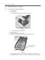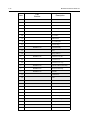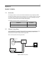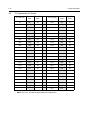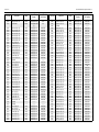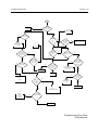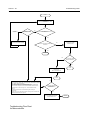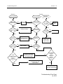
1
GP2000
Portable Radios
Service Manual
6804112J41-O
June, 2001
Computer Software Copyrights
The Motorola products described in this manual may include copyrighted Motorola computer programs stored
in semiconductor memories or other media. Laws in the United States and other countries preserve for
Motorola certain exclusive rights for copyrighted computer programs, including the exclusive right to copy or
reproduce in any form, the copyrighted computer program. Accordingly, any copyrighted Motorola computer
programs contained in the Motorola products described in this manual may not be copied or reproduced in
any manner without the express written permission of Motorola. Furthermore, the purchase of Motorola products shall not be deemed to grant, either directly or by implication, estoppel or otherwise, any license under
the copyrights, patents or patent applications of Motorola, except for the normal non-exclusive royalty-free
license to use that arises by operation of law in the sale of a product.
iii
SAFETY INFORMATION
SAFETY AND GENERAL INFORMATION
IMPORTANT INFORMATION ON SAFE AND EFFICIENT OPERATION.
READ THIS INFORMATION BEFORE USING YOUR RADIO.
The information provided in this document supersedes the general safety information contained in
user guides published prior to October 2000. For information regarding radio use in a hazardous
atmosphere please refer to the Factory Mutual (FM) Approval Manual Supplement or Instruction
Card, which is included with radio models that offer this capability.
RADIO FREQUENCY (RF) OPERATIONAL CHARACTERISTICS
To transmit (talk) you must push the Push-To-Talk button; to receive (listen) you must release
the Push-To-Talk button. When the radio is transmitting, it generates radio frequency (RF) energy;
when it is receiving, or when it is off, it does not generate RF energy.
RADIO OPERATION AND EME EXPOSURE
Your Motorola radio is designed to comply with the following national and international standards and
guidelines regarding exposure of human beings to radio frequency electromagnetic energy (EME):
¥ United States Federal Communications Commission, Code of
Federal Regulations; 47 CFR part 2 sub-part J
¥ American National Standards Institute (ANSI) / Institute of
Electrical and Electronic Engineers (IEEE) C95. 1-1992
¥ Institute of Electrical and Electronic Engineers (IEEE) C95.1-1999 Edition
¥ National Council on Radiation Protection and Measurements (NCRP) of the United States,
Report 86, 1986
¥ International Commission on Non-Ionizing Radiation Protection (ICNIRP) 1998
¥ Ministry of Health (Canada) Safety Code 6. Limits of Human
Exposure to Radiofrequency Electromagnetic Fields in the
Frequency Range from 3 kHz to 300 GHz, 1999
¥ Australian Communications Authority Radiocommunications (Electromagnetic Radiation Human Exposure) Standard 1999 (applicable to wireless phones only)
To assure optimal radio performance and make sure human exposure to radio frequency
electromagnetic energy is within the guidelines set forth in the above standards, always
adhere to the following procedures:
Two-way Radio Operation
When using your radio, hold the radio in a vertical position
with the microphone one to two inches (2.5 to 5 centimeters)
away from the lips.
2.5 to 5.0 cm
(1 to 2 in.)
Body-worn Operation
To maintain compliance with FCC RF exposure guidelines, if you
wear a radio on your body when transmitting, always place the
radio in a Motorola approved clip, holder, holster, case, or
body harness for this product. Use of non-Motorola-approved accessories may exceed FCC RF
exposure guidelines. If you do not use a Motorola approved body-worn accessory and are not
using the radio in the intended use positions along side of the head in the phone mode or in
front of the face in the two-way radio mode, then ensure the antenna and radio is kept the
following minimum distances from the body when transmitting:
¥
¥
Phone or Two-way radio mode: one inch (2.5 centimeters)
Data operation using any data feature with or without an accessory cable: one inch (2.5
centimeters)
iv
SAFETY INFORMATION
Antenna Care
Use only the supplied or an approved replacement antenna.
Unauthorized antennas, modiÞcations, or attachments could damage the radio and may violate FCC
regulations.
DO NOT hold the antenna when the radio is ÒIN USEÓ. Holding the antenna affects call quality and
may cause the radio to operate at a higher power level than needed.
Approved Accessories
For a list of approved Motorola accessories look in the appendix or accessory section of your radioÕs
User Guide.
ELECTROMAGNETIC INTERFERENCE/COMPATIBILITY
NOTE Nearly every electronic device is susceptible to electromagnetic interference (EMI) if inade-
quately shielded, designed, or otherwise conÞgured for electromagnetic compatibility.
Facilities
To avoid electromagnetic interference and/or compatibility conßicts, turn off your radio in any facility
where posted notices instruct you to do so. Hospitals or health care facilities may be using equipment
that is sensitive to external RF energy.
Aircraft
When instructed to do so, turn off your radio when on board an aircraft. Any use of a radio must be in
accordance with applicable regulations per airline crew instructions.
Medical Devices
¥
Pacemakers
The Health Industry Manufacturers Association recommends that a minimum separation of 6 inches
(15 centimeters) be maintained between a handheld wireless radio and a pacemaker. These
recommendations are consistent with those of the U.S. Food and Drug Administration.
Persons with pacemakers should:
¥
¥
¥
¥
¥
ALWAYS keep the radio more than six inches (15 centimeters) from their pacemaker when the
radio is turned ON.
not carry the radio in the breast pocket.
use the ear opposite the pacemaker to minimize the potential for interference.
turn the radio OFF immediately if you have any reason to suspect that interference is taking
place.
Hearing Aids
Some digital wireless radios may interfere with some hearing aids. In the event of such interference,
you may want to consult your hearing aid manufacturer to discuss alternatives.
¥
Other Medical Devices
If you use any other personal medical device, consult the manufacturer of your device to determine
if it is adequately shielded from RF energy. Your physician may be able to assist you in obtaining
this information.
SAFETY INFORMATION
v
SAFETY AND GENERAL
Use While Driving
Check the laws and regulations on the use of radios in the area where you drive. Always obey them.
When using your radio while driving, please:
¥
¥
¥
Give full attention to driving and to the road.
Use hands-free operation, if available.
Pull off the road and park before making or answering a call if driving conditions so require.
OPERATIONAL WARNINGS
For Vehicles With An Air Bag
Do not place a portable radio in the area over an air bag or in the air bag deployment
area. Air bags inßate with great force. If a portable radio is placed in the air bag
deployment area and the air bag inßates, the radio may be propelled with great force
and cause serious injury to occupants of the vehicle.
!
WARNING
Potentially Explosive Atmospheres
Turn off your radio prior to entering any area with a potentially
explosive atmosphere, unless it is a radio type especially qualiÞed for use in such areas as
ÒIntrinsically SafeÓ (for example, Factory Mutual, CSA, UL, or CENELEC). Do not remove, install, or
charge batteries in such areas. Sparks in a potentially explosive atmosphere can cause an explosion
or Þre resulting in bodily injury or even death.
NOTE The areas with potentially explosive atmospheres referred to above include fueling
areas such as below decks on boats, fuel or chemical transfer or storage facilities,
areas where the air contains chemicals or particles, such as grain, dust or metal powders, and any other area where you would normally be advised to turn off your vehicle engine. Areas with potentially explosive atmospheres are often but not always
posted.
Blasting Caps And Areas
To avoid possible interference with blasting operations, turn off your radio when you are near
electrical blasting caps, in a blasting area, or in areas posted: ÒTurn off two-way radio.Ó Obey all signs
and instructions.
OPERATIONAL CAUTIONS
Antennas
Do not use any portable radio that has a damaged antenna. If a damaged antenna
comes into contact with your skin, a minor burn can result.
!
Caution
Batteries
All batteries can cause property damage and/or bodily injury such as burns if a conductive material
such as jewelry, keys, or beaded chains touch exposed terminals. The conductive material may
complete an electrical circuit (short circuit) and become quite hot. Exercise care in handling any
charged battery, particularly when placing it inside a pocket, purse, or other container with metal
objects.
vi
SAFETY INFORMATION
vii
Table of Contents
Section 1
INTRODUCTION
1.0 Scope of Manual.................................................................................................. 1-1
2.0 Warranty and Service Support............................................................................. 1-1
2.1 Warranty Period and Return Instructions ....................................................... 1-1
2.2 After Warranty Period..................................................................................... 1-1
2.3 Piece Parts ..................................................................................................... 1-2
2.4 Technical Support .......................................................................................... 1-2
3.0 Radio Model Information...................................................................................... 1-3
Section 2
MAINTENANCE
1.0 Introduction .......................................................................................................... 2-1
2.0 Preventive Maintenance ...................................................................................... 2-1
2.1 Inspection ....................................................................................................... 2-1
2.2 Cleaning Procedures...................................................................................... 2-1
3.0 Safe Handling of CMOS and LDMOS Devices.................................................... 2-2
4.0 Repair Procedures and Techniques Ñ General.................................................. 2-3
5.0 Disassembling and Reassembling the Radio Ñ General.................................... 2-4
6.0 Radio Disassembly Ñ Detailed ........................................................................... 2-5
6.1 Front Cover from Chassis Disassembly ......................................................... 2-5
6.2 Control Board Disassembly............................................................................ 2-7
6.3 RF Board Disassembly................................................................................... 2-7
7.0 Radio Reassembly Ñ Detailed............................................................................ 2-8
7.1 RF Board Reassembly ................................................................................... 2-8
7.2 Control Board Reassembly ............................................................................ 2-8
7.3 Chassis and Front Cover Reassembly........................................................... 2-8
8.0 Mechanical View and Parts List......................................................................... 2-11
8.1 Exploded View and Parts List....................................................................... 2-11
9.0 Service Aids....................................................................................................... 2-14
10.0 Test Equipment.................................................................................................. 2-15
11.0 Programming Cable (DSK001C706) ................................................................. 2-16
12.0 IF Test Box (DSK001C702) ............................................................................... 2-17
Section 3
RADIO TUNING
1.0 Introduction .......................................................................................................... 3-1
2.0 Radio Tuning Setup ............................................................................................. 3-2
Section 4
RADIO PROGRAMMING
1.0 Introduction .......................................................................................................... 4-1
2.0 CPS Programming Setup .................................................................................... 4-1
3.0 Programming Your Radio .................................................................................... 4-2
3.1 Overview of the Programming Process.......................................................... 4-2
viii
3.2 Cloning Radio Parameters to User Radios.....................................................4-2
3.3 Parameters which are cloned .........................................................................4-2
3.4 Parameters which are not cloned ...................................................................4-2
3.5 To Clone a Radio............................................................................................4-2
3.6 Error Conditions..............................................................................................4-3
3.7 Dealer and User Configurations .....................................................................4-3
4.0 Programming Mode..............................................................................................4-4
4.1 Introduction .....................................................................................................4-4
4.2 Entering Programming Mode..........................................................................4-4
4.3 Exiting Programming Mode ............................................................................4-4
4.4 Accessing Programming Mode Parameters ...................................................4-4
4.5 Editing RW (Radio Wide) Parameters ............................................................4-5
4.6 Editing Channel Parameters.........................................................................4-11
4.7 Editing VFO Parameters...............................................................................4-14
4.8 PL Frequencies and Codes ..........................................................................4-18
4.9 DPL Codes ...................................................................................................4-19
4.10 Examples ......................................................................................................4-20
4.11 Factory Reset ...............................................................................................4-22
Section 5
Error Code Displays
1.0 Error Codes..........................................................................................................5-1
Section 6
1.0
2.0
3.0
4.0
5.0
6.0
7.0
8.0
ACCESSORIES
Antennas ..............................................................................................................6-1
Carrying Accessories ...........................................................................................6-1
Carry Cases .........................................................................................................6-1
Chargers ..............................................................................................................6-2
Batteries ...............................................................................................................6-2
Audio Accessories................................................................................................6-2
Manuals................................................................................................................6-2
Service Kits ..........................................................................................................6-3
Section 7
VHF Band Information (136-174 Mhz)
1.0 Model Chart..........................................................................................................7-1
2.0 Specifications .......................................................................................................7-3
3.0 Theory of Operation .............................................................................................7-4
3.1 General Information ........................................................................................7-4
3.2 Power Distribution...........................................................................................7-4
3.3 Power up Sequence .......................................................................................7-4
3.4 CPU / Control Section.....................................................................................7-5
3.5 VCO / Synthesizer Section .............................................................................7-5
3.6 Transmitter Section.........................................................................................7-6
3.7 Receiver Section.............................................................................................7-7
3.8 Battery Section ...............................................................................................7-8
ix
4.0 Block Diagrams.................................................................................................... 7-9
4.1 Complete ........................................................................................................ 7-9
4.2 Controller...................................................................................................... 7-10
4.3 VCO.............................................................................................................. 7-10
4.4 Transmitter ................................................................................................... 7-11
4.5 Receiver ....................................................................................................... 7-11
5.0 Circuit Board/Schematic Diagrams and Parts List............................................. 7-13
Controller Board .................................................................................................. 7-13
VHF 136-174 MHz Main Board Top Side............................................................. 7-14
VHF 136-174 MHz Main Board Bottom Side........................................................ 7-15
Complete Controller Board Schematic Diagram .................................................. 7-16
VHF 136-174 MHz RF Board Schematic Diagram............................................... 7-17
VHF 136-174 MHz Radio Parts List (Controller Board)........................................ 7-18
6.0 Troubleshooting charts ...................................................................................... 7-27
Troubleshooting Flow Chart for Receiver............................................................. 7-27
Troubleshooting Flow Chart for Transmitter......................................................... 7-28
Troubleshooting Flow Chart for Synthesizer ........................................................ 7-29
Troubleshooting Flow Chart for Microcontroller ................................................... 7-30
Troubleshooting Flow Chart for VCO ................................................................... 7-31
Glossary of Terms ....................................................................................... G-1
x
1-1
Section 1
INTRODUCTION
1.0
Scope of Manual
This manual is intended for use by service technicians familiar with similar types of equipment. It
contains service information required for the equipment described and is current as of the printing
date. Changes which occur after the printing date may be incorporated by a complete Manual
revision or alternatively as additions.
NOTE Before operating or testing these units, please read the Safety Information Section in the
front of this manual.
2.0
Warranty and Service Support
Motorola offers long term support for its products. This support includes full exchange and/or repair
of the product during the warranty period, and service/ repair or spare parts support out of warranty.
Any "return for exchange" or "return for repair" by an authorised Motorola Dealer must be
accompanied by a Warranty Claim Form. Warranty Claim Forms are obtained by contacting an
Authorised Motorola Dealer.
2.1
Warranty Period and Return Instructions
The terms and conditions of warranty are deÞned fully in the Motorola Dealer or Distributor or
Reseller contract. These conditions may change from time to time and the following notes are for
guidance purposes only.
In instances where the product is covered under a "return for replacement" or "return for repair"
warranty, a check of the product should be performed prior to shipping the unit back to Motorola.
This is to ensure that the product has been correctly programmed or has not been subjected to
damage outside the terms of the warranty.
Prior to shipping any radio back to the appropriate Motorola warranty depot, please contact
Customer Resources (Please see page 2 and page 3 in this Chapter). All returns must be
accompanied by a Warranty Claim Form, available from your Customer Services representative.
Products should be shipped back in the original packaging, or correctly packaged to ensure no
damage occurs in transit.
2.2
After Warranty Period
After the Warranty period, Motorola continues to support its products in two ways.
1.
Motorola's Accessories and Aftermarket Division (AAD) offers a repair service to both end
users and dealers at competitive prices.
2.
AAD supplies individual parts and modules that can be purchased by dealers who are technically capable of performing fault analysis and repair.
1-2
2.3
Warranty and Service Support
Piece Parts
Some replacement parts, spare parts, and/or product information can be ordered directly. If a
complete Motorola part number is assigned to the part, it is available from MotorolaÕs Accessories
and Aftermarket Division (AAD). If no part number is assigned, the part is not normally available
from Motorola. If the part number is appended with an asterisk, the part is serviceable by Motorola
Depot only. If a parts list is not included, this generally means that no user-serviceable parts are
available for that kit or assembly.
All orders for parts/information should include the complete Motorola identiÞcation number. All part
orders should be directed to your local AAD ofÞce. Please refer to your latest price pages.
2.4
Technical Support
Technical support is available to assist the dealer/distributor in resolving any malfunction which may
be encountered. Initial contact should be by telephone wherever possible. When contacting
Motorola Technical Support, be prepared to provide the product model number and the unitÕs serial
number.
Toll-Free
Location
Number
Australia
1800-774457
China
800-810-0976
Hong Kong SAR
25904800
Indonesia
0800-1-686868
Korea
080-300-7400
Malaysia
1800-801687
New Zealand
0800-442109
Philippines
1800-16510271
Singapore
1800-4855333
Taiwan
0080-651661
Thailand (outside Bangkok)
088-225412
Non-Toll-Free
Location
Number
India
80-6658922
Thailand (Bangkok area)
2548388
All Other Countries
IDD Code+(65)-4855333
Radio Model Information
3.0
1-3
Radio Model Information
The model number and serial number are located on a label attached to the back of your radio. You
can determine the RF output power, frequency band, protocols, and physical packages. The
example below shows one portable radio model number and its speciÞc characteristics.
Table 1-1 Radio Model Number (Example: AZH49KBH6AA9)
AZ
Type
of
Unit
Model
Series
Freq.
Band
Power
Level
Physical
Packages
Channel
Spacing
Protocol
Feature
Level
H
49
K
(136-174
MHz)
B
1W
F
Limited
Keypad with
Display
4
12.5K
AA
Conventional
6
GP2100
N
(216-257
MHz)
C
4W
H
Full Keypad
with Display
6
20/25K
Q
(403-440
MHz)
D
5W
R
(435-480
MHz)
H = Portable
AZ = Asia Regional Prefix
8
12.5/25K
9
GP2000
1-4
This page is intentionally left blank.
2-1
Section 2
MAINTENANCE
1.0
Introduction
This chapter provides details about the following:
2.0
¥
Preventive Maintenance
¥
Safe Handling of CMOS and LDMOS Devices
¥
General Repair Procedures and Techniques
¥
Disassembling and Reassembling the Radio
Preventive Maintenance
The radios do not require a scheduled preventive maintenance program; however, periodic visual
inspection and cleaning is recommended.
2.1
Inspection
Check that the external surfaces of the radio are clean, and that all external controls and switches
are functional. It is not recommended to inspect the interior electronic circuitry.
2.2
Cleaning Procedures
The following procedures describe the recommended cleaning agents and the methods to be used
when cleaning the external and internal surfaces of the radio. External surfaces include the front
cover, housing assembly and battery case. These surfaces should be cleaned whenever a periodic
visual inspection reveals the presence of smudges, grease, and/or grime.
NOTE Internal surfaces should be cleaned only when the radio is disassembled for service
or repair.
The only recommended agent for cleaning the external radio surfaces is a 0.5% solution of a mild
dishwashing detergent in water. The only factory recommended liquid for cleaning the printed circuit
boards and their components is isopropyl alcohol (70% by volume).
!
CAUTION: The effects of certain chemicals and their vapors can have harmful results on certain plastics. Avoid using aerosol sprays, tuner cleaners, and other chemicals.
Cleaning External Plastic Surfaces
Apply the 0.5% detergent-water solution sparingly with a stiff, non-metallic, short-bristled brush to
work all loose dirt away from the radio. Use a soft, absorbent, lintless cloth or tissue to remove the
solution and dry the radio. Make sure that no water remains entrapped near the connectors, cracks,
or crevices.
2-2
Safe Handling of CMOS and LDMOS Devices
Cleaning Internal Circuit Boards and Components
Isopropyl alcohol (70%) may be applied with a stiff, non-metallic, short-bristled brush to dislodge
embedded or caked materials located in hard-to-reach areas. The brush stroke should direct the
dislodged material out and away from the inside of the radio. Make sure that controls or tunable
components are not soaked with alcohol. Do not use high-pressure air to hasten the drying process
since this could cause the liquid to collect in unwanted places. After completing of the cleaning
process, use a soft, absorbent, lintless cloth to dry the area. Do not brush or apply any isopropyl
alcohol to the frame, front cover, or back cover.
NOTE Always use a fresh supply of alcohol and a clean container to prevent contamination by
dissolved material (from previous usage).
3.0
Safe Handling of CMOS and LDMOS Devices
Complementary metal-oxide semiconductor (CMOS) devices are used in this family of radios, and
are susceptible to damage by electrostatic or high voltage charges. Damage can be latent, resulting
in failures occurring weeks or months later. Therefore, special precautions must be taken to prevent
device damage during disassembly, troubleshooting, and repair.
Handling precautions are mandatory for CMOS circuits and are especially important in low humidity
conditions. DO NOT attempt to disassemble the radio without Þrst referring to the following
CAUTION statement.
!
CAUTION: This radio contains static-sensitive devices. Do not open the radio unless you are properly
grounded. Take the following precautions when working on this unit:
¥
Store and transport all CMOS devices in conductive material so that all exposed
leads are shorted together. Do not insert CMOS devices into conventional plastic
ÒsnowÓ trays used for storage and transportation of other semiconductor devices.
¥
Ground the working surface of the service bench to protect the CMOS device. We
recommend using the Motorola Static Protection Assembly (part number
0180386A82), which includes a wrist strap, two ground cords, a table mat, and a
ßoor mat.
¥
Wear a conductive wrist strap in series with a 100k resistor to ground. (Replacement
wrist straps that connect to the bench top covering are Motorola part number RSX4015.)
¥
Do not wear nylon clothing while handling CMOS devices.
¥
Do not insert or remove CMOS devices with power applied. Check all power
supplies used for testing CMOS devices to be certain that there are no voltage
transients present.
¥
When straightening CMOS pins, provide ground straps for the apparatus used.
¥
When soldering, use a grounded soldering iron.
¥
If at all possible, handle CMOS devices by the package and not by the leads. Prior
to touching the unit, touch an electrical ground to remove any static charge that you
may have accumulated. The package and substrate may be electrically common. If
so, the reaction of a discharge to the case would cause the same damage as
touching the leads.
Repair Procedures and Techniques Ñ General
4.0
2-3
Repair Procedures and Techniques Ñ General
Parts Replacement and Substitution
When damaged parts are replaced, identical parts should be used. If the identical replacement part
is not locally available, check the parts list for the proper Motorola part number and order the part
from the nearest Motorola Communications parts center listed in the Piece Parts section of this
manual.
Rigid Circuit Boards
This family of radios uses bonded, multi-layer, printed circuit boards. Since the inner layers are not
accessible, some special considerations are required when soldering and unsoldering components.
The printed-through holes may interconnect multiple layers of the printed circuit. Therefore, exercise
care to avoid pulling the plated circuit out of the hole.
When soldering near the 20-pin and 40-pin connectors:
¥
Avoid accidentally getting solder in the connector.
¥
Be careful not to form solder bridges between the connector pins.
¥
Examine your work closely for shorts due to solder bridges.
Flexible Circuits
The ßexible circuits are made from a different material than the rigid boards, and require different
soldering techniques. Excessive prolonged heat on a ßexible circuit can damage the material.
Therefore, avoid excessive heat and excessive bending.
For parts replacement, use the ST-1087 Temperature-Controlled Solder Station with a 600-700
degree F tip, and use small diameter solder such as ST-633. The smaller size solder will melt faster
and require less heat to be applied to the circuit.
To replace a component on a ßexible circuit:
1.
Grasp with seizers (hemostats) the edge of the ßexible circuit near the part to be removed.
2.
Pull gently.
3.
Apply the tip of the soldering iron to the component connections while pulling with the seizers.
NOTE Do not attempt to puddle-out components. Prolonged application of heat may damage the
ßexible circuit.
Chip Components
Use either the RLN-4062 Hot-Air Repair Station or the Motorola 0180381B45 Repair Station for chip
component replacement. When using the 0180381B45 Repair Station, select the TJ-65 minithermojet hand piece. On either unit, adjust the temperature control to 700 degrees F. (370 degrees
C), and adjust the airßow to a minimum setting. Airßow can vary due to component density.
¥
To remove a chip component, select a hot-air hand piece and position the nozzle of the hand
piece approximately 1/8Ó above the component to be removed. Begin applying the hot air.
Once the solder reßows, remove the component using a pair of tweezers. Using solder wick
and a soldering iron or a power desoldering station, remove the excess solder from the pads.
2-4
Disassembling and Reassembling the Radio Ñ General
¥
To replace a chip component using a soldering iron, select the appropriate micro-tipped
soldering iron and apply fresh solder to one of the solder pads. Using a pair of tweezers,
position the new chip component in place while heating the fresh solder. Once solder wicks
onto the new component, remove the heat from the solder. Heat the remaining pad with the
soldering iron and apply solder until it wicks to the component. If necessary, touch up the Þrst
side. All solder joints should be smooth and shiny.
¥
To replace a chip component using hot air, select the hot-air hand piece and reßow the solder
on the solder pads to smooth it. Apply a drop of solder paste ßux to each pad. using a pair of
tweezers, position the new component in place. Position the hot-air hand piece approximately
1/8Ó above the component and begin applying heat. Once the solder wicks to the component,
remove the heat and inspect the repair. All joints should be smooth and shiny.
Shields
Removing and replacing shields will be done with the R-1070 station with the temperature control
set to approximately 415¡F (215¡C); 445¡F (230¡C) max.
5.0
¥
To remove the shield, place the circuit board in the R-1070Õs holder. Select the proper heat
focus head and attach it to the heater chimney. Add solder paste ßux around the base of the
shield. Position the shield under the heat-focus head. Lower the vacuum tip and attach it to
the shield by turning on the vacuum pump. Lower the focus head until it is approximately 1/8Ó
(0.3cm) above the shield. Turn on the heater and wait until the shield lifts off the circuit board.
Once the shield is off, turn off the heat, grab the part with a pair of tweezers, and turn off the
vacuum pump. Remove the circuit board from the R-1070Õs circuit board holder.
¥
To replace the shield, add solder to the shield if necessary, using a micro-tipped soldering
iron. Next, rub the soldering iron tip along the edge of the shield to smooth out any excess
solder. Use solder wick and a soldering iron to remove excess solder from the solder pads on
the circuit board. Place the circuit board back in the R1070Õs circuit board holder. Place the
shield on the circuit board using a pair of tweezers. Position the heat-focus head over the
shield and lower it to approximately 1/8Ó above the shield. Turn on the heater and wait for the
solder to reßow.
Once complete, turn off the heat, raise the heat-focus head and wait approximately one
minute for the part to cool. Remove the circuit board and inspect the repair. No cleaning
should be necessary.
Disassembling and Reassembling the Radio Ñ General
Since these radios may be disassembled and reassembled with the use of only four (board to
casting) screws, it is important to pay particular attention to the snaps and tabs, and how parts align
with each other.
The following tools are required for disassembling the radio:
¥
Phillips screwdriver
¥
4mm socket wrench
If a unit requires more complete testing or service than is customarily performed at the basic level,
send this unit to a Motorola Authorized Service Center.
Radio Disassembly Ñ Detailed
2-5
6.0
Radio Disassembly Ñ Detailed
6.1
Front Cover from Chassis Disassembly
1.
Turn off the radio.
2.
Remove the battery:
a.
Slide the battery clasp away from the radio (see ÒFigure 2-1Ó).
Figure 2-1
b.
Slide battery down and away from radio.
3.
Remove the antenna.
4.
Pull the On/Off Volume knob off of its shaft.
5.
Remove the two screws at the back of the rear chassis (see ÒFigure 2-2Ó).
Insert screwdriver here
to remove chasis.
Figure 2-2
6.
Insert a small ßat-head screw driverÊat the bottom of the radio, between the chassis and
housingÊ(location marked in "Figure 2.2"), and lift the chassis gently. Be careful not to damage
2-6
Radio Disassembly Ñ Detailed
the housing or the O-ring underneath.
7.
Lift rear chassis away from the front cover (see ÒFigure 2-3Ó). Be careful not to damage the
speaker wire underneath.
Figure 2-3
8.
Slide the rear chassis downwards, and away from the front cover.
9.
Remove the speaker connector, which connects between RF Board and the internal speaker
on front cover (see ÒFigure 2-4Ó).
Figure 2-4
Radio Disassembly Ñ Detailed
6.2
2-7
Control Board Disassembly
1.
Remove the screws which hold the control board to the RF board.
2.
Remove the control board (the control board is connected to the RF board through a boardto-board connector -- see ÒFigure 2-5Ó).
board-to-board
connector
Figure 2-5
6.3
RF Board Disassembly
1.
Remove the screws and the stud which hold the RF board to the rear diecast with the Phillips
head screw driver and socket wrench respectively.
2.
Gently remove the RF board from rear diecast. The completely disassembly radio is shown in
ÒFigure 2-6Ó.
Figure 2-6 Completely Disassembled Radio
2-8
Radio Reassembly Ñ Detailed
7.0
Radio Reassembly Ñ Detailed
7.1
RF Board Reassembly
7.2
1.
Place the RF board on the rear diecast.
2.
Tighten the screws and the stud.
Control Board Reassembly
1.
Place the control board on the RF board.
2.
Connect the control board to the RF board by pressing it Þrmly downwards at the board-toboard connector (see ÒFigure 2-7Ó).
board-to-board
connector
Figure 2-7
3.
7.3
Tighten the screws using screwdriver to hold the control board in place.
Chassis and Front Cover Reassembly
1.
Connect the RF board to the internal speaker on front cover with the speaker connector (see
ÒFigure 2-8Ó).
Figure 2-8
2.
Place the front cover over the tabs on the rear diecast.
3.
Insert the On/Off Volume shaft into the front cover opening.
Radio Reassembly Ñ Detailed
4.
2-9
Lower the front cover until the bottom edges snap Þrmly into place on the rear diecast (see
ÒFigure 2-9Ó)
Figure 2-9
5.
Tighten the two (2) screws at the bottom of rear diecast using a screwdriver (see ÒFigure 210Ó).
Figure 2-10
6.
Attach the battery.
2-10
Radio Reassembly Ñ Detailed
7.
Attach the On/Off Volume Knob, and Antenna.
Figure 2-11 Completely Reassembled radio.
Mechanical View and Parts List
2-11
Mechanical View and Parts List
8.1
Exploded View and Parts List
16
8a
13
3b
3a
17
7a
7b
1
7c
7d
9
5
4b
4a
2a
11
6
12
2b
15
8b
2c
10
2d
2e
8c
2f
2g
14
8.0
Figure 2-12 Alpha Series Radio Exploded View
2-12
Mechanical View and Parts List
Item
Part
Number
1
DS1M001110
Front Cover Kit
2
DS1M001120
Chassis Hardware Kit
Description
2a
Rod (M2)
2b
Heatsink Tape
2c
Gasket (Screw M2.6)
2d
Screw M2.6
2e
PCB Bracket
2f
Screw M2 CÞms
2g
External Tape
3
DS1M001130
Knob Assembly
3a
Knob
3b
Spring (D4.75)
4
DS1M001140
External Cover Kit
4a
External Cover
4b
External Cover Cap
5
DS1M001150
Controller Board Assembly
6
DS1M001160
RF Board Assembly
7
DS1M001170
LCD Kit
7a
LCD Bracket
7b
LCD
7c
Interconnector
7d
Reßector
8
DS1M001180
Label Kit
8a
Label (Nameplate)
8b
Label (Serial)
8c
Label (Tuning)
9
DS1M001190
Speaker Assembly
10
PMNN4046
11
DSM2192004
Contact Gasket
12
DSM2192005
Main Gasket
Battery
Mechanical View and Parts List
2-13
Item
Part
Number
13
DSM2192006
14
HLN9844
15
DSM5190001
Back Housing
16
DSM6189003
PTT Button
17
Frequency dependant. Please see "Antennas" on page 6-1
Description
Volume Gasket
Beltclip
Antenna
2-14
Service Aids
9.0
Service Aids
Table 2-1 lists service aids recommended for working on the Alpha Series Radios. While all of these
items are available from Motorola, most are standard shop equipment items, and any equivalent
item capable of the same performance may be substituted for the item listed.
Table 2-1 Service Aids
Motorola
Part No.
Description
Application
PMVN4059_
Customer Programming Software - Software on 3.5Ó ßoppy
diskettes
Program customer option and channel data.
PMVN4061_
Customer Programming Software - Software on CD Rom
Program customer option and channel data.
PMVN4060_
Tuner - Software on 3.5Ó ßoppy
diskettes
Tune hardware parameters, front end, power, etc.
PMVN4062_
Tuner - Software on CD Rom
Tune hardware parameters, front end, power, etc.
DSK001C706
Programming Cable (2.5mm)
Connects radio and IF Test Box to Computer.
PMKN4003A
Cloning Cable (2.5mm)
To clone programmable information from one radio to
another radio.
DSK001C704
Test Cable
Connects radio to IF Test Box.
DSK001C714
Interconnect Service Cable
Connects RF board and CPU board.
DSK001C702
IF Test Box
Enables connection to the audio/accessory jack.
Allows switching for radio testing.
DSK001C705
Battery Eliminator
Interconnects radio to power supply (red-and-black
power cable included).
HLN8262A
BNC Adaptor
Adapts radioÕs antenna port to BNC cabling of test
equipment.
ENG/DA51
Ceramic Tuning Tool
To tune the variable resistor (RV601 for audio modulation adjustment and RV602 for sub-audio modulation adjustment).
4 mm Socket Wrench
Used to remove hexagon stud from the RF board.
Phillips Head Screwdriver
Used to remove M2 and M2.6 Phillips screws.
Repairing Leadless Component Assemblies
How to successfully remove and replace surface
mount devices.
TT907A
National Service Technical
Guide
Test Equipment
10.0
2-15
Test Equipment
Table 2-2 lists test equipment required to service the Alpha Series Radios and other two-way radios.
Table 2-2 Recommended Test Equipment
Motorola Part
No.
Description
R2000 or R2400
Service Monitor
*R1049
Digital Multimeter
*S1100
Audio Oscillator
67 to 200Hz tones
Used with service monitor for
injection of PL tones
*S1053,
*SKN6009,
*SKN6001
AC Voltmeter,
Power Cable for
meter, Test leads
for meter
1 mV to 300 V,
10 Mega Ohm input
impedance
Audio voltage measurements
R1053
Dual-trace Oscilloscope
20 MHz bandwidth,
5 mV/cm - 20 V/cm
Waveform measurements
*S1350, *ST1215
(VHF)
*ST1223 (UHF)
*T1013
Wattmeter,
Plug-in Elements
(VHF & UHF), RF
Dummy Load
50-Ohm, ±5% accuracy
10 W, max. 0-1000
MHz, 300 W
Transmitter power output
measurements
S1339
RF Millivolt Meter
100 mV to 3 VRF, 10
kHz to 1.2 GHz
RF level measurements
*R1013
SINAD Meter
S1347 or
S1348 (prog)
DC Power Supply
Characteristics
This monitor will
substitute for items with
an asterisk *
Application
Frequency/deviation meter
and signal generator for
wide-range troubleshooting
and alignment
Two meters recommended
for AC/DC voltage and current measurements
Receiver sensitivity measurements
0-20 Vdc, 0-5 Amps
Bench supply for 7.5Vdc
2-16
Programming Cable (DSK001C706)
11.0 Programming Cable (DSK001C706)
Figure 2-13 Programming Cable Schematic
5
4
9
3
8
2
7
1
6
Figure 2-14 Pin ConÞguration of the Side Connector
IF Test Box (DSK001C702)
2-17
12.0 IF Test Box (DSK001C702)
Figure 2-15 IF Test Box Schematic
2-18
This page is intentionally left blank.
3-1
Section 3
RADIO TUNING
1.0
Introduction
This chapter provides an overview of the software and hardware tuning for Alpha Series Radio.
The Alpha Series Radios Universal Tuner is designed for use in a Windows 95/98/NT environment.
This software and the Customer Programming Software (see page 4-1) essentially cover all the
functions of the traditional Radio Service Software (RSS) package.
An Installation instruction manual is contained within each kit.
Description
2.0
Kit Number
Tuner Installation Kit (Disk)
PMVN4060_
Tuner Installation Kit (CD)
PMVN4062_
Software Tuning Setup
A Windows 95/98/NT PC (personal computer) and Tuner are required to tune parameters such as
power, sensitivity, squelch and RSSI. To perform the tuning procedures, the radio must be
connected to the PC and IF Test Set as shown in Þgure below.
Refer to online help Þles for the tuning procedures.
Antenna Port
Acc
Jack
Radio
IF TEST SET
DSK001C702
9 Pin
Test Cable
(DSK001C704) Connector
BNC BNC
Mic
Spk
Programming Cable
(DSK001C706)
N Type
TEST EQUIPMENT
BNC
Output
BNC
Input
Figure 3-1 Radio Tuning Setup
Comm
Port
3-2
3.0
Hardware Tuning Setup and Procedure
Hardware Tuning Setup and Procedure
There is a silver seal on the bottom left of the radio chassis. Remove the seal to expose the two
potentiometers for audio and sub-audio (CTCSS) modulation adjustment. RV601, which is slightly
higher, is the trimmer potentiometer for audio modulation tuning. The lower trimmer potentiometer
(RV602) is meant for sub-audio modulation tuning.
RV601
RV602
Figure 3-2 Tuning Ports
3.1
Audio Modulation Tuning
1.
Set the radio to transmit at 155.025MHz with low power. Set Channel Spacing to "CS-25.0"
for 25kHz (see ÒRadio ProgrammingÓ on page 4-1).
2.
On the test equipment, set it to receive at 155.025MHz and with the following conÞgurations :
Audio bandwidth: 0.25Hz to 15,000Hz.
De-emphasis: OFF
3.2
3.
Inject a 60mV 1kHz tone to the radio through the extenal mic connector.
4.
Key up the radio.
5.
Using the ceramic tuning tool, adjust RV601 to tune the audio modulation deviation to settle
between 4.3kHz to 4.5kHz.
Sub-Audio Modulation Tuning
1.
Set the radio to transmit at 155.025MHz with low power and Tx PL frequency of 100.0Hz. Set
Channel Spacing to "CS-25.0" for 25kHz (see ÒRadio ProgrammingÓ on page 4-1).
2.
On the test equipment, set it to receive at 155.025MHz and with the following conÞgurations :
Audio bandwidth: 0.25Hz to 3,000Hz.
De-emphasis : OFF
3.
Do NOT inject any tone to the radio.
4.
Key up the radio.
5.
Using the ceramic tuning tool, adjust RV602 to tune the sub-audio modulation deviation to
settle between 0.65kHz to 0.75kHz.
4-1
Section 4
RADIO PROGRAMMING
1.0
Introduction
This chapter provides an overview of the Alpha Series Radios Customer Programming Software
(CPS), which has been designed for use in a Windows 95/98/NT environment.
An Installation instruction manual is contained within each kit.
Description
2.0
Kit Number
Alpha Series Radio CPS Installation Kit (Disk)
PMVN4059_
Alpha Series Radio CPS Installation Kit (CD)
PMVN4061_
CPS Programming Setup
Refer to online help Þles for the CPS Programming procedures.
Radio
Programming Cable (2.5mm)
DSK001C706
Figure 4-1 CPS Programming Setup
4-2
3.0
3.1
Programming Your Radio
Programming Your Radio
Overview of the Programming Process
To prepare properly programmed radios for your customers, you should
3.2
1.
program your radio with all the necessary parameters, as required by your customers, and
then
2.
clone these parameters over to all your customerÕs radios.
Cloning Radio Parameters to User Radios
Cloning duplicates the contents of Radio 1 (master radio) into Radio 2 (slave radio). However,
tuning and alignment information are not affected by cloning.
3.3
3.4
3.5
Parameters which are cloned
¥
Radio Wide parameters
¥
Channel settings
¥
VFO settings
Parameters which are not cloned
¥
All hardware tuning and alignment parameters.
¥
Unit Serial Number.
To Clone a Radio
Cloning duplicates the contents of your radio (master radio) into your customerÕs radio (slave radio).
Tuning and alignment information are not affected by cloning.
1.
Turn off both the master and slave radios (if any of them are turned on).
2.
Connect both radios with the cloning cable through the Programming Port (lower port of the
Accessory Connector).
3.
Turn on the slave radio.
4.
Press and hold the A button, and turn on the master radio.
5.
The master radio displays CLONE if cloning can proceed, otherwise an error message is
shown.
6.
The slave radio displays PROG while it is being programmed.
7.
When cloning is completed, the master radio displays END, and the slave radio resets automatically.
8.
Disconnect radios from the cloning cable. They are now ready for operation.
Programming Your Radio
3.6
4-3
Error Conditions
An error may occur when cloning a radio. When this happens, an error message is displayed. The
following lists the causes and the possible solutions for each error message.
Error Message
3.7
Description
TIME OUT
Data communications time-out. Please ensure that the slave radio is
switched on, and the cloning cable is properly connected.
BCC ERR
Data communications checksum error.
TYPE ERR
Mismatch in model numbers. Please ensure that the master and slave radios
are of the same model number.
CMD ERR
Data communications command error.
Dealer and User ConÞgurations
Your radio is shipped out from the factory conÞgured according to the User ConÞguration. In this
conÞguration, users can only access the channels that are preprogrammed by the dealer. Channels
and other radio settings can ONLY be programmed when the radio is operating in Dealer
ConÞguration.
To prepare radios for the users, the dealer should
3.7.1
1.
Set the radio into Dealer ConÞguration (if the radio is conÞgured in User ConÞguration).
2.
Program the radio with all the necessary parameters, according to the usersÕ requirements.
3.
Set the radio back to User ConÞguration.
4.
Clone the radioÕs parameters to all the users' radios.
Switching between Dealer and User ConÞgurations
From Dealer to User
1.
Turn off the radio.
2.
Press PTT, the Monitor button and the + button together, and turn on the radio.
3.
LCD displays PROTECT.
4.
To conÞrm switching to User ConÞguration, press PTT. To cancel, press any other button.
5.
Turn off the radio. The radio now operates in User ConÞguration.
From User to Dealer
1.
Turn off the radio.
2.
Press PTT, the Monitor button and the + button together, and turn on the radio.
3.
LCD displays PRO-CLR.
4.
To conÞrm switching to Dealer ConÞguration, press PTT. To cancel, press any other button.
5.
Turn off the radio. The radio now operates in Dealer ConÞguration.
IMPORTANT:
If the radio is to be given to the customer, REMEMBER to switch it back
to operate in User ConÞguration.
4-4
Programming Mode
4.0
Programming Mode
4.1
Introduction
This mode allows you to edit a number of features to enhance the use of this radio.
4.2
Entering Programming Mode
If the radio is turned on, turn it off. Press and hold the MON, and turn on the radio. A ringing tone is
heard, which indicates that the radio is in Programming Mode. The K indicator is displayed.
4.3
Exiting Programming Mode
To exit Programming Mode, turn off the radio.
4.4
Accessing Programming Mode Parameters
In Dealer ConÞguration, Programming Mode parameters are grouped into three main categories:
RW (Radio Wide), Channel (001 to XXX1) and VFO (Variable Frequency Operation).
Use + or - buttons, to move from one category to another.
RW ßà CH 001 ßà CH 002 ßà É ßà CH XXX1 ßà VFO
NOTE: Radio operating in User ConÞguration is only restricted to RW parameters.
Once you have selected the category, and wish to view its parameters, use PTT or MON to move
from one parameter to the other, as shown in the next diagram.
1. XXX denotes the maximum number of channels supported by your radio model.
Programming Mode
4-5
Press +
RW
(Radio Wide)
Squelch Level
Programming Mode
CH 002
CH 001
Press PTT
Channel On/Off
Press PTT
CH XXX
Press PTT
VFO
Scan Upper
Limit
Scan List (1,2,3)
Rx Frequency
Scan Lower
Limit
Special PL (1,2,3)
Tx Frequency
Frequency
Step Size
Rx/Tx DPL Setting
Rx PL/DPL
Rx Frequency
Time Out Timer
Tx PL/DPL
Tx Frequency
.....
.....
.....
.....
.....
.....
PL/DPL
Code Type
Scan Type
Acknowledgement
Enable
Scan Interval
Time
Scan List
Press MON
PTT ID Enable
Press MON
Press MON
PL Required
for Selcall
Copy Channel
Scan Hang Time
4.5
.....
Press -
Editing RW (Radio Wide) Parameters
Radio Wide parameters are common to the whole radio. They become effective after you press PTT
or MON.
RW
Parameter
SQL-XX
Description
Range
Default
from
Factory
Squelch Level
SQL-00, É,
SQL-15
model
dependent
Remarks
¥ Select low level when you need to receive very
weak signal, and select high level when the communications distance is near, or your radio is receiving
interference.
¥ Press + or - to select the desired squelch level.
4-6
RW
Parameter
SCANLST1
Programming Mode
Description
Scan List 1
Range
1-01-XXX,
É,
1-16-XXX,
XXX denotes
channel number.
Default
from
Factory
1-01-001,
1-02-002,
...,
1-16-016
Remarks
¥ Up to 16 members per scan list. First member is
assigned as Priority Channel if Priority Scan is
started.
¥ When scanning is started, only these 16 members
will be scanned.
¥ Each channel can choose to use Scan List 1, 2 or
3.
¥ By default, all your channels select Scan List 1. If
there is special need to use the other two scan lists
for some of your channels, please consult your
dealer.
¥ Press + and - to move from one scan list member to
another.
¥ To include a channel into the scan list, enter the
desired channel number using the keypad.
¥ To erase a channel number from the scan list, press
#.
¥ Refer to "4.10.3 Setting Up a Scan List" on page
21 for details.
SCANLST2
Scan List 2
2-01-XXX,
É,
2-16-XXX
See Above.
SCANLST3
Scan List 3
3-01-XXX,
É,
3-16-XXX
See Above.
PL1-XXX.X
Special PL
Frequency 1
PL1-067.0,
PL1-067.1,
É,
PL1-254.9,
PL1-255.0
¥ You may program any PL frequency from 067.0 Hz
to 255.0 Hz, with 0.1 Hz resolution. This PL can then
be used as receive and/or transmit PL for VFO or
any channel.
¥ Up to three special PL frequencies are available.
¥ Use the keypad to enter the PL frequency directly.
¥ Out-of-bound PL frequency will not be accepted. A
negative tone is heard when attempted.
PL2-XXX.X
Special PL
Frequency 2
PL2-067.0,
PL2-067.1,
É,
PL2-254.9,
PL2-255.0
See above.
PL3-XXX.X
Special PL
Frequency 3
PL3-067.0,
PL3-067.1,
É,
PL3-254.9,
PL3-255.0
See above.
Programming Mode
RW
Parameter
4-7
Description
Range
Default
from
Factory
Remarks
RDPL-XXX
Rx DPL
Setting
RDPL-NOR,
RDPL-INV
RDPLNOR
¥ Select RDPL-NOR to use the DPL codes listed
under "4.9 DPL Codes" on page 19.
¥ Select RDPL-INV to invert the received DPL before
decoding it.
¥ Inverted coding allows for more trafÞc/usage on frequencies.
¥ DPL Invert must be set on both receiving and transmitting radios for communication to occur.
TDPL-XXX
Tx DPL
Setting
TDPL-NOR,
TDPL-INV
TDPLNOR
¥ Select TDPL-NOR to use the DPL codes listed
under "4.9 DPL Codes" on page 19.
¥ Select TDPL-INV to encode DPL by inverting all the
bits in the chosen DPL code, before sending it.
TOT-XXX
Time Out
Timer
TOT-OFF,
TOT-001,
É,
TOT-010
TOT-001
¥ This determines the maximum duration that you
can transmit continuously.
¥ Press + or - to select the desired time out timer.
BS-XXXX
Battery Saver
BS-OFF,
BS-NORM,
BS-ENH
BS-ENH
¥ Battery Saver helps to extend your battery life.
¥ When enabled, it turns off the radio receiver circuitry periodically when no activity is detected.
¥ BS-NORM (Normal) turns off less frequently. Select
this if you want to save battery and are expecting
Selective Calls.
¥ BS-ENH (Enhanced) turns off the receiver for a
longer duration. Select this if you want to maximize
battery saving, and do not expect to receive any
Selective Call.
¥ Press + or - to select the desired battery saver setting.
BT-XXXX
Battery Type
BT-NIMH,
BT-NICD,
BT-ALK
BT-NIMH
¥ Select the type of battery that your radio is using:
NIMH (Nickel Metal Hydride), NICD (Nickel Cadmium) or ALK (Alkaline).
¥ Press + or - to select the desired battery type.
NOTE: Not all battery types are available at the time
of printing. Please consult your dealer.
BEEP-X
Alert Tone Volume
BEEP-OFF,
BEEP-1,
BEEP-2,
BEEP-3
BEEP-3
¥ Select the alert tone volume needed. Select BEEPOFF if you require a quiet operation, or BEEP-3 if
you are working in a noisy environment.
¥ Press + or - to select the desired alert tone volume
setting.
PRM-XXX
Prime Channel
Select
PRM-OFF,
PRM-001,
É.,
PRM-YYY,
PRM-OFF
¥ Prime Channel is a channel that you wish to spend
most of your time monitoring.
¥ The radio always powers up in the Prime Channel,
if it is programmed.
¥ The radio will always switch back to the Prime
Channel if it is idle longer than the Prime Channel
Return Hang Time (programmable) in other channel.
¥ Press + or - to select the desired channel number
as Prime Channel.
YYY denotes
the highest
channel number supported by
your model.
4-8
RW
Parameter
Programming Mode
Default
from
Factory
Description
Range
Remarks
PRMT-XXX
Prime Channel
Return Hang
Time
PRMT-OFF,
PRMT-001,
...,
PRMT-015
PRMT-007
¥ This feature is only valid if a Prime Channel is programmed.
¥ XXX denotes the time that the radio will stay idle in
a non-Prime channel before switching back to the
Prime channel.
¥ Select OFF if you do not wish to switch to the Prime
channel automatically.
¥ Unit is in seconds. Prime Channel Return Hang
Time is therefore programmable from 1 second to 15
seconds in increments of 1 second.
PID-XXXX
PTT ID Transmit Manner
PID-OFF,
PID-PRE,
PID-POST,
PID-BOTH
PID-PRE
¥ Select how the PTT ID is transmitted: OFF (not
transmitted), PRE (transmitted upon PTT press),
POST (transmitted after PTT is released), BOTH
(transmitted upon PTT press as well as after PTT is
released).
¥ Press + or - to select the desired PTT ID transmit
manner.
NOTE: PTT ID has to be enabled on a per channel
basis to enable transmission.
ST-XXX
PTT ID
Sidetone
ST-OFF,
ST-ON
ST-ON
¥ When PTT ID Sidetone is enabled (ON), an alert
tone is heard as soon as PTT is pressed, and when
PTT ID is being sent.
¥ Press + or - to select ON or OFF.
SST-XXX
PTT ID Short
Sidetone
SST-OFF,
SST-ON
SST-OFF
¥ When PTT ID short sidetone is enabled (ON), an
alert tone is heard after PTT ID is sent. It indicates
that the user is ready to start talking.
¥ Press + or - to select ON or OFF.
PTM-XXXX
Tx Pretime
PTM-0000,
PTM-0025,
É.,
PTM-4000
PTM-0050
¥ Pretime is the duration from which PTT is pressed
to the time when PTT ID is ready to be sent.
¥ Adjust the pretime to suit the repeaterÕs response
time.
¥ Unit is in ms. Pretime is therefore programmable
from 0 ms to 4000 ms in 25 ms steps.
¥ Press + or - to select the desired pretime.
LGT-XXXX
Backlight
Select
LGT-AUTO,
LGT-TOGL
LGT-AUTO
¥ Selecting LGT-TOGL causes the Backlight button
to toggle the ON/OFF status of the LCD backlight.
¥ Selecting LGT-AUTO causes the backlight to be
turned off, if there is no keypress for more than 5
seconds.
¥ Press + or - to select the desired backlight setting.
PTT-ID
PTT ID
8 characters consist
of 1,2, É, 9,
0, A, B, C,
D, *, # and
Pause.
Blank
¥ PTT ID is sent when PTT is pressed. It serves as
the identity of your radio.
¥ Press + or - to move the cursor to the appropriate
character. Use the keypad to enter the ID. Pause can
be entered by pressing * followed by #. Enter # 8
times to erase ID.
¥ Refer to "4.10.4 Programming an ID" on page 21
for details.
Programming Mode
RW
Parameter
4-9
Description
Range
Default
from
Factory
Remarks
IND ID
Individual ID
8 characters consist
of 1,2, É, 9,
0, A, B, C,
D, *, and #.
Blank
¥ IND ID is a unique ID for the radio. When the radio
receives a Selcall which matches its IND ID, the
radio is said to have received an Individual Call. A
ringing tone will sound. If ACK ID is enabled and programmed, the ACK ID will be sent.
¥ Press + or - to move the cursor to the appropriate
character. Use the keypad to enter the ID. Enter # 8
times to erase ID.
¥ Refer to "4.10.4 Programming an ID" on page 21
for details.
GROUP ID
Group ID
8 characters consist
of 1,2, É, 9,
0, A, B, C,
D, *, and #.
Blank
¥ GROUP ID is an ID for the group where the radio
belongs. When the radio receives a Selcall which
matches its GROUP ID, the radio is said to have
received a Group Call.
¥ Press + or - to move the cursor to the appropriate
character. Use the keypad to enter the ID. Enter # 8
times to erase ID.
¥ Refer to "4.10.4 Programming an ID" on page 21
for details.
ALL ID
All ID
8 characters consist
of 1,2, É, 9,
0, A, B, C,
D, *, and #.
Blank
¥ ALL ID is like an ID for all. When the radio receives
a Selcall which matches its ALL ID, the radio is said
to have received an All Call.
¥ Press + or - to move the cursor to the appropriate
character. Use the keypad to enter the ID. Enter # 8
times to erase ID.
¥ Refer to "4.10.4 Programming an ID" on page 21
for details.
ACK ID
Acknowledgement ID
8 characters consist
of 1,2, É, 9,
0, A, B, C,
D, *, and #.
Blank
¥ ACK ID is sent when the radio receives an Individual Call and Acknowledgement is enabled.
¥ Press + or - to move the cursor to the appropriate
character. Use the keypad to enter the ID. Enter # 8
times to erase ID.
¥ Refer to "4.10.4 Programming an ID" on page 21
for details.
ASP-XXXX
Button A Short
Press Function
ASP-DISP,
ASP-LGHT,
ASP-LOCK,
ASP-NDEL,
ASP-NOP,
ASP-OFS,
ASP-PHN,
ASP-PID,
ASP-PL,
ASP-PRM,
ASP-PWR,
ASP-SCAN,
ASP-SQL,
ASP-TA,
ASP-VFO
ASP-PWR
¥ The four buttons (A, B, C and D) are programmable
to meet the needs of the user.
¥ The functions available include DISP (Channel
Alias), LGHT (Backlight), LOCK (Keypad Lock),
NDEL (Nuisance Channel Delete), NOP (No Operation), OFS (Offset Frequency), PHN (Phone Mode),
PID (PTT ID Enable), PL (PL/DPL Enable), PRM
(Prime Channel), PWR (Power Select), SCAN
(Scan), SQL (Squelch Level), TA (Talkaround), VFO
(VFO/Memory).
¥ Press + or - to select the desired function for the
button.
4-10
RW
Parameter
Programming Mode
Default
from
Factory
Description
Range
Remarks
ALP-XXXX
Button A Long
Press Action
ALP-DISP,
É
(See above)
ALP-PID
See above.
BSP-XXXX
Button B Short
Press Action
BSP-DISP,
É
(See above)
BSP-SQL
See above.
BLP-XXXX
Button B Long
Press Action
BLP-DISP,
É
(See above)
BLP-PHN
See above.
CSP-XXXX
Button C Short
Press Action
CSP-DISP,
É
(See above)
CSP-PL
See above.
CLP-XXXX
Button C Long
Press Action
CLP-DISP,
É
(See above)
CLPLOCK
See above.
DSP-XXXX
Button D Short
Press Action
DSP-DISP,
É
(See above)
DSPSCAN
See above.
DLP-XXXX
Button D Long
Press Action
DLP-DISP,
É
(See above)
DLP-NDEL
See above.
AC CODE
Access Code
16 characters consist
of 1,2, É, 9,
0, A, B, C,
D, *, # and
Pause.
Blank
¥ Access Code is dialed when you want to access the
landline telephone network.
¥ Once it is programmed, it can be sent by pressing
PTT, followed by +, and then *.
¥ Pause can be entered by pressing * followed by #.
¥ Enter # 16 times, to completely erase entered code.
¥ Refer to "4.10.5 Programming an Phone Number/
Access Code/De-access Code" on page 22 for
details.
DA CODE
De-access
Code
16 characters consist
of 1,2, É, 9,
0, A, B, C,
D, *, # and
Pause.
Blank
¥ De-access Code is dialed when you want to disconnect from the landline telephone network.
¥ Once it is programmed, it can be sent by pressing
PTT, followed by +, and then #.
¥ Pause can be entered by pressing * followed by #.
¥ Enter # 16 times, to completely erase entered code.
¥ Refer to "4.10.5 Programming an Phone Number/
Access Code/De-access Code" on page 22 for
details.
Programming Mode
RW
Parameter
4-11
Description
Range
Default
from
Factory
Remarks
TELNO-X
Telephone
Number
16 characters consist
of 1,2, É, 9,
0, A, B, C,
D, *, # and
Pause.
Blank
¥ Up to nine telephone numbers can be programmed.
¥ Once programmed into the memory, phone number
can be speed dialed by pressing PTT, + and then X,
where X denotes the telephone number location.
¥ Pause can be entered by pressing * followed by #.
¥ Enter # 16 times, to completely erase entered code.
¥ Refer to "4.10.5 Programming an Phone Number/
Access Code/De-access Code" on page 22 for
details.
PL-XXXX
PL/DPL
Display Type
PL-CODE,
PL-FREQ
PL-FREQ
¥ Select the display type of PL/DPL: FREQ and
CODE.
¥ If FREQ has been selected, then the PL and DPL
will be displayed in frequency and octal code format
respectively.
¥ If CODE has been selected, then the PL and DPL
will be displayed in Motorola code number format
(see "4.8 PL Frequencies and Codes" on page 18
and "4.9 DPL Codes" on page 19).
¥ Press + or - to select CODE or FREQ.
SIT-XXXX
Scan Interval
Time
SIT-0250,
SIT-0500,
ÉÉ,
SIT-5000
SIT-0500
¥ Scan Interval Time is the duration the radio will
spend on the landed channel before switching to
scan the Priority Channel in Priority Scanning.
¥ Unit is in ms. Scan Interval Time is therefore programmable from 250ms to 5000ms in 250ms steps.
¥ Press + or - to select the desired Scan Interval
Time.
SHT-XXXX
Scan Hang
Time
SHT-0500,
SHT-1000,
ÉÉ,
SHT-9500
SHT-7000
¥ Scan Hang Time is the duration the radio will stay
on the landed channel without detecting any activity
before it resumes scanning.
¥ Unit is in ms. Scan Hang Time is therefore programmable from 500ms to 9500ms in 500ms steps.
¥ Press + or - to select the desired Scan Hang Time.
4.6
Editing Channel Parameters
Channel parameters only affect the channel where the parameters are modiÞed. They become
effective after you press PTT or MON.
Channel
Parameter
CH-XX
Description
Channel On/
Off
Range
CH-OFF,
CH-ON
Default
from
Factory
CH-ON
Remarks
¥ Select if the channel is enabled (ON) or disabled
(OFF).
¥ Disabled channel will not be accessible in Normal
Mode.
¥ Press + or - to select ON or OFF.
4-12
Channel
Parameter
Programming Mode
Description
Range
Default
from
Factory
Remarks
RXXX.XXXX
Channel
Receive Frequency
Within the
band limits
of your
model
R136.0250
¥ This is the frequency that the channel will use to
receive message.
¥ You are not allowed to enter out-of-bounds frequencies.
¥ Use the keypad to enter the frequency directly.
TXXX.XXXX
Channel
Transmit Frequency
Within the
band limits
of your
model
T136.0250
¥ This is the frequency that the channel will use to
transmit message.
¥ You are not allowed to enter out-of-bounds frequencies.
¥ Use the keypad to enter the frequency directly.
RPL-XXXX
Channel
Receive PL/
DPL
When PLFREQ is
selected in
RW:
OFF, 067.0,
É, 254.1,
023.D,
025.D,
É,754.D,
PL1, PL2,
PL3
OR
When PLCODE is
selected in
RW:
000, 001,
É, 126,
PL1, PL2,
PL3
RPL-OFF
¥ This is the PL or DPL code that the channel will use
to unsquelch the receive message.
¥ Two display formats are available: FREQ and
CODE, selectable in RW.
¥ OFF or 000 indicates that no PL/DPL is used for
receive, i.e., radio operates in carrier squelch mode.
¥ Press + or - to select the desired PL/DPL.
TPL-XXXX
Channel
Transmit PL/
DPL
When PLFREQ is
selected in
RW:
OFF, 067.0,
É, 254.1,
023.D,
025.D,
É,754.D,
PL1, PL2,
PL3
OR
When PLCODE is
selected in
RW:
000, 001,
É, 126,
PL1, PL2,
PL3
TPL-OFF
¥ This is the PL or DPL code that the channel will use
to transmit the message.
¥ Two display formats are available: FREQ and
CODE, selectable in RW.
¥ OFF or 000 indicates that no PL/DPL is used for
transmit.
¥ Press + or - to select the desired PL/DPL.
Programming Mode
Channel
Parameter
4-13
Description
Range
Default
from
Factory
Remarks
TOC-XXX
Turn Off Code/
Reverse Burst
TOC-OFF,
TOC-ON
TOC-ON
¥ TOC or Reverse Burst serves to cause the receiving radio to mute its speaker before a loss of carrier
is detected.
¥ If enabled (ON), Turn Off Code will be sent if Tx
DPL is enabled for the channel (Reverse Burst for Tx
PL).
¥ Press + or - to select ON or OFF.
XXX-POWR
Power Level
HI-POWR,
LOWPOWR,
ECOPOWR, RX
ONLY
HI-POWR
¥ Select the power level required for the channel.
¥ HI-POWR transmits at the maximum tuned power.
LOW-POWR is typically 1W and ECO-POWR, less
than 500mW. Set to RX ONLY if the channel is
intended as a Receive Only Channel.
¥ Press + or - to select the desired Tx power level.
BCL-XXX
Busy Channel
Lockout
BCL-OFF,
BCL-ON
BCL-OFF
¥ Select if the channel is to enable Busy Channel
Lockout (BCL).
¥ If BCL is enabled, the channel will check for channel activity before you can transmit. Detection of
channel activity which is not from the same group
would prevent radio from transmitting.
¥ Press + or - to select the desired BCL setting.
CH-TAG
Channel Alias
0,1,É.,9, A,
B, É., Z, +,
-, /, *, #,
Space.
Blank
¥ Allows the channel number to be displayed as alias.
¥ Press + or - to move to the character that needs to
be edited. Enter the character using the keypad.
¥ Refer to "4.10.2 Entering a Channel Alias" on page
20 for details.
CS Ð XX.X
Channel Spacing
CS Ð 12.5,
CS Ð 25.0
CS Ð 25.0
¥ Select the channel spacing for the channel.
¥ Press + or - to select the desired channel spacing.
SC-XXX
Selective Call
(Selcall)
SC-OFF,
SC-ON
SC-OFF
¥ Select if Selcall is to be enabled or disabled.
¥ If enabled, the channel would adopt Signaling
Squelch Mode, i.e., unsquelch only if radio is receiving carrier AND Selcall (matching ID).
¥ Press + or - to select the desired Selcall setting.
ACK-XXX
Acknowledgement Enabled
for Individual
Call
ACK-OFF,
ACK-ON
ACK-OFF
¥ Select if Acknowledgement is to be sent upon
receiving an Individual Call.
¥ If enabled, the preprogrammed Ack ID will be
replied once the Individual Call is received and carrier loss is detected.
¥ Press + or - to select the desired acknowledgement
setting.
PID-XXX
PTT ID
PID-OFF,
PID-ON
PID-OFF
¥ Select if PTT ID is to be sent upon PTT press.
¥ If enabled, PTT ID would be sent according to the
PTT ID Transmit Type selected in RW.
¥ Press + or - to select the desired PTT ID transmit
setting.
4-14
Programming Mode
Channel
Parameter
Description
Range
Default
from
Factory
Remarks
SCPL-XXX
PL Required
for Selcall
SCPL-OFF,
SCPL-ON
SCPL-OFF
¥ Select if the channel Rx PL/DPL is required for
qualifying the incoming Selcall.
¥ If enabled, incoming Selcall would be checked for
matching Rx PL/DPL before radio would unsquelch.
¥ Press + or - to select the desired setting.
SCN-XXXX
Scan Type
SCNNORM,
SCN-PRTY
SCNNORM
¥ Select the type of scan to be started if Scan button
is pressed.
¥ Two types of scan are available: Normal (NORM)
and Priority (PRTY).
¥ Press + or - to select the desired scan type.
SCN-LSTX
Scan List
SCN-LST1,
SCN-LST2,
SCN-LST3
SCN-LST1
¥ Select the scan list to be used by the channel.
¥ Press + or - to select the desired scan list.
CH-COPY
Copy Channel
C-01-XXX,
C-02-XXX,
É,
C-16-XXX
N/A
¥ Allows the same channel parameters to be copied
to up to 16 channels at one time.
¥ Press + or - to move to the channel holder and then
enter the channel number using the keypad.
¥ Refer to "4.10.1 Copying All Parameters from One
Channel to Other Channel(s)" on page 20 for details.
4.7
Editing VFO Parameters
VFO parameters are only valid when VFO is in use. They become active after you press PTT or
MON.
Channel
Parameter
Description
Range
Default
from
Factory
Remarks
UXXX.XXXX
VFO Scan
Upper Limit
Within the
band limits
of your
model
U174.0000
¥ This is the upper-most frequency that VFO will
scan.
¥ You are not allowed to enter out-of-bound frequencies.
¥ Use the keypad to enter the frequency directly.
LXXX.XXXX
VFO Scan
Lower Limit
Within the
band limits
of your
model
L136.0000
¥ This is the lowest frequency that VFO will scan.
¥ You are not allowed to enter out-of-bound frequencies.
¥ Use the keypad to enter the frequency directly.
STEP XXX
Frequency
Step Size
STEP 5,
STEP 625,
STEP 10,
STEP 12.5,
STEP 15,
STEP 20,
STEP 25
STEP 5
¥ Select the appropriate frequency step size for Rx/
Tx frequency entry.
¥ This step size will dictate the increment or decrement size when + or - is pressed in VFO.
¥ VFO scan will also use this step size to scan the
frequency band. Available step sizes are 5, 6.25, 10,
12.5, 15, 20 and 25 kHz.
¥ Press + or - to select the desired frequency step
size.
Programming Mode
Channel
Parameter
4-15
Description
Range
Default
from
Factory
Remarks
RXXX.XXXX
VFO Receive
Frequency
Within the
band limits
of your
model
R136.0000
¥ This is the frequency the VFO uses to receive messages.
¥ You are not allowed to enter out-of-bound frequencies.
¥ Use the keypad to enter the frequency directly.
TXXX.XXXX
VFO Transmit
Frequency
Within the
band limits
of your
model
T136.0000
¥ This is the frequency the VFO uses to transmit
messages, when repeater offset is set to OFSPROG (User DeÞned Tx Frequency).
¥ You are not allowed to enter out-of-bound frequencies.
¥ Use the keypad to enter the frequency directly.
OFS-XXX
Repeater Offset Frequency
OFS 000,
OFS 001,
É.,
OFS 100.
OFS 006
(VHF),
OFS 050
(UHF)
¥ Select the repeater offset frequency to be used.
¥ When repeater offset is set to OFS-POS, this offset
frequency will be added to the VFO Rx frequency to
transmit messages.
¥ When repeater offset is set to OFS-NEG, this offset
frequency will be deducted from the VFO Rx frequency to transmit messages.
¥ Unit is in 100kHz. Repeater offset frequency therefore ranges from 0kHz to 10MHz in the increment of
100kHz.
¥ Press + or - to select the desired repeater offset frequency.
RPT-XXXX
Repeater
Offset
RPT-OFF,
RPT-POS,
RPT-NEG,
RPT-PROG
RPT-OFF
¥ Selects the repeater offset to be used.
¥ Select OFF if Tx frequency equals Rx frequency.
¥ Select POS if Tx frequency is the sum of Rx frequency and the offset frequency.
¥ Select NEG if Tx frequency is the difference of Rx
frequency and the offset frequency.
¥ Select PROG if Tx frequency equals the User
DeÞned Tx frequency.
¥ Press + or - to select the desired repeater offset.
4-16
Channel
Parameter
Programming Mode
Description
Range
Default
from
Factory
Remarks
RPL-XXXX
Channel
Receive PL/
DPL
When PLFREQ is
selected in
RW:
OFF, 067.0,
É, 254.1,
023.D,
025.D,
É,754.D,
PL1, PL2,
PL3
OR
When PLCODE is
selected in
RW:
000, 001,
É, 126,
PL1, PL2,
PL3
RPL-OFF
¥ This is the PL or DPL code that the VFO will use to
unsquelch the receive message.
¥ Two display formats are available: FREQ and
CODE, selectable in RW.
¥ OFF or 000 indicates that no PL/DPL is used for
receive, i.e., radio operates in carrier squelch mode.
¥ Press + or - to select the desired PL/DPL.
TPL-XXXX
Channel
Transmit PL/
DPL
When PLFREQ is
selected in
RW:
OFF, 067.0,
É, 254.1,
023.D,
025.D,
É,754.D,
PL1, PL2,
PL3
OR
When PLCODE is
selected in
RW:
000, 001,
É, 126,
PL1, PL2,
PL3
TPL-OFF
¥ This is the PL or DPL code that the VFO will use to
transmit the message.
¥ Two display formats are available: FREQ and
CODE, selectable in RW.
¥ OFF or 000 indicates that no PL/DPL is used for
transmit.
¥ Press + or - to select the desired PL/DPL.
TOC-XXX
Turn Off Code/
Reverse Burst
TOC-OFF,
TOC-ON
TOC-ON
¥ TOC or Reverse Burst serves to cause the receiving radio to mute its speaker before a loss of carrier
is detected.
¥ If enabled (ON), Turn Off Code will be sent if Tx
DPL is enabled for the channel (Reverse Burst for Tx
PL).
¥ Press + or - to select ON or OFF.
Programming Mode
Channel
Parameter
4-17
Description
Range
Default
from
Factory
Remarks
XXX-POWR
Power Level
HI-POWR,
LOWPOWR,
ECOPOWR, RX
ONLY
HI-POWR
¥ Select the power level required for the channel.
¥ HI-POWR transmits at the maximum tuned power.
LOW-POWR is typically 1W and ECO-POWR, less
than 500mW. Set to RX ONLY if the channel is
intended as a Receive Only Channel.
¥ Press + or - to select the desired Tx power level.
BCL-XXX
Busy Channel
Lockout
BCL-OFF,
BCL-ON
BCL-OFF
¥ Select if the VFO is to enable Busy Channel Lockout (BCL).
¥ If BCL is enabled, the VFO will check for activity
before you can transmit. Detection of activity which is
not from the same group would prevent radio from
transmitting.
¥ Press + or - to select the desired BCL setting.
CS Ð XX.X
Channel Spacing
CS Ð 12.5,
CS Ð 25.0
CS Ð 25.0
¥ Select the channel spacing for the VFO.
¥ Press + or - to select the desired channel spacing.
SC-XXX
Selective Call
(Selcall)
SC-OFF,
SC-ON
SC-OFF
¥ Select if Selcall is to be enabled or disabled.
¥ If enabled, the VFO would adopt Signaling Squelch
Mode, i.e., unsquelch only if radio is receiving carrier
AND Selcall (matching ID).
¥ Press + or - to select the desired Selcall setting.
ACK-XXX
Acknowledgement Enabled
for Individual
Call
ACK-OFF,
ACK-ON
ACK-OFF
¥ Select if Acknowledgement is to be sent upon
receiving an Individual Call.
¥ If enabled, the preprogrammed Ack ID will be
replied once the Individual Call is received and carrier loss is detected.
¥ Press + or - to select the desired acknowledgement
setting.
PID-XXX
PTT ID
PID-OFF,
PID-ON
PID-OFF
¥ Select if PTT ID is to be sent upon PTT press.
¥ If enabled, PTT ID would be sent according to the
PTT ID Transmit Type selected in RW.
¥ Press + or - to select the desired PTT ID transmit
setting.
SCPL-XXX
PL Required
for Selcall
SCPL-OFF,
SCPL-ON
SCPL-OFF
¥ Select if the VFO Rx PL/DPL is required for qualifying the incoming Selcall.
¥ If enabled, incoming Selcall would be checked for
matching Rx PL/DPL before radio would unsquelch.
¥ Press + or - to select the desired setting.
4-18
4.8
Programming Mode
PL Frequencies and Codes
PL Freq (Hz)
Motorola
Code
Equiv. PL
Code
PL Freq (Hz)
Motorola
Code
Equiv. PL
Code
67
001
XZ
136.5
022
4Z
69.3
002
WZ
141.3
023
4A
71.9
003
XA
146.2
024
4B
74.4
004
WA
151.4
025
5Z
77
005
XB
156.7
026
5A
79.7
006
WB
162.2
027
5B
82.5
007
YZ
167.9
028
6Z
85.4
008
YA
173.8
029
6A
88.5
009
YB
179.9
030
6B
91.5
010
ZZ
186.2
031
7Z
94.8
011
ZA
192.8
032
7A
97.4
012
ZB
203.5
033
M1
100
013
1Z
206.5
034
8Z
103.5
014
1A
210.7
035
M2
107.2
015
1B
218.1
036
M3
110.9
016
2Z
225.7
037
M4
114.8
017
2A
229.1
038
9Z
118.8
018
2B
233.6
039
M5
123
019
3Z
241.8
040
M6
127.3
020
3A
250.3
041
M7
131.8
021
3B
254.1
042
0Z
PL1
PL1
PL2
PL2
PL3
PL3
NOTE: PL1, PL2, PL3 are the User DeÞned PL Frequencies.
Programming Mode
4.9
4-19
DPL Codes
DPL
Code
Motorola
Code
DPL
Code
Motorola
Code
DPL
Code
Motorola
Code
DPL
Code
Motorola
Code
23
043
152
065
343
087
606
109
25
044
155
066
346
088
612
110
26
045
156
067
351
089
624
111
31
046
162
068
364
090
627
112
32
047
165
069
365
091
631
113
43
048
172
070
371
092
632
114
47
049
174
071
411
093
645*
115
51
050
205
072
412
094
654
116
54
051
223
073
413
095
662
117
65
052
226
074
423
096
664
118
71
053
243
075
431
097
703
119
72
054
244
076
432
098
712
120
73
055
245
077
445
099
723
121
74
056
251
078
464
100
731
122
114
057
261
079
465
101
732
123
115
058
263
080
466
102
734
124
116
059
265
081
503
103
743
125
125
060
271
082
506
104
754
126
131
061
306
083
516
105
132
062
311
084
532
106
134
063
315
085
546
107
143
064
331
086
565
108
NOTE: The codes marked with an asterisk are not part of the 83 standard EIA/TIA-603 codes.
4-20
Programming Mode
4.10
Examples
4.10.1
Copying All Parameters from One Channel to Other Channel(s)
Scenario: To copy the parameters in Channel 005 into the following channels - 029, 032, 045, 089
Steps:
1.
Enter Programming Mode, by pressing MON and turning on the radio.
2.
Press + or - to select CH 005.
3.
Press PTT or MON until CH-COPY is displayed.
4.
Press +. The Þrst channel holder, C-01-, will be displayed. Use the keypad to enter 029.
5.
Press + again. When C-02- appears, use the keypad to enter 032. Repeat this step for channels 045 and 089.
NOTE: If a mistake is made, use + or - to move to the appropriate channel holder and press # to
erase the channel number.
4.10.2
6.
Press PTT or MON, when all the channel numbers have been entered. Radio will display
COPY OK.
7.
Press + to conÞrm channel duplication or - to exit without duplication.
8.
Turn off your radio, if you have completed the programming, or proceed to the next parameter.
Entering a Channel Alias
Scenario: To give Channel 028 an alias SECURITY.
Steps:
1.
Enter Programming Mode, by pressing MON and turning on the radio.
2.
Press + or - until CH 028 is displayed.
3.
Press PTT or MON until CH TAG is displayed.
4.
Press +. The cursor will be placed on the Þrst character.
5.
Press 7 Þve times. The display will change from 7 -> P -> Q -> R -> S.
6.
Use the table below to enter the other characters.
7.
Press PTT or MON, after the last character has been entered.
8.
Turn off your radio, if you have completed the programming, or proceed to the next parameter.
Keypad Button
1st Press
2nd Press
3rd Press
4th Press
1
1
2
2
A
B
C
3
3
D
E
F
4
4
G
H
I
5
5
J
K
L
5th Press
6th Press
7th Press
Programming Mode
4-21
Keypad Button
1st Press
2nd Press
3rd Press
4th Press
6
6
M
N
O
7
7
P
Q
R
8
8
T
U
V
9
9
W
X
Y
Z
0
0
+
-
/
*
4.10.3
5th Press
6th Press
7th Press
#
SPACE
S
Setting Up a Scan List
Scenario: To setup Scan List 2 with the following channels - CH 008, CH 036, CH 092, CH 083, CH
068.
Steps:
1.
Enter Programming Mode, by pressing MON and turning on the radio.
2.
Press + or - until RW is displayed.
3.
Press PTT or MON until SCANLST2 is displayed.
4.
Press +. The Þrst scan list member holder, 2-01-, will be displayed. Use the keypad to enter
008.
5.
Press + again. Enter 036, when 2-02- appears, and subsequently in this manner, enter the
other channels.
NOTE: If a mistake is made, use + or - to move to the appropriate scan list member holder and
press # to erase the channel number.
4.10.4
6.
Press PTT or MON, when all the channel numbers have been entered.
7.
Turn off your radio, if you have completed the programming, or proceed to the next parameter.
Programming an ID
Scenario: To program PTT ID with the value ÒA1018Ó.
Steps:
1.
Enter Programming Mode, by pressing MON and turning on the radio.
2.
Press + or - until RW is displayed.
3.
Press PTT or MON until PTT-ID is displayed.
4.
Press +. The cursor will be placed on the Þrst character.
5.
Use the keypad and the programmable buttons to enter A1018.
NOTE: If a mistake is made, use + or - to move to the appropriate location and then re-enter the
correct character. To erase the complete ID, enter # 8 times.
4-22
4.10.5
Programming Mode
6.
Press PTT or MON, when the complete ID has been entered.
7.
Turn off your radio, if you have completed the programming, or proceed to the next parameter.
Programming an Phone Number/Access Code/De-access Code
Scenario: To program the phone number, 9-72886338 (where Ò-Ó represents a Pause digit), at
memory location 8.
Steps:
1.
Enter Programming Mode, by pressing MON and turning on the radio.
2.
Press + or - until RW is displayed.
3.
Press PTT or MON until TELNO-8 is displayed.
4.
Press +. The cursor will be placed on the Þrst character.
5.
Use the keypad to enter 9.
6.
Enter a Pause digit, by entering * followed by #. These two characters will be converted into a
Pause, represented by Ô-Õ.
NOTE: Each Pause digit entered shortens the overall length of the code/number by a digit.
7.
Use the keypad to enter the rest of the phone number.
NOTE: If a mistake is made, use + or - to move to the appropriate location and then re-enter the
correct character. To erase the complete phone number/code, enter # 16 times.
4.11
8.
Press PTT or MON, when the complete phone number has been entered.
9.
Turn off your radio, if you have completed the programming, or proceed to the next parameter.
Factory Reset
This feature allows you to erase certain programmable parameters and restore the radio to the
factory default settings. The radio, upon reset, clears all memory channels, phone numbers, and
restores the default settings of RW parameters.
1.
Set the radio in Dealer ConÞguration (if it is operating in User ConÞguration).
2.
Press and hold Ð and MON together, while turning on the radio. LCD displays INIT OK.
3.
Press PTT to conÞrm factory reset, or turn off the radio to exit.
NOTE: When factory reset is in progress, LCD displays INITIAL for one second. When factory
reset is completed, radio turns itself off, and back on again. The radio is now restored to its
default factory settings.
5-1
Section 5
ERROR CODE DISPLAYS
1.0
Error Codes
The radio performs cursory tests to determine if its basic electronics and software are in working
order, during start-up and during operations. Problems detected during these tests are presented as
error codes on the radio display. The presence of an error code should prompt the user that a
problem exists and that a service technician should be contacted. Use the following table to aid in
understanding particular error code displays.
Table 5-1 Error Codes
Failure Display
Description
MEM ERR
Defective ROM.
EEP ERR
Defective external EEPROM. Codeplug data is corrupted.
PLL ERR
The radio cannot receive or transmit on the programmed frequencies.
5-2
This page is intentionally left blank.
6-1
Section 6
ACCESSORIES
1.0
2.0
3.0
Antennas
PMAD4027_
15cm Antenna, 136-155MHz
PMAD4028_
15cm Antenna, 148-174MHz
PMAD4012_
9cm Antenna, 136-155MHz
PMAD4013_
9cm Antenna, 155-174MHz
PMAD4014_
14cm Antenna, 136-155MHz
PMAD4015_
14cm Antenna, 155-174MHz
HLN8262_
External Antenna Adapter (BNC connector)
Carrying Accessories
4285820Z01
Shoulder Strap
HLN9844_
Belt Clip (1.5")
RLN4815_
Universal RadioPak Carry Case
HLN9985_
Waterproof Bag
JMZN4020_
Hand-strap for radio
Carry Cases
PMLN4467_
Carrying Case, Soft Leather Black
PMLN4468_
Carrying Holster Case, Neoprene Grey
PMLN4469_
Carrying Holster Case, Neoprene Blue
6-2
4.0
5.0
Chargers
Chargers
PMTN4047_
Std Wall Charger (16hr), 230V, EU 2pin
PMTN4052_
Wall Charger (16hr), 230V, UK 3pin
PMTN4053_
Wall Charger (16hr), 110V, US 2pin
PMTN4049_
Rapid Charger 230V, EU 2 pin
PMTN4050_
Rapid Charger 240V, UK 3 pin
PMTN4048_
Rapid Charger 110V, US 2 pin
Batteries
PMNN4046_R
6.0
7.0
Battery Std NiMH with Belt Clip
Audio Accessories
PMLN4442_
MAG ONE Earbud with in-line PTT/MIC/Vox Switch
PMLN4443_
MAG ONE Ear Receiver with in-line PTT/MIC/Vox Switch
PMLN4444_
MAG ONE Earset Boom Mic with in-line PTT/Vox Switch
PMLN4445_
MAG ONE Ultra-lightweight Headset with in-line PTT/Vox
PMMN4008_
MAG ONE Remote Speaker Mic
HMN9030_
Remote Speaker Microphone
PMLN4294_
Ear Set Microphone with PTT
PMLN4425_
Earset Boom Mic with remote Ring PTT
Manuals
6804112J32
GP2000 User Guide (English)
6804112J49
GP2000 User Guide (Mandarin)
6804112J41
GP2000 Service Manual
Service Kits
8.0
6-3
Service Kits
PMVN4059_
Alpha Series Radio CPS Installation Kit (Disk)
PMVN4061_
Alpha Series Radio CPS Installation Kit (CD)
PMVN4060_
Tuner Installation Kit (Disk)
PMVN4062_
Tuner Installation Kit (CD)
6-4
This page is intentionally left blank.
7-1
Section 7
VHF BAND INFORMATION (136-174 MHZ)
1.0
Model Chart
VHF, 136-174 MHz
Model
AZH49KDH8AA9
AZH49KDH8AA9
Description
GP2000, 136-174, 5W, 12.5/25K-99ch
GP2000, 136-174, 5W, 12.5/25K-99ch (SKD model)
Item
Description
X
X PMUD1738_
GP2000, 136-174, 1/5W, 12.5/25K
X
X PMUD1739_
GP2000, 136-174, 1/5W, 12.5/25K DT
X
X DS1M001110
Front Cover Kit
X
DS1M001120
X
X DS1M001130
X
DS1M001140
Ext. Cover Kit
X
DS1M001150
Controller Board Assembly
X
DS1M001160
RF Board Assembly
X
DS1M001170
LCD Kit
X
DS1M001180
Label Kit
X
DS1M001190
Speaker Assembly
X
X DSM1B26051
X
DSM2192004
X
X DSM2192005
Main Gasket
X
X DSM2192006
Volume Gasket
X
X DSM4193013
Gasket (Screw 26)
X
DSM5190001
X
X DSM6189003
PTT Button
X DS1M001200
Back Chassis Kit
X
X PMAD4027_
15cm Antenna, 136-155M
X
X PMAD4028_
15cm Antenna, 148-174M
X
X PMAD4014
VHF, 14cm (136-155 MHz)
X
X PMAD4015
VHF, 14cm (155-174 MHz)
X
X PMAD4012
VHF, Stubby (136-155 MHz)
X
X PMAD4013
VHF, Stubby (155-174 MHz)
X
X PMTN4047_
Standard Wall Charger (16hr), 230V, EU 2pin
Chassis Hardware Kit
Knob Assembly
Screw M2.6
Contact Gasket
Housing, Back
x = Indicates one of each is required.
7-2
Model Chart
VHF, 136-174 MHz
Model
X
6804112J32
X 6804112J49
Description
GP2000 User Guide (English)
GP2000 User Guide (Chinese)
x = Indicates one of each is required.
7-3
2.0
Specifications
SpeciÞcations
Transmitter
VHF
General
RF Output
NiMH @ 7.5V:
VHF
Frequency:
Dimensions with
Standard High
Capacity NiMH
Battery:
Channel Spacing
12.5/25 kHz
99
Freq. Stability
(-30°C to +60°C)
0.00025%
Spurs/Harmonics:
-26 dBm
Audio Response:
(from 6 dB/oct. PreEmphasis, 300 to
3000Hz)
+1, -3 dB
7.5 Volts ±20%
113.5mm x 56mm x
35mm
Weight: with Standard High Capacity
NiMH Battery:
350 g
Average Battery
Life @ (5-5-90 Duty
Cycle)
(Low Power)
(High Power)
>11 hrs
>8 hrs
Sealing:
Passes rain testing per
IPX4 (EN60529=1991)
Shock and
Vibration:
Dust and Humidity:
High
5W
136-174 MHz
Channel Capacity:
Power Supply:
Low
1W
Audio Distortion:
@ 1000 Hz, 60%
Rated Max. Dev.
<5%
FM Noise:
40 dB
Receiver
VHF
12.5kHz
VHF
25kHz
0.25 mV
0.25 mV
Diecast with impact resistant polycarbonate
housing passes EIA RS316B
Sensitivity
12dB SINAD:
Weather resistant housing passes EIA RS-316B
Adjacent Channel
Selectivity EIA
60 dB
65 dB
Intermodulation
60 dB
65 dB
Spur Rejection:
60 dB
65 dB
Image Rejection:
60 dB
65 dB
Hum and Noise
40 dB
Audio Distortion
< 5%
Conducted
Emmision
Audio Output
@ <5% Distortion
-57 dBm
500 mW
500 mW
All speciÞcations are subject to change without notice.
7-4
Theory of Operation
3.0
Theory of Operation
3.1
General Information
Your radio has two printed circuit boards: the Controller board, and the Radio Frequency (RF)
board. The Controller board contains the CPU/Control section. The RF board contains the VCO/
Synthesizer section, Transmitter section, Receiver section, Transmitter Audio circuitry, Receiver
Audio circuitry, and Battery section.
3.2
Power Distribution
Audio Power
AMP
Q702
VCO Buffer
Q308
PLL IC
Q323
Ripple Filter
Q330
TX/RX SW
Q309,310
TX VCO
Q325
RX VCO
Q324
RF AMP
Q404
RF PA
Q411
+ SW B
Power
Switch
SW201
Battery
Local AMP
Q416
IF AMP
Q408
IF AMP
Q506
LPF
Q502
HPF
Q505
Driver AMP
Q412
SAVE SW
Q210
RX SW
Q211
5V REG
Q204
TX/RX SW
Q210,211
RX +5V
MIC AMP
Q602
Sub Audio
LPF Q610
TX Driver
Q413,414
RF Power
Control
Q419
TX REG
Q201,202
TX +5V
Reset
Q105
CPU EEPROM
Q101 Q114
Divide
by 2
Q122
DA
Converter
Q121
DTMF
Decode
Q120
Diode
Q126
The above Þgure illustrates the DC distribution throughout the radio board. A battery supplies power
directly to the electronic on/off control. Radio power supply is triggered by the Power Switch (On/
Off/Volume control) and +SW B is distributed as show in the Þgure. Regulator output 5V is supplied
to the CPU. +SW B continues to support the Audio Power AMP, 5V Regulator, TX Regulator until
the radio is turned off.
The radio can be turned off on two ways:
1.
Power Switch turned-off
2.
Low Battery
When a low battery level is detected by the CPU, it stores the radio personality data to EEPROM
before turning off the radio.
3.3
Power up Sequence
1.
Power supply is turned on by the On/Off/Volume Control (Power Switch).
2.
Power from battery is supplied to the regulator through the switch.
3.
Output (5V) from the regulator is directed to the CPU (Q101).
4.
Q105 resets the CPU (Q101).
5.
The CPU loads radio personality data from EEPROM after the reset.
Theory of Operation
6.
This personality data is used to initialize the radio.
7.
The radio restores last power up state (i.e. state before the radio was turned-off).
8.
Power is supplied to PLL circuitry.
9.
Power is supplied to Rx and Rx VCO circuitry.
7-5
10. CPU sends data to PLL circuitry. If LOCK status is conÞrmed, radio continues the power-up
sequence. Otherwise, PLL ERR is displayed.
11. If the Rx audio level is less than the pre-programmed squelch level, and other unmuting conditions are met, the radio will open squelch.
3.4
CPU / Control Section
When the radio is turned ON, the CPU (Q101) reads the radio status from the EEPROM Q114. It
also monitors the keypad, the PTT line and other inputs such as the squelch detect, etc.
continuously. When there is a channel change, the CPU sends the correct frequency information to
the synthesizer via pins 2, 87 and 100. The CPU is clocked by the 8.388608MHz oscillator, which is
composed of X101, C101, C106, and R158.
3.5
VCO / Synthesizer Section
This section consists of the Temperature-Compensated Crystal Oscillator(TCXO), Voltage
Controlled Oscillator(VCO), Synthesizer and the Loop Filter. These circuits are found on the RF
board.
3.5.1
Temperature-Compensated Crystal Oscillator (TCXO)
The reference oscillator is a temperature compensated crystal-controlled, Pierce type circuit. It
utilizes a logic gate within Q323 as a gain element. C335 is used to adjust the oscillator on
frequency (14.4MHz) at room temperature (22ûC). Temperature variations cause resistance
changes in thermistor R330 and R567, which is on the base of Q320, thus varying the voltage
applied to varactor Q322. This changes the impedance across crystal X301 in a manner
complementary to the temperature drift characteristic of the crystal. In this way, the reference
oscillator is held within the speciÞed ±2.5 PPM from -30 to +60ûC.
3.5.2
Voltage-Controlled Oscillators
Only one of the VCOs runs at a time, which is controlled by Q310 and Q101. The receive VCO
consists of C344-C351, L302, L305, L306, L312-L314, Q311, and Q324. This VCO oscillates at
45.1 MHz above the programmed receive frequency. The VCOÕs oscillating frequency is tuned by
the varactor Q311. The tuning voltage is supplied from the output of the Loop Filter. The output of
the VCO is AC coupled (C352) to the synthesizer and the output buffer Q308 respectively. The
output of the VCO buffer Q308 is AC coupled (C475 and R422-R444, C312, C313) to the
synthesizer and the output buffer Q416 respectively.
When the PTT is pressed, Q101 pin36 goes low (approx. 0V) disabling the receive VCO by the
Q310 and biases on Q309 to enable the transmitter VCO. The transmitter VCO consists of C353,
C355, C357, C358, L315, L317, L318, Q325, Q326, Q329, and Q342. This VCO oscillates on the
programmed transmit frequency. The VCOÕs oscillating frequency is tuned by the varactor Q326.
The tuning voltage is supplied from the output of the Loop Filter. The transmit voltage controlled
oscillator is directly frequency-modulated and operates on the carrier frequency. The synthesizer is
tuned in 5.00kHz or 6.25kHz steps.
7-6
3.5.3
Theory of Operation
Synthesizer
The frequency synthesizer is a large-scale monolithic synthesizer integrated circuit Q323. The
synthesizer IC contains a dual modulus prescaler, programmable divide-by-N counter, prescale
control (swallow) counter, reference oscillator, reference divider, phase detector, charge pump and
lock detector. Also, included in Q323 are shift registers and control circuits for frequency controls
and general device control.
RF output from the active VCO is AC coupled to the synthesizer Q323 prescaler input at Pin 8. The
divide counter chain in Q323, consisting of the dual-modulus prescaler, swallow counter and
programmable counter, divides the VCO signal down to a frequency very close to 5.00kHz or
6.25kHz which is applied to the phase detector. The phase comparator compares the phase with
the 5.00kHz or 6.25kHz reference signal from the reference divider and drives the external charge
pump (Q314, Q315 and Q301). The synthesizer unlock detector circuit prevents the operation of the
transmitter and receiver, when the phase lock loop (PLL) is unlocked. The following discussion
assumes the unit has been placed in the transmit mode. Q323 lock detector Pin 7 goes high when
the PLL is locked. This high level is applied to Pin 25 of the CPU Q101. A software timing routing
brings the RX/TX line low (Pin 36 of Q101). With the RX/TX line goes low, Q209 is cut off and Q208
is biased on passing +5VTX-B to Q202; it biases on Q201 to pass switched TX-B to the transmitter
ampliÞer string which enables transmission.
When the PLL is unlocked, the lock detector at Q323 Pin 7 will begin pulsing low. A RC circuit
converts this low pulse to a low level for the CPU. The CPU then changes the RX/TX line to a high,
thus signaling the other transistor switches to drive Q201 into cutoff, which disables transmission.
Therefore, the transmitter remains disabled while the loop remains out of lock, and "PLL ERR" is
displayed.
3.5.4
Loop Filter
The Loop Filter, a passive lead-lag Þlter consisting of R314-R317, R356, C371, C323, and C369,
integrates the charge pump output to produce the DC turning voltage for the VCO. One parasitic
pole, consisting of RF chokes L306/L318, prevent modulation of the VCOs by the 5.00kHz or
6.25kHz reference energy remaining at the output of the loop Þlter. Direct FM is obtained for
modulating frequencies outside the PLL bandwidth by applying the CTCSS/DCS signals and the
pre-emphasized, limited microphone audio to the VCO modulation circuit. The modulation circuit
consists of R347 and Q329.
3.6
Transmitter Section
3.6.1
RF Power AmpliÞer
After the PTT is pressed, the +5VTX-B line switches to approximately 5V. Q309 is turned on,
enabling transmit VCO. The VCO buffer, pre-driver, driver and power ampliÞer are biased on by
Q201. Q201 is biased on by the +5VTX-B line switching to 5V. RF output from the transmit
VCO(Q325) is applied to the VCO output buffer Q308. Output from Q308 feeds the buffer Q414. The
output signal from Q414 feeds the pre-driver ampliÞer Q413, and feeds the driver ampliÞer Q412,
whose output from the driver stage feeds the Þnal RF power ampliÞer Q411 to produce the rated
output power of 5 watts. The Þnal output is feed to a low-pass Þlter (C446-C448, C451, C452, L418,
and L419) and then to the transmit/receive switch Q410. RF power is then fed to the antenna via the
output low-pass Þlter consisting of C440-C445, L415, and L416.
Theory of Operation
3.6.2
7-7
Antenna Switching
Switching of the antenna between the transmitter and the receiver is accomplished by the antenna
transmit/receive switch consisting of diodes Q409 and Q410. In the transmit mode, switched TX B+
is applied through R419 and RF choke L417, hard forward biasing the two diodes on Q410, thus
permiting the ßow of RF power from the output of the low-pass Þlter. L414 and C445 isolate the
receiver circuit from the transmitter power input.
3.6.3
Power Control
Output power is controlled by the CPU (Q101), the D/A converter (Q121), the dual Op-Amp (Q419),
which is used as a differential ampliÞer and comparator. Current is sensed by the voltage drop
across R445. When the radio is in high power mode, this voltage is compared to the
D/A converter voltage at 5-watt. When the radio is in low power mode, this voltage is compared to
the D/A converter voltage at 1-watt. The power output is then reduced or increased by varying the
applied voltage to the gate of the power ampliÞer Q411 and Q412.
3.6.4
Transmitter Audio Circuits
The transmitter audio circuits consist of the audio processing circuits, the CTCSS circuits and the
DCS circuits.
3.6.4.1 Audio Processing
Transmit speech audio is provided by either the internal electric microphone M101 or the external
microphone. The audio is pre-emphasized by 6dB per octave by C615 and R655, and then its signal
is ampliÞed. The microphone audio is directed to ampliÞer Q602B, Q602A and low-pass Þlter
Q602C and Q602D. Q602A has limiting function. The modulation adjustment is done by Pot RV601,
and directed to a four-pole active low-pass Þlter. The resulting signal is then limited, and is directed
to a low pass Þlter (18dB per octave roll-off above 3KHz). The audio is then directed through the
25KHz/12.5KHz channel spacing SW Q601 to varactor diode Q329 in transmit VCO. By varying the
voltage on the varactor diode Q329 at an audio rate, VCO output is frequency-modulated.
3.6.4.2 CTCSS Tone Encoder / Digital Code Squelch (DCS) Encoder
CTCSS signals and DCS signals are synthesized by CPU Q101 and appear as pulse waveform on
I/O line Pin 7. This I/O line is connected to a digital-to-analog converter network (consisting of C136,
C173, R150, R177 and R182), which produces a pseudo-sine wave at its output. The waveform is
smoothed by low pass Þlters Q610B to produce an acceptable sine wave output. The CTCSS tone
signal is adjusted to the proper level by RV602.
3.7
Receiver Section
3.7.1
Receiver Front End
In the receive mode, the RF signal enters thorough the antenna, then through the low-pass Þlter
C439-C445, and L414-L416. The diodes Q409 and Q410 are biased off, so that the output of the
low-pass Þlter is coupled (C437, C438, L413 and R418) to the Þrst band-pass Þlter C401-C406,
C408-C410, L401, L402, PCB_L1, Q401, R401, and to the Front End RF overload protection diode
pair Q403. The signal from the band-pass Þlter is directed to the input of the RF ampliÞer Q404. The
output of the RF ampliÞer is sent to three stages of band-pass Þlters, consisting of C415-C429,
7-8
Theory of Operation
C486, L404-L406, Q405 and R410. The output from the band-pass Þlter is directed to the mixerÕs
Q407/L407.
3.7.2
Local Oscillator (LO)
The Receive VCO (C344-C351, L302, L305, L306, L312-L314, Q311, and Q324) provides the LO
signal. The VCO is running at 45.1 MHz above the desired receive frequency and is applied to
output Buffer Q308/Q416. The output of the buffer is sent through the low-pass Þlter C430, C431,
L409, and to the mixer Q407/L408.
3.7.3
Mixer
The mixer is a DBM type (L407, Q407, L408). The mixer LO frequency is 45.1 MHz above the
desired receiver frequency. When the receiver frequency is present, the mixer output will be a
45.1MHz signal. The mixer output is peaked for 45.1MHz at L410, C432 and R413, and the signal is
Þltered by crystal Þlter F402 and ampliÞed by Q408 before being sent to IF IC Q506. The 45.1MHz
IF signal and LO frequency of 44.645 MHz (X501) are mixed in Q506. The 455kHz ceramic Þlter,
F501 or F502, Þlters the second mixerÕs output. The resulting signal is the second IF signal. The
mixerÕs output is then fed to the internal limiting ampliÞer, and consequently to the FM decoder.
3.7.4
FM Detector and Squelch
The FM detector output is used for squelch, decoding tones and audio output. The squelch ampliÞer
is inside of Q506, and its output is fed to an internal rectiÞer and squelch detector. The output on
Q506 Pin 14 signals the CPU Q101 with a low (~0V) to unmute the radio. The audio is unmuted by
the CPU Q101 Pin 41 switching to a high (5V), thus biasing on Q503. The audio is then routed to the
audio ampliÞer Q702 via the volume control SW201.
3.7.5
Receiver Audio Circuit
The detectorÕs audio output also is fed to the tone (CTCSS and DCS) low-pass Þlter Q505A. Then
the output of the low-pass Þlter is routed to the second stage Þlter Q505B. The output of Q505B is
passed to Q505C. The output of Q505C is directed to the squaring circuit Q505D, and Þnally to the
CPU Q101 Pin22 for decoding.
The detector output feeds the audio high-pass Þlter Q502. The output of the audio high-pass Þlter
feeds the Volume Control SW201 (VOL). From the wiper arm on the Volume Control, the audio is
routed to Pin 4, which is the input to the audio power ampliÞer Q702. The output of the audio power
ampliÞer is routed through the earphone jack J701 to the internal speaker SP701.
3.8
Battery Section
The battery connects to the contact (CN201). The positive terminal of the battery connects to the
ON/OFF Volume control switch (SW201), and the negative terminal connects to PWB ground. Low
battery is detected by R127/R128 and voltage regulator Q204.
Battery voltage status is monitored by Pin 19 of the CPU Q101 through R127/R128. When the
battery voltage goes below the threshold voltage, "LOW BATT" is displayed on LCD LC101. In the
BATTERY SAVER Mode, the CPU Q101 generates a square wave signal on Pin 37. The signal's
duty cycle varies according to what the BATTERY SAVE TIMER is set. When the signal goes high
(approximately 5 V), Q210 is biased off, and Q211 is cut off, thus turning the supply off to IF IC
Q506.
Hamonics Filter
C440-445
L415,L416
PTT
S102
Key
Pad
MIC
M101
Mon
S101
EEPROM
Q114
EXT MIC
Jack
J701(1/2)
Over
Voltage
Protect
Q707-710
Power
SW
SW201
LCD
LC101
CPU
Q101
+ SW B
Shift
Q102
Divide
by 2
Q122
X,tal
8.38MHz
X101
SAVE
SW
Q210
5V
REG
Q204
REG
Q206
Q207
Reset
Q105
Buffer
AMP
Q414
IF
AMP
Q408
CPU
Pin87
RC
NETWORK
RC
NETWORK
RX 5V
SAVE 5V
5V
TX/RX
SW
Q208
Q209
DC/DC
Converter
Q301
DTMF
Decode
Q120
DA
Converter
Q121
RX
SW
Q211
TX
REG/SW
Q201
Q202
TX 5V
Pre Driver
Q413
2-Pole
Crystal
Filter
f402
CPU
Pin21
CPU Pin22
DIODE
Q126
DC
AMP
Q125
TX
VCO
Q325
Q326
RX
VCO
Q311
Q324
CN701
15
16
22
25
22
25
3
4
31
13
35
9
27
DAC TX
DAC RX
5V
Detect
DTMF IN
5V
Pin15
16
6 Pole
Ceramic
Filter
F502
Ripple
Filter
Q330
Loop
Filter
Q314-316
TX/RX
SW
Q308
Q310
6 Pole
Ceramic
Filter
F501
15
16
3
4
31
13
35
9
27
CN101
Audio
Modulator
Q329
CPU Pin36
VCO
Buffer
Q308
2nd Local
44.654MHz
X501
IF IC Q506
(2nd Mix,2nd Local,IF AMP,DISC,Noise AMP)
Sub Audio
Modulator
Q322
TCXO
14.4MHz
X301
Q320
Q322
Pin1
2
PLL
Q323
LPF
(DTMF)
Q610A
MIC
AMP
Q602B
VOX
AMP
Q610D
ATT
Q608
Q609
Pin11
10
9
CN701
Pin37
38
39
Detect
Sub Audio
LPF
Q505
De-emphasis
Q502A
SP701
SPK
(1/2)
EXT Audio
Jack
J701
Audio
Power
AMP
Q702
Limitter
AMP
Q602A
LPF
(Sub Audio)
Q610A
DTMF
IN
Volume
SW201
(VR)
HPF
Q505
Deviation
Adj
RV601
LPF
Q602C,D
N/W
SW
Q601
Complete
DAC
TX
PA
Q412
Local
Buffer
Q416
Mixer
Q407
4.1
Power
Input
Final
AMP
Q411
Coupler
R445
DAC
RX
2-Pole
Band Pass
Filter
Q405
Block Diagrams
Power
Control
Q419
Matching
Network
C446-448,
451,452
L410,419
ANT
Switch
Q409,410
RF
AMP
Q404
4.0
BATTERY
ANT
2-Pole
Band Pass
Filter
Q401
Block Diagrams
7-9
7-10
Block Diagrams
4.2
Controller
CN101
27
MIC
M101
Divide
by 2
Q122
EEPROM
Q114
DTMF
Decode
Q120
RC
NETWORK
CPU
Q101
Key
Pad
CPU Pin36
35
9
CPU Pin22
13
31
CPU
Pin21
RC
NETWORK
Reset
Q105
4.3
Mon
S101
LCD
LC101
Shift
Q102
X,tal
8.38MHz
X101
DA
Converter
Q121
15
16
22
25
VCO
Power
Regulator
RX Local
Buffer
RX
VCO
Q311
Q324
DC/DC
Converter
Q301
Loop
Filter
Q314
Q315
Q316
VCO
Buffer
Q308
TX
VCO
Q325
Q326
TX
Buffer
4
3
DIODE
Q126
CPU
Pin87
PTT
S102
DC
AMP
Q125
Audio
Modulator
Q329
Audio
TX/RX
SW
Q309
Q310
Pin15
16
DATA
PLL
Q323
Pin 1
2
TCXO
14.4MHz
X301
Q320,322
Ripple
Filter
Q330
TX/RX
SW CONTL 5V
Sub Audio
Modulator
Q322
Sub Audio
Pin11
10
9
CN701
Pin37
38
39
Block Diagrams
4.4
7-11
Transmitter
To Receiver
DAC
RX
Hamonics
Filter
C440-445,L415,416
ANT
Switch
Q409,410
TX +B
ANT
Matching Network
C446-448,451,452
L418,419
+B
Final
AMP
Q411
Coupler
R445
PA
Q412
Power
Control
Q419
4.5
Pre Driver
Q413
DAC
TX
Buffer
AMP
Q414
P in
VCO
TX 5V
Receiver
2-Pole
Band Pass
Filter
Q401
From ANT
Switch
RF
AMP
Q404
2-Pole
Band Pass
Filter
Q405
DAC
RX
Mixer
Q407
2-Pole
Crystal
Filter
F402
Local
Buffer
Q416
IF
AMP
Q408
IF IC Q506
(2nd Mix,2nd Local,IF AMP,DISC,Noise AMP)
2nd Local
44.654MHz
X501
From
VCO
6 Pole
Ceramic
Filter
F501
6 Pole
Ceramic
Filter
F502
7-12
This page is intentionally left blank.
Circuit Board/Schematic Diagrams and Parts List
Circuit Board/Schematic Diagrams and Parts List
Q118
Q119
Q116
R108
R109
C141
C142
5.0
Section 7 -13
R107
Q115
LC101
M101
B
A
UP
D
C
DOWN
1
2
3
4
5
6
7
8
9
*
0
#
Top Side
Bottom Side
Controller Board
Section 7 -14
VHF 136-174 MHz Main Board Top Side
Circuit Board/Schematic Diagrams and Parts List
Circuit Board/Schematic Diagrams and Parts List
Section 7 -15
VHF 136-174 MHz Main Board Bottom Side
Section 7 -16
Complete Controller Board Schematic Diagram
Circuit Board/Schematic Diagrams and Parts List
Section 7 -17
5
2
C521
0.01(ECHU)
Q503
2SJ144Y
R524
2.2K
R522
NU
C524
0.068
R521
715K 1%
R519
150K 1%
R525
10K
R523
47K
C518
0.01(ECHU)
R516
29.4K 1%
C517
0.01(ECHU)
C516
0.01(ECHU)
R513
10K
R561
634k 1%
R515
25.5K 1%
C513
27p
4
R510
470K
C512
0.0022
11
VB
C543
0.0047
8
10
R546
100K
R547
100K
Q505D
NJM324V(4/4)
R550
1K
13
14
12
2.0
C544
0.22
Q505A
NJM324V(1/4)
R548
10K
7
R549
100K
R544
100K
C541
0.1
C539
0.039
2.0
R545
100K
5
9
C542
390p
11
C537
0.0027
3
C540
0.0015
4
C536
0.047
C535
0.027
Q505C
NJM324V(3/4)
6
MUTE
7.4
3
4
5
6
C339
0.001
7
C341
0.1
C718
J103
WC-013
C711
0.1
C713
0.1
R357
10
C715
100p
R708
2.2K
Q704
2SA1586GR
C313
15p
C312
10p
R358
47
R325
10K
C380
8p
C337
15p
C338
7p(UJ)
R334
3.3K
C716
100p
R710
100
C717
100p
C720
0.001
+
Q703
DTC144EE
Q319
1SS355
100p
R715
4.7K
Q710
UDZ 20B
Q712
1SS355
8
R707
3.9K
R706
470
R336
100K
R335
100K
3
X301
14.4MHz
R333
100K
UMZ2N
C335
10p(TZV02)
4
Q320
C343
4.8
Q322
1SV217
C333
0.01
5
2.5
9
10u6V(T)
R332
100K(1%)
R329
220k(1%)
6
3
10
2
R327
100k
4
11
J701(2/2)
09R80683Z01(2/2)
Q706
UDZ S 6.8B
2
12
Q705
R709
0.27 (1/8) 1SR154-400
L702
390nH
MB15A02
1
1
Q708
2SA1586GR
R711
10k
13
SP701
SPEAKER
1
2
1
2
C705
2.2uF/16V
C710
0.1
14
C707
0.001
7.4
C709
10u6V(T)
15
R705
22
L102
0(1/8W)
R703
470K
J702
53047-0210
6
5
C714
100p
OUT-
C706
0.1
Vcc
IN-
3.2
R713
10K
Q709
2SA1586GR
C317
47p
C318
47p
C319
47p
16
R328
NU
C367
0.01
IN+
R712
1K
Q316
UDZ S 7.5B
R355
NU
R319
10K
R321
6.8k
C336
33p(UJ)
C381
NU
R563
2.7k
1
2
R330
10K(TH)
7
GND
J701(1/2)
09R80683Z01(1/2)
L701
0 (1/8W)
8
OUT+
SVR
R702
1.5K
R714
10K
R323
NOTES:
: RX Mode
+
: TX Mode
C366
10u/10V(T)
C368
1u
4
C702
0.001
C324
10u/16V(T)
R318
10K
R365
470
R366
470
R364
2.7k
C370
NU
R317
2.2k
+
R568
10k
R567
10k(TH)
R337
150K(1%)
C363
0.001
R326
NU
C360
NU
22K
C323
2.2u16V(T)
C322
NU
C369
0.22u/35(T)
C361 470p
R350
4.7K
R324
NU
C311
0.001
R362
Q315
2SC4116GR
2.1
Q330
2SC4116GR
3.2
C703
0.22
Q707
Q711
2SA1313
1SR154-400
4.7K(CR168)
Q323
R564
82k(1%)
C327
NU
C371
1u/16V(T)
10K
22K
R316
1.5k
R566
18k
1uH
R361
R320
1.5k
R359
4.7K
L318
Q326
1SV228
C328
NU
+
R349
1K
R342
100K
L315
47nH
L317
47nH
C359
9p
Q329
1SV279
R363
220
C358
47p
C362
2.2u10V(T)
1
Q310
UMC4N
R347
R313
100K
C316 0.01
C326 C325
NU
NU
L313
47nH
C350
56p
L305
47nH
1uH
L312
C344
13p
L314
56nH
2
R343
2.2K
C211
0.001
C354
1.5p
R205
50k
3
MO
C719
100p
+
Q331
2SC4116GR
2
C708
0.001
C701
0.001
C305
0.22
R301
1K
DK
Vout
OSC GND
3
2
12.8
R315
2.7k
+
1
3
R701
2.2K
L303
1000uH
R314
0
0.02
R704
47K
C704
4.7u6V(T)
Q314
2SA1586GR
R356
4.7k
L307 BLM21A121S
4
C349
0.1
R341
33K
Q309
2SJ243
C355
7p
Q325
2SC4226(R24)
C357
15p
+
R322
10K
R312
220
C310
0.001
0.9
C214
0.001
C213
10u6V(T)
Q211
DTA123YE
5.0
VB
2.0
C523
0.22
12
Q702 TDA8541
C303
0.022
TI
Vin
1
C302
0.1
+
Q311
1SV228
5
R346
10K
10K
C353
0.1
1.6
C217
0.1
C212
0.001
R211
Q209
DTC114EE
0.06
R204
47K
Q210
2SA1362
L302
100nH(C2012-R10J)
C346
0.1
R339
15
R338
180
C347
0.001
R310
100
L301
100nH
C309
0.001
C210
0.001
R208
4.7K
C209
0.001
2SC5086Y
4.6
0.03
R209
10
C218
0.001
Q308
Q208 DTA114EE
+
C208
0.01
C207
10u6V(T)
CE
GND
R311
15K
R206
2.2K
R207
10K
4
NC
Vout
C348
0.01
L306
1uH
C351
68p
C345
5p
R340
22K
C308
10p
3
C206
0.001
Vin
0.47
5
R210
22
C205
0.01
CN201
09D86237A
5.0
Q204
XC62HR5002PR
2
1
1
GND
Q203
1SR154-400
2
THERM
Q324
2SC4226(R24)
C352
1.5p
Q207
UMW1N
4.8
1
4
5
6
C301
10u6V(T)
6.2
Q206
DTA123YE
3
BATT
R539
100K
2
R302
220
+
+
C204
0.01
+
R543
100K
R443
330
R442
330
R441
1K
R440
4.7K
R439
15K
R438
4.7
R437
680
Q301
TK11816M
TP301
R202
2.2K
14
C522
0.01(ECHU)
UNMUTE
R565
15k
R201
10K
5
R203
4.7K
C202 10u6V(T)
C201
0.01
3
Q202
UMW1N
+
VB
Q701
DTC144EE
6.5
2
13
8
C520
Q502B 0.01(ECHU)
NJM324V(2/4)
R444
22
7.5
Q201
2SB798
C203
1u16V(T)
C215
2.2uF/16V
5.0
Q502D
NJM324V(4/4)
R520
4.22K 1%
10
7
RX
Narrow Wide
0.1
4.5
Q504
DTC144EE
4
0.0
9
C538
0.01
R538
100K
Q509
DTA144EE
+
R212
100
R537
470K
R518
Q502C
11.5K 1% NJM324V(3/4)
5
Q505B
NJM324V(2/4)
R542
22K
F502
VB
2.0
C529
0.1
C547
0.1
2
6
3
C519
0.01
C534
2.2u/10V(T)
1.5k
R536
RB521S
VB
C546
0.1
3
4
5
C470 Q415
5p HSC277
SW201
TP76N17N 10K.A
DC Voltage
CN701
AXK6S40545J/P
1
2
R660
NU
Q602C
NJM324V(3/4)
R657
0
2.0
R656
100
VB
2.0
R642
33K 1%
8
10
+
+
R648
470K
C633
0.01
Q616
SSM3K03FE
R645
1M
7
8
VB
10
C620
0.22
Q610D
NJM324V(4/4)
9
11
12
Q615
DAN222
R633
12K
R635
1.2M
R634
680k
R661
10K
Q608
DTC144EE
DTMF IN
Vbb
DATA0
SQL MUTE
W/N
Vdd
Vdd
TDC
MC_PTT
PRO
GND
GND
16
18
21
22
23
27
C622
0.001
MOD_CMP
MC2
TX_MUTE
DETECT IN
15
26
C621
0.001
DTMF OUT
VOX IN
MC1
14
25
Q609
UMG2N
GND
ST_BY
13
20
R652
680K
R651
100K
C641
0.22
R663
100K
C635
0.1
Q610A
NJM324V(1/4)
9
C628
1u16V(T)
4
2.0
Q610C
NJM324V(3/4)
Q607
1SS372
14
24
1
2
+
R650
100K
C632
68p
3
R649
100K
C634
0.0018
C630
0.015
Q610B
NJM324V(2/4)
R637
0
C619
0.1
13
12
17
VB
C631
0.0082
11
VB
6
19
R640
150k
R641
680K
6
R639
150k
C627
470p
R638
330k
R643
22K 1%
2.0
7
C625
4.7u6V(T)
RV602
10K.B
5
C626
10u6V(T)
R654
10k
R632
33k
Q614
1SS372
Q613
DTA144EE
C623
0.01u
C638
4.7u6V(T)
R646
1K
+
R636
0
R626
18K
R628
0
1
VB
Q605
DTC144EE
R625
18K
C617
0.0047
Q602A
NJM324V(1/4)
R622
0
R620
4.7K
C642
0.022
C616
0.027
3
5
C637
2.2/6.3
RV601
10K.B
C615
0.01
R655
4.7K
7
11
C608
NU
R615
12K
R612
100k
R610
22K
VB
R611
50k
9
2.0
C629
1u
6
5
R631
820K
Q602B
NJM324V(2/4)
2
1
C639
27p
R616
4.7K
4
C618
82p
2
C607
0.1
R608
100K
R627
680K
R658
820
R607
100K
3
C603
82p
R602
6.8K
10
8
13
Q601
DTC144EE
R606
100K
4
R605
100K
R609
680K
12
14
R621
330k
R617
220k
R659
12k
C606
0.047
R601
3.3M
R604
6.8K
C604
0.0012
C605
680p
C60
0.01
C636
100p
C602
Q602D
NJM324V(4/4) 0.0033
3
R629
NU
C612
10p
C624
220p
1
R511
56K
1
Q510
NJM2107
R517
15.8K 1%
R514
3.3K
2
R512
47K
C509
0.001
R506
10k
C533
47p
C532
220p
R534
150K
C530
0.1
C531
220p
1
R540
22K
R530
22K
F501
X501
44.645MHz(TOP-B)
R508
10K
4
1
C551
0.01(ECHU)
C515
0.01(ECHU)
R503
2.7K
9
8
Q511
ALFYM455H
2
3
4
5
1
C511 R509
0.1
68K
C510
0.22
CD501 CDS455C24
R502
47K
R501
0
Q508
DAN235E
Q507
DAN235E
R527
10K
C527
0.001
3
R507
1K
C528
1u
C508
470p
1
L501
1uH
1
C526
39p
C474
0.01
R431
15k
R433
10K
R541
22K
2
R531
22K
C436
0.01
C493
0.01
R430
100
L427
100nH
1
R535
10k
ALFYM455F
L428
100nH
R436
4.7K
C478
5p
R435
10K
R429
470
L430
100nH
C476
0.001
C464
NU
R532
560k
C525
33p
4
Q502A
NJM324V(1/4)
2
Q501
UMC4N
TA31136FN
R526
0
C484
6.8u6V(T)
4
C504
0.1
L431
2.2uH
R416
1K
C501
0.001
R459
NU
C434 NU
C431
22p
L410
150nH
C432
82p
C545
33u6V(T)
Q506
3
5
4.88
1.1
Q414
2SC5086Y
C477
0.001
Q418
DTC144EE
4
R505
2.2K
+
C304
10u/16V(T)
Q419A
NJM2904V(1/2)
3
C469
10p
C479
0.001
R457
1 15K
R432
220
C473
0.001
C467
3p
C465
NU
C466
0.022
100K
R428
R427
12K
R434
10
8
0
Q416
2SC5086Y
Q413
2SC3356(R24)
C489
0.001
2
C505
100p
0.53
C468
22p
L426
0.3-1.0-4T
R426
100
L425
68nH
C460
27p
L424
0.3-1.0-5T
C461
0.022
R424
12K
C459
0.022
R423
22K
C483
0.001
100K
R453
C482
0.01
R451
R450
100K 1% 100K 1%
R447
100K 1%
Q417
DTC114EE
R466
1K
R452
100K
27K
5
R456
1M
R455
C481
0.001
R449
100K 1%
L429
R445
0.1(1/2W) ZBFS5105-PT
R454
10K
7
C480
0.001
C463
47p
4.8
R551
C475
22p
Q412
2SK3475
C502
0.1
C514
0.01
+
C485
2.2uF/16V
Q419B
NJM2904V(2/2)
R448
100K 1%
R446
100K 1% 6
R425
NU
L423
0.3-1.0-6T
C462
330p
R421
120
R422
56
L420
0.4-1.0-5T
Q411
2SK3476
C455
220p
C451
120p
C454
0.0033
C449
0.022
C453
1u/16
C445
12p
C471
5p
R569
1k(1/4W)
R419
220
C452
150p
0.3-1.0-7T
F402
45N12A5
F401
NOT USE
C503
0.1
Q408
2SC4215Y
4.79
4.6
C458 L422
0.001 0.4-0.9-3T
C495
100ohm
R413
56
C433
27p
3
4
C430
22p
1
L408
SMD-0314A
L21
39nH
R420
100
L419
0.4-0.9-3T
L418
L411
470nH
C420
330p
C418
100p
C419 100p
C486
33p
L409
33nH
6
4
3
R412
NU
2
1
R410
100K
2
R411
NU
1
3
6
C428
NU
C426 10p
C421
NU
PCB_L3
2
4
PCB_L2
C414
330p
C423
NU
L405
12nH
C416
NU
R408
1K
R409
390
R405
2.2
C413
0.1
C412 0.022
C450
NU
C446
9p
18p
C444
33p
C443
24p
C440
12p
Q405
1SV225
L406
0.3-1.0-4T
C457
330p
Q410
HVU131
C442
10p
L416
0.3-1.7-5T
Q407
HSMS-2817(B7)
C429
0.022
C425 20p
C456
22p
C448
22p
C441
12p
L415
0.3-1.7-5T
C422
150p
4.9
C506
0.1
R414
0
L407 SMD-0314A
C487
NU
C410
330p
C409 100p
Q409
HVU131
C439
7p
C438
120p
L417
1uH
J401
02D04852J
L403
470nH
Q403
1SS362
R401
100K
C417
16p
C415
150p
R407
10
R402
5.6K
C405
NU
Q401
1SV225
Q404
2SC5086Y
C447
C437
56p
R406
0
R404
10K
C407
0.1
L414
0.3-1.7-6T
R418
39
L413
0.4-0.9-3T
L402
12nH
C403
NU
C408
120p
PCB_L1
C401
13p
L401
12nH
C406
150p
L404
12nH
R403
3.3K
2.9
0.74
C404
20p
C490
100p
R415
330K
0.71
C427
47p
+
C424
10p
3
C550
0.01(ECHU)
3.6
C411
100p
C402
150p
R560
5.11K 1%
Circuit Board/Schematic Diagrams and Parts List
28
DAC_RX
TEMP IN
DAC_BAIS
DAC_TX
GND
MIC
SAVE
29
VDD
30
RESET
31
SU AU OUT
GND
32
33
34
35
36
37
38
39
40
SQL IN
RSSI
RX/TX
UNLOCK
PLL_LE
DATA
CLOCK
GND
VHF 136-174 MHz RF Board Schematic Diagram
Section 7 -18
Circuit Board/Schematic Diagrams and Parts List
VHF 136-174 MHz Radio Parts List (Controller Board)
Circuit Ref
C101
C102
C103
C104
C105
C106
C107
C108
C109
C110
C111
C112
C113
C114
C115
C116
C117
C120
C129
C131
C132
C133
C134
C135
C136
C137
C138
C139
C140
C141
C142
C143
C144
C145
C146
C147
C148
C149
C150
C151
C152
C153
C154
C155
C156
C157
C158
C159
Description
CAPACITOR
47pF; 50V; +-5%
10pF; 50V; +-0.5pF
10pF; 50V; +-0.5pF
100pF; 50V; +-5%
0.1uF; 25V; +-10%
33pF; 50V; +-5%
0.01uF; 50V; +-10%
0.1uF; 25V; +-10%
0.1uF; 25V; +-10%
0.001uF; 50V; +-10%
47uF; 6.3V; +-20%
0.1uF; 25V; +-10%
0.001uF; 50V; +-10%
47uF; 6.3V; +-20%
47uF; 6.3V; +-20%
47uF; 6.3V; +-20%
1uF; 6.3V; +-10%
0.001uF; 50V; +-10%
0.01uF; 50V; +-10%
100pF; 50V; +-5%
100pF; 50V; +-5%
0.001uF; 50V; +-10%
0.01uF; 50V; +-10%
2.2uF; 6.3V; +-10%
0.22uF; 10V; +-10%
0.1uF; 25V; +-10%
0.1uF; 25V; +-10%
0.1uF; 25V; +-10%
0.22uF; 10V; +-10%
0.001uF; 50V; +-10%
0.001uF; 50V; +-10%
0.001uF; 50V; +-10%
0.001uF; 50V; +-10%
47pF; 50V; +-5%
0.001uF; 50V; +-10%
0.001uF; 50V; +-10%
0.001uF; 50V; +-10%
0.001uF; 50V; +-10%
0.001uF; 50V; +-10%
0.001uF; 50V; +-10%
0.001uF; 50V; +-10%
0.001uF; 50V; +-10%
0.001uF; 50V; +-10%
0.001uF; 50V; +-10%
0.01uF; 50V; +-10%
0.01uF; 50V; +-10%
47pF; 50V; +-5%
47pF; 50V; +-5%
Circuit Ref
Vendor
Vendor Part
Number
Motorola Equivalent
Part Number
Murata
Murata
Murata
Murata
Murata
Murata
Murata
Murata
Murata
Murata
Ni-Chemi-Con
Murata
Murata
Ni-Chemi-Con
Ni-Chemi-Con
Ni-Chemi-Con
Murata
Murata
Murata
Murata
Murata
Murata
Murata
Murata
Murata
Murata
Murata
Murata
Murata
Murata
Murata
Murata
Murata
Murata
Murata
Murata
Murata
Murata
Murata
Murata
Murata
Murata
Murata
Murata
Murata
Murata
Murata
Murata
GRM39CH470J50PT
GRM39CH100D50PT
GRM39CH100D50PT
GRM39CH101J50PT
GRM39B104K25PT
GRM39CH330J50PT
GRM39B103K50PT
GRM39B104K25PT
GRM39B104K25PT
GRM39B102K50PT
6MCM476MB2TER
GRM39B104K25PT
GRM39B102K50PT
6MCM476MB2TER
6MCM476MB2TER
6MCM476MB2TER
GRM39B105K6.3PT
GRM39B102K50PT
GRM39B103K50PT
GRM39CH101J50PT
GRM39CH101J50PT
GRM39B102K50PT
GRM39B103K50PT
GRM40B225K6.3PT
GRM39B224K10PT
GRM39B104K25PT
GRM39B104K25PT
GRM39B104K25PT
GRM39B224K10PT
GRM39B102K50PT
GRM39B102K50PT
GRM39B102K50PT
GRM39B102K50PT
GRM39CH470J50PT
GRM39B102K50PT
GRM39B102K50PT
GRM39B102K50PT
GRM39B102K50PT
GRM39B102K50PT
GRM39B102K50PT
GRM39B102K50PT
GRM39B102K50PT
GRM39B102K50PT
GRM39B102K50PT
GRM39B103K50PT
GRM39B103K50PT
GRM39CH470J50PT
GRM39CH470J50PT
2113740F43
2113740F27
2113740F27
2113740F51
N/A
2113740F39
N/A
N/A
N/A
N/A
N/A
N/A
N/A
N/A
N/A
N/A
2113928P04
N/A
N/A
2113740F51
2113740F51
N/A
N/A
N/A
2113928G01
N/A
N/A
N/A
2113928G01
N/A
N/A
N/A
N/A
2113740F43
N/A
N/A
N/A
N/A
N/A
N/A
N/A
N/A
N/A
N/A
N/A
N/A
2113740F43
2113740F43
C160
C161
C162
C163
C164
C165
C166
C167
C171
C173
Q102
Q117
Q119
Q123
Q124
Q130
Q126
Q127
Q105
Q114
Q120
Q121
Q122
Q125
Q115
Q116
Q118
L112
CN101
S101
S102
Q101
LC101
M101
X101
R101
R102
R104
R105
R107
R108
R109
Description
47pF; 50V; +-5%
0.001uF; 50V; +-10%
0.001uF; 50V; +-10%
0.001uF; 50V; +-10%
0.001uF; 50V; +-10%
0.001uF; 50V; +-10%
47pF; 50V; +-5%
47pF; 50V; +-5%
0.1uF; 16V; +-10%
2.2uF; 6.3V; +-10%
TRANSISTOR:
Dual NPN
NPN
Dual NPN
PNP
NPN
FET
DIODE:
Single
Single
INTEGRATED CIRCUIT:
ÒIC, CPU Reset Ò
ÒIC, EEPROMÓ
ÒIC, DTMF DecoderÓ
ÒIC, D/A ConverterÓ
ÒIC, D Flip-ßopÓ
ÒIC, Op-AmpÓ
LIGHT EMITTING DIODE:
Green
Green
Green/Red/Amber
COIL:
10uH
JACK:
Connector
Tact Switch
Tact Switch
MODULE:
CPU
LCD
Capacitor Microphone
CRYSTAL:
ÒFilter, 8.388608 MHzÓ
RESISTOR:
470 ohm; 0.1W; +-5%
47 K ohm; 0.1W; +-5%
0 ohm; 0.1W; +-5%
10 K ohm; 0.1W; +-5%
470 ohm; 0.1W; +-5%
330 ohm; 0.1W; +-5%
330 ohm; 0.1W; +-5%
Vendor
Vendor Part
Number
Motorola Equivalent
Part Number
Murata
Murata
Murata
Murata
Murata
Murata
Murata
Murata
Murata
Murata
GRM39CH470J50PT
GRM39B102K50PT
GRM39B102K50PT
GRM39B102K50PT
GRM39B102K50PT
GRM39B102K50PT
GRM39CH470J50PT
GRM39CH470J50PT
GRM39B104K16PT
GRM40B225K6.3PT
2113740F43
N/A
N/A
N/A
N/A
N/A
2113740F43
2113740F43
N/A
N/A
Rohm
Rohm
Rohm
Rohm
Rohm
Toshiba
UMG2N TR
DTC114EETL
UMH6N TR
DTA144EETL
DTC144EETL
SSM3K03FE-TE85L
N/A
N/A
4880439V02
N/A
4880048M03
N/A
Rohm
Rohm
RB521S-30 TE61
1SS355 TE-17
4805656W22
4870360C15
Rico
Seiko El.
Sanyo
Fujitsu
Toshiba
JRC
RN5VD30CATR
S-24C16AFJ-01
LC73881M
MB88347PFV
TC7W74FU TE12L
NJM2107F (TE1)
N/A
DSIC510003
DSIC092007
DSIC042002
DSIC013029
DSIC025016
Stanley
Stanley
Rohm
PG1101F-TR
PG1101F-TR
SML-020MLT T86NN
N/A
N/A
4804810T02
Taiyo Uden
LEM2520T100J
N/A
Matsushita
Motorola
Motorola
AXK5S40245J/P
Y39A33110FP
Y39A33110FP
DSCN097002
4080523Z01
4080523Z01
Sanyo
Picvue
Bosung
LC87F72C8A
HT138ZAS
OB-22P44
DSIC092009
DSLC170003
DSMI505001
Daishinkuu
AT-38
DSXT182001
Rohm
Rohm
Rohm
Rohm
Rohm
Rohm
Rohm
MCR03 EZHJ 470
MCR03 EZHJ 473
MCR03 EZHJ 000
MCR03 EZHJ 103
MCR03 EZHJ 470
MCR03 EZHJ 331
MCR03 EZHJ 331
0662057A41
0662057A89
0662057B47
0662057A73
0662057A17
0662057A37
0662057A37
Circuit Board/Schematic Diagrams and Parts List
Circuit Ref
R110
R111
R112
R113
R114
R115
R116
R117
R118
R119
R120
R126
R127
R128
R129
R134
R135
R136
R137
R138
R141
R142
R143
R144
R145
R146
R147
R148
R150
R153
R154
R156
R158
R159
R160
R161
R162
R163
R164
R165
R166
R167
R168
R169
R170
R171
R172
R173
R174
R175
R176
Description
51 K ohm; 0.1W; +-5%
51 K ohm; 0.1W; +-5%
13 K ohm; 0.1W; +-5%
22 K ohm; 0.1W; +-5%
43 K ohm; 0.1W; +-5%
130 K ohm; 0.1W; +-5%
18 K ohm; 0.1W; +-5%
33 K ohm; 0.1W; +-5%
100 K ohm; 0.1W; +-5%
0 ohm; 0.1W; +-5%
0 ohm; 0.1W; +-5%
10 K ohm; 0.1W; +-5%
12.4 K ohm; 0.1W; +-1%
6.98 K ohm; 0.1W; +-1%
1 K ohm; 0.1W; +-5%
1 K ohm; 0.1W; +-5%
10 K ohm; 0.1W; +-5%
10 K ohm; 0.1W; +-5%
1 K ohm; 0.1W; +-5%
10 K ohm; 0.1W; +-5%
20 K ohm; 0.1W; +-5%
20 K ohm; 0.1W; +-5%
20 K ohm; 0.1W; +-5%
20 K ohm; 0.1W; +-5%
20 K ohm; 0.1W; +-5%
20 K ohm; 0.1W; +-5%
20 K ohm; 0.1W; +-5%
20 K ohm; 0.1W; +-5%
22 K ohm; 0.1W; +-5%
10 K ohm; 0.1W; +-5%
47 K ohm; 0.1W; +-5%
47 K ohm; 0.1W; +-5%
470 K ohm; 0.1W; +-5%
20 K ohm; 0.1W; +-5%
10 K ohm; 0.1W; +-5%
10 K ohm; 0.1W; +-5%
10 K ohm; 0.1W; +-5%
10 K ohm; 0.1W; +-5%
10 K ohm; 0.1W; +-5%
10 K ohm; 0.1W; +-5%
10 K ohm; 0.1W; +-5%
47 K ohm; 0.1W; +-5%
47 K ohm; 0.1W; +-5%
330 ohm; 0.1W; +-5%
47 K ohm; 0.1W; +-5%
47 K ohm; 0.1W; +-5%
47 K ohm; 0.1W; +-5%
4.7 K ohm; 0.1W; +-5%
4.7 K ohm; 0.1W; +-5%
4.7 K ohm; 0.1W; +-5%
22 K ohm; 0.1W; +-5%
Section 7 -19
Vendor
Vendor Part
Number
Motorola Equivalent
Part Number
Rohm
Rohm
Rohm
Rohm
Rohm
Rohm
Rohm
Rohm
Rohm
Rohm
Rohm
Rohm
Rohm
Rohm
Rohm
Rohm
Rohm
Rohm
Rohm
Rohm
Rohm
Rohm
Rohm
Rohm
Rohm
Rohm
Rohm
Rohm
Rohm
Rohm
Rohm
Rohm
Rohm
Rohm
Rohm
Rohm
Rohm
Rohm
Rohm
Rohm
Rohm
Rohm
Rohm
Rohm
Rohm
Rohm
Rohm
Rohm
Rohm
Rohm
Rohm
MCR03 EZHJ 513
MCR03 EZHJ 513
MCR03 EZHJ 133
MCR03 EZHJ 223
MCR03 EZHJ 433
MCR03 EZHJ 134
MCR03 EZHJ 183
MCR03 EZHJ 333
MCR03 EZHJ 104
MCR03 EZHJ 000
MCR03 EZHJ 000
MCR03 EZHJ 103
MCR03 EZHF 1242
MCR03 EZHF 6981
MCR03 EZHJ 102
MCR03 EZHJ 102
MCR03 EZHJ 103
MCR03 EZHJ 103
MCR03 EZHJ 102
MCR03 EZHJ 103
MCR03 EZHJ 203
MCR03 EZHJ 203
MCR03 EZHJ 203
MCR03 EZHJ 203
MCR03 EZHJ 203
MCR03 EZHJ 203
MCR03 EZHJ 203
MCR03 EZHJ 203
MCR03 EZHJ 223
MCR03 EZHJ 103
MCR03 EZHJ 473
MCR03 EZHJ 473
MCR03 EZHJ 474
MCR03 EZHJ 203
MCR03 EZHJ 103
MCR03 EZHJ 103
MCR03 EZHJ 103
MCR03 EZHJ 103
MCR03 EZHJ 103
MCR03 EZHJ 103
MCR03 EZHJ 103
MCR03 EZHJ 473
MCR03 EZHJ 473
MCR03 EZHJ 331
MCR03 EZHJ 473
MCR03 EZHJ 473
MCR03 EZHJ 473
MCR03 EZHJ 472
MCR03 EZHJ 472
MCR03 EZHJ 472
MCR03 EZHJ 223
0662057A90
0662057A90
0662057A76
0662057A81
0665027A88
0662257B01
0662057A79
0662057A85
0662057A97
0662057B47
0662057B47
0662057A73
0662057P69
0662057Y24
0662057A49
0662057A49
0662057A73
0662057A73
0662057A49
0662057A73
0662057A80
0662057A80
0662057A80
0662057A80
0662057A80
0662057A80
0662057A80
0662057A80
0662057A81
0662057A73
0662057A89
0662057A89
0662057B14
0662057A80
0662057A73
0662057A73
0662057A73
0662057A73
0662057A73
0662057A73
0662057A73
0662057A89
0662057A89
0662057A37
0662057A89
0662057A89
0662057A89
0662057A65
0662057A65
0662057A65
0662057A81
Circuit Ref
R177
R180
R182
R183
Description
2.7 K ohm; 0.1W; +-5%
560 K ohm; 0.1W; +-5%
0 ohm; 0.1W; +-5%
47 K ohm; 0.1W; +-5%
Vendor
Vendor Part
Number
Motorola Equivalent
Part Number
Rohm
Rohm
Rohm
Rohm
MCR03 EZHJ 272
MCR03 EZHJ 564
MCR10 EZH J 000
MCR03 EZHJ 473
0662057A59
0662057B16
0662057C01
0662057A89
VHF 136-174 MHz Radio Parts List (RF Board)
Circuit Ref
C201
C202
C203
C204
C205
C206
C207
C208
C209
C210
C211
C212
C213
C214
C215
C217
C218
C301
C302
C303
C304
C305
C308
C309
C310
C311
C312
C313
C316
C317
C318
C319
C323
C324
C325
C326
C327
C328
C333
C335
Description
CAPACITOR
0.01uF; 50V; +-10%
10uF; 6.3V; +-20%
1uF; 16V; +-20%
0.01uF; 50V; +-10%
0.01uF; 50V; +-10%
0.001uF; 50V; +-10%
10uF; 6.3V; +-20%
0.001uF; 50V; +-10%
0.001uF; 50V; +-10%
0.001uF; 50V; +-10%
0.001uF; 50V; +-10%
0.001uF; 50V; +-10%
10uF; 6.3V; +-20%
0.001uF; 50V; +-10%
2.2uF; 6.3V; +-10%
0.1uF; 16V; +-10%
0.001uF; 50V; +-10%
10uF; 6.3V; +-20%
0.1uF; 16V; +-10%
0.022uF; 50V; +-10%
10uF; 6.3V; +-20%
0.22uF; 10V; +-10%
10pF; 50V; +-0.5pF
0.001uF; 50V; +-10%
0.001uF; 50V; +-10%
0.001uF; 50V; +-10%
10pF; 50V; +-0.5pF
15pF; 50V; +-5%
0.01uF; 50V; +-10%
47pF; 50V; +-5%
47pF; 50V; +-5%
47pF; 50V; +-5%
2.2uF; 16V; +-20%
10uF; 16V; +-20%
Not Placed
Not Placed
Not Placed
Not Placed
0.01uF; 50V; +-10%
10pF
Vendor
Vendor Part
Number
Motorola Equivalent
Part Number
Murata
NEC
NEC
Murata
Murata
Murata
NEC
Murata
Murata
Murata
Murata
Murata
NEC
Murata
Murata
Murata
Murata
NEC
Murata
Murata
NEC
Murata
Murata
Murata
Murata
Murata
Murata
Murata
Murata
Murata
Murata
Murata
NEC
NEC
--------------------------------------------Murata
Murata
GRM39B103K50PT
TEMSVA0J106M8R
TESVA1C105M1-8R
GRM39B103K50PT
GRM39B103K50PT
GRM39B102K50PT
TEMSVA0J106M8R
GRM39B103K50PT
GRM39B102K50PT
GRM39B102K50PT
GRM39B102K50PT
GRM39B102K50PT
TEMSVA0J106M8R
GRM39B102K50PT
GRM40F225Z16PT
GRM39B104K16PT
GRM39B102K50PT
TEMSVA0J106M8R
GRM39B104K16PT
GRM39B223K50PT
16MCM106MB2TER
GRM39B224K10PT
GRM39CH100D50PT
GRM39B102K50PT
GRM39B102K50PT
GRM39B102K50PT
GRM39CH100D50PT
GRM39CH150J50PT
GRM39B103K50PT
GRM39CH470J50PT
GRM39CH470J50PT
GRM39CH470J50PT
TEMSVA1C225M8R
16MCM106MB2TER
--------------------------------------------GRM39B103K50PT
TZV02Z100A110T00
N/A
N/A
N/A
N/A
N/A
N/A
N/A
N/A
N/A
N/A
N/A
N/A
N/A
N/A
2113743F18
N/A
N/A
N/A
N/A
N/A
N/A
2113928G01
2113740F27
N/A
N/A
N/A
2113740F27
2113740F31
N/A
2113740F43
2113740F43
2113740F43
N/A
N/A
--------------------------------------------N/A
N/A
Section 7 -20
Circuit Ref
C336
C337
C338
C339
C341
C343
C344
C345
C346
C347
C348
C349
C350
C351
C352
C353
C354
C355
C357
C358
C359
C360
C361
C362
C363
C366
C367
C368
C369
C370
C371
C380
C381
C401
C402
C403
C404
C405
C406
C407
C408
C409
C410
C411
C412
C413
C414
C415
C416
C417
C418
Circuit Board/Schematic Diagrams and Parts List
Description
33pF; 50V; +-5%
15pF; 50V; +-5%
7pF; 50V; +-0.5pF
0.001uF; 50V; +-10%
0.1uF; 16V; +-10%
10uF; 6.3V; +-20%
13pF; 50V; +-5%
5pF; 50V; +-0.25pF
0.1uF; 16V; +-10%
0.001uF; 50V; +-10%
0.01uF; 50V; +-10%
0.1uF; 16V; +-10%
56pF; 50V; +-5%
68pF; 50V; +-5%
1.5pF; 50V; +-0.25pF
0.1uF; 16V; +-10%
1.5pF; 50V; +-0.25pF
22pF; 50V; +-5pF
15pF; 50V; +-5%
33pF; 50V; +-5%
9pF; 50V; +-0.5pF
Not Placed
470pF; 50V; +-10%
2.2uF; 10V; +-20%
0.001uF; 50V; +-10%
10uF; 10V; +-20%
0.01uF; 50V; +-10%
1uF; 6.3V; +-10%
0.22uF; 35V; +-20%
Not Placed
1uF; 16V; +-20%
8pF; 50V; +-0.5pF
Not Placed
13pF; 50V; +-5%
150pF; 50V; +-5%
Not Placed
20pF; 50V; +-5%
Not Placed
150pF; 50V; +-5%
0.1uF; 16V; +-10%
120pF; 50V; +-5%
100pF; 50V; +-5%
330pF; 50V; +-10%
100pF; 50V; +-5%
0.022uF; 50V; +-10%
0.1uF; 16V; +-10%
330pF; 50V; +-10%
150pF; 50V; +-5%
Not Placed
16pF; 50V; +-5%
100pF; 50V; +-5%
Vendor
Vendor Part
Number
Motorola Equivalent
Part Number
Circuit Ref
Murata
Murata
Murata
Murata
Murata
NEC
Murata
Murata
Murata
Murata
Murata
Murata
Murata
Murata
Murata
Murata
Murata
Murata
Murata
Murata
Murata
-----------Murata
NEC
Murata
NEC
Murata
Murata
NEC
-----------NEC
Murata
-----------Murata
Murata
-----------Murata
-----------Murata
Murata
Murata
Murata
Murata
Murata
Murata
Murata
Murata
Murata
-----------Murata
Murata
GRM39UJ330J50PT
GRM39CH150J50PT
GRM39UJ070D50PT
GRM39B102K50PT
GRM39B104K16PT
TEMSVA0J106M8R
GRM39CH130J50PT
GRM39CH050C50PT
GRM39B104K16PT
GRM39B102K50PT
GRM39B103K50PT
GRM39B104K16PT
GRM39CH560J50PT
GRM39CH680J50PT
GRM39CK1R5C50PT
GRM39B104K16PT
GRM39CK1R5C50PT
GRM39CH220J50PT
GRM39CH150J50PT
GRM39CH330J50PT
GRM39CH090D50PT
-----------GRM39B471K50PT
TESVA1A225M1-8R
GRM39B102K50PT
TESVA1A106M8R
GRM39B103K50PT
GRM39B105K6.3PT
TESVA1V224M8R
-----------TESVA1C105M1-8R
GRM39CH080D50PT
-----------GRM39CH130J50PT
GRM39CH151J50PT
-----------GRM39CH200J50PT
-----------GRM39CH151J50PT
GRM39B104K16PT
GRM39CH121J50PT
GRM39CH101J50PT
GRM39B331K50PT
GRM39CH101J50PT
GRM39B223K50PT
GRM39B104K16PT
GRM39B331K50PT
GRM39CH151J50PT
-----------GRM39CH160J50PT
GRM39CH101J50PT
N/A
2113740F31
N/A
N/A
N/A
N/A
2113740F30
N/A
N/A
N/A
N/A
N/A
2113740F45
2113740F47
N/A
N/A
N/A
2113740F35
2113740F31
2113740F39
N/A
-----------N/A
N/A
N/A
N/A
N/A
2113928P04
N/A
-----------N/A
N/A
-----------2113740F30
2113740F55
-----------2113740F34
-----------2113740F55
N/A
2113740F53
2113740F51
N/A
2113740F51
N/A
N/A
N/A
2113740F55
-----------2113740F32
2113740F51
C419
C420
C421
C422
C423
C424
C425
C426
C427
C428
C429
C430
C431
C432
C433
C434
C436
C437
C438
C439
C440
C441
C442
C443
C444
C445
C446
C447
C448
C449
C450
C451
C452
C453
C454
C455
C456
C457
C458
C459
C460
C461
C462
C463
C464
C465
C466
C467
C468
C469
C470
Description
Vendor
Vendor Part
Number
Motorola Equivalent
Part Number
100pF; 50V; +-5%
330pF; 50V; +-10%
Not Placed
150p; 50V; +-0.5pF
Not Placed
10pF; 50V; +-0.5pF
20pF; 50V; +-5%
10pF; 50V; +-0.5pF
47pF; 50V; +-5%
Not Placed
0.022uF; 50V; +-10%
22pF; 50V; +-5%
22pF; 50V; +-5%
82pF; 50V; +-5%
27pF; 50V; +-5%
Not Placed
0.01uF; 50V; +-10%
56pF; 50V; +-10%
120pF; 50V; +-5%
7pF; 50V; +-0.5pF
12pF; 50V; +-5%
12pF; 50V; +-5%
10pF; 50V; +-5%
24pF; 50V; +-5%
33pF; 50V; +-5%
12pF; 50V; +-5%
9pF; 50V; +-0.5pF
18pF; 50V; +-5%
22pF; 50V; +-5%
0.022uF; 50V; +-10%
Not Placed
120pF; 50V; +-5%
150pF; 50V; +-5%
1uF; 16V; +-10%
0.0033uF; 50V; +-10%
220pF; 50V; +-10%
22pF; 50V; +-5%
330pF; 50V; +-10%
0.001uF; 50V; +-10%
0.022uF; 50V; +-10%
27pF; 50V; +-5%
0.022uF; 50V; +-10%
330pF; 50V; +-10%
47pF; 50V; +-5%
Not Placed
Not Placed
0.022uF; 50V; +-10%
3pF; 50V; +-0.25pF
22pF; 50V; +-5%
10pF; 50V; +-0.5pF
5pF; 50V; +-0.25pF
Murata
Murata
-----------Murata
-----------Murata
Murata
Murata
Murata
-----------Murata
Murata
Murata
Murata
Murata
-----------Murata
Murata
Murata
Murata
Murata
Murata
Murata
Murata
Murata
Murata
Murata
Murata
Murata
Murata
-----------Murata
Murata
Murata
Murata
Murata
Murata
Murata
Murata
Murata
Murata
Murata
Murata
Murata
----------------------Murata
Murata
Murata
Murata
Murata
GRM39CH101J50PT
GRM39B331K50PT
-----------GRM39CH100D50PT
-----------GRM39CH100D50PT
GRM39CH200J50PT
GRM39CH100D50PT
GRM39CH470J50PT
-----------GRM39B223K50PT
GRM39CH220J50PT
GRM39CH220J50PT
GRM39CH820J50PT
GRM39CH270J50PT
-----------GRM39B103K50PT
GRM39CH560J50PT
GRM39CH121J50PT
GRM39CH070D50PT
GRM39CH120J50PT
GRM39CH120J50PT
GRM39CH100J50PT
GRM39CH240J50PT
GRM39CH330J50PT
GRM39CH120J50PT
GRM39CH090D50PT
GRM39CH180J50PT
GRM39CH220J50PT
GRM39B223K50PT
-----------GRM39CH121J50PT
GRM39CH151J50PT
GRM40B105K16PT
GRM39B332K50PT
GRM39B221K50PT
GRM39CH220J50PT
GRM39B331K50PT
GRM39B102K50PT
GRM39B223K50PT
GRM39CH270J50PT
GRM39B223K50PT
GRM39B331K50PT
GRM39CH470J50PT
----------------------GRM39B223K50PT
GRM39CJ030C50PT
GRM39CH220J50PT
GRM39CH100D50PT
GRM39CH050C50PT
2113740F51
N/A
-----------2113740F27
-----------2113740F27
2113740F34
2113740F27
2113740F43
-----------N/A
2113740F35
2113740F35
2113740F49
2113740F37
-----------N/A
2113740F45
2113740F53
N/A
2113740F29
2113740F29
N/A
2113740F36
2113740F39
2113740F29
N/A
2113740F33
2113740F35
N/A
-----------2113740F53
2113740F55
2113743A31
2155169M15
N/A
2113740F35
N/A
N/A
N/A
2113740F37
N/A
N/A
2113740F43
----------------------N/A
2103689A09
2113740F35
2113740F27
N/A
Circuit Board/Schematic Diagrams and Parts List
Circuit Ref
C471
C473
C474
C475
C476
C477
C478
C479
C480
C481
C482
C483
C484
C485
C486
C487
C489
C490
C493
C495
C501
C502
C503
C504
C505
C506
C508
C509
C510
C511
C512
C513
C514
C515
C516
C517
C518
C519
C520
C521
C522
C523
C524
C525
C526
C527
C528
C529
C530
C531
C532
Description
5pF; 50V; +-0.25pF
0.001uF; 50V; +-10%
0.01uF; 50V; +-10%
22pF; 50V; +-5%
0.001uF; 50V; +-10%
0.001uF; 50V; +-10%
5pF; 50V; +-0.25pF
0.001uF; 50V; +-10%
0.001uF; 50V; +-10%
0.001uF; 50V; +-10%
0.01uF; 50V; +-10%
0.001uF; 50V; +-10%
6.8uF; 6.3V; +-20%
2.2uF; 16V; +-0%
33pF; 50V; +-5%
Not Placed
0.001uF; 50V; +-10%
100pF; 50V; +-5%
0.01uF; 50V; +-10%
18pF; 50V; +-5%
0.001uF; 50V; +-10%
0.01uF; 50V; +-10%
0.01uF; 50V; +-10%
0.1uF; 25V; +-10%
100pF; 50V; +-5%
0.1uF; 16V; +-10%
470pF; 50V; +-10%
0.001uF; 50V; +-10%
0.22uF; 10V; +-10%
0.1uF; 16V; +-10%
0.0022uF; 50V; +-10%
27pF; 50V; +-5%
0.01uF; 50V; +-10%
0.01uF; 16V; +-2%
0.01uF; 16V; +-2%
0.01uF; 16V; +-2%
0.01uF; 16V; +-2%
0.01uF; 50V; +-10%
0.01uF; 16V; +-2%
0.01uF; 16V; +-2%
0.01uF; 16V; +-2%
0.22uF; 50V; +-10%
0.068uF; 16V; +-10%
33pF; 50V; +-5%
39pF; 50V; +-5%
0.01uF; 50V; +-10%
1uF; 6.3V; +-10%
0.1uF; 16V; +-10%
0.1uF; 16V; +-10%
220pF; 50V; +-10%
220pF; 50V; +-10%
Section 7 -21
Vendor
Vendor Part
Number
Motorola Equivalent
Part Number
Circuit Ref
Murata
Murata
Murata
Murata
Murata
Murata
Murata
Murata
Murata
Murata
Murata
Murata
NEC
Murata
Murata
-----------Murata
Murata
Murata
Murata
Murata
Murata
Murata
Murata
Murata
Murata
Murata
Murata
Murata
Murata
Murata
Murata
Murata
Panasonic
Panasonic
Panasonic
Panasonic
Murata
Panasonic
Panasonic
Panasonic
Murata
Murata
Murata
Murata
Murata
Murata
Murata
Murata
Murata
Murata
GRM39CH050C50PT
GRM39B102K50PT
GRM39B103K50PT
GRM39CH220J50PT
GRM39B102K50PT
GRM39B102K50PT
GRM39CH050C50PT
GRM39B102K50PT
GRM39B102K50PT
GRM39B102K50PT
GRM39B103K50PT
GRM39B102K50PT
TEMSVA0J685M8R
GRM40F225Z16PT
GRM39CH330J50PT
-----------GRM39B102K50PT
GRM39CH101J50PT
GRM39B103K50PT
GRM39CH180J50PT
GRM39B102K50PT
GRM39B103K50PT
GRM39B103K50PT
GRM39B104K25PT
GRM39CH101J50PT
GRM39B104K16PT
GRM39B471K50PT
GRM39B102K50PT
GRM39B224K10PT
GRM39B104K16PT
GRM39B222K50PT
GRM39CH270J50PT
GRM39B103K50PT
ECHU1C103GX5
ECHU1C103GX5
ECHU1C103GX5
ECHU1C103GX5
GRM39B103K50PT
ECHU1C103GX5
ECHU1C103GX5
ECHU1C103GX5
GRM39B224K10PT
GRM39B683K16PT
GRM39CH330J50PT
GRM39CH390J50PT
GRM39B102K50PT
GRM39B105K6.3PT
GRM39B104K16PT
GRM39B104K16PT
GRM39B221K50PT
GRM39B221K50PT
N/A
N/A
N/A
2113740F35
N/A
N/A
N/A
N/A
N/A
N/A
N/A
N/A
N/A
2113743F18
2113740F39
-----------N/A
2113740F51
N/A
2113740F33
N/A
N/A
N/A
N/A
2113740F51
N/A
N/A
N/A
2113928G01
N/A
N/A
2113740F37
N/A
DSCF097003
DSCF097003
DSCF097003
DSCF097003
N/A
DSCF097003
DSCF097003
DSCF097003
2113928G01
N/A
2113740F39
2113740F41
N/A
2113928P04
N/A
N/A
N/A
N/A
C533
C534
C535
C536
C537
C538
C539
C540
C541
C542
C543
C544
C545
C546
C547
C550
C551
C601
C602
C603
C604
C605
C606
C607
C608
C612
C615
C616
C617
C618
C619
C620
C621
C622
C623
C624
C625
C626
C627
C628
C629
C630
C631
C632
C633
C634
C635
C636
C637
C638
C639
Description
47pF; 50V; +-5%
2.2uF; 10V; +-20%
0.027uF; 25v; +-10%
0.047uF; 16V; +-10%
0.0027uF; 50V; +-10%
0.01uF; 16V; +-2%
0.039uF; 16v; +-10%
0.0015uF; 50V; +-10%
0.1uF; 16V; +-10%
390pF; 50V; +-10%
0.0047uF; 50V; +-10%
0.22uF; 10V; +-10%
33uF; 6.3V; +-20%
0.1uF; 16V; +-10%
0.1uF; 16V; +-10%
0.22uF; 10V; +-10%
0.01uF; 16V; +-2%
0.01uF; 50V; +-10%
0.0033uF; 50V; +-10%
82pF; 50V; +-5%
0.0012uF; 50V; +-10%
680pF; 50V; +10%
0.047uF; 16V; +-10%
0.1uF; 16V; +-10%
Not Placed
10pF; 50V; +-0.5pF
0.01uF; 50V; +-10%
0.027uF; 25V; +-10%
0.047uF; 25V; +-10%
82pF; 50V; +-5%
0.1uF; 16V; +-10%
0.22uF; 10V; +-10%
0.001uF; 50V; +-10%
0.001uF; 50V; +-10%
0.01uF; 16V; +-2%
220pF; 50V; +-10%
4.7uF; 6.3V; +-20%
10uF; 6.3V; +-20%
470pF; 50V; +-10%
1uF; 16V; +-20%
1pF; 6.3V; +-10%
0.015uF; 50V; +-10%
0.082uF; 50V; +-10%
68pF; 50V; +-5%
0.01uF; 50V; +-10%
0.0018uF; 50V; +-10%
0.1uF; 16V; +-10%
100pF; 50V; +-5%
2.2uF; 6.3V; +-20%
4.7uF; 6.3V; +-20%
27pF; 50V; +-5%
Vendor
Vendor Part
Number
Motorola Equivalent
Part Number
Murata
NEC
Murata
Murata
Murata
Murata
Murata
Murata
Murata
Murata
Murata
Murata
NEC
Murata
Murata
Murata
Panasonic
Murata
Murata
Murata
Murata
Murata
Murata
Murata
-----------Murata
Murata
Murata
Murata
Murata
Murata
Murata
Murata
Murata
Murata
Murata
NEC
NEC
Murata
NEC
Murata
Murata
Murata
Murata
Murata
Murata
Murata
Murata
Murata
NEC
Murata
GRM39CH470J50PT
TESVA1A225M1-8R
GRM39B273K25PT
GRM39B473K16PT
GRM39B272K50PT
GRM39B103K50PT
GRM39B393K16PT
GRM39B152K50PT
GRM39B104K16PT
GRM39B391K50PT
GRM39B472K50PT
GRM39B224K10PT
TEMSVB20J336M8R
GRM39B104K16PT
GRM39B104K16PT
GRM39B224K10PT
ECHU1C103GX5
GRM39B103K50PT
GRM39B332K50PT
GRM39CH820J50PT
GRM39B122K50PT
GRM39B681K50PT
GRM39B473K16PT
GRM39B104K16PT
-----------GRM39CH100D50PT
GRM39B103K50PT
GRM39B273K25PT
GRM39B472K50PT
GRM39CH820J50PT
GRM39B104K16PT
GRM39B224K10PT
GRM39B102K50PT
GRM39B102K50PT
GRM39B103K50PT
GRM39B221K50PT
TEMSVA0J475M8R
TEMSVA0J106M8R
GRM39B471K50PT
TESVA1C105M1-8R
GRM39B105K6.3PT
GRM39B153K50PT
GRM39B822K50PT
GRM39CH680J50PT
GRM39B103K50PT
GRM39B182K50PT
GRM39B104K16PT
GRM39CH101J50PT
GRM40B225K6.3PT
TEMSVA0J475M8R
GRM39CH270J50PT
2113740F43
N/A
2155169N29
N/A
21SW973A115
N/A
N/A
2155169M11
N/A
2113741F15
N/A
2113928G01
N/A
N/A
N/A
2113928G01
DSCF097003
N/A
2155169M15
2113740F49
N/A
N/A
N/A
N/A
-----------2113740F27
N/A
2155169N29
N/A
2113740F49
N/A
2113928G01
N/A
N/A
N/A
N/A
N/A
N/A
N/A
N/A
2113928P04
2113932E03
N/A
2113740F47
N/A
2155116E54
N/A
2113740F51
N/A
N/A
2113740F37
Section 7 -22
Circuit Ref
C641
C642
C701
C702
C703
C704
C705
C706
C707
C708
C709
C710
C711
C713
C714
C715
C716
C717
C718
C719
C720
Q201
Q202
Q206
Q207
Q208
Q209
Q210
Q211
Q308
Q309
Q310
Q314
Q315
Q320
Q324
Q325
Q330
Q331
Q404
Q408
Q411
Q412
Q413
Q414
Q416
Q417
Q418
Q501
Q503
Circuit Board/Schematic Diagrams and Parts List
Description
1pF; 6.3V; +-10%
0.022uF; 50V; +-10%
0.001uF; 50V; +-10%
0.001uF; 50V; +-10%
0.22uF; 10V; +-10%
4.7uF; 6.3V; +-20%
2.2uF; 16V; +-0%
0.1uF; 16V; +-10%
0.001uF; 50V; +-10%
0.001uF; 50V; +-10%
10uF; 6.3V; +-20%
0.1uF; 16V; +-10%
0.1uF; 16V; +-10%
0.1uF; 16V; +-10%
100pF; 50V; +-5%
100pF; 50V; +-5%
100pF; 50V; +-5%
100pF; 50V; +-5%
100pF; 50V; +-5%
100pF; 50V; +-5%
0.001uF; 50V; +-10%
TRANSISTOR:
PNP
DUAL NPN
PNP
DUAL NPN
PNP
NPN
PNP
PNP
NPN
FET
DUAL PNP/NPN
PNP
NPN
DUAL PNP/NPN
NPN
NPN
NPN
NPN
NPN
NPN
FET
FET
NPN
NPN
NPN
NPN
NPN
DUAL PNP/NPN
FET
Vendor
Vendor Part
Number
Motorola Equivalent
Part Number
Murata
Murata
Murata
Murata
Murata
NEC
Murata
Murata
Murata
Murata
NEC
Murata
Murata
Murata
Murata
Murata
Murata
Murata
Murata
Murata
Murata
GRM39B105K6.3PT
GRM39B223K50PT
GRM39B102K50PT
GRM39B102K50PT
GRM39B224K10PT
TEMSVA0J475M8R
GRM40F225Z16PT
GRM39B104K16PT
GRM39B102K50PT
GRM39B102K50PT
TEMSVA0J106M8R
GRM39B104K16PT
GRM39B104K16PT
GRM39B104K16PT
GRM39CH101J50PT
GRM39CH101J50PT
GRM39CH101J50PT
GRM39CH101J50PT
GRM39CH101J50PT
GRM39CH101J50PT
GRM39B102K50PT
2113928P04
N/A
N/A
N/A
2113928G01
N/A
2113743F18
N/A
N/A
N/A
N/A
N/A
N/A
N/A
2113740F51
2113740F51
2113740F51
2113740F51
2113740F51
2113740F51
N/A
NEC
Rohm
Rohm
Rohm
Rohm
Rohm
Toshiba
Rohm
Toshiba
NEC
Rohm
Toshiba
Toshiba
Rohm
NEC
NEC
Toshiba
Toshiba
Toshiba
Toshiba
Toshiba
Toshiba
NEC
Toshiba
Toshiba
Rohm
Rohm
Rohm
Toshiba
2SB798-T1 DK
UMW1N TL
DTA123YETL
UMW1N TL
DTA114EETL
DTC114EETL
2SA1362-GR TE85L
DTA123YETL
2SC5086-Y TE85L
2SJ243-T1
UMC4N TR
2SA1586-GR TE85L
2SC4116-GR TE85L
UMZ2N-TR
2SC4226-T1 R24
2SC4226-T1 R24
2SC4116-GR TE85L
2SC4116-GR TE85L
2SC5086-Y TE85L
2SC4215-Y TE85L
2SK3476
2SK3475
2SC3356-T1B R24
2SC5086-Y TE85L
2SC5086-Y TE85L
DTC114EETL
DTC144EETL
UMC4N TR
2SJ144Y-TE85L
N/A
N/A
N/A
N/A
4808317Y01
N/A
N/A
N/A
N/A
N/A
N/A
N/A
N/A
4809939C06
N/A
N/A
N/A
N/A
N/A
N/A
DSTR013027
DSTR013026
N/A
N/A
N/A
N/A
4880048M03
N/A
N/A
Circuit Ref
Q504
Q509
Q601
Q605
Q608
Q609
Q613
Q616
Q701
Q703
Q704
Q707
Q708
Q709
Q203
Q311
Q316
Q319
Q322
Q326
Q329
Q401
Q403
Q405
Q407
Q409
Q410
Q415
Q507
Q508
Q511
Q607
Q614
Q615
Q705
Q706
Q710
Q711
Q712
Q204
Q301
Q323
Q419
Q502
Q505
Q506
Q510
Q602
Q610
Description
NPN
PNP
NPN
NPN
NPN
DUAL NPN
PNP
FET
NPN
NPN
PNP
PNP
PNP
PNP
DIODE:
Single
Dual Varactor
Zener; 7.6V
Single
Varactor
Dual Varactor
Varactor
Dual Varactor
Dual Varactor
Dual Varactor
Diode
Single
Single
Single
Dual
Dual
Single
Dual
Dual
Dual
Single
Zener; 6.9V
Zener; 20.39V
Single
Single
INTEGRATED CIRCUIT:
ÒIC, RegulatorÓ
ÒIC, DC-DC ConverterÓ
ÒIC, PLLÓ
ÒIC, Op-AmpÓ
ÒIC, Op-AmpÓ
ÒIC, Op-AmpÓ
IF IC
ÒIC, Op-AmpÓ
ÒIC, Op-AmpÓ
ÒIC, Op-AmpÓ
Vendor
Vendor Part
Number
Motorola Equivalent
Part Number
Rohm
Rohm
Rohm
Rohm
Rohm
Rohm
Rohm
Toshiba
Rohm
Rohm
Toshiba
Toshiba
Toshiba
Toshiba
DTC144EETL
DTA144EETL
DTC144EETL
DTC144EETL
DTC144EETL
UMG2N TR
DTA144EETL
SSM3K03FE-TE85L
DTC144EETL
DTC144EETL
2SA1586-GR TE85L
2SA1313-Y TE85L
2SA1586-GR TE85L
2SA1586-GR TE85L
4880048M03
N/A
4880048M03
4880048M03
4880048M03
N/A
N/A
N/A
4880048M03
4880048M03
N/A
N/A
N/A
N/A
Rohm
Toshiba
Rohm
Rohm
Toshiba
Toshiba
Toshiba
Toshiba
Toshiba
Toshiba
HP
Hitachi
Hitachi
Hitachi
Rohm
Rohm
Rohm
Toshiba
Rohm
Rohm
Rohm
Rohm
Rohm
Rohm
Rohm
1SR154-400 TE25
1SV228-TPH3
UDZ S 7.5B TE-17
1SS355 TE-17
1SV217-TPH3
1SV228-TPH3
1SV279-TPH3
1SV225-TPH3
1SS362-TE85L
1SV225-TPH3
HSMS-2817 (B7)
HVU131TRF
HVU131TRF
HSC277TRF
DAN235ETL
DAN235ETL
RB521S-30 TE61
1SS372-TE85L
1SS372-TE85L
DAN222TL
1SR154-400 TE25
UDZ S 6.8B TE-17
UDZ S 20B TE-17
1SR154-400 TE25
1SS355 TE-17
4842006M02
N/A
N/A
4870360C15
N/A
N/A
N/A
N/A
N/A
N/A
N/A
N/A
N/A
N/A
N/A
N/A
N/A
N/A
N/A
4809606E02
4842006M02
4842006M03
N/A
4842006M02
4870360C15
Torex
Toko
Fujitsu
JRC
JRC
JRC
Toshiba
JRC
JRC
JRC
XC62HR5002PR
TK11816M
MB15A02PFV1-ER
NJM2904V(TE1)
NJM324V(TE1)
NJM324V(TE1)
TA31136FN-TP1
NJM2107F (TE1)
NJM324V(TE1)
NJM324V(TE1)
DSIC510004
DSIC011011
DSIC042003
DSIC510001
DSIC510002
DSIC510002
DSIC013007
DSIC025016
DSIC510002
DSIC510002
Circuit Board/Schematic Diagrams and Parts List
Circuit Ref
Q702
L102
L301
L302
L303
L305
L306
L307
L312
L313
L314
L315
L317
L318
L401
L402
L403
L404
L405
L406
L407
L408
L409
L410
L411
L413
L414
L415
L416
L417
L418
L419
L420
L421
L422
L423
L424
L425
L426
L427
L428
L429
L430
L431
L501
L702
CN201
CN701
Description
ÒIC, Audio AmpliÞerÓ
COIL:
0 ohm; 0.1W; +-5%
100nH
100nH
1000uH
47nH
1uH
Chip EmiÞl
1uH
47nH
56nH
47nH
47nH
1uH
12nH
12nH
470nH
12nH
12nH
Airwound Coil
Coil
Coil
33nH
150nH
470nH
Airwound Coil
Airwound Coil
Airwound Coil
Airwound Coil
1uH
Airwound Coil
Airwound Coil
Airwound Coil
39nH
Airwound Coil
Airwound Coil
Airwound Coil
68nH
Airwound Coil
100nH
100nH
Chip Beads
100nH
2.2uH
1uH
390nH
JACK:
Connector Contact
Connector
Section 7 -23
Vendor
Vendor Part
Number
Motorola Equivalent
Part Number
Philips
TDA8541T/N1
DSIC174004
Rohm
Toko
Murata
TDK
Sagami Elec
Sagami Elec
Murata
Toko
Sagami Elec
Sagami Elec
Sagami Elec
Sagami Elec
Sagami Elec
Sagami Elec.
Sagami Elec.
Toko
Sagami Elec
Sagami Elec
Uchida
Latest
Latest
Toko
Sagami Elec
Toko
Uchida
Uchida
Uchida
Uchida
Toko
Uchida
Uchida
Uchida
Sagami Elec
Uchida
Uchida
Uchida
Sagami Elec
Uchida
Toko
Toko
TDK
Toko
TDK
TDK
Sagami Elec
MCR10 EZH J 000
LL1608-FSR10J
C2012C-R10J
NL453232T-102J
C2012C-47NG
C2520C-1R0J
BLM21A121SPT
FSLM2520-1R0J
C2012C-47NG
C2012C-56NG
C2012C-47NG
C2012C-47NG
C2520C-1R0J
C2012C-12NJ
C2012C-12NJ
FSLM2520-R47K
C2012C-12NJ
C2012C-12NJ
E2-0.30-1.0-4TL
SMD-0314A
SMD-0314A
LL2012-FH33NJ
C2012C-R15J
FSLM2520-R47K
E2-0.40-0.9-3TL
E2-0.30-1.7-6TL
E2-0.30-1.7-5TL
E2-0.30-1.7-5TL
FSLM2520-1R0J
E2-0.30-1.0-7TL
E2-0.40-0.9-3TL
E2-0.40-1.0-5TL
C2012C-39NJ
E2-0.40-0.9-3TL
E2-0.30-1.0-6TL
E2-0.30-1.0-5TL
C2012C-68NJ
E2-0.30-1.0-4TL
LL1608-FSR10J
LL1608-FSR10J
ZBFS5105-PT
LL1608-FSR10J
MLF1608A2R2KT
MLF1608A1R0KT
C2012C-R39J
0662057C01
2413926N24
N/A
2413923B12
2462587N68
2480067M02
2485601J13
2413923B12
2413923B18
2413923B12
2413923B12
2462587N68
2462587V23
2462587V23
2485602J33
2462587V23
2462587V23
N/A
N/A
N/A
2413926K17
2462587V36
2485602J33
N/A
N/A
N/A
N/A
2485601J13
N/A
N/A
N/A
2462587V29
N/A
N/A
N/A
2462587V32
N/A
2413926N24
2413926N24
N/A
2413926N24
N/A
N/A
2462587V41
Motorola
Matsushita
Denko
09D86237A
AXK6S40545J/P
N/A
DSCN097003
Circuit Ref
J401
J701
F501
F502
F401
F402
X301
X501
J702
SW201
RV302
CD501
L701
R201
R202
R203
R204
R205
R206
R207
R208
R209
R210
R211
R212
R301
R302
R310
R311
R312
R313
R314
R315
R316
R317
R318
R319
R320
R321
R322
R323
R324
R325
R326
R327
Description
Antenna Jack
Audio Jack
CERAMIC FILTER:
455Khz
455Khz
CRYSTAL
Not Placed
ÒFilter, 45.1 MhzÓ
ÒCrystal, 14.4MHzÓ
ÒCrystal, 44.645MHzÓ
MISCELLANEOUS
Housing
Potentiometer
-----------Discriminator
RESISTOR:
0 ohm; 0.1W; +-5%
10 K ohm; 0.1W; +-5%
2.2 K ohm; 0.1W; +-5%
4.7 K ohm; 0.1W; +-5%
47 K ohm; 0.1W; +-5%
Chip Thermistor
2.2 K ohm; 0.1W; +-5%
10 K ohm; 0.1W; +-5%
4.7 K ohm; 0.1W; +-5%
10 ohm; 0.1W; +-5%
22 ohm; 0.1W; +-5%
10 K ohm; 0.1W; +-5%
100 ohm; 0.1W; +-5%
1 K ohm; 0.1W; +-5%
220 ohm; 0.1W; +-5%
100 ohm; 0.1W; +-5%
15 K ohm; 0.1W; +-5%
220 ohm; 0.1W; +-5%
100 K ohm; 0.1W; +-5%
0 ohm; 0.1W; +-5%
2.7 K ohm; 0.1W; +-5%
1.5 K ohm; 0.1W; +-5%
2.2 K ohm; 0.1W; +-5%
10 K ohm; 0.1W; +-5%
10 K ohm; 0.1W; +-5%
1.5 K ohm; 0.1W; +-5%
6.8 K ohm; 0.1W; +-5%
10 K ohm; 0.1W; +-5%
Chip Network Resistor
Not Placed
10 K ohm; 0.1W; +-5%
Not Placed
100 K ohm; 0.1W; +-5%
Vendor
Vendor Part
Number
Motorola Equivalent
Part Number
Motorola
Motorola
02D04852J
09R80683Z01
N/A
N/A
Toko
Toko
ALFYM455F
ALFYM455H
-----------Hertz
-----------45N12A5 (45.1MHz)
UM-5J-SMD
TOP-B 14.4MHz
TOP-B 44.645MHz
-----------DSXF137006
DSM5075001
DSVR010008
-----------Murata
Housing 53047-0210
TP76N17N A10Kohm
10SK
Not Used
CDBC455CX24-TP
Rohm
Rohm
Rohm
Rohm
Rohm
Hokuriku
Rohm
Rohm
Rohm
Rohm
Rohm
Rohm
Rohm
Rohm
Rohm
Rohm
Rohm
Rohm
Rohm
Rohm
Rohm
Rohm
Rohm
Rohm
Rohm
Rohm
Rohm
Rohm
Hokuriku
-----------Rohm
-----------Rohm
MCR10 EZH J 000
MCR03 EZHJ 103
MCR03 EZHJ 222
MCR03 EZHJ 472
MCR03 EZHJ 473
NSM3503J400J
MCR03 EZHJ 222
MCR03 EZHJ 103
MCR03 EZHJ 472
MCR03 EZHJ 100
MCR03 EZHJ 220
MCR03 EZHJ 103
MCR03 EZHJ 101
MCR03 EZHJ 102
MCR03 EZHJ 221
MCR03 EZHJ 101
MCR03 EZHJ 153
MCR03 EZHJ 221
MCR03 EZHJ 104
MCR03 EZHJ 000
MCR03 EZHJ 272
MCR03 EZHJ 152
MCR03 EZHJ 222
MCR03 EZHJ 103
MCR03 EZHJ 103
MCR03 EZHJ 152
MCR03 EZHJ 682
MCR03 EZHJ 103
CRA168-472J
-----------MCR03 EZHJ 103
-----------MCR03 EZHJ 104
0662057C01
0662057A73
0662057A57
0662057A65
0662057A89
N/A
0662057A57
0662057A73
0662057A65
0662057A01
0662057A09
0662057A73
0662057A25
0662057A49
0662057A33
0662057A25
0662057A77
0662057A33
0662057A97
0662057B47
0662057A59
0662057A53
0662057A57
0662057A73
0662057A73
0662057A53
0662057A69
0662057A73
N/A
-----------0662057A73
-----------0662057A97
Nikko Denshi
Nikko Denshi
Molex
Tocos
DSXT181001
DSXT181002
-----------DSFL506003
Section 7 -24
Circuit Ref
Circuit Board/Schematic Diagrams and Parts List
Description
Vendor
R328
R329
R330
Not Placed
220 K ohm; 0.1W; +-1%
Chip Thermistor
-----------Rohm
Murata
R332
R333
R334
R335
R336
R337
R338
R339
R340
R341
R342
R343
R346
R347
R349
R350
R355
R356
R357
R358
R359
R361
R362
R363
R364
R365
R366
R401
R402
R403
R404
R405
R406
R407
R408
R409
R410
R411
R412
R413
R414
R415
R416
R418
R419
R420
R421
100 K ohm; 0.1W; +-5%
100 K ohm; 0.1W; +-5%
3.3 K ohm; 0.1W; +-5%
100 K ohm; 0.1W; +-5%
100 K ohm; 0.1W; +-5%
150 K ohm; 0.1W; +-1%
180 K ohm; 0.1W; +-5%
15 ohm; 0.1W; +-5%
22 K ohm; 0.1W; +-5%
33 K ohm; 0.1W; +-5%
100 K ohm; 0.1W; +-5%
2.2 K ohm; 0.1W; +-5%
10 K ohm; 0.1W; +-5%
10 K ohm; 0.1W; +-5%
1 K ohm; 0.1W; +-5%
4.7 K ohm; 0.1W; +-5%
Not Placed
4.7 K ohm; 0.1W; +-5%
10 ohm; 0.1W; +-5%
47 ohm; 0.1W; +-5%
4.7 K ohm; 0.1W; +-5%
22 K ohm; 0.1W; +-5%
22 K ohm; 0.1W; +-5%
470 ohm; 0.1W; +-5%
2.7 K ohm; 0.1W; +-5%
470 ohm; 0.1W; +-5%
470 ohm; 0.1W; +-5%
100 K ohm; 0.1W; +-5%
5.6 K ohm; 0.1W; +-5%
3.3 K ohm; 0.1W; +-5%
10 K ohm; 0.1W; +-5%
2.2 K ohm; 0.1W; +-5%
0 ohm; 0.1W; +-5%
10 ohm; 0.1W; +-5%
1 K ohm; 0.1W; +-5%
390 ohm; 0.1W; +-5%
100 K ohm; 0.1W; +-5%
Not Placed
Not Placed
56 ohm; 0.1W; +-5%
0 ohm; 0.1W; +-5%
330 K ohm; 0.1W; +-5%
1 K ohm; 0.1W; +-5%
39 ohm; 0.1W; +-5%
220 ohm; 0.1W; +-5%
100 ohm; 0.1W; +-5%
120 ohm; 0.1W; +-5%
Rohm
Rohm
Rohm
Rohm
Rohm
Rohm
Rohm
Rohm
Rohm
Rohm
Rohm
Rohm
Rohm
Rohm
Rohm
Rohm
-----------Rohm
Rohm
Rohm
Rohm
Rohm
Rohm
Rohm
Rohm
Rohm
Rohm
Rohm
Rohm
Rohm
Rohm
Rohm
Rohm
Rohm
Rohm
Rohm
Rohm
----------------------Rohm
Rohm
Rohm
Rohm
Rohm
Rohm
Rohm
Rohm
Vendor Part
Number
Motorola Equivalent
Part Number
-----------MCR03 EZHF 2203
NTH5G16P39A103K07
TH
MCR03 EZHF 1003
MCR03 EZHJ 104
MCR03 EZHJ 332
MCR03 EZHJ 104
MCR03 EZHJ 104
MCR03 EZHF 1503
MCR03 EZHJ 181
MCR03 EZHJ 150
MCR03 EZHJ 223
MCR03 EZHJ 333
MCR03 EZHJ 104
MCR03 EZHJ 222
MCR03 EZHJ 103
MCR03 EZHJ 103
MCR03 EZHJ 102
MCR03 EZHJ 472
-----------MCR03 EZHJ 472
MCR03 EZHJ 100
MCR03 EZHJ 470
MCR03 EZHJ 472
MCR03 EZHJ 223
MCR03 EZHJ 223
MCR03 EZHJ 471
MCR03 EZHJ 272
MCR03 EZHJ 471
MCR03 EZHJ 471
MCR03 EZHJ 104
MCR03 EZHJ 562
MCR03 EZHJ 332
MCR03 EZHJ 103
MCR03 EZHJ 2R2
MCR03 EZHJ 000
MCR03 EZHJ 100
MCR03 EZHJ 102
MCR03 EZHJ 391
MCR03 EZHJ 104
----------------------MCR03 EZHJ 560
MCR03 EZHJ 000
MCR03 EZHJ 334
MCR03 EZHJ 102
MCR03 EZHJ 390
MCR03 EZHJ 221
MCR03 EZHJ 101
MCR03 EZHJ 121
-----------N/A
N/A
0662057P95
0662057A97
0662057A61
0662057A97
0662057A97
0662057P97
0662057A31
0662057A05
0662057A81
0662057A85
0662057A97
0662057A57
0662057A73
0662057A73
0662057A49
0662057A65
-----------0662057A65
0662057A01
0662057A17
0662057A65
0662057A81
0662057A81
0662057A41
0662057A59
0662057A41
0662057A41
0662057A97
0662057A67
0662057A61
0662057A73
0662057W09
0662057B47
0662057A01
0662057A49
0662057A39
0662057A97
----------------------0662057A19
0662057B47
0662057B10
0662057A49
0662057A15
0662057A33
0662057A25
0662057A27
Circuit Ref
R422
R423
R424
R425
R426
R427
R428
R429
R430
R431
R432
R433
R434
R435
R436
R437
R438
R439
R440
R441
R442
R443
R444
R445
R446
R447
R448
R449
R450
R451
R452
R453
R454
R455
R456
R457
R459
R466
R501
R502
R503
R505
R506
R507
R508
R509
R510
R511
R512
R513
R514
Description
56 ohm; 0.1W; +-5%
22 K ohm; 0.1W; +-5%
12 K ohm; 0.1W; +-5%
Not Placed
100 ohm; 0.1W; +-5%
12 K ohm; 0.1W; +-5%
100 K ohm; 0.1W; +-5%
470 ohm; 0.1W; +-5%
100 ohm; 0.1W; +-5%
15 K ohm; 0.1W; +-5%
220 ohm; 0.1W; +-5%
10 K ohm; 0.1W; +-5%
10 ohm; 0.1W; +-5%
10 K ohm; 0.1W; +-5%
4.7 K ohm; 0.1W; +-5%
680 ohm; 0.1W; +-5%
4.7 K ohm; 0.1W; +-5%
15 K ohm; 0.1W; +-5%
4.7 K ohm; 0.1W; +-5%
1 K ohm; 0.1W; +-5%
330 ohm; 0.1W; +-5%
330 ohm; 0.1W; +-5%
22 ohm; 0.1W; +-5%
0.1 ohm; 0.5W; +-5%
100 K ohm; 0.1W; +-1%
100 K ohm; 0.1W; +-1%
100 K ohm; 0.1W; +-1%
100 K ohm; 0.1W; +-1%
100 K ohm; 0.1W; +-1%
100 K ohm; 0.1W; +-1%
100 K ohm; 0.1W; +-5%
100 K ohm; 0.1W; +-5%
10 K ohm; 0.1W; +-5%
27 K ohm; 0.1W; +-5%
1 M ohm; 0.1W; +-5%
15 K ohm; 0.1W; +-5%
560 ohm; 0.1W; +-5%
1 K ohm; 0.1W; +-5%
0 ohm; 0.1W; +-5%
47 K ohm; 0.1W; +-5%
2.7 K ohm; 0.1W; +-5%
2.2 K ohm; 0.1W; +-5%
10 K ohm; 0.1W; +-5%
1 K ohm; 0.1W; +-5%
10 K ohm; 0.1W; +-5%
68 K ohm; 0.1W; +-5%
470 K ohm; 0.1W; +-5%
56 K ohm; 0.1W; +-5%
47 K ohm; 0.1W; +-5%
10 K ohm; 0.1W; +-5%
3.3 K ohm; 0.1W; +-5%
Vendor
Vendor Part
Number
Motorola Equivalent
Part Number
Rohm
Rohm
Rohm
-----------Rohm
Rohm
Rohm
Rohm
Rohm
Rohm
Rohm
Rohm
Rohm
Rohm
Rohm
Rohm
Rohm
Rohm
Rohm
Rohm
Rohm
Rohm
Rohm
Rohm
Rohm
Rohm
Rohm
Rohm
Rohm
Rohm
Rohm
Rohm
Rohm
Rohm
Rohm
Rohm
Rohm
Rohm
Rohm
Rohm
Rohm
Rohm
Rohm
Rohm
Rohm
Rohm
Rohm
Rohm
Rohm
Rohm
Rohm
MCR03 EZHJ 560
MCR03 EZHJ 223
MCR03 EZHJ 123
-----------MCR03 EZHJ 101
MCR03 EZHJ 123
MCR03 EZHJ 104
MCR03 EZHJ 471
MCR03 EZHJ 101
MCR03 EZHJ 153
MCR03 EZHJ 221
MCR03 EZHJ 103
MCR03 EZHJ 100
MCR03 EZHJ 103
MCR03 EZHJ 472
MCR03 EZHJ 681
MCR03 EZHJ 4R7
MCR03 EZHJ 153
MCR03 EZHJ 472
MCR03 EZHJ 102
MCR03 EZHJ 331
MCR03 EZHJ 331
MCR03 EZHJ 220
MCR50 JZH J R10
MCR03 EZHF 1003
MCR03 EZHF 1003
MCR03 EZHF 1003
MCR03 EZHF 1003
MCR03 EZHF 1003
MCR03 EZHF 1003
MCR03 EZHJ 104
MCR03 EZHJ 104
MCR03 EZHJ 103
MCR03 EZHJ 273
MCR03 EZHJ 105
MCR03 EZHJ 153
MCR03 EZHJ 561
MCR03 EZHJ 102
MCR03 EZHJ 000
MCR03 EZHJ 473
MCR03 EZHJ 272
MCR03 EZHJ 222
MCR03 EZHJ 103
MCR03 EZHJ 102
MCR03 EZHJ 103
MCR03 EZHJ 683
MCR03 EZHJ 474
MCR03 EZHJ 563
MCR03 EZHJ 473
MCR03 EZHJ 103
MCR03 EZHJ 332
0662057A19
0662057A81
0662057A51
-----------0662057A25
0662057A51
0662057A97
0662057A41
0662057A25
0662057A77
0662057A33
0662057A73
0662057A01
0662057A73
0662057A65
0662057A45
0662057W17
0662057A77
0662057A65
0662057A49
0662057A37
0662057A37
0662057A09
N/A
0662057P95
0662057P95
0662057P95
0662057P95
0662057P95
0662057P95
0662057A97
0662057A97
0662057A73
0662057A83
0662057B22
0662057A77
0662057A43
0662057A49
0662057B47
0662057A89
0662057A59
0662057A57
0662057A73
0662057A49
0662057A73
0662057A93
0662057B14
0662057A91
0662057A89
0662057A73
0662057A61
Circuit Board/Schematic Diagrams and Parts List
Circuit Ref
Description
Section 7 -25
Vendor
R515
R516
R517
R518
R519
R520
R521
R522
R523
R524
R525
R526
R527
R530
R531
R532
R534
R535
R536
R537
R538
R539
R540
R541
R542
R543
R544
R545
R546
R547
R548
R549
R550
R551
R560
R561
R563
R564
R565
R566
R567
25.5 K ohm; 0.1W; +-1%
29.4 K ohm; 0.1W; +-1%
15.8 K ohm; 0.1W; +-1%
11.5 K ohm; 0.1W; +-1%
150 K ohm; 0.1W; +-1%
4.2 K ohm; 0.1W; +-1%
715 K ohm; 0.1W; +-1%
Not Placed
47 K ohm; 0.1W; +-5%
2.2 K ohm; 0.1W; +-5%
10 K ohm; 0.1W; +-5%
0 ohm; 0.1W; +-5%
10 K ohm; 0.1W; +-5%
22 K ohm; 0.1W; +-5%
22 K ohm; 0.1W; +-5%
564 K ohm; 0.1W; +-5%
150 K ohm; 0.1W; +-5%
10 K ohm; 0.1W; +-5%
1.5 K ohm; 0.1W; +-5%
470 K ohm; 0.1W; +-5%
100 K ohm; 0.1W; +-5%
100 K ohm; 0.1W; +-5%
22 K ohm; 0.1W; +-5%
22 K ohm; 0.1W; +-5%
22 K ohm; 0.1W; +-5%
100 K ohm; 0.1W; +-5%
100 K ohm; 0.1W; +-5%
100 K ohm; 0.1W; +-5%
100 K ohm; 0.1W; +-5%
100 K ohm; 0.1W; +-5%
10 K ohm; 0.1W; +-5%
100 K ohm; 0.1W; +-5%
1 K ohm; 0.1W; +-5%
0 ohm; 0.1W; +-5%
5.11 K ohm; 0.1W; +-5%
634 K ohm; 0.1W; +-5%
2.7 K ohm; 0.1W; +-5%
82 K ohm; 0.1W; +-1%
15 K ohm; 0.1W; +-5%
18 K ohm; 0.1W; +-5%
10 K ohm; 0.1W; +-10%
Rohm
Rohm
Rohm
Rohm
Rohm
Rohm
Rohm
Rohm
Rohm
Rohm
Rohm
Rohm
Rohm
Rohm
Rohm
Rohm
Rohm
Rohm
Rohm
Rohm
Rohm
Rohm
Rohm
Rohm
Rohm
Rohm
Rohm
Rohm
Rohm
Rohm
Rohm
Rohm
Rohm
Rohm
Rohm
Rohm
Rohm
Rohm
Rohm
Rohm
Rohm
R568
R569
R601
R602
R604
R605
R606
R607
R608
10 K ohm; 0.1W; +-5%
1 K ohm; 0.25W; +-5%
3.3 M ohm; 0.1W; +-5%
6.8 K ohm; 0.25W; +-5%
6.8 K ohm; 0.25W; +-5%
100 K ohm; 0.1W; +-5%
100 K ohm; 0.1W; +-5%
100 K ohm; 0.1W; +-5%
100 K ohm; 0.1W; +-5%
Rohm
Hokuriku
Rohm
Rohm
Rohm
Rohm
Rohm
Rohm
Rohm
Vendor Part
Number
Motorola Equivalent
Part Number
MCR03 EZHF 2552
MCR03 EZHF 2942
MCR03 EZHF 1582
MCR03 EZHF 1152
MCR03 EZHF 1503
MCR03 EZHF 4221
MCR03 EZHF 7153
-----------MCR03 EZHJ 473
MCR03 EZHJ 222
MCR03 EZHJ 103
MCR03 EZHJ 000
MCR03 EZHJ 103
MCR03 EZHJ 223
MCR03 EZHJ 223
MCR03 EZHJ 564
MCR03 EZHJ 154
MCR03 EZHJ 103
MCR03 EZHJ 152
MCR03 EZHJ 474
MCR03 EZHJ 104
MCR03 EZHJ 104
MCR03 EZHJ 223
MCR03 EZHJ 223
MCR03 EZHJ 223
MCR03 EZHJ 104
MCR03 EZHJ 104
MCR03 EZHJ 104
MCR03 EZHJ 104
MCR03 EZHJ 104
MCR03 EZHJ 103
MCR03 EZHJ 104
MCR03 EZHJ 102
MCR03 EZHJ 000
MCR03 EZHF 5111
MCR03 EZHF 6343
MCR03 EZHJ 272
MCR03 EZHF 8202
MCR03 EZHJ 153
MCR03 EZHJ 183
NTH5G16P39A103K07
TH
MCR03 EZHJ 103
CR1/4-102J
MCR03 EZHJ 335
MCR03 EZHJ 682
MCR03 EZHJ 682
MCR03 EZHJ 104
MCR03 EZHJ 104
MCR03 EZHJ 104
MCR03 EZHJ 104
0662057T92
0662057P29
0662057Z03
0662057Z35
0662057P97
N/A
0662057T99
-----------0662057A89
0662057A57
0662057A73
0662057B47
0662057A73
0662057A81
0662057A81
0662057B16
0662057B02
0662057A73
0662057A53
0662057B14
0662057A97
0662057A97
0662057A81
0662057A81
0662057A81
0662057A97
0662057A97
0662057A97
0662057A97
0662057A97
0662057A73
0662057A97
0662057A49
0662057B47
0662057P06
N/A
0662057A59
N/A
0662057A77
0662057A79
N/A
0662057A73
N/A
0662057B34
0662057A69
0662057A69
0662057A97
0662057A97
0662057A97
0662057A97
Circuit Ref
R609
R610
R611
R612
R615
R616
R617
R620
R621
R622
R625
R626
R627
R628
R629
R631
R632
R633
R634
R635
R636
R637
R638
R639
R640
R641
R642
R643
R645
R646
R648
R649
R650
R651
R652
R654
R655
R656
R657
R658
R659
R660
R661
R663
R701
R702
R703
R704
R705
R706
R707
Description
680 K ohm; 0.1W; +-5%
22 K ohm; 0.1W; +-5%
Chip Thermistor
100 K ohm; 0.1W; +-5%
12 K ohm; 0.1W; +-5%
4.7 K ohm; 0.1W; +-5%
220 K ohm; 0.1W; +-5%
4.7 K ohm; 0.1W; +-5%
330 K ohm; 0.1W; +-5%
0 ohm; 0.1W; +-5%
18 K ohm; 0.1W; +-5%
18 K ohm; 0.1W; +-5%
680 K ohm; 0.1W; +-5%
0 ohm; 0.1W; +-5%
Not Placed
820 K ohm; 0.1W; +-5%
33 K ohm; 0.1W; +-5%
12 K ohm; 0.1W; +-5%
680 K ohm; 0.1W; +-5%
1.2 M ohm; 0.1W; +-5%
0 ohm; 0.1W; +-5%
0 ohm; 0.1W; +-5%
330 K ohm; 0.1W; +-5%
150 K ohm; 0.1W; +-5%
150 K ohm; 0.1W; +-5%
680 K ohm; 0.1W; +-5%
33 K ohm; 0.1W; +-1%
22 K ohm; 0.1W; +-1%
1 M ohm; 0.1W; +-5%
1 K ohm; 0.1W; +-5%
470 K ohm; 0.1W; +-5%
100 K ohm; 0.1W; +-5%
100 K ohm; 0.1W; +-5%
100 K ohm; 0.1W; +-5%
680 K ohm; 0.1W; +-5%
10 K ohm; 0.1W; +-5%
4.7 K ohm; 0.1W; +-5%
100 ohm; 0.1W; +-5%
0 ohm; 0.1W; +-5%
820 ohm; 0.1W; +-5%
12 K ohm; 0.1W; +-5%
Not Placed
10 K ohm; 0.1W; +-5%
100 K ohm; 0.1W; +-5%
2.2 K ohm; 0.1W; +-5%
1.5 K ohm; 0.1W; +-5%
470 K ohm; 0.1W; +-5%
47 K ohm; 0.1W; +-5%
22 ohm; 0.1W; +-5%
470 K ohm; 0.1W; +-5%
3.9 K ohm; 0.1W; +-5%
Vendor
Vendor Part
Number
Motorola Equivalent
Part Number
Rohm
Rohm
Hokuriku
Rohm
Rohm
Rohm
Rohm
Rohm
Rohm
Rohm
Rohm
Rohm
Rohm
Rohm
-----------Rohm
Rohm
Rohm
Rohm
Rohm
Rohm
Rohm
Rohm
Rohm
Rohm
Rohm
Rohm
Rohm
Rohm
Rohm
Rohm
Rohm
Rohm
Rohm
Rohm
Rohm
Rohm
Rohm
Rohm
Rohm
Rohm
-----------Rohm
Rohm
Rohm
Rohm
Rohm
Rohm
Rohm
Rohm
Rohm
MCR03 EZHJ 684
MCR03 EZHJ 223
NSM3503J400J
MCR03 EZHJ 104
MCR03 EZHJ 123
MCR03 EZHJ 472
MCR03 EZHJ 224
MCR03 EZHJ 472
MCR03 EZHJ 334
MCR03 EZHJ 000
MCR03 EZHJ 183
MCR03 EZHJ 183
MCR03 EZHJ 684
MCR03 EZHJ 000
-----------MCR03 EZHJ 824
MCR03 EZHJ 333
MCR03 EZHJ 123
MCR03 EZHJ 684
MCR03 EZHJ 125
MCR03 EZHJ 000
MCR03 EZHJ 000
MCR03 EZHJ 334
MCR03 EZHJ 154
MCR03 EZHJ 154
MCR03 EZHJ 684
MCR03 EZHF 3302
MCR03 EZHF 2202
MCR03 EZHJ 105
MCR03 EZHJ 102
MCR03 EZHJ 474
MCR03 EZHJ 104
MCR03 EZHJ 104
MCR03 EZHJ 104
MCR03 EZHJ 684
MCR03 EZHJ 103
MCR03 EZHJ 472
MCR03 EZHJ 101
MCR03 EZHJ 000
MCR03 EZHJ 821
MCR03 EZHJ 123
-----------MCR03 EZHJ 103
MCR03 EZHJ 104
MCR03 EZHJ 222
MCR03 EZHJ 152
MCR03 EZHJ 474
MCR03 EZHJ 473
MCR03 EZHJ 220
MCR03 EZHJ 471
MCR03 EZHJ 392
0662057B18
0662057A81
N/A
0662057A97
0662057A75
0662057A65
0662057B06
0662057A65
0662057B10
0662057B47
0662057A79
0662057A79
0662057B18
0662057B47
-----------0662057B20
0662057A85
0662057A75
0662057B18
0662057B24
0662057B47
0662057B47
0662057B10
0662057B02
0662057B02
0662057B18
N/A
N/A
0662057B22
0662057A49
0662057B14
0662057A97
0662057A97
0662057A97
0662057B18
0662057A73
0662057A65
0662057A25
0662057B47
0662057A47
0662057A75
-----------0662057A73
0662057A97
0662057A57
0662057A53
0662057B14
0662057A89
0662057A09
0662057A41
0662057A63
Section 7 -26
Circuit Ref
R708
R709
R710
R711
R712
R713
R714
R715
RV601
RV602
Circuit Board/Schematic Diagrams and Parts List
Description
2.2 K ohm; 0.1W; +-5%
0.27 ohm; 0.125W; +-5%
100 ohm; 0.1W; +-5%
2.2 K ohm; 0.1W; +-5%
1 K ohm; 0.1W; +-5%
10 K ohm; 0.1W; +-5%
10 K ohm; 0.1W; +-5%
4.7 K ohm; 0.1W; +-5%
10 K ohm; 0.1W; +-5%
10 K ohm; 0.1W; +-5%
Vendor
Vendor Part
Number
Motorola Equivalent
Part Number
Rohm
Rohm
Rohm
Rohm
Rohm
Rohm
Rohm
Rohm
Rohm
Rohm
MCR03 EZHJ 222
MCR10 EZHJ R27
MCR03 EZHJ 101
MCR03 EZHJ 222
MCR03 EZHJ 102
MCR03 EZHJ 103
MCR03 EZHJ 103
MCR03 EZHJ 472
MVR22 HXBR N 103
MVR22 HXBR N 103
0662057A57
0662057C02
0662057A25
0662057A57
0662057A49
0662057A73
0662057A73
0662057A65
N/A
N/A
Troubleshooting charts
6.0
Section 7 -27
Troubleshooting charts
Start
1
Very low or no 12
dB SINAD
Check IFIC
Q506 (see
below)
Is 2nd LO on
freq?
Noise at pin 9
of IFIC Q506?
NO
NO
NO
Check VDC of
all IFIC pins
Check 2nd LO
XTAL and
components
YES
YES
Is 1st LO at
TP302 >0
dBm?
Are VDC of
pin 4 and
10 of IFIC
OK?
YES
YES
NO
Noise at spkr
when radio is
unsquÕd?
NO
Check Q702
Check
VCO/Synth
Are voltages on
pins OK?
YES
Check IFIC
(see below)
NO
Check external
components
connected to IFIC
YES
Check external
components
connected to IFIC. If
OK, replace Q506
Inject on channel
signal at RF port,
L706 pin 6
YES
Is 12 dB SINAD
-110 dBm?
Inject on
channel signal
at C407
YES
NO
Inject 45.1
MHz signal at
R459 Terminal
NO
Is 12 dBS -116
dBm?
Check
harmonic
filter and
antenna path
YES
Is 12 dBS -117
dBm?
Is Q404 biased
properly?
Check mixer,
Q407
YES
Check 2-pole and
RF BPF
components
NO
Inject a 45.1
MHz signal at
C501
Is Q506 biased
correctly?
YES
Is 12 dBS -110
dBm?
NO
1
YES
Check XTAL
filter X501
NO
Check +5vRX and
Q404 bias circuitry
NO
Check +5vRX
and IF amp
components
Troubleshooting Flow Chart for
Receiver
Section 7 -28
Troubleshooting charts
Start
No
Power
Is
+5vTX and TXB+
OK?
Check
Q201, Q202
&
U151
NO
YES
1. Check Pin Diodes
2. Check Harmonic Filter
YES
Is
current
OK?
NO
Is
TP308
High or Low?
Inspect/Repair
TX Output
Network
LOW
Check
Voltages in
Power Control
Circuit
HIGH
Is
Power
OK?
Check Pin3
to Q419
NO
YES
Done
Troubleshooting Flow
Chart for Transmitter
Troubleshoot
VCO
NO
Is
Pin
OK?
YES
Check
Voltages in
PA Line-up
Troubleshooting charts
Section 7 -29
Start
NO
Correct
Problem
Visual
check of the
Board OK?
Check 5V
Regulator
YES
NO
Is Q314 EmitterAT=13VD
+5VQ323 at
Pins
3, 4
YES
Check Q301,
L303,C303,R301,
C304 & R302
Fix
Connection
Is Q310 Pin 2
<0.7 VDC in RX &
>4.3 VDC in TX?
NO
YES
Are signals
at PinÕs 2 of
Q323 ?
NO
Is 14.4MHz
Signal at
Q323 Pin 1?
NO
Check
X301,C337,C338,C336
YES
NO
Are Waveforms
at Pins 2 of Q323
NO
YES
YES
YES
NO
Is Connection
between Q310
Pin 2 & CN701
Pin 35 OK?
Is Q330 corrector
AT4.65 VDC?
NO
NO
NO
YES
Replace C701
YES
Is there a short
between Pin 32 and
Pins 9 & 10 of
U201?
Check programming
lines between Q323
Pins 9,10 & 11
Is RF level at
Q324
between -10 &
+5 dBm?
YES
YES
Remove
Shorts
Replace
Q201
Do Pins 9,10& 11
of Q323toggle
when channel is
changed?
NO
Is information
from Q101
correct?
NO
Check Q101
Troubleshooting
Chart
YES
Replace Q323
YES
Replace or
resolder
necessary
components
NO
See VCO
troubleshooting chart
Are Q308,L301
C308,C310,C309
YES
Replace Q308
Troubleshooting Flow Chart
for Synthesizer
Section 7 -30
Troubleshooting charts
START
APPLY POWER TO RADIO AND
TURN ON
NO/DONÕT
KNOW
ARE ALERT TONES
ENABLED IN SPM
NO
WAS GOOD OR BAD POWER-ON
BEEP PRESENT
YES
YES
USE SPM TO ENABLE TONES
NO
WAS GOOD POWER-ON BEEP
PRESENT
INVOKE FACTORY
RESET IN SPM
YES
DONE
NO
WAS GOOD POWER
ON BEEP PRESENT
YES
DONE
MAIN RADIO BOARDS MUST BE
REPLACED
(RF & CONTROLLER)
YES
DONE
NO
WITH POWER CONNECTED TO RADIO AND THE RADIO TURNED
ON CHECK THE FOLLOWING:
1) 5V AT PIN 87 OF Q101. IF NONE CHECK U411.
2) WITH HIGH IMPEDANCE PROBE CHECK FOR 7.9488MHZ AT
PIN 13 AND 12 OF Q101, IF NO SIGNAL CHECK/REPLACE X101.
3) CHECK DC AT PIN 9 OF Q121. IF < 4.5VDC CHECK CN101
PIN 15.
4) CHECK FOR TYPICAL VOLTAGES OF Q101 AND Q114
VOLTAGES.
NOTE: Q101 is not replaceable. If Q101 is damaged, the controller and
RF boards both need to be replaced.
ARE TONES PRESENT
ON POWER UP AT
CN101 PIN 3?
YES
AUDIO PROBLEM, TROUBLESHOOT AUDIO CKT
Troubleshooting Flow Chart
for Microcontroller
DONE
Troubleshooting charts
Section 7 -31
TX VCO
RX VCO
Low or no power
at Input to PA
Low or no Power
at Pin 4 of Mixer
VisualCheck
of Board OK?
NO
Correct
Problem
NO
Visual check
of Board OK?
YES
4.65 VDC at
Q415 collector?
Power OK but no
Modulation
NO
=151 mVrms
at Ò+Ó Side
of C311?
Replace
C311
YES
Make sure Synthesizer is
working correctly.
NO
YES
NO
4.65 VDC at
Q414 collector?
NO
4.65 VDC
at Q329?
Replace R347
YES
YES
0.7 VDC at
Q308 base ?
NO
Check runner
between U201 Pin 1
and U251 Pin 5
NO
4.3 VDC at
Q308 Pin 5?
YES
1.3 VDC at
Q308 emitter
?
YES
NO
Replace
L427 or R430
NO
1.3 VDC at
Q308 emitter?
YES
YES
Q324
emitter at 1.3VDC,
collector at
4.5VDC,
base at 0.7VDC
?
YES
If C359 and L316
are OK, then
replace Q329
NO
If all parts associated
with those PinÕs are OK,
then replace Q308
If all parts from Q324
of mixer are OK, then
replace Q324
NO
Are Q325PinÕs
emitter at
1.3VDC,
collector at
4.5VDC,
base at 0.7
VDC
YES
If all parts from Q325
Pin 4 to Input of PA are
OK, then replace Q325
Troubleshooting Flow Chart
for VCO
Section 7 -32
This page is intentionally left blank.
G-1
GLOSSARY OF TERMS
Term
DeÞnition
Active Scan State
The state when the radio is in Scan Mode, and when the radio is rapidly moving
through the Scan List Member channels looking for eligible transmission activity.
Busy Channel
Lockout (BCL)
If BCL is activated, the radio will check for channel activity before transmitting.
If activity is detected, transmission is prohibited. For carrier squelch mode, radio will not transmit, if it is receiving carrier. For coded squelch mode, it will not
transmit, if it is receiving carrier with different PL/DPL code.
Carrier
An electromagnetic signal that is transmitted on a selected frequency for the
purpose of carrying voice or data transmissions along with it. Carrier can then
be received by all radios listening on that frequency.
Carrier Squelch
(CSQ)
When the carrier energy exceeds the carrier energy threshold, known as the
Squelch Level, the radio unmutes.
CD
Compact Disk.
Channel
A single path separated by frequency or time divisions used for transmitting
and/or receiving voice and/or data.
Channel Alias
Channel Aliases are radio-user descriptions for the radioÕs channels. Alphabets, numbers, spaces, Ò+Ó, Ò-Ó, and Ò/Ó can be used. Examples: EMT-001, 500,
SECURITY.
Channel Bandwidth
The channel spacing when operating on the current channel.
Channel Enabled
When selected, the channel is enabled and accessible.
Coded Squelch
When the channel receives incoming message that contains the same PL or
DPL code as its Rx PL/DPL code, the radio unmutes.
Codeplug
A solid-state chip inside a radio where the radioÕs personality data is stored.
Communications
Port (COM Port)
A serial hardware interface connection at the back of a computer used to communicate with other hardware devices, such as radios, modems, and printers.
Also known as a Serial Port. COM Ports are designated by slot positions such
as Port1, Port2, Port3, Port4.
When programming a radio, the computer is connected to the radio with a RIB
cable via the COM port. The computerÕs CPS Com Port settings are independent of each other and apply to the Read and Write features.
CPS
Acronym for Customer Programming Software. Licensed Motorola software
used to program two-way radios with a unique set of features.
CSQ
Carrier Squelch.
CTCSS
Acronym for Continuous Tone Coded Squelch System. A generic term for subaudible tone/ code used to create communications groups. Also see PL.
Digital Private Line
(DPL)
DPL is a digital format transmitted along with the carrier. DPL allows for more
use and privacy on a frequency. DPL is transmitted at a sub-audible (not able
to be heard) frequency.
DPL
Digital Private-Lineª
G-2
Term
DeÞnition
DTMF
Dual-Tone Multi-frequency. A Signaling System protocol widely used in the telephone industry. Two tones are transmitted simultaneously at different amplitudes for each keypad key press. A sequential series of Dual Tones makes a
data word.
DTMF Tx Tone
Duration
DTMF Tx Tone Duration is the amount of time that a DTMF tone is transmitted
for a single digit. Once this Tx Tone Duration ends, the DTMF Tx Tone Interval
begins, and vice-versa.
DTMF Tx Tone
Interval
DTMF Tx Tone Interval is the amount of time that the radio waits between
DTMF digits. Once Tx Tone Interval ends, the DTMF Tx Tone Duration begins,
and vice-versa.
EEPROM
Electronically Erasable/Programmable Read-Only Memory: used by the radio
to store its personality.
Firmware
Software, or a software/hardware combination of computer programs and data,
with a Þxed logic conÞguration stores in a read-only memory. Information cannot be altered or reprogrammed.
FGU
Frequency Generation Unit.
Frequency
(a) The location of the center of a channel of operation in the radio spectrum.
Measured in Megahertz (MHz).
(b) A computer speed. Measured in Megahertz (MHz).
Hard Pot
Hardware potentiometer for adjustment of parameter settings.
Home Channel
The channel where scan is started.
Individual Call
Acknowledgement
If activated, the radio would send the preprogrammed Acknowledgement ID
when an Individual Call is received.
Landed Scan State
When the radio is in Scan Mode, and once Active Scan Þnds an eligible Scan
List Member channel/call to receive or unmute to, the radio is then in Landed
Scan State. Also, once both Transmit and Receive activity has ceased, and
while the Scan Hang Timer is counting down, the radio is still in Landed Scan
Mode.
Latest Codeplug
Version
The most recent version number of codeplug information that was loaded into
the radio. This is stored in the radioÕs codeplug.
LCD
Liquid Crystal Display: a module used to display the radioÕs current operating
channel info or status message.
Long Press
Function
Function that is invoked if the button is pressed and released after one second.
Lower Scan
Frequency
The lower limit that VFO will scan.
Maximum
Frequency
The highest frequency setting at which the radio is allowed to operate. The radioÕs frequency range is deÞned as being between, or equal to, the Minimum
and Maximum frequencies. This information is stored in the radioÕs codeplug.
Minimum
Frequency
The lowest frequency setting at which the radio is allowed to operate. The radioÕs frequency range is deÞned as being between, or equal to, the Minimum
and Maximum frequencies. This information is stored in the radioÕs codeplug.
Model Number
The model number identiÞes the type of radio. This information is stored in the
radioÕs codeplug.
G-3
Term
DeÞnition
Normal Scan
For Normal Scan, the radio assigns equal priority to all members in the Scan
List selected for the current channel. When the radio is scanning a Scan List
(Active Scan), all scan list members (including the Home Channel) will be allocated equal time to be scanned. For example, if the Home Channel is H1, and
the Scan List Members are Nn, then the scanning sequence is: N1, N2, N3, ...,
H1, N1, N2, ..., etc.
Offset Frequency
If Tx Offset is set to Positive, this frequency will be added to the VFO Rx Frequency when radio is transmitting. It will be subtracted from the VFO Rx Frequency if Tx Offset is set to Negative.
Original Codeplug
Version
The Þrst version number of codeplug information that was loaded into the radio.
This is stored in the radioÕs codeplug.
PC Board
Printed Circuit Board.
Phone Access
Code
The 16 digit Access Code for establishing connection to a telephone line and
subsequent dial tone.
Phone De-access
Code
The 16 digit De-access Code for disconnecting from a phone call.
Phone List
A list of phone numbers (up to nine phone numbers) that can be preprogrammed into the radios. Each phone number can contain 16 characters made
up by alphabets (A, B, C, D), numbers (0-9), spaces, Ò#Ó and Ò*Ó.
PL
Private-Line¨ tone squelch: a continuous sub-audible tone that is transmitted
along with the carrier.
PL Required For
Selective Call
If activated, the radio would need to receive matching Selective Call ID as well
as PL/DPL code in order to unmute on the current channel.
PLL
Phase-Locked Loop: a circuit in which an oscillator is kept in phase with a reference, usually after passing through a frequency divider.
Pretime
Selects the amount of time between PTT button press and the Þrst digit of ID
transmission. This time allows the receiving radio to stabilize before receiving
data.
Priority Scan
For Priority Scan, the radio assigns the highest priority to the Þrst member in
the Scan List selected for the current channel. When the radio is scanning a
Scan List (Active Scan), 50% of the scans are targeted at the Priority #1 Member channel. For example, if the Priority #1 Member is P1, and the non-priority
Scan List Members are Nn, then the scanning sequence is: P1, N1, P1, N2, P1,
N3, P1, N4, P1, N5, etc.
Priority #1 Scan
List Member
The Þrst member in the current Scan List. When the radio is scanning a Scan
List (Active Scan), 50% of the scans are targeted at the Priority #1 Member
channel. Example: If the Priority #1 Member is P1, and the non-priority Scan
List Members are Nn, then the scanning sequence is: P1 N1, P1 N2, P1 N3,
P1 N4, P1 N5, etc.
Note: When the radioÕs speaker is unmuted to a non-priority call (Landed Scan
mode), the radio continues to mute at a speciÞc time interval (the Scan Interval
Time), and scan for transmission activity on the Priority #1 Member channel. If
the radio discovers a valid Priority #1 transmission, it drops the current transmission, and unmutes to the Priority #1 call. Priority Scan has to be enabled
(per channel) for this feature to function.
Prime Channel
Return Hang Time
The amount of time that the radio will stay idle in another channel before reverting back to the Prime Channel.
G-4
Term
DeÞnition
Private Line (PL)
A sub-audible tone/code used to create unique/private communication groups
while operating in Conventional Dispatch mode. A generic term for Tone Private
Line (TPL), or Digital Private Line (DPL).
Program
The transfer of CPS information from the computerÕs temporary memory (RAM)
to the radio.
PTT
Push-To-Talk: the switch located on the left side of the radio which, when
pressed, causes the radio to transmit.
PTT ID Select
If PTT ID is activated for the channel, then PTT ID will be sent following the PTT
ID Transmission Type.
PTT Short Sidetone
PTT Short Sidetone causes the radio to sound one short alert tone, after the
PTT button is pressed, and immediately following the ID being transmitted. The
purpose is to indicate to the radio-user when voice may be initiated.
Random Access
Memory (RAM)
A temporary storage space used by a computer to operate a software program
currently running. Anything stored in RAM is lost when the computer is turned
off.
Registers
Short-term data-storage circuits within the microcontroller.
Repeater
Remote transmit/receive facility that retransmits received signals to improve
communications coverage.
RESET
Reset line: an input to the microcontroller that restarts execution.
RF PA
Radio Frequency Power AmpliÞer.
Radio Interface Box
(RIB)
Used to connect a personal computer to a radio for the purpose of communication between the two. The RIB consists of level-shifting circuits that convert
from the standard RS-232 voltage levels of the computer asynchronous serial
interface (COM Port) to the single-ended voltage levels present on the Serial
Bus contacts of the radioÕs connector. The RIB must have an appropriate RIBto-radio and RIB-to-computer Radio Interface Cable for communication and radio programming to occur.
Receive Frequency
A designated frequency used when receiving carrier for the current channel.
Reverse Burst /
Turn Off Code
Causes a Tone Private Line (TPL) or Digital Private Line (DPL) code to be
transmitted at the end of a transmission - once PTT is released, and while operating on the current channel. This sub-audible tone causes the receiving radio to mute its speaker before loss of a carrier is detected. Muting the speaker
eliminates unwanted noise (squelch tail) during loss of carrier detection.
ROM
Read Only Memory.
RSSI
Received Signal-Strength Indicator: a dc voltage proportional to the received
RF signal strength.
RPT/TA
Repeater/Talk-Around.
Rx DPL Code
The speciÞc code accepted when receiving Digital Private Line (DPL) encoding, while operating on the current channel.
Rx DPL Invert
Setting Rx DPL Invert causes Digital Private Line (DPL) signals to be inverted
when they are received by the radio, while operating on the current channel.
Inverted coding allows for more trafÞc/usage on frequencies.
G-5
Term
DeÞnition
Rx TPL Frequency
A designated frequency used when receiving Tone Private Line (TPL), while
operating on the current channel. This frequency can directly correlate to the
Rx TPL Code Þeld; however, non standard code frequencies may also be selected.
Scan List
The Scan List determines which channels the radio scans, when operating in
the Scan Mode, on the current channel.
Scan List Member
The Scan List allows you to select the grouping of channels that make up the
current Scan List Member channels. This grouping of Scan List Member channels can then be scanned for transmission activity - one at a time, when the radio is in Scan Mode. A Scan List can have a maximum of 16 Scan List
Members. Scan List Member scanning priority is deÞnable. A Scan List can be
assigned to a channel. Three Scan Lists are available. A Scan List can be assigned to more than one channel.
Scan Mode
When the radio is in one of the two Scan States: Active Scan and Landed Scan.
This mode is initiated when the programmable SCAN button is pressed.
Scan Type
There are two types of scanning available on the current Conventional Personality: Normal Scan or Priority Scan.
Selective Call
Also known as Selcall. This call that allows you to selectively call a radio or
group of radios based on a Call List - Individual, Group, and All ID's.
Serial Number
Each radio has its own unique serial number. This information is stored in the
radioÕs codeplug.
Short Press
Function
Function that is invoked if the button is pressed and released within one second.
Softpot
Software Potentiometer: a computer-adjustable electronic attenuator.
Software
Computer programs, procedures, rules, documentation, and data pertaining to
the operation of a system.
Squelch
Muting of audio circuits when received signal levels fall below a pre-determined
value.
Squelch Level
The amount of carrier energy required to unmute the radioÕs speaker upon satisfying the selected Carrier Squelch threshold. Low level allows more transmissions with less clarity to unmute the radioÕs speaker. High level increases the
squelch threshold causing a stronger carrier signal to be required before the radioÕs speaker will unmute. This helps to reduce unwanted noise.
Tone Private Line
(TPL)
Transmitted when the receiving radio is to only receive calls from radios with
speciÞc TPL codes, this creates communications groups while operating in
Conventional Dispatch mode. TPL allows for more use and privacy on a frequency. TPL is transmitted at a sub-audible (not able to be heard) frequency.
Also known as CTCSS.
TOT
Time-Out Timer: a timer that limits the length of a transmission.
TPL
Tone Private-line.
Tx DPL Code
The Digital Private Line (DPL) code that transmits while operating on the current channel.
G-6
Term
DeÞnition
Tx DPL Invert
Setting Tx DPL Invert causes Digital Private Line (DPL) signals to be inverted
before they are transmitted from the radio, while operating on the current channel. Inverted coding allows for more trafÞc/usage on frequencies.
Tx Frequency
A designated frequency used when transmitting carrier for the current channel.
Tx Offset
The offset that will be added to the VFO Rx Frequency when radio transmits in
VFO mode. Available options are: None (transmits using Rx Frequency), Pos
(transmits using Rx Frequency + Offset Frequency), Neg (transmits using Rx
Frequency - Offset Frequency), User (transmits using the User DeÞned Tx Frequency)
Tx Power
The transmit power level while operating on the current channel.
High: Used when a stronger signal is needed to extend transmission distances.
Low: Used when communicating in close proximity, and to keep the radio from
transmitting into other geographical groups operating on the same frequency.
Economy Low: Used when communicating distance is close, e.g., within the
same warehouse, stadium, etc.
Tx TPL Frequency
A designated frequency used to transmit Tone Private Line (TPL) encoding,
while operating on the current channel. This frequency can directly correlate to
the Tx TPL Code Þeld; however, non standard code frequencies may also be
selected.
µC
Microcontroller.
UHF
Ultra High Frequency.
Unmuting
A radio unmutes, when it opens its speaker to receive audio.
µP
Microprocessor.
Upper Scan
Frequency
The upper limit that VFO will scan.
User DeÞned PL
Frequency
You can customize up to three non standard PL frequencies to provide more
choices for PL.
VCO
Voltage-Controlled Oscillator: an oscillator whereby the frequency of oscillation
can be varied by changing a control voltage.
VFO
Variable Frequency Operation. The radio user chooses frequencies instead of
preprogrammed channels to operate the radio.
VFO Scan
Radio scans the preprogrammed frequency range deÞned by VFO Upper Scan
Frequency and Lower Scan Frequency in the increment deÞned by Frequency
Step Size.
VHF
Very High Frequency.
VSWR
Voltage Standing Wave Ratio
Technical Information Updates
As we continue to make engineering enhancements to our products, the information in our
Service Manuals need to be updated accordingly. If you wish to be informed of these updates,
kindly Þll in and fax us your details.
Fax to: 6-04-6124944
The Technical Publications Coordinator,
Media and Communications,
R&D Department,
Motorola Penang.
Your Details
Name/Contact Person:
Company Name:
Address:
Telephone No.:
Fax No.:
Email Address:
How would you like to receive the update notiÞcation?
Through:
o mail
o email
o fax
Manual No.: 6804112J41
Kindly complete the Service Manual Feedback Form on the next page to help us ensure that you
receive the most accurate and complete information.
Service Manual Feedback Form
We believe that reports from users provide valuable information for producing quality manuals.
Kindly take a few moments to provide feedback on this manual. Thank you for your cooperation.
Fax to: 6-04-6124944
Not Covered
in this Manual
Size
Too Small
Size
Adequate
Confusing
Clear
Incorrect
Correct
Incomplete
Complete
The Technical Publications Coordinator,
Media and Communications,
R&D Department,
Motorola Penang.
1. Please check all the appropriate boxes:
Disassembly Procedures
Alignment
Procedures
Exploded
Views
Schematic
Diagrams
Circuit Board
Details
Electrical Parts
List
Exploded View
Parts List
2. How do you rate this particular Service Manual?
o excellent
o very good
o good
o fair
o poor
3. Did this Service manual provide you with the information necessary to service and maintain
the speciÞc equipment?
o very much so o generally yes
o to some extent
o no
4. We would appreciate any corrections or recommendations for improving this manual. Please
include the speciÞc page number(s) of the diagram or procedure in question.
5. General comments/suggestions:
Manual No.: 6804112J41