1
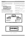
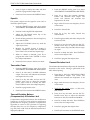
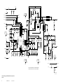
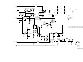
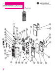
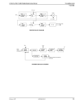
Maintenance
GTX/GTX LTR/LTS 2000 Portable Radios Service Manual
This page intentionally left blank
6-4
68P02948C90-O
February 1997
Section 7
Radio Tuning Procedure
Radio Tuning Procedure
CAUTION
Do NOT switch radios in the middle of
any SERVICE procedure. Always use
the EXIT key to return to the MAIN
menu screen before disconnecting the
radio. Improper exits from the SERVICE
s c re e n s m a y l e a v e t h e r a d i o i n a n
improperly configured state and result
in seriously degraded radio or system
performance.
General
An IBM PC (personal computer) and RSS (Radio
Service Software) are required to align the radio. Refer
to the applicable RSS Manual for installation and setup
procedures for the software.
To perform the alignment procedures, the radio must
be connected to the PC, RIB (Radio Interface Box), and
Test Set as shown inFigure 7-1.
All SERVICE screens read and program the radio
codeplug directly; you do NOT have to use the RSS
GET/SAVE functions to program new tuning values.
The SERVICE screens use the concept of the “Softpot”,
an analog SOFTware controlled POTentiometer used
for adjusting all transceiver alignment controls.
Each SERVICE screen provides the capability to
increase or decrease the ‘softpot’ value with the
COMPUTER
SYSTEM ANALYZER
R2000 SERIES
RF CABLE
AUDIO
OUT
AUDIO
IN
TEST SET CABLE
RKN4034
7.5 VDC POWER SUPPLY
RTX4005B
RADIO
PORTABLE TEST SET
RTX4005B
PROGRAMMING CABLE/
BATTERY ELIMINATOR
HKN9857
ANTENNA
ADAPTER
RIB RLN4008B
110 VAC
Figure 7-1.
February 1997
Radio Alignment Test Setup
68P02948C90-O
7-1
Radio Tuning Procedure
GTX/GTX LTR/LTS 2000 Portable Radios Service Manua
Tuning Procedure
keyboard UP/DOWN arrow keys respectively. A
graphical scale is displayed indicating the minimum,
maximum, and proposed value of the softpot, as
shown in Figure 3.
oscillator should be checked every time the radio is
serviced. The frequency counter used for this
procedure must have a stability of 0.1 ppm (or better).
1.
From the SERVICE menu, press F2 to select
ALIGNMENT: TRANSMITTER & RECEIVER.
2.
Press F5 to select
OSCILLATOR softpot.
3.
Press F6 to key the radio. The screen will
indicate that the radio is transmitting.
4.
Measure the transmit frequency on your
frequency counter.
5.
Use the UP/DOWN arrow keys to adjust the
reference oscillator.
Tuning Procedure
NOTE
Perform the following procedures in the
sequence indicated.
Reference Oscillator Alignment
Adjustment of the reference oscillator is critical for
proper radio operation. Improper adjustment will not
only result in poor operation, but also a misaligned
radio that will interfere with other users operating on
adjacent channels. For this reason, the reference
the
REFERENCE
Service
Menu
F2
F6
Board
Replacement
Menu
Alignment
Menu
F2 Logic or RF Board Replacement
F3 Tx Power
F4 Warp Reference Frequency
F5 Tx Power Calibration
F6 Tx Deviation Calibration
F9 Squelch Adjustment
F3 TX Deviation Adjustment
F5 Reference Oscillator Warp
F7 Transmitter Power
F8 Squelch Adjustment
Figure 7-2.
Service Menu Structure
0
15
Min.
Value
Max.
Value
MAEPF-22858-O
Figure 7-3.
7-2
Softpot Concept
68P02948C90-O
February 1997
GTX/GTX LTR/LTS 2000 Portable Radios Service Manual
Tuning Procedure
6.
Press F6 again to dekey the radio and then
press F8 to program the softpot value.
1.
From the SERVICE menu, press F2 to select
ALIGNMENT: TRANSMITTER & RECEIVER.
7.
Press F10, F10 to return to the SERVICE menu.
2.
Press F3 to select the transmit deviation
balance and deviation limit softpot. The
screen will indicate the transmit test
frequencies to be used.
3.
Begin with the lowest test frequency shown
on the screen.
4.
Press F4 to select 60 Hz.
5.
Press F6 to key the radio. Record this
measurement.
Squelch
The squelch softpots set the signal to noise ratio at
which the squelch opens.
1.
From the SERVICE menu, press F2 to select
ALIGNMENT: TRANSMITTER & RECEIVER.
2.
Press F8 to select SQUELCH Adjustment.
3.
Adjust the UP/DOWN arrow key to the
minimum squelch value.
4.
Set the RF test generator to the test frequency
plus +500 Hz offset.
6.
Press F6 again to dekey the radio, and press F4
to select 2.5 kHz.
5.
Adjust the UP/DOWN arrow key until the
squelch just closes.
7.
6.
Monitor for squelch chatter; if chatter is
present, continue to adjust the UP/DOWN
arrow. Wait a few seconds and repeat step 7.
Press F6 to key the radio, then use the UP/
DOWN arrow keys to adjust the deviation
until the value in step 5 and the value in step 6
are equal.
8.
7.
When no chatter is detected, press F8 to
program this value. Press “ENTER” to select
next softpot adjustment.
Press F6 to dekey the radio. Press ENTER to
move to next softpot value.
9.
Press F8 to program the softpot value.
8.
Press F10, F10 to return to the Service menu.
Transmit Deviation Limit
Transmitter Power
1.
From the SERVICE menu, press F2 to select
ALIGNMENT: TRANSMITTER & RECEIVER.
2.
Press F7 to select the Tx POWER calibration
softpot. The screen will indicate the transmit
test frequencies to be used.
3.
Press F6 to key the radio, and use the UP/
DOWN arrow keys to adjust the transmit
power value. Press F6 to dekey the radio.
Press ENTER to select next softpot frequency.
4.
Press F8 to program the value.
5.
Press F10, F10 to return to the SERVICE menu.
The transmit deviation limit softpot sets the maximum
deviation of the carrier. Tuning is performed for 25
kHz channel spacing.
Transmit Deviation Balance
(Compensation) & Deviation Limit
Compensation alignment balances the modulation
sensitivity of the VCO and reference modulation
(synthesizer low frequency port) lines. Compensation
algorithm is critical to the operation of signaling
schemes that have very low frequency components
(e.g. DPL) and could result in distorted waveforms if
improperly adjusted.
February 1997
68P02948C90-O
1.
Press F10 to select the DEVIATION LIMIT
ADJUSTMENT softpot. The screen will
indicate the transmit test frequencies to be
used.
2.
Begin with the lowest test frequency shown
on the screen.
3.
With Test Box 4460A: inject a 1 kHz tone,
2000 mVrms.
4.
Press F6 to key the radio, and use the UP/
DOWN arrow keys to adjust the deviation
between 2.1 kHz and 2.4 kHz for 900 MHz.
5.
Press F6 to dekey the radio. Press ENTER to
move to the next softpot value.
6.
Press F8 to program the softpot value.
7.
Press F10, F10 to return to the SERVICE menu.
7-3
Radio Tuning Procedure
GTX/GTX LTR/LTS 2000 Portable Radios Service Manua
This page intentionally left blank
7-4
68P02948C90-O
February 1997
SCHEMATIC DIAGRAMS,
CIRCUIT BOARD DETAILS,
& PARTS LISTS
February 1997
68P02948C90-O
1
This document was created with FrameMaker 4.0.3
5V
5V
SWB+
Q400
BCW68GLT1
3
TXB+ (SOURCE)
2
R419
10K
PB401
MON
1
R400
680
3
SWB+
Q401
3904L
1
5R
(SOURCE)
5V
SWB+
1
5V
5R
5R
TXB+
5V
TXB+
5V
5R
5R
ANTENNA
R416
2
SWB+
SWB+
SQ_ATT_IN
R404
10K
43K
GND
3
R424
200K
C466
39PF
1
Q405
3906L
R438
3.3K
C401 2
39PF
SQ_ATT_IN
7
TP402
1
TP402
ANTENNA_CONTACT
2
TRANSMITTER
ANT_CONN
DET_AUDIO
RX_IN
RX_IN
DET_AUDIO (J200-4)
C1
C0 C1
C0
DET_AUDIO
RECEIVER
PC3
PC2
PC1
PC0
C439
0.01UF
TP401
1
TP401
GND
2
5V
GND
ADAPT
PWR_REF
ADAPT (J200-6)
5V
(SOURCE)
R408
20K
8
4
2
1
GND GND
6
5V_TAP
8
1
IN
OUT
2
FDBK 7
SENSE
5
3
SHDN ERORR_
R411
43K
J6
8
7
6
GND
4
R460
50.0K
C419
18NF
SCI_IN
CR405
BYD17D
5
470
J200
1
CW 3
B+
R497
2
0.47UF
5V
1
SWB+
L460
2
150NH
3
SWB+
GND
2
20K
C467
39PF
3
1
C421
R417
GND
ADAPT
RX_INJ
TX_INJ
150NH
R410
20K
2
1
SWB+(SOURCE)
U420
LP_2951AC
RSSI
R401
120
L420
R409
43K
R420
10K
PB402
EMERG
RSSI (J200-5)
2
R407
10K
9
NOT USED
5V
ANTENNA_CONTACT
R406
10K
SW401
SW_FREQ_16POS
CONNECTOR
3
R405
10K
C475
39PF
C473
39PF
C479
39PF
C457
39PF
C477
39PF
R414
470K
C455
39PF
R415
470K
RX_IN
2
CCW 1
C418
10uF
C460
39PF
4
VR460
1 MMBZ5235L
DET_AUDIO
5
RSSI
1
VDD
HC_CNTL
CLK U400 DAC2 11
RESET DAC DAC1 9
3
EN
BIAS_EN
ANT_SEL 2
TEMP
BATT
2_POLE_V 8
12
AUX FREQ_SW_DA
R_T
SCB1 17
DATA_IN
SCB2 18
FREQ_SW0
19
SCB3
FREQ_SW1
FREQ_SW2
SCB4 20
5V
C472
39PF
C478
.01UF
C456
.01UF
C476
.01UF
6
C454
.01UF
ADAPT
MUTE
1
TX_INJ
5V
SWB+
5R
FREQ_SW3
VSS
13
LOCK_DET
WARP
1
LOCK_DET (J200-7)
C445
.01UF
C446
39PF
C449
39PF
EXP_AUDIO
2
SYNT_EN
SYNT_EN (J200-8)
SYNT_EN
MOD_IN
3
MOD_IN(J200-9)
R412
1.3K
R422
1.3K
TX_IN
SPI_CLOCK (J200-24)
2.1MHZ
TX_RX
R489
2.7
R488
1K
R490
2.7
HC_CNTL
DET_AUDIO
2
SPI_DATA (J200-17)
C438
4.7UF
1
Q412
HC_CNTL
DISC
RSSI
3906L
EXP_AUDIO
RX_IN
TX_IN
EXP_AUDIO
RX_IN
TX_IN
IN
HEAR CLEAR
5V
3
SWB+
R491
120K
EDGE1
EDGE2
EDGE4
EDGE5
EDGE3
GND_EDGE_1 GND_EDGE_2 GND_EDGE_3 GND_EDGE_4 GND_EDGE_5
GND
GND
GND
GND
GND
1
1
1
1
1
EDGE6
GND_EDGE_6
GND
1
C465
0.1UF
2.5V
C464
0.1UF
1
FROM U400-17 MUTE
U405
LM2904DR
1
2
7
R496
330
5
U405
LM2904DR
R467
10
R448
U409
CL1
CL2
CL3
CL4
CL5
CL6
C437
0.47UF
R498
0
CL7
CL8
R499
0
C471
47PF
R486
4.7K
C429
4700PF
C409
39PF
C481
39PF
C408
39PF
C436
39PF
2
VR436
1
3
C470
470PF
C469
47NF
GND GND1
3
6
R450
C441
0.1UF
4
4.7UF
R452
200K
10K
1
Q408
3906L
C442
1000PF
R451
C425
47NF
R454
R447
5.6K
R494
100K
C453
2K
C430
39PF
INT_SPKR-
J3
L405
150NH
39PF
5 5
4 4
6 6
L406
150NH
2.ALL RESISTORS MARKED "NO PART" ARE NOT ASSEMBLED.
INT_MICINT_SPKR+
2 2
3 3
1 1
3
220PF
INT_MIC+
EXT_MIC_SPKR
2.2K
C424
NO PART
Schematic Diagram for FUF5690A RF Board
Wiring Diagram
68P02948C90-O
5
4
2 NC OUTPUT1
INPUT
8
7
NC1 OUTPUT2
RX_AUDIO
1.ALL CAPACITORS MARKED "NO PART" ARE NOT ASSEMBLED.
2
R487
1.8K
NO PART
CL9
18NF
1
2
R453
330
C452
C480
180PF
1 TDA7052
VP
GND
2.1MHZ
J5
39PF
3
2
51K
RESET
28
L404
150NH
8
4
GROUND CLIPS
R449
100K
C426
2
6
R492
100K
C428
39PF
C451
Q411
BTA13
DAC_EN
26
L407
150NH
27
1
3
SPI_CLOCK
25
TP444
GND 2
SCI
24
2.5V
Q410
BCW68GLT1
SPI_CLOCK (J200-24)
C444
39PF
C427
18NF
INT_EXT_PTT
23
OUT
SWB+
2
RESET (J200-26)
RX_AUDIO
1
SWB+
C461
0.1UF
3
DAC_EN (J200-25)
GND
1
TX_IN
22
3
Q413
DTC144YK
NPN-1
ASFIC_MIC_AUD_OUT
2.1MHZ (J200-28)
3
TP405
HOLE_070
VOL
21
FILTERED_AUDIO
SWB+
R402
0
RED
UNATT_AUDIO
UNATT_AUDIO
4
DS401
RX_AUDIO
UNATT_AUDIO19
SPI_DATA (J200-17)
20
SPI_CLOCK
2
MIC_IN
SPI_DATA
18
SPI_DATA
C402
39PF
1
5V
17
MOD_IN
SYNTHESIZER
GREEN
2.5V
15
5V
16
6
R423
390
ROT2
14
IMX1
R413
390
ROT1
13
LOCK_DET
4
U410
EXP_AUD
12
2.5V
5
EMERG_MON
11
TP448
C468
39PF
3
MOD_IN
10
100
GND
SYNT_EN
9
MOD_IN
R418
2
RX_INJ
SYNT_EN
R421
22K
PB403
PTT
5R
LOCK_DET
8
LOCK_DET
5V
ADAPT
7
DET_AUDIO
C443
1000PF
7
GND
8
9 GND
GND
10
GND
22
24
21
16
14
15
10
23
4
5
6
7
C474
39PF
73B02948C84-O
SHEET 1 OF 5
February 1997
.3
RX_INJ
LNA
MIXER
SH2
SHIELD
SH51
SHIELD
1
1
5R
C4
39PF
R3
270
C5
0.01UF
1
5V
R21
470
5V
C2
0.01UF
5R
L1
4.2NH
R2
27K
L3
4.2NH
C9
39PF
R5
220
INP
GND
4
CF52
455K
3 4 5
PART
C61
1500PF
5
R51
51
8
MIXER_IN
7
LO_IN
C60
0.1UF
CR1
R4
270
1
C6
39PF
C7
0.01UF
C51
27PF
R6
360
L51
0.47UH
5R
C75
3.9PF
C74
36PF
C55
28
11
RSSI_OUT
25
RSSI_BYP
SQ_LIM_OUT
SQ_RECT_IN
ADAPT
SQ_OUT
CHAN_DET
SQ_NOISE
23
20
22
15
18
30
R60
7.5K
C85
39PF
C63
39PF
C81
0.1UF
R64
5.6K
C67
4.7UF
R58
13K
C64
39PF
C86
39PF
C87
39PF
C83
39PF
C66
0.1UF
C73
13PF
5R
100
0.1UF
SWB+
27
T_R
13
B+
14
DRIVE
C53
22PF
R55
IFIC
ADAPT
AUDIO_OUT
U51
10
OSC_OUT
9
OSC_FB
MMBD353LT
2
PREAMP_IN
PREAMP_OUT
33
DEMODE_FILT
32
DEMOD_FILT
3
4
3
6
GND
2
3
L52
0.47UH
19
RIPPLE_FILT
16
SQ_TAIL_TC
26
ICO_TUNE
24
SQ_LIM_IN
FL2
2
IN 938MHZOUT
CASE
36
IF_AMP_OUT
35
LIM_IN
1
1
Q1
2E_MRF9411L
3
1 MIXER_MOT91
LO
5
4
RF U50 IF
GND2
GND3
GND1
2
3
6
2PF
4
MIXER_OUT
3
IF_AMP_IN
1
21
2.5V_REG
2
5V_REG
12
5V_REG1
17
5V_REG2
34
5V_REG3
FL1
2
IN 938MHZOUT
CASE
DET_AUDIO
RSSI
C3
0.01UF
C1
18PF
SQ_ATT_IN
PART
R23
470
C8
N.C.
C62
0.47UF
NO
56NH
2
OUTP
NO
C10
0.01UF
L2
1
1
R22
10
5R
RX_IN
GND
3
MIXER SHIELD
LNA SHIELD
CF51
2
INP 455K OUTP
31
DEMOD_OUT
29
AUDIO_IN
R1
27K
SWB+
GND
GND
GND
SWB+
R54
2K
R52
33K
C82
R50
NU
R67
0.1UF
Y51A
45.1MHz
R66
820
C54
15PF
Q51
MMBR941
NPN
2
L53
1200NH
C77
3PF
1
C59
R78
3
C57
NO
L54
NO
PART
PART
1200NH
C70
0.1UF
2.ALL RESISTORS MARKED "NO PART" ARE NOT ASSEMBLED
CR51
MMBD353LT
C58
L58
1200NH
NO
PART
1.ALL CAPACITORS MARKED "NO PART" ARE NOT ASSEMBLED
C71
10UF
0.1UF
L55
2
C79
16PF
3
0
2
R53
12K
C69
3.3UF
R57
130K
5V
Y51B
45.1MHz
3
3
C68
.039UF
44.645MHZ
NO
PART
C56
20PF
6.8K
1
1
Y53
2
1
73B02948C84-O
SHEET 3 OF 5
Schematic Diagram for FUF5690A/RF Board
Receiver Module
February 1997
68P02948C90-O
3
FILT_5V
L206
5V
SFV+
1.0UH
5R
C261
22NF
C262
22NF
C207
39PF
C206
22NF
5R
SFV+
C270
22NF
C260
22NF
SH260
SHILD_890U01
SPI_DATA
SPI_DATA
R270
15K
U260
VCO SHIELD
VCO_900MHZ
SPI_CLOCK
U270
SW1B+
SPI_CLOCK
SYNT_EN
RF_OUT
CONT1
C220
3.3NF
FILT_5V
CLOSE
TO U220
MOD_IN
TX_INJ
SFV+
R274
0
L270
15NH
GND GND1GND2
1
5
12
C221
3.3NF
CLOSE
TO U220
CONT2
GND
C263
39PF
C274
4.7PF
3 D74F_VCOBIC
9
4
VCC
IN
TX
2
16
RX 8
13 TX_BIAS
RX_BIAS SP1
7
10
TRB
SP2
15
6
FLIP PS_OUT
11
14
N.C
N.C.
SW2
C264
39PF
C275
2PF
C272
39PF
TX_RX
1
C228
39PF
C223
0.1UF
CR220
TRIPLE_DIODE
C224
39PF
8
MOD_IN
7
C.E.
CLK 6
5
DATA
4
3
2
LOCK
5
C227
0.1UF
4
9
10
11
12
13
14
15
16
2.1_MHZ
C210
39PF
C231
0.1UF
C211
22NF
U210
FILT_5V
CLOSE
TO U220
PIN 12
C232
22NF
VMULT2
AUX3 1
32
VMULT1
VCP
31
FREF_OUT
I_ADAPT
30
DC_5V
FRACTIONAL_W46
29
GND
I_OUT
28
MOD_OUT 27
XTAL1
XTAL2
CPBAIS1
26
WARP
CPBAIS2
R232
1K
U220
C242
22NF
NO
PART
C213
1UF
C243
10NF
C245
10NF
R242
3.3K
C246
510PF
C247
39PF
R291
620
R280
13K
R292
620
L290
10n
C290
39PF
C241
1.2NF
SFV+
NO
PART
R238
150K
R237
82K
C244
22NF
C254
1.2NF
Q280
1
R244
51
3
NO
PART
C282
39PF
R282
10K
RX_INJ
R285
430
3
Q281
MMBR941
1
C203
39PF
C204
22NF
C233
0.1UF
CLOSE
TO U220
PIN 19
C234
0.1UF
CLOSE
TO U220
PIN 22
C237
39PF
C236
0.1UF
C235
10UF
CLOSE
TO U220
PIN 23
PS_IN
C291
0.1UF
L246
C248
0.1UF
NO
PART
C249
0.1UF
C250
0.1UF
C251
0.1UF
C252
0.1UF
C292
2.4PF
2
C284
2PF
C253
0.1UF
C238
C285
39PF
C283
22NF
NO
10UF
TP231
TX_RX
R290
620
C281
0.1UF
10UH
GND
3
C212
39PF
C280
39PF
620
17
18
19
20
21
22
23
24
25
1 VCO_16.8MHZ
VCC
2
4
Vwarp OUT
R245
TST1
TST2
39PF
C226
0.1UF
SUPF_CAP
SOUT
SIN
PREIN
3
C230
FILT_5V
5R
LOCK_DET
C229
39PF
C271
3PF
PS_IN
2
VOLTAGE
MULTIPLIER
SHIELD
WARP
C225
4.7UF
CLOSE
TO U220
PIN 32
6
SH229
SHIELD
C240
22NF
C239
0.1UF
TX_RX
C286
0.1UF
INJ. BUFFER
SHIELD
PART
SH220
SHIELD
SYNTHESIZER
SHIELD
SH283
SHIELD
SH250
SHIELD
LOOP FILTER
SHIELD
LOCK_DET
LOCK_DET
R258
100
1.ALL CAPACITORS MARKED "NO PART" ARE NOT ASSEMBLED.
2.ALL RESISTORS MARKED "NO PART" ARE NOT ASSEMBLED.
2.1_MHZ
2.1MHZ
CLOSE
TO U220
C258
39PF
CLOSE
TO U220
73B02948C84-O
SHEET 5 OF 5
Schematic Diagram for FUF5690A RF Board, Synthesizer
Module
4
68P02948C90-O
February 1997
C165
39PF
RX_IN
SWB+
SWB+
C121
1PF
5V
E101
C105
22NF
FERRITE BEAD
5V
C106
1UF
TXB+
1
CR161
SMBV1032LTI
0.1UF
NEAR BEAD
TXB+
NO
PART
L161
C108
C125
L121
ANT_CONN
7.66NH
2
C123
1PF
7.66NH
7.5PF
C162
1PF
3
C126
1PF
C122
1PF
C124
1PF
C163
39PF
C102
39PF
C103
0.1UF
NEAR P.A. NEAR P.A.
MODULE
MODULE
R161
680
C107
0.1UF
C104
39PF
NEAR P.A.
MODULE
RF_IN RF_OUT
3
SMBV1032LTI
NEAR P.A.
MODULE
2
L162
1
SH121
SHIELD
22NH
U111
3
4 SHW5177_STD
2
SV1 SV2 SV4
TX_INJ
C161
11PF
CR162
U101
1
R162
680
L122
10n
NO
PART
COUPLER_34L01
5
1
GND GND GND
8
6
7
2
L163
150NH
4
INPUT
OUTPUT_P
C.OUTPUT C.TERMINAL
1
R163
C101
39PF
NEAR P.A.
MODULE
HARMONIC FILTER
SHIELD
3
CR112
R87151
N.C.
3
51
CR111
R87151
R164
100K
2
2
N.C.
3
R113
4.7K
R114
3.3K
1
C156
100NF
R153
4.7K
C111
39PF
R112
51
C112
39PF
C158
0.22UF
SWB+
1. ALL CAPACITORS MARKED ''NO PART'' ARE NOT ASSEMBLED
2. ALL RESISTORS MARKED ''NO PART'' ARE NOT ASSEMBLED
SWB+
R155
47K
Q152
2 3906L
C155
0.1UF
1
R154
0
3
3
Q151
3904L
4
14
1
C157
0.1UF
R156
390
LM2902DR
2
NO
PART
C154
39PF
U151
11
R133
62K
LM2902DR
13
8
U151
10
V_det
9
12
C153
39PF
C132
39PF
R131
1.8K
5V
C131
39PF
R158
5.6K
5V
R152
47K
R157
300
R151
47K
R132
1.3K
C152
39PF
C151
0.1UF
LM2902DR
7
U151
CR141
MMBD6100L
2
R134
3
R148
R147
560
47K
PWR_REF
62K
5
6
R143
47K
C142
39PF
R146
47K
1
R144
47K
R142
39K
R141
6.8K
3
R145
50K
C141
39PF
2
LM2902DR
U151
1
C133
39PF
C143
0.1UF
R149
5R
0
73B02948C84-O
SHEET 4 OF 5
Schematic Diagram for FUF 5690A RF Board,
Transmitter Module
February 1997
68P02948C90-O
5
C560
EXP_AUDIO
0.1UF
SWB+
C574
SWB+
.01UF
U550
B3 CLEAR
VCC
NFILOUT C6
F4
C4
FFOUT
ICENAB
D1
A2
CPNENAB EXPOUT
F2
E3
FFENAB CBUFOUT
F3
C2
HIENAB COMPOUT
HC_CNTL
C550
100NF
C1
D3
F5
E4
B5
FILTERED_AUDIO
RSSI
C562
100NF
C500
0.22UF
DISC
C567
3300PF
B1
B4
E5
D6
E6
RX_IN
C561
TX_IN
EXPIN
LODSAB A5
C3
EXPBYP
CBUFIN
E1
RSSIIN COMPCAP
A4
FFIN
VAG
D4
FFCNTL
NFILIN
E2
CFBBYP
C5
NC
CLIPREF
NOISHLD D5
NC_1
D2
COMPBYP
NC_2
B6
HCIDSAB
NC_3
B2
EXPADJ
NC_4
0.1UF
C555
3.3UF
C553
0.33UF
C558
GND
0.33UF
A3
R555
1K
C565
0.1UF
C564
3300PF
R557
100K
C563
3300PF
C556
3.3UF
R556
10.0K
R554
100K
R552
47.5K
R553
1.5K
C554
.01UF
R551
R550
22K
100K
C551
470PF
ASFIC_MIC_AUD_OUT
Schematic Diagram for FUF5690A RF Board,
Hear Clear
6
68P02948C90-O
February 1997
C552
470PF
C557
.01UF
73B02948C84-O
SHEET 2 OF 5
parts lists
REFERENCE
SYMBOL
MOTOROLA
PART NO.
C163
C165
C203
C204
C206
C207
C210
C211
C212
C213
C220-221
C223
C224
C225
C226-227
C228-230
C231
C232
C233-234
C235
C236
C237
C238
C239
C240
C241
C243
C245
C246
C247
C249-253
C258
C260-262
C263-264
C270
C271
C272
C274
C275
C280
C281
C282
C284
C285
C286
C290
C291
C292
C401-402
C408-409
C418
C419
C421
C424
C425
C426-427
C428
C429
C430
C436
2113740F41
2113740F41
2113740F41
2113743E07
2113743E07
2113740F41
2113740F41
2113743E07
2113740F41
2311049A07
2113741F37
2113743K15
2113740F41
2311049J12
2113743K15
2113740F41
2113743K15
2113743E07
2113743K15
2311049A63
2113743K15
2113740F41
2311049A63
2113743K15
2113743E07
2105248W01
2109720D01
2109720D01
2113741F18
2113740F41
2109720D14
2113740F41
2113743E07
2113740F41
2113743E07
2113740F14
2113740F41
2113740F19
2113740F10
2113740F41
2113743K15
2113740F41
2113740F10
2113740F41
2113743K15
2113740F41
2113743K15
2113740F12
2113740F41
2113740F41
2311049C09
2113743E05
2311049A05
2113740F59
2113743E12
2113743E05
2113740F41
2113741F41
2113740F41
2113740F41
DESCRIPTION
REFERENCE
SYMBOL
MOTOROLA
PART NO.
DESCRIPTION
C437
C438
C439
C441
C442-443
C444
C445
C446
C449
C451
C452
C453
C454
C455
C456
C457
C460
C461
C464-465
C466-468
C469
C470
C471
C472-475
C476
C477
C478
C479
C480
C481
C500
C550
C551-552
C553
C554
C555-556
C557
C558
C560-561
C562
C563-564
C565
C567
C574
2311049A05
2311049J11
2113741F49
2113743K15
2113741F25
2113740F41
2113741F49
2113740F41
2113740F41
2113740F41
2311049J11
2113740F41
2113741F49
2113740F41
2113741F49
2113740F41
2113740F41
2113743K15
2113743K15
2113740F41
2113743E12
2113741F17
2113740F43
2113740F41
2113741F49
2113740F41
2113741F49
2113740F41
2113740F57
2113740F41
2113743A23
2113743A19
2113741F17
2311049A04
2113741F49
2311049A42
2113741F49
2311049A04
2113743K15
2113743A19
2113741A33
2113743K15
2113741A33
2113741A33
CR1
CR51
CR111-112
CR141
CR161-162
CR220
CR405
diodes: (see note)
4880154K03
353L
4880154K03
353L
4805218N57
Schottky R87151
4813833C02
MMBD6100L
4805129M96
SMBV1032LTI
4802233J09
triple diode
4880107R01
BYD17D
CF51
CF52
filters, ceramic:
9180453B04
filter, 455 KHz
9180454Bo4
filter, 455 KHz
REFERENCE
SYMBOL
MOTOROLA
PART NO.
DESCRIPTION
DS401
LEDs:
4805729G49
LED Red/Yel
E101
ferrite bead:
2484657R01
ferrite bead
FL1-2
filters:
9102603S25
938
J3
J5
J6
J200
connectors, receptacle:
0180417C01
External microphone/speaker jack
0180159R03
Speaker/mic header
0180965Z01
connector, B+
0904358J02
edge
L1
L2
L3
L51, L52
L53
L55
L58
L121
L122
L161
L162
L163
L206
L246
L270
L290
L404-407
L420
L460
coils:
2460591A01
4.2 nH
2462587T12
56 nH
2460591A01
4.22 nH
2483411T69
0.47 µH
2462587M19
1200 nH
2483411T74
1.2 µH
2483411T74
1.2 µH
2460591A11
7.66 nH
2413926E11
10.0 nH
2460591A11
7.66 nH
2462587V26
22 nH
2462587V36
150 nH
2462587T30
1.0 µH
2462587P24
10 µH
2462587V24
15 nH
2413926E11
10.0 nH
2462587T17
150 nH
2462587T17
150 nH
2462587T17
150 nH
PB1-PB3
pushbutton switches:
4080485C05
pushbutton switch
Q1
Q51
Q151
Q152
Q280
Q281
Q400
Q401
Q405
Q408
Q410
Q411
Q412
Q413
transistors: (see note 1)
4813827A18
NPN, 2E_MRF9411L
4813827A07
NPN, MMBR941
4813824A10
NPN, 3904L
4813824A17
PNP, 3906L
4813824A17
PNP, 3906L
4813827A07
NPN, MMBR941
4880141L03
PNP, BCW68GLT1
4813824A10
NPN, 3904L
4813824A17
PNP, 3906L
4813824A17
PNP, 3906L
4880141L03
PNP, BCW68GLT1
4813824A06
NPN, Darlington BTA13
4813824A17
PNP, 3906L
4882033T01
NPN DTC 144YK
FUF5690A RF Board
VIEWED FROM SIDE 1
REFERENCE
SYMBOL
MOTOROLA
PART NO.
DESCRIPTION
C1
C2-3
C4
C5
C6
C7
C8
C9
C10
C51
C53
C54
C55
C56
C59-60
C61
C62
C63-64
C66
C67
C68
C69
C70
C71
C73
C74
C75
C77
C79
C81-82
C83
C85-87
C101-102
C103
C104
C105
C106
C107-108
C111-112
C122-123
C125
C126
C131-133
C141-142
C143
C151
C152-154
C155
C156
C158
C161
C162
capacitors: pF, ±5% 50V, unless otherwise specified
2103689A08
18
2113741F49
0.01 µF
2113740F41
39
2113741F49
0.01 µF
2113740F41
39
2113741F49
0.01 µF
2113740F10
2
2113740F41
39
2113741F49
0.01 µF
2113740F37
27
2113740F35
22
2113740F31
15
2113743K15
0.1 µF
2113740F34
20
2113743K15
0.1 µF
2113741F29
1500
2311049A05
0.47 µF
2113740F41
39
2113743K15
0.1 µF
2311049J11
4.7 µF
2113743K05
0.039 µF
2311049A11
3.3 µF
2113743K15
0.1 µF
2311049A63
10 µF
2113740F30
13
2113740F40
36
2113740F17
3.9
2113740F14
3
2113740F32
16
2113743K15
0.1 µF
2113740F41
39
2113740F41
39
2113740F41
39
2113743K15
0.1 µF
2113740F41
39
2113743E07
22 nF
2311049A07
1 µF
2113743K15
0.1 µF
2113740F41
39
2103689A15
1
2113740F24
7.5
2110368A15
1
2113740F41
39
2113740F41
39
2113743K15
0.1 µF
2113743K15
0.1 µF
2113740F41
39
2113743K15
0.1 µF
2113743E20
100 nF
2113743A23
0.220 µF
2113740F28
11
2103689A15
1
VIEWED FROM SIDE 1
R551
C421
C206
47
48
49 50 51
5
34 35 36
37
38
39
40 41 42
25 26 27
28
29
30
31 32 33
16 17 18
19
20
21
22 23 24
10
11
12
13 14 15
R405
C212
R414
R415
R407
R406
C457
C477
R404
C476
C478
C479
C454
C456
C241
L51
R51
5
4
U50
2
3
1
8
9
2
3
4
5
C243
R23
7
C251
C250
C249
C252
C253
R242
6
L246
Y51B
3
3
C210
C254
R244
46
R245
L55
L53
7
C455
55 56 57
44 45
C247
C55
L52
R22
C58
6
C51
CF51
Y51A
R54
R55
R78
2
CF52
C211
C245
52 53 54
43
2
C248
U260
FL2
R1
3
C73
C244
3
C79
C56
2
C59
5
6
4
C242
C5
C4
C74
C75
J6
30
R460
3
C232
R232
SH51
5
2
F5
E6
SH260
FL1
SCI
1
8
R64
C66
12
U51
B+
U210
C561
A5
B6
2
SH250
Y53
23
F2
L58
2
7
3
CR1
C69
R3
+
C68
E1
A2
L206
R21
4
R57
C63
+
C67
C213
Q413
R421
R420
R419
U550
C207
L420
C419
2
SW401
C554
C246
9
+
8
C556
+
5
R145
C108
E101
+
C106
4
C557
B1
U420
C105
8
U405
CL9
C551
R494
5
R552
Q408
4
C418
C461
C465
4
TP401
8
R448 R447
C424 C425
C451
+
U101
U409
+
C481
C452
R451
R452
+
C125
C427
C428
L407
TP402
5
C550
C429
1
C453
C101
R454
2
C102
R491 R492
C275 R274 C274
C103
3
8
C464
R163 R164
4
C430
L404
C104
5
L122
CL2
CL5
R453
L163
C442
PB403
PB402
C409
PB401
CL4
CL7
CL6
CL3
CL1
VIEWED FROM SIDE 2
C258
16
C231
L270
15
3
C270
C283
Q281
C292
C107
C123
C124
CR51
VR460
R60
C408
4
R422
+
R412
C86
+
3
DS401
2
C62
C71
C472
C436
C474
C443
6
C70
R53
R50
L54
C60
R67
C54
R52
C77
C290
Q51
R58
4
U410
C87
VR436
R413
R423
C163
C121
C122
L406
C473 C475
R112
C111
C131 R113
C112
C162
C165
R141
R142
R131
R132
R144
R158
R157
C158
R147 R148 C141
R143
C85
C82
R292
R291
L290
C291
3
C64
R499
C284
C281
4
C280
C286
6
U270
1 7
8
C2
C53
R280 R290
C282
12
Q280
R282
C262
1
C285
7
2
3
L405
R66
11
J3
L121
C1
R2
C261
14
C155
4
L460
CR405
9
C226
C233
C154 C142
C57
C230
17
R258
C229
8
C227
C221
CR220
C152
R154
4
SH283
C235
R285
C220
C228
CR162
C7
C264
+
C272
C236
C234
U220
C239
R270
C224
+
C223
24
C225
C271
25
C263
R237
C237
R238
32
SH229
C260
C238
L162
L161
6
5
SH121
CR161
R5 2
L1 SIDE 1
3
VIEWED
FROM
L2
+
C126
4
Q1
C9
C10
SH220
C240
3
C460
C564 R553
7
CR141
R161
C161 R162
C83
R556
L3
U151
R114
10
C61
C563
R555
Q405
8
9
2
U111
C81
R402
R4
C567
C153 R133 C132
14
1
SH2
C8
R151 R152
CR111
R498
R557
C565
C574
C500
22
R6
C562
C203
C204
C446
C445
C449
21
17
R149 C143
16
C553
C3
R490
+
C560
R554
C402
4
C555
Q151
Q152
C401
U400
R489
J200
Q401
4
R401
Q411
C439
+
R400
5
R438
C558
R550
Q410
R156
R155
10 9
+
Q400
CR112
C6
+
C552
R488
C437
R496
C468
C444
+
C133
Q412
C156 R153
CL8
R134
C438
C471 R487
R418
C467
C466
R497
R416
28
R417
R424
R411
4
C441
R146
R467
R449
C426
R450
C480
R486
C470
C469
R408
R410
3
C157
J5
2
R409
C151
VIEWED FROM SIDE 2
39
39
39
22 nF
22 nF
39
39
22 nF
39
1 µF
3.3 nF
0.1 µF
39
4.7 µF
0.1 µF
39
0.1 µF
22 nF
0.1 µF
10 µF
0.1 µF
39
10 µF
0.1 µF
22 nF
1 nF
0.1 µF
0.1 µF
510
39
0.1 µF
39
22 nF
39
22 nF
3
39
4.7
2.0
39
0.1 µF
39
2.0
39
0.1 µF
39
0.1 µF
2.4
39
39
10 µF
18 nF
0.47 µF
220
47 nF
18 nF
39
4700
39
39
0.47 µF
4.7 µF
0.01 µF
0.1 µF
1000
39
0.01 µF
39
39
39
4.7 µF
39
0.01 µF
39
0.01 µF
39
39
0.1 µF
0.1 µF
39
47 nF
470
47
39
0.01 µF
39
0.01 µF
39
180
39
0.22 µF
0.1 µF
470
0.33 µF
0.01 µF
6
0.01 µF
0.33 µF
0.1 µF
0.1 µF
3.3 nF
0.1 µF
3.3 nF
0.01 µF
Circuit Board Details and Parts List
for FUF5690A RF Board
February 1997
68P02948C90-O
7
REFERENCE
SYMBOL
MOTOROLA
PART NO.
DESCRIPTION
R1
R2
R3
R4
R5
R6
R21
R22
R23
R51
R52
R53
R54
R55
R57
R58
R60
R64
R66
R67
R78
R112
R113
R114
R131
R132
R133
R134
R141
R142
R143
R144
R145
R146
R147
R148
R149
R151-152
R153
R154
R155
R156
R157
R158
R161-162
R163
R164
R232
R237
R238
R242
R244
R245
R258
R270
R274
R280
R282
resistors: Ω, 5%, 1/16 W unless otherwise stated
0662057A83
27K
0662057A83
27K
0662057A35
270
0662057A35
270
0662057A33
220
0662057A38
360
0662057A41
470
0662057A01
10
0662057A41
470
0662057A18
51
0662057A85
33K
0662057A75
12K
0662057A56
2K
0662057A25
100
0662057B01
130K
0662057A76
13K
0662057A70
7.5K
0662057A67
5.6K
0662057A47
820
0662057A69
6.8K
0662057B47
0
0662057A18
51
0662057A65
4.7K
0662057A61
3.3K
0662057A55
1.8K
0662057A52
1.3K
0662057A92
62K
0662057A92
62K
0662057A69
6.8K
0662057A87
39K
0662057A89
47K
0662057A89
47K
0605621T02
thermistor, 50K
0662057A89
47K
0662057A89
47K
0662057A43
560
0662057B47
0
0662057A89
47K
0662057A65
4.7K
0662057B47
0
0662057A89
47K
0662057A39
390
0662057A36
300
0662057A67
5.6K
0662057A45
680
0662057A18
51
0662057A97
100K
0662057A49
1K
0662057A95
82K
0662057B02
150K
0662057A61
3.3K
0662057A18
51
0662057A44
620
0662057A25
100
0662057A77
15K
0662057B47
0
0662057A76
13K
0662057A73
10K
Parts List for
FUF5690A RF Board (Cont)
8
68P02948C90-O
February 1997
REFERENCE
SYMBOL
MOTOROLA
PART NO.
DESCRIPTION
R285
R290-292
R400
R401
R402
R404-407
R408
R409
R410
R411
R412
R413
R414-415
R416
R417
R418
R419-420
R421
R422
R423
R424
R438
R447
R448
R449
R450
R451
R452
R453
R454
R460
R467
R486
R487
R488
R489
R490
R491
R492
R494
R496
R497
R550
R551
R552
R553
R554
R555
R556
R557
0662057A40
0662057A44
0662057A45
0662057A27
0662057B47
0662057A73
0662057A80
0662057A88
0662057A80
0662057A88
0662057A52
0662057A39
0662057B14
0662057A88
0662057A80
0662057A25
0662057A73
0662057A81
0662057A52
0662057A39
0662057B05
0662057A61
0662057A67
0662057A90
0662057A97
0662057A73
0662057A57
0662057B05
0662057A37
0662057A56
1880143S03
0662057A01
0662057A65
0662057A55
0662057A49
0611077A12
0611077A12
0662057A99
0662057A97
0662057A97
0662057A37
0662057A41
0662057G13
0662057A81
0662057R92
0662057A53
0662057G13
0662057R30
0662057R60
0662057A97
SH2
SH51
SH121
SH220
SH229
SH250
SH260
SH283
shields:
2680456K01
LNA shield
2605417V01
mixer shield
2680471K01
harmonic filter shield
2680510K01
synthesizer shield
2605259V01
voltage multiplier shield
2680470K01
loop filter shield
2605890U01
VCO shield
2680456K01
RX injection buffer shield
430
620
680
120
0
10K
20K
43K
20K
43K
1.3K
390
470K
43K
20K
100
10K
22K
1.3K
390
200K
3.3K
5.6K
51K
100K
10K
2.2K
200K
330
2K
potentiometer, 50.0K
10
4.7K
1.8K
1K
2.7
2.7
120K
100K
100K
330
470
100K
22K
47.5K
1500
100K
1000
10K
100K
REFERENCE
SYMBOL
MOTOROLA
PART NO.
DESCRIPTION
SW401
switch:
4080650D01
rotary switch
TP401
TP402
test points, contacts:
3980442K02
antenna ground
3980443K02
antenna contact
U50
U51
U101
U111
U151
U210
U220
U260
U270
U400
U405
U409
U410
U420
U550
integrated circuits: (see note 1)
0108106L10
MIXER_MOT91
5180207R01
IFIC
5108038H16
Module PA for 900 MHz
5880334L01
COUPLER 900 MHz
5113819A02
LM2902DR
5102845C11
VCO, 16.8 MHz
5105457W46
SCW39129ZP
5105279V01
VCO, 900MHZ
5105662U76
D74F_VCOBIC
5105226P38
D/A
5113818A01
LM2904DR
5180175R01
TDA7052
5180159R01
POLARITY_IMX1
5113816A23
LP2951ACDR2
5105662U60
Hear Clear
REFERENCE
SYMBOL
MOTOROLA
PART NO.
DESCRIPTION
VR436
VR460
Zener diodes: (see note 1)
4813830A23
MMBZ5240BL
4813830A18
MMBZ5235L
Y51A, Y51B
Y53
crystals: (see note 2)
9180112R06
filter, 45.1 MHz (Set of 2)
4880008K02
crystal, 44.645 MHz
Qty
9
1
1
1
1
non-referenced items:
4280138R03
butterfly clip
1405160A02
crystal insulator
5404977P01
Label Board Serial Number
7505295B07
Pad XTAL base
4280429K01
PA clip
Notes:
1. For optimum performance, diodes, transistors and integrated circuits
must be ordered by MOTOROLA part numbers.
2. When ordering quartz crystal units or ceramic resonators, specify
carrier frequency, crystal (or resonator) frequency, and crystal (or resonator) type number.
BATTERY FILTER BOARD
J3
SCI
SCI
C3
39PF
CHG+
J2
2
J1
CHG+
1
C4
39PF
-V
-V
VIEWED FROM SIDE 1
73A02951C19-O
J1
FLN8517A Battery Filter Board
MOTOROLA
PART NO.
C2-C4
capacitors, fixed: pF, ±5% 50 V, unless
otherwise specified
2113740F41
39
L1, L2
coils, RF:
2484657R01
ferrite bead
F1
fuse:
6580561D01
fuse
Qty
1
non-referenced item:
3980165S02
contact, B+
F1
DESCRIPTION
J3
E2
J2
C4
REFERENCE
SYMBOL
VIEWED FROM SIDE 2
P2
Y0808
C2
39PF
C3
C2
+V
F1
4A
E2
E1
E1
Circuit Board Details, Schematic Diagram, & Parts List
for FLN8517A Battery Filter Board
February 1997
68P02948C90-O
9
parts list
FLN8836A Logic Board
REFERENCE
SYMBOL
MOTOROLA
PART NO.
C406
C407
C435
C700
C707
C708
C710
C711
C716
C717
C718
C719
C720
C721
C733
C737
C738
C741-747
C752
C754
C758
C761
C763
C765
C769
C777
C781
C786-787
C788
C789
C790
capacitors: ±5%, 50 V unless otherwise stated
2113741F49
0.01 µ F
2311049A40
2.2 µF
2113743E20
100 nF
2113743E07
22 nF
2113741F17
470 pF
2113741F49
0.01 µF
2311049J11
4.7 µF
2311049A07
1 µF
2113743F08
0.22 µF
2113741A45
10 nF
2113743E20
100 nF
2113743F01
0.1 µF
2113741A45
10 nF
2311049A01
0.1 µF
2113740F41
39 pF
2113740F41
39 pF
2113740F41
39 pF
2113740F41
39 pF
2113743K15
0.1 µF
2113743E20
100 nF
2113743E20
100 nF
2113740F41
39 pF
2113741F49
0.01 µF
2113743E20
100 nF
2113740F41
39 pF
2311049A07
1 µF
2113743E20
100 nF
2113743E20
100 nF
2113743K15
0.1 µF
2113740F41
39 pF
2113741F13
330 pF
CR707-708
diodes: (see note)
4813833C02
MMBD6100L
DS701-704
LEDs:
4805729G92
GREEN
E01
shield:
2683423K03
423K03
J700
J750
connectors, receptacle:
0904658J02
edge
0980332L01
edge
Q1
Q2
transistors: (see note 1)
4813824A10
NPN, 3904L
4882033T01
NPN, 1_DTC144YK
R403
R468
R700
resistors: Ω, 5%, 1/16 W unless otherwise stated
0662057A97
100K
0662057A73
10K
0662057A97
100K
VIEWED FROM SIDE 2
DS701
DS703
DS702
DS704
VIEWED FROM SIDE 1
J701
1
R793
R794
32
C744 C781
16
7
17
Q1
16
33
U707
U706
U705
48
CR707
C720
R710
60
C719
+
U709
S01
S16
S15
S14
S13
J2
FLN8836A
C788
C435
REV. P1
8408116Y01
C708
C752
6
J750 4
2
R797
C790
CR708
C717
+
R705
R795
C721
61
5
3
C786 C743
R755 R700
R754 C700
R792
8
80
R756 C745
32
C765
17
R764
R753
C747
5
S02
64
49
4
U703
S03
VR707
8
21
S04
+
C777
22
C754 R790
R798 C746 C787
C758
34
J7
H1
S10
S09
S08
S07
S12
S11
S06
S05
H8
U701
C407
DESCRIPTION
R403
B1
28
E01
1
+
C710
C711
C716
C761 C707
C789
C737
C769
C741
2
TP9
C738
R725
C763
R763
R726
Q2
40
C742 C406
C733
21
R468
41
A7
+
20
B8
A2
27
Circuit Board Details & Parts List
for FLN8836A Logic Board
10
68P02948C90-O
C718
4 U704 3
2
5
6
February 1997
REFERENCE
SYMBOL
MOTOROLA
PART NO.
DESCRIPTION
R705
R710
R725
R726
R753
R756
R763
R764
R790
R792
R793
R794
R795
R797-798
0662057A89
0662057A89
0662057A94
0662057A95
0662057A73
0662057A73
0662057A65
0662057A73
0662057A81
0662057A73
0662057C55
0662057C55
0662057A85
0662057A73
U701
U703
U704
U705
U706
U707
U709
integrated circuits: (see note 1)
5105835U45
ASFIC_F83-1
5108444S49
X25320
5180633C01
TK11950
5105662U54
Hybrid 32K x 8 SRAM
5108444S41
SRAM 32Kx8
5102463J21
MSM6606
5102463J20
MC68HC11K1
VR707
Zener diodes: (see note 1)
4813830A27
MMBZ5244L
47K
47K
75K
82K
10K
10K
4.7K
10K
22K
10K
150
150
33K
10K
Notes:
1. For optimum performance, diodes, transistors and integrated circuits
must be ordered by MOTOROLA part numbers.
2. When ordering quartz crystal units or ceramic resonators, specify
carrier frequency, crystal (or resonator) frequency, and crystal (or resonator) type number.
SPI_DATA
VDD_PIN_0
VDD_PIN_1
VDD_PIN_2
AVDD
VRH
1
71
12
31
41
51
VDD
R763
4.7K
2
VDD
R794
150
R700
56
41
42
43
44
45
46
SPI_DATA
LOAD
59
57
RESET
TEST
C0
C1
C2
C3
C4
C5
DATA_IO
LOAD
DS702
GREEN
C765
100NF
IN
GND
72
NC
E
2
61
C700
22NF
TPS1
TPS2
TPS3
RESET
75
VPP
30
IRQ
RESET
XIRQ
74
NC
XTAL
UP_CLK
73
77
J701
1
2
3
4
5
6
7
8
9
10
11
12
13
14
15
16
17
18
19
20
21
22
23
24
25
26
27
28
29
30
31
32
33
34
COMB
COMA
SEG9
SEG10
SEG11
SEG12
SEG13
SEG14
SEG15
SEG16
SEG17
SEG18
SEG19
SEG20
SEG21
SEG22
SEG23
SEG24
SEG25
SEG26
SEG27
SEG28
SEG29
SEG30
SEG31
SEG32
SEG33
SEG34
SEG35
SEG36
SEG37
SEG38
SEG39
SEG40
KEYPAD
SWB+
76
R725
75K
LOWBATT 49
VOL_SENSE 48
C763
1
1
1
S01
1
S04
S03
S02
2
2
2
2
0.01UF
R726
82K
ROT1
47
ROT2
46
RSSI
45
EMERG_MON44
LOCK_DET 43
INT
1
1
1
S05
S06
2
MODA_LIR
MODB_VSTBY
PE0
PE1
PE2
PE3
PE4
PE5
PE6
PE7
1
S08
S07
2
2
42
EXTAL
2
VSS_PIN_3
VSS_PIN_4
VSS_PIN_5
VRL
AVSS
62
CLOCK
OUT
VPP_BOOT
PA0
PA1
PA2
PA3
PA4
PA5
PA6
PA7
PB0
PB1
PB2
PB3
PB4
PB5
PB6
PB7
PC0
PC1
PC2
PC3
PC4
PC5
PC6
PC7
PD0
PD1
PD2
PD3
PD4
PD5
PF0
PF1
PF2
PF3
PF4
PF5
PF6
PF7
PG0
PG1
PG2
PG3
PG4
PG5
PG6
PG7
PH0
PH1
PH2
PH3
PH4
PH5
PH6
PH7
RX_DATA
11
PL_LIM
10
MDC_REF
9
8
SQ
7
DTMF_ENCODE
6
PL_ENCODE
5
TX_DATA
4
INT_EXT_PTT
21
20
19
18
17
16
15
NC
14
DATA_BUS(0:7)
NC
0
PC0
62
1
63
2
64
3
65
4
66
5
67
6
68
7
PC7
69
RX D
78
TX D
79
80
SPI_DATA
1
SPI_CLK
2
EE_SEL
3
60
PF0
59
58
57
56
55
54
PF7
53
40
ADAPT
39
MEM 1
38
MEM 2
37
MEM 3
36
MEM 4
35
SYNTHLE
PGM_ENAB
34
33
MEM_WR_EN
22
NC
23
LOAD
24
CHACT
25
NC
26
DACLE
27
NC
RAM_CE1
28
29
ROM_E
+5V
RESET
VSS
EPROM 4
C758
100NF
C747
39PF
C786
100NF
1
1
S09
ADD_BUS(0:17)
J750
4
J750
3
+5V
SIG_NAME
SCI
R705
47K
RX D
C788
0.1UF
R795
33K
VDD
R752
0.1UF
C435
100NF
R797
10K
DETAUDIO
RX_IN
C790
330PF
0
1
2
3
4
5
6
7
R755
10K
N.P.
R756
10K
R754
+5V
0
N.P.
14
15
16
17
C720
10NF
C721
2
3
0.1UF
CR708
MMBD6100L
C719
1
0.1UF
C717
0.1UF
C710
4.7UF
R710
C406
RSSI
DAC_0
U701
ASFIC
MDC_RF
XTAL_OUT
RX_LIM
RX_AUD
UNAT_RX
MIC_AMP
VAG
SQ_DET
CHACT
PL_LIM
EXP_AUDIO
VOX_0
REF_ATTN
PRE_AMP
VCO_ATN
100NF
C407
2.2UF
F7
J700
A
J700
B
NC
B1
E2
GND
5
0.01UF
RSSI
G8
3
MDC_REF
NC
G4
1
SWB+
RX_DATA
GND 2
J4
RXAUDIO
H5
UNATT_AUDIO
A6
4
DETAUDIO
H1
SQ
H2
CHACT
A4
PL_LIM
R468
6
ADAPT
10K
LOCKDET 7
SYNTHLE
SYNLE 8
MODIN 9
MODIN
J5
2
0
1
2
3
4
5
6
7
8
9
10
11
12
2
TPS38
TPS40
5
RSSI
LOCK_DET
EXP_AUD
EMERG_MON 10
C6
G7
NC
EXP_AUD 11
NC
C733
39PF
C8
C737
39PF
C741
39PF
ROT1 12
C769
39PF
ROT2 13
H8
MODIN
VAG 14
2.5VDC
C708
0.01UF
5.0VDC 15
+5V
16
SPI_DATA 17
J750
5
C789
39PF
TX D
C787
R798
100NF
10K
0
1
2
3
4
5
6
7
8
9
10
11
12
13
14
15
16
17
SHIELD
E01
TPS41
14
SHIELD_2P
TPS42
1
10
9
8
7
6
5
4
3
25
24
21
23
2
26
1
VCC
A0
I|O0
A1
I|O2
I|O3
A2
I|O4
A3
I|O5
A4
I|O6
A5
I|O7
A6
I|O8
A7
A8
A9 MB84256_FTR
A10
SRAM
A11
WE
32K
OE
A12
CS
A13
A14
U706
2
11
12
13
15
16
17
18
19
27
22
20
0
1
2
3
4
5
6
7
WE
MEM_WR_EN
OE
RAM_CE1
Tx_Data_to_Flash
GND
EPROM/FLASH 8
VCC
20 A0
19
A1
18
A2
17
A3
16
A4
15
A5
14
A6
13
A7
3
A8
2
A9
31
A10
1
A11
12
A12
4
A13
5
A14
11
A15
10
A16
6
A17
ROM_E
30
CE
32 OE
MEM_WR_EN 7
WE
VPP
9
VPP
GND
RXAUDIO 18
VOL
VOL_SENSE 20
J750
2
R792
10K
ADD_BUS(0:17)
14
INT_EXT_PTT22
C744
39PF
SCI 23
SRCLOCK
U705
D0
D1
D2
D3
D4
D5
D6
D7
21
22
23
25
26
27
28
29
RESET 26
C738
39PF
0
1
2
3
4
5
6
7
2
VPP_BOOTJ750
1
CR707
3
MMBD6100L
SPI_CLK 24
DACLE 25
DACLE
DATA_BUS(0:7)
GND27
SIG_NAME
XTAL
SWB+
GND
RX_IN
RSSI
VAG
MEC
3
RX_IN
NC
D8
MEC
J700
MIC
C781
100NF
S16
TPS39
TPS43
4
TX_IN 21
1
S15
2
C711
1UF
C718
47K
28
2
C716
0.22UF
F1
CLK
D1
UP_CLK
B5
NC
GCB_0
GCB_1
A3
GCB_1
B4
NC
GCB_2
B3
GCB_3
A2
NC
C4 GCB_4
NC
GCB_5
F2
PGM_ENAB
PGM_ENAB
J2
RESET
RESET
F8
BIAS_RES
SPI_DATA
E3
DATA
E1
XTAL
XTAL
TX_DATA
G1
TRK_CLK
H6
A7 RX
TX_IN NCC7 EXT_MIC
TX
D7
AUX_TX
NC
H7
SQ
MIC
B8
MIC
J7
PL
C1
LOOP_CAP
B2
NC
UNIV_10
DTMF_ENCODE G2
DMTF_CLK
PL_ENCODE C3 PL_CLK
H3
TIMING_CAP
J3
RX_LIM_CAP
A5
L_CAP
C5
LOW_SP_CAP
B6
D_CAP
D6
BUFF_DISC
E7
VAG_CAP
E8
LIM
H4
NCJ6 EXT_VOL
NC AUX_RX
2
1
S14
C2
VDD
SPI_CLK
UP_CLK
DATA_BUS(0:7)
S13
U704
VOUT
BYPASS
RESET_OUT
2
CONTROL
VDD
C746
39PF
DISPLAY DRIVER
VIN
1
8
9
10
11
12
13
S12
2
1
VDD
R403
100K
UNATT_AUDIO19
VSS
55
1
SWB+
VDD
S11
2
2
RESET
1
1
S10
C743
39PF
6
70
13
32
50
52
RESET
58
DS701
GREEN
HEAT SEAL PADS(LCD)
U707
64
COMA
63
COMB
52
LED1
54
OSC
60 INT
INT
47
R0
48
R1 49
R2
50 NC
R3
51 NC
R4
1
SEG1
2
SEG2
3
SEG3
4
SEG4
5
SEG5
6
SEG6 7
SEG7
8
SEG8
9
SEG9
10
SEG10
11
SEG11
12
SEG12
13
SEG13
14
SEG14
15
SEG15
16
SEG16
17
SEG17
18
SEG18
19
SEG19
20
SEG20
21
SEG21
22
SEG22
23
SEG23
24
SEG24
25
SEG25
26
SEG26
27
SEG27
28
SEG28
29
SEG29
30
SEG30
31
SEG31
32
SEG32
33
SEG33 34
SEG34
35
SEG35
36
SEG36
37
SEG37
38
SEG38
39
SEG39
40
SEG40
61
BLANK
R793
150
3
Q2
NPN-1
DTC144YK
1
53
VDD
U709
uP CONTROLLER
100K
C745
39PF
SPI_CLK
R764
10K
DS704
GREEN
EE_SEL
SPI_CLK
39PF
TP9
GNDA
GNDD
GND6
GND7
GND8
GND9
GND10
GND11
GND12
GND13
3
DS703
GREEN
8 U703
VCC
5
SI
2
7
SOHOLD_
1
6 CS_
3
SCK WP_
C742
VDD
Q1
3904L
VDD
R753
10K
VDD
B7
D2
E6
F3
F4
F5
F6
G3
G5
G6
SWB+
C707
DETAUDIO
RSSI
ADAPT
LOCKDET
SYNLE
MODIN
EMERG_MON
EXP_AUD
ROT1
ROT2
2.5VDC
5.0VDC
MICIN
SPI_DATA
RXAUDIO
UNATT_AUDIO
VOL
TX_IN
INT_EXT_PTT
SCI
SRCLOCK
DACLE
RESET
GND
2.1MHZ 28
2.1MHZ
470PF
1
2
VR707
MMBZ5244L
C777
1UF
C
J700
D
J700
MEC
MEC
C761
39PF
1
73D02948C96-O
VPP
R790
22K
C754
100NF
24
SHORT WHEN PROGRAM
ADD_BUS(0:17)
VDD
TX_DATA
J750
6
Schematic Diagram
for FLN8836A Logic Board
Tx_Data
February 1997
68P02948C90-O
11
GTX/GTX LTR Mechanical Parts List
REFERENCE
SYMBOL
MOTOROLA
PART NO.
1
2
1580421K01
------
3
4
5
6
7
8
9
10
11
12
13
14
15
16
17
18
19
20
21
22
23*
24*
3380425K01
3286074C01
1380159S01
3880428C01
6180687Y01
3280960Y01
1386080C01
5880376L01
8505241U03
3680448K01
3680447K01
3580998Z04
3080560D01
1480577C01
5013920A03
5005589U05
7580506C02
3980546B02
7580685K01
7580427K01
-----------
25
26
27
28
29
30
31
32
33
34
35
36
37
38
39
40
41
42
FLN8514A
6180687K01
2680402K01
4105944K01
5580438B01
4280190R04
2680532C01
8408051Y01
FUF5690A
3286063C01
1480610B01
2780549B01
5480673K02
3286074C01
3980188R01
FLN8517A
HNN9628
HLN9724/
HLN8255
DESCRIPTION
front housing
LCD cover, part of 1580421K01
(cannot be ordered separately)
name plate
PTT keypad
PTT bezel
dust cap
light pipe
seal, 2 used
escutcheon
antenna adapter
antenna whip
frequency knob
volume knob
speaker felt
speaker/mic cable
microphone boot
microphone
speaker
speaker pad
front-shield ground contact
pad
keypad
heat-sealed flexible cable
LCD, 7 segments, 8 characters,
8 annunciators
logic board, assembled
light pipe
logic board shield
battery latch spring, 2 used
latch
shield clip, 4 used
front shield
RF-to-Logic flexible circuit
RF board, assembled
O-ring gasket
chassis insulator
chassis
FCC label
Pad PTT
contact, B+/Bbattery filter board, assembled
battery
standard belt clip
* Not field repairable
GTX/GTX LTR Mechanical Parts List
12
This document was created with FrameMaker 4.0.3
68P02948C90-O
February 1997
GTX/GTX LTR Exploded View
February 1997
68P02948C90-O
13
LTS 2000 Mechanical Parts List
REFERENCE
SYMBOL
MOTOROLA
PART NO.
1
2
1580422K01
------
3
4
5
6
7
8
9
10
11
12
13
14
15
16
17
18
19
20
21
22
23*
24*
3380455K01
7580430K01
1380431K01
3880428C01
6180687K01
3280960Y01
1380463K01
5880376L01
8505241U03
3680433K01
3680432K01
3580998Z04
3080560D01
1480577C01
5013920A03
5005589U05
7580506C02
3980546B02
7580685K01
7580428K01
-----------
25
26
27
28
29
30
31
32
33
34
35
36
37
38
39
40
41
42
FLN8514A
6180687K01
2680402K01
4105944K01
5580438B01
4280190R04
2680532C01
8408051Y01
FUF5690A
3286063C01
1480610B01
2780549B01
5480673K02
3286074C01
3980188R01
FLN8517A
HNN9628
HLN9724/
HLN8255
DESCRIPTION
front housing
LCD cover, part of 1580422K01
(cannot be ordered separately
name plate
PTT keypad
PTT bezel
dust cap
light pipe
seal, 2 used
escutcheon
antenna adapter
antenna whip
frequency knob
volume knob
speaker felt
speaker/mic cable
microphone boot
microphone
speaker
speaker pad
front-shield ground contact
pad
keypad
heat-sealed flexible cable
LCD, 7 segments, 8 characters,
8 annunciators
logic board, assembled
light pipe
logic board shield
battery latch spring, 2 used
latch
shield clip, 4 used
front shield
RF-to-logic flexible circuit
RF board, assembled
O-ring gasket
chassis insulator
chassis
FCC label
Pad PTT
contact, B+/Bbattery filter board
battery
standard belt clip
* Not field repairable
LTS 2000
Mechanical Parts List
14
68P02948C90-O
February 1997
LTS 2000 Exploded View
February 1997
68P02948C90-O
15
miscellaneous parts lists
FHN5873A Housing (GTX)
REFERENCE
SYMBOL
MOTOROLA
PART NO.
DESCRIPTION
Qty
1
1
1
1
2
1
1
1
1
2
1
1
1
1
non-referenced items:
1380159S01
PTT bezel, shadow black
1386080C01
escutcheon
1580421K01
housing
5880376K01
antenna nut
3280960Y01
seal
3286074C01
pad ptt
3380425K01
logo
3580998Z04
speaker felt
3880428C01
dust cap
4105944K01
battery latch spring
5580438B01
latch
5880376L01
adapter antenna
6180687K01
light pipe
7580427C01
PTT keypad
FLN8574A Miscellaneous Parts (GTX)
REFERENCE
SYMBOL
MOTOROLA
PART NO.
DESCRIPTION
Qty
1
1
1
1
1
non-referenced items:
2680402K01
logic board shield
3202386L03
RFI shield
6180687K01
light reflector
7580427K01
main keypad
7580685K01
pad
FLN8576A Miscellaneous Parts (LTS 2000)
REFERENCE
SYMBOL
MOTOROLA
PART NO.
DESCRIPTION
Qty
1
1
1
1
1
non-referenced items:
2680402K01
logic board shield
3202386L03
RFI shield
6180687K01
light reflector
7580428K01
main keypad
7580685K01
pad
FHN5874A Housing (LTS 2000)
REFERENCE
SYMBOL
MOTOROLA
PART NO.
DESCRIPTION
Qty
1
1
1
1
1
1
1
1
1
2
1
1
1
1
non-referenced items:
1380431K01
PTT bezel
1380463K01
top escutcheon
1580422K01
housing
5880376K01
Antenna nut
3280960Y01
seal
3286074C01
pad ptt
3380455K01
logo
3580998Z04
speaker felt
3880428C01
dust cap
4105944K01
battery latch spring
5580438B01
latch
5880376L01
adapter antenna
6180687K01
light pipe
7580430K01
PTT keypad
FLN8575A Shield & Parts
FLN8515A I/O Hardware
REFERENCE
SYMBOL
MOTOROLA
PART NO.
DESCRIPTION
Qty
1
1
non-referenced items:
8408050Y01
flexible circuit
7204616J01
LCD display
REFERENCE
SYMBOL
MOTOROLA
PART NO.
DESCRIPTION
Qty
1
4
non-referenced items:
2680532C01
front shield
4280190R04
shield clip
FLN8577A Miscellaneous Parts (GTX)
REFERENCE
SYMBOL
MOTOROLA
PART NO.
DESCRIPTION
Qty
1
1
1
1
1
non-referenced items:
3286063C01
O-ring, rectangular
3680447K01
volume knob
3680448K01
frequency knob
5480673K02
FCC label
8408051Y01
rf-to-logic flexible circuit
FLN8665A Miscellaneous Parts (LTS 2000)
FLN8518A Chassis Hardware
REFERENCE
SYMBOL
MOTOROLA
PART NO.
Qty
1
1
1
1
non-referenced items:
1480610B01
insulator, chassis
2780549B01
chassis
3980188R01
Contact B+B5402498S01
label
16
DESCRIPTION
68P02948C90-O
February 1997
REFERENCE
SYMBOL
MOTOROLA
PART NO.
DESCRIPTION
Qty
1
1
1
1
1
non-referenced items:
3286063C01
O-ring, rectangular
3680432K01
volume knob
3680433K01
frequency knob
5480673K02
FCC label
8408051Y01
rf-to-logic flexible circuit
FSN5509A Speaker & Microphone Assembly
REFERENCE
SYMBOL
MOTOROLA
PART NO.
DESCRIPTION
Qty
1
1
1
1
1
1
1
non-referenced items:
1480577C01
microphone boot
2113740F41
chip capacitor, 39 µF±5% 50V
3080560D01
speaker mic cable
3980546B02
front shield ground contact
5005589U05
speaker
5013920A03
microphone
7580506C02
speaker pad
NAF5039A Antenna
REFERENCE
SYMBOL
MOTOROLA
PART NO.
DESCRIPTION
Qty
1
non-referenced item:
8505241U03
whip antenna, 900 MHz
February 1997
68P02948C90-O
17
Notes
18
68P02948C90-O
February 1997
SERVICE MANUAL QUESTIONNAIRE
We believe that reports from users provide valuable information for producing quality manuals.
By taking a few moments to answer the following questions as they relate to this specific manual, you can take an active role in the continuing effort to ensure that our manuals contain the
most accurate and complete information of benefit to you. Thank you for your cooperation.
In reference to Manual Number: 68P02948C90-O
GTX/GTX LTR/LTS 2000™ Portable Radios
1. Please check all the appropriate boxes:
2. How would you rate the overall organization of this manual?
excellent
very good
good
fair
poor
3. Did this Service manual provide you with the information necessary to service and maintain
the specific equipment?
very much so
generally yes
to some extent
no
4. How do you rate this particular Service Manual?
excellent
very good
good
fair
poor
5. We would appreciate any corrections or recommendations for improving this manual. Please
include the specific page number(s) of the diagram or procedure in question.
a. Disassembly Procedures:(Page No. __________ )
b. Alignment Procedures:(Page No. __________ )
c. Exploded Views:(Page No. __________ )
FOLD
(Continued)
FOLD
Please specify the page number along with any corrections or recommendations for improvement.
d. Schematic Diagrams: (Page No. __________ )
e. Component Location Details: (Page No. __________ )
f. Electrical Parts List: (Page No. __________ )
g. Exploded View Parts List: (Page No. __________ )
6. General comments/suggestions:
Name:............................................................................................................................................
Company:......................................................................................................................................
Customer
COSC
MSS
FTR
Other
Address:........................................................................................................................................
City/State/Zip:................................................................................................................................
Phone Number (Please include Area Code):................................................................................
PLEASE USE TAPE TO SEAL
POSTAL REGULATIONS PROHIBIT USE OF STAPLES
REPLACEMENT PARTS ORDERING
ORDERING INFORMATION
When ordering replacement parts or equipment information, the complete identification number should be
included. This applies to all components, kits, and chassis. If the component part number is not known, the
order should include the number of the chassis or kit of which it is a part, and sufficient description of the
desired component to identify it.
Crystal and channel element orders should specify the crystal or channel element type number, crystal and carrier frequency, and the model number in which the part is used.
Orders for active filters, Vibrasender and Vibrasponder resonant reeds should specify type number and frequency, should identify the owner/operator of the communications system in which these items are to be used,
and should include any serial numbers stamped on the components being replaced.
MAIL ORDERS
Send written orders to the following addresses:
Replacement Parts/
Test Equipment/Manuals
Federal Government Orders:
Motorola Inc.
Crystal Service Items:
Americas Parts Division
Motorola Inc.
Attention: Order Processing
Americas Parts Division
7230 Parkway Drive
Attention: Order Processing Landover, MD 21076
1313 E. Algonquin Road
Schaumburg, IL 60196
International Orders:
Motorola Inc.
Americas Parts Division
Attention: International
Order Processing
1313 E. Algonquin Road
Schaumburg, IL 60196
TELEPHONE ORDERS
Americas Parts Division:
1-800-826-1913 (For Federal Government Orders)
Call: 847-576-8012
1-847-538-8023 (International Orders)
TELEX/FAX ORDERS
Americas Parts Division:FAX: 847-538-8198
(Domestic)
847-576-3023 (International)
Parts ID: 847-538-8194
Telex: 280127 (Domestic)
403305 (International)
Federal Government Orders:
FAX: 410-712-4991
PARTS CUSTOMER SERVICE
PRODUCT CUSTOMER SERVICE
Americas Parts Division:
Call: 1-800-422-4210
Customer Response Center
(Sales and Service Assistance):
Parts Identification:
Call: 847-538-0021
Call: 1-800-247-2346
FAX: 1-800-232-9272