1
HP-97
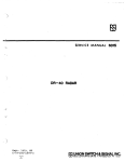
Programmable Printing Calculator
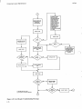
SERVICE MANUAL
o
t.2Ji:SS7()~3-2~ fto:;~
l/X
!. t:':439::'SJ7+ze
,..
i.~~3b4~S2$"4i1
u.
X'
~/////n
1.23Li56189D
TRACE
MAH..:JNORM
Off"ON
........
PRGM
c:: "
IIIiJ RUN
I
abc
d
e
mla • • • 111
. STF
ClF
F?
RNO
OSZ
ISZ
ABS
lOG
10 x
INT +H.MS H.MS+
•••••a
•••a ••
.allll • •
SIN-1 COS-1 TAN-1 FRAC O+R
R+O
iC
1:-
PAUSE
N!
S
%CH
91
.. ". III
a3:IM'&
•••
111000.
PRINT: SPACE-PRGM -REG--STACK
Rt
x"y?
RAO
GRO
1r
x=y?
x>Y?
x,;;y?
11000_
X~I
X_O?
X=O?
X>O?
X<O?
I·~~~I
0
I c:J losp]
WRITE DATA
HEWLETT· PACKARD
97
MERGE
lAST X
H.MS+
CALCULATOR
, - - - - - - - - - HEWLETT
IN
PACKARD - - - - - - - - - - - ,
HP-97
Programmable Printing Calculator
SERVICE MANUAL
00097 -90 130
HEWLETT-PACKARD COMPANY
1000 N.E. Circle Blvd., Corvallis, Oregon 97330
Printed August, 1976
Contents
/
{,
Section
Page
GENERAL INFORMATION
1-1.
1-5.
1-7.
1-10.
1-13.
1-15.
Introduction. . . . . . . . . . . . . . . . . . . . . . . . . . . .
Description .............................
Compatibility. . . . . . . . . . . . . . . . . . . . . . . . . ..
Identification ............................
Standard Accessories . . . . . . . . . . . . . . . . . . . . .
0I?tional Accessories .....................
"
THEORY OF OPERATION
2-1.
2-3.
2-10.
2-13.
2-17.
2-22.
2-24.
2-29.
2-32.
2-37.
2-41.
2-43.
HP-97 Logic ............................
Display ................................
Performing a Function ....................
Timing ................................
Printer .................................
Print Head Drivers .....................
Printer Motor Control ..................
Print Intensity Control ..................
Card Reader ............................
Power Inverter ..........................
Battery Charging ........................
Power-On Preset .........................
III
ASSEMBLY-LEVEL MAINTENANCE
3-1.
3-6.
3-7.
3-9 ..
3-12.
3-14.
3-16.
3-18.
3-21.
3-24.
Introduction ............................
Recommended Tools and Fixtures ..........
Individual Key Sequence Tests .............
Full Operational Test .....................
Initial Test ...........................
Program Memory Test ..................
Functional Test ........................
Keyboard Test ........................
Diagnostic Test ........................
HP-97 Assembly Removal and
Replacement Procedures ................
1-1
1-1
1-1
1-1
1-1
1-1
2-1
2-2
2-2
2-3
2-3
2-3
2-3
2-4
2-4
2-4
2-5
2-5
3-1
3-1
3-1
3-5
3-5
3-6
3-6
3-8
3-8
3-9
IV
COMPONENT-LEVEL MAINTENANCE
4-1.
4-3.
Introduction ............................ 4-1
Recommended Tools and Fixtures .......... 4-1
Section
4-4.
4-6.
4-8.
Page
4-10.
4-12.
4-14.
4-16.
4-21.
4-24.
4-26.
4-28.
4-30.
4-33.
4-35.
Logic PCA Troubleshooting ............... 4-1
Power Supply Troubleshooting ............. 4-1
Faulty Function Verification
and Repair ........................... 4-2
Logic PCA Operational Test ............... 4-6
Initial Test ........................... 4-6
Program Memory Test .................. 4-6
Functional Test ........................ 4-8
Printer Assembly Maintenance ............ 4-16
Printer Mechanical Maintenance ......... 4-16
Printer Electrical Maintenance ........... 4-17
Keyboard Troubleshooting ................ 4-22
Display Troubleshooting ................. 4-22
Cathode Driver IC Replacement ........... 4-22
Card Reader Troubleshooting ............. 4-24
V
ACCESSORIES
5-1.
5-3.
5-5.
5-12.
5-13.
Introduction ............................. 5-1
HP 82033A Battery Pack .................. 5-1
AC Adapter/Recharger .................... 5-1
HP 82044A Security Cable and Lock ........ 5-2
HP 82037A Reserve Power Pack ........... 5-2 (
VI
REPLACEABLE PARTS
6-1.
6-5.
Introduction ............................ 6-1
Ordering Information ................ : .... 6-1
)
Appendix A IMPROPER OPERATIONS
Appendix B SYMBOLS AND ABBREVIATIONS
Appendix C SERVICE CARDS
C-l.
C-7.
C-lO.
C-13.
C-16.
C-18.
Introduction ............................
Program Memory Test Program Card .......
Functional Test Program Card .............
Data Card 1 ............................
Data Card 2 ............................
Diagnostic Test Program Card .............
C-l
C-l
C-l
C-3
C-3
C-3
Illustrations
Figure
1-1.
2-1.
2-2.
ii
Title
Page
HP-97 Keyboard and Memory ............. 1-0
HP-97 Block Diagram .................... 2-1
LED Digit .............................. 2-2
Figure
2-3.
2-4.
2-5.
Title
Page
LED Display Format ..................... 2-2
SYNC and Display Timing ................ 2-2
Timing Diagram ......................... 2-3
(.~:~~')
\J
HP-97
Figure
2-6.
2-7.
2-8.
2-9.
2-10.
2-11.
3-1.
('
4-1.
4-2.
4-3.
•
4-4.
4-5.
4-6.
4-7.
4-8.
4-9.
I
4-10.
4-11.
4-12.
4-13.
4-14.
4-15.
4-16.
4-17.
4-18.
4-19.
I
\
Title
Page
Print Head .............................. 2-3
Printed Character ........................ 2-3
HP-97 Power Inverter Circuit .............. 2-4
Over- Voltage Circuit ..................... 2-4
Battery Charging Circuit .................. 2-5
Power-On Preset Circuit .................. 2-5
HP-97 Assembly-Level Troubleshooting
Flowchart ........................... 3-16
Faulty Function Verification
and Repair ........................... 4-2
Program Memory Test .................... 4-8
IC Replacement Flowchart,
Functional Test ....................... 4-11
CR5 and CR6 Anode Waveforms .......... 4-12
<1>1 and <1>2 Waveforms .................. 4-12
SYNC Waveform ....................... 4-12
STR and RCD Waveforms ............... 4-12
Logic PCA Troubleshooting
Flowchart ........................... 4-13
Logic PCA (AI) Component
Location Diagram ..................... 4-15
Logic PCA (AI) Schematic Diagram ....... 4-15
Printer PCA Lead Location ............... 4-16
Print Head Cable Removal ............... 4-16
Print Head Cable Insertion ............... 4-17
Print Head Cable Contacts ................ 4-17
Head Carriage Home Position ............. 4-17
FWD Waveform ........................ 4-18
STB Waveform ........................ 4-18
Printer PCA Troubleshooting Flowchart .... 4-19
Printer PCA (A4A1) Component
Location Diagram ..................... 4-21
Figure
Title
Page
4-20. Printer PCA (A4A1) Schematic Diagram .... 4-21
4-21. LED Digit. . . . . . . . . . . . . . . . . . . . . . . . . . . . . 4- 22
4-22. Keyboard PCA (A2A1) Component
Location Diagram ..................... 4-23
4-23. Keyboard PCA (A2A1) Schematic
Diagram ............................ 4- 23
4-24. Card Reader Switch Adjustment
Screws and Test Points ................ 4-24
4-25. W A and WB Waveforms ................. 4-24
4-26. RA and RB Waveforms .................. 4-24
4-27. Card Reader PCA (A3A1) Component
Location Diagram ..................... 4-25
4-28. Card Reader PCA (A3A1) Schematic
Diagram ............................ 4-25
4-29. Card Reader Troubleshooting
Flowchart ........................... 4-26
5-1. HP 82033A Battery Pack .................. 5-1
5-2. HP 82031A AC Adapter/Recharger ......... 5-1
5-3.
HP 82032A AC Adapter/Recharger ......... 5-1
5-4. HP 82032A Opt 001 AC Adapter/Recharger .. 5-1
5-5. HP 82039A AC Adapter/Recharger ......... 5-2
5-6. HP 82040A AC Adapter/Recharger ......... 5-2
5-7. HP 82043A AC Adapter/Recharger ......... 5-2
5-8. HP 82044A Security Cable and Lock ........ 5-2
5-9. HP 82037A Reserve Power Pack ........... 5-2
5-10. Reserve Power Pack Schematic
Diagram ............................. 5-3
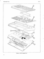
6-1.
HP-97 Exploded View .................... 6-2
6-2.
Printer Assembly Exploded View ........... 6-5
6-3. Card Reader Exploded View ............... 6-6
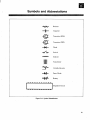
B-1. Symbol Identification ............... ~ .... B-1
C-1. Program Memory Test Program ............ C-1
Tables
Table
,
.I
1-1.
1-2.
1-3.
3-1.
3-2.
3-3.
3-4.
3-5.
3-6.
4-1.
4-2.
4-3.
4-4.
I
4-5.
4-6.
Title
Page
HP-97 Function Key Index ................ 1-2
HP-97 Programming Key Index ............ 1-3
Specifications ........................... 1-5
Individual Key Sequence Tests ............. 3-2
Initial Test ............................. 3-5
Program Memory Test .................... 3-6
Functional Test .......................... 3-6
Keyboard Test .......................... 3-8
Diagnostic Test .......................... 3-9
Faulty Function Repair ................... 4-3
Initial Test ............................. 4-7
Functional Test .......................... 4-9
IC Replacement, Calculator Halted
or Looping .......................... 4-11
IC Replacement, Error Display ............ 4-11
Logic PCA (AI) Replaceable Parts ......... 4-15
Table
4-7.
4-8.
4-9.
4-10.
5-1.
6-1.
6-2.
6-3.
6-4.
B-1.
C-1.
C-2.
C-3.
Title
Page
Printer PCA (A4A1) Replaceable Parts '..... 4-21
Cathode Driver Resistor Selection Chart .... 4-22
Keyboard PCA (A2A1) Replaceable Parts ... 4-23
Card Reader PCA (A3A1) Replaceable Parts. 4-25
AC Adapter/Rechargers ................... 5-1
HP-97 Replaceable Parts .................. 6-1
Keyboard Assembly (A2)
Replaceable Parts ...................... 6-3
Printer Assembly (A4)
Replaceable Parts ...................... 6-4
Card Reader Assembly (A3)
Replaceable Parts ...................... 6-6
Reference Designations and Abbreviations .... B-2
Functional Test Program .................. C-2
Data Card 2 ............................ C-3
Diagnostic Test Program .................. C-4
III
General Information
HP-97
o
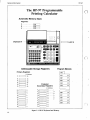
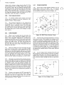
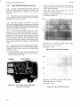
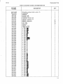
The HP-97 Programmable
Printing Calculator
Automatic Memory Stack
Registers
T ............. 10.00
z .............
~==~
~10=.0=0=~
y . . . . . . . . . . . . . 0c:.::.o=o_----"
c..:1
•
o
,,
:';"
Displayed X .....
-
I,23'i561B9CJ
TRACE
..... -=:1N011'"
PflC ... -=:JRlJI<
L ___._____I
aIlDU
•
•
abc
d
e
III mz!Um am 1m 1m
STF
eLF
F?
RND
DSZ
IS2
ASS
LOG
10 x
INT +H.MS H.MS+
SIN-1
cos-'
BI.lllmama
'--_----'I
91
LAST X
••
·;mu· • • •
PRINT;SPACE-PAGM-REG--STACK
DEG
RAO
GRD
1r
111000.
111000.
R+
x.y?
X=)'?
X>Y?
X:E)'?
X~I
X;tO?
X=O?
X>O?
X<O?
••• m•• 'II~~illl
1c:J§J
TAN-1 FRAC O+R
R+O
.allila.
PAUSE
(hpJ
N!
X
s
%CH
1:-
,
0
WRITE DATA
HEWLETT' PACKARD
97
MERGE
LAST
x
H.MS.
CALCULATOR
Addressable Storage Registers
Program Memory
Primary Registers
I
,
RE
RD
Rc
Rs
R.
,
,
,
,
,
000
(i) Address
25
24
23
22
21
20
Protected
Secondary Registers
9
Rsg ,
8
7
Rss'
Rs,l
S6
R
Rssl'
RS41
RS31
Rs,l
Rs, ,
Rso ,
001
51
002
51
003
51
004
51
005
51
(i) Address
Rg
Rs
R,
R6
Rs
R4
R3
R,
R,
Ro
6
5
4
3
2
1
0
1 19 ....... n
1 18 ....... LXY
17 ....... LY'
220
---51
16 ....... LY
221
51
LX'
LX
222
51
13
223
51
12
224
51
15
14
11
10
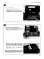
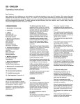
Figure 1-1. HP-97 Keyboard and Memory
1- 0
I
n
General Information
INTRODUCTION
1-1.
1-2.
This manual contains the information needed to
troubleshoot, disassemble, repair, and test the HP-97
Programmable Printing Calculator. (See figure 1-1.)
1-3.
The repair process for this calculator is broken up
into two parts, assembly-level and component-level repairs.
Basic operating information, specifications, theory of
operation, and maintenance information are included.
1-12.
The serial numbers located on the battery and on
the ac adapter/recharger are used to determine the week the
unit was fully charged and the date of manufacture, respectively. The format for each is described below:
Battery Charge Date
15L
Week of charging
1-4.
This section contains basic operating information
along with the specifications for the HP-97. Tables 1-1
and 1-2 list the various HP-97 keys and their functions.
Improper operations leading to an error display are listed in
appendix A.
' - - - - - Year of charging (1960
=
1975)
AC Adapter/Recharger
Manufacture Date
DESCRIPTION
1-5.
+ 15
1-6.
The HP-97 is a fully programmable, desktop
printing calculator. Mechanically, the HP-97 is essentially
similar to the HP-91, with the addition of a card reader.
(--
COMPATIBILITY
1-7.
1-8.
The HP-97 is compatible with the HP-67: programs
recorded on a magnetic card from an HP-67 can be loaded
into and executed on an HP-97, and vice versa.
1-9.
Programs recorded on a magnetic card from an
HP-65 cannot be loaded into an HP-97; however, most programs written for an HP-65 can be manually entered into an
HP-97 via the keyboard.
1-10.
Calculator Identification
L
12345
{
1-13.
+ 15
=
1975)
STANDARD ACCESSORIES
1-14.
The HP-97 comes complete with each of the following accessories:
IDENTIFICATION
1-11.
The serial number of the calculator is used for
identification and warranty determination. It is located just
above the battery door as the bottom of the calculator faces
you. The format is described below:
15QlA.
'-----Year manufactured (1960
•
•
•
•
•
•
Carrying Case
AC Adapter/Recharger
Owner's Handbook
Battery Pack
Printer Paper (two rolls)
Standard Pac
~~'~::num~'
•
B = Brazil
1-15.
S = Singapore
1-16.
The following items are optional accessories to the
HP-97 and as' such are sold separately:
Month manufactured
Programming Pad
OPTIONAL ACCESSORIES
•
HP 82044A Security Cable
Year manufactured
•
HP 82037 A Reserve Power Pack
+ 15
•
Pocket Card Holder (part number 00097-13142)
(1960
=
1975)
1-1
General Information
HP-97
Table 1-1. HP-97 Function Key Index
Manual RUN Mode. PRGM-RUN switch PRGM.mmll RUN set to RUN. Function keys pressed from the keyboard execute individual
functions as they are pressed. Input numbers and answers are displayed. All function keys listed below operate either from the keyboard
or as recorded instructions in a program.
n
'-
o
Paper advance pushbutton. Press to advance
paper without printing.
OFF.mmll ON Power switch.
TRACE
MAN _
NORM Print mode
switch. Selects printing
option.
PRGM .mmll RUN
IFRACI Leaves only fractional
portion of number in displayed
X-register by truncating integer
portion.
~
Rounds mantissa of 10-digit
number in X-register to actual
value seen in the display.
Number Manipulation
Program mode
~
switch.
Selects PRGM mode for
manual loading of program into
calculator or recording upon
magnetic card. Selects RUN mode
for manual operation of calculator,
loading of program into calculator
from magnetic card, or recording
or loading of data on or from
magnetic card.
Printing Functions
Rolls up contents of stack for
viewing in displayed X-register.
liD
Rolls down contents of stack
for viewing in displayed X-register.
CD3
Clears contents of displayed
X-register to zero.
Display Control
DEI
mI
PRINT: ~ Prints contents
of all primary storage
registers.
display.
IlIiIIm Prints contents of
displayed X-register.
Digit Entry
I3lmiD Enters a copy of number
displayed in X-register into
V-register. Used to separate
numbers.
Common antilogarithm.
Raises 10 to power of number in
displayed X-reigster.
mil
Natural antilogarithm. Raises
e (2.718281828) to power of
number in displayed X-register.
~
Computes common logarithm
(base 10) of number in displayed
X-register.
Em
Computes natural logarithm
(base e, 2.718 ... ) of number in
displayed X-register.
Magnetic Card Control
Selects scientific notation
display.
me Selects engineering notation
~
Followed by number key,
selects number of displayed digits.
Mathematics
@ Computes factorial of number
in displayed X-register.
Fa Computes reciprocal of number
IW/DATAllf a magnetic card is passed
through the card reader
immediately after this operation,
the contents of the storage
registers are recorded on the card.
IMERGE I Merges, rather than overwrites, data or program from magnetic card with data or program in
calculator.
Polar/Rectangular Conversion
em Converts x, y rectangular
coordinates placed in X- and
Y -registers to polar magnitude r
and angle O.
em COAverts polar magnituder and
angle 0 in X- and V-registers to
rectangular x and y coordinates.
in displayed X-register.
Ell
Computes square of number
in displayed X-register.
fiI
Computes square root of
number in displayed X-register.
Statistics
BI Accumulates numbers from Xand Y -registers into secondary
storage registers RS4 through Rs9.
~
or exponent of 10 in displayed
X-register.
@ Places value of pi
(3.141592654) into displayed
X-register.
Subtracts x and y values from
storage registers RS4 through RS9
for correcting or subtra_cting BI
accumulation entries.
ID3 Enter exponent. After press-
a II 13 a Arithmetic operators.
00
GmJ Changes sign of mantissa
ing, next numbers keyed in are
exponents of 10.
@] through
8
~
Digit keys.
Decimal point.
Number Alteration
~
Gives absolute value of
number in displayed X-register.
[illIJ Leaves only integer portion of
number in displayed X-register by
truncating fractional portion.
1-2
Selects fixed point display.
PRINT: [SPACE I advances
paper one space without
printing.
PRINT:I STACK I Prints contents of automatic memory
stack.
~
aD
Exchanges contents of X- and
Y -registers of stack.
Percentage
VA Computes x% of y.
1% CH I Computes percent of change
from number in Y -register to
number in displayed X-register.
Logarithmic and Exponential
Gil
Raises number in V-register to
power of number in displayed
X-register.
.'
Computes mean (average) of
x and y values accumulated
bYBl.
(!) Computes sample standard
deviations of x and y values
accumulated by BI.
Flags
@ill Set flag. Followed by flag
designator (0, 1,2, or 3), sets flag
true.
(lliJ Clear flag. Followed by flag
designator (0, 1,2, or 3), clears
flag.
('
'
.... _--"
)
HP-97
General Information
Table 1-1. HP-97 Function Key Index (Continued)
I • H.MS) Converts decimal hours or
degrees in displayed X-register
to hours, minutes seconds or
degrees, minutes, seconds.
I H.MS.) Converts hours, minutes,
seconds or degrees, minutes,
seconds in displayed X-register
.to.decimal qegrees.
I H.MS+ ) Adds hours, minutes,
seconds or degrees, minutes,
seconds in Y -register to those
in X -register.
I SIW' )lcos-')ITAw') Computes arc
sine, arc cosine, or arc tangent of
number in displayed X-register.
IlmI B
em Computes sine,
cosine, or tangent of value in
displayed X-register.
~
Converts degrees to radians.
~
Converts radians to degrees.
~
Sets decimal degrees mode
for trigonometric functions.
~
Sets radians mode for
trigonometric functions.
~
Sets grads mode for
trigonometric functions .
Storage
Indirect Control
Trigonometry
m:J Store. Followed by address
D
Recalls number from
I-register into displayed
X-register. (To store number
in I, use m:J D.)
UD
key, stores displayed number in
specified primary storage register
(Ro through Rg, RA through R E , I).
Also used to perform storage
register arithmetic.
When preceded by
~,mm,em,m:J,
. , [jg), or (QgJ, the
address or control value for
that function is specified by
the current number in I.
•
Recall. Followed by address
key, recalls number from specified
primary storage register (Ro
through Rg, RA through RE, J)
into the displayed X-register.
[jg) Increment and skip if
zero. Followed by D, adds
1 to contents if I. Followed
by UD, adds 1 to contents of
storage register specified
by value in I. Skips one step
if contents are then zero.
ICLREGI Clears contents of all
primary storage registers (Ro
through Rg, RA through RE, J) to
zero.
ILASU) Recalls number displayed
before the previous operation back
into the displayed X-register.
(QgJ Decrement and skip if
zero. Followed by D,
subtracts 1 from contents
of I. Followed by UD, subtracts 1 from contents of
storage register specified by
value in I. Skips one step if
contents are then zero.
~
Primary exchange secondary.
Exchanges contents of primary
storage registers Ro through Rg
with contents of protected
secondary storage registers Rso
through Rsg.
~
Exchanges contents of
displayed X-register with those of
I -register.
...-_ _ _ _ _ _ _ _ _ _ _--, Table 1-2. HP-97 Programming Key Index
Automatic RUN Mode
PROGRAM Mode
PRGM-RUN switch set to
PRGM PRGM ~ RUN
All function keys except the
ones below are loaded into
program memory when pressed.
Program memory contents
recorded upon magnetic card
when card passed through card
reader.
Active keys:
In PROGRAM mode only six
operations are active. These
operations are used to help record
programs, and cannot themselves
be recorded in·program memory.
PRGM-RUN switch
PRGM -.JRUN
set to RUN.
Function keys may be executed as part of a recorded program or
individually by pressing from the keyboard. Input numbers and
answers are displayed by the calculator, except where indicated. Data
or instructions loaded from magnetic card into calculator when card is
passed through card reader.
Pressed from keyboard:
B IlUIS II 0
~@)
@](!)
User-definable keys. Cause
calculator to search downward
through program memory to first
designated label and begin
execution there.
Executed as a recorded
program instruction:
BIUISII0~@)@](!)
@)CDm@]0m@00~
Label designators. When preceded by 1!ilI, define beginning of
routine. When preceded by mm
or em, cause calculator to stop
execution, search downward
through program memory to first
designated label, and resume
execution there.
1-3
HP-97
General Information
Table 1-2. HP-97 Programming Key Index (continued)
Automatic RUN Mode
PROGRAM Mode
Pressed from the keyboard:
Executed as a recorded
program instruction:
Ciml Go to. Followed by
Ciml Go to. Followed by
8
8
Ciml Go to. Followed by label
designator (B through D, D (!)
through D (!), @) through @) or
Active keys:
[ill [ill [ill, positions calculator to
step nnn of program memory. No
instructions are executed.
[ill [ill [ill, sets calculator to step
nnn of program memory without
executing instructions. Followed
by label designator (B through D,
D 0 through D (!), @) through
@) or (IIJ), causes calculator to
search downward through program memory to first designated
label and begin execution there.
m
Followed by label designator,
(B through D, D 0 through
D (!), @) through @), (IIJ), causes
calculator to start executing instructions, beginning with
designated label.
mm Return. Sets calculator to step
mm Return. If executed as a
000 of program memory.
result of pressing a label
designator or execution of a Ciml
instruction, stops execution and
returns control to keyboard. If
executed as a result of a miliJ
instruction, returns control to next
step after the miliJ instruction.
PRINT: I PRGM I Print program.
Prints contents of program memory,
beginning with current step and continuing until two consecutive
instructions are encountered or
step 224 is printed.
m
JClPRGMI After D prefix key, cancels
that key. After other keys, does
nothing. Does not disturb
program memory or calculator
status.
I PAUSE I Stops program execution
elm
elm
Ix<o?1
mJ
Single step. Moves calculator
forward one step in program
memory.
mJ
@ill Delete. Deletes current
instruction from program memory.
All subsequent instructions moved
up one step.
@ill After D prefix key, cancels
that key. After other keys, does
nothing. Does not disturb program
memory or calculator status.
JClPRGMI Clear program. Clears
program memory to all
instructions, sets calculator to step
000, clears· all flags, and specifies
FIX 2 and DEG modes.
m
Back step. Moves calculator
back one step in program memory.
Back step. Sets calculator to
and displays step number and
keycode of previous program
memory step when pressed;
displays contents of X-register
when released. No instructions are
executed.
Single step. Displays step
number and keycode of current
program memory step when
pressed; executes instruction,
displays result, and moves
calculator to next step when
released.
m
Run/stop. Begins execution
from current step of program
memory. Stops execution if
program is running.
Any key. Pressing any key on the
keyboard stops execution of a
running program.
1-4
miliJ Go to subroutine.
Followed by label designator
(B through D, D 0 through
D (!), @) through @) or (IIJ ), causes
calculator to search through
program memory to first designated label and execute that
section of program memory as a
subroutine.
miliJ Go to subroutine.
PRINT: I PRGM I Print program.
Prints contents of program
memory, beginning with current
step and continuing until
instructtwo consecutive
ions are encountered or step 224 is
printed.
(IIJ), causes calculator to stop
execution, search through
program memory to first designated label, and resume execution
there.
and transfers control to keyboard
for 1 second, then resumes
program execution.
IX'Y?llx=Y?llx>Y?llx~Y?llx,o?llx=o?llx>o?1
Conditionals. Each tests value in
X-register against 0 or value in
Y -register as indicated. If true,
calculator executes instruction in
next step of program memory. If
false, calculator skips one step
before resuming execution.
IB
If flag true. Followed by flag
designator (0, 1, 2, or 3), tests
designated flag. If flag is set (true),
the calculator executes the
instruction in the next step of
program memory. If flag is cleared
(false), calculator skips one step
before resuming execution. IB
clears flags F2 and F3 after test.
m
Run/stop. Stops program
execution.
(j
General Information
HP-97
Table 1-3. Specifications
Calculator Dimensions
•
•
•
•
Length: 8.0 inches (20.3 centimeters).
Width: 9.0 inches (22.9 centimeters).
Height: 2.5 inches (6.35 centimeters).
Weight
•
•
Calculator with battery pack: 40 ounces (1.13
kilograms).
U.S. Recharger: 5 ounces (155 grams).
Formats:
Fixed Point:
Scientific:
Numbers are shown in scientific notation with "n"
places to the right of the
decimal point.
Engineering:
Numbers are shown with
"I + n" digits and an exponent of I 0 that is the nearest multiple of three.
Special:
"Error" written on display
when improper operation is
attempted (see appendix A).
"Crd" written on display
when card is expected.
Power
•
Rechargers
HP Part
Number
United States
82040A
Australian
82039A
European
82043A
82031A
Desktop
(
•
82032A
90-127 Vac,
50-60 Hz, 7 watts
200-254 Vac,
50-60 Hz, 7 watts
90-127 Vac,
50-60 Hz, 7 watts
200-254 Vac,
50-60 Hz, 7 watts
200-254 Vac,
50-60 Hz, 7 watts
•
Special indications:
Overflow:
X-register overflow displays all nines
(±9.999999999 99).
Underflow:
Zero in scientific notation. If
in fixed notation, automatically reverts to scientific
notation for small numbers
that would otherwise appear
as zero.
LED at upper left of display lit for 30 seconds to 10
minutes before tlisplay
blanks.
Battery
Four cell, 4.4 to 6.0 volts, quick-charge, nickelcadmium battery pack.
•
Low Battery:
Operating time: 3 to 7 hours.
Note: Battery must be in place to operate the
calculator .
•
Numbers are shown with
"n" places to the right of the
decimal point.
Recharging time: 7 to 10 hours, calculator
OFF; 17 hours, calculator ON.
Environmental Specifications
Display
•
Rounding to last displayed digit. Internal operations are
calculated with 10 digits.
•
Numeric and decimal point: Eight segment, lightemitting diode (LED). Digit and decimal point are
contained within a single eight-segment LED.
•
15-digit display including two sign digits.
•
Minimum/maximum display number:
±1 X 10- 99 to ±9.999999999 X 1099
•
Operating: 0° to 45°C (32° to 113°F); with paper,
5% to 95% relative humidity.
•
Charging: 15° to 40°C (59° to 104°F).
•
Calculator Storage: _40° to 55°C (-40° to 131 ° F).
•
Paper Storage: _40° to 30°C (_40° to 86.0 F); less
than 60% relative humidity.
Note: A void exposure to direct sunlight or
artificial light sources for extended periods; keep in
box or appropriate container.
1-5/1 -6
II
Theory of Operation
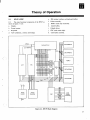
2-1.
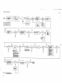
HP-97 LOGIC
e.
PIK (printer interface and keyboard buffer).
2-2.
The main functional components of the HP-97 as
shown in figure 2-1 are:
f.
Printer assembly.
g.
ROM's (read only memories).
a.
h.
Anode buffers.
Display.
b.
Power inverter.
i.
Cathode driver.
c.
Keyboard.
j.
CRC (card reader chip).
d.
ACT (arithmetic, control, and timing).
k.
Card reader assembly.
~
(RCD)
r;:=
Cathode Driver
r-
DATNROM 6
(Low Battery)
C1-.
!ll l l11 ~C14
STR
ti:JC±±:j
...f=
KBA
KBe
KBO
KBE
DATNROM 5
ROM 3
ACT
PIK
ROM
o
DATA/ROM 2
DATNROM 1
SYNC
DATA
Power
Inverter
Printer
Assembly
CRC
WA
WB
WE
RA
RS
MOTOR
WPS
t-~M~T;'R::':S::-~
Card
Reader
Assembly
HDS
Figure 2-1. HP-97 Block Diagram
2-1
Theory of Operation
2-3.
HP-97
DISPLAY
2-4.
The display consists of a 15-digit light-emitting
diode (LED) module plus a low battery indicator which are
controlled in part by each of the following components:
a. ACT.
b.
ROM O.
c.
Anode buffers.
d.
Cathode driver.
2-5.
Each digit consists of seven LED segments with an
additional segment for the decimal, which makes eight
segments, sequentially lettered a through h as shown below.
2-7.
By sequentially switching on each cathode driver,
only one digit at a time is actually lit. This happens too fast
though for the eye to detect. Each cathode driver transistor
is sequentially switched on by the strobe (STR) signal
provided by the display ROM and reset by reset cathode
driver (RCD), which is provided by the ACT. (See figure
2-4.)
--;:===:::;-_fL
STR -----.Il1 _______________________
L--
SYNC 1
SEGMENTS
A~L
B________
____________________________
__________________________
~r
~,---,L
L - - - - - - - - - - - - - -________
c-------------.---.
D________________
_________________
~L
____________________
a
~r___IL
_____________
F ___________________________'---OL________
G
H ----,
~
r---L
9
Figure 2-4. SYNC and Display Timing
·ll
[}
2-8.
The display of the HP-97 requires a large amount of
current. Though the display ROM decodes the display
information given on the Is bus by the ACT to switch on
the correct anodes, it alone is not capable of handling the
large amount of current. Anode buffers U3 and U4 are
used for this purpose.
d
Figure 2-2. LED Digit
2-6.
Since the display is a scanned diode array, both its
anode and cathode must be driven in order for the segment to
light. All cathodes of each digit are tied together, as shown
in figure 2-3. When a cathode driver transistor is turned on,
any segment of that digit may light; the segment that lights
will now be determined by which anode driver transistor is
switched on. As an example, if all cathode driver transistors
were switched on along with the a-segment anode driver,
the a segment of all digits across the display would light.
2-9.
Every cathode driver in the display that is switched
on returns to ground that corresponding cathode line in the
keyboard buffer U4 (PIK) which will decode and store up to
seven key codes. This allows the operator to press keys very
quickly without waiting for the calculator or printer to catch
up. The PIK will also hold each key code for approximately
4.5 milliseconds to negate the effects of key bounce.
2-10.
PERFORMING A FUNCTION
2-11.
Before a key is pressed the ACT is continually
asking, "has a key been pressed?" If the ACT is not tied up
in controlling a calculation, and a key haS" been pressed, it
will service that key code and the display will return. (The
display is blanked out during printing to conserve
power.)
CATHODE
DRIVE _
LINES
" KEYS
CATHODE LINES
(14 TOTAL)
Figure 2-3. LED Display Format
2-2
KEY
LINES
2-12.
The ACT services a key code by first requesting the
key code, corresponding to the key that was pressed, from
the PIK. The PIK returns that code to the ACT via the
DATA line. The ACT finally will put the address code on the
instruction address (Is) bus. This address goes to the ROM's
that will now send back to the ACT the specific instructions
of how to perform that function and at the same time
instruct the PIt< as to what function to print. The ACT will
then perform that function on the numbers in the display;
the printer will print (when the print mode switch is set to
TRACE) the function name and the result of that
operation.
0.
Theory of Operation
HP-97
2-13.
TIMING
2-14.
The ACT circuit produces two signals for timing
purposes: SYNC for the ROM's, PIK, and CRC, and RCD
for the PIK and cathode driver. Along with the connection
through the SYNC line, the ACT is connected to the
ROM's and PIK by the Is (instruction address) bus. The
Is bus instructs the data storage IC to store data sent on
the data line from the ACT, and to send data back to the
ACT on the same DATA line. Figure 2-5 shows the timing
relationship between the SYNC, DATA, and Is pulses.
2-20.
The head is mechanically moved across the paper
-by a lead-screw mechanism (see figure 6-2). By passing
current through the appropriate head resistor at the correct
time, as the head moves across the paper, characters are
thermally printed.
2-21.
Notice the slight slant of each character. This is
done to decrease instantaneous current demands. The
printer/interface and keyboard buffer (PIK) is responsible
for this operation. The PIK also controls print intensity, line
width, and motor movement commands.
L
OATA--------'
o
•• _ _ _-'-----_-1-_--1..._-'-----_ _-1-_ _- ' - - _ - ' - _ - - - - - '
00
SYNC----'
c:::J
c:::J
TlME---+1--1-1--+.-+I-+-'-----+1---+1--+1-+1146
155
12
17
1'6
127
'46
to
Printed 'ONE'
o
17
Figure 2-5. Timing Diagram
..
2-15.
In addition to being used to synchronize the system,
SYNC is also used to gate the 10-bit instruction that appears
on Is at bit times t46 through t55' During this time, SYNC
distinguishes instructions from addresses. Following an
"IF" instruction on the Is bus, the subsequent SYNC pulse
is suppressed to allow a 10-bit address to be sent on the Is bus.
D
ODD
Head moves right to
left while printing.
Figure 2-7. Printed Character
2-16.
At bit times t15 through t27 , the Is line carries a 12-bit
instruction address from the ACT to the ROM, while display
information is carried from the ACT to the ROM during
bit times to through t 7 • At bit times to through t3 , a digit is
carried from the ACT to the ROM's for decoding and display. On the following word time, the next digit is sent out.
Sign, decimal point, and blanking information for the number is carried to the ROM during bit times t4 through t7 •
2-23.
Each head resist9r requires approximately 0.5A of
current to adequately print on the heat-sensitive p·aper. NPN
transistors Ql through Q7 act as current amplifiers to supply
the head resistors with the required current and also lessen
the drive requirements from the PIK
2-17.
2-24.
PRINTER
2-18.
The printer used in the HP-97 employs a very hot
source (print head resistors) in close contact with heat
sensitive paper. This paper changes color in the area of heat
contact.
2-19.
The print head contains seven small resistors (each
about 10 ohms) that heat up when current is passed through
them. Figure 2-6 shows the print head and resistors.
/
/
Resistors --<
;r--)---
2-22.
Print Head Drivers
Printer Motor Control
2-25.
A small dc motor provides the mechanical power
through the action of the lead-screw and gears to move the
print head. Current for the motor is controlled by the on and
off action of six driver transistors Q9 through Q14.
2-26.
When the PIK gives the comand to move forward,
transistors Qll, Q14, and Q9 tum on. Transistors Q12,
Q13, and QI0 tum on to reverse the direction of head travel.
2-27.
Braking action is produced by shorting the dc
motor windings; when Q8 is turned on, it shorts the windings
and Q 10 provides a signal ground for the base current from
Q8.
)-)-
(Common ) -
~
V
Figure 2-6. Print Head
2-28.
The printed line width and character-to-character
spacing is determined by the speed of the dc motor. To
control the speed of the motor, U4 samples the output voltage
generated by the motor when the driver transistors are turned
off and the motor is coasting. Contained within U4 is a set of
comparators, Al through A4. Al compares the motor output
2-3
HP-97
Theory of Operation
voltage with a reference voltage derived within US. If the
motor is going too slow, its output voltage will be less than
the reference voltage. The Al comparator instructs the PIK
to speed up the motor. The PIK then changes the FWD signal
pulse width to accomplish this. This operaton occurs only
during forward head movement. If the head is moving too
fast, again the comparator output will change and the FWD
signal pulse width will change to compensate.
2-29.
POWER INVERTER
2-37.
2-3S.
Quick-charge nickel-cadmium batteries are the
primary power source for the HP-97. The +S.O nominal
battery voltage is converted to +6.2S Vdc and to -12.0 Vdc
by the transistor inverter circuit shown in figure 2-S.
o
Print Intensity Control
R10
2-30.
To maintain uniform print contrast, each head
resistor must be energized to the same temperature, independent of battery voltage changes.
2-31.
The remaining comparators in U4, alongwith the
resistor network in US, produce the variable duty-cycle
signal STB, which is nominally 10 kHz. The STD signal
will change its duty-cycle to keep its rms value constant and
thus print intensity constant. By changing the value of RS,
the nominal duty-cycle of STD can be changed to adjust
print intensity.
R9
Q4
R8
,TI
V
+6.2SCjS,,-S- - -
'12.0{V)G~G-
___---I~---40
~VDO)
2-32.
CARD READER
2-33.
When a card is inserted into the card reader, the
motor switch is closed, grounding the MTRS signal. This
signal is fed to the CRC, which tells the microprocessor
(contained in the ROM's and ACT) that a card is in the card
reader. The microprocessor in response tells the CRC to turn
on the card reader motor. The CRC then grounds the
MOTOR signal to the sense amp, which supplies power to
the motor. The motor turns a roller, which passes the card
through the card reader.
2-34.
When the leading end of the card reaches the card
reader head, the head switch is closed, grounding the HDS
signal. For a read operation, flux transitions on the card
are picked up by the head, amplified and converted to digital
levels by the sense amp, buffered by the ACT, and then passed to the appropriate data storage registers. For a write
operation, this process is reversed. The microprocessor
informs the CRC whether the operation is a read or write.
2-3S.
Information is recorded as a flux transition onto two
tracks on each edge of the card. A header at the beginning
of both tracks indicates whether the information on the card
is a program or data. If the card contains a program, this
header also contains flag and display format information and
indicates whether side 1 or side 2 of the program is being
read/written. At the end of the tracks is a checksum, which
is used by the microprocessor to check for errors in reading.
If an error is so detected, the microprocessor generates an
"Error" display.
Figure 2-8. HP-97 Power Inverter Circuit
2-39.
Transistor Q2 and toroidal transformer Tl form the
basic inverter circuit. With feedback from winding A, Q2
oscillates at a frequency of approximately 20.0 kHz. Winding B of T 1 forms the tranformer primary from which Vss is
derived; CRS rectifies and C4 filters the voltage from winding B. The voltage from winding C is rectified, filtered, and
doubled by the combined actions ofCl, C2, CR6, and CR7
to produce the output voltage VGG • Voltage regulation of
Vss is provided by controlling the frequency of oscillation of
Q2 through the combined action of zener diode CR9 and
transistor Q3.
( ~')
..'
2-40.
An over-voltage circuit consisting of Q4, QS, and
RS through RIO, as shown in figure 2-9, prevents VB (battery
voltage) from rising above Vss. When VB approaches Vss ,
CRIO conducts, turning on transistors Q4 and QS. Current is
drawn from the battery through RIO until VB falls below
Vss·
V.
+5.0
R10
Q4
R9
CR10
2-36.
During a write operation, the CRC interrogates the
write protect switch when the head switch closes to
determine if the card has a clipped corner. If so, the CRC
inhibits the write operation and informs the microprocessor,
which generates an "Error" display.
2-4
V.
+6.25c;::..--~------.,
( 0.'' ',)
"
"
',,--,",(
Figure 2-9. Over-Voltage Circuit
Theory of Operation
HP-97
2-41.
2-43.
BATTERY CHARGING
2-42.
Figure 2-10 illustrates the battery charging circui try. The ac adapter/recharger is a transformer that drops
the line voltage to 12.8 Vac at the input terminals of the
calculator. Diodes CRI through CR4 rectify the alternating
current, and resistor R4 limits the dc current applied to the
batteries. When the ON-OFF switch is turned ON, limiting
resistor R3 is shunted, and the dc voltage is applied directly
to the battery pack and the calculator power supply.
Transistor Ql turns on during periods of high display current
demands.
Note: With batteries removed, the calculator wiII not be
damaged by connecting the ac adapter/recharger to the
input terminals; however, it will not operate correctly
until the batteries have been reinstalled.
,-----------1
I
I
i
I
I
I
I
I
AC Adapteri
Recharger
I
I
I
I
I
I
I
Calculator
~--------«To
(To VB)
ACT)
Q1
I
I
I
(To
Vssl
I
I
I
I
I
I
I
I
2-44.
To ensure that the logic contained within the ACT
comes up in the correct logic state when power is applied to
the HP-97, a power-on preset circuit is included. Figure
2-11 shows the equivalent circuit.
I--~--------------~--l
I
I
POWER-ON PRESET
I
I
I
I
I
I
I
I
I
I
I
I
-=-
Figure 2-11. Power-On Preset Circuit
I
I
I
I
I
___
~__
I
I
L _ _ _ _ _ _ _ _ ~ _ _ _ _ _ _ _ _ _ _J
Figure 2-10. Battery Charging Circuit
2-45.
Basically, when power is applied, Q I is turned off;
V ss rises and the voltage across C I also rises, resetting the
ACT. When Vss rises to the correct level, QI turns on,
discharging C I-now ready for the next power on sequence.
2-5/2-6
Assembly-Level Maintenance
3-1.
INTRODUCTION
3-7.
3-2.
This section includes procedures for:
3-8.
Listed in table 3-1 are sequences of keystrokes that
may be used to check for properly functioning HP-97 operations. If the calculator's display or printout does not agree
with the entry in the appropriate column, the operation is not
functioning properly and the logic PCA and/or keyboard
PCA should be replaced. However, in some cases proper
functioning with the indicated keystrokes does not guarantee
that the operation functions properly with other acceptable
key sequences. Therefore, if a calculator is received for
repair with a particular operational key sequence that does
not perform properly, this key sequence should be used to
verify the complaint rather than the key sequence in table 3-1.
After performing the key sequence test(s), return to P on
figure 3-1.
a.
Isolating any calculator malfunction to a replaceable
assembly.
b.
Disassembling the calculator to permit the faulty
assembly to be replaced.
c.
Replacing either the faulty assembly or certain associated components that can be replaced without
desoldering.
3-3.
The HP-97 Assembly-Level Troubleshooting
Flowchart (figure 3 -1) shows the step-by-step procedures
for isolating a malfunction to a replaceable assembly. Refer
to the HP-97 Exploded View (figure 6-1) and the HP-97
Assembly Removal and Replacement Procedures (paragraph
3-24) for aid in replacing the faulty assembly. (CAUTION:
Be sure that the bench setup for trouble analysis has adequate
electrostatic protection; otherwise, IC's may be damaged.)
INDIVIDUAL KEY SEQUENCE TESTS
3-4.
If a calculator is received with a complaint regarding only a particular inoperable function, refer to the
individual key sequence tests (table 3-1) for verifying and
correcting the malfunction.
3-5.
After known malfunctions have been corrected and
the calculator reassembled, perform the full operational
test (paragraph 3-9) to ensure that all capabilities of the
calculator are functioning correctly.
3-6.
RECOMMENDED TOOLS AND FIXTURES
UP PART/MODEL NUMBER
6040-0297
8700-0003
8700-0006
8710-0026
8710-0549
8730-0008
8730-0020
8500-0232
T-155321
T-155239
T-155435
00091-92137-97
ET 9613-91-M
ET 9613-91-A
ET 9610
(See appendix C.)
(See appendix C.)
(See appendix C.)
(See appendix C.)
(See appendix C.)
DESCRIPTION
Silicone Lubricant
X-acto Knife
X-acto Knife Blade
Tweezers
Needle-Nose Pliers
Small Flat-Blade Screwdriver
Phillips Screwdriver
T.F. FREON
Holding Nest
HP-97 Card Reader Installation Tool
HP-91/97 Field Service Connector Tool
Sequence PROM Assembly
Fold Apart Tester
Automatic Tester Option
Test System Mainframe
Program Memory Test Program Card
Functional Test Program Card
Data Card 1
Data Card 2
Diagnostic Test Program Card
3-1
HP-97
Assembly-Level Maintenance
Table 3-1. Individual Key Sequence Tests
a.
Switch the calculator ON.
b.
Perform the indicated keystrokes.
c.
Compare the calculator display to the entry under DISPLAY and PRINT.
d.
To check more than one operation (or set of related operations), switch the calculator OFF and then ON
before entering the next key sequence.
/'
t )
OPERATION
-
@
@a
@(I]@&
@II
@i'lI
§!]
@IiDO§!]
digit entry
a
&
II
I'll
liD
mmiD
D
@1iD1iD1iD1iD
@mmiD_1iD
13
D
lospi
m
liD
E
@mmiD(I]D
@mmiD(I]1I
@mmiD(I]13
@mmiD(I]D
lospl @]
CD(I]@)m
CD(I]@)mliD
CD(I]@)@JE
1m
Im®
EiD
@mmiD(I]EiD
D
@m OILASrxJ
II
ILAST xJ
IRNOJ
IABSJ
IINTJ
IFRACJ
@D
~
m
I%CHJ
IO+RJ
IR+OJ
m
ISIW 1J
tml
Icos-1J
&
ITAWlj
IRAOJ
IGROJ
IOEGI
3-2
KEYSTROKES
CD(I]G@)@]@~
lospJ (I] 0 IRNOJ
lospl @]
@ a 0 IABSJ
CD (I] G @) @] 0 IINTJ
CD (I] G @) @] 0 IFRACJ
@O@D
O~
CD@@JmmiD~m
CD @@JmmiD CD [1]@J
OI%cHJ
@] @ 0 IO+RI
CD 0 IR+OJ
@)@Jm
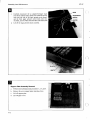
G@OISIW1J
~ @J tml
G @ 0 Icos-1J
@]@&
CD 0 ITAW1J
~ 0 IRAOJ tml
(I] @J @J 0 IGROJ tml
@) @J 0 IRADJ 0 IOEGJ m
o
DISPLAY
5.
-5.
0.00
5.00
25.00
0.20
5.00
5.00
5.00
7.00
3.00
10.00
2.50
0.0000
1.23
123.00
1.23
1.
5.00
0.40
·5.00
12.3456
12.35
12.3500
5.00
12.00
0.34
120.00
3.14
9.00
170.
13.33
0.79
57.30
0.50
30.00
0.50
60.00
1.00
45.00
-1.00
-1.00
0.50
02
03
09
(
)
-
)
Assembly-Level Maintenance
HP-97
Table 3-1. Individual Key Sequence Tests (Continued)
KEYSTROKES
OPERATION
[.H.MSI
[ H.MS·I
[H.MS+ I
~
~
~8m~mmm
@J 8 rn ill D [ H.MS+ I
@Jmmm0=
EiD
=
@J~8~illmmm
ail
mail
EiD
OJ mil
OJ mil 1m
@JD[lO I
rn @) D [LOGI
mil
1m
110 x I
[LOGI
m
mimiI3
PRINT: 1STACK
-
mm}
PRINT:
8 01·H.MSI
8 0 rn D 1H.MS· I
[REGI
X
rnmmm~m
I
OJmimi13
OJmmmrnmmm
@Jmmm0
D PRINT: 1STACK I
DISPLAY
PRINT
6.42
6.70
6.56
10.23
5.00
36.87
36.87
4.00
3.00
2.72
1.00
1000.00
1.30
256.00
1.00
2.00
4.
4.00
1. l1t)
1. ee
2.6e
J. fn":f
4. f'f~
2.00
2.00
1.00
2.00
3.00
4.00
4.00
{rnmmm
__ m
OJmmOJ
rnmmrn
@Jmm@J
0mm0
D PRINT: [REGI
0 .. 00
1. 00
2 [7(1
4
e.6t?:
f.O(i
6
- EI,fH3
B
9
R
B
C
D
£
I
0.£16
6.06
mmD
mma
~mmOJ
rnmmDOJ
_OJ
~mmOJ
rnmmaOJ
fI.0e
8.130
~
~
(1
1
4.06
6.00
6.80
8.60
mmm~
I
"
?:
2
3
e. eli
__
D[CLREGI _ _
,/
Z.B@
r
ICLREGI
T
z
~I
..,,.
5.00
0.00
8.00
2.00
10.00
8.00
2.00
3-3
HP-97
Assembly-Level Maintenance
Table 3-1. Individual Key Sequence Tests (Continued)
raCD
mmf3
Ip~sl
0mmf3CD
raCD
~mmCD
o mma CD
raCD
0~mm00
'
Ip~sl
m
~
6.00
8.00
2.00
16.00
8.00
2.00
4.00
~mmCD
mma
>
ra 0
mJ
mJ
mm8@J@J@J
2.00
12.50
mo~
000
00
1m
0.00
mmmmm
00
o )
17.79
(key down)
(key up)
1m (key down)
(key up)
mmUIJ
(positive i)
mmUIJ
(negative i)
D}
mm
lmm}
mm
!x;tY?1
!x=Y?1
!X=O?I
!x>o?1
!X<O?I
!x~Y?1
!x>Y?1
!x;to?1
ISTFI}
!ClFI
51
224
51
mm8CD0@)
123
51
002
21 02
220
51
003
21 13
002
21 12
PRGM~RUN
lID CD lID 0
lID@)
PRGM .mJI[] RUN
0mmOmm
UIJ PRGM urn. RUN
~emmmo
mm UIJ PRGM ~ RUN
IIDB
mmm
r~"'"""
{' ' . ~ """ DII
IIDmllDs
PRGM .mJI[] RUN
PRGM~RUN
CD0@)lmmma
mmllDmCD0
@) mm PRGM.mJI[] RUN B
o !x;to?1 ~ 0 !x=o?1
o !x<o?1 0 !x~Y?1 0
!x=Y?lmmm 0
!x>Y?1 em 0 !x>o?1
o !x>Y?1 0 !X;tO?1
PRGM~RUN
I
246.00
-
008
51
002
51
D
@J[)) D Illil ill
O§)@)O§)@)
o §) CD 0 !ClFI CD
O§)CD~O§)
@)PRGM~RUN
! PAUSE I
001
0.00
0.00
PRGM~RUN
3-4
PRINT
DISPLAY
KEYSTROKES
OPERATION
PRGM ~RUN lID B
('
't.
HP-97
Assembly-Level Maintenance
Table 3-1. Individual Key Sequence Tests (Continued)
OPERATION
DISPLAY
KEYSTROKES
PRINT
em
8
I x~11
alpAusel
B
PRGM.mI)RUN
@JB
8@J
@J a Ix~I1
.5
5.00
@JEITlEma
IW/DATAI
(insert data card 1)
5.00
5.00 (blinking)
a
Crd
OFF~ON
IW/DATAI}
IMERGE I
OFF.mI)ON
0.00
a
ITl E
a IMERGEI
(insert card again)
[SPACE I
muITl
mum
a PRINT: [SPACE I
mufBI
@Jmmm:1fB1fB1
EDD }
muDD
IDszl
a
1.00
5.00
0.00
(paper moves)
mufBI
EiD
{ @J E
mu@J
ITl E
DD BI3
a
mu
a loszl
DD
a
PRGM~RUN
Ilszl
a
ITl
em E a a
PRGM~RUN
3-10.
The Full Operational Test is used to verify proper
functioning of the assembled calculator before it is
returned to the customer.
3-11.
This test is comprised of the following separate
tests, which should be run in the order shown.
51
Initial test.
Table 3-2. Initial Test
KEYSTROKE
DISPLAY
~
9.
0.11
7.
0.78
-0.78
1.
00
1.
07
1.
76
-7.777777777-77
-7.777777777-77
I'll
0
13
em
ID3
b.
Program memory test.
c.
Functional test.
@)
d.
Keyboard test.
II
e.
Diagnostic test.
a
0
IX~II
3-12.
3-13.
b.
0.00
001
FULL OPERATIONAL TEST
3-9.
a.
51
Ilszl
00
a.
2.00
6.00
10.00
5.00
5.00
1.00
001
INITIAL TEST
To run this test:
Set switches as follows:
OFF.mI)ON
TRACE
MAN.mI) NORM
PRGM.mRUN
Press the keys listed in table 3-2. After each keystroke,
the calculator's display and printout should be identical
to the numbers indicated. If so, proceed to the program
memory test (paragraph 3-14); if not, return to Q on
figure 3-1.
a
a
ITAW'I
E
ITl
a
Ilszl
a
BI3
DD
0.00
PRINTOUT
9.(18
1/X
7.8e
,l(
CHS
i. +76
.
,1<:1
-7.777777777-77
RCLI
-1.357478307-78
-1.357478307-78
IAN
-7.777777777-77
-7.777777777-77
-7.777777777-77
-7.777777777-77
-7.777777777-77
-7.777777777-77
0.00
-7.777777777-77
TAN';
STOl
IS21
CLX
RCL ;
3-5
HP-97
Assembly-Level Maintenance
3-14.
Table 3-3. Program Memory Test
PROGRAM MEMORY TEST
3-15.
To run the program memory test, follow the
procedures given in table 3-3. The displays indicated should
be obtained. If so, proceed to the functional test (paragraph
3-16); if not, return to Q 00 figure 3- L
3-16.
FUNCTIONAL TEST
STEP
1
2
3
4
3-17.
To run the functional test, follow the step-by-step
procedures given in table 3-4. After each step the indicated
display and/or printout should be obtained. If so, assemble
the calculator and proceed to the keyboard test (paragraph
3-18); if not, return to Q on figure 3-1.
5
6
PROCEDURE
DISPLAY
OFF.mmON
TRACE
MANmn.NORM
PRGM.mmJRUN
Read side 1 of
program memory test card.
Read side 2 of
program memory test card.
Press liD
Crd
0.00
222.00
Table 3-4. Functional Test
STEP
1
DISPLAY
PROCEDURE
PRINTOUT
Set switches:
OFF.mmON
TRACE
MANmn.NORM
PRGM.mmRUN
11
Press e:t3
Read side 1 of functional test card.
Read side 2 of functional test card.
Switch to PRGM mode.
Press 1mB
Press mJ
Press D IOELI
PressD D
Switch to RUN mode.
Press D
12
13
Feed side 1 of data card 1.
Feed side 2 of data card 1.
14
15
Again feed side 1 of data card 1.
Feed side 2 of data card 1.
16
Read side 1 of data card 2.
2
3
4
5
6
7
8
9
10
0.00
Crd
0.000000000 00
000
24
224
001
00
000
21 11
001
0.000000000 00
-7.777777777-77
(pause)
Crd
Crd
6.000000000 00
(flashing)
-
Crd
6.000000000 00
(pause)
-1.000000000 00
(flashing)
-1.000000000 00
(pause)
-19.-12
-4.444444444-44
-3. 333333!33-:~3
-2.222222222-22
-1.111111111-11
3-6
,,'U
T
.,
.:..
'r'
i;'
i
Assembly-Level Maintenance
HP-97
Table 3-4. Functional Test (Continued)
STEP
PROCEDURE
PRINTOUT
DISPLAY
51.
-2. 2383e2'295+21
31.
-2. 2383832S5+21
4.381773678+27
0.
5
O.
6
ff
1
2
~
,;)
4
@.
7
O.
8
9
@.
-4.444444444- 4 4
H
-3.• 333333~33-.33
[I
-2.222222222-22
-1.111111111-11
8.888888088-77
G
D
E
I
-5.
17
18
19
Switch to PRGM mode.
Press:
8 [!) @) @)
Press D PRINT: I PRGM I
mm
-8.888888888-88
218 21 16 13
-41
200
001
21 11
lee
x" v
-41
-24
2132
SIN-I
2133
2134
285
2(36
e):
16 41
33
2131
2~?
28S
.
GS8c;
23 16 13
RCLA
RelP
ReLe
RCl!:'
36
36
36
36
210
ENG
PRTX
211
212
FIX
PEST
213
H.'E~
289
20
~I
11
12
13
14
-13
-14
Immediately after line 209 appears,
switch print mode to TRACE mode.
214
SPC
RCLE
215
x
216
~'/S
217
218 *LBLc:
219
ReLi
229
221
222
GIDa
..,-:....,'
,-,
224
21
22
23
Insert side 2 of data card 2.
Switch to RUN mode.
Press rD3
Error
Error
-8.888888888-88
X#'(?
DSZI
PSE
RTN
ERROR
3-7
HP-97
Assembly-Level Maintenance
3-18.
Table 3-5. Keyboard Test (Continued)
KEYBOARD TEST
3-19.
This test is used to check the operation of each key
on the keyboard after the calculator is assembled.
3-20.
a.
KEYSTROKES
@]
8
To run this test:
lospi @]
Set switches as follows:
m
OFF.u:JON
i'lI
EI
Ii
TRACE
MAN_NORM
PRGMw.lRUN
b.
m
ED
lim
cml
imI
ail
Enter the key sequence of table 3-5.
c.
Switch operating mode to
d.
Press:
e.
Compare resulting printout with that shown in table 3-5.
f.
If printout is correct, proceed with the diagnostic test
(paragraph 3-21); if not, inspect keyboard and replace if
necessary, then proceed with the diagnostic test.
mm D
PRINT:
PRGM.u:JRUN
I PRGM I
KEYSTROKES
IiEI
1m
OBl
Ot32
mmm
3B3
334
mmm
em
1m
a
liD
0
.~
@06
(1@7
8@8
889
818
@
fill
@
£112
f3
313
314
815
ENG
m
m
D
m
iU
.,
I
8
9
....,..
f:"';:r
4
@]
t'/1?
_ J,. i
5
II
mI3
1318
819
-
CD
0
828
0'-1.
t:.J
CLX
i
@)
£t'n
t:.
@23
I!I
-
916
......
B
ED':
3-21.
j .....\.::
t129
Xi
839
1331
9.32
.
./rvI'
.~~.
1+
SIN
833
1334
cas
e'35
TAN
336
<tK
838
~'CLI
1''>:
8.39
t34l1
LN
eX
841
~p
842
843
STOR
844
RCLA
845 *LBLP
GTOA
1346
847
GSBA
848
RTN
949
DSZI
858
1521
GSBH
851
852
GSBB
853
GSBC
354
GSBD
D loszlD
DllszlD
CHS
t32B
e
0
Oil
1m
mil
mm
PF;TN
ENTt
ENT1
Em
ill
ill
a
3-8
ftffC,
~iX
SCI
F.:./E:
+
e.37
mBB
DB
mBB
emmB
PRINTOUT
824
825
826
027
[fI]
=
15mB
Table 3-5. Keyboard Test
PRINTOUT
~CL
i
355
GBBE
856
F.: "':.
,,-'
'.~
DIAGNOSTIC TEST
l
6
r,
.,
~.
3-22.
This test ensures that the calculator will not fail
when the user runs the diagnostic program supplied with the
HP-97 Standard Pac, and in addition checks for proper
operation of the card reader.
3-23.
To run this test, follow the procedures shown in
table 3-6. If the indicated display or printout is not obtained,
or if "Error" is displayed, return to P on figure 3-1. If the
calculator passes the diagnostic test, return to R on figure
3-1.
Assembly-Level Maintenance
Table 3-6. Diagnostic Test
STEP
1
PRINTOUT
DISPLAY
PROCEDURE
0.00
Set switches:
OFF"ON
TRACE
MAN~NORM
PRGM"RUN
2
3
4
5
6
7
8
9
10
Read side 1 of diagnostic test card.
Read side 2 of diagnostic test card.
Swtich to PROM mode.
Feed side 1 of data card 1.
Feed side 2 of data card 1.
Switch to RUN mode.
Again feed side 1 of data card 1.
Feed side 2 of data card 1.
Press B.
Crd
0.00
000
Crd
000
0.00
Crd
0.00
-7.777777770-77
(pause)
J • +E!7
i 8. Bf1€1+C6. ;:*1/'
1.8&138+07
-8.888888888-88
3-24.
HP-97 ASSEMBLY REMOVAL AND
a.
Battery pack removal.
REPLACEMENT PROCEDURES
b.
Battery door latch removaVreplacement.
3-25.
The following procedures describe in detail
removal and replacement of the HP-97 assemblies. Follow
all directions as given, step by step, to detach and replace
any HP-97 assembly. In most cases it will be necessary to
perform first the previous steps as indicated.
3-26.
For a list of replaceable assemblies, refer to
section VI. To reassemble the HP-97, follow the removalreplacement procedures in reverse order. The removalreplacement procedures are given in the following order:
Jt:**
c.
Bottom case assembly removal.
d.
Rubber feet replacement.
e.
Printer assembly removal.
f.
g.
Logic printed-circuit assembly removal.
Support plate assembly removal.
h.
Card reader assembly removaVreplacement.
i.
Keyboard printed-circuit assembly removal.
j.
k.
Spacers, spring strips and slide switch replacement.
Key and key spring replacement.
I.
Paper advance switch assembly replacment.
Battery Pack Removal
a.
b.
c.
Lay the calculator upside down in a support fixture,
part number T-155321.
While grasping the sides of the calculator, place each
thumb firmly over the ridged door latches as shown.
Slide both latches inward with thumbs until they
click.
3-9
HP-97
Assembly-Level Maintenance
d.
Place one hand under the calculator (on the keyboard)
and the other hand over the battery door.
e.
Rotate the calculator to the face up position and allow
the battery door and battery pack to fall into your
hand.
Battery Door Latch Removal/Replacement
a.
Perform removal step 1.
b.
Lift inside tab over ridge and slide latch out.
c.
To replace latch, slide latch into slot until it snaps over
ridge.
( )
Bottom Case Assembly Removal
a.
Perform removal/replacement procedure 1.
b.
Remove the six Phillips screws as shown.
c.
Lift off bottom case.
Rubber Feet Removal/Replacement
3-10
a.
Grasp each rubber foot firmly with a needle-nose pliers.
b.
Pull out firmly to remove.
c.
Firmly press in new feet while being careful not
to damage bottom case.
d.
Cut off excess rubber.
Assembly-Level Maintenance
HP-97
Printer Assembly Removal
Perform removal/replacement procedures 1 and 3.
b. Remove the three printer supporting screws.
a.
c.
Carefully disconnect printer PCA from logic board.
d.
Carefully lift out the printer assembly from calculator.
Logic Printed-Circuit Assembly Removal
a.
Pull up-alternating pressure between the left hand and
right-on the logic PCA until it is free of the 18- and
9-pin connectors on the keyboard PCA.
b.
Remove the card reader cable from the connector on the
logic board by inserting the large end of the connector
tool (T-155435) into the connector and then pulling
the cable free.
During reassembly, insert the cable together with the
connector tool into the connector; then remove the cable
tool.
NOTE: The cable should be positioned with its contacts
facing the top of the connector, and the connector tool should
be positioned between these contacts and the connector.
3-11
Assembly-Level Maintenance
c.
Carefully disconnect the ac adapter/recharger leads
(two white) and the battery leads (one red/white and one
red) from one side of the logic printed-circuit board,
and the three paper advance switch leads (one red,
one black, and one white) from the other side of the board.
d.
Lift off the logic printed-circuit assembly.
HP-97
( ."')
Support Plate Assembly Removal
a.
Perform removal/replacement procedures 1, 3, 5, and 6.
b.
Remove the seven support plate retaining screws.
c.
Lift off support plate.
d.
Lift off paper cover.
3-12
Assembly-Level Maintenance
HP-97
Card Reader Assembly Removal/Replacement
a.
Perform removal/replacement procedures 1, 3, and 5
through 7.
b.
Remove the three Phillips screws indicated and lift the
card reader assembly off the support plate.
c.
To replace the card reader assembly, first remove the
card reader cable using the connector tool as in step 6b.
d.
Place the card reader installation tool (part number
T-155239) into the card reader cable slot as shown.
e.
Place the card reader assembly onto the support plate
straddling the tool as shown, and insert screws into the
slots of the three feet of the card reader support.
f.
Rotate the card reader assembly clockwise to position
the two feet against opposite sides of the long arm of the
tool.
g.
Tighten the three screws while holding the card reader
assembly in the position described in step f.
h.
Insert the card reader cable into the connector as in
step 6b.
3-13
Assembly-Level Maintenance
Keyboard Printed-Circuit Assembly Removal
a.
Perform removal/replacement procedures 1, 3, 5,
6, and 7.
b.
Apply light upward pressure to top case as shown.
c.
Press inward on red display window to separate from
top case.
d.
Remove the two keyboard support screws.
NOTE: Be careful not to bend the connector and plastic
guide pins that are located on the bottom.
e.
Lightly press outward on the keyboard and remove.
CAUTION
Do not put any sharp bends in the display cable as it may
fracture and break.
Spacers, Spring Strips and
Slide Switch Replacement
a.
Perform removal/replacement procedures 1, 3, 5, 6,
7, and 9.
b.
Remove the seven Phillips retaining screws.
c.
Carefully lift off circuit board.
3-14
HP-97
HP-97
Assembly-Level Maintenance
d.
Note position of guide pins and holes for the next
operation.
e.
f.
Lift off upper spacers.
Lift off key spring strips.
g.
Lift off lower spacers.
h.
To replace key spring strips and spacers, carefully
replace each in reverse order as described above.
1.
To replace a spring contact or slide switch, lift it out with
a tweezers or needle-nose pliers as shown. When replacing a spring contact, clean it with FREON and apply a
small amount of Silicone lubricant in the places indicated.
Hat, Key, and Key Spring Replacement
a.
Push key to be replaced so that hat is elevated.
b.
Pull off hat and allow key and key spring to fall out.
c.
To replace, align key and spring properly, then push
the hat onto the key stem until it snaps into place.
Paper Advance Switch Assembly Replacment
a.
b.
Perform removal/replacement procedures 1,3,5,6, and
7.
With needle-nose pliers firmly grasp the paper advance
key, pressing the tabs on the switch cover inwards.
c.
Firmly pull out to remove.
d.
Remove spring.
e.
With needle-nose pliers, remove switch retaining nut.
f.
Replace paper advance switch assembly.
3-15
Assembly-Level Maintenance
HP-97
MEASURE:
1. V... '" VOLTAGE AT POWER
OUTLET.
2. VD./T = AC ADAPTERI
RECHARGER OUTPUT.
PLUG AC ADAPTER!
RECHARGER INTO OUTLET
OF PROPER VOLTAGE
(SEE TABLE 5-1).
(
CONNECT LOAD
ACROSS OUTPUT
AS SHOWN.
MEASURE VOLTAGE
ACROSS LOAD.
1. REMOVE BATTERY
PACK.
2. CLEAN BATTERY
CONTACTS.
NOTE. A PORTION OF THIS FLOWCHART
APPEARS ON PAGE 3-17.
SWITCH:
CONNECT A 5-WATT,SOTO 100
NO
OHM RESISTOR ACROSS
BATTERY TERMINALS AND
OBSERVE DRAIN.
OFF-.JON
INSPECT CALCULATOR FOR
MECHANICAL DAMAGE.
TRACE
~AN~NOft~
I'fIGM~RUN
'1
'---_<
IS
,
DISPLAY BLANK
NO
>'::::_L.--'I~
YES
YES
NOTE: PRINTER OUTPUT SHOULD
NOTE: DISPLAY SHOULD READ:
-8.888888888-88.
BE -'.88888888-88. CHECK FOR
ACCEPTABLE PRINT INTENSITY.
POSSIBLE PROBLEMS INCLUDE:
• DIGIT OVER BRIGHT ON DtSPLAY.
• DIGIT HAS TENDENCY TO TURN ON NEXT
DIGIT, CAUSING GHOST IMAGE TO
APPEAR.
• ONE DtGIT MISSING SEGMENTS.
• ALL DtGlTS MISSING SAME SEGMENTS.
• SINGLE DtGITS MlS$jNG FROM DISPLAY.
• SEGMENTS OF DIGITS SHORTED.
IF INDlVlOUAL FUNCTION
FAILURE SUSPECTED, VERIFY
USING APPROPRlATE KEY
SEQUENCE TEST (PARA 3-7).
Figure 3-1. HP-97 Assembly-Level
Troubleshooting Flowchart
3-16
YES
YES
READ DATA CARD 2. CHECK
FOR THE FOLLOWING:
• "ERROR'DtSPLAYED.
• CARD READER MOTOR
NOISY.
• MOTOR DOESN'T TURN ON.
• MOTOR TURNS ON BUT
CARD DOESN'T FEED.
• CARD FEEDS BUT IS NOT
READ CORRECTLY.
• CARD IS NOT WRmEN ON
CORRECTLY.
• CARD WITH CUTOFF
CORNER IS OVERWRITTEN.
• CARD STICKS IN CARD
READER.
HP-97
Assembly-Level Maintenance
1. RETURN lOGIC
O'CA.'
2.:~~£
ASSEMBLY."
3. RUNfUU
OPERATIONAL
US<
l·~:;r~T~~
ASSEMBLY'
'UffLESS REPLACED IN "
2.AEPLACEKEY·
PREVIOUS PROCeDURE.
8OARDPCA.'
"""'''
,
'FEEL"
,
8
YES
TEST
OK'
)
",--.
Figure 3-1. HP-97 Assembly-Level Troubleshooting
Flowchart (Continued)
3-17/3-18
HP-97
Component-Level Maintenance
.........................................
4-1.
INTRODUCTION
4-2.
This section includes procedures, schematic and
assembly diagrams, and material lists for use in troubleshooting and repairing assemblies of the HP-97 calculator.
After the procedures of section III have shown a particular
assembly to be malfunctioning, refer to the appropriate
section below:
a.
b.
Logic printed-circuit assembly, including the power
supply circuitry-paragraph 4-4.
Printer assembly-paragraph 4-21.
c.
Keyboard assembly-paragraph 4-28.
4-3.
RECOMMENDED TOOLS AND FIXTURES
UP PART/MODEL NUMBER
0960-0062
6040-0329
8690-0060
8690-0082
8690-0129
8690-0132
8700-0003
8700-0006
8710-0026
8710-0549
8730-0008
8730-0020
8500-0232
8500-0790
T-155321
T-155435
T-155429
00091-92137-97
ET-9613-91-M
ET-9613-91-A
ET-96 10
HP 180C/1801A/1820C*
HP 6213C*
HP 3469B*
HP 10004*
-----
--(See
(See
(See
(See
(See
appendix
appendix
appendix
appendix
appendix
C.)
C.)
C.)
C.)
C.)
d.
Display circuitry-paragraph 4-30.
e.
Card reader assembly-paragraph 4-35.
4-4.
LOGIC PCA TROUBLESHOOTING
4-5.
To troubleshoot and repair the logic PCA, follow
the step-by-step procedures given in figure 4-8. See also the
logic PCA component location diagram (figure 4-9) and
schematic diagram (figure 4-10).
4-6.
POWER SUPPLY TROUBLESHOOTING.
4-7.
Troubleshooting of the power supply circuitrywhich is located on the logic PCA-is included in the logic
PCA troubleshooting flowchart, figure 4-8.
DESCRIPTION
Continuity Tester
Lubricant
Desoldering Tool
Desoldering Tool Tip
Soldering Iron
Soldering Iron Stand
X-acto Knife
X-acto Knife Blade
Tweezers
Needle-Nose Pliers
Small Flat-Blade Screwdriver
Phillips Screwdriver
T.F. FREON
MAGNA-SEE
Holding Nest
HP-91/97 Field Service Connector Tool
HP-67/97 Field Service Card Speed Gauge
Sequence PROM Assembly
Fold Apart Tester
Automatic Tester Option
Test System Mainframe
Oscilloscope. Measures pulse at 0.50ILS.
Maximum amplitude 13 Vdc.
Power Supply. Variable supply rated at 10
Vdc at 5A. (Add a 0.1 uf ceramic capacitor
across output terminals).
Multimeter. Accurate to 0.01 Vdc.
Oscilloscope Probe.
Ink Eraser
Retaining Ring Applicator, 1/16"
Retaining Ring Applicator, 3/32"
Program Memory Test Program Card
Functional Test Program Card
Data: Card 1
Data Card 2
Diagnostic Test Program Card
*or equivalent
4-1
HP-97
Component-Level Maintenance
4-8.
FAULTY FUNCTION VERIFICATION AND
REPAIR
4-9.
To verify (and repair if necessary) a suspected
faulty function on the HP-97, follow the procedures of
figure 4-1, which refers to table 4-1.
SET SWITCHES:
on.:IIJOH
TRACE
.............
M"'N~"'OflM
•
PRESS KEYS INDICATED
FOR DESIRED OPERATION.
(SEE TABLE 4-1)
YES
SWITCH
CALCULATOR
OFF.
NO
SWITCH TO PRGM MODE.
1. IF KEYCODE CONSISTS OF 2
DIGITS, PRESS OPERATION
KEY.
2. IF KEY CODE CONSISTS OF 4
DIGITS, PRESS
FOLLOWED
BY OPERATION KEY
3. IF KEYCODE CONSISTS OF 6
DIGITS, PRESS 2 OPERATION
KEYS FOLLOWED BY OJ.
a
REPLACE (ONE AT
A TIME, RETURNING
TO START AFTER
EACH REPLACEMENT) ROM 6,
ROM 2, ROM 0, AND
ROM 1, UNTIL
CORRECT DISPLAY/
PRINTOUT OR
KEYCODE IS
OBTAINED.
A
NO
YES
REPLACE (ONE AT
A TIME, RETURNING
TO START AFTER
EACH REPLACEMENT) THE ROMS
INDICATED UNDER
ROM FAILURE,
UNTIL CORRECT
DISPLAY/PRINTOUT
IS OBTAINED.
A
Figure 4-1. Faulty Function Verification and Repair
4-2
Component-Level Maintenance
HP-97
Table 4-1. Faulty Function Repair
\
KEYSTROKES
OPERATION
digit entry
rmJ
SI3
6
•
I'll
liD
@)
ImDm
D
a
£I
a
!oSPI
m
ID
I!mJ
1m
tm
!LAST xl
IRNOI
IABSI
IINTI
IFRACI
[0
0
0rmJ
0S13
rn06
0 •
0m
o liD liD liD liD
01iD0@)
01mDm Sl31iD
01mDm rn D
01mDm rna
o ImDm rn £I
01mDm rna
!ospl
~
m
m
ITl rn [I)
ITl rn [I)
ID
ITl rn [I) @) I!mJ
Im~
0lmDmrn tm
a
0m OILASTXI
ITlrn8[I)~0@
lospl rn 0 IRNOI
lospl ~
o rmJ 0 IABSI
ITl rn 8 [I)
ITl rn 8 [I)
00[0
0 IINTI
~ 0 IFRACI
~
@
O@
FA
ITl 0 @) ImDm @FA
ITl 0 @) ImDm ITl 0 @)
I%CHI
IO+RI
IR+oI
1m
ISIN-1!
em
!cos-1!
E
!TAW11
IRAOI
!GRol
IOEGI
!+H.MSI
I H.MS+I
I H.MS+ I
CD
OI%CH!
~0 OIO+R!
ITl 0 IR+oI
[I) @) 1m
800 ISIN-1!
@ @)em
800 ICOS-1!
~0E
ITl 0 ITAN-1!
o @ 0 !RAOI em
rn @) @) 0 IGRol em
[I) @) 0 !RAO! 0 IOEGI 1m
@8 01+H.MSI
@ 8 ~ rn OIH.MS+I
@80@1mDm
[I) 8 rn 0 0 I!mJ
[I)1mDm~CD
tm
PRINT
DISPLAY
5.
-5.
0.00
5.00
25.00
0.20
5.00
5.00
5.00
7.00
3.00
10.00
2.50
0.0000
1.23
123.00
1.23
1.
5.00
0.40
5.00
12.3456
12.35
12.3500
5.00
12.00
0.34
120.00
3.14
9.00
170.
13.33
0.79
57.30
0.50
30.00
0.50
60.00
1.00
45.00
-1.00
-1.00
0.50
6.42
6.70
6.56
10.23
5.00
36.87
02
03
09
KEY CODE
ROM FAILURE
05
-22
-51
54
53
52
-31
16-31
-21
-55
-45
-35
-24
63 04
-12
-11
-13
-23
-41
3,0,6
3,0
3,0
1,3,0
1,3,0
1,3,0
3,0
3,0
3,0
1,3,0
1,3,0
1,3,0
1, 3, 0
3, 6, 0
3, 1,6,0
3, 1,6,0
3, 1,6,0
3, 0
3,0
16-63
16 24
3,0
1,3,0
16 41
16 34
16 44
16 52
16-24
55
16 55
3,0
3,0
3,0
2,3",0
3,2,0
1,3,0
1, 3, 0
16 45
16 46
41
16 41
42
16 42
43
16 43
16-22
16-23
16-21
16 35
16 36
16-55
2,3,0
2,3,0
2,3,0
- 2,3,0
2,"3,0
2,3,0
2,3,0
2,3,0
3, ACT, 0
3, ACT, 0
3, ACT, 0
1,3,0
1, 3, 0
1,3,0
34
2, 1,3,0
4-3
HP-97
Component-Level Maintenance
Table 4-1. Faulty Function Repair (Continued)
KEYSTROKES
OPERATION
CD
mil
1m
0@J8®0mmi1l
0CD
Em
OJ mil
OJ mil 1m
00 110 x l
@] 0 ILOGI
0mmi1l®0iI
OJ IimIm
OJmmiIl0mmi1l
0mmi1l 0
°
110 x 1
ILOG 1
Oil
IimIm
PRINT: I STACK
1
o PRINT:
rlml
B
PRINT:
}
IREGI
I STACK 1
{0rlml0
rmB0
OJrlmlOJ
0rlml0
0rlml0
0rlml0
o PRINT:
IREGI
DISPLAY
36.87
4.00
3.00
2.72
1.00
1000.00
1.30
256.00
1.00
2.00
44
1. @!3
4.00
2.00
2.00
1.00
2.00
3.00
4.00
4.00
1. oe
T
2.['0
Z
3.06
4.60
';'
B.e@
2.00
3.06
4.t'f!.1
tt.f"0
..J
fl. 00
0.00
t'f.@e
€f.f1!?
0.e0
rlmla
rlmll3
rlmla
4-4
°
°
33
32
16 33
16 32
31
-14
1, 2, 3, 0
2, 1, 3, 0
1,2,3,0
2, 1,3, 0
1,2,3,0
0, PIK, 3
16-14
0, PIK, 3
35 05
36 05
16-13
3,0
3,0
0, PIK, 3
/
6
?
d
9
R
B
L.-
8.0[1
D
E
I
0.@6
rlmla
2, 1,3,0
c
ff.f10
8.oe
5.00
0.00
8.00
2.00
10.00
8.00
2.00
6.00
8.00
2.00
16.00
8.00
2.00
4.00
\/
"
8
1
2
2:
4
t3.e13
0rlml®rmB®
DlcLREGI rm B
®
®rlmlOJ
rlmla OJ
BOJ
®rlmlOJ
rlmla OJ
BOJ
®rlmlOJ
[2J rlml 13 (1)
BOJ
®rlmlOJ
0rlmlaOJ
BOJ
ROM FAILURE
4.
1 • fI[1
ICLREGI
KEY CODE
PRINT
16-53
3, 1,0
35-55 01
3, 1,0
35-45 01
3, 1,0
35-35 01
3, 1,0
35-24 01
3, 1,0
~.
J
Component-Level Maintenance
HP-97
Table 4-1. Faulty Function Repair (Continued)
OPERATION
Ip~sl
KEYCODE
ROM FAILURE
16-51
3,0, 1, 6
56
16 56
16 53
16 54
51
1, 3, 0
1,3,0,6
.1,3,0,6
1,3,0,6
0, 1, 5, CRC
51
0, 1, 5, CRC
DISPLAY
KEYSTROKES
@~a00
Ip~sl
m
mD 0
0.00
tmDmmm
~
00
mo~
000
[!]
2.00
12.50
17.79
001
0.00
O[!]
1mB (key down)
(key up)
g (key down)
(key up)
1mB
g
ma8@)@)@)
PRINT
224
0.00
6, 1
ma8OJ[I]@)
PRGM~RUN
maUD
123
51
PRGM~RUN
(positive i)
22 45
3,2,5, 6, 0
22 45
3, 1, 2, 5, 6, 0
21 11
3, 0
22 12
3,2,5, 6, 0
23 12
24
3,2,5,6,0
3,0-,6
16-32
16-33
16-43
16-44
16-45
16-35
16-34
16-42
3,0
3, 0
3,0
3,0
3,0
3, 1,0
3, 1,0
3, 0
lID OJ lID [I]
lID@)
PRGM..:JRUN
[I]aama
UDPRGM~RUN
maUD
~emaa
ma UD PRGM ~RUN
(negative i)
mI}
ma
{
~~OO"
lIDollDS
IIDB
PRGM..:JRUN
mao
PRGM~RUIo!
mI
{ ..... IIOI....
mmJ
mm }
Ix;ty?1
Ix=y?1
Ix=o?1
Ix>o?1
Ix<o?1
Ix:::Y?1
Ix>Y?1
Ix;to?1
002
OJ[I]@)mmJoD
lID 0 OJ [I]
@)
PRGM..:J RUN
a Ix;to?1 ~ a Ix=o?1
a Ix<o?1 a IX:::Y?I a
Ix=Y?11mDm a
Ix>Y?1 em a Ix>o?1
a Ix>Y?1 a luo?1
21 02
220
51
003
21 13
002
21 12
II
mm
mm
B
PRGM~RUN
246.00
008
51
-
(D~(!]D~@]
ISTFI
IClFI
}
a~@)a~@)
a ~ OJ a IClFI OJ
a~OJ~a~
@)PRGM~RUN
I PAUSE I
PRGM~RUN
al PAUSE I ma
PRGM..:JRUN
8
IX~II
002
3, 6, 0
3,6,0
16 51
0, 3, CRC
51
IIDB
B
~B
21 01
22 01
5.00 (blinking)
8~
.5
~ alx~Ij a
5.00
-62
3, 0, 6
16-41
3, 1,0
4-5
HP-97
Component-Level Mai ntenance
:.Table 4-1. Faulty Function Repair (Continued)
DISPLAY
KEYSTROKES
OPERATION
@JmeOJmemD
IW/OATAI
(insert data card -1)
PRINT
KEY CODE
ROM FAILURE
Crd
5.00
OFF W . ON
[W/OATAI
[MERGE I
}
OFF.mJON
OJ me a
0.00
DIMERGEI
(insert card again)
Imm
D PRINT: (SPACE I
I
(paper
moves)
@JlmDmfDfD
ImfD
afD
Em
merm
Imrm
}
{ @J me rm _
1m rm
1m@)
loszlO
OJ me a D loszl a
PRGMW.RUN
IlszlO
mmJ
00
OJ
me a D
2.00
6.00
10.00
5.00
5.00
1.00
001
0.00
001
LOGIC PCA OPERATIONAL TEST
Initial test.
b.
c.
Program memory test.
Functional test.
4-12.
INITIAL TEST
4-13.
To run this test:
a.
Set switches as follows:
OFF.mJON
TRACE
MAN.mJNORM
PRGM.mJRUN
4-6
3,0, CRC
16-11
0, PIK, 3
36 56
3,0
35 45
36 45
16 25 46
3,0
3,0
3, 1,0
16 26 46
3, 1,0
51
b.
4-11.
This test is used to identify faulty integrated circuits
on the logic PCA. It is comprised of the following separate
tests, which should be run in the order shown:
a.
16-62
51
Ilszl
PRGM W . RUN
4-10.
6,CRC, 3,0,
1.00
5.00
0.00
1m OJ
[SPACE
16-61
c.
Enter the key sequence of table 4-2. After each keystroke, compare the number in the calculator display to
that in the DISPLAY column. If they are not the same,
one of the ROM's indicated by number in the·ROM
FAILURE column is probably faulty. Replace these
ROM's in the order indicated; after each replacement,
return to the beginning of the test and run it again,
replacing additional ROM's as indicated until the number in the calculator's display agrees with that in the
DISPLAY column.
Compare the calculator printout to the PRINTOUT
column of table 4-2. If they are not identical, replace
(oneata time) ROM 5, RaMO, and theI~IKchipuntil the
proper printout is obtained when the entire initial test is
run after each replacement.
4-14.
PROGRAM MEMORY TEST
4-15.
To run the program memory test, follow the
procedures detailed in the flowchart of figure 4-2.
HP-97
Component-Level Maintenance
Table 4-2. Initial Test
KEYSTROKE
@]
I'll
0
f3
a
1m
0
@
II
D
I x~11
0
mn
D
ITAN-II
rim
OJ
D
Ilszl
0
em
UIJ
DISPLAY
9.
0.11
7.
0.78
-0.78
1.
00
1.
07
1.
76
-7.777777777-77
-7.777777777-77
0.00
-7.777777777-77
-1.357478307-78
-1.357478307-78
-7.777777777-77
-7.777777777-77
-7.777777777-77
-7.777777777-77
-7.777777777-77
-7.777777777-77
0.00
-7.777777777-77
ROM FAILURE
3,6,0
1,3,6,0
3,6,0
1,3,6,0
3,6,0
3,6,0
3,6,0
3,6,0
1,3,6,0
6, 0
3, 6, 0
1,3,6,0
2,3,6,0
6,6,0
2,3,6,0
6, 0
3,6,0
6,0
6, 0
3, 1,6, 0
3,6,0
3, 1,6,0
PRINTOUT
9.0@
1/,\
7.&6
x
CH5
.
1. +('6
x:r
RCLI
T~N
TRN-i
STDl
r ''7T
...
....C
CLX
RCLi
4-7
Component-Level Maintenance
HP-97
SET SWITCHES:
OFF-..JON
PRGM.eJRUN
TRACE
~/l"[=:.NORM
READ SIDE 1 AND SIDE 2 OF
"PROGRAM MEMORY TEST"
CARD.
REPLACE CRC, ROM 6, AND
PRESS:
~N.:..:O:....-.t ROM 0, RETURNING TO START
1m
AND CHECKING FOR PROPER
DISPLA Y AFTER EACH
REPLACEMENT.
1-_"
A
SWITCH TO:
PflGMum.RUN
NO
REPLACE ROM 5.
A
YES
REPLACE ROM 2.
PRESS:
GIl
Figure 4-2. Program Memory Test
4-16.
FUNCTIONAL TEST
4-17.
To run the functional test, follow the step-by-step
procedures shown in table 4-3.
4-18.
When the indicated display is not obtained, replace
Ie's (CRC, PIK,. or ROM's designated by number) one
at a time. After each replacement, return to step 1 of the
functional test and reiterate, replacing the indicated Ie's until
the proper display is obtained.
4-19.
Before using data card 1 in step 12, erase it using
the following procedures (to save time, a number of cards
4-8
can be erased at the same time and all labeled data card 1 for
use in later repairs):
a.
Switch a working calculator ON.
b.
Switch to PROM mode.
c.
Feed both sides of data card 1 through the card reader.
4-20.
Steps 16A, 16B, and 16C are checkpoints to
identify the point at which the functional test program halts
or begins to loop endlessly. This location is needed to isolate
the probable ROM failure, as given in table 4-4. The
numbers are oisplayed only to indicate these checkpoints and
need not be checked for accuracy; this is done internally
by the functional test program.
HP-97
Component-Level Maintenance
Table 4-3. Functional Test
STEP
1
PROCEDURE
IC
REPLACEMENT
PRINTOUT
DISPLAY
Set switches:
OFF...:JON
TRACE
MAN~NORM
PRGM...:JRUN
2
3
4
5
6
7
8
9
10
11
Press eEl
Read side 1 of functional test card.
Read side 2 of functional test card.
Switch to PRGM mode.
Press 1mB
Press liD
Press
IOELI
Press lID D
Switch to RUN mode.
Press D
a
0.00
Crd
°°
0.000000000 00
0.00
CRC,
CRC, 1,
0,5, 1, CRC
0,5, I, CRC
0,2
0, 2, I, 6, 5
24
224
00
001
000
21 11
001
0.000000000 00
-7.777777777-77
°
2, 1,
See Fig. 4-3
(pause)
12
13
Feed side 1 of data card 1.
Feed side 2 of data card 1.
Crd
Crd
See Fig. 4-3
6.000000000 00
See Fig. 4-3
(flashing)
14
15
\.
Again feed side 1 of data card 1.
Feed side 2 of data card 1.
Crd
6.000000000 00
(pause)
)
See Fig. 4-3
-1.000000000 00
(flashing)
16
Read side 1 of data card 2.
-1.000000000 00
See Fig. 4-3
(pause)
16A
See Fig. 4-3
30.88997250
(pause)
16B
See Fig. 4-3
-2.238303285 21
(pause)
16C
See Fig. 4-3
4.301773670 27
(pause)
-18.-12
~:j·t
-4.444444444-44
-3.333333333-33
-2.222222222-22
Z
-1.i11111lil-11
.};.:
51.
f1
1
2
-
T
.'
i
0, PIK, 3, 1
-2.238383285+21
31.
-2. 2383€r3285+21
4.38177.3678+27
f".
t~ •
"7
~.
4
C
~I
6
4-9
HP-97
Component-Level Maintenance
Table 4-3. Functional Test (Continued)
STEP
IC
REPLACEMENT
PRINTOUT
DISPLAY
PROCEDURE
C.
7
8
9
e.
0.
-4.444444444-44
H
-!.33333.:'333-33
B
-2.222222222-22
[.
-1.111111111-11
8. 8e8E1e8888-;n
D
E
1
-5.
16D
17
18
19
Switch to PRGM mode.
Press:
8
@) @)
Press: 0 PRINT: I PRGM
m:m
m
I
See Fig. 4-3
5,0, 1
5, 1, 0
5, 1,0
-8.888888888-88
218 21 16 13
-41
200
21 11
001
20e
·:·(if «
i..'_ J.
2f2
2·e3
2e4
2es
2136
2tJ?
2i3f'
2e9
21!3
20
\.· ... v
f"r-
-41
I
-24
SIN-'
i6 41
e):
,::,5
GS8c
2.? 16 13
...7't· 11
peL':;
7 .-
ReLf
peLe
RCLD
~.b
3f
7 .~·t·
ENG
PRTX
5, 0, 3, PIK
of .-,
Jot:.
n
.14
-13
-14
CRC (if format of
printout does not
change as shown)
Immediately after line 209
appears, switch print mode to
TRACE mode.
2i1
FIX
212
f'PST
213
214
215
216
PPH;
SPC
217
R. .·S
218
*LBLc
PCL;
219
22(1
221
21
Insert side 2 of data card 2.
Error
22
23
Switch to RUN mode.
Press mI3
Error
ReLE
\,.."
,',
222
223
X#i";'
GTOG.
[lSZI
PSE
224
RTN
ERFDi<:
4-10
0, PIK, 3, 1
-8.888888888-88
5, 0, 3, PIK
0,6, CRC
0, PIK
O,CRC
3,6,0
Component-Level Maintenance
HP-97
~,
( ....
I
REPLACE IC'S IN
ACCORDANCE
WITH POINT AT
WHICH CALCULATOR HALTS
OR LOOPS (SEE
TABLE 4-4).
REPLACE:"
CRC, ROM 6,
ROMO.
RETURN TO STEP 1 OF
FUNCTIONAL TEST, TABLE 4-3.
YES
NO
RETURN TO STEP 1 OF
FUNCTIONAL TEST, TABLE 4-3.
PRESS: I!lI3 D
/
REPLACE IC'S IN ACCORDANCE
WITH DISPLAYED VALUE (SEE
TABLE 4-5).
\
( )
"REPLACE THE INDICATED IC'S ONE AT A TIME, RETURNING
TO STEP 1 OF FUNCTIONAL TEST AFTER EACH REPLACEMENT. CONTINUE REPEATING THE FUNCTIONAL TEST,
REPLACING IC'S UNTIL ERROR DISPLAY IS NOT GENERATED.
Figure 4-3. IC Replacement Flowchart, Functional Test
Table 4-4. IC Replacement, Calculator Halted or Looping
BETWEEN STEPS
IC REPLACEMENT·
Table 4-5. IC Replacement, Error Display
DISPLAYED VALUE··
IC REPLACEMENT"
-
11
~
16A
16B
16C
~
~
~
16A
16B
16C
16D
6, 3, 0
I, 3, 0
2, 1,3,0
5,3,0
-5
-4
-3
-2
-I
0~9
10
20
~
~
19
23
24
any other value
*Replace the indicated IC's (designated by ROM number) one at a
time, returning to step 1 of functional test after each replacement.
Continue repeating the functional test, replacing IC's until proper
display is obtained.
5,0,3
2, I, 3, 0
I, 3, 0
3, 1,0
CRC, 6, 0, 3
1,3,0
6,3,0
1, 3, 0
3, 1,0
3,2, 1,0
*Replace IC's (CRC, or ROM's designated by number) one at a
time, returning to Step 1 of functional test after each replacement.
Continue repeating the functional test, replacing the indicated IC's
until "Error" display is not generated.
* *Di splay format for value may vary.
4-11
HP-97
Component-Level Maintenance
CAS
SYNC
/
(
0-
0-
0-
CA6
Test points: Anodes of CR5 and CR6
Test point: Pin 20 of ACT (U1)
Oscilloscope time base: 2 JLs/cm
Time base: 0.1 ms/cm
Vertical gain: 5 V/cm
Vertical gain: 2 V/cm
Figure 4-4. CR5 and CR6 Anode Waveforms *
Figure 4-6. SYNC Waveform*
</>1
0-
0-
Test point: Pins 16 and 17 of ACT (U1)
Oscilloscope time base: 1 JLs/cm
Test points: RCD: Pin 21 of ACT (U1)
STR: Pin 11 of ROM 0 (U2)
Vertical gain: 5 V/cm
Time base: 5 ms/cm
Vertical gain: 2 V/cm
Figure 4-5. <1>1 and <1>2 Waveforms*
Figure 4-7. STR and RCD Waveforms*
*These wavefonns are as seen with an HP 182C Oscilloscope, HP 1804A Vertical amplifier Plug-In. Vertical bandwidth:
50 MHz. Calculator ON, with 0.00 in display.
4-12
"'J")
Component-Level Maintenance
HP-97
(
IF INDIVIDUAL FUNCTtON
FAILURE SUSPECTED, VEAIFY
(ANO REPAIR IF NECESSARy)
USIfrfO APPROPRIATE KEY
SEOUENCE TEST (SEE FIGURE
PERFORM LOGtC PCA
OPERATIONAL TEST (SEE
PAAA.4-10).
4-1 ANOTABLE 4-1.)
REPLACE (ONE AT A nME) ROM 0,
........
....,
YES
PIK, AND ROM 3. UNTIL PROPER
DISPLAY AND PRINT ARE 08·
TAINED. (RETURN TO START
AFTER EACH REPLACEMENT.)"
REPLACE (ONE AT A nME)
ROMO,ROM1,AHDROM3,UNTlL
PROPER DISPlAY IS OBTAINED •
(RETURN TO STAAT AFTER
EACH REPLACeMENT.)
CHECK FOR SHORTED OR OPEN
TRACES. DEFECTIVE DISCRETE
COMPONENTS AND REPAIR IF
NECESSARY.
NO
REPLACE (ONE AT A nME)
UNTIL ALL WAVEFORMS
CHECK WAVEFORMS: </11,
~ SYNC, RCO, ANO STA
(SEE flO. 4-5 THROUGH
RG....7).
ARE CORRECT: ACT, PfK,
AOMO,CRC,ROM1.ROM2,
AOM 3. AOM 5, ROM' o 01,
CAl, R3, 01, AND A4.
(RETURN TO START AFTER
PAINT
NO
'00'
EACH REPLACEMENT.)
'IF NECESSARY, REPLACE
AEUNNING te'S UNTlL UNIT
OPERATES PROPEAl Y.
Figure 4-8. Logic peA Troubleshooting Flowchart
4-13/4-14
iiH"
HP-97
Table 4-6. Logic Printed-Circuit Assembly Al (00097-60001) Replaceable Parts
REFERENCE
DESIGNATION
f
HPPART
NUMBER
Cl,2,3
C4
C5
C6
0180-0575
0180-2615
0160-3995
0180-2602
CAPACITOR,
CAPACITOR,
CAPACITOR,
CAPACITOR,
CRI thru CR4
CR5thruCR7,10
CR8
CR9
1901-0704
1901-1098
1902-1324
1902-1314
DIODE,
DIODE,
DIODE,
DIODE,
R3,7
R4
R5
R6
R8
R9
RIO
0683-1025
0683-2215
0683-1525
0683-1515
0683-1035
0683-3915
0811-1674
RESISTOR,
RESISTOR,
RESISTOR,
RESISTOR,
RESISTOR,
RESISTOR,
RESISTOR,
Ql,5
Q2
Q3
Q4
1853-0395
1854-0668
1854-0071
1854-0713
TRANSISTOR,
TRANSISTOR,
TRANSISTOR,
TRANSISTOR,
T1
1900-3594
TRANSFORMER, toroidal
Ul
U2
U3
U4
U5
U6
U7
U8
U9
1820-1812
1818-0225
1820-1751
1820-1723
1818-0228
1818-0226
1818-0233
1818-0229
1818-0230
INTEGRATED
INTEGRATED
INTEGRATED
INTEGRATED
INTEGRATED
INTEGRATED
INTEGRATED
INTEGRATED
INTEGRATED
Jl-7
J8
PI
1251-0600
1251-4426
1251~4289
CONNECTOR, I-pin
CONNECTOR, 13-pin
CONNECTOR,21-pin
WI
8159-0005
WIRE, jumper
00097-80001
•
DESCRIPTION
fxd,
fxd,
fxd,
fxd,
2.2 /Lf
22 /Lf
3900 pf
47/Lf
silicon
silicon
zener
zener
fxd,
fxd,
fxd,
fxd,
fxd,
fxd,
fxd,
lK, 5%
220 ohm
1.5K, 5%
150 ohm
10K, 5%
390 ohm
4.7 ohm, 2W
PNP
NPN
NPN
NPN
CIRCUIT,
CIRCUIT,
CIRCUIT,
CIRCUIT,
CIRCUIT,
CIRCUIT,
CIRCUIT,
CIRCUIT,
CIRCUIT,
BOARD, etched
-
ACT
ROM
CRC
PIK
ROM
ROM
ROM
ROM
ROM
0
.
1
2
3
5
6
XA2P1
Q+
\:V@
W
5
18
R6
l<1li CR6
• TP7 (VGG)
• TP6 (02)
• TP5(01)
P2
•••
•
•
XA2P2
1
••
•
• 9
U5
1~
ROM 1
U6
1~
ROM 2
U7
1~
ROM 3
+
@
U3
CRC
1
J7 J6 J5 J4
E.:3E3
-..- -..-
U8
1~
ROM 4
U9
1~
ROM5
13
I • • • • • • • • • • • • • 1 J8
BAT
~
E
Figure 4-9. Logic PCA (AI) Component Location Diagram
RCHR
Component-Level Maintenance
~
~
~
~
0
0
~
~
u
~
u
XA2P2
8
~ ...
J'
J5
PAPER
ADVANCE
XA2Pl
~
•
3
2
J3
I
J2
XA2Pl
5
Pl
9
14
10
11
12
16
13
XA2Pl
J8
,,__________-L
1 __________- ,
Jl
I
15
TP7
3
4
6
7
8
9
11
12
13
5
XA2P2
,~
I
/
10
2
8
17
18
2
1
5
6
SYNC
PORO
POR
Ul
CR4
ACT
CR3
"
"
lCl
~"
IS/IA
lC2
I.
~
WI
-+__--'
U3 SiSF~2 1"""__
L-____________--j RA CRe
~V,
~
DATA
'-------------1 RS
16
L--______________- /
W
w,
SfJ ~
'--------------------jWA
CRB
m~
L--------------------IWB
IS 1"'-7____-+~
,--------I8CO
I
T'4
",DATA
VB
+5.0 V
SYNC~-
,------;11
T'3
Q-IS/IA
~'2
~VGG
RIO
KBE
IS/IA
DATA
.,
v,
SYNC
n"
~
~
I
~
9:
V
s
~
~
:;:
~
;;;
~
~
~
~
lJ4
PIK
>
c
~
~
T1
,
a5~
R5
R9
0
~i
R6
I
4
CD
3
+50V
Cl
~CR6
CR10
-
....
A~
~;:
~~
Figure 4-10. Logic peA (AI) Schematic Diagram
4-15
__________ 1" -
HP-97
Component-Level Maintenance
4-21.
PRINTER ASSEMBLY MAINTENANCE
CAUTION
Do not put any sharp bends in the head cable, motor leads, or
reed and out-of-paper switch leads. Do not bend or scratch
any printer parts. To do so would degrade printer
performance.
4-22.
The maintenance procedures for the HP-97 printer
assembly are divided into two sections; printer mechanical
maintenance and printer electrical maintenance. It is very
important that the mechanical portion of the printer assembly
(print head, dc motor, reed switch, head cable connector,
gears and associated parts) be repaired before the mechanical
and electrical portions are connected together and a print
command is given. Printer mechanical assembly parts
replacement is accomplished with the aid of the exploded
view drawing of the assembly. (See figure 6-2.)
4-23.
Once the mechanical portion of the printer assembly
has been repaired, reconnect the head connector, motor
leads, and reed switch leads to the printer printed-circuit
assembly and follow the electrical troubleshooting and
adjustment procedures as outlined in figure 4-18.
4-24
Printer Mechanical Maintenance
4-25
To perform printer mechanical maintenance perform the following steps:
a.
Test the out-of-paper switch as follows:
(1) Remove paper from the printer and press mmiI3.
The display should show "Error," and the printer
should not attempt to print. If the out-of-paper
switch passes this test, proceed to step b; otherwise,
continue troubleshooting the problem at step (2).
(2) If the out-of-paper switch does not inhibit printing
as described above, disconnect the two red
leads from the printer PCA near the' '0" (see figure
4-11) and insert a continuity tester between them.
If the tester does not light with paper out of the
printer, clean or-if necessary-replace the out-ofpaper switch after disassembling the printer using
steps band c and figure 6-2.
(3) If step (2) shows the out-of-paper switch to be
functioning properly, disconnect the red and black
leads to the paper advance switch from the logic
PCA (see step 6 of the HP-97 assembly removal
and replacement procedures, paragraph 3-24) and
insert a continuity tester between them. If the
tester does not light (when the paper advance switch
is not pressed), replace the switch by following the
procedures given in step 12 of the procedures
referenced above, paragraph 3-24.
(4) If steps (2) and (3) show the out-of-paper switch
and the paper advance switch to be functioning
properly, replace ROM 0 on the logic PCA.
b.
4-16
Disconnect the dc motor leads (one red and one black),
out-of-paper switch leads (two red), and reed switch
leads (two white) from the printer PCA. (See figure
4-11.)
Figure 4-11. Printer PCA Lead Location
c.
Disconnect the head cable from the printer PCA by
inserting the small end of the connector tool into the
head connector, positioned between the connector pins
and the cable, and pulling out on the cable. (See figure
4-12.) To reinsert the cable, place the connector tool in
the fold of the cable and carefully insert them together
into the connector with the fold facing the circuit side of
the board (see figure 4-B). Ensure that the cable con-
Figure 4-12. Print Head Cable Removal
HP-97
Component-Level Maintenance
tacts are properly aligned with the connector contacts as
shown in figure 4-14. Remove the connector tool.
(4)
(5)
e.
Replace any worn or defective parts.
f.
When reassembling the printer, be sure to lubricate
the four points indicated in figure 6-2.
g.
Test the home position reed switch:
(1)
(2)
h.
Figure 4-13. Print Head Cable Insertion
Excessive lead-screw end-play.
Excessive play in the paper advance assembly.
Manually rotate the lead-screw until the head carriage is positioned near, but not touching, the righthand wall as shown in figure 4-15.
Connect an ohmmeter to the reed switch leads.
When the head carriage is positioned near the righthand wall as shown in figure 4-15, the ohmmeter
should measure less than 1 ohm.
Test the motor for open or shorted windings and/or open
or shorted C2. Connect an ohmmeter to the de motor
leads. If the meter reads less than 9.0 ohms, carefully
disconnect one lead of C2 and measure again. Replace
the defective capacitor/de motor assembly if necessary .
.---"--
( )
Figure 4-14. Print Head Cable Contacts
d.
Figure 4-15. Head Carriage Home Position
Visually inspect the unit for:
(1)
Worn or defective gears.
(2)
Broken/bent leads.
(3)
Stretched or missing springs.
4-26.
Printer Electrical Maintenance
4-27.
To test the electrical portion of the printer assembly,
follow the procedures as outlined in figure 4-18.
4-17
HP-97
Component-Level Maintenance
FWD
0-
4-18
Test point: FWD (Pin 5 of XA 1P1)
Test point: STB (Pin 17 of XA1P1)
Time base: 2 ms/cm
Time base: 20 p.,s/cm
Vertical gain: 1 V/cm
Vertical gain: 1 V/cm
Figure4-16. FWD Waveform
Figure 4-17. STB Waveform
Component-Level Maintenance
HP-97
'ASS'
SWITCH CALCULATOR
VES
NO
DOES IT REVERSE?
TO ON.
DO NOT ATTEMPT TO
PRINT UNTIL
INSTRUCTED'
VES
VES
PASS?
.ASS'
DOes UNIT
DISPLAY
VES
VES
e
END
)
VES
PASS?
0.00'
.ASS'
\.
VES
CONNECT WORKING
PRINTER TO PRINTER PCA.
MEASURE RESISTANCE OF
EACH HEAD RESlSTOR
FROM HEAD CONNECTOR
TO GROUND, {YOOI.
VES
PASS?
NO
PASS?
NOTE; 1. FOR DARKER PRINT,
OOES EACH
MEASURE
>9.0n?
INCREASE RESISTANCE
VES
VES
PASS?
(SEE TABLE 4-7);
FOR LIGHTER PAINT,
DECREASE RESISTANCE.
2. PRINTED LINE LENGTH AT
5.70 VOLTS SHOULD BE 1.47
TO 1.54 INCHES (3.73 TO
3.'1 eM) MEASURED FROM A
POINT 0.33 INCHES (0.84 CM,
FROM AeGHT-HAHD WALL
FOR LONGER LINE,
DECREASE RESlSTANCE
(SEE TABLE 4-7); FOR
SHORTER LINE, INCREASE
RESISTANCE.
Figure 4-18. Printer peA Troubleshooting Flowchart
4-19/4-20
HP-97
Table 4-7. Printer Printed-Circuit Assembly (A4Al) Replaceable Parts
REFERENCE
DESIGNATION
HPPART
NUMBER
DESCRIPTION
Cl
C3
C4
0160-4292
0180-2602
0160-3456
CAPACITOR, fxd, 330 pF, 5%
CAPACITOR, fxd, 47 f.LF, 20%
CAPACITOR, fxd, 1000 pF, 10%
Rl,2
R3
R4
R5
R6
R7*
R7*
R7*
R7*
R7*
R7*
R7*
R7*
R7*
R7*
R7*
R7*
R8*
R8*
R8*
R8*
R8*
R8*
R8*
0683-2015
0698-3155
0683-4725
0698-3157
0757-0288
0698-4474
0757-0751
0698-3226
0757-0200
0698-4444
0698-3154
0698-3496
0757-0273
0757-0431
0698-4430
0698-4424
0757-0422
0698-3453
0757-0466
0757-0464
0757-0462
0757-0459
0698-3450
0757-0123
RESISTOR,
RESISTOR,
RESISTOR,
RESISTOR,
RESISTOR,
RESISTOR,
RESISTOR,
RESISTOR,
RESISTOR,
RESISTOR,
RESISTOR,
RESISTOR,
RESISTOR,
RESISTOR,
RESISTOR,
RESISTOR,
RESISTOR,
RESISTOR,
RESISTOR,
RESISTOR,
RESISTOR,
RESISTOR,
RESISTOR,
RESISTOR,
Q13, 14
Ul, 2, 3
1853-0393
1858-0044
TRANSISTOR, PNP
TRANSISTOR, quad
U4
U5
1826-0287
1810-0236
INTEGRA TED CIRCUIT, comparator
NETWORK, passive
L1
9100-3850
INDUCTOR, 140 f.LH
11 thru J6
17
1251-0600
1251-4143
00091-80001
*Values of R7 and R8 are selected.
fxd,
fxd,
fxd,
fxd,
fxd,
fxd,
fxd,
fxd,
fxd,
fxd,
fxd,
fxd,
fxd,
fxd,
fxd,
fxd,
fxd,
fxd,
fxd,
fxd,
fxd,
fxd,
fxd,
fxd,
200 ohm, 5%
4.64K, 1%
4.7K, 5%
19.6K, 1%
9.09K
8.45K, 1%, Ys W
7.50K, 1%, 'hW
6.49K, 1%, Ys W
5.62K, 1%, ~W
4.87K, 1%, ~W
4.22K, 1%, ~ W
3.57K, 1%, ~W
3.01K, 1%, ~W
2.43K, 1%, Ys W
1.91K, 1%, YsW
I.4K, 1%, ~W
909 ohms, 1%, 'hW
196K, 1%, ~ W
1l0K, 1%, ~W
90.9K, 1%, ~W
75.3K, 1%., Ys W
56.2K, 1%, ~W
42.2K, 1%, ~W
34.8K, 1%, ~W
CONNECTOR, pin, male
CONNECTOR,9-pin
BOARD, etched
I
MOTOR
XA1P1
1
00+
J1
J2
(;)
8
G;)
E
I
0
I
R3
E
1
0
(
U1
GND
0
GND
0
FWD
0
REV
0
BRK
0
R7
0
RS
0
R5
0
R4
0
R3
0
R2
0
R1
0
I
0
B
B
J7
a:
0
UJi-lU
ClUJ
<l:2
U2
1
0
U
(
U2
1
(
U3
I
_C4
B
,DB
I
0
U4
STB
0
LC1
0
LC2
0
I
L1
HOM
0
[
C1
OPS
0
21
I
I
I
I
U5
HOME
OP
JSO
OJ5
J4OJ3O
Figure 4-19. Printer PCA (A4Al) Component Location Diagram
Component-Level Maintenance
,--- ~--.
,
GND
3,4
~"... rt:'~ @-
H~
C2
013
:=
.....
HOM
OPS
15
20
,
"
HOME
SWITCH
I
~
""
<
21 ~-.
FWD
REV
t~
I
",
Ul
(010
R6
012
R7*
R4
MOTOR
SPEED
R.C.D. NETWORK
I
14
/
"
I
R3
C4
1.0V
"
XA1Pl
R2
-1(--
rQ
)
7
"
A~r6
/
BRK
Rl
1
all
5 /
6
RS
+ 7
PART
OF U4
09
OPS
R2
~
fR3
VM
014
-v
Rl
13
12
(---
11
~
RS
10
~
R6
9
R7
8
LC2
19
VSS
16
STB
17
~
j
RH2
I
RH3
.I.
I
Y
02·06
)..
DRIVERS
I
I
I'P
07
"
~
:
U5
'Q ~
CR1
5.45V
±3%
RH4
~
TO
~/
,
I
18
tY)01
(---
R4
LCl
RHl
If
:
RH5
~"
too
122K
333K
315K
29.2K
5
6
.~~F
53K
1\
RH6
RH7
COMMON
'--
1
2
x
3
4
~::/
8
9
R8*
L---
1'-'
PRINT
INTENSITY
~,".AC","
~
4 A2
-
CABLE-HEAD INTERFACE
CABLE - P.C. BOARD INTERFACE
LC2
13K
420.(1
FLEX CABLE
LCl
;;i=:
.001 pF
3.95V
12
11 A3
+
U4
13~
9!-4
14
NOTE:
01 TO 012 ARE TRANSISTORS IN OUAD
ASSEMBLIES Ul. U2. AND U3.
~
"
Figure 4-20. Printer peA (A4Al) Schematic Diagram
4-21
HP-97
Component-Level Maintenance
4-28.
KEYBOARD TROUBLESHOOTING
4-29.
If keyboard does not respond when any key is
pressed, check for:
(1) Bad connection between logic board and keyboard.
(2) Bent connector pins.
4-32.
Problem Item
ROM 0
Cathode Driver. (See paragraph 4-33.)
LED Module.
Anode Buffers:
(1) Segments a, b, c, or d missingreplace U4.
(2) Segments e, f, g, or h missingreplace U3.
d.
DISPLAY TROUBLESHOOTING
, ,,-,,-,,-,
4-31.
Figure 4-11 shows the LED digit structure. To test,
key in -8.888888888-88. Display should correspond to the
numbers keyed in. Possible problems are:
a.
Digit over bright on display.
b.
Digit has tendency to turn on next digit, causing ghost
image to appear.
c.
One digit missing segments.
d.
All digits missing same segments.
e.
Single digits missing from display.
f.
Caused By
d, f
a, b, c
c, e, f
(3) Bad keyboard.
4-30.
Probable causes for problems listed above are:
,-,,-,,-,,-,
CICICICt
CICICICI
, /I
,0
__- - - - - - - - -.....
~ C,
4-33.
Db
,
__ -----~ CJCJCJCJ
,-, '-11-'
Segments of digits shorted. ~-----------------------------~
a
"
CICIO
CJC,
-, -, -,
-, _,
1 -, -, -
1
1 -"
-,
=-1/1
CATHODE DRIVER IC REPLACEMENT
4-34.
After replacing cathode driver integrated circuit
Ul, a new value for resistor R2 may have to be selected.
Refer to table 4-8.
9
eO
Oh
0"
d
Figure 4-11. LED Digit
4-22
Table 4-8. Cathode Driver Resistor Selection Chart
Ul Category
I
J
Resistor Values
(kilohms)
200
330
HP-97
Table 4-9. Keyboard Printed-Circuit Assembly A2AI (00097-60002) Replaceable Parts
REFERENCE
DESIGNATION
HPPART
NUMBER
DESCRIPTION
Rl
R2*
R2*
R3
R4
R5
R6
R7
0683-4715
0683-2045
0684-3341
0812-0058
0811-1674
0698-8691
0683-1835
0683-3915
RESISTOR,
RESISTOR,
RESISTOR,
RESISTOR,
RESISTOR,
RESISTOR,
RESISTOR,
RESISTOR,
CR1
1990-0450
LED, low battery indicator
Q1
Q2
Q3
Q4
1853-0393
1853-0401
1853-0374
1854-0071
TRANSISTOR,
TRANSISTOR,
TRANSISTOR,
TRANSISTOR,
U1
U2
U3,4
1820-1629
1990-0595
1858-0044
INTEGRATED CIRCUIT, cathode driver
DISPLAY, numeric
INTEGRATED CIRCUIT, quad transistors
U5
1810-0252
INTEGRATED CIRCUIT, resistor network
P1,2
1251-3955
CONNECTOR, 9-pin
WI
8120-2206
CABLE, 24-conductor
00097-80002
·Value of R2 is selected.
fxd,
fxd,
fxd,
fxd,
fxd,
fxd,
fxd,
fxd,
BOARD, etched
470 ohm
200K
330K
8.2 ohm, 2W
4.7 ohm, 2W
4.0 ohm, 1%
18K, 5%, 1f4 W
390 ohm
PNP
PNP
PNP
NPN
eE~
Em
GE E 1
~
9
usl···· •••• ·1
P
U4
ANODE
DRIVERS
I P
5
~I
R6
R2
R1
U3
ANODE
DRIVERS
1
U1
CATHODE
DRIVER
I
TP1
TP24
Jll • • •••••• • •••••••• • ••••••
~
18
Pl' ••••••••••••••••••
I
~
9
P21· • • • • •• • .1
Figure 4-22. Keyboard PCA (A2AI) Component Location Diagram
I·
e
TP25 E
Component-Level Maintenance
DISPLAY
JI
}Wl
!!!
N
" !'l
U U U
Rl
11
(BAT
TRIM) Rl'
22
co
....
on
" " "'" "
($
~
" " u '"
N
C
I;l
u.
w
--~
'" '"'" '" '" '" '"'"
:I:
III
C12
C13
Cll
C14
cia
ltD
C9
BT
CB
Vee
C1
RCD
C&
STR
C5
Cl
C4
C2
C3
U3
ANODE
DRIVERS
NC
CATHODE
DRIVERS
NC
14
U4
NC
ANODE
DRIVERS
NC
14
OFF/ON
,
I
I
I
0
C
C
0:
"
I-
0:
III
'"
"
~
P2
PI
P2
P2
I
PI
P2
PI
P2
18
PI
,9
10
11 12 .13 14 15 16/
J
PI
Figure 4-23. Keyboard peA (A2AI) Schematic Diagram
4-23
HP-97
Component-Level Maintenance
4-35.
CARD READER TROUBLESHOOTING
4-36.
To repair a malfunctioning card reader, follow the
troubleshooting flowchart given in figure 4-29. Refer to the
card reader exploded view in figure 6-3 for aid in disassembly.
4-37.
When removing or reinserting the card reader cable,
use the HP-91/97 connector tool (part number T-155435) as
described in section 3-24, step 6b.
b.
Insert a card into the card reader slot until the motor
engages and starts to pull the card, but do not allow the
card to be pulled through.
c.
Adjust the eccentric cam (see figure 6-3) until the
current meter reads 180 ±20 rnA.
d.
Perfonn the fine adjustment of motor speed using the
procedures of figure 4-29.
4-38.
Note that the HP-97 card reader is a precIsIOn
electrical/mechanical assembly containing several small and
delicate parts. Handle with care. During disassembly and
reassembly, be sure the card reader motor is facing upward;
otherwise, small parts may fall out.
Avoid excessive handling of the leaf switch
4-39.
contacts on the card reader frame assembly; dirt or grease
on them prevents proper electrical contact. During reassembly, clean them while the head assembly is separate
from the card reader support by lightly rubbing the contacts
with an ink eraser. Rub each only toward the end of the
contact. If any of the switch contacts are bent, replace the leaf
switch contacts rather than attempting to bend them into
position.
4-40.
When the card reader motor speed cannot be adjusted to within the proper limits, as described in the procedures
of figure 4-29, the eccentric cam must be replaced and/or
adjusted as follows:
a. Carefully unsolder the red motor lead from the card
reader printed-circuit board and connect a current meter
between the lead and its pad.
Test points: Pins 11 (WS) and 10 (WA) of CRC (A1 U3)
Oscilloscope time base: 2 msec/div
Vertical gain: 2 V/div
Figure 4-25. WA and WB Waveforms
RB
0-
RA
0-
Test pOints: Pins 7 (RS) and 8 (RA) of CRC (A 1U3)
Oscilloscope time base: 2 msec/div
Vertical gain: 2 V/div
Figure 4-24. Card Reader Switch Adjustment
Screws and Test Points
4-24
Figure 4-26. RA and RB Waveforms
HP-97
Table 4-10. Card Reader Printed-Circuit Assembly A3Al Replaceable Parts
DESCRIPTION
REFERENCE
DESIGNATION
HPPART
NUMBER
Rl*
Rl*
Rl*
Rl*
Rl*
Rl*
Rl*
Rl*
Rl*
Rl*
Rl*
Rl*
Rl*
Rl*
Rl*
Rl*
Rl*
Rl*
Rl*
Rl*
Rl*
Rl*
Rl*
R2
R3
0698-3151
0757-0279
0757-0433
0698-3152
0757-0434
0698-3153
0698-5808
0698-3154
0698-4442
0698-3155
0698-4444
0757-0438
0698-3258
0757-0200
0698-3515
0757-0290
0698-3226
0757-0439
0698-4471
0757-0440
0698-3259
0757-0441
0757-0288
0757-0927
0757-0940
RESISTOR,
RESISTOR,
RESISTOR,
RESISTOR,
RESISTOR,
RESISTOR,
RESISTOR,
RESISTOR,
RESISTOR,
RESISTOR,
RESISTOR,
RESISTOR,
RESISTOR,
RESISTOR,
RESISTOR,
RESISTOR,
RESISTOR,
RESISTOR,
RESISTOR,
RESISTOR,
RESISTOR,
RESISTOR,
RESISTOR,
RESISTOR,
RESISTOR,
Cl,2
C3
C4
0180-2615
0180-2664
0180-2663
CAPACITOR, fxd, 22 pJ
CAPACITOR, fxd, 3.3p,[
CAPACITOR, fxd, 6.8 iJ-f
CRI
1901-1098
DIODE, silicon
Ql
1854-0071
TRANSISTOR, NPN
VI
1826-0322
INTEGRATED CIRCUIT, sense amp.
J1
1251-4426
CONNECTOR, 13-pin
00097-80003
fxd,
fxd,
fxd,
fxd,
fxd,
fxd,
fxd,
fxd,
fxd,
fxd,
fxd,
fxd,
fxd,
fxd,
fxd,
fxd,
fxd,
fxd,
fxd,
fxd,
fxd,
fxd,
fxd,
fxd,
fxd,
2.87K
3.16K
3.32K
3.48K
3.65K
3.83K
4.0K
4.22K
4.42K
4.64K
4.87K
5.llK
5.36K
5.62K
5.9K
6.19K
6.49K
6.81K
7.15K
7.50K
7.87K
8.25K
9.09K
1.3K, 2%
4.7K, 2%
BOARD, etched
*Value of Rl is selected.
RED VEL BLK ORN BLU
I•
•
•
•I
•
•
•
•
•
TP8 TP9 TP10 TP11
(GND) (M) (F)
(H)
I
1
8
+
I
13
Jll
•
R3
]
8'
•
+
• • •
8(
+
CR1
~)
8I
R2
1
• • • • • • •
•
I
R1
V
U1
SENSE
AMP
I 0)
+
• I
-
Figure 4-27. Card Reader PCA (A3Al) Component Location Diagram
Component-Level Maintenance
'--HEAD
I r----- ---,
I
I
I
I
CARD READER
HEAD ASSEMBL Y
(A3A2)
J
HEAD
WRITE
SWITCH PROTECT
MOTOR
SWITCH
R1
a:I
a:I
(.)
:I:
C
(.)
I
<C
Z
a:I
:I:
(.)
<C
:I:
t:l
(.)
a:I
<C
t:l
:x:
a:
:!;
....
>
I
U1
SENSE AMPLIFIER
I
w
a:I
a:I
3:
a:
<C
<C
3:
a:
3:
i
en
:!;
I
en
en
'"'
>'"'
'"
>'"
>
11
I
I
I
I
0
Z
C!l
a::
a::
I~
~1
(/)
0..
~
13
-
I~
12
0
W
Z
C!l
2
-
al
~
a::
8
10
I
J1
al
~
a::
6
'Jl
~
9
ell
>
7
0
0
0
~
~
en
<{
<{
0
>
3
:E
:E
4
5
1/
Figure 4-28. Card Reader PCA (A3Al) Schematic Diagram
4-25
NOTE: A PORTION OF THIS FLOWCHART
APPEARS ON PAGE 4-27.
J
1. FEED BLANK
CARD.
2. HOLD CARD WITH
1. FEED SIDE 1 OF
DATA CARD 2.
INSERT CARD.
2.
PRESS:a.~
TWEEZERS AND
DIP INTO MAGNA·
SEE.
3. LOOK FOR
MAGNETIC
TRACKS ON
REVERSE SIDE OF
CARD.
YES
1.PRESsa,~.
2. FEED A BLANK
CARD.
3. HOLD CARD WITH
TWEEZERS AND
DIP INTO MAGNA·
SEE.
4. COMPARE
LENGTHS OF
TRACKS TO LIMITS
GIVEN BELOW.
READ SIDE 1 OF
DATA CARD 2.
FEED SIDE 2 OF
DATA CARD 2.
PREss:a,~·
, __
f-ooII""I------
READ SIDE 1 OF
DATA CARD 2.
LMAx
LMIN
~I
----------~-----.~
_. •• ]
--------t~
~I
NO
HP-97
Component-Level Maintenance
CONNECT CONTINUITY TESTER
BElWEEN GROUND
AND PIN MOTOR
SWITCH (M) TEST
POINTS. TURN
SCREW ON MOTOR
SWITCH CONTACT
(SEE FIG. 4-24)
CLOCKWISE UNTIL
TESTER LIGHTS,
THEN TURN
COUNTERCLOCKWISE
Va TURN.
MONITOR MTRS PIN
OF CRC WITH VOLTMETER OR
OSCILLOSCOPE.
NO
MONITOR VOLTAGE
ACROSS MOTOR.
YES
MONITOR MOTOR
PIN OF CRC. INSERT
CARD.
NO
CLEAN SWITCH
CONTACTS AND PADS
ON CARD READER
PRINTED-CIRCUIT
BOARD WITH INK
ERASER.
, ...... --.~ ...,
'.I
/
YES
REPLACE CRC.
REPLACE SENSE
AMP.
NO
REPLACE ROM 6.
INSERT CARD.
YES
YES
~F
TESTER DOES NOT LIGHT.
CLEAN CONTACTS WITH INK ERASER.
B
Figure 4-29. Card Reader Troubleshooting Flowchart
4-26
CHECK TRACES.
HP-97
Component-Level Maintenance
CONNECT CONTINUITY TESTER BElWEEN
GROUND AND WRITE PROTECT SWITCH
(F)TEST POINTS. TURN SCREW ON WRITE
PROTECT SWITCH CONTACT (SEE AG.
4-24) CLOCKWISEUNnL TESTER UGHTS.
THEN TURN COUNTERCLOCKWISE V.
TURN. (SEE NOTE 1.)
CONNECT CONTI NUtTY TESTER
BETWEEN GROUND AND HEAD
SWlTat(H)TESTPOINTS. TURN
SCREW ON HEAD SWITCH
MONITOR R... AND
CONTACT (SEE FIG. 4-24)
AS PINS OF CRe ON
CLOCKWISE UNTIl TESTER
OSCilLOSCOPE
READ SIDE I OF
LIGHTS, THEN TURN COUNTERCLoa<wtSE V. TURN. (SEE
DATA CARD 2
NOTE 1.)
1. MONfTOA WA, we AND WE
PINS OF CRe ON OSCILLOSCOPE.
2, FEED DIAGNOSTIC TEST
CARD.
3. SWfTCH TO PRGM MODE.
4. FEED BLANK CARD.
NOTES'
1. IF TESTER ooes NOT LIGHT. CLEAN
CONTACTS WITH INK ERASER.
:2 WA AND
we
SHOULD BE RECTANGULAR
WAVEFORMS WITH AMPLITUDE ... T LEAST
6V (SEE FIG. 4025).
J. If THESE PAOCEEOUAES CANNOT BAING
THE LENGTH OF THE TRACTS WITHIN
THE PROPER LIMITS. REPlACE AND/OR
ADJUST THE ECCENTRIC CAM AS
DESCRIBED IN PARA.GRAPH 4-40.
NO
4. RA AND R8 SHOULD BE RECTANGULAR
WAVEFORMS WITH AMPLITUDe OF AT
LEAST 3.0 VDC (SEE AG. 4-26).
Figure 4-29_ Card Reader Troubleshooting
Flowchart (Continued)
4-27/4-28
II
Accessories
5-1.
INTRODUCTION
5-2.
This section identifies the accessories available for
use with the HP-97. Replacement is recommended except
at facilities where repair is feasible.
5-3.
BATTERY PACK
5-4.
Figure 5-1 shows the HP 82033A battery pack. A
checkout procedure is given in figure 3-1.
Figure 5-2. HP 82031A AC Adapter/Recharger
Figure 5-1. HP 82033A Battery Pack
5-5.
AC ADAPTER/RECHARGER
5-6.
Table 5-1 lists the various ac adapter/rechargers
available for use with the HP-97. Figures 5- 2 through 5-7
show the plug configuration and location of the part number.
A checkout procedure is given in figure 3-1.
Figure 5-3. HP 82032A AC Adapter/Recharger
Table 5-1. AC Adapter/Rechargers
HP MODEL
NUMBER
VOLTAGE*
IDENTIFICATION
8203IA
82032A
82032A Opt 001
82039A
82040A
82043A
230
230
230
230
115
115
European
UK desktop
UK with RSA plug
Australian
US
European
*Indicates nominal voltage; acceptable ranges are 200 to 254 Vac and
90 to 127 Vac.
Figure 5-4. HP 82032A Opt 001 AC Adapter/Recharger
5-1
HP-97
Accessories
5-7.
HP 82044A Security Cable and Lock
5-8.
Description
5-9.
Located on the back of the HP-97 is a permanently
mounted slide-out hasp. This hasp provides a convenient,
strong point of attachment to the calculator. The use of the
HP 82044A security cable and lock connected to the HP-97
hasp, securely ties down the calculator to prevent theft.
(See figure 5-8.)
Figure 5-5. HP 82039A AC Adapter/Recharger
Figure 5-8. HP 82044 Security Cable and Lock
5-10.
Conditions of Replacement
5-11.
Replace when cable, lock or hasp broken.
5-12.
HP does not stock replacement keys. For replacement, consult local locksmith.
Figure 5-6. HP 82040A AC Adapter/Recharger
Figure 5-7. HP 82043A AC Adapter/Recharger
5-2
5-13.
HP 82037A RESERVE POWER PACK
5-14.
Description
5-15.
The HP 82037A Reserve Power Pack:
a.
Allows spare battery recharge while calculator is in use.
b.
Is especially useful where calculator is in constant field
use.
Figure 5-9. Reserve Power Pack
HP-97
Accessories
c.
Attaches to standard ac adapter/recharger.
5-18.
Service Support
d.
Built-in indicator shows battery is charging. Uses
standard battery pack (one supplied).
5-19.
Complete replacement is recommended.
e.
Allows charging extra packs for extended usage of
calculator.
5-20.
Conditions of Replacement or Repair
f.
Provides extra portability around the user's facility.
5-21.
Replace plastic parts if cracked or broken. If unit
is damaged beyond repair, consider a replacement unit.
5-16.
Specifications
Note: Keep in mind repair cost versus that of a new unit.
5-17.
The following are specifications for the HP 82037 A
Reserve Power Pack:
a.
5-22.
Dimensions: length 4.63 inches, width 3.81 inches,
height 1.38 inch.
b.
c.
Weight: 3'12 ounces (including battery pack).
Material: High-impact plastic.
d.
Battery Charging Indicator: Light-emitting diode
(LED).
e.
Temperature Operating Range 15 0 to 40°C (59 0 to
104 OF).
f.
Power Input: From ac adapter/recharger.
~i,C~
5-23.
Guide battery pack into reserve power pack so that
the exposed metal battery contacts face the metal contacts
in the reserve power pack. Plug the two-prong female connector from an ac adapter/recharger into the bottom of the
reserve power pack. Then plug the ac adapter/recharger
into a wall outlet.
5-24.
A red light (LED) will glow when the proper
connections have been made and the batteries are charging.
The light does not go out when charging is complete.
330 YoW 5%
R1
*
.-*
* '7
*,
Operation
1
5082-4850
CR2
1
R2
120 2W 5%
*1901-0704
"-
/
"
/
>--1+
~-
Figure 5-10. Reserve Power Pack Schematic Diagram
5-3/5-4
II
Replaceable Parts
6-1.
6-5.
INTRODUCTION
ORDERING INFORMATION
6-2.
This section contains information pertaining to the
parts used in the HP-97. Parts descriptions, quantities,
HP stock numbers, reference designations (where applicable) and assembly breakdowns are given.
6-6.
To order replacement assemblies, address order or
inquiry to Corporate Parts Center, Parts Center Europe, or
International Operations. Specify the following information
for each part ordered:
6-3.
Symbols used in the schematics may be identified
by using figure B-1. Table B-1 lists reference designations
and abbreviations.
a.
b.
c.
d.
6-4.
Replaceable parts for the logic PCA, printer PCA,
keyboard PCA, and card reader PCA are listed for convenience alongside each appropriate schematic diagram in
section IV.
6-7.
Assemblies listed without an HP part number are
named for reference only and cannot be ordered as assembled
units. If needed, the parts comprising them can be ordered
individually using the part numbers given in the appropriate
table.
Calculator model and serial number.
Hewlett-Packard stock number for each part.
Description of each part.
Circuit reference designation (if applicable).
Table 6-1. HP-97 Replaceable Parts
FIGURE
& INDEX
NUMBER
6-11
2
3
4
5
HP PART
NUMBER
00097-60001
00097 -60004
00097-60010
00091-60013
5040-9204
5040-9440
0460-1218
5040-9202
5040-9207
6
5040-9206
0363-0067
1600-0525
0624-0354
3050-0227
7
5040-9709
00091-60016
1460-1465
5040-9213
00097-60008
5040-9208
2190-0891
0400-0009
0624-0354
0624-0355
QTY
DESCRIPTION
PCA AI, logic (refer to table 4-6)
ASSEMBLY A2, keyboard (refer to table 6-2)
ASSEMBLY A3, card reader (refer to table 6-4)
ASSEMBLY A4, printer (refer to table 6-3)
ASSEMBLY A5, bottom case
ASSEMBL Y, power pack
DOOR, battery
LATCH, battery door
TAPE, battery door
CASE, bottom
FOOT
ASSEMBL Y A6, support plate
PLATE, support
CONTACT, battery
HASP, security
SCREW, 4-20 x 0.5
WASHER, 0.149 ID
ASSEMBLY A7, top case
CASE, top
ASSEMBLY, paper advance switch
SPRING, compression
• BUTTON, paper advance switch
ASSEMBLY, recharger pin holder
COVER, paper
WASHER
GROMMETT, vinyl
SCREW, 4-20 x 0.5
SCREW, 4-20 x 0.375
•
•
•
•
•
•
•
•
•
•
•
•
•
•
-
1
1
.1
1
1
1
1
2
1
1
4
1
1
2
1
2
2
1
1
1
1
1
1
1
3
3
20
8
6-1
HP-97
Replaceable Parts
.
6-1 . HP-97 Exploded View
FIgure
6-2
Replaceable Parts
HP-97
Table 6-2. Keyboard Assembly (A2) Replaceable Parts
HPPART
NUMBER
00097-60002
00097-60013
5040~9229
4040-1054
4040-1086
5020-9230
5020-9233
1460-1465
1460-1487
5040-9210
5040-9300
5040-9209
1460-1471
7120-5385
5040-9256
5040-9257
5040-9258
5040-9259
5040-9260
5040-9261
5040-9262
5040-9263
5040-9264
5040-9265
5040-9266
5040-9267
5040-9268
5040-9269
5040-9270
5040-9271
5040-9272
5040-9273
5040-9274
5040-9275
5040-9276
5040-9278
5040-9298
5040-9299
5040-9401
5040-9402
5040-9403
5040-9404
5040-9405
5040-9406
5040-9407
5040-9408
5040-9409
5040-9410
5040-9411
5040-9412
5040-9413
5040-9414
5040-9415
5040-9416
5040-9417
5040-9418
DESCRIPTION
PCA A2Al, keyboard (reft:!r to table 4-9)
KEYBOARD
WINDOW
SPACER, large
SPACER, small
CO NT ACT, switch, 6-row
CONT ACT, switch, 5-row
SPRING, compression
SPRING, compression
HAT, large
HAT, small
SWITCH
SPRING, switch
LABEL, ID, US
KEY,.
KEY, EiD
KEY,g
KEY, liD
KEY, tmJ
KEY,
KEY, 13
KEY,
KEY,[mmrJ
KEY,1iU1mD
KEY,a
KEY, CD
KEY, ill
KEY, ill
•
•
•
•
•
•
•
•
•
•
•
•
•
•
•
•
•
•
•
•
•
•
•
•
•
•
•
•
•
•
•
•
•
•
•
•
•
•
•
•
•
•
a
a
KEY,~
KEY,~
KEY, @)
KEY, 0
KEY, @)
KEY,~
KEY,0
KEY, @)
KEY,g
KEY,m
KEY,a
KEY,g
KEy,a
KEy,a
KEY, Ii
KEY, lID
KEy,am
KEY,
KEY,mm
KEY, ImD
KEY, Em
KEY, Oil
KEY, m:I
KEY, mil
KEY,CD
KEY,
KEY, mD
KEY,.
rmm
mm
QTY
1
1
1
2
2
1
1
26
30
26
30
3
3
1
1
1
1
1
1
1
1
1
1
1
1
1
1
1
1
1
1
1
1
1
1
1
1
1
1
1
1
1
1
1
1
1
1
1
1
1
1
1
1
1
1
1
6-3
HP-97
Replaceable Parts
Table 6-2. Keyboard Assembly (A2) Replaceable Parts (Continued)
HP PART
NUMBER
QTY
DESCRIPTION
5040-9419
5040-9420
5040-9421
5040-9422
5040-9423
5040-9424
5040-9425
5040-9426
5040-9427
5040-9428
5040-9482
5040-9483
5040-9484
5040-9485
•
•
•
•
•
•
•
•
•
•
•
•
•
•
1
1
1
1
1
1
1
1
1
1
1
1
1
1
KEY,B
KEY,.
KEY,CiJ
KEY, lID
KEy,g
KEY,.
KEY,.
KEY,.
KEY, &
KEY,m
KEY, lospl
KEY,ma
KEY,1iEJ
KEY,m
Table 6-3. Printer Assembly (A4) Replaceable Parts
FIGURE
& INDEX
NUMBER
HP PART
NUMBER
QTY
DESCRIPTION
6-21
2
3
4
5
6
7
8
9
10
11
12
13
14
15
16
17
18
19
20
21
22
23
24
25
26
27
28
29
30
6-4
00091-60009
00091-60025
00091-60015
00091-60026
00091-60014
5040-8995
5040-8996
5040-8997
5040-8998
5040-8999
5040-9201
5040-9227
5040-9228
5040-9745
0510-0261
0510-0810
0515-0033
0570-0905
0624-0303
1460-1461
1460-1505
1480-0436
1500-0465
1500-0466
1500-0468
1530-1872
1600-0540
1600-0540
3050-0626
5020-9234
9270-0513
PCA A4A 1, printer (refer to table 4-7)
ASSEMBLY A4A2, print head
ASSEMBL Y, head carrier
ASSEMBLY A4A3, motor
ASSEMBL Y A4A4, reed switch
ASSEMBLY, paper feed cam
GEAR, lead screw
GEAR, idler
PUSHER, platen
HOLDER, platen pusher
BAR, tear
HOUSING, printer
BUSHING
ROLLER, pinch
PLATEN, lapped
RING, retaining, 3/32"
RING, retaining, 1/16"
SCREW, m2 x 0.40, 5 mm
SCREW, 1-72 x 0.312 in.
SCREW, 2-28 x 0.312 in.
SPRING, extension
SPRING, pusher
PIN, dowel
SHAFf, idler
ROD, guide
SHAFf, pinch roller
CLAMP, head
CONTACT, sensor
SENSOR
WASHER, flat
LEAD SCREW, microsealed
PAPER, thermal
-
1
1
1
1
1
1
1
1.
1
1
1
1
2
2
1
7
2
3
2
3
2
2
4
1
2
1
1
1
1
1
1
1/6
,.1
I
!
Replaceable Parts
HP-97
I
i
"':!/
'
20
~'5
Figure 6-2 . Pr·mter Assembly E xploded V·lew
6-5
Replaceable Parts
HP-97
Table 6-4 Card Reader Assembly (A3) Replaceable Parts
FIGURE
& INDEX
NUMBER
HP PART
NUMBER
DESCRIPTION
QTY
6-31
2
3
4
5
6
7
8
9
10
11
12
13
8120-2301
00067 -60904
00067-60905
00067 -60910
5040-9479
00065-20201
0516-0031
00065- 20202
0624-0393
0624-0307
0624-0308
00097-00001
1410-0848
1460-0558
PCA A3A 1, card reader (refer to table 4-10)
CABLE, interconnecting
ASSEMBL Y, motor, service
ASSEMBLY A3A2, head, service
ASSEMBLY, drive roller, service
SUPPORT, card reader
ROLLER
SCREW, machine
CAM, eccentric
SCREW, 2-28 x 0.375
SCREW, 2-28 x 0.250
SCREW, 0-48 x 0.085
SWITCH, card reader
BEARING, ball
SPRING, side load
Figure 6-3. Card Reader Exploded View
6-6
1
1
1
1
I
1
I
2
I
3
3
5
1
4
2
II
Improper Operations
If you attempt a calculation containing an improper operation
-say, division by zero-the calculator display will show
Error
In addition, if the Print Mode switch
I
I.
TRACE
MAN_NORM
is set to NORM or TRACE, the word
I
Error
will be printed (unless the calculator is
out of paper). The following are improper operations:
Ii
Oil
Oil
II
I'll
ILOG I
1m
ISIw1 1
Icos-11
IimlD
00
o
I%CHI
lospi lID
IimlllD
BlID
IISZ I lID loszl lID
EallDmmJlID
Iiml
a
where
where
where
where
where
where
where
where
where
where
where
where
where
where
where
where
where
where
x = 0
y = 0 and x ~ 0
y < 0 and x is non-integer
x < 0
x =0
x ~0
x ~ 0
x is > 1
is > 1
x =0
n =0
n ~ 1
y = 0
ABS (INT I) > 9
ABS (INT I) > 25
ABS (INT I) > 25
ABS (lNT I) > 25
-999 > INT I > 19.
II
Ixl
G, Iiml II G, IimlI3 G, Iiml D G,
magnitude of number in storage register
larger than 9.999999999 X 1099 •
where
G would then be
Iiml a lID, Iiml II lID, IimlI3 lID, Iiml D lID, where ABS
(INT I) > 25, or where magnitude of number in storage
register addressed by I would be larger than 9.999999999
x 1099 .
Card Reader malfunction.
mimJD,
PRINT: I PRGM I, PRINT: I STACK I, PRINT: IREGI,
PRINT: [SPACE I, where there is no paper in calculator.
Attempting to record on a protected side of a magnetic card.
A-l/A-2
Symbols and Abbreviations
~
Resistor
~r--
Capacitor
-@
-@
Transistor (PNP)
.1
Diode
~o-
Switch
.. , .......
~II~
~
~
~t'
J
<,.
Transistor (NPN)
=tIlt±-
I::::::::::
Inductor
Transformer
Variable Resistor
Zener Diode
Battery
: 1Integrated Circuit
Figure B-1. Symbol Identification
B-1
Symbols and Abbreviations
HP-97
Table B-1. Reference Designations and Abbreviations
REFERENCE DESIGNATIONS
A
B
BT
C
CB
CR
Ol
OS
E
F
FL
J
= assembly
= motor, synchro
= battery
= capacitor
= circuit breaker
= diode
= delay line
= indicator
= Mise electrical parts
= fuse
= filter
= receptacle connector
K
l
M
P
Q
R
RT
S
T
= relay
= inductor
= meter
= plug connector
= semiconductor device
=
=
=
=
other than diode or
integrated circuit
resistor
thermistor
switch
transformer
U
= terminal board
= test point
= integrated circuit,
V
=
VR
W
=
=
=
=
=
TB
TP
X
y
Z
nonrepairable assembly
vacuum tube,
photocell, etc_
voltage regulator
jumper wire
socket
crystal
tuned cavity, network
ABBREVIATIONS
A
ac
Ag
AI
ar
adj
assy
= amperes
= alternating current
= silver
= aluminum
= as required
= adjust
= assembly
b
bp
bpi
blk
blu
brn
brs
Btu
Be Cu
=
=
=
=
=
=
=
=
=
cpi
coli
cw
ccw
cer
com
crt
CTl
= characters per inch
= collector
= clockwise
= counterclockwise
= ceramic
= common
= cathode-ray tube
= complementary-transistor
logic
cathode
cadmium plate
composition
connector
complete
cath
Cd pi
comp
conn
compl
=
=
=
=
=
dc
dr
OTl
depc
dpdt
dpst
= direct current
= drive
= diode-transistor logic
= deposited carbon
= double-pole, double-throw
= double-pole, single-throw
em
ECl
ext
encap
elctlt
= emitter
= emitter-coupled
= external
= encapsulated
= electrolytic
F
FF
flh
flm
fxd
filh
B-2
base
bandpass
bits per inch
black
blue
brown
brass
British thermal unit
beryllium copper
= farads
= flip-flop
= flat head
= film
= fixed
= fillister head
G
= giga (10 9 )
Ge
gl
gnd
=
=
=
germanium
glass
ground(ed)
logic
gra
grn
= gray
= green
H
Hg
hr
Hz
hdw
hex
= henries
= mercury
= hourIs)
= hertz
= hardware
= hexagon, hexagonal
ID
IF
in_
I/O
int
incl
insul
impgrg
incand
ips
= inside diameter
= intermediate frequency
= inch, inches
= input/output
= internal
= include(s)
= insulation, insulated
= impregnated
= incandescent
= inches per second
k
=
Ip
m
M
My
mfr
mom
mtg
misc
met. ox_
mintr
= low pass
= milli 110-3 )
= mega (10 6 ), megohm
= Mylar
= manufacturer
= momentary
= mounting
= miscellaneous
= metal oxide
= miniature
n
nc
= nano (10-9)
= normally closed or no
Ne
no_
n.O.
np
NPN
NPO
= neon
= number
= normally open
= nickel plated
NSR
NRFR
=
kilo (10 3 ), kilohm
connection
00
aBO
orn
ovh
oxd
p
PC
PNP
pvw
porc
pasn
pozi
= printed-circuit assembly
= printed-wiring board
= phillips head
= peak
= peak-to-peak
= point
= peak inverse voltage
= positive-negative-positive
= peak working voltage
= porcelain
= position (s)
= pozidrive
rf
rdh
rms
rvw
rect
r/min
RTl
= radio frequency
= round head
= root-mean-iquare
= reverse working voltage
= rectifier
= revolutions per minute
= resistor-transistor logic
s
SB, TT
Se
Si
scr
sst
stl
spcl
spdt
spst
= second
= slow blow
= selenium
= silicon
= silicon controlled rectifier
= stainless steel
= steel
= special
= single-pole, double-throw
= single-pole, single-throw
Ta
td
Ti
tgl
thd
tol
TTL
= tantalum
= time delay
= titanium
= toggle
= thread
= tolerance
= transistor transistor logic
U(jJ)
=
V
var
= volt(s)
PCA
PWB
phh
pk
pop
pt
prv
= negative-positive-negative
= negative-positive zero
=
(zero
temperature coefficient)
not separately replaceable
not recommended for field
replacement
micro 110-6)
via
= outside diameter
= order by description
= variable
= violet
Vdcw
= direct current working volts
= orange
= oval head
W
= oxide
wht
WIV
= watts
= wirewound
= white
= working inverse voltage
yel
= yellow
=
=
pico 110- 12 )
printed circuit
ww
.'
Service Cards
C-1.
INTRODUCTION
C-9.
The listing of this program is given in figure C-I
below. Steps I through 222 all contain the instruction ISZI.
C-2.
The HP-97 is a powerful and complex electronic
device containing many components, including nine Ie's
which are used by the calculator's internal programming in
a sophisticated, systematic manner. Accordingly, the HP-97
is liable to malfunction due to faults in one or more of a
number of components (primarily the Ie's). Identifying
which of these Ie's is responsible for a particular malfunction can be costly (in both parts and labor) if the
trial-and-error approach to troubleshooting is used on this
complex calculator.
rC-~T
3a1
./...J~"
632
lEz[
IS:I
IS21
. s:r
IS:1
C-3.
Fortunately, this inherent sophistication enables the
calculator effectively to perform diagnostic troubleshooting
upon itself, with the aid of suitable programmed procedures.
Use of them will expedite the diagnostic process of isolating
a calculator malfunction to a particular IC failure.
B12
JSZ!
-:~-
:::.: .5
C-4.
The following magnetic cards are required to
thoroughly check out and troubleshoot the HP-97:
a. Program memory test program card.
b.
Functional test program card.
c.
Data card l.
d.
Data card 2.
e.
Diagnostic test program card.
014
.
,..~
JwL_
J5Zl
316
1 ~:'::'1
•
•
•
•
226
I52I
•
•
.-,-",
;'
.::..:...:.
C-5.
All five cards are required for assembly-level
maintenance; all but the diagnostic test card are required for
component-level maintenance of the logic PCA. The
diagnostic test card and data card I-which is the blank
(erased) card-are required also for component-level
maintenance of the card reader assembly.
",-'~"
317
l~~ZI
':':'L
lSZ]
22~
ReL!
.-:,,~:
224
Figure C-l. Program Memory Test Program
C-6.
These cards should be prepared by writing onto
them, using either an HP-97 or an HP-67, the program or
data given in the remainder of this appendix.
C-10.
C-7.
PROGRAM MEMORY TEST PROGRAM
CARD
C-8.
The program memory test program is used to check
for improper program storage and (during component-level
troubleshooting) to isolate this malfunction to a failure in one
of two ROM's.
FUNCTIONAL TEST PROGRAM CARD
C-II. The functional test program is used to check for
improperly operating functions and (during component-level
troubleshooting) to isolate such malfunctions to a failure in
one of the ROM's.
C-12.
The listing of this program is given in table C-l.
C-I
Service Cards
e
0~1
ee2
CLRG
o
-'
.·e
f
l-'"'
{!
•..
.~
rB?
er8
I"UC'
~I
"J
rfX
e~7
~ 1?
GTe 1
B5S
r;TC2
R/S
859
B62
psr
F:!'?
116 *LBL1
~72
e61
RTN
r;:c j
862
GrOk,
117
118
173
174
12e
121
..
ilp J
122
X
863
e64
e,1e
e5t:
ell
867
a6f
f12
STDl
e~t
2
4
~ .. ~!'
e7e
;SB4
e~7
(;8.94
21f
;554
87:
r19
GSB4
02B
r;SB!
~21
.'OG?
CTCe.
x=o?
869
e71
872
i:: ... !
374
P"C"
r0?
HO"
SFl
Fl'?
GTOl
IF7
1+
2
123
G"Sfl
e2~
r,SB1
bSBl
e2f
027
081
082
X(B?
T;N-'
D~R
179
",.,~-,
I.e • •
, i\
125'
L~
!'"L'
181
4.·t..
.....- ill
18~
187
18f!
S
LSTX
GRP-r.
136
1;!?
.'?ND
192
T~f!-'
,.•.
x-:r
19:?
~94
19~
X~(l?
141
H,~S4
03f3
STOi
es~
142
x:~
03~
~TC,
143
DSPB
f32
X;Y?
086
087
fr01
RC!. ;
CSZI
03~
RTN
036
RTN
0J1 tLPL2
F'sr
e3f!
MDTtI
e39
e4e
e41
042
e43
STe6
;S81:
RCL6
044
xn?
04S
~rru
f46
84?
RCL2
1:'''' ..•
~,\..-
048
849
858
GTO"
B51
2
EEX
x:r
852
853 r,SPk,
854
x::
855 HG2
e56 .tBU:.
age
.I?Cl.J
091
B92
.we,;,
(;TOo
e9J
P:S
~94
CLX
C9t
RCLe
If:'T
8Q7
..
,
C'~
~:
lee
;~HD
102
183
184
~
l8S
186
lB7
lef!
189
118
111
112
RND
20e
.: ...
l1f
2(' ~
."r
146
R~
"r '..'
L.i'
2P2
prq
~
1.!..·~..::.
v ......
ill~ ~
.:.:"
286
2e7
ST+l
STxl
154
~T-l
'~.
8;.;1
156
157
~58
fC:O
~ ~.-.
21f
211
.
., .,
~"'-'-
RCLl
GSBc
PI
21:
214
21~
216
I
c 1'''.!-1
.".t,1
~62
16!
ENT~
164
16?
~ 62
ReiB
,RC!.C
RCLD
£!;(;
P.RD:·
rIX
PRST
PREG
SPC
.~CLE
X
C08-1
l"!i4r,
.:.. ... 0
~:LBl..c
21~
RCLj
22e
g~y,?
221
+
.f?rL.~"
R/S
1€1
r,SPc:
!+
nf-
2~4
285
R·t
Ef·~'Tt
4P
'1~V
1~7
148
149
.c:c:
.....
! 01
~95
.!6f,.'
.....
~,...,.
.
144
i:
098
099
res
191
196
:97
034
,,'0
DSP5
14f
?tS
~T'''''
13~
fTC"
t:"PLl
~"j ..
189
1ge
884
e8f!
~·I..'
,
~~:!
R;D
r28
RTX
e29 *LPf...j
ess
LETX
186
''70
GTO~
,. ....
184
~~I_·
;881
D~R
182
18J
12f
B8?
e:r::
C-2
e79
383
1~
18e
tLSLl
VI(
176
177
178
CHS
127
:28
:29
He
Lcr;
:7:
124
1~2
876
v~r.
~22
~24
165
17e
114
115
86~
J09
t"
__
~1r
HP-97
Table C-l. Functional Test Program
222
227
224
GiGc.
P")'C'''''
....... .1
.
Service Cards
HP-97
C-13.
DATA CARD 1
C-14. Data card 1 is used in conjunction with the
functional test and also during troubleshooting of the card
reader assembly. This card is employed to check writing
and reading capability and therefore should be blank when
used.
C-lS. A number of cards can be erased at one time for
use in later repairs as data card 1 using the following
procedures:
C-17. Data card 2 is used in conjunction with the
functional test. It can be prepared using the following
procedures:
a. Switch a working calculator ON.
b.
Enter the numbers shown in table C-2 into the indicated
registers.
c.
Press D IW/DATA I.
d.
Feed side 1 of the card through the card reader.
e.
Clip both notched comers of the card.
a.
Switch a working calculator ON.
b.
Switch to PRGM mode.
C-18.
c.
Feed both sides of the card through the card reader.
C-19. This diagnostic test program is used to ensure
that the calculator will not fail when the user runs the
diagnostic program supplied with the HP-97 Standard
Pac (of which this program is a modification). A listing
of the diagnostic test program for assembly-level maintenance is given in table C-3.
C-16.
DATA CARD 2
Table C-2. Data Card 2
REGISTER
NUMBER
5.~51{79945.f.61
1
t:L 38BBg~~0e+f1e
J. eB89972:'3~@j
Co
-'
ti
f"-
I..
D
I
C-20. The diagnostic test program card can be generated
from the diagnostic program card SD-lSA supplied with the
Standard Pac as follows:
a.
Switch a working calculator ON.
[;.. Bae838e~r+8B
b.
c.
Switch to RUN mode.
Insert side 1 of the Standard Pac card SD-lSA.
8. 33eaSaeeg-'-6f
d.
Insert side 2 of the Standard Pac card SD-lSA.
e.
Switch to PRGM mode.
f.
Press:
-2.23g?0Z285~2i
4
DIAGNOSTIC TEST PROGRAM CARD
4.3[11?73'573~27
8.eeeaeeaee"'B3
B.gge2-8ef00+B8
B.eeeeeeree+ee
em G CD @] @]
I'll ® £I rmI
-4.~44444444-44
g.
Press: @]
"???,,,,-?,
_._---------
h.
1.
Press: lD3 @] (I]
£I
Feed side 1 of a blank card.
s.~eeaeeeee-77
j.
Feed side 2 of the card.
k.
Clip both notched comers of the card and label it
appropriately.
-?
-1.1il11111!-11
-J.eeeeeeeBa+ee
a
C-3
(J)
(")
CD
~
~
C).
CD
()
OJ
~~~~~~~~~~~~~~.~~~~.~~~~~~~~~~OO~~~~Q~~=~~~~~~~~~a~~~Q
.~ ."" .~ ..c.. ..,.. •.,.. .,.., ..fIt.
t...j' t:..., ( ..J t ..... t:•..J t:...J
t:...J I: ...J r....J '-'..' t·.,) t·.,) .....:1 t"_l r",) t· ..... "'':1 t',.) t',,) ...... 1-. t-. .. I.... I ..... I ............ '-" I•.•...... C':;'1 ''::::'
Ci:1 ~ ':=LI .~ rs.. I..'t;t
~ '·0 -::0 '~'.J 17..
..t:... ,...J t ...) ... 4
l.o C~") ....•J
C.." ,h, , ...J t·,.) ....... c;;,.. 1·.0 1":0 .....J .;,;r" 1~J1 -t:.. (.•. J t'.,) 1_.. '''::;:' V':I Cf) -',J t"f'" ';"'''" J't. (-"101 ......'1 , - ''':'''') 1.0 '':0 . ".J {,.1'.. r.t"I ..t!.. -:'".J .. ·.~I , - .
..til ' .... (..fI '.......,...
-..
:r.. ....
~;'!:
:t>
IT)
'.f') .(::;)
h;1 (.f')
I.. ::?: W
... -
r...,
J..
..r.:..
n::.
r.. ...
trJ t·.., ".flo
IT) '..t)
t,l')
("') ,..t) .... (J') .~
C:;)
:~-:::
U) (",1
J..:7..: ....
.... r.::.
to
to"
:::-;:: ::=1] :t:.1
(.) ,-)
-~ -i "
-4 ,_. r·· r,::., C') ..:: r'" 1-'
t· ••) t··.) ::z: ....... I..... -:;;:1 t·,.) "') (S) 1 1'1
................................. "'- ~ ~ I~ Q
f3i) ('S)
r:s:t "'" 'XI
t ..... r...,
r:r" '..11 .tt..
'n
*r'j')
to .... (n
t- r..:.l t'l)
(.··1 .r". r.-I
.......
."...
* ;'lJ ,.,..til.. ::0;, r..., 1.1;.1
t···
I~~
e:;:..,
~~
(l., OJ'")
r.:.;:. 'SI
C:::.I
'.a '..0 1..0 1..0 1..0
r::r, t.." ./.... t ..J t·..) ........
Ci) t::g ' ..0 1..0 1..0 -..0 ' ..0
t, .... f":;) 1·0 r:o ....J
::'lJ t:;;, r.,,) I ...
t4
tTl t.'I) ·l· .~ t'l) ::;~
•..0: t·..) ~,.,: r ..J t~:1 :.'lJ r.oJ - i
:' ':
r'
1;.1")
Ii")
11')
,." (.0')
·1.
_.
...... '''I
' ..
:.c: :....:
::-<:3
c;::.
r:o
1..0
~
r:o
r;,~
.-'"
..
~
t-.. ~oc:
C'')
e::;)
r:.....
r:r..
:>:: :.:rJ
(.,) -4 'fl.. (":;0
hJ c:t -r. 1-·
'-1 fl'")
I")
.....
~]
....... ...... "'::t ...... ..,...
~) I~I (~~, t!a:t I~i.'
t::o t::1"..' r::.;:. 1':1"..' 1:;0 1"(1
....J LT', (,.f1 "(." t.·J t·..,
r.::a
or"
1:.")
t:t::t
w
·11
too
tTl IJ':,
l")
:::.: r.1')
;~! )~ •....••.;.- I;.t:O
•• J
t·~
t.CI
1I~
-r.)
:;:0.::1
Irl1 ..
1.1")
;"':~:I
~
:~,
.... ;to
: :t:,
: .fHl
-;..
-;..
:>::;
,'...
••;: ............J
c.:;:1 -:;:1 "::~I I~i.' ,0:;) I:;"") ':!o:1 Cil r;'::t t~
0::.
t..".
r..,
("~
';~J t~·
r.)
:.:r:
-:;:.
I:'.;) ~I ~il ~
r::;.
~
I'":;)
c::;:, c=;:.
~
':.;)
C"~
~
')::t "J .....J ..... J . '.. J "".J ....J "J ' J . ".J .....J 0, ~, r:r, cr, r:T, 0'.. 'ooT, n'l I'J'l I::r, ' ..11 r."
CO ..... J 1':1", C
•., .t:.. (••. J t'.) t - .. ~) It:, r;f) ••..J 1.:'.. ( ..." .h ' .... J t· ..) ~ .. 'Sl '.. I') CI')
.....
,-.
"1
"4 -4.
:'·i u,; -:
~
•.~ (f)
>.::
-~
w
" .... '.;'
' - (.1')
~ ~:ao;:
~
t rl
Ltl :;:t..l 1 ... =":l .....
'....);,c: U"'J .... J """'J ..... J ....J •••. J ....J .....J .....J~..." .....J '-',J 1,.';'") L".' '7'"J:w::.
c::t I,.n
(.0')
I
r·:1
::r.:
a.en
,-, .,' , - .....
l'O
ott.
r
",., In
';')
Z~
IT,
>:
Ita... r.;:.
\.,..,
'." , "
1:...,
t."
:.t:
"..,
~
'·4 W "'" :...:: Ct,
-). W)..": tl) L.J
e:.
.~.J
{i') '.0')
l·
"')
~~r~_a~~~
,-. tn ~ 1::'0 1.0 ~.,: '.f)
ttl ~
~~: r....J
~ V) [,...J
!. ~. (.'') :;~ l.I,J ~
::>.: .....
I~i)
tJ1
...t~
~
G")
~
'1.
"
to
W
=
cr
;,
Cj
c...
~
iii'
IJQ
::
o
'"
=:
~
t ........................ _
....................................... t· .................................. I ............... , _
' .." '-" r:..'1 ,...., '-" 1':-"1 r....., fJt '_'1 '-'1 .r.~ ..f,:.. ..e, ·rlt. ...... ·fs.. ...r,", ·r:.. .r.:..
' ..1") r::o ....... "... 1':.."
.t:.. II;,..J r...) ...... ~ '.0 r::o ....J 17" ,-'" ..t.=..' I:...J t·,,) ......
::'lJ .....
• ., ( •.., ~.O') ::,..,
',.J ,... t··.J
'1\:) ...............
~
~~
....
:-T1 ' 0')
to•.) " ..J
·'.l t-..e
.~
~
;'o:J
:.'lJ
I· ...
I •.•
, .••
.....')
I ......... ..
:7.; "\..) .......... L. ... :-:.:::
, ...................... , _
1_..
~ ...
t-.. "".......
a.....
I .........
f."
,_.
f. .
t_
I....
...................
, .... 1_ 1_ ,_. I .... I .... __ 1_
I: ...J r ...J , ...J r ... J 1"..... r:...J r:...J I':...J r ...J I:...J t'...l h) t·•.) t-..) t·.,) t·..) t·.,) t·..) h) t·..) 1_ I n.. , _ .................... I.............. 4 • •.• IS)
Ci" 1·.0 r)) ....J r:, .. ' .." ·h. r ..J t·•.) I .... ~ '17) 1M!".) ....J n ..
.t-..
J t·,) I.... I:i:I '.0 .~O ...J r.y, ,,, .~ ' ...J "'.) I.... lSI 1·0
.;.;.
r. ..,) (.0') ;'lJ .. " r..,) ~.'') tl::! ;:0
.. , t··· hJ •. ~ c;:. ,... ' ...J , ...• • 'j
::'lJ •."
I ......
-rt..
.:oj.
.., .....
::~ ~3 ;:~ ~;; :,~ ~:: ;:~ ~~; ~;.; :.~ ~~ :;i :.t
~ '.1"'1
~, "';) , .• ' ...J ~~ '%.1 , ...• ' ..•J , .... -i r-o c;.~ r·· t·.J
~." ..,.:t ..........., :::~ .. ~:t ....... - .. (.11 :.;:!': C'1 .... :) ...... L....
:"f.: :·.t'Ml
::t::t II c.-')
t....
)..!::
t-..
~
::0 ..., l··)
.... ~.... ,.. , .. , ••.• -<: r-·
:!:: .. \.') '-t t.-t ='= .....:) .....
1..1')
4-
:.:.r,:
,...
~
...
tn.
:~
,.
','') ::t] It... .-)
t·...1
h.J ..... "::
,_ .. !:':': ":l
r-
• ..... ..II..
I ....
~
....
:.;.....
r-..,
l.',)
r~r·oJ
~
IS)
IX) ••.oj
:x;:;.;,
·n. n ~
... ......,r-Z
:.'lJ
~
~
~
DJ
:3
z ,,,, ,-. ....;; ....; .... t:.:;
t·..,
t·.,)
,'oJ h,)
t·,,) t·.., t·,,) t·,.) t·.,) t·,,) t·,.) t·,.) ..... t·................................................ I ..... ~ ................ , ............ 1_. I ............. I .......... "-.. ~ ............... fa....
.. ......... I.... ...... ...... ...... ...... ...... .....
.... ................. ...
~~~~~~~~~~~~~~~~~~~~~~OOOO~~~~~OOOOOO·~·~~·~·~·~~·~~·~~~~~~~~~~~
···oJ r::r.. r....... hr,. I': ...J t·........... I'::;:' t.:.:;. 0) ·.. ··1 I':r, r~." ·r!a. 'H..J t'l,) t· ... ~ 1.1) r:O ....J t:r.. r.." .t!.. I: .•.J t·..... I· ..... I"Ll 10 1'",;) •.••J ..,... r .." ·f:.. ....... h.l ..... r::l 1..0 r:.:t ....J r:r" '." ·llto. r...J t·.,) ........ ~i'1
...... D;) 1..0 0)
,...,*
t··;)
::oJ ;'lJ
~;::. ~
' " I:·.,
)<.
'1'
.r.. ~ r~~
Vi
r.n ··Tl r....) .....,
0-.
X
CO
;~
\.0
"r.)'"1'.) t·:;!
~
I:f') :"lJ
(.0')
'·0
ttl
~.,..,
;~ r.~ ~~ ;~ ;~ ~~~ ~ ~~ ~~ :;:~
I..,
'Tl
ri:t
t.'I) ~.,.., ~
~ , ...}
to "
t···· ··4 ......~ '.-J It··., t·
'.J :y;: r:r,
:.~
(T't
....:l
.,
.....
'!O!.
:';rJ , ... ,.....
-" I
.~
~.. '-t t:fl :;~
;;.;, ,
....
ti~:.
:.~.) 0- .• t··:"
(i",)
•.~ • ., ... .., ~O') to ::..., ..... ...., '.l (.0') t.'.)
t::I t·•.) ,•... ' ..J ,... •.•. ~ c--. .... r- t··.J t·~
V, ...:) ,-.. l - t 0', :;t: ii, ,., "-. . . . . t,...
.~
11')
......
~" - .. ...., If) to') tt) '.f) '.0') ::,..,
.-~ ~..') ~~., • .., . , ' . " . " ' ..oj •. ~
:.;': 0 .. .....) ,...J "'')
~-
1!"1 , ..... :::-:
I
iJ
,
CD
-...J
.
•
HEWLETT
00097-90130
¢I
PACKARD
Printed in U.S.A.