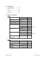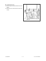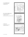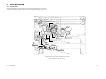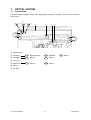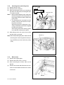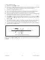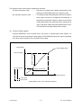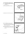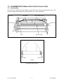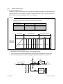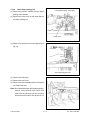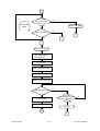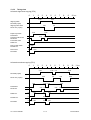
1
SERVICEPLAINMANUAL
PAPER COPIER
PAPER FEEDING UNIT
Click the Page Only button to close the overview area of the window.
Click the Bookmarks and Page button to open the Contents and
display bookmarks created for the document. Click a bookmark’s name
to go to the Page marked by that bookmark.
Click the Thumbnails and Page button to open the overview area and
display thumbnail images of each document page. Click a thumbnail to
go to the page marked by that thumbnail.
Copyright TOSHIBA CORPORATION 1995
ALL RIGHTS RESERVED
1550
MY-1004
GENERAL PRECAUTIONS REGARDING THE INSTALLATION
AND THE SERVICE OF THE 1550/MY-1004
1. Transportation/Installation
• When transporting/installing the copier, using two persons, be sure to use the positions as indicated below.
The copier is fairly heavy and weighs approximately 35 kg (76.8 lb), therefore pay full attention
when handling it.
4 portions
2. Installation
• Be sure to use a dedicated outlet with AC 115V/15A (220V, 240V/10A) or more for its power
source.
• The copier must be grounded for safety.
Never ground it to a gas pipe or a water pipe.
• Select a suitable place for installation.
Avoid excessive heat, high humidity, dust, vibration and direct sunlight.
• To insure adequate working space for the copying operation, keep a minimum clearance of 80 cm
(31.5”) on the left, 80 cm (31.5”) on the right and 10 cm (3.9”) in the rear.
3. Service of Machines
• Basically, be sure to turn the main switch off and unplug the power cord during service.
• Be sure not to touch high temperature sections such as the exposure lamp, the fuser unit, the
damp heater and their periphery.
• Be sure not to touch high-voltages sections such as the chargers and the high-voltage transformer.
• Be sure not to touch rotating/operating sections such as gears, belts, pulleys, etc.
• When servicing the machines with the main switch turned on, be sure not to touch live sections
such as the lamp terminal etc.
• Use suitable measuring instruments and tools.
4. Main Service Parts for Safety
• The thermofuse, thermistor, fuse, breaker and door switch, etc. are particularly important for safety.
Be sure to handle/install them properly.
5. Notice Labels
• Be sure to check the rating plate and the notice labels such as “Unplug the power cord during
service”, “Hot area” etc. to see if there is any dirt on their surface or if they are properly stuck to the
copier during servicing.
6. Disposition of Consumable Parts/Packing Materials
• Regarding the recovery and disposal of the copier, consumable parts and packing materials, it is
recommended to follow the relevant local regulations or rules.
7. When parts are disassembled, reassembly is basically the reverse of disassembly unless
otherwise noted in this manual or other related documents. Be careful not to reassemble
small parts such as screws, washers, pins, E-rings, toothed washers in the wrong places.
8. Basically, the machine should not be operated with any parts removed or disassembled.
1.
SPECIFICATIONS, ACCESSORIES AND OPTIONS
1.1 Specifications
Copy process ........................... Indirect electrophotographic process (dry)
Type ......................................... Desk top
Exposure type .......................... Slit exposure with fixed table
Original size ............................. Type: Sheets, books and three-dimensional objects
Maximum size: A3 or Ledger
Copy paper
Size
Cassette
A3~A5-R
64~80g/m2
Ledger~Statement-R
16lb.~22lb.
A3~A5-R
64~130g/m2
Ledger~Statement-R
16lb.~34lb.
678
Manual
Thickness
Sheet bypass
feeding only
Special paper: Label paper (type recommended by Toshiba) and OHP film (80 µm or more in thickness,
type recommended by Toshiba)
– bypass feeding only
Copy speed (sheets/minute)
Actual size
Paper size
A4, B5, A5-R
Reduction/Enlargement
Cassette
Manual
(Cassette/Manual)
15
1
8
12
1
8
10
1
8
8
1
8
LT, ST-R
A4-R, B5-R
LT-R
B4, FOLIO
LG, COMPUTER
A3
LD
First copy time ........... About 5.8 seconds (100%, A4/LT copier cassette feeding)
About 8.3 seconds (100%, A3/LG/LD PFU cassette feeding)
Warm-up time ............ About 28 seconds (100V series), About 28 seconds (200 V series)
Oct. 1995 © TOSHIBA
1-1
1550 SPECIFICATIONS
Multiple copying ........ Up to 999 sheets
Setting to adjustment mode allows selection of 9, 99, 500 and 999 copies.
Reproduction ratio ..... Actual size
1:1
By setting to adjustment mode, vertical reproduction only can be altered to
1:1.01.
Reduction/Enlargement
3R3E
50, 65, 78, 129, 154, 200% (For U.S.A, Canada)
50, 71, 82, 122, 141, 200% (For Europe)
Paper feeding
Type
Capacity
Cassette
Front Loading
500 sheets (50 mm or less)
Manual
* Foldable tray
1 sheet
* For Europe
Manual start: At the time of shipping, the copying operation is started by
the PRINT key. By inputting data for adjustment mode, it
can be changed to auto-start.
Toner supply .............. Automatic density detection and replenishment
Toner cartridge replacement method
Exposure ................... Automatic control and manual control
Weight ....................... 35 kg
Power source ............ 110 V – 50/60 Hz
115V – 60 Hz
127 V – 60 Hz
220 V – 50/60 Hz
220~240 V – 50/60 Hz
Power consumption ... 1.5 kW or less
Total counter .............. Mechanical total counter (6 digits)
Machine size ............. See the next page.
1550 SPECIFICATIONS
1-2
Oct. 1995 © TOSHIBA
548 mm
541 mm
340 mm
Oct. 1995 © TOSHIBA
1-3
1550 SPECIFICATIONS
1.2 Accessories
Copy receiving tray .................. 1 pc
Operator’s manual .................... 1 pc
Drum ........................................ 1 pc
Lever caps ................................ 2 pcs
Setup report ............................. 1 pc
1.3 Options and Supplies
Options
Automatic document feeder
MR-2004LT
660 84890
MR-2004A4
660 84891
Sorter
MG-1003
660 84838
Key copy counter (6 digit)
MU-8
660 02050
Key copy counter kit
MU-10
660 02051
Counter bracket kit
KN-1550K
660 84840
Cassette
KC-1550AF
660 84841
KC-1550LF
660 84842
KC-1550AFE
660 84914
MF-1550U
660 84848
MF-1550E
660 84849
MY-1004L
660 84835
MY-1004AE
660 84913
MY-1004A
660 84836
KN-1550S
660 84839
Drum
PS-OD1550
66084854
Developer material
PS-ZD1550
66084853
Toner
PS-ZT1550
66084851
Toner (for Europe)
PS-ZT1550E
66084852
Toner bag
PS-TB1550
66084859
Toner bag (for Europe)
PS-TB1550E
66084860
Damp heater kit
Paper feed unit
Sorter bracket kit
For Europe
For Europe
(for MG-1003)
Supplies
1550 SPECIFICATIONS
1-4
Oct. 1995 © TOSHIBA
2.
OUTLINE OF THE MACHINE
2.1 Sectional Views and Electrical Parts Location Diagram
2.1.1
1
Front and rear sectional views
5 23 4
^∞
!¶ !§ %£ %º
@º @ª !ª !∞
!¢ $º !£#ª
!•
1
Carriage 1
30
Magnetic roller
2
Mirror 1
31
Leveler (doctor)
3
Reflector
32
Auto toner sensor
4
Exposure lamp
33
Mixer
5
Exposure adjustment plates
34
Bypass feed guide
6
Carriage 2
35
Bypass feed tray
7
Mirror 2
39
Aligning roller (upper)
8
Mirror 3
40
Aligning roller (lower)
9
Mirror unit
41
Aligning switch
10
Mirror 4
42
Transport roller (left) (MY-1004)
11
Mirror 5
43
Transport roller (right) (MY-1004)
12
Mirror 6
44
Paper stop switch (MY-1004)
13
Slit glass
45
Separation roller
14
Auto exposure PC board
46
Feed roller
15
Lens
47
Pick-up roller
16
Original cover
48
Heat roller
17
Original glass
49
Heat roller (lower)
18
Main charger
50
Cleaning felt roller
19
Discharge lamp
51
Thermistor
20
Ozone filter
52
Thermostat
21
LED erasing array
53
Heater lamp
22
Main blade
54
Separation claws
23
Recovery blade
55
Exit switch
24
Toner recovery auger
56
Exit roller (upper)
25
Transfer charger
57
Exit roller (lower)
26
Separation charger
58
Discharge brush
27
Drum
59
Fuser guard
28
Pre-transfer bias guide
65
Air filter
29
Transport guide
69
Cleaning blade
Oct. 1995 © TOSHIBA
82
Paper empty switch
83
Empty switch (MY-1004)
@¡
!™
#¡
#™
#£
*™
#º
0
9
7
!¡
6
8
#¢
%ª
$¶
^ª
%•
%§
%¶
$§
#∞
$£
$™
$¢
$∞
$§
$∞
%∞
%¢
$•
$ª %¡
%™
@¢
@™
@£ @¶
@§ @∞
@• $¡
*£
2-1
$¶
1550 GENERAL
60
Scanning motor
61
Carriage drive wire
62
Lens motor
63
Mirror motor
64
Developer-unit drive gear
66
Drum gear
67
Main motor
68
Heat roller gear
70
Exit roller gear
72
Aligning roller clutch
73
Transport roller clutch (MY-1004)
75
Cassette
76
Feed roller clutch
&¶
77
Pick-up roller clutch
&§
78
(PFU) cassette (MY-1004)
79
(PFU) feed roller clutch (MY-1004)
80
(PFU) pick-up roller clutch (MY-1004)
81
(PFU) drive motor (MY-1004)
^£
^º ^¢
^¡
^§
^™
&™
&£
&∞
*º
&ª
&•
1550 GENERAL
*¡ ^¶
^•
&º
2-2
Oct. 1995 © TOSHIBA
2.1.2
Electrical parts location diagram
[A] DC electrical parts excluding motors
Symbol
2
@º
@¡
1
!ª
!¶
!•
!º
!§
!¢
!¡
!£
!∞
7
!™
3
Oct. 1995 © TOSHIBA
4
8
5
Name
1
Control panel PC board (PWA-F-PNL)
2
Total counter (T-CTR)
3
Feed roller clutch (FED-CLT)
4
Pick-up roller clutch (PKUP-CLT)
5
Aligning roller clutch (CLT-REG)
6
High-voltage transformer (PS-HVT)
7
Heat roller thermistor (THMS-HTR)
8
Exit switch (EXT-SW)
9
Logic PC board (PWA-F-LGC)
10
Power supply unit (PS-ACC)
11
Size switch (SIZE1-SW)
12
Paper empty switch (EMP2-SW)
13
Aligning switch (RGT-SW)
14
Toner-full switch (T-FUL-SW)
15
Auto-toner sensor (SNR-ATC)
16
Eraser lamp PC board (ASM-F-ERS)
17
LED discharge array PC board (ASM-DCH)
18
Mirror switch (MRR-SW)
19
Auto-exposure PC board (PWA-F-AES)
20
Lens switch (LNS-SW)
21
Home switch (HOME-SW)
9
6
2-3
1550 GENERAL
[B] Electrical parts such as motors
5
6
3
Symbol
8
2
4
7
Name
1
Main motor (MAIN-MTR)
2
Scanning motor (SCN-MTR)
3
Mirror motor (MRR-MTR)
4
Lens motor (LNS-MTR)
5
Front optics fan (OPT-FAN-F)
6
Rear optics fan (OPT-FAN-R)
7
Exit fan (EXIT-FAN)
8
Toner motor (TNR-MTR)
1
1550 GENERAL
2-4
Oct. 1995 © TOSHIBA
[C] AC electrical parts
!£
9
Symbol
8
7
0
2
!¡
1
!™
3
4
Name
1
Door switch (DOOR-SW)
2
Main switch (MAIN-SW)
3
Damp heater L (D-HTR-L)
4
Thermostat
5
AC power cable
6
Fuse PC board (PWA-F-FUS)
7
Damp heater U1 (D-HTR-U1)
8
Exposure lamp (EXPO-LAMP)
9
Thermofuse (FU-EXPO)
10
Lamp regulator PC board (PS-LRG)
11
Heater thermostat (K-THMO)
12
Heater lamp (HTR-LAMP)
13
Damp heater U2 (D-HTR-U2)
6
5
Oct. 1995 © TOSHIBA
2-5
1550 GENERAL
Go to DC Harness
Connection Diagram
2.2 Symbol and Function of Electrical Parts
(1) Motors
Symbol
M1
* Refer to SERVICE PARTS LIST ED-1550
Code name
MAIN-MTR (Main motor)
Function
Remarks
*Page/item No.
Drives the drum, developer
IC motor
P9, I1
and heat roller
M2
SCN-MTR (Scanning motor)
Scans the optical system
Pulse motor
P8, I14
M3
LNS-MTR (Lens motor)
Drives the lens unit
Pulse motor
P8, I4
M4
MRR-MTR (Mirror motor)
Drives the mirror unit
Pulse motor
P8, I4
M6
OPT-FAN-F (Optics fan (front))
Cools the optical system
IC motor
P3, I8
M7
OPT-FAN-R (Optics fan (rear))
M8
EXIT-FAN (Exit-fan)
Cools the drum and cleaner
M9
TNR-MTR (Toner motor)
Replenishes the toner
M60
IC motor: M60
P3, I8
Brush motor
P17, I31
Remarks
*Page/item No.
(2) Electromagnetic spring clutches
Symbol
CLT1
CLT2
Code name
Function
RGT1-CLT
Transmits aligning roller
P7, I4
(Aligning roller clutch)
drive.
FED1-CLT
Transmits feed roller drive.
P7, I22
PKLP-CLT
Transmits pick-up roller
P7, I22
(Pick-up roller clutch)
drive.
(Feed roller clutch)
CLT3
(3) Counters
Symbol
Code name
Function
T
T-CTR (Total counter)
Total counter
K
K-CTR (Key-copy counter)
Individual counter
Oct. 1995 © TOSHIBA
2-6
Remarks
6-digit
6-digit (option)
1550 GENERAL
Go to DC Harness
Connection Diagram
(4) Switches
Symbol
Code name
Function
Remarks
*Page/item No.
S1
MAIN-SW (Main switch)
Power supply
Tumbler type
P4, I2
S2
DOOR-SW (Door switch)
For safety, cancels
Push switch
P4, I4
P6, I20
abnormal condition
S3
EMP1-SW
Detects lack of paper in the
Reflecting photo
(Paper-empty switch 1)
cassette
sensor
S4
SIZE1-SW (Size switch)
Detects cassette size
Push switch
P6, I26
S5
RGT-SW (Aligning switch)
Detects paper in front of the
Photointerruptor
P7, I15
aligning roller
S6
EXIT-SW (Exit switch)
Detects exiting paper
Photointerruptor
P20, I15
S7
HOME-SW (Home switch)
Detects home position of the Photointerruptor
P12, I16
optical system
S8
LNS-SW (Lens switch)
Detects home position of the Photointerruptor
P12, I16
lens unit
S9
MRR-SW (Mirror switch)
Detects home position of the Photointerruptor
P8, I27
mirror unit
S10
T-FUL-SW
Detects when the used toner Microswitch
(Toner-full switch)
bag is full
P17, I22
(5) Heaters and lamps
Symbol
EXP
Code name
EXPO-LAMP
Function
Exposes the original
(Exposure lamp)
HTR
HTR-LAMP (Heater lamp)
Remarks
Halogen lamp
*Page/item No.
P10, I14
300W
Fixing
Halogen lamp
P19, I6
900W
ERS
ERS-LAMP
Discharges the drum
LED type
P15, I14
To interrupt the charge
LED
P15, I15
Keeps optical system warm
PTC
P12, I33
Keeps the drum and transfer/ PTC
P6, I36
(Discharge lamp)
DCH
DCH-LED
(LED eraser array)
DHU
D-HTR-U (Damp heater U)
(option)
DHL
D-HTR-L (Damp heater L)
separationcharger case
warm (option)
1550 GENERAL
2-7
Oct. 1995 © TOSHIBA
Go to DC Harness
Connection Diagram
(6) PC boards
Symbol
Code name
Function
Remarks
*Page/item No.
LGC
PWA-F-LGC (Logic PC board)
Controls the entire copier
P5, I14
ACC
PS-ACC
Supplies electrical power to
P5, I19
(Power supply PC board)
ICs, solenoids and motors
PWA-F-PNL
Controls condition displays
(Control panel PC board)
and operation keys
PS-LRG
Controls exposure lamp
P4, I35
ASM-DCH
Turns on and drives LED
P15, I15
(LED eraser array PC board)
during reduction
ASM-ERS
Discharge lamp
P15, I14
P8, I28
PNL
LRG
P2, I22
(Lamp regulator PC board)
DCH
ERS
(Discharge lamp PC board)
AES
PWA-F-AES
Reads dark/light of the original
FUS
PWA-F-FUS (Fuse PC board)
Fuse for the damp heater
Option
P5, I23
Remarks
*Page/item No.
circuit.
(7) Transformers
Symbol
HVT
Code name
Function
PS-HVT
Generates high voltage
(Charging transformer)
electricity for charging
P5, I18
(negative voltage)
(Transfer/separation transformer)
Generates high voltage
electricity for transfer/
separation and developing
bias voltage
(8) Others
Symbol
ATS
THMS
Code name
SNR-ATC
Reads toner density with a
(Auto-toner sensor)
magnetic sensor
THMS-HTR
Detects temperature of the
(Heat-roller thermistor)
heat roller
THERMO K-THERMO
FU
Function
Prevents abnormal heating
(Thermostat)
of heat roller
FU-EXPO (Thermofuse)
Prevents abnormal heating
Remarks
*Page/item No.
P18, I26
P20, I9
P20, I8
P10, I5
of the exposure lamp
TMS-DRM TMS-DRM (Drum thermistor)
Detects the drum tempera-
P3, I39
ture roughly
Oct. 1995 © TOSHIBA
2-8
1550 GENERAL
1550 GENERAL
M6
J53
J60
J61
J16
J17
2-9
M9
J76
J64
J74
DRM-THMS
J78
SCN-MTR
M2
ASM-FUS
PS-ACC
J82
J83
J73
LNS-MTR
J73
M3
J79
SNSR-A/T
J508
ASM-DCH
J81
TNR-MTR
J501
PWA-F-LGC
J9
ASM-ERS
J502
PS-LRG
LGC
J11
MRR-MTR M4
J80
MRR
-SW
J86
DUMP
HTR-U1
S9
J25
PWA-F
AES
DUMP
HTR-U2
HOME-SW
LNS-SW
FU-EXPO
EXPO-LAMP
S8
OPT
M7 -FAN-R
J57
J59
KCTR
J5
T-FUL-SW
M8
J51
J4
S10
J18
OPT
-FAN-F
S7
J52
PWA-F-PNL
T
EXIT-FAN
J58
J
T-CTR
2.3 Wire-Harness Location Diagram
A. Location Diagram for Upper Unit
AC
DC
J77
J77
J21
J90
J75
Oct. 1995 © TOSHIBA
J63
Oct. 1995 © TOSHIBA
J85
2 - 10
CLT2
J71
J70
J69
J64
J66
SIZE-SW
J67
S1
CLT3
MAIN-SW
CLT1
S2
J68
S3
PS-HVT
J31
J511
EMP-SW
S5
A2
J531
A1
A3
M1
J532
J522
TO UPPER UNIT
J8
AC INPUT POWER SUPPLY
TO UPPER UNIT
J10
DOOR-SW
RGT-SW
PRE-TRANSFER-GUIDE
B1
D-HTR-L
B2
TRANSFER-CHARGER
SEPARATION-CHARGER
K-THERMO
THMS-HTR
S6
PS-ACC
J7
PWA-F-LGC
J3
S4
J62
HTR-LAMP
EXIT-SW
J528
J529
J521 J526
J527
J65
J84
B. Location Diagram for Lower Unit
AC
DC
J506
B3
PWA-F FUS
J72
1550 GENERAL
2.4 Removing Covers and Electrical
Parts
2.4.1
Removing covers
[A] Front cover
(1) Remove the cassette (in the direction of the
arrow).
Front cover
Cassette
(2) Remove the screws fastening the hinge (4 pcs.).
Hinge
[B] Inner cover (upper)
Inner cover (upper)
(1) Open the front cover.
(2) Remove the toner cartridge.
(3) Remove three screws.
1550 GENERAL
2 - 11
Oct. 1995 © TOSHIBA
[C] Inner cover (lower left)
(1) Remove one screw.
Inner cover (lower left)
[D] Right-side covers (upper and lower) and
feed-side cover
Feed-side cover
Feed-side cover
•
Open the front cover.
•
Raise the upper unit.
•
Remove three screws.
Right side cover (lower)
•
Open the front cover.
•
Raise the upper unit.
•
Remove two screws.
Right-side cover (lower)
Right-side cover (upper)
•
Remove two screws.
•
Remove the glass holder (see 2.4.1).
Oct. 1995 © TOSHIBA
Right-side cover (upper)
2 - 12
1550 GENERAL
[E] Top cover and glass holder
Top cover
Glass holder
•
Open the original cover.
•
Remove two screws.
Top cover
•
Remove the original cover.
•
Remove three screws.
Glass holder
[F] Rear cover
•
Remove two screws.
Rear cover
1550 GENERAL
2 - 13
Oct. 1995 © TOSHIBA
[G] Left-top cover, left-side cover (upper) and
Left-top cover
left-side cover (lower)
Original scale
(1) Raise the upper unit.
Left-top cover
•
Remove the original scale. (Two screws)
•
Remove two screws.
Left-side cover (lower)
•
Remove two screws.
Left-side cover (lower)
Left-side cover (upper)
•
Remove one screw.
Left-side cover (upper)
Oct. 1995 © TOSHIBA
2 - 14
1550 GENERAL
[H] Control panel cover
(1) Raise the upper unit and remove the inner cover
(upper).
(2) Disconnect two connectors and remove four
screws.
Connectors
1550 GENERAL
2 - 15
Oct. 1995 © TOSHIBA
2.4.2
Removal and installation of electrical parts
[A] Remove the control-panel (PWA-F-PNL) PC board
(1) Remove the control panel cover.
Refer to 2.4.1 [H].
(2) Place the control panel cover upside down and remove its metal cover (6 screws).
Remove the earth screw of the shield. Remove the counter connector.
Earth screw
(3) When you remove nine (9) screws, the control-panel PC board can be taken out along with the
harness. They can be separated if you disconnect two connectors.
Connector
Note: Be careful not to allow the ground wire of the shield to be cut.
Oct. 1995 © TOSHIBA
2 - 16
1550 GENERAL
[B] Total counter
(1) Remove the control panel cover.
(2) Place the control panel cover upside down and
remove the two screws fastening the bracket.
(3) Remove one screw.
(4) Disconnect one connector.
Note: Be careful not to allow the ground wire of
the shield to be cut.
Screws fastening the bracket
[C] Logic PC board (PWA-F-LGC)
(1) Remove the rear cover.
(2) Disconnect connectors (10 pcs. when no optional equipment is used and 11 pcs. when optional equipment are used) and take out the PC
board from its four lock supports.
PWA-F-LGC
[D] Power supply unit
(1) Remove the rear cover.
(2) Disconnect connectors (9 pcs.).
(3) Remove four screws.
* About bottom 4 connectors, black harness
must be connected “L” terminal that is described on PC board and white must be “N”.
* Harness
color
1550 GENERAL
2 - 17
PS-ACC
White Black
Black
White
Oct. 1995 © TOSHIBA
[E] Door switch and Main switch (power
E-ring
Door switch
(Inside the unit)
switch)
(1) Remove the inner cover.
(2) Remove the feed-side cover.
(3) Remove the right side cover (upper).
(4) Snap off an E-ring.
(5) Take out the gas spring.
(6) Remove three screws and tilt the unit toward you
after having shifted it toward the right.
(7) Removing the respective connectors and
screws allows the door switch and the main
switch to be removed and replaced. Before
Main switch
replacement, pay attention to the colors of the
connectors and the harnesses.
Door switch
Main switch
Connector Yellow
Blue
Blue
Yellow
Connector
Blue
Blue
White
White
Harness
White
Black
Black
Harness
Black
White
Black
White
White
[F] High-voltage transformer for the main
charger (PS-HVT-M)
(1) Remove the rear cover.
(2) Disconnect seven (7) connectors.
(3) Remove two screws.
(4) Remove two lock supports.
PS-HVT-M
Oct. 1995 © TOSHIBA
2 - 18
1550 GENERAL
[G] Size switch
(1) Pull out the cassette.
Screws
(2) Remove two screws.
(3) Disconnect one connector.
Note: The left screw is tightened with the protective cover on the corner of the switch.
Size switch
[H] Exit fan
(1) Remove the left-side cover (upper) (1 screw).
Duct cover
Exit fan
(2) Disconnect three connectors (front).
(3) Remove the duct cover (1 screw).
(4) Separate the exit fan from the cover (1 connector).
[I]
Front optics fan (front)
Optics fan (front)
(1) Remove the inner cover.
(2) Disconnect one connector.
(3) Remove two screws.
1550 GENERAL
2 - 19
Oct. 1995 © TOSHIBA
[J]
Fuse (PWA-F-FUS-140)
(1) Remove the rear cover.
(2) Replace the fuse.
Fuse
[K] Fuse PC board (PWA-F-FUS-140)
(1) Disconnect one connector.
(2) Remove one screw.
(3) Remove the fuse PC board with the bracket.
PWA-F-FUS-140
[L] Main motor
(1) Disconnect two connectors.
(2) Remove two screws.
Oct. 1995 © TOSHIBA
2 - 20
1550 GENERAL
[M] Lamp regulator PC board (PS-LRG)
(1) Remove the top cover.
(2) Disconnect two connectors and remove the PC board from three lock supports.
PS-LRG
[N] Optics fan (rear)
(1) Remove the top cover.
Optics fan (rear)
Remove the connector from the sorter (two
screws).
(2) Disconnect one connector.
(3) Remove two screws.
1550 GENERAL
2 - 21
Oct. 1995 © TOSHIBA
3.
COPYING PROCESS
3.1 Copying Process
Document exposure
Halogen lamp
300 W
Optical
system
2
LED
eraser array
1
Main charger
Toner
Grid
–691 ±5 V
9
Carrier
Discharge lamp
_ _
LED
_
_
8
+
+
+
Cleaning
3
_
_
+
Development
+
Magnetic roller
+
_
_
7
Paper exit
Max. 200 sheets
Bias –200 VDC
+ +
Manual feed
Fixing
Heat roller
Separation
Transfer
900 W
AC 3.6 kV
–DC 6 kV
1000 Hz
Cassette paper feed
(500 sheets)
5
6
4
Transfer bias
–DC 1.2 kV
1 Main charger : A negative electrostatic charge
: The copy paper is separated
is placed on the photoconduc-
from the surface of the drum
tive (photosensitive) surface of
together with the toner image.
7 Fixing
the drum.
2 Exposure
6 Separation
copy paper by heat and pres-
: Forms an electrostatic latent
sure.
image on the photoconductive
8 Cleaning
surface of the drum.
: The toner image is fixed to the
: Any toner remaining on the
3 Development : Positively charged toner is at-
photoconductive surface of the
tracted to the photoconductive
drum is mechanically removed
surface of the drum to form a
by the cleaning blade.
9 Discharging
visible image.
: Erases the electrostatic charge
4 Transfer bias : Raises transfer efficiency.
remaining on the photoconduc-
5 Transfer
tive surface of the drum.
: Transfers the visible toner image from the surface of the
drum to the copy paper.
Oct. 1995 © TOSHIBA
3-1
1550 PROCESS
3.2 ED-1550 Copying Process
Process
1550
1. Drum
OD-1550 (OPC ø60)
(1) Sensitivity
Highly sensitized drum
(2) Surface potential
DC–700V
Scolotron system
2. Charging
Variable output
3. Exposure
(1) Light control
Automatic exposure/manual step setting
(2) Light source
300W halogen lamp stabilized with
regulator (light intensity remains
constant even when voltage varies)
4. Development
(1) Magnetic roller
One magnetic roller (with two shaft mixers)
(2) Auto-toner
Magnetic bridge-circuit system
(3) Toner replenishment
Toner cartridge system
(4) Toner-empty sensor
Intensity sensing system
(5) Toner
T-1550 or T-1550E
(6) Developing material
D-1550
(7) Developer bias
DC–200V
5. Transfer
Adjustable output (fixed current)
6. Separation
Adjustable output
(independently adjustable)
7. Discharge
(1) Discharging position
After cleaning
(2) Discharge lamp
LED type
8. Cleaning
(1) System
Blade system
(2) Recovery of toner
Non-reusable
1550 PROCESS
3-2
Oct. 1995 © TOSHIBA
Process
1550
9. Fixing
(1) Type
Heat roller system
• Fixing
• Fixing roller: Teflon coated roller
• Pressure
• Pressure roller: PFA tube silicon roller (ø28)
• Lamp rating
• 900W (infrared heat)
(2) Cleaning
Cleaning with silicon impregnated roller
(3) Heater temperature
ON/OFF control by thermistor
control
10. Control
Oct. 1995 © TOSHIBA
Microcomputer
3-3
1550 PROCESS
4.
COPIER OPERATION
4.1 Operation Outline
Copier operation
Operation during warm up and standby
Automatic-feed copying using Print key
Copying operation
Bypass-feed copying
Interrupt copying
4.2 Description of Operation
4.2.1
During warm up
(1) Copy quantity indicator shows "0" and print-key lights up "red" lamp.
Heater lamp comes ON.
Initial position setting for the optical system ~ moves the lens and the mirror to actual-size position.
Exit fan (M8) stops and optical fans (M6/M7) stop.
(2) When the heat-roller temperature is sufficient for fixing:
The heater lamp goes OFF.
The copy quantity indicator shows "1", and the print key changes to "green" lamp.
(Paper jam release cover to be closed when there is paper in the cassette.)
Exit fan (M8) starts rotating at low speed and optical fans (M6/M7) stop.
4.2.2
Standby (ready) condition
All keys on the control panel are operable.
When there is no other key entry for a predetermined period, the machine is set automatically to a copy
quantity of "1", a reproduction ratio of 100% and automatic exposure.
4.2.3
Cassette feed copying using the print key
(1) Print key ON
Print key display changes from "green" to "red".
Main charger, transfer charger, separation charger, transfer bias, discharge lamp and LED eraser
array come ON and optical fans (M6/M7) rotate at high speed. Exit fan (M8) starts rotating at high
speed.
Main motor (M1) comes ON.
~ Drum, developer, heat roller and paper-exit roller rotate.
(2) Paper feeding from cassette
The feed roller clutch (CLT2) and the pick-up roller clutch (CLT3) come ON.
~ The pick-up roller and paper feed roller rotate.
After a pre-difined period the pick-up roller clutch (CLT3) goes OFF.
Oct. 1995 © TOSHIBA
4-1
1550 OPERATION
Aligning operation
Paper arrives at the aligning roller.
~ Aligning switch (S5) ON
After a pre-difined period feed roller clutch (CLT2) goes OFF.
Paper feeding complete.
(3) Carriage operation
Exposure lamp ON
Carriage 1 and carriage 2 forward operation starts.
~ Scanning motor (M2) ON
At this time, if the toner density of the developer material is lower than the set value, toner replenishment is performed.
~ Toner motor (M9) is turned ON.
(4) When a fixed time has passed since the carriage operation
~ Paper is transported to transfer section, transport is promoted ~ aligning-roller clutch (CLT1) is
turned ON, and the copy quantity counted.
(5) Carriage scanning complete
Scanning motor (M2) is turned OFF.
The main charger and the exposure lamp are turned OFF.
Aligning-roller clutch (CLT1) is turned OFF. (The timing varies according to paper used.)
(6) Paper-exit operation
The exit switch (S6) detects the trailing end of the paper passing.
The main motor (M1), transfer charger, separation charger, transfer bias which is turned ON/OFF in
accordance with paper feeding, discharge lamp and LED erase array are turned OFF. Optical fans
(M6/M7) stop and exit fan (M8) starts rotating at low speed.
Print key: "Green" lamp is turned ON.
1550 OPERATION
4-2
Oct. 1995 © TOSHIBA
Oct. 1995 © TOSHIBA
4-3
PICUP-CLT
FED-CLT
RGT-CLT
PSTP-SW
EXIT-SW
HVT-SP
HVT-TR
HVT-M
EXPO-LAMP
SCN-MTR
MAIN-MTR-CW/CCW
MAIN-MTR
1
2
0.06 0.36
1.29
1.58
1.16
0.84
0.71
1.03
BWD
FWD
0.06
0
0
0
0
0
4
5
4.31
3.88
3.68
3.6
3.37
3.53
6
5.7
3.45
4.53 4.98
BWD FWD
3
6.33
7
7.72
8.28
8
9
10
11
12
13
14
15
A4 lateral single-sheet copying
1550 OPERATION
1550 OPERATION
4-4
PICUP-CLT
FED-CLT
RGT-CLT
PSTP-SW
EXIT-SW
HVT-SP
HVT-TR
HVT-M
EXPO-LAMP
SCN-MTR
MAIN-MTR-CW/CCW
MAIN-MTR
1
0.06 0.36
FWD
2
1.29
1.58
1.16
0.84
0.71
1.03
BWD
0.06
0
0
0
0
0
3
5
6
3.75 4.05
3.75
4.98
5.89
5.7
5.27
4.85
4.89
4.71
4.31
3.88
3.68
3.6
3.37
3.53
3.45 4.53 4.81
BWD
FWD
4
8
7.57
7.37
7.54
7.48
7.47
7.23
7
8.26
10.27
10
9.64
8.47 8.92
BWD
9
12.23
12
13
11.67 12.23
11
14
15
A4 lateral two-sheets copying
Oct. 1995 © TOSHIBA
4.2.4
Bypass-feed copying
(1) Insert paper in bypass feed guide.
Aligning switch (S5) is turned ON.
~ Bypass-feed indicator lights up
Carriage 1 and carriage 2 move to the home position.
(2) Print key ON
Main charger, transfer charger, separation charger, transfer bias, discharge lamp and LED eraser
array are turned ON.
Optical fans (M6/M7) and exit fan (M8) start rotating at high speed.
Main motor (M1) ON
~ Drum, developer, heat roller and paper-exit roller rotate.
(3) Subsequently operations for automatic-feed copying (3) ~ (6) are continued by the use of the print
key.
4.2.5
Interrupt copying
(1) Press interrupt key.
Interrupt lamp comes ON.
The copier temporarily interrupts the copying operation, and carriage 1 and carriage 2 return to their
fixed position.
Automatic exposure goes into the reproduction ratio 100% copy mode. The copy quantity indicator
remains unchanged.
(2) Select desired copying conditions (single-sheet copying only is possible).
(3) After interrupted mode copying has finished.
Press the interrupt key, then the interrupt lamp goes OFF and the conditions prior to interruption are
resumed.
(4) Press print key.
Copying operations prior to interruption are resumed.
Oct. 1995 © TOSHIBA
4-5
1550 OPERATION
4.3 Fault Detection
If a fault occurs in the copier, a symbol corresponding to the type of fault will be displayed in order to draw
the attention of the operator.
•
Classification of faults
A) Faults which can be cleared without turning OFF the door switch (S2)(yellow flashing display on
the display panel).
(1) Add paper
(2) Insert key-copy counter
(3) Replace toner bag (This is cleared by replacing the toner bag) (red flashing display)
B) Faults which can not be cleared without turning OFF the door switch (S2) (no display provided on
the display panel).
(1) Clear paper
(2) Add toner (yellow flashing display)
C) Faults which can not be cleared without turning OFF the main switch (S1).
(1) Service call
A-1)
Add paper (
•
)
When cassette is inserted in the machine, the paper-empty switch (S3) or (S16) detects the
existence of paper ~ When there is no paper, the switch goes OFF.
•
When cassette is not inserted in the machine, the paper size switch (S4) or (S18) detects the
G
non-existence of cassettes ~ The paper-size switches all go OFF.
When cassette is inserted in the
Signal is sent to control circuit.
f
machine but there is no paper.
f
machine
No-paper state
64748
When cassette is not inserted in the
"Add Paper" display will flash.
f
* Print key will be inoperable.
*
Bypass-feed copying is possible if there is paper on the manual feed guide, even when there
is no paper in the cassette.
1550 OPERATION
4-6
Oct. 1995 © TOSHIBA
A-2)
Bypass misfeed
•
During sheet bypass copying
Manual-feed roller clutch (CLT4) goes ON.
f
Aligning switch (S5) comes ON.
If the aligning switch goes OFF when the aligning-roller starts rotating.
f
Bypass misfeed
f
The bypass misfeed symbol is displayed. (
)
f
Copying cannot be started.
A-3)
Insert key-copy counter.
•
If the key-copy counter (option) has been inserted in the machine and is withdrawn, "Insert
Key Counter" is displayed.
Copying can not be started.
•
If the key counter is withdrawn during copying, the machine will stop after the paper being
copied has exited.
Oct. 1995 © TOSHIBA
4-7
1550 OPERATION
B-1)
Clear paper (
•
)
The leading-edge jam is detected by the exit switch (S6): (E01)
The aligning roller clutch (CLT1) is turned ON.
f
2.0 sec*
ON
The exit switch (S6) comes ON.
*
CLT1
When S6 has not come ON after 2.5
ON
S6
seconds have elapsed.
f
Timer
2.5 sec
0
The "Clear Paper" (E01) symbol appears and copying will stop.
•
Clear paper (E01)
The trailing-edge jam is detected by the
exit switch (S6) : (E02). Aligning roller
clutch (CLT1) is turned OFF.
f
CLT1
2.0 sec*
OFF
S6 OFF (detects paper)
*
S6
ON
When S6 has not come OFF after 2.5
seconds have elapsed.
f
Timer
The "Clear Paper" symbol (E02) ap-
0
2.5 sec
pears and copying stops.
•
Immediately after the power is turned
Clear paper (E02)
ON.
f
The aligning switch (S5) and exit switch (S6) detect the paper (ON).
f
"Clear Paper" symbol (E03)
•
The front cover is opened during copying.
f
"Clear Paper" symbol (no indication)
B-2)
)
Add toner (
Toner density has become low.
f
Toner empty signal detection: Auto-toner sensor
f
Control circuit:
"Add Toner" symbol appears: Copying is not possible.
Clearing method: Replace toner cartridge and close front cover.
Toner supply operation (toner density is resumed at the proper level): Copying
is possible.
1550 OPERATION
4-8
Oct. 1995 © TOSHIBA
B-3)
Replace toner bag (
)
The toner bag becomes full of toner.
f
The toner-recovery auger moves towards the front of the machine: Toner-full switch (S10) will
be turned ON.
f
"Replace Toner Bag" symbol is displayed.
•
When the toner-full switch (S10) comes ON during copying.
f
Copying will stop after the last sheet has been exited during copying.
Clearing method: Replace with a new toner bag.
C-1)
Service call
When the "CLEAR/STOP" key and the "8" key are pressed simultaneously while the "Service Call" symbol is flashing, an error code will be indicated in the copy quantity indicator.
For the contents of the error codes, refer to the “SERVICE HANDBOOK”.
Oct. 1995 © TOSHIBA
4-9
1550 OPERATION
4.4 Flow Charts
4.4.1
After power supply is turned ON.
Main switch S1 ON
DC power ON
Restart
YES
Covers open?
NO
Heater lamp HTR ON
Start initialization
• SCN-MTR M2
• LNS-MTR M3
• MRR-MTR M4
RGT-SW S5
ON?
YES
NO
EXIT-SW S6
ON?
YES
NO
Paper jammed "E03"
A
1550 OPERATION
4 - 10
Oct. 1995 © TOSHIBA
A
T-FUL-SW S10
ON?
YES
Replace toner bag
NO
Toner empty?
NO
YES
Add toner
NO
Twenty
seconds elapsed since
initialization?
NO
Initialization
completed?
YES
Service call
"C21"
Is heat roller
temperature high enough
for fixing?
YES
READY
NO
Has heater lamp
reached specified
temperature 20 seconds
after being turned ON?
YES
NO
Service call
"C41"
Oct. 1995 © TOSHIBA
4 - 11
1550 OPERATION
4.4.2
Automatic feed copying
Print key ON
Transport system control
Process system control
•
•
•
•
Is PLL checking
on main motor
Main charger ON
Transfer charger ON
Separation charger ON
Discharge lamp ON
Optical system control
Carriage moves
towards home position.
NG
OK
Service call
C
"C01"
NO
DCH ON
• CLT3 ON
• CLT1 ON
Main charger OFF
DCH OFF
EXP ON
CLT3 OFF
Carriage forward
CLT2 OFF
Carriage stops
• CLT1 ON
• T-CTR ON
YES
Remaining copy
quantity=0?
NO
T-CTR OFF
Carriage moves backward
to its home position.
• Transfer charger OFF
• Separation charger OFF
Remaining copying
quantity=0?
YES
Discharge lamp OFF
EXP OFF
CLT1 OFF
Carriage moves toward
copiable size display position.
Completed
S6 check 1
OK
B
1550 OPERATION
4 - 12
NG
Complete
Paper jammed
"E01"
Oct. 1995 © TOSHIBA
B
S6 Check 2
NG
Paper jammed
"E02"
OK
Final copy?
NO
C
YES
Drum reverses
Standby
Oct. 1995 © TOSHIBA
4 - 13
1550 OPERATION
5.
DISPLAY UNIT
5.1 Control Panel and Indication Panel
The display unit consists of a key switch which operates copying and to select the mode, and an LED
which displays machine condition and messages.
Signs and symbols are turned ON or flash when the attention of the operator needs to be drawn.
A4
122%
B4
82%
APS
000001
AMS
1
2
3
4
5
6
7
8
0
%
%
B4
FOLIO
200%
A3
A3
71%
A4
A5
141%
A4
FOLIO
A4
A3
A3
50%
A5
200%
A5 A3
9
C/
50%
@@@@@
For Europe
2 in 1
APS
AMS
ADF
ENERGY
SAVER
DUAL PAGE
COPY
000001
GROUP
SORT
SORTER
INTERRUPT
1
2
3
4
5
6
7
8
%
%
78%
ZOOM
COMP LT-R
LG
LD LG
200%
65%
LIGHT
AUTO
DARK
IMAGE MODE
LD ST-R
C/
CLEAR/STOP
@@@@@
ST-R COMP
LG
9
50%
0
154%
LT-R ST-R
LD LT-R
CASSETTE
129%
LT-R COMP
LD
50%
200%
ST-R LD
PRINT
For the U.S.A. and Canada
Oct. 1995 © TOSHIBA
5-1
1550 DISPLAY
5.2 Items Displayed on Control Panel
•
During normal copying operation
During warm up
When the power switch is turned ON the print key lights up red until capable of
copying. The copy quantity and reproduction ratio display show "0".
Ready condition
When the machine is capable of copying condition, the print key lights up green
and the copy quantity and reproduction ratio show "1".
While copying
When the print key is pressed, the print key lights up red. The copy quantity
display displays a countdown and finishes at "1". After completion of copying,
the copy quantity indicator returns to the initially set number.
•
If a fault occurs (copying is not possible)
“
” flashes
The symbol is displayed when the cassette selected has no paper (including “Insert Cassette”).
Bypass feeding is possible.
“
” flashes
The symbol is displayed when the toner in the toner cartridge runs out.
PRINT key flashes
The key flashes in red to indicate that the key-copy counter has been with-
in red
drawn when the optional key-copy counter is installed.
“
” flashes
The symbol is displayed when the toner bag is full.
“
” flashes
When the paper is jammed, the position is indicated 1 Paper feed, 2
Exit-paper area, 3 Paper feeding unit (option) 4 Sorter (option), 5 DF
(option)
“ ” flashes
“
” flashes
The symbol is displayed when a malfunction requiring service has occurred.
The symbol is displayed at the periodic maintenance cycle.
(When the PM counter has exceeded the PM set value.)
(Capable of copying.)
1550 DISPLAY
5-2
Oct. 1995 © TOSHIBA
Oct. 1995 © TOSHIBA
–
–
–
–
–
–
–
–
_
_
Key copy counter not
inserted (optional)
Bypass misfeed
Replace toner bag
Clear paper
Service call
Interrupt mode
Energy-saving mode
5-3
–
–
–
–
_
–
–
_
–
–
_
_
_
_
_
_
_
_
_
–
_
–
–
_
–
_
_
_
_
_
_
_
–
_
–
–
_
_
_
_
_
_
_
_
_
–
_
–
–
_
_
_
_
_
_
_
_
_
–
–
–
–
_
_
_
_
_
–
_
_
_
DUALPAGE
COPY
key
(Note) The interrupt mode will be automatically cancelled when the machine is not used for 45 seconds.
(4) During copying, avoid sheet bypass feeding because of possible paper jamming.
When not copying .... When pressed once, the copy quantity indicator returns to “1”.
During copying ......... Interruption of the copying (Stop function ..... The copy quantity indicator will not change.)
(3) The function of the CLEAR/STOP key changes in the following manner according to the machine status.
(2) During copying, avoid changing exposure as far as possible.
_
–
–
–
_
_
_
_
_
–
_
_
_
ENERGY
SAVER
key
–: Operation is ignored.
–
_
–
–
_
–
_
_
_
–
_
_
_
INTERRUPT
key
(1) By pressing the ENERGY SAVER key or the PRINT key, the energy-saving mode will be cancelled.
_: Machine operates or indicates in accordance with the operator’s action.
–
–
_
–
_
_
_
–
_
_
_
_
_
–
_
_
_
REPROAUTO
DUCTION- EXPOSURE Manual
CASSETTE
Photo
RATIO
exposure exposure SELECTION
key
selection (PHOTO key)
key
key
_
_
_
–
Add toner
_
_
–
Add paper
–
–
Copying
_
–
Reproduction-ratio
changing
_
_
_
_
Ready
_
Digital
keys
_
_
_
Warming up
Condition
CLEAR/
STOP
key
PRINT
key
Operation
–
_
–
–
_
–
_
_
_
x (4)
_
_
_
Sheet
bypass
5.3 Relationship between Machine Condition and Operator’s Action
1550 DISPLAY
5.4 LED Display Circuit
(1) LED display method
+5V
Described here is the LED for "dual-page copyDSPON0 signal goes to "L" level, transistor Q2
is turned ON. When pin 7 of the IC (D15) goes
Electrical
current
R3
ing" display when "DP" comes ON. When the
R4
“L”
DSPON0
“L”
to "L" level, electrical current flows through the
G
Q2
(LP32)
transistor to the LED (DP) from +5V. In other
R28
7
D15
PWA-PNL
words the LED (DP) comes ON.
(2) The actual circuit is controlled as follows:
8 msec 8 msec
•
DSPON0 and DSPON1 signal goes to "L"
level alternatively for 8 msec.
•
DSPON1
TR2
OFF
TR2
ON
DSPON0
TR1
ON
TR1
OFF
Q1 or Q2 goes to the ON condition when
the DSPON0 or DSPON1 signal is at "L"
level.
•
The LED ON/OFF signal from LGC is in-
DSPDAT
putted to the IC SIN (pin 5) terminal via the
D1
DSPDAT signal (serial data).
•
LED ON/OFF signal is outputted in parallel
LED “00”
ON
to D1-D16 output terminal, after being inLED “01"
putted to IC in series.
1550 DISPLAY
5-4
ON
ON
Oct. 1995 © TOSHIBA
Conditions for LED to come ON
1 The transistor (Q1 or Q2) connected on the anode side of LED is ON.
2 The output connected to the cathode side of the LED is at "L" level.
When 1, 2 above are fulfilled, the LED is turned ON.
Listed below are the names of LEDs of which ON/OFF is controlled by the DSPON0 signal and the
DSPON1 signal.
DSP-ON0
DSP-ON1
DAT1
2 IN 1
SRV
DAT2
APS
ADFJ
DAT3
AMS
SRTJ
DAT4
GRP
PM
DAT5
SRT
TE
DAT6
PS
MFJ
DAT7
INT
EXTJ
DAT8
EXP1
TF
DAT9
EXP2
FJ1
DAT10
EXP3
PE1
DAT11
EXP4
CS1
DAT12
EXP5
PE2
DAT13
EXP6
CS2
DAT14
EXP7
FJ2
DAT15
EXP8
AUTO
DAT16
EXP9
PHOT
DAT17
MAG2-g
MAG1-g
DAT18
MAG2-b
MAG1-b
DAT19
MAG2-a
MAG1-a
DAT20
MAG2-f
MAG1-f
DAT21
MAG2-e
MAG1-e
DAT22
MAG2-d
MAG1-d
DAT23
MAG2-c
MAG1-c
DAT24
ZM50
MAG3-g
DAT25
ZM71
MAG3-b
DAT26
ZM82
MAG3-a
DAT27
ZM100
MAG3-f
DAT28
ZM122
MAG3-e
DAT29
ZM144
MAG3-d
DAT30
ZM200
MAG3-c
DAT31
DPC
%
DAT32
RDY
WAIT
Oct. 1995 © TOSHIBA
5-5
1550 DISPLAY
6
DRIVE MECHANISM
6.1 Construction
The drive mechanism is so constructed as to drive the drum, developer unit, heat rollers
(including the cleaning felt roller), paper exit roller and paper feed rollers (copier’s and
PFU’s transport rollers) by means of the main motor.
G24/G40 Drum drive gear
G21/G30
G20
G20/G75
G63 (Drum gear)
G25
G23/G25
Developer
drive gear
Heat roller
Drum
G40
G30
G20
Feed roller
G34
G16/
G25
G30
G20
Exit roller (lower)
G34
G20 Pick-up G40
Aligning roller (lower)
roller
G18
G30
Transport roller
for PFU
Main motor
G26
G18 For PFU
connection
G34
G24
P39/G14
P51/14
P10
G20
G18
(PFU) Drive motor
All parts except the main motor are located inside the frames.
Dirve mechanism (as seen from the rear)
Oct. 1995 © TOSHIBA
6-1
1550 DRIVE
Upper Unit Drive
Lower Unit Drive
The horizontal bar (—) indicates the same shaft.
The horizontal bar (—) indicates the same shaft.
DRIVE-D/L
DRIVE-D/L
Main motor
No. of gear
teeth: 10
No. of gear
teeth: 75
Main motor
No. of gear
teeth: 20
No. of gear
teeth: 10
No. of gear
teeth: 75
FEED-U
No. of gear
teeth: 16
DRIVE-D/D
No. of gear
teeth: 34
No. of gear
teeth: 20
No. of gear
teeth: 30
No. of gear
teeth: 25
No. of gear
teeth: 25
Mixer
No. of gear
teeth: 20
No. of gear
teeth: 21
No. of gear
teeth: 40
No. of gear
teeth: 33
No. of gear
teeth: 33
No. of gear
teeth: 14
No. of gear
teeth: 24
No. of gear
teeth: 63
No. of pulley
teeth: 28
Drum ø60
Auger ø15
No. of pulley
teeth: 20
Belt 2M
Mixer
CL roller
ø20
No. of gear
teeth: 15
No. of gear
teeth: 23
No. of gear
teeth: 34
PRC
No. of gear
teeth: 76
No. of gear
teeth: 25
CL roller
ø20
No. of gear
teeth: 20
ALN/CLT
ø20 lower
roller
No. of gear
teeth: 15
No. of gear
teeth: 40
No. of gear
teeth: 30
ALN upper
roller ø15
No. of gear
teeth: 19
No. of gear
teeth: 40
No. of gear
teeth: 60
No. of gear
teeth: 40
H/R
ø30.053
(ø29.99)
Exit roller
ø20.55
(ø24)
No. of gear
teeth: 30
No. of gear
teeth: 34
No. of gear
teeth: 26
No. of gear
teeth: 20
Pick-up
CLT ø20
No. of gear
teeth: 18
FEED-L
No. of gear
teeth: 20
FUSER UNIT
Paper feed
CLT ø20
Mg roller
ø20
No. of gear
teeth: 18
To PFU CLT
1550 DRIVE
6-2
Oct. 1995 © TOSHIBA
6.2 Explanation of Functions
•
Drum drive .......................... Transmits the rotation of the main motor to the gears and drum drive
gear to drive the drum.
•
Developer unit drive ........... Transmits the rotation of the main motor through gears to the developerunit drive gear to drive the developer unit.
•
Heat roller drive .................. Transmits the rotation of the main motor through gears to the heat roller
gear to drive the heat roller.
•
Exit roller drive ................... Drives the exit roller gear through gears.
•
Copier’s aligning roller ........ Drives the copier’s aligning roller through gears.
•
PFU transport roller ............ Drivers the transport roller through the copier’s paper feed unit.
Oct. 1995 © TOSHIBA
6-3
1550 DRIVE
6.3 Disassembly and Replacement
6.3.1
Main motor
(1)
Remove the rear cover.
(2)
Disconnect two connectors.
(3)
Remove two screws.
6.3.2
Main motor
Drum drive gear and developer drive
gear
(1)
Remove the process unit (2 screws).
(2)
Remove the cover mirror 6 (1 screw).
Cover mirror 6
1550 DRIVE
6-4
Oct. 1995 © TOSHIBA
(3)
Remove the transfer/separation charger (Refer to 9.3.6).
Knob
Hook
(4)
Remove the transport guide (1 screw and 1
blue connector at the rear).
Transport guide
(5)
Remove the inner cover (lower left).
(6)
Remove the fuser unit (1 screw).
Oct. 1995 © TOSHIBA
6-5
1550 DRIVE
(7)
Remove the lamp regulator (two connectors).
Connectors
Lamp regulator
(8)
Remove the exposure lamp and power supply connector.
Connector
(9)
Disconnect the connector for the auto expoConnector
sure, lens switch and mirror motor.
1550 DRIVE
6-6
Oct. 1995 © TOSHIBA
(10) Pull out the three connectors for the main
charger and the bias wire from the high-voltage transformer.
(11) Disconnect the connector for the process unit.
Oct. 1995 © TOSHIBA
6-7
1550 DRIVE
(12) Remove the drive unit from the rear inside of
the machine (3 screws).
Drive unit
• Close the clamshell and remove 2 screws
from each of the 2 screw holes on the rear
frame.
(13) Removing two screws, take out the bracket
and the gear can be replaced.
1550 DRIVE
6-8
Oct. 1995 © TOSHIBA
6.3.3
Lower drive unit
(1)
Remove the fuser unit.
(2)
Remove the transfer/separation charger.
(3)
Remove the transport guide.
(4)
Remove the connector cover of the feeder
unit.
(5)
Remove the feeder unit (1 screw and connector).
Paper feed unit
(6)
Remove the lower drive unit bracket (1 screw)
and separate the drive unit from the bracket
(2 screws).
Screws fastening
the bracket
Oct. 1995 © TOSHIBA
6-9
Lower drive unit
1550 DRIVE
6.4 Main Motor
6.4.1
Main motor drive
FG pulse
LGC
Difference
Wave
rectification
Reference frequency
Crystal
oscillator
Voltage
detection
circuit
Speed
comparison
(F-MTR-REF)
Difference
678
PLL-OK
Control
signal
+
Excitation
phase
switching
section
Phase W
Hall
element B
Hall element A
Phase U
Hall element C
MAIN-CW/CCW
MTR-BRK
Rotation
control
MAINMTR-ON
Lock
protection
circuit
(1)
Phase V
+24V
Phase
comparison
Rotor
position
detection
Main motor (M1)
LGC outputs a control signal for main motor rotation. (MAIN-CW/CCW: Rotation direction, MAINMTR-ON: Motor rotation command)
(2)
The excitation phase switching section excites each phase of the main motor → main motor rotates.
(3)
Hall elements A-C detects rotation position of motor (rotor).
(4)
The excitation phase switching section switches the excitation of each phase.
(By repeating (2) through (4), the motor continues to turn.)
(5)
An FG pulse is generated by FG pattern attached to the main motor.
(6)
The FG pulse and the reference frequency are compared for their phase and speed, and their
differences added to IC3.
(7)
Change the switch timing of the excitation phase switching section, according to the signal obtained
at (6) above.
= Control so that the FG pulse and reference frequency are equal → main motor rotates at a fixed
speed (lock-range condition).
(8)
As the main motor goes into the lock-range condition, the excitation phase switching section outputs a PLL-OK signal to LGC (“L” level).
(9)
When MTR-BRK from LGC goes to “L” level, the brake is applied to rotation of the main motor, and
when the MAIN MTR-ON signal becomes “L” level, the main motor stops.
1550 DRIVE
6 - 10
Oct. 1995 © TOSHIBA
6.4.2
(1)
Control signal
MAIN-CW/CCW (LGC → MTR: Input)
This is a signal to change the direction of rotation of the main motor. When the CW/CCW signal is at
“L” level, the main motor rotates counterclockwise when viewed from the rear, and drives the developer, drum and heat roller in the designated direction.
(2)
PLL-OK signal (MTR → LGC: Output)
When the FG pulse cycle difference against the reference frequency is within the range of +4.6%
and –5.3%, it is defined as the lock range (normal state), and the signal becomes “L” and LED
“ED1” comes ON.
(3)
MTR-BRK signal (LGC → MTR: Input)
This is the signal to control the speed of the main motor. The brake is applied to the main motor
when the signal becomes “L” level.
(4)
MAINMTR-ON signal (LGC → MTR: Input)
This is a signal to turn ON/OFF the main motor. The main motor turns when this signal becomes “H”
level.
(5)
MOT-FG signal
This signal generates FG signals while the motor is rotating.
Signal level of motor circuit.
Signal name
“H” level
“L” level
MAIN-CW/CCW
CW direction
CCW direction
PLL-OK
Control deficiency
Normal
MOT-FG
Rotation pulse signal
MTR-BRK
Brake OFF
Brake ON
MAINMTR-ON
Motor ON
Motro OFF
The signals are respectively the level on the input/output pins of
IC1 and 3.
Oct. 1995 © TOSHIBA
6 - 11
1550 DRIVE
7.
OPTICAL SYSTEM
7.1 Construction
The optical system consists mainly of the original glass, carriage 1, carriage 2, lens unit, mirror unit and
drive motors.
2
2-3
2-2
2-1
1
4
7 6
3-1
3
3-2
5-1
5
5-2
1 Original glass
2 Carriage 1
2-1
Exposure lamp,
2-2
Reflector,
3 Carriage 2
3-1
Mirror 2,
3-2
Mirror 3
5-1
Mirror 4,
5-2
Mirror 5
2-3
Mirror 1
4 Lens unit
5 Mirror unit
6 Mirror 6
7 Slit glass
Oct. 1995 © TOSHIBA
7-1
1550 OPTICAL
8
!º
!º
9
8 Scanning motor
8-1 ,
8-2
Carriage drive wire
9 Mirror motor
!º Lens motor
10-1 Lens drive belt (1 pc.)
[Feed side]
10-1
5
8-1
9
[Front side]
[Rear side]
8-2
!¡
4
3
2
[Exit side]
!¡ Auto exposure PC board
1550 OPTICAL
7-2
Oct. 1995 © TOSHIBA
7.2 Explanation of Operation
7.2.1
Scanning motor
The rotation of the scanning motor (located on the rear) is transmitted to carriage 1 and 2.
Scanning motor
Pulley (Teeth: 15)
Timing belt
Pulley (Teeth: 66)
Pulley (Teeth: 18)
(2M-112)
Timing belt
Pulley (Teeth: 27)
(2M-77)
Carriage drive wire
Shaft
Carriage drive wire
Shaft
(Front)
Carriage 1 drive
Carriage 2 drive
(Rear)
Carriage 1 drive
Carriage 2 drive
Carriage drive wire
Carriage drive wire
View as seen from the rear
Shaft
View as seen from the front
[Feed side]
Scanning motor
Wire fixing
1 1
2M-112
[Exit side]
Fixed to CRG 1
CRG 2
P15
Wire fixing 7
2
8.5 turns
P27
3
4
6
5
Shaft 2M-77
P66/P18
P: Pulley
View as seen from the rear
Oct. 1995 © TOSHIBA
7-3
1550 OPTICAL
The scanning motor makes carriage 1 and 2 return
Home switch
to their home positions which are detected by carriage 1 passing the home switch.
When the PRINT key is pressed, the scanning
motor causes carriage 1 and 2 to scan the original.
Rear side
7.2.2
Mirror motor and lens motor
Mirror motor 2
2
Lens motor 1
View with the process unit and the stay removed and
the upper unit raised
1550 OPTICAL
Rack
G70/G10
G18
View as seen from the front
7-4
Oct. 1995 © TOSHIBA
Lens motor 1
Gear (Teeth: 70)
Pulley (Teeth: 16)
Gear (Teeth: 18)
Timing belt
(2M-465)
Fixed to the belt: Lens unit
Lens switch
Mirror motor 2
Gear (Teeth: 70)
Gear (Teeth: 10)
Gear (Teeth: 18)
Fixed to the rack: Mirror unit
Mirror switch
G18
1
Lens motor 1
Mirror switch
G70/P16
G: Gear
2M-465
Lens switch
Lens unit
View as seen from the rear
View as seen form the exit side
Immediately after the power on:
Both the lens unit and the mirror unit move from the position where the switches (lens switch and mirror
switch) are turned on toward the feed side (arrow direction), respectively.
If the lens and mirror units were in the off position , they first move toward exit side, then after turning on
the switch, move a specified amount toward the feed side, and stop at the actual-size (100%) position.
When a reproduction ratio is selected:
When a copy reproduction ratio is set, the lens unit and the mirror unit move to their respective positions
for the specified reproduction ratio.
Oct. 1995 © TOSHIBA
7-5
1550 OPTICAL
7.3 Disassembly and Replacement
At the time of disassembly or replacement, first remove the covers, process unit, original glass, etc., as
required.
7.3.1
Auto exposure PC board and damp
heater
(1)
Remove the original glass and move carriages
1 and 2 to the exit side.
(2)
Remove the optics cover (1 screw).
Optics cover
Damp heater: (Option)
•
Damp heater
Remove three screws, three clamps and disconnect one connector.
Connector
Clamp
Auto exposure PC board:
•
Auto exposure PC board
Remove one screw, disconnect one connector
and the PC board can be replaced.
1550 OPTICAL
7-6
Oct. 1995 © TOSHIBA
7.3.2
Scanning motor (and timing belt)
(1) Remove the top cover.
(2) Disconnect one connector.
(3) After removing three screws, you can take out
the whole unit. At this time, the timing belt (2M77) is also removed.
Note: 1. When reassembling the parts, make sure
that the timing belt is securely placed on
the pulleys (P66/P18) and the shaft drive
pulley (P22).
2. The scanning motor is screwed on in the
position of the hole A at the time of shipping from the factory.
When the belt tension adjustment is necessary, reinstall the screw at the elongated
hole B (not the hole A).
After having pushed the scanning motor
in the direction of the arrow, install it.
(4)
Elongated hole B
Hole A
Scanning motor
After taking out the unit, remove two screws
and the motor is removed.
TB (2M-77)
Note: When reassembling the parts, make sure that
the timing belt is securely placed on the pulleys (P66/P18) and the shaft drive pulley
(P22).
P22
7.3.3
Mirror motor
Mirror motor
(1)
Remove the original glass.
(2)
Remove the optics cover (1 screw).
(3)
After removing two screws, take out the
bracket.
(4)
Remove two screws and disconnect one connector from the bracket and the mirror motor
is removed.
Bracket
Oct. 1995 © TOSHIBA
7-7
1550 OPTICAL
7.3.4
(1)
Lens motor
Lens motor
Remove the main switch, door and switch unit
Connector
(see item 2.4.2 [E]).
(2)
Remove the connector of the lens motor.
(3)
Remove the lens motor (2 screws).
Note: The shape of the mirror motor and the lens
motor is same, but the output is different.
Mirror motor : silver maker name
Lens motor : red maker name
Main switch/
door switch unit
7.3.5
Home switch, mirror switch and lens
switch
Home switch:
(1)
Remove the top cover.
(2)
Remove the switch by disengaging its claws.
Home switch
Mirror switch:
(1)
Remove the original glass.
(2)
Remove the optics cover (1 screw).
(3)
Move both carriages 1 and 2 to the exit side
and the mirror unit to the feed side.
(4)
Remove the switch by disengaging its claws.
Mirror switch
1550 OPTICAL
7-8
Oct. 1995 © TOSHIBA
Lens switch:
Lens unit
(1)
Remove the original glass.
(2)
Move the lens unit to the feed side.
(3)
Raise the upper unit.
(4)
Remove the duct fan (1 screw).
(5)
Remove the switch by disengaging its claws.
Lens switch
7.3.6
Exposure lamp and thermofuse
(1)
Remove the original glass.
(2)
Align carriage 1 with the cutout section of the
Cutout section
frame.
Cutout section
Carriage 1
View as seen from the exit side
Exposure lamp:
(1)
While pushing the lamp toward the front (A),
disengage it from the supply blade.
Notes: 1. During replacement, don’t touch the
lamp surface with a bare hand.
2. Be careful not to allow the lamp to get
Front side
scratched by the wire.
Carriage drive wire
Oct. 1995 © TOSHIBA
7-9
Exposure lamp
1550 OPTICAL
Thermofuse:
(1)
Rear side
Remove two screws.
Thermofuse
Front
side
Rear
side
Teflon tube
Thermofuse
7.3.7
(1)
Carriage 1
Harness clamp
Carriage 1
Remove the supply cable’s harness clamp and
disconnect one connector.
Supply cable
View as seen from the exit side
(2) Move and align carriage 1 with the cutout section of the frame, then unhook the wire fixture
Cutout section
Cutout section
..... (each screws for the front and rear).
(3)
Remove the power supply cable from the carriage 2’s cable guide.
Carriage 1
View as seen from the exit side
1550 OPTICAL
7 - 10
Oct. 1995 © TOSHIBA
(4)
Slanting the whole carriage 1 unit, take it out
upwards.
Note: Be careful not allow the unit to get hitched
by the wire.
7.3.8
Carriage drive wire
The same procedure applies for removing the front
Cutout section
and rear wires.
(1)
Cutout section
Remove the original glass, top cover, rightside cover (upper), left-side cover (upper), inner cover, and control panel.
(2)
Remove carriage 1 and the wire fixture
....... (each screw for the front and rear).
Note: Be careful not to get hitched by the wire.
Carriage 1
(3)
Using the wire holder jig, fasten the wire on
the shaft, so that it does not loosen
Wire holder jig
....... at both front and rear.
Note: The front side wire can be identified by its
mark on the metal portion.
Front side wire : F
Rear side wire : R
View as seen from the feed side
Oct. 1995 © TOSHIBA
7 - 11
1550 OPTICAL
(4)
After having loosened the wire tension adjustment screw, disengage the hook on the feed
Carriage drive wire
side
....... for both front and rear.
(5)
Hook
Remove carriage 2.
Carriage 2
(6)
Remove the scanning motor (3 screws).
Scanning motor
1550 OPTICAL
7 - 12
Oct. 1995 © TOSHIBA
(7)
Remove the pulley on the rear side (1 screw).
Pulley
(8)
Loosen the screw for the wire take-up pulley
located inside the frame
Wire take-up pulley
....... for both front and rear.
(9)
Remove the stop ring from the shaft (front).
(10) Pull out the shaft from the rear.
Shaft
Stop ring
Oct. 1995 © TOSHIBA
7 - 13
1550 OPTICAL
7.3.9
Mirror 6
Mirror 6's bracket
(1)
Remove the process unit.
(2)
Remove the mirror 6's cover (1 screw).
(3)
Remove the mirror 6's bracket (1 screw).
(4)
Move the mirror 6's bracket in the directions
Mirror 6
1
of arrows 1 and 2 and take out the bracket.
2
1550 OPTICAL
7 - 14
Oct. 1995 © TOSHIBA
7.4 Pulse Motor
7.4.1
Pulse motor drive circuit (constant current type) (M2)
The scanning motor is driven by hybrid IC-STK6712BMK3 of the unipolar constant current chopper
drive. The driving circuit for phase A and A is shown below.
The same circuit is also used for the drive of phase B and phase B.
i ON
A
+5VSW
i OFF
+24V
+5V R11
A
R10
R9
D2
C10
R31
SG
CPU
VCC1
2
3
F1
F2
øA
15
øA Td1
13 8
NC
12
Vref R35
9
Drive voltage
regulator
C1
R7
IC2
E
R5
B
C
IC2
R9 A
IC1
IC1
D1
+
R1
PG 4
DG
Internal equivalent circuit of STK6712B
SG 5
SG
The circuit composition in the IC consists of each phase excitation switching section (IC2), a driver (F1,
F2), a comparator (IC1) and an electric current detection resistance (R11). The circuit operation in the
case of excitation of phase A is described below:
Oct. 1995 © TOSHIBA
7 - 15
1550 OPTICAL
– Phase A excitation process –
1
øA becomes “L” level (øA is “H” level).
2
The reference voltage which is determined by a resistance type potential divider of R9, R10 and
R11 is applied to reverse input E for comparator IC1 and non-reverse input B is “L”.
Therefore, IC1’s output C becomes “L” level.
3
Due to 1 and 2 above, D of IC2 becomes “L” level and F1 becomes ON (conductive state).
4
Electric current flows to coil A from the +24 V power supply and increases gradually.
5
The terminal voltage of the electric current detection resistance R1 increases, and as the B voltage
gets higher than E voltage, C becomes “H” level and F1 becomes OFF.
6
As coils A and A are bipolar wound, the energy accumulated in coil A is induced into coil A and
discharged using coil A. In other words the electric current flows in the direction of DG → R9 → F2
diode → coil A.
7
The voltage accumulated in capacitor C1 decreases, and when it gets lower than E voltage, C
goes to “L” level and F1 comes ON again to increase the phase A winding electric current.
8
The above ON/OFF operation (constant current chopping) of the electric current for the motor is
repeated (refer to the diagram below).
IOH
0 (A)
Form of electric wave that flows into the motor
When exciting phase A, phase øA becomes “L” level, while F2 becomes ON, and a similar operation is
conducted.
1550 OPTICAL
7 - 16
Oct. 1995 © TOSHIBA
Shown below is the waveform timing chart of each section:
øIN
1
Ioh
A
OA
CI discharge
voltage Ec
C1
EC
B
Vref
C
VOL
VOIreg
D
OV
IOFF
OA
ION
OA
2VCC
O1 VDS
VCC
Equivalent circuit of STK6712B
Vcc1 A
1
2
A
3
øA
15
øA Td1
13 8
Vref NC Vref
2
12 11
Td2 øB øB
18 14 16
B
7
B
5
PG PG
4
5
C3
Drive voltage
regulator
F1
F2
F4
IC2
C1
C2
R7
R8
R5
IC2
Oct. 1995 © TOSHIBA
IC1
F3
IC2
R6
R9
D1
R11
R12
7 - 17
R10
D2
IC1
IC2
1550 OPTICAL
Pulse motor dirve circuit (constant voltage type) (M3, M4)
678
7.4.2
Lens motor (M3) (LMS-MTR)
~Driven by IC5 (Logic PC board: TD62308F)
Mirror motor (M4) (MRR-MTR)
~Driven by IC4 (Logic PC board: TD62308F)
Phase A
DA
DC
24V
DB
DA
Phase A
QA
Phase B
DB
Phase B
QB
QA
QB
TD62308AP
The diagram on the right shows signals impressed
to QA, QB, QA, and QB bases in two-phase exci-
A
ON
tation.
The ON/OFF combination of the transistor is
ON
B
ON
switched.
ON
→
The combination of phases to which the current
A
flows is switched.
→
B
Motor rotates
1550 OPTICAL
7 - 18
ON
ON
ON
ON
Oct. 1995 © TOSHIBA
7.5 Exposure Control Circuit
(1)
Brief description
1 Lamp regulator
2 Automatic exposure sensor circuit
3 Arithmetic and control unit
6448 6448 648
The exposure control circuit is composed of the following four blocks.
Impresses a voltage corresponding to the duty ratio of
the EXP-PWM signal upon the exposure lamp.
Generates an AES signal indicating the density of the
original by sensing the light reflected by the surface of
the document.
Determines the lamp voltage by computation on the
basis of AES and K-RTN signals, etc., and outputs the
EXP-PWM signal to the lamp regulator.
*Note: The ON/OFF state of the exposure lamp is controlled by a special signal (EXPON), which is
different from the EXP-PWM signal.
Original
Exposure lamp
EXP-PWM
signal
Lamp
regulator
Automatic exposure
sensor circuit
PWA-AES-140
AES signal
K-RTN
Arithmetic and control unit
PWA-LGC
GA
IC12
UP/DOWN key
CPU
IC10: TMP96C141AFZ
Switching power supply
PS-ACC
EEPROM included
IC9:10C68-P45V
Zero-cross signal
Oct. 1995 © TOSHIBA
7 - 19
1550 OPTICAL
The exposure control circuit has the following two functions:
A Manual exposure mode .................. Impresses a constant lamp voltage corresponding to the
setting by the UP/DOWN keys on the exposure lamp.
B Automatic exposure mode ............. The quantity of light reflected by the surface of the original,
which varies according to its lightness and darkness, is
detected by the automatic exposure sensor circuit, and the
voltage impressed on the exposure lamp is varied accordingly; a high lamp voltage being impressed when the original is dark and a low lamp voltage when it is light.
(2)
Function of lamp regulator
A typical characteristic curve is shown below. By means of a phase-angle control system, it is
controlled so that a lamp voltage corresponding to EXP-PWM pulse duty ratio input is generated
even when some fluctuation occurs in the AC input voltage.
Lamp voltage
Limiter voltage (90V)
Range of actual use
184, 92 V approx.
92, 46 V approx.
Range of actual use
40 V%
90 V%
PWM pulse duty ratio
100 V series
200 V series
[Characteristics of the curve of the lamp regulator]
1550 OPTICAL
7 - 20
Oct. 1995 © TOSHIBA
(3)
Automatic exposure sensor circuit (PWA-F-AES-140)
Through the action of IC1, the incidence of light upon protocell PD1 generates an AES signal on J36.
(4)
Dim reflected lightf
Small AES output
Intense reflected lightf
Large AES output
Arithmetic and control unit
The arithmetic and control unit is composed of the following two blocks.
1 EEPROM built-in SRAM ................. Consists of IC9 (STK10C68), which stores exposure ad(NV-RAM)
justment data to ensure that optimal exposure is performed
for each reproduction ratio and for automatic exposure.
2 CPU (IC10) ..................................... Incorporates software which computes the voltage to be
impressed on the lamp in accordance with such copying
modes as photographic magnification, automatic exposure,
and manual exposure, as well as adjustment data inside
the SRAM.
Oct. 1995 © TOSHIBA
7 - 21
1550 OPTICAL
7.6 Lamp Regulator Circuit
The lamp regulator performs control to maintain the amout of light of the exposure lamp at a constant
value by monitoring the AC input voltage.
(Method)
Detects the AC input voltage.
•
Changes the input voltage to a DC voltage approximate to its effective value by means
f
•
of the waveform shaping circuit.
f
•
This DC voltage is compared with the reference voltage made by shaping the pulse
signal and is amplified.
f
•
Based on the reference voltage and the input voltage, the trigger pulse generation circuit generates trigger pulses in synchronism with the frequency of the power supply.
f
•
Controls the conduction angle of the triac.
=
The voltage applied across the lamp is kept consistent.
Reference pulse signal setting circuit
Waveform
shaping circuit
1550 OPTICAL
Operational
amplifier
(PWM)
Pulse signal
Pulse
waveform
shaping circuit
7 - 22
Exposure lamp
Trigger pulse
generation
circuit
Oct. 1995 © TOSHIBA
8.
FEEDER UNIT
8.1 Construction
The paper feeder unit consists of upper and lower paper feeder units.
G: Gear
G15
G20
Aligning roller (upper)
G30
G30
Aligning roller (lower)
[Rear side]
Aligning roller clutch
G40
Upper paper feeder unit
G: Gear
Feed roller clutch
Paper feed roller
Pick-up roller clutch
G20
G18
Grips
G20
G26
Pick-up roller
Lower paper feeder unit turned upside down
Oct. 1996
1995 © TOSHIBA
July
8 - 1®
1550 FEEDER
8.2 Explanation of Operation
8.2.1
Paper feeding operation
1
2
3
74
5 6
View as seen from the front
1 Aligning roller (upper)
4 Pick-up roller
7 Paper empty switch
2 Aligning roller (lower)
5 Paper feed roller
3 Aligning switch
6 Separation roller
!™
G30
G20
!£
G30
!¡
G40
G26
G20
!¢
G18
View as seen from the rear
!¡ Aligning roller clutch
!£ Feed roller clutch
1550 FEEDER
!™ Pick-up roller clutch
!¢ Main motor
8-2
Oct. 1995 © TOSHIBA
(A) Manual feeding operation
•
Paper manually inserted pushes the aligning switch 3.
•
When the PRINT key is pressed, the main motor starts rotating and the aligning roller clutch !¡ is
energized, causing the paper to be sent to the transfer process.
(B) Cassette feeding operation
•
Electromagnetic clutches (feed roller clutch and pick-up roller clutch) are energized to rotate the
pick-up roller 4 and feed roller 5, starting paper feeding.
•
Electromagnetic clutch !™ for the pick-up roller is de-energized, with the paper left pushing the
aligning switch 3.
•
The paper is aligned by the aligning rollers 1 and 2, the electromagnetic clutch !£ for the feed
roller is de-energized, the aligning roller clutch !¡ comes ON, then the paper is sent to the transfer process.
8.2.2
Paper separation operation
Since no paper separation claws are used in the
One-way clutch
Feed roller
cassette, a paper separation roller is installed inside the machine. The separation roller section
consists of a paper feed roller, one-way clutch,
separation roller spring joint, etc., as shown.
The feed roller is equipped with a weight and rotates in the direction of the arrow (
) at the same
timing with the pick-up roller.
Spring joint
(torque limiter)
Separation roller
The separation roller shaft, equipped with a torque
limiter based on a spring joint, is designed to rotate
in the direction of the arrow (
) and transmits
its rotation to the separation roller through the spring
joint.
Oct. 1995 © TOSHIBA
8-3
1550 FEEDER
For example, when only one sheet of paper 1 is
Feed roller
sent to the separation area, since the feed roller's
transporting force is stronger, the separation roller
is forced to rotate in the direction of the arrow (
),
causing the sheet to be sent toward the aligning
1
roller.
If, as shown, two sheets are fed at the same time,
2
since the friction between the sheets is smaller, the
lower sheet is stopped being fed any further while
the upper sheet is forced to be transported by the
feed roller in the direction of the arrow (
1550 FEEDER
Separation roller
).
8-4
Oct. 1995 © TOSHIBA
8.3 Disassembly and Replacement
Depending upon the locations of the parts to be
disassembled or replaced, covers should be removed or the upper unit should be opened as required.
8.3.1.
Upper paper feed unit
(1) Remove the transfer/separation charger unit.
(2) Remove the feed harness cover (1 screw).
Feed harness cover
(3) After removing one screw and disconnecting
one connector, pull the unit out to the front and
lift it out.
Upper paper feed unit
Aligning switch:
(1) Place the upper paper feed unit upside down.
Aligning switch
(2) Remove the paper dust brush.
(3) Disengage three claws and disconnect one
Connector
connector.
Oct. 1995 © TOSHIBA
8-5
1550 FEEDER
Clutch and aligning rollers (upper/lower):
(1) Remove the plate spring (1 screw).
(2) Snap off the clip.
[Front side]
Clip
Plate spring
(3) While pushing down the claw, pull out the bushing toward the front.
Bushing
Claw
(4) Disconnect one connector.
(5) While pushing down the rear claw, pull out the
Connector
bushing toward the rear.
Claw
Clutch
1550 FEEDER
8-6
Oct. 1995 © TOSHIBA
(6) Removing one setscrew allows the clutch and
the aligning roller (lower) to be disassembled,
respectively. Also, the aligning roller (upper)
Setscrew
Clutch
can be removed.
Aligning roller
(upper)
Aligning roller
(lower)
Notes: 1. During disassembly, be careful not to
damage the mylar.
2. Pay attention to the orientation of the
Mylar
clutch projection.
Clutch
projection
Oct. 1995 © TOSHIBA
8-7
1550 FEEDER
8.3.2
Lower paper feed unit
(1) Pull out the cassette.
(2) Remove the upper paper feed unit.
(3) Remove the feed side cover and right side covers (lower, upper).
(4) Remove the separation roller.
The roller unit can be removed by pulling it toward you.
Separation roller
Cover
Clutch spring
Separation
roller
Holder
(5) Disconnect two connectors and remove three
screws. Slide the whole unit toward the front,
then lower it and pull it out toward you.
Note that the feed roller can be removed without taking out the whole unit. Just remove the
Grip
grip and pull out the roller from its shaft.
Lower paper feed unit
Feed roller
1550 FEEDER
8-8®
Oct.
July 1995
1996 © TOSHIBA
Empty switch:
•
Remove the rail unit (2 screws and a connector).
•
Slide the rail unit toward the front and lower it
to remove.
•
Remove the rear cover and disconnect one
connector from the logic PC board.
Take the connector out through the window in
the rear frame to the front side.
Oct. 1995 © TOSHIBA
8-9
1550 FEEDER
•
After pulling out the whole unit to the front side,
remove one claw and raising the switch, disconnect the connector.
Empty switch
Note: When reassembling the rail unit, make sure
that the holder bottle is placed on the rail.
Rail
Holder bottle
1550 FEEDER
8 - 10
Oct. 1995 © TOSHIBA
Feed roller clutch
Grips
Paper feed roller Pick-up roller clutch
Pick-up roller
Lower paper feeder unit placed upside down
Pick-up roller and feed roller:
•
Snap off the grips and pull out each roller from its shaft. Note that the pick-up roller and the feed roller
are the same parts.
Pick-up roller clutch and feed roller clutch:
Clutch cover
•
Disengage one claw to remove the clutch cover.
•
While lifting each shaft in the direction of the
Clutches
arrow, remove each clutch from the shaft holder.
•
Disconnect the connector from the bracket.
•
Removing one setscrew allows the clutch and
the shaft to be separated.
•
The pick-up roller clutch and the feed roller
clutch are the same parts.
Setscrews
Oct. 1996
1995 © TOSHIBA
July
8 - 11 ®
Connector
Shaft holder
1550 FEEDER
9.
DRUM-RELATED SECTION
9.1 Construction
Discharge lamp
Main charger
LED erasing array
Transport guide
Drum
Pre-transfer bias guide
Separation charger
•
Process unit
Transfer charger
LED erasing array
Discharge lamp
Charging unit
Main charger
Drum
High-voltage transformer
•
Lower unit
Transfer/separation charger
Pre-transfer bias guide
Transfer guide
Oct. 1995 © TOSHIBA
9-1
1550 DRUM
9.2 Explanation of Functions
9.2.1
Drum
Main charger, discharge lamp and LED
erasing array
•
Main charger
Places a negative charger on the drum (through
a high-voltage transformer).
•
Discharge lamp
Eliminates the residual charge on the drum after cleaning.
•
LED erasing array
Process
unit
Erases the unnecessary parts of the latent imDischarge Main
LED erasing array
lamp
charger
age formed on the drum.
9.2.2
•
Transfer/separation chargers
Transfer charger
Helps transfer the toner image on the drum to
the copy paper (through a DC high-voltage
transformer).
•
Separation charger
Strips the copy paper along with the toner image from the drum (through an AC high-voltage transformer).
Separation
charger
1550 DRUM
9-2
Transfer charger
Oct. 1995 © TOSHIBA
9.3 Disassembly and Replacement
9.3.1
Process unit
Process unit
(1) Remove the toner cartridge.
(2) After removing one screw, pull out the entire
unit to the front and take it out.
Notes: 1. When pulling out the unit, be careful not
to touch the drum.
2. In order not to damage the drum, place
the unit on the flat surface of a stand.
With the control panel removed
9.3.2
Discharge lamp
Discharge lamp
(1) Remove the process unit.
(2) Disconnect a connector.
(3) Disengage two claws and take out the PC
board.
9.3.3
Claws
Main charger unit
(1) Remove the process unit.
(2) Disconnect the one connector.
(3) Move the entire unit toward the upper to have it
disengaged for the rear lock and take it out.
Main charger
unit
Note: Be careful not to damage the drum.
Front side
Oct. 1995 © TOSHIBA
9-3
1550 DRUM
9.3.4
LED erasing array
(1) Remove the main charger unit.
(2) Remove a connector.
(3) Remove a screw.
9.3.5
LED erasing array
Main charger
(1) Remove the main charger unit.
Grid
•
Remove the grid by pulling it toward the rear.
Note: Be careful not to touch the shaded area with
a bare hand.
Grid
Charge wire
(Entire length: 353 mm; tungsten wire: 0.06 mm
dia.)
•
Remove the front and rear terminal covers.
•
Pinching the hook of the rear terminal cover
with cross pliers etc. will facilitate the removal.
Spring
hanger
Charge wire
[Front side]
1550 DRUM
9-4
Charge wire
[Rear side]
Oct. 1995 © TOSHIBA
Notes: 1. Pay attention to the direction in which
the spring hanger on the front faces.
2. The charge wire should be placed seTerminal cover
curely in the V-grooves on the front and
rear sides.
Spring hanger
3. Don't allow the wire to kink.
4. Don't touch the wire with a bare hand.
Terminal base
Replacing the cleaning pad:
(1) Remove the charge wire.
[Rear side]
(2) Remove the LED erasing array.
(3) Move the cleaning pad to the rear side.
(4) Remove the pad holder snap from the shaft.
Pad holder
Shaft
Notes: 1. When reassembling, pay attention to
the direction of the pad holder in which
it faces.
2. When moved to the rear, the pads (2
pcs.) should be obviously away from the
wires.
Pad holder
[Rear side]
Oct. 1995 © TOSHIBA
9-5
1550 DRUM
9.3.6
Transfer/separation chargers
Knob
(1) Pull out the cassette.
(2) Remove the knob for the cleaning-pad shaft.
Cassette
(3) After opening the front cover, remove the hook
and then take out the entire unit.
Note: When reinstalling the transfer/separation
charger, be sure to fit it into the rear terminal
guide. Since the charger is pushed up by a
spring, make sure that it moves up and down
freely.
Hook
Transfer/separation
charger
Replacing the charge wire:
Transfer entrance guide
(Entire length: 353 mm; tungsten wire: 0.06 mm
dia.)
•
Disengage the claw of the transfer entrance
guide from the rear side.
•
Remove the front and rear terminal covers.
For the separation charger, remove the supTerminal cover
porter in addition.
Note: For replacing the cleaning pad, the same
procedure as for the main charger applies.
Terminal cover
1550 DRUM
9-6
Supporter
Oct. 1995 © TOSHIBA
Notes: 1. Pay attention to the direction in which
the spring hanger on the front faces.
2. The charge wire should be placed securely in the V-grooves on the front and
rear sides.
3. Don't allow the wire to kink.
Spring hanger
4. Don't touch the wire with a bare hand.
5. The supporter should be fitted securely
in the hook and groove.
9.3.7
Damp heater unit (Option)
(1) Remove the transfer/separation charger.
(2) Remove the transport guide (one screw).
(3) Remove one screw securing the damp heater.
(4) Remove the inner cover (lower left) and leftside cover (lower).
(5) Remove the rear cover.
(6) Remove a connector.
Damp heater unit
Oct. 1995 © TOSHIBA
9-7
1550 DRUM
9.3.8
Transfer/separation terminal
(1) Remove the transfer/separation charger.
Connector
(2) Remove the rear cover and disconnect three
connectors.
(3) Remove one screw.
Transfer guide
(4) Pull the transfer guide toward the front slightly
and lift it out.
Note: Be careful not lose the charger push-up
spring.
Springs
(5) Remove the two hooks and then take out the
transfer/separation terminal from the front side.
Transfer/
separation
terminal
1550 DRUM
9-8
Oct. 1995 © TOSHIBA
9.3.9
Main charger terminal
(1) Remove the drive unit.
(2) Remove the gear unit (2 screws).
Gear unit
Claw
[Front side]
(3) After removing the two claws on the front side,
Claw
slide out the main charger terminal to the right.
Main charger terminal
Oct. 1995 © TOSHIBA
9-9
Claw
1550 DRUM
9.4 Transfer/Separation Electric Current Control Circuit
(1) Brief description
•
The circuit generates voltage Vc for transfer and separation output current control.
•
Change Vc → changes output current to linear.
(2) Description of operation
Adjustment
nV-RAM value
Main
processor
Digital
data
GA
IC9
Analog
Vc
Transfer
separation
transformer
D/A
converter
Output
current
IC12
IC10
IC2
Transfer/separation output adjustment value in nV-RAM is fed to main processor.
•
The main processor outputs control voltage data through the GA to D/A converter.
•
Analog conversion made by D/A converter.
•
Control voltage is fed to transfer/separation transformer.
•
Transfer/separation transformer generates output current which is proportional to control voltage
→
•
→
→
→
Vc.
* Adjustment of control voltage Vc (alteration of adjustment data) must be made in AJ mode.
J1-B8
IC10
HV-TR-Vref
IC12
IC2
GA
D/A
CPU
J1-B9
HV-SP-Vref
IC9
nV-RAM
Transfer/separation control circuit diagram
1550 DRUM
9 - 10
Oct. 1995 © TOSHIBA
9.5 LED Eraser Array
Brief description
•
LED eraser array:
a) For reduction copying, the areas on the
LED eraser array
drum where the light from the exposure
lamp does not fall are exposed.
b) Exposes the portion, which is out of the
paper size and unnecessary charged, according to the cassette size signal.
Non-image section
The LEDs are turned on and the drum surface
Drum
is irradiated → the charge in the area hit by the
Non-image section
light disappears from the drum surface → the
image of the section where the light has fallen
is therefore erased.
Operation description
•
The LED eraser array consists of 32 LEDs, and the LEDs are in the same position in the front/rear
direction based on the image center, are connected to the same bit in parallel.
•
Data (according to input coordinate for paper size, reproduction rate) from the logic PC board are fed
to LED eraser array by 64 bits (effective data are the last 16 bits).
Data “1”: LED ON, Data “0”: OFF (the level on the input pins of IC L7932 of the driver controller)
Ex.) When one LED is turned ON at both ends of LED array:
•
“1” is fed from logic PC board to the 64th (last) datum (16th effective datum), and “0” to data 1 – 63
(effective data 1 – 15).
→
“1” is set in shift register equivalent to ED1 and ED32, and “0” is set for the others.
•
After setting is completed, it is transferred to latch.
•
According to the driver, turn ON LED on both ends in accordance with data.
→
•
→
A timing chart for the above is shown below.
Oct. 1995 © TOSHIBA
9 - 11
1550 DRUM
SI1
CLK
1
2
48
64
(1)
(16)
LT
OUT1
Timing chart
1550 DRUM
9 - 12
Oct. 1995 © TOSHIBA
OUT1
9.6 High-Voltage Transformer (PS-HVT)
OUT2
GRID
CN1
OUT5
Input connector
VR81.Bias
Signal
OUT3
Pin No.
OUT4
Input connector
OUT6
1
M-VREF
2
HVT-M-ON
3
G-VREF
4
+24V
5
DG
Output 1
Charge
–500 µA
6
HVT-TR-ON
Output 2
Grid
–692 V
7
TR-VREF
Output 3
Transfer
–400 µA
8
HVT-GB-ON
Output 4
Separation
AC 3.6 kV
9
HVT-SP-ON
Output 5
Developer bias
–200 V
10
SP-VREF
Output 6
Guide bias
–1200 V
Oct. 1995 © TOSHIBA
9 - 13
1550 DRUM
10. DEVELOPER UNIT
10.1 Construction
Top cover
Guide roller
Magnetic roller
Guide roller
Drum
Leveler
Mixer 1
Magnetic roller
Mixer 2
Auto-toner sensor
Front sectional view
Oct. 1995 © TOSHIBA
10 - 1
1550 DEVELOPER
10.2 Drive System
10.2.1
Magnetic roller, mixer 1 and mixer 2
G25
Mixer 2
Mixer 1
Magnetic roller
[Rear side]
10.2.2
Toner cartridge
[Developer-unit front side]
Toner cartridge drive motor
f
Drive gear (teeth: 26)
f
f
Toner cartridge (adding toner)
Toner is mixed by mixers 1 and 2.
Toner cartridge drive gear G26
Toner cartridge drive motor
1550 DEVELOPER
10 - 2
Oct. 1995 © TOSHIBA
10.3 Disassembly and Replacement
10.3.1
Removal and installation of the developer unit
(1) Remove the process unit.
(2) Disconnect the developer unit connector.
Developer unit
connector
(3) Lifting the levers, take out the developer unit.
Levers
10.3.2
Installing the developer material
(1) Remove the top cover (by rotating the two plate
spring hooks in the direction of “A” and moving
the cover in the direction “B”).
Note: While doing the above, be careful not to dam-
A
B
age the seal affixed to the back side of the
top cover.
A
Oct. 1995 © TOSHIBA
10 - 3
1550 DEVELOPER
(2) Remove the cap from the developer bottle and
install the nozzle (service jig) to the bottle.
Pour the developer material into the developer
unit.
Nozzle
(3) After pouring in the developer material, rotate
the gear in the direction of the arrow as shown
to deliver the developer material onto the magnetic roller.
(4) Reinstall the top cover; after inserting the hooks
(4 places) firmly, fix the plate spring hooks by
A
rotating in the direction of arrow A securely.
A
Plate spring hooks
1550 DEVELOPER
10 - 4
Oct. 1995 © TOSHIBA
(5) Pay special attention to the overlapping of the side shields (front and rear) and the rubber seal when
installing the top cover; the rubber seal should be over the side seals.
Side seal
10.3.3
Rubber seal
Removing the developer material
While tilting the developer unit, let the developer
material drain out from the position shown with an
arrow. Be careful not to allow gears and connectors nearby to get stained with developer material.
Oct. 1995 © TOSHIBA
10 - 5
1550 DEVELOPER
10.3.4
Guide rollers
Front side
(1) Pour out the developer material from the developer unit.
Plate spring
(2) Remove the leveler adjustment screw and the
springs (a coil spring and plate spring) at the
front.
Coil spring
(3) Remove the front plate (2 screws).
Front plate
(4) Replace the guide roller.
Note: When reinstalling the front plate, be careful
not to allow the harness to be pinched.
Guide roller
1550 DEVELOPER
10 - 6
Oct. 1995 © TOSHIBA
Rear side
(1) Pour out the developer material (refer to para.
Coil spring
10.3.3).
(2) Remove the leveler adjustment screw and the
springs (a coil spring and plate spring) at the
Plate spring
rear.
(3) Remove the adjuster plate (1 screw).
(Before removing it, memorize its original position.)
Remove the rear plate (2 screws).
Adjuster plate
(4) Replace the guide roller.
Notes: 1. The guide roller is common for the front
and rear sides.
2. After reassembly, the doctor-to-sleeve
gap and the pole position should be
adjusted.
Guide roller
Oct. 1995 © TOSHIBA
10 - 7
1550 DEVELOPER
10.3.5
Toner cartridge drive motor
Process unit cover
(1) Remove the process unit.
(2) Remove the process unit cover (2 claws).
(3) Take out the toner-cartridge drive motor (1
screw and connector).
Toner cartridge drive motor
10.3.6
Auto-toner sensor
(1) Pour out the developer material from the deConnector
veloper unit.
(2) Place the developer unit upside down and remove the auto-toner sensor (1 screw and connector).
Auto-toner sensor
1550 DEVELOPER
10 - 8
Oct. 1995 © TOSHIBA
10.3.7
Magnetic roller
(1) Pour out the developer unit from the developer
Adjustment screw
and two springs
unit. (Refer to para. 10.3.3.)
(2) Remove the front plate and the guide roller.
Adjustment screw
and two springs
(Refer to 10.3.4 Para. Front side.)
(3) Remove the adjustment plate, rear plate and
guide roller. (Refer to 10.3.4 Para. Rear side.)
(4) Remove the leveler (2 adjustment screws, 2
coil springs and 2 plate springs).
(5) Remove the sleeve drive pulley, gear and belt.
Gear
Belt
Sleeve drive
pulley
(6) Peel off the seal on the front and take out the
magnetic roller bearing. After removing the
magnetic roller from the frame slit, move the
magnetic roller in the direction of the arrow and
take it out toward you.
Note: After reassembly, the doctor-to-sleeve gap
and the pole position should be adjusted.
Magnetic roller
bearing
Seal
Oct. 1995 © TOSHIBA
10 - 9
1550 DEVELOPER
10.4 Brush Motor Drive (M9)
The toner motor is provided to supply toner to the developer unit.
The toner motor is driven by 2SC2873Y (Logic PC board: Q19).
+5 VSW
+24V
+24V
R1
D13
(+)
Toner motor
2
1
Q20
2
1
RN2401 3
(–)
Q19
3 2SC2873Y
DG
The (+) and (-) terminals of the motor winding is connected to +24V and pin 2 of Q19, respectively.
•
When pin 1 of Q20 becomes "L", pin 2 of Q19 also becomes "L".
•
A collector current flows from the +24V supply through the motor winding causing the motor to rotate.
•
When pin 1 of Q20 becomes "H", pin 2 of Q19 also becomes "H", causing the current flowing through
the motor winding to flow to the +24V supply through D13.fThe current decreases with a time
constant determined by the inductance and resistance of the windingfcausing the motor to stop.
1550 DEVELOPER
10 - 10
Oct. 1995 © TOSHIBA
10.5 Auto-Toner Sensor Circuit
Brief description
64748
Functions of auto-toner circuit:
•
•
Configuration of auto-toner circuit
64748
•
Detects density of toner in developer material.
•
Auto-sensor:
•
Control section: Control to maintain toner in developer at a constant specific density.
•
Toner motor:
Replenishes the toner in the developer unit.
•
Display unit:
Displays toner-empty status.
~ Density drops toner supply
•
Detects that toner in toner cartridge has been used up (toner empty).
Detects toner density.
Display unit
Arithmetic and control
unit PWA-LGC
Toner cartridge
R114
Toner
Toner motor
+
Control voltage signal
DA converter
6
IC2:M62
353FP
(A01)
R113
Toner sensor
Toner density
signal
13
R115
12
R127
IC12
14
R126
IC1
Developer material
MAIN
CPU
IC10:
96C141
AFZ
5
GA
7
D12
Developer
unit
nV-RAM
IC9
+5V
2
Q19
2
1
3 Q20
1
3
DG
PWA-F-LGC
Oct. 1995 © TOSHIBA
10 - 11
1550 DEVELOPER
Operation of auto-toner sensor
(1) Functions of auto-toner sensor
A Initialization adjustment function:
– When new settings are entered or when developer is replaced. –
Automatic or semi-automatic adjustment is made so that the output of the auto-toner sensor
will be 2.3 – 2.5 V (input of IC8) against the toner density of the new developer material.
B Toner density stabilization function:
– During copying operation –
Toner consumption → toner density decreases → auto-toner sensor output changes are
•
detected → toner motor is driven → toner is supplied to developer unit from toner cartridge.
~
The toner density is maintained at a constant level.
644474448
C Toner-empty detection and release function:
•
Detects toner-empty state inside toner cartridge
~
Drives toner motor → auto-toner sensor output is not changed → toner density does not
change → judges that there is no toner (toner empty)
•
Release of toner-empty state
~
Toner cartridge replacement → drives toner motor → auto-toner sensor output changes →
toner density returns to normal value → toner-empty state is released.
(2) Operation of auto-toner sensor
644474448
The auto-toner sensor is composed of the following circuits:
•
Drive winding:
Magnetic head which receives a high-frequency magnetic field (primary
side). When placed in developer material, it forms magnetic circuit.
•
Detection winding:
Receives the changes in magnetic resistance of the developer material
via a magnetic circuit (secondary side).
•
DC conversion circuit:
Converts the high-frequency output emitted from the detection winding
to a DC signal.
Auto-toner output VATS
Magnetic
resistance
Auto-toner
Drive
winding
Detection
output
DC
conversion
circuit
To microprocessor
VATS
(Developer
material)
Magnetic circuit
1550 DEVELOPER
10 - 12
Oct. 1995 © TOSHIBA
648
– When the toner density is low –
The toner amount in the developer material is less than the required level in comparison with
the iron powder (carrier).
→ Magnetic reluctance: Small → detection output: Large → Auto-toner output VATS: Large
648
– When the toner density is high –
The toner amount in the developer material is more than the required level in comparison
with the iron powder (carrier).
→ Magnetic reluctance: Large → detection output: Small → auto-toner output V: Small
•
DC voltage corresponding to toner density in the developer material = auto-toner output
VATS.
Oct. 1995 © TOSHIBA
10 - 13
1550 DEVELOPER
11. CLEANER UNIT (Shares Part of the Process Unit)
11.1 Construction
The cleaner unit consists of the main blade, recovery blade, toner recovery auger, toner bag, etc. (For
the main charger, LED erasing array, discharge lamp, etc., refer to Chapter 9.)
G: Gear
Main blade
Toner recovery auger
[Rear side]
[Front side]
Recovery blade
G25
View with the drum, main charger unit and developer unit removed
G63
(Rear side)
G76
(Front side)
G: Gear
View with the drum removed
Oct. 1995 © TOSHIBA
11 - 1
1550 CLEANER
11.2
•
Explanation of Functions
Main blade
Main blade
Scrapes the drum surface to remove the residual toner. The main blade is pressed on the
drum with a fixed pressure by the pressure
spring.
•
Recovery blade
Collects the toner scraped off by the main blade.
•
Toner recovery auger
Transports the toner scraped off to the toner
Toner recovery
auger
bag on the rear side.
•
Recovery
blade
Drum
Toner full switch
When the toner bag becomes full of recovered
toner, the toner recovery auger is forced to the
front, causing the toner full switch (S10) to be
turned on.
Toner full switch
1550 CLEANER
11 - 2
Oct. 1995 © TOSHIBA
11.3 Disassembly and Replacement
11.3.1
Main charger
unit
Cleaner unit
Developer unit
(1) Remove the process unit. Refer to para. 9.3.1.
(2) Remove the drum (when it is to be replaced).
•
Remove the developer unit.
•
Remove the main charger unit.
•
Disengage the two claws to remove the motor cover.
Motor cover
•
Unlock the drum shaft lock (by rotating it in
the direction of the arrow) and then pull the
shaft out from the front.
Drum shaft
•
[Front side]
When removing the drum, place your hands
on the sides of the drum, as shown in the
Drum
figure on the right and take it out carefully.
Oct. 1995 © TOSHIBA
11 - 3
1550 CLEANER
Notes: 1. When setting the drum in the process
unit, its smaller drive gear should be on
the rear side.
Smaller gear
(Rear side)
Larger gear
(Front side)
2. After inserting the drum shaft, apply patting
powder on the entire surface of the drum and
rotate the drum toward you.
Drum
The figure on the right shows the cleaner unit after
the developer unit, main charger unit and drum are
Cleaner unit
removed from the process unit.
1550 CLEANER
11 - 4
Oct. 1995 © TOSHIBA
11.3.2
Main blade
(1) Remove the developer unit, main charger unit
and drum.
Main blade
(2) Remove the spring.
Spring
(3) Remove the holder on the rear (1 screw).
(4) Remove the blade.
Holder
Oct. 1995 © TOSHIBA
11 - 5
1550 CLEANER
(5) Remove the collar on each side of the blade
Blade
and install them to the new blade.
Notes: 1. During reassembly, attach the spring
securely. (Make sure that the frame side
should look as shown below.)
Frame
Spring
2. After installing the drum, apply patting
power to the drum and rotate it. Refer
to Sec. 11.3.1.
Collar
11.3.3
Toner full switch
(1) Disconnect a connector.
(2) Remove the switch.
Toner full switch
1550 CLEANER
11 - 6
Connector
Oct. 1995 © TOSHIBA
12. FUSER AND PAPER EXIT SECTION
12.1 Construction
This section consists of the uppet heat roller, cleaning felt roller, paper-exit roller unit, separation claw
unit, thermistor, thermostat, lower heat roller, cleaning blade, heater lamp, etc.
G: Gear
G15
Upper heat roller
[Front side]
Cleaning felt roller
G19/G14
[Rear side]
Heater lamp
Separation claw unit
G60/G40
G40
Paper exit roller unit
View with the fuser guard removed
Thermostat
Thermistor
Cleaning blade
Lower heat roller
View with the upper heat roller removed
Oct. 1995 © TOSHIBA
12 - 1
1550 FUSER
12.2 Explanation of Operation
Cleaning blade
Heater lamp
Cleaning felt roller
Thermostat
Discharge brush
Thermistor
Upper exit roller
Lower exit roller
Lower heat roller
Paper exit switch
Separation claw
Upper heat roller
A. Fuser unit
This unit applies heat and pressure to the copy paper separated and transported from the drum to fix
the toner image to the paper. The upper and lower rollers are rotated under a fixed pressure (provided by spring force) by the drive from the main motor. The upper roller has a heater lamp inside it
and is rotated by the drive from the main motor but the heater lamp does not rotate.
Both the upper and lower rollers are always pressed against each other by spring force while the
upper unit is closed. But when the upper unit is raised, they are released from the pressure.
The copy paper which has finished being fixed is separated smoothly from the upper heat roller with
the aid of the separation claws. The temperature detection section functions to control the temperature of the upper roller (by means of a thermistor) and when it detects an abnormally high temperature, the power supply to the heater lamp is shut off (by means of a thermostat).
B. Paper exit section
The upper and lower exit rollers are rotated through gears by the drive from the fuser unit. The copy
paper which has finished the fixing process is smoothly exited onto the copy tray through the upper
and lower exit rollers.
The paper exit switch functions to detect whether or not the copy paper is properly exited onto the
copy tray.
1550 FUSER
12 - 2
Oct. 1995 © TOSHIBA
12.3 Disassembly and Replacement
12.3.1
Fuser unit
Fuser unit
(1) Remove the left side cover (lower) (2 screws).
(2) Remove the inner cover (lower left) (1 screw).
(3) Remove one screw and disconnect three connectors.
(4) Pull out the fuser unit toward the front.
Note: The screw holding the fuser unit is tightened
Front side
at the hole A at the time of shipping from the
Elongated hole B
factory.
However, when tilting the fuser unit in order
Hole A
to correct the inclination of the straight image, retighten the screw at the elongated
hole B.
12.3.2
Heater lamp
(1) Remove the fuser unit.
(2) Remove the fuser guard (1 screw).
Fuser guard
[Front side]
Heater lamp
(3) Remove the screw fastening the terminal on
Lamp holder bracket R
the rear.
(4) Remove the lamp holder bracket (R) (1 screw).
Terminal fixing screw
Oct. 1995 © TOSHIBA
12 - 3
1550 FUSER
(5) Disconnect one connector and remove one
screw to take out the lamp holder (F).
Notes: 1. When replacing the lamp, don't touch it
Lamp holder (F)
with a bare hand.
2. Be careful so that the Toshiba mark is
on the front side.
12.3.3
Thermostat, thermistor and brush
Thermostat
(1) Remove the fuser unit.
Thermistor
(2) Remove the fuser guard.
(3) Remove the rear screw of the thermostat.
(4) Remove the holder unit (2 screws).
Holder unit
Thermostat:
•
Remove one screw to take it out.
Thermistor:
•
Brush
Thermistor
Thermostat
Remove one screw to take it out.
Brush:
•
Remove one screw to take it out.
1550 FUSER
12 - 4
Oct. 1995 © TOSHIBA
12.3.4
Cleaning felt roller and cleaning blade
(1) Remove the fuser unit.
Cleaning felt roller
2
(2) Remove the fuser guard.
Cleaning felt roller:
•
Lifting the front side, take out the whole roller
1
unit upward (1f2).
Cleaning blade:
•
Remove two screws to take out the roller.
Cleaning blade:
12.3.5
Upper heat roller
(1) Take out the heater lamp.
(2) Remove the holder unit (2 screws).
Holder unit
(3) Remove the stop ring and bushing on the front
Gear
and then pull out the roller along with its gear
toward the rear.
Note: While replacing the roller, be careful not to
damage the roller surface with metal-plate
edges or be careful not to deform or dam-
Stop ring and
bushing
Upper heat roller
age the separation claws.
12.3.6
Lower heat roller
(1) Remove the upper heat roller.
Separation claw unit
(2) Remove the separation-claw unit (1 screw).
Oct. 1995 © TOSHIBA
12 - 5
1550 FUSER
(3) Remove the paper guide (2 screws).
Paper guide
(4) Placing your finger tip on each side of the roller,
take out the roller along with the bearings up-
Lower heat roller
Bearing's groove
ward.
Note: After setting the lower heat roller in the machine, check to make sure that the pressure
levers are fitted in the bearing grooves (at
the front and rear).
Pressure lever
12.3.7
Lower exit roller and paper exit switch
(1) Take out the fuser unit.
(2) Slide the exit roller unit to the front and then
take it out toward you (1f2).
1
2
Exit roller unit
1550 FUSER
12 - 6
Oct. 1995 © TOSHIBA
Lower exit roller:
•
Take it out in the direction of the arrow.
Paper exit switch:
•
Remove one screw.
12.3.8
Lower exit roller
Paper exit switch
Lever caps
When installing the lever caps, pay attention to their
Projection for preventing removal
orientations: The projection for preventing removal
of each lever cap should face front side.
12.3.9
Separation claws (6)
(1) Remove the inner cover (lower left) (1 screw).
(2) Remove the separation claw unit (1 screw).
Oct. 1995 © TOSHIBA
12 - 7
1550 FUSER
(3) Remove the upper cover of the separation claw
unit (2 screws).
(4) Remove the bracket from the separation claw
unit (4 screws).
Bracket
(5) Remove the lower cover (4 screws). (1 unit :
screws 2x2) Take off the six claws from the claw
holder.
Lower cover
1550 FUSER
12 - 8 ®
Oct. 1995 © TOSHIBA
Note: When reinstalling the lower cover, refer to
the lower figure.
Rear side
Aligning the 2 fixing screws of lower bracket
with the rear side of oblong hole, fasten them in
place.
}
Aligning the 2 fixing screws of lower bracket
with the front side of oblong hole, fasten them
in place.
}
Bracket
Front side
July
Oct. 1996
1995 © TOSHIBA
12 - 9 ®
1550 FUSER
12.4
Heater Control Circuit
(1) Temperature detection unit
In order to control the temperature of the heat roller, the temperature detector unit detects the heatroller temperature with a thermistor and ON/OFF controls the heater lamp. Heat roller surface temperature 180°C (thermistor resistance value: 7.4 KΩ approx.)
Reference
Relationship between heat roller surface temperature and thermistor
resistance value.
Temperature
Thermistor resistance
Heater lamp state
Less than 180°C
More than 7.4 KΩ
ON
180°C
7.4KΩ
Maintains previous state
More than 180°C
Less than 7.4 KΩ
OFF
°C
Warming up
Ready (180°C)
During copying (180°C)
180
ON
ON
OFF
Heater lamp OFF ON OFF ON OFF ON OFF
ON
OFF
Heat roller
temperature
distribution
(2) Thermistor disconnection detection
•
Resistance value of thermistor changesfInput voltage changes
•
Input voltage can be obtained by dividing the pressure of R170, thermistor, R27 and R29.
•
The main CPU detects the changes and judges whether the thermistor is normal or not.
+5V
R26
R7
R25
Thermistor
R170
IC10
P35/BSAK
C12
+5V
R8
R27
C13
R29
R28
DA converter
IC2:
M62353FP
(A06)
GA
IC12
1550 FUSER
12 - 10
Oct. 1995 © TOSHIBA
13. OPTIONAL PAPER FEEDING UNIT (MY-1004)
13.1 Specifications
Model Name
Paper feeding unit (PFU) MY-1004
Number of Cassette
One
Cassette Capacity
500 sheets (50mm or less)
Paper Size
A3 – A5-R
Ledger – Statement-R
Paper Weight
64 – 80 g/m2
17 – 22 lbs.
Dimensions
W 548 x D 506 x H 130 mm
W 21.6" x D 19.9" x H 5.1"
Weight
8 kg
18 lbs.
Power Source
Supplied from the copier
Factory-Set Size
A3 for Europe (User adjustable)
Ledger for USA/Canada (Serviceman adjustable)
Note: Specifications are subject to change without notice.
130 mm
506 mm
548 mm
MY-1004
Oct. 1995 © TOSHIBA
13 - 1
1550 OPTIONAL
13.2 General Description
13.2.1
Front sectional view .......... Refer to P2-1.
13.2.2
Rear side view ................... Refer to P2-2.
13.2.3
Names of the main components
Empty switch
Positioning pins
Positioning pin
Paper feeding unit
Separation roller
Drive PC board
Interface harness
(PFU) drive motor
Positioning pin
[Rear side]
View with the rear cover and cassette removed
Paper guide
Transport roller (right)
Transport roller clutch
Jam access cover
1550 OPTIONAL
13 - 2
Oct. 1995 © TOSHIBA
13.2.4
Electrical parts location diagram
Front side
Transport roller clutch (RGT2-CLT)
(PFU) pick-up roller
clutch (PKUP2-CLT)
Cassette size switch
(SIZE2-SW)
Drive PC board
Paper stop switch
(PSTP2-SW)
(PFU) drive motor
(PFU-MOT)
Empty switch
(EMP2-SW)
Door switch
(DOOR2-SW)
13.2.5
(PFU) feed roller clutch
(FED2-CLT)
Symbols and functions of electrical parts
*Refer to SERVICE PARTS LIST MY-1004
Symbol
M10
Name
PFU-MOT (Drive motor)
Function
Drives the pick-up and feed
Remarks
*Page/item No.
—
P2, I18
—
P3, I5
—
P2, I4
—
P2, I4
rollers.
CLT4
CLT6
CLT5
S15
RGT2-CLT
Controls the rotation of the
(Transport roller clutch)
transport roller.
PKUP2-CLT
Controls the rotation of the
(Pick-up roller clutch)
pick-up roller.
FED2-CLT (Feed roller clutch) Controls the rotation of feed roller.
PSTP2-SW
Detects the paper fed from the
(Paper stop switch)
cassette. It also detects when
P3, I7
the feed clutch is turned OFF.
S16
EMP2-SW (Empty switch)
Detects when the cassette runs Reflective-type
out of paper.
S17
DOOR2-SW (Door switch)
Detects whether or not the
P2, I16
photosensor
P3, I13
cover is open.
S18
SIZE2-SW
Detects the cassette size or
(Cassette size switch)
whether the cassette is install-
P2, I30
ed or removed.
Oct. 1995 © TOSHIBA
13 - 3
1550 OPTIONAL
13.3 Functions and Operation
13.3.1
Paper feeding operation
8
7
5
4
9
6
1
3
2
View as seen from the front
1 Pick-up roller
2 Paper feed roller
3 Separation roller
4 Transport roller (right)
5 Transport roller (left)
6 Paper stop switch
7 Aligning switch
8 Aligning roller (upper)
9 Aligning roller (lower)
!£
G20
G24 G14 P39 P51
P10
G20
P14
!™
G18
!¡
TB76
0
View as seen from the rear
!º Drive motor
1550 OPTIONAL
!¡ Pick-up roller clutch
!™ Feed roller clutch
13 - 4
!£ Transport roller clutch
Oct. 1995 © TOSHIBA
When the PRINT key is pressed, sheets of paper start being fed from the paper feeding unit (PFU) in
the sequence described below:
(1) About 0.1 sec. later, the drive motor
M10 !º is energized, causing the pick-up roller 1 and paper
feed roller 2 to rotate. The pick-up roller is rotated through the pick-up roller clutch
CLT6 !¡.
The paper feed roller is rotated through the feed roller clutch CLT5 !™ and the transport rollers are
rotated through the transport roller clutch CLT4
!£.
(The transport rollers are driven by copier’s main motor).
(2) The top sheet of paper in the cassette is fed out by the pick-up roller to the paper feed roller which
separates the top sheet from other sheets if more than one sheet has been fed out and sends only
the top sheet to the transport roller. When this sheet turns on the paper stop switch 6 located under
the transport roller, the feed roller clutch !™, pick-up roller clutch !¡ and drive motor are deenergized,
causing the pick-up and paper feed rollers to stop.
(3) At this time, if the copier's aligning switch 7 is off, the transport roller clutch maintains an on-status
until this switch is turned on. But if the copier's aligning switch is on, the transport roller clutch is
deenergized, csusing the rollers to stop.
(4) When the copier's aligning roller is turned off, transport roller clutch is turned on, the rollers start
rotating again. At this time, since the feed roller clutch !™ is off, only the transport roller is rotated,
sending the sheet fed from the cassette into the copier.
(5) After the sheet turns on the copier's aligning switch and is aligned by the copier's aligning rollers 8
and 9, the transport roller clutch is deenergized, causing the rollers to stop.
(6) After the first sheet's trailing edge has passed the paper stop switch 6 to turn it off, when the paper
feeding unit (PFU) receives the next paper feed signal from the copier, the above sequence of operation will be repeated.
13.3.2
Detection and clearing of paper jams
(1) Within 1.238 sec. after a sheet of paper is fed, if its leading edge does not arrive at the paper stop
switch 6, the jam detection device of the paper feeding unit (PFU) activates to turn off the drive
motor !º, pick-up roller clutch !¡ and feed roller clutch !™.
Oct. 1995 © TOSHIBA
13 - 5
1550 OPTIONAL
(2) To clear the paper jam condition, you open the cover of the paper feeding unit (PFU), remove the
jammed paper and close the cover. At this time, if the paper stop switch 6 continues to be turned on,
PFU decides that paper still remains in it and does not clear the paper jam status.
(3) During multicopying from the paper feeding unit (PFU), if a paper jam occurs inside the PFU, all the
sheets of paper fed before the jammed sheet will be processed normally.
1550 OPTIONAL
13 - 6
Oct. 1995 © TOSHIBA
13.4 Disassembly and Replacement
13.4.1
Covers and paper guide
[A] Jam access cover
(1) Open the jam access cover.
(2) Loosen the screw and take out the cover.
Jam access cover
[B] Rear cover
(1) Remove two screws to take out the cover.
Rear cover
[C] Paper guide
(1) Remove the jam access cover.
(2) Remove four screws.
Oct. 1995 © TOSHIBA
Paper guide
13 - 7
1550 OPTIONAL
(3) Disconnect one connector to take out the guide.
[D] Front cover
(1) Remove the cassettes of both the copier and
Front cover
the paper feeding unit.
(2) Unhook the right and left claws of the front
cover.
Claw
View with copier taken off
1550 OPTIONAL
13 - 8
Oct. 1995 © TOSHIBA
13.4.2
Transport rollers (right)/(left), paper
stop switch, transport roller clutch and
Transport roller clutch Setscrew
door switch
(1) Remove the paper guide.
Connector
Transport roller clutch:
(1) Disconnect one connector.
(2) Loosen one setscrew.
Notes: 1. When reassembling the clutch, fit the
Connector
clutch's projection into the groove
shown securely and fasten the setscrew.
2. The clutch harness should be passed
under the clutch as shown.
Door switch:
Groove
(1) Disconnect its connector, unhook its claws and
the switch can be taken out.
Harness
Door switch
Transport rollers (right)/(left) and paper stop switch:
(1) Remove the transport roller clutch.
(2) Remove the transport paper guide (3 screws).
Oct. 1995 © TOSHIBA
13 - 9
Transport roller
(right)
Transport paper
guide
1550 OPTIONAL
(3) While bending the transport guide in the direction of the arrow, remove the bushings from the
Transport roller (right)
frame
....... both front and rear, and the transport roller
(right) can be taken out along with the bushings.
Bushings
Transport paper guide
(4) Take out the bushings and the transport roller
Paper stop switch
(left).
(5) Take out the paper stop switch along with the
guide.
Notes: 1. During reassembly, fit the switch harness into the groove securely.
2. When reassembling the switch, pay attention to its orientation.
Harness
Transport roller (left)
3. When reinstalling the transport paper
guide, make sure that the plate spring
Plate spring
is in contact with the shaft of the transport roller (right) securely.
1550 OPTIONAL
13 - 10
Oct. 1995 © TOSHIBA
13.4.3
Separation, pick-up and feed rollers
(1) Remove the cassette.
(2) Remove the paper guide.
Separation roller:
(1) It can be taken out if you pull it toward you.
Separation roller
Spring
Pick-up and feed rollers:
(1) Snap off the clips and slide out the pick-up roller
Pick-up roller
Feed roller
from its shaft. The feed roller can be removed
by the same procedure.
Clip
Note:
The separation, pick-up and feed rollers are the same parts as used in the copier.
Caution: During disassembly or reassembly, be careful not to lose the spring.
Oct. 1995 © TOSHIBA
13 - 11
1550 OPTIONAL
13.4.4
Lower paper feeding unit
Lower paper feeding unit (copier)
(1) Remove the copier's cassette and the paper
feeding unit's cassette.
(2) Remove the roller cover (on the copier side) of
the paper feeding unit.
Roller cover
(3) Remove one screw from the lower paper feeding unit.
The screw being removed
(4) Remove the feed roller.
(5) Remove the rear cover.
(6) Remove one screw and then take out the whole
unit toward the front.
Note: Since the disassembly and replacement procedures for the pick-up roller clutch, feed
roller clutch and pick-up roller are the same
as for those of the copier, refer to para. 8.3.2.
1550 OPTIONAL
13 - 12
Oct. 1995 © TOSHIBA
13.4.5
Drive motor and drive PC board
(1) Remove the rear cover.
Drive PC board:
(1) After disconnecting six connectors, remove the
PC board from its four lock supports.
Drive motor:
(1) Disconnect one connector from the drive PC
board.
(2) Remove four screws and take out the motor
assembly.
Drive motor
Drive PC board
(3) Remove the bracket (2 screws).
(4) Remove three screws.
Bracket
Note: When installing the motor assembly to the
rear frame, take the following precaution.
Tighten respective screws so that the front
mm from the frame surface.
Rear frame
5~6 mm
edge of the damper should be down by 5~6
(Overtightening can damage the damper.)
Damper
Screw
Motor assembly
Oct. 1995 © TOSHIBA
13 - 13
1550 OPTIONAL
13.4.6
Empty switch
(1) Pull out the cassettes from both the copier and
the paper feeding unit.
Switch cover
(2) Remove one screw and take out the switch
along with the cover.
(3) Detach the switch from the cover.
Empty switch
1550 OPTIONAL
13 - 14
Oct. 1995 © TOSHIBA
13.5 Flow Charts and Timing Charts
13.5.1
Flow chart
Power ON
Checking mode?
1
YES
Check
NO
Is the cover open?
2
NO
Have "0" and "9"
keys been pressed
simultaneously?
YES
YES
1
Motor and all
clutches OFF
NO
Is the cover closed?
YES
Paper stop
switch ON?
YES
Paper jam
NO
Papers in the
cassette?
NO
5
"ADD PAPER" symbol flashing
YES
C1
Oct. 1995 © TOSHIBA
13 - 15
1550 OPTIONAL
C1
Has the copier
sent a paper feed
request to PFU?
During ready
period
YES
Ready for feeding paper.
NO
Is the cover open?
YES
3
NO
2
3
Ready for feeding paper.
Both feed and pick-up
roller clutches ON.
Drive motor ON
0.3 sec. delay
Pick-up roller clutch OFF
0.025 sec. delay
Transport roller clutch ON
Paper stop switch ON?
YES
NO
Have 1.238 sec.
passed after the feed
roller clutch became
ON?
0.15 sec. delay
NO
YES
Feed roller clutch OFF
Paper jam
C2
5
1550 OPTIONAL
13 - 16
Oct. 1995 © TOSHIBA
C2
4
Has 0.83 sec. elapsed
after the preceding copy
passed over the PFU’s
stop switch?
NO
YES
Transport roller clutch OFF
Is the
copier's aligning
switch ON?
NO
Has 0.83 sec. elapsed
after the preceding copy NO
passed over the PFU’s
stop switch?
YES
Delay corresponding to
the copier's aligning time
YES
Transport roller clutch ON
Transport roller clutch OFF.
Has the copier
sent a paper feed
request to PFU?
4
YES
NO
3
Paper feeding
operation complete.
Oct. 1995 © TOSHIBA
13 - 17
1550 OPTIONAL
5
Paper jam
Motor and all
clutches OFF
CLEAR PAPER
symbol flashing
NO
Is the cover open?
YES
NO
Is the cover closed?
YES
Paper stop
switch ON?
YES
NO
CLEAR PAPER
symbol OFF
C1
1550 OPTIONAL
13 - 18
Oct. 1995 © TOSHIBA
13.5.2
Timing chart
A4 lateral single-sheet copying (PFU)
0
1
2
3
4
5
2.49
6
7
8
9
10 sec.
7
8
9
10
5.35
Aligning switch
RGT-SW (copier)
3.29
Aligning roller clutch
RGT1-CLT (copier)
0.84
Paper stop switch
PSTP2-SW
Transport roller clutch
RGT2-CLT
3.56
0.32
Feed roller clutch
FED2-CLT
0
Pick-up roller clutch
PKUP2-CLT
0
Drive motor
PFU-MOT
0
5.6
2.74
3.31 3.93
0.99
0.29
0.99
A4 lateral two-sheets copying (PFU)
0
1
2
3
4
5
6
5.35
6.0
2.49
11 sec.
9.28
RGT-SW (copier)
3.29
RGT1-CLT (copier)
0.84
5.6
7.22
3.56 4.34
9.52
7.48
PSTP2-SW
0.32
RGT2-CLT
FED2-CLT
PKUP2-CLT
PFU-MOT
Oct. 1995 © TOSHIBA
0
0
0
2.74 3.31
0.99
0.29
0.99
3.5
6.24
7.23 7.86
4.49
3.5 3.75
3.5
13 - 19
4.49
1550 OPTIONAL
13.6 Explanation of Circuits
13.6.1
Interface signals
[A] Signals from the copier to the paper feeding unit (PFU):
(1) RGT-CLT2
Drives the transport roller clutch.
When the signal is "L", the clutch (RGT2-CLT) energizes.
(2) PKUP-CLT2
Drives the pick-up clutch.
When the signal is "L", the pick-up roller clutch (PKUP2-CLT) energizes.
(3) FED-CLT2
Drives the paper feed roller.
When the signal is "L", the clutch (FED2-CLT) energizes, causing the paper feed roller to start rotating.
(4) MOT-ON2
Rotates the drive motor.
When the signal is "L", the drive motor (PFU-MOT) starts rotating.
[B] Signals from the paper feeding unit (PFU) to the copier:
(1) CST2 (installation)
Tells the copier that PFU is installed. The signal becomes "L" with PFU installed.
(2) DR-SW2 (door switch)
Indicates whether or not the PFU's side cover is open. When the cover is closed, the door switch is
turned on, causing the signal to become "L".
(3) FED-SW2 (paper stop switch)
Indicates the status of the PFU's paper stop switch. When there is paper on the paper stop switch, it
is turned on, causing the signal to become "H".
(4) EMP-SW2 (paper empty switch)
Indicates whether or not there is paper in the PFU's cassette. When there is paper, the paper empty
switch is turned on, causing the signal to become "L".
(5) SIZ13 - 10 (Paper size switches)
Indicate the size of the cassette. When the size mark plate pushes the switches, the corresponding
paper size signal becomes "L".
1550 OPTIONAL
13 - 20
Oct. 1995 © TOSHIBA
13.6.2
Driving of the drive motor
The drive motor M10 (PFU-MOT) is driven by transistor Q1 as described below:
When the signal MOT-ON2*1 from the copier becomes "L", an "L" voltage is applied to the base of Q1, Q1
is turned on, causing current to flow from +24VfQ1's emitterfQ1's collectorfR3fDG. This will cause
the drive motor M10 (PFU-MOT) to rotate. When the MOT-ON2 signal becomes "H", Q1 is turned off,
shutting off the above current route. But while the motor continues to rotate due to its inertia, current also
tries to continue to flow, causing a voltage to be generated between the input and output terminals of the
motor. Since this voltage is applied between the anode and cathode of D1, the inverse electromotive
voltage occurring in the motor is short-circuited and restricted.
+24V
+24V
R1
R1
“L”
Q1
“H”
Q1
MOT-ON2
R2
IC1
IC1
R3
R3
M10
MOT-ON2
R2
M10
D1
D1
DG
DG
Current route while the motor is turned on
Current route while the motor is turned off
*1: The MOT-ON2 signal is to cause the motor (PFU-MOT) M10 to rotate and is supplied by the copier.
When this signal becomes "L", the motor starts rotating.
Oct. 1995 © TOSHIBA
13 - 21
1550 OPTIONAL
HINT
How to search for where a signal in a
circuit diagram has jumped to.
14. ELECTRIC CIRCUIT DIAGRAM
14.1 Logic Circuit (PWA-F-LGC) 1/8
1
2
3
4
5
6
7
8
VDD
VDD
2C
C34
D4 2
2C
D7
D6
D5
D4
D3
D2
D1
D0
WDTOUT
ALE
CLK
22
35
24
IC10
TMP96C141AFZ
GND
+24VCHK
DR-SW2
DEV-SW
PLL-OK
A16
[+24VCHK]
[DR-SW2]
[DEV-SW]
[PLL-OK]
[A16]
B
C
2 1/10W4700
2 1/10W4700
RTP
2 1/10W4700
2 1/10W4700
D
D(0:15)
WDT
ALE
R95 1
2
RTP
1/10W1M
1
[HTR-ON]
[CTR-CNT]
[HTR-RDY]
[EXP]
[5VSWON]
[STORE]
[WR]
[RD]
[D(0:15)]
R84 1
1/10W100
RTP 2
E
HTR-ON
CTR-CNT
HTR-RDY
EXP
5VSWON
STORE
WR
RD
1
RTP
1
RTP
X2
X1
NMI
EA
RESET
44
43
42
41
40
39
38
37
2 1/10W4700
27
26
21
28
23
P07/AD7
P06/AD6
P05/AD5
P04/AD4
P03/AD3
P02/AD2
P01/AD1
P00/AD0
[CS2]
[CS1]
VDD
RTP
P53/AN3
P52/AN2
P51/AN1
P50/AN0
VREF
AGND
D15
D14
D13
D12
D11
D10
D9
D8
1
1
CC0.1/25
CC2200P/50
02CZ5.1Y
3
1/10W22K
RTP
1
R44
1
C14
2
02CZ5.1Y
CC2200P/50
3
1/10W33K
2C
2
TP1
1
D12
GND
C19
2C
C54
1
2
D
CC2200P/50
1 RTP 2 1/10W22K
1
2 1/10W22K
RTP
76
75
74
73
78
79
52
51
50
49
48
47
46
45
1
1 RTP 2 1/10W22K
1 RTP 2 1/10W22K
RTP
R43
R127
R47
R30
P17/AD15
/A15
P16/AD14
/A14
P15/AD13
/A13
P14/AD12
/A12
P13/AD11
/A11
P12/AD10
/A10
P11/AD9
/A9
P10/AD8
/A8
2 1/10W4700
VDD
R125 1
1/10W4700
RTP 2
P67/PG13
P66/PG12
P65/PG11
P64/PG10
P63/PG03
P62/PG02
P61/PG01
P60/PG00
R68 1
2 1/10W22K
RTP
R70 1
2 1/10W22K
RTP
R69 1
2 1/10W22K
RTP
RTP
8
7
6
5
4
3
2
1
R53 1
2 1/10W100
RTP
R51 1
2 1/10W100
RTP
R54 1
2 1/10W100
RTP
1
P73/TO3
P72/TO2
P71/TO1
P70/T10
61
60
59
58
57
56
55
54
R33 1
2 1/10W22K
RTP
2 1/10W4700
12
11
10
9
P27/A7
/A23
P26/A6
/A22
P25/A5
/A21
P24/A4
/A20
P23/A3
/A19
P22/A2
/A18
P21/A1
/A17
P20/A0
/A16
CS2
CS1
RTP
CC1000P/50
GND
C17
2C
CC1000P/50
1
CC1000P/50
C27
GND
1 RTP 2 1/10W22K
1 RTP 2 1/10W22K
1 RTP 2 1/10W4700
1
1 RTP 2 1/10W22K
1 RTP 2 1/10W22K
69
68
67
66
65
64
63
62
1 RTP 2 1/10W1000
1 RTP 2 1/10W4700
1 RTP 2 1/10W4700
2 1/10W4700
11
P87/INT0
P86/TO6
P85/INT7
/TI7
P84/INT6
/TI6
P83/TO5
P82/TO4
P81/INT5
/TI5
P80/INT4
/TI4
P37/RAS
P36/R/W
P35/BSAK
P34/BSRQ
P33/WAIT
P32/HWR
P31/WR
P30/RD
A
2 1/10W4700
2 1/10W4700
RTP
10
IC14
2
20
19
18
17
16
15
14
13
72
71
70
RTP
RTP
2C
1
GND
2C
1
GND
7407M
P42/CS2
/CAS2
P41/CS1
/CAS1
P40/CS0
/CAS0
RTP
1
5
P95/SCK1
P94/RXD1
P93/TXD1
P92/SCLK0
/CTS0
P91/RXD0
P90/TXD0
1
1
6
9 7407M
IC14
CC1000P/50
MC74
HC14F
1
IC19
1
AES-VIN
ATSVIN
DRM-THM
TH-
C25
1 RTP 2 1/10W22K
1 RTP 2 1/10W22K
2C
LNS-D
LNS-C
LNS-B
LNS-A
SCN-D
SCN-C
SCN-B
SCN-A
R81
R66
R65
R64
R45
R46
C37
1
[LNS-D]
[LNS-C]
[LNS-B]
[LNS-A]
[SCN-D]
[SCN-C]
[SCN-B]
[SCN-A]
7407M
IC14
8
GND
MRR-D
MRR-C
MRR-B
MRR-A
3
R86 1
1/10W22K
RTP 2
34
33
32
31
30
29
1
R74
R73
R72
R71
R58
R57
R56
R55
IC14
7407M 4
IC14
5VCHK
REQ-DF
ZC
S-REQ
DFACK
SACK
MOT-FG
DF-REQ
1
1 RTP 2 1/10W4700
1 RTP 2 1/10W4700
D7
D6
D5
D4
D3
D2
D1
D0
7407M
C26
CC1000P/50
[MRR-D]
[MRR-C]
[MRR-B]
[MRR-A]
[AES-VIN]
[ATSVIN]
[DRM-THM]
[TH-]
1 RTP 2 1/10W4700
1 RTP 2 1/10W4700
R126
C
1 RTP 2 1/10W4700
1 RTP 2 1/10W4700
R87 1
1/10W22K
RTP 2
2C
[5VCHK]
[REQ-DF]
[ZC]
[S-REQ]
[DFACK]
[SACK]
[MOT-FG]
[DF-REQ]
1 RTP 2 1/10W4700
1 RTP 2 1/10W4700
2
1
B
ACKB-S
SRXD
STXD
ACKB-DF
DFRXD
DFTXD
VDD
[ACKB-S]
[SRXD]
[STXD]
[ACKB-DF]
[DFRXD]
[DFTXD]
1 RTP 2 1/10W4700
1 RTP 2 1/10W4700
1 RTP 2 1/10W4700
1 RTP 2 1/10W4700
D15 R102 1 RTP 2 1/10W4700
D14 R99 1 RTP 2 1/10W4700
D13 R98 1 RTP 2 1/10W4700
D12 R97 1 RTP 2 1/10W4700
D11 R96 1 RTP 2 1/10W4700
D10 R90 1 RTP 2 1/10W4700
R89 1
2 1/10W4700
D9
RTP
R88 1
2 1/10W4700
D8
RTP
R38
R106
R17
R37
R18
R80
R41
R20
A
R105
R148
R179
R50
R52
R34
R49
R36
R48
R32
[WDT]
[ALE]
E
GND
3
X2
12M
2
GND
[RST]
R85 1 RTP 2 1/10W4700
RST
1
C33
CC2200P/50 2 C
F
F
GND
1
Oct. 1995 © TOSHIBA
2
3
4
5
6
7
8
14 - 1
1
8
1550 CIRCUIT DIAGRAMS
F
1550 CIRCUIT DIAGRAMS
1
2
3
4
5
6
GARST
7
GND
2C
C49 1
CC2200P/50
R117 1
1/10W4700
RTP 2
R120 1
1/10W4700
RTP 2
R150 1
1/10W4700
RTP 2
R116 1
1/10W4700
RTP 2
GND
2
X1
8M
3
1 RTP 2
TEST2
TE01
ALE
RD
WR
CSI1
EN0
RST
X2
X1
CSIPC2
CSIPC1
CSRAM1
CSRAM2
TO1
PWM
WRRAM
LELTH
LEDAT
DADAT
SCK
DSPDAT
DSPLTH
DSON0
DSON1
DALTH
IO10
IO11
IO12
IO13
IO14
IO15
IO16
IO17
5
4
2
3
34
33
31
61
62
59
60
66
65
63
64
58
102
103
104
105
106
107
108
109
IC12
65641GD160
VDD_PIN=1,10,20,40
VDD_PIN=47,67,81,90
VDD_PIN=100,110,120
VDD_PIN=130,150
GND_PIN=15,16,21,35,41
GND_PIN=42,56,79,80
GND_PIN=84,101,114,121
GND_PIN=122,135,140
GND_PIN=145,159,160
57
8
7
112
111
6
9
113
82
83
ADR0
ADR1
ADR2
ADR3
ADR4
ADR5
ADR6
ADR7
ADR8
ADR9
ADR10
ADR11
ADR12
ADR13
ADR14
ADR15
91
92
93
94
95
96
97
98
151
152
153
154
155
156
157
158
13
RTP
RTP
RTP
RTP
RTP
RTP
RTP
RTP
2
2
2
2
2
2
2
2
2
2
2
2
2
2
2
DG
9
8
16
1
12
13
14
AO8
AO7
AO6
AO5
AO4
AO3
AO2
AO1
LD
CK
IC2
62353FP
VCC
VDD
GND
VSS
DO
1
1
DI
IC18
8
IC18
7407M
10
2
LED-LTH
LED-DAT
DSP-SCK
LED-SCK
DSP-DAT
DSP-LTH
DSP-ON0
DSP-ON1
8
14 - 2
WRRAM
EXP-PWM
CSSRAM
MRR-CHG
THM-VREF
SP-VREF
TR-VREF
G-VREF
M-VREF
ATSVREF
VDD
10
7
6
5
4
3
2
15
11
IC18
IC11
7407M
2
IC11
7407M
10
IC11
7407M
6
7407M
R16 1
2 1/10W4700
RTP
9
5
IC11 11
7407M
8
IC11
7407M
4
7407M
MOTON
MOTDIR
MOTBRK
SCN-H
SCN-L
CTR-ON
CN-ON
ERSON
SIZ10
SIZ11
SIZ12
SIZ13
FED-SW2
EMP-SW2
CST2
RGT-SW
[WRRAM]
[EXP-PWM]
[CSSRAM]
[MRR-CHG]
[THM-VREF]
[SP-VREF]
[TR-VREF]
[G-VREF]
[M-VREF]
[ATSVREF]
[LED-LTH]
[LED-DAT]
[DSP-SCK]
[LED-SCK]
[DSP-DAT]
[DSP-LTH]
[DSP-ON0]
[DSP-ON1]
[MOTON]
[MOTDIR]
[MOTBRK]
[SCN-H]
[SCN-L]
[CTR-ON]
[CN-ON]
[ERSON]
[SIZ10]
[SIZ11]
[SIZ12]
[SIZ13]
[FED-SW2]
[EMP-SW2]
[CST2]
[RGT-SW]
[TNRMOT]
[PKUPCLT]
[FEDCLT]
[RGTCLT]
[MOTON2]
[PKUPCLT2]
[FEDCLT2]
3B6
[SCN0]
[SCN1]
[SCN2]
[SCN3]
[SCN4]
[SCN5]
[REQ-S]
7
IC14
9
3
11
1 DUMMY 2
E6
12
1
1
1
1
1
1
1
1
*8
2
1/10W1000 *8
R142
R137
R141
R136
R140
R135
R139
R132
RTP
1/10W4700
R173 1
RTP
R174 1
RTP
R175 1
RTP
R176 1
RTP
R177 1
RTP
R178 1
RTP
R172 1
RTP
R164 1
C41
CC0.1/25
7407M
GND
2C
1
VDD
VDD
TNRMOT
PKUPCLT
FEDCLT
RGTCLT
MOTON2
PKUPCLT2
FEDCLT2
RGTCLT2
SCN0
SCN1
IC17
SCN2
7407M
SCN3
8
IC17
SCN4
7407M
SCN5
12
IC11 REQ-S
4 7407M
6
[GARST]
ALE
RD
WR
CS1
VDD
1
R157
1/10W1M
141
133
134
142
136
137
148
149
131
132
143
144
138
146
147
139
A0
A1
A2
A3
A4
A5
A6
A7
A8
A9
A10
A11
A12
A13
A14
A15
IO00
IO01
IO02
IO03
IO04
IO05
IO06
IO07
O30
O31
O32
O33
O34
O35
O36
O37
119
123
124
125
126
127
128
129
9
3
IC17 13
7407M
12
IC17
107407M
IC17
6 7407M
IC17
2 7407M
[OPT-H/L]
[OPTON]
[EXT-H/L]
[EXTON]
[HVT-M]
[HVT-TR]
[HVT-GB]
[HVT-SP]
5
[ALE]
[RD]
[WR]
[CS1]
A(0:15)
DT0
DT1
DT2
DT3
DT4
DT5
DT6
DT7
DT8
DT9
DT10
DT11
DT12
DT13
DT14
DT15
O20
O21
O22
O23
O24
O25
O26
O27
13
11
5
1
OPT-H/L
OPTON
EXT-H/L
EXTON
HVT-M
HVT-TR
HVT-GB
HVT-SP
4
[A(0:15)]
[D(0:15)]
E
D(0:15)
RTP
11
12
13
14
30
32
17
18
22
23
24
25
26
27
28
29
D0
D1
D2
D3
D4
D5
D6
D7
D8
D9
D10
D11
D12
D13
D14
D15
RTP
IN20
IN21
IN22
IN23
48
49
50
51
52
53
54
55
36
37
38
39
43
44
45
46
3
VDD
1/10W4700
*4
R165 1
2
RTP
R166 1
2
RTP
R167 1
2
RTP
R168 1
2
115
116
117
118
1/10W22K *4
R119 1
2
RTP
R118 1
2
RTP
R108 1
2
RTP
R107 1
2
O10
O11
O12
O13
O14
O15
O16
O17
O00
O01
O02
O03
O04
O05
O06
O07
C
SIZ01
SIZ02
SIZ03
SIZ05
RTP
IN10
IN11
IN12
IN13
IN14
IN15
IN16
IN17
IN00
IN01
IN02
IN03
IN04
IN05
IN06
IN07
B
[SIZ01]
[SIZ02]
[SIZ03]
[SIZ05]
76
77
78
85
86
87
88
89
1/10W22K *8
R134 1
2
RTP
R155 1
2
RTP
R156 1
2
RTP
R121 1
2
RTP
R122 1
2
RTP
R133 1
2
RTP
R158 1
2
RTP
R138 1
2
RTP
68
69
70
71
72
73
74
75
2
CRG-HOM
LNS-HOM
MRR-HOM
S-CNT
DF-CNT
TNR-FULL
EXT-SW
EMP-SW
K-RTN0
K-RTN1
K-RTN2
K-RTN3
K-RTN4
K-RTN5
K-RTN6
K-RTN7
RTP
A
1/10W22K *8
R128 1
2
RTP
R151 1
2
RTP
R129 1
2
RTP
R152 1
2
RTP
R130 1
2
RTP
R153 1
2
RTP
R131 1
2
RTP
R154 1
2
1
[CRG-HOM]
[LNS-HOM]
[MRR-HOM]
[S-CNT]
[DF-CNT]
[TNR-FULL]
[EXT-SW]
[EMP-SW]
[K-RTN0]
[K-RTN1]
[K-RTN2]
[K-RTN3]
[K-RTN4]
[K-RTN5]
[K-RTN6]
[K-RTN7]
D
VDD
1/10W4700
*16
R169 1
2
RTP
R171 1
2
RTP
R149 1
2
RTP
R40 1
2
RTP
R19 1
2
RTP
R63 1
2
RTP
R143 1
2
RTP
R123 1
2
RTP
R124 1
2
RTP
R144 1
2
RTP
R145 1
2
RTP
R146 1
2
RTP
R147 1
2
RTP
R159 1
2
RTP
R160 1
2
RTP
R161 1
2
Logic Circuit (PWA-F-LGC) 2/8
HINT
How to search for where a signal in a
circuit diagram has jumped to.
8
A
B
C
D
E
F
2
8
Oct. 1995 © TOSHIBA
HINT
How to search for where a signal in a
circuit diagram has jumped to.
Logic Circuit (PWA-F-LGC) 3/8
1
A
2
3
4
6
7
+5VSW
[LNS-D]
[LNS-C]
[LNS-B]
[LNS-A]
A16
[SKT]
A(0:15)
[A(0:15)]
A15
A14
A13
A12
A11
A10
A9
A8
A7
A6
A5
A4
A3
A2
A1
VDD
B
[CS2]
[RD]
37
36
35
34
33
32
31
29
28
27
26
25
24
23
22
21
39
2
20
1
CS2
RD
1
A15
A14
A13
A12
A11
A10
A9
A8
A7
A6
A5
A4
A3
A2
A1
A0
O15
O14
O13
O12
O11
O10
O9
O8
O7
O6
O5
O4
O3
O2
O1
O0
PGM
CE
OE
VPP
NC
IC13
27C210Q150
3
4
5
6
7
8
9
10
12
13
14
15
16
17
18
19
D15
D14
D13
D12
D11
D10
D9
D8
D7
D6
D5
D4
D3
D2
D1
D0
8
1
13
12
5
4
18
17
D
STORE
WRRAM
CSSRAM
VDD
E
C55 1
CC0.1/25 2 C
A12
A11
A10
A9
A8
A7
A6
A5
A4
A3
A2
A1
A0
1
27
20
22
NE
W
E
G
28
14
VDD
GND
NC
IC9
10C68-P45V
19
18
17
16
15
13
12
11
COM1
VDD1
COM0
VDD0
GND3
GND2
GND1
GND0
GND1FIN
GND0FIN
IC5
62308F
16
9
+5VSW
MRR-D
MRR-C
MRR-B
MRR-A
LNS-MOT-D
LNS-MOT-C
LNS-MOT-B
LNS-MOT-A
[LNS-MOT-D]
[LNS-MOT-C]
[LNS-MOT-B]
[LNS-MOT-A]
[PKUPCLT2]
PKUPCLT2
7
[FEDCLT2]
14
3
FEDCLT2
7
[RGTCLT2]
14
5
RGTCLT2
7
[MOTON2]
14
9
MOTON2
7
D7
D6
D5
D4
D3
D2
D1
D0
14
11
MOTDIR
7
+24V
14
11
6
3
8
1
13
12
5
4
18
17
1
C32
CC0.1/25 2 C
DQ7
DQ6
DQ5
DQ4
DQ3
DQ2
DQ1
DQ0
15
10
7
2
[MOTDIR]
[SKT]
2
23
21
24
25
3
4
5
6
7
8
9
10
O3
O2
O1
O0
I3
I2
I1
I0
A
14
1
DG
GND
A12
A11
A10
A9
A8
A7
A6
A5
A4
A3
A2
A1
A0
+24V
14
11
6
3
C24
CC0.1/25 2 C
[MRR-D]
[MRR-C]
[MRR-B]
[MRR-A]
38
LNS-D
LNS-C
LNS-B
LNS-A
1
C40
2 C CC0.1/25
[STORE]
[STORE]
[CSSRAM]
8
VDD
D(0:15)
[D(0:15)]
[A16]
C
5
O3
O2
O1
O0
15
10
7
2
COM1
VDD1
COM0
VDD0
GND3
GND2
GND1
GND0
GND1FIN
GND0FIN
IC4
62308F
16
9
I3
I2
I1
I0
MRR-MOT-D
MRR-MOT-C
MRR-MOT-B
MRR-MOT-A
[MRR-MOT-D]
[MRR-MOT-C]
[MRR-MOT-B]
[MRR-MOT-A]
[MOTBRK]
14
13
MOTBRK
7
1
7407M
2
IC15
PKUP-CLT2
7407M
4
IC15
FED-CLT2
[FED-CLT2]
7407M
6
IC15
RGT-CLT2
[RGT-CLT2]
[PKUP-CLT2]
B
7407M
8
IC15
MOT-ON2
[MOT-ON2]
7407M
10
IC15
MOT-DIR
[MOT-DIR]
7407M
12
IC15
MOT-BRK
[MOT-BRK]
C67
CC0.1/25 2 C
C
GND
+5VSW
DG
+5VSW
[CTR-ON]
[PKUPCLT]
[FEDCLT]
[RGTCLT]
CTR-ON
PKUPCLT
FEDCLT
RGTCLT
+24V
14
11
6
3
8
1
13
12
5
4
18
17
1
C58
CC0.1/25 2 C
26
O3
O2
O1
O0
15
10
7
2
COM1
VDD1
COM0
VDD0
GND3
GND2
GND1
GND0
GND1FIN
GND0FIN
IC8
62308F
16
9
I3
I2
I1
I0
1 DUMMY 2 K-CTR
E4
T-CTR
PKUP-CLT
FED-CLT
RGT-CLT
[K-CTR]
[T-CTR]
[PKUP-CLT]
[FED-CLT]
[RGT-CLT]
[MOTON]
[ERSON]
[CN-ON]
[HVT-M]
[HVT-TR]
[HVT-GB]
[HVT-SP]
MOTON
ERSON
CN-ON
HVT-M
HVT-TR
HVT-GB
HVT-SP
7
6
5
4
3
2
1
C39 1
CC0.1/25 2 C
9
8
I6
I5
I4
I3
I2
I1
I0
O6
O5
O4
O3
O2
O1
O0
10
11
12
13
14
15
16
MOT-ON
ERS-ON
LED-CN-ON
HVT-M-ON
HVT-TR-ON
HVT-GB-ON
HVT-SP-ON
[MOT-ON]
[ERS-ON]
[LED-CN-ON]
[HVT-M-ON]
[HVT-TR-ON]
[HVT-GB-ON]
[HVT-SP-ON]
D
VCC
GND
IC3
62305F
GND
E
DG
GND
F
F
1
Oct. 1995 © TOSHIBA
2
3
4
5
6
7
8
14 - 3
3
8
1550 CIRCUIT DIAGRAMS
HINT
How to search for where a signal in a
circuit diagram has jumped to.
Logic Circuit (PWA-F-LGC) 4/8
1
2
3
4
5
6
7
A
8
+24V
A
+24V
EXT-FAN1
D10
1SS193
[EXT-FAN1]
2
Q10
1
4700
3
RN2401
1 DUMMY 2
E5
EXT-FAN2
1 RTP 2
2
R83 1 RTP 2
RN1401 3
1 4700
Q7
2
4700
Q6
2SA1313Y
1
MRR24V
3
1/10W10K
[EXT-FAN2]
[MRR24V]
D6
1SS193
2
GND
MRR-CHG
3
[MRR-CHG]
3
4700
4700
2
Q15
2
B
Q17
2SA1313Y
1
R2
F-1W56
3
[EXT-H/L]
EXT-H/L
R110 1 RTP 2 1/10W10K
3
1
2
RN1401
1 4700
R82
1/10W4700
2
1 RTP 2
+5VSW
R111
1/10W4700
B
GND
+24V
DG
DG
+24V
3
+5VSW
3
2
D13
1SS193
[EXT-F-ON]
Q16
2SC2873Y
1
4700
3
[TNRMOT]
TNRMOT
1
4700
RN2401
2
EXT-F-ON
2
Q20
3 R163 1 RTP 2 1/10W1000
C
R162
1/10W4700
TNR-MOT
2
[TNR-MOT]
Q19
2SC2873Y
1
1 RTP 2
R112
1/10W4700
+5VSW
2
4700
2
Q18
1
4700
3 R109 1 RTP 2 1/10W1000
RN2401
1 RTP 2
[EXTON]
EXTON
D11
1SS193
3
C
DG
DG
+24V
Q13
2
[ATS-VIN]
3
358M
2
IC1
ATSVIN
1
OPT-FAN-R
3
R115 1
1/10W10K
RTP 2
ATS-VIN
[OPT-FAN-R]
GND
D9
1SS193
1 DUMMY 2
E3
OPT-FAN-F
D
C53
2 C CC0.1/50
4
4700
[ATSVIN]
1
3
[OPT-H/L]
OPT-H/L
Q14
2SA1313Y
1
R3
F-1W56
R114 1 RTP 2 1/10W15K
[OPT-FAN-F]
2
D
R103 1 RTP 2 1/10W10K
3
8
2
2
RN1401
1 4700
1
R104
1/10W4700
1 RTP 2
+24V
+24V
+24V
DG
8
DG
3
+5VSW
[OPTON]
E
OPTON
1
4700
RN2401
R101
1/10W4700
[ATSVREF]
D8
1SS193
ATSVREF
1 RTP 2
OPT-F-ON
2
1/10W10K
[OPT-F-ON]
Q11
2SC2873Y
1
5
358M
6
IC1
ATS-VREF
7
R113
2
2
Q12
3 R100 1 RTP 2 1/10W1000
1 RTP 2
4700
[ATS-VREF]
4
E
3
GND
DG
DG
F
F
1
1550 CIRCUIT DIAGRAMS
2
3
4
5
6
7
8
14 - 4
4
8
Oct. 1995 © TOSHIBA
HINT
How to search for where a signal in a
circuit diagram has jumped to.
Logic Circuit (PWA-F-LGC) 5/8
2
3
4
D1
1SS184
2
+24V
VDD
1 RTP 2
R4
1/10W22K
5
R5
1/10W6800
6
1 RTP 2
1 RTP 2
1
C7
CC0.1/25
2C
8
A
VDD
R21
1/10W22K
1 RTP 2
R6
1/10W4700
7
VDD
1 RTP 2
1
6
R23
1/10W560K
3
1 RTP 2
A
5
R24
1/10W22K
1 RTP 2
1
8 75393F
VCC
7
VEE
IC6
4
R22
1/10W1000
+24VCHK
[+24VCHK]
GND
GND
GND
GND
B
B
VDD
R25 1 RTP 2
1/10W1000
3
1
2C 2
TH-
R29
1/10W3900
GND
C12
CC0.1/25
1
2C
GND
1 RTP 2
R27
1/10W4700
CC2200P/50
C
[HTR-ON]
VDD
R7
1/10W10K
R28 1 RTP 2 1/10W3900
C13
[TH-]
THM-VREF
1 RTP 2 1/10W4700
1 RTP 2
[THM-VREF]
R170
1 RTP 2
[TH+]
TH+
1 RTP 2
R26 1
1/10W1M
RTP 2
8 75393F
VCC
1
VEE
1
IC6
4
2C
HTR-RDY
C
4700
C11
CC0.1/25
R8
1/10W3300
+5VSW
[HTR-RDY]
+5VSW
RN1401
1 4700
GND
1
4700
RN2401
3
Q1
2
2
Q3
3
SSR+
[SSR+]
SSR-
[SSR-]
4700
4700
2
Q8
1
4700
3
RN2401
GND
HTR-ON
GND
RN1401
1 4700
3
Q9
2
4700
GND
VDD
VDD
D
[SCN-H]
SCN-H
R31 1 RTP 2 1/10W4700
1
[SCN-L]
SCN-L
R35 1
1/10W4700
RTP 2
2
[SCN-D]
[SCN-B]
[SCN-C]
[SCN-A]
SCN-D
SCN-B
SCN-C
SCN-A
1 RTP 2
1SS181
R15
R13
R14
R12
R11
1/10W1500
2C
R9
1/10W180
1 RTP 2
E
1 RTP 2
R10
1/10W2700
1
1 RTP 2 1/10W4700
1 RTP 2 1/10W4700
3
D2
C10
CC0.1/25
D
1 RTP 2 1/10W4700
1 RTP 2 1/10W4700
+5VSW
C8 1
CC0.1/25 2 C
16
14
15
13
NB
B
NA
A
ONB
OB
ONA
OA
7
6
3
2
11
9
VREF1
VREF0
TB1
TB0
10
8
1
4
5
SCN-MOT-D
SCN-MOT-B
SCN-MOT-C
SCN-MOT-A
+24V
VCC
PG
SG
IC7
6712MK3
1
2
E
C1
CE22/35
6712G
GND
GND
[SCN-MOT-D]
[SCN-MOT-B]
[SCN-MOT-C]
[SCN-MOT-A]
[6712G]
GND
F
F
1
Oct. 1995 © TOSHIBA
2
3
4
5
6
7
8
14 - 5
5
8
1550 CIRCUIT DIAGRAMS
HINT
How to search for where a signal in a
circuit diagram has jumped to.
4
5
Logic Circuit (PWA-F-LGC) 6/8
1
2
3
6
7
8
VDD
A
+5VSW
1
R60
1/10W4700
1 RTP 2
3
D3
1SS184
10
9
1B8
1B8
EXP
R62 1 RTP 2 1/10W1000
5VSWON
R75 1 RTP 2 1/10W1000
C23
CC0.1/25
11
5
1
1
2C 2C
GND GND
C21
CC0.1/25
C5
CE22/16
1
1
2
2
C3
CE4.7/16
GND GND
R76
C
1
C31
CC0.1/25
1 RTP 2
2C
1/10W4700
C22
CC2200P/50
1
BB
BA
QB
QA
12
4
AB
AA
NQB
NQA
14
2
CX/RXB
CX/RXA
13
3
CLRB
CLRA
16
15
8
1
VDD
GND2
GND1
GND0
IC20
14538F
2C
1E8
WDT
IC16
MC74
HC
00F
11
IC16
4700
2
Q4
1
4700
3
RN2401
R59 1 RTP 2 1/10W330
EXP-ON
B
8B3
9
7
+5VSW
R42 1 RTP 2 1/10W4700
2
RN1401
1 4700
R61 1 RTP 2 1/10W1000
3
Q2
2SA1313Y
1
Q5
2
C
3
4700
D5
1SS193
MC74
5
HC
4 00F
3
13
12
GND
3
GND
10
6
VDD
GND
MC74
2
HC
1 00F
8
IC16
2
B
MC74
HC
00F
1 RTP 2
2
R79 1
1/10W820K
RTP 2
R78 1 RTP 2 1/10W100K
A
VDD
R39
1/10W4700
GND
6
IC16
VDD
VDD
R77 1
1/10W4700
RTP 2
R94
1/10W4700
13
MC74
HC14F
12
IC19
C70
0.1/25
GND
E
5
MC74
HC14F
6
IC19
9
MC74
HC14F
8
IC19
RST
D
1E2
3
MC74
HC14F
4
IC19
13
7407M
12
IC18
DSP-RST
7B6
11
MC74
HC14F
10
IC19
GARST
2E7
5VCHK
1B2
2
R93 1
1/10W22K
RTP 2
ACOFF
R92 1
1/10W4700
RTP 2
D7
1SS181
1
7D3
R91 1
1/10W1800
RTP 2
3
1 RTP 2
D
1 C2
CE4.7/16
2
GND
R67 1 RTP 2 1/10W4700
E
1
C28
2 C CC2200P/50
GND
F
F
1
1550 CIRCUIT DIAGRAMS
2
3
4
5
6
7
8
14 - 6 ®
6
8
July
Oct. 1996
1995 © TOSHIBA
HINT
How to search for where a signal in a
circuit diagram has jumped to.
1
2
3
4
VDD +24V
A
53313-30V
J9
PROCESS
B
C
1
2
3
4
5
6
7
8
9
10
11
12
13
14
15
16
17
18
19
20
21
22
23
24
J5
2 RXE185
TNR-MOT
TNR-FULL
[TNR-MOT]
[TNR-FULL]
1
C64
2 C CC0.1/50
DEV-SW
[DEV-SW]
ATS-VREF
[ATS-VREF]
ATS-VIN
[ATS-VIN]
DRM-THM
[DRM-THM]
LED-CN-ON
[LED-CN-ON]
LED-SCK
LED-DAT
LED-LTH
1
2C
[LED-SCK]
[LED-DAT]
[LED-LTH]
C52
CC0.1/25
ERS-ON
GND
CNTROL-PANEL
R1 1
175132-24
[ERS-ON]
DG
5
6
7
8
+24V VDD
GND
CTR-SIG
CTR-CNT
T-CTR
[CTR-SIG]
[CTR-CNT]
[T-CTR]
DSP-DAT
DSP-SCK
DSP-LTH
DSP-RST
DSP-ON0
DSP-ON1
SCN0
SCN1
SCN2
SCN3
SCN4
SCN5
K-RTN0
K-RTN1
K-RTN2
K-RTN3
K-RTN4
K-RTN5
K-RTN6
K-RTN7
[DSP-DAT]
[DSP-SCK]
[DSP-LTH]
[DSP-RST]
[DSP-ON0]
[DSP-ON1]
[SCN0]
[SCN1]
[SCN2]
[SCN3]
[SCN4]
[SCN5]
[K-RTN0]
[K-RTN1]
[K-RTN2]
[K-RTN3]
[K-RTN4]
[K-RTN5]
[K-RTN6]
[K-RTN7]
53313-22V
J11
MRR-MOT-D
MRR-MOT-C
MRR24V
MRR-MOT-B
MRR-MOT-A
1
2
3
4
5
6
7
8
9
10
11
12
13
14
15
16
17
18
19
20
21
22
53324-12
6712G
[6712G]
+5VE
GNDE
ZC
[ZC]
SSRACOFF
E1
1
2
GND
DG
E
[SSR-]
[ACOFF]
VDD
175487-7V
FUSER
J7
1
2
3
4
5
6
7
EXT-SW
J4
1
2
3
4
5
6
7
8
9
10
11
12
13
14
15
16
17
18
19
20
21
22
[SSR+]
[TH+]
[TH-]
[AES-VIN]
SCN-MOT-D
SCN-MOT-C
SCN-MOT-B
SCN-MOT-A
[SCN-MOT-D]
[SCN-MOT-C]
[SCN-MOT-B]
[SCN-MOT-A]
LNS-MOT-D
LNS-MOT-C
[LNS-MOT-D]
[LNS-MOT-C]
LNS-MOT-B
LNS-MOT-A
[LNS-MOT-B]
[LNS-MOT-A]
VDD
SIZ05
SIZ03
[SIZ05]
[SIZ03]
SIZ02
SIZ01
[SIZ02]
[SIZ01]
RGT-CLT
RGT-SW
FED-CLT
PKUP-CLT
EMP-SW
[RGT-CLT]
[RGT-SW]
[FED-CLT]
[PKUP-CLT]
1
2
3
4
5
6
7
8
9
10
11
12
13
14
15
16
17
18
LNS-HOM
OPT-FAN-F
OPT-F-ON
EXT-FAN1
EXT-F-ON
EXT-FAN2
1
[LNS-HOM]
[OPT-FAN-F]
[OPT-F-ON]
[EXT-FAN1]
[EXT-F-ON]
[EXT-FAN2]
K-CTR
CTR-SIG
[K-CTR]
[CTR-SIG]
CRG-HOM
[CRG-HOM]
D
2
JP1
OPT-FAN-R
[OPT-FAN-R]
E
GND
[EMP-SW]
GND
SSR+1
F
GND
1
Oct. 1995 © TOSHIBA
[EXT-SW]
SSR+
TH+
TH-
AES-VIN
53313-18V
UPPER-UNIT
POWER
D
1 DUMMY 2
E2
[MRR-HOM]
C
17513222V
J8
1
2
3
4
5
6
7
8
9
10
11
12
FED+RGT_UNIT
J3
MRR-HOM
GND
+24V
VDD
[MRR-MOT-D]
[MRR-MOT-C]
[MRR24V]
[MRR-MOT-B]
[MRR-MOT-A]
B
+24V
+24V VDD
A
VDD +24V
1
2
3
4
5
6
7
8
9
10
11
12
13
14
15
16
17
18
19
20
21
22
23
24
25
26
27
28
29
30
OPTICAL-UNIT
Logic Circuit (PWA-F-LGC) 7/8
2
F
3
4
5
6
7
8
14 - 7
7
8
1550 CIRCUIT DIAGRAMS
HINT
How to search for where a signal in a
circuit diagram has jumped to.
Logic Circuit (PWA-F-LGC) 8/8
1
2
3
4
5
6
7
8
A
VDD +24V
MOT_HVT_LRG
B
C
MOT-FG
1
2
3
4
5
6
7
8
9
10
11
12
13
14
15
16
17
18
19
20
21
22
23
24
MOT-DIR
PLL-OK
MOT-BRK
MOT-ON
EXP-PWM
EXP-ON
[MOT-FG]
[MOT-DIR]
[PLL-OK]
[MOT-BRK]
[MOT-ON]
J1
[EXP-PWM]
[EXP-ON]
SACK
S-REQ
REQ-S
S-CNT
SRXD
1
2
3
4
5
6
7
8
9
STXD
ACKB-S
SP-VREF
HVT-SP-ON
HVT-GB-ON
TR-VREF
HVT-TR-ON
G-VREF
HVT-M-ON
M-VREF
GND
[SP-VREF]
[HVT-SP-ON]
[HVT-GB-ON]
[TR-VREF]
[HVT-TR-ON]
PFU
C59
CC0.1/25
1
2C
10p
C45
CC0.1/25
1
2C
C60
CC0.1/25
20p
1
2C
C50
CC0.1/25
40p
1
2C
C51
CC0.1/25
47p
1
2C
C46
CC0.1/25
67p
1
2C
81p
C42
CC0.1/25
1
2C
[STXD]
[ACKB-S]
B
[G-VREF]
[HVT-M-ON]
[M-VREF]
VDD
53324-10
J2
1
2
3
4
5
6
7
8
9
10
DFACK
DF-REQ
REQ-DF
DF-CNT
DFRXD
[DFACK]
[DF-REQ]
[REQ-DF]
[DF-CNT]
[DFRXD]
DFTXD
[DFTXD]
ACKB-DF
[ACKB-DF]
90p
C61
CC0.1/25
1
2C
C47
CC0.1/25
100p
1
2C
C56
CC0.1/25
110p
1
2C
C43
CC0.1/25
120p
1
2C
C44
CC0.1/25
130p
1
2C
C62
CC0.1/25
150p
1
2C
C
GND
VDD
GND
14p
+24V
1
C6
C16
CC0.1/50 2 C CE47/35
17513218V
E
1p
DG
+5VSW VDD
D
[SACK]
[S-REQ]
[REQ-S]
[S-CNT]
[SRXD]
GND
+24V
J6
VDD
GND
DF
J10
A
53324-9
SORTER
53313-24V
1
2
3
4
5
6
7
8
9
10
11
12
13
14
15
16
17
18
DR-SW2
EMP-SW2
FED-SW2
1
C66
CC0.1/25
2
FED-CLT2
PKUP-CLT2
RGT-CLT2
C35
CC0.1/25
1
2C
7p
C30
CC0.1/25
14p
1
2C
7p
C36
CC0.1/25
14p
1
2C
7p
C68
CC0.1/25
14p
1
2C
7p
14p
C9 1
CC0.1/25 2 C
7p
14p
C20
CC0.1/25
1
2C
7p
7p
GND
D
VDD
[MOT-ON2]
[CST2]
VDD
SIZ10
SIZ11
SIZ12
SIZ13
2C
[DR-SW2]
[EMP-SW2]
[FED-SW2]
DG
MOT-ON2
CST2
1
14p
[SIZ10]
[SIZ11]
[SIZ12]
[SIZ13]
C38
CC0.1/25
1
2C
C4
CE47/16
1
ICMPU
2
MPU
36p
C29
CC0.1/25
GND
[FED-CLT2]
[PKUP-CLT2]
[RGT-CLT2]
1
2C
C18
CC0.1/25
77p
1
2C
C15
CC0.1/25
1
2C
C48
CC0.1/25
1
2C
C65
CC0.1/25
1
2C
C63
CC0.1/25
1
2C
C57
CC0.1/25
1
2C
E
GND
GND
DG
3
5
F
7407M
4
IC18
7407M
6
IC18
F
GND
1
1550 CIRCUIT DIAGRAMS
2
3
4
5
6
7
8
14 - 8
8
8
Oct. 1995 © TOSHIBA
HINT
How to search for where a signal in a
circuit diagram has jumped to.
14.2 Power Supply Circuit (PWA-F-PWR)
CN3(DC3)
F3
1 24VC
2 DGC
3.15A
CN4(DC4)
F4
C16
T1
RC1
FT1
RT1
L1
L
C1
C2
FT2
R64
C8
250V
C4
4A
C9
R12
FG
CN5
R8
R13
R9
R65
R55
R66
3.15A
Q1
D8
R22
F2
D1
C30
D7
R56
R67
R62
R68
R23 C18
R61
N
N
C27
DU1
R11
N
Lamp
Regulater
OUTPUT
3.15A
C17
C7
C3
CN1(DC1)
1 24VA
2
3
DGA
4
CN2(DC2)
12 24VB
11
10 DGB
9
F1
R21 R57
R10
F5
1 24VD
2
3 DGD
3.15A
R20
R42
R14
D12
2
C14
1
R6
1
C10
C20
R53
3
R15
2
M3
C19
D10
8 +5V
C21
C31
4
R54
DU2
R5
PI4*
C25
R25 R24 R27 R28
3
8
R35
R72
R1
Q6
C33 R70 R71 R69
D4
R36
1
2
7
1
C11 C12
*PI2
Q3
PI3*
R33
D6
2
R16
R37
PI1*
1
PI3*
M2
+5VE
5
SGE
4
Zerocross
3
SSR-
2
SSR-
1
AC
R19
R32
2
RV1
R17
2
[V.ADJ]
R18
6
R30
1 PI4*
R26 C26
3
C13
D5
4
R7
SG
R31
C24
R43
Q7
R29
1
5
M1
2
D15
C32
4
6
D3
R73
R34
7
C22
4
D2
R48 R50
D14
R38
C15
R58
R49
R63
R40
3
M4–4
6
C5
R44
PI1*
TH1
D9
N
Heat Lamp
OUTPUT
FT3
L
Oct. 1995 © TOSHIBA
R2
R4
D16
M4–3
M4–1
M4–2
C6
R52
3
D17
R46
R59
PI2* 4
R47
D11
4
R3
FT4
R45 D13
R39
R41
Q2
C29
C23
R51
Q4
C34
14 - 9
1550 CIRCUIT DIAGRAMS
HINT
How to search for where a signal in a
circuit diagram has jumped to.
14.3 Control Panel Circuit (PWA-F-PNL) 1/4
1
2
3
4
5
6
7
8
A
VDD
R3 1
PRINT
2 2200
3
[DSP-ON0]
R4 1
DSP-ON0
2 150
2
2
DP/C 2
2 2200
B
3
[DSP-ON1]
R1 1
DSP-ON1
2 150
Q1
2SA1428Y
1
2
2 2200
2 2200
2 2200
2 2200
VDD
R36
R15
R16
R9
1
1
1
1
C
[DSP-DAT]
[DSP-LTH]
[DSP-RST]
DSP-DAT
DSP-LTH
DSP-RST
R14 1
R17 1
R44 1
2 470
2 470
2 470
[DSP-SCK]
DSP-SCK
R18 1
2 470
27
4
26
28
2
3
29
LSET
L/R
SIN
LATCH
BE0
STB
CK
30
1
23
18
13
8
VDD
VSSL
VSSD3
VSSD2
VSSD1
VSSD0
IC1
7932
1
1
2
2
C2
C1
2
CKM33P/50
1
CKM33P/50
D
C4
CKM0.1/12
1
2
C3
CKM33P/50
VDD
D16
D15
D14
D13
D12
D11
D10
D9
D8
D7
D6
D5
D4
D3
D2
D1
SOUT
R41 1
R28 1
R43 1
6
7
9
10
11
12
14
15
16
17
19
20
21
22
24
25
5
2 100
2 100
2 100
R35
R34
R33
R31
R40
R32
R42
R30
R29
1
1
1
1
1
1
1
1
1
2 100
2 100
2 100
2 100
2 100
2 100
2 100
2 100
2 100
R13
R12
R11
R10
1
1
1
1
2 100
2 100
2 100
2 100
GND
GND
[DSPON1C]
A
3
"%"
R2 1
[DSPON0C]
LP36
1 SPR39MVWF
2
READY
Q2
2SA1428Y
1
DSPON0C
DSPON1C
ZM-200
2
ZM-144
2
ZM-122
2
ZM-100
2
ZM-82
2
ZM-71
2
ZM-50
2
15
20
19
11
12
14
16
17
3DP
3G
3F
3E
3D
3C
3B
3A
10
25
24
6
7
9
21
22
2DP
2G
2F
2E
2D
2C
2B
2A
5
30
29
1
2
4
26
27
1DP
1G
1F
1E
1D
1C
1B
1A
LP35
1 LTL16KG
LP32
1 LTL16KG
LP43
1 LTL16KG
LP41
1 LTL16KG
LP38
1 LTL16KG
LP40
1 LTL16KG
LP37
1 LTL16KG
LP39
1 LTL16KG
LP42
1 LTL16KG
B
100D
C
C32 18
C31 13
10D
C22 23
C21 8
D
1D
C12 28
C11 3
LP34
5836G DSP16N
SDAT
E
[SDAT]
LTH
[LTH]
RST
[RST]
CLK
[CLK]
E
F
F
1
1550 CIRCUIT DIAGRAMS
2
3
4
5
6
7
8
14 - 10
1
4
Oct. 1995 © TOSHIBA
HINT
How to search for where a signal in a
circuit diagram has jumped to.
Control Panel Circuit (PWA-F-PNL) 2/4
1
2
3
4
5
6
7
8
A
A
EXPO-9
R26 1
2
2
LP30
1 LTL433G
2
LP29
1 LTL433G
2
LP28
1 LTL433G
2
AUTO
2 100
2
B
EXPO-6
R25 1
IMAGE
2 100
EXPO-7
R38 1
1
2 100
EXPO-8
R37 1
2
LP31
LTL433G
FED2-JAM
EXPO-5
27
4
26
28
2
3
29
C
[SDAT]
[LTH]
[RST]
[CLK]
SDAT
LTH
RST
CLK
VDD
C7
CKM0.1/12
D
30
1
23
18
13
8
1
2
LSET
L/R
SIN
LATCH
BE0
STB
CK
VDD
VSSL
VSSD3
VSSD2
VSSD1
VSSD0
IC2
7932
D16
D15
D14
D13
D12
D11
D10
D9
D8
D7
D6
D5
D4
D3
D2
D1
SOUT
DATA16
DATA15
DATA14
DATA13
DATA12
DATA11
DATA10
DATA9
DATA8
DATA7
DATA6
DATA5
DATA4
DATA3
DATA2
DATA1
R23 1
2 100
R22 1
2 100
R27 1
2 100
R39 1
2 100
EXPO-3
EXPO-2
2
2
1
1
1
EXPO-1
2
2
1
LP19
LTL16KY
P-EMP2
LP26
LTL433G
2
P-CST1
1
LP18
LTL16KG
2
P-EMP1
1
LP17
LTL16KY
2
1
LP16
LTL16KR
2
1
LP15
LTL16KR
2
1
LP14
LTL16KR
2
1
LP12
LTL16KY
2
1
LP11
LTL16KY
2
1
LP10
LTL16KY
2
1
LP13
LTL16KR
2
1
LP9
LTL16KR
2
1
LP8
LTL16KR
LP25
LTL433G
LP24
LTL433G
LP23
1 LTL433G
TNR-FULL
R20 1
2 100
INT 2
LP7
1 LTL16KG
EXT-JAM
2 100
P/S 2
LP6
1 LTL16KG
MFED-JAM
R8 1
GND
2 100
SORT 2
1
LP5
LTL16KG
TNR-EMP
R7 1
2 100
GROUP 2
1
LP4
LTL16KG
PM-CALL
R21 1
2 100
AMS 2
1
LP3
LTL16KG
SRT-JAM
R6 1
2 100
APS 2
1
LP2
LTL16KG
ADF-JAM
E
R5 1
2 100
2IN1 2
1
1
LP21
LTL16KR
1
LP20
LTL16KG
FED1-JAM
R19 1
5
2
1
LP22
LTL16KG
2
LP27
1 LTL433G
2 100
EXPO-4
6
7
9
10
11
12
14
15
16
17
19
20
21
22
24
25
2
[DSPON0C]
[DSPON1C]
B
2 100
P-CST2
R24 1
DSPON0C
DSPON1C
1
LP33
LTL16KG
LP1
LTL16KG
SVC-CALL
C
D
E
F
F
1
Oct. 1995 © TOSHIBA
2
3
4
5
6
7
8
14 - 11
2
8
1550 CIRCUIT DIAGRAMS
HINT
How to search for where a signal in a
circuit diagram has jumped to.
Control Panel Circuit (PWA-F-PNL) 3/4
1
2
[SCN5]
[SCN4]
[SCN3]
[SCN2]
[SCN1]
[SCN0]
A
3
4
5
6
7
8
SCN5
SCN4
SCN3
SCN2
SCN1
SCN0
A
ADF
P/S
B3F
4
3
2
1
DP/C
B3F
4
3
2
1
B3F
4
3
S1
1000
S2
1000
S5
1000
SORTER
INT
CST
2
1
K-RTN0
B
B3F
4
3
2
1
B3F
4
3
S3
1000
2
1
B3F
4
3
[K-RTN0]
2
1
B
S6
1000
S4
1000
K-RTN1
[K-RTN1]
K-RTN2
[K-RTN2]
IMAGE
B3F
4
3
2
1
S10
1000
AUTO
LIGHT
B3F
4
3
C
2
1
2
1
S13
1000
"4"
"5"
"6"
B3F
4
3
2
1
S14
1000
S15
1000
S16
1000
"7"
"8"
"9"
B3F
4
3
2
1
"0"
B3F
S20
1000
2
1
2
1
CLR/STP
B3F
4
3
S21
1000
2
1
[K-RTN4]
2
1
D
S25
1000
2
1
ZM/DWN
B3F
4
3
S26
1000
100%
2
1
2
1
[K-RTN5]
2
1
B3F
4
3
K-RTN6
[K-RTN6]
2
1
S28
1000
S27
1000
50%
B3F
4
3
K-RTN5
ZM/UP
B3F
4
3
PRINT
B3F
S22
1000
B3F
4
3
PRINT
4
3
K-RTN4
2
1
2
1
S19
1000
2
1
B3F
4
3
200%
B3F
4
3
S18
1000
S17
1000
4
3
B3F
4
3
[K-RTN3]
S24
1000
B3F
4
3
K-RTN3
%
B3F
4
3
S12
1000
2
1
C
"3"
2
1
S11
1000
B3F
2
1
S9
1000
B3F
4
3
B3F
4
3
"2"
B3F
4
3
E
2
1
S8
1000
"1"
D
B3F
4
3
S7
1000
4
3
DARK
2
1
B3F
4
3
2
1
E
S29
1000
S23
1000
K-RTN7
[K-RTN7]
F
F
1
1550 CIRCUIT DIAGRAMS
2
3
4
5
6
7
8
14 - 12
3
4
Oct. 1995 © TOSHIBA
Oct. 1995 © TOSHIBA
14 - 13
F
E
D
C
B
A
1
1
2
2
3
3
J2
J1
1
2
3
4
5
6
7
8
9
10
11
12
13
14
53325-14V
53325-11V
1
2
3
4
5
6
7
8
9
10
11
4
4
K-RTN7
K-RTN6
K-RTN5
K-RTN4
K-RTN3
K-RTN2
K-RTN1
K-RTN0
SCN5
SCN4
SCN3
SCN2
SCN1
SCN0
DSP-ON1
DSP-ON0
DSP-RST
DSP-LTH
DSP-SCK
DSP-DAT
[K-RTN7]
[K-RTN6]
[K-RTN5]
[K-RTN4]
[K-RTN3]
[K-RTN2]
[K-RTN1]
[K-RTN0]
[SCN5]
[SCN4]
[SCN3]
[SCN2]
[SCN1]
[SCN0]
5
1 C6
CKM0.1/12
2
[DSP-ON1]
[DSP-ON0]
[DSP-RST]
[DSP-LTH]
[DSP-SCK]
[DSP-DAT]
5
GND
1 C5
CE33/16
2
VDD
6
6
7
7
8
8
4
4
F
E
D
C
B
A
Control Panel Circuit (PWA-F-PNL) 4/4
HINT
How to search for where a signal in a
circuit diagram has jumped to.
1550 CIRCUIT DIAGRAMS
1550 CIRCUIT DIAGRAMS
14 - 14
N
GND
L
P3
P1
P2
1
E1
E2
2
F1
1 C3
2 CK4700P/125
1 C2
2 CK4700P/125
1 C1
2 CF0.22/250
770178-6
B03P-VL
1
2
3
4
5
6
1
2
3
J32
J31
14.4 Fuser Circuit (PWA-F-FUS)
Oct. 1995 © TOSHIBA
15. POWER STABILIZING CIRCUIT (AC UNIT)
15.1 General Description
This power supply circuit has the following outputs:
1 DC outputs:
•
+5V : Supplied to LSIs, logic ICs, driver ICs, etc.
•
+5VE
: Power supply for LED eraser array (DCH).
•
+24VA
: Power supply for the main motor (M1).
•
+24VB
: Power supply for clutches and high-voltage transformer.
•
+24VC
: Power supply for the optional sorter.
•
+24VD
: Power supply for the optional ADF.
2 AC outputs:
•
For driving the heater lamp
•
For driving the lamp regulator
3 Other control signals:
•
Zero-cross output
: Zero-cross interrupting signals
•
AC OFF signal
: Reset signals
Oct. 1995 © TOSHIBA
15 - 1
1550 POWER
15.2 Explanation of Circuit Operation
(1) DC + 24V
The +24V system, which is a rated voltage circuit based on the switching method, is always controlled to
provide a fixed output voltage by feeding back fluctuation in the output to the primary side through a
photocoupler.
(2) DC + 5V
The +5V system is for providing a regulated 5V output by stabilizing the voltage from the 5V winding by
means of a 3-terminal regulator.
The following shows the output sequence of the power supply.
ON
AC inputs
500ms or less
OFF
4.75V or
more
4.75V or more
+5V
10ms or more
21.6V or more
+24V
21.6V or more
20ms or
more
0~5ms or less
ACOFF
Zero cross
1550 POWER
15 - 2
Oct. 1995 © TOSHIBA
16. PC BOARD ASSEMBLY
16.1 PWA-F-LGC
16.2 PWA-F-FUS
200V series
100V series
Oct. 1995 © TOSHIBA
16 - 1
1550 PC BOARD
16.3 PWA-F-PNL
16.4 PWA-F-AES
16.5 PWA-F-LRG
100V series
1550 PC BOARD
200V series
16 - 2
Oct. 1995 © TOSHIBA
17. HARNESS CONNECTION DIAGRAM
17.1 AC Harness Connection Diagram
Power
Plug
PWA-F-FUS
Thermostat
FUSE
PTC
Damp Heater-L
PTC
MAIN Switch
Damp Heater-U1
PTC
Door Switch
Damp Heater-U2
Switching
Regulator
Lamp Regulator
EXPO-lamp
Thermo-Fuse
HTR-lamp
THERMOSTAT
AC Control Circuit
Oct. 1995 © TOSHIBA
17 - 1
1550 WIRE
J8
1
2
3
4
5
6
7
8
9
10
11
12
J8
1
2
3
4
5
6
7
8
9
10
11
12
ACC
J523
FG
SACK
S-REQ
ERQ-S
S-CNT
SRXD
GND
STXD
GND
ACKB-S
PC boards
1 75
2
3
3
2
1
TNR-MOT
T-FULL-SW
Transformers
SNR-ATS
73
1
2
3
4
6
5
4
3
2
1
DRM-THMS
1
2
Others
DCH
1
2
1
2
3
4
5
6
7
8
9
10
11
21
1
2
2
1
78
11 11
10 10
9
9
8
8
7
7
6
6
5
5
4
4
3
3
2
2
1
1
77B
13
14
15
16
17
18
19
20
21
22
23
24
SP-VREF
HVT-SP-ON
HVT-GB-ON
TR-VREF
HVT-TR-ON
DG
+24V
G-VREF
HVT-M-ON
M-VREF
1
2
3
4
5
6
7
8
9
10
11
12
J9
1
2
3
4
5
6
7
8
9
10
11
12
+24V-TNR
TNR-MOT
TNR-FULL
GND
DEV-SW
GND
ATS-VREF
+24V
ATS-VIN
DG
DRM-THMS
GND
1
2
3
4
5
6
7
8
9
10
11
12
13
14
15
16
17
18
19
20
21
22
23
24
LED-CN-ON
+24V
GNDE
+5VE
LED-SCK
LED-DAT
LED-LTH
GND
VDD
+24V
ERS-ON
A
1
2
3
4
5
6
7
8
9
SCN0
SCN1
SCN2
SCN3
SCN4
SCN5
K-RTN0
K-RTN1
K-RTN2
K-RTN3
K-RTN4
K-RTN5
K-RTN6
K-RTN7
B
+24V
PK2-ON
+24V
FED2-0 10
GND
11
EMP-SW 12
VDD
13
SIZ13
14
SIZ12
15
N.C.
16
SIZ11
17
SIZ10
18
GND
9
8
7
6
5
4
3
2
1
J39
1
2
3
4
5
6
7
8
9
1
2
3
4
5
6
7
1
2
3
4
5
6
7
8
9
10
11
12
13
J38
1
2
3
4
5
6
7
8
9
10
11
12
13
HTRTHMS
J36
1
2
3
4
5
6
7
GND
FED-SW
VDD
DR-SW2
GND
+24V
RGT2-0
63
1 3
2 2
3 1
64
1 4
2 3
3 2
4 1
107
3
FED-SW2 2
1
106
2
DR-SW2
1
108
1 2
RGT2-CLT
2 1
101
1 2
PKUP2-CLT
2 1
102
1 2
FED2-CLT
2 1
104
PKUP1CLT
FED1-CLT
3
EMP-SW 2
1
72
62
3
EXT-SW 2
1
67
1 4
2 3
3 2
4 1
A
B
1 5
2 4
3 3
4 2
5 1
66
68
1 2
2 1
69
3
RGT-SW 2
1
71
1 2
2 1
70
1 2
2 1
RGT1-CLT
6
5
4
SIZ-SW
3
2
1
65
1550 WIRE
10
11
12
13
14
15
16
17
18
CTR-SIG
CTR-CNT
T-CTR
+24V
GND
GND
VDD
VDD
VDD
DSP-DAT
DSP-SCK
DSP-LTH
DSP-RST
DSP-ON0
DSP-ON1
A
ERS
1 76
2
74
1
2
3
4
5
6
90
2
1
1
2
3
4
5
6
7
8
9
10
11
12
+24V
K-CTR
STR-SIG
VDD
CRG-HOM
VDD
GND
OPT-FAN-R
OPT-F-ON
1
2
3
+24V
DG
1
2
3
4
+24V
+24V
DG
DG
J524
PS-ACC
J522
52
1
3
2
2
3
1
51
3
2
1
J88
11
12
J89
11
12
J532
1
2
MAIN-MOT
3
4
LNS-HOME
53
2
1
1
2
OPT-FANF
2
1
1
2
54
59
58
EXT-FAN
4
3
K-CTR
2
1
3
2 CRG-HOME
1
2
1
1
2
57
J5
1
2
3
4
5
6
7
8
9
10
11
12
13
14
15
1
2
3
4
5
6
7
8
9
10
11
12
13
14
15
60
1
15
2
14
3
13
4
12
5
11
6
10
7
9
8
8
9
7
6 10
5 11
12
4
3 13
2 14
1 15
16
17
18
19
20
21
22
23
24
25
26
27
28
29
30
1
2
3
4
5
6
7
8
9
10
11
12
13
14
15
1
14
2
13
3
12
4
11
5
10
6
9
7
8
8
7
9
6
5 10
4 11
12
3
2 13
1 14
61
OPT-FANR
18
4 1
3 2
2 3
1 4
T-CTR
11
10 16
9
8
7
6
5
4
3
2
1
14
13
12
11
10
9
8
7
6
5
4
3
2
1
PWA-F-PNL
17
PWA-F-PFU
103
Heaters and
lamps
B
1
2
3
4
5
6
7
8
9
+24V
DG
J37
1 1 PFU2 2 DG
PS-LRG
MOT-FG
VDD
MOT-DIR
PLL-OK
MOT-BRK
MOT-ON
GND
VDD
EXP-PWM
EXP-ON
GND
6
5
SIZE-SW2 4
3
2
1
4
3
2
1
502
511
10
9
8
7
6
PS-HVT
5
4
3
2
1
77A
11 11
10 10
9
9
8
8
7
7
6
6
5
5
4
4
3
3
2
2
1
1
1
2
3
4
5
6
7
8
9
10
11
12
J4
1
2
3
4
5
6
7
8
9
1
2
SIZ10
SIZ11
SIZ12
SIZ13
+24V
FED-CLT2
PKUP-CLT
RGT-CLT2
DG
Switches
A
VDD
LNS-HOM
GND
OPT-FAN-F
OT-F-ON
EXT-FAN1
EXT-F-ON
EXT-FAN2
EXT-F-ON
J523
10
11
12
13
14
15
16
17
18
ACC
J532
531
+24V
SCN-MOT-D
SCN-MOT-C
SCN-MOT-B
SCN-MOT-A
+24V
LNS-MOT-D
LNS-MOT-C
+24V
LNS-MOT-B
LNS-MOT-A
J521
12 12
11 11
10 10
9
9
8
8
7
7
6
6
5
5
4
4
3
3
2
2
1
1
1
2
3
4
5
6
7
8
9
M/DC-MAIN
1
2
3
4
7
6
5
4
3
2
1
83
12
13
14
15
16
17
18
19
20
21
22
J10
1
2
3
4
5
6
7
8
9
10
11
12
1
2
3
4
5
6
7
8
9
10
11
12
9
8
7
6
5
4
3
2
1
5
4
3
2
1
1
2
3
4
5
6
7
8
9
10
11
3
EMP-SW2 2
1
Counters
1
2
3
4
5
B
J3
1
2
3
4
5
6
7
8
9
10
11
12
B
LNS-MOT
82
+24V
+24V
DG
DG
VDD
GND
+5VE
GNDE
ZC
SSR+1
SSRACOFF
B
Electromagnetic
spring clutches
6
5
4
3
2
1
+5VSW
DR-SW2
EMP-SW2
FED-SW2
VDD
GND
MOT-ON2
CST2
SCN-MOT
1
2
3
4
5
6
J6
1
2
3
4
5
6
7
8
9
25
1
2
3
4
5
6
7
8
9
Motors
A
3
2
1
GND
EXT-SW
VDD
SSR+
TH+
THSSR+1
PWA-F-AES
3
2
1
80
MRR-MOT-D
MRR-MOT-C
MRR-24V
MRR-MOT-B
MRR-MOT-A
GND
MRR-HOM
VDD
+24V
AES-VIN
GND
J7
1
2
3
4
5
6
7
3
2
1
J11
1
2
3
4
5
6
7
8
9
10
11
1
2
3
4
5
6
7
3
2
1
1
2
3
4
5
6
7
8
9
10
11
+24V
FED-CLT
+24V
PKUP-CLT
GND
EMP-SW
VDD
MRR-HOME
A
81
1 11
2 10
9
3
8
4
7
5
6
6
5
7
4
8
3
9
2
10
1
11
12
13
14
15
16
17
18
19
20
21
22
5
4
3
2
1
MRR-MOT
1
2
3
4
5
6
7
8
9
10
11
79
1
2
3
4
5
J8
1 1 SIZ05
2 2 SIZ04
3 3
4 4 SIZ02
5 5 SIZ01
6 6 GND
7 7 +24V
8 8 RGT-CLT
9 9 GND
10 10 RGT-SW
11 11 VDD
Go to
Symbol and Function
of Electrical Parts
ACC
J524
DFACK
DF-REQ
REQ-DF
DF-CNT
DFRXD
GND
DFTXD
GND
ACKB-DI
J1
1
2
3
4
5
6
7
8
9
1
2
3
4
5
6
7
8
9
FG
J2
1 1
2 2
3 3
4 4
5 5
6 6
7 7
8 8
9 9
10 10
17.2 DC Harness Connection Diagram
PFU-MOT
PFU
MY-1004
17 - 2
Oct. 1995 © TOSHIBA
18. UNPACKING PROCEDURE
18.1 Unpacking and Set-up Procedure for the 1550
A. Unpacking Procedure
Lifting bands
1. Open the carton and take out the accessory
package and other packing materials. The accessory package includes the following parts:
•
Copy receiving tray
•
Set-up report (U.S.A., Canada, Europe)
•
Operator’s manual
•
Fuser unit lever caps (2 pcs.)
•
Set-up instruction
Accessories
Plastic bag
2. Open the plastic bag and holding the lifting
bands, take out the machine from the carton.
3. Remove all packing materials from the outside
and inside of the machine.
4. Pull out the cassette and take out the packing
material located at the front side.
5. Remove the screw fastening the carriage.
Note: For the screw fastening the carriage, a
coin screw is used. So, after loosening
it with a suitable coin, the screw can be
removed by manually turning it.
Coin screw
•
Remove the carriage fastening screw located in the left-top cover.
Oct. 1995 © TOSHIBA
18 - 1
1550 UNPACKING PROCEDURE
6. Open the front cover:
•
Open the front cover and raise the upper
unit.
7. Install the fuser unit lever caps (2):
*
The lever caps are provided in the accessory package.
•
Securely fit the lever caps onto front and
Face C
rear levers.
•
Cap
Install the fuser unit lever cap paying
Front
side
particular attention to the orientation. Make
Arm
sure the hook portion of the cap is firmly
inserted in the window of the arm. (The C
face of two caps on both sides (front and
Copy receiving tray
rear) must be installed toward the front
side.)
Caution:
If the installation is not perfect, the
PUSHR-FUSER pushing the cap may
come off the duct.
B. Set-up Procedure
1. Installing the copy receiving tray
•
Install the copy receiving tray by fitting it
into the holes in the left-side cover.
1550 UNPACKING PROCEDURE
18 - 2 ®
July
Oct. 1996
1995 © TOSHIBA
2. Setting the developer unit
(1) Remove the part fastening the lens unit
from the machine.
•
Push it to the rear side and lower it simultaneously to remove it.
1
2
(2) Take out the process unit (1 screw).
(3) Remove the developer unit spacer from the
process unit.
Spacer
Developer unit
Spacer
(4) Place the process unit on a flat surface.
Raise the lever located on each side of the
process unit in the direction of the arrow.
(5) Pull out one connector.
(6) Take out the developer unit from the proc-
Lever
ess unit.
Note: If the photoconductor is exposed to
fluorescent light or external light for
Developer unit
Lever
Connector
long time, it may suffer from lightcaused fatigue. So, be sure to cover
the process unit with, for example, a
suitable cloth.
Oct. 1995 © TOSHIBA
18 - 3
1550 UNPACKING PROCEDURE
(7) Push the hook located on each side of the
developer unit with your fingers in the direction of the arrows to disengage them and
then remove the top cover.
Top cover
(8) Pour in the developer material.
Note: Before pouring in the developer material, be sure to shake the developer
bottle fully.
(9) By rotating the magnetic roller, check to
make sure that the developer material is
transported properly.
(10) Reinstall the top cover. The two hooks
should be securely latched.
Make sure that the top cover is securely
closed. Also, make sure that the rubber
seal of the top cover is positioned outside
of the side seals (both sides).
(11) After placing the developer unit in the process unit, move down the lever on each side
by 90° to fix the developer unit. Be sure to
insert the connector securely.
(12) Reinstall the proccess unit into the machine
(1 screw).
Note: Be sure not to install the toner cartridge at this time.
1550 UNPACKING PROCEDURE
18 - 4
Oct. 1995 © TOSHIBA
C. Adjustment Procedure
1. Automatic adjustment of the auto-toner sensor
(1) When the power switch is turned on, the
auto-toner sensor is automatically adjusted
1
2
3
4
5
6
by the following procedure.
(2) “UA” is shown on the copy quantity display
and the PRINT key lights in red.
7
8
9
0
%
%
C/
CLEAR/STOP
PRINT
And the automatic adjustment of the autotoner sensor starts.
(3) The machine starts its operation. The output value of the toner sensor is shown on
the display and changes quickly.
(4) About 2 minutes and 30 seconds later, the
Power ON
%
value on the display stabilizes at 23 – 25.
(5) About 30 seconds later, the automatic adjustment of the auto-toner sensor is com-
%
plete and “UA” is shown on the copy quantity display. Also, the ADD TONER
is
displayed.
(6) Open the front cover and install the toner
cartridge.
(7) Close the front cover.
• If the adjustment has finished abnor-
During automatic
adjustment
%
Abnormal
Normal
mally, the machine stops its operation
and displays the CALL SERVICE
. Then, for the subsequent ad-
Flashing
justment of the auto-toner sensor, follow the procedure described in the
Service Manual.
%
%
%
Flashing
Warm-up start
Oct. 1995 © TOSHIBA
18 - 5
1550 UNPACKING PROCEDURE
D. Final Operation Check
Making copies in both the cassette and bypass feeding modes, check the following items:
•
•
•
Check for correct paper feeding from both the cassette and sheet bypass.
Check for proper copy image.
Check for correct displaying of the control panel lamps and the correct operation of the keys.
Note: Dispose of the packing materials properly.
E. Changing the Image Settings
1. Light distribution adjustment
(1) With the exposure set at a darker point,
Rear side
make a copy of the test chart and check for
uneven light distribution.
(2) If necessary, make adjustment in the following manner:
a) Turn off the power and unplug the
power cord plug. Then, remove the
Front side
Rear side
right-hand top glass holder (2 screws)
and the glass.
b) Loosening the screw of the adjustment
plate corresponding with the position of
the uneven light distribution, adjust the
plate:
Front side
If you move it toward the left, copy image becomes darker and if you move it
toward the right, copy image becomes
lighter.
c) If the rear side of the copy is too dark
and gradually lighter toward the front,
adjust the adjustment plates as shown
on the right (lower).
d) Make a copy of the test chart and check
for the correct image density.
ENERGY
SAVER
DUAL PAGE
COPY
INTERRUPT
CASSETTE
2. Exposure adjustment
2.1 Adjustment of manual exposure (100%)
(1) Turn off the power of the machine. While
pressing keys 0 and 5 simultaneously, turn on the power switch.
• Check that the “AJ” mode is shown.
(2) Press the Auto Exposure
key to
LIGHT
AUTO
DARK
PHOTO
@@@@@(Image Mode)
switch to manual exposure. (Check that
the Auto Exposure lamp has gone off.)
(3) Using the exposure keys, set the exposure
level at the center point.
1550 UNPACKING PROCEDURE
18 - 6
Oct. 1995 © TOSHIBA
(4) Press the
100%
key to set at 100% mode.
a)
(5) To check the current image density, press
key to make
the ENERGY SAVER
%
%
a test copy.
200%
65%
50%
adjustment using the following procedure:
LD ST-R
129%
LT-R COMP
LD
154%
ST-R COMP
LG
50%
200%
ST-R LD
PRINT
(7) Key in code “1” from the 10-key pad and
•
ZOOM
LT-R ST-R
LD LT-R
(6) If the image density is not appropriate, make
press the PRINT
78%
COMP LT-R
LG
LD LG
key.
Digital key
1
The current adjustment value is shown
on the display.
(8) If the image density is too high, increase
the value by using the ZOOM UP
200%
b)
%
key.
200%
(9) If the image density is too low, reduce the
value by using the ZOOM DOWN
50%
c)
key.
(10)Press the INTERRUPT
%
key to cause
the new value on the display to be memo-
50%
rized.
•
After you press the key, the display re-
d)
%
e)
%
turns to “AJ”.
•
Press the ENERGY SAVER
key
to make a test copy.
(11) If the image density is not appropriate, repeat steps (7) – (10) above.
2.2 Adjustment of manual exposure (50%, 154%
and 200%)
Note: Before performing manual exposure adjustment (50%, 154% and 200%), check
to make sure that manual exposure adjustment for 100% has been properly
done.
(1) Make copies at 154%, 50% and 200% reproduction ratios, respectively. (In the “AJ”
mode, if you press the ENERGY SAVER
key, copies will be made.)
(2) If the image density is not appropriate for
certain reproduction ratios, perform manual
exposure adjustments (a), (b) or (c) in Sec.
2.4 for the inappropriate ratios.
Oct. 1995 © TOSHIBA
18 - 7
1550 UNPACKING PROCEDURE
2.3 Automatic adjustment of auto exposure
(50%, 100%, 154% and 200%)
Note: Before performing automatic exposure
adjustment, check to make sure that
manual exposure adjustment for 100%
has been properly done.
(1) Make sure that “AJ” is shown on the display.
Blank copy paper
(2) Place blank A3-sized (or Ledger-sized)
copy paper on the glass and set it against
the original scale, then close the original
cover.
(3) After keying in code “49”, press the PRINT
key and the automatic adjustment
of auto exposure commences. (The car-
%
%
78%
ZOOM
COMP LT-R
LG
LD LG
200%
65%
riage, lens unit and mirror unit, respectively,
154%
LT-R ST-R
LD LT-R
move to the positions corresponding to the
ST-R COMP
LG
50%
50%
LD ST-R
four reproduction ratios, making the expo-
129%
LT-R COMP
LD
200%
ST-R LD
PRINT
sure lamp also to light four times.)
Note: Do not touch the machine while it is
performing automatic exposure adjustment.
%
(4) When the display changes to “AJ”, the automatic adjustment is complete.
(5) Make copies at the respective reproduction
ratios and check the image density. (In the
%
“AJ” mode, simply press the ENERGY
SAVER
key to make copies.)
(6) If the image density of test copies is not
appropriate for any reproduction ratio, make
%
adjustments in Sec. 2.4 Automatic exposure
adjustment (d), (e), (f) or (g) for the inappropriate reproduction ratio.
%
%
1550 UNPACKING PROCEDURE
18 - 8
Oct. 1995 © TOSHIBA
2.4 Manual adjustment of exposure
Note: Only when the user is not satisfied with the results of the exposure adjustments in Sec. 2.2 and
2.3, perform the manual adjustments of exposure (a) – (m) as described below.
Adjustment procedure
Exposure mode
Reproduction ratio
Adjustment code
154%
2
50%
3
(c)
200%
4
(d)
100%
5
154%
6
50%
7
200%
8
(a)
(b)
Manual exposure center
(e)
Automatic exposure
(f)
(g)
(h)
Light (max.)
100%
9
(i)
Dark (min.)
100%
10
100%
14
154%
15
50%
16
200%
17
C
D
C
E
(j)
(k)
Photo exposure
(l)
(m)
C
C
Adjustment Procedure
(1) Make sure that “AJ” is shown on the display.
(2) Set exposure mode C.
(3) Set reproduction ratio D using the REDUCE
200%
, ENLARGE
, ZOOM DOWN
50%
or ZOOM UP
.
(4) To check the current image density, make test copies in the manual, automatic and photo modes and
check them for proper image density.
(5) Key in adjustment code E and press the PRINT
key.
Then, using the procedure of (7) – (11) in Sec. 2.1, make adjustments.
(6) Finally, press keys
Oct. 1995 © TOSHIBA
0
and
9
simultaneously to clear the test mode.
18 - 9
1550 UNPACKING PROCEDURE
Changing the Paper Size of the Cassette
(1) Pull out the cassette and push down the bottom plate. Then move the both side guides and
trail-edge guide to align them to the desired
size.
•
Before moving the side guides, push the
lever in the direction of A to unlock the side
guides.
•
Before moving the trail-edge guide, push
on its sides in the direction of B to unlock
the guide.
B
A
(2) Take out the paper size plate from the cassette
and reset it to show the desired size on the display.
(3) Place the paper on the cassette and check the
gaps between the paper and the side guides.
(4) Insert the cassette gently.
1550 UNPACKING PROCEDURE
18 - 10
Oct. 1995 © TOSHIBA
Procedure for Installing the Toner Cartridge
(1) Open the front cover and pushing the lock lever, take out the toner cartridge from the front
side.
(2) Shake the new toner cartridge to the right and
to the left 5 or 6 times to loosen the toner inside.
(3) Pull to remove the seal from the new toner cartridge.
•
Do not shake the toner cartridge after removing the seal (The toner may spill).
(4) Install the new toner cartridge in the machine.
•
Push the toner cartridge fully in until it is
locked securely.
(5) Close the front cover.
Oct. 1995 © TOSHIBA
18 - 11
1550 UNPACKING PROCEDURE
18.2 Unpacking and Set-up Procedure for the Paper Feeding Unit MY-1004
A. Unpacking Procedure
(1) Open the carton and take out the package 1
and the paper guide 0.
0
1
(2) Remove packing materials and take out the
paper feeding unit MY-1004.
(3) Remove packing material 6.
6
•
The following parts are included in the package 1:
9
8
Tapping screws (M4 x 8, 3 pcs.) ........... 8
Screws (M4 x 6, 5 pcs.) ........................ 9
Separation roller pressure
spring (1 pc.) ................................ !¡
!¡
Fixing plates (4 pcs.) ............................ !™
[Reference]
!™
The applicable model is the ED-1550.
1550 UNPACKING PROCEDURE
18 - 12
Oct. 1995 © TOSHIBA
B. Installation Procedure
1. Docking the MY-1004 with the copier
(1) Place the MY-1004 on the copier stand.
(2) Using two people, lift the copier and place
it slowly onto the MY-1004 so that the copier’s cassette guide holes (not shown in the
diagram) are aligned with the MY-1004’s
positioning pins.
Notes: 1 When docking the MY-1004 with the
copier, aligning the front and righthand surfaces of the copier with
those of the MY-1004, respectively,
will make the installation easier.
2 Before the copier and the MY-1004
are fastened with screws (4 places),
do not move or carry them to another
place.
2. Removing the covers
(1) Remove the rear cover of the MY-1004 (2
screws).
(2) Remove the rear cover of the copier (2
screws).
(3) Remove the lower feed side cover of the
copier (2 screws).
Oct. 1995 © TOSHIBA
18 - 13
1550 UNPACKING PROCEDURE
3. Fastening the MY-1004 and the copier
(1) Remove the cassettes from the copier and
the MY-1004, respectively.
(2) Using the fixing plate and screws (8, 9)
provided, fasten the copier and the MY-
9
1004 as shown in the Figure.
One place at the front
8
8
Two places on the rear
8
One place on the feed side
4. Installing the wire harness:
(1) Fit the wire harness on the rear of the MY1004 into the respective edge saddles of
the copier and the MY-1004 and connect
the harness to the J6 connector of the copier’s PC board.
1550 UNPACKING PROCEDURE
18 - 14
Oct. 1995 © TOSHIBA
5. Installing the paper guide
(1) The paper guide 0 provided has its metal
guide section and outer panel section joined
by magnets.
Separate them when installing the paper
guide.
(2) Insert the separation roller pressure spring
!¡ (provided) into the hole in the separation roller holder at the feed side of the MY1004.
(3) Plug the connector of the paper guide !º
into the connector J36 from the feed side
of the MY-1004.
J36
Oct. 1995 © TOSHIBA
18 - 15
1550 UNPACKING PROCEDURE
(4) Fasten the paper guide !º using the fixing
screws 9 provided, as shown (4 places).
Note: When fastening the paper guide !º,
check to make sure that the separation
roller pressure springs !¡ are fitted in the
separation roller holders of the copier and
the MY-1004, respectively.
(5) Close the outer panel of the paper guide
0.
6. Reinstalling the rear covers
(1) Reinstall the rear covers of the copier and
the MY-1004.
(2) Return the cassettes to the original positions, respectively.
C.
Operation Check of the MY-1004
(1) Plug the copier’s power cord into the electrical outlet and turn on the power switch.
(2) Set sheets of paper in the MY-1004’s cassette.
(3) Selecting the MY-1004’s cassette, make a
few copies and check that the MY-1004
operates normally.
1550 UNPACKING PROCEDURE
18 - 16
Oct. 1995 © TOSHIBA