1
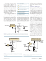
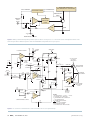
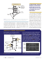
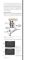
DEsigN a 100a
activE loaD to tEst powEr suppliEs
Y
Wideband
response lets
you test for
the transient
behavior
of your supply.
28 EDN | SEPTEMBER 22, 2011
ou use an active-load test circuit to ensure
that a power supply for a microprocessor or
for other digital loads supplies 100A transient currents. This active load can provide
a dc load for a power supply, and it can rapidly switch between dc levels. These transient
loads simulate the fast logic switching in the
microprocessor.
Ideally, your regulator output is invariant
during a load transient. In practice, however, you will encounter
some variations, which become problematic if allowable operatingvoltage tolerances are exceeded. You can base your active-load
circuit on previous designs of wideband loads that operate at lower
currents (Reference 1). This approach allows you to design a closedloop, 500-kHz-bandwidth, 100A active load having linear response.
[www.edn.com]
imagE: ThinksTock
By J im W il l ia ms • C o n s u lt i n g E d i to r
Conventional active-load circuits
have shortcomings (Figure 1). The
regulator under test drives dc and
switched resistive loads. Monitor the
switched current and the output voltage so that you can compare the stable
output voltage versus the load current
under both static and dynamic conditions. The switched current is either
on or off. You cannot control it in the
linear region as it changes.
You can further develop the concept by including an electronic-load
switch control (Figure 2). The input
pulse switches the FET through a
drive stage, generating a transient
load current from the regulator and its
output capacitors. The size, composition, and location of these capacitors
have a profound effect on transient
response. Although the electronic con-
wideband harmonics into the measurement that may corrupt the oscilloscope
display.
AT A G L A N C E
↘
Use active loads to test your
power supplies.
↘
TRANSIENT GENERATOR
Placing Q 1 within a feedback loop
allows true, linear control of the load
tester (Figure 3). You can now linearly
control Q1’s gate voltage, allowing you
to set an instantaneous transient current at any point and to simulate nearly
any load profile. Feedback from Q1’s
source to control amplifier A1 closes
a control loop around Q1, stabilizing
its operating point. The instantaneous
input-control voltage and the value
of the current-sense resistor set Q 1’s
current over a wide bandwidth. You
use the dc-load-set potentiometer to
bias A1 to the conduction threshold
of Q1. Small variations in A1’s output
result in large current changes in Q1,
meaning that A1 need not supply large
output excursions. The fundamental
speed limitation is the small-signal
bandwidth of the amplifier. As long
as the input signal stays within this
bandwidth, Q1’s current waveform is
identical in shape to A1’s input control
voltage, allowing linear control of the
load current. This versatile capability
permits you to simulate a wide variety
of loads.
You can improve this circuit by adding some components (Figure 4). A
gate-drive stage isolates the control
amplifier from Q 1’s gate capacitance
Using wide-bandwidth circuitry
allows fast transient response.
↘
Trim the circuit to obtain the
cleanest load-step signals.
↘ Minimize the inductance
in the high-current path.
↘ Verify the measurements
in a separate test setup.
trol facilitates high-speed switching,
the architecture cannot emulate loads
that are between the minimum and the
maximum currents. Additionally, you
are not controlling the FET’s switching speed because doing so introduces
+EREGULATOR
REGULATOR
INPUT SUPPLY
REGULATOR
UNDER TEST
DC LOAD
VOLTAGE
MONITOR
CURRENT
MONITOR
RSWITCHED
LOAD
LOAD
SWITCH
ISWITCHED=
EREGULATOR
RSWITCHEDLOAD
Figure 1 This conceptual regulator-load tester includes switched and dc loads and
monitors voltage and current. The resistor values set dc and switched-load currents.
REGULATOR UNDER TEST,
INCLUDING OUTPUT CAPACITORS
+
–
INPUT
PULSE
DC
LOAD
GATEDRIVE
STAGE
RSWITCHED
LOAD
100A REGULATOR UNDER TEST,
INCLUDING OUTPUT CAPACITORS
+
–
REGULATOR
VOLTAGE
MONITOR
REGULATOROUTPUTVOLTAGE
MONITOR
+
A1
NEGATIVE
INPUT
PULSE
Q1
−
0.001
0.001
EDN_110922DF_Figure 1.eps
ISWITCHED
MONITOR
Figure 2 A conceptual FET-based load tester permits step loading. Switched current is either on or off; there is no controllable
linear region.
[www.edn.com]
Q1
DIANE
–V
BASELINE/DC LOAD SET
ISWITCHED
AND DC LOAD
MONITOR
Figure 3 A feedback-controlled load-step tester allows continuous FET-conductivity control.
SEPTEMBER 22, 2011 | EDN 29
INPUT AVERAGE
REGULATOR UNDER TEST,
INCLUDING OUTPUT CAPACITORS
+
−
FET TEMPERATURE
DISSIPATION LIMITER
TEMPERATURE
SENSE
+
NEGATIVE
INPUT
PULSE
SHUTDOWN
A1
Q1
GATE-DRIVE
STAGE
−
+
×10
0.001
−
–V
BASELINE/DC LOAD SET
Figure 4 Adding a differential amplifier provides high-resolution sensing across a 1-mΩ shunt resistor. A dissipation limiter shuts
down the gate drive. Added capacitors tailor the bandwidth and optimize the loop response.
15V
15V
100k
+
GATE DRIVE
15V
POWER
LIMIT
DISSIPATION LIMITER
2.2k
IC1
LT1011
1k
0.01
−
10 μF
DISSIPATION
LIMIT
ADJUST
+
2k
0.1 μF
–5V
470k
33k
INPUT
0V
–1V
0 TO –1V=
0 TO 100A
FETRESPONSE
COMPENSATION
2N3904
TP-0610L
100k
TO LOAD POINT
OF SUPPLY
UNDER TEST
2N3904
Q6
3
S1
OPENS AT 70ºC
7- TO 45-pF
LOOP
EDN_110922DF_Figure
DIANE
COMPENSATION 4.epsIN754
1M
6.8V
5V
HEAT SINK
Q1
HIGH-CURRENT
CRITICAL PATH
100k
1.5k*
51
Q4
200Ω
Q2
BASELINE
CURRENT
–5V
13k
10k
20 pF
1.5k*
3
−
300 pF
3.01k*
50k
20 pF
A1
LT1220
CONTROL
AMPLIFIER
+
1k
VN2222L
4.5k*
Q5
0.001
−
–15V
1k
MINIMIZE
INDUCTANCE
+
A3 R
LT1193 F
2N3906
Q3
GAIN
100Ω FETCURRENT
SINK
432*
IQ
10 mA
—5V
1Ω
5V
×10 CURRENT SENSE
10k
LT1004
2.5V
0.02 μF
150k
IQ ADJUST
1k
10k
–15V
CURRENT
MONITOR
1V=100A
FEEDBACK
−
A2
LT1006
+
GATE-DRIVE BIAS CONTROL
10k
1 μF
SUPPLY-UNDERTEST RETURN
POINT
NOTES:
±5V REGULATORS, +=LT1121, −=LT1175.
S1 MOUNTED ON Q1 HEAT SINK.
S1=CANTHERM F20A07005ACFA06E.
* =1% FILM RESISITOR.
Q1=INFINEON IPB015N04LG.
=1N4148.
A1, A2, IC1=±15V POWERED.
BYPASSING NOT SHOWN.
0.001Ω RESISTORS=TEPRO-TPSM3.
Figure 5 You can derive a detailed active-load schematic from the conceptual design.
30 EDN | SEPTEMBER 22, 2011
[www.edn.com]
DC POWER SUPPLY
+
–
10,000-μF
COMBINATION
OF OS-CON, FILM,
AND CERAMIC
CAPACITORS
MINIMIZE
INDUCTANCE
MINIMIZE
INDUCTANCE
Q1
FIGURE 5’S
CIRCUIT
Figure 6 The test fixture for dynamic response has massive, broadband bypassing and
a low-inductance layout. This setup provides low-loss, high-current power to Q1.
to maintain the amplifier’s phase margin and provide low delay and linear
current gain. A gain-of-10 differential amplifier provides high-resolution
sensing across the 1-mΩ current-shunt
resistor. You can design a power-dissipation limiter that acts on the aver-
aged input value and Q1’s temperature.
It shuts down the FET’s gate drive to
preclude excessive heating and subsequent destruction. Capacitors can be
added to the main amplifier to tailor
the bandwidth and optimize the loop
response.
capacitors can be
added to the main
amplifier to tailor
the bandwidth and
optimize the loop
response.
You can develop a detailed schematic based on these concepts (Figure
5). The main amplifier, A1, responds to
dc and pulse inputs. You also send it a
feedback signal from A3 that represents
load current. A1 sets Q1’s conductivity
through the Q4 /Q 5 gate-drive stage,
which is actively biased using A2. The
voltage drop across the gate drive’s
input diodes would be high enough to
fully turn on Q4 and Q5. To prevent this
overdrive, reduce the voltage across
the lower diode with Q3. Amplifier A2
determines the gate-drive-stage bias
by comparing Q5’s averaged collector
current with a reference and controlling Q 3’s conduction, thus closing a
loop. That loop keeps the voltage drop
VERIFYING CURRENT MEASUREMENT
Theoretically, Q1’s source and drain current are
EDN_110922DF_Figure 6.eps DIANE
equal. Realistically, they can differ due to the efTO FIGURE 6’s
CAPACITOR BANK
AND DC SUPPLY
+
0.001
R
F LT1193
−
4.5k*
Q1
TO FIGURE 5’s
CIRCUIT
432*
+
R
LT1193 F
0.001
−
BOTTOM-SIDE
CURRET
4.5k*
fects of residual inductances and the 28,000-pF gate
capacitance. A3’s indicated instantaneous current
could be erroneous if these or other terms come into
play. You can verify that the source and the drain currents are equivalent (Figure A). Add a top-side, 1-mΩ
shunt and a gain-of-10 differential amplifier to duplicate the circuit’s bottom-side current-sensing section. The results should eliminate concern over Q1’s
dynamic-current differences (Figure B). The two 100A
pulse outputs are identical in amplitude and shape,
promoting confidence in the circuit’s operation.
432*
GAIN
100
TRACE A
50A/DIV
GAIN
100
TOP-SIDE
CURRENT
NOTE: *=1% FILM RESISTOR.
Figure A Use this arrangement for observing Q1’s top and bottom dynamic currents.
32 EDN | SEPTEMBER 22, 2011
TRACE B
50A/DIV
2 μSEC/DIV
Figure B Q1’s top (Trace A) and bottom (Trace B) currents
show identical characteristics despite high-speed operation.
[www.edn.com]
Figure 7 When you
optimize the dynamic
response, you get an
exceptionally pure
100A current pulse.
20A/DIV
2 μSEC/DIV
Figure 8 The response
becomes overdamped
if you set an excessive
feedback-capacitor
value for A1.
20A/DIV
2 μSEC/DIV
20A/DIV
2 μSEC/DIV
Figure 9 An inadequate feedbackcapacitor value for A1
decreases the transition time but promotes
instability. Further
capacitor reduction
causes oscillation.
Figure 10 Overdoing
the FET’s response
compensation results
in corner peaking.
20A/DIV
2 μSEC/DIV
Figure 11 By optimizing the dynamic
trims, the circuit gets
a 650-nsec rise time,
corresponding to a
540-kHz bandwidth.
20A/DIV
500 nSEC/DIV
20A/DIV
Figure 12 The optimized trims yield a
500-nsec fall time.
500 nSEC/DIV
[www.edn.com]
across the bases of Q4 and Q5 to a value well under 1.2V,
and servos that value until Q4 and Q5 have a 10-mA average
collector-bias current.
The duty cycle of the load overheats if it is on for too
long. You can fashion a protection circuit with techniques
that high-power-pulse-generator designers use (references
2, 3, and 4). Feed comparator IC1 the average input-voltage value. It compares that voltage to a reference voltage
set with the dissipation-limit-adjust potentiometer. If the
input duty cycle exceeds this limit, comparator IC1 turns
off the FET gate drive through Q2. Thermal switch S1 pro-
vides further protection. If Q1’s heat sink gets too hot, S1
opens and disconnects the gate-drive signal. By diverting
Q4’s bias voltage, transistor Q6 and the zener diode prevent
Q1 from turning on if the −15V supply is not present. A
1-kΩ resistor on A 1’s positive input prevents amplifier
damage should you lose the 15V power supply.
Trimming optimizes the dynamic response, determines
the loop’s dc baseline idle current, sets the dissipation limit,
and controls the gate drive’s stage bias. The dc trims are selfexplanatory. The loop-compensation and FET-response ac
trims at A1 are subtler. Adjust them for the best compromise
INSTRUMENTATION CONSIDERATIONS
The pulse-edge rates in the main
article are not particularly fast,
but high-fidelity response requires
some diligence. In particular, the
input pulse must be cleanly defined
and devoid of parasitics, which
would distort the circuit’s outputpulse shape. A1’s 2.1-MHz input
RC (resistance/capacitance) network filters the pulse generator’s
preshoot, rise-time, and pulsetransition aberrations, which are
well out of band. These terms are
not of concern. Almost all generalpurpose pulse generators should
perform well.
A potential offender is excessive
tailing after transitions. Meaningful
dynamic testing requires a rectangular pulse shape, flat on the top
and the bottom within 1 to 2%. The
circuit’s input band-shaping filter
removes the aforementioned highspeed-transition-related errors but
does not eliminate lengthy tailing in
the pulse flats. You should check the
pulse generator for this issue with a
well-compensated probe at the circuit input. The oscilloscope should
register the desired flat-top- and
flat-bottom-waveform characteristics.
In making this measurement, if highspeed-transition-related events are
bothersome, you can move the probe
to the bandlimiting 300-pF capacitor.
This practice is defensible because
the waveform at this point determines
A1’s input-signal bandwidth.
Some pulse-generator output
stages produce a low-level dc offset when their output is nominally
at its 0V state. The active-load circuit processes such dc potentials
as legitimate signals, resulting in a
dc-load baseline-current shift. The
active load’s input scale factor of
1V=100A means that a 10-mV zerostate error produces 1A of dc baseline-current shift. A simple way to
check a pulse generator for this error is to place it in external-trigger
mode and read its output with a
DVM (digital voltmeter). If offset is
present, you can account for it by
COAXIAL METAL
ENCLOSURE
INPUT FROM
PULSE-GENERATOR
TRIGGER OUTPUT
1k
50
300 pF
T1
1k
OUTPUT TO
OSCILLOSCOPE’S
EXTERNAL
TRIGGER INPUT
INSULATEDSHELL BNC
NOTES: T1=ALMOST ANY SMALL PULSE TRANSFORMER.
1-kΩ AND 300-pF VALUES ARE TYPICAL.
Figure A You can make a trigger isolator that floats input BNC’s ground using an insulated-shell BNC connector. A capacitively coupled pulse transformer avoids loading
input, maintains isolation, and delivers the trigger to the output. A secondary resistor
on T1 terminates ringing.
34 EDN | SEPTEMBER 22, 2011
nullifying it with the circuit’s baseline-current trim. You could also
use a different pulse generator.
Keep in mind parasitic effects
due to probe grounding and instrument interconnection. At pulsed
100A levels, you can easily induce
parasitic current into “grounds”
and interconnections, distorting
displayed waveforms. Use coaxially grounded probes, particularly
at A3’s output-current monitor and
preferably anywhere else.
It is also convenient and common practice to externally trigger
the oscilloscope from the pulse
generator’s trigger output. There is
nothing wrong with this practice; in
fact, it is a recommended approach
for ensuring a stable trigger as
you move probes between points.
This practice does, however, potentially introduce ground loops
due to multiple paths between
the pulse generator, the circuit,
and the oscilloscope. This condition can falsely cause apparent
distortion in displayed waveforms.
You can avoid this effect by using
a trigger isolator at the oscilloscope’s external-trigger input. This
simple coaxial component typically
comprises isolated ground and
signal paths, which often couple
to a pulse transformer to provide a
galvanically isolated trigger event.
Commercial examples include
the Deerfield Laboratory (www.
deerfieldlab.com) 185 and the
Hewlett-Packard (www.hp.com)
11356A. Alternatively, you can construct a trigger isolator in a small
BNC-equipped enclosure (Figure A).
[www.edn.com]
between loop stability, edge rate, and pulse purity. You can
use A1’s loop-compensation trimming capacitor to set the
roll-off for maximum bandwidth and accommodate the
phase shift that Q1’s gate capacitance and A3 introduce.
The FET-response adjustment partially compensates Q1’s
inherent nonlinear-gain characteristic, improving the front
and rear pulses’ corner fidelity (see sidebar “Trimming
procedure,” with the online version of this article at www.
edn.com/110922df).
CIRCUIT TESTING
You initially test the circuit using a fixture equipped with
massive, low-loss, wideband bypassing (Figure 6). It is
important to do an exceptionally low-inductance layout
in the high-current path. Every attempt must be made
DC POWER SUPPLY
+
–
MINIMIZE
INDUCTANCE
10,000-μF
COMBINATION
OF OS-CON, FILM,
AND CERAMIC
CAPACITORS
DELIBERATELY
INTRODUCED
20-nH PARASITIC
INDUCTANCE
MINIMIZE
INDUCTANCE
Q1
FIGURE 5’s
CIRCUIT
Figure 13 You can deliberately introduce a parasitic, 20-nH inductance to test layout sensitivity.
20A/DIV
(a)
10 μSEC/DIV
EDN_110922DF_Figure 13.eps
20A/DIV
(b)
2 μSEC/DIV
[www.edn.com]
DIANE
Figure 14 A 20-nHinductance, 1.5×
0.075-in., flat-copper,
braided wire completely distorts (a) the
optimized response
(b). Note the fivetimes-horizontalscale change between a and b.
to minimize inductance in the 100A path. You should
get good results after you properly trim the circuit if you
minimize inductance in the high current path (Figure 7).
The 100A-amplitude, high-speed waveform is pure, with
barely discernible top-front and bottom-rear corner infidelities (see sidebars “Verifying current measurement” and
“Instrumentation considerations”).
To study the effects of ac trim on the waveform, you
must perform deliberate misadjustments. An overdamped
response is typical of excess A1 feedback capacitance (Figure
8). The current pulse is well-controlled, but the edge rate is
INPUT
7 TO 14V
slow. Inadequate feedback capacitance from A1 decreases the
transition time but promotes instability (Figure 9). Further
reducing the trim capacitance causes loop oscillation because
the loop’s phase shift causes a significant phase lag in the
feedback. Scope photos of uncontrolled 100A loop oscilla-
Figure 16 The regulator’s response to
a 100A pulsed load
(Trace A) is wellcontrolled on both
edges (Trace B).
TRACE A
100A/DIV
TRACE B
0.1V/DIV
AC
COUPLED
+
LTC3829-BASED, SIX-PHASE,
1.5V, 120A POWER SUPPLY
–
–
+
Q1
10 μSEC/DIV
MINIMIZE
INDUCTANCE
FIGURE 5’s
CIRCUIT
Figure 17 You can
use the circuit to
create a 100-kHz,
100A-sine-wave
load.
50A/DIV
Figure 15 Use low-impedance connections to test a six-phase,
120A buck regulator.
10 μSEC/DIV
Figure 18 The
active-load circuit
sinks 100A p-p
in response to a
gated randomnoise input.
50A/DIV
20 μSEC/DIV
EDN_110922DF_Figure 15.eps
DIANE
100
90
4% LEADING-EDGE
OVERSHOOT
80
NO
OVERSHOOT
70
60
LOAD
CURRENT 50
(A)
40
30
20
10
0
0 0.1 0.2 0.3 0.4 0.5 0.6 0.7 0.8 0.9 1 1.1 1.2
MINIMUM Q1 DRAIN VOLTAGE (V)
Figure 19 Active-load characteristics feature small current-accuracy and regulation errors. The bandwidth mildly retards at low
currents. The compliance voltage is less than 1V at 100A with
4% leading-edge overshoot and 1.1V with no overshoot.
36 EDN | SEPTEMBER 22, 2011
[www.edn.com]
A11_EDN_1-3V_2-25x10_A11.qxd 8/10/11 11:28
TAbLe 1 Active-loAd chArActeristics
Current accuracy
(referred to input)
1% full-scale
Temperature drift
100 ppm/°C of reading +20 mA/°C
Current regulation
versus supply
Greater-than-60-db power-supply-rejection ratio
Bandwidth
540 kHz at 100A with a rise time of 650 nsec, 435
kHz at 10A with a rise time of 800 nsec
Compliance voltages
for full output current
0.95V minimum (see Figure 19); 70°C Q1 thermaldissipation limiter sets maximum
tion are unavailable. The event is too
thrilling to document. Overdoing the
FET’s response compensation causes
peaking in the corners of the waveform
(Figure 10). Restoring the ac trims to
nominal values causes a 650-nsec rise
time, equivalent to a 540-kHz bandwidth, on the leading edge (Figure 11).
Examining the trailing edge under the
same conditions reveals a somewhatfaster 500-nsec fall time (Figure 12).
LAYOUT EFFECTS
If parasitic inductance is present in the
high-current path, your design cannot remotely approach the previous
responses. You can deliberately place
a tiny, 20-nH parasitic inductance in
Q1’s drain path (Figure 13), which will
cause an enormous waveshape degradation deriving from the inductance and
the loop’s subsequent response (Figure
14a). A monstrous error dominates the
leading edge before recovery occurs at
the middle of the pulse’s top. Additional
aberration is evident in the falling edge’s
turn-off. The figure’s horizontal scale is
five times slower than the optimized
response (Figure 14b). The lesson is
clear: High-speed 100A excursions do
not tolerate inductance.
REGULATOR TESTING
After you address the compensation and layout issues, you can test
your power-supply regulator (Figure
15). The six-phase, 120A Linear
Technology Corp (www.linear.com)
LTC1675A buck regulator acts as a
demonstration board. The test circuit
generates the 100A load pulse (Trace
A of Figure 16). The regulator maintains a well-controlled response on
both edges (Trace B of Figure 16).
The active load’s true linear response
and high bandwidth permit wideranging load-waveform characteris[www.edn.com]
tics. Although the step-load pulse in
Figure 16 is the commonly desired
test, you can generate any load profile.
A burst of 100A, 100-kHz sine waves is
an example (Figure 17). The response
is crisp, with no untoward dynamics
despite the high speed and current. You
could form a load even from an 80-μsec
burst of 100A p-p noise (Figure 18).
The load circuit has high accuracy,
compliance, and regulation specifications (Figure 19 and Table 1).EDN
REFERENCES
1 Williams, Jim, “Load Transient
Response Testing for Voltage Regulators,” Application Note 104, Linear
Technology Corp, October 2006,
http://bit.ly/p5q2AD.
2 “Overload Adjust,” HP-214A Pulse
Generator Operating and Service
Manual, Hewlett-Packard, figures 5
through 13.
3 “Overload Relay Adjust,” HP-214A
Pulse Generator Operating and Service
Manual, Hewlett-Packard, 1964, pg 5.
4 “Overload Detection/Overload
Switch,” HP-214B Pulse Generator
Operating and Service Manual,
Hewlett-Packard, March 1980, pg 8.
AUThOR’S bIOGRAphY
Jim Williams was a staff scientist at Linear Technology
Corp, where he specialized
in analog-circuit and instrumentation design. He
served in similar capacities
at National Semiconductor, Arthur D
Little, and the Instrumentation Laboratory at the Massachusetts Institute of
Technology (Cambridge, MA). He enjoyed sports cars, art, collecting antique
scientific instruments, sculpture, and restoring old Tektronix oscilloscopes. A
long-time EDN contributor, Williams died
in June 2011 after a stroke.