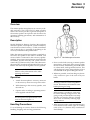
1
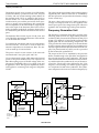
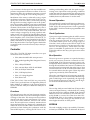
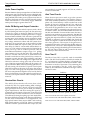
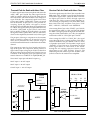
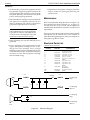
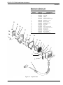
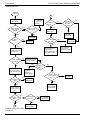
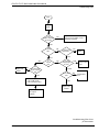
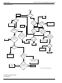
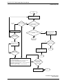
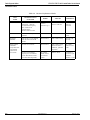
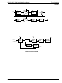
GTX/GTX-LTR/LTS 2000 Portable Radios Service Manual
TheoryofOperation
Transmitter
“5R” (5 V)
MIXER
RX IN
1ST
BANDPASS
FILTER
2ND
BANDPASS
FILTER
RF
AMP
LO +3 dBm
1ST
CRYSTAL
FILTER
2ND
CRYSTAL
FILTER
IF
AMP
DETECTED AUDIO
IF IC
RECEIVER BLOCK DIAGRAM
TXB+
0 dBm
FROM
VCO BUFFER
POWER
MODULE
RX IN
ANTENNA
SWITCH
COUPLER
HARMONIC
FILTER
ANTENNA
MATCHING
Vcontrol
RECTIFIER
POWER
CONTROL
POWER CONTROL REFERENCE
FROM DAC
TRANSMITTER BLOCK DIAGRAM
February 1997
68P02948C90-O
2-3
Theory of Operation
GTX/GTX LTR/LTS 2000 Portable Radios Service Manual
Frequency Generation Unit
The antenna switch circuit consists of two PIN diodes
(CR161 and CR162), a pi network (C126, L161, and part
of C162), and one current limiting resistor (R163). In
the transmit mode, TX B+ is applied to the circuit to
bias the diodes “on”. The shunt diode (CR161) shorts
out the receiver port, and the pi network, which operates as a quarter wave transmission line, transforms
the low impedance of the shunt diode to a high impedance at the input of the harmonic filter. In the receive
mode, the diodes are both off, and hence, there exists a
low attenuation path between the antenna and receiver
ports.
The voltage at the second input of the summing amp is
supplied by DAC U400-P9. This DAC is controlled by
the microprocessor and provides the reference voltage
for the control loop.
The error voltage at the input of U151B-13 produces a
voltage at its output which is in turn applied to the
drivers Q151, Q152. The voltage from Q151 collector is
applied to the controlled stage of the power module.
Frequency Generation Unit
The Frequency Generation Unit (FGU) consists of the
following major sections: the high stability reference
oscillator (U210), fractional-N synthesizer (U220), VCO
(U260), VCO buffer IC (U270) and Rx injection buffer
(Q280, Q281 and the surrounding components). The
VCO provides the carrier frequency for the transmitter
(U270 Tx output) and provides the local oscillator (LO)
injection signal for the Rx injection buffer (U270 Rx output). The phase-locked loop (PLL) circuit is provided
by the fractional-N synthesizer IC.
The harmonic filter consists of part of C122, L121, and
C123. This filter attenuates the harmonic of the module
to a level better than -55 dBc.
To optimize the transmitter and receiver performance
into the antenna, a network is used to match the
antenna’s impedance to the harmonic filter. The network is made up of C125 and L122.
The power control circuit consists of the networks
associated with U151, Q151, Q155, and U111.
The output of the VCO is amplified by the prescaler
buffer, routed through a low-pass filter, and applied to
the prescaler dividers of the synthesizer. The divide
ratios are determined from information stored in memory and bussed to the synthesizer by way of the microcontroller. The divide ratio determines the VCO
frequency. The resulting VCO buffer signal is applied
to a comparator located in the synthesizer. The synthesizer comparator also receives a reference frequency by
U111 is a directional coupler which detects the forward
power of the power module U101. The couple has 21
dB±1 dB coupling at port 2. The RF voltage at the coupler port 2 is rectified by CR111, C111, R114, C112, and
is applied to U151A. This signal is amplified by U151A
and applied to summing and integrator amplifier
U151B.
SWITCHING CCTS
FOR VCO AND BUFFER
POSITIVE MULTIPLIER
RX VCO
RX OUT
16.8 MHz
REF OSC
U210
RX INJ.
BUFFER
MIXER
RX BUFFER
LOOP
FILTER
REFERENCE
DIVIDER
TX OUT
MOD OUT
COUNTER FOR
MULTIPLIER
A/D
FRACTIONAL
DIVIDER
TX VCO
PRE-SCALER
DIVIDER
U260
VCO
U220
FRACTIONAL-N
SYNTHESIZER
MATCHING
CCT
RF PA
TX BUFFER
Prescaler
BUFFER
U270
VCO BUFFER IC
LOW PASS FILTER
2.1 MHz
REFERENCE
CLOCK TO
ASFIC
MODULATING
SIGNAL
FGU CIRCUITS
2-4
68P02948C90-O
February 1997
GTX/GTX-LTR/LTS 2000 Portable Radios Service Manual
TheoryofOperation
Controller
way of reference divider input from the 16.8 MHz temperature-compensated reference oscillator. If the two
frequencies differ, the synthesizer generates a control
(error) voltage causing the VCO to change frequency.
Modulation of the carrier is achieved by using a 2-port
modulation technique. The deviation of the low frequency tone, such as PL/DPL, is achieved by injecting
the signal into an analog/digital circuit in the synthesizer. The resulting digitized signal is then modulated
by the fractional N divider; this generates the required
deviation. The deviation of the high frequency tone is
achieved by modulating the modulation varactor on
the VCO. To cover a very wide bandwidth, the VCO
control voltage is stepped up by using a positive multiplier circuit. A 13-V supply powers the phase detector
circuitry. The VCO signal is amplified by the integrated
buffer amplifier of the VCO buffer. The buffer IC Tx
output signal is filtered and channeled to the RF PA
(U101). The buffer IC Rx output signal is connected to
the Rx injection buffer. The output signal of that buffer
is supplied to the receiver first mixer (U50) as the injection signal.
Controller
The GTX/GTX LTR/LTS 2000 controller is an open
architecture which consists of:
• U709, Motorola 68HC11K1 microprocessor
• U701, Audio Signalling Filter Integrated Circuit,
ASFIC
• U703, 1 Kbyte EEPROM
• U705, 128/256 Kbyte OTP/FLASH ROM
• U706, 8/32 Kbyte Static RAM
• U707, LCD Display Driver
• U704, 5 V Voltage Regulator
• U550, Hear Clear
U709, U703, U705, U706 and U707 are powered by
U704. U701 is powered from a 5V Regulator (U708) on
Radio Module. In addition to the external memory
devices, U709 has 768 bytes of RAM and 640 bytes of
EEPROM.
Functions
The microprocessor has two basic functions: interfacing with the outside world, and controlling the internal
workings of the radio. The microprocessor interfaces
directly with the keypad, side buttons, PTT, rotary
switch, low battery indicator, EXT PTT and volume
sense. The microprocessor constantly monitors these
inputs and interprets any changes into commands that
control the rest of the radio. Some control functions it
performs include loading the synthesizer with the
desired RF frequency, turning the RF PA on or off,
February 1997
enabling and disabling audio and data paths and generating tones. Operations and operating conditions
within the radio are interpreted by the microprocessor
and fed back to the operator as visible (the display) or
audible (alert tone) indications of current status.
Normal Operation
The regulated 5V output from U704 powers the microprocessor (U709) and the rest of the digital IC except
ASFIC (U701). The microprocessor’s clock is generated
by the ASFIC, which has a built-in programmable clock
synthesizer.
Clock Synthesizer
Upon power-up and assuming that the ASFIC receives
a proper 2.1 MHz input on U701-P38 (which comes
from the transceiver board), the ASFIC outputs a
7.776 MHz CMOS square wave (0-5Vpp logic) on
U701-P30, which connects to the EXTAL input of the
microprocessor, U709-P73. The microprocessor operates at 1/4 of this frequency, which in this case computes to 1.944 MHz. In particular, the E clock output
(U709-P72) will be a 50% duty cycle square wave at this
frequency.
Bus Operation
The microprocessor operates in expanded memory
mode and executes firmware contained in OTP/
FLASH ROM, U705. The microprocessor uses a nonmultiplexed address data bus, consisting data lines D0
through D7 and address lines A0-A17. In addition, the
microprocessor has integrated chip-select logic so that
external memories can be accessed without the need
for external address decoder gates. These chip-select
signals are provided by U709-P28 and P29.
When the controller board is functioning normally,
microprocessor’s address and data lines should be toggled at CMOS logic levels. Specifically, the logic-high
levels should be between 4.8 and 5.0V, and the logiclow levels should be between 0 and 0.2V.
RAM
The on-chip 768 byte static RAM from U709 provides
some scratch-pad memory, with the bulk of it coming
from the external 8 or 32Kbyte SRAM, U706. External
SRAM accesses are indicated by the U709-P28. Normally SRAM is accessed less often than the OTP/
FLASH ROM, U705; i.e. the number of transitions per
second on U705 chip select (pin 30) should be 5-15
times higher than those on U706 pin 20.
EEPROM
The radio codeplug storage is provided by U709 internal 640 byte EEPROM, with an additional 4K byte of
68P02948C90-O
2-5
Theory of Operation
GTX/GTX LTR/LTS 2000 Portable Radios Service Manual
Controller
memory space provided by external EEPROM, U703.
There are three basic types of codeplug information:
information on the trunked system on which the radio
is authorized to operate; information on the conventional system, which is either of the repeater or talkaround type on which the radio is authorized to operate, and information on the configuration and tuning
of the radio itself. Tuning information is normally
located in the internal EEPROM of U709.
microprocessor when the radio transmits or receives a
signal. Also, there are minor differences in the functioning of both paths depending on whether an internal or external (accessory) microphone/speaker is
being used. The radio constantly monitors the received
data path for control-channel data in trunking operation or sub-audible data in conventional operation.
External PTT Sense Circuits
SPI Interface
The microprocessor communicates with several ICs
and modules through a dedicated on-chip serialperipheral-interface (SPI) port which consists of transmit data line MOSI (U709-P1), receive data line MISO
(U709-P80), and clock line SCK (U709-P2). In addition,
each IC that can be accessed by the microprocessor
using the SPI read/write select line associated with it.
The ICs or circuits and their associated select lines are:
• EEPROM (U703) with select line U709-P3
On connecting an external MIC through connector J3,
external PTT sense transistor Q408 switches “ON”
when the external PTT switch is closed. Q408 collector
voltage is monitored by U709-P4. When collector voltage is logic “HIGH”, the microprocessor configures the
radio for transmit mode. In PTT equipped accessories,
the PTT switch is series connected with the external
MIC element.
MIC Amplifier
• ASFIC (U701) with select line U709-P34
• LCD Driver (U707) with select line U709-P23
• OTP/FLASH ROM (U705) with select line
U709-P29
• SRAM (U706) with select line U709-P28
• Transceiver Board Synthesizer (U201) with
select line U709-P35
• Transceiver Board DAC IC (U400) with select
line U709-P26
The LCD Driver uses the master out/slave in (MOSI)
line to send data to the display driver IC, and the master in/slave out (MISO) line to send data back to the
microprocessor (U709). Note, however, that the keypad (or any other SPI device) can never initiate display
data; the microprocessor is at all times the SPI master
device. Thus the MOSI line and MISO line are always
in the master configuration.
MIC audio from internal MIC MK401 is coupled
through C429, L404, J3 and L403 to the MIC buffer circuit U405-1. External MIC plug insertion mechanically
disconnects the internal MIC. External MIC audio is
coupled through L403 to the MIC buffer input. The
buffer will route the MIC audio into MIC IN (U701-B8)
through flex and connectors J200 and J700. Inside the
ASFIC, the MIC audio is filtered to eliminate components outside the 300-3000 Hz voice band, pre-emphasized, and then limited. The limited MIC audio is then
routed through a summer, which is used to add in PL
or DPL sub-audio band modulation, and then to a
splatter filter to eliminate high frequency spectral components generated by the limiter. After the splatter filter, the audio is routed to the 8 bit modulation
attenuators, which are tuned in the factory of the field
to set the proper amount of FM deviation. The TX
audio emerges from the ASFIC at U701-J4 and is dc
coupled and applied through flex and connectors J700
and J200 to the synthesizer (U201) pin 8.
LED Control
The bicolor LED located on the top of the radio is indirectly activated by SPI of U709 via the DAC IC (U400)
on Transceiver Board. When either input to the dual
NPN transistor (U410) is at logic high, the corresponding output pin (pin 6 for the green LED, pin 3 for the
red) should be at approximately 4.3 Vdc. Note that it is
possible to have both LED outputs on simultaneously,
in which case the LED emits a yellow/orange light.
Audio & Data Circuitry
The transmit and receive audio paths are disabled in
the standby mode and selectively enabled by the
2-6
TX Data Circuits
There are four major types of transmit data: sub-audible data (PL/DPL/Connect Tone) that gets summed
with voice, high speed data for trunking control channel communication, DTMF data for telephone communication in trunked and conventional systems, and
MDC data for use in Motorola proprietary MDC systems. The deviation levels of the latter three types are
tuned by a 5-bit digital attenuation inside the ASFIC.
For each data type and each band split, there is a distinct set of tuning values that are programmed into the
ASFIC before the data is generated and transmitted.
68P02948C90-O
February 1997
GTX/GTX-LTR/LTS 2000 Portable Radios Service Manual
TheoryofOperation
Controller
Sub-Audible Data (PL/DPL)
Sub-audible data is composed of low-frequency PL and
DPL waveforms for conventional operation and connect tones for trunked voice channel operation. (The
trunking connect tone is simply a PL sine wave at a
higher deviation level than PL in a conventional system). Although it is referred to as “sub-audible data”,
the actual frequency spectrum of these waveforms may
be as high as 250 Hz, which is audible to the human ear.
However, the radio receiver filters out any audio below
300 Hz, so these tones are never heard in the actual system.
Only one type of sub-audible data can be generated by
U701 at a time. The process is as follows: using the SPI,
the microprocessor programs the ASFIC (U701) to set
up the proper low-speed data deviation and select the
PL or DPL filters. The microprocessor then generates a
square wave from U705-P6 which strobes the ASFIC
PL_CLK (U701-C3). For encode input at twelve times
the desired data rate. (For example, for a PL frequency
of 103 Hz, the frequency of the square wave at U701P20 would be a1236 Hz). This derives a tone generator
inside U701, which generates a staircase approximation to a PL sine wave or DPL data pattern. This internal waveform is then low-pass filtered and summed
with voice or data. The resulting summed waveform
then appears on U701-H8 (VCO_ATN), where it is sent
to the transceiver board as previously described for
transmit audio.
High-Speed Data
High-speed data refers to the 3600 baud data waveforms (ISWS AND OSWS) used in a trunking system
for high-speed communication between the radio and
the central controller. To generate an ISW, the microprocessor (U709) first programs the ASFIC (U701) to
the proper filter and gain settings. It then begins strobing U701-G1 (Trunking Clock In) with a square wave
(from U709-P5) at the same baud rate as the data. The
output waveform from 5-3-2 State Encoder of U701 is
then fed to the post-limiter summer block and then the
splatter filter. From that point it is routed through the
mode attenuator and then out of the ASFIC to the
transceiver board via VCO_ATN (U701-H8).
DTMF Data
DTMF data is a dual-tone waveform used during
phone interconnect operation. They are divided into
low-group and high-group tones. The high-group tone
is generated by U709-P5 strobing U701-G1 at six times
the tone frequency for tones less than 1440 Hz, or twice
the frequency for tones greater than 1440 Hz. The lowgroup tone is generated by U709-P7 strobing U701-G2
(DTMF Clock) at six times the tone frequency. Inside
U701 the low-group and high-group tones are summed
(with the amplitude of the high-group tone being
February 1997
approximately 2dB greater than that of the low-group
tone) and then pre-emphasized before being routed to
the summer and splatter filter. The DTMF waveform
then follows the same path as was described for high
speed data.
MDC Data
The MDC signal follows exactly the same path as the
DTMF high-group tone. MDC data utilizes MSK modulation, in which a logic zero is represented by one
cycle of a 1200 Hz sine wave, and a logic one is 1.5
cycles of an 1800 Hz sine wave. To generate the data,
the microprocessor (U709) first programs the ASFIC
(U701) to the proper filter and gain settings. It then
begins strobing U701-G1 with a square wave (from
U709-P5) at the same baud rate as the data. The output
waveform from U701 is fed to the post-limiter summer
block and then the splatter filter. From that point it is
routed through the mode attenuator and then out of
ASFIC to the transceiver board via VCO_ATN (U701H8).
RX Audio Processing and Digital Volume
Control
The radio’s RF circuit are constantly producing an output at the Detected Audio line. Whenever the radio is
in trunked standby mode, it is processing data from the
control channel; while in conventional standby mode,
it is always monitoring the squelch line and/or subaudible data. The detected audio from the transceiver
board enters the controller board at connector J700
pin 4. In addition to the detected audio line, the transceiver board also provides a squelch noise from U51P30 into the ASFIC squelch-detect circuitry via U701H7. When the microprocessor determines that it has
received the proper data or signal type for unsquelching, it sets up the receive audio path and sends data to
U701 to do the same within.
The detected audio will enter U701 through RX IN (pin
H6) and PL IN (pin J7) for further processing. Inside
the IC, the signal first passes through a low-pass filter
to remove any frequency components above 3000 Hz
and then a high-pass filter to strip off any sub-audible
data below 300 Hz. Next, the recovered audio passes
through a de-emphasis filter to reduce the effects of FM
noise. Finally, the IC amplifies the audio and passes it
through the 8-bit programmable attenuator whose
level is set, depending on the value of the volume control. The microprocessor (U709) programs the value of
the 8-bit attenuator in accordance with the voltage
sensed at the volume potentiometer, which is connected to U709-P48. This pin is one of the eight channels of U709’s 8 bit A/D convertor. After passing
through the 8-bit digital attenuator, the audio goes to a
buffer amplifier and then exits at U701-J4, where it is
routed to the Audio power amplifier circuit in the
transceiver board.
68P02948C90-O
2-7
Theory of Operation
GTX/GTX LTR/LTS 2000 Portable Radios Service Manual
Controller
and trunking low-speed) appears at U701-A4, where it
connects to U709-P10.
Audio Power Amplifier
Resistor R466 sets the input impedance to U409-P2 of the
audio power amp. The audio PA circuit is a bridged-tiedload (BTL) configuration with fixed gain of 40dB, developing 500mW (rated audio power) output at less than 5%
harmonic distortion into the 16 Ohm internal speaker
LS401 with nominal 7.5 V DC battery supply. Maximum
audio power output is greater than 1.2 W.
Audio PA Muting and Output Protection
PNP transistor Q410, the audio PA power switch, driven
by NPN darlington transistor Q411, the PA mute amp,
controls Vcc supply to Audio PA U409-P1. U701-A3 is
connected to Q411 base, controlling audio PA Vcc supply.
Resistors R489 and R490, PNP transistor Q412 and the
current sense circuit monitor current supplied to audio
PA U409-P1. Worst case audio PA current (at 9 V DC battery voltage, maximum volume and full system deviation) does not exceed 450 mA at the nominal 16 Ohm
load. Resistor R488 and capacitor C461 provide an RC
time delay for U405-2, a monostable multivibrator circuit. A 2.5 V DC reference voltage is fed to U405-2-P6. On
radio power-up, and in normal operation U405-P7
monostable multivibrator output is logic “LO” pulling
Q411 emitter to Vee with the audio PA controlled by
U701-A3. Should U409-P5 and/or U409-P8 become
shorted to each other or to the ground (Vee), current consumption exceeds 500 mA (approximately) and Q412
collector. When U405-2-P5 voltage rises higher than the
U405-2-P6 reference voltage (rise time is less than 50
µsec), U405-2 is triggered and U405-2-P7 dc output voltage is switched to 4Vdc, effectively biasing Q411 into cutoff and turning off the audio PA power switch Q410.
U405-2-P7 remains in this state for 15 msec, then reset to
logic “LO” state. Average power dissipation in the audio
PA circuit components is helped to a low level by the low
duty cycle (less than 0.3%) of the audio PA protection circuit. The cycle repeats until the audio PA output short is
removed.
Receive Data Circuits
The ASFIC (U701) decodes all receive data, which
includes PL, DPL, low-speed trunking, MDC, and highspeed trunking data. The “decode” process for each data
type typically involves low pass or band pass filtering,
signal amplification, and then routing the signal to a
comparator, which outputs a logic zero or one signal. The
detected audio from the transceiver board is routed to
U701-H6 and J7 through coupling cap C435. Inside U701,
the data is filtered according to the data type (HS data or
LS data, then hard-limited to a 0-5V digital level. The
high-speed limited data output (MDC and trunking
high-speed) appears at U701-G4, where it connects to
U709-P11. The low speed limited data output (PL, DPL
2-8
Alert Tone Circuits
When the microprocessor needs to give the operator
feedback (for a good key press or for a bad key press) or
radio status (trunked system busy, low battery condition,
phone call, circuit failures), it sends an alert tone to the
speaker. It does so by sending data to U701, which sets
up the audio path to the speaker for alert tones. The alert
tone itself can be generated in one of two ways: internally by the ASFIC, or externally using the microprocessor and the ASFIC. The allowable internal alert tones are
300, 900, and 1800 Hz. For external alert tones, the microprocessor can generate any tone within the 100-3000 Hz
audio band. This is accomplished by the microprocessor
toggling the output line U709-P7, which is also the same
line used to generate low-group DTMF data. Inside the
ASFIC, this signal is routed to the external input of the
alert tone generator. The output of the generator is
summed into the audio chain just after the RX audio deemphasis block. The tone is then amplified and filtered
before passing through the 8-bit digital volume attenuator. The tone exits at U701-J4, and is routed to the audio
PA circuitry in the transceiver board.
Hear Clear IC
The Hear Clear (HC) is typically used for 900 MHz
radios. The HC has three main circuit blocks within the
IC.: 1) Compressor, 2) Flutter Fighter, 3) Expander Circuits. There are six enable/control lines on the HC which
determine its mode of operation. The remaining five
lines are controlled by the HC_CNTL line of DAC
U1400-15. The table below summarizes the logic controls
and the IC states.
Table 2-1.
Logic State
Set By
TX1
RX1
TX2
RX2
U550-C4
SWB+
1
1
X
1
FFENAB
U550-E3
HC_CNTL
1
1
X
0
LODSAB
U550-A5
HC_CNTL
1
1
1
x
HIENAB
U550-C2
GND
0
0
X
0
HCIDSAB
U550-B6
HC_CNTL
1
1
1
1
CPNENAB
U550-D1
HC_CNTL
1
1
X
0
Name
ICENABLE
Ref.Des
TX1: transmit mode with carrier squelch, PL or DPL.
RX1: receive mode with carrier squelch, PL or DPL.
TX2: transmit mode with all data HST, MDC, MPT & DTMF.
RX2: receive voice with all data HST, MDC, MPT & DTMF.
68P02948C90-O
February 1997
GTX/GTX-LTR/LTS 2000 Portable Radios Service Manual
TheoryofOperation
Controller
Transmit Path for Radio with Hear Clear
Receive Path for Radio with Hear Clear
TX audio signal comes from microphone and enters the
ASFIC “MIC” pin U701-B6. The audio signal from the
ASFIC is routed to ASFIC pin U701- H5, from where it
leaves the ASFIC and enters the Hear Clear compressor
at pin U550-D3. The compressed signal leaves Hear
Clear at pin U550-F3 “COMP OUT” where it is routed
back to the ASFIC TX pin U701-C7, C561 provides AC
coupling. Inside the ASFIC, the signal is routed
through a LPF and HPF that limits the signal between
0.3 - 3KHz. The signal is then pre-emphasized and exits
the ASFIC “PRE_AMP” at pin U701-C8, and routed
back to ASFIC at LIM pin U701-E8 where it is routed
through the limiter, splatter filter, and two attenuators
which set the amplitude (deviation level) of the signal.
The audio signal enters the Hear Clear controller from
BBR signal “DET_AUDIO” at pin U51-28. The discriminator audio signal “DISC” enters the Hear Clear Flutter Fighter pin U550-U4 “FFIN” through capacitors
C500 and C567. C567 is a part of a noise sampling circuit consisting of components- C567, R556, R553, C564,
R555, R557 and C565; and Hear Clear ports “CLIPREF”, “NFILIN”, “NFILOUT” and “NOISHLD”.
The purpose of having a compressor in the transmit
mode is twofold: 1) improve S/N ratio for low level
audio and 2) maintain the same dynamic range of
12.5 KHz bandwidth channel as obtained in the 25 KHz
channel.
The compressor raises low level signals and lowers
high level signals. The compressor circuit produces a
signal whose output voltage at pin U550-F3 is based on
the input voltage of the signal at pin U550-D3. It is not
a function of the frequency (as in pre-emphasis). The
transfer function is: COMP OUT==SQRT(80*MIC_IN.
After exiting Hear Clear at the “FFOUT” pin U550-F4,
the signal enters ASFIC at “RX” pin U701-H6. Within
the ASFIC, the signal passes through LPF and HPF limiting the audio bandwidth to 0.3-3 Khz, de-emphasis
and exit the ASFIC at “UNAT_RX”pin U701-H5.
After exiting the ASFIC at “UNAT_RX”, the signal
passes through the AC coupling capacitor C550 and is
routed to the Hear Clear pin “EXPIN” U550-C1, which
is Expander input buffer. The Expander output signal
“EXPOUT” at pin U550-A2 is a normalized received
audio signal which is routed back to the ASFIC
through the AC coupling capacitor C560 for volume
adjustment at pin “EXP_AUDIO” U701-J5. The
adjusted signal exits ASFIC at pin “RX AUDIO” U701J4 and is routed to the Audio Power Amplifier.
Note: 80 mV input provides 80mV output: e.g
20 mV input == 40 mV output
80 mV input == 80 mV output
150 mV input == 110 mV output
HEAR CLEAR
HEAR
CLEAR
HPF
COMPOUT
Accessory
Connector
External
MIC
Exp
In
CBUFIN
UNAT_RX
External
Spkr
AUDIO
POWER
AMPLIFIER
TX
FF
Out
P1
In
Rx
In
ASFIC
MIC
Internal
Spkr
Hear Clear Receive Path
Hear Clear Transmit Path
February 1997
Exp
Aud
In
FF
In
Rx Aud Out
ASFIC
Internal
MIC
Rx
Out
Exp
Out
.
68P02948C90-O
2-9
Theory of Operation
GTX/GTX LTR/LTS 2000 Portable Radios Service Manual
Controller
The purpose of Flutter Fighter is to sample the amount
of Noise in the receive audio between 10 - 20 Khz using
the Noise Filter IN pin “FFIN” U550-E4, Noise Filter
Out the leg “FFOUT” U550-C6 and Noise Hold the pin
“NOISHLD” U550-D5. In addition, it monitors the rate
of change of RSSI (Receive Signal Strength In) signal in
“RSSI IN”pin U550-F5. The discriminated audio signal
DISC enters into the Hear Clear IC at ”FFIN” U550-E4.
The circuit then reduces the amount of popping Noise
associated with fading. The improved audio exits the
IC at ”FFOUT” pin U550-F4.
The expander is used after de-emphasis but before the
ASFIC volume attenuation. The Expander purpose is
to transpose the compressed audio back to “normal”
audio. As with the compressor circuit, the expander
circuit adjusts the amplitude of a signal based upon its
input amplitude, NOT its frequency.
Note that an input of 191 mV will exit as 191 mV. While
a smaller signal will be made even smaller and a signal
larger than 191 mV will exit “EXPOUT” even larger.
Hear Clear IC (U550) Data Signal Routing
While, transmitting, all signals bypass the Hear Clear
Compressor.
While receiving, subaudible signals PL/DPL/LST go
through the Flutter Fighter and ASFIC. Inside the
ASFIC, the sub-audible signaling is separated from the
voice for decoding. Sub-audible signaling never goes
through the expander.
While receiving, other signals HST/MDC/MPT (not
sub-audible), the Flutter Fighter is set to “pass through
mode”: the signal is routed from “FFIN” to “FFOUT”
without any adjustment.
Example:
100 mV EXPIN == 52 mV EXPOUT
191 mV EXPIN == 191 mV EXPOUT
250 mV EXPIN == 327 mV EXPOUT
Note: this operation is NOT a function of frequency
between .3-3 Khz.
2-10
68P02948C90-O
February 1997
Section 3
Accessory
Overview
The remote speaker microphone is an accessory available with the GTX/GTX LTR/LTS 2000 portable
radios. This section provides a general description of
the remote speaker microphone and describes the
operation, handling precautions, and maintenance of
this accessory.
Description
Model HMN9725 Remote Speaker Microphone
includes a speaker, a microphone, a push-to-talk (PTT)
switch and associated circuitry. A cable, terminated
with a special plug, is provided for attaching to the
accessory connector on the portable radio.
When the remote speaker microphone is attached to
the radio, the speaker in the radio is disabled, and
receiver audio is connected to the accessory speaker.
Similarly, the accessory microphone is connected to the
transmitter, and the accessory PTT switch can now
control the PTT function in the radio. The radio microphone and PTT switch are still operational, but you can
listen to the radio only through the accessory speaker.
IMPORTANT
Observe safety information in the radio
operating instructions.
• Prior to and while servicing a remote speaker
microphone, particularly after moving within
the service area, momentarily place both hands
on a bare metal, earth-grounded surface. This
will discharge any static charge which may have
accumulated on the person doing the service.
• Whenever possible, avoid touching any electrically conductive part of the unit with your
hands.
Operation
1.
Attach the microphone’s accessory connector
to the accessory connector on top of the radio.
2.
While listening to the accessory speaker, turn
the radio on.
3.
Operate radio according to operating instructions supplied with the radio.
NOTE
The microphone will perform best if it is
worn as shown in Figure 3-1.
Handling Precautions
To avoid damage to circuits, observe the following
handling, shipping, and servicing precautions.
February 1997
Figure 3-1. Ideal Microphone Position
68P02948C90-O
NOTE
Wearing a conductive wrist strap (Motorola No. RSX-4015A) will minimize static
buildup during servicing.
WARNING
While wearing a conductive wrist strap,
be careful near high voltage sources. The
good ground provided by the wrist strap
will also increase the danger of lethal
shock from accidentally touching high
voltage sources.
• When servicing a unit, avoid carpeted areas, dry
environments, and certain types of clothing
(silk, nylon, etc.) because they contribute to
static buildup.
3-1
Accessory
GTX/GTX LTR/LTS 2000 Portable Radios Service Manual
Maintenance
• All electrically powered test equipment should
be grounded. Apply the ground lead from the
test equipment to the unit before connecting the
test probe. Similarly, disconnect the test probe
prior to removing the ground lead.
• If the microphone cartridge is removed from the
unit, place it on a conductive surface, such as a
sheet of aluminum foil which is connected to
ground through 100k ohms of resistance.
WARNING
If the aluminum foil is connected directly
to ground, be cautious of possible electrical shock from contacting the foil at the
same time as other electrical circuits.
• Replacement microphone cartridges should be
kept in conductive packaging until they are
placed in unit.
Maintenance
Refer to the schematic diagram (shown in Figure 3-2),
the exploded view (shown in Figure 3-3, on page 3-3),
and the parts lists. Every part in the microphone is
identified and illustrated for assistance in removal and
replacement.
If necessary, the external surfaces of the remote speaker
microphone may be cleaned with a 0.5% solution of
mild dishwashing detergent in water (one teaspoon of
detergent in a gallon of water).
• When soldering, be sure the soldering iron is
grounded
• Prior to replacing circuit components or touching the microphone cartridge, be sure to discharge any static buildup. Since voltage
differences can exist across the human body, it is
recommended that only one hand be used if it is
necessary to touch the microphone cartridge
and associated wiring.
Electrical Parts List
HMN9725 Electrical Parts List
REFERENCE
SYMBOL
MOTOROLA
PART NO.
C1
C2
C3
C4
L1
2113740A53
2113740A67
2113741A53
2113741B69
2462575A02
L2
L3
L4
2462575A02
2462575A02
2462575A02
S1
3905834K06
MK1
LS1
0180703Y69
5005910P05
L2
S1 PTT
L1
MK1
+
2.5 mm plug
(Tip)
_
C1
C2
C3
L3
+
DESCRIPTION
capacitor, fixed: µF ±10%; 100 V unless otherwise stated
chip, 82 pF, ±5%, 50V
chip, 330 pF ±5%, 50V
chip,.022 µF, ±5%, 50V
chip,.1 µF ±5%, 50V
chip inductor, 680 nH, ±10%
coil, rf:
chip, 680 nH, ±10%
chip, 680 nH, ±10%
chip, 680 nH, ±10%
switch:
dome, PTT
miscellaneous:
microphone assembly
speaker
L4
2.5 mm plug
(Sleeve)
3.5 mm plug
(Tip)
C4
_
3.5 mm plug
(Sleeve)
LS1
Figure 3-2. Schematic Diagram
3-2
68P02948C90-O
February 1997
GTX/GTX LTR/LTS 2000 Portable Radios Service Manual
Maintenance
Mechanical Parts List
HMN9725 Remote Speaker Microphone
REFERENCE MOTOROLA
SYMBOL
PART NO.
1
2
3
4
5
6
7
8
9
10
11
12
13
14
15
16
17
18
19
20
21
21
20
19
18
17
16
0105953N42
3305259Q01
4505182Q01
3505152J01
1105461R01
0180703Y70
0180703Y67
3905834K06
3205231Q01
1405219Q01
0180703Y69
5005910P05
7505283Q02
3205690R01
6405689R01
0300139982
1505172Q01
0484345A06
0305137Q02
0105959N54
0300139982
15
DESCRIPTION
Front Housing, items 1 thru 5
Nameplate, Motorola
Lever, PTT
Grille, cloth
Adhesive
Coil cord & connector
PCB: Includes electrical parts
Switch: dome, PTT (S1)
Seal, dome
Boot, microphone
Microphone assembly
Speaker (LS1)
Pad, speaker
Gasket
Plate, housing mounting
Screw, Phillips; 2-56 x 5/32”
Housing, back
Washer, 3 used
Screw, Phillips, 3 used
Belt clip assembly
Screw, Phillips, 4 used
14
13
12
4
5
7
11
1
10
2
8
9
3
6
Figure 3-3. Exploded View
February 1997
68P02948C90-O
3-3
Accessory
GTX/GTX LTR/LTS 2000 Portable Radios Service Manual
This page intentionally left blank
3-4
68P02948C90-O
February 1997
Section 4
Troubleshooting
Overview
This section contains three troubleshooting tables for the following GTX/LTS 2000 components:
• Receiver
• Transmitter
• Synthesizer
• Controller
Troubleshooting Charts
Refer to following pages.
February 1997
68P02948C90-O
4-1
Troubleshooting
GTX/GTX LTR/LTS 2000 Portable Radios Service Manual
Troubleshooting Charts
Start
1
Very low or no 12
dB SINAD
Check IFIC
U51 (see
below)
NO
Is 2nd LO on
freq?
NO
Noise at spkr
when radio is
unsqu’d?
Noise at pin 23
of IFIC U51?
YES
YES
NO
Check 2nd LO
XTAL and
components
Check ASFIC
NO
Is 1st LO
3dBM?
NO
Check VDC of
all IFIC pins
YES
YES
Are VDC of
pins 7,9, and
10 of IFIC
OK?
Are voltages on
pins OK?
Check
VCO/Synth
YES
Check IFIC
(see below)
NO
YES
Is 12 dB SINAD
-112 dBm?
YES
Inject on Channel
signal at pin 1 of
Front End filter
FL1
YES
NO
Inject signal at
IF Port of mixer
U50 at 45.1 MHz
Is 12 dBS -120
dBm?
Check external
components
connected to IFIC
Check external
components
connected to IFIC. If
OK, replace U51
Inject on channel
signal at RF port
of mixer U50
Is 12 dBS -117
dBm?
Check
harmonic
filter and
antenna path
YES
NO
3.7VDC at
junction of R3
and L3?
NO
Check 5R
and Q405
Check mixer
components
YES
NO
Check Q1
and external
components
Inject a 45.1
MHz signal at
C59
YES
Is 12 dBS -112
dBm?
NO
1
Is Q51 biased
correctly?
NO
Check 5R
and IF amp
components
YES
Check XTAL filters
Y51A & Y51B
Troubleshooting Flow Chart
for Receiver
4-2
68P02948C90-O
February 1997
GTX/GTX LTR/LTS 2000 Portable Radios Service Manual
Troubleshooting Charts
Start
No
power
Is the
LED’s red light
on or not?
NO
Inspect:
1) Front cover flexible circuit
2)Voltage regulator
YES
Is Tx B+
OK?
NO
Replace PA
module
NO
Is
current
OK?
NO
Replace
Q400
YES
YES
YES
Is biasing of
Q400 OK?
NO
Is Power Out
of pin 5 at PA
OK
Is control
voltage high
or low?
LOW
Troubleshoot
Power Control
circuit
HIGH
Is PA drive
OK?
YES
1. Check coupler U111
2. Check PIN diodes
3. Check harmonic filter
NO
Troubleshoot
VCO
YES
Replace PA
module
Inspect/repair
TX output
network
Troubleshooting Flow Chart
for Transmitter
February 1997
68P02948C90-O
4-3
Troubleshooting
GTX/GTX LTR/LTS 2000 Portable Radios Service Manual
Troubleshooting Charts
Start
Visual
check of the
board OK?
NO
Correct
problem
Check 5V
Regulator
YES
NO
Is U220 pin 32
AT = 13 VDC
+5V at U220
pins
12,22,23
&3
YES
Check C223-C230,
C240 and CR220
Fix
Connection
Is U220 pin 1
<0.7 VDC in RX &
>4.3 VDC in TX?*
NO
YES
NO
Are signals
at pins 9 &
10 of U220?
Is 16.8MHz
signal at
U220 pin 14?
Check
U210,
R210,C232,R232.
NO
YES
NO
Are waveforms
at pins 9 & 10
triangular?
NO
YES
YES
YES
NO
Check U400
Is connection
between U220
pin 1 &
U270 pin 6 OK?
Is U270 pin 1
<0.7 V DC in
RX and > 4.7 V
DC in TX?
NO
NO
NO
YES
Is there a short
between pin 32 and
pins 9 & 10 of
U220?
Replace U220
Is U220 pin 18
at 4.65 VDC?
YES
YES
YES
NO
Check programming
lines between U709
and U220 pins 5,6 & 7
Do pins 5, 6 & 7
of U220 toggle
when channel is
changed?
Remove
shorts
NO
YES
Check µP U709
troubleshooting
chart
Is information
from µP U709
correct?
YES
Replace U220
If pin 18 is properly
soldered to the
PCB, replace U220.
Is RF level at
pin 20
between -10 &
+5 dBm?
NO
If C271 and runners between
U220 pin 20 & U220 pin 15
are OK, then see VCO
troubleshooting chart.
YES
Replace or
resolder
necessary
components
NO
Are C241,C243,
C245-C247, C249C253, L246,
R242,R244, and R245
OK?
YES
Replace U220
* TX not at talk-around frequency
Troubleshooting Flow Chart
for Synthesizer
4-4
68P02948C90-O
February 1997
GTX/GTX LTR/LTS 2000 Portable Radios Service Manual
Troubleshooting Charts
Start
Apply power to radio
and turn on.
Are alert tones
enabled with RSS?
No/Don’t
know
No
Was good or bad power-on
beep present?
Yes
Yes
Use RSS to enable tones
Yes
Are alert tones
enabled with RSS?
Reprogram radio with
RSS. Apply power to
radio and turn on.
No
Was good power-on beep
present?
Yes
Done
No
No
Check radio connection to RIB and
computer
Was good poweron beep present?
Yes
Done
Main radio board must be
replaced
No
RIB/radio
connections OK?
Done
Yes
No
With power connected to radio and the radio turned
on, check the following:
1) 5 V at pin 4 of U704 and pin 71,12,31,41 of U709.
2) Check for 14.7456 MHz at pin 73 of U709.
3) Check DC at pin 75 of U709. If < 4.5V DC check J700,
pin 238 for 2.1 MHz signal.
4) Check for typical voltages of U709 and U701.
Are tones present
on power up at
U700, pin 18
(RX AUDIO)?
Yes
Audio problem. Troubleshoot audio circuitry
Done
Troubleshooting Flow Chart
for Controller
February 1997
68P02948C90-O
4-5
Troubleshooting
GTX/GTX LTR/LTS 2000 Portable Radios Service Manual
This page intentionally left blank
4-6
68P02948C90-O
February 1997
Section 5
Radio Diagnostic Utilities
Test Mode/Entry
NOTE
You may use the programming cable battery as external power supply for the
radio.
Test Mode allows radio checks to be performed in the
field. To provide a level of protection to the Test Mode
entry, proceed according to the following sequence:
1.
Place radio in TRUNKING operation mode
and wait for 6 seconds. (See Quick Start card
for instructions on how to enter that mode.)
2.
Turn radio off.
3.
Remove battery from radio.
4.
Plug the 25-pin end of the HKN9857 programming cable into the RIB. The other end of this
cable has a battery eliminator.
5.
Put the battery eliminator in place of the radio
battery.
6.
Verify that RIB is off.
7.
Turn radio power supply (7.5 V DC) on.
8.
Turn radio on.
The radio enters Test Mode operation:
• Speaker unmutes.
• One beep is heard to indicate operation on the
first test frequency (default).
• Display shows “4 1".
CHANNEL
MODE (4 IS INITIAL MODE)
Test Mode/Channel Selection
Use the PTT switch for channel selection. A short press
and de-press on the PTT switch (button-like push) will
advance the radio to the next channel (cyclical). Seven
channels are available during test mode, as shown in
the table below.
Table 5-1. 900 MHz Test Mode/Channel Selection
Channel Number
Rx Frequency
Tx Frequency
Display
1
2
3
4
5
6
7
935.0125 MHz
938.0125 MHz
941.0000 MHz
CC1 (1)
CC1 (2)
CC1 (3)
CC1 (4)
896.0125 MHz
899.0125MHz
902.0000MHz
CC1-45 MHz
CC1-45 MHz
CC1-45 MHz
CC1-45 MHz
“M 1” (2)
“M 2” (2)
“M 3” (2)
“M 4” (2)
“M 5” (2)
“M 6” (2)
“M 7” (2)
(1) CC1-CC4 are control channels programmed in association with the selected trunking system.
(2) M stands for modulation type (0-3), see Table 5-2.
*
Channel numbers 4 through 7 do not apply to LTR Models.
February 1997
68P02948C90-O
5-1
Radio Diagnostic Utilities
GTX/GTX LTR/LTS 2000 Portable Radios Service Manual
Test Mode/Tx Modulation
Test Mode/Tx Modulation
Use PTT switch for modulation type selection. A continuous press will advance the radio to the next modulation test (cyclic scroll) and perform Tx test till PTT is
released. The modulation selection is described in the
table below.
T
Table 5-2. Test Mode/Tx Modulation
Modulation Type
Internal Speaker Audio Signaling
Internal Microphone Status
Display
CSQ
Low Speed
High Speed
DTMF “#”
None
None
Call Back
DTMF “#”
On
On
Off
Off
“0 C” (1)
“1 C” (1)
“2 C” (1)
“3 C” (1)
* C stands for the selected channel (1-7) see Table 5-1.
Non-critical errors will be temporarily indicated as
described in the table below.
Fail Mode
The radio will enter Fail Mode upon detecting one of
the following errors:
• Application start-up self check error
• Codeplug information check error
There are two categories of errors: critical and non-critical. Critical errors will stop radio normal operation.
Exiting Test Mode
To exit Test Mode, proceed as follows:
• Turn radio off.
• Turn RIB on.
• Turn radio on.
Table 5-3. Fail Mode
Error number
Failure Description
Display
Critical
Tone Sound
1
2
Fatal 01
Fatal 02
Yes
Yes
Illegal tone
Illegal tone
5
6
7 (1)
Internal RAM
External RAM
Reserved
Reserved
Flash checksum
Codeplug checksum
Codeplug personality
Fatal 05
Error 06
Error 06
Yes
Yes
No
8
Codeplug tuning error
Error 06
Yes
Illegal tone
Illegal tone
Illegal Tone (when selected personality
has checksum error)
Illegal tone
(1) For error no. 7, personality (system) change is allowed although the illegal tone is heard. For error no. 8 the temporary illegal tone is heard. (See the Quick Start card for instructions on how to change personality.) To exit fail
mode, power radio off.
5-2
68P02948C90-O
February 1997
GTX/GTX LTR/LTS 2000 Portable Radios Service Manual
Performance Checks
Performance Checks
Table 5-4 Transmitter Performance Checks
TEST
NAME
COMMUNICATION
ANALYZER
RADIO
TEST SET
COMMENTS
Reference
Frequency
Mode: PWR MON
2nd channel test frequency Monitor.
Frequency error input at RF In/Out
TEST MODE,
Display: 2 0
PTT to continuous
(during the
performance check)
Frequency error to be
< 700 Hz
Power RF
Same as Above
TEST MODE,
Display: 2 0
Same as Above
Refer to Maintenance
Specification Page IX
Voice Modulation
Mode: PWR MON
4th channel test frequency
atten to -70, input to rf In/Out
Monitor: DVM, AC Volts
Set 1kHz mod Out level for
0.025Vrms at test set,
80mVrms at AC/DC test set jack.
TEST MODE,
Display: 2 0
Same as Above,
meter selector to mic
Deviation:
800 MHz:
≥3.6 kHz but ≤ 5.0 kHz
900 MHz:
≤ 2.5 kHz
Low-Speed Data
Modulation
800/900
Same as Above
TEST MODE,
Display: 2 1
PTT to continuous
(during the
performance check)
Deviation:
800 MHz:
≥800 Hz but ≤ 1200 Hz
900 MHz:
≥ 350 Hz ≤ 650 Hz
Voice Modulation
(Internal)
Mode: PWR MON
2nd channel test frequency
atten to -70, input to RF In/Out
TEST MODE,
Display: 2 0
Remove modulation
input
Press PTT switch on radio.
Say “four” loudly into the
radio mic. Measure deviation:
800 MHz:
≥3.8 kHz but ≤5.0 kHz
900 MHz:
≤ 2.5 kHz
High-Speed Data
Modulation
Same as Above
TEST MODE,
Display: 2 2
PTT to continuous
(during the
performance check)
Deviation:
800 MHz:
≥2.3 kHz but ≤3.8 kHz
900 MHz:
≥1.2 kHz but ≤ 2 kHz
DTMF Modulation
(# SIGN)
Same as Above
2nd channel test frequency
TEST MODE,
Display: 2 3
output at antenna
Same as Above
Deviation:
800 MHz:
≥2.8 kHz but ≤3.8 kHz
900 MHz:
≥1.4 kHz but ≤ 1.9 kHz
PL/DPL
Modulation (radios
with conventional
coded squelch
operation only)
Change frequency to a
conventional transmit
frequency, BW to narrow
Conventional coded
squelch personality
Same as Above
Deviation:
800 MHz:
≥500 Hz but ≤1000 Hz
900 MHz:
≥250 Hz but ≤ 500 Hz
Talk-around
Modulation (radios
with conventional
talk-around
operation only)
Change frequency to conventional
talk-around frequency.
Mode:PWR MON
deviation, attenuation to -70,
input to RF In/Out
Monitor: DVM, AC volts
Set 1kHz Mod Out level for
25mVrms at test set.
Conventional talkaround personality
Same as Above
Deviation:
800 MHz:
≥3.8 kHz but ≤5.0 kHz
900 MHz:
≥1.9 kHz but ≤ 2.45 kHz
February 1997
68P02948C90-O
5-3
Radio Diagnostic Utilities
GTX/GTX LTR/LTS 2000 Portable Radios Service Manual
Performance Checks
Table 5-5. Receiver Performance Checks
TEST
NAME
5-4
COMMUNICATION
ANALYZER
RADIO
TEST SET
COMMENTS
Rated Audio
Mode: GEN
Output level: 1.0mV RF
1st Channel test frequency
Mod: 1 kHz tone at
3 kHz deviation
Monitor: DVM: AC Volts
TEST MODE,
Channel 0
Modulation Type 1
PTT to OFF (center),
meter to Audio PA
Set volume
control to
2.84 Vrms
Distortion
Same as above, except for
distortion
Same as Above
Same as Above
Distortion
<5.0%
Sensitivity
(SINAD)
Same as above, except SINAD,
lower the rf level for 12 dB
SINAD
Same as Above
PTT to OFF (center)
RF input to be
<0.35 µV
Noise Squelch
Threshold
(only radios with
conventional
system need
to be tested
RF level set to 1mV RF
Same as Above
PTT to OFF (center),
meter selection to
Audio PA, spkr/load
to speaker
Set volume
control to 2.84
Vrms
As above, except change
frequency to a conventional
system. Raise RF level from
Zero until radio unsquelches.
out of TEST
MODE, select a
conventional
system
Same as Above
Unsquelch to
occur at <0.3 µV
Preferred
SINAD=<12 dB
68P02948C90-O
February 1997
Section 6
Maintenance
Introduction
This section of the manual describes preventive
maintenance, safe handling of CMOS devices, and
repair procedures and techniques. Each of these topics
provides information vital to the successful operation
and maintenance of your radio.
Preventive Maintenance
GTX, GTX LTR, and LTS2000 radios do not require a
scheduled preventive maintenance program; however,
periodic visual inspection and cleaning is
recommended.
Inspection
Check that the external surfaces of the radio are clean,
and that all external controls and switches are
functional. A detailed inspection of the interior
electronic circuitry is neither needed nor desired.
Cleaning
The following procedures describe the recommended
cleaning agents and the methods to be used when
cleaning the external and internal surfaces of the radio.
External surfaces include the front cover, housing
assembly, and battery case. These surfaces should be
cleaned whenever a periodic visual inspection reveals
the presence of smudges, grease, and/or grime.
Internal surfaces should be cleaned only when the
radio is disassembled for servicing or repair.
CAUTION
The effects of certain chemicals and
their vapors have harmful results on
certain plastics. Aerosol sprays, tuner
cleaners, and other chemicals should be
avoided.
Cleaning External Plastic Surfaces
The detergent-water solution should be applied
sparingly with a stiff, non-metallic, short-bristled
brush to work all loose dirt away from the radio. A soft,
absorbent, lintless cloth or tissue should be used to
remove the solution and dry the radio. Make sure that
no water remains entrapped near the connectors,
cracks, or crevices.
Cleaning Internal Circuit Boards and Components
Isopropyl alcohol may be applied with a stiff, nonmetallic, short-bristled brush to dislodge embedded or
caked materials located in hard-to-reach areas. The
brush stroke should direct the dislodged material out
and away from the inside of the radio.
Alcohol is a high-wetting liquid and can carry
contamination into unwanted places if an excessive
quantity is used. Make sure that controls or tunable
components are not soaked with the liquid. Do not use
high-pressure air to hasten the drying process, since
this could cause the liquid to puddle and collect in
unwanted places.
Upon completion of the cleaning process, use a soft,
absorbent, lintless cloth to dry the area. Do not brush or
apply any isopropyl alcohol to the frame, front cover,
or back cover.
NOTE
Always use a fresh supply of alcohol and
a clean container to prevent contamination by dissolved material (from previous usage).
The only recommended agent for cleaning the external
radio surfaces is a 0.5% solution of a mild dishwashing
Safe Handling of CMOS Devices
detergent, such as JOY©, in water. The only factory
recommended liquid for cleaning the printed circuit
boards and their components is isopropyl alcohol (70%
by volume).
Complementary metal-oxide semiconductor (CMOS)
devices are used in this family of radios. While the
attributes of CMOS are many, their characteristics
make them susceptible to damage by electrostatic or
February 1997
68P02948C90-O
6-1
Maintenance
GTX/GTX LTR/LTS 2000 Portable Radios Service Manual
Repair Procedures and Techniques
high voltage charges. Damage can be latent, resulting
in failures occurring weeks or months later. Therefore,
special precautions must be taken to prevent device
damage during disassembly, troubleshooting, and
repair. Handling precautions are mandatory for CMOS
circuits and are especially important in low humidity
conditions. DO NOT attempt to disassemble the radio
without first referring to the CMOS CAUTION
paragraph in the Disassembly and Reassembly section
of the manual.
piece. On either unit, adjust the temperature control to
700˚ F (370˚ C), and adjust the airflow to a minimum
setting. Airflow can vary due to component density.
1.
To remove a chip component, select a hot-air
hand piece and position the nozzle of the
hand piece approximately 1/8” above the
component to be removed. Begin applying the
hot air. Once the solder reflows, remove the
component using a pair of tweezers. Using
solder wick and a soldering iron or a power
desoldering station, remove the excess solder
from the pads.
2.
To replace a chip component using a soldering iron, select the appropriate micro-tipped
soldering iron and apply fresh solder to one of
the solder pads. Using a pair of tweezers,
position the new chip component in place
while heating the fresh solder. Once solder
wicks onto the new component, remove the
heat from the solder. Heat the remaining pad
with the soldering iron and apply solder until
it wicks to the component. If necessary, touch
up the first side. All solder joints should be
smooth and shiny.
3.
To replace a chip component using hot air,
select the hot-air hand piece and reflow the
solder on the solder pads to smooth it. Apply
a drop of solder paste flux to each pad. Using
a pair of tweezers, position the new component in place. Position the hot- air hand piece
approximately 1/8” above the component
and begin applying heat. Once the solder
wicks to the component, remove the heat and
inspect the repair. All joints should be smooth
and shiny.
Repair Procedures and Techniques
Refer to the Disassembly and Reassembly section of
the manual for pertinent information prior to replacing
and substituting parts.
General
Parts Replacement and Substitution
Special care should be taken to be as certain as possible
that a suspected component is actually the one at fault.
This special care will eliminate unnecessary
unsoldering and removal of parts, which could
damage or weaken other components or the printed
circuit board itself.
When damaged parts are replaced, identical parts
should be used. If the identical replacement
component is not locally available, check the parts list
for the proper Motorola part number and order the
component from the nearest Motorola
Communications Parts office listed in the
“Replacement Parts Ordering” section of this manual.
Rigid Circuit Boards
This family of radios uses bonded, multi-layer, printed
circuit boards. Since the inner layers are not accessible,
some special considerations are required when
soldering and unsoldering components. The printedthrough holes may interconnect multiple layers of the
printed circuit. Therefore, care should be exercised to
avoid pulling the plated circuit out of the hole.
Over-Molded Pad-Array Carrier (OMPAC)
When soldering near the 28-pin connector, use care to
avoid accidentally getting solder in the connector.
Also, be careful not to form solder bridges between the
connector pins. Closely examine your work for shorts
due to solder bridges.
CAUTION
ASFIC U701 is an OMPAC. It must be
kept in a sealed bag with desiccant in
the bag (in a “dry box” as supplied by
the Motorola Parts Department prior to
use. If the OMPAC is ambient for an
unknown amount of time or for more
than 96 hours, then it must be baked for
at least eight hours at 260 ˚ F (185˚ C).
Chip Components
Use either the RLN4062 Hot-Air Repair Station or the
Motorola 0180381B45 Repair Station for chip
component replacement. When using the 0180381B45
Repair Station, select the TJ-65 mini-thermojet hand
6-2
68P02948C90-O
CAUTION
If neighboring OMPAC components are
heated above 365˚ F (185˚ C), they will
suffer die-bond delamination and possible “popcorn” failure.
February 1997
GTX/GTX LTR/LTS 2000 Portable Radios Service Manual
Repair Procedures and Techniques
During all repair procedures, heating neighboring
components can be minimized by:
imately 1/8” (0.3cm) over the carrier. Using
the same heat and airflow setting used to
remove the OMPAC, turn on the heater and
wait for the carrier to reflow (heating and
reflow should take longer than 60 seconds).
• Using upper heat only. using the correct size
heat-focus head, approximately the same size as
the carrier being replaced.
Once the carrier reflows, raise the heat-focus
head and wait approximately one minute for
the part to cool. Remove the circuit board and
inspect the repair. No cleaning should be necessary.
• Keeping the heat-focus head approximately 1/
8” (0.3cm) above the printed circuit board when
removing or replacing the device.
1.
2.
To remove the OMPAC, select the R-1319A
Air-Flow Station and the appropriate heatfocus head (approximately the same size as
the OMPAC. Attach the heat-focus head to the
chimney heater. Adjust the temperature
control to approximately 415˚ F (215˚ C) 445˚ F
(230˚ C) maximum. Adjust the airflow slightly
above the minimum setting. Apply the solder
paste flux around the edge of the OMPAC.
Place the circuit board in the R-1319AR1319A's circuit board holder, and position the
OMPAC under the heat-focus head. Lower the
vacuum tip and attach it to the OMPAC by
turning on the vacuum pump. Lower the
heat-focus head until it is approximately 1/8”
(0.3cm) above the carrier. Turn on the heater
and wait until the OMPAC lifts off the circuit
board. Once the part is off, grab it with a pair
of tweezers and turn off the vacuum pump.
Remove the circuit board from the R-1319AR1319A's circuit board holder.
Shields
To replace the OMPAC, the solder pads on
the board must first be cleaned of all solder to
ensure alignment of the new chip carrier.
Prepare the sight by using solder wick and a
soldering iron to remove all solder from the
solder pads on the circuit board. If a power
desoldering tool is available, it can be used
instead of the solder wick. Clean the solder
pads with alcohol and a small brush. Dry and
inspect. Ensure that all solder is removed.
Once the preparation is complete, place the
circuit board back in the R-1319A's circuit
board holder. Add solder paste flux in the
trench of the flux block and spread it using a
one-inch putty knife. Flux the OMPAC by
placing it in the trench of the flux block. Once
the flux is applied, place the OMPAC on the
circuit board, making certain that it is oriented
correctly on the board. Position the heat-focus
head over the OMPAC and lower it to approx-
February 1997
68P02948C90-O
1.
Removing and replacing the shields will be
done with the R-1319A, using the same heat
and airflow profile used to remove and
replace OMPAC components.
Place the circuit board in the R-1319A's holder.
Select the proper heat focus head and attach it
to the heater chimney. Add solder paste flux
around the base of the shield. Position the
shield under the heat-focus head. Lower the
vacuum tip and attach it to the shield by turning on the vacuum pump. Lower the focus
head until it is approximately 1/8”(0.3cm)
above the shield. Turn on the heater and wait
until the shield lifts off the circuit board. Once
the shield is off, turn off the heat, grab the part
with a pair of tweezers, and turn off the vacuum pump. Remove the circuit board from
the R-1319A's circuit board holder.
2.
To replace the shield, add solder to the shield
if necessary, using a micro-tipped soldering
iron. Next, rub the soldering iron tip along the
edge of the shield to smooth out any excess
solder. Use solder wick and a soldering iron to
remove excess solder from the solder pads on
the circuit board. Place the circuit board back
in the R-1319A's circuit board holder. Place the
shield on the circuit board using a pair of
tweezers. Position the heat-focus head over
the shield and lower it to approximately 1/8”
above the shield. Turn on the heater and wait
for the solder to reflow.
Once complete, turn off the heat, raise the
heatfocus head, and wait approximately one
minute for the part to cool. Remove the circuit
board and inspect the repair. No cleaning
should be necessary.
6-3