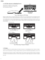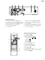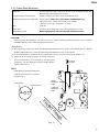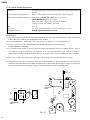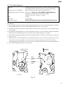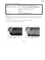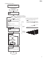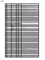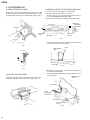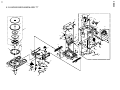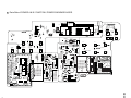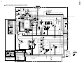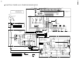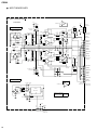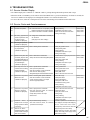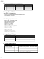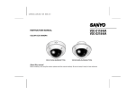
1
Service Manual
Model
CR200
Compact Disc Recorder
DANGER - LASER RADIATION WHEN OPEN.
AVOID DIRECT EXPOSURE TO BEAM.
CAUTION:
CAUTION
TO PREVENT ELECTRIC SHOCK, MATCH
RISK OF ELECTRIC SHOCK
DO NOT OPEN
WIDE BLADE OF PLUG TO WIDE SLOT,
FULLY INSERT.
ATTENTION:
CAUTION: TO REDUCE THE RISK OF ELECTRIC SHOCK,
POUR ÉVITER LES CHOCS ÉLECTRIQUES,
DO NOT REMOVE COVER (OR BACK).
INTRODUIRE LA LAME LA PLUS LARGE DE
NO USER-SERVICEABLE PARTS INSIDE.
LA FICHE DANS LA BORNE CORRESPONDANTE DE LA PRISE ET POUSSER
REFER SERVICING TO QUALIFIED SERVICE PERSONNEL.
JUSQU' AU FOND.
The lightening flash with arrowhead symbol,
within an equilateral triangle, is intended to
alert the user to the presence of uninsulated
“dangerous voltage” within the product's enclosure that may be of sufficient magnitude to
constitute a risk of electric shock to persons.
The exclamation point within an equilateral
triangle is intended to alert the user to the
presence of important operating and maintenance (servicing) instructions in the literature
accompanying the appliance.
“WARNING”
“TO REDUCE THE RISK OF FIRE OR ELECTRIC SHOCK,
DO NOT EXPOSE THIS APPLIANCE TO RAIN OR MOISTURE.”
SAFETY INSTRUCTIONS
1.
2.
3.
4.
5.
6.
Read instructions - All the safety and operating instructions should be read before the appliance is operated.
Retain instructions - The safety and operating instructions
should be retained for future reference.
Heed warnings - All warnings on the appliance and in the
operating instructions should be adhered to.
Follow instructions - All operating and use instructions
should be followed.
Water and Moisture - The appliance should not be used
near water - for example, near a bathtub, washbowl,
kitchen sink, laundry tub, in a wet basement, or near a
swimming pool, and the like.
Carts and Stands - The appliance should be used only
with a cart or stand that is recommended by the manufacturer.
9.
10.
11.
12.
13.
14.
15.
7.
8.
An appliance and cart combination should be moved with
care. Quick stops, excessive force, and uneven surfaces
may cause the appliance and cart combination to overturn.
Wall or Ceiling Mounting - The appliance should be
mounted to a wall or ceiling only as recommended by the
manufacturer.
Ventilation - The appliance should be situated so that its
location or position does not interfere with its proper ventilation. For example, the appliance should not be situated on a bed, sofa, rug, or similar surface that may block
the ventilation openings; or, placed in a built-in installation, such as a bookcase or cabinet that may impede the
flow of air through the ventilation openings.
16.
17.
Heat - The appliance should be situated away from heat
sources such as radiators, heat registers, stoves, or other
appliances (including amplifiers) that produce heat.
Power Sources - The appliance should be connected to a
power supply only of the type described in the operating
instructions or as marked on the appliance.
Grounding or Polarization - The precautions that should
be taken so that the grounding or polarization means of
an appliance is not defeated.
Power Cord Protection - Power supply cords should be
routed so that they are not likely to be walked on or
pinched by items placed upon or against them, paying
particular attention to cords at plugs, convenience receptacles, and the point where they exit from the appliance.
Cleaning - The appliance should be cleaned only as recommended by the manufacturer.
Nonuse Periods - The power cord of the appliance should
be unplugged from the outlet when left unused for a long
period of time.
Object and Liquid Entry - Care should be taken so that
objects do not fall and liquids are not spilled into the enclosure through openings.
Damage requiring Service - The appliance should be serviced by qualified service personnel when:
A. The power supply cord or the plug has been damaged;
or
B. Objects have fallen, or liquid has been spilled into the
appliance; or
C. The appliance has been exposed to rain; or
D. The appliance does not appear to operate normally or
exhibits a marked changed in performance; or
E. The appliance has been dropped, or the enclosure
damaged.
Servicing - The user should not attempt to service the appliance beyond that described in the operating instructions. All other servicing should be referred to qualified
service personnel.
CR200
TABLE OF CONTENTS
1. CD-R THEORY . . . . . . . . . . . . . . . . . . . . . . . . . . . . . . . . . . . . . . . 4
2. SPECIFICATIONS . . . . . . . . . . . . . . . . . . . . . . . . . . . . . . . . . . . . . . . 7
3. CONTROLS, INDICATORS & CONNECTORS . . . . . . . . . . . . . . . . . 10
4. ADJUSTING PROCEDURES . . . . . . . . . . . . . . . . . . . . . . . . . . . . . 12
5. ADDITIONAL INFORMATION . . . . . . . . . . . . . . . . . . . . . . . . 39
6. EXPLODED VIEW, PCB ASSEMBLY & PARTS LIST . . . . . . . . 65
7. CIRCUIT & BLOCK DIAGRAMS. . . . . . . . . . . . . . . . . . . . . . . . . 77
8. TROUBLESHOOTING . . . . . . . . . . . . . . . . . . . . . . . . . . . . . . 85
NOTES
* Adjusting procedures are given in this manual which also includes a Parts List and circuit diagrams to
assist the service technician in maintaining the Model CR200.
* The following accessory is supplied with CR200 as a standard.
Owner's manual, CR200
Remote control unit Model 8317
Audio cable (L : 1.2m)
Power cable
: 8288407000 (for export model)
: 8270829000
: 8276912000
: 8276910000 (for USA model)
: 8276911000 (for EUR model)
* Following is the packing material for the Model CR200.
Carton, inner, CR200
: 8228718000
Carton, outer, CR200
: 8228897000
Packing, L, CR200
: 8228443000
Packing, R, CR200
: 8228444000
CAUTION
! Parts marked with this sign are safety critical components. They must always be replaced with identical
components. Refer to the Fostex Parts List and ensure exact replacement.
3
CR200
1. CD-R THEORY
Φ120
max Φ118
Φ44.7
1-1. Physical layout compared to CD
min Φ33
The conventional CD and CD-R discs basically have the same
physical layout. However, as you can see from the Fig. 1,
comparing to the conventional CD, the CD-R disc also has socalled “minus” areas such as PCA (Power Calibration Area) and
PMA (Program Memory Area) where the temporary information
is recorded.
min Φ26
Φ15
Center
hole
Clamping
area
Information area
Pregroove area with address (ATIP)
Layout of unrecorded CD-R disc
max Φ118
• Unrecorded, blank disc
The information area is located next to the clamping area and the
center hole. This area contains a pregroove with CLV (Constant
Linear Velocity) clocking information and a time code.
max Φ116
Φ50
recorded
part
Φ46
Φ44.7
MUSIC
• Partially recorded disc
The CD-R system gives the opportunity to record a disc in several
actions at a different time on a different recorder. After the first
recording, the information area is divided into five parts as shown
below and in the right.
1: Power Calibration Area (PCA)
2: Program Memory Area (PMA)
3: Lead-in Area
4: Program Area
5: Lead-out Area
• Finalized disc
After finalizing the disc, the CD-R disc will become compatible
with the RED Book (for regular CD) definitions and specifications.
Therefore, it can be played back on conventional CD players. The
Information Area of a finalized disc consists of three parts:
1: Lead-In Area
2: Program Area
3: Lead-Out Area
PCA
PMA
temporary
Table Of Contents (TOC)
Program
Area
Recordable
User Area
+ Lead-out Area
Lead-in Area
Layout of partially recorded CD-R disc
max Φ118
max Φ116
Φ50
recorded part
Φ46
MUSIC
Lead-in Area
final Table of Contents (TOC)
Program Area Lead-out
Area
Layout of recorded CD-R disc
max Φ118
max Φ116
Φ50
recorded part
Φ46
MUSIC
TOC
Layout of conventional CD disc
Lead-out
Area
Fig. 1 Cross Section of CD-R & CD Disc
4
CR200
1-2. Pregrooved track wobbling + ATIP
When manufacturing the CD-R disc, it has been ÒpregroovedÓ. This pregroove in the CD-R disc is not a perfect spiral but
is wobbled so that the CD-R disc can be recognized by a CD-R recorder even when it is completely blank.
It has many purposes. It not only helps keep the servo on an exact tracking of outgoing spiral but also the demodulated
wobbling frequency contains the time information in digital format (21.05 kHz = Ò0Ó, 23.05 kHz = Ò1Ó). These frequencies
have been selected so that the mean frequency is equal to Fs / 2 (= 22.05 kHz). Also the interleaved is the manufacturer's
measured default laser power level.
0.6µm
(track width)
1.6µm
(track distance)
22.05 ± 1kHz = ~ 60µm
Fig. 2 Structure of Pregrooved Disc
1-3. PCA + consequence
Each recorder has a tolerance in the laser power and the dye from different manufacturers varies. In order to optimize the
recorder / disc combination, there is a PCA (Power Calibration Area) included in the CD-R disk. This area consists of two
parts, the Count Area and Test Area. In the Test Area, test recordings are made, stepping through several power levels. After
playing back the recorded test signal, the optimum level is automatically determined. This value is memorized until the disk
tray is opened. The Count Area keeps the track on how many of the test areas have been used indicating where to start the
next test. The PCA is designed to accommodate for 100 tests. When the PCA is full, the default value written in the wobbled
groove is used instead.
PCA
Test Area
Partition
100 98
PMA
Count Area
4 3 2 1
98
5
3
Lead In
Area
1
Fig. 3 Organization of PCA, PMA and Lead-In Area
CAUTION :
Every time the CD-R disc is inserted, one test is performed. Also if you leave the disc in the recorder at power off, a test will
be performed when powering on. This might lead to the situation that the PCA might be fully used up even if there is a
remaining space to record audio signal. The recordings made after the PCA is fully used up will not be optimal in performance.
5
CR200
1-4. CD-R Disc Structure and Bubbling Process
The materials of CD-R disc consists of label,
protective layer, reflective layer, organic dye
layer and transparent substrate.
Label
UV protective layer
123456789012345678901234567890121234567890123456
123456789012345678901234567890121234567890123456
123456789012345678901234567890121234567890123456
123456789012345678901234567890121234567890123456
Refective layer
123456789012345678901234567890121234567890123456
Organic dye layer
Transparent
substrate
Land
Groove
Laser beam
Fig. 4 Cross Section of CD-R disc
During recording, the laser is tracing the wobbled groove. When a pit is to be recorded, the laser fires off a high power beam
and the organic dye will become black and deformed. This is the way a Ònon-reflectiveÓ part is created. When a groove is
to be recorded, the laser is not fired and the high-reflective surface is maintained. If the data word contains successive the
same information (e.g. 111 or 000), the pit will be continuous. When the data word contains changes, the pit - groove status
will also change.
• Recording Principle
A high power laser beam is shot.
• Playback Principle
NO PITS
A low power laser beam is shot
and high reflectance is obtained.
Organic dye becomes black
and pit is created.
ON PITS
A low power laser beam is shot
and only low reflectance is obtained.
Fig. 5 Recording & Playback Principle
1-5. Finalize
In order to be playable on an ordinal CD-player, the CD-R disc must have a corresponding data for TOC (Table Of Contents).
This area is not used until all the recording is completed. Instead, a special area called PMA (Program Memory Area) is used.
When the disk is full or all the recording is completed, the disk can be finalized. This means that the temporary information
in the PMA is checked and transferred to TOC. Now the disk is playable on an ordinal CD player but it will not be recordable
any more.
6
CR200
2. SPECIFICATIONS
FUNCTIONS
Sampling rate converter
Automatic disk distinction
Time display switching
Synchronous to one song / All songs / DAT ID
REC mute
Automatic power calibration
Automatic track increment
Manual track increment
Automatic REC PAUSE
Previous
Fader in / fader out
Disk remaining time display
Sampling monitor
Skip play
Track skip on / off
One song / all songs program repeat
Program play
Manual search
Track search
Direct search
Program setting / clear
Input sensitivity switch
Infra-red remote controller on / off switch
Digital out on / off switch
Copy bit setting switch
Fs : 48 kHz / 32 kHz → 44.1 kHz
End section of previous track can be reproduced during REC
PAUSE mode.
Can be controlled only by infra-red remote controller
Can be controlled only by main unit key
Can be controlled only by infra-red remote controller
Can be controlled only by infra-red remote controller
Can be controlled only by infra-red remote controller
SW 1 (+4 dBu / -8 dBu, rear panel)
SW 2 (rear panel)
SW 2 (rear panel)
SW 2 (No restriction / One time only / Prohibited, rear panel)
FL DISPLAY CONTENTS
PLAY
REC
PAUSE
REPEAT
1-REPEAT
AUTO TRACK No.
PROGRAM
TOC
Level meter
Track number
Input sampling frequency
Elapsed time
Remaining time
Total time
Remaining record time
7
CR200
GENERAL
Model
Applicable discs
Number of channels
Power supply
Power consumption
Weight (without package)
Maximum dimensions
AUDIO UNIT
Playback (CD)
Frequency characteristics
S/N
Dynamic range
Total harmonic distortion
Channel separation
De-emphasis deviation
Level difference between channels
Output voltage
Monitoring (analog RCA pin input)
Frequency characteristics
S/N
Dynamic range
Total harmonic distortion
Maximum input level
Minimum input level
Record & Playback (analog RCA pin input)
Frequency characteristics
S/N
Dynamic range
Total harmonic distortion
Monitoring (Digital coaxial input)
Frequency characteristics
S/N
Dynamic range
Total harmonic distortion
Maximum input level
Minimum input level
Record & Playback (Digital coaxial input)
Frequency characteristics
S/N
Dynamic range
Total harmonic distortion
8
Compact disc recorder
CDs and CD-Rs
2 channels (stereo)
AC 120 V, 60 Hz
AC 220 ~ 230 V, 50 / 60 Hz
21 W
6.2 kg / 13.7 lbs
482 (W) x 134 (H) x 294 (D) mm
18-31/32 (W) x 5-9/32 (H) x 11-9/16 (D) inch
4 Hz ~ 20 kHz ± 1.0 dB
83 dB or more (EIAJ)
83 dB or more (EIAJ)
0.01 % or less (EIAJ)
90 dB or more (EIAJ)
0 ± 1.5 dB or less (EIAJ)
1.0 dB or less (EIAJ)
2.4 V ± 0.3 V rms
4 Hz ~ 20 kHz ± 1.0 dB
83 dB or more (EIAJ)
83 dB or more (EIAJ)
0.01 % or less (EIAJ)
3.2 V rms or more
0.4 V rms or less
4 Hz ~ 20 kHz ± 1.0 dB
83 dB or more (EIAJ)
83 dB or more (EIAJ)
0.01 % or less (EIAJ)
4 Hz ~ 20 kHz ± 1.0 dB
95 dB or more (EIAJ)
90 dB or more (EIAJ)
0.01 % or less (EIAJ)
0.6 V rms or more
0.2 V rms or less
4 Hz ~ 20 kHz ± 1.0 dB
90 dB (analog) / 105 dB (digital)
90 dB (analog) / 95 dB (digital)
0.01 % (analog) / 0.003 % (digital)
CR200
INPUT / OUTPUT JACKS
Analog Input
XLR-3-31 type (x 2)
Standard input level
Input impedance
RCA type (x 2)
Standard input level
Input impedance
Analog Output (x 2)
RCA type
Standard output level
Load impedance
Digital Input
XLR-3-31 type
RCA type
Optical type
Digital Output
RCA type
Optical type
Parallel remote
+4 dBu / -10 dBV (switchable)
10 k½
-10 dBV
27 k½ or more
-10 dBV
10 k½
IEC958 Part 2 (AES/EBU)
IEC958 Part 3 (S/P DIF)
IEC958 Part 3 (S/P DIF)
IEC958 Part 3 (S/P DIF)
IEC958 Part 3 (S/P DIF)
DIN 8-pin connector (Outer shell is grounded.)
Pin 1 : PAUSE
Pin 2 :
Pin 3 : PLAY
Pin 4 : NC
Pin 5 : Manual track write
Pin 6 : REC
Pin 7 :
Pin 8 : STOP
9
CR200
3. CONTROLS, INDICATORS & CONNECTORS
25
24
23
22
21
20 19
18 17
16
CR200 COMPACT DISC RECORDER
TRACK
MIN
REC BALANCE
SEC
REC LEVEL
RECORD
REC MUTE
15
SKIP
SET
TRACK NO.
L
COPY BIT
R
MIN
CLEAR
SKIP PLAY
ON/OFF
MAX
14
PHONES LEVEL
(MANUAL)
1
AUTO/MANUAL
WRITE
13
TIME
POWER
MIN
MAX
PHONES
2
INPUT
SELECTOR
DIGITAL
SYNCHRO
FINALIZE
3
4
5
6
7
8
9
10
11
12
< Front Panel Section >
1.
2.
3.
4.
5.
6.
7.
8.
9.
10.
11.
12.
13.
10
Power indicator
Power switch [POWER]
Input selector button [INPUT SELECTOR]
Digital synchro button [DIGITAL SYNCHRO]
Finalize button [FINALIZE]
Time button [TIME]
Disc tray
Stop button [ ]
Open/close button [ ]
Pause button [ ]
Play button [ ]
Headphone jack [PHONES]
Headphone level control [PHONES LEVEL]
14.
15.
16.
17.
18.
19.
20.
21.
22.
23.
24.
25.
Skip play on/off switch [SKIP PLAY ON/OFF]
Record muting button [REC MUTE]
Record indicator
Record button [RECORD]
Track skip buttons [SKIP SET, CLEAR]
Record level control [REC LEVEL]
Track search buttons [
][
]
Record balance control [REC BALANCE]
Display panel
Remote control sensor
Copy bit indicator [COPY BIT]
Track no. write button
[TRACK NO. AUTO/MANUAL, WRITE]
CR200
26
IN
R
29
28
27
OUT
IN
30
31
OUT
L
R
L
AC IN
OPTICAL
COAXIAL
IEC 958
DIGITAL IN/OUT
LINE IN
LINE OUT
SW 1
R
L
PUSH HEAR
PUSH HEAR
PUSH HEAR
1 2 3
AES/EBU
DIGITAL IN
SIGNAL GND
ON
BALANCE IN
1 2 3 4
OFF
ON
DIGITAL OUT
36
37
PARALLEL
REMOTE
SW 2
34
35
32
33
< Rear Panel Section >
26.
27.
28.
29.
30.
31.
Analog line input connectors [LINE IN L, R]
Digital input/output connectors [OPTICAL IN, OUT]
Digital input/output connectors [COAXIAL IN, OUT]
Analog line output connectors [LINE OUT]
GND terminal [SIGNAL GND]
AC inlet [AC IN]
32.
33.
34.
35.
36.
37.
Parallel remote connector [PARALLEL REMOTE]
Digital input connector [AES/EBU DIGITAL IN]
Dip switch [SW 2]
Digital out on/off switch [DIGITAL OUT OFF/ON]
Analog balanced input connectors [BALANCE IN]
Input select switch [SW 1]
< Remote Controller Section >
MODEL 8317
48
REC
FADER
47
TRACK NO.
WRITE
46
38
REPEAT
39
40
41
1
2
3
4
5
6
7
8
9
10
10
TIME
45
PGM
42
CHECK
CLEAR
44
43
38. Fader button [FADER]
39. Repeat button [REPEAT]
40. Manual search buttons [
][
]
Track search buttons [
][
]
Stop button [ ]
Pause button [ ]
Play button [ ]
41. Numeric buttons [1 to 10, >10]
42. Program button [PGM]
43. Program check button [CHECK]
44. Program clear button [CLEAR]
45. Time button [TIME]
46. Record muting button [ ]
47. Manual track no. write button [TRACK NO. WRITE]
48. Record button [ REC]
11
CR200
4. ADJUSTING PROCEDURES
4-1. ADJUSTING PROCEDURES
Even if nothing is wrong with the pickup section and hardware components in the circuits, due to the misalignment of
various adjustments, there is a possibility that the CR200 does not work properly or at all. According to the following
procedures, make adjustments correctly.
Test equipment and adjusting tools
• Dual trace oscilloscope, 100MHz or higher bandwidth
• Sinewave signal generator
• Test disk: TCD-785 (Almedio) and STD-R03 (Pioneer)
• Low pass filter
15k½ + 0.001µF x 2 pcs.
39k½ + 0.001µF x 1 pc.
• High pass filter
3.9k½ + 180pF x 1 pc.
• Resistor
100k½
• Hex wrench: 1.27mm diagonal
• Regular tools such as a pair of tweezers, cutter, long-nose pliers and minus screw driver
• Ceramic screw driver. Vessel 9000 series are recommended.
• Digital multimeter (measuring voltage: less than 1mV)
Table of adjusting item / test point / pot
Adjustment 1
No.
1
2
3
12
Item
Playback power adjustment
Coarse focus offset adjustment
Coarse skew adjustment
Test Point
CN104 Pin-7 (PWAJT)
CN204 Pin-1 (RF)
CN204 Pin-1 (RF)
4
5
6
7
Coarse grating adjustment
DPP (tracking offset) adjustment
Fine focus offset adjustment
Fine skew adjustment
CN104 Pin-3 (TE)
CN104 Pin-3 (TE)
CN204 Pin-1 (RF)
CN204 Pin-1 (RF)
8
Grating readjustment
CN104 Pin-3 (TE)
Pot
VR103 (PB. PW)
VR105 (FE. OFS)
Radial adjustment screw
Tangential adjusting screw
Grating adjustment screw
VR112 (TE. OFS)
VR105 (FE. OFS)
Radial adjustment screw
Tangential adjusting screw
Grating adjustment screw
CR200
Adjustment 2
No.
1
2
3
Item
CD-R VCO control voltage adjustment
Multi pulse time adjustment
EFM rising edge time adjustment
4
3T rising edge time adjustment
5
6
7
8
9
10
WBL + offset adjustment
Coarse WBL offset adjustment
RF offset adjustment
Playback power readjustment
Coarse focus offset adjustment
Main and sub mix ratio adjustment
11
Tracking amp. gain adjustment
Test Point
CN331 Pin-1 (VCOIN)
CN3506 Pin-6 (MPLS)
CN3506 Pin-5 (EFMIN)
CN3506 Pin-4 (SEFM)
CN3506 Pin-3 (3TIN)
CN3506 Pin-2 (3TOUT)
CN104 Pin-6 (RWBL)
CN104 Pin-5 (WBL)
CN204 Pin-1 (RF)
CN104 Pin-7 (PWAJT)
CN204 Pin-1 (RF)
CN104 Pin-1 (STE)
CN104 Pin-2 (MSTE)
CN104 Pin-3 (TE)
Pot
VR301 (VCO CON)
VR3501 (MPLS DLY)
VR3502 (EFM DLY)
VR3503 (3T DLY)
VR107 (WBL+. OFS)
VR108 (WBL. OFS)
VR121 (RF. OFS)
VR103 (PB. PW)
VR105 (FE. OFS)
VR110 (MS. MIX)
VR111 (TE. GAIN)
SERVO UCOM BOARD ASSY
STRATEGY BOARD ASSY
1
CN5021
1. ACT ERR
2. ACT IN
3. V+5A
3
1
CN3506
1 2
CN5021
CN331
TP30
VR201
FCS. GAIN
123
123
123
123
123
VR3502
EFM DLY
VR3501
MPLS DLY
TEST
MODE
123
123
123
123
123
CN331
1. VCOIN
2. GND
VR3503
VR301
3T.
DLY
VCO CON
VR202
TE. GAIN
Shorten the two lands
to put the CR200 into
the TEST MODE.
6
CN3506
1. DGND
2. 3T OUT
3. 3T IN
4. SEFM
5. EFM IN
6. MPLS
6
CN204
ADJUST TP
1
CN204
1. RF
2. TRKER
3. TRKIN
4. A GND
5. FCSIN
6. FCSER
Fig. 7
Fig. 6
13
CR200
Adjustment 2 (continued)
No.
12
13
14
15
16
17
18
19
20
21
Item
Tracking offset adjustment
ACT offset adfjustment
ACT gain adjustment
Fine focus offset adjustment
WBL balance adjustment
Fine WBL offset adjustment
WBL focus offset adjustment
Recording power adjustment
HF amp. gain adjustmnet
Focus servo loop gain adjustment
22
Tracking servo loop gain adjustment
Test Point
CN104 Pin-3 (TE)
CN5021 Pin-1 (ACT ERR)
CN5021 Pin-1 (ACT ERR)
CN204 Pin-1 (RF)
CN104 Pin-5 (WBL)
CN104 Pin-5 (WBL)
CN104 Pin-5 (WBL)
CN104 Pin-7 (PWAJT)
CN104 Pin-8 (HF)
CN204 Pin-5 (FCSIN)
CN204 Pin-6 (FCSER)
CN204 Pin-2 (TRKER)
CN204 Pin-3 (TRKIN)
Pot
VR112 (TE. OFS)
VR1 (ACT. OFS)
VR10 (ACT. GAIN)
VR105 (FE. OFS)
VR106 (WBL. BALANCE)
VR108 (WBL. OFS)
VR115 (WFE. OFS)
VR104 (REC. PW)
VR119 (HF. GAIN)
VR201 (FCS. GAIN)
VR202 (TE. GAIN)
VR103
PB. PW
VR10
ACT. GAIN
HEAD BOARD ASSY
VR110
MS. MIX
VR112
TE. OFS
VR111
TE. GAIN
VR119
HF GAIN
VR121
RF. OFS
VR106
WBL BALANCE
VR105
FE. OFS
VR115
WFE. OFS
VR104
REC. PW
VR108
WBL. OFS
Fig. 8
14
VR107
WBL+. OFS
CN104
VR1
ACT. OFS
1. STE
2. MSTE
3. TE
4. A GND
5. WBL
6. RWBL
7. PWAJT
8. HF
CR200
Notes
(1) Use a 10 : 1 probe for the oscilloscope.
(2) All the knob positions (settings) for the oscilloscope in the adjustment procedures are for when a 10 : 1 probe is used.
Test Mode
This model has a test mode so that the adjustments and checking required for servicing can be carried out easily.
When this model is put into test mode, the keys on the front panel would work differently from normal condition.
Adjustments and checks can be carried out by operating these keys with the correct procedures. On this model, all
adjustments are carried out in test mode.
[ Setting to Test Mode ]
The way to set this model into test mode.
(1) Plug the power cord back into the AC socket.
(2) Shorten the test mode lands. (See Fig. 6.)
(3) Press the Power SW ON.
When the test mode is set correctly, the display is different from what it usually is when the power is turned on. (lights up
all FL display) If the display is still the same as usual, test mode has not been set correctly, so repeat Steps 1 Ð 3.
[ Release from Test Mode ]
Here is the procedure for releasing the test mode.
(1) Press the STOP key and stop all operations.
(2) Press the Power SW OFF.
[ Operations of the Keys in Test Mode ]
Code Key Name Function in Test Mode
DIGITAL
Playback laser diode ON
SYNCHRO
FINALIZE
PLAY
PAUSE
Explanation
Lights up the laser diode by playback power.
The laser diode is lit up and the focus actuator is lowered,
then raised slowly and the focus servo is closed at the point
where the objective lens is focused on the disc.
With the player in this state, if you slightly rotate the stopped
disc by hand, you can hear the sound of focus servo. If you
Focus servo closes
can hear this sound, the focus servo is operating correctly.
If you press the key with no disc mounted, the laser diode
lights up, the focus actuator is pulled down, then the
actuator is raised and lowered three times and returned to
its original position.
Starts the spindle motor in the clockwise direction and when
the laser rotation reaches the prescribed speed (about 500
Spindle servo ON
rpm at the inner periphery), set the servo in a closed loop.
Pressing this key when the focus servo and spindle servo
are operating correctly in closed loops puts the tracking
servo into a closed loop, displays the track number being
played back and the elapsed time on the front panel.
Tracking servo close/open If the elapsed time is not displayed or not counted correctly,
it may be that something is out of adjustment, or that there is
some other problem.
This key is a toggle key and open/close the tracking servo
alternately. This key has no effect if no disc is mounted.
15
CR200
Code
•
•
Key Name
Function in Test Mode
Explanation
Moves the pickup position toward the inner diameter of the
disc. When this key is pressed with the tracking servo in a
closed loop, the tracking servo automatically goes into an
MANUAL/
Carriage reverse
open loop.
TRACK
(inwards)
Since the motor does not automatically stop at the
SEARCH REV
mechanical end point in test mode, be careful with this
operation.
Moves the pickup position toward the outer diameter of the
disc. When this key is pressed with the tracking servo in a
closed loop, the tracking servo automatically goes into an
MANUAL/
Carriage forward
open loop.
TRACK
(outwards)
Since the motor does not automatically stop at the
SEARCH FWD
mechanical end point in test mode, be careful with this
operation.
Initializes and the disc rotation stops.
STOP
The pickup and disc remain where they are when this key is
Stop
pressed.
Open/close the disc tray. This key is a toggle key and
open/close tray alternately.
Pressing this key when the disc is turning stops the disc,
OPEN/CLOSE Disc tray open/close
then opens the tray.
This key operation does not affect the position of the pickup.
Lights up the laser diode with maximum recording power and
RECORD
Maximum recording power normal EFM by pressing REC and REC MUTE keys in order.
* The laser diode may be damaged if adjustments are made
Laser diode ON
before pressing these keys.
REC MUTE
Switches the focus offset state.
AUTO/
Focus offset servo
COPY BIT LED Lights UP: C/N in the best condition
MANUAL
Lights OFF: Jitter in the best condition
Switches the ON/OFF of the optical axis servo.
Optical axis servo
WRITE
(MANUAL) LED Lights UP: Optical axis servo ON
switching
Light OFF: Optical axis servo OFF
When using the CD-R disc, search to the lead (0 min.
Search to the lead of disc.
TIME
0 sec.) of disc.
(It works only CD-R use.) (It doesn't work in CD disc use.)
[ How to Play Back a Disc in Test Mode ]
In test mode, each servo operates independently. Thus, it is required to press the keys and close the servo in a correct order
so that a disc can be played
Here is the key operation sequence for playing back a disc in test mode.
FINALIZE
Lights up the laser diode and closes the focus servo.
PLAY
Starts the spindle motor and closes the spindle servo.
PAUSE
Closes the tracking servo.
Wait at least 2 ~ 3 seconds between each of these operations.
16
CR200
4.2 Adjustment 1
4.2.1 Playback Power Adjustment
DANGER - LASER RADIATION WHEN OPEN.
AVOID DIRECT EXPOSURE TO BEAM.
• Objective
To optimize the playback power of the laser diode.
• Symptom when out of adjustment
Does not start playing, track search is impossible, tracks are skipped.
• Measurement instrument connections Multimeter to CN104, Pin-7 (PWAJT) (HEAD BOARD assy)
GND probe can be connected to CN104, Pin-4 (AGND).
• Disc
None needed
• Player state
Test mode, Playback laser diode ON
• Adjustment location
VR103 (PB. PW) (HEAD BOARD assy)
CAUTION:
(a) Perform this adjustment more than 5 minutes after starting up the test mode.
(b) This adjustment cannot be performed accurately if disc is inserted. Be sure to remove disc first before adjustments.
(c) If the specified voltage is not obtained by turning VR103, the pickup assy might be defective. Also be careful not to get
the pickup lens dirty.
[ Procedures ]
• When adjusting with the multimeter.
(1) Lights up the playback laser diode using the DIGITAL SYNCHRO key.
(2) Adjust the voltage value of Pin-7 (PWAJT) of CN104 (TP1) to the voltage value (PB PW voltage ± 5mV) displayed on
the pickup flexible cable using VR103 (PB PW).
• Reference: When adjusting with the optical power meter.
(1) Move the pickup to the outer edge of the disc with the MANUAL / TRACK SEARCH FWD key.
(2) Lights up the playback laser diode by the DIGITAL SYNCHRO key.
(3) Shine the light discharged from the objective lens in the pickup on the light power meter sensor. Adjust VR103 (PB.
PW) so that the playback laser diode output is an average 0.65 mW ± 0.05mW.
(Wavelength 790nm, Average mode)
P : Playback power
R : Recording power
Fig. 9
* Recording on the disc is not possible in test mode.
17
CR200
4.2.2 Coarse Focus Offset Adjustment
• Objective
To coarse adjust the DC offset voltage of the focus servo circuit to perform the
tracking and slider adjustments correctly.
• Symptom when out of adjustment
The unit does not focus in, sound is cracking and the RF signal is dirty.
• Measurement instrument connections Osciloscope to CN204, Pin-1 (RF) (SERVO UCOM BOARDassy)
GND probe can be connected to CN204, Pin-4 (AGND).
[ Settings ]: 20 mV/div., 2 mS/div., DC mode
• Disc
TCD-785
• Player state
Test mode, focus and spindle servos: closed, tracking servo: open
• Adjustment location
VR105 (FE. OFS) (HEAD BOARD assy)
[ Procedures ]
(1) Press the FINALIZE key and the PLAY key in the order to close the focus servo and then the spindle servo.
(2) Adjust VR105 (FE. OFS) so that the amplitude of waveform at CN204 (TP201), Pin-1 (RF) is maximum.
NOTE: The oscilloscope displays a moving image, not a ÒSTILLÓ image as shown below. In order to verify that the focus
servo is on, tap on the machine gently and listen to the sound indicating the servo operation.
Out of adjustment
Optimum adjustment
(Waveform amplitude is at maximum.)
Fig. 10
18
CR200
4.2.3 Coarse Skew Adjustment
• Objective
To coarse adjust the angle of pickup to the disc for performing the grating and
DPP (tracking offset) adjustments correctly.
• Symptom when out of adjustment
Sound is cracking, some discs can be played but not others.
• Measurement instrument connections Oscilloscope to CN204, Pin-1 (RF) (SERVO UCOM BOARD assy)
GND probe can be connected to CN204, Pin-4 (AGND).
[ Settings ]: 20 mV/div., 200 nS/div., AC mode
• Disc
TCD-785
• Player state
Test mode, focus and spindle servos: closed, tracking servo: open
• Adjustment location
Radial adjustment screw and tangential adjustment screw
CAUTION:
Before executing this adjustment, you must cut a few wire binders, disconnect cable and loosen 4 screws so that the
HEAD BOARD assy can be tilted up and fixed into the slits.
[ Procedures ]
(1) Move the pickup to the position where the radial/tangential adjustment screws will be seen with the MANUAL / TRACK
SEARCH FWD or REV keys so that the radial/tangential adjustment screws can be adjusted.
(2) Press the FINALIZE key and the PLAY key in the order to close the focus servo and then the spindle servo.
(3) Adjust the RAD (radial direction) and TAN (tangential
direction) adjustment screws alternately with hexagonal
screwdriver (1.27 mm diagonal) to maximize the RF output at
CN204 (TP201), Pin-1.
Hexagonal
screwdriver
NOTE:
Radial direction and tangential direction
mean the direction relative to the disc
shown in Fig. 11.
Radial
adjustment
screw
Radial direction
Tangential direction
Tangential
adjustment
screw
Disc
Fig. 2
FR
O
NT
PA
NE
L
Fig. 11
19
CR200
4.2.4 Coarse Grating Adjustment
• Objective
To align the tracking error generation laser beam spots to the optimum angle on
the track.
• Symptom when out of adjustment
Does not start playing, track search is impossible, tracks are skipped.
• Measurement instrument connections Oscilloscope to CN104, Pin-3 (TE) via a low pass filter.
(HEAD BOARD assy) See Fig. 14 below.
GND probe can be connected to CN104, Pin-4 (AGND).
[ Settings ]: 50 mV/div., 5 mS/div., DC mode
• Disc
TCD-785
• Player state
Test mode, focus and spindle servos: closed, tracking servo: open.
• Adjustment location
Grating adjustment screw in the slit
[ Procedures ]
(1) Move the pickup to the position where the grating adjustment slit will be seen with the MANUAL / TRACK SEARCH
FWD or REV keys so that the grating adjustment can be adjusted.
(2) Press the FINALIZE key and the PLAY key in the order to close the focus servo and then spindle servo.
(3) Insert a screwdriver into the grating adjustment slit and adjust the grating to find the null point.
For more details, see next page.
(4) If you slowly turn the screwdriver clockwise from the null point, the amplitude of the wave gradually increases. Then, if
you continue turning the screwdriver, the amplitude of the wave becomes smaller again. Turn the screwdriver
counterclockwise from the null point and set the grating to the first point where the wave amplitude reaches its maximum.
Reference : Fig. 13 shows the relation between the angle of the tracking beam with the track and the waveform.
(5) Return the pickup to more or less midway across disc with the MANUAL / TRACK SEARCH key. Then, press the
PAUSE key and check that the track number and elapsed time are displayed on the front panel. If they are not displayed
at this time or the elapsed time changes irregularly, check the null point and adjust the grating again.
Small
screwdriver
CN104
(TP1)
LPF
(10 : 1)
Grating
adjustment
screw
15kΩ
Pin 3
(TE)
0.001
µF
Pin 4
(AGND)
HEAD BOARD
ASSY
Fig. 3
Fig. 12
20
CR200
[ How to find the null point ]
When you insert the small screwdriver into the slit for the grating adjustment and change the grating angle, the amplitude
of the tracking error signal at CN104 (TP1), Pin 3 (TE) changes. Within the range for the grating, there are five or six
locations where the amplitude of the wave reaches a minimum. Of these five or six locations, there is only one at which
the envelope of the waveform is smooth. This location is where the three laser beams divided by the grating are all right
above the same track. (See Fig. 13.)
This point is called the null point. When adjusting the grating, this null point is found and used as the reference position.
Turning the grating counterclockwise
Turning the grating clockwise
Null point waveform
Maximum amplitude
waveform
Waveform other than the
null point
Note : If the difference between the amplitude of the error signal at the
innermost edge and outermost edge of the disc is more than 10%,
adjust the grating again.
Null point
Grating adjustment position
Waveform of
CN104 (TP1), Pin 3 (TE)
Fig. 4
Fig.
13
4.2.5 DPP (Tracking Offset) Adjustment
• Objective
To correct for the variation in the sensitivity of the tracking photodiode.
• Symptom when out of adjustment
The unit does not playback, track search is impossible, tracks are skipped.
• Measurement instrument connections Oscilloscope to CN104, Pin-3 (TE)
[This connection must be via a low pass filter (15kW + 0.001µF). ]
GND probe can be connected to CN104, Pin-4 (AGND).
[ Settings ]: 50 mV/div., 5 mS/div., DC mode
• Disc
TCD-785
• Player state
Test mode, focus and spindle servos: closed, tracking servo: open.
• Adjustment location
VR112 (TE. OFS) (HEAD BOARD assy)
[ Procedures ]
(1) Move the pickup to the midway across the disc (R = 35mm) with the MANUAL / TRACK SEARCH FWD or REV keys.
(2) Press the FINALIZE key and the PLAY key in the order to close the focus servo and then spindle servo.
(3) Line up the bright line (ground) at the center of the oscilloscope screen and put the oscilloscope into DC mode.
(4) Adjust VR112 (TE. OFS) so that the positive amplitude and negative amplitude of the tracking error signal at CN104,
Pin-3 (TE) are the same (in other words, so that there is no DC component).
A=B
A
A=B
A
GND
B
GND
B
When there is a DC
component
When there is no DC
component
Fig. 14
21
CR200
4.2.6 Fine Focus Offset Adjustment
• Objective
To optimize the DC offset voltage of the focus servo circuit.
• Symptom when out of adjustment
The unit does not focus in, sound is caracking and the RF signal is dirty.
• Measurement instrument connections Oscilloscope to CN204, Pin-1 (RF) (SERVO UCOM BOARD assy)
GND probe can be connected to CN204, Pin-4 (AGND).
[ Settings ]: 20 mV/div., 500 nS/div., AC mode
• Disc
TCD-785
• Player state
Test mode, play
• Adjustment location
VR105 (FE. OFS) (HEAD BOARD assy)
[ Procedures ]
(1) Move the pickup to midway across the disc (R = 35mm) with the MANUAL / TRACK SEARCH FWD or REV keys.
(2) Press the FINALIZE key, the PLAY key and the PAUSE key in the order to close the respective servos and put the player
into play mode.
(3) Adjust VR105 (FE. OFS) so that the 3T waveform at CN204, Pin-1 (RF) is maximum.
Out of adjustment
Optimum adjustment
Fig. 15
22
CR200
4.2.7 Fine Skew Adjustment
• Objective
To adjust the angle of the pickup relative to the disc so that the laser beams are
shone straight down into the disc for the best read out of the RF signals.
• Symptom when out of adjustment
Sound is cracking, some discs can be played but not others..
• Measurement instrument connections Oscilloscope to CN204, Pin-1 (RF) (SERVO UCOM BOARD assy)
GND probe can be connected to CN204, Pin-4 (AGND).
[ Settings ]: 20 mV/div., 200 nS/div., AC mode
• Disc
TCD-785
• Player state
Test mode, play
• Adjustment location
Pickup radial adjustment screw and tangential adjustment screw
[ Procedures ]
(1) Move the pickup to the position where the radial/tangential adjustment screws will be seen with the MANUAL / TRACK
SEARCH FWD or REV keys so that the radial/tangential adjustment screws can be adjusted.
(2) Press the FINALIZE key, the PLAY key and the PAUSE key in the order to close the respective servos and put the player
into play mode.
(3) First, adjust the radial adjustment screw with the hexagonal screwdriver (1.27 mm) so that the eye pattern (the diamond
shape at the center of the RF signal) can be seen the most clearly and the amplitude is at maximum..
(4) Next, adjust the tangential adjustment screw with the hexagonal screwdriver so that the eye pattern can be seen the most
clearly. (Fig. 17).
(5) Adjust in the order of the radial adjustment screw and the tangential screw again, so that the eye pattern can be seen the
most clearly. As necessary, adjust the two screws alternately so that the eye pattern can be seen the most clearly.
After the adjustment, remove the float screw, turn over the servo mechanism assembly, then secure the radial adjustment
(6) screw and the tangential adjustment screw with loc-tite.
Hexagonal
screwdriver
Stabilize each screw
with an adhesive.
Radial
adjustment
screw
Tangential
adjustment
screw
(Front side)
(Rear side)
Fig. 16
23
CR200
Out of adjustment
Optimum adjustment
Out of adjustment
Optimum
Out of
Out of
adjustment adjustment adjustment
Fig. 17
4.2.8 Grating Re-adjustment
Adjust in the same manner as "4.2.4 Coarse Grating Adjustment ".
4.3 Adjustment 2
4.3.1 CD-R VCO Control Voltage Adjustment
• Objective
To optimize the CD-R VCO control voltage adjustment of VCO IC.
• Symptom when out of adjustment
The unit does not record or playback CD-R discs.
• Measurement instrument connections Multimeter to CN331, Pin-1 (VCOIN) (STRATEGY BOARD assy)
GND probe can be connected to CN331, Pin-2 (GND).
• Disc
None needed
• Player state
Test mode, stop
• Adjustment location
VR301 (VCOIN) (STRATEGY BOARD assy)
[ Procedures ]
(1) Adjust VR301 (VCO CON) so that the voltage at Pin 1 (VCOIN) of CN331 (TP30) becomes 2.5 ± 0.1V.
24
CR200
4.3.2 Multi Pulse Time Adjustment
• Objective
Pulse adjustment for recording (1)
• Symptom when out of adjustment
The unit does not playback CD-R discs which was recorded with this player .
• Measurement instrument connections Oscilloscope to CN3506, Pin-6 (MPLS) (STRATEGY BOARD assy)
GND probe can be connected to CN3506, Pin-1 (DGND).
[ Settings ]: 1 V/div., 20 nS/div., DC mode
• Disc
None needed
• Player state
Test mode, stop
• Adjustment location
VR3501 (MPLS DLY) (STRATEGY BOARD assy)
[ Procedures ]
(1) Disconnect a connector CN3502 (white wires with green connector).
(2) Adjust the time from rising edge to falling edge of Waveform with 2V level.
(3) Adjust VR3501 (MPLS DLY) so that the DC voltage at CN3506 pin-6 (MPLS) becomes 70nS ± 3nS.
(4) Press the STOP key.
(5) Connect a connector CN3502.
2V
GND
70nS
±3nS
4.3.3 EFM Rising Edge Time Adjustment
• Objective
Pulse adjustment for recording (2)
• Symptom when out of adjustment
The unit does not playback CD-R discs which was recorded with this player .
• Measurement instrument connections Oscilloscope to
CH1 : CN3506, Pin-5 (EFM IN) (STRATEGY BOARD assy)
CH2 : CN3506, Pin-4 (SEFM) (STRATEGY BOARD assy)
GND probe can be connected to CN3506, Pin-1 (DGND).
[ Settings ]
CH1 : 1 V/div. DC mode, 20 nS/div.
CH2 : 1 V/div. DC mode
• Disc
None needed
• Player state
Test mode, recording power ON
• Adjustment location
VR3502 (EFM DLY) (STRATEGY BOARD assy)
[ Procedures ]
Disconnect a connector CN3502.
Turn VR104 (REC. PW) fully counterclockwise to reduce the power to minimum.
Press RECORD and REC MUTE keys in the order to lights up the laser diode.
Adjust the time from rising edge of CN3506 pin 5 to rising edge of pin 4 of waveform
at the 2V level.
(5) Adjust VR3502 (EFM DLY) so that the delay becomes 80nS ± 3nS.
CH1
CH2
(1)
(2)
(3)
(4)
2V
GND
80nS
±3nS
25
CR200
4.3.4 3T Rising Edge Time Adjustment
• Objective
Pulse adjustment for recording (3)
• Symptom when out of adjustment
The unit does not playback CD-R discs which was recorded with this player .
• Measurement instrument connections Oscilloscope to
CH1 : CN3506, Pin-3 (3T IN) (STRATEGY BOARD assy)
CH2 : CN3506, Pin-2 (3T OUT) (STRATEGY BOARD assy)
GND probe can be connected to CN3506, Pin-1 (DGND).
[ Settings ]
CH1 : 1 V/div., DC mode, 20 nS/div.
CH2 : 1 V/div., DC mode
• Disc
None needed
• Player state
Test mode, recording power ON
• Adjustment location
VR3503 (3T DLY) (STRATEGY BOARD assy)
[ Procedures ]
(1) Disconnect a connector CN3502.
(2) Turn VR104 (REC. PW) fully counterclockwise to reduce the power at minimum.
(3) Press the RECORD and the REC MUTE keys in the order to lights up the laser
diode.
(4) Adjust the time from rising edge of CN3506 pin-3 to rising edge of pin 2 of waveform
with 2V level.
(5) Adjust VR3503 (3T DLY) so that the delay becomes 42nS ± 3nS.
(6) Connect a connector CN3502.
CH1
CH2
2V
GND
42nS
±3nS
4.3.5 WBL+ Offset Adjustment
• Objective
To adjust the gain balance of the wobble signal.
• Symptom when out of adjustment
The unit does not record or playback CD-R discs.
• Measurement instrument connections Oscilloscope to CN104, Pin-6 (RWBL) (HEAD BOARD assy)
GND probe can be connected to CN104, Pin-4 (AGND).
[ Settings ]: 1 mV/div., 5 mS/div., DC mode
• Disc
None needed
• Player state
Test mode, stop
• Adjustment location
VR107 (WBL+. OFS) (HEAD BOARD assy)
[ Procedures ]
(1) Turn VR108 (WBL. OFS) to fully counterclockwise.
(2) Adjust VR107 (WBL+. OFS) so that the DC voltage at CN104 (TP1), Pin-6 (RWBL) is Ð20mV ± 10mV.
26
CR200
4.3.6 Coarse WBL Offset Adjustment
• Objective
To optimize the DC offset voltage of the wobble amp.
• Symptom when out of adjustment
The unit does not record or playback CD-R discs.
• Measurement instrument connections Oscilloscope to CN104, Pin-5 (WBL) (HEAD BOARD assy)
GND probe can be connected to CN104, Pin-4 (AGND).
[ Settings ]: 1 mV/div., 5 mS/div., DC mode
• Disc
None needed
• Player state
Test mode, stop
• Adjustment location
VR108 (WBL. OFS) (HEAD BOARD assy)
[ Procedures ]
(1) Adjust VR108 (WBL. OFS) so that the DC voltage at Pin 5 (WBL) of CN104 (TP1) becomes 0 ± 10mV.
4.3.7 RF Offset Adjustment
• Objective
To optimize the DC offset voltage of the RF amp.
• Symptom when out of adjustment
The unit does not playback..
• Measurement instrument connections Oscilloscope to CN204, Pin-1 (RF) (SERVO UCOM BOARD assy)
GND probe can be connected to CN204, Pin-4 (AGND).
[ Settings ]: 1 mV/div., 5 mS/div., DC mode
• Disc
None needed
• Player state
Test mode, stop
• Adjustment location
VR121 (RF. OFS) (HEAD BOARD assy)
[ Procedures ]
(1) Adjust VR121 (RF. OFS) so that the DC voltage at Pin 1 (RF) of CN204 (TP201) becomes 0 ± 10mV.
4.3.8 Playback Power Re-adjustment
[ Procedures ]
(1) Adjust in the same manner as "4.2.1. Playback Power Adjustment " in Adjustment 1.
27
CR200
4.3.9 Coarse Focus Offset Adjustment
• Objective
To optimize the DC offset voltage of the focus error amp.
• Symptom when out of adjustment
The unit does not focus in and the RF signal is dirty.
• Measurement instrument connections Oscilloscope to CN204, Pin-1 (RF) (SERVO UCOM BOARD assy)
GND probe can be connected to CN204, Pin-4 (AGND).
[ Settings ]: 20 mV/div., 2 mS/div., DC mode
• Disc
TCD-785
• Player state
Test mode, focus and spindle servos: closed, tracking servo: open
• Adjustment location
VR105 (FE. OFS) (HEAD BOARD assy)
[ Procedures ]
(1) Press the FINALIZE key and the PLAY key in the order to close the focus servo and then the spindle servo.
(2) Adjust VR105 (FE. OFS) so that the amplitude of RF signal at CN204, Pin-1 (RF) is maximum.
Optimum adjustment
Out of adjustment
Fig. 18
4.3.10 Main and Sub Mix Ratio Adjustment
• Objective
To mix the gain of the main signal output and sub signal output of the pickup.
• Symptom when out of adjustment
The unit does not playback.
• Measurement instrument connections Oscilloscope to
CH1: CN104, Pin-1 (STE) (HEAD BOARD assy)
CH2: CN104, Pin-2 (MSTE) (HEAD BOARD assy)
[These connections must be via low pass filters. ]
GND probe can be connected to CN104, Pin-4 (AGND).
[ Settings ]
CH1 : 50 mV/div. AC mode
10 mS/div. ADD mode
CH2 : 100 mV/diV. AC mode
• Disc
TCD-785
• Player state
Test mode, focus and spindle servos: closed, tracking servo: open
• Adjustment location
VR110 (MS. MIX) (HEAD BOARD assy)
[ Procedures ]
(1) Press the FINALIZE key and the PLAY key in the order to close the focus servo and then the spindle servo.
(2) Set the oscilloscope to ADD mode (waveform adding mode of CH1 and CH2) and observe the adding waveform of CH1
and CH2.
(3) Adjust VR110 (MS. MIX) so that the amplitude of waveform becomes minimum.
28
CR200
4.3.11 Tracking Amp. Gain Adjustment
• Objective
To correct the discrepancy in the tracking error level with the pickup.
• Symptom when out of adjustment
The unit does not playback, track search is impossible, tracks are skipped.
• Measurement instrument connections Oscilloscope to CN104, Pin-3 (TE) (HEAD BOARD assy)
[The connection must be via a low pass filter (15k½ + 0.001µF). ]
GND probe can be connected to CN104, Pin-4 (AGND).
[ Settings ]: 20 mV/div., 5 mS/div.DC mode
• Disc
TCD-785
• Player state
Test mode, focus and spindle servos: closed, tracking servo: open
• Adjustment location
VR111 (TE. GAIN) (HEAD BOARD assy)
[ Procedures ]
(1) Move the pickup to midway across the disc (R = 35mm) with the MANUAL /
TRACK SEARCH FWD or REV keys.
(2) Press the FINALIZE key and the PLAY key in the order to close the focus servo
and then the spindle servo.
(3) Line up the bright line (ground) at the center of the oscilloscope screen and put
the oscilloscope into DC mode.
(4) Adjust VR111 (TE. GAIN) so that the positive amplitude and negative amplitude
of the tracking error signal at CN104 (TP1), Pin 3 (TE) is 1.0V ± 0.05V.
GND
1.0V ± 0.05V
4.3.12 Tracking Offset Adjustment
• Objective
To correct for the variation in the sensitivity of the tracking photodiode.
• Symptom when out of adjustment
The unit does not playback, track search is impossible, tracks are skipped.
• Measurement instrument connections Oscilloscope to CN104, Pin-3 (TE) (HEAD BOARD assy)
[ This connection must be via a low pass filter (15k½ + 0.001µF).]
GND probe can be connected to CN104, Pin-4 (AGND).
[ Settings ]: 20 mV/div., 5 mS/div., DC mode
• Disc
TCD-785
• Player state
Test mode, focus and spindle servos: closed, tracking servo: open
• Adjustment location
VR112 (TE. OFS) (HEAD BOARD assy)
[ Procedures ]
(1)
(2)
(3)
(4)
Move the pickup to midway across the disc (R = 35mm) with the MANUAL / TRACK SEARCH FWD or REV keys.
Press the FINALIZE key and the PLAY key in the order to close the focus servo and then the spindle servo.
Line up the bright line (ground) at the center of the oscilloscope screen and put the oscilloscope into DC mode.
Adjust VR112 (TE. OFS) so that the positive amplitude and negative amplitude of the tracking error signal at CN104,
Pin-3 (TE) are the same (in other words, so that there is no DC component).
Note : If the great offset is observed, perform the adjustments in the section 4.3.11 and 4.3.12.
A=B
A
A=B
A
GND
B
When there is a DC
component
GND
B
When there is no DC
component
29
CR200
4.3.13 ACT Offset Adjustment
• Objective
To optimize the DC offset voltage of the actuator servo.
• Symptom when out of adjustment
The unit does not pause, track search is impossible, tracks are skipped.
• Measurement instrument connections Oscilloscope to CN5021, Pin-1 (ACT ERR) (SERVO UCOM BOARD assy)
[ Settings ]: 5 mV/div, 5 mS/div., DC mode
• Disc
TCD-785
• Player state
Test mode, focus and spindle servos: closed, tracking servo: open
• Adjustment location
VR1 (ACT. OFS) (HEAD BOARD assy)
[ Procedures ]
(1) Move the pickup to midway across the disc (R = 35mm) with the MANUAL / TRACK SEARCH FWD or REV keys.
(2) Press the FINALIZE key and the PLAY key in the order to close the focus servo and then the spindle servo.
(3) Adjust VR1 (ACT. OFS) so that the DC voltage at CN5021 (TP00), Pin 1 (ACT ERR) is 0 ± 20mV.
4.3.14 ACT Gain Adjustment
• Objective
To optimize the actuator servo gain.
• Symptom when out of adjustment
The unit does not pause, track search is impossible, tracks are skipped.
• Measurement instrument connections Oscilloscope to CN5021, Pin-1 (ACT ERR) (SERVO UCOM BOARD assy)
[ Settings ]: 10 mV/div., 5 mS/div., DC mode
• Disc
TCD-785
• Player state
Test mode, focus and spindle servos: closed, tracking servo: open
• Adjustment location
VR10 (ACT. GAIN) (HEAD BOARD assy)
[ Procedures ]
(1) Move the pickup to midway across the disc (R = 35mm) with the MANUAL / TRACK SEARCH FWD or REV keys.
(2) Press the FINALIZE key and the PLAY key in the order to close the focus servo and then the spindle servo.
(3) Press the WRITE key to light up the WRITE KEY LED, and short-circuit the Pin-2 and Pin-3 of CN5021.
Adjust VR10 (ACT. GAIN) so that the DC voltage at CN5021 (TP00), Pin 1 (ACT ERR) is Ð380 ± 20mV.
Note : If the great offset is observed, perform the adjustments in the section 4.3.13 and 4.3.142.
30
CR200
4.3.15 Fine Focus Offset Adjustment
• Objective
To optimize the DC offset voltage of the focus servo circuit.
• Symptom when out of adjustment
The unit does not focus in, sound is cracking and the RF signal is dirty.
• Measurement instrument connections Oscilloscope to CN204, Pin-1 (RF) (SERVO UCOM BOARD assy)
GND probe can be connected to CN204, Pin-4 (AGND).
[ Settings ]: 20 mV/div., 500 nS/div., AC mode
• Disc
STD-R03
• Player state
Test mode, play
• Adjustment location
VR105 (FE. OFS) (HEAD BOARD assy)
[ Procedures ]
(1) Move the pickup to midway across the disc (R = 35mm) with the MANUAL / TRACK SEARCH FWD or REV keys.
(2) Press the FINALIZE key, the PLAY key and the PAUSE key in the order to close the respective servos and put the player
into play mode.
(3) Adjust VR105 (FE. OFS) so that the 3T waveform at CN204, Pin-1 (RF) is maximum.
Note : Adjust after confirming that the WRITE KEY LED is OFF.
Out of adjustment
Optimum adjustment
Fig. 19
31
CR200
4.3.16 WBL Balance Adjustment
• Objective
To adjust the gain balance of the wobble signal.
• Symptom when out of adjustment
The unit does not record or search or pause CD-R discs.
• Measurement instrument connections Oscilloscope to CN104, Pin-5 (WBL) (HEAD BOARD assy)
[ This connection must be via high-pass filter (180pF+3.9kΩ).]
GND probe can be connected to CN104, Pin-4 (AGND).
[ Settings ]: 5 mV/div., 20 µS/div., DC mode
• Disc
STD-R03
• Player state
Test mode, play
• Adjustment location
VR106 (WBL. BALANCE) (HEAD BOARD assy)
[ Procedures ]
(1) Move the pickup to midway across the disc (R = 35mm) with the MANUAL / TRACK SEARCH FWD or REV keys.
(2) Press the FINALIZE key, the PLAY key and the PAUSE key in the order to close the respective servos and put the player
into play mode.
(3) Adjust VR106 (WBL. BALANCE) so that the amplitude of waveform at CN104 (TP1), Pin 5 (WBL) is minimum.
Out of adjustment
Optimum adjustment
Fig. 20
32
CR200
4.3.17 Fine WBL Offset Adjustment
• Objective
To adjust the gain balance of the wobble signal.
• Symptom when out of adjustment
The unit does not record, search or pause CD-R discs.
• Measurement instrument connections Oscilloscope to CN104, Pin-5 (WBL) (HEAD BOARD assy)
[ This connection must be via high-pass filter (180pF+3.9kΩ).]
GND probe can be connected to CN104, Pin-4 (AGND).
[ Settings ]: 5 mV/div., 20 µS/div., DC mode
• Disc
STD-R03
• Player state
Test mode, play
• Adjustment location
VR108 (WBL. OFS) (HEAD BOARD assy)
[ Procedures ]
(1) Move the pickup to midway across the disc (R = 35mm) with the MANUAL / TRACK SEARCH FWD or REV keys.
(2) Press the FINALIZE key, the PLAY key and the PAUSE key in the order to close the respective servos and put the player
into play mode.
(3) Adjust VR108 (WBL. OFS) so that the amplitude of waveform at CN104, Pin-5 (WBL) is minimum.
Out of adjustment
Optimum adjustment
Fig. 21
33
CR200
4.3.18 WBL Focus Offset Adjustment
• Objective
To adjust the gain balance of the wobble signal.
• Symptom when out of adjustment
The unit does not record, search or pause CD-R discs.
• Measurement instrument connections Oscilloscope to CN104, Pin-5 (WBL) (HEAD BOARD assy)
[ This connection must be via high-pass filter (180pF+3.9k½).]
GND probe can be connected to CN104, Pin-4 (AGND).
[ Settings ]: 5 mV/div., 20 mS/div., DC mode
• Disc
STD-R03
• Player state
Test mode, play
• Adjustment location
VR115 (WFE. OFS) (HEAD BOARD assy)
[ Procedures ]
(1) Move the pickup to midway across the disc (R = 35mm) with the MANUAL / TRACK SEARCH FWD or REV keys.
(2) Press the FINALIZE key, the PLAY key and the PAUSE key in the order to close the respective servos and put the
CR200 into play mode.
(3) Press the AUTO/MANUAL key to light up the COPY BIT LED.
(4) Adjust VR115 (WFE. OFS) so that the amplitude of waveform at CN104, Pin-5 (WBL) is minimum.
Out of adjustment
Optimum adjustment
Fig. 22
34
CR200
4.3.19 Recording Power Adjustment
DANGER - LASER RADIATION WHEN OPEN.
AVOID DIRECT EXPOSURE TO BEAM.
• Objective
• Symptom when out of adjustment
To optimize the recording power of the laser diode.
The unit does not either record or playback self-recorded discs. It also skips
tracks and the RF waveform is dirty. (No problem shown during CD playback)
• Measurement instrument connections Multimeter to CN104, Pin-7 (PWAJT) (HEAD BOARD assy)
GND probe can be connected to CN104, Pin-4 (AGND).
• Disc
None needed
• Player state
Test mode, maximum recording power ON
• Adjustment location
VR104 (REC. PW) (HEAD BOARD assy)
CAUTION:
(a) Perform this adjustment more than 5 minutes after starting up the test mode.
(b) Power more than ten times greater than playback power is released during these adjustment. Never look directly at the
objective lens.
(c) This adjustment cannot be performed accurately if disc is inserted. Be sure to remove disc first before adjustments.
(d) The laser diode may be damaged if the recording power is greater than the specified value. Always perform the step 1
below before making adjustments and be careful not to exceed the adjustment value by more than 50mV from the
specified value in the step 3 below).
[ Procedures ]
• When Adjusting with the multimeter
(1) Fully turn VR104 (REC. PW) counterclockwise to reduce the power to the minimum.
(2) Press RECORD and REC MUTE keys in this order to lights up the laser diode.
(3) Adjust the voltage value of Pin 7 (PWAJT) of CN104 to the voltage value (REC. PW voltage ± 10mV) displayed on the
pickup flexible cable using VR104 (REC. PW).
• Reference: When adjusting with optical power meter
CAUTION:
(a) Perform this adjustment more than two minutes after starting up the test mode (after inserting the AC plug).
(b) The laser diode may be damaged if the recording power is greater than the specified value. Always perform step 1 before
making adjustments and be careful not to exceed the adjustment value by more than 0.3mW (specified value in step 3).
(c) Power more than ten times greater than playback power is released during this adjustment. Never look directly at the
objective lens.
35
CR200
[ Procedures ]
(1) Fully turn VR104 (REC. PW) counterclockwise to reduce the power to the minimum.
(2) Move the pickup to the outer edge of the disc with the MANUAL / TRACK SEARCH FWD key.
(3) Press RECORD and REC MUTE keys in that order to lights up the laser diode.
(4) Shine the light discharged from the objective lens in the pickup on the light power meter sensor and adjust VR104 (REC.
PW) so that the recording laser diode output is an average of 4.7mW ± 0.1mW (Wavelength 790nm, Average mode).
P : Playback Power
R : Recording Power
4.3.20 HF Amp. Gain Adjustment
• Objective
To correct the discrepancy in the HF level with the pickup.
• Symptom when out of adjustment
The unit does not record, track search is impossible.
• Measurement instrument connections Oscilloscope to CN104, Pin 8 (HF) (HEAD BOARD assy)
GND probe can be connected to CN104, Pin-4 (AGND).
[ Settings ]: 50 mV/div., 500 nS/div., DC mode
• Disc
TCD-785
• Player state
Test mode, play
• Adjustment location
VR119 (HF. GAIN) (HEAD BOARD assy)
[ Procedures ]
(1) Move the pickup to midway across the disc (R = 35mm) with the MANUAL / TRACK SEARCH FWD or REV keys.
(2) Press the FINALIZE key, the PLAY key and the PAUSE key in the order to close the respective servos and put the player
into play mode.
(3) Line up bright line (ground) at the center of the oscilloscope screen and put the oscilloscope into DC mode.
(4) Adjust VR119 (HF. GAIN) so that the amplitude of waveform at CN104 , Pin-8 (HF) is 2.0V ± 0.1V.
NOTE :
Adjust after checking that the COPY BIT LED is OFF.
2.0V ± 0.1V
Fig. 23
36
CR200
4.3.21 Focus Servo Loop Gain Adjustment
• Objective
To optimize the focus servo loop gain.
• Symptom when out of adjustment
Playback does not start or focus acutuator noisy.
• Measurement instrument connections Oscilliscope CH1 to CN204, Pin-5 (FCSIN) via 100k½ resistor
Oscilloscope CH2 to CN204, Pin-6 (FCSER)
(SERVO UCOM BOARD assy) See Fig.23 below.
[ Settings ]
CH1 : 0.1 V/div., X-Y mode
CH2 : 10 mV/div.
GND probe can be connected to CN204, Pin-4 (AGND).
• Disc
TCD-785
• Player state
Test mode, play
• Adjustment location
VR201 (FCS. GAIN) (SERVO UCOM BOARD assy)
[ Procedures ]
(1) Set the AF generator output to 1.4kHz and 1Vp-p.
(2) Move the pickup to midway across the disc (R = 35mm) with the MANUAL / TRACK SEARCH FWD or REV keys.
(3) Press the FINALIZE key, the PLAY key and the PAUSE key in the order to close the respective servos and put the player
into play mode.
(4) Adjust VR201 (FCS. GAIN) so that the lissajous waveform is symmetrical about X axis and the Y axis.
CN204
(TP201)
(10 : 1)
100kΩ
Pin 5 (FCSIN)
Pin 4 (AGND)
1.4kHz
1Vp-p
∼
X
Y
Pin 6 (FCSER)
(10 : 1)
Fig.
Fig. 24
6
Higher gain
Optimum gain
Lower gain
37
CR200
4.3.22 Tracking Servo Loop Gain Adjustment
• Objective
To optimize the tracking servo loop gain.
• Symptom when out of adjustment
The unit does not start, during searches the acutuator is noisy, or tracks are skipped.
• Measurement instrument connections Oscilliscope CH1 to CN204, Pin-3 (TRKIN) via 100k½ resistor
Oscilloscope CH2 to CN204, Pin-2 (TRKER)
(SERVO UCOM BOARD assy) See Fig.24 below.
[ Settings ]
CH1 : 0.1 V/div., X-Y mode
CH2 : 10 mV/div.
GND probe can be connected to CN204, Pin-4 (AGND).
• Disc
TCD-785
• Player state
Test mode, play
• Adjustment location
VR202 (TE. GAIN) (SERVO UCOM BOARD assy)
[ Procedures ]
(1) Set the AF generator output to 1.2kHz and 2Vp-p.
(2) Move the pickup to midway across the disc (R = 35mm) with the MANUAL / TRACK SEARCH FWD or REV keys.
(3) Press the FINALIZE key, the PLAY key and the PAUSE key in the order to close the respective servos and put the player
into play mode.
(4) Adjust VR202 (TE. GAIN) so that the lissajous waveform is symmetrical about X axis and the Y axis.
CN204
(TP201)
(10:1)
100kΩ
Pin 3 (TRKIN)
Pin 4 (AGND)
Pin 2 (TRKER)
1.2kHz
(10:1) 2Vp-p
∼
X
Y
39kΩ
0.001µF
Low pass filter
Fig. 7
Fig. 25
Higher gain
38
Optimum gain
Lower gain
CR200
5. ADDITIONAL INFORMATION
5-1. WAVEFORM AND VOLTAGES
HEAD BOARD ASSY
• Measuring condition: DC input unless otherwise noted.
2
CN111 pin 1 (EFM)
7
3
CN105 pin 4 (XSAMP)
6
Test mode
During maximum recording
power laser diode ON
2V/div 0.2µS/div
11
IC202 pin 7 (TRKCON)
2V/div 0.5mS/div
IC202 pin 1 (TD)
0.2V/div 0.5mS/div
10
During PLAY
CN106 pin 5 (SPDL)
1V/div 2mS/div
IC203 pin 4 (SPD MT)
2V/div 2mS/div
TP1 pin 5 (WBL)
15
CN105 pin 11 (WBL)
During CD-R PLAY
100mV/div 20µS/div
During PLAY
11
GND
7
14
2
GND
GND
GND
10
6
3
14
GND
15
GND
GND
GND
5
IC202 pin 6 (FCS ON)
9
IC203 pin 1 (SLDCON)
12
4
IC202 pin 3 (FD)
8
IC203 pin 3 (SLD MT)
During PLAY
0.5V/div 0.2mS/div
13
During PLAY
5V/div 1mS/div
5
GND
4
GND
9
GND
8
GND
IC101 pin 47 (MTE)
200mV/div
CN105 pin 3 (M+STE)
500mV/div
Pin
MODE
No. STOP PLAY
1
0.01
2
0.02 -0.12
3
0
-0.16
4
-4.9
-4.9
5
0
0
6
0
0
7
0
0
8
0
0
9
0
0
10
0
0
11
0
0
12
0
0
13
0
0
14
0
0
15
0
0
16
0
0
17
0
0
18
0
0
19
0
0
20
0
0
21
0
0
22
0
0
23
1.4
1.4
24
1.4
1.4
25
0
0
26
0
0.2
27
0
0
28
0
0
29
5.0
5.0
30
4.2
1.2
31
-3.4
-1.7
32
0
0
33
-1.0
0
34
4.3
3.6
RE C
-0.1
-0.4
0
-4.9
0
0
0
0
0
0
0
0
0
0
0
0
0
0
0
0
0
1.4
1.4
0.9
0.2
1.2
0
5.0
1.2
-1.7
0
0
3.6
REC
0.8
0.8
1.5
3.1
0
-0.1
0
0
0.1
-0.1
-4.9
-0.1
0
0
0
0
0
0
-0.1
0.2
0
0
0.1
-4.0
-2.7
0
0
0
5.0
0.3
0
1.2
0
0
Pin
MODE
No. STOP PLAY
1
0
0.2
2
1.4
1.4
3
4.4
1.4
4
-5.0
-5.0
5
0
0
6
0
0
7
0
0
8
5
5
REC
1.5
1.5
1.4
-5.0
0
0
0.1 to
0.6
5
IC103 (TC7S08F) [V]
Pin
MODE
No. STOP PLAY
1
0
0
2
0
0
3
0
4
0
0
5
5
-
REC
0
2.0
2.0
-
IC104 (BA4560F) [V]
Pin
MODE
No. STOP PLAY
1
0
-0.1
2
0
-0.1
3
0
-0.1
4
-5.0
5
0
0
6
0
0
7
0
0
8
5.0
-
Pin
MODE
No. STOP PLAY
E
5.0
5.0
C
1.5
1.5
B
4.3
3.8
GND
REC
-0.2
-0.1
-0.1
0
0
0
-
IC202 (LA6517) [V]
Pin
MODE
No. STOP PLAY
1
0
0
2
9.4
3
-0.4
-0.4
4
-10.0
5
-0.4
-0.4
6
-0.4
-0.4
7
0
0
8
0
0
REC
0.8
1.4
Q102 (2SB1189) [V]
GND
12
IC102 (BA4560F) [V]
Pin
MODE
No. STOP PLAY
35
0.6
0.6
36
0.6
0.6
37
1.2
1.2
38
0.1
0.1
39
5.0
0
40
0
0
41
0
0
42
0
0
43
0
0
44
0
-0.1
45
-4.9
-4.9
46
0
-0.1
47
0
0
48
0
0
49
0
0
50
0
0
51
0
0
52
0
-0.1
53
0
-0.1
54
0
0.2
55
0
0
56
0
0
57
0.1
0.1
58
-4.0
-4.0
59
-2.9
-2.7
60
0
0
61
0
0
62
0
0
63
5.0
5.0
64
-0.1
0.3
65
0
-0.1
66
-0.3
1.4
67
0
0
68
-0.1
0
Pin
MODE
No. STOP PLAY
E
0.6
0.6
C
B
1.2
1.2
Test mode
CD FCS
CLOSE
SPDL
TRK
OPEN
13
IC101 (PA4022A) [V]
Q101 (2SC2412K) [V]
REC
0
-0.4
-0.4
-0.4
0
0
IC203 (LA6520) [V]
Pin
MODE
No. STOP PLAY REC
1
0.01
0.01 0 to 0.2
0.1 to
2
0.01
0.3
0.4
0.2 to
3
0
0.3
0.3
-0.5 to
4
0.04
-0.1
-0.7
5
2.2
2.2
2.2
6
2.2
2.2
2.2
7
0
0
0
8
0
0
0
9
0
0
0
10
11
12
9.4
-10.0
-
REC
4.5
1.8
3.8
Q103~5 (2SA1037K) [V]
1Pin
MODE
No. STOP PLAY
E
5.0
5.0
C
1.0
1.0
B
-
REC
4.8
2.2
-
Q106 (2SA1037K) [V]
Pin
MODE
No. STOP PLAY
E
5.0
5.0
C
B
-
REC
4.8
-
Q107 (2SA1461) [V]
Pin
MODE
No. STOP PLAY
E
C
1.5
1.5
B
3.0
3.0
REC
1.8
3.0
Q109 (DTC114TS) [V]
Pin
MODE
No. STOP PLAY
E
0
C
0
1.1
B
5.0
0
REC
1.2
0
Q111 (DTA114TK) [V]
Pin
MODE
No. STOP PLAY
E
5.0
C
0
0
B
5.0
0
REC
4.4
0
39
CR200
SERVO UCOM BOARD ASSY
• Measuring condition: DC input unless otherwise noted.
1
J201 pin 10 (HF)
5
IC205 pin 63 (MIRR) 2V/div
9
IC356 pin 48 (SPSP) 2V/div
1
2
CN204 pin 1 (RF)
2
CN204 pin 1 (RF) 0.5V/div
10
IC205 pin 13 (CLV) 10V/div
19
During manual search
0.5mS/div
11
IC205 pin 14 (ECLV) 10V/div
In the
FCS ON
test mode SPDL ON (CD)
20µS/div
TRK OPEN
20
During CD PLAY
500mV/div 0.5µS/div
GND
9
GND
2
GND
GND
1
GND
IC205 pin 13 (CLV) 10V/div
13
22
J208 pin 13 (MCK) 2V/div
11
IC205 pin 14 (ECLV) 10V/div
During CD PLAY
20µS/div
IC205 pin 17 (FGOUT)
In the test mode
FCS ON
SPDL ON (CD)
TRK OPEN
2V/div 2mS/div
GND
10
GND
11
GND
21
12
22
GND
13
GND
IC206 pin 34 (DATA)
10
IC205 pin 13 (CLV) 10V/div
15
IC206 pin 32 (LRCK)
11
IC205 pin 14 (ECLV) 10V/div
During CD-R REC
20µS/div
16
IC206 pin 35 (BCLK)
During CD PLAY (1kHz 0dB)
10V/div 2µS/div
14
GND
15
GND
16
GND
7
GND
GND
11
GND
8
IC205 pin 9 (SPDLO) 1V/div
17
J201 pin 11 (WBL) 50mV/div
IC205 pin 13 (CLV) 10V/div
18
IC207 pin 1 (WBL) 2V/div
11
IC205 pin 14 (ECLV) 10V/div
During STOP
20µS/div
17
GND
GND
GND
11
GND
Pin
MODE
No. STOP PLAY
17
1.3
1.3
18
0
0
19
-4.0
-4.9
20
5. 0
5.0
21
5.0
5.0
22
4. 8
4.9
23
5.0
5.0
24
0.7
0.7
25
4.9
4.9
26
0.1
0.1
27
0.8
1.5
28
0
0
29
0
0
30
-4.9
-4.9
31
2.5
2.5
32
2.6
2.6
REC
1.3
0
-4.9
5.0
5.0
5.0
5.0
0.7
0
1.2
1.9
0
3.7
-4.9
2.5
2.8
18
Pin
MODE
No. STOP PLAY
33
0.1
5.0
34
1.4
-1.1
35
-1.0
-1.4
36
5.0
5.0
37
0
-0.4
38
-4.0
-3.2
39
0
0
40
-0.1
0.1
41
-4.9
-4.9
42
0
0
43
0
0
44
0
0
45
0
0
46
0
0
47
0.2
0
48
0.2
0
GND
REC
5.0
-4.8
-4.8
5.0
-4.0
-1.9
0
3.9
-4.9
0
0
0
0
0
0
0
Pin
MODE
No. STOP PLAY
U
9.3
G
0
+5
5.0
-
REC
-
IC311 (PST529C) [V]
Pin
MODE
No. STOP PLAY
1
5. 0
5.0
2
0
0
3
5. 0
5.0
REC
5.0
0
5.0
IC204 (HD74HC4053FP) [V]
During CD-R PLAY
20µS/div
IC201 (CXA1372Q) [V]
40
IC208 (LM2940CT-5.0) [V]
10
10
GND
GND
14
8
REC
0
0
0
0
-0.4
0
0.3
0
0
5.0
0
0
0
0.3
0
-4.0
During CD PLAY
0.1µS/div
IC207 pin 4 (MDP) 2V/div
GND
Pin
MODE
No. STOP PLAY
1
0
0
2
0
0
3
0
0
4
0
0
5
-0.4
-0.4
6
0
0
7
0.3
0.3
8
0
0
9
0
0
10
5.0
5.0
11
0
0
12
0
0
13
0
0
14
0
0.3
15
0
0
16
-4.0
-4.0
GND
10
GND
Test mode
TRK, CLOSE state
0.5V/div 2mS/div
20
J209 pin 5 (DOUT) 5V/div
10
CN204 pin 6 (FE)
GND
21
7
Test mode FSC, SPDL ON
TRK, OPEN
state
Top
: FILTER exist
Bottom : FILTER none
500mV/div 0.5mS/div
11
GND
19
IC205 pin 19 (FGIN)
6
CN204 pin 2 (TE)
GND
12
GND
GND
10
IC206 pin 4 (MDP) 2V/div
6
CN204 pin 2 (TE)
Test mode
TRK, CLOSE state
Top
: FILTER exist
Bottom : FILTER none
500mV/div 0.5mS/div
4
IC356 pin 24 (RFB)
During CD-R PLAY
(in common with GND of 1 and 19)
1V/div 1mS/div
GND
2
3
IC356 pin 23 (RFT)
5
1
3
J201 pin 10 (HF)
Pin
MODE
No. STOP PLAY
1
0
0
2
0
0
3
0.9
1.5
4
0.9
0.1
5
0.1
0.1
6
0
0
7
0
0
8
0
0
9
5.0
0
10
0
0
11
0
4.9
12
5.0
5.0
13
0
5.0
14
5.0
5.0
15
0
0
16
5.0
5.0
REC
0
0
1.9
9
1.3
0
0
0
5.0
0
0.2
5.0
5.0
5.0
0
5.0
CR200
IC205 (PA9004A) [V]
Pin
MODE
No. STOP PLAY
1
5.0
5.0
2
2.5
2.4
3
3.1
3.1
4
0.8
0.8
5
0.8
0.8
6
2.5
2.5
7
2.5
2.4
8
2.5
2.5
9
2.4
2.6
10
2.5
2.5
11
0
0
12
2.4
2.4
13
0
4. 9
14
0
4.9
15
2.5
2.5
16
0
0
17
5.0
2.8
18
-4.0
-4.0
19
0
3. 3
20
0
0
21
0
0
22
0
0
23
0
0
24
0
0
25
1.0
1.0
26
5.0
5.0
27
0
5. 0
28
0
0
29
0
0
30
0
0
31
0
0
32
0
0
REC
5.0
2.5
2.5
2.3
2.3
2.5
1.8
2.5
2.6
2.5
0
2.4
4.9
0
2.6
0
2.8
-4.0
3.3
0
0
5.0
5.0
0
1.4
5.0
0
0
0
0
0
0
IC206 (CXD2500BQ) [V]
Pin
MODE
No. STOP PLAY
33
3.9
3. 9
34
0
0
35
0.6
0. 6
36
0.1
0.1
37
0
0
38
0
0
39
0
0
40
0
0
41
0
0
42
0
0
43
0
0
44
0
0
45
5.0
2.4
46
0
0
47
1.6
0.9
48
1.6
2.6
49
1.6
2.6
50
1.6
2.6
51
1.6
1.6
52
-0.3
1.4
53
-4.0
-4.0
54
0.3
1.4
55
-1.0
1.5
56
-0.3
1.9
57
0
0
58
-0.8
-0.6
59
0
0.9
60
0.4
0.4
61
5.0
0
62
1.7
0.4
63
5.0
5.0
64
3.9
3.9
REC
3.9
0
0.6
0.1
0
0
0
0
0
0
0
0
2.4
0
1.2
1.2
1.9
1.9
1.6
1.8
-4.0
2.3
1.3
1.9
0
-0.8
0.3
0.4
5.0
1.7
2.8
3.9
Pin
MODE
No. STOP PLAY
41
4.9
5.0
42
5.0
5.0
43
5.0
5.0
44
5.0
5.0
45
0
0
46
0
0
47
0
0
48
0
0
49
0
0
50
0
0
51
0
0
52
0
0
53
0
0
54
0
0
55
0
0
56
0
0
57
0
0
58
5.0
5.0
59
1.9
1.6
60
5.0
5.0
61
0
0
62
0
0
63
0
5.0
64
0
5.0
65
5.0
0
66
5.0
5.0
67
5.0
5.0
68
0
0
69
5.0
0
70
5.0
0
71
0
5.0
72
0
0
73
0
0
74
0
0
75
0
0
76
0
0
77
0
0
78
5.0
5.0
79
0
0
80
0
0
REC
4.9
5.0
5.0
5.0
0
0
0
0
0
0
0
0
0
0
0
0
0
5.0
2.5
5.0
0
0
5.0
0
0
5.0
5.0
0
5.0
0
5.0
0
0
0
0
0
0
5.0
0
0
IC207 (PDJ006A) [V]
Pin
MODE
No. STOP PLAY
1
0.1
2.3
2
5.0
0
3
0.1
0
4
5.0
5.0
5
0
0
6
0.3
0
7
0
0
8
0
0
9
5.0
5.0
10
0.1
0.1
11
5.0
5.0
12
5.0
5.0
13
2.4
0
14
4.9
4.9
15
0
0
16
0
0
17
0
5.0
18
5.0
5.0
19
0.1
0.1
20
4.9
4.9
21
4.9
4.9
22
4.9
4.9
23
1.6
0.9
24
3.3
2.4
25
3.6
3.3
26
4.1
3.2
27
1.1
0.9
28
0
0
29
1.4
1.0
30
0.5
0.7
31
4.7
4. 7
32
2.8
3.4
33
3.0
3.1
34
3.2
3.2
35
3.2
3.4
36
1.8
1.8
37
3.4
3.2
38
5.0
5.0
39
1.2
1.4
40
2.9
2.6
REC
2.1
2.8
0.1
2.5
0
0.2
0
0
5.0
0.2
5.0
5.0
2.4
4.9
5.0
5.0
5.0
5.0
0.4
4.9
4.9
1.3
2.2
2.2
3.5
1.1
0
1.7
0.8
4.7
3.1
3.3
2.8
2.9
2.5
3.4
5.0
1.3
3.3
Pin
MODE
No. STOP PLAY
1
0.1
4.9
2
0
0.2
3
0
5.0
4
2.4
2.5
5
0.1
0.2
6
0
5.0
7
0.1
0.2
8
5.0
5.0
9
0
0
10
0
0
11
0.1
0.2
12
0
0
13
0.1
0.2
14
0.1
0.2
15
0.1
0.2
16
5.0
5.0
17
0
0
18
2.6
2.6
19
2.5
2.5
20
2.5
2.5
21
0
0
22
2.6
2.6
23
5.0
5.0
24
2.6
2.6
25
0
0.1
26
0
0
27
2.5
2.5
28
0
0
29
0
0.1
30
0
0
31
2.5
2.5
32
0
0.1
33
5.0
5.0
34
0
1.2
35
1.9
1.9
36
0
1.2
37
1.9
1.9
38
2.5
2.5
39
5.0
0
40
5.0
5.0
REC
4.8
0.6
5.0
3.8
0.6
5.0
0.6
5.0
0
0
0.6
0
0.6
0.6
0.3
5.0
0
2.6
2.5
2.5
0
2.6
5.0
2.8
0.4
0
2.5
0
0.4
0
2.5
2.5
5.0
0
1.9
0
1.9
2.5
0
5.0
IC354 (TC7S00F) [V]
Pin
MODE
No. STOP PLAY
1
0
0
2
4.9
4.9
3
0
0
4
4.5
4.5
5
4.5
4.5
IC352 (LC3517BML-15) [V]
Pin
MODE
No. STOP PLAY
41
1.1
1.1
42
0
5.0
43
2.5
2.5
44
5.0
0
45
0
5.0
46
4.3
4.4
47
3.3
0
48
3.3
0
49
0
0
50
1.2
1.2
51
1.2
1.2
52
0
0
53
2.1
2.1
54
2.8
2.7
55
0
0
56
2.8
2.7
57
1.0
1.0
58
2.1
2.1
59
5.0
5.0
60
2.1
2.1
61
0
0
62
2.5
2.5
63
0
0.1
64
1.5
0.1
65
0
0
66
0
4.6
67
4.9
4.9
68
0
0
69
0.1
2.7
70
4.9
4.9
71
0.7
0.6
72
4.9
4.9
73
5.0
5.0
74
4.8
4.9
75
0.9
1.4
76
0.8
0.1
77
0.7
0.6
78
5.0
5.0
79
4.8
4.9
80
0.9
0.1
REC
0
4.9
0
4.5
4.5
REC
1.1
5.0
2.5
0
5
4.4
0
0
0
1.2
1.2
0
2.1
2.7
0
2.7
1.0
2.1
5.0
2.1
0
2.5
0.1
0.1
0
4.7
4.9
0
2.8
4.9
0.7
4.9
5.0
4.9
1.7
1.7
0.7
5.0
4.9
1.8
IC361 (PST572E) [V]
Pin
MODE
No. STOP PLAY
1
5.0
5.0
2
0
0
3
4.9
5.0
REC
5.0
0
5.0
IC362 (TC7S04F) [V]
IC355 (TC7S04F) [V]
Pin
MODE
No. STOP PLAY
1
0
0
2
4.9
5.0
3
0
0
4
0
0
5
5.0
5.0
REC
0
5.0
0
0
5.0
Pin
MODE
No. STOP PLAY
1
0.2
0
2
5.0
0
3
0
0
4
0
5.0
5
5.0
5.0
RE C
0.1
5.0
0
0
5.0
IC360 (XL93LC46AF) [V]
Pin
MODE
No. STOP PLAY
1
0
0
2
5.0
5.0
3
0
0
4
4.9
4.8
5
4.3
2.2
6
4.8
4.7
7
0
0
8
0
0
REC
0
5.0
0
4.8
2.2
4.7
0
0
Pin
MODE
No. STOP PLAY
1
2.8
2.7
2
0.7
1.4
3
3.8
3.3
4
2.7
2.0
5
4.0
3.4
6
3.6
3.0
7
3.2
2.5
8
1.5
0.9
9
2.7
3.3
10
3.0
3.1
11
3.2
3.1
12
0
0
13
3.3
3.4
14
1.8
1.8
15
3.4
3.3
16
1.2
1.5
17
2.9
2.7
18
4.5
4.5
19
0.9
0.8
20
4.9
4.9
21
4.9
4.9
22
2.7
2.5
23
2.8
2.8
24
4.6
4.6
REC
2.7
1.1
3.7
2.5
3.7
2.6
2.6
1.1
3.1
3.3
3.0
0
3.2
2.0
3.4
1.4
2.8
4.5
1.1
4.9
4.9
2.5
2.9
4.5
IC353 (HD74HC573FP) [V]
Pin
MODE
No. STOP PLAY
1
0
0
2
2.7
3.4
3
3.0
3.2
4
3.2
3.2
5
3.2
3.3
6
1.9
1.8
7
3.5
3.1
8
1.2
1.4
9
2.8
2.7
10
0
0
11
0.1
0.1
12
2.8
2.7
13
0.8
1.6
14
3.9
3.5
15
0.3
1.9
16
4.1
3.0
17
3.6
3.2
18
3.2
2.3
19
1.5
0.9
20
5.0
5.0
REC
0
3.1
3.4
3.0
3.2
2.1
3.3
1.4
2.7
0
0.1
3.0
1.0
3.7
2.9
3.4
2.2
2.2
1.4
5.0
IC5008 (BA4560F) [V]
Pin
MODE
No. STOP PLAY
1
0
-0.2
2
0
0
3
0
0
4
-5.0
-5.0
5
0
0
6
0
0
7
0
0.1
8
5.0
5.0
REC
-0.5
0
0
-5.0
0
0
-0.3
5.0
IC363 (TC7S14F) [V]
Pin
MODE
No. STOP PLAY
1
0.2
0
2
0
5.0
3
0
0
4
5.0
0
5
5.0
5.0
RE C
0.1
0
0
5.0
5.0
41
CR200
IC356 (PD4786A) [V]
IC351 (PD4760A9) [V]
Pin
MODE
No. STOP PLAY
1 -22.6 -22.0
2
0
0
3
0
0
4
0
0
5
-22.6
0
6
0
-22.0
7
-22.6 -22.0
8
5.0
5.0
9
0.06
5.0
10 0.06
0
11
0
0
12
0
0
13
0
0
14
5.0
0
15
4.5
0
16
0.8
0
17
5.0
0
18
*1
*1
19
0
0
20 0.08
0
21 0.08
0
22 0.05
0
23 0.05
5.0
24
0
0
25
5.0
5.0
26 0.06
5.0
27 0.06
0
28
*2
*2
29 0.06
0
30 0.06
0
31
0
0
32
0.07
0
Pin
MODE
REC No. STOP PLAY
-22.0 41
4.8
4.8
0
42
4.8
4.8
0
43
0.1
5.0
-22.0 44
0.1
4.9
-22.0 45
5.0
0
-22.0 46 0.08
0
-22.0 47 0.08
0
5.0
48 0.07
0
5.0
49 0.07
0
0 or 5 50
4.9
4.9
0
51
4.9
4.9
52
5.0
5.0
0
53
4.7
4.7
0
54
4.7
4.7
0
55
4.7
4.7
0
56 -23.6 -23.2
0
57 -23.6 -23.2
*1
58
0
0
0
59
0
0
0
60
0
0
0
61
0
0
0
62
0
0
5.0
63
0
0
0
64
0
5.0
5.0
65 -24.6 -24.3
66 -13.8 -13.6
0
67 -21.8 -13.4
*2
68 -24.5 -24.4
0.1
69 -24.6 -16.3
0.1
70
-8.8
-13.3
0
71 -25.0 -24.6
0
72
-12.1
33
0.07
0
0.1
73
-12.0
34
35
36
37
38
39
40
0.07
0.06
0
0
*3
*3
*3
0
0
0
0
*3
*3
*3
0.1
0.1
0
0
*3
*3
*3
74
75
76
77
78
79
80
-9.6
-9.6
-12.1
-22.4
-22.4
-22.3
-22.4
REC
4.8
4.8
5.0
0.1
0.1
0.1
0.1
0.1
0.1
0
0
5.0
4.7
4.7
4.7
-23.2
-23.1
0
0
0
0
0
0
5.0
-16.0
-10.9
-13.3
-21.4
-16.2
-13.4
-24.7
-11.7 (-1124)to
(-14 to
0
8)
-9.4
0
-9.4
0
-6.9
-9.3
-22.1 -22.0
-22.1 -22.0
-22.0 -22.0
-22.0 -22.0
*1 : COPY BIT LED
Off : 5V
On : 0V
*2 : It depends on the key input from
Parallel remote controller. If the
remote controller is not
connected, th voltage is at 0V.
*3 : The voltage depends on the
selection of SW2 (DIP SW).
IC359 (TC7S04AF) [V]
Pin
MODE
No. STOP PLAY
1
0
0
2
0.2
0.3
3
0
0
4
4.7
4.7
5
5.0
5.0
REC
0.1
0.3
0
4.7
5.0
Pin
MODE
No. STOP PLAY
1
3.3
3.4
2
1.9
1.8
3
3.4
3.3
4
1.2
1.6
5
0
0
6
0
0
7
0
0
8
0
0
9
0
0
10
0
0
11
0
0
12
0
0
13
0.6
0.8
14
0.2
0.3
15
5.0
5.0
16
0
0
17
4.9
4.9
18
0
0
19
0
0
20
0
0
21
0
0
22
0
0.1
23
1.7
2.6
24
1.6
0.8
25
4.8
4.8
26
5.0
5.0
27
5.0
5.0
28
5.0
5.0
29
4.9
5.0
30
0.4
2.8
31
0.4
0
32
0.3
0
33
0
0
34
5.0
0
35
0
5.0
36
0.8
0
37
0.2
0
REC
5.0
4.8
2.6
4.7
4.8
0
4.2
5.0
0
4.9
2.3
0.1
4.9
0
0
5.0
4.8
0
4.9
5.0
4.9
4.9
5.0
0
4.9
4.9
4.9
4.9
0.1
3.1
3.3
3.0
Pin
MODE
No. STOP PLAY
1
4.4
4.3
2
0
0
3
0
0
4
4.5
4.4
5
4.5
2.3
6
5.4
5.0
7
4.7
2.5
8
0
0
9
4.8
4.8
10
4.8
4.8
11
0
0
12
0
0
13
4.8
4.7
14
4.5
4.4
15
4.5
4.4
16
5.0
5.0
REC
4.3
0
0
4.4
2.3
5.0
2.5
0
4.7
4.8
0
0
4.7
4.5
4.5
5.0
IC358 (TC74HC367AF) [V]
Pin
MODE
No. STOP PLAY REC
1
0.6
0.6
0.6
2
4.9
4.9
4.8
3
4.9
4.9
4
4.9
4.9
4.8
5
4.8
4.8
4.7
1.8 to 2.2 to
6
4.3
2.3
2.7
7
4.7
2.5
2.5
8
0
0
0
9
4.4
2.2
2.2
10
4.4
2.2
2.3
11
4.8
4.7
4.7
12
0
4.6
4.6
13
5.0
4.9
4.9
14
4.9
4.8
4.8
15
5.0
4.8
4.8
16
5.0
5.0
5.0
IC5024 (HD74HC4053FP) [V]
Pin
MODE
No. STOP PLAY REC
1
0
0.3
-0.5
2
0
0
0
3
0
0
0
4
0
0
0
5
0
0
0
6
0
0
0
7
-4.9
-4.9
-5.0
8
0
0
0
9
0
4.9
5.0
10
0
0
0
11
0
0
0
12
0
0
0
-0.7 to -1.0 to
13
0
-0.2
-0.5
14
0
0
0
15
0
0
0
16
5.0
5.0
5.0
Q13 (DTC114TK) [V]
Pin
MODE
No. STOP PLAY
E
0
0
C
0
0
B
5.0
5.0
42
REC
3.3
2.0
3.4
1.3
0.3
0.2
0.2
1.0
0.2
0.2
1.4
0.2
0.9
0.3
5.0
0
4.9
0
0
0
0
0
2.0
1.2
4.8
5.0
5.0
5.0
4.9
2.8
0
0
0
5.0
5.0
2.8
0
IC357 (TC74HC367AF) [V]
Pin
MODE
No. STOP PLAY
38
0.1
5.0
39
4.7
4.8
40
4.3
2.0
41
4.8
4.7
42
4.9
4.9
43
0
0
44
4.3
4.3
45
0
5.0
46
0
4.9
47
0
4.9
48
2.5
2.6
49
0.1
0.1
50
0.1
0.1
51
2.6
52
2.6
53
0
0
54
0
0
55
5.0
5.0
56
0.1
4.8
57
0
0
58
5.0
4.9
59
60
0.1
5.0
61
62
63
0.1
5.0
64
0.1
0
65
0.1
5.0
66
0.1
0
67
4.9
4.9
68
4.9
4.9
69
4.9
4.9
70
4.9
4.9
71
0.1
0.1
72
3.5
3.3
73
0.1
3. 2
74
0.1
3.2
REC
0
0
5.0
Q14 (DTA124EK) [V]
Pin
MODE
No. STOP PLAY
E
5.0
5.0
C
5.0
5.0
B
0
0
REC
5.0
5.0
0
Q201 (DTA124ES) [V]
Pin
MODE
No. STOP PLAY
E
5.0
5.0
C
0
0
B
5.0
5.0
REC
5.0
3.4
2.8
Q202 (2SC2412K) [V]
Pin
MODE
No. STOP PLAY
E
-3.8
0
C
-4.9
5.0
B
-4.7
4.6
REC
3.9
5.0
4.6
Q203 (2SA1037K) [V]
Pin
MODE
No. STOP PLAY
E
3.9
-3.9
C
5.0
-4.9
B
4.6
-4.7
REC
-3.9
-4.9
-4.7
Q208 (DTC114TS) [V]
Pin
MODE
No. STOP PLAY
E
0
0
C
0.6
0.6
B
4.4
4.3
REC
0
0.6
4.3
Q5026 (DTC124ES) [V]
Pin
MODE
No. STOP PLAY
E
5.0
5.0
C
5.0
3.6
B
0
5.0
REC
5.0
3.6
5.0
CR200
AUDIO DIGITAL BOARD ASSY
• Measuring condition: DC input unless otherwise noted.
1
2
IC801 pin 2
(ADC LDATA)
IC801 pin 27
(ADC RDATA)
During REC
(Analog 1kHz 0dB)
1V/div 1mS/div
6
IC401 pin 28(LRCKI)
11
7
IC401 pin 1 (DIN)
12
8
IC401 pin 2 (BCKI)
13
During REC
10V/div 2µS/div
16
IC302 pin 9 (VCO IN)
1V/div
IC302 pin 4 (VCO OUT)
10V/div
IC301 pin 80 (EC ERR)
10V/div
17
18
6
GND
2
GND
GND
7
GND
8
GND
3
IC801 pin 14 (ADC LRCK)
9
4
IC801 pin 16 (ADC DATA)
10
5
IC801 pin 15 (ADC BCK)
12
GND
GND
13
GND
IC304 pin 9 (AO)
14
IC304 pin 1 (I/O)
Optical input during REC
5V/div 0.2µS/div
15
4
5
GND
9
GND
10
GND
GND
17
GND
18
GND
IC301 pin 1
(DIN1 : OPT IN)
IC301 pin 4
(DIN2 : COAX IN)
14
GND
15
GND
GND
GND
IC304 (MB81C4256A
IC301 (LC89585) [V]
Pin
MODE
No. STOP PLAY REC
1
0
0
0
2
0
0
0
3
0
0
0
4
0
0
0
5
2.4
2.4
2.4
6
2.4
2.4
2.4
7
5.0
5.0
5.0
8
1.8
1.8
1.8
9
0
0
0
10
2.5
2.5
2.5
11
2.5
2.5
2. 5
12
0
0
0
13
5.0
5.0
5.0
14
2.0
2.3
2.4
15
0
0
0
16
0
0
0
17
0
0
0
18
0
5.0
5.0
19
0
5.0
5. 0
20
5.0
5.0
5. 0
21
0
0
0
22
0
0
0
23
0
0
0
24
0
0
0
25
0
0
0.1
26
2.4
2.4
5. 0
27
2.4
2.4 0 to 3.4
28
2.4
2.4 0 to 2.4
29
5.0
5.0
5. 0
30
0
1.6
0
31
2.0
2.0
2. 2
32
2.5
0
2. 5
33
0
0
0.6
34
0
0.6
0.6
16
Optical, coaxial and
simultaneous input
During REC
10V/div 0.2µS/div
During REC (1kHz 0dB)
10V/div 2µS/div
3
IC406 pin 7
(HP OUT Lch) 10V/div
During PLAYBACK
(CD 1kHz)
0.5mS/div
During REC 50nS/div
11
1
IC404 pin 7
(LIN OUT Lch) 5V/div
Q409 (Emitter) 5V/div
Pin
MODE
No. STOP PLAY
35
2.0
2.0
36
0
2.5
37
0
5.0
38
2.2
2.2
39
2.7
2.7
40
0
0
41
5.0
5.0
42
2.0
2.0
43
2.0
2.2
44
0
2.4
45
2.0
2.0
46
2.5
2.5
47
2.4
2.4
48
2.0
2.0
49
0
0
50
4.9
4.9
51
0
0
52
5.0
5.0
53
5.0
5.0
54
0
0
55
0
0
56
0
0
57
0
0
58
0
0
59
0
0
60
0
0
61
5.0
5.0
62
0
0
63
0
0
64
0
0
65
0
0
66
5.0
5.0
67
5.0
5.0
68
0
0
REC
2.0
2.5
0
2.2
2.6
0
5.0
2.2
2.2
0
2.0
2.5
2.4
2.1
0
4.9
0
3.9
4.1
2.3
2.3
2. 4
2.5
2.5
2.5
2.4
5.0
0
1.4
1.3
2.4
2.0
4.1
0.9
Pin
MODE
No. STOP PLAY
69
0
0
70
0
0
71
0
0
72
0
0
73
0
0
74
0
0
75
5.0
5.0
76
2.6
0
77
2.7
5.0
78
2.4
0
79
2.4
0
80
0
5.0
81
0
0
82
0
0
83
5.0
0
84
0
0
85
0
0
86
0
0
87
0
0
88
0
0
89
5.0
5.0
90
0
0
91
1.4
5.0
92
5.0
5.0
93
5.0
4.9
94
0.2
0
95
0
0
96
0
0
97
4.8
4.8
98
4.9
4.8
99
0.6
2.3
100 5.0
5.0
REC
0.8
0
0.7
0
0
0
5.0
2.5
2.7
2.4
2.4
0
0
0
5.0
4.9
3.1
0.6
0.7
1.9
5.0
0
1.3
5.0
4.9
0.3
0
0
4.8
4.8
2.3
5.0
-70PJ) [V]
Pin
MODE
No. STOP PLAY
1
0
0
2
0
0
3
5.0
5.0
4
5.0
5.0
5
0
0
6
7
8
9
0
0
10
0
0
11
0
0
12
0
0
13
5.0
5.0
14
0
0
15
0
0
16
0
0
17
0
0
18
0
0
19
20
21
22
5.0
5.0
23
5.0
5.0
24
0
0
25
0
0
26
0
0
REC
1.4
1.4
4.1
2.0
2.5
1.3
1.4
2.5
2.5
5.0
2.5
2.5
2.5
2.5
2.5
4.1
3.9
0.9
0.8
0
IC404 (NJM5532MD) [V]
Pin
MODE
No. STOP PLAY
1
0
0
2
1.2
1.2
3
1.2
1.2
4
-9
-9
5
0
0
6
0
0
7
0
0
8
9
9
REC
0
1.2
1.2
-9
0
0
0
9
IC406 (M5218AFP) [V]
Pin
MODE
No. STOP PLAY
1
0
0
2
0
0
3
0
0
4
-9
-9
5
0
0
6
0
0
7
0
0
8
9
9
REC
0
0
0
-9
0
0
0
9
43
CR200
IC801 (AK5340-VS) [V]
Pin
MODE
No. STOP PLAY
1
2.5
2.5
2
2.5
2.5
3
5.0
5.0
4
5.0
5.0
5
0
0
6
0
0
7
0
0
8
0
0
9
0
0
10
5.0
5.0
11
0
0
12
5.0
5.0
13
0
0
14
2.5
2.5
15
2.0
2.0
16
0
0
17
5.0
5.0
18
5.0
5.0
19
0
0
20
2.1
2.1
21
0
0
22
0
0
23
0
0
24
5.0
5.0
25
0
0
26
5.0
5.0
27
2.5
2.5
28
2.5
2.5
REC
2.5
2.5
2.4
0
0
0
0
0
0
0
0
5.0
0
2.5
2.2
2.5
5.0
5.0
0
2.1
0
0
0
5.0
0
2.4
2.5
2.5
IC803, 804 (NJM5532DD) [V]
Pin
MODE
No. STOP PLAY
1
0
0
2
0
0
3
0
0
4
-9
-9
5
0
0
6
0
0
7
0
0
8
9
9
REC
0
0
0
-9
0
0
0
9
Q301 (DTA114TS) [V]
Pin
MODE
No. STOP PLAY
E
5.0
5.0
C
0.5
0.4
B
5.0
5.0
REC
5.0
0.4
5.0
Q303 (DTA114TS) [V]
Pin
MODE
No. STOP PLAY
E
5.0
5.0
C
0.9
0.8
B
5.0
5.0
REC
5.0
0.8
5.0
Q304 (DTC114ES) [V]
Pin
MODE
No. STOP PLAY
E
0
0
C
2.0
-0.1 to
B
0.2
0
REC
0
0
Q401 (DTC124ES) [V]
Pin
MODE
No. STOP PLAY
E
-9
-9
C
1.4
-9
-9
2.0
B
REC
-9
-9
2.0
Q402 (DTA114ES) [V]
Pin
MODE
No. STOP PLAY
E
5.0
5.0
C
-9
5.0
5.0
3.6
B
44
REC
5.0
5.0
3.6
Q403, 405 (DTA124ES) [V]
Pin
MODE
No. STOP PLAY
E
5.0
5.0
C
-9
5.0
5.0
0.2
B
REC
5.0
5.0
0.2
Q407, 408 (2SD2114K) [V]
Pin
MODE
No. STOP PLAY
E
-9
-9
C
1.1
-9
-9
3.7
B
REC
-9
-9
3.7
Q409 (2SD2114K) [V]
Pin
MODE
No. STOP PLAY
E
0
0
C
0
0
0.6
-0.7
B
REC
0
0
-0.1
CR200
5-2. PARTS INFORMATION
The contents described here is the basic information. It might differ from the information described in the circuit diagram.
PD4786A (IC356) on the SERVO UCOM BOARD ASSY
(1) Function of terminal
No.
Symbol
Terminal
Description
I/O
Initial
Voltage
1
P43/AD3
AD3
I/O
-
2
P44/AD4
AD4
I/O
-
3
P45/AD5
AD5
I/O
-
4
P46/AD6
AD6
I/O
-
5
P47/AD7
AD7
I/O
-
6
P50/A8
A8
O
-
7
P51/A9
A9
O
-
Function
Data address line
8
P52/A10
A10
O
-
9
P53/A11
A11
O
-
Address line
10
P54/A12
A12
O
-
11
P55/A13
A13
O
-
12
NC
GND
-
-
Not used.
Address line
13
P56/A14
A14
O
-
14
P57/A15
A15
O
-
15
Vdd
+5V
-
-
Positive voltage supply terminal
16
AVss
GND
-
-
GND for A/D converter
17
P70/AN0
XOPEN
I
-
OPEN SW. It goes LOW when the tray is completely open.
18
P71/AN1
XCLMP
I
-
CLAMP SW. It goes LOW when the clamper goes down.
19
NC
GND
-
-
20
P72/AN2
GND
I
-
21
P73/AN3
GND
I
-
Not used.
22
P74/AN4
TEPP
I (A)
-
Tracking Error Peak to Peak (For adjusting tracking gain).
23
P75/AN5
RFT
I (A)
-
Upper side of reproduce RF envelope
24
P76/AN6
RFB
I (A)
25
P77/AN7
MACK
I
-
It goes LOW when serial hand-shaking.
26
AVref
+5V
-
-
Reference voltage input for A/D converter
27
AVdd
+5V
-
-
Analog voltage applied to A/D converter
28
Vdd
+5V
-
-
Positive voltage supply terminal
29
P20/NM1
XPFAIL
I
-
It goes LOW when detecting blackout.
30
P21/INTP0
FG
I
-
It detects falling edge of spindle FG.
31
P22/INTP1
SCOR
I
-
EFM decoder. It detects falling edge of frame sync signal.
32
P23/INTP2
ATIP
I
-
It detects rising and falling edges of ATIP sync signal.
33
P24/INTP3
ESYN
I
-
EFM encoder. It detects falling edge of frame sync signal.
34
P25/INTP4
XRFDT
I
-
It goes LOW when detecting EFM reproduce RF signal.
35
P26/INTP5
TOCP
I
-
TOC position sensor. (for stopping slider when the TOC
position is at LOW level.
36
P27/INTP3/TI
SENS
I
-
SENS signal of SONY servo IC.
37
NC
GND
-
-
Not used.
38
P30/TxD
FOK
I
-
Focus okay input. (It goes HIGH when focused properly.)
39
P31/RxD
XECE
O
H
It goes LOW when reading test jig enable output.
40
P32/SO/SBO
MSO
O
L
Clock sync serial transfer data output
Lower side of reproduce RF envelope
CAUTION : (A) idicates ANALOG IN.
45
CR200
46
No.
Symbol
41
P33/SI/SBI
Terminal
Description
I/O
Initial
Voltage
MSI
I
L
Function
Clock sync serial transfer data input
42
P34/SCK
MSCK
O
H
Clock sync serial transfer clock output
43
NC
GND
-
-
Not used.
44
P80/T000
XFUSE
I
H
It goes LOW when in the communicaation between LC89585
and mode controller.
45
P81/T001
GFS
I
-
GFS input (It goes HIGH when GFS is okay.)
46
P82/T002
ECLV
O
H
Spindle servo EFM/Wobble CLV mode
47
P83/T003
CLV
O
H
Spindle servo CLV/CAV mode
48
P84/T010
SPSQ
O
-
Spindle drive PWM output when in the spindle CAV.
49
P85/T001
MREQ
O
H
It goes LOW when seiral hand-shaking.
50
RESET
XRST
I
-
It goes LOW when reset signal is input.
51
X1
CLOCK
I
-
Crystal connection terminal for system clock oscillation
52
X2
CLOCK
-
-
When feeding an external clock, it should be input to X1
terminal.
53
NC
GND
-
-
Not used.
54
Vss
GND
-
-
GND terminal
55
WDTO
NC
O
L
Not used.
56
P00/RTP0
XSUBQE
O
L
EFM decoder. It goes LOW when reading subcode Q is
enabled.
57
NC
GND
-
-
Not used.
58
P01/RTP1
XENCE
O
L
It goes HIGH when LC89585 serial enable is output.
59
P02/RTP2
XASYN
O
L
ATIP frame sync. LOW.
60
P03/RTP3
XEXSC
O
H
It goes LOW when LC89585 external sync enable is output.
61
P04/RTP4
SSO
O
L
Serial data output for SONY servo IC command.
62
P05/RTP5
SSCK
O
H
Seiral clock output for SONY servo IC command
63
P06/RTP6
XLT
O
H
It goes LOW when SONY servo IC command is latched.
64
P07/RTP7
RECE
O
L
It goes HIGH when laser diode recording power is on.
65
EA
EA
I
-
It is used as an internal ROM mode with connecting to +5V.
Npp
66
Vss
GND
-
-
GND terminal
67
P93/TMD
RAME
O
H
It goes HIGH when the external SRAM is enabled.
68
P92/TAS
XSVRST
O
L
It goes LOW when servo system IC mode control reset signal
is output.
69
P91/WR
XWR
O
L
Strobe signal output for external memory writing operation
70
P90/RD
XRD
O
L
Strobe signal output for external memory reading operation
71
ASTB
ASTB
O
-
Signal to externally latch the lower address signal for
accessing the external memory
72
P40/ADD
AD0
I/O
-
73
P41/AD1
AD1
I/O
-
74
P42/AD2
AD2
I/O
-
Data address line
CR200
(2) External port output from IC207 (PDJ006A) on the SERVO UCOM BOARD ASSY
(External RAM area (8000H ~ 8FFFH))
No.
*
Terminal
Description
Symbol
I/O
Initial
Voltage
Function
45
POA0
LDPW0
O
L
46
POA1
LDPW1
O
L
47
POA2
LDPW2
O
L
49
POA3
LDPW3
O
L
50
POA4
LDPW4
O
L
MSB
51
POA5
SSEL
O
L
It goes LOW when the tracking error envelope reset signal is
detected.
52
POA6
-
O
L
Not used.
53
POA7
LJUMP
O
L
It goes HIGH when in the N track jump operation.
54
POB0
LIN
O
L
It goes HIGH when in the loading close operation.
55
POB1
LOUT
O
L
It goes HIGH when in the loading open operation.
56
POB2
KOJK
O
L
Turning on/off of laser axis switching circuit
57
POB3
EECS
O
L
EEPROM data writing/reading enable output
59
POB4
-
O
L
Not used.
60
POB5
FC
O
L
Focus offset switching output. It is LOW when searching and
HIGH when in the mode other than searching.
61
POB6
STCN1
O
L
Strategy control output 1 (Refer to the table below.)
62
POB7
STCN2
O
L
Strategy control output 2 (Refer to the table below.)
63
POC0
TEG0
O
L
LS B
64
POC1
TEG1
O
L
65
POC2
TEG2
O
L
66
POC3
TEGM
O
L
MSB
67
POC4
DIRC
O
H
It goes LOW when DIRC is output from SONY servo IC.
69
POC5
XCDMIR
O
H
Mirror detection circuit select SW. CD
70
POC6
XLDON
O
H
Laser diode OFF/
71
POC7
XAMUTE
O
H
When it is HIGH, signal is muted at last stage of audio path.
(It depends on mode controller instruction.) While in the REC
PAUSE / STOP mode with input switching, mute is turned on.
OST
LSB
Setting of 5-bit (D/A output) recording laser power
Tracking error amp gain adjustment
R/
CD
ON
According to the characteristics of CD-R disc, the CR200 switches the recording EFM. There are 4 kinds of pulse
(strategy) and they are controlled by the above mentioned output 1 and 2 (STCN1 & STCN2).
STCN1
0
0
1
1
STCN2
0
1
0
1
Strategy Type
EFM1
EFM2
EFM3
EFM4
CAUTION : In the Test mode, only “EFM2” can be selected.
47
CR200
(3) Surrounding Circuit Block Diagram (Servo System)
ATIP decoder
RAM
IC207
DIRC (To servo LSI)
Audio final stage mute
XCE0
IC352
Addresses 9000 to 9FFF
LH5116NA-10 2 kbytes
PDJ006A
Tracking error
gain adjustment
TE envelope detection reset
Addresses
8000-8FFF
A8-10
XWR, XRD
Address decoder
Laser diode ON/OFF
Mirror detection circuit selection
Address
data bus
A0-7
IC353
TC74HC573FP
Spindle STOP output
Recording laser
power output
XCE
AD0-7
Focus offset switching output
ASTB
XWR
XRD
Servo LSI
Optical axis switching output
A12-14
IC201
One jump output
EEPROM communication LE output
RAME
Mechanism control
microprocessor
A15
CXA1372Q
XLT, SENS
Strategy control 1
Strategy control 2
ATIP
Loading open
Loading close
Spindle
circuit
PD4786A
FG
SPSP
ECLV
CLV
RECE
ESYN
EXSC
SSO
SSCK
XLT
SCOR
SENS
OPEN
CLMP
MSI
Loading
mechanism
SSO, SSCK
IC356
Serial bus SW
XFUSE MSCK, MSI
MREQ MSO, XSUBQE
MACK XENCE
Serial bus SW
IC357
TC74HC367AF
IC206
CXD2500BQ
XRESET
SQSO
SQCK
IC358
TC74HC367AF
XFUSE
MREQ
MACK
MSO
MSCK
DO
DI
CE
FSO, FSI
FSCK, LCE
Mode control
microprocessor
XFUSE
IC351
PD4760A9
IC301
LC89585
CD encoder LSI
(AUDIO DIGITAL BOARD assy)
48
CR200
(4) Operation Flow Chart 1
Sequence when powering on.
Turn on POWER SW.
1
No
Is battery okay ?
Confirmed by
RAM (IC352) checksum.
No
Yes
Is there
PLAY request ?
Yes
Confirmed by
backed up data in RAM.
Disc and TOC exist ?
Yes
No
1
SETUP
4
STOP
¥Seek to TOC area.
¥Turn on Focus servo.
¥Spindle kick and turn on CAV servo.
¥Distinguish disc.
¥Adjust tracking gain.
¥Turn on Tracking servo.
¥CD
Turn on Spindle EFM servo.
¥CD-R
Turn on Spindle Wobble servo.
SEARCH
¥Turn off servo.
¥Stop spindle.
¥Seek to end of TOC area.
(Home Position)
¥Search to requested track
no. or ABS time.
¥Turn off mute.
End
End
(STOP mode)
(PLAY mode)
TOC read
¥CD
Read TOC information.
¥CD-R
Read ATIP special information.
Operation image (carriage movement)
(Searching TOC area three times at max.)
No
Is disc CD-R ?
Yes
2
PMA read
¥Search beginning position of PMA.
¥Read PMA data.
1
2
3
Search to 00:00:00
¥Search absolute time 00:00:00.
¥Measure disc rotation ratio.
3
PLAY
1
4
49
CR200
(5) Operation Flow Chart 2
STOP to PLAY sequence.
(From STOP mode)
Press PLAY key.
SETUP
¥Seek to TOC area.
¥Turn on Focus servo.
¥Turn on Spindle servo (CAV).
¥Turn on Tracking servo (CLV).
Operation image
SEARCH
1 Track count search
Using N track move, search to destination coarsely.
This operation is repeatedly executed unless
position is closed within 500 track. Zigzag search is
used afterwards.
2 96, 48, 32, 16 track FWD/RWD jump.
3 10 track FWD/REV jump.
4 1 track FWD/REV jump.
Velocity
1
Unit actually locates to
the position 5 frame before
desired destination.
PAUSE
PLAY request ?
Distance
Yes
Tracking Error Waveform
No
No
Desired
Destination ?
1 track REV jump
2
Yes
About 16 - 96 track
End
(PLAY mode)
3
About 10 track
4
1 track
50
CR200
(6) Operation Flow Chart 3
STOP to REC sequence.
(From STOP mode)
Start recording.
SETUP
Same as ÒSTOP to PLAY sequenceÓ.
No
Execute OPC ?
If OPC (Optical Power Calibration) is
already executed on presently inserted
disc after powering on, no more OPC
will be executed.
The optimum recording power is automatically adjusted
by making 15 levels of sweep recording every 13.3ms.
Yes
OPC
1 ATIP (sub code) frame : 13.3ms
1 Execute test recording (sweep recording)
at inner section of disc (power calibration
area).
ATIP
sync
1
2
3
4
5
6
13 14
15
2 Playback recorded area.
3 Upon result of playback, optimum power
is decided.
Recording
power
SEARCH
Search section to be recorded continuously
(end of last recording section).
Reproduce
RF waveform
(AC coupled)
REC - PAUSE
REC request ?
Yes
No
No
Pass through
end of recording
section ?
Yes
1 track REV jump
REC
¥Set EFM Encoder and Servo circuit to REC
mode.
¥Output optimum recording power obtained
by OPC.
End
(REC mode)
51
CR200
(7) Operation Flow Chart 4
STOP to OPEN sequence.
(From STOP mode)
Press OPEN/CLOSE key.
No
CD-R disc ?
Yes
No
PMA REC required ?
If addional recording is made or skip information is
changed on disc presently inserted, data has to be
added to PMA before disc is ejected.
Yes
Arrange data to be recorded in PMA.
SEARCH
Search section to be additionally recorded
in PMA.
During these operations,
PMA REC
Record PMA data additionally.
STOP
¥Turn off servo controling.
¥Stop rotating spindle.
OPEN
¥Release disc clamper.
¥Open disc tray.
End
(REC mode)
52
will blink.
CR200
(8) Timing Chart
1 Timing chart when powering on
1)
POWER (IN)
2)
XRST (IN)
3)
XPFAIL (IN)
4)
RAME
5)
XSVRST
MACK (IN)
XTAL OFF
1) Turn on the power.
2) XRST goes ÒHÓ and reset is turned off.
3) After reset is turned off, the unit stands by till XPFAIL goes ÒHÓ.
4) After XPFAIL goes ÒHÓ, the microprocessor starts operating. RAME goes ÒHÓ and the external RAM is put into ÒenableÓ condition.
5) XSVRST goes ÒHÓ and the servo circuit starts operating.
2 Timing chart when in blackout.
POWER (IN)
XRST (IN)
XPFAIL (IN)
About 100us
XSVRST
About 5ms
RAME
1) If power supply voltage drops and at a certain level, XPFAIL goes ÒLÓ.
2) When XPFAIL is at ÒLÓ, the unit is in internal interruption mode and the Current Operation mode and disc data wiill be backed up.
3) At the same time, XSVRST goes ÒLÓ and the servo circuit will be reset. RAME goes ÒLÓ and the external SRAM will be disabled.
4) XRST also goes ÒLÓ and is reset.
CAUTION : If XRST goes ÒLÓbefore RAME goes ÒLÓ, value of backup RAM (IC352) will not be memorized correctly.
53
CR200
3 Seek track 0
Carriage moves toward the TOC area (Home Position).
Carriage movement will be decided by the TOCP condition.
Start the operation 1 .
Start the operation 2 .
Move to
inner direction.
Signal
Move to
outer direction.
Move to
inner direction
at slow speed.
STOP
Program Area
Program Area
TOC Area
TOC Area
TOCP (IN)
Limit 3.4S
Limit 300ms
Limit 500ms
Command
23 : Tracking OFF
Slider REV
22 : Tracking OFF
Slider FWD
23 : Tracking OFF Slider FWD
30 : Slider at slow speed command
20 : Tracking and Slider OFF
33 : Slider at high speed command
4 Focus ON
Auto Focus condition
Focus
down
Signal
FCSON
(Servo signal)
Focus down when
Òno discÓ condition
is detected 3 times.
600ms
Focus in when disc
is inserted.
600ms
FOK
BUSY
(Decoder
internal signal)
200ms
Command
9B20 : DCLV, ASEQ = 1, DPLL = ON, FLFC = H
33 : Slider kick height + 4
40 : Auto sequence OFF
02 : Focus servo OFF, Focus gain NORMAL, Search ON, Focus DOWN
55 : Blind time 0.112ms
47 : Start Auto Focusing
OC : Focus servo ON, Focus gain DOWN
54
CR200
(9) Tracking Error Gain Adjusting Flow Chart
Focus servo ON
Spindle CAV servo
Tracking servo OFF
START
•SSEL output H = Reset of TEPP hold circuit is cancelled.
•Setting of Tracking Gain 7 STEP (Judgement STEP)
•SSEL output H = Reset of TEPP hold circuit is cancelled.
•Stand by till the disc makes one rotation.
•Detect if thre is a RF signal or not.
•Stand by till the disc makes one rotation.
•Calculate TEPP value in every 13.3ms.
•Calculate TEPP value in every 13.3ms.
No
Calculate 9 times ?
No
Calculate 9 times ?
Yes
Yes
•SSEL output L = TEPP hold circuit is reset.
•SSEL output L = TEPP hold circuit is reset.
•Average TEPP value obtained in the Judgement STEP.
•Average TEPP value obtained in the Optimum STEP.
RF signal ?
No
Yes
•Recognize disc as
CD temporarily.
TEPP value in the
Optimum STEP in the CD/CD-R
at optimum range ?
No
•Recognize disc as CD-R temporarily.
By average TEPP value, an Optimum STEP for CD
and CD-R will be set temporarily and the mode is
changed to Optimum STEP.
Yes
•Present STEP is memorized
as Optimum STEP and the
adjustment will be completed.
Precise Optimum STEP is calculated by Decision STEP,
Decision STEP TEPP value, Optimum STEP, Optimum
STEP TEPP value and CD/CD-R optimum TEPP value.
This STEP is memorized in the Optimum STEP and the
adjustment will be completed.
NOTE : Precise Optimum STEP
=
Decision STEP - Optimum STEP
CD/CD-R Optimum Optimum STEP
TEPP value
TEPP value
Decision STEP TEPP value - Optimum STEP TEPP value
+ Optimum STEP
55
CR200
(10) Tracking Gain Adjusting Timing Chart
(11) Loading Control for Turntable
Optimum TEPP value : 2.494V ± 0.103V (2.372 - 2.649V)
2.26V ± 0.103V (2.157 - 2.372V)
OPEN/CLOSE control & SW condition
The figure below indicates the relationship of loading
input/output by the timing chart.
1) Example when the gain increases to the maximum
after the disc gain decreases.
TEPP
Optimum
TEPP value
Loading
condition
OPEN
In between
CLOSE
13 STEP
About 200ms
7 STEP
About 200ms
XCLMP
SSEL
While
Loading
2) Example when the gain increases after the disc
gain decreases.
Optimum
TEPP value
TEPP
LIN
LOUT
9 STEP
About 200ms
7 STEP
About 200ms
TIME
While
opening
SSEL
Loading request
TIME
LIN
3) Example when the gain decreases to the minimum
after the disc gain increases.
LOUT
Optimum
TEPP value
Open request
TEPP
7 STEP
About 200ms
7 STEP
About 200ms
SSEL
(12) Spindle Servo Selection in STOP → PLAY → SEARCH Operation on CD-R
500ms/div.
TER
1
Spindle
rotation
speed
2
CVL (H)/
CAV (L)
3
EFM (H)/
WOBBLE (L)
WOBBLE CLV
MODE
STOP
CAV
CAV
4
WOBBLE CLV
EFM CLV CAV WOBBLE
CLV
EFM CLV
CAV
WOBBLE
CLV
EFM CLV
CAV
STOP
Accelerate
Spindle
Focus
ON
Start searching
track 1
SETUP
56
Search
completed
Search
completed
TRACK 1 PLAY
Start searching
track 10
TRACK 10 PLAY
Search
completed
Start searching
track 1
TRACK 1 PLAY
STOP procedure
completed
Start
STOP procedure
STOP
CR200
PD4760A9 (IC351) on the SERVO UCOM BOARD ASSY
(1) General Function
1. Operation key input analysis
The key matrix method is adopted by 5 output x 4 input (20
key max.).
The KEYIN0 is also used as a test mode detection port when
4. Display Output
FL display : Dynamic scan method.
Sound quality improvment is realized by Display OFF.
LED :
powering on.
2. Remote controller input analysis
5. Communication with mechanical contorl microcomputer
It corresponds to the two-fold cord complying to the universal
standards. [It receives CD-R remote commands (A3**,
AF**).]
3. Parallel remote controller input analysis
The CR200 receives the key input from DIN 8-pin connector
on the rear panel.
The input command can be distinguished by the analog data
(0 ~ 5V) applied to pin-28.
The table below indicates the relationship between the analog
data and key distinction.
Analog
Data (V)
4 ~ 4.5
4.5 ~ 5
3.5 ~ 4
2 ~ 2.5
3 ~ 3.5
1.5 ~ 2
1 ~ 1.5
2.5 ~ 3
Key
Distinction
STOP
REV TRACK
REC
MANUAL TRACK NO
Not used.
PLAY
FWD TRACK
PAUSE
Direct driving (REC indicator, manual, track
increment)
Pin No. of
DIN connector
8
7
6
5
4
3
2
1
Reading/Transferring of information on mechanical opeation,
disc and time information inside disc, skip information.
6. Communication with LSI (LC89585)
Reading of information such as C bit, U bit, Unlock.
Reading of data for level meter
Swiching and setting of digital interface
Controlling of digital circuit
Controlling of attenuator
Controlling of digital memory delay circuit
7. Controlling of Fs converter (PDC020A)
Controlling of Fs converter
Controlling of parallel output
8. Audio Circuit
Controlling of DAC, emphasis
Turning on/off of crystal
9. Rest controlling
10. Nominal mode system control
11. Test mode system control
(2) Function of terminal
No.
Terminal
Description
Symbol
I/O
Initial
Voltage
Function
1
FIP6
GRID 6
O
L
FL grid output 5
2
FIP5
GRID 5
O
L
FL grid output 6
3
FIP4
GRID 4
O
L
FL grid output 7
4
FIP3
GRID 3
O
L
FL grid output 8
5
FIP2
GRID 2
O
L
FL grid output 9
6
FIP1
GRID 1
O
L
FL grid output 10
7
FIP0
GRID 0
O
L
FL grid output 11
8
VDD
-
O
L
Connected to VDD.
9
SCKO
RSCK
O
H
Serial clock for JIG communication
10
SO0
RSO
O
L
Serial output for JIG communication
11
SI0
RSI
I
-
Serial input for JIG communication
12
P24
RACK
O
L
Not used.
13
P23
RREQ
O
L
Not used.
14
SCK1
FSCK
I/O
H
LSI serial clock for mechanical controller
15
SO1
FSO
O
L
LSI serial output for mechanical controller
16
SI1
FSI
I
L
LSI serial input for mechanical controller
17
RESET
XRESET
O
L
Reset input for mode controller
18
P74
LED4
O
H
For displaying Copy Bit. L : ON
57
CR200
No.
58
Terminal
Description
Symbol
I/O
Initial
Voltage
Function
19
P73
LED5
O
H
Not used.
20
AVSS
GND
I
-
Connected to GND.
21
P17
XFUSE
O
H
Serial communication for mode controller. It goes LOW when
in the communication.
22
P16
-
O
L
Not used.
23
P15
FSLAT
O
H
CE for PDC020A. L : select
24
P14
XTALOFF
O
L
XTAL on : L. OFF : H
25
P13
XEMP
O
H
Emphasis controlling. L : Deemphasis
26
P12
XRST
O
L
ATIP decoder reset output for mechanical controller
27
P11
-
O
L
Not used.
28
P10
PRIM
I
-
Parallel remote controller key SW input (A/D input)
29
AVDD
VDD
-
-
Connected to VDD.
30
AVREF
VDD
-
-
Connected to VDD.
31
P04
SLCT
I
-
Not used.
32
XT2
-
SW
O
-
Not used.
33
VSS
GND
-
-
Connected to GND.
34
X1
-
I
-
Oscillator for system. 4.19MHz
35
X2
-
O
-
36
P37
O
-
Not used.
37
P36
DIN
I
-
Not used.
38
P35
RMCN
I
-
DIP SW2 (Infra-red remote controller operation prohibit SW)
H : PROHIBIT
39
P34
CP
BIR1P
I
-
DIP SW3 (Copy Bit select SW 1)
40
P33
CP
BIT0P
I
-
DIP SW4 (Copy Bit select SW 0)
41
P32
MACK
O
H
Communication reply for mechanical controller
42
P31
LREQ
O
H
LC89585 CE signal
43
P30
UNLOCK
I
-
Detecting digitally unlock condition.
44
INTP3
DIGOUT
I
-
Digital output ON/OFF. H : ON
45
INTP2
XPFAIL
I
-
Detecting power down. L : Power down
46
INTP1
MREQ
I
-
mechnical controller communication request (interruption)
47
INTP0
REMIN
I
-
Remote controller input (interruption)
48
IC
VPP
I
-
Connected to GND.
49
P72
LED2
O
L
Not used.
50
P71
LED1
O
L
REC indicator LED. L : ON
PREQ
SEL
SW
51
P70
LED0
O
L
Manual track increment permission. L : ON
52
VDD
VDD
-
-
Connected to VDD.
53
P127
SCAN4
O
L
Key matrix output 4
54
P126
SCAN3
O
L
Key matrix output 3
55
P125
SCAN2
O
L
Key matrix output 2
56
P124
SCAN1
O
L
Key matrix output 1
57
P123
SCAN0
O
L
Key matrix output 0
58
P122
KEYIN3
I
-
Key matrix input 3
59
P121
KEYIN2
I
-
Key matrix input 2
60
P120
KEYIN1
I
-
Key matrix input 1
61
P117
KEYIN0
I
-
Key matrix input 0 (Used as test mode SW as well)
62
P116
-
O
L
Not used.
63
P115
-
O
L
Not used.
64
P114
-
O
L
Not used.
CR200
No.
Symbol
Terminal
Description
I/O
Initial
Voltage
Function
65
P113
SEG10
O
L
FL segment output 10
66
P112
SEG 9
O
L
FL segment output 9
67
P111
SEG 8
O
L
FL segment output 8
68
P110
SEG 7
O
L
FL segment output 7
69
P107
SEG 6
O
L
FL segment output 6
670 P106
SEG 5
O
L
FL segment output 5
71
VLOAD
VLOAD
-
-
VLOAD
72
P105
SEG 4
O
L
FL segment output 4
73
P104
SEG 3
O
L
FL segment output 3
74
P103
SEG 2
O
L
FL segment output 2
75
P102
SEG 1
O
L
FL segment output 1
76
P101
SEG 0
O
L
FL segment output 0
77
P100
GRID 10
O
L
FL grid output 10
78
FIP9
GRID 9
O
L
FL grid output 9
79
FIP8
GRID 8
O
L
FL grid output 8
80
FIP7
GRID 7
O
L
FL grid output 7
LC89585 (IC301) on the AUDIO DIGITAL BOARD ASSY
(1) Block Diagram
DIRLPF, DIRVCO
DIRRC1, DIRRC2
DIRRS, DIRERR
DIN1 - 4
DIRU,
DIRWDCK
DIRDATA,
DIRBCK,
DIRLRCK, DIRCK
CDTX
DIR
DTT
MUTE
FADER
CDDATA,
CDBCK,
CDLRCK
DATSEL
CJSDATA,
CJSBCK,
CJSLRCK
JITPCO,
JITLPFI,
JITLPFO
JITERR
DACDATA,
DACBCK,
DACLRCK
LEVEL
METER
ADCDATA
ADCSTBY
ADCCLK,
ADCBCK,
ADCLRCK
MEMCON
A9-0, DO4-1,
RAS, CAS,
OC, WR
DACCKOUT
CLKSEL
JITVCOIN
DITOUT
ENCCKOUT
CJS
CLKGEN
ENCPCO,
ENCLPFI,
ENCLPFO,
ENCERR
PLL
RAM
CDENC
XTALIN
SUBCODE
XTALOUT
MICON
I/F
RESET
DRAMSW
STRATEGY
ENCVCOIN,
ENCCK,
RFDET,
RECEN,
EXTSYNC,
EXTACK,
ATIPSYNC,
SUBSYNC
EFM,
DEC3T, DEC4T,
XSAMPLE
CCB,
CE, CL, DI, DO
59
CR200
(2) Function of Terminal
No.
1
60
Terminal
Description
DIN 1
I/O
I
Function
Optical module reply data input
2
DIN 2
I
Optical module reply data input
3
DIN 3
I
Optical module reply data input
4
DIN 4
I
Optical module reply data input
5
DIRRC 1
I
RC oscillation input
6
DIRRC 2
O
RC oscillation output
7
AVDD
-
Analog power supply voltage
8
DIRRS
I
VCO oscillation bandwidth adjusting input
9
AGND
-
Analog GND
10
DIRVCO
I
VCO free-run oscillation setting input
11
DIRCK
O
PLL low-pass filter
12
VSS
-
GND
13
VDD
-
+5V power supply voltage
14
DIRCK
O
DIR system clock output
15
DIRBCK
O
DIR bit clock output
16
DIRLRCK
O
DIR LR clock output
17
DIRDATA
O
DIR retrieve data output
18
DIRWDCK
O
DIR word clock output
19
DIRU
O
User Bit output
20
DIRERR
O
Data error/lock condition monitor output. H : UNLOCK. L : LOCK
21
DRAMSW
O
External DRAM capacity setting output. H : 4MBit. L : 1MBit
22
CJSDATA
I
Clock jitter restrain data input
23
CJSBCK
I
Clock jitter restrain bit clock input
24
CJSLRCK
I
Clock jitter restrain LR clock input
25
JITVCOIN
I
VCO input
26
JITLPFO
O
LPF output
27
JITLPFI
I
LPF input
28
JITPCO
O
Phase comparison output
29
JITERR
O
Lock conditin monitoring output. H : UNLOCK. L : LOCK
30
DACDATA
O
DAC data output
31
DACBCK
O
DAC bit clock output
32
DACLRCK
O
IDAC LR clock output
33
ADCDATA
I
ADC recording data input
34
ADCCLK
O
ADC clock output
35
ADCBCK
O
ADC bit clock output
36
ADCLRCK
O
ADC LR clock output
37
ADCSTBY
O
ADC standby signal output. H : Operating. L : Standby
38
XTALIN
I
System clock input
39
XTALOUT
O
System clock output
40
VSS
-
GND
CR200
No.
41
Terminal
Description
VDD
I/O
Function
-
+5V power suply voltage
42
DACCKOUT
O
DAC system clock output
43
ENCCKOUT
O
CD decoder system clock output
44
CDDATA
I
CD decoder data input
45
CDBCK
I
CD decoder bit clock input
46
CDLRCK
I
CD decoder LR clock input
47
CDTX
I
Input signal from CD decoder output
48
DITOUT
O
2 phase modulation output
49
TP6
I
For testing
50
XRESET
I
System reset input. L : Rest
51
TP7
I
For testing
52
XCAS
O
DRAM load address strobe signal output
53
XOE
O
DRAM output enable signal output
54
A8
O
55
A7
O
56
A6
O
57
A5
O
58
A4
O
DRAM address output
59
A3
O
60
A2
O
61
VDD
-
+5V power suply voltage
62
VSS
-
GND
63
A1
O
64
A0
O
65
A9
O
66
XRAS
O
DRAM column address strobe signal output
DRAM read/write signal output
67
XWR
O
68
DQ2
I/O
69
DQ1
I/O
70
DQ4
I/O
71
DQ3
I/O
DRAM address output
DRAM data input/output
72
TP0
I
73
TP1
I
74
TP2
I
75
TP3
I
76
ENCVCOIN
I
Clock input for encode circuit
77
ENCLPFO
O
LPF output
78
ENCLPFI
I
LPF input
79
ENCPCO
O
Phase comparison output
80
ENCERR
O
Lock condition monitoring signal output. H : UNLOCK. L : LOCK
For testing
61
CR200
Terminal
Description
No.
81
TP4
I/O
O
Function
For testing
82
TP5
I
83
XRFDET
I
RF detection signal input. H : No RF. L : RF exists.
84
RECEN
I
REC enable signal input. H : REC enabled. L : REC disabled.
85
TP8
O
Test terminal
86
DET4T
O
4T detection signal output
87
DET3T
O
3T detection signal output
88
EFM
O
EFM signal output
89
VDD
-
+5V power supply voltage
90
VSS
-
GND
91
ENCCK
O
Encode clock output
92
XEXTACK
O
ATIP sync notifying signal output
93
XEXTSYNC
I
ATIP sync enable signal inut
94
ATIPSYNC
I
ATIP sync signal input
95
SUBSYNC
O
Subcode sync signal output
96
CCB
I
CPU interface method selecting signal input.
H : Sanyo CCB format. L : Common serial format
97
CE
I
CPU interface chip enable signal input
98
CL
I
CPU interface data transfer clock input
99
DI
I
CPU interface data input
O
CPU interface data output
100 DO
TK16124M (IC333, 334, 340) on the STRATEGY BOARD ASSY
(1) Block Diagram
VCC 1
TTL - ECL
Interface
6 VIN
Reference
5 GND
DELAY
Circuit
GND 2
TTL - ECL
Interface
VOUT 3
62
Output
Circuit
4 VCR
CR200
PEL1086 (V701) on the FUNCTION BOARD ASSY
FL INDICATOR TUBE
PATTERN AREA
Pin Connection
Pin No.
1
2
3
Connection
F1
F1
Pin No.
18
19
Connection
NP
4
P
5
P
6
P
7
P
8
P
9
P
10
P
11
P
12
P
13
P
a
b
c
d
e
f
g
h
i
j
20
21
22
23
24
25
26
27
28
29
30
14 15 16 17
P 11G 10G 9G
k
31
32
33
34
35
8G 7G 6G 5G 4G 3G 2G 1G NP NP NP NP NP NP NP NP
F2
F2
NOTES : 1) F : Filament 2) G : Grid 3) P : Anode 4) NP : No Pin
Grid Assignment
11G
e
f
g
10G 9G
a
h
f
c
8G
7G
6G
5G
4G
3G
h a i
h a i
h a i
h a h
a
a
a
k
k
h
h
h
f
f
f
f
b f g g b f
f
b
b
b i
b
g b
g b
g
g
g
k
k
g
g g
g
g
g
i
c e
h c
e
c e h c e j c e
j c
h c e
c e
k
k
k
d
d
d
d
d
d j
k d j
g
c
i
i
i
e
h a i
b b
i
g
e
d
j
d
j
j
k
j
k
j
3G
9G
j
k
j
k
j
7G
f
g
e
d
a
j
d
g
c
c
j
f
h
1G
i
b
k
i
j
h
b
a
2G
Anode Connection
11G
10G
9G
8G
7G
6G
5G
4G
3G
2G
a
a
a
a
a
a
a
a
a
a
b
b
b
b
b
b
b
b
b
b
c
c
c
c
c
c
c
c
c
c
d
d
d
d
d
d
d
d
d
d
e
e
e
e
e
e
e
e
e
e
f
f
f
f
f
f
f
f
f
f
g
g
g
g
g
g
g
g
g
g
h
h
h
h
h
h
h
h
h
h
i
i
i
i
i
i
i
i
i
i
j
j
j
j
j
j
j
j
j
j
k
k
k
k
k
k
k
1G
k
63
CR200
5.3 DISASSEMBLING
(3) REMOVE AND SET UP THE HEAD BOARD ASSY
1. Remove the rack mount angle L, R and bonnet.
2. Remove the tray panel (Refer to section 1).
Remove the five screws of the front panel and remove a
3. screw of HEADPHONE BOARD ASSY.
4. Remove the under panel to sliding it towards the right.
(1) REMOVE THE TRAY PANEL
Hold the tray panel with your hands as shown in Fig. 1, and
grasp the tray with your thumbs and then lift the tray panel
up while pulling it toward you with the other fingers. (Fig. 2)
(Right side)
Front panel
1
Tray panel
HEADPHONE
BOARD ASSY
3
3
1
4
Rack mount
angle L
Under panel
3 3
Rack mount
angle R
4
3
Fig. 4
5. Pull out the right side of the front panel to the front and
remove the four screws of the board.
Fig. 1
HEAD BOARD
ASSY
Screw
Pull
Front panel
Fig. 5
Fig. 2
(2) INSTALL THE TRAY PANEL
6. Remove the fixtures of the wires connected to the board
(cord holder, PCB binder).
7. Place the HEAD BOARD ASSY upright against the slit
of the float base.
HEAD BOARD
ASSY
Align the tray panel with the grooves located at both edges
of the tray. And then press it down till it stops. (Fig. 3)
Slit
Cord holder
Loosen
(Unfasten the
fixed wire rod)
Tray panel
Float base
Tray
Fig. 3
Servo mechanism
assy TT
Fig. 6
64
Slit
CR200
6. EXPLODED VIEWS AND PARTS LIST
NOTES:
• Parts marked by “NSP” are generally unavailable because they are not in our Master Spare Parts List.
• The mark found on some component parts indicates the importance of the safety factor of the part.
Therefore, when replacing, be sure to use parts of identical designation.
• Screws adjacent to mark on the product are used for disassembly.
6.1 PACKING
(1) PARTS LIST
Mark No. Description
13
NSP
NSP
NSP
NSP
NSP
1
6
4
5
NSP
7
3
1
2
3
4
5
6
7
8
9
10
11
12
13
Audio cable (L : 1.2m)
Owner's manual, CR200, ENG
Caution
Remote Control Unit
Battery Cover
Dry Cell Battery (R03,AAA)
Polyethylene Bag
Sheet
Packing, L, CR200
Packing, R, CR200
Carton, inner, CR200
Top Plate
AC Power Cord, USA
AC power cord, EUR
14 Carton, outer, CR200
Part No.
8276 9120 00
8288 4070 00
8270 8290 00
8228 4430 00
8228 4440 00
8228 7180 00
8276 9100 00
8276 9110 00
8228 8970 00
2
9
12
FR
ON
T
8
10
11
14
65
CR200
(1) PARTS LIST
Mark No. Description
1
2
3
4
5
6
7
8
9
10
11
12
13
14
15
16
NSP
NSP
NSP
NSP
NSP
NSP
NSP
66
17
18
19
20
21
22
23
24
25
26
27
28
29
30
31
32
33
34
35
36
37
38
39
40
41
42
43
44
45
46
47
48
49
50
51
52
53
54
55
56
57
58
59
60
61
62
63
64
65
66
67
68
69
70
Strategy Board assy
Servo Ucom Board assy
Audio Digital Board assy
REC VR Board assy
Headphone Board aSSY
Power SW Board assy, USA
Power SW Board assy, EUR
Function Board assy
Power A Board assy
Power B Board assy, USA
Power B Board assy, EUR
Balance Input Board assy
Cable assy, 39P, FFC/30V
Cable assy, 5P
Parallel Remote Board assy
Core, ferrite
Transformer, power, servo, USA
Transformer, power, servo, EUR
Transformer, power, audio, USA
Transformer, power, audio, USA
Inlet, AC with line filter
Screw, 3 x 6, B
Cord clamper
Cushion (3.5)
Spacer A
Spacer, rubber, A
Spacer, rubber, B
Under Base
Chassis, audio board
Panel, rear, USA
Panel, rear, EUR
Plate, earth
Insulator
Holder, PCB
Holder, PCB, B
PCB Spacer
Loading Mechanism assy TT
Knob, headphone
Button, operation, R
Button, REC
Button, power
Cord Clamper
Display Window
FL Sheet
Panel, front
Panel, tray
Panel, display, 7
Lens, LED
Ring, REC
Lens, REC
Holder
Holder, tray
Panel, control
¥¥¥¥¥
¥¥¥¥¥
Label, caution
Lens, indicator
Bonnet
Screw, BBT30P080FCC
Core, ferrite
Screw, BBZ30P080FCC
Screw, IBZ30P060FCC
Screw, IBZ30P080FCC
Screw, IBZ30P150FCC
Screw, PPZ30P150FMC
Rivet
Label, black
Screw, ABZ40P080FZK
Disc Guard
¥¥¥¥¥
IC, EEPROM
Stopper
Knob, VR
Button, operation, L
Chassis, balance
Mark No. Description
Part No.
8274 1430
8274 1440
8274 1450
8274 1460
8274 1470
8274 1480
8274 1490
8274 1500
8274 1510
8274 1520
8274 1530
8274 1540
8277 4570
8277 4580
8274 1550
8223 2990
8242 2510
8242 2520
8242 2530
8242 2540
8245 3150
8204 1580
8221 1140
00
00
00
00
00
00
00
00
00
00
00
00
00
00
00
00
00
00
00
00
00
00
00
NSP
NSP
NSP
NSP
NSP
NSP
NSP
NSP
NSP
NSP
8216 6760 00
8216 6770 00
8221 2410
8221 2420
8221 2430
8221 2440
8212 6360
00
00
00
00
00
NSP
8212 6370 00
8226 2400
8226 2410
8226 2420
8226 2430
00
00
00
00
8212 6380
8216 6700
8221 2450
8221 2460
8221 2470
8212 6390
8212 6400
8212 6410
8212 6420
8212 6430
8212 6440
00
00
00
00
00
00
00
00
00
00
00
8218 7670
8212 6450
8221 2480
8204 1590
8223 2980
8214 3790
8214 2980
8214 2990
8214 3800
8214 3810
8207 0127
8218 7680
8204 1600
8216 6780
00
00
00
00
00
00
00
00
00
00
00
00
00
00
8236 0841
8216 6790
8226 2440
8226 2450
8221 2490
00
00
00
00
00
NSP
NSP
NSP
NSP
NSP
NSP
NSP
71
72
73
74
75
76
77
78
79
80
81
82
83
84
85
86
87
88
89
90
91
92
93
94
95
96
97
98
99
100
101
102
103
104
105
106
107
108
109
110
111
112
113
114
115
116
117
118
119
Edge Saddle
Spacer
Sheet
Screw, IBZ30P100FCC
Wire Clamp
Connector Assy, 4P
Connector Assy, 9P
Connector Assy, 9P
Binder
Screw, PMZ30P060FCC
Screw, AMZ40P060FCU
Screw, PMA30P060FCU
Screw, PMZ26P040FMC
Binder Holder
Cap
Terminal Screw, SI-A2475
PCB Base
PC Support
Chassis, STG
Locking Card Spacer
Earth Lead
Chassis, SW
Spacer
Panel, under
Angle, rack mount, L
Angle, rack mount, R
Screw, BBZ40P160FZK
Screw, 3 x 8, B
Sheet, shield
FL Shield
FL Spacer
Washer
Screw, IPZ30P080FMC
Connector Assy, 2P
Connector Assy, 3P
Connector Assy, 4P
Jumper Wire
Jumper Wire
¥¥¥¥¥
Fuse, 1A/125V, USA
Fuse, T500mA/250V, EUR
65 Label
Caution label, EUR
Caution label, G, EUR
Caution Label (HE)
Cushion
Fuse Caution Label
Earth Label, EUR
Switch Cover
Connect Sleeve
Part No.
8212 6470 00
8214 3850 00
8277 4590 00
8277 4600 00
8277 4610 00
8204 1610
8204 1620
8204 1630
8204 1640
00
00
00
00
8245 3160 00
8221 2500 00
8221 2510
8212 6460
8221 2520
8221 2530
8221 2540
8204 1650
8204 1660
8221 2550
8221 2560
00
00
00
00
00
00
00
00
00
8204 1670
8204 1680
8277 4620
8277 4630
8277 4640
00
00
00
00
00
8239 1180 00
8239 1190 00
8218 7640 00
8218 7650 00
8216 6810 00
8218 7660 00
6.2 OVERALL EXPLODED VIEW
103
60
19 101
7
(1/2)
19
99
11
60
69
D
101
43
60 101
52
61
54
63
102
100
4
53
60
39
7
(2/2)
34
40
44
45
CR200
EUR Only 113
111
M
35
38
104 R
56
56
Y
63
AA
61
J
5
46
48
27
57
42
18
*
18
68
33
Note * :
Accessory of No.4.
57
G
14
AA
84
110
118
U
37
H
15
57
N
A
8(1/2)
30
9
97
92
82
31
80
B
L
79
29
19
I
20 Y
I
95
36
76
18
X
S T
R
93
64
20
47
57
67
57
97
98
87
87
3
25
72
W
21
10
89
106
D
77
84
18
90
O
71
71
18
70
96
58
X
Front
67
74
94
74
O
21
18
Rear
28
41
78
Q
T
72
105
57
67
B C
W
L
V
1
57
57
19
85
23
57
93
37
18
Z
28
V
19
Q
64
115
58
58
58
F
E
73
74
18
84
57
C
H
S
K
58
114
F 55
2
E A
75
63
83
112
Z
59
18
62
16 N
8
(2/2) 18
CR200
USA 116
Only 24
56
CR200
EUR Only
66
6
107
119
86
18
G
58
P
U
108
88
J
18
26
57
22
K
57
17
119
13
19
31
M
32
Refer to
"2.3 LOADING
MECHANISM ASSY TT"
56
P
57
59
12
84
51
CR200 USA Only
37
117 81 91
CR200
USA Only
19
63
CR200
67
CR200
68
6.3 LOADING MECHANISM ASSY TT
40
45
50
15
59(2/2)
47
48
47
49
58
36
35
29
21
43
38
25
21
56
2
65
51
A
44
41
64
63
32
52
42
54
28
39
A
53
30
31
34
20
13
14
14
10
19
12
37
58
21
20
58
18
27
33
45
21
46
45
45
26
59(1/2)
21
62
44
22
9
61
11
5
6
55
8
16
7
17
17
24
57
23
4
1
57
3
24
32
CR200
(1) Parts List
Mark No. Description
NSP
NSP
NSP
NSP
NSP
NSP
1
2
3
4
5
6
7
8
9
10
11
12
13
14
15
16
17
18
19
20
21
22
23
24
25
26
27
28
29
30
31
32
33
34
35
36
37
38
39
40
41
42
43
44
45
46
47
48
49
50
51
52
53
54
55
56
57
58
59
60
Switch, lever
Float screw
Belt, rubber
Pulley, motor
Gear, drive
Lever, timing
Gear, pulley
Bracket, SW
Base, float
Guide, left
Guide, right
Float spring
Lock spring
Float rubber
Sheet, rubber table
Tray
Guide, table
Plate, lock
Motor, DC, 0.75W, loading
Float rubber
Clamper, cord
Screw, BNZ26P040FMC
Screw, IPZ26P060FCU
Screw, IPZ20P080FMC
Turn table assy
Screw, IPZ30P080FCU
Base, loading
Holder, table shaft
Turn table
Shaft, guide
Earth spring
Earth lead unit /300V
Base, TAN
Stopper ring
Gear 2
Gear 3
Bracket, TT
Chassis, mechanism
Gear 1
Disc table, TT Assy
Carriage motor Assy
DC motor assy, spindle
Pickup assy
Screw, BBZ26P040FMC
Screw, BBZ26P080FMC
Screw, BBZ20P040FMC
Screw, JFZ20P030FNI
Washer
Mirror Mat
Disc Table, TT
Pinion Gear
Motor, DC, spindle, 0.3W
Servo mechanism assy
Ring, stop
Holder, shaft
Head Board assy
Screw, BPZ26P060FMC
Screw, IBZ30P080FCC
Mechanism Board assy
¥¥¥¥¥
61
62
63
64
65
Connector assy, 5P
Spring, clamp
Spacer
Table Base Assy
Double Face Tape
Part No.
8253
8214
8216
8212
8212
8212
8212
8212
8212
8212
8212
8214
8214
8216
8216
8212
8212
8212
8249
8216
8221
8214
8214
8214
8260
8214
8212
8212
8223
8223
8214
4630
3740
6710
5120
6180
6190
6200
6210
6220
6230
6240
3750
3760
6720
6730
6250
6260
6270
0420
6740
1050
3820
3830
3840
5490
3860
6280
6290
2960
2970
3770
00
00
00
00
00
00
00
00
00
00
00
00
00
00
00
00
00
00
00
00
00
00
00
00
00
00
00
00
00
00
00
8221
8216
8212
8212
8212
8221
8212
8260
8260
8260
8260
8204
8204
8204
8204
8204
2360
6750
6300
6310
6320
2370
6330
5500
5510
5520
5530
1510
1520
1530
1540
1550
00
00
00
00
00
00
00
00
00
00
00
00
00
00
00
00
·How to install the disc table
1 Use nippers or other tool to cut the two sections
marked A in figure 1 . Then remove the spacer.
2
While supporting the spindle motor shaft with the
stopper, put the spacer on top of the mechanism chassis
and stick the disc table TT on top (takes about 9kg
pressure). Take off the spacer.
8212 6340 00
8212 6350 00
2
1
8212 6480
8221 2380
8274 1410
8204 1560
8214 2990
8274 1420
00
00
00
00
00
00
Mechanism
Chassis
A
(Pressure of about 9kg)
Disc Table TT
Spacer
8.1mm
Spacer
8277 4560 00
8214 3780 00
8204 1570 00
A
Mechanism
Chassis
TAN base
Stopper
Mechanism Board
69
Q3704
Q3703
R3715
C3705
D3703
D3702
R3706
Q3702
R3714 Q3701
R3730
D3701
R3721
D3706
D3708
Q3708
C3718
R3712
R3728 R3711
C3717
R3004
C8022
C8021
CN3002
1. DIN
2. GNDD
3. V+5D
4. GNDD
R8051
R3001
C3005
R3003
C3003
3
R8024
R8016
R8053
R8006
R8030
R8026
R8022
8
R8018
4
2
1
1
1
IC8004
IC8002
VRLOUT
LGND
C8014
RGND
C8016
R8014
R8020
3
R8057
JA8002
R8004
R8010
C8018
R8008
R8034 R8056
R8002
R8012
R3002
C3002
R8054
8
R3713
C3719
Q3706
C3716
R3727 R3710
D3705
2
1
C3001
R8052
1
C3713
1
JA3001
SK3 V0
NP
9
1
CN8003
1. V+12
2. GND 1
3. V-12
P.RIN
VRROUT
RGND
GAUD
P.LIN
LGND
CN8004
1
R3722
R3724
C3750
R3707
R3719
C3714
R3708
C3715
4
4
3
1
1
10
VRROUT
GNDA
VRRIN
GNDA
GAUD
GNDA
C8013
C8015
R8029
R8033
C8017
VRLOUT
GNDA
VRLIN
CN8005
R3723 C3712 R3720
R3725
R3726
R3709
D3704
6
2
KN8001
C3006
R3716
CN3702
7
5
C8002
R3717
PWZ3466 PWZ3660
PWZ3658 PWZ3661
L3704
C3709
PWZ3379 PWZ3659
3
KN3710
R3731 C3708
SK3 V0
8
PWZ3378 PWZ3653
PWZ3465 PWZ3654
R
4
1
1
5
JA3001
3
4
SK3 V0
S3701
C8006
SPACER
C8008
D8002
C8001
D8004
IC3001
R
CN3002
L8006
RY8002
L8004
8
L8002
SPACER
CN8004
CN8003
S8001
C8012
C8004
C3004
R
1
1
JA8002
RY8004
C8010
L3001
PWZ3655
PWZ3656
70
CN8005
L8003
L8005
9
1
2
8
3
8
IC8003
1
R8013
R8015
R8021
R8025
R8023
1
R8019
R8011
R8003
R8060
R8058 R8059
R8005 R8009
R8007
JA8001
R8017
IC8001
R8001
4
NP
C8003
D8001
C8007
RY8003
C8011
JA8001
C8009
D8003
RY8001
L8001
C8005
NP
CR200
6.4 PCB PATTERN
Parts & Foil Side of INPUT / PARALLEL REMOTE BOARD ASSYS
NP
1
9
9
D3707
Q3707
CR200
Parts Side of SERVO UCOM BOARD ASSYS
71
CR200
Foil Side of SERVO UCOM BOARD ASSYS
C298
R295
C1222
C1221
J209
1. CDLRCK
2. CDBCK
3. CDDATA
4. GND
5. CDTX
6. GND
7. CL
8. DI
9. DO
10. ENCE
11. FSCE
12. DEEM
13. XMUTE
14. RESET
R1317
R9999
IC352 S-RAM
R378
R385
R384
C280
1
74
C357
C239
1
Mechanism
controller
EFM [Play]
IC356
C356
R1389
R1216
37
38
AGND
R1355 C355
C1309
R1209
D210
C1232
R9
R15
Q13
57
56
R1208
R1210
C1231
Q14
R1359
R1309
R321
R5012
C5013
R5014
R5010
C274
R10
C5019
R5015
C275
V
C5011
F
R
C1310
EFM [Play]
J210
9. FCSCON
8. TRKCON
7. FG
6. SLDCON
5. REFV
4. SPDLCON
3. LOUT
2. LIN
1. LDRV
R1390
1
R1361
C233
D206
41
40
25
24
64
R1305 R9998
R1306 R1307
R9997
R351
R17
C18
R352
65
80
1
IC351
Mode Controller
R5050
R369
R368
R367
R366
R365
R364
R363
R362
C257
C256
C255
C254
C253
C252
C251
C250
C249
C248
C247
R372
R371
R370
J201
13. TE
12. FE
11. WBL
10. HF
9. RF
8. AGND
7. TOCP
6. EFM
5. DGND
4. XSAMP
3. RECE
2. LDPW
1. XLDON
R1310
R1311
R1312
R1313
R1314
R1362
C352
C295
R5009 R5003
C5004
R5005
C1301 R5001
R375
R1316
C5017
R376
4
CN5002
C294
C242
IC5008
J210
J201
R230
R231
C234
Q202
Q203
8
R240
R5020
[1]
72
J3502
1. STCN2
2. STCN1
IC353
20
R387 R388
R386
EFM
J208
R278
R1207
R298
R283
DATA
16. XTALOFF
R1245
C1308
0521R
R275
C1304
4. GND
5. EFM
6. GND
24
7. 4.32M
8. GND
9. XEXTSYNC
10. ATIP
11. SUBSYNC
12. GND
13. DACCKOUT
14. GND
15. UNLOCK
1
CN1
1. V+5D
2. GNDD
3. WIRED
J209
1
CN203
1. V+U
2. DGND
3. A+5V
4. AGND
5. A-5V
R1203
IC362
IC363
R1391
IC204
1521R
R1392
C1402
C285
R271
R261 R272
C291
16
R1363
R277
R276
C292
R263
R265
R264
J208
1. XRFDET
2. RECE
3. XSAMPLE
[1]
C1307
R5027
R293
IC359
R1318
R1319
R1320
R333
R273
R274
L201
C283
C284
R294
CR200
Parts Side of AUDIO DIGITAL BOARD ASSYS
73
C810
C5802
C849
C816
R818
R814
R826
R820
R822
8
1
C847
R832
R816
5
4
C801
K
K
C808
R812
1
C820
R824
R823
4
C834
R813
1
C5801
R807
R809
R821
8
C819 C831
R827
C846
C807
C373
16
V
V+V+ V-1 -1
1212 2 2
R825
R819 C809
C803
R811
5
L310
1
C322
C364
C383
L306
C307
L302
C338
C334
C340
C374
C375
V+12
Q302
C365
4231R
C325
R332
C5317
C303
R319
V-12
R1325
R318
R1321
C321
L305
DATA
C313
C316
C311
L304
R1326
C380
C1403
C369
C378
C368
1
D5V
R310
L303
R1328
C326
C438 R420
R424 R422
C436 R418
1
C344
C478
V+12
L316
3
C469
C477
R1322
L317
L314
C1331
12
V-12
C468
R482
C406
C420
R501
C424
R408
R454
R440
R452
R466
R416 C434
R410 R412 C474
R414 C432 C401
L406
V-12
V+
Q408
C402
C428
R464
Q412
L311
L312
L301
14
C342
IC307
C821
C349 C350 C371 C372
IC801
D801
L328
C836
RGND
GAUD
LGND
D802
15
K
K
K
V-12
1
R815
R817
C815
R808
R810
C804
D5V
D804
D803
14
K
28
CN301
1
D5V
L308
D5V
8. DI
9. DO
10. ECE
11. FSCE
12. DEEM
13. XMUTE
14. LRST
C336
D301
9. VRRIN
8. AGND
7. VRROUT
6. AGND
5. GAUD
4. AGND
3. VRLOUT
2. AGND
1. VRLIN
CN801
1. XRFD
2. RECE
3. XSPM
4. GND
5. EFM
6. GND
7. 4.32
MHZ
8. GND
9. XESC
10. ATPS
11. SUBS
12. GND
13. ECKO
14. GND
15. UNLK
16. X'TAL
OFF
C391
C332
Q304
1
C327
D5V
Q410
R407
L329
D5V
L309
CN302
1. CDLR
2. CDBC
3. CDDA 5. CDTX
4. GND 6. GND
7. CL
C416
C463
C464
R468
V+12
R492
R460
R462
R493
D5V
L319
P1
V+12
R443
R441
L404
R442
R458
R485
D401
V-12
R491
R500 R490
R502
C408
D5V
R486
R497
R496
R489
R495
D5V
D5V
D5V
CN401
1. LCH
2. GAUD
3. RCH
D403
C414
C1401
C427
C437
R423
C435
R419
R421
R417
V+12
7
Q409
C407
C405
C419
R406
V-12
R453
V+12
R439
R451
L405
C423
Q411
R463
R1483
C415
Q407
C403
R405
R404
R403
R401
R402
D5V
R1331
C845
L313
L401
C467
R481
C320
7. GND
6. V+5D
5. GNDA
4. V+5A
3. V-AU
2. GAUD
1. V+AU
CN303
C413
1
R459
R461
D402
R457
R415 C433
R409 R411
R413 C431
GND
C445
12 12
V- V+
C446
P1'
GND
R465
C470
C471
R467
V-12
V+12
74
V+12
C376
CR200
Foil Side of AUDIO DIGITAL BOARD ASSYS
V+12
V+12
CR200
Parts Side of HEAD / STRATEGY / REC VR / HEADPHONE / MECHANISM BOARD ASSYS
75
CR200
Foil Side of HEAD / STRATEGY / REC VR / HEADPHONE / MECHANISM BOARD ASSYS
R131
R132
R137
C137
Q105
Q103
VR10
R154
VR1
R109
C139
R7
C114
C129
C145
34
R104
35
C122
C146
21
R4
R3
R110
20
54
C111
C108
C107
55
C128
R118
R160
1
C112
R1102
VR105
C106
C110
C109
C105
68
R112
VR119
R158
9
VR106
VR115
VR107
R178
R158
R229
R228
R227
R147
R146
R116
R226
C223
R179
VR108
C141
VR104
R1103 Q117
IC104
D110
C164
C226
C220
C187
C189 R221
R153 C228
R150 R222 C232
R152 C231 R225
R142
PC1001
R802
L463
C1464
C1467
R801
C1489
C1468
C1463
2. V+5D
1. GNDD
R1323
2. VCOCON
1. VCOIN
2. GNDD
1. EFMOUT
R3552
C3519
R3551
1
2. STCN1
R3558
1. STCN2 C3515
C3521
R3528
C396
R3504
R3508
R3503
R3507
R3502
R3506
R3514
R3518
R3511
R3512
R3527
R3526
R3525
R3535
R3524
R3534
R3523
R3532
R3519
R3531
C3502
Q3507
1
IC339
1 2
1 2
C222
R219
C229
C103
R141 R117
R143
R115 R145
C118 R144
1
R159
C148
R157
C147
R224
R151
Q115
R114
R3522
R3555 Q3503 Q3504
Q3506
1
IC338
Q3501
Q3502
R3521
C149
VR111
1 R113
2
Q108
VR112 C126
7
13
1
GND
1 2
R111
1
R108
R107
R149
R220
C225
R1002
R1003 R1001
VCOIN
1
Q109
R139
Q116
R102
R101
C104
FCSC
TRKC
FG
SLDC
REFV
SPDL
LOUT
LIN
LDRV
FOSEL
R133
GND
R1101
C140
Q110
C124
R3513
R3533
Q3505
1
1. GNDD
2. 3TOUT
3. 3TIN
4. SEFM
5. EFMIN
6. MPLS
D101
IC101
RWBL
PWAJT
HF
C123
TE
FE
WBL
HF
RF
AGND
TOCP
EFM
DGND
XSAMP
RECE
LDPW
XLDON
R119 VR110
TE
GND
R129
MSTE
C143
C120
WBL
R105 C142
R106
R123 AGND
Q102
D103
C115
Q101
-5V
Q104
R140
Q107
EFM
E1-E2
STE
RECINH
GND
C29
76
F2-F1
AGND
XSPL
VR103
6
R121
R120
S R122
PB2
PB1
LDPW
+5V 1
Q120
C119
R126 C138
R128 C130
C132 R125
R127 C131
R124
S
+5V
-5V
IC120
C1485
C1488
L462
L461
COLD
KN108
W146
W151 V+A
R55
W150 V+A
R57
L23
1. D5V 3. V+A
5. V-A
2. GNDD 4. GNDA
CN17
1
5
W134
W133
PWZ3591
PWZ3592
PWZ3593
PWZ3594
D706
W186
W188
11
W185
W178 SK
R715
W202
CN91
FU91
R
CP1V0
T500mAL250V /MY
1A 125V
/J, KUC
CN92
LIVE NEUTRAL NEUTRAL LIVE
V+AU
W132
V-AU
J12
KN104
W123
W183
1
W115
ICP-N10
IC907
IC903
R901
W117
D902
J12
1. V+AU 3. V-AU 5. GNDA 7. GNDD
2. GAUD 4. V+5A 6. V+5D
W221
D907
IC908
D905
D908
1
HO T
W222
D906
R902
C905
PWZ3354
PWZ3355
PWZ3587
PWZ3588
PWZ3589
PWZ3590
W140
PWZ3046
PWZ3047
PWZ3048
PWZ3049
PWZ3352
PWZ3353
IC13
J902
W153
V+AU
W154
ICP-N10
W120
W149
C901
C914 D901
C915
D903
W137
C25
(/J)
(/KU)
(/ME8, MY)
(/KUC,MY)
(/J)
(/KUC)
(/MY)
KN107
C26
KN112
PTT1305
PTT1309
PTT1316
PTT1331
PTT1333
PTT1338
PTT1340
L24
CN14
J18
1
W223
H92
W194
C91
HOT
S91
PWZ3360
PWZ3361
PWZ3392
PWZ3393
PWZ3394
PWZ3603
PWZ3604 PWZ3605 PWZ3606
DIP
CN17
W142
C24 W144
C23
PWZ3595
PWZ3596
PWZ3597
PWZ3598
PWZ3599
PWZ3600
W104
PT1
C18
KU, KC
HB, HP
ME, MY
KUC
C16
C15
J
C28
/ME8
/J, KUC
C29
T500mAL250V
L21
R58
1A125V
W177 SJ
W174
R56
W166
C13
HOT
W180
C17
D12
D14
PTT1339 - ( /MY)
CN18
PWZ3601
PWZ3602
C72
S716
S710
1
CN19
ATTENTION
SKIP
ON/OFF
CP1V0
R
H91
/J)
/KU)
/ME8, MY)
/KUC,MY)
/J)
/KUC)
PTT1337 - ( /KUC)
/MY)
KN102
S715
S713
S709
(
(
(
(
(
(
(
ICP-N10
1
CAUTION
SKIP
CLEAR
OPEN/CLOSE
PTT1304
PTT1308
PTT1315
PTT1330
PTT1332
PTT1337
PTT1339
IC15
D11
C904
V+U
D13
REPLACE WITH SAME TYPE
AND RATING OF FUSE.
REPLACER PAR LE FUSIBLE
PAR UN MODELE IDENTIQUE
EN INTENSITE.
SKIP
SET
W183
KN106
W124V-AU
S718
J301
S712
S711
S708
PTT1304 - ( / J) PTT1308 - ( /KUC) PTT1315 - ( /ME8, MY)
PTT1330 - ( KUC, MY)
PTT1332 - ( /J)
W125GNDD
COLD
IC23
W129V+5D
L901
IC11
ICP-N10
R
C912
W204
CN16
C71
W128
V+5A
J16
1. V+A 4. V+U
2. GNDA 5. GNDU
3. V-A 6. V-U
KN101
C911
J16
SD
L902
IC14
ICP-N10
CN12
1
J905
W121
KN105
C78
W122
IC22
C75
W193
PTT1333-( /J )
W101
H12
PTT1316-( /ME8, MY )
FU11
LIVE
J901
W135
V-A
W102
C906
IC12
ICP-N10
J
PTT1331-( /KUC, MY )
CP1V0
W103
J904.
R
J904
IC904
J91
KU, KC
ME8 MY
KUC
1
CN11
NEUTRAL
H11
PTT1305-( /J ), PTT1309-( /KU ),
PTT1338-( /KUC )
PTT1340-( /MY )
J92
C902
PT901
SD
REC MUTE
STOP
C54
W152
W107
1
D54
S707
ICP-N10
L11
R706
S717
W163
W106
PWZ3356 W147
PWZ3357
PWZ3359 PWZ3050 PWZ3052
KN109
PWZ3051 PWZ3053
W192
CP1V0
R52
R53
FINALIZE
S706
R51
DIGITAL
SYNCHRO
S705
S704
DISPLAY OFF
OR
TIME
R54
INPUT
SELECTOR
W190
W191
POWER
D703
U52
WRITE
[ MANUAL ]
REC
9. KI1
10. KI0
11. GNDS
Q704
W187
S714
C52
AUTO/MANUAL
W176 SI
L701
S703
S702
W181
R713
W127
KN701
W126
Q703
C704
W182
V+5D
SD
R703
W155 V+5D
KI2
CN701
9. KI2
10. KI1
GNDS 11. KI0
12. SA
13. SB
14. SC
GNDD 15. SD
16. SE
V+5D
J703A
W168 GNDD
W167
J703
R714
W169
W156 GNDD
W179
1
W157 KI2
W175 SH
KI1
J19
W189
SA W164
KI0
W170
J110
W108 GNDD
D702
S701
D701
REMO W165
SB W148
SC W145
SD W141
SE W139
W138
SF W138
W131
C701
C702
AC1
W171
W158 KI1
SD
Q702
W172
W159 KI0
C11
W109 KI2
R702
W160 REMO
J703
1. V+5D 5. KS3
2. GNDD 6. KS2
3. LED1 7. KI3
4. KS4 8. KI2
SG
CN15
Q701
KN111
J704
W110 LED0
J703
R
W205
R701
W111 V+5D
W173
1. -27V
2. GNDA
3. AC1
4. AC2
5. GNDS
CP1V0
L702
W112 LED3
CN701
1. REMO
2. LED1
3. KS4
4. KS3
5. KS2
6. KS1
7. KS0
8. KI3
W162 SG
W116
W118
W201 -27V
CN701
W161 AC1
W113 GNDD
R
KI2
KI1
5
W114
J701
1 C703
IC701
1
J110
R712
V701
33. G10
34. LED4
35. LED0
36. D5V
37. LED3
38. GND
39. -27V
25. G2
26. G3
27. G4
28. G5
29. G6
30. G7
31. G8
32. G9
11
W105 GNDS
R711
CN701
17. SF
18. SG
19. SH
20. SI
21. SJ
22. SK
23. G0
24. G1
1
W130
Parts Side of POWER A & B / FUNCTION / POWER SW BOARD ASSYS
CP1V0
CR200
77
CR200
78
Foil Side of POWER A & B / FUNCTION / POWER SW BOARD ASSYS
KI1
KI2
GNDS
AC1
AC1
REMO
GNDS
-27V
SG
LED3
SKIP
SET
KI0
SKIP
CLEAR
V+5D
SF
-27V
KI0
KI1
KI1
KI2
GNDD
KI2
GNDD
V+5D
V+5D
GNDD
LED3
V+5D
LED0
V+5D
D
KI2
GNDD
COLD
PWZ3042
PWZ3351
PWZ3358
PWZ3383
B
A
STOP
DISPLAY OFF
OR
TIME
-27V
FINALIZE
AUTO/MANUAL
DIGITAL
SYNCHRO
INPUT
SELECTOR
V-A
V-A
V+A
V+A
GNDD
HOT
V-U
V-U
V+U
V-A
V+A
V+5D
PWZ3583
PWZ3584
PWZ3585
PWZ3586
E
WRITE
[ MANUAL ]
HOT
GNDD
V-AU
GAUD
COLD
HOT
V+5A
GNDD
GNDA
CAUTION
REPLACE WITH
SAME TYPE AND
RATINGS OF FUSE.
PWZ3579
PWZ3580
PWZ3581
PWZ3582
GNDD
OPEN/CLOSE
GNDD
GNDA
SKIP
ON/OFF
GNDD
C
SH
SI
REC
J701
5. GNDS
4. AC2
3. AC1
2. GND
1. -27V
SG
30
KI0
GNDS
SE
20
SJ
REC MUTE
10
SK
CN701
1. REMO 9. KI2
2. LED1 10. KI1
3. KS4 11. KI0
4. KS3 12. SA
5. KS2 13. SB
6. KS1 14. SC
7. KS0 15. SD
16. SE
8. KI3
33. G10
34. LED4
35. LED0
36. DSV
37. LED3
38. GND
39. -27V
SD
1. V+5D 5. KS3 9. KI1
2. GNDD 6. KS2 10. KI0
3. LED1 7. KI3 11. GNDS
4. KS4 8. KI2
SA
REMO
J703
25. G2
26. G3
27. G4
28. G5
29. G6
30. G7
31. G8
32. G9
SC
39
30
SB
1
CN701
17. SF
18. SG
19. SH
20. SI
21. SJ
22. SK
23. GD
24. G1
POWER
GNDS
V+AU
M
M
M
SPDL
MOTOR
LOADING
MOTOR
FG
POSITION
SENSOR
SLD
MOTOR
PICKUP
ASSY
TRK
COIL
FCS
COIL
OSC
LD MD
FCS 6
DRIVER
TRK 7
DRIVER
9
4
3
IC203 (2/3)
38
LOADING
DRIVER 7
8
IC203 (3/3)
(LA6517)
(LA6517)
SPDL 5
DRIVER
SLD 1
DRIVER
IC203 (1/3)
(LA6517)
1
IC202
(LA6517)
3
IC202
(LA6517)
PB LD
REC LD
S/H
S/H
SUB BEAM
I-V AMP
FRONT
MONITOR
I-V AMP
S/H
MAIN BEAM
I-V AMP
L IN
L OUT
SPDL
FG
TOC POS
TRK CON
SLD CON
FCS CON
27
PB APC
SUB
BEAM
TE AMP
MAIN
BEAM
TE AMP
RF AMP
LD PW
(REC)
35
37
9
CLV, ECLV
2
6
3
IC205
(PA9004A)
VR103 VR104
LD PW
(PB)
34
REC PW
CONTROL
AMP
(E2-E1) + (F2-F1)
MAIN
/SUB
MIN TE
TE AMP
(A+D) – (B+C)
LPF
LPF
LPF
66
68
4
LD PW
61
25
29
REC PA
D/A
IC205
(PA9004A)
BPF
38
AGC
VR201
FCS. GAIN
IC205
(PA9004A)
WBL
HF
RF
IC205
(PA9004A)
3
ATIP
45
DECODER
IC207
(PDJ006A)
IC102
(BA4560F)
7
Q110
(2SJ146)
AUTO
BALANCE
CIRCUIT
WOBBLE
AMP
(A+D) – (B+C)
55
(A+C) – (B+D)
HE AMP
ACT
AMP
51
(A+B+C+D)
HF AMP
ATIP
(A+B+C+D)
SPSP
IC101
(PA4022A)
PW0–4
TEG0, 2
32
51
52
VR202
29
TRK
SERVO
FCS
SERVO
5
63
CD
MIRR
IC205 (PA9004A)
RF
DET.
CD-R
MIRR
KOJK
LJUMP
47
61
49
SLD
SERVO
FOK
14
24
23
KEY
MATRIX
UNLOCK
AMUTE, DEEM
X’TAL OFF
FUNCTION BOARD ASSY
FL
MODE
CONTROL
MCROCOMPUTER
IC351
(PD4785A)
TO
AUDIO DIGITAL
BOARD ASSY
ATIP
XRFDET
FSCE, ENCE,
CL, DI, DO
IC352
(LH5116NA-10)
RAM
RECE, XEXT, SYNC
MECHANISM
CONTROL
MICROCOMPUTER
IC356
(PD4786A)
IC360
(XL93LC46AF)
EEPROM
PARALLEL
LATCH
IC207
(PDJ006A)
RFT
RFB
22
GFS, SCOR
EFM
XSAMPLE
LRCK, BCLK, DATA, D OUT
SERIAL DATA
SPDL
SERVO
IC206
(CXD2500BQ)
TEPP
FOK
4
1
33
SERIAL
DATA
24
32
SERVO UCOM BOARD ASSY
IC201
(CXA1372Q)
11
IC5024
(HD74HC4053FP)
IC5024
(HD74HC4053FP)
DIGITAL BUS
RF LEVEL
DET.
MIRR
DET.
AXIS
SERVO
7
IC5008
(BA4560F)
6 OPTICAL
ATOR
HOLD
1
TE. LEVEL 36
DET.
IC205
(PA9004A)
DFCT
DFCT
EFM
COMPARATOR
TRK. GAIN
2 ACTU-
43
47
39
MIRR
SERVO SYSTEM BLOCK DIAGRAM
CR200
7. BLOCK & CIRCUIT DIAGRAMS
79
CR200
80
AUDIO SYSTEM BLOCK DIAGRAM
JA801
L ch
IC402
( PD2028B(S) )
INPUT
IC803
(NJM4565DD)
JA801
R ch
IC8002
2 (AK5340-VS)
IC401
(SM5813AP)
18
A/D
CONVERTER
7 27
RELAY
DIGITAL
FILTER
IC403
( PD2028B(S) )
26 BCK
IC8001-IC8004 :
NJM5532DD
AES/EBU
IN
JA3001
BCK
WCKO
RDTA
DACR
28
REC
VOL
IC804
(NJM4565DD)
VR
BOARD ASSY
23 RDTA
IC3001
(SN75157P)
18
INPUT
BOARD ASSY
3
IC404
(NJM5532MD)
Q410
(2SD2114K)
Q412
(2SD2114K)
2
1
3
13
IC405
(NJM5532MD)
7
DEEMPHASIS
MUTE
JA402
R ch
OUTPUT
Q413
(DTA124ES)
Q402
(DTA114ES)
HEADPHONE
BOARD ASSY
IC406
(M5218AFP)
7
JA403
HEADPHONE
OUTPUT
IC406
(M5218AFP)
48
DIT
Q401
(DTC124ES)
STCN2
STCN1
1
1
IC307
IC312
(TC74HCU04AF) (TC7S14F)
4
(HP VOL)
DATSEL
4
4
DIR
FADER
MUTE
IC304
(MB81C4256A-70PJ)
LRCK, BCK, DATA
IC306
(PDC020A)
LEVEL
METER
IC307 :
TC74HCU04AF
MEMCON
CLKSEL
20
RAM
PLL
8
IC307
6
CD ENC
SUBCODE
12
4
IC308 : TC74HCU04AF
IC309 : TC74HC00AF
Q304
(DTC114EK)
17.28M
4.32M
IC309
3
IC308
EFMIN
DET3T
85 86 88
IC308 IC308
IC309
STRATEGY
CIRCUIT
8
IC309
X’ TAL OFF
MUT
DEEM
EFM
STRATEGY
BOARD ASSY
XSAM
IC308
(TC74HCU04AF)
ENCK, SUBS
11
XRFD, RECE,
XESC, ATPS
UNLK
Q303
(DTA114TS)
43
ECL, CL, DI, DO
SW
38
ECKO
VCO
+5V
Q302
(DTC124EK)
8
CDLR, CDBC, CDDA
IC303 1
(PCX1021)
STCN1
STRATEGY
CPU I/F
STCN2
5
COMMAND
REGISTER
JA302
COAXIAL
OUTPUT
10
IC307
VCO
PLL
SERVO UCOM BOARD ASSY
IC307
IC307
IC302
(CD74HC4046AM)
9
FS
CONVERTER
CJS
JA303
OPTICAL
OUTPUT
DRAM
DACK
X’ TAL
Q301
(DTA114TS) +5V
SW
VR401
2
XEVCO
2
XOPT
XEVCO
XTAL
VCO
JA304
COAXIAL
INPUT
Q408
(2SD2114K)
ZERO
DET.
MUTE
DEEM
IC301
(LC89585)
JA301
OPTICAL
INPUT
JA401
L ch
OUTPUT
IC405
(NJM5532MD)
CDTX
CLKGEN
MUTE
Q409
(2SD2114K)
33 37
EFM
ENCODER
ZERO
DET.
Q406
(DTC124ES)
2
D/A
CONVERTER 3
Q407
(2SD2114K)
7
DEEMPHASIS
Q411
(2SD2114K)
12
LRCK, BCK, DATA
REC
BAL
DACK
RY8003
1
Q404
(DTA124ES)
1
IC8003
IC8001
2
13
RY8004
IC8002
IC8001
IC404
(NJM5532MD)
2
12
D/A
CONVERTER 3
25 WCKO
LRCK, BCK
R ch
JA8002
1
DATA
BALANCE
INPUT
IC801
IC8004
DACL
LDTA
WCKO
BCK
24 LDTA
7
VR802 VR801
RELAY
1
STBY
L ch
JA8001
Q405
(DTC124EK)
Q403
(DTA124ES)
AUDIO DIGITAL BOARD ASSY
DACL
DACR
IC308
IC309
6
CONNECTION DIAGRAM
1
2
3
4
5
1
2
3
4
PWZ3641-
V+12
GAUD
V-12
1
2
3
1
2
3
CN801
B9B-PH-K-R
CN303
B7B-PH-K-S
VRL IN
GNDA
VRLOUT
GNDA
GAUD
GNDA
VRROUT
GNDA
VRR IN
1
2
3
4
5
6
7
8
9
KN302
PNB1558(Screw Terminal)
1
2
3
4
5
6
7
8
9
LIVE
NEUTRAL
1
2
3
4
5
6
7
1
2
1
2
3
4
5
1
2
Transformer
CR200USA
CR200EUR
LIVE
NEUTRAL
D20PWY1120E
J703
1
2
3
4
5
6
7
8
9
10
11
V+5D
GNDD
LED1
KS4
KS3
KS2
KI3
KI2
KI1
KI0
GNDS
1
2
1
2
EFM
GNDD
1
2
CN3501
B2B-PH-K-Y
VR BOARD ASS'Y
PWZ3645-
PT901
PTT1338
PTT1340
J16
J1
J12
POWER A BOARD ASS'Y
V+U
GNDA
V+5A
PWZ3587-
V+AU
GAUD
V-AU
V+5A
GNDA
V+5D
GNDD
1
2
3
4
5
6
7
1
2
LIVE
NEUTRAL
CN17
B5B-PH-K-S
CN15
52147-0510
Distinction of PITCH width
1.5mm PITCH
CN ASSY
2mm PITCH
CN ASSY
Transformer PT1
CR200USA
PTT1337
CR200EUR
PTT1339
CN
***
POWER B BOARD ASS'Y
PWZ3596- : CR200USA
PWZ3597- : CR200EUR
J
1
2
3
1
2
3
1
2
3
1
2
3
***
1
2
3
CN
***
J
1
2
3
1
2
3
***
1
2
3
2mm PITCH
PARALLEL CABLE
CN
***
J
***
1
2
3
J901
1
2
3
J904
INPUT BOARD
ASS'Y
PWZ3653-
1
2
3
4
5
6
7
8
9
PDE1272-A
1
2
1
V+5D
2
GNDD
3
LED1
4
KS4
5
KS3
6
KS2
7
KI3
8
KI2
9
KI1
KI0 10
GNDS 11
J701
PDE1271-A
PDE1273-A
CN12
B2P3-VH
CN11
RKC-061-0
1
2
POWER SW BOARD ASS'Y
PWZ3393- : CR200USA
PWZ3394- : CR200EUR
CN92
B2P3-VH
VRL IN
GNDA
VRLOUT
GNDA
GAUD
GNDA
VRROUT
GNDA
VRR IN
D20PWY0515E
CN91
RKC-061-0
1
2
3
4
5
6
7
8
9
1
2
3
4
5
NEUTRAL
LIVE
FUNCTION BOARD
ASS'Y
PWZ3579-
1
2
3
4
5
2
1
V+12
GAUD
V-12
1
2
3
4
5
2
1
1
2
3
CN8004
B9B-PH-K-R
-27V
GNDD
AC1
AC2
GNDS
LIVE
NEUTRAL
CN701
HLEM39R-1
1
2
3
4
5
SERVO MECHANISM
ASS'Y
PXA1560
1
2
STCN1
STCN2
CN8003
B3B-PH-K-S
1
2
3
PDE1279
1
2
3
4
5
6
7
8
9
1 DIN
2 GNDD
3 V+5D
4 GNDD
1
2
3
4
PF03PP-C25
CN306
B3B-PH-K-S
1 4.32M
2 EFMIN
3 DET3T
4 17.28M
CN3002
B4B-PH-K-S
PF04PP-C17
1
2
3
4
5
6
7
SR
LED1
KS4
KS3
KS2
KS1
KS0
KI3
KI2
KI1
KI0
SK
SJ
SI
SH
SG
SF
SE
SD
SC
SB
SA
G10
G9
G8
G7
G6
G5
G4
G3
G2
G1
G0
LED4
LED0
V+5D
LED3
GNDD
-27V
39
38
37
36
35
34
33
32
31
30
29
28
27
26
25
24
23
22
21
20
19
18
17
16
15
14
13
12
11
10
9
8
7
6
5
4
3
2
1
PARALLEL
REMOTE
BOARD ASS'Y
PWZ3658-
V+U
GNDD
V+5A
GNDA
V-5A
PWZ3649-
1
2
J703
-27V
GNDD
AC1
AC2
GNDS
CN3701
B3B-PH-K-S
1
2
3
4
5
6
1
MECHANISM
BOARD ASS'Y
Noise filter with inlet
OTF1006
1
2
3
4
1
2
3
4
5
6
7
8
9
10
11
12
13
14
15
16
17
18
19
20
21
22
23
24
25
26
27
28
29
30
31
32
33
34
35
36
37
38
39
1
2
3
4
5
6
V+A
GNDA
V-A
V+U
GNDU
V-U
M
DIN
GNDD
V+5D
GNDD
1
2
3
4
1
2
3
1
2
3
4
5
6
1
2
3
V+A
GNDA
V-A
V+U
GNDU
V-U
GNDA
VA+5
TOCPOS
FG
SLD MT
SPD MT
GNDU
SR
LED1
KS4
KS3
KS2
KS1
KS0
KI3
KI2
KI1
KI0
SK
SJ
SI
SH
SG
SF
SE
SD
SC
SB
SA
G10
G9
G8
G7
G6
G5
G4
G3
G2
G1
G0
LED4
LED0
V+5D
LED3
GNDD
-27V
1
2
3
4
5
6
7
WIRED
GNDD
V+5D
1
2
3
4
5
6
7
1
2
3
4
5
6
7
PDE1276-A
+
2
WIRED
GNDD
V+5D
1
2
3
D20PWW0405E
J1002
GND
VA+5
TOCP
FG
SLD MT
SPD MT
GNDU
CN107
S6B-PH-K-S
CN110
S7B-PH-K-S
SPINDLE MOTOR
CARRIAGE
MOTOR
CDLRCK
CDBCK
CDDATA
GND
CDTX
GND
CL
DI
DO
ENCODER CE
Fs CONV. CE
DE-EMPHASIS
AUDIO MUTE
LSI RESET
1
2
3
4
CN305
B4B-PH-K-S
AUDIO DIGITAL
BOARD ASS'Y
CN302
52147-1410
1
2
3
4
5
6
7
8
9
10
11
12
13
14
PDE1283
1
2
3
4
STRATEGY
BOARD ASS'Y
PWZ3651-
GNDD
V+5D
CN3503
S4B-ZR-SM3A
1.25mmPITCH FFC
PDE1260-A
2
M
1
2
3
CN1
S3B-PH-K-S
1
2
3
4
5
6
7
8
9
10
11
12
13
14
1
2
VRL IN
GNDA
VRLOUT
GNDA
GAUD
GNDA
VRROUT
GNDA
VRR IN
CN205
HLEM39S-1
1
2
3
4
5
6
7
8
9
10
11
12
13
14
4.32M
EFMIN
DET3T
17.28M
XRFDET
RECE
XSAMPLE
GND
GND
4.32MHz
GND
XEXTSYNC
ATIPSYNC
SUBSYNC
GND
DECCK
GND
UNLOCK
X'TAL OFF
1
2
CN3504
B2B-PH-K-R
1
2
CN308
B4B-ZR-SM3
CN301
52147-1610
1
2
3
4
5
6
7
8
9
10
11
12
13
14
15
16
D20PWY1415E
CDLRCK
CDBCK
CDDATA
GND
CDTX
GND
CL
DI
DO
ENCODER CE
Fs CONV. CE
DE-EMPHASIS
AUDIO MUTE
LSI RESET
V+U
GNDD
V+5A
GNDA
V-5A
GNDD
V+5D
1
2
3
4
5
6
7
8
9
PWZ3636-
FCSCON
TRKCON
FG
SLDCON
REFV
SPDL
LOUT
LIN
LDRV
FOSEL
1
2
3
4
5
6
7
8
9
10
11
12
13
14
15
16
1 VCOIN
2 VCOCON
PDE1278
HEAD BOARD ASS'Y
PWZ3632-
1
2
3
4
5
CN3505
B2B-PH-K-B
1
2
J3504
PG02KA2E10
Lch
GAUD
Rch
1
2
3
D20PWY1615E
1
2
3
4
5
GND
6
4.32MHz
7
GND
8
XEXTSYNC 9
ATIPSYNC 10
SUBSYNC 11
GND
12
DECCK
13
GND
14
UNLOCK
15
X'TAL OFF 16
J209
PC1001
+
1
2
3
1
2
3
GND
3TOUT
3TIN
SEFM
EFMIN
MPLS
1
2
3
4
5
6
B9B-PH-K-S
CN8005
Lch
GAUD
Rch
CN203
B5B-PH-K-S
1
2
3
4
5
CN3506
B6B-PH-SM3
CN3502
B2B-PH-K-S
1
2
J3502
PG02KAE17
1
2
3
4
5
MNT3
MNT2
MNT1
MNT0
GNDD
CN204 (TP202)
B5P-SHF-1AA
RF
TE
TEIN
GNDA
FEIN
FE
CN204 (TP201)
B6P-SHF-1AA
1
2
3
4
5
6
1
2
3
4
5
XCLMP
XOPEN
LOAD
GNDD
GNDD
173981-5
CN202
EFM
GNDD
ACTERR
ACTIN
V+5A
1
2
10
9
8
7
6
5
4
3
2
1
10
9
8
7
6
5
4
3
2
1
Lch
GAUD
Rch
CN401
52147-0310
D20PWY0330E
J212
J210
10
9
8
7
6
5
4
3
2
1
HEADPHONE
BOARD ASS'Y
PWZ3648-
J401
1
2
3
PDE1284
SERVO, UCOM BOARD ASS'Y
FCSCON
TRKCON
FG
SLDCON
REFV
SPDL
LOUT
LIN
LDRV
FOSEL
1
2
3
4
1
2
3
4
GND
VA+5
TOCP
FG
1
1
2
3
52147-0310
PDE1269-A
CN106
S10B-ZR
J1001
J1001
1
2
3
1
2
3
4
5
6
7
8
9
1
2
4
3
1
4
Lch
GAUD
Rch
3
2
R1001
2
1
R1003
1 2
D20PWY0305E
CN211
XRFDET
RECE
XSAMPLE
GND
R1002
2
1
TE
FE
WBL
HF
RF
AGND
TOCPOS
EFM
DGND
XSAMP
M+STE
LDPW
XLDON
J208
CN101
52207-2090
D1001
13
12
11
10
9
8
7
6
5
4
3
2
1
VRL IN
GNDA
VRLOUT
GNDA
GAUD
GNDA
VRROUT
GNDA
VRR IN
OSC
13
12
11
10
9
8
7
6
5
4
3
2
1
CN801
S9B-PH-K-S
E2
E1
A
F2
K
F1
D
C
E1
E2
B
GNDA
FR
TR
TD
FD
MD (K)
MD (A)
LD
GND
PD
VA+5
J201
13
12
11
10
9
8
7
6
5
4
3
2
1
PDF1168-
A
B
20
19
18
17
16
15
14
13
12
11
10
9
8
7
6
5
4
3
2
1
TE
FE
WBL
HF
RF
AGND
TOCPOS
EFM
DGND
XSAMP
M+STE
LDPW
XLDON
V+AU
GAUD
V-AU
V+5A
GNDA
V+5D
GNDD
D
C
4PD A
FPD F2
KCM
FPD F1
4PD D
4PD C
RPD E1
RPD E2
4PD B
GND (BODY)
ACT FR
ACT TR
ACT TD
ACT FD
MD K
MD AN
LD
GND
PD
VDD
1.25mmPITCH FPC
F2
F1
PDE1264-A
CN105
S13B-ZR
B3P-SHF-1AA
CN5021
PWY1029
CN3501
B2B-PH-K-Y
PICKUP
STE
MSTE
TE
AGND
WBL
RWBL
PWAJT
HF
CN104 (TP1)
BS8P-SHF-IAA
1
2
3
4
5
6
7
8
M
LOADING MOTOR
1
2
3
+
1
2
1
2
3
4
5
1
2
CLMP
STCN1
STCN2
OPEN
DXWW0315E
V+U
GNDA
V+5A
PDE1270-A
81
CR200
J904
1
2
3
HF
PWAJT
RWBL
WBL
AGND
TE
MSTE
STE
E1-E2
F2-F1
CR200
82
MECHANISM & HEAD BOARD ASSYS
8
7
6
5
4
3
2
1
CN104 (TP1)
BS8P-SHF-1AA
VA+5
PWAJT
Q110
2SJ146
GNDA
F
E
R113
R116
100K
VR107
10K
WBL+. OFS
470P
C147
100K
VR106
22K
VA+5
YB
R157
56K
VA+5
STE
VR106
22K
R145
RF. OFS
8
NP
5.1K
R159
5
8
-
8
+
7
4
4
IC104 (2/2)
BA4560F
WBL. OFS
VA-5
VA+5
VA-5
R143
1
4
1K
IC104 (1/2)
BA4560F
3
GNDA
D101
DA114
15K
2
10K
VA-5
VA+5
R160
3.9K
R144
R158
27K
WBL. BALANCE
6
R1106
2K
C127
4.7/16
2.2K
VR121
10K
R1104
R163
100K
2.2K
R1104 : PCN1039
(TEMP. COEFFICIENT)
VA+5
R1105
VA-5
C148
470P
YB
VR118
10K
VA-5
R117
5.6K
VA-5
R179
0
VA-5
4
3
PD
2
VDD
1
MD (A)
LD
GND
C129
0.01
YF
YB
+
C139
0.01
VA+5
CN101
52207-2090
C142
91P
CH
D103
1SS355
Q102
2SB1189
R128
22
C132
Q105
0.1
2SA1037
Q104
2SA1037
B
B
B
R130
62
Q116
DTC114TK
B
Q106
2SA1037
VA+5
F
YF
C120
0.01
10K
39
38
C131
0.01
R124
180
C144
0.01
Q107
2SA1461
Q108
2SA1461
YB
B
37
36 REI-
R109
180
R125
270
R140
47K
1.3K
R134
3.6K
11 WBL
YB
10 HF
VA+5
C116
10/16
R149
47K
DTC114TS
Q109
V+U
YF
C222
0.01
YF
0.068
C11
8
8
5
4
R8
4.7K
C135
0.01
YF
YB
7
4
IC202 (2/2)
BA4560F
YF
C223
0.01
FG
SLDCON
6
REFV
5
SPDL
V+U
4
LOUT
+
3
LIN
2
LDRV
1
FOSEL
-
C225
0.01
+
8
7
YF
R220
47
TRACKING DRIVER
YF
12
-
13
+
3
C228
0.01
R221
47
14
+
1
R226
IC203 (1/3)
LA6520
2
100K
SLIDER DRIVER
- 8
C230
47/16
9
V-U
IC203 (3/3)
LA6520
R222
100K
470
2
D1001 4
GP1S24
3
47K
R1003
R1002
1
J1001
D20PWW0405E
A5V
TOCPOS
4
2
3
FG
270
R1001
1
C232
0.01
R225
47
VA+5
2
TOC POS
3
FG
4
SLD MT
SPD MT
GNDU
+
1
SERVO MECHANISM ASS'Y
PXA1560
2
M
SPINDLE MOTOR
+
2
M
2
2
3
3
4
4
5
5
6
6
7
7
YF
X
R151
12K
+ 6
YF
VA+5
+ 7
1
CH Ceramic CCSQCH
YF Ceramic CKSQYF
YB Ceramic CKSQYB
TX Film
CFTXA
Electric Capacitor without indication CEAS
Without indication
1608 type
2125 type
Resistor unit :
1/16W
Without indication 1/10W
Metal resistor RN1/10SE
CN110
S7B-PH-K-S
YF
HEAD BOARD ASS'Y
PWZ3632-
Semi-fixed resistor unit :
Capacitor without unit : µF
Q113
DTC144ES
C164
0.01
100K
R228
100K
R229
100K
NOTE
R142
47K
GNDU
SLIDER MOTOR
YF C189
0.01
R153
47
R227
Y
R150
12K
R152
100K
SPINDLE DRIVER
VA+5
1
R224
47
- 5
4
1
XLDON
TRKCON
LA6520
IC203 (2/3)
GNDA
LDPW
1
7
LOADING DRIVER
1
M+STE
2
8
IC202 (2/2)
LA6517
D110 VDZ6.2B
PDE1260J1002
XSAMP
3
10 FCSCON
V-U
47
MECHANISM BOARD ASS'Y
PWZ3649-
DGND
4
CN106 S10B-ZR (TO SERVO)
C224
47/16
R7
VA-5
EFM
5
9
+
C227
47/16
IC102 (1/2)
BA4560F
6
R219
47
FOCUS DRIVER
1
C134
0.01
YF
TOCPOS
6
GNDA
6
4
VA-5
13K
R6
- 5
+
C226
0.01
1
4
30K ME
R161
470
PWAJT
(CN104)
AGND
7
3
YF
8
12K ME
R162
R2
100K
YB
C9
3900P
RF
8
IC202 (1/2)
LA6517
YF
2.2K
3 +
ACT. GAIN
R12
12K
9
+
C220
0.01
C229
0.01
VR10
ME
-
VR1
10K
M
0.01
2
GNDA
CN105 S13B-ZR (TO SERVO)
13 TE
PB.PW
2
PC1001
NJL5803K-F1
R29
0
VA+5
C118
0.01
VA+5
R138
GNDD
12 FE
ACT. OFS
C133
EFMIN
(FROM STRATEGY PCB)
1K
VA+5
VA+5
2
5 1
5
3 2
IC103 3
TC7S08F
GNDA
R108
C221
47/16
30K
1
4
REC. PW
B
35 REI+
YF
Q111
DTA114TK
ME
R1103
47K
GNDD
R136
V-U
VA-5
GNDA
R135
B
VA-5
10K
GNDU
GNDD
Q101
2SC2412K
10K
E
40
V+U
5
CN111
B2B-PH-K-Y
VA-5
C121
100/10
+
41
V-A
4
Q117
DTA124EK
R139
42
3.3K
YF
R121
R120
YB
C137
0.01
R137
100K
R127
22
R126
22
Q103
2SA1037
MS MIXRATE
STE
R4
43
VR112 10K
47K
GNDA
3
V-U
B
10K
45
44
TE. OFS
R110
V+A
2
6
WFE. OFS
R123
0
E1
VR110
R130 : PCN1037
(TEMP. COEFFICIENT)
33
C
REO
46
VR115
10K
68 x 2
39K
R3
47
VA+5
33
R133
VC
48
C122
CH 62P
TE. GAIN
VA-5
R131
XSPL
VR111
22K
49
VA-5
220P
V+U
1
VA+5
33
R132
D
50
VR105 10K
FE
FEVR
V1
WBL
DWBL
DWBL-
XLDON
51
21 22 23 24 25 26 27 28 29 30 31 32 33 34
5
R107
R106
MD (K)
VCC
VCC
F2-F1
F1
GNDU
PD
WBL-
E1-E2
F2
R105
5
LD
GND
WMON
RWBL
RSUB2
A
52
R111
47K
10K
VR104
20
SE2
PBO
19
E1
STE
PBI-
C
RMAIN
PBI+
TR
YB R118
1.5K
C128
1800P
17
VEE
SE1
R104
6
MD AN
OSC
D
R10K
PA4022A
SF2
7
MD K
300MHz ± 100MHz
16
SF1
53
100/10
R178
820
C102 +
100/10
Q115
DTA114EK
C141
0.01
ACT FD
15
18
FR
TD
14
F1
MTE
IC101
SD
C124
220P
CH
C123
CH
54
CN107 S6B-PH-K-S (FROM POWER SUPPLY PCB)
VA+5
C126
0.01
FE. OFS
R148
2.2K
YF
8
13
F2
RTE
SC
NP
9
ACT TD
12
MSTE
SB
PBLO
10
ACT TR
11
SA
PBL
ACT FR
C146
10P
CH
9
VCC
11
GND
CH C112
8
NC
GND (BODY)
A
B
CH C111
C109~112
390P
E1
E2
CH C110
7
10
C117
1/50
12
C108
0.1
13
C107
SL
TE-
R119
16K
14
C106
SL
TE
IVMON
E2
4PD B
FPC
RPD E2
C105
SL
CH C109
VA-5
C
SL
VEE
10K
VR103
RPD E1
D
6
B
E2
E1
15
+
C113
100/10
F1
5
YF
4PD C
K
C105~108
820P
CF2
CF1
PBL
16
C104
0.01
F2
CF3
HDMON
SMD
17
4
RFSUM
1M
C115
18
4PD D
A
RF-
200K
KCM
FPD F1
A
B
3
CMD
19
2
MD
D
C
20
FPD F2
F2
F1
13K
YB
C114
0.01
4PD A
1
C101
100/10
SL
PWY1029
+
YF
C125
68 67 66 65 64 63 62 61 60 59 58 57 56 55
MD
C145
10P
CH
VA+5
R148 : PCN1038
(TEMP. COEFFICIENT)
R147
3K
R146
HF
RF
C103
10P
CH
PICKUP
HF-
R102
5.6K
MDMON
15K
2P
CH
18K
B
VR119 47K
VA-5
HF. GAIN
VA+5
C140
R103
R101
C187
0.047
J101
DE015WFO
GNDS
ME
2.2K : RCP101910K : RCP104522K : RCP104647K : RCP1047: Chip volume
Others
: Chassis GND
SERVO UCOM BOARD ASSY (1/2)
YF
C359
0.1
R378
120
R377
47K
R380
47K
C357 0.1
C358 RCH1139-
DATA
GFS
CLOK
DATA
R1304
XENCE
XLAT
SSCK
XEXSC
XLT
RECE
RAME
LRST
XWR
XRD
ASTB
AD0
AD1
AD2
GNDD
R1303
R1302
R1301
47K
R1357
R1356 47K
10 GND
AD7 9 D7
R388
AD6 8 D6
R387
AD5 7 D5
R386
AD4 6 D4
AD3 5 D3
R385
1C
P01
P02
P03
P04
P05
P06
P07
R1355
1M
P93
P92
VSS
XEA/VPP
ASTB
XRD P90
XWR P91
AD0
AD1
GNDD
47K x 4
R1354
R1353
R1352
C241
10/50
SENS
TOCP
FG
ATIP
SCOR
+
R399
47K
SENS
10 EN CE
FSCE 11
Fs CE
DEEM 12
DAC DEEM
13 AMUTE
14 LSI RESET
XRFDT
SUBSYNC
RFB
MACK
TEPP
D5V
6 GND
CL 7
CL
DI 8
DI
DO 9
DO
R1351
SQCK
1C
P27/IN6
P25/INTP4
P24/INTP3
P23/INTP2
P22/INTP1
P21/INTP0
P20/NM1
VDD
AVDD
AVREF
P77/AN7
P76/AN6
P75/AN5
P74/AN4
P73/AN3
P72/AN2
1C
4 GND
DOUT 5
CDTX
V+5D
1C 43
R1389
P34/SCK 42 MSCK
100
P33/SI 41 MSI
R1390
SO 40 MSO
100
XECE
39
RXD
TXD 38 FOK
P26/IN5
R276
47K
YF
CH
C282
100P
WBL 1
CH
C355
15P
19 20 21 22 23 24 25 26 27 28 29 30 31 32 33 34 35 36 37
R240
47K
C242 GNDD
0.01
3
2
47K
RFT
GND
AD2
A2
A3
AI2
AI3
SYA13
SYA3
FSK 2
J209 (TO AUDIO)
D20PWY1415E
SCOR
V+5D
3 CS
IC360
4 SK
C370
0.01
YF
NC 8
GND 7
V+5D
R321
47K
EEPROM
DO 6
XL93LC46AF
5
DI
GNDD
V+5D
GNDD
Q5026
DTC124ES
R1305
47K
R1312
47K
YF
24
D1351
DAN202K
1
2
SQSO
YF
C354
0.01
IC358
C353
0.01
SQCK
GNDD
RID JACK
C352
0.1
10K
R1308
GNDD
V+5D
Q208
DTC114TS
DEEM
FSCE
R1381
(SQCK) 6Y 13
(SQSO) 5A 12 100
R1382
(MSI) 5Y 11
(MSO) 4A 10 100
(DI) 4Y 9
TC74HC367AF
YF
100
R1388
+
5 2Y (CE)
100 6 3A (MSO)
R13877 3Y (FSI)
100 8 GND
R1383
100
3
R1358
47K
4 2A (ENCE)
R1385
R373 47K
GNDD
10K R1309
23 FSLAT
47K
(MSCK) 6A 14
3 1Y (FSCK)
DA
R1212
R32
0
0
GNDD
JA203
PKN1005
R297
0
LED3
V+5D
C1302
SERVO UCOM BOARD ASS'Y
GNDD
C1301
0.1
PWZ3636CN1
S3B-PH-K-S
GNDD
3
2.2/50
+
Bus buffer
V+5D
R376 47K
LED4
R1316
47K
3
2
2 1A (MSCK) (XSUBQE) XG2 15
CL
R372
R371
R370
R369
R368
R367
R366
System
Reset
(NC) 5Y 11
S201
DIGITAL OUT ON/OFF SW
PSH1010
DOUT
VCC 16
1 XG1(FUCE)
(LCE) 4A 10 100
R1386
8 GND
(CE) 4Y 9
TC74HC367AF
R1306 47K
D5V
IC361
PST572E
XRST
(NC) 5A 12
6 3A (DO)
X351
VSS1014
4.19MHz
R1362
DI
R1307
WIRED
DEEMP
22
RS232C
21 XFUSE
GRID9
GRID8
20 GND
GRID10
19 STANDBY LED
VDD
(MSI) 6Y 13
5 2Y (DI)
R1359
VDD
SEG0
(FSO) 6A 14
R1216 47K
7 3Y (FSI)
DO
MODE
MODE CONTROLLER
SEG1
XG2 15
3 1Y (NC)
4 2A (FSO)
GNDD
VCC 16
2 1A (NC)
YF
SEG2
J222
DE010NS0
(To CN203 Pin-2)
C351
RCH1139-
41
MACK
X2
25 26 27 28 29 30 31 32 33 34 35 36 37 38 39 40
LREQ 42
UNLOCK 43
GND 48
MREQ 46
REMIN 47
XPFAIL 45
DIGOUT 44
49
REC LED 50
WRITE LED 51
VDD 52
SW1
GND
SEG3
47K
SEG
SCAN4 53
SCAN3 54
SCAN2 55
SCAN0 57
KEYIN0 61
62
SCAN1 56
IC351
PD4760C
X1
SEG4
C1302
SR
DIP2
V-27
18 DISPLAY LED
G7
DIP3
DIP1
R9998 16 FSI
100
17 XSRST
G8
R365
DIP4
DOUT
100
R1384
GNDD
47K
KS4
KS3
KS2
KS1
IC362 D354 DA114
IC363 TC7S14F
5
TC7S04F 2 55 4 R1363
4
2 5
3
3
470 YB
3
3
C1304
470P
UNLOCK
R1360
47K
LED0
LED1
15 FSO
G9
R364
39
38
37
KS4
KS3
36
KS2
35
34
KS1
KS0
KI3
32
R379
47K
LE 11
Q7 12 A7
Q6 13 A6
Q5 14 A5
Q4 15 A4
Q3 16 A3
Q2 17 A2
Q1 18 A1
Q0 19 A0
VCC 20
1 XOE
AD1 3 D1
AD0 2 D0
AD2 4 D2
R384
R383
R381
47K x 8
R382
YF
C283
0.047
AI5
AD0
AD1
AD2
AD3
AD4
AD5
AI4
SYA14
SYA15
SYD0
SYD1
SYD2
SYD3
SYD4
SYD5
SYA12
SBSY 3
16 AVSS
XOPEN 17 P70
XCLMP 18 P71
47K
2 VCC
100 13 RREQ
R9997 14 FSCK
R363
KEY
R259
C5008
R258
C5007
R257
C5006
R256
C5005
KI1
KI0
KI2
31
30
29
SJ
SI
SK
28
27
26
25
SH
SF
SG
24
23
22
SE
SD
21
SC
20
19
SB
G10
SA
18
17
16
G9
G8
G7
(TO FRONT)
15
14
G5
G4
G6
13
12
11
10
G3
G2
9
G1
8
7
6
G0
CN205 HLEM39S-1
A14 13 P56
A15 14 P57
47K
X2 51
GFS 45 GFS
P80/TO00 44 XFUSE
1 NC
9 RSCK
SA
G10
GNDD
5
4
3
J3502
PG02KA-E17
V+5D
2
1
1
2
GNDD
R277
47K
R278
100K
8 VDD
SB
R362
0.1
-27V
R ch
L ch
1
2
3
M
47K
16 X'TAL OFF
LRCK 1
CDLRCK
BCLK 2
CDBCK
DATA 3
CDDATA
83
CR200
GND
C5001
(FROM AUDIO)
POC1
KS0
KI0
120K x 15
SC
R361
C5005 - C5008 : 470P x 4 YB
R256 - R259 : 10K x 4
LED1
STCN1
GNDS
J212
D20PWY0330E
POC0
120K x 7
LED0 LED4
GNDS
MDP 4
POB7 STCN1
GRI
LED3
ACK 7
ATIP 6
SPSEL 5
POB6 STCN2
V+5D
STCN2
R ch 3
POB5
SEG5
GNDS
GND 2
POB4
SEG6
G3 4 GRID3
R359
TEST MODE
CH
GNDD
GND 8
VCC
SEG7
G4 3 GRID4
SD
63
64
SE
R358
80 79 78 77 76 75 74 73 72 71 70 69 68 67 66 65
SSEL
SF
R357
SEG8
G5 2 GRID5
SG
SEG9
G6 1 GRID6
R355
C1307 0.1
CN211
52147-0310
(TO HEADPHONE)
AOUTPE 9
4.7K
SI
SH
R360
Q14
DTA124EK
R9
62
SJ
R354
R356
TE
SK
R353
GNDA
V-5A
PDJ006A
POB3
TEG2
R1207
YB
R236
27K
C270
330P
YB
CH
C12
27P
R255 56K
C264
2.2/50
VA+5
YF
C1308 100P
L ch 1
TEG0
TEG1
100K
R1209
110K
R253
110K
R254
PCL1043-
YB
VCC
SSEL
3.6K
R243
TEG2
TEG1
TEG0
GNDD
15 UNLOCK
P83/TO03 47 CLV
P82/TO02 46 ECLV
15 VDD
R397
R398
AOUT 10
65 66 67 68 69 70 71 72 73 74 75 76 77 78 79 80
YB C268
R234
330P 27K
HF
VEE
RFOPC
TRKG1
TE
TEG2
TEG1
TEG0
LDPWO
Q4
Q3
PW4
R352
47K
V+5A
R351
5.6K
R241
1M
0.33
+ YB C274
0.1
RFT
C273
M
0.1
C278 1/50
C277 0.33
C275
C276
0.33
B
B
CBL
CPL
CDRMRI
CDRMR-
XCD
RFDT
XRFDET
RFREF
Q1
Q2
PW3
PW2
PW1
PW0
FGIN
VEE
FGOUT
YB
R1208
47K
POB1
POB2
A13 11 A13
12 NC
XCK 13
AIN 12
AINPE 11
ATIP DECODER
POB0
47K
14 GND
C356
15P
X352
CH PSS1010
XRST 50
P85/TO11 49 MREQ
P84/TO10 48 SPSP
PD4584B
1 XG1(XFUSE)
LD
C1309
0.0027
C280 + C240
0.01
470/10
POA7
R396
47K
9 A11
A12 10 A12
13 DECCK
16MHz
P00 56 XSUBQE
WOTO 55
VSS 54
1C 53
X1 52
MECHANISM
CONTROLLER
7 A9
8 A10
IC357
R15
5
+
IC207
POA6
R395
A10
12 GND
MCK
UNLOCK
GNDD
33
V-A
V+5D
GNDD
Q0
C238
47/10
17 18 19 20 21 22 23 24 25 26 27 28 29 30 31 32
SICK 15
XSRST 14
POA5
A9
47K
R1392
10K
R238
R10
Q13
DTC114TK
4
33
R5025
9.1K
3
34
C263
0.33
0.01
R1202
C237
47/10
+
R242 3K
2
V+A
GNDA
CTR 35
15 SPDL
CRCOK 16
POA4
A8
47K
R237
5.1K
C267
330P
WBLI- 38
BIAS 37
PROTECT 17
POA3
GNDD
C269
330P
YB
WBLIO 39
TEDET 36
14 ECLV
YF
Heatsink
PNB1207-
GNDD
(CDR SERVO AMP.)
13 CLV
64
R393
R394
5.1K
R235
YB
WBL2- 40
12 REFIN
LM2940CT-5.0
IC208
OUT
IN
YF
WBL3- 42
9 SPDLO
16 FWREV
+
V+5D
C239
0.01
WBL2O 41
TRKG2
YB
27K C1202
YF
C1305
0.1
YF
WBL3O 43
11 GND
27K
LI
1
8 SPDL10 REFV
CN203
B5B-PH-K-S
(FROM
POWER
SUPPLY)
IC205
PA9004A
7 PWM3O
V+5A
C271
2.2/50
+
RFB 47
GND 46
WBLC- 44
5 PWM2+
6 PWM3
63
D210
0.1
RFB+ 48
TRKGR
YB
YB
GNDD
VU+5D
YB
C279 0.001
+
C262
3300P
R1201
C272
M
WBLO 45
4 PWM2O
0.047
R247
10K
3
CDRMR2
R249
470K
C261
R248
10K
V-5A
YB
C259
680P
0.082
GND 5
VCC
2
MIRR
1
R1206
39K
C1310
0.1
R1210
100K
RFT
11 SUBSYNC
XPFAIL
61
R391
47K
YF
60
R390
BLACKOUT
DETECTING
CIRCUIT
59
DAP202K
64 63 62 61 60 59 58 57 56 55 54 53 52 51 50 49
VDD
PWM1
PWM2
C1201 R1204
YB 27K
YB
R233
1K
0.1
C1306
YF
R252
33K
YB
R232
13K
GNDA
R250
680K
C260
0.068
Q203
2SA1037K
C258
0.022
C233
0.01
R231
75
GND 4
GNDA
R246
47K
LOAD 3
YF
+
C235
47/10
D206
DA204K
D205
MTZJ3.9B
PCL1045-
XCLMP
XOPEN
C234
0.01
XCLMP 1
XOPEN 2
+YF
C236
47/10
CN202
173981-5
(TO LOADING MECHANISM)
V+5A
R251
100K
9 XEXTSYNC
10 ATIPSYNC
IC356
5 AD7
6 A8
AD7
R389
VCC 18
GND
3 AD5
4 AD6
AD6
A1
A0
IC311
PST529C
FEOSEL
58
62
Q202
2SC2412K
1 AD3
2 AD4
AD3
IC281
0.047
57
V+5D
R1205
10K
POA2
VCC
56
EECS
NC 19
TEST3
55
POA1
TEST2
3
54
KOJK
SYA0 23
XADSEL 20
TEST1
53
LIN
LOUT
SYA1 24
GNDD
8 GND
AD5
POA0
TEST0
52
LJUMP
V+5A
V+5D
D202
MTZJ3.9B
AHB
XRE 22
XWE 21
TEST
50
51
V+5A
DIP SW
7 4.32MHz
ALB
XCE3
TESTB
49
PW4
C275 - C277 :
PCL1043-
5
DIP4
6 GND
GNDD
XCE2
12 RACK
ACTIN
48
PW3
SSEL
V+5A
XCE1
XAMUTE
46
XCE0
XLDON
45
47
R1203
39K
AD6
AD7
44
PW2
R1205
4.7K
R230
75
CH
C284
100P
RF
AVdd
24
23
V+5D
43
CN5021 (TP00)
B3P-SHF-1AA
V-5A
IC352
LC3517BML-15
S-RAM
41
PLCK
42
GFS
44
43
CLTV
AVss
22
21
6.8K
GNDD
42
V-5A
2
YF
GNDA
RFCK
C2PO
45
RAOF
PCO
20
19
FILI
FILO
VCKI
18
VPCO
17
41
PW0
XCD
GND
GNDA
CZ 9
GND
8
4 GND
DIP3
GNDD
V+5D
40 39 38 37 36 35 34 33 32 31 30 29 28 27 26 25
VCC
0X 12
AX 11
BY 10
BY 10
CZ 9
3 XSAMPLE
DIP2
GNDD
ADB
A15
2
3
2 RECE
DIP1
R139
47K
V+5D
V+5D
5
3
1 XRFDET
S202
XSAMP
AD4
11 RSI
GND
0X 12
AX 11
10 RSO
VEE
4
J208
D20PWY1615E
(TO AUDIO)
V+5D
R1301 - R1304 :
47K
74 73 72 71 70 69 68 67 66 65 64 63 62 61 60 59 58 57
R5020
0
C5016
47/10
+
GNDA
YB
JA
IC359
TC7SU04F
R275
5
DIRC
INH
VEE
: Hole for earth lead
GNDD
YF
IC353
HD74HC573FP
8-BIT LATCH
C289
0.01
+
47K
GNDA
GNDA
7 BA4560F
IC5008 (2/2)
4 C5017
0.01
GNDD
KI3
0Z
7
INH
1/16W
Without indication 1/10W
Others
: Cut wire for hand-fixing
TEST2
KI2
ZC
XC 14
1X 13
0Z
PCH1131
0.22F
TC7S04F
: Chassis GND
C360
0.01
V+5D
KI1
1Z
6
ZC
+ C361
Electric 2-layer
capactior
2 IC355
5
3
3
3
R298
10K
XC 14
1X 13
4
2
3
D3 13 AD3
12 GND
TEST3
KEYIN3 58
8
0Y
5
VCC 16
YC 15
1Y
1Z
D4 14 AD4
1
5
D6 16 AD6
D5 15 AD5
GNDD
IC354
TC7S00F 5
5
4
D7 17 AD7
AD211 D2
TEGM
3
0Y
A10 19 A10
XCE 18
AD110 D1
C290
100/6.3 +
JA
L2202
VTH1015-
VCC 16
YC 15
1Y
PW1
4
LRCK
XOE 20
100
KEYIN2 59
7
8
8
100
R265
C288
0.47/50
KEYIN1 60
4
6
ACTERR
YB
5
R5015
0
C5011
0.15
PCL1044-
+
DATA
XWE 21
FOK
2
3
5
1
MNT3
MNT2
46
MNT3
MNT2
47
49
50
51
52
53
54
55
48
MNT1
MNT0
APTR
NC
16
15
NC
14
NC
13
R269
2
V+5A
R5030
12K
1
5
1
6
R5012
470K
BCLK
GNDD
4
R5007
1K
C5018
47/10
YB
R5010
470K
R263
100
R264
GNDS
R268
10K
+
C5013 0.033
AD0 9 D0
V+5D
YB
C287
0.0015
R5023 2.2K
R5006
10K
1
BA4560F
IC5008 (1/2)
V+5A
V+5D
R267
100K
V+5D
3
4
A0 8 A0
G0 7 GRID0
+
Vss
C286
0.047
GNDS
GNDA
R5014 470K
A1 7 A1
2
+
A2 6 A2
1
C206
0.1
YB
A4 4 A4
R266
10K
R270
3.3K
A9 22 A9
LRCK (64)
G1 6 GRID1
GNDA
3
12
11
PDO
TEST1
10
VCOI
VCOO
9
8
NC
LOCK
7
6
MDS
5
FOK
MDP
4
3
FSW
MON
ASYO
YB
270K
R205
750K
8
NC
TEST4
68K
R204
+
A5 3 A5
GTOP
GFS
CN in
GNDD
IC5024
HD74HC4053FP
R5003
3.6K
PCL1044-
-
PSSL
R207
82K
V-5A
2
WDCK (48)
(DECODER)
25 26 27 28 29 30 31 32 33 34 35 36 37 38 39 40
SE in
FCOK
Vdd
LRCK (48)
CXD2500BQ
CLK
R202
68K
GNDA
YB
R5005 62K
Vss
56
57
58
59
60
61
62
63
IC206
Vdd
G2 5 GRID2
R206
1M
1
VR202
10K
PCP1045
XTAI
XTAO
FSTT
XTSL
C4M
C16M
MD2
DOUT
64
SBSO
EMPH
SCOR
WFCK
DATA (48)
1
MD
DATA (64)
BCLK (48)
DATA
IC204
HD74HC4053FP
4.7K
APTL
C293
47/10
MIRR
13
C204
0.1
YF
CLK
BLCK (64)
LRST
XLT
A8 23 A8
A3 5 A3
SENS
2
25 LRST
26 COUT
C292
0.1
0.1
C285
V+5A
R209
510K
SLO
2
YB
1
2
3
X
R5001
24K
C5002
0.15
2
DATA
XLT
YB
C208
0.01
V+5A
C5004 2200P
4
3
COUT
MUTE
A6 2 A6
UGFS
CH Ceramic CCSQCH
YB Ceramic CKSQYB
TX Film
CFTXA
M Mylar
CQMA
Electric Capacitor without indication CEAS
1608 type
Without indication 2125 type
Resistor unit :
1SS133X
D353
VCC 24
A7 1 A7
MCK
R1245
100
GNDD
SQCK
1
LOUT
LIN
SENS
GNDD
R5022 220
5
LDRV
47
R218
(BC-AD)
SPDL
FOSEL
XLAT
CLOK
V-5A
R210
200K
C5019
0.01
6
R217
R5009
0
REF V
DATA
GNDD
FOK
2
Y
FCSCON 10
7
LRST
YF
+
GNDD
C291
10P
CH
R208
13K
3
1
(BD-AC)
(FROM HEAD)
PDE1269
J210
SLDCON
100/6.3
C209
V+5A
TE.GAIN
8
SENS
GNDD
V+5D
LOCK
C207
4.7/50
X
C219
0.0033
9
1K
R203
FCS.GAIN
R215 R216
47
10K
Y
FG
Q201
DTA124ES
CLK
SL+
XSAMP
GNDD
TRKCON
13 14 15 16 17 18 19 20 21 22 23 24
27 SENS
28 DGND
9 TG2
12 TA-
11 TAO
10 AVCC
8 TGU
7 SRCH
YB
6 FE-
5 FEO
FDFCT
4 FLB
FE
80 79 78 77 76 75 74 73 72 71 70 69 68 67 66 65
YB
29 MIRR
30
31 ASY
C211
0.033
32 EFM
33 FCOK
CC1 34
SL-
SQCK
CH
1
FSET
FZC
EXCK
SQSO
Capacitor without unit : µF
V+5D
C295
100P
2
ISET
GNDD
GNDD
XLT
YF
LDPW
XLDON
SSTOP
ATSC
C205
47/10
3
AVee
(SERVO
CONTROLLING)
TDFCT
V+5D
+
R298
10K
DATA
C294
0.047
M+STE
TE
C203
4.7/50
4
YB
5
DIRC
TZC
VR201
10K
PCP1045
DGND
XSAMP
LOCK
CXA1372Q
DVee
C202 YB
0.1
R201
80K
6
CC2 35
48 47 46 45 44 43 42 41 40 39 38 37
10K
R214
GNDA
RFO
YB
R260
100K
CLK
IC201
FC3 3
GNDA
YB
C217
0.033
7
R213
10K
C218
0.01
8
YB
0.1
9
AGND
R212 270K
VC 1
V-5A
C243
WBL 11
TOCPOS
C215 YB
0.0047
C216
0.047
C18
1000P
YB
DATA
XLT
C201
0.1
R17
7.5K
GNDD
DS
C210
0.01
YB
RFI
YB
(FROM HEAD)
PDE1264
J201
TE 13
CP
R211
3K
YB
CB
YB
C214
0.0047
YB
GNDD
FGD 2
C213
0.01
DVcc 36
GNDD
RF
NOTE
PB
DOUT
IC311
PST529C
V+5D
SCOR
+
C212
100/6.3
GNDA
HF 10
MNT1
GNDD
R261
V+5D
FE 12
MNT0
RF
TE
FE
TEIN
FEIN
GNDA
6
5
4
3
2
1
CN206
(TP202)
(BS5P-SHF-1AA)
4
CN204 (TP201)
(B6P-SHF-1AA)
CR200
84
SERVO UCOM (2/2) / AUDIO DIGITAL / HEADPHONE BOARD ASSYS
V+5A
V+5D
YF
J402
DE010NS0
C470
100P CH
TX
C465
0.068
YB
YB
YB
PD2028B
IC402
YB
CH
GNDA
R424
15K
R422
7.5K
DEEMP
YB
R480
1M
L403
PTL1014-A
C342
YF 0.1
D403
DA114
R462
47
GNDD
18P
YB
C330
DGND 29
DO0
DO1
DO2
DO3
DO4
DGND
DVDD
PIN-32 : 14.112MHz
CI
XEVCO
CL
C332
0.1
YF
GNDD
10K
R473
M
28
BCLKO
R336
27
WCLKO
26
LRCKO
100
R335 100
25
DATAO
R334
R1330
100
Rch
TX
Lch
1
2
3
2
GAUD
1
Lch INPUT
1
L461
5
YF
CH
C1466
C1465
0.1
YF
CH
C1467
C1464
YF
0.01
C1468
1
2
VR401 (2/2)
14 5
7
C1463
3
CH
L463
100P
DACL
DACR
GAUD
10K
R474
YB
C1401
0.1
CH
CH
C1403
560P
C369
100P
100P
C368
YF
R4323
0
330
R498
13
Rch INPUT
100P
6
PTL1014-A x 3
L462
4
3
(FROM HEADPHONE) J401
D20PWY0305E
R324
100
R1329
100
D20PWY0330E
J212 (FROM AUDIO)
PCS1002-A
VR401 (1/2)
11
YF
1
6
14
7
C346
0.047
8
2
1
IC309 (3/4)
TC74HC00AF
12
YB
14
7
3
2
0.01
R1336
100
C309
CH
R310
C345
100P
R338
5.1K
R339
33K
0.1
R340
5.1K
C335
150
YB
C336
0.1
R337
GNDA
HEADPHONE BOARD ASS'Y
PWZ3648-
X'TAL
Others
: Chassis GND
: Ferrite beads
NOTE
100
270
+
C331
47/10
GNDD
PWZ36363
IC308 (3/6)
R444
CH
CH
100
YF
C334
0.1
DACK
13 14 15 16 17 18 19 20 21 22 23 24
XOPT
IC309 (2/4)
TC74HC00AF
14
7
FERRITE CORE
PTH1009-A
(WIND AROUND D20PWY0330E
BY 2 TURNS.)
CN211
7
4
IC406 (2/2)
M5218AFP
(TO SERVO)
14 TC74HC00AF
3
5
47
C444
47/50
+
CN401
52147-0310
14
7
R1450
10K
27P
GND
VCC
VOUT
GND
GND
GND
GND
GND
GND
VIN
ADD
NC 30
Fs CONVERTER IC
DI
CL
C390
4700P
MCLK2
IOSEL
9 DATAI
1K
R311
1K
680
TX
PTL1014L309
MUTE
FSEL3
TEST
DVDD
FSEL2
FSEL1
DLSEL
MSEL2
8 LRCKI
11 SPSEL
12 CE
AGND 31
2
10
GNDS
GNDD
IC309 (1/4)
1
R1335
270
R470
1
4
SERVO UCOM BOARD
ASS'Y
YF
9
IC309 (4/4)
TC74HC00AF
VCO 32
IC306
PDC020A
7
GNDD
R 34
7 DVDD
10 CCB
FsCE
Q304
DTC114EK
X'TAL OFF
UNLK 36
8
-
GNDS
(TO HEADPHONE)
52147-0310
9 14 8
+
R472
10K
C478
100P
C344
0.1
YF
TC74HCU04AF
IC308 (4/6)
1M
X301
C308
12P
C469
0.1
CH
16.9344MHz
VIN 33
6 DGND
C477
100P
R320
C333
100/6.3
STOP 35
3
2
L316
PTL1014-A
IC308 (6/6)
TC74HCU04AF
GNDS
1K
PKB1027JA302
COAXIAL OUTPUT
D302
1SR35-100AVL-T
R1333
220
C363
0.047
+
75
PTL1003
V+5D
V+5D
PTL1017-A
L321
R1328
+
IC307 (5/6)
C443
47/50
+
L318
C362
33/35
R1322
47K
C337
100/6.3
R456
C1331
0.01
YF
Q303
DTA114TS
TC74HCU04AF
IC308 (5/6)
47
GAUD
GNDD
8
V+5D
C328
47/50
IC406 (1/2)
M5218AFP
R469
1K
7
C327
7
4
R455
DATA
+
5 +
13 14 12
L303
PTL1014-A
8
IC307 (6/6)
YF
10K
6
47/50
7
IC307 (3/6)
C326 0.01
5 WCLKI
GAUD
V-12
+ C366
YF
1114 10
BCK
R316
100
1 2 3 4 5 6 7 8 9 10
4 BCLKI
R466
470
Q406
DTC124ES
R458
1.8K
IC308 (2/6)
C381 C367
100P 0.1
9 14
LRCK
100
31 DACBCK
IC303 PCX1021
16.9344MHz
MSEL1
3
GNDS
R468
270
Q410
2SD2114K
7
IC307 (4/6) PTL1014-A
L314
6
7
47K
R349
0
2
MCK1
ECKO
C321
100P CH YF
MKSEL 1
LRST
R464
470
+
Q404
DTA124ES
OPTICAL OUTPUT
514
YB
UNLK
R454
22K
3 14 4
7
R318
100
R317
C329
1µ
V+5D
470
Q408
2SD2114K
C460
4.7/50
R460
47K
C343
47/10
+
V+5D
GNDD
CDDA
FROM IC302
COAXIAL INPUT
32 DACLRCK
R313
1K
470
V+5A
C468
0.01
GAUD
JA303
GP1F32T
PKB1031JA402
PTL1014-A
L406
R440
R
C458
100/50
R450
330
IC405 (2/2)
NJM5532M
Q412 2SD2114K
R482
2.2K
V+5A
GAUD
4
C452
0.001
R436
18K
CH
R452
+
7
+
C463
100P CH
J403
DE010NS0
C438
33P
CH
YB
8
-
5
C448
0.0056
C466
0.068
C442
47P
YF
YB
YB
PD2028B
IC403
R420
15K
CH
C436
180P
C341
10/16
R319
100
33 ADCDATA
DACDATA
JITERR
JITPCO
JITLPFI
JITLPFO
JITVCOIN
CJSLRCK
CJSBCK
CJSDATA
DRAM
DIRERR
DIRU
DIRWDCK
R312
100
100
R309
R308
100
100
R305 150
YB
C305
0.01
0.047
+
C338
0.1 YF
DAC DEEM 12 DEEM
AMUTE 13 MUT
LSI RESET 14 LRST
100
0
YF
0
R497
R496
DO 9 DO
R489
EC CE 10 ECE
R495
Fs CE 11 FsCE
YF
C375 0.047
C374 0.047
GND 6 GND
CL 7 CL
DI 8 DI
CN302
52147-1410
(FROM SERVO)
CDDATA 3 CDDA
GND 4 GND
CDTX 5 CDTX
GND 14
UNLOCK 15
X'TAL OFF 16
GNDS
CDLRCK 1 CDLR
CDBCK 2 CDBC
GNDD
UNLK
ECKO
SUBS
GND 12
DECCK 13
SUBSYNC 11
ATPS
ATIPSYNC 10
XEXTSYNC 9
XESC
YF
YB
YF
YF
C372 0.047
C373 0.047
YF
YF
C350 0.047
C371 0.047
C349 0.047
YF
ENCK
GND 8
4.32MHz 7
GND 6
5
1
GAUD
CH
R448
1.2K
R478
220
L312
PTL1014-A
CH
R314
R303
5.1K
YF
YB
GNDS
C348
0.047
IC405 (1/2)
NJM5532M
YF
R418
7.5K GNDS
2
C450
680P
R484
1.6K
6
3 +
GNDD
IC308 (1/6)
V+5D
C347
100P
1
R432
6.8K
C446
0.047
3
C416
0.0082
PTL1014-A
L317
100
2
1 14
7
GNDD
PTL1014-A R306
R307
+
100/6.3
X'TAL OFF
GND 4
XSAMPLE 3
R430
6.8K
0.0047
R438
750
2 -
GNDA
4
C418
330/16
XTALIN 38
C307
0.047
R304
5.1K
PTL1014-A
L301
TC7S14F
IC312
C304
0.1
L302
2
CH
R302 36K
V+5D
1
YB
C380
47P
R1326
2.2K
3
C302
CH
2 5 4
3
C303
R344
47
PTL1019-A
L320
+
R326
100
+
DIN2
DA204K
D301
R301 33K
4
GNDS
XSAM
6 C428
5
R434
18K
R428
6.8K
V+5A
V+5A
YB
+
CH
V-12
220/25
C456
+
R446
2.4K GAUD
GNDA
C426
330/16
+
7
D401
DAP202K
+
220/25
C454
C440
47P
PTL1020-A
L330
R315
100
YB
3 14
7
C310 100/6.3
C311 0.1
VSS 40
R323
1 2 3 4 5 6 7 8 9 10 11 12 13 14 15 16 17 18 19 20 21 22 23 24 25 26 27 28 29 30
CH
GAUD
100P
A8
A7
A6
A5
A4
A3
A2
VDD 41
PTL1014-A
L310
RECE
RO-
10 C424
9
8
R426
6.8K
C430
330/16
+
CDLR
ADCBCK 35
DIRDATA
VSS
DIRLPF
DIRVCO
AGND
DIRRS
AVDD
DIRRC2
DIRRC1
DIN4
99 DI
CO
XRFD
RO+
GA
V+5A
XTALOUT 39
EFM ENCODER IC
98 CL
R465
470
PTL1014-A
L404
CH
R416
15K
CDTX
34 ADCCLK
C301
1000P
2
CH
1 14
7
100P
C382
(J901)
RECE 2
GA
12 C420
11
LRST
V+5D
XRFDET 1
27 GD
28 VDA
CDBC
DACCKOUT 42
GNDA
CN301
52147-1610
(FROM SERVO)
R406
1K
IC401
R441 10K
R442 10K
R443 10K
XCE
XCAS
TP7
C313
0.1
A1
A0
A9
VSS
VDD
DQ2
DQ1
DQ4
XRAS
DQ3
XWR
TP0
TP1
TP2
TP3
ENCLPFI
IC301
LC89585
100 DO
D402
DA114
R461
47
Q405
DTC124ES
R471
ENCCKOUT 43
90 VSS
R486
100
4.7/50
Q403
DTA124ES
V-12
V+5A
+
CDTX 47
89 VDD
KN302
PNB1558SCREW TERMINAL
GNDD GNDA GAUD
NC 26 MCK
R407
1K
TP6 49
97 CE
TO IC307 PIN-14
TC74HCU04AF
IC307 (2/6)
IC307 (1/6)
C378
47P
R1331
75
XI
XO
CH
DACR
L304
PTL1014-A
YB
XRESET 50
CDBCK 45
DIN3
DI
DO
R467
270
Q409
2SD2114K
+ C459
R459
47K
V+12
13
GNDD
V+5D
C312
4700P
ADCSTBY 37
4.7K
L
GNDS
V+5A
C467
0.01
R457
1.8K
V-12
C306
100/6.3
R1325 47K
(TO POWER A BOARD ASS'Y)
YB
R493
0
0.1
C314
100/6.3
7 C1B
5 INT
CH 6 C1A
8 GND
YF
ADCLRCK 36
4.7K
R463
470
R453
22K
DITOUT 48
(INPUT BOARD ASS'Y)
C845
1000P
GNDA
GX
VDA
C474
0.1
YF
DEEMP
PIN-14 : 12.28MHz 18.432MHz
ECE
0.0056
470
Q407
2SD114K
R481
2.2K
C434
33P
R414
7.5K
14
R1483
10K
OSCILLATOR SECTION
C365
47P
C379
0.01
+
VDA
VDX
NC 25 RZ
C410
330/16
Q413
DTA124ES
95 SUBSYNC
V+5D
YB
C408
0.1
CH
C316
94 ATIPSYNC
4
M
21 DLI
22 DRI
V-12
C401
100P
YF 0.1
GA
23 M1
24 M2
L319
PTL1014-A
C315
47/10
CDDATA 44
93 XEXTSYNC
CL
R1321
1K
YB
C402
0.047
470
R827
25 NC
26 VREF
27 AINR28 AINR+
A4 14
ATPS
R345
C457
100/50
4
V+5A
V+5A
YF
C847
C836
0.1
L305
PTL1014-A
A5 15
LO-
19 WCKO
20 BCKO
BCKR
RDTA
CDLRCK 46
96 CCB
R348
PTL1014-A
L313
SM5813AP
R492
0
YF
0.1
C831
AS
4.7/50
C832
AINL+ 1
VREFIN 3
AINL- 2
PD 10
SEL18 9
TST1 8
L/R 14
YB
C318
0.01
VCOIN 9
DEOUT 10
R1 11
R2 12
4 VCOOUT
3 COMPIN
A6 16
SUBS
47K
GNDD
GNDA
GA
LO+
17 RST
18 LZ
WCKO
A7 17
13 VCC
87 DET3T
92 XEXTACK
R300
1K
XESC
100
R347
COAXIAL INPUT
D-RAM
12 A3
86 DET4T
91 ENCCK
DIN
PKB1028JA304
C403
0.047
L831
1µ
LFA010K
YF
C834
0.1
C833
10/50 AS
23 NC
24 VDB+
21 TST3
22 TST4
19 DGND
20 CLK
17 FSYNC
18 VDP+
YF
AS
C835
10/50
R331
1K
R1324
5.1K
CH
100/6.3
+
R449 IC404 (2/2)
NJM5532M
330
PTL1014-A
L405
R439
Q411 2SD2114K
GAUD
R412
15K
C432
180P
YB
15 VDA
16 VDD
Q401
DTC124ES
A8 18
9 A0
11 A2
YF
YF
ENCK
2
3
C414
0.0082
YB
4.7K
R485
XOE 22
IC304
85 XSAMPLE
+ C324
C325
0.1
PKB1030JA401
R451
470
+
7
5
GAUD
R410
7.5K
GAUD
8
-
6
C447
R479
1M
C455
220/25
+
CH
YB
YB
CH
CH
R423
15K
R421
7.5K
C412
330/16
+
I/O3 24
10 A1
88 EFM
YF
FROM CN3002
2 PC1OUT
84
100
R342
C339
+
47/50
1
GNDA
C437
33P
CH
DEEMP
C406
0.01
MUTE
Q402
DTA124ES
I/O4 25
+
DIRLRCK
4.32M
83
RECEN
R341
RECE
XSAM
0
C376
0.1
B4B-PH-K-S
CN305
C435
180P
R447
1.2K
R477
220
C441
47P
R435
18K
C449
680P
R483
1.6K
IC404 (1/2)
NJM5532M
GNDD
V+5D
+
DIRBCK
EFMIN
82
1
R431
6.8K
C445
0.047
R437
750
-
YF
R417
7.5K GNDS R419
15K
GNDD
VSS 26
80 79 78 77 76 75 74 73 72 71 70 69 68 67 66 65 64 63 62 61 60 59 58 57 56 55 54 53 52 51
81
TP3
2
3 +
C427
DACL
V+5D
47P
ENCLPFO
DET3T
680
TP4
XRFD XRFDET
R343
OPTICAL INPUT
LRCK
LRST
MB81C4256A
ENCVCOIN
17M
L311
PTL1014-A
1
2
3
C415
0.0082
YB
+
C417
330/16
XCAS 23
5 A9
DIRCK
Q301
DTA114TS
GNDS
JA301
GP1F32R
V+5A
R433
18K
R427
6.8K
R429
6.8K
L402
PTL1014-A
4 XRAS
VDD
V+5D
CN308
B4B-ZR-SM3
(TO STRATEGY BOARD ASS'Y)
PTL1014-A
L306
V+5D
V-12
1
7
R330
1.0TX
3
GNDD
GNDA
IN
OUT
IC408
NJM7912FA
V+5D
GNDA
V+5A
3 XWE
R328 100
C317
4
6
NC 25 RZ
+
NC 26 MCK
GD
C409 27
330/16 28 VDA
C407
0.1
J404
DE007NS0
C453
220/25
R445
2.4K GAUD
CH
V+5D
R499 270
C473
3300/16
2
5
23 M1
24 M2
V-12
+
C439
47P
R425
6.8K
C421
330/16
+
GNDA
C425
330/16
V+5A
GNDA
+
V+5A
MUTE
C319
XEVCO
C472 3300/16
+
C446
100P
C475
0.01
4
V+5D
YB
V+5A
GNDA
100P
21 DLI
22 DRI
R415
15K
V+5A
V+12
1K
3
CH
R329
CH
CH
V+12
13 0.0082
LO12 C419
GA
11
VDA
10 C423
GX
9
0.1
XI
8
XO
7
VDX
6 C427
VDA
5
GA
4
0.0047
RO+
3
RO2
GA
1
L832
DIN1
2
ENCERR
C445
1
GNDA
19 WCKO
20 BCKO
LDTA
DEEM
ENCPCO
CN303
VU+12
SIGIN 14
VCC 16
NJM7812FA
IC407
OUT
IN
+
BCKL
V+5A
CD74HC4046AM
PWZ3641-
V+12
V+5A
B7B-PH-K-S
17.287MHz
1 PCPOUT
V-12
(FROM POWER A BOARD ASS'Y)
IC302
AUDIO DIGITAL
BOARD ASS'Y
GNDA
RDTA
C404
470/6.3
R408
10K
BCK
1 I/O1
PC2OUT 13
V+12
PC3OUT 15
C323
C322
YF
C383
0.1
CN306
R405
+
MUT
100P
47/10
B3B-PH-K-S
LDTA
WCKO
WCKO
YB
2
1
YF
GNDD
330
R404
GNDD GNDD
DAC PLATE PNC-383-
GNDD
2 I/O2
+
C1333
0.01
C433
33P
CH
R413
7.5K
14
DATA
L308
PTL1014-A
V+12
J3501
VU-12
14 XRST
17 RST
18 LZ
R403
(NC) 19 R490
0
(NC) 18
OW18 17 R502
0
OW20 16
COB 15
V+5D
J3501A
3
13 (NC)
BCKL
GA
LO+
330
330
CH
GNDD
2
12 (NC)
DOL 24
DOR 23
VDD 22
VSS2 21
DG 20
6.8K
C804
120P
R411
15K
C431
180P
15 VDA
16 VDD
YB
100
C801
100P
15 SCLK
16 SDATA
D802
DAP202K
300
R810
R1404
27 (1/2)
RS1/2LMF270J
PDE1284
1
YB
NA
47/50
11 (NC)
C846
0.01
R402
330
C405
0.01
BCKR
GNDD
R832
8
8 VSS1
BCKO 26
WCKO 25
1µ
LFA010K
R824
C814
+
+
D801
DAN202K
2
-
820P
10K
L328 PTL1014-A
GNDS
TO CN8003
NC 7
R825
R814
IC804 (2/2)
7 XTO
GNDD 10 SYN
YF
300
C820
10K
V-12
4
+
6 XTI
J405
DB015NT0
NA
47/50
5 (NC)
R401
330
DACK
R820
C848
+
7
6 -
47K
C843
47/50
NJM072DE
GAUD
IC804 (1/2)
5 +
R812
R826
+
1
CH
(INPUT BOARD ASS'Y)
SMODE 13
CMODE 12
TST2 11
AS
C817
10/50
R852
4.7K
NJM072DE
R851
4.7K
AS
YF
C816
0.1
R818
10K
AS
AS
+
4 CKDV
9 CKO
D804
DAP202K
R815
10K
YF
C815
0.1
AS
YF
0.01
C807
R817
10K
C811
22/50
YF
AS
300
R822
PKB1029-
JA801 (2/2)
R
3
V+5D
J3504
PG02KA2E10
C805
22/50
R807
2.7K
R808
2.7K
R801
10K
+
VR801
(REC VOL.)
VR802
(REC BAL.)
R819
AK5340-VS
+
REAR PANEL
9 VRRIN
VR801 (2/2)
CN803
S9B-PH-K-S
C844
+
47/50
+
IC801
7 VRROUT
8 GNDA
9
1
C818
10/50
8
-
IC803 (2/2)
+
10K
2
3
3
2
10K
3 +
R816
1
2
5 GAUD
6 GNDA
10K
R811
YF
0.01
7
C810
6
+
+
C812
22/50
5
GAUD
VR802 (2/2)1
3 VRLOUT
4 GNDA
C809
0.01
4
YF
3
R1403
(1/2W)
RS1/2LMF270J
0.047
C808
0.01
2
VR802 (1/2)
RCV1091-A
3 CKSL
+
R409
7.5K
YB
GNDA
LRCKI 28
FSCO 27
1 DIN
2 BCKI
R813
IC803 (1/2)
GNDS
+
1 VRLIN
2 GNDA
R1402
(1/2W)
RS1/2LMF270J
INPUT BOARD ASS'Y
6
6
4
C806
22/50
B9B-PH-K-S
(TO VOLUME)
1
5
5 +
YF
VR801 (1/2)
RCV1092-A
4
47/50
C842
CN801
4
5
C823
R801
10K
CH
47K
7
C413
0.0082
NC 6
AGND 5
VA+ 4
300
D803
DAN202K
47/50
8
-
YB
820P
6
R821
6.8K
R823
47K
PTL1014-A
100P
L329
C821
C813
+
C819
CH
R809
C411
330/16
+
V+5A
PTL1014-A
47K
PKB1029-
JA801 (1/2)
PWZ3645-
C411
330/16
+
L401
V+5A
C451
0.001
V+12
R1401
27 (1/2W)
RS1/2LMF270J
C803
120P
VR BOARD ASS'Y
VCO
Q302
DTC124EK
Capacitor without unit : µF
CH Ceramic CCSQCH
YF Ceramic CKSQYF
YB Ceramic CKSQYB
TX Film
CFTXA
M Mylar
CQMA
GNDD
Without indication
1608 type
2125 type
Resistor unit :
Without indication
1/16W
1/10W
Metal resistor RN1/10SE
: Hole for earth lead
GNDS
HEADPHONE
JACK
AKN-045
JA403
MPLS
EFMIN
SEFM
3TIN
3TOUT
GNDD
6
5
4
3
2
1
STRATEGY BOARD ASSY
CN3506
B6P-SHF-1AA
GNDD
V+5D
TC74HC08AF
Vcc 14
2 1B
4B 13
3 1Y
4A 12
IC331
1 1A
4 2A
5 2B
STRATEGY BOARD ASS'Y
C3512 +
47/10
YF
4Y 11
C3502
0.01
PWZ3651-
3B 10
6 2Y
3A 9
7 GND
3Y 8
V+5D
CN3505
B2B-PH-K-E
CN331
(TP30)
B2P-SHF-1AA
VCOIN
1
VCOCON
2
1
4
GNDD
1
2
XCNT2
IC344
TC7S08F
2
R1323
3K
VR301
RCP1055
V+5D
GNDD
GNDD
V+5D
V+5D
TC74HC00AF
IC341
5
3
2
4
EFMOUT
TC7SH32F
2
EFMIN
1
4
3
DET3T
4.32M
YF
17.28MHz
R3015
100
1
2
5
3
4B 13
3 1Y
4A 12
5 2B
V+5D
IC342
TC7SH32F
C394
0.01
Vcc 14
2 1B
4 2A
GNDD
CN3503
S4B-ZR-SM3A
1 1A
IC336
C3020
0.01
YF
1
CNT2
TK16124M
YF
4Y 11
3A 9
7 GND
3Y 8
V+5D
YF
2 GND
3 OUT
1 Vcc
IN 6
IC333
YF
2 GND
GND 5
GNDD
GNDD
R3531
0
IN 6
GND 5
IC334
3 OUT
CONT 4
C395
0.01
GNDD
CONT 4
(60nsec)
V+5D
2
47/16
C392
MULTI PULSE TIME SETTING
+
C393
0.01
YF
Q3504
DTA124EK
XCNT1
(20nsec)
EFM RISE TIME SETTING
VR3501
PCP1043
47K
MPLS DLY
EFM DLY
Vcc 14
2 B
QH 13
3 QA
QG 12
5 QC
IC337
1 A
4 QB
1.8K
5.1K
2.2K
XCNT3
(60nsec)
18K
XCNT1
(40nsec)
D331
UDZ3.0B
D332
1SS355
Q3502
DTA124EK
(80nsec)
15K
240
R296
XCNT3
(50nsec)
Q331
2SC2412K
R3505 R3504 R3503 R3502
V+3D
CN3504
B2B-PH-K-R
+ C3501
330/16
GNDD
(70nsec)
V+5D
Q3503
DTA124EK
QF 11
R3516
YF
0
C3513
0.01
R3527
PCN1039GNDD
17.28MHz
VR3502
PCP1042
10K
Capacitor without unit : µF
CH Ceramic
CCSQCH
YF Ceramic
CKSQYF
Electric w/o indication CEAS
V+5D
XCNT2
Vcc 16
2 B
XY0 15
3 C
XY1 14
XCNT1
4 G2A
XY2 13
XCNT2
XY3 12
XCNT3
XY4 11
XCNT4
5 G2B
6 G1
7 XY7
XY5 10
8 GND
XY6 9
5 2Q
YF
6 2Cx
C3519
0.01
1Q 13
2XQ 12
C3509
0.01
2B 10
8 GND
2A 9
CH
Vcc 14
2 1Y
6A 13
3 2A
6Y 12
4 2Y
5 3A
C3507
2CLR 11
7 2Rx/Cx
1 1A
82P
5A 11
4A 9
7 GND
4Y 8
GNDD
1608 type
2125 type
Resistor unit :
C3515
0.01
YF
4
IC343
TC7S14F
2
Without indication
5Y 10
6 3Y
VR3503
PCP1042
10K
Metal resistor
GNDD
1/16W
1/10W
RN1/10SE
Others
: Chassis GND
GNDD
85
CR200
GNDD
GNDD
YF
IC338
4 X1Q
1 A
CNT2
R3509
2.2K
1Cx 14
IC335
1
STCN2
STCN1
IC339
2
Vcc 16
1Rx/Cx 15
3 1CLR
Without indication
TC74VHC04AF
2 1B
3T DLY
NOTE
V+5D
1 1A
R3525
2.7K
R3526
0
V+5D
TC74HC138AF
Q3507
SDTA124EK
3T FALL TIME SETTING
GNDD
R3552
100K
R3523
0
R3524
0
XCNT4
(40nsec)
QE 10
GNDD
R3551
100K
Q3506
DTA124EK
CK 8
7 GND
GNDD
TC74HC123AF
0
XCNT2
(40nsec)
XCLR 9
6 QD
2.4K
Q3501
DTA124EK
R3515
GNDD
R3522
0
0
R3556
V+3D
V+3D
GNDD
R3528
XCNT1
(55nsec)
TC74HC164AF
C3506
YF 0.01
Q3505
DTA124EK
4.7K
YF
R3514 R3513 R3512
1
C3521
0.01
6.2K
EFMOUT
CN3502
B2B-PH-K-S
C398
0.01
V+3D
GNDD
TK16124M
CN3501
B2B-PH-K-Y
GNDD
GND 5
CONT 4
GNDD
1 Vcc
1
IN 6
IC340
3 OUT
C3012
0.01
YF
4
TK16124M
V+5D
2
2 GND
C3517
0.01
YF
3B 10
6 2Y
1 Vcc
C3511
0.01
CR200
86
2
3
1
SR
4
(FROM SERVO)
LED1
KS4
R715
5
KS3
R714
8
6
KS2
7
KS1
R713
V+5D
GNDD
R711
9
10
11
12
13
14
15
16
17
18
19
20
21
22
23
24
25
GNDD
FOR CONTINUED PROTECTION
AGAINST RISK OF FIRE,
REPLACE ONLY WITH SAME
TYPE AND RATINGS ONLY.
HLEM-39R-1
KS0
KI3
KI2
KI1
KI0
SK
SJ
SI
SH
SG
SF
SE
SD
SC
SB
SA
26
27
28
29
30
31
32
33
34
35
36
37
CN701
G10
G9
G8
G7
G6
G5
G4
G3
G2
G1
G0
LED4
PDD1181-
R712
GNDS
V+5D
470K x 5
FUNCTION BOARD ASS'Y
IC701
Vcc 1
OUT 2
YB
L702
VTH1020
34 35
4 5 6 7 8 9 10 11 12 13 14 15 16 17 18 19 20 21 22 23 24 25
KS4
KS3
LED1
LED4
LED0
KI3
KI2
KI1
KSI
TYPE CONNECTORS.)
KI0
KS0
CONNECTED BY FASTEN
PNB1285- FL holder
PWZ35791 2
GNDD
(ALL THE THREE WIRES
PEL1086
C702
0.01
C704
100P
GND 3
INLET
NOISE FILTER
OTF1006
V701
V+5D
GP1U27X
SA
SB
SC
SD
SE
SF
SG
SH
SI
SJ
SK
G10
G9
G8
G7
G6
G5
G4
G3
G2
G1
G0
L701
VTH1020
KS2
CAUTION -
LED0
38
39
-27V
39P F¥F¥C
LED3
GND
AC1
1
AC2
3
2
Chassis GND
4
D20PWY0515E
J701
(FROM POWER SUPPLY)
5
FUNCTION / POWER A & B / POWER SW BOARD ASSYS
PDF1173V+5D
V+5D
V+5D
PDF1171(YELLOW)
LIVE
GNDS
LAPPING
TERMINAL
POWER SW
BOARD ASS'Y
PWZ3393- : CR200USA
PWZ3394- : CR200EUR
FUSE HOLDER
H91, H92
AKR1003-A-T
FU91
FUSE
D702
SEL6210S-TS
PW
LED1
GNDD
KS4
COPY BIT
GNDD
KS2
GNDD
KI3
KI2
AUTO/MANU
CR200USA
REK1075
1A125V
VCG-044
CR200EUR
AEK1051
T500mAL250V
ACG7020
PSG1006
WRITE
TIME
PSG1006
PSG1006
KI1
S703
KI0
1
S702
1
1
2
2
3
3
4
4
5
5
6
6
7
7
8
8
9
9
10
10
11
11
Q704
DTA124ES
V+5D
J703
R706
470
D706
SEL6210S-TS
GNDD
REC INDICATOR LED
GNDD
PAUSE
PSG1006
PLAY
PSG1006
S708
REC
MUTE
PSG1006
S709
S717
S710
S718
PSG1006
PSG1006
LIVE
NEUTRAL
2
S91
PSA-009
J703
D20PWW1120E
KS3
S701
CN92
B2P3-VH
V+5D
D703
SEL6210S-TS
WRITE [MANUAL]
GNDD
C91
FU91
C91
PDE1276-
R702
470
POWER ON LED
CN91
RKC-061
Q703
DTA124ES
R703
470
R701
470
D701
SEL6210S-TS
1
2
NEUTRAL
(WHITE)
PDF1172-
V+5D
Q702
DTA124ES
GNDS
S705
S706
GNDS
S711
S712
PSG1006
PSG1006
S707
PSG1006
J91
J92
PSG1006
WHITE
YELLOW
POWER A BOARD ASS'Y
INPUT SEL
PSG1006
SYNCHRO
S715
S714
S713
PSG1006
SKIP SET
FINALIZE
S716
PSG1006
PSG1006
PSG1006
SKIP ON/OFF
SKIP CLEAR
STOP
(FOR AUDIO)
PWZ35871
2
GAUD
+
V-AU
C904
DCH1057
(3300/16)
GNDA
V+5D
+
D904
C901
0.01
C905
DCH1057
(3300/16)
GNDD
4
5
4
6
5
7
(TO AUDIO)
6
7
POWER B BOARD ASS'Y
(FOR SERVO)
4
YF
13
5
YF
C915
0.01
IC903
µPC24M05HF
OUT
IN
D905 - D908 :
11ES2
C902
0.01
D906
D907
IC13
ICP-N10
D11 - D14 :
PWZ3596- 11ES2
PWZ3597- 11EQS06
+
+
C906
2200/16
C911
1000/16
C912
DCH1057
(3300/16)
C18
0.01
D12
V+U
GNDS
(FROM AUDIO KN302
SCREW TERMINAL)
FERRITE CORE
PTH1021(WIND AROUND PDE1273- WIRES BY 2 TURNS.)
C17
0.01
3
YF
EARTH LEAD
V+5A
J901
PDF1168-
2
1
CN12
B2P3-VH
WHITE
GNDA
J904
DXWW0315E
1
C15
0.01
IC904
µPC24M05AHF
OUT
IN
+
+
C28
470/10
+
C54
47/35
+
D54
MTZJ20A
GNDA
3
V-A
4
V+U
5
GNDU
6
V-U
IC14
ICP-N10
IN
1
V+U
2
GNDD
3
V+A
4
GNDA
5
V-5A
L23
VTH1020-
HEATSINK
PNB1207-
2
3
+
V+A
2
CN17
B5B-PH-K-S
(TO SERVO)
YF
PWZ3587-
C29
470/10
1
D13
L22
OUT
VTH1020-
IC22
NJM7905FA
2
14
IC12
ICP-N10
13
D52
11ES2
PT1 (SERVO)
PT901 (AUDIO)
CR200USA
CR200EUR
PTT1337
PTT1338
PTT1340
YF Ceramic CKSQYF
TX Audio
CENP
multi-layer CFTXA
film
Electric Capacitor without indication CEAS
8
Resistor unit :
Without indication
1/4W
C11
0.01
240
VERSION
7
PTI
Others
R52
R53
1.1K
R54
1.1K
: Chassis GND
: Ferrite beads
(EARTH METAL PLATE)
GNDS
R58
240
YF
Capacitor without unit : µF
R56
NOTE
L21
VTH1020-
R55
YF
R57
240
5
TRANSFORMER
PTT1339
+
C13
0.01
240
PDE1280-
100/35
C52
1.1K
4
J1
R51
12
11
10K
1
2
L902
VTH1020-A-T
D11
YF
C16
0.01
YF
D14
YELLOW
J16
PDE1271(TO HEAD)
GNDD
L901
VTH1020-
HEATSINK
PNB1207-
D908
+
D905
PWZ3596- : CR200USA
PWZ3597- : CR200EUR
IC23
LM2940CT-5.0
IN
OUT
HEATSINK
RNE1011
TX
C23
4700P
D902
14
3
3
TX
C24
4700P
C901
0.01
V+5A
C25
D903
C26
D901
IC11
ICP-N10
10
R902
330K
C914
0.01
VCH1057
(10000/16)
R901
330K
YF
11
YF
12
2
DCH1057
(3300/16)
D901 - D904 :
11ES2
1
IC15 ICP-N10
V+AU
PT901
CN15
52147-0510
(TO FRONT)
1
-27V
2
GND
3
AC1
4
AC2
5
GNDS
CR200
WIRED
TO CN1
(SERVO PCB)
GNDD
PARALLEL REMOTE BOARD ASSY
1
2
CN3701
3
B3B-PH-K-S
PARALLEL REMOTE ASS'Y
V+5D
Q3708
DTA114EK
GNDD
R3730
47K
C3718
0.01
R3712
4.7K
D3708
DA114
YF
B
V+5D
YF
YF
C3713
0.01
R3707
4.7K
D3703
DA114
Q3707
DTA114EK
R3721
1.8K
C3717
0.01
R3711
4.7K
D3707
DA114
B
V+5D
4
2
4
5
2
GNDD
R3727
47K
Q3705
DTA114EK
B
V+5D
GNDD
C3712
0.01
R3706
4.7K
D3702
DA114
YF
YF
D3701
DA114
5
YF
R3720
3K
C3716
0.01
R3710
4.7K
D3706
DA114
6 7
6 7
8
1 3 8 1 3
Q3706
DTA114EK
B
V+5D
R3719
5.1K
YF
CN3702
RKN1030
9 9
D3705
DA114
C3720
0.1
YF
B
V+5D
GNDD
R3724
47K
GNDD
R3728
47K
B
V+5D
GNDD
R3723
47K
B
V+5D
B
V+5D
GNDD
R3725
47K
GNDD
R3729
47K
YF
GNDD
Q3704
R3726 DTA114EK
47K
Q3703
DTA114EK
Q3702
DTA114EK
Q3701
DTA114EK
R3717
47
R3716
560
C3708
0.1
R3715
820
YF
C3714
0.01
R3708
4.7K
D3704
DA114
AS
R3722
1.2K
+
332
R3731
4.7K
R3714
1K
L3704 C3709
RTF117147/16
R3709
4.7K
C3719
0.01
R3713
4.7K
V+5D
C3715
0.01
PWZ3658-
GNDD
GNDS
NOTE
Capacitor without unit : µF
CH Ceramic CCSQCH
YF Ceramic CKSQYF
NP Electric CENP
Electric Capacitor without indication CEAS
Without indication
Resistor unit :
1608 type
2125 type
Others
1/16W
Without indication 1/10W
Metal resistor
: Chassis GND
RN1/10SE
87
CR200
INPUT BOARD ASSY
INPUT BOARD ASS'Y
PWZ3653-
5 8
V+12
IC8003 (2/2)
D8001
DAN202K
7
V+12
4
6
CN8003
B3B-PH-K-S
D8003
DAN202K
BALANCED IN
6
100K
R8011
2.7K
1%
33K
2
8
1
R8019
7
3
+
33K
1%
3
4
C8011
100/25
+
V+12
1
V-12
1
6
V-12
3
IC8001 (1/2)
M5238AP
V-12
+
+
9
VRR IN
8
GNDA
7
VRROUT
6
GNDA
5
GAUD
4
GNDA
3
VRLOUT
V+12
2
GNDA
1
VRL IN
3
2
+
1
-
+
GAUD GAUD
R8016
100K
R8014
2.7K
1%
33K
1%
IC8002 (1/2)
M5238AP
3
100K
R8012
R8024
5.6K
2
4
NP
22/50 RY8002 (3/3)
L8004
R8020
7
3.9K
1%
R8008 R8010
C8004
3.9K
1%
470K
GAUD
R8006
3
CN8002
PKP1011
470K
1
R8002
2
C8002
0.047
TY
R8004
L8006
RTF1171
332
C8006 RY8002 (2/3)5
NP
6
22/50
5.6K
1% C8008
47/50
GAUD
L8002
4
CN8005
B9B-PH-K-S
RY8003 (2/2)
Lch (CH1)
RTF1167
3
GAUD
C8009
47/50
6
2
5
FROM CN306
(AUDIO PCB)
IC8003 (1/2)
22/50 RY8001 (3/3) 5
RTF1167
GS
3.9K
1%
R8005
C8005
NP
4
2
C8010
47/50
RTF1167
5
1%
5.6K
5.6K
C8007 1%
47/50
L8001
1%
R8021
5.6K
7
VSR1006
R8023
5.6K
R8013
L8003
470K
R8003
GAUD
3
3.9K
1%
332
3
R8017
2
R8009 R8007
2
NP
22/50
470K
4
8
IC8001 (2/2)
C8003 RY8001 (2/3) 4
100K
C8001
TY 0.047
L8005
RTF1171
1
R8001
CN8001
PKP1011
RY8003 (1/2)
R8025
R8015
Rch (CH2)
1
2
RY8001 (1/3)
VSR1006
1%
R8018
5
+
4
6
-
8
33K
IC8002 (2/2)
GS
+
+
5
4
-
8
+
IC8004 (2/2)
6
R8022
5.6K
1%
7
V-12
7
C8012
100 / 25
RY8004 (2/2)
1
3
6
FROM CN803
(VR PCB)
R8026 1%
V+12
5.6K
5
C
V-12
C
6
5
7
2
8
D8004
DAN202K
GAUD
9
4
D8002
DAN202K
RY8004 (1/2)
VSR1006
C
10
1
(+)
2
8
3
RY8002 (1/3)
VSR1006
S8001
PSH1012
1
C
RTF1167
AES/EBU IN
CH
CH
330
5
7
C3006
330P
4
2
1
Electric Capacitor
C8007, C8008
C8009, C8010
R3004
1K
L3001
+
3
SN75157P
8
V+5D
RTF1163
IC3001
6
YX
CN3001
PKP1011
IC8004 (1/2)
2
CH
120
4
R3001
2
1
GNDS
C3005
0.01
C3004
47/16
GNDD
V+5D
DIN
GNDD
1
CN3002
B4B-PH-K-S
88
1
R3002
330
R3003
PIN RIN
8
RGND
7
VRROUT
6
RGND
5
GAUD
4
LGND
3
VRLOUT
2
LGND
1
PIN LIN
3
C3002 C3003
47P
47P
3
9
2
3
4
TO CN305
(AUDIO PCB)
PCH1124
CN8004
B9B-PH-K-R
FROM CN801
(AUDIO PCB)
CR200
8. TROUBLESHOOTING
8-1. Service Number Display
• The CR200 displays the “CHECK” or “CHECK” “DISC?” prompts during abnormal operations and it stops.
• When the STOP or CLEAR key on the remote control unit Model 8317 is pressed continuously for about 10 seconds, the
last service number will be displayed even though the CR200 is once turned off and back on.
• To correct the error, check the “Checkpoint” device and its surrounding circuit indicated in the table below.
8-2. Service Codes and Countermeasures
Contents
Code
Unit does not operate.
H0
H1
H2
H5
L*
E*
P*
Recording preparations
cannot be performed and
tray does not open.
(“CHECK” is displayed.)
Recording is impossible.
(“CHECK” is displayed.)
Unit stops operating while
tray is open/close.
(“CHECK” is displayed.)
Operations stop when disc
is inserted, playback start
is requested, REC/PLAY is
requested and operations
are acknowledged.
(“CHECK” is displayed.)
Unit stops when disc is
inserted without reading
internal information.
(“CHECK” is displayed.)
C*
Operations stop before
REC/PLAY is set.
(“CHECK” is displayed.)
F*
Operations stop before
playback or recording.
(“CHECK” is displayed.)
A*
“CHECK” “DISC” is
displayed and unit stops
during operations related
to recording.
Same as “A*” above.
Internal information on disc
cannot be read. Unit stops
when disc is inserted.
B*
Location of fault
H0: Communication is not properly made
between mechanism and mode controllers.
H1: Fault on mechanism controller is detected.
Cause
• Faulty soldering
• PCB pattern is shorted or open.
• Parts next to each other is shorted.
• Faulty power supply
IC205
H2: Voltage error on Mechanism controller pin22, 23 and 24.
(See page 42 to check voltage.)
IC360
• IC 360 is faulty.
• Faulty tray position sensor.
• Faulty loading motor.
• Faulty soldering
• PCB pattern is shorted or open.
• Faulty power supply.
• Flexible cable is not properly connected.
Fault on slider section is detected.
• Pickup cannot be moved to designated position. • Faulty drive circuit.
• Faulty TOC position SW.
• Faulty soldering.
• PCB pattern is shorted or open.
• Faulty power supply.
• Faulty spindle motor.
Fault on spindle section is detected.
• Faulty spindle drive circuit.
• Disc is placed upside-down.
• Error in FG detection.
• Disc with scratches or dusts is inserted.
• Faulty WBL circuit.
• Disc does not rotate regularly.
• Designated signal cannot be obtained from disc. • ATIP or subcodes cannot be read.
• Error rate is high.
Fault on recording laser power is detected.
• Faulty laser diode.
• Disc with scratches or dusts is inserted.
• Error in RF detection.
• Proper recording power is not output.
• Faulty RFT, RTB circuit.
• RF is not properly detected.
• Insufficient recording power.
• Faulty soldering.
• PCB pattern is shorted or open.
• ATIP or subcodes cannot be read.
Fault on pickup section is detected.
• Disc with scratches, dusts, etc obstructs • Faulty laser diode.
• Faulty focus drive circuit.
operations and unit stops.
• Faulty pickup.
• Proper laser power is not output.
• Faulty soldering.
• Not focused.
• PCB pattern is shorted or open.
• Faulty power supply.
If hardware problems occur before A* or
Stop is detected during recording.
• Disc with scratches, dusts, etc obstructs B* is displayed, unit stops with displaying
operations and unit stops.
service codes other than these.
Consequently, these service codes are
displayed only when disc is faulty.
Faulty soldering, shorted / open PCB
pattern and faulty power supply would
cause same symptom.
Fault on loading section is detected.
Checkpoint
IC356, IC357,
IC207, IC358,
IC352, IC353
IC360
IC203
D1001, IC203,
IC201, IC206
PC1001, IC202,
IC201, IC206
IC205, IC101,
IC362, IC363
IC206, IC203
89
CR200
NOTE : * indicates the mechanism mode listed in the chart below.
No.
0
1
2
3
4
Mechanism Mode
PLAY
OPEN
STOP
-
No.
5
6
7
8
9
Mechanism Mode
SETUP
TOC read
SEARCH
REC/PAUSE
No.
A
B
C
D
E
Mechanism Mode
REC
TOC REC
OPC
TOC check
PMA, actual pause recording
8-3. Judging Method of Unit
1. Look into the symptom thoroughly
• Check the location of fault (optical, electrical or mechanical system).
• Check if the disk is okay or faulty.
• Check if external unit connected to the CR200 is faulty.
2. Remembering the operation flow chart
Example of fault : The CR200 does not play.
• If the initial operation is completed.
• If the pickup is at initial position.
• If the laser diode is lighting.
• If the LD ON signal is output.
• If the lens is making the sweep operation.
• If the spindle is rotating.
• If the spindle is locked.
• If the FG signal is output.
• If the proper laser power is output.
• If the RF signal (eye pattern) is clear.
8-4. Judging Method of Pickup
Item
If the slider operation is normal ?
Check if the laser diode is lit.
Check if the lens is moving up/down.
Checking Method
• Check the slider circuit and mechanism in the TEST mode.
• If not, check the LD ON signal.
• If the lens is dirty, clean it and check the RF level before and after cleaning.
• If not, check the actuator, FSC and TRK coil.
• Check if the actuator is bent by the contact with cleaning disc, etc.,
8-5. Typical Cause & Symptom
90
Cause
The laser diode is not lit.
The laser diode is deteriorated.
Frequency
The lens is dirty.
The coil is cut or broken.
*
**
The actuator is bent.
****
***
Symptom
• The unit does not focus-lock.
• The RF level is not normal. (Normal value : 1.2Vp-p at middle of test disk)
• The RF waveform is dirty.
• The FSCG or TRKG is small.
• TRK : The unit cannot close the TRK servo.
• FSC : The unit cannot move the lens up/down.
• The TRK error level is small.
• The unit cannot search the designated position.
CR200
8-6. Typical Faults on CD-R
1. Signal skipping or interruption
• There are scratches, dusts and / or fingerprints on the disc.
• The pickup is faulty.
• Misalignment (Screw, etc.).
2. Signal skipping or interruption occurs when the disc is recorded and then played back on the same CD-R unit.
• The recording power is too low.
• The pickup is faulty.
• Some of the section on the disc where dusts were attached could not be properly recorded.
3. SEARCH operation cannot be executed.
• AC voltage is too low (-15% or more).
• The gear in the servo mechanism is faulty (scratches, etc.).
• Misalignment (Screw, etc.).
• The pickup is faulty.
4. The unit cannot be put into REC-PAUSE mode.
• The recording power is too low.
• The pickup is faulty.
5. The tray cannot be open.
• There are scratches or dusts on the FG detection photo reflector pattern attached to the bottom side of disc table.
• The wires inside the unit get entangled.
• The oil put in the loading mechanism is too less.
91
FOSTEX CORPORATION 3-2-35 Musashino, Akishima, Tokyo, Japan 196-0021
FOSTEX CORPORATION OF AMERICA 15431 Blackburn Ave., Norwalk, CA 90650, U.S.A.
© PRINTED IN JAPAN FEB. 1998 8288768000