1
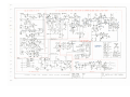
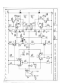
Technical Service Manual
lecs
ecson
Lecson Audio Ltd. Burrel Road, St. Ives, Cambridgeshire, England. PE17
4LE
Telephone St lves (0480)64508 Telex 32562 AB Lecson StIves
Contents
1 AC1 Pre Amplifier
2 AP1/2 Power Amplifier
3
4
5
6
7
8
9
ACl PreAmplifier
1.0
General Description
The ACI control unit is a self-powered pre-amplifier of advanced design, all input and
output connections are standard DIN with the exception of the connection to the power
amplifier which is via an 8-pin DIN socket.
This manual gives all circuit details and descriptions in sections 2 and 3 and it is
recommended that these sections be read before commencing a repair.
Section 4 gives full testing and fault-finding procedures and section 5 describes details and
fault conditions which are unusual or particular to the electronics of the AC 1.
Any components may be ordered direct from LECSON for servicing purposes.
Questions on service will be answered by the service department at St. Ives. Tel. No. (0480)
64508.
2.0
Circuit Description
Circuit diagram for ACI. The heavy line on the diagram illustrates the path taken by a signal
fed into the RAD input (left channel).
The circuit is unusually complex for a control unit because of the electronic switching which
involves 36 field effects and 7 bipolar transistors.
Description of the circuit treats the control unit in blocks as follows:
1. Input switching and control logic
TR1 - 24, TR38 - 41
2. Input amplifier (low noise)
TR28 - 37
3. Volume control
TR38 - 45
4 Low filter
TR46 - 49
5. High filter
TR50 - 57
6. Tone control
TR58 - 61
7. Cancel facility
TR27, TR62 - 65
8. Power supply
TR25, 26
2.1
Input switching and control logic
Five inputs are provided, PU1 and 2 are low-level inputs, for magnetic cartridge source, and
in these positions the input amplifier 2.2 is arranged to have an R1AA playback response.
Three inputs, RAD, AUX1 and AUX2 are provided each with an input sensitivity of 125mV
and a flat response is selected on the input amplifier.
All the signal routing in AC1 is effected by series FET switches.
The series FET switch is ‘ON’ when the instantaneous voltage between the gate source and
drain is very small <100mV. The switch is ‘OFF’ with a gate source or gate drain pd of
more than -4V. In ACI any intermediate state is carefully avoided by the use of good quality
coupling capacitors (either tantalum bead or polycarbonate) and so avoiding polarisation of
the switches by leakage currents. The consequence of a voltage remaining on any terminal
of the FET between ±160mV and -4V would be indeterminate switching and high distortion
of 2nd order.
The PU inputs use single series FETs and the ‘flat’ inputs employ dual series FETs. This is
arranged to give good input isolation and normally at 10kHz isolation between a desired and
undesired input should be >55dB with desired input o/c; >100dB with desired input fed
from <1KΩ.
For example in the PU1 switch TR1, R7 and R82 hold the d.c. potentials of the source and
drain respectively to 0V ±50mV. Cl ensures that the gate and source of the device follow
each other maintaining the switch on in the ‘ON’ mode and off in the ‘OFF’ mode. The
control voltage on the gate is fed from C3 via R1. When the voltage at Z1 is 0V the signal
flows through the FET TR1, when the voltage at Z1 is -18V the signal at pin 3 cannot enter
the amplifier.
TR19 and 20 shunt the input signal when the amplifier is turned off, normally in use the
gates are tied to the -18V switching supply and have no effect on the operation of AC1.
A tape monitoring facility is available, when the monitor is switched ‘on’ the signals on the
AUX2 inputs are routed to the volume control stage via TR17 and 18.
The control logic performs the following functions:
Input logic Dl, D2 and TR21 and SW1-5. This sets the input FET switch control voltages
which appear on capacitors C3(T1), C6(T2), C11(T3), C16(T4), C21(T5). The desired input,
e.g. PU2, has 0V ±50mV on T2 and the potential of the other points (T1, T3, T4, T5) is -l5V
±3V. The selected signal is then able to enter the low noise stage (see ii) and the output of
the stage is always available at the tape output regardless of the monitor switch position.
Dl, D2 and TR21 produce the control voltage which adjusts the frequency response and gain
of the input stage.
When RAD, AUX1 or 2 are selected TR21 is switched on and the voltage on T8 is 0V
±200mV.
Selection of PU1 or 2 allows Dl or D2 to conduct switching off TR21 and the voltage on T8
rises to -12V ±3V.
Normally it is not possible to select two or more inputs at once; this condition would be the
result of a failure on the pcb or bad magnet alignment.
Tape monitor TR22 and 23. Normally the amplifier is operated in the monitor ‘off position
- SW6 closed. In this mode TR22 and 23 produce control voltages for routing the signal
from the input amplifier to the volume control.
For inputs RAD, AUX1 and AUX2 the voltage on T6 is 0V ±200mV and on T7 is -18V
±3V.
For inputs PU1 or PU2 the voltage on T6 is -18V ±3V and on T7 is 0V ±200mV.
When monitor ‘on’ is selected (SW7 closed) TR22 and 23 are both off and the voltage on
T6 and T7 is -18V ±3V.
Remote. In the normal manual mode TR24 is switched ‘on’ allowing the input to be selected
via SW1-5. Pushing the monitor switch to the ‘remote’ position switches off TR24 and thus
disables the input selector. Inputs may be selected via the 5-pin socket at the rear. D5
ensures that in the ‘remote’ mode the tape monitor is ‘off.
2.2
Input amplifier low noise
This stage comprises TR28, 30, 32, 34, 36 and 66 Left (TR29, 31, 33, 35, 37 and 67 Right).
The selected input signal which appears at T9 (T10 Right) is amplified by this stage and the
output signal appears across R124 (R125 Right). The input amplifier has a gain of 1.2X or
+2dB when RAD, AUX1 and 2 are selected and an RIAA response with a gain of 10X or
+20dB @ 1kHz when PU1 or 2 are selected.
Four transistors form the basic amplifier. TR28 and 32 are common emitter gain stages with
high frequency correction applied by C47, C51, C53. The output of TR32 (across R110)is
buffered by the emitter follower TR34 which has a constant tail current supplied by TR36.
The d.c. working point is maintained by d.c. feedback applied via R120, R118 and R108 to
the emitter of TR28.
In the PU mode TR30 is switched ‘on’ and TR66 ‘off. Here a.c. negative feedback is
supplied by the network of R120, R118, C57, C55 and R96.
In the ‘flat’ mode TR30 is switched ‘off and TR66 ‘on’, the feedback network being in this
case for a.c. TR66 and R106.
The input stage is capable of producing an output of 28V p-p with PU and monitor ‘off
selected.
2.3
Volume control
The volume control stage is of the shunt feedback type, with variable feedback applied
around the gain stage TR42 and 44, by the volume control VR1.
TR42 operates as a high-gain bootstrapped common-emitter amplifier and its output is
buffered by TR44 which acts as an emitter follower.
The d.c. working point is controlled by the potential divider R142 and R144 and by the d.c.
feedback resistor R146.
The signal fed to the base of TR42 (the virtual earth) is fed either through TR38, R128,
R134 for PU1 or 2 or through TR40 and R132 for RAD, AUX1 or 2.
When the monitor on is selected TR38 and 40 are ‘off and the AUX2 left signal is fed in via
TR17 and R132.
R124 and R136 maintain the switches TR38 and 40 with 0V ±200mV d.c. on drain and
source.
The output from the volume control stage at T21 is fed to the low filter stage and to the
cancel switch.
2.4
Low filter
The low filter is a 2nd order active filter formed by C85, C87, C89, TR48 and R166; this
filter is disabled by switching ‘on’ TR46 which shorts the signal across C85 and 87. With
the filter off the gate of TR46 is tied to 0V by R156, switching the filter on, SW9, applies
-12V ±3V to the gate of TR46 switching this transistor off allowing the filter to operate.
2.5
High filter
This stage TR50, 52, 54 and 56 is a 3rd order active feedback filter. TR54 and 56 form a
super emitter-follower and the filter frequencies are selected by SW13-15. With this high
filter off TR50 and 52 have gate voltages of -12V ±3V and the frequency response is
tailored by C93, C99 and C97.
Selection of F1 switches TR50 on making C91 effective.
Selection of F2 switches TR52 on making C95 effective.
Selection of F3 switches TR50 and 52 on simultaneously.
The mono switch SW10 parallels the left and right channels by connecting R182 to R183
via C117.
2.6
Tone control
The signal appearing at the output of the high filter stage - at T25, is fed into the tone
control stage. This is of the normal feedback type with the feedback network of VR2 and
VR3 applied around the high-gain bootstrapped amplifier stage formed by TR58 and TR60.
The d.c. working point is controlled by the feedback network formed by R206, R208 and
R250.
Normally for 500mV rms output the shorting link across R204 is fitted, removal of the link
reduces the feedback and raises the output to l.2V rms.
The output of this stage appearing across R210 is fed to the cancel switch.
2.7
Cancel switch
TR62 and 64 are series switches controlled by TR27. In the normal ‘out’ mode TR27 is
switched on, thus TR62 is switched on and TR64 switched off and the signal coming out of
the tone control stage is fed through to the balance control VR4 and hence to the output
socket.
In the cancel mode TR27 turns off, switching TR62 off and TR64 on. In this mode the direct
signal from the volume control stage is fed through to the balance control and output.
2.8
Power Supply
Each channel of AC1 has a regulated -30V supply of a constant current type. This is used
because of its good regulation and the high degree of protection offered to the circuits in a
fault condition.
TR25 and 26 provide the constant currents each of -27mA ±5mA; the rail voltage is
stabilised by ZD1 and ZD2. A -18V rail used for switching is derived from the raw d.c.
across C33 via R74, ZD3 and C32.
3.0
Dismantling
1.
Ensure that all slider controls are fully retracted to the front edge of the unit;
2. Place the amplifier face down on a soft surface (e.g. felt).
3. Remove screws ‘A’.
4. Carefully raise the amplifier off the top plate for a distance not exceeding 2”.
5. Placing hand between top plate and amplifier extract light-emitting diode from its
housing in top plate.
6. The bottom plate is taken off by removing the five flange head fixing screws ‘B’.
3.1
Top Plate Assembly
This is a laminated assembly which cannot be dismantled without special tooling, therefore
should any part of the above become damaged it will be necessary to replace in total.
3.2
Polished Cover Plate
This item is held in position by double-sided adhesive tape, which can be softened by gently
warming, allowing the cover to be peeled off. A replacement cover plate can be obtained
from the factory complete with adhesive tape.
3.3
Fitting
Remove protective paper backing from tape and offer new cover plate up to amplifier.
Ensure that cover plate is correctly positioned before pressing into place.
Replacement of Sliders
Should a slider become damaged the following procedure is to be followed.
After removing the top plate assembly as detailed above it will be necessary to remove the
magnet carriers. These are held on with an cyano acrylate adhesive AVDELBOND ‘C’, and
the only way of breaking the bond is by applying a sideways leverage.
After removing the magnet carriers the sliders can be withdrawn from the front. Note the
orientation of the magnet carrier as it is important that this is replaced accurately during
reassembly.
The replacement of sliders is the reverse of operations one and two. In the case of sliders
having ball-click position it will be necessary to lift the ball-retaining spring to allow the
slider to be inserted. If the adhesive stated above is not available an epoxy resin, i.e.
Araldite, may be used to secure the magnet block to the sliders.
Note: It is important that if magnets are removed from their respective holders then polarity
must be maintained in the same direction, i.e. N-S, N-S, N-S.
4.0
Testing Procedure
If the AC1 is returned with a description of the fault then refer to the table of typical faults
(section iv d).
In order to check a fault or to diagnose a fault condition three testing procedures are
outlined:
Listening test of the AC1 complete with AP1/2.
Bench testing of the complete AC1.
Bench testing of the uncased printed circuit board of the AC I.
4.1
Listening Testing
A full listening test when correctly carried out can - apart from providing very quickly an
indication that all functions of the AC1 are working correctly - be a very useful technique
for diagnosing and pin-pointing any fault condition; and is the only useful way of tackling
intermittent crackles, etc.
This test is best carried out with the AC1 connected to a AP1,/2 via the usual connecting
lead and the listening carried out with the use of headphones connected to the speaker
outlets On the AP1/2 via a suitable attenuator. The headphone outlet on AC1 is not used all
the time in order that switching anomalies (if they exist) on the low filter and cancel slider
may be tested.
The tester can perform a useful check in the absence of any signal by listening to the
background noise in the unit and by injecting hum into each input with a screwdriver
(blade), but the full test requires a flat 100mV signal and a disc source of speech or music.
The primary functions of the listening test are:
To establish operation of both channels in ‘cancel’ and ‘out’ modes.
To establish operation of tone controls, high filters, low filters, headphone mute.
To check operation of input selection circuits and equalisation switching.
To check tape monitor switching.
To check volume control.
To establish a reasonable quality and quantity of background noise and hum.
4.2
Bench Testing of the Complete AC1.
The following equipment will be necessary to test the AC1.
Audio range oscillator with output variable between lmV and 1V rms sine and square.
Oscilloscope 1MHz with sensitivity of at least 200mV/cm.
Electronic a.c. millivoltmeter 1 mV- lV rms.
To check noise and distortion in addition:
Low distortion oscillator t.h.d. 0.01%.
Distortion factormeter capable of reading down to 0.01% t.h.d. at 1kHz.
DIN shorting plug.
Inputs are connected to AC1 using five DIN plugs and the output taken from an 8-pin DIN
plug.
Some method should be available for simply changing the signal from left to right input and
switching the oscilloscope and meter from left to right output.
Procedure
1. Set AC1 switches as follows:
Input
RAD
Tape
Off
Volume
8
Treble
0
Bass
0
Balance
0
Mode
Stereo
High F
Out
Low F
Out
‘Phones
On
Power
On
Connect an input lead from the oscillator to the RAD input, connect the output of the AC1 to
the oscilloscope, voltmeter and DFM.
2. Feed in a sinewave input of 100mV into the left channel, check that the output voltage is
left, 500mV rms. Check that the waveform on the oscilloscope is a clear sinewave. Check
that this disappears when balance control is moved to right 4. Return balance control to 0.
Switch output to right, check that the crosstalk output is less than 5mV rms.
To ensure that no intermittent connections are present.
To ensure that the switching of AC1 does not interact (magnetic or electrical faults).
A flow-chart testing procedure is given below. Follow through all the tests before attempting
a repair so that all faults may be isolated if possible.
3. Feed the same signal into the right channel. Check that the output signal on the right
channel is 500mV ±50mV rms. Check that this disappears when the balance control is
moved to left 4. Return balance control to 0.
Check that output of left channel is less than 5mV rms.
So far it has been established that the amplifier is working with the right gain and that all the
stages seem to function.
4. Increase the input signal and ensure that both channels will deliver 2V rms at least.
5. Feed a square wave 1kHz into the left RAD input. Adjust the input to give 0.5V pKc
-pk output.
Check that the output waveform is clear with no overshoot and with flat tops.
6. Repeat test 5 for the right channel.
7. To test quickly the functioning of the tone and filter controls make the following tests,
and in each case refer to the diagram which shows the desired output, waveform. Repeat for
left and right channels.
a Set treble control to +4, refer to Fig. 2.
b Switch low f to cancel. Check that original square wave is restored, at about 500mV
pk-pk.
c Reset treble to 0, low f to out.
d Set treble to -4. Refer Fig. 3.
e Reset treble to 0.
f Set bass control to +4, refer Fig. 4.
g Set bass control to -4, refer Fig. 5.
h Set bass control to 0. Switch mode to mono. Check that output is halved and that this
appears in both channels.
I Reset mode to stereo. Set high filter to f 1, refer Fig. 6.
I Set high filter to f2, refer Fig. 7.
k Set high filter to f3, refer Fig. 8.
1 Set high filter to out.
m Set low filter to f 1, refer Fig. 9.
For more accurate testing of these functions the following performance is expected of these
controls.
Sinewave input of 10mV rms, 10kHz.
Treble control should give +9dB at +4
-9dB at -4.
Set treble control to 0.
High f should give the following responses:
Out
0dB
f1
-3dB at 10kHz
f2
-5dB at 10kHz
f3
-7dB at 10kHz
change to input of 10mV rms 100Hz.
Bass control should give +10dB at +4
-10dB at -4
Set bass controls to 0.
Low filter should give - 1dB at f 1.
8. Procedure for Listening Test
Follow through the tests a-z in order.
a Connect AC1 to main supply and to AP1. Connect AP1 mains lead to AC1 outlet. Connect
headphone to AP1 as described above and put on ‘phones.
b Set the controls as follows:
AP1 speaker switch to AB
AC1 input to PU1
Monitor
off
Volume
0
Treble
Bass
Balance
Mode
High f
Low f
‘phones
Power
0
0
0
Stereo
out
out
off
on
Result
Background and hum should be inaudible, red light indicating operation of power supply to
AC1 should be alight.
c Advance volume control to number 8, a fairly loud rumbly-hiss should be heard in both
channels, the level of hiss and rumble need not be the same in both channels. Fit a shorting
plug to the PU1 socket (socket pins 3-5-2) and note that the level of noise drops
considerably in both channels and that a small amount of hum can be heard. Remove
shorting plug.
d Advance treble control to +4, observe correct change in noise character in both channels.
e With treble set to +4 check that original sound is restored in both channels when low
filter switch is set to cancel.
f Move ‘phone switch to ‘on’, check that the unit stays in the cancelled mode. Move ‘phone
switch to mute and check that both channels become silent.
g Return ‘phone to ‘off, low filter switch to ‘out’, treble to 0.
h Move treble to -4 and observe equal cut in brilliance on both channels. Reset treble to 0,
check that bass control gives boost and cut.
I Reset bass control to 0. Check that mode switch gives ‘mono’ in the ‘mono’ mode. This
will be observed by a central image of the noise.
j Reset mode to stereo. Check that high filter gives progressively more out in brilliance in
both channels as it is advanced through f1to f3. Reset to out.
k Check low filter gives deep bass cut set to f1. Reset to out.
l Set tape’ switch to ‘on’, observe that the noise levels drop considerably. Set tape switch to
‘rem’, observe small rise in hiss level.
m Set tape switch to ‘on’, check that AUX2 inputs are functional by injecting hum with a
screwdriver blade or similar, into pin 3 (left) then pin 5 (right).
n Set tape switch of ‘off’, check that both AUX2 inputs are disconnected by injecting hum
as in test 13. Correct result should give no hum.
o Check by injecting in the same way that the left and right inputs of PU1 (pin 3 and 5) are
connected and that PU2 left and right are not connected.
p Switch to PU2, note low frequency switching noises are normal at full volume. Check that
PU2 left and right are connected and that PU1 left and right are not connected.
q Switch to RAD. Check by injecting hum that both channels (left and right, pin 3 and 5) are
connected. N.B. The circuits take up to ten seconds to change from PU mode equalization to
‘flat’.
r Switch to AUX1. Check by injecting hum that RAD left and right have switched ‘off. Check
that AUX1 left and right have switched on.
s Switch to AUX2. Check that AUX1 left and right have switched off, and that AUX2 left and
right have switched on.
Further Optional Tests using a signal source.
t Set controls as in test 2. Connect pick-ups to PU1 socket and advance volume control. Check
that noise is smooth and at a reasonable level. Place pick-up on record and adjust a
comfortable listening level.
u Repeat tests 4 to 11 inclusive, checking that the controls give the desired effects.
v Set tape switch to on, note than music disappears after a small delay.
w Connect a flat (100mV rms signal) to the AUX2 socket and check that this signal is
correctly reproduced with the tape monitor on and that switching to monitor off restores the
original disc signal after a delay.
x Switch to PU2, observe that the disc signal disappears.
y Connect disc signal to PU2 and check that both channels are correct with the mode switch
still set to stereo.
z Using the flat 100mV signal check that RAD, AUX 1 and AUX2 switch on and off
correctly.
Testing of PU inputs
9. Connect an input lead to the PU1 socket of the AC1. Set all controls as for step 1 and then
switch the input to PU 1.
10. Feed in an input of 1kHz sinewave 2.6mV rms and check that for left and right channels
the output is 500mV ±50mV rms.
11. Increase the input to the AC1, and reduce the volume control setting towards 0 keeping
the output at 500mV mis.
Check that serious waveform distortion does not occur below 200mV rms input and that there
are no clipping effects with an input of 800mV rms.
12. Reduce input level to 2.6mV and set volume control for an output of 50mV rms (about 4).
Feed in an input of 2.6mV at 10kHz and check that the output is -13dB ±1dB on 1kHz level.
Feed in an input of 2.6V at 100Hz and check that the output is +13dB ±1dB. Repeat this test
for left and right channels.
13. Reset input to 2.6mV 1kHz and set volume to maximum ‘8’. Switch the tape switch to
‘monitor’ and check that left and right channels have no output.
14. Measure the tape output signal appearing on pins 1 and 4 of the AUX1 or 2 sockets.
Check that this is 25 ±5mV rms.
15. Reset the tape switch to ‘off, check that left and right channels reappear at the output.
16.
Set input to PU2 and note that the output of both channels disappears.
17.
Move the input lead from PUI socket to PU2. Note that the signals reappear at 500mV
±50mV in the left and right channels.
18.
Set input switch to PU1 and note that the output of both channels disappears.
19.
Set input switch to RAD. Connect input lead to RAD with a signal of 100mV rms.
Check that an output of 500mV ±50mV is present left then right.
20.
Move input switch to AUX1. Check that the output signal has disappeared (left then
right), isolation should be >60dB.
21.
Move input plug to AUX1 socket. Check that an output of 500mV ±50mV is present
left then right.
22.
Move input switch to AUX2. Check that the output signal has disappeared (left then
right).
23.
Move input plug to AUX2 socket. Check that an output of 500mV ±50mV rms is
present (left then right).
24.
Move input switch to AUX1. Check that output signal has disappeared (left then
right).
25.
Move tape switch to ‘monitor’. Check that an output signal appears of 450mV ±50mV
(left then right).
26.
Move tape switch to ‘remote’. Check that the output disappears (left then right).
This completes the functional testing of AC1.
Measurement of noise, hum and distortion
27.
Set the controls of AC1 as in 1. Connect a low distortion signal of 100mV rms to the
radio input. 1kHz.
Make a fine adjustment of the input to get an output of 500mV. Measure the total harmonic
distortion and check that this is less than 0.05%.
28.
Remove input plug and fit a shorting plug to the RAD input. Measure the noise and
hum content of the output of the AC1. Check that the combined noise and hum is less than 70dB for both channels.
29.
Move the shorting plug to the PU1 input socket and switch input to PU1. Check, after
20 seconds, that the noise is less than -70dB, and that noise and hum are less than -60dB.
4.3
Bench Testing of the cased printed circuit board of AC1
Refer to section 3 for instructions on uncasing of the AC1. It is often advantageous to test the
AC! uncased during fault-finding. In addition to the a.c. tests carried out in Test T2 it is of
course possible to measure the quiescent d.c. voltage throughout the circuit.
N.B. It is, of course, not possible to measure noise and hum with the unit uncased. With
AC1 uncased the general procedure is as below:
Place the board the right way up on a foam block or other protective surface, taking care
that nothing can short the underside of the p.c.b.
At all times take extreme care because mains voltages are exposed at the rear right-hand
corner, around the outlet socket.
The mains supply is switched on by holding the microswitch button depressed. This is best
done with adhesive tape.
The slider controls can be easily moved.
The switching which is normally activated by the magnets in the top of the AC1 has to be
effected, using free magnets, and four magnets are supplied with this manual.
Remember to remove these magnets before recasing!
The procedure for activating any function is to rest a magnet on top of the appropriate reed
switch - note that several switch positions have no reed.
Thus to set up the AC1 as for test 1 in section 4.2 the controls would be as follows:
Place a magnet on the RAD input reed. Middle of left row.
Place a magnet on the tape ‘off reed.
Set volume slider to maximum.
Set the other 3 slider controls half way.
Switch the microswitch on.
This now duplicates all the control settings of 4.2.1.
D.C. Tests
Quiescent d.c. levels are shown on the circuit diagram. These should be checked using a
20,000Ω/V multimeter at the appropriate test points. Switching voltages can be checked
against the following test table.
Input Switching
PU1 selected
PU2 selected
RAD selected
AUX1 selected
AUX2 selected
T1
T2-T5
T6
tape off
tape monitor
T7
tape off
tape monitor
T8
T1
T2
T3-T5
T6
tape off
tape monitor
T7
tape off
tape monitor
T8
T1, 2
T3
T4, 5
T6
tape off
tape monitor
T7
tape off
tape monitor
T8
T1 -3
T4
T5
T6, 7, 8
T1 -4
T5
T6, 7, 8
0V ±50mV
-12V ±5mV
-15V ±3V
-15V ±3V
0V ±50mV
-15V ±3V
-15V ±3V
-15V ±3V
0V ±50mV
-12V±5V
-15V±3V
-15V ±3V
0V ±50mV
-15V ±3V
-15V ±3V
-12V ±5V
0V ±50mV
-12V ±5V
0V ±50rnV
-15V ±3V
-15V ±3V
-15V ±3V
0V ±50mV
-!2V ±5V
0V ±50mV
-12V ±5V
as RAD
-12V ±5V
0V ±50mV
as RAD
Tape Switching
T6, T7 see Input switching
Voltage on C24 tape off
tape monitor
12V ±5V
0V ±50mV
Mode
Check voltage across C117
High Filter
Junction of R172 and 173
Junction R176 and 177
0V ±500mV
Voltage measured at two points
out
-12V ±5V
-12V ±5V
f1
0V
-12V ±5V
f2
-l2V ±5V
0V
f3
-0.5V ±0.3V
-0.5V ±0.3V
Low Filter
Set to Out (no magnet applied)
T29
0V±50mV
Junction R75 and R76
-10V ±5V
Junction R154 and Rl55
-12V±5V
Set to cancel
T29
Junction R75 and R76
Junction R154 and Rl55
-15V ±3V
0V ±50mV
0V ±5V
Set f1
T29
Junction R75 and R76
Junction Rl54 and R155
0V ±50mV
-10V ±5V
50V ±50mV
A.C. Tests
Using the general procedure outlined at the beginning of section T3, all a.c. tests may be
carried out as in section T2.
In addition, for the controls set as described at the beginning of section T3 (refer T2.1) the
following a.c. voltages are considered normal for an output of 500mV rms:
T9, 10
100mV ±25mV rms
(2.6mV ±5mV rms)
T11, 12
120mV ±27mV rms
(28mV ±5mV rms)
T13, 14
98mV ±25mV rms
(2.4mV ±0.5mV rms)
T15, 16
0V rms
(27mV ±V rms)
T17, 18
1mV rms approx.
T19, 20
550mV ±50mV rms
T21, 22
550mV ±50mV rms
T25, 26
520mV ±50mV rms
T2
510mV ±20mV rms
With PU1 or 2 input arranged for 500mV rms output the voltages shown in brackets would
apply.
5.0
Special Details
Using the test procedures described in section 4 it will be possible to locate the area of any
fault condition and to solve it by normal techniques.
The AC1 does, however, have some unusual features which on first acquaintance may be
confusing.
5. 1
Field Effect Transistors
The FET used in the AC1 is an n-channel junction FET. Common failure modes are:
Short-circuit drain-source-gate. This results in switches being on even when switched off.
Typical symptoms would be:
An input not switching off and breaking through on all input positions.
Lack of RIAA equalization or incorrect gain in any mode. TR66, 38, 40.
Low gain on all inputs. TR19, 20.
Filter failure. TR50-53.
Cancel failure -- e.g. dead or heavily distorted in the cancel or out mode. TR62-65.
Open circuit drain-source. This will not allow the transistor to switch on. Typical symptoms
would be:
An input not switching on. TR1-16.
RIAA equalization on RAD, AUX1 or AUX2. TR66, 67.
No output either in cancel, on or off. TR38-41.
Filter failure. TR46, 47.
No output in one of the cancel modes but correct output in the other TR62-66
Oscillating in the off mode.
This oscillating takes place in the off mode and is of very high frequency >10mHz. It
manifests itself as a loud hiss in the affected channel which disappears when the particular
FET is switched on. Typical solutions would be:
Loud hiss on all inputs affected by volume control. TR19, 20.
Loud hiss on all but one input. In this case the oscillating FET is in the input switch of that
one input.
Hiss on filter out high or low, but disappears in a mode f1, f2 or f3 or f1 low. TR46, 47,
50-53.
Hiss on cancel or out. TR62-65.
Rumbling in the off mode.
This is due to the leakage around the FET junction and occurs in the same situations as (c)
above.
IMPORTANT Before suspecting or changing a FET ensure that the control voltages on the
gate are correct as described above.
5.2 Light Emitting Diode
All the supply current in the left-hand channel passes through the LED. The common failure
mode is an internal short-circuit so that the amplifier will work with no visible light.
5.3 Reed Switches
These sealed switches are activated by magnets carried on the top plate. Common failure to
switch would be either fracture of the switch casing or mis-alignment of the magnets.
It is extremely important that the magnets on the top plate are placed in the correct
orientation with respect to each other and in the correct position. Observe this location
carefully before removing any magnet. If the magnets are not in the correct position and/or
orientation the switches may fail to operate or may interact from side to side.
5.4 Constant Current Power Supply
In order to achieve high regulation a constant current supply is used with zener diode
stabilisation. The service engineer must be aware of the fact that fault conditions tending to
cause a stage of the amplifier to drain too much current may result in a collapsed or
oscillating rail voltage, and that this does not necessarily indicate a failure of the supply.
5.5 Double-sided Printed Circuit Board
AC1s up to serial number 1300 (approx.) used a double-sided p.c.b. with griplet or pin
connections between the two sides of the board. The griplet and/or pin system proved to be
somewhat unreliable, typical symptoms are:
(i) Crackling and/or intermittent contact between sides of the board.
(ii) Channel fading or low-frequency disturbances.
(iii) Microphony.
Amplifiers of serial number from 1300 approx. onwards use a through-hole plated board
which is much more reliable. No problems should be encountered but great care must be
taken not to damage the tracks when removing a component.
5.6 Modifications
Mains click and radio interference: Units up to serial number 1200 were not fitted with
components: R217, 218, 221, 222, 226, 227; C117, 118 or ferrite beads on TR28, 29, 42,
43. These components can be added to units to reduce the susceptibility to outside
interference and are available in sub-assembly form from LECSON.
AP1 / 2 Power Amplifiers
1.0
General Instructions
AP1 and AP2 are high-powered, direct-coupled audio power amplifiers enclosed in black
anodised aluminium extruded cases, the case also acts as the heat sink for the output
transistors.
The power amplifiers have an input sensitivity of 500mV rms and are suitable for use with
any signal source in the audio band.
Unconditional stability ensures that any load is suitable although reduced output is available
for loads less than 4Ω or greater than Ω
2.0
Mechanical Details
2.1
Description
The AP1 /2 is constructed from two semi-cylindrical aluminium ribbed plates which slide
together to form the cylindrical body of the power amplifier. The whole is clamped together
by the top and bottom circular aluminium plates which are each fixed by six self-tapping
pozidrive screws. There is, in addition, a perspex top disc fastened to the top plate by
double-sided adhesive tape.
One half extrusion carries the mains transformer, line fuses, bridge rectifier and thermal
cut-out switch (this is called hereafter “the transformer half’). Both halves each carry a
channel sub-assembly of printed board and integral heat sink (hereafter called “power
board”).
The transformer half carries the left channel power board.
The top plate supports the two reservoir capacitors and the bottom plate carries the 7-pin
DIN input socket, the speaker outlets, fuse holders and cut-out relay. The top plate,
transformer half and bottom plate are connected by a cable-form.
2.2
Dismantling Switch Off
1. Remove the perspex top disc with a rubber sucker or alternatively by carefully inserting a
knife blade between the edge of the disc and the body and slowly levering the disc away.
2. Remove the six pozidrive self-tapping screws. The top plate now may be removed and
set on one side (taking care not to short out the reservoir capacitors), in order to inspect the
inside. In this form it is possible to change the internal 1 OA 1¼” fuses.
3. Invert the amplifier and remove the six self-tapping pozidrive screws from the base plate.
The base plate may now be pulled to one side to operate on the base plate circuits. (Beware
of mains voltage if the unit is switched on.)
4. With the base plate sitting in its normal position stand the amplifier on its base and pull
the top plate up and away towards the transformer half.
5. Unclip the top most connections input lead on the power board in the free half (right
channel).
6. Slowly slide the free extrusion half upwards 2” (with early serial numbers some
persuasion with a soft-faced hammer may be necessary to move the free half).
7. Remove the middle connection to the power board in the free half.
8. Slowly slide the free half upwards a further 3”- 4”.
9. Unsolder the red and black leads from the tags on the power transistors.
10. The power board is now disconnected and the extrusion half can be completely
detached.
2.3
Working on the unit
The unit is best serviced with the amplifier opened up in this way.
1 .Lay the transformer extrusion half, curved side downwards, on a soft surface.
2. Arrange the top and bottom plates so that the cable form is not strained and no cables or
contacts short to each other or the casing.
3. Lay the free half alongside the transformer half.
2.4
Re-assembly
I. If the boards have been worked upon or exchanged the quiescent current of each half
must be adjusted as described in Section 4.
2. Push the base plate. on to its correct location on the transformer half taking care not to
disturb any insulation and not to trap any wires. Use one screw to hold this in place.
3. Stand the amplifier on its base and offer up the free half extrusion, and then slide the
halves together about 1”.
4. Pull all the free wires to the top of the amplifier.
5. Solder the red and black supply wires to the tags on the power transistors, the red wire
to the 2N3442, the black to the BDX18/80/BDX2O.
6. Slide the free half down 3”—4” and push on the middle connection (purple wire).
7. Push the free half down to the base plate taking great care that no wires are trapped
between the extrusion and base plate.
8. Fit the input push connections to the top of the power board and insulate any exposed
part of this connection with P.V.C. adhesive tape.
9. Carefully insert the top plate, ensuring that the speaker output connections on the
power boards are not deflected by the capacitors.
10. Replace all the screws in top and bottom plates.
11. Fit new adhesive tape to the perspex top disc and press this into place with the
LECSON logo adjacent to the left-hand seam on the extrusions.
3.0
Circuit Description
3.1
Power Supply
The main circuit includes a thermal cut-out switch and a 2.SA anti-surge 20mm fuse. The
transformer has a dual 1 20V primary which is either connected in series or parallel
depending on the local supply. See instruction manual. Some export models are fitted with
voltage selector switches.
The secondary circuit consists of a bridge rectifier feeding two l0,000pF (6,800pF AP2)
reservoir capacitors. The capacitors are connected to the boards via two 10A 1¼”fuses
fitted internally.
The supply is ±40V AP1, ±50V AP2.
3.2
Power Board
The amplifier is a directly-coupled class B circuit using complementary output triples. The
output circuit TR acts as a voltage follower with high power gain and low distortion.
Each half of the input signal is handled by the two halves of the input and driver, TR for the
+ve half and TR for the —ye half.
Quiescent voltages are shown in the circuit diagram.
Negative feedback is applied through R, R and C.
R1 and C1 form an input filter.
The quiescent current is adjusted by a VR1 to l36mA for APi and 3OmA for AP2.
Tantalum capacitors are used throughout to achieve high d.c. stability.
Protection against short-circuit loads or adverse load conditions is provided by the delayed
V-l limiters TR and fly-back is protected through Dl and D2.
Output Circuits
The base plate carries the output circuits; the zobel networks R and C, headphone
alternators R67-70, muting relay RL1, and output fuses and the A-AB-B output switch.
4.0
Testing Procedures
4.1
Complete Amplifier
1. As a complete unit the amplifier is tested in the normal way. Input signals are fed into
the 7-pin DIN socket on the base plate; left line to pin 1, right line to pin 2, and ground to
pin 3.
2. The sensitivity of the units is such that 500mV rms input will give I 6V rms output
(APi) or 22V rms (AP2).
3. Check that the amplifiers will produce at least SOW per channel into 8~2 both channels
driven (API), or 90W into 8~2 (AP2).
4. Check that the distortion is within the specified limits at 35W for AP1 or 70W for AP2.
S. Check that the static d.c. offset voltage at the output terminals of the power amplifiers
is below 250mV.
6. Check that the output is switched off when pin 7 of the DIN socket is connected to
ground — this tests the relay.
7. Test the speaker switch A-AB-B.
4.2
Power Board
It is possible to run the amplifier in the dismantled state if it is laid out as described in
section 2.3, but the need for great care cannot be over emphasised. Firstly, mains voltages
are exposed on the transformer and secondly, the power supply is powerful enough to do
considerable damage if it is accidentally shorted out.
Some repair work can be done on a power board in this mode but it is not practical to
remove and replace the board many times as this is a very time-consuming and tedious
operation.
If there is any doubt at all about working on a power board place on a jig which provides
the following:
I.
Quick release clamps on to the heat tabs to hold the board and remove heat.
2. ±40V supplies (±50V AP2) with optional current limit of l00mA to assist work on
faulty boards.
3. An output circuit consisting of zoebel network 5.6 Ω and 0.1 5µF, 2.5A fuse and
switch-able 8Ω load
4. Input lead connected to variable output oscillator.
5. Means for connecting an ammeter into either supply lead.
It is important that the board is not allowed to over-heat on this jig, and great care must be
taken at all times.
When working on the heat sink, changing driver or output transistors, ensure that the
insulation is not damaged. If in doubt on re-assembly please refer to Fig. 3. Before
switching on check that there is not continuity between any transistor and the heat-sink tab.
4.3
Setting Quiescent currents
It is not possible to adjust the quiescent current with the amplifier assembled, it will
therefore be necessary to set the unit out on the bench as described in section 2.3.
1. Connect only the board in the transformer half and insulate the flying leads which
connect to the power board in the free half.
2. Remove the internal 10A fuses fitted to the transformer half.
3. Plug the unit into a mains supply and switch on.
4. Check that ±40V (AP1) or ±50V (AP2) is present on the reservoir capacitors.
5. Insert a multimeter set to 1A f.s.d. in the fuse holder for the +ve supply and check that
the current is less than 10mA.
6. Remove the multimeter, switch off the amplifier and fit the +ve 10A fuse.
7. Insert the multimeter, set to 1 A f.s.d. in the —ye fuse holder, switch on and check that
the current is less than f.s.d.
8. Adjust VR1 on the power board for a current of 135mA (AP1) or 30mA (AP2) after 30
seconds. If any difficulty is experienced disconnect the blue output lead, and readjust.
9. Switch off and connect the following leads to the board in the free half. Input screened
lead, red supply lead to 2N3442. Do not connect output lead.
10. Insert multimeter set to 1 A f.s.d. between the —ve fuse holder and the BDX18
(BDX2O) solder tag.
11. Switch on and set current as described in step 8.
12. Switch off and discharge the reservoir capacitors with a 10A 2W resistor.
13. The amplifier can now be reassembled as described in 2.4.
4.4
Likely Faults
1. No output at all Check all fuses, mains supply and control unit connecting lead. Check
that loudspeaker switch is set to the correct position. Ensure that the muting relay is not
operating (switch off and listen for it dropping out). Check that there is zero offset
voltage at the output terminals. Check internal fuses.
2. No output one channel Check as in 1, ensure that there is not a large d.c. offset
(this indicates major failure of power board). Remove top plate and ensure that the
input signal tags are not shorted together or shorting to the top plate itself (common
fault).
Remove bottom plate and check for continuity from the board outputs (top of speaker
fuses) to the output terminals.
Inspect board for dry joints or burnt-out components.
3. Distorted Output This will be due either to an internal fuse or power board
component failure. Check all joints on the board of the affected channel, test all
semiconductors in-circuit, using an ohm-meter.
4. High Hum level Check all earthing to board inputs. Look for dry joints or broken
tracks associated with C4 and C5 on the affected channel.
5. Crackling Inspect base-plate and power board for dry joints, check for leaking
capacitors, particularly C2 and C3, C6 and C7. Test for leaky transistors particularly
in early stages.
6. Massive failure Indicated by several charred components on a board and possibly
high offset voltage at the output.
Replace all visibly damaged components and all semiconductors on the board, or
exchange board.
4.5
AP2 Differences
A small number of AP2s, serial numbers 5030 to 5100 approx., were produced with
different circuit and insulation details.
The testing of these units is identical to AP1 and quiescent current should be set to
30mA.