1
HP Archive
This vintage Hewlett Packard document was
preserved and distributed by
www.hparchive.com
Please visit us on the web !
Scanned by on-line curator: Tony Gerbic
** For FREE Distribution Only ***
HEWLETT-PACKARD COMPANY
202A
LOW FREQUENCY
FUNCTION
GENERATOR
'"
N
o
N
>
OPERATING AND SERVICE MANUAL
MODEL 202A
SERIALS PREFIXED:
037 -
LOW FREQUENCY
FUNCTION GENERATOR
Copyright
HEWLETT-PACKARD COMPANY
1959
1501 PAGE Mll..L ROAD, PALO ALTO, CALIFORNIA. U.S.A.
00011·3
Printed: MAR 1962
Table of Contents
List of lllustrations
TABLE OF CONTENTS
Section
GENERAL INFORMATION
I
1-1. General .. ·
........·...
II
III
OPERATING INSTRUCTIONS.
2-1. Inspection
2-2. Controls and Terminals.
2-3. 230-Volt Operation.
2-4. Operation.
2-5. Single -Ended Output
2-6. Balanced Output.
2-7. Sync. Out.
·. .. ..
..
·.
·....
·.
...
PRINCIPLES OF OPERATION
3-1. General
3-2. Bi-Stable Circuit .
3-3. Linear Integrator. .
3-4. Sine Synthesizer and Function
Selector Switch. .
3-5. Output System
3-6. Sync Pulse Output
3-7. Power Supply .
..
..
..
IV. MAINTENANCE.
4-1. General
4-2. Power Supply.
..
Page
1-1
1-1
2-1
2-1
2-1
2-1
2-1
2-2
2-2
2-2
3-1
3-1
3-2
3-3
3-4
3-6
3-7
3-8
4-1
4-1
4-1
Section
Page
IV MAINTENANCE (cont'd)
4-3. Function Generator (bi-stable circuit and integrator)
4-2
4-4. Sine Synthesizer and Function
Selector. .
4-2
4-3
4-5. Output Amplifier
4-3
4-6 . Sync Out.
.
4-7. Tube Replacement.
.4-3
4-4
4-8. Tube Replacement Chart
4-9. Power Supply Regulator Adjustment. 4-4
4-10. Theory of DC Balance and Dist
Distortion Adjustments
4-5
4-11. DC Balance and Distortion . .
,4-5
Adjustments .
4-12. Adjust Squarewave Amplitude
4-8
4-13. Frequency Ratio and Calibration
Procedure.
. 4-8
4-14. Replacement of R58 Potentiometer
4-8
4-8
4-15. Performance Check.
4-16.
Output Voltage and Waveform
Check
4-8
4-17.
Sync Pulse Check
4-10
4-18.
Sine Wave Distortion Check.
4-10
4-19.
Dial Accuracy Check
4-10
.....
..
..
. .
..
.
V
TABLE OF REPLACEABLE PARTS.
5-1. Table of Replaceable Parts
5-1
5-2
LIST OF ILLUSTRATIONS
Page
Figure
1-1. Model 202A Low Frequency Function
Generator. . . . . . . . . . . .
1-0
2-1. Single-Ended Output Connections
2-2
2-2. Balanced Output Connections
2-2
3-1. Model202A Function Generator .
. 3-1
3-2. Details of Bi -Stable Circuit and
Switching System. . . . . . .
. . 3-2
3-3. Generalized Miller or Feedback
Integrator . . . . . . . . • . .
. . 3-3
3-4. Simplified Linear Integrator • . .
. 3-4
3-5. Sine Synthesizer and Function Selector . . 3-5
3-6. 50 '\, Waveforms . . . . . . . . . . . . • 3-5
3-7. Output Amplifier System of Model202A . . 3-6
3-8. Sync Output Circuit of Model 202A
3-7
3-9. Model 202A Power Supply
3-7
00011-2
Page
Figure
4 -1. Minimum Distortion and Frequency
4-6
Adjustment Instrumentation. . . .
4-2. Effect of Triangle Maladjustment on
Distortion and Frequency. . . . . . . 4-7
4-3. Patterns Showing the Adjustments of R49,
R51, R60 and R119 to Obtain Minimum
Distortion and Correct Frequency . . 4-9
4-4. Output Voltage and Sync Pulse Test Setup. 4-10
4-5. Sine Wave Distortion Test Setup . . . . 4-10
4-6. Dial Accuracy Test Setup
4-10
4-7. Model 202A Top View Cover Removed. 4-12
4-8. Model 202A Bottom View
4-13
Bottom Plate Removed . . . . . .
4-14
4-9. Function Generator and Amplifier .
4-15
4-10. Power Supply
.
iii
00011-2
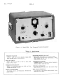
Se ct. I Page 0
Figure 1-1. Model 202A.
Low Frequency Function Generator
Table 1-1. Specifications
FREQUENCY RANGE:
0.098 to 1200 cps in five decade ranges with
wide overlap at each dial extreme
DIAL ACCURACY:
Within ±2% from "1. 2" to "12" on dial; ±3%
from ".8" to "1. 2"
MAXIMUM OUTPUT VOLTAGE:
At least 30 voltspeak-to-peak across rated load
(4000 ohms) for all three waveforms. (10.6
volts rms for sine wave)
FREQUENCY RESPONSE:
Constant within ±O. 2 db over entire frequency
range at rated output and load
FREQUENCY STABILITY:
Within ±1% including warm-up drift and line
voltage variations of ±10%
INTERNAL IMPEDANCE:
Approximately 40 ohms over the entire range
OUTPUT WAVEFORMS:
Sinusoidal, square, and triangular. Selected by
panel switch
SINE WAVE DISTORTION:
Less than 1% on all ranges except X100. Less
than 2% rms on X100.
00011-2
Sect. I Page 1
SECTION I
GENERAL INFORMATION
1-1
GENERAL
The Model 202A Low Frequency Function Generator
is a compact, convenient, and versatile source of
transient-free test voltages between. 008 and 1200
cycles per second. It is useful for any general
purpose low frequency testing application and is
particularly valuable in the testing of servo systems,
geophysical equipment, vibration and stability characteristics of mechanical systems, electro-medical
equipment, and for the electrical simulation of
mechanical phenomena. Three types of output waveform are available; sine, square and triangular.
Also, a sync output pulse is available for external use.
The Model 202A Low Frequency Function Generator
contains a type of relaxation oscillator that is particularly advantageous for the generation of very low
frequencies. Both a triangular and a squarewave
voltage function of time are inherent in the oscillating
system. Also, a sinewave function is produced
by synthesis from the triangular wave.
Output amplitude and distortion are Virtually independent of the frequency of operation. This type
of oscillating system in inherently a constant amplitude device so that no A. V. C. system, with associated delay in stabilization after frequency changes,
is required
The frequency range from. 008 to 1200 cycles per
second is covered in 5 bands. The frequency dial
is linear.
The output system is a direct-coupled amplifier
system designed for either single ended or balanced
output. It has good stability with respect to direct
current in the output and very low hum level. Both
the FUNCTION selectro switch and the AMPLITUDE
control are so arranged that the characteristics of
the amplifier are independent of their position. The
internal impedance of the output amplifier is approximately 40 ohms, and the unit is rated to deliver
at least 30 volts peak-to-peak to a 4000 ohm load.
A negative peak sync pulse of 10 volts into a 2500
ohm load is also prOVided. It has a duration of less
than 5 microseconds and occurs at the crest of the
sinewave and at corresponding positions with the
other functions.
Table 1-1. Specifications (Cont'd)
OUTPUT SYSTEM:
Can be operated either balanced or singleended. Output system is direct-coupled; dc
level of output voltage remains stable over long
periods of time.
POWER:
115 or 230 volts ±10%, 50 to 1000 cps, 150 watt
DIMENSIONS: Cabinet Mount: 20-3/4 in. wide,
12-3/4 in. high, 14-5/8 in. deep.
Rack Mount:
HUM LEVEL:
Less than O. 5% at rated output.
SYNC PULSE
10 volts peak negative, less than 5 microseconds
duration. Sync pulse occurs at crest of sine
wave and with correspondingpositions on other
waveforms.
WEIGHT:
Cabinet Mount: Net 42 lbs
Rack Mount:
Net 37 Ibs
TOP
[J..~
Sect. II Page 1
SECTION II
OPERATING INSTRUCTIONS
2-1
INSPECTION
After the instrument is unpacked, the instrument
should be carefully inspected for damage received
in transit. If any shipping damage is found, follow
the procedure outlined in the "Claim for Damage in
Shipment" page at the back of the instruction book.
2-2
CONTROLS AND TERMINALS
RANGE
This switch is used to select the desired frequency
range to be covered by the frequency dial.
FUNCTION
This switch is used to select anyone of the three
types of output waveform.
FREQUENCY
This dial is calibrated directly in cycles per second
for the Xl frequency range of the oscillator. The
knob just below the dial escutcheon is directly connected to the frequency varying element. The lower
knob is a mechanical ve rnier for fine adjustment
of the frequency.
AMPLITUDE
This control adjusts the amplitude of the oscillator
voltage admitted to the amplifier and, therefore, the
output of the instrument. This control is calibrated
from 0 to 100 in arbitrary units.
POWER
This toggle switch controls the power supplied to
the instrument from the power line.
FUSE
The fuseholder, which is located on the panel, contains the power line fuse. Refer to the Table of
Replaceable Parts for the correct fuse rating.
OUTPUT
This group consists of three te rminals. The one
marked "G" is connected directly to the instrument
chassis. The other two terminals, vertically aligned,
are the OUTPUT terminals. With respect to the
ground terminal each of these outputs has equal
magnitude of signal, but they are 180 0 out of phase
with each other. The internal impedance between
the two OUTPUT terminals is approximately 40 ohms.
SYNC OUT
The Sync Out terminals are single -ended and have
an internal impedance of about 2,000 ohms.
Power Cable
The three -conductor power cable is supplied with
a three -prong plug. The third prong is a round
off-set pin which provides a chassis ground. An
adapter may be obtained to permit use of this plug
with two-conductor receptacles.
2-3
230-VOLT OPERATION
This instrument is shipped from the factory with
the power transformer primaries connected in
parallel for 115 voperation, unless otherwise specified on the order. If 230 v operation is desired, the
primaries will have to be connected in series as
shown in "Transformer Details" on the Schematic
wiring diagram of the Power Supply Section.
2-4
OPERATION
The following step-by-step procedure should be
used as a guide when operating this instrument.
1) Turn the POWER switch to ON. Allow thirty
seconds for oscillations to start. The instrument
will operate nearly within specifications after a
few minutes warm-up. It will be within specifications after 30 minutes.
Sect. II Page 2
2) Set the RANGE and FREQUENCY controls for the
desired frequency. The frequency dial scale must
be multiplied by the multiplying factor indicated by
the RANGE switch setting to obtain the oscillator
frequency. Example: 4 (on dial scale) x .1 (multiplying factor indicated by RANGE switch setting)
= .4 cycles/sec.
3) Set the FUNCTION switch for the desired output
waveform.
4) Connect the equipment under test to the OUTPUT
terminals.
5) Adjust the AMP LITUDE Control for the desired
output voltage. Because the frequency response
is rated ±O. 2 db, the output amplitude may be measured at any convenient frequency and the output
level will be correct (within these limits) for any
other frequency.
must be connected to one of the OUTPUT terminals,
and the strapped pair will then be the ground side of
the output.
2-6
BALANCED OUTPUT
Connect the two OUTPUT binding posts to the eqUipment being supplied. The "G" binding post may
then be connected to the chassis of the equipment
being driven. Under these conditions the inte rnal
impedance of the Model 202A from either OUTPUT
terminal to ground is 7900 ohms in series with a 1 J.Lf
capacitor (C29). A maximum de voltage of 400 volts
may be applied between either OUTPUT terminal
and the "G" terminal without damaging the 1 J.Lf
capacitor (C29). The 40 ohms internal impedance
(resistive) will shunt the impedance existing between
the two signal inputs of the system being driven.
Under circumstances where the connection places
the Model 202A in series with a path carrying current, distortion of the Model 202A output will occur
if greater than 10 rna peak current is caused to flow
through the Model 202A output system.
NOTES
When small output voltages are required it may be
desirable to use an exte rnal attenuator. This is
because the hum and no ise in the output is nearly
constant with output amplitude.
To minimize distortion in the output waveform,
always use the lowest RANGE when the overlap
of the FREQUENCY dial permits a choice.
G
EQUIPMENT
BEING
SUPPLIED
OUTPUT
ground or no
signal point
RO
2-5
SINGLE-ENDED OUTPUT
Figure 2-2.
Balanced Output Connections
The terminal marked "G' is isolated from the actual
OUTPUT tenninals. For single-ended operation "G'
2-7
EQUIPMENT
BEING
SUPPLIED
OUTPUT
RO
Figure 2-l
Single-Ended Output Connections
SYNC. OUT
The SYNC. OUT is a negative pulse of less than
5 microseconds duration and at least 10 volts peak
amplitude. It occurs on one of the sine and triangular crests and at the rise or fall of the squarewave. n occurs at the positive crests with respect
to one of the OUTPUT terminals and at the negative crest of the other. Therefore, it can be changed
by 180 0 with respect to the output system by reversing connections to the two OUTPUT terminals
which are otherwise completely interchangeable.
The SYNC. OUT terminal marked "G" is directly
connected to the chassis.
00011-2
m
Sect.
Page 1
SECTION III
PRINCIPLES OF OPERATION
3-1
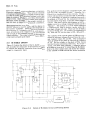
is that seen between points Band D. The conversion
of square wave to triangular wave takes place in
the integrator unit which is carefully designed to
produce an accurate integral of the applied square
wave. The bi-stable circuit and linear integrator
are loop coupled in such a manner that the resulting
relaxation oscillator is suitable for very low frequency operation.
GENERAL
Figure 3-1 depicts the general scheme of the ~Model
202A and indicates the waveforms produced. The bistable circuit consists of a flip-flop circuit capable
of producing a square-wave output at point A, provided it is triggered at the proper time. This is
done by including in the bi-stable cirCUit, a two-way
comparator circuit which produces the proper triggers for the flip-flop whenever the switc.hing signal
becomes equal to either the "plus switching reference"
or the "minus SWitching reference". The triangular
switching signal returned to the bi-stable circuit
The sinewave output is taken from a point C between
the triangular voltage at point B and the average
level at point D. The resistance between Band C
is fixed, and the network between C and D is a
A
B
+ SWITCHING
C
REF.
8+
~
... 1
\J
'---
@
Q
OUTPUT
AMPLIFIER
... 1
'-:..Y
©
BI-STABLE
CIRCUIT
f-<~
0
LINEAR
INTEG RATOR
®.
~VOaAGEFROM
o
~
L..o
.
-0
-0
\:J
•
+s~II!;A
AVE.
~
SWITCHING SIGNAL
_L _____V
L..o
\.J
A
-SWITCHING REF.
"
1\
AVE
-SWITCHING REF.
7
t'\
I
V
A
TO
VOLTAGE FR OM
'\
~
"
@TO@
VOLTAGE FR OM
@ro @
0
THE SYNTHESIZ EO
FUNCTION
'D·W-~6
8-
Figure 3-1.
Model
202A
Function Generator
@
0
Sect. In Page 2
non-linear system which synthesizes a sinewave
from the triangular wave. This network consists
of a group of biased diodes arranged in such a manner that at certain predetermined voltage levels they
begin to conduct, therefore, providing shunt paths
from C to D. Each additional shunt path reduces
the slope of the triangle in the proper amount so
that the wave is shaped to approximate a sinewave.
This approximation is as shown, and the degree to
which a sinewave may be approached depends on
the number of diodes. Thus there are available
the sinewave C, triangular wave B, and squarewave A functions with respect to D to be selected
and brought to the OUTPUT terminals through the
output amplifier. The output amplifier has a differential input and push -pull output.
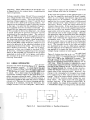
3-2
BI-STABLE CIRCUIT
Figure 3-2 shows the details of the bi-stable circuit
and includes the integrator in block form in order
to indicate the bilateral connection from integrator
output to comparator input.
The portion of the diagram composed of VI, V2
and V3 is the "bi-stable circuit". Actually, this
circuit is a combination of two circuits. H capacitors ClO and Cl3 are disconnected so that there
is no poss ibility of inductive coupling from grids
to cathode of VI and V2, the remaining circuit is
the well-known "flip-flop" or Eccles-Jordan trigger
circuit. The other circuit which appears in the bistable circuit is a voltage comparator known as the
"Multiar". The multiar is a circuit which employs
a regenerative loop to produce a pulse when the
two input voltages are equal. There are two of these
in the bi-stable unit. One multiar is composed of
VI, V3A and T2, and the other of V2, 3B and Tl.
The cathode of V3A and the plate of V3B are connected to reference voltages derived from the voltage regulator tubes V5 and V6. The triangular
wave is applied to the plate of V3A and the cathode
of V3B. As the voltage on the plate of V3A rises
towards the plus sWitching reference, VI is conducting, but when V3A conducts, a negative pulse
is formed on the grid of VI which flips the Bi-Stable
Unit to its other stable state and starts the voltage
on the cathode of V3B towards the minus switching
......- - - - - - - - - - - - - B +
r--------_-~~------___..------
R21
R20
C13
V6
+-REF
-REF
R57
+RI03
R58
'-----+--_-+---4-~~_+......-_+----4l---+__-+_-~-------__1f__---B-
LINEAR
INTEGRATOR
Figure 3-2.
Details of Bi-Stable Circuit and Switching System
Sect. ill Page 3
reference. When V3B conducts the Bi-Stable Unit
is flipped back to its original state, completing one
cycle of operation.
Voltage regulator tubes V5 and V6 are connected
by a voltage divider from which the sWitching reference voltages are taken. They also provide the
limiting voltages applied to tubes V7 and V8 which
are seen to be a push-pull clamping system. Inasmuch as the integrator output is directly related
to the input, it is seen that the magnitude of squarewave applied must be carefully controlled. Although only the squarewave appearing at the plate
of VI is needed to drive the integrator, the clamp
is made push-pull to prevent excessive current
variations in the regulator tubes. The action of
V7B and V8B is such that if the applied waveform
has peak excursions in excess of the potentials on
the remaining cathode and plate, these being determined by regulator tubes V5 and V6, a current will
flow through R20 which drops the voltage to ~ery
nearly the potential of the regulated element of the
conducting section of the diode. The action of the
other diodes is the same, but 180 0 out of phase,
inasmuch as they are coupled to the plate of V2.
In this way, waveforms appearing on the clamped
sides of R2l and R20 are assured to be of equal
magnitude as well as 180 0 out of phase, and further
the average of dc level of the squarewave is accurately controlled.
3-3
LINEAR INTEGRATOR
Consider the block diagram of the linear of feedback integrator as shown in Figure 3-3. Starting
with the output voltage Eo, it is seen that if the gain
of the amplifier is high, then the signal appearing
at the junction of Rand C (the amplifier input) must
be small. For a fixed output Eo as the gain is increased the resultant signal at the input of the amplifier becomes arbitrarily small. Since the voltage
at the junction at Rand C is arbitrarily small, a
squarewave applied to the input will cause a constant
current in R. Because the current charging and discharging C is constant, except for direction) the
voltage across C w ill be triangular. Since there
E"flfl
Figure 3-3.
r
'--
is virtually no signal at the junction of Rand C the
output voltage must also be triangular.
In this case the frequency of the applied signal is so
low that the amplifier used must be direct coupled.
There is a net voltage rise between input level and
output level in a dc amplifier. In this particular
application the average output level is determined
as the average of the "plus reference" and "minus
reference" levels, since the output excursion is
limited to these levels. If this level does not coincide
with the average level of the applied squarewave,
then the positive and negative excursions of the
squarewave will not be equal, resulting in unequal
rise and fall rates of the output triangle. Because
the squarewave input is generated from the triangular
output by the bi-stable circuit, the net result is that
under such conditions the squa:rewave is really a
rectangular wave. The resulting rectangular wave
has an average value just equal to that demanded
of the amplifier input by virtue of the pre-set output
level. The average levels of the input and output
are stabilized by the use of a differential amplifier
that has high gain to the difference between the voltage applied to its inputs but little or no gain to any
voltage change common to both inputs.
Figure 3-4 shows how this is done. The right hand
grid of the differential amplifier V15, is the signal
input and is driven through R by the rectangular
wave appearing on the FREQUENCY control. The
average voltage of this rectangular wave is dependent on the clamping levels and the ratio of "on" to
"off" time. When the system is adjusted for equal
on-off times (squarewave) the average is just the
average of the clamping levels. The left hand grid
has no signal because the voltage divider which includes the balance control is connected to the nosignal sides of the clamping tubes. However, any
change in the clamping level changes the average
level appearing on both input grids in the same
amount. Due to the large common cathode resistors
of Vl5 and Vl6 a common mode change has very
little ef~ect. The input to the left hand grid has
another function. If the balance control R60, is
varied slightly, the output of the amplifier will show
a considerable change in average level; and therefore
AMP.
1
-
EOUT
1
Generalized Miller or Feedback Integrator
Sect. ill Page 4
,---------------------_._----1~-----......_____1~----_._--B.,.
.------...., OIFREQ.1
+ REF.
V15
VI6
R
c
V17A
R60>+--+--+-
L-------+----+-----------+-----.----+-------.._-----4~_+_-B-
•
TRIANGLE
BI-STABLE
CIRCUIT
Figure 3-4.
Simplified Linear Integrator
the average level of the output can be adjusted to
exactly the voltage midway between the "reference"
levels. This control then serves adequately to adjust
the triangular wave balance which in turn equalizes
the on-off time of the squarewave. The signals
appearing at the plates of the first tube V15, are
180 0 out of phase and nearly equal in magnitude.
These signals are also very nearly the difference
between the inputs on the two grids. Sinc~ there
is no signal on the left grid, the only signal into
the amplifier is thlt at the junction of Rand C, which
is the condition originally required. The second
stage is a push-pull amplifier employing the signals
from the plates of the previous stage. Again the
common cathode resistance is very high, but there
is very little degeneration of the push-pull input.
The gain of the system to changes common to both
grids is about one-half while the gain to voltages
appearing between the input grids is something over
250. Finally C is fed back to the signal grid from
the cathode of Vl7A which is 180 0 out of phase with
the signal input.
The plus and minus switching references in the
bi-stable unit are adjusted so that the ratio of the
triangular wave amplitude to the conduction voltages
of the synthesizer diodes produces the least distortion
of the sinewave. This adjustment also fixes the
average voltage at C and is equal to the average
of the plus and minus switching references.
The cathode follower is used as an isolation stage
between the integrator and the bi-stable circuit.
This completes the oscillating loop with its inherent
production of both square and tr.iangular functions.
The dc voltages at D, and the cathode of V4 are
adjusted to be the average of the plus and minus
switching references. Since these voltages are equal
there is no change in DC level applied to the Output
Amplifier as the AMPLITUDE control is varied.
3-4
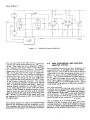
SINE SYNTHESIZER AND FUNCTION
SELECTOR SWITCH
The triangular wave from the linear integrator is
connected to R94. In the SINE position of the FUNCTIoN selector switch (S3) the other end of R94 is
connected to the sine synthesizing diodes and to
R93B, one half of the dual AMPLITUDE potentiometer. The synthesized sinewave signal appears
as the difference signal between points C and D,
but an error signal which appears at D with respect
to B- also appears at C with respect to B-. This
cOmplsite signal is applied to a differential amplifier
in the output circuit.
Sect. ITI Page 5
~-----,.®
B I-STABLE
UNIT
R22
R23
R59
®
LINEAR
INTEGRATOR
R94
©
S3C
S38
R63
S30
f-225 VDC REG.
r-----~-
f-375VDC REG
- - - - - - _-----I
R93B
f225 VDCREG
R95
V4
®
R54>+---r
R93A
S3A
80- .. ·628
f-75VDC
REG.
TO OUTPUT
AMPLIFIER
Figure 3-5.
f-75VDC
REG.
B-
Sine Synthesizer and Function Selector
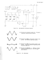
(A) Waveform from integrator output to B-. Triangular
regardless of function selector position.
(B) Waveform from©to B- with selector switch in sine
position. Note distortion especially at peaks.
(C) Waveform from@to B- with selector SWitch in sine
position. This is the distortion component present
in waveform (B) above.
(D) Waveform from©to@ (i. e.: difference between
waveforms (B) and (C) above.) This is the approximated sinewave.
RO
Figure 3-6.
50 tV Waveforms
Sect. ill Page 6
The sinewave is approximated by varying the shunt
resistance across R93B is steps determined by the
diode synthesizing network. The waveform slope,
at first, is just that determined by R94, R93B and
the input waveform. When the first diode conducts
R93 is shunted by a I: redetermined amount, decreasing the slope. Each diode in turn decreases the
slope until all the diode s are conducting and the
triangular wave has reached its crest. The triangular
wave starts down, the diodes stop conducting in turn
until the triangular wave has reached its crest. The
triangular wave starts down, the diodes stop conducting in turn until the triangular wave reaches the
average level. The other half-cycle is formed in
the same manner, but by the diodes that are biased
to shape the negative excursion.
It can be shown that using seven segments to approximate one quarter cycle of the sinewave results in ap-
proximately 1/6% rms distortion. However, variations
in the diodes limit the practical result to about 1%
rms distortion.
In the triangular wave position of the FUNCTION
selector switch the non-linear load consisting of
the diode network is replaced by R95 so that the
combination R94 and R95 is a simple linear divider
for all voltage levels. It is adjusted to give equal
sine and triangular wave peak magnitude. The
squarewave is connected to the FUNCTION selector
switch through the divider R59 and R22 which adjusts
the average voltage of the squarewave to the voltage
at the cathode of V 4. In the squarewave position
of the selector switch, R63 parallels R93B to adjust
the amplitude of the squarewave to be equal to the
amplitude of the sinewave and the triangular wave.
3-5
OUTPUT SYSTEM
The output system consists of three stages as shown
in Figure 3-7. The first stage V18 is a dual triode
acting as a pair of separate cathode followers. These
cathode followers isolate the signal input from the
output stage. Any dc unbalance at the output terminals can be corrected by varying R65.
The second stage V19 is a differential amplifier.
The diffe rence between the two signals at its grids
appears at both plates in nearly equal magnitudes
and 180 0 out of phase. This effect is due to the large
common cathode resistance. In this stage amplification takes place and also the signal difference
E minus F is converted to push-pull voltages. The
third stage V20 is another pair of cathode followers.
The signals appearing at the plates of V19 are
-J15
R72
R74
VIS
R 6
V20
Vl9
C27
R67
R75
R70
R71
R98
R76
R68
8-
C29
R77
R66
Z
R99
R81
R69
R97
Rn
-315----..-----+----.-.<...------------'
Figure 3-7.
Output Amplifier System of Model 202A
sect. ill Page 7
....----
- - - - - - - - - - B+
T4
1
R43
I
I
CRI
I
I
ISYNCO~
I
1t.....4----+-------{
R42
l._.J
C21
C20
R44
B-
~-----+------+------l
Figure 3-8.
Sync Output Circuit of Model 202A
attenuated before being applied to the cathode follower
grids. The small shunt capacitors on the upper sides
of the dividers improve the high frequency response
of the amplifier. The voltages appearing at the
cathode follower output terminals are equal in magnitude and 180 0 out of phase. Negative feedback is
used to reduce distortion, lower the output impedance
and improve stability. This improved stability
applies not only to the signal output, but to the dc
level at the output te rminals.
The symbol for chassis or ground is used for the
first time in the output terminal network R98, R99
and C29. In all other description the reference level
for operation has been B-, and in the Model 202A
the B- line is completely isolated from the chassis.
Thus, the chassis ground is available for whatever
FULL WAVE
RECTIFIER
connection is desired. It is possible to consider
the two output terminals as a transformer output
and further to balance this apparent transformer to
chassis by making R98 equal to R99. The capacitor
C29 insulates the apparent transformer secondary
from ground. If single-ended operation is desired
the ground connection can be tied to either output
terminal without affecting the amplifier.
3-6
SYNC PULSE OUTPUT
The output sync pulse is obtained from the bi-stable
circuit VI and V2. On the minus switching reference
at the plate of multiar diode V3, one positive pulse
and one negative pulse appear for every cycle of
operation. These pulses are coupled to the grid
REGULATOR
7- 315 VOLTS REG.
V5
+225 VOLTS REG
f15 VOLTS REG
V6
B-
Figure 3-9.
Model 202A
Power Supply
Sect. ill Page 8
of the sync pulse amplifier, V17, through an nc
coupling which lowers the average voltage on the
grid to B-.. In the absence of pulses, Vl7 is biased
to cut-off by the bleeder to B+. When a positive
pulse appears at the grid, it momentarily turns
Vl7 "on", thus, inducing a large voltage swing in
the pulse transformer primary. The resistor and
diode in the secondary remove the positive excursion,
resulting in a negative pulse at the SYNC OUT terminals.
I
3-7
POWER SUPPLY
The Power Supply is a full wave rectifier and regulator which supplies + 375 volts. The + 75 volt and
+ 225 volt regulated outputs are taken from a voltage
divider across the + 375 volt supply. The main
requirement on the three regulated voltages is very
low impedance at low frequencies. Reasonable variations in the actual voltages do not affect the output
frequency or waveform.
Sect. IV Page 1
SECTION IV
MAINTENANCE
4-1
GENERAL
4-2
Most of the following analyzing and adjustment procedures require the measurement of dc voltages or
the observation of waveforms. To obtain accurate
results, use a voltmeter with an input resistance of
100 megohms or more. The ~Model 410B Vacuum
Tube Voltmeter is recommended.
POWER SUPPLY
After power supply pa.rts replacements or .adjustments, a final check of regulated voltages should
be made. See Power Supply Regulator Adjustments
in paragraph 4-9.
TABLE 4-1
SYMPTOM
All dc voltages are measured with respect to B- and
not with respect to the chassis. The B- points in
the instrument are connected with black hook-up wire.
CAUSE AND/OR
REMEDY
Instrument inoperative
(Indicator lamp won't
light, no output voltage).
Blown fuse, Flo
Instrument inoperative
(Indicator lamp lights,
no output voltage).
Measure resistance
from V2l socket
(pins 2 or 8) to B-.
55,000 ohms or
more replace V2lo
If less than 55,000
ohms clear short
circuit in filter or
regulator circuits
then replace V21.
Whenever possible the instrument frequency should
be set to approximately 50 cycles/ sec. to permit
the use of a capacitor in series with the ac voltmeter
or oscilloscope to eliminate the dc component.
Instrument inoperative
(normal voltage at V2l).
(Extremely low or no
voltage between V5,
pin 5 and B-).
Defective 6AU5
tubes (V22, V23).
Interaction between most of the circuits of the Model
202A makes a fairly definite procedure for trouble
shooting necessary. For example, a fault in the
oscillator section may easily cause conSiderable
voltage deviations in the output system. Therefore,
it is more desirable to divide the instrument into
five sections as follows and consider each in turn.
Instrument inoperative
(normal + 375V regulated) (+ 225V regulated, off voltage).
Defective OA2 tube
(V5).
(+ 75V regulated, off
voltage)
Defective OA3 tube
(V6).
Instrument inoperative
(No + 225 regulated
+ 75 regulated voltages,
V5 and/or V6 not
ionized).
Open circuit in R62,
R84, R85, R9l, or
R92.
CAUTION
Isolate all test equipment from the main chassis or
grOlmd. Otherwise, both B- and one side of the output
may be connected to the main chassis through the
test equipment. ]f this happens, one cathode resistor
in output stage V20 will be shorted and the tube will
be severely damaged.
4-2
4-3
4-4
4-5
4-6
Power Supply
Function Generator
Sine Synthesizer and Function Selector
Output Amplifier
Sync Out
Capacitor C6 short
circuited.
Sect. IV Page 2
4-3
TABLE 4-2. (CONT'D)
FUNCTION GENERATOR
(bi-stable circuit and integrator)
REPAIR ANALYSIS OF FUNCTION GENERATOR
If replacing tUbes does not restore the triangle
voltage, then a simple test should be made to determine whether the fault is in the integrator or the
bi-stable circuit. This test is as follows:
SYMPTOM
A.
1) Connect a high resistance dc voltmeter between
B- and pin 3 of tube V17.
CAUSE AND/OR
REMEDY
Same symptoms as
above when frequency
dial is set near low
frequency end.
Try replacement
tubes for V15, V16,
and/or V17.
Triangle not linear.
Replace tubes V15,
V16, V17. Check
DC Balance.
2) Set the RANGE switch to the X. 01 position. Disconnect the lead from the center lug of the variable
resistor R58. Temporarily connect this lead to
pin 5, V6 (+ 75 Reg.).
~
3) After this connection is made, the voltage indicated by the voltmeter should slowly climb until it
is over 200 volts.
4-4
4) Remove the lead from the + 75 Reg. supply and
connect it to pin 2, V5 (+ 225 regulated). The voltmeter indication should now drop slowly to less than
140 volts. Disconnect the lead from V5 and return
it to the original connection on R58.
When the trouble has been corrected in the Sine
Synthesizer and Function Selector, the follOWing
checks should be made to determine if the instrument is again functioning correctly.
5) If the instrument meets the above voltage requirements, then the integrator section is functioning
normally and the fault is confined to the bi-stable
circuit. If the instrument does not pass the test,
then the trouble is in the integrator.
After all defective parts have been replaced and
the necessary adjustments made, an oscilloscope
should be connected betw~n pin 3, tube V17 and
B- to see if a good triangular waveform is obtained
on all ranges.
TABLE 4-2.
SYMPTOM
No output voltage (Power
Supply Section normal,
no triangle voltage be tween V17, pin 3 and Bon any range).
same symptoms as above
on one or more ranges.
CAUSE AND/eR
REMEDY·
Replace VI, V2,
V3, VI5, V16,
or V17. If tube
replacement fails
to cure the trouble,
see analysis procedure follOWing
this chart.
Check RANGE
switch contacts,
components, and
connections.
Check C14-C18
for excessive
leakage.
SINE SYNTHESIZER AND FUNCTION
SELECTOR
1) Sine Wave - Observe the waveform between pin 2,
V18 and B- with.oscillator set to 50 cycles/sec. and
the AMPLITUDE control at maximum. Set the
FUNCTION switch in the SINE position. The waveform should be substantially sinusoidal and approximately 30 volts peak-to-peak. See Figure 3-6B.
Observe the waveform between pin 7, V18 and Bwith the same conditions as above. The waveform
should be similar to Figure 3-6C and approximately
1 volt peak-to-peak.
2) Triangular Wave - Observe the waveform between Pin 2, V18 and B- with the oscillator set to
50 cycles/sec. and the AMPLITUDE control at maximum. Set tre FUNCTION switch in the TRIANGUIAR
position. The waveform should be triangular and
approximately 30 volts peak-to-peak.
Observe the waveform between pin 7, VI8 and B- with
same conditions as above. The waveform should be
triangular and approximately 1 volt peak-to-peak.
3) Square Wave - Observe the waveform between
pin 7, VI8 and B- with the oscillator set to 50 cycles/
sec. and the AMPLITUDE control at maximum.
Set the FUNCTION switch to the SQUARE position.
The waveform soould be square and approximately
30 volts peak-to-peak.
The dc voltage across the OUTPUT terminals should
be adjustable to zero under any operating conditions
by means of R65.
Sect. IV Page 3
TABLE 4-3.
CAUSE AND/OR
REMEDY
SYMPTOMS
Maladjustment of
R49, R51, and R60
or defective diodes
CR2 through CRl3.
Sinewave badly
distorted.
DC component at OUTPUT terminals independent of AMPLITUDE
control setting or varied
by AMPLITUDE control.
4-5
After adjustment or tube replacement, the amplifier
should meet the following specifications:
Maladjustment of
R65, R54, and RUB
or defective tubes
V4, VIB, V19, V20.
See DC Balance
Adjustment.
OUTPUT AMPLIFIER
Increased distortion
when amplifier is
loaded with 4000 ohms.
- - - The distortion should remain within specifications when the output is loaded with 4000 ohms
or higher.
--- The peak-to-peak output voltage should be at
least 30 volts (10. 6 volts rms with a sinewave)
when the output is loaded with 4000 ohms or
higher.
4-6
TABLE 4-4.
SYMPTOMS
- -- The output voltage should not drop more than
2% when a 4000 ohm load is connected to the
output.
CAUSE AND/OR
REMEDY
Replace VlB , Vl9,
V20. If distortion
re mains 1 turn off
the power and measure resistance between internal
chassis and main
chassis. See paragraph 4-9.
DC voltage component
exists across the OUTPUT terminals.
See paragraph 4-4.
Distortion increases
appreciably with reduced AMPLITUDE
control setting.
Replace variable
resistor R93A,
R93B.
Failure to deliver 10
volts rms sinewave
output.
Adjust regulated B+
voltage. See paragraph 4-9.
Hum in output voltage.
Replace VIB , Vl9,
V20.
Excessive hum from
power supply. See
paragraph 4-9.
SYNC OUT
Specifications call for a negative sync pulse of 10
volts peak with a duration less than 5 microseconds.
The sync pulse occurs at the sinewave crest and
at corresponding positions on other waveforms.
TABLE 4-5.
SYMPTOMS
CA USE AND lOR
REMEDY
No sync pulse (Check
for negative pulse
with oscilloscope and
with Model 202A set
for highest frequency).
Replace Vl7.
Large overshoot.
Replace CRI.
4-7
TUBE REPLACEMENT
Any tube with standard JETEC characteristics can
be used for replacement purposes.
Whenever a tube is replaced, that part of the instrument which might be affected by the change
must be tested and if necessary, adjusted to be
within specifications. See paragraph 4-B , Tube
Replacement Chart.
.
Sect. IV Page 4
4-8
TUBE REPLACEMENT CHART
TABLE 4-6.
EFFECT
TUBE
4-9
READJUSTMENT
VI, V2
None. Variations in bottoming
voltage eliminated by clamps V7
and VB.
None.
V3
Frequency shift and distortion
increase due to contact potential
variations.
Min. Distortion and Correc
Freq. Adj.
V4
DC output level shift, probably
as a function of amplitude control setting.
DC Ba!. Adj.
V5, V6
Possible change in frequency,
distortion, or dc balance from
change in regulated voltages.
Power Supply.
DC Bal Adjust.
Minimum Distortion and
Correct Freq. Adjust.
V7, VB
Same effect as change in V3
possible, but to much less
degree.
Min. Distortion and Correct
Freq. Adj.
V15, VI6, Vl7
Frequency change and unlnlance
of triangle.
Min. Distortion and Correct
Freq. Adj.
VIB, VI9, V20
Change in dc output component,
independent of AMPLITUDE
control setting.
Set dc output component to
zero by R65, with amplitude
control min.
V21
No effect
None.
V22, V23, V24, V25
Possible change in + 375 and
+ 225 regulated voltages.
Carry out procedure under
"Power Supply Regulator
Adjustment". Paragraph
4-9.
POWER SUPPLY REGULATOR
ADJUSTMENT
2) Connect the 202A to the power line and turn on.
The voltmeter indication should be between + 190
and + 230 volts with line voltage set to 115 volts.
Resistance ~asured between inner and outer chassis
should be at least two megohms with OUTPUT terminals disconnected from panel ground or a load.
This resistance check should be made before starting
the following adjustment procedure:
3) Measure the regulated output voltage between
B- and pin 2 of tube V5. Adjust control R11 to give
a voltage of + 225 volts.
1) Connect the shorting strap between the lower
output terminal and chassis ground. Connect the dc
voltmeter between B- and the inner chassis. The
voltmeter must not be grounded and the common
terminal should be connected to B-.
4) Measure the voltage between pin 5 of tube V5 and
B-. This voltage should be about + 375 volts. Variations in OA3 tubes can cause this voltage to be as
low as 365 or as high as 393.
Sect. IV Page 5
5) Measure the voltage between pin 5 of tube V6
and B-. This voltage should be about + 75 volts.
Variations in OA3 tubes can cause this voltage to
fall at any point between 68 and 85 volts.
6) Repeat step 3 if you replace either V5 or V6.
The characteristics of cold-cathode regulator tubes
drift during about the first 72 hours of operation.
This drift can affect the 202A output. A 72 hour
aging is recommended for a new tube for either
V5 or V6.
7) Test the regulated output voltage at pin 5 of tube
V5 while varying line voltage between 103 and 127
volts. The regulated voltage will normally not change
by more than ±l%. Check power supply tubes and
components if the change is excessive.
4-10
THEORY OF DC BALANCE AND
DISTORTION ADJUSTMENTS
The output AMPLrrUDE control is located at the
input to the output amplifier. H the dc component
at the output terminals is to be zero for all settings
of the AMPLITUDE control the dc levels at the ends
of the AMPLITUDE control must be the same and
also equal to the average level of the input wave.
From the schematic wiring diagram, it is seen that
the common connection between the two sections of
the control is connected to the cathode of V4. The
level of this point can be adjusted to the desired value
by R54. The signal impedance of this point is very
low compared with the magnitude of the AMPLITUDE
control impedance, and therefore, the cathode of
V4 has virtually zero signal.
When R49, R51, R54, and R60 are adjusted properly,
there is no dc component across either section of
the AMPLITUDE control.
When the FUNCTDN switch is in the squarewave
position, there is no signal input to one section of
the AMPLITUDE control, hence, the tap on that
section merely carries the constant bias level set
by the cathode of V4. The other section is connected
through a network to the clamp section of the bistable circuit. R22 of this network adjusts the average level of the squarewave applied to the amplitude
control to the same value as the cathode of V4.
The dc levels at the input to the amplifier are independent of AMPLrrUDE control setting. The dc
levels of the two output terminals may be adjusted
to be equal by R65. Control R65 varies the de level
of the signal on one grid of the second stage of the
amplifier. When these adjustments are made, the
dc component between the output terminals will
remain at a very low value, independent of amplitude
setting or waveform selected.
Control R49 varies the level to which the output of
the integrator rises in a positive direction and R51
varies the level of the negative excursion. The bias
leve Is of the shape r diode s are not variable and
therefore, the triangle input to the shaper can have
one and only one correct magnitude and average
level.
Figure 4-2· shows the situation at the shaper when
the two reference levels are properly adjusted.
Figure 4-2B shows the effect of having the reference
levels adjusted for too large a magnitude, but with
the proper average value. Figure 4-2C shows the
effect of having reference levels adjusted for a
triangle of the proper magnitude, but incorrect
average level. This indicates a close relationship
between correct frequency calibration and minimum
distortion. In fact, the two conditions are simultaneously satisfied by optimum settings of the same
adjustments.
4-11
DC BALANCE AND DISTORTION
ADJUSTMENTS
The follOWing test procedure requires a de voltmeter
with an input resistance of at least 100 megohms
such as an ~Model 410B. In addition, the voltmeter must not be grounded as the common side of
the meter must be connected to points within the
202A that are not at ground potential. A Distortion
Analyzer and an Oscilloscope will also be required.
A 20 minute warm-up is recommended before you
start this procedure. You should also adjust the
power supply as outlined in paragraph 4-9.
1) Adjust the insulated 410B voltmeter to indicate
O. 5 on the 1 volt range with the dc leads shorted.
Use either the "+" or the "-" position of the SELECTOR switch -- whichever one will permit the
O. 5 setting with the ZERO ADJ. control. This meter
indication will be called "0 volts" in the remaining
portion of this procedure.
2) Connect the COMMON lead from the voltmeter
to the common junction of AMPLITUDE controls
R93A and R93B (violet wire).
3) Conne.ct the DC volts probe to the opposite end
of R93A. This is a slate wire connected to the AMPLITUDE control.
4) Set the FUNCTION switch to TRIANGULAR and
adjust R54 for a voltmeter indication of "0 volts".
5) Move the DC volts probe to the arm of R1l8 and
adjust Rll8 for an indication of apprOXimately "0
volts" .
00011-2
Sect. IV Page 6
6) Set the AMPLrrUDE control to minimum (maximum CCW) and move the voltmeter leads to the
red OUTPUT terminals.
15) Switch the FUNCTION selector to TRIANGULAR
and note the voltmeter indication (0.5 on 0-1 scale is
"0 volts"). Adjust R49 to reduce the dc voltage to
one -half of its initial value, then adjust R51 to remove
the remaining dc voltage. The voltmeter should now
indicate "0 volts".
7) Adjust R65, located behind a hole in the panel
near the OUTPUT terminals, for an indication of
"0 volts".
8) Set R1l9, located near VI and T2, to the middle
of its range.
16) Set the FUNCT ION selector to SINE and adjust
Rll8 for a voltmeter indication of "0 volts" .
9) Disconnect the voltmeter and connect equipment as
shown in Figure 4-1.
17) Verify the distortion in the output sine wave at
100 cp s, fir st on the XlO RANGE with the FREQuENcy dial at 10, then on the X100 RANGE with
the FREQUENCY dial at 1. If the distortion indications are not approximately identical, careful
adjustment of Rll9 will lower the 100 cps 'distortion
on the X100 RANGE.
10) Set the FREQUENCY dial to 10, the RANGE
switch to XlO (100 cps), FUNCTION selector to
SINE, and the AMPLITUDE control for an output
of approximately 10 volts rms.
ll) Adjust R49 and R51 to eliminate the points or
spikes at the ends of the Oscilloscope pattern. Adjustment of these controls will shift the output frequency' you should follow the frequency shift with the
Distortion Analyzer. Adjust the Distortion Analyzer
sensitivity as necessary to obtain a useful pattern
on the Oscilloscope (see Figure 4-3).
18) Connect the voltmeter COMMON lead to the
common junction of AMPLITUDE controls R93A
and R93B (violet wire). Connect the DC volts probe
to the green wire on the opposite end of R93B.
12) Adjust R60 for minimum distortion as indicated
on the Distortion Analyzer. Repeat steps II and 12
until the distortion measured is at least 40 db below
the output voltage (1%).
19) Set the FUNCT ION selector to SQUARE and
the RANGE switch to XIO. Adjust R22 for a voltmeter indication of "0 volts".
13) Connect the voltmeter COMMON lead to the
common junction of AMPLITUDE controls R93A and
R93B (violet wire).
20) Any dc between the red OUTPUT terminals with
the AMPLITUDE control at minimum may be eliminated by adjusting R65 (behind the hole in the panel).
This voltage should vary less than ±O. 5 volts when
the AMPLITUDE control is rotated through its full
range.
14) Connect the DC volts probe to the opposite end of
R93B. This is a green wire connected to the AMPLITUDE control.
-hp- MODEL 202A
-hp- MODEL 330
LOW FREQU EN C Y
FUNCTION GENERATOR
DISTORTION
ANALYZER
<:
r::-.
f\
OUT~ ..J
~
1~'N
~
OUT"""
-hp- MODEL
120 OR 130
OSCILLOSCOPE
f\
\.
@.. ~
f\
'el VERT.
L ~
HORIZ,Q.
~
0
BO-S-38
Figure 4-1.
Minimum Distortion and Frequency Adjustment Instrumentation
Sect. IV Page 7
(A) Correct setting of
reference levels.
Triangle & Sine Ave.
(B) Both Ref. levels too large.
Causes decrease in frequency
and high 3rd harmonic distortion (i. e. flattened peaks).
+ Ref.
Ref.
_
Sine Ave.
--ProperAve.-----_Tria..!!,g~Ave.
(C) + Ref. too high and -Ref. too low.
Frequency
correct but large 2nd harmonic as seen by peak
flatteniilg on one side and sharpening on other.
Also sine average not same as triangle.
Triangle & Sine Ave.
Figure 4-2.
(D) References are correct but triangle unbalanced. Frequency
correct but high second harmonic
component in phase with fundamental.
Ref.
Effect of Triangle Maladjustment on Distortion and Frequency.
Ten-Segment Approximations Used for Clarity.
RO
00011-3
Sect. IV Page 8
(A) R60 and R119 misadjusted
(B) R51 misadjusted
(C) R49 misadjusted
0
(D) R49 and R51 misadjusted in
same direction
(E) R49 and R51 misadjusted
E
F
I
I
(F) R49 and R51 misadjus.ted in
opposite direction of pattern
D above
!
I
II
l
...
~~
~ ~
~
Figure 4-3.
~~
J}.
I'i..A
~,-
W
Typical adjusted pattern for minimum distortion and correct ~re
quency
I
Patterns Showing the Adjustments of R49, R51, R60 and R119 to
Obtain Minimum Distortion and Correct Frequency
Sect. IV
00011-2
4-12
ADJUST SQUAREWAVE AMPLITUDE
Adjust control R63 to produce an output squarewave
with the same peak-to-peak amplitude as the sine
and triangular output waveforms.
4-13
FREQUENCY RATIO AND
CALIBRATION PROCEDURE
The following procedure is intended for use after
replacement of the Range Switch or any of the frequency determining components on the Range Switch.
This procedure is also required following replacement of frequency determining potentiometer R58.
1) Remove the cabinet or top and bottom instrument covers.
2) Check that the upper and lower dial stops fall
about an equal distance outside the upper and lower
dial calibration marks. Correct the dial setting,
if necessary, by rotating the dial on the dial mounting
hub. The dial stops and not the potentiometer mechanical stops should be limiting dial travel.
7) Set the frequency dial to 0.8 and adjust control
R109 to obtain a period of 1250 milliseconds. Check
the setting made in step 6 and, if necessary, repeat
step 6.
If RI09 has insufficient range, center the control mechanicallyand repeat steps 6 and 7. This will electrically center the adjustment range of R109 which
c an then be used to make any final adjustments.
8) Check calibration of the "Xl" range. The output frequency should be within ±2% of the dial reading over the entire range. Adjust R26B if necessary.
9) Check the calibration of the other ranges. Adjust R24B for the "X. 01" range, R25B for the "X. 1"
range, R27B fo r the "XlO" range and R28B for the
"XlOO" range.
On the "XlOO" range only, adjust C 33 to calibrate
the high end of the band.
10) Replace the cabinet or the top and bottom cover.
4-14
3) Tum the 202A on, set the line voltage to 115 volts,
turn the FUNCTION switch to "SQUARE", and allow
at least a 1 hour warm-up period.
4) Adjust power supply, then adjust DC Balance
and Distortion.
Page 9
REPLACEMENT OF R58
POTENTIOMETER
Replacement of the frequency control potentiometer
involves two basic operations:
1) The mechanical procedure for replacing a defective potentiometer with a new one.
2) The necessary electrical adjustments described
in paragraph 4-13.
5) Determine the ratio between the two frequencies
obtained with the frequency dial at "0. 8" and "12"
with the RA NGE switch at "Xl".
Frequency determination is most easily accomplished
by measuring the period of the unknown frequency.
An electronic counter such as ~Model 522B, 523B,
or 524B will be needed. A frequency of O. 8 cps has
a period of 1250 milliseconds while 12 cps has a
period of 83.3 milliseconds.
6) The ratio obtained in step 5 must be 15 to 1. Adjust
by loosening the coupler between the dial and potentiometer (R58) shafts. See Figure 4-4 for coupler
access hole location. Rotate one shaft with respect
to the other to obtain a period of 83.3 milliseconds
with a dial reading of 12. Tighten both set screws
in the coupler.
All neces~ry specialized instructions are included
with the replacement potentiometer.
4-15
PERFORMANCE CHECK
4-16.
OUTPUT VOLTAGE AND WAVEFORM
CHECK.
1) Connect test setup as shown in figure 4-4, including a 3.9Kohm shunt resistor across the OUTPUT terminals of Model 202A.
2) Set Model 202A controls as follows:
RANGE. . . . • • . • .
. . . . X10
FREQUENCY DIAL
• . • • . . . . 10 (100 cps)
AMPLITUDE.
. . . . . . . full cw
FUNCTION. . . . . .
SINE
3) Set oscilloscope VERTICAL SENSITIVITY to
5 volts/cm.
00011-3
Sect. IV Page 10
4) Sinewave observed should be sinusoidal and have
an amplitude of at least 30 volts peak-to-peak.
MODEL
5) Set FUNCTION to TRIANGULAR.
LOW FREOUENCY
FUNCTION GENERATOR
~
r!j)
MODEL
330 B/C/D
DISTORTION
ANALYZER
202A
6) Wave observed should be triangular and have an
amplitude of at least 30 volts peak-to-peak.
SYNC
8) Square wave observed should have an amplitude
of at least 30 volts peak-to-peak.
SYNC PULSE CHECK.
1) Connect test setup as sh()wn in figure 4-4, except
oscilloscope is to be connected to SYNC. OUT on
Model 202A and not to OUTPUT.
~
MODEL 130B
OSCI LLOSCOPE
c!jJ
•
MODEL
202A
LOW FREOUENCY
FUNCTION GENERATOR
0
SYNC OUT
0
0
~
@
00
OUTPUT
3.9K
~
o
00
lD-S-SI.
0
'--~
o
o
@
3.9K
~
METER
I
UT
AF INPUT
o
o
@
o
o
Figure 4-5. Sine Wave Distortion Test Setup
3) Set Model 202A controls as follows:
RANGE . • . . • . . . . . . . . . . . . . . . . . X10
FREQUENCY DIAL . • . . • . . . . . 10 (100 cps)
FUNCTION. . . . . . . . . . . . • . . . . . • SINE
AMPLITUDE adjusted for 10.6 volts output (read
on Model 330B/ C/D) .
4) Disconnect cable from METER INPUT and reconnect it to AF INPUT.
@@@
0
[gJ
OUTPU
7) Set FUNCTION to SQUARE.
4-17.
o
5) Set FUNCTION to SET LEVEL and METER
RANGE to 100%.
6) Adjust INPUT SENSITIVITY for 100% on the 10
scale (full scale is 100%).
----'
7) Set FUNCTION to DISTORTION.
Figure 4-4.
Output Voltage and Sync Pulse
Test Setup
2) Set RANGE to X100 and FREQUENCY DIAL to
10 (1000 cps).
3) Set oscilloscope VERTICAL SENSITIVITY to
5 volts/cm and SWEEP TIME to 1 sec/cm.
4) The negative pulse observed should be less than
5 sec duration and have an amplitude equal to or
greater than 10 volts.
8) Tune Model 330B/C/D for null.
9) Set METER RANGE to 3% and retune for null.
Reading should be less than 1 on the 3 scale (full
scale is 3%).
10) On Model 202A change RANGE to X100 and
FREQUENCY to 1 (100 cps). Repeat steps 1 through
9 at this frequency. Reading should be less than 2.
4-19. DIAL ACCURACY CHECK.
1) Connect test setup as shown in figure 4-6.
4-18. SINE WAVE DISTORTION CHECK.
2) Allow 1/2 hour warmup period.
1) Connect test setup as shown in figure 4-5, including a 3. 9K ohm shunt resistor across the OUTPUT terminals of Model 202A.
3) Set Model 202A controls as follows:
RANGE. . . . .
. . . . . .
.
X100
FREQUENCY
12 (1200 cps)
FUNCTION
'. . . SQUARE
2) Set Model 330B/C/D controls as follows:
INPUT . . • . . . . . .
FREQUENCY RANGE .
FREQUENCY DIAL
FUNCTION . • . .
METER RANGE . .
.
.
•
•
.AF
• Xl
100 cps
. • • .
• METER
•••.
• • • • • 30 RMS VOLTS
4) Set Model 523C/D for period measurement as
follows:
FUNCTION SELECTOR
PERIOD
TIME UNIT. . . . . . . . . . . . . . . . • . IlSEC
5) Model 523C/D should read between 816 and 850.
00011-3
~
MODEL 202A
r!jJ
MODEL
523 C/O
ELECTRONIC COUNTER
LOW FREQUENCY
FUNCTION GENERATOR
0
SYNC OUT
0
0
~
@
0
O"~
1(5<tCct~Q,1
~
@
@
Sect. IV Page 11
7) Counter should read between 8.16 and 8.50.
8) Set Model 202A RANGE to Xl and FREQUENCY
dial to 1. 4 (1. 4 cps).
9) Counter should read between 699.9 and 728.5.
10) Set Model 202A RANGE to Xl (.14 cps).
@
IN~T
I
11) Counter should read between 6999.9 and 7284. 7.
Figure 4-6. Dial Accuracy Test Setup
12) Set Model 202A RANGE to X.01, FREQUENCY
dial to .8 (.008 cps) and Model 523C/D TIME UNIT
to SEC.
6) Set Model 202A RANGE to X10 (120 cps) and
Model 523C/D TIME UNIT to Mll..,LISEC.
13) Counter should read between 121.25 and 128.75.
Due to such a low frequency the counter may not
start its count for approximately 2 min and 5 sec.
\.0-$-$16
4-13
SEE
PARA.
~
R51
R49
R248
R258
R268
R288
R278
V2
Cf4
T3
T2
C33
V5
VI5
V21 V3
VI
VI6
RI19
VI7
R58
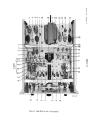
Figure 4-7. Model 202A Top View
V6
VI9
....
-
RI09
C6
V20
e
V22
Cover Removed
VI8
TI
V24
V20
R63
V7 - - - -
R54
R60
R22
V23
I
I'"
.'
I :1
I·
~.
I
~
____
't
WIt\
...... ___ ,.._
"
_
_
_ _-_ _ _._"""' ....
VI9
VIS
~
_ .- ~
~
-~~
tan'·
...~l
VI7
VI6
Vl5
------_-...... ,,--- -
_ _ _ - ;1
--_.--
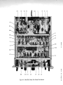
Figure 4-8. Model202A Bottom View Bottom Plate Removed
R93
_ _ • _ _ _ _ 'v _ _..
lwk~'"
_;o-~.. ~___
R65
--
__ . __
......-...,...........-.~
I
I
r--
GRN-BlK
PAl.
--
TRANSFORMER
I
BLACK
,III
TI
TI
DETAil
~lK
PAl. 2
----rY'El- BlK
I
230V
50-IOOO'\"
'V
~IOOO
115V
BLACK
TI
~
~
3
7
4
-I
IV
I
4
R5
27K
POINTS AND B-
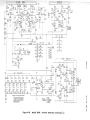
Figure 4-9.
PRIMARY START.>
3. PANEL CONTROLS SET AS FOLLOWS:
RANGE AT X 10.
FREQUENCY AT 5.
FUNCTION AT SINE.
AMPLITUDE AT MAX.
~~2;[
R7
100
!~O~
4
I
§'
I
.llIf
C4
I
'+149
••
RI2
181K
0~RII
•
25K
RIO
284K
INTERNAL CHASSIS, ONE POINT CONNECTION TO DIVIDER
~~,
UNLESS OTHERWISE NOTED,
Power Supply
202A - PS - T037AB
CAPACITY IN
V,POWER SUPPLY RETURN) IS ~ CONNECTED TO CHASSI
6R78 a R7i
rh
.... MAIN'(EXTERNAL) CHASSIS,ISOLATED FROM POWER SUPPL
VOLTAGES.
K = 1000 OHMS
M- I MEGOHM
AMPLIFIER SECTION AS WELL AS TO POWER SUPPLY SECTION).
3
R4
.V'., -,
220K
WITH A VOLTMETER OF 122MEGOHMS INPUT RESISTANCE.
(8- IS ANY BLACK LEAD IN POWER SUPf:'LY EXCEPT T I
I. 115/230V, 50/l0OO,\- POWER SUPPLY
2, MEASURED BETWEEN THE INDICATED
CONDITIONS OF DC VOLTAGE MEASUREMENT:
a
boo
~=
R3
100
+ 545
23
=~-_:~-~-~""t-~~----I--T-~~~~~• • •
[
n-,
+545~
-
NOTES: (APPLY TO FUNCTION GENERATOR
7
tv ~V22~V23
2
!
4
4
4
1~V ~VI ~V2
1
11:71:
R22
1M
I
R42
150K
,/'
B-
R41*
12K
12AU7
R84B
273
RII4
115K
f'SV
•
~~2:1~~t~~~~rd_ ~~:r"Y'
r
R85A
350
l6
214 K
R84A
350
~
I
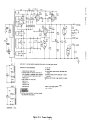
Figure 4-10.
R92
3000
R84C
150
RI13
71.56K
Thl. drawln, I. Intended for the op.rollon
Gnd ",oln'.nonce of He.leu-'ackard eqvlp·
",en' and I. not to b. "•• d otherwl.. or
,.prodwc.d without w,ltten con'."1 of the
R84D
94.4
RII2
37.4K
COPYlIGHT 19$9 tY HfWlm.PACK.... D COMPANY
R84E
59.5
Rill
13.2K
C20
.01j.lF
8
'-..fa'
.".
V178
OUT
-Om
R20
27K
R58
lOOK
f170V
RI5
120K
RI09
2000
R46
12K
f170V
6AL5
RI03
1800
f'SV
,
2
:~A*
3
2
•
f22SV
5000
t
>+_"':'::~I-
f75V
1500K R54
FUNCTION I
R29
5.16M
fJ75V ....
N'}60
GRIO
~:
""
FROM-
•
I'
R95
67.5K
R94
33K
®~
0[U]
[!J]
® l:!ZJ
G)
S2C
CI5
I~F
CI4
R39
1.031M
2
fJ'SV
B-
R70*
270K
R97
390K
R96
390K
'
I
----+--..
R66
39K
R68
39K
R67
1200
,
12AU7
VI8
r - - - - OUTPUT
@---il-------@
CI8
100
@----if-0
CI7
1000
R35
1.5M
S2D
1>--0
'
405K
R38
0
3 f85V
12'X
6 fl60V
-
(D---l~
.01j.lF
R36
1.5M
, "V16
'
,
'1l
M"\
~~
CI6
o-{I
fJ'SV _
OIRANGEI
0~
S2A-D
260 V
R30
405K
+
~
l
~'
fISOvl ......
8
R31
405K
Function Generator and Amplifier
oS3A-D
I
fJ'SV
+
fR'2"7iil 4
:~~:* ~8B
r-------t
4
-
Model 202A
ClJ
1M
R26B
KIM
R26A
900K*
R25A
RI05
14.5K
lR'19
500
RI04
14.5 K
+J75V-..
,r-------INTEGRATOR--
I ~
~~
3
2
R25B
R24B
~
~R118
RI17
4.7M
I
@
S2B
R57
103.5K
;T4J
f
V78 \ .....
470
CI3
1
I
V88
5b
1'~6AL5
1
+
f225 V
'...
_fISOV 2
+J'5V
o~
,
'"
~9OOK*
! FREOUENCY
I SYNC
AMPLIFIER - - "
SIN E SYNTHESIZER - - - - -
!R44
3.3M
~=}
.1.C21
1'820
•
fJ7SV
I
r - - SYNC
~
106
120K
_
CIRCUI T - - - - - - - - - - -,
R91
2500
R84F
29.3
~g&,~~~~
R59*
330K
R23*
3.3M
• r
f22SV
f'5V
t
R52
27.5K
(lJ
5000
R51
R50
14.4K
•
f225 V
@
,.---- - - - - - - BI-STABLE
Sect. V Page 1
SECTION Y
TABLE OF REPLACEABLE PARTS
. . . - - - - - - - - - - - - - - - - - - N 0 T E- - - - - - - - - - - - - - - - - - - ,
Standard components have been used in
whenever possible.
this
instrument,
Special components may be obtained
from your local Hewlett-Packard representative or from
the factory.
When ordering parts always include:
1.
~
2.
Complete description of part including
reference.
3.
Model number and serial number of instrument.
4.
If part is not listed, give complete description,
function and location of part.
Stock Number.
circuit
Corrections to the Table of Replaceable Parts are listed
on an Instruction Manual Change sheet at the front of this
manual.
. . . . . . . - - - - - - - - - - - RECOMMENDED SPARE PARTS LIST - - - - - - - - - -.......
Column RS in the Table lists the recommended spare parts
quantities to maintain one instrument for one year of isolated service.
Order complete spare parts kits from the
Factory Parts Sales Department.
ALWA YS MENTION THE
MODEL AND SERIAL NUMBERS OF INSTRUMENTS INVOLVED.
12-1-59
Sect. V
Page 2
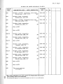
TABLE OF REPLACEABLE PARTS
cmcurr
REF.
Cl,2
C3
C4
C5
~ STOCK
DESCRIPTION, MFR. * & MFR. DESIGNATION
Capacitor: fixed, electrolytic,
20 f.J.f, 450 vdcw
Capacitor: fixed, paper,
1 f.J.f ±20%, 400 vdcw
Capacitor: fixed, paper,
0.1 f.J.f ±lO%, 400 vdcw
CC*
Capacitor: fixed, paper,
. 22 f.J.f ±1O%, 400 vdcw
CC*
fixed, paper
4 f.J.f ± 10%, 600 vdcw
C7,8
Same as C4
C9
Capacitor: fixed, mica,
82 pf ±10%, 500 vdcw
V*
Capacitor: fixed, mica,
470 pf ±1O%, 500 vdcw
V*
Capacitor: fixed, mica,
39 pf ± 10%, 500 vdcw
C13
Same as ClO
C14
Capacitor: fixed,
1 f.J.f ±5%, 400 vdcw
C15
C16
C17
C18
C19
p.
Capacitor: fixed, ceramic
.01 f.J.f, tol. -0% +100%, 1000 vdcw
C12
RS
0180-0011
2
1
0160-0016
2
1
0160-0013
5
2
0160-0018
1
1
0160-0077
1
1
0140-0006
1
1
0140-0027
3
1
0150-0012
3
1
0140-0021
1
1
0170-0059
1
1
0170-0001
1
1
0170-0023
1
1
0140-0079
1
1
0150-0007
1
1
A*
Ca.pacitor~
Cll
TQ
CC·
C6
CIO
NO.
CC*
V·
.
AL*
Capacitor: fixed, polystyrene,
.1 f.J.f ±5%, 300 vdcw
J*
Capacitor: fixed, polystyrene,
.01 f.J.f ±5%, 600 vdcw
AL*
Capacitor: fixed, silver mica,
. 001 f.J.f ± 5%, 500 vdcw
A*
Capacitor: fixed, ceramic,
100 pf ± 5%, 500 vdcw
K*
This circ uit reference
not assigned
• See "List of Manufacturers Code Letters For Replaceable Parts Table" •
TQ - Total quantity used in the instrument.
RS - Recomrre nded spares for one year isolated service for one instrument.
00011-2
Sect. V Page 3
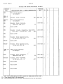
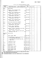
TABLE OF REPLACEABLE PARTS
CIRCUIT
REF.
DESCRIPTION, MFR.
*
~ STOCK
&MFR. DESIGNATION
C20
Same as Cll
C21
Capacitor: fixed, mica,
820 pf ±1O%, 500 vdcw
C22
Same as Cll
C23
Capacitor: fixed, ceramic,
. 005 J.lf, 500 vdcw
NO.
TQ
RS
0140-0010
1
1
0150-0014
1
1
0140-0026
2
1
0130-0001
1
1
V*
K*
C24
Same as C4
C25
This circuit reference
not assigned
C26
Same as C4
C27, 28
Capacitor: fixed, mica,
22 pf ±10%, 500 vdcw
C29
Same as C3
C30, 31, 32
These circuit references
not assigned
C33
Capacitor: variable, ceramic,
7-45 pf, 500 vdcw. Optimum value
selected at factory. Average value shown.
C34
Same as C10
C35
Capacitor: fixed, electrolytic, 2 section
20 J.lf/ sect., 450 vdcw
0180-0012
1
1
CC*
CHI
Diode, germanium
BU* 1910-0009
1
1
CH2-l3
Diode, silicon
HP* G-29M-45
12
12
Fl
Fuse, cartridge: 3 amp (ll5V)
Fuse, cartridge: 1. 6 amp (230V)
T* 2110-0003
E* 2110-0005
1
1
10
n
Lamp, incandescent: 6-8V, 2pin base GE#12 N* 2140-0012
1
1
Ll
Inductor: 6H at 125 MA, 264 ohms
HP* 9110-0004
1
1
PI
Power Cable
Elec. Cords Co. 8120-0015
1
1
Z*
L*
* See" List of Manufacturers Code Letters For Replaceable Parts Table".
TQ - Total quantity used in the instrument.
RS - Recommended spares for one year isolated service for one instrument.
o
Sect. V Page 4
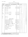
TABLE OF REPLACEABLE PARTS
cmcurr
$ STOCK
NO.
TQ
RS
0687-1011
4
1
0693-2241
1
1
0690-2731
3
1
0690-3941
3
1
0816-0009
1
1
0730-0083
1
1
Rll
2100-0009
Resistor: variable, composition, linear taper,
BO*
25, 000 ohm~ ±20%, 1/3 W
1
1
R12
Resistor: fixed, deposited carbon,
181, 000 ohms ±1%, 1 W
0730-0077
1
1
0690-3341
5
2
0690-2231
2
1
0693-1241
4
1
0693-8231
2
1
REF.
DESCRIPTION, MFR. * &MFR. DESIGNATION
R1
This circuit reference
not assigned
R2,3
Resistor: fixed, composition,
100 ohms ±1O%, 1/2 W
B*
Resistor: fixed, composition,
220, 000 ohms ±10%, 2 W
B*
Resistor: fixed, composition,
27, 000 ohms ±1O%, 1 W
B*
Resistor: fixed, composition,
390, 000 ohms ±1O%, 1 W
B*
R4
R5
R6
R7
Same as R2
R8
Resistor: fixed, wirewound,
25,000 ohms ±1O%, 10 W
S*
R9
Same as R2
RIO
Resistor: fixed, deposited carbon,
284,000 ohms ±1%, 1 W
R13
R14
R15
R16
Resistor: fixed, composition,
330, 000 ohms ±1O%, 1 W
..
NN*
NN*
B*
Resistor: fixed, composition,
22,000 ohms ±10%, 1 W
B*
Resistor: fixed, composition,
120,000 ohms ±1O%, 2 W
B*
Resistor: fixed, composition,
82,000 ohms ±1O%, 2 W
B*
R17
same as R15
R18
Same as R13
* See" List of Manufacturers Code Letters For Replaceable Parts Table".
TQ - Total quantity used in the instrument.
RS - Recommended spares for one year isolated service for one instrument.
Sec t. V Page 5
00011-2
TABLE OF REPLACEABLE PARTS
r$j) STOCK
cmcurr
REF.
DESCRIPTION, MFR. * &MFR. DESIGNATION
NO.
TQ
RS
R19
Same as Rl4
R20, 21
Same as R5
R22
Resistor: variable, composition, linear taper,
00*
1 megolun ± 30%, 1/4 W
2100-0074
6
2
R23
Resistor: fixed, composition,
3.3 megohms ±10%, 1 W Optimum ·,alue
adjusted at factory. Average value shown. B*
0690-3351
1
1
0730-0103
4
1
NN* 0730-0100
Resistor: fixed, deposited carbon
Optimum value
800,000 ohms ± 1%
selected at factory. Average value shown. NN*
1
1
0730-0126
1
1
0730-0088
4
1
0730-0113
2
1
0690-1551
2
1
0730-0106
2
1
0693-3331
1
1
These circuit references not assigned
R24 thru
R28
R24A thru Resistor: fixed, deposited carbon,
Optimum value
900,000 ohms ±1%
R27A
selected at fact9ry. Average value shown.
R28A
R24Bthru
R28B
Same as R22
R29
Resistor: fixed, deposited carbon,
5.16 megohms ±1%, 1 W
NN*
Resistor: fixed, deposited carbon,
405,000 ohms ±1%, 1 W
NN*
Resistor: fixed, deposited carbon,
2.163 megohms ±1%, 1 W
NN*
R30 thru
R32
R33, 34
R35, 36
R37
Resistor: fixed, composition,
1. 5 megohm ±1O%, 1 W
Resistor: fixed, deposited carbon,1. 031 megohm ±1%, 1 W
R38
Same as R31
R39
Same as R37
R40
Resistor: fixed, composition,
33,000 ohms ±1O%, 2 W
B*
NN*
R*
R41
Resistor: fixed, composition,
12,900 oluns ±1O%, 1/2 W Optimum value
selected at factory. Average value shown. B*
0687-1231
1
1
R42
Resistor: fixed, composition,
150,000 ohms ±1O%, 2 W
0693-1541
5
2
B*
Resistor: fixed, composition,
1200 ohm s ±10%, 1 W
0690-1221
3
1
B*
R43
• See" List of Manufacturers Code Letters For Replaceable Parts Table".
TQ - Total quantity used in the instrument.
RS - Recommended spares for one year isolated service for one instrument.
00011-2
Sect. V Page 6
TABLE OF REPLACEABLE PARTS
CIRCUIT
REF.
R44
~ STOCK
DESCRIPTION, MFR. * & MFR. DESIGNATION
Resistor: fixed, composition,
3.3 megohms ±1O%, 1 W
R45
Same as R43
R46, 47
Resistor: fixed, composition,
12, 000 ohms ±1O%, 1 W
R48
Resistor: fixed, deposited carbon,
10.310 ohms ±1%, 1 W
NO.
TQ
RS
0690-3351
1
1
0690-1231
2
1
0730-0031
1
1
B*
B*
NN*
R49
Resistor: variable, wirewound, Ii near taper,
BO*
5000 ohms ±1O%, 2 W
2100-0006
4
1
R50
Resistor: fixed, deposited carbon,
14,400 ohms ±1%, 1 W
0730-0034
1
1
0730-0044
1
1
0730-0048
2
1
0730-0049
1
1
0730-0070
1
1
2100-0244
1
1
NN*
R51
Same as R49
R52
Resistor: fixed, deposited carbon,
27,500 ohms ±1%, 1 W
NN*
Resistor: fixed, deposited carlx>ll,
33,000 ohms ±1%, 1 W
NN*
R53
R54
Same as R49
R55
Resistor: fixed, deposited carbon,
37,000 ohms ±1%, 1 W
NN*
R56
This circuit reference
not assigned
R57
Resistor: fixed, deposited carbon,
103, 500 ohms ±1%, 1 W
NN*
Resistor: variable, wirewound,
100,000 ohms ± 1%, 8 W
HP*
R58
R59
Optimum value selected at
Same as R13
factory. Average value shown.
R60
Same as R49
R61
This circuit reference
not assigned
R62
Resistor: fixed, wirewound,
3000 ohms ±1O%, 10 W
.
0816-0002
S*
* See" List of Manufacturers Code Letters For Replaceable Parts Table".
TQ - Total quantity used in the instrument.
RS - Recommended spares for one year isolated service for one instrument.
2
1
Sect. V Page 7
TABLE OF REPLACEABLE PARTS
~ STOCK
cmcurr
DESCRIPTION, MFR. * & MFR. DESIGNATION
NO.
TQ
R63
Resistor: variable, composition, linear taper,
BO*
125,000 ohms ± 20%, 1/4 W
2100-0073
1
1
R64
Resistor: fixed, wirewound,
30,000 ohms ± 5%, 10 W
0815-0001
1
1
REF.
RS
R*
R65
Resistor: variable, composition, linear taper
BO*
2000 ohms ±20%, 1/3 W
2100-0153
2
1
R66
Resistor: fixed, composition,
39, 000 ohms ±1O%, 1 W
0690-3931
2
1
0690-2741
2
1
0690-5641
1
1
0690-1051
2
1
0690-2251
2
1
0693-2731
2
1
0690-1841
1
1
0690-2241
1
1
B*
R67
Same as R43
R68
same as R66
R69, 70
Resistor: fixed, composition,
270, 000 ohms ±10%, 1 W
B*
Resistor: fixed, composition,
560, 000 ohms ±1O%, 1 W
B*
R71
R72, 73
same as R13
R74
Resistor: fixed, composition,
1 megohm ±1O%, 1 W
B*
Resistor: fixed, composition,
2.2 megohms ±1O%, 1 W
B*
Resistor: fixed, composition,
27 ,000 ohms ±1O%, 2 W
B*
Resistor: fixed, composition,
180, 000 ohms ±1O%, 1 W
B*
Resistor: fixed, composition,
220,000 ohms ±10%, 1 W
B*
R75
R76, 77
R78
R79
R80
Same as R74
R81
Same as R75
R82
This circuit reference
not assigned
* See" List of Manufacturers Code Letters For Replaceable Parts Table".
TQ - Total quantity used in the instrument.
RS - Recommended spares for one year isolated service for one instrument.
00011-2
Sect. V Page 8
TABLE OF REPLACEABLE PARTS
CIRCUIT
REF.
<liJ STOCK
DESCRIPTION, MFR. * & MFR. DESIGNATION
H83
This circuit reference
not assigned
R84a-f,
1R85a-f
Resistor: fixed, wirewound
R86 thru
R90
These circuit references
not assigned
1R91
Resistor: fixed, wirewound,
2500 ohms ±1O%, 10 W
R93
Resistor: variable, composition, dual tandem,
linear taper, 1 megohm/sect. ±20%
BO*
R94
Same as R53
R95
Resistor: fixed, deposited carbon,
67, 500 ohms ±1%, 1/2 W
R98,99
Resistor: fixed, deposited carbon,
15,800 ohms ±l%, 1 W
R100, 101
102
R103
R104,105
RS
.
1
0816-0005
1
1
2100-0258
1
1
0727-0199
1
1
0730-0036
2
1
0690-1821
1
1
0811-0038
2
1
S*
Same as R62
Same as R6
TQ
2
HP* 202A-26C
1R92
R96,97
NO.
NN*
NN*
These circuit references
not assigne d
Resistor: fixed, composition,
1800 ohms ±1O%, 1 W
Resistor: fIXed, wirewound,
14, 500 ohms, ±1%, 3 W
R106
Same as R15
R107
Same as R16
RI08
Same as R15
B*
AC*
* See" List of Manufacturers Code Letters For Replaceable Parts Table".
TQ - Total quantity used in the instrument.
RS - Recommended spares for one year isolated service for one instrument.
Sect. V Page 9
00011-2
TABLE OF REPLACEABLE PARTS
cmcurr
*
~ STOCK
NO.
TQ
RS
0727-0096
1
1
0727-0165
1
1
0727-0187
1
1
NN* 0727-0201
1
1
0727-0213
1
1
0727-0222
1
1
0687-4751
1
1
Rl18
2100-0015
Resistor: variable, composition, linear taper,
B>I
500,000 ohms, ± 20%, 1/4 W
1
1
Rl19
2100-0054
Resistor: variable, wirewound, linear taper
500 ohms, ± 10%, 2 W
BO'"
1
1
R120 thru
R123
Same as R42
4
Sl
Switch, toggle: SPST
S2
REF.
DESCRIPTION, MFR.
&MFR. DESIGNATION
R109
Same as R65
R110
Resistor: fixed, deposited carbon,
920 ohms ±1%, 1/2 W
NN*
Resistor: fixed, deposited carbon,
13,200 ohms ±1%, 1/2 W
NN*
Resistor: fixed, depo~ited carbon,
37,400 ohms ±1%, 1/2 W
NN*
R111
R112
R113
Resistor: fixed, deposited carbon,
71,560 ohms ±1%, 1/2 W
Rl14
Resistor: fixed, deposited carbon,
115,000 ohms ±1%, 1/2 W
Rl15
This circuit reference not assigned
Rl16
Resistor: fixed, deposited carbon,
214, 000 ohms ±1%, 1/2 W
Rl17
Resistor: fixed, composition,
4.7 megohms ±10%, 1/2 W
NN*
NN*
B*
D'" 3101-0001
1
1
Range Switch Assy: (includes C15 thru C18,
C33, R24A thru R28A, R29)
HP'" 202A-19W
1
1
S3
Function Switch Assy: (includes C34, R94,
R95, R117)
HP'" 202A-19B
1
1
T1
Transformer, power
HP* 9100-0026
1
1
T2,3
Transformer, pulse
HP* 9130-0002
2
1
T4
Transformer, pulse
HP* 202A-60B
1
1
V1,2
V3
Tube, electron: 6AU6
Tube, electron: 6AL5
zz* 1923-0021
3
3
3
3
V4
Tube, electron: 6C4
ZZ* 1921-0005
1
1
ZZ* 1940-0004
ZZ* 1940-0006
2
1
2
1
V5
V6
V7,8
Tube, electron: OA2
Tube, electron: OA3
Same as V3
* See" LIst of Manufacturers Code Letters For Replaceable Parts Table".
TQ - Total quantity used in the instrument.
RS - Recommended spares for one year isolated service for one instrument.
00011..3
Sect. V Page 10
TABLE OF REPLACEABLE PARTS
cmcurr
REF.
~ STOCK
DESCRIPTION, MFR. • & MFR. DESIGNATION
NO.
TQ
RS
V9 thru
V14
These circuit references
not assigned
V15, 16
Tube, electron: 12AX7
ZZ.*
1932-0030
3
3
V17, 18
Tube, electron: 12AU7
zz*
1932-0029
3
3
V19
Same as V15
V20
Same as Vl7
V21
Tube, electron: 5U4GA/B
ZZ*
1930-0008
1
1
V22, 23
Tube, electron: 6AV5GA or
ZZ*
1923-0023
2
2
6AU5GT
V24
same as VI
V25
Same as V5
ZZ* 1923-0020
MISCELLANEOUS
Binding Post Assembly: red
HP* AC-lOD
3
1
Binding Post Assembly: black
HP* AC-IOC
1
1
Binding Post Insulator: (2 holes)
HP* AC-54A
1
0
Binding Post Insulator: (3 holes)
HP* AC-54B
1
0
Connector Assembly: (binding·post, with
ground link)
1
1
HP*
Couple r, flexible: 1/4" to 1/4" shaft
HP* AC-32A
2
1
Coupler, metal bellows type
HP* 417A-32
1
1
Dial, frequenc y
HP* 202A-40A
1
0
Escutcheon, dial window
Hp· G-99E
1
0
1
1
Fuseholder
G-76K
T* 1400-0084
• See" LIst of Manufacturers Code Letters For Replaceable Parts Table".
TQ - Total quantity used in the instrument.
RS - Recommended spares for one year isolated service for one instrument.
Sect. V Page 11
TABLE OF REPLACEABLE PARTS
~STOCK
cmcurr
REF.
DESCRIPTION, MFR. * & MFR. DESIGNATION
NO.
TQ
RS
Indicator, dial
HP* 202A-40B
1
0
Knob: AMPLITUDE
HP* G-74K
1
0
Knob: FREQ.
HP* G-74R
2
0
Knob: FUNCTION, RANGE
HP* G-74N
2
0
United Carr Fast. Corp 6960-0003
1
0
Plug button (R65)
Pilot Light Assembly: jewel
Pilot Light Assembly: lampholder
HP*
HP*
1450-0020
1450-0022
1
1
0
0
Soc ket, tube, 9 pin
AE*
1200-0008
6
1
Soc ket, tube, 7 pin
AE*
1200-0009
9
1
Socket, tube, octal
AE*
1200-0020
4
1
* See "List of Manufacturers Code Letters For Replaceable Parts Table" •
TQ - Total quantity used in the instrument.
RS - Recommended spares for one year isolated service for one instrument.
LIST OF CODE LETTERS USED IN TABLE OF REPLACEABLE PARTS
TO DESIGNA,TE THE MANUFACTURERS
CODE
LEITER
A
B
C
0
E
F
G
H
HP
I
J
K
L
M
N
0
P
0
R
S
T
U
V
W
X
Y
Z
AA
BB
CC
DO
EE
FF
GG
HH
II
JJ
KK
LL
MM
NN
00
PP
QQ
RR
SS
IT
UU
VV
WW
XX
YY
ZZ
AB
AC
AD
AE
AF
AG
AH
AI
AJ
MANUFACTURER
Aerovox Corp.
Allen-Bradley Co.
Amperite Co.
Arrow, Hart & Hegeman
Bussman Manufacturing Co.
Carborundum Co.
Centra lab
Cinch-Jones Mfg. Co.
Hewlett-Packard Co.
Clarostat Mfg. Co.
Cornell Du'bilier Elec. Co.
Hi-O Division of Aerovox
Erie Resistor Corp.
Fed. Telephone & Radio Corp.
General Electric Co.
General Electric Supply Corp.
Girard-Hopkins
Industrial Products Co.
International Resistance Co.
Lectrohm Inc.
littlefuse Inc.
Maguire Industries Inc.
Micamold Radio Corp.
Oak Manufacturing Co.
P. R. Mallory Co., Inc.
Radio Corp. of America
Sangamo Electric Co.
Sarkes Tarzian
Signal Indicator Co.
Sprague Electric Co.
Stackpole Carbon Co.
Sylvania Electric Products Co.
Western Electric Co.
Wilkor Products, Inc.
Amphenol
Dial Light Co. of America
Leecraft Manufacturing Co.
Switchcraft, Inc.
Gremar Manufacturing Co.
Carad Corp.
Electra Manufacturing Co.
Acro Manufacturing Co.
Alliance Manufacturing Co.
Arco Electron ics, Inc.
Astron Corp.
Axel Brothers Inc.
Belden Manufacturing Co.
Bird Electronics Corp.
Barber Colman Co.
Bud Radio Inc.
Allen D. Cardwell Mfg. Co.
Cinema Engineering Co.
Any brand tube meeting
RETMA standards.
Corning Glass Works
Dale Products, Inc.
The Drake Mfg. Co.
Elco Corp.
Hugh H. Eby Co.
Thomas A. Edison, Inc.
Fansteel Metallurgical Corp.
Gene~al Ceramics & Steatite Corp.
The Gudeman Co.
ADDRESS
New Bedford, Mass.
Milwaukee 4, Wis.
New York, N. Y.
Hartford, Conn.
St. Louis, Mo.
Niagara Falls, N. Y.
Milwaukee I, Wis.
Chicago 24, III.
Palo Alto, Calif.
Dover, N. H.
South Plainfield, N. J.
Olean, N. Y.
Erie 6, Pa.
Clifton, N. J.
Schenectady 5, N. Y.
San Francisco, Calif.
Oakland, Calif.
Danbury, Conn.
Philadelphia 8, Pa.
Chicago 20, III.
Des Plaines, III.
Greenwich, Conn.
Brooklyn 37, N. Y.
Chicago 10, III.
Indianapolis, Ind.
Harrison, N. J.
Marion, III.
Bloomington, Ind.
Brooklyn 37, N. Y.
North Adams, Mass.
St. Marys, Pa.
Warren, Pa.
New York 5, N. Y.
Cleveland, Ohio
Chicago 50, III.
Brooklyn 37, N. Y.
New York, N. Y.
Chicago 22, III.
Wakefield, Mass.
Redwood City, Calif.
Kansas City, Mo.
Columbus 16, Ohio
Alliance, Ohio
New York 13, N. Y.
East Newark, N. J.
Long Island City, N. Y.
Chicago 44, III.
Cleveland 14, Ohio
Rockford, III.
Cleveland 3, Ohio
Pla:nville, Conn.
Burbank, Calif.
Corning, N. Y.
Columbus, Neb.
Chicago 22, III.
Philadelphia 24, Pa.
Philadelphia 44, Pa.
West Orange, N. J.
North Chicago, III.
Keasbey, N. J.
Sunnyvale, Calif.
CODE
LEITER
AK
AL
AM
AN
AO
AP
AO
AR
AS
AT
AU
AV
AW
AX
AY
AZ
BA
BC
BD
BE
BF
BG
BH
BI
BJ
BK
BL
BM
BN
BO
BP
BO
BR
BS
BT
BU
BV
BW
BX
BY
BZ
CA
CB
CD
CE
CF
CG
CH
CI
CJ
CK
CL
CM
CN
CO
CP
CO
CR
CS
CT
CU
CV
CW
MAN UFACTU RER
Hammerlund Mfg. Co., Inc.
Industrial Condenser Corp.
Insuline Corp. of America
Jennings Radio Mfg. Corp.
E. F. Johnson Co.
Lenz Electric Mfg. Co.
Micro-Switch
Mechanical Industries Prod. Co.
Model Eng. & Mfg., Inc.
The Muter Co.
Ohmite Mfg. Co.
Resistance Products Co.
Radio Condenser Co.
Shallcross Manufacturing Co.
Solar Manufacturing Co.
Sealectro Corp.
Spencer Thermostat
Stevens Manufacturing Co.
Torrington Manufacturing Co.
Vector Electronic Co.
Weston Electrical Inst. Corp.
Advance Electric & Relay Co.
E. I. DuPont
Electron ics Tube Corp.
Aircraft Radio Corp.
Allied Control Co., Inc.
Augat Brothers, Inc.
Carter Radio Division
CBS Hytron Radio & Electric
Chicago Telephone Supply
Henry L. Crowley Co., Inc.
Curtiss-Wright Corp.
Allen B. DuMont Labs
Excel Transformer Co.
General Radio Co.
Hughes Aircraft Co.
International Rectifier Corp.
James Knights Co.
Mueller Electric Co.
Precision Thermometer & Inst. Co.
Radio Essentials Inc.
Raytheon Manufacturing Co.
Tung-Sol Lamp Works, Inc.
Varian Associates
Victory Engineering Corp.
Weckesser Co.
Wilco Corporation
Winchester Electron ics, Inc.
Malco Tool & Die
Oxford Electric Corp.
Camloc-Fastener Corp.
George K. Garrett
Union Switch & Signal
Radio Receptor
Automatic & Precision Mfg. Co.
Bassick Co.
Birnbach Radio Co.
Fischer Specialties
Telefunken (c/o MVM, Inc.)
Potter-Brumfield Co.
Cannon Electric Co.
Dynac, Inc.
Good-All Electric Mfg. Co.
ADDRESS
New York I, N. Y.
Chicago 18, III.
Manchester, N. H.
San Jose, Calif.
Waseca, Minn.
Chicago 47, III.
Freeport, III.
Akron 8, Ohio
Huntington, Ind.
Chicago 5, III.
Skokie, III.
Harrisburg, Pa.
Camden 3, N. J.
Collingdale, Pa.
Los Angeles 58, Calif.
New Rochelle, N. Y.
Attleboro, Mass.
Mansfield, Ohio
Van Nuys, Calif.
Los Angeles 65, Calif.
Newark 5, N. J.
B:Jrbank, Calif.
San Francisco, Calif.
Philadelphia 18, Pa.
Boonton, N. J.
New York 21, N. Y.
Attleboro, Mass.
Ch:cago, III.
Danvers, Mass.
Elkhart, Ind.
West Orange, N. J.
Carlstadt, N. J.
Clifton, N. J.
Oakland, Calif.
Cambridge 39, Mass.
Culver City, Calif.
EI Segundo, Calif.
Sandwich, III.
Cleveland, Ohio
Philadelphia 30, Pa.
Mt. Vernon, N. Y.
Newton, Mass.
Newark 4, N. J.
Palo Alto, Calif.
Union, N. J.
Chicago 30, III.
Indianapolis, Ind.
Santa Monica, Calif.
Los Angeles 42, Calif.
Chicago 15, III.
Paramus, N. J.
Philadelph:a 34, Pa.
Swissva Ie, Pa.
New York II, N. Y.
Yonkers, N. Y.
Bridgeport 2, Conn.
New York 13, N. Y.
Cincinnati 6, Ohio
New York, N. Y.
Princeton, Ind.
Los Angeles, Calif.
Palo Alto, Calif.
Ogallala, Nebr.
~ MANUAL CHANGES
MODEL 202A
LOW FREQUENCY FUNCTION GENERATOR
Manual Serial Prefixed: 037Manual Printed: 1/61
To adapt this manual to instruments with other serial prefixes check for errata below, and make
changes shown in tables.
Instrument Serial Prefix
All
CHANGE
Make Manual Changes
Instrument Be rial Prefix
Make Manual Changes
1
1
Table of Repla~able Parts,
CRl: Change ~Stock No. to 1910-0009.
Under MISCELLANEOUS:
Fusebolder: Change ~Stock No. to 1400-0084.
FiKure 4-7, Power Supply schematic diagra.,
The wire color-code of TI priaary 1s as follows:
TI
uev
50-1000'\1
REO-BlK
Table or Replaceable Parts,
CR2 thru CR13: Change to diode, IN459A; ~Stock No. 1901-0033.
ERRATA:
~. Qt.
CII:
C15:
R48:
3/15/62
1/8/62
Replaceable Parts,
description to: "Capacitor, fixed, ceramic, 0.01 uf
Z2~, 1000 vdcw.
Change description to: "Capacitor, fixed, polystyrene, 0.1 uf
ZS", 400 vdcw.
Chan~e value to 10.31K oh.s.
Chan~e
PRINTED
IN
U.S.A.