1
DIRECT CUSTOM
2
3
5
6
7
RANDOM
DISPLAY
INPUT
8
UPDATE
10
SEARCH
PUSH ENTER
9
AUDIO/VIDEO
TEXT
PLAY MODE
DISC/
CHARA
1
4
CLEAR
STANDBY
FILE-TYPE DVD MECHANISM
STANDBY / ON
SINGLE LOADER
ACCESS
OPEN/
CLOSE
PLAY
ORDER NO.
KEYBOARD
/MOUSE
RRV2236
FILE-TYPE DVD PLAYER
DV-F727
DV-F07
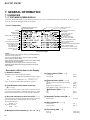
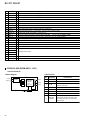
THIS MANUAL IS APPLICABLE TO THE FOLLOWING MODEL(S) AND TYPE(S).
Type
Model
DV-F727
DV-F07
Power Requirement
Region No.
KU
–
AC120V
1
KC
–
AC120V
1
KU/RC
–
AC120V
3
AC120V
1
KU/CA
–
Remarks
CONTENTS
1. SAFETY INFORMATION ....................................... 2
2. EXPLODED VIEWS AND PARTS LIST ................. 3
3. BLOCK DIAGRAM AND SCHEMATIC DIAGRAM .. 12
4. PCB CONNECTION DIAGRAM ........................... 39
5. PCB PARTS LIST ................................................ 55
6. ADJUSTMENT ..................................................... 62
7. GENERAL INFORMATION ..................................
7.1 DIAGNOSIS ...................................................
7.1.1 TEST MODE SCREEN DISPLAY .............
7.1.2 TROUBLE SHOOTING ............................
7.1.3 OPERATION FLOW CHART ....................
7.1.4 ERROR CODE .........................................
7.1.5 INTERFACE CONNECTOR .....................
7.1.6 DISASSEMBLY ........................................
66
66
66
68
69
70
74
77
7.1.7 ABOUT SERVICE IN THE
MECHANISM FAILURE ............................
7.2 PARTS ...........................................................
7.2.1 IC .............................................................
7.2.2 DISPLAY ..................................................
8. PANEL FACILITIES AND SPECIFICATIONS .......
79
80
80
95
96
PIONEER CORPORATION
4-1, Meguro 1-chome, Meguro-ku, Tokyo 153-8654, Japan
PIONEER ELECTRONICS SERVICE, INC. P.O. Box 1760, Long Beach, CA 90801-1760, U.S.A.
PIONEER ELECTRONIC (EUROPE) N.V. Haven 1087, Keetberglaan 1, 9120 Melsele, Belgium
PIONEER ELECTRONICS ASIACENTRE PTE. LTD. 253 Alexandra Road, #04-01, Singapore 159936
c PIONEER CORPORATION 1999
T – IZE DEC. 1999 Printed in Japan
DV-F727, DV-F07
1. SAFETY INFORMATION
This service manual is intended for qualified service technicians ; it is not meant for the casual do-ityourselfer. Qualified technicians have the necessary test equipment and tools, and have been trained
to properly and safely repair complex products such as those covered by this manual.
Improperly performed repairs can adversely affect the safety and reliability of the product and may
void the warranty. If you are not qualified to perform the repair of this product properly and safely, you
should not risk trying to do so and refer the repair to a qualified service technician.
WARNING
This product contains lead in solder and certain electrical parts contain chemicals which are known to the state of California to cause
cancer, birth defects or other reproductive harm.
Health & Safety Code Section 25249.6 – Proposition 65
NOTICE
(FOR CANADIAN MODEL ONLY)
Fuse symbols
(fast operating fuse) and/or
be of identical designation.
(slow operating fuse) on PCB indicate that replacement parts must
REMARQUE
(POUR MODÈLE CANADIEN SEULEMENT)
Les symboles de fusible
(fusible de type rapide) et/ou
de remplacement doivent avoir la même désignation.
(fusible de type lent) sur CCI indiquent que les pièces
(FOR USA MODEL ONLY)
1. SAFETY PRECAUTIONS
The following check should be performed for the
continued protection of the customer and service
technician.
ANY MEASUREMENTS NOT WITHIN THE LIMITS
OUTLINED ABOVE ARE INDICATIVE OF A POTENTIAL
SHOCK HAZARD AND MUST BE CORRECTED BEFORE
RETURNING THE APPLIANCE TO THE CUSTOMER.
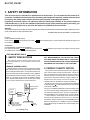
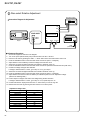
LEAKAGE CURRENT CHECK
Measure leakage current to a known earth ground (water
pipe, conduit, etc.) by connecting a leakage current tester
such as Simpson Model 229-2 or equivalent between the
earth ground and all exposed metal parts of the appliance
(input/output terminals, screwheads, metal overlays, control
shaft, etc.). Plug the AC line cord of the appliance directly
into a 120V AC 60Hz outlet and turn the AC power switch
on. Any current measured must not exceed 0.5mA.
Reading should
Leakage not be above
current 0.5mA
tester
Device
under
test
Test all
exposed metal
surfaces
Also test with
plug reversed
(Using AC adapter
plug as required)
AC Leakage Test
2
Earth
ground
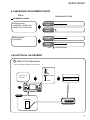
2. PRODUCT SAFETY NOTICE
Many electrical and mechanical parts in the appliance
have special safety related characteristics. These are
often not evident from visual inspection nor the protection
afforded by them necessarily can be obtained by using
replacement components rated for voltage, wattage, etc.
Replacement parts which have these special safety
characteristics are identified in this Service Manual.
Electrical components having such features are identified
by marking with a on the schematics and on the parts list
in this Service Manual.
The use of a substitute replacement component which does
not have the same safety characteristics as the PIONEER
recommended replacement one, shown in the parts list in
this Service Manual, may create shock, fire, or other hazards.
Product Safety is continuously under review and new
instructions are issued from time to time. For the latest
information, always consult the current PIONEER Service
Manual. A subscription to, or additional copies of, PIONEER
Service Manual may be obtained at a nominal charge from
PIONEER.
DV-F727, DV-F07
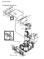
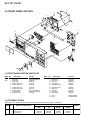
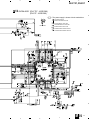
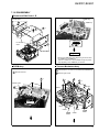
2. EXPLODED VIEWS AND PARTS LIST
NOTES:
• Parts marked by "NSP" are generally unavailable because they are not in our Master Spare Parts List.
• The mark found on some component parts indicates the importance of the safety factor of the part.
Therefore, when replacing, be sure to use parts of identical designation.
• Screws adjacent to mark on the product are used for disassembly.
2.1 PACKING
9
2 (1/2)
10
2 (2/2)
3
11
Except
DV-F727/KU/RC
13
5
7
15 DV-F727
/KC
Only
6
12
8
1
DV-F727
/KU/RC
Only
16
DV-F727
/KC
14
Only
DV-F727
/KU/RC
Only
16
14
DV-F727/KC
Only
4
(1) PACKING PARTS LIST
Mark No.
Description
Part No.
Mark No.
1
2
3
4
5
Protector F
Protector R
Packing Sheet
Packing Case
Polyethylene Bag B5
See Contrast table (2)
See Contrast table (2)
RHC1023
See Contrast table (2)
VHL1051
6
7
Operating Instructions (English)
Remote Control Unit
(CU-DV039)
Battery Cover
Audio Cord (L = 1.5m)
See Contrast table (2)
VXX2629
8
9
10
11
NSP
NSP
Description
Part No.
12
13
Video Cord (L = 1.5m)
Master-Slave Control Cord
(L = 0.75m)
Dry Cell Battery (R6P, AA)
Warranty Card
VDE1034
RDE1023
14
15
16
KC Label
See Contrast table (2)
Operating Instructions (French) See Contrast table (2)
Region Label
See Contrast table (2)
VEM-013
See Contrast table (2)
VNK4423
VDE1033
(2) CONTRAST TABLE
DV-F727/KU, KC, KU/RC and DV-F07/KU/CA are constructed the same except for the following :
Part No.
Mark No.
Symbol and Description
DV-F727
DV-F727
DV-F727
/KU
/KC
/KU/RC
NSP
1
2
4
6
13
DV-F07
/KU/CA
Protector F
Protector R
Packing Case
Operating Instructions (English)
Warranty Card
PHA1325
PHA1326
VHG1840
VRB1237
ARY7023
PHA1325
PHA1326
VHG1840
VRB1237
ARY7024
PHA1325
PHA1326
VHG1840
VRB1237
Not used
PHA1336
PHA1337
VHG1841
VRB1238
ARY1026
14 KC Label
15 Operating Instructions (French)
16 Region Label
Not used
Not used
Not used
VRW1716
VRC1107
Not used
Not used
Not used
VRW1702
Not used
Not used
Not used
Remarks
3
DV-F727, DV-F07
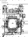
2.2 EXTERIOR SECTION (1/2)
23
24
29
27
26
DV-F07
Only
28
DV-F727
Only
DV-F07
Only
25
22
DV-F727/KU
and
DV-F07/KU/CA
Only
28
DV-F727
Only
27
9
29 1
10
29
26
8
16
29
15
2
DV-F07
Only
29
Note ∗1
3
7
Part of Center Pole
6
Cut
30
29
13 12
Cut
17
11
4
29
5
∗1 DV-F07
14 Only
DV-F727/KU/RC
29
Only
31
29
Refer to
"2.3 EXTERIOR SECTION (2/2)".
DV-F07 19
Only
20
29
21
from PS2B Assy
Refer to
"2.5 FRONT PANEL SECTION".
4
DV-F07 20
Only
18
29
DV-F727, DV-F07
(1) EXTERIOR SECTION (1/2) PARTS LIST
Mark No.
Description
1
2
3
4
5
Part No.
Mark No.
Description
Part No.
16
17
18
19
20
PCB Spacer
Main Holder
Side MoleR
Side Mole L
Spacer
VEC2077
VNE2215
See Contrast table (2)
See Contrast table (2)
See Contrast table (2)
VWG2127
VDA1779
See Contrast table (2)
VDA1781
VDA1778
21
22
23
24
25
Caution Label 301
65 Label
Bonnet Case S
Side Wood L
Side Wood R
VRW1817
See Contrast table (2)
See Contrast table (2)
See Contrast table (2)
See Contrast table (2)
VDA1782
VDA1707
VDA1784
See Contrast table (2)
VEC2079
26
27
28
29
30
Wood Collar
Screw
Screw
Screw
Screw
See Contrast table (2)
See Contrast table (2)
See Contrast table (2)
BBZ30P080FZK
IPZ30P080FMC
31
Region Label
See Contrast table (2)
DVDM Assy
232B Assy
VQEB Assy
MSJB Assy
AVJB Assy
See Contrast table (2)
See Contrast table (2)
VWV1669
See Contrast table (2)
See Contrast table (2)
6
7
8
9
10
MDRB Assy
Flexible Cable (12P)
Flexible Cable (7P)
Flexible Cable (11P)
Flexible Cable (12P)
11
12
13
14
15
Flexible Cable (7P)
Flexible Cable (14P)
Flexible Cable (15P)
Screw (#4-40/M2)
PCB Support Cushion
NSP
NSP
(2) CONTRAST TABLE
DV-F727/KU, KC, KU/RC and DV-F07/KU/CA are constructed the same except for the following :
Part No.
Mark No.
Symbol and Description
DV-F727
DV-F727
DV-F727
/KU
/KC
/KU/RC
NSP
DV-F07
/KU/CA
1
2
4
5
8
DVDM Assy
232B Assy
MSJB Assy
AVJB Assy
Flexible Cable (7P)
VWS1386
Not used
VWG2131
VWV1719
Not used
VWS1386
Not used
VWG2131
VWV1719
Not used
VWS1386
Not used
VWG2131
VWV1719
Not used
VWS1396
VWG2129
VWG2128
VWV1720
VDA1777
14
18
19
20
22
Screw (#4-40/M2)
Side Mole R
Side Mole L
Spacer
65 Label
Not used
Not used
Not used
Not used
ARW7050
Not used
Not used
Not used
Not used
Not used
Not used
Not used
Not used
Not used
Not used
DBA1078
PAN1374
PAN1373
PNM1331
ARW7050
23
24
25
26
27
Bonnet Case S
Side Wood L
Side Wood R
Wood Collar
Screw
VXX2692
Not used
Not used
Not used
Not used
VXX2692
Not used
Not used
Not used
Not used
VXX2692
Not used
Not used
Not used
Not used
VXX2693
PMM1043
PMM1044
PNW1238
PBA1103
28 Screw
31 Region Label
FBT40P080FZK FBT40P080FZK FBT40P080FZK
Not used
Not used
VRW1703
Remarks
Not used
Not used
5
DV-F727, DV-F07
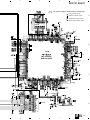
2.3 EXTERIOR SECTION (2/2)
25
15
2
13
26
26
Note ∗3 :
Froil 397 (for Service) : GYA1001
Note ∗4 :
Ha Narl PN955R (for Service) : GEM1016
12
Refer to
"2.4 DISC RACK SECTION".
23
21
18 19
∗4
20
∗4
17
Note ∗2 (Screw Cover)
23
10
4
Part of Trans Cover (No.10)
16
∗3
5
3
1
Cut
11
7
24
A
24
24
5
10
22
26
14
24
A
24
∗2
24
8
9
24
6
DV-F727, DV-F07
(1) EXTERIOR SECTION (2/2) PARTS LIST
Mark No.
Description
Part No.
Mark No.
Description
Part No.
NSP
NSP
NSP
1
2
3
4
5
POWER SUPPLY Assy
LEDB Assy
DOMB Assy
DOSB Assy
AC Power Cord
VWR1317
VWG2124
VWG2121
VWG2122
ADG7024
16
17
18
19
20
Motor Pulley
Hood Base 301
Gear M1
Gear AW
Gear Pulley
PNW1634
PNW2791
PNW2800
PNW2906
VNL1662
NSP
6
7
8
9
10
Carriage Motor (DOOR)
Hood
Under Base DVD
Insulator
Trans Cover
VXM1033
See Contrast table (2)
VNA2125
PNW2766
VNK4542
21
22
23
24
25
Belt
Cord Stopper
Screw
Screw
Screw
PEB1300
CM-22C
IPZ20P080FMC
BBZ30P080FZK
IPZ30P080FMC
11
12
13
14
15
Flexible Cable (26P)
CR Lens
Dispersion Sheet
Rear Base
Center Pole 301
VDA1776
PNW2816
VEC2113
See Contrast table (2)
PNW2792
26
Screw C
PBA1106
(2) CONTRAST TABLE
DV-F727/KU, KC, KU/RC and DV-F07/KU/CA are constructed the same except for the following :
Part No.
Mark No.
Symbol and Description
DV-F727
DV-F727
DV-F727
/KU
/KC
/KU/RC
7 Hood
14 Rear Base
VNK4531
VNA2126
VNK4531
VNA2126
VNK4531
VNA2126
DV-F07
/KU/CA
Remarks
VNK4532
VNA2127
7
DV-F727, DV-F07
52
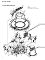
2.4 DISC RACK SECTION
Note ∗3 :
Froil 397 (for Service) : GYA1001
Note ∗4 :
Ha Narl PN955R (for Service) : GEM1016
53
52
52
B
11
40
33
44
44
44
46
44
44
45
44
A
51
9
10
21
31
35
52
52
36
8
52
2
1
43
20
5
19
7
52
6
42
55
C
∗3
32
50
32
15
32
∗4
32
52
∗3
B
∗3
A
∗3
41
50
38
C
39
32
∗3
32
∗3
37
28
∗3
47
∗3
32
8
34
30
DV-F727, DV-F07
DISC RACK SECTION PARTS LIST
Mark No.
Refer to
"2.6 TRAVERSE MECHANISM ASSY".
13
26
23
NSP
NSP
NSP
NSP
NSP
1
2
3
4
5
NSP
NSP
25
∗3
24
NSP
54
Description
Part No.
SSRB Assy
SEMB Assy
LOMB Assy
LOSB Assy
RADB Assy
VWG2113
VWG2114
VWG2115
VWG2116
VWG2117
6
7
8
9
10
PHOB Assy
VOLB Assy
Clamp Spring
Loading Belt
Gear Pulley (B)
VWG2118
VWG2123
VBH1318
AEB7029
ANW7062
11
12
13
14
15
Roller B
Drive Arm Spring
Traverse Mechanism Assy
Sheet 301
Clamper Assy 301
ANW7075
PBH1226
VWT1161
PED1028
VXA2382
16
17
18
19
20
Gear 1
Gear 2
Gear Holder
Slider Cam
Clamp Pole
PNW2819
PNW2820
PNW2822
PNW2823
PNW2826
21
22
23
24
25
Clamper Holder
Drive Arm
Float Rubber A
Balancer
Flexible Cable (8P)
PNW2827
PNW2829
AEB7063
VNL1842
VDA1785
26
27
28
29
30
Flexible Cable (24P)
Float Base
Link L
Drive Cam
Lock Plate
VDA1780
VNL1841
PNW2844
PNW2873
PNA2438
31
32
33
34
35
Motor Pulley
Roller
Disc Rack
Rack Base
ST Gear 0.6
PNW1634
PNW2647
PNW2790
PNW2835
PNW2836
36
37
38
39
40
ST Gear 1.0
Disc Divider
Guide Support L
Guide Support R
Disc Guard
PNW2837
PNW2838
PNW2839
PNW2840
PNW2841
41
42
43
PNW2842
PNW2843
VXM1033
44
Sensor Stay
Guide Roller
Carriage Motor
(SELECT, LOADING)
Rack Label
45
46
47
48
49
S Label
+1 Label
Screw
Screw
Screw
PAM1771
PRW1507
BBZ30P080FZK
BMZ26P040FZK
BPZ26P060FMC
50
51
52
53
54
Screw
Screw
Screw
Arm Assy
Float Spring
BPZ30P100FCU
IPZ20P080FMC
PPZ30P080FMC
PXA1615
VBH1319
55
Screw
IPZ30P080FMC
14
51
27
22
14
Note)
Tightening Torque: 2 kg·cm
b
51
9
29
17
b
10
49
16
12
a
4
48
a
∗3
∗3
31
43
18
PAM1770
3
9
DV-F727, DV-F07
17
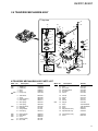
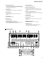
2.5 FRONT PANEL SECTION
21
6
1
7
21
21
21
2
8
14
13
9
4
15
12
16
5
22
10
3
11
20
19
18
(1) FRONT PANEL SECTION PARTS LIST
Mark No.
NSP
Description
Part No.
Mark No.
Description
Part No.
1
2
3
4
5
FLKY Assy
KEYB Assy
PS2B Assy
Flexible Cable (11P)
Flexible Cable (7P)
See Contrast table (2)
VWG2120
VWG2125
VDA1787
VDA1792
11
12
13
14
15
JOG Sheet
Sensor Lens
LED Lens
Power Button
Mode Button DVD
PEC1042
PNW2804
PNW2019
VNK4527
VNK4525
6
7
8
9
10
Flexible Cable (7P)
Flexible Cable (15P)
Operation Panel
Pioneer Badge
Display Window
VDA1786
VDA1775
See Contrast table (2)
See Contrast table (2)
PAM1782
16
17
18
19
20
Play Button DVD
PCB Cover
JOG Dial
Enter Spring
Enter Button
VNK4526
PNM1324
PAC1882
PBH1228
PAC1883
21
22
Screw
Screw
PPZ30P100FMC
PPZ30P050FMC
(2) CONTRAST TABLE
DV-F727/KU, KC, KU/RC and DV-F07/KU/CA are constructed the same except for the following :
Part No.
Mark No.
Symbol and Description
DV-F727
DV-F727
DV-F727
/KU
/KC
/KU/RC
1 FLKY Assy
8 Operation Panel
9 Pioneer Badge
10
VWG2126
VNK4529
PAM1776
VWG2126
VNK4529
PAM1776
VWG2191
VNK4529
PAM1776
DV-F07
/KU/CA
VWG2119
VNK4530
PAN1376
Remarks
DV-F727, DV-F07
2.6 TRAVERSE MECHANISM ASSY
• Top View
37
18
33
35
28
15
30
10
5
34
16
10
19
13
8
6
20
37
22
10
33
26
18
11
32
14
25
10
12
27
31
37
23
9
7
37
21
17
7
2
24
29
7
1
3
36
4
TRAVERSE MECHANISM ASSY PARTS LIST
Mark No.
NSP
NSP
NSP
NSP
NSP
NSP
NSP
NSP
Part No.
Mark No.
Description
SMEB Assy
FGSB Assy
Motor
Motor
Pickup Assy
VWG2048
VWG2009
VXM1079
VXM1078
VWY1055
21
22
23
24
25
Hook
FFC Holder
Mechanism Base
FG Holder
Gear A
VNL1770
VNL1802
VNL1806
VNL1807
VNL1808
6
7
8
9
10
Table Sheet
Screw
Centering Spring
Hook Spring
Skew Spring
DEC2040
VBA1058
VBH1278
VBH1317
VBH1303
26
27
28
29
30
Gear B
Gear C
Slider
Gear D
Magnet
VNL1809
VNL1810
VNL1811
VNL1814
VYM1024
11
12
13
14
15
Gear Spring
Reflected Sheet
Guide Bar
Sub-guide Bar
Hold Spring
VBH1308
VEC1959
VLL1504
VLL1505
VNC1017
31
32
33
34
35
Screw
Screw
Screw
Magnet Holder Assy
Spindle Motor Assy
JFZ17P025FZK
JGZ17P028FMC
VBA1051
VXX2507
VXX2649
16
17
18
19
20
Magnet Holder
Motor Base
Cover
Centering Ring
Disc Table
VNE2070
VNE2154
VNE2155
VNL1746
VNL1747
36
37
Carriage Motor Assy
Screw
VXX2650
PBA1069
1
2
3
4
5
Description
NSP
Part No.
11
DV-F727, DV-F07
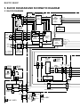
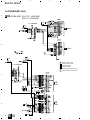
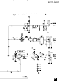
3. BLOCK DIAGRAM AND SCHEMATIC DIAGRAM
3.1 BLOCK DIAGRAM
SPDL
MOTOR
CN120
RF
10
OEIC
7,6,
3,2
FCS
21
TRKG
24
22
23
M DVDM ASSY
(24P)
(24P)
RF
10
B1-B4
7,6,
3,2
F_RTN
F_DRV
T_DRV
T_RTN
3
21
RF IC
6-9
IC101
LA9701M
54
46
56
57
24
42
22
35
23
33M 16M
107
4
RFO
170
DSPRF
BH
PH
FE
TE
DVD
DECODER
MY CHIP
57-60
63-66
IC701
PD4995A
111
SD0-SD7
SREQ
56
CDDATA
Q105
PICKUP
ASSY
Q MDRB
ASSY
(8P)
7
8
8
CARRIAGE
MOTOR
M
M
LOADING
MOTOR
(12P)
CN301
CN303
10
5
6
3
4
2
7
1
9
SPDL+
SPDLSLDR_R
SLDR_F
LOAD+
LOAD-
(12P)
32 33 30 31 39
13 12 10 9
CN1030
5
31
3
32
14
9
15
6
34
4
35
CN305
3
(12P)
M
8
3
7
10
DOOR
MOTOR
M
4
14
9
12
SPDL & FTS
DRIVER
IC352
M56788FP
SPDO
28
48
45
46
SYSTEM
CONTROL CPU
SH1 BASE ASIC
14
LODDRV
SRT/
SLT
MCLS/
MOPH
16M
7
CN921
PS2B
ASSY
IC610
TC7W53FU
T
1
7
CN703
CN802
-1/2
CN101
-1/2
7
27
KEYB
ASSY
DNR
D0-D7
14
VIDEO ENCODER
(6ch, DNR)
IC101
PM0023AF
101
117
DTR
TXD
RXD
CTS
D0-D7
25-32
34
OUTV
125
1
11
1
11
CN101
VIDEO
-2/2
FILTER Q542
(V)
F102
2
OUTY Q551
Q552
Q531
Q532
OUTC
CN802 (15P)
-2/2 CN901
V
22
(Y)
4
Y
24
(C)
6
C
26
10
12
8
SEL IR
6
IR
5
15
4
3
KEY SW
(14P)
(15P)
CN905
CN602
CN701
2
SEL IR
IR
1
7
14
7
12
4
16
6
13
SEL IR
14
IR
IC807
MC74VHCT541ADT
REMOTE
SENSOR
(7P)
(7P)
CN702
CN903
4
2
S FLKY ASSY
Q541
16M SDRAM
IC102
MB811171622A-100FN
CN1202
FL CONTROL
IC701
PE5144A
N VQEB
ASSY
117
(15P)
FL TUBE
V701
VAW1052
102
88
CN1201
7
KEYBOARD
/MOUSE
118
1
115
1
IC601
PD3410A
42
1
8
3
(Y0-Y7)
12
SERVO DSP
IC201
LC78652W
CN307
(9P)
IC301
LA6531
SELECT DOOR
MOTOR DRIVER
301 CHANGER
MECHANISM
CN801
SLDO
17
47
(12P)
CN302
CN304
SELECT
MOTOR
JA801
TDO
37
(5P)
(4P)
U
FDO
20
7
4M DRAM
IC702
MN414800CSJ-07
SCK0
SB1
CN904
MASTER
4
CN905
2
SLAVE
P
MSJB ASSY
(1/2)
ADATA0
ADAI (AC3)
DV-F727, DV-F07
27M
55
64
MPEG2
DECODER
MITUBISHI
AV-1
149,150,
152-155,
158,159
162
48
16M
36/16M
IC801
M65773AFP
(26P)
YCBR0-7
95-98, (Y0-Y7)
100-103
IC22
TC7WH74FU
1
27M
33M
M + 6V
+12V
36/16M
6
5
1,2
5
5
V
7
+5V
10
|
12
10
|
12
+3.3V
13
|
16
13
|
16
1
CLOCK GENERATOR
IC21
CY2081SL-655
1,2
7
AD0
DOUT0
CN201
+12V
71
74
(26P)
CN110
5
POWER
SUPPLY
ASSY
CN101
LIVE
1
AC IN
2
16M SDRAM
IC802
MB811171622A
-100FN
E+5V
22
22
– 27V
26
26
EDO DRAM
IC803
M5M4V18165
DTP-6S
FLASH
MEMORY
IC603
VYW1668
WORK SRAM
(1M)
IC604
TC55V1001AF8
NEUTRAL
DV-F07 ONLY
DV-F07 ONLY
R 232B ASSY
IC611
MC74VHCT541ADT
16
5
15
CN106
CN401
TXD
1
RXD
2
16
4
15
5
IC401
MAX232EPE
(7P)
(7P)
4
DTR
3
CTS
4
7
10
7
6
9
8
5
11
14
4
12
13
JA401
INTERFACE
CONNECTOR
2
3
4
14
IC612
MC74VHC541DT
JA504
(2/2)
COMPOSITE
VIDEO IN
CN503
(2/2)
1
S VIDEO
3
IN
O AVJB ASSY
VIDEO
SELECTOR
IC502 BU4551BF (V/Cb)
(15P)
CN501
6
12
6
13
4
AMP
BIN
AMP
15
(C/Cr)
1
8
10
(Y)
14
6
23
21
(Y)
10
CIN
19
(C)
17
PR (RED)
(V/Cb)
PB (BLUE)
(Y)
10
11
(C/Cr)
(R)
(G)
(B)
: V Signal Route
: Y Signal Route
: C Signal Route
: R Signal Route
: G Signal Route
: B Signal Route
JA505
15
13
S VIDEO
OUT
8
(C/Cr)
AMP
(Y)
COMPOSITE
VIDEO OUT
CN503
(1/2)
6
(C/Cr)
(Y)
AIN
(V/Cb)
JA504
(1/2)
(V)
3
11
(V/Cb)
3IN 6OUT
VIDEO AMP
IC501 LA7135AM
: RF Signal Route
: Audio Signal Route (L ch)
Y (GREEN)
ANALOG
COMPONENT
VIDEO
OUT
5
IC203
BA4560F
DV-F727 ONLY
VOUTL
DIN
(14P)
CN101
Hi-bit
8
14
9
8
IC241
PD0236AM
AC3/PCM
2
96k,24-bit
2ch DAC
IC201
PCM1716E
(DV-F727)
PE8001A
(DV-F07)
16
JA201
2
3
VOUTR
13
5
6
L
1
AUDIO
OUT
R
7
L
R
AUDIO
IN
DV-F07 ONLY
6
3
4
CN502
(7P)
(7P)
CN902
4
5
2
JA906
SR OUT
JA907
SR IN
OPTICAL
COAXIAL
IN
IC922
IC901
COAXIAL
AC-3/PCM
DIGITAL
AUDIO
OUT
IC931
DIGITAL
SELECTOR
P MSJB ASSY (1/2)
13
1
2
3
4
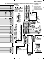
DV-F727, DV-F07
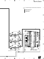
3.2 FGSB, SMEB, SSRB, SEMB, LOMB, LOSB, RADB, PHOB, DOMB, DOSB,
VOLB, LEDB, PICKUP ASSYS and OVERALL WIRING DIAGRAM
FGSB ASSY
(VWG2009)
A
DV-F07 ONLY
L
R
J1601
LEDB ASSY
(VWG2124)
A
232B ASSY
(VWG2129)
CN201
52044-0345
CN202
CARRIAGE
MOTOR
ASSY
VXX2656
(S)
VKN1212
S201
DSG1016
(S)
(S)
(S)
(S)
(S)
(SP)
(SP)
(SP)
CN203
B
SPINDLE
MOTOR
ASSY
VXX2649
J
(SP)
(L)
(SP)
(L)
(S)
(SP)
(L)
(SP)
(L)
(S)
(S)
(S)
(SP)
(SP)
SMEB ASSY
(VWG2048)
(D)
(D)
(SL)
DOSB ASSY
(VWG2122)
(SL)
DOMB ASSY
(VWG2121)
I
J632
J631
B
J632
(D)
(D)
(D)
E
F
LOMB ASSY
(VWG2115)
O O 1/2, O 2/2
LOSB ASSY
(VWG2116)
AVJB ASSY
(DV-F727 : VWV1719)
(DV-F07 : VWV1720)
(L)
(L)
LEAF SW
J652
J651
C
CN605
J605
J603
C
SSRB ASSY
(VWG2113)
Q
ASSY
K VOLB
(VWG2123) H
MDRB ASSY
PHOB ASSY
(VWG2118) (VWG2127)
CN604
J604
LED
HOLDER
RNK1795
G
RADB ASSY
(VWG2117)
J601
P
MSJB ASSY
(DV-F727 : VWG2131)
(DV-F07 : VWG2128)
D
J602
(SL)
(SL)
D
14
SEMB ASSY
(VWG2114)
A B C D E F G H I J K L
1
2
3
4
5
6
7
8
DV-F727, DV-F07
Note : When ordering service parts, be sure to refer to "EXPLODED VIEWS and PARTS LIST" or "PCB PARTS LIST".
: RF SIGNAL ROUTE
(F)
(T)
(S)
M M 1/4- M 4/4
(SP)
(L)
DVDM ASSY
(DV-F727 : VWS1386)
(DV-F07 : VWS1396)
(SP)
(L)
(SP)
(L)
(S)
(D)
(SL)
: FOCUS SERVO LOOP LINE
: TRACKING SERVO LOOP LINE
A
: SLIDER SERVO LOOP LINE
: SPINDLE DRIVE SIGNAL ROUTE
: LOADING DRIVE SIGNAL ROUTE
: DOOR DRIVE SIGNAL ROUTE
: SELECT DRIVE SIGNAL ROUTE
V
POWER
SUPPLY ASSY
(VWR1317)
(S)
AC POWER CORD
ADG7024
(D)
(SL)
(T)
(T)
(F)
(F)
CN101
CN101
(F)
(F)
(T)
(F)
(F)
(T)
(F)
(T)
(T)
(F)
(T)
PICKUP
ASSY
(VWY1055)
B
(F)
(T)
(T)
(F)
C
T
KEYB ASSY
(VWG2120)
N VQEB ASSY
(VWV1669)
S
FLKY ASSY
(DV-F727/KU, KC : VWG2126)
(DV-F727/KU/RC : VWG2191)
(DV-F07 : VWG2119)
U
PS2B ASSY
(VWG2125)
15
5
6
7
8
D
1
2
3
4
DV-F727, DV-F07
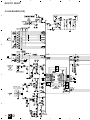
3.3 DVDM ASSY (1/4)
A
M 2/4
1
1/2
M 2/4
(DVD)
(DVD)
CN201
VKN1324
2
CN110
M 2/4
VKN1479
M 2/4
(DVD)
M 2/4
V CN201
4
(CD)
(CD)
(CD)
B
(F)
(F)
M 2/4
M 2/4
(F)
RF IC
(F)
(F)
(F)
(F)
(T)
(T)
(T)
(T)
(T)
(T)
CN120
VKN1464
M 2/4
(F)
(F)
(T)
PICKUP ASSY
M 2/4
CN1030
M 2/4
VKN1471
SPINDLE & FTS
DRIVER
(SP)
Q CN301
(L)
(SP)
(L)
(F)
(S)
M 1/4
1
(T)
(F)
(F)
(S)
(F)
M 2/4
16
(L)
(L)
(SP)
(SP)
(F)
(T)
(T)
(F)
D
M 2/4
M 2/4
2
3
(T)
(T)
C
(T)
(F)
(F)
(S) (T)
4
5
6
7
8
DV-F727, DV-F07
M 1/4 DVDM ASSY (DV-F727 : VWS1386)
(DV-F07 : VWS1396)
A
: The power supply is shown with the marked box.
: RF SIGNAL ROUTE
: ROM DATA SIGNAL ROUTE
(F)
2/2
(T)
FOR CHECKER
(S)
(SP)
(L)
(DVD)
: FOCUS SERVO LOOP LINE
: TRACKING SERVO LOOP LINE
: SLIDER SERVO LOOP LINE
: SPINDLE DRIVE SIGNAL ROUTE
: LOADING DRIVE SIGNAL ROUTE
(DVD)
E 2/4
M 3/4
B
M 2/4
M 2/4
6
(T)
(T)
(F)
(F)
(CD)
5
DSP IC
(CD)
C
(S)
(S)
(F)
(F)
(T)
(T)
M 2/4
M 2/4
M 2/4
M 2/4
7
M 2/4
M 2/4,4/4
2/2
11 10
M 2/4
5
M 2/4
8
1/2
6
7
9
D
M 2/4
M 1/4
8
17
1
2
3
4
DV-F727, DV-F07
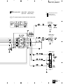
3.4 DVDM ASSY (2/4)
M 2/4 DVDM ASSY (DV-F727 : VWS1386)
A
(DV-F07 : VWS1396)
M 1/4
M 1/4
PGM 16M FLASH MEMORY
3→5 CONVERTER
M 3/4
WORK SRAM
M 4/4
5→3 CONVERTER
IC603
VYW1668
IC604
TC55V1001FAF8
M 4/4
DV-F07
ONLY
CN106
B
R CN401
VKN1299
M 3/4
M 3/4,4/4
CN107
VKN1575
M 1/4
C
M 1/4,3/4
SH1 BASE ASIC
M 1/4
M 3/4
M 4/4
M 4/4
M 3/4
(D)
M 1/4
D
M 1/4
M 1/4
M 1/4
M 1/4 M 4/4
(SL)
18
M 2/4
1
2
M 4/4 M 4/4
M 1/4
M 1/4
M 4/4
3
4
5
6
7
8
DV-F727, DV-F07
: The power supply is shown with the marked box.
: AUDIO SIGNAL ROUTE
A
: ROM DATA SIGNAL ROUTE
(D)
(SL)
: DOOR DRIVE SIGNAL ROUTE
: SELECT DRIVE SIGNAL ROUTE
M 1/4
IC702
MN414800CSJ-07
M 4/4
4M DRAM
M 3/4
M 4/4
M 3/4
B
M 1/4
(MY CHIP ES2)
DVD ENCODER
M 1/4
3
C
M 1/4
M 1/4
M 3/4
M 3/4
M 1/4
3→5 CONVERTER
M 4/4
M 1/4
S CN701
D
M 1/4
M 3/4
CN602
VKN1474
5
6
7
M 2/4
8
19
1
2
3
4
DV-F727, DV-F07
3.5 DVDM ASSY (3/4)
A
1M × 16 EDO DRAM (TSOP)
DV-F07 ONLY
16M SDRAM
B
M 2/4
C
IC801
M65773AFP
AV1
MPEG2 ENCODER
3→5 CONVERTER
D
M 2/4
M 2/4
M 2/4
20
M 3/4
1
2
3
4
5
6
7
8
DV-F727, DV-F07
M 3/4 DVDM ASSY (DV-F727 : VWS1386)
: AUDIO SIGNAL ROUTE
(DV-F07 : VWS1396)
A
: ROM DATA SIGNAL ROUTE
(V)
(Y)
(C)
: VIDEO SIGNAL ROUTE
: Y SIGNAL ROUTE
: C SIGNAL ROUTE
M 2/4
M 2/4
M 4/4
M 2/4
M 1/4
B
FOR SERVO DSP
CLOCK GEN. BLOCK
N CN101
M 4/4
M 2/4
(V)
(Y)
(C)
C
M 2/4
M 2/4
M 2/4
M 2/4
M 4/4
D
5
6
7
M 3/4
8
21
1
2
3
4
DV-F727, DV-F07
3.6 DVDM ASSY (4/4)
A
M 4/4 DVDM ASSY (DV-F727 : VWS1386)
(DV-F07 : VWS1396)
CN921
(D)
5→3 CONVERTER
M 2/4 M 2/4
VKN1471
(SL)
M 2/4
Q CN302
M 2/4
CN903
VKN1497
B
P CN901
M 2/4
M 2/4
M 2/4
M 3/4
: AUDIO SIGNAL ROUTE
(V)
(Y)
3→5 CONVERTER
(C)
(D)
(SL)
: VIDEO SIGNAL ROUTE
: Y SIGNAL ROUTE
: C SIGNAL ROUTE
: DOOR DRIVE SIGNAL ROUTE
: SELECT DRIVE SIGNAL ROUTE
CN905
VKN1473
C
O 1/2
CN101
M 3/4
(Y)
(V)
O 2/2
(C)
D
CN501
M 2/4
M 1/4, 2/4
22
M 4/4
1
CN901
M 2/4
VKN1474
2
3
4
DV-F727, DV-F07
23
1
2
3
4
DV-F727, DV-F07
3.7 VQEB ASSY
N VQEB ASSY (VWV1669)
A
(C)
(V)
(Y)
B
(6 ch, DNR) VIDEO ENCODER
C
D
24
N
1
2
3
4
5
6
7
8
DV-F727, DV-F07
: The power supply is shown with the marked box.
A
: ROM DATA SIGNAL ROUTE
(V)
(Y)
(C)
: VIDEO SIGNAL ROUTE
: Y SIGNAL ROUTE
: C SIGNAL ROUTE
B
M 3/4
CN802
(V)
3 ,6
(C)
(Y)
(C)
(C)
C
(V)
1 ,4
(V)
2 ,5
(Y)
(Y)
Q531, Q532, Q541, Q542, Q551, Q552 : 2PB709A (QR)
F102 : VTF1155
5
D
6
7
N
8
25
1
2
3
4
DV-F727, DV-F07
3.8 AVJB ASSY (1/2)
A
O 1/2 AVJB ASSY
(DV-F727 : VWV1719)
(DV-F07 : VWV1720)
O 2/2
IC201
DV-F727 : PCM1716E
DV-F07 : PE8001A
DAC
B
CN101
VKN1190
M 4/4
CN905
O 2/2
C
DV-F727 ONLY
DV-F07
ONLY
D
Hi-Bit
26
O 1/2
1
2
3
4
5
6
7
8
DV-F727, DV-F07
: AUDIO SIGNAL ROUTE
: The power supply is shown with the marked box.
A
JA201
DV-F727 : VKB1132
DV-F07 : VKB1133
1/2
B
2/2
O 2/2
C
D
5
6
7
O 1/2
8
27
1
2
3
4
DV-F727, DV-F07
3.9 AVJB ASSY (2/2)
A
O 1/2
CN501
VKN1191
M 4/4
(Y)
(Y)
(V/PB)
(V/PB)
(C/PR)
(C/PR)
CN901
B
CN502
VKN1183
O 1/2
(V/PB)
P
CN902
O 1/2
(C/PR)
(Y)
(V)
JA504 (2/2)
DV-F727 : VKB1134
DV-F07 : VKB1135
(Y)
C
(Y)
(V/PB)
(Y)
(C/PR)
(V/PB)
(C/PR)
(C)
(Y)
(Y)
CN503 (2/2)
VIDEO
SELECTOR
(Y)
DV-F727 : AKP7020
DV-F07 : AKP7023
(C)
(C)
(C)
D
28
O 2/2
1
2
3
4
5
6
7
8
DV-F727, DV-F07
O 2/2 AVJB ASSY
A
(DV-F727 : VWV1719)
(DV-F07 : VWV1720)
(VPB)
(Y)
(C/PR)
: VIDEO/PB SIGNAL ROUTE
: Y SIGNAL ROUTE
: C/PR SIGNAL ROUTE
: The power supply is shown with the marked box.
JA504 (1/2)
DV-F727 : VKB1134
DV-F07 : VKB1135
(V)
(V)
B
CN503 (1/2)
DV-F727 : AKP7020
DV-F07 : AKP7023
VIDEO AMP
(Y)
(V)
(V/PB)
(C)
(V/PB)
(PB)
(C/PR)
(C/PR)
(C)
(PR)
(Y)
(Y)
(Y)
JA505
(Y)
DV-F727 : VKB1131
DV-F07 : VKB1100
(PR)
(PR)
(PB)
(PB)
(Y)
(Y)
C
D
5
6
7
O 2/2
8
29
1
2
3
4
DV-F727, DV-F07
3.10 MSJB ASSY
A
P
MSJB ASSY (DV-F727 : VWG2131)
(DV-F07 : VWG2128)
CN904
AKN1028
CN905
AKN1028
CN903
VKN1211
S
B
CN702
MSCHK, SLCHK
Normal : Low
Plug in : High
JA906
RKN1004
JA907
RKN1004
CN901
VKN1215
C
M 4/4
JA908
CN903
PKN1005
CN902
VKN1211
O 2/2
CN502
D
30
P
1
(D)
(D)
2
(D)
3
4
5
6
7
8
DV-F727, DV-F07
A
(D)
: The power supply is shown with the marked box.
: DIGITAL AUDIO SIGNAL ROUTE
JA902
GP1F32T
(D)
(D)
(D)
(D)
B
JA901
DV-F727 : VKB1077
DV-F07 : VKB1074
(D)
(D)
(D)
(D)
(D)
C
JA903
DV-F727 : VKB1077
DV-F07 : VKB1074
(D)
(D)
(D)
(D)
(D)
(D)
D
(D)
5
6
7
P
8
31
1
2
3
4
DV-F727, DV-F07
3.11 MDRB ASSY
A
Q MDRB ASSY (VWG2127)
CN306
52147-0310
L
J1601
CN303
B CN202
VKN1184
VKN1188
M 1/4 CN1030
B
CN301
CN304
I
J631
52147-0410
CN302
VKN1188
CN305
E
M 4/4 CN921
J651
52147-0510
CN307
52147-0910
D J601
C
D
32
Q
1
2
3
4
1
2
3
4
DV-F727, DV-F07
3.12 232B ASSY (DV-F07 ONLY)
A
R
232B ASSY (VWG2129)
B
CN401
VKN1183
M 2/4
CN106
C
D
1
2
3
R
4
33
1
2
3
4
DV-F727, DV-F07
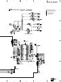
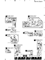
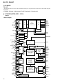
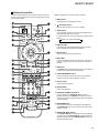
3.13 FLKY, KEYB and PS2B ASSYS
S
A
FLKY ASSY
(DV-F727/KU, KC : VWG2126)
(DV-F727/KU/RC : VWG2191)
(DV-F07 : VWG2119)
M 2/4 CN602
CN701
VKN1191
DV-F727
/KU/RC
ONLY
B
C
D
34
S
1
2
3
4
5
6
7
8
DV-F727, DV-F07
MSCHK, SLCHK
Normal : Low
VKN1183 Plug in : High
CN702
: The power supply is shown with the marked box.
P
T
CN903
A
KEYB ASSY (VWG2120)
B
CN703
52045-1145
FLKY ASSY
S701 :
STYANDBY/ON
S702 : ACCESS SINGLE LOADER
S703 : PLAY
S704 : PLAYMODE
S705 : RANDOM
S706 : DISPLAY
TEXT
S707 : INPUT
S708 : SEARCH
KEYB ASSY
S1200 : DISC CHARA (MULTI JOG)
S1201 : PUSH ENTER
S1202 : CLEAR
S1203 : 41
S1204 : ¡¢
S1205 : 8 (PAUSE)
S1206 : 7 (STOP)
S1207 : 3
S1208 : 2
S1209 : 1
S1210 : 4
S1211 : 5 DIRECT CUSTOM
S1212 : 6
S1213 : 9
S1214 : 8
S1215 : 7
S1216 : 10
S1217 : AUDIO/VIDEO
S1218 : UPDATE
S1219 : 3(PLAY)
S1220 : 0(OPEN/CLOSE)
CN1202
52045-1145
U
PS2B ASSY (VWG2125)
C
CN801
VKN1211
CN1201
VKN1211
D
5
6
7
S T U
8
35
1
2
3
4
DV-F727, DV-F07
3.14 POWER SUPPLY ASSY
A
V
POWER SUPPLY ASSY (VWR1317)
T101
TRANS
D201
R110
R102
D105
C108
R103
D102
B
D101
R113
L102
D203
R112
C107
D106
D103
D104
D202
R115
C106
Q103 D110
Q101
C111
PC102
R104
R114
R101
D109
C109
C102
C110
D204
Q102
R107
R106
C204
3300/10
C105
C104
C103
PC101
C
D206
D108
R109
D205
R206
10
L207
P202
C205
100/35
D107
L101
T102
TRANS
C101
D301
R121
R122
C123
Z101
R130
R123
C301
470/10
D302
C121
R125
R126
Q121
F101
REK1078
2A/125V
R124
CN101
Q122
GND
D
AC IN
R127
R128
C122
D121
R129
PC121
36
V
1
2
3
4
5
6
7
8
DV-F727, DV-F07
A
NOTE OF SPARE PARTS IN POWER SUPPLY (SYPS) ASSY
• In case of repairing, use the described parts only to prevent an accident.
• Please write the red
mark on the board when the primary section of POWER SUPPLY (SYPS) Assy is repaired.
• Please take care to keep the space, not touching other parts when replacing the parts.
• NOTE FOR FUSE REPLACEMENT
CAUTION - FOR CONTINUED PROTECTION AGAINST RISK OF FIRE.
REPLACE WITH SAME TYPE AND RATINGS ONLY.
L201
20µH
P201
C201
1000/16
C206
100/16
R211
100
L202
20µH
P203
CN201
VKN1202
1 +M6.0V
2 +M6.0V
C207
100/16
R201
47
R202
1k
PC101
IC203
AEK7064
1A
VR201
1k
R203
3.3k
C211
100/16
C213
0.1/25
C203
2200/10
R205
1k
IC201
R204
2.7k
IC202
AEK7066
1.6A
L205
20µH
R208
5.6k
R214
100
C210
33/50
R216
1k
R209
5.6k
R215 VR202 C212
100
200 100/16
D207
L301
20µH
R301
470
R302
1k
R306
1k
R303
2.2k
PC121
R305
1k
VR301
1k
3
4
5
6
7
8
9
10
11
12
13
14
15
16
17
18
19
20
21
22
23
24
25
26
GND
GND
+12V
GND
+12V
GND
GND
+5V
+5V
+5V
+3.3V
+3.3V
+3.3V
+3.3V
GND
GND
B
M 1/4 CN110
C202
1000/16
C
GND
GND
GND
E+5.0V
P. CONT
FLAC-A
FLAC-B
-27V
PC102
C302
100/16
C303
0.1
Q301
R307
270
IC301
R304
2.7k
D
5
6
7
V
8
37
DV-F727, DV-F07
WAVEFORMS
Note : The encircled numbers denote measuring point in the schematic diagram.
Measurement condition : No. 1 to 4 and 6 to 11 : Disc MA1, Title 1-chp 1
No. 5
: CD, ABEX-784 Track 1
No. 12 to 14
: MJK1, Title 1-chp 4 or T2-1
No. 15 to 17
: MJK1, Title 1-chp 5 or T2-19
No. 18 to 20
: T2-19, Color-bar (WY and WV Types only)
DVDM ASSY
1
VQEB ASSY
Foot of R169 (RF)
V: 100mV/div. H: 0.2µsec/div.
7
Q281 - Collector (FG)
V: 1V/div. H: 5msec/div.
1
Q541 Base (Composite Video output)
V: 0.1V/div. H: 10µsec/div.
GND
GND
2
CN201 - pin 5, 6 (RFO)
V: 500mV/div. H: 0.1µsec/div.
GND
8
Foot of R261 (FPWM)
V: 1V/div. H: 5msec/div.
2
Q551 Base (Y output)
V: 0.1V/div. H: 10µsec/div.
GND
GND
GND
3
IC701 - pin 170 (MY CHIP input)
V: 1V/div. H: 0.2µsec/div.
9
Foot of R262 (VPWM)
V: 1V/div. H: 5msec/div.
3
Q531 Base (C output )
V: 0.1V/div. H: 10µsec/div.
GND
GND
GND
4
CN201 - pin 9, 10 (Tracking Error)
(AI-Inner Tracking Off)
V: 500mV/div. H: 2msec/div.
10
Foot of R263 (PPWM)
V: 1V/div. H: 5msec/div.
4
Q541 Base (CB output when selecting
color difference output)
V: 0.1V/div. H: 10µsec/div.
GND
GND
5
IC201 - pin 39 (EFM before slice)
V: 1V/div. H: 1µsec/div.
11
Foot of R264 (RPWM)
V: 1V/div. H: 5msec/div.
5
Q551 Base (Y output when selecting
color difference output)
V: 0.1V/div. H: 10µsec/div.
6
Q531 Base (CR output when selecting
color difference output)
V: 0.1V/div. H: 10µsec/div.
GND
GND
6
IC201 - pin 1 (EFM)
V: 1V/div. H: 0.2µsec/div.
GND
38
GND
DV-F727, DV-F07
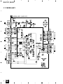
4. PCB CONNECTION DIAGRAM
NOTE FOR PCB DIAGRAMS :
1. Part numbers in PCB diagrams match those in the schematic
diagrams.
2. A comparison between the main parts of PCB and schematic
diagrams is shown below.
Symbol In PCB
Diagrams
Symbol In Schematic
Diagrams
B C E B C E
Connector
Capacitor
Transistor
B C E
B
C
E B
C
SIDE A
E
Transistor
with resistor
B C E
D
D G S
Part Name
3. The parts mounted on this PCB include all necessary parts for
several destinations.
For further information for respective destinations, be sure to
check with the schematic diagram.
4. View point of PCB diagrams.
G S D
G S
Field effect
transistor
P.C.Board
Chip Part
SIDE B
Resistor array
3-terminal
regulator
39
1
2
3
4
DV-F727, DV-F07
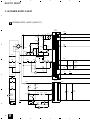
4.1 FGSB, SMEB, SSRB, SEMB, LOMB, LOSB, RADB, PHOB,DOMB, DOSB,
VOLB and LEDB ASSYS
A FGSB ASSY
PC101
A
Q CN303
B SMEB
R101
ASSY
M
M
CARRIAGE
MOTOR
(VNP1661-B)
SPINDLE
MOTOR
(VNP1695-A)
Q CN307
C SSRB ASSY
D SEMB
ASSY
M
B
SELECT MOTOR
(VNP1727-A)
(VNP1727-A)
Q603
Q602 Q601
G RADB
Q604
ASSY
K VOLB
Q621
ASSY
(VNP1727-A)
H PHOB
ASSY
CN306
(VNP1726-A)
C
I
L
Q
(VNP1727-A)
VR601
LEDB
ASSY
DOMB ASSY
(VNP1726-A)
Q
E LOMB ASSY
CN304
Q
J
M
DOOR
MOTOR
DOSB
ASSY
CN305
(VNP1727-A)
D
LOADING
MOTOR
M
(VNP1726-A)
SIDE A
(VNP1726-A)
40
F
LOSB ASSY
(VNP1727-A)
A B C D E F G H I J K L
1
2
3
4
1
2
3
4
DV-F727, DV-F07
A
C SSRB ASSY
D SEMB ASSY
B
(VNP1727-A)
(VNP1727-A)
G RADB
ASSY
(VNP1727-A)
L
H
K VOLB ASSY
PHOB
ASSY
LEDB
ASSY
(VNP1727-A)
(VNP1726-A)
C
I
DOMB ASSY
(VNP1726-A)
E LOMB ASSY
F
LOSB ASSY
J
DOSB
ASSY
D
(VNP1727-A)
(VNP1727-A)
(VNP1726-A)
SIDE B
1
(VNP1726-A)
C D E F G H I J K L
2
3
4
41
1
2
3
4
DV-F727, DV-F07
• This PCB is a four-layered board.
4.2 DVDM ASSY
M DVDM ASSY
A
O CN101
O CN501
R CN401
IC23
IC26
IC31 Q810 Q808
Q812
IC25
IC54
Q809 Q807 Q811
IC21
IC801
VR851 IC807
VC21 IC22
IC806
B
IC903
IC261
IC303
PICKUP
ASSY
IC302 IC702
IC610
Q111
Q112 Q107
C
IC101
IC601
Q
CN301
Q102
IC761
Q281
IC352 IC603
IC606
Q601
Q602
D
(VNP1706-B)
V CN201
42
M
1
S CN701
P CN901 Q CN302
SIDE A
2
3
4
1
2
3
4
DV-F727, DV-F07
• This PCB is a four-layered board.
M DVDM ASSY
A
IC905
IC803
IC27
IC805
IC802
IC73
N
B
CN101
IC201
IC701
IC231
Q542
IC608 Q179
Q106 Q105 Q237
IC299
Q543 Q113
Q106
IC904
IC609 Q114
IC611
IC612
IC751
C
Q101
Q103
IC792
Q251
IC604
IC791
IC607
D
(VNP1706-B)
SIDE B
1
2
3
M
4
43
1
2
3
4
DV-F727, DV-F07
4.3 AVJB ASSY
O AVJB ASSY
A
Q120
IC203
IC206
IC202
B
IC201
IC241
IC150
Q150
Q588
C
IC501 IC502 Q589
Q592
Q591
Q591 Q587 Q586
D
(VNP1725-A)
M CN901
44
O
1
M CN905
P CN902
SIDE A
2
3
4
1
2
3
4
DV-F727, DV-F07
A
O AVJB ASSY
Q201 Q202
Q257
Q277
Q281
B
Q151
Q582
Q584 Q585
Q583
C
Q561
Q581
D
(VNP1725-A)
SIDE B
1
2
3
O
4
45
1
2
3
4
DV-F727, DV-F07
4.4 VQEB ASSY
A
N VQEB ASSY
SIDE A
B
(VNP1696-B)
VR102
VR101
Q551 Q541
Q531
Q521 Q511
Q501
IC1
IC103
IC106
IC105
N VQEB ASSY
SIDE B
C
(VNP1696-B)
D
M CN802
Q1
46
N
1
2
IC102
Q502 Q512
Q522 IC104
Q532 Q542
Q552
3
4
1
2
3
4
DV-F727, DV-F07
4.5 MSJB ASSY
P
A
MSJB ASSY
S CN702
M CN903
O CN502
B
(VNP1726-A)
Q987
SIDE A
C
P MSJB ASSY
D
(VNP1726-A)
IC921
IC922
Q981
IC931
IC901
SIDE B
1
2
3
P
4
47
1
2
3
4
DV-F727, DV-F07
4.6 MDRB ASSY
A
Q MDRB ASSY
Q MDRB ASSY
I
J631
E
J651
L
J1601
Q301
B
M
CN921
M
CN1030
Q302
C
Q303
B
IC301
CN202
D
VR301
J601
D
(VNP1726-A)
48
Q
1
SIDE A
SIDE B
2
3
4
1
2
3
4
DV-F727, DV-F07
4.7 232B ASSY (DV-F07 ONLY)
R 232B ASSY
A
IC401
B
M CN106
(VNP1726-A)
SIDE A
R 232B ASSY
C
D
(VNP1726-A)
SIDE B
1
2
3
R
4
49
1
2
3
4
DV-F727, DV-F07
4.8 FLKY, KEYB and PS2B ASSYS
A
S
P CN903
FLKY ASSY
M CN602
B
C
(VNP1726-A)
IC701
IC702
D
SIDE A
50
S
1
2
3
4
5
6
7
8
DV-F727, DV-F07
A
T KEYB ASSY
IC1251
IC1201
B
C
(VNP1726-A)
U PS2B
ASSY
D
(VNP1726-A)
5
6
7
T U
8
51
1
2
3
4
DV-F727, DV-F07
A
T KEYB ASSY
B
C
(VNP1726-A)
U PS2B
ASSY
D
(VNP1726-A)
52
T U
1
2
3
4
5
6
7
8
DV-F727, DV-F07
A
S FLKY ASSY
B
C
(VNP1726-A)
Q702 Q701
D
SIDE B
5
6
7
S
8
53
1
2
3
4
DV-F727, DV-F07
4.9 POWER SUPPLY ASSY
V POWER SUPPLY ASSY
A
AC IN
B
Q103
Q101
Q122
Q102
Q121
IC201
C
IC301
VR201
VR301
VR202
IC203 IC202
Q301
D
M CN110
54
V
1
SIDE A
2
3
4
DV-F727, DV-F07
Mark No.
Description
Part No.
Mark No.
Description
Part No.
5. PCB PARTS LIST
NOTES:
• Parts marked by "NSP" are generally unavailable because they are not in our Master Spare Parts List.
• The mark found on some component parts indicates the importance of the safety factor of the part.
Therefore, when replacing, be sure to use parts of identical designation.
• When ordering resistors, first convert resistance values into code form as shown in the following examples.
Ex.1 When there are 2 effective digits (any digit apart from 0), such as 560 ohm and 47k ohm (tolerance is shown by J=5%,
and K=10%).
561 ........................................................ RD1/4PU 5 6 1 J
560 Ω
→
56 × 101 →
473 ........................................................ RD1/4PU 4 7 3 J
47k Ω
→
47 × 103 →
0.5 Ω
→
R50 ..................................................................................... RN2H R 5 0 K
1Ω
→
1R0 ..................................................................................... RS1P 1 R 0 K
Ex.2 When there are 3 effective digits (such as in high precision metal film resistors).
5621 ...................................................... RN1/4PC 5 6 2 1 F
5.62k Ω →
562 × 101 →
LIST OF WHOLE PCB ASSEMBLIES
Part No.
Mark
Symbol and Description
DV-F727
DV-F07
KU
KC
KU/RC
KU/CA
NSP
NSP
NSP
NSP
TRAVERSE MECHANISM ASSY
FGSB ASSY
SMEB ASSY
PICKUP ASSY
VWT1161
VWG2009
VWG2048
VWY1055
VWT1161
VWG2009
VWG2048
VWY1055
VWT1161
VWG2009
VWG2048
VWY1055
VWT1161
VWG2009
VWG2048
VWY1055
NSP
NSP
NSP
NSP
NSP
NSP
NSP
MECB ASSY
SSRB ASSY
SEMB ASSY
LOMB ASSY
LOSB ASSY
RADB ASSY
PHOB ASSY
VWM1957
VWG2113
VWG2114
VWG2115
VWG2116
VWG2117
VWG2118
VWM1957
VWG2113
VWG2114
VWG2115
VWG2116
VWG2117
VWG2118
VWM1957
VWG2113
VWG2114
VWG2115
VWG2116
VWG2117
VWG2118
VWM1957
VWG2113
VWG2114
VWG2115
VWG2116
VWG2117
VWG2118
NSP
NSP
NSP
NSP
NSP
NSP
SUBB ASSY
KEYB ASSY
DOMB ASSY
DOSB ASSY
VOLB ASSY
LEDB ASSY
PS2B ASSY
FLKY ASSY
MDRB ASSY
MSJB ASSY
232B ASSY
VWM1958
VWG2120
VWG2121
VWG2122
VWG2123
VWG2124
VWG2125
VWG2126
VWG2127
VWG2131
Not used
VWM1958
VWG2120
VWG2121
VWG2122
VWG2123
VWG2124
VWG2125
VWG2126
VWG2127
VWG2131
Not used
VWM1999
VWG2120
VWG2121
VWG2122
VWG2123
VWG2124
VWG2125
VWG2191
VWG2127
VWG2131
Not used
VWM1959
VWG2120
VWG2121
VWG2122
VWG2123
VWG2124
VWG2125
VWG2119
VWG2127
VWG2128
VWG2129
DVDM ASSY
VQEB ASSY
AVJB ASSY
POWER SUPPLY ASSY
VWS1386
VWV1669
VWV1719
VWR1317
VWS1386
VWV1669
VWV1719
VWR1317
VWS1386
VWV1669
VWV1719
VWR1317
VWS1396
VWV1669
VWV1720
VWR1317
Remarks
CONTRAST OF PCB ASSEMBLIES
M DVDM ASSY
VWS1386 and VWS1396 are constructed the same except for the following :
Mark
Symbol and Description
IC803
C834, C838, C840
CN106 7P FFC CONNECTOR
Part No.
VWS1386
VWS1396
Not used
Not used
Not used
M5M4V18165DTP-6S
CKSRYF104Z16
VKN1299
Remarks
55
DV-F727, DV-F07
Mark No.
Description
Part No.
O AVJB ASSY
Mark No.
Description
Part No.
VWV1719 and VWV1720 are constructed the same except for the following :
Mark
Part No.
Symbol and Description
IC201
IC241
F241 CHIP SOLID INDUCTOR
C241, C243
R241, R242
R243-R245
R247-R249
CN503 DUAL 4P MINI DIN SOCKET
JA201 4P PIN JACK
JA504 2P PIN JACK
JA505
3P PIN JACK
VWV1719
VWV1720
PCM1716E
Not used
Not used
Not used
Not used
PE8001A
PD0236AM
VTF1096
CKSQYF104Z25
RS1/10S471J
Not used
RS1/10S0R0J
AKP7020
VKB1132
VKB1134
RS1/10S101J
Not used
AKP7023
VKB1133
VKB1135
VKB1131
VKB1100
Remarks
P MSJB ASSY
VWG2131 and VWG2128 are constructed the same except for the following :
Mark
Part No.
Symbol and Description
JA901, JA903
1P PIN JACK
VWG2131
VWG2128
VKB1077
VKB1074
Remarks
S FLKY ASSY
VWG2126 and VWG2119 are constructed the same except for the following :
Mark
Part No.
Symbol and Description
R753
R754
R755
R756
VWG2126
VWG2191
VWG2119
RS1/10S363J
RS1/10S622J
Not used
RS1/10S0R0J
RS1/10S363J
RS1/10S622J
RS1/10S623J
RS1/10S473J
RS1/10S392J
RS1/10S103J
Not used
RS1/10S0R0J
Remarks
PCB PARTS LIST FOR DV-F727/KU UNLESS OTHERWISE NOTED
Mark No.
Description
Part No.
Mark No.
Description
Part No.
RESISTORS
A FGSB ASSY
All Resistors
RD1/4PU
SEMICONDUCTOR
PC101
OTHERS
TLP910(O)
RESISTORS
All Resistors
RS1/10S
B SMEB ASSY
DSG1016
OTHERS
OTHERS
CN201
CN202
3P FFC CONNECTOR
8P FFC CONNECTOR
PC BOARD SMEB
52044-0345
VKN1212
VNP1695
C SSRB ASSY
J601
E
56
7P CABLE HOLDER
9P CABLE HOLDER
JUMPER WIRE 9P
51048-0700
51048-0900
D20PDY0930E
LOMB ASSY
OTHERS
SEMICONDUCTORS
Q604
Q601,Q602
D601,D602
51048-0300
51048-0700
D20PDD0310E
D20PDD0725E
D20PDY0310E
D SEMB ASSY
SWITCH
S201
J603
J602
J605
J
3P CABLE HOLDER
7P CABLE HOLDER
JUMPER WIRE 3P
JUMPER WIRE 7P
JUMPER WIRE 3P
2SC1740S
DTC124ES
GP1S58V
J652
J651
3P CABLE HOLDER
5P CABLE HOLDER
JUMPER WIRE 3P
JUMPER WIRE 5P
51048-0300
51048-0500
D20PDD0310E
D20PDY0530E
J
DV-F727, DV-F07
Mark No.
F
Description
Part No.
Mark No.
L
LOSB ASSY
SWITCH
Description
LEDB ASSY
SEMICONDUCTORS
LEAF SWITCH
VSK1011
3P CABLE HOLDER
51048-0300
D1611
D1601
OTHERS
HZU6.2B
NSPB500-9235
RESISTORS
All Resistors
J1601
SEMICONDUCTOR
D611
51048-0300
D20PDY0325E
SEMICONDUCTORS
51048-0300
RNK1795
IC21
IC101
IC201
IC609
IC352
H PHOB ASSY
SEMICONDUCTOR
Q621
PT381FBC
OTHERS
3P CABLE HOLDER
JUMPER WIRE 3P
51048-0300
D20PDY0315E
DOMB ASSY
RESISTORS
All Resistors
RS1/10S
J
OTHERS
J
3P CABLE HOLDER
JUMPER WIRE 3P
M DVDM ASSY
3P CABLE HOLDER
LED HOLDER
J631
J
GL381J
OTHERS
I
RS1/10S
OTHERS
G RADB ASSY
J604
Part No.
3P CABLE HOLDER
4P CABLE HOLDER
JUMPER WIRE 4P
51048-0300
51048-0400
D20PDY0445E
DOSB ASSY
CY2081SL-655
LA9701M
LC78652W
LC89170M
M56788FP
IC801
IC802
IC612,IC904
IC608,IC611,IC807,IC905
IC607
M65773AFP
MC74VHC541DT
MC74VHCT541ADT
MC74VHCT574ADT
IC702
IC261,IC302
IC601
IC701
IC604
MN414800CSJ-07
NJM2100M
PD3410A
PD4995A
TC55V1001AF8
IC606
IC751
IC24-IC27,IC303
IC610
IC22
TC7SET32F
TC7SH32FU
TC7SHU04F
TC7W53FU
TC7WH74FU
IC603
Q106,Q109
Q105,Q114,Q251
Q602
Q107,Q111,Q601
VYW1668
2SA1576A
2SC4081
DTA114EUA
DTC114EUA
Q102
Q103,Q281,Q542,Q543
Q101
Q112,Q113
Q108
HN1A01F
HN1B04FU
HN1C01F
HN1C01FU
HN1K03FU
Q503
D302
D601
D501,D502
RN1911
KV1470
RB501V-40
RB521S-30
MB811171622A-100FN
SWITCH
S631
LEAF SWITCH
VSK1011
3P CABLE HOLDER
JUMPER WIRE 3P
51048-0300
D20PDD0315E
OTHERS
J632
K VOLB ASSY
RESISTOR
VR601 (22kΩ)
VCP1158
OTHERS
CN604,CN605
52147-0310
3P JUMPER CONNECTOR
KN601
JUMPER TERMINAL
PKX1001
COILS AND FILTERS
F5050,F5090 CHIP BEAD
F4010,F4020,F4030,F4040,F4050
CHIP BEAD
F4060,F8330,F9590 CHIP BEAD
L304
CHIP COIL (1.5µH)
L151
CHIP COIL (10µH)
DTF1067
DTF1070
DTF1070
VTL1059
VTL1061
L47
CHIP BEAD
L1400
CHIP BEAD
L9490,L9500,L9510 CHIP BEAD
L101,L330 CHIP COIL (8.2µH)
VTL1084
VTL1088
VTL1105
VTL1125
57
DV-F727, DV-F07
Mark No.
Description
Part No.
CAPACITORS
58
Mark No.
Description
Part No.
RESISTORS
C612
C123,C145,C21,C282,C617
C26
C126,C333
C206,C210,C211
CCSRCH100D50
CCSRCH101J50
CCSRCH120J50
CCSRCH150J50
CCSRCH151J50
R123 (39Ω×4)
R715,R716 (47Ω×4)
R531,R543,R545,R613 (10kΩ×4)
R648,R649,R706,R707,R748
(10kΩ×4)
ACN7047
ACN7077
DCN1094
DCN1094
C322
C116,C151,C314
C152
C632
C209
CCSRCH180J50
CCSRCH220J50
CCSRCH221J50
CCSRCH330J50
CCSRCH331J50
R751 (10kΩ×4)
R121,R532,R689,R691,R732
(22Ω×4)
R736,R785,R786,R818-R820
(22Ω×4)
DCN1094
DCN1104
C104-C108,C128,C134,C297
C335
C122,C208
C127,C334
C124,C146
CCSRCH470J50
CCSRCH470J50
CCSRCH471J50
CCSRCH5R0C50
CCSRCH680J50
R825,R848,R849 (22Ω×4)
R1020,R162,R2010,R2020,R2030
R2040,R3050,R3520,R506,R510
R520,R601,R701,R801,R8410
R9200,R9210,R9230,R9240
DCN1104
RS1/10S0R0J
RS1/10S0R0J
RS1/10S0R0J
RS1/10S0R0J
C117,C240,C352,C360
C129,C142,C22,C405,C601
C701,C763,C801,C802,C804
C113,C139,C358,C368,C411
C111,C147,C149,C205,C207
CCSRCH681J25
CEV101M10
CEV101M10
CEV220M16
CEV470M6R3
R939-R948,R952-R958,R960
R964,R973-R975,R979
R361,R364
R363,R365
R164
RS1/10S0R0J
RS1/10S0R0J
RS1/16S1203F
RS1/16S1503F
RS1/16S5600F
C401,C403,C407
C502
C140,C223,C224,C252,C264
C312
C229
CEV470M6R3
CKSQYB103K50
CKSQYB105K10
CKSQYB105K10
CKSQYB224K16
R3510 (100Ω)
Other Resistors
VCN1120
RS1/16S
C217
C216,C313
C133,C136,C203,C220,C225
C239,C320,C321,C619,C703
C722
CKSQYF105Z16
CKSRYB102K50
CKSRYB103K50
CKSRYB103K50
CKSRYB103K50
C101,C102,C114,C118,C119
C121,C130,C138,C204
C212,C213,C227,C228,C231
C24,C263,C315-C317,C332
C281,C354
CKSRYB104K16
CKSRYB104K16
CKSRYB104K16
CKSRYB104K16
CKSRYB222K50
C153,C266
C214,C251,C261
C357
C330
C109,C110,C120,C131,C148
CKSRYB223K25
CKSRYB472K50
CKSRYB473K16
CKSRYB682K50
CKSRYF104Z16
C150,C202,C215,C221,C222
C226,C230,C235,C265,C29
C31,C33,C35,C359,C367
C369-C372,C402,C404,C406
C408,C410,C412,C501
CKSRYF104Z16
CKSRYF104Z16
CKSRYF104Z16
CKSRYF104Z16
CKSRYF104Z16
C602-C611,C613-C616,C618
C621-C631,C702,C704-C714
C716-C721,C723-C725
C761,C762,C822,C827,C829
C832,C833,C836,C920,C921
CKSRYF104Z16
CKSRYF104Z16
CKSRYF104Z16
CKSRYF104Z16
CKSRYF104Z16
C143,C319,C806-C819
C328,C821,C824,C825,C828
(2.2µF)
C830,C837 (2.2µF)
C23,C299 (0.47µF)
CKSRYF105Z10
VCG1030
VCG1030
VCG1032
VC21 (30pF)
VCM1013
DCN1104
J
OTHERS
X601
CHIP CERALOCK
(20MHz)
FLEXIBLE CABLE 7P
CN201
CN120
B TO B CONNECTOR 14P
DSS1110
VDA1681
VKN1324
24P FFC CONNECTOR VKN1464
CN1030,CN921
VKN1471
12P FFC CONNECTOR
CN905
14P FFC CONNECTOR VKN1473
CN602,CN901
VKN1474
15P FFC CONNECTOR
CN110
CN903
CN802
CN107
X21
26P FFC CONNECTOR VKN1479
11P FFC CONNECTOR VKN1497
VKN1529
B TO B CONNECTOR 40P
7P FFC CONNECTOR VKN1575
BARCODE LABEL
VRW1773
CRYSTAL RESONATOR VSS1129
(13.824MHz)
N VQEB ASSY
SEMICONDUCTORS
IC102
IC101
IC105,IC106
Q531,Q532,Q541,Q542
Q551,Q552
MB811171622A-100FN
PM0023AF
TC7SH14FU
2PB709A
2PB709A
COIL AND FILTER
F102
L101
VIDEO FILTER
CHIP COIL
VTF1155
VTL1067
DV-F727, DV-F07
Mark No.
Description
Part No.
Mark No.
CAPACITORS
C130
C101,C120
C110-C119,C121-C126,C150
C160,C532,C542,C552
C201,C202 (2.2µF)
CCSRCH102J50
CEV101M16
CKSRYB104K16
CKSRYB104K16
VCG1031
RESISTORS
R105,R106,R404,R405 (22Ω×4)
R12,R201,R409,R418,R419
R501
R122
R532,R542,R552
DCN1104
RS1/10S0R0J
RS1/10S0R0J
RS1/10S2701F
RS1/16S3300F
R534,R544,R554
Other Resistors
RS1/16S4700F
RS1/16S
J
VKN1530
O AVJB ASSY
C101,C103,C120,C123,C151
C153,C204,C205,C208,C209
C214,C215,C230,C233,C234
C281,C290,C502,C527
C529,C530,C590
CKSQYF104Z25
CKSQYF104Z25
CKSQYF104Z25
CKSQYF104Z25
CKSQYF104Z25
C201,C202,C210,C212,C213
C531
CKSQYF105Z16
CKSQYF105Z16
R597-R599
R533,R534,R542,R551,R555
R558,R581,R585,R589
R250,R270
R251,R271
RN1/10SC18R0D
RN1/10SC62R0D
RN1/10SC62R0D
RN1/10SE1602D
RN1/10SE2702D
Other Resistors
RS1/10S
J
OTHERS
SEMICONDUCTORS
IC203
IC502
IC501
IC206
IC150
BA4560F
BU4551BF
LA7135AM
NJM78L05A
NJM78M08FA
IC201
IC202
Q202,Q581-Q584
Q151,Q281,Q585
Q150
PCM1716E
TC7SU04F
2PB709A
2PD601A
2SB1260
Q120
Q257,Q277
Q201,Q561,Q586-Q589
D230
D281
2SC1740S
2SD2114K
PDTC124EK
HZU5.6B
MA111
COILS AND FILTER
L220
L202
F201
Part No.
CEAT471M6R3
CKSQYB103K50
CKSQYB104K25
CKSQYB222K50
CKSQYB473K50
RESISTORS
OTHERS
CN101 B TO B CONNECTOR 40P
Description
C550,C552
C150
C520-C522,C561,C585
C587
C583
P
CN503
JA505
JA201
JA504
CN502
DUAL 4P MINI DIN SOCKET AKP7020
CN101
CN501
14P FFC CONNECTOR VKN1190
15P FFC CONNECTOR VKN1191
SCREW TERMINAL
VNE1948
3P PIN JACK
4P PIN JACK
2P PIN JACK
7P FFC CONNECTOR
VKB1131
VKB1132
VKB1134
VKN1183
MSJB ASSY
SEMICONDUCTORS
IC922
IC901,IC931
Q981
D971,D981
TC74HC00AF
TC74HCU04AF
PDTC124EK
MA111
COILS AND FILTERS
CHIP INPEDER
DTL1028
LAU1R0J-TA
CHIP SOLID INDUCTOR VTF1096
L901
PULSE TRANS.
PTL1003
L902
NOISE FILTER
RTF1167
F901,F904,F912,F922
VTF1096
CHIP SOLID INDUCTOR
SWITCH AND RELAY
S501
RY281
VSH1009
RSR1029
CAPACITORS
C253,C273
C251,C271
C523-C525
C255,C275
C104,C154,C211,C232,C501
CCSQCH221J50
CCSQCH330J50
CCSQCH470J50
CCSQSL331J50
CEAT101M10
C526,C528,C581,C582
C102,C121,C122,C152,C231
C203,C541,C555,C560
C206,C207
C250,C252,C270,C272
CEAT101M10
CEAT101M16
CEAT102M6R3
CEAT470M16
CEAT470M25
CAPACITORS
C932
C902,C912,C915,C958
C903,C931
C905,C906,C913,C916,C922
C933,C936,C959,C973
CCSQCH101J50
CEAT101M10
CKSQYF103Z50
CKSQYF104Z25
CKSQYF104Z25
RESISTORS
All Resistors
RS1/10S
J
OTHERS
CN904,CN905 MINI JACK
AKN1028
JA902
OPTICAL LINK OUT
GP1F32T
JA908
MINI JACK
PKN1005
JA906,JA907
RKN1004
REMOTE CONTROL JACK
59
DV-F727, DV-F07
Mark No.
Description
JA901,JA903 1P PIN JACK
CN902,CN903
7P FFC CONNECTOR
CN901
11P FFC CONNECTOR
SCREW TERMINAL
Part No.
Mark No.
VKB1077
VKN1211
S
Part No.
FLKY ASSY
SEMICONDUCTORS
VKN1215
VNE1948
IC701
IC702
Q701-Q704
D701
Q MDRB ASSY
PE5144A
S-806D
PDTC124EK
SLR-343VC(NP)
COILS
SEMICONDUCTORS
IC301
Q303
Q301
Q302
Description
L721,L722
LA6531
2SA1037K
2SC2412K
PDTC124EK
CHIP BEAD
VTL1105
SWITCHES
S701-S708
ASG7013
CAPACITORS
CAPACITORS
C306
C303
C301
C302,C304,C305,C307
CCSQCH101J50
CEAT101M10
CEAT470M16
CKSQYF104Z25
RESISTORS
R333
R302,R329
R311,R312
R335,R336
R322,R323,R326,R327
RS1/10S1503F
RS1/10S1803F
RS1/10S2202F
RS1/10S3003F
RS1/10S3302F
R324,R328
R334,R338
Other Resistors
RS1/10S3902F
RS1/10S3903F
RS1/10S
J
C710
C701,C703,C709
C740-C743,C751,C753
C707
C702,C704-C706,C708,C714
CEAL100M50
CEAL470M6R3
CKSQYB102K50
CKSQYF102Z50
CKSQYF104Z25
C711
CKSQYF104Z50
RESISTORS
R791
R792
R794
R741
Other Resistors
RA10T104J
RA13T104J
RA4T104J
RN1/10SE1001D
RS1/10S
J
OTHERS
OTHERS
CN306
CN304
CN305
CN307
CN303
3P JUMPER CONNECTOR
4P JUMPER CONNECTOR
5P JUMPER CONNECTOR
9P JUMPER CONNECTOR
8P FFC CONNECTOR
CN703
IR701
V701
CN702
52147-0310
52147-0410
52147-0510
52147-0910
VKN1184
CN701
X701
CN301,CN302
VKN1188
12P FFC CONNECTOR
T
R 232B ASSY (DV-F07/KU/CA Only)
15P FFC CONNECTOR VKN1191
CERAMIC RESONATOR VSS1142
(5MHz)
KEYB ASSY
SEMICONDUCTORS
SEMICONDUCTOR
IC401
13P CABLE HOLDER
51048-1300
11P FFC CONNECTOR 52045-1145
REMOTE RECEIVER UNIT GP1U28X
FL TUBE
VAW1052
7P FFC CONNECTOR VKN1183
D1201-D1204
MAX232EPE
DA204K
SWITCHES
FILTERS
F401-F403 EMI FILTER
S1201-S1220
S1200
VTH1009
CAPACITORS
C404,C405
C401
C403
C402
C406
CEANP1R0M50
CEAT101M10
CEAT1R0M50
CKSQYF104Z25
CEAL1R0M50
ASG7013
PSX1002
CAPACITORS
C1252
C1201,C1202
C1203,C1251
CEAL470M6R3
CKSQYF103Z50
CKSQYF104Z25
RESISTORS
RESISTORS
All Resistors
All Resistors
RS1/10S
RS1/10S
J
OTHERS
OTHERS
JA401
CN401
60
15P D-SUB SOCKET
7P FFC CONNECTOR
DKN1111
VKN1183
CN1202
CN1201
11P FFC CONNECTOR 52045-1145
7P FFC CONNECTOR VKN1211
J
DV-F727, DV-F07
Mark No.
Description
Part No.
Mark No.
Description
Part No.
U PS2B ASSY
FILTERS
F801-F804
EMI FILTER
VTH1009
CAPACITORS
C801-C804
C813,C814
CCSQCH101J50
CKSQYF104Z25
RESISTORS
All Resistors
RS1/10S
J
OTHERS
JA801
CN801
V
MINI DIN 6P SOCKET
7P FFC CONNECTOR
RKN1038
VKN1211
POWER SUPPLY ASSY
SEMICONDUCTORS
IC203 (1A)
IC201,IC202 (1.6A)
VARISTOR
AEK7064
AEK7066
VZF1092
OTHERS
FU101
CN201
FUSE (2A)
REK1078
26P FFC CONNECTOR VKN1202
61
DV-F727, DV-F07
6. ADJUSTMENT
6.1 ADJUSTMENT ITEMS AND LOCATION
Note : When the Traverse mechanism adjustment is not properly adjusted, jitter, error rate and play ability are defective.
The noise may come out by the case.
Adjustment Points (PCB Part)
DVDM ASSY
CN703
IC21
1
Pin 5
IC801
2
VR601
VC21
KN601
VOLB ASSY
CN120
IC601
IC101
Adjustment Items
CN1030
[Electrical Part]
CN252
1 Master Clock Adjustment
CN110
2 Disc-select Rotation Adjustment
SIDE A
6.2 JIGS AND MEASURING INSTRUMENTS
A
V
CH1
(X)
DC power supply
CD TEST DISC
(YEDS-7)
Digital multi meter
Frequency counter
Display digit ≥ 8-digit
CH2
(Y)
Oscilloscope
Jig (Peak hold circuit)
22k
V+B
0.01
+
470k
M5238(2/2)
33/16
+
OUTPUT
+
–
INPUT 470
M5238(1/2)
–
Screwdriver
(small)
62
Precise screwdriver
Test mode remote
control unit
(GGF1067)
47
0.01
from KN601
(VOLB ASSY)
+
SW
V-B
CQM or CFTX
33/16
0.1
0.1
(Peak hold OUT)
DV-F727, DV-F07
6.3 NECESSARY ADJUSTMENT POINTS
When
Adjustment Points
EXCHANGE PCB ASSY
Exchange board
VOLB ASSY, SSRB ASSY,
RADB ASSY, PHOB ASSY
Mechanical
point
Electric
point
2
Mechanical
point
Exchange board
DVDM ASSY
Electric
point
Note :
is adjusted already.
6.4 ELECTRICAL ADJUSTMENT
1
Master Clock Adjustment
• When not properly adjusted : Uneven color
DVDM ASSY
• Normal mode
• Power ON
33.868800MHz ± 160Hz
VC21
Player
START
DVDM ASSY
IC21
Frequency counter
Pin 5
63
DV-F727, DV-F07
2 Disc-select Rotation Adjustment
DC power supply
Connection Diagram for Adjustment
V
A
–8V
GND
+8V
VOLB ASSY
VR601
KN601
JIG
(Peak hold circuit)
SW
INPUT
Player
Digital multimeter
OUTPUT
GND
(Under Base)
Adjustment Procedure
1.
2.
3.
4.
5.
6.
7.
8.
9.
10.
11.
12.
13.
14.
Connect all equipment as shown in the diagram.
Turn on the power (Normal mode) and put the test disc in the No. 1 disc slot.
Enter the Test mode by pressing the "ESC" → "TEST" button of the test mode remote control unit.
Press the "DIG/ANA" button of the test mode remote control unit. (Disc 1 is clamped.)
Adjust VR601 on the VOLB Assy so that the voltage becomes 830 ± 5mV.
Switch the connection of Digital multimeter from INPUT to OUTPUT of the Jig.
Press the "DIG/ANA" button of the test mode remote control unit. (Starts the disc detection and peak hold .)
Confirm the voltage during the disc detection.
If voltage is between 920 to 1170mV, go to step 13. If not, go to step 9.
Switch the connection of Digital multimeter form OUTPUT to INPUT of the Jig.
Press the "DIG/ANA" button of the test mode remote control unit. (Disc 1 is clamped.)
Adjust VR601 to become the value for addition (or subtraction) that to have an adjustment voltage.
(Refer to the following table.)
Perform steps 6 to 8 again and confirm the voltage during the disc detection.
If voltage is between 920 to 1170mV, go to step 13. If not, repeat steps 9 to 12.
Confirm that Disc No. display doesn't become "1" others when you turn the Jog dial.
Release the Test mode by pressing the "ESC" button or turn off the power.
Adjustment voltage value
Peak hold voltage (mV)
to 859
859 to 879
879 to 920
920 to 1170
1170 to 1309
1309 to 1520
1520 to 1840
1840 to 2220
2220 to
64
Adjustment voltage (mV)
+20
+10
+5
OK
-5
-10
-20
-30
-40
DV-F727, DV-F07
Simple Adjustment of Disc Detection
Connection Diagram for Adjustment
Stopped
22 - NOV - 1999 16 46
2 s/d
CH2 = 200mV
DC P*10
Peak value is
OK with 950 - 1100mV.
GND
Go arround
(except for single loader)
VOLB ASSY
Oscilloscope
CH1
(X)
CH2
(Y)
VR601
KN601
Player
Chassis GND
Peak
Minimum
Peak
Maximum
VR601
Adjustment Procedure
1. Connect an oscilloscope.
2. Turn the POWER SW to ON.
3. Open the Food.
4. Press the "SINGLE LOADER PLAY" button of the player without putting a disc.
Start the disc detection if loading is come and there is no disc.
5. If the peak value is 950 - 1100mV while a disc detection goes arround the disc, is OK.
6. When peak value is except for OK range, adjust VR601 and repeat steps 3 - 5.
65
DV-F727, DV-F07
7. GENERAL INFORMATION
7.1 DIAGNOSIS
7.1.1 TEST MODE SCREEN DISPLAY
Consecutive double-OSD display is supported during test mode. The screen is composed 10 lines with a maximum of 32 characters per line.
It can't be used with the debugging display mode together.
• Screen Composition
Character in bold : Item name
: Information display
Remote control code
Key code
Mechanism position value and
slider position
Address
Background color
Output video system and
Skirt terminal output
AV1 chip version
FL controller version and
region setting for the player
Tracking status
Spindle status and AFB status
AGC setting
FL controller destination setting
FTS servo IC information
Port No. of Flash ROM and
system controller
Flash ROM version and Flash ROM size
System controller revision
C1 error value of CD and DVD
Internal operation mode of
the mechanism control
Disc judgment and
CD 1/3 beam switch
DVD mechanism controller revision
(Control and part No. of GUI-ROM)
Equalizer value and
jitter value
First Screen Display
Caution :
The first screen and second screen switch by pressing [DISPLAY]
key of the remote control unit.
It is only a version display part on the lower right of the screen
those contents of display change.
ATB : ON/OFF information display and AGC manual setting display
deleted with the second generation.
The displays of Tilt error value, Tilt servo status and pickup
DVD/CLD display deleted with the third generation becomes LD
part is deleted.
• Description of Each Item on the Display
(1) Address indication
The address being traced is displayed in number.
DVD
: ID indication (hexadecimal number, 8 digits)
[∗∗∗∗∗∗∗∗]
CD
: A-TIME (min. sec.) [ 0 0 0 0 ∗ ∗ ∗ ∗ ]
(Note : For DVDs, decimal-number indication is possible.)
(5) Tracking status [TRKG – ∗∗∗]
Tracking on
Tracking off
(6) 1 Spindle status [SPDL – ∗ ∗ ∗]
(2) Code indication of the remote control unit
[R – ∗ ∗ ∗ ∗]
Spindle accelerator and brake, free-runnimg
FG servo
Rough, velocity phase servo
Offset addition, rough, velocity phase servo
The code for the key pressed on the remote control unit, which is
received by the FL controller, is displayed while the key is pressed.
In the case of the double code, the second code will be displayed.
ON
OFF
(3) Key code indication for the main unit [K – ∗ ∗ ]
The code for the key pressed on the main unit, which is received by
the system controller, is displayed while the key is pressed.
At keyboard code input
K-KBD ∗∗ ∗∗ :
At mouse code input
K-MS ∗∗ ∗∗
(4) Background color indication [C – R∗ ∗ G∗ ∗ B∗ ∗]
66
[ON ]
[OFF]
[A/B]
[FG]
[SRV]
[O_S]
2 AFB status [AFB – ∗ ∗]
[ON ]
[OFF]
(7) Mechanism position value [M – ∗]
Position code
[1] to [3]
(8) Slider position [S – ∗ ∗ ∗ ∗]
CD TOC area
CD active area
[IN ]
[CD ]
(9) AGC setting [AGC – ∗ ∗]
AGC on
AGC off
[AGC-ON]
[AGC-OFF]
DV-F727, DV-F07
(10) Output video system [V – ∗ ∗ ∗ ∗]
NTSC system
PAL system
Auto-setting
[NTSC]
[PAL ]
[AUTO]
Skirt terminal output [SK – ∗ ∗]
VIDEO
[00]
S-VIDEO
[01]
RGB
[02]
∗ : Display only the model which can do the output setting of skirt
terminal.
(11) FTS servo IC information
DSP coefficient indication
[KS – [∗ ∗ ∗ ∗] ∗ ∗ ∗ ∗ ]
Displays the address (four digits) of the specified coefficient
and the setting value (four digits) with [TEST] and [9] keys.
(12) Error rate indication
1 C1 error value of CD
2 C1 error value of DVD
[ER – C1 ∗ ∗ ∗ ∗ ]
[ER – ∗ ∗ ∗ ∗ ∗ ∗ ∗ ∗ ]
(13) Internal operation mode of mechanism controller
[MM – ∗ ∗ : ∗ ∗]
Internal mechanism mode (2 digits) and internal mechanism step (2
digits) of the mechanism controller
(19) The part number of the flash ROM and system
controller [∗ ∗ ∗ ∗ ∗ ∗ / ∗ ∗ ∗ ∗ ∗ ∗ ∗ ]
1 Part number of the flash ROM
(Example) VYW1536-A
(Example) PD6256A9
2 Part number of the system controller
(Example) PD3381T1
<Front>
= W1536A
= 6256A9
<Rear>
= 3381T1
(20) 1 Version of the flash ROM [V : ∗ . ∗ ∗ ∗ ]
2 Flash ROM size [FLSH ∗∗ ]
(21) Revision of the system controller
[S : ∗ . ∗ ∗ ∗ / ∗ . ∗ ∗ ]
1 Revision number of the external ROM part (flash ROM) of the
system controller
<Front>
2 Revision of the internal ROM part of the system controller
<Rear>
(22) Revision of the DVD mechanism controller
[M : ∗ . ∗ ∗ ∗ ]
Revision number of the external ROM part (flash ROM) of the DVD
mechanism controller
(23) Control and part numbers of the GUI-ROM
[G : ∗ ∗ ∗ ∗ ]
(14) 1 Disk sensing [DSC – ∗ ∗ ∗]
The type of discs loaded is displayed.
[DVD], [CD ], [VCD], [
]
2 CD 1/3 beam switch [BM – ∗ ∗]
No GUI model displays as "––– / ––––".
OEM model displays the part number of GUI-ROM [G : ∗ ∗ ∗ ∗]
(15) 1 Equalizer value [E – ∗ ∗]
2 Jitter value [J – ∗ ∗]
nake the jitter four times, and renew it in every one second.
[4 – ∗ ∗]
CD is effective only in the jitter value.
(16) Version of the AV-1 chip [ AV : ∗ . ∗ / ∗ ∗ ∗ ∗ ]
(17) 1 Version of the FL controller
[FL : ∗ ∗ ∗ ∗]
2 Region setting of the player [REG : ∗ ]
Setting value
[1] to [6]
(18) Destination setting of the FL controller
[MDL : ∗ ∗ ∗ ∗ / ∗ ∗ ∗ ]
For charactors in front represent the type of model :
There charactors that follow represent the destination code.
J : /J, K : /KU, /KC, /KU/KC, R : /RAM, /RL, /RD, /LB,
WY : /WY
67
DV-F727, DV-F07
7.1.2 TROUBLE SHOOTING
• No Power ON
• FL is not turned ON
• FL indication is unusual
START
Power ON
• Blow out fuse (F101) of the primary side.
• Varister (Z101) on the POWER SUPPLY Assy is damaged.
• Blow out micro-fuse (P201, P202, P203) on the POWER SUPPLY Assy.
(Check the each voltage.)
• FL controller IC (IC701) on the FLKY Assy is damaged.
Turn on the power again
after 2 - 3 minutes.
Is FL turn on ?
• Check the following connections :
POWER SUPPLY Assy - DVDM Assy (26P flexible cable)
DVDM Assy - FLKY Assy (15P flexible cable)
FLKY Assy - KEYB Assy (11P flexible cable)
• Check each voltage (EV+5V, SW+5V, SW+3.3V, +6V and +12V)
(If above voltage are not supplied, check the micro-fuse.)
No
Yes
No
Is the indication
of FL normal ?
FL indication is dark or flickers.
• Short or open the zenner diode
on the POWER SUPPLY Assy.
(D207)
• Check the values of R761 - R763
on the FLKY Assy.
Yes
Indicates the error message
Refer to the section "7.1.4 ERROR CODE".
• Blow out micro-fuse (P201) on the POWER
SUPPLY Assy.
Is door open ?
• Check the following connections :
DVDM Assy (CN1030) - MDRB Assy (CN301) (12P flexible cable)
DVDM Assy (CN921) - MDRB Assy (CN302) (12P flexible cable)
MDRB Assy - SEMB Assy (9P parallel cord)
MDRB Assy - DOMB Assy (4P parallel cord)
MDRB Assy - LOMB Assy (5P parallel cord)
• Check the +6V power supply voltage (above micro fuse).
No
Yes
Do the video and
sound come on ?
Yes
No
• Check the following connections :
MDRB Assy - SMEB Assy (8P flexible cable)
DVDM Assy - AVJB Assy (15P flexible cable)
DVDM Assy - AVJB Assy (14P flexible cable)
AVJB Assy - MSJB Assy (7P flexible cable)
DVDM Assy - VQEB Assy (B to B connector)
OK
Indicate the error message.
68
Refer to the section "7.1.4 ERROR CODE".
DV-F727, DV-F07
7.1.3 OPERATION FLOWCHART
From power-on till the end of initialization
(Power ON)
Initialization of memory
Setup of the destination and the type of player
according to the data received from the microprocessor
for the FL display.
Process of closing the hood
Process of rejecting a disc
Changing the target address of the selector to the
address of the player
(Park)
Until start of playback of the specified disc
(Playback of the specified disc)
Changing the target address of the selector to the
address of the player
Placing the disc in the player with a load command
and clamping it
(Playback)
Closing the hood
(Closing the hood)
During closing
Finishing closing
the hood
It there a command
for playback ?
Yes
No
Detection of existence of discs through the selector
(Playback of the specified disc)
(End of the playback)
Detection of existence of discs through the selector
(Park)
69
DV-F727, DV-F07
7.1.4 ERROR CODE
Error codes that are displayed on the FL display without using the remote control unit
FL Display
AV1 VER
Possible causes
Operation of the unit
The sound may not out with
the specific audio.
AV-1 chip is not a match with the program of system controller
CPU AERR
CPU address error (Hardware is unusual.)
No operation
DMA AERR
DMA address error (Hardware is unusual.)
No operation
FLASH ID
Difference in versions of the internal ROM of the system controller and of the flash
ROM, or bus line failure or reverse installation
No operation
FLASH WRP
Write protect error of the flash ROM
No operation
FLASH SIG
Difference in part number of the flash ROM (When the ROM which could't be used was
No operation
used.)
FLASH SUM
Check sum error of the flash ROM (It exceeds the regular size.) or reverse installation
(Hardware is unusual.)
No operation
FLASH SIZE
Size error of the flash ROM (Use 4 or 8 M-bit.)
No operation
ILLGAL
The system controller fetched a code other than an operation code
(Hardware is unusual.)
No operation
RESERVE
Undefined interrupt (Hardware is unusual.)
No operation
SLOT
Inappropriate slot command issued (Hardware is unusual.)
No operation
Error codes that are displayed on the FL display by using the remote control unit
(Mechanism controller error)
To display: ESC + DISPLAY + DISPLAY; Location of the display: At the two digits of center of the FL display
To display the error history: ESC + DISPLAY + One shot; Location of the display: TV screen
FL
Description
of Error
Causes if with a DVD
Causes if with a CD
Operation of the Unit
Search timeout
Search could not be complete within 7
seconds.
Search could not be complete within 7
seconds, and it could not enter the
target area within 7 seconds by VCD
scan.
12
Search retry
error
A search could not be completed after 3
retries, search backup was executed 4
times, or in a case of timeout (6
seconds) while the unit was tracing 11
tracks or more beyond the target while
the search operation was converging.
Backup against slider skip was executed
4 times during a search, or slider skip
CD: Stops,
twice resulted in starting from the read- DVD: Continues operation
in point.
19
Tracing timeout
while
converging
Timeout (10.5 seconds) while tracing at
the stage of convergence of a search.
11
CD : Stops,
DVD: Continues operation
Stop
During Track (Index) Search, the search
for the beginning of a program could not
be completed within 3 seconds (20
Stop
seconds in the case of Index Search)
after positioning based on the TOC data
was completed.
1B
Index 0 search
error
22
Timeout of
slider inner
circumference
Inside switch could not ON within 3 seconds.
Stop
23
Timeout of
slider outer
circumference
Inside switch could not OFF within 2 seconds.
Stop
When the focus was deviated continuously 20 times.
Adjusts focus at the innermost
circumference and tries to
return to its position where the
error was generated (for 3
times),then opens.
If the same error persists after
one retry, the tray opens. (No
FOK pulse)
33
No FOK pulse
during playback
CLVA
38
If normal starting was impossible in the following three cases, disc-type sensing will
be retried if other errors occure excepting C5 error. However, when the focus error
Disc-type-sensi- "33" was occured continuously 3 times, it is finished as "38 error" at the moment:
ng error
(1) startup with the first disc-type-sensing result, (2) forced startup with another disc Open
by designating the disc type, (3) forced startup with the original disc by designating
the disc type.
70
DV-F727, DV-F07
FL
Description of
Error
Causes if with a DVD
Causes if with a CD
Operation of the
Unit
39
SGC converge
timeout
SGC could not converge during detects the peak
Open
41
Spindle timeout
The unit did not enter Stop mode within 10 seconds of issuance of a Stop command.
Stop
48
Spindle FG
transition timeout
The spindle could not converge into within ± 12% of
the target FG rotation speed within 10 seconds after
spindle kick.
The first time after startup (the first time after disc
distinction), it doesn't become the number of the target
rotation within five seconds.
The first time after startup, detects the abnormal
rotation number of high-speed continuously 3 loops.
DVD: 5 to 9 mS , CD: 40 to 60 mS
Stops. (FG timeout)
49
Spindle PLL
transition timeout
After the second times after startup, it doesn't become the number of the target
rotation within five seconds.
Detects the abnormal high-speed or low-speed rotations.
DVD: 5 to 9 mS , CD: 40 to 60 mS
Stops.
("73" is displayed during
starting process.)
4A
Spindle lock timeout Spindle could not lock more than 1.5 seconds before start the AFB.
Stops.
("73" is displayed during
starting process.)
51
Auto sequence
timeout of peak
detection
ABUSY did not return within 1 second after the
DDTCT (peak detection) command was sent.
Stop
52
Auto sequence
timeout of focus
jump down
ABUSY did not return within 30 mS after the FJMPD
(Focus jump 1 to 0) command was sent.
Stop
53
Auto sequence
timeout of focus
jump up
ABUSY did not return within 30 mS after the FJMPU
(Focus jump 0 to 1) command was sent.
Stop
54
Auto sequence
ABUSY did not return within 50 mS after the
timeout of play AGC GSUMON (play-AGC-measuring) command was sent.
Stop
55
Auto sequence
timeout of disc-type- ABUSY did not return within 2 seconds after the
DJSRT (disc-sensing) command was sent.
sensing
Stop
56
Auto sequence
timeout of ATB2
ABUSY did not return within 1 second after the
TBLOFS (Internal ATB after the completion of external
ATB) command was sent.
Stop
57
Auto sequence
timeout of tracking
servo ON
ABUSY did not return within 500 mS after the TSON
(tracking servo ON) command was sent.
Stop
58
Auto sequence
timeout of ATB1
ABUSY did not return within 200 mS after the TBL
(external ATB) command was sent.
Stop
59
Auto sequence
timeout of focus
gain adjustment
ABUSY did not return within 2 seconds after the FGN
(focus gain adjustment) command was sent.
Stop
5A
Auto sequence
timeout of tracking
gain adjustment
ABUSY did not return within 2 seconds after TGN
(tracking gain adjustment) command was sent.
Stop
5B
Auto sequence
timeout of offset
adjustment
ABUSY did not return within 1 second after the
CMDAVE (offset adjustment) command was sent.
Stop
5C
Auto sequence
timeout of
modulation factor
measurement
ABUSY did not return within 200 mS after the ADJMIR
(modulation factor measurement) command was sent.
Stop
5D
Auto sequence
timeout of auto
focus bias
ABUSY did not return within 2 seconds after the AFB
(auto focus bias) command was sent.
Stop
5F
Auto sequence
already busy
A command could not be sent because ABUSY was
low. ABUSY did not return within 200 mS after TLV
command was sent.
Stop
62
Pause retry error
Pause mode could not be restored within three retries
after it had been released.
Continues operation
71
DV-F727, DV-F07
FL
Description of
Error
Causes if with a DVD
Causes if with a CD
Operation of the Unit
71
ID can not read
during tracing
72
Subcode check
failure during
playback
73
ID can not read at
the startup
74
Subcode check
failure during startup
No subcode could be read within 3
pens (Subcode readout
seconds after AFB adjustment had O
failure).
been finished.
81
Timeout for reading
TOC of
the mechanism
controller
TOC readout took 30 seconds or
more.
82
Timeout for reading
TOC of the system
controller
Reading TOC of the system
controller took 30 seconds or more. Stop
A1
Communication
timeout of DSP
command
A command could not be issued to DSP
because Command Busy (XCBUSY) was in
force (XCBUSY = L) for a specified time (about
200 µS).
No operation
A2
Communication
timeout for reading
DSP coefficient
Command Busy (XCBUSY) was in force for a
specified time (about 200 µS) before and after a
coefficient read command was issued to DSP, or
the address echo-back after command issuance
did not match the setup address.
No operation
A3
Communication
timeout for writing
DSP coefficient
Command Busy (XCBUSY) was in force for a
specified time (about 1024 mS) before and after
the coefficient write command was issued to
DSP.
No operation
A4
Communication
timeout for
continuously writing
DSP coefficient
Command Busy (XCBUSY) was in force for 200
µS during continuous coefficient writing, or
before and after a continuous write command
was issued to DSP.
No operation
B1
Timeout error for
backup
In the tracing state during the backup sequence, codes could not be read for 1
second or more.
In the backup sequence, tracking ON sequence of the servo DSP could not be
completed even if more than 500 mS after the tracking ON command was issued.
Stops
B2
Retry error for
backup
Tracing impossible after retring the tracking ON for 3 times in the backup sequence.
Stops
B3
Retry error for trace
During tracing, runaway was detected after three iterations of backup operations for
detecting runaway.
Stops
C3
Detection of tracking During playback, the overcurrent detection port was at L for 300 ms or more
overcurrent
continuously.
(C5) cSohrorerts-cpiorcnudiitntgesetrror
An ID could not be read for 1 second or more.
Stop
No frame could be read for 3
seconds or more.
An ID could not be read within 1 second after
the AFB adjustment had been finished.
Stop
Opens
(ID readout failure)
While the power was on, the overcurrent detection port was at L for 40 ms or more
continuously.
Stop
Stops (the mechanical
controller operates
independently).
Turns off the power
instantly (No indication on
the FL display and no
writing to flash memory)
E3
Violation against
digital copy guard
F5
Tray being pushed
The tray switch that had been Open mode was forcibly changed to a mode other than Closes
Open by an external force.
F8
Loading timeout
Reverses the loading
Loading, unloading or clamping could not be completed within a specified time (about direction. It timeout is
5 seconds).
repeated upon retry, the
unit stops.
FC
Focus
The following error occured eight times.
(1) Focus ON sequence could not be completed even if more than two seconds after
the focus ON command (to the servo DSP) was sent.
(2) Focus IN sequence was finished, actually focus IN was not completed.
Stops
E00, E04-E06, E11, E16, E17, E90-E92, E99
: Refer to page 76.
72
Stops wherever possible
then opens (stops in the
case of side B).
DV-F727, DV-F07
Error codes that are displayed on the FL display by using the remote control unit
(Device error)
To display: ESC + DISPLAY + DISPLAY; Location of the display: At the two digits of left of the FL display
FL
Description of Error
AV1 access error
bit3=1 08 etc.
(read, write NG)
bit2=1 04 etc. MY CHIP access error
Causes if with a DVD
Causes if with a CD
Operation of the Unit
No operation or it becomes debugging
indication if the power is able to ON.
bit1=1 01 etc. SRAM access error
73
DV-F727, DV-F07
7.1.5 INTERFACE CONNECTOR
• Communication control
• Specifications of Interface
The protocol system is based on a system in which the computer
gives commands and the player returns statuses. The communication
protocol used conforms to that used by industrial and educational
equipment (changers, drives, LD players for educational use, etc.)
of our company, and supports Communication Mode 7 (CM 7).
CM 7 uses a method of proceeding a program by issuing each
execution command and confirming the execution status with a
request command.
First, the controller sends an execution command, and the player
returns the status of having received the command. Then, the
controller sends a request command, and the player returns the
corresponding status data. The controller repeats this operation until
it receives the status data required.
In CM 7, neither Completion of Execution Status nor error messages
are returned. Statuses returned in response to execution commands
are the End of Receive message <R> and Communication Errors
<E 00>. To confirm Completion of Execution or occurrence of
errors, use the request command “?J.” However, note that some
commands have restrictions or conditions, and that some commands
cannot be executed or may not be executed as they should be.
Signal level
: RS-232C level
Data format
Data length : 8 bits
Stop bit
: 1 bit
Parity
: none
Transmission speed (baud rate):
Selectable between 9600 and 19200 bps, by exclusive command
of the player. Every time the power is turned on, the baud rate
is reset to 9600 bps.
Connection:
The computer and this unit are connected through three lines, as
shown below:
• Format
Serial control interface in conformance with the RS-232C Standards
• Connector
Computer
TxD
RxD
RxD
TxD
GND
GND
This Unit
The player can receive commands any time as long as the power is
on. So, even when the RS-232C port of the computer is used,
connection of any control lines other than TxD and RxD is NOT
necessary.
However, some computers need physical CTS input for operation.
In this case, the DTR output, which always outputs positive electric
potential as long as transmission is possible, can be used. Connect
the DTR output to the CTS input of the computer as shown below:
15-pin, D-sub connector
Example of connection (connection with a DOS/V computer)
9 10 11 12 13 14 15
1
2
3
4
5
6
7
This Unit (Player)
D-SUB 15P
8
• Signal Line
No.
Name
I/O
Function
1
GND
−
Ground
2
TxD
O
Transmission output
3
RxD
I
Receiving input
4
DTR
O
Transmission permission
5
Reserved
−
6
Reserved
−
7
Reserved
−
8
Reserved
−
9
Reserved
−
10
Reserved
−
11
GND
−
12
Reserved
−
13
Reserved
−
14
Reserved
−
15
GND
−
74
Ground
Ground
Computer (DOS/V)
D-SUB 9P
TxD (2)
RxD (2)
RxD (3)
TxD (3)
GND (1)
GND (5)
DTR (4)
CTS (8)
DV-F727, DV-F07
• List of Commands
Mnemonic
Command Name
Argument
Job
OP
UL
CO
ZS
RJ
ZR
PL
KP
PA
ST
SF
SR
NF
NR
NS
SE
TM
CH
TI
TR
SU
AU
AG
AP
RP
DS
OPEN
UNLOAD
CLOSE
DISC SELECT
REJECT
DISC RETURN
PLAY
1 TRACK PLAY
PAUSE
STILL
STEP FORWARD
STEP REVERSE
SCAN FORWARD
SCAN REVERSE
SCAN STOP
SEARCH
TIME MODE SET
CHAPTER MODE SET
TITLE MODE SET
TRACK MODE SET
SELECT SUBTITLE
SELECT AUDIO
SELECT ANGLE
SELECT ASPECT
REPEAT MODE SET
DISPLAY CONTROL
−
0 - 300
−
0 - 300 (600)
−
−
−
−
−
−
−
−
−
−
−
See below.
MMMSS
1 - 99
1 - 99
1 - 99
0 - 32, None
1-8
0-9
1-3
0-3
0 -5, None
CL
PM
CP
UD
BC
CLEAR
PLAY MODE SET
CUSTOM PLAY SET
AUTO UPDATE
BAUD RATE CHANGE
−
0-1
1 - 20
1-2
0 -1
Displays the specified OSD.
(0: OSD OFF, none: equivalent to key input from the remote control unit)
Cancels the function input, Repeat mode, and Function mode in this order.
Sets the playback mode to 0 (All Discs) or 1 (Single Disc).
1-10: Audio 1-10 mode, 11-20: Video 1-10 mode
Executes the following: 0 (Additional Update) or 1 (All Update)
Switches the transmission speed to 0 (9600 bps) or 1 (19200 bps).
ID
KO
NI
AI
NO
AO
DISC-ID OUTPUT
DISC TYPE OUTPUT
DISC TEXT INPUT
ARTIST TEXT INPUT
DISC TEXT OUTPUT
ARTIST TEXT OUTPUT
1 - 300 (600)
1 - 300 (600)
1 - 300 (600)
1 - 300 (600)
1 - 300 (600)
1 - 300 (600)
Outputs distinction data for the specified disc.
Outputs disc type data for the specified disc.
Inputs title data for the specified disc.
Inputs artist's name data for the specified disc.
Outputs title data for the specified disc.
Outputs artist's name data for the specified disc.
?J
?P
?Z
?E
?T
JOB STATUS REQUEST
PLAYER AVTIVE STATUS REQUEST
DISC NUMBER REQUEST
ERROR REQUEST
TIME CODE REQUEST
?R
?C
?A
?K
?H
?M
?X
TITLE/TRACK NUMBER REQUEST
CHAPTER REQUEST
PLAY TIME REQUEST
DISC TYPE REQUEST
PLAYER MODE REQUEST
COMMUNICATION MODE REQUEST
PLAYER MODEL NAME REQUEST
Opens the hood.
Moves the specified disc to the front and opens the hood.
Closes the hood and detects the existence of discs.
Executes playback of the specified disc.
1st time: Stops playback. 2nd time: Returns the disc to the rack.
Returns disc being played to the rack.
Executes playback.
During one-track playback, the status becomes busy.
Pauses playback temporarily and displays a still picture.
Pauses the playback temporarily.
Plays back picture forward frame by frame.
Plays back picture in reverse frame by frame.
Scans picture forward (scanning mode is locked).
Scans picture in reverse (scanning mode is locked).
Stops scanning and returns to the normal playback mode.
Executes search. (Arguments differ from mode to mode.)
Sets search by time (M: minute, S: second).
Sets search by chapter.
Sets search by title.
Sets search by track.
Switches to the specified subtitle. (0 or none: OFF)
Switches to the specified audio.
Switches to the specified angle.
Switches aspects either to 1 (Pan & Scan), 2 (Letter Box), or 3 (wide).
Execute Repeat mode of the following: 0 (OFF), 1 (TRACK), 2 (DISC), or 3 (FUNCTION).
Returns the operational status of the execution command (R: finished, B: busy, EXX: error).
Returns the operational status of the player (PXX: XX = operational status).
Returns the number of the disc being played back.
Returns the latest error code (EXX: XX = Error code).
Returns the time from the beginning of the TITLE/DISC to the current point
(MMMSS: M = minute, S = second).
Returns the TITLE/TRACK No. being played back.
Returns the chapter No. being played back.
Returns the current playback time (TTCCMMSSS: T = title, C = chapter).
Returns the disc type (00: unknown, 01: none, 02: CD, 10: DVD, 40: VCD)
Returns the player mode (XX: second digit = Play mode, first digit = Repeat mode).
Returns the communication mode (CM 7 : always Mode 7).
Returns the player model distinction number (P1560XX: XX = version)
Argument: Argument of a command. The values in parentheses are those when the slave player(s) is(are) connected, and "0"
stands for a single loader.
75
DV-F727, DV-F07
• Error List
Error
Code
Error Name
E00
Communication Error
A communication error was generated between
the player and the host computer.
A string of commands exceeded the defined buffer size.
E04
Command Error
An inappropriate command string was detected.
An undefined command was issued or a command was
issued at inappropriate timing.
E05
Request Error
A request command was detected at inappropriate A request command was issued in circumstances where a
timing.
status signal could not be returned.
E06
Argument Error
Inappropriate argument, or argument missing
The argument was out of range or missing
Meaning
Circumstance when an error occurs
E11
No Disc Error
No disc
No disc in the specified location, or a command was
issued without a disc present.
E16
Key Input Error
There was key input at inappropriate timing.
Because of a key input through the remote control unit, for
example, during execution of a command, the execution of
the command was interrupted.
E17
GUI Menu Error
The GUI menu is displayed, or the unit entered
GUI Menu mode during execution of a command.
The normal command was issued while the GUI Menu
was already on-screen, or the GUI Menu was being output
to the screen during execution of a command.
E90
Connect Error
Connection error of the master and slave players
Connections are not correct.
E91
Slave Player Error
A direct command from the host computer to a
slave player was detected.
The host computer is connected to the slave player.
E92
Master-Slave Error
Communication error between the master player
and the slave player(s)
Whether a command to the slave player(s) was issued
correctly or not could not be confirmed.
E99
Panic Error
An error was generated, and playback could not
be continued.
An error in the mechanical control system or the servo
system was generated, and continuation of playback
became impossible.
• Notes
Normal operation
• Some operations in Search mode are prohibited for some discs. In such a case, an error is not generated when the mode is specified, but an error
is generated when execution of the SE command is attempted.
• Always use the ZS command at the beginning of a command string.
• To use the ZS command during setup (PLAYER ACTIVE STATUS = P03,) always use the ZR command before the ZS command.
• If a disc does not exist at the location specified by the ZS command, playback of the disc in the next location in numerical sequence is executed
if it is before the location of no-disc detection. If it is after the location of no-disc detection, a “No Disc Error” (E11) is generated.
• If an RJ command is issued during startup of the disc, the disc is returned to the rack, as with the ZR command.
• During GUI Menu mode (during Setup or Sub-Set-up mode,) normal commands, the NI command, or AI command cannot be accepted. If GUI
Menu mode is entered during execution of a command, only normal commands are canceled. Other commands can be accepted during GUI
Menu mode.
• Repeat mode is canceled if the SE command is executed.
• If the KO command is issued before location of no-disc detection, an error is generated, and the error code is displayed.
• The setting of Repeat mode is disabled in playback mode (Status is P1X with ?P).
• If an impossible OSD display item is specified (for example, if time display is specified for a DVD for which time data are not available) with the
DS command, an error is generated, and the error code is displayed.
• The NI and AI commands are effective only when the disc type has been detected (except for NO DISC and UNKNOWN). disc type can be
checked using the KO command.
Operation with master-slave communication
• If the disc is being returned to the rack with the ZS command, etc., while a slave player is operating, the master player will assume success of the
operation.
• The “End of Receive” Status (R) is generated by the master player. If a communication error is generated between the master and a slave player,
only the error data item “E92” is stored, and the error code “E00” will not be returned to the host computer.
• The OP, UL, and CO commands apply to only the master player even during Slave Player Operation mode. That is, opening/closing of the hood
of a slave player cannot be controlled with RS-232C commands.
• Any part of a command string after the ZR and RJ commands sent to a slave player is ignored.
• A request command to the slave player(s) takes 0.5 seconds at maximum. The ?T and ?A commands are exceptions, and return status data
immediately.
• The ?T and ?A commands during Stop mode, etc., will generate errors if issued to the master player. But this is not the case for the slave player(s),
and time data are always transmitted.
• If any connection error is detected between the master and slave players, the player returns a “E92” code once in response to any command.
Afterwards, the players will not accept any commands.
• If the host computer is connected to the slave player, the player returns a “E92” code once in response to any command. Afterwards, the players
will not accept any commands.
• Allow at least 0.5 second (1 second recommended) between commands to the slave player(s), except for the ?A, ?T, NI, AI, NO, AO, KO, and ID
commands.
• No command can be accepted during the first approximately 3 seconds after the power is turned on.
76
DV-F727, DV-F07
7.1.6 DISASSEMBLY
Bonnet and Side Panle L, R
DVDM Assy
DV-F07 ONLY
2
VQEB Assy
C
1
×4
B
D
6
7
×3
A
5
×2
C
DVDM Assy
B
D
DV-F727
ONLY
5
×2
4
A
3
5
×2
Slit
×4
DV-F07 ONLY
Diagnosis
• Remove the VQEB Assy when diagnosing the circuit under
the VQEB Assy of DVDM Assy.
There is no hindrance in other actuation though the picture
stops appearing when VQEB Assy is removed.
DVDM Assy
1
Traverse Mechanism Assy
1
2
Remove a Bonnet .
3
Remove Eleven connectors on the DVDM and MDRB Assys.
Remove eight screws.
×4
2
2
×2
2
×2
3
Flexible Cable
CN110
2
×2
Release
4
CN307
2
CN120
CN602
2
CN905
CN901
2
DVDM Assy
CN304
CN303
CN903
MDRB
ASSY
CN305
CN306
DVDM
ASSY
77
DV-F727, DV-F07
4
×5
11
Center Pole 301
11
Clamper Holder
Float Base
7
6
5
Traverse Mechanism Assy
×3 Unhook
Clamp
Spring
Clamp pole
Open
Front
Hood
Arm Assy
8
×3
Traverse Mechanism Assy
10
12
×4
PU FFC
15
Disc Guard
×4
Float Rubber A
12
8P
FFC
9
17
Remove
Link part.
Balancer
14
Float
Spring
Float Base
13
16
78
Unhook
DV-F727, DV-F07
7.1.7 ABOUT SERVICE IN THE
MECHANISM FAILURE
Gear Holder Assy and Disc Rack
1
Perform the steps 1 to 0 of the Traverse Mechanism Assy.
2
×2
Gear Holder Assy
Disc Rack
• Draw two discs of CD
• Pin of A portion in the figure deviates from the groove
of cam
• Arm comes off
When a symptom of the above (mechanism failure, etc.)
was occured, perform the check of following items in the
Check Table with repair of failure section simultaneously.
Check Table
3
Item
1
2
3
4
5
Check
Does Roller B installs it justly?
Does Disc Divider installs it justly?
Does Clamp Spring installs it justly or hang it?
Does Drive Arm Spring installs it justly or hang it?
Does hook of Link L installs to the Gear Holder justly?
C
Clamp Spring
Hood and Hood Base Assy
1
Roller B
Perform the steps 1 to 0 of the Traverse Mechanism Assy,
and steps 2 and 3 of the Gear Holder Assy and Disc Rack.
Disc
Divider
DV-F07 ONLY
Side Mole L
5
Gear Holder
Hood
2
A
Hood Base Assy
Link L
Drive Arm
Spring
Operation
Panel
4
3
×4 Unhook
2
Side Mole R
DV-F07 ONLY
6
×2
Hood Base
Assy
7
79
DV-727, DV-F07
7.2 PARTS
7.2.1 IC
• The information shown in the list is basic information and may not correspond exactly to that shown in the schematic diagrams.
•List of IC
LC78652W, PD3410A, VYW1668, M65773AFP, PM0023AF, CY2081SL-655
LC78652W (DVDM ASSY : IC201)
• DSP IC
• Block Diagram
FE 33
47 FDO
TE 32
48 TDO
TILTE 29
MPX
RF_PH 30
Servo
Processor
(16×16+32→32)
8bit
A/D
45 SLDO
8bit
D/A
46 SPDO
44 TBAL
RF_BH 31
43 TILTDO
42 AUXO
JITT 28
HFLIO 51
CMP
24 DRF
TES 26
PP2/EVENT 56
Track Counter
22 FAST
Event Counter
95 DVDSYEQ
FG 55
SLCIST1,2 34,35
EFMIN 39
SLCO1,2 36,37
FG Counter
SLC
EFMOUT 1
PCKIST1,2 87,88
DVDFR 90
CDFR 91
PD01-3 83-85
JV 92
PLL
DVDSYNC 96
PCK 93
LEFM
CLV
23 V_PB
DVD Lock
Detection
21 FSEQ
Frame Synchronous
Detection, Protection,
Insertion EFM
Demodulation
Sub Code
Decode
CRC
74 SQOUT
75 CQCKB
76 RWC
17 EMPH
12 PW
10 SBCK
100
18 SBSY
LEFM2 97
11 SFSY
VPDO 81
VCOC 80
XIN 14
XOUT 15
XTALOUT 8
ADRAO 94
CSB 58
WRB 60
RDB 59
P0-7 63-70
BUSYB 73
LASER 52
Clock
Generator
Error Detect
Correction
C1-Twofold,
C2-Fourfold
PP0-3
53,54
,56
For De-Interleave
16k SRAM
9 FSX
20 EFLG
5 LRSY
Command
Interface
Supplement/Mute
D Attenuate
Deemphasis Filter
4 ROMCK
Serial Out
General Purpose Register
3 ROMXA
2 C2F
DOUT
FBUSYB 7
80
77 WRQ
19 DOUT
25,27
38,50
TEST1-4
57 RESB
DV-F727, DV-F07
• Pin Function
No.
1
Pin Name
EFMOUT
I/O
O
Function
Output the state that was binary-stated value EFM
2
C2F
O
C2 flag output
3
ROMXA
O
CD-ROM data output
4
ROMCK
O
Shift clock output for CD-ROM data output
5
LRSY
O
L/R clock output for CD-ROM data output
6
PP3
I/O General-purpose port input/output / DVD sync. signal input
7
FBUSYB
O
Busy signal output of DSP process operation
8
XTALOUT
O
External system clock output
9
FSX
O
CD 1 frame sync. signal output
10 SBCK
I
Subcode reading out clock input
11 SFSY
O
Frame sync. signal output of subcode
Subcode P, Q, R, S, T, U, V and W output
12 PW
O
13 VSS
−
GND pin
14 XIN
I
Connect a crystal resonator (16.9344MHz)
15 XOUT
O
Connect a crystal resonator
16 DVDD1
−
3.3V power supply of the oscillation circuit
17 EMPH
O
Monitor pin of the deemphasis
18 SBSY
O
Sync. signal output of the subcode block
19 DOUT
O
Audio EIAJ data output
20 EFLG
O
Error correction state monitor of the error correction C1 and C2
21 FSEQ
O
Detection monitor of the CD/DVD frame sync. signal
22 FAST
O
Playback speed monitor
23 V_PB
O
Monitor output of the rough servo/CLV control
24 DRF
O
In focus monitor
25 TEST3
I
Test input 3
26 TES
I
Tracking error signal input
N ch-OD output
27 TEST2
I
Test input 2
28 JITT
I
Jitter quantity detecting signal input of EFM PLL
29 TILTE
I
Tilt error signal input
30 RF_PH
I
RF peak hold signal input
31 RF_BH
I
RF bottom hold signal input
32 TE
I
Tracking error signal input
33 FE
I
Focus error signal input
N ch-OD output
N ch-OD output
34 SLCIST1
−
Current setting pin 1 of the constant current charge pump for SLC
35 SLCIST2
−
Current setting pin 2 of the constant current charge pump for SLC
36 SLCO1
O
Control output 1 for SLC
37 SLCO2
O
Control output 2 for SLC
38 TEST1
I
Test input 1
39 EFMIN
I
EFM/EFM + input
40 AVDD
−
5V power supply of A/D and D/A for servo
41 AVSS
−
GND of A/D and D/A for servo
42 AUXO
O
DA auxiliary output
43 TILTDO
O
Tilt control signal output
44 TBAL
O
Tracking balance control signal output
45 SLDO
O
Sled control signal output
46 SPDO
O
Spindle control signal output
47 FDO
O
Focus control signal output
48 TDO
O
Tracking control signal output
49 VREF
−
Reference level of D/A for servo
50 TEST4
I
Test input 4
81
DV-727, DV-F07
No.
Pin Name
51 HFLIO
I/O
Pin Function
I/O Mirror detection signal input/output
52 LASER
O
53 PP0/DVD_CDB
I/O General-purpose port input/output / Disc discrimination signal output
54 PP1/CRCERRB
I/O General-purpose port input/output / Subcode CRC result signal output
55 FG
56 PP2/EVENT
57 RESB
I
Output pin for laser ON/OFF control
FG counter input
I/O General-purpose port input/output / Event counter input
I
Reset input
58 CSB
I
Chip select input
59 RDB
I
Internal state reading signal input
60 WRB
I
Command / data writing signal input
61 DVDD2
−
5V power supply
62 VSS
−
GND
63 P0
64 P1
65 P2
66 P3
67 P4
I/O Command / data input/output
68 P5
69 P6
70 P7
71 VSS
−
GND
72 DVDD1
−
3.3V power supply for internal
73 BUSYB
O
Busy signal output of command process
74 SQOUT
O
Serial output of subcode Q
75 CQCKB
I
Shift clock input for subcode Q data output
76 RWC
I
Update permission input of subcode Q
77 WRQ
O
Read out ready monitor of subcode Q
78 AVSS
−
PLL GND for internal system clock
VCO oscillation range setting of PLL for system clock
79 VRPFR
−
80 VCOC
I
81 VPDO
O
82 AVDD
−
Connect a PLL filter for system clock
PLL 5V power supply for system clock
83 PDO1
I/O PLL filter connection pin 1 for EFM playback
84 PDO2
I/O PLL filter connection pin 2 for EFM playback
85 PDO3
I/O PLL filter connection pin 3 for EFM playback
86 AVSS
−
PLL GND for EFM playback
87 PCKIST1
−
Current setting 1 of PLL constant current charge pump for EFM playback
88 PCKIST2
−
Current setting 2 of PLL constant current charge pump for EFM playback
89 AVDD
−
PLL 5V power supply for EFM playback
90 DVDFR
−
VCO oscillation range setting of PLL for EFM playback 1
91 CDFR
−
VCO oscillation range setting of PLL for EFM playback 2
92 JV
O
Jitter output of PLL clock for EFM playback
93 PCK
O
Bit clock output for EFM playback
94 ADRAO
I
Address input
95 DVDSYEQ
I
DVD synchronize pulse input
96 DVDSYNC
I
DVD synchronous signal input
97 LEFM2
O
Output the state that cut and out a signal which was binary-stated value EFM with PCK 2
98 DVDD1
−
3.3V power supply for I/O
99 VSS
−
GND
100 LEFM
O
Output the state that cut and out a signal which was binary-stated value EFM with PCK 1
82
DV-F727, DV-F07
PD3410A (DVDM ASSY : IC601)
• System Control IC
• Pin Function
No.
Mark
Pin Name
I/O
Function
1
XCS3/XCASL
XCS3
O
PD4995A (MY CHIP) chip select signal output
2
GND
3
CK
GND
−
GND
HCPUCK
O
4
VCC
V+3D
5
PICLK
−
I/O N.C.
6
PIDATA
−
I/O N.C.
7
GND
GND
8
PORTH0
XCSSP0
O
9
PORTH1
33MVH
O
−
−
V+3D
GND
10
PORTH2
36MVH
O
11
PORTH3
V_SEL2
O
Composite/S switching signal output of the skirt terminal
12
VCC
V+3D
−
V+3D
13
PORTH4
SCTAON
O
14
PORTH5
27MVH
O
15
PORTH6
XCSSPD
O
16
PORTH7
XAUDRST/
VPOFF/
ECHO
O
YSS922 (Dolby AC-3/Pro logic, audio DSP built-in DTS decoder)
Video system
17
GND
GND
−
GND
18
EXTAL
EXTAL
I
19
XTAL
XTAL
O
20
VCC
V+3D
−
V+3D
21
PORTG0
XCSDF0
O
DAC chip select signal output
22
PORTG1
XCSDF1/
XCSDASP
O
YSS912 (Dolby AC-3/Pro logic, audio DSP built-in DTS decoder)
AD1853 (3D audio processor) TC74VHC595FT (Serial/parallel) → SM5847AF (DAC for Mch)
YSS922 (DASP)
23
PORTG2
XCSDF2/
DFRST1/
XMIC_ON
O
YSS912 (Dolby AC-3/Pro logic, audio DSP built-in DTS decoder)
SM5847AF (DAC for Mch)
24
PORTG3
HIBSEL
O
PD0236AM
25
PORTG4
LFEON/
DFRST0
O
Buffer → Audio amp
SM5847AF (DAC for Mch)
26
GND
GND
−
GND
27
PORTG5
6CHMD/
XMAOFF
O
Buffer → Front DAC selector
28
PORTG6
DTSMD/
XMRST/
XDASP
O
SW (Switch circuit)
29
PORTG7
XAMUTE/
XMUTM
O
Last stage mute signal output of the audio
30
PORTF0
44X48
O
DAC 44/48 FS switching signal output
31
PORTF1
DI_ERR/
XDIGIO
I
DIR1700 (Digital audio interface receiver)
32
PORTF2
3DON/
XMMUTE/
48X44
O
33
VCC
V+3D
−
V+3D
34
PORTF3
XCSADSP0/
SYNC1
I
CD deck synchronous input
35
PORTF4
XCSADSP1/
XAVS_RT/
DISC
I
Disc detection input
36
PORTF5
XCSADSP2/
DPOS/ODD
I
Disc position detection input
Connect a ceramic resonator
83
DV-727, DV-F07
No.
Mark
Pin Name
I/O
Function
37
PORTF6
XVQERST/
XANR
38
PORTF7
XCSVE/
XCSVQE
O
Serial communication enable signal output of the video encoder
39
GND
GND
−
GND
40
AVSS
GND
−
GND
41
AVCC
V+3D
−
V+3D
Loading drive output
O
VQE4 reset output
42
OUTA_P
LODRV
O
43
VREF
V+3D
−
V+3D
44
OUTB_P
TEI
O
Tracking offset signal output
45
AVSS
GND
−
GND
46
AVSS
GND
−
GND
47
PORTE0
V_SEL
O
Component/composite switching signal output
48
PORTE1
CDGM
I
PDC016A (Graphic IC)
49
PORTE2
OEM???
50
PORTE3
FOFST1
I
I/O Focus offset adjustment output 1
51
PORTE4
FOFST2
I/O Focus offset adjustment output 2
52
PORTE5
XDFINH
I/O Defect shunt signal output
53
PORTE6
DVD/XCD
O
DVD/CD switching signal output
54
PORTE7
LD1_ON
O
650 nm laser diode ON signal output
780 nm laser diode ON signal output
55
PORTD0
LD2_ON
O
56
VCC
V+3D
−
V+3D
57
PORTD1
DPD/TE
O
1 beam/3 beams switching signal output
58
PORTD2
AGOFF
O
AGC ON/OFF switching signal output of RF IC
59
PORTD3
XCD2X
O
Signal output for switching the double speed playback
60
PORTD4
OEICG
O
OEIC gain switching signal output
61
GND
GND
−
GND
Control output ON/OFF switching output of the spindle motor
62
PORTD5
XMON
O
63
PORTD6
XBCA
O
64
PORTD7
OPEN_SW/
X???RST
I
65
PORTJ0
XDRVMUT
O
Driver mute output
66
PORTJ1
DR/XLD
O
TC7W53F (Analog SW)
67
PORTJ2
XDSPRST
O
LC78652W (Servo DSP)
68
PORTJ3
MNJACK/
MC_MO
I/O LA6531
69
VCC
V+3D
−
V+3D
70
PORTJ4
TM_ENT
I
Test mode input
71
PORTJ5
XEXPE
O
TC74VHCT574F/FS (3-state buffer)
72
PORTJ6
VSEL_SW
I
Component/composite SW input
Mechanism connector
73
PORTJ7
DQSY
I
Timing input of CD TEXT DAT
74
PB0/TIOCA2
XCBUSY
I
Command busy input
75
PB1/TIOCB2
XABUSY
I
Auto-sequence busy input
76
PB2/TIOCA3
XINT2/
XAVIRQ2
I
Interrupt input 2 (AV-1)
77
VCC
V+3D
−
V+3D
78
PB3/TIOCB3
LT1
O
Communication response signal output to the FL controller
79
PB4/TIOCA4
SBSY
I
Subcode block sync. input
V+3D
80
XMTEST
−
I
81
XCPUMD
−
I
V+3D
82
XRES
XRESET
I
Reset input
84
DV-F727, DV-F07
No.
Mark
Pin Name
I/O
Function
83
GND
GND
−
GND
84
AN0
LODPOS
I
Loading position input
85
AN1
SLDPOS
I
Slider position input
86
AN2
DOORSW
I
Mecha. connector
NAP_SW
I
NTSC/AUTO/PAL SW input
87
AN3
88
AN4
I
89
AN5
I
90
AN6
91
AN7
I
525IP_SW
I
92
Avref
V+3D
−
V+3D
93
AVCC
V+3D
−
V+3D
94
AVSS
GND
−
GND
PB5/TIOCB4
DIBLK/HFL/
DCNT2
I
Disc count input
95
96
PB6/TIOCXA4/TCLKC C2F
I
C2 error input
97
PB7/TIOCXB4/TCLKD XRDY
I
Communicatio request input from the FL controller
98
PB8/RxD0
SSI
I
Serial data input (FL controller)
99
PB9/TxD0
SSO
O
Serial data output (FL controller, DAC)
V+3D
−
V+3D
100 VCC
101 PB10/RxD1
RXD
I
Data input of the RS-232C
102 PB11/TxD1
TXD
O
Data output of the RS-232C
I/O Serial clock output (FL controller, DAC)
103 PB12/XIRQ4/SCK0
SSCK
104 PB13/XIRQ5/SCK1
XIRQL10
I
105 GND
GND
−
GND
106 PB14/XIRQ6
XIRQL11
I
Interrupt input 2 (MY CHIP)
107 PB15/XIRQ7
XINT0/
XAVIRQ0
I
Interrupt input 0 (AV-1)
Interrupt input 1 (MY CHIP)
108 PA0/XCS4/TIOCA0
XCS4
O
Servo DSP chip select signal output
109 PA1/XCS5/XRAS
N.C.
O
Non connection
110 PA2/XCS6/TIOCB0
XCS6
O
AV-1 chip select signal output
111 XWAIT
XWAIT
I
Wait signal input
Write pulse output L
112 XWRL
XWRL
O
113 GND
GND
−
GND
114 XWRH
XWRH
O
Write pulse output H
115 XRD
XRD
O
Read pulse output
116 PA7/XBACK
XCURDET
I
Over-current detection signal input
117 PA8/XBREQ
CTS
I
RS-232C transfer permit input
DTR
O
RS-232C transfer permit output
119 PA10/DPL/TIOCA1
XAVIRQ1/
XINT1
I
Interrupt input 1 (AV-1)
120 PA11/DPH/TIOCB1
THLD
I
Tracking hold signal input
121 VCC
V+3D
−
V+3D
PA12/XIRQ0/DACK0/
122
TCLKA
DACK0
O
DMA response output (MY CHIP)
XDREQ0
I
DMA request input (MY CHIP)
124 PA14/XIRQ2/XDACK1 XDACK1
O
DMA response output (AV-1)
125 PA15/XIRQ3/XDREQ1 XDREQ1
I
DMA request input (AV-1)
118
123
PA9/XAH/XIRQOUT/
XADTRG
PA13/XIRQ1/
XDREQ0/TCLKB
126 AD0
D0
I/O Data bus 0
85
DV-727, DV-F07
No.
Mark
Pin Name
I/O
−
Function
127 GND
GND
128 AD1
D1
I/O Data bus 1
129 AD2
D2
I/O Data bus 2
130 AD3
D3
I/O Data bus 3
131 AD4
D4
I/O Data bus 4
132 AD5
D5
I/O Data bus 5
133 AD6
D6
I/O Data bus 6
134 VCC
V+3D
135 AD7
D7
I/O Data bus 7
136 AD8
D8
I/O Data bus 8
137 AD9
D9
I/O Data bus 9
138 AD10
D10
I/O Data bus 10
139 GND
GND
140 AD11
D11
I/O Data bus 11
141 AD12
D12
I/O Data bus 12
142 AD13
D13
I/O Data bus 13
143 AD14
D14
I/O Data bus 14
144 VCC
V+3D
145 AD15
D15
−
−
−
GND
V+3D
GND
V+3D
I/O Data bus 15
146 A0 (XHBS)
A0
O
Address bus 0
147 A1
A1
O
Address bus 1
Address bus 2
148 A2
A2
O
149 GND
GND
−
GND
150 A3
A3
O
Address bus 3
151 A4
A4
O
Address bus 4
152 A5
A5
O
Address bus 5
153 A6
A6
O
Address bus 6
154 A7
A7
O
Address bus 7
155 A8
A8
O
Address bus 8
156 A9
A9
O
Address bus 9
157 A10
A10
O
Address bus 10
158 A11
A11
O
Address bus 11
159 A12
A12
O
Address bus 12
160 A13
A13
O
Address bus 13
161 A14
A14
O
Address bus 14
162 A15
A15
O
Address bus 15
163 A16
A16
O
Address bus 16
Address bus 17
164 A17
A17
O
165 VCC
V+3D
−
V+3D
166 A18
A18
O
Address bus 18
167 A19
A19
O
Address bus 19
168 A20
A20
O
Address bus 20
169 A21
A21
O
N.C.
170 XNMI
XNMI
I
V+3D
171 GND
GND
−
GND
172 XCS10
XCS10
O
VHCT574F/FS (3-state buffer)
173 XCS20
XCS20
O
Chip select signal output of the flash ROM
174 XCS22
XCS22
O
(GUI ROM)
175 XCS23
XCS23
O
Chip select signal output of the SRAM
O
N.C.
176 XCS2
86
DV-F727, DV-F07
VYW1668 (DVDM ASSY : IC603)
• 16M bit Flash Memory IC
• Block Diagram
DQ0 - DQ15
29-36,38-45
RY/BY 15
VCC 37
RY/BY
Buffer
VSS 27
WE 11
BYTE 47
RESET 12
Erase Voltage
Generator
Input/Output
Buffers
State
Control
Command
Register
Program Voltage
Generator
Chip Enable
Output Enable
Logic
CE 26
OE 28
Y-Decoder
STB
Low VCC Detector
Time for
Program/Erase
STB
Address
Latch X-Decoder
Data Latch
Y-Gating
Cell Matrix
A0 - A19 9,16-25
A-1 45
• Pin Function
No. Pin Name I/O
1
Pin Function
A15
No. Pin Name I/O
25
A0
Pin Function
I
Address input
2
A14
26
CE
I
Chip enable
3
A13
27
VSS
−
Ground
I
Output enable
4
A12
5
A11
28
OE
29
DQ0
6
7
A10
30
DQ8
A9
31
DQ1
8
A8
32
DQ9
9
A19
33
DQ2
10
N.C.
−
Non connection
34
DQ10
11
WE
I
Write enable
35
DQ3
I
Hardware reset pin/Temporary sector
unprotection
36
DQ11
−
Non connection
37
VCC
12
RESET
13
N.C.
14
I
Address inputs
N.C.
−
Non connection
38
DQ4
15
RY/BY
O
Ready/Busy output
39
DQ12
16
A18
40
DQ5
17
A17
41
DQ13
18
A7
42
DQ6
19
A6
43
DQ14
20
A5
44
DQ7
I
Address inputs
21
A4
45
DQ15/A-1
22
A3
46
VSS
I/O Data inputs/outputs
−
Power supply
I/O Data inputs/outputs
I/O Data inputs/outputs / Address input
−
Ground
23
A2
47
BYTE
I
Selects 8-bit or 16-bit mode
24
A1
48
A16
I
Address input
87
DV-727, DV-F07
M65773AFP (DVDM ASSY : IC801)
• MPEG2 Decoder IC
• Block Diagram
16M bit SDRAM
Bit Streem
Input Interface
ROM
Read BUS
SDRAM
Controller
Descrambler
Write BUS
Bit Streem
Video Decoder
RAM
Sub-picture
Decoder
Internal
CPU
Display
Processor
Special Playback
Processor
Host
Interface
Video Output
Interface
H BUS
Host CPU
16M DRAM
Video Output
PCM Audio Output
Audio Output
Interface
IEC958 Output
• Pin Function
No. Pin Name I/O
1
GND
I
Pin Function
Ground
No. Pin Name I/O
21
5VDD
2
HD0
22
HD15
3
HD1
23
CS
I/O Data input and output port
I
Pin Function
5V power supply
I/O Data input and output port
I
Chip select signal input
4
HD2
24
RE
I
Read Enable signal input
5
HD3
25
WE
I
Write Enable signal input
6
HD4
26
BHE
I
Byte High Enable signal input
7
5VDD
I
5V power supply
27
RDY
O
Acknowledge signal which is indicated the
finish of data reading or writing via the host
bus
8
VDD
I
Power supply
28
INTR
O
Interrupt request signal against to the
external CPU from M65773FP
I
Ground
I
Address input port
9
HD5
29
GND
10
HD6
30
HA0
11
HD7
31
HA1
12
HD8
32
HA2
13
HD9
33
HA3
14
GND
34
HA4
I/O Data input and output port
I
Ground
15
HD10
35
VDD
I
Power supply
16
HD11
36
5VDD
I
5V power supply
17
HD12
37
HA5
18
HD13
38
HA6
19
HD14
39
HA7
I
Address input port
20
VDD
40
HA8
88
I/O Data input and output port
I
Power supply
DV-F727, DV-F07
No. Pin Name I/O
41
HA9
I
Pin Function
Address input port
No. Pin Name I/O
83
VDD
I
Pin Function
Power supply
42
GND
I
Ground
84
VSYNC
O
Vertiacl sync. signal output
43
CDMCK
I
Connect to ground
85
HSYNC
O
Horizontal sync. signal output
44
CDLRCK
I
L/R clock clock input from CDDSP
86
PICSTRT
45
CDBCK
I
PCM bit clock input from CDDSP
87
MBSTRT
46
CDDATA
I
Digital audio interface input
88
MBDATA
47
VDD
I
Power supply
89
GND
I
Ground
48
CDDIN
I
PCM audio data input from CDDSP
90
PWD
O
Phase comparator output for external sync.
operation
49
INT2
O
Interrupt request signal against to the
external CPU from M65773FP
91
CSYNC
I
Composite SYNC signal input
50
INT3
92
OSDKEY
O
OSD key flag output
51
DREQ
O DMA request signal for OSD bitmap transfer
93
PXCLK
O
Pixel clock (27MHz free-running clock)
52
DACK
I
DMA acknowledge signal for OSD bitmap
transfer
94
VDD
I
Power supply
53
GND
I
Ground
95
PD7
54
CLKO
O 27MHz clock output
96
PD6
55
CLKIN
I
System clock input
97
PD5
O
Digital pixel data
I
Analog power supply
I
Ground
O
Digital pixel data
56
AVDD1
57
AGND1
58
AGND3
59
98
PD4
99
GND
I
Analog ground
AVDD3
I
Analog power supply
101 PD2
60
CCAP
I
Connect to ground
102 PD1
61
AGND2
I
Analog ground
103 PD0
62
AVDD2
I
Analog power supply
104 VDD
I
Power supply
63
ACLKO
−
Open
105 GND
I
Ground
I
Hardware reset input
I
Connect to ground normally
I
Power supply
100 PD3
64
ACLKI
I
Audio clock input
106 RESET
65
HMODE1
I
Setting pin of host interface operating mode
107 TEST0
66
GND
I
Ground
108 TEST1
67
VDD
I
Power supply
109 TEST2
68
AOD
110 VDD
69
AO2
111 NMD0
70
AO1
71
AO0
72
GND
73
DOUT1
74
DOUT0
75
SDA
76
SCL
77
VDD
78
79
80
O PCM output of audio data
112 NMD15
113 NMD1
I
Ground
O Digital audio interface output
114 NMD14
115 GND
I
Ground
116 NMD2
−
Open
117 NMD13
−
Open
118 NMD3
I
Power supply
119 NMD12
GND
I
Ground
DACCLK
O Over-sampling operating clock output
121 NMD4
DOCLK
O PCM bit clock output
122 NMD11
81
LRCLK
Clock output for discriminating the channel
O
(L/R) of PCM audio data
123 NMD5
82
HMODE0
I
124 NMD10
Setting pin of host interface operating mode
I/O Data transfer line with DRAM
120 VDD
I/O Data transfer line with DRAM
I
Power supply
I/O Data transfer line with DRAM
89
DV-727, DV-F07
No. Pin Name I/O
125 GND
Pin Function
Ground
No. Pin Name I/O
Pin Function
167 MA5
O
Address line with SDRAM
126 NMD6
168 GND
I
Ground
127 NMD9
169 MA1
O
Address line with SDRAM
I
Power supply
O
Address line with SDRAM
178 GND
I
Ground
179 DCS
O
Chip select of SDRAM
180 RAS
O
RAS (Row Address Strobe) control line of
SDRAM
181 CAS
O
CAS (Column Address Strobe) control line
of SDRAM
182 VDD
I
Power supply
141 NMA1
183 MCLK
O
Operation clock of SDRAM
142 NMA6
184 GND
I
Ground
185 DWE
O
WE control line of SDRAM
186 DQMU
O
DQM control line of SDRAM
Use for mask of upper byte output.
187 DQML
O
DQM control line of SDRAM
Use for mask of lower byte output.
146 NMA3
188 VDD
I
Power supply
147 NMA4
189 MD7
128 NMD7
I
I/O Data transfer line with DRAM
129 NMD8
170 MA6
171 MA0
130 VDD
I
131 NCAS0
CAS (Column Address Strobe) control line of
O
DRAM
173 VDD
132 NWE
O WE control line of DRAM
174 MA10
133 NCAS1
CAS (Column Address Strobe) control line of
O
DRAM
175 MA8
134 NRAS
O
RAS (Row Address Strobe) control line of
DRAM
176 MA11
135 GND
I
Ground
177 MA9
136 NMA9
137 NMA8
138 VDD
Power supply
O Address line with DRAM
I
Power supply
139 NMA0
140 NMA7
143 GND
O Address line with DRAM
I
Ground
144 NMA2
145 NMA5
148 VDD
149 BD7
150 BD6
151 GND
O Address line with DRAM
I
Power supply
I
Bit stream input port
I
Ground
172 MA7
190 MD8
191 MD6
192 MD9
193 GND
152 BD5
194 MD5
153 BD4
195 MD10
154 BD3
I
Bit stream input port
155 BD2
196 MD4
156 VDD
I
Power supply
198 VDD
I
Ground
199 MD3
I
Bit stream input port
159 BD0
160 BCLK
200 MD12
201 MD2
I
Strobe signal (clock) of BD port
161 BDEN
I
Indicates the effective or invalid data which is
203 GND
sampled from BD port
162 BDREQ
Output permission signal against to the
O device (channel decoder) which connecting
to BD port
204 MD1
163 VDD
I
205 MD14
Power supply
164 MA3
165 MA4
166 MA2
90
I
Ground
I/O Data transfer line with SDRAM
197 MD11
157 GND
158 BD1
I/O Data transfer line with SDRAM
I
Power supply
I/O Data transfer line with SDRAM
202 MD13
I
Ground
I/O Data transfer line with SDRAM
206 MD0
O Address line with SDRAM
207 MD15
208 VDD
I
Power supply
DV-F727, DV-F07
PM0023AF (VQEB ASSY : IC101)
• VQE4 IC
• Block Diagram
MPU Interface with
Configuration Register
MPU
MPEG2
Video
Decoder
Sync and Timing
Generator
MPEG2
Video
Decoder
Input
Interface
16M bit
SDRAM
Macrovision
Closed Caption
VBID
WSS
Signal Generator
Video Processing Engine
with
NTSC/PAL Video Encoder
SDRAM Interface
6 ch
D/A
OSD
Interface
6 ch
75 Ω
Driver
OSD
• Pin Function
No. Pin Name I/O
Pin Function
1
GND_00
−
Ground Connect to reference voltage (0V).
2
CLAMP
O
Clamp pulse output
I
Register monitor address input
I
Output data control input
3
RMA0
4
RMA1
5
RMA2
6
RMA3
7
RMA4
8
RMA5
9
DOC0
10
DOC1
11
VDD_00
−
Power supply
12
GND_01
−
Ground Connect to reference voltage (0V).
Connect to 3.3V.
13
CSB
I
Chip select input for microcomputer interface L: select
14
SDATA
I
Serial data input for microcomputer interface Schmitt input
15
SCLK
I
Serial clock input for microcomputer interface Lead in SDATA at rising edge. Schmitt input
16
SRN
I
System reset input L: reset Schmitt input
17
TEST
I
Test mode cntrol input Connect to GND.
18
VCC_S0
−
Power supply Connect to 3.3V.
19
GND_S0
−
Ground Connect to reference voltage (0V).
Schmitt input
20
XI
I
Connect a crystal resonator (27MHz) Connect to VCC (+3.3V) when using CLK (pin 23).
21
XO
O
Connect a crystal resonator (27MHz) Set to open when using CLK (pin 23).
22
GND_02
−
Ground Connect to reference voltage (0V).
23
CLKI
I
External clock (27MHz) input
24
VDD_01
−
Power supply Connect to 3.3V.
91
DV-727, DV-F07
No. Pin Name I/O
25
VI0
26
VI1
27
VI2
28
VI3
29
VI4
30
VI5
31
VI6
32
VI7
33
GND_03
Pin Function
(LSB)
I
Video data input
Input 8-bit parallel signal of CCIR-601 or CCIR-656 systems.
(MSB)
−
Ground Connect to reference voltage (0V).
34
NHS
Horizontal sync. signal input Outputs at Master mode and inputs at Slave mode (set with the register).
I/O
Negative polarity
35
NVS
I/O
Vertical sync. signal input Outputs at Master mode and inputs at Slave mode (set with the register).
Negative polarity
36
VDD_02
−
Power supply Connect to 3.3V.
37
DOC2
I
Output data control input
−
Ground Connect to reference voltage (0V).
38
GND_04
39
MD00
40
MD01
41
MD02
42
MD03
(LSB)
I/O Data input and output for external memory with pull-up
43
VDD_03
−
Power supply Connect to 3.3V.
44
GND_05
−
Ground Connect to reference voltage (0V).
45
MD04
46
MD05
47
MD06
48
MD07
49
VDD_04
50
MD15
51
MD14
52
MD13
53
MD12
I/O Data input and output for external memory with pull-up
−
Power supply Connect to 3.3V.
I/O Data input and output for external memory with pull-up (MSB)
I/O Data input and output for external memory with pull-up
54
VCC_S1
−
Power supply Connect to 3.3V.
55
GND_S1
−
Ground
56
MD11
57
MD10
58
MD09
Connect to reference voltage (0V).
I/O Data input and output for external memory with pull-up
59
MD08
60
GND_06
−
Ground
61
MCLK
O
Clock output for external memory
O
Address output for external memory
62
MA09
63
MA08
64
MA07
Connect to reference voltage (0V).
65
MA06
66
VDD_05
−
Power supply Connect to 3.3V.
−
Ground
O
Address output for external memory
O
Writing control output for external memory
67
GND_07
68
MA05
69
MA04
70
MWEB
Connect to reference voltage (0V).
71
MCASB
O
CAS output for external memory
72
MRASB
O
RAS output for external memory
73
MA11
O
Address output for external memory (MSB)
74
MA10
O
Address output for external memory
75
MA00
O
Address output for external memory (LSB)
92
DV-F727, DV-F07
No. Pin Name I/O
Pin Function
76
VDD_06
−
Power supply Connect to 3.3V.
77
GND_08
−
Ground
O
Address output for external memory
78
MA01
79
MA02
80
MA03
Connect to reference voltage (0V).
81
OSDHSY
O
Horizontal sync. signal output for external OSD
82
OSDVSY
O
Vertical sync. signal output for external OSD
83
VDD_07
−
Power supply Connect to 3.3V.
84
GND_09
−
Ground
85
OSDCLK
O
Clock output for external OSD
86
GND_10
−
Ground
I
OSD data input
Connect to reference voltage (0V).
Connect to reference voltage (0V).
87
CTA2
88
CTA1
89
CTA0
90
VCC_S2
−
Power supply Connect to 3.3V.
−
Ground
I
OSD blend control input
I
Control input for scan test Connect to 3.3V.
O
Data output
O
Register monitor output
−
Power supply Connect to 3.3V.
O
Register monitor output
91
GND_S2
92
BLD1
93
BLD0
94
SCAN_T
95
SCAN_W
96
DO0
97
DO1
98
DO2
99
DO3
100 DO4
101 DO5
Negative polarity
Negative polarity
Connect to reference voltage (0V).
102 DO6
103 DO7
104 DO8
105 DO9
106 RMO0
107 RMO1
108 VDD_08
109 RMO2
110 RMO3
111 VDD_09
−
Power supply Connect to 3.3V.
112 GND_11
−
Ground Connect to reference voltage (0V).
113 GND_AGB0
A
Ground for Guard band Connect to reference voltage (0V).
114 VDDDA_A0
A
Power supply for A0 channel DAC Connect to 3.3V.
Current output Connect a 330Ω resistor to GND.
115 DAO_A0
A
DAC output of A0 channel
116 GNDDA_A0
A
DAC ground of A0 channel Connect to reference voltage (0V).
Current output Connect a 330Ω resistor to GND.
117 DAO_A1
A
DAC output of A1 channel
118 GNDDA_A1
A
DAC ground of A1 channel Connect to reference voltage (0V).
119 VDDDA_A1
A
Power supply for A1 channel DAC Connect to 3.3V.
120 CBU_A
A
Connect a phase compensation capacitor for Group_A_DAC
Connect a 0.1µF capacitor to GND.
93
DV-727, DV-F07
No. Pin Name I/O
Pin Function
121 REXT_A
A
Connect a reference resistor for Group_A_DAC Connect a 3.1 (3.0) kΩ resistor to GND>
122 CBL_A
A
Connect a by-pass capacitor for Group_A_DAC
Connect a 0.1µF capacitor to GND.
123 VDDDA_A2
A
Power supply for A2 channel DAC Connect to 3.3V.
124 GNDDA_A2
A
DAC ground of A2 channel Connect to reference voltage (0V).
Current output Connect a 330Ω resistor to GND.
125 DAO_A2
A
DAC output of A2 channel
126 VDDDA_B0
A
Power supply for B0 channel DAC Connect to 3.3V.
127 GNDDA_B0
A
DAC ground of B0 channel Connect to reference voltage (0V).
128 DAO_B0
A
DAC output of B0 channel
129 GNDDA_B1
A
DAC ground of B1 channel Connect to reference voltage (0V).
Current output Connect a 330Ω resistor to GND.
Current output Connect a 330Ω resistor to GND.
130 DAO_B1
A
DAC output of B1 channel
131 VDDDA_B1
A
Power supply for B1 channel DAC Connect to 3.3V.
Connect a 0.1µF capacitor to GND.
132 CMU_B
A
Connect a phase compensation capacitor for Group_B_DAC
133 REXT_B
A
Connect a reference resistor for Group_B_DAC Connect a 3.1 (3.0) kΩ resistor to GND>
Connect a 0.1µF capacitor to GND.
134 CBL_B
A
Connect a by-pass capacitor for Group_B_DAC
135 GNDDA_B2
A
DAC ground of B2 channel Connect to reference voltage (0V).
Current output Connect a 330Ω resistor to GND.
136 DAO_B2
A
DAC output of B2 channel
137 VDDDA_B2
A
Power supply for B2 channel DAC Connect to 3.3V.
138 GND_AGB1
A
Ground for Guard band Connect to reference voltage (0V).
O
Register monitor output
139 RMO4
140 RMO5
141 RMO6
142 RMO7
143 VDD_10
−
Power supply Connect to 3.3V.
144 CLKO
O
Clock (27MHz) output
CY2081SL-655 (DVDM ASSY : IC21)
• Clock Generate IC
• Pin Function
• Block Diagram
No.
XTALIN 3
XTALOUT 4
Reference
Oscillator
PLL1
PLL2
PLL3
EPROM
Configurable
Multiplexer
and
Divide Logic
8
CE/PD/FS/SUSPEND
1 CLKA
5 CLKB
6 CLKC
Pin Function
1
CLKA
Configurable clock output
2
GND
Ground
3
XTALIN
Reference crystal input of external
reference clock input
4
XTALOUT
Reference crystal feedback
5
CLKB
Configurable clock output
6
CLKC
Configurable clock output
7
VDD
Voltage supply
OE/PD/FS/
SUSPEND
Output control pin; either active-HIGH
output enable, active-LOW power down,
CLKA frequency select, or active-LOW
suspend input
8
94
Pin Name
DV-F727, DV-F07
7.2.2 DISPLAY
VAW1052 (FLKY ASSY : V701)
• FL Display
Pin Assignment
Pin Connection
98
50
Pin No.
98
97
96
95
94
88
87
86
Connection
F1
F1
F1
F1
NP NP 13G 12G 11G 10G 9G
8G
7G
85
Pin No.
Connection
Pin No.
VIDEO CD
DISC
TRK
CHP
TITLE
Connection
REMAIN
TOTAL
PBC PLAY
DOLBY
DIGITAL
96 kHz
CD TEXT ANGLE
PREVIOUS SCAN
BEST PROGRAM
RANDOM REPEAT
COND. MEMORY
LAST MEMORY
ALL
SINGLE
CUSTOM
AUDIO
VIDEO
1
92
91
78
84
83
82
81
80
74
73
4G
3G
2G
1G NX NX NX NX NX NX
NX
72
70
69
68
67
60
66
65
77
89
6G 5G
71
79
90
64
76
63
75
62
61
NX NX NX P37 P36 P35 P34 P33 P32 P31 P30 P29 P28
Pin No.
CD
DVD
93
54
53
52
51
50
49
48
47
Connection P27 P26 P25 P24 NP NP
59
58
57
56
55
F2
F2
F2
F2
F2
F2
F2
40
39
38
37
36
35
34
GUI
49
Pin No.
46
45
Connection
F2
NP NP P23 P22 P21 P20 P19 P18 P17 P16 P15 P14
44
43
Pin No.
33
32
22
21
NX
20
30
41
Connection P13 P12 P11 NX NX NX NX NX NX NX NX NX
Pin No.
31
42
29
28
27
26
25
24
23
19
18
17
16
15
14
13
12
11
Connection P10 P9
P8
P7
P6
P5
P4
P3
P2
P1 16G 15G 14G
Pin No.
7
Connection
IC
6
5
NP NP
4
3
2
1
F1
F1
F1
F1
Note (1) F1, F2 : Filament
(2) NP
: No pin
(3) NX
: No extend pin
10
9
8
(4) DL
: Datum Line
(5) 1G to 16G : Grid
(6) IC
: Internal connection
Grid Assignment
1G
1-1
2-1
3-1
4-1
5-1
1-2
2-2
3-2
4-2
5-2
1-3
2-3
3-3
4-3
5-3
1-4
2-4
3-4
4-4
5-4
2G
VIDEO CD
4a
3a
3G
DISC
4G
1a
5G
TITLE
2a
1-5
2-5
3-5
4-5
5-5
1-6
2-6
3-6
4-6
5-6
1-7
2-7
3-7
4-7
5-7
CD
DVD
(1G to 12G)
6G
2a
7G
1a
3a
TRK
CHP
PBC PLAY
96 kHz
15G
9G 10G 11G 12G
REMAIN
TOTAL
3a
DOLBY
DIGITAL
16G
8G
2a
3a
col
2a
1a
1a
CD TEXT ANGLE
PREVIOUS SCAN
BEST PROGRAM
RANDOM REPEAT
COND. MEMORY
LAST MEMORY
ALL
SINGLE
CUSTOM
5b
AUDIO
VIDEO
5c
14G
GUI
4a
13G
Anode Connection
1G to 12G
13G
P1
P2
P3
P4
P5
P6
P7
P8
P9
P10
P11
P12
1-1
2-1
3-1
4-1
5-1
1-2
2-2
3-2
4-2
5-2
1-3
2-3
VIDEO
AUDIO
P13
3-3
P14
P15
P16
P17
P18
4-3
5-3
1-4
2-4
3-4
14G
15G
16G
LAST MEMORY DOWN MIX
COND. MEMORY
LFE
REPEAT
RANDOM
V-PART
DVD
PROGRAM
RS
CD
BEST
SCAN
S
LS
PREVIOUS
R
ANGLE
TEXT
CD
REMAIN
C
192kHz
4d
4e
4c
4g
4f
4b
4a
col
TOTAL
PBC PLAY
DOLBY
DIGITAL
2d
2e
2c
2g
2f
3d
3e
3c
3g
3f
3d
3e
3c
3g
3f
3d
3e
3c
3g
3f
CUSTOM
SINGLE
5d
3d
3e
3c
3g
3f
3b
3a
L
96kHz
P19
P20
P21
P22
P23
P24
P25
P26
P27
P28
P29
P30
P31
P32
P33
P34
P35
P36
P37
1G to 12G
13G
14G
15G
16G
4-4
5-4
1-5
2-5
3-5
4-5
5-5
1-6
2-6
3-6
4-6
5-6
1-7
2-7
3-7
4-7
5-7
2b
2a
3b
3a
3b
3a
2d
2e
2c
2g
2f
2b
2a
CHP
1d
1e
1c
1g
1f
1b
1a
TRK
2d
2e
2c
2g
2f
2b
2a
TITLE
1d
1e
1c
1g
1f
1b
1a
GRP
3b
3a
VIDEO CD
2d
2e
2c
2g
2f
2b
2a
5b, 5c
1d
1e
1c
1g
1f
1b
1a
GUI
4d
4e
4c
4g
4f
4b
4a
ALL
1d
1e
1c
1g
1f
1b
1a
DISC
95
DV-F727, DV-F07
8. PANEL FACILITIES AND SPECIFICATIONS
8.1 PANEL FACILITIES
Front Panel
FILE-TYPE DVD PLAYER
DIRECT CUSTOM
2
3
4
5
6
7
RANDOM
DISPLAY
INPUT
8
UPDATE
10
SEARCH
PUSH ENTER
9
AUDIO/VIDEO
TEXT
PLAY MODE
DISC/
CHARA
1
CLEAR
STANDBY
FILE-TYPE DVD MECHANISM
SINGLE LOADER
STANDBY / ON
ACCESS
OPEN/
CLOSE
PLAY
KEYBOARD
/MOUSE
• DV-F727
1
PLAY MODE button
7
Press repeatedly to select one of the player’s play modes. You
can select either single play, ALL play, or custom play.
2
3
Display window
Press the number button of the custom file you want to play.
Playback of the discs in the selected custom file begins
automatically.
Displays system information.
AUDIO/VIDEO button
Press repeatedly to select the audio or video custom file bank.
TEXT DISPLAY button
Press repeatedly to display the disc title or artist name in the
display window. When text information is included on the disc,
this information will also be displayed.
4
TEXT INPUT button
8
9
Enter button
TEXT SEARCH button
Hood
The hood can be opened and closed by pressing OPEN/
CLOSE.
96
Selection dial
Rotate to select a disc number. When inputting text, rotate to
select a character.
Press to select the disc or enter text that has been selected
using the selection dial.
Press to search for a disc loaded in the rack by format, disc
title, or artist .
6
UPDATE button
Use to update information on the discs loaded in the rack.
Press to start text input.
5
DIRECT CUSTOM buttons
Number buttons
0
4 1 (reverse) button
Press to go back to previous chapters/tracks. Press and hold to
perform reverse playback scanning. When using the front panel
to edit input text, use to move the position of the cursor.
DV-F727, DV-F07
-
$
¡ ¢ (forward) button
Press to advance to chapters/tracks. Press and hold to perform
fast-forward scanning. When using the front panel to edit input text,
use to move the position of the cursor.
=
Press to open and close the hood.
%
^
8 (pause) button
SINGLE LOADER ACCESS button
Press to have the hood open and the single loader slot brought
to the front position.
Press during playback to pause. Press again to continue
playback.
&
!
SINGLE LOADER PLAY button
Press to play the disc loaded in the single loader slot. This
button can be used at any time, even if another disc is being
played.
CLEAR button
Use to cancel repeat and random playback, edit programs, and
clear text entries.
~
OPEN/CLOSE button
3 (play) button
RANDOM button
Press to start random playback.
Press to start disc playback.
*
@
7 (stop) button
Point the remote control toward the remote sensor to operate
the player.
Press to stop playback.
#
Remote sensor
(
KEYBOARD/MOUSE connection jack
STANDBY/ON button
Press to switch the player on or to put in standby.
A PS/2 compatible keyboard or mouse can be connected to this
jack for easy entry and editing of text information.
)
STANDBY indicator
Indicates that the player is in standby, using a minimum
amount of power to maintain system settings.
Display Window
VIDEO CD
CD
DVD
DISC
TRK
CHP
TITLE
PBC PLAY
DOLBY
DIGITAL
96 kHz
REMAIN
TOTAL
CD TEXT ANGLE
PREVIOUS SCAN
BEST PROGRAM
RANDOM REPEAT
COND. MEMORY
LAST MEMORY
ALL
SINGLE
CUSTOM
AUDIO
VIDEO
GUI
CD TEXT ANGLE
PREVIOUS SCAN
BEST PROGRAM
RANDOM REPEAT
COND. MEMORY
LAST MEMORY
97
DV-F727, DV-F07
1
Character display
#
Displays text information already recorded on the disc such as
CD TEXT or DVD text, and also text manually input into the
player.
2
Indicates the Last Memory location is registered in memory for
the DVD currently playing.
$
VIDEO CD indicator
DISC indicator
%
Indicates the disc number.
4
TITLE indicator
TRK and CHP indicators
^
REMAIN and TOTAL indicators
&
Counter display
*
(
0
Indicates the DVD currently playing contains an audio signal
with a sampling frequency of 96 kHz.
)
Indicates PBC (playback control) playback of a Video CD.
Indicates the number of the currently selected custom audio or
video file.
_
AUDIO and VIDEO indicators
+
ALL, SINGLE, and CUSTOM indicators
ANGLE indicator
SCAN indicator
¡
PROGRAM indicator
Indicates program playback is being performed.
@
REPEAT indicator
Indicates repeat playback is being performed.
98
* (pause) indicator
Indicates playback is paused.
™
# (play) indicator
Indicates a disc is playing.
£
DVD indicator
Indicates a DVD is currently selected in the player.
Indicates a Hi-Lite scan is being performed.
!
DTS indicator
Indicates DTS audio playback.
Indicates Multi-Angle playback is in progress.
~
DOLBY DIGITAL indicator
Indicates Dolby Digital audio playback.
Indicates the current play mode.
=
PBC PLAY indicator
Custom file indicator
During custom play, indicate whether the current custom file is
an audio (CD) or video (DVD or Video CD) custom file.
-
96 kHz indicator
GUI indicator
Indicates an on-screen menu operation is being performed.
9
CD TEXT indicator
Indicates the CD is recorded with CD TEXT information. When
a DVD recorded with text is encountered, only the TEXT
indicator lights.
Displays title and chapter/track numbers, playback time, etc.
8
PREVIOUS SCAN indicator
Indicates Previous scan is being performed.
REMAIN indicates the remaining playback time of a title or
chapter/track is being displayed. TOTAL indicates the disc in
the player is stopped and DISPLAY has been pressed.
7
BEST indicator
Indicates Best play is being performed.
Indicates a chapter or track number is being displayed.
6
RANDOM indicator
Indicates random playback is being performed.
Indicates a title number is being displayed.
5
COND. MEMORY indicator
Indicates Condition Memory settings are memorized for the
DVD currently playing.
Indicates a Video CD is currently selected in the player.
3
LAST MEMORY indicator
¢
CD indicator
Indicates a CD is currently selected in the player.
DV-F727, DV-F07
Remote Control Unit
All of the command buttons on the remote control glow in the dark
for easy control of the player even in the dark. Hold the unit under a
light for optimal results.
(Buttons indicated with * are used for menu operation.)
1
MENU button*
Use to display or close the DVD menu screen .
2
(standby/on) button
Press to switch the player on or to put in standby.
OPEN/
CLOSE
DISPLAY
AUDIO
SUBTITLE
SETUP
3
AUDIO button
Press repeatedly to select one of the audio languages and/or
audio formats programmed on a DVD.
For Video CD and CD, each press changes the audio output as
follows.
= Stereo = 1/L (Left) = 2/R (Right)
ANGLE
TOP MENU
MENU
MULTI DIAL
4
DISPLAY button
Press during playback to display statistical disc information.
Press repeatedly to display different information.
5
ENTER
SETUP button*
Press to open and close the Setup screen.
6
FUNCTION
MEMORY
F.MEM
DNR
RETURN
JOG MODE
DISC
JOG
NUMBER
PLAY
STOP
PREVIOUS
SELECT
NEXT
REV
STEP/SLOW
In Select Disc Number Mode, use to select one of the discs in
the rack. In Jog Mode, use to control the rate and direction of
playback.
7
8
1
2
3
C
4
5
6
+10
7
8
9
0
RANDOM
REPEAT
9
0
CONDITION
MEMORY
HI-LITE
PREVIOUS
SCAN
BEST
STOP 7 button
Press to stop playback.
-
PREVIOUS 4/NEXT ¢ buttons*
During playback, press PREVIOUS 4 to go back to a
previous chapter/track and NEXT ¢ to advance to the next
chapter/track. Also use to display different sets of information in
on-screen displays.
PROGRAM
LAST
MEMORY
PLAY 3 button
Press to start disc playback.
A-B
SUB
SETUP
FUNCTION MEMORY button*
Press to incorporate a menu item into a shortcut list that is
stored in memory and can be called up at any time.
SEARCH MODE
CLEAR
DNR button
Press DNR to select a preprogrammed picture quality setting or
to adjust various attributes of the video picture.
PAUSE
FWD
MULTI DIAL
PLAY
MODE
=
RETURN
button*
Use to go one menu back (current settings are maintained).
Use RETURN
when you do not want to change the option
setting in a menu.
~
STEP/SLOW e/E buttons
Press STEP/SLOW E during playback to view slow playback.
In pause mode, press STEP/SLOW E to advance DVDs and
Video CDs frame by frame and STEP/SLOW e to back up a
DVD a few frames at a time.
99
DV-F727, DV-F07
!
Number buttons (1-9, 0, +10)*
¡
Use to select a disc, perform direct title and chapter/track
searches, and to input numerical values.
@
RANDOM button
Lights red when the player is in the Jog Mode and green when
the player is in the Select Disc Number mode.
™
Press to start random playback.
#
SUB SETUP button*
LAST MEMORY button
£
HI-LITE button
¢
PREVIOUS SCAN button
Press to a play highlight from up to 20 previously played discs
in order from the most recently played disc.
&
∞
§
¶
)
Press at the beginning and end of the section you want to
repeat or to mark a location you want to return to.
•
ª
º
+
SELECT DISC NUMBER button
Press to turn on the Select Disc Number Mode. The dial mode
indicator lights green and turning MULTI DIAL selects the
number of a disc loaded in the rack.
100
CONDITION MEMORY button
Press CONDITION MEMORY during DVD playback to
memorize playback settings.
ENTER button*
Press to implement settings selected with the cursor control
joystick or to set items highlighted in a menu.
PLAY MODE button
Press repeatedly to select one of the player’s playback modes.
You can select either single play, ALL play, or custom play
mode.
Cursor control joystick*
Use to move the cursor through the options on menu screens
and to change settings.
PROGRAM button
You can program discs, titles, chapters, or tracks to play back
in a desired order.
TOP MENU button*
Press to call up the top menu programmed on the DVD.
Depending on the DVD, the top menu may be identical to the
DVD menu.
_
A-B button
ANGLE button
Press repeatedly to display different camera angles as
recorded on some DVDs.
REPEAT button
Press to repeat playback.
Press repeatedly to select one of the subtitle languages
programmed on a DVD or to turn the subtitles off.
(
CLEAR button
Press to cancel repeat and random playback, edit programs, and
clear text entries.
OPEN/CLOSE 0 button
SUBTITLE button
SEARCH MODE button*
Press to perform a title, chapter/track or elapsed time search.
Press to open or close the hood.
*
REV 1/FWD ¡ (fast reverse/ fast forward) buttons
During playback, press FWD ¡ to perform fast forward
scanning and REV 1 to perform fast reverse scanning.
Press to perform a highlight scan of all of the discs included in
the current play mode.
^
PAUSE 8 button
Press to pause playback of a disc. Press again to continue
playback.
Press LAST MEMORY during playback to set a Last Memory
point .
%
JOG MODE button
Press to put the player in the Jog Mode. The dial mode
indicator lights red, and turning MULTI DIAL controls the
playback of DVDs and Video CDs in both forward and reverse
directions.
Press to open and close the player’s Sub Setup screen.
$
Dial mode indicator
–
BEST button
Press during playback to add tracks or chapters to the Best
play program. Press when the player is stopped to begin Best
play.
DV-F727, DV-F07
Rear Panel
8
AUDIO IN jacks
Connect to the analog audio outputs of another
DV-F727 or component with audio output capability.
OUT
VIDEO
9
IN
MASTER-SLAVE
CONTROL
Connect two DV-F727 players for singular control of both
players and a total of 601 discs. Connect the MASTER jack on
the player to be used as the “Master” to the SLAVE jack of a
second “Slave” player using the supplied Master-Slave control
cord. Do not attempt to make connections to other components
using this jack.
OUT
MASTER
S-VIDEO
IN
SLAVE
VIDEO SELECT
OPT.
OUT
OUT
Y
PB
R
DIGITAL
0
PR
COMPONENT
VIDEO OUT
IN
OUT
CONTROL
IN
IN
DIGITAL OPT. OUT (optical) jack
Connect the DIGITAL OPT. OUT (optical) to the digital optical
input of an AV component with a
built-in decoder, etc. to output the digital audio signal recorded
on discs.
L
OUT
MASTER-SLAVE CONTROL jacks
CD-DECK
SYNCHRO
AUDIO
-
Connect the DIGITAL OUT (coaxial) to the digital coaxial input of
an AV component to output the digital audio signal recorded on
discs.
• DV-F727
1
VIDEO OUT jack
=
Connect the VIDEO OUT jack to the video input on a TV or
monitor or to an AV component with video input capability. When
using this jack, be sure to set VIDEO SELECT to the top
position.
2
~
VIDEO IN jack
4
S-VIDEO IN jack
Connect the S-VIDEO IN jack to another DV-F727 player or
component with S-video output capability.
5
COMPONENT VIDEO OUT jacks
If your TV, projection monitor, projector, or similar component
has component video inputs, you can produce a high quality
picture by connecting to the component video outputs on this
unit. When using these jacks, be sure to set VIDEO SELECT to
the bottom position.
7
!
CD-DECK SYNCHRO jack
If you have a Pioneer cassette deck that has the
CD-Deck synchro function, connect the CD-DECK SYNCHRO
jacks on this unit to the identical jack on the cassette deck
using a commercially available cord with a mini plug (2.5 mm
dia. with no resistance).
• DV-F07 ONLY
VIDEO SELECT switch
Use to set which output is used to output the video signals. Set
to the top position for composite video and S-video output and
to the bottom position for component video output.
6
CONTROL jacks
Use to connect this player to another component bearing the
Pioneer Î mark. This lets you control this unit as though it
were a component in a system. Player operations are then
performed by pointing the remote control at the component that
the player is connected to.
S-VIDEO OUT jack
If your TV or monitor has an S-video input, clear picture
reproduction is possible by connecting the
S-VIDEO OUT jack to your TV or monitor using a commercially
available S-video cable. When using this jack, be sure to set
VIDEO SELECT to the top position.
DIGITAL IN (coaxial) jack
Connect the DIGITAL IN (coaxial) jack of another
DV-F727 player or another component with digital output
(coaxial) capability.
Connect the VIDEO IN jack to the video output of another DVF727 player or another component with video output capability.
3
DIGITAL OUT (coaxial) jack
INTERFACE
CONNECTOR
INTERFACE CONNECTOR jack
This jack is intended for use by a system commander in the
integration of some systems. Normally, this jack is not used.
AUDIO OUT jacks
Connect to the stereo audio inputs of a TV or stereo AV
component. If you are connecting to an AV component that has
both digital and analog input jacks for DVD player connection, it
may be beneficial to make both connections.
101
DV-F727, DV-F07
8.2 SPECIFICATIONS
General
System .......................................... File-type DVD system and Compact
Disc digital audio system
Power requirements .............................................. AC 120 V, 60 Hz
Power consumption ................................................................. 21 W
Power consumption in standby mode ..................... less than 0.9 W
Weight (DV-F727) .................................................... 7.7 kg (17 lbs.)
Weight (DV-F07) .............................................. 9.7 kg (21 lbs. 6 oz.)
Dimensions (DV-F727) ................. 420 (W) x 434 (D) x 193 (H) mm
(16 9/16 (W) x 17 1/16 (D) x 7 5/8 (H) in.)
(Not including protruding cables, etc.)
Dimensions (DV-F07) ................... 460 (W) x 434 (D) x 194 (H) mm
(18 1/8 (W) x 17 1/16 (D) x 7 5/8 (H) in.)
(Not including protruding cables, etc.)
Operating temperature ..................... +5°C to +35°C (+36°F to +96°F)
Operating humidity ............................ 5% to 85% (no condensation)
Other jacks
CD-DECK SYNCHRO jack ...................................... Minijack (2.5 ø)
KEYBOARD/MOUSE jack ...................... 6-pin DIN connection jack
S-Video input/output
Y (luminance) - Output level ...................................... 1 Vp-p (75 Ω)
C (color) - Output level ........................................ 286 mVp-p (75 Ω)
Jacks .......................................................................... S-VIDEO jack
• Manufactured under license from Dolby Laboratories. “Dolby” and the
double-D symbol are trademarks of Dolby Laboratories. Confidential
unpublished works. © 1992-1997 Dolby Laboratories. All rights
reserved.
• “DTS” is a trademark of Digital Theater Systems, Inc. Manufactured
under license from Digital Theater Systems, Inc.
• TruSurround and the
symbol are trademarks of SRS Labs, Inc. in
the United States and selected foreign countries. TruSurround
technology is incorporated under license from SRS Labs, Inc.
Video input/output
Output level ................................................................ 1 Vp-p (75 Ω)
Jacks ................................................................................. RCA jack
Accessories
Remote control unit ........................................................................ 1
AA (R6P) dry cell batteries ............................................................. 2
Audio cord ...................................................................................... 1
Video cord ...................................................................................... 1
Master-Slave control cord .............................................................. 1
Operating Instructions .................................................................... 1
Warranty Card ............................. (U.S. and Canadian models only)
Note
The specifications and design of this product are subject to change without
notice, due to improvement.
Accessories
Component video output
(Y, PB, PR)
Output level .......................................................... Y: 1.0 Vp-p (75 Ω)
PB, PR: 0.7 Vp-p (75 Ω)
Jacks ................................................................................. RCA jack
Audio input/output
Output level
During audio output .............................. 200 mVrms (1 kHz, –20 dB)
Number of channels ....................................................................... 2
Jacks ................................................................................. RCA jack
Digital audio characteristics
Frequency response ..................... 4 Hz to 44 kHz (DVD fs: 96 kHz)
S/N ratio ............................................................... more than 115 dB
Dynamic range ..................................................... more than 102 dB
Total harmonic distortion ...................................................... 0.002%
Wow and flutter .............................................. Limit of measurement
(±0.001% W. PEAK) or lower
Digital output
Optical digital output ........................................... Optical digital jack
Coaxial digital input/output ................................................ RCA jack
Control jacks
Control input/output .................................. Monaural minijack (3.5 ø)
MASTER-SLAVE ......................................... Stereo minijack (3.5 ø)
102
Audio Cord (L = 1.5m) : VDE1033
White
Red
Video Cord (L = 1.5m) : VDE1034
Yellow
Master-Slave Control Cord (L = 0.75m) : RDE1023
Black
Remote Control Unit (CU-DV039) : VXX2629
Dry Cell Battery (R6P, AA)