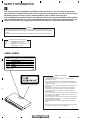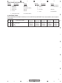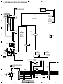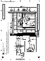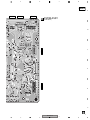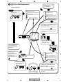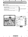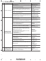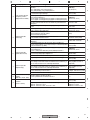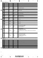
1
ORDER NO.
RRV2959
DV-470-S
DVD PLAYER
DV-470-S
DV-470-K
THIS MANUAL IS APPLICABLE TO THE FOLLOWING MODEL(S) AND TYPE(S).
Model
Type
Power Requirement
Region No.
Serial No.
Confirm 3rd & 4th
alphabetical letters.
DV-470-S
WYXCN
AC220-240V
2
&&TE######$$
DV-470-S
WYXCN/FG
AC220-240V
2
&&TE######$$
DV-470-S
WVXCN
AC220-240V
2
&&TE######$$
DV-470-K
WYXCN
AC220-240V
2
&&TE######$$
DV-470-K
WYXCN/FG
AC220-240V
2
&&TE######$$
For details, refer to "Important symbols for good services".
PIONEER CORPORATION
4-1, Meguro 1-chome, Meguro-ku, Tokyo 153-8654, Japan
PIONEER ELECTRONICS (USA) INC. P.O. Box 1760, Long Beach, CA 90801-1760, U.S.A.
PIONEER EUROPE NV Haven 1087, Keetberglaan 1, 9120 Melsele, Belgium
PIONEER ELECTRONICS ASIACENTRE PTE. LTD. 253 Alexandra Road, #04-01, Singapore 159936
PIONEER CORPORATION 2004
T-ZZE JUNE 2004 printed in Japan
1
2
3
4
SAFETY INFORMATION
A
This service manual is intended for qualified service technicians ; it is not meant for the casual
do-it-yourselfer. Qualified technicians have the necessary test equipment and tools, and have been
trainedto properly and safely repair complex products such as those covered by this
manual.Improperly performed repairs can adversely affect the safety and reliability of the product
and mayvoid the warranty. If you are not qualified to perform the repair of this product properly and
safely, youshould not risk trying to do so and refer the repair to a qualified service technician.
WARNING !
THE AEL (ACCESSIBLE EMISSION LEVEL) OF THE LASER POWER OUTPUT IS LESS THAN CLASS 1
BUT THE LASER COMPONENT IS CAPABLE OF EMITTING RADIATION EXCEEDING THE LIMIT FOR
CLASS 1.
A SPECIALLY INSTRUCTED PERSON SHOULD DO SERVICING OPERATION OF THE APPARATUS.
B
LASER DIODE CHARACTERISTICS
FOR DVD : MAXIMUM OUTPUT POWER : 5 mW
WAVELENGTH : 650 nm
FOR CD : MAXIMUM OUTPUT POWER : 5 mW
WAVELENGTH : 780 nm
C
LABEL CHECK
D
Additional Laser Caution
(Printed on the Rear Panel)
E
1. Laser Interlock Mechanism
• Loading switch (S101 on the LOAB Assy) is used for interlock
mechanism of the laser.
When this switch turned ON in SW2 (CLOSE) side (OPEN signal is
0V and CLOSE signal is 3.5V), a laser becomes the status which can
completely oscillation.
Furthermore, the laser completely oscillates in the disc judgment and
disc playback.
When player is power ON state and laser diode is not completely
oscillating, 780nm laser diode is always oscillating by half power.
• Laser diode is driving with Q7 (650nm LD) and Q8 (780nm LD)
on the DVDM Assy.
Therefore, when short-circuit between the emitter and collector of these
transistors or the base voltage is supplied for transistors turn on, the
laser oscillates. (failure mode)
• In the test mode ∗ , there is the mode that the laser oscillates except
for the disc judgment and playback. LD ON mode in the test mode
oscillates with the laser forcibly.
The interlock mechanism mentioned above becomes invalid in this
mode.
2. When the cover is open, close viewing through the objective lens with
the naked eye will cause exposure to the laser beam.
F
∗ : See page 47.
2
DV-470-S
1
2
3
4
5
6
7
8
[ Important symbols for good services ]
In this manual, the symbols shown-below indicate that adjustments, settings or cleaning should be made securely.
When you find the procedures bearing any of the symbols, be sure to fulfill them:
A
1. Product safety
You should conform to the regulations governing the product (safety, radio and noise, and other regulations), and
should keep the safety during servicing by following the safety instructions described in this manual.
2. Adjustments
To keep the original performances of the product, optimum adjustments or specification confirmation is indispensable.
In accordance with the procedures or instructions described in this manual, adjustments should be performed.
3. Cleaning
For optical pickups, tape-deck heads, lenses and mirrors used in projection monitors, and other parts requiring cleaning,
proper cleaning should be performed to restore their performances.
B
4. Shipping mode and shipping screws
To protect the product from damages or failures that may be caused during transit, the shipping mode should be set or
the shipping screws should be installed before shipping out in accordance with this manual, if necessary.
5. Lubricants, glues, and replacement parts
Appropriately applying grease or glue can maintain the product performances. But improper lubrication or applying
glue may lead to failures or troubles in the product. By following the instructions in this manual, be sure to apply the
prescribed grease or glue to proper portions by the appropriate amount.For replacement parts or tools, the prescribed
ones should be used.
C
D
E
F
3
DV-470-S
5
6
7
8
1
2
3
4
CONTENTS
SAFETY INFORMATION ..................................................................................................................................... 2
1. SPECIFICATIONS ............................................................................................................................................ 5
2. EXPLODED VIEWS AND PARTS LIST ............................................................................................................ 6
2.1 PACKING ................................................................................................................................................... 6
2.2 EXTERIOR SECTION................................................................................................................................ 8
2.3 FRONT PANEL SECTION ....................................................................................................................... 10
2.4 04 LOADER ASSY................................................................................................................................... 12
3. BLOCK DIAGRAM AND SCHEMATIC DIAGRAM .......................................................................................... 14
3.1 BLOCK DIAGRAM ................................................................................................................................... 14
3.1.1 SIGNAL ROUTE BLOCK DIAGRAM ................................................................................................. 14
3.1.2 POWER SUPPLY BLOCK DIAGRAM................................................................................................ 16
3.2 WAVEFORMS .......................................................................................................................................... 18
3.3 LOAB ASSY and OVERALL WIRING DIAGRAM..................................................................................... 20
3.4 DVDM ASSY (1/3).................................................................................................................................... 22
3.5 DVDM ASSY (2/3).................................................................................................................................... 24
3.6 DVDM ASSY (3/3).................................................................................................................................... 26
3.7 JCKB ASSY ............................................................................................................................................. 28
3.8 FLKY and PWSB ASSYS ........................................................................................................................ 30
3.9 POWER SUPPLY UNIT............................................................................................................................ 32
4. PCB CONNECTION DIAGRAM ..................................................................................................................... 33
4.1 LOAB ASSY ............................................................................................................................................. 33
4.2 DVDM ASSY ............................................................................................................................................ 34
4.3 FLKY and PWSB ASSYS ........................................................................................................................ 38
4.4 POWER SUPPLY UNIT............................................................................................................................ 40
4.5 JCKB ASSY ............................................................................................................................................. 42
5. PCB PARTS LIST ........................................................................................................................................... 43
6. ADJUSTMENT ............................................................................................................................................... 45
6.1 ADJUSTMENT ITEMS AND LOCATION ................................................................................................. 45
6.2 JIGS AND MEASURING INSTRUMENTS............................................................................................... 45
6.3 NECESSARY ADJUSTMENT POINTS ................................................................................................... 46
6.4 TEST MODE ............................................................................................................................................ 47
6.5 MECHANISM ADJUSTMENT .................................................................................................................. 48
7. GENERAL INFORMATION ............................................................................................................................. 50
7.1 DIAGNOSIS ............................................................................................................................................. 50
7.1.1 TEST MODE ...................................................................................................................................... 50
7.1.2 DISPLAY SPECIFICATION OF THE TEST MODE............................................................................ 51
7.1.3 FUNCTIONAL SPECIFICATION OF THE SHORTCUT KEY ............................................................ 52
7.1.4 SPECIFICATION OF MODEL INFORMATION DISPLAY .................................................................. 53
7.1.5 FUNCTIONAL SPECIFICATION OF THE SERVICE MODE ............................................................. 54
7.1.6 METHOD FOR DIAGNOSING DEGRADATION OF THE LDS ON THE PICKUP ASSY .................. 55
7.1.7 TROUBLE SHOOTING ...................................................................................................................... 56
7.1.8 ID NUMBER AND ID DATA SETTING ............................................................................................... 59
7.1.9 SEQUENCE AFTER POWER ON..................................................................................................... 62
7.1.10 DISASSEMBLY................................................................................................................................ 63
7.2 IC ............................................................................................................................................................. 71
7.3 DISC / CONTENT FORMAT PLAYBACK COMPATIBILITY ..................................................................... 82
7.4 CLEANING............................................................................................................................................... 84
8. PANEL FACILITIES ........................................................................................................................................ 85
A
B
C
D
E
F
4
DV-470-S
1
2
3
4
5
6
7
8
1. SPECIFICATIONS
A
B
C
D
E
F
5
DV-470-S
5
6
7
8
1
2
3
4
2. EXPLODED VIEWS AND PARTS LIST
NOTES:
A
Parts marked by "NSP" are generally unavailable because they are not in our Master Spare Parts List.
The
mark found on some component parts indicates the importance of the safety factor of the part.
Therefore, when replacing, be sure to use parts of identical designation.
Screws adjacent to mark on product are used for disassembly.
For the applying amount of lubricants or glue, follow the instructions in this manual.
(In the case of no amount instructions, apply as you think it appropriate.)
2.1 PACKING
For WVXCN type
5
3
B
4
2
12
1
18
C
For WYXCN and WYXCN/FG types
6
5
2
12
7-10
"Operating Instructions"
3
12
4
D
1
15
16
14
E
17
F
6
DV-470-S
1
2
3
4
5
6
7
8
PACKING parts List
Mark No.
Description
Mark No.
Part No.
Description
1
2
3
4
NSP 5
Power Cable
Audio/Video Cable
Remote Control
Battery Cover
Dry Cell Battery (AA,R6P)
See Contrast table(2)
VDE1078
VXX2913
VNK4997
VEM1010
10
11
12
13
Operating Instructions
(Spanish/Dutch)
•••••
Polyethylene bag B5
•••••
NSP 6
7
8
Warranty Card
Operating Instructions (English)
Operating Instructions
(English/Italian)
Operating Instructions
(French/German)
ARY7065
See Contrast table(2)
See Contrast table(2)
14
15
16
17
18
Polyethylene Bag
Pad L
Pad R
Packing Case
Accessory Box
>
9
See Contrast table(2)
Part No.
See Contrast table(2)
VHL1076
VHA1358
VHA1359
See Contrast table(2)
See Contrast table(2)
A
VHL1051
B
(2) CONTRAST TABLE
DV-470-S/WYXCN, WYXCN/FG, WVXCN, DV-470-K/WYXCN and WYXCN/FG are constructed the same except for
the following:
DV-470-S/
WYXCN
DV-470-S/
WYXCN/FG
DV-470-S/
WVXCN
DV-470-K/
WYXCN
DV-470-K/
WYXCN/FG
1 Power cable
7 Operating Instructions (English)
8 Operating Instructions
(English/Italian)
9 Operating Instructions
(French/German)
10 Operating Instructions
(Spanish/Dutch)
ADG1154
Not used
VRD1195
ADG1154
Not used
Not used
ADG1156
VRB1346
Not used
ADG1154
Not used
VRD1195
ADG1154
Not used
Not used
VRD1196
VRD1196
Not used
VRD1196
VRD1196
VRD1197
Not used
Not used
VRD1197
Not used
17 Packing Case
18 Accessory Box
VHG2540
Not used
VHG2542
Not used
VHG2541
VHC1114
VHG2543
Not used
VHG2544
Not used
Mark No.
>
Symbol and Description
C
D
E
F
7
DV-470-S
5
6
7
8
1
2
3
4
2.2 EXTERIOR SECTION
19
A
NON-CONTACT
SIDE
20
21
CONTACT SIDE
18
25
21
Refer to
"2.4 04 LOADER ASSY".
4
24
24
B
21
7
E
B
C
D
25
9
C
9
9
F
22
9
G
6
E
G
21
C
5
D
F
B
21
22
3
F
D
C
23
2
B
21
21
A
1
8
16
22
22
22
22
10
21
E
A
12
14
13
11
Refer to "2.3 FRONT PANEL SECTION".
F
8
DV-470-S
1
2
3
4
5
6
7
8
EXTERIOR SECTION parts List
Mark No.
1
2
>
3
NSP 4
5
Description
DVDM Assy
JCKB Assy
POWER SUPPLY Unit
04 LOADER Assy
Connector Assy (13P)
6
7
8
9
10
11
12
NSP 13
Mark No.
Part No.
VWS1585
VWV1995
VWR1377
VWT1210
VKP2320
Flexible Cable (17P)
Connector Assy (5P)
Flexible Cable (15P)
Adapter 2
Binder
VDA1994
VKP2324
VDA1991
VNL1967
VEC2414
Tray Panel
DVD A/V Badge
Base Chassis
See Contrast table(2)
See Contrast table(2)
VNA2693
Description
Part No.
14
15
Rubber Foot
•••••
VEB1349
16
17
18
19
20
Rear Sheet
•••••
Bonnet
WY label
Caution Label
See Contrast table(2)
See Contrast table(2)
VRW2138
VRW1872
21
22
23
24
25
Screw
Screw
Screw
Screw
Screw
BBZ30P060FNI
BBZ30P080FNI
PPZ30P080FNI
BBZ30P100FNI
See Contrast table(2)
A
B
(2) CONTRAST TABLE
DV-470-S/WYXCN, WYXCN/FG, WVXCN, DV-470-K/WYXCN and WYXCN/FG are constructed the same except for
the following:
Mark No.
11
12
16
18
25
Symbol and Description
Tray Panel
DVD A/V Badge
Rear Sheet
Bonnet
Screw
DV-470-S/
WYXCN
VNK5411
VAM1135
VRW2135
VNA2677
BBZ30P060FNI
DV-470-S/
WYXCN/FG
DV-470-S/
WVXCN
DV-470-K/
WYXCN
DV-470-K/
WYXCN/FG
VNK5411
VNK5411
VNK5413
VNK5413
VAM1135
VAM1135
VAM1120
VAM1120
VRW2135
VRW2135
VRW2136
VRW2136
VNA2677
VNA2677
VNA2678
VNA2678
BBZ30P060FNI BBZ30P060FNI BBZ30P060FBN BBZ30P060FBN
C
D
E
F
9
DV-470-S
5
6
7
8
1
2
3
4
2.3 FRONT PANEL SECTION
11
2
A
10
E
11
11
11
11
10
1
8-1/3
D
7
11
11
11
B
6
11
4
8-3/3
8-2/3
7
C
5
3
NON-CONTACT
SIDE
CONTACT SIDE
4
D
E
F
10
DV-470-S
1
2
3
4
5
6
7
8
FRONT PANEL SECTION parts List
Mark No.
1
2
3
4
5
Description
FLKY Assy
PWSB Assy
Front Panel
Rubber Foot
FL Lens
6
Pioneer Name Plate
Mark No.
Part No.
VWG2511
VWG2482
See Contrast table(2)
VEB1349
VNK5414
Description
Part No.
7
8
9
10
Key Top
Main Key
•••••
FP Angle
See Contrast table(2)
See Contrast table(2)
VNE2332
11
Screw
PPZ30P080FNI
A
See Contrast table(2)
(2) CONTRAST TABLE
DV-470-S/WYXCN, WYXCN/FG, WVXCN, DV-470-K/WYXCN and WYXCN/FG are constructed the same except for
the following:
Mark No.
3
6
7
8
Symbol and Description
Front Panel
Pioneer Name Plate
Key Top
Main Key
DV-470-S/
WYXCN
DV-470-S/
WYXCN/FG
DV-470-S/
WVXCN
DV-470-K/
WYXCN
DV-470-K/
WYXCN/FG
VNK5610
VAM1129
VNK5410
VNK5404
VNK5610
VAM1129
VNK5410
VNK5404
VNK5610
VAM1129
VNK5410
VNK5404
VNK5611
VAM1130
VNK5409
VNK5406
VNK5611
VAM1130
VNK5409
VNK5406
B
C
D
E
F
11
DV-470-S
5
6
7
8
1
2
3
4
2.4 04 LOADER ASSY
8
Note :
Refer to
" Application of Lubricant".
A
2
25
6
8
8
To DVDM CN101 (Pickup)
To DVDM CN104 (Stepping Motor)
Daifree
GEM1036
To DVDM CN102 (Spindle Motor)
8
B
18
12
Lubricating Oil
GYA1001
24
3
20
13
A
23
22
17
4
16
5
19
22
C
21
15
22
To
DVDM CN103
7
A
10
14
11
D
A
9
Lubricating Oil
GYA1001
1
22
04 LOADER ASSY parts List
Mark No.
F
Mark No.
Part No.
LOAB Assy
Traverse Mecha. Assy-S
Loading Motor Assy
Motor Pulley
Motor
VWG2346
DXX2536
VXX2912
PNW1634
VXM1107
16
17
18
19
20
6
7
8
9
10
Flexible Cable (24P)
Connector Assy 2P
Floating Rubber
Belt
Stabilizer
VDA1990
VKP2325
VEB1351
VEB1358
VNE2253
21
22
23
24
25
11
12
13
14
15
Loading Base
Float Base 04
Drive Cam
Gear Pulley
Loading Gear
VNL1917
VNL1968
VNL1919
VNL1921
VNL1922
NSP 1
2
3
4
NSP 5
E
Description
12
Description
Part No.
Drive Gear
SW Lever
Clamper Plate 04
Bridge 04
Clamper 04
VNL1923
VNL1925
VNE2342
VNE2343
VNL1969
Screw
Screw
Tray
Clamp Magnet
03 SD Pickup Assy-S
JGZ17P028FNI
VBA1093
VNL1920
VMG1029
OXX8005
DV-470-S
1
2
3
4
5
6
7
8
Application of Lubricant
A
Lubricating Oil
GYA1001
Around the shaft
No. 11
Loading Base
B
Lubricating Oil
GYA1001
Lubricating Oil
GYA1001
Lubricating Oil
GYA1001
Lubricating Oil
GYA1001
Inner side of a ditch
No. 13
Drive Cam
Lubricating Oil
GYA1001
Inner side of a ditch
C
No. 13
Drive Cam
Lubricating Oil
GYA1001
Front View
Rear View
D
Daifree
GEM1036
Concave of unevenness
No. 23
Tray
Daifree
GEM1036
Concave of unevenness
No. 23
Tray
E
Inner side of a ditch
Daifree
GEM1036
Top View
Bottom View
Concave of unevenness
Side of the rib
Daifree
GEM1036
Daifree
GEM1036
13
DV-470-S
5
6
F
7
8
1
2
3
4
3. BLOCK DIAGRAM AND SCHEMATIC DIAGRAM
3.1 BLOCK DIAGRAM
3.1.1 SIGNAL ROUTE BLOCK DIAGRAM
A
ı1/3
B DVDM ASSY
IC204
BR24L16FV-W
EEPROM
6
SCL
102
5
SDA
103
225
CN101
(24P)
SPINDLE
MOTOR
OEIC
B
(24P)
22
21
19
17
B3
16
15
B1
D
3
4
6
8
B4
C
A
5
4
18
19
3
A
E
F
B
9
10
B2
C
Q8
LD(780)
IC201
MT1389EE-L1
DVD IC
2
LD2
9
16
LD(650)
7
18
03 SD
PICKUP
ASSY-S
22
LD1
23
Q7
4
3
2
1
T DRV
T+
T RTN
T-
21
22
F DRV
23
F RTN
24
F+
F-
31
30
34
35
217
ı1/3
2
(12P)
U+
2
U-
3
V+
4
V-
5
W+
6
W-
7
U
9
V
10
11
W
HU+
HUHV+
HV-
21
20
19
18
HW+
HWU
17
16
IC101
M63018FP
FTS DRIVER
• Focus
• Tracking
• Stepper
• Spindle
• Loading Drive
• FG Detection
2
FMSO
24
FG
26
DMSO
27
FOSO
28
TRSO
40
TROPEN
V
40
38
196
47
37
198
42
194
41
200
39
202
3
14
203
13
W
12
CN104 5
ST2-
STEPPING
MOTOR
M
ST2+
ST1+
ST1-
D
–
1
2
3
4
ST2-
6
ST2+
5
ST1+
ST1-
CN601
2
1
LOAD-
1
LOAD-
36
1
2
LOAD+
2
LOAD+
37
+
S101
SW2
3
LOADING
MOTOR
ASSY
4
TROUT
49
48
CN103
CN602
M
TRIN
9
10
V+3D
SW1
5
3
4
5
TRIN
IC203
V+3D
FLASH ROM
IC202
K4S641632H-TC75-K
64M SDRAM
TROUT
ı1/3
ı1/3
A LOAB ASSY
E
E
POWER SUPPLY
UNIT
CN2
LIVE
CN201
(15P)
CN301
(13P)
(13P)
CN1
AC IN
F
NEUTRAL
14
DV-470-S
1
2
ASDAT0
4
PWMOUT1
1
CN102
C
ASPDIF
ı1/3
CN1013
3
4
S_C
CVBS
S_Y
G/Y
B/Cb
R/Cr
5
6
7
8
Refer to "3.2 WAVEFORMS".
DVDM Assy : 2 – @
JCKB Assy : 1 – 2
JA901
OPTICAL
DIGITAL
AUDIO
OUT
Q901
COAXIAL
A
B
10
11 14
ASDAT0
IC501 PCM1742KE
AUDIO DAC (L, R)
VOUTL
16
7
1 ı3/3
2
8
AUDIO LPF & AMP
2
3
6
VOUTR
5
3
15
12 13
S_C
CVBS
S_Y
G/Y
B/Cb
R/Cr
IC502-1/2
8 BA4560F
1
JA501
L
ı3/3
7
IC502-2/2
L
IC401
MM1623BF
VIDEO DRIVE AMP
ı2/3 C OUT
C IN
2
26
4
6
10
12
14
V IN
V OUT
Y IN
Y OUT
CY IN
CY OUT
Cb IN
Cb OUT
Cr IN
Cr OUT
AUDIO
OUT (2 ch)
R
AUDIO
OUT (2 ch)
R
JA401
6
COMPOSITE
VIDEO
OUTPUT
23
21
C
7
Y
20
8
18
COMPONENT
VIDEO
OUTPUT
PB
9
PR
16
CN451
(17P)
FRONT L
5
3
L OUT
15
AUD.R
3
1
R OUT
15
11
B/Pb
7
7
4
B
13
9
G/Py
9
11 G
7
R/C/Pr
11
15 R/C
FRONT R
C IN
C OUT
V IN
V OUT
(21P)
(17P)
AUD.L
ı2/3
2
JA902
CN901
13
AV CONNECTOR
(RGB)-TV/AV
RECEIVER
IC471 MM1505XN
6
Y IN
Y OUT
10
4
6
IC451
MM1566AJ
VIDEO DRIVE AMP
H
2
L
IC472 MM1507XN
4
6
D
19 V/Y
1
C
17
5
V/Y
13
3
Y
15
H
2
L
1
CN941
Y
C
S VIDEO
OUT
2
C
JCKB ASSY
E
Remote
Sensor
Unit
CN101
(15P)
IC101 PE5374B
FL CONTROL
MICROCOMPUTER
17
22
20,21
V101
FL TUBE
CN103
CN102
SEL IR
KEY0
KEY0
KEY1, KEY2
D FLKY ASSY
E
F
PWSB ASSY
15
DV-470-S
5
6
7
8
1
2
3
4
3.1.2 POWER SUPPLY BLOCK DIAGRAM
A
ı1/3
B DVDM ASSY
V+3
IC204
BR24L16FV-W
EEPROM
8
V+3D
V+3D
ı1/3
CN1013
SPINDLE
MOTOR
(24P)
OEIC
VCC
2
46,65,73,80,
108,127,141,
155,167,182,
204,212
CN101
(24P)
V+5S
IC201
MT1389EE-L1
DVD IC
2
189,195,
199
V+3V
B
24,234,239, V+3RF
244,256
03 SD
PICKUP
ASSY-S
ı1/3
CN102 V+5S
(12P)
IC101
M63018FP
FTS DRIVER
• Focus
• Tracking
• Stepper
• Spindle
• Loading Drive
• FG Detection
V+5S 1
C
V+1R8
52,97,122,
152,173,221
228
X201
27MHz
229
CN104
ST2-
STEPPING
MOTOR
M
ST2+
ST1+
ST1-
D
–
1
4
CN103
CN601
2
1
LOAD-
1
1
2
LOAD+
2
+
3,22,
32,39
3
CN602
M
V+6
2
V+3D
S101
SW2
3
LOADING
MOTOR
ASSY
4
V+3D
SW1
5
IC203
3
4
IC202
K4S641632H-TC75-K
64M SDRAM
FLASH ROM
12 37
ı1/3
5
V+3
ı1/3
1,3,9,14,
27,43,49
V+3D
V+3D
A LOAB ASSY
V+3 V+6 V+12
IC801
V+5A V+5S V+5V V+1R8
NJM78M05FA
5V REG.
E
E
IC311
PQ1M505M2ZPQ
5V REG.
V+6B
POWER SUPPLY
UNIT
CN2
(13P)
13
CN1
12
11
8
AC IN
7
F
NEUTRAL
(15P)
CN301
(13P)
LIVE
CN201
IC321
BA00BC0WT
1.8V REG.
5
4
2
-28V
FL DC+
FL DCEV+4V
SW+3.3V
EV+6V(A)
EV+6V(B)
SW+12V
16
13
4
12
6
11
2
V+3E
8
IC341
S-L2980A33MC-C6S
3V REG.
7
5
4
5
IC205
PST3228
RESET
8
V+4E
2
DV-470-S
1
2
3
4
-28V
FL DC+
FL DCV+3E
RESET
5
6
7
8
A
JA901
V+3
V+5A
OPTICAL
V+12
DIGITAL
AUDIO
OUT
COAXIAL
B
AUDIO LPF & AMP
IC501 PCM1742KE
AUDIO DAC (L, R)
IC502-1/2
8 BA4560F
1
2
ı3/3
5
3
6
6
JA501
L
ı3/3
7
5
R
IC502-2/2
V+5V
L
IC401
MM1623BF
VIDEO DRIVE AMP
ı2/3
R
AUDIO
OUT (2 ch)
AUDIO
OUT (2 ch)
JA401
1,3,
5,28
COMPOSITE
VIDEO
OUTPUT
C
Y
COMPONENT
VIDEO
OUTPUT
PB
PR
CN451
(21P)
(17P)
V+5V
ı2/3
JA902
CN901
(17P)
L OUT
V+5
R OUT
V+5V
16
1,5,
14,16
V+5
2
B
AV CONNECTOR
(RGB)-TV/AV
RECEIVER
G
IC471 MM1505XN
4
6
IC451
MM1566AJ
VIDEO DRIVE AMP
H
3
2
R/C
L
D
V/Y
IC472 MM1507XN
4
6
3
H
2
CN941
L
S VIDEO
OUT
C
JCKB ASSY
E
V+3E
CN101
(15P)
V+3E
1 24 25 59
-28V
FL DC+
FL DC+3.3V
RESET
IC101 PE5374B
FL CONTROL
-28V
60 MICROCOMPUTER
12
CN102
3
4
CN103
X101
5MHz
10
6
14
RESET
11
8
F
34,35
1,2
V101
FL TUBE
D FLKY ASSY
E
PWSB ASSY
17
DV-470-S
5
6
7
8
1
2
3
4
3.2 WAVEFORMS
Note : The encircled numbers denote measuring point in the schematic diagram.
A
B DVDM ASSY
Measurement condition ;
No. 2 to 9
: reference A1 (DVD), T2-chp 19, Color-bar
No. 10 to 15 : reference A1 (DVD), T2-chp 1
2
IC101-pin 24 [FG]
V: 1V/div. H: 5msec/div.
GND
B
3
IC201-pin 39 [TROPENPWM]
V: 1V/div. H: 5µsec/div.
[Tray stops]
[Tray is opening]
[Tray is closing]
GND
GND
GND
C
4
Foot of R201 (IC201-pin 37) [DMSO]
V: 1V/div. H: 10µsec/div.
V: 1V/div. H: 10µsec/div.
[DMSO_OPEN]
V: 1V/div. H: 2sec/div.
[DMSO_PLAY]
[DMS~3]
Tray :
opening
GND
GND
GND
PLAY
D
OPEN KEY ON :
The condition which braking is worn in a turn of disc.
OPEN KEY ON
PLAY KEY ON :
starting a turn of disc
Braking a turn of disc
5
CN102-pin 11, 10, 9 (IC101-pin 14, 13, 12)
[SPINDLE (WVU)]
V: 2V/div. H: 2msec/div.
7
JA401 [Component Video Out-Y]
V: 1V/div. H: 10µsec/div.
8
JA401 [Component Video Out-PB]
V: 2V/div. H: 10µsec/div.
9
JA401 [Component Video Out-PR]
V: 2V/div. H: 10µsec/div.
7
GND
8
GND
E
GND
9
GND
6
JA401 [Composite Video Out]
V: 1V/div. H: 10µsec/div.
10
IC501-pin 16 [PCMCK]
V: 100mV/div. H: 20nsec/div. fs=48kHz
11
IC501-pin 1 [PCMBCK]
V: 2V/div. H: 200nsec/div.
GND
GND
F
GND
18
DV-470-S
1
2
3
4
5
12
6
IC501-pin 3 [PCMLRCK]
V: 2V/div. H: 5µsec/div.
7
13
IC501-pin 3 [PCMLRCK]
V: 2V/div. H: 500nsec/div.
14
IC501-pin 1 [PCMBCK]
V: 2V/div. H: 500nsec/div.
8
A
13
15
GND
GND
IC501-pin 2 [PCMDATA]
V: 2V/div. H: 500sec/div.
14
GND
15
GND
B
C JCKB ASSY
Measurement condition :
reference A1 (DVD), T2-chp 19, Color-bar
1
CN941 [S Video Out-Y]
V: 1V/div. H: 10µsec/div.
2
CN941 [S Video Out-C]
V: 1V/div. H: 10µsec/div.
C
1
GND2
2
GND1
D
E
F
19
DV-470-S
5
6
7
8
1
2
3
4
3.3 LOAB ASSY and OVERALL WIRING DIAGRAM
A
ASSY
C JCKB
(VWV1995)
B
F
POWER SUPPLY UNIT
(VWR1377)
AC IN
STEPPING
MOTOR
C
03 SD PICKUP ASSY-S (OXX8005)
(RF)
(RF)
(RF)
(RF)
(RF)
04 LOADER ASSY
(VWT1210)
D
E
TRAVERSE MECHA. ASSY-S
(DXX2536)
(RF)
(T)
(T)
(F)
(F)
INNER
SPINDLE
MOTOR
ASSY
A LOAB
(VWG2346)
S101
VSK1011
LOADING MOTOR
ASSY
(VXX2912)
E
F
PWSB ASSY
(VWG2482)
A
20
DV-470-S
1
2
3
4
5
6
7
8
÷ When ordering service parts, be sure to refer to "EXPLODED VIEWS and PARTS LIST" or
"PCB PARTS LIST".
÷ The > mark found on some component parts indicates the importance of the safety factor
of the part. Therefore, when replacing, be sure to use parts of identical designation.
÷
: The power supply is shown with the marked box.
(RF)
(F)
(T)
A
: RF SIGNAL ROUTE
: FOCUS SERVO LOOP LINE
: TRACKING SERVO LOOP LINE
B
C
ASSY
B DVDM
(VWS1585)
B 1/3 : DVD IC BLOCK
B 2/3 : POWER and VIDEO BLOCK
B 3/3 : AUDIO BLOCK
D
E
ASSY
D FLKY
(VWG2511)
F
21
DV-470-S
5
6
7
8
1
2
3
4
3.4 DVDM ASSY (1/3)
B
B 1/3 DVDM ASSY (VWS1585)
03 SD PICKUP ASSY-S CN1013
A
(RF)
(RF)
(RF)
(RF)
(RF)
(RF)
LD Driver for CD
(RF)
(RF)
(RF)
(RF)
(T)
(T)
(F)
(F)
(T)
(T)
(F)
4
3
2
Focus, Tracking,
Stepping, Spindle
and Loading Driver
A
STEPPING MOTOR
D
5
(RF)
(RF)
CN601
C
(F)
SPINDLE MOTOR
LD Driver for DVD
E
VYW2197
F
B 1/3
22
DV-470-S
1
2
3
4
5
6
7
8
B 2/3
(G/Y)
(B/CB)
(R/CR)
(V)
(SY)
(SC)
A
B 3/3
(B/CB)
(D)
(R/CR)
(G/Y)
(V)
(SC)
(D)
(AD)
(SY)
B
B 2/3
B 3/3
C
K4S641632H-7C75-K
DVD IC
D
E
(RF)
(F)
(T)
(R/CR)
(G/Y)
B 2/3
(B/CB)
B 2/3
(SY)
(SC)
(V)
(D)
D
CN101
(AD)
: RF SIGNAL ROUTE
: FOCUS SERVO LOOP LINE
: TRACKING SERVO LOOP LINE
: VIDEO SIGNAL ROUTE (R/CR)
: VIDEO SIGNAL ROUTE (G/Y)
: VIDEO SIGNAL ROUTE (B/CB)
: S VIDEO SIGNAL ROUTE (Y)
: S VIDEO SIGNAL ROUTE (C)
F
: VIDEO SIGNAL ROUTE (V)
: AUDIO SIGNAL ROUTE (DIGITAL ch)
B 1/3
: AUDIO DATA SIGNAL ROUTE
23
DV-470-S
5
6
7
8
1
2
3
4
3.5 DVDM ASSY (2/3)
A
B 2/3 DVDM ASSY (VWS1585)
5V Regulator
B
R323
33K (F)
R321
33K (F)
DVD IC
BA00BC0WT
1.8V Regulator
R322
33K (F)
DVD IC
C
3V Regulator
(B/CB)
(G/Y)
F
CN2
(R/CR)
B 1/3
B 1/3
(G/Y)
(R/CR)
(B/CB)
D
(SC)
(V)
E
(SY)
B 1/3
(G/Y)
(B/CB)
(R/CR)
F
B 2/3
B 1/3
24
DV-470-S
1
2
3
4
5
6
7
(R/CR)
(G/Y)
(B/CB)
(SY)
(SC)
(V)
8
(FL)
: VIDEO SIGNAL ROUTE (R/CR)
: AUDIO SIGNAL ROUTE (Front L ch)
A
: VIDEO SIGNAL ROUTE (G/Y)
: VIDEO SIGNAL ROUTE (B/CB)
: S VIDEO SIGNAL ROUTE (Y)
: S VIDEO SIGNAL ROUTE (C)
: VIDEO SIGNAL ROUTE (V)
B
B 3/3
Video Driver Amp.
C
(B/CB)
(G/Y)
(G/Y)
CN901
(FL)
(B/CB)
C
(SC) (R/CR)
(R/CR)
(SY) (V)
(V)
(SY)
(SY)
(SC)
Video DAmp.
with SW
(SY)
(V)
(SY)
(SC)
(V)
Video Driver Amp.
D
(SC)
E
6
(V)
VIDEO OUT
(SY)
Y
8
(B/CB)
7
PB
9
(R/CR)
PR
COMPONENT
VIDEO OUT
(G/Y)
F
B 2/3
25
DV-470-S
5
6
7
8
1
2
3
4
3.6 DVDM ASSY (3/3)
A
B 3/3 DVDM ASSY (VWS1585)
B 1/3
B
(D)
(D)
COAXIAL
(D)
DIGITAL
AUDIO OUT
(D)
OPTICAL
(D)
C
D
10
B 1/3
E
(FL)
(AD)
(D)
(FL)
(SL)
(C)
F
(SW)
11 14
: AUDIO DATA SIGNAL ROUTE
(AD)
: AUDIO SIGNAL ROUTE (DIGITAL ch)
: AUDIO SIGNAL ROUTE (Front L ch)
B 1/3
15
12 13
: AUDIO SIGNAL ROUTE (Surround L ch)
: AUDIO SIGNAL ROUTE (Center ch)
: AUDIO SIGNAL ROUTE (Sub Woofer ch)
B 3/3
26
DV-470-S
1
2
3
4
5
6
7
8
A
B
C
D
SW for Mute Control
B 1/3
B 2/3
(FL)
(FL)
(FL)
L AUDIO
OUT 2
R (2 ch)
Mute
SW
(FL)
E
Mute
SW
(FL)
(FL)
(FL)
Mute
SW
Mute
SW
L AUDIO
OUT 1
R (2 ch)
B 2/3
Reference Voltage Gen.
for Audio Amp.
B 3/3
27
DV-470-S
5
F
6
7
8
1
2
3
4
3.7 JCKB ASSY
C
A
JCKB ASSY (VWV1995)
B
(FL)
(FL)
(FL)
C
B 2/3
(B/CB)
(B/CB)
(G/Y)
(G/Y)
CN451
(SC) (R/CR)
(SC) (R/CR)
(SC) (R/CR)
(SY) (V)
(SY) (V)
(SY)
(SY)
(SC)
(SC)
(SY)
(SC)
D
E
(SC)
(SY)
F
C
28
DV-470-S
1
2
3
4
5
6
7
(R/CR)
(G/Y)
(B/CB)
(SY)
(SC)
(V)
: VIDEO SIGNAL ROUTE (R/CR)
8
(FL)
: AUDIO SIGNAL ROUTE (Front L ch)
A
: VIDEO SIGNAL ROUTE (G/Y)
: VIDEO SIGNAL ROUTE (B/CB)
: S VIDEO SIGNAL ROUTE (Y)
: S VIDEO SIGNAL ROUTE (C)
: VIDEO SIGNAL ROUTE (V)
B
(FL)
(FL)
(B/CB)
(B/CB)
AV CONNECTOR (RGB)
- TV/AV Receiver
(G/Y)
C
(G/Y)
(SC) (R/CR)
(SC) (R/CR)
(SY) (V)
(SY) (V)
D
E
2
(SC)
(SC)
(SY)
S VIDEO
OUT
(SY)
1
F
C
29
DV-470-S
5
6
7
8
1
2
3
4
3.8 FLKY and PWSB ASSYS
A
D FLKY ASSY
(VWG2511)
S105-S108, S117, S119 : VSG1024
B
C
D
PE5374B
E
F
D
30
DV-470-S
1
2
3
4
5
6
7
8
A
E
PWSB ASSY
(VWG2482)
VSG1024
B
PWSB ASSY
S101 :
STANDBY-ON
FLKY ASSY
S105 : 0 (OPEN/CLOSE)
S106 : 4 (REV)
S107 : ¢ (FWD)
S108 : 7 (STOP)
S117 : 8 (PAUSE)
S119 : 3 (PLAY)
C
D
B 1/3
CN201
E
F
D E
31
DV-470-S
5
6
7
8
C
D
1
32
2
F
AC IN
CN2
2
3
B 2/3 CN301
F
3
• NOTE FOR FUSE REPLACEMENT
CAUTION - FOR CONTINUED PROTECTION AGAINST RISK OF FIRE.
REPLACE WITH SAME TYPE AND RATINGS OF FUSE.
AEK7008
800mA
CP1
• In case of repairing, use the described parts only to prevent an accident.
• Please write the red
mark on the board when the primary section of POWER SUPPLY (SYPS) Unit is repaired.
• Please take care to keep the space, not touching other parts when replacing the parts.
CAUTION : FOR CONTINUED PROTECTION AGAINST RISK OF FIRE.
REPLACE ONLY WITH SAME TYPE NO. 491.800 MFD, BY
LITTELFUSE INC. FOR CP1 (AEK7008).
B
CN1
E
POWER SUPPLY UNIT
(VWR1377)
A
NOTE OF SPARE PARTS IN POWER SUPPLY (SYPS) UNIT
F
1
4
3.9 POWER SUPPLY UNIT
DV-470-S
F
4
5
6
7
8
4. PCB CONNECTION DIAGRAM
4.1 LOAB ASSY
NOTE FOR PCB DIAGRAMS :
A
1. Part numbers in PCB diagrams match those in the schematic
diagrams.
2. A comparison between the main parts of PCB and schematic
diagrams is shown below.
Symbol In PCB
Diagrams
Symbol In Schematic
Diagrams
B C E B C E
Part Name
3. The parts mounted on this PCB include all necessary parts for
several destinations.
For further information for respective destinations, be sure to
check with the schematic diagram.
4. View point of PCB diagrams.
Capacitor
Connector
Transistor
B C E
B
C
E B
C
SIDE A
E
Transistor
with resistor
B C E
D
G S D
B
G S
Field effect
transistor
D G S
SIDE B
Chip Part
P.C.Board
Resistor array
3-terminal
regulator
C
SIDE A
SIDE B
A LOAB ASSY
A LOAB ASSY
(VNP1879-B)
(VNP1879-B)
D
VNP1879-B
LOAB
GB-04
5
1
C102
C101
CN601
1
5
5
LOAD+
LOAD-
SW2
1 2
5
VWG2346- -CN
VWG
V+3D
(V+5D)
1
CN602
GND
S101
1
CN602
CN601
CN602
M
LOADING
MOTOR
ASSY
CN601
CN601
CN602
E
B CN103
F
A
A
33
DV-470-S
5
6
7
8
4
Q372
Q371
Q373
Q7
Q5 Q4
IC202 IC201
IC341
IC202
C288
C287
R209
C286
1
1
1585
1596
C291
C285
C281
1
4
5
IC205
3
C283
CN204
C244
C236
4
5
C233
R841
R231
C234
C235
R230
R229
R227
C231
R226
1
8
C294
C232
R228
C290
C292
R294
R296
C298
Q291
IC204
C297
128
R220
C227
C225
R234
C289
C296
C241
1
25
2
X201
C247
C239
R238
C228
R239
R235
C295
CN203
9
R222
R219
R218
15
C240
R244
R215
C226
R236
10
193
C245
1.GND
2.FLDC3.GND
4.-28v
5.V+3E
6.FLDC+
7.ACK
8.RESET
9.NC
10.SCK
11.XRES
12.MtoF
13.Pow
14.FtoM
15.XREA
4
1
54
C284
R225
R223
C293
129
C246 192
C230
R237
R221
CN201
R280
R279
R243
CN201
C237
28
R249
C242
C243
R241
R242
R293
VWS
1582
1583
1584
1/2
C282
27
IC311
IC321
C503
Q8
C248
3
DV-470-S
IC204
IC101
R257 R247
C253
2
B
CN101
R245
R246
1
34
F
IC203
Q291
IC205
E
D
48
IC201
C224
29
IC203
R248
30
R252
R224
C254
C223
C256
R233
CN202
R251
R253
D
R285
C222
256
C220
65
C263
C45
C46
C43
C44
C213
R295
R282
C152
C270
C215
R36
C208
R205
C212
R202
C209
R37
R204
C210
C322
C203
R341
D341
D321
C10
C9
C132
DI P
R42
22
42
C142
CN103
C211
C130
R39
R208
R41
R40
R206
R43
C271
C221
R201
C139
C136
C125
R38
R211
R256
C202
C272
R207
IC321
CN103
IC801
C204
R210
C124
24
1
R
21
6
C216
R286
C219
R232
R284
R217
C214
C217
C207
C205
C206
1
64
1
C273
C266
R263
R264
C134
R35
R321 R323
5 4
C11
R30
R10
R269
IC101
R27
IC341
1
C342
R25
3
21
1
C113
R28
C102
4
IC311
3 2 1
R322
C304
C303
R115
R13
1
5 4
R75
R73
R72
R71
R104
L311 D311
C313
5
R117
R119
C401
3
R107 R118
C302
Q4
R26
R116
R103
C73
C112
C12
4
R120
R74
13
C118
C120
C116
R21
Q7
Q8
R14
Q5
R106
R15
L9
L8
R18
C114
C341
C331
R22
C311
R275
74
1 R312
C312
C301
CN301
2
C261
60
C262
C264
C265
C267
R255
C268
C269
C201
D802
332
R262
R266
R268
C405
3
R277 R278
R271 R272
21
R302
1
R213
R212
5
1
1
C72
C3
CN601
A
C
B
CN101
13.-28v
R371
R372
R374
R375
1
CN104
23
2
5.6.8vA
4.6.8vB
2.SW12
R373
Q371
C74
Q372
9.Pow
8.EV4
7.SW33
1
Q373
C71
R301
12.FLDC+
11.FLDC-
12
CN102
C6
24
PC
VNP1966-D
CN101
CN104
03 SD PICKUP
M
ASSY-S
DC
(VNP1966-D)
B DVDM ASSY
CN102
SPINDLE
MOTOR
M
A
CN301
F CN2
STEPPING
MOTOR
SIDE A
4.2 DVDM ASSY
1
2
3
4
IC311
IC321
IC801
IC841
5
6
7
8
DV-470-S
Q482
IC451
IC471
Q401
IC401
IC472
Q761
Q481
IC702
IC701
Q492
IC602
Q471 Q491
IC601
IC502
IC501 Q762
Q593 Q592
35
B
Q901 Q741
Q742
Q662
Q561 Q562 Q641
Q642
Q541-Q545
F
Q661
Q546
Heat Resistance Pri-Flux
C507
R523
Q592
C517
Q593
JA501
R592
C237
C505
1
R826
4
R544
C515
R517
R521
R511
R249
R241
R242
R280
R279
R243
C246
R551
C248
R556
C614
R614
R547
R555
R548
C618
R613
R835
R253
R663
R661
C256
BLACK
R643
R631
R632
C615
R617
C613
R612
C701
C254
R251
R611
R248
R254
R621
C251
R644
C252
C241
X201
C247
R257 R247
C253
IC601
C239
R238
C616
R618 C632
Q546
R245
R246
R825
R549
R512
C607
C604
C605
1
8
16
R252
C255
C257
C258
R744
R743
C732
R732
C714
C259
C261
C260
C263
R714
8
IC701
16
C273
C713
R711
R761
R721
IC801
R731
C266
C270
R712
C804
C715
R901
R717
C901
Q761
C264
C265
C267
R255
C268
C269
C201
C271
R762
R
C27
D802
R332
R262
C913
R421
D481
R483
R488
Q481
R482
R484
JA901
C911
C482
C415
R266
R268
R263
R264
IC321
R269
C404
R493 C492
C912
R401
R911
15
14
Q901
D801
C405
D474
1
L422
D472
3
IC471
4
COLOR
3
6
L311 D311
C313
C402
5
IC401
28 C472
4
R275
R274
C411 R312
C403
1
D473
R473
6
C311
4
1
R489
R277 R278
C412 R271 R272
IC311
3 2 1
C475
C322
R903
R902
C903
R491
C491
Q762
Q471
256
R718
C716
R713
C718
C705
1
C245
C513
C601
5 IC841
1
R841
R531
R501
3
16
C841
C842
C240
R244
RED&WHITE
Q541
R542
C514
R532
R518
C516
R514
C518
C504
R552
C501
C512 C502
8
C506
R623
C617
C602
C612
9
C606
C611
C704
C702
C717
C712
Q491
C416
R471
Q492
C414
C481
R481
C413
C474
C473
IC472
C471
C312
R472
R
L421
1
C301
8
9
C401
D471
C454
C476
C453
IC451
C463
12.FL
11.FL
16
1
JA401
9.Pow
8.EV4
7.SW33
R301
C462
C461
C451
C452
E90142
5.6.8vA
4.6.8vB
2.SW12
17
A
B
C
0 1 2 3 4 5 6 7 8 9
1596
R620
C503
C508
R519
R513
R520
C531
C532 8
R836
9
4
1
R561
R516
R619
8
5
C622
IC602
4
1
C621
5
C707
R723
R616
R720
R719
Q661 R615
8
C262
C706
R763
R716
Q401
R494
R492
R487 R486 R485
Q482
C422
R209
R553
C522
IC501
C511
5
IC502
C521
R515
Q561
R562
Q543
R645
R746
R745
C722
R906
C421
C423
C424
R424
9
IC702
4
1
R908
R904
C431
C432
R422
C434
R474
R423
CN
(17PIN 451
)
C433
1
CN4
(5PIN 52 5
)
1
0
FC DC
1
C CN901
01
CN451
0
1583
1584
C592
C591
R591
D591
R554
Q545
R543
R546 R541
R545
Q562
Q542
Q544
R563
R550
R646
Q642 Q641
R642
R641
R662
Q662
Q742
C721
C711
R742 R741
R907
R715
C902
R905
C
B
0 1 2 3
21
C3
Q741
C593
E
D
JA502
C509
C801
N2
A
SIDE A
5
6
7
8
1
2
3
4
SIDE B
A
CN451
CN301
CN104
17
5
1
1
13
B
1
C
D
E
F
B
36
DV-470-S
1
2
3
4
4
5
6
7
8
SIDE B
A
CN104
CN101
CN102
B DVDM ASSY
(VNP1966-D)
12
1
1
B
CN103
1
4
5
C
D
CN201
15
E
1
1
13
F
B
37
DV-470-S
5
6
7
8
1
2
3
4
SIDE A
1
A
E
CN103
3
PWSB ASSY
CN103
4.3 FLKY and PWSB ASSYS
S101
POWER
(VNP1956-B)
4/4
VWG2482-
D105
PWSB
3
CN102
1
CN102
VWG
B
IC104
D102
S103
FL DIM
V101
C
SIDE B
D
1
2
3
4
5
6
7
8
9
1
2
3
4
5
6
7
8
9
1
2
3
4
5
6
7
8
9
C
D
LF
R154
R134
CMKD-P3X
CN102
3
1
CN102
B
K
LF
CMKD-P3X
C154
E
3
PWSB ASSY
F
CN103
J
R138
CN103
1
4/4
(VNP1956-B)
D E
38
DV-470-S
1
2
3
4
1 2 3 4 5 6 7 8 9
VWM2 0 0 0 -A
R155
A
B
C
E
5
6
7
8
SIDE A
A
D FLKY ASSY
(VNP1956-B)
X101
FLKY
VWG2478VWG2479VWG2480VWG2481-
B
VWG
PC
VWG2483VWG2484VWG2485VWG2486-
V+3E
IC104
4/4
VNP1956-B
DC FC
GND
VWG2487VWG2488-
S119
PLAY
V+3E
V+3E
S105
EJECT
S106
<<
S107
>>
S108
STOP
S117
PAUSE
CONTACT SIDE
C181
C101
L101
1
21
CN101
C
CN104
CN101
B CN201
SIDE B
CN101
CN101
F
C199
C158
C157
C106
1
R159
C128
R160
R107
R105
R103
R189
R187
R185
R109
R196
R111
R177 C151
R171
R152
C152
C102
R108
R106
R104
R190
R188
R186
R110
R195
R112
R139
R172
R176
R183
4/4
60
61
A
IC101
C105
80
1
1
0 1 2 3
E
21
20
R123
R140
R173
I
C183
R130
R129
R128
R127
H
R136
R135
G
C153 R178
R184
0
41
40
R181
C159
C103
21
C104
C184
C155
C156
R199
C182
CN104
D
E
D FLKY ASSY
(VNP1956-B)
F
D
39
DV-470-S
5
6
7
8
0
1
0 1 2 3 4 5 6 7 8 9
A
B
C
1
2
3
4
4.4 POWER SUPPLY UNIT
SIDE A
SIDE A
A
F
POWER SUPPLY UNIT
AC IN
CN1
B
C
IC1
D
CN2
IC3
E
CP1
B
CN301
IC2
F
F
F
40
DV-470-S
1
2
3
4
5
6
7
8
SIDE B
SIDE B
A
F
POWER SUPPLY UNIT
CN1
B
C
CN2
D
E
Q6
Q3
Q2
F
F
F
41
DV-470-S
5
6
7
8
CON
TAC
SIDE T
GB-04
CN941
R992
CN921
W107
W105
W103
W102
1
GND
2.ASP
4.GN ECT
D
R990 R989 C999
C941
R943
D993
CN91
21
20
C904
W106 GND
BLANK/IP
ASPECT
G/Py
W104
W109
GND
C942
ASPECT
ASPECT
VWV1994VWV1995VWV1996VWV
R910
GND
GND
R941
C943
C
1.GND
3.AUD.R
5.AUD.L
7.B/Pb
9.G/Py
11.R/C/Pr
13.V/Y
15.S_Y
17.S_C
4
GND
GND
Y
D991
D994
2.V+5
4.GND
6.GND
8.SQUEEZE
10.GND
12.BLANK/IP
14.ASPECT
16.GND
C
C
VWV
L922
C944
GND
1.V/Y
3.S_Y
5.S_C
VWV1994VWV1995VWV1996GND
L921
Cb
W108
1
R909
Y
R991
GND
Cr
R923
CN90
GND
C917
C918
R925
R996
R908
R907
V/Y
5
2.V+5
4.GN
6.GN D
8.SQ D
10.GN UEEZE
12.BLAD
14.AS NK/IP
16.GN PECT
D
R905
R906
JA902
LF
PC
L
C916
R
ASP
2
1.GN
3.AU D
5.AU D.R
7.B/PD.L
9.G b
11.R/C/Py
13.V/Y /Pr
15.S_Y
17.S_C
2
1
VNP1968-B 1/4
R
C915
G
9
D992
JCKB
SIDE B
SIDE A
R995
C914
VNP1968-B 1/4
JCKB
R901
R902
C911 C912
B
P/XN
8
R942
1
DV-470-S
42
3
2
1
2
10
R994
R922
1
B CN451
F
17
17
5 17
1
CN901
CN901
1
1 1
E
R921
R924
R993
BLK
C
R997
W110 Cb
D
(VNP1968-B)
(VNP1968-B)
R904
R903
C913
B
C JCKB ASSY
C JCKB ASSY
A
4
3
2
1
4.5 JCKB ASSY
C901
W115
GND
C902
W114
GND
W113
GND
C903
GND
W112
C921
C922
GND
C923
W111 GND
GND
W101
CN91
1 (5P
CN90
IN)
1 (1
7PIN)
901
5
6
7
8
5. PCB PARTS LIST
NOTES:
Parts marked by "NSP" are generally unavailable because they are not in our Master Spare Parts List.
The mark found on some component parts indicates the importance of the safety factor of the part.
Therefore, when replacing, be sure to use parts of identical designation.
When ordering resistors, first convert resistance values into code form as shown in the following examples.
Ex.1 When there are 2 effective digits (any digit apart from 0), such as 560 ohm and 47k ohm (tolerance is shown by J=5%,
and K=10%).
560 Ω
56 x 10 1
RD1/4PU 5 6 1 J
561
47k Ω
RD1/4PU 4 7 3 J
47 x 10 3
473
0.5 Ω
RN2H R 5 0 K
R50
1Ω
RS1P 1 R 0 K
1R0
Ex.2 When there are 3 effective digits (such as in high precision metal film resistors).
5.62k Ω
562 x 10 1
5621
RN1/4PC 5 6 2 1 F
Mark No.
Description
Part No.
LIST OF ASSEMBLIES
NSP 1..04 LOADER ASSY
NSP
2..LOAB ASSY
VWT1210
VWG2346
1..DVDM ASSY
VWS1585
1..JCKB ASSY
VWV1995
NSP 1..FLKB ASSY
2..FLKY ASSY
2..PWSB ASSY
VWM2281
VWG2511
VWG2482
>
VWR1377
1..POWER SUPPLY UNIT
Mark No.
Description
A
Part No.
IC203
Q482, Q492, Q562
Q372, Q373
Q371, Q4, Q481, Q491, Q901
VYW2197
2SA1576A
2SA1602A
2SC4081
Q541–Q546
Q401
Q7, Q8
Q592
Q5
2SD2114K
DTC114YUA
HN1A01F
HN1C01FU
UM5K1N
Q561
D471–D474, D481, D801
D591
UMH9N
1SS355
UDZS6R8(B)
B
C
COILS AND FILTERS
L421, L422 CHIP BEADS
L311 CHIP BEADS
Mark No.
Description
Part No.
A LOAB ASSY [VWG2346]
SWITCHES AND RELAYS
S101
VSK1011
VTL1089
VTL1095
CAPACITORS
C292, C293, C297
C265
C142, C227
C294, C295, C903
C507, C515, C516
CCSRCH101J50
CCSRCH220J50
CCSRCH221J50
CCSRCH330J50
CCSRCH331J50
C254
C211, C212
C251
C252
C256, C471, C506
CCSRCH391J50
CCSRCH561J50
CCSRCH8R0D50
CCSRCH9R0D50
CEAT100M50
C401, C405, C454, C511, C512
C517, C804, C911
C281, C421, C422, C501
C901
C201, C202, C237, C302, C73
CEAT101M10
CEAT101M10
CEAT102M6R3
CEAT1R0M50
CEAT221M6R3
C10, C203, C206, C215
C521, C522, C531, C591, C801
C9
C423, C424
C11, C124, C230, C267, C296
CEAT470M16
CEAT470M16
CEAT470M16
CEAT471M6R3
CKSRYB102K50
C298, C304, C505, C913
C130, C134, C136, C226
C313
C219
C209
CKSRYB102K50
CKSRYB103K50
CKSRYB105K10
CKSRYB152K50
CKSRYB153K25
C112–C114, C513, C514
C269
C208, C210
C258, C259
C255
CKSRYB222K50
CKSRYB333K16
CKSRYB472K50
CKSRYB473K50
CKSRYB474K10
D
OTHERS
CN602 KR CONNECTOR
CN601 KR CONNECTOR
PC BOARD LOAB
S2B-PH-K
S5B-PH-K
VNP1879
B DVDM ASSY [VWS1585]
SEMICONDUCTORS
> IC321
IC502
IC204
IC202
IC101
BA00BC0WT
BA4560F
BR24L16FV-W
K4S641632H-TC75
M63018FP
IC471
IC472
IC451
IC401
IC201
MM1505XN
MM1507XN
MM1566AJ
MM1623BF
MT1389EE-L1
> IC801
NJM78M05FA
PCM1742KE
PQ1M505M2SPQ
PST3228
S-L2980A33MC-C6S
IC501
> IC311
IC205
> IC341
IC841
TC7SHU04FU
6
F
43
DV-470-S
5
E
7
8
1
Mark No.
2
Description
3
Part No.
Mark No.
4
Description
Other Resistors
A
B
C125, C204, C205, C207
C213, C214, C216, C217, C220
C222–C225, C228, C231–C236
C239–C241, C244–C246, C253
C257, C260, C262, C264, C266
CKSRYF104Z25
CKSRYF104Z25
CKSRYF104Z25
CKSRYF104Z25
CKSRYF104Z25
C268, C270–C273, C282
C284–C288, C290, C312, C402
C404, C411, C415, C416, C453
C461–C463, C472–C476, C482
C492, C502, C532, C71, C72
CKSRYF104Z25
CKSRYF104Z25
CKSRYF104Z25
CKSRYF104Z25
CKSRYF104Z25
C74
C102, C132, C139, C243, C261
C263, C283, C289, C303, C311
C321, C341, C342, C412–C414
C43–C46, C504, C518
CKSRYF104Z25
CKSRYF105Z10
CKSRYF105Z10
CKSRYF105Z10
CKSRYF105Z10
C592, C593, C6, C841, C912
CKSRYF105Z10
OTHERS
CN941 4P MINI DIN SOCKET
CN901 FFC CONNECTOR 17P
JA902 RGB CONNECTOR
D
AKP7045
HLEM17S-1
VKB1157
D FLKY ASSY [VWG2511]
SEMICONDUCTORS
IC101
PE5374B
SWITCHES AND RELAYS
S105–S108, S117, S119
VSG1024
CAPACITORS
C183
C151–C153
C102, C105, C182
C104
RESISTORS
C
Part No.
RS1/16S###J
CKSRYB102K50
CKSRYB103K50
CKSRYF104Z25
CKSRYF104Z50
R222, R225
R515, R520
R511, R514
R207–R209, R217
R904
RAB4C330J
RN1/16SE1002D
RN1/16SE5601D
RS1/10S0R0J
RS1/10S151J
R562
R103, R106
R104, R107
R115–R120
R421–R424
RS1/10S182J
RS1/10S1R0J
RS1/10S1R8J
RS1/10S4R7J
RS1/10S75R0F
R262, R264, R268, R271, R274
R277
R279
R321–R323
R905
RS1/16S1500F
RS1/16S1500F
RS1/16S2201F
RS1/16S3302F
RS1/16S75R0F
E PWSB ASSY [VWG2482]
Other Resistors
RS1/16S###J
F POWER SUPPLY UNIT [VWR1377]
RESISTORS
All Resistors
RS1/16S###J
OTHERS
IC104 REMOTE RECEIVER UNIT
V101 FLUORESCENT TUBE
CN101 15P CONNECTOR
0
CONNECTOR ASS'Y(2P)
X101 (5MHz)
RPM7240-H4
VAW1078
VKN1246
VKP2322
VSS1142
SWITCHES AND RELAYS
S101
OTHERS
VSG1024
OTHERS
CN301 CONNECTOR
CN103 CONNECTOR POST
CN451 CONNECTOR POST
JA501 JACK
JA401 JACK
B13B-PH-K
B5B-PH-K
HLEM17S-1
VKB1132
VKB1168
CN104 4P CONNECTOR
CN102 12P CONNECTOR
CN201 15P CONNECTOR
CN101 24P CONNECTOR
JA901 JACK
VKN1235
VKN1243
VKN1246
VKN1464
VKX1013
X201
VSS1168
> CP1
PROTECTOR (800mA)
AEK7008
E
(27MHz)
C JCKB ASSY [VWV1995]
SEMICONDUCTORS
D991–D994
1SS355
CAPACITORS
C911, C912
C901–C904,C942
C914, C941
F
CCSRCH331J50
CEAT471M6R3
CKSRYF104Z25
RESISTORS
R903, R906, R907, R909, R910
R941, R942
RS1/10S75R0F
RS1/10S75R0F
44
DV-470-S
1
2
3
4
5
6
7
8
6. ADJUSTMENT
6.1 ADJUSTMENT ITEMS AND LOCATION
Adjustment Items
Adjustment Points (Mechanism Part)
[Mechanism Part]
1 Tangential and Radial Height Coarse Adjustment
A
Cautions: After adjustment, adjustment screw locks with the
Screw tight.
2 DVD Error Rate Adjustment
1 2
Tangential
adjustment
screw
[Electrical Part]
1 2
Radial
adjustment
screw
Electrical adjustments are not required.
B
C
D
6.2 JIGS AND MEASURING INSTRUMENTS
Screwdriver (large)
Screwdriver (medium)
Test mode remote control
unit (GGF1381)
TV monitor
E
Screw tight
(GYL1001)
Precise screwdriver
DVD test disc
(GGV1025)
Soldering iron
F
45
DV-470-S
5
6
7
8
1
2
3
4
6.3 NECESSARY ADJUSTMENT POINTS
When
Adjustment Points
Exchange Parts of Mechanism
A
Mechanical ~, Ÿ
point
Exchange the 03 SD Pickup Assy-S
∗ After adjustment, screw locks
with the Screw tight.
Electric
point
Mechanical
point
Exchange the Traverse Mecha.
Assy-S
B
Electric
point
C
Exchange PCB Assy
Mechanical
point
Exchange PC Board
LOAB and DVDM ASSYS
Electric
point
D
E
F
46
DV-470-S
1
2
3
4
5
6
7
8
6.4 TEST MODE
A
POWER ON
POWER
ON
B
DISC SET
<TRAY OPEN>
OPEN/CLOSE
(Player)
<TRAY CLOSE>
OPEN/CLOSE
DVD disc
(Player)
C
TEST MODE: PLAY
CHECK
DVD, CD
<PLAY>
ESC
Press the play key
(
) of the normal
remote control unit.
An address is displayed
TEST
D
GGF1381
Test mode
remote control
unit
DSC - &&&
Notes:
• After going into test mode, if you play back the disc, "DISC-NON" is displayed.
• The video signal and the audio signal are outputted during the test mode.
• The SKIP key and the SCAN key are effective during the test mode.
E
TEST MODE: OFF
ESC
POWER
OR
GGF1381
Test mode
remote control
unit
OFF
F
47
DV-470-S
5
6
7
8
1
2
3
4
6.5 MECHANISM ADJUSTMENT
A
1 Tangential and Radial Height Coarse Adjustment
START
03 SD Pickup Assy-S
• Remove the 03 SD Pickup Assy-S from the Traverse Mecha. Assy.
• Remove the joint and the joint spring of the 03 SD Pickup Assy-S.
Note:
Before removing the flexible cable for the
pickup, soldering of the pickup circuit is
necessary.
For details, see "7.1.10 DISASSEMBLY".
B
Joint
Joint Spring
• Pass through the guide shaft to a new 03 SD Pickup Assy-S.
• Attach it to the Traverse Mecha. Assy.
03 SD Pickup Assy-S
C
Guide Shaft
D
• Put the joint between the Tangential (or Radial) adjustment screw and the mechanism base
and turn each screw to adjust the height.
(Refer to "6.1 ADJUSTMENT ITEMS AND LOCATION".)
Joint
7.5mm
Mechanism base
E
• Attach the Traverse Mecha. Assy-S to the 04 LOADER Assy.
• Turn it over and attach the joint and the joint spring.
• Arrange the flexible cables.
(Refer to "7.1.10 DISASSEMBLY".)
F
48
DV-470-S
1
2
3
4
5
6
7
2 DVD Error Rate Adjustment
8
• Play the DVD test disc
at inner track
(around #30000)
Notes:
• Use disc: GGV1025
• BER:Block Error Rate
A
START
Mechanism Assy
• Play the DVD test disc
at inner track
• Display BER on the monitor
Mechanism Assy
Adjust the radial adjustment
screw so that
BER becomes under "5E-5".
ESC CHP/TIM
Fasten the radial
adjustment screw so that
BER becomes over "1E-3".
BER : under "5E-5"
BER : over "1E-3"
B
• Unfasten the radial adjustment screw
by 90 degrees step till BER becomes
over "1E-3" again .
• Record the number of rotation (N1).
• Fasten the radial adjustment screw
till the number of rotation becomes
harf of N1.
C
ESC
BER : - - - -
Player
Service mode end
• Play the DVD test disc
at outer track
(around #200000)
Monitor
Turn the POWER OFF in
case of NG once, and
perform the adjustment
once again.
D
ESC CHP/TIM
N
G
If error rate is OK,
locks a root of
tangential and radial
adjustment screws with
the Screw tight.
Screw tight: GYL1001
\ Service mode
Mechanism Assy
CHECK
OK
Confirm that the error rate is
under "5E-5".
Fasten the tangential
adjustment screw so that
BER becomes over "1E-3".
BER : over "1E-3"
E
Disc playback normally.
• The measurement of
block error rate
ESC CHP/TIM
ESC
Service mode end
• Unfasten the tangential screw
by 90 degrees step till BER becomes
over "1E-3" again .
• Record the number of rotation (N1).
• Fasten the tangential adjustment screw
till the number of rotation becomes
harf of N1.
F
49
DV-470-S
5
6
7
8
1
2
3
4
7. GENERAL INFORMATION
7.1 DIAGNOSIS
A
7.1.1 TEST MODE
Test Mode Functional Specification
1 Test mode entry
In the power ON state, press the [ESC] (A8-5F) key and [TEST / RANDOM] (A8-5E) key in order of the Test mode remote control
unit.
• Light the all FL and LEDs.
• OSD displays test mode.
Note:
* When pressing the keys of something, the FL displays "NO DISC" and the LED lighting disappears.
B
2 Release the Test mode
• Turn off the power.
• Press the [ESC] (A8-5F) key of the remote control unit and reset it.
3 LD ON
DVD : Press the [TEST] (A8-5E) and [1] (A8-01) keys in order, and turn on the laser diode (650n).
CD : Press the [TEST] (A8-5E) and [4] (A8-04) keys in order, and turn on the laser diode (780n).
C
D
E
F
50
DV-470-S
1
2
3
4
5
6
7
8
7.1.2 DISPLAY SPECIFICATION OF THE TEST MODE
2
Character in bold : Item name
: Information display
A
3
7
8
9
1
5
6
12
13
14
15
10
11
B
1 Address indication
The address being traced is displayed in number.
(as for the DVD, indication of decimal number is possible.)
DVD : ID indication (hexadecimal number, 8 digits)
[∗ ∗ ∗ ∗ ∗ ∗ ∗ ∗]
CD : ID indication
[∗ ∗ ∗ ∗ ∗ ∗ ∗ ∗]
0 Disc sensing [DSC – ∗ ∗ ∗]
The type of discs loaded is displayed.
[DVD], [CD ], [VCD], [ ]
2 Code indication of remote control unit [R – ∗ ∗ ∗ ∗]
In case of double code, display a 2nd code.
= Version of the FL controller [FL: ∗ ∗ ∗ ∗]
- Jitter value [J – ∗ ∗ ∗ ∗]
Note:Don't use it.
C
~ Region setting of the player [REG: ∗]
Setting value : [1] to [6]
3 Main unit keycode indication [K – ∗ ∗]
5 Tracking status [TRKG – ∗ ∗ ∗]
Tracking on : [ON]
Tracking off : [OFF]
! Destination setting of the FL controller
[MDL: ∗ ∗ ∗ ∗ / ∗ ∗ ∗]
Four characters in the front represent code 01.
Three characters in the back represent the destination code.
J: /J, K: /KU, /KC, /KU/KC, R: /RL/RD, RAM : /RAM,
LB: /LB, WY: /WY
6 Spindle status [SPDL – ∗ ∗ ∗]
[OFF], [CLV]
7 Mechanism (loading) position value [M – ∗ ∗]
Unknown
: [01] or [41]
Open state
: [04]
Close state
: [08]
During opening : [12]
During closing : [22]
D
@ Version of the flash ROM [V: ∗ ∗. ∗ ∗]
Flash ROM size [FLASH = ∗ ∗]
8 Slider position [S – ∗ ∗ ∗ ∗]
In Side Switch ON : [01]
In Side Switch OFF : [00]
E
9 Output video system [V – ∗ ∗ ∗ ∗]
NTSC system
: [NTSC]
PAL system
: [PAL]
Automatic setting : [AUTO]
Scart terminal output [SK – ∗ ∗]
(Display only the WY model which can do the output setting
of scart terminal.)
VIDEO : [00]
S-VIDEO : [01]
RGB
: [02]
F
51
DV-470-S
5
6
7
8
1
2
3
4
7.1.3 FUNCTIONAL SPECIFICATION OF THE SHORTCUT KEY
Only during normal playback, the following shortcut keys can be assigned by pressing a required key after pressing the ESC
key of the remote control unit. To quit, press the ESC key
A
Command Contents
Remote Control
Remote
Key Name
Control Code
Conditions
Memory clear and region / revision indication
Average value measurement of DVD error rate
CD error rate measurement
Scart terminal output : VIDEO
Scart terminal output : S-VIDEO
WY, models equipped with Scart terminal
Scart terminal output : RGB
Progressive OFF
Only for progressive models
Progressive ON
B
FL indication of ID number
ZOOM ON (X2 -> X4 -> x1)
Service mode indication (error rate indication, etc.)
Model information indication
CLEAR (∗1)
A8-45
5 (∗1)
A8-05
5 (∗1)
A8-05
AUDIO
AF-BE
SUBTITLE
AF-36
ANGLE
AF-B5
R_SKIP
A3-9D
F_SKIP
A3-9C
STEREO (∗1)
A8-4A
ZOOM
AF-37
CHP/TIM (∗1)
A8-13
CHAP (∗1)
A8-40
Title search Input mode IN
Title No. input
Search execution
SIDE A (∗1)
Numbers (∗1)
PLAY (∗1)
A8-4D
A8-00 to A8-09
A8-17
Region confimation mode
AUDIO (∗1)
Numbers (∗1)
A8-1E
A8-01 to A8-08
∗1 : Test mode remote control unit
C
• Service mode indication (ESC + CHP/TIM keys)
ID Address
The error rate is always displayed in exponential notation, e.g., ∗.∗ ∗ e - ∗, for both DVDs and CDs.
EDC/ID/AV 1 error history (ID Address, EDC/ID Error, last eight errors)
• Calculation of the average error rate (ESC + "5" [Test mode remote control unit] keys)
The average of the last eight error rates is calculated and indicated in exponential notation. After the calculation is completed, "OK" or "NG" is
displayed. If "NG" is displayed, the disc tray will open (for both DVDs and CDs)
For DVDs: OK with 5.0e-4 or less, for CDs: OK with 7.6e-3 or less
• Indication of model information (ESC + CHAP keys)
The items from 12 to 15 of the TEST MODE Indications are displayed. However, in the indications, S in the standard test mode is changed to
CHIP VERSION, and M is changed to RF VERSION. For details, see 7.1.4.
D
• Region confirmation mode (ESC + AUDIO [Test mode remote control unit] + "1"-"8" [Test mode remote control unit] keys)
After you press the AUDIO key while holding the ESC key pressed and then input the region number, if the number is different from that set in
the unit, an error message is displayed, and the tray opens.
E
F
52
DV-470-S
1
2
3
4
5
6
7
8
7.1.4 SPECIFICATION OF MODEL INFORMATION DISPLAY
To display model information : Press the ESC key then the CHAP key.
To close the model information display : Press the ESC key.
A
• Display contents
1
10
9
2
Don't care.
B
3
4
5
6
7
Character in bold : Item name
: Information display
C
1 Destination indication
Display it according to model information set from the FL controller.
2 Region No.
3 Part number
4 ROM version
5 Flash size
6 FL controller version
7 CHIP VERSION
D
9 Remote control code
0 Key code of Main unit
E
F
53
DV-470-S
5
6
7
8
1
2
3
4
7.1.5 FUNCTIONAL SPECIFICATION OF THE SERVICE MODE
• Display during Service Mode
To enter Service Mode, press the CHP/TIM key while holding the ESC key pressed.
To quit, press the ESC key.
A
Service mode display
1 ID Address
2 Error rate (always displayed), in exponential notation
ERROR RATE : ∗ ∗ ∗ ∗ ∗ ∗ ∗
(∗∗∗∗)
Number of error
• Calculation of the average error rate
For DVDs: OK with 5.0e-4 or less, for CDs: OK with 7.6e-3 or less
B
ex) For DVDs
• Step 2
• Step 1
%%e -&
%%e -6
%%e -5
%%e -4
%%e -3
%%e -2
C
%%e -4
: OK
: OK
: Refer to Step 2
: NG
: NG
3.0e -4
4.0e -4
5.0e -4
6.0e -4
7.0e -4
: OK
: OK
: OK
: NG
: NG
3 EDC/ID error history (ID Address, EDC/ID errors, last eight errors)
Note:
∗ Error of AV1 is not supported in this player.
Indication plan contents
3
1
2
D
Character in bold : Item name
: Information display
E
F
54
DV-470-S
1
2
3
4
5
6
7
8
7.1.6 METHOD FOR DIAGNOSING DEGRADATION OF THE LDS ON THE PICKUP ASSY
Case when this diagnosis is required :
When playback of any disc, including a test disc (DVD: GGV1025, CD: STD-905), cannot be performed
A
How to diagnose
In the case mentioned above, degradation of the laser diodes (LDs) mounted on the 03 SD Pickup Assy-S is suspected.
Measure the voltage between the two ends of one of the resistors mentioned below.
No playback of a DVD :
Measure the voltage between the two ends of R22 or R25 on the DVDM Assy.
If the voltage is 0.4 V or higher, the 650-nm LD is degraded.
If the measurements show degradation
of an LD, replace the 03 SD Pickup
Assy-S.
No playback of a CD :
Measure the voltage between the two ends of R21 or R26 on the DVDM Assy.
If the voltage is 0.4 V or higher, the 780-nm LD is degraded.
03 SD PICKUP
ASSY-S
C
B
DVDM ASSY
R372
Q371
R371
R374
R375
Q372
PC
24
24
2
2
CN104
13
C71
1
C74
CN101
C6
12
B
12
23
23
1
1
CN102
CN101
4
4
R75
55
R73
R72
R71
R104
C331
R22
C73
R26
L8
L9
C12
Q8
Q7
R21
C116
C102
IC341
4
R28
R115
C118
C120
C113
21
R25
R10
33
R117
R119
R116
C112
R18
R103
R14
C114
D
R15
R107 R118
4
R74
R106
13
R120
Q5
C72
1
1
R27
IC101
Front side
SIDE A
E
F
55
DV-470-S
5
6
7
8
1
1
2
3
4
7.1.7 TROUBLE SHOOTING
No.
Symptoms
A
1
The power is not turned on.
Diagnosis Contents
Possible Defective Points
Check the voltage of EV4.0V, –28V, FLDC + and FLDC - on the
POWER SUPPLY Unit.
POWER SUPPLY Unit
Are wires of output connector (POWER SUPPLY Unit) and CN301
(DVDM Assy) disconnected or damaged ?
Connector / cable
Check that the voltage at IC101-pin 22 (KEY0) on the FLKY Assy
becomes 0 V when the POWER key is pressed and 3.3 V when it is
released.
FLKY Assy
Tact SW
(when operation of only the
POWER key on the main unit is
not accepted)
Check that the following voltage is output :
IC341-pin 5 : 3.3V on the DVDM Assy
DVDM Assy
3.3V Regulator IC (IC341)
FLKY Assy
Check that the voltage at IC101-pin 17 (SEL IR) on the FLKY Assy is in Remote receiver section
the range between 0 and 3.3 V while receiving signals from the remote (when operation of only the
control unit when any key on it is pressed.
POWER key on the remote
control unit is not accepted)
B
Is the level at both IC101-pin 12 (RESETOUT) and pin 11 (POWER
ON) on the FLKY Assy "H" ?
• Check the voltage of E+6.8V and SW3.3V on the POWER SUPPLY
Unit.
• Check the voltage of Pcont is about 3V on the POWER SUPPLY
Unit.
FLKY Assy
FL Control IC (IC101)
Check that the following voltage are output :
IC311-pin 5 : 5V on the DVDM Assy.
DVDM Assy
5V Regulator IC (IC311)
Is a resonator (X201 : 27MHz) on the DVDM Assy oscillating ?
DVDM Assy
Crystal resonator (X201)
• Is a signal input into IC203-pin26 (PCE#) on the DVDM Assy ?
(Is a signal "H" for 80 mS and then "L" after the power is turned
on ?)
→ Communication with flash ROM.
• Are the signals input into IC202-pin 16 (DWE#), pin 19 (DCS#)
and pin 38 (SDCLK) on the DVDM Assy ?
(Is a signal fluctuating ?)
→ Communication with SDRAM
DVDM Assy
DVD IC (IC201)
Flash ROM (IC203)
SDRAM (IC202)
C
2
An opening screen is not
displayed on the monitor
(The FL display lights. The
mechanism does not work.)
POWER SUPPLY Unit
Is a signal output from IC203-pin 28 (PRD#) on the DVDM Assy?
DVDM Assy
(Is a signal fluctuating for several hundred mS after the power is turned
Flash ROM (IC203)
on ?)
DVDM Assy
Is a signal input into IC101-pin 16 (ACK) on the FLKY Assy ?
DVD IC (IC201)
(Is a signal fluctuating ?)
FLKY Assy
→ Communication with FL Control IC
FL Control IC (IC101)
Is a signal output from IC101-pin 10 (XREADY) on the FLKY Assy ?
FLKY Assy
(Is a signal fluctuating in the range of 0-3V ?)
FL Control IC (IC101)
D
Are the signals output from IC101-pin 9, pin 8 and pin 7 on the FLKY
Assy ?
(in the range of 0-3V)
DVDM Assy
DVD IC (IC201) –
FLKY Assy
FL Control IC (IC101)
communication line
E
Are the signals of IC204-pin 5(SDA) and pin 6(SCL) on the DVDM Assy DVDM Assy
fluctuating for one or two seconds after the power is turned ?
EEPROM (IC204)
3
An opening screen is not
DVDM Assy
displayed on the monitor
Check the video signal path between DVD IC (DVDM Assy IC201) and
Video circuit after DVD IC
(The FL display lights. The video-out terminal (see the block diagram)
(IC201)
mechanism does not work.)
F
56
DV-470-S
1
2
3
4
5
No.
4
6
Symptoms
A tray cannot be opened.
(An opening screen is
displayed on the monitor)
7
Diagnosis Contents
Possible Defective Points
Does the voltage of CN103-pin 3 and pin 5 on the DVDM Assy change
normally ?
LOAB Assy
Pin 3 (SW2(TRIN)): Tray is fully closed: "L"
Tray SW (S101)
Pin 5 (SW1(TROUT)): Tray is fully opened: "L"
DVDM Assy
Is a LOAD-DRV signal reaching ?
DVD IC (IC201)
Are the signals output from IC101-pin 36 and pin 37 (CN103-pin 1 and
pin 2) on the DVDM Assy ?
DVDM Assy
Pin 36: Approx. 6V during opening tray approx. 0V during closing tray. FTS Driver IC (IC101)
Pin 37: Approx. 0V during opening tray approx. 6V during closing tray.
Are wires of CN104 and CN103 on the DVDM Assy disconnected or
damaged ?
5
Playback impossible
(no focusing)
6
Playback impossible
(Spindle does not turn)
7
Playback impossible
(Playback stops)
8
9
Picture disturbance during
playback
(block noise, freeze, other)
No sound
(Picture is normal)
8
Does the voltage of CN102-pin 12 change by pressing the Inside
switch.
Are the signals output from IC101-pin 34 (FOCS_DRV) and pin 35
(FOCS_RTN) on the DVDM Assy ?
Does 650-nm LD emit light ?
Does a pickup lens move up / down ?
Does an actuator spring bend ?
Are plastic parts damaged ? Or is a shaft detached ?
Is the turntable detached or tilted ?
Is flexible cable of CN101 on the DVDM Assy disconnected or
damaged ?
Is signal output from IC201-pin 42 (FOSO) on the DVDM Assy ?
(Device control of about 1.4 V is output usually. It is fluctuated by about
± 250 mV with focus up / down.)
Are the signals output from IC101-pin 12 (W), pin 13 (V) and pin 14 (U)
on the DVDM Assy ?
Is pin 41 (STBY) fixed LOW and is pin 38 (ENDM) fixed LOW ?
Is there any part detached from the spindle motor ?
Or Is there any foreign object lodged in it ?
Are wires of CN102 on the DVDM Assy disconnected or damaged ?
A
Connector / cable
Inside switch
DVDM Assy
FTS Driver IC (IC101)
B
Pickup
Mechanism section (motor)
Flexible cable / connector
DVDM Assy
DVD IC (IC201)
DVDM Assy
FTS Driver IC (IC101)
C
Mechanism section
(Spindle motor)
Flexible cable / connector
DVDM Assy
Is signal output from IC201-pin 37 (DMSO) on the DVDM Assy ?
DVD IC (IC201)
Does 650-nm LD deteriorate ?
650-nm LD deteriorated.
If the voltage at each both ends of R22 and R25 on the DVDM Assy is (When playback of a DVD is
0.4 V or more, the 650-nm LD is definitely deteriorated.
impossible)
Does 780-nm LD deteriorate ?
780-nm LD deteriorated.
If the voltage at each both ends of R21 and R26 on the DVDM Assy is (When playback of a CD is
0.4 V or more, the 780-nm LD is definitely deteriorated.
impossible)
DVDM Assy
Is there abnormality in FG waveform ?
FG output : FTS Driver IC (IC101)
Are there scratches or dirt on the disc ?
Disc
Are there scratches or dirt on the disc ?
Is there a problem with the format of the disc ?
Disc
Check the waveform (ABCK, ALRCK, ACLK, ASDATA).
DVDM Assy
DVD IC (IC201)
Is signal output from audio DAC IC on the DVDM Assy ?
Main CH : IC501-pin 7, pin 8
Multi CH : IC601-pin 7, pin 8, IC701-pin 7, pin 8
DVDM Assy
Audio Dac IC (IC501)
Audio Dac IC (IC601, IC701)
D
E
F
57
DV-470-S
5
6
7
8
1
2
3
4
Symptoms That May Occur When Any Of The Following ICs Is In Failure
IC
A
Symptoms
EEP ROM
(DVDM Assy : IC204)
User's data cannot be stored in memory.
The ID number is lost.
16M Flash ROM
(DVDM Assy : IC203)
The power cannot be turned on.
Downloading of the firmware cannot be performed.
DVD IC
(DVDM Assy : IC201)
Any kind of symptoms (no power, a failure in any of the servo, video and audio systems, etc.) may be
generated, because the DVD processing is performed by a single chip.
64M SDRAM
(DVDM Assy : IC202)
No power.
Block noise is generated during playback.
B
C
D
E
F
58
DV-470-S
1
2
3
4
5
6
7
8
7.1.8 ID NUMBER AND ID DATA SETTING
Caution:
For the DVD players compatible with DVD-RW, for playback of a DVD-RW disc (CPRM), it is necessary that an individual ID
number and ID data are set for each player. If the ID number and ID data be not properly set in the manner described below,
future operations cannot be guaranteed. The ID number is written on the yellow label at the rear panel of the player.
If there is no yellow label, before downloading FLASH ROM, take note of the ID number set following the procedures
outlined in "ID Number Confirmation Mode" on the next page.
A
Note: Enter ID numbers while the unit is in Stop mode so that the values set will be immediately written to the flash ROM.
Setting an ID number or ID data is required in the
following case:
If "No ID Number!" or "NO ID DATA!" is displayed on the
TV screen and on the FL display for a few seconds
immediately after the power to the player is turned on or
during Stop mode.
5 After entering all 9 digits, if you press the SEARCH key, the
unit unconditionally sets the input number as the ID number.
Then the unit automatically enters Player's Data Input Mode.
(The SEARCH key is not accepted after all 9 digits have been
entered.)
[Player's ID Number Setting]
ID Number ?
000000001
JIGS AND MEASURING INSTRUMENTS
4
5
B
<PLAY>
Compare Mode
<SEARCH> Enter
Input ID Number !
Service Remote Control Unit
[GGF1381]
DVD Data Disc
[GGV1175 (& GGV1171)]
Note) GGV1175 is to be released in May, 2004.
ID Number Input Mode
1 To enter ID Number Input Mode, with no ID number set, such as
in a case of immediately after upgrading the firmware, press the
ESC key then the STEREO key.
6 This display appears when the PLAY key is pressed in Step 4.
Enter a 9-digit number to compare. The number is also
displayed on the FL display.
7 By pressing the CLEAR key without having input a number, the
unit returns to Step 2 without doing anything else. Each press
of this key after a number has been input deletes one digit.
Note: If a previous ID number and ID data, such as a factorypreset ID number and ID data, are maintained, the unit
enters ID Number Confirmation Mode when the above keys
are pressed. However, if only an ID number is maintained,
the unit enters ID Data Input Mode.
6
2 Enter a 9-digit ID number. The ID number is also displayed on
the FL display.
2
3
[Player's ID Number Setting]
ID Number ?
000000001
Compare
∗∗∗∗∗∗∗∗∗
D
3 By pressing the CLEAR key without having input a number, you
can exit this mode. Each press of this key after a number has
been input deletes one digit.
[Player's ID Number Setting]
ID Number ?
---------
C
Input ID Number !
8 After entering all 9 digits, if you press the PLAY key, the unit
compares the numbers input in Steps 2 and 6, and only if the
numbers match, that number is set as the ID. Then the unit
automatically enters ID DATA Input Mode. If the numbers do not
match, the disc tray is opened, and the unit exits ID Number
Input Mode.
<CLEAR> Exit
Note: If you press the PLAY button before inputting a 9-digit ID
number, the unit returns to Step 6 without doing anything
else.
Input ID Number !
E
[Player's ID Number Setting]
ID Number ?
000000001
Compare
000000001
4 After entering all 9 digits, if you press the PLAY key, the unit
enters Compare mode. Enter the same ID number again. Only
if your two input numbers match, the ID number is set. Compare
mode helps eliminate mistyping of the ID number.
Note: If you press the PLAY button before inputting a 9-digit ID
number, the unit returns to Step 2 without doing anything
else.
8
<PLAY> Enter
Input ID Number !
F
59
DV-470-S
5
6
7
8
1
2
3
4
ID Number Confirmation Mode
1 To enter ID Number Confirmation Mode after the ID number and
the ID data are set, press the ESC key then the STEREO key.
A
2 The ID number already set is displayed.
(It is also displayed on the FL display.)
3 Enter a 9-digit number for comparison. This is not required
when you only wish to check the ID number visually.
(The number is also displayed on the FL display.)
4 By pressing the CLEAR key without having input a number, you
can exit this mode. Each press of this key after a number has
been input deletes one digit.
B
2
3
• Indication of an ID number already set
An ID number already set is displayed in the following cases:
1) When the ESC key then the CLEAR key are pressed, user
settings are cleared, then the ID number set is displayed on
the screen. In this case, the ID number is not displayed on the
FL display.
2) When the unit enters ID Number Confirmation Mode by your
pressing the ESC key then the CLEAR key, the ID number set
is displayed. In this case, the ID number is also displayed on
the FL display.
If you only need to confirm the ID number, you can exit
this mode by pressing the CLEAR key or turning off the power.
• Indication when no ID number is set
[Player's ID Number Setting]
ID Number ?
000000001
Compare
∗∗∗∗∗∗∗∗∗
If no ID number is set, the message "No ID Number!" flashes on
the screen and FL display for a few seconds after the power is
turned on or during Stop mode.
<CLEAR> Exit
4
Input ID Number !
C
5 After entering all 9 digits, if you press the PLAY key, the unit
compares the number entered in Step 2 with the ID number
set, and only if the numbers match, the unit automatically exits
ID Number Confirmation Mode. If an ID data has not been
entered, the unit enters ID DATA Input Mode. If the numbers do
not match, the disc tray is opened, and the unit exits ID Number
Confirmation Mode.
Note: If you press the PLAY button before inputting a 9-digit ID
number, the unit returns to Step 4 without doing anything
else.
D
6 After entering all 9 digits, if you press the STOP key, the unit
compares the number entered in Step 3 with the ID number
set, and only if the numbers match, the unit automatically
deletes the ID number and exits this mode. If the numbers do
not match, the disc tray is opened, and the unit exits this mode.
(The STOP key is not accepted after all 9 digits have been
entered.)
[Player's ID Number Setting]
ID Number ?
000000001
Compare
000000001
<PLAY> Enter
<STOP> Memory Clear
5
6
E
Input ID Number !
F
60
DV-470-S
1
2
3
4
5
6
7
8
ID DATA Input Mode
1 To enter ID DATA Input Mode, with the ID number set, press the
ESC key then the STEREO key.
2 When the STEREO key is pressed, the unit enters ID DATA
Input Mode.
5 When writing of the data read from the disc to flash ROM is
completed, "Rom Write OK!" is displayed. After seeing this
message, you can exit this mode by pressing the CLEAR key.
[Player's Data Input Mode]
[Player's ID Number Setting]
ID Number ?
[000000001]
Compare
>∗∗∗∗∗∗∗∗∗
2
A
Note: Whether or not the data have been written to flash ROM can
be confirmed by watching for the message "Rom Write OK!"
being displayed after the disc is read.
5
Rom Write OK!
<CLEAR> Exit
<CLEAR> Exit
<STEREO> ID Data Setting Mode
B
Input ID Number !
3 If the DVD DATA DISC is loaded in this mode, the unit
automatically starts reading the data.
(If the DVD DATA DISC has already been loaded, the unit does
not start reading the data. In this case, open then close the
tray.)
6 If the data cannot be read from the disc, "Disc Error!" is
displayed on the screen, and the disc is ejected.
C
[Player's Data Input Mode]
4 To exit this mode, press the CLEAR key. While data are being
read from the DVD DATA DISC, you cannot exit this mode.
[Player's Data Input Mode]
6
Disc Error!
<CLEAR> Exit
4
<CLEAR> Exit
D
• Indication when the data have not been set
Insert The ID Data Disc !
If no ID data are set after the ID number is changed, the message
"NO ID DATA" flashes on the screen and FL display for a few
seconds after the power is turned on or during Stop mode.
E
F
61
DV-470-S
5
6
7
8
1
2
3
4
7.1.9 SEQUENCE AFTER POWER ON
Flow chart from power on to the picture output
A
STANDBY
Power on operation by a user
(remote controller key or product key)
[DVD IC]
Accesses 64M SDRAM
(Remaining part)
(Display of VFD : LOADING)
FL controller receives a message
Disc detection (Focus control)
[FL controller]
FL lighting / outputs a power on signal
(POWER ON: "L"→"H")
B
Spindle turn
[FL controller]
Release the reset for DVD IC
(XRESET: "L"→"H")
Read DISC information code
Disc Identification
[DVD IC]
Accesses flash ROM
C
The picture appears
[FL controller]
Request communication to DVD IC
(FP_XRDY)
[DVD IC]
Outputs the communicable signal to
FL controller (FP_ACK)
D
DVD IC – FL controller
communication
[DVD IC]
Accesses 64M SDRAM (part)
The opening picture appears
E
(Pioneer Logo)
F
62
DV-470-S
1
2
3
4
5
6
7
8
7.1.10 DISASSEMBLY
Note: Even if the unit shown in the photos and illustrations in this manual may differ from your product, the procedures
described here are common.
A
Diagnosis of the DVDM Assy
1 Bonnet and Tray panel
1
2
Remove the bonnet by removing the seven screws.
3
4
5
6
Press the 0 button to open the tray.
Press the
power.
STANDBY/ON button to turn on the
2 6
Remove the tray panel.
B
Press the 0 button to close the tray.
Press the
power.
STANDBY/ON button to turn off the
4
3
Tray
3 5
5
C
Tray panel
How to open the Tray when the power cannot be on
Insert a screwdriver (small) into the slit located at the bottom of the
unit, and slide the projection of the drive cam in the 04 LOADER
Assy in the direction of the arrow, as indicated in the photo. If the tray
pops out a little, fully pull it out by a hand.
D
Screwdriver (small)
Projection
Slit
Drive cam
E
Tray open
04 LOADER Assy
Screwdriver (small)
F
63
DV-470-S
5
6
7
8
1
2
3
4
2 Front panel section
A
1
2
Front panel section
Remove the six hooks.
2
1
Remove the front panel section.
1
1
1
1
1
B
3 DVDM Assy
1
2
Remove the three screws.
1
Remove the three screws.
1 1
C
2
D
DVDM Assy
3
DVDM Assy
Remove the DVDM Assy and stand it against the
other parts.
Diagnosis
E
3
F
64
DV-470-S
1
2
3
4
×3
5
6
7
8
4 04 LOADER Assy
1
Short-circuit two points of C and D by soldering.
Rear view
A
Note: After replacement, connect the flexible cable,
then remove the soldered joint (open).
2
3
4
Disconnect the four connectors.
2 2 2
CD
Remove the four screws.
1
Remove the 04 LOADER Assy.
2
B
3
3
3
3
4
C
04 LOADER Assy
D
E
F
65
DV-470-S
5
6
7
8
1
2
3
4
Removing the Traverse Mecha. Assy-S and 03 SD Pickup Assy-S
A
1 Bridge and Tray
1
2
Remove the bridge by removing the one screw.
Pull out the tray, then remove it by pressing the hook.
Hook
2
-1
B
1
-1
Bridge
1
-2
C
Tray
2
-2
D
Drive cam
Note when reinserting the Tray
Pin
When reinserting the tray, first align the triangle
printed on the loading base and the pin of the drive
cam, then insert the tray.
E
Front Side
Loading base
Triangle
F
66
DV-470-S
1
2
3
4
5
6
7
8
2 Traverse Mecha. Assy-S
1
Flexible cable
for the spindle motor
Dislodge the flexible cables from their packaged
placement.
Front Side
A
1
B
1
C
Flexible cable for the pickup
Bottom View
D
2
3
2
Traverse Mecha. Assy-S
Remove the four hooks.
×2
Remove the Traverse Mecha. Assy-S.
3
E
2
×2
F
67
DV-470-S
5
6
7
8
1
2
3
4
3 03 SD Pickup Assy-S
A
Front Side
Note: The 03 SD Pickup Assy-S can be removed
without removing the Traverse Mecha. Assy-S.
(shown as Step ø.)
1
Remove the flexible cable for the pickup.
B
1
C
Flexible cable for the pickup
Bottom View
Adjustment screw
(Skew screw)
2
3
Remove the two adjustment screws.
2
2
03 SD Pickup Assy-S
Remove the 03 SD Pickup Assy-S.
D
3
E
Note:
Be careful not to lose the spring for the skew screw.
Skew screw
Spring
F
68
DV-470-S
1
2
3
4
Adjustment
screw
(Skew screw)
5
4
6
7
8
Remove the one screw.
03 SD Pickup Assy-S
Note: The screw is secured with the silicone adhesive.
Make sure to apply the silicone adhesive after
reattaching the screw.
A
B
4
Silicone Adhesive
GEM1037
C
Arrangement of the flexible cable for the spindle motor
: Conductive surface
Front Side
Hook
D
E
Hook
Bottom View
F
69
DV-470-S
5
6
7
8
1
2
3
4
Arrangement of the flexible cable for the pickup
: Conductive surface
A
Note:
Be sure to move the 03 SD Pickup Assy-S to the innermost perimeter.
1
4
5
Fold the flexible cable of pickup with the backing outward
in the illustration below.
Hook the part folded in Step 1 to the hook.
Pass the flexible cable through the hook.
Reference line
Reference line
Hook
1
5
4
B
Backing
76 mm
Hook
C
2
6
7
Attach the flexible cable of the pickup to the connector.
Fold the flexible cable along the hook.
Pass the flexible cable through the hook.
Hook
2
7
Backing
6
D
Bottom View
Front Side
Hook
3
Pass the flexible cable through the hook.
E
Hook
Hook
3
Make sure that the cable is loose
F
70
DV-470-S
1
2
3
4
5
6
7
8
7.2 IC
• The information shown in the list is basic information and may not correspond exactly to that shown in the schematic diagrams.
List of IC
A
MT1389EE-L1
MT1389EE-L1 (DVDM ASSY : IC201)
• DVD IC
AVDD3
IREF
RFGC
OSN
OSP
CEQN
CEQP
RFGND
CRTPLP
HRFZC
RFRPAC
RFRPDC
RFVDD3
S_VREFN
S_VREFP
ADCVSS
S_VCM
ADCVDD3
LPFOP
LPFIN
LPFIP
LPFON
PLLVDD3
IDACEXLP
PLLVSS
JITFN
JITFO
XTALI
XTALO
RFVDD18
RFGND18
SPDIF
MC_DATA
DVSS
ASDATA4
DVDD18
ASDATA3
ASDATA2
ASDATA1
ASDATA0
DVSS
ACLK
ABCK
ALRCK
DVDD3
SPBCK
SPLRCK
SPDATA
SPMCLK
HSYN / V_ADIN2
YUV7
VSYN / V_ADIN1
DVDD3
YUV6/R
YUV5/B
DACVSSA
YUV4/G
DACVDDA
YUV3/CVBS
DACVSSB
YUV2/C
DACVDDB
YUV1/Y
DACVSSC
Pin Arrangement
256
255
254
253
252
251
250
249
248
247
246
245
244
243
242
241
240
239
238
237
236
235
234
233
232
231
230
229
228
227
226
225
224
223
222
221
220
219
218
217
216
215
214
213
212
211
210
209
208
207
206
205
204
203
202
201
200
199
198
197
196
195
194
193
B
1
2
3
4
5
6
7
8
9
10
11
12
13
14
15
16
17
18
19
20
21
22
23
24
25
26
27
28
29
30
31
32
33
34
35
36
37
38
39
40
41
42
43
44
45
46
47
48
49
50
51
52
53
54
55
56
57
58
59
60
61
62
63
64
YUV0/CIN
FS
VREF
DACVDDC
RD16
RD17
RD18
RD19
RD20
RD21
DVDD3
RD22
RD23
DQM2
DQM3
RD24
RD25
DVSS
RD26
DVDD18
RD27
RD28
RD29
RD30
RD31
DVDD3
RA4
RA5
RA6
DVSS
RA7
DVSS
RA8
RA9
RA11
CKE
RCLK
DVDD3
RCLKB
RVREF / V_ADIN 3
DVDD18
RA3
RA2
RA1
DVSS
RA0
RA10
BA1
DVSS
BA0
RCS#
DVDD3
RAS#
CAS#
RWE#
DQM1
DQS1
RD8
DVSS
RD9
RD10
RD11
RD12
RD13
C
D
E
65
66
67
68
69
70
71
72
73
74
75
76
77
78
79
80
81
82
83
84
85
86
87
88
89
90
91
92
93
94
95
96
97
98
99
100
101
102
103
104
105
106
107
108
109
110
111
112
113
114
115
116
117
118
119
120
121
122
123
124
125
126
127
128
192
191
190
189
188
187
186
185
184
183
182
181
180
179
178
177
176
175
174
173
172
171
170
169
168
167
166
165
164
163
162
161
160
159
158
157
156
155
154
153
152
151
150
149
148
147
146
145
144
143
142
141
140
139
138
137
136
135
134
133
132
131
130
129
APLLVDD3
IOWR#
A16
HIGHA7
HIGHA6
HIGHA5
HIGHA4
HIGHA3
DVDD3
HIGHA2
HIGHA1
IOA20
IOCS#
IOA1
IOOE#
DVDD3
AD0
AD1
AD2
AD3
DVSS
AD4
AD5
AD6
IOA21 / V_ADIN0
ALE
AD7
A17
IOA0
DVSS
UWR#
URD#
DVDD18
UP1_2
UP1_3
UP1_4
UP1_5
UP1_6
UP1_7
UP3_0
UP3_1
UP3_4
UP3_5
DVDD3
ICE
PRST#
IR
INT0#
DQM0
DQS0
RD7
DVSS
RD6
RD5
DVSS
RD4
RD3
DVDD18
RD2
RD1
RD0
RD15
DVDD3
RD14
AGND
DVDA
DVDB
DVDC
DVDD
DVDRFIP
DVDRFIN
MA
MB
MC
MD
SA
SB
SC
SD
CDFON
CDFOP
TNI
TPI
MDI1
MDI2
LDO2
LDO1
SVDD3
CSO / RFOP
RFLVL / RFON
SGND
V2REFO
V20
VREFO
FEO
TEO
TEZISLV
OP_OUT
OP_INN
OP_INP
DMO
FMO
TROPENPWM
PWMOUT1 / V_ADIN9
TRO
FOO
USB_VSS
USBP
USBM
USB_VDD3
FG / V_ADIN8
TDI / V_ADIN4
TMS / V_ADIN5
TCK / V_ADIN6
TDO / V_ADIN7
DVDD18
IOA2
IOA3
IOA4
IOA5
IOA6
IOA7
HIGHA0
IOA18
IOA19
DVSS
APLLCAP
APLLVSS
F
71
DV-470-S
5
6
7
8
1
2
3
4
Block Diagram
A
RF
Amplifier
DVD
PUH
Module
Debug
Port
108 MHz
TV Encoder
Video
DAC
CVBS, Y/C
Component Video
Servo I/O
Servo
Processor
Motor
Drive
B
Video
Processor
Spindle
Control
MPEG-1/2
MPEG-4
JPEG
Video Decoder
Flash ROM
Memory
Controller
C
Audio
DSP
Video
Input
SACD
Processor
DRAM
USB
Controller
System
CPU
GPIO
Audio
DAC
Audio
Output
SPDIF
Audio
Input
30-bit
RISC
D
CCIR601/65
PCM / DSD
System
Parser
CPPM/CPRM
DRM
USB
Deinterlacer
I2S
MIC
IR/VFD
E
F
72
DV-470-S
1
2
3
4
5
6
7
8
Pin Function
RF Interface (28)
No.
Name
Alt.
I/O
Function
A
226 RFGND18
Ground
Analog ground
227 RFVDD18
Power
Analog power 1.8V
250 CEQP
Analog output
EQ offset loop capacitance
251 CEQN
Analog output
EQ offset loop capacitance
252 OSP
Analog output
RF Offset cancellation capacitor connecting
253 OSN
Analog output
RF Offset cancellation capacitor connecting
254 RFGC
Analog output
RF AGC loop capacitor connecting for DVD-ROM
255 IREF
Analog Input
Current reference input. It generates reference current for RF path.
Connect an external 15K resistor to this pin and AVSS.
256 AVDD3
Power
Analog power 3.3V
1 AGND
Ground
Analog ground
2 DVDA
Analog Input
AC coupled input path A
3 DVDB
Analog Input
AC coupled input path B
4 DVDC
Analog Input
AC coupled input path C
5 DVDD
Analog Input
AC coupled input path D
6 DVDRFIP
Analog Input
AC coupled DVD RF signal input RFIP
7 DVDRFIN
Analog Input
AC coupled DVD RF signal input RFIN
8 MA
Analog Input
DC coupled main-beam RF signal input A
B
9 MB
Analog Input
DC coupled main-beam RF signal input B
10 MC
Analog Input
DC coupled main-beam RF signal input C
11 MD
Analog Input
DC coupled main-beam RF signal input D
12 SA
Analog Input
DC coupled sub-beam RF signal input A
13 SB
Analog Input
DC coupled sub-beam RF signal input B
14 SC
Analog Input
DC coupled sub-beam RF signal input C
15 SD
Analog Input
DC coupled sub-beam RF signal input D
16 CDFON
Analog Input
CD focusing error negative input
17 CDFOP
Analog Input
CD focusing error positive input
18 TNI
Analog Input
3 beam satellite PD signal negative input
19 TPI
Analog Input
3 beam satellite PD signal positive input
C
ALPC (4)
No.
D
Name
Alt.
I/O
Function
20 MDI1
Analog Input
Laser power monitor input
21 MDI2
Analog Input
Laser power monitor input
22 LDO2
Analog Output
Laser driver output
23 LDO1
Analog Output
Laser driver output
ADC for SACD (5)
No.
Name
Alt.
I/O
Function
239 ADCVDD3
Power
Analog 3.3V Power for ADC
240 S_VCM
Analog Inout
SACD- Common mode reference
241 ADCVSS
Ground
Analog ground for ADC
242 S_VREFP
Analog Inout
SACD- TOP Reference
243 S_VREFN
Analog Inout
SACD- Bottom Reference
E
Reference Voltage (3)
No.
Name
Alt.
I/O
Function
28 V2REFO
Analog output
Reference voltage 2.8V
29 V20
Analog output
Reference voltage 2.0V
30 VREFO
Analog output
Reference voltage 1.4V
F
73
DV-470-S
5
6
7
8
1
2
3
4
Analog Monitor Output (7)
No.
Name
Alt.
24 SVDD3
A
I/O
Function
Power
Analog power 3.3V
25 CSO
RFOP
Analog output
Central servo
26 RFLVL
RFON
Analog output
RFRP low pass, or Negative main beam summing output
Positive main beam summing output
27 SGND
Ground
Analog ground
31 FEO
Analog output
Focus error monitor output
32 TEO
Analog output
Tracking error monitor output
33 TEZISLV
Analog output
TE Slicing Level
Analog Servo Interface (6)
No.
B
Name
Alt.
I/O
Function
244 RFVDD3
Power
Analog Power
245 RFRPDC
Analog output
RF ripple detect output
246 RFRPAC
Analog Input
RF ripple detect input(through AC-coupling)
247 HRFZC
Analog Input
High frequency RF ripple zero crossing
248 CRTPLP
Analog output
Defect level filter capacitor connecting
249 RFGND
Ground
Analog Ground
RF Data PLL Interface (9)
No.
C
Name
Alt.
I/O
Function
230 JITFO
Analog output
The output terminal of RF jitter meter.
231 JITFN
Analog Input
The input terminal of RF jitter meter.
232 PLLVSS
Ground
Ground pin for data PLL and related analog circuitry.
233 IDACEXLP
Analog output
Data PLL DAC Low-pass filter
234 PLLVDD3
Power
Power pin for data PLL and related analog circuitry.
235 LPFON
Analog Output
The negative output of loop filter amplifier
236 LPFIP
Analog Input
The positive input terminal of loop filter amplifier.
237 LPFIN
Analog Input
The negative input terminal of loop filter amplifier.
238 LPFOP
Analog Output
The positive output of loop filter amplifier
Motor and Actuator Driver Interface (10)
No.
D
Name
Alt.
Function
Analog output
Op amp output.
35 OP_INN
Analog input
Op amp negative input
36 OP_INP
Analog input
Op amp positive input
37 DMO
Analog Output
Disk motor control output. PWM output.
38 FMO
Analog Output
Feed motor control. PWM output.
39 TROPENPWM
Analog Output
Tray PWM output / Tray open output.
40 PWMOUT1
V_ADIN9
Analog Output
1st General PWM output, or Version AD input 9
Analog Output
Tracking servo output. PDM output of tracking servo compensator.
42 FOO
Analog Output
Focus servo output. PDM output of focus servo compensator
47 FG (Digital pin)
LVTTL 3.3V Input,
Schmitt Input,
pull-up , with
Motor Hall sensor input, or Version AD input 8
analog input path
for V_ADIN8
41 TRO
E
I/O
34 OP_OUT
V_ADIN8
F
74
DV-470-S
1
2
3
4
5
6
7
8
General Power / Ground (32)
No.
Name
Alt.
I/O
Function
52, 97, 122,
152, 173, 221
DVDD18
Power
1.8V power pin for internal digital circuitry
85, 116, 144,
163, 216
DVSS
Ground
1.8V Ground pin for internal digital circuitry
73, 80, 108,
127, 141, 155,
167, 182, 212
DVDD3
Power
3.3V power pin for internal digital circuitry
62, 94, 119,
134, 148, 161,
175, 223
DVSS
Ground
3.3V Ground pin for internal digital circuitry
204
DVDD3
Power
3.3V power pin Video DAC digital circuitry only
63
APLLCAP
Analog Inout
APLL External Capacitance connection
64
APLLVSS
Ground
Ground pin for audio clock circuitry
65
APLLVDD3
Power
3.3V Power pin for audio clock circuitry
A
B
Micro Controller and Flash Interface (48)
No.
Name
Alt.
I/O
Function
59 HIGHA0
Inout, 2-16MA, SR, PU
Microcontroller address 8
75 HIGHA1
Inout, 2-16MA, SR, PU
Microcontroller address 9
74 HIGHA2
Inout, 2-16MA, SR, PU
Microcontroller address 10
72 HIGHA3
Inout, 2-16MA, SR, PU
Microcontroller address 11
71 HIGHA4
Inout, 2-16MA, SR, PU
Microcontroller address 12
70 HIGHA5
Inout, 2-16MA, SR, PU
Microcontroller address 13
69 HIGHA6
Inout, 2-16MA, SR, PU
Microcontroller address 14
68 HIGHA7
Inout, 2-16MA, SR, PU
Microcontroller address 15
91 AD7
Inout, 2-16MA, SR
Microcontroller address/data 7
88 AD6
Inout, 2-16MA, SR
Microcontroller address/data 6
87 AD5
Inout, 2-16MA, SR
Microcontroller address/data 5
86 AD4
Inout, 2-16MA, SR
Microcontroller address/data 4
84 AD3
Inout, 2-16MA, SR
Microcontroller address/data 3
83 AD2
Inout, 2-16MA, SR
Microcontroller address/data 2
82 AD1
Inout, 2-16MA, SR
Microcontroller address/data 1
81 AD0
Inout, 2-16MA, SR
Microcontroller address/data 0
93 IOA0
Inout, 2-16MA, SR, PU
Microcontroller address 0 / IO
78 IOA1
Inout, 2-16MA, SR, PU
Microcontroller address 1 / IO
53 IOA2
Inout, 2-16MA, SR, PU
Microcontroller address 2 / IO
54 IOA3
Inout, 2-16MA, SR, PU
Microcontroller address 3 / IO
55 IOA4
Inout, 2-16MA, SR, PU
Microcontroller address 4 / IO
56 IOA5
Inout, 2-16MA, SR, PU
Microcontroller address 5 / IO
57 IOA6
Inout, 2-16MA, SR, PU
Microcontroller address 6 / IO
58 IOA7
Inout, 2-16MA, SR, PU
Microcontroller address 7 / IO
67 A16
Output, 2-16MA, SR
Flash address 16
92 A17
Output, 2-16MA, SR
Flash address 17
60 IOA18
Inout, 2-16MA, SR, SMT
Flash address 18 / IO
61 IOA19
Inout, 2-16MA, SR, SMT
Flash address 19 / IO
76 IOA20
Inout, 2-16MA, SR, SMT
Flash address 20 / IO
89 IOA21
Inout, 2-16MA,
SR, SMT
Flash address 21 / IO
While External FLASH size <= 2MB:
Version AD input port 0, or
GPIO
V_ADIN0
C
D
E
F
75
DV-470-S
5
6
7
8
1
No.
A
B
C
2
Name
Alt.
3
I/O
4
Function
90 ALE
Inout, 2-16MA,
SR, PU, SMT
Microcontroller address latch enable
79 IOOE#
Inout, 2-16MA, SR, SMT
Flash output enable, active low / IO
66 IOWR#
Inout, 2-16MA, SR, SMT
Flash write enable, active low / IO
77 IOCS#
Inout, 2-16MA,
SR, PU, SMT
Flash chip select, active low / IO
95 UWR#
Inout, 2-16MA,
SR, PU, SMT
Microcontroller write strobe, active low
96 URD#
Inout, 2-16MA,
SR, PU, SMT
Microcontroller read strobe, active low
98 UP1_2
Inout, 4MA, SR, PU, SMT
Microcontroller port 1-2
99 UP1_3
Inout, 4MA, SR, PU, SMT
Microcontroller port 1-3
100 UP1_4
Inout, 4MA, SR, PU, SMT
Microcontroller port 1-4
101 UP1_5
Inout, 4MA, SR, PU, SMT
Microcontroller port 1-5
102 UP1_6
SCL
Inout, 4MA, SR, PU, SMT
Microcontroller port 1-6
I2C clock pin
103 UP1_7
SDA
Inout, 4MA, SR, PU, SMT
Microcontroller port 1-7
I2C data pin
104 UP3_0
RXD
Inout, 4MA, SR, PU, SMT
Microcontroller port 3-0
8032 RS232 RXD
105 UP3_1
TXD
Inout, 4MA, SR, PU, SMT
Microcontroller port 3-1
8032 RS232 TXD
106 UP3_4
RXD
SCL
Inout, 4MA, SR, PU, SMT
Microcontroller port 3-4
Hardwired RD232 RXD
I2C clock pin
107 UP3_5
TXD
SDA
Inout, 4MA, SR, PU, SMT
Microcontroller port 3-5
Hardwired RD232 TXD
I2C data pin
111 IR
Input, SMT
IR control signal input
112 INT0#
Inout, 2-16MA,
SR, PU, SMT
Microcontroller external interrupt 0, active low
D
E
F
76
DV-470-S
1
2
3
4
5
6
7
8
Audio Interface (14)
No.
Name
Alt.
I/O
208 SPMCLK
SCLK0
Inout
209 SPDATA
SDIN0
Inout
210 SPLRCK
SDO0
Inout
211 SPBCK
SDCS0
ASDATA5
Inout
Function
Inout
4MA, PD, SMT
213 ALRCK
214 ABCK
Fs64
215 ACLK
217 ASDATA0
218 ASDATA1
219 ASDATA2
Output
4MA
Inout, 4MA
B
Audio serial data 0 (Front-Left/Front-Right)
DSD data left channel
Trap value in power-on reset :
1 : manufactory test mode
0 : normal operation
Inout, 4MA,
PD SMT
Audio serial data 1 (Left-Surround/Right-Surround)
DSD data right channel
Trap value in power-on reset :
1 : manufactory test mode
0 : normal operation
While only 2 channels output:
GPIO
Inout, 4MA,
PD SMT
Audio serial data 2 (Center/LFE)
DSD data left surround channel
Trap value in power-on reset :
1 : manufactory test mode
0 : normal operation
While only 2 channels output:
GPIO
D
Audio serial data 3 (Center-back/ Center-left-back/Center-right-back, in 6.1 or
7.1 mode)
DSD data right surround channel
Trap value in power-on reset :
1 : manufactory test mode
0 : normal operation
While only 2 channels output:
GPIO
Audio serial data 4 (Down-mixed Left/Right)
DSD data center channel
Trap value in power-on reset :
1 : manufactory test mode
0 : normal operation
While only 2 channels output:
Microcontroller external interrupt 1
GPIO
Microphone serial input
While not support Microphone:
Microcontroller external interrupt 2
GPIO
E
222 ASDATA4
INT1#
Inout, 4MA,
PD SMT
224 MC_DATA
INT2#
Inout
Output, 2-16MA,
SR : ON/OFF
225 SPDIF
A
Inout, 4MA,
PD SMT
Inout, 4MA,
PD SMT
220 ASDATA3
Audio DAC master clock of SPDIF input
While SPDIF input is not used:
Serial interface port 0 clock pin
GPIO
Audio data of SPDIF input
While SPDIF input is not used:
Serial interface port 0 data-in
GPIO
Audio left/right channel clock of SPDIF input
While SPDIF input is not used:
Serial interface port 0 data-out
GPIO
Audio bit clock of SPDIF input
While SPDIF input is not used:
Serial interface port 0 chip select
Audio serial data 5 part I : DSD data sub-woofer
channel or Microphone output
GPIO
Audio left/right channel clock
Trap value in power-on reset:
1 : use external 373
0: use internal 373
Audio bit clock
Phase de-modulation
Audio DAC master clock
C
SPDIF output
F
77
DV-470-S
5
6
7
8
1
2
3
4
Video Interface (18)
No.
A
Name
Alt.
Function
Power
3.3V power pin for VIDEO DAC circuitry
190 VREF
Analog
Bandgap reference voltage
191 FS
Analog
Full scale adjustment
192 YUV0
Output
4MA, SR
Video data output bit 0
Compensation capacitor
Ground
Ground pin for VIDEO DAC circuitry
Y
Output
4MA, SR
Video data output bit 1
Analog Y output
195 DACVDDB
Power
3.3V power pin for VIDEO DAC circuitry
196 YUV2
C
Output
4MA, SR
Video data output bit 2
Analog chroma output
Ground
Ground pin for VIDEO DAC circuitry
Output
4MA, SR
Video data output bit 3
Analog composite output
Power
3.3V power pin for VIDEO DAC circuitry
Y/G
Output
4MA, SR
Video data output bit 4
Green or Y
201 DACVSSA
Ground
Ground pin for VIDEO DAC circuitry
202 YUV5
B/Cb/Pb
Output
4MA, SR
Video data output bit 5
Blue or CB
203 YUV6
R/Cr/Pr
Output
4MA, SR
Video data output bit 6
Red or CR
V_ADIN1
Inout
4MA, SR
SMT
Vertical sync input/output
While no External TV-encoder:
Vertical sync for video-input
Version AD input port 1
GPIO
INT3#
ASDATA5
Inout
4MA, SR
SMT
Video data output bit 7
While no External TV-encoder:
Microcontroller external interrupt 3
Audio serial data 5 part II : DSD data sub-woofer channel or Microphone
output
GPIO
INT4#
V_ADIN2
Inout
4MA, SR
SMT
Horizontal sync input/output
While no External TV-encoder:
Horizontal sync for video-input
Microcontroller external interrupt 4
Version AD input port 2
GPIO
CIN
193 DACVSSC
194 YUV1
B
I/O
189 DACVDDC
197 DACVSSB
198 YUV3
CVBS
199 DACVDDA
200 YUV4
C
205 VSYN
206 YUV7
D
207 HSYN
MISC (8)
No.
E
Name
Alt.
I/O
Function
43 USB_VSS
USB Ground
USB ground pin
44 USBP
Analog Inout
USB port DPLUS analog pin
45 USBM
Analog Inout
USB port DMINUS analog pin
46 USB_VDD3
USB Power
USB Power pin 3.3V
110 PRST#
Input
PU, SMT
Power on reset input, active low
109 ICE
Input
PD, SMT
Microcontroller ICE mode enable
228 XTALO
Output
27M crystal out
229 XTALI
Input
27M crystal in
F
78
DV-470-S
1
2
3
4
5
6
7
8
DRAM Interface (63)(sorted by position)
No.
Name
Alt.
LLC_CLK
SMPTE_C[0]
188 RD16
I/O
Function
Inout
Pull-Down
DRAM data 16
While using 16-bits wide DRAM:
Line Locked Clock input/output
Digital Video output C bit 0
GPIO
187 RD17
YUVIN0
SMPTE_C[1]
Inout
Pull-Down
DRAM data 17
While using 16-bits wide DRAM:
Video input data 0
Digital Video output C bit 1
GPIO
186 RD18
YUVIN1
SMPTE_C[2]
Inout
Pull-Down
DRAM data 18
While using 16-bits wide DRAM:
Video input data 1
Digital Video output C bit 2
GPIO
YUVIN2
SMPTE_C[3]
185 RD19
YUVIN3
SMPTE_C[4]
184 RD20
Inout
Pull-Down
DRAM data 19
While using 16-bits wide DRAM:
Video input data 2
Digital Video output C bit 3
GPIO
Inout
Pull-Down
DRAM data 20
While using 16-bits wide DRAM:
Video input data 3
Digital Video output C bit 4
GPIO
183 RD21
YUVIN4
SMPTE_C[5]
Inout
Pull-Down
DRAM data 21
While using 16-bits wide DRAM:
Video input data 4
Digital Video output C bit 5
GPIO
181 RD22
YUVIN5
SMPTE_C[6]
Inout
Pull-Down
DRAM data 22
While using 16-bits wide DRAM:
Video input data 5
Digital Video output C bit 6
GPIO
180 RD23
YUVIN6
SMPTE_C[7]
Inout
Pull-Down
DRAM data 23
While using 16-bits wide DRAM:
Video input data 6
Digital Video output C bit 7
GPIO
Inout
Pull-Up
Data Mask 2
While using 16-bits wide DRAM:
Video input data 7
GPIO
Inout
Pull-Up
Data Mask 3
While using 16-bits wide DRAM:
Microcontroller external interrupt 6
Digital Video output Clock
USB port CLK input (48MHz) part II
GPIO
Inout
Non-pull
DRAM data 24
While using 16-bits wide DRAM:
Serial interface port 1 data-in
MS Card BS pin part II
Digital Video output Y bit 0
GPIO
Inout
Non-pull
DRAM data 25
While using 16-bits wide DRAM:
Serial interface port 1 data-out
MS Card SDIO pin part II
Digital Video output Y bit 1
GPIO
179 DQM2
YUVIN7
INT6#
SMPTE_CLK
USB_CLK
178 DQM3
177 RD24
SDIN1
MS_BS
SMPTE_Y[0]
176 RD25
SDO1
MS_SDIO
SMPTE_Y[1]
A
B
C
D
E
F
79
DV-470-S
5
6
7
8
1
No.
Name
A
B
2
Alt.
I/O
174 RD26
SDCS1
MSCLK
SMPTE_Y[2]
Inout
Non-pull
172 RD27
SCLK2
SDCLK
SMPTE_Y[3]
Inout
Non-pull
171 RD28
SDIN2
SD_CMD
SMPTE_Y[4]
4
Function
DRAM data 26
While using 16-bits wide DRAM:
Serial interface port 1 chip select
Memory Stick Clock part II
Digital Video output Y bit 2
GPIO
DRAM data 27
While using 16-bits wide DRAM:
Serial interface port 2 clock pin
Security Disk Clock part II
Digital Video output Y bit 3
GPIO
Inout
Non-pull
DRAM data 28
While using 16-bits wide DRAM:
Serial interface port 2 data-in
SD Card CMD pin part II
Digital Video output Y bit 4
GPIO
170 RD29
SDO2
SD_DAT
SMPTE_Y[5]
Inout
Non-pull
DRAM data 29
While using 16-bits wide DRAM:
Serial interface port 2 data-out
SD Card Data pin part II
Digital Video output Y bit 5
GPIO
169 RD30
SDCS2
SMPTE_Y[6]
Inout
Pull-Up
DRAM data 30
While using 16-bits wide DRAM:
Serial interface port 2 chip select
Digital Video output Y bit 6
GPIO
Inout
Pull-Up
DRAM data 31
While using 16-bits wide DRAM:
Microcontroller external interrupt 5
Audio serial data 5 part III : DSD data sub-woofer channel or Microphone
output
Digital Video output Y bit 7
GPIO
166 RA4
Inout
DRAM address 4
165 RA5
Inout
DRAM address 5
164 RA6
Inout
DRAM address 6
162 RA7
Inout
DRAM address 7
160 RA8
Inout
DRAM address 8
159 RA9
Inout
DRAM address 9
Inout
Pull-Down
DRAM address bit 11
While using DRAM size <=4MB:
GPIO
157 CKE
output
DRAM clock enable
156 RCLK
Inout
DRAM clock
C
INT5#
ASDATA5
SMPTE_Y[7]
168 RD31
D
3
158 RA11
GPIO
154 RCLKB
USB_CLK
Inout
DRAM clock invert
While not using DDR:
I) USB port CLK input (48MHz) part I
153 RVREF
V_ADIN3
Analog Inout
Reference voltage for DDR DRAM
While not using DDR :
Version AD input port 3
151 RA3
Inout
DRAM address 3
150 RA2
Inout
DRAM address 2
149 RA1
Inout
DRAM address 1
147 RA0
Inout
DRAM address 0
E
146 RA10
Inout
DRAM address 10
145 BA1
Inout
DRAM bank address 1
143 BA0
Inout
DRAM bank address 0
F
80
DV-470-S
1
2
3
4
5
No.
Name
6
Alt.
7
I/O
8
Function
142 RCS#
output
DRAM chip select, active low
140 RAS#
output
DRAM row address strobe, active low
139 CAS#
output
DRAM column address strobe, active low
138 RWE#
output
DRAM Write enable, active low
137 DQM1
Inout
Data mask 1
Inout
Data strobe 1 for DDR DRAM
While not using DDR:
Microcontroller external interrupt 7
MS Card BS pin part I
GPIO
135 RD8
Inout
DRAM data 8
133 RD9
Inout
DRAM data 9
132 RD10
Inout
DRAM data 10
131 RD11
Inout
DRAM data 11
130 RD12
Inout
DRAM data 12
129 RD13
Inout
DRAM data 13
128 RD14
Inout
DRAM data 14
126 RD15
Inout
DRAM data 15
125 RD0
Inout
DRAM data 0
124 RD1
Inout
DRAM data 1
123 RD2
Inout
DRAM data 2
121 RD3
Inout
DRAM data 3
120 RD4
Inout
DRAM data 4
118 RD5
Inout
DRAM data 5
117 RD6
Inout
DRAM data 6
115 RD7
Inout
DRAM data 7
Inout
Data strobe 0 for DDR DRAM
While not using DDR:
Serial interface port 1 clock pin
MS Card SDIO pin part I
GPIO
Inout
Data mask 0
INT7#
MS_BS
136 DQS1
SCLK1
MS_SDIO
114 DQS0
113 DQM0
A
B
C
JTAG Interface (4)
No.
Name
D
Alt.
I/O
48 TDI
SDO3
V_ADIN4
SD_DAT
Inout
49 TMS
SDIN3
V_ADIN5
SD_CMD
Inout
50 TCK
SCLK3
V_ADIN6
SDCLK
Inout
51 TDO
SDCS3
V_ADIN7
MSCLK
Inout
Function
JTAG data in
While not using Boundary Scan:
Serial interface port 3 data-out
Version AD input port 4
SD Card Data pin part I
GPIO
While not using Boundary Scan:
Serial interface port 3 data-in
Version AD input port 5
SD Card CMD pin part I
GPIO
JTAG clock
While not using Boundary Scan:
Serial interface port 3 clock pin
Version AD input port 6
Security Disk Clock part I
GPIO
JTAG data out
While not using Boundary Scan:
Serial interface port 3 chip-select
Version AD input port 7
Memory Stick Clock part I
GPIO
E
F
81
DV-470-S
5
6
7
8
1
2
3
4
7.3 DISC / CONTENT FORMAT PLAYBACK COMPATIBILITY
A
B
C
D
E
F
82
DV-470-S
1
2
3
4
5
6
7
8
A
B
C
D
E
F
83
DV-470-S
5
6
7
8
1
2
3
4
7.4 CLEANING
A
Before shipping out the product, be sure to clean the following positions by using the prescribed cleaning tools:
Position to be cleaned
Pickup lenses
Cleaning tools
Cleaning liquid : GEM1004
Cleaning paper : GED-008
B
C
D
E
F
84
DV-470-S
1
2
3
4
5
6
7
8
8. PANEL FACILITIES
A
B
C
D
E
F
85
DV-470-S
5
6
7
8
1
2
1
2
3
4
3
4
A
B
C
D
E
F
86
DV-470-S
5
6
7
8
A
B
C
D
E
F
87
DV-470-S
5
6
7
8
1
2
3
4
7 Jigs list
A
Name
Service Remote Control Unit
DVD Data Disc
Jig No.
GGF1381
GGV1175 (& GGV1171)
Remarks
diagnosis
diagnosis (ID data setting)
• GGV1175 is to be released in May, 2004.
Use only GGV1175 after GGV1175 was
released because GGV1175 includes all the
data of GGV1171.
DVD Test Disc (DVD-Video)
CD Test Disc
GGV1025
STD-905
Check of DVD-Video
Check of CD
B
C
D
E
F
88
DV-470-S
1
2
3
4