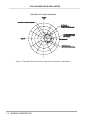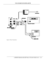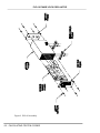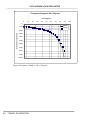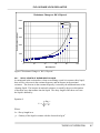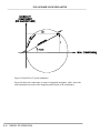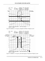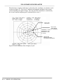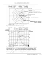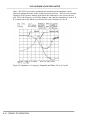
1
O P E R A T I O N
A N D
S E R V I C E
M A N U A L
PLO-10
Series
Phase Lock Oscillator
IPN 605800 Rev. G
O P E R A T I O N
A N D
S E R V I C E
M A N U A L
PLO-10
Series
Phase Lock Oscillator
IPN 605800 Rev. G
®
www.inficon.com
[email protected]
Due to our continuing program of product improvements, specifications are subject to change without notice.
©2007 INFICON
Trademarks
The trademarks of the products mentioned in this manual are held by the companies that
produce them.
INFICON® is a trademark of INFICON Inc.
All other brand and product names are trademarks or registered trademarks of their respective companies.
Disclaimer
The information contained in this manual is believed to be accurate and reliable. However, INFICON assumes
no responsibility for its use and shall not be liable for any special, incidental, or consequential damages related
to the use of this product.
Disclosure
The disclosure of this information is to assist owners of INFICON equipment to properly operate and maintain
their equipment, and does not constitute the release of rights thereof. Reproduction of this information and
equipment described herein is prohibited without prior written consent from INFICON, Two Technology Place,
East Syracuse, NY 13057-9714. Phone 315.434.1100. See www.inficon.com.
Copyright
©2000 All rights reserved.
Reproduction or adaptation of any part of this document without permission is unlawful.
First Edition, February 2000 Revision A, May 2000 Revision B, October 2000 Revision C, December 2001
Revision D, March 2003 Revision E, February 2005 , Revision F, October 2007, Revision G, November 2007
WARNING
All standard safety procedures associated with the safe
handling of electrical equipment must be observed. Always
disconnect power when working inside the controller. Only
properly trained personnel should attempt to service the
instrument.
Warranty
INFICON warrants the product to be free of functional defects in material and
workmanship and that it will perform in accordance with its published specification
for a period of (twenty-four) 24 months.
The foregoing warranty is subject to the condition that the product be properly
operated in accordance with instructions provided by INFICON or has not been
subjected to improper installation or abuse, misuse, negligence, accident,
corrosion, or damage during shipment.
Purchaser's sole and exclusive remedy under the above warranty is limited to, at
INFICON's option, repair or replacement of defective equipment or return to
purchaser of the original purchase price. Transportation charges must be prepaid
and upon examination by INFICON the equipment must be found not to comply
with the above warranty. In the event that INFICON elects to refund the purchase
price, the equipment shall be the property of INFICON.
This warranty is in lieu of all other warranties, expressed or implied and
constitutes fulfillment of all of INFICON's liabilities to the purchaser. INFICON
does not warrant that the product can be used for any particular purpose other
than that covered by the applicable specifications. INFICON assumes no liability in
any event, for consequential damages, for anticipated or lost profits, incidental
damage of loss of time or other losses incurred by the purchaser or third party in
connection with products covered by this warranty or otherwise.
www.inficon.com
[email protected]
Table of Contents
OPERATION AND SERVICE MANUAL.................................................................................................. I
1
GENERAL DESCRIPTION............................................................................................................. 1-1
1.1
1.1.1
1.1.2
1.1.3
1.1.4
1.1.5
1.1.6
1.2
1.2.1
1.2.2
1.2.3
1.2.4
1.3
1.4
2
FEATURES.............................................................................................................................. 1-2
VERY WIDE FREQUENCY RANGE................................................................................... 1-2
SUPPORT FOR VERY LOW Q, HIGHLY DAMPED, CRYSTALS...................................... 1-2
DIRECT REAL TIME MEASUREMENT OF CRYSTAL RESISTANCE .............................. 1-2
ELECTRODE CAPACITANCE CANCELLATION.............................................................. 1-2
“AUTOLOCK”.................................................................................................................... 1-2
CRYSTAL FACE ISOLATION (PLO-10i Models only) ....................................................... 1-3
CHARACTERIZING THE PLO .............................................................................................. 1-3
FREQUENCY ERRORS....................................................................................................... 1-3
FREQUENCY ERROR DUE TO PHASE ERROR............................................................... 1-3
FREQUENCY ERROR DUE TO IMPERFECT CAPACITANCE CANCELLATION.......... 1-3
CONDUCTANCE ERRORS................................................................................................. 1-5
SPECIFICATIONS .................................................................................................................. 1-6
ACCESSORIES ....................................................................................................................... 1-7
UNDERSTANDING AND SETTING UP THE INFICON PLO-10............................................. 2-1
2.1
2.2
NORMAL OPERATION ......................................................................................................... 2-1
CHECKOUT ............................................................................................................................ 2-1
3
CALCULATING CRYSTAL RESISTANCE................................................................................. 3-1
4
ADJUSTING THE CAPACITANCE CANCELLATION............................................................. 4-1
4.1
4.2
ADJUSTING CAPACITANCE CANCELLATION TRIMMER CAPACITORS ................... 4-1
WORKING WITH VERY LOW Q CRYSTALS ..................................................................... 4-3
5
FREQUENCY ERRORS DUE TO IMPERFECT CAPACITANCE CANCELLATION.......... 5-1
6
CALCULATING CRYSTAL POWER ........................................................................................... 6-1
7
CRYSTALS, HOLDERS AND FLOW CELL................................................................................ 7-1
7.1
1 INCH DIAMETER CRYSTALS........................................................................................... 7-1
7.1.1
ELECTRODE CONFIGURATION ...................................................................................... 7-1
7.1.2
CRYSTAL PARAMETERS ................................................................................................... 7-2
7.1.3
CRYSTAL SURFACE FINISH ............................................................................................. 7-3
7.1.4
CRYSTAL ELECTRODE MATERIALS................................................................................ 7-3
7.1.5
CRYSTAL THICKNESS ....................................................................................................... 7-3
7.1.6
MASS SENSITIVITY ............................................................................................................ 7-3
7.1.7
STABILITY........................................................................................................................... 7-4
7.1.8
CRYSTAL LIFE EXPECTANCY .......................................................................................... 7-5
7.1.9
TEMPERATURE COEFFICIENT ....................................................................................... 7-5
7.2
CRYSTAL CARE AND HANDLING ..................................................................................... 7-7
7.2.1
CRYSTAL CLEANING......................................................................................................... 7-8
7.2.1.1 General Cleaning ............................................................................................................ 7-8
7.2.1.2 Organic (hydrocarbon contaminants).............................................................................. 7-8
7.2.1.3 Biomaterials (lipids, proteins and similar biomolecules)................................................ 7-8
7.2.1.4 Lipid vesicles on SiO2 surfaces....................................................................................... 7-8
7.2.1.5 Polystyrene removal ....................................................................................................... 7-9
7.2.2
ELECTRODE SURFACE MODIFICATIONS ..................................................................... 7-9
7.2.2.1 SPIN COATING............................................................................................................. 7-9
7.2.2.2 SELF-ASSEMBLED MONOLAYERS (SAM) ............................................................. 7-9
iv
7.2.2.3 PHYSICAL VACUUM DEPOSITION (PVD) .............................................................. 7-9
7.3
CRYSTAL HOLDERS............................................................................................................. 7-9
7.3.1
HOW TO INSTALL A CRYSTAL IN A INFICON CRYSTAL HOLDER............................. 7-10
7.3.2
HOLDER CARE AND HANDLING................................................................................... 7-12
7.3.3
CONSIDERATIONS FOR BUILDING YOUR OWN HOLDER ........................................ 7-13
7.4
FLOW CELL.......................................................................................................................... 7-13
8
THEORY OF OPERATION ............................................................................................................ 8-1
8.1
8.2
8.3
8.4
8.4.1
8.5
8.6
8.7
8.7.1
8.7.2
8.7.3
8.8
8.9
9
10
SAUERBREY EQUATION..................................................................................................... 8-1
Z-MATCH EQUATION .......................................................................................................... 8-2
THICKNESS CALCULATION............................................................................................... 8-3
LIQUID MEASUREMENTS................................................................................................... 8-4
DECAY LENGTH OF SHEAR WAVE IN LIQUID.............................................................. 8-7
DISSIPATION METHOD........................................................................................................ 8-8
ELECTRICAL DESCRIPTION OF THE QUARTZ CRYSTAL............................................. 8-8
CHARACTERIZING THE CRYSTAL MEASUREMENT................................................... 8-15
FREQUENCY ERRORS..................................................................................................... 8-16
FREQUENCY ERROR DUE TO PHASE ERROR............................................................. 8-17
FREQUENCY ERROR DUE TO IMPERFECT CAPACITANCE CANCELLATION........ 8-17
FREQUENCY ERRORS DUE TO IMPERFECT CAPACITANCE CANCELLATION ...... 8-17
CALCULATING CRYSTAL POWER .................................................................................. 8-19
GLOSSARY ....................................................................................................................................... 9-1
REFERENCES ............................................................................................................................ 10-1
v
Table of Figures
FIGURE 1 EQUIVALENT PHASE ERROR DUE TO IMPERFECT CAPACITANCE CANCELLATION ........................ 1-4
FIGURE 2 SYSTEM CONNECTIONS ................................................................................................................ 2-3
FIGURE 3 FRONT CONNECTIONS .................................................................................................................. 2-4
FIGURE 4 REAR CONNECTIONS .................................................................................................................... 2-5
FIGURE 5 RESISTANCE VS. CONDUCTANCE VOLTAGE .................................................................................. 3-1
FIGURE 6 CAPACITANCE ADJUSTMENTS ....................................................................................................... 4-2
FIGURE 7 FREQUENCY ERROR DUE TO IMPERFECT CAPACITANCE CANCELLATION ..................................... 5-2
FIGURE 8 CRYSTAL POWER DISSIPATION VS. CONDUCTANCE VOLTAGE...................................................... 6-1
FIGURE 9 PLO-10 ASSEMBLY ..................................................................................................................... 6-2
FIGURE 10 INFICON 1" CRYSTAL – ELECTRODE CONFIGURATION ............................................................... 7-2
FIGURE 11 INFICON 1" CRYSTAL - AS SEEN FROM THE FRONT SIDE ........................................................... 7-2
FIGURE 12 FREQUENCY VS. TEMPERATURE OF INFICON 1" AT-CUT CRYSTAL FOR 90 C ............................ 7-7
FIGURE 13 FREQUENCY VS. TEMPERATURE OF INFICON 1" AT-CUT CRYSTAL FOR 25 C ............................ 7-7
FIGURE 14 CHC-100 CRYSTAL HOLDER .................................................................................................... 7-10
FIGURE 15 CRYSTAL INSTALLATION .......................................................................................................... 7-11
FIGURE 16 FREQUENCY CHANGE VS. WT % GLYCEROL............................................................................... 8-6
FIGURE 17 RESISTANCE CHANGE VS. WT % GLYCEROL .............................................................................. 8-7
FIGURE 18 CRYSTAL EQUIVALENT CIRCUIT ................................................................................................. 8-9
FIGURE 19 POLAR PLOT OF CRYSTAL ADMITTANCE .................................................................................. 8-10
FIGURE 20 ADMITTANCE VS. FREQUENCY, MAGNITUDE AND PHASE OF HIGH Q CRYSTAL ....................... 8-11
FIGURE 21 ADMITTANCE VS. FREQUENCY, REAL AND IMAGINARY COMPONENTS OF HIGH Q CRYSTAL ... 8-11
FIGURE 22 POLAR ADMITTANCE PLOT OF HIGH Q CRYSTAL ..................................................................... 8-12
FIGURE 23 POLAR ADMITTANCE PLOT OF LOW Q CRYSTAL ...................................................................... 8-13
FIGURE 24 ADMITTANCE VS. FREQUENCY, REAL AND IMAGINARY COMPONENTS OF LOW Q CRYSTAL .... 8-13
FIGURE 25 ADMITTANCE VS. FREQUENCY, MAGNITUDE AND PHASE OF LOW Q CRYSTAL ........................ 8-14
FIGURE 26 NON-ZERO PHASE LOCK ........................................................................................................... 8-15
FIGURE 27 FREQUENCY ERROR DUE TO IMPERFECT CAPACITANCE CANCELLATION ................................. 8-19
FIGURE 28 CRYSTAL POWER DISSIPATION VS. CRYSTAL RESISTANCE ....................................................... 8-20
vi
PLO-10 PHASE LOCK OSCILLATOR
1 GENERAL DESCRIPTION
The INFICON Phase Lock Oscillator was developed specifically to support the use
of the quartz crystal microbalance in the measurement of lossy films and in liquid
applications. In addition to accurately tracking the frequency of heavily damped
crystals, the PLO-10 provides a dc voltage that is proportional to the crystal’s
conductance (1/resistance). This provides additional information in the study of
lossy films and viscous solutions.
The PLO utilizes an internal oscillator referred to as a Voltage Controlled
Oscillator (VCO) to drive the crystal. The crystal current is monitored and the
frequency of the oscillator is adjusted until there is zero phase between the crystal
voltage and current. Assuming that the crystal’s electrode capacitance has been
effectively cancelled, this point of zero phase between the crystal current and
voltage is the exact series resonant point of the crystal. The magnitude of the
current at this point is directly proportional to the crystal’s conductance. This
current is converted to a voltage, demodulated and amplified to create a dc
voltage proportional to crystal conductance.
The PLO contains a phase detector that continuously monitors the phase
difference between the crystal’s current and voltage. At frequencies below the
crystal’s resonant frequency the current leads the voltage and the phase goes to 90
degrees as the frequency separation continues to increase, see Figure 20. Above
the resonant point the current lags the voltage and the phase go to minus 90
degrees. As the frequency increases through the resonant frequency, the phase
goes from plus 90 through 0 to minus 90. It is interesting to note that the phase
angle is 45 degrees when the VCO frequency is one half of the crystal’s
bandwidth above or below the crystal’s resonant frequency.
The output of the phase detector is fed into an integrator. The integrator
accumulates the phase error such that any positive phase error causes the
integrator output to climb; a negative phase causes the integrator output to fall.
With zero phase error the Integrator output holds steady.
The integrator output is connected to the VCO. Thus, if the VCO frequency is
initially below the crystal resonant frequency, the phase will be positive,
producing a positive output at the phase detector. This causes the Integrator
output to climb, which causes the VCO frequency to increase. When the VCO
frequency matches the resonant frequency of the crystal the phase will decrease to
zero, the phase detector output will go to zero, the Integrator output will hold
steady and the VCO frequency will be “locked” to the crystal’s resonant
frequency.
If the crystal’s resonant frequency moves up or down, a phase difference between
the crystal voltage and current will develop, producing a phase detector output.
The non-zero phase detector output will drive the Integrator output up or down
until the phase is zero once again, thus keeping the VCO frequency locked to the
crystal’s resonant frequency.
Once the frequency of the VCO is locked to the series resonant frequency of the
GENERAL DESCRIPTION
1-1
PLO-10 PHASE LOCK OSCILLATOR
crystal, the in-phase component (at zero phase error, there is no out of phase
component) of the crystal current is demodulated to a DC voltage. The amplified
output of the demodulator is provided at the Conductance output.
1.1
1.1.1
FEATURES
VERY WIDE FREQUENCY RANGE
The PLO-10 supports a wide frequency range from 3.8 to over 6 MHz. It will
support both 5 and 6 MHz crystals; and with a low limit of 3.8 MHz it will
support 1.2 MHz of frequency shift on a 5MHz crystal. Also, available is the
PLO-10-2 to support higher frequency crystals. Its frequency range is 5.1 to over
10 MHz.
1.1.2
SUPPORT FOR VERY LOW Q, HIGHLY DAMPED, CRYSTALS
The PLO-10 will reliably lock to crystals with resistance of 5 KΩ or less. In most
cases it will maintain lock up to a resistance of 10 KΩ. It will support crystal
oscillation in highly viscous solutions of more that 88% glycol in water.
1.1.3 DIRECT REAL TIME MEASUREMENT OF CRYSTAL RESISTANCE
The PLO-10 provides a dc voltage output that is proportional to the crystal’s
conductance. Conductance is the inverse of resistance. Based on the measured
conductance output voltage, the crystal resistance is easily calculated.
1.1.4
ELECTRODE CAPACITANCE CANCELLATION
The total quartz crystal impedance includes a shunt capacitance (due to the
capacitance of the crystal electrodes and holder) in parallel with the series
resonant arm. The total current through the crystal is the sum of the current
through the shunt capacitance plus the current through the series resonant arm.
The physical motion of the crystal is reflected in the values of the L, R and C in
the series arm of the crystal only, and therefore we want to subtract out or
otherwise cancel the current through the shunt electrode capacitance. The
INFICON PLO includes a method of canceling the electrode capacitance insuring
that the measured crystal current does not include the current through the
electrode capacitance and therefore is essentially the current through the series
resonant arm of the crystal only.
1.1.5
“AUTOLOCK”
When the PLO-10 loses lock, the VCO is ramped up to the maximum frequency
at which time it is automatically reset to the minimum frequency and a new scan
is initiated.
To insure that the VCO ramps up in frequency, a small amount of quadrature
current is injected into the current to voltage buffer whenever the PLO is
unlocked. This current is equivalent to a shunt capacitance of about 1.5 pfd. As
soon as lock is detected, the quadrature current is turned off.
1-2 GENERAL DESCRIPTION
PLO-10 PHASE LOCK OSCILLATOR
1.1.6
CRYSTAL FACE ISOLATION (PLO-10i Models only)
The PLO-10i Models provide transformer isolation of the crystal front face
electrode. This feature allows user to connect the crystal face to an
electrochemical instrument such as a potentiostat.
1.2
1.2.1
CHARACTERIZING THE PLO
FREQUENCY ERRORS
The first thing we want to know regarding the performance of the PLO, is “What
is the magnitude of the frequency error we can expect from the PLO-10?”
In any oscillator and sensing crystal system, the error in the frequency
measurement, is a function of both the oscillator and the sensing crystal. The
same is true for phase locked loops. Any phase error will introduce a frequency
error and this frequency error will be inversely proportional to the sensing
crystal’s Q. These errors are over and above any change in crystal frequency due
to temperature changes.
There are four important parameters that determine the frequency error of the
PLO and sensing crystal system or indeed, any oscillator and sensing crystal
system. The first two, the zero phase error and the electrode capacitance
cancellation errors, are characteristics of the PLO. The second two are
characteristics of the crystal, the Q of the crystal and the conductance
(1/resistance) of the crystal.
1.2.2
FREQUENCY ERROR DUE TO PHASE ERROR
Given some finite zero phase error, the resulting frequency error depends on the
sensing crystal’s Q, the higher the Q, the lower the error. For phase errors below
10 degrees the frequency error is 0.087 PPM per degree for crystals with a Q of
100,000. Thus a one degree phase error in the PLO results in a 0.44 Hz frequency
error for a 5MHz crystal with a Q of 100,000. For a 5 MHz crystal with a Q of
10,000, the error is 10 time greater or 4.4 Hz per degree.
Frequency Error/degree = df/f = PI/(360*Q)
1.2.3
FREQUENCY ERROR DUE TO IMPERFECT CAPACITANCE
CANCELLATION
The effect of imperfect electrode capacitance cancellation can also be viewed as
an equivalent phase error. This error is directly proportional to crystal resistance.
The equivalent phase error due to a non-zero shunt capacitance equal to 1 pfd is
one degree for a crystal with a series resistance of 556 Ω. Since the equivalent
phase error is proportional to the crystal resistance, a 1-pfd residual capacitance
error will result in a 10-degree equivalent error for a sensing crystal with a
resistance of 5.56 KΩ.
GENERAL DESCRIPTION
1-3
PLO-10 PHASE LOCK OSCILLATOR
Polar Plot of Crystal Conductance
Figure 1 Equivalent Phase Error Due to Imperfect Capacitance Cancellation
1-4 GENERAL DESCRIPTION
PLO-10 PHASE LOCK OSCILLATOR
1.2.4
CONDUCTANCE ERRORS
Conductance measurements are meaningful over the range of 0.0001 to 0.04
siemens (a crystal resistance of 10 KΩ to 5 Ω). Two characteristics of the PLO
limit the range of the conductance measurement. The first is the zero drift of the
demodulator and amplifier and determines the minimum measure-able
conductance. This drift can amount to 0.00005 siemens. The second
characteristic is the non-zero source impedance of the crystal drive voltage. This
source impedance, 20 Ω, appears in series with the crystal resistance and the
conductance output is proportional to the conductance of the crystal and source
combination. The equation for crystal resistance is:
Rcry = (100/Vcond) -20
GENERAL DESCRIPTION
1-5
PLO-10 PHASE LOCK OSCILLATOR
1.3
SPECIFICATIONS
Frequency range:
Capacitance compensation range:
Achievable capacitance cancellation:
Crystal conductance range:
Crystal resistance range:
Phase angle accuracy:
Phase angle stability:
Frequency error vs. phase error and crystal Q:
Conductance output range:
Conductance output scaling:
Conductance output accuracy:
Operating temperature range:
Operating temperature range for stated stability:
Controls:
Indicators:
Crystal Drive Voltage, open circuit:
Crystal Drive Source Impedance:
Crystal Power:
Crystal Isolation (PLO-10i):
Frequency Output Level:
Frequency Output Source Impedance:
Conductance Output Level:
Conductance Output Source Impedance:
Power:
Size:
Weight (shipping):
1-6 GENERAL DESCRIPTION
3.8 to 6.06 MHz, or 5.1 to 10 MHz
40 to 200 pfd
± 0.3 pfd
0.2 down to 0.0002 siemen
5 Ω to 5.0 KΩ
± 2 degrees
± 0.5 degrees
Q= 100,000 0.087 ppm per degree
Q=10,000
0.87 ppm per degree
Q=1,000
8.7 ppm per degree
0 to 40 millisiemen
100 volt/siemen
± 5 % ±50 microsiemen.
0 to 50°C
20 ± 10°C
Reset Switch
Capacitance Adjustment Trimmer,
Course and Fine
Green “Lock” LED
Red “Unlock” LED
Yellow “Sweep Rate” LED
125 mV rms
20 Ω ± 1%
200 µW, maximum
Transformer, 25 Vdc maximum
4 Vp-p
50 Ω
0 to 4 Vdc
1 KΩ
12 to 15 Vdc @ 150 mA
1.6” W x 3.2” H x 4.8” D
3 lbs.
PLO-10 PHASE LOCK OSCILLATOR
1.4
ACCESSORIES
Part Number
172205
Description
CHT-100 Crystal Holder, Teflon®, SMB
Connector
173205
CHC-100 Crystal Holder, CPVC, BNC
Connector
184204
CHK-100 Crystal Holder, Kynar®, SMB
Connector
828007
Cable, SMB Plug-SMB Plug,1' length,
RG174A/U coax
888023
Adapter, BNC Male to SMB Jack
888026
Adapter, BNC male to binding posts
803081
Power Cord
803312
Capacitance Tuning Tool
900037
Power Supply, 100-250VAC to 12VDC
Refer to INFICON Price List for more accessories and other products.
GENERAL DESCRIPTION
1-7
PLO-10 PHASE LOCK OSCILLATOR
2 UNDERSTANDING AND SETTING UP THE INFICON PLO-10
There are several LED’s on the PLO-10 to indicate its operation.
The green, Lock LED is on when the frequency is locked to a connected crystal’s
resonant frequency.
The Red, Unlock LED will be on whenever the frequency is not locked.
The Yellow, Sweep Rate LED flashes each time the frequency ramp is reset to its low
starting point.
The Reset switch allows you to force the VCO to its lowest frequency independently of
the Integrator output. The Reset switch also forces the Lock LED on, thus turning off the
quadrature current injection. The Quadrature current injection must be off to properly
adjust the capacitance cancellation. To insure that the VCO ramps up in frequency, a
small amount of quadrature current is injected into the current to voltage buffer whenever
the PLO is unlocked. This current is equivalent to a shunt capacitance of about 1.5 pfd.
As soon as lock is detected, the quadrature current is turned off.
2.1 NORMAL OPERATION
The PLO-10 comes set up for operation with a INFICON cable and crystal holder. If a
INFICON cable and crystal holder is being used, then no initial adjustments should be
needed.
During normal operation with a crystal installed and connected to the oscillator, the green
Lock LED will be on and the frequency output will reflect the crystal resonance. The red
Unlock LED will be off.
If the Unlock LED is on, the Sweep Rate LED should slowly flash. Continuous
sweeping of the frequency range indicates that the crystal’s resonant frequency is outside
of the PLO’s frequency range or the crystal’s conductance is below the conductance
threshold.
No flashing of the Sweep Rate LED when the Unlock LED is on can mean one of two
things. First, if the VCO frequency is sitting at its low limit, it means the electrode
capacitance is over compensated. Second, in some cases, even though the crystal
conductance has fallen below the threshold necessary to indicate lock, the internal signals
are still sufficient to keep the VCO locked to the crystal. In that case, the PLO really is
locked and the VCO frequency will be sitting at the crystal frequency somewhere
between its minimum and maximum frequencies.
If the VCO frequency is sitting at its low limit, press and hold the Reset switch and adjust
the fine capacitance trimmer a few degrees clockwise (not more than ten) until the Reset
LED begins to flash.
CHECKOUT
2.2
Make sure the wall mount power supply is specified for the voltage in your lab (120/240
volts).
UNDERSTANDING AND SETTING UP THE INFICON PLO-10
2-1
PLO-10 PHASE LOCK OSCILLATOR
Connect a frequency counter to the Frequency Output.
Connect a voltmeter to the Conductance output. The center conductor on the BNC
connector is positive with respect to ground.
Connect the crystal holder, with a crystal installed, to the PLO by means of the 12-inch
coax cable.
Plug the wall mount power supply into the wall and plug the power plug into the PLO-10.
Refer to Figure 2, Figure 3, and Figure 4 for a complete system connections.
The green, Lock, LED should come on, the frequency should indicate the correct crystal
frequency and the voltmeter should indicate something between 5 millivolts and 4 volts.
Check the capacitance cancellation by pressing and holding the Reset switch. The green,
Lock LED should light. Keeping the Reset switch pressed, adjust the fine capacitance
trimmer clockwise by about 5 degrees. The yellow, Reset LED should flash. Back the
trimmer counterclockwise to the point where the Reset LED just stops flashing. The
capacitance cancellation should be checked and readjusted every time the environment of
the crystal and holder is changed. For example, if the crystal and holder are moved from
air to liquid or liquid to air, the capacitance cancellation should be checked and
readjusted.
Remove the crystal. The red, Unlock, LED should light. The green, Unlock, LED
should go off. The Sweep Rate LED should not flash. If the Sweep Rate LED flashes
the capacitance is under compensated.
2-2 UNDERSTANDING AND SETTING UP THE INFICON PLO-10
PLO-10 PHASE LOCK OSCILLATOR
Figure 2 System Connections
UNDERSTANDING AND SETTING UP THE INFICON PLO-10
2-3
PLO-10 PHASE LOCK OSCILLATOR
Figure 3 Front Connections
2-4 UNDERSTANDING AND SETTING UP THE INFICON PLO-10
PLO-10 PHASE LOCK OSCILLATOR
Figure 4 Rear Connections
UNDERSTANDING AND SETTING UP THE INFICON PLO-10
2-5
PLO-10 PHASE LOCK OSCILLATOR
3 CALCULATING CRYSTAL RESISTANCE
The PLO-10 provides a dc output voltage proportional to conductance. Conductance is
the inverse of Resistance. Thus, Conductance = 1/Resistance or Resistance =
1/Conductance. The units of resistance are ohms (volts per ampere) and the units of
conductance are siemens (amperes per volt). The PLO-10 Conductance Output is
inversely proportional to the sum of the crystal resistance plus the Crystal Drive Voltage
source resistance. Thus,
Conductance Output = 100/(Rcry + Rsource).
The Conductance Output scaling is 100 volts per siemen. Solving for Rcry,
Rcry = (100/Conductance in volts) - Rsource
The Crystal Drive Source Resistance is 20 Ω, so
Rcry, in ohms = (100/Conductance, in volts) – 20 Ω
Examples:
1.
Conductance output voltage = 1.000 volt.
Rcry, in ohms = (100/1.000) – 20 = 80 Ω
2.
Conductance output voltage = 0.015 volts.
Rcry, in ohms = (100/0.015) – 20 = 6667 – 20 = 6647 Ω = 6.647 KΩ
R e s is ta n c e v s . V o lta g e
1 0 0 0 0 .0 0
Equivalent Resistance (R)
1 0 0 0 .0 0
1 0 0 .0 0
1 0 .0 0
4.00
3.75
3.50
3.25
3.00
2.75
2.50
2.25
2.00
1.75
1.50
1.25
1.00
0.75
0.50
0.25
0.00
1 .0 0
C o n d u c ta n c e V o lta g e (V )
Figure 5 Resistance vs. Conductance Voltage
CALCULATING CRYSTAL RESISTANCE
3-1
PLO-10 PHASE LOCK OSCILLATOR
4 ADJUSTING THE CAPACITANCE CANCELLATION
Proper adjustment of the Capacitance Cancellation is critical in obtaining accurate results
with high resistance crystals. See Section 1.2.3 FREQUENCY ERROR DUE TO
IMPERFECT CAPACITANCE CANCELLATION. The cancellation adjustment should
be performed with the crystal holder and crystal in the measurement environment. For
instance, if liquid measurements are to be made insert the crystal and its holder into the
liquid where the measurement will be made.
With the crystal and holder in the measurement environment, press and hold the Reset
switch. Pressing and holding the Reset switch forces the VCO to its minimum frequency,
turns on the Lock LED, and turns off the quadrature current injector. Forcing the VCO to
its minimum frequency insures that the crystal is being driven at a frequency far from its
resonant frequency where its impedance is essentially due only to the shunt electrode
capacitance. With the quadrature current injector turned off, the measured current is due
only to the net shunt capacitance. The measured net shunt capacitance is the capacitance
of the cable, holder and crystal electrodes minus the compensation capacitance. If the
capacitance is under compensated, the phase of the measured current leads the voltage, (a
phase angle of plus 90 degrees). If the capacitance is over compensated, it lags the
voltage, (a phase angle of minus 90 degrees).
The Yellow Sweep LED is used to determine whether the crystal capacitance is over
compensated or under compensated. The Sweep LED flashes whenever the crystal
capacitance in under compensated.
If the Sweep LED is not flashing, turn the fine compensation clockwise until it begins to
flash then back up until it just stops. If it is flashing, turn the fine adjustment counter
clockwise until it just stops flashing. This is a very fine adjustment. Go back and forth
until you are sure you are right on the edge. The sensitivity of the fine adjustment is
approximately 0.05 pfd per degree. In situations where the crystal resistance is very high
(over 1 KΩ) a net capacitance of over 0.5 pfd can result in a significant frequency error
so try to get this adjustment to within a couple of degrees. Remember to keep the Reset
switch depressed while making this adjustment.
4.1 ADJUSTING CAPACITANCE CANCELLATION TRIMMER CAPACITORS
Setting up the capacitance cancellation is fairly straightforward. The thing to remember
is that there are two variable capacitors, a course and a fine with the total compensation
capacitance being the sum of the two. These trim capacitors have no stops so it’s not
obvious when they are at their minimum or their maximum.
The capacitors have circular, rotor plates that mesh into fixed stator plates. The
capacitance is at a maximum when the plates are fully meshed and a minimum when
rotor plates are above the stator plates and not meshed. As the capacitors are rotated
clockwise they go through a full cycle from maximum to minimum and back to
maximum. Or, depending on where you start they may go first toward a minimum, then
to a maximum and then back toward a minimum. To avoid confusion, we always want to
be turning clockwise as we approach the desired capacitance and we want the capacitance
to be decreasing.
ADJUSTING THE CAPACITANCE CANCELLATION
4-1
PLO-10 PHASE LOCK OSCILLATOR
If you are using a crystal holder and cable supplied with your PLO-10 then you should
not have to change the course adjustment. Connect the cable and crystal holder to the
PLO but don’t install a crystal.
If the Sweep LED is flashing, press and hold the Reset button and then turn the fine
trimmer counter clockwise until it just stops flashing. Go back and forth a few times to
get a feel for the point where the Sweep LED just stops flashing. Release the Reset
button and the Sweep LED should begin to flash again.
Install a crystal. The PLO should lock. Even so, press and hold the Reset button and
again adjust the fine trimmer to the point where the flashing just stops. The capacitance
cancellation adjustment is now perfect. Remember to check this adjustment whenever
the crystal holder is moved or changed to a new environment.
If you could not find the proper zero capacitance point using the fine trimmer alone, then
we have found the following approach which is best for adjusting the coarse trimmer.
First adjust the fine trimmer so that it is 50% meshed and the rotor plates are below the
shaft with the oscillator upright. You can see these plates through the oversize
adjustment hole. See Figure 6. Next connect a cable and crystal holder, if you haven’t
already done so. Don’t install the crystal at this point.
Figure 6 Capacitance Adjustments
Do not press the reset button, now slowly turn the course trimmer clockwise while
watching the Lock and Unlock LED’s. The green, Lock, LED will come on when the
capacitance is grossly out of adjustment. Continue turning the course trimmer clockwise
until the Unlock LED comes on. The adjustment is getting close. Press and hold the
reset button, Slowly continue to turn the trimmer clockwise until the yellow, Sweep, LED
begins to flash. If you continue to turn clockwise the Sweep LED will cease flashing, but
4-2 CALCULATING CRYSTAL POWER
PLO-10 PHASE LOCK OSCILLATOR
this is not the point you want. Back off the course adjustment until the flashing begins
again, then continue to the point where the flashing just stops. The course adjustment is
now complete.
Install a crystal into the holder. Now depress and hold the Reset button. Slowly adjust
the fine trimmer clockwise until the flashing of the Sweep LED begins again and then
back off until it just stops. The capacitance compensation adjustment is now complete.
Release the Reset button and assuming the crystal is not dead or out of range, the PLO-10
will lock on it.
4.2 WORKING WITH VERY LOW Q CRYSTALS
Very low Q crystals require very close adjustment of the compensating capacitance to
insure a successful lock. To adjust the compensation capacitance one pushes the Reset
button and adjusts the capacitance to the point where the Sweep LED just ceases to flash.
With very low Q crystals, the PLO may not lock upon release of the Reset button. The
Unlock LED will be on and the Sweep LED will be flashing. This is normal. Even so it
may be possible to lock on the crystal by slowly adjusting the fine capacitance
counterclockwise until the Sweep LED again ceases to flash. Lock is evidenced by the
Lock LED turning on or by a value of greater than 8 millivolts at the Conductance output.
Once lock is achieved the true series resonant point can be found by adjusting the
capacitance for maximum conductance. The limits of the crystal bandwidth can be
determined by adjusting the capacitance and reading the maximum frequency and the
minimum frequency just before the PLO loses lock.
ADJUSTING THE CAPACITANCE CANCELLATION
4-3
PLO-10 PHASE LOCK OSCILLATOR
5 FREQUENCY ERRORS DUE TO IMPERFECT CAPACITANCE
CANCELLATION
There are two reasons that proper capacitance cancellation is so important with high
resistance crystals.
The first is that to a first approximation, the frequency error resulting from a given phase
error is proportional to the bandwidth of the crystal. The bandwidth of the crystal is
proportional to the crystal’s resistance. A ten-ohm crystal might typically have a
bandwidth of 42 Hz, while a one thousand-ohm crystal will have a bandwidth of 4,200
Hz. A five thousand-ohm crystal will have a bandwidth of 21,000 Hz. Since the
frequency error for a given phase error is proportional to the bandwidth, a phase error that
would result in a 0.5 Hz frequency error in a ten ohm crystal will cause a 50 Hz error in a
one thousand ohm crystal and 250 Hz error in a five thousand ohm crystal.
The second reason is that the effective phase error caused by a non-zero net quadrature
current is inversely proportional to the real current, which is inversely proportional to the
crystal resistance. In other words, the effective phase error is proportional to the crystal
resistance. For instance, a net unbalance of 1 pfd leads to an effective phase error of 0.02
degrees for a ten ohm crystal, but it leads to a 2 degree error for a one thousand ohm
crystal and a 10 degree error for a five thousand ohm crystal.
Examples:
A ten-ohm, 5 MHz crystal will have a Q (Quality Factor) of about 120,000. The
bandwidth is equal to the crystal frequency divided by Q. Thus, the bandwidth of this
crystal would be about 42 Hz. To a first approximation, near zero phase, the frequency
error per degree of phase error is given by the following formula,
Frequency Error = -½(Phase Error, in radians)(Bandwidth)
Or,
Frequency Error = -(1/(2*57.3))(Phase Error, in degrees)(Bandwidth)
For the above ten-ohm crystal, the frequency error caused by a one-degree phase error is
42/114.6 or approximately 0.37 Hz. For a one thousand-ohm crystal, one degree of phase
error results in a 37 Hz error and for a ten thousand-ohm crystal the frequency error is
370 Hz per degree of phase error.
Now, the effective phase error caused by a non-zero quadrature (imaginary) current is
given by the following formula,
Effective Phase error = arctangent (imaginary current/real current)
And since current is proportional to conductance,
Effective Phase error = arctangent (imaginary conductance/real conductance)
The conductance of a one picofarad capacitor at 5 MHz is 31.4 microsiemens. The
conductance of a ten-ohm crystal at resonance is 100 millisiemens.
FREQUENCY ERRORS DUE TO IMPERFECT CAPACITANCE
CANCELLATION
5-1
PLO-10 PHASE LOCK OSCILLATOR
Effective Phase error = arctangent ((31.4e-6)/(100e-3)) = 0.018 degrees
In other words a one picofarad capacitance unbalance will result in an effective phase
error of only 0.018 degrees when measuring a ten-ohm crystal. However, when
measuring a one thousand-ohm crystal the effective phase error will increase to 1.8
degrees and it will increase to 9 degrees when measuring a five thousand-ohm crystal.
Combining these two errors we can get an idea of the magnitude of the frequency error
caused by imperfect capacitance cancellation.
For a 10 Ω crystal a one picofarad capacitance imbalance results in a 0.018 degree phase
error and a 0.0067 Hz frequency error.
For a 100 Ω crystal, the phase error is 0.18 degrees and the frequency error is 0.67 Hz.
For a 1000 Ω crystal, the phase error is 1.8 degrees and the frequency error is 67 Hz. For
a 5000 Ω crystal, the phase error is 9 degrees and the frequency error is 1,635 Hz.
A two picofarad capacitance imbalance will result in approximately twice the above
error.
Frequency Error vs. Crystal Resistance
100000.000
10000.000
Frequency Error (Hz)
1000.000
100.000
10.000
Freq. Error due to a
5 pfd capacitance
imbalance
1.000
Freq. Error due to a
2 pfd capacitance
imbalance
0.100
Freq. Error due to a
1 pfd capacitance
imbalance
10
16
25
40
63
100
158
251
398
631
1,000
1,585
2,512
3,981
6,310
0.001
10,000
0.010
Crystal Resistance (ohm)
Figure 7 Frequency Error Due to Imperfect Capacitance Cancellation
5-2 FREQUENCY ERRORS DUE TO IMPERFECT CAPACITANCE CANCELLATION
PLO-10 PHASE LOCK OSCILLATOR
6 CALCULATING CRYSTAL POWER
Using the PLO conductance voltage output, crystal power can be calculated. Refer to
Section 3 CALCULATING CRYSTAL RESISTANCE, crystal resistance, Rcry, is given
as (100/ Vcond)-20, where Vcond = Conductance Voltage.
Crystal power, Pcry = i2 * Rcry
Since icry = Vsoc/(20 + Rcry) or (Vcond /100) * Vsoc
Hence, Pcry = i2 * Rcry = [(Vcond /100) * Vsoc]2 * [(100/ Vcond)-20]
Pcry = Vsoc2 * (Vcond /100) * [1-20(Vcond /100)]
Vsoc = Voltage of source open circuit = 125 mV (open circuit source voltage crystal drive)
Then, Pcry = 0.1252 * (Vcond /100) * [1-20(Vcond /100)]
Examples:
1.
Conductance output voltage = 1.000 volt
Pcry, in watts = 0.1252 * (1/100) * [1-20(1/100)] = 1.25E-4 watts or 125 µW
2.
Conductance output voltage = 0.015 volts
Pcry, in watts = 0.1252 * (0.015/100) * [1-20(0.015/100)] = 2.3E-6 watts or 2.3 µW
Crystal Power vs. Conductance Voltage
250.0
Crystal Power (uW)
200.0
150.0
100.0
50.0
4
3.8
3.6
3.4
3.2
3
2.8
2.6
2.4
2.2
2
1.8
1.6
1.4
1.2
1
0.8
0.6
0.4
0.2
0
0.0
Conductance Voltage (volts)
Figure 8 Crystal Power Dissipation vs. Conductance Voltage
CALCULATING CRYSTAL POWER
6-1
PLO-10 PHASE LOCK OSCILLATOR
Figure 9 PLO-10 Assembly
6-2 CALCULATING CRYSTAL POWER
PLO-10 PHASE LOCK OSCILLATOR
7 CRYSTALS, HOLDERS AND FLOW CELL
An essential part of the PLO-10 Oscillator is the sensing crystal. Careful handling of
both the crystal and the crystal holder must be observed to ensure proper and
reproducible measurements. Furthermore, the sensing crystal, the crystal holder and the
connecting cable must be orientated and connected correctly in order for the PLO-10 to
work properly. This is especially true if you design your own crystal or holder.
If you have purchased a INFICON crystal, holder and cable, the installation is simple.
Follow the instructions below.
If you plan to build your own crystal or holder or cable, see Section 7.3.2 HOLDER
CARE AND HANDLING.
7.1 1 INCH DIAMETER CRYSTALS
INFICON pioneered the standard AT-cut, 5 MHz, 1-inch diameter crystals for use in liquid
applications. The AT-cut quartz is chosen for its superior mechanical and piezoelectric
properties, and the angle of cut can be adjusted to obtain a zero temperature coefficient at
a desired operating temperature. The 1 inch diameter was chosen to allow enough
distance between the active area of the crystal and the mounting o-ring. This improves
the overall stability of the crystal by reducing the frequency changes due to mounting
stress.
7.1.1
ELECTRODE CONFIGURATION
Figure 10 below shows INFICON’s 1” crystal electrode patterns. The left figure shows the
½ inch diameter front electrode (also called sensing electrode) with an extended electrode
that wraps around the edge of the crystal and extends into a semicircle shown in the top
half of the right figure. The lower half of the right figure shows the ¼ inch diameter rear
electrode (also called contact electrode).
This configuration enables both electrical contacts to be made on the backside of the
crystal allowing measurement in conductive liquids.
The oversized front electrode (½ inch in diameter as oppose to the ¼ inch diameter rear
electrode) was chosen to ensure a more consistence deposition across the active area of
the crystal. The exposed area of the front electrode is 0.212 in2 (137 mm2), but the active
oscillation region (displacement area) is limited to the overlapping area of the front and
rear electrodes (0.053 in2 or 34.19 mm2).
CRYSTALS, HOLDERS AND FLOW CELL
7-1
PLO-10 PHASE LOCK OSCILLATOR
Figure 10 INFICON 1" Crystal – Electrode Configuration
The figure below shows a INFICON 1” diameter as seen from the front side.
Figure 11 INFICON 1" Crystal - as Seen From The Front Side
7.1.2
CRYSTAL PARAMETERS
Polished one-inch diameter crystals that are commonly available for liquid work have the
typical values as listed below.
Type
5 MHz
9 MHz
Frequency
Range (MHz)
4.976 – 5.020
8.976 – 9.036
Electrode
Material
Gold
Gold
7-2 CRYSTALS, HOLDERS AND FLOW CELL
Resistance
(ohms)
~10
~7
Q Factor
120,000
55,000
PLO-10 PHASE LOCK OSCILLATOR
7.1.3
CRYSTAL SURFACE FINISH
Studies have shown that electrode surface roughness can cause large apparent mass
loadings due to the liquid that is trapped within pores at the crystal surface 1 . INFICON’s
crystals are optically polished to 50 Å average surface roughness to minimize this effect.
Polished crystals are required to obtain good agreement between theory and measurement
during liquid immersion experiments. Polished crystals are also required to obtain
measurements reproducibility from crystal to crystal2.
Non-polished crystals (Ra=1.8 microns) are also available at reduced costs for
applications that do not require the accuracy and reproducibility of the polished crystals.
7.1.4
CRYSTAL ELECTRODE MATERIALS
INFICON’s crystals are available in a variety of electrode materials including Gold,
Platinum, Aluminum, Silver, Titanium, etc. INFICON also offers Gold electrode crystals
with an additional SiO2 outer layer to create a hydrophilic surface needed for some
biological applications.
7.1.5
CRYSTAL THICKNESS
INFICON AT cut, 1-inch diameter crystals are plano-plano. Their physical thickness is
determined by a frequency constant and their final frequency. The frequency constant for
an AT cut crystal is 1.668E5 Hz × cm or 65.5 kHz × in. Therefore, the crystal
thicknesses for various frequencies are as follows.
5 MHz AT cut thickness = 333 microns (0.013 inch)
6 MHz AT cut thickness = 227 microns (0.0109 inch)
9 MHz AT cut thickness = 185 microns (0.007 inch)
7.1.6
MASS SENSITIVITY
The quartz crystal microbalance is an extremely sensitive sensor capable of measuring
mass changes in the nanogram/cm2 range with a wide dynamic range extending into the
100 µg/cm2 range.
Sauerbrey was the first to recognize the potential usefulness of the technology and
demonstrate the extremely sensitive nature of these piezoelectric devices towards mass
changes at the surface of the QCM electrodes3. The results of his work are embodied in
the Sauerbrey equation, which relates the mass change per unit area at the QCM electrode
surface to the observed change in oscillation frequency of the crystal:
∆f= - Cf × ∆m
where
∆f = the observed frequency change in Hz,
Cf = the sensitivity factor of the crystal in Hz/ng/cm2
(0.056 Hz/ng/cm2 for a 5 MHz crystal @ 20° C)
CRYSTALS, HOLDERS AND FLOW CELL
7-3
PLO-10 PHASE LOCK OSCILLATOR
(0.081 Hz/ng/cm2 for a 6 MHz crystal @ 20° C)
(0.181 Hz/ng/cm2 for a 9 MHz crystal @ 20° C)
∆m = the change in mass per unit area, in g/cm2
The minimum detectable mass change is typically a few ng/cm2 and limited by the noise
specifications of the crystal oscillator and the resolution of the equipment used to
measure frequency shifts. For example, the INFICON RQCM has a frequency resolution of
0.03 Hz @ 6 MHz, therefore, its minimum detectable mass change is 0.37 ng/cm2.
The Sauerbrey equation relies on a sensitivity factor, Cf, which is a fundamental property
of the QCM crystal. Thus, in theory, the QCM mass sensor does not require calibration.
This ability to calculate the mass sensitivity from first principles is obviously a very
attractive feature of these devices. However, it is very important to notice, that the
Sauerbrey equation is only strictly applicable to uniform, thin-film deposits originating
from a low pressure (i.e. vacuum) gas environment21. Thick deposits and operation in
liquid environments or in contact with lossy films, relies on the use of more complex
equations relating the frequency shifts to mass loading, and often requires calibration of
the setup for accurate results. Several articles have been published on simple ways to
calibrate the mass sensitivity of QCMs for electrochemical applications4 and for vacuum
thin-film deposition processes5 6 7, and some useful calibration guidelines are also
described herein.
Many studies have shown that the crystal's sensitivity is approximately Gaussian. The
maximum sensitivity is in the center of the crystal and it tapers off towards the edge of
the active area8 9 10. The mass sensitivity distribution has also been shown to become
slightly more confined to the electrode region as the mass loading is increased.
7.1.7
STABILITY
A sensor crystal cannot distinguish the difference between a frequency shift due to
deposited material or that due to other disturbances. Thus any extraneous factors, other
than the deposited mass, which may cause the quartz crystal to change its resonant
frequency, must be properly controlled. Factors that can influence the stability of a
sensor crystal are categorized as follows11:
♦ The crystal itself: Improper design, localized stress, damage to the crystal
♦ The crystal holder: Improper seating of the crystal, large mechanical coupling
between the crystal and the holder
♦ Thermal input: Radiation from evaporation source, radiation from substrate heater,
bombardment by charge particles, energy released by condensates
♦ Stress: Thermal stress, stress release in the deposited materials
♦ Temperature: See section 7.1.9 for data on frequency versus temperature for
INFICON’s crystals.
Other factors that can affect stability are humidity, shock, vibration and change in
pressure. Controlling those conditions is a must to insure accurate measurements of
7-4 CRYSTALS, HOLDERS AND FLOW CELL
PLO-10 PHASE LOCK OSCILLATOR
small mass changes over long periods of time.
7.1.8
CRYSTAL LIFE EXPECTANCY
It is difficult to predict the useful life of a crystal since it depends on many factors. Some
of these factors are11:
♦ The quality of the quartz
♦ The amount of deposited material
♦ The stress generated in the crystal due to deposited material
♦ The acoustic losses in the deposited material
♦ The design of the oscillator circuitry
Other aspects that affect the crystal life include the type of the deposited material,
splitting of source material resulting in non- uniform films, film flakes that landed on the
crystal’s active area, and of course, physical damage to the crystal such as chipping,
cracking, or peeling of the electrode, etc.
In general, a sensor crystal can be used until its frequency drops below 50% of its
uncoated value. However, for the reasons stated above, crystal failures often occur well
before a 40% shift in frequency is reached.
The sensor crystals are considered expendable. However, a crystal may be reused up to
20 times on average in experiments that don’t physically alter the crystal electrode. In
experiments where a film is deposited, the crystal can be stripped using a chemical
etchant . Care must be taken so only the deposited material is stripped and not the crystal
electrodes. The amount of times that a crystal can be reused greatly depends on its
condition after each experiment or stripping. Needless to say, careful handling and
cleaning of the crystal is required to maximize its re-usability.
Noisy or erratic measurement indicates that the crystal is about to fail. It might even be
difficult to obtain a stable baseline. Spurious signals might become evident in
electrochemical QCM experiments. Visually, traces of consumption and wear can often
be seen on the crystal surface. Edges of the sensor crystal might become cracked and the
deposited film, even the electrode, starts to show scratches and tears.
The crystal motional resistance R does reflect the influence of deposited material on the
performance of a crystal. This resistance is associated with the damping of acoustic
waves by the electrodes, deposited materials, and the supporting structure. This
resistance increases as more material is being deposited onto the crystal11. This
resistance value can be used to determine when a crystal reaches a maximum loading.
7.1.9
TEMPERATURE COEFFICIENT
The temperature coefficient of quartz crystals is normally specified in units of parts per
million per degree of temperature change. A one part per million change in frequency of
the sensing crystal corresponds to an indicated thickness change of approximately 7.4 Å
for a material with a density of 1.0 gm/cm³. For Aluminum with a density of 2.7 gm/cm³,
this is equivalent to approximately 2.7Å. This intrinsic dependence of resonance
CRYSTALS, HOLDERS AND FLOW CELL
7-5
PLO-10 PHASE LOCK OSCILLATOR
frequency of a sensor crystal on temperature is generally small in experiments in gas
phase when operating at or near its “turn-around-point”. The “turn-around-point” is
where the temperature coefficient of the crystal is zero. That is, there is no change in
resonance frequency due to a change in the temperature of the crystal at the turnaround
point. INFICON 1 inch crystals are optimized for two operating temperatures namely 90ºC
and 25ºC. These crystals have very good temperature stability when operating close to
their specified temperature.
Even though AT cut crystals are designed to minimize the change in frequency due to
temperature, the effect of temperature can be significant when attempting to resolve small
mass (frequency) changes over long periods of time. This frequency change due to
temperature is magnified when the sensor crystal is submerged in liquids. This is due to
the coupling of the shear mode oscillation with the temperature dependent viscosity and
density of the fluid. For experiments in liquid phase in which the frequency is to be
monitored over long periods of time, the temperature must be controlled to at least 0.1°C,
and preferably better. In electrochemical experiments this is often achieved with
temperature controlled baths and jacketed cells. It is always good practice to wait at least
30 minutes before performing any accurate measurements after the crystal comes in
contact with a new medium. This allows the crystal to come to equilibrium with the
medium. If temperature control is not possible or practical, attempts should be made to
measure the temperature of the solution around the crystal during the experiments and
perform temperature compensation.
In short, each PLO-10 user must determine the effect of temperature on the experiments
being performed and either control the temperature accordingly, or measure the
temperature and compensate for it.
Delta Frequency (Hz)
Freq Change vs. Temp
INFICON AT cut for 90C
175
150
125
100
75
50
25
0
-25
-50
-75
-100
-125
-150
-175
-200
-225
-250
0
10
20
30
40
50
60
70
Temperature (C)
7-6 CRYSTALS, HOLDERS AND FLOW CELL
80
90
100
110
120
PLO-10 PHASE LOCK OSCILLATOR
Figure 12 Frequency vs. Temperature of INFICON 1" AT-Cut Crystal for 90 C
Delta Frequency (Hz)
Freq Change vs. Temp
INFICON AT cut for 25C
275
250
225
200
175
150
125
100
75
50
25
0
-25
0
10
20
30
40
50
60
70
80
90
100
110
120
Temperature ( C)
Figure 13 Frequency vs. Temperature of INFICON 1" AT-Cut Crystal for 25 C
7.2 CRYSTAL CARE AND HANDLING
It is essential that a sensor crystal is clean and free of foreign matter that may react with
the experiment inducing errors in the measurements. The following guidelines are
recommended for general handling of the sensor crystals.
♦ Keep the crystals in a clean environment. Store them in their original package until
use.
♦ Never handle the crystals with bare hands.
♦ Always use plastic tweezers around the edge of the crystal during handling.
♦ Do not touch the center of a sensor crystal, as any oil, dirt, dust, or scratches will
quickly degrade the quality of the crystal.
♦ When using a chemical agent to clean the crystal, ensure that the crystal electrode
material(s) will not be damaged by the chemical.
♦ Never use cleaner that will etch the quartz surface.
♦ Always rinse with deionized water, or another appropriate pure liquid, before drying
the crystal.
♦ Always use a flow of dry, oil-free, non-reactive gas (e.g. filtered nitrogen) to blowCRYSTALS, HOLDERS AND FLOW CELL
7-7
PLO-10 PHASE LOCK OSCILLATOR
dry the crystal. It is better to chase liquid off the crystal than to let it evaporate off the
crystal.
♦ Never wipe the crystal – even soft, lint-free cloth will scratch the crystal.
7.2.1
CRYSTAL CLEANING
The surface properties of the sensor crystal determine the interaction of sample material
with the surface. Therefore, the developments of proper procedures for cleaning are
required to obtain meaningful and reproducible measurements. This section provides the
basic information you need to develop a cleaning procedure suited to your sample/surface
preparation.
CAUTION – When developing a cleaning procedure, always perform
a test run on a crystal before committing to a larger batch cleaning.
Follow the crystal handling guidelines throughout the cleaning process
to protect the crystal quality. Avoid using high pH cleaners since they
will etch the crystal surface.
7.2.1.1
General Cleaning
For general purpose applications such as electrochemistry and liquid or viscoelastic film
experiments, it is usually sufficient to use ultrasonic cleaning method to clean the crystals
in a solution of non-basic detergent in deionized water. Immediately rinse liberally with
deionized water and dry in a gentle flow of filtered nitrogen gas.
7.2.1.2
Organic (hydrocarbon contaminants)
UV/ozone treatment12 is a powerful tool for removing hydrocarbon impurities which
have been adsorbed from the ambient air. This method utilizes irradiation with ultra
violet light that breaks up the organics on the surface of the sample being cleaned. A
flow of air or a weak vacuum carries off the organics. This method does not affect the
quartz surface; it is low cost and is very efficient.
Oxygen plasma cleaning is another effective method that will remove organic matters. In
this method, the plasma reaction breaks up organic matters at the surface of the sample
being cleaned into smaller molecules and a vacuum pump removes them from the surface
of the sample.
7.2.1.3
Biomaterials (lipids, proteins and similar biomolecules)
Start by treating the crystal in an UV/ozone chamber for 10 minutes, then immerse it into a
1:1:5 solution of hydrogen peroxide (30%), ammonia (25%) and deionized water heated
to a temperature of about 75°C for 5 minutes 22 . Immediately rinse liberally with
deionized water and dry in a gentle flow of nitrogen gas. Immediately before
measurement, treat the crystal with UV/ozone for 10 minutes.
7.2.1.4
Lipid vesicles on SiO2 surfaces
Treat the crystal in an UV/ozone chamber for 10 minutes, then immerse it into water with
2% of sodium dodecyl sulfate (SDS) at room temperature for 30 minutes 23 . Rinse
generously with deionized water and blow dry with filtered nitrogen gas. Immediately before
measurement, treat the crystal with UV/ozone for 10 minutes.
7-8 CRYSTALS, HOLDERS AND FLOW CELL
PLO-10 PHASE LOCK OSCILLATOR
7.2.1.5
Polystyrene removal
To clean polystyrene (PS) off a crystal, immerse the crystal into a 1:1 solution of hexane
and deionized water and treat it in an ultrasonic bath for 1 minute. Rinse thoroughly with
deionized water and blow dry with filtered nitrogen gas.
7.2.2
ELECTRODE SURFACE MODIFICATIONS
A QCM will response to anything that has mass. Thus, it is imperative for the QCM user
to develop a “condition” where the QCM will only responsed to the substance of interest.
This usually involves a chemically or biologically sensitive layer applied to the surface of
the crystal13.
INFICON offers a wide variety of standard electrode materials for you to choose from.
Contact us if you don’t see one that fits your needs. If you choose to do your own crystal
surface modification, use the following guidelines.
7.2.2.1
SPIN COATING
Thin films (nm to microns) of polymers and other materials can be applied by spin
coating14. Polystyrene is a common material spin-coated on QCM sensor crystals.
UV/Ozone treatment can be used to change the hydrophobicity of organic polymeric
coatings15 16.
7.2.2.2
SELF-ASSEMBLED MONOLAYERS (SAM)
7.2.2.3
PHYSICAL VACUUM DEPOSITION (PVD)
Self-assembling monolayers can be laid down on gold or silver surface by thiolization17
18 19
or on SiO2 by silanization20 to control surface properties.
Thin films of metals or metal oxides can be applied by sputtering or thermal evaporation
in a vacuum chamber. To ensure quality and reproducible films, careful attention to
cleanliness must be observed, both in the vacuum chamber and in the preparation of the
crystals prior to coating. INFICON is an expert in PVD. Consult us for any special needs.
7.3 CRYSTAL HOLDERS
Figure 14 shows a INFICON CHC-100 Crystal Holder (without a crystal, the crystal
retainer or the retainer cover). It has a cavity for a 1-inch diameter crystal. Inside the
cavity there are two Pogo® pins providing connections to the crystal’s front and rear
electrodes. Note the locations of the Pogo® pins. These pins are internally connected to
the BNC connector (SMB Jack for CHT-100 and CHK-100 holders) via an internal
coaxial cable.
CRYSTALS, HOLDERS AND FLOW CELL
7-9
PLO-10 PHASE LOCK OSCILLATOR
Figure 14 CHC-100 Crystal Holder
7.3.1
HOW TO INSTALL A CRYSTAL IN A INFICON CRYSTAL HOLDER
1. Identify the Front and Rear Sides of the crystal. See Section 7.1.1.
2. Clean & Dry the Crystal Holder cavity, then insert the Crystal with the Front Side
(Sensing Electrode) exposed. The “Wrap-Around Extended Electrode” MUST be in the
60º region as in Figure 15 below.
710
CRYSTALS, HOLDERS AND FLOW CELL
PLO-10 PHASE LOCK OSCILLATOR
Figure 15 Crystal Installation
3. Place the Retainer Ring over the Crystal, with the Notch mating to the Index Pin.
4. Mount and turn the Retainer Cover approximately ¼ turn. Then with a gloved-finger
or cotton swab gently press the Retainer Ring down at the Notch to make sure that it stays
mated to the Index Pin. Finish tightening the Cover until it’s snug.
CRYSTALS, HOLDERS AND FLOW CELL
7-11
PLO-10 PHASE LOCK OSCILLATOR
7.3.2
HOLDER CARE AND HANDLING
With a robust design, INFICON crystal holders require little care. However, the crystal
holder is in direct contact with the sensor crystal and your experiment environment.
Thus, care must be taken to ensure its cleanliness eliminating any contaminants that may
react with the crystal or the experiment media. The following guidelines are
recommended for general handling of the holders.
♦ Always keep the holder clean and dry when not in use.
♦ Always use clean room grade gloves while handling the holder and its components.
♦ Never handle the holder with bare hands as human skin oils may deposit on it and
react with your experiment.
♦ Always ensure that your holder is compatible with your experiment environment.
♦ Never submerge the holder unassembled or without a crystal.
♦ Never submerge the holder pass its terminal connector at the end of the rod.
♦ Always rinse the holder generously with deionized water and thoroughly blow dry
using filtered air after each experiment. This is especially important if the holder has
been exposed to oxidizing acids.
712
CRYSTALS, HOLDERS AND FLOW CELL
PLO-10 PHASE LOCK OSCILLATOR
♦ Always act fast in the event that liquids or chemicals have entered the crystal cavity
in the holder. Immediately clean the holder using the following procedure.
o Remove the crystal to expose the crystal cavity.
o Remove both Pogo® contact pins from their sockets. Use a pair of
tweezers (or gloved fingernail), grab the Pogo® head firmly and pull it
straight out of its socket.
o Rinse the holder, the crystal cavity and the Pogo® sockets generously with
deionized water to remove all traces of chemicals and thoroughly blowdry the whole holder using filtered air. Ensure all liquids that may have
been trapped inside the sockets are removed.
o Generously rinse the Pogo® contact pins with deionized water,
occasionally squeeze the pins to push out any liquids that may have been
trapped inside the pins. Thoroughly blow-dry the pins using filtered air.
o Install the Pogo® pins back into their sockets. Use the tip of a pair of
tweezers and push down on each Pogo® pins to verify their deflection.
7.3.3
CONSIDERATIONS FOR BUILDING YOUR OWN HOLDER
You MUST consider the following aspects when building your own crystal holder.
The holder must be designed so that when a crystal is installed, its front electrode
(sensing electrode) is connected to the housing (shell) of the SMB Crystal Connector on
the PLO- 10; and the rear electrode is connected to the center pin of the SMB Crystal
Connector.
The crystal should be clamped, as close as possible, to the edge of the crystal to avoid
damping of the crystal’s oscillations.
The holder clamping mechanism should have a positive stop to avoid excessive clamping
force on the crystal.
If the crystal is to be used in a conductive fluid or conductive gas, the rear electrode must
be sealed from the conductive environment to avoid an electrical short between the
electrodes. The electrodes should be designed so the rear electrode and the electrodes
contacts can be sealed. Only the front electrode should be exposed.
The connecting cable must be coaxial all the way, from SMB on the PLO-10, on up to the
crystal. The shield of the coaxial must connect to the front electrode and the center
conductor must connect to the rear electrode of the crystal. In addition, the coaxial cable
must be free of kinks, knots, etc. to avoid unbalanced capacitance in the cable. Note that a
one-foot of well balance RG174A/U coaxial cable has approximately 29 picofarads.
The total capacitance of the crystal, the crystal holder and the cable must be within the
PLO-10’s capacitance compensation limits (between 40 and 200 pfd).
7.4 FLOW CELL
The FC-550 Flow Cell is designed to be used with any of INFICON's 100 series crystal
holders. The FC-550 is made from Kynar®. The cell has two stainless steel inlet and
CRYSTALS, HOLDERS AND FLOW CELL
7-13
PLO-10 PHASE LOCK OSCILLATOR
outlet tubes with a .047” I.D. x .062” O.D., compatible with 0.062” I.D. tubing. A
Viton® O-ring provides sealing between the cell and the face of the sensor crystal. The
cell is used in place of the Crystal Retainer Ring. Once installed in a probe, it creates a
flow chamber of approximately 0.1 mL.
714
CRYSTALS, HOLDERS AND FLOW CELL
PLO-10 PHASE LOCK OSCILLATOR
8 THEORY OF OPERATION
Sauerbrey was the first to recognize the ability of the Quartz Crystal Microbalance
(QCM) to measure very small mass changes on the crystal surface. His seemingly simple
equations have been used for many years and in many different applications.
8.1 SAUERBREY EQUATION
Equation 1
∆f = −C f × ∆m
Where:
∆f = Frequency change in Hz.
C f = Sensitivity factor of the crystal in Hz/ng/cm2
(0.0566 Hz/ng/cm2 for a 5 MHz crystal @ 20° C)
(0.0815 Hz/ng/cm2 for a 6 MHz crystal @ 20° C)
(0.1834 Hz/ng/cm2 for a 9 MHz crystal @ 20° C)
∆m = Change in mass per unit area in g/cm2.
The Sauerbrey equations assumed that the additional mass or film deposited on the
crystal has the same acousto-elastic properties as quartz. This assumption resulted in a
sensitivity factor, Cf, which is a fundamental property of the QCM crystal as shown in
equation 2.
Equation 2
Cf =
2n × f
2
ρq × µq
Where:
n = Number of the harmonic at which the crystal is driven.
f = Resonant frequency of the fundamental mode of the crystal in Hz.
ρ q = Density of quartz = 2.648 g · cm-3
µ q = Effective piezoelectrically stiffened shear modulus of quartz = 2.947 · 1011 g · cm-1 ·
sec-2.
Solving these equations for ∆m yields
Equation 3
∆m =
− ∆f ( f q − f ) ρ q × µ q
=
Cf
2n × f 2
Where:
THEORY OF OPERATION
8-1
PLO-10 PHASE LOCK OSCILLATOR
fq = Resonant frequency of unloaded crystal in Hz.
f = Resonant frequency of loaded crystal in Hz.
It is important to note that under these assumptions, the change in frequency is a function
of mass per unit area. Therefore, in theory, the QCM mass sensor does not require
calibration. However, keep in mind that the Sauerbrey equation is only strictly applicable
to uniform, rigid, thin-film deposits 21. Vacuum and gas phase thin-film depositions
which fail to fulfill any of these conditions actually exhibit more complicated frequencymass correlations and often require some calibration to yield accurate results.
8.2 Z-MATCH EQUATION
Sauerbrey’s original assumptions were of course, questionable and indeed work with
crystals heavily loaded with certain materials showed significant and predictable
deviations between the measured mass and that predicted by Equation 3. Lu and Lewis22
analyzed the loaded crystal as a one-dimensional composite resonator of quartz and the
deposited film which led to the equation shown below which is also referred to as the ZMatch equation.
Equation 4
⎛ Nq ⋅ ρq
∆m = ⎜
⎜ π ⋅ Rz ⋅ f
⎝
⎡
⎞
⎡
⎟ ⋅ tan −1 ⎢ R z ⋅ tan ⎢π
⎟
⎢⎣
⎢⎣
⎠
⎛ f q − f ⎞⎤ ⎤
⎟⎟⎥ ⎥
⋅ ⎜⎜
f
⎝
⎠⎥⎦ ⎥⎦
where:
∆m = change in mass per unit area in g/cm2,
Nq = Frequency Constant for AT-cut quartz crystal = 1.668 x 10⁵ Hz x cm =
ρq µq
2ρ q
ρq = Density of quartz = 2.648 g/cm3.
fq = Resonant frequency of unloaded crystal in Hz.
f = Resonant frequency of loaded crystal in Hz.
Rz = Z-Factor of film material =
ρq ⋅ µq
= Acoustic Impedance Ratio
ρf ⋅µf
ρ f = Density of material g/cm3
µ q = shear modulus of quartz = 2.947×10¹¹ g · cm-1 · s-2
µ f = shear modulus of film material in g · cm-1 · s-2.
This equation introduces another term into the relationship which is the ratio of the
acoustic impedance of quartz to the acoustic impedance of the deposited film. The
acoustic impedance is associated with the transmission of a shear wave in the deposited
8-2
THEORY OF OPERATION
PLO-10 PHASE LOCK OSCILLATOR
mass. Notice that the units of the frequency constant for quartz is length/time or velocity.
Also note that if the acoustic impedance ratio is equal to one, quartz on quartz, then
Equation 4 reduces to Equation 3.
8.3 THICKNESS CALCULATION
Film thickness is often the parameter of interest in many QCM applications. Thickness
can be derived from Equation 4 as follows:
Equation 5
TK f =
∆m
ρf
⎛
Nq ⋅ ρq
=⎜
⎜π ⋅ R ⋅ f ⋅ ρ
z
f
⎝
⎡
⎞
⎡
⎟ ⋅ tan −1 ⎢ R z ⋅ tan ⎢π
⎟
⎢⎣
⎢⎣
⎠
⎛ f q − f ⎞⎤ ⎤
⎟⎥ ⎥
⋅ ⎜⎜
⎟
f
⎝
⎠⎥⎦ ⎥⎦
where:
TK f = thickness of the film in cm.
∆m = change in mass per unit area in g/cm2 (calculated from the Lu and Lewis
equation).
ρ f = density of film material in g/cm3
If the period of oscillation is measured rather than the frequency, 1/period can be
substituted for frequency resulting in the following equation. (See INFICON TechNote
RTK-101 for details discussion).
Equation 6
⎛ρ
TK f = ⎜ q
⎜ρ
⎝ f
⎞
⎡
τ − τ q ⎞⎤
⎛
⎞
⎟ ⋅ N q ⋅ ⎜ τ ⎟ ⋅ tan −1 ⎢ Rz ⋅ tan π ⋅ ⎛⎜
⎟⎟⎥
⎜
⎜
⎟
⎟
π
R
τ
⎝
⎠⎦
z
⎝
⎠
⎣
⎠
where:
τ q = Period of unloaded crystal in seconds
τ = Period of loaded crystal in seconds
Although the above equation still involves a number of simplifying assumptions, its
ability to accurately predict the film thickness of most commonly deposited materials has
been demonstrated.
The basic measurement is period, which can be thought of as a measurement of
equivalent quartz mass. The actual film mass on the crystal is then found by applying the
acoustic impedance correction factor.
The Lu and Lewis equation is generally considered to be a good match to the
experimental results5 6 for frequency changes up to 40% (relative to the unloaded crystal).
Keep in mind that the Z-match equation strictly applies to elastic (lossless) films. Films
which behave viscoelastically, such as some organic polymer films with large thickness
or viscosity, will exhibit significant deviations from both Equation 3 and Equation 6.
THEORY OF OPERATION
8-3
PLO-10 PHASE LOCK OSCILLATOR
8.4 LIQUID MEASUREMENTS
QCMs have been used as gas-phase mass detectors with lossless films for many years.
However, only recently has their applications been extended to liquids and with
viscoelastic deposits. In these cases, both frequency and series resonance resistance∗ of
the quartz crystal are important to completely characterize the material and/or the liquid
in contact with the crystal electrode. The development of QCM systems for use in liquids
opened a new world of applications, including electrochemistry and micro-rheology.
More recent developments have focused on tailoring electrode surface chemistry (i.e.
specialized polymer coatings) so that these devices can be applied as discriminating mass
detectors for many applications including: specific gas detection, environmental
monitoring, biosensing and basic surface-molecule interaction studies.
When the QCM comes in contact with a liquid, there is a decrease in frequency that is
dependent upon the viscosity and density of the liquid. Kanazawa’s solution for the
change in resonant frequency of the crystal due to liquid loading is shown in Equation 7.
Equation 7
∆f = − f q
3
2
ηL ⋅ ρL
π ⋅ µq ⋅ ρq
Where:
fq = Resonant frequency of unloaded crystal in Hz.
ρq = Density of quartz = 2.648×10³ kg/m3.
µ q = shear modulus of quartz = 2.947×10¹⁰ Pa
ρ L = density of the liquid in contact with the electrode in kg/m3,
η L = viscosity of the liquid in contact with the electrode in N · Sec/m2
Liquid loading also dampens the resonant oscillation of the crystal causing an increase in
series resonance resistance, R, of the crystal. ∆f and ∆R measurements are both routinely
used as independent indicators of mass loading and viscosity at the crystal-liquid
interface of the QCM resonator during chemical and electrochemical depositions in
solution23.
A Butterworth-Van Dyke equivalent circuit model (Figure 18) was applied to derive a
linear relationship between the change in series resonance resistance, ∆R, of the crystal
and η L ⋅ ρ L under liquid loading. Using the relations in this study the change in
resistance, ∆R, can be put in the form:
Equation 8
2π ⋅ (ρ q ⋅ µ q )
3
∆R = ∆f ⋅
∗
8-4
f 3 ⋅ 32 ⋅ Ar ⋅ (ρ q ⋅ e26 )
See Section 8.6 for a detail discussion.
THEORY OF OPERATION
2
2
PLO-10 PHASE LOCK OSCILLATOR
Where:
∆R = change in series resonance resistance in Ω,
Ar = active area of INFICON 1-inch crystal = 3.419×10⁻⁵ m2
e26 = piezoelectric constant for an AT cut quartz = 0.095 kg/sec2/V
For example, moving the crystal from air to pure water @ 20°C, Equation 7 and Equation
8 predict a decrease in f of 714 Hz and an increase in R of 357.4 Ω, respectively. Note
that at pure water @ 20°C has a density (ρL) of 998.2 kg/m3, and a viscosity (ηL) of
1.002×10⁻³ N · sec/m2.
Excellent agreement between the frequency and resistance equations and the
experimental results has been proved24 25 26, making the QCM an excellent tool for the
evaluation of fluid properties. Application examples include in-situ monitoring of
lubricant and petroleum properties27. The tight correspondence between theory (Equation
7 and Equation 8) and the PLO is clearly illustrated by Figure 16 and Figure 17,
respectively. Note that some of the discrepancy in the resistance curve could arise from
an error in estimating the active electrode area.
The PLO-10 utilizes the PLO technology which allows the sensor crystal to operate under
heavy viscous loading. INFICON Crystal Holders support operation in gas and liquid
environments and provide single-electrode exposure to liquids as required for
compatibility with electrochemical QCM measurements. The PLO-10 will maintain
oscillation up to a series resonance resistance of about 5 kΩ. It will support crystal
operation in highly viscous solutions up to 88% weight percentage of glycerol28.
THEORY OF OPERATION
8-5
PLO-10 PHASE LOCK OSCILLATOR
Frequency Change vs. Wt % Glycerol
Wt % Glycerol
0
10
20
30
40
50
60
70
80
90
0
-1000
Delta Frequency (Hertz)
-2000
-3000
-4000
-5000
-6000
-7000
-8000
-9000
-10000
Figure 16 Frequency Change vs. Wt % Glycerol
8-6
THEORY OF OPERATION
Theory
RQCM
100
PLO-10 PHASE LOCK OSCILLATOR
Resistance Change vs. Wt % Glycerol
5000
Theory
RQCM
Delta Resistance (ohms)
4000
3000
2000
1000
0
0
20
40
60
80
100
Wt % Glycerol
Figure 17 Resistance Change vs. Wt % Glycerol
8.4.1
DECAY LENGTH OF SHEAR WAVE IN LIQUID
As mentioned in the section above, when an oscillating crystal is in contact with a liquid,
there will be a decrease in the resonant frequency and an increase in the motional
resistance. The decrease in the resonant frequency is caused by the additional mass of the
vibrating liquid. The increase in motional resistance is caused by the power dissipation
of the shear wave that radiates into the liquid. The decay length of the shear wave into
the liquid is defined by
Equation 9
LD =
2η L
ρL ⋅ωS
Where:
LD = Decay length in m
ρ L = Density of the liquid in contact with the electrode in kg/m3
THEORY OF OPERATION
8-7
PLO-10 PHASE LOCK OSCILLATOR
η L = Viscosity of the liquid in contact with the electrode in kg/m/sec
ω S = Angular frequency at series resonance ( 2πf )
For example, the decay length for a 5 Mhz crystal in water at 20°C is 2.5×10⁻⁷ m = 0.25
microns.
8.5 DISSIPATION METHOD
The Dissipation Method is an alternate way of measuring the crystal to determine the
properties of the film and/or the liquid. In this method, the crystal is driven at its resonant
frequency by an oscillator then the crystal shorted and both the resonant frequency and
the oscillation decay time are measured. The crystal dissipation is related to Q and R as
follows:
Equation 10
D=
R
1
=
Q ωS ⋅ L
Where:
D = Dissipation
Q = Quality Factor
R = resistance in Ω
L = inductance in H
D can be determined from R if L is known. It has been shown that L will remain constant
unless there is an acoustic resonance in the film on the crystal. Independent studies 25
have shown that as long as the effect of the parasitic capacitance (CS) is properly
cancelled, the results provided by the PLO-10 System are in good agreement with those
obtained by the Dissipation Method.
8.6 ELECTRICAL DESCRIPTION OF THE QUARTZ CRYSTAL
Figure 18 shows the equivalent circuit of a quartz crystal. The circuit has two branches.
The motional branch, which contains the L, R & C, is the branch that is modified by mass
and viscous loading of the crystal. The shunt branch, which contains the lone Cs
element, represents the shunt capacitance of the crystal electrodes and any cable and
fixture capacitance.
8-8
THEORY OF OPERATION
PLO-10 PHASE LOCK OSCILLATOR
Figure 18 Crystal Equivalent Circuit
Because a crystal’s impedance is minimum at resonance it is convenient to characterize a
crystal in terms of admittance. Admittance is the inverse of impedance, (Y = 1/Z), thus
the admittance reaches a maximum at resonance. While impedance is proportional to the
voltage developed across a device when it is subjected to a current, the admittance is
proportional to the current through the device when it is subjected to a voltage.
At any frequency the admittance of a quartz crystal is a complex value that can be
expressed in terms of magnitude and phase or in terms of a real and imaginary value.
The relationship of these two representations is shown in Figure 19.
THEORY OF OPERATION
8-9
PLO-10 PHASE LOCK OSCILLATOR
Figure 19 Polar Plot of Crystal Admittance
Figure 20 shows the conductance in terms of magnitude and phase, while shows the
same information in terms of the imaginary and real part of the conductance.
8-10 THEORY OF OPERATION
PLO-10 PHASE LOCK OSCILLATOR
PHASE
DEG
MAGNITUDE
-3
X10 SIEMENS
BANDWIDTH
≈38Hz
90
PHASE
60
45
30
140
120
MAGNITUDE
0
100
−30
−45
−60
80
−90
40
60
20
0
Figure 20 Admittance vs. Frequency, Magnitude and Phase of High Q Crystal
(IMAGINARY)
SUSCEPTANCE
-3
X10 SIEMENS
60
PEAK
IMAGINE
CURRENT
(REAL)
CONDUCTANCE
-3
X10 SIEMENS
BANDWIDTH
≈38Hz
IMAGINARY
40
20
140
120
REAL
100
0
-20
80
-40
60
-60
40
20
0
20Hz
Figure 21 Admittance vs. Frequency, Real and Imaginary Components of High Q Crystal
THEORY OF OPERATION
8-11
PLO-10 PHASE LOCK OSCILLATOR
When the above complex conductance is plotted in polar coordinates, one obtains a circle
as shown in Figure 22. The vector V indicates the magnitude and phase of the crystal
current divided by the applied voltage. The real part of the conductance is indicated by
the vector R and the imaginary part is indicated by the vector I.
no
OSCILLATOR
LOCK POINT
OSCILLATOR
PHASE ERROR
OF 15 DEGREES
FREQUENCY = 4.987966 MHz
RESISTANCE = 8.6Ω
BANDWIDTH ≈ 38Hz
Q ≈130,000
ZERO PHASE
ERROR LOCK POINT
TRUE SERIES RESONANCE
Figure 22 Polar Admittance Plot of High Q Crystal
8-12 THEORY OF OPERATION
PLO-10 PHASE LOCK OSCILLATOR
FREQUENCY = 4.986414 MHz
RESISTANCE = 657Ω
Q = 1,700
CIRCLE TOP
4.984964 MHz
CRYSTAL MEASURED IN GLYCEROL AND WATER
SOLUTION.
FROM AIR TO SOLUTION:
RESISTANCE CHANGED FROM 8.6Ω TO 657Ω
FREQ. CHANGED FROM 4.987966 TO 4.987414 MHz
∆f = -526 Hz
TRUE SERIES RESONANCE
4.986414 MHz
EFFECTIVE PHASE ERROR
CIRCLE BOTTOM
4.987914 MHz
BANDWIDTH = BOTTOM – TOP (CIRCLE)
= 4.987914 – 4.984964 MHz
= 2,950 Hz
Figure 23 Polar Admittance Plot of Low Q Crystal
(IMAGINARY)
SUSCEPTANCE
-3
X10 SIEMENS
0.8
(REAL)
CONDUCTANCE
-3
X10 SIEMENS
IMAGINARY
0.6
0.4
0.2
140
REAL
120
100
0
-0.2
80
-0.4
60
-0.6
40
-0.8
20
0
2 KHz
Figure 24 Admittance vs. Frequency, Real and Imaginary Components of Low Q Crystal
The conductance of the L, R & C series arm creates the circle in the polar plot with its
center on the real axis. The effect of the shunt capacitance conductance is to offset the
circle vertically. Figure 23 shows a heavily loaded crystal in which the offset is obvious.
It is the imaginary (quadrature) current through the shunt capacitance that creates the
THEORY OF OPERATION
8-13
PLO-10 PHASE LOCK OSCILLATOR
offset. The PLO-10 provides a mechanism for canceling out the imaginary current
effectively putting the center of the crystal back on the real axis. The true series resonant
frequency of the crystal is then the point where the conductance circle crosses the real
axis. This is the frequency at which the inductive and capacitive impedance’s in the L, R
& C branch cancel out and the crystal looks like a pure resistance of value R.
PHASE
MAGNITUDE
Figure 25 Admittance vs. Frequency, Magnitude and Phase of Low Q Crystal
8-14 THEORY OF OPERATION
PLO-10 PHASE LOCK OSCILLATOR
CRYSTAL BANDWIDTH
Figure 26 Non-zero Phase Lock
Figure 26 shows the result of a non-zero phase lock. Note that the frequency difference
between the top of the conductance circle and the bottom is equal to the bandwidth of the
crystal. For a high Q, (high conductance, low resistance) crystal, the bandwidth is very
narrow and small errors in phase lock angle are insignificant. For a low Q crystal the
bandwidth can be quite large and small phase errors can result in significant frequency
errors. See the equations in the error discussion section.
8.7 CHARACTERIZING THE CRYSTAL MEASUREMENT
The INFICON Phase Lock Oscillator (used on the Crystal Measurement Card) was
developed specifically to support the use of the quartz crystal microbalance in the
measurement of lossy films and in liquid applications. In addition to accurately tracking
the frequency of heavily damped crystals, the PLO-10 also tracks the crystal’s resistance.
This provides additional information in the study of lossy films and/or viscous solutions.
The PLO utilizes an internal oscillator referred to as a Voltage Controlled Oscillator
(VCO) to drive the crystal. The crystal current is monitored and the frequency of the
oscillator is adjusted until there is zero phase between the crystal voltage and current.
Assuming that the crystal’s electrode capacitance has been effectively cancelled, this
point of zero phase between the crystal current and voltage is the exact series resonant
point of the crystal. The magnitude of the current at this point is directly proportional to
THEORY OF OPERATION
8-15
PLO-10 PHASE LOCK OSCILLATOR
the crystal’s conductance. This current is monitored by the PLO-10 and displayed as
crystal resistance. The PLO contains a phase detector that continuously monitors the
phase difference between the crystal’s current and voltage. At frequencies below the
crystal’s resonant frequency the current leads the voltage and the phase goes to 90
degrees as the frequency separation continues to increase, see Figure 21. Above the
resonant point the current lags the voltage and the phase go to minus 90 degrees. As the
frequency increases through the resonant frequency, the phase goes from plus 90 through
0 to minus 90. It is interesting to note that the phase angle is 45 degrees when the VCO
frequency is one half of the crystal’s bandwidth above or below the crystal’s resonant
frequency.
The output of the phase detector is fed into an integrator. The integrator accumulates the
phase error such that any positive phase error causes the integrator output to climb; a
negative phase causes the integrator output to fall. With zero phase error the Integrator
output holds steady.
The integrator output is connected to the VCO. Thus, if the VCO frequency is initially
below the crystal resonant frequency, the phase will be positive, producing a positive
output at the phase detector. This causes the Integrator output to climb, which causes the
VCO frequency to increase. When the VCO frequency matches the resonant frequency
of the crystal the phase will decrease to zero, the phase detector output will go to zero,
the Integrator output will hold steady and the VCO frequency will be “locked” to the
crystal’s resonant frequency.
If the crystal’s resonant frequency moves up or down, a phase difference between the
crystal voltage and current will develop, producing a phase detector output. The non-zero
phase detector output will drive the Integrator output up or down until the phase is zero
once again, thus keeping the VCO frequency locked to the crystal’s resonant frequency.
Once the frequency of the VCO is locked to the series resonant frequency of the crystal,
the in-phase component (at zero phase error, there is no out of phase component) of the
crystal current is demodulated to a DC voltage.
8.7.1
FREQUENCY ERRORS
The first thing we want to know regarding the performance of the crystal measurement is
“What is the magnitude of the frequency error we can expect from the crystal
measurement portion of the PLO-10?”
In any oscillator and sensing crystal system, the error in the frequency measurement, is a
function of both the oscillator and the sensing crystal. The same is true for phase locked
loops. Any phase error will introduce a frequency error and this frequency error will be
inversely proportional to the sensing crystal’s Q. These errors are over and above any
change in crystal frequency due to stress, temperature, adsorption, and humidity changes.
There are four important parameters that determine the frequency error of the PLO and
sensing crystal system or indeed, any oscillator and sensing crystal system. The first two,
the zero phase error and the electrode capacitance cancellation errors, are characteristics
of the PLO. The second two are characteristics of the crystal, the Q of the crystal and the
conductance (1/resistance) of the crystal.
8-16 THEORY OF OPERATION
PLO-10 PHASE LOCK OSCILLATOR
8.7.2
FREQUENCY ERROR DUE TO PHASE ERROR
Given some finite zero phase error, the resulting frequency error depends on the sensing
crystal’s Q, the higher the Q, the lower the error. For phase errors below 10 degrees the
frequency error is 0.087 PPM per degree for crystals with a Q of 100,000. Thus a one
degree phase error in the PLO results in a 0.44 Hz frequency error for a 5MHz crystal
with a Q of 100,000. For a 5 MHz crystal with a Q of 10,000, the error is 10 time greater
or 4.4 Hz per degree.
Frequency Error/deg = df/f = π/(360*Q)
8.7.3
FREQUENCY ERROR DUE TO IMPERFECT CAPACITANCE CANCELLATION
The effect of imperfect electrode capacitance cancellation can also be viewed as an
equivalent phase error. This error is directly proportional to crystal resistance. The
equivalent phase error due to a non-zero shunt capacitance equal to 1 pfd is one degree
for a crystal with a series resistance of 556 Ω. Since the equivalent phase error is
proportional to the crystal resistance, a 1-pfd residual capacitance error will result in a
10-degree equivalent error for a sensing crystal with a resistance of 5.56 KΩ.
8.8
FREQUENCY ERRORS DUE TO IMPERFECT CAPACITANCE
CANCELLATION
There are two reasons that proper capacitance cancellation is so important with high
resistance crystals.
The first is that to a first approximation, the frequency error resulting from a given phase
error is proportional to the bandwidth of the crystal. The bandwidth of the crystal is
proportional to the crystal’s resistance. A ten-ohm crystal might typically have a
bandwidth of 42 Hz, while a one thousand-ohm crystal will have a bandwidth of 4,200
Hz. A five thousand-ohm crystal will have a bandwidth of 21,000 Hz. Since the
frequency error for a given phase error is proportional to the bandwidth, a phase error that
would result in a 0.5 Hz frequency error in a ten ohm crystal will cause a 50 Hz error in a
one thousand ohm crystal and 250 Hz error in a five thousand ohm crystal.
The second reason is that the effective phase error caused by a non-zero net quadrature
current is inversely proportional to the real current, which is inversely proportional to the
crystal resistance. In other words, the effective phase error is proportional to the crystal
resistance. For instance, a net unbalance of 1 pfd leads to an effective phase error of 0.02
degrees for a ten ohm crystal, but it leads to a 2 degree error for a one thousand ohm
crystal and a 10 degree error for a five thousand ohm crystal.
Examples:
A ten-ohm, 5 MHz crystal will have a Q (Quality Factor) of about 120,000. The
bandwidth is equal to the crystal frequency divided by Q. Thus, the bandwidth of this
crystal would be about 42 Hz. To a first approximation, near zero phase, the frequency
error per degree of phase error is given by the following formula,
Frequency Error = -½(Phase Error, in radians)(Bandwidth)
THEORY OF OPERATION
8-17
PLO-10 PHASE LOCK OSCILLATOR
Or,
Frequency Error = -(1/(2*57.3))(Phase Error, in degrees)(Bandwidth)
For the above ten-ohm crystal, the frequency error caused by a one-degree phase error is
42/114.6 or approximately 0.37 Hz. For a one thousand-ohm crystal, one degree of phase
error results in a 37 Hz error and for a ten thousand-ohm crystal the frequency error is
370 Hz per degree of phase error.
Now, the effective phase error caused by a non-zero quadrature (imaginary) current is
given by the following formula,
Effective Phase error = arctangent (imaginary current/real current)
And since current is proportional to conductance,
Effective Phase error = arctangent (imaginary conductance/real conductance)
The conductance of a one picofarad capacitor at 5 MHz is 31.4 microsiemens. The
conductance of a ten-ohm crystal at resonance is 100 millisiemens.
Effective Phase error = arctangent ((31.4e-6)/(100e-3)) = 0.018 degrees
In other words a one picofarad capacitance unbalance will result in an effective phase
error of only 0.018 degrees when measuring a ten-ohm crystal. However, when
measuring a one thousand-ohm crystal the effective phase error will increase to 1.8
degrees and it will increase to 9 degrees when measuring a five thousand-ohm crystal.
Combining these two errors we can get an idea of the magnitude of the frequency error
caused by imperfect capacitance cancellation.
For a 10 Ω crystal a one picofarad capacitance imbalance results in a 0.018 degree phase
error and a 0.0067 Hz frequency error.
For a 100 Ω crystal, the phase error is 0.18 degrees and the frequency error is 0.67 Hz.
For a 1000 Ω crystal, the phase error is 1.8 degrees and the frequency error is 67 Hz. For
a 5000 Ω crystal, the phase error is 9 degrees and the frequency error is 1,635 Hz.
A two picofarad capacitance imbalance will result in approximately twice the above
error.
8-18 THEORY OF OPERATION
PLO-10 PHASE LOCK OSCILLATOR
Frequency Error vs. Crystal Resistance
100000.000
10000.000
Frequency Error (Hz)
1000.000
100.000
10.000
Freq. Error due
to a 5 pfd
1.000
Freq. Error due
to a 2 pfd
capacitance
Freq. Error due
to a 1 pfd
capacitance
0.100
0.010
10
16
25
40
63
100
158
251
398
631
1,000
1,585
2,512
3,981
6,310
10,000
0.001
Crystal Resistance (ohm)
Figure 27 Frequency Error Due to Imperfect Capacitance Cancellation
8.9 CALCULATING CRYSTAL POWER
Crystal power can be calculated as follows:
Crystal power, Pcry = i2 * Rcry
Crystal current, i = Voc/( Rs + Rcry)
Hence, Pcry = i2 * Rcry = [Voc/( Rs + Rcry)]2 * Rcry
Where:
Voc = Open Circuit crystal drive voltage = 125 mV
Rs = Crystal drive source resistance = 20 ohms
Rcry = Crystal resistance value in ohms
Examples:
1.
Crystal Resistance = 80 ohms
Pcry, in watts = [0.125/(20 + 80)]2 * 80 = 1.25E-4 watts or 125 µW
3.
Crystal Resistance = 4000 Ω
Pcry, in watts = [0.125/(20 + 4000)]2 * 4000 = 3.87E-6 watts or 3.87 µW
THEORY OF OPERATION
8-19
PLO-10 PHASE LOCK OSCILLATOR
Crystal Power vs. Crystal Resistance
250
Crystal Power (uW)
200
150
100
50
Crystal Resistance (ohms)
Figure 28 Crystal Power Dissipation vs. Crystal Resistance
8-20 THEORY OF OPERATION
5
6
8
9
11
13
16
18
21
25
30
35
42
51
63
79
103
144
224
456
10000
0
PLO-10 PHASE LOCK OSCILLATOR
9 GLOSSARY
Å
Symbol for angstrom, a unit of length equal to 10-10 meter.
Conductance
The ability to conduct. Conductance is the inverse of resistance.
Conductance = 1/Resistance, or Resistance = 1/Conductance.
The units of resistance are Ohms [Ω = V/A] and the units of conductance are Siemens
(S = A/V].
CPVC
Abbreviation for chlorinated polyvinyl chloride, a resin patented by Goodrich, it has
excellent mechanical strength and stability over temperature, and offers good
resistance over a selective range of chemicals.
Crystal Bandwidth
Refers to the crystal’s frequency response range, bounced by the frequency values
cross at half the resonance frequency’s magnitude. It is defined as fo /Q (resonance
frequency/crystal Q).
Crystal Holder
A device that houses the crystal and provides connections to the crystal’s electrodes
via a coaxial connector.
Crystal Q
A figure of merit used in describing the "sharpness" of the crystal response. (It is also
called crystal quality factor.)
Elastic
Flexible or springy - the property of immediately returning to its original size, shape,
or position after being stretched, squeezed, flexed, etc.
Hydrocarbon
A compound containing only the elements carbon and hydrogen.
Hydrophilic
Water-loving; attracted to water molecules and polar molecules.
Hydrophobic
Water-hating; not attracted to water molecules or polar molecules.
I.D.
Abbreviation for Inside Diameter. Usually use in specifying a tube size in the form
inch I.D. x inch O.D., where inch are the dimensions.
Kynar®
Pennwalt’s registered trademark of Polyvinilidene Fluoride (PVDF), a homopolymer
of 1,1-di-fluoro-ethene, is a tough thermoplastic that offers unique properties
including: high chemical inertness, low permeability to gases and liquids, resistance to
radiation and excellent mechanical strength and toughness. Visit
www.atofinachemicals.com for more detailed information.
Lipid
An organic compound found in tissue and that is soluble in nonpolar solvents.
Molar mass
The mass of a mole of substance; the same as molecular weight for molecular
substances.
Mole
That amount of a substance containing the same number of units as 12 g of carbon-12.
nonpolar
Describing a molecule having no separation of centers of positive and negative
electrical charge that would make the molecule assume certain orientations more than
others in an electric field.
GLOSSARY
9-1
PLO-10 PHASE LOCK OSCILLATOR
O.D.
Abbreviation for Outside Diameter. Usually use in specifying a tube size in the form
inch I.D. x inch O.D., where inch are the dimensions.
Organic
In chemistry, organic refers to a species containing carbon. Certain small ions and
compounds containing carbon (such as carbon dioxide) are usually not considered to
be organic, but rather are classed as inorganic.
Picofarad
10-12 farads. A common unit of capacitance (abbreviated as pfd). By definition, 1
farad will store a 1 Coulomb charge when connected across a 1 volt potential.
Plasma Cleaning
A method that utilizes plasma reaction at the surface of the sample and volatile byproducts are removed by the vacuum pump. The basic instrumentation required this
process includes a reaction chamber, a power supply, and a vacuum source. The
sample being cleaned is put into the chamber which is evacuated by the vacuum pump.
Gas (oxygen) is introduced into the chamber and converted to reactive plasma by the
power supply. For more information visit http://www.marchplasma.com/
PLO
Phase Lock Oscillator. A type of electronic circuit in which the frequency and the
phase of the Voltage Controlled Oscillator (VCO) is locked to the frequency and the
phase of a reference signal (in our case the signal from the sensing crystal).
Quadrature (current)
Refers to the imaginary component of the current through the shunt capacitance, CS.
Redox
An oxidation-reduction reaction; the term "redox" is obtained from the first few letters
of "reduction" and "oxidation."
RTD
Resistance Temperature Detector. A device that changes its resistance as a function of
temperature.
Shunt Capacitance
Effective capacitance due to the electrodes on the crystal. This is the "unwanted"
capacitance we try to cancel out (along with the capacitance in the cable and the holder
of course) while adjusting the Fine & Coarse capacitance cancellation on the PLO10.CM.
Silanization
The chemical conversion of hydroxyl (OH) groups, which often act as adsorption sites
on silica or glass stationary chromatographic phases, with silane coupling agents to
give the inactive -O-SiR3 grouping. Silanization can neutralize surface charges, thus
eliminating non-specific binding.
Teflon®
DuPont Company’s registered trademark of Perfluoroalkoxy Fluorocarbon Resin, a
class of Teflon that offers excellent inertness to aqueous acid and aqueous alkaline,
superior resistance over a wide range of pH. Visit www.dupont-dow.com for more
information.
Ultrasonic cleaning
This method utilizes high frequency (ultrasonic) and high intensity sound waves into a
liquid producing cavitations (rapid formation and collapse of minute cavities in a
cleaning liquid. For more information, visit
http://www.aqueoustech.com/images/UltrasonicPrimer.PDF
UVO cleaning
Ultra-Violet/Ozone. The UVO cleaning method is a photo-sensitized oxidation
process in which the contaminant molecules are excited and/or dissociated by the
absorption of short-wavelength UV radiation. Near atomically clean surfaces can be
achieved using this method. The basic instrumentation required this process includes a
UVO chamber, a gas (oxygen) supply, or an exhaust system. For more information,
visit http://www.jelight.com/uvo-ozone-cleaning.htm
9-2 GLOSSARY
PLO-10 PHASE LOCK OSCILLATOR
VCO
Voltage Controlled Oscillator. An oscillator circuit designed so that the output
frequency can be controlled by applying a voltage to its control or tuning port.
Viscoelastic
Having or exhibiting both viscous and elastic properties.
Viscosity
The internal friction of a fluid, caused by molecular attraction, which makes it resist a
tendency to flow.
Viton®
DuPont Dow Elastomers’ registered trademark of Fluoroelastomer, offers superior
mechanical properties and resistance to aggressive fuels and chemicals, well known for
its excellent heat resistance. Visit www.dupont-dow.com/viton for more detailed
information.
GLOSSARY
9-3
PLO-10 PHASE LOCK OSCILLATOR
10 REFERENCES
1
Martin, Stephen, et. al., “Effect of Surface Roughness on the Response of Thickness-Shear
Mode Resonators in Liquids”, Anal. Chem., 65 (1993) 2910.
2
Sullivan, C. K. and Guilbault, G.G. “Commercial Quartz Crystal Microbalances- theory and
applications”, Biosensors and Bioelectronics 14 (1999) 663-670.
3
Sauerbrey, G. Z. Phys. 155 (1959) 206.
4
Gabrielli, C. et. al., “Calibration of the Electrochemical Quartz Crystal Microbalance”, J.
Electrochem. Soc. 139(9) (1991) 2657.
5
Denison, D. R., “Linearity of Heavily Loaded Quartz Crystal Microbalance”, J. Vac. Sci.
Technol. 10(1973) 126.
6
Behrndt, K. H., “Long Term Operation of Crystal Oscillators in Thin-Film Deposition”, J. Vac.
Sci. Technol. 8(5) (1971) 622.
7
Lu, Chih-shun, “Mass determination with piezoelectric quartz crystal resonators”, J. Vac. Sci
Technol., 12(1) (1975) 578.
8
Rodahl, M. and Kasemo, B., “Frequency and dissipation-factor responses to localized liauid
deposits on a QCM electrode”, Sensors and Actuators B37 (1996) 111-116.
9
Ward, M. D. and Delawski, E. J., “Radial Mass Sensitivity of the Quartz Crystal Microbalance
in Liquid Media”, Anal. Chem. 63(1991) 886.
10
Cernosek, R.W. et. al., “Analysis of the radial dependence of mass sensitivity for Modified
electrode quartz crystal resonators”, Anal. Chem.50(1998) 237.
11
Lu, Chih-shun, “Monitoring And Controlling Techniques For Thin Film Deposition Processes”,
AVS Course Material, published under the auspices of The Education Committee American
Vacuum Soiety, (1981), p. 64-65.
12
Vig, J. R., "UV/Ozone Cleaning of Surfaces," in Treatise on Clean Surface Technology, Vol. 1,
ed. By K. L. Mittal, Plenum Press, (1987) p. 1-26.
13
Cohen, Y., Levi, S., Rubin, S. and Willner, I., “Modified Monolayer electrodes for
electrochemical and PZ analysis. Novel immunosensor electrodes”, J. ElectroAnal Chem. 417
(1996) 65. Minunni, M., Guilbault, G.G. and Hock, B., “Quartz Crystal microbalance as a
biosensor”, Anal. Lett. 28 (1995) 749. Patel, Rupa, Zhou, R., Zinszer, K., Josse, F., and
Cernozek, R., “Real-time Detection of Organic Compounds in Liquid Environments Using
Polymer-coated Thickness Shear Mode Quartz Resonators”, Anal. Chem. 72 (2000) 4888.
14
Stange, T. G. et. al. , “STM and AFM Characterization of Polystyrene Spin-coated onto Silicon
Surfaces”, Langmuir 8 (1992) 920.
15
Vig, J. R., “UV/Ozone cleaning of surfaces: A review”, in Surface contamination: Genesis,
Detection and Control, K.L. Mittal Ed., Plenum Press, NY, (1979), Pages 235-253.
16
Krozer, A. and Rodahl, Michael, “X-ray Photoemission spectroscopy study of UV/ozone
oxidation of Au under ultrahigh vacuum conditions”, J. Vac. Sci. Technol. A 15(3) (1997) 1704.
REFERENCES
10-1
PLO-10 PHASE LOCK OSCILLATOR
17
Prime, K. L., Whitesides, G. M., Science, 252 (1991) 1164. Prime, K.L., Whitesides, G.M., J.
“A Model System Using Self-Assembled Monolayers”, Am. Chem. Soc., (1993), v.115, 1071410721.
18
Colorado Jr., Ramon, Villazana, Ramon J., and Lee, T. Randall, “Self-Assembled Monolayers
on Gold Generated from Aliphatic Dithiocarboxylic Acids”, Langmuir 14 (1998) 6337-6340.
19
Duan, Lili and Garrett, Simon J., “Self-Assembled Monolayers of 6-Phenyl-n-hexanethiol and
6-(p-Vinylphenyl)-n-hexanethiol on Au(111): An Investigation of Structure, Stability, and
Reactivity”, Langmuir (2001) 17, 2986-2994.
20
P. E. Hockberger et. al., “Cellular engineering: control of cell-substrate interactions” in
Nanofabrication and Biosystems, H. C.Hoch, L.W. Jelinski and H.G. Craighead Eds., Cambridge
University press (1996) 276-299.
21
Buttry, Daniel “Applications of the QCM to Electrochemistry”, in A Series of Advances in
Electroanalytical Chemistry, edited by Allen Bard, Marcel Dekker, (1991), p. 23-33.
22
C. Lu and O. Lewis, “Investigation of film-thickness determination by oscillating quartz
resonators with large mass load”, J. Appl. Phys. 43 (1972) 4385.
23
Martin, Stephen J., Spates, James J., Wesendorf, Kurt O., Thomas Schnneider and Robert J.
Huber, “Resonator /Oscillator Response to Liquid Loading”, Anal Chem 69 (1997) 2050.
24
Muramatsu, H., Tamiya, Eiichi and Karube, Isao, “Computation of Equivalent Circuit
Parameters of Quartz Crystals in Contact with Liquids and Study of Liquid Properties”, Anal.
Chem. 60 (1988) 2142.
25
Geelhood, S.J., Frank, C. W. and Kanazawa, K., “Transient Quartz Crystal Microbalance
Behaviors Compared”, Journal of the Electrochemical Society, 149 (2002) H33-H38.
26
Yang, Mengsu and Thompson, Michael, “Multiple Chemical Information from the Thickness
Shear Mode Acoustic Wave Sensor in the liquid Phase”, Anal. Chem. 65 (1993) 1158.
27
S. J. Martin, R. W. Cernosek and J.J. Spates, “Sensing Liquid Properties with Shear-mode
Resonator Sensors”, in Proceeds from Transducers/Eurosensors IX, Stockholm, Sweden (1995).
28
Kanazawa, K., “Characterization of Operating Behavior of the PLO-10”, A Report Submitted
to Maxtek, Inc. by Process Monitor, April 2000, p. 6.
10- REFERENCES
2