1
ORDER NO.
RRV2468
COMPACT DISC PLAYER
CDJ-1000
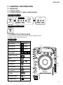
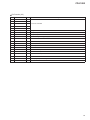
THIS MANUAL IS APPLICABLE TO THE FOLLOWING MODEL(S) AND TYPE(S).
Type
Model
Power Requirement
Remarks
CDJ-1000
KUC
O
AC120V
TL
O
AC110- 240V
WY
O
AC220- 240V
CONTENTS
1. SAFETY INFORMATION ....................................... 2
2. EXPLODED VIEWS AND PARTS LIST ................. 4
3. BLOCK DIAGRAM AND SCHEMATIC DIAGRAM 12
4. PCB CONNECTION DIAGRAM ........................... 38
5. PCB PARTS LIST ................................................ 52
6. ADJUSTMENT ..................................................... 57
7. GENERAL INFORMATION .................................. 59
7.1 DIAGNOSIS ................................................... 59
7.1.1 SERVICE MODE .................................. 59
7.1.2 ERROR DISPLAY ................................. 61
7.1.3 DISASSEMBLY ..................................... 62
7.1.4 PART REPLACEMENT METHOD OF JOG
SECTION ............................................... 66
7.1.5 ABOUT ELECTRIC DISCHARGE .......... 69
7.1.6 SEQUENCE AFTER THE POWER ON . 70
7.2 PARTS .......................................................... 71
7.2.1 IC ........................................................... 71
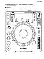
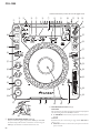
8. PANEL FACILITIES AND SPECIFICATIONS ....... 87
PIONEER ELECTRONIC CORPORATION
4-1, Meguro 1-chome, Meguro-ku, Tokyo 153-8654, Japan
PIONEER ELECTRONICS SERVICE, INC. P.O. Box 1760, Long Beach, CA 90801-1760, U.S.A.
PIONEER ELECTRONIC NV Haven 1087, Keetberglaan 1, 9120 Melsele, Belgium
PIONEER ELECTRONICS ASIACENTRE PTE. LTD. 253 Alexandra Road, #04-01, Singapore 159936
c PIONEER ELECTRONIC CORPORATION 2001
T – ZZY JULY 2001 Printed in Japan
CDJ-1000
1. SAFETY INFORMATION
This service manual is intended for qualified service technicians; it is not meant for the casual
do-it-yourselfer. Qualified technicians have the necessary test equipment and tools, and have been
trained to properly and safely repair complex products such as those covered by this manual.
Improperly performed repairs can adversely affect the safety and reliability of the product and may
void the warranty. If you are not qualified to perform the repair of this product properly and safely, you
should not risk trying to do so and refer the repair to a qualified service technician.
WARNING
This product contains lead in solder and certain electrical parts contain chemicals which are known to the state of California to
cause cancer, birth defects or other reproductive harm.
Health & Safety Cod e Section 25249.6 – Proposition 65
NOTICE
(FOR CANADIAN MODEL ONLY)
Fuse symbols
(fast operating fuse) and/or
(slow operating fuse) on PCB indicate that replacement parts
must be of identical designation.
REMARQUE
(POUR MODÈLE CANADIEN SEULEMENT)
Les symboles de fusible
(fusible de type rapide) et/ou
(fusible de type lent) sur CCI indiquent que les
pièces de remplacement doivent avoir la même désignation.
(FOR USA MODEL ONLY)
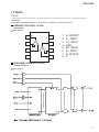
1. SAFETY PRECAUTIONS
The following check should be performed for the
continued protection of the customer and service
technician.
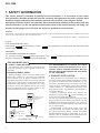
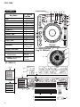
LEAKAGE CURRENT CHECK
Measure leakage current to a known earth ground
(water pipe, conduit, etc.) by connecting a leakage
current tester such as Simpson Model 229-2 or
equivalent between the earth ground and all exposed
metal parts of the appliance (input/output terminals,
screwheads, metal overlays, control shaft, etc.). Plug
the AC line cord of the appliance directly into a 120V
AC 60 Hz outlet and turn the AC power switch on. Any
current measured must not exceed 0.5 mA.
Leakage
current
tester
Device
under
test
Reading should
not be above
0.5 mA
Test all exposed
metal surfaces
Also test with plug
reversed
(Using AC adapter
plug as required)
Earth ground
AC Leakage Test
2
ANY MEASUREMENTS NOT WITHIN THE LIMITS
OUTLINED ABOVE ARE INDICATIVE OF A POTENTIAL SHOCK HAZARD AND MUST BE CORRECTED BEFORE RETURNING THE APPLIANCE
TO THE CUSTOMER.
2. PRODUCT SAFETY NOTICE
Many electrical and mechanical parts in the appliance have special safety related characteristics. These
are often not evident from visual inspection nor the
protection afforded by them necessarily can be obtained by using replacement components rated for
voltage, wattage , etc. Replacement parts which have
these special safety characteristics are identified in
this Service Manual.
Electrical components having such features are
identified by marking with a
on the schematics and
on the parts list in this Service Manual.
The use of a substitute replacement component which
does not have the same safety characteristics as the
PIONEER recommended replacement one, shown in
the parts list in this Service Manual, may create shock,
fire, or other hazards.
Product Safety is continuously under review and
new instructions are issued from time to time. For
the latest information, always consult the current
PIONEER Service Manual. A subscription to, or additional copies of, PIONEER Service Manual may be
obtained at a nominal charge from PIONEER.
CDJ-1000
IMPORTANT
THIS PIONEER APPARATUS CONTAINS
LASER OF CLASS 1.
SERVICING OPERATION OF THE APPARATUS
SHOULD BE DONE BY A SPECIALLY
INSTRUCTED PERSON.
LASER DIODE CHARACTERISTICS
MAXIMUM OUTPUT POWER: 5 mW
WAVELENGTH: 780 – 785 nm
WARNING !
The AEL(accessible emission level) of the laser power output is less then CLASS 1
but the laser component is capable of emitting radiation exceeding the limit for
CLASS 1.
A specially instructed person should servicing operation of the apparatus.
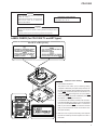
LABEL CHECK (for CDJ-1000/ TL and WY types)
CDJ-1000/ TL and WY Types Only
Additional Laser Caution
Bottom Plate
Printed on the Bottom Plate
1. Laser Interlock Mechanism
The position of the switch (S1) for detecting loading
completion is detected by the system microprocessor, and
the design prevents laser diode oscillation when the switch
is not in LPS1 terminal side (when the mechanism is not
clamped and LPS1 signal is high level.) Thus, the interlock
will no longer function if the switch is deliberately set to LPS1
terminal side. ( if LPS1 signal is low level ).
In the test mode∗ the interlock mechanism will not function.
Laser diode oscillation will continue, if pin 33 of CXA1782CQ
(IC101) on the MOTHER BOARD ASSY is connected to
GND, or pin 43 of IC701 (LDON) is connected to low level
(ON), or else the terminals of Q101 are shorted to each
other (fault condition).
2. When the cover is opened, close viewing of the objective
lens with the naked eye will cause exposure to a Class 1
laser beam.
∗ : Refer to page 57.
3
CDJ-1000
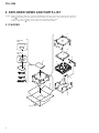
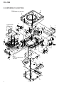
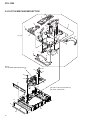
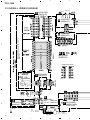
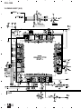
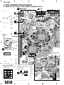
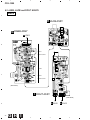
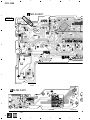
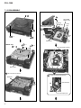
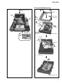
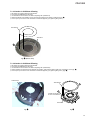
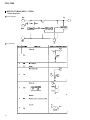
2. EXPLODED VIEWS AND PARTS LIST
NOTES:
• Parts marked by "NSP" are generally unavailable because they are not in our Master Spare Parts List.
• The mark found on some component parts indicates the importance of the safety factor of the part.
Therefore, when replacing, be sure to use parts of identical designation.
• Screws adjacent to mark on the product are used for disassembly.
2.1 PACKING
9
KUC Type
Only
2
10
WY Type
Only
16
17
14
11
7
13
4
6
5
3
1
12
8
15
4
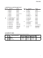
CDJ-1000
(1) PACKING PARTS LIST
Mark No.
Description
Part No.
1
2
3
4
5
Power Cord
Warranty Card
Forced Eject Pin
Operating Instructions
Control Cord (L= 1m)
See Contrast table (2)
See Contrast table (2)
DEX1013
See Contrast table (2)
PDE1247
6
7
Audio Cable (L = 1.5m)
Polyethylene Bag
(0.03 × 230 × 340)
Pad (A)
Pad (B)
VDE1033
Z21-038
NSP
10
11
12
13
14
Pad (C)
Pad (D)
Packing Case
Sheet
Mini Catalogue
DHA1523
DHA1524
See Contrast table (2)
RHX1006
See Contrast table (2)
NSP
NSP
NSP
15
16
17
Label
Pamphlet
MMC Catalog
See Contrast table (2)
See Contrast table (2)
See Contrast table (2)
NSP
NSP
8
9
DHA1518
DHA1519
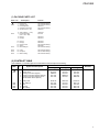
(2) CONTRAST TABLE
CDJ-1000/KUC, TL and WY types are constructed the same except for the following :
Mark
NSP
NSP
NSP
NSP
NSP
No.
1
2
4
4
4
12
14
15
16
17
Symbol and Description
Part No.
KUC Type
TL Type
WY Type
Power Cord
Warranty Card
Operating Instructions (English)
Operating Instructions (English/ Spanish)
Operating Instructions (English/ French
/German/ Italian/ Dutch/ Spanish)
ADG7021
ARY7043
DRB1297
Not used
Not used
ADG1154
Not used
Not used
DRB1299
Not used
ADG1154
Not used
Not used
Not used
DRB1298
Packing Case
Mini Catalogue
Label
Pamphlet
MMC Catalog
DHG2145
Not used
VRW1629
Not used
Not used
DHG2146
Not used
Not used
Not used
Not used
DHG2129
DRY1194
Not used
DRY1188
DRY1195
Remarks
5
CDJ-1000
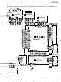
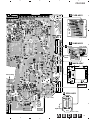
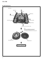
2.2 EXTERIOR (1/2) SECTION
48
Refer to
"2.3 EXTERIOR (2/2) SECTION".
40
TL and WY Type
Only
30
F
47
45
46
47
39
Q
47
47
44
25
47
P
6
47
10
47
32
15
23
33
11
47
5
26
33
17
J
8
E
25
C
13
B
3
18
25
33
G
47
F
33
47
37
47
14
B
47
47
4
47
27
47
G
36
Refer to
"2.4 SLOT-IN MECHANISM
SECTION".
48
24
35
47
A
J
K
I
47
H
12
19
47
G
L
1
21
A
22
C
D
E
F
20 B
16
41
43
48
41
42
48
D
7
31
I
9
37
L
34
48
47
25
6
M
H
E
K
49
D
38
M
C
47
I
H
2
29
47
28
A
CDJ-1000
(1) EXTERIOR (1/2) SECTION PARTS LIST
Mark No.
Description
Part No.
Mark No.
Description
Part No.
26
27
28
29
30
Earth Spring
Chassis
Rear Panel
Heat Sink
Power Knob
DBH1398
DNK3869
See Contrast table (2)
DNG1081
DAC1895
1
2
3
4
5
MAIN Assy
MMCB Assy
SPCN Assy
STCN Assy
SLMB Assy
DWX2161
DWX2169
DWX2170
DWX2171
DWX1309
6
7
8
9
10
PSWB Assy
DABB Assy
JACB Assy
DOUT Assy
FLRB Assy
See Contrast table (2)
DWX2162
DWX2163
DWX2164
DWX2166
31
32
33
34
35
Front Plate
Cord Clamper
Damper
Earth Plate (CU)
Shield Case
DNH2480
RNH-184
CNV6011
VBK1070
DNH2481
11
12
13
14
15
SW POWER SUPPLY Assy
25P Flexible Cable/60V
12P Flexible Cable/60V
4P Flexible Cable/60V
Earth Lead Unit/300V
DWR1344
DDD1189
DDD1190
DDD1191
DDF1015
36
37
38
39
40
Shield Cushion
Insulator Assy
Memory Holder
Flap Spring
SD Flap
DEC2445
DXA1904
DNK3884
DBH1487
DNK3883
16
17
18
19
20
Connector Assy 3P
Connector Assy 3P
FPC D5 Slot
Jumper Wire 03P
Jumper Wire 05P
DKP3546
DKP3548
DNP1951
D20PYY0310E
D20PYY0510E
NSP
41
42
43
44
45
Silicone Rubber D5L
Bottom Plate
Bottom Cushion
Mecha Plate
Caution Label
DEB1456
DNH2479
DEC2444
DNH2339
See Contrast table (2)
21
22
23
24
25
Jumper Wire 09P
Jumper Wire 15P
Connector Assy
Connector Assy
Float Spring (G5)
D20PYY0910E
D20PYY1510E
PF03PP-B30
PG07KK-F15
DBH1485
NSP
46
47
48
49
Caution Label HE
Screw
Screw
Screw
See Contrast table (2)
BPZ30P080FZK
BBZ30P060FZK
BBZ30P120FZK
NSP
(2) CONTRAST TABLE
CDJ-1000/KUC, TL and WY types are constructed the same except for the following :
Mark
NSP
NSP
No.
6
28
45
46
Symbol and Description
PSWB Assy
Rear Panel
Caution Label
Caution Label HE
Part No.
KUC Type
TL Type
WY Type
DWS1312
DNC1576
Not used
Not used
DWS1311
DNC1577
VRW1094
VRW1297
DWS1311
DNC1567
VRW1094
VRW1297
Remarks
7
CDJ-1000
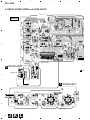
17
2.3 EXTERIOR (2/2) SECTION
16
8
42
7 (1/3)
20
44
21
*1
9
43
25 (2/2)
41
*1
22
*1
10
23
K
45
7 (3/3) × 8
30
4
31
11
E
29
45
L
24
2
C
26
45
27
M
45
E
36
28
34
33
25 (1/2)
45
40 45
45
37
D
45
10
35
14
18
32 19
7 (2/3)
3
C
45
J
45
A
D
B
45
39
38
*
1
13
12
1
45
45
6
O
A
45
B
45 39
* 1 Lubricant : ZLB-HFD1600 (GEM1038)
N
15
46
45
8
5
45
CDJ-1000
• EXTERIOR (2/2) SECTION PARTS LIST
Mark No.
1
2
3
4
5
NSP
Description
Part No.
MFLB Assy
KSWB Assy
SLDB Assy
RSWB Assy
JFLB Assy
DWG1548
DWS1307
DWS1308
DWS1310
DWG1549
6
7
8
9
10
JOGB Assy
JOG Sheet Assy
JOG Dial A
JOG Dial B
Screw
DWG1550
DXB1757
DNK3870
DNK3871
PBA1062
11
12
13
14
15
Encoder Plate
JOG Holder
JOG Stay Assy
Sheet SW
Encoder Guide
DEC2425
DNK3872
DXB1760
DSX1057
DNK3873
16
17
18
19
20
JOG Plate
JOG Panel
VR Stay
Flange Nut (M9)
Control Panel
DAH2052
DAH2051
DNF1663
DBN1004
DNK3875
21
22
23
24
25
Eject Guard
Card Lens
Ring Lens
Set Knob (PLAY) Assy
Mode Lens
DNK3958
DNK3885
DNK3880
DXB1750
DNK3881
26
27
28
29
30
Set Knob (HS)
Set Knob (LOOP)
Re-loop Knob
Set Knob (TIME)
Tempo Reset Knob
DAC1986
DAC1995
DAC1992
DAC1991
DAC1993
31
32
33
34
35
Tempo Lens
Set Knob (MT)
Mode Select Knob
Set Knob (SC)
Eject Knob
DNK3882
DAC1987
DAC1989
DAC1988
DAC1990
36
37
38
39
40
Set Knob (MEMO)
Slide SW Knob
Earth Plate (CU)
Cord Clamper
Card Plate
DAC1994
DAC1926
VBK1070
Z09-061
DBK1212
41
42
43
44
45
Slide Sheet 1C
Display Panel
Slide Knob
Rotary Knob C
Screw
DAH1988
DAH2022
DNK2936
DAA1143
BPZ30P080FZK
46
Screw
BPZ20P120FMC
9
CDJ-1000
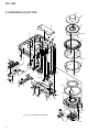
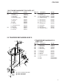
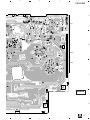
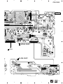
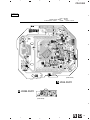
2.4 SLOT-IN MECHANISM SECTION
*3
7
17
5
11
15
3
14
*3
6
10
18
12
9
* 2.
8
4
13
16
Refer to
"2.5 TRAVERSE MECHANISM ASSY-S".
19
*3
1
2
29
26
26
25
26
25
27
28
Dyefree : ME-913A (ZLX-ME413A)
* 2.
3.
Grease : ZLB-PN397B
*
22
21
20
23
21
10
CDJ-1000
• SLOT-IN MECHANISM SECTION PARTS LIST
Mark No.
NSP
1
2
3
4
5
NSP
Description
Part No.
Mark No.
DC Motor
Connector Assy
Clamp Spring
Guide Spring
SW Lever Spacer (PET)
DXM1093
PF02PY-B32
DBH1374
DBH1375
DEC2420
6
7
8
9
10
Loading Lever
Main Cam
Lever B
Lever A
Clamp Arm
11
12
13
14
15
Loading Base Assy-S
Eject Lever
Worm Gear
Loading Gear
Drive Gear
Description
Part No.
16
17
18
19
20
Disc Guide
Clamper D4 Assy
Slot-in Mechanism G5 Assy
Traverse Mechanism Assy-S
Float Base (G5) Assy
DNK3914
DXA1881
DXA1906
DXX2502
DXB1748
DNK3406
DNK3407
DNK3558
DNK3564
DNK3576
21
22
23
24
25
Vessel Cushion C
Vessel Cushion A
Vessel Cushion B
•••••
Float Rubber D3
DEC2424
DEC2257
DEC2258
DEA1022
DNK3684
DNK3910
DNK3911
DNK3912
26
27
28
29
Float Fastener
Front Sheet
Spacer POR (T3)
Loading Motor Assy-S
DBA1139
DED1132
DEB1467
DEA1008
NSP
DEB1404
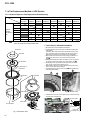
2.5 TRAVERSE MECHANISM ASSY-S
• TRAVERSE MECHANISM ASSY-S
12
PARTS LIST
2
Mark No.
*5
10
3
5
9
4
*4
6
*5
*6
Spindle Motor
Stepping Motor
Pickup Assy
Adjust Screw
Precision Screw
DXM1138
DXM1142
VWY1069
DBA1119
DBA1124
NSP
NSP
NSP
NSP
NSP
6
7
8
9
10
Skew Spring
Joint Spring
Guide Shaft
Slider G4
Mechanism Frame G5
DBH1437
DBK1188
DLA1840
DNK3733
DNK3776
NSP
11
12
13
Joint
Screw
Screw
DNK3777
BPZ20P080FMC
BPZ26P080FMC
11
*4
8
1
2
3
4
5
Part No.
7
6
8
NSP
NSP
NSP
NSP
NSP
Description
4
5
1
13
Screw Lock #300UB: ZBA-300UB
* 4.
ZLB-PN397B
5.
* 6. Grease:
* Grease: ZLB-PN948P
11
1
2
3
4
CDJ-1000
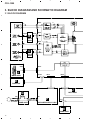
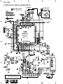
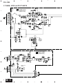
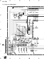
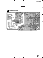
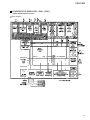
3. BLOCK DIAGRAM AND SCHEMATIC DIAGRAM
3.1 BLOCK DIAGRAM
A
CN800
(RF)
(RF)
(RF)
(FS)
(TS)
CN911
CN912
B
(SM)
CN900
(SM)
(SM)
SPCN
ASSY
CN302
(LM)
B
(LM)
CN913
C
(CM)
CN914
CN950
(CM)
STCN
ASSY
CN99
CN202
F
C
CN102
MMCB ASSY
CN101
CN203
CN1501
D
FLRB ASSY
CN2217
CN1101
Q
AN1
CN1
P
J1701
SW POWER SUPPLY ASSY
PSWB ASSY
D
J
MFLB ASSY
J1701
K
RSWB ASSY
12
1
2
3
4
5
6
7
8
CDJ-1000
A
SIGNAL ROUTE
(D)
: DIGITAL SIGNAL
(PB)
(TS)
: PB SIGNAL
(RF)
(FS)
(SM)
: RF SIGNAL
(CM)
(LM)
: FOCUS SERVO LOOP LINE
: TRACKING SERVO LOOP LINE
: SPINDLE MOTOR ROUTE
: CARRIAGE MOTOR ROUTE
: LOADING MOTOR ROUTE
CN1801
CN12
JA1801
(D)
(D)
(D)
Digital Out
(D)
CN13
S1801
CN1802
Digital Out
ON/OFF
I
J1801
DOUT ASSY
B
CN1904
JA1901
Control Jack
CN11
(PB)
(PB)
BKB1017
(PB)
CN1901
G
CN1902
CN1903
H
DABB
ASSY
JACB
ASSY
A MAIN ASSY
C
O
JOGB ASSY
CN1102
J1601
J1202
J1601
CN1201
J1101
J1103
N
CN1401
JFLB ASSY
D
Sheet SW
CN1301
M
L
SLDB ASSY
KSWB ASSY
13
5
6
7
8
1
2
3
4
CDJ-1000
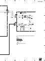
3.2 OVERALL WIRING DIAGRAM
B
A
CONTROL
SPCN ASSY
(DWX2170)
AUDIO OUT
ASSY
H JACB
(DWX2163)
(WHT)
(WHT)
TRAVERSE MECHANISM ASSY-S
DXX2502
G
B
DABB ASSY
(DWX2162)
A A 1/4 - A 4/4
MAIN ASSY
(DWX2161)
CONNECTOR FOR I/F
ASSY
C STCN
(DWX2171)
C
(FOR IC300)
(FOR IC201)
Q
PSWB ASSY
(KUC
: DWS1312)
(TL, WY : DWS1311)
E
SLMB ASSY
(DWS1309)
D
POWER
P SW
SUPPLY ASSY
(DWR1344)
EARTH LUG ASSY
DDF1015
AN1
KUC:
AKP7032
TL, WY: BKP1046
AC POWER CORD
KUC : ADG7021
TL, WY : ADG1154
14
1
2
3
4
5
6
7
8
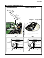
CDJ-1000
Note : When ordering service parts, be sure to refer to "EXPLODED VIEWS and PARTS LIST" or "PCB PARTS LIST".
DIGITAL OUT
ON/OFF
DIGITAL OUT
MMC CARD CONNECTOR
A
DOUT ASSY
(DWX2164)
I
ASSY
F MMCB
(DWX2169)
ASSY
L KSWB
(DWS1307)
(GRN)
ASSY
M SLDB
(DWS1308)
(GRN)
B
J J 1/2, J 2/2
MFLB ASSY
(DWG1548)
C
ASSY
K RSWB
(DWS1310)
ASSY
N JFLB
(DWG1549)
ASSY
D FLRB
(DWX2166)
ASSY
O JOGB
(DWG1550)
SHEET SW
DSX1057
D
15
5
6
7
8
1
2
3
4
CDJ-1000
3.3 MAIN (1/4), SPCN and STCN ASSYS
ASSY
A 1/4 MAIN
(DWX2161)
A 2/4
To PICKUP ASSY CN801
A
6
(FS)
4
(TS)
A 2/4
B
Q800
DTC124EUA
A 2/4
Q600
2SA1577
A 2/4
(TS)
(FS)
A 2/4
C
(L)
A 2/4
(L)
(L)
13
12
5
7
Q950
DTC124EUA
(FS)
A 2/4
(TS)
A 2/4
(FS)
D
16
A 1/4
1
2
3
4
5
6
7
8
CDJ-1000
(L)
(FS)
(TS)
: RF SIGNAL ROUTE
: LOADING MOTOR SIGNAL ROUTE
: FOCUS SERVO SIGNAL ROUTE
: TRACKING SERVO SIGNAL ROUTE
A
A 3/4
B
11
10 18 19
Q701
DTC124EUA
(L)
(TS)
(TS)
(FS)
(FS)
A 2/4
A 2/4
C
A 2/4
To
SPINDLE
MOTOR
(CN2220)
ASSY
C STCN
(DWX2171)
To
STEPPING
MOTOR
ASSY
B SPCN
(DWX2170)
D
NOTES
ALL RESISTORS ARE IN Ω
RS1/16S∗∗∗J
ALL CAPACITORS ARE IN µF
YF
: CKSRYF
CH
: CCSRCH
OTHERS : CKSRYB
: CEHAR
5
6
7
A 1/4 B C
8
17
1
2
3
4
CDJ-1000
3.4 MAIN (2/4), FLRB and SLMB ASSYS
A
NOTES
ASSY
A 2/4 MAIN
(DWX2161)
E
SLMB ASSY
(DWS1309)
A 1/4
ALL RESISTORS ARE IN Ω
RS1/16S∗∗∗J
ALL CAPACITORS ARE IN µF
YF
: CKSRYF
CH
: CCSRCH
OTHERS : CKSRYB
: CEHAR
To LOADING
MOTOR
A 1/4
DIODE
SLMB ASSY
S1501 : CLAMP SW
S1502 : CLAMP SW
: 1SS355
A 3/4
A 1/4
B
A 1/4
MECHA.
CONTROL
CPU
A 1/4
A 4/4
C
Q301
DTC124EUA
A 1/4
D
A 1/4
FLRB ASSY
(DWX2166)
D
CAUTION : FOR CONTINUED PROTECTION AGAINST
RISK OF FIRE, REPLACE ONLY WITH
SAME TYPE NO. ICP-N20, MFD BY ROHM
CO., LTD. FOR IC101 AND IC104.
18
A 2/4 D E
1
P
2
CN2217
3
4
5
6
7
8
CDJ-1000
: The power supply is shown with the marked box.
A 3/4
A
A 3/4,4/4
Q201
DTC124EUA
A 3/4
1
B
Q202
DTA124EUA
SYSTEM
CONTROL
CPU
A 3/4
3 2
A 3/4
A 3/4
C
A 4/4
F
CN99
Q203
Q204
2SC4081
Q203
DTC124EUA
J 1/2
CAUTION : FOR CONTINUED PROTECTION AGAINST
RISK OF FIRE, REPLACE ONLY WITH
SAME TYPE NO. ICP-N15, MFD BY ROHM
CO., LTD. FOR IC102 AND IC103.
5
D
CN1101
CAUTION : FOR CONTINUED PROTECTION AGAINST
RISK OF FIRE, REPLACE ONLY WITH
SAME TYPE NO. ICP-N25, MFD BY ROHM
CO., LTD. FOR IC105.
6
CAUTION : FOR CONTINUED PROTECTION AGAINST
RISK OF FIRE, REPLACE ONLY WITH
SAME TYPE NO. ICP-N10, MFD BY ROHM
CO., LTD. FOR IC106.
7
A 2/4
8
19
1
2
3
4
CDJ-1000
3.5 MAIN (3/4) and MMCB ASSYS
A
17
A 3/4 MAIN ASSY (DWX2161)
A 2/4
A 2/4
A 3/4,4/4
A 2/4
A 2/4
A 2/4
B
C
A 4/4
14
16
15
A 1/4
A 2/4
D
20
A 3/4
1
2
3
4
5
6
7
8
CDJ-1000
: The power supply is shown with the marked box.
A
NOTES
ALL RESISTORS ARE IN Ω
RS1/16S∗∗∗J
ALL CAPACITORS ARE IN µF
YF
: CKSRYF
CH
: CCSRCH
OTHERS : CKSRYB
: CEHAR
A 2/4,4/4
Q11
DTA124EUA
(D)
: PB AUDIO SIGNAL ROUTE
: DIGITAL DATA SIGNAL ROUTE
(D)
A 4/4
G CN1901
B
(GUARD GND)
C
CN1801
I
CN1802
A 2/4
MMC CARD CONNECTOR
I
A 4/4
A 2/4
CN202
(BODY GND)
5
6
D
F
7
MMCB ASSY
(DWX2169)
A 3/4 F
8
21
1
2
3
4
CDJ-1000
3.6 MAIN ASSY (4/4)
A 2/4,3/4
A
A 2/4
INVERTER
5V → 3.3V BUFFER
A 3/4
B
C
A 3/4
A 2/4,3/4
D
A 3/4
22
A 4/4
1
2
3
4
5
6
7
8
CDJ-1000
A 4/4 MAIN ASSY (DWX2161)
: The power supply is shown with the marked box.
A
(D)
: DIGITAL DATA SIGNAL ROUTE
NOTES
ALL RESISTORS ARE IN Ω
RS1/16S∗∗∗J
ALL CAPACITORS ARE IN µF
YF
: CKSRYF
CH
: CCSRCH
OTHERS : CKSRYB
: CEHAR
B
C
(D)
A 3/4
D
(D)
5
6
A 3/4
7
A 4/4
8
23
1
2
3
4
CDJ-1000
3.7 DABB, JACB and DOUT ASSYS
G
A
DABB ASSY
(DWX2162)
NJM4580D
A 3/4
Q1903
2SD2144S
CN11
Q1901
2SD2144S
Q1904
2SD2144S
Q1902
2SD2144S
NJM4580D
B
Q1905
DTC124EUA
Q1907
2SA1145
Q1906
DTA124EUA
C
I
DOUT ASSY
(DWX2164)
A 3/4
CN12
DIGITAL
OUT
DIGITAL OUT
ON/OFF
A 3/4
CN13
D
24
G I
1
2
3
4
5
6
7
8
CDJ-1000
A
H
JACB ASSY
(DWX2163)
AUDIO
OUT
B
CONTROL
: The power supply is shown with the marked box.
C
NOTES
ALL RESISTORS ARE IN Ω
RS1/16S∗∗∗J
ALL CAPACITORS ARE IN µF
YF
: CKSRYF
CH
: CCSRCH
OTHERS : CKSRYB
: CEHAR
: PB AUDIO SIGNAL ROUTE
D
5
6
7
H
8
25
1
2
3
4
CDJ-1000
3.8 MFLB (1/2) and RSWB ASSYS
J 1/2 MFLB ASSY (DWG1548)
A
: The power supply is shown with the marked box.
J 2/2
DISPLAY
MICROCOMPUTER
B
A 2/4
CN203
C
D
M CN1401
26
J 1/2
1
2
N
3
J1202
4
5
6
7
8
CDJ-1000
SWITCHES
MFLB ASSY
S1101
:A
S1102
:B
S1103
:C
S1104
: DISPLAY
TEXT/WAVE
S1105
: TIME MODE
S1106
S1107
S1109
S1110
S1111
S1112
: 0 (EJECT)
: SELECT
VINYL – CDJ
: 2 CALL
: CALL 3
: MEMORY
: DELETE
S1113
: IN/REALTIME CUE
S1114
: LOOP OUT
S1115
: RELOOP/EXIT
S1116
: 2 WAVE
S1117
: WAVE 3
S1118
: EJECT LOCK
S1119
: SELECT
RSWB ASSY
S1701
: FWD – REV
A
Q1103
DTC124EUA
S1101-S1103,S1113-S1115 : DSG1063
S1104-S1107,S1109-S1112 : ASG7013
S1116,S1117,S1119
: ASG7013
Q1104
DTC124EUA
B
Q1106
DTC124EUA
Q1107
DTC124EUA
Q1108
DTC124EUA
Q1109
DTC124EUA
Q1101
DTC124EUA
Q1110
DTC124EUA
D1104-D1107:
EMAY3864X-HM
Q1111
DTC124EUA
Q1102
DTC124EUA
C
10k-B
10k-B
Q1112
DTA124EUA
J 2/2
L
5
CN1301
K
NOTES
ALL RESISTORS ARE IN Ω
RS1/16S∗∗∗J
ALL CAPACITORS ARE IN µF
YF
: CKSRYF
CH
: CCSRCH
OTHERS : CKSRYB
: CEHAR
6
7
RSWB ASSY
(DWS1310)
J 1/2 K
8
27
D
1
2
3
4
CDJ-1000
3.9 MFLB ASSY (2/2
A
J 2/2 MFLB ASSY (DWG1548)
J 1/2
J 1/2
Q1118
Q1117
Q1116
Q1008
Q1009
Q1010
B
Q1011
Q1012
FL INDICATOR TUBE
Q1013
Q1014
Q1015
Q1016
Q1017
Q1113
Q1114
C
Q1115
Q1007
J 1/2
Q1007-Q1017,Q1113-Q1118:
2SC4081
J 1/2
NOTES
ALL RESISTORS ARE IN Ω
RS1/16S∗∗∗J
ALL CAPACITORS ARE IN µF
YF
: CKSRYF
CH
: CCSRCH
OTHERS : CKSRYB
: CEHAR
D
28
J 2/2
1
2
3
4
5
6
7
8
CDJ-1000
3.10 KSWB and SLDB ASSYS
L
Q1301
DTA124EUA
A
KSWB ASSY
(DWS1307)
J 1/2
J1103
D1301-D1304,D1310
D1311,D1316,D1317
D1312-D1315
D1305-D1308
D1309
: EMAY3864X-HM
: EMAY3864X-HM
: SLR-342PC (KLM)
: SLR-343MC(NPQ)
: SLR-343VC
Q1302
DTA124EUA
Q1303
DTA124EUA
D1321-D1328: 1SS355
SWITCHES
KSWB ASSY
S1301
: CUE
S1302
:6
S1303
:4
S1304
:¢
S1305
:1
S1306
: ¡
B
ASSY
M SLDB
(DWS1308)
C
J 1/2
J1101
SWITCHES
SLDB ASSY
S1401
: TEMPO RESET
S1402
: MASTER TEMPO
S1403
: TEMPO RANGE
Q1401
DTA124EUA
Q1402
DTA124EUA
D
: The power supply is shown with the marked box.
5
6
7
LM
8
29
1
2
3
4
CDJ-1000
3.11 JFLB and JOGB ASSYS
N
A
JFLB ASSY (DWG1549)
FL HOLDER
DNK3959
FL INDICATOR TUBE
STBY
Q1215
2SB1237X
B
Q1201-Q1207
2SC2412K
IC1201
UPD16306B
DRIVER IC
Q1201
Q1202
Q1203
Q1204
Q1205
Q1206
Q1207
C
J 1/2
CN1102
D1201-D1208:
1SS355
D
30
N
1
2
3
4
5
6
7
8
CDJ-1000
A
Q1213
2SB1237X
R1299
R1298
Q1212
2SA933S
Q1214
2SC2412K
To SHEET SW
B
NOTES
ALL RESISTORS ARE IN Ω
RS1/16S∗∗∗J
ALL CAPACITORS ARE IN µF
YF
: CKSRYF
CH
: CCSRCH
OTHERS : CKSRYB
: CEHAR
C
O
JOGB ASSY
(DWG1550)
D
: The power supply is shown with the marked box.
5
6
7
NO
8
31
1
2
3
4
CDJ-1000
3.12 SW POWER SUPPLY and PSWB ASSYS
A
SUPPLY ASSY
P SW POWER
(DWR1344)
Q
PSWB ASSY
(KUC: DWS1312)
(WY, TL: DWS1311)
AN1
AC INLET
KUC : AKP7032
WY, TL : BKP1046
B
AC Power Cord
KUC : ADG7021
WY, TL : ADG1154
CAUTION: FOR CONTINUED PROTECTION
AGAINST RISK OF FIRE.
REPLACE ONLY WITH SAME
TIME AND RATINGS ONLY.
C
D
A
32
PQ
1
2
CN101
3
4
CDJ-1000
Waveforms
A 2/4 MAIN ASSY
Mode: Power ON
1
2
IC201- 63pin (XRST)
V: 2V/div. H: 20mS/div.
IC201- 19pin (XSRST)
V: 2V/div. H: 20mS/div.
A 1/4 MAIN ASSY
Mode: 1trak Jump
4
IC800- 18pin (TE)
V: 500mV/div. H: 500µS/div.
A 1/4 MAIN ASSY
A 3/4 MAIN ASSY
Mode: Search
8pin (ST1+)
12 IC950V: 5V/div. H: 20mS/div.
13 IC950- 6pin (ST2+)
Mode: Play
3pin (VCOOUT)
17 IC604V: 2V/div. H: 20nS/div.
V: 5V/div. H: 20mS/div.
1
8
12
17
2
13
A 2/4 MAIN ASSY
A 1/4 MAIN ASSY
1
3
IC201- 63pin (XRST)
V: 2V/div. H: 50mS/div.
IC201- 18pin (XFRST)
V: 2V/div. H: 50mS/div.
A 3/4 MAIN ASSY
A 1/4 MAIN ASSY
Mode: 3100rpm/ Inside Play
Mode: Power ON
Mode: Focus UP/Down
6
IC800- 22pin (FE)
V: 200mV/div. H: 500µS/div.
Mode: Play
162pin (SDATA)
14 IC601V: 2V/div. H: 1µS/div.
8pin (ARF)
18 IC700V: 200mV/div. H: 50nS/div.
19 IC700- 9pin (NARF)
V: 200mV/div. H: 50nS/div.
1
18
14
6
3
19
A 1/4 MAIN ASSY
A 1/4 MAIN ASSY
Mode: Search
4
5
IC800- 18pin (TE)
V: 1V/div. H: 200µS/div.
IC950- 11pin (T+)
V: 500mV/div. H: 200µS/div.
A 3/4 MAIN ASSY
Mode: Play
6pin (TEDRV)
10 IC700V: 200mV/div. H: 5µS/div.
Mode: Play
182pin (BCK)
15 IC601V: 2V/div. H: 500nS/div.
4
10
15
A 1/4 MAIN ASSY
A 3/4 MAIN ASSY
5
A 1/4 MAIN ASSY
Mode: Focus
6
7
IC800- 22pin (FE)
V: 1V/div. H: 50mS/div.
IC950- 13pin (F+)
V: 1V/div. H: 50mS/div.
Mode: Play
Mode: Play
5pin (FEDRV)
11 IC700IC601- 168pin (LRCK)
V: 100mV/div. H: 20mS/div. 16 V: 2V/div. H: 5µS/div.
6
16
7
11
33
CDJ-1000
Waveforms (1/4)
A 1/4 MAIN ASSY
IC700 (MN677061ZY)
IC700 (MN677061ZY)
Pin No.
Pin No.
Voltage (V)
Pin No.
91
92
93
94
95
96
97
98
99
100
0 to 3.3
0
0
0 to 3.3
0
2.5
1.65
1.65
1.65
2.2
1
2
3
4
14
15
16
17
18
19
20
21
22
23
24
25
26
27
28
29
30
31
32
33
34
35
36
37
38
39
40
41
42
43
44
45
46
47
48
49
50
51
52
53
54
55
56
57
58
59
60
61
62
63
64
1
2
3
4
5
6
7
8
9
10
11
12
13
14
15
16
17
18
19
20
21
22
23
24
25
26
27
28
29
30
31
32
33
34
35
36
37
38
39
40
41
42
43
44
45
46
47
48
49
50
51
52
53
54
55
56
57
58
59
60
61
62
63
64
65
66
67
68
69
70
71
72
73
74
75
76
77
78
79
80
81
82
83
84
85
86
87
88
89
90
34
Voltage (V)
2.2
1.65
1.65
3.3
1 to 2.2
1.65
0
1.65
1.65
1.65
1.65
1.65
1.65
3.3
1.65
0
0
2.2
1.2
0
1
1
1.65
0
0
0
3.3
0
0
0
0
0
0
1.65
1
0 to 1.65
0
3.3
0
0
0
1.65
1.65 to 3.3
1.65 to 3.3
0
3.3
0 to 3.3
0 to 3.3
0
0
0
0 to 3.3
0 to 3.3
0
0
0
0
2.5
0
0
0 to 3.3
0 to 3.3
0 to 3.3
0
0
0
0
0
0 to 3.3
0 to 3.3
0 to 3.3
0
0
0
3.3
0 to 3.3
0
0
0
0 to 3.3
0
3.3
0
0 to 5
5
0 to 5
0 to 3.3
0 to 5
0 to 5
0 to 3.3
IC701 (TC7WU04FU)
Pin No.
1
2
3
4
5
6
7
8
Voltage (V)
0 to 3.3
0 to 3.3
3.3
0
0
0.5 to 2.5
0 to 3.3
3.3
IC710 (TC7SET08FU)
Pin No.
1
2
3
4
5
Voltage (V)
0
0
0
0
3.3
IC711(TC7SET32FU)
Pin No.
1
2
3
4
5
Voltage (V)
0
0
0
0
3.3
A 2/4 MAIN ASSY
IC800 (AN8702NFH)
Voltage (V)
5
0
0
3.3
0 to 5
1.2
0
1.65
1 to 2
1.65
2 to 2.2
1.65
1.65
0
1.65
3.3
0
2.2
5
1.65
1.65 to 2.2
1.65 to 2.2
1.8
0
0
0
3.3
0
0
0 to 3.3
0
3.3
1.2
1.65
2.2
2.2
2.2
1.65 to 2.2
1.65 to 2.2
2.2
2.2
2.2
2.2
2.2
2.2
5
2.2
2.2
2.2
2.2
2.2
0
2.2
2.2
1.651
IC850 (BA10358F)
Pin No.
1
2
3
4
5
6
7
8
Voltage (V)
1.65
2.2
2.2
0
2.2
2.2
2.2
5
IC900 (LB11975)
IC100 (PQ2TZ15)
Pin No.
Pin No.
1
2
3
4
5
6
7
8
9
10
11
12
13
14
15
16
17
18
19
20
21
22
23
24
25
26
27
28
29
30
31
32
33
34
35
36
37
38
Voltage (V)
0 to 12
0 to 12
0 to 12
0 to 12
0
0
0
12
12
0
1.65 to 3.3
1.65 to 3.3
0
1.65
14.65
5
0
0
1.65
1.65
1.65
1.65
1.65
1.65
5
5
5
1.65
0
1.65
1.65
1.65
1.65
1.65
0
1.65
0
0
IC950(LA6562)
Pin No.
1
2
3
4
5
6
7
8
9
10
11
12
13
14
15
16
17
18
19
20
21
22
23
24
25
26
27
28
29
30
31
32
33
34
35
36
37
38
Voltage (V)
5
5
12
5
5
7.5
3.5
6.5
5
0
2 to 3.3
2 to 3.3
1.65 to 3.3
1.65 to 3.3
5
1 to 2
1.65
1.65
1.65
1.65
1.65
1.65
1.65
1.65
5
5
5
1.65
0
1.65
1.65
1.65
1.65
1.65
0
1.65
0
0
I 1
2
3
4
5
Voltage (V)
5
5
2.5
0
0
IC150 (PQ1R33)
Pin No.
1
2
3
4
5
6
Voltage (V)
5
0
1.2
3.3
0
5
IC202(BR24C64F)
Pin No.
1
2
3
4
5
6
7
8
Voltage (V)
0
0
0
0
5
5
0
5
IC203(TC74HC4053AFT)
Pin No.
1
2
3
4
5
6
7
8
9
10
11
12
13
14
15
16
Voltage (V)
5
0 to 5
5
0 to 5
0 to 5
0
0
0
0
0
0
0 to 5
5
0 to 5
0 to 5
5
IC204 (TC7SET08FU)
Pin No.
1
2
3
4
5
Voltage (V)
0 to 3.3
5
0
0 to 5
5
IC205 (TC74VHC08FT)
Pin No.
Voltage (V)
1
2
3
4
5
6
7
8
9
10
11
12
13
14
0
0
0
0 to 5
3.3
0 to 3.3
0
0 to 3.3
3.3
3.3
0 to 3.3
0 to 5
3.3
3.3
IC206(PQ1R33)
Pin No.
1
2
3
4
5
6
Voltage (V)
5
0
1.2
3.3
0
5
CDJ-1000
Waveforms (2/4)
A 2/4 MAIN ASSY
A 3/4 MAIN ASSY
IC300 (PD3431A9)
IC300 (PD3431A9)
IC600 (M51957BFP)
Pin No.
Pin No.
Voltage (V)
Pin No.
0
0
0 to 3.3
0 to 3.3
0 to 3.3
0 to 3.3
0 to 3.3
0 to 5
5
0 to 3.3
1
2
3
4
5
6
7
8
1
2
3
4
5
6
7
8
9
10
11
12
13
14
15
16
17
18
19
20
21
22
23
24
25
26
27
28
29
30
31
32
33
34
35
36
37
38
39
40
41
42
43
44
45
46
47
48
49
50
51
52
53
54
55
56
57
58
59
60
61
62
63
64
65
66
67
68
69
70
71
72
73
74
75
76
77
78
79
80
81
82
83
84
85
86
87
88
89
90
Voltage (V)
3.3
0 to 5
0
0
0
0 to 5
0 to 5
0
0
0
0
0 to 5
5
0 to 3.3
5
0 to 5
0
5
0 to 5
0 to 5
0 to 5
0
0
0
0
0 to 5
0 to 5
0 to 5
0 to 5
0 to 5
0 to 5
0 to 5
0 to 5
5
0 to 5
0 to 5
0 to 5
0 to 5
0 to 5
0 to 5
0
0
0
0
0
0
0
0
0
0
0
0
0
0
0 to 5
0 to 5
0
0
0
0 to 5
0
5
0 to 5
0
0
1.65 to 3.3
1.65 to 3.3
5
0
0 to 5
0 to 5
0
5
0
5
3.3
3.3
1.65
1.65
1.65
0 to 3.3
0
0 to 5
0 to 5
0 to 5
0
0 to 3.3
0 to 3.3
0 to 5
0
91
92
93
94
95
96
97
98
99
100
Voltage (V)
0
1.2
0
0
1.2
5
5
0
IC201 (PD3432A9)
Pin No.
Pin No.
Voltage (V)
76
77
78
79
80
81
82
83
84
85
86
87
88
89
90
91
92
93
94
95
96
97
98
99
100
5
5
2.5
2.5
0
0
0
0
0
0
0
0 to 5
0 to 5
0 to 3.3
0
0
0
0 to 5
0 to 5
0 to 5
0 to 5
5
0
0 to 5
0 to 3.3
1
2
3
4
5
6
7
8
9
10
11
12
13
14
15
16
17
18
19
20
21
22
23
24
25
26
27
28
29
30
31
32
33
34
35
36
37
38
39
40
41
42
43
44
45
46
47
48
49
50
51
52
53
54
55
56
57
58
59
60
61
62
63
64
65
66
67
68
69
70
71
72
73
74
75
3.3
0 to 5
0 to 5
0 to 5
0 to 5
0 to 5
0 to 5
0 to 5
0 to 5
0
0
0 to 5
0 to 5
0 to 5
0 to 5
0 to 5
0 to 5
0 to 5
0 to 5
0 to 5
0
0
0
5
0 to 5
0
0 to 5
0 to 5
0 to 5
0 to 5
0 to 5
0 to 5
0 to 5
0 to 5
5
0 to 5
0 to 5
0 to 5
0 to 5
0 to 5
0
0
0
0
0
0
0
0
0
0
0
0
0
0
0 to 5
0 to 5
0
0
0 to 5
0 to 3.3
0
5
0 to 5
0
0
1.65 to 3.3
1.65 to 3.3
5
0
0 to 5
0 to 5
0
5
0
5
IC610 (TC7SH08FU)
Voltage (V)
Pin No.
Voltage (V)
Pin No.
1
2
3
12
0
5
1
2
3
4
5
6
7
8
9
10
11
12
13
14
15
16
17
18
19
20
21
22
23
24
25
26
27
28
29
30
31
32
33
34
35
36
37
38
39
40
41
42
43
44
45
46
47
48
49
50
51
52
53
54
3.3
0 to 3.3
3.3
0 to 3.3
0 to 3.3
0
0 to 3.3
0 to 3.3
3.3
0 to 3.3
0 to 3.3
0
0 to 3.3
3.3
0
0 to 3.3
0 to 3.3
0 to 3.3
0
0
0
0 to 3.3
0 to 3.3
0 to 3.3
0 to 3.3
0 to 3.3
3.3
0
0 to 3.3
0 to 3.3
0 to 3.3
0 to 3.3
0 to 3.3
0 to 3.3
0 to 3.3
0
2 to 2.2
0 to 3.3
0
0
0
0 to 3.3
3.3
0 to 3.3
0 to 3.3
0
0 to 3.3
0 to 3.3
3.3
0 to 3.3
0 to 3.3
0
0 to 3.3
0
1
2
3
4
5
IC10 (BA178M05EP)
IC11(PE8001A)
Pin No.
IC201 (PD3432A9)
Voltage (V)
IC606 (K4S641632D)
Pin No.
1
2
3
4
5
6
7
8
9
10
11
12
13
14
15
16
17
18
19
20
21
22
23
24
25
26
27
28
Voltage (V)
0 to 5
0 to 5
0 to 5
0
0 to 5
0
0
5
5
0
0
0
0
0
5
0
0
0
0
5
0 to 5
0 to 5
0
0
0
0 to 5
0 to 5
0 to 5
IC12 (TC74HCT7007AF)
Pin No.
Voltage (V)
1
2
3
4
5
6
7
8
9
10
11
12
13
14
0 to 3.3
0 to 5
0 to 3.3
0 to 5
0 to 3.3
0 to 5
0
0
0
0
0
0
0
5
IC607 (PQ2TZ15)
IC13 (TC7WU04FU)
Pin No.
1
2
3
4
5
6
7
8
Voltage (V)
0 to 5
0 to 5
0
0
0
0 to 5
0 to 5
5
Pin No.
Voltage (V)
1
2
3
4
5
3.3
3.3
2.5
0
0
Voltage (V)
5
3.3
0
3.3
3.3
IC611 (TC7SU04FU)
Pin No.
1
2
3
4
5
Voltage (V)
0
1.2 to 1.65
0
0 to 3.3
3.3
IC612 (TC7WU04FU)
Pin No.
Voltage (V)
1
2
3
4
5
6
7
8
0 to 3.3
0 to 3.3
0
0
0
0 to 3.3
0 to 3.3
3.3
IC602 (PE9012A)
Pin No.
1
2
Voltage (V)
0
0
IC604 (TLC2932IPW)
Pin No.
1
2
3
4
5
6
7
8
9
10
11
12
13
14
Voltage (V)
5
0
0 to 5
0
0
0
0
0
5
0
0
3.3
2.5
5
IC605(TC7WT241FU)
IC608(TC7WU04FU)
Pin No.
1
2
3
4
5
6
7
8
Voltage (V)
0.5 to 3.3
0 to 3.3
0
0
0 to 3.3
0 to 3.3
0 to 3.3
3.3
Pin No.
Voltage (V)
1
2
3
4
5
6
7
8
0
0
3.3 to 5
0
0 to 3.3
0
0
5
IC609 (NJM78L05UA)
Pin No.
Voltage (V)
1
2
3
5
0
12
35
CDJ-1000
Voltage (3/4)
A 3/4 MAIN ASSY
36
A 4/4 MAIN ASSY
IC601 (XC2S50-5PQ208C)
IC601 (XC2S50-5PQ208C)
IC401(XCA56367PV15)
IC404 (MM1561JF)
Pin No.
Voltage (V)
Pin No.
Voltage (V)
Pin No.
Voltage (V)
Pin No.
Voltage (V)
Pin No.
Voltage (V)
Pin No.
1
2
3
4
5
6
7
8
9
10
11
12
13
14
15
16
17
18
19
20
21
22
23
24
25
26
27
28
29
30
31
32
33
34
35
36
37
38
39
40
41
42
43
44
45
46
47
48
49
50
51
52
53
54
55
56
57
58
59
60
61
62
63
64
65
66
67
68
69
70
71
72
73
74
75
76
77
78
79
80
81
82
83
84
85
86
87
88
89
90
0
0
0 to 3.3
0 to 3.3
0 to 3.3
0 to 3.3
0 to 3.3
0 to 3.3
0 to 3.3
0 to 3.3
0
3.3
2.5
0 to 3.3
0 to 3.3
0 to 3.3
0 to 3.3
0 to 3.3
0
0 to 3.3
0 to 3.3
0 to 3.3
0 to 3.3
0 to 3.3
0
3.3
0 to 3.3
2.5
0 to 3.3
0 to 3.3
0 to 3.3
0
0 to 3.3
0 to 3.3
0 to 3.3
0 to 3.3
0 to 3.3
2.5
3.3
0
0 to 3.3
0 to 3.3
0 to 3.3
0 to 3.3
0 to 3.3
0 to 3.3
0 to 3.3
0 to 3.3
0 to 3.3
0
0
0
3.3
3.3
2.5
0
0 to 5
0 to 5
0 to 5
0 to 5
0 to 5
0 to 5
0 to 5
0
3.3
2.5
0 to 5
0 to 5
0 to 5
0 to 5
0 to 5
0
0 to 5
0
0
2.5
0 to 3.3
3.3
0
0 to 3.3
0
0
0 to 3.3
0 to 3.3
0
0
0 to 5
0 to 5
0 to 5
0
91
92
93
94
95
96
97
98
99
100
101
102
103
104
105
106
107
108
109
110
111
112
113
114
115
116
117
118
119
120
121
122
123
124
125
126
127
128
129
130
131
132
133
134
135
136
137
138
139
140
141
142
143
144
145
146
147
148
149
150
151
152
153
154
155
156
157
158
159
160
161
162
163
164
165
166
167
168
169
170
171
172
173
174
175
176
177
178
179
180
2.5
3.3
0
0
0
0
0
0
0
0
0
0 to 3.3
0
3.3
3.3
3.3
3.3
0 to 3.3
0 to 3.3
0 to 3.3
0 to 3.3
0 to 3.3
0 to 3.3
0 to 3.3
0 to 3.3
0
3.3
2.5
0 to 3.3
0 to 3.3
0 to 3.3
0 to 3.3
0 to 3.3
0
0 to 3.3
0 to 3.3
0 to 3.3
2.5
0
3.3
0
0 to 3.3
0 to 3.3
0 to 3.3
0 to 3.3
0 to 3.3
0
0 to 3.3
0 to 3.3
0 to 3.3
0 to 3.3
0 to 3.3
2.5
3.3
0
0
0
0
0
0
0
0
0 to 3.3
0
0 to 3.3
3.3
0
0
0
3.3
3.3
0 to 3.3
0 to 3.3
0 to 3.3
0 to 3.3
0 to 3.3
0 to 3.3
0 to 3.3
0
3.3
2.5
0
0
0
0
0 to 3.3
0
0 to 5
0 to 5
0
181
182
183
184
185
186
187
188
189
190
191
192
193
194
195
196
197
198
199
200
201
202
203
204
205
206
207
208
0
0 to 3.3
0
3.3
0 to 3.3
2.5
0 to 5
0 to 5
0 to 5
0
0 to 5
0 to 5
0 to 5
0 to 5
0 to 5
2.5
3.3
0
0 to 5
0 to 5
0 to 5
0 to 5
0 to 5
0 to 5
0
0 to 3.3
0
3.3
1
2
3
4
5
6
7
8
9
10
11
12
13
14
15
16
17
18
19
20
21
22
23
24
25
26
27
28
29
30
31
32
33
34
35
36
37
38
39
40
41
42
43
44
45
46
47
48
49
50
51
52
53
54
55
56
57
58
59
60
61
62
63
64
65
66
67
68
69
70
71
72
73
74
75
76
77
78
79
80
81
0 to 3.3
0 to 3.3
0 to 3.3
0 to 3.3
0 to 3.3
0 to 3.3
0 to 3.3
3.3
0 to 3.3
0 to 3.3
0 to 3.3
0 to 3.3
1.8
0 to 3.3
0 to 3.3
3.3
0 to 3.3
1.8
0
3.3
0
0
0 to 3.3
3.3
3.3
0
0 to 3.3
0 to 3.3
0 to 3.3
0 to 3.3
0
0
0
0
0
0
0
3.3
0
0
0
0
0
3.3
1.8
0 to 3.3
0
0
3.3
0
0
0
0
0
0 to 3.3
1.8
3.3
0
0
0
0
0
0
0 to 3.3
3.3
0
0 to 3.3
0 to 3.3
0
0
0 to 3.3
0 to 3.3
0 to 3.3
3.3
0
0 to 3.3
0 to 3.3
0 to 3.3
0 to 3.3
3.3
0
82
83
84
85
86
87
88
89
90
91
92
93
94
95
96
97
98
99
100
101
102
103
104
105
106
107
108
109
110
111
112
113
114
115
116
117
118
119
120
121
122
123
124
125
126
127
128
129
130
131
132
133
134
135
136
137
138
139
140
141
142
143
144
0 to 3.3
0 to 3.3
0
0
3.3
0
0
0
0
1.8
0
0
0
3.3
0
0
0 to 3.3
0 to 3.3
0 to 3.3
0
0
3.3
0
0
0
0
0
0
0 to 3.3
3.3
0
0 to 3.3
0 to 3.3
0 to 3.3
0 to 3.3
0 to 3.3
0 to 3.3
3.3
0
0 to 3.3
0 to 3.3
0 to 3.3
0 to 3.3
0 to 3.3
1.8
0
0 to 3.3
3.3
0
0 to 3.3
0 to 3.3
0 to 3.3
3.3
3.3
3.3
3.3
0
0
3.3
3.3
3.3
0 to 3.3
0 to 3.3
1 1.8
20
30
4 0.5
5 3.3
60
7 3.3
IC601 (XC2S50-5PQ208C)
IC401(XCA56367PV150)
IC402(TC7WU04FU)
Pin No.
Voltage (V)
1
2
3
4
5
6
7
8
0 to 3.3
0 to 3.3
0
0
3.3
0 to 3.3
0 to 3.3
3.3
IC403 ( TC7SET08FU)
Pin No.
Voltage (V)
1
2
3
4
5
0 to 3.3
5
0
0 to 5
5
Voltage (V)
IC405 (TC74VHC541FT)
Pin No.
Voltage (V)
1
2
3
4
5
6
7
8
9
10
11
12
13
14
15
0
0
0
5
0 to 5
0 to 5
0 to 5
0 to 5
0 to 5
0
3.3
0 to 3.3
0 to 3.3
0 to 3.3
3.3
IC406 (TC7SU04F)
Pin No.
Voltage (V)
1
2
3
4
5
0 to 5
0 to 5
0
0 to 3.3
3.3
IC407 (TC7S04FU)
Pin No.
1
2
3
4
5
Voltage (V)
0
0 to 3.3
0
0 to 3.3
3.3
IC506 (TC7SU04F)
Pin No.
Voltage (V)
1
2
3
4
5
0 to 5
0 to 5
0
0 to 3.3
3.3
CDJ-1000
Voltage (4/4)
A 4/4 MAIN ASSY
J 1/2 MFLB ASSY
N
IC501(XCA56367PV150)
IC501(XCA56367PV150)
IC1101 (PE5243A)
IC1101 (PE5243A)
IC1201 (UPD16036B)
Pin No.
Voltage (V)
Pin No.
Pin No.
Pin No.
Pin No.
1
2
3
4
5
6
7
8
9
10
11
12
13
14
15
16
17
18
19
20
21
22
23
24
25
26
27
28
29
30
31
32
33
34
35
36
37
38
39
40
41
42
43
44
45
46
47
48
49
50
51
52
53
54
55
56
57
58
59
60
61
62
63
64
65
66
67
68
69
70
71
72
73
74
75
76
77
78
79
80
81
82
83
84
85
86
87
88
89
90
0 to 3.3
0 to 3.3
0 to 3.3
0 to 3.3
0 to 3.3
0 to 3.3
0 to 3.3
3.3
0
0 to 3.3
0 to 3.3
0 to 3.3
0 to 3.3
0 to 3.3
0 to 3.3
0 to 3.3
0
1.8
0
3.3
0
0
3.3
0 to 3.3
3.3
0
0
0
0
0
0
0
0
0
0
0
0
3.3
0
0
0
0
0
0 to 3.3
1.8
0
0
0
3.3
0
0
0
0
0
0 to 3.3
1.8
3.3
0
0
0
0
0
0
3.3
3.3
0
0
0
0
0
0
0
0
3.3
0
0
0
0
0
3.3
0
0
0
0
0
3.3
0
0
0
0
91
92
93
94
95
96
97
98
99
100
101
102
103
104
105
106
107
108
109
110
111
112
113
114
115
116
117
118
119
120
121
122
123
124
125
126
127
128
129
130
131
132
133
134
135
136
137
138
139
140
141
142
143
144
Voltage (V)
1.8
0
0
0
3.3
0
0
0
0
0
0
0
3.3
0
0
0
0
0
0
0
3.3
0
0
0
0
0
0
0
3.3
0
0
0
0
0
0
1.8
0
0
3.3
0
0
0
0
0
3.3
0
3.3
0
0
3.3
3.3
3.3
0
0
1
2
3
4
5
6
7
8
9
10
11
12
13
14
15
16
17
18
19
20
21
22
23
24
25
26
27
28
29
30
31
32
33
34
35
36
37
38
39
40
41
42
43
44
45
46
47
48
49
50
51
52
53
54
55
56
57
58
59
60
61
62
63
64
65
66
67
68
69
70
71
72
73
74
75
76
77
78
79
80
81
82
83
84
85
86
87
88
89
90
Voltage (V)
5
0 to 5
0 to 5
0 to 5
0 to 5
0 to 5
0 to 5
0 to 5
0 to 5
0 to 5
0 to 5
0 to 5
0
0
0 to 5
5
0 to 5
0 to 5
0 to 5
0 to 5
0 to 5
0 to 5
0 to 5
0 to 5
0
0
0 to 5
0 to 5
0 to 5
0 to 5
0 to 5
0 to 5
0 to 5
5
5
0 to 5
0 to 5
0 to 5
0 to 5
0
0 to 5
0 to 5
0 to 5
0 to 5
0 to 5
5
-38.5 to 5
-38.5 to 5
-38.5 to 5
-38.5 to 5
-38.5 to 5
-38.5 to 5
-38.5 to 5
-38.5 to 5
-38.5 to 5
-38.5 to 5
-38.5 to 5
-38.5 to 5
-38.5 to 5
-38.5 to 5
-38.5 to 5
-38.5 to 5
-38.5 to 5
-38.5 to 5
-38.5 to 5
-38.5 to 5
-38.5 to 5
-38.5 to 5
-38.5 to 5
-38.5 to 5
-38.5 to 5
-38.5 to 5
-38.5 to 5
-38.5 to 5
-38.5 to 5
-38.5 to 5
-38.5 to 5
-38.5 to 5
-38.5 to 5
-38.5
-38.5 to 5
-38.5 to 5
-38.5 to 5
-38.5 to 5
-38.5 to 5
-38.5 to 5
-38.5 to 5
-38.5 to 5
-38.5 to 5
-38.5 to 5
91
92
93
94
95
96
97
98
99
100
Voltage (V)
-38.5 to 5
-38.5 to 5
-38.5 to 5
-38.5 to 5
-38.5 to 5
-38.5 to 5
-38.5 to 5
-38.5 to 5
-38.5 to 5
-38.5 to 5
1
2
3
4
5
6
7
8
9
10
11
12
13
14
15
16
17
18
19
20
21
22
23
24
25
26
27
28
29
30
31
32
33
34
35
36
37
38
39
40
41
42
43
44
45
46
47
48
49
50
51
52
53
54
55
56
57
58
59
60
61
62
63
64
65
66
67
68
69
70
71
72
73
74
75
76
77
78
79
80
81
82
83
84
85
86
87
88
89
90
JFLB ASSY
Voltage (V)
0
3.3
0
0
-38.5
0
0
-38.5 to 3.3
-38.5 to 3.3
-38.5 to 3.3
-38.5 to 3.3
-38.5 to 3.3
-38.5 to 3.3
-38.5 to 3.3
-38.5 to 3.3
-38.5 to 3.3
-38.5 to 3.3
-38.5 to 3.3
-38.5 to 3.3
-38.5 to 3.3
-38.5 to 3.3
-38.5 to 3.3
-38.5 to 3.3
0
-38.5 to 3.3
-38.5 to 3.3
-38.5 to 3.3
-38.5 to 3.3
-38.5 to 3.3
-38.5 to 3.3
3.3
0
0
-38.5
0
0
-38.5 to -33.5
-38.5 to -33.5
-38.5
0
-33.5
-33.5
-38.5 to -33.5
-38.5
-38.5 to -33.5
0
-38.5
0
0
3.3
-38.5 to 3.3
-38.5 to 3.3
-38.5 to 3.3
-38.5 to 3.3
-38.5 to 3.3
-38.5 to 3.3
-38.5 to 3.3
-38.5 to 3.3
-38.5 to 3.3
-38.5 to 3.3
-38.5 to 3.3
-38.5 to 3.3
-38.5 to 3.3
-38.5 to 3.3
-38.5 to 3.3
-38.5 to 3.3
-38.5 to 3.3
-38.5 to 3.3
-38.5 to 3.3
-38.5 to 3.3
-38.5 to 3.3
-38.5 to 3.3
-38.5 to 3.3
0
0
-38.5
0
0
3.3
0
0
-38.5 to 3.3
-38.5 to 3.3
-38.5 to 3.3
-38.5 to 3.3
-38.5 to 3.3
-38.5 to 3.3
-38.5 to 3.3
-38.5 to 3.3
-38.5 to 3.3
IC1201 (UPD16036B)
Pin No.
91
92
93
94
95
96
97
98
99
100
Voltage (V)
-38.5 to 3.3
-38.5 to 3.3
-38.5 to 3.3
-38.5 to 3.3
-38.5 to 3.3
-38.5 to 3.3
-38.5 to 3.3
-38.5 to 3.3
-38.5 to 3.3
0
IC1202 (NJM2903D)
Pin No.
Voltage (V)
1
2
3
4
5
6
7
8
5
2.5
4.5
0
0
0
0
5
I
DOUT ASSY
IC1801 (TC74HCU04AF)
Pin No.
1
2
3
4
5
6
7
8
9
10
11
12
13
14
Voltage (V)
0
0
0 to 5
0 to 5
0 to 5
0 to 5
0
0 to 5
0 to 5
0 to 5
0 to 5
0 to 5
0 to 5
5
37
1
2
3
4
CDJ-1000
4. PCB CONNECTION DIAGRAM
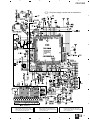
4.1 MAIN, SPCN, STCN, FLRB, SLMB and MMCB ASSYS
A
A
P
MAIN ASSY
CN2217
Q11
G
CN1901
IC202
IC106
IC105
Q202 VR601
IC102 IC104
IC609 IC605
IC101 IC103
Q201
IC604
IC607
IC201
IC10
CN1802
IC611
IC13
IC608
I
IC12
IC610
IC404
IC600
B
I
IC606
Stepping
Motor
CN1801
IC601
IC403 IC401
IC204
IC206
IC402 IC205
IC609
IC602
Q203
(DNP-1986B)
C STCN ASSY
C
Q204
IC405
IC407 Q301
IC501 IC100
Pick up Assy
SIDE A
IC300
IC150
IC710
IC711
Q950
IC950 IC850
IC200
IC900
IC701
Q600
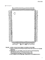
NOTE FOR PCB DIAGRAMS :
1. Part numbers in PCB diagrams match those in the schematic
diagrams.
2. A comparison between the main parts of PCB and schematic
diagrams is shown below.
Symbol In PCB
Diagrams
Symbol In Schematic
Diagrams
B C E B C E
Connector
Capacitor
Transistor
B C E
B
D
Part Name
3. The parts mounted on this PCB include all necessary parts for
several destinations.
For further information for respective destinations, be sure to
check with the schematic diagram.
4. View point of PCB diagrams.
C
E B
C
IC900
SIDE A
E
Transistor
with resistor
B C E
D
G S D
D G S
Q701
Q800
G S
Field effect
transistor
IC700
IC901
P.C.Board
Chip Part
SIDE B
3-terminal
regulator
38
A C
1
2
3
4
5
6
7
8
CDJ-1000
D FLRB ASSY
A
(DNP-1987B)
E
J
SLMB ASSY
B
(DNP-1987B)
CN1101
Loading
Motor
F
MMCB ASSY
C
Pick up Assy
(DNP-1986B)
SIDE A
B SPCN ASSY
(DNP-1986B)
D
Spdl Assy
(DNP-1986B)
5
6
A B D E F
7
8
39
1
2
3
4
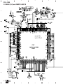
CDJ-1000
D
FLRB ASSY
E
SLMB ASSY
A
• This PCB is a four-layered board.
MAIN ASSY
A
B
F
MMCB ASSY
C
(DNP-1986B)
SIDE B
B SPCN ASSY
(DNP-1986B)
D
(DNP-1986B)
40
A B D E F
1
2
3
4
5
6
7
8
CDJ-1000
A
IC11
B
IC406
IC506
C
SIDE B
D
5
6
7
A
8
41
1
2
3
4
CDJ-1000
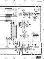
4.2 JABB, JACB and DOUT ASSYS
SIDE A
A
H JACB ASSY
G DABB ASSY
A CN11
B
(DNP1988-B)
Q1907
Q1904 Q1903
IC1901
C
Q1909
Q1902 Q1901
(DNP1988-B)
I DOUT ASSY
(DNP1988-B)
A CN12
D
42
G H I
1
2
3
A CN13
4
1
2
3
4
CDJ-1000
SIDE B
A
H JACB ASSY
(DNP1988-B)
G
DABB ASSY
B
Q1906
Q1905
C
IC1801
(DNP1988-B)
I
DOUT ASSY
(DNP1988-B)
D
1
2
3
G H I
4
43
1
2
3
4
CDJ-1000
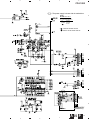
4.3 MFLB, RSWB, KSWB and SLDB ASSYS
A
SIDE A
B
(DNP1987-B)
K RSWB ASSY
N J1
(DNP1987-B)
C
L
KSWB ASSY
D
(DNP1987-B)
44
J K L
1
2
3
4
5
6
7
8
CDJ-1000
A
SIDE A
B
J
MFLB ASSY
N J1202
C
M SLDB ASSY
Y
D
(DNP1987-B)
5
6
7
J M
8
45
1
2
3
4
CDJ-1000
J
A
MFLB ASSY
SIDE B
B
IC1101
C
(DNP1987-B)
Q1103
Q1104
M SLDB ASSY
D
(DNP1987-B)
46
J M
1
Q1401
Q1402
2
3
4
5
6
7
8
CDJ-1000
A
SIDE B
B
Q1013 Q1009
Q1007
Q1012 Q1008 Q1102
Q1017
Q1114 Q1016 Q1115 Q1011 Q1116 Q1118
Q1115 Q1113
Q1015 Q1014 Q1010 Q1117
K
RSWB
ASSY
C
Q1106
Q1107 Q1109 Q1108
Q1101
Q1111 Q1110
Q1112
L
KSWB ASSY
D
(DNP1987-B)
B)
Q1302
5
Q1301 Q1303
6
7
J K L
8
47
1
2
3
4
CDJ-1000
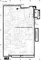
4.4 JFLB and JOGB ASSYS
A
SIDE A
J CN1102
Q1212 Q1213
Q1215
IC1202
B
C
(DNP1988-B)
N JFLB ASSY
O JOGB ASSY
(DNP1988-B)
D
48
N O
1
2
3
4
1
2
3
4
CDJ-1000
SIDE B
A
Q1211 Q1209
Q1210
Q1202 Q1204 Q1205
IC1201 Q1201 Q1203
Q1206
Q1207 Q1214
B
C
(DNP1988-B)
N JFLB ASSY
O JOGB ASSY
(DNP1988-B)
D
1
2
3
N O
4
49
1
2
3
4
CDJ-1000
4.5 POWER SUPPLY and PSWB ASSYS
SIDE A
A
P
POWER SUPPLY ASSY
B
(Whit)
(Orange)
A CN101
AC INLET
KUC: AC 120V
TL: AC110- 240V
WY: AC220- 240V
C
Q
PSWB ASSY
D
50
P Q
1
2
3
4
5
6
7
8
CDJ-1000
SIDE B
P
A
POWER SUPPLY ASSY
B
C
D
5
6
7
Q
8
51
CDJ-1000
5. PCB PARTS LIST
NOTES:
• Parts marked by "NSP" are generally unavailable because they are not in our Master Spare Parts List.
• The mark found on some component parts indicates the importance of the safety factor of the part.
Therefore, when replacing, be sure to use parts of identical designation.
• When ordering resistors, first convert resistance values into code form as shown in the following examples.
Ex.1 When there are 2 effective digits (any digit apart from 0), such as 560 ohm and 47k ohm (tolerance is shown by J=5%,
and K=10%).
561 ........................................................ RD1/4PU 5 6 1 J
560 Ω
→
56 × 101 →
473 ........................................................ RD1/4PU 4 7 3 J
47k Ω
→
47 × 103 →
0.5 Ω
→
R50 ..................................................................................... RN2H R 5 0 K
1Ω
→
1R0 ..................................................................................... RS1P 1 R 0 K
Ex.2 When there are 3 effective digits (such as in high precision metal film resistors).
5621 ...................................................... RN1/4PC 5 6 2 1 F
5.62k Ω →
562 × 101 →
• LIST OF WHOLE PCB ASSEMBLIES
Part No.
Mark
Symbol and Description
Remarks
CDJ-1000/ KUC
CDJ-1000/ TL
CDJ-1000/ WY
NSP
MOTHER ASSY
MAIN ASSY
MMCB ASSY
SPCN ASSY
STCN ASSY
DWM2123
DWX2161
DWX2169
DWX2170
DWX2171
DWM2123
DWX2161
DWX2169
DWX2170
DWX2171
DWM2123
DWX2161
DWX2169
DWX2170
DWX2171
NSP
DISP ASSY
MFLB ASSY
KSWB ASSY
SLDB ASSY
SLMB ASSY
RSWB ASSY
PSWB ASSY
DWM2126
DWG1548
DWS1307
DWS1308
DWS1309
DWS1310
DWS1312
DWM2124
DWG1548
DWS1307
DWS1308
DWS1309
DWS1310
DWS1311
DWM2124
DWG1548
DWS1307
DWS1308
DWS1309
DWS1310
DWS1311
SUB ASSY
JFLB ASSY
JOGB ASSY
DABB ASSY
JACB ASSY
DOUT ASSY
FLRB ASSY
DWM2125
DWG1549
DWG1550
DWX2162
DWX2163
DWX2164
DWX2166
DWM2125
DWG1549
DWG1550
DWX2162
DWX2163
DWX2164
DWX2166
DWM2125
DWG1549
DWG1550
DWX2162
DWX2163
DWX2164
DWX2166
SW POWER SUPPLY ASSY
DWR1344
DWR1344
DWR1344
NSP
∗1
*1: For PSWB ASSY , Refer to “ CONTRAST OF PCB ASSEMBLIES ” and “ PARTS LIST FOR CDJ-1000/KUC ”.
• CONTRAST OF PCB ASSEMBLIES
P
PSWB ASSY
DWS1312 and DWS1311 are constructed the same except for the following:
Part No.
Mark
AN 1 (AC SOCKET)
AN 1 (1P AC INLET)
52
Remarks
Symbol and Description
DWS1312
DWS1311
AKP7032
Not used
Not used
BKP1046
CDJ-1000
• PARTS LIST FOR CDJ-1000/KUC
Mark No.
Description
Part No.
A MAIN ASSY
Mark No.
Description
Part No.
CAPACITORS
SEMICONDUCTORS
C 417, C 418, C 517, C 518, C 638
C 831
C 221, C 223, C 38–C 40, C 405
C 411, C 413, C 415, C 421, C 423
C 425, C 427, C 429, C 435, C 437
CCSRCH100D50
CCSRCH100D50
CCSRCH101J50
CCSRCH101J50
CCSRCH101J50
C 439, C 445, C 469, C 505, C 511
C 513, C 515, C 521, C 523, C 525
C 527, C 529, C 535, C 537, C 539
C 545, C 569, C 700
C 635, C 637
CCSRCH101J50
CCSRCH101J50
CCSRCH101J50
CCSRCH101J50
CCSRCH120J50
C 603, C 633
C 464, C 634
C 463
C 803
C 957
CCSRCH121J50
CCSRCH150J50
CCSRCH180J50
CCSRCH181J50
CCSRCH220J50
C 407, C 431, C 441, C 461, C 507
C 531, C 541, C 614
C 959
C 649
C 914
CCSRCH221J50
CCSRCH221J50
CCSRCH270J50
CCSRCH271J50
CCSRCH331J50
C 807
C 467, C 468, C 567, C 568, C 707
C 713
C 453
C 723, C 818, C 819
CCSRCH390J50
CCSRCH470J50
CCSRCH470J50
CCSRCH471J50
CCSRCH561J50
C 724
C 103, C 108, C 110, C 121, C 155
C 17, C 20, C 201, C 21, C 211
C 22, C 29, C 401, C 452, C 499
C 501, C 502, C 599, C 602, C 622
CCSRCH681J50
CEHAR101M10
CEHAR101M10
CEHAR101M10
CEHAR101M10
C 624, C 625, C 901, C 951
C 101, C 105, C 25–C 28, C 828
C 900
C 33, C 704, C 708, C 712, C 806
C 811–C 813
CEHAR101M10
CEHAR470M16
CEHAR470M16
CKSRYB102K50
CKSRYB102K50
C 10, C 102, C 104, C 106, C 109
C 11, C 112, C 122, C 123, C 154
C 157, C 158, C 16, C 200
C 202, C 203, C 205–C 210
C 217, C 218, C 225, C 226
CKSRYB103K50
CKSRYB103K50
CKSRYB103K50
CKSRYB103K50
CKSRYB103K50
CKSRYB103K50
CKSRYB103K50
CKSRYB103K50
CKSRYB103K50
CKSRYB103K50
IC800
IC850
IC10
IC202
IC106 (I = 0.4A)
AN8702NFH
BA10358F
BA178M05FP
BR24C64F
ICP-N10
IC102, IC103 (I = 0.6A)
IC101, IC104 (I = 0.8A)
IC105 (I = 1A)
IC606
IC950
ICP-N15
ICP-N20
ICP-N25
IC900
IC600
IC404
IC700
IC609
LB11975
M51957BFP-TFB
MM1561JF
MN677061ZY
NJM78L05UA
IC300
IC201
IC11
IC602
IC150, IC206
PD3431A9
PD3432A9
PE8001A
PE9012A
PQ1R33
IC100, IC607
IC203
IC12
IC205
IC405
PQ2TZ15
TC74HC4053AFT
TC74HCT7007AF
TC74VHC08FT
TC74VHC541FT
IC407
IC204, IC403, IC710
IC711
IC610
IC406, IC506
TC7S04FU
TC7SET08FU
TC7SET32FU
TC7SH08FU
TC7SU04F
IC611
IC605
IC13, IC402, IC608, IC612, IC701
IC604
IC601
TC7SU04FU
TC7WT241FU
TC7WU04FU
TLC2932IPW
XC2S50-5PQ208C
IC401, IC501
Q 600
Q 204
Q 11, Q 202
Q 201, Q 203, Q 301, Q 701, Q800
XCA56367PV150
2SA1577
2SC4081
DTA124EUA
DTC124EUA
Q 950
D 11, D 203–D 232
DTC124EUA
1SS355
C 230–C 233, C 31, C 32
C 331–C 333, C 400, C 402, C 406
C 408, C 412, C 414, C 416, C 422
C 424, C 426, C 428, C 430, C 432
C 436, C 438, C 440, C 442
L 401, L 402, L 601, L 602
L 11, L 13, L 200
L 404, L 504
L 10, L 101, L 111, L 15, L 152
L 201, L 600, L 603–L 611
ATL7002
DTL1024
LCTA1R0J2520
PTL1014
PTL1014
C 446–C 451, C 456, C 457, C 462
C 466, C 500, C 506, C 508, C 512
C 514, C 516, C 522, C 524, C 526
C 528, C 530, C 532, C 536, C 538
C 540, C 542, C 546–C 551
CKSRYB103K50
CKSRYB103K50
CKSRYB103K50
CKSRYB103K50
CKSRYB103K50
L 701–L 705
PTL1014
C 556, C 557, C 6001,C 6002,C 601
C 604, C 607, C 613, C 615, C 616
C 618, C 623, C 626–C 632, C 636
C 641–C 644, C 651–C 683, C 714
C 726, C 730, C 733, C 751–C 755
CKSRYB103K50
CKSRYB103K50
CKSRYB103K50
CKSRYB103K50
CKSRYB103K50
K4S641632D-TL1L
LA6562
COILS AND FILTERS
53
CDJ-1000
Mark No.
Description
Part No.
C 800, C 857, C 910, C 964
C 159, C 18, C 204, C 213, C 215
C 228, C 23, C 24, C 30, C 300
C 306, C 605, C 608–C 610, C 612
C 620, C 621, C 715, C 716, C 725
CKSRYB103K50
CKSRYB104K16
CKSRYB104K16
CKSRYB104K16
CKSRYB104K16
C 902, C 904, C 905
C 229, C 600, C 640, C 648
C 911
C 606, C 639, C 833, C 903
C 820
CKSRYB104K16
CKSRYB105K6R3
CKSRYB222K50
CKSRYB224K10
CKSRYB273K16
C 470, C 570
C 706, C 802, C 821
C 703
C 834, C 835
C 301, C 303, C 305, C 702, C 705
CKSRYB472K50
CKSRYB473K25
CKSRYB562K50
CKSRYB682K50
CKSRYF104Z25
C 709–C 711, C 717–C 722, C 732
C 801, C 804, C 805, C 808–C 810
C 815, C 822, C 825, C 826, C 830
C 832, C 950, C 952–C 956
C 455, C 940
CKSRYF104Z25
CKSRYF104Z25
CKSRYF104Z25
CKSRYF104Z25
CKSRYF105Z10
C 454 (2.2µF/ 10V)
VCG1031
Mark No.
Description
B SPCN ASSY
OTHERS
CN911, CN912 12P CONNECTOR
DKN1205
C STCN ASSY
OTHERS
CN913, CN914
4P CONNECTOR
DKN1223
D FLRB ASSY
RESISTORS
R 1504-R 1508
RS3LMF300J
OTHERS
CN1501 3P JUMPER CONNECTOR
E
52147-0310
SLMB ASSY
SWITCHES
S 1501,S 1502
DSG1017
OTHERS
RESISTORS
R 825 (47Ω)
R 900, R 901 (4.7Ω)
R 323, R 324, R 419, R 654–R 657
R 681, R 682
R 828
DCN1133
DCN1141
RAB4C101J
RAB4C101J
RAB4C123J
R 453
R 800, R801
R 834
R 218, R 401, R 420, R421, R501
R 829
R 1–R 7
R 604
R 806
R 605
VR601 (4.7KΩ)
RAB4C220J
RAB4C273J
RAB4C303J
RAB4C473J
RAB4C822J
RS1/10S0R0J
RS1/16S1502F
RS1/16S2202F
RS1/16S8202F
VCP1172
Other Resistors
RS1/16S&&& J
OTHERS
CN1501 KR CONNECTOR POST
F
S3B-PH-K
MMCB ASSY
CAPACITORS
C 91
C 99
C 97
CCSRCH221J50
CKSRYB103K50
CKSRYB104K16
RESISTORS
Other Resistors
RS1/16S&&& J
OTHERS
CN99
CN999
CONNECTOR POST
SD CONNECTOR
B7B-PH-K
DKN1231
G DABB ASSY
SEMICONDUCTORS
X 401
X 701
X 201, X 300
X 601
X 602
20.000MHz
33.8688MHz
20MHz
33.8688MHz
27.0MHz
ASS7023
DSS1126
DSS1127
RSS1055
VSS1086
IC1901
Q 1907
Q 1906
Q 1901 -Q 1904
Q 1905
NJM4580D
2SA1145
DTA124EUA
2SD2144S
DTC124EUA
CN13 5P JUMPER CONNECTOR
CN11 9P JUMPER CONNECTOR
CN101 15P JUMPER CONNECTOR
CN102 3P JUMPER CONNECTOR
CN201, CN301 KR CONNECTOR
52147-0510
52147-0910
52147-1510
52151-0310
B6B-PH-K
D 1906
D 1904,D 1905,D 1907
D 1918
1SR154-400
1SS355
UDZ13B
CN900 12P FFC CONNECTOR
CN950 4P FFC CONNECTOR
CN203 25P CONNECTOR
CN302 CONNECTOR POST
CN12, CN303 CONNECTOR POST
DKN1205
DKN1223
HLEM25R-1
S2B-PH-K
S3B-PH-K
CN202
S7B-PH-K
CONNECTOR POST
CAPACITORS
C 1906,C 1907
C 1912
C 1905,C 1908
C 1915,C 1916
C 1909,C 1910,C 1913,C 1914
CEANP101M16
CEAT101M50
CKSRYB104K16
CQMBA102J50
CQMBA152J50
RESISTORS
R 1908,R 1919
R 1909,R 1918
R 1907,R 1920,R 1938,R 1939
R 1916,R 1917
R 1906,R 1910,R 1913,R 1923
54
Part No.
RD1/2VM103J
RD1/2VM113J
RD1/2VM182J
RD1/2VM273J
RD1/2VM471J
CDJ-1000
Mark No.
Description
R 1936,R 1937
Other Resistors
Part No.
RD1/2VM471J
RS1/16S&&& J
9P JUMPER CONNECTOR 52147-0910
CONNECTOR POST
B3B-PH-K
H JACB ASSY
SEMICONDUCTORS
D 1902
D 1901,D 1903
1SS355
UDZS10B
CAPACITORS
C 1901
C 1903,C 1904
CKSRYB104K16
CQMBA102J50
RESISTORS
R 1903
R 1902,R 1911,R 1912
RD1/2VM271J
RD1/2VM471J
OTHERS
CN1904
JA1902
JA1901
CN1903
I
J
Description
Part No.
MFLB ASSY
SEMICONDUCTORS
OTHERS
CN1901
CN1902
Mark No.
3PJUMPER CONNECTOR
2P PIN JACK
REMOCON JACK
CONNECTOR POST
52151-0310
BKB1017
RKN1004
S3B-PH-K
DOUT ASSY
SEMICONDUCTORS
IC1801
TC74HCU04AF
PE5243A
2SC4081
DTA124EUA
DTC124EUA
BR5364X
D 1104-D 1107
D 1108
D 1112,D 1114,D 1116
D 1101,D 1109
D 1111,D 1113,D 1115
EMAY3864X-HM
NSPB500-0008
SLA570MT
SLR-343MC
SLR-343VC
COILS AND FILTERS
L 1001,L 1002
PTL1014
SWITCHES
S 1104-S 1107,S 1109-S 1112
S 1116,S 1117,S 1119
S 1101-S 1103,S 1113-S 1115
S 1118
ASG7013
ASG7013
DSG1063
DSH1049
CAPACITORS
C 1143-C 1145
C 1112-C 1114,C 1138-C 1142
C 1121-C 1137
C 1108,C 1109,C 1116,C 1118
C 1100-C 1107,C 1110,C 1111,C 1115
CCSRCH101J50
CCSRCH102J50
CCSRCH471J50
CEHAR470M16
CKSRYB103K50
C 1117,C 1119,C 1120
CKSRYB103K50
RESISTORS
COILS AND FILTERS
L 1802
L 1803
L 1801
IC1101
Q 1007-Q 1017,Q 1113-Q 1118
Q 1112
Q 1101-Q 1104,Q 1106-Q 1111
D 1117
PTL1003
PTL1014
PTL1017
VR1101,VR1102 (10KΩ- B)
Other Resistors
DCS1045
RS1/16S&&& J
OTHERS
SWITCHES AND RELAYS
S 1801
DSH1025
CAPACITORS
C 1810
C 1809
C 1808
C 1802
C 1803,C 1804,C 1806,C 1807
CEAT101M6R3
CEAT470M10
CGCYX104M16
CKSRYB102K50
CKSRYB104K16
RESISTORS
Other Resistors
RS1/16S&&& J
X 1101
0
0
0
CN1101
4.19MHz
2P CABLE HOLDER
9P CABLE HOLDER
12P CABLE HOLDER
25P CONNECTOR
DSS1130
51048-0200
51048-0900
51048-1200
52492-2520
J 1103
J 1101
V 1101
0
9P JUMPER WIRE
12P JUMPER WIRE
FL INDICATOR TUBE
FL HOLDER
D20PYY0915E
D20PYY1215E
DEL1044
DNF1665
K RSWB ASSY
SWITCHES
OTHERS
0
J 1801
JA1801
CN1801
S 1701
3P CABLE HOLDER
JUMPER WIRE
1P JACK
CONNECTOR POST
51048-0300
D20PYY0305E
PKB1028
S3B-PH-K
DSK1021
OTHERS
0
J 1701
2P CABLE HOLDER
2P JUMPER WIRE
51048-0200
D20PYY0210E
55
CDJ-1000
Mark No.
L
Description
Part No.
KSWB ASSY
Q 1301-Q 1303
D 1321-D 1328
D 1301-D 1304,D 1310,D 1311
D 1316,D 1317
D 1312-D 1315
DTA124EUA
1SS355
EMAY3864X-HM
EMAY3864X-HM
SLR-342PC
D 1305-D 1308
D 1309
SLR-343MC
SLR-343VC
PTL1014
SWITCHES
ASG7013
DSG1063
CCSRCH101J50
CCSRCH102J50
RESISTORS
Other Resistors
RS1/16S&&& J
OTHERS
CN1301 9P JUMPER CONNECTOR 52151-0910
M SLDB ASSY
CAPACITORS
C 1211,C 1213,C 1214,C 1216,C 1224
C 1201,C 1215
C 1225
C 1203
C 1202,C 1204,C 1206,C 1207,C 1209
CEHAT100M50
CEHAT101M16
CEHAT101M50
CKSRYB102K50
CKSRYB103K50
RESISTORS
R 1269,R 1282
R 9999
Other Resistors
0
CN1201
J 1202
V 1201
0
4P CABLE HOLDER
FPC CONNECTOR
15P JUMPER WIRE
FL INDICATOR TUBE
FL HOLDER
RD1/2VM221J
RS1/10S0R0J
RS1/16S&&& J
51048-0400
5597-03CPB
D20PYY1505E
DEL1043
DNK3959
O JOGB ASSY
SEMICONDUCTORS
D 1601
GP1A037RBK
C 1601,C 1602
DTA124EUA
1SS355
SLR-343MC
SLR-343VC
CKSRYB103K50
RESISTORS
Other Resistors
RS1/16S&&& J
OTHERS
SWITCHES
S 1401-S 1403
LRCA101J
PTL1014
CAPACITORS
SEMICONDUCTORS
Q 1401,Q 1402
D 1401-D 1404
D 1405
D 1406
L 1201
L 1202-L 1205
OTHERS
CAPACITORS
C 1302
C 1301
Part No.
C 1212,C 1218-C 1221,C 1223,C 1226 CKSRYB103K50
COILS AND FILTERS
S 1303-S 1306
S 1301,S 1302
Description
COILS AND FILTERS
SEMICONDUCTORS
L 1304-L 1308
Mark No.
ASG7013
0
4P CABLE HOLDER
J 1601 4P JUMPER WIRE
51048-0400
D20PYY0405E
CAPACITORS
C 1407
C 1404
C 1406
C 1401
C 1402,C 1403
CCSRCH101J50
CCSRCH102J50
CEHAT100M50
CKSRYB103K50
CKSRYB104K16
RESISTORS
VR1401 (10kΩ-B)
Other Resistors
DCV1012
RS1/16S&&& J
N JFLB ASSY
There is no service parts.
Q PSWB ASSY
SWITCHES
S1
RSA1001
OTHERS
SEMICONDUCTORS
56
P SW POWER SUPPLY ASSY
IC1202
IC1201
Q 1212
Q 1201-Q 1207, Q 1214
Q 1208-Q 1211
NJM2903D
UPD16306B
2SA933S
2SC2412K
2SJ209
Q 1213, Q1215
D 1201-D 1208
D 1210
D 1221
D 1219
2SB1237X
1SS355
MTZJ30D
UDZ12B
UDZ4.3B
AN1
J1
0
POWER SOCKET
CONNECTOR ASSY
PCB BINDER
AKP7032
DKP3545
VEF1040
CDJ-1000
6. ADJUSTMENT
6.1 ADJUSTMENT ITEMS AND LOCATION
Adjustment Points (PCB Part)
A
VCO ADJ
MAIN ASSY
VR601
VCOIN
VCO-TP
GND
Pick up Assy
SIDE A
Adjustment Items
[Electrical Part]
1 VCO Free-running Adjustment
6.2 JIGS AND MEASURING
INSTRUMENTS
6.3 NECESSARY ADJUSTMENT POINTS
When
CH1
(X)
CH2
(Y)
Exchange
MAIN ASSY
Adjustment Points
1 = Page 58
Dual-trace oscilloscope
(10:1 probe)
57
CDJ-1000
6.4 ELECTRICAL ADJUSTMENT
1
VCO Free-running Adjustment
Objective : To optimize the VCO free-running frequency
When not properly adjusted :
• Master Tempo does not function normally.
• TEMPO display does not become the same as that
of actual voice tempo.
• Power ON
• None disc
• The position of TEMPO
slider is set to 0
• DOUT OFF
MAIN ASSY
VR601
Player
DC voltage
2.5±0.2V
CH1
(X)
CH2
(Y)
START
MAIN ASSY
VCO IN
GND
58
Probe (10:1)
Oscilloscope
V: 50mV/div.
H: 10msec/div.
DC mode
CDJ-1000
7.1 GENERAL INFORMATION
7.1 DIAGNOSIS
7.1.1 SERVICE MODE
7.1.1.1 HOW TO START / CANCEL SERVICE MODE
SERVICE MODE : ON
SERVICE MODE
POWER OFF
IN ADJUST
Release
TEMPO
IN ADJUST
POWER ON
TEMPO
SERVICE MODE : CANCEL
POWER OFF
7.1.1.2 OPERATION IN SERVICE MODE
• In the service mode, can check "LED and FL displays" partially as follows.
• In addition, it lights while pressing the key.
LED CHECK
Key Name
LED lighting
1 HOT CUE -A
A
(Green)
2 HOT CUE -B
B
(Green)
3 HOT CUE -C
C
(Green)
4 REC MODE
A
5 DIRECTION (SW)
B
89
1
C
(Red) (Red) (Red)
REV
2
3
4
0
5
6 CUE
CUE
7 PLAY/PAUSE
CARD
8 IN ADJUST
=
IN ADJUST
9 OUT ADJUST
OUT ADJUST
0 JOG MODE
CDJ
- TEMPO
VINYL
6
7
7
= MASTER TEMPO
CARD
~
MASTER TEMPO
~ TEMPO RESET
TEMPO RESET
59
CDJ-1000
• Key Position
%^
FL CHECK
( * _ ¡ +
FL lighting
Position
Key Name
!¢
A- 1 , P- 1
@4
A- 2 , P- 2
#1
B- 1 , P- 3
$¡
B- 2 , P- 4
% TIME MODE/AUTO CUE
C
^ DISPLAY
D
& RELOOP/ EXIT
E
* WAVE - FWD
F
( WAVE - REV
G
) CALL - FWD
H
_ CALL - REV
I
+ DELETE
J
¡ MEMORY
&
™
£
)
¢
∞
!
@
#
$
All of FL,P: Jog-FL
and LED
light up.
™ EJECT LOCK (SW)
L
£ EJECT
M
¢ MEMORY JOG ADJUST
-TOUCH (VOL)
Right
from
VR Center
∞ MEMORY JOG ADJUST
-RELESE (VOL)
Right from
VR Center
• FL lighting Position
(Jog- FL DISPLAY)
P-3
P-4
P-4
N
O
P
P-1
(FL DISPLAY)
P-2
A- 1
B- 1
B- 2
B
A
c
J
A- 2
D
E
L
D
G
H
I
60
F
ON
M
CDJ-1000
7.1.2 ERROR DISPLAY
• When trouble occurred in the player operation in the normal use, display the error code in FL a second and a freames.
In addition, can display a history of error content.
1. Display the software version to display part of minute, second and freame that continues pressing RELOOP button for 10
seconds.
2. RAM address (FFEF20-FFFFFF) of the microcomputer inside and the content (00-FF) display it with a hexadecimal number to
character display section when turns the Jog Dial.
3. Display 16 histories of the latest error content in RAM address (FFF020-FFF02F).
• Error Code Table
Error Code
E - 7201
Error Name
Error Content
TOC READ ERROR
26: Cannot lead TOC data
PLAYER ERROR (Abnormality of raising up)
11: All the error stop before disc distinction is this error.
20: Spindle does not turn
21: No disc (Focus servo error small)
24: Address is not readable
E - 8302
PLAYER ERROR (Abnormality of playback)
12: Specified address were not able to search
15: Address is not readable
22: Focus servo cannot close
23: Tracking servo cannot close
E - 8303
PLAYER ERROR (Abnormality of buffer write)
99: Abnormality of buffer write
E - 9101
MECHANICAL TIME OUT
90: Abnormality of the disc loading mechanism (Timeout)
E - 8301
Error disply explanation
1. Soft version display
ERR code No.
2. RAM address and Contents display
RAM address
Content
3. Error history display
RAM address
Error Content
61
CDJ-1000
7.1.3 DISASSEMBLY
1
5
SW POWER
SUPPLY Assy
FACB Assy
Cord Clamper is started and
a connector is removed.
6
1
7
PSWB Assy
JACB
Assy
CN1101
Cord Clamper
1
×2
DOUT
Assy
1
MMCB Assy
2
• Bottom view
2
×3
×3
2
DABB
Assy
×3
Slot-in Mechanism G5 Assy
9
3
Bottom Plate
4
Disconnect two Connectors.
8
MAIN Assy
4
Unhook four springs and Dampers.
Unhook Damper
CN302
CN202
Unhook Float Spring G5
62
CDJ-1000
Traverse Mechanism Assy
14
1
Remove Slot-in Mechanism
G5 Assy.
1
×2
2
SPCN
Assy
11
STCN
Assy
10
1
4
13
Mechanism
Holder Plate
Release
connector
wires
3
×2
Unhook
5
3
×2
Unhook
MAIN Assy
Pickup
Flexible
Cable
CN800
12
• Bottom side
Caution:
Be careful not to lost
Earth Spring.
Loading Base
STCN Assy
6
CN913
SPCN Assy
7
CN912
• Bottom view
8
×3
9
Traverse Mechanism Assy
63
CDJ-1000
JOG Dial Section
• Rear view
1
MFLB Assy
×5
CN1102
RSWB Assy
4
Release a Binder.
5
2
×2
3
Release a Binder.
SLDB Assy
7
KSWB Assy
JOGB Assy
6
JOGB Assy is removed from a hook.
Note:
There is a possibility that a crack may be
attached to not opening JOG DIAL part,
with JOGB Assy attached and an encoder plate.
8
JOG Holder section
JOG Dial section
Diagnosis or Replacement
64
CDJ-1000
The processing method of each wire rod
Processing of flexible cable
1
Processing of each wire rod
About 7cm
About 3cm
About 4cm
Cord Clamper
A wire rod is slacked.
Cord Clamper
2
6
CN1101
CN101
3
6
25P Flexible Cable
It processes so that a wire rod may n
ot run aground.
The cautions on an assembly
[ NG ]
[ OK ]
MFLB Assy
Control Panel
MFLB Assy
Control Panel
Slot -In Mecha
25P Flexible Cable
OK
MAIN Assy
Bottom Plate
Slot -In Mecha
25P Flexible Cable
NG
MAIN Assy
Bottom Plate
65
CDJ-1000
7.1.4 Part Replacement Method of JOG Section
7.1.4.1 A part to Replace in Part Replacement Simultaneously
Replacement Part
Sheet SW
(DSX1057)
JOG Sheet A JOG Sheet B JOG Sheet C JOG Plate
(DXB1757)
(DXB1757)
(DXB1757)
(DAH2052)
JOG Holder
(DNK3872)
JOG Dial A
(DNK3870)
JOG Dial B
(DNK3871)
Sheet SW
JOG Sheet A
JOG Sheet B
A Part to
JOG Sheet C
Replace
Simultaneo- JOG Plate
usly
JOG Holder
JOG Dial A
JOG Dial B
Note
: Do not need to replace the JOG Holder when replacing the Sheet SW. However, be careful so that paste
does not remain on the former Sheet SW.
7.1.4.2 Caution in Sheet SW Installation
1 Be careful not to bend and fold the Sheet SW.
2 Confirm that the dust or trash does not adhere to pasting side
(JOG Holder).
In addition, when tear off the former Sheet SW and put a new
part, completely wipe the JOG Holder off with alcohol so that
paste does not remain on the pasting side of JOG Holder.
3 Bend a cable of the Sheet SW in a right angle in difference in
grade shape, and put it in corner hole of the JOG Holder.
(Fig. Ÿ)
4 When put the Sheet SW, match the position not to run aground
on rib of the internal circumference of JOG Holder. (Fig. Ÿ)
5 Sheet SW pushes all the sides including the point of contact
fully, and put it. (No good air getting into it.)
6 When insert a cable in connector, release a lock by all means,
and connector locks after inserting it.
7 A cable performs styling as shown in Fig. ! after installing the
JFLB Assy (DWG1549).
JOG Panel
JOG Plate
JOG Dial A
JOG Sheet A
JOG Dial B
7
3
JOG Sheet C
(×8)
4
Sheet SW
Fig. Ÿ
JOG Sheet B
Fig. ! (Bottom View)
8 It assembles so that an encoder plate may go into the slot of the
encoder guide of JOGB Assy.
encoder guide
JOGB ASSY
JOG Holder
Encoder Plate
encoder plate
JOGB ASSY
JFLB Assy
Fig. 1 JOG Section View
66
Encoder plate
Encoder guide
[ Sectional view ]
CDJ-1000
7.1.4.3 Caution in JOG Sheet A Pasting
1
2
3
4
5
Be careful not to bend and fold the JOG Sheet A.
Put a lubricant (GEM1038) on the sheet.
Confirm that the dust or trash do not adhere to pasting side (JOG Dial A).
Match JOG Sheet A with marking of inner and outer circumference for pasting of JOG Dial A. (Fig. ⁄)
Put it to push you out of the inner circumference toward the periphery. (No good air getting into it.)
JOG Sheet A
JOG Dial A
4
Fig. ⁄ (Bottom View)
7.1.4.4 Caution in JOG Sheet B Pasting
1
2
3
4
5
Be careful not to bend and fold the JOG Sheet B.
Put a lubricant (GEM1038) on the sheet.
Confirm that the dust or trash do not adhere to pasting side (JOG Holder).
Pasting method: Two places have this side with 90°. Paste it while matching with a guide of rib, and match a round. (Fig. @)
Put it to push you out of the inner circumference toward the periphery. (No good air getting into it.) (Fig. ¤)
JOG Sheet B
JOG Sheet B
5
4
It unites with the rib of
an inner circumference.
JOG Holder
Fig. @
Fig. ¤
67
CDJ-1000
7.1.4.5 Caution in JOG Sheet C Pasting
1
2
3
4
Be careful not to bend and fold the JOG Sheet C.
Put a lubricant (GEM1038) on the sheet.
Confirm that the dust or trash do not adhere to pasting side (JOG Dial B).
Pasting method: Match the inside diameter direction with edge side of the inside diameter of JOG Dial B, and match eight places of
periphery directions in rib. (No good JOG Dial B protruding outward) (Fig. #)
JOG Sheet C
(×8)
JOG Dial B
4
4
Fig. # (Bottom View)
7.1.4.6 Caution in JOG Plate pasting
1 Confirm that the dust or trash do not adhere to pasting side (JOG Dial A).
2 JOG Plate matches it with rib of the inner circumference of JOG Dial A, and put it. However, be careful not to run aground on the rib.
(Fig. ‹)
3 Be careful so that air gets into it, and the appearance of sheet does not wave.
JOG Plate
2
JOG Dial A
It unites with the rib of
an inner circumference.
Fig. ‹
68
CDJ-1000
7.1.5 About electric discharge
• To the capacitor (C5) of a switching circuit part, it is in power supply OFF. (after 5 minutes) Although remained
abbreviation 20V, there is no danger of an electric shock.
P
POWER SUPPLY ASSY
C5
69
CDJ-1000
7.1.6 SEQUENCE AFTER THE POWER ON
Power ON
IC201 (System CPU) Reset
63 pin (XRST) : H
IC601 (FPGA) Program download start
106 pin (XPROGRAM) : H
IC601 (FPGA) download end
104 pin (DONE) : H
IC401 (DSP1),IC501 (DSP2)
Program download
IC300 (Mecha Control) Pin 63 (XMRST)
IC1101 (Display CPU) Pin 10 (/RST)
Reset release
Focus offset and Traking offset
Adjustment.
Laser Diode ON
Spindol ON
Focus UP/DOWN
Disc existence check by detecting the Focus S curve signal.
No disc
Disc exist
Unloading
Spindle 2000rpm
Focus ON
Focus Position adjustment (TE MAX)
Traking Balance adjustment
OFTR Slice level adjustment
Tracking ON
Focus Position adjustment
(RFENV MAX)
Focus Gain adjustment
Tracking Gain adjustment
TOC read
Less than 30 minutes
30 minutes or more
Line speed measurement
Search for 00 min 01 sec
Spindle: 3100rpm
Audio Data read start
70
8 cm Adapter detection
00 min 01 sec
CDJ-1000
7.2 PARTS
7.2.1 IC
• The information shown in the list is basic information and may not correspond exactly to that shown in the schematic diagrams.
•List of IC
NJM2903D, UPD16306BGF, MM1561JF, XCA56367PV150, PD3431A9, PD3432A9, PE5243A
NJM2903D (JFLB ASSY : IC1202)
• Comparator
Block Diagram
1
2
3
8
–
A
+
7
+B–
4
6
5
1.
2.
3.
4.
5.
6.
7.
8.
A OUTPUT
A – INPUT
A + INPUT
GND
B + INPUT
B – INPUT
B OUTPUT
V+
UPD16306B (JFLB ASSY : IC1201)
• Output VFD Driver
Block Diagram
71
CDJ-1000
MM1561JF (MAIN ASSY : IC404)
• 500mA Regulator
Block Diagram
Pin Function
72
CDJ-1000
Pin Arrangement
73
CDJ-1000
Pin Function
74
CDJ-1000
XCA56367PV150 (MAIN ASSY : IC401, IC501)
• 24-Bit Digital Signal Processor
Block Diagram
75
CDJ-1000
Pin Function
76
CDJ-1000
77
CDJ-1000
PD3431A9 (MAIN ASSY : IC300)
• Mecha. Control CPU
Pin Function (1/3)
No.
1
Mark
Vcc
Pin Name
I/O
-
-
Description
Power supply (VD5V)
2
PB0
XDMUTE1
O
Driver IC mute control (0: MUTE 1: MUTE release)
3
PB1
-
I
It connects with Vss.
4
PB2
FCSG
O
A focus gain is changed.
5
PB3
CRC
O
CRC check result of a sub code (NG 1: 0: O.K.)
6
PB4
XFEPRST
O
FEP reset pulse (0: Reset 1: Reset release)
7
PB5
XDSCRST
O
ADSC reset pulse (0: Reset 1: Reset release)
8
PB6
LDONM
I
LD ON (0: usually 1: LD on-mode)
9
PB7
-
O
NC
10
FE W
WFLASH
I
The write-in enable signal of a flash memory
11
Vss
-
-
GND
12
TxD0
CPUDTIN
O
The serial output to FEP/ADSC
13
TxD1
REMO
O
The serial output to a personal computer/remote control
14
RxD0
CPUDTOUT
I
The serial input from FEP/ADSC
15
RxD1
REMI
I
The serial input to a personal computer/remote control
16
SCK0
SCK
O
The serial communication clock with FEP/ADSC
17
P9 5
WFLASH
O
The write-in control signal of a flash memory
18
P4 0
TKS
O
The slice level of TE is chosen. (zero: high-speed 1: low speed)
19
P41
INSW
I
Slider Inside detection switch
20
P42
XDMUTES
O
Stepper control
21
P43
DSPSTOP
O
Read-out of DSP is forbidden.
22
Vs s
-
-
GND
23
P4 4
-
O
NC
24
P45
-
O
NC
25
P4 6
GSW
O
OEIC gain selection (0: Low 1: Hi)
I
Test mode (0: It shifts to test mode)
26
P47
TMODE
27
D0
D0
I/O
28
D1
D1
I/O
29
D2
D2
I/O
30
D3
D3
I/O
31
D4
D4
I/O
32
D5
D5
I/O
33
D6
D6
I/O
34
D7
D7
I/O
35
Vcc
-
-
36
A0
A0
O
37
A1
A1
O
38
A2
A2
O
39
A3
A3
O
40
A4
A4
O
78
Data bus
Power supply (VD5V)
Address bus
CDJ-1000
Pin Function (2/3)
No.
41
Mark
A5
Pin Name
A5
I/O
O
42
A6
-
I
43
A7
-
I
44
Vss
-
-
45
A8
-
I
46
A9
-
I
47
A10
-
I
48
A11
-
I
49
A1 2
-
I
50
A1 3
-
I
51
A14
-
I
52
A15
-
I
53
A1 6
-
I
54
A17
-
I
55
P52
LPS1
I
56
P53
LPS2
I
57
Vss
-
-
58
WAIT
-
I
59
P6 1
-
I
60
P62
ILMASK
O
Discription
Address bus
It connects with Vss.
GND
It connects with Vss.
A loading mechanism's condition
GND
It connects with Vss.
The mask of the Interruption circuit is carried out.
61
P67
-
I
It connects with Vss.
62
STBY
XSTBY
I
It connects with Vss.
63
RES
XMRST
I
Reset input (0:reset 1:reset release)
64
NMI
NMI
I
It connects with Vss.
65
Vss
Vss
-
GND
66
EXTAL
EXTAL
I
(20MHz)
67
XTAL
XTAL
I
(20MHz)
68
Vc c
Vcc
-
Power supply (VD5V)
69
AS
-
O
NC
70
RD
XRD
O
Read strobe signal
71
S39/PE7
XWR
O
Write strobe signal
NC
72
VDD4
-
O
73
S40/PF0
MD0
I
74
S41/PF1
MD1
I
75
S42/PF2
MD2
I
76
S43/PF3
-
-
77
S44/PF4
-
-
78
S45/PF5
HI
I
79
S46/PF6
RFDIF
I
80
S47/PF7
VHALF
I
CPU mode setup
Power supply (VD3V)
Function (Analog)
Function
79
CDJ-1000
Pin Function (3/3)
No.
Mark
Pin Name
I/O
Description
81
AN 3
OFTR
I
Function
82
P7 4
-
I
It connects with Vss.
The monitor of ST1
83
AN 5
P75
I
84
DA0
ST1
O
85
DA1
ST2
O
86
AVss
-
-
87
IRQ0
MBLKCK
I
88
IRQ1
BLKCK
I
89
IRQ2
CPUIRQ
I
Stepper drive (analog)
Analog GND
The interruption demand from FPGA
90
P8 3
-
I
91
P8 4
-
I
92
Vs s
-
-
GND
93
PA 0
OFTR
I
Function
It connects with Vss.
94
TCLKB
TKCNT
I
Track pulse input (pulse width is measured and speed is detected)
95
PA2
ENC
O
Serial input enable of ADSC CIRC part (0: permission 1: prohibition)
96
PA3
ENS
O
Serial input enable of ADSC part (0: permission 1: prohibition)
97
PA 4
TKCNT
I
Track pulse input
98
PA5
XDMUTE2
O
Driver IC mute control (0:MUTE 1:MUTE release)
99
PA6
FESEN
O
FEP serial input enable (0: permission 1: prohibition)
FG
I
FG pulse input
100 TIOCB2
80
CDJ-1000
PD3431A9 (MAIN ASSY : IC201)
• System Control CPU
Pin Function (1/3)
No.
Pin Name
I/O
1
Vcc
-
2
DGP2
I
3
XHREQ1
I
4
XHREQ2
I
Descreption
By the capacitor (0.1µF) It GND-connects.
Motorola DSP (preceding paragraph) Interface
Motorola DSP (latter part) Interface
5
XSS1
O
Motorola DSP (preceding paragraph) Interface
6
XSS2
O
Motorola DSP (latter part) Interface
7
DOSW
I
Digital OUT ON/OFF SW detection
8
CNT2
I
Control 2 input terminal
9
CNT1
I/O
Control 1 input and output terminal
10
WFlLSH
I
The terminal which detects a flash write-in permission signal
11
Vss
-
Digital GND
12
S2DO
O
The serial output terminal to DSP
13
S1DO
O
A serial output besides a controller
14
S2DI
I
The serial input from DSP
15
S1DI
I
A serial input besides a controller
16
S2CK
O
The serial clock to DSP
17
S1CK
O
A serial clock besides a controller
18
XFRST
O
Reset to FPGA
19
XSRST
O
Reset to circumference IC
20
ASWC
O
Serial change SW enable
21
MUTE
O
Line OUT output MUTE
22
Vss
-
Digital GND
23
MON2
O
Monitor terminal 2
24
XZOFF
O
The terminal for repealing zero detection
25
XDRST
O
The reset terminal for DAC
26
NC
-
-
27
D0
-
28
D1
-
29
D2
-
30
D3
-
31
D4
-
32
D5
-
33
D6
-
34
D7
-
35
Vcc
-
36
A0
-
37
A1
-
38
A2
-
39
A3
-
40
A4
-
FPGA interface (data bus)
Power supply (VD5V)
FPGA interface (data bus)
81
CDJ-1000
Pin Function (2/3)
No.
Pin Name
I/O
41
NC
O
42
NC
I
43
NC
I
Description
It connects with GND.
44
Vss
-
45
NC
I
Digital (GND)
46
NC
I
47
NC
I
48
NC
I
49
NC
I
50
NC
I
51
NC
I
52
NC
I
53
NC
I
54
NC
I
55
KEYI
I
The key processing demand from front CPU
56
TCH
I
JIG touch sensor input
57
Vs s
-
Digital GND
58
NC
I
It connects with GND.
It connects with GND.
59
XMDT
I
MMC detection signal
60
DONE
O
The initialization end signal from FPGA
61
20M
I
It connects with GND.
62
STBY
I
Low power consumption mode
63
XRST
I
Hard reset
64
NMI
I
Compulsive interruption
Digital GND
65
Vs s
-
66
EXTAL
I
67
XTAL
I
68
Vc c
-
Digital 5V
69
NC
O
-
Crystal oscillation
70
XSRD
O
FPGA Read
71
XSWR
O
FPGA Wright
72
NC
O
-
73
MD0
I
74
MD1
I
75
MD2
I
CPU mode setup
76
Avcc
-
The power supply terminal of A/D conversion machine, and D/A conversion machine
77
VRE F
-
The standard voltage input terminal of A/D conversion machine, and D/A conversion machine
78
ADCT
I
Slider center value
79
ADIN
I
Slider data value
80
NC
I
It connects with GND.
82
CDJ-1000
Pin Function (3/3)
No.
Pin Name
I/O
81
NC
I
82
NC
I
83
NC
I
84
NC
O
85
NC
O
86
AVss
-
Description
It connects with GND.
The grand terminal of A/D conversion machine, and D/A conversion machine
87
JOG1
I
JOG pulse input 1
88
JOG2
I
JOG pulse input 2
89
DQCK
I
Motorola DSP (preceding paragraph) Interface
90
NC
I
It connects with GND.
91
RMIN
I
For a RS232C input
92
Vs s
-
GND
93
XMEN
I
MMC chip enable
94
XDEN
I
DAC communication enable
95
ICDT
O
EEPROM data output
96
ICCK
O
EEPROM clock output
97
HRST
I
MMC hard reset output
98
NC
O
It connects with GND.
99
XPRGM
O
FPGA program permission signal
I
-
100 XINT
83
CDJ-1000
PE5243A (MFLB ASSY : IC1101)
• Disply Control CPU
Pin Function (1/3)
No.
Mark
Pin Name
I/O
Description
1
VD D
-
-
Power supply (VD5V)
2
P37
LED15, Model distinction
O
LOUT, and NEXT / NET distinction
3
P36/BUZ
LED14
I
LIN
4
P35/PCL
LED13
O
CRED
5
P34/TI2
LED12
O
CGREEN
6
P33/TI1
LED11
O
BRED
7
P32/TO2
LED10
O
BGREEN
8
P31/TO1
LED9
O
ARED
9
P30/TO0
LED8
O
AGREEN
10
RESET
RESET
I
RESET
11
X2
CLOCK
-
(5MHz)
12
X1
CLOCK
-
(5MHz)
13
IC
GND
-
-
14
XT2
NC
-
-
15
P04/XT1
SW0
I
Reverse Switch
16
VDD
-
-
-
17
P27/SCK0
SCLK1
I
The clock input from host CPU
18
P26/SO0/SB1
SDO1
O
The data output to host CPU
19
P25/SI0/SB0
SDI1
I
The data input from host CPU
20
P24/BUSY
ENABLE
O
The enable output to host CPU
21
P23/STB
BLK
O
The blank output to FL drive
22
P22/SCK1
SCLK2
O
The clock output to FL driver
23
P21/SO1
SDO2
O
The strike robe to FL driver
24
P20/SI1
STB
O
NC
25
Avss
GND
-
GND
26
P17/ANI7
LED5
I
-
27
P16/ANI6
KEYAD5
I
28
P15/ANI5
KEYAD4
I
29
P14/ANI4
KEYAD3
I
30
P13/ANI3
KEYAD2
I
31
P12/ANI2
KEYAD1
I
32
P11/ANI1
VOL1
I
33
P10/ANI0
VOL2
I
34
AVDD
VDD
-
35
AVREF
VDD
-
Key input
Turntable VOL
Power supply (+5V)
36
P03/INT3/CI0
LED16
O
VINYL
37
P02/INTP2
LED7
O
CDJ
38
P01/INTP1
LED6
O
MT
39
P00/INTP/TI0
ELSW
I
Eject Switch
40
Vss
-
-
-
84
CDJ-1000
Pin Function (2/3)
No.
Mark
Pin Name
I/O
Description
41
P74
LED4
O
TRES
42
P73
LED3
O
MMC
43
P72
LED2
O
CUE
44
P7 1
LED1
O
PLAY
45
P70
LED0
O
REVERSE
46
VDD
-
-
Power supply (5V)
47
P127/FIP52
S37
O
48
P126/FIP51
S36
O
49
P125/FIP50
S35
O
50
P124/FIP49
S34
O
51
P123/FIP48
S33
O
52
P122/FIP47
S32
O
53
P121/FIP46
S31
O
54
P120/FIP45
S30
O
55
P117/FIP44
S29
O
56
P116/FIP43
S28
O
57
P115/FIP42
S27
O
58
P114/FIP41
S26
O
59
P113/FIP40
S25
O
60
P112/FIP39
S24
O
61
P111/FIP38
S23
O
62
P110/FIP37
S22
O
63
P107/FIP36
S21
O
64
P106/FIP35
S20
O
65
P105/FIP34
S19
O
66
P104/FIP33
S18
O
67
P103/FIP32
S17
O
68
P102/FIP31
S16
O
69
P101/FIP30
S15
O
70
P100/FIP29
S14
O
71
P97/FIP28
S13
O
72
P96/FIP27
S12
O
73
P95/FIP26
S11
O
74
P94/FIP25
S10
O
75
P93/FIP24
S9
O
76
P92/FIP23
S8
O
77
P91/FIP22
S7
O
FL display
78
P90/FIP21
S6
O
79
VLOAD
-
-
-
80
P87/FIP20
S5
O
FL display
85
CDJ-1000
Pin Function (3/3)
No.
Mark
Pin Name
I/O
81
P86/FIP19
S4
O
82
P85/FIP18
S3
O
83
P84/FIP17
S2
O
84
P83/FIP16
S1
O
85
P82/FIP15
G16
O
86
P81/FIP14
G15
O
87
P80/FIP13
G14
O
88
FIP12
G13
O
89
FIP11
G12
O
90
FIP10
G11
O
91
FIP9
G10
O
92
FIP8
G9
O
93
FIP7
G8
O
94
FIP6
G7
O
95
FIP5
G6
O
96
FIP4
G5
O
97
FIP3
G4
O
98
FIP2
G3
O
99
FIP1
G2
O
100 FIP0
G1
O
86
Description
FL display
CDJ-1000
8. PANEL FACILITIES AND SPECIFICATIONS
8.1 PANEL FACILITIES
Front Panel
87
CDJ-1000
buttons indicated by * cannot be used in digital mode.
2
1
3
4
5
6
7
8
9
0
-
=
~
!
@
¤
#
⁄
$
Ÿ
%
≠
^
–
&
º
*
ª
•
(
¶
)
§
£
∞
MMC
¢
1 DISPLAY CD TEXT/WAVE (ZOOM) button (*)
Each press of this button toggles the display between WAVE display and CD-TEXT
disc/track title display. When the button is held down for1 second or longer, the
WAVE display cycles between the 1 track full-scale and 2x zoom scale.
88
™
¡
+
_
2 TIME MODE/AUTO CUE button (*)
TIME MODE:
Each time this button is pressed, the time display changes between elapsed playback
time and remaining playback time (REMAIN) of each track.
÷ The TIME MODE is stored in memory and persists even when the power is
turned off.
AUTO CUE:
Hold down this key for 1 second or longer to toggle between AUTO CUE on
and off. ☞ P.11
÷ AUTO CUE on/off status is stored in memory and persists even when the
power is turned off.
CDJ-1000
3 POWER switch OFF —/ON _
¶ The JOG MODE is stored in memory and remains in memory even if the
power is turned off.
CDJ mode: above operation is not performed even when the Jog dial surface
is pressed.
This switch is located on the rear panel of the unit.
4 LOOP IN/REALTIME CUE/IN ADJUST button/indicator (*)
Real-time cue
Enter loop in point
Loop in point adjust
5 LOOP OUT/OUT ADJUST button/indicator (*)
Enter loop out point
Loop out point adjust
6 RELOOP/EXIT button (*)
7 Display
8 WAVE SEARCH (ZOOM)/CD TEXT buttons (2, 3) (*)
This button moves the displayed area when WAVE is in zoom display mode.
In the TEXT display mode, pressing the 2 button will display the disc title
and pressing the 3 button will display the track title.
9 CUE/LOOP CALL buttons (2, 3) (*)
Calls Cue points and Loop points stored in internal memory or external memory
(when a memory card is inserted). (When a memory card is inserted, the external memory takes precedence.)
% VINYL indicator (*)
This indicator lights when the JOG MODE is in VINYL mode.
^ CDJ indicator (*)
This indicator lights when the JOG MODE is in CDJ mode.
& TEMPO Control Range button ±6/±10/±16/±24 (*)
Each time the button is pressed, the range changes (±6%/±10%/±16%/±24%).
* MASTER TEMPO button/indicator (*)
Each press of the button turns the master tempo function on or off.
( Tempo Control knob (*)
Slide the knob towards you (+) to increase the tempo and slide it away from
you (–) to decrease it.
) Tempo Reset indicator (*)
Shows that the tempo has been reset to [0] (normal tempo) regardless of the
position of the Tempo Control knob.
_ TEMPO RESET button (*)
Resets the tempo to [0] (normal tempo) regardless of the position of the
Tempo Control knob. Press button once more to release it.
0 CUE/LOOP MEMORY button (*)
Stores Cue points and Loop points in internal memory or external memory
(when a memory card in inserted). (When a memory card is inserted, the
external memory takes precedence.)
- Digital Mode switch (ON/OFF)
This switch is located on the rear panel of the unit. Set to ON when the digital
output is to be used. When set to On, the DJ functions do not function. (Functions marked * do not operate in this mode.) And the muted pause mode is
used instead of the audible pause mode.
= CUE/LOOP DELETE button (*)
Deletes Cue points or Loop points stored in internal memory or external memory
(when memory card is inserted). (When a memory card is inserted, the external memory takes precedence.)
~ EJECT UNLOCK/LOCK switch
UNLOCK: In this mode the disc can be ejected even during playback.
LOCK: In this mode, the disc cannot be ejected during playback. The disc can
be ejected when in pause mode.
! EJECT button (0)
When this button is pressed the disc is ejected through the disc insertion slot
when it stops rotating. When the EJECT UNLOCK/LOCK switch is set to
[LOCK] position, the disc can only be ejected when in pause mode.
@ VINYL SPEED ADJUST TOUCH/BRAKE dial (*)
When the JOG MODE SELECT button is set to [VINYL] position, you can
use this dial to adjust the speed by which the playback stops when the surface
of the Jog dial is pressed.
Playback stops faster as the dial is turned counterclockwise and stops slower
as the dial is turned clockwise.
# VINYL SPEED ADJUST RELEASE/START dial (*)
When the JOG MODE SELECT button is set to [VINYL] position, you can use this
dial to adjust the speed by which playback starts after you take your hand off the
surface of the Jog dial. Playback starts normal speed faster as the dial is turned
counterclockwise and takes longer time to return to normal speed when turned
clockwise.
$ JOG MODE SELECT button (*)
VINYL mode: when the surface of the Jog dial is pressed during playback, playback stops and if the dial is rotated, music is output according to the speed the dial
is turned.
+
¡
™
£
¢
∞
Jog Dial Display
Jog dial (+FWD/–REV) (*)
Disc Loading Slot
Force Ejection Hole
Memory Card Loading Slot
Memory Card indicator
Lights when the MMC card is being accessed.
¶ Do not remove the card or turn off the power when this lamp is on.
§ Play/Pause indicator (6)
Lights during play and flashes during pause.
¶ PLAY/PAUSE button (6)
• CUE indicator (*)
Lights when a Cue point is set and a search is not being performed. Flashes in
pause mode.
ª CUE button (*)
Cue point settings
Cue point sampler
Back cue
º SEARCH button (1, ¡)
– TRACK SEARCH button (4, ¢)
≠ Reverse indicator (REV) (*)
Lights when the DIRECTION FWD/REV switch is set to reverse.
Ÿ DIRECTION FWD/REV switch (*)
Plays tracks backwards when set to the [REV] position (forward position).
⁄ HOT CUE REC MODE button (*)
Switches HOT CUE button function (REC/CALL).
¶ It is set to call when the power is turned on.
¤ HOT CUE A, B, C button/indicator
It is set to hot cue point recording mode when A, B and C light in red.
It is set to call mode when A, B and C light in green. When the button is
pressed, playback starts from the hot cue point. It is off when no hot cue point
has been recorded.
89
CDJ-1000
Display
‹
±
›
[
]
fi
\
fl ‡
{
‹ Calendar display (1 – ;, \)
TRACK numbers beyond the current track lights. When the next track is 21 or beyond,
\ lights. When Cue points or loops are stored, an underscore lights in the corresponding TRACK numbers.
› TRACK Number indicator
Displays TRACK numbers.
fi Auto Cue indicator (A. CUE)
Lights when auto cue is on.
fl REMAIN indicator
Indicates that track remaining time is being displayed.
‡ Time display (min) (M)
° Time display (sec) (S)
· Frame display (F)
One second is 75 frames.
‚ Playback Tempo display (TEMPO)
Indicates the rate of change in the playback tempo.
— Tempo Adjustment Range indicator (±6, ±10, ±16, ±24)
Indicates the variable range of the Tempo Control knob selected with the TEMPO
Control Range button.
± Reverse indicator (REV)
Indicates that the DIRECTION FWD/REV switch is set to reverse ([REV] position).
[ MEMORY LOOP indicator
Displays the selected track loop memory position above the playback address display (13
points). Even when there may be several memory points in the same block, only one lights.
] MEMORY CUE indicator
Displays the selected cue memory positions under the playback address display (13
points). Even when there may be several memory points in the same block, only one
lights.
\ ZOOM indicator
Indicates that WAVE is indicated in zoom mode.
{ RELOOP indicator
Lights when the unit is in reloop standby or performing a loop.
90
°
}
·
‚
|
“
—
‘ «
} Wave/Text display
When WAVE is displayed the music level of the current track.
The level is indicated either in 1-track full scale, or zoom when only part of the track is
shown. In the zoom mode, the display area is moved using the WAVE SEARCH (ZOOM)
buttons (2, 3).
CD TEXT will be displayed in the TEXT mode.
The contents of the display is the disc title and track title in English upto a maximum of 48
letters which can be scrolled.
| Playback Address display
Indicates elapsed playback time and remaining playback time in an easy to grasp 1track full scale or 2x zoom scale bar graph.
¶ The 1-track full scale mode shows elapsed time by lit segments from the left.
¶ The 1-track full scale mode shows remaining time by unlit segments from the left.
¶ When the remaining time is 30 seconds or less, the display flashes gently and the
flashing becomes faster when there is 15 seconds or less left.
¶ In the 2x zoom scale mode, only the playback position is lit for the WAVE display.
“ BPM Counter
Indicates BPM for the current track.
The BPM counter may sometimes not be able to measure the BPM of a track.
‘ EJECT LOCK indicator
Lights when the EJECT UNLOCK/LOCK switch is set to the [LOCK] position.
« Master Tempo indicator (MT)
Lights when the master tempo function is on.
CDJ-1000
Jog Dial Display
’
»
;
'
”
:
"
…
” Operation display
Indicates play position in frames 135 frames for one full rotation. Turns during playback and stops during pause.
’ All Track display
Indicates track currently being played.
» Memory Cue/ Loop display
Lights when there is a MEMORY CUE or LOOP in a track.
; All Track Display Reference Point
Displays the first track starting point of the disc.
' Direction display
This display the direction of the playback.
: Display the condition of the audio memory
When set in the audio memory display mode the light will flash when recording.
" Displays the condition of the VINYL mode movement
Lights up when there is a pause or when the Jog dial is touched in the VINYL mode.
… VINYL mode display.
Lights up in the VINYL mode.
91
CDJ-1000
8.2 SPECIFICATIONS
CDJ-1000/ KUC type
1. General
3. Accessories
System ......................... Compact disc digital audio system
Power requirements ................................. AC 120 V, 60 Hz
Power consumption .................................................... 33 W
Operating temperature .................................. +5˚C – +35˚C
Operating humidity ............................................. 5% – 85%
(There should be no condensation of moisture.)
Weight ......................................................... 4.2 kg (9.26 lb)
Dimensions ...................... 320 (W) x 370 (D) x 105 (H) mm
12 – 5/8 (W) x 14 – 9/16 (D) x 4 – 1/8 (H) in
2. Audio section
• Operating instructions .................................................... 1
• Power cord ..................................................................... 1
• Audio cable ..................................................................... 1
• Control cord .................................................................... 1
• Forced eject pin
(housed in a groove in the bottom panel) ...................... 1
• Limited warranty ............................................................. 1
NOTE:
Specifications and design are subject to possible modification without notice.
Frequency response ..................................... 4 Hz – 20 kHz
Signal-to-noise ratio ......................... 115 dB or more (EIAJ)
Distortion ...................................................... 0.006% (EIAJ)
CDJ-1000/ WY type
1. General
3. Accessories
System ......................... Compact disc digital audio system
Power requirements .................... AC 220 -240V, 50/60 Hz
Power consumption .................................................... 31 W
Operating temperature .................................. +5˚C – +35˚C
Operating humidity ............................................. 5% – 85%
(There should be no condensation of moisture.)
Weight ......................................................... 4.2 kg (9.26 lb)
Dimensions ...................... 320 (W) x 370 (D) x 105 (H) mm
12 – 5/8 (W) x 14 – 9/16 (D) x 4 – 1/8 (H) in
2. Audio section
• Operating instructions .................................................... 1
• Power cord ..................................................................... 1
• Audio cable ..................................................................... 1
• Control cord .................................................................... 1
• Forced eject pin
(housed in a groove in the bottom panel) ...................... 1
• Limited warranty ............................................................. 1
NOTE:
Specifications and design are subject to possible modification without notice.
Frequency response ..................................... 4 Hz – 20 kHz
Signal-to-noise ratio ......................... 115 dB or more (EIAJ)
Distortion ...................................................... 0.006% (EIAJ)
CDJ-1000/ TL type
1. General
3. Accessories
System ......................... Compact disc digital audio system
Power requirements .................... AC 220 -240V, 50/60 Hz
Power consumption .................................................... 31 W
Operating temperature .................................. +5˚C – +35˚C
Operating humidity ............................................. 5% – 85%
(There should be no condensation of moisture.)
Weight ........................................................................ 4.2 kg
Dimensions ...................... 320 (W) x 370 (D) x 105 (H) mm
2. Audio section
• Operating instructions .................................................... 1
• Power cord ..................................................................... 1
• Audio cable ..................................................................... 1
• Control cord .................................................................... 1
• Forced eject pin
(housed in a groove in the bottom panel) ...................... 1
NOTE:
Specifications and design are subject to possible modification without notice.
Frequency response ..................................... 4 Hz – 20 kHz
Signal-to-noise ratio ......................... 115 dB or more (EIAJ)
Distortion ...................................................... 0.006% (EIAJ)
Accessories
Audio Cable
(VDE1033) L=1.5m
92
Control Cord
(PDE1247) L=1 m
Power Cord
(KUC type : ADG7021
(TL, WY type: ADG1154)
Forced Eject Pin
(DEX1013)