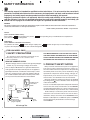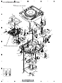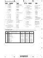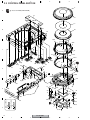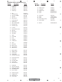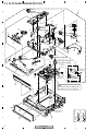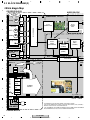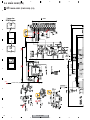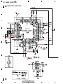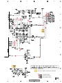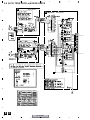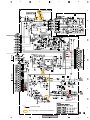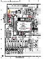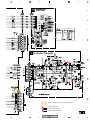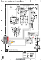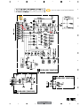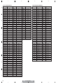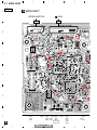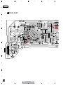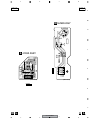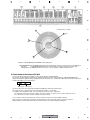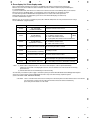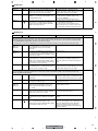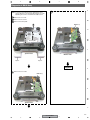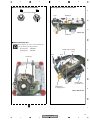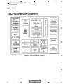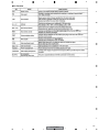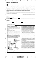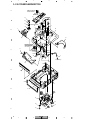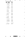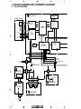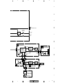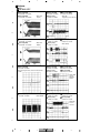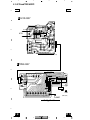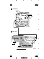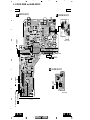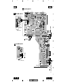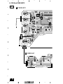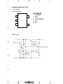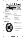
1
ORDER NO.
RRV3364
CDJ-800MK2
COMPACT DISC PLAYER
CDJ-800MK2
THIS MANUAL IS APPLICABLE TO THE FOLLOWING MODEL(S) AND TYPE(S).
Model
Type
Power Requirement
CDJ-800MK2
KUCXJ
AC 120 V
CDJ-800MK2
WYXJ5
AC 220 – 240 V
CDJ-800MK2
RLFXJ
AC 110-120 V / 220-240 V
Remarks
For details, refer to "Important symbols for good services" .
PIONEER CORPORATION
4-1, Meguro 1-chome, Meguro-ku, Tokyo 153-8654, Japan
PIONEER ELECTRONICS (USA) INC. P.O. Box 1760, Long Beach, CA 90801-1760, U.S.A.
PIONEER EUROPE NV Haven 1087, Keetberglaan 1, 9120 Melsele, Belgium
PIONEER ELECTRONICS ASIACENTRE PTE. LTD. 253 Alexandra Road, #04-01, Singapore 159936
PIONEER CORPORATION 2006
T-ZZR JUNE 2006 printed in Japan
1
2
3
4
SAFETY INFORMATION
A
This service manual is intended for qualified service technicians ; it is not meant for the casual do-ityourselfer. Qualified technicians have the necessary test equipment and tools, and have been trained
to properly and safely repair complex products such as those covered by this manual.
Improperly performed repairs can adversely affect the safety and reliability of the product and may
void the warranty. If you are not qualified to perform the repair of this product properly and safely, you
should not risk trying to do so and refer the repair to a qualified service technician.
WARNING
This product contains lead in solder and certain electrical parts contain chemicals which are known to the state of California to
causecancer, birth defects or other reproductive harm.
Health & Safety Code Section 25249.6 – Proposition 65
B
NOTICE
(FOR CANADIAN MODEL ONLY)
Fuse symbols
(fast operating fuse) and/or
parts must be of identical designation.
(slow operating fuse) on PCB indicate that replacement
REMARQUE
(POUR MODÈLE CANADIEN SEULEMENT)
Les symboles de fusible
(fusible de type rapide) et/ou
les pièces de remplacement doivent avoir la même désignation.
C
(fusible de type lent) sur CCI indiquent que
(FOR USA MODEL ONLY)
1. SAFETY PRECAUTIONS
The following check should be performed for the
continued protection of the customer and
ser vice technician.
ANY MEASUREMENTS NOT WITHIN THE LIMITS
OUTLINED ABOVE ARE INDICATIVE OF A POTENTIAL
SHOCK HAZARD AND MUST BE CORRECTED BEFORE
RETURNING THE APPLIANCE TO THE CUSTOMER.
LEAKAGE CURRENT CHECK
Measure leakage current to a known earth ground (waterpipe
, conduit, etc.) by connecting a leakage current tester
such as Simpson Model 229-2 or equivalent between the
earth ground and all exposed metal parts of the appliance
(input/output terminals, screwheads, metal overlays, control
shaft, etc.). Plug the AC line cord of the appliance directly
into a 120V AC 60Hz outlet and turn the AC power switch
on. Any current measured must not exceed 0.5mA.
D
Reading should
Leakage not be above
current 0.5mA
tester
Device
under
test
E
Test all
exposed metal
surfaces
Also test with
plug reversed
(Using AC adapter
plug as required)
Earth
ground
2. PRODUCT SAFETY NOTICE
Many electrical and mechanical parts in the appliance
have special safety related characteristics. These are
often not evident from visual inspection nor the protection
afforded by them necessarily can be obtained by using
replacement components rated for voltage, wattage, etc.
Replacement parts which have these special safety
characteristics are identified in this Service Manual.
Electrical components having such features are identified
by marking with a on the schematics and on the parts list
in this Service Manual.
The use of a substitute replacement component which does
not have the same safety characteristics as the PIONEER
recommended replacement one, shown in the parts list in
this Service Manual, may create shock, fire, or other hazards.
Product Safety is continuously under review and new
instructions are issued from time to time. For the latest
information, always consult the current PIONEER Service
Manual. A subscription to, or additional copies of, PIONEER
Service Manual may be obtained at a nominal charge
from PIONEER.
AC Leakage Test
F
2
CDJ-800MK2
1
2
3
4
5
6
7
IMPORTANT
THIS PIONEER APPARATUS CONTAINS
LASER OF CLASS 1.
SERVICING OPERATION OF THE APPARATUS
S H O U L D B E D O N E B Y A S P E C I A L LY
INSTRUCTED PERSON.
8
A
LASER DIODE CHARACTERISTICS
MAXIMUM OUTPUT POWER: 5 mW
WAVELENGTH: 780 – 785 nm
WARNING !
The AEL(accessible emission level) of the laser power output is less then CLASS 1
but the laser component is capable of emitting radiation exceeding the limit for
CLASS 1.
A specially instructed person should servicing operation of the apparatus.
B
LABEL CHECK
CDJ-800MK2 WYXJ5 and KUCXJ : Types Only
for RLFXJ
(DRW2308)
C
(DRW2248)
D
Additional Laser Caution
Bottom Plate
1. Laser Interlock Mechanism
The position of the switch (S1901) for detecting loading
completion is detected by the system microprocessor,
and the design prevents laser diode oscillation when
the switch is not in LPS1 terminal side (when the
mechanism is not clamped and LPS1 signal is
high level.)
Thus, the interlock will no longer function if the switch is
deliberately set to LPS1 terminal side. ( if LPS1 signal
is low level ).
In the test mode∗ the interlock mechanism will not
function. Laser diode oscillation will continue, if pin 41
of TC94A15FG (IC101) on the MAIN Assy is
connected to GND, or else the terminals of Q101 are
shorted to each other (fault condition).
E
2. When the cover is opened, close viewing of the
objective lens with the naked eye will cause exposure
to a Class 1 laser beam.
Printed on the Bottom Plate
∗ : Refer to page 86.
F
3
CDJ-800MK2
5
6
7
8
1
2
3
4
[Important Check Points for Good Servicing]
In this manual, procedures that must be performed during repairs are marked with the below symbol.
Please be sure to confirm and follow these procedures.
1. Product safety
A
Please conform to product regulations (such as safety and radiation regulations), and maintain a safe servicing environment by
following the safety instructions described in this manual.
1 Use specified parts for repair.
Use genuine parts. Be sure to use important parts for safety.
2 Do not perform modifications without proper instructions.
Please follow the specified safety methods when modification(addition/change of parts) is required due to interferences such as
radio/TV interference and foreign noise.
3 Make sure the soldering of repaired locations is properly performed.
B
When you solder while repairing, please be sure that there are no cold solder and other debris.
Soldering should be finished with the proper quantity. (Refer to the example)
4 Make sure the screws are tightly fastened.
Please be sure that all screws are fastened, and that there are no loose screws.
5 Make sure each connectors are correctly inserted.
Please be sure that all connectors are inserted, and that there are no imperfect insertion.
6 Make sure the wiring cables are set to their original state.
Please replace the wiring and cables to the original state after repairs.
In addition, be sure that there are no pinched wires, etc.
C
7 Make sure screws and soldering scraps do not remain inside the product.
Please check that neither solder debris nor screws remain inside the product.
8 There should be no semi-broken wires, scratches, melting, etc. on the coating of the power cord.
Damaged power cords may lead to fire accidents, so please be sure that there are no damages.
If you find a damaged power cord, please exchange it with a suitable one.
9 There should be no spark traces or similar marks on the power plug.
When spark traces or similar marks are found on the power supply plug, please check the connection and advise on secure
connections and suitable usage. Please exchange the power cord if necessary.
0 Safe environment should be secured during servicing.
D
When you perform repairs, please pay attention to static electricity, furniture, household articles, etc. in order to prevent injuries.
Please pay attention to your surroundings and repair safely.
2. Adjustments
To keep the original performance of the products, optimum adjustments and confirmation of characteristics within specification.
Adjustments should be performed in accordance with the procedures/instructions described in this manual.
3. Lubricants, Glues, and Replacement parts
Use grease and adhesives that are equal to the specified substance.
Make sure the proper amount is applied.
E
4. Cleaning
For parts that require cleaning, such as optical pickups, tape deck heads, lenses and mirrors used in projection monitors, proper
cleaning should be performed to restore their performances.
5. Shipping mode and Shipping screws
To protect products from damages or failures during transit, the shipping mode should be set or the shipping screws should be
installed before shipment. Please be sure to follow this method especially if it is specified in this manual.
F
4
CDJ-800MK2
1
2
3
4
5
6
7
8
CONTENTS
SAFETY INFORMATION......................................................................................................................................2
1. SPECIFICATIONS .............................................................................................................................................6
2. EXPLODED VIEWS AND PARTS LIST.............................................................................................................8
2.1 PACKING ....................................................................................................................................................8
2.2 EXTERIOR SECTION ..............................................................................................................................10
2.3 CONTROL PANEL SECTION...................................................................................................................12
2.4 SLOT-IN MECHANISM SECTION ............................................................................................................14
3. BLOCK DIAGRAM AND SCHEMATIC DIAGRAM ..........................................................................................16
3.1 BLOCK DIAGRAM....................................................................................................................................16
3.2 BLOCK DIAGRAM (2) ..............................................................................................................................18
3.3 BLOCK DIAGRAM (Power).......................................................................................................................20
3.4 OVERALL WIRING DIAGRAM .................................................................................................................22
3.5 MAIN (1/3) and RLYB ASSYS ..................................................................................................................24
3.6 MAIN ASSY(2/3).......................................................................................................................................26
3.7 MAIN ASSY(3/3).......................................................................................................................................30
3.8 AC IN, TRNS, SECB and REGB ASSYS..................................................................................................32
3.9 DFLB, JACK and KSWB ASSYS ..............................................................................................................34
3.10 JFLB, SLDB, SLMB and JOGB ASSYS .................................................................................................36
3.11 WAVEFORMS.........................................................................................................................................38
3.12 VOLTAGES..............................................................................................................................................45
4. PCB CONNECTION DIAGRAM ......................................................................................................................49
4.1 MAIN ASSY ..............................................................................................................................................50
4.2 RLYB ASSY ..............................................................................................................................................54
4.3 SECB ASSY .............................................................................................................................................56
4.4 TRNS ASSY..............................................................................................................................................60
4.5 AC IN ASSYS ...........................................................................................................................................62
4.6 DFLB ASSY ..............................................................................................................................................64
4.7 REGB and JACK ASSYS..........................................................................................................................68
4.8 KSWB ASSY.............................................................................................................................................70
4.9 JFLB ASSY...............................................................................................................................................72
4.10 SLDB ASSY............................................................................................................................................76
4.11 SLMB and JOGB ASSYS .......................................................................................................................78
5. PCB PARTS LIST ............................................................................................................................................80
6. ADJUSTMENT ................................................................................................................................................85
7. GENERAL INFORMATION .............................................................................................................................86
7.1 DIAGNOSIS..............................................................................................................................................86
7.1.1 SERVICE MODE ................................................................................................................................86
7.1.2 RESET and CLOCK MAP ..................................................................................................................92
7.1.3 TROBLE SHOOTING .........................................................................................................................94
7.1.4 POWER ON SEQUENCE ................................................................................................................105
7.1.5 DISASSEMBLY ................................................................................................................................106
7.2 PARTS ....................................................................................................................................................114
7.2.1 IC......................................................................................................................................................114
8. PANEL FACILITIES .......................................................................................................................................140
A
B
C
D
E
F
5
CDJ-800MK2
5
6
7
8
1
2
3
4
1. SPECIFICATIONS
Specifications
A
B
• KUCXJ type
1. General
• RLFXJ type
1. General
System..............................Compact disc digital audio system
Power requirements.....................................AC 120 V, 60 Hz
Power consumption.......................................................20 W
Operating temperature.......... +5˚C to +35˚C (+41˚F to +95˚F)
Operating humidity...............................................5 % to 85 %
(There should be no condensation of moisture.)
Weight..............................................................4.0 kg (8.8 lb)
Dimensions..................... 305 (W) × 344.1 (D) × 106.5 (H)mm
12 (W) × 13 –9/16 (D) × 4 – 1/4 (H) in
System........................... Compact disc digital audio system
Power requirements .... AC 110-120 V/220-240 V, 50/60 Hz
Power consumption ..................................................... 22 W
For Taiwan: 21 W
Operating temperature ..................................+5°C to +35°C
Operating humidity ........................................... 5 % to 85 %
(There should be no condensation of moisture.)
Weight ........................................................................4.0 kg
Dimensions .................. 305 (W) x 344.1 (D) x 106.5 (H) mm
2. Audio section
2. Audio section
Frequency response........................................4 Hz to 20 kHz
Signal-to-noise ratio.......................... 115 dB or more (JEITA)
Distortion.................................................... .0.006 % (JEITA)
3. Accessories
3. Accessories
C
• Operating instructions........................................................1
• Power cord........................................................................ 1
• Audio cable....................................................................... 1
• Control cable..................................................................... 1
• Forced eject pin (housed in a groove in the bottom panel)... 1
• Limited warranty................................................................ 1
NOTE:
Specifications and design are subject to possible modification
with-out notice.
• Operating instructions .....................................................
• Power cord ......................................................................
• Audio cable .....................................................................
• Control cable ...................................................................
• Forced eject pin (housed in a groove in the bottom panel)...
System.......................... Compact disc digital audio system
Power requirements .................... AC 220-240 V, 50/60 Hz
Power consumption ..................................................... 22 W
Operating temperature .................................. +5°C to +35°C
Operating humidity ............................................ 5 % to 85 %
(There should be no condensation of moisture.)
Weight ....................................................................... 4.0 kg
Dimensions ..................305 (W) x 344.1 (D) x 106.5 (H) mm
NOTE:
Specifications and design are subject to possible modification
with-out notice.
• You can find the voltage selector switch on the bottom plate
of the unit.
The factory setting for the voltage selector is 220 – 240 V.
Please set it to the correct voltage for your country or region.
• For Taiwan, please set to 110 – 120 V before using.
Before changing the voltage, disconnect the AC power cord.
Use a medium size screwdriver to change the voltage
selector switch.
220-240V
2. Audio section
Frequency response...................................... 4 Hz to 20 kHz
Signal-to-noise ratio ....................... 115 dB or more (JEITA)
Distortion ................................................... 0.006 % (JEITA)
110-120V
E
3. Accessories
• Operating instructions .....................................................
• Power cord ......................................................................
• Audio cable .....................................................................
• Control cable ...................................................................
• Forced eject pin (housed in a groove in the bottom panel)...
1
1
1
1
1
NOTE:
Specifications and design are subject to possible modification
with-out notice.
F
6
CDJ-800MK2
1
2
1
1
1
1
1
Voltage selector (RLFXJ type only)
• WYXJ5 type
1. General
D
Frequency response...................................... 4 Hz to 20 kHz
Signal-to-noise ratio ....................... 115 dB or more (JEITA)
Distortion ................................................... 0.006 % (JEITA)
3
4
5
6
7
8
A
Accessories
Power Cord
(ADG7021 : KUCXJ)
(ADG7097 : RLFXJ)
Audio Cable
(VDE1064) L=1.5m
Forced Fject Pin
(housed in a groove in
the bottom panel)
(DEX1008)
B
(ADG1154 : WYXJ,RLFXJ)
Control Cord
(XDE3063) L=1 m
C
D
E
F
7
CDJ-800MK2
5
6
7
8
1
2
3
4
2. EXPLODED VIEWS AND PARTS LIST
NOTES:
A
Parts marked by "NSP" are generally unavailable because they are not in our Master Spare Parts List.
The
mark found on some component parts indicates the importance of the safety factor of the part.
Therefore, when replacing, be sure to use parts of identical designation.
Screws adjacent to mark on product are used for disassembly.
For the applying amount of lubricants or glue, follow the instructions in this manual.
(In the case of no amount instructions, apply as you think it appropriate.)
2.1 PACKING
6
B
4
7
3
2
8
C
5
KUCXJ & RLFXJ
1
types only
9
1
1
WYXJ & RLFXJ
type only
D
10
13
KUCXJ type
only
E
11
12
14
F
8
CDJ-800MK2
1
2
3
4
5
6
7
8
PACKING parts List
Mark No.
>
1
2
3
4
NSP 5
6
7
8
Description
Mark No.
Part No.
AC Power Cord
Control Cord
Audio Cord
Operating Instructions
Polyethylene Bag
See Contrast table(2)
XDE3063
VDE1064
See Contrast table(2)
AHG7117
Pad B
Pad C
Pad D
DHA1556
DHA1557
DHA1558
9
10
11
12
NSP 13
NSP 14
Description
Part No.
Sheet
Push Rod
RHX1006
DEX1008
Pad A
Packing Case
Warranty Card
Label
DHA1555
See Contrast table(2)
See Contrast table(2)
See Contrast table(2)
A
(2) CONTRAST TABLE
CDJ-800MK2/KUCXJ, /WYXJ5 and RLFXJ types are constructed the same except for the following:
B
Mark No.
Symbol and Description
CDJ-800MK2/
KUCXJ
CDJ-800MK2/
WYXJ5
CDJ-800MK2/
RLFXJ
>
1 AC Power Cord
ADG7021
ADG1154
ADG1154
>
1 AC Power Cord
Not used
Not used
ADG7097
4 Operating Instructions (English)(KUCXJ)
DRB1401
Not used
Not used
4 Operating Instructions (WYXJ5)(English,
Not used
DRB1400
Not used
Not used
Not used
DRB1402
French, German, Italian, Dutch, Spanish)
4 Operating Instructions (RLFXJ)
(English, Spanish, Chinese)
12 Packing Case
DHG2595
DHG2594
DHG2596
NSP
13 Warranty Card
ARY7043
Not used
Not used
NSP
14 Label
DRW2311
VRW1629
VRW1629
C
D
E
F
9
CDJ-800MK2
5
6
7
8
1
2
3
4
2.2 EXTERIOR SECTION
Refer to
"2.3 CONTROL PANEL SECTION".
42
A
38
43
17
43
B
44
35
A
33
6
31
M
B
C
37
D 44
33x4
E
B
31
24
28
4
44 10
41
B D
5
F
41
I
45
33
G
44
13
31
9-(b)
41
C
33
34
F
I
H
31x4
C
44
14
18
D
3
19
32
44
12
7
2
E
15
44
Refer to
"2.4 SLOT-IN MECHANISM SECTION".
E
36
29
D
44
30
44
44
A
30
46x4
11
44
39
44
44
44
C
1
F 44
F
G
12
11
J
23
22
40
CONTACT SIDE
NON-CONTACT
SIDE
44
25
8
H
E
16
I
J
A
46
26
44
27
44
10
44
CDJ-800MK2
1
2
3
4
21
5
6
7
8
EXTERIOR SECTION parts List
Mark No.
>
>
>
Description
Mark No.
Part No.
1
2
3
4
5
MAIN Assy
AC IN Assy
TRNS Assy
SECB Assy
REGB Assy
DWG1622
See Contrast table(2)
See Contrast table(2)
DWR1309
DWR1310
6
7
8
9
10
SLMB Assy
RLYB Assy
JACK Assy
• • • •
Fuse
DWS1388
DWX2602
DWG1626
11
12
13
14
15
FFC (9p)
FFC (32p)
FFC (25p)
FFC (17p)
FFC (24p)
DDD1311
DDD1312
DDD1313
DDD1314
DDD1315
Earth Lead
Power Transfomer
Connector Assy
Connector Assy
• • • •
DE010VF0
See Contrast table(2)
PF03PP-B05
PF03PP-C12
NSP 16
>
17
18
19
20
21
NSP 22
23
24
Power Knob
Silicon Lubber D5 L
Bottom Cushion S4
Heat Sink
25
Description
Part No.
Earth Plate
DNH2532
Bottom Plate
Bottom Earth Plate
Trans Plate
Chassis
Insulator Assembly
See Contrast table(2)
DNH2694
DNH2733
See Contrast table(2)
DXA2069
Damper
Earth Spring
Float Spring (G5)
Front Sheet
Mecha Plate
CNV6011
DBH1398
DBH1494
DED1132
DNH2642
PCB Holder
Float Base 04 Assy
Laser Caution
Serial Label (UPC)
Screw
DNK4524
DXB1838
See Contrast table(2)
See Contrast table(2)
BBT30P060FCC
41
42
43
44
45
Screw
Screw
Screw
Screw
DM Screw (FTC)
BBZ30P060FTC
BBZ30P100FTC
BBZ40P060FTC
BPZ30P080FTB
DBA1260
46
Screw
IPZ30P100FTC
A
26
27
28
NSP 29
30
31
32
33
34
35
See Contrast table(2)
36
37
38
NSP 39
40
DAC2073
DEB1456
DEC2506
DNG1102
B
C
(2) CONTRAST TABLE
CDJ-800MK2/KUCXJ, /WYXJ5 and RLFXJ types are constructed the same except for the following:
Mark No.
CDJ-800MK2/
KUCXJ
Symbol and Description
CDJ-800MK2/
WYXJ5
CDJ-800MK2/
RLFXJ
>
2 AC IN ASSY
DWR1430
DWR1429
DWR1432
>
3 TRANS ASSY
DWR1371
DWR1371
DWR1428
>
10 Fuse (T1.6A)
AEK7075
Not used
Not used
>
10 Fuse (800MA)
Not used
REK1021
REK1021
>
17 Power Transfomer
DTT1204
DTT1203
DTT1203
26 Bottom Plate
DNK2689
DNK2689
DNK2691
29 Chassis
DNK4518
DNK4517
DNK4519
38 Laser Caution
DRW2308
DRW2308
DRW2248
39 Serial Label
DRW2311
VRW1629
VRW1629
NSP
D
E
F
11
CDJ-800MK2
5
6
7
8
1
2
3
4
2.3 CONTROL PANEL SECTION
8
A
* 1 Grease: GYA1001( ZLB-PN397B)
47
21
51
9
52
31
26
B
53
41
46
56x3
56
17
28x9
A
40
C
10
18
43
C
B
35
39
10
44
17x3
13
17
10x3
13x12
42
45
38-(b)
38-(a)
34
36
38-(c)
39
60
*1
32
58
48-2
58
58
50
A
6
2
H
27
13
13
E
37
D
13
33
29
1
G
58
30x8
58
58 D
60
58
20
58
58
58
4
58
J
C
12
58
E
58
56
B
58
58
15
54x2
23
58
D
CONTACT SIDE
NON-CONTACT
SIDE
F
5
48-1
49
57
58
22
61
24
L
3
6
11
K
*1
19
59
55
E
7
58
58
12
CDJ-800MK2
1
25
16
14
2
3
4
5
6
7
8
CONTROL PANEL SECTION parts List
Mark No.
Description
Mark No.
Part No.
1
2
3
4
5
DFLB Assy
KSWB Assy
JFLB Assy
SLDB Assy
JOGB Assy
DWG1623
DWS1386
DWG1624
DWS1387
DWG1625
6
7
8
9
10
FFC
Connector Assy
Jog Panel (PMMA)
Jog Plate
SW spring 25
DDD1220
PF04PP-B07
DAH2182
DAH2438
DBH1514
11
12
13
14
15
Gear spring 200
ARM Sprimg
SW Cushion HH48/2
Encorder Plate
Protector Sheet
DBH1525
DBH1566
DEC2538
DEC2889
DEC2945
16
17
18
19
20
FL Sheet
Ring Cushion L24/2.0
SW Ring
Adjust Plate
Jog Holder
DEC2946
DEC2958
DNK4070
DNK4178
DNK4545
Description
Part No.
50
FFC Guard
DEC2586
51
52
53
54
55
Reloop Guard
Q R Guard
Control Panel
Screw
Screw
DNK4057
DNK4058
DNK4525
BPZ20P060FTC
BPZ20P100FTC
56
57
58
59
60
Screw (FE)
Screw
Screw
Ecsane Tape (10x50 )
Cord Clamper
DBA1265
IPZ30P100FTC
BPZ30P080FTB
DEC2988
RNH-184-0
61
Washer
WA42D080D050
A
B
C
21
22
23
24
25
Jog B
Gear ARM
Gear
Smoother
Load Gear A
DNK4557
DNK4559
DNK4560
DNK4561
DNK4562
26
27
28
29
30
Jog A
Sheet SW
Roller A Assy
Jog Stay Assy
Roller B Assy
DNK4586
DSX1065
DXB1825
DXB1876
DXB1877
31
32
33
34
35
Rotary Knob C
TEMPO Knob
VINYL Knob
LOOP Knob
Auto Beat Loop Knob
DAA1194
DAC2061
DAC2063
DAC2066
DAC2069
36
37
38
39
40
Quick Return Knob
PLAY Knob
Set Knob (Eject)
CALL Knob
RELOOP Knob
DAC2070
DAC2286
DAC2287
DAC2289
DAC2291
41
42
43
44
45
Slide Knob
TEXT/A.CUE Knob
Folder Search Knob
DEL/MEMO Knob
Reverse Knob
DAC2292
DAC2294
DAC2298
DAC2299
DAC2364
46
47
48
49
Slide Sheet (gray)
Display Panel
Earth Plate (CU)
Vessel Sheet
DAH2374
DAH2418
DBK1224
DEC2495
D
E
F
13
CDJ-800MK2
5
6
7
8
1
2
3
4
2.4 SLOT-IN MECHANISM SECTION
Grease
GYA1001
(ZLB-PN397B)
A
1
11
20
21
Dyefree
GEM1036
(ZLX-ME413A) 9
23
10
18
17
Grease
GYA1001
(ZLB-PN397B)
7
B
22
24
13
14
19
C
Dyefree
GEM1036
(ZLX-ME413A)
8
Dyefree
GEM1036 (ZLX-ME413A)
15
Cleaning liquid : GEM1004
Cleaning paper : GED-008
25
To
RLYB CN12
(Pickup)
16
3
4
5
To
RLYB CN16
(Loading Motor)
12
D
25
To
RLYB CN14
(Stepping Motor)
25
Grease
GYA1001
(ZLB-PN397B)
6
27
2
25
31
Note:
The TM. Assy 03-S is supplied only in
assembly form, not as a single part.
E
F
To MAIN CN102
(Spindle Motor)
26
28
30
14
CDJ-800MK2
1
2
3
4
CONTACT SIDE
29
NON-CONTACT
SIDE
30
5
6
7
8
SLOT-IN MECHANISM SECTION parts List
Mark No.
Description
Part No.
NSP 1
2
3
NSP 4
NSP 5
Slot-in Mecha SV Assy
TM. Assy 03-S
Loading Motor Assy-S
Worm Gear
DC Motor S (ROHS)
DXA2005
VXX3125
DXX2510
DNK3910
DXM1230
6
7
8
9
10
Connector Assy
Clamp Spring
Guide Spring
SW Lever Spacer SV
Loading Lever
PF02PY-B22
DBH1374
DBH1375
DEC2831
DNK3406
11
12
13
14
15
Main Cam
Disc Guide
Clamp Arm
Eject Lever
Lever AP
DNK3407
DNK3478
DNK3576
DNK3684
DNK3835
16
17
18
19
20
Lever BP
Loading Gear
Drive Gear
Loading Base SV
SW Lever SV1
DNK3836
DNK3911
DNK3912
DNK4369
DNK4370
A
B
C
21
22
23
24
25
SW Lever SV2
Gear Holder SV
Clamper 04 Assy
Screw
Floating Rubber (SI)
DNK4371
DNK4372
DXB1859
BPZ20P060FTC
VEB1351
26
27
28
29
30
Float Base 04 Assy
Spacer POR (T3)
Vessel Cushion A
Vessel Cushion B
Vessel Cushion C
DXB1838
DEB1566
DEC2852
DEC2853
DEC2854
31
Front Sheet
DED1132
D
E
F
15
CDJ-800MK2
5
6
7
8
1
2
3
4
3. BLOCK DIAGRAM AND SCHEMATIC DIAGRAM
3.1 BLOCK DIAGRAM
A
TM. ASSY 03-S (VXX3125)
SPINDLE
MOTOR 04
M63018FP
STEPPING
MOTOR 04
B
PICKUP ASSY
Loading MOTOR
ASSY-S
(DXX2510)
C
M
SLMB ASSY
COMPARATOR
B
SLOT-IN
MECHANISM SV
ASSY
RLYB ASSY
A
MAIN ASSY
NJM2885DL1
D
J91
BA008C0WCP
CN301
CN301
BA008C0WCP
CN53
F
CN52
REGB ASSY
V+10B
V+7A
CN53
V+6B
V+3D
E
For KUCXJ, WYXJ5
C
CN51
11
SECB ASSY
9
CN22
E
ACIN ASSY
CN56
J2
D
For RLFXJ
TRNS ASSY
S2
CN50
BROWN
S1
VIOLET
F
J3
BLUE
E
ACIN ASSY
16
CDJ-800MK2
1
2
3
4
5
A
6
7
8
A
÷ When ordering service parts, be sure to refer to "EXPLODED VIEWS and PARTS LIST" or
"PCB PARTS LIST".
÷ The > mark found on some component parts indicates the importance of the safety factor
of the part. Therefore, when replacing, be sure to use parts of identical designation.
÷
: The power supply is shown with the marked box.
MAIN ASSY
IC300
IC303
K U
8 Mbit
64 Mbit
B
IC701
DSPC56371AF180-K
I
JACK ASSY
IC301
SCF5249VM140-K
MPU
IC801
OP AMP
JA801
DKB1053
AUDIO OUT
C
CN701
CN801
1
9
4
6
9
1
JA802
PKB1033
IC702
PE8001A
IC304
DIGITAL OUT
BU4230G
CN802
D
CN602
CN601
CN1601
L
G
DFLB ASSY
JOGB ASSY
CN500
CN501
CN1503
J
CN502
SLDB ASSY
CN503
E
K JFLB ASSY
CN600
CN1502
F
H
KSWB ASSY
17
CDJ-800MK2
5
6
7
8
1
2
3
4
3.2 BLOCK DIAGRAM (2)
• Blick diagra Map
A
CD DRIVE BLOCK
M
Pickup ASSY
KP 2PIN
B
DRIVE ASSY
SLMB ASSY
DWS1388
SW
M
KP 3PIN
C
IC701
AUDIO
DSP
IC102 DRIVER
Spindle
DWG1622
IC101
SERVO DSP
IC302
FPGA
(50000GATE)
FFC 32PIN
M
DWX2602
SLED
MAIN ASSY
IC
RLYB ASSY
B
A
KP 4PIN
TRAVERS
MECHA
FFC 17PIN
M
Loading
AUDIO BLOCK
IC301
MPU
(140MHz)
SDRAM
(64 Mbit)
R
1
FLASH
(8 Mbit)
FFC 25PIN
REGB ASSY
SEC
DWR1310
DWR
+3.3V
D
+7V
TRNS ASSY
Transformer
V+6
UnReg
E
IC91
C
6PIN
F
IC92
D
V+10
UnReg
Vload
+32V
POWER
SUPPLY
FLAC_D
FLAC_J
3PIN
DATA
Cntrol
E
CDJ-800MK2 has two MPU, MPU (MAIN), DISPLAY-MPU (DFLB).
One controls CORE BLOCK, Another is Top panel about DISPLAY, LED, VOLUME, S
RESET IC and X'TAL have on the MAIN ASSY too.
It has two MEMORY. One 64MB sized SDRAM, Another is 8MB sized FLASH MEMOR
About POWER BLOCK, Please refer to POWER DELIVERY MAP.
ACIN ASSY
F
POWER BLOCK
18
CDJ-800MK2
1
2
3
4
5
6
7
8
A
IO BLOCK
AUDIO OUT LINE
DIGITAL OUT LINE
AUDIO MUTE LINE
CONTROL LINE
DRIVE CONTROL
JACK ASSY DWG1626
I
ZERO
DETECT
AUDIO OUT
(L/R)
9PIN
IC701
AUDIO
DSP
IC801 OPAMP
FFC
IC702
DAC
MUTE
MUTE
B
IC301
MPU
(140MHz)
RESET IC
16.934MHz
CORE BLOCK
Digital OUT
PANEl BLOCK
KSWB ASSY DWS1386
H
C
LED
SW
B to B 8PIN
SECB ASSY
SLDB ASSY
G DFLB ASSY
DWR1309
DWS1387-A/J
DWS1387
DWG1623
C
LED
SW
Vol
J
D
IC501
DISPLAY
MPU
(MASK)
RESET IC
B to B 11PIN
FFC 17PIN
VYNIL
16.00MHz
SW
SLIDER
E
V501
DATA FL
JOGB ASSY
Cntrol
JOG
FL
(DFLB).
ISPLAY, LED, VOLUME, SW, JOG, etc.
K
8MB sized FLASH MEMORY.
Y MAP.
DWG1625
13PIN
KP 4PIN
DATA
R to R
JFLB ASSY DWG1624
L
Rotation Detect
19
CDJ-800MK2
5
6
F
7
8
1
2
3
4
3.3 BLOCK DIAGRAM (Power)
• Power Delivery Map
A
Motor Drive
MAIN ASSY
A DWG1622
GNDM
M
TRAVERS
MECHA
B
Spindle
M
M
SLED
5A
DAC
IC704 <0.3A
GNDM
RLYB ASSY DWX2602
Loading
Pickup ASSY
B
MUTE
GNDD
GN
+1.2D
IC307 <0.6A
FPGA (SPARTAN3)
IC703 <0.6A
DSP
IC305 <0.5A
CPU (AMADEUS)
IC306 <0.5A
FPGA (SPARTAN3)
GN
Stby
1.25D
1.8D
2.5D
GNDS
V+3D
CUP 21 FPGA 60 DSP 5
SDRAM 22 FLASH 5
C
SLMB ASSY
DWS1388
3.3S
GNDD
ServoDSP 83
M
IC100 <x.x0.6A
LD 80
F
V+5P
V+6B
GNDS
REGB ASSY
DWR1310
V+7M V+8A
GNDD
GNDM
GNDS
C SECB
DWR130
+3.3D
-7
IC91
<
<1.0A
D
C52
IC92
+7A
TRNS ASSY
Transformer
V+6
UnReg
E
V+10
UnReg
Vload
+32V
ICP
<10 A
IC56
<1.0A
D
IC57 <1.0A
ICP <200mA IC60
+5P
IC23,24
+8A
<3.5A
IC21,22
<800mA IC53
<5.0A
IC25
<1.5A IC54
<1A IC50
C
<0.8A IC61
GN
<200mA
IC58
<630mA
<200mA
IC59
Q53
FLAC_D
FLAC_J
3.3V
3.3V
E
F
ICP
IC Protect
Pori SW
FUSE
A MAX SPEC
ACIN ASSY
20
DATA
Regurator supporting Current Shutdown
15W POINT
Before REG-IC
GND
Screw (Chasis GND)
CDJ-800MK2
1
2
3
Cntrol
4
5
6
7
8
A
JACK ASSY DWG1626-A/J
I
DAC
<0.3A
L
OP
AMP
MUTE
R
Jack
GNDD
GNDA
B
D
6A
GNDD
FPGA (SPARTAN3)
Stby
6A
DSP
5A
CPU (AMADEUS)
5A
FPGA (SPARTAN3)
CUP 21 FPGA 60 DSP 5
KSWB ASSY DWS1386 H
SDRAM 22 FLASH 5
LED
ServoDSP 83
A
SW
LD 80
GNDAD
GNDS
GNDS
C
C SECB ASSY
V+5P
V+7
SLDB ASSY
G DFLB ASSY
DWR1309
DWS1387
DWG1623
SW
-7
LED
GNDD
J
<1.0A IC51
LED
GNDD
EarthPlate
ChasisGND
Vol
GNDF
GNDAD
DISPLAY
MPU
SW
C506
GNDD
SLIDER
DATA FL
DATA
Cntrol
15W POINT
Before REG-IC
GND
Screw (Chasis GND)
E
JOGB ASSY
GNDD
GNDD
n
V+5P
L
JOG
FL
<200mA IC603
Q604
DWG1625
K JFLB ASSY DWG1624
6
F
Rotation Detect
21
CDJ-800MK2
5
D
VYNIL
GNDF
7
8
1
2
3
4
3.4 OVERALL WIRING DIAGRAM
A
(VXX3125)
CD PLAYER UNIT
B
C
(Loading Motor Assy-S)
DXX2510
SLOT-IN
D
B RLYB ASSY
M
SLMB ASSY
E
D TRNS ASSY
ACIN ASSY
DWR1429(WYXJ5)
DWR1430(KUCXJ)
(RLFXJ)
(KUCXJ, WYXJ5)
C SECB ASSY
E
E
ACIN ASSY
DWR1432(RLFXJ)
F
REGB ASSY
F
22
CDJ-800MK2
1
2
3
4
5
6
7
8
A MAIN ASSY
( A 1/3 – A 3/3)
A
B
I
JACK ASSY
C
JFLB ASSY
L
JOGB ASSY
K
SLDB ASSY
D
J
G DFLB ASSY
E
H
KSWB ASSY
F
23
CDJ-800MK2
5
6
7
8
1
2
3
4
3.5 MAIN (1/3) and RLYB ASSYS
A 1/3 MAIN ASSY (DWG1622)
A
20
17
28
B
12
(TS)
(F)
14
9
(TS)
(TS)
(TS)
11
(F)
8
C
(RF)
(RF)
(RF)
(RF)
(RF)
(TD)
(TD)
(RF)
(RF)
(RF)
(F)
(F)
(F)
(F)
(RF)
(RF)
1
2
13
D
5
16
(S)
(S)
15
(S)
10
(S)
to SPINDLE MOTOR
E
37
(S)
(S)
38
(F)
(F)
(S)
(S)
(F)
(TS)
(TS)
(TS)
(TS)
(F)
F
A 1/3
24
CDJ-800MK2
1
2
3
4
5
6
7
8
(RF)
: RF DATA SIGNAL ROUTE
A
(TD)
: TRACKING DATA SIGNAL ROUTE
(F)
: FOCUS SERVO LOOP LINE
(TS)
: TRACKING SERVO LOOP LINE
(S)
: STEPPING SERVO LOOP LINE
(F)
(RF)
(F)
(RF)
(F)
(RF)
(F)
to PICK UP ASSY (CN1)
(RF)
B
(TD)
(TD)
4
C
3
(TS)
(TS)
(F)
(F)
M CN1901
6
7
to LOADING MOTOR
(S)
D
(S)
(S)
to STEPPER MOTOR
(S)
RLYB ASSY
B (DWX2602)
E
: The Power supply is shown with the marked box.
F
A 1/3 B
25
CDJ-800MK2
5
6
7
8
1
2
3
4
3.6 MAIN ASSY(2/3)
A 2/3
MAIN ASSY (DWG1622) (1/2)
A
Large size
SCH diagram
C
CN53
1/2
(Data)
(Data)
B
22
2/2
C
(Data)
(Data)
(Data)
1/2
(Data)
D
(Data)
(Data)
: PANEL DATA (Digital)
A 2/3
E
18
71
F
26
CDJ-800MK2
1
2
3
4
5
6
7
8
A
A 3/3
27
26
B
24
C
19
D
36
MODE
MODE
E
F
27
CDJ-800MK2
5
6
7
8
1
A 2/3
3
4
MAIN ASSY (DWG1622) (2/2)
: The Power supply is shown with the marked box.
A
2
B
25
C
Large size
SCH diagram
30
1/2
(Data)
(Data)
D
(Data)
(Data)
2/2
E
to ICE BOARD
2/2
F
A 2/3
28
CDJ-800MK2
1
2
3
4
5
6
7
8
A
B
A 3/3
C
A 3/3
D
23
E
(Data)
: PANEL DATA (Digital)
F
A 2/3
29
CDJ-800MK2
5
6
7
8
1
2
3
4
3.7 MAIN ASSY(3/3)
A 3/3
MAIN ASSY (DWG1622)
(Data)
A
B
C
A 2/3
31
32
34
A 2/3
D
21
A 2/3
29
E
F
A 3/3
30
CDJ-800MK2
1
2
3
4
5
6
7
8
A
70
46
44
39
45
B
(Ana)
A 2/3
(Ana)
33
41
(Data)
C
42
43
D
35
E
: The Power supply is shown with the marked box.
(Data)
: AUDIO DATA (Digital)
(Ana)
F
: AUDIO Lch OUT (Analog)
: DATA AUDIO OUT (Digital)
A 3/3
31
CDJ-800MK2
5
6
7
8
1
2
3
4
3.8 AC IN, TRNS, SECB and REGB ASSYS
E
A
ACIN ASSY
DWR1439 (KUCXJ)
DWR1429 (WYXJ5)
D TRNS ASSY
DWR1371 (KUCXJ, WYXJ5)
DWR1428 (RLFXJ)
B
E
ACIN ASSY
DWR1432 (RLFXJ)
C
D
E
KUCXJ
WYXJ5
DWR1371
DWR1371
RLFXJ
F
E D
32
CDJ-800MK2
1
2
3
4
5
6
7
8
C SECB ASSY (DWR1309)
A
F
REGB ASSY
B
C
CN501
CN802
(Data)
I
G
(Data)
t
A 2/3 CN301
D
(Data)
E
(Data)
59
58
(Data)
: AUDIO DATA (Digital)
F
: The Power supply is shown with the marked box.
C F
33
CDJ-800MK2
5
6
7
8
1
2
3
4
3.9 DFLB, JACK and KSWB ASSYS
A
G DFLB ASSY (DWG1623)
50
13
53
51
B
(Data)
56
57
CN56
52
54
55
C
48
74
C
(Data)
(Data)
72
D
49
E
F
G
34
CDJ-800MK2
1
2
3
4
5
6
H
7
8
KSWB ASSY
(DWS1386)
A
K
CN600
B
C
I
JACK ASSY (DWG1626)
47
40
(Ana)
A 3/3 CN701
(Ana)
CN50
D
CN1503
C
E
J
: The Power supply is shown with the marked box.
(Data)
(Ana)
: PANEL DATA (Digital)
F
: AUDIO Lch OUT (Analog)
: DIGITAL AUDIO OUT (Digital)
H I
35
CDJ-800MK2
5
6
7
8
1
2
3
4
3.10 JFLB, SLDB, SLMB and JOGB ASSYS
A
B
C
D
66
to Sheet SW
(DSX1065)
CN500
60
61
62
63
G
64
65
L
CN1601
E
K JFLB ASSY (DWG1624)
F
K
36
CDJ-800MK2
1
2
3
4
5
6
7
8
A
: The Power supply is shown with the marked box.
68
CN503
B
67
G
69
C
D
J
SLDB ASSY (DWS1387)
E
B
K
CN1105
CN601
M SLMB ASSY (DWS1388)
L
JOGB ASSY (DWG1625)
F
J L M
37
CDJ-800MK2
5
6
7
8
1
2
3
4
3.11 WAVEFORMS
Note: The numbers for the waveform photos (circled) are identical to those for the schematic diagrams, PCB diagrams,
and troubleshooting flowcharts.
A
A
MAIN ASSY
CD player
CD player
CD player
RF eye pattern waveform (RFO)
Load in (2/2)
Focus in (1/2)
1
CH1 : RFO
V: 500 mV/div. H: 200 nsec/div.
3
4
6
7
B
CH1 : LPS1
V: 5.0 V/div.
CH2 : LPS2
V: 5.0 V/div.
CH3 : LO+
V: 5.0 V/div.
CH4 : LO–
V: 5.0 V/div.
8
H: 100 msec/div.
CH1 : FE
V: 0.5 V/div. H: 2 msec/div.
H: 100 msec/div.
H: 100 msec/div.
H: 100 msec/div.
CH1
CH2
CH3
CH4
CD player
CD player
CD player
RF eye pattern waveform (AGCRF)
Load out (1/2)
Focus in (2/2)
2
C
CH1 : AGCRF
V: 500 mV/div. H: 200 nsec/div.
3
4
5
CH1 : LPS1
V: 2.0 V/div. H: 500 msec/div.
CH2 : LPS2
V: 2.0 V/div. H: 500 msec/div.
CH3 : PWMLO
V: 2.0 V/div. H: 500 msec/div.
8
9
CH1 : FE
V: 0.5 V/div. H: 100 msec/div.
CH2 : FOO
V: 0.5 V/div. H: 100 msec/div.
CH1
CH1
D
CH2
CH2
CH3
CD player
CD player
CD player
Load in (1/2)
Load out (2/2)
Start up
3
4
5
CH1 : LPS1
V: 2.0 V/div. H: 100 msec/div.
CH2 : LPS2
V: 2.0 V/div. H: 100 msec/div.
CH3 : PWMLO
V: 2.0 V/div. H: 100 msec/div.
E
3
4
6
7
CH1 : LPS1
V: 5.0 V/div.
CH2 : LPS2
V: 5.0 V/div.
CH3 : LO+
V: 5.0 V/div.
CH4 : LO–
V: 5.0 V/div.
H: 500 msec/div.
10
H: 500 msec/div.
8
H: 500 msec/div.
11
H: 500 msec/div.
12
CH1
CH1
CH1
CH1 : INSIDE
V: 5.0 V/div. H: 200 msec/div.
CH2 : FE
V: 1.0 V/div. H: 200 msec/div.
CH3 : TE
V: 1.0 V/div. H: 200 msec/div.
CH4 : DMO
V: 2.0 V/div. H: 200 msec/div.
CH2
CH2
CH2
CH3
CH3
CH4
CH3
CH4
F
38
CDJ-800MK2
1
2
3
4
5
A
6
7
8
MAIN ASSY
A
CD player
CD player
CD player
Stop
Pause
Track search (1/2)
8
11
12
13
CH1 : FE
V: 1.0 V/div.
CH2 : TE
V: 1.0 V/div.
CH3 : DMO
V: 2.0 V/div.
CH4 : LDO
V: 2.0 V/div.
H: 200 msec/div.
11
H: 200 msec/div.
14
H: 200 msec/div.
1
H: 200 msec/div.
17
CH1 : TE
V: 1.0 V/div. H: 1 msec/div.
CH2 : TRO
V: 1.0 V/div. H: 1 msec/div.
CH3 : RFO
V: 1.0 V/div. H: 1 msec/div.
CH4 : SBOK
V: 5.0 V/div. H: 1 msec/div.
11
14
1
17
CH1 : TE
V: 1.0 V/div. H: 50 msec/div.
CH2 : TRO
V: 1.0 V/div. H: 50 msec/div.
CH3 : RFO
V: 1.0 V/div. H: 50 msec/div.
CH4 : SBOK
V: 5.0 V/div. H: 50 msec/div.
CH1
CH1
CH1
CH2
CH2
CH2
CH3
CH3
CH4
CH4
B
CH3
CH4
CD player
CD player
CD player
Auto adjust
Scan (1/2)
Track search (2/2)
8
9
11
14
CH1 : FE
V: 1.0 V/div.
CH2 : FOO
V: 1.0 V/div.
CH3 : TE
V: 1.0 V/div.
CH4 : TRO
V: 2.0 V/div.
H: 500 msec/div.
11
H: 500 msec/div.
14
H: 500 msec/div.
1
H: 500 msec/div.
17
CH1 : TE
V: 1.0 V/div. H: 2 msec/div.
CH2 : TRO
V: 1.0 V/div. H: 2 msec/div.
CH3 : RFO
V: 1.0 V/div. H: 2 msec/div.
CH4 : SBOK
V: 5.0 V/div. H: 2 msec/div.
8
11
15
16
CH1 : FE
V: 1.0 V/div. H: 50 msec/div.
CH2 : TE
V: 1.0 V/div. H: 50 msec/div.
CH3 : SL1IN
V: 1.0 V/div. H: 50 msec/div.
CH4 : SL2IN
V: 1.0 V/div. H: 50 msec/div.
CH1
CH1
CH1
CH2
CH2
CH2
CH3
CH3
CH3
CH4
CD player
CD player
Play
Scan (2/2)
11
15
16
D
CH4
CH4
8
C
CH1 : FE
V: 1.0 V/div. H: 500 msec/div.
CH2 : TE
V: 1.0 V/div. H: 500 msec/div.
CH3 : SL1IN
V: 1.0 V/div. H: 500 msec/div.
CH4 : SL2IN
V: 1.0 V/div. H: 500 msec/div.
8
11
15
16
Reset system in the core block
CH1 : FE
V: 1.0 V/div. H: 50 msec/div.
CH2 : TE
V: 1.0 V/div. H: 50 msec/div.
CH3 : SL1IN
V: 1.0 V/div. H: 50 msec/div.
CH4 : SL2IN
V: 1.0 V/div. H: 50 msec/div.
18
19
20
21
CH1 : RST from Reset IC to CPU
V: 5.0 V/div. H: 200 msec/div.
CH2 : PRGM from CPU to FPGA through IC312
V: 5.0 V/div. H: 200 msec/div.
CH3 : SRVRST from CPU to IC101
V: 5.0 V/div. H: 200 msec/div.
CH4 : DSPRST from CPU to IC701
V: 5.0 V/div. H: 200 msec/div.
Conditions: At the time of power on,
without a disc loaded
a - b : 370 msec
a - c : 636 msec
a -d : 1 182 msec
e - a : 70 msec
Reset clear
CH1
CH1
CH2
CH1
CH2
CH3
CH3
CH4
CH4
3.3 V
a
CH2
3.3 V
b
CH3
CH4
d
e
E
c
3.3 V
3.3 V
F
39
CDJ-800MK2
5
6
7
8
1
A
A
2
3
4
MAIN ASSY
MPU
FPGA
Audio DSP
Delay time of Reset IC (IC304)
Configuration (2/3)
Configuration (2/2)
CH2 : XINIT to CPU
V: 5.0 V/div. H: 100 msec/div.
: DATA from CPU
26 CH4
V: 5.0 V/div. H: 100 msec/div.
: DONE to CPU
27 CH5
V: 5.0 V/div. H: 100 msec/div.
: XFRST from CPU
30 CH8
V: 5.0 V/div. H: 100 msec/div.
Conditions: At the time of power on, without a disc loaded
29
22
18
CH1 : V+3D
V: 2.0 V/div. H: 10 msec/div.
CH2 : RST from Reset IC to CPU
V: 2.0 V/div. H: 10 msec/div.
24
Conditions: At the time of power on, without a disc loaded
Remark: Set value for reset delay time: 70 msec
26
34
35
CH1 : DSP16M from FPGA
V: 5.0 V/div. H: 200 msec/div.
CH5 : DATA from CPU
V: 5.0 V/div. H: 200 msec/div.
CH6 : DSPDREQ to FPGA & CPU
V: 5.0 V/div. H: 200 msec/div.
CH7 : DAC11M to IC702
V: 5.0 V/div. H: 200 msec/div.
Conditions: At the time of power on, without a disc loaded
a - b : 442 msec
a - c : 682 msec
a - b : 68.7 msec
a - b : 670 msec
B
CH2
CH1
b
a
b
a
CH1
3.3 V
Power ON
CH5
CH4
c
Reset clear
3.3 V
CH2
a
C
b
CH5
CH6
CH8
CH7
MPU
FPGA
Servo DSP
Association between the 16.93 MHz clock
signal and resetting of the MPU
Configuration (3/3)
Configuration (1/2)
22
71
18
CH1 : V+3D
V: 5.0 V/div. H: 10 msec/div.
CH2 : CPU16M from IC310 to CPU
V: 5.0 V/div. H: 10 msec/div.
CH3 : RST from Reset IC to CPU
V: 5.0 V/div. H: 10 msec/div.
27
28
29
30
Conditions: At the time of power on, without a disc loaded
CH5 : DONE to CPU
V: 5.0 V/div. H: 100 msec/div.
CH6 : SRV16M to IC101
V: 5.0 V/div. H: 100 msec/div.
CH7 : DSP16M to IC701
V: 5.0 V/div. H: 100 msec/div.
CH8 : XFRST from CPU
V: 5.0 V/div. H: 100 msec/div.
20
36
37
Conditions: At the time of power on, without a disc loaded
a - b : 67.8 msec
CH1
28
CH1 : SRV16M from FPGA
V: 5.0 V/div. H: 200 msec/div.
CH2 : SRVRST from CPU
V: 5.0 V/div. H: 200 msec/div.
CH3 : SRVBUS0 CPU - SRV
V: 5.0 V/div. H: 200 msec/div.
CH4 : DRVMUTE1 from CPU to IC102
V: 5.0 V/div. H: 200 msec/div.
Conditions: At the time of power on, without a disc loaded
a - b : 681 msec
CH5
a - b : 1 256 msec
CH1
b
a
a
CH2
D
CH3
a
CH2
CH7
CH3
CH8
CH4
b
b
FPGA
Audio DSP
Servo DSP
Configuration (1/3)
Configuration (1/2)
Configuration (2/2)
23
24
25
E
CH6
26
CH1 : PROG_B (IC302 - pin 99) from CPU to FPGA
V: 5.0 V/div. H: 100 msec/div.
CH2 : XINIT to CPU
V: 5.0 V/div. H: 100 msec/div.
CH3 : CLK from CPU to FPGA
V: 5.0 V/div. H: 100 msec/div.
CH4 : DATA from CPU
V: 5.0 V/div. H: 100 msec/div.
Conditions: At the time of power on, without a disc loaded
29
21
31
32
CH1 : DSP16M from FPGA
V: 5.0 V/div. H: 200 msec/div.
CH2 : DSPRST from CPU
V: 5.0 V/div. H: 200 msec/div.
CH3 : DSPSIN to CPU
V: 5.0 V/div. H: 200 msec/div.
CH4 : CLK from CPU
V: 5.0 V/div. H: 200 msec/div.
c
36
38
CH1 : SRV16M from FPGA
V: 5.0 V/div. H: 200 msec/div.
CH2 : SRVRST from CPU
V: 5.0 V/div. H: 200 msec/div.
CH3 : SRVBUS0 CPU - SRV
V: 5.0 V/div. H: 200 msec/div.
CH5 : DRVMUTE2 from CPU to IC102
V: 5.0 V/div. H: 200 msec/div.
Conditions: At the time of power on, without a disc loaded
a - b : 1 256 msec
a - c : 1 318 msec
a - b : 680 msec
b
CH1
CH1
CH2
CH2
CH2
CH3
CH3
CH3
CH4
CH5
CH4
a
a
a
F
20
Conditions: At the time of power on, without a disc loaded
a - b : 69 msec
a - c : 442 msec
b - c : 373 msec
CH1
28
b
40
b
c
CDJ-800MK2
1
2
3
4
5
6
7
8
A
A
MAIN ASSY
DAC
Audio mute
Audio mute
DAC reset
Association between zero-data detection and
muting control (1/2)
Conditions in which muting for zero-data
detection is activated (pause, continuous search)
CH1 : DACLRCK from DAC
V: 5.0 V/div. H: 1 sec/div.
: DACDATA from DAC
42 CH2
V: 5.0 V/div. H: 1 sec/div.
: DACBCK from DAC
43 CH3
V: 5.0 V/div. H: 1 sec/div.
: ZERO to CPU
44 CH4
V: 5.0 V/div. H: 1 sec/div.
Conditions: At the time of power on, with a disc loaded
41
18
35
39
40
CH1 : RST from CPU Reset IC
V: 2.0 V/div. H: 1 sec/div.
CH2 : DAC11M from AUDIO DSP
V: 5.0 V/div. H: 1 sec/div.
CH3 : DACRST from CPU IC
V: 2.0 V/div. H: 1 sec/div.
CH4 : L4 (JACK Assy) Audio Signal Line
V: 20.0 V/div. H: 1 sec/div.
41
The MPU is started after a specific delay time.
42
43
44
CH1 : DACLRCK from DAC
V: 5.0 V/div. H: 1 sec/div.
CH2 : DACDATA from DAC
V: 5.0 V/div. H: 1 sec/div.
CH3 : DACBCK from DAC
V: 5.0 V/div. H: 1 sec/div.
CH4 : ZERO to CPU
V: 5.0 V/div. H: 1 sec/div.
Conditions: During playback
B
a - b : 690 msec
CH1
CH1
CH1
CH2
CH2
CH2
CH3
DAC reset
CH3
CH3
7 sec typ
CH4
a
PLAY start
b
During
pause
During continuous search
(fast forward)
CH4
CH4
Power ON
PLAY start
DAC
Audio mute
Audio mute
Initialization of DAC (downloading using the
common 3-wire serial lines)
Association between zero-data detection and
muting control (2/2)
Conditions in which muting for zero-data
detection is activated (Jog Touch, track search)
39
32
26
33
CH3 : DACRST from CPU IC
V: 5.0 V/div. H: 200 msec/div.
CH5 : CLK from CPU IC
V: 5.0 V/div. H: 200 msec/div.
CH6 : DATA from CPU IC
V: 5.0 V/div. H: 200 msec/div.
CH7 : DACCS from CPUIC
V: 5.0 V/div. H: 200 msec/div.
44
45
46
47
CH4 : ZERO to CPU
V: 5.0 V/div. H: 1 sec/div.
CH5 : L ch to JACK Assy
V: 5.0 V/div. H: 1 sec/div.
CH6 : MUTE to JACK Assy
V: 5.0 V/div. H: 1 sec/div.
CH7 : L ch (JACK Assy)
V: 5.0 V/div. H: 1 sec/div.
41
42
43
44
CH3
DAC reset
CH1 : DACLRCK from DAC
V: 5.0 V/div. H: 1 sec/div.
CH2 : DACDATA from DAC
V: 5.0 V/div. H: 1 sec/div.
CH3 : DACBCK from DAC
V: 5.0 V/div. H: 1 sec/div.
CH4 : ZERO to CPU
V: 5.0 V/div. H: 1 sec/div.
Conditions: During playback
Conditions: At the time of power on, with a disc loaded
Power ON
C
PLAY start
CH4
CH1
CH5
FPGA download
D
DSP/DAC download
CH2
CH5
CH6
CH3
CH6
CH7
Touch the
touch panel
Track search
CH4
CH7
DAC
Audio mute
Audio mute
DAC controlled by the MPU (fixed-cycle polling
using the common 3-wire serial lines)
Conditions in which muting for zero-data
detection is activated (Standby)
Conditions in which muting for zero-data
detection is activated (between musical pieces)
39
32
26
33
CH3 : DACRST from CPU IC
V: 5.0 V/div. H: 5 µsec/div.
CH5 : CLK from CPU IC
V: 2.0 V/div. H: 5 µsec/div.
CH6 : DATA from CPU IC
V: 2.0 V/div. H: 5 µsec/div.
CH7 : DACCS from CPU IC
V: 2.0 V/div. H: 5 µsec/div.
41
42
43
44
Remarks:
• The MPU polls the audio DSP and DAC in a fixed cycle.
• The intervals of a cycle are 3 msec for playback of a
CD-DA, and 10 msec for playback of a signal for MP3.
CH3
CH1 : DACLRCK from DAC
V: 5.0 V/div. H: 1 sec/div.
CH2 : DACDATA from DAC
V: 5.0 V/div. H: 1 sec/div.
CH3 : DACBCK from DAC
V: 5.0 V/div. H: 1 sec/div.
CH4 : ZERO to CPU
V: 5.0 V/div. H: 1 sec/div.
41
42
43
44
CH1 : DACLRCK from DAC
V: 5.0 V/div. H: 1 sec/div.
CH2 : DACDATA from DAC
V: 5.0 V/div. H: 1 sec/div.
CH3 : DACBCK from DAC
V: 5.0 V/div. H: 1 sec/div.
CH4 : ZERO to CPU
V: 5.0 V/div. H: 1 sec/div.
E
Conditions: During playback
Conditions: At the time of power on, with a disc loaded
CH1
CH1
CH2
CH2
CH3
CH3
CH5
CH6
CH7
F
Between musical pieces
CH4
DSP
CH4
DAC
Power ON
PLAY start
41
CDJ-800MK2
5
6
7
8
1
A
A
MAIN ASSY
2
C
3
4
SECB ASSY
Digital output
Data copy (DATA IN/OUT terminal)
Data copy (DATA IN/OUT terminal)
Digital output (on PLAY)
Detection of connection/disconnection of
cables (connection)
Detection of connection/disconnection of
cables (disconnection)
70
CH1 : DOUTJ to JACK Assy
V: 0.5 V/div. H: 2 µsec/div.
Conditions: During playback
58
59
CH1 : RMIN Detect Line
V: 2.0 V/div. H: 50 msec/div.
CH2 : JDATA Data Line
V: 2.0 V/div. H: 50 msec/div.
58
59
Conditions: At the time of cable connection
CH1 : RMIN Detect Line
V: 2.0 V/div. H: 5 msec/div.
CH2 : JDATA Data Line
V: 2.0 V/div. H: 5 msec/div.
Conditions: At the time of cable disconnection
B
CH1
CH1
Connection
Disconnection
CH2
Digital output
Data copy (DATA IN/OUT terminal)
Data copy (DATA IN/OUT terminal)
Digital output (idle state)
Detection of connection/disconnection of
cables (wireless)
Detection of connection/disconnection of
cables (in a state in which the cables are
connected)
70
C
CH2
CH1 : DOUTJ to JACK Assy
V: 0.5 V/div. H: 2 µsec/div.
Conditions: No disc
58
59
CH1 : RMIN Detect Line
V: 1.0 V/div. H: 1 msec/div.
CH2 : JDATA Data Line
V: 1.0 V/div. H: 1 msec/div.
58
59
Conditions: Wireless, during idling
CH1 : RMIN Detect Line
V: 1.0 V/div. H: 1 msec/div.
CH2 : JDATA Data Line
V: 1.0 V/div. H: 1 msec/div.
Conditions: In a state in which the cables are connected,
during idling
CH1
D
CH1
CH2
CH2
Data copy (DATA IN/OUT terminal)
Data copy (DATA IN/OUT terminal)
Data copy
Data copy (Expansion)
58
59
CH1 : RMIN Detect Line
V: 2.0 V/div. H: 1 sec/div.
CH2 : JDATA Data Line
V: 2.0 V/div. H: 1 sec/div.
58
59
Conditions: 10 POINTS × 1 disc
CH1 : RMIN Detect Line
V: 2.0 V/div. H: 100 µsec/div.
CH2 : JDATA Data Line
V: 2.0 V/div. H: 100 µsec/div.
Conditions: 10 POINTS × 1 disc
E
CH1
CH1
CH2
CH2
Expansion
Expansion
F
42
CDJ-800MK2
1
2
3
4
5
G
6
7
8
J
DFLB ASSY
SLDB ASSY
DISPLAY_MPU
DATA-FL
Tempo slider
Delay time of Reset IC (IC502)
Three-wire serial lines (at the time of power on)
Slide operation
48
49
CH1 : V+5
V: 2.0 V/div. H: 10 msec/div.
CH2 : XRST to DISP_CPU
V: 2.0 V/div. H: 10 msec/div.
54
55
Conditions: At the time of power on, without a disc loaded
Remark: Set value for reset delay time: 70 msec
56
57
CH1 : FLBK
V: 5.0 V/div. H: 100 msec/div.
CH2 : FLLAT
V: 5.0 V/div. H: 100 msec/div.
CH3 : FLSDO
V: 5.0 V/div. H: 100 msec/div.
CH4 : FLSCLK
V: 5.0 V/div. H: 100 msec/div.
68
67
69
A
CH1 : ADIN Detect DATA
V: 1.0 V/div. H: 500 msec/div.
CH2 : ADCT Compare Level
V: 1.0 V/div. H: 500 msec/div.
CH3 : GNDAD GND Level
V: 1.0 V/div. H: 500 msec/div.
Conditions: When the slider is moved from –100% to +100%
Conditions: At the time of power on, without a disc loaded
Power ON
TEMPO -100% point
(MP3 -16%)
CH1
B
CH1
CH1
CH2
5.0 V
TEMPO 0% point
CH2
Power ON
Reset clear
CH3
CH2
TEMPO +100% point
(MP3 +16%)
2.5 V
CH3
CH4
DISPLAY_MPU
DATA-FL
Association between 16 MHz clock signal and
resetting of the DISPLAY_MPU
Association between the built-in driver and
the VLDD power
48
72
49
73
CH1 : V+5
V: 5.0 V/div. H: 10 msec/div.
CH2 : XOUT to DISP_CPU
V: 5.0 V/div. H: 10 msec/div.
CH3 : XRST to DISP_CPU
V: 5.0 V/div. H: 10 msec/div.
48
54
Conditions: At the time of power on, without a disc loaded
74
CH5 : VLDD
V: 20.0 V/div. H: 100 msec/div.
CH6 : 5V
V: 5.0 V/div. H: 100 msec/div.
CH1 : FLBK
V: 5.0 V/div. H: 100 msec/div.
CH7 : FLAC1 and FLAC2
V: 5.0 V/div. H: 100 msec/div.
C
Conditions: At the time of power on, without a disc loaded
a - b : 70.10 msec
Remark: According to the FL specifications, the Vload
power must be stably supplied before the built-in
driver starts.
CH1
CH5
CH2
CH6
a
Power ON
b
CH3
D
CH1
CH7
DISPLAY_MPU
DATA-FL
Communication between the FPGA and
DISPLAY_MPU (3-wire serial)
Three-wire serial lines
(during indication on the FL display)
50
51
52
53
CH1 : TSCLK
V: 5.0 V/div. H: 200 msec/div.
CH2 : TSCS
V: 5.0 V/div. H: 200 msec/div.
CH3 : TSDI
V: 5.0 V/div. H: 200 msec/div.
CH4 : TSDO
V: 5.0 V/div. H: 200 msec/div.
Conditions: At the time of power on,
without a disc loaded
54
55
56
57
a - b : 169.5 msec
a - c : 679.7 msec
a - d : 1 186.4 msec
CH1 : FLBK
V: 5.0 V/div. H: 1 msec/div.
CH2 : FLLAT
V: 5.0 V/div. H: 1 msec/div.
CH3 : FLSDO
V: 5.0 V/div. H: 1 msec/div.
CH4 : FLSCLK
V: 5.0 V/div. H: 1 msec/div.
E
Conditions: During playback
Expansion A
CH1
b
d
CH1
Expansion B
CH2
CH2
CH3
CH3
Expansion C
Expansion D
CH4
a
c
CH4
Power ON
F
43
CDJ-800MK2
5
6
7
8
1
K
A
2
Three-wire serial lines (At the time of power on)
61
62
63
4
JFLB ASSY
JOG-FL
60
3
CH1 : JBK
V: 5.0 V/div. H: 100 msec/div.
CH2 : JXSTB
V: 5.0 V/div. H: 100 msec/div.
CH3 : JSDO
V: 5.0 V/div. H: 100 msec/div.
CH4 : JSCLK
V: 5.0 V/div. H: 100 msec/div.
During Jog Dial rotation (encoder process) During touch on the Jog plate
(detection of pressing force)
Encoder detection (during idling)
64
65
CH1 : JOG1 PHASE1 DATA
V: 2.0 V/div. H: 100 msec/div.
CH2 : JOG2 PHASE2 DATA
V: 2.0 V/div. H: 100 msec/div.
Detection of touch (without pressing force)
66
CH1 : TCH
V: 2.0 V/div. H: 10 msec/div.
Conditions: Without pressing force
Conditions: Idling
Conditions: At the time of power on, without a disc loaded
Power ON
CH1
B
CH1
CH2
CH3
CH2
CH4
JOG-FL
Three-wire serial lines (during indication on
the FL display, no disc)
C
60
61
62
63
CH1 : JBK
V: 5.0 V/div. H: 2 msec/div.
CH2 : JXSTB
V: 5.0 V/div. H: 2 msec/div.
CH3 : JSDO
V: 5.0 V/div. H: 2 msec/div.
CH4 : JSCLK
V: 5.0 V/div. H: 2 msec/div.
During Jog Dial rotation (encoder process) During touch on the Jog plate
(detection of pressing force)
Encoder detection (during Jog Dial rotation)
64
65
CH1 : JOG1 PHASE1 DATA
V: 2.0 V/div. H: 100 msec/div.
CH2 : JOG2 PHASE2 DATA
V: 2.0 V/div. H: 100 msec/div.
Detection of touch (with pressing force)
66
CH1 : TCH
V: 2.0 V/div. H: 10 msec/div.
Conditions: With pressing force
Conditions: During fast rotation
Conditions: No disc
CH1
CH1
CH2
D
CH3
CH2
CH4
Rotation detection
JOG-FL
Three-wire serial lines (during indication on
the FL display, during playback)
60
61
62
E
63
CH1 : JBK
V: 5.0 V/div. H: 2 msec/div.
CH2 : JXSTB
V: 5.0 V/div. H: 2 msec/div.
CH3 : JSDO
V: 5.0 V/div. H: 2 msec/div.
CH4 : JSCLK
V: 5.0 V/div. H: 2 msec/div.
Conditions: With a disc loaded, during playback
Expansion A
CH1
Expansion B
CH2
Expansion C
CH3
Expansion D
CH4
F
44
CDJ-800MK2
1
2
3
4
5
6
7
8
3.12 VOLTAGES
Note: The voltage measured using the HOZAN DT-113 Digital Tester is an approximation of DC voltage.
Note that the result of measurement of a waveform comprising many AC-current components will vary from tester to tester.
Conditions of measurement:
Play back Track 2 of the STD-905 Test Disc from Pioneer.
• For the IC mounted on the SECB Assy, measurement is performed with loads at the downstream stages lifted.
• The voltage at the MPU (IC301 on the MAIN Assy) is to be measured in Standby mode (not during CD playback), because the unit
will freeze up (cannot play back a CD) if the core block is defective.
• As IC303 (SDRAM), IC101 (Servo DSP), IC312 (Logic), IC311 (Logic), IC103 (OP AMP), and IC310 (Logic) are mounted on surface
B, measurement is performed with the FFC cable connecting the MAIN and JACK Assys disconnected.
A
MAIN ASSY
IC100 NJM2885DL1-33
Pin No. Voltage (V)
1
6.0
2
0.00
3
3.3
IC103 NJU7013F
Pin No. Voltage (V)
1
0.2
2
0.0
3
0.2
4
0.2
5
3.3
IC104 NJM2903M
Pin No. Voltage (V)
1
3.1
2
1.7
3
1.8
4
0.0
5
1.7
6
1.7
7
1.5
8
3.3
IC105 TC7W04FU
Pin No. Voltage (V)
1
0.0
2
1.7
3
0.0
4
0.0
5
3.3
6
1.6
7
3.3
8
3.3
IC106 TC7W08FU
Pin No. Voltage (V)
1
3.3
2
0–3.2
3
0–3.2
4
0.0
5
0–3.2
6
0–3.2
7
0–3.2
8
3.3
IC101 TC94A15FG
Pin No. Voltage (V)
1
0.0
2
2.9–3.3
3
0.0
4
3.3
5
0.0
6
0.0
7
0.0
8
0.0
9
0.0
10
0.0
11
3.3
12
0.0
13
3.3
14
1.6
15
1.6
16
1.6
17
1.6
18
1.4
19
1.6
20
0.6
21
1.6
22
1.6
23
1.6
24
0.0
25
1.7
26
1.6
27
1.6
28
1.6
29
3.3
30
1.5
31
1.6
32
1.5
33
1.6
34
0.0
35
1.6
36
1.3
37
1.3
38
3.3
39
0.0
40
3.3
41
2.4
42
0.2
43
0.0
44
1.8
45
1.7
46
1.7
47
1.7
48
1.8
49
1.8
50
–
Pin No.
51
52
53
54
55
56
57
58
59
60
61
62
63
64
65
66
67
68
69
70
71
72
73
74
75
76
77
78
79
80
81
82
83
84
85
86
87
88
89
90
91
92
93
94
95
96
97
98
99
100
Voltage (V)
1.6
0.0
2.4
1.6
1.5
1.8
1.7
1.6
3.3
1.6
1.6
1.6
1.6
2.0
0.0
0.0
0.7–1.0
0.0
0.0
3.3
0.0
0.0
1.6
1.5
3.3
0.0
1.6
3.3
0.0
1.6
0.0
0.0
0.0
3.2
3.2
3.2
3.2
3.2
2.8–3.0
3.3
3.3
1.8–2.4
3.3
0.0
3.3
0.0
1.7
1.7
1.7
0.0
IC102 M63018FP
Pin No. Voltage (V)
1
1.0–2.5
2
1.0–2.5
3
7.1
4
7.1
5
0–7
6
0–7
7
0.0
8
7.1
9
0–7
10
0–7
11
0.0
12
0.5–1.2
13
0.5–1.2
14
0.5–1.2
15
7.1
16
2.5
17
2.5
18
2.5
19
2.5
20
2.5
21
2.5
22
7.1
23
1.7
24
1.6
25
1.7
26
1.7
27
1.7
28
1.7
29
0.0
30
3.1
31
3.1
32
7.1
33
0.0
34
3.1
35
3.1
36
1.1
37
1.1
38
3.3
39
7.1
40
1.7
41
3.3
42
1.1
A
IC300 DYW1753-B/J
Pin No. Voltage (V)
1
2.2
2
2.1–2.4
3
0.9–1.2
4
1.7–2.0
5
1.7–1.9
6
1.9–2.2
7
2.0–2.2
8
2.1–2.4
9
0.0
10
0.0
11
2.5–2.8
12
3.3
13
0.0
14
0.0
15
3.3
16
0.5
17
1.2–1.5
18
2.1–2.4
19
2.1–2.4
20
1.8–2.2
21
1.9–2.2
22
1.9–2.2
23
0.9–1.1
24
2.1–2.4
25
1.9
26
3.3
27
0.0
28
3.3
29
0.0
30
3.3
31
0.5–0.8
32
0.5–0.9
33
0.5–0.8
34
0.5–0.8
35
0.5–0.8
36
0.4–0.7
37
3.3
38
0.7–0.8
39
0.6–0.8
40
0.6–0.8
41
0.8–1.0
42
0.5–0.7
43
0.4–0.6
44
0.6–0.7
45
0.5–0.7
46
0.0
47
3.3
48
1.3–1.5
B
C
D
E
F
45
CDJ-800MK2
5
6
7
8
1
A
B
C
D
E
F
IC301 SCF5249VM140
Pin No. Voltage (V)
A1
3.3
A2
3.3
A3
2.3
A4
2.4
A5
2.4
A6
3.3
A7
0.0
A8
3.3
A9
3.3
A10
0.0
A11
2.7
A12
3.3
A13
0.0
A14
0.0
B1
2.3
B2
2.0
B3
2.3
B4
2.4
B5
0.9
B6
2.1
B7
3.3
B8
0.0
B9
3.3
B10
0.0
B11
3.3
B12
0.0
B13
3.2
B14
0.0
C1
2.4
C2
2.1
C3
0.0
C4
1.8
C11
3.3
C12
2.2
C13
0.0
C14
0.0
D1
1.2
D2
1.1
D3
0.3
D4
0.0
D5
0.0
D6
0.0
D7
3.3
D8
0.0
D9
0.0
D10
0.0
D11
0.0
D12
0.0
D13
0.0
D14
0.0
E1
3.3
E2
1.7
E3
0.0
E4
2.7
E5
3.3
E6
0.0
E7
3.3
E8
3.3
E9
1.8
E10
0.0
E11
0.0
E12
0.0
E13
0.0
E14
0.0
F1
0.0
2
Pin No.
F2
F3
F4
F11
F12
F13
F14
G1
G2
G3
G4
G11
G12
G13
G14
H1
H2
H3
H4
H11
H12
H13
H14
J1
J2
J3
J4
J11
J12
J13
J14
K1
K2
K3
K4
K5
K6
K7
K8
K9
K10
K11
K12
K13
K14
L1
L2
L3
L4
L5
L6
L7
L8
L9
L10
L11
L12
L13
L14
M1
M2
M3
M4
M11
M12
Voltage (V)
0.3
3.2
0.0
0.0
0.0
3.3
0.0
0.5
0.5
0.8
0.0
3.3
0.0
0.0
0.0
0.4
0.6
0.0
0.0
1.8
3.2
3.3
1.6
0.7
0.4
3.2
0.0
0.0
3.3
0.0
0.0
0.5
2.0
0.0
0.0
0.0
1.8
0.5
3.3
0.0
0.0
0.0
0.0
0.0
0.0
0.9
2.4
3.3
3.3
3.3
3.3
4.9
0.0
4.4
1.8
0.0
3.2
1.6
3.3
2.3
0.6
0.0
0.0
3.3
0.0
3
Pin No.
M13
M14
N1
N2
N3
N4
N5
N6
N7
N8
N9
N10
N11
N12
N13
N14
P1
P2
P3
P4
P5
P6
P7
P8
P9
P10
P11
P12
P13
P14
46
Voltage (V)
3.2
1.5
0.7
1.2
3.0
3.3
0.0
0.6
0.4
0.0
0.0
3.3
1.7
3.3
2.5
1.7
3.0
2.6
0.0
3.3
3.3
3.3
0.6
0.5
0.0
1.5
0.0
3.3
3.3
3.3
IC302 XC3S50-4VQG100C
Pin No. Voltage (V) Pin No.
51
1
0–1.8
52
2
1.6
53
3
0.0
54
4
3.2
55
5
0.0
56
6
3.3
57
7
2.5
58
8
0.0
59
9
1–4.5
60
10
0.0
61
11
1–4.5
62
12
1.6
63
13
1.6–1.8
64
14
1.7
65
15
1.7
66
16
1.8
67
17
1.9
68
18
1.2
69
19
3.3
70
20
0.0
71
21
0.5–0.7
72
22
0.5–0.7
73
23
0.5–0.7
74
24
2.5
75
25
2.5
76
26
2.5
77
27
0.7–0.9
78
28
0.7–0.9
79
29
0.0
80
30
0.5–0.7
81
31
3.3
82
32
0.4–0.7
83
33
2.5
84
34
0.6–0.9
85
35
0.4–0.8
86
36
0.5–0.7
87
37
1.6
88
38
0.5–0.7
89
39
1.7
90
40
0.0
91
41
0.0
92
42
3.3
93
43
0.5–0.7
94
44
0.8–1.0
95
45
1.2
96
46
3.3
97
47
0.6–0.8
98
48
0.0
99
49
0.5–0.8
100
50
0.5–0.8
4
Voltage (V)
2.5
0.0
2.0
1.9–2.2
0.0
0.0
3.3
2.5
0.9
2.4
2.8
0.0
3.3
3.3
0.0
0.0
1.6
1.7
1.2
3.3
1.6
3.3
0.0
3.2
0.2
2.5
2.5
2.5
0.0
2.7
0.0
0.0
3.3
2.5
0.0
0.0
0.0
0.0
0.0
0.0
0.0
0.0
1.2
3.3
0.0
0.0
0.0
0.0
2.5
2.5
CDJ-800MK2
1
2
3
4
5
IC303 K4S641632K-UC75
Pin No. Voltage (V)
1
3.3
2
0.0
3
3.3
4
0.5–0.7
5
0.6–0.9
6
0.0
7
0.6–0.8
8
0.7–0.8
9
3.3
10
0.6–0.9
11
0.7–0.9
12
0.0
13
0.6–0.8
14
3.3
15
0.0
16
3.0
17
2.6
18
2.8
19
1.2
20
0.9–1.1
21
0.4–0.8
22
0.6
23
0.0
24
2.3
25
0.9–1.1
26
1.7–1.9
27
3.3
28
0.0
29
1.7–1.9
30
1.9–2.2
31
2.0–2.2
32
2.1–2.4
33
1.3–1.6
34
1.2–1.5
35
0.8–1.1
36
0.0
37
3.3
38
1.7
39
0.1
40
0.0
41
0.0
42
0.5–0.7
43
3.3
44
0.5–0.8
45
0.5–0.8
46
0.0
47
3.3
48
0.4–0.7
49
3.3
50
0.8–1.0
51
0.5–0.7
52
0.0
53
0.5–0.8
54
0.0
IC304 BU4230G
Pin No. Voltage (V)
1
3.3
2
3.3
3
0.0
4
0.0
5
1.7
6
IC305 MM1561JF
Pin No. Voltage (V)
1
1.8
2
0.0
3
0.0
4
0.5
5
3.3
6
0.0
7
3.3
7
IC311 TC7SH08FUS1
Pin No. Voltage (V)
1
2.5
2
0.0
3
0.0
4
0.0
5
2.5
IC312 TC7SH08FUS1
Pin No. Voltage (V)
1
2.5
2
3.3
3
0.0
4
2.5
5
2.5
IC306 MM1562FF
Pin No. Voltage (V)
1
2.5
2
0.0
3
0.0
4
1.2
5
3.3
6
0.0
7
3.3
IC702 PE8001A
Pin No. Voltage (V)
1
1.6
2
0.0
3
1.6
4
0.0
5
1.6
6
0.0
7
0.0
8
5.0
9
5.0
10
0.0
11
2.5
12
0.0
13
2.5
14
0.0
15
5.0
16
2.5
17
0.0
18
2.5
19
0.0
20
5.0
21
3.3
22
5.0
23
0.0
24
0.0
25
0.0
26
0.0
27
0.0
28
3.3
IC307 BD00KA5WFP
Pin No. Voltage (V)
1
3.3
2
3.3
3
0.0
4
1.2
5
0.8
IC308 TC74VHC08FTS1
Pin No. Voltage (V)
1
3.3
2
4.8
3
3.2
4
3.3
5
4.3
6
2.9
7
0.0
8
0.0
9
3.3
10
0.0
11
2.7
12
3.3
13
4.0
14
3.3
IC309 TC7SET08FUS1
Pin No. Voltage (V)
1
4.9
2
3.3
3
0.0
4
4.9
5
4.9
8
IC701 DSPC56371AF180
Pin No.
1
2
3
4
5
6
7
8
9
10
11
12
13
14
15
16
17
18
19
20
21
22
23
24
25
26
27
28
29
30
31
32
33
34
35
36
37
38
39
40
Voltage (V)
0.0
0.0
3.3
0.0
0.0
0.0
0.8
1.3
0.0
0.0
0.0
0.0
0.0
0.0
0.0
0.0
3.3
0.0
0.0
0.0
0.0
0.0
3.3
0.0
3.3
0.0
0.0
0.0
1.3
1.1
3.0
0.0
3.0
0.0
2.6
0.0
3.3
0.0
3.3
0.0
Pin No.
41
42
43
44
45
46
47
48
49
50
51
52
53
54
55
56
57
58
59
60
61
62
63
64
65
66
67
68
69
70
71
72
73
74
75
76
77
78
79
80
Voltage (V)
3.3
0.0
0.0
1.3
1.7–1.8
1.2
3.3
0.6
3.3
0.6
3.3
1.3
0.0
0.0
0.0
0.0
0.0
0.0
1.0
3.2
1.6
0.0
1.7
3.3
0.0
0.0
0.0
0.0
1.6
1.6
1.3
0.0
1.6
0.0
3.3
1.7
1.6
1.6
1.6
0.0
A
B
C
D
IC703 BD00KA5WFP
Pin No. Voltage (V)
1
3.3
2
3.3
3
0.0
4
1.3
5
0.8
IC310 TC7WU04FU
Pin No. Voltage (V)
1
1.6
2
1.6
3
1.6
4
0.0
5
1.6
6
1.6
7
1.6
8
3.3
E
IC704 NJM2880U1-05
Pin No. Voltage (V)
1
8.0
2
0.0
3
1.3
4
5.0
5
8.0
F
47
CDJ-800MK2
5
6
7
8
1
B
C
DFLB ASSY
IC050 BA00BC0WCP-V5
Pin No. Voltage (V)
1
12.3
2
12.3
3
0.0
4
8.0
5
1.3
IC501 PEG237B
Pin No. Voltage (V)
1
0.0
2
0.0
3
0.0
4
0.0
5
0.0
6
4.9
7
0.0
8
0.0
9
0.0
10
0.0
11
0.0
12
4.5
13
2.6
14
0.0
15
2.3
16
5.0
17
5.0
18
5.0
19
5.0
20
5.0
21
5.0
22
5.0
23
5.0
24
4.9
25
4.9
26
0.0
27
4.9
28
3.9
29
0.0
30
1.4–1.8
31
0.8
32
4.9
33
4.5
34
4.9
35
4.3
36
0.1
37
4.8
38
4.0
39
4.9
40
0.0
41
0.0
42
0.0
43
0.6
44
0.0
45
2.8
46
4.9
47
0.0
48
4.9
49
4.9
50
0.0
IC051 NJM2374AM
Pin No. Voltage (V)
1
8.0
2
-2.7
3
-6.1
4
-7.0
5
-5.7
6
8.1
7
8.0
8
8.0
IC052 TC7S04FU
Pin No. Voltage (V)
1
0.0
2
0.0
3
0.0
4
2.7
5
5.0
REGB ASSY
E
4
I
SECB ASSY
IC057 BA50BC0WFP
Pin No. Voltage (V)
1
8.0
2
8.0
3
0.0
4
5.0
5
0.0
D
3
G
C
A
2
IC091 BA00BC0WCP-V5
Pin No. Voltage (V)
1
6.0
2
6.0
3
0.0
4
3.3
5
1.3
IC092 BA00BC0WCP-V5
Pin No. Voltage (V)
1
11.2
2
11.2
3
0.0
4
7.2
5
1.3
JACK ASSY
Pin No.
51
52
53
54
55
56
57
58
59
60
61
62
63
64
65
66
67
68
69
70
71
72
73
74
75
76
77
78
79
80
81
82
83
84
85
86
87
88
89
90
91
92
93
94
95
96
97
98
99
100
Voltage (V)
0.0
4.9
4.9
4.9
4.9
4.9
0.0
4.9
0.0
0.0
0.0
4.9
0.0
0.0
0.0
0.0
0.0
0.0
0.0
0.0
0.0
0.0
0.0
0.0
0.0
0.0
0.0
0.0
4.9
4.9
4.9
4.9
4.9
4.9
4.9
4.9
4.9
4.9
2.5
2.5
4.9
4.9
4.9
4.9
4.9
0.0
0.0
4.9
4.9
4.9
IC502 BU4242G
Pin No. Voltage (V)
1
4.5
2
4.9
3
0.0
4
0.0
5
2.6
IC503 TC7SET08FUS1
Pin No.
1
2
3
4
5
Voltage (V)
4.9
0.0
0.0
0.1
4.9
IC801 NJM4558DX
Pin No. Voltage (V)
1
0.0
2
0.0
3
0.0
4
-6.0
5
0.0
6
0.0
7
0.0
8
8.0
F
48
CDJ-800MK2
1
2
3
4
5
6
7
8
4. PCB CONNECTION DIAGRAM
NOTE FOR PCB DIAGRAMS :
A
1. Part numbers in PCB diagrams match those in the schematic
diagrams.
2. A comparison between the main parts of PCB and schematic
diagrams is shown below.
Symbol In PCB
Diagrams
Symbol In Schematic
Diagrams
B C E B C E
Part Name
3. The parts mounted on this PCB include all necessary parts for
several destinations.
For further information for respective destinations, be sure to
check with the schematic diagram.
4. View point of PCB diagrams.
Connector
Capacitor
Transistor
B C E
B
C
E B
C
SIDE A
E
Transistor
with resistor
B C E
B
D
G S D
G S
Field effect
transistor
D G S
P.C.Board
Chip Part
SIDE B
Resistor array
3-terminal
regulator
C
D
E
F
49
CDJ-800MK2
5
6
7
8
IC300
IC104
IC300
IC104
C356
C357
7
R321
4
5
R322
C340
C339
R752
R753
C718
R339
C342
C341
IC307
C311
C310
KN301
AOI ICT
C300
R327
R386
R747 C746
C335
C334
V1R2
V+3D
V2R5
IC306
4
5
R319
C358
TP49
C333
TP45
TP28
25
R350
FC
DSP16M
C748
IC302
C352
1
2
C355
R354
R394
C343
C344
R385
R388
R387
R336
R302
C307
R340
CN1301
R351
DSPSIN
1
1
14
TP14
TP1
R109
R108
R107
R345
A
TP42
C302
R355
70M
R370
4
5
IC305
C320
SBOK
DONE
3
TP37
R375
R380
R381
Q304
Q305
IC309
R338
R357
C312
R318
LF
C318
R353
4
IC304
5
R376
C102
IC300
P
CPU16M
R373
R378
7
C303
R317
30
C319
V1R8
TP31
C336
Production code
IC301
R377
TP36
R356
C337
RST
2
FP16M
R382
R301
LDCHECK
R740
R739
R741
VCA
R738
Q706
TSDI
R308
R329
R306
R309
A3
H1-
H2-
A1
H1+
H2+
A2
C313
C317
IC308
GNDD
LD3S
R732
R731
Q705
INSIDE
R305
C321
R303
R143
LPS1
LPS2
H3+
CN102
R144
CN301
GNDM
TSCS
TSDO
DNP2131-C
50
26
R374
R379
R358
TP39
R359
R361
R365
C137
C308
R328
R780
4
R342
R383
CDJ-800MK2
R343
R347
R384
Q706
Q705
Q706
Q705
IC306
IC306
23
29
754
R323
C359
Q301
Q305 Q302
IC302
Q305 Q304
Q303
IC302
Q301 IC309
Q302
Q303 IC309
Q304
IC307 IC301
IC307 IC301
100
21
C747
76
C360
30
48
4
71
C126
R113
R115 R112
R114
R116
C128
IO1A
R304
R310
PRGM
19
C130
C131
C132
R369
XINT
R368
8
14
26
4
C129
7
Q303
C309
C301
3
Q302
Q301
TSCLK
R307
2
V+5P
A
V+3D
50
22
5
IC308
IC308
27
75
IC304
IC305
IC304
IC305
36
1
8
D
25
4
18
24
51
1
10
5
C
3
F
1
4
E
12
V+8A
R
CONTACT SIDE=UP
H3-
CN102
IC104
SPINDLE MOTOR
C138 R150
B
3
R145
SIDE A
2
C139
A
CONTACT SIDE=UP
1
4
4.1 MAIN ASSY
A MAIN ASSY
C CN53
CN301
3
2
25
17
2
1
24
31
34
IC703
R743
R742
C725
C757
C700
C756
C754
KN701
11M
V1R25
R780
R750
Rch
14
IC702 IC704
IC702 IC704
46
7
70
I CN801
CN701
CONTACT SIDE=UP
SL2IN
SPDLFG
C163
IO3A
C104
R118
V+6B
C160
IC100
D100
R129
DMO
IC105
16
REFLOW
R
V+3S
8
5
4
C146
TRO
C127
TE
FTE
FD
C
R149 R148
A
B4
R135
R134
R137
R136
MAIN 1/2
DWG1622
DWG1645
ST1+ ST1-
ST2+
LO+
B2
B1
C145
ST2-
FR
TD
TR
RW
B3
VCA
SIDE_A
(SECOND)
SL1IN
IC102
SBAD
TEZI
FOO LO-
FE
R103
R104
R101
R102
RFI
RFZI
RFO
15
1
9
PWMLO
IC106
5
4
DRVMUTE1
IO0B
IO2A
IO1B
7
CN
1
R
R700
V-7A
DOUT
IC704
R701
IPF
IO3B
IO2B
SBOK
C102
C162
R151
ADC
R147
6
70
L
C731
MUTE
V5DAC
C733
15
R302
C752
28 R775
20
DSPSIN
C750
C751
IC701
R109
R108
R107
R106
R105
R345
IC300
C117 C124
R
R754
C
4
C335
C334
R747 C746
40
21
R748
C755
R757
C732
C734
C753
R751 R749
C758
MOTHER
C748
5
C749
3
C352
DSP16M
C702
C729
C130
C131
C132
C129
TACTHI
R752
R753
C718
C168
R110
DRVMUTE2
C116
R159
SRV16M
C137
C161
AGCRF
R145
C139
IC10
C138 R150
Q101
C126
R113
R115 R112
R114
R116
C128
IO1A
R130
C747
C730
31
R343
R347
R384
IC702
6
Lch
IC105 IC703 IC106
IC105 IC703 IC106
DWM2232
DWM2276
35
V+8A
42
1
45
2
33
C728
39
C164
5
12
R164
PDO
C151
MONIT
R120
41
VCAD
43
37
9
C147
R131 C148 R100
C152
C150
80
RFDC
C123
5
C103
Q101
Q101
IC701
IC701
C106
61
44
R119
38
6
R133
R132
R155
C143
R154
C142
C113
32
31
28
8
C149
14
11
RFRP
1
CN101
32
1
34
20
8
29
60
00
IC104
00
IC104
41
21
17
CONTACT SIDE
5
5
2
8
4
2
13
C101
B CN1101
V+7M
5
7
8
SIDE A
A
NOTE : The encircled numbers denote measuring point.
CN101
B
C
D
E
(DNP2131-C)
IC100
IC102
IC100
IC102
F
A
CDJ-800MK2
8
51
1
2
3
4
CDJ-800MK2
52
A
IC101
IC101
IC103
IC103
Q707
R736
R733
R734
C743
Q707
Q707
D705
F
C706
C704
C712
R735
E
C705
R389
C703
CN701
D707
C701
R776
C105
R341
D
R344
R346
C368
C370
C167
C136
R165
R146
75
C166
C165
C100
R161
R162
R163
C115
C114
C372
C109
C112
C154
R157
C153
C155
R156
R158
100
76
C373
R168
C133
C
R170
25
26
R171
C111
IC101
50
R126
51
C110
C121
C135
C122
R142
1
5
C119
R169
C107
C108
C120
4
C141
R153
C140
R152
IC103
C118
C134
R125
R124
R123
R122
R121
LF
3
B
R139
R138
CN101
A MAIN ASSY
A
SIDE B
1
2
3
4
5
6
IC311
IC311
IC310
IC310
8
53
NOTE : The encircled numbers denote measuring point.
F
D302
D304
C304
5
4
IC312
C306
(DNP2131-C)
3
E
R333
IC311
5
R331
R330
R362
4
D305
C354
3
X301
C315 C316
R316 R315
16M X'TAL
R389
R320
R393
D301
D307
C345
C346
R312
R311
C347
R324
C314
C325
C323
C348
C366
R352
R344
C322
R346
C324
R392
C327
R364
D306
1
0
C332 C328
C338
R337
D101
R367
R127
R366
R300
R332
0
1
0 1 2 3
IC303
C1
R128
TP12
A
B
C
0 1 2 3 4 5 6 7 8 9
R325
R360
C305
R372
TP11
C330 R334
R391
C326
C329
C331
54
R363
R371
R314
IC310
R313
5
8
4
TP30
28
TP19
C363
C361
C372
C373
SIDE_B_(FIRST)
C353
R326
C350
C351
27
C368
C370
C166
7
CDJ-800MK2
A
IC303
IC312
IC303
IC312
25
D
C
D102
D103
R348
R349
C159
D104
C118
C134
B
C156
C158
R166
C144
C157
CN301
CN102
A
SIDE B
5
6
7
8
54
2
4
1
3
3
C1106
CN1102
CN1102
CONTACT SIDE=DOWN
C1104
CONTACT SIDE
CN1101
1
2
HEAT PROOF PRE FLUX
CN1106
2
PICKUP ASSY (CN1)
LOADING MOTOR
CN1105
-> LD SHORT
S1101
C1109
DWX2602
C1108
1/2
LF
31
32
2
CN1104
1
CONTACT SIDE
1
1
E
R
RLYB
D
->
CN1106
C
1
1
CN1101
A CN101
24
CN1105
B
OPEN
1
3
4
4.2 RLYB ASSY
A
SIDE A
SIDE A
B RLYB ASSY
M CN1901
STEPPER MOTOR
(DNP2131-C)
F
B
CDJ-800MK2
B
4
CN1104
5
6
7
8
SIDE B
SIDE B
A
FL
RLYB ASSY
CN1101
B
B
C1105
CN1102
C
CN1105
C1107
CN1106
D
CN1104
E
(DNP2131-C)
F
B
B
55
CDJ-800MK2
5
6
7
8
1
2
3
4
4.3 SECB ASSY
SIDE A
A
C SECB ASSY
F J91
B
IC
W493
CN51
W491
VLD
D CN22
C53
W479
IC50
491.200
IC58
V+10B
VLOD
3300/25
VLD
1
CHARACTER
SIDE
V+8
491.800
IC61
W494
V+10B
W490
GND
C
W480
R73
R74
11
CN52
W492
V+10B
JA51
B
C51
V6B
6
54
1
6800/16
IC53
491.800
GND
1.V+10B
2.GND
3.V+7A
4.V+6B
5.GND
6.V+3D
49
10
1.
5
V10B
KN51
CN52
CN51
C64
C52
3300/25
W457
CONTACT SIDE
W484
W483
W482
W481
W446
C
CN50
W449
GND
V+5P
CN56
CN56
I CN802
G CN501
F
C
56
CDJ-800MK2
1
2
3
V+5P
V+7M
GND
Q54
491.200
C57
AC
H
AR
V+5P
W445
W458
17
E
R70
C
D
W456
SI
TE
R
R62
1
D
E
R41
Q52
4
W448
W447
GNDD
JA52
CAUTION
REPLACE IC
MFD.BY LITTE
W451
1.V+8
Q53
V+7M
C65
FLAC1
FLAC2
FLAC3
FLAC4
3.V-7
2.V+8
1
Q51
1.FLAC2
2.FLAC1
3.GND
4.GND
5.GND
6.FLAC3
7.GND
8.FLAC4
9.XRST
10.V+5
11.TSDI
12.V7AL
13.TSCS
14.GND
15.TSDO
16.VLDD
17.TSCLK
W450
VLD
L61
IC59
D
3
W472
CN50
C61
C60
F51
11.V+6B
10.GND
9.V+10B
8.GND
7.GND
6.GND
5.VLD
4.FLAC4
3.FLAC3
2.FLAC2
1.FLAC1
W473
GND
L51
C54
C50
5
6
7
8
SIDE A
A
B
IC53
IC54
IC61
C
IC58
IC50
Q53 Q52
V+3D
V+5
491.200
IC60
C72
D
Q51
REMPLACER LE IC LINK
COMME INDIQUE.
DE CHEZ LITTELFUSE INC.
DWR1309
W701
CN53
CONTACT SIDE
IC59
1
25
W452
A
Q54
IC60
V+6B
7.V+8A
8.V+3D
9.V+3D
10.GNDD
11.GNDD
12.GNDD
13.GNDD
14.GNDD
15.V+6B
16.GNDS
17.V+5P
18.JSDATA
19.TSDI
20.RMIN
21.TSCS
22.CONT1
23.TSDO
24.CONT2
25.TSCLK
1.V+7M
2.V+7M
3.V+7M
4.GNDM
5.GNDM
6.GNDM
C66
W451
V+7M
C65
GNDD
REPLACE IC
LINKS AS MARKED.
MFD.BY LITTELFUSE INC.
ATTENTION
SECB
W459
CAUTION
CN53
E
(DNP2132-C)
A CN301
F
C
57
CDJ-800MK2
5
6
7
8
1
2
3
4
SIDE B
A
C SECB ASSY
B
C
0
D
1
0 1 2 3
0
0 1 2 3 4 5 6 7 8 9
A
B
C
2.F
3.GN
4.GND
5.GND
6.FLAC3
7.GND
8.FLAC4
9.XRST
10.V+5
11.TSDI
12.V7AL
13.TSCS
14.GND
15.TSDO
16.VLDD
17.TSCLK
1
-GNDS-GNDD-GNDMIC55
-V+3DD62
IC57
SECB
-V+7M-V+6B-
DWR1309
4 5
C77
-V+5P-
CN53
F
C
58
CDJ-800MK2
1
2
LF
-V+8C71
1 2
1.V+7M
2.V+7M
3.V+7M
4.GNDM
5.GNDM
6.GNDM
(DNP2132-C)
1
7.V+8A
8.V+3D
9.V+3D
10.GNDD
11.GNDD
12.GNDD
13.GNDD
14.GNDD
15.V+6B
16.GNDS
17.V+5P
18.JSDATA
19.TSDI
20.RMIN
21.TSCS
22.CONT1
23.TSDO
24.CONT2
25.TSCLK
E
IC60
25
C67
CN53
3
4
5
6
7
8
SIDE B
A
B
CN52
IC54
IC53
11
CN52
1
11.V+6B
6
10.GND
9.V+10B
IC61
8.GND
D56
4.FLAC4
3.FLAC3
C
1.FLAC1
JA51
1
ADD
SOLDER
IC58
2.FLAC2
IC50
1.V+10B
2.GND
3.V+7A
4.V+6B
5.GND
6.V+3D
CN51
7.GND
6.GND
5.VLOD
R81
R82
C76
R60
CN51
C63
D51
D59
D58
IC56
C59
C58
R53
R51
R52
1
CN50
Q51
R63
3.V-7
1
C62
5
R61
3
1.FLAC2
2.FLAC1
3.GND
4.GND
5.GND
6.FLAC3
7.GND
8.FLAC4
9.XRST
10.V+5
11.TSDI
12.V7AL
13.TSCS
14.GND
15.TSDO
16.VLDD
17.TSCLK
4
ADD SOLDER
2.V+8
59
D57
L56
1.V+8
D
IC51
IC51
8
R65
JA52
R79
R72
D52
R66
Q52
R64
1
CN56
Q53
R77
IC59
3
1
IC52
5
4
58
IC52
R78
D55
R50
D54
C56
D53
IC57
R71
Q54
C55
17
C77
E
CN50
CN56
NOTE : The encircled numbers denote measuring point.
F
C
59
CDJ-800MK2
5
6
7
8
1
2
3
4
4.4 TRNS ASSY
SIDE A
SIDE A
A
D TRNS ASSY
E CN 1
J2
BLU
VLT
BRN
J3
PRIMARY
B
J2
W514
W513
DWR1371
DWR1428
(KUC/JJ,
WY/WA)
(RLF)
TRNS
SECONDARY
C
T21
ICP21
11
ICP24
49103.5
ICP23
49103.5
E
C CN51
1
CN22
11.V+6B
10.GND
9.V+10B
8.GND
7.GND
6.GND
5.VLD
4.FLAC4
3.FLAC3
2.FLAC2
1.FLAC1
CAUTION
491005
ICP22
LINKS AS MARKED.
REPLACE IC
MFD.BY LITTELFUSE INC.
D
491.630
ICP25
CN22
J11
491005
(DNP2132-C)
IC22 IC21
IC25 IC23
IC24
F
D
D
60
CDJ-800MK2
1
2
3
4
5
6
7
8
SIDE B
SIDE B
A
D
TRNS ASSY
PRIMARY
J2
ADD SOLDER
C24
C29
12
5
11
C30
C31
9
COMME INDIQUE.
10
D26
D27
8
IC21
IC25
D25
D21
D
IC22
D28
IC24
D22
1
CN22
11.V+6B
10.GND
9.V+10B
8.GND
7.GND
6.GND
5.VLD
4.FLAC4
3.FLAC3
2.FLAC2
1.FLAC1
TRNS
11
LF
D23
IC23
D24
ATTENTION
REMPLACER LE IC LINK
DE CHEZ LITTELFUSE INC.
C
C28
13
C27
14
C26
15
4
SECONDARY
3
16
C23
17
C22
18
C21
19
C25
B
E
CN22
(DNP2132-C)
IC24
IC23 IC25
IC21 IC22
F
D
D
61
CDJ-800MK2
5
6
7
8
1
2
3
4
4.5 AC IN ASSYS
SIDE A
SIDE A
A
E
ACIN ASSY
B
L1
T
mAL
V
T AL
W500
W501
V
FU8001
C2
AN1
NEUTRAL
H2
H1
C3
ACIN
LITTELFUSE INC.
CN1
D J2
1
POWER SW
OFF
ON
2
S1
1
3
CN1
/RLF
S2
D
110-120V
220-240V
VOLTAGE SELECTOR
W495
C1
W474
LIVE
- REPLACE
FUSE AS
MARKED.
W487
W496
W485
W497
DWR1429
DWR1430
DWR1431
DWR1432
/KUC/JJ/WY/WA
RISK OF FIRE
W498
W486
AN1
AC IN
C
PRIMARY
FU8001
21801.6
W8001
(DNP2132-C)
E
F
E
E
62
CDJ-800MK2
1
2
3
4
5
6
7
8
SIDE B
SIDE B
A
E
ACIN ASSY
B
NEUTRAL
ADD SOLDER
C
1NA
S1
CN1
LIVE
3
POWER SW
ON OFF
ADD SOLDER
LF
220-240V
ACIN
S12
1
3.NEUTRAL
2.220-240V
1.110-120V
100-110V
PRIMARY
VOLTAGE SELECTOR
CN1
2.NEUTRAL
1.LIVE
D
(DNP2132-C)
E
F
E
E
63
CDJ-800MK2
5
6
7
8
1
2
3
4
4.6 DFLB ASSY
SIDE A
A
G DFLB ASSY
C CN56
CN501
S501
B
D505
B1
Q501
W586
17
W592
W591
CN501
49
42
W590
53
W589
S510
S509
W567
W538
W539
W556
LOOP-OUT
S512
S511
W523
W522
W525
W524
W509
S514
8.CLED
7.PLED
6.V7AL
5.GND
4.GNDAD
3.CUE
2.PLAY
1.KEY0
W508
D511
W511
CN500
W512
W507
W519
W518
RELOOP
W526
W521
W520
LOOP-IN
1
13
S513
D512
CN500
D510
W537
W534
W532
W533
D508
B8
REV
8
E
D504
D503
W527
S504
DFLB
D
D502
D501
W703
W702
DWG1623
DWG1646
W531
W536
W535
K CN600
W510
CN502
1
CN502
H CN1502
F
G
64
CDJ-800MK2
1
2
3
4
W596
W571
W570
W569
W568
W595
W566
W594
W564
W565
W563
W562
W561
W558
W560
W559
W555
D507
W554
W552
1
TEXT
TIME
S503
B4
W593
W551
C
FL HOLDER
W553
W587
W557
B2
C502
D506
C505
C531
W588
S502
5
6
7
8
SIDE A
A
ICT
W609
FC
W611
W610
W613
W608
W605
W604
W603
W602
W600
Production Code
B
W616
W615
1
W614
V501
W617
MEMORY
W607
DELL
W612
W573
W601
W599
W598
W597
W596
W571
S508
W585
W570
W569
S507
W578
W577
W595
W594
W568
W606
W576
W575
C
W579
<CALL
W548
W584
W581
W547
W545
X501
W583
S516
W543
S505
W549
C506
S517
W550
W572
D509
CN503
4.ADCT
5.GNDAD
6.JVOL
7.KEY1SL
8.VINL
9.MTL
10.TEMPOL
11.GND
D
11
W515
1.GNDF
2.V5AD
3.ADIN
W530
QUICK
RETURN
J CN1503
1
CN503
W529
W528
W542
W541
W540
W539
S506
F+
CALL>
W582
FS515
W546
W567
W544
W580
W574
(DNP2132-C)
E
F
G
65
CDJ-800MK2
5
6
7
8
CN503
31
50
C535
C536
4
R581
R582
R563
G
C537
C538
R558
F
BK
LAT
SDO
SCLK
GND
C539
R528
R571
R575
R574
RXD
BUSY
R509
R570
R576
R532
R533
R519
R550
E
TXD
R525
R573
30
Q511
R551
)C-2312PND(
R583
R584
R569
R567
R568
C529
GND
V7AL
Q512
R552
R546
11
7.KEY1SL
8.VINL
9.MTL
10.TEMPOL
11.GND
RXD
SCLK
R548
R572
R526
R527
1
GND
C528
V+5
R545
D
S517
1
Q510
VCC
GND
51
R523
R560
R524
R555
R554
C526
0
R579
R520
C507
R515
S506
F-
BUSY
GND
CNVSS
1
50
IC
10
XRST
R514
R522
XRST
80
81
C523 R513
C524 R557
S508
C527
D515
XRST
C511
C512
C513
C514
C515
C516
C517
C518
C519
C520
FLAC2
R517
C525
C
72
S505
S513
CN503
CDJ-800MK2
66
S515
F+
Q508
3
2
1
X501
R559
GNDF
D
RELOO
/EXIT
A
S516
49
D509
V5AD
1
R521
R500
C532 C533
5
QUICK
RETURN
4.ADCT
5.GNDAD
6.JVOL
R516
S507
R512
Q
1
<CALL
1.GNDF
2.V5AD
3.ADIN
CNVSS
IC502
CALL>
GND
C
C522
55
DELL
V+5
C521
57
GND
GND
GND
56
GND
GND
MEMORY
LF
DFLB
B
4
3
2
1
A
SIDE B
G DFLB ASSY
5
6
7
8
SIDE B
A
CN501
Q506
CONTACT SIDE
Q501
R506
D513
D514
C501
R581
R582
R583
R584
R569
R567
R568
R503
CN500
R542
R541
V7AL
Q507
R504
R544
V+5
5.JOG1
4.GND
3.JOG2
2.GND
1.V+5
V7AL
V7AL
13
CN502
R547
Q509
D510
D
8.CLED
7.PLED
6.V7AL
5.GND
4.GNDAD
3.CUE
2.PLAY
1.KEY0
S514
D511
R549
V+5
REV
R511
R510
R556
CONTACT
SIDE
13.FLAC4
12.FLAC3
11.JBK
10.JXSTB
9.JSDO
8.JSCLK
7.TCH
6.VLDD
S504
D508
VLDD
V7AL
S511
R531
D501 R553
R543
B8
CN500
1
C
Q509
B4
S503
D507
Q506
V7AL
V7AL
D502
LOOP-IN
S512
V7AL
RELOOP
/EXIT
Q502
R535
D503
LOOP-OUT
D512
B
V7AL
R534
R536
D504
V7AL
S513
GND
R502
TIME
CN501
17.FLAC2
15.GND
13.GND
11.GND
8.V+5
9.XRST
6.V7AL
7.TSDI
4.GND
5.TSCS
2.VLDD
3.TSDO
1.TSCLK
GND
Q503
R562
R563
Q513
Q510
Q505
R540
R539
C509
TEXT
1
73
S502
D506
R518
V+5
XRST
51
53
50
Q511
B2
12.FLAC3
10.FLAC4
V+5
GND
3
Q512
52 16.FLAC1
14.GND
1
C
S501
R538
C534
C508
R561
V+5
GND
IC503
5 4
48
Q507
Q508
R537
TDDI
R578
CN501
FLAC1
R505
C535
C536
C537
C538
55
C504
56
FLAC2
C503
R564
R565
R566
RXD
54
Q504
B
Q513 Q503
R501
V+5
TXD
VLDD
D505
17
BK
LAT
SDO
SCLK
47
ADD SOLDER
V+5
57
Q502
B1
VLDD
FLAC2
V7AL
CN502
1
E
8
CN500
CN502
NOTE : The encircled numbers denote measuring point.
F
G
67
CDJ-800MK2
5
6
7
8
1
2
3
4
4.7 REGB and JACK ASSYS
SIDE A
SIDE A
A
F
REGB ASSY
IC92
IC91
W503
IC92 IC91
W504
C96
C93
1
1.V+10B
2.GND
3.V+7A
4.V+6B
5.GND
6.V+3D
DWR1310
REGB
B
6 J91
(DNP2132-C)
J91
C CN52
C
JA802
JA801
R4
W488
L4
L3
R3
C803
C833
W475
C836
C804
C834
C838
C805
DWG1626
D
JACK ASSY
W477
I
C807
IC801
8
L2
C808
C806
W476
5
R2
4
E
1
JACK
IC801
W466
W461
L1
R1
C801
C831
W460
W465
W463
DE
CT
1
80
1
CN
W467
9
E
UT
4.M 8A
+
V
.
5 CH
6.R ND
7.G ND
8.G CH
9.L
W454
W453
SI
TA
N
CO
3.V-7
2.V+8
1.V+8
T
OU
1.D ND
2.G A
-7
3.V
A CN701
CN801
W462
W464
F
3 CN802
1
CN802
F I
(DNP2132-C)
F I
C CN50
68
CDJ-800MK2
1
2
3
4
R840
1
C813
C809
R821
R836
R835
R841
C832
R834
R804
IC801
R811
4
JA802
R820
Q832
R839
R838
R806
8
1.V+10B
2.GND
C811
R837
R807
R805
R832
D831
R803
R801
R815
R831
R833
D801
Q801
1
R802
CN802
3.V-7
2.V+8
1.V+8
1.DOUT
2.GND
3.V-7A
4.MUTE
5.V+8A
6.RCH
7.GND
8.GND
9.LCH
8
7
D
R818
Q832
R808
C810
E
5
D92
LF
JA801
C802
R810
3
1
F
(DNP2132-C)
CN802
CN801
C95
R92
R91
3.V+7A
4.V+6B
5.GND
6.V+3D
R809
47
Q831
Q831
R816
Q802
Q802
1
6
LF
DWR1310
REGB C94
D91
R93
R95
C91
DOUT
R
L
R814
C812
40
6
5
JACK ASSY
I
IC92
IC91
R94
F I
NOTE : The encircled numbers denote measuring point.
F I
REGB ASSY
F
8
7
6
5
SIDE B
SIDE B
A
C92
B
J91
(DNP2132-C)
J91
C
Q801
CN 9
80
1
69
CDJ-800MK2
1
2
3
4
4.8 KSWB ASSY
SIDE A
SIDE A
A
H KSWB ASSY
KSWB
DWS1386
S1501
PLAY
B
D1504
D1503
S1502
C
CUE
D1502
D1501
133mm
W517
W516
W505
W506
S1506
D
S1505
SEARCH-R
W502
113mm
SEARCH-F
W499
E
S1504
S1503
T-SEARCH-F
W489
F
G CN502
CN1502
1.KEY0
2.PLAY
3.CUE
4.GNDAD
5.GND
6.V7AL
7.PLED
8.CLED
T-SEARCH-R
W478
CN1502
1
8
(DNP2132-C)
H
H
70
CDJ-800MK2
1
2
3
4
5
6
7
8
SIDE B
SIDE B
A
H
KSWB ASSY
B
PLAY
S1501
D1504
D1503
Q1502
Q1502
R1507
R1506
KSWB
DWS1386
B
LF
CUE
S1502
D1501
D1502
C
Q1501
Q1501
R1504
R1505
C
SEARCH-F
S1506
C1501
D
R1503
R1502
S1505
SEARCH-R
E
T-SEARCH-F
R1501
S1504
S1503
T-SEARCH-R
8.CLED
7.PLED
6.V7AL
5.GND
4.GNDAD
3.CUE
2.PLAY
1.KEY0
A
8
1
F
(DNP2132-C)
CN1502
CN1502
H
H
71
CDJ-800MK2
5
6
7
8
1
2
3
4
4.9 JFLB ASSY
SIDE A
A
K JFLB ASSY
IC601
CN600
E
VLDJ
W132
W131
FLAC3
W130
W129
W135
W122
Q602
6
9
13
C602
5
W201
1
C608
4
CN601
L CN1601
Production code
F
K
CDJ-800MK2
1
2
W118
CN601
1
E
72
W125
E
E
Q601
VLDJ
E
R600
C600
W120
Q603
W123
W121
1.JOG1
2.JOG2
3.V+5V
4.GNDD
W124
VLDJ
C601
GNDD
GNDD
GNDD
GNDD
VLDJ
V+5V
W128
JOG2
V+5V
W133
W137
W136
W134
CN600
W139
GNDD
CONTACT SIDE-UP
V601
13
W127
JOG1
D
ATTENT
REMPLACER LE I
COMME INDIQUE
DE CHEZ LITTELF
FLAC3
VLDD
W138
1
CN600
G CN500
C
L
REPLACE IC
MFD.BY LITTELFU
Q604
B
CAUTION
IC603
491.200
1.FLAC4
2.FLAC3
3.JBK
4.JXSTB
5.JSDO
6.JSCLK
7.TCH
8.VLDD
9.JOG1
10.GNDD
11.JOG2
12.GNDD
13.V+5V
3
4
23
5
6
7
8
SIDE A
A
AUTION
IC603
LINKS AS MARKED.
PLACE IC
D.BY LITTELFUSE INC.
ATTENTION
DWG1624
JFLB 2/2
MPLACER LE IC LINK
MME INDIQUE.
CHEZ LITTELFUSE INC.
Q604
B
IC601
R
C
W118
C606
FC
GNDD
JSDO
W126
1.TCH
2.NC
3.GNDD
38
1
30
Q601
CN602
W119
23
Q603
Q602
3
E
Q603
W125
GNDD
D
E
SHEET SW
code
F
(DNP2133-D)
K
73
CDJ-800MK2
5
6
7
8
1
2
3
4
SIDE B
A
K JFLB ASSY
LF
J
DWG1624
2/2
B
C
GNDD
LG
Q603
JSDO
PG
VH
GNDD
R610
R616
R617
C604
3
C603
CLK
5V
CN602
LAT
BK
SI
1
66
F2
3.GNDD
2.NC
1.TCH
C612
C611
C614
C613
R611
R618
R619
C605
D
E
0
1
0 1 2 3
0
F
(DNP2133-D)
K
74
CDJ-800MK2
1
2
3
4
1
K
0 1 2 3
0
0
5
1
0 1 2 3 4 5 6 7 8 9
A
B
C
4
CN601
6
1.JOG1
R602
D601
R601
JOG1
JOG2
GNDD
FLAC3
V+5V
IC602
C610
13
FLAC3
GNDD
VLDJ
FLAC4
64
65
C609
R624
R613
IC601
R614
D605
D604
IC603
E
D603
Q604
6
CN600
CN600
61
63
1
VLDD
1.FLAC4
2.FLAC3
3.JBK
4.JXSTB
5.JSDO
6.JSCLK
7.TCH
8.VLDD
9.JOG1
10.GNDD
11.JOG2
12.GNDD
13.V+5V
D602
R620
R622
R621
R623
V+5V
GNDD
1
2.JOG2
Q601
VLDJ
E
4.GNDD
3.V+5V
VLDJ
R615
C607
R612
5
F1
R604 R605
Q2
R603
Q602
TCH
NC
E
GNDD
R608
R607
GNDD
JFLB
NC
Q1
Q2
1G
2G
E
R609
D
Q603
JSDO
C612
C611
C614
C613
4
R606
C603
5V
LAT
BK
SI
5
7
7
8
SIDE B
A
LF
B
60
62
C
IC602
D
VLDJ
1
E
CN601
1
NOTE : The encircled numbers denote measuring point.
NP2133-D)
F
K
CDJ-800MK2
8
75
1
2
3
4
4.10 SLDB ASSY
SIDE A
A
J
SLDB ASSY
W104
VR1551
MASTER TEMPO
2/2
SLDB DWS1387
W103
B
W101
S1551
D1553
D
R
C
SIDE B
69
C1554
ADD SOLDER
CDJ-800MK2
2
3
4
S1551
D1553
MASTER
TEMPO
R1553
R1557
C1558
C1557
R1552
R1560
J
1
R1556
C1559
C
S1552
F
76
D1552
TEMPO
R1564
R1563
S1553
D1551
VINYL SPEED ADJUST
V5AD
R1551
GNDD2
D1558
C1563
68
R1559
GNDAD
E
D1559
R1554
V5AD
C1562
A
EJECT
S1554
GNDAD
VR1552
ADCT
V5AD
C1561
GNDF
R1555
GNDAD
GNDAD
C1560
R1565
67
R1561
ADIN
GNDF
VINYL
11
CN1503
GNDF
R1558
GNDD2
MTL
TEMPOL
VINL
KEY1SL
JVOL
ADCT
ADIN
1
V5AD
SLDB ASSY
GNDF
J
GNDAD
CN1503
D
5
6
7
8
SIDE A
A
G CN503
CN1503
W115
1
11
CN1503
W110
W117
GNDF
GNDF
ADIN
GNDAD
W116
B
GNDF
S1554
D1559
S1553
VINYL
W107
W105
EJECT
GNDD2
W109
GNDAD
GNDAD
LED
W111
W114
V5AD
W106
TEMPO
W113
ADCT
W108
D1551
GNDF
V5AD
ADIN
ADCT
GNDAD
JVOL
MTL
D1552
KEY1SL
VINL
GNDD2
S1552
D1553
C1577
C1551
S1551
TEMPOL
W112
W102
VR1552
VINYL SPEED ADJUST
(DNP2133-D)
C
SIDE B
S1551
ADCT
V5AD
VR1551
ADCT
ADIN
LF
D1561
D1554
GNDAD
C1552
Bend
C1553
D1560
Bend
D1557
R1562
C1555
GNDF
D1555
B
SLDB 2/2
DWS1387
V5AD
D1556
MASTER
TEMPO
D1553
R1553
C1558
R1557
D1552
ADD SOLDER
C1557
R1560
R1552
D
GNDAD
E
(DNP2133-D)
NOTE : The encircled numbers denote measuring point.
F
J
77
CDJ-800MK2
5
6
7
8
1
2
3
4
4.11 SLMB and JOGB ASSYS
SIDE A
SIDE A
A
M SLMB ASSY
SLOTSW
S190
1
B
SLOTSW
S1902
JOGB 2/2
DWG1625
3
CN1901
D1601
R
CN1601
4
3.LPS2
2.GND
1.LPS1
(DNP2133-D)
CN1901
1
1.JOG1
2.JOG2
3.V+5V
4.GNDD
1
D
B CN1105
JOGB ASSY
R
L
DWS1388
SLMB 2/2
C
(DNP2133-D)
CN1601
K CN601
E
F
M L
M L
78
CDJ-800MK2
1
2
3
4
5
6
7
8
SIDE B
SIDE B
A
M SLMB ASSY
SLOTSW
S1901
B
S1902
SLOTSW
D1601
DWG1625
C1602
JOGB
R1603
C1601
2/2
D
1
CN1901
4
4.GNDD
3.V+5V
2.JOG2
1.JOG1
1
R1602
LF
R1601
LF
JOGB ASSY
CN1901
L
2/2
DWS1388
SLMB
C
3.LPS2
2.GND
1.LPS1
CN1601
(DNP2133-D)
(DNP2133-D)
CN1601
E
F
M L
M L
79
CDJ-800MK2
5
6
7
8
1
2
3
4
5. PCB PARTS LIST
NOTES:
A
B
7 LIST OF HOLE PCB ASSEMBLIES
Mark
Symbol and Description
CDJ-800MK2/
KUCXJ
CDJ-200MK2/
WYXJ5
CDJ-800MK2/
RLFXJ
NSP
1..MOTHER ASSY
2..MAIN ASSY
2..RLYB ASSY
DWM2232
DWG1622
DWX2602
DWM2232
DWG1622
DWX2602
DWM2232
DWG1622
DWX2602
NSP
1..DISP ASSY
2..DFLB ASSY
2..JACK ASSY
2..SECB ASSY
2..REGB ASSY
2..TRNS ASSY
DWM2234
DWG1623
DWG1626
DWR1309
DWR1310
DWR1371
DWM2233
DWG1623
DWG1626
DWR1309
DWR1310
DWR1371
DWM2236
DWG1623
DWG1626
DWR1309
DWR1310
DWR1428
2..ACIN ASSY
2..KSWB ASSY
DWR1430
DWS1386
DWR1429
DWS1386
DWR1432
DWS1386
1..SUB ASSY
2..JFLB ASSY
2..JOGB ASSY
DWM2237
DWG1624
DWG1625
DWM2237
DWG1624
DWG1625
DWM2237
DWG1624
DWG1625
2..SLDB ASSY
2..SLMB ASSY
DWS1387
DWS1388
DWS1387
DWS1388
DWS1387
DWS1388
C
NSP
D
Parts marked by "NSP" are generally unavailable because they are not in our Master Spare Parts List.
The mark found on some component parts indicates the importance of the safety factor of the part.
Therefore, when replacing, be sure to use parts of identical designation.
When ordering resistors, first convert resistance values into code form as shown in the following examples.
Ex.1 When there are 2 effective digits (any digit apart from 0), such as 560 ohm and 47k ohm (tolerance is shown by J=5%,
and K=10%).
560 Ω
56 x 10 1
RD1/4PU 5 6 1 J
561
47k Ω
RD1/4PU 4 7 3 J
47 x 10 3
473
0.5 Ω
RN2H R 5 0 K
R50
1Ω
RS1P 1 R 0 K
1R0
Ex.2 When there are 3 effective digits (such as in high precision metal film resistors).
5.62k Ω
562 x 10 1
5621
RN1/4PC 5 6 2 1 F
7 CONTRAST OF PCB ASSEMBLIES
E ACIN ASSY
DWR1430, DWR1429 and DWR1432 are constructed the same except for the following :
Mark
>
>
>
>
E
Symbol and Description
AN1 1P AC INLET
CN1 2P VH CONNECTOR
CN1 3P VH CONNECTOR
S2 VOLTAGE SELECTOR
DWR1430
DWR1429
DWR1432
XKP3042
B2P3-VH
Not used
Not used
XKP3041
B2P3-VH
Not used
Not used
XKP3041
B2P3-VH
B3P5-VH
DSA1026
D TRNS ASSY
DWR1371 and DWR1428 are constructed the same except for the following :
Mark
>
>
Symbol and Description
J2 CONNECTOR ASSY
J3 CONNECTOR ASSY
DWR1371
DWR1428
DKP3621
Not used
Not used
DKP3720
F
80
CDJ-800MK2
1
2
3
4
5
6
7
8
7 PCB PARTS LIST FOR CDJ-800MK2 UNLESS OTHER WISE NOTED
Mark No.
Description
Part No.
A MAIN ASSY
SEMICONDUCTORS
> IC307, IC703
BD00KA5WFP
BU4230G
DSPC56371AF180
DYW1753
K4S641632K-UC75
IC304
IC701
IC300
IC303
IC102
M63018FP
MM1561JF
MM1562FF
NJM2880U1-05
NJM2885DL1-33
> IC305
> IC306
> IC704
> IC100
IC104
IC103
IC702
IC301
IC308
NJM2903M
NJU7013F
PE8001A
SCF5249VM140
TC74VHC08FTS1
IC309
IC311, IC312
IC105
IC106
IC310
TC7SET08FUS1
TC7SH08FUS1
TC7W04FU
TC7W08FU
TC7WU04FU
IC101
IC302
Q101
Q707
Q302, Q303
TC94A15FG
XC3S50-4VQG100C
2SA1036K
2SC2412K
2SC4081
Q705
Q304
Q301, Q305, Q706
D101–D104
DTA124EUA
DTA143EUA
DTC124EUA
1SS355
COILS AND FILTERS
X301 (16.9 MHz)
Mark No.
Description
Part No.
C161–C164, C307, C309, C312
C314, C318, C319, C322–C335
C339–C348, C350–C355
C358, C359, C361, C363, C366
C368, C370, C372, C373, C725
CKSRYB104K16
CKSRYB104K16
CKSRYB104K16
CKSRYB104K16
CKSRYB104K16
C728–C730, C746–C758
C145, C147, C148
C320, C356, C360
C152
C120, C128
CKSRYB104K16
CKSRYB105K10
CKSRYB105K6R3
CKSRYB152K50
CKSRYB153K50
C130, C131, C155
C123, C127
CKSRYB223K50
CKSRYB333K25
A
B
RESISTORS
R300, R747
R154, R155, R170, R171
R733
R132, R133, R743
R168, R321, R742
RAB4C103J
RS1/16S1002F
RS1/16S1801F
RS1/16S2202F
RS1/16S3302F
R734
R322
R131
R392
Other Resistors
RS1/16S3901F
RS1/16S5602F
RS1/16S8201F
RS1/16SS000J
RS1/16S###J
C
OTHERS
CN701
CN102
CN301
CN101
KN301
CONNECTOR
CONNECTOR 13P
CONNECTOR
32P FFC CONNECTOR
EARTH METAL FITTING
CKS4176
CKS4179
CKS4192
DKN1447
VNF1109
B RLYB ASSY
D
SWITCHES AND RELAYS
VSS1084
S1101
CAPACITORS
VSH1018
CAPACITORS
C160, C338
C315, C316
C146
C142, C143
C126, C153, C313, C317, C321
CCSRCH101J50
CCSRCH150J50
CCSRCH221J50
CCSRCH391J50
CCSRCH470J50
C118, C337, C357
C122, C154
C135
C100, C101, C700, C702
C105, C106, C301
CCSRCH471J50
CCSRCH680J50
CCSRCH681J50
CEHVW101M10
CEHVW101M6R3
C302, C304, C306, C712
C701, C703–C706
C102–C104
C132, C718
C111, C129, C136, C141
CEHVW220M6R3
CEHVW470M16
CEHVW470M6R3
CKSRYB102K50
CKSRYB103K50
C156–C158, C165–C168, C303
C305, C731–C734, C743
C107–C110, C112–C117, C119
C121, C124, C134, C137–C140
C144, C149–C151, C159
CKSRYB103K50
CKSRYB103K50
CKSRYB104K16
CKSRYB104K16
CKSRYB104K16
C1108
C1105, C1107
C1104, C1109
CEVW220M6R3
CKSRYB103K50
CKSRYB104K16
OTHERS
CN1106
CN1105
CN1102
CN1101
CN1104
PH CONNECTOR 2P(SMT)
PH CONNECTOR 3P(SMT)
24P FFC CONNECTOR
32P FFC CONNECTOR
4P FFC CONNECTOR
AKM1273
AKM1274
DKN1445
DKN1447
VKN1409
E
C SECB ASSY
SEMICONDUCTORS
> IC53, IC61
> IC58–IC60
> IC54
AEK7008
AEK7023
AEK7065
BA00BC0WCP-V5
BA50BC0WFP
IC50
> IC57
> IC51
NJM2374AM
TC7S04FU
IC52
81
CDJ-800MK2
5
6
F
7
8
1
Mark No.
2
Description
Q51
Q52, Q54
> Q53
Part No.
2SB1238X
2SD1859X
2SD2012
3
4
Mark No.
Description
CAPACITORS
C21–C31
Part No.
CKSRYB473K50
A
D55
D51, D58, D59
D56, D57
D53
D52
1SS355
EP05Q04
NNCD6.2MF
UDZS30(B)
UDZS5R1(B)
OTHERS
> J2
CN22 11P CONNECTOR
PCB BINDER
D TRNS ASSY (DWR1428)
COILS AND FILTERS
L56
L51
L61
CTF1386
DTL1083
LRCA180J
SEMICONDUCTORS
> IC25
> IC23, IC24
> IC21, IC22
> D25–D28
> D21–D24
B
CAPACITORS
C
CCSRCH181J50
CCSRCH220J50
CEHAT101M10
CEHAT1R0M50
CEHAT221M2A
C61, C65, C66, C72
C56, C71
C55, C63, C67, C76, C77
C62
C52, C53
CEHAT330M25
CKSRYB103K50
CKSRYB104K16
DCH1200
DCH1223
OTHERS
C51
DCH1224
E ACIN ASSY (DWR1429)
CAPACITORS
C21–C31
> J3 CONNECTOR ASSY
CN22 11P CONNECTOR
PCB BINDER
RD1/2VM102J
RD1/2VM271J
RD1/2VM330J
RD1/2VM471J
RD1/2VM562J
R81
R51, R82
R52
R53
Other Resistors
RS1/16S1203F
RS1/16S2202F
RS1/16S4701F
RS1/4SA4R7J
RS1/16S###J
CN52
JA52
CN50
CN56
CN51
> L1
DKP3620
S11B-XH-A-1
VEF1040
VTL-004
SWITCHES AND RELAYS
> S1
RSA1001
CAPACITORS
> C2, C3
> C1
ACE7027
ACG7033
OTHERS
H1, H2 FUSE CLIP
6P JUMPER CONNECTOR
MINI JACK
FFC BOTTOM CONNECTOR
FFC CONNECTOR 17P
11P SOCKET
JA51 JACK
PCB BINDER
CN53 25P FFC CONNECTOR
KN51 WRAPPING TERMINAL
HEAT SINK
52147-0610
AKN7003
B3B-PH-K
HLEM17S-1
KP250NA11
> CN1 2P-VH CONNECTOR
> AN1 AC INLET 1P
RKN1004
VEF1040
VKN1256
VNF1084
VNH1074
COILS AND FILTERS
> L1
VTL-004
SWITCHES AND RELAYS
> S1
RSA1001
CAPACITORS
> C2, C3
> C1
SEMICONDUCTORS
> IC25
(630 mA)
> IC23, IC24 (3.5 A)
> IC21, IC22 (5.0 A)
> D25–D28
> D21–D24
AKR1004
B2P3-VH
XKP3041
E ACIN ASSY (DWR1430)
D TRNS ASSY (DWR1371)
F
CKSRYB473K50
COILS AND FILTERS
R41
R74
R70
R73
R62
OTHERS
E
AEK7006
AEK7017
AEK7019
1SR154-400
RB060L-40
C59
C58
C50, C60, C64
C57
C54
RESISTORS
D
DKP3621
S11B-XH-A-1
VEF1040
AEK7006
AEK7017
AEK7019
1SR154-400
RB060L-40
82
ACE7027
ACG7033
OTHERS
H1, H2 FUSE CLIP
> CN1 2P-VH CONNECTOR
> AN1 AS INLET 1P
AKR1004
B2P3-VH
XKP3042
CDJ-800MK2
1
2
3
4
5
Mark No.
6
Description
Part No.
E ACIN ASSY (DWR1432)
7
Mark No.
8
Description
Part No.
C534
C535–C537
C531
C506
CCSRCH121J50
CCSRCH330J50
CEHAR100M16
CEHAR101M10
C502
C505
C511–C520, C523–C525
C501, C507, C526–C529
C504, C508
CEHAR220M35
CEHAR330M10
CKSRYB102K50
CKSRYB103K50
CKSRYB104K16
C521, C522
C503
CKSRYB105K6R3
CKSRYF104Z50
A
COILS AND FILTERS
> L1
VTL-004
SWITCHES AND RELAYS
> S2
> S1
DSA1026
RSA1001
CAPACITORS
> C2, C3
> C1
ACE7027
ACG7033
RESISTORS
Other Resistors
F REGB ASSY
OTHERS
SEMICONDUCTORS
> IC91, IC92
BA00BC0WCP-V5
CAPACITORS
C93, C96
C91, C92, C94, C95
CEHAR101M10
CKSRYB103K50
CN500 FFC BOTTOM CONNECTOR
CN501 FFC BOTTOM VONNEVTOR
V501
VFD
FL HOLDER
CN502 8P SOCKET
13P52492-1320
17P52492-1720
DEL1059
DNF1736
KP200IB8L
CN503 B TO B CONNECTOR 11P
VKN1363
H
RESISTORS
R93
R94, R95
R91
R92
RS1/16S1002F
RS1/16S1202F
RS1/16S3902F
RS1/16S8201F
OTHERS
6P CABLE HOLDER
J91 JUMPER WIRE
REGULATOR PLAT
B
RS1/16S###J
51048-0600
D20PDY0610E
DNH2707
C
KSWB ASSY
SEMICONDUCTORS
Q1501, Q1502
D1501, D1502
D1503, D1504
2SC4081
SLI-343YCW(RST)
TLGE68TG(NP)
SWITCHES AND RELAYS
S1501, S1502
S1503-S1506
DSG1079
VSG1024
D
RESISTORS
G DFLB ASSY
Other Resistors
RS1/16S###J
SEMICONDUCTORS
IC502
IC501
IC503
Q501
Q502–Q513
BU4242G
PEG237B
TC7SET08FUS1
2SB1237X
2SC4081
D515
D510, D511
D501–D508, D512
D509
D514
1SS355
SLI-343URCW(RST)
SLI-343YCW(RST)
TLGE68TG(NP)
UDZS6R2(B)
(16.0 MHz)
DSG1079
VSG1024
SEMICONDUCTORS
IC801
Q801, Q802, Q831, Q832
D801, D831
NJM4558DX
2SD2114K
1SS355
CEHAT101M16
CKSRYB104K16
CQMBA102J50
CQMBA152J50
R806, R836
Other Resistors
F
RN1/16SE1102D
RS1/16S###J
CCSRCH120J50
83
CDJ-800MK2
5
E
RESISTORS
CAPACITORS
C532, C533, C538
AKM7032
I JACK ASSY
C803, C805, C807, C833
C802, C809, C832
C801, C804, C831, C834
C806, C808, C836, C838
DSS1149
SWITCHES AND RELAYS
S501–S504, S511–S514
S505–S510, S515–S517
CN1502 8P PLUG
CAPACITORS
COILS AND FILTERS
X501
OTHERS
6
7
8
1
Mark No.
2
Description
3
Part No.
Mark No.
OTHERS
OTHERS
CN802 KR CONNECTOR 3P
JA801 2P JACK
JA802 1P JACK
PCB BINDER
CN801 9P FFC CONNECTOR
A
D1601
1SS355
E1L4E-9B1A(PQ)
SLI-343URCW(RST)
SLI-343YCW(RST)
GP1A038RBK
CAPACITORS
C1601, C1602
CKSRYB103K50
RESISTORS
VSG1024
Other Resistors
CAPACITORS
C1551
C1552, C1553
C1558–C1561
CKS1072
DEL1058
DNF1735
HLEM13R-1
S4B-PH-K
SEMICONDUCTORS
SWITCHES AND RELAYS
S1551–S1554
Part No.
L JOGB ASSY
SEMICONDUCTORS
B
Description
CN602 CONNECTOR
V601 FL INDICATOR
FL HOLDER
CN600 FFC CONNECTOR 13P
CN601 KR CONNECTOR
B3B-PH-K
DKB1053
PKB1033
VEF1040
VKN1240
J SLDB ASSY
D1554–D1557
D1551
D1553
D1552
4
RS1/16S###J
OTHERS
CEHAR100M16
CKSRYB102K50
CKSRYB103K50
CN1601 KR CONNECTOR
B4B-PH-K
M SLMB ASSY
C
RESISTORS
R1563, R1564
VR1552
VR1551
Other Resistors
SWITCHES AND RELAYS
RS1/16S2201F
DCS1062
DCV1009
RS1/16S###J
S1901, S1902
DSG1017
OTHERS
CN1901 KR CONNECTOR
S3B-PH-K
OTHERS
CN1503 B–B CONNECTOR
D
K JFLB ASSY
SEMICONDUCTORS
> IC603
E
F
DKN1289
Q601
Q602, Q603
Q604
D603
AEK7057
2SB1237X
2SC1815
2SD1858X
1SS355
D604
D605
D601
UDZS13(B)
UDZS15(B)
UDZS8R2(B)
CAPACITORS
C611–C614
C601
C600, C602
C606
C608
CCSRCH221J50
CEHAR100M16
CEHAR101M10
CEHAR220M35
CEHAR330M10
C607
C603, C605, C609
C604
CKSRYB102K50
CKSRYB103K50
CKSRYF104Z50
RESISTORS
R600
Other Resistors
RD1/2VM680J
RS1/16S###J
84
CDJ-800MK2
1
2
3
4
5
6
7
8
6. ADJUSTMENT
1.• Mode
Service
Summary
forMode
checking
the load on the Jog dial
A
This
unitmode
is controlled
withthe
twoload
microcomputers.
One microcomputer
performs
It is the
which judges
(light/-- heavy) numerically
when rotating
JOG dial.the button input and indication of FL and LED
(display
and the other microcomputer
drivesand
thedisplay
playerfunction
(playerofsection).
If it goessection),
into the above-mentioned
check mode of button
the display part, a TOUCH/RELEASE knob is
made
in theismaximum
(right-hand
side) and arbitrary buttons are pushed once, it will become JOG load check mode and top speed
Test
mode
prepared
in each microcomputer.
and time will displayed on a dot-matrix part.
1 Confirmation mode of the button of display section and display function
0m
It is the mode 0.0:
which confirms
button input and display function.
2 The mode
which confirms
the operation of the player section (use the remote control unit)
Time (msec)
Max speed
Connect the remote control unit (RU-V101) to the data copy terminal of the player, and confirms the operation.
3 Version confirmation mode
speed
Can confirm software version of eachMax
microcomputer.
FL display
Time (msec)
B
2. Confirmation Mode of the Button of Display Sectiont and Display Function
Enter this mode when turns the power on while pressing the [MEMORY] key and [TIME] key simultaneously.
It can light display part in this mode partially as follows. And it can perform each button and the input of volume and indication
normally. Further, display lights while pressing the button.
Button
Display
Light LED of QUICK RETURN
QUICK RETURN
Measuring
method
AUTO
BEAT (1, 2, 4, 8)
Light LED of each beat
In this state, if you rotate the Jog dial rapidly either clockwise or counterclockwise, figures are displayed.
Light LED of REVERSE
REVERSE
For example, if "16.14 0135" is displayed, it means as follows:
Light
LED ofisCUE
CUE
16.14: Highest speed (given that the normal [1x]
speed
when it takes 1.8 sec for the Jog dial to rotate one full turn.)
LED ofits
PLAY/PAUSE
0135: TimePLAY/PAUSE
(msec) required for the Jog dial toLight
decrease
speed from 3x speed to 1.5x speed
LED
LOOP IN
Light LED of LOOP IN
TEMPO RANGE
Light LED of TEMPO RANGE
C
As to the time required for the Jog dial to decrease its speed, if the measurement is performed for several times
Light LED of LOOP OUT
repeatedly,LOOP
from OUT
the second measurement and afterward, the average of the current required time and the previous
LED of VINYLthe result becomes closer to the mean.
JOG
MODE
required time is displayed. Thus, after severalLight
measurements,
Notes
Light LED of MASTER TE M PO
MASTER TEMPO
• Perform the measurement of load on the Jog dial more than three times.
Lightthe
"REMAIN",
" : ", "88"7 of
a minute
and speed
"8" of high-order
digit
of a second
TRACK/SEARCH
FWD
• The measurement result is displayed only when
Jog dial"M",
is rotated
times
normal
"07.00" or
more.
TRACK/SEARCH - REV
Management
value
SEARCH
- FWD
Jog management value: 150 ± 25 (msec)
SEARCH -REV
Load
TIME MODE/AUTO
CUE
adjustment
method
Light "88" of the track number, "A. COU" and "QUICK RETURN"
D
Light "S", "F", "8" of low order digit of a second and "88" of a frame
Light all of Playing bar and frame
Light "+1888%" of tempo, "888" of BPM, "WIDE", "MT" and "BPM"
all FLs,
JOG-FLs
and
LEDs of the main
unit value (-1, -2, -3, +1, or +2) for a
Remove the
screw fixing the adjust plate, thenLight
screw
it into
the hole
corresponding
to the
RELOOP/EXIT
FL to be added:
load
Light all the rotation display parts of JOG-FL
CALL
-1, -2, -3 : To decrease the load
Light all CUE point marks of JOG-FL
MEMORY
+1, +2 : To increase the load
EJECT
Light "VINYL" character and a frame (blue) of the JOG-FL center
JOG ADJUST Adjust
VOLUME
plate
Goes out the ring A of JOG-FL when the volume position is less than the center. And
light it when it is more than the center.
SLIDER-3VOLUME
Goes out the ring B of JOG-FL when the volume position is less than the center. And
light it when it is more than the center.
-2
-1
To decrease
the load
+2
0 +1
E
To increase
the load
JOG Check Mode : CANCEL
F
POWER OFF
85
CDJ-800MK2
5
6
7
8
1
2
3
4
7. GENERAL INFORMATION
7.1 DIAGNOSIS
7.1.1 SERVICE MODE
A
1.The outline in service mode
This machine is controlled by two microcomputers, a display microcomputer and a player microcomputer, and test mode is prepared for
each. A display microcomputer performs processing to a button input, display of FL, and lighting of LED. A player microcomputer drives
a player.
[1] Check mode of a button and a display function of a display microcomputer.
It is the mode which checks a button input and a display function.
[2] Check mode of the load of JOG dial
It is the mode which measures the load when rotating JOG dial.
[3] Check mode of operation of a player microcomputer
It is the mode which performs the check of the mechanism and serbo of a player microcomputer of operation.
This mode consists of "player operation mode" and "test operation mode."
B
[4] Version check mode
It is the mode which can check the version of the software of each microcomputer.
[5] Error display list / Error display mode
The history of the contents of an error can be checked to 16 pieces.
2.Check mode of a button and a display function of a display microcomputer.
TEMPO
MEMORY
FL Display
S ERV I CE
C
POWER ON
In this mode, it can check whether a display microcomputer can be made to turn on partially as follows, the input of each button and
volume is normal, and a display is normal. In addition, a display is turned on only while pushing the button.
If a TOUCH/RELEASE knob is made into states other than the maximum (right-hand side), it will become the check mode of button and
display function, and if each button is pushed, FL display and LED which correspond light up.
Moreover, if a knob is made into the maximum (right-hand side) and arbitrary buttons are pushed once, it will become JOG load check
mode and top speed and time will be displayed on a FL dot-matrix part. (After-mentioned)
D
E
F
Button, Switch
PLAY/PAUSE
CUE
IN/REALTIME CUE
OUT/OUT ADJAST
RELOOP/EXIT
FOLDER <FOLDER ->
TRACK (|<<)
TRACK (>>|)
REV (<<)
FWD (>>)
BEAT LOOP 1
BEAT LOOP 2
BEAT LOOP 4
BEAT LOOP 8
JOG MODE
TEMPO
MASTER TEMPO
QUICK RETURN
TIME MODE/AUTO CUE
TEXT MODE
DELETE
MEMORY
EJECT
CUE/LOOP CALL <
CUE/LOOP CALL >
REVERSE
TOUCH SENSOR
FL Dot-matrix display
PLAY
CUE
IN
OUT
RELOOP
FOLDER <FOLDER ->
TRACK |<<
TRACK >>|
REV <<
FWD >>
BEAT 1
BEAT 2
BEAT 4
BEAT 8
JOG MODE
TEMPO
MASTER TE
QUICK RET
TIME/ACUE
TEXT MODE
All FL lights up
MEMORY
EJECT
CALL <
CALL >
REVERSE
TOUCH SW
JOG rotating to FWD
JOG rotating to REV
JOG >
< JOG
86
FL Other display
Light up LED
PLAY/PAUSE
CUE
IN/REALTIME CUE
OUT/OUT ADJAST
RELOOP
1G lights up
(1)
(2)
(3)
BEAT LOOP 1
BEAT LOOP 2
BEAT LOOP 4
BEAT LOOP 8
VINYL
TEMPO 10%/WIDE
MASTER TEMPO
QUICK RETURN
(5)
All FL lights up
All LED lights up
(4)
REV
CDJ-800MK2
1
2
3
4
5
6
7
8
A
• Unspecified color : White
1
B
5 Blue
2
Red
C
4
3
A display of TOUCH/RELEASE and TEMPO slider reading value
TOUCH/RELEASE and the TEMPO slider reading value is displayed in the form of a bar in 7G area of FL display part.
CUE Area :
If a TOUCH/RELEASE knob is turned to the right, the number of display dots will increase.
Playing Address : If TEMPO slider knob is moved to + side, the number of display dots will increase.
D
3.Check mode of the load of JOG dial
It is the mode which judges the load (light/-- heavy) numerically when rotating JOG dial.
If it goes into the above-mentioned check mode of button and display function of the display part, a TOUCH/RELEASE knob is
made in the maximum (right-hand side) and arbitrary buttons are pushed once, it will become JOG load check mode and top speed
and time will displayed on a dot-matrix part.
0.0:
Max speed
0m
Time (msec)
E
It goes into this mode, and a number will be displayed if JOG dial is turned with sufficient vigor.
the rotation direction -- right-handed rotation and left-handed rotation -- either is O.K.
For example, when displayed as "8.6: 115", the following contents are shown, respectively.
8.6 = What time speed came out by the highest. (The time of turning one rotation in 1.8 seconds is made into 1 time.)
115 = Time taken for rotation to fall by 1.5 times from 3 times (msec)
It is necessary to make it rotate top speed to 7.0 or more times to measure the rotation fall time required.
When it carries out continuously several times, the time which took the average with a part for greatest ever 4 time is
displayed 2nd henceforth. Measurement which absorbed variation can be performed by performing this.
F
87
CDJ-800MK2
5
6
7
8
1
2
3
4
4.Check mode of operation with a player microcomputer simple substance
TIME
MODE
AUTO
BEAT
A
1
Player mode of operation
POWER ON
This mode consists of "player operation mode" and "test operation mode."
〈 Player oparation mode 〉
Basic operation of SABO, such as setup, play, pause, and track search, is carried out.
Moreover, measurement of an error rate can also be performed.
〈 Test opalation mode 〉
Serbo operation is finely controllable gradually.
* It becomes player operation mode and shifts to test operation mode by the key input in the beginning.
* The command treated here is for mainly testing a mechanism and a servo system, and is not for DJ functions, such as scan and tempo.
B
C
D
Function
〈 Player oparation mode 〉
Play(trace) / Pause
Track Search F/R
Error Rate Count
Eject
Mode Change
The button of the main body
PLAY/PAUSE
TRACK SEARCH F/R
CUE
EJECT
MASTER TEMPO
〈 Test opalation mode 〉
Servo All Off
LD On/Off
Focus On/Off
Spindle Kick, Tracking On/Off
Tracking Off
Slide FWD (2mm)
Slide REV (2mm)
Pickup Up/Down
Mode Change
TIME
TEMPO
RELOOP
LOOPIN
LOOPOUT
SEARCH FWD
SEARCH REV
TEXT
MASTER TEMPO
♦ Player operation mode command
Play(trace) / Pause
If it is in a stop state, it will set up and play.
Moreover, if it is in a play state, whenever it will push a button, a pause and a play are carried out by turns.
The address under present reproduction is displayed on FL.
∗ In this mode, even if it inserts a disk, an automatic setup is not carried out.
Moreover, a play is not carrying out audio reproduction, but is tracing the signal side of a disk.
At a play, a disk is traced by 4X rotation. A sound is not outputted.
Track Search F/R
It searchs in the direction of FWD or REV and stops in of the displayed track.
E
Error Rate Count
The error rate for about 10 seconds after the present position currently played is measured, and it displays on FL.
Usually, a track to measure is made to search and this button is inputted from a pause state.
For example, it is displayed as "3.56E-4 O.K." etc.
If an error rate is less than 3.00E-3, it will be displayed as O.K. If an error rate is larger than 3.00E-3, it will be displayed as NG.
Measurement with the managed disk at the time of factory shipments is a premise.
The product does not judge whether they are inferior goods at the time of service.
Eject
A disk is ejected.
Mode Change
If the MASTER TEMPO button is pushed into player operation mode, MASTER TEMPO LED will light up, and it will shift to
the below-mentioned "test operation mode."
F
88
CDJ-800MK2
1
2
3
4
5
6
7
8
♦ Test operation mode command
Serbo operation is sinely controllable gradually.
Keep in mind a test operation mode command that it may give a gamage to a player sa mistaking the usage.
Servo All Off
When serbo is ON, all serbo will be turned off if the TIME button is pushed.
A
LD On/Off
If the TEMPO button is pushed, On and Off of LD will change.
Focus On
If the RELOOP button is pushed when having stopped, LD will be turned on and an auto focus will be performed.
Spindle Kick, Tracking On/Off
If the LOOP IN button is pushed into tracking serbo OFF, a spindle kick is performed and automatic adjustment processing and
tracking serbo are turned on. Moreover, tracking serbo is turned off if it pushes into tracking serbo ON.
Tracking Off
Tracking serbo is turned off if the LOOP OUT button is pushed into tracking serbo ON.
B
Slide FWD
If the SEARCH FWD button is pushed into tracking serbo ON, tracking serbo will be turned off and a slider will be moved
in the FWD direction about 2mm.
Slide REV
If the SEARCH REV button is pushed into tracking serbo ON, tracking serbo will be turned off and a slider will be moved
in the REV direction about 2mm.
Pickup UP/DOWN
If an TEXT button is pushed when stopped, LD will be turned on and a pickup will be moved up and down.
A focus is not made to close.
C
Mode Change
If the MASTER TEMPO button is pushed into "player operation mode", MASTER TEMPO LED will light up, and it will
shift to the below-mentioned "test operation mode."
∗ When you rise at a step in test mode, please input a command in order of "Servo All Off",
"Focus On", and "Spindle Kick, Tracking On."
D
E
F
89
CDJ-800MK2
5
6
7
8
1
2
3
4
5. Version Check mode
Mode for checking the software version of each microcomputer
• How to check the software version of the Main microcomputer
A
AUTO
BEAT
TIME MODE
The software version of the Display
microcomputer is displayed
(Ver. 1.00 for the first edition).
1
POWER ON
POWER OFF
• How to check the software version of the Player microcomputer
RELOOP/EXIT
B
Hold the key pressed
for about 10 seconds.
POWER ON
4 The software version
of the FPGA is
displayed
(Ver. 1.10 for the first
edition).
CALL
[1] Ver.
[2] disp
[3] DSP
[4] FPGA
C
1.00
1.00
1.00
1.00
CALL
1 The software version of
the Main microcomputer
is displayed
(Ver. 1.10 for the first
edition).
2 The software version
of the Display microcomputer is displayed
(Ver. 1.10 for the first
edition).
3 The software version
of the audio DSP
processor is displayed
(Ver. 1.10 for the first
edition).
CALL
CALL
The version of the microcomputer of a player part (main microcomputer).
The version of the microcomputer of a display part.
The version of the audio DSP.
The version of the FPGA.
∗ Audio DSP and FPGA are the processors which performs audio processing and various signal control, and operates independently
with a player microcomputer. However, the program is stored in FLASH-ROM of a player microcomputer, and has structure
transmitted to each processor from a player microcomputer at the time of a power supply ON.
• How to upgrade the software of the microcomputer
QUICK RETURN
AUTO
BEAT
POWER
2
CDJ-800Mk2
FL Display
d own l o a d
D
POWER ON
Version up disc
POWER
FL Display
E RR OR
Repeat from
the beginning.
POWER OFF
Failure
Automatically
ejected (Note)
E
FL Display
d own l o a d
Success
CDJ-800Mk2
FL Display
C OM P L E T E
Scrolling
(during downloading)
Automatically ejected (Note)
Note:
• Do NOT turn off the power after the upgrade disc is loaded till it is automatically ejected. If you do, the unit may not operate
properly afterward.
• Eject a disc automatically even if updating fails.
F
90
CDJ-800MK2
1
2
3
4
5
6
7
8
6. Error display list / Error display mode
When it cannot operate normally in the usual use, the following error numbers are displayed on a display part.
Moreover, at the time of the mode of the above-mentioned "check of the software version of a player microcomputer",
if a JOG MODE button.
is pushed, a detailed error (E-XX which is the number of the "contents of an error" of the following table) can be checked.
Whenever it pushes JOG MODE button, "a version display" and "an error display" are changed by the toggle.
The error which pushed JOG MODE button and appeared first is the newest error. And the past error is
displayed by pushing the CALL REV button (a push on the CALL FWD button displays the oldest error).
The error is memorized to 16 pieces.
A
Moreover, only "E-12" and "E-15" memorize the place (TNO : MIN:SEC:FRM) which the error generated. And it can change
with the TIME button. (Toggle operation)
Error number
Error name
The contents of an error
E-6002
DSP PROGRAM
DOWNLOAD ERROR
E-7201
TOC READ ERROR
26: TOC data cannot be read.
E-8301
PLAYER ERROR
(Starting is unusual.)
12 : A desired address has not been searched.
(∗Notes
15 : An address cannot be read.
22 : Focal serbo cannot be closed.
91 : A pickup does not return to an inner circumference.
E-8302
PLAYER ERROR
(Reproduction is unusual.)
E-8303
PLAYER ERROR
(The writing of a buffer is unusual.)
E-8304
MP3 DECODE ERROR
(The abnormalities of decoding)
Decoding is unusual.
E-8305
DATA FORMAT ERROR
(The format of data is unusual.)
The format of those other than MP3
E-8709
COMMUNICATION ERROR
E-9101
MECHANICAL TIME OUT
A program cannot be written in DSP.
B
12 : A desired address has not been searched.
15 : An address cannot be read.
22 : Focal serbo cannot be closed.
99: The writing of a buffer is unusual.
C
Communication of the microcomputer of a display part and
the microcomputer of a player part cannot be performed.
90: A disk loading mechanism's abnormalities (Timeout).
∗ Notes : (1) Before a disk is recognized to be CD, when these errors take place, a disk is ejected automatically.
Although an error number is not displayed at this time, since the contents of an error are stored in the memory,
please refer to it.
(2) E-8304 and E-8305 are not memorized by the internal memory.
D
An error history is clearable if a power supply is switched on pushing the QUICK RETURN button and the BEAT[4] button together.
At this time, a setup of AUTO CUE and TIME MODE turns into a setup at the time of factory shipments together.
(AUTO CUE LEVEL=-60dB, TIME MODE=REMAIN)
∗ CAUTIONT There is a function which carries out the memory of the CUE/LOOP point for the 800 maximum disks in this machine.
If an error history is cleared, since all CUE/LOOP memories will also be cleared simultaneously,
please take great care about use in this mode.
E
F
91
CDJ-800MK2
5
6
7
8
F
1
A
2
A
92
2
MAIN ASSY
3
XRST
M16C/30P Series
PEG237B
IC501
DISPLAY
MPU
5 .DFLB
XRST
VLD
PowerSupply
CIRCUIT
6 .SECB
TC94A15FG
IC101
ServoDSP
G
DSP
B
5
6
C
SECB ASSY
DSPC56371AF180
IC701
DFLB ASSY
3
3
CDJ-800MK2
4
The RESET-LINE name is same as NET-NAME of schematic.
DETECT VOLTAGE 4.2V
DELAY TIME
70ms
BU4242G
IC502
4
IC302
IC301
DSPRST
SPARTAN3
AMADEUS
FPGA
XC3S50-4VQG100C
SRVRST
PRGM
SCF5249VM140
MPU
C
RESET I C
1
3
XRST
DETECT VOLTAGE 3.0V
DELAY TIME
70ms
BU4230G
IC304
2
2
DC5V
E
RESET I C
1
D
B .DFLB
DC3.3V
A
B
MAIN ASSY
A
CDJ-800MK2 RESET ROOT MAP
1
4
7.1.2 RESET and CLOCK MAP
5
6
JSCLK
400kHz
7
G
X'TAL
FUNDAMENTAL
Tolerance±20ppm
Temp. Drift±30ppm
16.000MHz
B.DSS1149-A
M16C/30P Series
PEG237B
IC501
DISPLAY
MPU
DFLB
1MHz
TSCLK
16MHz
DSPC56371AF180
IC701
DSP
K4S641632K-UC75
HY57V641620ETP-H
SDRAM
A
MAIN ASSY
: Discontinuous Clock Line
: The current of line is possible to drive variable.
The CLOCK-LINE name is same as NET-NAME of schematic.
TC94A15FG
IC101
ServoDSP
SRV16M
16MHz
IC302
SPARTAN-3
DSP16M
70MHz and 16MHz do not
interfere in the FPGA inside.
(Other block)
XC3S50 Series
FPGA
70MHz
A
DEL1058-x
1.6MHz
FLSCLK
CLK
70MHz
Output current adjustment is possible
instead of the buffer by way of the FPGA
inside, and suppress the return-loss by
outputting a clock from different port.
IC301
AMADEUS
SCF5249VM140
MPU
Output a clock only in the
display data
transmission.
FP16M
CPU16M
11MHz
DAC11M
DAC
PE8001A
IC702
6
JOG-FL
JFLB
DEL1059-x
DATA-FL
DFLB
X'TAL
FUNDAMENTAL
Tolerance±50ppm
Temp. Drift±50ppm
VSS1084-A
16.9344MHz
MAIN ASSY
A.TC7WU04FU
CDJ-800MK2 CLOCk DELIVERY MAP
5
7
8
A
X'TAL
CDJ-800MK2
8
93
B
C
D
DFLB ASSY
E
X'TAL
B
F
1
2
3
4
7.1.3 TROBLE SHOOTING
Note : The numbers for the waveform photos are identical to those for the schematic diagrams and board diagrams.
A
Points to be checked beforehand and a note :
• When a failure judgment of the ICP (Micro Fuse) is performed using a tester, be sure to judge according to the resistance values. If a simplified measurement
method, such as Short-circuit Check mode, is used for testing, a partially-damaged ICP cannot be detected.
• The ICP is very sensitive. First, check the power line to verify that the placed ICP is not damaged.
• Defective soldering of surface mount devices may have caused a problem. Check if the symptom changes when you press the corresponding surface mount
device with a finger.
• For the address-bus and data-bus lines on the MAIN Assy, the dump (serial) resistance is never used.
Freeze (1/2)
Sites
B
Waveforms
Causes & Measures to be taken
z Play back a CD.
Check if the audio signal is output from the
analog output terminal (JA801).
If the audio signal is output, the core block is OK.
The cause is a failure in communication between
the DISPLAY MPU and the MAIN Assy. On the
contrary, if the CD cannot be played, the core
block is in failure. Proceed to Step b.
DFLB Assy
SECB Assy
x Disconnect then reconnect the FFC cable
between the DFLB and SECB Assys, and that
between the SECB and MAIN Assys to check if
the symptom is ameliorated.
If the symptom is ameliorated, loose connection
of the FFC cable is the cause.
Unit
c Disconnect then reconnect the FFC cable
between the MAIN and JACK Assys and the
cable with connectors that connects the JACK
and SECB Assys to check if the symptom is
ameliorated. Also check for the 5 V power line,
including loose connection of the connectors.
If 5 V power is not supplied to the DAC (IC702),
the 3-wire serial signal level between the DAC
and the MPU is lowered, because the DAC is not
started, which will lead to a failure in starting of
the FPGA (the loading motor rattles). Repair the
5 V power line.
v Check the waveform at the points (TSCLK,
TSDO, TSDI, and TSCS) designated in the
waveform photo to confirm that the
communication line between the DISPLAY MPU
(IC301) and FPGA (IC302) is normal.
If the waveform is unstable or extremely low in
level, loose connection of the output terminals or
connectors on the line, chip fracture, poor power
supply to IC308, or partial damage of IC308 may
be the cause. Replace IC308 and check the
connections.
b 5 Deployment of the data that had been
written in the flash memory (IC300) into the
SRAM built into the MPU (IC301) may have
failed. Check that the voltage at TP19 is 0 V.
If the waveform at TP19 continuously fluctuates,
deployment of the data failed. A checksum error
of the SRAM built into the MPU (IC301) was
generated. Check the mounting status of IC301.
n 6 Deployment of the program and data that
had been written in the flash memory (IC300)
into the SDRAM (IC303) may have failed. Check
that the voltage at TP30 is 0 V.
If the waveform at TP30 continuously fluctuates,
deployment of the program and data failed. A
checksum error of the SDRAM (IC303) was
generated. Check the mounting status of IC303.
m Check if the soldered portion of IC311 on the
CLK line is lifted off the board.
Note: It has been found that the cell and the part
are not compatible. With the Assys of the lots
before the modification, defective mounting may
have occurred.
, Check if the soldered portion of IC312 on the
PRGM line is lifted off the board.
Note: It has been found that the cell and the part
are not compatible. With the Assys of the lots
before the modification, defective mounting may
have occurred.
. Check the power system for the core block,
paying attention to the following points: (1) Is the
ICP damaged?, and (2) Are cables firmly
connected?
If the defective mounting of IC311 is the cause,
"POWER ON" is displayed for a while, a rattle is
generated from the player, then E8709 error is
indicated. A disc cannot be loaded in the player.
/ If power is not supplied to any power system,
check the primary source. Inappropriate
commercial power input or blown primary fuse
(FU8001) or transformer fuse (T21) may be the
cause.
Replace the fuses.
Ω Check the waveform at the RST Test Land,
referring to the waveform photo, to confirm that
the Reset IC (IC304) resets the MPU (IC301)
properly. The Reset IC is normal if resetting is
canceled about 70 msec after the power is
turned on.
Abnormal delay time or an unstable waveform
suggests fracture of the C303 chip. Replace the
C303. If the symptom is not ameliorated, replace
the IC304.
C
DFLB Assy
SECB Assy
MAIN Assy
DFLB Assy
4 to 7
D
MAIN Assy
MAIN Assy
E
Points to be checked
Remarks
E8709 error
If the power supply is normal, this symptom is caused either by a defective core block of the MAIN Assy or a failure in
communication between the DISPLAY MPU (IC501) and MAIN Assy. A defective core block means that the processes up to the
FPGA (IC302) configuration have not been completed. In a case of a failure in the communication line, the core block is normal. In
either case, no error indication is displayed on the control panel because the E8709 error code is sent to the DATA-FL display by
the DISPLAY MPU itself.
Note: The core block comprises 4 main ICs: MPU (IC301), SDRAM (IC303), FLASH (IC300), and FPGA (IC302).
MAIN Assy
SECB Assy
REGB Assy
TRNS Assy
ACIN Assy
MAIN Assy
MAIN Assy
18
F
94
Control panel
If the defective mounting of IC312 is the cause,
"POWER ON" is displayed for a while, then
E8709 error is indicated. A disc cannot be loaded
in the player.
Replace the ICP or check the cable connections.
CDJ-800MK2
1
2
3
4
5
6
7
8
Freeze (2/2)
Sites
MAIN Assy
Waveforms
MAIN Assy
71
MAIN Assy
MAIN Assy
19
MAIN Assy
MAIN Assy
23 to 30
Points to be checked
Causes & Measures to be taken
≈ Check the waveform at the CPU16M Test Land,
referring to the waveform photo, to confirm that the
crystal oscillation circuit is operating normally.
Remarks
An unstable waveform or extremely low level
suggests chip fracture or partial damage of the crystal
oscillator (X301). Replace the chip or X301.
A
ç Check the waveform at the designated point on the An unstable waveform suggests loose connection of
PRGM line, to confirm that the MPU (IC301) resets
the output terminal of the MPU (IC301) or chip
the FPGA (IC302) properly.
fracture on the PRGM line.
Even if the waveform at the designated point is
√ Check the waveform at the point designated on the An unstable waveform suggests loose connection of
waveform photo, to confirm that the configuration
the output terminal or chip fracture.
procedures between the MPU (IC301) and FPGA
Even if the waveform at the designated point is
(IC302) are properly performed.
normal, there may be poor contact of connectors in
downstream lines. Resolder the output connectors,
B
Display (1/2)
Sites
Waveforms
Points to be checked
Causes & Measures to be taken
Remarks
Lighting of the LEDs and indications and the FL display on the control panel do not function.
If the power supply is normal, this symptom is caused by a defective DISPLAY MPU (IC501,) which controls the display on the control panel,
including the FL indication and lighting of the LEDs. (If the DISPLAY MPU is normal, the indications of internal data on the DISPLAY MPU,
such as POWERON and E-8709, will be displayed on the DATA-FL display.)
To confirm that the core block of the MAIN Assy is normal, play back a CD without using the control panel and check the audio output.
DFLB Assy
SECB Assy
REGB Assy
z Check the power to be supplied to the control
panel, paying attention to the following points: (1) Is
the ICP damaged?, and (2) Are cables firmly
connected?
Replace the ICP or check the cable connections.
TRNS Assy
ACIN Assy
x If power is not supplied to any power system,
check the primary source. Inappropriate commercial
power input or blown primary fuse (FU8001) or glass
fuse (T21) are possible.
Replace the fuses.
c Check the waveform of the XRST line, referring to
the waveform photo, to confirm that the Reset IC
(IC502) resets the DISPLAY MPU (IC501) properly.
The Reset IC is normal if resetting is canceled about
70 msec after the power is turned on.
Abnormal delay time or an unstable waveform
suggests fracture of the C507 chip. Replace the
C507. If the symptom is not ameliorated, replace the
IC502.
v Check the waveform at Pin 12 of IC501, referring
to the waveform photo, to confirm that the crystal
oscillation circuit is operating normally.
An unstable waveform or extremely low level
suggests chip fracture or partial damage of the crystal
oscillator (X501). Replace the chip or X501.
DFLB Assy
DFLB Assy
49
DFLB Assy
DFLB Assy
72
C
No indication only on the DATA-FL display
If the power supply is normal, this symptom can be caused only by a failure in the DATA-FL (V501) or the communication between the
DATA-FL and DISPLAY MPU (IC501).
z Enter Display Check mode of Service mode and
If the LEDs and JOG-FL (V601) do not light, nor does
check if other keys on the control panel function and if the DATA-FL (V501) display, the DISPLAY MPU that
the LEDs light.
controls those will not function properly. See "Lighting
ACIN Assy
x Check the setting of the voltage selector switch (on Set the switch to the position that corresponds to the
the rear panel). (for RLF model)
commercial power source.
DFLB Assy
SECB Assy
TRNS Assy
c Check the Vload voltage (VLD, VLDD). If the
voltage measured at the periphery of the power
terminal of the DATA-FL (V501) is 29.3 V DC or
more, it is OK.
If the voltage is 0 V, the ICPs (IC25, IC58, and IC59)
are fried. Replace the ICPs.
v Check the FLAC voltage (FLAC1, FLAC2). If the
voltage measured at the both ends of the DATA-FL
(V501) lead is 4 V AC or more, it is OK.
If the AC current waveform does not appear, check
the connection between the Assys.
DFLB Assy
DFLB Assy
74
b Check the waveform at Pin 46 of DATA-FL (V501), If the 5 V power is not supplied, soldering touchup is
to confirm that 5 V power is supplied to the built-in
needed.
driver.
DFLB Assy
DFLB Assy
D
DFLB Assy
54 to 57
n Check the points designated in the waveform
photo to confirm that the procedures of the
communication between the DISPLAY MPU (IC501)
and the DATA-FL (V501) are normal.
E
A solder fracture of the DATA-FL terminal or loose
connection of the terminals on the communication line
between the DISPLAY MPU and the DATA-FL is
suspected. Soldering touchup is needed. If the
symptom is not ameliorated after soldering touchup,
replace the DATA-FL.
F
95
CDJ-800MK2
5
6
7
8
1
2
3
4
Display (2/2)
Sites
A
B
Waveforms
Causes & Measures to be taken
z Enter Display Check mode of Service mode
and check if other keys on the control panel
function and if the LEDs light.
If the LEDs and DATA-FL (V501) do not light, nor
does the JOG-FL (V601) display, the DISPLAY
MPU that controls those will not function
properly. See "Lighting of the LEDs and
indications and the FL display on the control
panel do not function."
ACIN Assy
x Check the setting of the voltage selector
switch (on the rear panel). (for RLF model)
Set the switch to the position that corresponds to
the commercial power source.
JFLB Assy
DFLB Assy
SECB Assy
TRNS Assy
c Check the Vload voltage (VLD, VLDD, VLDJ). If the voltage is 0 V, the ICPs (IC25, IC58, IC59,
If the voltage measured at the periphery of the
and IC603) are fried. Replace the ICPs.
power terminal of the JOG-FL (V601) is 27.8 V
DC or more, it is OK.
JFLB Assy
v Check the FLAC voltage (FLAC3, FLAC4). If
the voltage measured at the both ends of the
JOG-FL (V601) lead is 2.6 V AC or more, it is
OK.
JFLB Assy
If the 5 V power is not supplied, soldering
b Check the waveform at Pin 23 of JOG-FL
(V601), to confirm that 5 V power is supplied to the touchup is needed.
built-in driver.
JFLB Assy
C
Points to be checked
Remarks
No indication only on the JOG-FL display
If the power supply is normal, this symptom can be caused only by a failure in the JOG-FL (V601) or the communication between
the JOG-FL and the DISPLAY MPU (IC501).
JFLB Assy
60 to 63
n Check the points designated in the waveform
photo to confirm that the procedures of the
communication between the DISPLAY MPU
(IC501) and the JOG-FL (V601) are normal.
If the AC current waveform does not appear,
check the connection between the Assys.
A solder fracture of the JOG-FL terminal or loose
connection of the terminals on the
communication line between the DISPLAY MPU
and the JOG-FL is suspected. Soldering touchup
is needed. If the symptom is not ameliorated
after soldering touchup, replace the JOG-FL.
No indication on either the DATA-FL nor JOG-FL displays
This symptom occurs when the Vload voltage, to be supplied to both the DATA-FL (V501) and JOG-FL (V601), is not supplied.
JFLB Assy
DFLB Assy
z Check if the Vload voltage (VLD, VLDD,
VLDJ) is supplied.
If the voltage is 0 V, the ICPs on the line are
fried. Replace the ICPs.
SECB Assy
x Check if the Vload power circuit is reset
canceled. Check if the voltage at Pin 9 of CN56
becomes high after the power is turned on.
Resetting of this circuit is performed by the Reset
circuit (IC502) mounted on the DLFB Assy.
Resetting is done simultaneously with the
DISPLAY MPU (IC501). As only the FL display
has a problem, Pin 9 of CN501 on the DFLB
Assy is in failure.
Part of the FL display does not light, frequently flickers, or is dark.
D
DFLB Assy
JFLB Assy
z Visually check if the symptom occurs
constantly in the same area.
JFLB Assy
DFLB Assy
SECB Assy
TRNS Assy
x If the symptom does not occur in the same
If the supply is unstable, soldering touchup is
area, check the waveform of the Vload voltage, needed. If the symptom persists, replace the
FLAC voltage and 5 V power, to confirm that the part.
supply is stable.
(See Steps c, b, and n in "No indication only
on the DATA (or JOG)-FL display.")
If the symptom occurs constantly in the same
area, the FL display is defective.
Black dots or stains appear on some parts of the FL display afer Display Check mode of Service mode is entered.
Impurities in the FL tube are the cause.
For amelioration, replace the DATA-FL or JOGFL.
E
F
96
CDJ-800MK2
1
2
3
4
5
6
7
8
Audio output
Sites
Waveforms
Points to be checked
Causes & Measures to be taken
Remarks
No audio signal is output.
If a signal waveform is normally output from the digital output terminal (JA802), the AUDIO DSP (IC701) is judged to be normal. In
such a case, the problem exists at the subsequent stages of the AUDIO DSP output. During CD playback, first check the analog
output terminal (JA801) then the previous stages. Be sure to carefully check for solder fractures at the phono plug.
JACK Assy
z Check the waveform of the audio output signal
at the analog output terminal (JA801).
Check if the audio signal is not output from L and
R channels, or only from one channel.
JACK Assy
x Check if the digital audio signal is output from If the digital audio signal is also not output, the
the digital output terminal (JA802).
AUDIO DSP (IC701) Assy is defective. See Step
v in "No digital output."
c Check the waveform at the L4 and R4 Test
Lands near analog output terminal (JA801).
If the audio signal is output from those points, a
solder fracture of the phono plug or chip fracture
on the audio line is suspected. Soldering touchup
is needed.
JACK Assy
SECB Assy
v Check if 8 V and -7 V power are supplied to
the OP AMP (IC801).
If the power is not supplied, check the cable
connection of the power line.
JACK Assy
b Check the waveform at the L1 and R1 Test
Lands on the OP AMP (IC801).
JACK Assy
JACK Assy
40
MAIN Assy
MAIN Assy
45
MAIN Assy
MAIN Assy
MAIN Assy
35
MAIN Assy
MAIN Assy
41 to 43
n Check the waveform at the Lch and Rch Test
Lands near C705/C706.
If the audio signal is output at the point, audio
muting may remain activated. During CD
playback, check if the logical state of the signal
at Pin 4 of CN801 is low.
m Check if 5 V power is supplied to the DAC
(IC702).
If the power is not supplied, check the cable
connection of the power line.
, Check the waveform at the 11M Test Land,
referring to the waveform photo, to confirm that
the clock input to the DAC (IC702) is normal.
An unstable waveform or extremely low level
suggests loose connection of the clock terminal
on the AUDIO DSP.
. Check the points (DACLRCK, DACDATA,
DACBCK) designated in the waveform photo to
confirm if the procedures of the communication
between the DAC (IC702) and AUDIO DSP
(IC701) are normal.
An unstable waveform suggests loose connection
output terminals on the AUDIO DSP or chip
fracture on the line.
Audio performance is poor.
As grounding to the chassis is poor with this model, audio performance is largely affected if the specify screws are not tightened
with the standard torque.
JA802
A
JA801
B
C
BBZ
z Check if the screw that secures the bottom
Replace with a BBT screw if the original screw is
plate and is located near the plug is a screw with not BBT.
a projection (BBT).
D
x Check if the two screws that secure the
bottom plate, including the above-mentioned
screw with a projection, are firmly secured.
If the screws are loosely tightened, retighten the
screws with the standard torque.
BBT
Poor S/N ratio at the intervals of no sound, such as between musical pieces
The S/N ratio is poor at the intervals of no sound, such as between musical pieces and at the time of power on, because audio
muting is not activated. Possible causes are zero-data detection signals not output from the DAC (IC702) or a defective audio
muting circuit. The following checks must be performed during CD playback.
MAIN Assy
MAIN Assy
44
MAIN Assy
MAIN Assy
46
z Check the waveform at the terminal (Pin 21)
If inversion of the logical state of signals is not
for zero-data detection on the DAC (IC702). If the performed, loose connection of Pin 21 on the
level is low between musical pieces and at the
DAC is most likely. Soldering touchup is needed.
time of power on and high during CD playback,
the terminal is normal.
E
x Check the waveform at Pin 6 of CN701. If the If audio muting remains deactivated, check chip
level is high between musical pieces and at the fracture on the line or cable connection.
time of power on and low during CD playback,
the terminal is normal.
F
97
CDJ-800MK2
5
6
7
8
1
2
3
4
Digital output
Sites
A
Waveforms
Points to be checked
JACK Assy
z Check the waveform of the digital audio signal
at the digital output terminal (JA802).
JACK Assy
x Check if the analog audio signal is output from If neither digital nor analog audio signal is output,
the analog output terminal (JA801).
the AUDIO DSP (IC701) does not function
properly. Proceed to Step v.
MAIN Assy
MAIN Assy
c Check the waveform at the point designated.
70
B
Causes & Measures to be taken
Remarks
No digital output
First, check if neither analog nor digital signals are output. If neither is output, the AUDIO DSP (IC701) is in failure. During CD
playback, first check the digital output terminal (JA802) then the previous stages. Be sure to carefully check for solder fractures at
the digital output terminal.
MAIN Assy
MAIN Assy
29
MAIN Assy
MAIN Assy
21 , 26 , 31 ,
32 , 34 , 35
No signal suggests lifted soldered portion of the
AUDIO DSP (Pin 69 of IC701) or chip fracture on
the line. If there is a signal output, poor cable
connection, loose connection of the connectors,
or solder fracture of the phono plug is suspected.
v Check the waveform at the DSP16M Test
Land, to confirm that the 16 MHz clock signal is
supplied from the MPU (IC301) via the FPGA
(IC302).
b Check the waveform at the point designated,
to confirm that the configuration procedures
between the MPU (IC301) and the AUDIO DSP
(IC701) are properly performed.
An unstable waveform suggests loose
connection of the output terminal or chip fracture.
Player (1/4)
C
Sites
Waveforms
Points to be checked
Causes & Measures to be taken
Remarks
No disc playback.
A disc is ejected immediately after it is loaded. (without an error code)
RLYB Assy
z Visually check if the LD short-circuit switch
(S1101) remains closed.
Set the LD short-circuit switch to OPEN.
Player
x Check if the slot-in mechanism SV Assy is
securely hooked to the player unit.
Firmly secure the Assy with the four hooks.
LD short-circuit switch
Pickup Assy
c Visually check if solder is short-circuited at the
LD short-circuit Land on the Pickup Assy.
Unit
v Check if the FFC cables between the pickup If the symptom is ameliorated by replacement of
and the RLYB Assy and the RLYB and MAIN
the FFC cable, the defective cable is the cause.
Assys are improperly connected, if the conductor
side is defective, and if there is poor contact,
such as cable disconnection. Also check for
loose connection of connectors.
D
MAIN Assy
b Check the voltage of each section on the
MAIN Assy.
MAIN Assy
n Replace the MAIN Assy.
LD short-circuit land
A disc cannot be loaded.
Unit
z Check if the FFC cables between the pickup If the symptom is ameliorated by replacement of
and the RLYB Assy and the RLYB and MAIN
the FFC cable, the defective cable is the cause.
Assys are improperly connected, if the conductor
side is defective, and if there is poor contact,
such as cable disconnection. Also check for
loose connection of connectors.
MAIN Assy
x Check the voltage of each section on the
MAIN Assy.
MAIN Assy
c Replace the MAIN Assy.
E
F
98
CDJ-800MK2
1
2
3
4
5
6
7
8
Player (2/4)
Sites
Waveforms
Points to be checked
Causes & Measures to be taken
Remarks
Loading-in attempts are repeated although no CD is loaded.
(On the DATA-FL display, the indications "NO-DISC" and "EJECT" are alternately displayed.)
A CD cannot be loaded.
A failure in the detection system of the slot-in mechanism SV Assy is most likely the cause.
The detection switch detects a trigger signal for operation start or stop of the loading motor.
The present symptom may be caused by the disability of detection of a trigger signal for operation start.
SLMB Assy
MAIN Assy
MAIN Assy
MAIN Assy
3 ,4
MAIN Assy
5
A
z Visually check if the loading detection switch
(S1902) is kept pressed by the switch lever
(white) as the lever overrides the switch.
Disengage the switch lever from the loading
detection switch (S1902). If the detection switch
is not closely seated on the board, soldering
touchup is needed.
x Check the SW signal at the LPS2 and LPS1
Test Lands at the time of CD loading, referring to
the waveform photo.
Does the SW signal change from L to H?
Especially pay attention to a change at LPS2.
Repeated loading-in attempts may be caused by
short-circuiting of the line to ground. Disabled CD
loading may be caused by a solder fracture at
the loading detection switch (S1902), soldered
portion lifted off the board of the surface mount
part on the line, or loose connection of the FFC
cables.
B
c By observing the waveform at the PWMLO
Test Land, check that the duty at PWMLO
changes, as indicated in the waveform photo:
• During stop: Duty 50 %
• During loading-in: Duty 0 %
• During loading-out:
Duty changes from 100 %, 25 %, then to 75 %.
v Check the voltage at the MPU (IC301), FPGA
(IC302), IC105 (TC7W04), and the driver IC
(IC102).
MAIN Assy
No ejection. Abnormal noise generated after a CD is loaded
A failure in the detection system of the slot-in mechanism SV Assy is most likely the cause.
The detection switch detects a trigger signal for operation start or stop of the loading motor.
The present symptom may be caused by the disability of detection of a trigger signal for operation stop.
MAIN Assy
MAIN Assy
3 , 4
z Check the SW signal at the LPS1 and LPS2
Test Lands at the time of CD loading, referring to
the waveform photo.
Does the SW signal change from L to H?
Especially pay attention to a change at LPS2.
MAIN Assy
MAIN Assy
x By observing the waveform at the PWMLO
Test Land, check that the duty at PWMLO
changes, as indicated in the waveform photo:
• During stop: Duty 50 %
• During loading-in: Duty 0 %
• During loading-out:
Duty changes from 100 %, 25 %, then to 75 %.
5
C
This symptom may be caused by short-circuiting
of the line to ground. It may also be caused by a
solder fracture at the loading detection switch
(S1901), soldered portion lifted off the board of
the surface mount part on the line, or loose
connection of the FFC cables.
D
c Check the voltage at the MPU (IC301), FPGA
(IC302), IC105 (TC7W04), and the driver IC
(IC102).
MAIN Assy
E
F
99
CDJ-800MK2
5
6
7
8
1
2
3
4
Player (3/4)
Sites
Waveforms
Points to be checked
Causes & Measures to be taken
Remarks
The error rate measured in Test Operation mode of Service mode is high.
A
z To which the cause is attributed, disc or
player, must be judged first.
Visually check the disc for stains on the
recording surface.
If the disc is clearly stained, replace it with a
clean CD.
x Using the disc that produced a high error rate, If the error rate at addresses in a different area is
measure an error rate at addresses in a different not high, the CD is defective. Replace it with a
area.
high-quality CD.
If the error rates at addresses in different areas
on the whole disc are high, proceed to Step 3.
Pickup Assy
c Check if shavings or dirt are attached to the
pickup lens.
Player
v Check if the TM Assy (servo mechanism) is
securely attached.
Player
b Check if the loading mechanism SV Assy is
securely attached.
Pickup Assy
n Check if any foreign object is on the spindle
table.
Remove the foreign object.
Pickup Assy
m Check if any foreign object is attached to the
magnet section of the Pickup Assy.
Remove the foreign object.
B
MAIN Assy , Check the S-curve, TE, RFO, and AGCRF
1 , 2 , 8 , 11 levels in Service mode.
Player
Clean the lens.
See "Failure judgment of the Pickup Assy" for
details.
The LD is not turned on after entering Test Operation mode of Service mode.
C
RLYB Assy
z Visually check if the LD short-circuit switch
(S1101) remains closed.
MAIN Assy
x Check that Pins 41 and 42 on the Servo DSP
(IC101) are open or short-circuited.
Player
c Check if the FFC cable that connects the
Pickup and the RLYB Assys is securely
connected to the Pickup Assy, if the conductor
side is defective, and if there is any cable
breakage. Also check for loose connection of
connectors.
MAIN Assy
v Check if the R101 to R105 or Q105 are
missing.
MAIN Assy
b Check if the FFC cable that connects the
RLYB and MAIN Assys is firmly connected to
CN101.
D
Set the LD short-circuit switch to OPEN.
LD short-circuit switch
If the symptom is ameliorated by replacement of
the FFC cable, the defective cable is the cause.
The pickup lens does not move up or down after entering Test Operation mode of Service mode.
E
Player
z Check if the FFC cable that connects the TM If the symptom is ameliorated by replacement of
and the RLYB Assy is securely connected to the the FFC cable, the defective cable is the cause.
Pickup Assy, if the conductor side is defective, or
if there is any cable breakage. Also check for
loose connection of connectors.
Pickup Assy
x Check if the resistance of the focus coil is too
large or if the focus coil is broken, using Service
mode.
MAIN Assy
c Check if the 7 V power is supplied to Pin 32 of
IC102.
MAIN Assy
MAIN Assy
9
See "Failure judgment of the Pickup Assy" for
details.
v Check if the signal output from the FOO
terminal on the MAIN Assy oscillates centered
around 1.65 V.
F
100
CDJ-800MK2
1
2
3
4
5
6
7
8
Player (4/4)
Sites
Waveforms
Points to be checked
Causes & Measures to be taken
Remarks
The spindle motor does not rotate after entering Test Operation mode of Service mode.
MAIN Assy
z Check if the FFC cable that connects the TM If the symptom is ameliorated by replacement of
and MAIN Assys is securely connected to
the FFC cable, the defective cable is the cause.
CN102, if the conductor side is defective, or if
there is any cable breakage. Also check for loose
connection of connectors.
Player
x Check if the Loading Mechanism Assy
operates normally. (Check if there is a clamping
error or scratching noise of the disc.)
MAIN Assy
c Check if 7 V power is supplied to R121 to
R126 on the MAIN Assy.
MAIN Assy
MAIN Assy
12
A
v Check if the PWM waveform that oscillates
centered around 1.65 V can be observed for the
DMO Test Land on the MAIN Assy.
B
The slider does not move after entering Test Operation mode of Service mode.
RLYB Assy
z Check if the FFC cable (stepper flexible cable)
is connected to CN1104 on the RLYB Assy.
MAIN Assy
x Because the slider does not move until the
Inside signal is recognized, check if the FFC
cable that connects the TM and MAIN Assys is
securely connected to CN102, if the conductor
side is defective, and if there is any cable
breakage. Also check for loose connection of
connectors.
MAIN Assy
c Check if the signal at Pin 1 of CN102
becomes low when the power is turned on.
(Is the Inside switch damaged?)
MAIN Assy
v Check if power is supplied to IC102.
If the symptom is ameliorated by replacement of
the FFC cable, the defective cable is the cause.
Inside switch
C
MAIN Assy
MAIN Assy
15 , 16
b Check if a sine-wave signal is input to Pins 1
and 2 of IC102.
User setting
Sites
Waveforms
Points to be checked
Causes & Measures to be taken
Remarks
After the power is turned off, the user settings, such as AUTO CUE and TIME MODE settings, are cleared.
With this model, the CUE point, AUTO CUE, and TIME MODE settings and error logs are stored in the flash memory on the MAIN
Assy as user settings. No error indication is displayed for this symptom.
MAIN Assy
After resetting the user settings to default in
Service mode, set a CUE point while a CD is
being played back. After the CUE point setting,
wait at least 5 seconds and turn the power off
then back on. Check if the CUE point is called.
Loose connection of the FLASH IC (IC300)
connector is likely. If the symptom is not
ameliorated after touching up the solder with a
soldering iron, replace the FLASH IC.
D
Updating
Sites
Waveforms
Points to be checked
Causes & Measures to be taken
Remarks
"ERROR" is displayed on the DATA-FL display.
Updating of the firmware is possible in Service mode.
All errors generated during updating are indicated as "ERROR," and updating fails.
Player
z Check if a wrong CD has been loaded.
Use the correct CD for updating.
Player
x Check if the recording surface of the disc is
stained.
Replace with a clean CD for updating.
RLYB Assy
c Visually check if the LD short-circuit switch
(S1101) remains closed.
Set the LD short-circuit switch to OPEN.
Pickup Assy
v Check if shavings or dirt are attached to the
pickup lens.
Clean the lens.
MAIN Assy
b After resetting the user settings to default in
Service mode, set a CUE point while a CD is
being played back. After the CUE point setting,
wait at least 5 seconds and turn the power off
then back on. Check if the CUE point is called.
Loose connection of the FLASH IC (IC300)
connector is likely. If the symptom is not
ameliorated after touching up the solder with a
soldering iron, replace the FLASH IC.
E
F
101
CDJ-800MK2
5
6
7
8
1
2
3
4
Error codes (1/2)
Sites
A
Waveforms
MAIN Assy
B
Points to be checked
Causes & Measures to be taken
Remarks
E-6002
DSP PROGRAM DOWNLOAD ERROR
At the time of initialization, the program was not downloaded (written) to the EEPROM on the AUDIO DSP. There may be a factor
that hampers normal initialization of the EEPROM on the AUDIO DSP at the time of power on. The possible cause is defective state
of 3-wire serial lines that are commonly used by the MPU and the FPGA, AUDIO DSP, and DACs.
The data on this symptom are not stored in the internal memory.
MAIN Assy
26 , 32 , 34
Check the waveforms of the 3-wire serial lines
Chip fracture or soldered portion of IC lead lifted
(CLK, DATA, DSPDREQ) to confirm that the
off the board on the line where the waveform
configuration procedures are properly performed. does not change is most likely the cause. In the
former case, replace the chip. In the latter case,
soldering touchup is needed.
E-7201
TOC READ ERROR
Table of Contents (TOC) data cannot be read.
This symptom is associated with the reading accuracy of the servo motor of the CD player.
Player
Measure the error rate in Player Operation mode Follow the procedures described in "The error
of Service mode. To which the cause is
rate measured in Test Operation mode of
attributed, disc or player, must be judged first.
Service mode is high."
For measuring, play back the lead-in point
indicated in the error code by listening the sound.
E-8301
PLAYER ERROR (Startup error)
• E830112: The desired address could not be searched for.
• E830115: The address could not be read.
• E830122: The focus servo could not be closed.
• E830191: The pickup did not return toward the inner tracks.
If the above-mentioned error codes are indicated before the loaded disc is recognized as a CD, the disc will be automatically
ejected. This symptom is associated with the reading accuracy of the servo motor of the CD player.
C
z Measure the error rate in Player Operation
mode of Service mode. For the error codes other
than E830191, proceed to Step c.
Player
Slider
x Check the waveform at the INSIDE Test Land
near CN102, by changing the positions of the
Inside switch. Does the signal change between
low and high according to the switch settings?
If the signal does not change, a defective Inside
switch, solder fracture, soldered portion lifted off
of the surface mount on the line, and loose
connection of the FFC cables are likely causes.
Player
c Visually check if the joint spring on the TM
Assy is deformed. Also check for the sliding
smoothness of the slider.
If the joint spring is deformed or displaced or if
the slider moves abnormally smoothly, replace
the pickup.
Player
v Measure the error rate in Player Operation
Follow the procedures described in "The error
mode of Service mode. To which the cause is
rate measured in Test Operation mode of
attributed, disc or player, must be judged first.
Service mode is high."
For measuring, play back the lead-in point
indicated in the error code by listening the sound.
MAIN Assy
MAIN Assy
10
D
Joint spring
E-8302
PLAYER ERROR (Abnormality in playback)
• E-830212: The desired address could not be searched for.
• E-830215: The address could not be read.
• E-830222: The focus servo could not be closed.
This symptom is associated with the reading accuracy of the servo motor of the CD player.
Player
Measure the error rate in Player Operation mode Follow the procedures described in "The error
of Service mode. To which the cause is
rate measured in Test Operation mode of
attributed, disc or player, must be judged first.
Service mode is high."
For measuring, play back the lead-in point
indicated in the error code by listening the sound.
E
F
102
CDJ-800MK2
1
2
3
4
5
6
7
8
Error codes (2/2)
Sites
Waveforms
Points to be checked
Causes & Measures to be taken
Remarks
E-8303
PLAYER ERROR (Abnormality in writing in the buffer)
• E830399: Abnormality in writing in the buffer
In theory, this error code means that buffering to the SDRAM (IC303) was impossible. However, a defective SDRAM may not be a
real cause, because the unit would freeze if the SDRAM were defective. This error code is generated by factors associated with the
reading accuracy of the servo motor of the CD player, such as a high error rate and subcode not read.
Player
A
Measure the error rate in Player Operation mode Follow the procedures described in "The error
of Service mode. To which the cause is
rate measured in Test Operation mode of
attributed, disc or player, must be judged first.
Service mode is high."
For measuring, play back the lead-in point
indicated in the error code by listening the sound.
E-8304
MP3 DECODE ERROR (Abnormal decoding)
As this is a decoding error code for MP3 format, it is of no relevance to reading of data in CD-DA format, which does not need
decoding. As the MP3 decoding process precedes the process of writing in the buffer, this error code is associated with the process
that precedes the process with which E-8303 is associated. This code may also be indicated when the quality of the RF signal is
deteriorated.
Player
B
Measure the error rate in Player Operation mode
of Service mode. To which the cause is
attributed, disc or player, must be judged first.
For measuring, play back the lead-in point
indicated in the error code by listening the sound.
E-8305
DATA FORMAT ERROR (Abnormal data format)
The CD is played back in a format other than MP3. Or the quality of the RF signal is deteriorated.
The data on this symptom are not stored in the internal memory.
z Check if the CD being played back is in MP3
format.
C
x Measure the error rate in Player Operation
Follow the procedures described in "The error
mode of Service mode. To which the cause is
rate measured in Test Operation mode of
attributed, disc or player, must be judged first.
Service mode is high."
For measuring, play back the lead-in point
indicated in the error code by listening the sound.
Player
E-8709
COMMUNICATION ERROR
See "E8709" error.
E-9101
MECHANICAL TIME OUT
• E910190: Abnormality in the disc-loading mechanism (timeout)
Player
Follow the procedures described in "The error
rate measured in Test Operation mode of
Service mode is high."
D
E
F
103
CDJ-800MK2
5
6
7
8
E
1
104
2
3
1.2 Vp-p ± 10 %
Reference: 1.2 Vp-p
RFO level
Usually use a pressed CD, as the
measurement result depends on the disc
type.
The pickup or the MAIN Assy is in failure if the
measurement result is more than double or less
than 50% of the specified (reference) value.
1 Play back a CD.
2 During playback, measure the peak-to-peak RF
waveform at the AGCRF Test Land on the MAIN
Assy.
1 Play back a pressed CD.
2 Measure the peak-to-peak RF waveform at the
RFO Test Land on the MAIN Assy.
You may disconnect the measuring
equipment during measurement, if you
wish.
Focus coil and Tracking coil
If the RFO level is within the specified values,
You may disconnect the measuring
and if the AGC RF level is outside the range of
equipment during measurement, if you
the specified values, the MAIN Assy is in failure. wish.
The pickup or the MAIN Assy is in failure if the
measurement result is more than double or less
than 50% of the specified (reference) value.
1 Enter Service mode.
The pickup or the MAIN Assy is in failure if the
2 Load a pressed CD. (Standby)
measurement result is more than double or less
3 During Test Operation mode, press the buttons in than 50% of the specified (reference) value.
the following order to send a command: TIME,
TEMPO, RELOOP, then LOOPIN twice.
4 Measure the peak-to-peak TE waveform at the TE
Test Land on the MAIN Assy.
1 Enter Service mode.
2 Load a pressed CD. (Standby)
3 During Test Operation mode, press the TIME, A,
then CUE buttons to send a command.
1 Make sure that no CD is loaded.
If the measurement result is beyond the specified
2 Remove the bottom plate and set the LD shortvalue, the pickup is in failure.
circuit switch (S1101) to Short-circuiting.
3 Disconnect the FFC cable that connects the RLYB
Assy and the MAIN Assy from the CN101
connector.
4 Measure the conductor resistance of the terminal
assembly between Pins 15 and 16 of the FFC
cable.
LD short-circuit switch
3
Auto Gain Control (AGC) RF level
The measurement result does not depend
on the disc type.
Reference: 1.1 Vp-p
Reference: 1.5 Vp-p
4.1 ± 0.6 Ω
Remarks
2
Tracking Error (TE) level
Usually use a pressed CD, as the
measurement result depends on the disc
type.
S-curve level
Usually use a pressed CD, as the
measurement result depends on the disc
type.
Tracking coil resistance
1 Make sure that no CD is loaded.
If the measurement result is beyond the specified
2 Remove the bottom plate and set the LD shortvalue, the pickup is in failure.
circuit switch (S1101) to Short-circuiting.
3 Disconnect the FFC cable that connects the RLYB
Assy and the MAIN Assy from the CN101
connector.
4 Measure the conductor resistance of the terminal
assembly between Pins 13 and 14 of the FFC
cable.
3.4 ± 0.5 Ω
Failure judgment
If the measurement result of the LD current is 80 To prevent damage to the LD, after the
mA or more, the LD is deteriorated.
LD is turned on (Step 3 of the
measurement procedures and after),
Note: Check the mounting status of R101 to
never connect or disconnect the
R104 (22 ohms).
measuring equipment.
Focus coil resistance
Measurement procedures
C
1 Make sure that no CD is loaded.
2 Enter Service mode.
3 During Test Operation mode, press the TEMPO
button to turn the LD on.
4 Measure the voltage difference (DC value)
between the Test Lands LD3S and LDCHECK on
the MAIN Assy.
B
Typ 70 mA
Max 80 mA
A
Laser Diode (LD) current
Specifications
D
Item
FAILURE JUDGMENT OF THE Pickup Assy
1
4
F
CDJ-800MK2
4
5
6
7
8
7.1.4 POWER ON SEQUENCE
POWER ON SEQUENCE
A
POWER ON
RESET ROOT
1
RESET ROOT
DATA-FL/JOG-FL
Indication
2
RESET IC
IC304 (Reset IC) RESET START
IC502 (Reset IC) RESET START
MPU
IC301(MPU) Reset receiving pin P12
IC501(DISPLAY-MPU) Reset receiving pin 12
FPGA
IC302(FPGA) Reset receiving pin 72
IC501(DISPLAY-MPU) Indication 'POWER ON' DISPLAY
# 'POWERON' data is inside of DISPLAY-MPU.
MPU
RESET IC
IC501(DISPLAY-MPU) Communication start to MPU
B
IC701(DSP) Reset receiving pin 47
DSP
IC701(DSP) Program download
ServoDSP
(No Display)
IC101 (Servo DSP) Reset receiving pin 90
Inside SW check
Laser Diode ON
LD : Laser Diode
Tracking and focus offset adjustment
Spindle kick & focus sweep & focus on
When a check fails one times,S-curve waveform is
measured in RF gain up.
C
When S-curve waveform level is 0.88Vp-p or
less,focus on is carried out by OEIC and RG gain up.
Focus OK check
CD-DRIVE
Spindle acceleration 100msec
When a check fails three times,display EJECT.
CLV servo ON
Wait for 300msec
Tracking balance adjustment (T open)
Tracking close
GFS check
GFS : RF LOCK
D
Focus balance adjusutment
Focus gain adjusutment
Tracking gain adjusutment
CD-DRIVE
TOC read
The 1st time carries out TOC
position memory by stepper
accuracy after power on.
RF gain adjusutment
When TOC read is completion
If it is a program area, it
jump-backs to TOC area.
Search the first tune
Play (mute off)
E
As CD-DRIVE is same as CDJ-200, CDJ-800MK2' Function is as same it too.
F
105
CDJ-800MK2
5
6
7
8
1
2
3
4
7.1.5 DISASSEMBLY
A
Note 1: Do NOT look directly into the pickup lens. The laser beam may cause eye injury.
Note 2: Even if the unit shown in the photos and illustrations in this manual may differ from your product, the procedures
described here are common.
PCB Location
F
J
SLDB Assy
G DFLB Assy
K JFLB Assy
C SECB Assy
E
REGB Assy
ACIN Assy
D TRNS Assy
B
C
Bottom view
L
H KSWB Assy
JOGB Assy
I
JACK Assy
D
Bottom view
M SLMB Assy
Rear view
B RLYB Assy
E
Bottom view
A MAIN Assy
Traverse Assy 03-S
Slot-in Mecha. SV Assy
F
106
CDJ-800MK2
1
2
3
4
5
6
7
8
Diagnosis of MAIN Assy
A
Note: To work on the unit having it set upside-down, place
spacers below it, as shown in the photo below, to avoid
imparting stress to the sheet SW of the JOG section.
1
2
3
5
Stand the MAIN Assy.
Remove the one screw.
Remove the five screws.
Remove the bottom plate.
MAIN Assy
1
2
B
2
2
5
3
2
2
Bottom plate
C
Bottom view
Bottom view
Spacer
Spacer
Diagnosis
D
4
Remove the four screws.
MAIN Assy
4
4
4
4
E
Bottom view
F
107
CDJ-800MK2
5
6
7
8
1
2
3
4
Disassembly
A
1 Control Panel Section
1
Short-circuit switch for the pickup
Remove the one screw.
Before disconnecting the flexible cable for the
pickup, change the position of the S1101 switch on
the RLYB Assy to LD SHORT.
1
LD SHORT
Rear view
B
S11
5
Disconnect the flexible cable
for the pickup.
6
7
Disconnect the flexible cable.
RLYB Assy
Remove the five screws.
7
7
5
C
Note: To work on the unit having it set upside-down, place
spacers below it, as shown in the photo below, to avoid
imparting stress to the sheet SW of the JOG section.
2
3
4
CN101
MAIN Assy
6
7
Remove the one screw.
CN102
7
7
Remove the five screws.
Remove the bottom plate.
2
D
3
Bottom view
3
3
8
Remove the control panel section.
4
Control panel section
3
3
Bottom plate
8
E
Bottom view
Spacer
Spacer
F
108
CDJ-800MK2
1
2
3
4
5
6
7
8
2 Slot-in Mecha. Section
1
2
Remove the earth lead unit by removing the one screw.
How to handle the float spring G5
To avoid losing the float spring G5, after removing it, put it on the
hook of the float base 04 Assy.
Remove the four DM screws.
Hook
A
Float base 04 Assy
2
2
1
2
B
2
Eart lead unit
Float spring G5
C
3
4
Remove the four float springs G5.
Remove the slot-in mecha. section.
Direction of the dampers when attaching them
3
When attaching the dampers, place them so that their
projections (large) face front.
Projection (large)
Float spring G5
D
To the front
Damper
4
E
Slot-in mecha. section
F
109
CDJ-800MK2
5
6
7
8
1
2
3
3 Slot-in Mecha. SV Assy
1
2
A
4
4 Traverse Assy 03-S
Remove the three screws.
1
Remove the mecha. plate.
Note: After replacement, connect the flexible cable,
then remove the soldered joint (open).
Short-circuit two points C and D soldering.
Caution:
Be careful not to lost earth spring.
1
1
B
C D
1
2
1
1
Rear view
C
Mecha. plate
2
3
4
3
4
D
Unhook the four hooks.
Disconnect cables, as required.
Remove the traverse Assy 03-S.
Unhook the four hooks.
2
Remove the slot-in mecha. SV Assy.
3
2
3
2
3
2
3
4
E
Traverse Assy 03-S
Replace
Slot-in mecha. SV Assy
F
110
CDJ-800MK2
1
2
3
4
5
6
Note on the float rubber installation
NG
7
8
Arrangement of the flexible cables
OK
A
Pole of the float base 04 Assy
Hook
SLMB Assy
Hook ×2
B
Rear view
RLYB Assy
Cleaning the pickup lens
Before shipment, be sure to clean the pickup lens,
using the following cleaning materials:
Cleaning liquid
Cleaning paper
: GEM1004
: GED-008
C
Flexible cable for pickup
Hook
Hook
Hook
Pickup lens
D
Hook
Flexible cable
for spindle motor
Flexible cable
for stepping motor
E
Rear / Bottom view
F
111
CDJ-800MK2
5
6
7
8
1
2
3
4
5 JOG Section
A
6
7
Note: To work on the unit having it set upside-down, place
spacers below it, as shown in the photo below, to avoid
imparting stress to the sheet SW of the JOG section.
1
2
3
Remove the three screws.
Remove the SW ring.
Caution:
Be careful not to lost SW spring 25.
Disconnect the flexible cable.
Remove the six screws.
Remove the JOG section.
6
SW ring
SW spring 25
2
2
6
1
B
3
2
2
6
CN600
7
2
2
JOG section
C
Spacer
Spacer
Bottom view
4
5
Unhook the three hooks.
8
9
Disconnect the connector.
10
Remove the JFLB Assy.
Remove the JOG A and JOG Bs.
Remove the four screws.
D
4
4
5
9
9
10
9
9
E
CN1601
8
4
JOG B
JOG A
JOGB Assy
JFLB Assy
F
112
CDJ-800MK2
1
2
3
4
5
6
7
8
Notes on Replacement
Notes on replacing the JFLB Assy
Notes on replacing the Sheet SW
A
Place to adhere the Sheet SW
JFLB Assy
Be careful not to pinch the flexible
cable coming from the sheet SW
during assembly.
Notes:
1. Be careful not to warp the sheet SW.
2. Remove any dirt on the JOG holder to which the sheet SW
is to be adhered. If some adhesive for the old sheet SW
remains on the JOG holder, completely remove it with a cloth
moistened with alcohol.
3. Do NOT place the sheet SW so that it is mounted on the
rib of JOG holder.
4. When adhering the sheet SW, be careful not to trap air
bubbles in it. If air bubbles are formed, remove the sheet SW
and adhere a new sheet SW.
Do NOT reuse the removed sheet SW.
5. When making a connection, be sure to first release the lock
of the connector then securely relock the connector after
making the connection.
B
Apply tape to the circumference of the JOG FL
section to secure it.
Adhere a reinforcing polycarbonate sheet to the surface.
C
Places to Roller Assys A and B
Sheet SW
Rib
JOG holder
D
Place to adhere the SW cushions HH48/2
Adhere the cushions to the right and left of the engraved
arrows (←) (12 positions in total) on the sheet SW.
E
Roller A Assy ×9
SW ring
Roller B Assy ×8
SW cushion HH48/2 Engraved arrow SW cushion HH48/2
Sheet SW
JOG holder
F
113
CDJ-800MK2
5
6
7
8
1
2
3
4
7.2 PARTS
7.2.1 IC
• The information shown in the list is basic information and may not correspond exactly to that shown in the schematic diagrams.
A
÷ List of IC
TC94A15FG, PEG237B, DYW1753, SCF5249VM140, BA00BCOWCP-V5, NJM2374AM,TC7S04FU, M63018FP
BA50BC0WFP, NJM4558DX, XC3S50-4VQ100C, K4S641632K-UC75, BU4230G, DSPC56371AF180, PE8001A
TC94A15FG (MAIN ASSY : IC101)
• Digital Servo IC
÷ Pin Assignment (Top view)
B
RO 77
DVDD3 78
51 RFZI
52 AVSS3
53 RFRP
54 RFDC
55 FEI
56 SBAD
57 TEI
58 TEZI
59 AVDD3
60 FOO
61 TRO
62 VREF
63 FMO
64 DMO
65 IO2A
66 IO3A
67 MONIT
68 FGIN
69 VSS3
70 VDD3
71 TESIN
XSTOP
Clock
GEN.
DVSS3 76
C
72 XVSS3
73 XI
74 XO
75 XVDD3
Block Diagram
50 FTE
5-bit
R-2R DAC
PWM
ANA.
LPF
49 TNI
10-bit
SAR DAC
TE
48 TPI
1-bit
DAC
DVR 79
47 FPI1
LO 80
46 FPI2
FE
DVSS3 81
45 FNI1
ZDET 82
44 FNI2
RF Block
VSS5 83
43 RVSS3
BUS0 84
42 MDI
APC
BUS1 85
41 LDO
BUS2 86
Servo
Control
CPU
I/F
40 RVDD3
BUS3 87
D
39 EQSET
BUCK 88
ROM
/CCE 89
RAM
/RST 90
38 PNSEL
Digital EQ
Auto ADJ.
RF
Address Circuit
Pull-up
37 RFO
36 RFDCI
RFDC
VDD5 91
35 AGCI
AGC
Correction
Circuit
IO0B(TEZC) 92
CAV Servo
16k
RAM
CLV Servo
34 INVSEL
IO1B(DFCT) 93
33 TESTR
IO2B(TRSR) 94
32 VMDIR
Synchronous Guarantee
EFM Decoder
IO3B(HYS) 95
31 VRO
VRO
EMPH 96
Subcode
Demodulator
LRCK 99
28 RFEQO
RFRP
27 RFRPI
26 RFI
SLCO 25
PVSS3 24
DTCP 23
LPFO 18
PVREF 19
LPFN 17
EFM Slice
TMAX 16
PDO 14
TMAXS 15
AWRC 12
PVDD3 13
IO1A 10
ARSEL 11
SBSY 8
IO0A(RW) 9
SFSY 7
DATA 6
VSS3 5
VDD3 4
REFQ
VCO
PLL
TMAX
AWRC
CLCK 3
SBOK 2
IPF 1
DOUT 100
Digital
Out
DTCN 22
AOUT 98
29 AVDD3
Audio
Out
VCOF 20
E
30 RESIN
VCOREF 21
BCK 97
F
114
CDJ-800MK2
1
2
3
4
5
6
7
8
Pin Function
No.
Pin Name
I/O
Pin Function
1
IPF
O
Correction flag output. "H" if the AOUT output is an uncorrectable symbol in C2 correction.
2
SBOK
O
CRCC check result output for subcode Q data. "H" if the check result is OK.
3
4
CLCK
VDD3
I/O
−
Clock input/output for reading subcode P to W data. The polarity of the input/output can be selected with a command.
Power supply for 3.3V digital circuits.
5
VSS3
−
Grounding for digital circuits.
6
DATA
O
Subcode P to W data output.
7
8
SFSY
SBSY
O
I/O
Playback section frame sync signal output.
Subcode block sync output. "H" in the S1 position when a subcode sync is detected.
9
IO0A (RW)
O
"H" when the CD-RW is detected (usually "L"), and switch the OEIC gain.
10
IO1A
O
Unsetting. Always "L"
11
12
ARSEL
AWRC
I
O
Usually fixed at "H" level.
VCO control for active wide-range PLL.
13
PVDD3
−
3.3V power supply dedicated to the PLL section.
14
PDO
O
Signal output for phase difference between EFM and PLCK signals.
15
TMAXS
O
TMAX detection result output. The same signal is output from the TMAX and TMAXS pins.
16
TMAX
O
TMAX detection result output. The same signal is output from the TMAX and TMAXS pins.
17
18
LPFN
LPFO
I
O
Inversion input for PLL section low-pass filter amplifier.
Output for PLL section low-pass filter amplifier.
19
PVREF
VCOF
VCOREF
DTCN
−
1.65V reference voltage dedicated to the PLL section.
20
21
22
O
I
O
VCO filter pin.
Input for VCO center frequency reference level.
Analog slicer filter.
23
DTCP
O
Analog slicer filter.
24
25
PVSS3
SLCO
−
Grounding dedicated to the PLL section.
EFM slice level output.
26
RFI
RFRPI
27
28
29
I
RFEQO
AVDD3
B
C
I
RF signal input. An input resistance can be selected using a command.
I
O
−
RF ripple signal input.
RF equalizer circuit output.
Power supply for 3.3V analog circuits.
30
RESIN
I
Pin for connecting a rtesistor for reference current generation.
31
32
VRO
VMDIR
O
−
1.65V reference voltage output.
1.533V reference voltage output.
33
TESTR
O
Pin for connecting filter for RFEQO offset correction.
34
35
INVSEL
AGCI
I
I
Test pin, usually fixed at "L" level.
Input for RF signal amplitude adjustment amp.
36
RFDCI
I
Input for RF signal peak detection.
37
38
39
RFO
PNSEL
EQSET
O
I
O
Output for RF signal generation amp.
Test pin, usually fixed at "H" level.
External-connection for RF signal equalizer.
40
RVDD3
−
Power supply for 3.3V RF amp. core section.
41
42
LDO
MDI
O
I
Laser diode amp. output.
Monitor photodiode amp. input.
43
RVSS3
−
Grounding for 3.3V RF amp. core section.
44
FNI2
I
Main beam input. To be connected to PIN diode C.
45
46
FNI1
FPI2
I
Main beam input. To be connected to PIN diode A.
Main beam input. To be connected to PIN diode D.
47
FPI1
I
Main beam input. To be connected to PIN diode B.
48
TPI
I
Subbeam input. To be connected to PIN diode F.
49
FNI
I
Subbeam input. To be connected to PIN diode E.
I
A
D
E
F
115
CDJ-800MK2
5
6
7
8
1
No.
50
A
B
C
E
Pin Name
FTE
3
I/O
Focus/tracking signal output. (Test pin for servo characteristiv measurement.)
51
RFZI
I
Input for RF ripple zero-cross signal.
AVSS3
RFRP
−
O
Grounding for analog circuits.
RF ripple signal output.
54
RFDC
O
Pin for the RF peak detection signal supporting hologram.
55
FEI
O
Focus error signal pin.
56
57
SBAD
TEI
O
O
Subbeam addition signal pin.
Tracking error signal pin.
58
TEZI
I
Input for tracking error signal zero-cross.
59
AVDD3
−
Power supply for 3.3V analog circuits.
60
61
FOO
TRO
O
O
Focus equalizer output.
Tracking equalizer output.
62
VREF
O
Reference voltage for analog circuits.
63
64
FMO
DMO
O
O
Speed error/feed equalizer output.
Disc equalizer output.
65
IO2A
O
Unsetting. Always "L"
66
67
IO3A
MONIT
O
O
Unsetting. Always "L"
Pin for monitoring signals in the DSP.
68
FGIN
VSS3
VDD3
TESIN
I
FG signal input for CAV. CLV: "L", CAV: FG input
69
70
71
−
−
I
Grounding for digital circuits.
Power supply for 3.3V digital circuits.
Test input pin, usually fixed at "L" level.
72
XVSS3
−
Grounding for system clock oscillator circuit.
73
74
XI
XO
I
O
Input for system clock oscillator circuit.
Output for system clock oscillator circuit.
75
XVDD3
DVSS3
−
Power supply for 3.3V system clock oscillator circuit.
−
O
−
Grounding for 1-bit DAC.
R channel data normal output for 1-bit DAC.
3.3V power supply for 1-bit DAC.
RO
DVDD3
4
Pin Function
O
52
53
76
77
78
D
2
79
DVR
O
Reference voltage for 1-bit DAC.
80
81
LO
DVSS3
O
−
L channel data normal output for 1-bit DAC.
Grounding for 1-bit DAC.
82
ZDET
O
Zero detection flag output for 1-bit DAC.
83
84
VSS5
BUS0
−
I/O
Grounding for interface.
Data input/output for the microcomputer interface
85
BUS1
I/O
Data input/output for the microcomputer interface
86
87
88
BUS2
BUS3
BUCK
I/O
I/O
I
Data input/output for the microcomputer interface
Data input/output for the microcomputer interface
Clock input for the microcomputer interface
89
/CCE
I
Chip enable signal input for the microcontroller interface. BUS3 to BUS0 are active if this pin is "L".
90
/RST
I
Reset signal input. The internal registers and servo section registers are reset, respectively, when
the reset signal is "L" and on the rising edge of the reset signal.
91
VDD5
−
Power supply for the interface,
92
IO0B (TEZC)
O
The signal that inverts H/L with TE zero-cross.
93
IO1B (DFCT)
O
Defect signal. Normally "H", but it becomes "L" when detecting dirts on the disc.
94
95
IO2B (TRSR)
IO3B (HYS)
O
O
It becomes "L" during tracking close or search.
It becomes "L" in the hysteresis operation.
96
EMPH
O
Emphasis flag output. EMPH ON: "H", EMPH OFF: "L" The output polarity is switched, using a command.
97
BCK
O
Bit clock output. 32fs, 48fs and 64fs are selected, using a command.
98
AOUT
O
Audio data output. Which bit is first (MSB first or LSB first) can be selected, using a command.
99
LRCK
O
LR channel clock output. L ch: "L", R ch: "H" The output polarity can be inverted, using a command.
100 DOUT
O
Digital-out output
F
116
CDJ-800MK2
1
2
3
4
5
6
7
8
DYW1753 (MAIN ASSY : IC300)
• Flash ROM
A
Pin Arrangement (Top view)
A15
A14
A13
A12
A11
A10
A9
A8
N.C.
N.C.
WE
RESET
N.C.
N.C.
RY/BY
A18
A17
A7
A6
A5
A4
A3
A2
A1
1
2
3
4
5
6
7
8
9
10
11
12
13
14
15
16
17
18
19
20
21
22
23
24
48
47
46
45
44
43
42
41
40
39
38
37
36
35
34
33
32
31
30
29
28
27
26
25
A16
BYTE
VSS
DQ15/A-1
DQ7
DQ14
DQ6
DQ13
DQ5
DQ12
DQ4
VCC
DQ11
DQ3
DQ10
DQ2
DQ9
DQ1
DQ8
DQ0
OE
VSS
CE
A0
B
C
Block Diagram
DQ15 to DQ0 (A-1)
29-36,38-45
RY/BY
37
Selector Switch
VCC 37
D
VSS 27
VSS 46
WE 11
BYTE 47
RESET 12
Input/Output
Buffers
Erase Voltage
Generator
State
Control
Command
Register
Program Voltage
Generator
STB
Data Latch
Chip Enable
Output Enable
Logic
CE 26
OE 28
Y-Decoder
Low Vcc
Detector
Timer
Address
Latch X-Decoder
A18 to A0 1-8,16-25,48
E
Y-Gating
STB
Cell Matrix
A-1 45
F
117
CDJ-800MK2
5
6
7
8
1
2
3
4
Pin Function
No. Pin Name I/O
A
B
C
1
A15
I
2
A14
I
3
A13
4
5
Pin Function
No. Pin Name I/O
Pin Function
Address input
25 A0
I
Address input
Address input
26 CE
I
Chip enable
I
Address input
27 VSS
−
Ground
A12
I
Address input
28 OE
I
Output enable
A11
I
Address input
29 DQ0
I/O Data input/output
6
A10
I
Address input
30 DQ8
I/O Data input/output
7
A9
I
Address input
31 DQ1
I/O Data input/output
8
A8
I
Address input
32 DQ9
I/O Data input/output
9
N.C.
−
No connection
33 DQ2
I/O Data input/output
10 N.C.
−
No connection
34 DQ10
I/O Data input/output
11 WE
I
Write enable
35 DQ3
I/O Data input/output
12 RESET
I
Hardware reset
36 DQ11
I/O Data input/output
13 N.C.
−
No connection
37 VCC
14 N.C.
−
No connection
38 DQ4
I/O Data input/output
15 RY/BY
O
Ready/Busy output
39 DQ12
I/O Data input/output
16 A18
I
Address input
40 DQ5
I/O Data input/output
17 A17
I
Address input
41 DQ13
I/O Data input/output
18 A7
I
Address input
42 DQ6
I/O Data input/output
19 A6
I
Address input
43 DQ14
I/O Data input/output
20 A5
I
Address input
44 DQ7
I/O Data input/output
21 A4
I
Address input
45 DQ15/A-1
I/O Data input/output / Address input
22 A3
I
Address input
46 VSS
−
Ground
23 A2
I
Address input
47 BYTE
I
Selects 8-bit or 16-bit mode
24 A1
I
Address input
48 A16
I
Address input
−
Power supply
D
E
F
118
CDJ-800MK2
1
2
3
4
5
6
7
8
SCF5249LAG140 (MAIN ASSY : IC301)
• 32-bit RISC MPU
A
Block Diagram
B
C
D
E
F
119
CDJ-800MK2
5
6
7
8
1
IC301 : SCF5249VM140
_No.1/4
A
Pin Function
B
C
D
E
F
2
No.
3
Pin Name
I/O
4
Pin Function
D4
SCL/QSPI_CLK
A1
CS0
O
IIC clock/QSPI clock pin function select is
PLLCR(11)
Static chip select 0
D3
A21
O
SDRAM address / static adr
B1
A11
O
SDRAM address / static adr
C2
A10
O
SDRAM address / static adr
C1
A9
O
SDRAM address / static adr
E3
CMD_SDIO2/GPIO34
IO
MemoryStick/SD
D2
A18
O
SDRAM address / static adr
D1
A17
O
SDRAM address / static adr
E2
BCLK/GPIO10
I/O
SDRAM clock output
F3
SCLK_OUT/GPIO15
I/O
MemoryStick/SD
E1
BCLKE
E4
SDA/QSPI_DIN
I/O
F2
DATA24
I/O
I/O
O
SDRAM clock enable output
IIC data/QSPI data in function select is
PLLCR(11)
Data bus bit 24
G3
A22
O
SDRAM address / static adr
F1
SDUDQM
O
SDRAM UDQM
F4
EF/GPIO19
IO
Error flag input
G4
SDATA0_SDIO1/GPIO54
I/O
MemoryStick/SD
G1
DATA25
I/O
Data bus bit 25
G2
DATA26
I/O
Data bus bit 26
H3
RSTO/SDATA2_BS2
I/O
Reset output/MemoryStick/SD/
H1
DATA27
I/O
Data bus bit 27
H4
PAD-GND
–
PAD-GND
H4
PAD-GND
–
PAD-GND
H2
DATA28
I/O
Data bus bit 28
J1
DATA29
I/O
Data bus bit 29
J3
SDATA3/GPIO56
IO
SD interface data line
J2
DATA30
I/O
Data bus bit 30
J4
BUFENB1/GPIO57
IO
External buffer 1 enable
K1
DATA31
I/O
Data bus bit 31
K6
CORE-VDD
–
CORE-VDD
K6
CORE-VDD
–
CORE-VDD
K2
A13
O
SDRAM address / static adr
K3
A25/GPO8
O
SDRAM address / static adr
K5
CORE-GND
–
CORE-GND
K5
CORE-GND
–
CORE-GND
K4
A 23
O
SDRAM address / static adr
L1
A14
O
SDRAM address / static adr
L2
A15
O
SDRAM address / static adr
M1
A16
O
SDRAM address / static adr
L3
PAD-VDD
–
PAD-VDD
L3
PAD-VDD
–
PAD-VDD
M2
A19
O
SDRAM address / static adr
N1
A20
O
SDRAM address / static adr
L4
QSPI_CS1/GPIO24
IO
QSPI select 1
M3
TEST2
I
Structural test
N2
SDRAM_CS1
M4
SDATA1_BS1/GPIO9
P1
SDRAS
O
SDRAM RAS
P2
SDCAS
O
SDRAM CAS
N3
SDWE
O
SDRAM write enable
P3
SDLDQM
O
SDRAM LDQM
N4
GPIO5
I/O
General purpose i/o
P4
QSPI_CS0/GPIO29
I/O
QSPI chip select 0
N5
QSPI_DOUT/GPIO26
I/O
Qspsi data out
120
O
I/O
SDRAM chip select out 1
MemoryStick/SD
CDJ-800MK2
1
2
3
4
5
6
7
8
IC301 : SCF5249VM140_No.2/4
Pin Name
No.
Pin Function
I/O
L5
GPIO6
I/O
General purpose i/o
P5
DATA21
I/O
Data bus bit 21
N6
DATA19
I/O
Data bus bit 19
QSPI chip select 2
A
L6
QSPI_CS2/GPIO21
I/O
P6
DATA20
I/O
Data bus bit 20
L7
DATA22
I/O
Data bus bit 22
P7
DATA18
I/O
Data bus bit 18
K7
DATA23
I/O
Data bus bit 23
N7
DATA17
I/O
Data bus bit 17
L8
QSPI_CS3/GPIO22
IO
QSPI Chip Select 3
K8
PAD-VDD
–
PAD-VDD
K8
PAD-VDD
–
PAD-VDD
P8
DATA16
I/O
data bus bit 16
N8
SDRAM_CS2/GPIO7
I/O
SDRAM chip select out 2 gpo
P9
EBUOUT2/GPO37
O
Audio interfaces EBU out 2
L9
CFLG/GPIO18
IO
CFLG input
N9
EBUOUT1/GPO36
O
Audio interfaces EBU out 1
K9
CORE-GND
–
CORE-GND
K9
CORE-GND
–
CORE-GND
EBUIN3/ADIN0/GPI38
I
N10 EBUIN2/GPI37
I
Audio interfaces EBU in 3
A/D convertor input 0
Audio interfaces EBU in 2
L10
CORE-VDD
–
CORE-VDD
L10
CORE-VDD
–
CORE-VDD
P11
SCL2/GPIO3
I/O
P12
RSTI
P10
B
C
IIC clock
I
Reset input
N11 TOUT1/ADOUT/GPO35
O
Timer output 1/ad output
P13
IO
Audio interfaces serial word clock 2
LRCK2/GPIO44
N12 OE
M11 SDA2/GPIO55
P14
SDATAO2/GPO41
O
Output Enable
I/O
IIC 2 data line
O
Audio interfaces serial data 2 out
N13 SCLK2/GPIO48
IO
Audio interfaces serial clock 2
K10
PAD-GND
–
PAD-GND
K10
PAD-GND
–
PAD-GND
K11
BUFENB2/GPIO17
IO
External buffer 2 enable
M12 TEST3
I
Structural test
L12
IO
Audio interfaces serial data 1 out
SDATAO1/GPIO25
D
N14 LRCK1
IO
Audio interfaces serial word clock 1
M13 LRCK4/GPIO46
IO
Audio interfaces serial word clock 4
M14 SDATAI4/GPI42
I
Audio interfaces serial data 4 in
L13
SCLK1
IO
Audio interfaces serial clock 1
L14
SCLK4/GPIO50
IO
Audio interfaces serial clock 4
L11
TA/GPIO20
I/O
Transfer Acknowledge
K13
SDATAI1
I
Audio interfaces serial data 1 in
K12
EBUIN1/GPI36
I
Audio interfaces EBU in 1
K14
PLLGRDVDD
IO
PLL guard supply (1.8V)
J11
PLLGRDGND
–
PLL guard supply GND
J13
PLLPADGND
–
3.3 Volt PLL GND
J12
PLLPADVDD
–
3.3 Volt PLL VDD
J14
PLLCOREGND
–
1.8 Volt PLL analog supply-GND
E
H11 PLLCOREVDD
–
1.8 Volt PLL analog supply-VDD
H12 IDE-DIOW/GPIO14
IO
ide diow
H14 CRIN
I
crystal
H13 IDE-DIOR/GPIO13
IO
IDE DIOR
G11 IDE-IORDY/GPIO16
I/O
IDE IORDY
F
121
CDJ-800MK2
5
6
7
8
1
2
3
4
IC301 : SCF5249VM140_No.3/4
No.
Pin Name
G11 IDE-IORDY/GPIO16
A
B
C
D
E
I/O
I/O
Pin Function
IDE IORDY
G14 MCLK1/GPO39
O
Audio master clock output 1
G12 SUBR/GPIO53
IO
Subcode data
G13 MCLK2/GPO42
O
Audio master clock output 2
F14
XTRIM/GPO38
O
Audio interfaces X-tal trim
F11
TRST/DSCLK
I
Jtag
F13
SFSY/GPIO52
IO
Subcode sync
E9
CORE-VDD
–
CORE-VDD
E9
CORE-VDD
–
CORE-VDD
E14
RW_B
O
Bus write enable
F12
RCK/GPIO 51
IO
Subcode clock
E13
TMS/BKPT
I
Jtag
E10
CORE-GND
–
CORE-GND
E10
CORE-GND
–
CORE-GND
E12
TCK
I
Jtag
E11
PAD-GND
–
PAD-GND
E11
PAD-GND
–
PAD-GND
D14 PST3/GPIO 62
IO
ColdFire debug port
D13 CNPSTCLK/GPO 63
O
Coldfire debug clock
C14 PST1/GPIO 60
IO
ColdFire debug port
D12 PAD-VDD
–
PAD-VDD
D12 PAD-VDD
–
PAD-VDD
C13 PST2/GPIO 61
IO
ColdFire debug port
B14
IO
ColdFire debug port
D11 TDI/DSI
I
Jtag
C12 TEST0
I
Structural test
B13
i
Timer input 0
PST0/GPIO 59
TIN0/GPI33
C11 Hl-Z
I
Jtag
A14
DDATA 3 / GPIO 4
IO
ColdFire debug port
A13
TOUT0 / GPO33
O
Timer output 0
B12
DDATA1/GPIO 1
IO
ColdFire debug port
A12
DDATA2/GPIO 2
IO
ColdFire debug port
B11
CTS2_B / ADIN3/GP131
I
Second UART clear to send, AD input 3
A11
DDATA0/GPIO 0
IO
ColdFire debug port
B10
RXD2 / GPI28/ADIN2
I
Second UART receive data input AD input 2
D10 TDSO
O
Jtag
A10
RTS2_B/GPO31
O
Second UART request to send
B9
SDATAI3 / GPI 41
I
audio interfaces serial data 3 in
D9
CTS1_B/GPI30
I
First UART clear to send
A9
TXD2/GPO28
O
Second UART transmit data output
D8
RTS1_B / GPO30
O
First UART request to send
A8
EBUIN4/ADIN1/GPI 39
I
E8
SRE/GPIO11
IO
audio interfaces EBU in 4/
AD convertor input 1
SmartMedia read enable
B8
LRCK3 / GPIO 45
IO
Audio interfaces serial word clock 3
E7
SWE/GPI012
IO
SmartMedia write enable
D7
TXD1/GPO27
O
First UART transmit data output
A7
SCLK3/GPIO49
IO
Audio interfaces serial clock 3
B7
RXD1 / GPI27
I
First UART receive data input
A6
CS1 / GPIO58
IO
Static chip select l / gpio l
E6
CORE-GND
–
CORE-GND
E6
CORE-GND
–
CORE-GND
B6
A1
O
Static address A1
D6
TIN1/GP1O23
IO
Timer l in
A5
A2
O
Static address A2
F
122
CDJ-800MK2
1
2
3
4
5
6
7
8
IC301 : SCF5249VM140_No.4/4
A
No.
Pin Name
I/O
Pin Function
B5
A3
O
Static address A3
D5
PAD-GND
–
PAD-GND
D5
PAD-GND
–
PAD-GND
A4
A4
O
Static adr 4
A3
A6
O
Static adr6
B4
A5
O
Static adr 5
A2
A8
O
Static adr 8
B3
A7
O
Static adr7
C4
CORE-VDD
–
CORE-VDD
C4
CORE-VDD
–
CORE-VDD
B2
A12
O
SDRAM address / static adr
C3
TEST1
I
Structural test
E5
PAD-VDD
–
PAD-VDD
E5
PAD-VDD
–
PAD-VDD
B
C
D
E
F
123
CDJ-800MK2
5
6
7
8
1
2
3
4
BA00BC0WCP-V5 (SECB ASSY : IC50, REGB ASSY : IC91, IC92)
• Regulator IC (Built-in thermal shutdown protection, output variable type)
Block Diagram
A
Pin Function
No. Pin Name I/O
Vref
Driver
1
CTL
2
Vcc
CTL
I
Output switch control
2
Vcc
−
Power supply
3
GND
−
Ground
4
OUT
O Output
5
C
I
Voltage comparison
OCP
TSD
B
Pin Function
1
3
GND
4
OUT
5
C
NJM2374AM (SECB ASSY : IC51)
• PWM TYPE DC/DC CONVERTER IC
Block Diagram
Pin Function
No. Pin Name I/O
CS
1
Q
S
CD
PWM
Logic
1.5A
C
8
R
160Ω
ES
2
7
Vth=300mV
Max. ON
Duty
9:1
OSC Block
CT
GND
Vref
1.25V
±2%
4
CS
I
Collector Terminal
2
ES
O Emitter Terminal
3
CT
I
Timing Conndenser Connection
4
GND
−
Ground
5
IN+
I
Reference Voltaage
6
V+
−
Power supply
7
SI
I
Current Detection Terminal
8
CD
I
Logic Control Terminal
Ipk Sense
3
D
SI
Pin Function
1
6
V+
5
IN+
PWM COMP
ERR.AMP
TC7S04FU (SECB ASSY : IC52)
• INVERTER IC (Logic IC)
Block Diagram
Pin Function
No. Pin Name I/O
E
NC 1
5 VCC
IN A 2
GND 3
4 OUT Y
Pin Function
−
Non connection
IN A
I
Input
GND
−
Ground
4
OUT Y
0
Output
5
Vcc
−
Power supply
1
NC
2
3
F
124
CDJ-800MK2
1
2
3
4
5
6
7
8
PEG237B (DFLB ASSY : IC501)
• Display Microcomputer
Pin Arrangement (Top view)
80
79
78
77
76
75
74
73
72
71
70
69
68
67
66
65
64
63
62
61
60
59
58
57
56
55
54
53
52
51
P1_0
P1_1
P1_2
P1_3
P1_4
P1_5/INT3
P1_6/INT4
P1_7
P2_0
P2_1
P2_2
P2_3
P2_4
P2_5
P2_6
P2_7
VSS
P3_0
VCC2
P3_1
P3_2
P3_3
P3_4
P3_5
P3_6
P3_7
P4_0
P4_1
P4_2
P4_3
A
81
82
83
84
85
86
87
88
89
90
91
92
93
94
95
96
97
98
99
100
50
49
48
47
46
45
44
43
42
41
40
39
38
37
36
35
34
33
32
31
M16C/30P Group
P4_4
P4_5
P4_6
P4_7
P5_0
P5_1
P5_2
P5_3
P5_4
P5_5
P5_6
P5_7/CLKOUT
P6_0/CTSWRTS0
P6_1/CLK0
P6_2/RXD0/SCL0
P6_3/TXD0/SDA0
P6_4/CST1/RTS1/CTS0/CLKS1
P6_5/CLK1
P6_6/RXD1/SCL1
P6_7/TXD1/SDA1
B
P9_6/ANEX1
P9_5/ANEX0
P9_4
P9_3
P9_2/TB2IN
P9_1/TB1IN
P9_1/TB0IN
BYTE
CNVSS
P9_7/XCin
P8_6/XCOUT
RESET
XOUT
VSS
XIN
VCC1
P8_5/NM1
P8_4/INT2
P8_3/INT1
P8_2/INT0
P8_1
P8_0
P7_7
P7_6
P7_5/TA2IN
P7_4/TA2OUT
P7_3/CTS2/RTS2/TA1IN
P7_2/CLK2/TA1OUT
P7_1/RXD2/SCL2/TA0IN (Note 1)
P7_0/TXD2/SDA2/TA0OUT (Note 1)
1
2
3
4
5
6
7
8
9
10
11
12
13
14
15
16
17
18
19
20
21
22
23
24
25
26
27
28
29
30
P0_7/AN0_7
P0_6/AN0_6
P0_5/AN0_5
P0_49AN0_4
P0_3/AN0_3
P0_2/AN0_2
P0_1/AN0_1
P0_0/AN0_0
P10_7/AN7/KI3
P10_6/AN6/KI2
P10_5/AN5/KI1
P10_4/AN4/KI0
P10_3/AN3
P10_2/AN2
P10_1/AN1
AVSS
P10_0/AN0
VREF
AVCC
P9_7/ADTRG
Block Diagram
8
8
8
8
8
8
8
Port P0
Port P1
Port P2
Port P3
Port P4
Port P5
Port P6
C
NOTES:
1. P7_0 and P7_1 are N channel open-drain
output pins.
2. Use the M16C/30P on VCC1=VCC2.
D
M16C/60 series16-bit CPU core
8
A0
A1
FB
ROM
(Note 1)
SB
USP
ISP
INTB
PC
FLG
RAM
(Note 2)
8
Multiplier
Port P10
DMAC
(2 channels)
R0L
R1L
R2
R3
E
Memory
Port P9
R0H
R1H
8
Port P8_5
CRC arithmetic circuit (CCITT)
(Polynomial : X16+X12+X5+1)
Watchdog timer
(15 bits)
8
UART or
clock synchronous serial I/O
(3 channels)
8
Timer (16-bit)
Output (timer A): 3
Input (timer B): 3
Port P8
System clock
generation circuit
XIN-XOUT
XCIN-XCOUT
A/D converter
(10 bits x 18 channels)
Port P7
Internal peripheral functions
(Note 1) ROM size depends on microcomputer type.
(Note 2) RAM size depends on microcomputer type.
F
125
CDJ-800MK2
5
6
7
8
1
2
3
4
Pin Function
No.
C
D
E
I/O
Pin Function
–
I
Not used (ground)
2
TCH/REL
I
Volume input (A/D conversion port) For VINYL SPEED ADJUST
3
MODEL2
I
Model setting 2 Distinguish between CDJ-800MK2, CDJ-1000MK3 and DVJ-1000.
4
MODEL1
I
Model setting 1
5
–
O Not used (non connection)
6
JOG1
I
7
–
O Not used (non connection)
8
–
−
Not used (ground)
9
CNVss
−
For built-in flash memory updating (not used)
10 –
I
Not used (ground)
11 –
I
Not used (ground)
12 XRST
−
Reset input
13 XOUT
−
16 MHz clock input
14 Vss
−
Ground
15 XIN
−
16MHz clock input
16 Vcc
−
Power supply 5 V
17 XNMI
I
18 –
I
Not used (power supply 5 V)
19 –
I
Not used (power supply 5 V)
20 –
I
Not used (power supply 5 V)
21 –
I
Not used (power supply 5 V)
22 –
I
Not used (power supply 5 V)
23 –
I
Not used (power supply 5 V)
24 –
I
Not used (power supply 5 V)
25 JOG2
I
A
B
Pin Name
1
Pulse period measurement processing
26 JOG1
I
Two-phase pulse signal input Input signal of a TA2OUT terminal is a period of "H", up count (clockwise) at
rising edge of TA2IN terminal and down count (counterclockwise) at falling edge.
27 TOUCH
I
JOG touch sensor
28 JSCLK
O Serial clock signal for JOG-FL
29 –
O Not used (non connection)
30 J_SDO
O Communication Serial data signal for JOG-FL
31 FLSDO
O Communication Serial data signal for DATA-FL
32 –
I
33 FLSCLK
O Communication Serial clock signal for DATA-FL
Not used (non connection) For built-in flash memory updating
34 –
I
35 SDO
O Communication Data out signal for MPU (MAIN ASSY)
Not used (non connection) For built-in flash memory updating
36 SDI
I
37 CLK
O Communication Clock signal for MPU (MAIN ASSY)
Communication Data in signal for MPU (MAIN ASSY)
38 XCS
O Communication Chip select signal for MPU (MAIN ASSY)
39 –
O Not used (non connection)
40 –
O Not used (non connection)
41 –
I
42 FLLAT
O Communication Latch signal for DATA-FL
Not used (pull up)
43 FLBK
O Communication Blank signal for DATA-FL
44 JXSTB
O Communication Latch signal for JOG-FL
45 JBK
O Communication Blank signal for JOG-FL
46 XCE
I
47 LED24
O LED control for RELOOP/EXIT button 0 : Lights-out
Not used (pull up)
48 LED23
O LED control for REALTIME CUE OUT button 0 : Lights-out
49 LED22
O LED control for PLAY/PAUSE button 0 : Lights-out
50 LED21
O LED control for CUE button 0 : Lights-out
F
126
CDJ-800MK2
1
2
3
4
5
6
7
8
Pin Function
No.
Pin Name
I/O
Pin Function
51 LED20
O LED control for REV button 0 : Lights-out
52 LED19
O LED control for REALTIME CUE IN button 0 : Lights-out
53 LED18
O LED control for AUTO BEAT LOOP 8 button 0 : Lights-out
54 LED17
O LED control for AUTO BEAT LOOP 4 button 0 : Lights-out
55 LED16
O LED control for AUTO BEAT LOOP 2 button 0 : Lights-out
56 LED15
O LED control for AUTO BEAT LOOP 1 button 0 : Lights-out
57 LED14
O LED control for QUICK RETURN button 0 : Lights-out
58 LED13
O LED control for JOG MODE button 0 : Lights-out
59 LED12
O LED control for MASTER TEMPO button 0 : Lights-out
60 LED11
O LED control for TEMPO button 0 : Lights-out
61 –
O Not used (non connection) 0 : Lights-out
62 Vcc
−
63 –
O Not used (non connection) 0 : Lights-out
A
B
Power supply 5 V
64 Vss
−
65 –
O Not used (non connection) 0: Lights-out
66 –
O Not used (non connection) 0: Lights-out
67 –
O Not used (non connection) 0: Lights-out
68 –
O Not used (non connection) 0: Lights-out
69 –
O Not used (non connection) 0: Lights-out
70 –
O Not used (non connection) 0: Lights-out
71 –
O Not used (non connection) 0: Lights-out
72 –
O Not used (non connection) 0: Lights-out
73 –
I
Not used (ground)
74 –
I
Not used (ground)
75 –
I
Not used (ground)
76 –
I
Not used (ground)
77 –
I
Not used (ground)
78 –
I
Not used (ground)
79 SW10
I
SW input (direct port) for RELOOP/EXIT button
80 SW09
I
SW input (direct port) for PLAY/PAUSE button
81 SW08
I
SW input (direct port) for CUE button
82 SW07
I
SW input (direct port) for REALTIME CUE OUT button
83 SW06
I
SW input (direct port) for REV button
84 SW05
I
SW input (direct port) for REALTIME CUE IN button
85 SW04
I
SW input (direct port) for AUTO BEAT LOOP 8 button
86 SW03
I
SW input (direct port) for AUTO BEAT LOOP 4 button
87 SW02
I
SW input (direct port) for AUTO BEAT LOOP 2 button
88 SW01
I
SW input (direct port) for AUTO BEAT LOOP 1 button
89 TEMPOR
I
SW input (A/D conversion port) for TEMPO SLIDER (2.5 V input)
90 TEMPO
I
SW input (A/D conversion port) for TEMPO SLIDER + direction: Vcc side, - direction: GND side
91 KEY0
I
SW input (A/D conversion port) for PLAY/CUE/TRACK SEARCH L/TRACK SEARCH R/SERCH L/SEARCH R button
92 KEY1
I
SW input (A/D conversion port) for FOLDER SEARCH +/FOLDER SEARCH -/QUICK RETURN button
93 KEY2
I
SW input (A/D conversion port) for CALL </CALL >/CUE DELETE/CUE MEMORY/TEXT MODE/TIME MODE button
94 –
I
Not used (power supply 5 V)
95 –
I
Not used (power supply 5 V)
96 AVss
−
Ground (for A/D conversion port)
97 MODEL
I
Power supply 5 V DVD destination seeting
98 VREF
−
Reference voltage (for A/D conversion port)
99 AVcc
−
Power supply 5 V (for A/D conversion port)
100 –
I
Power supply 5 V
Ground
C
D
E
F
127
CDJ-800MK2
5
6
7
8
1
2
3
4
BA50BC0WFP (SECB ASSY: IC57)
• Regulator IC (Built-in thermal shutdown protection, output variable type)
A
Block Diagram
Pin Function
GND(FIN)
Vref
No. Pin Name I/O
CTL
I
Output switch control
2
VCC
−
Power supply
3
N.C.
−
Non connection
4
OUT
O Output
5
N.C.
−
Non connection
FIN GND
−
Ground
Driver
R2
R1
TSD
1
CTL
B
2
Vcc
DCP
3
N.C.
4
OUT
Pin Function
1
5
N.C.
NJM4558DX (JACK ASSY : IC801)
• DUAL OP-AMP IC (OP-AMP)
Block Diagram
Pin Function
No. Pin Name I/O
C
1
8
A
2
7
B
3
6
4
5
Pin Function
1
A OUTPUT
O Output A
2
A -INPUT
I
3
A +INPUT
I
Input A+
4
V-
−
Power supply -
5
B +INPUT
I
Input B+
6
B -INPUT
I
Input B-
7
B OUTPUT
O Output B
8
V+
−
Input A-
Power supply +
D
E
F
128
CDJ-800MK2
1
2
3
4
5
6
7
8
M63018FP (MAIN ASSY : IC102)
• Spindle Motor and 5ch Actuator Driver
A
Pin Arrangement (Top view)
B
C
Block Diagram
D
E
F
129
CDJ-800MK2
5
6
7
8
1
2
3
4
3
4
Pin Function
A
B
C
D
E
F
130
CDJ-800MK2
1
2
5
6
7
8
XC3S50-4VQG100C-K (MAIN ASSY : IC302)
• FPGA IC
A
PROG_B
HSWAP_EN
IO_L01N_0/VRP_0
IO_L01P_0/VRN_0
GND
VCCO_0
VCCINT
IO_L31N_0
IO_L31P_0/VREF_0
IO_L32N_0/GCLK7
IO_L32P_0/GCLK6
IO_L32N_1/GCLK5
IO_L32P_1/GCLK4
IO_L31N_1/VREF_1
IO_L31P_1
VCCAUX
VCCO_1
GND
IO
IO_L01N_1/VRP_1
IO_L01P_1/VRN_1
TMS
TCK
TDO
99
98
97
96
95
94
93
92
91
90
89
88
87
86
85
84
83
82
81
80
79
78
77
76
100 TDI
Pin Arrangement (Top view)
B
IO_L01P_7/VRN_7
1
IO_L01N_7/VRP_7
2
GND
IO_L21P_7
3
4
72
IO_L21N_2
IO_L21N_7
5
71
IO_L21P_2
70
VCCO_2
69
VCCINT
7
8
IO_L23N_7
9
GND
IO_L40P_7
Bank 2
6
Bank 1
Bank 7
VCCO_7
VCCAUX
IO_L23P_7
Bank 0
75
IO_L01N_2/VRP_2
74
IO_L01P_2/VRN_2
73
GND
IO_L24P_2
10
66
GND
11
65
IO_L40N_2
IO_L40N_7/VREF_7
12
64
IO_L40P_2/VREF_2
IO_L40P_6/VREF_6
13
63
IO_L40N_3/VREF_3
IO_L40N_6
14
62
IO_L40P_3
IO_L24P_6
IO_L24N_6/VREF_6
15
61
IO_L24N_3
16
60
IO_L24P_3
IO
17
59
IO
58
VCCAUX
VCCINT
18
VCCO_6
19
GND
Bank 3
IO_L24N_2
67
Bank 6
68
57
VCCO_3
20
56
GND
IO
IO_L01P_6/VRN_6
21
55
IO
22
54
IO_L01N_3/VRP_3
IO_L01N_6/VRP_6
23
53
IO_L01P_3/VRN_3
M1
24
Bank 4
52
CCLK
M0
25
(no VREF)
51
DONE
Bank 5
26
27
28
29
30
31
32
33
34
35
36
37
38
39
40
41
42
43
44
45
46
47
48
49
50
M2
IO_L01P_5/CS_B
IO_L01N_5/RDWR_B
GND
IO_L28P_5/D7
VCCO_5
IO_L28N_5/D6
VCCAUX
IO_L31P_5/D5
IO_L31N_5/D4
IO_L32P_5/GCLK2
IO_L32N_5/GCLK3
IO_L32P_4/GCLK0
IO_L32N_4/GCLK1
IO_L31P_4/DOUT/BUSY
GND
IO_L31N_4/INIT_B
IO_L30P_4/D3
IO_L30N_4/D2
VCCINT
VCCO_4
IO_L27P_4/D1
IO_L27N_4/DIN/D0
IO_L01P_4/VRN_4
IO_L01N_4/VRP_4
(no VREF, no DCI)
C
D
E
Figure 5 : VQ100 Package Footprint (top view). Note pin 1 indicator in top-left corner and logo orientation.
22
14
7
0
I/O: Unrestricted, general-purpose user I/O
DCI: User I/O or reference resistor input for
bank
CONFIG: Dedicated configuration pins
N.C.: No unconnected pins in this package
12
DUAL: Configuration pin, then possibl
user I/O
7
8
GCLK: User I/O or global clock buffer
input
8
JTAG: Dedicated JTAG port pins
4
4
GND: Ground
10
4
VREF: User I/O or input voltage reference for
bank
VCCO: Output voltage supply for bank
VCCINT: Internal core voltage supply (+1.2V)
VCCAUX: Auxiliary voltage supply (+2.5V)
F
131
CDJ-800MK2
5
6
7
8
1
2
3
4
Block Diagram
A
T
D
T1
Q
TFF1
CE
CK
SR
REV
DDR
MUX
TCE
D
T2
Q
TFF2
B
CE
CK
SR
REV
Three-state Path
D
O1
Q
VCCO
OFF1
CE
C
OTCLK1
CK
SR
Pull-Up
ESD
REV
I/O
Pin
DDR
MUX
OCE
D
O2
Programmable
Output
Driver
Q
OFF2
CE
OTCLK2
CK
SR
DCI
PullDown
ESD
REV
Keeper
Latch
D
Output Path
LVCMOS, LVTTL, PCI
IQ1
I
D
Q
CK
SR
ICE
Single-ended Standards
using VREF
IFF1
CE
ICLK1
Fixed
Delay
VREF
Pin
REV
Differential Standards
E
IQ2
D
I/O Pin
from
Adjacent
IOB
Q
IFF2
CE
ICLK2
CK
SR
REV
SR
REV
Input Path
Note : All IOB signals communicating with the FPGA's internal logic have the option of inverting polarity.
Figure 1: Simplified IOB Diagram
F
132
CDJ-800MK2
1
2
3
4
5
6
7
8
Block Diagram
A
B
C
D
E
Notes:
1. Options to invert signal polarity as well as other options that enable lines for various functions are not shown.
2. The index i can be 6, 7, or 8, depending on the slice. In this position, the upper right-hand slice has an F8MUX,
and the upper left-hand slice has an F7MUX. The lower right-hand and left-hand slices both have an F6MUX.
Figure 6 : Simplified Diagram of the Left-Hand SLICEM
F
133
CDJ-800MK2
5
6
7
8
1
2
3
4
3
4
K4S641632K-UC75 (MAIN ASSY : IC303)
• SDRAM (64Mbit)
A
Pin Arrangement (Top view)
B
C
Block Diagram
D
E
F
134
CDJ-800MK2
1
2
5
6
7
8
Pin Function
A
B
C
D
E
F
135
CDJ-800MK2
5
6
7
8
1
2
3
4
BU4230G (MAIN ASSY : IC304)
• RESET IC
A
Block Diagram
Pin Function
Pin Number
Pin Name
1
VOUT
2
VDD
3
GND
4
N.C.
5
CT
B
C
D
E
F
136
CDJ-800MK2
1
2
3
4
5
6
7
8
DSPC56371AF180 (MAIN ASSY : IC701)
• DSP IC
Pin Arrangement (Top view)
A
B
C
D
Pin Function
Pin No.
1
2
3
4
5
6
7
8
9
10
11
12
13
14
15
16
17
18
19
20
Pin Name
SDO4_SDM_PC7
IO_GND
IO_VDD
SDO3_SDI2_PC8
SDO2_SDI3_PC9
SDO1_PC10
SDO0_PC11
CORE_VDD
PF8
PF6
PF7
CORE_GND
PF2
PF3
PF4
PF5
IO_VDD
PF1
PF0
GND
Pin No.
21
22
23
24
25
26
27
28
29
30
31
32
33
34
35
36
37
38
39
40
Pin Name
PF9
SCAN
PF10
IO_GND
IO_VDD
TI0_PB0
TI0_PB1
CORE_GND
CORE_VDD
TDO
TDI
TCK
TMS
MOSI_HA0
MISO_SDA
SCK_SCL
SS_HA2
HREQ
PLLA_VDD
PLLA_GND
Pin No.
41
42
43
44
45
46
47
48
49
50
51
52
53
54
55
56
57
58
59
60
Pin Name
PLLP_VDD
PLLP_GND
PLLD_GND
PLLD_VDD
EXTAL
PINIT_NMI
RESET_B
MODD_IRQD
MODC_IRQC
MODB_IRQB
MODA_IRQA
CORE_VDD
CORE_GND
SDO0_PE11
SDO1_PE10
SDO2_SDI3_PE9
SDO3_SDI2_PW8
SDO4_SDI1_PE7
SDO5_SD10_PE6
FST_PE4
Pin No.
61
62
63
64
65
66
67
68
69
70
71
72
73
74
75
76
77
78
79
80
Pin Name
FSR_PE1
SCKT_PE3
SCKR_PE0
IO_VDD
IO_GND
HCKT_PE5
HCKR_PE2
CORE_GND
ADO_PD1
ADI_PD0
CORE_VDD
HCKR_PC2
HCKT2_PC5
IO_GND
IO_VDD
SCKR_PC0
SCKT_PC3
FSR_PC1
FST_PC4
SDO5_SDI10_PC6
6
F
137
CDJ-800MK2
5
E
7
8
1
2
3
4
3
4
PE8001A (MAIN ASSY : IC702)
• DAC IC
A
Pin Arrangement (Top view)
B
C
Block Diagram
D
E
F
138
CDJ-800MK2
1
2
5
6
7
8
Pin Function
A
B
C
D
E
F
139
CDJ-800MK2
5
6
7
8
1
2
3
4
8. PANEL FACILITIES
8.1 PANEL FACILITES
A
1 4
5
2
3
6
7
8
9
10 11 12
8. CUE/LOOP DELETE button
Use to delete cue points and loop points from internal memory.
9. POWER OFF /ON switch
30
13
This switch is located on the rear panel of the unit.
10. CUE/LOOP MEMORY button
14
Use to record cue points and loop points to internal memory .
11.CUE/LOOP CALL buttons (, )
15
29
Use to call cue points and loop points recorded in internal memory.
12.EJECT button ()
When button is pressed, disc rotation stops and disc is
ejected fromport.
B
16
28
17
13.QUICK RETURN button/indicator
If this switch is set to ON when the JOG MODE is set to [VINYL],
pressing the surface of the Jog dial will cause play to return quickly
to the cue point.
27
14.VINYL SPEED ADJUST TOUCH/RELEASE dial
18
26
This dial control is used to adjust the deceleration speed from play to
full stop when the JOG MODE is set to [VINYL] and the jog dial
surface is pressed, and also the acceleration speed from full stop to
play when the user’s finger is removed from the surface of the jog
dial.
25
24
15.JOG MODE VINYL button/indicator
C
23
22
21
20
VINYL mode: The button indicator lights. When the surface of the
jog dial is pressed during playback, play stops, and if the jog dial is
then rotated, sound is produced in accordance with the degree of
rotation.
• The currently set jog mode is stored in memory even when power
is turned off.
CDJ mode: The above action does not occur when the jog dial is
pressed.
19
1. LOOP IN/REALTIME CUE button/indicator
Realtime cue
Loop-in point input
16.TEMPO control range selector button/indicator
(TEMPO ±10/WIDE)
2. LOOP OUT (OUT ADJUST) button/indicator
D
Each time the button is pressed, the variable range of the TEMPO
adjust slider alternates (±10 %/WIDE). The button lights when [WIDE]
is selected.
• When playing CDs, the variable during [WIDE] selection is ±100 %;
when playing MP3, the variable range with [WIDE] is ±16 %.
Loop-out point input
Loop-out point adjust
3. RELOOP/EXIT button/indicator
4. TIME MODE/AUTO CUE button
TIME MODE:
Eachtime the button is pressed, the display’s time display alternates
between the current elapsed play time and the remaining play time
(REMAIN).
When playing MP3, the REMAIN time may not display immediately,
depending on the track.
• The current TIME MODE setting is retained in memory even when
the power is turned off.
AUTO CUE:
When the button is held depressed for 1 second or more, the AUTO
CUE mode is alternately enabled and disabled.
When the button is held depressed for 5 seconds or more, the AUTO
CUE level is toggled.
• The current AUTO CUE on/off and AUTO CUE level settings are
retained in memory even when power is turned off.
E
5. TEXT MODE button
17.MASTER TEMPO button/indicator
When pressed, the master tempo function alter nates ON/OFF.
18. TEMPO adjust slider
When moved toward the user (+ front), the track tempo increases,
and when moved away from the user (– rear), the tempo decreases.
19. Jog dial display
20. Jog dial (+FWD/–REV)
21. Disc loading slot
22. Forced eject hole
23. Play/pause indicator ()
Lights during playback, and flashes during pause mode.
24. PLAY/PAUSE button ()
25. CUE indicator
When this button is pressed, the TEXT display mode is enabled, and
each additional time the button is pressed, the display alternates
between track name, album name, and artist name.
• To set to time display, press the TIME MODE/AUTO CUE button.
Lights when a Cue point is set. Flashes in pause mode.
26. CUE button
Cue point setting
Back cue
Cue point sampler
6. Display
F
7. FOLDER SEARCH buttons (← , →)
During MP3 playback, layered CD-ROM folder search will be performed in the designated direction.
140
27. SEARCH buttons (, )
CDJ-800MK2
1
2
3
4
5
6
7
8
28. TRACK SEARCH buttons (, )
A
29. Reverse button / indicator (REV)
When this button is pressed, its indicator lights and the unit is set to
reverse play.
30. AUTO BEAT LOOP buttons / indicators (1, 2, 4, 8)
(1/8, 1/4, 1/2, 1/1)
When this button is pressed, auto loop play is performed based on
the track’s BPM (1 beat, 2 beats, 4 beats or 8 beats).
When a loop has been set manually, the button operates as a loop
shortening button. (1=1/8, 2=1/4, 4=1/2, 8=1/1).
B
Rear Panel
31
33
32
36
34
35
C
31. AC inlet (AC IN)
Use the accessory power cord to connect this inlet to a standard AC
power outlet.
32. POWER OFF/ON switch
33. CONTROL connector
When the accessory control cord is used to connect this connector
to the corresponding CONTROL connector on a Pioneer DJ mixer,
the DJ mixer can be used to control the CD player for fader start play
and back cue.
Also, by connecting this connector to the CONTROL connector on
another Pioneer DJ CD player, automatic relay play can be performed.
D
34. DATA IN/OUT connector
When a commercially available miniplug cord (or the accessory control cord) is used to connect this jack to the same jack on another
CDJ-800MK2, recorded data such as cue points and loop points can
be copied from one player to the other .
35. AUDIO OUT L, R connectors
RCA-type analog audio output jacks.
E
36. DIGITAL OUT connector
RCA type coaxial digital output connectors used to connect a DJ
mixer or AV amplifier, CD player, etc., equipped with digital input
connectors. The digital outputs here support all DJ and other functions, but only audio data is output (without subcodes; CD graphics
are not supported).
F
141
CDJ-800MK2
5
6
7
8
1
2
3
4
Display Section
A
51
52
59
53
54
55
56
60
61
57
62
58
63
B
51. Track number/folder number display (TRK/FLD)
When playing an audio CD, the [TRK] indicator lights, and the twodigit track number appears (01 to 99).
When playing MP3, [TRK] lights and the track number is displayed in
three digits (01 to 999). During folder search, the [FLD] indicator lights,
and a two-digit folder number is displayed (00 to 99).
Jog dial display
71
72
73
74
75
52. Auto cue indicator (A.CUE)
Lights when auto cue is ON.
53. REMAIN indicator
This indicator lights to indicate that track’s remaining time is being
displayed.
C
54. Time (minutes) display (M)
55. Time (seconds) display (S)
56. Frame display (F)
71. Operation display
Seventy-five frames equal one second.
This display shows the relative playing position, with one revolution
equivalent to 135 frames. During playback, the display rotates, and it
stops during pause mode.
57. TEMPO display
Displays change in playing speed (tempo) caused by movement of
the TEMPO adjust slider.
72. Cue point position indicator
58. Tempo control range display (WIDE)
Indicates position of cue points.
Lights when TEMPO ±10/WIDE button is set to [WIDE].
D
73. Audio memory status indicator
59. Playing address display
To provided a quick grasp of the current track’s elapsed time and
remaining playing time, the entire track is shown as a bar graph scaled
over the entire width of the display.
• During elapsed time display, the bar graph’s indicator segments
turn on from left to right.
• During remaining time display, the bar graph indicator segments
turn off from left to right.
• When a track has less than 30 seconds of remaining play time,
the graph flashes slowly; when less than 15 seconds remain, the
flashing becomes quicker.
This indicator flashes during audio memory write, and lights when
writing has been sufficiently completed. When the indicator is flashing, it may not be possible to record real time cue points. The indicato ralso flashes when memory insufficiency occurs due to scratch
operation.
74. Jog touch detection indicator
In VINYL mode, this indicator lights to indicate that the jog dial surface has been touched.
75. VINYL mode indicator
Lights during VINYL mode.
60. Memory point display
If cue memory or loop memory has been recorded in the currently
playing track, its relative starting position is displayed here.
E
61. Dot matrix display (7x5 dots by 9 segments)
The dot matrix is used to display TEXT, guides and other information.
Text up to 48 characters can be displayed (text longer than 8 characters is scrolled).
62. BPM display (0 to 360 BPM)
This display shows the Beats-Per-Minute (BPM) of the currently playing track (detection range 70 to 180 BPM). The automatic BPM counter may be unable to compute the correct BPM for some tracks.
63. Master tempo indicator (MT)
Lights when the master tempo function is ON.
F
142
CDJ-800MK2
1
2
3
4
5
6
7
8
A
B
C
D
E
F
143
CDJ-800MK2
5
6
7
8
1
2
3
4
Lubricants and Glues list
A
Name
Lubricants and Glues No.
Remark
Dyefree
GEM1036 (ZLX-ME413A)
Refer to "2.4 SLOT-IN MECHANISM SECTION"
Grease
GYA1001 (ZLB-PN397B)
Refer to "2.3 CONTROL PANEL SECTION", "2.4 SLOT-IN MECHANISM SECTION"
Grease
GYA1007 (ZLB-PN348P)
Refer to "2.4 SLOT-IN MECHANISM SECTION", "2.3 CONTROL PANEL SECTION"
B
Cleaning
• Before shipping out the product, be sure to clean the following positions by using the prescribed cleaning tools:
Position to be cleaned
Pickup leneses
Cleaning tools
Remark
Cleaning liquid : GEM1004
Cleaning paper : GED-008
Refer to "2.4 SLOT-IN MECHANISM SECTION" , "7.1.5 DISASSEMBLY SECTION".
C
D
E
F
144
CDJ-800MK2
1
2
3
4
ORDER NO.
RRV3475
COMPACT DISC PLAYER
CDJ-800MK2
THIS MANUAL IS APPLICABLE TO THE FOLLOWING MODEL(S) AND TYPE(S).
Model
Type
Power Requirement
CDJ-800MK2
WAXJ5
AC 220 to 240 V
Remarks
¶ This service manual should be used together with the following manual(s):
Model No.
Order No.
CDJ-800MK2/KUCXJ
RRV3364
Remarks
¶ For SPECIFICATIONS and PANEL FACILITIES, refer to the operating instructions.
PIONEER CORPORATION
4-1, Meguro 1-chome, Meguro-ku, Tokyo 153-8654, Japan
PIONEER ELECTRONICS (USA) INC. P.O. Box 1760, Long Beach, CA 90801-1760, U.S.A.
PIONEER EUROPE NV Haven 1087, Keetberglaan 1, 9120 Melsele, Belgium
PIONEER ELECTRONICS ASIACENTRE PTE. LTD. 253 Alexandra Road, #04-01, Singapore 159936
PIONEER CORPORATION 2006
T – ZZS AUG. 2006 Printed in Japan
1
2
3
4
1. CONTRAST OF MISCELLANEOUS PARTS
A
NOTES:
B
Parts marked by "NSP" are generally unavailable because they are not in our Master Spare Parts List.
The
mark found on some component parts indicates the importance of the safety factor of the part.
Therefore, when replacing, be sure to use parts of identical designation.
Screws adjacent to mark on product are used for disassembly.
p and Nos. in thef service manual
y for the base model.
Reference jNos. indicate the pages
For the applying amount of lubricants or glue, follow the instructions in this manual.
(In the case of no amount instructions, apply as you think it appropriate.)
• When ordering resistors, first convert resistance values into code form as shown in the following examples.
Ex.1 When there are 2 effective digits (any digit apart from 0), such as 560 ohm and 47k ohm (tolerance is shown by J=5%,
and K=10%).
561 ........................................................ RD1/4PU 5 6 1 J
560 Ω
→
56 × 101 →
473 ........................................................ RD1/4PU 4 7 3 J
47k Ω
→
47 × 103 →
0.5 Ω
→
R50 ..................................................................................... RN2H R 5 0 K
1Ω
→
1R0 ..................................................................................... RS1P 1 R 0 K
Ex.2 When there are 3 effective digits (such as in high precision metal film resistors).
5621 ...................................................... RN1/4PC 5 6 2 1 F
5.62k Ω →
562 × 101 →
CONTRAST TABLE
CDJ-800MK2/WAXJ5 and CDJ-800MK2/KUCXJ are constructed the same except for the following :
Part No.
Ref.
No.
Mark
CDJ-800MK2
/KUCXJ
CDJ-800MK2
/WAXJ5
P11-2
PCB ASSEMBLIES
DISP Assy
AC IN Assy
DWM2234
DWR1430
DWM2233
DWR1429
P9-1
P9-4
P9-4
P9-12
P9-13
NSP
PACKING SECTION
AC Power Cord
Operating Instructions (English)
Operating Instructions (English, Chinese)
Packing Case
Warranty Card
ADG7021
DRB1401
Not used
DHG2595
ARY7043
ADG7079
Not used
DRB1403
DHG2597
Not used
P9-14
NSP
Label
DRW2311
VRW1629
EXTERIOR SECTION
Fuse(T1.6 A)
Fuse(T0.8 A)
Power Transfomer
Chassis
Laser Caution(7L)
AEK7075
Not used
DTT1204
DNK4518
DRW2308
Not used
REK1021
DTT1203
DNK4520
Not used
Caution Label(CHK)
CCC S&E Label
Serial Label
Not used
Not used
DRW2311
DRW2177
DRW2310
VRW1629
NSP
C
P11-10
P11-10
P11-17
D
NSP
P11-38
P11-38
NSP
NSP
P11-39
Symbol and Description
Remarks
∗1
∗1 : Refer to “ 7 CONTRAST OF PCB ASSEMBLIES ”
CONTRAST OF PCB ASSEMBLIES
E
E F AC IN ASSY
DWR1429 and DWR1430 are constructed the same except for the following :
Mark
Symbol and Description
Part No.
DWR1430
DWR1429
XKP3042
XKP3041
AC Inlet 1P
Remarks
F
2
CDJ-800MK2
1
2
3
4
ORDER NO.
RRV2690
CDJ-800
COMPACT DISC PLAYER
CDJ-800
THIS MANUAL IS APPLICABLE TO THE FOLLOWING MODEL(S) AND TYPE(S).
Model
Type
Power Requirement
CDJ-800
KUCXJ
AC120V
CDJ-800
WYXJ
AC220-240V
Remarks
For details, refer to "Important symbols for good services" .
PIONEER CORPORATION
4-1, Meguro 1-chome, Meguro-ku, Tokyo 153-8654, Japan
PIONEER ELECTRONICS (USA) INC. P.O. Box 1760, Long Beach, CA 90801-1760, U.S.A.
PIONEER EUROPE NV Haven 1087, Keetberglaan 1, 9120 Melsele, Belgium
PIONEER ELECTRONICS ASIACENTRE PTE. LTD. 253 Alexandra Road, #04-01, Singapore 159936
PIONEER CORPORATION 2002
T-ZZR OCT. 2002 2002 printed in Japan
1
2
3
4
SAFETY INFORMATION
A
This service manual is intended for qualified service technicians ; it is not meant for the casual do-ityourselfer. Qualified technicians have the necessary test equipment and tools, and have been trained
to properly and safely repair complex products such as those covered by this manual.
Improperly performed repairs can adversely affect the safety and reliability of the product and may
void the warranty. If you are not qualified to perform the repair of this product properly and safely, you
should not risk trying to do so and refer the repair to a qualified service technician.
B
WARNING
This product contains lead in solder and certain electrical parts contain chemicals which are known to the state of California to cause
cancer, birth defects or other reproductive harm.
Health & Safety Code Section 25249.6 – Proposition 65
NOTICE
(FOR CANADIAN MODEL ONLY)
Fuse symbols
(fast operating fuse) and/or
be of identical designation.
(slow operating fuse) on PCB indicate that replacement par ts must
REMARQUE
(POUR MODÈLE CANADIEN SEULEMENT)
Les symboles de fusible
(fusible de type rapide) et/ou
de remplacement doivent avoir la même désignation.
(fusible de type lent) sur CCI indiquent que les pièces
C
(FOR USA MODEL ONLY)
1. SAFETY PRECAUTIONS
The following check should be performed for the
continued protection of the customer and ser vice
technician.
ANY MEASUREMENTS NOT WITHIN THE LIMITS
OUTLINED ABOVE ARE INDICATIVE OF A POTENTIAL
SHOCK HAZARD AND MUST BE CORRECTED BEFORE
RETURNING THE APPLIANCE TO THE CUSTOMER.
LEAKAGE CURRENT CHECK
Measure leakage current to a known earth ground (water
pipe, conduit, etc.) by connecting a leakage current tester
such as Simpson Model 229-2 or equivalent between the
earth ground and all exposed metal parts of the appliance
(input/output terminals, screwheads, metal overlays, control
shaft, etc.). Plug the AC line cord of the appliance directly
into a 120V AC 60Hz outlet and turn the AC power switch
on. Any current measured must not exceed 0.5mA.
D
Reading should
Leakage not be above
current 0.5mA
tester
Device
under
test
E
Test all
exposed metal
surfaces
Also test with
plug reversed
(Using AC adapter
plug as required)
Earth
ground
2. PRODUCT SAFETY NOTICE
Many electrical and mechanical parts in the appliance
have special safety related characteristics. These are
often not evident from visual inspection nor the protection
afforded by them necessarily can be obtained by using
replacement components rated for voltage, wattage, etc.
Replacement parts which have these special safety
characteristics are identified in this Service Manual.
Electrical components having such features are identified
by marking with a on the schematics and on the parts list
in this Service Manual.
The use of a substitute replacement component which does
not have the same safety characteristics as the PIONEER
recommended replacement one, shown in the parts list in
this Service Manual, may create shock, fire, or other hazards.
Product Safety is continuously under review and new
instructions are issued from time to time. For the latest
information, always consult the current PIONEER Service
Manual. A subscription to, or additional copies of, PIONEER
Service Manual may be obtained at a nominal charge from
PIONEER.
AC Leakage Test
F
CDJ-800
2
1
2
3
4
5
6
7
IMPORTANT
THIS PIONEER APPARATUS CONTAINS
LASER OF CLASS 1.
SERVICING OPERATION OF THE APPARATUS
S H O U L D B E D O N E B Y A S P E C I A L LY
INSTRUCTED PERSON.
8
A
LASER DIODE CHARACTERISTICS
MAXIMUM OUTPUT POWER: 5 mW
WAVELENGTH: 780 – 785 nm
WARNING !
The AEL(accessible emission level) of the laser power output is less then CLASS 1
but the laser component is capable of emitting radiation exceeding the limit for
CLASS 1.
A specially instructed person should servicing operation of the apparatus.
B
LABEL CHECK
CDJ-800 WYXJ : Types Only
C
Additional Laser Caution
D
1. Laser Interlock Mechanism
The position of the switch (S1901) for detecting loading
completion is detected by the system microprocessor, and
the design prevents laser diode oscillation when the switch
is not in LPS1 terminal side (when the mechanism is not
clamped and LPS1 signal is high level.) Thus, the interlock
will no longer function if the switch is deliberately set to LPS1
terminal side. ( if LPS1 signal is low level ).
In the test mode∗ the interlock mechanism will not function.
Bottom Plate
Laser diode oscillation will continue, if pin 9 of TA2153FN
(IC118)on the MAIN ASSY is connected to GND,
E
or pin 10 of IC118 (LDON) is connected to low level
(ON), or else the terminals of Q110 are shorted to each
other (fault condition).
2. When the cover is opened, close viewing of the objective
lens with the naked eye will cause exposure to a Class 1
laser beam.
Printed on the Bottom Plate
∗ : Refer to page 53.
F
CDJ-800
5
6
7
3
8
1
2
3
4
[ Important symbols for good services ]
In this manual, the symbols shown-below indicate that adjustments, settings or cleaning should be made securely.
When you find the procedures bearing any of the symbols, be sure to fulfill them:
A
1. Product safety
You should conform to the regulations governing the product (safety, radio and noise, and other regulations), and
should keep the safety during servicing by following the safety instructions described in this manual.
2. Adjustments
To keep the original performances of the product, optimum adjustments or specification confirmation is indispensable.
In accordance with the procedures or instructions described in this manual, adjustments should be performed.
3. Cleaning
For optical pickups, tape-deck heads, lenses and mirrors used in projection monitors, and other parts requiring cleaning,
proper cleaning should be performed to restore their performances.
B
4. Shipping mode and shipping screws
To protect the product from damages or failures that may be caused during transit, the shipping mode should be set or
the shipping screws should be installed before shipping out in accordance with this manual, if necessary.
5. Lubricants, glues, and replacement parts
Appropriately applying grease or glue can maintain the product performances. But improper lubrication or applying
glue may lead to failures or troubles in the product. By following the instructions in this manual, be sure to apply the
prescribed grease or glue to proper portions by the appropriate amount.For replacement parts or tools, the prescribed
ones should be used.
C
[ NOTES ON SERVICING ]
7 CLEARNING
Before shipping out the product, be sure to clean the following positions by using the prescribed cleaning tools:
D
Position to be cleaned
Cleaning tools
Pickup leneses
Cleaning liquid : GEM1004
Cleaning paper : GED-008
E
F
CDJ-800
4
1
2
3
4
5
6
7
8
CONTENTS
SAFETY INFORMATION......................................................................................................................................2
1. SPECIFICATIONS .............................................................................................................................................6
2. EXPLODED VIEWS AND PARTS LIST.............................................................................................................8
2.1 PACKING ....................................................................................................................................................8
2.2 EXTERIOR SECTION ..............................................................................................................................10
2.3 CONTROL PANEL SECTION...................................................................................................................12
2.4 SLOT-IN MECHANISM SECTION ............................................................................................................14
3. BLOCK DIAGRAM AND SCHEMATIC DIAGRAM ..........................................................................................16
3.1 BLOCK DIAGRAM....................................................................................................................................16
3.2 OVERALL WIRING DIAGRAM .................................................................................................................18
3.3 MAIN ASSY(1/2).......................................................................................................................................20
3.4 MAIN ASSY(2/2).......................................................................................................................................22
3.5 AC IN, TRNS, SECB and REGB ASSYS..................................................................................................24
3.6 MFLB, SLMB and KSWB ASSYS.............................................................................................................26
3.7 JFLB, SLDB and JOGB ASSYS ...............................................................................................................28
4. PCB CONNECTION DIAGRAM ......................................................................................................................35
4.1 MAIN ASSY ..............................................................................................................................................36
4.2 AC IN and TRNS ASSYS..........................................................................................................................38
4.3 SECB, REGB and SLMB ASSYS .............................................................................................................40
4.4 MFLB and KSWB ASSYS.........................................................................................................................42
4.5 SLDB, JOGB and JFLB ASSYS ...............................................................................................................46
5. PCB PARTS LIST ............................................................................................................................................50
6. ADJUSTMENT ................................................................................................................................................54
7. GENERAL INFORMATION .............................................................................................................................55
7.1 DIAGNOSIS..............................................................................................................................................55
7.1.1 SERVICE MODE ...................................................................................................................................55
7.1.2 POWER ON SEQUENCE......................................................................................................................60
7.1.3 DISASSEMBLY......................................................................................................................................62
7.2 PARTS ......................................................................................................................................................65
7.2.1 IC ...........................................................................................................................................................65
7.2.2 DISPLAY ................................................................................................................................................75
8. PANEL FACILITIES .........................................................................................................................................76
A
B
C
D
E
F
CDJ-800
5
6
7
5
8
1
2
3
4
1. SPECIFICATIONS
A
2. Audio section
1. General
System .............................. Compact disc digital audio system
Power requirements ......................... (KUCXJ)AC 120 V, 60 Hz
Power requirements ...............(WYXJ)AC 220 -240V, 50/60 Hz
Power consumption ............................................ (KUCXJ)18 W
Power consumption ..............................................(WYXJ)21 W
Operating temperature ...................................... +5°C to +35°C
Operating humidity ................................................ 5% to 85%
(There should be no condensation of moisture.)
Weight ............................................................. 3.9 kg (8.6 lb)
Dimensions .................... 305 (W)x 344.1 (D) x 108.5 (H) mm
12 - 5/8 (W) x 13 -17/32 (D) x 4 - 1/4 (H) in
B
Frequency response .................................4 Hz to 20 kHz
Signal-to-noise ratio ...................115 dB or more (JEITA)
Distortion ..............................................0.006% (JEITA)
3. Accessories
÷
÷
÷
÷
÷
Operating instructions ............................................. 1
Power cord ............................................................... 1
Audio cable ............................................................. 1
Control cord............................................................. 1
............................................. 1
Forced eject pin
(housed in a groove in the bottom panel)
÷ Warranty(KUCXJ) ................................................... 1
NOTE:
Specifications and design are subject to possible
modification without notice.
C
Accessories
Audio Cable
(VDE1052) L=1.5m
Forced Fject Pin
(housed in a groove in
the bottom panel)
(DEX1008)
Power Cord
(ADG1154 : WYXJ)
(ADG7021 : KUCXJ)
Control Cord
(PDE-319) L=1 m
D
E
F
CDJ-800
6
1
2
3
4
5
6
7
8
A
B
C
D
E
F
CDJ-800
5
6
7
7
8
1
2
3
4
2. EXPLODED VIEWS AND PARTS LIST
NOTES:
A
Parts marked by "NSP" are generally unavailable because they are not in our Master Spare Parts List.
The
mark found on some component parts indicates the importance of the safety factor of the part.
Therefore, when replacing, be sure to use parts of identical designation.
Screws adjacent to mark on product are used for disassembly.
For the applying amount of lubricants or glue, follow the instructions in this manual.
(In the case of no amount instructions, apply as you think it appropriate.)
2.1 PACKING
6
B
7
4
8
C
5
3
9
2
1
13
10
KUCXJ type
only
D
11
E
12
14
F
CDJ-800
8
1
2
3
4
5
6
7
8
PACKING parts List
Mark No.
>
Description
Mark No.
Part No.
1
2
3
4
5
AC Power Cord
Control Cord
Audio Cord
Operating Instructions
Polyethylene Bag
See Contrast table(2)
PDE-319
VDE1052
See Contrast table(2)
Z21-038
6
7
8
Pad B
Pad C
Pad D
DHA1556
DHA1557
DHA1558
9
10
11
12
NSP 13
NSP 14
Description
Part No.
Sheet
Push Rod
RHX1006
DEX1008
Pad A
Packing Case
Warranty Card
Label
DHA1555
See Contrast table(2)
See Contrast table(2)
VRW1629
A
(2) CONTRAST TABLE
CDJ-800/KUCXJ and WYXJ types are constructed the same except for the following:
B
Part No.
Mark No.
>
NSP
Symbol and Description
KUCXJ
WYXJ
1 AC Power Cord
ADG7021
ADG1154
4 Operating Instructions (KUCXJ)
DRB1333
Not used
4 Operating Instructions (WYXJ)
Not used
DRB1332
12 Packing Case
DHG2291
DHG2290
13 Warranty Card
ARY7043
Not used
C
D
E
F
CDJ-800
5
6
7
9
8
1
2
3
4
2.2 EXTERIOR SECTION
A
Refer to "2.3 CONTROL PANEL SECTION".
32
33
7
B
D
37
F
32
B
A
WYXJ type only
33
8
9
4
31
D
3
C
G
32
33
33 32
C
10
11
15 16
B
E
33
13
12
29
30
G
F
6
28
A
I
36
5
14
15
33
E
E
16
G
33
27
33
16
33
33
18
15
D
17
H
16
2
C
15
26
Refer to "2.4 SLOT-IN MECHANISM
SECTION".
33
33
19
I
33
E
1
D
33
19
35
35
33
25
A
20
24
C
22
H
33
21
33
32
23
33
F
33
CDJ-800
10
1
B
33
2
3
4
5
6
7
8
EXTERIOR SECTION parts List
Mark No.
Description
Mark No.
Part No.
1
2
3
4
5
MAIN Assy
AC IN Assy
TRNS Assy
SECB Assy
REGB Assy
DWG1563
See Contrast table(2)
DWR1364
DWR1361
DWR1362
6
7
8
9
10
SLMB Assy
19P F•F•C/60V
Caution Label
Caution Label HE
Earth Lead Unit
DWS1322
DDD1222
See Contrast table(2)
See Contrast table(2)
PDF1104
11
NSP 12
13
14
15
Mecha Plate
Cord with Plug
Earth Spring
Connector Assy
Damper
DNH2339
DE010VF0
DBH1398
PG03KK-E22
CNV6011
16
NSP 17
18
19
Float Spring G5
Slot-in Mecha S4 Assy
Lead Card 16P
Insulator Assy
DBH1494
DXA1946
DDD1221
DXA1945
20
Description
25P F•F•C/60V
Part No.
DDD1223
A
NSP 21
22
23
24
25
Silicon Rubber D5 L
Bottom Cushion S4
Bottom Plate P
Bottom Plate M
Earth Plate
DEB1456
DEC2506
DNH2531
DNH2546
DNH2532
NSP 26
> 27
28
29
30
Chassis
FU11 Fuse
Power Knob
Heat Sink
Trans Plate
See Contrast table(2)
See Contrast table(2)
DAC2073
DNG1086
DNH2529
>
31
32
33
34
35
T21 Power Transformer
Screw
Screw
......
Screw
See Contrast table(2)
BBZ30P080FMC
BPZ30P080FZK
36
37
Screw
Screw
PMA30P060FMC
BBZ40P060FMC
B
IPZ30P100FMC
C
(2) CONTRAST TABLE
CDJ-800/KUCXJ and WYXJ types are constructed the same except for the following:
Part No.
Mark No.
Symbol and Description
KUCXJ
WYXJ
2 AC IN Assy
DWR1366
DWR1363
8 Caution Label
Not used
VRW1094
9 Caution Label HE
Not used
PRW1233
NSP
26 Chassis
DNK4060
DNK4059
>
27 FU11 Fuse (1.6A/125V)
REK1077
Not used
D
>
27 FU11 Fuse (T800mA/L250V)
Not used
REK1021
>
31 T21 Power Transformer
DTT1169
DTT1168
E
F
CDJ-800
5
6
7
11
8
1
2
3
4
2.3 CONTROL PANEL SECTION
A
* 1 Lubricaing oil : ZLB-PN397B
26
6
7
27
9
10
8
B
29
11
28
30
24
B
49
49
C
49
A
17
31
32
35
35
15
14
21
16
12
D
18
1
13-2/2
20
13-1/2
34
F
35
23
19
H
46
*
1
*
*311
46
46
46
C
46
46
46
46
46
49
46 40
41
4
42
23
46
48
F
*1
C
46
*
1
46
39
3
I
44
47
43
46
D
46
5
K
46
*1
CDJ-800
12
2
*1
A
E
J
38
*1
B
1
1
*1
45
25
37
D
46
2
36
46
34
22
3
4
5
6
7
8
CONTROL PANEL SECTION parts List
Mark No.
Description
Part No.
1
2
3
4
5
MFLB Assy
KSWB Assy
JFLB Assy
SLDB Assy
JOGB Assy
DWG1564
DWS1321
DWG1565
DWS1323
DWG1566
6
7
8
9
10
Display Panel
RELOOP Guard
Control Panel
QR Guard
Rotary Knob C
DAH2139
DNK4057
DNK4054
DNK4058
DAA1143
11
12
13
14
15
Slide Knob
PLAY Knob
SET Knob (EJECT)
REVERSE Knob
AUTO BEAT LOOP Knob
DAC2067
DAC2059
DAC2060
DAC2068
DAC2069
16
17
18
19
20
LOOP Knob
TIME MODE Knob
RELOOP Knob
TEMPO Knob
QUICK RETURN Knob
DAC2066
DAC2065
DAC2064
DAC2061
DAC2070
21
22
23
24
25
CALL Knob
VINYL Knob
Earth Plate (CU)
Slide Sheet 1C
Vessel Sheet
DAC2062
DAC2063
DBK1224
DAH1988
DEC2495
26
27
28
29
30
JOG B
JOG Panel
JOG Assy-S
JOG Plate
JOG A
DNK4068
DAH2182
DXX2521
DAH2052
DNK4067
31
32
33
34
35
Roller A Assy
SW Ring
......
SW Cushion HH48
SW Spring
DXB1773
DNK4070
DEC2523
DBH1514
36
37
38
39
40
Sheet SW
JOG Stay Assy
JOG Holder
13P F•F•C/60V
Arm Spring
DSX1060
DXB1774
DNK4069
DDD1220
DBH1503
41
42
43
44
45
D Gear
ENC Plate
Gear Arm
Connector Assy
Cord Clamper
DNK4066
DEC2498
DNK4065
PF04PP-B07
RNH-184
46
47
48
49
Screw
Screw
Screw
Screw
BPZ30P080FZK
BPZ20P060FMC
IPZ30P100FMC
PBA1062
A
B
C
D
E
F
CDJ-800
5
6
7
13
8
1
2
3
4
2.4 SLOT-IN MECHANISM SECTION
A
Paint grease the inner
surface of the wall.
Grease
(ZLB-PN397B)
13
11
32
22
10
Paint on side of axle. 21
33
12
23
7
9
16
Grease
Grease
(ZLB-PN397B)
(ZLB-PN397B)
B
17
15
Paint grease
Paint
grease
the
the
inner
inner
surface ofofthe
wall.
surface
the
wall.
Dyefree
Dyefree
(ZLX-ME413A)
(ZLX-ME413A)
8
C
Grease
(ZLB-PN397B)
18
1
19
20
24
To MAIN Assy
28
14
2
D
4
25
3
5
25
6
E
27
26
26
31
30
30
F
29
CDJ-800
14
1
2
3
4
5
6
7
8
SLOT-IN MECHANISM SECTION parts List
Mark No.
Description
Part No.
1
2
3
4
5
Connector Assy
Spacer Por (T3)
Float Base S4 Assy
Front Sheet
Vessel Cushion A
DKP3522
DEB1566
DXB1772
DED1132
DEC2455
6
7
8
9
10
Vessel Cushion B
Clamp Spring
Guide Spring
SW. Lever Spacer (Pet)
Clamp Magnet
DEC2456
DBH1374
DBH1375
DEC2420
DMG1009
11
12
13
14
15
Yoke S4
Loading Lever
Main Cam
Disc Guide
Clamp Arm
DNH2528
DNK3406
DNK3407
DNK3478
DNK3576
16
17
18
19
NSP 20
Loading Base Assy-S
Eject Lever
Lever AP
Lever BP
Worm Gear
DEA1022
DNK3684
DNK3835
DNK3836
DNK3410
21
22
23
NSP 24
25
Loading Gear
Drive Gear
Clamper S4
DC Motor
Vessel Cushion C
DNK3409
DNK3565
DNK4072
DXM1173
DEC2457
Float Rubber S4
CD Mechanism
DC Motor Assy-S
Connector Assy (6P)
Screw DM
DEB1568
DXA-DA114
DXX2510
PF06PP-B25
DBA1104
Screw
Centering Guide
Loading Base
BBZ20P040FMC
DNK4073
DNK3637
26
27
28
29
30
31
32
NSP 33
A
B
C
D
E
F
CDJ-800
5
6
7
15
8
1
2
3
4
3. BLOCK DIAGRAM AND SCHEMATIC DIAGRAM
3.1 BLOCK DIAGRAM
A
A MAIN ASSY
IC109
K4S281632C-TC1H
SDRAM
CD MECHANISM
LR Clock Audio
BCK
Data
50MHz
CN113
(16P)
A-F
PICKUP
ASSY
9
RFO
4
A-F
14
IC118
TA2153FN
RF AMP
7
25
38 RFI
TEO
14
46 TEI
FEO
17
43 FEI
B
T+,TF+,F-
T+,TF+,F-
1
11
4
SLED –
MOTOR
M
SL+
+
SLSP-
SPINDLE –
MOTOR
M
SP+
+
14
3
6
4
7
2
8
1
9
IC110
TC9495F
SERVO
PROCESSOR
18
48 FOO
19
49 TRO
4
(6P)
83
LRCK
5
IC119
LA6562
BTL DRIVER
CN111
AOUT
8
BCK
7
IC102
PDC101A
ASIC
85
84
O_SDATA
88
67
60
25MHz
25MHz
78
Parallel data
BUS0
BUS1
BUS2
BUS3
5
16MHz
25MHz
25MHz
61
IC112
PD3442B8
SYSTEM CONTROL
MICROCOMPUTER
IC113
BR24C64F
EEPROM
C
11
55
SDOO 4
IC117
XCA56367PV150
DSP
ADO 27
28
IC122
M51957BFP
RESET IC
CN122
(25P)
2
16MHz
1
LO-
Clock Serial data in
Enable data out
LO+
24 25
CN53
CONTROL
DATA IN/OUT
DIGITAL OUT MODE SW
NORMAL— DJ
(25P)
LOADING –
MOTOR
M
LO-
2
+ LO+
1
D
CN54
CN51
CN22
C
V+7B
(11P)
(11P)
V+7B
11
TRNS ASSY
9
V+11B
D SECB ASSY
CN56
(19P)
V+11B
11
CN55
(3P)
9
T21 PT
V+5D
V+7A
CN1901
(3P)
CN52
E
1
2
CN11
1
3
4
5
1
3
4
5
LOADING PHASE SW
(6P)
G SLMB ASSY
J91
B
(6P)
AC IN ASSY
E
AN11
1
IC91
BA05T
REG.
2
IC92
PQ15RW11
REG.
REGB ASSY
NEUTRAL
LIVE
F
AC IN
CDJ-800
16
1
2
3
4
5
6
7
8
A
B
CN110
ONLY DESIGNER USER
IC104
2 PE8001A
DAC
16
IC103 (1/2)
NJM4558MD
2
1
3
L
C
DIGITAL
OUT
16MHz
F
AUDIO
OUT
MFLB ASSY
4MHz
Serial data
Latch clock
IC501
PD5848A
DISPLAY
MICROCOMPUTER
IC502
UPD16306B
FL DRIVER
J
V501
MAIN FL
SLDB ASSY
D
CN501
(19P)
PANEL KEY
CN503
CN1503
(11P)
CN502
(11P)
CN500
(6P)
(13P)
PANEL KEY
Slider
VR
Serial data
CN600
CN1502
PANEL KEY
(13P)
(6P)
IC601
UPD16306B
FL DRIVER
H KSWB ASSY
I
CN601
(4P)
E
V601
JOG FL
SHEET SW
JFLB ASSY
CN602
(3P)
CN1601
(4P)
K
JOGB ASSY
F
JOG ENCODER
CDJ-800
5
6
7
17
8
1
2
3
4
3.2 OVERALL WIRING DIAGRAM
A
ASSY
G SLMB
(DWS1322)
LOADING MOTOR
ASSY-S
DXX2510
B
CD MECHANISM
(DXA-DA114)
C
A A 1/2- A 2/2
MAIN ASSY
(DWG1563)
AKP7032 (KUCXJ)
BKP1046 (WYXJ)
D
AC POWER CORD
(KUCXJ : ADG7021)
(WYXJ : ADG1154)
IN ASSY
B AC
(KUCXJ : DWR1366)
(WYXJ
ASSY
C TRNS
(DWR1364)
: DWR1363)
E
E
REGB ASSY
(DWR1362)
F
CDJ-800
18
1
2
3
4
5
6
7
8
Note : When ordering service parts, be sure to refer to
"EXPLODED VIEWS and PARTS LIST" or "PCB PARTS LIST".
H
A
KSWB ASSY (DWS1321)
D
J
SECB ASSY
(DWR1361)
F
SLDB ASSY
(DWS1323)
B
MFLB ASSY (DWG1564)
C
D
I
JFLB ASSY (DWG1565)
E
ASSY
K JOGB
(DWG1566)
F
CDJ-800
5
6
7
19
8
1
2
3
4
3.3 MAIN ASSY(1/2)
A
A 2/2
DSS1139
ONLY
DESIGNER
USER
A 2/2
B
A 2/2
A 2/2
A 2/2
C
ONLY
DESIGNER
USER
A 2/2
(AD)
(AD)
A 2/2
(AD)
(D)
(D)
(AD)
A 2/2
(AD)
D
(AD)
E
F
A 2/2
A 1/2
CDJ-800
20
1
2
3
4
5
6
7
8
A 1/2 MAIN ASSY
A
(DWG1563)
A 2/2
(AD)
6
B
A 2/2
(T)
(RF)
8
(F)
(RF)
(T)
(F)
C
3
D
(T)
1
2
TO CD MECHANISM
(F)
(F)
(T)
(T)
(T)
4
E
A 2/2
(T)
(F)
(T)
(T)
(F)
7
(RF)
(AD)
5
(D)
(F)
(T)
TO CD MECHANISM
: RF SIGNAL ROUTE
: AUDIO DATA SIGNAL ROUTE
: DIGITAL OUT SIGNAL ROUTE
: FOCUS SERVO SIGNAL ROUTE
: TRACKING SERVO SIGNAL ROUTE
F
A 1/2
CDJ-800
5
6
7
21
8
1
2
3
4
3.4 MAIN ASSY(2/2)
A 2/2
(AD)
A 1/2
A
(AD)
MAIN ASSY
(DWG1563)
GND
GND
A 1/2
GND
GND
B
GND
GND
(AD)
GND
GND
C
GND
GND
A 1/2
GND
GND
GND
GND
GND
GND
GND
GND
A 1/2
D
E
F
A 2/2
CDJ-800
22
1
2
3
4
5
6
7
8
A 1/2
A
A 1/2
B
(AD)
(D)
(D)
(D)
A 1/2
A 1/2
A 1/2
C
D
A 1/2
A 1/2
D
CN53
E
: AUDIO SIGNAL ROUTE
(AD)
(D)
: AUDIO DATA SIGNAL ROUTE
: DIGITAL OUT SIGNAL ROUTE
F
A 2/2
: The power supply is shown with the marked box.
CDJ-800
5
6
7
23
8
1
2
3
4
3.5 AC IN, TRNS, SECB and REGB ASSYS
A
C TRNS ASSY (DWR1364)
IN ASSY
B AC
(KUCXJ : DWR1366)
(WYXJ : DWR1363)
FU11
KUCXJ: 1.6A/125V (REK1077)
WYXJ: T800mA/L250V (REK1021)
LIVE
B
NEUTRAL
AC POWER CORD
KUCXJ: ADG7021
WYXJ: ADG1154
KUCXJ: DTT1169
WYXJ: DTT1168
C
D
• NOTE FOR FUSE REPLACEMENT
CAUTION - FOR CONTINUED PROTECTION AGAINST RISK OF FIRE.
REPLACE WITH SAME TYPE AND RATINGS ONLY.
E
F
B C
CDJ-800
24
1
2
3
4
5
6
D SECB ASSY (DWR1361)
7
8
A
: The power supply is shown with the marked box.
E
REGB ASSY (DWR1362)
A 2/2 CN122
B
C
D
G
CN501
CN1901
F
E
F
D E
CDJ-800
5
6
7
25
8
1
2
3
4
3.6 MFLB, SLMB and KSWB ASSYS
F
A
MFLB ASSY (DWG1564)
B
C
D
MFLB ASSY
Switches
E
I
F
CN6001
D
F
CDJ-800
26
1
2
3
4
CN56
5
6
7
G SLMB ASSY (DWS1322)
H
8
A
KSWB ASSY (DWS1321)
D
CN55
B
KSWB ASSY
Switches
S1503 : TRKB
S1504 : TRKF
S1501 : SCNB
S1502 : SCNF
S1505 : CUE
S1506 : PLAY
C
J
CN1503
D
E
F
: The power supply is shown with the marked box.
F G H
CDJ-800
5
6
7
27
8
1
2
3
4
3
4
3.7 JFLB, SLDB and JOGB ASSYS
A
I
JFLB ASSY (DWG1565)
B
C
F
CN500
D
E
F
I
CDJ-800
28
1
2
5
6
7
A
SLDB ASSY (DWS1323)
CN503
J
8
F
B
C
SLDB ASSY
Switches
S1554 : EJECT
S1553 : VINYL
S1552 : TEMPO
S1551 : MT
D
E
K
JOGB ASSY (DWG1566)
F
: The power supply is shown with the marked box.
I J K
CDJ-800
5
6
7
29
8
1
2
3
4
Waveforms
A 1/2 MAIN ASSY
A
1
2
IC118-28 pin (RFO)
V: 500mV/div. H: 100nS/div.
IC118-25 pin (ARF)
V: 500mV/div. H: 100nS/div.
4
• Mode: STD
905 play
5
6
IC110-12 pin (SBOK)
V: 5V/div. H: 1mS/div.
• Mode: SR
Single jump (reverse side only)
4
1
5
2
B
IC118-14 pin (TEO)
V: 0.5V/div. H: 1mS/div.
IC113-1 pin (T+)
V: 1V/div. H: 1mS/div.
6
1
2
IC118-28 pin (RFO)
V: 200mV/div. H: 100nS/div.
IC118-25 pin (ARF)
V: 200mV/div. H: 100nS/div.
4
• Mode: STD
RW play
5
IC118-14 pin (TEO)
V: 1V/div. H: 0.5S/div.
IC113-1 pin (T+)
V: 2V/div. H: 0.5S/div.
6
IC110-12 pin (SBOK)
V: 5V/div. H: 0.5S/div.
• Mode: Start up
4
1
5
C
2
6
3
IC118-16 pin (FEO)
V: 0.5V/div. H: 5mS/div.
• When pressing the remote control unit in the test mode
(7+TM)
4
5
IC118-14 pin (TEO)
V: 1V/div. H: 2mS/div.
IC113-1 pin (T+)
V: 2V/div. H: 2mS/div.
7
8
• Mode: 16MF
16 track
Multi-jump
forward
4
D
IC119-33 pin (SLV)
V: 1V/div. H: 2mS/div.
IC114-1 pin (HK)
V: 1V/div. H: 2mS/div.
5
7
8
4
IC118-14 pin (TEO)
V: 0.5V/div. H: 5mS/div.
4
Mode: T-OPEN
E
5
IC118-14 pin (TEO)
V: 1V/div. H: 0.2S/div.
IC113-1 pin (T+)
V: 2V/div. H: 0.2S/div.
7
8
IC119-33 pin (SLV)
V: 1V/div. H: 0.2S/div.
IC114-1 pin (HK)
V: 1V/div. H: 0.2S/div.
• Mode: FS-F
Track 1 to
16 search
4
5
7
8
F
CDJ-800
30
1
2
3
4
5
6
7
8
Voltages
A 1/2
A
MAIN ASSY
IC110 (TC9495F-P)
IC112 (PD3442A8)
IC117 (XCA56367PV150)
Pin No
Voltage (V)
Pin No
Voltage (V)
Pin No
Voltage (V)
Pin No
Voltage (V)
Pin No
Voltage (V)
Pin No
Voltage (V)
Pin No
Voltage (V)
1
5
61
0-5
1
3.3
61
2.5
1
0-3.3
61
0
121
0-3.3
2
5
62
5
2
0-5
62
5
2
0-3.3
62
0
122
0-3.3
3
0-5
63
0
3
0-5
63
0-5
3
0
63
3.3
123
0-3.3
4
0
64
5
4
0-5
64
0
4
0-3.3
64
3.3
124
0-3.3
5
0-5
65
0
5
0-5
65
0
5
0-3.3
65
3.3
125
0-3.3
6
0
66
0
6
0-5
66
2.6
6
0-3.3
66
0
126
1.8
7
0-5
67
0
7
0-5
67
2.6
7
0-3.3
67
0-3.3
127
0
8
0-5
68
5
8
0-5
68
5
8
3.3
68
0-3.3
128
0-3.3
3.3
9
0
69
5
9
0-5
69
0-5
9
0
69
3.3
129
10
0
70
5
10
0-5
70
0
10
0-3.3
70
3.3
130
0
11
0-5
71
0
11
0
71
0-5
11
0-3.3
71
0
131
0-3.3
12
0-5
72
0
12
0-5
72
0-5
12
0-3.3
72
0-3.3
132
0-3.3
13
0-5
73
0
13
0-5
73
5
13
0-3.3
73
0-3.3
133
0-3.3
14
5
74
0
14
0-5
74
5
14
0-3.3
74
3.3
134
0-3.3
15
0
75
5
15
0-5
75
5
15
0-3.3
75
0
135
0-3.3
16
0-5
76
5
16
0-5
76
5
16
0-3.3
76
0-3.3
136
0-3.3
17
0-5
77
0
17
0-5
77
0
17
0-3.3
77
0-3.3
137
0-3.3
18
0-5
78
2.2
18
0-5
78
0
18
1.8
78
0-3.3
138
0-3.3
19
0-5
79
2.3
19
0-5
79
0
19
0
79
0-3.3
139
0
20
0-5
80
5
20
0-5
80
0-5
20
3.3
80
3.3
140
3.3
21
0-5
81
0
21
0-5
81
0-5
21
0
81
0
141
3.3
22
0-5
82
0
22
0
82
0-5
22
0
82
0
142
3.3
23
5
83
0
23
0-5
83
0-5
23
0
83
0
143
0-3.3
24
0
84
0
24
0
84
0-5
24
0
84
0
144
0-3.3
25
4.2
85
0
25
0
85
0-5
25
3.3
85
0
26
2.1
86
0
26
0
86
0-5
26
0
86
3.3
27
5
87
5
27
0
87
0-5
27
0-3.3
87
0
28
0-5
88
5
28
0
88
0-5
28
0-3.3
88
0
29
2.1
89
5
29
0
89
0-5
29
3.3
89
0
30
2.1
90
0-5
30
0
90
0-5
30
3.3
90
0
31
2.1
91
0-5
31
0
91
0-3.3
31
0-3.3
91
1.8
32
2.1
92
0-5
32
0
92
0-5
32
0-3.3
92
0
33
2.1
93
0-5
33
0
93
0
33
0-3.3
93
0
34
2.1
94
5
34
0
94
0-5
34
0
94
0
35
1.6
95
0
35
5
95
0-5
35
0
95
3.3
36
0
96
0-5
36
0-5
96
0-5
36
0
96
0
37
2.1
97
0-5
37
0-5
97
0-5
37
0
97
0
38
2.1
98
5
38
0-5
98
0-5
38
3.3
98
0
39
5
99
5
39
0-5
99
0-5
39
0
99
0
40
2.6
100
0-5
40
0-5
100
0-5
40
0
100
0-3.3
41
3.3
41
0-5
41
0
101
0-3.3
42
2.6
42
0-5
42
0
102
0-3.3
43
2.1
43
0-5
43
0
103
3.3
44
2.6
44
0
44
0-3.3
104
0
45
2.1
45
0-5
45
1.8
105
0-3.3
46
2.1
46
0-3.3
46
0
106
0-3.3
47
1-4.2
47
0
47
0
107
0-3.3
48
2.1
48
0
48
0
108
0-3.3
49
2.1
49
0-5
49
3.3
109
0-3.3
50
2.1
50
0-5
50
0
110
0-3.3
51
0-5
51
0-3.3
51
3.3
111
3.3
52
0-5
52
0-5
52
3.3
112
0
53
0-5
53
0-5
53
0
113
0-3.3
54
2.1
54
0-5
54
0
114
0-3.3
55
2.3
55
0-5
55
1.6
115
0-3.3
56
4.2
56
0-5
56
1.8
116
0-3.3
57
5
57
0
57
3.3
117
0-3.3
58
0-5
58
0-5
58
0
118
0-3.3
59
5
59
0-5
59
0
119
3.3
60
0-5
60
0
60
0
120
0
B
C
D
E
F
CDJ-800
5
6
7
31
8
1
A 1/2
A
2
B
C
A 2/2
MAIN ASSY
IC118 (TA2153FN)
IC119 (LA6565)
3
4
MAIN ASSY
IC102 (PDC101A)
IC104 (PE8001A)
IC109
(K4S281632C-TC1H)
Pin No
Voltage (V)
Pin No
Voltage (V)
Pin No
Voltage (V)
Pin No
Voltage (V)
Pin No
Voltage (V)
Pin No
Voltage (V)
Pin No
1
5
1
0-5
1
3.3
61
0
121
0-3.3
1
0-3.3
1
3.3
2
0-5
2
0-5
2
0
62
0
122
0-3.3
2
0-3.3
2
0-3.3
3
2.1
3
7.2
3
0-3.3
63
0-3.3
123
0-3.3
3
0-3.3
3
3.3
4
2.2
4
3.3
4
0-3.3
64
0-3.3
124
0-3.3
4
1.8
4
0-3.3
5
2.2
5
3.3
5
0-3.3
65
0-3.3
125
3.3
5
1.8
5
0-3.3
6
2.1
6
3.3
6
0-3.3
66
0-3.3
126
0
6
3.5
6
0
7
2.4
7
3.3
7
0-3.3
67
0-3.3
127
3.3
7
0
7
0-3.3
8
0
8
2.5
8
0
68
0
128
0
8
5
8
0-3.3
9
0-5
9
4.2
9
3.3
69
3.3
129
0-3.3
9
5
9
3.3
10
0-5
10
0
10
0-3.3
70
3.3
130
1.3
10
0
10
0-3.3
11
1.9
11
3.7
11
0-3.3
71
3.3
131
0-3.3
11
2.5
11
0-3.3
12
4.2
12
3.7
12
0-3.3
72
0
132
0-3.3
12
0
12
0
13
2.1
13
3.9
13
0-3.3
73
0
133
0-3.3
13
0-5
13
0-3.3
14
2.1
14
3.5
14
3.3
74
0-3.3
134
0-3.3
14
0
14
3.3
15
2.6
15
7.2
15
0
75
0-3.3
135
0
15
5
15
0-3.3
16
2.1
16
2.2
16
3.3
76
0-3.3
136
0-3.3
16
0-5
16
0-3.3
17
2.1
17
2.1
17
0
77
0-3.3
137
0-3.3
17
0
17
0-3.3
18
0
18
2.2
18
0
78
0-3.3
138
0-3.3
18
2.5
18
0-3.3
19
2.1
19
2.1
19
0-3.3
79
0-5
139
0-3.3
19
0
19
0-3.3
20
2.7
20
2.1
20
0-3.3
80
0-5
140
0-3.3
20
5
20
0-3.3
21
3.3
21
2.1
21
0-3.3
81
0
141
0-3.3
21
0-5
21
0-3.3
22
2.6
22
1.9
22
0
82
3.3
142
0
22
5
22
0-3.3
23
1.9
23
2.1
23
0-3.3
83
0-5
143
0
23
0
23
0-3.3
24
2.1
24
2.1
24
3.3
84
0-5
144
3.3
24
5
24
0-3.3
25
2.1
25
1.1
25
0
85
0-5
25
5
25
0-3.3
26
5
26
1.8
26
0-3.3
86
0
26
0-5
26
0-3.3
27
2.1
27
1.1
27
0-3.3
87
0
27
0-3.3
27
3.3
28
1.7
28
2.1
28
0-3.3
88
2
28
0-5
28
0
29
0
29
0
29
0-3.3
89
0
29
0-3.3
30
2.1
30
2.1
30
0-3.3
90
3.3
30
0-3.3
31
2.1
31
0-3.3
91
0-5
31
0-3.3
32
2.1
32
0
92
3.3
32
0-3.3
33
2.1
33
0
93
0-3.3
33
0-3.3
34
3.4
34
0
94
0-5
34
0-3.3
35
5
35
3.3
95
0-5
35
0-3.3
36
5
36
3.3
96
0-5
37
0
37
1.1
97
3.3
38
0-5
38
0
98
0
39
0
99
0-3.3
40
0-3.3
100
0-3.3
41
0-3.3
101
0-3.3
42
0-3.3
102
43
0-3.3
44
0-3.3
45
46
47
D
E
IC122 (M51957BFP)
Pin No
Voltage (V)
1
0
2
2.1
3
0
4
0
5
1.3
6
5
7
5
8
0
36
0
37
3.3
38
1.5
39
0-3.3
40
0
41
0
0-3.3
42
0-3.3
103
0-3.3
43
3.3
104
0
44
0-3.3
0
105
3.3
45
0-3.3
0-3.3
106
3.3
46
0
0-3.3
107
3.3
47
0-3.3
48
0-3.3
108
3.3
48
0-3.3
49
0-3.3
109
0
49
3.3
50
0-3.3
110
0
50
0-3.3
51
0-3.3
111
0
51
0-3.3
52
0
112
0-3.3
52
0
53
3.3
113
0-3.3
53
0-3.3
54
0
114
0-3.3
54
0
55
3.3
115
0-3.3
56
0-3.3
116
0-3.3
57
0-3.3
117
0-3.3
58
0-3.3
118
0-3.3
59
0
119
0
60
0-3.3
120
0-3.3
F
CDJ-800
32
1
Voltage (V)
2
3
4
5
F
6
7
I
MFLB ASSY
IC501 (PD3848A)
IC502 (UPD16306B)
8
A
JFLB ASSY
IC601 (UPD16306B)
Pin No
Voltage (V)
Pin No
Voltage (V)
Pin No
Voltage (V)
Pin No
Voltage (V)
Pin No
Voltage (V)
Pin No
Voltage (V)
1
0
61
0-42
1
0
61
0-31
1
0-5
61
0
2
42
62
0-42
2
31
62
0-31
2
2.5
62
0
3
0
63
0-42
3
0
63
0-31
3
0-5
63
0
4
0
64
0-42
4
0
64
0-31
4
0-5
64
0
5
0
65
0-42
5
0
65
0-31
5
0-5
65
0
6
0
66
0-42
6
0
66
0-31
6
0-5
66
0
7
0
67
0-42
7
0
67
0-31
7
0
67
0
8
0-42
68
0-42
8
0-31
68
0-31
8
0
68
0
9
0-42
69
0-42
9
0-31
69
0-31
9
0
69
0
10
0-42
70
0-42
10
0-31
70
0-31
10
0-5
70
0
11
0-42
71
0-42
11
0-31
71
0-31
11
0-5
71
0
12
0
72
0-42
12
0-31
72
0-31
12
0-5
72
0
13
0
73
0-42
13
0-31
73
0-31
13
0-5
73
0-5
14
0
74
0
14
0
74
0
14
0
74
0-5
15
0-42
75
0
15
0
75
0
15
0
75
0-5
16
0-42
76
0
16
0
76
0
16
0
76
0-5
17
0-42
77
0
17
0
77
0
17
0-5
77
0-5
18
0-42
78
0
18
0
78
0
18
0
78
0-5
19
0-42
79
42
19
0
79
31
19
0
79
0-5
20
0-42
80
0
20
0
80
0
20
0
80
0-5
21
0-42
81
0
21
0
81
0
21
2.1
81
0-5
22
0-42
82
0-42
22
0
82
0-31
22
2.4
82
0-5
23
0-42
83
0-42
23
0
83
0-31
23
5
83
0-5
24
0-42
84
0-42
24
0
84
0-31
24
0
84
0-5
25
0-42
85
0-42
25
0
85
0-31
25
0
85
0-5
26
0
86
0-42
26
0
86
0-31
26
0
86
0
27
0
87
0-42
27
0
87
0-31
27
0
87
0
28
0
88
0-42
28
0
88
0-31
28
0
88
0-5
29
0
89
0-42
29
0
89
0-31
29
0
89
0
30
0
90
0-42
30
0
90
0-31
30
0
90
0
31
42
91
0-42
31
0
91
0-31
31
0
91
0-5
32
0
92
0-42
32
0
92
0-31
32
0
92
0-5
33
0
93
0-42
33
0
93
0-31
33
5
93
0-5
34
0
94
0-42
34
0
94
0-31
34
5
94
0-5
35
0
95
0-42
35
0
95
0-31
35
0
95
0-5
36
0-5
96
0-42
36
0-5
96
0-31
36
5
96
0-5
37
0-5
97
0-42
37
0-5
97
0-31
37
0
97
0
38
0-5
98
0-42
38
0-5
98
0-31
38
0
98
5
39
0
99
0-42
39
0
99
0-31
39
0
99
0-5
40
0
100
0
40
31
100
0
40
0
100
0-5
41
5
41
5
41
0
42
5
42
5
42
0
43
0-5
43
0-5
43
0
44
0
44
0
44
0
45
0-5
45
0-5
45
0
46
0
46
0
46
0
47
0
47
0
47
0
48
0
48
0
48
0
49
0
49
0
49
0
50
42
50
31
50
0
51
0-42
51
0-31
51
0
52
0-42
52
0-31
52
0
53
0-42
53
0-31
53
0
54
0-42
54
0-31
54
0
55
0-42
55
0-31
55
0
56
0-42
56
0-31
56
0
57
0-42
57
0-31
57
5
58
0-42
58
0-31
58
0
59
0-42
59
0-31
59
0
60
0-42
60
0-31
60
0
B
C
D
E
F
CDJ-800
5
6
7
33
8
1
2
1
2
3
4
3
4
A
B
C
D
E
F
CDJ-800
34
5
6
7
8
4. PCB CONNECTION DIAGRAM
A
NOTE FOR PCB DIAGRAMS :
1. Part numbers in PCB diagrams match those in the schematic
diagrams.
2. A comparison between the main parts of PCB and schematic
diagrams is shown below.
Symbol In PCB
Diagrams
Symbol In Schematic
Diagrams
B C E B C E
Part Name
3. The parts mounted on this PCB include all necessary parts for
several destinations.
For further information for respective destinations, be sure to
check with the schematic diagram.
4. View point of PCB diagrams.
Connector
Capacitor
Transistor
B C E
B
C
E B
C
SIDE A
E
Transistor
with resistor
B C E
D
G S D
B
G S
Field effect
transistor
D G S
P.C.Board
Chip Part
SIDE B
Resistor array
3-terminal
regulator
C
D
E
F
CDJ-800
5
6
7
35
8
5.GNDD
4.SL-
CN111
C284
CN122
ZZRES35
R211
R217
C234
R212
R213
R218
C232
6.CDINSIDE
contact side=top
C246
R233
R215
1
8
8
1
1
5
IC122
R163
4
5
DMO
C271
C270
25
25
R199
CN122
C170
C167
R160
R224
SPV
20
TRO
FOO
F+
SP+
SLC286
SP-
C171
27
27
C272
C186
C184
IC124
R270
IC116
C277
C218
C276
R214
R269
D1207
FMO
R191
C211
R190
C273
2.SP3.SL+
CN110
C256
IC119
1.SP+
C289
SL+
R279
LO+
IC109
R261
R101
C291
C253
T+
38
R278
C160
C191
R281
SLV
C112
R282
R280
C126
C125
C148
C187
C149
MAIN
26
26
R161
R162
C147
BUF
1
1 IC113
C111
1
1
C198
L110 VC1
C240
C260
C173
R157
C181
50
50
X102
R171
C174
R285
C175
36
C285
36
R286
C123
DATA
IPF
R201
C282
1
80
BCK
25MHz
BLKCK
C124
R263
80
R250
L108
C138
R274
LRCK
C258
R249
R216
R248
C254
R235
R234
C243
C242
C237
R193
C185
FLGA
C222
C236
IC110
C188
73
C261
R185
C209
IC117
51
30
VE
R184
C224
R252
VB VD
R137
C207
C201
C196
VA
not contact side
CN113
R205
R243
FE
108
C257
C247
C244
C239
IC108
C202
C200
C195
R167
R169 R170
R168
SBAD
R247
VC R242
R245
Q111 C223
R207
RFRP
11
88
RF0
C163
R156
R155
C249
R254
C130
Production code
44
5
5
30
TEB
11
VRX2
IC125
16MHz F110
TE
VF
30
R174
C199
C194
C193
C251
C230
C114
C120
IC104
R187
C204
R188
R182
R183
C221
R236
15
15
C229
C228
16
16
C231
R253
C113
Q102
C127
IC115
1
8
5
ES3
ZZR
IC111
ZZRES35
C205
Q103
TZC
R116
VC1
CN113
C208
C214
C267
MAIN
DWG1563DNP2035-
Q110
FLGB
FLGC
FLGD
5
4
R150
C115
R149
R152
C269
ARF
R173
IC114
HK
MUTE12
T-
R172
R220
IC120
R195
R165
R273
R271
R264
IC112
R231
R258
CN123
R219
R272
R164
C274
R266
R256
R257
C168
C169
R267
C101
C161
C259
C176
R196
C212
C110
75
75
R265
C177
R178
C203
R176
C197
R175
C109
51
51
C146
R283
R284
C108
25MHz
C275
R181
R179
C279
R177
C107
C288
1
1
1.LO+
2.LO3.LPS2
4.LPS1
5.S0CK
6.TSDI
7.GND
8.JSDI
9.SENBL
10.TSDO
11.XSRST
12.JSDO
13.RMIN
3
144
144
14.CONT2
15.XDOSW
1
IC102
25MHz
C145
C144
C190
1.F2.T3.T+
4.F+
5.PD
6.VR
7.LD
C189
8.GND
9.F
10.C
11.B
12.A
13.D
14.E
15.CD+5
16.VC
72
R251
F-
C216
GND
IC118
R228
R225
C241
R226
R227
R230
R229
C264
50
31
C265
LO54
16.CONT1
72
17.TCH
18.JOG1
19.JOG0
20.V+3R3
21.V+5D
22.GND
23.GND
24.V+11B
25.V+7
72
6
37
R277
C235
R166
R148
C150
8
R121
5
D1206
D1205
C159
IC103
1
C132
C116
R130
Q106
R131
C153
C283
C151
R153
IC107
R146
C238
R222
R221
C217
R238
R240
R241
C192
144
C183
R158
C182
R276
R275
1
C262
R287
109
109
R262
54
37
C162
C165
C157
R200 R192
R198 C213
C219
R197
C266
R239
R244
R246
C206
R208
L109
C225
RFGC
C287
4
1
R206
X101
C268
37
C106
C281
C280
C215
C263
6
R154
25
C129
C245
C164
C248
C250
C128
R125
R114
4
L104
C152
CN111
R117
R145
R186
C220
R209
C226
R194
C210
R189
R223
14
C155
1
109
R111
5
8
R110
R112
R151
C131
R147
R128
4
1
C158
5
8
R124
C233
C227
R210
15
IC123
1 2
25
28
DC FC
1
D1204
C117
2
1
108 108
9
36
6
1
9
88
6
R118
4
4
Q104
5
100
1616
1
1
C290
1 2
5
73
73
1
1
20
Q107
R120
R122
C133
C135
R134
R132
Q105
C122
C121
C136
1
1
8
8
100
100
19
A
To CD Mech
anism
4
38
19
F
1
IC116
IC122
IC124
1
1
IC109
IC119
5
76
76
IC112
8
1
36
IC113
81
5
R119
D
1
IC114
IC102
16 16
IC110
Q110
15 15
IC117
22
To CD Mech
anism
C118
IC125
R113
IC108
Q111
R133
IC118
11
E
Q108
JA103
JA104
2
5
C
1
IC123
IC104
R129
R127
Q103
Q102
R126
IC111
NP
IC115
R115
Q107
C119
IC103
C134
R138
IC107
Q104
Q106
R141
B
R140
R139
Q105
R123
Q108
R136
A
R135
1
3
4
4.1 MAIN ASSY
SIDE A
SIDE A
A MAIN ASSY
NP
28
28
D CN53
(DNP2035-A)
CDJ-800
4
A
To Mechanism
A
B
C
CN123
1
6
1
CN110
To Mechanism
15
16
CN113
0 1 2 3 4 5 6 7 8 9
CN122
24.V+11B
25.V+7
A
1.LO+
2.LO3.LPS2
4.LPS1
5.S0CK
6.TSDI
7.GND
8.JSDI
9.SENBL
10.TSDO
11.XSRST
12.JSDO
13.RMIN
14.CONT2
15.XDOSW
16.CONT1
17.TCH
18.JOG1
19.JOG0
20.V+3R3
21.V+5D
22.GND
23.GND
6.CDINSIDE
5.GNDD
4.SL-
3.SL+
2.SP-
1.SP+
CN111
CN111
1
CN113
1
2
0
1
0 1 2 3
0
8
37
7
6
5
CDJ-800
F
1
6
A
SIDE B
SIDE B
D
1.F2.T3.T+
4.F+
5.PD
6.VR
7.LD
8.GND
9.F
10.C
11.B 14.E
12.A 15.CD+5
13.D 16.VC
(DNP2035-A)
A
1
25
CN122
MAIN ASSY
A
8
7
6
5
B
C
E
1
2
3
4
4.2 AC IN and TRNS ASSYS
A
SIDE A
SIDE A
B AC IN ASSY
T
mAL
V
A
W63
B
NEUTRAL
V
W64
NEUTRAL
_A_V
C12
FU101
H12
H11
L11
W44
W43
W42
3
220-240V
VOLTAGE SELECTOR
CN11
3
1
1
W31
W30
W28
/RL
ACIN
1
POWER SW
ON
OFF
100-110V
C
1
S11
W29
LIVE
S12
/KUC/J/WY/NK
AN11
W41
DWR1359
DWR1363
DWR1365
DWR1366
C13
C11
PRIMARY
CN11
LIVE
- REPLACE
FUSE AS
MARKED
2
RISK OF FIRE
AC IN
(DNP2036-B)
C TRNS ASSY
D
491.630
491005
IC25
CN22
D
CN51
J11
8
19
(DNP2036-B)
T21
IC25
49103.5
IC22
IC21
W19
491005
J3:DWR1360J2:DWR1364-
J2
TRNS
E
IC23
11
IC24
1
For Power Transformer
J3
PRIMARY
W18
3
J2
5
11
BRN
CN22
49103.5
1.FLAC1
2.FLAC2
3.FLAC3
4.FLAC4
5.VLOD
6.GND
7.GNDF
8.GND
9.V+11B
10.GND
11.V+7B
VLT
REPLACE IC
LINKS
AS MARKED.
MFD.BY LITTELFUSE INC.
1
BLU
DWR1360DWR1364-
CAUTION
To GNDF
IC21
IC24
IC22
IC23
F
B C
B C
CDJ-800
38
1
2
3
4
5
6
7
8
SIDE B
SIDE B
A
B AC IN ASSY
NEUTRAL
MANUAL SOLDER
S11
POWER SW
OFF
ON
CN11
1
3.NEUTRAL
2.220-240V
1.110-120V
LIVE
ACIN
LIVE
S12
CN11
MANUAL SOLDER
AC IN
220-240V
100-110V
VOLTAGE SELECTOR
3
2.NEUTRAL
1.LIVE
B
NEUTRAL
C
PRIMARY
(DNP2036-B)
C TRNS ASSY
D
ATTENTION
D24
D26
IC24
D28
D27
11
D23
D25
11.V+7B
1
8.GND
10.GND
9.V+11B
7.GNDF
6.GND
5.VLOD
4.FLAC4
2.FLAC2
3.FLAC3
1.FLAC1
CN22
IC25
TRNS
D21
R74
IC23
J2
MANUAL SOLDER
REMPLACER LE IC LINKS
COMME INDIQUE.
DE CHEZ LITTELFUSE INC.
CN22
PRIMARY
D22
D
CN51
IC21
E
IC22
C31
C30
MANUAL SOLDER
C29
C28
C27
C26
To GNDF
IC23
C24
C23
C22
C21
C25
(DNP2036-B)
IC24
IC21
IC22
IC25
F
B C
B C
CDJ-800
5
6
7
39
8
1.LPS1
6.V+3R3
3.LPS2
2.GND
CN55
W46
W47
3
3.LPS2
2.GNDD
1.LPS1
SLMB
DWS1322-
1 2 3
1
CN1901
D CN55
DE CHEZ LITTELFUSE INC.
REMPLACER LE IC LINKS
COMME INDIQUE.
ATTENTION
7.JOG0
8.JOG1
9.TCH
1.LO+
2.LOW65
10.CONT1
11.XDOSW
12.CONT2
13.RMIN
14.JSDO
15.XSRST
16.TSDO
17.SENBL
18.JSDI
1.V+7
2.V+11B
3.GND
4.GND
5.V+5D
W45
19.GND
20.TSDI
21.S1CK
22.LPS1
23.LPS2
24.LO25.LO+
CONTACT SIDE
W48
V+11B
1 2 3
OPEN SIDE
W50
GNDD
3
CN53
W51
1
C68
L53
DWR1361-
W53
C67
W52
V+5D
W66
GNDD
1
C62
C57
15.SENBL
16.TSDI
17.S1CK
18.GLED
10.V+5
19.V+7B
11.XSRST
12.FLAC2
13.TSDO
14.FLAC1
IC56
491.500
W54
C59
1
W67
CN56
CN56
1.FLAC4
2.FLAC3
3.JOG0
4.JOG1
5.TCH
6.GND
7.GND
8.VLDJ
9.GND
W32
W56
SECB
W55
V+7B
L55
L56
W24
W22
W23
W33
W34
CN51
W58 FLAC4
GNDD
GNDD
V+7A
V+11B
V+5D
V+7B
IC59
491.200
CONTACT SIDE
W35
W72
FLAC3
W57
LINKS
V+5D
C51
E
W36
IC57
491.200
E
6.GND
5.VLOD
1.FLAC1
2.FLAC2
3.FLAC3
4.FLAC4
C53
7.GNDF
8.GND
9.V+11B
C55
C61
E
CHARACTER SIDE
W60
Q55
R81
C69
W25
CN53
11.V+7B
10.GND
W61
CN54
Q54
CN54
Q52
E
GND
C54
C52
GND
W20
W70
W26
L57
CN55
W62
CN52
Q53
F CN501
W71
W59
REPLACE IC
AS MARKED.
LITTELFUSE INC.
CAUTION
CN52
W39
1
W21
C65
R66
J91
GND
W37
GND
W38
52
S51
J CN1901
C64
SIDE A
CDJ-800
4
4
W13
R76
C70
W14
1.V+7B
2.GND
3.V+5D
4.V+11B
5.V+7
IC92
1
L58
1
MFD.BY
W27
W68
W49
SLOTSW
IC91
CN51
2
3
W15
JA52
W40
JA51
W69
A CN122
3
C94
To Loading motor
REGB DWR1362
C92
90
2
11
11
90
E
S1
D SECB ASSY
6
S1
D E G
6
20
40
1
1
10
25 25
Q52
1
1
19 19
J91
1
1
1 1
6
1
E
10
6
C
1
B
1
D
2
KN51
A
DOUT MODE
NORMAL<-->DJ
1
4
4.3 SECB, REGB and SLMB ASSYS
SIDE A
REGB ASSY
6.GND
(DNP2036-B)
(DNP2036-B)
C CN22
G SLMB ASSY
SLOTSW
CN1901
(DNP2036-B)
Q54 Q53 IC59 IC57
Q55 IC56
F
D E G
V+7A
5
6
7
8
41
CDJ-800
D E G
D E G
F
CN55
CN55
1.LPS1
CN54
E
CN54
1.LO+
1
1
1.V+7
2.V+11B
3.GND
4.GND
5.V+5D
6.V+3R3
7.JOG0
2.GND 8.JOG1
9.TCH
10.CONT1
3.LPS2 11.XDOSW
12.CONT2
13.RMIN
14.JSDO
15.XSRST
16.TSDO
17.SENBL
18.JSDI
19.GND
20.TSDI
21.S1CK
22.LPS1
23.LPS2
24.LO3
2.LO-
Q56
25
20
D CN55
10
CN53
3
CN1901
1
CN1901
25.LO+
SLMB
DWS1322-
Q51
1
To Loading motor
Q54 Q53 IC59 IC57
Q55 IC56
J CN1901
Q52
(DNP2036-B)
(DNP2036-B)
3.LPS2
2.GNDD
1.LPS1
S1902
S1901
1
CN53
SLOTSW
D
SLOTSW
R52
R51
5
C60
8
8 IC51
4
1
1
R58
R57
R56
R55
R54
R53
IC55
D51
C56
DWR1361-
SECB
G SLMB ASSY
C CN22
IC56
CN56
1
1.FLAC4
2.FLAC3
3.JOG0
4.JOG1
CN51
CN56
19
1
FLAC3
FLAC4
F CN501
V+5D
CN51
IC57
IC59
R67
Q55
R91
Q54
R82
C66
E
DWR1362
REGB
R79
Q52
D55
5
R85
1
3.V+5D
R60
2.GNDD
1.V+7B
CN52
C63
R61
R92
C93
C91
1
MANUAL
SOLDER
D63
D64
R62
L54
6.GND
5.V+7
4.V+11B
3.V+5D
2.GND
1.V+7B
J91
5.V+7
4.V+11B
R84
D54
D53
C58
D52
6
6.GNDD
Q53
R63
CN52
IC63
R59
R70
R71
E
B
R64
1
5.TCH
6.GND
7.GND
8.VLDJ
9.GND
10.V+5
11.XSRST
12.FLAC2
R75
R78 R83
GND
6
J91
IC91
R73
R65
R68
R72
DOUT MODE
S51
MANUAL SOLDER
REGB ASSY
C
E
E
IC92
10
V+7B
V+5D
V+7A
V+11B
GNDD
GNDD
GNDD
1.FLAC1
2.FLAC2
3.FLAC3
4.FLAC4
5.VLOD
6.GND
7.GNDF
8.GND
9.V+11B
10.GND
11.V+7B
13.TSDO
14.FLAC1
15.SENBL
16.TSDI
17.S1CK
18.GLED
19.V+7B
1
11
(DNP2036-B)
DJ<-->NORMAL
E
D SECB ASSY
SIDE B
SIDE B
5
6
7
A
8
1
2
3
4
4.4 MFLB and KSWB ASSYS
A
SIDE A
F
MFLB ASSY
D511
B1
Q501
E
46
W5
W540
V+7B
CN501
GND
FL HOLDER
1
1
S504
C506
W539
V+5
S510
W513
W510
Q502
S505
REV
W508
W507
GLED
W503
W506
V+7B
W502
V+7B
GNDA
GLED
V+7B
W509
13
W505
CN500
S512
W512
IC510
13
D510
1
D509
1
GLED
LOOP-OUT
GNDA
CN500
W511
LOOP-IN
W504
S507
S506
1
6
1
6
CN502
CN502
IC510
D
Q502
Q501
S1501
S1503
6
6
W501
1
CN1502
CN1502
S1502
S1504
1
E
KSWB
DWS1321-
H KSWB ASSY
F
F H
CDJ-800
42
1
2
3
4
SCLK2
W514
VLDJ
D514
B8
BLK0
LAT0
S511
C510
RELOOP
/EXIT
D506
W529
E
W530
D508
VLDJ
D505
V+5
VLDM
D507
W524
W526
W523
TIME
GND
W528
W525
V+7B
D CN56
C503
W527
W537
S509
W538
D513
B4
I CN600
49
B2
B
C
W554
W553
W551
CN501
C502
D512
V501
53
W552
W550
19
19
V+7B
W548
GLED
FC DC
S508
MFLB DWG1
W549
W521
W540
W544
LDER
W542
11
D1503
W522
D1501
6
V5AD
GNDAD
W543
W546
GND
W545
V+5
W562
TSDO
TSDI
W541
7
GLED
W563
V+7B
XSRST
W561
W560
S1CK
SENBL
KD0
W559
W558
W557
W556
W555
QUICK
RETURN
CN503
W547
5
CN503
GNDA
GND
10
GLED
W520
W536
W518
V+5
W534
20
V+7B
W519
W516
W533
6
11
11
S1506
PLAY
W517
W535
C509
W515
W532
SDO2
BLK0
LAT0
VLDM
B DWG1564-
1
1
S1505
5
D1504
D1502
CUE
W531
SOUT
W514
SCLK2
W529
W530
W528
V+5
W526
W527
5
7
8
SIDE A
G
F H
CDJ-800
8
43
A
Production Code
GND
MEMORY
C504
S503
GNDAD
B
X501
CALL
S502
D515
S501
C
CN1503
(DNP2036-B)
D
E
(DNP2036-B)
F
1
3
4
SIDE B
MFLB ASSY
KD0
0
10
50
50
IC502
81
1
5
KSWB ASSY
R1505
PLAY
R1503
S1505
D1502
CUE
C1501
D1504
S1506
E
R1502
D1501
R588
D1503
Q1501
R1504
R1501
Q1502
F
F H
CDJ-800
44
1
2
3
4
VLDM
Q508
R549
IC503
BLK0
SCLK2
H
IC501
R564
C542
LAT0
D
Q504
V+5
C545
C544
C523
SDO2
SOUT
R565
C520
IC503
IC
50
1
GND
80 8
0
51
51
50
50
V+7B
R523
Q504
Q506
Q503
Q506
C521
30 0
3
GNDA
V+5
81
C522
C509
CN503
1.GNDF
VINL
V5AD
MTL
ADIN 10.TENPOL
ADCT
GLED
5.GNDAD
JVOL
KD2
Q515
R597
51
1
C543
R546
1
2
50
IC
0
C531
R558
R545
11
80
10
0
C524
C519
1
10
R561
R559
1
31 3
R521
GNDA
GLED
R522
CN503
C525
81
10
0
R551 R550
VLDM
1
R562
R560
30
R594
D515
R520
Q503
Q515
81
C537
C536
R563
1
30
R544
R515
C530
S501
CN503
G
C541
XOE
R531
R548
C511
C513
R526
RXD
C517
C518
C546
SCLK21
CN1503
V+5
R501
R504
V+5
XSRDY2
C
C539
C538
R502
XRESETM
QUICK
RETURN
R539
R540
C540
GND
CNVSS
S502
GNDAD
V5AD
GND
R541
CALL
C514
R525
C515
R584
C504
C547
R503
R524
B
GND
C516
S503
R527
R567
MEMORY
R585
R538
R537
R536
R547
C526
Q508
GNDAD
51
SENBL
TSDI
S1CK
TSDO
XSRST
V+7B
GLED
MFLB DWG156
80
F
31
31
A
2
5
6
7
8
SIDE B
CN501
D513
S511
R518
R505
D514
R519
Q514
R593
R529
S505
S510
LOOP-IN
B8
C
GLED
IC510
GLED
I
CN600
S512
V+7B
R589
R566
REV
D509
D510
1
CN502
6.PLAYL
5.GLED
4.CUEL
3.V+7B
2.GNDA
1.KD4
(DNP2036-B)
R532
R509
Q509
R510
GLED
GNDA
CN500
FLAC4
FLAC3
JOG0
JOG1
TCH
GND
GND
VLDJ
V+5
SCLK2
SDO2
LATCH1
BLK1
CONTACT SIDE
6
GNDA
V+7B
1
S506
R533
R514
VLDJ
D505
D506
D507
R568
D508
LOOP-OUT
B4
CN500
R506
Q513
13
51
B
CN56
R534
50
S509
50
S508
R535
R517
R513
V+7B
R569
R599
R508
R507
Q502
R557
D503
R530
R549
SCLK2
S507
B2
D
VLDJ
Q505
RELOOP
/EXIT
C534
R516
Q512
D504
D516
C535
Q507
C532
C542
LAT0
BLK0
C510
VLDM
R564
C544
C523
V+5
C545
V+5
GND
E
R512
S504
TIME
V+7B
0 1 2 3 4 5 6 7 8 9
1
B1
D512
1
C521
0
R555
0 1 2 3
A
B
C
C503
1
R556
0
R511
C502
R596
GND
Q511
CN501
E
R528
R597
51
SDO2
SOUT
2
Q501 D502
2
50
IC
D501
VLDM
V+7B
GLED
S1CK
TSDI
SENBL
FLAC1
TSDO
FLAC2
XSRST
V+5
GND
VLDJ
GND
GND
TCH
JOG1
JOG0
FLAC3
FLAC4
D511
V+7B
19
R591
R590
R592
GLED
MANUAL
SOLDER
C543
CONTACT SIDE
DWG1564-
CN502
C502
Q502
Q507
Q505
D
Q511 Q514 Q509
Q512
Q513
PLAYL
GLED
CUEL
6
S1503
V+7B
CN1502
KD4
1
R586
E
GNDA
R1508
S1501
R1507
R1509
R587
Q1501
S1504
R1506
S1502
DWS1321KSWB
R1502
A
CN1502
(DNP2036-B)
F
F H
CDJ-800
5
6
7
45
8
1
2
3
4
4.5 SLDB, JOGB and JFLB ASSYS
SIDE A
I
JFLB ASSY
JFLB
DWG1565-
GND
CONTACT SIDE=TOP
1
75
46
46
DC FC
44
W635
W643
W642
W637
W634
W631
W644
W641
GND
GND
13
W630
W639
W636
13
W640
W638
W627
V+5
W632
W629
C602
GND
W628
F CN500
E
77
77
W633
CN600
1
CN600
W622
W624
C607
W626
W621
C603
3
CN602
44
CN601
D
V+5
1 2
16
34
34
18
37
37
W620
4
V601
TCH1
FL
4
1
W619
1
66
CONTACT SIDE=TOP
W625
W623
To Sheet SW
C
C604
Q608
C601
W646
W645
B
CN602
A
CN601
Production code
(DNP2037-B)
J
E
SLDB ASSY
W604
VR1551
MASTER TEMPO
SLDB DWS1323W608
F
J I
CDJ-800
46
1
2
3
4
S1551
D1553
D1
5
6
7
8
SIDE A
A
B
1
6
3
DWG1566JOGB
4
4
1 2
1
D1601
CN1601
CN1601
K JOGB ASSY
(DNP2037-B)
C
D
F CN503
CN1503
CN1503
W618
1
GNDAD
11
11
W611
GNDF
1
2
D1559
W606
S1553
VINYL
W605
±10 /±100
3
S1554
EJECT
GLED
GNDAD
W612
GNDAD
W614
V5AD
D1551
W615
C1551
ADCT
W613
GNDF
GNDF
ADIN
W609
S1552
LED
D1552
TEMPO
W604
S1551
D1553
E
W617
W616
W610
W607
VR1552
F
(DNP2037-B)
J K
CDJ-800
5
6
7
47
8
GNDAD
VR1552
2
MANUAL SOLDER
3
D1551
S1552
J I
CDJ-800
4
C1553
R1557
C1557
S1551
D1553
MASTER
TEMPO
R1553
C1558
R1561
R1552
ADCT
R1560
V5AD
±10 /±100
Q606 Q607 Q605 Q608 Q602 Q601
Q604 Q603
D1552
4
F CN500
GND
13
GND
R619
VLDJ
SCLK2
C617
C619
CN600
FLAC3
JOG0
JOG1
TCH
GND
GND
VLDJ
V+5
SCLK2
SDO2
LATCH1
13.BLK1
TEMPO
CN1503
ADIN
R1555
V+5
BLK1
R621
SDO2
V+5
GND
1
C612
C620
C613
50
50
GND
51
FLAC4
R1556
C602
GND
R618
R620
VLDJ
Q601
VLDJ
C611
30
30C618 1
3 31
IC
60
1
C614
R622
R608
C616
IC602
D602
R699
D601
R609
R610
3
C1559
GND
R1564
A
B
C
GND
C615
R601
R603
R607
R606
R605
R604
R602
C610
80
E
R1563
VLDJ
VINYL
GNDF
C1554
GND
V+5
JOG1
JOG0
Q602
1
VLDJ
B
R1559
R1551
GLED
TEMPOL
MTL
TCH1
S1553
GNDAD
R611
R612
Q604
Q603
C1560
GLED
0 1 2 3 4 5 6 7 8 9
VINL
1
KD2
JVOL
R614
1
D1558
GNDF
R613
Q607
Q606
D1559
GNDF
GNDAD
R615
C609
GND
Q608
R1558
V5AD
C604
C1556
C1561
SLDB ASSY
R616
VLDJ
ADCT
IC601
ADIN
0
GNDF
R617
CN602
V5AD
0 1 2 3
GNDAD
R1599
0
C1563
GNDAD
GND
C1562
R1554
EJECT
S1554
CN602
0
1
10
0
10
48
81
F
81
J
1
E
TCH1
1
D
To Sheet SW
51
80
C
1
JFLB
DWG1565-
11
I
5
A
2
1
1
4
SIDE B
JFLB ASSY
C601
GND
CN600
1.FLAC4
VLDJ
GND
C607
Q605
V+5
C603
CN601
1
1
CN601
(DNP2037-B)
IC602
F CN503
CN1503
5
6
7
8
SIDE B
A
B
C1602
4
1
R1603
C1601
R1602
JOGB
R1601
DWG1566-
CN1601
D1601
CN1601
K JOGB ASSY
(DNP2037-B)
C
D
R1562
D1557
S1551
C1552
D1555
ADCT
THIS PRODUCT CONTAINS LEAD IN SOLDER AND CERTAIN
ELECTRICAL PARTS CONTAIN CHEMICALS WHICH ARE KNOWN
TO THE STATE OF CALIFORNIA TO CAUSE CANCER,BIRTH
DEFECTS OR OTHER REPRODUCTIVE HARM.
HEALTH & SAFETY CODE SECTION 25249.6 - PROPOSITION 65
D1554
ADCT
C1555
D1556
V5AD
V5AD
C1553
MASTER
TEMPO
R1560
C1557
WARNING
VR1551
D1553
R1553
R1557
C1558
R1552
E
GNDAD
ADIN
SLDB
DWS1323-
F
(DNP2037-B)
J K
CDJ-800
5
6
7
49
8
1
2
3
4
5. PCB PARTS LIST
NOTES:
A
B
Parts marked by "NSP" are generally unavailable because they are not in our Master Spare Parts List.
The mark found on some component parts indicates the importance of the safety factor of the part.
Therefore, when replacing, be sure to use parts of identical designation.
When ordering resistors, first convert resistance values into code form as shown in the following examples.
Ex.1 When there are 2 effective digits (any digit apart from 0), such as 560 ohm and 47k ohm (tolerance is shown by J=5%,
and K=10%).
560 Ω
56 x 10 1
RD1/4PU 5 6 1 J
561
47k Ω
RD1/4PU 4 7 3 J
47 x 10 3
473
0.5 Ω
RN2H R 5 0 K
R50
1Ω
RS1P 1 R 0 K
1R0
Ex.2 When there are 3 effective digits (such as in high precision metal film resistors).
5.62k Ω
562 x 10 1
5621
RN1/4PC 5 6 2 1 F
Mark No.
Description
Mark No.
Part No.
LIST OF ASSEMBLIES
1..MAIN Assy
NSP
NSP
C
NSP
D
DWG1563
1..DISP Assy (WYXJ)
1..DISP Assy (KUCXJ)
2..MFLB Assy
2..SECB Assy
2..REGB Assy
2..TRNS Assy
2..AC IN Assy
(KUCXJ)
2..AC IN Assy
(WYXJ)
2..KSWB Assy
2..SLMB Assy
DWM2147
DWM2149
DWG1564
DWR1361
DWR1362
DWR1364
DWR1366
1..SUB Assy
2..JFLB Assy
2..JOGB Assy
2..SLDB Assy
DWM2146
DWG1565
DWG1566
DWS1323
Mark No.
Description
Part No.
SEMICONDUCTORS
F
IC107
IC123
IC124
IC115
IC103
NJM2374AM
NJM2870F05
NJM2870F18
NJM2903M
NJM4558MD
IC112
IC102
IC104
IC118
IC120
PD3442B8
PDC101A
PE8001A
TA2153FN
TC74VHC257FT
IC125
IC108
IC110
IC117
Q110
TC7S04FU
TC7WU04FU
TC9495F-P
XCA56367PV150
2SA1036K
1SS355
EC10QS04
HZU2.0B
DTL1083
DTL1090
PTL1014
CAPACITORS
A MAIN ASSY
E
D1204, D1205
D1206
D1207
L104 (470uH)
F110 (Ferrite core)
L108, L109 (Chip beads)
DWS1321
DWS1322
BR24C64F
K4S281632C-TC1H
LA6562
M51957BFP
NJM2100M
Part No.
2SC2412K
2SD2114K
DTA124EUA
DTC114TK
DTC124EUA
COILS AND FILTERS
DWR1363
IC113
IC109
IC119
IC122
IC111, IC114, IC116
Description
Q108
Q104-Q107
Q102
Q111
Q103
C224, C230
C232
C164, C165
C213, C219
C158
CCSRCH100D50
CCSRCH101J50
CCSRCH120J50
CCSRCH180J50
CCSRCH181J50
C159, C223
C238
C192, C251
C210
C220
CCSRCH220J50
CCSRCH270J50
CCSRCH470J50
CCSRCH471J50
CCSRCH680J50
C150, C152, C157
C127, C175, C206, C221, C240
C249, C256, C258, C260
C270, C271, C282, C283
C153
CEAT101M10
CEJQ101M10
CEJQ101M10
CEJQ101M10
CEJQ330M10
C114, C115, C130, C131, C135
C119, C133
C163
C101, C106-C113, C117, C118
C120, C123-C126, C128, C129
CEJQ470M16
CEJQNP220M16
CKSRYB102K50
CKSRYB103K50
CKSRYB103K50
C134, C138, C144-C149, C151
C160-C162, C167-C171
C173, C174, C181, C183, C184
C186, C187, C189, C194, C198
C200, C205, C211, C212
CKSRYB103K50
CKSRYB103K50
CKSRYB103K50
CKSRYB103K50
CKSRYB103K50
C214-C218, C222, C226, C227
C233, C234, C236, C237, C239
C242-C244, C246, C247, C254
C257, C259, C261-C266, C272
C274, C275, C284
CKSRYB103K50
CKSRYB103K50
CKSRYB103K50
CKSRYB103K50
CKSRYB103K50
C136, C155, C176, C177, C182
C185, C188, C190, C191, C196
C207, C231, C245, C248, C250
CKSRYB104K25
CKSRYB104K25
CKSRYB104K25
CDJ-800
50
1
2
3
4
5
Mark No.
6
Description
Part No.
C253, C267-C269, C273, C280
C285-C287, C291
CKSRYB104K25
CKSRYB104K25
C195
C197, C203, C228, C229, C279
C204
C202
C208, C209
CKSRYB153K50
CKSRYB224K16
CKSRYB333K16
CKSRYB472K50
CKSRYB473K50
C241
C235
C116, C121, C122, C132
CKSRYB562K50
CKSRYB682K50
CQMA152J50
RESISTORS
R223, R253, R254
R195
R136
R115, R127
R145
RAB4C223J
RS1/16S1502F
RS1/16S1801F
RS1/16S2202D
RS1/16S2202F
R214, R215, R257
R138
R198, R200
R146, R196, R256
R199
RS1/16S3301F
RS1/16S3901F
RS1/16S3902F
RS1/16S4701F
RS1/16S5600F
R192, R197
Other Resistors
RS1/16S8202F
RS1/16S###J
OTHERS
X101 CRYSTAL RES. (16.93MHz)
CN123 KR CONNECT POST 2P
CN110 KR CONNECT POST 6P
JA104 1P PINJACK
X102 CERAMIC RES.(24.57MHz)
ASS1073
B2B-PH-K-S
B6B-PH-K-S
DKB1056
DSS1139
CN122 CONNECTOR 25P
CN111 CONNECTOR 6P
CN113 FFC CONNECTOR
JA103 2P JACK
HLEM25R-1
S6B-PH-K-S
SLW16S-1C7
VKB1050
F
MFLB ASSY
Mark No.
8
Description
S501, S502, S503, S504
S505, S506, S507, S508
S509, S510, S511, S512
PD5848A
TC7S04F
UPD16306B
2SB1237X
2SC4081
Q506, Q507
Q508, Q509
Q511, Q512, Q513
Q514, Q515
Q502
2SC4081
2SC4081
2SC4081
2SC4081
2SD1858X
D516
D509, D510
D505, D506, D507
D508, D511
D512, D513, D514
1SS355
SLI-343URCW
SLI-343YCW
SLI-343YCW
SLI-343YCW
D515
D503
D504
D501
TLGE68TG
UDZS13B
UDZS18B
UDZS6.8B
A
C536, C537
C542
C531, C543, C544, C545
C506, C510
C502, C504
CCSRCH102J50
CCSRCH151J50
CCSRCH271J50
CEJQ100M50
CEJQ470M16
C503
C509
C530, C532, C534, C538, C539
C540
C511, C513, C514, C515, C516
CEJQ1R0M50
CEJQ4R7M50
CKSRYB102K50
CKSRYB102K50
CKSRYB103K50
C520, C521, C522, C523, C524
C525, C526, C535
C517, C518, C519
CKSRYB103K50
CKSRYB103K50
CKSRYB105K6R3
Other Resistors
RS1/16S###J
OTHERS
CN500 13P CONNECTOR
CN501 19P CONNECTOR
V501 FL DISPLAY
FL HOLDER
CN502 6P SOCKET
52492-1320
52492-1920
DEL1048
DNF1674
KP200IB6L
CN503 11P CONNECTOR
VKN1363
C
D SECB ASSY
SEMICONDUCTORS
> IC56
> IC57, IC59
AEK7005
AEK7023
NJM2374AM
TC7S04F
2SB1238X
IC51
IC63
Q54
Q51
Q56
D52
2SD1859X
2SD2012
DTA143EUA
DTC124EUA
1SS355
D51
D63, D64
D53
D54
D55
EC10QS04
UDZS10B
UDZS20B
UDZS22B
UDZS5.1B
D
E
COILS AND FILTERS
L53 (82uH)
L55, L56, L57, L58 (Ferrite beads)
L54 (Chip beads)
DTL1104
VTH1020
VTL1084
SWITCHES AND RELAYS
S51
DSH1025
CAPACITORS
COILS AND FILTERS
DSS1131
SWITCHES AND RELAYS
C60
C57, C59, C62, C67, C68
C69, C70
C61
CCSRCH331J50
CEAT101M10
CEAT101M10
CEAT1R0M50
C55
C51, C52
CEAT221M2A
CEAT222M25
CDJ-800
5
B
RESISTORS
> Q52
IC501
IC503
IC502
Q501
Q503, Q504, Q505
Part No.
ASG7013
DSG1063
DSG1063
CAPACITORS
Q53, Q55
SEMICONDUCTORS
X501 CERAMIC RES.(4MHz)
7
6
7
F
51
8
1
Mark No.
2
Description
C53, C54
C58
C56, C63, C66
A
3
Part No.
Mark No.
Description
COILS AND FILTERS
CEAT332M16
CKSRYB103K50
CKSRYB104K25
> L11
RD1/2VM103J
RD1/2VM271J
RD1/2VM470J
RS1/16S2002D
RS1/16S3302D
Other Resistors
RS1/16S###J
CN52 6P JUMPER CONN.
52 MINI JACK
CN54 KR CONN. POST
CN55 3P CONN. POST
CN56 19P FFC CONN.
52147-0610
AKN7003
B2B-PH-K-S
B3B-PH-K-M
HLEM19S-1
CN53 25P CONNECTOR
CN51 11P SOCKET
JA51 REMOCON JACK
PCB BINDER
KN51 EARTH METAL FITT.
HLEM25S-1
KP250NA11
PKN1004
VEF1040
VNF1084
> C12, C13 (Film capa.)
> C11 (10000P/AC250V)
> AN11 POWER SOCKET
H11, H12 FUSE CLIP
> CN11 2P-VH CONNECTOR
COILS AND FILTERS
> L11
VTL-004
SWITCHES AND RELAYS
> S11
DSA1029
CAPACITORS
> C12, C13 (Film capa.)
> C11 (10000P/AC250V)
ACE7027
ACG7033
OTHERS
H11, H12 FUSE CLIP
> CN11 2P-VH CONNECTOR
> AN11 POWER SOCKET
CAPACITORS
AKR1004
B2P3-VH
BKP1046
H KSWB ASSY
CEAT101M10
CEAT470M16
CKSRYB103K50
SEMICONDUCTORS
Q1501, Q1502
D1501, D1502
D1503, D1504
RESISTORS
RS1/16S2201D
RS1/16S3901D
2SC4081
SLI-343YCW
TLGE68TG
SWITCHES AND RELAYS
D
OTHERS
91 6P CABLE HOLDER
J91 6P JUMPER WIRE
REGURATOR PLATE
S1501, S1502, S1503, S1504
S1505, S1506
51048-0600
D20PDY0610E
DNH2533
C1501
Other Resistors
AEK7006
AEK7017
AEK7019
1SR154-400
RB060L-40
CN1502 6P PLUG
AKM7030
I JFLB ASSY
SEMICONDUCTORS
CKSRYB473K50
CKSRYB473K50
CKSRYB473K50
IC601
Q608
Q601, Q602, Q603, Q604, Q605
Q606, Q607
D601
RESISTORS
Other Resistors
RS1/16S###J
OTHERS
CAPACITORS
C21, C22, C23, C24, C25
C26, C27, C28, C29
C30, C31
CKSRYB102K50
RESISTORS
SEMICONDUCTORS
> IC25
> IC23, IC24
> IC21, IC22
> D25, D26, D27, D28
> D21, D22, D23, D24
ASG7013
DSG1063
CAPACITORS
C TRANS ASSY
E
AKP7032
AKR1004
B2P3-VH
B AC IN ASSY (for WYXJ type)
BA05T
PQ15RW11
R92
R91
ACE7027
ACG7033
OTHERS
SEMICONDUCTORS
C92
C94
C91, C93
DSA1029
CAPACITORS
E REGB ASSY
> IC91
> IC92
VTL-004
> S11
R76
R66
R81
R51
R52
OTHERS
C
Part No.
SWITCHES AND RELAYS
RESISTORS
B
4
UPD16306B
2SB1237X
2SC4081
2SC4081
UDZS9.1B
RS1/16S###J
CAPACITORS
OTHERS
> J2 CONNECTOR ASSY
CN22 11P CONNECTOR
PCB BINDER
F
DKP3621
S11B-XH-A-1
VEF1040
B AC IN ASSY(for KUCXJ type)
C617
C618, C619, C620
C604, C607
C601
C602, C603
CCSRCH151J50
CCSRCH271J50
CEJQ100M50
CEJQ1R0M50
CEJQ470M16
C616
CKSRYB102K50
CDJ-800
52
1
2
3
4
5
Mark No.
6
Description
C609, C610, C611, C612, C613
C615
7
8
Part No.
CKSRYB103K50
CKSRYB103K50
A
RESISTORS
Other Resistors
RS1/16S###J
OTHERS
CN602 CONNECTOR
V601 FL DISPLAY
FL HOLDER
CN600 13P CONNECTOR
CN601 KR CONNECTOR
5597-03APB
DEL1049
DNK3956
HLEM13R-1
S4B-PH-K-S
G SLMB ASSY
B
SWITCHES AND RELAYS
S1901, S1902
DSG1017
OTHERS
CN1901 KR CONNECTOR
S3B-PH-K-M
K JOGB ASSY
SEMICONDUCTORS
D1601
GP1A038RBK
CAPACITORS
C1601, C1602
CKSRYB103K50
C
RESISTORS
Other Resistors
RS1/16S###J
OTHERS
CN1601 KR CONNECTOR
B4B-PH-K-S
J SLDB ASSY
SEMICONDUCTORS
DD1554, DD1555, D1556, D1557
D1551
D1553
D1552
1SS355
E1L4E-7B1A
SLI-343URCW
SLI-343YCW
D
SWITCHES AND RELAYS
S1551, S1552, S1553, S1554
ASG7013
CAPACITORS
C1557
C1556
C1551
C1552, C1553
C1558, C1559, C1560, C1561
CCSRCH101J50
CCSRCH102J50
CEJQ100M50
CKSRYB102K50
CKSRYB103K50
E
RESISTORS
R1563, R1564
VR1552 10kB
VR1551 VR slide(50k)
Other Resistors
RS1/16S2201F
DCS1062
DCV1009
RS1/16S###J
OTHERS
CN1503 PLUG
DKN1252
F
CDJ-800
5
6
7
53
8
1
2
3
4
3
4
6. ADJUSTMENT
A
There is no information to be shown in this chapter.
B
C
D
E
F
CDJ-800
54
1
2
5
6
7
8
7. GENERAL INFORMATION
7.1 DIAGNOSIS
7.1.1 SERVICE MODE
A
1. Service Mode Summary
This unit is controlled with two microcomputers. One microcomputer performs the button input and indication of FL and LED
(display section), and the other microcomputer drives the player (player section).
Test mode is prepared in each microcomputer.
1 Confirmation mode of the button of display section and display function
It is the mode which confirms button input and display function.
2 The mode which confirms the operation of the player section (use the remote control unit)
Connect the remote control unit (RU-V101) to the data copy terminal of the player, and confirms the operation.
B
3 Version confirmation mode
Can confirm software version of each microcomputer.
2. Confirmation Mode of the Button of Display Sectiont and Display Function
Enter this mode when turns the power on while pressing the [MEMORY] key and [TIME] key simultaneously.
It can light display part in this mode partially as follows. And it can perform each button and the input of volume and indication
normally. Further, display lights while pressing the button.
Button
LED
FL
Display
QUICK RETURN
Light LED of QUICK RETURN
AUTO BEAT (1, 2, 4, 8)
Light LED of each beat
REVERSE
Light LED of REVERSE
CUE
Light LED of CUE
PLAY/PAUSE
Light LED of PLAY/PAUSE
LOOP IN
Light LED of LOOP IN
LOOP OUT
Light LED of LOOP OUT
JOG MODE
Light LED of VINYL
TEMPO RANGE
Light LED of TEMPO RANGE
MASTER TEMPO
Light LED of MASTER TE M PO
TRACK/SEARCH - FWD
Light "REMAIN", "M", " : ", "88" of a minute and "8" of high-order digit of a second
TRACK/SEARCH - REV
Light "88" of the track number, "A. COU" and "QUICK RETURN"
SEARCH - FWD
Light "S", "F", "8" of low order digit of a second and "88" of a frame
SEARCH -REV
Light all of Playing bar and frame
TIME MODE/AUTO CUE
Light "+1888%" of tempo, "888" of BPM, "WIDE", "MT" and "BPM"
RELOOP/EXIT
Light all FLs, JOG-FLs and LEDs of the main unit
CALL
Light all the rotation display parts of JOG-FL
MEMORY
Light all CUE point marks of JOG-FL
EJECT
Light "VINYL" character and a frame (blue) of the JOG-FL center
JOG ADJUST VOLUME
Goes out the ring A of JOG-FL when the volume position is less than the center. And
light it when it is more than the center.
SLIDER VOLUME
Goes out the ring B of JOG-FL when the volume position is less than the center. And
light it when it is more than the center.
C
D
E
F
CDJ-800
5
6
7
55
8
1
2
3
4
3. Confirmation Mode of the Operation with the Player being Simple
A
Connect the remote control unit (RU-V101) to DATA IN/OUT terminal of the Rear panel, and confirms the operation.
These commands test a mechanism and servo system mainly. Therefore, DJ function such as scan or tempo does not work.
Prepare only a command that searches arbitrary music and playback the audio.
Connect the remote control unit, and enter this mode when turns the power on while pressing the [MEMORY] key and
[REVERSE] key simultaneously.
REJECT
PAUSE
Function
PLAY
STILL/STEP
– MULTI-SPEED +
B
SCAN
CLEAR
C
FUNC
7
8
9
AUDIO
SPEED
OPEN
4
5
6
VIDEO
STOP.M
START
1
2
3
DISPLAY
0
STILL
C-MODE
FRAME
TIME
CHAPTER
A
B
C
Button corresponding to RU-V101
A Time mode set
Track mode set
Block mode set
Play
Reject
Pause
Search
Eject
Audio Play
Test/Normal Mode Change
Servo All Off
Focus On
Spindle Kick, Tracking On/Off
Tracking Off
Slide FWD
Slide REV
Search TR No.2
Pickup Up/Down
SEARCH
CR
TIME
CHAPTER
FRAME
PLAY
REJECT
PAUSE
SEARCH
OPEN
(FUNC + 9)
AUDIO
(FUNC + 7)
C-MODE (FUNC + 3)
0 + TIME
1 + TIME
2 + TIME
3 + TIME
4 + TIME
5 + TIME
6 + TIME
7 + TIME
• Specification method of addressing modes in the search
There are three ways of search methods of time search, track search and block search in this unit.
It is necessary to specify each mode when performs each search.
After specified the mode once, mode is maintained till modifies it next.
D
• Time search (A Time mode set)
Set absolute time (minute, second) in the address mode.
Examples: When search for 2 minutes 34 seconds
Press buttons of [TIME], [0], [2], [3], [4] and [SEARH] in order.
• Track search (Track mode set)
Set track number in the address mode.
Examples: When search for track 5
Press buttons of [CHAPTER], [5] and [SEARCH] in order.
E
• Block search (Block mode set)
Set block in the address mode.
Examples: When search for 2 minutes 34 seconds 56 frame
Press buttons of [FRAME], [0], [2], [3], [4], [5], [6] and [SEARCH] in order.
• Player operation command
(Play)
Set up and play. (it is not audio playback)
In addition, release it if it is the pause state.
(Reject)
Stop
F
CDJ-800
56
1
2
3
4
5
6
7
8
(Pause)
Pauses at the position.
A
(Eject)
In the playback state or stop state, perform the disc eject.
(Audio Play)
Audio playbacks the arbitrary music.
It is necessary for this command that Player is set up beforehand. Please execute (Play) first.
(Reject) Stop by the command.
Examples: When audio playbacks at track 8 Press buttons of [8], [AUDIO], ([FUNC] and [7]) in order.
• Test operation command
B
It can control servo operation finely.
Be careful not to damage the player by mistake the usage of test command.
(Test/Normal Mode Change)
[C-MODE] Switch the Test mode/Normal mode by [FUNC] and [3] buttons.
Can use only commands of 7TM from 0TM in the test mode.
(Servo All Off)
During servo ON, turn all servos OFF when pressing the [0] and [TIME] buttons in order.
(Focus On)
During CD STOP, turns the LD ON when pressing [1] and [TIME] buttons in order, and perform the autofocus.
C
(Spindle Kick, Tracking ON/Off)
During tracking servo OFF, perform the spindle kick and turn the automatic adjustment processing and tracking servo ON
when pressing [2] and [TIME] buttons in order.
Also during tracking servo ON, turn the tracking servo OFF when pressing [2] and [TIME] buttons in order.
(Tracking OFF)
During tracking servo ON, turn the tracking servo OFF when pressing [3] and [TIME] buttons in order.
(Slide FWD)
During tracking servo ON, turn the tracking servo OFF and move the slider in the FWD direction when pressing [4] and
[TIME] buttons in order.
D
(Slide REV)
During tracking servo ON, turn the tracking servo OFF and move the slider in the REV direction when pressing [5] and
[TIME] buttons in order.
(Search TR No.2)
During CD STOP, perform the following operations when pressing [6] and [TIME] buttons in order.
LD ON → Autofocus → Spindle kick → Automatic adjustment processing → Second tune search → Tracking servo ON
When performed Tracking OFF, there is the case that cannot rise up in this command. In that case please repeat once
again.
E
(Pickup UP/DOWN)
During CD STOP, turn the LD ON and move the pickup up and down when pressing [7] and [TIME] buttons in order.
Do not close the focus.
* When rise by a step with the test mode, input a command by pressing buttons of [0], [TIME], [1], [TIME], [2] and [TIME] in
order.
F
CDJ-800
5
6
7
57
8
1
2
3
4
4. Version confirmation mode
Confirm the software version of each microcomputer.
A
• Symptom of the microcomputer software version of the display section
Turn the power on while pressing the [MEMORY] and [TRACK-SEARCH-REV] buttons, then two figures character is
displayed at the track number display section. This shows a version. (First edition is as 10)
• Symptom of the microcomputer software version of the player section
In the normal use, three figures of numbers are displayed at the tempo display section that continues pressing the
[RELOOP] button for 10 seconds. This shows a version. (First edition is as 1.00)
5. Error display list
B
When normal operation is not completed in normal use, indicate the following error code in the display section.
It can confirm the history of error contents till 16 histories when enter the version confirmation mode of the foregoing
paragraph.
In this mode In this mode, display the error content in the "minute" display section (M) and display the memory address of
microcomputer in the "second + frame" display section (S, F). (hexadecimal number)
Address changes when rotating the jog dial, and check range of DF20H-DF2FH. (initial value is DF20H)
DF20H is the newest, and DF2FH is the oldest error contents. The latest error is stored into DF20H.
Error Code
Error Name
Error Contents
E-7201
TOC READ ERROR
26: Cannot lead TOC data
E-8301
PLAYER ERROR
(Abnormality of raising up)
12: Specified address were not able to search
(* Note)
15: Address is not readable
22: Focus servo cannot close
91: Pickup does not return to the internal periphery of the disc
E-8302
PLAYER ERROR
(Abnormality of playback)
12: Specified address were not able to search
15: Address is not readable
22: Focus servo cannot close
E-8303
PLAYER ERROR
(Buffer writing abnormality)
99: Abnormality of buffer write
E-9101
MECHANICAL TIME OUT
90: Abnormality of disc loading mechanism (Timeout)
C
* Note: When these error occurred before recognizing disc to be a CD, eject the disc automatically.
Then, error code is not displayed, but please refer to the error contents which are stored into the memory.
D
E
F
CDJ-800
58
1
2
3
4
5
6
7
8
Chart of a remote control unit function of CDJ-800
* Caution in the remote control unit use: Please connect to the DATA IN/OUT terminal before turning the power on.
REJECT
Stop
PAUSE
A
PLAY
Pause
Play
STILL/STEP
Invalidity
– MULTI-SPEED +
B
Invalidity
SCAN
Invalidity
FUNC
CLEAR
C
Invalidity
7
8
9
AUDIO
SPEED
OPEN
Audio playback
Invalidity
Eject
4
5
6
VIDEO
STOP.M
START
Invalidity
Invalidity
Invalidity
1
2
3
DISPLAY
STILL
Invalidity
Invalidity
0
C-MODE
D
Switch the Normal/Test mode
SEARCH
CR
Search
FRAME
TIME
CHAPTER
A
B
C
Invalidity
Invalidity
Invalidity
E
F
CDJ-800
5
6
7
59
8
1
2
3
4
7.1.2 POWER ON SEQUENCE
A
Power ON
IC112 (System Control CPU) Reset release pin 63
IC102 (ASIC) Reset release pin 91: H
IC501 (Display CPU) Reset release pin 18: H
B
IC117 (Audio DSP) Reset release pin 44: H
IC110 (Servo DSP) Reset release pin 100: H
IC117 (Audio DSP) Program download
Tracking and focus offset adjustment
Spindle extra kick
C
Begin to waver among the tri-value of 0-2.1-4.2V of IC110 pin 55.
LD ON
Base voltage of Q110 becomes 3.3V.
Focus sweep and focus on
When a check fails three times, go to the CD-RW mode.
When a check fails three times,
display the error E-8301.
Gain of RF amplifier ups,
and the focus sweeps it.
Focus OK check
D
Spindle acceleration 100msec
CLV servo ON
Wait for 300msec
Focus balance adjustment
Tracking balance adjustment (T open)
Focus gain adjustment
Address lead permission
Tracking gain adjustment
E
TOC read
RF gain adjustment
Search the first tune
Play (mute off)
F
CDJ-800
60
1
2
3
4
5
6
7
8
GOOD OR BAD JUDGEMENT METHOD OF THE PICKUP
A
1. LD current : 20 to 80mA TYP : 40 to 50mA
Measure both end of R249 on the MAIN Assy in the play state. (Fig. 1)
There must be the value that divided the measured value with 23.5 Ω within the numerical value mentioned above.
2. Focus coil DC resistor : 7.0 ± 1.0 Ω
Pull out the flexible cable from the side of the pickup Assy.
Measure the resistance value between the feet(F+, F-) of the posts.
It must be within the above mentioned value.
3. Tracking coil DC resistor : 6.0 ± 1.0 Ω
Pull out the flexible cable from the side of the pickup Assy.
Measure the resistance value between the feet(T+, T-) of the posts.
It must be within the above mentioned value.
B
A MAIN ASSY
SIDE A
C
L109
R207
VF
VC
R252
VE
51
R184
FLGB
FLGC
FLGD
L108
C188
Q110
R185
FLGA
C183
R158
C182
14.E
15.CD+5
16.VC
C260
C268
R250
R247
R245
R243
R242
VA
not contact side
CN113
C267
C209
C268
C209
R249
D
C267
FLGB
FLGC
FLGD
C208
CN113
R243
VC R242
R252
VA
R184
CN113
C208
CN113
not contact side
C224
R205
Q111 C223
C224
R205
Q111 C223
R206
16 16
15 15
16 16
15 15
C269
RFGC
22
11
22
11
To CD Mech
anism
80
80
L108
R249
14.E
15.CD+5
16.VC
C260
R250
C183
R158
C182
C269
Q110
FLGA
R249
E
V
I=
(Fig. 1)
V
23.5
F
CDJ-800
5
6
7
61
8
1
2
3
4
7.1.3 DISASSEMBLY
1 MAIN Assy
1
2
A
2 CD Mechanism
1
Remove three screws to remove the Bottom Plate M.
Remove three screws to remove the Bottom Plate M.
Remove four screws to remove the Bottom Plate P.
2
Bottom Plate M
2
2
1
1
2
1
B
5
Short land
Bottom View
Bottom Plate P
C
3
2
3
4
5
Remove a screw.
6
Remove the CD Mechanism.
• When installing the Mechanism Assy, release the short
-circuit of LD Short land 5 after connecting the flexible
cable to the connector. (For LD fracture prevention)
Remove two screws.
Rear View
3
Remove four screws.
Disconnect a spindle connector.
Disconnect a pickup flexible cable
[Caution in the Mechanism Assy replacement]
• When removing the Mechanism Assy, short-circuit a LD
Short land 5 before disconnecting a flexible cable from
the connector.
3
D
4
5
2
Disconnect two flexible cables and a connector.
3
Remove the MAIN Assy.
MAIN Assy
4
4
CN113
4
5
5
E
CN111
3
6
3
CN122
3
4
CD Mechanism
Bottom View
F
CDJ-800
62
1
2
3
4
5
6
7
3 Control Panel Section
1
8
4 JOG Section
1
2
3
Remove five screws.
1
Release a Cord Clamper.
A
Disconnect a flexible cable.
Remove six screws.
1
3
3
2
1
CN500
3
3
1
1
3
1
3
B
Bottom View
Bottom View
4
5
2
Unhook three hooks.
Remove the JOG B and JOG A.
Remove a screw.
4
C
5
2
4
Rear View
4
JOG A
JOG B
3
4
D
Remove the Control Panel Section.
Disconnect a flexible cable.
6
3
Remove three screws to remove the SW Ring.
Caution (∗) :
Be careful not to lose
the SW spring.
6
(∗)
4
E
CN56
6
6
Control Panel
Section
(∗)
(∗)
SW Ring
F
CDJ-800
5
6
7
63
8
1
2
3
Caution in Sheet SW Installation
1
2
A
3
B
Caution in Roller A Assy Installation
1
Be careful not to bend and fold the Sheet SW.
Confirm that the dust or trash does not adhere to pasting side
(JOG Holder).
In addition, when tearing off the former Sheet SW and putting
a new part, completely wipe the JOG Holder off with alcohol
so that paste does not remain on the pasting side of
JOG Holder.
When putting the Sheet SW, match the position not to run
aground on rib of the internal circumference of JOG Holder.
4
Sheet SW pushes all the sides including the point of contact
fully, and put it. (No good air getting into it.)
(When the air got into it, remove it and replace the new one.
Do not recycle it.)
5
Put the SW Cushion HH48 on direction arrow part (12 places)
of the Sheet SW.
6
4
Apply a grease to the shaft bearing section of JOG Holder
side and SW Ring side.
(Apply it to two places for roller one.)
(Be careful so that grease does not adhere to rubber section
of the roller.)
Roller A Assy
Roller A Assy ×9
1
When inserting a cable in connector, release a lock by all
means, and connector locks after inserting it.
1
5
SW Cushion HH48 ×12
Roller A Assy
C
SW Ring
1
1
Roller A Assy ×8
Sheet SW
D
JOG Holder
JOG Holder
E
3
F
CDJ-800
64
1
2
3
4
5
6
7
8
7.2 PARTS
7.2.1 IC
A
• The information shown in the list is basic information and may not correspond exactly to that shown in the schematic diagrams.
÷ List of IC
PD3442B8, PD101A, NJM2374AM, NJM2870F05
7 PD3442B8 (MAIN ASSY : IC112)
• SYSTEM CONTROL Microcomputer
÷ Pin Assignment (Top view)
B
C
D
E
F
CDJ-800
5
6
7
65
8
1
2
3
4
• Pin Function
A
No.
B
C
D
E
Pin Name
I/O
Descreption
1
Vcc
-
By the capacitor (0.1µF) It GND-connects.
2
TCH
I
JIG touch sensor input
3
CNT1
I/O
4
CNT2
I
Control 2 input terminal
5
XDOSW
I
Digital OUT ON/OFF SW detection
Control 1 input and output terminal
6
RMI N
I
For a RS232C input
7
SENBL
I
The enable output to host CPU
8
LPS1
I
9
LPS2
I
10
FLWR
I
The terminal which detects a flash write-in permission signal
11
Vss
-
Digital GND
A loading mechanism's condition
12
S0DO
O
The serial output terminal to DSP
13
S1DO
O
A serial output besides a controller
14
S0DI
I
The serial input from DSP
15
S1D1
I
A serial input besides a controller
16
S0CK
O
The serial clock to DSP
17
S1CK
O
A serial clock besides a controller
18
SEL
O
Reset to FPGA
19
XST
O
Reset to circumference IC
20
MUTE
O
Line OUT output MUTE
21
ML
O
The reset terminal for DAC
22
Vss
-
Digital GND
The terminal for repealing zero detection
23
XZERO
O
24
NC
-
25
NC
-
-
26
NC
-
-
27
NC
-
-
28
NC
-
-
29
NC
-
-
30
NC
-
-
31
NC
-
-
32
NC
-
-
33
NC
-
-
34
NC
-
-
35
Vcc
-
Power supply (Digital 5V)
36
A0
-
37
A1
-
38
A2
-
39
A3
-
40
A4
-
FPGA interface (data bus)
F
CDJ-800
66
1
2
3
4
5
6
7
8
• Pin Function
No.
Pin Name
I/O
41
NC
O
42
NC
I
43
NC
I
44
Vss
-
A
Description
It connects with GND.
Digital (GND)
45
XSS
O
Motorola DSP (preceding paragraph) lnterface
46
DGP
I
Motorola DSP (preceding paragraph) lnterface
47
NC
I
48
NC
I
49
FPGARST
O
FPGA program permission signal
50
XDSPRESET
O
Motorola DSP (latter part) lnterface reset
51
ISO
I
52
XCDRST
O
TC9495F reset (H: reset)
53
BUS0
I/O
TC9495F microcomputer I/F data 0
54
BUS1
I/O
TC9495F microcomputer I/F data 1
55
BUS2
I/O
TC9495F microcomputer I/F data 2
56
BUS3
I/O
TC9495F microcomputer I/F data 3
57
Vss
-
Digital GND
58
XCDCE
O
TC9495F chip enable signal
59
BUCK
O
TC9495F microcomputer I/F clock signal
60
Vss
-
Digital GND
61
25M
O
Clock output (25MHz) to FPGA and DSP
B
C
62
XSTBY
I
Low power consumption mode
63
XRST
I
Hard reset
64
NMI
I
Compulsive interruption
65
Vss
-
Digital GND
66
EXTAL
I
67
XTAL
I
68
Vcc
-
Digital 5V
69
NC
O
-
70
XSRD
O
FPGA Read
Crystal oscillation
D
71
ICDT
O
EEPROM data output
72
ICCK
O
EEPROM clock output
73
MD0
I
74
MD1
I
75
MD2
I
76
Avcc
-
The power supply terminal of A/D conversion machine, and D/A conversion machine
77
VREF
-
The standard voltage input terminal of A/D conversion machine, and D/A conversion machine
78
AN0
-
It connects with GND.
79
AN1
-
It connects with GND.
80
HK
I
It connects with GND.
CPU mode setup
E
F
CDJ-800
5
6
7
67
8
1
2
3
4
• Pin Function
A
No.
B
C
Pin Name
I/O
Description
81
AN3
I
82
AN4
I
83
AN5
I
84
DA0
O
85
DA1
O
86
AVss
-
The grand terminal of A/D conversion machine, and D/A conversion machine
87
JOG0A
I
JOG pulse input 0A
88
JOG1A
I
JOG pulse input 1A
It connects with GND.
89
SBLKCK
I
Motorola DSP (preceding paragraph) Interface
90
DQCK
I
Motorola DSP (preceding paragraph) Interface
91
MUTE12
I
Driver IC mute control
92
Vss
-
GND
93
JOG0A
I
JOG pulse input 0A
94
JOG1A
I
JOG pulse input 1A
95
XDMUTE
O
Data OUT output MUTE
96
LDIN
O
Slider data value
97
TZC
O
TC9495F zero detecting flag
98
IN SW
I
Slider lnside detection switch
99
FLWR
O
FL Wright
O
Reset output for Topcpu
100 TOP-RST
D
E
F
CDJ-800
68
1
2
3
4
5
6
7
8
7 PD101A (MAIN ASSY : IC102)
A
• ASIC Microcomputer
÷ Pin Function(1/4)
No.
Pin Name
I/O
-
Description
1
VDD(I/O)
Power supply (3.3V) for I/O
2
NC
-
NC
3
RAS X
O
SDRAM row address strobe
4
CS_X
O
Chip select (for SDRAM)
5
BA0
O
SDRAM bank address
6
BA1
O
SDRAM bank address
7
A10
O
SDRAM address bus
8
GND
-
GND for core
B
9
VDD(core)
-
Power supply (3.3V) for core
10
A0
O
SDRAM address bus
11
A1
O
SDRAM address bus
12
A2
O
SDRAM address bus
13
A3
O
SDRAM address bus
14
VDD(core)
-
Power supply (3.3V) for core
15
GND
I
GND D
16
VDD (I/O)
-
Power supply (3.3V) for I/O
17
GND
-
GND for I/O
18
COUNT_TEST
I
Count test pin
19
HD15
I/O
DSP Data bus
20
HD14
I/O
DSP Data bus
21
HD13
I/O
DSP Data bus
22
S1 IN
I
23
HD12
I/O
C
PLL TEST terminal
DSP Data bus
24
VDD (core)
-
Power supply (3.3V) for core
25
GND
-
GND for core
26
HD11
I/O
DSP Data bus
27
HD10
I/O
D
28
HD9
I/O
29
HD8
I/O
30
HD7
I/O
31
HD6
I/O
32
TEST1
I
33
GND
-
GND for I/O
34
TEST2
I
PLL TEST terminal
35
VDD (I/O)
-
Power supply (3.3V) for I/O
36
AVDD (AVss)
-
Power supply for PLL
37
VCNT
-
PLL terminal
38
AVSS (AVSS)
-
GND for PLL
39
NC
-
40
HD5
I/O
DSP Data bus
PLL TEST terminal
E
NC
DSP Data bus
F
CDJ-800
5
6
7
69
8
1
2
3
4
• Pin Function(2/4)
A
No.
41
B
C
D
E
Pin Name
HD4
I/O
I/O
Description
DSP Data bus
42
HD3
I/O
DSP Data bus
43
HD2
I/O
DSP Data bus
44
HD1
I/O
DSP Data bus
45
GND
-
GND for CORE
46
HD0
I/O
47
HA5
I
DSP Data bus
DSP Address bus
48
HA4
I
DSP Address bus
49
HA3
I
DSP Address bus
50
HA2
I
DSP Address bus
51
HA1
I
DSP Address bus
52
GND
-
GND for I/O
53
VDD (I/O)
-
Power supply (3.3V) for I/O
54
HCS_X
I
DSP chip selection
55
VDD (core)
-
Power supply (3.3V) for CORE
56
HA0
I
DSP Address bus
57
RD_X
I
DSP read strobe signal
58
WR_X
I
DSP write strobe signal
59
GND
-
GND for CORE
60
0_25M
O
Clock output (25MHz)
61
GND
-
GND for I/O
62
GND
I
GND D
63
O_DGP
O
5-3v converte output
64
O_SIPF
O
5-3v converte output
65
O_SBCK
O
5-3v converte output
66
O_SLRCK
O
5-3v converte output
O
5-3v converte output
67
O_SDATA
68
NC
69
PLLRESET-X
NC
I
PLL Reset input
70
VDD (I/O)
-
Power supply (3.3V) for I/O
71
VDD (I/O)
-
Power supply (3.3V) for I/O
72
NC
73
GND
NC
-
GND for I/O
74
O_SBLKCK
O
5-3v converte output
75
O_XSS
O
5-3v converte output
76
I_SIDI
I
5-3v converte input
77
O_SIDI
O
5-3v converte output
78
O_SICK
O
5-3v converte output
79
I_SBLKCK
I
5-3v converte input
80
I_SIPF
I
5-3v converte input
F
CDJ-800
70
1
2
3
4
5
6
7
8
• Pin Function(3/4)
No.
81
Pin Name
A
I/O
Description
GND
-
GND for CORE
82
VDD (core)
-
Power supply (3.3V) for CORE
83
I_SDATA
I
5-3v Switching input
84
I_SBCK
I
5-3v Switching input
85
I_SLRCK
I
5-3v Switching input
86
S21N
I
PLL TEST terminal
87
S31N
I
PLL TEST terminal
88
SCLK
I
System clock
B
89
GND
-
GND for I/O
90
VDD (I/O)
-
Power supply (3.3V) for I/O
91
RESET_X
I
System reset
92
VDD (core)
-
Power supply (3.3V) for CORE
93
I_DGP
I
5-3v Switching input
94
I_XSS
I
5-3v Switching input
95
I_SIDO
I
5-3v Switching input
96
I_SICK
I
5-3v Switching input
97
VDD (core)
-
Power supply (3.3V) for CORE
98
GND
-
GND for CORE
99
O_SIDI
100 DQ0
I/O
SDRAM Data bus
I/O
SDRAM Data bus
101 DQ1
I/O
SDRAM Data bus
102 DQ2
I/O
SDRAM Data bus
103 DQ3
I/O
SDRAM Data bus
104 NC
-
NC
105 SCANTEST
I
Test terminal
106 SCANEN
I
Test terminal
107 VDD (I/O)
-
Power supply (3.3V) for I/O
D
108 VDD (I/O)
-
Power supply (3.3V) for I/O
109 GND
-
GND for CORE
110 GND
-
GND for I/O
111 GND
-
GND for I/O
112 DQ4
I/O
SDRAM Data bus
113 DQ5
I/O
SDRAM Data bus
114 DQ6
I/O
SDRAM Data bus
115 DQ7
I/O
SDRAM Data bus
116 DQ15
I/O
SDRAM Data bus
117 DQ14
I/O
SDRAM Data bus
118 DQ13
I/O
SDRAM Data bus
119 GND
-
120 DQ12
I/O
C
E
GND for I/O
SDRAM Data bus
F
CDJ-800
5
6
7
71
8
1
A
2
3
4
• Pin Function (4/4)
No.
Pin Name
121 DQ11
C
I/O
Description
SDRAM interface Data bus
122 DQ10
I/O
SDRAM interface Data bus
123 DQ9
I/O
SDRAM interface Data bus
124 DQ8
I/O
125 VDD (core)
B
I/O
-
SDRAM interface Data bus
Power supply (3.3V) for CORE
126 GND
-
GND for CORE
127 VDD (I/O)
-
Power supply (3.3V) for I/O
128 GND
-
GND for I/O
129 NC
-
NC
130 SDRAMCLK
O
SDRAM Clock
131 A11
O
SDRAM interface Address bus
132 A9
O
SDRAM interface Address bus
133 A8
O
SDRAM interface Address bus
134 A7
O
SDRAM interface Address bus
135 GND
-
GND for I/O
136 A6
O
SDRAM interface Address bus
137 A5
O
SDRAM interface Address bus
138 A4
O
SDRAM interface Address bus
139 DQML
O
SDRAM Data mask
140 WE_X
O
SDRAM Write enable
141 CAS_X
O
SDRAM columu address strobe
142 NC
-
NC
143 GND
-
GND for I/O
144 VDD (I/O)
-
Power supply (3.3V) for I/O
D
E
F
CDJ-800
72
1
2
3
4
5
6
7
8
A
7 NJM2374AM (MAIN ASSY : IC107)
÷ DC-DC CONVERTER
÷ Block Diagram
1.
2.
3.
4.
5.
6.
7.
8.
Cs
Es
Cr
GND
IN+
V+
Sl
Cp
B
C
÷ Pin Arrangement
5
6
8
7
D
4
3
1
2
E
F
CDJ-800
5
6
7
73
8
1
2
3
4
7 NJM2870F05 (MAIN ASSY : IC123)
÷ 5V Regulator
A
÷ Pin Configuration
PIN FUNCTION
1 . CONTROL
2 . GND
3 . NOISE BYPASS
4 . Vout
5 . Vin
5
1
2
B
6
3
÷ Block Diagram
C
D
E
F
CDJ-800
74
1
2
3
4
5
6
7
8
7.2.2 DISPLAY
DEL1048 (MFLB ASSY : V501)
A
• FL Indicator Tube
Grid Assignment
B
Pin Connection
C
Anode Connection
D
E
F
CDJ-800
5
6
7
75
8
1
2
3
4
8. PANEL FACILITIES
8.1 PANEL FACILITES
A
7 Front Panel
1 2 3 4 5
6
7
8 9 10
28
B
11
12
13
27
C
14
15
26
25
16
24
23
D
22
21
20
19
TIME MODE:
Each time this button is pressed, the time display changes
between elapsed playback time and remaining playback
time (REMAIN)of each track.
÷ The TIME MODE is stored in memory and persists even when
the power is turned off.
This switch is located on the unit's rear panel.
When set to DJ, the DIGITAL OUT connector
outputs audi odata alone. When set to NORMAL,
digital data (including sub-codes) is output, but
the unit's DJ functions are not supported
(operation buttons marked with the asterisk
(*) are disabled).
No sound will be produced in the Pause mode.
3 LOOP IN/REALTIME CUE button / indicator (*)
AUTO CUE:
Hold down this key for 1 second or longer to toggle between
AUTO CUE on and off.
÷ AUTO CUE on/off status is stored in memory and persists
even when the power is turned off.
F
17
2 DIGITAL OUT MODE switch (DJ/NORMAL)
1. TIME MODE/AUTO CUE button (*)
E
18
Real-time cue
Enter loop in point
4 LOOP OUT (OUT ADJUST) button / indicator (*)
Enter loop out point
Loop out point adjust
CDJ-800
76
1
2
3
4
5
6
7
5 RELOOP/EXIT button (*)
6 Display
7 POWER switch (OFF—/ON _)
8
16 TEMPO control slider (*)
A
Slide the knob towards you (+) to increase the tempo and
slide it away from you (-) to decrease it.
This switch is located on the rear panel of the unit.
17 Jog Dial Display
8 CUE/LOOP MEMORY button (*)
18 Jog dial (+FWD/-REV) (*)
Stores Cue points and Loop points in internal memory.
19 Disc loading slot
9 CUE/LOOP CALL button (*)
20 Force ejection hole
Calls Cue points and Loop points stored in internal memory.
10 EJECT button (0)
21 PLAY/PAUSE indicator (6)
Lights during play and flashes during pause.
When this button is pressed the disc is ejected through the
disc loading slot when it stops rotating.
B
22 PLAY/PAUSE button (6)
11 QUICK RETURN button / Indicator (*)
If this switch is set to ON when the JOG MODE is set to
VINYL, pressing the surface of the Jog dial will cause play to
return quickly to the cue point .
12 VINYL SPEED ADJUST TOUCH/RELEASE dial (*)
This dial control is used to adjust the deceleration speed from
play to full stop when the JOG MODE is set to VINYL and
the Jog dial surface is pressed, and also the acceleration speed
from full stop to play when the user's finger is removed from
the surface of the Jog dial .
23 CUE indicator (*)
Lights when a Cue point is set.
Flashes in pause mode.
24 CUE button (*)
Cue point settings
Cue point sampler
Back cue
25 SEARCH buttons (1, ¡)
26 TRACK SEARCH buttons (4, ¢)
13 JOG MODE VINYL button / indicator (*)
VINYL mode: when the surface of the Jog dial is pressed during
playback, playback stops and if the dial is rotated, music is output
according to the speed the dial is turned.
÷ The JOG MODE is stored in memory and remains in
memory even if the power is turned off.
CDJ mode: above operation is not performed even when the
Jog dial surface is pressed.
C
27 Reverse button / indicator (REV) (*)
When this button is pressed, its indicator lights and
the unit is set to reverse play.
28 AUTO BEAT LOOP buttons / indicators (1, 2, 4, 8) (*)
(MANUAL 1/8, 1/4, 1/2, 1/1)
14 TEMPO control range button / indicator
( ±10/±100 WIDE) (*)
Each time this button is pressed, the variable range of the
TEMPO control slider changes between ± 10% and ±100%;
when set to ±100 WIDE, the button indicator lights.
When this button is pressed, auto loop play is performed based
on the track's BPM (1 beat, 2 beats, 4 beats or 8 beats).
When a loop has been set manually, the button operates as a
loop shortening button (1=1/8, 2=1/4, 4=1/2, 8=1/1).
D
15 MASTER TEMPO button / indicator (*)
Each press of the button turns the master tempo function on or
off.
E
F
CDJ-800
5
6
7
77
8
1
2
3
4
7 DisPlay
51
A
52
53
54
55
56
57
58
59
B
60
51 TRACK number display
Displays TRACK numbers.
62
60 Playback address display
52 Auto cue indicator (A. CUE)
Lights when auto cue is on.
53 QUICK RETURN indicator
Lights when QUICK RETURN function is ON.
54 REMAIN indicator
Indicates that track remaining time is being displayed.
Indicates elapsed playback time and remaining playback
time in an easy to grasp 1-track full scale bar graph.
÷ The 1-track full scale mode shows elapsed time by lit seg
ments from the left.
÷ The 1-track full scale mode shows remaining time by unlit
segments from the left .
÷ When the remaining time is 30 seconds or less, the
display flashes gently and the flashing becomes faster
when there is 15 seconds or less left.
55 Time display (min) (M)
56 Time display (sec) (S)
57 Frame display (F)
C
61
61 BPM counter
One second is 75 frames.
Indicates BPM for the current track.
The BPM counter may sometimes not be able to
measure the BPM of a track.
58 TEMPO display
Displays how much change is being applied to playback
speed by the TEMPO control slider.
62 Master tempo indicator (MT)
59 Tempo control range indicator (WIDE)
Lights when the master tempo function is on.
Lights when TEMPO ±10/±100 WIDE button is set to
"±100 WIDE".
7 Jog Dial Display
D
82
83
81 Operation display
81
Indicates play position in frames 135 frames for one
full rotation. Turns during playback and stops
during pause.
84
82 Cue point position indicator
Indicates the current cue point position.
85
83 Display the condition of the audio memory
When set in the audio memory display mode the
light will flash when recording.
E
84 Jog touch detection indicator
In the VINYL mode, this indicator lights when the
surface of the Jog dial is pressed.
85 VINYL mode display.
Lights up in the VINYL mode.
F
CDJ-800
78
1
2
3
4
ORDER NO.
RRV3479
COMPACT DISC PLAYER
CDJ-800MK2
THIS MANUAL IS APPLICABLE TO THE FOLLOWING MODEL(S) AND TYPE(S).
Model
Type
Power Requirement
CDJ-800MK2
NKXJ
AC 220 V
Remarks
¶ This service manual should be used together with the following manual(s):
Model No.
Order No.
CDJ-800MK2/KUCXJ
RRV3364
Remarks
¶ For SPECIFICATIONS and PANEL FACILITIES, refer to the operating instructions.
PIONEER CORPORATION
4-1, Meguro 1-chome, Meguro-ku, Tokyo 153-8654, Japan
PIONEER ELECTRONICS (USA) INC. P.O. Box 1760, Long Beach, CA 90801-1760, U.S.A.
PIONEER EUROPE NV Haven 1087, Keetberglaan 1, 9120 Melsele, Belgium
PIONEER ELECTRONICS ASIACENTRE PTE. LTD. 253 Alexandra Road, #04-01, Singapore 159936
PIONEER CORPORATION 2006
T – ZZS AUG. 2006 Printed in Japan
1
2
3
4
SAFETY INFORMATION
A
This service manual is intended for qualified service technicians ; it is not meant for the casual doit-yourselfer. Qualified technicians have the necessary test equipment and tools, and have been
trained to properly and safely repair complex products such as those covered by this manual.
Improperly performed repairs can adversely affect the safety and reliability of the product and may
may void the warranty. If you are not qualified to perform the repair of this product properly and
safely, you should not risk trying to do so and refer the repair to a qualified service technician.
IMPORTANT
THIS PIONEER APPARATUS CONTAINS
LASER OF CLASS 1.
SERVICING OPERATION OF THE APPARATUS
S H O U L D B E D O N E B Y A S P E C I A L LY
INSTRUCTED PERSON.
B
LABEL CHECK
LASER DIODE CHARACTERISTICS
MAXIMUM OUTPUT POWER: 5 mW
WAVELENGTH: 780 – 785 nm
WARNING !
The AEL(accessible emission level) of the laser power output is less then CLASS 1
but the laser component is capable of emitting radiation exceeding the limit for
CLASS 1.
A specially instructed person should servicing operation of the apparatus.
C
(DRW2321)
D
Additional Laser Caution
E
Bottom Plate
1. Laser Interlock Mechanism
The position of the switch (S1901) for detecting loading
completion is detected by the system microprocessor,
and the design prevents laser diode oscillation when
the switch is not in LPS1 terminal side (when the
mechanism is not clamped and LPS1 signal is
high level.)
Thus, the interlock will no longer function if the switch is
deliberately set to LPS1 terminal side. ( if LPS1 signal
is low level ).
In the test mode∗ the interlock mechanism will not
function. Laser diode oscillation will continue, if pin 41
of TC94A15FG (IC101) on the MAIN Assy is
connected to GND, or else the terminals of Q101 are
shorted to each other (fault condition).
2. When the cover is opened, close viewing of the
objective lens with the naked eye will cause exposure
to a Class 1 laser beam.
Printed on the Bottom Plate
F
2
∗ : Refer to page 86 on the service manual RRV3364.
CDJ-800MK2
1
2
3
4
5
6
7
8
1. CONTRAST OF MISCELLANEOUS PARTS
NOTES:
Parts marked by "NSP" are generally unavailable because they are not in our Master Spare Parts List.
The
mark found on some component parts indicates the importance of the safety factor of the part.
Therefore, when replacing, be sure to use parts of identical designation.
Screws adjacent to mark on product are used for disassembly.
p and Nos. in thef service manual
y for the base model.
Reference jNos. indicate the pages
For the applying amount of lubricants or glue, follow the instructions in this manual.
(In the case of no amount instructions, apply as you think it appropriate.)
• When ordering resistors, first convert resistance values into code form as shown in the following examples.
Ex.1 When there are 2 effective digits (any digit apart from 0), such as 560 ohm and 47k ohm (tolerance is shown by J=5%,
and K=10%).
561 ........................................................ RD1/4PU 5 6 1 J
560 Ω
→
56 × 101 →
473 ........................................................ RD1/4PU 4 7 3 J
47k Ω
→
47 × 103 →
0.5 Ω
→
R50 ..................................................................................... RN2H R 5 0 K
1Ω
→
1R0 ..................................................................................... RS1P 1 R 0 K
Ex.2 When there are 3 effective digits (such as in high precision metal film resistors).
5621 ...................................................... RN1/4PC 5 6 2 1 F
5.62k Ω →
562 × 101 →
A
B
CONTRAST TABLE
CDJ-800MK2/NKXJ and CDJ-800MK2/KUCXJ are constructed the same except for the following :
Ref.
No.
Part No.
Mark
CDJ-800MK2
/KUCXJ
CDJ-800MK2
/NKXJ
P11-2
P13-1
PCB ASSEMBLIES
Mother Assy
MAIN Assy
DISP Assy
AC IN Assy
DFLB Assy
DWM2232
DWG1622
DWM2234
DWR1430
DWG1623
DWM2276
DWG1645
DWM2289
DWR1429
DWG1646
P9-1
P9-4
P9-4
P9-12
P9-13
NSP
PACKING SECTION
AC Power Cord
Operating Instructions (English)
Operating Instructions (Korean)
Packing Case
Warranty Card
ADG7021
DRB1401
Not used
DHG2595
ARY7043
XDG3036
Not used
DRB1419
DHG2662
Not used
P9-14
NSP
Label
Recycle Label
DRW2311
Not used
VRW1629
DRW2307
AEK7075
Not used
DTT1204
DNH2689
DNK4518
Not used
REK1021
DTT1203
DNH2770
DNK4754
DRW2308
DRW2311
DRW2321
VRW1629
NSP
P11-1
NSP
Symbol and Description
P11-10
P11-10
P11-17
P11-26
P11-29
NSP
EXTERIOR SECTION
Fuse(T1.6 A)
Fuse(T0.8 A)
Power Transfomer
Bottom Plate
Chassis
P11-38
P11-39
NSP
Laser Caution
Serial Label
Remarks
C
No.1
D
Notes : ÷The numbers in the remarks column correspond to the numbers on the “ PACKING ”.
÷ For PCB ASSEMBLIES, Refer to “CONTRAST OF PCB ASSEMBLIES”.
EXPLODED VIEWS
E
No.1
PACKING
Sheet
F
3
CDJ-800MK2
5
6
7
8
1
2
3
4
CONTRAST OF PCB ASSEMBLIES
A
A F MAIN ASSY
DWG1645 and DWG1622 are constructed the same except for the following :
Mark
Symbol and Description
C313, C317, C321
Part No.
DWG1622
DWG1645
CCSRCH470J50
CCSRCH151J50
Remarks
E F AC IN ASSY
B
DWR1429 and DWR1430 are constructed the same except for the following :
Mark
Symbol and Description
Part No.
DWR1430
DWR1429
XKP3042
XKP3041
AC Inlet 1P
Remarks
C
G F DFLB ASSY
DWG1646 and DWG1623 are constructed the same except for the following :
Mark
Symbol and Description
R573, R574, R575
Part No.
DWG1623
DWG1646
RS1/16S561J
RS1/16S271J
Remarks
D
E
F
4
CDJ-800MK2
1
2
3
4