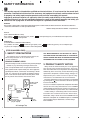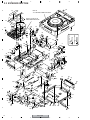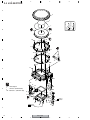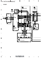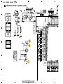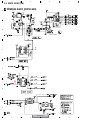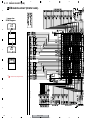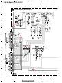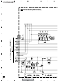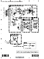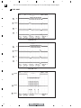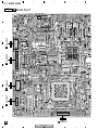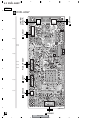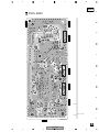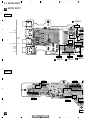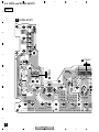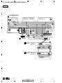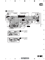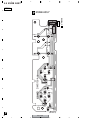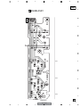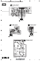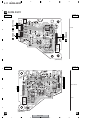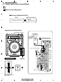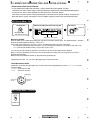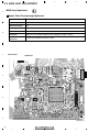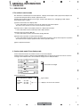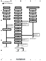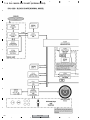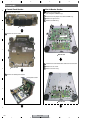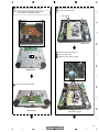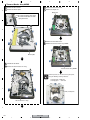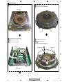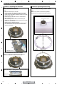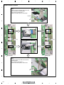
1
POWER
OFF
TIME
MODE
ON
DVJ-1000
STOP
UNLOCK
AUTO
CUE
LOCK
EJECT
TEXT MODE
DVD TITLE
MP3 FOLDER
HOT CUE
ANGLE
SUBTITLE
AUDIO
DISPLAY
REALTIME CUE
IN
OUT
IN ADJUST
OUT ADJUST
RELOOP/
EXIT
DELETE
4-BEAT
ONE-TRACK
MEMORY
MENU
T.MENU
CUE / LOOP
CALL
RETURN
SETUP
TOUCH/BRAKE
ENTER
LOOP
JOG ADJUST
RELEASE/START
LIGHT
BACK & FORTH
HEAVY
REC MODE
HYPERJOG MODE
JOG MODE
DIRECTION
VINYL
FWD
WIDE
REV
PREVIOUS
NEXT
REV
FWD
TEMPO
MASTER TEMPO
TEMPO
RESET
CUE
PLAY/PAUSE
REV
ORDER NO.
FWD
RRV3454
TEMPO
DVJ-1000
DVD PLAYER
DVJ-1000
THIS MANUAL IS APPLICABLE TO THE FOLLOWING MODEL(S) AND TYPE(S).
Model
Type
Power Requirement
Region No.
DVJ-1000
KUCXJ
AC 120 V
1
DVJ-1000
WYXJ5
AC 220 – 240 V
2
DVJ-1000
TLXJ/RD
AC 110-120 V / 220-240 V
4
DVJ-1000
TLFXJ
AC 110-120 V / 220-240 V
3
Remarks
For details, refer to "Important symbols for good services" on the next page.
PIONEER CORPORATION
4-1, Meguro 1-chome, Meguro-ku, Tokyo 153-8654, Japan
PIONEER ELECTRONICS (USA) INC. P.O. Box 1760, Long Beach, CA 90801-1760, U.S.A.
PIONEER EUROPE NV Haven 1087, Keetberglaan 1, 9120 Melsele, Belgium
PIONEER ELECTRONICS ASIACENTRE PTE. LTD. 253 Alexandra Road, #04-01, Singapore 159936
PIONEER CORPORATION 2006
T-ZZR OCT. 2006 printed in Japan
1
2
3
4
SAFETY INFORMATION
A
This service manual is intended for qualified service technicians ; it is not meant for the casual do-ityourselfer. Qualified technicians have the necessary test equipment and tools, and have been trained
to properly and safely repair complex products such as those covered by this manual.
Improperly performed repairs can adversely affect the safety and reliability of the product and may
void the warranty. If you are not qualified to perform the repair of this product properly and safely, you
should not risk trying to do so and refer the repair to a qualified service technician.
WARNING
This product contains lead in solder and certain electrical parts contain chemicals which are known to the state of California to
causecancer, birth defects or other reproductive harm.
Health & Safety Code Section 25249.6 – Proposition 65
B
NOTICE
(FOR CANADIAN MODEL ONLY)
Fuse symbols
(fast operating fuse) and/or
parts must be of identical designation.
(slow operating fuse) on PCB indicate that replacement
REMARQUE
(POUR MODÈLE CANADIEN SEULEMENT)
Les symboles de fusible
(fusible de type rapide) et/ou
les pièces de remplacement doivent avoir la même désignation.
C
(fusible de type lent) sur CCI indiquent que
(FOR USA MODEL ONLY)
1. SAFETY PRECAUTIONS
The following check should be performed for the
continued protection of the customer and
ser vice technician.
ANY MEASUREMENTS NOT WITHIN THE LIMITS
OUTLINED ABOVE ARE INDICATIVE OF A POTENTIAL
SHOCK HAZARD AND MUST BE CORRECTED BEFORE
RETURNING THE APPLIANCE TO THE CUSTOMER.
LEAKAGE CURRENT CHECK
Measure leakage current to a known earth ground (waterpipe
, conduit, etc.) by connecting a leakage current tester
such as Simpson Model 229-2 or equivalent between the
earth ground and all exposed metal parts of the appliance
(input/output terminals, screwheads, metal overlays, control
shaft, etc.). Plug the AC line cord of the appliance directly
into a 120V AC 60Hz outlet and turn the AC power switch
on. Any current measured must not exceed 0.5mA.
D
Reading should
Leakage not be above
current 0.5mA
tester
Device
under
test
E
Test all
exposed metal
surfaces
Also test with
plug reversed
(Using AC adapter
plug as required)
Earth
ground
2. PRODUCT SAFETY NOTICE
Many electrical and mechanical parts in the appliance
have special safety related characteristics. These are
often not evident from visual inspection nor the protection
afforded by them necessarily can be obtained by using
replacement components rated for voltage, wattage, etc.
Replacement parts which have these special safety
characteristics are identified in this Service Manual.
Electrical components having such features are identified
by marking with a on the schematics and on the parts list
in this Service Manual.
The use of a substitute replacement component which does
not have the same safety characteristics as the PIONEER
recommended replacement one, shown in the parts list in
this Service Manual, may create shock, fire, or other hazards.
Product Safety is continuously under review and new
instructions are issued from time to time. For the latest
information, always consult the current PIONEER Service
Manual. A subscription to, or additional copies of, PIONEER
Service Manual may be obtained at a nominal charge
from PIONEER.
AC Leakage Test
F
2
DVJ-1000
1
2
3
4
5
6
IMPORTANT
7
8
LASER DIODE CHARACTERISTICS
MAXIMUM OUTPUT POWER : 5 mW
WAVELENGTH : 780 – 785 nm
THIS PIONEER APPARATUS CONTAINS
LASER OF CLASS 1.
SERVICING OPERATION OF THE APPARATUS
S H O U L D B E D O N E B Y A S P E C I A L LY
INSTRUCTED PERSON.
A
WARNING !
THE AEL (ACCESSIBLE EMISSION LEVEL) OF THE LASER POWER OUTPUT IS LESS THAN CLASS 1
BUT THE LASER COMPONENT IS CAPABLE OF EMITTING RADIATION EXCEEDING THE LIMIT FOR
CLASS 1.
A SPECIALLY INSTRUCTED PERSON SHOULD DO SERVICING OPERATION OF THE APPARATUS.
LABEL CHECK (for WYXJ5, KUCXJ and TLXJ/RD types)
B
for WYXJ5, KUCXJ and TLXJ/RD types
(DRW2317)
C
D
Additional Laser Caution
1. Laser Interlock Mechanism
The position of the switch (S2401) for detecting loading
completion is detected by the system microprocessor, and the
design prevents laser diode oscillation when the switch is not
in LPS1 terminal side (when the mechanism is not clamped
and LPS1 signal is high level.)
Thus, the interlock will no longer function if the switch is
deliberately set to LPS1 terminal side. ( if LPS1 signal is low
level ).
In the test mode∗ the interlock mechanism will not function.
Laser diode oscillation will continue, if pin 5 of AN22022A
(IC7000) on the DVPL Assy is connected to GND, or else the
terminals of Q7001(Q7002) are shorted to each other (fault
condition).
for TLFXJ type
E
2. When the cover is opened, close viewing of the objective
lens with the naked eye will cause exposure to a Class 1
laser beam.
(VRW2159)
F
3
DVJ-1000
5
6
7
8
1
2
3
4
[Important Check Points for Good Servicing]
In this manual, procedures that must be performed during repairs are marked with the below symbol.
Please be sure to confirm and follow these procedures.
1. Product safety
A
Please conform to product regulations (such as safety and radiation regulations), and maintain a safe servicing environment by
following the safety instructions described in this manual.
1 Use specified parts for repair.
Use genuine parts. Be sure to use important parts for safety.
2 Do not perform modifications without proper instructions.
Please follow the specified safety methods when modification(addition/change of parts) is required due to interferences such as
radio/TV interference and foreign noise.
3 Make sure the soldering of repaired locations is properly performed.
B
When you solder while repairing, please be sure that there are no cold solder and other debris.
Soldering should be finished with the proper quantity. (Refer to the example)
4 Make sure the screws are tightly fastened.
Please be sure that all screws are fastened, and that there are no loose screws.
5 Make sure each connectors are correctly inserted.
Please be sure that all connectors are inserted, and that there are no imperfect insertion.
6 Make sure the wiring cables are set to their original state.
Please replace the wiring and cables to the original state after repairs.
In addition, be sure that there are no pinched wires, etc.
C
7 Make sure screws and soldering scraps do not remain inside the product.
Please check that neither solder debris nor screws remain inside the product.
8 There should be no semi-broken wires, scratches, melting, etc. on the coating of the power cord.
Damaged power cords may lead to fire accidents, so please be sure that there are no damages.
If you find a damaged power cord, please exchange it with a suitable one.
9 There should be no spark traces or similar marks on the power plug.
When spark traces or similar marks are found on the power supply plug, please check the connection and advise on secure
connections and suitable usage. Please exchange the power cord if necessary.
0 Safe environment should be secured during servicing.
D
When you perform repairs, please pay attention to static electricity, furniture, household articles, etc. in order to prevent injuries.
Please pay attention to your surroundings and repair safely.
2. Adjustments
To keep the original performance of the products, optimum adjustments and confirmation of characteristics within specification.
Adjustments should be performed in accordance with the procedures/instructions described in this manual.
3. Lubricants, Glues, and Replacement parts
Use grease and adhesives that are equal to the specified substance.
Make sure the proper amount is applied.
E
4. Cleaning
For parts that require cleaning, such as optical pickups, tape deck heads, lenses and mirrors used in projection monitors, proper
cleaning should be performed to restore their performances.
5. Shipping mode and Shipping screws
To protect products from damages or failures during transit, the shipping mode should be set or the shipping screws should be
installed before shipment. Please be sure to follow this method especially if it is specified in this manual.
F
4
DVJ-1000
1
2
3
4
5
6
7
8
CONTENTS
SAFETY INFORMATION......................................................................................................................................2
1. SPECIFICATIONS .............................................................................................................................................6
2. EXPLODED VIEWS AND PARTS LIST.............................................................................................................8
2.1 PACKING ....................................................................................................................................................8
2.2 EXTERIOR SECTION ..............................................................................................................................10
2.3 CONTROL PANEL SECTION...................................................................................................................12
2.4 JOG SECTION .........................................................................................................................................14
2.5 SLOT-IN MECHANISM SECTION ............................................................................................................16
3. BLOCK DIAGRAM AND SCHEMATIC DIAGRAM ..........................................................................................20
3.1 BLOCK DIAGRAM (1/2) ...........................................................................................................................20
3.2 BLOCK DIAGRAM (2/2) ...........................................................................................................................22
3.3 OVERALL WIRING DIAGRAM .................................................................................................................24
3.4 MAIN ASSY (1/8)......................................................................................................................................26
3.5 MAIN ASSY(2/8).......................................................................................................................................30
3.6 MAIN ASSY(3/8).......................................................................................................................................32
3.7 MAIN ASSY(4/8).......................................................................................................................................34
3.8 MAIN ASSY(5/8).......................................................................................................................................36
3.9 MAIN ASSY(6/8).......................................................................................................................................38
3.10 MAIN ASSY(7/8).....................................................................................................................................40
3.11 MAIN ASSY(8/8).....................................................................................................................................42
3.12 DVPL ASSY ............................................................................................................................................46
3.13 STCN, SPCN, INSW and SDCB ASSYS................................................................................................48
3.14 MJCB ASSY ...........................................................................................................................................50
3.15 AUDB and AJCB ASSYS........................................................................................................................52
3.16 JFLB and JOGB ASSYS.........................................................................................................................54
3.17 DIPB and PSWB ASSYS........................................................................................................................56
3.18 DFLB ASSY ............................................................................................................................................58
3.19 KSWB and SLMB ASSYS ......................................................................................................................60
3.20 SLDB, LED1, LED2 and PSWB ASSYS.................................................................................................62
3.21 POWER SUPPLY ASSY .........................................................................................................................63
3.22 WAVEFORMS.........................................................................................................................................64
3.23 VOLTAGES..............................................................................................................................................73
4. PCB CONNECTION DIAGRAM ......................................................................................................................77
4.1 MAIN ASSY ..............................................................................................................................................78
4.2 DVPL ASSY ..............................................................................................................................................82
4.3 SPCN, STCN, INSW and SDCB ASSYS..................................................................................................84
4.4 MJCB ASSY .............................................................................................................................................86
4.5 JFLB ASSY...............................................................................................................................................88
4.6 DIPB and RSWB ASSYS..........................................................................................................................90
4.7 SLDB, LED1 and LED2 ASSYS ...............................................................................................................94
4.8 KSWB ASSY.............................................................................................................................................96
4.9 AJCB, SLMB, JOGB and PSWB ASSYS .................................................................................................98
4.10 POWER SUPPLY ASSY .......................................................................................................................100
4.11 AUDB ASSY .........................................................................................................................................102
5. PCB PARTS LIST ..........................................................................................................................................103
6. ADJUSTMENT ..............................................................................................................................................110
7. GENERAL INFORMATION ...........................................................................................................................113
7.1 DIAGNOSIS............................................................................................................................................113
7.1.1 SERVICE MODE ..............................................................................................................................113
7.1.2 HOW TO UPGRADE THE SOFTWARE OF THE MICROCOMPUTER ...........................................119
7.1.3 HOW TO INPUT THE ID NUMBER ..................................................................................................120
7.1.4 SEQUENCE .....................................................................................................................................122
7.1.5 DVJ-1000 BLOCK CHART (DJ MODE)............................................................................................124
7.1.6 DVJ-1000 BLOCK CHART (NORMAL MODE).................................................................................126
7.1.7 DISASSEMBLY ................................................................................................................................128
7.3 PARTS ....................................................................................................................................................140
7.3.1 IC......................................................................................................................................................140
8. PANEL FACILITIES .......................................................................................................................................156
A
B
C
D
E
F
5
DVJ-1000
5
6
7
8
1
2
3
4
1. SPECIFICATIONS
A
Specifications
B
1. General
4. Audio Output
System ............................................................... DVD-Video, CD
Power requirements ................ AC 220 V to 240 V, 50 Hz/60 Hz
Power consumption .......................................................... 40 W
Operating temperature ...................................... +5 ˚C to +35 ˚C
Operating humidity ................................................. 5 % to 85 %
(There should be no condensation of moisture.)
Weight .............................................................................. 5.4 kg
Dimensions .............. 320 mm (W) 408 mm (D) 109 mm (H)
Audio output (2 channels)
Output level ......................................... 2 V rms (1 kHz, 0 dB)
Channels .............................................................................. 2
Jack ......................................................................... RCA jack
Digital audio output
Frequency response (CD) .............................. 4 Hz to 20 kHz
Frequency response (DVD, 96 kHz) ............... 4 Hz to 44 kHz
Signal-to-noise ratio .......................... 115 dB or more (JEITA)
Distortion ..................................................... 0.004 % (JEITA)
Digital output
Jack ......................................................................... RCA jack
2. Video Output
Composite output (2)
Output level ..................................................... 1 V p-p (75 Ω)
Jack ................................................ RCA jack(1), BNC jack(1)
S-Video output
Y (luminance) ................................................... 1 V p-p (75 Ω)
C (color) ........................................ 286 mV p-p (75 Ω) (NTSC)
300 mV p-p (75 Ω) (PAL)
Jack ................................................................ 4-pin mini DIN
C
3. Preview Video Output
Composite output
Output level ..................................................... 1 V p-p (75 Ω)
Jack ......................................................................... RCA jack
S-Video output
Y (luminance) ................................................... 1 V p-p (75 Ω)
C (color) ........................................ 286 mV p-p (75 Ω) (NTSC)
300 mV p-p (75 Ω) (PAL)
Jack ................................................................ 4-pin mini DIN
5. Other jacks
CONTROL jack ................................ Mini phone jack (ø3.5 mm)
SYNC IN jack ............................................................... BNC jack
6. Accessories
Audio cable .......................................................................... 1
Video cable .......................................................................... 1
Control cord ......................................................................... 1
Power cord .......................................................................... 1
Forced eject pin ................................................................... 1
(housed in a groove in the bottom panel)
Operating instructions ......................................................... 1
Note:
Specifications and design are subject to possible modification
without notice.
D
E
F
6
DVJ-1000
1
2
3
4
5
6
7
8
A
Accessories
Power Cord
(ADG7021 : KUCXJ)
(ADG7097 : TLFXJ)
Audio Cable
(VDE1064) L=1.5m
Forced Eject Pin
(housed in a groove in
the bottom panel)
(DEX1021)
B
(ADG1154 : WYXJ5,TLFXJ
TLXJ/RD)
Control Cord
(XDE3063) L=1 m
Video Cable
(VDE1065) L=1.5m
C
D
E
F
7
DVJ-1000
5
6
7
8
1
2
3
4
2. EXPLODED VIEWS AND PARTS LIST
NOTES:
A
Parts marked by "NSP" are generally unavailable because they are not in our Master Spare Parts List.
The
mark found on some component parts indicates the importance of the safety factor of the part.
Therefore, when replacing, be sure to use parts of identical designation.
Screws adjacent to mark on product are used for disassembly.
For the applying amount of lubricants or glue, follow the instructions in this manual.
(In the case of no amount instructions, apply as you think it appropriate.)
2.1 PACKING
B
12
18
11
6
9
14
3
C
16
4
2
1
1
8
D
13
14
17
15
E
F
8
DVJ-1000
1
2
3
4
5
6
7
8
PACKING parts List
Mark No.
>
1
2
3
4
5
Description
AC Power Cord
Control Cord (L= 1m)
Audio Cable (L= 1.5m)
Video Cable (L=1.5m)
•••••
NSP 6
7
8
9
10
Part No.
See Contrast table(2)
XDE3063
VDE1064
VDE1065
Mark No.
Description
NSP 11
Polyethylene Bag
(230 x 340 x 0.06)
Pad (A)
Pad (B)
Pad (C)
Packing Case
AHG7117
Mirror mat Sheet
Label
User Card
AHG7010
See Contrast table(2)
DRM1262
12
13
14
15
Warranty Card
See Contrast table(2)
•••••
Forced Eject Pin
DEX1021
Operating Instructions(English) See Contrast table(2)
•••••
16
17
NSP 18
Part No.
A
DHA1716
DHA1717
DHA1718
See Contrast table(2)
B
(2) CONTRAST TABLE
DVJ-1000/KUCXJ, /WYXJ5, /TLXJ/RD and TLFXJ types are constructed the same except for the following:
Mark No.
Symbol and Description
DVJ-1000
/KUCXJ
DVJ-1000
/WYXJ5
DVJ-1000
/TLXJ/RD
DVJ-1000
/TLFXJ
>
1 AC Power Cord
ADG7021
ADG1154
ADG1154
ADG1154
>
1 AC Power Cord
Not used
Not used
Not used
ADG7097
NSP
6 Warranty Card
ARY7043
Not used
Not used
Not used
9 Operating Instructions (English)(KUCXJ)
DRB1413
Not used
Not used
Not used
9 Operating Instructions (WYXJ5)(English,
Not used
DRB1414
Not used
Not used
C
French, German, Italian, Dutch, Spanish)
9 Operating Instructions (TLFXJ)
Not used
Not used
Not used
DRB1415
Not used
Not used
DRB1416
Not used
15 Packing Case
DHG2636
DHG2637
DHG2639
DHG2638
17 Label
DRW2311
VRW1629
VRW1629
VRW1629
(English, Chinese)
9 Operating Instructions (TLXJ/RD)
(English, Spanish)
NSP
D
E
F
9
DVJ-1000
5
6
7
8
1
2
3
4
2.2 EXTERIOR SECTION
A
62
58
Refer to
"2.3 CONTROL PANEL SECTION".
63
C
Refer to "2.5 SLOT-IN
MECHANISM SECTION".
57
52
D
49
51
49
50
58
E
61
B
20
3
E
F
53
H
24
7
A
51
I
51
G 57
57
54
T
C
57
9
58
19
18
P
6
J
57
44
32
55
5
R
32
36 57
60
C
R
60
49
F
Q
57 60
49
57
Q
17
45
30
57
64
58
R
37
D
D
57
57
53
57
57
41
G
P
4
42
58
56
58
57
15
Q
L
58
O
K
57
53
25
8
21
N
M
26
CONTACT SIDE
S
NON-CONTACT
SIDE
65
51
53
40
18
57 43
58
38
58
34
58
60
57
58
48
47
47
E
57
57
F
E
61
12
57
H
G
J
14
58
29
56
B
27
58
23
58
58
11
F
39
K
2
53
A
A
13
58
58
33
1
I
B
28
35
B
10
20
57
31
27
58
10
N
O
31
16
58
L
M
21
58
58 56
58
46
22
58
DVJ-1000
1
2
3
4
5
6
7
8
EXTERIOR SECTION parts List
Mark No.
1
2
3
4
5
>
>
Description
MAIN Assy
DVPL Assy
SLMB Assy
MJCB Assy
SDCB Assy
Mark No.
Part No.
DWG1630
DWX2627
DWS1395
DWG1633
DWX2630
POWER SUPPLY Assy
PSWB Assy
AUDB Assy
AJCB Assy
26P FFC/30V
DWR1436
See Contrast table(2)
DWG1638
DWG1639
DDD1337
11
12
13
14
15
FFC/30V (40p)
FFC/60V (13p)
FFC/60V (4p)
FFC/60V (13p)
FFC/60V (27p)
DDD1338
DDD1339
DDD1340
DDD1341
DDD1342
16
17
18
19
20
FFC/60V (10p)
FFC/60V (9p)
Earth Lead Unit
Earth Lead Unit
Connector Assy
DDD1343
DDD1344
DDF1032
DDF1033
PF03PP-B35
Connector Assy
6P Connector Assy
8P Connector Assy
Power Knob
Door Spring
DKP3778
PF06PP6D15
PF08PP-D25
DNK4635
DBH1565
Card Door
Earth Plate 1(CU)
Earth Plate 2(CU)
Silicon Rubber D5 L
Door Cushion
DNK4651
DBK1300
DBK1301
DEB1456
DEB1780
31
Insulation Sheet
DEC2694
32
PC Support
DEC2736
33
Shield Cushion
DEC2905
34
Gasket L40
DEC2979
26
27
28
NSP 29
30
Part No.
DNG1098
NSP 36
Shield Plate 2
DNH2723
NSP 37
Front Plate
DNH2724
NSP 38
39
Earth Plate
Heat Plate
See Contrast table(2)
40
Blind Cap
DNK4218
Chassis
Rear Protector (R)
Rear Protector (L)
Card Plate
Door Holder
DNK4591
DNK4636
DNK4637
DBK1296
DNK4652
46
47
48
49
50
Push Rod Holder
Insulator Assembly
Shield Plate 1 Assy
Damper
Earth Spring
DNK4671
DXA1904
See Contrast table(2)
CNV6011
DBH1398
51
52
53
54
55
Float Spring G11
Mecha Plate
Cord Clamper (STEEL)
Binder
DM Screw (FTC)
DBH1526
DNH2339
RNH-184
ZCA-SKB90BK
DBA1260
56
57
58
59
60
Screw
Screw
Screw
Screw
Screw
BPZ30P120FTB
BPZ30P080FTB
BBZ30P080FTC
BPZ30P080FZK
BBZ30P140FTC
61
62
63
64
65
2P Connector
Laser Caution (7L)
Guard Cushion
Door Plate
Shield Sheet Assy
PF02PY-B37
See Contrast table(2)
DEC2984
DNK4650
DXB1941
A
6
7
8
9
10
21
22
23
24
25
Description
Heat Sink
35
NSP 41
42
43
44
45
DNH2726
B
C
D
(2) CONTRAST TABLE
DVJ-1000/KUCXJ, /WYXJ5, /TLXJ/RD and TLFXJ types are constructed the same except for the following:
Mark No.
>
Symbol and Description
DVJ-1000
/KUCXJ
DVJ-1000
/WYXJ5
DVJ-1000
/TLXJ/RD
DVJ-1000
/TLFXJ
7 PSWB ASSY
DWS1392
DWS1396
DWS1396
DWS1396
39 Heat Plate
DNH2744
DNH2749
DNH2750
DNH2750
48 Shield Plate 1 Assy
DXB1883
DXB1892
DXB1894
DXB1893
62 Laser Caution
DRW2317
DRW2317
DRW2317
VRW2159
E
F
11
DVJ-1000
5
6
7
8
1
2
3
4
2.3 CONTROL PANEL SECTION
A
13
19
14
12
60
B
59
17
61
16
20
56
15
A
N
6
18
29
C
5
K
44
56
B
F
58
56
24
62
41
L
E
4
25
29
2
26
C
D
42
O
63
E
32
30
35
47
47
F
D
50 51
38
52
39
56
34 56
54
56
A
M
H
C
1
53
Refer to
"2.4 JOG SECTION".
56
3
56
10
E
49
56
I
56
H
J
8
R
B
G
P
56
31
11
56
33
I
56
9
J 56
55
56
56
49
56
I
56
58
CONTACT SIDE
45
56
34
47 56
7
28
56
37
32
56
45
D
27
34
NON-CONTACT
SIDE
G
36
56
F
12
DVJ-1000
1
2
3
4
5
6
7
8
CONTROL PANEL SECTION parts List
Mark No.
Description
Mark No.
Part No.
1
2
3
4
5
DIPB Assy
RSWB Assy
SLDB Assy
LED 1 Assy
LED 2 Assy
See Contrast table(2)
DWS1391
DWS1393
DWG1634
DWG1635
6
7
8
9
10
DFLB Assy
KSWB Assy
22P FFC/60V
25P FFC/60V
10P FFC/60V
DWG1632
DWS1394
DDD1345
DDD1346
DDD1347
11
12
13
14
15
9P FFC/60V
Adjust Knob
Display Panel(PMMA)
Top Panel
Slide SW Knob
DDD1348
DAC2350
DNK4601
DNK4599
DNK4592
16
Eject Knob
DAC2335
17
18
19
20
Rotary Knob
Slide Knob
Jog Ring
Control Panel
DAA1182
DAC2376
DNK4600
DNK4598
21
22
23
24
25
• • • •
• • • •
• • • •
Card Lens
SETKnob 1
DNK4596
DAC2331
26
27
28
29
30
SETKnob 2
SETKnob 3
SETKnob 4
TEMPO Lens
SET Knob (H. C.)
DAC2332
DAC2333
DAC2334
DNK4593
DAC2321
31
32
REC Knob
SET Knob (LOOP)
DAC2322
DAC2324
Description
Part No.
33
34
35
RELOOP Knob
ENTER Knob
CALL Knob
DAC2325
DAC2326
DAC2323
36
37
38
39
40
Shield Sheet 1
Cross Key
Change Knob
SET Knob (TEMPO)
• • • •
DEC2899
DAC2327
DAC2328
DAC2329
41
42
43
Reflector
Front Lens
• • • •
DNK4597
DNK4595
44
45
Shield Sheet 2
Ring Lens
DEC2909
DNK3880
46
47
48
• • • •
SET Knob (PLAY) Assy
• • •
DXB1912
49
50
Earth Plate (CU)
RESET Knob
DBK1224
DAC2330
51
TEMPO RESET Lens
DNK4708
52
Cross Key Holder
DNK4798
53
VR Stay
DNF1663
54
Flange Nut M9
DBN1008
55
Cord Clamper (steel)
RNH-184
56
Screw
BPZ30P080FTB
57
• • • •
58
59
60
Rivet (PLASTIC)
TIMX Knob
TEXT Knob
RBM-003
DAC2336
DAC2338
61
STOP Knob
DAC2354
62
Screw
OBA8038
63
LOOP MODE Lens
DNK4594
A
B
C
D
(2) CONTRAST TABLE
DVJ-1000/KUCXJ, /WYXJ5, /TLXJ/RD and TLFXJ types are constructed the same except for the following:
Mark No.
Symbol and Description
1 DIPB ASSY
DVJ-1000
/KUCXJ
DVJ-1000
/WYXJ5
DVJ-1000
/TLXJ/RD
DVJ-1000
/TLFXJ
DWG1631
DWG1640
DWG1642
DWG1641
E
F
13
DVJ-1000
5
6
7
8
1
2
3
4
2.4 JOG SECTION
A
9
7
B
CONTACT SIDE
NON-CONTACT
SIDE
5
*2
*2
8
28
28
28
14
11
*2
12
C
*1
14
14
17
13
17
31
17
A
3
17
17
17
15
40x8
13
27
D
39
16
38
37
18
*
E
27
19 30
1. Lubricating oil
* 2.
GYA1001 (ZLB-PN397B)
Lubricants : (ZLB-HPD1600)
36
20
28
J
21
2 10
27
33
32
A
*1
H
4
31
G
MJCB to
CN4508
22
26
23
34
35
25
1
31
31
I
DIPB to
CN3002
24
29
F
14
DVJ-1000
1
2
3
4
5
6
7
8
JOG SECTION parts List
Mark No.
Description
Part No.
1
2
3
4
5
JFLB Assy
JOGB Assy
Sheet SW
Connector Assy
Jog Panel (PMMA)
DWG1636
DWG1637
DSX1065
PF04PP-B07
DAH2182
6
7
8
9
10
• • • •
JOG Plate
JOG A
JOG B
Protector Sheet
DAH2438
DNK4586
DNK4557
DEC2945
11
12
13
14
15
SW Ring
Roller A Assy
SW Spring 25
Ring Cushion L24/2.0
JOG Stay Assy
DNK4070
DXB1825
DBH1514
DEC2958
DXB1876
16
17
18
19
20
JOG Holder 1000
SW Cushion HH48/2
Arm Spring
Gear
ENCORDER Plate
DNK4558
DEC2538
DBH1566
DNK4560
DEC2889
A
B
C
21
22
23
24
25
Gear Arm
Load Gear A
Smoother
Adjust Plate
Gear Spring 200
DNK4559
DNK4562
DNK4561
DNK4178
DBH1525
26
27
28
29
30
Washer
Screw
Screw (FE)
Screw
Screw
WA52D120D025
IPZ30P100FTC
DBA1265
BPZ20P100FTC
BPZ20P060FTC
31
32
33
34
35
Screw
25P FFC / 60V
FL Sheet
CAM Plate
PRESS Plate
BPZ30P080FTB
DDD1346
DEC2946
DNK4567
DNK4566
36
37
38
39
40
GEAR Plate
Link Gear 3
Link Gear 2
Link Gear 1
Roller B Assy
DNH2713
DNK4565
DNK4564
DNK4563
DXB1877
D
E
F
15
DVJ-1000
5
6
7
8
1
2
3
4
Lubricating oil
GYA1001
∗2 :
Daifree
GEM1036
25
31
*1
32
36
33
34
35
37
CONTACT SIDE
A
∗1 :
NON-CONTACT
SIDE
2.5 SLOT-IN MECHANISM SECTION
30
∗1
∗1
∗2
38
B
39
∗2
*2
∗2
40
B
DVPL to
CN7005
41
42
27 ∗1 28
43
C
29
26
20
20
18
19
19
Refer to
"2.6 TRAVERSE MECHA.
4
ASSY-S".
D
21
21
B
DVPL to
CN7002
6
5
B
16
23
DVPL to
CN7001
16
23
4
C
2
7
3
17
14
U
15
E
9
22
23
1
8
D
12
B
10
DVPL to
CN7003
13
11
F
12
16
DVJ-1000
1
2
3
4
5
6
7
8
SLOT-IN MECHANISM SECTION parts List
Mark No.
Description
Part No.
1
STCN Assy
DWX2628
2
SPCN Assy
DWX2629
3
INSW Assy
DWS1398
4
Traverse Mechanism G11 Assy-S DXX2566
NSP 5
Pickup Assy
OWY8071
6
26P Flexible Cable/30V
DDD1337
7
13P Flexible Cable/60V
DDD1339
8
4P Flexible Cable/60V
DDD1340
9
Connector Assy
DKP3769
10
Vessel Cushion A
DEC2852
11
Vessel Cushion B
DEC2853
12
Vessel Cushion C
DEC2854
13
Float Base (G11) Assy
DXB1793
14
Spacer POR (T3)
DEB1566
15
Front Sheet
DED1132
16
Float Rubber D3
DEB1404
17
Inside SW Base
DNK4236
18
Weight G11
DNH2775
NSP 19
A
B
DRA Rubber G5
DEB1454
20
DRA Screw R (G7)
DBA1264
21
Float Fastener
DBA1286
22
Screw
VBA1062
23
Screw
IPZ20P060FTC
24
•••••
NSP 25
26
NSP 27
NSP 28
Slot-in Mechanism G11 assy
C
DXA2085
Loading Motor Assy-S
DEA1008
Worm Gear
DNK3910
DC Motor
DXM1229
29
Connector Assy
PF02PY-B37
30
Loading Base Assy-S
DEA1022
31
Main Cam
DNK3407
32
Driver Gear
DNK3912
33
Loading Gear
DNK3911
34
SW Lever Spacer
DEC2420
35
Loading Lever Assy
DXB1880
36
Clamper D4 Assy
DXA2043
37
Clamper Spring
DBH1374
38
Clamper Arm
DNK3576
39
Eject Lever
DNK3684
40
Lever AP
DNK3835
41
Lever BP
DNK3836
42
Guide Spring
DBH1375
43
Disc Guide
DNK3478
D
E
F
17
DVJ-1000
5
6
7
8
1
2
3
4
2.6 TRAVERSE MECHA ASSY-S SECTION
12
1
A
D
STCN to
CN7406
∗1
10
B
Cleaning paper
GED-008
Cleaning liquid
GEM1004
3
5
C
7
9
11
8
∗1
D
4
6
2
8
11
∗2
C
E
4
SPCN to
CN7402
13
Grease : GYA1001 (ZLB-PN397B)
* 1.
2.
* Grease : GEM1007 (ZLB-PN948P)
13
F
18
DVJ-1000
1
2
3
4
5
6
7
8
TRAVERSE MECHA ASSY-S SECTION parts List
Mark No.
NSP
NSP
NSP
NSP
NSP
1
2
3
4
5
NSP 6
NSP 7
NSP 8
9
NSP 10
11
12
13
Description
Part No.
Spindle Motor
Stepping Motor
Pickup Assy-S
Skew Screw
Skew Spring
DXM1227
DXM1231
OXX8071
DBA1263
DBH1437
Joint Spring
Leaf Spring G11
Guide Bar (S)
Joint
Mecha.Chassis G11
DBK1261
DBK1262
DLA1918
DNK3858
DNK4307
Tapping Screw 04
Screw
Screw
VBA1092
BPZ20P080FTC
BPZ26P080FTC
A
B
C
D
E
F
19
DVJ-1000
5
6
7
8
1
2
3
4
3. BLOCK DIAGRAM AND SCHEMATIC DIAGRAM
3.1 BLOCK DIAGRAM (1/2)
A
B DVPL ASSY
OEIC
CN7001
CN7004
GNDD
2
LPS2
3
2
3
LPS2
S4401
CN701
IC7100
MN103S71F
SODC
176
E
67
LOAD
SLMB ASSY
26
53
VDEC DATA BUS
GSL
CONTROL
BUS
IC7101
PEA006C8
FLASH ROM
(1M)
119 120
VD
CON
B
IC701
PE5337B
Giant Slalom
(GSL)
ATAPI
175
FEDRV
B
LPS1
1
CN7007
111 109 112
TRDRV
LPS1
1
512M
DDR-SDRAM ×4
256M
SDRAM ×2
RFENV
TE
PICKUP
ASSY
S4402
IC2001-IC2004
EDD5108AFTA-6B-E
IC702, IC703
K4S561632H-UC75
IC7000
AN22022A
FEP
14 18 29
FE
SPINDLE
MOTOR
A MAIN ASSY
IC2000
EP2C20F484C8
DMA/VMC/CAPT/FPGA
VDEC DATA BUS
52
B17
CN7402 CN7401
CN7002
IC7200
BD7905BFS
6ch DRIVER
C
MOTOROLA
CONTROL
BUS
IC113
DYW1756
32M FLASH
ROM
SPCN
ASSY
CN7406 CN7405
MO
CONT1
CN7404
INSW
ASSY
MO
A18
CONT2
256M
SDRAM ×2
U
A17
C SYNC
IC103, IC109
K4S561632H-UC75
C
A
CON
B
MO DATA
MO DOUT
IC505
TMS320DA150PGE16D
AUDIO DECODER
IC111
HD6417709SHF200B
CPU
CN7003
4
IC506
DSPD56367PV150
DSP
27
IC503 TE4300PF
SD/MMC MEMORY
CARD CONTROLLER
CN1702
M
STEPPING
MOTOR
D
STCN
ASSY
G
CN4502
D
CN4508
CN7005
MJCB ASSY
M
CN4000
LOADING
MOTOR
ASSY-S
TRAVERSE
SLOT-IN
MECHANISM
MECHANISM G11 ASSY-S
G5 ASSY
V4000
JOG FL
H
JFLB
ASSY
CN4003
CN4100
P
JOGB
ASSY
CN4001
CN3002
N
E
DFLB
ASSY
CN3201
V3200
DATA FL
15
IC3004
PEG237B
CONTROL CPU with
FL CONTROLLER
CN4201
P
X3001
16MHz
13
J3006
75
J3006
2
I
KSWB
ASSY
SW0
DIPB ASSY
CN3005
K
J3350
LED1 ASSY
J3350
20
RSWB ASSY
CN3300
L
J3300
2
O
CN3004
LED2 ASSY
F
CN3001
J3300
M
SLDB ASSY
DVJ-1000
1
2
3
4
5
6
7
8
A
E
IC1904-IC1907
K4S641632K-UC75
64M SDRAM
×4
VDEC
CONTROL
BUS
VDEC DATA BUS
G
MJCB
ASSY
IC903
PD6449A
MPEG VIDEO
DECODER
VIDEO
DATA
BUS
JA4502
IC1501
LA73054
AV
CONTROL
BUS
IC305
M65774BFPA
AV-1
VDEC DATA BUS
MO DATA
MO DOUT
46
71
48
74
35
IC1502
ADV7172KST
33
VIDEO
ENCODER 29
AV
DATA
4
7
V
Y
Y
C
C
2
8
6
33
28
31
MAIN VOUT
MAIN YOUT
MAIN COUT
CN4505
18
14
6
MAIN V
MAIN Y
MAIN C
B
VIDEO
OUT S1/S2
C
10
Y
PREVIEW
OUT S1/S2
14
C
22
JA4500
AV
DOUT
MO DATA
V
CN703
Y
35
IC1506
ADV7172KST
33
VIDEO
ENCODER 29
IC303
K4S641632K-UC75
64M SDRAM
V
Y
C
2
33
8
28
6
31
SUB VOUT
SUB YOUT
SUB COUT
16
12
10
PRE V
PRE Y
PRE C
VIDEO OUT
COMPOSITE
12
PREVIEW OUT
COMPOSITE
16
18
JA4504
IC1505
LA73054
MO DOUT
AV
DOUT
IC1514
8 TC7SH08FU 4
COMPOSITE
DOUT
1
C SYNC
6
2
1
24
DATA
5
IC1513
PQ0274A
AQE
SYNC IN
SYNC
IN
8
JA4503
DOUT
CN4506
C
Q
CN4301
AUDB
ASSY
24
CONT1
4
1
9
CONT1
26
CONT2
2
3
7
CONT2
6
25
5
26
AV DATA
20
27
IC1104
LM1881M
IC1102
TC7WH34FU
1
2
DOUT
IC1510
PCM1738EG-3
AUDIO DAC
7
(2/2)
LCH OUT_P
1
LCH OUT_N
2
3
5
6
L+OUT
5
L-OUT
CN1704
6
5
7
6
D
CN4300
IC1512 (1/2)
NJM5532MD
AUDIO IV CONV
CN4302
CN4303
CN501
4
7
8
4
7
8
LO
CONT2
P
CN7502
CONT1
CN7501
SD/MMC
CARD
MONITOR
OGB
SSY
L
R
JA4300
AUDIO
OUT
F
JA4301
CONTROL
R
SDCB ASSY
E
AJCB ASSY
: VIDEO DATA BUS
: AUDIO DATA BUS
SSY
F
21
DVJ-1000
5
6
7
8
1
2
3
4
3.2 BLOCK DIAGRAM (2/2)
• POWER
A
Q
G
H
MJCB ASSY
JFLB
ASSY
V+5D
AUDB
ASSY
1
CN4506
V+5D
8
2
V+12S
V4000
JOG FL
9
CN4301
B
CN101
J4501
1
AN3400
AC IN
LIVE
J3400
1
2
CN1
ORG
3
1
4
NEUTRAL
WHT
2
6
FLAC1
1
FLAC2
13
2
FLAC3
FLAC4
VLOAD
5
21
IC4501
15
IC4502
3
17
4
19
6
CN4001
CN4000
CN4508
VLDMFL
FLAC1
FLAC2
FLAC3
FLAC4
2
3
10
2
8
4
9
VLED
4
14
8
3
PSWB ASSY
C
4
10
T
11
3
V+5D
4
V+5S
7
V+12S
5
1
V+5D
V+12S
18
25
IC4504
1
IC4506
2
11
POWER
SUPPLY
ASSY
CN4103
V+12A
V+5D
CN4100
V+5D1
V+5D
V+5D2
J
CN4500
2
7
8
V+12S
V+5S
7
V+12S
V+5S
1
2
8
CN7008
D
VA5V VD5V
VD1R5
B
V12DR
IC7300
MM1478DFBE
RESET
VD3V VA3V
+3.3V REG.
IC7301
BA15BC0WFP
+1.5V REG.
DVPL ASSY
E
F
22
DVJ-1000
1
2
3
V+5D
3
IC4505
IC4507
1
VLED
3
IC4510
7
10
V+5D
CN4504
V+12A
IC4503
J4507
1
FLAC2
V+5D
5
S
FLAC1
6
V+5D
V+12A
VLDMFL
VLOAD
2
CN102
VLDMFL
4
JOGB
ASSY
5
6
7
8
A
I
DIPB ASSY CN3001
N
CN3201
2
VLDMFL
FLAC1
3
FLAC2
4
V+5D
11
15
DFLB
ASSY
14
V+5D
13
2
V3400
MAIN FL
CN3002
VLDMFL
VLDMFL
FLAC1
FLAC2
21
B
23
24
22
VLED
VLED
6
V+5D
V+5D
1
VLED
VLED
2
P
8
CN4201
CN3005
CN3004
KSWB
ASSY
C
CN3300
VLED
10
VLED
1
VLED
V+5AD
V+5AD
V+5AD
1
1
10
VLED
J3300
1
L
J3300
1
M SLDB ASSY
1
VLED
K
CN1701
V+12A
V+5D2
J3350
J3350
D
LED2
ASSY
A MAIN ASSY
V+5A
5
IC2013
R1224N102H
DCDC CONV
V+5D1
IC1507
NJM78L05UA
+5V REG.
LED1
ASSY
IC121
PQ070XZ02ZP
+2V REG.
V+3D1
V+2SH
1
2
IC2014
R1224N102H
DCDC CONV
IC912
NJM2872F33
+3.3V REG.
V+3D2
V+3R3
IC507
MM1661GH
+1.6V REG.
IC301
MM1562FF
+2V REG.
V3R3
V+2AV1
V3R3
5
CN7502
V1R6TI
IC902
PQ070XZ02ZP
V+2VDEC
+2V REG.
9
IC504
MM1561JF
+1.8V REG.
F
SDCB
ASSY
E
V1R8MOT
VREF
IC2005
PQ070XZ02ZP
+2.5V REG.
V+2R5
IC2006
R1224N102H
DCDC CONV
V+1R2
V+2R5D
IC2011
LP2996M
VTT
F
23
DVJ-1000
5
6
7
8
1
2
3
4
3.3 OVERALL WIRING DIAGRAM
A
S
PSWB ASSY
T
POWER SUPPLY ASSY
(DWR1436)
ASSY
U INSW
(DWS1398)
ASSY
C SPCN
(DWX2629)
B
B DVPL ASSY (DWX2627)
G MJCB ASSY
(DWG1633)
C
D
ASSY
D STCN
(DWX2628)
A A 1/8 - A 8/8
MAIN ASSY (DWG1630)
E
SLMB ASSY
(DWS1395)
F
SDCB ASSY
(DWX2630)
E
F
24
DVJ-1000
1
2
3
4
5
6
7
8
JOGB ASSY
(DWG1637)
A
J
H JFLB ASSY
(DWG1636)
B
ASSY
Q AUDB
(DWG1638)
ASSY
K LED2
(DWG1635)
L
LED1 ASSY
(DWG1634)
ASSY
R AJCB
(DWG1639)
C
ASSY
M SLDB
(DWS1393)
I DIPB ASSY
D
ASSY
N DFLB
(DWG1632)
E
ASSY
O RSWB
(DWS1391)
P
KSWB ASSY
(DWS1394)
÷ When ordering service parts, be sure to refer to "EXPLODED VIEWS and PARTS LIST" or
"PCB PARTS LIST".
÷ The > mark found on some component parts indicates the importance of the safety factor
of the part. Therefore, when replacing, be sure to use parts of identical designation.
÷
: The power supply is shown with the marked box.
25
DVJ-1000
5
6
F
7
8
1
2
3
4
3.4 MAIN ASSY (1/8)
A 1/8
A 1/8 MAIN ASSY (DWG1630)
A
Large size
SCH diagram
1/2
B
2/2
C
A 7/8, 8/8
A 7/8
A 1/8 A 7/8
A 1/8
1/2
D
E
F
26
DVJ-1000
1
2
3
4
5
6
A 1/8
A 7/8
7
A 8/8 A 1/8
8
A 1/87
A 1/8
A
B
1
C
CPU
A 4/8
D
A 6/8
A 3/8
A 8/8
A 6/8
A 5/8
E
A 3/8
A 2/8
A 8/8
F
27
DVJ-1000
5
6
7
8
1
2
3
4
A
A 1/8 MAIN ASSY
B
C
A 3/8
A 8/8
A 1/8
2
Large size
SCH diagram
A 1/8
1/2
D
2/2
E
2/2
F
A 1/8
28
DVJ-1000
1
2
3
4
5
6
7
8
A
B
C
2
8
D
E
F
A 1/8
29
DVJ-1000
5
6
7
8
1
2
3
4
3.5 MAIN ASSY(2/8)
A
A 2/8 MAIN ASSY (DWG1630)
A 4/8
A 2/8
A 3/8
A 8/8
A 2/8
A 5/8
B
Master Clock ADJ
A 8/8
C
A 8/8
D
3
A 2/8
E
A 8/8
A 7/8
A 8/8
F
A 7/8
A 2/8
A 8/8
30
DVJ-1000
1
2
3
4
5
6
7
8
A
6
B
A 1/8
C
(DA)
(DA)
(D)
D
(DA)
5
A 2/8
4
E
(DA)
(DA)
(D)
(DA)
(DA)
(D)
F
: Audio Data Signal Rout.
: Digital Out Signal Rout.
A 2/8
31
DVJ-1000
5
6
7
8
1
2
3
4
3.6 MAIN ASSY(3/8)
A
A 3/8 MAIN ASSY
(DWG1630)
A 1/8
7
B
SD CARD
CONTROLLER
F
CN7502
C
A 1/8
10
D
DSP
E
F
A 3/8
32
DVJ-1000
1
2
3
4
5
6
7
8
A
B
C
DSP
A 2/8
8
D
9
(DA)
(D)
(DA)
(DA)
A 1/8
E
(DA) (D)
A 2/8
(DA)
(D)
: Audio Data Signal Rout.
: Digital Out Signal Rout.
F
A 3/8
33
DVJ-1000
5
6
7
8
1
2
3
4
3.7 MAIN ASSY(4/8)
A
B
C
ATAPI I/F
A 6/8
D
A 2/8
A 1/8
E
F
A 4/8
34
DVJ-1000
1
2
3
4
5
6
7
8
A 4/8 MAIN ASSY
A
(DWG1630)
A 8/8
B
C
B 0/0 (CN7007)
D
E
A 1/8
11
F
A 4/8
35
DVJ-1000
5
6
7
8
1
2
3
4
3.8 MAIN ASSY(5/8)
A
A 5/8 MAIN ASSY (DWG1630)
A 2/8
A 8/8
B
A 1/8
C
A 8/8
D
E
F
A 5/8
36
DVJ-1000
1
2
3
4
5
6
7
8
A
12
B
C
A 8/8
D
13
E
F
A 5/8
37
DVJ-1000
5
6
7
8
1
2
3
4
3.9 MAIN ASSY(6/8)
A
ASSY
A 6/8 MAIN
(DWG1630)
A 1/8, 6/8
A 8/8
(DV)
14
B
(DV)
(DA)
A 1/8, 6/8
A 8/8
(D)
: Video Data Signal Rout.
: Audio Data Signal Rout.
: Digital Out Signal Rout.
C
15
(DV)
D
(D)
(D)
A 7/8
A 1/8
E
A 2/8
DAC
17
(DA)
(DA)
(DA)
A 2/8
16
F
A 6/8
38
DVJ-1000
1
2
3
4
5
6
7
8
A
(V)
(V)
(V)
(V)
B
A 4/8
A 4/8
C
(V)
(V)
(V)
D
A 7/8
A 1/8
E
(A)
A 7/8
(A)
(A)
(A)
(A)
(V)
(A)
(A)
: Analog Audio Signal Rout.
: Analog Video Signal Rout.
F
(A)
(A)
A 7/8
A 6/8
39
DVJ-1000
5
6
7
8
1
2
3
4
3.10 MAIN ASSY(7/8)
A
ASSY
A 7/8 MAIN
(DWG1630)
A 2/8
A 1/8
A 6/8
A 2/8
18
(V)
19
(V)
(A)
B
(D)
: Analog Video Signal Rout.
: Analog Audio Signal Rout.
: Digital Out Signal Rout.
(D)
A 6/8
G
CN4505
(A)
20
21
(A)
(A)
22
23
C
(A)
Q
CN4300
G
CN4502
A 1/8
24
A 1/8, 8/8
A 8/8
25
D
A 8/8
A 1/8
E
F
A 7/8
40
DVJ-1000
1
2
3
4
5
6
7
8
A
B
C
D
A 8/8
E
F
A 7/8
41
DVJ-1000
5
6
7
8
1
2
3
4
3.11 MAIN ASSY(8/8)
A 7/8
A 1/8
A 1/8, 8/8
A 8/8 MAIN ASSY(DWG1630)
A
Large size
SCH diagram
1/2
B
2/2
C
1/2
D
(DV)
: Video Data Signal Rout.
E
A 2/8
F
42
DVJ-1000
1
2
3
4
5
6
7
8
A 7/8
A 1/8
A 1/8
A
B
A 5/8
A 5/8
A 1/8
C
A 5/8
A 1/8, 8/8
A 2/8
D
A 4/8
E
(DV)
A 2/8
A 7/8
A 2/8
A 1/8, 7/8
A 6/8
F
43
DVJ-1000
5
6
7
8
1
2
3
4
A
A 8/8 MAIN ASSY
(DWG1630)
B
28 29
C
Large size
SCH diagram
1/2
D
2/2
E
2/2
F
A 8/8
44
DVJ-1000
1
2
3
4
5
6
7
8
A
B
26 27
C
D
E
F
A 8/8
45
DVJ-1000
5
6
7
8
1
2
3
4
3.12 DVPL ASSY
A
B
DVPL ASSY(DWX2627)
RF
RF
RF
RF
Fo
B
Tr
G
H
Tr
Tr
Fc
Fc
I
J K
C
Tr
Fo
Load
C
C CN7401
D
D
A
ST
ST
ST
B
SPDL
E
Load
ST
F
A 4/8
B
(CN7007)
46
DVJ-1000
1
2
3
4
5
6
7
8
Fo : Focus Servo.
ST : Stepping Motor.
Tr : Tracking Servo.
Load : Loading Motor.
SPDL : Spindle Motor.
A
RF :
Fo
Tr
Fo
Tr
F
E
RF
B
C
LOAD
ST
D
SPDL
E
F
B
47
DVJ-1000
5
6
7
8
1
2
3
4
3.13 STCN, SPCN, INSW and SDCB ASSYS
A
D
INSW ASSY
(DWS1398)
B CN7003
C CN7403
B
U
STCN ASSY
(DWX2628)
C
B CN7002
D
U CN7404
E
C
SPCN ASSY
(DWX2629)
F
C D U
48
DVJ-1000
1
2
3
4
5
6
7
8
A
SDCB ASSY
(DWX2630)
B
A 3/8 (CN501)
F
C
D
E
F
F
49
DVJ-1000
5
6
7
8
1
2
3
4
3.14 MJCB ASSY
A
(D)
B
A 7/8 (CN1703)
(V)
(V)
(V)
(V)
(V)
(V)
T CN101
C
A 7/8 (CN1702)
D
T CN102
E
F
B 0/0 (CN7008)
A 4/8
G
(CN1701)
50
H CN4000
DVJ-1000
1
2
3
4
5
6
7
G
8
A
MJCB ASSY
(DWG1633)
(V)
B
(V)
64
(V)
(V)
Q CN4301
C
D
(V)
E
55
(D)
(V)
(D)
: Analog Video Signal Rout.
: Digital Out Signal Rout.
F
G
51
DVJ-1000
5
6
7
8
1
2
3
4
3.15 AUDB and AJCB ASSYS
A
Q AUDB ASSY(DWG1638)
(A)
B
(A)
A 7/8 (CN1704)
53 a
53 b
(A)
(A)
C
G CN4506
D
E
(A)
: Analog Audio Signal Rout.
F
Q
52
DVJ-1000
1
2
3
4
5
6
7
8
A
R
AJCB ASSY(DWG1639)
54
B
(A)
(A)
(A)
(A)
(A)
(A)
C
D
(A)
: Analog Audio Signal Rout.
E
F
Q R
53
DVJ-1000
5
6
7
8
1
2
3
4
3.16 JFLB and JOGB ASSYS
A
H
JFLB ASSY(DWG1636)
B
59
58
C
57
G CN4506
56
60
63
62
61
I CN3002
D
E
47
48
F
54
DVJ-1000
1
2
3
4
5
6
7
8
A
B
C
D
J
E
JOGB ASSY(DWG1637)
F
55
DVJ-1000
5
6
7
8
1
2
3
4
3.17 DIPB and PSWB ASSYS
DIPB ASSY(DWG1631: /KUCXJ, DWG1640 : /WYXJ5
DWG1641 : /TLFXJ, DWG1642 : /TLXJ/RD )
I
A
45
CN3201
B
49
N
46
51
50
52
C
CONTROL CPU
with FL CONTROLLER
H
D
CN4001
E
F
P
M CN3300
I
56
CN4201
DVJ-1000
1
2
3
4
5
6
7
8
A
B
C
D
E
F
O
PSWB ASSY(DWS1392 : /KUCXJ, DWS1396 : /WYXJ5,
DWS1396 : /TLFXJ, DWS1396 : TLXJ/RD)
I O
57
DVJ-1000
5
6
7
8
1
2
3
4
3.18 DFLB ASSY
A
N
DFLB ASSY(DWG1632)
B
CN3001
C
I
D
E
F
N
58
DVJ-1000
1
2
3
4
5
6
7
8
A
B
C
D
E
F
N
59
DVJ-1000
5
6
7
8
1
2
3
4
3.19 KSWB and SLMB ASSYS
A
KSWB ASSY(DWS1394)
I CN3005
P
B
C
S4201 : PLAY
S4202 : CUE
S4203 : PREVIOUS
S4204 : NEXT
S4205 : REV
S4206 : FWD
D
E
SLMB ASSY
(DWS1393)
B CN7004
E
F
E P
60
DVJ-1000
1
2
3
4
5
6
7
8
A
B
C
D
E
F
E
61
DVJ-1000
5
6
7
8
1
2
3
4
3.20 SLDB, LED1, LED2 and PSWB ASSYS
A
I CN3004
M SLDB ASSY(DWS1393)
B
L LED1 ASSY
(DWG1634)
K
LED2 ASSY
(DWG1635)
C
D
S
PSWB ASSY
(DWS1396)
E
F
K L M S
K L M S
62
DVJ-1000
1
2
3
4
5
6
7
8
DVJ-1000
63
CN201
C7
C58
Q51
C52
C78
Q72
R69
C5
R92
R91
Q2
R72
D78 D79 R77 R76 R75
Z1
D71
C21
D72
R71
C1
C10
Q71
Q53
C31
R1
C20
R7
R6
C60
D7
Q54
Q52
R51
L1
R13
D4
L2
R64
R70
R56
R57
C2
D57
NTC2
D59 R68 R66 R67
D6
D58
R54
NTC1
D15 R10
R86
R85
R53
R84
PC1
R65
R17
F1
Q73
R19
R93
CN1
C701
Q1
BEA7
BEA71
R52
D5
R11
R9
R62
C11
D54
D14
D65 R60
D11
D12
C61
PC2
R57
D13
D56
T51
T1
D501
D301
D401
C152
D601
D201
D151
C601
C211
C105
C401
D101
D302
POWER SUPPLY ASSY
(DWR1436)
D
C501
R612
D406
D102
C602
W1
Q601
P401
R601
C151
IC601
R450
C605
C301
R501
T
R78
R79
D75
C77
R80
C9
R12
R8
D55
R63
LIVE
R55
C51
C73
R5
R81
C72
D74 D73
D76
D77
R83
C71
R82
C59
C62
R58
R61
R59
C66
NEUTRAL
T
BEA51
J3400
C302
S
F
E
C504
T
C101
C102
PC2
R605
R610
R301
D602
Q403
R102
Q101
R310 C310
R407
R111
PC601
L601
R601
D110
PC1
R110 C110
R603
C604
W2 W2
C503
C402
D502
R406
R609
L101
D405 D404 D403
VR301 R403
R611
C502
D503
R506
• NOTE FOR FUSE REPLACEMENT
CAUTION - FOR CONTINUED PROTECTION AGAINST RISK OF FIRE.
REPLACE WITH SAME TYPE AND RATINGS OF FUSE.
R302
IC301
R304
C
R608
R602
R104
R101
R103
VR101
C115
R115
R405
R507
C505
R404
R403
D505
R505
Q401
P501
L301
Q501
Q402
D402
R402
IC201
C404
R112
R113
C612
B
R114
R202
C403
R201
C103
Q421
L102
C202
PC601 R422 R421
IC202
C201
C104
C203
C611
R424 R423
C304
R425
D421
W3
C511
C421
D422
W3
W1
C512
VLDCNT
GLOAD
9
6
FLAC4
FLAC3
G
4
VLOAD
5
J4507
3
FLAC2
GNDV
GADA
2
11
8
FLAC1
V+12A
10 V+5V
7
1
CN101
V+3R3
V+3R3
V+3R3
GNDD
GNDD
GNDD
GNDS
GNDS
1
2
3
9
10
V+5S
11
5
4
6
V+12S
V+12S
7
8
CN102
G
A
J4501
3.21 POWER SUPPLY ASSY
5
6
7
8
1
2
3
4
3.22 WAVEFORMS
WAVEFORMS
DJ MODE : PLAY, VINAL, SD IN, MASTAR TEMPO : OFF, SRIDER : 0%, HOT CUE : OFF
A
DISC : DVD-REF-Z1 TITLE35 – 01
Note : The encircled numbers denote measuring point in the schematic diagram and pcb diagram.
A 1/8 MAIN ASSY
1
IC111– 162pin (CLK66M)
V:1V/div. H:5nS/div
2
IC109– 38pin (66MSDR)
V:1V/div. H:5nS/div
B
A 2/8
C
MAIN ASSY
3
IC1707– 7pin (27M_CKGEN)
V:1V/div. H:20nS/div
4
IC305– 55pin (27MAV1)
V:1V/div. H:20nS/div
5
IC305– 64pin (16/36M)
V:1V/div. H:10nS/div
6
IC303– 38pin(MCLK)
V:1V/div. H:10nS/div
D
E
F
64
DVJ-1000
1
2
3
4
5
A
6
MAIN ASSY
7
8
DJ MODE : PLAY, VINAL, SD IN, MASTAR TEMPO :OFF, SRIDER :0%, HOT CUE :OFF
DISC : DVD-REF-Z1 TITLE35– 01
A
Note : The encircled numbers denote measuring point in the schematic diagram and pcb diagram.
A 3/8
7
MAIN ASSY
IC503– 38pin (CARD_66M)
V:1V/div. H:5nS/div
8
IC506– 55pin (27M_MOT)
V:1V/div. H:20nS/div
B
9
IC506– 16pin (22/24M)
V:1V/div. H:20nS/div
10 IC505–
97pin
V:1V/div. H:20nS/div
C
D
A 4/8
11
MAIN ASSY
IC702– 38pin (SLMCLK)
V:1V/div. H:10nS/div.
E
F
65
DVJ-1000
5
6
7
8
1
A
2
MAIN ASSY
3
4
DJ MODE : PLAY, VINAL, SD IN, MASTAR TEMPO :OFF, SRIDER :0%, HOT CUE :OFF
DISC : DVD-REF-Z1 TITLE35– 01
A
Note : The encircled numbers denote measuring point in the schematic diagram and pcb diagram.
A 5/8
12
MAIN ASSY
IC904– 38pin (M1CLK)
V:1V/div. H:2nS/div.
13
IC906– 38pin (M2CLK)
V:1V/div. H:2nS/div.
B
A 6/8
C
MAIN ASSY
14
IC1502– 48pin (M_PRG27M)
V:1V/div. H:20nS/div.
15
IC1506– 48pin (S_PRG27M)
V:1V/div. H:20nS/div.
16
IC1510– 7pin (22/24M_DAC)
V:1V/div. H:20nS/div.
17
IC1513– 6pin (22/24M_AQE)
V:1V/div. H:20nS/div.
D
E
F
66
DVJ-1000
1
2
3
4
5
A
6
MAIN ASSY
A 7/8
18
7
8
Note : The encircled numbers denote measuring point in the schematic diagram and pcb diagram.
MAIN ASSY
A
CN1703-18pin(MAIN_V)
V:1V/div. H:200uS/div.
19
CN1703-16pin(PRE V)
V:1V/div. H:200uS/div.
B
20
ODD Field
CN1704-6pin(L-OUT)
V:2V/div. H:200uS/div.
21
ODD Field
CN1704-5pin(L+OUT)
V:2V/div. H:200uS/div.
C
22
CN1704-2pin(R+OUT)
V:2V/div. H:200uS/div.
23
CN1704-1pin(R-OUT)
V:2V/div. H:200uS/div.
D
24
IC2015-5pin(DIS_XCS)
V:1V/div. H:500uS/div.
25
IC2015-7pin(DIS_SCLK)
V:1V/div. H:1uS/div.
E
F
67
DVJ-1000
5
6
7
8
1
A
2
MAIN ASSY
3
4
DJ MODE : PLAY, VINAL, SD IN, MASTAR TEMPO :OFF, SRIDER :0 %, HOT CUE :OFF
DISC : DVD-REF-Z1 TITLE35– 01
A
Note : The encircled numbers denote measuring point in the schematic diagram and pcb diagram.
A 8/8
MAIN ASSY
26
IC2001-45pin (CK)
V:1V/div. H:2nS/div.
27
IC2001-46pin (/CK)
V:1V/div. H:2nS/div.
28
IC2003-45pin (CK)
V:1V/div. H:2nS/div.
29
IC2003-46pin (/CK)
V:1V/div. H:2nS/div.
B
C
D
E
F
68
DVJ-1000
1
2
3
4
5
B
6
DVPL ASSY
B
7
8
Note : The encircled numbers denote measuring point in the schematic diagram and pcb diagram.
A
DVPL ASSY
A : LPS1
B : LPS2
C : EMN
B
D
: EMP
In a load inn
C
A : LPS1
B : LPS2
C : EMN
D : EMP
D
In unloading
: TE
E
F : TEDRV
E
G : T+
H
: T-
In a CD pose
F
69
DVJ-1000
5
6
7
8
1
B
3
4
Note : The encircled numbers denote measuring point in the schematic diagram and pcb diagram.
B
A
2
DVPL ASSY
E
: TE
F : TEDRV
B
G
: T+
H
: T-
In CD FWD scan
C
E
: TE
F : TEDRV
G
: T+
H
: T-
D
In CD REV scan
I : FEPEN
E
J : FEPCK
K : FEPDT
F
70
DVJ-1000
1
2
3
4
5
WAVEFORMS
I
6
7
8
Note : The encircled numbers denote measuring point in the schematic diagram and pcb diagram.
MODE : POWER ON
DIPB ASSY
A
45 IC3009-2pin (V+5D)
45
46 IC3009-1pin (XRESET)
46
H
B
MODE : JOG turns between PLAY
JFLB ASSY
47 CN4003-1pin (JOG2)
47
48 CN4003-2pin (JOG1)
48
C
I
DIPB ASSY
MODE : PLAY
49
49 CN3001-8pin (FL_SDO)
50
50 CN3001-9pin (FL_SCLK)
51
51 CN3001-11pin (FL_LAT)
52
52 CN3001-12pin (FL_BK)
D
MODE : PLAY (1kHz 0dB)
Q AUDB ASSY
53a
53a CN4300-1pin (R-OUT)
53b
53b CN4300-2pin (R+OUT)
E
R
MODE : PLAY (1kHz 0dB)
AJCB ASSY
54 JA4300-1pin (R)
54
F
71
DVJ-1000
5
6
7
8
1
2
3
4
WAVEFORMS
Note : The encircled numbers denote measuring point in the schematic diagram and pcb diagram.
A
G MJCB ASSY
MODE : PLAY
55 JA4503 (D OUT)
55
Measurement condition: 75 Ω termination
([1.0V] that a level doubles in case of opening)
B
H
MODE : PLAY
JFLB ASSY
56
56 CN4000-10pin (FLAC1)
57 CN4000-8pin (FLAC2)
57
C
H
MODE : PLAY
JFLB ASSY
58 CN4000-6pin (FLAC3)
58
59 CN4000-4pin (FLAC4)
59
D
H
MODE : PLAY
JFLB ASSY
60
60 DEL1058-24pin (SI)
61
61 DEL1058-27pin (CLK)
62
E
62 DEL1058-26pin (LAT)
63
63 DEL1058-25pin (BK)
F
72
DVJ-1000
1
2
3
4
5
6
7
8
3.23 VOLTAGES
VOLTAGES
A
A
A
A
B
C
A
A
D
A
A
E
F
73
DVJ-1000
5
6
7
8
1
2
3
4
VOLTAGES
Measurement condition : DVD Single reconstruction, VINAL, MASTER TEMPO : OFF, SLIDER 0 %
A
B
DVPL ASSY
IC7000
Pin No.
1
2
3
4
5
6
7
8
9
10
11
12
13
14
15
16
17
18
19
20
21
22
23
24
25
26
27
28
29
30
31
32
33
34
35
36
37
38
39
40
41
42
43
44
45
46
47
48
B
C
D
(AN22022A)
Voltage (V)
2.2
0.185
3.48
0.186
4.31
0.04 – 0.06
1.57
3.32
0
3.32
0
0
1.67
1.74
0
2.19
1.67
1.67
0
1.61
2.23
2.21
1.92
1.92
1.71
1.51
0
0
1.57
2.1
1.57
1.7
2.1
2.26
2.26
2.21
2,21
4.76
2.22
2.22
3.32
2.21
2.36
2.35
4.76
2.37
2.35
2.21
IC7200
Pin No.
1
2
3
4
5
6
7
8
9
10
11
12
13
14
15
16
17
18
19
20
21
22
23
24
25
26
27
28
29
30
31
32
33
34
35
36
37
38
39
40
41
42
43
44
45
46
47
48
49
50
51
52
53
54
(BD7905BFS)
Voltage (V)
3.05
3.05
3.07
3.06
3.07
3.07
1.27
0
5.3
11.9
5.31
0
0
0
0
0
0
5.3
11.9
11.9
1.59
3.3
3.3
1.77
0
1.67
1.67
1.3 – 2.1
1.3 – 2.1
11.9
11.7
11.8
0.82
7 – 12
11.5
7 – 12
6 – 12
0
0
0
0
0
0
4.85
2.43
2.4
2.44
2.38
5.56
5.56
11.94
1.66
1.67
4.85
IC7100
Pin No.
1
2
3
4
5
6
7
8
9
10
11
12
13
14
15
16
17
18
19
20
21
22
23
24
25
26
27
28
29
30
31
32
33
34
35
36
37
38
39
40
41
42
43
44
(MN103S71F)
Voltage (V)
3.3
3.3
0
3.33
0
3.32
0
0
0
1.89
1.41
1.49
1.64
1.06
0.92
3.33
0.21
2.06
1.64
0
0
0.45
2.1
1.7
3.33
1.65
1.66
1.65
1.8
1.73
0
3.33
2.22
2.97
2.53
2.71
2.51
2.36
2.55
2.5
0.41
1.4
1.49
0
IC7100
Pin No.
45
46
47
48
49
50
51
52
53
54
55
56
57
58
59
60
61
62
63
64
65
66
67
68
69
70
71
72
73
74
75
76
77
78
79
80
81
82
83
84
85
86
87
88
(MN103S71F)
Voltage (V)
3.33
0
3.22
3.19
3.33
3.31
3.33
1.65
1.66
0
1.67
1.84
1.67
1.4
0 – 3.2
0 – 3.2
1.42
1.45
0
0
3.33
0
1.67
0
0
3.33
0
1.64
3.33
3.33
1.59
0
1.49
0
1.2
0.18
0.21
0
0.02
0
1.67
1.67
3.33
0.3
E
F
74
DVJ-1000
1
2
3
4
5
VOLTAGES
IC 7100 (MN103S71F)
IC7100 (MN103S71F)
Pin No.
Voltage (V)
89
1.66
90
3.32
91
1.67
92
1.67
93
1.66
94
0
95
1.7
96
1.75
97
0
98
1.63
99
1.65
100
1.67
101
1.5
102
2.21
103
1.52
104
1.66
105
3.32
106
0
107
3.32
108
1.28
109
1.67
110
2.18
111
1.75
112
1.57
113
1.62
114
1.66
115
1.65
116
0
117
0
118
0
119
1.66
120
1.65
121
0
122
3.33
123
0
124
3.33
125
0
126
3.32
127
3.32
128
0
129
3.32
130
0
131
3.28
132
3.28
6
B
7
8
DVPL ASSY
IC 7100 (MN103S71F)
IC7100 (MN103S71F)
Pin No.
Voltage (V)
133
0 – 3.2
134
3.28
135
3.33
136
0
137
2.8 – 3.3
138
3.29
139
2.0 – 3.3
140
0
141
3.32
142
1.0 – 1.7
143
3.32
144
0.6 – 1.1
145
0
146
3.33
147
0.7 – 1.2
148
1.2 – 2.0
149
3.29
150
3.33
151
2.88
152
2.88
153
2.9
154
2.9
155
2.9
156
3.33
157
1.49
158
0
159
3.27
160
3.26
161
3.28
162
3.25
163
3.27
164
3.28
165
2.91
166
0
167
3.33
168
2.80 – 3.28
169
2.80 – 3.28
170
2.80 – 3.28
171
2.80 – 3.28
172
4.86
173
3.29
174
0
175
3.28
176
0
A
IC 7101 (PEA008A8)
IC7101 (PEA008A8)
Pin No.
Voltage (V)
1
1.86
2
1.42
3
1.63
4
1.04
5
1.12
6
0
7
3.33
8
4.85
9
0
10
0.2
11
2
12
0.6 – 0.9
13
2.18
14
1.7
15
1.62
16
1.68
17
1.67
18
1.67
19
1.88
20
1.8
21
2.24
22
2.98
23
2.5
24
0
25
3.2
26
2.7
27
2.5
28
2.31
29
2.48
30
0.33
31
1.8
32
1.43
IC 7300 (MM1478DFBE)
IC7300 (MM1478DFBE)
Pin No.
Voltage (V)
1
0
2
3.32
3
4.5
4
4.85
5
3.33
6
0
7
0
8
4.78
B
IC 7301 (BA15BCOWFP)
IC7301 (BA15BC0WFP)
Pin No.
Voltage (V)
1
4.85
2
4.43
3
0
4
1.49
5
0
C
D
E
F
75
DVJ-1000
5
6
7
8
1
2
3
4
VOLTAGES
Measurement condition : DVD Reconstruction (DJ transmission mode), VINYL ON, TEMPO ±10, TEMPO RESET ON, SLIDER 0 %
A
I
DIPB ASSY
B
C
D
E
IC3004
Pin No.
1
2
3
4
5
6
7
8
9
10
11
12
13
14
15
16
17
18
19
20
21
22
23
24
25
26
27
28
29
30
(PEG237B-K)
Voltage (V)
0.0
0.0
5.0
0.0
0.0
5.0
0.0
0.0
0.0
0.0
0.0
5.0
2.5
0.0
2.2
5.0
5.0
0.0
0.0
0.0
0.0
0.0
0.0
0.0
0.1
5.0
5.0
3.9
0.0
1.6
31
32
33
34
35
36
37
38
39
40
41
42
43
44
45
46
47
48
49
50
0.7
5.0
4.0
5.0
0.6
2.1
4.6
3.5
0.0
0.0
0.0
0.03
0.6
0.02
2.7
5.0
5.0
5.0
5.0
0.0
IC3004
Pin No.
51
52
53
54
55
56
57
58
59
60
61
62
63
64
65
66
67
68
69
70
71
72
73
74
75
76
77
78
79
80
81
82
83
84
85
86
87
88
89
90
91
92
93
94
95
96
97
98
99
100
(PEG237B-K)
Voltage (V)
5.0
0.0
0.0
0.0
0.0
0.0
0.0
0.0
0.0
0.0
0.0
5.0
0.0
0.0
0.0
5.0
5.0
0.0
0.0
5.0
5.0
0.0
0.0
5.0
0.0
0.0
0.0
0.0
0.0
5.0
5.0
5.0
5.0
5.0
5.0
5.0
5.0
2.5
2.5
2.5
5.0
5.0
5.0
5.0
5.0
0.0
5.0
5.0
5.0
0.0
F
76
DVJ-1000
1
2
3
4
5
6
7
8
4. PCB CONNECTION DIAGRAM
NOTE FOR PCB DIAGRAMS :
1. Part numbers in PCB diagrams match those in the schematic
diagrams.
2. A comparison between the main parts of PCB and schematic
diagrams is shown below.
Symbol In PCB
Diagrams
Symbol In Schematic
Diagrams
B C E B C E
Part Name
A
3. The parts mounted on this PCB include all necessary parts for
several destinations.
For further information for respective destinations, be sure to
check with the schematic diagram.
4. View point of PCB diagrams.
Connector
Capacitor
Transistor
B C E
B
C
E B
C
SIDE A
E
Transistor
with resistor
B C E
D
G S D
B
G S
Field effect
transistor
D G S
P.C.Board
Chip Part
SIDE B
Resistor array
3-terminal
regulator
C
D
E
F
77
DVJ-1000
5
6
7
8
1
2
3
4
4.1 MAIN ASSY
SIDE A
IC912
C531
4
3
C532
IC2011
C6011
IC2001
R2146
C6158
C6015
R2147
R2125
R2128
R2126
C5050
C539
C5007
C6026
33
C542
C6023
R2151
C6022
C6021
C6032
34
5
R551
C6030
C6028
33
C513
1
C995
1
C5008
IC1513
F502
C6044
R2152
C6043
C6042
C6041
C6040
C6039
C5054
R563
C5009
C512
12
C6055
C6053
C6057
C6051
C6049
C6045
34
7
C1630
LF
F510
R1718
C1725
R2181
R1729
C535
C534
IC2003
4
5
C530
C525
C5010
R2182
C1629
R1623
SIDE A(SECOND)
C516
1
IC504
F511
C514
F503
KN1701
C515
A MAIN ASSY
A
1
4
C6153
C6020
C6010
C6173
C6074
R358
R366
R2068
R2014
A
D2000
C6069
C60
1
L2005
IC2010
4
C1112
R2159
R2156
R2155
R2157
R2160
R2178
8
DVJ-1000
1
2
3
4
4
C6104
IC1703
C1716
C1715
4
8
IC1702
Prod
5
4 1 1 4
3
TP
27M
5
1
L1701
B CN7007
78
5
7
CN701
A
1
C1743
C5205
C1740
C5206
CONTACT SIDE=UP
F
10
X1701
C52
16
9
1
F9
20.DMARQ
19.GND
18.XDIOW
17.GND
16.XDIOR
15.GND
14.IORDY
13.GND
12.XDMACK
11.GND
10.INTRQ
9.GND
8.DA1
7.GND
6.DA0
5.DA2
4.GND
3.XCS0
2.XCS1
1.GND
F702
1
1
C5052 F903
C5024
CN701
C710
KN1703
40
C1723
R718
F705
R717
11
C1741
R703
FC
R783
R785
R788
IC2012
R2201
L2109
VC1701
R798
R822
R821
ICT
3
IC1708
IC701
25.HD14
24.HD0
23.HD15
22.GND
21.GND
C727
C5012
C6172
R829
R749
R764
1
54
C5017
R750
R707
R1749
C736
C730
20
R2122
IC1104
R810
R803
R792
R801
R807
R806
IC1102
4
R1105
2
R748
C731
R799
R787
R820 R827
IC702
28
R816
R817
C1727
R1750
10
27
D2011
Q2000
1
R2057
R2046
R2185
R2188
R2187
R2059
22
R705
R737
R711
5
1
R800
R819
Q2005
C737
1
CONTACT SIDE=UP
CN1702
C6192
40.XHRST
39.GND
38.HD7
37.HD8
36.HD6
35.HD9
C742
34.HD5
33.HD10
32.HD4
31.HD11
30.HD3
29.HD12
28.HD2
27.HD13
26.HD1
C740
C6066
R2009
R2007
R2008
R2017
R2179
C6078
C6018
F2010
AB R2067
R2066
R2064
R2086
R2045
R742
R759
8
C1101
5
L2012
1.VLOAD_OFF
2.SOUT
3.SIN
4.GNDD
5.SCLK
6.GNDD
7.XCS
8.GNDD
9.TXD
6
10.RXD
R2186
CN1702
4
8
GNDA
R1753
C1728
6
3
C6070
V+12A
C1729
1
C6084
R802
3.GNDA
4.GNDA
5.LOUT+
6.LOUT-
C6008
1
R2026
R2051
R2069
R2049
R2097
R2071
R2070
R2030
R2099
66
1
66
A
R830
Q2006
R2019
R2018
R795
R805
R782
R2043
R736
R797
R790
R769
R758
C1528
R1524
R1525
R1523
R2031
C354
C355
C357
C360
R2054
C5204
19.GNDV
CN1703
20.SYNC IN
21.GNDD
22.W_MUTE
23.GNDD
24.CONT1
25.GNDD
26.CONT2
27.MODE
D2009
C6183
R1509
R1510
R1508
R1507
R1506
C1501
R1501
R2158
R2053
1
L2011
C6180
C
8.PRE DC
9.GNDV
10.PRE C
11.GNDV
12.PRE V
13.GNDV
14.MAIN V
15.GNDV
16.PRE V
17.GNDV
18.MAIN V
5.GNDV
6.MAIN C
7.GNDV
4.MAIN DC
1.ROUT-
CN1701
12
25
1.D OUT
2.GNDD
3.GNDD
C6
R2161
R2015
R2052
R1549
R1561
R1573
R2065
R2016
R2055
R2056
F1502
C1627
C1503
Q1504
Q1503
Q1501
C6177
2.ROUT+
R1545
R1556
R1560
R2035
R2075
R2038
R823
V+5D2
GNDD
GNDD
36
C1513
1
C1560
R1516
C1519
C1516
C1515
C1510
V+5D1
Q1506
C1637
L2010
F1708
CN1704
F1709
BLUE
C1531
C1562
C1561
R1512
F1704
C5057
C5039
C353
F1506
48
C1507
1
C6176
C6181
CN1701
G CN4504
G CN4502
C1636
IC1501
36
C1517
CN1703
R1708
C5202
E
E2 C2
B2 B
C E
C1545
C1567
C1579
C1521
IC1502
37
C1512
Q1509
13
C1552
24
C1522
C1518
27
C1783
C1782
C1781
D
C1529
18
19
C1526
CONTACT SIDE=UP
CN1703
G CN4505
C346
C340
A
C5201
C1784
C348
C334
C1794
C5058
1
208
C359
R2036
IC2000
157
R2027 R2131
R2040
R2085
R740
R708
R383
1
156
R384
C1530
C1509
B
C1623
C602
R2044
R385
C327
C326
C1622
C5038
C6080
IC305
C328
1
8
CN1704
6
C1620
R1758
R1759
C
R386
R2141
C6064
R1517
C601
R387
5
C1587
C6024
R391
R390
R389
R388
C329
1
CN1704
B
C
C6009
R396
R1585
4
R1519
28
15
R1769
R1768
53
C333
C339
C343
C347
IC1510
C1602
R1527
C1612
IC1511
C1610
R1526
3
104
C1506
R1505
R1503
C1505
1
1
C545
R344
R345
R350
R353
4
R1522
C1527
R1521
R1518
14
C1589
5
R552 C543
C540
C536
IC1515
105
R1594
R545
R1728
C1520
R1530
R1553
IC1507
C330 C331
R1586
C1631
Q CN4300
R2180
C1591
52
24
13
B
C1731
R1624
R1618
R1617
C5037
C5051
C994
5
6
7
8
SIDE A
R199
1
1
7
8
C102
14
R132
15
R511
48
R506
1
37
F CN7502
CONTACT SIDE=UP
C571
13
1
CN501
R970
X501
C993
CN501
C508
IC503
R516
IC1102
IC2012
A
B
C
R939
1
0
Q2005
E
IC702
IC1703
1
R933
IC2010
R947
R964
Q2006
R520
R942
IC701
IC1702
IC1708
IC903
C986
HAET PROOFPRE FLEX
MAIN ASS'Y
C5083
C5018
DNP2252-C
DWG1630-/J
KN1704
R962
R961
R960
R956
R955
R958
C5013
C5209
C5052 F903
C5024
C5020
C5205
R957
R963
IC1104
R521
0 1 2 3 4 5 6 7 8 9
C948
R514
0 1 2 3
R930
R943
R959
D
R509
R513
R518
R931 R928 R924
C936
C935
C938
C947
C946
R951 R949
128
IC903
IC910
Q1509
Q1504 Q2000
Q1503
IC911 Q1501
IC507 Q1506
R517
192
R944
R954
KN1702
C5084
R205
6
R109
R217
R110
R117 R116 R115
13
24
R562
1
3
R574
C561
R921
C930
R925
R905
5
F909
4.GND
3.XCS0
2.XCS1
1.GND
129
65
Production code
C5049
R2183
C578
C560
R950
C6104
R2122
5
4
R941
R948 64
C5055
C574
4
IC2000
IC1502
IC1501
IC505
IC113 IC503
R510
R940
TP1
27MHz
IC305
IC102
IC1511
C576
R932
R937
IC1703
C1716
C1715
IC1702
4
1
3.+5D
2.RXD
1.TXD
C
C502
R501
R507
C559
C931
193
256
8
1
3
1
L1701
1
4
R929
16
9
10
1
C5207
R2201
11
C907
C6082
IC2010
C926
C917
C918
C919
C928
C921
C1112
R2159
R2156
R2155
R2157
R2160
R2178
2
L2105
C916
C915
C923
C920
R508
C572
IC507
5
8
F507 1
C6201
C6202
C929
C927
F902
C932
R923
C5208
1
1
C992
F515
C556
IC111
6.GND
5.NC
4.NC
IC108
3
R972 108
45 4
C552
R910 R911
F908
L2005
C555
C554
R915
02
8
IC102
73
36
72
37
R971
IC911
IC910
C544
CN1501
C547
48
1.SDWP
2.GND
3.XMMCD
4.SDAT2
5.SDAT1
6.MDAT0
7.GNDD
8.MMCLK
9.V3R3
10.MMCMD
11.GNDD
1
12.SDAT3
13.XCARDIN
C6069
C6068
IC120
CN102
12
25
5
D2000
0
03
92
01
07
06
IC119
36
1
24
25
109
C538
C528
B
IC1507
IC1510
1
L2004
IC113
R554
R555
R560
C529
C527
144
IC505
IC1515
R515
R522
R523
R524
R144
C526
5
R512
R141
IC504
IC122
IC2011
IC912
IC118
IC116
IC118
IC116
1 C154
0
R149
IC2001
R114
R133
R108
ID LABEL
C6070
C6084
C109
C117
R137 R136
48
R154
R102
C157
R129
R135
157
C123
IC2003
CN101
R213
R139
R150
IC111
104
53
R138
1
R143
R161
C130
R146
R140
R184
R185
R168
C134
C141
R165 R162
C6066
4
R145
C110
C116
R105 R104
R180
C151
IC120
C162
L2101
R215
C145
IC1513
3
3
4
5
1
R2118
R121
105
IC105
C115
R122
52
IC121
R126
R107
R106
C155
6
3
Q2000
1
R155
156
R182
R183
25
R159
R2093
1
C122
R157
C6075
R2017
R2179
C6078
C6018
F2010
R148
3
R131
C114
4 R130
IC122
3
R103
R169
C150
L2009
F2007
F2008
F2000
R153
F2002
24
C6081
IC108
R2161
R225
R230
R226
L2008
F2006
1
R2117
IC119
C163
L2102
20
C6175
C6008
C6009
R181
11
C6174
C6020
C6010
C6173
1
C5019
IC105
5
C133 C126
208
R177
C113
R179
5
10
4
C149
C6153
4
C5014
C108
5
1
R178
1
3
C152
5
R2158
R173
C140
R160
R164
C146
8
1
R187
R172
R188
R229
R220
R167
4
65
C148
R170
R171
R175
X101
C169
R223
R222
C167
L101
IC121
R2147
R2146
C6158
IC2011
33
R232
C168
A
F
(DNP2252-C)
A
79
DVJ-1000
5
6
7
8
1
2
SIDE B
3
4
C6155
28
R2144
R2145
C6164
R2137
C6170
R2140
R2139
R2138
C6162
R2136
C6163
C605
33
IC2004
33
R2135
R2134
C6171
34
C6159
F107
1
R2127
34
C103
C136
IC123
C132
54
C6156
3
C170
F108
R158
1
C165
R111
C101
4
C125
5
C166
F102
F112
7
IC101
8
R236
14
F111
F104
A MAIN ASSY
A
IC2002
C6035
C6034
C941
R2130
1
66
1
R2033
R2098
R2087
R2084
C6169
C6038
C6146
R2037
C6134
C6141
R2074
C1542
R1538
R1539
C1543
R1533
C1534
R1540
R706
C712
R734
R768
R775
R815
C701
C735
R791
R1710
R704
R753
R709
C746
F
C713
R81
C709
R710
C707
C706
C705
R766
R735
C1742
R767
C703
VR ADJ
27MHz
C1720
R1713
R1711
D1701
C702
R1714
C1719
R752 R
R744
R743
R727
R719
R712
CN701
A
80
DVJ-1000
1
2
3
4
R2061
R2119
C6123
C6160
C6107
C6121
C6003
C6125
C6004
C6130
C6127
C6005
C6128
R2060
R773
C1119
R1106
R1107
C1113
4 5
3 1
R774
R2024
C1118
C6105
R741
R739
R738
C704
C708
C745
C942
R784
R786
R765
R733
28
R1720
28
IC904
C914
27
C940
C939
L2108
R1743
C1721
R917
1
C949
IC1701
R1705
R794
R793
R757
R751
R2116
R1740
R1741
C925
C6161
C6135
R2072
C6151
R2076
R2077
R2079
R2078
C6148
C943
54
R934
C6117
C1735
R1732
C924
54
27
C967
R918
C968
C969
C970
C962
C971
C972
C973
C975
C974
C964
C963
1
IC905
R935
C6138
C1736
C5203
F905
C6150
R2184
C902
R904
C913
IC906
F911
R2120
C1711
C903
C912
C953
C957
C961
C950
C6145
54
1
C911
R922
R938
R936
C952
C955
28
R2023
R2058
R2089
R1733
R1704
C1737
C933
C910
C922
R926
R927
R946
C977
R945
C956
R952
R953
28
C966
C951
C6114
C6147
C6116
C6129
F907
C960
C959
27
R2124
R2050
R2123
F2009
C6019
C6111
C6120
Q2003
C909
R920
R919
R967
54
C978
1
C983 C982 C981 C980
C944
C965
C6149
R725
R908
L2103
C984
27
C937
C954
R966
R965
C976
C987
R914
R916
R902
C945
C958
C6113
C908
C934
IC907
C6136
C6037
R2083
C6152
C6122
R2010
F901
C906
E
C6142
C6131 C6119
IC902
R912
C6126 C6106 C6139 C6137 C6118 C6144
R573
R583
R584
C558
R585
C557
R586
C6124
F506
R571
C577
C579
R2121
R570
C575
C509
IC114
R568
R569
F514
C503
C537
C541
4 5
C6072
R2096
R197 R198
C991
C573
8
7
R559
C990
IC104
C104
IC115
C153
IC112
C147
IC110
C142
F501
F508
C533
R2082
IC2006
R202 R210
1
R541
C6143
C
C6110
R2095
1
3
D2001
R113 R120 R124 R125 L2100
R2092
C156
R2094
R211
14
R543 R542 R540
R504
R163
R166
R539
C507
C517
C501
R186 R176
R204 R203
R112
R2129
C6109
R503
C506
CN501
R2091
R2032
R2022
20
R128
C138
20
11
C129
20
11
3
C505
20
11
11
C6132
C6007 R2041
4
R505
R502
4
3
C
D
C6076
C164
C158
C504
66
R2163
1
R2132
R2133
C6167
R2039
C6140
R2080
R2081
R2088
R2048
R2047
10
C6133
R2025
1
R2034
R2012
R2013
10
R2142
R2143
R2073
R2011
1
R2028
C6166
F2001
10
5
1
10
1
3 IC117
5
1
1
4
C6077
C121
C118
C112
R214
C120
C137
IC107
27
3 C159
5
C6062
C6061
C6063
C6060
C6059
C6058
C6031
R2153
C6029
C6027
C6025
C6014
C6013
C128
IC106
1
R201
R2029
F2003
C124
C105
C106
R207
4
C6012
F2011
C6065
54
R2162
1
R156
5
R2150
IC124
C171
IC2005
28
IC103
R147
R152
R151
R142
R119
R127
R123
R118
C6036
C6033
C6017
C6016
R756
C139
R134
C144
C127
C131
C107
C135
C119
27
1
C6165
IC109
B
C6157
C6154
5
6
7
8
SIDE B
A
F312
F311
C1734
IC109
C1592
28
R1532
C318
R316
R315
R314
C1554
R719
R712
R701
5
1
C1586
C1616
R1529
C1625
3
4 5
1
IC1514
Q1523
Q1518
C
Q1512
Q1514
IC2006
IC1506 IC1505
F1705
IC110
D
Q2003
CN1701
C6188
F1710
L2013
F1711
C6190
IC112
IC902
IC907
D2010
IC1701 IC2014
IC2015
8
5
1
4
R1754
R1752
C738
E
IC2015
IC703
CN1702
C6195
C6187
C6193
R2176
27
28
4
IC115
F1715
F1714
C6189
R2175
C741
54
F1706
R1534
C1582
R2171
C6186
R2177
C6185
R2173
R2172
C6191
R2174
1
5
3
IC703
IC104
IC2013
C1717
C743
C733
Q1701
IC904
R1751
C732
IC906
IC905
F701
C728
F704
R727
F706
F707
C744
743
C1712
C6179
R826
R825
C734
R776 R789
Q1511
Q1523
C1709
C1710
C1714
C739
R813
R752 R760
L2104
R710
R1721
1
R781
C1547
C1555
C1556
C1568
R1557
C1563
R1562
C1564
C1581
R818
R814
R766
C705
R824
C707
C706
R780
C709
Q1701
IC2014
R828
R809
C713
R812
R796
C729
R767
C723
C715
C726
R808
C735
C702
C703
R709
R2167
D2008
R2168
R811
C724
C722
R2164
R2169
C717
C718
C714
C712
R2170
IC1514
R1709
C1580
C1565
R804
C721
R704
C6184
C716
C720
C725
C719
R775
R815
R2165
1
IC2013
5
4
C6178
C704
C708
C701
R1531
R2166
R1513
R1511
C1508
C6182
R1767
R1766
R1760
R1761
R1748
C1575
C1566
25
R1515
R1514
C1514
R2062
R2063
D
C1546
IC107
IC117
IC114
C1574
C1511
3
R706
41
39
38
R2061
C6107
C6121
C6003
C6125
C6004
C6130
C6127
C6005
C6128
R2060
R1764
R1765
R1504
R1502
C1502
R1763
19
C1578
R1571
C1577
R1569
R1570
R1762
D
18 IC1505
R1559
F1501
IC106
R1747
R1603
C1793
C1792
C1791
C1790
C1789
C1788
C1787
C1786
C1785
R1755
R1757
R1756
R1746
C1557
Q1514
R1572
12
13
24
IC1506
C1542
R1538
R1539
C1543
R1533
C1534
R1540
R1541
R1542
R1544
R1543
C1553
IC124
C1590
36
Q1512
37
C1573
C1541
48
1
36
C1540
R365
R352
R343
R332
F1505
C604
L2106
R1554
1
C1544
R367
R357
R349
R336
R326
R2006
R2149
R2003
R2004
R2005
C6114
C6147
C6116
R1528
C1614
8
R342
R321
C317
C372 C373
C371
R1587
Q1511
C6129
C1624
C1621
R1588
Q1518
C6149
IC103
IC1512
C1593
C1603
IC1512
27
1
C313
C314
C315
C316
C6079
C374 C375 C376
R306 R307 R302 R301
R2087
R2084
C6146
B
IC303
C1588
4
54
L2107
CN1704
IC303
IC2005 IC1707
CN1703
R327 R322
R313
C6113
C5085
IC1707
R341
IC2004
IC301
IC2002
9
C603
R2042
IC123
C312
C1619
R2082
C6037
4
IC301
F305
C1732
8
C6168
R2083
C6152
1
C303
F1703
C369
C6046
5
16
1
R308
C301
C302
R303
R337
R334
R2130
1
R2033
R368
R359
C6048
C6047
R2098
29
R572 C546
C305
7
C1713
R578 37
R579
C6050
72
R558
C6054
C6052
73
C523
C1733
36
R577
R2032
C304
C520
C521
R2154
C522
33
R582
C550
C551
C549
C6056
IC2004
C306
108
C518
C519
R2144
R580
R581
IC506
IC101
F306
109
C548
1
R2145
C6164
IC506
144
LF
SIDE B(FIRST)
F
(DNP2252-C)
CN701
A
81
DVJ-1000
5
6
7
8
1
2
3
4
4.2 DVPL ASSY
SIDE A
A
R7201
R7202
R7203
FC
code
ICT
Production
R7220
CN7007
C7139
1
11
C7
C7116
C7161
88
R7146
R7134
C7141
L7105
L7106
L7107
L7108
ST2ST11. ST1+
C7114
HD14
15 HD1
HD13
H D2
HD12
HD3
10 HD11
H D4
HD10
R7140
L7109
L7110
L7111
L7112
L7113
L7114
IC7101
R
L7115
L7116
C7302
L7101
L7102
L7103
L7104
C7104
45
R7100
R7145
R7154
C7103
C7146
5
4
16
16
C7
C7
C7132
C7168
R7152
R7153
1
4
R7147
R7148
1
HD5
HD9
5 HD6
HD8
HD7
GND
1 XHRST
L7300
C7310
C7311
C7305
C7318
C7308
C7315
CN7007
1
CN7008
+12S
8. +12S
GNDS
5. GNDS
GNDS
1
V+5S
V+5S
GNDS
KN7004
C7303
R7301
C7304
C7317
C7312
CONTACT SIDE-UP
C7100
C7101
4.
ST2+
R7102
X7100
R7101
17
CN7003
44
C7166
C7167
C7102
16
D CN7405
R7120
C7149
R7136
CN7003
1
C7148
C7147
32
CN7007
C7150
R7150
R7111
C7109
C7108
C7160
C7107 R7110
CN7007
24
C7105
GND
XDIOW
GND
DMARQ
C7106
20
GND
GND
HD15
HD0
IC7100
C7142
1
IC7101
R7163
C
C 713 R7155
C7 717 0
13 0
C7
C7
1
12
1
C7
C7 28
C7 9
16
17
17
9
1
2
40
R7151
CONTACT SIDE-UP
CN7007
C7151
R7156
176
E
C7152
8
IC7100
A CN701
CN7001
40 GND
XCS1
XCS0
GND
DA2
35 GND
DA0
DA1
GND
INTRQ
30 GND
XDMACK
GND
IORDY
GND
XDIOR
C7110
C7117
R7312
C7023
3
17
Q7002
C7120
C7122
C7163
C7127
C7162
C7138
C7115
R7112
C7140
C7125
C7143
C7113
C7112
C7121
C7124
LF
R7113 C7119
C7118
R7105
R7126
R7125
FE
VREF2
R7124
R7123
R7127
R7121
PDSW
20. B
C
VCC
RF+
R7005
R7004
C7145
C7144
DWX2627-/J
DVPL Q7202
R7002
R7011
R7135
Q7003
TE
C7020
3
C7001
E CN4401
CN7004
CN7004
3.LPS2
2.GNDD
1.LPS1
R7221
RFAS
VHALF
R7001
12
1
C7007
R7311 Q7001
C7008
RF-
C7006
1
VR650
VREF
15. D
A
GND
F
25.RFE
26. GND
C7022
1
26
2.EMP
1.EMN
CN7005
R7208
C7217
R7222
R7115
R7114
R7223
ARF
C7015
NARF
IC7000
C7208
C7003
C7005
C7004
RF+
R7010
C7
CONTACT SIDE-DOWN
CN7001
5 4
C7316
Q7201
48
133
PICK UP ASSY
C7203
C7214
13
C7012
C7013
RFENV
BDO
OFTR
24
36
Q7002
D
27
IC7200
C7016
37
C7002
CN7001
1. FF+
T+
T5. VSHF
GND
65 0LD
MPD
780LD
GND
10.
VR780
VRCOM
C7202
C7201
1
25
Q7003
R7215
28
C7219
C7014
IC7000
Q7001
R7205
C7215
C7216
Q7201
Q7202
C7209
R7214
C7211
C7206
R7216
C7220
C7218
R7217
1.INSW
GND
CN7002
W
V
5.U
HB 12.HU+
HWVCC
HW+
HV10.HV+
HU-
C
1
R7207
C7205
54
C7021
IC7200
CONTACT SIDE-DOWN
CN7002
C CN7401
1
C7210
3
C7207
13
B
1 R7210
2
132
CN7005
C7204
R7206
89
LOADING
MOTOR
B DVPL ASSY
F
CN7008
B
(DNP2253-C)
G CN4500
82
DVJ-1000
1
2
3
4
5
6
7
8
SIDE B
A
CN7005
CN7004
B DVPL ASSY
KN7012
B
ST1 ST2
CN7002
C7222
EC
R7133
R7132
C7221
TT+
F-
XDMUTE1
XDMUTE2
KN7010
F+
R7003
C7009
C7010
C7011
C
R7006
B
C
A
C7123
D
KN7009
CN7001
VREF1
C7135
R7143
R7144
F
E
D
R7142
C7154
R7204
C7126
C7137
R7141
R7137
KN7006
R7107
R7106
R7128
C7136
DWX2627-/J
DVPL
LF
R7130
R7129
R7108
C7134
C7133
R7109
VD3V
R7104
R7103
CN7007
LOAD
KN7005
KN7008
E
KN7007
R7302
R7304
C7300
IC7300
8
5
VD5V
R7307
Q7302
R7308
Q7301
IC7301
4
IC7300
C7306
C7313
R7300
R7309
1
R7310
C7301
R7305
C7307
C7309
V12DR
VD1R5
VA3V
R7303
CN7003
GNDR
C7212
R7212
R7213
C7213
IC7301
Q7301 Q7302
F
(DNP2253-C)
CN7008
B
83
DVJ-1000
5
6
7
8
1
2
3
4
4.3 SPCN, STCN, INSW and SDCB ASSYS
SIDE A
A
U INSW ASSY
1
CN7404
2
CN7405
1
4
STCN
CN7405
4
CN7406
1
CONTACT
SIDE
CN7406
1
SDCB ASSY
CONTACT
SIDE-UP
/J
F
STCN ASSY
LF DWX2628-
C
D
R
STEPING
MOTOR B CN7003
13
CN7401
C CN7403
U CN7404
LF
(DNP2253-C)
(DNP2253-C)
MOTOR
1
12
CN7402
CN7402
CONTACT SIDE-DOWN
SPCN
B CN7002 PSDL
1
CONTACT
SIDE
DOWN
CN7401
CN7404
DWS1398
/J
INSW
CN7403
2
DWX2629-/J
B
S7404
CN7403
LF
C SPCN ASSY
(DNP2253-C)
S7501
DOOR SW
CN7501
DWX2630SDCB /J
R
D
9
1
8
C7502
R7505
D7504
R7502
R7510
R7504
R7513
R7512
R7508
R7507
R7506
R7511
C7501
R7501
R7503
D7506
D7502
R7509
D7509
LF
C7503
E
D7501
D7505
D7503
D7508
D7507
C7504
R7514
R7515
CN7502
CONTACT
SIDE-UP
(DNP2253-C)
13
1
CN7502
A CN501
F
C D F U
84
DVJ-1000
1
2
3
4
R7520
SDCB
DWX2630-/J
LF
F
5
R7522
R7521
R7528
R7526
R7525
R7524
R7523
R7527
SDCB ASSY
CN7406
INSW
D
6
7
(DNP2253-C)
R
DWS1398/J
LF
CN7404
R
INSW
CN7403
C SPCN ASSY
CN7405
LF
SPCN
DWX2629-/J
GND
CN7402
6
STCN
DWX2628-/J
LF
CN7401
5
7
8
SIDE B
A
U INSW ASSY
(DNP2253-C)
B
STCN ASSY
C
(DNP2253-C)
D
E
(DNP2253-C)
CN7502
F
C D F U
DVJ-1000
8
85
8.V+5S
7.V+5S
6.GNDS
9
R4549
8.GNDA
9.V+12A
1.FLAC1
2.FLAC2
3.FLAC3
4.FLAC4
5.GLOAD
6.VLOAD
3.GNDS
4.GNDS
5.GNDS
6.GNDS
7.V+5S
8.V+5S
CN4500
1.CONT1
2.V+5D
3.CONT2
4.GNDD
5.MODE
27
R4506
J4501
1
27.D OUT
26.GNDD
25.GNDD
24.MAIN DC
23.GNDV
22.MAIN C
21.GNDV
20.PRE DC
19.GNDV
18.PRE C
17.GNDV
16.PRE Y
15.GNDV
14.MAIN Y
13.GNDV
12.PRE V
11.GNDV
CN4504
R4541
8.SYNC IN
10.MAIN V
9.GNDV
7.GNDD
6.W_MUTE
5.GNDD
4.CONT1
3.GNDD
2.CONT2
1.MODE
1
J4501
C4516
R4504
6.GNDD
7.W_MUTE
8.GNDA
9.V+12A
BLUE
D4504
R4500
R4505
R4502
C4525
C4526
4
IC4504
11.V+12S
10.V+12S
9.GNDS
8.GNDS
7.V+5S
6.GNDD
5.GNDD
4.V+5D
3.V+5D
2.GNDA
1.V+12A
IC4506
R4501
G
5.GNDS
4.GNDS
3.GNDS
2.V+12S
1.V+12S
6.GNDA
5.V+12A
4.GNDD
3.GNDD
2.V+5D2
1.V+5D1
IC4505
Q4500
9
MJCB
IC4507
J4507
R4503
CN4508
R4510
10
3
IC4503
C4512
IC4500
R4520
R4540
4
1
B CN700
A CN1701 T CN102
CN
CN4505
CN4502
CN4500
J4507
CN4504
1
6
1
5
IC4510
Q4503
C4506
BNC
C4514
DWG1633- /J
R
IC4500 491.250
IC4501 491.800
IC4502 491002.
IC4503 491.315
IC4504 49101.6
IC4505 49102.5
IC4506 49102.5
IC4507 49101.6
IC4510 491.800
MFD BY LITTELFUSE INC.
C4509
C4511
C4515
1
CN4505
IC4501
IC4502
10
IC4509
C4502
22
C4524
1
22.GLOAD
21.VLDMFL
20.GLOAD
19.FLAC4
18.GLOAD
17.FLAC3
16.GLOAD
15.FLAC2
14.GLOAD
13.FLAC1
12.GLOAD
10.VLD_OFF
11.XRESET
9.SOUT
10.SOUT
8.SIN
9.VLED
7.GNDD
8.SIN
6.SCLK
7.GNDD
5.GNDD
6.SCLK
4.XCS
5.V+5D
3.GNDD
4.XCS
2.TXD
1.RXD
3.GNDD
2.TXD
1.RXD
4
3
5
11
1
19.GNDV
20.PRE DC
21.GNDV
22.MAIN C
23.GNDV
24.MAIN DC
25.GNDD
26.GNDD
27.D OUT
S VIDEO
REPLACE IC
LINKS AS MARKED
CAUTION
IC4507
3
2
C4508
C4510
1
1
C4523
C4521
DVJ-1000
86
VIDEO
C
JA4500
C4522
E
NP
IC4504
IC4506
IC4503
6
1
Q4503
CN4506
IC4501
8
IC4510 IC4505
27
JA4502
IC4502 IC4500
CN4506
D OUT
Q4502
Q4501
Q CN4301
JA4503
B
1
G MJCB ASSY
A
4
3
2
1
4.4 MJCB ASSY
SIDE A
D
SIDE B
8
F
CN4500
JA4504
CN4502
L4501
IC4508
C4517
CN4508
R4511
CN4500
1.RXD
2.TXD
3.GNDD
4.XCS
5.V+5D
6.SCLK
7.GNDD
8.SIN
9.VLED
10.SOUT
1
CN4508
22
6
1
E
Q4500
4
3
JA4502
R4546
8
D4505
1
R4513
R4521
R4523
R4542
R4544
R4545
R4525
R4547
MANUAL SOLDER
7
R4526
R4530
2
IC4506
R4517
C4520
IC4503
C4505
R4529
D4506
R4531
R4548
R4528
IC4510
IC4505
C4519
1.V+12A
2.GNDA
3.V+5D
4.V+5D
5.GNDD
6.GNDD
7.V+5S
8.GNDS
6
C4500
ATTENTION
C4518
IC4500 491.250
IC4501 491.800
IC4502 491002.
IC4503 491.315
IC4504 49101.6
IC4505 49102.5
REMPLACER LE IC
IC4506 49102.5
LINKS COMME INDIQUE
IC4507 49101.6
IC4510 491.800
DE CHEZ LITTELFUSE INC.
9.GNDS
1
J4501
C4513
CN4506
LF
CN4504
6
C4526
C4525
10.V+12S
11.V+12S
4
R4532
R4508
R4507
5
R4524
R4515
R4516
1.V+5D1
2.V+5D2
3.GNDD
4.GNDD
5.V+12A
6.GNDA
1.V+12S
2.V+12S
3.GNDS
4.GNDS
5.GNDS
6.GNDS
7.V+5S
8.V+5S
R4527
Q4504
1.CONT1
2.V+5D
3.CONT2
4.GNDD
5.MODE
6.GNDD
7.W_MUTE
8.GNDA
9.V+12A
1.FLAC1
2.FLAC2
3.FLAC3
3
D4502
DWG1633- /J
1
27.D OUT
26.GNDD
25.GNDD
24.MAIN DC
23.GNDV
22.MAIN C
21.GNDV
20.PRE DC
19.GNDV
18.PRE C
17.GNDV
16.PRE Y
15.GNDV
MAIN Y
JA4504
D4500
MANUAL SOLDER
D4503
R4522
C4504
R4539
R4537
R4534
7
F
1
R4538
D4501
Q4504
R4533
9
R4549
IC4508
JA4500
R4536
C4501
R4543
R4514
C4503
R4512
MJCB
IC4502
8.V+5S
7.V+5S
6.GNDS
10
11.XRESET
Q4502
R4509
Q4501
3.FLAC3
4.FLAC4
5.GLOAD
6.VLOAD
C4507
12.GLOAD
13.FLAC1
14.GLOAD
15.FLAC2
16.GLOAD
17.FLAC3
18.GLOAD
19.FLAC4
20.GLOAD
21.VLDMFL
22.GLOAD
1
9
B
1.RXD
2.TXD
3.GNDD
4.XCS
5.GNDD
6.SCLK
7.GNDD
8.SIN
9.SOUT
10.VLD_OFF
IC4500
1.MODE
2.CONT2
3.GNDD
4.CONT1
5.GNDD
6.W_MUTE
7.GNDD
8.SYNC IN
2.FLAC2
1.FLAC1
10.MAIN V
11.GNDV
12.PRE V
13.GNDV
14.MAIN Y
15.GNDV
16.PRE Y
17.GNDV
18.PRE C
19.GNDV
20.PRE DC
21.GNDV
22.MAIN C
23.GNDV
24.MAIN DC
25.GNDD
26.GNDD
27.D OUT
C
T CN101
IC4504
IC4509
9
8
7
6
5
1
11
G
(DNP2254-D)
CN4504
CN4500
1
6
(DNP2254-D)
CN4508
5.GNDS
4.GNDS
3.GNDS
2.V+12S
1.V+12S
1
8
9.GNDV
IC4501
CN4506
CN4506
N4505
H CN4000
J4501
8
5
CN4502
2
CN4505
8
CN4506
3
A CN1702
JA4503
A CN1703
MANUAL SOLDER
Q CN4301
8
7
6
5
A
SIDE A
CN4500
B CN7008
D
SIDE B
J4507
87
DVJ-1000
CN4502
10
CN4505
27
C4
CN4500
R4535
CN4500
J4507
1.CONT
2.V+5D
3.CONT
4.GNDD
5.MODE
1
1
IC4507
2
1
27
R45
1
2
3
4
4.5 JFLB ASSY
SIDE A
A
H
JFLB ASSY
B
J CN4100
C4009
C4006
9
13
23
38
30
W4028
6
22
5
W4027
CN4003
1
W4034
CN4003
4
C
22.RXD
21.TXD
20.GNDD
19.XCS
18.V+5D
17.SCLK
16.GNDD
15.SIN
14.VLED
1
4.FLAC4
3.GLOAD
2.VLDMFL
1.GLOAD
13.SOUT
12.XRESET
11.GNDAD
10.FLAC1
9.GLOAD
8.FLAC2
7.GLOAD
6.FLAC3
5.GLOAD
1.JOG2
2.JOG1
3.V+5D
4.GNDD
GNDD
W4039
W4033
W4031
V+5D
W4036
GNDD
W4032
W4023
W4019
VLDJ
1
CN4000
1
GLOAD
3
FLAC4
W4040
W4030
Q4000
W4022
W4021
W4020
GLOAD
W4005
Q4001
VLDJ
Q4002
VLDJ
W4004
VLDJ
W4007
W4014
VLDMFL
W4025
W4008
V+5D
FLAC4
W4042
Q4002
FLAC3
W4044
W4035
Q4001
W4026
FLAC2
W4012
V4000
V+5D
R4013
R4018
W4000
C4010
GNDD
W4001
GNDD
25.V+5D
24.GNDD
23.XRESET
22.JOG2
21.JOG1
20.TCH
19.J_SCLK
18.J_SDO
17.SIN
16.GNDD
15.SOUT
14.SCLK
13.XCS
12.GNDD
11.J_XSTB
10.J_BK
9.RXD
8.VLED
7.TXD
6.GNDD
5.VLDMFL
4.FLAC2
3.VLDMFL
2.FLAC1
1.GLOAD
W4006
C4005
(DNP2255-D)
W4003
C4012
GNDD
1
R4000
25
CN4001
CN4001
I CN3002
F
H
DVJ-1000
1
2
3.GNDD
JFLB
DWG1636- /J
W4009
88
2.NC
C4007
FLAC1
W4010
FLAC4
G CN4508
E
IDE
1.TCH
W4011
W4045
W4017
D
CN4000
W4018
Q4000
CN
40
0
CO 2
UP NTA
CT
S
3
4
5
6
7
8
SIDE B
A
H JFLB ASSY
B
FLAC4
GNDD
R4009
CN4000
D4000
VLDJ
Q4000
CONTACT SIDE
GLOAD
R4005
R4010
R4022
C4001
D4001
R4003
CN4000
R4019
R4008
R4015
R4004
C4011
R4021
D4006
1
R4017
C
R4001
3
3.GNDD
17.SCLK
18.V+5D
19.XCS
20.GNDD
21.TXD
22.RXD
1
2.NC
R4016
V+5D
11.GNDAD
12.XRESET
13.SOUT
14.VLED
15.SIN
16.GNDD
GNDD
CN4002
1.TCH
R4002
R4023
1
R4020
C4002
4
1.JOG2
2.JOG1
3.V+5D
4.GNDD
C4004
C4000
CN4003
1.GLOAD
2.VLDMFL
3.GLOAD
4.FLAC4
5.GLOAD
6.FLAC3
7.GLOAD
8.FLAC2
9.GLOAD
10.FLAC1
22
JFLB
DWG1636/J
C4008
CN4003
LF
C4003
R
D
FLAC1
FLAC2
VLDJ
FLAC3
VLDMFL
GLOAD
V+5D
Q4003
Q4003
1.GLOAD
2.FLAC1
3.VLDMFL
4.FLAC2
5.VLDMFL
6.GNDD
7.TXD
8.VLED
9.RXD
10.J_BK
11.J_XSTB
12.GNDD
13.XCS
14.SCLK
15.SOUT
16.GNDD
17.SIN
18.J_SDO
19.J_SCLK
20.TCH
21.JOG1
22.JOG2
23.XRESET
24.GNDD
25.V+5D
R4014
FLAC4
Q4002
R4012
D4002
VLDJ
R4011
D4003
D4005
FLAC4
D4004
R4007
VLDJ
Q4001
R4006
V+5D
E
GNDD
(DNP2255-D)
GNDD
GNDD
CN4001
CONTACT SIDE
1
25
CN4001
F
H
89
DVJ-1000
5
6
7
8
D3017
D3016
D3020
D3003
21.VLDMFL
19.TXD
17.RXD
15.J_XSTB
13.XCS
9.SIN
11.SOUT
18.VLED
16.J_BK
14.GNDD
12.SCLK
10.GNDD
8.J_SDO
6.TCH
4.JOG2
2.GNDD
C3004
DIPB
4
3.XRST
I
7.J_SCLK
L3001
S3003
4-BEAT LOOP
/J
DWG1641-
/J
DWG1640-
S3014
/J
DWG1631-
S3019
DISPLAY
DELETE
DWG1644-
DWG1643-
DWG1642-
/J
S3026
F
5.JOG1
1.V+5D
LOOP
S3005
S3028
CN3002
/J
S3020
MEMORY
CN3004
S3004
CALL
S3027
LEFT
S3021
MENU
ENTER
S3022
S3024
T.MENU
RET
VR3001
S3025
RIGHT
TOUCH BRAKE
DVJ-1000
90
10.VLED
9.GLED
8.TRESL
7.GNDAD
6.GNDAD
5.KEY1A
4.ADIN
3.ADCT
2.GNDAD
1.V+5AD
VR3002
RELEASE START
1
3
2
1
10
D
H CN4001
D3021
UP
E
1
M CN3300
D3018
B
CN3004
D3019
JOG MODE
C
DIPB ASSY
I
4
3
2
1
4.6 DIPB and RSWB ASSYS
A
SIDE A
CN3002
S3031
M.TEMPO
S3030
TEMPO
S3029
HYPERJOG
S3032
C3002
DOWN
S3006
/J
S3023
6
SETUP
D3023
D3005
D3022
S3018
E
D3009
S3009
REC
HOT CUE C
D3010
S3008
LOOPIN
S3001
S3017
S3013
TITLE+
ANGLE
S3012
S3011
SUB.TI
AUDIO
1.GLOAD
2.VLDMFL
3.FLAC1
4.FLAC2
5.NC
6.TXD
7.RXD
8.FL_SDO
9.FL_SCLK
10.GNDD
11.FL_LAT
12.FL_BK
13.ELSW
14.KEY2A
15.V+5D
16.GNDD
TITLE-
D3012
D3026
D3013
D3014
D3015
C3011
S3007
C3004
HOT CUE A
1
2.SW0
1.GLED
2.VLED
3.MMCL
4.CUEL
5.MODE
6.KEY0A
7.CUE
8.PLAY
9.GNDD
S3102
D3006
LOOPOUT
1
10.GNDD
12.SCLK
14.GNDD
16.J_BK
18.VLED
24.FLAC1
22.FLAC2
20.GNDD
X3001
D
8.J_SDO
6.TCH
4.JOG2
2 GNDD
(DNP2254-D)
CN3001
HOT CUE B
9
D3024
(DNP2254-D)
D3007
25
S3010
CN3002
J3006
CN3005
25.GLOAD
23.VLDMFL
21.VLDMFL
19.TXD
17.RXD
9.SIN
11.SOUT
15.J_XSTB
13.XCS
S3014
CN3001
16
DISPLAY
7.J_SCLK
D3008
LOOP MODE
RELOOP
S3003
D3025
S3002
DIPB
5.JOG1
1
1.GNDD
1.GNDD
2.SW0
1
REV FWD
J3101
RSWB
DWS1391- /J
CN3005
H CN4001
C
P CN4201
8
7
6
5
D3011
O RSWB ASSY
8
7
6
5
SIDE A
A
B
F
N CN3201
O I
91
DVJ-1000
S3180
ANGLE
SUB.TI
R3051
C3016
R3038
S3013
C3035
C3061
S3017
C3021
R3037
S3012
13.ELSW
14.KEY2A
15.V+5D
16.GNDD
R3004
9.FL_SCLK
10.GNDD
11.FL_LAT
12.FL_BK
1.GLOAD
2.VLDMFL
3.FLAC1
4.FLAC2
5.NC
6.TXD
7.RXD
8.FL_SDO
R3020
R3079
R3106
R3071
D3015
D3014
Q3011
R3107
R3078
R3124
C3007
IC3007
R3024
R3111
C3008
R3008
R3007
C3054
C3050
C3048
C3051
C3049
C3013
Q3022
R3099
R3091
R3063
R3119
R3117
R3122
R3118
R3116
R3012
R3110
R3023
C3042
C3041
R3022
R3102
C3033
R3112
C3032
C3052
C3047
C3053
C3012
C3010
0
10
R3127
R3082
C3038
C3039
R3081
R3017
C3003
81
D3007
8.CNVSS
7.XRESET
6.GNDD
5.BUSY
4.V+5AD
3.M_SCLK
2.M_RXD
1.M_TXD
D3023
S3008
R3015
HOT CUE B
Q3003
C3057
D3013
R3098
D3012
L3003
R3123
D3026
R3068
R3130
R3131
R3018
R3125
C3043
C3055
Q3004
HOT CUE A
R3087
R3086
LOOPIN
S3007
D3005
R3090
R3064
8
R3114
LOOPOUT
R3069
S3001
S3002
D3006
D3025
R3080
R3062
R3070
IC3002
D3022
C3040
D3008
Q3006
R3108
S3018
Q3021
R3105
R3061
5 1
C3005
1
R3148
C3045
C3059
R3095
R3066
R3094
R3065
25.GLOAD
24.FLAC1
23.VLDMFL
22.FLAC2
21.VLDMFL
20.GNDD
19.TXD
18.VLED
17.RXD
16.J_BK
15.J_XSTB
14.GNDD
13.XCS
12.SCLK
11.SOUT
10.GNDD
9.SIN
8.J_SDO
7.J_SCLK
6.TCH
5.JOG1
4.JOG2
3.XRST
2.GNDD
1.V+5D
R3113
R3115
R3121
R3120
C3029
C3030
R3126
C3009
R3044
C3023
R3050
C3025
R3013
R3014
R3036
C3020
C3018
R3032
C3015
R3025
R3026
S3010
CN3005
R3076
C3036
R3067
D3024
S3009
Q3008
D3009
HOT CUE C
Q3005
3.MMCL
4.CUEL
TITLE-
1
CN3001
16
S3011
S3014
R3077
Q3010
C3056
AUDIO
TITLE+
DISPLAY
LETE
4
S3019
DVJ-1000
4
I O
5
F
1
R3019
S3003
7.CUE
8.PLAY
9.GNDD
Q3016
1
RELOOP
51
CN3001
3
25
4
3
S3004
DL PORT
L3002
IC
30
04
C3060
S3102
80
4-BEAT LOOP
LOOP MODE
R3150
C3006
Q3017
1.GLED
2.VLED
C3058
1
50
3
CN3002
J3006
Q3007
Q3018
REC
1.GNDD
S3180
D3010
5.MODE
6.KEY0A
R3009
2
2.SW0
RSWB
Q3009
DWS1391- /J
31
2
30
92
REV FWD
1
LF
1
J3101
1
E
9
D
2
1.GNDD
2.SW0
2 1
C
R
1
4
A
SIDE B
B
D3011
O RSWB ASSY
C3034
CN3005
(DNP2254-D)
CN3002
R3048
R3049
R3047
R3046
MENU
C3026
R3051
LF
5
R3083
5 1
C3024
R3055
S3027
R3057
R3111
DOWN
C3060
R3058
C3062
4-BEAT LOOP
5
R3148
C3065
CN3004
IC3009
C3046
C3014
R3147
R3011
C3045
1
7
RELEASE START
R3005
C3019
10.VLED
9.GLED
8.TRESL
7.GNDAD
6.GNDAD
5.KEY1A
4.ADIN
3.ADCT
2.GNDAD
1.V+5AD
C3063
IC3008
9.SIN
8.J_SDO
7.J_SCLK
6.TCH
5.JOG1
4.JOG2
3.XRST
2.GNDD
1.V+5D
HYPERJOG
S3032
D3021
Q3002
R3033
R3059
R3060
C3031
D3004
R3003
D3020
R3034
R3072
D3016
R3073
D3017
R3074
Q3014
R3035
D3018
R3075
Q3015
C3037
6
TOUCH BRAKE
C3027
S3004
R3053
CALL
S3025
R3045
4
4
1
3
R3054
DELETE
MEMORY
RET
T.MENU
SETUP
S3019
S3020
S3021
S3022
S3024
S3023
AG MANAGE B
UP
1
IC3007
S3028
R3004
VR3001
CN30
4
5
IC3002
S3026
/J
/J
/J
DWG1642DWG1643DWG1644/J
/J
/J
DWG1631DWG1640DWG1641-
R3052
S3006
LEFT
RIGHT
DIPB
S3005
R3056
ENTER
1
10
C3028
3
CN3004
C3008
R3008
R3007
VR3002
C3007
S3029
6
D3003
Q3019
JOG MODE
5
S3030
1
TEMPO
I
D3019
M.TEMPO
5
7
8
SIDE B
A
DIPB ASSY
Q3015
Q3014
IC3004
DVJ-1000
8
B
Q3013
Q3013
Q3012
Q3019
Q3009
Q3002
C
Q3007 Q3018
Q3020
Q3020
Q3008
IC3008 Q3005
Q3017
IC3009
D
Q3006
Q3016
Q3003 Q3010 Q3022
Q3004
Q3011 Q3021
IC3002 IC3007
E
(DNP2254-D)
F
I
93
S3031
Q3012
1
2
3
4
4.7 SLDB, LED1 and LED2 ASSYS
SIDE A
A
M SLDB ASSY
Production Code
SLDB
DWS1393- /J
(DNP2255-D)
W3309
W3307
V+5AD
GNDF
W3315
GNDF
W3314
D3300
W3305
W3312
10.V+5AD
9.GNDAD
8.ADCT
7.ADIN
6.KEY1A
5.GNDAD
4.GNDAD
3.TRESL
2.GNDD
1.VLED
W3304
GNDF
10
W3310
W3303
V+5AD
VR3300
W3311
B
FC
1
ICT
VR3301
ZERO POINT ADJ
CN3300
VLED
CN3300
W3313
S3300
C
T.RESET
I CN3004
L
1.VLED
2.GNDD
J3300
1
LED1 ASSY
(DNP2255-D)
D20PYY0205E
1.VLED
J3301
1
D3350
2.GNDD
J3350
LED1
D
1
K LED2 ASSY
(DNP2255-D)
DWG1634- /J
D20PYY0225E
1
J3351
1.VLED
D3370
2.GNDD
LED2
DWG1635- /J
E
F
K L M
94
DVJ-1000
1
2
3
4
5
6
7
8
SIDE B
A
0
3 2 1 0
C3300
V+5AD
R3305
R3306
R3307
ADIN
10.V+5AD
9.GNDAD
8.ADCT
7.ADIN
6.KEY1A
5.GNDAD
4.GNDAD
3.TRESL
2.GNDD
1.VLED
R3303
GNDF
GNDF
D3300
R
1
VR3301
C3305
C3304
R3301
R3304
CONTACT SIDE
ADCT
10
R3302
bend
B
Q3300
bend
R3300
C3302
0
V+5AD
C3303
1
SLIDER
MANUAL SOLDER
D3301
D3302
1
9 8 7 6 5 4 3 2 1 0
GNDF
A
B
C
V+5AD
DWS1393/J
D3304
D3303
C3301
SLDB
D3305
M SLDB ASSY
GNDAD
MANUAL SOLDER
LF
(DNP2255-D)
CN3300
Q3300
VLED
C
S3300
1.VLED
2.GNDD
CN3300
T.RESET
1
R3352
R3350
D3350
LF
DWG1634/J
L
1.VLED
LED1 ASSY
(DNP2255-D)
2.GNDD
1
R3353
C3350
LED1
D3351
1
R
D
R3370
R3372
D3370
R3371
R3351
K LED2 ASSY
1
LF
R
(DNP2255-D)
1.VLED
D3371
C3370
2.GNDD
LED2
DWG1635- /J
E
F
K L M
95
DVJ-1000
5
6
7
8
1
2
3
4
4.8 KSWB ASSY
SIDE A
A
1
9
CN4201
9.GNDD
8.VLED
7.MMCL
6.CUEL
5.PLAYL
4.KEY0A
3.CUE
2.PLAY
1.GNDAD
W4208
W4207
B
PREV
S4203
S4204
I CN3005
KSWB ASSY
CN4201
P
NEXT
W4205
W4206
C
REV
S4205
FWD
S4206
D4201
W4204
GNDD
D
D4204
D4202
W4203
DWS1394- /J
D4203
E
W4202
GNDD
S4202
CUE
W4201
W4200
D4208
KSWB
D4207
D4211
D4209
S4201
PLAY/PAUSE
F
CARD
D4213
P
(DNP2255-D)
96
DVJ-1000
1
2
3
4
5
6
7
8
SIDE B
A
1
CN4201
9.GNDD
CONTACT SIDE
8.VLED
7.MMCL
6.CUEL
5.PLAYL
4.KEY0A
3.CUE
2.PLAY
1.GNDAD
S4203
PREV
R4213
S4204
R4214
NEXT
B
R4211
9
KSWB ASSY
R4212
CN4201
P
C
S4206
FWD
S4205
REV
D4201
GNDD
Q4201
R4201
D4204
D4202
D4203
DWS1394/J
C4209
Q4201
D
S4202
GNDD
CUE
KSWB
C4212
R4202
C4204
Q4202
C4206
R4205
R4204
C4203
R4203
Q4202
E
LF
D4208
R
C4205
D4211
D4207
D4209
PLAY/PAUSE
R4208
R4206
C4210
S4201
R4207
Q4203
Q4203
D4213
F
CARD
P
(DNP2255-D)
97
DVJ-1000
5
6
7
8
1
2
3
4
4.9 AJCB, SLMB, JOGB and PSWB ASSYS
SIDE A
AJCB ASSY
10
1
AJCB
W4313
DWG1639/J
JA4301
C4314
Q4307
Q4302
Q4306
W4314
Q4306 Q4302 Q4307 Q4303
W4312
W4318
R4329
Q4303
CN4303
10.MODE
9.GNDD
8.CONT1
7.CONT2
6.NC
5.MUTE
4.LO
3.GNDA
2.RO
1.GNDA
R
A
C4315
DJ NORMAL
S4300
JA4300
(DNP2255-D)
B
CN4303
Q CN4302
J
SLMB ASSY
JOGB ASSY
1.JOG2
2.JOG1
3.V+5D
4.GND
SLOTSW
1 CN4100
3
S4
40
1.LPS1
OPEN SIDE
40
2
2.GNDD
CN4401
S4
3.LPS2
D4100
SLMB
DWS1395- /J
(DNP2255-D)
SLOTSW
CN4100
(DNP2255-D)
CN4401
D
4
1
JOGB
1
DWG1637/J
E
C
H CN4003
B CN7004
S
PSWB ASSY
E
C3400
R
POWER SW
OFF ON
S3400
PSWB
ORANGE
J3400
WHITE
AN3400
DWS1392- /J
W3401
DWS1396- /J
W3402
F
PRIMARY
E J R S
(DNP2255-D)
98
DVJ-1000
1
2
3
4
5
6
7
8
SIDE B
AJCB ASSY
R4347
R4318
C4317
Q4302
AUDIO
1
L
LF
C4319
D4304
C4318
D4308
R4335
B
NORMAL DJ
CONT
E
JOGB ASSY
R4102
JA4301
R4320
JA4300
MANUAL SOLDER
R
D4307
D4306
L4
Q4306
Q4303
R4
Q4307
(DNP2255-D)
4
C4316
D4311
R4321
C4100
D4305
R4346
D4312
AJCB
DWG1639- /J
J
C4320
R4328
LF
R4319
1.GNDA
2.RO
3.GNDA
4.LO
5.MUTE
6.NC
7.CONT2
8.CONT1
9.GNDD
10.MODE
CN4303
1
R
A
CN4303
10
R
S4300
SLMB ASSY
C
SLOTSW
R4101
DWG1637- /J
JOGB
S4401
1.LPS1
LF
R4100
C4101
3
1
2.GNDD
3.LPS2
R
R
S4402
(DNP2255-D)
SLOTSW
CN4100
CN4401
SLMB
DWS1395- /J
(DNP2255-D)
CN4401
D
S
PSWB ASSY
MANUAL SOLDER
E
S3400
LF
POWER SW
MANUAL SOLDER
PSWB
MANUAL SOLDER
L
N
DWS1392- /J
DWS1396- /J
F
PRIMARY
(DNP2255-D)
E J R S
99
DVJ-1000
5
6
7
8
1
2
3
4
4.10 POWER SUPPLY ASSY
SIDE A
SIDE A
A
T
POWER SUPPLY ASSY
B
C
E
CN102
G J4507
D
CN101
(DWR1436)
G J4501
F
T
T
100
DVJ-1000
1
2
3
4
5
6
7
SIDE B
8
SIDE B
A
T
POWER SUPPLY ASSY
B
C
CN102
D
E
CN101
(DWR1436)
F
T
T
101
DVJ-1000
5
6
7
8
1
2
3
4
4.11 AUDB ASSY
A
Q AUDB ASSY
SIDE A
W4317
C4329
IC4300
NP
CN4302
GNDD
V-12A
W4310
C4326
10
W4308
GNDD
W4301
CN4302
C4305
W4311
C4307
GNDA
W4303
NP
1.V+12A
2.GNDA
3.W_MUTE
4.GNDD
C4324
L4300
C4327
1.RO
2.GNDA
3.GNDA
4.LO
5.MUTE
6.NC
7.CONT2
8.CONT1
9.GNDD
10.MODE
.
471
C4325
C
R CN4303
5
C4302
W4315
V-12A
C4303
C4301
W4300
NP
IC4300
NP
W4309
W4302
NP
GNDA
CN4300
9
CN4301
C4328
C4300
1
CN4301
1
5.MODE
6.GNDD
7.CONT2
8.V+5D
9.CONT1
C4304
1
4
C4306
W4305
CN4300
NO
USE
NP
8
6
B
1.R-OUT
2.R+OUT
3.GNDA
4.GNDA
5.L+OUT
6.L-OUT
1
G CN4506 A CN1704
SIDE A
AUDB
DWG1638- /J
(DNP2255-D)
SIDE B
SIDE B
1
R4342
CN4301
9 CN4301
1
6
1
R4330
D4303
Q4305 Q4304
1.V+12A
2.GNDA
3.W_MUTE
4.GNDD
5.MODE
6.GNDD
GNDD
7.CONT2
8.V+5D
9.CONT1
CN4300
CN4300
GNDA
R4336
R4301
D4302
GNDD
D4310
C4323
R4333
R4332
L1
R4304
R4327
R4326
Q4305
R4303
R4323
R4322
R4324
R4325
C4309
R4311 R4345
R4309 C4311
R4339
C4322
C4321
R4317
D4309
IC4301
R4334
R4331
IC4301
R4337
10
D4313
5
1.RO
2.GNDA
3.GNDA
4.LO
5.MUTE
6.NC
7.CONT2
8.CONT1
9.GNDD
10.MODE
8
CN4302
R4343
R4306
R4307
V-12A
C4313
C4312
R4314
1
GNDA
R4315
V-12A
4
CN4302
L2
1
R4316
8
E
5
L3
R4300
R1
IC4300
R4302
R4308
R4338
R2
LF
Q4304
4
R3
1.R-OUT
2.R+OUT
3.GNDA
4.GNDA
5.L+OUT
6. L-OUT
R
D4301
1
C4310
C4308
R4344
R4310
D
AUDB
DWG1638/J
F
(DNP2255-D)
Q
Q
102
DVJ-1000
1
2
3
4
5
6
7
8
5. PCB PARTS LIST
NOTES:
Parts marked by "NSP" are generally unavailable because they are not in our Master Spare Parts List.
The mark found on some component parts indicates the importance of the safety factor of the part.
Therefore, when replacing, be sure to use parts of identical designation.
When ordering resistors, first convert resistance values into code form as shown in the following examples.
Ex.1 When there are 2 effective digits (any digit apart from 0), such as 560 ohm and 47k ohm (tolerance is shown by J=5%,
and K=10%).
560 Ω
56 x 10 1
RD1/4PU 5 6 1 J
561
47k Ω
RD1/4PU 4 7 3 J
47 x 10 3
473
0.5 Ω
RN2H R 5 0 K
R50
1Ω
RS1P 1 R 0 K
1R0
Ex.2 When there are 3 effective digits (such as in high precision metal film resistors).
5.62k Ω
562 x 10 1
5621
RN1/4PC 5 6 2 1 F
A
7 LIST OF HOLE PCB ASSEMBLIES
B
DVJ-1000
/KUCXJ
DVJ-1000/
WYXJ5
DVJ-1000/
TLXJ/RD
DVJ-1000/
TLFXJ
1..MAIN ASSY
DWG1630
DWG1630
DWG1630
DWG1630
NSP
1..DVPB ASSY
2..DVPB ASSY
2..STCN ASSY
2..SPCN ASSY
2..SDCB ASSY
2..INSW ASSY
DWM2267
DWX2627
DWX2628
DWX2629
DWX2630
DWS1398
DWM2267
DWX2627
DWX2628
DWX2629
DWX2630
DWS1398
DWM2267
DWX2627
DWX2628
DWX2629
DWX2630
DWS1398
DWM2267
DWX2627
DWX2628
DWX2629
DWX2630
DWS1398
NSP
1..SUB 1 ASSY
2..DIPB ASSY
2..DFLB ASSY
2..MJCB ASSY
2..RSWB ASSY
DWM2268
DWG1631
DWG1632
DWG1633
DWS1391
DWM2269
DWG1640
DWG1632
DWG1633
DWS1391
DWM2271
DWG1642
DWG1632
DWG1633
DWS1391
DWM2270
DWG1641
DWG1632
DWG1633
DWS1391
NSP
1..SUB 2 ASSY
2..LED 1 ASSY
2..LED 2 ASSY
2..JFLB ASSY
2..JOGB ASSY
2..AUDB ASSY
2..AJCB ASSY
2..PSWB ASSY
2..SLDB ASSY
2..KSWB ASSY
2..SLMB ASSY
DWM2274
DWG1634
DWG1635
DWG1636
DWG1637
DWG1638
DWG1639
DWS1392
DWS1393
DWS1394
DWS1395
DWM2275
DWG1634
DWG1635
DWG1636
DWG1637
DWG1638
DWG1639
DWS1396
DWS1393
DWS1394
DWS1395
DWM2275
DWG1634
DWG1635
DWG1636
DWG1637
DWG1638
DWG1639
DWS1396
DWS1393
DWS1394
DWS1395
DWM2275
DWG1634
DWG1635
DWG1636
DWG1637
DWG1638
DWG1639
DWS1396
DWS1393
DWS1394
DWS1395
1..POWER SUPPLY ASSY
DWR1436
DWR1436
DWR1436
DWR1436
Mark
>
Symbol and Description
C
D
7 CONTRAST OF PCB ASSEMBLIES
I DIPB ASSY
DWG1631, DWG1640, DWG1642 and DWG1641 are constructed the same except for the following :
Mark
Symbol and Description
R 3014
R 3013
DWG1631
DWG1640
DWG1642
E
DWG1641
RS1/16S0R0J
Not used
RS1/16S183J RS1/16S332J
Not used
RS1/16S0R0J RS1/16S332J RS1/16S182J
S PSWB ASSY
DWS1392 and DWS1396 are constructed the same except for the following :
Mark
>
>
Symbol and Description
AN3400 AC INLET ASSY
AN3400 1P AC INLEET
DWS1392
DWS1396
AKP7032
Not used
Not used
BKP1046
F
103
DVJ-1000
5
6
7
8
1
2
3
4
7 PCB PARTS LIST FOR DVJ-1000 UNLESS OTHER WISE NOTED
Mark No.
A
Description
Mark No.
Part No.
A MAIN ASSY
> IC1507
MISCELLANEOUS
B
L101
L1701
L2004,2010–2013
L2005
L2100–2109
LCYA1R5J2520
LCYA2R2J2520
CTH1254
ATH7011
CTF1305
F102,111,112,305
F306,501–503,506
F507,701,702,706
F901–903,905,1501
F1502,1703–1706
CCG1160
CCG1160
CCG1160
CCG1160
CCG1160
F1708–1711,1714,1715
F2000–2003,2006,2007
KN1701–1704
VC1701
X101 CRYSTAL RES. (65.97MHz)
DTF1070
CCG1160
VNF1109
VCM1012
DSS1144
X501 CERAMIC OSCILLATOR
X1701 CRYSTAL RES. (27MHz)
CN102,1704 PH CNNECTOR
CN501 13P FFC CONNECTOR
CN701 40P FFC CONNECTOR
DSS1161
VSS1146
AKM1292
VKN1305
VKN1811
CN1701
CN1702
CN1703
0
DKN1482
VKN1302
VKN1319
VXW1006
E
D1701
D2000,2009,2011
D2001,2008,2010
HD6417709SHF200B
DYW1756
TC74LCX32FTS1
BU4230G
TC7SZU04FU
IC120,2012
IC122,911
IC124,1514,1515
> IC301
TC74LCX541FTS1
PQ070XZ02ZP
TC7SH04FUS1
TC7SH08FUS1
MM1562FF
IC303,904–907
IC305
IC503
> IC504,1708
IC505
K4S641632K-UC75
M65774BFPA
TE4300PF
MM1561JF
TMS320DA150PGE16D
IC103,109,702,703
IC701
IC903
> IC912
IC1102,2015
IC1104
IC1501,1505
IC1502,1506
F
DSPD56367PV150
MM1661GH
K4S561632H-UC75
PE5337B
PD6449A
NJM2872BF33
TC7WH34FU
LM1881M
LA73054
ADV7172KSTZ
104
R1224N102H
SN0406014PW
LP2996M
2SA1576A
RN4982
2SA1576A
2SD2114K
DTC114YK
DTC124EUA
CPH6314
2SJ598
KV1837K
RB051L-40
1SS355
RESISTORS
IC111
IC113
IC114
IC117
IC119,910
IC506
TC4W53FU
NJU7013F
SM8707HV
EP2C20F484C8N
EDD5108AFTA-6B-E
> Q2005,2006
TC74VHC04FTS1
TC74LCX541FTS1
TC7SH08FUS1
TC7SZ08FU
TC74LCX16245AFT
> IC507
IC1702
IC1703
IC1707
IC2000
IC2001–2004
Q1512,1514
Q1518
Q1523,2003
Q1701
Q2000
IC101,102
IC104,110,112,115
IC105,116,118,123
IC106,107
IC108
> IC121,902,2005
NJM78L05UA
PCM1738EG-3
NJM5532MD
PD0274A
TC7SHU04FUS1
IC2010
> IC2011
Q1501,1503,1504,1511
Q1506,1509
SEMICONDUCTORS
D
Part No.
IC1510
IC1511,1512
IC1513
IC1701
> IC2006,2013,2014
C
PH CNNECTOR
10P FFC CNNECTOR
27P FFC CNNECTOR
ID LABEL ASSY
Description
R102,104–106,113
R112,203,204
R115–119,123,127
R120,124,125,145
R136–138,141-144
RAB4C103J
RAB4C560J
RAB4C220J
RAB4C103J
RAB4C220J
R147–154,157,159
R155,164,167,177
R161–163,165,166
R168,176,178-186
R197,198,202,210
RAB4C220J
RAB4C103J
RAB4C220J
RAB4C220J
RAB4C220J
R220
R229
R232,908,914,2162
R301,302,306,307
R322,326,327,332
RS1/16S3300F
RS1/16S2700F
RS1/16S1001F
RAB4C220J
RAB4C220J
R336,349,352,357
R365,367,383,385
R387,542,543,560
R507,508,563
R511
RAB4C220J
RAB4C220J
RAB4C220J
RAB4C223J
RAB4C0R0J
R515,522–524
R573,574,584,586
R578,579,704
R701,712,719,727
R703,718,725,733
RAB4C330J
RAB4C472J
RAB4C220J
RAB4C102J
RAB4C103J
R709–711,752
R743,744,808,813
R758–760,769,776
R782,789,790,795
R797,798,802,803
RAB4C220J
RAB4C102J
RAB4C220J
RAB4C220J
RAB4C220J
R805,823,830,910
R814
R819–822,824–829
RAB4C220J
RAB4C102J
RAB4C560J
DVJ-1000
1
2
3
4
5
Mark No.
6
Description
Part No.
R911,2003–2019
R921,924,928,931
RAB4C220J
RAB4C101J
R925,929,932,937
R933
R939–944,947,948
R950,954–964
R967
RAB4C560J
RAB4C101J
RAB4C560J
RAB4C560J
RAB4C103J
R1504,1513,1515,1549
R1509,1543
R1510,1544
R1519
R1525,1572
RS1/16S1500F
RS1/16S6800F
RS1/16S5101F
RN1/16SE1602D
RS1/16S4701F
R1526–1529
R1561,1573,1740,1741
R1743
R2022–2040
R2091
RN1/16SE2200D
RS1/16S1500F
RS1/16S3301F
RAB4C220J
RS1/16S1502F
R2094
R2096,2164,2175
R2123–2130
R2163
R2166,2177
RS1/16S7502F
RS1/10S100J
RAB4C221J
RS1/16S1001F
RS1/16S2202F
R2170,2171
Other Resistors
RS1/16S5102F
RS1/16S###J
CAPACITORS
C101,102,104–108
C103,164–166,304
C109,110,162,163
C112–114,116–124
C115,312,516,1119
CKSRYB104K16
CEHVKW101M6R3
CKSRYB105K6R3
CKSRYB104K16
CCSRCH471J50
C125,140,159,318
C126–139,141,142
C144–158,170,171
C167
C168
CKSRYB103K50
CKSRYB104K16
CKSRYB104K16
CCSRCJ3R0C50
CCSRCH5R0C50
C169
C301–303,305
C306,503,513,515
C313–317,326–331
C333,334,339,340
CCSRCH102J50
CKSRYB104K16
CEHVKW101M6R3
CKSRYB104K16
CKSRYB104K16
C343,346–348
C353–355,357,359
C360,369,371–376
C501,916,1731,6008
C502,538,539,546
CKSRYB104K16
CKSRYB104K16
CKSRYB104K16
CKSQYB106K6R3
CKSRYB103K50
C504–507,517,543
C508,509,512,514
C518–523,525–537
C540,541,544,545
C542
CKSRYB105K6R3
CKSRYB104K16
CKSRYB104K16
CKSRYB104K16
CKSRYB222K50
C547–552,554–557
C558,560,710,734
C559
C561,994,995,1101
C601–604,1610,1612
CKSRYB104K16
CEHVKW101M6R3
CKSRYB471K50
CKSRYB104K16
CCSRCH222J50
C701–709,712–728
C729,909,1501,1502
C730–733,736–746
C902,903,908
CKSRYB105K6R3
CKSRYB103K50
CKSRYB105K6R3
CKSRYB105K6R3
7
Mark No.
8
Description
Part No.
C906,907,986,987
CEHVKW101M6R3
C910–915,917–978
C980–984,990,991
C992,993
C1112,1113,1503,1506
C1118
CKSRYB105K6R3
CKSRYB105K6R3
CCSRCH180J50
CKSRYB104K16
DCH1260
C1507,1511–1513,1515
C1508,1514,1520,1534
C1509,1530,1546,1580
C1510,1517,1526,1531
C1516,1518,1519,1521
CKSRYB104K16
CKSRYB103K50
CEHVW470M10
CKSRYB105K10
CKSRYB104K16
C1522,1527,1528,1540
C1541,1627,6157
C1543,1544,1552–1556
C1545,1567,1579,1629
C1547,1557,1575,1581
CKSRYB104K16
CEHVW470M6R3
CKSRYB104K16
CKSRYB103K50
CKSRYB105K6R3
C1566,1568,1573,1574
C1577,1578,1587,1590
C1586,1592,1593,1622
C1588,1603,1619,1740
C1589,1623,1721,6003
CKSRYB104K16
CKSRYB104K16
CEHVW470M16
CEHVKW101M6R3
CKSRYB105K6R3
C1591,1620,1621,1630
C1614,1616
C1625,1710,1712,1714
C1631,1636,1637,1709
C1711,1713,1715–1717
CKSRYB104K16
CCSRCH222J50
CEHVW470M16
CKSRYB104K16
CKSRYB104K16
C1719,1732–1734,1736
C1720
C1723
C1725,6005,6007,6015
C1727–1729
CKSRYB104K16
CCSRCH470J50
CCSRCK2R0C50
CKSRYB103K50
CCSRCH221J50
C1735
C1737
C1741,1742,5007–5010
C1743
C1794
CKSRYB332K50
CKSRYB472K50
CKSRYB104K16
CCSRCH471J50
CCSRCH680J50
C5012–5014,5017–5020
C5024,5037–5039
C5049–5052,5054,5055
C5057,5058,5083–5085
C5201–5209,6004,6010
CKSRYB104K16
CKSRYB104K16
CKSRYB104K16
CKSRYB104K16
CKSRYB104K16
C6009,6011,6013,6016
C6012,6018,6019,6024
C6014,6021,6023
C6017,6020,6025,6041
C6022,6029,6039,6043
CKSRYB105K6R3
CKSQYB106K6R3
CKSRYB104K16
CKSRYB103K50
CKSRYB105K6R3
C6026–6028,6030–6036
C6037,6046,6064
C6038,6040,6042,6044
C6045,6047,6054,6058
C6048,6051–6053
CKSRYB104K16
CKSQYB106K6R3
CKSRYB104K16
CKSRYB105K6R3
CKSRYB104K16
C6049,6050,6059,6110
C6055–6057,6060–6063
C6065,6178,6186
C6066,6068–6070,6176
C6072,6184,6190
CKSRYB103K50
CKSRYB104K16
CCSRCH121J50
DCH1165
CKSQYB104K25
C6074–6082,6084,6156
C6104,6106,6107,6109
C6105
C6111,6113,6117,6119
CEHVKW101M6R3
CKSRYB104K16
CEHVW220M6R3
CKSRYB104K16
6
B
C
D
E
F
105
DVJ-1000
5
A
7
8
1
Mark No.
2
Description
3
Part No.
Mark No.
4
Description
Part No.
C6114,6123,6126,6131
CKSRYB105K6R3
C7013,7015,7021,7023
CKSRYB104K16
C6116,6118,6120,6124
C6121,6122,6125,6128
C6127,6129,6132,6140
C6130,6133,6134,6141
C6135–6139,6142,6145
CKSRYB103K50
CKSRYB104K16
CKSRYB103K50
CKSRYB104K16
CKSRYB105K6R3
C7014,7114,7115,7121
C7016,7204
C7020,7022,7308,7312
C7100,7103,7167
C7104,7300
CKSRYB102K50
CCSRCH151J50
CEHVW470M6R3
CKSSYB105K6R3
CKSRYB105K6R3
C6143,6146,6147,6151
C6144,6149,6150,6160
C6148,6152,6172,6175
C6153–6155,6158,6159
C6161
CKSRYB104K16
CKSRYB103K50
CKSRYB105K6R3
CKSRYB104K16
CKSRYB103K50
C7105–7107,7110,7116
C7108,7111,7120,7122
C7109,7211
C7113,7144,7145,7147
C7117,7138,7141,7142
CKSRYB104K16
CKSSYB104K10
CKSRYB103K50
CCSRCH101J50
CKSRYB104K16
C6162–6171,6195
C6173,6174,6180–6182
C6177,6179,6183,6185
C6187,6188,6192
C6189,6191,6193
CKSRYB104K16
CEHVKW101M6R3
DCH1165
DCH1165
CEHVKW101M6R3
C7118
C7119,7208,7209
C7123,7135
C7124,7136,7137,7140
C7125
CKSRYB122K50
CKSRYB472K50
CKSRYB471K50
CKSRYB182K50
CKSRYB222K50
C6201,6202
CKSRYB105K6R3
C7126
C7127–7130,7132,7165
C7133
C7139,7149,7154
C7148
CKSRYB562K50
CKSSYB104K10
CKSRYB474K10
CKSRYB102K50
CCSRCH101J50
IC7000
IC7100
IC7101
IC7200
> IC7300
AN22022A
MN103S71F
PEA008C8
BD7905BFS
MM1478DFBE
C7160–7164,7166,7168
C7169
C7170–7173
C7201,7202,7315,7316
C7203,7206,7217,7221
CCSSCH221J50
CKSSYB104K10
CCSSCH221J50
CEHVW470M16
CKSRYB104K16
> IC7301
Q7001,7002
Q7003
Q7201
Q7202
BA15BC0WFP
2SA1577
UM5K1N
DTC124EUA
2SJ598
C7205
C7207,7303,7305,7310
C7218–7220
C7301,7304,7306,7307
C7302
CCSRCH121J50
CEHVW101M6R3
CKSRYB102K50
CKSRYB104K16
CCH1426
Q7301,7302
DTC114YK
C7309,7313,7317
C7311
CKSRYB104K16
CEHVW101M6R3
A
B
B DVPL ASSY
SEMICONDUCTORS
C
MISCELLANEOUS
D
L7101–7116 CHIP BEAD
L7300
CHIP COIL
KN7004 EARTH METAL FITING
X7100 CHIP CERALOCK(16MHz)
CN7001 26P FFC CONNECTOR
CTF1334
OTL1009
VNF1109
DSS1107
DKN1448
CN7002
CN7003
CN7004
CN7005
CN7007
DKN1275
DKN1288
AKM1289
AKM1288
VKN1811
13P FFC CONNECTOR
4P FFC CONNECTOR
3P PH CONNECTOR
2P PH CONNECTOR
40P FFC CONNECTOR
C SPCN ASSY
MISCELLANEOUS
CN7401 13P FFC CONNECTOR
CN7402 12P FFC CONNECTOR
CN7403 2P ZH CONNECTOR
DKN1275
DKN1205
VKN1940
D STCN ASSY
MISCELLANEOUS
CN7008 8P PH CONNECTOR
AKM1294
CN7405 4P FFC CONNECTOR
CN7406 4P FFC CONNECTOR
E
DKN1288
VKN1409
RESISTORS
F
R7010
R7011,7302–7304
R7112
R7114,7115,7201–7203
R7151–7155,7163
RS1/4SA120J
RS1/4SA240J
RS1/16S1502F
DCN1143
RAB4C330J
R7214,7215
R7221–7223
Other Resistors
RS1/4SA2R0J
DCN1143
RS1/16S###J
E SLMB ASSY
MISCELLANEOUS
S4401,4402 SWICHES
CN4401
KR CONNECTOR
F SDCB ASSY
CAPACITORS
C7001–7004,7006–7008
C7009
C7010,7112
C7011,7134
DSG1017
S3B-PH
MISCELLANEOUS
CKSRYB104K16
CKSRYB561K50
CKSRYB273K16
CKSRYB473K16
106
CN7501 SD CONNECTOR
CN7502 13P CONNECTOR
S7501
SWICHE
DKP3748
VKN1305
CSN1068
DVJ-1000
1
2
3
4
5
Mark No.
Description
SEMICONDUCTORS
D7501,7503,7505,7507
D7502,7504,7506,7508
D7509
6
Part No.
DAP202K
DAN202K
DAN217
Description
RESISTORS
RS1/16S###J
0
FL HOLDER
G MJCB ASSY
D4002,4003,4005
D4004
D4006
SEMICONDUCTORS
> IC4500 (250mA)
> IC4501,4510 (800mA)
> IC4502 (2A)
> IC4503 (315mA)
> IC4504,4507 (1.6A)
AEK7002
AEK7008
AEK7013
AEK7003
AEK7012
> IC4505,4506 (2.5A)
AEK7014
TC7SET08FUS1
TC7SET04FUS1
CPH3323
2SC1740S
DNF1735
SEMICONDUCTORS
Q4001,4002
Q4502
Q4504
D4500–4503
D4504–4506
A
MISCELLANEOUS
> Q4003
IC4508
IC4509
> Q4500 MOS FET
Q4501,4503
Part No.
CEAT470M16
CCSRCH220J50
H JFLB ASSY
CKSRYB104K16
CEHVW101M6R3
All Resistors
Mark No.
8
C4514
C4516,4517
CAPACITORS
C7501,7503
C7504
7
2SC1815
2SD1760F5
UDZS9R1(B)
1SR154-400
PTZ6R8(B)
MISCELLANEOUS
2SD1859X
2SC2412K
DF3A5.6FU
1SS355
V4000
CN4000
CN4001
CN4002
CN4003
FL TUBE
22P FFC CONNECTOR
25P FFC CONNECTOR
CONNECTOR
KR CONNECTOR
DEL1058
52492-2220
52492-2520
CKS1072
S4B-PH
RESISTORS
R4000
R4013,4018
R4021–4023
Other Resistors
RD1/2VM272J
RD1/2VM220J
RS1/10S0R0J
RS1/16S###J
C
CAPACITORS
MISCELLANEOUS
L4501 CHIP BEAD
J4501 CONNECTOR ASSY 6P
J4507 11P CONNECTOR ASSY
JA4500 2P PIN JACK
JA4502 4P MINI DIN SOCKET
VTL1169
DKP3771
DKP3772
VKB1123
AKP7116
JA4503 1P PIN JACK
JA4504 BNC CONNECTOR
CN4500 KR CONNECTOR
CN4502 10P FFC CONNECTOR
CN4504 KR CONNECTOR
VKB1074
DKN1415
B8B-PH
VKN1241
B6B-PH-K-E
CN4505 27P FFC CONNECTOR
CN4506 9P FFC CONNECTOR
CN4508 22P FFC CONNECTOR
VKN1258
VKN1240
HLEM22S-1
RESISTORS
R4509
R4513,4514,4521
R4523–4525,4527
R4531
R4534
RD1/2VM470J
RS1/16S1100F
RS1/16S1100F
RS1/16S75R0F
RS1/16S1801F
R4537
R4542–4548
Other Resistors
RS1/16S3901F
RS1/16S2000F
RS1/16S###J
CAPACITORS
C4500
C4501–4505
C4506
C4507
C4508–4511,4515
CKSRYB103K50
CKSRYB104K16
CEANP220M10
CEHAT100M50
CEAT102M10
C4512
C4513
CEAT470M10
CEHAT221M25
C4000
C4001
C4002,4003,4008,4011
C4004
C4005,4007,4010,4012
CKSRYB103K50
CKSRYB104K50
CCSRCH221J50
CKSRYB102K50
CEHAZL100M50
C4006,4009
CEHAR470M16
I DIPB ASSY
D
MISCELLANEOUS
X3001 CERAMIC RESO.(16MHz)
0
2P CABLE HOLDER
CN3005 FFC CONNECTOR 9P
CN3004 FFC CONNECTOR 10P
S3001-S3003, S3007-S3009
DSS1149
51048-0200
52492-0920
52492-1020
DSG1079
S3004-S3006, S3010-S3014
S3017-S3032, S3102
CN3002 FFC CONNECTOR 25P
CN3001 B TO B CONNECTOR 16P
L3002, 3003 CHIP INDUCTOR
VSG1024
VSG1024
52492-2520
DKN1468
CTF1306
L3001
LRCA331J
INDUCTOR
6
E
SEMICONDUCTORS
IC3004
IC3009
Q3002-Q3022
IC3002, 3007, 3008
D3005, 3007, 3009, 3011, 3019, 3021
PEG237B
BU4242G
DTC124EUA
TC7SET08FUSI
SLI-343URCW(RST)
D3012- 3015, 3022- 3026
D3003
D3006, 3008, 3010
D3016- 3018, 3020
SLI-343YYW(RST)
SLR-343BBT(HJKL)
SLR-343EBT(KLMN)
TLGE68TG
F
107
DVJ-1000
5
B
7
8
1
Mark No.
Description
CAPACITORS
A
2
3
Part No.
C3005, 3006
C3002
C3004, 3011
C3012, 3015, 3018, 3020, 3023
C2025, 3047, 3048, 3049, 3050
CCSRCH150J50
CEAT331M10
CEHAT470M16
CKSRYB102K50
CKSRYB102K50
C3051- 3054
C3007, 3009, 3027- 3031, 3036
C3045, 3063, 3065
C3003, 3013, 3014, 3032, 3033
C3010
C3008
CKSRYB102K50
CKSRYB103K50
CKSRYB103K50
CKSRYB104K16
CKSRYB105K10
CKSRYB221K50
Mark No.
Description
SEMICONDUCTORS
Q3300
D3300
D3301–3304
VR3001, VR3002 (10KB)
Other Resistors
VR3300
VR3301
S3300
CN3300
All Resistors
C3300,3303,3304
C3302
C3305
DCS1045
RS1/16S###J
DCV1013
DCP1105
VSG1024
52492-1020
RS1/16S###J
CKSRYB104K16
CKSRYB103K50
CCSRCH101J50
N DFLB ASSY
MISCELLANEOUS
SEMICONDUCTORS
0
FL HOLDER
DNF1737
GP1A038RBK
MISCELLANEOUS
CN4100 KR CONNECTOR
All Resistors
C
DTC124EUA
TLGE68TG(NP)
1SS355
CAPACITORS
J JOGB ASSY
D4100
Part No.
MISCELLANEOUS
RESISTORS
B
4
SEMICONDUCTORS
B4B-PH
RS1/16S###J
D3202
CAPACITORS
C4100,4101
PTZ11(B)
MISCELLANEOUS
CKSRYB104K16
JV3200
S3200
S3201–3204
CN3200
CN3201
DEL1062
DSH1049
VSG1024
S6B-PH
VKN1368
51048-0200
All Resistors
RS1/16S###J
K LED2 ASSY
MISCELLANEOUS
0
2P CABLE HOLDER
SEMICONDUCTORS
D3370
D
CAPACITORS
NSPB500-0008
MISCELLANEOUS
All Resistors
RS1/16S273J
CAPACITORS
C3370
CKSRYB103K50
L LED1 ASSY
E
2P CABLE HOLDER
51048-0200
CEHAR470M16
CCSRCH221J50
0
2P CABLE HOLDER
S3180
NSPB500-0008
RESISTORS
All Resistors
C3207
C3208–3211
MISCELLANEOUS
SEMICONDUCTORS
D3350
CCSRCH101J50
CKSRYB103K50
CKSRYB104K16
CEHAT470M50
CEHAT100M50
O RSWB ASSY
MISCELLANEOUS
0
C3200
C3201
C3202–3204
C3205
C3206
51048–0200
DSK1047
P KSWB ASSY
RS1/16S###J
SEMICONDUCTORS
Q4201–4203
D4201–4204
D4207–4209,4211
D4213
CAPACITORS
C3350
CKSRYB103K50
M SLDB ASSY
F
MISCELLANEOUS
MISCELLANEOUS
0
2P CABLE HOLDER
DTC124EUA
SLI-343YYW(RST)
SLR-343BBT(HJKL)
TLGE68TG(NP)
S4201,4202 SWITCH
S4203–4206 SWITCH
CN4201 9P FFC CONNECTOR
All Resistors
51048-0200
108
DSG1079
VSG1024
52492-0920
RS1/16S###J
DVJ-1000
1
2
3
4
5
Mark No.
Description
6
7
Part No.
Mark No.
RESISTORS
Description
R4329
Other Resistors
CAPACITORS
C4203–4206
C4209,4210,4212
8
Part No.
RD1/2VM271J
RS1/16S###J
A
CKSRYB103K50
CCSRCH101J50
CAPACITORS
C4314,4315
C4316,4317
C4318,4319
Q AUDB ASSY
CQMBA102J50
CKSRYB103K50
CKSRYB104K16
SEMICONDUCTORS
IC4300
Q4304
Q4305
D4301–4303
NJM4580D
NJM2374AM
DTA124EUA
DTC124EUA
1SS355
D4309
D4310
D4313
EC10QS04
1SR154-400
EP05Q04
> IC4301
S PSWB ASSY
MISCELLANEOUS
> AN3400 1P AC INLET
> J3400 CONNECTOR ASSY
> S3400 AC SWITCH
BKP1046
DKP3779
DSA1029
B
U INSW ASSY
MISCELLANEOUS
L4300
INDUCTER
CN4300 KR CONNECTOR
CN4301 9P FFC KR CONNECTOR
CN4302 B TO B CONNECTOR
MISCELLANEOUS
DTL1122
S6B-PH
VKN1269
VKN1362
S7404
CN7404
CSN1031
VKN1940
T POWER SUPPLY ASSY
RESISTORS
There is no service parts.
R4300,4301,4314,4315
R4302,4303,4306–4309
R4310,4311,4338,4339
R4331,4337
R4334
RN1/16SE4702D
RN1/16SE3301D
RN1/16SE1002D
RS1/16S5101F
RS1/16S2202F
R4342,4343
R4344,4345
Other Resistors
RN1/16SE4702D
RN1/16SE3301D
RS1/16S###J
C
CAPACITORS
C4300,4301,4303,4305
C4302
C4304
C4306,4307
C4308–4311,4321
CEAT101M50
CEAT471M25
CEAT221M16
CQMBA561J50
CCSRCH220J50
C4312,4313,4323
C4322
C4324,4326,4327
C4325
C4328,4329
CKSRYB104K16
CCSRCH181J50
CEHAT101M16
CEHAT330M25
CEAT101M50
R
D
E
AJCB ASSY
SEMICONDUCTORS
Q4302,4303,4306,4307
D4304,4311,4312
D4305,4306
D4308
2SD2144S
1SS355
UDZS5R6(B)
NNCD6.2MF
MISCELLANEOUS
JA4300
JA4301
S4300
CN4303
2P PIN JACK
REMOTE CONTROL JACK
SWITCH
B TO B CONNECTOR
DKB1074
RKN1004
DSH1025
DKN1477
F
109
DVJ-1000
5
6
7
8
1
2
3
4
6. ADJUSTMENT
6.1 TEMPO ZERO POINT ADJUSTMENT
A
Slider Zero Point Adjustment
Necessary Adjustment Points
When
Adjustment points
Exchange the SLIDER VR
B
VR3301
(Zero Point ADJ.)
Adjustment and Check Points
Value of TEMPO indication
C
POWER
OFF
TIME
MODE
ON
DVJ-1000
LOCK
EJECT
TEXT MODE
DVD TITLE
MP3 FOLDER
ANGLE
SUBTITLE
REALTIME CUE
IN
HOT CUE
AUDIO
DISPLAY
RELOOP/
EXIT
OUT
DELETE
4-BEAT
ONE-TRACK
MEMORY
MENU
T.MENU
CUE / LOOP
CALL
0 ± 10mV
STOP
UNLOCK
AUTO
CUE
RETURN
SETUP
TOUCH/BRAKE
ENTER
The digital multimeter which can
be measured
to 0.1mV.
M SLDB ASSY
LOOP
OUT ADJUST
JOG ADJUST
RELEASE/START
LIGHT
BACK & FORTH
HEAVY
REC MODE
HYPERJOG MODE
VR3300
(DNP2255-D)
IN ADJUST
W3310
VINYL
FWD
TEMPO
7 pin: ADIN
PREVIOUS
NEXT
REV
FWD
FC
GNDF
8 pin: ADCT
WIDE
REV
ICT
JOG MODE
DIRECTION
MASTER TEMPO
D
10.V+5AD
9.GNDAD
8.ADCT
7.ADIN
6.KEY1A
5.GNDAD
4.GNDAD
3.TRESL
2.GNDD
1.VLED
Precise screwdriver (small)
2
1
PLAY/PAUSE
REV
FWD
10
W3311
W3312
W3303
V+5AD
W3304
W3305
TEMPO
SLDB
T.RESET
S3300
D3300
W3313
TEMPO knob
(SLDB Assy)
Zero Point ADJ.
Production Code
CN3300
TEMPO
RESET
CUE
VLED
W3314
GNDF
E
DWS1393- /J
W3315
GNDF
VR3301
1
1.VLED
2.GNDD
POWER ON
ZERO POINT ADJ
J3300
TEMPO
RESET
VR3301
W3307
V+5AD
W3309
VR3301
(Zero Point ADJ)
F
Set the TEMPO knob to the
center "0" point.
110
DVJ-1000
1
2
3
4
5
6
7
8
6.2 MODE FOR CHECKING THE LOAD ON THE JOG DIAL
• Check mode of the load of JOG dial
• It is the mode which judges the load (light/-- heavy) numerically when rotating JOG dial.
A
It will become this mode if a power supply is switched on pushing the TEMPO button and the MEMORY button together.
If it goes into this mode, it will be displayed on FL dot-matrix part as "SERVICE. MODE".
In this mode, it can check whether a display microcomputer can be made to turn on partially as follows, the input of each
button and volume is normal, and a display is normal. In addition, a display is turned on only while pushing the button.
JOG Check Mode : ON
Mode for checking the load on the Jog dial
TOUCH/BRAKE
JOG ADJUST
Centrepoint
B
JOG
Maximum position
(fully clockwise direction)
0 . 0 : 0msec
Top speed
Time (msec)
Measuring method
Enter this mode, and a number will be displayed if JOG dial is turned with sufficient vigor. The rotation direction -- clockwise
direction and counterclockwise direction -- either is O.K.
For example, when displayed as "JOG 8.6: 115msec", the following contents are shown, respectively.
8.6 = What time speed came out by the highest. (The time of turning one rotation in 1.8 seconds is made into 1 time.)
115 = Time taken for rotation to fall by 1.5 times from 3 times (msec)
C
It is necessary to make it rotate top speed to 7.0 or more times to measure the rotation fall time required.
When it carries out continuously several times, the time which took the average with a part for greatest ever 4 time is
displayed 2nd henceforth.
Measurement which absorbed variation can be performed by performing this.
Jog Management Value : 150 ± 25 (msec)
It judges by the 3rd measured value.
Load adjustment method
Remove the screw fixing the adjust plate, then screw it into the hole corresponding to the value (-1, -2, -3, +1, or +2) for a
load to be added:
-1, -2, -3 : To decrease the load
+1, +2 : To increase the load
D
Adjust plate
To decrease
the load
-3
-2 +2
-1 +1
0
To increase
the load
E
JOG Check Mode : CANCEL
POWER OFF
F
111
DVJ-1000
5
6
7
8
1
2
3
4
6.3 MAIN ASSY ADJUSTMENT
MAIN Assy Adjustment
A
Master Clock Free-running Adjustment
Adjustment Condition
SYNC signal is no input. No disc
Adjustment point
VC1701
Measurement point
TP1
Measuring Instrument
Frequency counter
Adjustment Value
27 MHz ± 135 Hz
Procedures
Adjust VC1701 so that the frequency of TP1 becomes 27 MHz ± 135 Hz.
Symptom of an adjus
tment error
Displays are disrupted, not correct, or stop.
B
C
Check Points
MAIN ASSY
R514
R521
R520
C986
HAET PROOFPRE FLEX
MAIN ASS'Y
DWG1630-/J
1
R962
KN1704
R961
R960
R958
C5083
C5018
C5013
20.DMARQ
19.GND
18.XDIOW
17.GND
16.XDIOR
15.GND
14.IORDY
13.GND
12.XDMACK
11.GND
10.INTRQ
9.GND
8.DA1
7.GND
6.DA0
5.DA2
4.GND
3.XCS0
2.XCS1
1.GND
C5052 F903
C5024
R956
F909
C5020
C5205
R957
R963
0
1
R950
R964
0
R959
R954
R951 R949
128
IC903
R947
0 1 2 3
0 1 2 3 4 5 6 7 8 9
A
B
C
R933
R930
R942
R943
129
65
CN501
1
R931 R928 R924
R517
R939
C948
R509
R513
R518
C560
DNP2252-C
F
(DNP2252-C)
112
DVJ-1000
1
2
3
4
CN501
R516
C578
4
CONTACT SIDE=UP
R574
R921
192
R932
R948 64
C571
13
R970
X501
C993
3
1
3
1
C544
C552
C555
R925
R905
C576
C936
C935
C938
C947
C946
R941
Production code
C574
73
36
C547
1
R944
4
C1740
C5206
R703
C931
193
256
8
IC1702
C920
C5049
R2183
R510
R940
TP1
27MHz
5
7
IC1708
L2105
C916
C915
C923
R937
IC1703
C1716
C1715
C1743
C927
C572
IC507
5
8
C559
F515
C556
C6201
C6202
C929
C992
IC911
IC910
F507 1
C930
C6082
IC2010
4
R929
5
3
1
L1701
1
C1741
R707
C6104
10
X1701
C5207
16
9
1
4 1 1 4
3
C1723
R718
R749
5
R750
R764
1
C5209
C6172
VC1701
E
2
11
R910 R911
F902
C932
R923
C5208
R2201
8
IC2012
C554
R915
C907
L2005
8
72
37
F908
C1112
R2159
R2156
R2155
R2157
R2160
R2178
1
CN1501
R955
IC1102
4
R1105
1.SDWP
2.GND
3.XMMCD
4.SDAT2
5.SDAT1
6.MDAT0
7.GNDD
8.MMCLK
9.V3R3
10.MMCMD
11.GNDD
1
12.SDAT3
13.XCARDIN
C6069
C6068
C926
C917
C918
C919
C928
C921
5
R810
R803
R792
R801
R807
R806
R2122
8
48
C6084
D
R972
45 4
4
C6070
5
3
C155
6
C561
D2000
1
Q2000
R2188
R2187
R2057
R2185
SIDE A
5
6
7
8
7. GENERAL INFORMATION
7.1 DIAGNOSIS
7.1.1 SERVICE MODE
A
1.The outline in service mode
This machine is controlled by three microcomputers, a display microcomputer and a player microcomputer and
a system microcomputer,and test mode is prepared for each.
A display microcomputer performs processing to a button input, display of FL, and lighting of LED. A player
microcomputer drives a player.
[1]Version check mode / Error display mode
It is the mode which can check the version of the software of each microcomputer.
The history of the contents of an error can be checked to 16 pieces.
B
[2]Check mode of a button and a display function of a display microcomputer.
It is the mode which checks a button input and a display function.
[3]Check mode of the load of JOG dial
It is the mode which measures the load when rotating JOG dial.
[4]Check mode of operation of a player microcomputer
It is the mode which performs the check of the mechanism and serbo of a player microcomputer of operation.
This mode consists of "player operation mode" and "test operation mode."
[5]How to input the ID number
C
2. Version check mode / Error display mode
It is the mode which checks the software version of each microcomputer.
It will become this mode if it continues pushing RELOOP button for about 10 seconds in the state of usual use.
I change version indication with a Cross button for left/right, and it is indication better.
Ver 1. 00
D
Cross button for left/right
PL
1. 00
SUB 1. 00
Service mode screen
DVJ-1000 SERVICE MODE
02
MAIN
: Ver 1.00
PLAYER : Ver 1.00
SUB
: Ver 1.00
region number
E
I display a version of each software
F
113
DVJ-1000
5
6
7
8
1
2
3
4
In addition, I am replaced by an error history indication mode when I push a JOGMODE button with a version
confirmation indication mode.
A
Error history indication displays it to 16, and the first increases with the latest error.
I change indication with a Cross button for left/right, and it is indication better.
ERROR CHECK MODE
E-7202 DVD 9 E-7001 ERR
E-7201 CD 10 E-7002 ERR
1
2
3
4
5
6
7
8
E-7201
E-8302
E-8302
E-8302
E-8302
E-9101
CD
CD
CD
CD
CD
ERR
11
12
13
14
15
16
PAGE:01/03
B
Version Information
MAIN
FPGA
TI DSP
MOT DSP
:
:
:
:
1.00
0018
0133
1000
PAGE:02/03
DEVICE ERROR
FPGA-LOAD :
MOTROLA :
VDEC
:
FPGA
:
AV1
:
GSL
:
ATAPI
:
CPRM
:
C
TI
:
TE4300
:
VDEC-SDRAM :
FPGA-SDRAM :
GSL-SDRAM :
PAGE:03/03
I finish a mode and return to an original state when I push a RELOOP button again.
In addition, in an error history indication mode, I push a JOG MODE button and push a RELOOP button after having
done it with a version indication mode.
D
List of error codes
Error code
Description
E-7001
ATAPI system (drive) error
E-7002
FPGA device error
E-7004
FPGA memory error
E-7007
AV1 device error
E-7008
GSL device error
E-7009
GSL memory error
E-7010
TI DSP device error
E-7011
MOT DSP device error
E-7012
TE4300 device error
E-7015
FPGA download error
E-7016
"No ID number" input error
E-7101
An exception interrupt outbreak error
E-7201
TOC not readable
E-7202
Incompatible region number
E-8301
Error during startup
E-8302
Error during playback
E-8303
Other error of the player section
E-8305
Data format error
E-8304
MP3 decode error
E
Unrecoverable: Turn the power off.
The error indication will be cleared.
The error indication is cleared when the EJECT process is finished.
The error indication is cleared when the EJECT process is finished or
startup is completed successfully.
I display it in search for two seconds.
Reproduction is continued by possible data.
E-8709
Communication error
Communication of the microcomputer of a display part and the
microcomputer of a system part cannot be performed.
E-9101
Error in mechanical operations
Unrecoverable: Turn the power off. The error indication will be cleared.
* Notes: E-7016,E-8304,E-8305 and E-8709 are not memorized by the internal memory.
F
114
DVJ-1000
1
2
3
4
5
6
7
8
3.Check mode of a button and a display function of a display microcomputer
It will become this mode if a power supply is switched on pushing the TEMPO button and the MEMORY button together.
If it goes into this mode, it will be displayed on FL dot-matrix part as "SERVICE. MODE"
In this mode, it can check whether a display microcomputer can be made to turn on partially as follows, the input of each
button and volume is normal, and a display is normal. In addition, a display is turned on only while pushing the button.
A
If a TOUCH/BRAKE knob is made into states other than the maximum (right-hand side), it will become the check
mode of button and display function, and if each button is pushed, FL display and LED which correspond light up.
Moreover, if a knob is made into the maximum (right-hand side) and arbitrary buttons are pushed once, it will
become JOG load check mode and top speed and time will be displayed on a FL dot-matrix part.(After-mentioned)
Button, Switch
PLAY/PAUSE
CUE
IN/REALTIME CUE
OUT/OUT ADJAST
RELOOP/EXIT
TITLE/FOLDER <TITLE/FOLDER ->
PREVIOUS (|<<)
NEXT (>>|)
REV (<<)
FWD (>>)
HOT CUE (A)
HOT CUE (B)
HOT CUE (C)
REC MODE
4-BEAT LOOP
LOOP MODE
JOG MODE
TEMPO
MASTER TEMPO
TEMPO RESET
HYPERJOG MODE
TIME MODE/AUTO CUE
TEXT/WAVE
DELETE
MEMORY
EJECT
STOP
CUE/LOOP CALL
ENTER
Cross button for left ( )
Cross button for up ( )
Cross button for right ( )
Cross button for down ( )
AUDIO
SUB.TITLE
ANGLE
DISPLAY
MENU
T.MENU
SETUP
RETUEN
FL Dot-matrix display
PLAY
CUE
IN
OUT
RELOOP
TITLE/FOLDER <TITLE/FOLDER ->
PREVIOUS |<<
NEXT >>|
REV <<
FWD >>
HOT CUE A
HOT CUE B
HOT CUE C
REC MODE
4-BEAT LOOP
LOOP MODE
JOG MODE
TEMPO
MASTER TEMPO
TEMPO RESET
HYPER JOG
TIME/ACUE
TEXT/WAVE
All FL lights up
MEMORY
EJECT
STOP
CALL
ENTER
LEFT
UP
RIGHT
DOWN
AUDIO
SUB.TITLE
ANGLE
DISPLAY
MENU
T.MENU
SETUP
RET.
TOUCH SENSOR
TOUCH SW
JOG rotating to FWD
JOG rotating to REV
JOG >
< JOG
DIRECTION REVERSE
EJECT LOCK
lock
FL Other display
Light up LED
PLAY/PAUSE
CUE
IN/REALTIME CUE
OUT/OUT ADJAST
RELOOP
B
15G lights up
16G lights up
14G lights up
(1)
(2)
(3)
HOT CUE(A), (B), (C) red
HOT CUE(A), (B), (C) green
HOT CUE(A), (B), (C) orange
LOOP MODE
VINYL
TEMPO ±6%, ±10%, ±16%, WIDE
MASTER TEMPO
TEMPO RESET
HYPER JOG
(5)
All FL lights up
C
All LED lights up * Notes
CARD
Direction is also displayed in Area (1)
Direction is also displayed in Area (1)
Direction is also displayed in Area (1)
Direction is also displayed in Area (1)
D
(4)
REV
E
* Notes: As for HOT CUE button LED, as for HOT CUE(A), red, HOT CUE(B) are green, and LED of an orange
turns on HOT CUE(C)
F
115
DVJ-1000
5
6
7
8
1
2
3
4
A
B
(5)
C
(1)
(4)
(2)
(3)
A display of TOUCH/BRAKE , RELEASE/START and TEMPO slider reading value
In the following area of FL indication department, a bar displays TOUCH/BRAKE, RELEASE/START, a TEMPO
slider reading value.
MEMORY Area : If a TOUCH/BRAKE knob is turned to the right, the number of display dots will increase.
CUE Area
: If a RELEASE/START knob is turned to the right, the number of display dots will increase.
Playing Address: If TEMPO slider knob is moved to + side, the number of display dots will increase.
D
E
F
116
DVJ-1000
1
2
3
4
5
6
7
8
4.Check mode of operation with a player microcomputer simple substance
If a power supply is switched on pushing the TIME MODE button and the HOT CUE[A] button together,
it will become "player operation mode."
This mode consists of "player operation mode" and "test operation mode."
A
<Player oparation mode>
Basic operation of servo, such as setup, play, pause, and track search, is carried out.
Moreover, measurement of an error rate can also be performed.
<Test opalation mode>
Servo operation is finely controllable gradually.
* It becomes player operation mode and shifts to test operation mode by the key input in the beginning.
* The command treated here is for mainly testing a mechanism and a servo system, and is not for DJ
functions, such as scan and tempo.
Function
<Player oparation mode>
Play(trace) / Pause
Track Search F/R
Error Rate Count
Eject
Mode Change
The button of the main body
PLAY/PAUSE
TRACK SEARCH F/R
CUE
EJECT
MASTER TEMPO
<Test opalation mode>
Servo All Off
CD Select
DVD Select
Focus Jump Up
Focus Jump Down
Slider Move Fwd
Slider Move Rev
Step Command
Mode Change
TIME
MENU
T.MENU
RETUEN
SETUP
SEARCH FWD
SEARCH REV
TITLE/FOLDER
/
MASTER TEMPO
B
C
Player operation mode command
Play(trace) / Pause
If it is in a stop state, it will set up and play.
Moreover, if it is in a play state, whenever it will push a button, a pause and a play are carried out by turns.
I display time and the truck number that now I am tracing in FL in the case of a CD.
I display stratum number and the physical address that now I am tracing in FL in the case of DVD.
D
* In this mode, even if it inserts a disc, an automatic setup is not carried out.
Moreover, a play is not carrying out audio reproduction, but is tracing the signal side of a disc.
At a play, a disc is traced by 4000rpm/CAV rotation. A sound is not outputted.
I trace it in 4000rpmCAV in the case of a CD in 5000rpmCAV in the case of DVD by a play.
Track Search F/R
I search a track displayed by a FWD / REV course and, in the case of a CD, do pause.
A track search is not possible in CD-ROM (MP3).
* Whenever a FWD / REV direction is pushed, I search it with the following turn and, in the case of DVD, do a pause.
When a FWD direction was pushed with DUAL LAYER DISC.
L0 inside L0 middle L0 outside L1 inside L1 middle L1 outside
E
When a REV direction was pushed with DUAL LAYER DISC.
L0 inside L0 middle L0 outside L1 inside L1 middle L1 outside
When a FWD direction was pushed with SINGLE LAYER DISC.
L0 inside L0 middle L0 outside
When a REV direction was pushed with SINGLE LAYER DISC.
L0 inside L0 middle L0 outside
* A search address is different in inside/middle/outside at total capacity of a Disc in a relative address.
* Outside searches about 20000 sector I than a Disc most circumference address.
117
DVJ-1000
5
6
F
7
8
1
2
3
4
Error Rate Count
I measure an error rate of 10000 blocks in the case of DVD in the case of a CD from a present position doing a
play / pause for about 20 seconds and display a measurement result in FL.
Usually, a track to measure is made to search and this button is inputted from a pause state.
For example, it is displayed as "3.56E-4 O.K." etc.
If an error rate is less than 3.00E-3, it will be displayed as O.K. If an error rate is larger than 3.00E-3, it will be displayed as NG.
Measurement with the managed disc at the time of factory shipments is a premise.
The product does not judge whether they are inferior goods at the time of service.
A
Eject
A disc is ejected.
Mode Change
If the MASTER TEMPO button is pushed into player operation mode, MASTER TEMPO LED will light up, and it
will shift to the below-mentioned "test operation mode."
Indication of FL display increases with "All Servo Off" indication.
Test operation mode command
Serbo operation is finely controllable gradually.
Keep in mind a test operation mode command that it may give a damage to a player as mistaking the usage.
Please operate this mode after making a disc a set completion state.
B
Servo All Off
When serbo is ON, all serbo will be turned off if the TIME button is pushed.
I display it with "All Servo Off" in FL display for time that I push indication, and shine or one second (long one).
CD Select
When I start a CD, I push a MENU button and choose a CD.
I display it with "CD Select" in FL for time that I push indication, and shine or one second (long one).
DVD Select
When I start DVD, I push a T.MENU button and choose DVD.
I display it with "DVD Select" in FL for time that I push indication, and shine or one second (long one).
C
Focus Jump Up
In DVD choice, a focus jumps in L1.
I display it with "Focus Jump Up" in FL for time that I push indication, and shine or one second (long one).
Focus Jump Down
In DVD choice, a focus jumps in L0.
I display it with "Focus Jump Down" in FL for time that I push indication, and shine or one second (long one).
Slider Move Fwd
I send about 1.8mm sliders to a circumference direction whenever I push a SEARCH FWD button.
While I shine or I push a button display it with "Slider Move Fwd" in FL indication for one second.
Slider Move Rev
I send about 1.8mm sliders to an internal circumference direction whenever I push a SEARCH REV button.
While I shine or I push a button display it with "Slider Move Rev" in FL indication for one second.
D
Step Command
I let I stand and carry out serial movement of advance by a step.
I step when I push step up, a FOLDER SEARCH REV button when I push a FOLDER SEARCH FWD button and am downed.
step
STEP0:
STEP1:
STEP2:
STEP3:
STEP4:
STEP5:
STEP6:
STEP7:
STEP8:
STEP9:
STEP10:
STEP11:
STEP12:
E
Servo all off
Laser diode on
Disc presence judgment
Spindle on (2000rpm)
Disc search
Focus serve on
Focus position fault adjustment
Tracking balance adjust
Tracking servo on
Focus position adjust
Focus gain adjust
Tracking gain adjust
Address lead start
FL display
All Servo Off
STEP1 LD
STEP2 D.SENSE
STEP3 SPDL
STEP4 D.SRCH
STEP5 FCS
STEP6 F.POS
STEP7 T.BAL
STEP8 TRK
STEP9 F.POS
STEP10 F.GAIN
STEP11 T.GAIN
STEP12 READ
FOLDER SEARCH FWD button: step up
FOLDER SEARCH REV button : step down
* All Servo Off indication displays indication, indication of STEP1 to 12 for one second till I am replaced by the next mode.
* It turns in 2000rpmCAV.I do not come in turn UP more than it.
Mode Change
If the MASTER TEMPO button is pushed into "player operation mode", MASTER TEMPO LED will light up, and it
will shift to the below-mentioned "test operation mode."
F
118
DVJ-1000
1
2
3
4
5
6
7
8
7.1.2 HOW TO UPGRADE THE SOFTWARE OF THE MICROCOMPUTER
REC MODE
POWER
RELOOP/EXIT
REC MODE
FL Display
RELOOP/EXIT
A
NO - D l S C
Release
POWER ON
DVJ-1000
B
Version up disc
POWER
FL Display
E RR OR
Repeat from
the beginning.
POWER OFF
Failure
Automatically
ejected (Note)
C
FL Display
D OWN L O A D
Success
DVJ-1000
FL Display
C OM P L E T E
Scrolling of [Download-Main]
(during downloading)
Automatically ejected (Note)
D
Note:
• Do NOT turn off the power after the upgrade disc is loaded till it is automatically ejected. If you do, the unit may not operate
properly afterward.
• Eject a disc automatically even if updating fails.
E
F
119
DVJ-1000
5
6
7
8
1
2
3
4
7.1.3 HOW TO INPUT THE ID NUMBER
• Serial control terminals
• The serial control terminals for checking the ID number and the player section are provided inside the rear panel
(hidden inside the slit of the rear panel) and inside the main unit (6-pin connector).
• To use the terminals, a PC with an RS-232C serial communications terminal, and either of the special device for level
conversion dedicated for the hidden connector inside the slit of the rear panel or a special device for downloading, such
as the CDJ-1000, are required.
• Do NOT use both terminals simultaneously, because these terminals are internally connected.
A
The terminal is hidden inside the slit.
B
C
5. How to input the ID number
• If error E-7016 is displayed, the ID number must be input.
• For inputting the ID number, a PC with an RS-232C serial communications terminal, the special device for level
conversion, and the ID data disc (a special DVD disc on which the ID-number data) are written are required.
This product is a player, please use a disc for recorder as ID data disc.
Procedures
1 Check the ID number. The 9-digit ID number is written on the label attached to the bottom of the main unit.
D
2 Connect the RS-232C terminal of the PC and the DVJ-1000 using a special device. (See next page.)
• When the special device for level conversion is used, connect the card cable to the hidden connector inside the slit of
the rear panel.
• When a special device for downloading, such as the CDJ-1000, is used, open the bottom plate of the main unit to
reveal the 6-pin connector and connect the special device with the connector.
• As the hidden connector inside the rear panel and the 6-pin connector inside the main unit are internally connected,
they must not be connected simultaneously.
3 Start up the terminal software of the PC (communication speed: 4800 bps, parity: none, STOP bit: 1).
4 Turn on the power of the DVJ-1000.
If error E-7016 is displayed, press the ENTER key on the PC several times to confirm that "R" is returned.
E
5 Enter "2MC" to confirm that "R" is returned. Use uppercase alphabetics for input.
6 Enter the 9-digit ID code then "ID" and confirm that "R" is returned.
If you type a wrong number for the ID code, type the correct numbers again.
7 Load the special DVD disc into the player.
Wait for the unit to start up then enter "IW" to confirm that "R" is returned.
If error E11 is returned, wait a few moments then enter "IW" again.
8 Enter "EJ" to eject the disc, then turn off the power of the DVJ-1000 then turn it back on. Check that no error is displayed.
F
120
DVJ-1000
1
2
3
4
5
6
7
8
[ Connection Diagram ]
MAIN Assy
CN102
RS-232C Jig
A
R2
10k
CN3
DTA124
Q1
CN2
+
C5 +
10/50
To. Personal Computer (RS-232C)
C4
10/50
C1 +
10/50
1
2
3
4
5
6
NC
7
C2 +
10/50
8
9
NC
CN1
XM2C-0192-111
C3
10/50 +
1
16
2
15
3
14 NC
4
13
5
12 NC
6
11 NC
7
10
8
9
C6
0.01
1
2
R3
10k
X
B2B-PH
Q2
1
2
3
4
5
6
TXD
RXD
V+5V
NC
NC
GNDD
B6B-PH
To. MAIN ASSY (CN102)
RS-232C Jig Schematic Diagram
B
X: Short Connector
(DVJ-1000 : OPEN)
DTC124
C
IC1
MAX1M
MAX232EPE
Parts List
SEMICONDUCTORS
IC1
Q1
Q2
: MAX232EPE
: DTA124
: DTC124
CAPACITORS
C1, C2, C3, C4, C5
C6
: CEAT100M50
: CKSQYF103Z50
D
RESISTORS
R2, R3
: RD1/2VM103J
OTHERS
CN1 (RS-232C CONNECTOR) : XM2C-0192-111
CN2 (2P CONNECTOR)
: B2B-PH
CN3 (6P CONNECTOR)
: B6B-PH
E
F
121
DVJ-1000
5
6
7
8
1
2
3
4
7.1.4 SEQUENCE
Power On Sequence
A
Player section
MAIN CPU
Power on
Canceling reset of SODC
(IC7100), Pin 45 "H"
B
Initial setting
Initialization of
loading mechanism
CPU for the Operation section
Power on
Power on
Canceling reset of CPU
(IC111), Pin 193 "H"
Canceling reset of the
CPU (IC3004), Pin 12
Initial setting for the CPU
Initial setting for the CPU
Initialization of the SDRAM
"POWER ON" is indicated
on the FL display.
Program transfer from
FLASH to SDRAM
Data and clock output
from Pins 164 and 165
of the CPU (IC111).
When data transfer to
the FPGA is finished,
FPGA_DONE (Pin 125)
becomes high.
Program transfer to the
FPGA
A disc can be loaded
before communication
between the main CPU
and the player section
starts.
C
Long press processing
of the key In the power ON
Program transfer to the
DSP (IC505, IC506)
After a disc is loaded, loading
and startup processes begin.
Device check
Canceling reset of
peripheral devices
Once communication
with the main CPU is
established, the
"POWER ON"
indication disappears.
Communications with the
Operation section start.
D
Communications with the
ATAPI system start.
If the result of the check
is NG, error E70** is
generated.
Checking result of
peripheral devices
After a disc is loaded, loading
and startup processes begin.
Input of statuses of keys,
output of display data
Long press processing
of the key In the power ON
If a disc is loaded,
the playback process
starts.
E
Reading data, etc.
Distinction
between
DVD/CD
CD
DVD
DVD playback
process
CD playback process
F
122
DVJ-1000
1
2
3
4
5
6
7
8
Sequence of Starting Up the Drive
Note:
Install a disc after turning the unit on.
Detection by the Inside switch is
performed only for the first disc.
Disc installation
Focus gain adjustment
CD
Carriage shifted to the focus position
A
Tracking gain adjustment
Canceling offset for
FE, TE, AS, PFENV, LNSC, and JIT
Tracking open
Light emitted from the CD laser
Tracking balance adjustment
DVD
Focus search, detection of disc presence,
tentative judgment of medium type by
No disc present
measuring the distance between the focus
pseudo-S-curve waveform and the actual
S-curve waveform
Adjustment of tracking-error amplitude
B
Off-track threshold adjustment
Disc present
Tracking close
Spindle starts rotating at 2,000 rpm.
Unloading
Tracking gain adjustment
CD
DVD
Light emitted from the CD laser Light emitted from the DVD laser
Focus search
After the medium type is judged according
to the disc reflectivity, FE, TE, AS, and
RFENV amplification gains are switched.
Focus gain adjustment
Lens-error gain adjustment
C
Learning focus-error attenuation
Canceling offset for
FE, TE, AS, PFENV, LNSC, and JIT
Focus on
Reading lead-in data:
CD: If the total duration of data areas in
the TOC is less than 30 minutes
DVD: Depending on control data and disc
capacity
DVD
CD
Final judgment of CD/DVD by detecting
a sync signal
Yes
No
Detection of the 8-cm adaptor
D
Coarse adjustment of focus position
CD
DVD
After tracking open,
the spindle starts
rotating at 5,000 rpm.
Offset adjustment of the tracking actuator
Tracking balance adjustment
Adjustment of tracking-error amplitude
Searching for 30000H
Searching for
0m01s time point
Spindle starts
rotating at 3,100 rpm.
Off-track threshold adjustment
DVD
E
CD
Measuring eccentricity
Tracking on
Accurate adjustment of focus position
Start of acquiring addresses
F
123
DVJ-1000
5
6
7
8
1
2
3
4
3
4
7.1.5 DVJ-1000 BLOCK CHART (DJ MODE)
A
B
C
D
E
F
124
DVJ-1000
1
2
5
6
7
8
A
B
C
D
E
F
125
DVJ-1000
5
6
7
8
1
2
3
4
3
4
7.1.6 DVJ-1000 BLOCK CHART (NORMAL MODE)
A
B
C
D
E
F
126
DVJ-1000
1
2
5
6
7
8
A
B
C
D
E
F
127
DVJ-1000
5
6
7
8
1
2
3
4
7.1.7 DISASSEMBLY
A
Note 1: Do NOT look directly into the pickup lens. The laser beam may cause eye injury.
Note 2: Even if the unit shown in the photos and illustrations in this manual may differ from your product, the procedures
described here are common.
Note 3: The DEX1021 forced-eject pin supplied with this model is dedicated to this model only. The DEX1007 or DEX1013
forced-eject pin used in other models must not be used with this model, because it is very dangerous for the following
reason: If the disc being rotated is forcibly ejected with a DEX1007 or DEX1013 forced-eject pin, the rapidly rotating
disc will pop out.
PCB Location
H JFLB Assy
I
DIPB Assy
S
N DFLB Assy O RSWB Assy
PSWB
Assy
T
SW POWER
SUPPLY Assy
R AJCB Q AUDB
Assy
Assy
B
J
JOGB Assy
C
Bottom view
M
SLDB Assy
L
LED 1 Assy
K LED 2 Assy P
KSWB Assy
F
D
Traverse Mecha. Assy 04RM2
D STCN
E
G MJCB Assy
SDCB Assy
SLMB Assy
Assy
Be sure to visually check the
earth spring after it is installed.
Earth spring
Mecha. plate
C SPCN
Assy
A MAIN Assy
E
Slot-in Mecha. G11 Assy
Bottom view
Bottom view
U INSW Assy
B DVPL Assy
F
128
DVJ-1000
1
2
3
4
5
6
7
8
Diagnosis of MAIN Assy
1
More when measure the regulator output of
IC2005 and IC902
Remove the two screws.
1
5
6
7
1
A
Disconnect the two flexible cables.
Remove the eight screws.
Stand the MAIN Assy.
6
6
Rear view
6
7
6
2
3
4
Remove the eight screws.
6
Remove the six screws.
B
5
6
6
6
Remove the heatsink plate.
Heatsink plate
5
3
2
3
2
3
2
3
2
3
2
C
Bottom view
3
2
4
MAIN Assy (Side B)
IC902
2
2
Bottom view
D
IC2005
MAIN Assy
DVPL Assy
E
Bottom view
Bottom view
Diagnosis
Diagnosis
F
129
DVJ-1000
5
6
7
8
1
2
3
4
Disassembly
A
1 Control Panel Section
1
2 Slot-in Mecha. Section
Remove the four screws.
1
1
1
1
1
Remove the heatsink plate.
(See "Diagnosis of MAIN Assy".)
2
3
4
Disconnect the all jumper wires from the MAIN Assy.
Remove the eight screws.
Remove the MAIN Assy.
3
3
3
Rear view
4
B
3
2
C
2
2
Remove the seven screws.
2
2
2
2
3
3
3
MAIN Assy
3
2
Bottom view
2
2
2
5
6
7
Bottom view
D
3
Disconnect the two flexible cables and the three connectors.
Remove the six screws.
Reverse the DVPL Assy.
Remove the control panel section.
Control panel section
3
6 5
E
5 6
6
6
5
5
6
6
7
5
DVPL Assy
Bottom view
F
130
DVJ-1000
1
2
3
4
5
8
6
Short-circuit two points of C and D by soldering.
Note : After replacement, connect the flexible cable,
then remove the soldered joint. (open)
7
8
10
Remove the two earth lead units by removing the two screws.
11
Remove the four DM screws.
A
Earth lead unit
10
11
11
11
C
11
10
B
D
Earth lead unit
12
Remove the four float springs G11.
13
Loosen the jumper wire.
14
Remove the slot-in mecha. section.
C
12
Bottom view
D
Float spring G11
Damper
9
Disconnect the one flexible cable.
9
14
13
E
DVPL Assy
Bottom view
Slot-in mecha. section
F
131
DVJ-1000
5
6
7
8
1
2
3
4
3 Traverse Mecha. Assy 04RM2
A
1
2
5
6
Remove the three screws.
Remove the mecha. plate.
Remove the three DRA screws.
Remove the weight G11.
Weight G11
Caution:
• Be careful not to lost earth spring.
• Be careful not to attach the earth
spring to this boss.
5
5
1
6
5
1
B
1
7
8
2
Remove the three float screws.
Remove the traverse mecha. Assy 04RM2.
7
C
8
Mecha. plate
7
3
4
7
Unhook the four hooks.
Remove the slot-in mecha. G11 Assy.
Traverse mecha. Assy 04RM2
D
3
3
Before shipment, be sure to clean the pickup lens,
using the following cleaning materials:
3
Cleaning liquid : GEM1004
Cleaning paper : GED-008
3
4
E
Pickup lens
Slot-in mecha. G11 Assy
F
132
DVJ-1000
1
2
3
4
5
6
7
8
4 JOG Section
1
5
6
Remove the adjust knob.
Remove the two screws.
Remove the JOG A and JOG Bs.
A
Adjust knob
1
6
5
5
B
JOG B
JOG A
C
2
3
4
Disconnect the one flexible cable.
7
8
Remove the five screws.
Remove the JOG section.
Remove the three screws.
Remove the SW ring.
Caution:
Be careful not to lost SW spring 25.
DIPB Assy
SW spring 25
7
3
3
2
D
SW ring
3
7
CN4001
7
JFLB Assy
3
4
8
3
E
Bottom view
JOG section
F
133
DVJ-1000
5
6
7
8
1
2
3
4
Notes on Replacement
Notes on replacing the Sheet SW
A
Notes on replacing the SW Ring
Place to adhere the Sheet SW
B
Place to adhere the Ring cushions L24/2.0
Notes:
1. Be careful not to warp the sheet SW.
2. Remove any dirt on the JOG holder to which the sheet SW
is to be adhered. If some adhesive for the old sheet SW
remains on the JOG holder, completely remove it with a cloth
moistened with alcohol.
3. Do NOT place the sheet SW so that it is mounted on the
rib of JOG holder 1000.
4. When adhering the sheet SW, be careful not to trap air
bubbles in it. If air bubbles are formed, remove the sheet SW
and adhere a new sheet SW.
Do NOT reuse the removed sheet SW.
5. When making a connection, be sure to first release the lock
of the connector then securely relock the connector after
making the connection.
Note:
Adhere a ring cushion on and inside the pedestal.
Do NOT place the ring cushion outside the pedestal.
Ring cushion L24/2.0
C
Sheet SW
Rib
D
SW ring
Bottom view
JOG holder 1000
Place to adhere the SW cushions HH48/2
Adhere the cushions to the right and left of the engraved
arrows (←) (12 positions in total) on the sheet SW.
E
SW cushion HH48/2
Engraved arrow
SW cushion HH48/2
Sheet SW
F
134
DVJ-1000
1
2
3
4
5
6
7
8
Positioning of the JOG ADJ. mechanism
Note: When reassembling the JOG ADJ. mechanism,
be sure to perform positioning, as shown below:
3
Install the washer, gear A, washer, then smoother,
in that order.
A
3
Smoother
JOG section
JOG ADJ. mechanism
Washer
Gear A
Washer
JFLB Assy
B
Gear A
Place Gear A plane side up.
Smoother
Place it with the side with the
indication ">ABS<" facing
downward.
Bottom view
C
Upper side
(Plane side)
1
2
Lower side
(With ridges)
Upper side
Lower side
(With >ABS< embossed)
Mount the joint gear 1.
Align the projection of JOG holder 1000 (
arrow head (
) on joint gear 1.
) with the
4
Align.
Mount the cam plate on place it so that the slit of the cam
plate aligns with the gear stopper.
JOG holder 1000
Cam plate
D
Slit
Projection
Joint gear 1
Gear stopper
2
E
Joint gear 1
4
1
Slit
JOG holder 1000
Cam plate
F
135
DVJ-1000
5
6
7
8
1
A
2
3
5
Turn the cam plate clockwise until the slit aligns with the
positioning hole.
6
Insert the forced-eject pin through the positioning hole to
immobilize the cam plate.
9
4
Secure the gear plate, using the four screws.
10 Remove the forced-eject pin.
Forced-eject pin
Gear plate
Forced-eject pin
9
6
9
9
Slit
5
9
10
9
B
Positioning hole
Cam plate
Forced-eject pin
6
11 Mount the cam plate.
C
12 Install the gear spring 200.
13 Secure the adjust plate, using one screw.
5
Slit & positioning hole
Cam plate
Default value "0"
D
+1
+2
To decrease
the load
Mount the joint gear 3.
0
7
8
-3
-1
-2
To increase
the load
Mount the two joint gears 2. (There is "> POM <" marked beneath)
Note:
For details on adjustment, see "Load
Check mode for the JOG Dial."
Note: When mounting joint gears 2, engage the gears,
being careful not to move joint gear 1.
Forced-eject pin
Joint gear 2
Joint gear 3
Joint gear 1
8
8
E
13
Adjust plate
Gear spring 200
-2
12
Cam plate
Place it with the side with
the indication ">ABS<"
facing upward.
-1
7
11
Cam plate
Upper side
(With >ABS< embossed)
Cam plate
F
136
DVJ-1000
1
2
3
4
5
6
7
8
Notes on Lead Dressing
Control Panel Section
A
Notes:
• Fold one end of the flat cable along a line 13 mm from
the edge.
• The folded end of the cable must be inserted to connector B.
• Connect the end not folded first to connector A then the
folded end to B.
• NEVER fold the cable at the A end.
Push the cable downward.
Notes:
• Fold one end of the flat cable at the end of the reinforcing
plate.
• The folded end of the cable must be inserted to connector B.
• Connect the end not folded first to connector A then the
folded end to B.
• Fold the flat cable at point C so that the fold forms a right
angle.
• Never fold the cable at the A end.
B
C
A
B
CN3002
(DIPB Assy)
CN4001
(JFLB Assy)
B
CN3005
(DIPB Assy)
A
CN3002
(DIPB Assy)
C
B
A
CN4201
(KSWB Assy)
CN4001
(JFLB Assy)
Note:
• Fold both ends of the flat cable, each along a line 15 mm
from the edge.
D
Push the cable downward.
CN3004
(DIPB Assy)
CN3300
(SLDB Assy)
Notes:
• Fold one end of the flat cable along a line 13 mm from the
edge.
• The folded end of the cable must be inserted to connector A.
E
A
CN4000
(JFLB Assy)
Bottom view
F
137
DVJ-1000
5
6
7
8
1
2
3
4
Bottom Section of Chassis
A
Notes:
• Fold one end of the flat cable along a line 5 mm
from the end of the reinforcing plate.
Then connect it to connector A.
• Fold the flat cable at point B to fold it back.
B
Reinforcing plate
CN7002
(DVPL Assy)
5 mm
A
B
Insert the folded part B into the slot
of the chassis.
B
C
DVPL Assy
DVPL Assy
Insert the folded part B into the slot
of the chassis.
B
D
Bottom view
Bottom view
Notes:
• Fold one end of the flat cable at the end of the
reinforcing plate.
Then connect it to connector A.
• Fold the flat cable at point B to fold it back.
E
B
CN7003
(DVPL Assy)
A
F
138
DVJ-1000
1
2
3
4
5
6
7
8
7.2 PASS / FALL JUDGMENT OF PICK UP
• Pass/fail judgment of pick up
A
Pick up pass/fail judgment
CHECK POINT
CD : PU LD Power for CD (Wavelength=790ns) is checked within 0.18 ± 0.017 mW
DVD : PU LD Power for DVD (Wavelength=650ns) is checked within 0.193 ± 0.018 mW
CHECK POINT
METHOD
• LD current: CD LD Typ 55mA Max 65mA / DVD LD Typ 60mA Max 73mA
CD LD : DVPB ASSY:The voltages (DC value) of both sides of R7011 is measured and divided by 24
DVD LD : DVPB ASSY:The voltages (DC value) of both sides of R7010 is measured and divided by 12
NOTE
CHECK POINT
METHOD
• Focus coil resistance value: 3.7 ± 0.55
FFC is removed from CN7001 of DVPB ASSY after LD short land of PU ASSY, the resistance value
between the terminal board conductor sides of 1 Pin and 2 Pin of FFC is measured.
CHECK POINT
METHOD
• Tracking coil resistance value: 4.3 ± 0.65
FFC is removed from CN7001 of DVPB ASSY after LD short land of PU ASSY, the resistance value
between the terminal board conductor sides of 3 Pin and 4 Pin of FFC is measured.
B
C
D
E
F
139
DVJ-1000
5
6
7
8
1
2
3
4
7.3 PARTS
7.3.1 IC
A
• The information shown in the list is basic information and may not correspond exactly to that shown in the schematic diagrams.
List of IC
AN22022A, MN103S71F, EP2C20F484C8, HD6417709SHF200B
AN22022A (DVPL ASSY : IC7000)
• FEP
AGCG
VREF1
VCC3
VCC2
VCC1
GND3
GND1
VREF2
AGCO
28
27
32
31 27 22 42
41
38
45
15
19
VHALF
OFTR
B
BDD
Block Diagram
LEVEL
Cont
LEVEL
Cont
DFLTON 23
BDD
Dat
DFLTOP 24
DCFLT 21
DFTR
Dat
AGC
Cont
Vel Adj.
REG
RFENV 29
PEAK 30
C
HOLD
EQ
SIF
8
DTRD
9
IDGT
10 SEN
BST Cont
11 SCK
FC Cont
12 STDI
VGA
LPC
AMP
2
LPC1
3
LPCO1
4
LPC2
5
LPCO2
RFINP 34
RFINN 35
TESTSG 33
VFOSHORT 6
D
DCRF 26
14 TEOUT
RFOUT 25
Cont
FEOUT 18
FBAL
SW
FBAL 7
FBAL
ADD
Differential
Phase
Det.
Mirror
Det.
ADD
EO
ASOUT 16
EO
EO
EO
DPP
ADD
E
20 RFDIFO
ADD
AMP
S-Line
VIN8
46
20 JLINE
47
VIN4
VIN7
44
VIN3
VIN6
48 1 43
VIN2
40
VIN1
39
VIN12
37
VIN11
36
VIN5
J-Line
F
140
DVJ-1000
1
2
3
4
5
6
7
8
Pin Function
No.
Pin Name
Pin Function
1
VIN12
3-beam sub (CD) input 2
2
LPC1
Laser pin input (DVD head)
3
LPCO1
Laser drive output (DVD head)
4
LPC2
Laser pin input (CD head)
5
LPCO2
Laser drive output (CD head)
6
VFOSHORT
VFOSHORT control
7
FBAL
Focus balance control
8
DTRD
Data read signal input of data slice (for RAM)
A
9
IDGT
Gate signal input of data slice-address block (for RAM)
10
SEN
Serial enable input
11
SCK
Serial clock input
12
STDI
Serial data input/output
13
JLINE
JLINE current setting
14
TEOUT
Tracking error signal output
15
GND3
Ground 3
16
ASOUT
All addition signal output
17
VHALF
VHALF voltage output
18
FEOUT
Focus error signal output
19
GND1
Ground 1
20
RFDIFO
Radial differential output
21
DCFLT
Capacitor connection pin for filter output
22
VREF2
VREF 2 voltage output
23
DFLTON
Filter amplifier inverting output
24
DFLTOP
Filter amplifier non-inverting output
25
RFOUT
RF all addition amplifier output
26
DCRF
Filter pin for DC cut of RF addition amplifier
27
OFTR
OFTR output
28
BDO
BDO output
29
RFENV
RF envelope output
30
PEAK
Peak envelope detecting filter
31
AGCG
AGC amplifier gain control
32
AGCO
AGC amplifier level control
33
TESTSG
TEST signal input
34
RFINP
RF signal non-inverting input
35
RFINN
RF signal inverting input
36
VIN5
RF input pin 1 of inside division into 4 (CD)
37
VIN6
RF input pin 2 of inside division into 4 (CD)
38
VCC2
Power supply pin 2 (5V)
39
VIN7
RF input pin 3 of inside division into 4 (CD)
40
VIN8
RF input pin 4 of inside division into 4 (CD)
41
VCC3
Power supply pin 3 (3.3V)
42
VREF1
VREF1 voltage output
43
VIN1
RF input pin 1 of inside division into 4 (DVD)
44
VIN2
RF input pin 2 of inside division into 4 (DVD)
45
VCC1
Power supply pin 1 (5V)
46
VIN3
RF input pin 3 of inside division into 4 (DVD)
47
VIN4
RF input pin 4 of inside division into 4 (DVD)
48
VIN1
3-beam sub (CD) input 1
B
C
D
E
F
141
DVJ-1000
5
6
7
8
1
2
3
4
MN103S71F (DVPL ASSY : IC7100) (1/3) [SODC]
Pin Function
• SSCDC-IC
No.
1
2
3
4
5
6
7
8
9
10
11
12
13
14
15
16
17
18
19
20
21
22
23
24
25
26
27
28
29
30
31
32
33
34
35
36
37
38
39
40
41
42
43
44
45
46
47
48
49
50
51
52
53
54
55
56
57
58
59
60
61
62
63
64
65
66
67
68
69
70
71
72
73
74
A
B
C
D
E
F
Mark
P2
P3
P4/EXCNT0
VDD3
VSS
P5/EXCNT1
P6/NSPCCS
P7/FADR17
P8/FADR18
FADR11
FADR9
VDD15
FADR8
FADR13
FADR14
NWE
FADR16
FADR15
DRAMVDD15
DRAMVSS
VSS
FADR12
FADR7
FADR6
FADR5
FADR4
FADR3
FADR2
FADR1
FADR0
VSS
VDD3
FDT0
FDT1
FDT2
FDT3
FDT4
FDT5
FDT6
FDT7
NCE
FADR10
NOE
MMOD
NRST
VSS
SCLOCK
SDATA
TxD/EXTRG0/MDATA
RxD/EXTRG1/MCLOCK
VDD3
OSCI
OSCO
VSS
DRV0
DRV1
DRV2
DRV3
DRV4
DRV5
DRV6
DRV7
VSS
DRV8
DRV9
DRV10
DRV11
DRV12
DRV13
DRV14
DRAMVSS
DRAMVDD15
DRAMVDD33
VDD3
Pin name
XDMUTE1
XDMUTE2
ILMUSK
VDD3
VSS
INSIDE
GSW
FADR17/NSPCCS
FADR18
FADR11
FADR9
VDD15
FADR8
FADR13
FADR14
NWE
FADR16
FADR15
DRAMVDD15
DRAMVSS
VSS
FADR12
FADR7
FADR6
FADR5
FADR4
FADR3
FADR2
FADR1
FADR0
VSS
VDD3
FDT0
FDT1
FDT2
FDT3
FDT4
FDT5
FDT6
FDT7
NCE
FADR10
NOE
MMOD
NRST
VSS
SCLOCK
SDATA
TXD
RXD
VDD3
OSCI
OSCO
VSS
DRV0(VRCAP)
DRV1(SPDRV)
DRV2(FBAL)
DRV3(TBAL)
DRV4(STPM1P)
DRV5(STPM1N)
DRV6(6VRSW)
DRV7(7VRSW)
VSS
DRV8(FCSG)
DRV9(NFEPRST)
DRV10
DRV11(LOAD)
DRV12(FEPCK)
DRV13(FEPDT)
DRV14(FEPEN)
DRAMVSS
DRAMVDD15
DRAMVDD33
VDD3
142
I/O
O
O
I
I
O
O
O
O
O
O
O
O
O
O
O
O
O
O
O
O
O
O
O
O
I/O
I/O
I/O
I/O
I/O
I/O
I/O
I/O
O
O
O
I
I
I/O
I/O
I/O
I/O
I
O
O
O
O
O
O
O
O
O
O
O
O
O
O
I/O
O
-
Function
Driver IC mute control
Driver IC mute control
Connect to VSS
Power supply (VD3V)
GNDD
Servo mechanism inside SW input (L:ON)
PU LD lighting selection (L:DVD H:CD)
Address output to FLASH ROM
NC
Address output to FLASH ROM
Address output to FLASH ROM
Power supply (VD1R5)
Address output to FLASH ROM
Address output to FLASH ROM
Address output to FLASH ROM
Write enable output to FLASH ROM
Address output to FLASH ROM
Address output to FLASH ROM
DRAM power supply (DRAMD1R5)
GND for DRAM
GNDD
Address output to FLASH ROM
Address output to FLASH ROM
Address output to FLASH ROM
Address output to FLASH ROM
Address output to FLASH ROM
Address output to FLASH ROM
Address output to FLASH ROM
Address output to FLASH ROM
Address output to FLASH ROM
GNDD
Power supply (VD3V)
Data input/output to FLASH ROM
Data input/output to FLASH ROM
Data input/output to FLASH ROM
Data input/output to FLASH ROM
Data input/output to FLASH ROM
Data input/output to FLASH ROM
Data input/output to FLASH ROM
Data input/output to FLASH ROM
Chip enable output to FLASH ROM
Address output to FLASH ROM
Output enable output to FLASH ROM
Connect to VSS
Hardware reset input
GNDD
NC
NC
NC
NC
Power supply (VD3V)
Oscillation input
Oscillation output (16.93MHz)
GNDD
NC
Spindle motor control
Focus balance control
NC
Stepping motor control
Stepping motor control
NC
NC
GNDD
NC
PU monitor current DVD selection (H:ON L:OFF)
PU monitor current CD selection (H:ON L:OFF)
Loading motor control
Clock output to FEP
Data input/output to FEP
Enable output to FEP
GND for DRAM
DRAM power supply (DRAMD1R5)
Power supply (VD3V)
Power supply (VD3V)
DVJ-1000
1
2
3
4
5
6
7
8
MN103S71F (DVPL ASSY : IC7100) (2/3) [SODC]
Pin Function
No.
75
76
77
78
79
80
81
82
83
84
85
86
87
88
89
90
91
92
93
94
95
96
97
98
99
100
101
102
103
104
105
106
107
108
109
110
111
112
113
114
115
116
117
118
119
120
121
122
123
124
125
126
127
128
129
130
131
132
133
134
135
136
137
138
139
140
141
142
143
144
145
146
147
148
Mark
FG
TX
VDD15
VSS
TSTSG
VFOSHORT
JLINE
BDO
OFTR
AVSSD
ROUT
LOUT
AVDDD
VCOF
TRCRS
AVDDC
WBLIN
CSLFLT
RFDIF
AVSSC
PLFLT2
PLFLT1
AVSSB
ARF
NARF
VHALF
RVI
VREFH
DSLF2
DSLF1
AVDDB
JITOUT
AVDDA
TECAPA
AD0
AD2
AD1
AD3
AD4
AD5
AD6
AD7
AD8
AVSSA
PWM0
PWM1
VSS
VDD3
IDGT
DTR
MONI0/P9
MONI1/P10
MONI2/P11
MONI3/P12
MSTPOL/MONI4
DASPST/MONI5
NEJECT/MONI6
NTRYCL/MONI7
DMARQ
NIOWR
VDD3
VSS
NIORD
IODRY
NDMACK
INTRQ
NIOCS16
DA1
NPDIAG
DA0
VSS
VDD3
DA2
NCS1FX
Pin name
FG
TX
VDD15
VSS
TSTSG
VFOSHORT
JLINE
BDO
OFTR
AVSSD
ROUT
LOUT
AVDDD
VCOF
TRCRS
AVDDC
WBLIN
CSLFLT
RFDIF
AVSSC
PLFLT2
PLFLT1
AVSSB
ARF
NARF
VHALF
RVI
VREFH
DSLF2
DSLF1
AVDDB
JITOUT
AVDDA
TECAPA
AD0(FE)
AD2(AS)
AD(TE)
AD3(RFENV)
AD4(RFDIF)
AD5(FEDRV)
AD6(TEDRV)
AD7(T+)
AD8(T-)
AVSSA
PWM0
PWM1
VSS
VDD3
IDGT
DTR
SPGAIN/MONI0
DL_CHK/MONI1
SETUP_CHK/MONI2
NDMUTE2/MONI3
MSTPOL/MONI4
DASPST/MONI5
NEJECT/MONI6
NTRYCL/MONI7
DMARQ
NIOWR
VDD3
VSS
NIORD
IODRY
NDMACK
INTRQ
NIOCS16
DA1
NPDIAG
DA0
VSS
VDD3
DA2
NCS1FX
I/O
I
O
O
O
O
I
I
O
O
I
I
I
I
I
I
I
I
I
I
I
I
I
I
O
I
I
I
I
I
I
I
I
I
I
O
O
O
O
I/O
I/O
I/O
I/O
I
I
O
O
O
I
I
O
I
O
O
I
I/O
I
I
I
Function
Spindle motor FG input
NC
Power supply (VD1R5)
GNDD
EQ calibration signal to FEP
VFO short control
NC
BDO (black dot out) input
OFTR (off track) input
GNDA
NC
NC
Power supply (VA3V)
VCO control voltage
Input for TRCRS (track cross) formation
Power supply (VA3V)
Connect to VSS
NC
NC
GNDA
Capacitor connection for PLL
Capacitor connection for PLL
GNDA
RF+input
RF-input
Reference voltage (1.65V) input
VREFH reference current source control
Reference voltage (2.2V) input
Capacitor connection for DSL (data slicer)
Capacitor connection for DSL (data slicer)
Power supply (VA3V)
Jitter monitor output
Power supply (VA3V)
NC
Focus error input
RFAS input
Tracking error input
RF envelope input
Radial differential input
Focus drive input
Tracking drive input
Connect to VSS
Connect to VSS
GNDA
Focus drive control
Tracking drive control
GNDD
Power supply (VD3V)
NC
NC
SPDL motor current switching control (at reverse brake: H)
Program start check (at program start: H)
SETUP check (at disc start process complete: H)
L output
6
B
C
D
Connect to VSS
NC
NC
DMA request output to host
Host write input
Power supply (VD3V)
GNDD
Host read input
Ready output to host
Host DMA acknowledge input
Interrupt output to host
Data bus width selection
Address input
E
Address input
GNDD
Power supply (VD3V)
Address input
Chip select input
F
143
DVJ-1000
5
A
7
8
1
2
3
4
MN103S71F (DVPL ASSY : IC7100) (3/3) [SODC]
Pin Function
No.
149
150
151
152
153
154
155
156
157
158
159
160
161
162
163
164
165
166
167
168
169
170
171
172
173
174
175
176
A
B
Mark
NCS3FX
NDASP
HDD15
HDD0
HDD14
HDD1
HDD13
VDD3
VDD15
VSS
HDD2
HDD12
HDD3
HDD11
HDD4
HDD10
HDD5
VSS
VDD3
HDD9
HDD6
HDD8
HDD7
VDDH
NRESET
MASTER
P0/SERIAL
P1/SERIAL
Pin name
NCS3FX
NDASP
HDD15
HDD0
HDD14
HDD1
HDD13
VDD3
VDD15
VSS
HDD2
HDD12
HDD3
HDD11
HDD4
HDD10
HDD5
VSS
VDD3
HDD9
HDD6
HDD8
HDD7
VDDH
NRESET
MASTER
LPS1
LPS2
I/O
I
I/O
I/O
I/O
I/O
I/O
I/O
I/O
I/O
I/O
I/O
I/O
I/O
I/O
I/O
I/O
I/O
I/O
I
I
I
I
Function
Chip select input
Data input/output
Data input/output
Data input/output
Data input/output
Data input/output
Power supply (VD3V)
Power supply (VD1R5)
GNDD
Data input/output
Data input/output
Data input/output
Data input/output
Data input/output
Data input/output
Data input/output
GNDD
Power supply (VD3V)
Data input/output
Data input/output
Data input/output
Data input/output
Power supply (VD5V)
Reset input from host
Connect to VSS
Loading mechanism SW input
Loading mechanism SW input
C
D
E
F
144
DVJ-1000
1
2
3
4
5
6
7
8
EP2C20F484C8 (MAIN ASSY : IC2000) (1/8)
• DMA / VMC / CAPT FPGA
A
Pin Function
No.
A1
A2
A3
A4
A5
A6
A7
A8
A9
A10
A11
A12
A13
A14
A15
A16
A17
A18
A19
A20
A21
A22
AA1
AA2
AA3
AA4
AA5
AA6
AA7
AA8
AA9
AA10
AA11
AA12
AA13
AA14
AA15
AA16
AA17
AA18
AA19
AA20
AA21
AA22
AB1
AB2
AB3
AB4
AB5
AB6
AB7
AB8
AB9
AB10
AB11
AB12
AB13
AB14
AB15
AB16
AB17
AB18
Pin name
GND
VCCIO3
IO
IO
IO
IO
IO
IO
IO
IO
IO
IN
IO
IO
IO
IO
IO
IO
IO
IO
VCCIO4
GND
VCCIO1
GND
IO
IO
IO
IO
IO
IO
IO
IO
IO
IO
IO
IO
IO
IO
IO
IO
IO
IO
GND
VCCIO6
GND
VCCIO8
IO
IO
IO
IO
IO
IO
IO
IO
IO
IO
IO
IO
IO
IO
IO
IO
Signal name
GNDD
VLTTL
VTAG0
VC6
VC4
VC2
VC0
VY6
VY4
VY2
VY0
VCLK54M
GNDD
VDEC_BSCLK
XRD_FPGA
INT_HSYNC
CONT1
CSYNC
33M_GSL
GSL_XCS04
VLTTL
GNDD
VLTTL
GNDD
DCKE1
GNDD
GNDD
DQ4
DQ6
DQ11
DQ9
DQ13
GNDD
DCKN0
DCKN1
DA1
DA3
DA10
DA11
DBA0
DDWE
DRAS
GNDD
VLTTL
GNDD
V+2R5D
DCKE0
DCS0
DCS1
DQ5
DQ7
DQ10
DQ8
DQ12
DQS1
DCK0
DCK1
DA0
DA2
DA8
DA9
DBA1
I/O
I
I
I
I
I
I
I
I
I
I
O
O
I
O
I
I
O
O
O
O
O
IO
IO
IO
IO
IO
O
O
O
O
O
O
O
O
O
O
O
O
O
IO
IO
IO
IO
IO
IO
O
O
O
O
O
O
O
Function
GND
Input/output power supply (3.3V)
VDEC status
Video data
Video data
Video data
Video data
Video data
Video data
Video data
Video data
Clock for video data
GND (unused pin)
Bus strobe for VDEC
Host read
HSYNC for external sync
Mixer control
CSYNC for external sync
GSL 33MHz clock
GSL chip select
Input/output power supply (3.3V)
GND
Input/output power supply (3.3V)
GND
DDR SDRAM clock enable
GND (unused pin)
GND (unused pin)
DDR SDRAM data
DDR SDRAM data
DDR SDRAM data
DDR SDRAM data
DDR SDRAM data
GND (unused pin)
DDR SDRAM clock
DDR SDRAM clock
DDR SDRAM address
DDR SDRAM address
DDR SDRAM address
DDR SDRAM address
DDR SDRAM address
DDR SDRAM write
DDR SDRAM RAS
GND
Input/output power supply (3.3V)
GND
Input/output power supply (2.5V)
DDR SDRAM clock enable
DDR SDRAM chip select
DDR SDRAM chip select
DDR SDRAM data
DDR SDRAM data
DDR SDRAM data
DDR SDRAM data
DDR SDRAM data
DDR SDRAM DQS
DDR SDRAM clock
DDR SDRAM clock
DDR SDRAM address
DDR SDRAM address
DDR SDRAM address
DDR SDRAM address
DDR SDRAM address
B
C
D
E
F
145
DVJ-1000
5
6
7
8
1
2
3
4
3
4
EP2C20F484C8 (MAIN ASSY : IC2000) (2/8)
Pin Function
No.
AB19
AB20
AB21
AB22
B1
B2
B3
B4
B5
B6
B7
B8
B9
B10
B11
B12
B13
B14
B15
B16
B17
B18
B19
B20
B21
B22
C1
C2
C3
C4
C5
C6
C7
C8
C9
C10
C11
C12
C13
C14
C15
C16
C17
C18
C19
C20
C21
C22
D1
D2
D3
D4
D5
D6
D7
D8
D9
D10
D11
D12
D13
D14
D15
D16
D17
A
B
C
D
E
Pin name
IO
IO
VCCIO7
GND
VCCIO2
GND
IO
IO
IO
IO
IO
IO
IO
IO
IO
GND+
IO
IO
IO
IO
IO
IO
IO
IO
GND
VCCIO5
IO
IO
IO
IO
GND
VCCIO3
IO
GND
IO
IO
VCCIO3
VCCIO4
IO
IO
GND
IO
IO
IO
IO
IO
IO
IO
IO
IO
IO
IO
IO
IO
IO
IO
IO
GND
IO
IN
GND
IO
IO
IO
VCCIO4
Signal name
DA12
DCAS
V+2R5D
GNDD
VLTTL
GNDD
GNDD
VC7
VC5
VC3
VC1
VY7
VY5
VY3
VY1
GNDD
VDEC_VALID
VDEC_XSTOP
SYNC_ON
EXT_HSYNC
CONT2
M_CONT1_ON
GSL_XCS01
GSL_RDWR
GNDD
VLTTL
XWE0
XWE1
GNDD
GNDD
GNDD
VLTTL
VDEC_D7
GNDD
VDEC_D4
VDEC_D2
VLTTL
VLTTL
VDEC_D0
GNDD
GNDD
GSL_D0
GSL_D6
GSL_D2
DIS_XCS
DIS_SCLK
GSL_XWE0
GSL_XWAIT
XCS0
XCS6
DMA_XINT
CAP_XINT
VDEC_XCS
GNDD
BSLATCH
VDEC_D6
VDEC_D3
GNDD
VDEC_D1
PLL_CLK
GNDD
GSL_DREQ
GSL_DACK
GSL_D1
VLTTL
I/O
O
O
O
I
I
I
I
I
I
I
I
O
I
O
O
I
O
O
O
I
I
O
O
O
O
O
O
O
I
I
I
I
I
O
I
I
I
O
O
O
O
O
O
O
O
I
O
I
I
-
Function
DDR SDRAM address
DDR SDRAM CAS
Input/output power supply (2.5V)
GND
Input/output power supply (3.3V)
GND
GND (unused pin)
Video data
Video data
Video data
Video data
Video data
Video data
Video data
Video data
GND
Video data valid
Video data output stop
External sync ON/OFF
HSYNC for external sync
Mixer control
Mixer control
GSL chip select
GSL read write
GND
Input/output power supply (3.3V)
Host/write
Host/write
GND (unused pin)
GND (unused pin)
GND
Input/output power supply (3.3V)
VDEC stream data
GND
VDEC stream data
VDEC stream data
Input/output power supply (3.3V)
Input/output power supply (3.3V)
VDEC stream data
GND (unused pin)
GND
GSL stream data
GSL stream data
GSL stream data
Panel microcomputer chip select
Panel microcomputer serial clock
GSL host write
GSL host wait
Host chip select
Host chip select
DMA interrupt
CAP interrupt
VDEC host chip select
GND (unused pin)
VDEC bus cycle latch
VDEC stream data
VDEC stream data
GND
VDEC stream data
PLL clock
GND
GSL data request
GSL data acknowledge
GSL stream data
Input/output power supply (3.3V)
F
146
DVJ-1000
1
2
5
6
7
8
EP2C20F484C8 (MAIN ASSY : IC2000) (3/8)
Pin Function
No.
D18
D19
D20
D21
D22
E1
E2
E3
E4
E5
E6
E7
E8
E9
E10
E11
E12
E13
E14
E15
E16
E17
E18
E19
E20
E21
E22
F1
F2
F3
F4
F5
F6
F7
F8
F9
F10
F11
F12
F13
F14
F15
F16
F17
F18
F19
F20
F21
F22
G1
G2
G3
G4
G5
G6
G7
G8
G9
G10
G11
G12
G13
G14
G15
G16
Pin name
GND
IO
IO
IO
IO
IO
IO
IO
IO
VCCD_PLL3
VCCA_PLL3
IO
IO
IO
VCCIO3
IO
GND+
VCCIO4
IO
IO
GNDA_PLL2
GNDG_PLL2
IO
IO
IO
IO
IO
IO
IO
IO
IO
GNDG_PLL3
GNDD_PLL3
GNDA_PLL3
IO
IO
IO
IO
IO
IO
IO
IO
VCCA_PLL2
VCCD_PLL2
GNDD_PLL2
GND
IO
IO
IO
NC
NC
IO
GND
IO
IO
IO
IO
VCCIO3
GND
IO
IO
GND
VCCIO4
IO
IO
Signal name
GNDD
DIS_DOUT
DIS_DIN
GSL_XWE1
GSL_XRD
XCS5
RDWR
XDREQ1
XDREQ0
V+1R2PLL
V+1R2PLL
DVC_XRST
VDEC_XWAIT
VDEC_D5
VLTTL
GNDD
GNDD
VLTTL
GSL_D5
GSL_D4
GNDD
GNDD
SPD5
SPD7
SPD6
GSL_A24
GSL_A25
XCS4
XCS2
A24
A25
GNDD
GNDD
GNDD
GNDD
CARD_XCS
CARD_XWR
GNDD
CARD_XRD
GNDD
GSL_D7
GSL_D3
V+1R2PLL
V+1R2PLL
GNDD
GNDD
SPD4
MPD0
MPD2
A8
GNDD
A24
A5
GNDD
TI_HRDY
VLTTL
GNDD
GNDD
TI_XHDS1
GNDD
VLTTL
GNDD
AVD7
I/O
I
O
O
O
I
I
O
O
I
I
O
O
I
I
O
O
O
O
O
I
I
I
I
O
O
O
O
O
O
I
I
O
O
O
I
I
I
O
I
O
O
O
I
Function
GND
Panel microcomputer data input
Panel microcomputer data output
GSL host write
GSL host read
Host chip select
Read write
Host data request
Host data request
PLL power supply (1.2V)
PLL power supply (1.2V)
Reset
VDEC host wait
VDEC stream data
Input/output power supply (3.3V)
GND (unused pin)
GND
Input/output power supply (3.3V)
GSL stream data
GSL stream data
GND(PLL)
GND(PLL)
VDEC sub video data
VDEC sub video data
VDEC sub video data
GSL address
GSL address
Host chip select
Host chip select
Host address
Host address
GND(PLL)
GND(PLL)
GND(PLL)
GND (unused pin)
TE4300 host chip select
TE4300 host write
GND (unused pin)
TE4300 host read
GND (unused pin)
GSL stream data
GSL stream data
PLL power supply (1.2V)
PLL power supply (1.2V)
GND(PLL)
GND
VDEC sub video data
VDEC main video data
VDEC main video data
NC
NC
Host address
GND
Host address
Host address
GND (unused pin)
TI DSP ready
Input/output power supply (3.3V)
GND
GND (unused pin)
TI DSP data strobe
GND
Input/output power supply (3.3V)
GND (unused pin)
AV1 video data
A
B
C
D
E
F
147
DVJ-1000
5
6
7
8
1
2
3
4
3
4
EP2C20F484C8 (MAIN ASSY : IC2000) (4/8)
Pin Function
No.
G17
G18
G19
G20
G21
G22
H1
H2
H3
H4
H5
H6
H7
H8
H9
H10
H11
H12
H13
H14
H15
H16
H17
H18
H19
H20
H21
H22
J1
J2
J3
J4
J5
J6
J7
J8
J9
J10
J11
J12
J13
J14
J15
J16
J17
J18
J19
J20
J21
J22
K1
K2
K3
K4
K5
K6
K7
K8
K9
K10
K11
K12
K13
K14
K15
A
B
C
D
E
Pin name
IO
IO
VCCIO5
IO
IO
IO
IO
IO
IO
IO
IO
IO
IO
IO
IO
IO
IO
IO
IO
IO
IO
IO
IO
IO
IO
GND
NC
NC
IO
IO
NC
IO
NC
NC
VCCIO2
NC
NC
VCCINT
VCCINT
VCCINT
VCCINT
IO
IO
VCCIO5
IO
IO
IO
IO
IO
IO
nCE
TCK
GND
DATA0
TDI
TMS
GND
NC
VCCINT
GND
GND
GND
GND
VCCINT
NC
Signal name
SPD3
SPD1
VLTTL
MPD3
MPD1
M_PRG_27M
XBS
A22
XWAIT
A8
A6
GNDD
GNDD
GNDD
TI_XCS
GNDD
GNDD
M_XRD
GNDD
GNDD
GNDD
AVD2
AVD6
AVD5
SPD2
GNDD
A2
A3
LATCH
VLTTL
V+1R2
V+1R2
V+1R2
V+1R2
GNDD
GNDD
VLTTL
AVD1
AVD4
MPD4
MPD6
MPD5
S_PRG_27M
FTCK
GNDD
COFDAT1
FTDI
FTMS
GNDD
V+1R2
GNDD
GNDD
GNDD
GNDD
V+1R2
-
I/O
O
O
O
O
O
I
I
O
I
I
O
O
O
O
O
O
O
O
O
O
I
I
I
O
-
Function
VDEC sub video data
VDEC sub video data
Input/output power supply (3.3V)
VDEC main video data
VDEC main video data
VDEC main video data clock
Host bus cycle start
Host address
Host wait
Host address
Host address
GND (unused pin)
GND (unused pin)
GND (unused pin)
TIDSP host chip select
GND (unused pin)
GND (unused pin)
DSP host read
GND (unused pin)
GND (unused pin)
GND (unused pin)
AV1 video data
AV1 video data
AV1 video data
VDEC sub video data
GND
NC
NC
Host address
Host address
NC
Latch (for debug)
NC
NC
Input/output power supply (3.3V)
NC
NC
Core power supply (1.2V)
Core power supply (1.2V)
Core power supply (1.2V)
Core power supply (1.2V)
GND (unused pin)
GND (unused pin)
Input/output power supply (3.3V)
AV1 video data
AV1 video data
VDEC main video data
VDEC main video data
VDEC main video data
VDEC sub video data clock
Chip enable
Pull down
GND
Configuration data
Pull up
Pull up
GND
NC
Core power supply (1.2V)
GND
GND
GND
GND
Core power supply (1.2V)
NC
I
I
O
O
O
I
I
O
O
O
O
I
I
I
I
I
-
F
148
DVJ-1000
1
2
5
6
7
8
EP2C20F484C8 (MAIN ASSY : IC2000) (5/8)
Pin Function
No.
K16
K17
K18
K19
K20
K21
K22
L1
L2
L3
L4
L5
L6
L7
L8
L9
L10
L11
L12
L13
L14
L15
L16
L17
L18
L19
L20
L21
L22
M1
M2
M3
M4
M5
M6
M7
M8
M9
M10
M11
M12
M13
M14
M15
M16
M17
M18
M19
M20
M21
M22
N1
N2
N3
N4
N5
N6
N7
N8
N9
N10
N11
N12
N13
N14
Pin name
GND
NC
NC
GND
IO
IO
IO
IN
GND+
VCCIO2
nCONFIG
TDO
DCLK
NC
IO
VCCINT
GND
GND
GND
GND
VCCINT
NC
NC
NC
IO
IO
VCCIO5
GND+
GND+
GND+
GND+
VCCIO1
GND
IO
IO
NC
NC
VCCINT
GND
GND
GND
GND
VCCINT
NC
NC
MSEL0
IO
IO
VCCIO6
GND+
IN
IO
IO
IO
IO
NC
IO
GND
NC
VCCINT
GND
GND
GND
GND
VCCINT
Signal name
GNDD
GNDD
MPD7
GNDD
GNDD
SYS_66M
GNDD
VLTTL
FPGA_XPRG
FTDO
COFIG_CLK4
GNDD
V+1R2
GNDD
GNDD
GNDD
GNDD
V+1R2
AVD3
SPD0
VLTTL
GNDD
GNDD
GNDD
GNDD
VLTTL
GNDD
A4
A1
V+1R2
GNDD
GNDD
GNDD
GNDD
V+1R2
MSEL0
AVD0
AVSD7
VLTTL
GNDD
27M_FPGA
D0
D16
D2
D3
D19
GNDD
V+1R2
GNDD
GNDD
GNDD
GNDD
V+1R2
I/O
O
O
O
I
I
O
O
-
I
O
I
I
I
I
O
I
IO
IO
IO
IO
IO
-
Function
GND
NC
NC
GND
VDEC main video data
GND (unused pin)
GND (unused pin)
System clock
GND
Input/output power supply (3.3V)
FPGA configuration signal
NC
Configuration serial clock
NC
GND (unused pin)
Core power supply (1.2V)
GND
GND
GND
GND
Core power supply (1.2V)
NC
NC
NC
AV1 video data
VDEC sub video data
Input/output power supply (3.3V)
GND
GND
GND
GND
Input/output power supply (3.3V)
GND
Host address
Host address
NC
NC
Core power supply (1.2V)
GND
GND
GND
GND
Core power supply (1.2V)
NC
NC
Configuration mode select
AV1 video data
AV1 stream data
Input/output power supply (3.3V)
GND
Video system clock
Host data
Host data
Host data
Host data
NC
Host data
GND
NC
Core power supply (1.2V)
GND
GND
GND
GND
Core power supply (1.2V)
A
B
C
D
E
F
149
DVJ-1000
5
6
7
8
1
2
3
4
EP2C20F484C8 (MAIN ASSY : IC2000) (6/8)
Pin Function
No.
N15
N16
N17
N18
N19
N20
N21
N22
P1
P2
P3
P4
P5
P6
P7
P8
P9
P10
P11
P12
P13
P14
P15
P16
P17
P18
P19
P20
P21
P22
R1
R2
R3
R4
R5
R6
R7
R8
R9
R10
R11
R12
R13
R14
R15
R16
R17
R18
R19
R20
R21
R22
T1
T2
T3
T4
T5
T6
T7
T8
T9
T10
T11
T12
T13
A
B
C
D
E
Pin name
IO
GND
MSEL1
CONF_DONE
GND
nSTATUS
IO
IO
VCCINT
NC
NC
NC
IO
VCCIO1
VCCIO1
IO
IO
VCCINT
VCCINT
VCCINT
VCCINT
NC
IO
VCCIO6
IO
NC
NC
NC
NC
NC
IO
IO
GND
NC
IO
IO
IO
IO
IO
IO
IO
IO
IO
IO
IO
IO
IO
IO
IO
IO
IO
GND
GND
GND
VCCIO1
VCCIO1
IO
IO
IO
IO
VCCIO8
GND
IO
IO
GND
Signal name
GNDD
GNDD
MSEL1
FPGA_DONE
GNDD
FPGA_XINIT
AVSD5
AVSD6
D17
D18
D4
D1
D20
VLTTL
GNDD
GNDD
V+1R2
V+1R2
V+1R2
V+1R2
GNDD
VLTTL
AVSD0
AVSD4
D21
D22
GNDD
XRD
D6
GNDD
GNDD
GNDD
GNDD
GNDD
GNDD
GNDD
GNDD
GNDD
GNDD
AVBDACK
AVSD1
AVSD2
AVSD3
M_XCS
M_VALID
D23
D24
D7
VLTTL
D8
D10
GNDD
GNDD
V+2R5D
GNDD
GNDD
GNDD
GNDD
I/O
O
I
IO
IO
O
O
IO
IO
IO
IO
IO
O
O
O
O
O
IO
IO
I
IO
O
O
O
O
O
O
O
O
O
O
O
O
O
O
O
O
IO
IO
IO
IO
IO
O
O
O
O
-
Function
GND (unused pin)
GND
Configuration mode select
FPGA configuration signal
GND
FPGA configuration signal
AV1 stream data
AV1 stream data
Host data
Host data
Host data
NC
Host data
Host data
Input/output power supply (3.3V)
GND (unused pin)
GND (unused pin)
Core power supply (1.2V)
Core power supply (1.2V)
Core power supply (1.2V)
Core power supply (1.2V)
NC
GND (unused pin)
Input/output power supply (3.3V)
AV1 stream data
AV1 stream data
NC
NC
NC
NC
Host data
Host data
GND
NC
Host read
Host data
GND (unused pin)
GND (unused pin)
GND (unused pin)
GND (unused pin)
GND (unused pin)
GND (unused pin)
GND (unused pin)
GND (unused pin)
GND (unused pin)
GND (unused pin)
AV1 video data acknowledge
AV1 stream data
AV1 stream data
AV1 stream data
DSP host chip select
DSP audio data valid
Host data
Host data
Host data
Input/output power supply (3.3V)
Host data
Host data
GND (unused pin)
GND (unused pin)
Input/output power supply (2.5V)
GND
GND (unused pin)
GND (unused pin)
GND
F
150
DVJ-1000
1
2
3
4
5
6
7
8
EP2C20F484C8 (MAIN ASSY : IC2000) (7/8)
Pin Function
No.
T14
T15
T16
T17
T18
T19
T20
T21
T22
U1
U2
U3
U4
U5
U6
U7
U8
U9
U10
U11
U12
U13
U14
U15
U16
U17
U18
U19
U20
U21
U22
V1
V2
V3
V4
V5
V6
V7
V8
V9
V10
V11
V12
V13
V14
V15
V16
V17
V18
V19
V20
V21
V22
W1
W2
W3
W4
W5
W6
W7
W8
W9
W10
W11
W12
Pin name
VCCIO7
IO
IO
GND_PLL4
IO
VCCIO6
GND
IO
IO
IO
IO
IO
GNDD_PLL1
VCCD_PLL1
VCCA_PLL1
VCCA_PLL1
IO
IO
IN
GND+
GND+
IO
IO
IO
VCCA_PLL4
VCCD_PLL4
IO
IO
IO
IO
IO
VCCIO8
IO
GND
IO
GND_PLL1
GNDA_PLL1
GNDA_PLL1
IO
IO
VCCIO8
IN
GND+
VCCIO7
IO
IO
GNDA_PLL4
GNDG_PLL4
GND_PLL4
IO
IO
IO
GND
GND
IO
IO
IO
VCCIO8
VCCIO8
IO
IO
IO
GND
IN
GND+
Signal name
V+2R5D
GNDD
GNDD
GNDD
GNDD
VLTTL
GNDD
GNDD
M_XWE
D25
D5
D9
PLL_CLK
GNDD
V+1R2PLL
V+1R2PLL
DQ0
DQM1
GNDD
GNDD
GNDD
GNDD
GNDD
GNDD
V+1R2PLL
V+1R2PLL
AVXWE1
AVXCS
AVBDREQ
M_BCLK
M_REQ
D26
D27
GNDD
GNDD
GNDD
GNDD
GNDD
DQ1
GNDD
V+2R5D
DQ15
GNDD
V+2R5D
GNDD
GNDD
GNDD
GNDD
GNDD
F_INITDONE
AVXWE0
M_DATL1
M_DBCLK
D28
D29
D12
D13
D11
V+2R5D
DQ2
DQ3
GNDD
GNDD
DQ14
GNDD
I/O
O
O
O
O
O
IO
IO
IO
O
IO
O
I
O
O
O
O
I
O
O
I
IO
IO
O
IO
O
IO
O
O
O
O
O
O
IO
IO
IO
IO
IO
IO
IO
O
IO
-
Function
Input/output power supply (2.5V)
GND (unused pin)
GND (unused pin)
GND(PLL)
GND (unused pin)
Input/output power supply (3.3V)
GND
GND (unused pin)
DSP host /write
Host data
Host data
Host data
PLL clock
GND(PLL)
PLL power supply (1.2V)
PLL power supply (1.2V)
DDR SDRAM data
DDR SDRAM mask
GND (unused pin)
GND
GND
GND (unused pin)
GND (unused pin)
GND (unused pin)
PLL power supply (1.2V)
PLL power supply (1.2V)
AV1 host/write
AV1 host chip select
AV1 video data request
DSP audio data clock
DSP audio data request
Host data
Host data
GND
GND (unused pin)
GND(PLL)
GND(PLL)
GND(PLL)
DDR SDRAM data
GND (unused pin)
Input/output power supply (2.5V)
DDR SDRAM data
GND
Input/output power supply (2.5V)
GND (unused pin)
GND (unused pin)
GND(PLL)
GND(PLL)
GND(PLL)
Pull up
AV1 host/write
DSP audio data
DSP audio data switching
Host data
Host data
Host data
Host data
Host data
Input/output power supply (2.5V)
DDR SDRAM data
DDR SDRAM data
GND (unused pin)
GND
DDR SDRAM data
GND
A
B
C
D
E
F
151
DVJ-1000
5
6
7
8
1
2
3
4
EP2C20F484C8 (MAIN ASSY : IC2000) (8/8)
Pin Function
No.
W13
W14
W15
W16
W17
W18
W19
W20
W21
W22
Y1
Y2
Y3
Y4
Y5
Y6
Y7
Y8
Y9
Y10
Y11
Y12
Y13
Y14
Y15
Y16
Y17
Y18
Y19
Y20
Y21
Y22
A
B
C
Pin name
GND
IO
IO
VCCIO7
VCCIO7
NC
GND
IO
IO
IO
IO
IO
IO
IO
IO
IO
VREFB8N1
GND
IO
VREFB8N0
VCCIO7
VCCIO7
IO
GND
GND
IO
IO
IO
IO
IO
IO
IO
Signal name
GNDD
GNDD
DA6
DA5
V+2R5D
GNDD
GNDD
M_DATR1
M_DATL2
D30
D31
D14
D15
GNDD
DQM0
VREF
GNDD
DQS0
VREF
V+2R5D
V+2R5D
GNDD
DA7
GNDD
GNDD
DA4
AVDACK
AVDREQ
AVXWAIT
SUB_CODE
M_DATR2
I/O
O
O
O
O
O
O
IO
IO
IO
IO
O
O
IO
O
O
O
O
O
I
I
O
O
Function
GND
GND (unused pin)
Host address
Host address
Input/output power supply (2.5V)
NC
GND
GND (unused pin)
DSP audio data
DSP audio data
Host data
Host data
Host data
Host data
GND (unused pin)
DDR SDRAM mask
DDR reference (1.25V)
GND
DDR SDRAM DQS
DDR reference (1.25V)
Input/output power supply (2.5V)
Input/output power supply (2.5V)
GND (unused pin)
Host address
GND
GND (unused pin)
Host address
AV1 host acknowledge
AV1 host request
AV1 host wait
Sub code
DSP audio data
D
E
F
152
DVJ-1000
1
2
3
4
5
6
7
8
HD6417709SHF200B (MAIN ASSY : IC111) (1/2) [CPU]
Pin Function • MPU-IC
No.
1
2
3
4
5
6
7
8
9
10
11
12
13
14
15
16
17
18
19
20
21
22
23
24
25
26
27
28
29
30
31
32
33
34
35
36
37
38
39
40
41
42
43
44
45
46
47
48
49
50
51
52
53
54
55
56
57
58
59
60
61
62
63
64
65
66
67
68
69
70
71
72
73
Pin name
MD1
MD2
Vcc-RTC
XTAL2
EXTAL2
Vss-RTC
NMI
IRQ0
IRQ1
IRQ2
IRQ3
IRQ4
D31
D30
D29
D28
D27
D26
VssQ
D25
VccQ
D24
D23
D22
D21
D20
Vss
D19
Vcc
D18
D17
D16
VssQ
D15
VccQ
D14
D13
D12
D11
D10
D9
D8
D7
D6
VssQ
D5
VccQ
D4
D3
D2
D1
D0
A0
A1
A2
A3
VssQ
A4
VccQ
A5
A6
A7
A8
A9
A10
A11
A12
A13
VssQ
A14
VccQ
A15
A16
Signal name
MD1
MD2
V+2SH
XTAL2
EXTAL2
GNDD
NMI
XBS_REQ
XPCM_REQ
CAP_XINT
DIS_REQ
D31
D30
D29
D28
D27
D26
GNDD
D25
V+3SH
D24
D23
D22
D21
D20
GNDD
D19
V+2SH
D18
D17
D16
GNDD
D15
V+3SH
D14
D13
D12
D11
D10
D9
D8
D7
D6
V+3SH
D5
V+3SH
D4
D3
D2
D1
D0
A0
A1
A2
A3
GNDD
A4
V+3SH
A5
A6
A7
A8
A9
A10
A11
A12
A13
GNDD
A14
V+3SH
A15
A16
I/O
I
I
O
I
I
I
I
I
I
I
IO
IO
IO
IO
IO
IO
IO
IO
IO
IO
IO
IO
IO
IO
IO
IO
IO
IO
IO
IO
IO
IO
IO
IO
IO
IO
IO
IO
IO
IO
IO
IO
O
O
O
O
O
O
O
O
O
O
O
O
O
O
O
O
O
Function
pull up
pull up
Power supply for RTC (2.0V)
pull down
Power supply for RTC (0V)
pull down
TI DSP Input data request
TI DSP Output data request
Capture process interrupt
pull up
Operation section data receive complete interrupt
Data bus
Data bus
Data bus
Data bus
Data bus
Data bus
Power supply for input/output (0V)
Data bus
Power supply for input/output (3.3V)
Data bus
Data bus
Data bus
Data bus
Data bus
Power supply (0V)
Data bus
Power supply (2.0V)
Data bus
Data bus
Data bus
Power supply for input/output (0V)
Data bus
Power supply for input/output (3.3V)
Data bus
Data bus
Data bus
Data bus
Data bus
Data bus
Data bus
Data bus
Data bus
Power supply for input/output (0V)
Data bus
Power supply for input/output (3.3V)
Data bus
Data bus
Data bus
Data bus
Data bus
Address bus
Address bus
Address bus
Address bus
Power supply for input/output (0V)
Address bus
Power supply for input/output (3.3V)
Address bus
Address bus
Address bus
Address bus
Address bus
Address bus
Address bus
Address bus
Address bus
Power supply for input/output (0V)
Address bus
Power supply for input/output (3.3V)
Address bus
Address bus
A
B
C
D
E
F
153
DVJ-1000
5
6
7
8
1
2
3
4
HD6417709SHF200B (MAIN ASSY : IC111) (2/3) [CPU]
Pin Function
No.
74
75
76
77
78
79
80
81
82
83
84
85
86
87
88
89
90
91
92
93
94
95
96
97
98
99
100
101
102
103
104
105
106
107
108
109
110
111
112
113
114
115
116
117
118
119
120
121
122
123
124
125
126
127
128
129
130
131
132
133
134
135
136
137
138
139
140
141
142
143
144
145
146
A
B
C
D
E
F
Pin name
A17
A18
A19
A20
A21
Vss
A22
Vcc
A23
VssQ
A24
VccQ
A25
XBS
XRD
XWE0
XWE1
XWE2
XWE3
RDXWR
XAUDSYNC
VssQ
XCS0
VccQ
XCS2
XCS3
XCS4
XCS5
XCS6
PTE[4]
PTE[5]
CKE
XRAS3L
PTJ[1]
XCASL
VssQ
PTJ[3]
VccQ
PTJ[4]
PTJ[5]
XDACK0
XDACK1
PTE[6]
PTE[3]
XRAS3U
PTE[1]
TDO
XBACK
XBREQ
XWAIT
XRESETM
XADTRG
XIOIS16
XASEMD0
XASEBRKAK
PTG[4]
AUDATA[3]
AUDATA[2]
Vss
AUDATA[1]
Vcc
AUDATA[0]
XTRST
TMS
TDI
TCK
PINT[11]
PINT[10]
PINT[9]
PINT[8]
MD0
Vcc-PLL1
CAP1
Signal name
A17
A18
A19
A20
A21
GNDD
A22
V+2SH
A23
GNDD
A24
V+3SH
A25
XBS
RD
XWE0
XWE1
XWE2
XWE3
RDWR
AUDSYNC
GNDD
XCS0
V+3SH
XCS2
XCS3
XCS4
XCS5
XCS6
P_XI
PRO2_XCS
CKE
RAS3L
AV1_RST
CASL
GNDD
MOT_RST
V+3SH
TI_RST
VDEC_RST
XDACK0
XDACK1
AQE_RST
44X48
MUTE
TDO
BACK
BREQ
XWAIT
RESETM
FPGA_DONE
RY/XBY
ASEMD0
ASEBRKAK
FPGA_XINIT
AUDATA[3]
AUDATA[2]
GNDD
AUDATA[1]
V+2SH
AUDATA[0]
TRST
TMS
TDI
TCK
VDEC_XINT
AV1_XINTR
GSL_XIRQS
GSL_XIRQ
MD0
V+2SH
CAP1
I/O
O
O
O
O
O
O
O
O
O
O/IO
O
O
O
O/IO
O/IO
O
O
O/IO
O/IO
O/IO
O/IO
O
O/IO
O/IO
O/IO
O/IO
O
O/IO
O
O
O
O
O
O
O/IO
O/IO
O
I
I
I
I
I
I
I
I
I
I
I
-
154
Function
Address bus
Address bus
Address bus
Address bus
Address bus
Power supply (0V)
Address bus
Power supply (2.0V)
Address bus
Power supply for input/output (0V)
Address bus
Power supply for input/output (3.3V)
Address bus
Bus cycle start signal
Read strobe
Write strobe
Write strobe
Write strobe
Write strobe
Read/write
Power supply for input/output (0V)
CS0
Power supply for input/output (3.3V)
CS2
CS3 (for SDRAM)
CS4
CS5
CS6
Progressive/interlace switching
Chip select output for PM0033A
CKE(SDRAM)
RAS3L(SDRAM)
AV-1 reset
CASL(SDRAM)
Power supply for input/output (0V)
Reset for Motorola DSP
Power supply for input/output (3.3V)
Reset for TI DSP
Reset for MPEG decoder
DMA acknowledge 0
DMA acknowledge 1
PD0274A reset
44.1/48K selection
Audio output stage mute (mute ON at H)
pull up
Connect to FPGA
pull up
DONE for FPGA configuration
Connection to FLASH ROM
INIT for FPGA configuration
Power supply (0V)
Power supply (2.0V)
MPEG2 decoder interrupt
PINT[10] AV-1 INTR interrupt
PIN[9] GSL XIRQS interrupt
PIN[8] GSL XIRQ interrupt
pull up
Power supply for PLL1 (2.0V)
C
DVJ-1000
1
2
3
4
5
6
7
8
HD6417709SHF200B (MAIN ASSY : IC111) (3/3) [CPU]
Pin Function
No.
147
148
149
150
151
152
153
154
155
156
157
158
159
160
161
162
163
164
165
166
167
168
169
170
171
172
173
174
175
176
177
178
179
180
181
182
183
184
185
186
187
188
189
190
191
192
193
194
195
196
197
198
199
200
201
202
203
204
205
206
207
208
Pin name
Vss-PLL1
Vss-PLL2
CAP2
Vcc-PLL2
AUDCK
Vss
Vss
Vcc
XTAL
EXTAL
PTJ[6]
PTJ[7]
PTH[7]
XIRQOUT
VssQ
CKIO
VccQ
TxD0
SCK0
TxD1
SCK1
TxD2
SCPT[5]
SCPT[6]
SCPT[0]
RxD1
Vss
RxD2/SCPT[4]
Vcc
IRQ5
PTC[7]
PTC[6]
PTC[5]
PTC[4]
VssQ
PTD[3]
VccQ
PTD[2]
PINT[3]
PINT[2]
PINT[1]
PINT[0]
PTD[1]
PTD[0]
XDREQ0
XDREQ1
XRESETP
CA
MD3
MD4
MD5
AVss
PTL[0]
AN[1]
AN[2]
AN[3]
AN[4]
AN[5]
AVcc(3.3V)
AN[6]
AN[7]
AVss
Signal name
GNDD
GNDD
CAP2
V+2SH
AUDCK
GNDD
GNDD
V+2SH
XTAL
EXTAL
XPCM_ACK
XBS_ACK
FPGA_XPRG
GNDD
CKIO
V+3SH
MD
MC
OSD_MD
OSD_MC
TXD2
OSD_RESET
OSD_XCS
DJMODE_SW
GNDD
RxD2
V+2SH
AV1_XINT2
VQE_RST
DMA_RST
CAP_RST
VMC_RST
GNDD
TE4300_RST
V+3SH
CAP_XINT
TE4300_XINT
DMA_XINT
GSL_RST
DREQ0
DREQ1
XRESET
CA
MD3
MD4
MD5
GNDD
MOT_EMPTY
V+3SH
GNDD
I/O
I
O
I
O
O
IO
O
I
O
IO
O
I
I
I
O
O
O
O
O
O/IO/I
O/IO/I
O/IO/I
O/IO/I
O
I
I
I
I
I
I
I
I
I
I
I
I
I
I
I
-
Function
Power supply for PLL1 (0V)
Power supply for PLL2 (0V)
C
Power supply for PLL2 (2.0V)
Use with JTAG terminal
Power supply (0V)
Power supply (0V)
Power supply (2.0V)
GNDD
TI DSP Output data acknowledge
TI DSP Input data acknowledge
PRG for FPGA configuration
Power supply for input/output (0V)
Clock input (66MHz)
Power supply for input/output (3.3V)
A
B
FPGA configuration serial data output
FPGA configuration serial clock output
RS-232-C communication output
Normal mode/DJ mode switching SW
Power supply (0V)
RS-232-C communication input
Power supply (2.0V)
AV-1 INT2 interrupt
ADV7172 reset
Reset for DMA FPGA
Reset for capture FPGA
Reset for VMC FPGA
Power supply for input/output (0V)
TE4300 reset
Power supply for input/output (3.3V)
Capture FPGA interrupt
TE4300 interrupt
DMA FPGA interrupt
GSL reset
DMA request 0
DMA request 1
Reset input
pull up
pull down
pull up
pull down
Power supply for analog (0V)
Motorola FIFO empty signal input (High at EMPTY)
Power supply for analog (3.3V)
Power supply for analog (0V)
C
D
E
F
155
DVJ-1000
5
6
7
8
1
2
3
4
8. PANEL FACILITIES
8.1 PANEL FACILITES
A
Operation panel
Buttons and controls with the
Buttons and controls with the
1 2
POWER
45
B
OFF
TIME
MODE
mark are disabled when the NORMAL/DJ switch is set to NORMAL.
mark are disabled when the NORMAL/DJ switch is set to DJ.
534
6 7 8 9 10
49 50 51 52 53
46 4748
ON
7. 4-BEAT/ONE-TRACK button
11
DVJ-1000
12
13
14
STOP
LOCK
UNLOCK
AUTO
CUE
EJECT
TEXT MODE
44
DVD TITLE
MP3 FOLDER
43
ANGLE
SUBTITLE
REALTIME CUE
IN
HOT CUE
AUDIO
DISPLAY
RELOOP/
EXIT
OUT
DELETE
4-BEAT
ONE-TRACK
MEMORY
MENU
T.MENU
CUE / LOOP
CALL
RETURN
SETUP
TOUCH/BRAKE
ENTER
LOOP
IN ADJUST
8. CUE/LOOP CALL button
55
56
15
Press to turn cue point navigation mode ON/
OFF.
9. Cursor button ( / / / )
This button is used for cue point navigation;
during MP3 playback, functions for performing
selections with MP3 navigator, and for making
various DVD settings.
OUT ADJUST
JOG ADJUST
RELEASE/S TART
LIGHT
42
BACK & FORTH
HEAVY
REC MODE
HYPERJOG MODE
41
JOG MODE
DIRECTION
VINYL
FWD
WIDE
40
39
C
• 4-Beat Loop
When this button is pressed, loop play will begin with that point as the loop-in point, and the
loop-out automatically point set 4 beats later.
• One-Track Loop
When this button is held depressed for 1 second or more, the chapter loop or track loop play
will begin.
54
REV
PREVIOUS
TEMPO
NEXT
MASTER TEMPO
16
17
18
19
20
21
22
10. ENTER button
This button is used for cue point navigation;
during MP3 playback, functions for performing
selections with MP3 navigator, and for making
various DVD settings.
11. NORMAL/DJ switch
Located on the rear panel.
12. STOP button
23
38
REV
Stops disc playback. When the eject/stop mode
select switch is set to LOCK, playback will not
stop unless the PAUSE mode is set first.
FWD
37
36
13. Eject/stop mode select switch
(UNLOCK/LOCK)
TEMPO
RESET
CUE
24
35
PLAY/PAUSE
REV
UNLOCK: If the EJECT () button is pressed
during playback, the disc stops and is ejected.
If the STOP button is pressed during playback,
the disc playback stops.
LOCK: If the EJECT () button is pressed during playback, the disc will not be ejected. To
eject the disc, set the unit to pause, then press
the EJECT () button. Likewise, playback will
not stop if the STOP button is pressed during
playback; to stop disc playback, set the unit to
pause, then press the STOP button.
FWD
34
33
D
TEMPO
32
30
31
29
28 27
26 25
14. EJECT() button
When this button is pressed, disc rotation stops
and the disc is ejected from the loading slot. If
the eject/stop mode select switch is set to the LOCK position, the
disc will not be ejected unless the unit is set to pause before pressing the EJECT () button .
1. POWER OFF ()/ON () switch
Located on the rear panel.
2. Loop in/realtime cue/loop in point adjust button/indicator (IN/REALTIME CUE/IN ADJUST)
E
15. TOUCH/BRAKE response dial
Adjusts the disc deceleration speed (time to playback stop) when
the jog dial’s top surface is touched with jog mode set to VINYL ON.
Rotate the dial counterclockwise to stop playback quickly, and rotate
dial clockwise to cause slower deceleration.
Real time cue
Loop-in point input
Loop-in point adjust
3. Loop out/loop out point adjust button/indicator
(OUT/OUT ADJUST)
16. RELEASE/START response dial
Adjusts the disc acceleration speed (playback startup time) when
the jog dial’s top surface is released with jog mode set to VINYL ON.
Rotate the dial counterclockwise to restart playback quickly, and rotate dial clockwise to cause slower acceleration.
Loop-out point input
Loop-out point adjust
4. BACK & FORTH button
Use to switch between normal loop mode and back & forth loop mode.
5. Loop mode indicator
17. JOG ADJUST dial
Use to adjust the felt resistance (light/heavy) of the jog dial when it is
rotated.
Lights during back & forth loop mode.
6. RELOOP/EXIT button/indicator
18. HYPERJOG MODE button/indicator
When hyper jog mode is set to ON with jog mode set to VINYL ON,
turning the jog dial causes the rate of change of image and sound to
increase to 4x the rate of changed normally produced (when the hyper
jog mode is OFF).
F
156
DVJ-1000
1
2
3
4
5
6
19. JOG MODE select button
7
8
42. HOT CUE (A, B, C) buttons/indicators
Each time pressed, sets VINYL mode alternately ON/OFF.
VINYL mode ON: If surface of jog dial is touched during playback,
playback stops, and if the dial is then rotated, image and sound are
output in response to the amount of rotation. (if the angled surface
of the jog dial is rotated without touching the top, pitch bend operation is enabled.)
The current jog mode is memorized even when power is turned
off.
VINYL mode OFF: The above operations are disabled even when
the jog dial’s surface is touched.
20. VINYL mode indicator
Lights when the jog mode is set to VINYL mode.
A, B, or C indicator lights red to indicate hot cue point record mode.
A, B, or C indicator lights green for hot cue point, and orange for hot
loop point; when an indicator is lighted, call mode is enabled for that
point; pressing the button initiates playback from the hot cue point.
When indicator is not lighted, no hot cue point is recorded.
43. Title/folder search buttons
(DVD TITLE/MP3 FOLDER
/)
During DVD playback, titles are forwarded or reversed in the direction corresponding to the button pressed.
During MP3 playback, goes in designated direction for folders in layered CD or DVD.
44. TEXT MODE select button
21. TEMPO control range select button
Each time this button is pressed, the TEMPO control slider’s variable range changes (±6 %, ±10 %, ±16 %, WIDE).
When WIDE is selected, the variable range during DVD and MP3 playback is set to +70 % to –100 %, and during CD playback, ±100 %.
22. TEMPO control range indicator (±6, ±10, ±16, WIDE)
When control range is set to ±6 %, the ±6 indicator lights.
When control range is set to ±10 %, the ±6 and ±10 indicators
light.
When control range is set to ±16 %, the ±6, ±10 and ±16 indicators light.
When control range is set to WIDE, the ±6, ±10, ±16 and WIDE
indicators light.
23. MASTER TEMPO button/indicator
Each time this button is pressed, the master tempo function turns
alternately ON/OFF.
24. TEMPO control slider
When pulled forward (+), playback tempo is accelerated, and when
pushed away(–), tempo is slowed.
25. TEMPO RESET indicator
When lighted, indicates that the playback tempo is set to normal
tempo “0”, regardless of the position of the TEMPO control slider.
Each time this button is pressed, the display alternates between
WAVE and TEXT (track name/album name/artist name).
45. TIME MODE/AUTO CUE button
TIME MODE :
Each time the button is pressed, the time display switches alternately between playback elapsed time and remaining time (REMAIN).
In the case of MP3, the remaining playtime (REMAIN) may not immediately be displayed, depending on the file .
The time mode remains set in memory even when power is turned
off.
AUTO CUE:
Hold depressed for one second or more to set/release the auto cue
function.
Hold depressed for five seconds or more to switch the auto cue
level .
The auto cue ON/OFF setting and auto cue level remains set in
memory even when power is turned off.
46. ANGLE button
B
C
Press to change the viewing angle during DVD playback (on supported discs only).
In DJ mode, when the angle is changed both video and audio
playback temporarily stop (due to writing to buffer memory).
47. SUBTITLE button
26. TEMPO RESET button
Pressing this button instantly resets the playback tempo to “0” (normal tempo), regardless of the current position of the TEMPO control
slider. Press the button once again to cancel the reset.
During DVD playback, press to alternately turn subtitle display ON/
OFF (on supported discs only).
This function is disabled in DJ mode.
48. AUDIO button
27. Jog dial display
28. Jog dial (+FWD/–REV)
29. Disc loading slot
30. Forced eject hole
31. Memory card door and slot
32. Memory card indicator
This indicator lights with a memory card is loaded and the door is
closed, and flashes during memory card access.
Do not open the door or turn off power while the indicator is flashing.
33. PLAY/PAUSE indicator
Lights during playback, and flashes during pause mode.
34. PLAY/PAUSE (/) button
35. CUE indicator
Lights to indicate a cue point has been set. Flashes during pause
mode.
36. CUE button
During DVD playback, press this button to change language or audio
channel (on supported discs only).
In DJ mode, when the language/audio channel is changed, both
video and audio playback temporarily stop (due to writing to buffer
memory).
49. Display
(1 to 24)
D
50. DISPLAY button
When pressed in DJ mode, turns the hot cue, cue point, and playback time guide display ON/OFF on the monitor connected to the
preview video output connector .
When pressed in NORMAL mode, turns the disc information guide
display ON/OFF.
When power is switched ON, the display function defaults to ON
when the unit is in the DJ mode, and OFF (no display) in the NORMAL mode.
51. DELETE button
Press to delete cue points and loop points recorded in memory card.
Cue point setting
Back cue
Cue point sampler
52. MEMORY button
E
Press to store cue points or loop points in memory card.
53. MENU button
37. Manual search buttons (REV/FWD)
38. Track search buttons
(PREVIOUS /NEXT )
Press to display DVD menu.
Also, during MP3 playback, displays MP3 navigator screen.
Use to return/advance playback by track (during CD, MP3) or chapter
(during DVD).
During DVD playback, use to return to menu page or change page.
39. REV indicator
Lights when DIRECTION FWD/REV select switch is set to reverse.
40. DIRECTION FWD/REV select switch
Set to REV position for reverse playback.
54. Top menu (T.MENU) button
Press to display a DVD’s top menu level.
55. SETUP button
Press to display the setup menu.
56. RETURN button
When setup or other menus are displayed, press this button to return to the previous menu or item .
F
41. HOT CUE REC MODE button
Press to select the HOT CUE button’s function (record/call).
Defaults to call mode when power is switched on.
157
DVJ-1000
5
A
6
7
8
1
2
3
4
Display
A
1
2
3
4
5 6
7
8
9
10
11
24
12
23 22 21 20 19 18 17
16
1. Title/Folder number display (TITLE/FLD 00 to 99)
Indicates the DVD chapter number.
During CD/MP3 playback, “CHP” does not appear.
3. Track number (TRACK 00 to 99/000 to 999 (MP3))
Indicates CD or MP3 track number.
“TRACK” is not displayed during DVD playback.
4. Total track number (ALL)
When playing DVD, displays the total number of chapters within the
title. When playing an audio CD, displays the total number of tracks
on the disc. When playing MP3, displays the total number of tracks
within the folder .
Lights when auto cue is ON. Does not light during NORMAL mode.
6. Remaining time (REMAIN) indicator
Indicates that the current numerical display is of a track’s remaining
time .
7. Minutes display (000 to 999 M)
8. Seconds display (00 to 59 S)
9. Frame display (00 to 74 F)
Some DVD discs or players do not support certain functions or operations; if an effort is made to perform such operations, this indicator appears for about 2 seconds.
When a point is recorded in the CUE button or IN/REALTIME CUE/
IN ADJUST button for the currently selected track, the “CUE” indicator lights and the point’s relative starting position is shown in the
display (2 lighted dots).
Does not light in NORMAL mode.
19. MEMORY display
Display audio frame numbers. 75 frames are equivalent to one second of normal play. Not displayed in NORMAL mode.
10. Video frame display (00 to 29 VIDEO F)
Lights during DVD playback in DJ mode. 30 frames are equivalent to
one second. Video frame display does not appear during CD playback and in NORMAL mode.
Since this unit controls video frames (1/30 second) based on the
audio frame (1/75 second), combining the two will result in a maximum deviation of 1.
11. TEMPO indicator
Displays tempo variation produced when TEMPO control slider is
operated.
Does not light in NORMAL mode.
12. Tempo control range display (±6, ±10, ±16, WIDE)
Lights to indicate the TEMPO control slider’s variable range as selected with the tempo control range select button.
Does not light in NORMAL mode.
13. BPM counter display
Lights to indicate the beats per minute (BPM) of the currently playing track. Some tracks may not be measurable with the automatic
BPM counter.
Does not light in NORMAL mode.
E
17. Prohibited indicator ( )
18. CUE point indicator
5. Auto cue (A.CUE) indicator
D
13
Displaysa bar graph to allow an immediate visual grasp of the elapsed
and remaining playing time of the currently playing track. The full
scale bar length indicates the full track length.
The bar graph is off at the beginning of the track, and lights from
left to right.
The bar graph is lighted at the beginning of the track, and goes out
from left to right.
When the remaining playing time falls below 30 seconds, the bar
graph flashes slowly; when less than 15 seconds are left, the bar
graph flashes quickly.
2. Chapter number (CHP 000 to 999)
C
14
16. Play address display
Indicates the DVD title number.
During MP3 playback, displays folder number.
Not displayed during CD playback.
B
15
14. Master tempo indicator (MT)
If the currently selected track includes cue memory or loop memory,
the “MEMORY” indicator lights and the MEMORY display indicates
the relative starting position of the cue or loop. Two dots are used to
display 1 point, and even if multiple starting positions are included
within a single point, only one point is displayed.
Does not light in NORMAL mode.
20. SRS indicator (
)
Lights when TruSurround function is selected. This function is disabled in DJ mode.
21. Dolby Digital indicator (2 D)
Lights during playback when Dolby Digital audio has been selected.
22. DTS indicator
Lights during playback when DTS audio has been selected.
Not supported in DJ mode.
23. Video out indicators (VIDEO OUT/PAL/NTSC)
When the video output TV system is set to AUTO, only the “VIDEO
OUT” indicator lights.
When NTSC has been selected, both the “VIDEO OUT” and “NTSC”
indicators light.
When PAL has been selected, both the “VIDEO OUT” and “PAL”
indicators light.
24. Angle indicator (
)
During DVD playback, this mark appears to indicate a scene with
variable angle.
Lights when master tempo function is ON.
Does not light in NORMAL mode.
15. Dot matrix display (100x7 dots)
Used for displaying various items, including TEXT, WAVE, guide, etc.
During CD TEXT display, shows up to 72 characters for disc title or
up to 48 characters for track title; for MP3, displays up to 48 characters (display scrolls when 15 or more characters are to be shown).
In the case of WAVE display, the varying volume levels of the currently playing track are displayed, with the track sized to fit into the
entire 100-dot display width.
For guide messages, “Dot Matrix Guide Display Messages”.
F
158
DVJ-1000
1
2
3
4
5
6
7
8
Jog dial display
1
1. Operation display
Displays play position, with one revolution equivalent to 135 frames. The display rotates
during playback, and stops during pause.
A
2
2. Cue point position display
3
4
Displays the position of cue points.
3. Audio/video memory status display
Flashes during writing to the audio/video memory. While indicator is flashing, it may not be
possible to record real time cue points or hot cue points.
5
4. Jog touch detector indicator
When VINYL mode is set to ON, this indicator lights when the top panel of the jog dial is
touched.
5. VINYL mode indicator (Vinyl)
Lights when VINYL mode is set to ON.
B
Rear panel
5
4
3 2
AUDIO OUT
R
L
1
CONTROL NORMAL
DJ
C
COMPOSITE
VIDEO OUT
DIGITAL
OUT
POWER
OFF
ON
S
AC IN
S
PREVIEW OUT
6
7
SYNC IN
8
9
1. POWER OFF ()/ON () switch
2. NORMAL/DJ switch
If this switch position is changed during playback, playback
will stop, and then resume playback from the disc’s beginning.
DJ: For jog dial, tempo variation and other DJ operations.
During DVD playback, subtitles and some other functions,
operations, or playback points may not be supported.
NORMAL: DJ functions are not supported. Pause mode is
silent, not audible. During DVD playback, selected audio signals are output from the digital output connectors. During
CD playback, digital data containing subcodes are output (does
not support CD graphics).
3. CONTROL connector
Using the supplied accessory control cord, this connector can
be connected to a Pioneer DJ mixer (sold separately) to allow control of this unit from the DJ mixer. This facilitates the
use of functions such as fader start play and back cue.
Alternately, linking this connector to another DJ player allows
automatic relay play.
4. AUDIO OUT L/R connectors
RCA type analog audio output connectors.
5. Main video output connectors (VIDEO OUT)
Includes RCA and BNC type connectors for outputting DVD
playback video only (composite signals), as well as S-Video
output connector.
6. DIGITAL OUT connector
RCA type coaxial digital output, for connecting AV amplifier,
Dolby Digital/DTS decoder, CD recorder, etc.
When NORMAL/DJ switch is set to “DJ”, during DVD playback the unit outputs 2-channel linear PCM digital data, regardless of the selected audio signal format. During CD playback, the unit outputs only audio data that do not include
subcodes.
When NORMAL/DJ switch is set to “NORMAL”, during DVD
playback the unit outputs digital data in the audio signal format selected. During CD playback, the unit outputs digital
data including subcodes.
7. Preview video output connectors (PREVIEW OUT)
RCA type connector (composite signals) and S-Video output
connector. These connectors output monitor images used to
aid the DJ during operation. Outputs various guide messages
and displays.
8. SYNC IN connector
BNC type input connector for inputting external sync signal .
Use to connect optional dedicated sync signal generator.
9. AC inlet (AC IN)
Use auxiliary power cord to connect to standard electrical
outlet.
6
E
F
159
DVJ-1000
5
D
7
8
1
2
3
4
7 Jigs list
A
Name
DVD Test Disc (DVD-Video)
Jig No.
GGV1025
DVD Data Disc
DVD Audio Disc
GGV1175
GGV1070
Remarks
Check of DVD-Video
Diagnosis (ID data setting)
Check of DVD-Audio
Lubricants and Glues list
Name
B
Lubricants and Glues No.
Dyefree
GEM1036 (ZLX-ME413A)
Grease
GYA1001 (ZLB-PN397B)
Remark
Refer to "2.5 SLOT-IN MECHANISM SECTION"
Refer to "2.4 JOG SECTION", "2.5 SLOT-IN MECHANISM SECTION" and "2.6
TRAVERSE MECHA ASSY-S SECTION"
Grease
GYA1007 (ZLB-PN948P)
Lubricants
C
Refer to "2.6 TRAVERSE MECHA ASSY-S SECTION"
(ZLB-HRD1500)
Refer to "2.4 JOG SECTION"
Cleaning
• Before shipping out the product, be sure to clean the following positions by using the prescribed cleaning tools:
Position to be cleaned
Pickup leneses
Cleaning tools
Remark
Cleaning liquid : GEM1004
Cleaning paper : GED-008
Refer to "2.6 TRAVERSE MECHANISM ASSY-S SECTION" ,
"7.1.7 DISASSEMBLY SECTION".
D
E
F
160
DVJ-1000
1
2
3
4