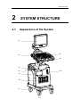
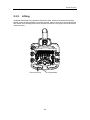
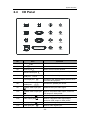
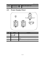
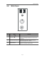
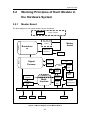
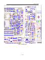
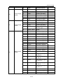
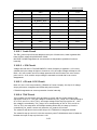
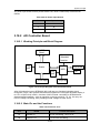
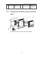
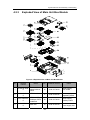
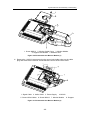
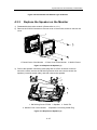
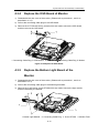
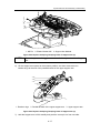
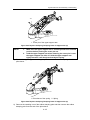
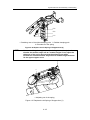
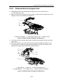
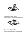
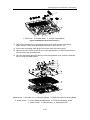
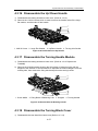
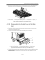
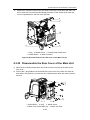
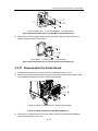
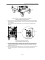
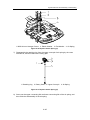
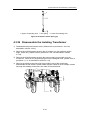
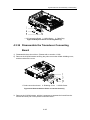
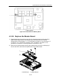
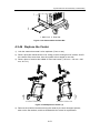
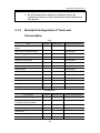
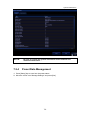
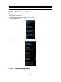
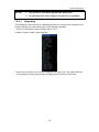
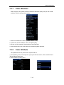
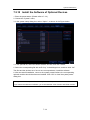
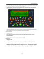
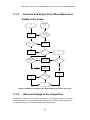
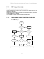
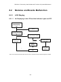
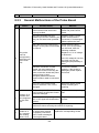
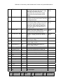
1
DC-3 Series Diagnostic Ultrasound System Service Manual Contents Intellectual Property Statement .......................................................................................................... I Responsibility on the Manufacturer Party........................................................................................... I Warranty ............................................................................................................................................ II Return Policy .................................................................................................................................... III 1 System Introduction.................................................................................................... 1-1 1.1 2 System Structure......................................................................................................... 2-1 2.1 Appearance of the System ................................................................................................... 2-1 2.2 LCD Monitor ......................................................................................................................... 2-3 2.2.1 Contrast& Brightness Control Key of the Monitor ......................................................... 2-4 2.2.2 Up/down Deflector Rod of Monitor................................................................................ 2-4 2.2.3 Up/down Lock of Upper Support Arm ........................................................................... 2-6 2.2.4 Tuning Screw of Air Spring on Support Arm ................................................................. 2-6 2.3 3 Intended Use ........................................................................................................................ 1-1 Turning and Lifting the Keyboard ......................................................................................... 2-7 2.3.1 Turning .......................................................................................................................... 2-7 2.3.2 Lifting............................................................................................................................. 2-8 2.4 I/O Panel............................................................................................................................... 2-9 2.5 Power Supply Panel ........................................................................................................... 2-10 2.6 ECG Panel.......................................................................................................................... 2-11 2.7 Control Panel ...................................................................................................................... 2-12 System Principle ......................................................................................................... 3-1 3.1 System Principle ................................................................................................................... 3-1 3.2 Working Principles of Each Module in the Hardware System .............................................. 3-3 3.2.1 Master Board ................................................................................................................ 3-3 3.2.2 Ultrasound Receiving .................................................................................................... 3-4 3.2.3 Signal Processing ......................................................................................................... 3-4 3.2.4 Power Management ...................................................................................................... 3-4 3.2.5 System Monitoring ........................................................................................................ 3-5 3.2.6 Video Processing .......................................................................................................... 3-5 3.2.7 Sockets on Master Board.............................................................................................. 3-6 3.2.8 Testing Points on the Master Board .............................................................................. 3-9 3.3 Transmitting Board ............................................................................................................. 3-12 i 3.4 Probe Board/4D Probe Board Module................................................................................ 3-13 3.4.1 Principle of Probe Board/4D Probe Board Module ..................................................... 3-13 3.4.2 Definition of Sockets ................................................................................................... 3-16 3.5 I/O Connecting Board ......................................................................................................... 3-20 3.5.1 3.6 Definition of Sockets on I/O Connection Board .......................................................... 3-21 IO Front Board .................................................................................................................... 3-22 3.6.1 USB ............................................................................................................................. 3-22 3.6.2 Sockets Definition of IO Front Board .......................................................................... 3-23 3.7 IO Port Board...................................................................................................................... 3-25 3.7.1 Functional Modules ..................................................................................................... 3-25 3.7.2 Sockets Definition of I/O Port Board ........................................................................... 3-27 3.7.3 Introduction of Testing Points on IO Port Board.......................................................... 3-31 3.8 IO Rear Panel ..................................................................................................................... 3-31 3.8.1 3.9 Sockets Definition of IO Rear Panel ........................................................................... 3-31 CW Board ........................................................................................................................... 3-32 3.9.1 Functional Modules Introduction ................................................................................. 3-33 3.9.2 Sockets Definition ....................................................................................................... 3-36 3.9.3 Layout of CW Board ................................................................................................... 3-37 3.10 Control Panel ...................................................................................................................... 3-38 3.10.1 The Buckled Board on the Control Panel ................................................................... 3-38 3.10.2 Control Panel .............................................................................................................. 3-39 3.11 ECG Module (optional) ....................................................................................................... 3-42 3.11.1 Principle and Functions .............................................................................................. 3-42 3.11.2 Outlet Definition .......................................................................................................... 3-42 3.11.3 Plug-in Diagram and Components.............................................................................. 3-44 3.12 4D Power Supply Board ..................................................................................................... 3-46 3.12.1 Principle of 4D Power Supply Board........................................................................... 3-46 3.12.2 Interface Definition of 4D Power Board ...................................................................... 3-46 3.13 4D &TEE Drive Board ........................................................................................................ 3-47 3.13.1 Basic Principle of 4D &TEE Drive Board .................................................................... 3-47 3.13.2 Interface Definition of 4D &TEE Drive Board .............................................................. 3-47 3.14 4D Converting Board .......................................................................................................... 3-49 3.14.1 Principle Block Diagram & Principle Description ........................................................ 3-49 3.14.2 Socket Definition ......................................................................................................... 3-50 3.15 USB-to-IDE Port Board ...................................................................................................... 3-51 3.15.1 Socket Definition ......................................................................................................... 3-52 3.16 Power Supply System ........................................................................................................ 3-53 3.16.1 Basic Functions of Power Supply System .................................................................. 3-53 3.16.2 Basic Principle of Power Supply System .................................................................... 3-53 3.17 System Power Supply Distribution ..................................................................................... 3-57 3.18 LCD .................................................................................................................................... 3-58 4 3.18.1 Inverter ........................................................................................................................ 3-58 3.18.2 AD Controller Board .................................................................................................... 3-61 System Structure and Assembly / Disassembly ...................................................... 4-1 4.1 Overall Exploded View ......................................................................................................... 4-1 4.2 Exploded View of Each Module ............................................................................................ 4-3 4.2.1 Exploded View of LCD Display and Support Arm ......................................................... 4-3 4.2.2 Exploded View of Monitor Components-install Board................................................... 4-4 4.2.3 Exploded View of Main Unit Box Module ...................................................................... 4-5 4.2.4 Exploded View of Probe Board Module ........................................................................ 4-7 4.3 Overall Disassemble and Parts Replace .............................................................................. 4-7 4.3.1 Disassemble the Monitor Module ................................................................................. 4-7 4.3.2 Disassemble the Bottom Lights of the Monitor ............................................................. 4-9 4.3.3 Replace the Speaker on the Monitor .......................................................................... 4-10 4.3.4 Replace the OSD Board of Monitor ............................................................................ 4-11 4.3.5 Replace the Bottom Light Board of the Monitor.......................................................... 4-11 4.3.6 Replace the Power Supply Inverter Board of the LCD ............................................... 4-12 4.3.7 Replace the LCD Screen and LCD Control Board ..................................................... 4-14 4.3.8 Replace the Spring Damping Parts of Support Arm ................................................... 4-16 4.3.9 Disassemble the Support Arm .................................................................................... 4-20 4.3.10 Disassemble the Control Panel .................................................................................. 4-21 4.3.11 Replace the Encoder Connecting Board .................................................................... 4-22 4.3.12 Replace the Trackball ................................................................................................. 4-23 4.3.13 Disassemble the Control Panel Buckled Board .......................................................... 4-24 4.3.14 Replace the Control Panel .......................................................................................... 4-24 4.3.15 Disassemble the Casting Aluminium Base Cover ...................................................... 4-26 4.3.16 Disassemble the Up/ Down Handle ............................................................................ 4-27 4.3.17 Disassemble the Turning Handle Module ................................................................... 4-27 4.3.18 Disassemble the Turning Block Cover ........................................................................ 4-27 4.3.19 Disassemble the Frontal Cover of the Main Unit ........................................................ 4-28 4.3.20 Disassemble the Rear Cover of the Main Unit ........................................................... 4-29 4.3.21 Disassemble the IO Module........................................................................................ 4-30 4.3.22 Disassemble the Power Supply Input Module ............................................................ 4-30 4.3.23 Disassemble the DVD-R/W Module............................................................................ 4-31 4.3.24 Disassemble the DVD and USB-to-SATA Port Board ................................................. 4-32 4.3.25 Disassemble the Power Supply Adapter..................................................................... 4-33 4.3.26 Disassemble the IO Frontal Board and ECG Board ................................................... 4-34 4.3.27 Disassemble the Probe Board .................................................................................... 4-35 4.3.28 Replace the Air Spring ................................................................................................ 4-38 4.3.29 Disassemble the Isolating Transformer ...................................................................... 4-41 4.3.30 Replace the HDD ........................................................................................................ 4-42 4.3.31 Disassemble the Main Unit Box Module ..................................................................... 4-43 4.3.32 Replace the IO Port Board.......................................................................................... 4-45 4.3.33 Replace the IO Connecting Board .............................................................................. 4-47 4.3.34 Disassemble the Transducer Connecting Board ........................................................ 4-48 4.3.35 Replace the Power Supply Main Board and Auxiliary Board ...................................... 4-49 4.3.36 Replace the Transmitting Board ................................................................................. 4-51 4.3.37 Replace the CW Board ............................................................................................... 4-52 4.3.38 Replace the CPU Board ............................................................................................. 4-53 4.3.39 Replace the Master Board .......................................................................................... 4-55 4.3.40 Replace the Air Inlet Fan ............................................................................................ 4-56 4.3.41 Disassemble 4D&TEE Drive Board ............................................................................ 4-57 4.3.42 Disassemble 4D&TEE Connecting Board .................................................................. 4-58 4.3.43 Disassemble 4D&TEE Power Board .......................................................................... 4-58 4.3.44 Disassemble 4D Probe Board .................................................................................... 4-60 4.3.45 Disassemble the Dust Net .......................................................................................... 4-60 4.3.46 Replace the Caster ..................................................................................................... 4-61 4.4 4.4.1 5 Installation of W/B Video Printer ................................................................................. 4-62 Maintenance Requirements ........................................................................................ 5-1 5.1 Tools Used in Maintenance .................................................................................................. 5-1 5.1.1 Tools, Measurement Devices, Consumables ............................................................... 5-1 5.1.2 Standard Configuration of Tools and Consumables ..................................................... 5-2 5.2 6 Installation of Peripherals ................................................................................................... 4-62 Maintenance Personnel ........................................................................................................ 5-3 Checking ...................................................................................................................... 6-1 6.1 6.1.1 Checking Plan ............................................................................................................... 6-1 6.1.2 Confirmation before Checking ...................................................................................... 6-1 6.2 Flow of Functionality Checking ..................................................................................... 6-2 6.2.2 Details of Functionality Check ...................................................................................... 6-3 Safety Checking ................................................................................................................... 6-4 6.3.1 Electrical Safety Checking ............................................................................................ 6-4 6.3.2 Mechanical Safety Checking ........................................................................................ 6-4 6.4 Image Checking.................................................................................................................... 6-7 6.4.1 Checking the B/W Image Phantom Data and Image Recording .................................. 6-7 6.4.2 Checking Phantom Data ............................................................................................... 6-7 6.4.3 Final Operation Checking and Image Archiving ........................................................... 6-8 6.4.4 Color flow image check ................................................................................................. 6-8 System Maintenance ................................................................................................... 7-1 7.1 System Cleaning .................................................................................................................. 7-1 7.1.1 Cleaning Flow ............................................................................................................... 7-1 7.1.2 Details for Cleaning....................................................................................................... 7-2 7.2 Software Maintenance .......................................................................................................... 7-4 7.2.1 Confirming the System Starting .................................................................................... 7-4 7.2.2 Preset ............................................................................................................................ 7-5 7.2.3 Viewing System Information ......................................................................................... 7-5 7.2.4 Preset Data Management ............................................................................................. 7-6 7.2.5 Maintenance Status ...................................................................................................... 7-8 7.2.6 Software Upgrading ...................................................................................................... 7-8 7.2.7 Enter Windows ............................................................................................................ 7-12 7.2.8 Enter 4D Mode ............................................................................................................ 7-12 7.2.9 Model ConFigureuration ............................................................................................. 7-13 7.2.10 Install the Software of Optional Devices ..................................................................... 7-14 7.3 8 Checking Functionality ......................................................................................................... 6-2 6.2.1 6.3 7 System Status Checking ...................................................................................................... 6-1 System Self-diagnosis ........................................................................................................ 7-15 7.3.1 Self-diagnosis Interface .............................................................................................. 7-15 7.3.2 Description of Testing Items ........................................................................................ 7-16 7.3.3 Details of the Testing Items ......................................................................................... 7-18 Troubleshooting .......................................................................................................... 8-1 8.1 Malfunction ........................................................................................................................... 8-1 8.1.1 Examine and Repair Flow of Blank Screen .................................................................. 8-1 8.1.2 Examine and Repair Flow When No Image Displayed in the Image Area ................... 8-2 8.1.3 Examine and Repair Flow When Black Area Exists in the Image ................................ 8-3 8.1.4 Abnormal Image in the Image Area .............................................................................. 8-3 8.1.5 CW Image Abnormity .................................................................................................... 8-4 8.1.6 Examine and Repair Flow When the System Can’t Start-up ........................................ 8-4 8.2 Modules and Boards Malfunction ......................................................................................... 8-5 8.2.1 LCD Display .................................................................................................................. 8-5 8.2.2 General Malfunctions of the Control Panel Unit ........................................................... 8-7 8.2.3 General Malfunctions of the Probe Board .................................................................... 8-8 8.2.4 General Malfunctions of CW Doppler Board ................................................................ 8-9 8.2.5 General Malfunctions of USB-to-IDE Port Board........................................................ 8-11 8.2.6 PC System Related Malfunctions ............................................................................... 8-12 8.2.7 Power Supply Malfunction .......................................................................................... 8-13 8.3 Software Troubleshooting ................................................................................................... 8-19 8.3.1 Troubleshooting in the Case of HDD Damaged ......................................................... 8-19 8.3.2 XP Operation System Troubleshooting....................................................................... 8-20 8.3.3 Ultrasound Software System Troubleshooting ........................................................... 8-21 8.3.4 Patient Databank Troubleshooting.............................................................................. 8-22 Appendix ADefinition of Commonly Used Sockets and Functions in System Maintenance A-1 Appendix B .................................................................................. Electrical Safety Inspection B-1 ©2008-2013 Shenzhen Mindray Bio-Medical Electronics Co., Ltd. All rights Reserved. For this Operator’s Manual, the issue date is 2013-06. Intellectual Property Statement SHENZHEN MINDRAY BIO-MEDICAL ELECTRONICS CO., LTD. (hereinafter called Mindray) owns the intellectual property rights to this Mindray product and this manual. This manual may refer to information protected by copyright or patents and does not convey any license under the patent rights or copyright of Mindray, or of others. Mindray intends to maintain the contents of this manual as confidential information. Disclosure of the information in this manual in any manner whatsoever without the written permission of Mindray is strictly forbidden. Release, amendment, reproduction, distribution, rental, adaptation, translation or any other derivative work of this manual in any manner whatsoever without the written permission of Mindray is strictly forbidden. , , , , , BeneView, WATO, BeneHeart, are the trademarks, registered or otherwise, of Mindray in China and other countries. All other trademarks that appear in this manual are used only for informational or editorial purposes. They are the property of their respective owners. Responsibility on the Manufacturer Party Contents of this manual are subject to change without prior notice. All information contained in this manual is believed to be correct. Mindray shall not be liable for errors contained herein or for incidental or consequential damages in connection with the furnishing, performance, or use of this manual. Mindray is responsible for the effects on safety, reliability and performance of this product, only if: z all installation operations, expansions, changes, modifications and repairs of this product are conducted by Mindray authorized personnel; z the electrical installation of the relevant room complies with the applicable national and local requirements; and z the product is used in accordance with the instructions for use. Upon request, Mindray may provide, with compensation, necessary circuit diagrams, calibration illustration list and other information to help qualified technician to maintain and repair some parts, which Mindray may define as user serviceable. I Note This equipment is not intended for family usage. This equipment must be operated by skilled/trained medical professionals. Warning It is important for the hospital or organization that employs this equipment to carry out a reasonable service/maintenance plan. Neglect of this may result in machine breakdown or injury of human health. Warranty THIS WARRANTY IS EXCLUSIVE AND IS IN LIEU OF ALL OTHER WARRANTIES, EXPRESSED OR IMPLIED, INCLUDING WARRANTIES OF MERCHANTABILITY OR FITNESS FOR ANY PARTICULAR PURPOSE. Exemptions Mindray's obligation or liability under this warranty does not include any transportation or other charges or liability for direct, indirect or consequential damages or delay resulting from the improper use or application of the product or the use of parts or accessories not approved by Mindray or repairs by people other than Mindray authorized personnel. This warranty shall not extend to: z Any Mindray product which has been subjected to misuse, negligence or accident; z Any Mindray product from which Mindray's original serial number tag or product identification markings have been altered or removed; z Any product of any other manufacturer. Safety, Reliability and Performance Mindray is not responsible for the effects on safety, reliability and performance of the product if: z Assembly operations, extensions, re-adjusts, modifications or repairs are carried out by persons other than those authorized by Mindray. z Personnel unauthorized by Mindray repairs or modifies the instrument. II Return Policy Return Procedure In the event that it becomes necessary to return this product or part of this product to Mindray, the following procedure should be followed: 1. Obtain return authorization: Contact the Mindray Service Department and obtain a Customer Service Authorization (Mindray) number. The Mindray number must appear on the outside of the shipping container. Returned shipments will not be accepted if the Mindray number is not clearly visible. Please provide the model number, serial number, and a brief description of the reason for return. 2. Freight policy: The customer is responsible for freight charges when this product is shipped to Mindray for service (this includes customs charges). 3. Return address: Please send the part(s) or equipment to the address offered by Customer Service department Company Contact Manufacturer: Address: Shenzhen Mindray Bio-Medical Electronics Co., Ltd. Mindray Building, Keji 12th Road South, Hi-tech Industrial Park, Nanshan, ShenZhen 518057, P. R. China Tel: +86 755 26582479 26582888 Fax: +86 755 26582934 26582500 EC-Representative: Address: Shanghai International Holding Corp. GmbH(Europe) Eiffestraβe 80, Hamburg 20537, Germany Tel: 0049-40-2513175 Fax: 0049-40-255726 III Safety Precautions 1. Meaning of Signal Words In this operator’s manual, DANGER, WARNING, CAUTION and CAUTION are signal words used to indicate safety and other important instructions. The signal words and their meanings are defined as follows. Please understand their meanings clearly before reading this manual. Signal Word DANGER Indicates death or serious injury may occur imminently in this hazardous situation if not avoided. WARNING Indicates death or serious injury may occur potentially in this hazardous situation if not avoided. CAUTION Indicates minor or moderate injury may occur potentially in this hazardous situation if not avoided. CAUTION 2. Meaning Indicates property damage may occur potentially in this hazardous situation if not avoided. Meaning of Safety Symbols Symbol Description Type-BF applied part. The ultrasound transducers connected to this system are Type-BF applied parts. The ECG module connected to this system is also a Type-BF applied part. “Attention” indicates the points requiring attention. Be sure to read the operation manual concerning these points before using the equipment. IV 3. Safety Precautions Please read the following precautions carefully to ensure the safety of the patient and the operator when using the system. DANGER: WARNING: Do not operate this system in an atmosphere containing flammable or explosive gases such as anesthetic gases, oxygen, and hydrogen because an explosion may occur. 1 Do connect the power plug of this system and power plugs of the peripherals to wall receptacles that meet the ratings indicated on the rating nameplate. Using an adapter or multifunctional receptacle may affect the system’s grounding performance, and cause the leakage current to exceed safety requirements. Besides, do connect the video printer to the auxiliary power supply socket of this system, and use the printing cable provided with this system to connect the printer. Otherwise, it may cause electric shock. 2 Connect the grounding conductor only before turning ON the system. Connect the grounding cable after turning OFF the system. Otherwise, electric shock may result. 3 For the connection of power and grounding, follow the appropriate procedures described in this operator’s manual. Otherwise, there is risk of electric shock. Do not connect the grounding cable to a gas pipe or water pipe; otherwise improper grounding may result or a gas explosion may occur. 4 Before cleaning the system, disconnect the power cord from the socket. System failure may result in electric shock. 5 This system is not water-proof. Do not use this system in any place where water leakage may occur. If any water is sprayed on or into the system, electric shock may result. If water is accidentally sprayed on or into the system, please turn off the system power immediately and contact Mindray Customer Service Department or sales representative. 6 Store and use the transducers carefully. In case that a scratched transducer surface is found, immediately stop using the transducer and contact Mindray Customer Service Department or sales representative. There is risk of electric shock if using a damaged or scratched transducer. 7 Do not allow the patient to contact the live parts of the ultrasound system or other devices, e.g. signal I /O ports. If the system or other devices is defective, there is risk of electric shock. V CAUTION: 8 Do not use an aftermarket transducer other than those specified by Mindray. The transducers may damage the system, causing a profound failure, e.g. a fire in the worst case. 9 Do not subject the transducers to knocks or drops. Use of a defective transducer may cause an electric shock. 10 Do not open the covers and front panel of the system. Otherwise, short circuit or electric shock may result. 11 Do not use this system simultaneously with equipments such as an electrical knife, high-frequency therapy equipment, or a defibrillator, etc., otherwise, electric shock may result. 12 Only use the ECG leads accompany with the ECG module; otherwise electric shock may result. 13 Attentions in the transportation: when this system is moved, please hold the handle. If other parts of the system are held, it may cause damage due to the abnormal force. Do not push the system from the left/right side, otherwise, it may be toppled over. 14 Accessory equipments connected to the analog and digital ports must comply with the relevant IEC standards (e.g., IEC 60950 information technology equipment safety standard and IEC 60601-1 medical equipment standard). Furthermore, all conFigureurations must comply with the standard IEC60601-1-1. It is the responsibility of the person, who connects additional equipments to the signal input or output ports and configures a medical system, to verify if the system complies with the requirements of IEC60601-1-1. If you have any questions regarding these requirements, consult your sales representative. 15 Prolonged and repeated use of keyboards may result nerve disorders in hand or arm for some individuals. Observe the local safety or health regulations concerning the use of keyboards. 1 Precautions concerning clinical examination techniques: (1) This system must be used only by qualified medical professionals. (2) This operator’s manual does not describe clinical examination techniques. The clinician should select the proper examination techniques based on specialized training and clinical experience. VI 2 Malfunctions due to radio wave: (1) Using devices transmitting RF signals in the vicinity of the system may affect the system’s performance. Do not use or take any devices transmitting RF signals (such as cellular phones, transceivers and radio controlled products) in the room placing the system. (2) If a person brings a device that generates radio waves near the system, ask him / her to immediately turn OFF the device. 3 Precautions concerning moving the system: (1) Make sure the system is installed on a plane with the caster been locked, otherwise, movement of the system may result in damage. (2) Do not move the system laterally, which may result in damage in case of toppling. (3) Move the system slowly on the slope by two people, otherwise, damage may result in case of unexpected sliding. (4) Do not sit on the system, which may result individual falling in case of system moving. (5) Object placed on the monitor may fall and injure an individual. (6) Fasten and fully secure any peripheral device before moving the system. A loose peripheral device may fall and injure an individual. (7) When move the system on the steps, please take care to prevent the system from toppling. 4 Do not expose the system to excessive vibration during the transportation. Mechanical damage may result (such as damage to the caster). If the system has to be moved on uneven floor frequently, please contact Mindray Customer Service Department or sales representative. 5 Do not connect this system to outlets with the same breakers and fuses that control the current of devices such as life-support systems. If malfunctions or over-current appear on this system, or when there is an instantaneous current at power ON, the breakers and fuses of the building’s supply circuit may be tripped. VII 6 Always keep the system dry. Avoid transporting this system suddenly from a cold place to a warm place; otherwise condensation or water droplets may form, which may result short circuit. 7 If the circuit protector is tripped on, it indicates that malfunction appears on the system or a peripheral device. You should not repair the system under this circumstance but call the Mindray Customer Service Department or sales representative for help. 8 There is no risk of high-temperature burns during normal ultrasound examinations. It is possible for the surface temperature of the transducer to exceed the body temperature of a patient due to environmental temperature and exam type combinations. If a patient complains of abnormal heat from the transducer, immediately stop scanning. To prevent patient burns, ensure there is no surface damage to the transducer. Do not apply the transducer to the same region on the patient for a long time. Apply the transducer only for a period of time required for the purpose of diagnosis. 9 The system and its accessories have not been disinfected or sterilized prior to delivery. The operator is responsible for the cleaning and disinfection of transducers and sterilization of biopsy brackets according to the manuals before application. All items must be thoroughly processed to completely remove harmful residual chemicals, which will not only harmful to the human body, but also damage the accessory. 10 It is necessary to press [End Exam] to end the current scan and clear the current Patient Information field. Otherwise new patient data may be mixed with the previous patient data. 11 Do not connect or disconnect the system’s power cord or its accessories (e.g., a printer or a recorder) without turning OFF the power first. This may damage the system and its accessories or cause electric shock. 12 Do not turn OFF the power supply of the system during printing, file storage or data invoking. An interrupted work may not be completed afterwards, and the file may be lost or corrupted. 13 If the system is powered off improperly during operation, it may result in data damage to the system’s hard disk or system failure. VIII NOTE: 14 Do not use the system to examine a fetus in the Doppler mode for a long period of time. 15 Do not use a USB memory device (e.g., a USB flash drive, or removable hard disk) which may include unsafe data. Otherwise, system damage may result. 16 It is recommended to use the video devices specified in this manual. 17 Read the Acoustic Output Principle in the operation manual carefully before operate this system on clinical examination. 18 The auxiliary power output outlet in the system is used to supply power for the recommended peripheral devices. Do not connect other devices to the outlet, otherwise the rated output power may be exceeded and failure may result. Maximum output outlet for peripheral devices is 330V. 1 Do not use the system in the vicinity of strong electromagnetic field (such as a transformer), which may affect the performance of the system. 2 Do not use the system in the vicinity of high-frequency radiation source, which may affect the performance of the system or even lead to system failure. 3 To avoid damage to the system, do not use it in the following environment conditions: (1) Locations exposed to direct sunlight; (2) Locations subject to sudden changes of environmental temperature; (3) Dusty locations; (4) Locations subject to vibration; (5) Locations near heat generators; (6) Locations of high humidity. 4 Turn ON the system only after the power is turned OFF for more than 20 seconds. If the system is turned ON immediately after being turned OFF, the system may not reboot properly and may lead to malfunction. IX 4. 5 Do not disconnect a transducer that remains in a live imaging state. This can damage the system and / or transducer. Press [Freeze] or turn off the power of the system before connecting or disconnecting a transducer. 6 Remove the ultrasound gel from the face of the transducer when the examination is completed. Water in the gel may enter the acoustic lens and adversely affect the performance and safety of the transducer. 7 To ensure safety of the data, please back up all the data to a secure external storage media, as data stored to the system’s internal memory may be lost due to system failure, or improper operation. 8 Do not apply external force to the control panel. The system may be damaged. 9 If the system is used in a small room, the room temperature may rise. Please ensure good ventilation. 10 To dispose the system or any part, please contact Mindray Customer Service Department or sales representative. Mindray would bear no responsibility for the damages resulting from disposal of this system without consulting Mindray. 11 Electrical and mechanical performance may be degraded due to long usage (such as current leakage or distortion and abrasion). To ensure optimal system operations, it is recommended that you maintain the system under a Mindray service agreement. Various aspects of system performance and operation can be maintained under the professional supervision of a service representative. 12 The iScape feature constructs a single extended image from a series of continuous individual image frames scanned on the interesting field. The quality of the final image is user-dependent and thus requires skills to efficiently apply the feature and technique. Exercise caution when measurements are performed under an iScape mode. 13 Ensure that the current exam date and time are the same as the system date and time. Warning Labels The warning labels are attached to this system in order to call your attention to potential hazards. The symbol on the warning labels indicates safety precautions. The warning labels use the same signal words as those used in the operator’s manual. X Please refer to the operator’s manual for detailed information about the warning labels. Read operator’s manual carefully before using the system. The name, pattern and meaning of each warning label are described as follows: No. Label Meaning (a) Do not sit on the system. <1> (b) There is explosion risk if the system is applied around flammable gas. (c) Before using the system, be sure to carefully read the relevant contents of this operator’s manual. (a) Place the system on a plane. <2> (b) (b) Do not open the cover, because the high voltage inside may result in electric shock. XI 1 1.1 SYSTEM INTRODUCTION Intended Use DC-3/DC-3T diagnostic ultrasound system is applicable for clinical ultrasound diagnostic examination. There is one difference between DC-3 and DC-3T, that is, DC-3 has an orthopedics measurement package, but DC-3T does not. DC-3Vet is intended for diagnosis of animals. 1-1 System Structure 2 2.1 SYSTEM STRUCTURE Appearance of the System <1> <8> <2> <9> <3> <10> <4> <5> <6> <7> 2-1 System Structure <11> <12> <13> <14> No. Part Function <1> Monitor Displays the images and parameters during scanning. <2> Control panel Operator-system interface, operation control. <3> DVD-RW DVD-RW drive. <4> Power switch Used for turning on/ off the power supply. <5> Compartment for placing video printer Used for placing B/W video printer. <6> Transducer socket Sockets connecting transducers and the main unit. There are 3 active sockets and 1 parking socket. 2-2 System Structure <7> Caster Used for fixing or moving the system. <8> Transducer& gel holder Used for placing transducers and gel temporarily. <9> Handle Used for pushing and moving the system. <10> ECG panel Used for connecting the ECG cable, USB devices and footswitch. <11> Monitor support arm Used for supporting and adjusting the height and position of monitor. <12> Table for placing objects Used for placing articles and instruments and so on. <13> I/O panel Port panel for input and output signals. <14> Power panel Electrical port panel. 2.2 LCD Monitor 2-3 System Structure 2.2.1 Contrast& Brightness Control Key of the Monitor Shown as figure at the right side: <1>, <2> refer to the brightness control keys with a sun marked at the top side; key <1>, which marked a “-” on the top side, can be used to decrease the brightness; while key<2>, which marked a “+” on the top side, can be used to increase the brightness <3>, <4> refer to the contrast control keys with a lune marked at the top side; key <3>, which marked a “-” on the top side, can be used to decrease the contrast, while key <4>, which marked a “+” on the top side, can be used to increase the contrast. 2.2.2 Up/down Deflector Rod of Monitor Deflector rod L R Shown as above, the deflector rod is located at the left lower corner at the back of the monitor. When the deflector is at the rightmost, the monitor is at working status and the angle between monitor and support arm can be changed at the range controlled by the deflector rod. The monitor can be turned for 20° both forward and backward, shown as follows: 2-4 System Structure In the process of transportation or moving the system, the deflector rod can be toggled left to level the monitor, shown as follows: 2-5 System Structure 2.2.3 Up/down Lock of Upper Support Arm Put the support arm to horizontal position, the arm will be locked if the lock is at the locked position; when the lock is located at the unlocked position, the arm can be adjusted from upside to downside. 2.2.4 Tuning Screw of Air Spring on Support Arm Turn the monitor and the support arm to the same position, adjust the tuning screw by screwdriver. Try to adjust the screw when the monitor rises and falls automatically, and the air spring needs to be replaced if it can not meet the requirement even when the screw is at the tightest or loosest status. (For the replacement of the air spring, please refer to 4.3.8). 2-6 System Structure Tuning screw 2.3 Turning and Lifting the Keyboard 2.3.1 Turning Hold and push the handle in the direction of front part of machine (located at the frontal part of back keyboard ), turn the keyboard left and right within 45°, the keyboard will be locked at where the handle be loosened. Hold and push the handle in the direction of front part of machine to turn the 2-7 k b d Handle System Structure 2.3.2 Lifting Handhold the handle of the keyboard with both hands, with the left hand hold the lifting handle, press the lifting handle to a certain position, uplift or push down the keyboard with both hands, then the keyboard can be elevated or lowered. The height can be adjusted is 150mm at most. Lifting handle Push in this way 2-8 System Structure 2.4 I/O Panel <1> <5> <9> <13> <2> <6> <10> <14> <3> <7> <11> <15> <8> <12> <16> <4> No. <1>, <2> Port Function USB port Used to connect USB devices. <3> Reset System reset. <4> Ethernet port Used to connect to the network. <5> <6> <7> <8> Remote control port Serial port VGA output port Parallel port Connects to the video printer control port. Connects to the serial port device. Connects to the external display devices such as monitor and projector. Connects the parallel port device. <9> Separate video input port <10> Separate video output port Used for composite video output, connect to VCR output or video printer. <11> Video input port Used for composite video input. <12> Video output port Used for composite video signal output, connect to VCR output or video printer. <13> Audio input port Used for audio signal input. <14> Audio input port Used for audio signal input. Separates the input video signal. 2-9 System Structure <15> Audio output port Used for audio signal output. <16> Audio output port Used for audio signal output. 2.5 Power Supply Panel <1> <2> <5> <3> No. <1> <4> Name Equipotential Function Connects the equipotential points terminal <2> Power inlet <3>, <4> Power output <5> Circuit breaker AC power inlet Supply power for optional peripheral devices (e.g. VCR) Switches off the power supply 2-10 System Structure 2.6 ECG Panel <1> <2> <3> <4> No. Name Function <1> USB ports (2) Connects the USB devices. <2> Mic In port Reserved for future use. (used for connecting microphone to record vocal comments). <3> ECG lead signal input port <4> Pencil probe port Connects to ECG leads, to directly obtain the electrocardiosignal of the patient. Reserved for future use. (used for connecting a pencil probe) 2-11 System Structure 2.7 No. Control Panel Symbol Name Function Escape Press to exit the current status to the previous status. Help Press to open or close the accompanying help documents. / Press to enter or exit patient information management system. <4> F1 User-defined key The function is definable. <5> F2 User-defined key The function is definable. <1> Esc <2> Help <3> iStation 2-12 System Structure <6> F3 User-defined key The function is definable. <7> F4 User-defined key The function is definable. <8> F5 User-defined key The function is definable. <9> F6 User-defined key The function is definable. <10> Quad Quad-split screen Press to enter/ exit quad-split screen mode. <11> Biopsy Biopsy Press to show or hide the biopsy guide line. <12> Setup Preset Press to open/ close the preset dialog box. <13> / Character key Same as the keys of PC. <14> / Indicating light 1 The indicator light is on after the power is switched on; it is off after the system is turned on. <15> / Indicating light 2 The indicator light flashes when the hard disk is reading or writing; and in other situations, it is off. <16> F8 User-defined key The function is definable. <17> F9 User-defined key The function is definable. <18> F7 User-defined key The function is definable. <19> TGC Slide bar To adjust the depth and gain. <20> Volume Volume Rotate to increase or decrease spectrum volume. <21> / Multi-function knob 1 To adjust the parameters, the functions are shown by the sketch map displayed at the downside of the screen. <22> / Multi-function knob 2 To adjust the parameters, the functions are shown by the sketch map displayed at the downside of the screen. <23> / Multi-function knob 3 To adjust the parameters, the functions are shown by the sketch map displayed at the downside of the screen. <24> / Four-direction key The functions are shown by the sketch map displayed at the downside of the screen. <25> / Multi-function knob 4 To adjust the parameters, the functions are shown by the sketch map displayed at the downside of the screen. <26> / Multi-function knob 5 To adjust the parameters, the functions are shown by the sketch map displayed at the downside of the screen. <27> iTouch / Press to optimize the images. 2-13 System Structure <28> Info Patient information To enter into patient information input interface. <29> Probe Transducer switch To switch the transducer and exam mode. <30> Review Review To review the stored images. <31> Report Diagnostic report Press to open/ close the report. <32> End Exam End exam To end an exam. <33> F10 Self-defining key The function is definable. / To switch the live image window in the multi-window mode. <35> CW / Reserved key (press to enter the CW mode). <36> M / Press to enter the M mode. <37> PW / Press to enter the PW mode. <38> Gain Gain To adjust the gain of the live image, the light is on; press to adjust the gain of the corresponding mode in 2D mode or 3D mode. <39> Power / Press to enter the Power mode. / To enter Dual mode in Non-Dual mode; <34> Update <40> Dual or to switch the live window in Dual mode. <41> Color / Press to enter Color mode. <42> B / Press to enter B mode. <43> Body Mark Body mark To enter/ exit Body mark mode. <44> Comment Comment To enter/ exit the character comment mode. Clear To clear the comments and measurement caliper and so on. <46> Arrow Arrow To enter/ exit arrow comment. <47> Cine Cine review To enter/ exit Cine review. <45> Clear <48> Depth/Zoom Depth/ Zoom Press to switch to the depth/zoom function, the corresponding light will be on; turn the knob to adjust the depth or zoom factor. <49> Print Print Press to print the contents which have been set. <50> Save Save Save the single frame image. <51> Exit Exit To exit the current status. <52> Measure Measure To enter/ exit the general measure mode. <53> Change Change To change the active point of the caliper during measurement. <54> Caliper Caliper To enter/ exit the general measure mode. 2-14 System Structure Multi-function knob Status dependent. Main menu To invoke or close the menu corresponding to the current status. <57> Freeze Freeze Press to freeze or unfreeze an image. <58> Back Back Press to return to the previous operation or to delete the last project. <55> / <56> Menu <59> / <60> Set Trackball Set Rotate to change the position of the cursor on the screen. To confirm an operation, equivalent to the left-button of the mouse. 2-15 System Principle 3 3.1 SYSTEM PRINCIPLE System Principle The block diagram of DC-3 system is shown as follows: Figure 3-1 Block Diagram of DC-3 The system consists of main unit and power system, and the main unit consists of: Master board: including ultrasound system, PC system, and power supply management and filtering system; Ultrasound system: to carry out functions including echo receiving, zoom in, sampling, Beam 3-1 System Principle forming, signal processing, ultrasound scanning receiving control as well as data exchange between PCs; PC system: post processing the echo data, communicate with users, to support many kinds of peripherals; Power management and filtering system: to ensure the normal working of power system, support system shutdown, stand-by mode and dormancy mode; Meanwhile, master board provides connecting sockets with each module; Transmitting board: to realize delay focusing transmitting for N channels; Control panel can communicate with the master board through USB; CPU board; Probe board module: including probe control board, probe board, probe connection board, used to connect the transducers, supports 4 transducer sockets, of which 3 sockets are general, the other one is 4D transducer socket. CW Board: processing CW signal and pencil transducer signal; 4D driver board: implements the transfer function of 4D controlling signals; The peripheral extension modules including: I/O connecting board: connects the master board and IO front board, IO interface board, provides power supply to the hard disk; IO front board,USB HUB(one input, three outputs), provides external MIC port, USB port as well as pencil probe port; IO port board: USB HUB (one input, six outputs), video acquisition, and provides sockets to some inner wires; IO rear board: provides IO port for the rear part; USB-to-IDE board: USB to IDE converting board, connects to DVD R/W; ECG board; Display module: including display and speaker; 4D driver board: implements the drive function of 4D probe. The power system consists of (In fact, it also includes the power management system on the master board and the filtering system): Power supply board: provides power for the system; Power supply connecting board: provides connection sockets between auxiliary output, breaker and isolating transformer, to realize voltage input selection; 4D power supply board: implements the power supply for 4D driver board; AC/DC board: to change the AC input into 12V DC. 3-2 System Principle 3.2 Working Principles of Each Module in the Hardware System 3.2.1 Master Board The block diagram of the master board is shown as follows: 4D port 1 Probe module Beamform er FPGA2 FPGA1 Transmitting board Ultrasound receiving 4D port Fan port FPGA3 Extension port CW port 1 DC3 power port CW port 2 Signal Process Video process Master board Multifunction Master board power Tempe rature sensor Adapter port System monitor DC3 signal port Power management COME INTERFACE USB HDD Audio Network Figure 3-2 Block Diagram of the Master Board 3-3 Power port System Principle Shown as above, the function modules of the master board are: Ultrasound receiving; Signal process; Power management; System monitoring; Video process. And the master board provides connecting sockets for the following devices: Probe board module; Transmitting board; CW board; 4D board (reserved); CPU module; IO connection board; Power supply module; Hard disk; DC-3 power socket; DC-3 signal socket; Fan; Speaker; Network. The layout of the above modules’ sockets on the master board is shown as Figure A-1. 3.2.2 Ultrasound Receiving Ultrasound receiving consists of high voltage isolating & receiving channel selection, voltage-control gain amplifier and ADC. The receiving channel selection is controlled by two CPLDs, the analog control voltage of the amplifier comes from a DAC, and SPI signals of DAC, the amplifier as well as the ADC all come from beamformer FPGA1. 3.2.3 Signal Processing Signal processing is completed by two FPGAs, they are FPGA1 and FPGA2. FPGA1 mainly controls the front-end chip (channel selection CPLD, VGA gain control DAC, ADC and the transducers), produces transmitting sequence pulse, carries out wave combination, quadrature demodulation and so on. FPGA2 is used to process signal, upload data, call real-time parameter scanning and so on, data is uploaded through PCI socket, and the USB port is a reserved port. 3.2.4 Power Management Power management is basically completed by CPLD. 3-4 System Principle According to the power on sequence, the system power can be classified into: STANDBY power supply, CPU STANDBY power supply and normal working power supply. STANDBY power supply is the power supply under POWERDOWN status. It includes +5VSTB, +3V3STB and +1.8VSTB. They power the comparator that generated POWER OK, crystal of 6M, power supply management CPLD, power supply drive and 244 status drive. Just to connect to AC power and switch on the breaker. CPU STANDBY is the power supply when PC is in standby mode, it stops working when the system is turned off, and it works first when the system begins to work. The normal working power supply refers to the power required during normal work of the system. Except STANDBY and CPU STANDBY mode, others all belong to normal working power supply, of which the indicator lights are shown as follows: Table 3-1 Indicator Lights of the Master Board Power Supply No. LED number Meaning 1 D7 12V 2 D25 3.3V indicator light 3 D26 5V indicator light One indicator light on the DC-3 control panel indicates the working status of the breaker. The related lights descriptions are described as Table 3-2: Table 3-2 Description of Power Supply Indicator Lights 1 Indicator light of breaker status (refer to the 14th item marked on the control panel Figureure) 3.2.5 Single color(green), indicates the working status of the breaker after mains power connected; the light is off when the breaker is switched off; The light is green when the breaker is switched on, it flashes during start-up process, and it is off when the back light of the keyboard is on. System Monitoring System monitoring including monitor on the voltage, temperature, fan malfunction detection and control on the fan speed; Monitor on the voltage: direct measurement, including measurement of 12V, VCC(+5V), VDD(+3.3V), 2.5V, 1.5V, PHV, A+3, -5V, -12V; Monitor on the power supply module and temperature of ultrasound front-end; Monitor and control on fans and ventilation unit. 3.2.6 Video Processing Video signal that outputs from the PC module is converted into standard S_Video and video signal post processed by FPGA3 and video code chip. 3-5 System Principle 3.2.7 Sockets on Master Board The standard sockets, which have no definition in the master board sockets, are required to be designed by the related standards, the sockets include: dual-USB port, SATA socket, Ethernet socket, SATA hard disk socket of notebook, COM EXPRESS socket, button-shaped battery socket and S-Video socket. 3.2.7.1 Socket between Master Board and Probe Module Signals between the probe board module and master board socket are defined as Table A-1. Descriptions of signals are described as follows: Table 3-3 Definition of Signals between the Master Board and Probe Module Socket Signal name Description SPI_CLK SPI_DIN Commands and data port to the probe module. SPI_DOUT SPI_CS FLASH_POWER Reserved FLASH_WP Reserved PROBE_ID[7:6] Reserved signal PROBEID_CS[1:0] RELAY_EN[1:0] PROBE_PRESENT Presents probe signal EXP_PRESENT Connected to earth (in the probe unit) PE[1:N] N channel transmitting and receiving signal 3.2.7.2 Socket between Master Board and Transmitting Board Signals between the master board and transmitting board are defined in Table A-1 and Table A-2. 3.2.7.3 Socket between CW Board and Master Board Signals between the CW board and master board sockets are defined as Table A-3 and Table A-4. Of which, the signals of CW CON1 are defined as follows: Table 3-4 Signals Definition at CW CON1 Socket Name Description CW[9:0] CW echo signal 12V +12 power supply -12V -12V power supply 5V +5V power supply 3-6 System Principle -5V 3.2.7.4 -5V power supply JTAG Socket Definition of Clock Chip The JTAG socket is defined as follows: Table 3-5 Definition of JTAG Socket PIN 3.2.7.5 SIG 1 CLK_TMS 2 CLK_TDI 3 CLK_TDO 4 CLK_TCK 5 GND 6 VDD_CLK Socket between 4D Board and Master Board Socket design between 4D board and master board is reserved currently, and the signals are defined as Table A-6. 3.2.7.6 Socket between Speaker and Master Board Socket between speaker and master board is defined as follows: Table 3-6 Definition of Sockets between Speaker and master Board PIN 3.2.7.7 SIG 1 ROUTP 2 ROUTN 3 NC 4 LOUTP 5 LOUTN Socket between Fan and Master Board Socket between fan and master board is defined as follows; Table 3-7 Definition of Socket between Fan and Master Board PIN SIG PIN 1 FANSPEED4 2 12V 3 PWM45 4 12V 5 FANSPEED5 6 CPU_FAN_PN 7 FANSPEED2 8 CPU_FAN_SPEED 9 PWM23 10 12V 11 FANSPEED3 12 12V 3-7 SIG System Principle 3.2.7.8 Socket of Master Board CPLD JTAG Socket Master board CPLD JTAG socket is defined as follows: Table 3-8 Definition of Master Board CPLD JTAG Socket 3.2.7.9 PIN SIG 1 TCK 2 TDO 3 TMS 4 TDI 5 3V3 6 GND 7 3V3 8 PLUGED Signal Socket Signal socket is defined as follows: Table 3-9 Definition of Signal Socket No. Name No. Name 1 I^C_DA 2 GND 3 I^C_CK 4 GND 5 GND 6 Gnd 7 Power_ON 8 HDD_Status 9 SYS_RESET 10 Gnd 11 C_Print 12 Breaker_Status 13 C_Busy 14 Gnd 15 Gnd 16 Y_Svideo 17 Power_SSW 18 C_Svideo 19 Gnd 20 Gnd 3.2.7.10 Power Supply Socket Power supply socket is defined as follows: Table 3-10 Definition of Power Supply Socket No. Name No. Name 1 +12V 2 +12V 3 +12V 4 +12V 5 Gnd 6 Gnd 3-8 System Principle No. Name No. Name 7 Gnd 8 Gnd 9 Gnd 10 Gnd 11 +5V 12 +5V 13 +5V 14 +5V 15 +5V 16 +5V 17 +5V 18 +5V 19 Gnd 20 Gnd 21 Gnd 22 Gnd 23 +3.3V 24 +3.3V 3.2.7.11 Socket between Adapter and Master Board Socket between adapter and master board is defined as follows: Table 3-11 Definition of Socket between Adapter and Master Board No. Name Direction 1 Gnd \ 6 Gnd \ 2 Gnd \ 4 Gnd \ 3 +12V In 7 +12V In 5 +12V In 8 +12V In 3.2.7.12 Socket between Power Supply Module and Master Board Definition of socket between power supply module and master board is shown as Table A-8, and the signals description is shown in Table A-9. The signal direction is defined relative to the power supply module. 3.2.7.13 Signal Definition between Master Board and Extended Socket Signal definition between master board and extended socket is shown as Table A-10. 3.2.8 Testing Points on the Master Board The testing points on the master board are shown as follows: 3-9 System Principle Figure 1 Testing Points 3-10 System Principle Figure 2 Testing Points Table 3-12 Testing Points on the Master Board 3-11 System Principle No. Symbol Location 1 1V2_BF FPGA1 kernel voltage (1.2V) 2 1V2_DSP FPGA2, FPGA3 kernel voltage (1.2V) 3 2V5_BF FPGA1 IO voltage (2.5V) 4 3V3_BF FPGA1 IO voltage (3.3V) 5 12V 12V voltage 6 A+3 Changeable gain amplifier voltage (3V) 7 A+5V_REV Voltage of receiving module (4.65V) 8 A-5V_REV Voltage of receiving module (-4.65V) 9 A+3V3_REV Voltage of receiving module (3.3V) 10 A1V8 Voltage of receiving module (1.8V) 11 A3V3_SW Voltage of receiving module (3.3V) 12 MMF_VREF FPGA3 DDR voltage (1.25V) 13 MMF_VTT FPGA3 DDR voltage (1.25V) 14 PHV Remote control high voltage 5-10V(CW), 20-140V(B\C\D) 15 TP3 STB voltage (3.3V) 16 TP6 Working voltage (5V) 17 TP17 Left audio input 18 TP18 Right audio input 19 TP20 Power supply management CPLD clock (6M) 20 TP30 Power for CPLD power supply management (1.8V) 21 VDR0 FPGA2 DDR0 voltage (1.25V) 22 VTT0 FPGA2 DDR0 voltage (1.25V) 23 VDR1 FPGA2 DDR1 voltage (1.25V) 24 VTT1 FPGA2 DDR1 voltage (1.25V) 25 A_N3V3_REV Voltage of receiving module (-3.3V) 3.3 Transmitting Board The function of transmitting board is to convert the low voltage pulse from the master board into high voltage pulse that required by transmitting. The block diagram is shown as follows: Figure 3-3 Ultrasound Transmitting Diagram 3-12 System Principle Sockets definition of transmitting board and master board is shown in Table A-1 and Table A-2. The testing points related to the power supply of transmitting board is defined as follows: Table 3-13.Testing Points Related to Power Supply of Transmitting Board No. Symbol Location 1 PHV Remote control high voltage 5-10V(CW),20-140V(B\C\D) 2 A+12 11.4V voltage 3 VOE 3.3V voltage The N testing points are corresponding to the N transmitting channels. Of the 4 rows of testing points, the upper two rows are even number points, while the lower two rows are odd number points. The numbers are marked between the spaces, e.g. P65 refers to the 65th channel. The tested wave of transmitting signal under B Mode is shown as follows: Figure 3-4 Tested Wave of Transmitting Signal in B Mode Note: the amplitude, pulse width and pulse number vary with the transmitting parameters. 3.4 Probe Board/4D Probe Board Module 3.4.1 Principle of Probe Board/4D Probe Board Module Functions of the probe are carried out by the probe connection board, probe control board as well as probe board. Probe control board are buckled with probe board, probe board and 3-13 System Principle master board are combined by probe connection board. Signals between the three panels and the control structure are shown as follows: Figure 3-5 Electrical Block Diagram of Probe Board Module Figure 3-6 Electrical Block Diagram of 4D Probe Board Module The probe connection board is applied to connect the master board and the probe board: the probe control board, which is buckled with probe board, takes control on the switching relays on the probe board, switches the working probes and A probe mode (probes including general probes, 4D probe and TEE probe), and reads the probe ID and so on. Port D of 260 PIN 4D probe is newly added to 4D probe board. The new circuitous philosophy diagram of 4D probe board module is shown as below: 3-14 System Principle Figure 3-7 Circuitous Philosophy Diagram of 4D Probe Board Module Figure 3-8 Principle Diagram of Relay Control Circuit The above diagram shows the control circuit principle of a group of relays. Control signal produced by CPLD turns into RELAY_EN1 after driven by 245, and the RELAY_EN1 signal will then take control on the conduction and cut-off of N-MOSFET Q1. Q1 controls the contactor position of relay K1 (whether toggle to normal open or to normal close). When the contactor is normal close, signal KA2 and KA3 are of VCC level, both signals can act as the power supply of the related relay, let the relay to be working status. 3-15 System Principle 3.4.2 Definition of Sockets Table 3-14 Sockets between Probe connection board and Probe Board Socket P1 No. Name No. Name No. Name No. Name No. Name A1 Gnd B1 PE127 C1 Gnd D1 PE128 E1 Gnd A2 PE124 B2 Gnd C2 PE125 D2 Gnd E2 PE126 A3 PE121 B3 Gnd C3 PE122 D3 Gnd E3 PE123 A4 Gnd B4 PE119 C4 Gnd D4 PE120 E4 Gnd A5 PE116 B5 Gnd C5 PE117 D5 Gnd E5 PE118 A6 PE113 B6 Gnd C6 PE114 D6 Gnd E6 PE115 A7 Gnd B7 PE95 C7 Gnd D7 PE96 E7 Gnd A8 PE92 B8 Gnd C8 PE93 D8 Gnd E8 PE94 A9 PE89 B9 Gnd C9 PE90 D9 Gnd E9 PE91 A10 Gnd B10 PE87 C10 Gnd D10 PE88 E10 Gnd A11 PE84 B11 Gnd C11 PE85 D11 Gnd E11 PE86 A12 PE81 B12 Gnd C12 PE82 D12 Gnd E12 PE83 A13 Gnd B13 PE79 C13 Gnd D13 PE80 E13 Gnd A14 PE76 B14 Gnd C14 PE77 D14 Gnd E14 PE78 A15 PE73 B15 Gnd C15 PE74 D15 Gnd E15 PE75 A16 Gnd B16 PE71 C16 Gnd D16 PE72 E16 Gnd A17 PE68 B17 Gnd C17 PE69 D17 Gnd E17 PE70 A18 PE65 B18 Gnd C18 PE66 D18 Gnd E18 PE67 A19 Gnd B19 PE63 C19 Gnd D19 PE64 E19 Gnd A20 PE60 B20 Gnd C20 PE61 D20 Gnd E20 PE62 A21 PE57 B21 Gnd C21 PE58 D21 Gnd E21 PE59 A22 Gnd B22 PE55 C22 Gnd D22 PE56 E22 Gnd Socket P2 No. Name No. Name No. Name No. Name No. Name A1 PE52 B1 Gnd C1 PE53 D1 Gnd E1 PE54 A2 PE49 B2 Gnd C2 PE50 D2 Gnd E2 PE51 A3 Gnd B3 PE47 C3 Gnd D3 PE48 E3 Gnd A4 PE44 B4 Gnd C4 PE45 D4 Gnd E4 PE46 A5 PE41 B5 Gnd C5 PE42 D5 Gnd E5 PE43 A6 Gnd B6 PE111 C6 Gnd D6 PE112 E6 Gnd 3-16 System Principle A7 PE108 B7 Gnd C7 PE109 D7 Gnd E7 PE110 A8 PE105 B8 Gnd C8 PE106 D8 Gnd E8 PE107 A9 Gnd B9 PE103 C9 Gnd D9 PE104 E9 Gnd A10 PE100 B10 Gnd C10 PE101 D10 Gnd E10 PE102 A11 PE97 B11 Gnd C11 PE98 D11 Gnd E11 PE99 A12 Gnd B12 PE39 C12 Gnd D12 PE40 E12 Gnd A13 PE36 B13 Gnd C13 PE37 D13 Gnd E13 PE38 A14 PE33 B14 Gnd C14 PE34 D14 Gnd E14 PE35 A15 Gnd B15 PE31 C15 Gnd D15 PE32 E15 Gnd A16 PE28 B16 Gnd C16 PE29 D16 Gnd E16 PE30 A17 PE25 B17 Gnd C17 PE26 D17 Gnd E17 PE27 A18 Gnd B18 PE23 C18 Gnd D18 PE24 E18 Gnd A19 PE20 B19 Gnd C19 PE21 D19 Gnd E19 PE22 A20 PE17 B20 Gnd C20 PE18 D20 Gnd E20 PE19 A21 Gnd B21 PE15 C21 Gnd D21 PE16 E21 Gnd A22 PE12 B22 Gnd C22 PE13 D22 Gnd E28 PE14 Socket P3 No. Name No. Name No. Name No. Name No. Name A1 PE9 B1 Gnd C1 PE10 D1 Gnd E1 PE11 A2 Gnd B2 PE7 C2 Gnd D2 PE8 E2 Gnd A3 PE4 B3 Gnd C3 PE5 D3 Gnd E3 PE6 A4 PE1 B4 Gnd C4 PE2 D4 Gnd E4 PE3 A5 Gnd B5 Gnd C5 Gnd D5 Gnd E5 Gnd A6 PROBEID _CS1 B6 Gnd C6 RELAY_E N1 D6 Gnd E6 EXP_PRE SENT A7 PROBEID _CS0 B7 Gnd C7 RELAY_E N0 D7 Gnd E7 PROBE_ PRESEN T A8 Gnd B8 Gnd C8 Gnd D8 Gnd E8 Gnd A9 SPI_DIN/ PROBE_I D1 B9 SPI_DOU T/PROBE _ID2 C9 FLASH_P OWER/P ROBE_ID 4 D9 FLASH_W P/PROBE _ID5 E9 PROBE_I D7 A10 SPI_CLK/ PROBE_I D0 B10 Gnd C10 SPI_CS/P ROBE_ID 3 D1 0 Gnd E10 PROBE_I D6 A11 Gnd B11 Gnd C11 Gnd D1 1 Gnd E11 Gnd A12 Gnd B12 Gnd C12 Gnd D1 Gnd E12 Gnd 3-17 System Principle 2 A13 +5V B13 +5V C13 +5V D1 3 +5V E13 +5V A14 +5V B14 +5V C14 +5V D1 4 +5V E14 +5V A15 +5V B15 +5V C15 +5V D1 5 +5V E15 +5V A16 Gnd B16 Gnd C16 Gnd D1 6 Gnd E16 Gnd A17 Gnd B17 Gnd C17 Gnd D1 7 Gnd E17 Gnd A18 4D-Gnd B18 4D-Gnd C18 4D-Gnd D1 8 4D-Gnd E18 4D-Gnd A19 4D-RES1 Thermiso n+ B19 4D-RES2 Thermiso n- C19 4D-RES3 TEE-Agnd D1 9 4D-RES4 Hall_signa l E19 4D-RES5 4D-ID A20 4D-Gnd B20 4D-Gnd C20 4D-RES6 TEE-Angl e D2 0 4D-Gnd E20 4D-Gnd A21 4D-MOTO ROUT1A Sin+ B21 4D-MOTO ROUT1B Sin- C21 4D-Gnd D2 1 4D-MOTO ROUT2B Cos- E21 4D-MOTO ROUT2A Cos+ A22 4D-MOTO ROUT1A Sin+ B22 4D-MOTO ROUT1B Sin- C22 4D-Gnd D2 2 4D-MOTO ROUT2B Cos- E22 4D-MOTO ROUT3A Cos+ Table 3-15 Definition of 4D Reserved Socket on Probe connection board PIN No. Name PIN No. Name 1 4D_MOTOROUT1A 2 4D_MOTOROUT1A 3 4D_MOTOROUT1B 4 4D_MOTOROUT1B 5 4D_MOTOROUT2A 6 4D_MOTOROUT2A 7 4D_MOTOROUT2B 8 4D_MOTOROUT2B 9 4D_GND 10 4D_GND 11 4D_GN D 12 4D_GND 13 4D_RES1/Thermison+ 14 4D_RES2/Thermison- 15 4D_RES3/TEE_AGND 16 4D_RES4/4D_Hall_angle 17 4D_RES5/4D_ID 18 4D_RES6/TEE_angle_out 19 4D_GND 20 4D_GND Table 3-16 Definition of Sockets on Probe Board Module Probe control board socket J1 PIN No. Name PIN No. 3-18 Name System Principle 1 KA3 2 KA2 3 KA7 4 KA1 5 SPI4/FLASH_POWER 6 GND 7 PROBEID_CS1 8 SPI5/FLASH_WP 9 RELAY_EN0 10 SPI7/PROBE_ID7 11 GND 12 PROBE_PRESENT 13 PROBEID_CS0 14 RELAY_EN1 15 SPI2/SPI_DOUT 16 EXP_PRESENT 17 SPI1/SPI_DIN 18 GND 19 SPI6/PROBE_ID6 20 A+5V 21 SPI3/SPI_CS 22 A+5V 23 SPI0/SPI_CLK 24 A+5V 25 GND 26 A+5V 27 4D_GND 28 GND 29 4D_RES4/4D_Hall_angle 30 4D_RES5/4D_ID 31 4D_RES1/Thermison+ 32 4D_RES3/TEE_AGND 33 4D_RES2/Thermison- 34 4D_RES6/TEE_angle_out 35 4D_GND 36 4D_GND 37 4D_MOTOROUT1A 38 4D_MOTOROUT2B 39 4D_MOTOROUT1B 40 4D_MOTOROUT2A Probe control board socket J2 PIN No. Name PIN No. Name 1 KD2 2 DID4 3 KD3 4 DID7 5 KD7 6 KD4 7 KD1 8 KD8 9 GND 10 GND 11 DID1 12 KD6 13 DID2 14 KD5 15 D_ON 16 GND 17 DID8 18 KA8 19 DID6 20 KA6 21 DID3 22 KA5 23 DID5 24 KA4 3-19 System Principle PIN No. Name PIN No. Name 25 GND 26 GND 27 4D_RES3/TEE_AGND 28 PA_6S 29 4D_RES6/TEE_angle_out 30 PA_5S 31 A_ON 32 4D_GND 33 4D_ON 34 PA_6P 35 4D_GND 36 PA6R 37 PA_5M 38 PA5R 39 PA_5N 40 PA5P Probe control board socket J3 PIN No. Name PIN No. Name 1 C_ON 2 CID3 3 CID1 4 CID5 5 CID2 6 CID4 7 CID7 8 CID6 9 GND 10 GND 11 CID8 12 KC4 13 KC3 14 KB4 15 KC1 16 KC5 17 KB7 18 KC6 19 GND 20 GND 21 KC7 22 KC8 23 KC2 24 KB5 25 KB2 26 KB6 27 KB3 28 KB8 29 GND 30 GND 31 DID7 32 BID8 33 KB1 34 BID6 35 B_ON 36 BID5 37 BID1 38 BID4 39 BID2 40 BID3 3.5 I/O Connecting Board Function of I/O connection board includes sending signals from the master board to port board and front board, providing power supply to SATA hard disk and so on. 3-20 System Principle 3.5.1 Definition of Sockets on I/O Connection Board 1 connecting socket to the master board 50Pin I/O extended ports, signals definition is shown as Table A-10. 1 connecting socket to the master board 20Pin reserved socket, signals definition is shown as Table 3-9. 1 connecting socket to the master board 24Pin power reserved socket, signals definition is shown as Table 3-10. 1 connecting socket to the CW board pencil probe port, the signals definition is shown as follows: Table 3-17 Signal Definition between I/O Connecting Board and CW Board Pencil Probe Port PIN NUM SIGNAL 1 PENCIL_R 2 AGND 3 AGND 4 PENCIL_T 1 connecting socket to the DC-3 master board speaker socket, socket definition is shown as Table 3-6. 1 connecting socket to the DC-3 I/O front board socket, the socket definition is shown as Table 3-21. 1 connecting socket to the DC-3 I/O port board socket, the socket definition is shown as follows: Table 3-18 Socket Definition between the I/O Connecting Board and I/O Port Board No. Name No. Name No. Name No. Name No. Name A1 3V3 B1 3V3 C1 3V3 D1 3V3 E1 3V3 A2 GND B2 GND C2 GND D2 GND E2 GND A3 5V B3 5V C3 5V D3 5V E3 5V A4 5V B4 5V C4 5V D4 5V E4 5V A5 GND B5 GND C5 GND D5 GND E5 GND A6 12V B6 12V C6 12V D6 12V E6 12V A7 GND B7 GND C7 GND D7 GND E7 GND A8 C_SVIDEO B8 Y_SVIDEO C8 VIDEO D8 VGA_GREEN E8 GND A9 GND B9 GND C9 GND D9 GND E9 VGA_RED A10 RIGHT- B10 LEFT- C10 AUDIO_L D10 GND E10 GND A11 RIGHT+ B11 LEFT+ C11 AUDIO_R D11 GND E11 VGA_BLUE A12 GND B12 GND C12 GND D12 GND E12 GND A13 USB-5 B13 UART_RX0 C13 POWER_SSW D13 VGA_VS E13 VGA_HS 3-21 System Principle A14 USB+5 B14 UART_TX0 C14 BREAKER_STATUS D14 C_BUSY E14 C_PRINT A15 GND B15 GND C15 GND D15 GND E15 GND A16 D2 B16 HD_STATUS C16 SYS_RESET D16 POWER_ON E16 D0 A17 RM_PRINT B17 GND C17 I^2C_CK D17 I^2C_DA E17 D1 A18 GND B18 GND C18 GND D18 GND E18 GND A19 ACK_N B19 BUSY C19 RM_BUSY D19 D3 E19 D4 A20 D5 B20 D6 C20 D7 D20 PE E20 AUTOFD_N A21 SEL B21 ERROR_N C21 INIT_N D21 STROBE_N E21 SELIN_N A22 GND B22 GND C22 GND D22 GND E22 GND Power socket definition of SATA hard disk is shown as follows: Table 3-19 Power Supply Socket Definition of SATA Hard Disk No. 3.6 Name 1 12V 2 GND 3 +5V 4 GND 5 +3.3V 6 GND IO Front Board The main function of I/O front board is to extend 1 channel USB signal into 3 channels, and transmit some signals from the master board at the same time. 3.6.1 USB The one-channel USB signal from the master board turns into 3 channels after processed by HUB, of which, 1 channel is connected to ECG module and the other two channels are connected to external standard USB ports. Meanwhile, the external USB port is turned into VBUS that connects to U port by a 2042. 3-22 System Principle USB1 over-current protection USB2 over-current protection NC NC 2042 VBUS VBUS USB1 USB2 ECG_USB Up -channel USB GL850G NC The chip is externally powered, the chip and peripheral circuits are powered by 3.3V, which is adapted from 5V VCC by the adapter that built-in the chip; the drive level of HUB U port is powered by on-board power supply. After powered on, the requested bus ID will be recorded in the built-in memory by GL850G, so no external EEPROM or FLASH is required for memory. In the PGANG position, interface to a pull-up resistor to enable the chip’s GANG mode, and we reserve a 0ohm resistor position to make the chip work in independent mode. The corresponding indicator light is used to indicate if the USB channel is OK. The relationship between the indicator light and USB channel is as follows: Table 3-20 Function of LED Indicator Lights on I/O Front Board Item D1 USB3 abnormal work indicator light D2 USB3 normal work indicator light D3 GANG mode indicator light D4 USB1 normal work indicator light D5 USB1 abnormal work indicator light D6 USB2 normal work indicator light D7 USB2 abnormal work indicator light 3.6.2 Function Sockets Definition of IO Front Board 1 socket connected to I/O connecting board, defined as Table 3-21: Table 3-21 Socket Definition between I/O Front Board and I/O Connecting Board No. Name No. Name 1 GND 2 AGND 3 MIC_L 4 PENCIL_T 5 MIC_R 6 AGND 7 GND 8 PENCIL_R 9 USB-4 10 GND 11 USB+4 12 3.3V 13 GND 14 GND 3-23 System Principle No. Name No. Name 15 +5V 16 +5V 17 +5V 18 +5V 19 GND 20 GND 1 pencil probe port (reserved), defined as follows: Table 3-22 Socket Definition between I/O Front Board and Pencil Probe PIN NUM SIGNAL 1 PENCIL_R 2 AGND 3 AGND 4 PENCIL_T 2 USB ports that provide external output, defined as follows: Table 3-23 Standard USB Ports for External Output No. Name 1 +5 2 USB- 3 USB+ 4 GND 5 GND 6 GND Table 3-24 USB Port for ECG Module No. Name 1 +5V 2 +5V 3 USB- 4 USB+ 5 Gnd 6 Gnd 1 MIC port (function reserved), defined as follows: Table 3-25 MIC Port Definition No. Name 1 GND 2 MIC_R 3 MIC_L 3-24 System Principle 3.7 IO Port Board I/O port board mainly provides connections for master board, I/O rear board, the console, the printer, LCD, DVD-RW and so on; other functions including extending 1 channel VIDEO signal into 2 channels S-VIDEO signal, 1 channel VGA signal into 2 channels, 1 channel USB signal into 6 channels, and video/audio signal collection and so on. Signals through I/O port board can be classified into two kinds: some signals are processed on the board, including USB, VGA output, VIDEO input/output, S-VIDEO input, and left/right audio input; other signals are not processed on the board, just transmitted, including parallel port, serial port, left/right audio output, speaker output, HD of keyboard, BREAKER signal, soft switch control signal and 2 channels remote signals. 3.7.1 Functional Modules 3.7.1.1 USB The one-channel USB signal from the master board is connected to the board through a 110PIN socket, two one-to-four USB HUB CONTROLLER ICs are used to work in cascade mode to realize USB 1-to-6, the diagram is shown as follows: TP2042 NC NC NC NC Over-current protection Up-channel USB GL850G Over-current protection NC Down-channel port 1 Down-channel port 1 Down-channel port 2 Down-channel port 2 Down-channel port 3 GL850G Down-channel port 4 Down-channel port 3 Down-channel port 4 TP2042 Printer Rear board standard U port 1 Rear board standard U port 2 NC Video/ audio collection Control panel DVD(usb2ide) The chip is externally powered, the chip and peripheral circuits are powered by 3.3V level, which is adapted from 5V VCC by the adapter that built-in the chip; the drive level of HUB U port is powered by on-board power supply. After powered on, the requested bus ID will be recorded in the built-in memory by GL850G, so no external EEPROM or FLASH is required for memory. In the PGANG position, interface to a pull-up resistor to enable the chip’s GANG mode, and we reserve a 0Ohm resistor position to make the chip work in independent mode. There is no great difference between the two modes. In the assignment of pins of the HUB, considering the bandwidth, we assign the port which has more data 3-25 System Principle onto the first level HUB. The corresponding indicator lights are used to indicate if the USB channel is OK. The relationship between the indicator lights and USB channels is as follows: No. Name D1 EM2860 working indicator light. D3 HUB1working indicator light. D4/D5 HUB1 1 channel (HUB2 up-channel) indicator light. D6/D7 Working status indicator light of video/ audio collection module. D8/D9 Working status indicator light of control panel U port. D10/D11 D12 Working status indicator light of DVD U port. Working status indicator light of HUB2. D13/D14 Working status indicator light of standard USB port 2 on rear board. D15/D16 Working status indicator light of printer U port. D36/D37 Working status indicator light of standard USB port 2 on rear board. Of which, the yellow light means abnormal work, and the green light means normal work. Indicator light EM2860 can only be lightened when the collection software is running. 3.7.1.2 Video/ Audio Collection Solution of EMPIA is applied for video/ audio collection. For audio collection, one EMP202, which change the audio data into serial data (the data will be sent to EM2860 through SDI signal and then to the master board by USB bus via the connecting board), is involved for signal encoding and decoding. For video data collection, TVP5150AM1 of TI is applied for video decoding. The S-VIDEO or VIDEO signal, which is sampled by TVP5150AM1 after being sent to the port board via the rear board, will be transferred to 8 bits digital signal and be output in parallel to EM2860, and then to be sent to the master board through USB bus. An analog switch is required in the process of S-VIDEO and VIDEO signal to be input into the port board, this is because TVP5150AM1 can encode only one signal at a time. ADG774 is applied here, and one channel is selected for collection. The analog switch is controlled under GPCL signal of TVP5150AM1. After powered on, the control signal will be sent to TVP5150AM1 by USB port from EM2860 via I2C bus. Then BIT5 and BIT6 of Miscellaneous Control Register, (When BIT5 is high, enable GPCL signal output, the value of GPCL is reflected on BIT6), as well as BIT0, BIT1 of Input Source Selection Register will be set. (When BIT0 is high, AIPIA/AIPIB signal receives SVIDEO signal, and when BIT0 is low, COMPOSITE VIDEO signal will be received; BIT1 controls the input of AIPIA/AIPIB, when it is low, input AIPIA, when it is high, input AIPIB). At the same time, a high level pass through a PMOS to control the reset time of EM2860 costs less time than EMP202. The signals from EMP202 and TVP5150AM1 will be gathered by EM2860, and then be sent to the master board by USB bus, at the same time, it is a way for the master board to control video collection via USB bus. Block diagram of video collection is shown as follows: 3-26 System Principle DV Interface HUB USB Video Capture Device Video signal Video Decoder COMP_In Analog switch Switch control I2C Y_In C_In Rear board Line_In_R AC97 Link 3.7.1.3 Audio Codec Line_In_L Signal Extension Signal extension is driven by ISL59830, which will extend one signal into two signals, the block diagram is shown as follows: VGA RGB ISL59830 VGA HS/VS SVIDEO ISL59830 3.7.2 Sockets Definition of I/O Port Board 1 socket connected to I/O connecting board, which is defined as Table 3-18. 1 socket connected to I/O rear board, which is defined as follows: Table 3-26 Socket between I/O Port Board and I/O Rear board No. Name No. Name A1 GND B1 GND A2 D0 B2 D1 A3 GND B3 D2 A4 D3 B4 D4 A5 D5 B5 D6 A6 GND B6 D7 A7 AUTOFD_N B7 PE A8 BUSY B8 ACK_N 3-27 System Principle No. Name No. Name A9 GND B9 SELIN_N A10 STROBE_N B10 INIT_N A11 SEL B11 ERROR_N A12 GND B12 GND A13 UART_RX0 B13 UART_TX0 A14 USB_1- B14 USB_1+ A15 USB_1BUS B15 USB_1BUS A16 GND B16 GND A17 USB_2- B17 USB_2+ A18 USB_2BUS B18 USB_2BUS A19 GND B19 GND A20 C_PRINT B20 C_BUSY A21 SYS_RESET B21 GND A22 VGA_HS B22 VGA_VS A23 GND B23 GND A24 Y_SVIDEO_IN B24 C_SVIDEO_IN A25 GND B25 VIDEO_IN A26 GND B26 GND A27 VGA_RED2_FI B27 GND A28 B28 GND VGA_GREEN2_FI A29 VGA_BLUE2_FI B29 GND A30 GND B30 GND A31 AUDIO_L_IN B31 AUDIO_R_IN A32 GND B32 GND A33 Y_SVIDEO B33 C_SVIDEO A34 GND B34 VIDEO_OUT2_FI A35 GND B35 GND A36 AUDIO_R B36 AUDIO_L 73 GND 74 GND 75 GND 76 GND 77 +12V 78 +12V 79 +12V 80 +12V 1 socket connected to the USB port on DVD-RW module, which is defined as follows: Table 3-27 Socket between I/O Port Board and USB Port on DVD-RW Module 3-28 System Principle No. Name 1 +5V 2 +5V 3 DM6 4 DP6 5 GND 6 GND 1 power supply socket of DVD-RW module, which is defined as follows: Table 3-28 Socket between I/O Port Board and Power Supply of DVD-RW Module No. Name No. Name 1 +5V 2 GND 3 +12V 4 GND 1 socket connected to VGA port of LCD, which is defined as follows: Table 3-29 Socket Connected to VGA Port of LCD No. Name 1 VGA_V 2 GND 3 VGA_H 4 GND 5 VGA_R 6 VGA_B 7 VGA_G 8 GND 9 GND 10 GND 1 socket of speaker output, which is defined as follows: Table 3-30 Speaker Output Port No. Name 1 LEFT+ 2 LEFT- 3 RIGHT+ 4 RIGHT- 1 socket of W/B video printer, which is defined as follows: 3-29 System Principle Table 3-31 Socket of W/B Video Printer Output No. Name 1 VIDEO_OUT 2 VIDEO_OUT 3 GND 4 GND 5 RM_PRINT 6 RM_BUSY 1 socket between I/O port board and control panel, which is defined as follows: Table 3-32 Socket between I/O Port Board and Control Panel No. Name No. Name 1 DM5 2 HD_STATUS 3 DP5 4 BREAKER_STATUS 5 GND 6 GND 7 +12V 8 +12V 9 GND 10 GND 11 +5V 12 +5V 1 socket between I/O port board and power supply soft switch, which is defined as follows: Table 3-33 Socket between I/O Port Board and Power Soft Switch No. Name 1 POWER_SSW 2 GND 1 socket of power supply auxiliary output control, which is defined as follows: Table 3-34 Socket of Power Supply Auxiliary Output Control No. Name 1 +12V 2 +12V 3 GND 4 GND Socket connected to built-in USB port of digital W/B video printer, which is defined as follows: Table 3-35 Socket Connected the USB Port of Digital W/B Video Printer No. Name 1 USB_DM1BUS 2 USB_DM1BUS 3-30 System Principle 3 DM1 4 DP1 5 GND 6 GND 3.7.3 Introduction of Testing Points on IO Port Board 3.7.3.1 USB The working status of USB channel can be seen from the indicator light on the IO port board. If the light is still off after booting strap, it means no power on the board or the first USB received no signal from the up-channel USB, or the chip didn’t be initialized. Check if there are clock waves on C58, C59, if not, it means the chip or crystal is damaged. 3.7.3.2 Video Collection The video collection part tests the 9th pin of TVP5150 to check if it is working at 27MHz, if not, check the input frequency of crystal; If the input frequency of crystal is 14MHz, and the voltage of 4th pin is 1.8V and the 3rd pin is of 0V, then the chip should be replaced. Check if the signal frequency of R28 is about 12.36MHz, if not, check if the frequency of 6th pin on EMP202 is normal, if it is still abnormal, please replace the IC. If USB device can be recognized by PC, then EM2860 is normal. 3.8 IO Rear Panel IO rear panel is installed on the back of the machine, it provides all kinds of ports to the external devices (most of them are standard ports), the main signals are from IO port board as well as network ports of the master board. 3.8.1 Sockets Definition of IO Rear Panel The definition is only concerned on the un-standard sockets: 1 socket connected to I/O port board, which is defined as Table 3-26. 1 socket connected to RESET button, which is defined as follows: Table 3-36 Definition of Socket Connected to RESET Button No. Name 1 SYS_RESET_FI 2 GND 1 reserved socket to the power supply of fan, which is defined as follows: Table 3-37 Socket Definition of Fan Power Supply No. 1 Name +12V 3-31 System Principle 3.9 2 GND 3 +12V 4 GND CW Board Principle of CW board is shown as follows. It mainly consists of a CW receiving channel and pencil probe receiving & transmitting channel. It can be classified into several modules, which include socket unit (power supply filtering and transforming), delay-line unit, pencil probe unit, low pass filter unit, demodulation unit, wall filter wave unit, gain adjusting unit and A/D conversion unit; power supply on the board can be classified into analog and digital one, the former one includes A+5V, VCC(5V), A-5V, A+12V, A-12V, PHV, A+1v5, and the latter one includes VDD(3.3V). +/-5V 3.3V Single-end to differential I_V switching Amplifier Analog delayline I-V switching Electro nic switch Amplifier 2 Reference level drive Quadrature demudulator ADC Low-pass filter CW 9 I_V switching Amplifier Pencil probe socket Wall filter Wall filter Reference level drive LOCLK( differential) 8MHZ Low noise amplifier SW_CTRL Passive Lowpass filter Drive Mos Transm itting drive 2M square wave Analog power: +5V, -5V, PHV, +12V, -12V (external power), +1.5V digital power: +3.3V (external input) +/-12V PHV Figure 3-9 Principle Diagram of CW Panel 3-32 Single-end to differential Amplifier 2 Connector 2 Connector 1 CW 0 System Principle 3.9.1 Functional Modules Introduction 3.9.1.1 Interface Circuit The interface circuit module consists of analog signal socket (connect 1), digital signal socket (connect 2), power supply filtering circuit and 1.5V transforming circuit, for the detailed definition of pins, please refer to definition of analog and digital signal sockets. Filtering module is used to filter the power supply that provided by the main control board, and there are indicator lights for +5V and 3.3V power supply, the return circuit of indicator lights is connected in series with current-limiting resistance of 510 Ohm, the diagram is shown as follows: Table 3-10 Diagram of Power Indicator Light In 1.5V converting circuit, +5V is converted into 1.5V through voltage drop IC, and voltage control is determined by the peripheral sampling resistors according to R1=R2*[(VOUT/0.9)-1]. 3.9.1.2 Delay-line Circuit The main function of delay-line module is to combine CW signal into a current signal after processed by the delay-line. But in order to adapt to the later quadrature demodulation, filtering, amplification and A/D conversion, the current signal should to be transformed into voltage signal. So the delay-line unit consists of two parts: the one is delay-line circuit and the other is I-V conversion circuit. 3-33 System Principle 3.9.1.3 Pencil Probe Unit Pencil probe unit consists of two parts: transmitting circuit and receiving circuit. Of which, the transmitting circuit is shown as follows: PHV CW CON2 MD1201 TC2320 Pencil probe Figure 3-11 Transmitting and Receiving Circuits of Pencil Probe The function of receiving circuit is to amplify the signal received by the pencil probe, and then send the signal to the front-end filter to share the after filtering demodulation and A/D sampling circuit with the voltage wave output from CW, and before sharing, both signals will be switched by analog switch. 3.9.1.4 Low-pass Filter Two functions are involved in this unit, the one is to make channel selection for CW voltage wave and signals received by the pencil probe; the other is to filter the signal input from analog switch. In application, channel selection is controlled by signals from the main control board, S1, S2 are connected to CW voltage signal and the signal received by the pencil probe respectively. Controlling signal SW_CTRL is produced by FPGA, at the same time, a pull-down resistance is connected to the pin of analog switch to ensure the default input channel is CW input. For the filter, two active filtering units are involved to make a four–scale low-pass filter. The low-pass filter is applied to filter out the high frequency signals (above 2.5M). The principle diagram is shown as follows: Figure 3-12 Principle Diagram of Analog Switch The block diagram of low-pass filter unit is shown as follows: 3-34 System Principle In VCC 0 1 2 U1 1 2 99 50 45 10 3 4 5 VSS R6 C1 C3 VSS 0 C8 R8 Figure 3-13 Principle Diagram of Low-pass Filter 3.9.1.5 Demodulation Circuit Quadrature demodulation unit is to convert the analog signal sent from the front filter into I/Q baseband signal by quadrature demodulating, the I/Q baseband signal is to be applied by the sampling unit. 3.9.1.6 Wall Filter Wave Circuit The I and Q voltage signals have to be processed by low and high pass filter after quadrature demodulation. The main object of high-pass filter in CW Doppler system receiving circuit is to eliminate DC level caused by interference and the low frequency signal resulted from slow movement tissue, then dynamic range of ADC can be fully used. The structure is shown as follows. Low-pass filter of CW receiving circuit acts to filter the wide-range high frequency harmonic wave caused by frequency mixing and to filter the wide-band noise. C1=100nf R1=23.45k C2=100nf R2=31.24k R3=25.0k Figure 3-14 Structure of High-pass Filter (Two-scale Bessel) 3.9.1.7 Gain Adjustment Circuit This unit can be divided into two parts: before the high-pass filter and after the low-pass filter respectively. The current design is to amplify 13dB before the filter, the gain is controlled by a feedback resistance that the gain varies with the resistance. The position of first-order gain circuit is reserved for adjustment of circuit gain mode according to the system requirements in the final period. The current way is to short-circuit 0 Ohm resistance. The purpose to amplify the gain is to adjust I, and Q signal to the full range of A/D converter. 3.9.1.8 A/D Converting Circuit The I and Q signals, after the gain is adjusted by AD8671, will finally be sampled by A/D converter of high resolution. In ADC, the analog input is differential monopole signal, while 3-35 System Principle signal output at stage of amplification is single-end signal. So, a single-end to differential circuit is required, and a DC biasing voltage of 2.5V is input into ADC. So a drive circuit of reference level is added to this unit. 3.9.2 Sockets Definition Sockets between the board and system can be divided into three parts: analog signal socket, digital signal socket and pencil probe port. 3.9.2.1 Analog Signal Socket Signals at analog signal socket J1 include the input of CW current signal and power input of analog circuit. The definition is shown in Table A-3. For the definition of signal, please refer to Table 3-4. 3.9.2.2 Digital Signal Socket Signals at digital signal socket J2 include all the digital signals between each board and the main control board, as well as power input digital signal, for the definition, please refer to Table A-4. 3.9.2.3 Pencil Probe Port The pencil probe port J3 includes the receiving and transmitting sockets of the probe. Table 3-38 Pencil Probe Port PIN NUM SIGNAL 1 PIN 2 PENPRESENT 3 AGND 4 POUT Table 3-39 Definition of Pencil Probe Port Name Description PIN Receive POUT Transmit PENPRESENT Presenting signal 3-36 System Principle 3.9.3 Layout of CW Board Figure 3-15 Components Layout of CW Front Board 3-37 System Principle Figure 3-16 Components Layout of the Rear Control Board 3.10 Control Panel 3.10.1 The Buckled Board on the Control Panel This buckled board is the control center of the whole control panel, it consists of FPGA, SDRAM, SPI Flash, reset circuit and USB control chip; FPGA consists of soft kernel NiosII and other necessary logic circuits, the block diagram of the buckled board is shown as follows: 3-38 System Principle I/O’s R_Config Module SDRAM EP2C8 SPI Flash NiosII USB 1.2V Frequency extension 3.3V LDO 25MHz 3.3V Figure 3-17 Block Diagram of the Buckled Board After powered by 3.3V and the reset signal output from R_ConFigure Module became effectless, the buckled board will read out data from SPI Flash and allocate FPGA, after the allocation is completed, program Boot Loader saved in FPGA will copy the application program Boot Loader to SDRAM, and the whole board starts to work. 3.10.2 Control Panel The peripheral components of control panel include encoders, keys, trackball, LED, buzzer, TGCs and so on. The control panel is powered by 5V and 12V external power supply. The encoders and trackball are 5V powered, LEDs and drive circuit are 12V powered, and other circuits are 3.3V powered. The block diagram of control panel is shown as follows: 5V Rotating encoder Trackball Signal standardization circuit Buzzer LDO 3.3V Control panel buckled board socket JI TGCadjus t(8 sections) SPI ADI Key matrix Board ID Ref V (2.5V) LEDdrive circuit LEDscanning matrix 3.3V Figure 3-18 Block Diagram of the Control Panel 3-39 12V System Principle 3.10.2.1 LED Drive Circuit The LED matrix consists of 4 arrays, the signal in row and signal in array are controlled differently. The principle is show as Table 3-16. Signals in array are connected to the LED anode, driven by EL7212, when the control signal is of high level (input pin of EL7212), LED anode is connected to 5V power, LED is array enable. Signals in row are connected to the LED cathode, when 74LS07 outputs low level under the control of FPGA, LED is row enable. When both the row and array control signals of a LED are enable, this LED will be lightened. 3.10.2.2 Key Scanning Circuit The key matrix consists of 11 rows and 12 arrays, the signal in row and signal in array are controlled differently. Testing signal will be output from FPGA row by row, when press a certain key, the signal in row will corresponding to a signal in array. The location of the pressed key can be known from the number of row and array. 74LS0 7 F P G A L0 R L1 R L2 R R0 R1 R2 GND 74HC14 Figure 3-19 Principle Diagram of Key Scanning 3.10.2.3 Socket Definition Table 3-40 Socket Definition of the Control Panel Socket number on PCB J2, J6, J9 Name Single-encoder socket Pin definition No. Pin name Specification 1 GND Signal grounding 2 EDA Encoder signal A 3 KLx Key scanning signal in row 4 LRy Key scanning signal in array 5 VCC 5V power supply 3-40 Remarks System Principle J3 J7 J5 Power supply socket Power supply socket Multi-encoder socket 6 EDB Encoder signal B 1 VCC 5V power supply 2 GND System grounding 3 GND System grounding 4 GND System grounding 5 VPP 12V power supply 6 VPP 12V power supply 1 DP USB-DP signal 2 DN USB-DN signal 3 GND System grounding 4 HD_Status Signal of HDD status indicator light 5 Break_Status Break 1 ED1A Encoder 1 signal A 2 ED1B Encoder 1 signal B 3 ED2A Encoder 2 signal A 4 ED2B Encoder 2 signal B 5 ED3A Encoder 3 signal A 6 ED3B Encoder 3 signal B 7 ED4A Encoder 4 signal A 8 ED4B Encoder 4 signal B 9 ED5A Encoder 5 signal A 10 ED5B Encoder 5 signal B 11 ED6A Encoder 6 signal A 12 ED6B Encoder 6 signal B 13 KR9 Key scanning signal in array 9 14 KL8 Key scanning signal in row 8 15 KR10 Key scanning signal in array 10 16 KL9 Key scanning signal in row 9 17 KR11 Key scanning signal in array 11 18 NC Not connected 19 VCC 5V power supply 20 GND System grounding 3-41 System Principle 3.11 ECG Module (optional) 3.11.1 Principle and Functions The function of the ECG board contains: ECG signal detection; ECG waveform display; ultrasound image reference signal; real-time 2-D image and color flow image synchronous signal. The electrocardiosignal, after been amplified, filtered, and sampled, will be uploaded to the PC for R-wave testing, the tested cardioelectrical trigger signal will be uploaded to PC through USB port. Block diagram is shown as follows: Rightleg drive Electrode 2 Electrode 1 Electrode 2 Input protection Difference amplification Buffer Lead off checking Pace rejection Highpass filter Amplification lowpass filter Control signal serial port ECG Testing signal 1 Buffer Data serial port A D MCU Testing signal 2 UART-to USB Power supply 3.11.2 Footswitch port DC IN Bias adjust DC_IN Outlet Definition Table 3-41 Socket Definition of ECG Module Socket number on PCB J1 J2 Name DC_IN socket Lead cable socket Pin definition No. Pin name Specification 1 FGND ECG module floating ground 2 FGND ECG module floating ground 3 DC_IN DC IN input 4 DC_IN DC IN input 5 FGND ECG module floating ground 6 FGND ECG module floating ground 1 Lead_F_IN Lead cable, Green 2 Lead_R_IN Lead cable Red 3-42 DSC control system 2105 Remarks PC 2108 System Principle J3 J4 J5 Main system socket USB port Footswitch socket 3 Lead_N_DR Lead cable, Black (Fixed to the right leg) 4 NC Not connected 5 C_SHIELD Cable shielding level drive 6 NC Not connected 1 GND Earth terminal of main system 2 +12V Power supply of the main system 3 GND Earth terminal of main system 4 +12V Power supply of the main system 5 ECG_CTRLT Serial control transmitting 6 +12V Power supply of the main system 7 ECG_CTRLR Serial control receiving 8 GND Earth terminal of main system 9 GND Earth terminal of main system 10 GND Earth terminal of main system 11 ECG_DATAT Serial data transmitting 12 GND Earth terminal of main system 13 ECG_DATAR Serial data receiving 14 GND Earth terminal of main system 15 GND Earth terminal of main system 16 GND Earth terminal of main system 17 ROW Common input terminal of footswitch 18 GND Earth terminal of main system 19 LINE1 Input of switch cable 1 20 LINE2 Input of switch cable 2 1 VBUS 5V input 2 DM Differential signal DM 3 DP Differential signal DP 4, 5,6 GND Earth terminal of main system 1 ROW Common input terminal of footswitch 2 LINE1 Input of footswitch cable 1 3 LINE2 Input of footswitch cable 2 4 NC Not connected 3-43 System Principle J6 J7 J8 JTAG debugging socket 1 VCC 3.3V 2 GND ECG module floating ground 3 TRST JTAG——TRST signal 4 TCK JTAG——TCK signal 5 TDI JTAG——TDI signal 6 TDO JTAG——TDO signal 7 TMS JTAG——TMS singal 8 RTCK JTAG——RTCK signal 9 NRST JTAG——NRST signal 10 NC Not connected ARM BOOT socket 1 / To pin LPC213X P0.14 2 GND ECG module floating ground USB port 1 VBUS 5V VBUS signal 2 USB- 3 USB+ JTAG——TRST signal 4 TCK JTAG——TCK signal Applied in Debugging Applied in repairing 3.11.3 Plug-in Diagram and Components The blue broken line means electrical insulation, the right part is power supply input and communication ports, and the left part is electro cardia signal processing circuit. 3-44 System Principle Lead cable socket J2 J8 USB port (2109 exclusive) J4 USB port (2108 exclusive) ARM BOOT socket J7 Footswitch socket J5 (2105 exclusive) DC_IN socket J1 JTAG debugging socket J6 Main system socket J3 (2105 exclusive) At the back of board Figure 3-20 ECG Plug-in Diagram and Components Layout 3-45 System Principle 3.12 4D Power Supply Board 3.12.1 Principle of 4D Power Supply Board +12V EMI filtering, full-wave rectifying -12V Feed-back compensating network L6566B Figure 3-21 Block Diagram of 4D&TEE Power Supply Board ±12V AC/DC circuit with the character of overcurrent protection adopts quasi resonant flyback converter controlled by L6566B and it is controlled by current mode. The circuit estimates the situation of core reset by checking the voltage of assistant winding to implement quasi resonant cut-over and decrease cut-over loss, at the same time, sending the voltage information of auxiliary winding to internal comparator and implementing overvoltage protection function. Two secondary windings respectively generate +12V and -12V and both of two outputs participate in feedback adjustment. 3.12.2 Interface Definition of 4D Power Board Table 3-42 Interface Definition of 4D Power Board No. Name Description Function &Model of Connector J1-1 L line J1-2 NC NC means J1-2 are blank As the AC input interface of 4D&TEE power board, the model is M32-032005-00, HEADER WTB 3.96mm DIP1*3 SIDE VHseries J1-3 N line J2-1 GND Secondary ground of power board J2-2 +12V +12V output As the output interface of 4D&TEE power board and drive board, the model is M32-049003-00, HEADER 3-46 System Principle J2-3 GND Secondary ground of power board J2-4 -12V -12V output WTB 4.2mm DIP2*2SIDE 3.13 4D &TEE Drive Board 3.13.1 Basic Principle of 4D &TEE Drive Board 4D &TEE drive board mainly implements two relative independent functions: Power amplification for drive signal of 4D probe; Amplification for temperature signal and angle signal of TEE probe and supply of AD acquisition channel. Figure 3-22 Principle Block Diagram of 4D &TEE Drive Board 4D driving signal is divided to A and B two channels via DAC. When the signal drives 4D probe works normally, the phase difference of two signals is 90°. The relation of phrase advance decides the swing direction of probe. TEE circuit includes amplifications for two signals: temperature signal and angle signal, finally inputting them to ADC. 3.13.2 Interface Definition of 4D &TEE Drive Board The interface socket between 4D &TEE drive board and power is J1. The interface definition is shown as below. Table 3-43 Interface Definition between 4D &TEE Drive Board and Power No. Signal No. 3-47 Signal System Principle 1 +12V 2 GND 3 -12V 4 GND The interface socket between 4D &TEE drive board and 4D/TEE is J2. The interface definition is shown as below. Table 3-44 Interface Definition between 4D &TEE Drive Board and 4D/TEE No. Signal No. Signal 1 GND 2 GND 3 +5V 4 +3.3V 5 GND 6 GND 7 RES 8 HALL 9 SPI_CLK 10 SPI_DAT 11 SPI_SYNC 12 FD_ID 13 GND 14 GND 15 AD_SCLK 16 AD_DIN 17 AD_DOUT 18 AD_NCS 19 GND 20 GND The interface socket between 4D &TEE drive board and probe connection board is J3. The interface definition is shown as below. Table 3-45 Interface Definition between 4D &TEE Drive Board and Probe Connection Board PIN No. Name PIN No. Name 1 PHASE_A_POS 2 PHASE_A_POS 3 PHASE_A_NEG 4 PHASE_A_NEG 5 PHASE_B_POS 6 PHASE_B_POS 7 PHASE_B_NEG 8 PHASE_B_NEG 9 NC 10 NC 11 AGND 12 NC 13 T+_TEE 14 T-_TEE 15 AGND 16 HALL_4D 17 +5V_4D 18 ANGLE_TEE 19 NC 20 NC NOTE: Twin twist the positive and negative driving wires of electric machine with the current design of 2A virtual value. Table 3-46 Signal Definition of Interface 3-48 System Principle No. Name Signal transmission form Description 1 +5V Power input 5V power supply 2 +3.3V Power input 3.3V power supply 3 GND Ground Ground 4 HALL Output Reset signal of probe origin 5 P_E Input Reserved power enable end 6 SPI_CLK Input DAC serial clock input of 4D drive circuit 7 SPI_DAT Input DAC serial data input of 4D drive circuit 8 SPI_SYNC Input DAC serial sync signal input of 4D drive circuit 9 FD_ID Inout 4D&TEE drive board ID,1-wire device 10 AD_SCLK Input ADC serial clock input of TEE circuit 11 AD_DIN Input ADC serial data input of TEE circuit 12 AD_DOUT Output ADC serial data output of TEE circuit 13 AD_NCS Input ADC chip select signal of TEE circuit 14 PHASE_A_POS Current signal Phase A positive end of probe drive signal 15 PHASE_A_NEG Current signal Phase A negative end of probe drive signal 16 PHASE_B_POS Current signal Phase B positive end of probe drive signal 17 PHASE_B_NEG Current signal Phase B negative end of probe driving signal 18 AGND TEE angle ground TEE probe angle ground 19 T+_TEE Analog signal Positive end of TEE probe temperature signal 20 T-_TEE Analog signal Negative end of TEE probe temperature signal 21 +5V_4D Reserved 5V output Reserved 5V output to probe board 22 HALL_4D Input Reset signal of probe origin 23 ANGLE_TEE Analog signal TEE probe angle signal NOTE: Signal transmission is based on 4D &TEE drive board, and input means input for drive board. 3.14 4D Converting Board 3.14.1 Principle Block Diagram & Principle Description 4D/TEE converting board is only used for 4D control signal converting, the principle block diagram is shown as below: 3-49 System Principle Figure 3-23 Principle Block Diagram of 4D/TEE Converting Board 3.14.2 Socket Definition Table 3-47 Interface Definition between 4D/TEE Converting Board and Master Board No. Name No. Name 1 NC 2 NC 3 NC 4 NC 5 NC 6 NC 7 GND 8 GND 9 GND 10 NC 11 NC 12 NC 13 GND 14 GND 15 +5V 16 +5V 17 +5V 18 +5V 19 GND 20 GND 21 GND 22 GND 23 +3.3V 24 +3.3V 25 GND 26 GND 27 FD_ON 28 HALL 29 SPI_CLK 30 SPI_DAT 31 SPI_SYNC 32 FD_ID 33 GND 34 GND 35 AD_SCLK 36 AD_DIN 37 AD_DOUT 38 AD_NCS 39 GND 40 GND 3-50 System Principle Table 3-48 Interface Signal Description between 4D/TEE Converting Board and Master Board Name Description FD_ON 4D drive board on-site signal HALL HALL feedback signal SPI_CLK SPI clock signal SPI_DAT SPI data signal SPI_SYNC Sync signal FD_ID 4D board ID AD_DIN AD SPI data input end AD_DOUT AD SPI data output end AD_SCLK AD SPI clock AD_NCS AD SPI chip select Table 3-49 Interface Definition between 4D/TEE Converting Board and 4D Drive Module No. Name No. Name 1 FD_ON 2 GND 3 FD_ID 4 GND 5 SPI_SYNC 6 GND 7 SPI_CLK 8 GND 9 SPI_DAT 10 GND 11 AD_NCS 12 GND 13 AD_DIN 14 GND 15 AD_SCLK 16 GND 17 AD_DOUT 18 GND 19 HALL 20 GND 3.15 USB-to-IDE Port Board The structure of USB-to-IDE port board is shown as Table 3-19. The kernel is GL811S, which supports protocols USB2.0 and ATA/ATAPI-6 1.0; it will convert IDE port to USB port. The chip is connected to 12MHz crystal X1, the power supply voltage of the chip is 3.3V, and it is powered by the VBUS of USB. LDO (U2) on the board will convert 5V voltage into 3.3V. 3-51 System Principle Crystal IDE socket Electrostatic prevention, filter GL811S Power supply module 5V USB port VBUS Figure 3-24 Block Diagram of USB-to-IDE Module 3.15.1 Socket Definition Table 3-50 Socket Definition of USB-to-IDE Socket numbe r on PCB Name J1 IDE port J2 USB Pin definition Pin No. Pin name Specification 1 RESET IDE device reset signal 3~18 DD0~DD15 IDE device data cable(16 bit) 2,19,22,24,26,2 8,30,40 GND Earth grounding 20 NC Free 21 DMARQ DMARQ signal 23 DIOW DIOW signal 25 DIOR DIOR signal 27 IORDY IORDY signal 29 DMACK DMACK signal 31 INTRQ INTRQ signal 32 OBSOLETE Pull-down 5V 33 DA1 DA1 signal 34 CBLID/PDIAG NC 35 DA0 DA0 signal 36 DA2 DA2 signal 37 CS0 CS0 signal 38 CS1 CS1 signal 39 DASP Communication indicator light 1,2 VBUS 5V 3-52 Rem arks System Principle port 3 DM USB signal DM 4 DP USB signal DP 5,6 GND System grounding 3.16 Power Supply System 3.16.1 Basic Functions of Power Supply System The power supply system, which powers the whole system, consists of power supply connecting board, isolating transformer, adapter, the power supply master board and auxiliary board and 4D&TEE power board. The layout of each part is shown in Figure 3-25. In Figure 8-7, the input power supply is mains supply, the different connections of primary and secondary windings are changed by the voltage-controlled switch, so the AC input voltage can be changed in different countries. There are four AC power outputs on the power supply connecting board, of which, three are for the external devices and one for adapter and 4D&TEE power board. The adapter output is connected to the power supply master board and auxiliary board via system master board, the DC outputs provided to the main machine by the two power supply boards are listed as follows: Table 3-51 DC Output of Power Supply System No. Output Board Remarks 1 +12V Master Controlled by power_on signal 2 5Vstb Master Keep output 3 5Vstb_CPU Master Controlled by 5Vstb_CPU_EN signal 4 +5V Master Controlled by power_on signal 5 +3.3V Master Controlled by power_on signal 6 THV Master Controlled by power_on signal 7 +2.5V Auxiliary Controlled by power_on signal 8 +1.2V Auxiliary Controlled by power_on signal 9 -5V Auxiliary Controlled by power_on signal 10 -12V Auxiliary Controlled by power_on signal 4D&TEE power supply board mainly provides ±12V power for 4D&TEE drive board. The positive and negative rated load is 2A. As long as switching on the system, the power board is at work. 3.16.2 Basic Principle of Power Supply System There are four AC power outputs on the power supply connection board, of which, three are for the external devices and one for adapter and 4D&TEE power board, the +12V output is input to the DC bus of the power supply master board and the auxiliary board. 4D&TEE power board mainly provides 4D&TEE drive board with ±12V power supply. 3-53 System Principle The system master board and power supply master board are connected through a 64-pin socket, signal is defined as Table A-9. In Table 3-20, the inputs of related signals on the system master board and power supply to the power supply master board is finished through the 64-pin socket. The power supply master board and auxiliary board output +12V, +5V, 5Vstb, 5Vstb-cpu, +3.3V, THV; the two boards are connected through 26-pin socket (signal definition is shown as Table 3-52). The Vbus+, +5v, EDC_Power signals that input to the power supply master board are transformed into -12V, -5V, +2.5V, and +1.2V outputs by the auxiliary board, the four outputs are returned to the power supply master board through 26-pin socket, and then be output to each electro-terminal on the system master board through 64-pin socket. 3-54 System Principle Primary winding tap Isolation transformer Mains input Secondary winding tap Power connection board AC output Power adapter 4D&TEE power board Edc_power Peripherals output(3channels) ±12V to 4D&TEE drive board Edc_power Edc_power Power_on Power_on CW_mode 5Vstb_cpu_en THV_range TEMP_D+ System master board TEMP_D- start +12V VBUS+ +5V +5V +5Vstb +5Vstb_cpu Power master board Power auxiliary board +3.3V THV +2.5V +2.5V +1.5V +1.5V -5V -5V -12V -12V Figure 3-26 Block Diagram of Power Supply System Table 3-52 Definition of Signals between the Power Supply Master Board and Auxiliary Board No. Name No. 3-55 Name System Principle 1 GND 2 -5.3V 3 Scan_status 4 -12V 5 Power_on 6 +2.5V 7 B_Battery_NTC 8 +2.5V 9 A_Battery_NTC 10 GND 11 GND 12 GND 13 B_Battery+ 14 1.5V_feedback 15 A_Battery+ 16 +1.5V 17 Edc_power 18 +1.5V 19 GND 20 GND 21 GND 22 GND 23 Vbus+ 24 +5VL 25 GND 26 Start 3.16.2.1 5vstb Circuit The Edc_power output from the adapter is the input of 5vstb circuit, 5vstb is gained after linear regular voltage chip MIC5202-5.0YMS. MIC5202-5.0YMS integrated over-current and over-temperature protection functions internally. 3.16.2.2 +12V Circuit Voltage rise-and-fall IC LTC3780EG#PBF of Linear Company is applied in +12V circuit, whether the input voltage is higher or lower than 12V, the output voltage will keep at 12V. Both +12V over-current and over-voltage protection will not be locked, the over-current point is 6.5A~9.5A, and the output voltage is resumed to normal after over-current disappeared. 3.16.2.3 +5V and +3.3V Circuit Both +5V and +3.3V are provided by LTM4600 of Linear Company, the chip is of voltage drop synchronous, integrates two MOSs and power inductor. LTM4600 integrated over-current protection function internally. 3.16.2.4 THV Circuit THV consists of a step-down circuit and step-up circuit, with the output voltage of the step-down circuit is 5~10V (the voltage is controlled by THV_range, 0V is corresponding to 5V of THV, and 4V to 10V of THV), and output voltage of the step-up circuit is 20~140V (the voltage is controlled by THV_range, 0V is corresponding to 20V of THV, and 4V to 140V of THV), the step-down circuit keeps working all the time; the step-up circuit is controlled by cw_mode, it works only when the cw_mode is of low level. The model of step-down circuit control chip u10 is TPS54350, it integrates a MOS. The model of step-up circuit IC U2 is the commonly used TL594CDR2G, there is PMOS U6 between the input of step-up circuit and +12V. 3-56 System Principle There is no over-voltage protection in step-down circuit, while such function exists in the step-up circuit (20V~140V), the over-voltage is about 170V, the voltage keeps at about 170V without been locked. There is over-current protection in both step-up and step-down circuits, over-current appears in any circuit will stop the work of both circuits and lock the circuit. 3.16.2.5 +2.5V and +1.5V Circuit Both +2.5V and +1.5V are provided by the commonly used synchronous rectifying voltage drop IC EL7566, it is a chip of high reliability with few malfunction appeared in the products. EL7566 integrated over-current protection function internally, it will not be locked in case of over-current, and it will resume to normal status after over-current disappeared. 3.16.2.6 -5V and -12V Circuit Both -5V and -12V are provided by the commonly used IC Max1847 that applied to generate negative voltage. Both circuits have over-current and over-voltage protection that both outputs will be stopped in case of over-voltage and over-current in any circuit, and the circuits will be locked. 3.17 System Power Supply Distribution The power supply distribution is shown as follows: Table 3-53 Power Supply Distribution No. Power supply Loads 1 +5VSTB Power supply management CPLD, crystal, 244 chip and so on. 2 +12V CPU module, audio operational amplifier, transmitting board, CW board, keyboard board, CD-ROM driver, fan 3 +5VSTB_CPU CPU module 4 -5V High voltage insulation, CW panel 5 -12V CW panel 6 +5V CW panel, high voltage isolating, beamformer FPGA, hard disk, key board, CD-ROM-driver, audio encode and decode chip, electrostatic prevention chip, parallel port drive, gain and remote control high voltage control DA, probe module, video collection 7 +2.5V DDR, FPGA 8 +1.5V FPGA 9 +3.3V FPGA, channel selection control CPLD, ADC, transmitting board, VCA, audio encode and decode chip, 2245 chip, clock drive chip, crystal, system reset chip, FPGA configure FLASH, video encoder, video amplifier, SSRAM, USB HUB 10 PHV Transmitting board, CW board 3-57 System Principle 3.18 LCD 3.18.1 Inverter 3.18.1.1 Block Diagram and Principle Diagram Voltage feedback Switch power PWM control AC power input Voltage-up transfer MOSFET Switching Output to the light On/Off Luminance control Current feedback Figure 3-27 Block Diagram of LCD Inverter Figure 3-28 Principle Diagram of LCD Inverter Power Supply 3-58 System Principle Figure 3-29 Principle Diagram of LCD Inverter 3.18.1.2 Working Principle Both power supply and inverter are integrated on the power supply board, the power supply, which provides 12V and 5V power to the inverter and AD board, adopts power switch circuit with wide voltage range. The inverter works in full bridge mode that 4 MOSFETs are connected into a bridge, the work status (close/ open) is driven by the main IC, and AC voltage is imposed on the primary winding of the transformer. The secondary square wave of the transformer, after LC resonance, is changed into sine wave to drive the CCFL gives out light. The light is controlled by the switch signal (the signal will control the enable pin of the main IC), the brightness of the light is controlled by the brightness signal, which will control the duty cycle of square wave of main IC. The power supply board consists of open circuit, over-voltage and over-current protection circuit. For example, when open circuit happened to any of the light, the open circuit protection circuit will act; when the current is too high, the feedback signal from the light to main IC will limit the duty ratio of the square wave to decrease the current for circuit protection; when the output voltage is too high, the feedback signal from the light to main IC will turn off PWM drive. 3-59 System Principle 3.18.1.3 Sockets Definition CN4 CN5 CN1 CN100 AC power input CN2 CN3 Figure 3-30 Sockets Location Table 3-54 Socket of between Power Supply and Inverter CN1 Pin definition Pin1 ADJ(Backlight Adjust) Pin2 EN(Backlight ON/Off) Pin3 GND Pin4 GND Pin5 12V Pin6 12V Pin7 PS(Power Saving) Lights drive output sockets CN2, CN3, CN4, and CN5 are defined as follows: Table 3-55 Output Socket Definition of Lights Drive Pin Symbol Description 1 Vout -H High-voltage terminal 2 Vout -L Low voltage terminal 3-60 System Principle AC power input socket CN100 (socket model: JST, B03P-VL600V20A) are defined as follows: Table 3-56 AC Power Input Socket Pin Symbol 1 L 2 N 3 GND 3.18.2 AD Controller Board 3.18.2.1 Working Principle and Block Diagram LVDS Panel Cry stal Power Module& Inverter Scaler EEPROM MCU Cry stal VGA Input IIC KeyPad Figure 3-31 Principle Diagram of AD Controller Board After VGA signal is input to RTD2620, MCU will carry out functions including signal recognition, zoom, color process and transform signal into LVDS signal and then display it to LCD. U6 (MTV412) is MCU, functions of MCU include: controlling on RTD2620 and external related operation, such as operation on the keys and IIC. U1, U3, U4 carry out DC-DC voltage converting, thus providing normal voltages to each circuit. 3.18.2.2 Main ICs and the Functions Table 3-57 Functions of IC Item Model Function description U1 LM2596-33 DC-DC converting, 12V to 3.3V U3 AMS1117 2.5 3.3V-to-2.5V converting 3-61 System Principle U4 AIC1804-18PM 3.3V-to-1.8V converting U5 24C16 EEPROM U6 MTV412 MCU U7 RTD2620 Signal processing U8 K4D263238I GDDR U9 4435 Panel Power On/Off K24.000 Crystal Y1/Y2 3.18.2.3 Socket Definition Figure 3-32.Sockets Location Table 3-58 LVDS Sockets J1 Pin definition J1 Pin definition Pin1 GND Pin2 GND Pin3 RXOIN3+ Pin4 RXOIN3- Pin5 GND Pin6 RXOCKIN+ Pin7 RXOCKIN- Pin8 GND Pin9 RXOIN2+ Pin10 RXOIN2- 3-62 System Principle Pin11 GND Pin12 RXOIN1+ Pin13 RXOIN1- Pin14 GND Pin15 RXOIN0+ Pin16 RXOIN0- Pin17 GND Pin18 GND Pin19 PANEL_VCC Pin20 PANEL_VCC Table 3-59 Input Socket of Speaker J2 Pin definition Pin1 L-SDBX+ Pin2 L-SDBX- Pin3 R-SDBX+ Pin4 R-SDBXTable 3-60 Signal Input Socket J3 Pin definition Pin1 VSYNC Pin2 GND Pin3 HSYNC Pin4 GND Pin5 RED Pin6 BLUE Pin7 GREEN Pin8 GND Pin9 GND Pin10 GND Table 3-61 Output Socket of Speaker J4 Pin definition Pin1 L-SDBX+ Pin2 L-SDBX- Pin3 R-SDBX+ Pin4 R-SDBX- Table 3-62 Socket of Key Board J5 Pin definition Pin1 R_LED Pin2 G_LED Pin3 AD0 Pin4 AD1 3-63 System Principle Pin5 GND Pin6 GND Pin7 12V Pin8 5V Table 3-63 Control Socket of Power Supply and Converter J6 Pin definition Pin1 ADJ(Backlight Adjust) Pin2 EN(Backlight ON/OFF) Pin3 GND Pin4 GND Pin5 12V Pin6 12V Pin7 PS(Power Saving) 3-64 System Structure and Assembly / Disassembly 4 SYSTEM STRUCTURE AND ASSEMBLY / DISASSEMBLY 4.1 Overall Exploded View Figure 4-1 Overall Exploded View 4-1 System Structure and Assembly / Disassembly No. Material number Name No. Material number Name 1 2109-30-7618 2 Main unit left cover 15 2 115-002826-0 0 DVD-R/W module 16 2109-30-76189 Up/down air spring module 3 2109-20-7621 4 Isolating transformer 17 2109-20-76078 Rotating axis barrel 4 2109-30-7618 1 Main unit rear cover 18 2109-30-76178 Front cover of main unit module 5 2109-30-7619 9 Main unit box module 19 2109-30-76183 Main unit right cover 6 2109-30-7618 8 IO module 20 2109-30-76193 ECG module 7 2109-30-7618 7 Power input module 21 2109-30-76258 Probe board 051-000384-0 0 2109 built-in adapter’s power PCBA 22 2109-30-76179 Main unit frontal cover 9 2109-30-7617 7 Main unit top cover 23 2109-20-76091 Cover of printer compartment 10 2109-20-7605 9-51 Cast aluminium keyboard base 24 2109-30-76180 Footswitch 11 2109-30-7616 9 Support arm base 25 2109-30-76185 Main unit housing module 12 2109-20-7607 1 Cover of cast aluminium base 26 2109-20-76145 Dustproof net bracket 13 2109-30-7626 1 Control panel 27 2109-30-76184 System soft switch module 14 115-003062-0 0 Support arm 8 4-2 2109-30-76336 Monitor module System Structure and Assembly / Disassembly 4.2 Exploded View of Each Module 4.2.1 Exploded View of LCD Display and Support Arm 7 8 11 10 12 13 6 9 5 4 3 2 14 1 Figure 4-2 Exploded View of LCD Display and Support Arm No. Material number Name No. Material number Name 1 2109-20-7605 7 Cover of lower support arm 8 043-000396-00 Cover of upper support arm 2 2111-20-7331 3 Upper arm turning auxiliary pressing block 9 2111-20-73285-51 Decorative cover 3 M6T-020002-- Dish-shaped spring, the 3rd series D=50 10 2111-20-73325 Damp axis 4 2111-20-7329 6 Upper arm turning auxiliary washer 11 2111-20-73288 Monitor rear cover 5 2109-30-7617 0 Lower support arm 12 2109-20-76334 Monitor components-install board module 6 115-003061-0 0 Upper support arm 13 2111-30-73334 Frontal cover 4-3 System Structure and Assembly / Disassembly 7 2111-20-7328 9 4.2.2 Monitor cable cover 14 2111-30-73335 Bottom lights(included in the frontal cover module) Exploded View of Monitor Components-install Board Figure 4-3 Exploded View of Monitor Components-install Board 4-4 System Structure and Assembly / Disassembly 4.2.3 Exploded View of Main Unit Box Module Figure 4-4 Exploded View of Main Unit Box Module No. Material number 1 2109-20-7632 6 2 2109-20-7630 5 3 023-000045-0 0 4 042-000509-0 0 Name No. Material number 16 2109-30-76310 Power supply main board 17 2108-20-65745 Power supply separating board HDD 160GB 5400rpm SATA notebook 18 2109-30-76312 Power supply auxiliary board Main box 19 2108-20-65744 Bottom cover of power supply box Power and signal cable of SATA HDD bracket 4-5 Name System Structure and Assembly / Disassembly 5 2109-30-7620 1 IO connecting board 20 2109-20-76158 Shielding cover of port board 6 2109-30-7621 1 Probe connection board 21 2109-30-76224 IO port board 7 2109-20-7615 5 Board guide-pin socket 22 2109-20-76149 Transmitting board shielding cover 8 2109-20-7615 4 Shielding frame of probe connection board 23 2109-30-76456 Transmitting board 9 / / 24 2108-20-65750 CW board shielding cover 10 023-000040-0 0 Industrial control board CE760A 25 2108-30-65899 CW Doppler board 11 047-001186-0 0 Heat conducting washer (conductivity factor=3) 26 2109-30-76294 Master board 12 045-000092-0 0 Radiator (CE760A) 27 2109-20-76061 Lower shielding cover of master board 13 2109-20-7623 8 CPU fan and connecting cable 28 2109-20-76153 Air inlet fan frame 14 042-000511 Cover of main unit box 29 2109-20-76231 Air inlet fan and the connecting cable 15 2108-20-6574 3 Top cover of power supply box 4-6 System Structure and Assembly / Disassembly 4.2.4 Exploded View of Probe Board Module Figure 4-5 Exploded View of Probe Board Module No. Material number 1 2109-20-7616 1 2 Name Name No. Material number Probe board shielding cover 5 2105-20-40131 Probe aluminium shielding cover 2109-20-7616 0 Guide-pin installation bar 6 2109-30-76311 Probe board 3 2105-20-4013 2 Aluminium shielding frame of probe port 7 2109-30-76309 Probe control board 4 2105-20-4013 3 Probe installation bracket 8 2109-20-76162 Probe board shielding cover 4.3 Overall Disassemble and Parts Replace 4.3.1 Disassemble the Monitor Module 1) Lock the upper support arm by the up/ down spanner. (Refer to 2.2.3) 2) Turn the monitor to the level position when toggle the deflector rod left side. (Refer to 2.2.2) 3) Remove the two M4X12 screws which are used to secure the monitor cable, and then remove the monitor cable cover aslant. 4-7 System Structure and Assembly / Disassembly 1. Screw M4X12 2. Monitor Cable Cover 3. Monitor Module 4. Support Arm Module 5.Deflector Rod Figure 4-6 Disassemble the Monitor Module (1) 4) Remove the 1 M4X12 screw securing the ground wire holder, take out the cable plug and remove the 6 M4X12 screws that are used to secure the monitor. 1. Signal Cable 2. Audio Cable 5. Ground Wire Holder 3. Power Supply 6. Screw M4X12 4.M4X12 7. Monitor Module Figure 4-7 Disassemble the Monitor Module (2) 4-8 8. Support System Structure and Assembly / Disassembly 5)Hold the lateral sides of the monitor, raise up the monitor to separate it with the support arm hooker when the monitor is 20° from the vertical direction, and then remove the monitor. Figure 4-8 Disassemble the Monitor Module (3) 4.3.2 Disassemble the Bottom Lights of the Monitor 1) Turn the monitor to one side of the main unit. 2) Remove the 2 M3X8 screws securing the light cover, and then remove the cover. 3) Take the lights from the light hanger gently. 1. Bottom Light 2. Transparent Cover 4-9 3. M3X8 Screw System Structure and Assembly / Disassembly Figure 4-9 Disassemble the Bottom Light of Monitor 4.3.3 Replace the Speaker on the Monitor 1) Disassemble the monitor module. (Please refer to 4.3.1) 2) Remove the 5 M4X12 screws on the rear cover of the monitor, and then remove the cover. 1.Frontal Cover of the Monitor 2. Rear Cover of the Monitor 3.M4X12 Screw Figure 4-10 Replace the Speaker (1) 3) Pull out the speaker connecting cable plug and cut off the tie which is used to secure the cable, remove the self-driving screws which are used to secure the speaker (4 screws at each side), and then remove the speaker. 1. Self-driving Screw PT3X8 4. Monitor Front Cover Module 2 Speaker 3. Cable Tie 5.Speaker Connecting Cable Plug Figure 4-11 Replace the Speaker (2) 4-10 System Structure and Assembly / Disassembly 4.3.4 Replace the OSD Board of Monitor 1) Disassemble the rear cover of the monitor. (Please refer to procedure 1, and 2 as described in 4.3.3). 2) Pull out the connecting cable plug on the OSD board. 3) Remove the 2 PT3X8 self-driving screws which are used to secure the OSD board, and then remove the OSD board. 1. Connecting Cable Plug 2. OSD Board 3. PT3X8 Screw 4.Connnecting Cable Plug 5. Monitor Figure 4-12 Replace the OSD Board 4.3.5 Replace the Bottom Light Board of the Monitor 1) Disassemble the rear cover of the monitor. (Please refer to procedure 1, and 2 as described in4.3.3). 2) Pull out the connecting cable plug on the bottom light module. 3) Remove the 3 self-driving screws PT3X8 which are used to secure the light module, and then take away the module. 1. Bottom Light Module 2. Connecting Cable Plug 4-11 3. Screw PT3X8 4. Monitor Front System Structure and Assembly / Disassembly Figure 4-13 Replace the Bottom Light Board of Monitor (1) 4) Remove the 2 M3X8 sunk screws securing the transparent cover, and remove the cover. 5) Take off the two light tubes. 6) Remove the 3 self-driving screws PT3X8 which are used to secure the monitor light board, and then remove the board. 1. ScrewPT3X8 2. Light Board 3. Light Secure Base 4. Light Tube 5. Cover 6. Screw M3X8 Figure 4-14 Replace the Bottom Light Board of Monitor (2) 4.3.6 Replace the Power Supply Inverter Board of the LCD 1)Remove the rear cover of the LCD.(Please refer to procedure 1, and 2 as described in 4.3.3). 2)Pull out the connecting cable plug of OSD board and connecting cable plug of speaker output from the left side of LCD components-install board module. 3)Remove the 10 M3X8 screws which are used to secure the PCB shielding cover, and remove the cover. 4-12 System Structure and Assembly / Disassembly 1. M3X8 Screw 2. PCB Shielding Cover 3. Connecting Cable Plug of OSD Board 4. Connecting Cable Plug of Speaker Output Figure 4-15 Replace the Power Supply Inverter Board of the Monitor (1) 4)Pull out the 4 LCD connecting cable plugs at the left side of LCD power supply converter, and pull out the connecting cable plug at the right side between the LCD power supply board and the driving board. 5)Remove the 5 M3X8 screws which are used to secure the LCD power supply inverter, and then remove the power supply inverter. 1. LCD Power Supply Cable Plug Board 2. M3X8 Screw 3. LCD Power Supply inverter Power Supply with Drive Board LCD(2) Control 4. Cable connecting Figure 4-16LCD Replace the PowerBoard Supply Inverter Board of5.LCD 4-13 System Structure and Assembly / Disassembly 4.3.7 Replace the LCD Screen and LCD Control Board 1) Disassemble the rear cover of the monitor, pull out the LCD OSD board connecting cable plug and the speaker output connecting cable plug. (Please refer to procedure 1, and 2 as described in 4.3.3). 2) Remove the 11 M3X8 screws securing the monitor components-install board, and remove the board. 1. M3X8 Screw 2. Monitor Components-install Board 3. Front Cover M d l Figure 4-17 Replace the LCD Screen and LCD Control Board (1) 3)Remove the 10 M3X8 screws which are used to secure the PCB shielding cover, and then remove the cover. 1. M3X8 Screw 2. PCB Shielding Cover 3. LCD Secure Frame Figure 4-18 Replace the LCD Screen and LCD Control Board (2) 4-14 System Structure and Assembly / Disassembly 4)Pull out the 4 LCD connecting cable plugs at the left side of LCD power supply inverter, and pull out the connecting cable plug on the LCD control board between the LCD power supply board and drive board, pull out the LCD LVDS connecting cable plug. 5)Cut off the 2 ties which are used to secure the connecting cable, remove the 5 M3X8 screws which are used to secure LCD power supply inverter and the 5 M3X8 screws which are used to secure LCD control board, and then take away the inverter board and LCD control board. 1. Power Supply Converter Board 2. LCD Connecting Cable Board 3. M3X8 Screw 4. Connecting Cable between LCD Power Supply Board and Drive Board 5. M3X8 Screw 6.LCD LVDS Connecting Cable Figure 4-19 Replace the LCD Screen and LCD Control Board (3) 6)Remove the 4 M3X8 screws which are used to secure LCD screen, take away the LCD screen, and then finish the replacement of LCD screen and LCD control board. 1. M3X8 Screw 2. LCD Shielding Cover 3. LCD Secure Frame Figure 4-20 Replace the LCD Screen and LCD Control Board (4) 4-15 System Structure and Assembly / Disassembly 4.3.8 Replace the Spring Damping Parts of Support Arm 1) Stamp down the 4 caster brakes to lock the machine. 2) Take away the monitor module. (Refer to 4.3.1) 3) Take the cover of upper support arm from the support arm module. 1. Upper Support Arm Cover 2. Upper Support Arm Module 3. Caster Figure 4-21 Replace the Air Spring of Support Arm (1) 4) Lock the upper support arm by the up/down spanner of upper support arm. (Refer to 2.2.3). 5) Push down the upper support arm by left hand, screw out the securing pins and remove them. And then leave the arm carefully. 4-16 System Structure and Assembly / Disassembly 1. M5 Pin 2. Elastic Washer M5 3. Support Arm Module Figure 4-22 Replace the Spring Damping Parts of Support Arm (2) NOTE: Please drop some fixing glue onto the tail of the pin when installing the pin. 6) Lift the support arm upward to the extreme position, and then remove the two retainer rings at the end of the parallel bracket of the upper support arm. <3> <2> <1> 1. Retainer rings 2. Parallel bracket of the upper support arm 3. Upper support arm Figure 4-23 Replace the Spring Damping Parts of Support Arm (3) 7) Hold the support arm to lift it steadily and push the cross-pin out from one side. 4-17 System Structure and Assembly / Disassembly <1> 1. Cross-pin of the upper support arm Figure 4-24 Replace the Spring Damping Parts of Support Arm (4) NOTE: 1. Make sure the upper support arm is turned upward to the extreme position before pushing the cross-pin out. 2. Hold the upper support arm when removing the cross-pin in case the upper support arm falls off. Hold the upper support arm tightly because it will be ejected out by the spring. 8) Extract the upper support arm along the pilot sleeve and extract the spring from the pilot sleeve. <1> <2> 1. Pilot sleeve of the spring 2. Spring Figure 4-25 Replace the Spring Damping Parts of Support Arm (5) 9) Remove the retaining nuts of the rubber damping pole and then remove the rubber damping pole from the end of the pilot sleeve. 4-18 System Structure and Assembly / Disassembly <3> <2> <1> 1. Retaining nuts of the rubber damping pole 2. Rubber damping pole 3. Pilot sleeve of the spring Figure 4-26 Replace the Air Spring of Support Arm (6) NOTE: After assembling the support arm (including the monitor), check whether the monitor stays still at a random height. If not, adjust the tightness of the spring by screwing the adjusting nut with a screwdriver until the monitor stays still at a random height and then fix the upper support cover. 1 1. Adjusting nut of the spring Figure 4-27 Replace the Air Spring of Support Arm (7) 4-19 System Structure and Assembly / Disassembly 4.3.9 Disassemble the Support Arm 1) Disassemble the monitor and the upper support arm cover. (Please refer to 4.3.1and step 3 of 4.3.8). 2) Remove the 2 M4X12 screws which are used to secure the lower support arm cover, slightly move the cover laterally and take it off. 1. Support Arm Module 2. Lower Support Arm Cover 3. M4X12 Screw Figure 4-28 Disassemble the Support Arm Module (1) 3) Cut off the tie on the monitor signal cable, and pull out the cable from the joint of the support arm. 4) Take off the plastic cover from the support arm using the straight screwdriver, and then take off the 3 internal hexagonal screws M5X16 as well as the washer, at last separate the support arm module from the base module. 1. Signal Cable 4. Support Module 2. Cable Tie 3. Joint of the Support Arm 5. Decorative Cover 6. M5X16 Screw and Washer Figure 4-29 Disassemble the Support Arm Module (2) 4-20 System Structure and Assembly / Disassembly 4.3.10 Disassemble the Control Panel 1) Turn the keyboard module to the right/left side of the main machine, remove the 9 M4X12 screws which are used to secure the keyboard module at both sides of the casting aluminium base. 1. M4X12 Screw 2. Casting Aluminium Base Figure 4-30 Disassemble the Control Panel Module (1) (Bottom View) 2) Slightly pull out the control panel module forward in the frontal handle direction, lift the frontal part of the panel and draw out the external cable plug connected to the control panel module. 3) Remove the 1 M3X8 screw that jointed with the base module, and separate the control panel module from the base. 1. Control Panel Module 2. M3X8 Screw 3. Grounding Wire 4. Casting Aluminium Base 5 M4X12 Screws 6. Cable Plug Figure 4-31 Disassemble the Control Panel Module (2) 4-21 System Structure and Assembly / Disassembly 4.3.11 Replace the Encoder Connecting Board 4.3.11.1 Replace the Encoder 6-to-1 Connecting Board 1) Disassemble the control panel module. (Refer to 4.3.7). 2) Draw out the 6 knobs on the connecting board. 1. Encoder Knob 2. Control Panel Module Figure 4-32 Replace the Encoder 6-to-1 Connecting Board (1) 3) Pull out the connecting cable plug on the control panel, remove the 6 M3X8 screws which are used to secure the encoder 6-to-1 connecting board, then replace the board. 1. Control Panel 2. M3X8 Screw 3. Encoder 6-to-1 Connecting Board Figure 4-33 Replace the Encoder 6-to-1 Connecting Board (2) 4.3.11.2 Replace the Single-encoder Connecting Board 1) Disassemble the control panel module.(Refer to 4.3.7) 2) Pull out the knobs on the encoder connecting boards. (1 knob on 1 board). 4-22 4. System Structure and Assembly / Disassembly 1. Encoder Knob 2. Control Panel Module Figure 4-34 Replace the Single-encoder Connecting Board (1) 3) Pull out the connecting cable plug of the single encoder connecting board from the control panel, remove the 2 M3X8 screws and replace the connecting board. 1. M3X8 Screw 2. Connecting Board of Single Encoder 3. Connecting Cable Plug 4. Control Panel Figure 4-35 Replace the Single-encoder Connecting Board (2) 4.3.12 Replace the Trackball 1) Disassemble the control panel module. (Refer to 4.3.7) 2) Pull out the connecting cable plug connected to the trackball, remove the 2 M3X8 screws which are used to secure the trackball, and take away the trackball. 4-23 System Structure and Assembly / Disassembly 1. Connecting Cable Plug 2. M3X8 Screw 3. Trackball 4. Control Panel Figure 4-36 Replace the Trackball 4.3.13 Disassemble the Control Panel Buckled Board 1) Disassemble the control panel module. (Refer to 4.3.7) 2) Loosen the board clip on the left and right sides of the buckled board, and the board will automatically spring up, and then take the board out from the socket. 1. Buckled Board 2. Board Clamp 3. Control Panel Figure 4-37 Replace the Control Panel Buckled Board 4.3.14 Replace the Control Panel 1) Disassemble the control panel module.(Refer to 4.3.7) 2) Pull out the 8 TGC knobs and 9 encoder knobs upward from the control panel. (Refer to 4.3.8) 4-24 System Structure and Assembly / Disassembly 1. TGC Knob 2. Encoder Knob 3. Control Panel Module Figure 4-38 Replace the Control Panel (1) 3) Take off the encoder 6-to-1 connecting board, each single encoder connecting board and the control panel buckled board.(Refer to 4.3.8 and 4.3.10) 4) Pull out the connecting cable plug of the buzzer from the control panel. 5) Remove the 26 PT3X10 screws on the control panel and the 1 M3X8 screw which is used to secure the grounding wire. 6) Take out the control panel and the keys from the keyboard cover, and then separate them to finish the replacement. M3X8 Screw 2. Encoder 6-to-1 Connecting Board 4. M3X8 Screw 3. Single Encoder Connecting Board 5. Control Panel Buckled Board 6. PT3X10 Self-driving Screw 7. Control Panel 8. Silica Gel Key 9. Keyboard Cover Figure 4-39 Replace the Control Panel (2) 4-25 System Structure and Assembly / Disassembly 4.3.15 Disassemble the Casting Aluminium Base Cover 1) Disassemble the monitor module, support arm module and control panel module. (Refer to 4.3.1, 4.3.6 and 4.3.7) 2) Take off the 1 transducer gel holder and the 4 probe holders, and then remove the 4 M4X8 screws which are used to secure the casting aluminium base cover from the frontal surface. 1. Transducer Gel Holder 2. Probe Holder 3. Control Panel Module 4. M4X12 Screw 5. Casting Aluminium Base Cover Figure 4-40 Disassemble the Casting Aluminium Base Cover 3) Remove the 15 M4X12 screws which are used to secure the casting alumilinium cover at the back of the cover, and then remove the cover. 1. Casting Aluminium Base Cover 2. Casting Aluminium Base 3. M4X12 Screw Figure 4-41 Disassemble the Casting Aluminium Cover (2) 4-26 System Structure and Assembly / Disassembly 4.3.16 Disassemble the Up/ Down Handle 1) Disassemble the casting aluminium base cover. (Refer to 4.3.12) 2) Remove the 1 M4X12 screw which is used to secure the handle, take off the large flat washer, and then take off the handle. 1. M4X12 Screw 2. Large Flat Washer 3. Up/Down Handle 4. Turning Axis Socket Figure 4-42 Disassemble the Up/ Handle 4.3.17 Disassemble the Turning Handle Module 1) Disassemble the casting aluminium base cover. (Refer to 4.3.12 Replace the Trackball) 2) Remove the 2 M4X8 screws securing the fixing block of balancing pole, pull the dragline to the direction of frontal machine to separate the head of dragline from the locating hole, then remove the fixing block and pull out the turning handle. 1. Screw M4X8 2. Fixing Block of Balancing Pole 3. Dragline 4. Turning Handle Figure 4-43 Disassemble the Rotating Handle 4.3.18 Disassemble the Turning Block Cover 1) Disassemble the cast aluminium base cover.(Refer to 4.3.12) 4-27 System Structure and Assembly / Disassembly 2) Remove the 4 M4X8 screws which are used to secure the cover, after taking off the turning block cover, the turning block as well as the spring can be dissembled. 1. M4X8 Screw 2. Turning Block Wearing Piece 3. Turning Block 4. Spring 5. Figure 4-44 Disassemble the Turning Block Cover 4.3.19 Disassemble the Frontal Cover of the Main Unit 1) Remove the 3 M4×8 screws which are used to secure the base of the main unit rack below the footswitch board. 2) Pull out the footswitch board module horizontally from the machine. 1. Main Unit Rack Base 2. Footswitch Board Module 3. M4X8 Screw Figure 4-45 Disassemble the Frontal Cover of the Main Unit (1) 3) Pull out the plugs (three at each side) that are filled in the left and right lateral sides, and then remove the screws (three at each side) which are installed on the two sides of the rack. 4-28 System Structure and Assembly / Disassembly 4) Remove the 4 M4X8 screws which are used to secure the rack below the main unit cover, remove the cover downward slightly and take off the frontal cover when the cover is separated from the slot at the top side. 1. Plug 2. M4X8 Screw 3. Frontal Shell of Main Unit 4. M4X8 Screw 5. Main Unit Rack Figure 4-46 Disassemble the Frontal Cover of the Main Unit (2) 4.3.20 Disassemble the Rear Cover of the Main Unit 1) Remove the 3 M4X8 screws which are used to secure the rack at the back of the rear cover. 2) Pull out the 7 plugs filled in the bolt hole at the rear cover of the main unit from the back side of the machine, and remove the 7 M4X8 screws which are used to secure the rack. 1. M4X8 Screw 2. Plug 3. M4X8 Screw 4. Back Cover of the Main Unit 4-29 5. Main Unit Rack System Structure and Assembly / Disassembly Figure 4-47 Disassemble the Back Cover of the Main Unit 4.3.21 Disassemble the IO Module 1) Disassemble the rear cover of the main unit. (Please refer to 4.3.17) 2) Remove the 4 M4X8 screws which are used to secure the IO module, then the IO module can be turned around within 90°outward. 3) To disassemble the IO module, first pull out the connecting cable, then slightly lift the module and separate it from the rack shaft. 1. Connecting Cable 2. I/O Module 3. M4X8 Screw Figure 4-48 Disassemble the IO Module 4.3.22 Disassemble the Power Supply Input Module 1) Disassemble the rear cover of the main unit. (Please refer to 4.3.17) 2) Remove the 6 M4X8 screws which are used to secure the module. 1. Main Unit Rack 2. M4X8 Screw 3. Power Supply Input Module Figure 4-49 Disassemble the Power Supply Input Module (1) 4-30 System Structure and Assembly / Disassembly 3) Turn the module 90°to insert its two lugs into the rectangular hole at the lower part of the rack. 4) If the module has to be disassembled, first remove the 5 M4X8 screws securing the rack base, and then pull out the cables. 1. M4X8 Screw 2. Connecting Cable 3. Power Supply Input Module Figure 4-50 Disassemble the Power Supply Input Module (2) 4.3.23 Disassemble the DVD-R/W Module 1) Disassemble the rear cover of the main unit. (Please refer to 4.3.17) 2) Remove IO module and pull out DVD power cable and DVD signal cable. 3) Remove 2 M4X8 screws fixing DVD-R/W module. 4) Pull out the module from the back of the machine, separate the frontal edge fold from the main unit rack. 1. DVD-R/W Module 2.M4X8 Screw 3. Main Unit Rack 4. Elastic Sheet of the Main Unit Rack 5. Edge fold of DVD-R/W Figure 4-51 Disassemble the DVD-R/W Module 5) When assemble the module, put the edge fold of the module totally on the elastic sheet of main unit, and close the bottom guarding edge to the main unit rack, meanwhile, try to press down the DVD button and make some changes if necessary. 4-31 System Structure and Assembly / Disassembly 1. Elastic Sheet of Main Unit Rack 2. DVD-R/W Module 3. DVD-R/W Guarding Edge 4. DVD-R/W Front Edge Fold Figure 4-52 Assemble the DVD-R/W Module 4.3.24 Disassemble the DVD and USB-to-SATA Port Board 1) Disassemble the DVD-R/W module. (Please refer to 4.3.20) 2) Remove the DVD-R/W M3X8 screws at the two sides (two screws at each side), and take out the DVD-R/W module outwardly. (Note: Properly connect the connector of the DVD-R/W with the connector on the port board when assemble the module, take care when insert the module.) 1. DVD Rack 2. M3X8 Screw 3. DVD-R/W Figure 4-53 Disassemble the DVD-R/W 3) Remove 4 M3X8 screws connecting DVD shielding cover and the racket,then take out the shielding cover; 1. M3X8 Screw 2. DVD shielding cover 3. DVD Rack Figure 4-54 Disassemble the USB-to-SATA Port Board (1) 4-32 System Structure and Assembly / Disassembly 4) Remove 2 combination M3X8 screws fixing USB to SATA board to remove the board and DVD power cable and signal cable (the cable is not drawn in the figure). 1. M3X8 Screw 2. USB-to-SATA Port Board Figure 4-55 Disassemble the USB-to-SATA Port Board (2) 4.3.25 Disassemble the Power Supply Adapter 1) Remove the 4 M4X8 screws on the IO module, and turn it within a certain angle ( can be turned within 90°). (Please refer to 4.3.21 ) 2) Remove the 6 M4X8 screws on the power supply input module, and turn it 90°to insert its two lugs into the rectangular hole at the lower part of the rack.(Please refer to procedure 1, 2, 3 as described in 4.3.22 ) 3) Remove the 2 M4X12 screws which are used to secure the power supply adapter rack, slightly lift the rack and then take off the rack and power supply adapter, at last, pull out the connecting cable to complete the disassembly.(Note: Pull out the connecting cable plug between the adapter and the main unit box.) 1. Main Unit Rack 2. M4X12 Screw(2 pieces) 3. Power Supply Adapter 4. Connecting Cable Adapter Figure 4-56 Disassemble the Power Supply 4-33 System Structure and Assembly / Disassembly 4.3.26 Disassemble the IO Frontal Board and ECG Board 1) Disassemble the frontal cover of the main unit. (Please refer to 4.3.16) 2) Pull out the cable connecting to the ECG module, remove the 2 M4 X8 screws securing the ECG module, and then take out the ECG module. 1. Main Unit Rack 2. M4X8 Screw 3. ECG Module Figure 4-57 Disassemble the ECG Module 3) Remove the 4 M3 X8 screws on the enclosure of ECG module, take off the internal cables and disassemble the ECG base module and ECG installation cover module. 1. ECG Base Module 2. M3X8 Screw 3. ECG Installation Cover Module Figure 4-58 Disassemble the IO Frontal Board and ECG Board (1) 4) Pull out the internal cables, remove the 4 M3X8 screws securing the IO frontal board, and then take off the I/O frontal Board. 4-34 System Structure and Assembly / Disassembly 1. ECG Frontal cover 2. I/O Frontal Board 3. M3X8 Screw Figure 4-59 Disassemble the I/O Frontal Board and ECG Board (2) 5) Remove the 4 M3X8 screws securing the ECG board, and then take off the ECG. (When configured with ECG module.) 1. ECG Base 2. M3X8 Screw 3. ECG Board Figure 4-60 Disassemble the I/O Frontal Board and ECG Board (3) 4.3.27 Disassemble the Probe Board 1) Disassemble the frontal cover of the main unit. (Please refer to 4.3.16) 2) Remove the 8 M4x8 screws which are used to secure the probe board module, hold the 2 handles and stably pull out the probe board module. 1. Main Unit Rack 2. M4X8 Screw 3. Probe board Module Figure 4-61 Disassemble the Probe Board Module (1) 3) Remove the 10 M4X8 screws which are used to secure the probe board shielding cover and then take off the cover. 4-35 System Structure and Assembly / Disassembly 1. Probe Board Shielding Cover 2. Shielding Plate of Probe Board 3. M4X8 Screw Figure 4-62 Disassemble the Probe Board (2) 4) Remove the 6 M3X8 screws which are used to secure the probe control board, vertically pull out the board, and then slightly separate the 3 connectors from the board. 1.M3X8 Screw 2. Probe Control Board Figure 4-63 Disassemble the Probe Board (3) 5) Remove the 19 M3X8 screws which are used to secure the shielding cover of the probe board and aluminium shielding frame, then remove the 7 M3X8 screws and 2 M3X7 bolts securing the probe board and the probe board shielding cover, and at last take away the 4 gaskets, then the probe board shielding cover can be taken off. 4-36 System Structure and Assembly / Disassembly 1. M3X8 Screw 2. Shielding Cover of the Probe Board 3. Probe Board 4. M3X8 Screw 5. M3X7 Stud Screw 6. D3 Gasket Figure 4-64 Disassemble the Probe Board (4) 6) Remove the M3X8 sunk screws on the aluminium shielding frames and shielding plates of the transducer socket (6 for each), then remove the 3 shielding frames of the transducer. (Do not move the pseudo transducer at the leftmost). 1. Aluminium Shielding Plate 2. Aluminium Shielding Frame 3. M3X8 Sunk Screw Figure 4-65 Disassemble the Probe Board (5) 7) Remove the M3×8 sunk screws securing the probe installing bracket and the aluminium probe shielding cover (there are 2 sunk screws on each part), then remove the 2 M2.5X8 panhead screws securing the probe port and probe installing bracket, and then take off the 6 installing brackets. 4-37 System Structure and Assembly / Disassembly 1. Probe Port 2. Probe Installing Bracket 3. M3X8 Sunk Screw 4. M2.5X8 Panhead Screw Figure 4-66 Disassemble the Probe Board (6) 8) Remove the 12 M3X8 screws securing the transducer board and aluminium shielding plate, then remove the 4 M3X7+8-6 stud screws and 8 gaskets, and then separate the shielding plate from the transducer board. 1. Aluminium Shielding Plate 2. Transducer Board 3. M3X8 Screw 4. M3X7 Stud Screw 5. D3 Gasket Figure 4-67 Disassemble the Probe Board (7) 4.3.28 Replace the Air Spring 1) Trample down the brake of the caster to lock the caster, raise the keyboard and the monitor to the top. 2) Disassembly the control panel module and frontal cover of the main unit. (Please refer to 4.3.7and 4.3.16) 3) Pull out the lower cross-pin of the air spring from the guide holder. 4-38 System Structure and Assembly / Disassembly 1. Main Unit Rack 2. Lower Cross-pin of the Air Spring Figure 4-68 Replace the Air Spring (1) 4) Draw the spanner of the retainer cross-pin outwardly, turn it 90°clockwise, and the spanner will be locked after releasing. (There are lock and unlock symbols marked on the retainer). (Note: Remove the ECG module first if it is an obstacle for the operation of the spanner). 1. Spanner of the Retainer Cross-pin Figure 4-69 Replace the Air Spring (2) 5) Hold the keyboard handle by both hands, press down the up/down handle on the keyboard handle and raise the keyboard. When you hearing “Cluck”, it means the cross-pin is inserted into the hole of the back-up block, the keyboard is vertically locked with the main unit. 6) Remove the 6 M5X16 inner hexagon screws, the flat washer, and elastic washer by the inner hexagon spanner, and then take out the air spring module from the machine. 4-39 System Structure and Assembly / Disassembly 1. M5X16 Inner Hexagon Screw 2. Elastic Washer 3. Flat Washer 4. Air Spring Figure 4-70 Replace the Air Spring (3) 7) Disassemble the retaining ring from the upper cross-pin of air spring by the cross screwdriver, and then take off the rotary gear. 1. Retaining ring 2. Rotary Gear 3. Upper Cross-pin 4. Air Spring Figure 4-71 Replace the Air Spring (4) 8) Screw out the upper connecting link and lower connecting link of the air spring, and then finish the disassembly of the air spring. 4-40 System Structure and Assembly / Disassembly 1. Upper Connecting Link 2. Air Spring 3. Lower Connecting Link Figure 4-72 Replace the Air Spring (5) 4.3.29 Disassemble the Isolating Transformer 1) Disassemble the probe board module. (Please refer to procedure 1 and 2 as described in section 4.3.24). 2) Remove the 4 M4X8 screws securing the IO module, turn the module a certain angle. (within 90°) (Please refer to procedure 1 and 2 as described in section 4.3.18). 3) Remove the 6 M4X8 screws securing the power supply input module, turn the module 90°, insert the two supporting lugs into the rectangular hole. (Please refer to procedure 1, 2, 3 as described in section 4.3.19). 4) Remove the M4X8 screws securing the grounding wire of the transformer, disassemble the flat washer, elastic washer and the 4 M5X10 inner hexagon screws securing the isolating transformer, then take off the transformer. 4-41 System Structure and Assembly / Disassembly 1. M5X10 Inner Hexagon Screw 2. Elastic Washer 3. Flat Washer 4. Isolating Figure 4-73 Disassemble the Isolating Transformer 4.3.30 Replace the HDD NOTE Please pay attention to the following matters during disassembling/assembling, otherwise the hard disk will be damaged: z Hold the side of the hard disk, and please do not touch the board of the hard disk. z Fasten the screws with the handy screw driver, and do not with the electric screw driver. z The torsion value of the screw lock is: M3: 4 to 6 kgf.cm M4: 6 to 8 kgf.cm 1) Disassemble the IO module. (Please refer to section 4.3.18). 2) Remove the 2 M4X8 screws securing the HDD bracket. 1. HD Module 2. M4X8 Screw Figure 4-74 Replace the HDD (1) 4-42 System Structure and Assembly / Disassembly 3) Take out the HDD bracket and pull out the HDD plug. 1. HDD 2. HDD Plug 3. HDD Bracket Figure 4-75 Replace the HDD (2) 4) Take off the HDD and its bracket, remove the 4 M3X4 panhead screws securing the HDD, and then finish the replacement. 1. HDD 2. M3X4 Screw 3. HDD Bracket Figure 4-76 Replace the HDD (3) 4.3.31 Disassemble the Main Unit Box Module 1) Disassemble the ECG and IO modules. (Please refer to section 4.3.18 and procedure 1, 2 as described in section 4.3.23). 2) Remove the 6 M4X8 screws securing the power supply input module, turn the module 90°, insert the two supporting lugs into the rectangular hole. (Please refer to procedure 1, 2, 3 as described in section 4.3.19). 3) Remove the 4 M4X8 screws securing the main unit box module from the front part of the machine. 4-43 System Structure and Assembly / Disassembly 1. Main Unit Box Module 2. M4X8 Screw Figure 4-77 Disassemble the Main Unit Box (1) 4) Pull out the cable plugs on the IO port board, take off the IO module, and remove the 4 M4X8 screws securing the main unit box module from the back part of the machine. 1. Main Unit Box Module 2. M4X8 Screw (used to fix the cable) 3. M4X8 Screw (To fix the main unit box) Figure 4-78 Disassemble the Main Unit Box (2) 5) Hold the handle of the main unit box, slowly pull out the main unit box module, pull out the plugs of network cable and power supply adapter (when the plugs can be seen on the top part of the main unit box), and then finish the disassembly. 4-44 System Structure and Assembly / Disassembly 1. Main Unit Box Module 2. Handle of the Main Unit Box 3. Plug of the Network Cable 4. Plug of the Power Supply Adapter Figure 4-79 Disassemble the Main Unit Box (3) 6) When assemble the main unit box module, make sure to align the guide-pin socket with the guide-pin, and align the plug of probe connection board with the socket on the probe board. 1. Transducer Board Module 2. Guide Pin 3. Guide-pin Socket 4. Main Unit Box module Figure 4-80 Disassemble the Main Unit Box Module 4.3.32 Replace the IO Port Board 1) Remove the 4 M4X8 screws securing the IO module, and turn the module a certain angle (within 90°).(Please refer to procedure 1 and 2 as described in section 4.3.18). 2) Pull out all the connecting cables on the IO port board, and remove the 4 M3X8 screws securing the IO port board. 4-45 System Structure and Assembly / Disassembly If it is not convenient to remove the screws above, you can first remove the 6 M4X8 screws securing the power supply input module, turn the module 90°, insert the two supporting lugs into the rectangular hole. (Please refer to procedure 1, 2, 3 as described in section 4.3.19). 1. IO Port Board 2. M3X8 Screw Figure 4-81 Replace the IO Port Board (1) 3) Pull the two spanners to separate the socket of IO port board from the socket of IO connecting board, and then take out the IO port board upward. 1. Spanner 2. IO Port Board Gap 3. Limit Bridge Figure 4-82 Replace the IO Port Board (2) 4) Remove the 4 M3X8 screws securing the IO port board shielding cover and then finish the replacement. 1. Shielding Cover 2. I/O Port Board 4-46 3. M3X8. Screw System Structure and Assembly / Disassembly Figure 4-83 Replace the IO Port Board (3) 4.3.33 Replace the IO Connecting Board 1) Disassemble the main unit box module. (Please refer to section 4.3.28). 2) Disassemble the IO port board. (Please refer to procedure 2, 3 as described in section 4.3.29). 3) Remove the 11 M3X8 screws securing the main unit box cover, and then take off the cover. 1. M3X8 Screw 2. Main Unit Box Cover 3. IO Connecting Board 4. Cables between the Master Board and IO Connecting Board Figure 4-84 Replace the IO Connecting Board (1) 4) Remove the 6 M3X8 screws securing the IO connecting board, pull out the IO connecting board outward, and draw out the cable plugs on the IO connecting board, then finish the replacement. 4-47 System Structure and Assembly / Disassembly 1. IO Connecting Board 2. M3X8 Screw 3. Cable Plug Figure 4-85 Replace the IO Connecting Board (1) 4.3.34 Disassemble the Transducer Connecting Board 1) Disassemble the main unit box. (Please refer to section 4.3.28). 2) Remove the 6 M3X8 screws securing the probe connection board shielding cover, and then take off the cover. 1. Probe connection board 2. Shielding Cover 3. M3X8 Screw Figure 4-86 Disassemble the Probe connection board (1) 3) Remove the 3 M3X8 screws, pull the 2 spanners to separate the board from the sockets and then pull out the probe connection board. 4-48 System Structure and Assembly / Disassembly 1. M3X8 Screw 2. Probe connection board 3. Spanner Figure 4-87 Disassemble the Probe connection board (2) 4) Remove the 4 M3X8 screws securing the guide-pin socket, and then replace the connecting board. 1. Guide-pin Socket 2. Probe connection board 3. M3X8 Screw Figure 4-88 Disassemble the Probe connection board (3) 4.3.35 Replace the Power Supply Main Board and Auxiliary Board 1) Remove the main unit box cover. (Please refer to the procedure 1, 2, 3 as described in section 4.3.30). 2) Remove the 4 M3X6 panhead screws securing the power supply module, draw out the cables on the power supply module and take out the module. 4-49 System Structure and Assembly / Disassembly 1. M3X8 Screw 2. Power Supply Module 3. Main Unit Box Figure 4-89 Replace the Main Board and Auxiliary Board of Power Supply (1) 3) Remove the 2 M3X6 panhead screws securing the power supply box, take off the cover; remove the 4 M3X6 screws securing the power supply main board; take out the main board, the power supply box clapboard and power supply auxiliary board assembly. 1. Upper Cover of Power Supply Box 2. M3X6 Screw 3. M3X6 Screw 4 Power Supply Main Board Figure 4-90 Replace the Power Supply of Main Board and Auxiliary Board (2) 4) Raise the power supply main board to separate it from the connecting socket of the auxiliary board, and then take off the power supply main board. 4-50 System Structure and Assembly / Disassembly 1. Power Supply Main Board 3. Clapboard 3. Connecting Socket Figure 4-91 Replace the Main Board and Auxiliary Board of Power Supply (3) 5) Remove the 4 M3X6 panhead screws securing the power supply auxiliary board, and then take off the auxiliary board. 1. M3X6 Screw 2. Power Supply Main Board 3. Clapboard Figure 4-92 Replace the Main Board and Auxiliary Board of Power Supply (4) 4.3.36 Replace the Transmitting Board 1) Disassemble the cover of main unit box. (Please refer to procedure 1, 2, 3 as described in section 4.3.30). 2) Remove the 3 M2.5X8 panhead screws securing the transmitting shielding cover and lower shielding cover of master board, then remove the 1 M3X8 screw securing the transmitting shielding cover and main unit box, take off the 2 board pressing blocks, remove the 2 M3X6 screws securing the transmitting board. Pull out the board upward, and then remove the board. (If the double glue on the block became effectless, please replace the block or the glue.) 4-51 System Structure and Assembly / Disassembly 1. M2.5X8 Screw 2. Shielding Cover of the Transmitting Board 3. M3X6 Screw 4. Transmitting Board Figure 4-93 Replace the Transmitting Board 4.3.37 Replace the CW Board 1) Disassemble the cover of main unit box. (Please refer to procedure 1, 2, 3 as described in section 4.3.30). 2) Remove the 4 M3X8 screws securing the shielding cover of CW board and the 2 screws securing the CW board, then replace the board. 4-52 System Structure and Assembly / Disassembly 1. M3X8 Screw 2. Shielding Cover of CW Board Figure 4-94 Replace Board the CW Board 3. M3X6 Screw 4. CW 4.3.38 Replace the CPU Board 1) Remove the cover of main unit box (Please refer to procedure 1 and 2 as described in 4.3.33 Replace the IO Connecting Board). 2) Pull out the plug of CPU fan, remove the four M3X30 panhead screws securing the fan, take off the fan as well as the connecting cable; then remove the four M3X8 screws securing the industrial control board, and then remove the board. 1. M3X35 Screw (4 pcs) 2. Fan and the Connecting Cable 4. Main Unit Box 3. M3X8 Screw (4 pcs) 5. Industry Control Board Module Figure 4-95 Replace the CPU Board (1) 3) Remove the 3 (4 screws for L7400) plastic screws M2.6X10 that securing the industry control board and the CPU radiator; remove the 4 (no screw for L7400) M2X10 screws securing the CPU bracket on the radiator, remove the 3 (4 screws for L7400) M2.5X8 screws securing the CPU radiator and industry control board. Slightly poke (in the direction as shown in the figure below) the industry control board with an isolating stick to remove the industry control board. To replace the 4-53 System Structure and Assembly / Disassembly CPU heat-conducting washer, heat-conducting cream is needed to be covered onto the washer. Pay attention to the direction of the fan during the assembly. When poke the industry control board, perpendicular the stick to the top of the radiator through the hole, using gradually increasing force. 1. Screw M2X10 (4 pcs) 2. Screw M2.5X8 3. CPU bracket 5. Industry control board 6. CPU heat-conducting washer 4. Plastic screw M2.6X10 7. CPU radiator Figure 4-96 Replace the CPU Board 760A and L7100 (2) 4.3.38.1 Disassemble the Memory Bank Loosen the two clips outward, the memory will automatically spring up, then replace the memory. 4-54 System Structure and Assembly / Disassembly 1 1. Memory Bank Figure 4-97 Disassemble the Memory Bank 4.3.39 Replace the Master Board 1) Disassemble the main unit box cover, the IO connecting board, probe connection board, power supply board, transmitting board, CW board and CPU module. (Please refer to the procedure 1, 2, 3 as described in section 4.3.30, procedure 2, 3 in section 4.3.31, procedure 2 in section 4.3.32, procedure 2 in section 4.3.33, procedure 2 in section 4.3.34 and procedure 2 in section 4.3.35). 2) Remove the 3 M3X8 screws securing the master board, pull out the cable plug of the fan and HDD, then finish the replacement of the master board. 1. M3X8 Screw 2. Master Board 4-55 System Structure and Assembly / Disassembly Figure 4-98 Replace the Master Board 4.3.40 Replace the Air Inlet Fan 1) Remove the main unit box cover. (Please refer to procedure 1, 2, 3 as described in section 4.3.30). 2) Pull out the cable plug of the fan, remove the 4 M3X8 screws securing the fan module, turn the fan slightly inward and then take out the fan module. 1. M3X8 Screw 2. Fan Module 3. Plug Figure 4-99 Replace the Air inlet Fan (1) 3) Cut off the tie securing the magnetic ring, remove the 8 screws securing the fan covers, take off the fan after removing the cover. 1. Screw 2. Fan Cover 3. Fan Bracket 4. Magnetic Ring 5. Fan and the Cables Figure 4-100 Replace the Air inlet Fan (2) 4-56 System Structure and Assembly / Disassembly 4.3.41 Disassemble 4D&TEE Drive Board 1) Disassemble the main unit box module (refer to 4.3.31Disassemble the Main Unit Box Module). 2) Remove the 2 M4X8 combination screws which set 4D drive board, and then pull out the cables of internal board of main unit box, at last disassemble 4D drive board module. 1. Main unit box module 2. 4D drive board module 3. M3X8 combination screw (totally 2) Figure 4-101 Replace 4D Drive Board (1) 3) Remove the 4 M3X6 combination screws which set 4D drive board, and then remove 4D drive board. 1. M3X6 combination screw (totally 4) 2. 4D drive board Figure 4-102 Replace 4D Drive Board (2) 4-57 System Structure and Assembly / Disassembly 4.3.42 Disassemble 4D&TEE Connecting Board 1) Pull out the cables connecting 4D drive board with internal boards of main unit box and remove the cover of main unit box (Refer to procedure 1, 2, and 3 described in 4.3.33Replace the IO Connecting Board). 2) Remove the 2 M3X8 setting screws which set the board, and then remove the press layer, at last carefully pull out the connection socket of 4D connecting board and main board (don’t pull it rudely to avoid the impact between board and sheet-metal of power module). 1. M3X8 screw (totally 3) 2. Press layer of board 3. 4D connecting board 4. Main unit box Figure 4-103 Replace 4D Connecting Board 4.3.43 Disassemble 4D&TEE Power Board 1) Remove the 4 M4X8 screws on IO module, and then turn the module a certain angle (within 90°). (Refer to procedure 1 and 2 described in 4.3.21Disassemble the IO Module). 2) Remove the 6 M4X8 combination screws set on power input module, and then turn the module a certain angle (within 90°) to insert 2 lugs into rectangular slots below framework. (Refer to procedure 1, 2 and 3 described in 4.3.22Disassemble the Power Supply Input Module). 3) Remove the 4 M3X8 combination screws set on 4D power module, and then remove 4D power module. 4-58 System Structure and Assembly / Disassembly 1. M3X8 combination screw(totally 4) 2. 4D power module 3. Power input module Figure 4-104 Replace 4D&TEE Power Board (1) 4) Remove the 3 M3X8 combination screws set on the cover of 4D power board, and then remove the cover of 4D power module, at last remove 4 M3X8 combination screws set on 4D power board and remove it. 1. M3X8 combination screw (totally 7) 2. Cover of 4D power board 3. 4D power board 4. 4Dpower board box Figure 4-105 Replace 4D&TEE Power Board (2) 4-59 System Structure and Assembly / Disassembly 4.3.44 Disassemble 4D Probe Board 1) Remove the front cover. (Refer to procedure 1 to 7 described in 4.3.27Disassemble the Probe Board). 2) Remove the screws set on the shielding cover of 4D probe and 4D probe bracket, and then remove them. 1. Aluminium shielding frame of probe 2. 4D probe board 3. Bracket of probe port 4. Shielding cover of 4D probe port 5. M3X6 sunk screw(totally 10)6. Pad 7. M3X14 pan head screw(totally 4) Figure 4-106 Disassemble Probe Bracket and Shielding Cover of 4D Probe Port 3) Remove the screws set on 4D probe board and aluminium shielding frame, and then remove 4D probe board (the method is the same as that of probe board disassembly. Refer to procedure 8 described in 4.3.27Disassemble the Probe Board). 4.3.45 Disassemble the Dust Net 1) Grab the lower side of the dust net frame, and then pull out the net. 4-60 System Structure and Assembly / Disassembly 1. Main Unit 2. Dust Net Figure 4-107 Disassemble the Dust Net 4.3.46 Replace the Caster 1) Lock the casters that needn’t to be replaced. (Front or rear) 2) Place a jack (with maximal load: over 100kg) in the mounting area of casters, and lift the casters at the same time, thus the system will not topple to one side. 3) Place a piece of wood at the middle of front/ rear bottom. (150 mm × 150 mm × 220 mm, W×L×H). Figure 4-108 Replace the Caster (1) 4) Remove the 4 M8X16 screws securing the caster by the inner hexagon spanner, take out the flat washers, and then disassemble the caster for replacement. 4-61 System Structure and Assembly / Disassembly 1. Caster 2. Flat Washer 3. M8X16 Inner Hexagon Screw Figure 4-109 Replace the Caster (2) 4.4 Installation of Peripherals 4.4.1 Installation of W/B Video Printer 1) Remove the cover of the printer placing compartment, connect the power cable, control cable and signal cable that reserved in the compartment to the printer. 1. Printer Placing Compartment 2. W/B Printer 3. Cover Figure 4-110 Installation of W/B Printer (1) 2) Place the printer into the compartment and grab it with the frontal cover of the main unit. (To avoid slippage) 4-62 System Structure and Assembly / Disassembly Figure 4-111 Installation of W/B Printer (2) 3) Take away the cover of the compartment. 4-63 Maintenance Requirements 5 MAINTENANCE REQUIREMENTS 5.1 Tools Used in Maintenance 5.1.1 Tools, Measurement Devices, Consumables Tools and Measurement Devices Tool/Device Qty. Description Resin or stainless steel container 1 Can hold two transducers Plastic bag 1 About 2m×2m (0.3mm thickness) Vacuum dust-collector 1 Air blower (600W ~16000 mm/min) 1 Makita 4014NV or like devices Brush 1 About a toothbrush size Air blowout device and blower brush 1 For fan cleaning Cleaner Consumables Consumable Aluminum foil Qty. Description 1 Physiological saline (0.85 - 0.95%) Glass cleaner To fill the whole container. 1 To clean the display Neutral cleanser Soft cloth NOTE: 1 Do not use soluble solvent (such as paint thinner or gasoline) or abrasive cleanser to clean the system. Otherwise, the system may be 5-1 Maintenance Requirements damaged. 2 5.1.2 Do not use hydrocarbon detergent or detergent used on OA equipments to clean the screen. Otherwise, the display performance may degrade. Standard Configuration of Tools and Consumables Tools Tool Model Manufacturer Specification/Standard Screwdrivers (all models and sizes) Not specified Blunt cross screwdriver (big) Not specified Wire cutting pliers Not specified Sharp nose pliers Not specified Diagonal cutting pliers Not specified Electric iron and its holder Not specified De-soldering gun Not specified Wrench suite Not specified Adjustable wrench Not specified Tweezers Not specified Hammer Not specified Metric general wrench suite Not specified Cable (all models) Not specified Knife Not specified Consumables Consumable Model Manufacturer Specification/Standard Insulating tape Not specified Hishilite tube (heat shrink tube), insulating tube (all models) Not specified Cable (all models) Not specified Screws, nuts, gaskets (all models) Not specified Solder stick File folders (all models) Alcohol for cleaning and 5-2 Maintenance Requirements disinfection 5.2 Maintenance Personnel To ensure the system performance and safety, only Mindray engineers or engineers authorized by Mindray can perform maintenance. 5-3 Checking 6 CHECKING 6.1 System Status Checking 6.1.1 Checking Plan Check plan within one year after installation: Check times Model 6 months after installation 12 months after installation DC-3 series - 1 6.1.2 Confirmation before Checking 6.1.2.1 Checking System Status Remarks Check the following items or the log together with the customer to confirm the system status. 1) Any abnormality when the system is running; 2) Occasional abnormality; 3) 6.1.2.2 Other items the customer requires to check. Checking Operation Environment Check the ambient temperature and humidity. The measurements related to safety features are sensitive to humidity, and measurement position and circuit as well. If the insulation feature of the system degrades as the service time increases or due to the system malfunctions, the deflection range of measurement result may increase as the humidity increases. 6.1.2.3 Checking System Setup Check the system’s preset, contrast and brightness of display, optional parts, transducers, etc. 6-1 Checking 6.1.2.4 Checking the System Version Press [Setup] key on the control panel to enter the menu of Setup, select [About] to enter the system information page for system version checking. 6.1.2.5 Checking System Running Status Check if all menus and dialog boxes can pop up normally. Check if measurements can be performed in each exam mode. Check if exam modes can be switched normally. Check if images modes can be switched normally. Check if transducers can be switched normally. 6.2 Checking Functionality 6.2.1 Flow of Functionality Checking Time and date displaying ⏐ ↓ Check initial operations ⏐ ↓ Check general operations ⏐ ↓ Check keys on the control panel ⏐ ↓ Check the trackball ⏐ ↓ Check the transducers ⏐ ↓ Check the fans 6-2 Checking 6.2.2 Details of Functionality Check 1) Time and date displaying z Confirm the time and date displayed are correct. z If they are incorrect, correct them. 2) Checking the initial operations z Check the functions of keys under each mode. z Check the images produced by each transducer and print them. z Check the functions of peripherals. 3) Checking general operations z Check if the [Freeze] key can work normally. z Check if the total gain can be adjusted properly. z Check if the CW, Color, PW, M and B modes can be switched. 4) Checking keys on the control panel z Check all keys on the control panel from left to right and from up to down to see if they can work properly. z If a video printer is connected to the system, check if the [Print] key can work normally. 5) Checking the trackball z Press the [Freeze] key to enter the image freeze status. Press the [Measure] key to enter the measurement status. z Measure the vertical distance and horizontal distance to see if the trackball can work normally. 6) Checking the peripherals z Check if the CD-ROM-drive can jet normally. z Check if the breaker can work normally. z Check if the transducers can be pulled out properly. Check if the transducers can work normally after been connected to the main unit. 7) Checking the fans z Check if the system fan (fan in the main unit) can work normally after the main unit is powered on. z Check if the fans make any abnormal noise when they are working. 6-3 Checking 6.3 Safety Checking 6.3.1 Electrical Safety Checking Refer to Appendix B Electrical Safety Inspection. 6.3.2 Mechanical Safety Checking Evaluation Perform the evaluation by eye-measuring and checks. • Checking flow Check the caster ⏐ ↓ Check the connection of the caster ⏐ ↓ Check the handle ⏐ ↓ Check the rotating part and strutting piece of keyboard ⏐ ↓ Check the structure of up/ down system ⏐ ↓ Check the monitor and structure of support arm ⏐ ↓ Check the status of the peripheral instruments ⏐ ↓ Check the cable connection ⏐ ↓ Check the transducer appearance 6-4 Checking ⏐ ↓ Check other mechanical structures If the check result is “fail”, the system is in abnormal status. Stop the system and adopt proper measures. Type Check Procedure Tool 1) Check by sight if the caster has any crack. Caster Connection of the caster 2) Operate the caster, make sure the caster can be locked and loosened normally. 1) Check by sight if the caster is skew, and make sure no damage to the screw and no screw is missing. 2) Check with the spanner to make sure that there is no looseness between the caster and the base connection screw. 1) Check by sight if the handle has any crack. Handle 2) Pull the handle to make sure it is not loose. Mechanical safety Rotating part and strutting piece of keyboard 1) Pull the keyboard to make sure it is not loose. 2) Turn the keyboard within 45°both left and right to see if it can move smoothly and flexibly, without any abnormity such as giving out friction noise. 3) Rotate the main body by moving the handle, leave the handle at the left end, right end and at the middle position, and check if the upper part of the main body can stay still without any turning. Structure of the up/down system 1) Posit the main body to the lowest position and then loosen the up/ down handle, then raise the cast aluminium base to check if the upper main body can keep still. 2) Posit the main body to the highest position and then loosen the handle, then press down the cast aluminium base cover to check if the upper main body can keep still. 6-5 Inner hexagon spanner Checking 3) When the main body is at the highest position, hold still the up/down handle, the body shown not fall down 4) The machine can be smoothly moved without any abnormity such as giving out friction noise. 1) Check by sight if any inclination happened to the monitor 2) Manually operate the monitor to make sure the monitor can act normally when turned left/ right, lifted/ lowered, and no abnormal noise exists. Structure of the monitor and support arm 3) Manually turn the monitor left/ right, make sure there is no obvious looseness. 4) Lower the monitor to posit the support arm at level and slope-down, check if the monitor can keep still at the two positions when no outside force is imposed on it. 5) Take apart the upper cover of the support arm, check by sight if any cable is scratched or clipped out that the core can be seen. Status of the peripheral instruments Cable connection Check manually if any instrument is loose. 1) Check by sight to make sure that there is no damage happened to the cable both inside and outside the instrument. 2) Check manually to make sure that there is no looseness and falling off happened to the cable inside the instrument Probe appearance Check by sight to make sure that there is no crack, peel, loose and damage happened to the transducer Other mechanical structures Check to make sure that there is no part is crack, and no conducting part is exposing to the outside 6-6 Phillips screwdriver Checking 6.4 6.4.1 Image Checking Checking the B/W Image Phantom Data and Image Recording 6.4.1.1 System Setups The user-defined setups are adopted for all the setups which aren’t mentioned in this manual. For any setups changed due to special reason, they shall be recorded as the additional information. 6.4.1.2 Image Recording and Archiving Print the images and archive them with data recorded. 6.4.1.3 Checking Flow Check the lateral and axial resolution ↓ Check the penetration ↓ Check the spot features ↓ Record and check the images Perform the checks above on all transducers used by customers. 6.4.2 Checking Phantom Data 6.4.2.1 Lateral / Axial Resolution 1) Put some gel on the phantom and then scan the phantom with a transducer. 2) After obtaining an optimal image, freeze the image and record it. Condition: system preset parameters. 6.4.2.2 Penetration 1) Put some gel on the phantom and then scan the phantom with a transducer. 2) Adjust the gain to make the soft tissue spot displayed at the deepest position. 3) Measure the depths of noise and of the soft tissue boundary, and record the images for the measurement. 6-7 Checking 6.4.2.3 Spot Features Evaluate the change of image quality after the system is used for a long time. The evaluation items include the gain, and the periodic record of the images described above. 6.4.2.4 Recording images Archive the images printed out according to the descriptions above. 6.4.3 Final Operation Checking and Image Archiving 6.4.3.1 Operation Checking Check image operations with each transducer in each mode. 6.4.3.2 Image Printing and Archiving Print images and archive them with data recorded. 6.4.3.3 Checking Flow Functionality checking ⏐ ↓ Image operations checking ⏐ ↓ Image archiving Perform all the checks above on each transducer. 6.4.3.4 1) Checking Details Functionality check Check changes of the exam mode, measurements and related information. 2) Image operation check Perform image operations with each transducer in each mode. 3) Image archiving Print images obtained through the steps above and archive them. 6.4.4 Color flow image check The service engineers should be trained by Mindray’s professionals, and the method is to use a transducer to examine and capture a color carotid flow image. The color image should be evaluated depending on whether the flow is full, whether there is an artifact and overflow, and whether the flow is flat. 6-8 System Maintenance 7 SYSTEM MAINTENANCE 7.1 System Cleaning 7.1.1 Cleaning Flow Disconnect the power cable from the power socket ⏐ ↓ Disconnect the accessories ⏐ ↓ Disassemble the enclosure of main unit ⏐ ↓ Disassemble the box of main unit ⏐ ↓ Clean the interior of main unit and the fans ⏐ ↓ Clean the covers and control panel ⏐ ↓ Clean the screen ⏐ ↓ Clean the peripherals and accessories ⏐ ↓ Clean the cable and the power cord 7-1 System Maintenance 7.1.2 1) Details for Cleaning Clean the interior of main unit and fans Disconnect the power cord from the power socket. Disassemble accessories such as transducers and printers. Disassemble the enclosure of main unit, and the relative shielding covers to check the PCBA and power supply part. If the PCBA have no abnormality, do not disassemble them. Cover the main unit with a big plastic bag. Put the mouth of the vacuum dust-collector into the plastic bag and turn on the dust-collector to collect the dust. Open a small hole on the top of the plastic bag to insert the mouth of the air blower. Then turn on the blower to remove the dust. Take away the plastic bag carefully, avoiding dust rising. Use the dust collector to remove all remaining dust. 2) Clean the enclosure and control panel Use neutral cleanser to remove the dust on the enclosure of main unit and on the control panel. If it is difficult to clean the control panel, disassemble the keys first and then use neutral cleanser to clean it. 3) Clean the display Make sure the display is not skew and the fixing mechanism is secured. 4) Transducers Remove the dust on the transducer. Check if it has any abnormality such as crack. Then connect it to the main unit. Use a soft brush to clean the transducer holder. 5) Video printer Clean the thermal head according to the user manual of the printer. 6) Cable / cord Use neutral cleanser to clean the cable and power cord. 7) Cleaning of the trackball a)Disassemble Press the bulges on the clamping ring by both the hands and turn the ring about 45°clockwise until it lifts. Take out the ring and the rotary ball. Be careful not to drop the ball. Shown as follows: 7-2 System Maintenance Rotary ball Clamping ring Top cover i b)Cleaning Clean the two long shafts, the bearing and the rotary ball with soft dry cloth or paper. Bearing Long shaft Long shaft c)Installing Put the rotary ball back in the trackball and then align the clamping ring click with the top cover notch. Press the bulges on the ring with both hands and turn the ring about 45°counterclockwise until the ring clicks. As the bulges are flush with the top cover, the ring is secured. 7-3 System Maintenance Clamping ring click Top cover notch 7.2 Software Maintenance NOTE: 7.2.1 Do not turn off the power supply in the process of upgrading, otherwise, it will lead to upgrading failure and can’t be restarted. Confirming the System Starting There are three courses from starting the system to enter the ultrasound interface, they are BIOS guiding, WINDOWS guiding and ultrasound software guiding. BIOS guiding: from the appearing of boot-strap interface 1 to the disappearing of the blue progress bar on interface 1. WINDOWS guiding: from the company logo to appear the boot-strap interface 2, till the blue progress bar on interface 2 disappears. Ultrasound software guiding: from the appearing of boot-strap interface 3 to the disappearing of the blue progress bar on interface 3. And again, this part can be divided into the following parts: Step Phenomenon Task 1 Appear boot-strap interface 3, but no progress bar To initialize the system clock and soft interruption module. 2 Appear the progress bar, but not any progress To initialize the preset server, need to preset the data. 3 1/7 progress bar To set the region, language and font. 4 2/7 progress bar Can’t be seen. 5 3/7 progress bar To create the operation interface (can’t be seen), to initialize the icons and the function bank. 7-4 System Maintenance 6 4/7 progress bar To initialize the keyboard. 7 5/7 progress bar To initialize the ultrasound system, USB manager, video printer, VCR, CD-RW, file manager, iVision player and so on. 8 6/7 progress bar To initialize the application software, including the measurement, patient management, report printing, system monitor, running log, fore/ end image parameters, POD data is needed. 9 7/7 progress bar End, switch to the ultrasound system operation interface. Before performing the software maintenance, ensure the data used matches the model; and enter the maintenance status: Press the combination key Ctrl+/, and select “service” from the [User Name], input the password and click [Login] to enter the maintenance status. 7.2.2 Preset Press [Setup] key, pops up the preset menu. 7.2.3 Viewing System Information In the Setup menu, select “System”, and the system information dialog box appears. Move the cursor onto “Save” and press [Set], you can export the system information in “txt” format. 7-5 System Maintenance NOTE 7.2.4 Be sure to confirm the system information before and after the software maintenance. Preset Data Management 1)Press [Setup] key to enter into the preset status. 2)Move the cursor onto “Manage Settings” and press [Set]. 7-6 System Maintenance 3)Select Export (Import or Restore factory) as required. A C B D E Mark Function A To export the selected presets, and save them in different files. B To import the preset parameters according to the selection, or to restore it to the original factory default. C To export all the preset parameters, and save them in a file. D To import all the preset parameters at one time. 7-7 System Maintenance E 7.2.5 To restore all preset parameters to the default value. Maintenance Status Copy the files to be used into a USB flash drive. Then insert the USB flash drive into the USB port on the main unit. 1. Enter into the setup status; (Please refer to 7.2.2) 2. Select “Maintenance”. 3. Press [Set], to enter the “Maintenance” menu. 7.2.6 Software Upgrading 7-8 System Maintenance NOTE 7.2.6.1 1 The process is slow when upgrade FP2, please wait. 2 Do not turn off the power supply in the process of upgrading. Upgrading This upgrading is done through an upgrading package, the content to be upgraded is the content changed in the last version prior to the upgrading package. 1. Enter into maintenance status (Please refer to 7.2.5); 2. Select “System Update”, press [Set] key; 3. Select the correct file in the Load File dialog box, and click “OK”, the system will start the upgrading, and the progress will be displayed on the bottom of the screen. 7-9 System Maintenance 4. After the upgrading is complete, the successful prompt appears. Restart the system according to prompts. NOTE: 7.2.6.2 Select the proper upgrading program (package) whether or not ECG module is configured. Upgrading a Single Item 1. Enter into maintenance status (Please refer to 7.2.5) 2. Select [Single update]. 7-10 System Maintenance 3. Select the item to be upgraded, and press [Set], select the right file in the Load File dialog box, and click “OK” then the system begins to upgrade the file and the progress will be displayed at the bottom of the screen. 4. After the upgrading is completed, the system will give out related information and prompt the user to restart the system. WARNING: After upgrading preset data, you shall recover the preset data according to steps described in section 7.2.4, so that the upgraded preset data can take effect. Select the preset data according to machine models and Regions where the machine is sold. After all the upgrading is finished, please turn off the machine, switch of the power and then restart the system. Preset & Machine model Model DC-3(CE) DC-3(FDA) DC-3Vet(CE) DC-3Vet(FDA) Preset NO. G-110-000927-00 G-110-000927-00 G-110-000935-00 G-110-000935-00 Model DC-3T(CE) DC-3T(FDA) / / Preset NO. G-2109-30-76426 G-2109-30-76426 / / 7-11 System Maintenance 7.2.7 Enter Windows After doing this, the system enters the Windows interface quickly, and you can install software or drives through the interface. 1. Enter into maintenance status. (Please refer to 7.2.5) 2. Choose the “Enter Windows” menu, and press [Set]. 3. It’ll pop up “My computer” window about 2 seconds later. 4. Close the window, then it will retune to ultrasound system interface. 7.2.8 Enter 4D Mode The operations are only used for the system with 4D: 1. Press [Menu] on the control panel to pop up the B mode menu, roll the trackball onto "B" and select [Other] item. 2. Select 3D/4D in [other] menu. 7-12 System Maintenance 7.2.9 Model ConFigureuration 1. Enter into maintenance status. (Please refer to 7.2.5) 2. Choose the “Config”, and press [Set]. 3. The following dialogue box pops up. 4. Select correct files, and click “OK”. After the operation is complete, the successful prompt appears. Restart the system according to prompts. 7-13 System Maintenance 7.2.10 Install the Software of Optional Devices 1. Enter the preset status. (Please refer to 7.2.2) 2. Choose the “System” menu; 3. In the system setup dialog box, select “Option”, as shown in the Figure below: 4. In the optional list, select the desire software function, and click “Install”; 5. Select the corresponding file with suffix “key” in the dialogue box, and then click “OK”. The files and the devices are of one-to-one correspondence, install the software. 6. After successful installation, return to the system preset interface, the corresponding optional modules should be shown as installed. Click “OK” to close the system preset dialog box. Note: you can find the optional function Key file in the CD provided with the machine. If you restore the ultrasound software, you must install the Color function and iClear function. 7-14 System Maintenance 7.3 System Self-diagnosis 7.3.1 Self-diagnosis Interface Item Select Area Diagram Area Status 7.3.1.1 Option Area of Self-diagnosis Items The testing items can be set in this area, each item is classified into the corresponding upper item, if the check box is selected (that is ), it means this testing item is put into the testing sequence, otherwise, it will not. When the upper item is selected, all the corresponding default lower items are also selected, if the upper item is cancelled, all the corresponding default lower items will be cancelled. Function of [OutDentAll]: click this button, the closed testing items will be opened; Function of [InDentAll]: click this button, the opened testing items will be closed; Function of [SelectAll]: click this button to select all the testing items; Function of [SelectNone]: click this button to cancel all the selected testing items. 7.3.1.2 Display and Control Area of the Testing Information This area displays the testing results of all items. Messages: to display the information of all testing items, of which, Index means the testing sequence number; TestName means the testing name; TestResult means the testing result; Remark displays remark information, e.g. if the test failed, the detailed error information can be checked by right-drawing the level scroll bar. 7-15 System Maintenance OnFail drop-down list box: two options, they are Continue and Stop, when select Continue, the test will be continued even though a test item fails during testing, while Stop means the test will stop once a test item fails during testing. Loops check-box: this item determines whether to recycle the test, if it is selected, the test will be repeated according to the number entered in the right box. Start button: click this button to perform the tests one by one, and at the same time, the button will change into Stop button; click Stop, the test will be stopped, and the button changes to Start, waiting for the next test. NextFail button: there will have many fails after the tests are finished, click this button to browse the details one by one. Click this button for once, the current failed test will be displayed in the first row of the table, when click the button again, the next failed test will be displayed in the first row of the table. ClearHistory button: click this button to clear all the tested results listed in the Messages, and the flow diagram will be returned to the original status. Quit button: click this button to exit the self-diagnosis and return to the operation interface. 7.3.1.3 Status Bar Some information as well as the testing progress are displayed in the status bar. The version and issued date of the system self-diagnosis software will be displayed at the left side of the status bar when the program is running. The information of versions is displayed in the following forms: Table 7-1 Version Information of System Self-checking Software Model Application Information DC-3 Production test DC-3 SelfTest Software for Manufacuture Version:xx; Release Date:YYYYMMDDXX DC-3 User and user service DC-3 SelfTest Software for Maintainese Version:xx; Release Date:YYYYMMDDXX During the test, the progress bar is displayed at the right side of the status bar to indicate the testing progress. 7.3.1.4 Structure Diagram Area This area shows the structure of the whole hardware system, each module will be colorized according to the test result during the testing. Red means communication failure of the module or between the related module and the system; while green means the module is working normally. 7.3.2 Description of Testing Items Differences exist in the testing items of different user groups. Table 7-2 Differences in the Test Items of Each Version DC-3 Testing Item Manufacturer 7-16 Maintenance System Maintenance Register Read MainBoard ID Read DSP Logic Version Read MultiFunction Logic Version Read Interconnect Test The Connection of BF and DSP(System Control Bus) The Connection of BF and DSP(RF Data Port) The Connection of CPU and DSP(PCI) The Connection of CPU and MultiFunction (PCI) Memory Test DataBuffer SSRAM0 Test DataBuffer SSRAM1 Test Frame Correlation SSRAM Test RealTime Data Upload DDR1 Test Scan Parameter Setting DDR Test MuliFunction DDR Test Power Circuit Test Battery A Test Battery B Test Scan Mode and PHV Control Test System Monitor Test Voltage Monitor Test FrontEnd Circuit Test ADC Digital Port SelfTest CPU Temperature Monitor Test CW Circuit Port Test Adjust Module Connunication Test Prober Port Test Prober Expension Module Port Test Port Test KeyBoard Communication Test Serial Port Test Video Test S-Video Test Audio Test ECG Module Port Test Note: : means this testing item exists in the system self-diagnosis software of this version. 7-17 System Maintenance : means this testing item doesn’t exist in the system self-diagnosis software of this version. 7.3.3 Details of the Testing Items 7.3.3.1 Register Read 1)MainBoard ID Read Testing function: Read boards and cards IDs of the main board. Details description: The boards and cards IDs of the main board will be displayed in the Remark column of Messages list box in the format of: MainBoard Version:x.x. 2)DSP Logic Version Read Testing function: Read the DSP logic version. Details description: DSP logic version will be displayed in the Remark column of Messages list box in the format of: The Release Date is YY/MM/DD. The Compile Version of BF Logic is :xx; 3)MultiFunction Logic Version Read Testing function: Read the multifunction FPGA logic version. Details description: Multifunction FPGA logic version will be displayed in the Remark column of Messages list box in the format of: The Version of: MultiFunction FPGA is: xx. The date of MultiFunction Modified is: YY/MM/DD. 7.3.3.2 InterConnect Test 1)The connection of BF and DSP (System Control Bus) Testing function: Test the connection of system control bus between BF and DSP. Details description: Test if the system control bus between BF and DSP is working normally. 2)The connection of BF and DSP (RF Data Port) 7-18 System Maintenance Testing function: Test the connection of RF data port between BF and DSP. Details description: Test if the RF data port between BF and DSP is working normally. 3)The Connection of CPU and DSP (PCI) Testing function: Test the connection of CPU module and DSP (PCI). Details description: Test if the PCI channel between the CPU module and DSP is working normally. 4)The Connection of CPU and MultiFunction (PCI) Testing function: Test the (PCI) connection of CPU and MultiFunction FPGA. Details description: Test if the PCI channel between the CPU module and MultiFunction FPGA is working normally. 7.3.3.3 Memory Test 1)DataBuffer SSRAM0 Test Testing function: Test the databuffer SSRAM0. Details description: Overall test on SSRAM U36, which including two parts: Test if the connections between FPGA U310 and SSRAM U36 (including the data bus, address bus and control signal cable) are normal. Test if the SSRAM U36 itself is normal. 2)DataBuffer SSRAM1 Test Testing function: Test the data-buffer SSRAM1. Details description: Overall test on SSRAM U313, which including two parts: Test if the connections between FPGA U310 and SSRAM U313 (including the data bus, address bus and control signal cable) are normal. Test if the SSRAM U313 itself is normal. 3)Frame Correlation SSRAM Test Testing function: Test frame correlation SSRAM. Details description: Overall test on SSRAM U314, which including two parts: 7-19 System Maintenance Test if the connections between FPGA U310 and SSRAM U314 (including the data bus, address bus and control signal cable) are normal. Test if the SSRAM U314 itself is normal. 4)RealTime Data Upload DDR1 Test Testing function: Real-time data upload DDR1 test. Details description: Overall test on DDRAM U312, which including two parts: Test if the connections between FPGA U310 and DDRAM U312 (including the data bus, address bus and control signal cable) are normal. Test if the DDRAM U312 itself is normal. 5)Scan Parameter Setting DDR Test Testing function: Scan parameter setting DDR test. Details description: Overall test on DDRAM U311, which including two parts: Test if the connections between FPGA U310 and DDRAM U311 (including the data bus, address bus and control signal cable) are normal. Test if the DDRAM U311 itself is normal. 6)MultiFunction DDR Test Testing function: Multi-function DDR test. Details description: Overall test on DDRAM U28, which including two parts: Test if the connections between FPGA U30 and DDRAM U28 (including the data bus, address bus and control signal cable) are normal. Test if the DDRAM U28 itself is normal. 7.3.3.4 Power Circuit Test 1)Battery A Test, Battery B Test This testing item does not included in Model DC-3, only in M5. 2)Scan Mode and PHV Control Test Testing function: Mainly test if the PHV control is normal under all kinds of scanning modes. Details description: The circuits concerned including the connecting circuit between Beamformer (U302) and DA chip (U297), U279, connecting circuit between DA output of U297 to the power supply module, as well as PHV power circuit. NOTE: It may take about 3 minutes to finish this test, please wait. 7-20 System Maintenance 7.3.3.5 System Monitor Test 1) Voltage Monitor Test Testing function: The voltage detection test is to test if power detection circuit of the system main board and power circuit of each group can work normally. Details description: To test if the connecting circuit between PC module and power monitor IC U9, U9, and the 12V, +5V, 2.5V, 1.5V, -5V and 3.3V voltages on the boards are normally working. 2) CPU Temperature Monitor Test Test function: CPU temperature test, to check if the radiating temperature of the CPU is in the normal range. Test Description: The software monitors the CPU temperature for about 10 min by checking value of "Current Temperature" on the testing interface. The system warns for CPU overheat if the temperature exceeds 80 °C. Click "Test Fail" to exit; Otherwise, if the temperature is not more than 80 °C, click "Test Pass" to exit the CPU temperature monitor test. (In product that configured with 4D module, it's normal when the CPU temperature occasionally exceed 80°C but with no increment during 10 min monitoring.)FrontEnd Circuit Test 2)ADC Digital Port SelfTest Testing function: To test if the frontend circuit ADC digital port is normally working. Details description: The concerned circuits include the connecting circuit between BeamFomer (U302) and frontend AD (U298~U301) and AD converter itself. 3)ADC DC Bias SelfTest Testing function: Frontend ADC DC biasing test, to judge if the noise level is normal by gathering the system noise through the frontend circuit ADC. Details description: The concerned circuits include the connecting circuit between BeamFomer (U302) and AD(U298~U301) as well as frontend AD itself. 7.3.3.6 Port Test 1)CW Circuit Interface Test Testing function: It is CW circuit interface test. Details description: The main function is to test if connection between CW module and the system, as well as CW module itself are normally working. 7-21 System Maintenance 2)AD Controller Board Communication Test Testing function: It is AD controller board communication test. Details description: It is to test if SM bus between PC module and AD controller board is normal, and if AD controller board is normal. 3)Probe Port Test Testing function: To test the ID communication channel between the probe board and the probe is normally working. Details description: Plug the probe 7L4A into the A socket of the probe board before testing the DC-3 series instruments. DC-3 probe is equal to probe 7L4A 4)KeyBoard Communication Test Testing function: It is to test the keyboard board assembly (key, encoder, trackball, TGC and key backlight), boards and cards ID read, keyboard FPGA version read and keyboard operating program version read. Details description: The keyboard testing interface is shown as follows: 7-22 System Maintenance Click [Start] to start the testing, each control on the simulating keyboard is corresponding to the one control on the actual keyboard. Press down the key on the actual keyboard, the corresponding key on the simulating keyboard will flash and change into green, flashing means the key is being tested, while green means the key past the test. Scroll the trackball, the cursor on the interface will be shifted accordingly. on the simulating keyboard represents the encoder Encoder rotating function test: on the actual keyboard, when the rotating function of the encoder is being tested, the ball corresponding to the encoder will flash and change into green. Flashing means the encoder is being tested, while green means the encoder past the tested. Meanwhile, with the rotating of the encoder, the green ball around with the encoder. will rotate in the same direction Encoder key test: press down the key of the encoder, the ball corresponding to the encoder will flash and change into green. Flashing means the encoder being tested, while green means the encoder past the test. Meanwhile, the central key of change with the changing of the encoder. will controls on the TGC test: the 8 TGCs on the keyboard are corresponding to simulating keyboard respectively. Slide the TGC on the keyboard, the TGC on the simulating keyboard will slide accordingly. Keyboard back lights test: when the keyboard is initialized, all the two-color lights will change into green; when being tested, the color will change into orange under the control of the running program. Zoom, Depth LED lights test: press down Zoom/Depth encoder, the Zoom and Depth lights will be turned on alternately under the control of the running program. 7-23 System Maintenance B C D LED lights test: when rotate the gain encoder, the B, C, D LED lights will be turned on cyclically under the control of the related programs. After all parts are tested, the keyboard will be shown as below. (Note: when test the Alt key, you have to press down Ctrl + Alt). If all parts of keyboard are in normal conditions, press down [KeyBoard is OK and Quit] button, otherwise, press down [KeyBoard is Bad and Quit] button. 5)Serial Port Test Testing function: Serial port test, the main function is to test if the serial ports are normally working. Details description: Connect a tester with the serial port before the testing. 6)Audio Test Testing function: The main function is to test if the two buzzers and the related circuits are normally working. Details description: During the test, the left side of machine will play out “Ding~~”, and pops up the following dialog box to ask if you can hear “Ding~~” playing out of the left side machine. If you didn’t hear it, please click “Retry” to play it again, and click “No, I Can’t”, if you still can’t hear it after trying many times. And if you heard it, please click “Yes, I Can”. 7-24 System Maintenance After that, the program will control the right side of the machine to play out “Ding~~”, and pop up the same dialog box, please do the same operation as described above. 7)ECG Module Port Test Test function: The main function is to test if the ECG module is normally working. Details description: After the ECG module is connected to the machine, it will communicate the system self-checking module during the self-checking process, and the ECG module can be judged if it is normally working according to the feedback information. NOTE: If no ECG module is configured, this item is a Fail item during the self-checking. 7-25 8 Troubleshooting 8.1 Malfunction 8.1.1 Examine and Repair Flow of Blank Screen N Blank screen Y Blank screen? Y N Machine can’t be started Can the machine be started? Replace master board Replace CPU Y Y VGA output to the monitor Blank screen? Any display? N Replace IO port board N Re-connect or replace the cable N Over Y If the LCD signal power connected well? Y Replace monitor module Y Blank screen? N Over Figure 8-1 Examine and Repair Flow of Blank Screen 8-1 Definition of Commonly Used Sockets and Functions in System Maintenance 8.1.2 Examine and Repair Flow When No Image Displayed in the Image Area Over Replace the master board No image N Any probe connected Y Y Noise-free Image? Remove all probes N Connect the probe, replace power supply module No image displayed? N Over Follow the flows to check blank screen Figure 8-2 Examine and Repair Flow When No Image Displayed in the Image Area 8-2 Definition of Commonly Used Sockets and Functions in System Maintenance 8.1.3 Examine and Repair Flow When Black Area Exists in the Image Black area in the image Over Replace the master board Any probe connected N Y Y Remove all probes Black area? N Replace the probe Black area? N Replace probe control board Replace transmitting board Y Over N Y Black area exists with all probes N Black area? Y Replace probe board Replace the master board Y Black area? N Over Figure 8-3 Examine and Repair Flow When Black Area Exists in the Image 8.1.4 Abnormal Image in the Image Area Problems concerned in this section including B, C, PW images abnormity, to exclude these malfunctions, first you shoud make sure there is no power supply malfunction according to Figure 8-8, and then change the master board. 8-3 Definition of Commonly Used Sockets and Functions in System Maintenance 8.1.5 CW Image Abnormity To exclude this problem, there are three steps to be carried out: Replace the power supply module to judge if it is normal, for the examine and repair flow, please refer to Figure 8-8. Replace the CW board to judge if it is normal, for the malfunction collection, please refer to General Malfunction of CW Board. If CW board has no problem, you have to change the master board. 8.1.6 Examine and Repair Flow When the System Can’t Start-up Machine can’t be started Any output in adapter? N Replace adapter Y Properly connect the soft switch Can't be started? Soft switch properly connected? N Y Y Can’t be started? Y N Replace IO port board Over N Over N Y Can’t be started? Replace master board Y Replace CPU N Can’t be started? Figure 8-4 Examine and Repair Flow When the System Can’t Start-up 8-4 Definition of Commonly Used Sockets and Functions in System Maintenance 8.2 Modules and Boards Malfunction 8.2.1 LCD Display 8.2.1.1 No Displaying in the LCD and the Indicator Lights are OFF Check if LCD control board is properly connected with OSD board N Y Check if power supply (12V/ 5V) to J6 on LCD control board is normal N Y Reconnect the two boards Check if power supply (12V/ 5V) to CN1 is normal N Replace LCD control board and LCD screen Y Check if CN1 is properly connected N Y Reconnect the cable Check if power cable of CN100 is properly connected Y Replace the power supply board Note: LCD control board should match with the screen, and them should be replaced together if required. 8-5 Definition of Commonly Used Sockets and Functions in System Maintenance 8.2.1.2 LCD Malfunction, While the Indicator Lights Can be ON Check if voltage output (12V/ 5V) of CN1 is normal N Check if power cable of CN100 is properly connected Y N Check if switch signal (EN) of CN1 is 1 N Y Check if the switch signal from the LCD control board is normal N Replace LCD control board and LCD screen Y Check if the connecting wire of light is loose Y Make sure the power supply board and drive board are properly connected N Replace the power supply inverter board Reconnect the cable Note: LCD control board should match with the screen, and they should be replaced together if required. 8.2.1.3 No. General Malfunctions of the AD Controller Board Failure Possible Cause Measure 1 The image is located in the wrong area, or lateral and vertical strips appear on the image. Try Auto Adjust under the image without boundary. 2 The image color is abnormal. Try Auto Color under the black/ white image. 3 There is signal input, but nothing displayed on the screen. Check the socket of the back-light board, check if LVDS is connected well with PANEL, and if LVDS is properly connected with J1 socket of AD board. 4 The displaying image is abnormally fluttering. Check if AD board is securely connected with the master board, and LVDS is properly connected. 5 Appears remnant image. Check if the display protection program or timer is acting when the same image is displayed for a long time. The remnant image is caused by the LCD itself, please avoid displaying the same 8-6 Definition of Commonly Used Sockets and Functions in System Maintenance image for a long time. Check if socket of J5 key board is connected well; 6 The indicator light is OFF, no response to the switches Check if J6 socket power cable is connected well; Check the 12V, 5V power supply of J6 socket is normal. 7 If the output of main unit is normal, but the display indicator light is orange and no display on the screen, please check if J3 signal input port is connected well and if there are voltages input to HSYNC, VSYNC synchronization signals. The color of the indicator lights are orange 8.2.2 General Malfunctions of the Control Panel Unit 8.2.2.1 General Malfunctions of the Control Panel Buckled Board No. Failure Possible Cause Measure 1 Indicator light D4 is OFF No 3.3V power supply to the control panel. Check the 3.3V power supply output on the control panel. 2 Indicator light D1 is OFF USB is not properly enumerated. Check if USB cable is damaged or dropped down. FPGA configure file hasn’t been burned. Burn the FPGA configure file. Check if the kernel voltage of FPGA is normal, test the voltage drop of C27, the standard voltage is 1.2V. Replace U20. FLASH malfunction Replace U3. 3 Indicator light D3 is OFF sometimes. 8.2.2.2 No. General Malfunctions of the Control Panel Failure Possible Cause Measure 1 Indicator light D6 is OFF. No 12V power supply to the control panel. Check the 12V power supply circuit of the control panel. 2 Indicator light D175 is OFF. No 3.3V power supply to the control panel. Check the 3.3V power supply circuit of the control panel. 3 Indicator light D176 is OFF. No 5V power supply to the control panel. Check the 5V power supply circuit of the control panel. 4 When operating the trackball, it has no Trackball connecting cable malfunction. Check if the trackball connecting cable is properly connected. Trackball damaged. Check if the trackball is 8-7 Definition of Commonly Used Sockets and Functions in System Maintenance response. 8.2.3 No. 1 2 dust-covered or damaged. General Malfunctions of the Probe Board Failure Possible Cause Measure Check if the two boards of the probe board module have been properly buckled. Properly buckle the probe board and probe control board. The probe expander can’t be powered (no sound of switching the relay can be heard when powered on) Checks if fuse F1 of the probe control board is conducted, if it is damaged, please replace the fuse. Test if the VCC (5V), VDD (3.3V) voltages on the probe control board are normal. Check if there is short circuit, if no such problem can be found, take the following methods: The probe can‘t be recognized by the probe port of the main unit. Probe A, B, C sockets can’t be recognized by the main unit. Replace U1 if 3.3V voltage is abnormal; If the 5V voltage is over-low, the main unit may be damaged (the possibility is little). Check the connection of each boards, pay more attention to check if the socket connecting the probe connection board and probe board is loose or been damaged.(make sure that the communication cable is connected well). Connect the boards properly. If the socket is damaged, please replace the board. CPLD U3 of the probe control board or the driver’s U3, U4 are damaged. Return the probe control board for testing and repairing. U9 (A socket), U12 (B socket) or U13(C socket) of the probe control board are damaged. Replace the corresponding unit. The resistors corresponding to AID, BID or CID signal are shortened or opened. Replace the corresponding resistor. Note: Carry out testing on the testing jig to determine the malfunction before returning the module for repairing. 3 When the probes of A, B, C sockets are working, about 1/8 or Check if the two boards of the probe board module are properly connected, and if socket is damaged or the leg deviated. 8-8 Properly connect the boards, or replace the corresponding socket. Definition of Commonly Used Sockets and Functions in System Maintenance 1/4 of fixed area has no image displayed. The parts in the relay control circuit of the corresponding probe are damaged. Check if other probes have the same problem. Replace the damaged parts. If all other probes have the same problem, may be the board of the main unit is damaged. If only one probe has this problem, may be the probe is damaged. If the three sockets have this problem, the possible causes are: 4 When the probes of A, B, C socket are working, there are one or several vertical blank passes in the images. 1. The probe board sockets P1~P3 have been damaged; 2. The probe module is not properly connected with the probe connection board (the possibility is little); Check if the probes of sockets A, B, C have the same problem. 3. If the two passes are in series, it may caused by the damaged corresponding relays. If the problem only exists in one of the socket, the possible causes are: 1. The two boards are not buckled well; 2. The “board-to-board” socket is damaged; The probe port of the probe board module is damaged (the possibility is little). 8.2.4 No. 1 2 General Malfunctions of CW Doppler Board Failure Possible Cause Measure The 3.3V or 5V power supply indicator light is OFF after powered on. Make sure the board is properly connected to the master board, and there is power supply to the CW board from the master board. Fix the connections; make sure there are power supply existing in J1, J2 power pins, otherwise, please replace the master board. The L41,L40 are effectless. Replace the effectless inductor. Test the frequency of the output signal of U30, and U31; if they are normal, then test the output of U12, and U14 to check if the output signal is normal and if there are distortion in the Replace U30, U31 if error exists in output signals of U30, U31, if error still exists, replace U13; if U30, U31 and U13 are normal but error exists in output signals of U12, U14, first check if the CW output signal frequency error. 8-9 Definition of Commonly Used Sockets and Functions in System Maintenance 3 4 5 Amplitude inconsistency of the CW output signal I, Q. High harmonic wave appears in the CW output signal. No CW output signal signal. peripheral resistors and power supply of U12, U14 are OK, if they are normal, then replace U12, U14. The pre-demodulation low-pass filter is damaged. Check if there is damage to the filtering peripheral units, and replace the damaged units. 2.5V voltage input/output error in U2, and U4. Replace U6, U2 or U4. U1,U5 is damaged, which can be concluded from the same input but different output. Replace U1 or U5. U13 is damaged, which can be concluded from the output inconsistency. Replace U13. There are amplifier or peripheral devices be damaged in the amplification stage or filtering unit of I and Q. Test and compare the testing points, and then replace the damaged units. U13 is damaged. Replace U13 The pre-demodulation low-pass filter is damaged. Check if there is damage to the filtering peripheral units, and replace the damage units. Output signal saturation distortion in the amplification stage of I, Q. Check if any peripheral unit in the amplification stage is damaged, if any, please replace it. I, Q wall filter output distortion. Check if there is damage to the filtering peripheral units, and replace the damage units. Electronic switch is damaged. Replace U11. The low-pass filter is damaged. Check if any amplifier in the amplification stage is damaged, if any, replace it. Demodulation IC U13 is damaged. Replace U13. Amplifier damaged in the amplification stage and wall filter of I, Q. Replace the damaged units. Damage to ADC IC U6 or signal end to difference circuit. Replace U6, U2 or U4. 8-10 Definition of Commonly Used Sockets and Functions in System Maintenance 8.2.5 General Malfunctions of USB-to-IDE Port Board No. Failure Possible Cause Measure Check if USB connecting cable can work normally. Replace USB connecting cable. 1 After DVD RW is connected, Windows doesn’t ask to test the device. Malfunction of USB communication. Refer to USB communication troubleshooting. Malfunction in the 5V voltage testing point. Replace USB connecting cable or inductor L1. 2 No power on the board (refer to testing method of board power supply). Malfunction in the 3.3V voltage testing point. Replace U2. USB communication malfunction on USB-to-IDE port board USB signal input circuit is shown as Figure 8-5. DP and DM are USB signal differential input pair, they are connected to ESD protection IC IP4220 through J2 (PIN5 2mm). The electrostatic level of this IC is 8000V. L1 is the common-mode inductance specified for USB. Figure 8-5 USB Port To judge the USB communication malfunction, you can test if L1 is working normally, if not (the conducting resistor is less than 1Ohm), it means malfunction exists in L1. And if L1 is normal, please replace IP4220CZ6 to judge the malfunction. At last, test should be done to U3 and the peripheral circuit if the former method can’t determine the malfunction. Power supply test of USB-to-IDE port board The board is powered by VBUS, which will be converted into 3.3V through LDOSPX1117, the circuit is shown as follows: 8-11 Definition of Commonly Used Sockets and Functions in System Maintenance Figure 8-6 USB-to-IDE Power Supply Circuit 5V testing point: the voltage of L2, the standard value is 5V±5%; 3.3V testing point: the voltage-drop of C10, the standard value is 3.3V±5%. 8.2.6 No. PC System Related Malfunctions Failure Possible Cause Measure If 5VSTB has no output, the malfunction may exist in the power supply module. PC can’t be started. 5VSTB and 12V have no voltage output for PC board. 2 The system gets reset repeatedly after powered on. Management sequential malfunction in PC power supply. Check if CPLD is damaged. 3 System startup is very low. System access speed is slow because when flash memory is applied on the system, the system will be restarted from the flash memory. Remove the flash memory and use it after accessing the operation system. The battery has no power. Replace for a new battery. 4 System clock is abnormal. RTC clock of CPU can’t work normally. Replace CPU. Malfunction in PCI peripheral units (multi-function FPGA, DSP FPGA). FPGA is damaged. Replace the corresponding FPGA. Malfunction in testing of Multi-function FPGA can’t work normally. Check if multi-function FPGA is damaged. 1 5 6 8-12 If just the 12V has no output, the malfunction may exist in the power supply management module. Definition of Commonly Used Sockets and Functions in System Maintenance system voltage, temperature, as well as fan rotating speed. 7 Malfunction in Video & S-Video output 8 USB port can not be applied. 8.2.7 Multi-function FPGA is normal, but ADT7462 can’t work normally. If the testing of voltage, temperature and fan rotating speed is abnormal while the multi-function FPGA is normal, then the malfunction must exist in ADT7462. Multi-function FPGA can’t work normally. Check if multi-function FPGA is damaged. Multi-function FPGA is normal, but the video converting IC 25874 can’t work normally. If Video/SVideo output is abnormal while multi-function FPGA is normal, then the malfunction must exist in 25874. Check if the bus current to the USB is more than 1A. If the USB port can’t be used because of surge, just to turn off the system and then restart it. Power Supply Malfunction Most of the devices on the power supply connecting board are passive one, so they are not easy to be damaged, but it is possible that the fuse may be damaged due to peripheral device over-current or short circuit. When malfunction exists in the voltage selection switch of the power supply connecting board, there are two possible causes: 1. Connection of 120Vac: when input 230Vac, the isolating transformer may be saturated, which will lead to the temperature fuse in the transformer be burnt out or cause the breaker tripped. 2. Connection of 230Vac: when input 120Vac, the transformer copper loss will get severe, which will lead to greater heat emitting. This will not be obvious when the overall load is insignificant. The following Figureure shows the internal winding and the different connections of the isolating transformer. 8-13 Definition of Commonly Used Sockets and Functions in System Maintenance Periphe rals Main unit 90~140Vac Primary windings are connected in parallel, which increased the load capability 198~264Vac Periphe rals Main unit Secondary windings are connected in series, which increased the voltage-adapt capability Figure 8-7 Connections of the Transformer Winding When the malfunction exists in the adapter of the power supply system or the DC power, the malfunction can be determined according to the flows in Figure 8-8. 8-14 Definition of Commonly Used Sockets and Functions in System Maintenance M a k e s u re th e b o a rd s a r e p ro p e rly c o n n e c te d C o n n e c t A C a d a p te r a n d AC pow er M a lfu n c tio n in T H V , o r s h o rt-c irc u it /o v e r-c u rre n t in th e lo a d N o rm a l M a lfu n c tio n in a d a p te r o r s h o rt c irc u it o n p o w e r s u p p ly m a s te r b o a rd A b n o rm a l If e d c _ p o w e r o n p o w e r s u p p ly m a s te r b o a rd is n o rm a l? A b n o rm a l R e p a ir + 2 .5 V a n d 1 .5 V u n its o n th e p o w e r s u p p ly a u x ilia ry b o a rd A b n o rm a l A b n o rm a l W hen 5 V s tb _ c p u _ e n is 0 , if 5 V s tb _ c p u is n o rm a l? If + 2 .5 V a n d 1 .5 V a re n o rm a l? N o rm a l If 5 V s tb is n o rm a l? R e p a ir -5 .3 V a n d -1 2 V u n its o n th e p o w e r s u p p ly a u x ilia ry b o a rd N o rm a l R e p a ir p o w e r s u p p ly m a s te r b o a rd 5 v s tb _ c p u re la te d u n it If T H V is n o rm a l? N o rm a l N o rm a l R e p a ir p o w e r s u p p ly m a s te r b o a rd U 9 re la te d u n it A b n o rm a l A b n o rm a l If -5 .3 V a n d -1 2 V a re n o rm a l? N o rm a l O ver N o rm a l R e p a ir th e p o w e r s u p p ly m a s te r b o a rd + 1 2 V re la te d u n it A b n o rm a l W hen P ow er_on is 0 , if + 1 2 V is n o rm a l? N o rm a l R e p a ir th e p o w e r s u p p ly m a s te r b o a rd + 5 V re la te d u n it A b n o rm a l If + 5 V is n o rm a l? N o rm a l R e p a ir th e p o w e r s u p p ly m a s te r b o a rd + 3 .3 V re la te d u n it A b n o rm a l If + 3 .3 V is n o rm a l? N o rm a l R e p a ir th e p o w e r s u p p ly m a s te r b o a rd U 1 re la te d u n it A b n o rm a l If o u tp u t o f U 1 (1 2 V ) is n o rm a l? 8-15 Definition of Commonly Used Sockets and Functions in System Maintenance Figure 8-8 Examine and Repair Flow of DC-DC Power Supply 8.2.7.1 Power Supply Connecting Board When malfunction exists in the power supply connecting board, you should first check if the settings of the two voltage selection switches of the isolating transformer are correct and then observe if the fuses corresponding to the 3 peripheral devices’ outputs are damaged. 8.2.7.2 Isolating Transformer The malfunction in the isolating transformer may be caused by the burnt-out of the internal temperature fuse, disconnect the transformer external wiring and then test if the two primary windings are opened. 8.2.7.3 Malfunctions in the Power Supply Master Board and Auxiliary Board 8.2.7.4 Troubleshooting of 5vstb Circuit If the malfunction exists in 5vstb, first test if the input voltage of PIN1 of U9 is normal; if it is normal, then it can be concluded that U9 is damaged or there are over-current or short circuit happened at the load end. 8.2.7.5 Troubleshooting of +12v Circuit Before the test, please make sure that the power_on signal is of low level, and the input voltage VBUS+ is normal. Examine and repair flow: Test the voltage of PIN8 of U3, which should be higher than 4V; Test the voltage of PIN19 of U3, which should be higher than 6V; Check if there are drive pulse at the G polarity of MOS Q11, Q18, Q24 and Q25 by the oscilloscope. The normal status is that there should have 2 MOS have drive pulse at the G polarity. Check if there are any damage to the 4 MOS Q11, Q18, Q24, Q25, and the 2 diodes D5, and D7. 8.2.7.6 Troubleshooting of +5v and +3.3v Circuit Before the test, please make sure that the +12V input as well as the input voltage VBUS+ are normal. Examine and repair flow: Test the level of PIN23, which should be high; Check by sight if R6 (+3.3v unit) and R12 (+5v unit) are properly jointed. Check by sight if the joint of IC is deviated, which will lead to short circuit between the pins at the bottom of IC. 8-16 Definition of Commonly Used Sockets and Functions in System Maintenance 8.2.7.7 Troubleshooting of THV Circuit Before the test, please make sure that the +12V output as well as the U1 negative voltage output are normal. Low voltage section and high voltage section are independent from each other. First, check if the THV is at circuit protection status because of over-current and short circuit, and this can be done by the ocp signal (the ocp signal is of high level in the case of over-current). When the malfunction exists in the low voltage section, please check if U10 (TPS54350), U7, D1, R142 and R143 are in good conditions. When the malfunction exists in the high voltage section, please check if U6 (TL594), U2, Q5, D9, R110 and R111 are in good conditions. Troubleshooting of U10 and the peripheral circuits: Test the voltage of PIN7, which should be higher than 0.5V; Test the voltage of PIN12, which should be higher than 8V; Test the voltage of PIN12, which should be 8V higher than that of PIN15; Test the voltage of PIN14 and PIN15, which should have pulse voltage wave. Troubleshooting of U6 and the peripheral circuits: Before the test, please make sure that the cw_mode is of low voltage, that means the instrument is working at high voltage section. Test the voltage of PIN8 and PIN11, which should be higher than 12V; Test the voltage of PIN14, which should be higher than +5V; Test the voltage of PIN5, which should have oscillatory wave; Test the voltage of PIN15, which should be higher than 1.6V; Test PIN9 and PIN10, which should have drive pulse. 8.2.7.8 Troubleshooting of +2.5V and +1.5V circuit units Before power on, please check by sight if EL7566 and the peripheral units are properly jointed, and if any pins of EL7566 are of short circuit and dry joint. Examine and repair flow: Test the voltage of PIN19~PIN21, which should be +5V; Test the voltage of PIN22, which should be +5V; Test PIN27, which should have oscillatory wave output; Test PIN8~PIN13, which should have pulse voltage wave. 8.2.7.9 Troubleshooting of -5V and -12V Circuits Make sure the power supply VBUS+ to the -5V and -12v circuits are at the normal range. Examine and repair flow after powered on: Test the voltage of PIN15 (power supply to the power supply chip), which should be the same with VBUS. Test the voltage of PIN5 (the reference voltage pin), which should be 1.25V. 8-17 Definition of Commonly Used Sockets and Functions in System Maintenance Test the voltage of PIN8 (over-voltage/ over-current protection control pin), which should be higher than 0.5V. Test PIN14 (drive pin), which should output drive pulse. 8.2.7.10 Troubleshooting of 4D&TEE Power Supply Board The control chip of this power board integrates relatively perfect protective function, which is reliable. When you find it can’t work normally, firstly check if it’s under protection, and then check if there is breakdown devices. The procedures are as follows: 1. When it’s on load, measure any output of ±12V to check whether the voltage is zero or output voltage is floating in a range. At the same time, listen to the power board to check whether there is abnormal sound. If there are the situations described above, you can estimate power is under protection, and the reasons maybe overload or short of secondary circuit. 2. When it’s no-load, if output voltage is floating in a range and it turns to zero after on load, you can change U1 or U2 to make the power normal. 3. If there is no output voltage, check the fuse and R17 after power down. It is recommended use the continuity test function of multimeter to directly test two connectors of the devices described above. In addition, there is black and yellow burning mark outside R17. If fuse and R17 are both normal, you can change Q1 to make the power normal. 4. Visually measure whether there is dig on the surface of U3. Under malfunction, the chip will be broke down under acute electric stress and its surface will be defected. Next you can measure PIN voltage of U3: when U3 is in normal working, the typical voltage value of PIN10 is 5V; the voltage of PIN15 is over 3V or that of PIN15 is less than 0.45V, which both make U3 can’t work normally. WARNING: Because all boards of power system involve high voltage part, please be careful at test. Not only pay attention to the correct use of measurement device to avoid damage, but also notice tester’s safety. Specially, under power on, don’t touch the parts on the board, especially the high voltage part. 8.2.7.11 Troubleshooting of 4D Drive Board 1. Power lights D11 and D12 are off Possible reason: protective tube is burned down. Firstly measure its connectivity using multimeter. If it is off or the resistance value is high, please change the protective tube and validate it. 2. Without drive output 1) Ondoscope measures DAC SPI interface, referencing from the specification of AD5324. If the signal is correct, measure DAC3.3V power and 2.5V for reference. If they are both normal, while there is no output wave of DAC, please change DAC or drive board. 2) Based on step 1, if there is output wave from DAC, check ±12V power supply of power amplifier and input pin. If there is no input, check the amplification node of M signal. Change the drive board, if there is no signal from M node. 3) Based on step 2, if there is output wave from DAC, and the power supply of power amplifier is normal; in addition, there is input for input pin, and there is no output from power amplifier, please change power amplifier or drive board. 8-18 Definition of Commonly Used Sockets and Functions in System Maintenance 3. Hall signal, TEE angle signal and temperature signal can be referenced from the procedures described above, checking each node according to the signal transmission and clarifying the problem. 8.3 Software Troubleshooting 8.3.1 Troubleshooting in the Case of HDD Damaged If the hard disk is damaged due to some special causes, please make a new one follow to the following steps: 1. Use the Nero tool, select the menu [Rewriter| R/W CD-ROM image file…”], and then select the image file (2108-30-66180), rewrite a hard disk initialized CD-ROM. 2. Set the BIOS of ultrasound system. 2.1) Start the ultrasound system, press F2 on the control panel, enter the BIOS password to begin the BIOS setting. 2.2) Set 【CMOS Restore Condition】 as Never in the 【Exit】 page; then click Save Changes--Save CMOS To Flash; set 【Boot Order】as Boot from USB CDROM in the 【Boot】 page (Select USB CDROM by the up arrow or down arrow, press the ‘Shift” key while pressing, at each pressing of “+”, the USB CDROM will move up a step, we should put the item to the top). 3. Make a hard disk 3.1)Start the power, put the hard disk into the CD-ROM drive, it will prompt “Press any key to boot CD-ROM…” on the screen, press any key to automatically enter into the Windows XP pre-installation environment. 3.2)The control window will appear on the screen after successfully started, the version information will be displayed, and will prompt “Press any key to continue …”, press any key to continue the hard disk initialization. 3.3)The initialization is automatically processed, and “Over” means the whole process is completed, and it will display “Press any key to continue …” again, press any key to restart the system, then a hard disk is made. 4. Change the BIOS setting after the hard disk is repaired. Enter into BIOS, cancel the function to start from USB-CDROM by setting the【Boot Order】 on【Boot】page, (select the USB CDROM by up arrow or down arrow, press the ‘Shift” key while pressing, at each pressing of “-”, the USB CDROM will move down a step, we should put the item below the HDD), set 【CMOS Restore Condition】 as Always on 【Exit】 page, then click Save Changes--Save CMOS To Flash; at last, click 【Exit Saving Changes】 on 【Exit】 page to exit. WARNING: All the data on the hard disk will be deleted after formatting! Note: To make a new hard disk, you have to re-install the XPE system (refer to 8.3.2 XP Operation System Troubleshooting), and run the user service ultrasound software restore program (refer to 8.3.3 Ultrasound Software System Troubleshooting); then upgrade preset data (refer to 7.2.6.2 Upgrading a Single Item), and then configure the 8-19 Definition of Commonly Used Sockets and Functions in System Maintenance machine according to the model, at last, configure the optional functions according to the function CD-ROM owned by the user. (see 7.2.9and 7.2.10). 8.3.2 XP Operation System Troubleshooting 1. Use Nero tool, select the menu [Rewriter| Rewrite CD-ROM image file”], add the XPE setup program to rewrite a CD-ROM with the XPE setup program (110-000336-00). 2. Set the BIOS of the ultrasound system 2.1) Start the ultrasound system, press F2 on the control panel, enter the BIOS password to begin the BIOS setting. 2.2) Set 【CMOS Restore Condition】 as Never on 【Exit】 page, click Save Changes--Save CMOS To Flash; set 【Boot Order】 as Boot from USB CDROM on 【Boot】 page (select USB CDROM by the up arrow or down arrow, press “Shift” key while pressing, at each pressing of “+”, the USB CDROM will move up a step, we should move the item to the top), at last, select 【Exit Saving Changes】 on 【Exit】 page to exit. 3. Setup XP operation system 3.1) Put the XPE setup image CD-ROM into the CD-ROM driver, it will prompt “Press any key to boot CD-ROM…” on the screen, press any key to automatically enter into the Windows XP pre-installation environment. 3.2) The control window will appear on the screen after been successfully booted, the version information will be displayed, and will prompt “Press any key to continue …”, press any key to continue the Windows© XPE installation. 3.3) “Over” means the whole process is completed, and it will display “Press any key to continue …” again, press any key to reboot the system. NOTE: 1. The Windows setup is automatically processed, never do anything during the setup to avoid problem. 2. XPE will re-setup the drive program after XP is rebooted, it may ask to reboot again, and setup will be completed after rebooting. 3. Change the BIOS setting after the hard disk is repaired. Enter into BIOS, cancel the function to boot from USB-CDROM by setting the 【Boot Order】 on 【Boot】 page, (select the USB CDROM by up arrow or down arrow, press the ‘Shift” key while pressing, at each pressing of “-”, the USB CDROM will move down a step, we should put the item below the HDD), set 【CMOS Restore Condition】 as Always on 【Exit】 page, then click Save Changes--Save CMOS To Flash; at last, click 【Exit Saving Changes】 on 【Exit】 page to exit. WARNING: After the system is recovered, the ultrasound software will be deleted. However, the optional software、the model of product and the files in D disk and E disk still remain. After the ultrasound software 8-20 Definition of Commonly Used Sockets and Functions in System Maintenance is reinstalled, you need to perform steps in section 7.2.6.2 to update preset data. 8.3.3 Ultrasound Software System Troubleshooting 8.3.3.1 System Malfunction Classification and Simple Troubleshooting There are two situations if the ultrasound software is damaged: Situation 1: System can not normally enter into the ultrasound system interface, if this happened, first, you have to restore the XPE system (see XP Operation System Troubleshooting), and then to restore the ultrasound system software; Situation 2: System can enter into the ultrasound operation system, but some of the functions can not be normally operated. There are two methods to deal with this problem: 2.1) Upgrade the software according to the software maintenance methods that introduced in Chapter 7; 2.2) If no response to the first method, then restore the ultrasound system software according to the software maintenance methods that introduced in Chapter 7. 8.3.3.2 Ultrasound System Software Restore Preparation: use Nero tool, select the menu [Rewriter| Rewrite CD-ROM image file”], select the ultrasound system restore software (2109-30-76419) to rewrite an ultrasound system restore software. 1)The ultrasound system software must be setup in XP interface, if the XPE system is setup just for a short time, the system can be restored by the ultrasound system restore software; if the machine is still running under the ultrasound system, some simple operations are required before restoring the system by the ultrasound system restore software. 1.1) To restore the ultrasound system software in the case that the XPE system is setup just for a short time: put the prepared ultrasound system restore software CD-ROM to the CD-ROM drive, the system software setup will be automatically started. When the interface prompts “System need reboot!Please input Enter key to quit the Program!”, press [Enter] on the control panel and the system will return to the Windows desk. Take out the CD-ROM and press the system soft switch to turn off the main machine and then switch off the breaker. After the system is booted, it will enter into the ultrasound system. 1.2)To restore the ultrasound system software in the case that the machine is still running under the ultrasound system: Press “Ctrl + Shift + =” on the control panel, and enter the correct password in the popped out dialogue box, open the online debugger, and enter “shellapp off” in the debugging column, press [Enter], turn off the machine and then reboot it. After the machine is booted, it will directly enter into the Windows desk; delete the M5, and PatientBak file folders in C disk, and the PADIENTDATA_2108 folder in D disk; put the prepared ultrasound system restore CD-ROM into the CD-ROM drive, the setup will be automatically started, when it prompts “System need reboot! Please input Enter key to quit the Program!”, press [Enter] and the system will return to Windows desk. Take out 8-21 Definition of Commonly Used Sockets and Functions in System Maintenance the CD-ROM and press the system soft switch to turn off the main machine and then switch off the breaker. After the system is started, it will enter into the ultrasound system.; 3) If the ultrasound system is restored, the machine has to be configured, also, the optional functions should be configured according to the function CD-ROM owned by the user. (see 7.2.9and 7.2.10) Note: if the ultrasound system is restored, you must upgrade preset data (refer to 7.2.6.2 Upgrading a Single Item) and install optional software, otherwise the system may not work normally.(You must install Color function and iClear function). WARNING: After the ultrasound software system can be applied on the machine, the original ultrasound software, the related information (including the user preset files and backup information in patient data bank ), as well as the patient information in the D disk will be deleted when restore the system of the machine, so remember to backup all the information before deletion. 8.3.4 Patient Databank Troubleshooting All information will be backed up when the main databank is working, when any error appeared during the working, the backed up information can be used to restore the databank automatically without any manual operation. 1) Press “Ctrl + Shift + =” on the control panel, and enter the correct password in the popped out dialog box, open the online debugger, and enter “shellapp on” in the debugging column, press [Enter], turn off the machine and then reboot it. 2) After the machine is rebooted, it will enter into Windows desk, manually delete D:\PATIENT_2108 and C:\PATINET.BAK, and run the doppler.exe file under directory of C:\M5\TargetData\exe to start the ultrasound software. 3) Press “Ctrl + Shift + =” on the control panel, and enter the correct password in the popped out dialog box, open the online debugger, and enter “shellapp on” in the debugging column, press [Enter], turn off the machine and then restart it. WARNING: Manual databank deletion is non-reverse, after deletion, all the saved patient information will be lost forever. NOTE: If the patient databank loaded to the external mediums is damaged, there is no way to restore it. 8-22 Appendix A Definition of Commonly Used Sockets and Functions in System Maintenance Figure A-1 Layout of Each Module and Socket on the Master Board A-1 CW board Receiving unit Ports of probe module Definition of Commonly Used Sockets and Functions in System Maintenance Power supply module SVIDEO Network port Dual-USB port Adapter port CPU module Extended port Master board Signal processing unit T ra n sm ittin g b o a rd Table 8-1-1 Sockets between the Master Board and Probe Board CON1 CON2 PIN PI N 1 NAM E GND PI N 2 PIN NAM E PE1 PIN PI N 3 NAM E GND PIN PI N 1 A-2 PIN NAME PE69 PI N NAM E 2 PE70 PI N 3 PIN NAME PE71 Definition of Commonly Used Sockets and Functions in System Maintenance 4 PE2 5 GND 6 PE3 4 PE72 5 PE73 6 PE74 7 GND 8 PE4 9 PE5 7 PE75 8 GND 9 PE76 10 PE6 11 PE7 12 GND 10 GND 11 PE77 12 PE78 13 PE8 14 GND 15 PE9 13 PE79 14 PE80 15 GND 16 GND 17 PE1 0 18 PE1 1 16 PE81 17 GND 18 PE82 19 PE1 2 20 PE1 3 21 GND 19 GND 20 PE83 21 PE84 22 PE1 4 23 GND 24 PE1 5 22 PE85 23 PE86 24 GND 25 GND 26 PE1 6 27 PE1 7 25 PE87 26 GND 27 PE88 28 PE1 8 29 PE1 9 30 GND 28 GND 29 PE89 30 PE90 31 PE2 0 32 GND 33 PE2 1 31 PE91 32 PE92 33 GND 34 GND 35 PE2 2 36 PE2 3 34 PE93 35 GND 36 PE94 37 PE2 4 38 PE2 5 39 GND 37 GND 38 PE95 39 PE96 40 PE2 6 41 GND 42 PE2 7 40 PE97 41 PE98 42 GND 43 GND 44 PE2 8 45 PE2 9 43 PE99 44 GND 45 PE100 46 PE3 0 47 PE3 1 48 GND 46 PE101 47 PE10 2 48 PE103 49 PE3 2 50 GND 51 PE3 3 49 PE104 50 PE10 5 51 GND 52 GND 53 PE3 4 54 PE3 5 52 PE106 53 GND 54 PE107 55 PE3 6 56 PE3 7 57 GND 55 GND 56 PE10 8 57 PE109 58 PE3 8 59 GND 60 PE3 9 58 PE110 59 PE11 1 60 PE112 61 GND 62 PE4 0 63 PE4 1 61 PE113 62 GND 63 PE114 64 PE4 2 65 PE4 3 66 GND 64 PE115 65 PE11 6 66 PE117 67 PE4 4 68 GND 69 PE4 5 67 PE118 68 PE11 9 69 GND 70 GND 71 PE4 6 72 PE4 7 70 PE120 71 GND 72 PE121 A-3 Definition of Commonly Used Sockets and Functions in System Maintenance 73 PE4 8 74 PE4 9 75 GND 73 GND 74 PE12 2 75 PE123 76 PE5 0 77 GND 78 PE5 1 76 PE124 77 PE12 5 78 PE126 79 GND 80 PE5 2 81 PE5 3 79 PE127 80 GND 81 PE128 82 PE5 4 83 PE5 5 84 GND 82 SPI_CLK 83 SPI_ CS 84 SPI_DIN 85 PE5 6 86 GND 87 PE5 7 85 SPI_DOU T 86 FLAS H_W P 87 GND 88 GND 89 PE5 8 90 PE5 9 88 FLASH_P OWER 89 GND 90 PROBE _ID6 91 PE6 0 92 PE6 1 92 PRO BE_I D7 93 PROBEI D_CS0 94 PE6 2 95 RELA Y_EN 0 96 RELAY_ EN1 93 GND 96 PE6 3 95 GND 99 PE6 5 91 GND 94 PROBEI D_CS1 97 EXP_PR ESENT 98 GND 99 PROBE _PRESE NT 97 GND 98 PE6 4 10 0 PE6 6 10 1 PE6 7 10 2 GND 10 0 GND 10 1 GND 10 2 GND 10 3 GND 10 4 GND 10 5 PE6 8 10 3 VCC 10 4 VCC 10 5 VCC Table A-1 Definition of Input Sockets on Transmitting Board CON1 PIN SIG PIN SIG PIN SIG PIN SIG 1 TPU58 2 TPU73 61 TPU82 62 TPU90 3 GND 4 GND 63 GND 64 GND 5 TPU50 6 TPU75 65 TPU127 66 TPU128 7 GND 8 GND 67 GND 68 GND 9 TPU79 10 TPU77 69 TPU89 70 TPU92 11 GND 12 GND 71 GND 72 GND 13 TPU71 14 TPU83 73 TPU91 74 TPU123 15 GND 16 GND 75 GND 76 GND 17 TPU49 18 TPU85 77 TPU121 78 TPU122 19 GND 20 GND 79 GND 80 GND A-4 Definition of Commonly Used Sockets and Functions in System Maintenance 21 TPU57 22 TPU87 81 TPU124 82 TPU126 23 GND 24 GND 83 GND 84 GND 25 TPU41 26 TPU76 85 TPU119 86 TPU118 27 GND 28 GND 87 GND 88 GND 29 TPU56 30 TPU74 89 TPU116 90 TPU120 31 GND 32 GND 91 GND 92 GND 33 TPU72 34 TPU78 93 TPU112 94 TPU113 35 GND 36 GND 95 GND 96 GND 37 TPU54 38 TPU88 97 TPU105 98 TPU103 39 GND 40 GND 99 GND 100 GND 41 TPU68 42 TPU86 101 TPU114 102 TPU110 43 GND 44 GND 103 GND 104 GND 45 TPU80 46 TPU84 105 TPU104 106 TPU107 47 GND 48 GND 107 GND 108 GND 49 TPU66 50 TPU81 109 TPU108 110 TPU106 51 GND 52 GND 111 GND 112 GND 53 TPU93 54 TPU96 113 TPU101 114 TPU97 55 GND 56 GND 115 TPU100 116 TPU99 57 TPU95 58 TPU94 117 GND 118 GND 59 GND 60 GND 119 TPU98 120 TPU102 CON2 PIN SIG PIN SIG PIN SIG PIN SIG 1 TPU5 2 TPU34 61 TPU16 62 TPU61 3 GND 4 GND 63 GND 64 GND 5 TPU2 6 TPU42 65 TPU40 66 TPU45 7 TPU3 8 TPU46 67 TPU18 68 TPU37 9 GND 10 GND 69 GND 70 GND 11 TPU1 12 TPU25 71 TPU20 72 TPU29 13 TPU4 14 TPU48 73 TPU22 74 TPU70 15 GND 16 GND 75 GND 76 GND 17 TPU8 18 TPU23 77 TPU24 78 TPU69 19 TPU10 20 TPU62 79 TPU26 80 TPU52 A-5 Definition of Commonly Used Sockets and Functions in System Maintenance 21 GND 22 GND 81 GND 82 GND 23 TPU12 24 TPU21 83 TPU59 84 TPU60 25 TPU14 26 TPU64 85 TPU44 86 TPU51 27 GND 28 GND 87 GND 88 GND 29 TPU11 30 TPU19 89 TPU43 90 TPU125 31 TPU9 32 TPU27 91 TPU36 92 TPU115 33 GND 34 GND 93 GND 94 GND 35 TPU7 36 TPU33 95 TPU35 96 TPU109 37 TPU17 38 TPU65 97 TPU117 98 TPU111 39 GND 40 GND 99 GND 100 GND 41 TPU15 42 TPU55 101 VDD 102 VDD 43 TPU13 44 TPU63 103 GND 104 GND 45 GND 46 GND 105 GND 106 GND 47 TPU6 48 TPU47 107 GND 108 GND 49 TPU28 50 TPU39 109 12V 110 12V 51 GND 52 GND 111 GND 112 GND 53 TPU30 54 TPU31 113 GND 114 GND 55 TPU32 56 TPU67 115 57 GND 58 GND 117 PHV 118 PHV 59 TPU38 60 TPU53 119 PHV 120 PHV 116 Table A-2 Definition of Output Sockets on Transmitting Board CON1 PIN SIG PIN SIG PIN SIG PIN SIG 1 POUT1 2 POUT2 61 POUT33 62 POUT34 3 GND 4 GND 63 GND 64 GND 5 POUT3 6 POUT4 65 POUT35 66 POUT36 7 POUT5 8 POUT6 67 GND 68 GND 9 GND 10 GND 69 POUT37 70 POUT38 11 POUT7 12 POUT8 71 GND 72 GND 13 POUT9 14 POUT10 73 POUT39 74 POUT40 15 GND 16 GND 75 GND 76 GND 17 POUT11 18 POUT12 77 POUT41 78 POUT42 A-6 Definition of Commonly Used Sockets and Functions in System Maintenance 19 GND 20 GND 79 GND 80 GND 21 POUT13 22 POUT14 81 POUT43 82 POUT44 23 GND 24 GND 83 GND 84 GND 25 POUT15 26 POUT16 85 POUT45 86 POUT46 27 GND 28 GND 87 GND 88 GND 29 POUT17 30 POUT18 89 POUT47 90 POUT48 31 GND 32 GND 91 GND 92 GND 33 POUT19 34 POUT20 93 POUT49 94 POUT50 35 GND 36 GND 95 GND 96 GND 37 POUT21 38 POUT22 97 POUT51 98 POUT52 39 GND 40 GND 99 GND 100 GND 41 POUT23 42 POUT24 101 POUT53 102 POUT54 43 GND 44 GND 103 GND 104 GND 45 POUT25 46 POUT26 105 POUT55 106 POUT56 47 GND 48 GND 107 GND 108 GND 49 POUT27 50 POUT28 109 POUT57 110 POUT58 51 GND 52 GND 111 GND 112 GND 53 POUT29 54 POUT30 113 POUT59 114 POUT60 55 GND 56 GND 115 POUT61 116 POUT62 57 POUT31 58 POUT32 117 GND 118 GND 59 GND 60 GND 119 POUT63 120 POUT64 CON2 PIN SIG PIN SIG PIN SIG PIN SIG 1 POUT65 2 POUT66 61 POUT97 62 POUT98 3 GND 4 GND 63 GND 64 GND 5 POUT67 6 POUT68 65 POUT99 66 POUT100 7 POUT69 8 POUT70 67 GND 68 GND 9 GND 10 GND 69 POUT101 70 POUT102 11 POUT71 12 POUT72 71 GND 72 GND 13 POUT73 14 POUT74 73 POUT103 74 POUT104 15 GND 16 GND 75 GND 76 GND 17 POUT75 18 POUT76 77 POUT105 78 POUT106 A-7 Definition of Commonly Used Sockets and Functions in System Maintenance 19 GND 20 GND 79 GND 80 GND 21 POUT77 22 POUT78 81 POUT107 82 POUT108 23 GND 24 GND 83 GND 84 GND 25 POUT79 26 POUT80 85 POUT109 86 POUT110 27 GND 28 GND 87 GND 88 GND 29 POUT81 30 POUT82 89 POUT111 90 POUT112 31 GND 32 GND 91 GND 92 GND 33 POUT83 34 POUT84 93 POUT113 94 POUT114 35 GND 36 GND 95 GND 96 GND 37 POUT85 38 POUT86 97 POUT115 98 POUT116 39 GND 40 GND 99 GND 100 GND 41 POUT87 42 POUT88 101 POUT117 102 POUT118 43 GND 44 GND 103 GND 104 GND 45 POUT89 46 POUT90 105 POUT119 106 POUT120 47 GND 48 GND 107 GND 108 GND 49 POUT91 50 POUT92 109 POUT121 110 POUT122 51 GND 52 GND 111 GND 112 GND 53 POUT93 54 POUT94 113 POUT123 114 POUT124 55 GND 56 GND 115 POUT125 116 POUT126 57 POUT95 58 POUT96 117 GND 118 GND 59 GND 60 GND 119 POUT127 120 POUT128 Table A-3 Pins Definition of CW CON1 SIGNA SIGNA L L PIN PIN 1 GND 2 GND 3 CW0 4 CW1 5 GND 6 GND 7 CW2 8 CW3 9 GND 10 GND 11 CW4 12 CW5 13 GND 14 GND 15 CW6 16 CW7 17 GND 18 GND 19 CW8 20 CW9 A-8 Definition of Commonly Used Sockets and Functions in System Maintenance 21 GND 22 GND 23 GND 24 GND 25 12V 26 12V 27 GND 28 GND 29 -12V 30 -12V 31 GND 32 GND 33 5V 34 5V 35 GND 36 GND 37 -5V 38 -5V 39 GND 40 GND Table A-4 Pins Definition of CW CON2 PIN NUM Signal name Note 1 AD_NRST AD reset signal( Alreadyposited to the right position, can be reserved) 2 RESERVED Reserved, not be used temporarily 3 RESERVED Reserved, not be used temporarily 4 RESERVED Reserved, not be used temporarily 5 GND 6 GND 7 LOCLK_P Quadrature demodulation local oscillation input (If it is difference, it is positive end) 8 RESERVED Reserved, not be used temporarily 9 LOCLK_N Quadrature demodulation local oscillation input (If it is difference, it is negative end) 10 RESERVED Reserved, not be used temporarily 11 GND 12 GND 13 RESERVED Reserved, not be used temporarily 14 RESERVED Reserved, not be used temporarily 15 RESERVED Reserved, not be used temporarily 16 AD_HPFD AD internal high-pass filter enable control (Already posited to normal open, can be reserved) 17 GND 18 GND 19 AD audio serial port left/ right output clock AD_LRCK (Audio serial port left/ right (or word) clock) A-9 Definition of Commonly Used Sockets and Functions in System Maintenance 20 AD audio serial port output data AD_DATA 21 (Audio serial port left and right channel PCM data) AD audio serial port output bit clock AD_BCK (Audio serial port bit clock) 22 SW_CTRL Analog switch channel selection control signal 23 GND 24 GND 25 TPU Input of pencil probe drive signal 26 RESERVED Reserved, not be used temporarily 27 GND 28 GND 29 RESERVED Reserved, not be used temporarily 30 RESERVED Reserved, not be used temporarily 31 RESERVED Reserved, not be used temporarily 32 GND 33 GND 34 GND 35 D3V3 36 D3V3 37 GND 38 GND 39 HV Remote control, high voltage 40 HV Remote control, high voltage Table A-5 Interface Signal Definition between Master Board and 4D Board Pin Signal Pin Signal 1 NC 2 NC 3 NC 4 NC 5 NC 6 NC 7 GND 8 GND 9 GND 10 NC 11 NC 12 NC 13 GND 14 GND 15 +5V 16 +5V 17 +5V 18 +5V 19 GND 20 GND A-10 Definition of Commonly Used Sockets and Functions in System Maintenance 21 GND 22 GND 23 +3.3V 24 +3.3V 25 GND 26 GND 27 FD_ON 28 HALL 29 SPI_CLK 30 SPI_DAT 31 SPI_SYNC 32 FD_ID 33 GND 34 GND 35 AD_SCLK 36 AD_DIN 37 AD_DOUT 38 AD_NCS 39 GND 40 GND Pin Table A-6 Signal Definition between the Master Board and 4D Board Signal Pin Signal 1 +12V 2 +12V 3 +12V 4 +12V 5 +12V 6 +12V 7 GND 8 GND 9 GND 10 USB-2 11 USB_2_3_OC_N 12 USB+2 13 Gnd 14 Gnd 15 +5V 16 +5V 17 +5V 18 +5V 19 GND 20 GND 21 GND 22 GND 23 +3.3V 24 +3.3V 25 GND 26 GND 27 STEP 28 DIR 29 SLEEP 30 Reserved 31 Reserved 32 Reserved 33 GND 34 GND 35 SPI_CLK(Reserve SPI Ad port)/Txd 36 SPI_DIN/Rxd 37 SPI_DOUT 38 SPI_/CS 39 GND 40 GND Table A-7 Pins Definition between the Master Board and AD Control Board A-11 Definition of Commonly Used Sockets and Functions in System Maintenance PIN NUM NET NAME PIN NUM NET NAME 1 GND 2 GND 3 12V 4 12V 5 12V 6 12V 7 12V 8 12V 9 12V 10 12V 11 GND 12 GND 13 GND 14 GND 15 GND 16 GND 17 GND 18 GND 19 5V 20 5V 21 5V 22 5V 23 3.3V 24 3.3V 25 3.3V 26 3.3V 27 3.3V 28 3.3V 29 3.3V 30 3.3V 31 GND 32 GND 33 GND 34 VGA_SDA 35 GND 36 GND 37 GND 38 VGA_SCL 39 GND 40 GND 41 GND 42 VGA_VSYNC 43 GND 44 GND 45 GND 46 VGA_HSYNC 47 GND 48 GND 49 GND 50 VGA_BLUE 51 GND 52 GND 53 GND 54 VGA_GREEN 55 GND 56 GND 57 GND 58 VGA_RED 59 GND 60 GND Table A-8 Pins Definition between the Master Board and Power Supply Module PIN NUM Name PIN NUM Name 1 EDC_Power 2 A-12 EDC_Power Definition of Commonly Used Sockets and Functions in System Maintenance 3 EDC_Power 4 EDC_Power 5 GND 6 GND 7 GND 8 GND 9 A_Battery+ 10 A_Battery+ 11 A_Battery- 12 A_Battery- 13 B_Battery+ 14 B_Battery+ 15 B_Battery- 16 B_Battery- 17 Gnd 18 Gnd 19 A_Battery_NTC 20 B_Battery_NTC 21 EDC_Status 22 Power_ON 23 Gnd 24 Scan_Status 25 Temperature_D+ 26 CW_Mode 27 Temperature_D- 28 +5VStb_CPU_En 29 Gnd 30 Gnd 31 +5VStb 32 +5VStb_CPU 33 +12V 34 +12V 35 Gnd 36 Gnd 37 GND 38 GND 39 -12V 40 -5V 41 Gnd 42 Gnd 43 +5V 44 +5V 45 Gnd 46 Gnd 47 +2.5V 48 +2.5V 49 Gnd 50 Gnd 51 Gnd 52 NC 53 +1.5V 54 +1.5V 55 Gnd 56 Gnd 57 3.3V 58 3.3V 59 Gnd 60 Gnd 61 Gnd 62 Gnd 63 THV 64 THV_Range Table A-9 Signal Definition between the Master Board and Power Supply Module No. Name Direction Description Notes 1 +12V In EDC in (external adapter input) 10A 2 +11.1V In Battery in (internal battery input) 9200mA A-13 Definition of Commonly Used Sockets and Functions in System Maintenance 3 EDC_Status Out To indicate whether the main unit is connected with the mains power supply that high level means they are connected and normal power supply, while low level means battery power supply 5V TTL level 4 Scan_Status In Never charge the battery during scanning, and low level means scanning is being performed. 5V TTL level 5 CW_mode In Control the output range of remote control high voltage, when it is low level, the output voltage adjustable range of THV is 20~140V, when it is high level, the output voltage adjustable range of THV is 5~10V. 5V TTL level 6 Power_ON IN Control the power supply output, output in the power supply board should be normal in the case of low level. 5V TTL level +5Vstb_CPU_EN IN +5Vstb_CPU output control, normal output in +5Vstb_CPU in the case of low level. 5V TTL level 7 THV_Range IN Control the output range of remote control high voltage 8 Temperature_D+ Out Control the ambient temperature of power supply module. 9 Temperature_D- out Control the ambient temperature of power supply module. 10 A_Battery_NTC IN Control the temperature of battery A. 11 B_Battery_NTC IN Control the temperature of battery B. 12 +12V Out 13 THV Out 14 +5V Out 15 +5VStb Out 16 +5VStb_CPU Out 17 +3.3V Out 18 +2.5A Out 19 +1.5V Out 20 -5V Out 21 -12V Out Exclusive for CW board. 22 NC / No connection. PIN Remote control high voltage. Table A-10 Signal Definition between Mater Board and Extended Socket Signal Name PIN Signal PIN Signal Name PIN Signal Name Name A-14 Definition of Commonly Used Sockets and Functions in System Maintenance A1 USB+4 B1 USB-4 C1 USB+5 D1 USB-5 A2 VBUS_SYS45 B2 GND C2 VBUS_SYS45 D2 GND A3 GND B3 VGA_HS C3 VGA_RED D3 VGA_GREEN A4 UART_RX0 B4 VGA_VS C4 GND D4 GND A5 UART_TX0 B5 GND C5 VGA_BLUE D5 D0 A6 GND B6 AUDIO_L C6 GND D6 D1 A7 RM_PRINT B7 AUDIO_R C7 D2 D7 GND A8 RM_BUSY B8 GND C8 D3 D8 AUTOFD_N A9 GND B9 D7 C9 D4 D9 BUSY A10 MIC_L B10 PE C10 GND D10 GND A11 MIC_R B11 STROBE_N C11 D5 D11 ACK_N A12 VIDEO B12 INIT_N C12 D6 D12 SELIN_N \ B13 SEL \ \ D13 ERROR_N \ Table A-11 Signal Definition between Master Board and Keyboard Board No. Name Direction No. Name Direction 1 +3.3V 2 +3.3V 3 +3.3V 4 +3.3V 5 Gnd 6 Gnd 7 Gnd 8 Gnd 9 +5V 10 +5V 11 +5V 12 +5V 13 Gnd 14 Gnd 15 Gnd 16 Gnd 17 Gnd 18 Gnd 19 Work_Status_O 20 Work_Status_G 21 Battery_Status_O 22 Battery_Status_G 23 Gnd 24 EDC_Status_G 25 USB_DN 26 LCD_SW 27 USB_DP 28 Power_BTN 29 Gnd 30 Gnd A-15 Appendix B Electrical Safety Inspection The following electrical safety tests are recommended as part of a comprehensive preventive maintenance program. They are a proven means of detecting abnormalities that, if undetected, could prove dangerous to either the patient or the operator. Additional tests may be required according to local regulations. All tests can be performed using commercially available safety analyzer test equipment. These procedures assume the use of a 601PROXL International Safety Analyzer or equivalent safety analyzer. Other popular testers complying with IEC 60601-1 used in Europe such as Fluke, Metron, or Gerb may require modifications to the procedure. Follow the instructions of the analyzer manufacturer. The consistent use of a safety analyzer as a routine step in closing a repair or upgrade is emphasized as a mandatory step if an approved agency status is to be maintained. The safety analyzer also proves to be an excellent troubleshooting tool to detect abnormalities of line voltage and grounding, as well as total current loads. Electrical Safety Inspection B-1 ELECTRICAL SAFETY INSPECTION 1- Power Cord Plug TEST PROCEDURE The Power Plug The Power Plug Pins No broken or bent pin. No discolored pins. The Plug Body No physical damage to the plug body. The Strain Relief No physical damage to the strain relief. No plug warmth for device in use. The Power Plug No loose connections. The Power Cord No physical damage to the cord. deterioration to the cord. The Power Cord No --For devices with detachable power cords, inspect the connection at the device. --For devices with non-detachable power cords, inspect the strain relief at the device. Electrical Safety Inspection B-2 ELECTRICAL SAFETY INSPECTION 2- Device Enclosure And Accessories TEST PROCEDURE Visual Inspection No physical damage to the enclosure and accessories. No physical damage to meters, switches, connectors, etc. The Enclosure and Accessories No residue of fluid spillage (e.g., water, coffee, chemicals, etc.). No loose or missing parts (e.g., knobs, dials, terminals, etc.). Contextual Inspection No unusual noises (e.g., a rattle inside the case). The Enclosure and Accessories No unusual smells (e.g., burning or smoky smells, particularly from ventilation holes). No taped notes that may suggest device deficiencies or operator concerns. Electrical Safety Inspection B-3 ELECTRICAL SAFETY INSPECTION 3- Device Labeling TEST PROCEDURE Check the labels provided by the manufacturer or the healthcare facilities are present and legible. ¾ Main Unit Label ¾ Integrated Warning Labels ¾ Slope and High Voltage Caution Label ¾ Don’t Stress Label Electrical Safety Inspection B-4 ELECTRICAL SAFETY INSPECTION 4- Protective Earth Resistance VOERVIEW Protective Earth Resistance is measured using the RED test lead attached to the DUT Protective Earth terminal or Protective Earth Metal enclosure or equipotential terminal. Select the test current by pressing SOFT KEY 3 to toggle between 1AMP, 10AMP, and 25AMP. The front panel outlet power is turned off for this test. The following conditions apply: L1 and L2 Open. TEST PROCEDURE Prepare 1) First select the test current that will be used for performing the Protective Earth Resistance test by pressing AMPERES (SOFT KEY 3). 2) Connect the test lead(s) between the RED input jack and the GREEN input jack. 3) Press CAL LEADS. The 601PRO will measure the lead resistance, and if less than 0.150 Ohms, it will store the reading and subtract it from all earth resistance readings taken at the calibrated current. 4) If the calibration fails, the previously stored readings will be used until a passing calibration has occurred. Warning During Earth Resistance testing, the DUT must be plugged into the 601PRO front outlet. If the DUT fails Earth Resistance, discontinue tests and label the device defective. Perform the Test 1) From the MAIN MENU, or with the outlet unpowered, plug the DUT into the 601PRO front panel outlet. 2) Attach the 601PRO RED input lead to the device’s Protective Earth terminal or an Electrical Safety Inspection B-5 ELECTRICAL SAFETY INSPECTION 4- Protective Earth Resistance exposed metal area. 3) Press shortcut key 3. The Protective Earth Resistance test is displayed. 4) Press SOFT KEY 3 to select a test current (1AMP, 10AMP, or 25AMP). The selected test current is displayed in the upper right corner of the display. 5) Press START TEST to start the test. The test current is applied while resistance and current readings are taken. This takes approximately 5 seconds. 6) Press the print data key at any time to generate a printout of the latest measurement(s). Note When "Over" is displayed for Ohms, this signifies that a valid measurement was not obtained because either an open connection was detected or that the measurement was not within range. Readings greater than 9.999 Ohms will be displayed as Over. Failure Once it reaches the limitation, stop using and inform the Customer Service Engineer for analysis and disposal. LIMITS ALL COUNTRIES R = 0.2Ω Maximum Electrical Safety Inspection B-6 ELECTRICAL SAFETY INSPECTION 5- Earth Leakage Test OVERVIEW Run an Earth Leakage test on the device being tested before performing any other leakage tests. Leakage current is measured the following ways: ♦ Earth Leakage Current, leakage current measured through DUT outlet Earth ♦ Earth Leakage Current AP-EARTH (ALL Applied Parts connected to Earth), leakage current measured through DUT outlet Earth There is no need to attach a test lead; the 601PRO automatically connects the measuring device internally. TEST PROCEDURE Perform the Test 1) From the MAIN MENU, or with the outlet unpowered, plug the DUT into the 601PRO front panel outlet, and turn on the device. 2) Attach the device's applied parts to the 601PRO applied part terminals if applicable. 3) Press shortcut key 4.The Earth Leakage test appears on the display, and the test begins immediately: 4) ¾ SOFT KEY 1 toggles the DUT outlet Polarity from Normal to Off to Reverse. ¾ SOFT KEY 2 toggles the DUT outlet from Earth to No Earth. ¾ SOFT KEY 3 toggles the DUT outlet from L2 to No L2. ¾ SOFT KEY 4 toggles the AP to Earth to No AP to Earth. Press the print data key at any time to generate a printout of the latest measurement. Electrical Safety Inspection B-7 ELECTRICAL SAFETY INSPECTION 5- Earth Leakage Test Figure 1 Earth leakage test Failure Check any broken of the AC/DC adapter and its cable. Replace a new one if any portion defective. Check any broken of the enclosure. Replace any defective part. Inspect wiring for bad crimps, poor connections, or damage. Test the wall outlet; verify it is grounded and is free of other wiring abnormalities. Notify the user or owner to correct any deviations. As a work around, check the other outlets to see if they could be used instead. Change another probe to confirm if the fail is caused by console. Inspect wiring for bad crimps, poor connections, or damage. If the leakage current measurement tests fail on a new unit and if situation can not be corrected, submit a Safety Failure Report to document the system problem. Remove unit from operation. If all else fails, stop using and inform the Customer Service Engineer for analysis and disposal. LIMITS For UL60601-1: 300 μA Normal Condition 1000 μA Single Fault Condition For IEC60601-1: 500 μA Normal Condition 1000 μA Single Fault Condition Electrical Safety Inspection B-8 ELECTRICAL SAFETY INSPECTION 6- Patient Leakage Current OVERVIEW Patient leakage currents are measured between a selected applied part and mains earth. All measurements may have either a RMS response. TEST PROCEDURE Prepare Perform a calibration from the Mains on Applied Part menu. The following outlet conditions apply when performing this test: Normal Polarity, Earth Open, Outlet ON Normal Polarity, Outlet ON Normal Polarity, L2 Open, Outlet ON Reversed Polarity, Outlet ON Reversed Polarity, Earth Open, Outlet ON Reversed Polarity, L2 Open, Outlet ON Warning If all of the applied parts correspond to the instrument type, the applied parts will be tied together and one reading will be taken. If any of the applied parts differ from the instrument type, all applied parts will be tested individually, based on the type of applied part. This applies to Auto and Step modes only. Perform the Test 1) From the MAIN MENU, or with the outlet unpowered, plug the DUT into the 601PRO front panel outlet, and turn on the device. 2) Attach the applied parts to the 601PRO's applied part terminals. 3) Press shortcut key 6. The Patient Leakage test is displayed, and the test begins immediately. 4) Press APPLIED PART (SOFT KEY 4) at any time to select the desired applied part leakage current. Electrical Safety Inspection B-9 ELECTRICAL SAFETY INSPECTION 6- Patient Leakage Current 5) Modify the configuration of the front panel outlet by pressing the appropriate SOFT KEY on the 601PRO. 6) Press the print data key at any time to generate a printout of the latest measurement. Figure 2 patient leakage Current Note If the current test standard being used does not include Patient Leakage DC readings, or the DC option is not enabled, then DC readings will not be available through the APPLIED PART SOFT KEY selections. Refer to Chapter 8, Standards and Principles. Failure Check any broken of the AC/DC adapter and its cable. Replace a new one if any portion defective. Check any broken of the enclosure. Replace any defective part. Inspect wiring for bad crimps, poor connections, or damage. Test the wall outlet; verify it is grounded and is free of other wiring abnormalities. Notify the user or owner to correct any deviations. As a work around, check the other outlets to see if they could be used instead. Change another probe to confirm if the fail is caused by console. Inspect wiring for bad crimps, poor connections, or damage. If the leakage current measurement tests fail on a new unit and if situation can not be corrected, submit a Safety Failure Report to document the system problem. Remove unit from operation. If all else fails, stop using and inform the Customer Service Engineer for analysis and disposal. LIMITS Electrical Safety Inspection B-10 ELECTRICAL SAFETY INSPECTION 6- Patient Leakage Current For BF: ECG Input and transducer 100μA Normal Condition 500μA Single Fault Condition Electrical Safety Inspection B-11 ELECTRICAL SAFETY INSPECTION 7- Mains on Applied Part Leakage OVERVIEW The Mains on Applied Part test applies a test voltage, which is 110% of the mains voltage, through a limiting resistance, to selected applied part terminals. Current measurements are then taken between the selected applied part and earth. Measurements are taken with the test voltage (110% of mains) to applied parts in the normal and reverse polarity conditions as indicated on the display. The following outlet conditions apply when performing the Mains on Applied Part test. Normal Polarity; Reversed Polarity TEST PROCEDURE Prepare To perform a calibration from the Mains on Applied Part test, press CAL (SOFT KEY 2). 1) Disconnect ALL patient leads, test leads, and DUT outlet connections. 2) Press CAL to begin calibration, as shown: If the calibration fails, the previously stored readings will be used until a passing calibration has occurred. Also, the esc/stop key has no effect during calibration. 3) When the calibration is finished, the Mains on Applied Part test will reappear. Warning 1) A 2-beep-per-second signal indicates high voltage present at the applied part terminals while a calibration is being performed. 2) High voltage is present at applied part terminals while measurements are being taken. Electrical Safety Inspection B-12 ELECTRICAL SAFETY INSPECTION 7- Mains on Applied Part Leakage Performance 1) From the MAIN MENU, or with the outlet unpowered, plug the DUT into the 601 2) Attach the applied parts to the 601PRO applied part terminals. 3) Attach the red terminal lead to a conductive part on the DUT enclosure. 4) Press shortcut key 7. The Mains on Applied Part test is displayed. 5) Select the desired outlet configuration and applied part to test using the appropriate SOFT KEYS: 6) Press START TEST (SOFT KEY 1) to begin the test. 7) Press the print data key to generate a printout of the latest measurement. Figure 3 Mains on Applied part leakage Note If all of the applied parts correspond to the instrument type, the applied parts will be tied together and one reading will be taken. If any of the applied parts differ from the instrument type, all applied parts will be tested individually, based on the type of applied part. This applies to Auto and Step modes only. Failure Check any broken of the AC/DC adapter and its cable. Replace a new one if any portion defective. Check any broken of the enclosure. Replace any defective part. Electrical Safety Inspection B-13 ELECTRICAL SAFETY INSPECTION 7- Mains on Applied Part Leakage Inspect wiring for bad crimps, poor connections, or damage. Test the wall outlet; verify it is grounded and is free of other wiring abnormalities. Notify the user or owner to correct any deviations. As a work around, check the other outlets to see if they could be used instead. Change another probe to confirm if the fail is caused by console. Inspect wiring for bad crimps, poor connections, or damage. If the leakage current measurement tests fail on a new unit and if situation can not be corrected, submit a Safety Failure Report to document the system problem. Remove unit from operation. If all else fails, stop using and inform the Customer Service Engineer for analysis and disposal. LIMITS For BF: ECG Input and transducer 5000μA Electrical Safety Inspection B-14 ELECTRICAL SAFETY INSPECTION 8- Patient Auxiliary Current overview Patient Auxiliary currents are measured between any selected ECG jack and the remaining selected ECG jacks. All measurements may have either a true RMS or a DC-only response. TEST PROCEDURE Prepare 1) From the MAIN MENU, or with the outlet unpowered, plug the DUT into the 601PRO front panel outlet, and turn on the device. 2) Attach the patient leads to the 601PRO ECG jacks. 3) Define the Lead Types from the View Settings Option (refer to: Lead Type Definitions in Section 5 of this chapter). 4) Press shortcut key 8. The Patient Auxiliary Current test is displayed, and the test begins immediately. Display values are continuously updated until another test is selected. 5) Press SOFT KEYS 1-4 to select leakage tests 6) Press APPLIED PART (SOFT KEY 4) at any time to select the desired applied part leakage current: 7) Modify the configuration of the front panel outlet by pressing the appropriate SOFT KEY on the 601PRO: 8) Press the print data key at any time to generate a printout of the latest measurement. Electrical Safety Inspection B-15 ELECTRICAL SAFETY INSPECTION 8- Patient Auxiliary Current Figure 4 patient Auxiliary Current Note If the current test standard being used does not include Patient Auxiliary Current DC readings, or the DC option is not enabled, then DC readings will not be available through the APPLIED PART SOFT KEY selections. Failure Check any broken of the AC/DC adapter and its cable. Replace a new one if any portion defective. Check any broken of the enclosure. Replace any defective part. Inspect wiring for bad crimps, poor connections, or damage. Test the wall outlet; verify it is grounded and is free of other wiring abnormalities. Notify the user or owner to correct any deviations. As a work around, check the other outlets to see if they could be used instead. Change another probe to confirm if the fail is caused by console. Inspect wiring for bad crimps, poor connections, or damage. If the leakage current measurement tests fail on a new unit and if situation can not be corrected, submit a Safety Failure Report to document the system problem. Remove unit from operation. If all else fails, stop using and inform the Customer Service Engineer for analysis and disposal. LIMITS For BF: ECG Input 100μA Normal Condition 500μA Single Fault Condition Electrical Safety Inspection B-16 ELECTRICAL SAFETY INSPECTION FORM (Class I equipment) Overall assessment: Scheduled inspection Test item: 1, 2, 3, 4, 5, 6, 7, 8 Unopened repair type Test item: 1, 2, 3 Opened repair type, not modify the power part including transformer or patient circuit board Opened repair type, modify the power part including transformer Test item: 1, 2, 3, 4 Opened repair type, modify patient circuit board Test item: 1, 2, 3, 4, 6, 7, 8 Test item: 1, 2, 3, 4, 5 Location: Technician: Equipment: Control Number: Manufacturer: Model: SN: Measurement equipment /SN: Date of Calibration: INSPECTION AND TESTING Pass/Fail 1 2 3 4 Power Cord Plug Device Enclosure and Accessories Device Labeling Protective Earth Resistance Ω Earth Leakage 5 Patient Leakage Current 6 Normal condition(NC) ____μA Single Fault condition(SFC) ____μA Normal condition(NC) □BF____μA Single Fault condition(SFC) □BF____μA 7 Mains on Applied Part Leakage 8 Patient Auxiliary Current 9 Max 0.2 Ω Max: NC: 300μA(refer to UL60601-1) * NC: 500μA(refer to IEC60601-1) * SFC: 1000μA Max: BF applied part: NC:100μA, SFC: 500μA Max: BF applied part: 5000μA □BF____μA Normal condition(NC) □BF____μA Single Fault condition(SFC) □BF____μA Limit Max: BF applied part: NC:100μA, SFC: 500μA Functional test (parameters tested): Note: The equipment which sell to America shall comply with the requirement of UL60601-1, others shall comply with the requirement of IEC60601-1. Name/ Signature: ____________________ ___________________________ Electrical Safety Inspection B-1-1 Date: P/N: 2109-20-76227(V16.0)