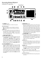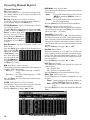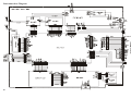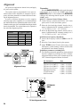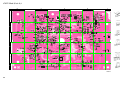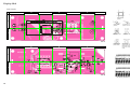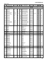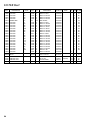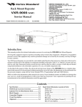
1
VERTEX STANDARD CO., LTD.
4-8-8 Nakameguro, Meguro-Ku, Tokyo 153-8644, Japan
VERTEX STANDARD
US Headquarters
10900 Walker Street, Cypress, CA 90630, U.S.A.
Desktop Repeater
YAESU EUROPE B.V.
VXR-7000 (VHF)
P.O. Box 75525, 1118 ZN Schiphol, The Netherlands
YAESU UK LTD.
Unit 12, Sun Valley Business Park, Winnall Close
Winchester, Hampshire, SO23 0LB, U.K.
Service Manual
©2003 VERTEX STANDARD CO., LTD.
VERTEX STANDARD HK LTD.
Unit 5, 20/F., Seaview Centre, 139-141 Hoi Bun Road,
Kwun Tong, Kowloon, Hong Kong
E136790A
Introduction
This manual provides technical information necessary for servicing the VXR-7000 FM Land Mobile Repeater.
Servicing this equipment requires expertise in handling surface-mount chip components. Attempts by non-qualified
persons to service this equipment may result in permanent damage not covered by the warranty, and may be illegal in
some countries.
Two PCB layout diagrams are provided for each double-sided circuit board in the repeater. Each side of is referred to
by the type of the majority of components installed on that side (“leaded” or “chip-only”). In most cases one side has only
chip components, and the other has either a mixture of both chip and leaded components (trimmers, coils, electrolytic
capacitors, ICs, etc.), or leaded components only.
While we believe the technical information in this manual to be correct, VERTEX STANDARD assumes no liability
for damage that may occur as a result of typographical or other errors that may be present. Your cooperation in pointing
out any inconsistencies in the technical information would be appreciated.
Contents
Operating Manual Reprint ............................ 2
CE27 Programming Software Instruction ............................. 9
Specifications ................................................. 14
Exploded View & Miscellaneous Parts .... 15
Block Diagram ............................................... 17
Interconnection Diagram ............................. 20
Circuit Description ...................................... 21
Alignment ....................................................... 23
Board Unit (Schematics, Layouts & Parts)
PA Unit .................................................................... 27
TX Unit ..................................................................... 35
RX Unit .................................................................... 43
CNTL Unit ............................................................... 55
LPF Unit ................................................................... 73
Display Unit ............................................................ 75
Key Unit ................................................................... 79
Filter Unit ................................................................ 87
VR Unit .................................................................... 95
SQL Unit .................................................................. 97
PS Unit ..................................................................... 99
1
Operating Manual Reprint
Controls & Connectors
Front Panel
POWER Switch
MONITOR Switch
This is the main power switch for the repeater.
This switch selects the “Squelch” (receiver mute) mode.
When the green LED above it is off, “Tone” or “Coded”
squelch is active. When you press this switch momentarily, the green LED will glow steadily; in this condition, only “noise squelch” is active, and any signal present
on the channel will be heard. If you press and hold this
switch for more than 2 second, the green LED will blink
and the squelch will open; in this condition, background
noise will be heard if no signal is present.
LED Indicators
AC: This LED glows green during AC operation.
DC: This LED glows yellow during DC operation.
MIC Jack
This 8-pin modular jack accepts the microphone input, and provides a standby control line to activate the
transmitter when using the “BASE” mode of operation. This jack also provides a “Hook” control line, as
well as a “Clone Data” line.
BASE/REPEATER Switch
This switch toggles the operating mode between the
“REPEATER” mode and the “BASE” transceiver
mode. When the “REPEATER” mode is selected, the
LED above it glows green. While in the “BASE” mode
(the green LED is off), you can speak into the microphone to use it as a transceiver. For normal repeater
operation, set this switch to the “REPEATER” mode.
LOCAL/REMOTE Switch
This switch toggles the control mode between the “REMOTE” mode and “LOCAL” mode. When the “LOCAL” mode is selected, the LED above it is off, and
the repeater operates according to the control data programmed into the repeater. While in the “REMOTE”
mode, the LED glows green, and the repeater operates according to the control instructions received from
an external device (connected to the ACC jack on the
rear panel).
ACCESSORY Switch
This switch can be set up for special applications, such
as High/Low power selection, as determined by your
Vertex Standard dealer. The LED above it glows green
when this function is activated. For further details,
contact your Vertex Standard dealer.
VOL Knob
This control knob adjusts the receiver volume level
from the front panel speaker. If desired, this control
knob may be set fully counterclockwise when repeater
monitoring is not needed.
SQL Knob
This control knob selects the noise squelch threshold
level. Set it to a position just above the point where
the BUSY lamp goes out when no signal is present.
Channel Selector Buttons ( and )
Press one of these buttons to select the operating channel.
Channel Indicator
This seven-segment LED indicates the operating channel number.
2
Operating Manual Reprint
ANI Display
ANI RESET Button
The ANI LCD (Liquid Crystal Display) indicates the
pre-programmed ANI message according to the ANI
code received.
(1) ANI
Press this button to clear the message on the ANI
display, and turn off the LCD backlight.
(2) ENI
Press this button to turn off the Alert tone.
Press this button again to clear the message on the
ANI display, and turn off the LCD backlight.
TX/BUSY Indicator
The BUSY indicator glows green when the channel is
busy, and the TX indicator glows red when the repeater
is transmitting.
Rear Panel
EXT SP Jack
LINE Jack
This 3.5-mm, 2-pin jack provides variable audio output for an external speaker. The audio output impedance at this jack is 4 Ω ~ 16 Ω, and level varies according to the setting of the front panel’s VOL control.
This 8-pin modular jack is used for remote control. It
provides TX and RX audio, TX keying, and squelch
status output. The TX and RX audio impedance is 600
Ω.
TX Antenna Jack
For best performance and safety, the GND terminal
should be connected to a good earth ground using a
short, heavy, braided cable.
This N-type coaxial jack provides the transmitting output signal for connection to the transmitting antenna
or TX jack on the duplexer, if used. The output impedance requirement is 50 Ω.
RX Antenna Jack
This N-type coaxial jack accepts the receiver input
signal from the receiving antenna or RX jack on the
duplexer, if used. The input impedance requirement is
50 Ω.
ACC Jack
This DB-25 connector provides a data interface between the microprocessor in the VXR-7000 and peripheral devices (such as the VX-TRUNK Unit).
GND Terminal
AC Jack
This receptacle accepts the AC power cord, which
should be connected to the AC mains supply or wall
outlet. The AC line voltage must match that for which
the repeater is wired.
BATT Terminal
These terminal posts accept 12~ 15 VDC for operating the repeater from a battery or other DC source.
When operating from AC mains, a small trickle current is present at these terminals to maintain battery
charge. A battery rated for 12 volts, 55 Ah (minimum)
is recommended for short-term emergency/backup operation.
3
Operating Manual Reprint
ACC Connector Port
The VXR-7000 repeater is provided with a 25-pin DB25F female connector for interconnections to accessories. Use a DB-25M 25-pin male connector to connect
accessories to the repeater. The pins on the accessory connector are explained in detail as follows:
Pin 1: GND
Chassis ground for all logic levels and power supply
return.
Pin 7: GND
Chassis ground for all logic levels and power supply
return.
Pin 8: RSSI [Analog Output]
A DC voltage proportional to the strength of the signal
currently being received (Receiver Signal Strength Indicator) is provided on this pin. This low impedance
output is generated by the receiver IF sub-system and
buffered by an internal op-amp. Typical voltages are
graphed as follows:
Pin 2: +13.8 V [Power Supply]
This pin provides 13.8 Volts, 1.0 A, regulated DC from
the repeater supply. Use a 1 A fuse in the external
device’s DC line to prevent damage to the repeater.
Pin 3: TX AF IN [Analog Transmitter Input]
(Voice Band: 300 ~ 3,000 Hz)
Input impedance is approx. 600 Ω. This audio is injected before the splatter filter stage, so excess signal
input levels are clipped.
Use shielded cable to connect to this pin, and connect
the shield to GND.
Pin 4: TONE IN [Transmitter Input]
(Sub-audible Band: 6 ~ 250 Hz)
The input is high impedance (approx. 22 kΩ). Injecting too high a voltage here causes over-deviation of
CTCSS or DCS, degrading performance. Use shielded
cable to connect to this pin, connecting the shield to
GND.
Pin 9: COAX. SW [Logic Output (Active Low)]
This output is intended for controlling an external coaxial switching relay. It is an open collector output
which can sink approx. 10 mA when active. This signal only switches if the repeater has been programmed
for “SIMPLEX” mode. If programmed for “DUPLEX,” the signal remains open (high impedance) at
all time.
Pin 5: N.C. (No connection.)
Pin 10: N.C. (No connection.)
Pin 6: DISC OUT [Analog Output]
(Wide-Band: 0 ~ 3,000 Hz)
Received signals with standard deviation produce
approx. 1 Vp-p audio at this pin. The output impedance
is approx. 600 Ω, and is extracted before the de-emphasis and squelch circuitry. Use shielded cable to connect to this pin, and connect the shield to GND.
Pin 11: NSQ DET
This is an open-collector, active-low output capable of
sinking about 10 mA. It indicates that the receiver
squelch is open. If the squelch control is properly set,
this indicates a carrier on the receiver channel.
ACC Jack
DB-25 Pin Numbering
4
Operating Manual Reprint
Pin 12: EXT PTT
This input is internally pulled up to 5 VDC. When
pulled low by an external device, it keys the repeater
transmitter while the repeater is operating in the
“BASE” mode. Avoid voltage in excess of 5 V on this
pin, or internal damage to the microprocessor on the
repeater CNTL Unit may result.
Pin 13: GND
Chassis ground for all logic levels and power supply
return.
Pin 14: GND
Chassis ground for all logic levels and power supply
return.
Pin 15: N.C. (No connection.)
Pin 16, 17, 18, & 19: REMOTE CH DATA
[Logic Inputs D3, D2, D1, and D0] (Active Low)
These inputs are internally pulled up to 5-V DC. When
pulled low by an external device, they select one of the
16 pre-programmed repeater operating channels. The
logic truth table below shows the combinations for selecting all 16 channels.
In the truth table, “1” represents no connection, and
“0” represents a ground connection on the pin.
The channel selection logic is not inhibited while the
transmitter is keyed: the repeater will change frequency
when instructed, even while transmitting.
Avoid voltage in excess of 5 V on these pins or internal damage to the microprocessor on the repeater CNTL
Unit may result.
Channel
Pin 16
(D3)
Pin 17
(D2)
Pin 18
(D1)
Pin 19
(D0)
1
2
3
4
5
6
7
8
9
10
11
12
13
14
15
16
1
1
1
1
1
1
1
1
0
0
0
0
0
0
0
0
1
1
1
1
0
0
0
0
1
1
1
1
0
0
0
0
1
1
0
0
1
1
0
0
1
1
0
0
1
1
0
0
1
0
1
0
1
0
1
0
1
0
1
0
1
0
1
0
Pin 20: GND
Chassis ground for all logic levels and power supply
return.
Pin 21: A-OUTPUT [Logic Output] (Active Low)
This open collector logic output is pulled low when
the front panel’s ACCESSORY key is turned on. It
can sink approx. 10 mA when active.
Pin 22: RXD LOW
[Digital Output for DATA Communications]
(300 ~ 3,000 Hz)
This pin is an output for low speed receiving data signals, with the data being extracted after the de-emphasis and low pass filter stages.
Pin 23: RXD HI
[Digital Output for DATA Communications]
This pin is an output for high speed receiving data signals, with the data being extracted immediately after
the discriminator prior to any de-emphasis).
Pin 24: TXD LOW
[Digital Input for DATA Communications]
(300 ~ 3,000 Hz)
This pin is intended to be used as a low speed digital
data signal input to the repeater. This digital data signal is injected before transmitter pre-emphasis and limiting stage, so excess signal input levels are clipped.
Pin 25: TXD HI
[Digital Input for the DATA Communications]
This pin is intended to be used as a high speed digital
data signal input to the repeater. This digital data signal is injected after transmitter splatter filter stage.
5
Operating Manual Reprint
LINE Interface Port
Installation
The VXR-7000 is provided with an 8-pin modular jack
for line interfacing applications. A Western Electric® modular-type RJ45 plug should be used to connect to this jack.
The LINE jack pin-out is shown below.
Note that there are both 4-line and 8-line types of modular
plugs. If a 4-line modular plug is used, only the LINE
OUT and LINE IN connections will be made. An 8-line
plug is required to access all lines. In accordance with
standard telecommunications interface, the line connections on the LINE interface jack are impedance balanced,
and are described as follows.
Antenna Considerations
Pins 1 & 2: [RX SQ(+), RX SQ(–)]
(max voltage: 20 V, max current: 7 mA)
An opto-isolator is provided to facilitate E (EAR) signaling. The opto-isolator comes on when a signal exceeding the receiver squelch appears on the receiver
channel (with correct CTCSS tone or DCS code, if enabled). The RX SQ(–) pin is the emitter, and RX SQ(+)
is the collector.
Pins 3 & 4: [LINE IN (Tx Line Audio)]
Analog signals between 300 and 3000 Hz supplied to
this pair are fed to the transmitter when the repeater is
set to the BASE mode (the REPEATER LED is turned
off) and keyed either by the TX KEY input signal (see
below), or by the EXT PTT signal on pin 12 of the rear
panel’s ACC jack. Standard deviation is obtained with
a line level of –10 dBm.
Pins 5 & 6: [LINE OUT (Rx Line Audio)]
Receiver audio is available from this pair, subject to
internal CTCSS or DCS decode if the received signal
strength is above the squelch threshold.
As shipped from the factory, a 1-kHz receiver signal
with standard deviation gives –10 dBm on the line,
but this can be varied by VR4002 and S4001 (on the
repeater’s CNTL Unit).
Pins 7 & 8 [
( ),
( )]
(max voltage: 20 V, max current: 4 mA)
An opto-isolator is provided to facilitate M (MIC) signaling. That is, a voltage presented to these pins turns
on the opto-isolator and keys the transmitter. The TX
KEY(+) pin is the anode of the opto-isolator, and RX
SQ(–) is the cathode of the opto-isolator.
LINE Jack
Modular Jack Pin Numbering
6
Repeater operation without a duplexer requires that two
antennas be installed, one for receiving and one for transmitting, so that the receiving antenna does not absorb energy from the transmitting antenna. There are a number of
ways to do this, depending on the TX/RX frequency separation, and on the locations available for antenna mounting. If a duplexer is used, a single antenna suffices for
both transmitting and receiving. If using a reduced-size
duplexer, a six-cavity model (minimum) is recommended.
Vertex Standard recommends the use of the duplexer. For
further details, contact your Vertex Standard dealer.
Regardless of the above choice, it is of paramount importance that the antenna(s) be mounted as high and in the
clear as possible, preferably within line-of-sight to all repeater users. Furthermore, losses in the feedline(s) must
be minimized, so the feedline(s) should be high quality,
and as short as possible. If a long feedline is necessary,
use coaxial “hardline” cable to reduce losses.
Repeater antennas should have an impedance of 50 Ω at
the operating frequency. When separate receive and transmit antennas are used, high-Q narrow-band types may
serve to minimize interaction. However, when a single
antenna is used with a duplexer, it should be a low-Q wideband type.
NEVER TRANSMIT WITHOUT HAVING A
TRANSMIT ANTENNA CONNECTED TO THE
TX ANTENNA JACK OF THE REPEATER.
AC Power Supply Voltage Selection
Each repeater is wired for a particular AC mains voltage
between 100 and 253 VAC. This should be indicated by a
label near the AC jack on the rear panel. If no label is
present, or if the AC voltage on the label is different from
the local AC line, check the wiring inside the Switching
Regulator Unit of the repeater, and change the connections (and label) if necessary, as shown page 8.
Changing the AC input voltage wiring also requires changing the fuse on the FILTER Unit if the voltage is changed
from 100 VAC (100-127 VAC) to 200 VAC (207-253
VAC), or vice-versa. Use a 5-amp fuse for 100 VAC, or a
3-amp fuse for the 200 VAC.
Operating Manual Reprint
DC Power Supply Backup
Equipment Location
For uninterrupted operation during power failures, a 12
volt rechargeable type battery (55-Ah or more recommended) may be connected to the BATT terminal posts
on the rear panel. While the repeater is operating from the
AC source, a slight charging current will maintain battery
charge. In the event of an AC power outage, the automatic power control circuit will automatically switch the
repeater to the backup battery, and operation will not be
interrupted.
While the operating temperature range of the repeater is
quite broad, the best location is one in which the air temperature does not approach the extremes of the specified
range, and one that does not change rapidly. Make sure to
allow for free air flow around the heatsink on the rear apron
at all times. In warm climates, the repeater should not be
sealed in a small closed room.
After prolonged operation from the battery, it should be
disconnected from the repeater and recharged separately
before re-connecting, as the trickle charge is not sufficient
for recharging a completely discharged battery.
Protect the repeater from wind and rain, and extremes in
temperature or humidity that may shorten the useful life
of the equipment. Try to locate the repeater in an environment that is also comfortable for service personnel, if possible.
Never reapply AC power to the repeater with a discharged
battery connected, as the DC startup current can damage the repeater and battery.
While operating from a battery or DC supply, the repeater
requires approximately 7 amperes at 12 Volts during transmit.
7
Operating Manual Reprint
Changing Switching Regulator unit AC Mains Jumper Wiring
Before attempting this jumper wire change, remove the
AC power cord from the AC jack on the rear panel.
Referring to Figure 1, remove the 14 screws affixing
the top and bottom covers of the repeater, and remove
the covers.
Remove the eight screws affixing the shield cover for
the FILTER Unit, and remove the cover (see Figure 1).
Disconnect all wires and connectors from the FILTER
Unit, then remove the six screws affixing the Switching Regulator Unit, and remove it (the Switching Regulator Unit is mounted with the FILTER Unit: Figure
2).
Referring to Figure 3, remove the four screws and remove the heatsink from the Switching Regulator Unit.
Referring to Figure 4, perform the correct jumper wiring on the Switching Regulator Unit for the AC Mains
voltage used in your area (100-127 VAC or 207-253
VAC).
Replace the heatsink onto the Switching Regulator Unit,
then replace the Switching Regulator Unit onto the
chassis, and connect all wires and connectors to the
FILTER Unit.
Replace the AC fuse (FH6001) on the FILTER Unit
according to the AC Mains voltage range:
100 VAC (100-127 VAC): 5A
200 VAC (207-253 VAC): 3A.
Replace the shield cover and replace the top and bottom covers. This completes the wiring change.
Important!: If you change the AC voltage range, you must
also change the AC fuse on the FILTER Unit. Do not replace with a slow-blow type fuse.
FILTER Unit
B
A
Switching
Regulator
Unit
C
B
C
Figure 2
A
Figure 1
Switching Regulator Unit
Figure 3
8
Figure 4
Operating Manual Reprint
CE-27 Programming Software Instruction
With the CE27 Programming Software, you can quickly
and easily program the Vertex Standard VXR-7000
repeater’s channels and configuration from your personal
computer. In the event of an accidental memory failure,
repeater memory and configuration data may be re-loaded
in a matter of minutes.
The CE27 Programming Software diskette contains the
following files:
• CE27.EXE
• CE27.HLP
Before connecting the VXR-7000 for programming, turn
off both the computer and the VXR-7000. Now connect
the VPL-1 Connection Cable to the computer’s serial port
and the VXR-7000.
Then it will be safe to restart the computer; turning off the
equipment during interconnection avoids the potential for
damage to the electronics caused by voltage spikes.
Insert the distribution diskette into your 3½” drive (after
booting DOS), and make a copy of the diskette; use the
distribution diskette for archive purposes, and use the disk
copy for programming.
Place the CE27 (copy) diskette into your 3½” drive (usually “Drive A”), and log onto this drive by typing “A:
[ENTER]”, then load the contents of the CE27 diskette into
a directory named CE27, using the COPY command (e.g.
“COPY A:*.* C:\CE27”).
Now type “CE27 [ENTER]” to start the program. The introductory screen will appear, and you may press any key
to enter the main screen.
Choose the “Help” contents option (F1) from the program’s
Menu for assistance with channel programming or setting
of parameters.
Important Note!
Do not run the CE27 programming software directly from the original distribution diskette.
Copy the programming software to your
computer's hard disk, then run the software from
the hard disk only. Keep the original distribution diskette in a safe place in case you need to
make another copy of it at a later date.
Before creating the programming data for your
VXR-7000 via the CE27 programming software,
upload the current factory hardware environment data from the VXR-7000, using the [F5]
(ReadRom) command. Use this data profile to
create the programming data for this repeater.
VXR-7000 Programming Setup
CE27 Main Screen (Left)
9
Operating Manual Reprint
Channel Data Items
Ch: Channel Number
This 2-digit number (01 - 16) is used to identify the channel. Channel numbers occur in sequence, and their order
can not be changed.
Rx Freq.: Edit Receive (or simplex) Frequency
Use the [0] - [9] keys to enter the desired channel frequency directly, and press the [ENTER] key.
CTCSS Decoders: Toggle CTCSS Decoder ON/OFF,
sets CTCSS Frequency
Press the [SPACE] bar to toggle the CTCSS Decoder “on”
or “off,” or press the [ENTER] key to display the “TONE
SELECT ” window, from which
you may select a CTCSS frequency using the [ARROW] key;
press [ENTER] again to accept the
selected tone, or press [ESC] key
to cancel.
DCS Decoders: Toggle DCS Decoder ON/OFF, sets
DCS Code #
Press the [SPACE] bar to toggle the DCS Decoder ON or
OFF, or press the [ENTER] key to display the
“CODE S ELECT ” window, from which you
may select a DCS code
using the [ARROW] key;
press [ENTER] again to accept the selected code, or press
the [ESC] key to cancel.
W/N: Wide/Narrow Channel Spacing
This function selects the channel spacing environment in
which the VXR-7000 operates.
W (Wide) = 25 kHz Channel Spacing, ±5 kHz Deviation.
N (Narrow) = 12.5 kHz Channel Spacing, ±2.5 kHz
Deviation.
Press the [SPACE] bar to select the desired channel spacing environment.
Clk Sft: Enable/disable the CPU Clock Shift
This function is only used to move a spurious response
“birdie” should it fall on a current frequency.
Press the [SPACE] bar to toggle “yes” or “no.”
10
NSQ Mode: Noise Squelch Mode
This command selects the manner of setting of the Squelch
threshold level.
User = The squelch threshold level is fixed via the
“NSQ Lv” parameter (NSQ Lv: 0 [min.] ~
255 [max.]).
Prpgm = The squelch threshold level determined via
the dealer programming.
Press the [SPACE] bar to select the desired NSQ Mode.
NSQ Lv: Noise Squelch threshould level
Use the [0] - [9] keys to enter the desired Squelch threshold level directly, and press the [ENTER] key. Available
values are 0 (min.) ~ 255 (max.).
Court Blip: Courtesy Blip
When this parameter is set to “on,” this function causes
the VXR-7000 to send out a “blip” on the portable/mobile
radio is frequency each time the portable radio is unkeyed.
This provides audible confirmation to the user that the
VXR-7000 was able to receive the transmission from the
portable.
Press the [SPACE] bar to toggle “on” or “off.”
Rev Bst: Reverse Burst.
When this parameter is set to “on,” the CTCSS tone
signal’s phase is inverted just before the repeater turns to
receive. This allows the portable/mobile station’s CTCSS
Decoder to begin switching off, thus reducing the transition time required.
Press the [SPACE] bar to toggle “on” or “off.”
DCS Typ: DCS Format
This command is effective only when DCS is chosen for
squelch control.
A = “Normal” DCS
B = “Inverted” (complement) DCS
Press the [SPACE] bar to select the desired DCS Type.
DDec Type: DCS Decoder Type
This command selects the manner in which DCS is to be
decoded.
Fixed = Decodes only the type selected in above parameter (DCS Typ: Normal or Inverted).
Auto = Both types (Normal and Inverted) will be decoded.
Press the [SPACE] bar to select the desired DCS Decoder
Mode.
CE27 Main Screen (Scrolled Right)
Operating Manual Reprint
Multi Tone: Enable/disable Multi Tone Operation
Press the [SPACE] bar to toggle Multi Tone Operation between selections “yes” and “no.”
Press the [ENTER] key to display the “MULTI T ONE S ELECT” window, from which
you may select a CTCSS
tone or DCS code; move the
cursol to the appropriate field
you using the [ARROW] key, then press the [ENTER] key to
open the “TONE SELECT” or “CODE SELECT” window. Now
select the desired CTCSS tone or DCS code using the [ARROW] key, then press the [ENTER] key again to accept the
selected tone or code, or press the [ESC] key to cancel.
You may set as many as 16 CTCSS tones and/or DCS
codes.
Note that, if you do not yet program a CTCSS tone or
DCS code in the “MULTI TONE SELECT” window (when
the “M ULTI T ONE S ELECT ” window data is not programmed), press the [SPACE] bar to display the “MULTI
TONE SELECT” window directly.
CWID ANI/ENI: Select the Identifier mode
Press the [SPACE] bar to toggle the selections “CW ID,”
“ANI/ENI,” or “off.” To select this feature to the “CW
ID” or “ANI/ENI,” the “CW ID” parameter must be enabled via the dealer programming.
Action Mode: Select the repeater operation mode
Press the [SPACE] bar to toggle between “Duplex” operation or “Simplex” operation.
Tx Freq.: Edit Transmit Frequency
Use the [0] - [9] keys to enter the desired channel frequency directly, and press the [ENTER] key.
CTCSS Encoders: Toggle CTCSS Encoder ON/OFF,
sets CTCSS Frequency
Press the [SPACE] bar to toggle the CTCSS Encoder “on”
or “off,” or press the [ENTER] key to display the “TONE
SELECT ” window, from which
you may select a CTCSS frequency using the [ARROW] key;
press [ENTER] again to accept the
selected tone, or press the [ESC]
key to cancel.
DCS Encoders: Toggle DCS Encoder ON/OFF, sets DCS
Code #
Press the [SPACE] bar to toggle the DCS Encoder “on” or
“off,” or press the [ENTER] key to display the
“CODE S ELECT ” window, from which you
may select a DCS code
using the [ARROW] key;
press [ENTER] again to accept the selected code, or press
the [ESC] key to cancel.
Base TOT: Enable/disable the Time-Out Timer while in
the “BASE” station mode
Press the [SPACE] bar to toggle the TOT feature selects
“yes” and “no.”
The TOT time is determined via dealer programming.
Base Guard: Enable/disable the Base Guard Feature
When this parameter is set to “yes,” the transmitter will
be inhibited for a few seconds before the repeater (in the
“BASE” station mode) turns to receive.
The inhibit time is determined via dealer programming.
LOUT: Select the Lock Out Feature’s mode
Press the [SPACE] bar to toggle the Lock Out Feature between “BCLO,” “BTLO,” or “off,” then press the [ENTER] key to accept the setting. “BCLO” inhibits transmitting while there is carrier present. “BTLO” inhibits transmitting while there is carrier present unless there also is a
valid tone present.
TX Pwr: Transmitter Power Output Selection
This parameter selects the desired power output from the
VXR-7000 on the current channel. The available values
are HIGH and LOW.
Press the [SPACE] bar to select “Hi” or “Lo.”
TOT Mute: Enable/disable the TOT (Time-Out Timer)
beep monitoring
When this parameter is set to “on,” the alert beep will
sound from the front panel speaker before the repeater
turns itself off.
RptTOT Use: Enable/disable the Time-Out Timer while
operating in the repeater mode
Press the [SPACE] bar to toggle the Repeater TOT selects
“yes” or “no.”
The TOT time is determined via dealer programming.
RptTOT Beep: Enable/disable the TOT beep Transmission
Press the [SPACE] bar to toggle the TOT beep selects “yes”
or “no.”
When this parameter is set to “yes,” the alert beep will be
sent out on the air before the repeater turns itself off, while
oprtating in the “REPEATER” mode.
RPT HT: Enable/disable the Repeater Hang-on Timer
Press the [SPACE] bar to toggle the Repeater Hang-on Timer
selects “yes” or “no.”
When this parameter is set to “yes,” the repeater will remain keyed for a desired seconds after a receiving carrier
is dropped.
The Hang-up time is determined via dealer programming.
RPT GT: Enable/disable the Repeater Guard
When this parameter is set to “yes,” the transmitter inhibit few second before the repeater is unkeyed.
The inhibit time is determined via dealer programming.
11
Operating Manual Reprint
Duplexer Installation
Important Note
Be certain to observe the specifications for Frequency Separation and Maximum Transmitter Power
of the duplexer connected to the VXR-7000. The
Frequency Separation should be 5 MHz (min.) to
10 MHz (max.), and the Maximum TX Power Rating should be at least 40 Watts.
If the VXR-7000 TX output power or frequency
specification is out of the range of the duplexer's
capability, you may re-program the Tx/Rx frequency pair and/or reduce the TX output power of the
VXR-7000, so as to allow temporary operation of
the VXR-7000 until a duplexer of proper ratings
can be obtained.
Please consult with your Authorized Vertex Dealer for assistance with procurement of a suitable
duplexer.
1. Connect the VXR-7000’s TX antenna port to a wattmeter and dummy load (the duplexer must not be connected at this point). Connect any Vertex Standard
microphone to the MIC jack, and place the BASE/
REPEATER switch in the “BASE” position. Select
Channel 1 for alignment purposes.
2. Press and hold in the ACCESSORY switch for two
seconds to enter the adjustment mode. The channel
number will begin to blink.
3. Press and hold in the PTT key on the microphone.
The display will indicate “Po” while transmitting. Observe the power output as indicated on the watmeter.
4. Press the (UP: increment) or (DOWN: decrement) button (to the right of the channel display) repeatedly to adjust the TX output power to 40 Watts
(or less) while holding in the PTT key.
5. Once the desired power level has been obtained, release the PTT key. Now press and hold in the ACCESSORY button for at least two seconds to save
the new setting and exit to the normal operation.
6. Repeat steps 2. through 5. (above) for any other channels (2 through 16) if they are to be used.
7. Re-test each channel in the normal operating mode to
confirm the proper power output. You may now disconnect all test equipment.
8. The duplexer may now be installed.
The above procedure should only be performed by your
Authorized Vertex Standard Dealer or a qualified radio
technician, in order to ensure accurate calibration. Please
consult with your Authorized Vertex Standard Dealer for
assistance with procurement of a suitable duplexer.
12
Operating Manual Reprint
Installations
1. Remove the 14 screws affixing the top and bottom
covers of repeater, and remove the covers (Figure 1).
2. Turn the repeater upside down.
3. Referring to Figure 2, remove the upper screw in either side of the front panel, and loosen the lower screw
in either side of the front panel, then slide the front
panel forward slightly.
4. Remove the coaxial cables connected to the TX and
RX antenna jacks of the repeater.
5. Mount the duplexer to the bottom side of the repeater,
using the four screws supplied with the optional Antenna Cable CT-68 (Figure 3).
6. Connect the optional Antenna Cable CT-68 between
the TX antenna jack of the repeater and ANT (center)
jack of the duplexer.
7. If your repeater’s Tx/Rx frequency relationship is “upper shift” type (TXf > RXf), connect the coaxial cable
from the RX Unit to the LOW PASS jack of the duplexer and connect the coaxial cable from the PA Unit
to the HIGH PASS jack of the duplexer.
If your repeater’s Tx/Rx frequency relationship is
“lower shift” type (TXf < RXf), connect the coaxial
cable from the RX Unit to the HIGH PASS jack of the
duplexer and connect the coaxial cable from the PA
Unit to the LOW PASS jack of the duplexer.
Note: Route the TX coaxial cable from the PA Unit as
far as possible from the RX coaxial cable from the RX
Unit.
8. Duplexer installation is now complete. Replace the
front panel back into place, and replace the top and
bottom covers.
Top Side
Bottom Side
Figure 1
Bottom Side
Figure 2
Figure 3
13
Specifications
General
Frequency Range:
Number of Channels:
Channel Spacing:
Frequency Stability:
Antenna Impedance:
Tx Activation System:
Power Requirements:
Ambient Temperature Range:
Dimensions (w/o knobs):
Weight (approx.):
136 ~ 150 MHz (A) or 150 ~ 174 MHz (C)
16
12.5/25 kHz
±2.5 ppm
50 Ω (N-Type)
Carrier-operated, CTCSS tone operated, DCS operated, or remote control
115/230 V AC ±10%, 50/60 Hz or 13.8 VDC
–30 °C ~ +60 °C
325 x 115 x 391.5 mm (12.8 x 4.5 x 15.4 inches)
10 kg (22 lbs.)
Receiver
Receiver Type:
Sensitivity:
Selectivity:
Intermodulation:
Spurious & Image Rejection:
Audio Output:
Double-conversion Superheterodyne
0.35 µV for 12 dB SINAD, 0.45 µV for 20 dB NQ
75 dB
75 dB
80 dB
4W@4Ω
Transmitter
RF Output:
Duty Cycle:
Maximum Deviation:
Modulation Type:
Audio Distortion:
Spurious Emissions:
10 ~ 50 W (Adjustable)
100 %
±5.0 kHz (25 kHz spacing), ±2.5 kHz (12.5 kHz spacing)
16K0F3E/11K0F3E
Less than 2.5 % @ 1 kHz
Better than 75 dB below carrier
Specifications are subject to change without notice.
14
Exploded View & Miscellaneous Parts
Ref. YAESU P/N
U04308001
U30312012
U04408001
U30306012
U30314012
U30308012
U04306002
Description
SEMS SCREW HSM3×8
FLAT HEAD SCREW M3×12BSNI
SEMS SCREW HSM4×8
FLAT HEAD SCREW M3×6BSNI
FLAT HEAD SCREW M3×14BSNI
FLAT HEAD SCREW M3×8BSNI
SEMS SCREW HSM3×6NI
Qty.
5
1
4
9
5
2
12
FILTER Unit
RA0181300
TOP CASE
S8001786
COVER
S6000384
PCB SPACER (6pcs)
Q7000303 (VTX)
Q7000391 (EXP : CE ON)
Q7000427 (EXP : CE OFF)
POWER SUPPLY ASS’Y
S6000366
EDGE HOLDER
RA018100A
SHIELD CASE COVER
S6000366
EDGE HOLDER
S8000030
FITTING
S8001794
SPACER(5pcs)
RA0180900
SHIELD CASE COVER (PA)
Q6000169
TERMINAL STRIP
S8001785
HEATSINK
S8001782
THERMAL CONDUCTOR(4pcs)
S8001784
FITTING(5pcs)
S5000215
FAN GUARD
P0090811
CONNECTOR
CNTL Unit
P1091072
CONNECTOR
Ref. VXSTD P/N
S5000182
U10306007
U04408001
U04308001
U24306001
U24308001
U23308001
U20406007
U20308002
U20306001
U04306002
U02308002
U02206002
U00206002
U00305001
U30308001
U01330007
U04335007
U52408002
U51416007
U70004002
U71004002
U72004002
U20308001
Description
SCREW JFS-4S-B1WM
TRUSS HEAD SCREW M3×6B
SEMS SCREW HSM4×8
SEMS SCREW HSM3×8
TAPTITE SCREW M3×6
TAPTITE SCREW M3×8
TAPTITE SCREW M3×8
BINDING HEAD SCREW M4×6B
BINDING HEAD SCREW M3×8NI
BINDING HEAD SCREW M3×6
SEMS SCREW HSM3×6NI
SEMS SCREW SM3×8NI
SEMS SCREW SM2.6×6NI
PAN HEAD SCREW M2.6X6NI (Lot. 3-)
PAN HEAD SCREW M3×5
FLAT HEAD SCREW M3×8
SEMS SCREW HM3×30B
SEMS SCREW HSM3×35B (Lot. 17-)
HEX HEAD BOLT M4×8NI
HEXA SOCKET BOLT M4×16B
PLAIN WASHER FW4NI
SPRING LOCK WASHER SW4NI
TOOTHED LOCK WASHER OW4NI
BINDING HEAD SCREW M3×8
Qty.
2
14
4
2
34
18
1
4
8
6
12
2
2
2
2
4
4
RA0180800
SHIELD CASE COVER (RF)
N4090143
PUSH SWITCH
RA0181500
PANEL FRAME
P9090014
CONNECTOR (2pcs)
M2090032
FAN
PA Unit
Display Unit
KEY Unit
RA0180000 (Lot. 1~)
RA018000A (Lot. 19~)
CHASSIS
RX Unit
P1090654
CONNECTOR
RA0180600
KNOB (POW)
RA018270A (Lot. 1~)
RA018270B (Lot. 26~)
FRONT PANEL ASS’Y
RA0181400
BOTTOM CASE
1
2
1
1
1
3
R3054370
FOOT (4pcs)
TX Unit
SQL Unit
Non-designated parts are available only as
part of a designated assembly.
M4090066
SPEAKER
RA0065800
RUBBER HOLDER (SP)
RA0180500
VOLUME KNOB
RA0181200
HOLDER (MJ)
P1091073
CONNECTOR
VOL Unit
RA0180700
PUSH KNOB (4pcs)
15
Exploded View & Miscellaneous Parts
Note:
16
Block Diagram
17
Block Diagram
18
Block Diagram
19
Interconnection Diagram
20
Circuit Description
Receive Signal Path
Incoming RF from the RX antenna jack is delivered to the
RX Unit and passes through the protection diode D3001
(MA143) and a varactor-tuned band pass filter consisting of
coils L3002 and L3004, capacitors C3019, C3021, C3024,
C3027, and C3028, and diodes D3004 and D3008 (both
HVU350). Signals are then applied to the RF amplifier, Q3008
(2SC3357). The amplified RF signal is applied through a varactor-tuned band pass filter consisting of coils L3009 and L3012,
capacitors C3053, C3054, C3059, C3060, and C3065, and diodes D3012 and D3013 (both HVU350) to the first mixer D3014
(GN2011-Q) along with the first local signal from the PLL
circuit.
The first local signal is generated between 114.6 MHz and
152.6 MHz by the RX VCO, which consists of FET Q3007
(2SK508) and varactor diodes D3005, D3006, D3009, and
D3010 (HVU350) according to the programmed receiving frequency; the local signal then passes through buffer amplifier
Q3009 (2SC5226) and first local amplifier Q3011 (2SC3357)
to the first mixer D3014.
The 21.4 MHz first IF signal is applied to monolithic crystal filters XF3001 and XF3002 (both 21M10B1: ±10 kHz B.W.)
which strip away unwanted mixer products, and the IF signal is
applied to the first IF amplifier Q3016 (2SC2620QB). The
amplified first IF signal is then delivered to the FM IF subsystem IC Q3012 (TA31136FN), which contains the second
mixer, second local oscillator, limiter amplifier, noise amplifier, and FM detector.
The second local oscillator signal, generated by the 20.945
MHz crystal X3002, produces the 455 kHz second IF signal
when mixed with the first IF signal within Q3021. The second
IF signal passes through ceramic filter CF3001 (CFWM455G:
±4.5 kHz B.W.) or CF3002 (CFWM455F: ±6.0 kHz B.W.)
which strips away all but the desired signal, and then passes
through the limiter amplifier within Q3021 to ceramic discriminator CD3001 (CDB455C7), which removes any amplitude
variations in the 455 kHz IF signal before detection of speech.
The detected audio passes through the low pass filter, consisting of R3067 and C3115, which rejects the 455 kHz IF component, then delivers the audio to pin 12 of JP3001.
The audio signal from the RX Unit is delivered to the CNTL
Unit and passes through the audio amplifier Q4014-3
(NJM2902M) to the active high pass filter section of Q4024
(FX-805) which rejects the sub-audible frequency component.
The filtered audio signal is delivered to potentiometer VR4001,
which adjusts the audio sensitivity to compensate for audio level
variations, then passes through audio amplifier Q4014-2
(NJM2902M), audio switch Q4030 (NJU4066BM), a 20 dB
attenuator consisting of R4180 and R4211, and limiter amplifier Q4018-2 (NJM2902M), to the electronic volume control
Q4029 (M51132FP), where the maximum deviation is set. The
audio signal subsequently passes through the a 3-section active
low pass filter consisting of Q4019-1/-2/-3 (NJM2902M) and
audio amplifier Q4019-4 to J4008’s pin 10, providing the repeater transmit audio.
A portion of the audio signal from the active high pass filter
section of Q4024 is de-emphasized by Q4020-1 (NJM2902M),
providing a flat audio response. The filtered audio then passes
through the active band pass filter Q4016 (NJM2902M) and
audio mute gate Q4038 (DTC323TK) to audio power amplifier Q4043 (TDA2003H), providing up to 2 Watts of audio power
to the 8 Ω loudspeaker.
Sub-Audible Signaling (Decoder)
A portion of the audio signal from the audio amplifier
Q4014-1 passes through the active low pass filter at Q4014-2
and the low pass filtering section of Q4024 to separate the subaudible tones from the received audio signal. The sub-audible
tones are sent to the CTCSS/DCS decoder section of Q4024.
When a CTCSS tone or DCS code is received, the CTCSS or
DCS information is delivered to pin 20 of the Main CPU Q4012
from pin 4 of Q4024, which compares the CTCSS tone or DCS
code with the programmed tone or code data. If the received
CTCSS tone or DCS code matches the programmed tone or
code, pin 39 of the Main CPU Q4012 goes low, turning on the
squelch switch Q4036 (DTC323TK) and passing the received
audio signal to the audio power amplifier, Q4043.
Squelch Control
The squelch circuit consists of noise amplifier Q3014
(2SC4116) and noise detector D3018 (MA143) on the RX
Unit, and control circuitry within main microprocessor Q4012
on the CNTL Unit.
When no carrier is received, noise at the output of the audio
detector stage of Q3012 is amplified by Q3014 (2SC4116GR),
and then rectified by D3018 (MA143) to provide a DC control
voltage for the squelch switch. The resulting DC voltage is delivered to pin 6 of JP3001.
The DC voltage from the RX Unit is delivered to the A-D
analog input port (pin 31) of the Main CPU Q4012
(HD64F3337YF16) on the CNTL Unit, which compares the
squelch threshold level to that which is memorized in EEPROM
Q4008 (NM93C86A) or set by the front panel SQL control.
RX PLL and VCO Circuits
The receiver’s PLL circuitry consists of PLL subsystem
IC Q3001 (MB15A02PFV1) on the RX Unit, which contains
a reference oscillator/divider, serial-to-parallel data latch, programmable divider, phase comparator and a swallow counter.
Stability is obtained by a regulated 5 VDC supply via Q3021
(TA78L05) and the temperature-compensated temperature compensated 14.4 MHz crystal oscillator X3001 via thermistor
TH3001 and TH3002.
The RX VCO, consisting of FET Q3007 and varactor diodes D3005, D3006, D3009, and D3010, oscillates between
114.6 MHz and 152.6 MHz according to the programmed re-
21
Circuit Description
ceiving frequency. The RX VCO output passes through buffer
amplifier Q3009 and first local amplifier Q3011 to the first mixer
D3014, as described previously. A portion of the RX VCO output is applied to the prescaler/swallow counter section in the
PLL IC, Q3001. There the RX VCO signal is divided by 64 or
65, according to a control signal from the Main CPU Q4012 on
the CNTL Unit, before being applied to the programmable divider section of the PLL IC Q3001.
The data latch section of the PLL IC Q3001 also receives
serial dividing data from the Main CPU Q4012, which causes
the pre-divided RX VCO signal to be further divided by 22,920
~ 30,520 in the programmable divider section in the PLL IC
Q3001, depending upon the desired receive frequency, so as to
produce a 5 kHz or 6.25 kHz derivative of the current RX VCO
frequency. Meanwhile, the reference divider section of the PLL
IC Q3001 divides the 14.4 MHz crystal reference from the reference oscillator X3001 and Q3002 (2SC4116GR) by 2880
(or 2304) to produce the 5 kHz (or 6.25 kHz) loop reference.
The 5 kHz or 6.25 kHz signal from the programmable divider (derived from the RX VCO) and that derived from the
crystal are applied to the phase detector section of the PLL IC
Q3001, which produces a pulsed output with pulse duration
depending on the phase difference between the input signals.
This pulse train is then converted to DC, low pass filtered, then
fed back to the RX VCO varactor diodes D3005, D3006, D3009,
and D3010.
Changes in the DC voltage applied to the varactor diodes
D3005, D3006, D3009, and D3010 affect the reactance in the
tank circuit RX VCO Q3007, changing the oscillating frequency according to the phase difference between the signals derived from the RX VCO and the crystal reference oscillator.
The RX VCO is thus phase-locked to the reference frequency
standard.
Transmit Signal Path
The TX VCO, consisting of FET Q2005 (2SK508) and varactor diodes D2004 and D2005, oscillates between 136 MHz
and 174 MHz according to the programmed transmit frequency. The theory of operation of the remainder of the PLL circuitry is similar to that of the RX PLL circuit; however, dividing
data from the Main CPU Q4012 on the CNTL Unit is such that
the VCO frequency is the actual transmit frequency.
The speech audio from the CNTL Unit is applied to varactor diode D2005 (HVU350), which frequency modulates the
TX VCO up to ±5 kHz (wide band) or ±2.5 kHz (narrow band)
from the unmodulated carrier at the transmit frequency. The
modulated transmit signal is buffered by Q2008 (2SC5226),
then passes through the RF amplifier Q2010 (2SC3357) and
RF diode switch D2008 (RN739F) to the PA Unit.
The transmit signal is applied to the RF amplifier Q1501
(2SC3357) and RF power module IC Q1502 (PF0310A), then
22
finally amplified by power amplifier Q1507 (2SC5125) up to
50 Watts. Harmonic and spurious radiation in the final output
is suppressed by a low pass filter consisting of coils L1511 ~
L1515, plus capacitors C1546, C1547, C1554, C1556, C1560,
and C1566 on the PA Unit, before delivery to the TX antenna
jack.
APC (Automatic Power Control)
RF power output from the final amplifier Q1507 is sampled
by C1548/C1558 and is then rectified by D1503/D1504 (both
1SS319). The resulting DC voltage is applied to the comparator Q1509 (TA75S01F), where the voltage is compared with a
reference voltage from the Main CPU Q4012 on the CNTL
Unit, to produce a control voltage for the Automatic Power Controller Q1503 (2SB1122S) and Q1504 (2SC4116GR), which
regulates supply voltage to the RF power module IC Q1502, so
as to maintain stable high (or low) output power under varying
antenna loading conditions.
CONTROL (CNTL) Unit
The CNTL Unit consists of 8-bit CPU Q4012
(HD64F3337YF16), EEPROM Q4008 (NM93C86A), RX and
TX speech audio circuits, and various analog switches for the
CPU and repeater interconnections.
Microprocessor operational code is stored in Q4008, while
channel data and repeater configuration information is programmed from an external PC connected to the front panel’s
MIC jack via a VPL-1 programming cable.
The output from the Main CPU, Q4012, contains serial control data used for REPEATER/BASE mode control, as well as
TX and RX PLL data. Crystal X4001 oscillates at 16 MHz, and
provides stable clock timing for the Main CPU. When the repeater is powered on, the voltage at pin 8 of Q4012 becomes
stable, and the output of voltage detector IC Q4005
(RH5VL45AA), which is tied to Q4012 (pin 1-RST) becomes
high, resetting the Main CPU.
Base Operation (Tx, Line-Input Audio)
Line input from J4009 (pins 3 and 4) is impedance matched
by transformer T4001, then passes through the audio amplifier
Q4018 (NJM2902M) and audio switch Q4030 (NJU4066BM)
to the pre-emphasis network at Q4018-1, where the signal is
processed in the same manner as previously described. The line
level can be attenuated by switch S4002, and line sensitivity
can be adjusted to –10 dBm ~ +10 dBm by potentiometer
VR4003 to compensate for audio line level variations.
Base Operation (Tx, Mic-Input Audio)
Microphone input is delivered past the MIC MUTE switch
Q4026 (DTC323TK), then passes through the audio amplifier
and active low pass filter at Q4021 (NJM2902M) to the preemphasis network at Q4018-1, where the signal is processed in
the same manner as previously described.
Alignment
The VXR-7000 is carefully aligned at the factory for
the specified performance across the entire operating frequency range. Realignment should therefore not be necessary except in the event of a component failure. All component replacement and service should be performed only
by an authorized Vertex Standard representative, or the
warranty policy may be void.
The following procedures cover the sometimes critical
and tedious adjustments that are not normally required once
the repeater has left the factory. However, if damage occurs and some parts subsequently are placed, realignment
may be required. If a sudden problem occurs during normal operation, it is likely due to component failure; realignment should not be done until after the faulty component has been replaced.
We recommend that servicing be performed only by
authorized Vertex Standard service technicians who are
experienced with the circuitry and fully equipped for repair and alignment. Therefore, if a fault is suspected, contact the dealer from whom the repeater was purchased for
instructions regarding repair. Authorized Vertex Standard
service technicians realign all circuits and make complete
performance checks to ensure compliance with factory
specifications after replacing any faulty components.
Those who do undertake any of the following alignments are cautioned to proceed at their own risk. Problems caused by unauthorized attempts at realignment are
not covered by the warranty policy. Also, Vertex Standard
reserves the right to change circuits and alignment procedures in the interest of improved performance, without
notifying owners.
Under no circumstances should any alignment be attempted unless the normal function and operation of the
repeater are clearly understood, the cause of the malfunction has been clearly pinpointed and any faulty components replaced, and realignment determined to be absolutely necessary.
The following test equipment (and thorough familiarity with its correct use) is necessary for complete realignment. Correction of problems caused by misalignment
resulting from use of improper test equipment is not covered under the warranty policy. While most steps do not
require all of the equipment listed, the interactions of some
adjustments may require that more complex adjustments
be performed afterwards.
Do not attempt to perform only a single step unless it
is clearly isolated electrically from all other steps. Have
all test equipment ready before beginning, and follow all
of the steps in a section in the order presented.
Required Test Equipment
RF Signal Generator with calibrated output level at 200
MHz
Deviation Meter (linear detector)
In-line Wattmeter with 5% accuracy at 200 MHz
50 Ω RF Dummy Load with power rating 100W at
200MHz
4 Ω AF Dummy Load
Frequency Counter with 0.2 ppm accuracy at 200MHz
AF Signal Generator
AC Voltmeter
DC Voltmeter: High input impedance
VHF Sampling Coupler
SINAD Meter
IBM PC/compatible Computer with MS-DOS or later
operating system
Yaesu VPL-1 Connection Cable & CE27 Channel/
Alignment Diskette
Alignment Preparation & Precautions
A 50 Ω RF Dummy Load and in-line wattmeter must
be connected to the TX antenna jack in all procedures that
call for transmission, except where specified otherwise.
Correct alignment is not possible with an antenna.
After completing one step, read the following step to
determine whether the same test equipment will be required. If not, remove the test equipment (except dummy
load and wattmeter, in connected) before proceeding.
Correct alignment requires that the ambient temperature be the same as that of the repeater and test equipment,
and that this temperature be held constant between 68° F
~ 86° F (20° C ~ 30° C). When the repeater is brought into
the shop from hot or cold air, it should be allowed time to
come to room temperature before alignment.
Whenever possible, alignments should be made with
oscillator shields and circuit boards firmly affixed in place.
Also, the test equipment must be thoroughly warmed up
before beginning.
Note: Signal levels in dB referred to in the alignment procedure are based on 0 dBµ = 0.5 µV (closed circuit).
23
Alignment
Set up the test equipment as shown below, and apply
AC power to the repeater.
The repeater must be programmed for use in the intended system before alignment is attempted. The frequency and other parameters are loaded from the file during the alignment process.
In order to facilitate alignment over the complete
switching range of the equipment it is recommended that
the channel data first be uploaded and then stored to disk.
Channels at the upper, lower and middle band edges should
then be downloaded. The original data can be replaced at
the end of the alignment process.
Channel
Low band edge
Mid 1
Center
Mid 2
High band edge
Frequency (MHz)
TYP C
TYP A
150.000 136.000
160.000 140.000
162.000 143.000
170.000 145.000
174.000 150.000
Transmitter
Press the BASE/REPEATER switch on the front panel
of the repeater so as to set it to the “BASE” mode if the
REPEATER LED is on. You should see the REPEATER
LED turn off, indicating that the repeater is now in the
“BASE” mode.
PLL VCV (Varactor Control Voltage) Check
Connect the DC voltmeter between the VCV check
point (on the TX Unit) and chassis ground.
Select the Low band edge channel, then key the repeater. Confirm that the DC voltmeter reading is 1.7 V
~ 2.4 V (TYP C) or 1.6 V ~ 2.2 V (TYP A).
Select the High band edge channel, then key the repeater. Confirm that the DC voltmeter reading is 3.9 V
~ 5.3 V (TYP C) or 3.0 V ~ 4.0 V (TYP A).
PLL Reference Frequency Adjustment
Connect the Frequency counter to J2001 on the TX
Unit.
Select the Center channel, then key the repeater.
Adjust TC2001 (on the TX unit), if necessary, so that
the frequency counter reading is within ±100 Hz of the
programmed Center channel frequency.
Transmitter parameters (excluding PLL)
The following transmitter parameters can be adjusted
from the computer by utilizing the CE27 Channel/
Alignment Diskette. Refer to the onboard help of the
CE27 Channel/Alignment Diskette for details.
Alignment Setup
TX Parameters
TX Power Level (High)
TX Power Level (Mid 1)
TX Power Level (Mid 2)
TX Power Level (Low)
Maximum Deviation
CTCSS Deviation
DCS Deviation
J2001
TX Unit Alignment Points
24
Data
0 (00h) ~ 255 (FFh)
0 (00h) ~ 255 (FFh)
0 (00h) ~ 255 (FFh)
0 (00h) ~ 255 (FFh)
0 (00h) ~ 255 (FFh)
0 (00h) ~ 255 (FFh)
0 (00h) ~ 255 (FFh)
Alignment
Receiver
PLL VCV (Varactor Control Voltage) Check
Connect the DC voltmeter between the VCV check
point (on the RX Unit) and chassis ground.
Select the Low band edge channel, and confirm that
the DC voltmeter reading is 0.9 V ~ 1.5 V (TYP C) or
1.6 V ~ 2.0 V (TYP A).
Select the High band edge channel, and confirm that
the DC voltmeter reading is 2.7 V ~ 4.0 V (TYP C) or
3.4 V ~ 4.0 V (TYP A).
Receiver parameters (excluding PLL)
The following receiver parameters can be adjusted from
the computer by utilizing the CE27 Channel/Alignment
Diskette. Refer to the onboard help of the CE27 Channel/Alignment Diskette for details.
RX Parameters
Squelch Threshold Level
Squelch W/N Level
RSSI Threshold Level
RX Tune Level
Data
0 (00h) ~ 255 (FFh)
0 (00h) ~ 255 (FFh)
0 (00h) ~ 255 (FFh)
0 (00h) ~ 255 (FFh)
PLL Reference Frequency Adjustment
Connect the Frequency counter to J3001 on the RX
Unit.
Select the Center channel, adjust TC3001 (on the RX
Unit), if necessary, so that the frequency counter reading is within ± 100 Hz of the programmed Center channel frequency.
RX Unit Alignment Points
25
Alignment
Repeater Mode
Base Mode
Deviation Adjustment
First ensure that the “DUPLEX” mode of operation is
enabled via CE27 programming.
Set the BASE/REPEATER switch on the front panel
of the repeater to the “REPEATER” mode (the REPEATER LED will turn on).
Inject a signal on the Center channel frequency at a
level of 40 dBµ (1 kHz tone @ ±3 kHz deviation) from
the RF Signal Generator into the RX antenna jack, and
adjust VR4001 (on the CNTL Unit) so that the deviation meter reading (TX deviation) is ±3.0 kHz (±0.3
kHz) deviation.
Alignment Setup
Set the BASE/REPEATER switch on the front panel
of the repeater to the “BASE” mode (the REPEATER
LED will turn off).
Press the LOCAL/REMOTE switch on the front panel
of the repeater to the “REMOTE” mode (the REMOTE LED will turn on).
Set S4001 and S4002 (on the CNTL Unit) to the
“OFF” position, then select the Center channel.
Audio Level Adjustment (LINE OUT Level)
Inject a signal on the Center channel frequency at a
level of 40 dBµ (1 kHz tone @ ±3.5 kHz deviation)
from the RF Signal Generator into the RX antenna jack,
and adjust VR4002 (on the CNTL Unit) so that the
“Line Out” audio level (LINE jack pins 5 and 6) is –10
dBm (±0.5 dBm).
Deviation Adjustment (LINE IN Level)
Connect the AF generator to LINE jack pins 3 and 4,
and the AF generator output level to –10 dBm, at a
frequency of 1 kHz.
Key the repeater, and adjust VR4003 (on the CNTL
Unit) so that the deviation meter reading (TX deviation) is 3.0 kHz (±0.1 kHz) deviation.
CNTL Unit Alignment Points
26
PA Unit
Circuit Diagram
27
PA Unit
Parts Layout
A
B
C
D
E
F
G
H
I
1
2
3
Side A
2SC5125
(Q1507)
28
PF0314 (TYP C)
PF0313 (TYP A: Lot. 7~)
(Q1502)
PA Unit
a
b
c
d
e
f
g
h
i
1
2
3
Side B
TA75S01F (SA)
(Q1509)
NJM78L09UA (8H)
(Q1508)
UN5213 (8C)
(Q1506)
2SB1122S (BE)
(Q1503, 1505)
2SC3357 (RK)
(Q1501)
2SC4116GR (LG)
(Q1504)
1SS319 (A4)
(D1503, 1504)
MA143 (MC)
(D1502)
RN739F (5F)
(D1501)
29
PA Unit
Note:
30
PA Unit
Parts List
REF
DESCRIPTION
VALUE
V/W
TOL
MFR’S DESIG
PCB with Components
C 1501
C 1503
C 1504
C 1505
C 1506
C 1507
C 1508
C 1508
C 1508
C 1509
C 1510
C 1512
C 1513
C 1514
C 1515
C 1515
C 1516
C 1517
C 1518
C 1519
C 1520
C 1521
C 1521
C 1521
C 1522
C 1522
C 1522
C 1523
C 1523
C 1523
C 1523
C 1524
C 1524
C 1524
C 1524
C 1525
C 1525
C 1525
C 1525
C 1526
C 1527
C 1527
C 1527
C 1527
C 1527
C 1528
C 1529
C 1529
C 1529
C 1530
C 1530
C 1530
C 1530
C 1530
C 1531
C 1531
C 1531
C 1531
C 1532
C 1533
Printed Circuit Board
CHIP CAP.
CHIP CAP.
CHIP CAP.
CHIP CAP.
CHIP CAP.
CHIP CAP.
CHIP CAP.
CHIP CAP.
CHIP CAP.
CHIP CAP.
CHIP TA.CAP.
CHIP CAP.
CHIP CAP.
CHIP CAP.
CHIP CAP.
CHIP CAP.
CHIP CAP.
CHIP CAP.
CHIP CAP.
CHIP CAP.
CHIP CAP.
CHIP CAP.
CHIP CAP.
CHIP CAP.
CHIP CAP.
CHIP CAP.
CHIP CAP.
CHIP CAP.
CHIP CAP.
CHIP CAP.
CHIP CAP.
FILM CAP.
FILM CAP.
FILM CAP.
FILM CAP.
FILM CAP.
FILM CAP.
FILM CAP.
FILM CAP.
CHIP TA.CAP.
FILM CAP.
FILM CAP.
FILM CAP.
FILM CAP.
FILM CAP.
CHIP CAP.
FILM CAP.
FILM CAP.
FILM CAP.
CHIP CAP.
CHIP CAP.
CHIP CAP.
CHIP CAP.
CHIP CAP.
FILM CAP.
FILM CAP.
FILM CAP.
FILM CAP.
CHIP CAP.
AL.ELECTRO.CAP.
0.001uF
56pF
0.001uF
0.01uF
0.001uF
39pF
15pF
18pF
15pF
0.001uF
10uF
0.01uF
0.001uF
0.01uF
1uF
1uF
1uF
0.001uF
0.001uF
0.01uF
1uF
12pF
8pF
12pF
47pF
56pF
47pF
5pF
5pF
3pF
5pF
390pF
180pF
180pF
390pF
220pF
270pF
270pF
220pF
10uF
120pF
270pF
120pF
270pF
120pF
0.01uF
82pF
100pF
82pF
120pF
120pF
150pF
150pF
120pF
82pF
82pF
100pF
82pF
0.01uF
1000uF
50V
50V
50V
25V
50V
50V
50V
50V
50V
50V
16V
25V
50V
50V
25V
50V
10V
50V
50V
50V
25V
500V
500V
500V
500V
500V
500V
500V
500V
500V
500V
500V
500V
500V
500V
500V
500V
500V
500V
16V
500V
500V
500V
500V
500V
25V
500V
500V
500V
300V
300V
300V
300V
300V
500V
500V
500V
500V
25V
25V
B
CH
B
B
B
CH
CH
CH
CH
B
B
B
B
W5R
B
B
B
B
B
W5R
CH
CH
CH
CH
CH
CH
CH
CH
CJ
CH
B
CG
CG
CG
CG
CG
B
GRM39B102K50PT
GRM39CH560J50PT
GRM39B102K50PT
GRM39B103M25PT
GRM39B102K50PT
GRM39CH390J50PT
GRM39CH150J50PT
GRM39CH180J50PT
GRM39CH150J50PT
GRM39B102K50PT
TEMSVB21C106M-8R
GRM39B103M25PT
GRM40B102M50PT
GRM40B103M50PT
CM32W5R105K25AT
GRM42-2B105K50PT
GRM40B105K10PT
GRM39B102K50PT
GRM40B102M50PT
GRM40B103M50PT
CM32W5R105K25AT
GRM42-6CH120J500PT
GRM42-6CH080D500PT
GRM42-6CH120J500PT
GRM42-6CH470J500PT
GRM42-6CH560J500PT
GRM42-6CH470J500PT
GRM42-6CH050C500PT
GRM42-6CH050C500PT
GRM42-6CJ030C500PT
GRM42-6CH050C500PT
UC342H3900J-T
UC342H1800J-T
UC342H1800J-T
UC342H3900J-T
UC342H2200J-T
UC342H2700J-T
UC342H2700J-T
UC342H2200J-T
TEMSVB21C106M-8R
UC342H1200J-T
UC342H2700J-T
UC342H1200J-T
UC342H2700J-T
UC342H1200J-T
GRM39B103M25PT
UC232H0820J-T
UC232H1000J-T
UC232H0820J-T
C17CG121K3TXLT
C17CG121K3TXLT
C17CG151K3TXLT
ATC700B151KW300XT
C17CG121K3TXLT
UC232H0820J-T
UC232H0820J-T
UC232H1000J-T
UC232H0820J-T
GRM39B103M25PT
RJ3-25V102M 1000UF
VXSTD P/N
VERS
CS1645001
CS1645002
FR003510C
K22174821
K22174229
K22174821
K22144802
K22174821
K22174225
K22174215
K22174217
K22174215
K22174821
K78120025
K22144802
K22170805
K22170817
K22145801
K22175801
K22100802
K22174821
K22170805
K22170817
K22145801
K22271215
K22271211
K22271215
K22271229
K22271231
K22271229
K22271208
K22271208
K22271206
K22271208
K33279040
K33279039
K33279039
K33279040
K33279011
K33279013
K33279013
K33279011
K78120025
K33279026
K33279013
K33279026
K33279013
K33279026
K22144802
K33279033
K33279048
K33279033
K22253205
K22253205
K22253204
K22253207
K22253205
K33279033
K33279033
K33279048
K33279033
K22144802
K40149041
VERSION C
VERSION A
VERSION A
VERSION C
VERSION A
VERSION C
VERSION A
VERSION C
VERSION C
VERSION A
VERSION C
VERSION A
VERSION A
VERSION C
VERSION A
VERSION A
VERSION C
VERSION A
VERSION C
VERSION A
VERSION C
VERSION A
VERSION C
VERSION C
VERSION A
VERSION A
VERSION C
VERSION C
VERSION A
VERSION C
LOT SIDE LAY ADR
11111111-6
7711-18
11111911111
1-6
771-6
771-6
1977-18
1-6
387-37
71-6
387-37
711-6
38197-37
7-18
11-6
771-6
197187-18
1-6
1977-18
11-
B
B
B
B
B
A
A
A
A
B
B
B
B
B
A
A
B
B
B
B
A
A
A
A
A
A
A
A
A
A
A
A
A
A
A
A
A
A
A
B
A
A
A
A
A
B
A
A
A
A
A
A
A
A
A
A
A
A
B
A
i3
i2
i2
i2
i2
A2
B2
B2
B2
h2
h2
h3
h2
h2
B2
B2
h2
h2
g2
g2
B2
C2
C2
C2
D2
D2
D2
D2
D2
D2
D2
D2
D2
D2
D2
D2
D2
D2
D2
i2
D2
D2
D2
D2
D2
i1
E1
E1
E1
E2
E2
E2
E2
E2
E1
E1
E1
E1
i1
G1
31
PA Unit
REF.
C 1534
C 1534
C 1535
C 1536
C 1537
C 1537
C 1538
C 1539
C 1540
C 1541
C 1541
C 1541
C 1541
C 1541
C 1542
C 1542
C 1542
C 1542
C 1542
C 1543
C 1544
C 1546
C 1546
C 1546
C 1546
C 1547
C 1547
C 1547
C 1548
C 1549
C 1550
C 1552
C 1553
C 1554
C 1554
C 1554
C 1556
C 1556
C 1556
C 1557
C 1558
C 1559
C 1560
C 1560
C 1560
C 1561
C 1562
C 1563
C 1564
C 1565
C 1566
C 1566
C 1566
C 1567
C 1567
C 1567
C 1567
C 1567
C 1568
C 1568
C 1568
D 1501
D 1502
32
DESCRIPTION
AL.ELECTRO.CAP.
AL.ELECTRO.CAP.
CHIP CAP.
CHIP CAP.
CHIP CAP.
CHIP CAP.
CHIP CAP.
CHIP CAP.
FILM CAP.
FILM CAP.
FILM CAP.
FILM CAP.
FILM CAP.
FILM CAP.
FILM CAP.
FILM CAP.
FILM CAP.
FILM CAP.
FILM CAP.
FILM CAP.
CHIP CAP.
FILM CAP.
FILM CAP.
FILM CAP.
FILM CAP.
FILM CAP.
FILM CAP.
FILM CAP.
CHIP CAP.
CHIP CAP.
CHIP CAP.
CHIP CAP.
CHIP CAP.
FILM CAP.
FILM CAP.
FILM CAP.
FILM CAP.
FILM CAP.
FILM CAP.
CHIP CAP.
CHIP CAP.
CHIP CAP.
FILM CAP.
FILM CAP.
FILM CAP.
FILM CAP.
CHIP CAP.
CHIP CAP.
AL.ELECTRO.CAP.
CHIP CAP.
FILM CAP.
FILM CAP.
FILM CAP.
FILM CAP.
FILM CAP.
FILM CAP.
FILM CAP.
FILM CAP.
FILM CAP.
FILM CAP.
FILM CAP.
DIODE
DIODE
VALUE
1000uF
1000uF
0.001uF
0.01uF
1uF
1uF
0.001uF
0.01uF
82pF
68pF
8pF
68pF
8pF
68pF
12pF
9pF
12pF
9pF
12pF
100pF
0.001uF
15pF
18pF
18pF
15pF
27pF
33pF
27pF
1pF
0.001uF
0.001uF
1pF
0.001uF
27pF
47pF
27pF
27pF
33pF
27pF
0.001uF
1pF
0.001uF
15pF
18pF
15pF
470pF
0.001uF
0.001uF
1000uF
0.01uF
27pF
33pF
27pF
56pF
68pF
56pF
68pF
56pF
470pF
470pF
470pF
V/W
25V
25V
500V
200V
25V
50V
500V
200V
500V
500V
500V
500V
500V
500V
500V
500V
500V
500V
500V
500V
50V
500V
500V
500V
500V
500V
500V
500V
50V
50V
50V
50V
50V
500V
500V
500V
500V
500V
500V
50V
50V
50V
500V
500V
500V
500V
50V
50V
25V
50V
500V
500V
500V
500V
500V
500V
500V
500V
500V
500V
500V
TOL.
W5R
X7R
W5R
B
W5R
X7R
B
CK
B
B
CK
B
B
CK
B
B
B
B
MFR’S DESIG
VXSTD P/N
RJ3-25V102M 1000UF
RJ3-25V102M 1000UF
GRM42-6W5R102K500PT
GRM42-6X7R103K200PT
CM32W5R105K25AT
GRM42-2B105K50PT
GRM42-6W5R102K500PT
GRM42-6X7R103K200PT
UC232H0820J-T
UC232H0680J-T
UC232H0080D-T
UC232H0680J-T
UC232H0080D-T
UC232H0680J-T
UC232H0120J-T
UC232H0090D-T
UC232H0120J-T
UC232H0090D-T
UC232H0120J-T
UC342H1000J-T
GRM39B102K50PT
UC232H0150J-T
UC232H0180J-T
UC232H0180J-T
UC232H0150J-T
UC232H0270J-T
UC232H0330J-T
UC232H0270J-T
GRM40CK010C50PT
GRM39B102K50PT
GRM39B102K50PT
GRM40CK010C50PT
GRM39B102K50PT
UC232H0270J-T
UC232H0470J-T
UC232H0270J-T
UC232H0270J-T
UC232H0330J-T
UC232H0270J-T
GRM39B102K50PT
GRM40CK010C50PT
GRM39B102K50PT
UC232H0150J-T
UC232H0180J-T
UC232H0150J-T
UC342H4700J-T
GRM39B102K50PT
GRM39B102K50PT
RJ3-25V102M 1000UF
GRM40B103M50PT
UC232H0270J-T
UC232H0330J-T
UC232H0270J-T
UC232H0560J-T
UC232H0680J-T
UC232H0560J-T
UC232H0680J-T
UC232H0560J-T
UC342H4700J-T
UC342H4700J-T
UC342H4700J-T
RN739F T106
MA143-(TX)
K40149041
K40149041
K22271801
K22231802
K22145801
K22175801
K22271801
K22231802
K33279033
K33279030
K33279005
K33279030
K33279005
K33279030
K33279020
K33279047
K33279020
K33279047
K33279020
K33279031
K22174821
K33279028
K33279029
K33279029
K33279028
K33279023
K33279024
K33279023
K22170202
K22174821
K22174821
K22170202
K22174821
K33279023
K33279034
K33279023
K33279023
K33279024
K33279023
K22174821
K22170202
K22174821
K33279028
K33279029
K33279028
K33279015
K22174821
K22174821
K40149041
K22170817
K33279023
K33279024
K33279023
K33279035
K33279030
K33279035
K33279030
K33279035
K33279015
K33279015
K33279015
G2070626
G2070536
VERS.
VERSION A
VERSION A
VERSION C
VERSION A
VERSION C
VERSION A
VERSION C
VERSION A
VERSION C
VERSION A
VERSION A
VERSION C
VERSION A
VERSION C
VERSION A
VERSION C
VERSION A
VERSION C
VERSION A
VERSION C
VERSION A
VERSION C
VERSION A
VERSION C
VERSION A
VERSION C
VERSION C
VERSION C
LOT. SIDE LAY ADR
1
2111191171-6
381923-37
7-18
1-6
38197-37
7-18
111-6
387-37
71-6
771-18
11111-6
771-6
771111-6
77111111-6
771-6
38197-37
7-18
1-6
197-18
11-
A
A
B
B
A
A
B
B
A
A
A
A
A
A
A
A
A
A
A
A
B
A
A
A
A
A
A
A
B
B
B
B
B
A
A
A
A
A
A
B
B
B
A
A
A
B
B
B
A
B
A
A
A
D1
D1
d1
d1
F1
F1
d1
c1
F2
F2
F2
F2
F2
F2
F2
F2
F2
F2
F2
G2
g3
G2
G2
G2
G2
G2
G2
G2
c2
g3
g2
b2
c2
H2
H2
H2
H1
H1
H1
b2
b2
g3
I2
I2
I2
a2
f3
g3
G1
i2
H2
H2
H2
B
B
i2
i2
PA Unit
REF.
D 1503
D 1504
FB1501
FB1502
FB1503
J 1501
JP1501
JP1502
JP1502
JP1503
JP1503
JP1504
JP1504
L 1501
L 1502
L 1503
L 1504
L 1504
L 1504
L 1505
L 1506
L 1507
L 1508
L 1509
L 1510
L 1511
L 1512
L 1513
L 1514
L 1515
Q 1501
Q 1502
Q 1502
Q 1503
Q 1504
Q 1505
Q 1506
Q 1507
Q 1507
Q 1508
Q 1509
R 1501
R 1502
R 1503
R 1504
R 1505
R 1506
R 1507
R 1508
R 1509
R 1510
R 1511
R 1512
R 1513
R 1514
R 1515
R 1516
R 1517
R 1519
R 1520
R 1521
R 1522
R 1523
DESCRIPTION
DIODE
DIODE
M.RFC
FERRITE BEADS
FERRITE BEADS
CONNECTOR
WIRE ASSY
WIRE ASSY
WIRE ASSY
WIRE ASSY
WIRE ASSY
WIRE ASSY
WIRE ASSY
M.RFC
M.RFC
COIL A1
COIL A1
COIL A1
COIL A1
COIL A1
COIL A1
COIL A1
COIL A1
COIL A1
COIL A1
COIL A1
COIL A1
COIL A1
COIL A1
COIL A1
TRANSISTOR
IC
IC
TRANSISTOR
TRANSISTOR
TRANSISTOR
TRANSISTOR
TRANSISTOR
TRANSISTOR
IC
IC
CHIP RES.
CHIP RES.
CHIP RES.
CHIP RES.
CHIP RES.
CHIP RES.
CHIP RES.
CHIP RES.
CHIP RES.
CHIP RES.
CHIP RES.
CHIP RES.
CHIP RES.
CHIP RES.
CHIP RES.
CHIP RES.
CHIP RES.
CHIP RES.
CHIP RES.
CHIP RES.
CHIP RES.
CHIP RES.
VALUE
V/W
TOL.
0.022uH
0.056uH
270
270
5.6k
100
4.7
1.5k
1.5k
470
10
470
470
1k
2.2k
22
1k
2.2k
10k
1k
33k
10k
100k
10k
1/16W
1/16W
1/16W
1/16W
1/10W
1/16W
1/16W
1/10W
1/10W
1/10W
1/16W
1/16W
1/16W
1/16W
1/16W
1/16W
1/16W
1/16W
1/16W
1/16W
1/16W
1/10W
5%
5%
5%
5%
5%
5%
5%
5%
5%
5%
5%
5%
5%
5%
5%
5%
5%
5%
5%
5%
5%
5%
MFR’S DESIG
1SS319 TE85R
1SS319 TE85R
FBA03VA450AB-00
4A2 RI3X3-1
4A2 RI3X3-1
TMP-J01X-V6
A1367+
A1367+
A1367+
RED 230 FV2/(3)
RED 230 FV2/(3)
BLK 240 FV2/(3)
BLK 240 FV2/(3)
HK2125 22NK-T
HK2125 56NK-T
4.5T4.5D0.8UEW R
5.5T2.5D0.5UEW R
4.5T2.5D0.5UEW R
5.5T2.5D0.5UEW R
2.5T3.0D0.6UEW R
8.5T3.0D0.5UEW R
3.5T5.0D1.2UEW R
3.5T5.0D1.2UEW R
1.5T3.0D1.2UEW R
1.5T5.0D1.2UEW R
3.5T6.0D1.2UEW R
3.5T6.0D1.2UEW R
3.5T6.0D1.2UEW R
3.5T6.0D1.2UEW R
3.5T6.0D1.2UEW R
2SC3357-T2 RF
PF0313-04
PF0314-04
2SB1122S-TD
2SC4116GR TE85R
2SB1122S-TD
UN5213-(TX)
2SC2630
2SC5125-21
NJM78L09UA TE2
TA75S01F TE85R
RMC1/16 271JATP
RMC1/16 271JATP
RMC1/16 562JATP
RMC1/16 101JATP
RMC1/10T 4R7J
RMC1/16 152JATP
RMC1/16 152JATP
RMC1/10T 471J
RMC1/10T 100J
RMC1/10T 471J
RMC1/16 471JATP
RMC1/16 102JATP
RMC1/16 222JATP
RMC1/16 220JATP
RMC1/16 102JATP
RMC1/16 222JATP
RMC1/16 103JATP
RMC1/16 102JATP
RMC1/16 333JATP
RMC1/16 103JATP
RMC1/16 104JATP
RMC1/10T 103J
VXSTD P/N
G2070080
G2070080
L1190389
L9190001
L9190001
P1090210
T9206790
T9206787A
T9206787A
T9318118
T9318118
T9318119
T9318119
L1690381
L1690386
L0021907A
L0021808A
L0021807A
L0021808A
L0021811A
L0020724A
L0022130
L0022130
L0022152
L0022163
L0022614
L0022614
L0022614
L0022614
L0022614
G3333577F
G1092949
G1092850
G3211228S
G3341167G
G3211228S
G3070192
G3326300
G3351250
G1091305
G1091593
J24185271
J24185271
J24185562
J24185101
J24205479
J24185152
J24185152
J24205471
J24205100
J24205471
J24185471
J24185102
J24185222
J24185220
J24185102
J24185222
J24185103
J24185102
J24185333
J24185103
J24185104
J24205103
VERS.
VERSION A
VERSION C
VERSION A
VERSION C
25W
50W
LOT. SIDE LAY ADR
11111111-18
191-18
191-18
19111
1-22
2323111111111111711111191111111111111111111111111-18
B
B
A
b2
b2
B2
A
A
A2
C3
A
A
A
A
B
B
A
A
A
A
A
A
A
A
A
A
A
A
A
A
A
B
A
A
B
B
B
B
A
A
B
B
B
B
B
B
B
B
B
A
A
A
A
A
B
B
B
B
B
B
B
B
B
B
F1
F1
F1
F1
i2
h2
B2
C2
C2
C2
C2
D2
F1
F1
F2
F2
G2
G2
H2
I2
H1
i2
A1
A1
h2
h2
h3
h3
E2
E2
i1
g3
i2
i2
i3
i2
i2
i2
i2
B2
B2
B2
B2
B2
h2
h2
h2
h3
h3
h3
h3
g2
g3
c2
33
PA Unit
REF.
R 1523
R 1523
R 1523
R 1524
R 1524
R 1524
R 1524
R 1525
R 1526
R 1527
R 1527
R 1527
R 1527
R 1528
R 1528
R 1528
R 1528
R 1529
R 1530
R 1533
TH1501
34
DESCRIPTION
CHIP RES.
CHIP RES.
CHIP RES.
CHIP RES.
CHIP RES.
CHIP RES.
CHIP RES.
CHIP RES.
CHIP RES.
CHIP RES.
CHIP RES.
CHIP RES.
CHIP RES.
CHIP RES.
CHIP RES.
CHIP RES.
CHIP RES.
CHIP RES.
CHIP RES.
CHIP RES.
THERMISTOR
LEAF SPRING
NYLON CLAMP
GROUND PLATE
GAP PAD
VALUE
10k
10k
6.8k
4.7k
4.7k
4.7k
4.7k
1k
10k
10k
10k
10k
6.8k
4.7k
4.7k
4.7k
4.7k
47k
47k
1k
V/W
1/10W
1/10W
1/10W
1/16W
1/16W
1/16W
1/16W
1/16W
1/16W
1/10W
1/10W
1/10W
1/10W
1/16W
1/16W
1/16W
1/16W
1/10W
1/10W
1/16W
TOL.
5%
5%
5%
5%
5%
5%
5%
5%
5%
5%
5%
5%
5%
5%
5%
5%
5%
5%
5%
5%
MFR’S DESIG
RMC1/10T 103J
RMC1/10T 103J
RMC1/10T 682J
RMC1/16 472JATP
RMC1/16 472JATP
RMC1/16 472JATP
RMC1/16 472JATP
RMC1/16 102JATP
RMC1/16 103JATP
RMC1/10T 103J
RMC1/10T 103J
RMC1/10T 103J
RMC1/10T 682J
RMC1/16 472JATP
RMC1/16 472JATP
RMC1/16 472JATP
RMC1/16 472JATP
RMC1/10T 473J
RMC1/10T 473J
RMC1/16 102JATP
NT732ATD2.0K K
PLT-1M BK-1
GP1-5.2-015025
VXSTD P/N
VERS.
J24205103
J24205103
J24205682
J24185472
J24185472
J24185472
J24185472
J24185102
J24185103
J24205103
J24205103
J24205103
J24205682
J24185472
J24185472
J24185472
J24185472
J24205473
J24205473
J24185102
G9090079
R0140031
S3000022
RA0015200
S6000379
VERSION C
VERSION A
VERSION A
VERSION A
VERSION C
VERSION A
VERSION C
VERSION A
VERSION A
VERSION A
VERSION C
VERSION A
LOT. SIDE LAY ADR
1919231-18
381919-37
111-18
1919231-18
381919-37
11111-18
111-
B
B
B
B
B
B
B
B
B
B
B
B
B
B
B
B
B
B
B
c2
c2
c2
c2
c2
c2
c2
g3
g2
b2
b2
b2
b2
b2
b2
b2
b2
a3
a3
A
D3
TX Unit (Lot. 1~)
Circuit Diagram
35
TX Unit (Lot. 1~)
Parts Layout
A
B
a
C
1
1
2
2
b
c
3
3
Side A
MB15A02PFV
(Q2001)
36
TA78L05F (AE)
(Q2012)
2SK508 (K52)
(Q2005)
2SC3357 (RK)
(Q2010)
UN5213 (8C)
(Q2014, 2016)
Side B
2SA1179 (M6)
(Q2013, 2017)
2SA1586Y (SY)
(Q2003, 2007)
2SC4116GR (LG)
(Q2002, 2006, 2009)
2SC5226 (R22)
(Q2008)
UN5215 (8E)
(Q2004)
XN1213 (9L)
(Q2011, 2015)
RN739F (5F)
(D2007, 2008)
MA143 (MC)
(D2009, 2010)
TX Unit (Lot. 6~)
Circuit Diagram
37
TX Unit (Lot. 6~)
Parts Layout
A
B
a
C
1
1
2
2
b
c
3
3
Side A
MB15A02PFV
(Q2001)
38
TA78L05F (AE)
(Q2012)
2SK508 (K52)
(Q2005)
2SC3357 (RK)
(Q2010)
UN5213 (8C)
(Q2014, 2016)
Side B
2SA1179 (M6)
(Q2013, 2017)
2SA1586Y (SY)
(Q2003, 2007)
2SC4116GR (LG)
(Q2002, 2006, 2009)
2SC5226 (R22)
(Q2008)
UN5215 (8E)
(Q2004)
XN1213 (9L)
(Q2011, 2015)
RN739F (5F)
(D2007, 2008)
MA143 (MC)
(D2009, 2010)
TX Unit
Parts List
REF
DESCRIPTION
VALUE
V/W
TOL
MFR’S DESIG
PCB with Components
Printed Circuit Board
C 2001
C 2001
C 2001
C 2002
C 2003
C 2004
C 2005
C 2006
C 2007
C 2008
C 2009
C 2010
C 2011
C 2012
C 2013
C 2014
C 2015
C 2016
C 2017
C 2018
C 2019
C 2020
C 2021
C 2022
C 2023
C 2024
C 2025
C 2026
C 2027
C 2028
C 2029
C 2030
C 2031
C 2032
C 2033
C 2033
C 2033
C 2033
C 2034
C 2035
C 2036
C 2037
C 2038
C 2039
C 2040
C 2041
C 2042
C 2043
C 2044
C 2045
C 2046
C 2047
C 2048
C 2049
C 2050
C 2051
C 2052
C 2053
C 2054
CHIP CAP.
CHIP CAP.
CHIP CAP.
CHIP TA.CAP.
CHIP CAP.
CHIP CAP.
CHIP CAP.
CHIP CAP.
CHIP CAP.
CHIP CAP.
CHIP TA.CAP.
CHIP TA.CAP.
CHIP CAP.
CHIP CAP.
CHIP CAP.
CHIP TA.CAP.
CHIP CAP.
CHIP CAP.
CHIP CAP.
CHIP CAP.
CHIP CAP.
CHIP CAP.
CHIP CAP.
CHIP CAP.
CHIP CAP.
CHIP CAP.
CHIP CAP.
CHIP CAP.
CHIP CAP.
CHIP CAP.
CHIP CAP.
CHIP CAP.
CHIP CAP.
CHIP CAP.
CHIP CAP.
CHIP CAP.
CHIP CAP.
CHIP CAP.
CHIP CAP.
CHIP CAP.
CHIP CAP.
CHIP TA.CAP.
CHIP CAP.
CHIP TA.CAP.
CHIP CAP.
CHIP CAP.
CHIP CAP.
CHIP CAP.
CHIP CAP.
CHIP CAP.
CHIP CAP.
CHIP CAP.
CHIP CAP.
CHIP TA.CAP.
CHIP CAP.
CHIP CAP.
CHIP CAP.
CHIP TA.CAP.
CHIP CAP.
0.001uF
0.033uF
0.1uF
10uF
0.01uF
0.01uF
0.01uF
0.001uF
33pF
0.001uF
10uF
1.5uF
33pF
5pF
0.1uF
0.1uF
82pF
12pF
0.001uF
47pF
0.1uF
1uF
0.1uF
0.001uF
0.01uF
0.001uF
10pF
10pF
0.1uF
0.1uF
1pF
2pF
0.01uF
0.1uF
0.001uF
0.001uF
0.001uF
0.001uF
0.001uF
0.001uF
10pF
10uF
18pF
10uF
22pF
100pF
120pF
100pF
0.001uF
100pF
100pF
470pF
470pF
10uF
470pF
470pF
0.001uF
10uF
0.001uF
50V
16V
16V
10V
25V
25V
25V
50V
50V
50V
10V
16V
50V
50V
16V
35V
50V
50V
50V
50V
16V
10V
16V
50V
25V
50V
50V
50V
16V
16V
50V
50V
25V
16V
50V
50V
50V
50V
50V
50V
50V
16V
50V
16V
50V
50V
50V
50V
50V
50V
50V
50V
50V
10V
50V
50V
50V
16V
50V
B
B
B
B
B
B
B
CH
B
CH
UJ
B
UJ
UJ
B
CH
B
F
B
B
B
B
CH
CH
B
B
CK
CK
B
B
B
B
B
B
B
B
CH
CH
CH
CH
CH
CH
B
CH
CH
CH
CH
CH
CH
B
B
GRM39B102K50PT
ECJ1VB1C333K
GRM39B104K16PT
TEMSVA1A106M-8R
GRM39B103M25PT
GRM39B103M25PT
GRM39B103M25PT
GRM39B102K50PT
GRM39CH330J50PT
GRM39B102K50PT
TEMSVA1A106M-8R
TESVA1C155M1-8R
GRM39CH330J50PT
GRM39UJ050C50PT
GRM39B104K16PT
TESVA1V104M1-8R
GRM39UJ820J50PT
GRM39UJ120J50PT
GRM39B102K50PT
GRM39CH470J50PT
GRM39B104K16PT
GRM39F105Z10PT
GRM39B104K16PT
GRM39B102K50PT
GRM39B103M25PT
GRM39B102K50PT
GRM39CH100D50PT
GRM39CH100D50PT
GRM39B104K16PT
GRM39B104K16PT
GRM39CK010C50PT
GRM39CK020C50PT
GRM39B103M25PT
GRM39B104K16PT
GRM39B102K50PT
GRM39B102K50PT
GRM39B102K50PT
GRM39B102K50PT
GRM39B102K50PT
GRM39B102K50PT
GRM39CH100D50PT
TEMSVB21C106M-8R
GRM39CH180J50PT
TEMSVB21C106M-8R
GRM39CH220J50PT
GRM39CH101J50PT
GRM39CH121J50PT
GRM39CH101J50PT
GRM39B102K50PT
GRM39CH101J50PT
GRM39CH101J50PT
GRM39CH471J50PT
GRM39CH471J50PT
TEMSVA1A106M-8R
GRM39CH471J50PT
GRM39CH471J50PT
GRM39B102K50PT
TEMSVB21C106M-8R
GRM39B102K50PT
VXSTD P/N
VERS
CB0740001
CB0740002
FR003520D
FR003520E
K22174821
K22129515
K22124805
K78100028
K22144802
K22144802
K22144802
K22174821
K22174223
K22174821
K78100028
K78120020
K22174223
K22174305
K22124805
K78160025
K22174330
K22174302
K22174821
K22174227
K22124805
K22105001
K22124805
K22174821
K22144802
K22174821
K22174211
K22174211
K22124805
K22124805
K22174202
K22174203
K22144802
K22124805
K22174821
K22174821
K22174821
K22174821
K22174821
K22174821
K22174211
K78120025
K22174217
K78120025
K22174219
K22174235
K22174237
K22174235
K22174821
K22174235
K22174235
K22174249
K22174249
K78100028
K22174249
K22174249
K22174821
K78120025
K22174821
VERSION C
VERSION A
VERSION A
VERSION C
VERSION A
LOT SIDE LAY ADR
16172311111111111111111111111111111111-18
381919-37
111111111111111111111-
A
A
A
B
A
A
A
B
A
A
A
B
A
A
B
B
A
A
A
B
A
B
B
B
B
A
A
A
B
B
A
A
A
B
A
A
A
A
A
A
A
B
A
B
A
B
A
B
A
A
B
A
B
A
A
B
B
B
B
B2
B2
B2
a2
B2
B2
B2
b2
B2
B2
B2
b1
B2
B2
b1
b2
C2
C2
C2
b1
C2
a2
a2
a2
a2
B2
B2
B2
a1
a1
B2
B2
B1
a2
B2
B2
B2
B2
B2
B2
B2
b2
B2
b2
B2
a1
B2
a1
B3
B3
a1
A2
b2
A1
A3
b3
b1
b1
b1
39
TX Unit
REF.
C 2055
C 2056
C 2057
C 2058
C 2059
C 2060
C 2061
C 2062
C 2063
C 2064
C 2065
C 2066
C 2067
C 2068
C 2069
C 2070
C 2070
C 2071
D 2001
D 2002
D 2003
D 2004
D 2005
D 2006
D 2007
D 2008
D 2009
D 2010
J 2001
JP2001
L 2001
L 2001
L 2002
L 2002
L 2002
L 2003
L 2004
L 2005
L 2006
Q 2001
Q 2002
Q 2003
Q 2004
Q 2005
Q 2006
Q 2007
Q 2008
Q 2009
Q 2010
Q 2011
Q 2012
Q 2013
Q 2014
Q 2015
Q 2016
Q 2017
R 2001
R 2002
R 2003
R 2004
R 2005
R 2006
R 2007
40
DESCRIPTION
CHIP CAP.
CHIP CAP.
CHIP CAP.
CHIP CAP.
CHIP CAP.
CHIP CAP.
CHIP CAP.
CHIP CAP.
CHIP TA.CAP.
CHIP CAP.
CHIP CAP.
CHIP CAP.
CHIP CAP.
CHIP CAP.
CHIP CAP.
TANTALUM CAP.
CHIP TA.CAP.
CHIP CAP.
DIODE
DIODE
DIODE
DIODE
DIODE
DIODE
DIODE
DIODE
DIODE
DIODE
CONNECTOR
WIRE ASSY
CHIP COIL
CHIP COIL
COIL
COIL
COIL
M.RFC
CHIP COIL
CHIP COIL
CHIP COIL
IC
TRANSISTOR
TRANSISTOR
TRANSISTOR
FET
TRANSISTOR
TRANSISTOR
TRANSISTOR
TRANSISTOR
TRANSISTOR
TRANSISTOR
IC
TRANSISTOR
TRANSISTOR
TRANSISTOR
TRANSISTOR
TRANSISTOR
CHIP RES.
CHIP RES.
CHIP RES.
CHIP RES.
CHIP RES.
CHIP RES.
CHIP RES.
VALUE
470pF
0.001uF
0.001uF
0.001uF
470pF
0.01uF
0.01uF
0.01uF
10uF
0.001uF
0.001uF
0.001uF
1pF
2pF
0.0068uF
3.3uF
3.3uF
0.0082uF
V/W
50V
50V
50V
50V
50V
25V
25V
25V
10V
50V
50V
50V
50V
50V
50V
10V
10V
25V
TOL.
CH
B
B
B
CH
B
B
B
B
B
B
CK
CK
B
B
0.22uH
0.39uH
0.22uH
0.22uH
0.047uH
0.22uH
10k
560
1k
1.8k
1.8k
47
4.7k
1/16W
1/16W
1/16W
1/16W
1/16W
1/16W
1/16W
5%
5%
5%
5%
5%
5%
5%
MFR’S DESIG
GRM39CH471J50PT
GRM39B102K50PT
GRM39B102K50PT
GRM39B102K50PT
GRM39CH471J50PT
GRM39B103M25PT
GRM39B103M25PT
GRM39B103M25PT
TEMSVA1A106M-8R
GRM39B102K50PT
GRM39B102K50PT
GRM39B102K50PT
GRM39CK010C50PT
GRM39CK020C50PT
GRM39B682M50PT
TPDN1A3R3M8S(MX0)
TEMSVA1A335M-8R
GRM39B822M25PT
RD6.8UMB2-T1B
HVU350TRF
HVU350TRF
1T363-01-T8A
1T363-01-T8A
HVU350TRF
RN739F T106
RN739F T106
MA143-(TX)
MA143-(TX)
TMP-J01X-A2
A1367+
C2520C-R22J
C2520C-R39J
E2 0.3-1.7-7T-R
E2 0.3-1.7-8T-L
E2 0.3-1.7-7T-R
LK2125 R22K-T
C2520C-R22J
C2520C-47NK
C2520C-R22J
MB15A02PFV1-G-BND-EF
2SC4116GR TE85R
2SA1586Y TE85R
UN5215-(TX)
2SK508-T2B K52
2SC4116GR TE85R
2SA1586Y TE85R
2SC5226-4/5-TL
2SC4116GR TE85R
2SC3357-T2 RF
XN1213-(TX)
TA78L05F TE12R
2SA1179M6-TA
UN5213-(TX)
XN1213-(TX)
UN5213-(TX)
2SA1179M6-TA
RMC1/16 103JATP
RMC1/16 561JATP
RMC1/16 102JATP
RMC1/16 182JATP
RMC1/16 182JATP
RMC1/16 470JATP
RMC1/16 472JATP
VXSTD P/N
VERS.
K22174249
K22174821
K22174821
K22174821
K22174249
K22144802
K22144802
K22144802
K78100028
K22174821
K22174821
K22174821
K22174202
K22174203
K22174819
K76100003
K78100015
K22144801
G2070438
G2070380
G2070380
G2070114
G2070114
G2070380
G2070626
G2070626
G2070536
G2070536
P1090255
T9206792
L1690548
L1690551
L0022372
L0022376 VERSION A
L0022372 VERSION C
L1690311
L1690548
L1690540
L1690548
G1092541
G3341167G
G3115867Y
G3070193
G3805087B
G3341167G
G3115867Y
G3352268Z
G3341167G
G3333577F
G3070194
G1091014
G3111797F
G3070192
G3070194
G3070192
G3111797F
J24185103
J24185561
J24185102
J24185182
J24185182
J24185470
J24185472
LOT. SIDE LAY ADR
1111111111111111311111111111111
21-6
771111111111111111111111111111-
A
B
B
B
A
A
A
A
B
B
A
A
A
A
A
B
B
B
B
A
A
A
A
A
A
A
B
B
A
A
A
A
A
A
A
A
A
A
A
A
A
A
A
A
B
B
A
B
A
B
A
B
B
B
B
B
B
B
A
B
B
A
B
A3
b1
b1
b1
A2
C2
A1
A1
a2
a1
B2
B3
B1
B1
B1
a2
a2
b1
a2
B2
C2
A1
A1
B1
A2
A2
a2
a2
A2
B1
A1
A1
A2
A2
A2
A2
B2
B2
B3
B2
B2
C2
C2
B2
a1
a1
B2
b2
B3
b3
A1
c1
b1
b2
c1
c1
a2
a2
C2
a2
b1
B2
b1
TX Unit
REF.
R 2008
R 2009
R 2010
R 2011
R 2012
R 2013
R 2014
R 2015
R 2016
R 2017
R 2017
R 2018
R 2018
R 2019
R 2020
R 2021
R 2022
R 2023
R 2024
R 2025
R 2026
R 2026
R 2027
R 2027
R 2028
R 2029
R 2030
R 2031
R 2032
R 2033
R 2034
R 2035
R 2036
R 2037
R 2038
R 2039
R 2040
R 2041
R 2042
R 2043
R 2044
R 2045
R 2046
R 2047
R 2048
R 2049
R 2050
R 2051
R 2052
R 2052
R 2052
R 2053
R 2056
R 2058
R 2059
R 2060
R 2061
R 2062
R 2063
R 2064
R 2065
R 2065
R 2066
DESCRIPTION
CHIP RES.
CHIP RES.
CHIP RES.
CHIP RES.
CHIP RES.
CHIP RES.
CHIP RES.
CHIP RES.
CHIP RES.
CHIP RES.
CHIP RES.
CHIP RES.
CHIP RES.
CHIP RES.
CHIP RES.
CHIP RES.
CHIP RES.
CHIP RES.
CHIP RES.
CHIP RES.
CHIP RES.
CHIP RES.
CHIP RES.
CHIP RES.
CHIP RES.
CHIP RES.
CHIP RES.
CHIP RES.
CHIP RES.
CHIP RES.
CHIP RES.
CHIP RES.
CHIP RES.
CHIP RES.
CHIP RES.
CHIP RES.
CHIP RES.
CHIP RES.
CHIP RES.
CHIP RES.
CHIP RES.
CHIP RES.
CHIP RES.
CHIP RES.
CHIP RES.
CHIP RES.
CHIP RES.
CHIP RES.
CHIP RES.
CHIP RES.
CHIP RES.
CHIP RES.
CHIP RES.
CHIP RES.
CHIP RES.
CHIP RES.
CHIP RES.
CHIP RES.
CHIP RES.
CHIP RES.
CHIP RES.
CHIP RES.
CHIP RES.
VALUE
33k
22k
47k
1k
100k
100k
47k
22
10k
100k
220k
100k
220k
47k
10k
4.7k
0
680
100
1k
47k
27k
12k
27k
47k
33k
47k
3.3k
2.2k
100
220
18
18
18
2.2k
10k
4.7k
100
470
150
330
18
330
820
10k
820
10k
820
680
1.2k
680
10k
0
47k
330
18
330
10k
0
0
10k
0
100k
V/W
1/16W
1/16W
1/16W
1/16W
1/16W
1/16W
1/16W
1/16W
1/16W
1/16W
1/16W
1/16W
1/16W
1/16W
1/16W
1/16W
1/16W
1/16W
1/16W
1/16W
1/16W
1/16W
1/16W
1/16W
1/16W
1/16W
1/16W
1/16W
1/16W
1/16W
1/16W
1/16W
1/16W
1/16W
1/16W
1/16W
1/16W
1/10W
1/16W
1/16W
1/16W
1/16W
1/16W
1/16W
1/16W
1/16W
1/16W
1/16W
1/16W
1/16W
1/16W
1/16W
1/16W
1/16W
1/16W
1/16W
1/16W
1/16W
1/16W
1/16W
1/16W
1/16W
1/16W
TOL.
5%
5%
5%
5%
5%
5%
5%
5%
5%
1%
1%
1%
1%
5%
5%
5%
5%
1%
5%
5%
1%
1%
1%
1%
5%
5%
5%
5%
5%
5%
5%
5%
5%
5%
5%
5%
5%
5%
5%
5%
5%
5%
5%
5%
5%
5%
5%
5%
5%
5%
5%
5%
5%
5%
5%
5%
5%
5%
5%
5%
1%
5%
1%
MFR’S DESIG
RMC1/16 333JATP
RMC1/16 223JATP
RMC1/16 473JATP
RMC1/16 102JATP
RMC1/16 104JATP
RMC1/16 104JATP
RMC1/16 473JATP
RMC1/16 220JATP
RMC1/16 103JATP
RMC1/16 104FTP
RMC1/16 224FTP
RMC1/16 104FTP
RMC1/16 224FTP
RMC1/16 473JATP
RMC1/16 103JATP
RMC1/16 472JATP
RMC1/16 000JATP
RMC1/16 681FTP
RMC1/16 101JATP
RMC1/16 102JATP
RMC1/16 473FTP
RMC1/16 273FTP
RMC1/16 123FTP
RMC1/16 273FTP
RMC1/16 473JATP
RMC1/16 333JATP
RMC1/16 473JATP
RMC1/16 332JATP
RMC1/16 222JATP
RMC1/16 101JATP
RMC1/16 221JATP
RMC1/16 180JATP
RMC1/16 180JATP
RMC1/16 180JATP
RMC1/16 222JATP
RMC1/16 103JATP
RMC1/16 472JATP
RMC1/10T 101J
RMC1/16 471JATP
RMC1/16 151JATP
RMC1/16 331JATP
RMC1/16 180JATP
RMC1/16 331JATP
RMC1/16 821JATP
RMC1/16 103JATP
RMC1/16 821JATP
RMC1/16 103JATP
RMC1/16 821JATP
RMC1/16 681JATP
RMC1/16 122JATP
RMC1/16 681JATP
RMC1/16 103JATP
RMC1/16 000JATP
RMC1/16 473JATP
RMC1/16 331JATP
RMC1/16 180JATP
RMC1/16 331JATP
RMC1/16 103JATP
RMC1/16 000JATP
RMC1/16 000JATP
RMC1/16 103FTP
RMC1/16 000JATP
RMC1/16 104FTP
VXSTD P/N
VERS.
J24185333
J24185223
J24185473
J24185102
J24185104
J24185104
J24185473
J24185220
J24185103
J24183104
J24183224
J24183104
J24183224
J24185473
J24185103
J24185472
J24185000
J24183681
J24185101
J24185102
J24183473
J24183273
J24183123
J24183273
J24185473
J24185333
J24185473
J24185332
J24185222
J24185101
J24185221
J24185180
J24185180
J24185180
J24185222
J24185103
J24185472
J24205101
J24185471
J24185151
J24185331
J24185180
J24185331
J24185821
J24185103
J24185821
J24185103
J24185821
J24185681
J24185122 VERSION A
J24185681 VERSION C
J24185103
J24185000
J24185473
J24185331
J24185180
J24185331
J24185103
J24185000
J24185000
J24183103
J24185000
J24183104
LOT. SIDE LAY ADR
1111111111717111111116161111111111111111111111111-6
77111111111161-
A
A
A
A
A
B
B
A
A
B
B
B
B
A
B
A
B
B
A
A
A
A
A
A
A
A
A
A
A
A
A
A
B
B
B
A
A
A
A
A
A
A
A
A
A
A
B
A
A
A
A
A
B
B
B
B
B
B
B
B
A
A
A
B2
C2
C2
C2
B2
b1
a2
B1
C2
a2
a2
a2
a2
C2
a2
C2
a2
a2
B2
A2
C1
C1
C1
C1
B2
B2
B1
B2
A2
B2
B2
B2
a2
b2
b2
B3
B2
B3
B3
B2
B2
B2
B2
A2
B3
A3
c1
A3
B1
B1
B1
B1
b1
b1
b2
c2
c2
b1
a2
a2
C1
C1
C1
41
TX Unit
REF.
R 2066
R 2067
R 2067
R 2068
R 2068
R 2069
R 2069
R 2070
R 2070
R 2071
R 2071
R 2072
R 2073
R 2074
R 2075
R 2076
TC2001
TH2001
TH2002
X 2001
42
DESCRIPTION
CHIP RES.
CHIP RES.
CHIP RES.
CHIP RES.
CHIP RES.
CHIP RES.
CHIP RES.
CHIP RES.
CHIP RES.
CHIP RES.
CHIP RES.
CHIP RES.
CHIP RES.
CHIP RES.
CHIP RES.
CHIP RES.
TRIMMER CAP.
THERMISTOR
THERMISTOR
XTAL TOP-B
SHIELD CASE
SHIELD CASE
VALUE
56k
82k
0
56k
0
5.6k
2.2k
3.9k
4.7k
1.2k
4.7k
6.8k
56k
10k
10k
0
10pF
14.4MHz
V/W
1/16W
1/16W
1/16W
1/16W
1/16W
1/16W
1/16W
1/16W
1/16W
1/16W
1/16W
1/16W
1/16W
1/16W
1/16W
1/16W
TOL.
1%
1%
5%
1%
5%
1%
1%
1%
1%
1%
1%
1%
1%
5%
5%
5%
MFR’S DESIG
RMC1/16 563FTP
RMC1/16 823FTP
RMC1/16 000JATP
RMC1/16 563FTP
RMC1/16 000JATP
RMC1/16 562FTP
RMC1/16 222FTP
RMC1/16 392FTP
RMC1/16 472FTP
RMC1/16 122FTP
RMC1/16 472FTP
RMC1/16 682FTP
RMC1/16 563FTP
RMC1/16 103JATP
RMC1/16 103JATP
RMC1/16 000JATP
ECR-JA010A11X
NTCCM20123SH223JCT
NTCCM20123NH153JCT
14.4MHZ
VCO
VXSTD P/N
J24183563
J24183823
J24185000
J24183563
J24185000
J24183562
J24183222
J24183392
J24183472
J24183122
J24183472
J24183682
J24183563
J24185103
J24185103
J24185000
K91000227
G9090106
G9090105
H0103221
RA0014300
R0151950
VERS.
LOT. SIDE LAY ADR
6161616161611-5
116111111-
A
A
A
A
A
A
A
A
A
A
A
B
A
B
B
B
A
A
A
A
C1
C1
C1
C1
C1
B1
B1
B1
B1
B1
B1
a2
C1
b2
c1
b1
B2
C1
B1
C2
RX Unit (Lot. 1~)
Circuit Diagram
43
RX Unit (Lot. 1~)
Parts Layout
A
B
C
D
E
F
1
2
3
Side A
MB15A02PFV
(Q3001)
44
TA31136FN
(Q3012)
GN2011-Q (4W)
(D3014)
TA78L05F (AE)
(Q3021)
UN5215 (8E)
(Q3004)
2SA1586Y (SY)
(Q3003)
2SC2620 (QB)
(Q3016)
2SC4116GR (LG)
(Q3002, 3014)
2SC5226 (R22)
(Q3009)
2SK508 (K52)
(Q3007)
2SC3357 (RK)
(Q3008, 3011)
MA143 (MC)
(D3011, 3018, 3019)
RN739F (5F)
(D3003)
RX Unit (Lot. 1~)
a
d
c
b
e
f
1
2
3
Side B
XN1213 (9L)
(Q3015, 3020, 3022)
2SB1122S (BE)
(Q3018)
2SA1586Y (SY)
(Q3006)
2SC2812 (L6)
(Q3013)
2SC4116GR (LG)
(Q3005, 3010)
MA143 (MC)
(D3001, 3021)
MA142WK (MU)
(D3015, 3016)
HZM5.6NB2 (562)
(D3017)
45
RX Unit (Lot. 6~)
Circuit Diagram
46
RX Unit (Lot. 6~)
Parts Layout
A
B
C
D
E
F
1
2
3
Side A
MB15A02PFV
(Q3001)
TA31136FN
(Q3012)
GN2011-Q (4W)
(D3014)
TA78L05F (AE)
(Q3021)
UN5215 (8E)
(Q3004)
2SA1586Y (SY)
(Q3003)
2SC2620 (QB)
(Q3016)
2SC4116GR (LG)
(Q3002, 3014)
2SC5226 (R22)
(Q3009)
2SK508 (K52)
(Q3007)
2SC3357 (RK)
(Q3008, 3011)
MA143 (MC)
(D3011, 3018, 3019)
RN739F (5F)
(D3003)
47
RX Unit (Lot. 6~)
a
d
c
b
e
f
1
2
3
Side B
XN1213 (9L)
(Q3015, 3020, 3022)
48
2SB1122S (BE)
(Q3018)
2SA1586Y (SY)
(Q3006)
2SC2812 (L6)
(Q3013)
2SC4116GR (LG)
(Q3005, 3010)
MA143 (MC)
(D3001, 3021)
MA142WK (MU)
(D3015, 3016)
HZM5.6NB2 (562)
(D3017)
RX Unit
Parts List
REF
DESCRIPTION
VALUE
V/W
TOL
MFR’S DESIG
PCB with Components
Printed Circuit Board
C 3001
C 3002
C 3003
C 3003
C 3003
C 3004
C 3005
C 3006
C 3007
C 3008
C 3009
C 3010
C 3011
C 3012
C 3013
C 3014
C 3015
C 3016
C 3017
C 3018
C 3019
C 3019
C 3019
C 3019
C 3020
C 3021
C 3021
C 3021
C 3022
C 3023
C 3024
C 3024
C 3024
C 3025
C 3026
C 3027
C 3027
C 3027
C 3028
C 3028
C 3028
C 3029
C 3030
C 3030
C 3030
C 3031
C 3032
C 3033
C 3033
C 3033
C 3034
C 3035
C 3036
C 3037
C 3038
C 3039
C 3040
C 3041
C 3042
CHIP CAP.
CHIP TA.CAP.
CHIP CAP.
CHIP CAP.
CHIP CAP.
CHIP CAP.
CHIP CAP.
CHIP CAP.
CHIP CAP.
CHIP CAP.
CHIP TA.CAP.
CHIP CAP.
CHIP CAP.
CHIP CAP.
CHIP CAP.
CHIP CAP.
CHIP TA.CAP.
CHIP CAP.
CHIP CAP.
CHIP CAP.
CHIP CAP.
CHIP CAP.
CHIP CAP.
CHIP CAP.
CHIP TA.CAP.
CHIP CAP.
CHIP CAP.
CHIP CAP.
CHIP CAP.
CHIP CAP.
CHIP CAP.
CHIP CAP.
CHIP CAP.
CHIP CAP.
CHIP CAP.
CHIP CAP.
CHIP CAP.
CHIP CAP.
CHIP CAP.
CHIP CAP.
CHIP CAP.
CHIP CAP.
CHIP CAP.
CHIP CAP.
CHIP CAP.
CHIP CAP.
CHIP CAP.
CHIP CAP.
CHIP CAP.
CHIP CAP.
CHIP CAP.
CHIP CAP.
CHIP CAP.
CHIP CAP.
CHIP TA.CAP.
CHIP CAP.
CHIP CAP.
CHIP CAP.
CHIP CAP.
0.001uF
10uF
0.001uF
0.033uF
0.1uF
0.01uF
0.01uF
0.001uF
0.001uF
0.01uF
1.5uF
22pF
12pF
33pF
0.001uF
0.033uF
10uF
0.001uF
56pF
4pF
7pF
9pF
9pF
7pF
0.1uF
10pF
12pF
10pF
0.1uF
2pF
33pF
39pF
33pF
0.01uF
0.001uF
10pF
12pF
10pF
8pF
10pF
8pF
0.1uF
10pF
12pF
10pF
0.001uF
0.1uF
10pF
22pF
10pF
4pF
47pF
0.001uF
8pF
10uF
0.001uF
100pF
18pF
0.1uF
50V
10V
50V
16V
16V
25V
25V
50V
50V
25V
16V
50V
50V
50V
50V
16V
10V
50V
50V
50V
50V
50V
50V
50V
35V
50V
50V
50V
16V
50V
50V
50V
50V
25V
50V
50V
50V
50V
50V
50V
50V
16V
50V
50V
50V
50V
16V
50V
50V
50V
50V
50V
50V
50V
10V
50V
50V
50V
16V
B
B
B
B
B
B
B
B
B
CH
CH
CH
B
R
B
CH
UJ
CH
CH
CH
CH
CH
CH
CH
B
CK
CH
CH
CH
B
B
CH
CH
CH
CH
CH
CH
B
CH
CH
CH
B
B
CH
CH
CH
CH
CH
B
CH
B
CH
CH
B
GRM39B102K50PT
TEMSVA1A106M-8R
GRM39B102K50PT
ECJ1VB1C333K
GRM39B104K16PT
GRM39B103M25PT
GRM39B103M25PT
GRM39B102K50PT
GRM39B102K50PT
GRM39B103M25PT
TESVA1C155M1-8R
GRM39CH220J50PT
GRM39CH120J50PT
GRM39CH330J50PT
GRM39B102K50PT
GRM39R333K16PT
TEMSVA1A106M-8R
GRM39B102K50PT
GRM39CH560J50PT
GRM39UJ040C50PT
GRM39CH070D50PT
GRM39CH090C50PT
GRM39CH090D50PT
GRM39CH070D50PT
TESVA1V104M1-8R
GRM39CH100D50PT
GRM39CH120J50PT
GRM39CH100D50PT
GRM39B104K16PT
GRM39CK020C50PT
GRM39CH330J50PT
GRM39CH390J50PT
GRM39CH330J50PT
GRM39B103M25PT
GRM39B102K50PT
GRM39CH100D50PT
GRM39CH120J50PT
GRM39CH100D50PT
GRM39CH080C50PT
GRM39CH100D50PT
GRM39CH080C50PT
GRM39B104K16PT
GRM39CH100D50PT
GRM39CH120J50PT
GRM39CH100D50PT
GRM39B102K50PT
GRM39B104K16PT
GRM39CH100D50PT
GRM39CH220J50PT
GRM39CH100D50PT
GRM39CH040C50PT
GRM39CH470J50PT
GRM39B102K50PT
GRM39CH080D50PT
TEMSVA1A106M-8R
GRM39B102K50PT
GRM39CH101J50PT
GRM39CH180J50PT
GRM39B104K16PT
VXSTD P/N
VERS
CS1646001
CS1646002
FR003530D
FR003530E
K22174821
K78100028
K22174821
K22129515
K22124805
K22144802
K22144802
K22174821
K22174821
K22144802
K78120020
K22174219
K22174213
K22174223
K22174821
K22124801
K78100028
K22174821
K22174229
K22174304
K22174208
K22174247
K22174210
K22174208
K78160025
K22174211
K22174213
K22174211
K22124805
K22174203
K22174223
K22174225
K22174223
K22144802
K22174821
K22174211
K22174213
K22174211
K22174246
K22174211
K22174246
K22124805
K22174211
K22174213
K22174211
K22174821
K22124805
K22174211
K22174219
K22174211
K22174205
K22174227
K22174821
K22174209
K78100028
K22174821
K22174235
K22174217
K22124805
VERSION C
VERSION A
VERSION A
VERSION A
VERSION C
VERSION A
VERSION C
VERSION A
VERSION C
VERSION A
VERSION C
VERSION A
VERSION C
VERSION A
VERSION C
VERSION A
VERSION C
VERSION A
LOT SIDE LAY ADR
161117231111111111111111-6
7
8711-6
77111-6
77111-6
771-6
7711-6
77111-6
77711111111-
B
B
A
A
A
A
A
A
A
A
B
A
A
A
A
B
A
A
A
A
A
A
A
A
B
A
A
A
B
A
A
A
A
A
A
A
A
A
A
A
A
A
A
A
A
A
B
A
A
A
A
A
A
A
B
A
A
A
B
a1
e2
A2
A2
A2
A2
A2
F2
F1
A2
e2
E1
E1
A1
A1
e2
A2
E2
A2
A2
E1
E1
E1
E1
e2
E1
E1
E1
b2
A2
E1
E1
E1
A1
A2
E1
E1
E1
E1
E1
E1
A1
E2
E2
E2
E2
f2
E1
E1
E1
C3
B3
E1
C2
f2
B2
E1
B2
f2
49
RX Unit
REF.
C 3043
C 3044
C 3045
C 3046
C 3047
C 3047
C 3048
C 3049
C 3049
C 3049
C 3050
C 3050
C 3050
C 3051
C 3052
C 3053
C 3053
C 3053
C 3054
C 3054
C 3054
C 3055
C 3056
C 3057
C 3058
C 3059
C 3059
C 3059
C 3060
C 3060
C 3060
C 3061
C 3062
C 3063
C 3064
C 3065
C 3065
C 3065
C 3066
C 3067
C 3067
C 3067
C 3068
C 3069
C 3069
C 3069
C 3070
C 3071
C 3072
C 3073
C 3074
C 3075
C 3076
C 3077
C 3078
C 3079
C 3080
C 3081
C 3083
C 3084
C 3086
C 3087
C 3088
50
DESCRIPTION
CHIP CAP.
CHIP CAP.
CHIP CAP.
CHIP CAP.
CHIP CAP.
CHIP CAP.
CHIP CAP.
CHIP CAP.
CHIP CAP.
CHIP CAP.
CHIP CAP.
CHIP CAP.
CHIP CAP.
CHIP CAP.
CHIP CAP.
CHIP CAP.
CHIP CAP.
CHIP CAP.
CHIP CAP.
CHIP CAP.
CHIP CAP.
CHIP CAP.
CHIP CAP.
CHIP CAP.
CHIP CAP.
CHIP CAP.
CHIP CAP.
CHIP CAP.
CHIP CAP.
CHIP CAP.
CHIP CAP.
CHIP CAP.
CHIP TA.CAP.
CHIP CAP.
CHIP CAP.
CHIP CAP.
CHIP CAP.
CHIP CAP.
CHIP TA.CAP.
CHIP CAP.
CHIP CAP.
CHIP CAP.
CHIP CAP.
CHIP CAP.
CHIP CAP.
CHIP CAP.
CHIP CAP.
CHIP CAP.
CHIP CAP.
CHIP CAP.
CHIP CAP.
CHIP CAP.
CHIP CAP.
CHIP CAP.
CHIP CAP.
CHIP CAP.
CHIP CAP.
CHIP CAP.
CHIP CAP.
CHIP CAP.
CHIP CAP.
CHIP CAP.
CHIP CAP.
VALUE
0.1uF
0.1uF
10pF
0.001uF
0.001uF
0.01uF
2pF
9pF
22pF
9pF
10pF
12pF
10pF
0.001uF
0.001uF
8pF
10pF
8pF
10pF
12pF
10pF
0.001uF
0.001uF
0.001uF
0.1uF
22pF
39pF
22pF
10pF
12pF
10pF
15pF
10uF
0.001uF
18pF
8pF
10pF
8pF
10uF
9pF
12pF
9pF
100pF
15pF
22pF
15pF
100pF
27pF
0.001uF
12pF
100pF
100pF
0.001uF
47pF
0.001uF
0.001uF
15pF
5pF
0.01uF
0.01uF
0.1uF
22pF
0.001uF
V/W
16V
16V
50V
50V
50V
25V
50V
50V
50V
50V
50V
50V
50V
50V
50V
50V
50V
50V
50V
50V
50V
50V
50V
50V
16V
50V
50V
50V
50V
50V
50V
50V
16V
50V
50V
50V
50V
50V
16V
50V
50V
50V
50V
50V
50V
50V
50V
50V
50V
50V
50V
50V
50V
50V
50V
50V
50V
50V
50V
50V
16V
50V
50V
TOL.
B
B
CH
B
B
B
CK
CH
CH
CH
CH
CH
CH
B
B
CH
CH
CH
CH
CH
CH
B
B
B
B
CH
CH
CH
CH
CH
CH
CH
B
CH
CH
CH
CH
CH
CH
CH
CH
CH
CH
CH
CH
CH
B
CH
CH
CH
B
CH
B
B
CH
CH
B
B
B
CH
B
MFR’S DESIG
GRM39B104K16PT
GRM39B104K16PT
GRM39CH100D50PT
GRM39B102K50PT
GRM39B102K50PT
GRM39B103M25PT
GRM39CK020C50PT
GRM39CH090D50PT
GRM39CH220J50PT
GRM39CH090D50PT
GRM39CH100D50PT
GRM39CH120J50PT
GRM39CH100D50PT
GRM39B102K50PT
GRM39B102K50PT
GRM39CH080D50PT
GRM39CH100D50PT
GRM39CH080D50PT
GRM39CH100D50PT
GRM39CH120J50PT
GRM39CH100D50PT
GRM39B102K50PT
GRM39B102K50PT
GRM39B102K50PT
GRM39B104K16PT
GRM39CH220J50PT
GRM39CH390J50PT
GRM39CH220J50PT
GRM39CH100D50PT
GRM39CH120J50PT
GRM39CH100D50PT
GRM39CH150J50PT
TEMSVB21C106M-8R
GRM39B102K50PT
GRM39CH180J50PT
GRM39CH080C50PT
GRM39CH100D50PT
GRM39CH080C50PT
TEMSVB21C106M-8R
GRM39CH090D50PT
GRM39CH120J50PT
GRM39CH090D50PT
GRM39CH101J50PT
GRM39CH150J50PT
GRM39CH220J50PT
GRM39CH150J50PT
GRM39CH101J50PT
GRM39CH270J50PT
GRM39B102K50PT
GRM39CH120J50PT
GRM39CH101J50PT
GRM39CH101J50PT
GRM39B102K50PT
GRM39CH470J50PT
GRM39B102K50PT
GRM39B102K50PT
GRM39CH150J50PT
GRM39CH050C50PT
GRM39B103M50PT
GRM39B103M50PT
GRM39B104K16PT
GRM39CH220J50PT
GRM39B102K50PT
VXSTD P/N
K22124805
K22124805
K22174211
K22174821
K22174821
K22144802
K22174203
K22174210
K22174219
K22174210
K22174211
K22174213
K22174211
K22174821
K22174821
K22174209
K22174211
K22174209
K22174211
K22174213
K22174211
K22174821
K22174821
K22174821
K22124805
K22174219
K22174225
K22174219
K22174211
K22174213
K22174211
K22174215
K78120025
K22174821
K22174217
K22174246
K22174211
K22174246
K78120025
K22174210
K22174213
K22174210
K22174235
K22174215
K22174219
K22174215
K22174235
K22174221
K22174821
K22174213
K22174235
K22174235
K22174821
K22174227
K22174821
K22174821
K22174215
K22174206
K22174823
K22174823
K22124805
K22174219
K22174821
VERS.
VERSION A
VERSION C
VERSION A
VERSION C
VERSION A
VERSION C
VERSION A
VERSION C
VERSION A
VERSION C
VERSION A
VERSION C
VERSION A
VERSION C
VERSION A
VERSION C
VERSION A
VERSION C
LOT. SIDE LAY ADR
111111111-6
771-6
77111-6
771-6
7711111-6
771-6
7711111-6
7711-6
7711-6
7711111111111111111-
B
B
A
A
A
A
A
A
A
A
A
A
A
A
A
A
A
A
A
A
A
A
A
A
B
A
A
A
A
A
A
A
B
A
A
A
A
A
B
A
A
A
B
A
A
A
B
A
A
A
B
A
B
A
B
A
A
A
B
B
B
A
A
f2
f2
C2
D2
D1
D1
B2
D1
D1
D1
D1
D1
D1
D2
B2
D1
D1
D1
D1
D1
D1
B2
B2
B2
c2
D1
D1
D1
D1
D1
D1
B2
e2
D2
B2
D1
D1
D1
e2
D2
D2
D2
e3
C1
C1
C1
e3
C2
B1
C1
e3
B1
e3
C1
f3
B1
B1
B1
c2
c2
b3
E3
D3
RX Unit
REF.
C 3089
C 3091
C 3092
C 3094
C 3095
C 3096
C 3097
C 3098
C 3099
C 3100
C 3101
C 3102
C 3103
C 3104
C 3105
C 3106
C 3107
C 3108
C 3109
C 3110
C 3111
C 3112
C 3113
C 3114
C 3115
C 3116
C 3117
C 3118
C 3119
C 3120
C 3121
C 3122
C 3123
C 3125
C 3126
C 3127
C 3128
C 3129
C 3130
C 3131
C 3132
C 3133
C 3134
C 3136
C 3137
C 3138
C 3138
CD3001
CF3001
CF3002
D 3001
D 3002
D 3003
D 3004
D 3005
D 3006
D 3007
D 3008
D 3009
D 3010
D 3011
D 3012
D 3013
DESCRIPTION
CHIP CAP.
CHIP CAP.
CHIP CAP.
CHIP CAP.
CHIP CAP.
CHIP CAP.
CHIP CAP.
CHIP CAP.
CHIP CAP.
CHIP CAP.
CHIP CAP.
CHIP CAP.
CHIP CAP.
CHIP CAP.
CHIP CAP.
CHIP CAP.
CHIP CAP.
CHIP CAP.
CHIP CAP.
CHIP TA.CAP.
CHIP CAP.
CHIP CAP.
CHIP CAP.
CHIP CAP.
CHIP CAP.
CHIP CAP.
CHIP CAP.
CHIP CAP.
CHIP CAP.
CHIP CAP.
CHIP CAP.
CHIP CAP.
CHIP CAP.
CHIP CAP.
CHIP CAP.
CHIP TA.CAP.
CHIP CAP.
CHIP CAP.
CHIP CAP.
CHIP CAP.
CHIP CAP.
CHIP TA.CAP.
CHIP CAP.
CHIP CAP.
CHIP CAP.
TANTALUM CAP.
CHIP TA.CAP.
CERAMIC DISC
CERAMIC FILTER
CERAMIC FILTER
DIODE
DIODE
DIODE
DIODE
DIODE
DIODE
DIODE
DIODE
DIODE
DIODE
DIODE
DIODE
DIODE
VALUE
56pF
0.1uF
0.1uF
0.01uF
0.001uF
0.1uF
0.001uF
0.01uF
82pF
0.1uF
0.01uF
180pF
180pF
0.1uF
0.001uF
0.001uF
0.001uF
0.1uF
0.01uF
10uF
0.001uF
0.1uF
0.001uF
0.001uF
0.0047uF
0.001uF
12pF
0.001uF
0.1uF
0.001uF
39pF
0.001uF
0.001uF
0.001uF
0.01uF
10uF
0.1uF
0.1uF
0.001uF
0.047uF
0.001uF
10uF
0.001uF
1pF
18pF
10uF
10uF
V/W
50V
16V
16V
25V
50V
16V
50V
25V
50V
16V
25V
50V
50V
16V
50V
50V
50V
16V
25V
10V
50V
16V
50V
50V
50V
50V
50V
50V
16V
50V
50V
50V
50V
50V
25V
10V
16V
16V
50V
16V
50V
16V
50V
50V
50V
10V
10V
TOL.
CH
B
B
B
B
B
B
B
CH
B
B
CH
CH
B
B
B
B
B
B
B
B
B
B
B
B
CH
B
B
B
CH
B
B
B
B
B
B
B
B
B
B
CK
UJ
MFR’S DESIG
GRM39CH560J50PT
GRM39B104K16PT
GRM39B104K16PT
GRM39B103M25PT
GRM39B102K50PT
GRM39B104K16PT
GRM39B102K50PT
GRM39B103M25PT
GRM39CH820J50PT
GRM39B104K16PT
GRM39B103M25PT
GRM39CH181J50PT
GRM39CH181J50PT
GRM39B104K16PT
GRM39B102K50PT
GRM39B102K50PT
GRM39B102K50PT
GRM39B104K16PT
GRM39B103M25PT
TEMSVA1A106M-8R
GRM39B102K50PT
GRM39B104K16PT
GRM39B102K50PT
GRM39B102K50PT
GRM39B472M50PT
GRM39B102K50PT
GRM39CH120J50PT
GRM39B102K50PT
GRM39B104K16PT
GRM39B102K50PT
GRM39CH390J50PT
GRM39B102K50PT
GRM39B102K50PT
GRM39B102K50PT
GRM39B103M25PT
TEMSVA1A106M-8R
GRM39B104K16PT
GRM39B104K16PT
GRM39B102K50PT
GRM39B473K16PT
GRM39B102K50PT
TEMSVB21C106M-8R
GRM39B102K50PT
GRM39CK010C50PT
GRM39UJ180J50PT
TPDN1A100M8S(MX0)
TEMSVA1A106M-8R
CDB455C7
CFWM455G
CFWM455F
MA143-(TX)
RD6.8UMB2-T1B
RN739F T106
HVU350TRF
HVU350TRF
HVU350TRF
HVU350TRF
HVU350TRF
HVU350TRF
HVU350TRF
MA143-(TX)
HVU350TRF
HVU350TRF
VXSTD P/N
K22174229
K22124805
K22124805
K22144802
K22174821
K22124805
K22174821
K22144802
K22174233
K22124805
K22144802
K22174241
K22174241
K22124805
K22174821
K22174821
K22174821
K22124805
K22144802
K78100028
K22174821
K22124805
K22174821
K22174821
K22174817
K22174821
K22174213
K22174821
K22124805
K22174821
K22174225
K22174821
K22174821
K22174821
K22144802
K78100028
K22124805
K22124805
K22174821
K22124804
K22174821
K78120025
K22174821
K22174202
K22174314
K76100006
K78100028
H7900180
H3900399
H3900395
G2070536
G2070438
G2070626
G2070380
G2070380
G2070380
G2070380
G2070380
G2070380
G2070380
G2070536
G2070380
G2070380
VERS.
LOT. SIDE LAY ADR
111111111111111111111111111111111111111111111131111111111111111-
A
B
B
B
B
A
B
B
A
A
A
B
B
B
B
B
B
A
B
B
B
B
B
B
B
B
B
B
A
B
A
B
A
A
A
A
A
A
A
A
A
B
A
A
A
B
B
A
A
A
B
B
A
A
A
A
A
A
A
A
A
A
A
E3
b3
a3
d3
b3
E3
d2
d2
D3
E3
C3
b2
b2
c3
a3
a2
e3
E2
c3
b3
b3
b3
e3
b2
c2
d3
c3
e3
E2
e3
D3
e3
D3
D3
D3
C3
E2
E2
C3
E2
C3
d3
B1
A2
A2
c3
c3
D2
E3
F3
a1
f2
F1
E1
B3
B3
A2
E1
B3
B3
E1
D1
D1
51
RX Unit
REF.
D 3014
D 3015
D 3016
D 3017
D 3017
D 3018
D 3019
D 3021
J 3001
JP3001
JP3002
JP3051
JP3052
L 3001
L 3002
L 3002
L 3002
L 3003
L 3004
L 3004
L 3004
L 3005
L 3005
L 3005
L 3006
L 3007
L 3008
L 3009
L 3009
L 3009
L 3010
L 3011
L 3012
L 3012
L 3012
L 3013
L 3015
L 3016
L 3017
L 3018
L 3019
Q 3001
Q 3002
Q 3003
Q 3004
Q 3005
Q 3006
Q 3007
Q 3008
Q 3009
Q 3010
Q 3011
Q 3012
Q 3013
Q 3013
Q 3014
Q 3015
Q 3016
Q 3018
Q 3020
Q 3021
Q 3022
R 3001
52
DESCRIPTION
IC
DIODE
DIODE
DIODE
DIODE
DIODE
DIODE
DIODE
CONNECTOR
WIRE ASSY
WIRE ASSY
WIRE ASSY
WIRE ASSY
M.RFC
CHIP COIL
CHIP COIL
CHIP COIL
CHIP COIL
CHIP COIL
CHIP COIL
CHIP COIL
COIL
COIL
COIL
CHIP COIL
CHIP COIL
M.RFC
CHIP COIL
CHIP COIL
CHIP COIL
CHIP COIL
CHIP COIL
CHIP COIL
CHIP COIL
CHIP COIL
M.RFC
M.RFC
CHIP COIL
M.RFC
CHIP COIL
M.RFC
IC
TRANSISTOR
TRANSISTOR
TRANSISTOR
TRANSISTOR
TRANSISTOR
FET
TRANSISTOR
TRANSISTOR
TRANSISTOR
TRANSISTOR
IC
TRANSISTOR
TRANSISTOR
TRANSISTOR
TRANSISTOR
TRANSISTOR
TRANSISTOR
TRANSISTOR
IC
TRANSISTOR
CHIP RES.
VALUE
V/W
TOL.
10uH
0.1uH
0.12uH
0.1uH
0.68uH
0.1uH
0.12uH
0.1uH
0.22uH
0.82uH
0.22uH
0.1uH
0.12uH
0.1uH
0.22uH
0.047uH
0.1uH
0.12uH
0.1uH
0.082uH
0.082uH
0.22uH
10uH
1uH
0.047uH
10k
1/16W
5%
MFR’S DESIG
VXSTD P/N
GN2011-Q(TX)
MA142WK-(TX)
MA142WK-(TX)
RD5.6EB3
HZM5.6NB2 TR
MA143-(TX)
MA143-(TX)
MA143-(TX)
TMP-J01X-V6
A1367+
A1367+
GRN 55 2/2
GRN 35 2/2
LK1608 100K-T
C2520C-R10J
C2520C-R12J
C2520C-R10J
C2520C-R68J
C2520C-R10J
C2520C-R12J
C2520C-R10J
E2 0.3-1.7-8T-L
E2 0.25-1.9-8T-L
E2 0.3-1.7-8T-L
C2520C-R22J
C2520C-R82J
LK2125 R22K-T
C2520C-R10J
C2520C-R12J
C2520C-R10J
C2520C-R22J
C2520C-47NK
C2520C-R10J
C2520C-R12J
C2520C-R10J
LK2125 82NM-T
LK2125 82NM-T
C2520C-R22J
LK2125 100K-T
C2520F-1R0K
HK1608 47NJ-T
MB15A02PFV1-G-BND-EF
2SC4116GR TE85R
2SA1586Y TE85R
UN5215-(TX)
2SC4116GR TE85R
2SA1586Y TE85R
2SK508-T2B K52
2SC3357-T2 RF
2SC5226-4/5-TL
2SC4116GR TE85R
2SC3357-T2 RF
TA31136FN(EL)
2SC2812L6-TA
2SC2812NL6-TB
2SC4116GR TE85R
XN1213-(TX)
2SC2620QBTR
2SB1122S-TD
XN1213-(TX)
TA78L05F TE12R
XN1213-(TX)
RMC1/16 103JATP
G1092183
G2070534
G2070534
G2090193
G2070722
G2070536
G2070536
G2070536
P1090210
T9206791
T9206788
T50505500
T50503500
L1690689
L1690544
L1690545
L1690544
L1690554
L1690544
L1690545
L1690544
L0022376
L0022550
L0022376
L1690548
L1690555
L1690311
L1690544
L1690545
L1690544
L1690548
L1690540
L1690544
L1690545
L1690544
L1690604
L1690604
L1690548
L1690331
L1690584
L1690524
G1092541
G3341167G
G3115867Y
G3070193
G3341167G
G3115867Y
G3805087B
G3333577F
G3352268Z
G3341167G
G3333577F
G1091605
G3328127F
G3328128F
G3341167G
G3070194
G3326207B
G3211228S
G3070194
G1091014
G3070194
J24185103
VERS.
VERSION A
VERSION C
VERSION A
VERSION C
VERSION A
VERSION C
VERSION A
VERSION C
VERSION A
VERSION C
LOT. SIDE LAY ADR
1111611111131111-6
7711-6
771-6
771111-6
77111-6
7711111111111111111111811111111-
A
B
B
B
B
A
A
B
A
A
C2
b3
b3
c2
c2
E2
E2
f2
C1
A3
A
A
A
A
A
A
A
A
A
A
A
A
A
A
A
A
A
A
A
A
A
A
A
A
A
B
A
A
A
A
A
A
B
B
A
A
A
B
A
A
B
B
A
B
A
B
B
A
B
B
F2
E1
E1
E1
B3
E1
E1
E1
C3
C3
C3
B2
D1
C2
D1
D1
D1
B2
B2
D1
D1
D1
C1
C1
B1
d2
D3
D2
A2
A2
A1
A1
f2
f2
C2
D1
B2
e2
B1
E3
c3
c3
E2
a3
D3
c2
b3
C3
b2
a1
RX Unit
REF.
R 3002
R 3003
R 3004
R 3005
R 3006
R 3007
R 3008
R 3009
R 3010
R 3011
R 3012
R 3013
R 3014
R 3015
R 3016
R 3017
R 3018
R 3019
R 3020
R 3023
R 3024
R 3025
R 3026
R 3027
R 3028
R 3028
R 3029
R 3030
R 3031
R 3032
R 3033
R 3034
R 3035
R 3036
R 3037
R 3038
R 3039
R 3040
R 3042
R 3043
R 3044
R 3045
R 3046
R 3046
R 3047
R 3048
R 3049
R 3049
R 3050
R 3050
R 3051
R 3052
R 3054
R 3055
R 3056
R 3057
R 3058
R 3059
R 3061
R 3063
R 3064
R 3065
R 3066
DESCRIPTION
CHIP RES.
CHIP RES.
CHIP RES.
CHIP RES.
CHIP RES.
CHIP RES.
CHIP RES.
CHIP RES.
CHIP RES.
CHIP RES.
CHIP RES.
CHIP RES.
CHIP RES.
CHIP RES.
CHIP RES.
CHIP RES.
CHIP RES.
CHIP RES.
CHIP RES.
CHIP RES.
CHIP RES.
CHIP RES.
CHIP RES.
CHIP RES.
CHIP RES.
CHIP RES.
CHIP RES.
CHIP RES.
CHIP RES.
CHIP RES.
CHIP RES.
CHIP RES.
CHIP RES.
CHIP RES.
CHIP RES.
CHIP RES.
CHIP RES.
CHIP RES.
CHIP RES.
CHIP RES.
CHIP RES.
CHIP RES.
CHIP RES.
CHIP RES.
CHIP RES.
CHIP RES.
CHIP RES.
CHIP RES.
CHIP RES.
CHIP RES.
CHIP RES.
CHIP RES.
CHIP RES.
CHIP RES.
CHIP RES.
CHIP RES.
CHIP RES.
CHIP RES.
CHIP RES.
CHIP RES.
CHIP RES.
CHIP RES.
CHIP RES.
VALUE
10k
100
560
1.8k
1k
1.8k
6.8k
47
47k
33k
22k
47k
33
1k
100k
47k
10k
47k
4.7k
100
3.3k
2.2k
1k
220
10
100
47k
12k
1k
3.3k
2.2k
47k
220
100
47k
18
18
2.2k
18
56
10k
4.7k
150
100
100
470
100
100
100
100
22k
47k
33k
33k
1.2k
33k
33k
150k
0
10k
1k
1.8k
22k
V/W
1/16W
1/16W
1/16W
1/16W
1/16W
1/16W
1/16W
1/16W
1/16W
1/16W
1/16W
1/16W
1/16W
1/16W
1/16W
1/16W
1/16W
1/16W
1/16W
1/16W
1/16W
1/16W
1/16W
1/16W
1/16W
1/16W
1/16W
1/16W
1/16W
1/16W
1/16W
1/16W
1/16W
1/16W
1/16W
1/16W
1/16W
1/16W
1/16W
1/16W
1/16W
1/16W
1/16W
1/16W
1/10W
1/16W
1/16W
1/16W
1/16W
1/16W
1/16W
1/16W
1/16W
1/16W
1/16W
1/16W
1/16W
1/16W
1/16W
1/16W
1/16W
1/16W
1/16W
TOL.
5%
5%
5%
5%
5%
5%
5%
5%
5%
5%
5%
5%
5%
5%
5%
5%
5%
5%
5%
5%
5%
5%
5%
5%
5%
5%
1%
1%
5%
5%
5%
5%
5%
5%
5%
5%
5%
5%
5%
5%
5%
5%
5%
5%
5%
5%
5%
1%
5%
1%
5%
5%
5%
5%
5%
5%
5%
5%
5%
5%
5%
5%
5%
MFR’S DESIG
RMC1/16 103JATP
RMC1/16 101JATP
RMC1/16 561JATP
RMC1/16 182JATP
RMC1/16 102JATP
RMC1/16 182JATP
RMC1/16 682JATP
RMC1/16 470JATP
RMC1/16 473JATP
RMC1/16 333JATP
RMC1/16 223JATP
RMC1/16 473JATP
RMC1/16 330JATP
RMC1/16 102JATP
RMC1/16 104JATP
RMC1/16 473JATP
RMC1/16 103JATP
RMC1/16 473JATP
RMC1/16 472JATP
RMC1/16 101JATP
RMC1/16 332JATP
RMC1/16 222JATP
RMC1/16 102JATP
RMC1/16 221JATP
RMC1/16 100JATP
RMC1/16 101JATP
RMC1/16 473FTP
RMC1/16 123FTP
RMC1/16 102JATP
RMC1/16 332JATP
RMC1/16 222JATP
RMC1/16 473JATP
RMC1/16 221JATP
RMC1/16 101JATP
RMC1/16 473JATP
RMC1/16 180JATP
RMC1/16 180JATP
RMC1/16 222JATP
RMC1/16 180JATP
RMC1/16 560JATP
RMC1/16 103JATP
RMC1/16 472JATP
RMC1/16 151JATP
RMC1/16 101JATP
RMC1/10T 101J
RMC1/16 471JATP
RMC1/16 101JATP
RMC1/16 101FTP
RMC1/16 101JATP
RMC1/16 101FTP
RMC1/16 223JATP
RMC1/16 473JATP
RMC1/16 333JATP
RMC1/16 333JATP
RMC1/16 122JATP
RMC1/16 333JATP
RMC1/16 333JATP
RMC1/16 154JATP
RMC1/16 000JATP
RMC1/16 103JATP
RMC1/16 102JATP
RMC1/16 182JATP
RMC1/16 223JATP
VXSTD P/N
J24185103
J24185101
J24185561
J24185182
J24185102
J24185182
J24185682
J24185470
J24185473
J24185333
J24185223
J24185473
J24185330
J24185102
J24185104
J24185473
J24185103
J24185473
J24185472
J24185101
J24185332
J24185222
J24185102
J24185221
J24185100
J24185101
J24183473
J24183123
J24185102
J24185332
J24185222
J24185473
J24185221
J24185101
J24185473
J24185180
J24185180
J24185222
J24185180
J24185560
J24185103
J24185472
J24185151
J24185101
J24205101
J24185471
J24185101
J24183101
J24185101
J24183101
J24185223
J24185473
J24185333
J24185333
J24185122
J24185333
J24185333
J24185154
J24185000
J24185103
J24185102
J24185182
J24185223
VERS.
LOT. SIDE LAY ADR
11111111111111111111111111111111111111111111111116161111111111111-
B
B
B
B
A
B
B
A
A
A
A
A
A
A
A
A
A
A
A
A
A
A
A
A
A
A
A
A
A
A
A
A
A
A
A
A
B
B
B
B
A
A
A
A
A
A
B
B
B
B
B
A
B
B
A
B
B
B
A
B
B
B
B
f1
a2
e1
e2
A2
e2
e2
A2
E2
A1
A2
A2
B3
A2
A1
E2
A1
A2
A1
B2
D2
E1
D1
D1
D2
D2
A3
A2
C2
B2
B2
D2
B2
B2
D2
B2
e1
e2
e1
d2
B1
B1
B1
B1
B1
B1
c2
c2
c2
c2
b3
E3
a3
a3
D3
b3
b3
b3
C3
a2
d3
b2
b3
53
RX Unit
REF.
R 3067
R 3068
R 3069
R 3070
R 3071
R 3072
R 3074
R 3075
R 3076
R 3077
R 3078
R 3080
R 3082
R 3083
R 3084
R 3086
R 3088
R 3089
R 3090
R 3092
R 3093
R 3096
R 3099
R 3100
R 3101
R 3102
R 3103
R 3106
R 3107
R 3108
R 3109
R 3110
R 3111
R 3112
R 3113
R 3114
T 3001
T 3002
T 3003
TC3001
TH3001
TH3002
X 3001
X 3002
XF3001
XF3002
54
DESCRIPTION
CHIP RES.
CHIP RES.
CHIP RES.
CHIP RES.
CHIP RES.
CHIP RES.
CHIP RES.
CHIP RES.
CHIP RES.
CHIP RES.
CHIP RES.
CHIP RES.
CHIP RES.
CHIP RES.
CHIP RES.
CHIP RES.
CHIP RES.
CHIP RES.
CHIP RES.
CHIP RES.
CHIP RES.
CHIP RES.
CHIP RES.
CHIP RES.
CHIP RES.
CHIP RES.
CHIP RES.
CHIP RES.
CHIP RES.
CHIP RES.
CHIP RES.
CHIP RES.
CHIP RES.
CHIP RES.
CHIP RES.
CHIP RES.
COIL WIDE-TRANS.
COIL WIDE-TRANS.
COIL WIDE-TRANS.
TRIMMER CAP.
THERMISTOR
THERMISTOR
XTAL TOP-B
XTAL LP-5.0S.2S
XTAL FILTER
XTAL FILTER
SHIELD CASE
SHIELD CASE
SHIELD CASE
NYLON CLAMP
VALUE
6.8k
1.8k
330
10k
47
220k
1k
1k
100
47k
47k
6.8k
220
12k
18k
1k
10k
10k
33k
10k
10k
4.7k
18k
100k
8.2k
47k
3.9k
4.7k
56k
6.8k
4.7k
2.7k
1k
1.8k
0
0
10pF
14.4MHz
20.945MHz
V/W
1/16W
1/16W
1/10W
1/16W
1/16W
1/16W
1/16W
1/16W
1/16W
1/16W
1/16W
1/16W
1/16W
1/16W
1/16W
1/16W
1/16W
1/16W
1/16W
1/16W
1/16W
1/16W
1/16W
1/16W
1/16W
1/16W
1/16W
1/16W
1/16W
1/16W
1/16W
1/16W
1/16W
1/16W
1/16W
1/16W
TOL.
5%
5%
5%
5%
5%
5%
5%
5%
5%
5%
5%
5%
5%
5%
5%
5%
5%
5%
5%
5%
5%
5%
1%
1%
1%
1%
1%
5%
1%
1%
1%
1%
1%
1%
5%
5%
MFR’S DESIG
RMC1/16 682JATP
RMC1/16 182JATP
RMC1/10T 331J
RMC1/16 103JATP
RMC1/16 470JATP
RMC1/16 224JATP
RMC1/16 102JATP
RMC1/16 102JATP
RMC1/16 101JATP
RMC1/16 473JATP
RMC1/16 473JATP
RMC1/16 682JATP
RMC1/16 221JATP
RMC1/16 123JATP
RMC1/16 183JATP
RMC1/16 102JATP
RMC1/16 103JATP
RMC1/16 103JATP
RMC1/16 333JATP
RMC1/16 103JATP
RMC1/16 103JATP
RMC1/16 472JATP
RMC1/16 183FTP
RMC1/16 104FTP
RMC1/16 822FTP
RMC1/16 473FTP
RMC1/16 392FTP
RMC1/16 472JATP
RMC1/16 563FTP
RMC1/16 682FTP
RMC1/16 472FTP
RMC1/16 272FTP
RMC1/16 102FTP
RMC1/16 182FTP
RMC1/16 000JATP
RMC1/16 000JATP
960812088
950812004
960812088
ECR-JA010A11X
NTCCM20123SH223JCT
NTCCM20123NH153JCT
14.4MHZ
20.945MHZ
21M10B1
21M10B1
VCO
PLT-1M BK-1
VXSTD P/N
J24185682
J24185182
J24205331
J24185103
J24185470
J24185224
J24185102
J24185102
J24185101
J24185473
J24185473
J24185682
J24185221
J24185123
J24185183
J24185102
J24185103
J24185103
J24185333
J24185103
J24185103
J24185472
J24183183
J24183104
J24183822
J24183473
J24183392
J24185472
J24183563
J24183682
J24183472
J24183272
J24183102
J24183182
J24185000
J24185000
L0022478
L0022479
L0022478
K91000227
G9090106
G9090105
H0103221
H0103169
H1102314
H1102314
RA0014300
R0151950
RA0014200
S3000022
VERS.
LOT. SIDE LAY ADR
11111111111111111111111111111111111111111111111111-
B
B
B
B
A
A
A
A
A
A
A
B
A
A
A
A
B
B
A
B
B
B
A
A
A
A
A
B
A
B
B
B
A
A
B
B
A
A
A
A
A
A
A
A
A
A
b3
b2
c3
a2
E2
E2
D3
E2
E2
D3
D3
b3
D3
E2
E2
D2
b2
b2
E2
c3
b2
c3
A2
A3
A3
A3
A2
a2
A3
f2
f2
f2
A2
A3
f2
f2
C2
C2
C2
A2
A3
A3
A2
D3
C3
C3
CNTL Unit (Lot. 1~)
Circuit Diagram
55
CNTL Unit (Lot. 1~)
Parts Layout
A
B
C
D
E
F
G
H
I
HD64F3337YF16
(Q4012)
1
NM93C86AM
(Q4008)
M51132FP
(Q4029)
FX805LG
(Q4024)
M62354FP
(Q4015)
NJM2902M
(Q4014, 4016, 4018,
4019, 4020, 4021,
4031, 4033, 4034)
NJU4066BM
(Q4030)
NJM2904M
(Q4040)
2
TDA2003H
(Q4043)
UPC78M05AHF
(Q4002)
3
AN6541
(Q4001)
RH5VA45AA (D5)
(Q4005)
DTA143XK (33)
(Q4039)
4
FMG2 (G2)
(Q4028, 4032)
DTC323TK (H02)
(Q4036, 4038)
TLP181
(Q4041, 4042)
2SC4116GR (LG)
(Q4027)
DTC144EK (26)
(Q4023, 4035, 4044)
5
6
Side A
56
DA204K (K)
(D4006, 4009, 4012, 4016,
4019, 4020, 4022, 4023)
MA143 (MC)
(D4036, 4037)
2SA1586Y (SY)
(Q4007)
CNTL Unit (Lot. 1~)
a
b
c
d
e
f
g
h
i
1
2
3
TC74HC74AF
(Q4022)
LC73881M
(Q4017)
AN8005M
(Q4004)
FMG2 (G2)
(Q4006, 4009, 4010,
4011)
DTC144EK (26)
(Q4003)
DTC323TK (H02)
(Q4026, 4037)
2SC4116GR (LG)
(Q4013)
4
5
DA204K (K)
(D4001, 4002, 4003,
4004, 4005, 4017,
4018, 4021, 4024)
1SS184 (B3)
(D4025, 4026)
6
HZM7C (24)
(D4008)
Side B
57
CNTL Unit (Lot. 6~)
Circuit Diagram
58
CNTL Unit (Lot. 6~)
Parts Layout
A
B
C
D
E
F
G
H
I
FX805LG
(Q4024)
HD64F3337YF16 (Lot. 1-8, 18-)
DF3337YF16 (Lot. 9-17)
(Q4012)
1
M51132FP
(Q4029)
M62354FP
(Q4015)
NJM2902V
(Q4014, 4016, 4018,
4019, 4020, 4021,
4031, 4033, 4034,
4045, 4046)
NJU4066BV
(Q4030)
NM93C86AM
(Q4008)
2
3
TDA2003H
(Q4043)
UPC78M05AHF
(Q4002)
NJM2904V
(Q4040)
AN6541
(Q4001)
RH5VA45AA (D5)
(Q4005)
DTA143XK (33)
(Q4039)
4
FMG2 (G2)
(Q4028, 4032)
DTC323TK (H02)
(Q4036, 4038)
TLP181
(Q4041, 4042)
2SC4116GR (LG)
(Q4027)
DTC144EK (26)
(Q4023, 4035, 4044)
5
2SA1586Y (SY)
(Q4007)
6
Side A
DA204K (K)
(D4006, 4009, 4012, 4016,
4019, 4020, 4022, 4023)
MA143 (MC)
(D4036, 4037)
59
CNTL Unit (Lot. 6~)
a
b
c
d
e
f
g
h
i
1
2
3
TC74HC74AF
(Q4022)
LC73881M
(Q4017)
AN8005M
(Q4004)
FMG2 (G2)
(Q4006, 4009, 4010,
4011)
DTC144EK (26)
(Q4003)
DTC323TK (H02)
(Q4026, 4037)
2SC4116GR (LG)
(Q4013)
4
5
DA204K (K)
(D4001, 4002, 4003,
4004, 4005, 4017,
4018, 4021, 4024,
4040)
6
HZM7.5NB2
(D4008)
Side B
60
1SS184 (B3)
(D4025, 4026)
CNTL Unit
Parts List
REF
DESCRIPTION
VALUE
V/W
TOL
MFR’S DESIG
PCB with Components
Printed Circuit Board
C 4001
C 4002
C 4003
C 4004
C 4005
C 4006
C 4007
C 4008
C 4009
C 4010
C 4011
C 4012
C 4013
C 4014
C 4015
C 4016
C 4017
C 4018
C 4019
C 4020
C 4021
C 4022
C 4023
C 4024
C 4025
C 4026
C 4027
C 4028
C 4029
C 4030
C 4031
C 4032
C 4033
C 4034
C 4035
C 4036
C 4037
C 4038
C 4039
C 4040
C 4041
C 4042
C 4043
C 4044
C 4045
C 4046
C 4047
C 4048
C 4049
C 4050
C 4051
C 4052
C 4053
C 4054
C 4055
C 4055
C 4056
C 4057
C 4058
CHIP CAP.
CHIP CAP.
CHIP CAP.
CHIP CAP.
CHIP CAP.
CHIP CAP.
CHIP CAP.
CHIP CAP.
AL.ELECTRO.CAP.
CHIP CAP.
CHIP CAP.
CHIP CAP.
CHIP CAP.
CHIP CAP.
CHIP CAP.
CHIP CAP.
AL.ELECTRO.CAP.
CHIP CAP.
CHIP CAP.
CHIP CAP.
CHIP CAP.
CHIP CAP.
AL.ELECTRO.CAP.
CHIP CAP.
CHIP CAP.
CHIP CAP.
AL.ELECTRO.CAP.
CHIP TA.CAP.
CHIP CAP.
CHIP CAP.
AL.ELECTRO.CAP.
CHIP CAP.
CHIP CAP.
CHIP TA.CAP.
CHIP TA.CAP.
CHIP CAP.
CHIP TA.CAP.
CHIP CAP.
CHIP TA.CAP.
CHIP CAP.
CHIP TA.CAP.
CHIP CAP.
CHIP CAP.
CHIP CAP.
CHIP TA.CAP.
CHIP TA.CAP.
CHIP CAP.
CHIP CAP.
CHIP TA.CAP.
CHIP TA.CAP.
CHIP CAP.
CHIP CAP.
CHIP CAP.
CHIP CAP.
CHIP CAP.
CHIP CAP.
CHIP CAP.
CHIP CAP.
CHIP CAP.
100pF
100pF
100pF
100pF
100pF
100pF
0.01uF
100pF
100uF
100pF
100pF
0.001uF
100pF
100pF
100pF
100pF
10uF
100pF
0.001uF
100pF
100pF
0.001uF
100uF
0.001uF
0.001uF
1uF
10uF
4.7uF
0.001uF
1uF
470uF
56pF
0.001uF
4.7uF
4.7uF
0.01uF
2.2uF
0.1uF
4.7uF
330pF
33uF
0.001uF
330pF
0.001uF
4.7uF
4.7uF
1uF
0.047uF
4.7uF
4.7uF
0.022uF
100pF
100pF
100pF
100pF
220pF
330pF
0.1uF
330pF
50V
50V
50V
50V
50V
50V
25V
50V
25V
50V
50V
50V
50V
50V
50V
50V
25V
50V
50V
50V
50V
50V
16V
50V
50V
10V
16V
16V
50V
10V
16V
50V
50V
16V
16V
25V
25V
16V
16V
50V
10V
50V
50V
50V
16V
16V
10V
16V
16V
16V
25V
50V
50V
50V
50V
50V
50V
16V
50V
CH
CH
CH
CH
CH
CH
B
CH
CH
CH
B
CH
CH
CH
CH
CH
B
CH
CH
B
B
B
F
B
F
CH
B
B
B
CH
B
CH
B
F
B
B
CH
CH
CH
CH
CH
CH
B
CH
GRM39CH101J50PT
GRM39CH101J50PT
GRM39CH101J50PT
GRM39CH101J50PT
GRM39CH101J50PT
GRM39CH101J50PT
GRM39B103K25PT
GRM39CH101J50PT
RE2-25V101M 100UF
GRM39CH101J50PT
GRM39CH101J50PT
GRM39B102K50PT
GRM39CH101J50PT
GRM39CH101J50PT
GRM39CH101J50PT
GRM39CH101J50PT
RC2-25V100M(5X7)
GRM39CH101J50PT
GRM39B102K50PT
GRM39CH101J50PT
GRM39CH101J50PT
GRM39B102K50PT
ECEV1CA101WP
GRM39B102K50PT
GRM39B102K50PT
GRM39F105Z10PT
ECEV1CS100SR
TEMSVA1C475M-8R
GRM39B102K50PT
GRM39F105Z10PT
RE3-16V471M 470UF
GRM39CH560J50PT
GRM39B102K50PT
TEMSVA1C475M-8R
TEMSVA1C475M-8R
GRM39B103K25PT
TEMSVA1E225M-8R
GRM39B104K16PT
TEMSVA1C475M-8R
GRM39CH331J50PT
TEMSVB21A336M-8R
GRM39B102K50PT
GRM39CH331J50PT
GRM39B102K50PT
TEMSVA1C475M-8R
TEMSVA1C475M-8R
GRM39F105Z10PT
GRM39B473K16PT
TEMSVA1C475M-8R
TEMSVA1C475M-8R
GRM39B223K25PT
GRM39CH101J50PT
GRM39CH101J50PT
GRM39CH101J50PT
GRM39CH101J50PT
GRM39CH221J50PT
GRM39CH331J50PT
GRM39B104K16PT
GRM39CH331J50PT
VXSTD P/N
VERS
CS1647001 VERSION C
CS1647002 VERSION A
FR003540C
FR003540D
K22174235
K22174235
K22174235
K22174235
K22174235
K22174235
K22144803
K22174235
K40149028
K22174235
K22174235
K22174821
K22174235
K22174235
K22174235
K22174235
K40149012
K22174235
K22174821
K22174235
K22174235
K22174821
K48120012
K22174821
K22174821
K22105001
K48120001
K78120031
K22174821
K22105001
K40129066
K22174229
K22174821
K78120031
K78120031
K22144803
K78140020
K22124805
K78120031
K22174253
K78100047
K22174821
K22174253
K22174821
K78120031
K78120031
K22105001
K22124804
K78120031
K78120031
K22144807
K22174235
K22174235
K22174235
K22174235
K22174243
K22174253
K22124805
K22174253
LOT SIDE LAY ADR
16111111111111111111111111111111111111111111111111111111119111-
B
B
B
B
B
B
B
B
A
B
B
B
B
B
B
B
A
B
B
B
B
B
A
B
B
B
A
B
B
A
A
B
B
B
B
B
B
B
B
B
B
B
B
B
B
B
B
B
A
B
B
B
B
B
B
B
B
B
B
g2
g2
g2
h1
h1
h1
h3
h1
A5
h3
h1
h4
g3
h2
g3
h2
A3
h2
i3
h2
h2
i4
A4
h3
g2
g1
A3
g1
g1
B2
B3
f1
g3
g2
h2
g4
h4
f1
g2
g2
g1
h4
g2
g2
g2
h4
h2
g4
B2
g2
f1
g6
g6
g6
h6
h6
g2
g3
g2
61
CNTL Unit
REF.
C 4059
C 4060
C 4061
C 4062
C 4063
C 4064
C 4065
C 4066
C 4067
C 4068
C 4069
C 4070
C 4071
C 4072
C 4073
C 4074
C 4075
C 4076
C 4077
C 4078
C 4079
C 4080
C 4081
C 4082
C 4083
C 4084
C 4085
C 4086
C 4087
C 4088
C 4088
C 4089
C 4090
C 4091
C 4092
C 4093
C 4094
C 4095
C 4096
C 4097
C 4098
C 4099
C 4100
C 4101
C 4102
C 4104
C 4105
C 4106
C 4107
C 4108
C 4110
C 4111
C 4112
C 4113
C 4114
C 4115
C 4116
C 4117
C 4118
C 4119
C 4120
C 4120
C 4121
62
DESCRIPTION
CHIP CAP.
CHIP CAP.
CHIP CAP.
CHIP CAP.
CHIP CAP.
CHIP CAP.
CHIP CAP.
CHIP CAP.
CHIP CAP.
CHIP CAP.
CHIP CAP.
CHIP CAP.
CHIP CAP.
CHIP TA.CAP.
CHIP CAP.
CHIP CAP.
CHIP CAP.
CHIP CAP.
CHIP CAP.
CHIP CAP.
CHIP CAP.
CHIP CAP.
CHIP CAP.
CHIP TA.CAP.
CHIP CAP.
CHIP CAP.
CHIP TA.CAP.
CHIP CAP.
CHIP CAP.
CHIP CAP.
CHIP CAP.
CHIP CAP.
CHIP CAP.
CHIP CAP.
CHIP CAP.
CHIP CAP.
CHIP CAP.
CHIP CAP.
CHIP CAP.
CHIP TA.CAP.
CHIP CAP.
CHIP CAP.
CHIP TA.CAP.
CHIP CAP.
CHIP CAP.
CHIP TA.CAP.
CHIP CAP.
CHIP CAP.
CHIP CAP.
CHIP CAP.
CHIP CAP.
CHIP CAP.
CHIP CAP.
CHIP CAP.
CHIP CAP.
CHIP CAP.
CHIP CAP.
CHIP CAP.
CHIP TA.CAP.
CHIP CAP.
CHIP TA.CAP.
CHIP CAP.
CHIP CAP.
VALUE
100pF
0.1uF
100pF
100pF
100pF
100pF
100pF
100pF
100pF
100pF
10pF
0.01uF
3pF
1uF
100pF
100pF
100pF
100pF
100pF
100pF
100pF
100pF
0.01uF
4.7uF
0.001uF
15pF
4.7uF
0.01uF
100pF
100pF
220pF
100pF
100pF
0.1uF
0.1uF
0.1uF
0.022uF
0.01uF
0.1uF
1uF
0.022uF
0.0039uF
1uF
0.1uF
0.001uF
1uF
0.015uF
0.001uF
1uF
0.001uF
0.0015uF
1uF
100pF
100pF
100pF
100pF
0.015uF
470pF
10uF
0.0033uF
0.1uF
0.1uF
0.1uF
V/W
50V
16V
50V
50V
50V
50V
50V
50V
50V
50V
50V
25V
50V
25V
50V
50V
50V
50V
50V
50V
50V
50V
25V
16V
50V
50V
16V
25V
50V
50V
50V
50V
50V
16V
16V
16V
25V
25V
16V
25V
25V
50V
25V
16V
50V
25V
25V
50V
10V
50V
50V
10V
50V
50V
50V
50V
25V
50V
10V
50V
35V
16V
16V
TOL.
CH
B
CH
CH
CH
CH
CH
CH
CH
CH
CH
B
CJ
CH
CH
CH
CH
CH
CH
CH
CH
B
B
CH
B
CH
CH
CH
CH
CH
B
B
B
B
B
B
B
B
B
B
B
B
B
B
B
B
CH
CH
CH
CH
B
CH
B
B
B
MFR’S DESIG
GRM39CH101J50PT
GRM39B104K16PT
GRM39CH101J50PT
GRM39CH101J50PT
GRM39CH101J50PT
GRM39CH101J50PT
GRM39CH101J50PT
GRM39CH101J50PT
GRM39CH101J50PT
GRM39CH101J50PT
GRM39CH100D50PT
GRM39B103K25PT
GRM39CJ030C50PT
TEMSVA1E105M-8R
GRM39CH101J50PT
GRM39CH101J50PT
GRM39CH101J50PT
GRM39CH101J50PT
GRM39CH101J50PT
GRM39CH101J50PT
GRM39CH101J50PT
GRM39CH101J50PT
GRM39B103K25PT
TEMSVA1C475M-8R
GRM39B102K50PT
GRM39CH150J50PT
TEMSVA1C475M-8R
GRM39B103K25PT
GRM39CH101J50PT
GRM39CH101J50PT
GRM39CH221J50PT
GRM39CH101J50PT
GRM39CH101J50PT
GRM39B104K16PT
GRM39B104K16PT
GRM39B104K16PT
GRM39B223K25PT
GRM39B103K25PT
GRM39B104K16PT
TEMSVA1E105M-8R
GRM39B223K25PT
GRM39B392K50PT
TEMSVA1E105M-8R
GRM39B104K16PT
GRM39B102K50PT
TEMSVA1E105M-8R
GRM39B153K25PT
GRM39B102K50PT
GRM40B105K10PT
GRM39B102K50PT
GRM39B152M50PT
GRM40B105K10PT
GRM39CH101J50PT
GRM39CH101J50PT
GRM39CH101J50PT
GRM39CH101J50PT
GRM39B153K25PT
GRM39CH471J50PT
TEMSVA1A106M-8R
GRM39B332M50PT
TESVA1V104M1-8R
GRM39B104K16PT
GRM39B104K16PT
VXSTD P/N
K22174235
K22124805
K22174235
K22174235
K22174235
K22174235
K22174235
K22174235
K22174235
K22174235
K22174211
K22144803
K22174204
K78140013
K22174235
K22174235
K22174235
K22174235
K22174235
K22174235
K22174235
K22174235
K22144803
K78120031
K22174821
K22174215
K78120031
K22144803
K22174235
K22174235
K22174243
K22174235
K22174235
K22124805
K22124805
K22124805
K22144807
K22144803
K22124805
K78140013
K22144807
K22174830
K78140013
K22124805
K22174821
K78140013
K22144805
K22174821
K22100802
K22174821
K22174811
K22100802
K22174235
K22174235
K22174235
K22174235
K22144805
K22174249
K78100028
K22174815
K78160025
K22124805
K22124805
VERS.
LOT. SIDE LAY ADR
1111111111111111111111111111111911111111116111161111111116111161-
B
B
B
B
B
B
B
B
B
B
B
B
B
B
B
B
B
B
B
B
B
B
B
B
B
B
B
B
B
B
B
B
B
B
B
B
B
B
B
A
B
B
B
B
A
B
B
B
B
B
B
B
B
B
B
B
A
B
B
A
A
A
B
f1
f2
g6
g6
f1
f1
d6
d6
d6
d6
g4
f4
g4
f4
f1
e1
e1
e1
e1
e1
e1
e1
e1
f4
f2
f4
f2
f4
d6
d6
d6
d6
e1
e3
f3
f3
e5
d5
e5
D2
c4
e2
e4
c5
D2
e4
e2
e4
c4
e4
e1
e4
c6
c6
c6
g6
E2
d4
e2
E1
E2
E2
c5
CNTL Unit
REF.
C 4122
C 4124
C 4125
C 4126
C 4127
C 4129
C 4130
C 4131
C 4132
C 4133
C 4134
C 4135
C 4136
C 4137
C 4138
C 4139
C 4140
C 4141
C 4142
C 4143
C 4144
C 4145
C 4145
C 4146
C 4147
C 4148
C 4148
C 4149
C 4150
C 4151
C 4152
C 4153
C 4154
C 4155
C 4156
C 4157
C 4158
C 4161
C 4162
C 4162
C 4163
C 4164
C 4165
C 4166
C 4167
C 4168
C 4169
C 4170
C 4171
C 4171
C 4172
C 4173
C 4174
C 4175
C 4176
C 4177
C 4178
C 4180
C 4181
C 4182
C 4183
C 4183
C 4184
DESCRIPTION
VALUE
V/W
CHIP CAP.
CHIP TA.CAP.
CHIP CAP.
CHIP CAP.
CHIP CAP.
CHIP CAP.
CHIP TA.CAP.
CHIP CAP.
CHIP TA.CAP.
CHIP CAP.
CHIP CAP.
CHIP CAP.
CHIP CAP.
CHIP CAP.
CHIP CAP.
CHIP TA.CAP.
CHIP TA.CAP.
CHIP CAP.
CHIP CAP.
CHIP CAP.
CHIP CAP.
CHIP TA.CAP.
CHIP CAP.
CHIP CAP.
CHIP CAP.
AL.ELECTRO.CAP.
AL.ELECTRO.CAP.
CHIP CAP.
CHIP CAP.
CHIP TA.CAP.
CHIP TA.CAP.
CHIP CAP.
CHIP CAP.
CHIP CAP.
AL.ELECTRO.CAP.
CHIP TA.CAP.
CHIP CAP.
CHIP TA.CAP.
CHIP CAP.
CHIP TA.CAP.
CHIP CAP.
CHIP CAP.
CHIP CAP.
CHIP TA.CAP.
CHIP TA.CAP.
CHIP TA.CAP.
CHIP CAP.
CHIP TA.CAP.
CHIP CAP.
CHIP TA.CAP.
CHIP CAP.
CHIP CAP.
CHIP CAP.
CHIP CAP.
CHIP TA.CAP.
CHIP TA.CAP.
CHIP CAP.
CHIP CAP.
CHIP CAP.
CHIP TA.CAP.
CHIP TA.CAP.
CHIP CAP.
CHIP TA.CAP.
0.001uF
1.5uF
0.0015uF
0.1uF
1uF
470pF
1.5uF
33pF
1uF
100pF
100pF
100pF
0.1uF
0.001uF
0.0047uF
1uF
4.7uF
330pF
0.001uF
0.1uF
0.01uF
0.1uF
0.1uF
1uF
0.1uF
100uF
100uF
68pF
0.1uF
47uF
4.7uF
330pF
0.1uF
0.001uF
22uF
4.7uF
15pF
1uF
1uF
10uF
0.001uF
0.015uF
0.015uF
10uF
4.7uF
4.7uF
0.001uF
4.7uF
1uF
10uF
0.015uF
0.0018uF
0.0039uF
0.0039uF
4.7uF
4.7uF
0.0015uF
0.0022uF
100pF
4.7uF
1uF
1uF
4.7uF
50V
20V
50V
16V
10V
50V
20V
50V
25V
50V
50V
50V
16V
50V
50V
25V
16V
50V
50V
16V
25V
35V
16V
10V
16V
10V
16V
50V
16V
6.3V
16V
50V
16V
50V
16V
16V
50V
25V
10V
10V
50V
25V
25V
10V
16V
16V
50V
16V
10V
10V
25V
50V
50V
50V
16V
16V
50V
50V
50V
16V
25V
10V
16V
TOL.
B
B
B
B
CH
CH
CH
CH
CH
B
B
B
CH
B
B
B
B
F
B
CH
B
CH
B
B
CH
F
B
B
B
B
F
B
B
B
B
B
B
CH
B
MFR’S DESIG
GRM39B102K50PT
TEMSVA1D155M-8R
GRM39B152M50PT
GRM39B104K16PT
GRM40B105K10PT
GRM39CH471J50PT
TEMSVA1D155M-8R
GRM39CH330J50PT
TEMSVA1E105M-8R
GRM39CH101J50PT
GRM39CH101J50PT
GRM39CH101J50PT
GRM39B104K16PT
GRM39B102K50PT
GRM39B472M50PT
TEMSVA1E105M-8R
TEMSVA1C475M-8R
GRM39CH331J50PT
GRM39B102K50PT
GRM39B104K16PT
GRM39B103K25PT
TESVA1V104M1-8R
GRM39B104K16PT
GRM39F105Z10PT
GRM39B104K16PT
RC3-10V101M 100UF
ECEV1CA101WP
GRM39CH680J50PT
GRM39B104K16PT
TEMSVB20J476M-8R
TEMSVA1C475M-8R
GRM39CH331J50PT
GRM39B104K16PT
GRM39B102K50PT
ECEV1CA220SR
TEMSVA1C475M-8R
GRM39CH150J50PT
TEMSVA1E105M-8R
GRM39F105Z10PT
TEMSVA1A106M-8R
GRM39B102K50PT
GRM39B153K25PT
GRM39B153K25PT
TEMSVA1A106M-8R
TEMSVA1C475M-8R
TEMSVA1C475M-8R
GRM39B102K50PT
TEMSVA1C475M-8R
GRM39F105Z10PT
TEMSVA1A106M-8R
GRM39B153K25PT
GRM39B182M50PT
GRM39B392K50PT
GRM39B392K50PT
TEMSVA1C475M-8R
TEMSVA1C475M-8R
GRM39B152M50PT
GRM39B222K50PT
GRM39CH101J50PT
TEMSVA1C475M-8R
TEMSVA1E105M-8R
GRM40B105K10PT
TEMSVA1C475M-8R
VXSTD P/N
K22174821
K78130013
K22174811
K22124805
K22100802
K22174249
K78130013
K22174223
K78140013
K22174235
K22174235
K22174235
K22124805
K22174821
K22174817
K78140013
K78120031
K22174253
K22174821
K22124805
K22144803
K78160025
K22124805
K22105001
K22124805
K40109030
K48120012
K22174231
K22124805
K78080048
K78120031
K22174253
K22124805
K22174821
K48120002
K78120031
K22174215
K78140013
K22105001
K78100028
K22174821
K22144805
K22144805
K78100028
K78120031
K78120031
K22174821
K78120031
K22105001
K78100028
K22144805
K22174812
K22174830
K22174830
K78120031
K78120031
K22174811
K22174822
K22174235
K78120031
K78140013
K22100802
K78120031
VERS.
LOT. SIDE LAY ADR
111111111111111111111161116111111111111611111111161111111111161-
B
B
B
B
B
A
A
B
B
B
B
B
B
B
A
B
B
B
B
A
B
B
B
A
A
A
A
B
B
B
B
A
B
B
A
B
B
B
B
B
B
B
B
B
A
A
A
B
B
B
B
A
A
A
B
A
A
B
A
B
A
A
B
c6
e4
d1
g5
e4
C5
E3
e2
d4
g6
f6
f6
d4
d5
F1
e1
c3
d2
e1
D3
d3
c4
c4
F3
G5
D1
D1
e2
d2
d1
d1
F4
d2
d1
E2
e3
b5
c5
d2
d2
c5
b5
b5
c5
F3
F3
F3
c2
d1
d1
b5
F3
F3
F3
c2
E2
F3
c3
G3
c3
F2
F2
c2
63
CNTL Unit
REF.
C 4185
C 4186
C 4187
C 4188
C 4189
C 4190
C 4191
C 4192
C 4193
C 4193
C 4193
C 4194
C 4195
C 4196
C 4197
C 4198
C 4199
C 4200
C 4201
C 4202
C 4203
C 4204
C 4205
C 4206
C 4207
C 4208
C 4209
C 4210
C 4211
C 4212
C 4213
C 4214
C 4215
C 4216
C 4217
C 4219
C 4220
C 4221
C 4222
C 4223
C 4224
C 4225
C 4226
C 4227
C 4228
C 4229
C 4230
C 4231
C 4232
C 4233
C 4234
C 4235
C 4236
C 4237
C 4238
C 4239
C 4240
C 4241
C 4242
C 4243
C 4244
C 4245
C 4246
64
DESCRIPTION
VALUE
CHIP CAP.
CHIP TA.CAP.
CHIP CAP.
CHIP CAP.
CHIP TA.CAP.
CHIP CAP.
CHIP CAP.
CHIP CAP.
CHIP TA.CAP.
CHIP TA.CAP.
CHIP TA.CAP.
CHIP TA.CAP.
CHIP CAP.
CHIP CAP.
CHIP CAP.
CHIP CAP.
CHIP TA.CAP.
CHIP CAP.
CHIP CAP.
CHIP CAP.
CHIP CAP.
CHIP CAP.
CHIP CAP.
CHIP CAP.
CHIP CAP.
CHIP CAP.
CHIP CAP.
CHIP CAP.
CHIP CAP.
CHIP CAP.
CHIP TA.CAP.
CHIP CAP.
CHIP CAP.
CHIP CAP.
CHIP CAP.
CHIP CAP.
CHIP CAP.
CHIP CAP.
CHIP TA.CAP.
CHIP TA.CAP.
CHIP CAP.
AL.ELECTRO.CAP.
CHIP CAP.
CHIP CAP.
CHIP CAP.
CHIP TA.CAP.
AL.ELECTRO.CAP.
CHIP CAP.
CHIP CAP.
CHIP TA.CAP.
CHIP CAP.
CHIP TA.CAP.
CHIP CAP.
CHIP CAP.
CHIP TA.CAP.
CHIP CAP.
CHIP CAP.
CHIP CAP.
CHIP CAP.
CHIP CAP.
CHIP CAP.
CHIP CAP.
CHIP CAP.
0.1uF
4.7uF
82pF
0.01uF
10uF
0.015uF
560pF
0.1uF
4.7uF
1uF
4.7uF
1uF
150pF
0.1uF
0.015uF
0.001uF
1uF
47pF
0.01uF
0.001uF
0.01uF
0.001uF
0.01uF
150pF
0.001uF
0.001uF
0.0015uF
100pF
15pF
0.0022uF
10uF
0.001uF
0.1uF
100pF
100pF
100pF
100pF
100pF
1uF
10uF
0.1uF
10uF
150pF
0.0033uF
270pF
4.7uF
10uF
330pF
0.001uF
10uF
680pF
1uF
560pF
0.001uF
1uF
0.001uF
33pF
0.001uF
0.001uF
330pF
0.0012uF
0.001uF
330pF
V/W
16V
16V
50V
25V
10V
25V
50V
16V
16V
25V
16V
25V
50V
16V
25V
50V
25V
50V
25V
50V
25V
50V
25V
50V
50V
50V
50V
50V
50V
50V
10V
50V
16V
50V
50V
50V
50V
50V
25V
10V
16V
35V
50V
50V
50V
16V
16V
50V
50V
10V
25V
25V
50V
50V
25V
50V
50V
50V
50V
50V
50V
50V
50V
TOL.
B
CH
B
B
B
B
CH
B
B
B
CH
B
B
B
B
B
CH
B
B
B
CH
CH
B
B
B
CH
CH
CH
CH
CH
B
CH
B
CH
CH
B
CH
B
B
B
CH
B
B
CH
B
B
CH
MFR’S DESIG
GRM39B104K16PT
TEMSVA1C475M-8R
GRM39CH820J50PT
GRM39B103K25PT
TEMSVA1A106M-8R
GRM39B153K25PT
ECUV1H561KBV
GRM39B104K16PT
TEMSVA1C475M-8R
TEMSVA1E105M-8R
TEMSVA1C475M-8R
TEMSVA1E105M-8R
GRM39CH151J50PT
GRM39B104K16PT
GRM39B153K25PT
GRM39B102K50PT
TEMSVA1E105M-8R
GRM39CH470J50PT
GRM39B103K25PT
GRM39B102K50PT
GRM39B103K25PT
GRM39B102K50PT
GRM39B103K25PT
GRM39CH151J50PT
GRM39B102K50PT
GRM39B102K50PT
GRM39B152M50PT
GRM39CH101J50PT
GRM39CH150J50PT
GRM39B222K50PT
TEMSVA1A106M-8R
GRM39B102K50PT
GRM39B104K16PT
GRM39CH101J50PT
GRM39CH101J50PT
GRM39CH101J50PT
GRM39CH101J50PT
GRM39CH101J50PT
TEMSVA1E105M-8R
TEMSVA1A106M-8R
GRM39B104K16PT
RC2-35V100MS-F1
GRM39CH151J50PT
GRM39B332M50PT
GRM39CH271J50PT
TEMSVA1C475M-8R
ECEV1CS100SR
GRM39CH331J50PT
GRM39B102K50PT
TEMSVA1A106M-8R
GRM39CH681J25PT
TEMSVA1E105M-8R
ECUV1H561KBV
GRM39B102K50PT
TEMSVA1E105M-8R
GRM39B102K50PT
GRM39CH330J50PT
GRM39B102K50PT
GRM39B102K50PT
GRM39CH331J50PT
GRM39B122K50PT
GRM39B102K50PT
GRM39CH331J50PT
VXSTD P/N
VERS.
K22124805
K78120031
K22174233
K22144803
K78100028
K22144805
K22179611
K22124805
K78120031
K78140013 VERSION A
K78120031 VERSION C
K78140013
K22174239
K22124805
K22144805
K22174821
K78140013
K22174227
K22144803
K22174821
K22144803
K22174821
K22144803
K22174239
K22174821
K22174821
K22174811
K22174235
K22174215
K22174822
K78100028
K22174821
K22124805
K22174235
K22174235
K22174235
K22174235
K22174235
K78140013
K78100028
K22124805
K40169025
K22174239
K22174815
K22174251
K78120031
K48120001
K22174253
K22174821
K78100028
K22144203
K78140013
K22179611
K22174821
K78140013
K22174821
K22174223
K22174821
K22174821
K22174253
K22174826
K22174821
K22174253
LOT. SIDE LAY ADR
111111111-39
40401111111111111111111111111111111111111111111111111111-
B
B
B
B
B
B
B
A
B
B
B
B
B
B
B
B
A
B
A
B
B
B
B
B
A
A
B
B
B
B
A
B
A
B
B
B
B
B
B
B
A
A
B
A
A
B
A
B
B
B
A
B
B
A
B
B
B
A
B
B
A
B
B
b4
c2
c3
c4
c3
b5
c3
F1
c1
c1
c1
c3
c1
c2
b5
c3
F2
c2
G4
a3
c4
c3
c4
b4
H1
G4
b4
a3
c3
c3
F2
c4
G5
d1
c1
c1
c1
c1
c4
c1
H4
G2
c2
I4
G1
c3
H4
b4
a1
c4
G1
c2
b4
F2
a2
a3
b5
F2
a2
c3
G2
a3
b4
CNTL Unit
REF.
C 4247
C 4248
C 4249
C 4250
C 4251
C 4252
C 4253
C 4254
C 4255
C 4256
C 4257
C 4258
C 4259
C 4260
C 4261
C 4263
C 4265
C 4266
C 4267
C 4269
C 4270
C 4272
C 4273
C 4274
C 4275
C 4276
C 4277
C 4278
C 4279
C 4280
C 4281
C 4282
C 4283
C 4284
C 4285
C 4287
D 4001
D 4002
D 4003
D 4004
D 4005
D 4006
D 4007
D 4008
D 4008
D 4009
D 4010
D 4011
D 4012
D 4013
D 4014
D 4015
D 4016
D 4017
D 4018
D 4019
D 4020
D 4021
D 4022
D 4023
D 4024
D 4025
D 4026
DESCRIPTION
VALUE
AL.ELECTRO.CAP.
CHIP CAP.
CHIP CAP.
AL.ELECTRO.CAP.
CHIP CAP.
CHIP CAP.
CHIP CAP.
CHIP CAP.
CHIP CAP.
CHIP CAP.
CHIP CAP.
AL.ELECTRO.CAP.
CHIP CAP.
CHIP CAP.
CHIP CAP.
CHIP CAP.
CHIP CAP.
CHIP CAP.
CHIP CAP.
CHIP CAP.
CHIP CAP.
CHIP TA.CAP.
CHIP CAP.
CHIP CAP.
CHIP CAP.
CHIP TA.CAP.
CHIP CAP.
CHIP CAP.
CHIP TA.CAP.
CHIP CAP.
CHIP TA.CAP.
CHIP CAP.
CHIP TA.CAP.
CHIP TA.CAP.
CHIP CAP.
CHIP CAP.
DIODE
DIODE
DIODE
DIODE
DIODE
DIODE
DIODE
DIODE
DIODE
DIODE
DIODE
DIODE
DIODE
DIODE
DIODE
DIODE
DIODE
DIODE
DIODE
DIODE
DIODE
DIODE
DIODE
DIODE
DIODE
DIODE
DIODE
470uF
330pF
220pF
10uF
0.1uF
120pF
0.001uF
0.001uF
0.001uF
0.001uF
0.001uF
470uF
0.0022uF
0.0047uF
0.001uF
220pF
0.012uF
330pF
56pF
0.033uF
0.0015uF
10uF
0.022uF
0.056uF
0.0027uF
10uF
0.0018uF
0.056uF
1uF
0.001uF
1uF
0.001uF
10uF
1uF
0.001uF
0.033uF
V/W
16V
50V
50V
35V
25V
50V
50V
50V
50V
50V
50V
16V
50V
50V
50V
50V
50V
50V
50V
16V
50V
10V
25V
16V
50V
10V
50V
16V
25V
50V
25V
50V
10V
25V
50V
16V
TOL.
CH
CH
B
CH
B
B
B
B
B
B
B
B
CH
B
CH
CH
B
B
B
B
B
B
B
B
B
B
B
MFR’S DESIG
RE3-16V471M 470UF
GRM39CH331J50PT
GRM39CH221J50PT
RC2-35V100MS-F1
GRM40B104M25PT
GRM39CH121J50PT
GRM39B102K50PT
GRM39B102K50PT
GRM39B102K50PT
GRM39B102K50PT
GRM39B102K50PT
RE3-16V471M 470UF
GRM39B222K50PT
ECJ1VB1H472K
GRM39B102K50PT
GRM39CH221J50PT
GRM39B123K50PT
GRM39CH331J50PT
GRM39CH560J50PT
ECJ1VB1C333K
GRM39B152K50PT
TEMSVA1A106M-8R
GRM39B223K25PT
GRM39B563K16PT
ECJ1VB1H272K
TEMSVA1A106M-8R
ECJ1VB1H182K
GRM39B563K16PT
TEMSVA1E105M-8R
GRM39B102K50PT
TEMSVA1E105M-8R
GRM39B102K50PT
TEMSVA1A106M-8R
TEMSVA1E105M-8R
GRM39B102K50PT
ECJ1VB1C333K
DA204K T146
DA204K T146
DA204K T146
DA204K T146
DA204K T146
DA204K T146
D1F20-4063
HZM7C-TR
HZM7.5NB2 TR
DA204K T146
1SS355 TE-17
1SS355 TE-17
DA204K T146
1SS355 TE-17
1SS355 TE-17
MA729-(TX)
DA204K T146
DA204K T146
DA204K T146
DA204K T146
DA204K T146
DA204K T146
DA204K T146
DA204K T146
DA204K T146
1SS184 TE85R
1SS184 TE85R
VXSTD P/N
K40129066
K22174253
K22174243
K40169025
K22140811
K22174237
K22174821
K22174821
K22174821
K22174821
K22174821
K40129066
K22174822
K22179622
K22174821
K22174243
K22174825
K22174253
K22174229
K22129515
K22174827
K78100028
K22144807
K22124807
K22179619
K78100028
K22179617
K22124807
K78140013
K22174821
K78140013
K22174821
K78100028
K78140013
K22174821
K22129515
G2070388
G2070388
G2070388
G2070388
G2070388
G2070388
G2070474
G2070070
G2070864
G2070388
G2070470
G2070470
G2070388
G2070470
G2070470
G2070320
G2070388
G2070388
G2070388
G2070388
G2070388
G2070388
G2070388
G2070388
G2070388
G2070009
G2070009
VERS.
LOT. SIDE LAY ADR
1111111111111666666666666666666666661111111149111111111111111111-
A
B
A
A
B
A
B
B
B
B
B
A
A
A
A
A
B
A
A
B
A
B
A
A
A
B
A
B
B
B
B
B
B
A
B
I4
b4
G2
G3
a4
G2
a2
a2
a5
a2
a2
H5
G2
E2
E2
E2
d2
E2
E3
d2
E2
e3
E3
E3
E3
d3
F3
d3
d4
d3
d3
d4
d4
E2
e2
B
B
B
B
B
A
B
B
B
A
B
B
A
A
B
B
A
B
B
A
A
B
A
A
B
B
B
h2
h1
h1
h1
h1
B2
h3
h3
h3
B4
h4
h3
B5
B4
f1
f4
B5
e6
d5
F5
C5
e4
C5
C5
b3
a3
a2
65
CNTL Unit
REF.
D 4027
D 4028
D 4029
D 4030
D 4031
D 4032
D 4033
D 4034
D 4036
D 4037
D 4038
D 4039
D 4040
F 4001
J 4001
J 4002
J 4003
J 4004
J 4005
J 4006
J 4007
J 4008
J 4009
J 4010
J 4011
JP4051
JP4052
JP4053
JP4054
JP4055
JP4056
JP4057
JP4058
JP4059
JP4060
JP4061
L 4006
NF4001
NF4002
NF4003
NF4004
NF4005
Q 4001
Q 4001
Q 4002
Q 4003
Q 4004
Q 4005
Q 4006
Q 4007
Q 4008
Q 4009
Q 4010
Q 4011
Q 4012
Q 4012
Q 4012
Q 4013
Q 4014
Q 4014
Q 4015
Q 4016
Q 4016
DESCRIPTION
SURGE ABSORBER
SURGE ABSORBER
SURGE ABSORBER
SURGE ABSORBER
SURGE ABSORBER
SURGE ABSORBER
SURGE ABSORBER
SURGE ABSORBER
DIODE
DIODE
DIODE
DIODE
DIODE
CHIP FUSE
CONNECTOR
CONNECTOR
CONNECTOR
CONNECTOR
CONNECTOR
CONNECTOR
CONNECTOR
CONNECTOR
CONNECTOR
CONNECTOR
CONNECTOR
WIRE ASSY
WIRE ASSY
WIRE ASSY
WIRE ASSY
WIRE ASSY
WIRE ASSY
WIRE ASSY
WIRE ASSY
WIRE ASSY
WIRE ASSY
WIRE ASSY
M.RFC
EMI FILTER
EMI FILTER
EMI FILTER
EMI FILTER
EMI FILTER
IC
IC
IC
TRANSISTOR
IC
IC
TRANSISTOR
TRANSISTOR
IC
TRANSISTOR
TRANSISTOR
TRANSISTOR
IC
IC
IC
TRANSISTOR
IC
IC
IC
IC
IC
VALUE
3A
2.7uH
66 Please contact VERTEX STANDARD.
V/W
TOL.
MFR’S DESIG
ERZ-V07D121
ERZ-V07D121
ERZ-V07D121
ERZ-V07D121
ERZ-V07D121
ERZ-V07D121
ERZ-V07D121
ERZ-V07D121
MA143-(TX)
MA143-(TX)
1SS355 TE-17
1SS355 TE-17
DA204K T146
F0805B3R00FWTR
B26B-PHDSS
SB20-08WS
SB20-14WS
SB20-06WS
SB20-06WS
SB20-15WS
SB20-14WS
SB20-13WS
B8B-PH-K-S
SB20-03WS
SB20-02WS
GRN 55 2/2
GRN 25 2/2
GRN 20 2/2
GRN 50 2/2
GRN 25 2/2
RED 30 (2)/(2)
BLK 40 (2)/(2)
YEL 40 (2)/(2)
ORG 80 (2)/(2)
VIO 60 (3)/(3)
GRN 30 5/5
LK1608 2R7K-T
DSS706-351D221M25-50
DSS706-351D221M25-50
DSS706-351D221M25-50
DSS706-351D221M25-50
DSS706-351D221M25-50
AN6541
UPC2409AHF
UPC78M05AHF
DTC144EK T146
AN8005M-(E1)
RH5VL45AA-T1
FMG2 T148
2SA1586Y TE85R
NM93C86AM8(TAPING)
FMG2 T148
FMG2 T148
FMG2 T148
HD64F3337YF16
DF3337YF16
HD64F3337YF16
2SC4116GR TE85R
NJM2902M(TE1)
NJM2902V-TE1
M62354FP-75NC
NJM2902M(TE1)
NJM2902V-TE1
VXSTD P/N
Q9000604
Q9000604
Q9000604
Q9000604
Q9000604
Q9000604
Q9000604
Q9000604
G2070536
G2070536
G2070470
G2070470
G2070388
Q0000082
P0091239
P0090615
P0090656
P0090613
P0090613
P0091093
P0090656
P0090620
P0090402
P0090610
P0090609
T50505500
T50502500
T50502000
T50505000
T50502500
T9318124
T9318125
T9318126
T9318127
T9318128
T50503020
L1690848
Q9000642
Q9000642
Q9000642
Q9000642
Q9000642
G1091146
G1092259
G1092314
G3070033
G1091454
G1090966
G3070015
G3115867Y
G1092512
G3070015
G3070015
G3070015
G3341167G
G1093092
G1091679
G1091842
G1093092
G1091679
VERS.
LOT. SIDE LAY ADR
11111111111-5
1-5
61111111111113-5
3-5
3-5
3-5
3-5
3-5
3-5
3-5
3-5
3-5
3-5
1111111611111111111918116116-
A
A
A
A
A
A
A
A
A
A
H1
H3
I1
H3
H2
H2
H2
H2
D2
D2
B
A
A
A
A
A
A
A
A
A
A
A
A
d3
C1
B1
B3
B6
C1
B5
E6
D1
F1
I2
H5
H5
B
A
A
A
A
A
A
A
A
B
B
A
B
A
A
B
B
B
A
A
A
B
A
A
A
A
A
g4
B1
B1
B1
B1
B2
A5
A5
A2
g3
h4
B4
h2
B3
C4
f2
f1
d1
C3
C3
C3
f4
D2
D2
D2
G4
G4
CNTL Unit
REF.
Q 4017
Q 4018
Q 4018
Q 4019
Q 4019
Q 4020
Q 4020
Q 4021
Q 4021
Q 4022
Q 4023
Q 4024
Q 4025
Q 4026
Q 4027
Q 4028
Q 4029
Q 4030
Q 4030
Q 4031
Q 4031
Q 4032
Q 4033
Q 4033
Q 4034
Q 4034
Q 4035
Q 4036
Q 4037
Q 4038
Q 4039
Q 4040
Q 4040
Q 4041
Q 4042
Q 4043
Q 4044
Q 4045
Q 4046
R 4001
R 4002
R 4003
R 4004
R 4005
R 4006
R 4007
R 4008
R 4009
R 4010
R 4011
R 4011
R 4012
R 4013
R 4015
R 4016
R 4017
R 4018
R 4019
R 4020
R 4021
R 4025
R 4026
R 4029
DESCRIPTION
IC
IC
IC
IC
IC
IC
IC
IC
IC
IC
TRANSISTOR
IC
IC
TRANSISTOR
TRANSISTOR
TRANSISTOR
IC
IC
IC
IC
IC
TRANSISTOR
IC
IC
IC
IC
TRANSISTOR
TRANSISTOR
TRANSISTOR
TRANSISTOR
TRANSISTOR
IC
IC
PHOTO COUPLER
PHOTO COUPLER
IC
TRANSISTOR
IC
IC
CHIP RES.
CHIP RES.
CHIP RES.
CHIP RES.
CHIP RES.
CHIP RES.
CHIP RES.
CHIP RES.
CHIP RES.
CHIP RES.
CHIP RES.
CHIP RES.
CHIP RES.
CHIP RES.
CHIP RES.
CHIP RES.
CHIP RES.
CHIP RES.
CHIP RES.
CHIP RES.
CHIP RES.
CHIP RES.
CHIP RES.
CHIP RES.
VALUE
4.7
47
47
0
330
330
1k
1k
0
0
0
2.7k
1k
560
1k
1k
1k
1k
1k
22k
0
47k
10k
22k
V/W
1W
1W
1W
1/16W
1/16W
1/16W
1/16W
1/16W
1/16W
1/16W
1/16W
1/16W
1/16W
1/16W
1/16W
1/16W
1/16W
1/16W
1/16W
1/16W
1/16W
1/16W
1/16W
1/16W
TOL.
5%
5%
5%
5%
5%
5%
5%
5%
5%
5%
5%
5%
5%
5%
5%
5%
5%
5%
5%
5%
5%
5%
5%
5%
MFR’S DESIG
LC73881M-TLM
NJM2902M(TE1)
NJM2902V-TE1
NJM2902M(TE1)
NJM2902V-TE1
NJM2902M(TE1)
NJM2902V-TE1
NJM2902M(TE1)
NJM2902V-TE1
TC74HC74AF EL
DTC144EK T146
FX805LG-TR
FX803LG-TR
DTC323TK T146
2SC4116GR TE85R
FMG2 T148
M51132FP 600C
NJU4066BM(TE2)
NJU4066BV-TE1
NJM2902M(TE1)
NJM2902V-TE1
FMG2 T148
NJM2902M(TE1)
NJM2902V-TE1
NJM2902M(TE1)
NJM2902V-TE1
DTC144EK T146
DTC323TK T146
DTC323TK T146
DTC323TK T146
DTA143XK T146
NJM2904M(TE2)
NJM2904V-TE1
TLP181-GB(TPR)
TLP181-GB(TPR)
TDA2003H
DTC144EK T146
NJM2902V-TE1
NJM2902V-TE1
RMC1 4R7JTE
RMC1 470JTE
RMC1 470JTE
RMC1/16 000JATP
RMC1/16 331JATP
RMC1/16 331JATP
RMC1/16 102JATP
RMC1/16 102JATP
RMC1/16 000JATP
RMC1/16 000JATP
RMC1/16 000JATP
RMC1/16 272JATP
RMC1/16 102JATP
RMC1/16 561JATP
RMC1/16 102JATP
RMC1/16 102JATP
RMC1/16 102JATP
RMC1/16 102JATP
RMC1/16 102JATP
RMC1/16 223JATP
RMC1/16 000JATP
RMC1/16 473JATP
RMC1/16 103JATP
RMC1/16 223JATP
VXSTD P/N
G1092755
G1093092
G1091679
G1093092
G1091679
G1093092
G1091679
G1093092
G1091679
G1091446
G3070033
G1092528
G1093037
G3070042
G3341167G
G3070015
G1091930
G1093087
G1091873
G1093092
G1091679
G3070015
G1093092
G1091679
G1093092
G1091679
G3070033
G3070042
G3070042
G3070042
G3070032
G1093091
G1091677
G0090021
G0090021
G1090815
G3070033
G1091679
G1091679
J24305479
J24305470
J24305470
J24185000
J24185331
J24185331
J24185102
J24185102
J24185000
J24185000
J24185000
J24185272
J24185102
J24185561
J24185102
J24185102
J24185102
J24185102
J24185102
J24185223
J24185000
J24185473
J24185103
J24185223
VERS.
LOT. SIDE LAY ADR
116161616111111111616116161111116111166111111111-5
1-5
16111111111111-
B
A
A
A
A
A
A
A
A
B
A
A
A
B
A
A
A
A
A
A
A
A
A
A
A
A
A
A
B
A
A
A
A
A
A
A
A
A
A
B
A
A
B
A
A
A
A
e5
G2
G2
G1
G1
G3
G3
G5
G5
f5
F5
E4
F5
c5
F3
F2
F2
F2
F2
C1
C1
F3
C2
C2
E2
E2
F3
G4
c3
F4
H1
D4
D4
H1
H3
H5
G1
E2
E3
h5
A3
A3
g3
B2
B2
B2
B2
A
A
B
B
A
A
A
A
A
B
B
A
B
A
F2
F2
g2
g1
B1
B1
B1
B1
B1
g3
e2
C2
g3
B2
67
CNTL Unit
REF.
R 4031
R 4033
R 4034
R 4035
R 4036
R 4037
R 4038
R 4039
R 4041
R 4042
R 4043
R 4044
R 4045
R 4046
R 4047
R 4048
R 4048
R 4049
R 4051
R 4052
R 4053
R 4054
R 4055
R 4056
R 4057
R 4058
R 4059
R 4060
R 4061
R 4062
R 4063
R 4064
R 4065
R 4066
R 4067
R 4068
R 4069
R 4070
R 4071
R 4072
R 4073
R 4074
R 4075
R 4076
R 4077
R 4078
R 4079
R 4080
R 4081
R 4082
R 4083
R 4084
R 4085
R 4086
R 4087
R 4088
R 4089
R 4090
R 4091
R 4092
R 4093
R 4094
R 4095
68
DESCRIPTION
CHIP RES.
CHIP RES.
CHIP RES.
CHIP RES.
CHIP RES.
CHIP RES.
CHIP RES.
CHIP RES.
CHIP RES.
CHIP RES.
CHIP RES.
CHIP RES.
CHIP RES.
CHIP RES.
CHIP RES.
CHIP RES.
CHIP RES.
CHIP RES.
CHIP RES.
CHIP RES.
CHIP RES.
CHIP RES.
CHIP RES.
CHIP RES.
CHIP RES.
CHIP RES.
CHIP RES.
CHIP RES.
CHIP RES.
CHIP RES.
CHIP RES.
CHIP RES.
CHIP RES.
CHIP RES.
CHIP RES.
CHIP RES.
CHIP RES.
CHIP RES.
CHIP RES.
CHIP RES.
CHIP RES.
CHIP RES.
CHIP RES.
CHIP RES.
CHIP RES.
CHIP RES.
CHIP RES.
CHIP RES.
CHIP RES.
CHIP RES.
CHIP RES.
CHIP RES.
CHIP RES.
CHIP RES.
CHIP RES.
CHIP RES.
CHIP RES.
CHIP RES.
CHIP RES.
CHIP RES.
CHIP RES.
CHIP RES.
CHIP RES.
VALUE
560
270k
10k
15k
6.8k
10k
22k
3.9k
47k
1k
100
330
470
4.7k
0
470
1k
22k
47k
22k
4.7k
4.7k
10k
8.2k
22k
10k
3.3k
5.6k
39k
4.7k
470k
47k
47k
10k
47k
470
470
10k
10k
47k
10k
330
0
330
330
22k
0
4.7k
1k
1k
1k
330
1k
330
330
10k
1M
330
330
1k
0
0
10k
V/W
1/16W
1/16W
1/16W
1/16W
1/16W
1/16W
1/16W
1/16W
1/16W
1/16W
1/16W
1/16W
1/16W
1/16W
1/16W
1/16W
1/16W
1/16W
1/16W
1/16W
1/16W
1/16W
1/16W
1/16W
1/16W
1/16W
1/16W
1/16W
1/16W
1/16W
1/16W
1/16W
1/16W
1/16W
1/16W
1/16W
1/16W
1/16W
1/16W
1/16W
1/16W
1/16W
1/16W
1/16W
1/16W
1/16W
1/16W
1/16W
1/16W
1/16W
1/16W
1/16W
1/16W
1/16W
1/16W
1/16W
1/16W
1/16W
1/16W
1/16W
1/16W
1/16W
1/16W
TOL.
5%
5%
5%
5%
5%
5%
5%
5%
5%
5%
5%
1%
1%
5%
5%
1%
1%
5%
5%
5%
1%
5%
5%
5%
5%
5%
5%
5%
5%
5%
1%
5%
5%
5%
5%
5%
5%
5%
5%
5%
5%
5%
5%
5%
5%
5%
5%
5%
5%
5%
5%
5%
5%
5%
5%
5%
5%
5%
5%
5%
5%
5%
5%
MFR’S DESIG
RMC1/16 561JATP
RMC1/16 274JATP
RMC1/16 103JATP
RMC1/16 153JATP
RMC1/16 682JATP
RMC1/16 103JATP
RMC1/16 223JATP
RMC1/16 392JATP
RMC1/16 473JATP
RMC1/16 102JATP
RMC1/16 101JATP
RMC1/16 331FTP
RMC1/16 471FTP
RMC1/16 472JATP
RMC1/16 000JATP
RMC1/16 471FTP
RMC1/16 102FTP
RMC1/16 223JATP
RMC1/16 473JATP
RMC1/16 223JATP
RMC1/16 472FTP
RMC1/16 472JATP
RMC1/16 103JATP
RMC1/16 822JATP
RMC1/16 223JATP
RMC1/16 103JATP
RMC1/16 332JATP
RMC1/16 562JATP
RMC1/16 393JATP
RMC1/16 472JATP
RMC1/16 474FTP
RMC1/16 473JATP
RMC1/16 473JATP
RMC1/16 103JATP
RMC1/16 473JATP
RMC1/16 471JATP
RMC1/16 471JATP
RMC1/16 103JATP
RMC1/16 103JATP
RMC1/16 473JATP
RMC1/16 103JATP
RMC1/16 331JATP
RMC1/16 000JATP
RMC1/16 331JATP
RMC1/16 331JATP
RMC1/16 223JATP
RMC1/16 000JATP
RMC1/16 472JATP
RMC1/16 102JATP
RMC1/16 102JATP
RMC1/16 102JATP
RMC1/16 331JATP
RMC1/16 102JATP
RMC1/16 331JATP
RMC1/16 331JATP
RMC1/16 103JATP
RMC1/16 105JATP
RMC1/16 331JATP
RMC1/16 331JATP
RMC1/16 102JATP
RMC1/16 000JATP
RMC1/16 000JATP
RMC1/16 103JATP
VXSTD P/N
J24185561
J24185274
J24185103
J24185153
J24185682
J24185103
J24185223
J24185392
J24185473
J24185102
J24185101
J24183331
J24183471
J24185472
J24185000
J24183471
J24183102
J24185223
J24185473
J24185223
J24183472
J24185472
J24185103
J24185822
J24185223
J24185103
J24185332
J24185562
J24185393
J24185472
J24183474
J24185473
J24185473
J24185103
J24185473
J24185471
J24185471
J24185103
J24185103
J24185473
J24185103
J24185331
J24185000
J24185331
J24185331
J24185223
J24185000
J24185472
J24185102
J24185102
J24185102
J24185331
J24185102
J24185331
J24185331
J24185103
J24185105
J24185331
J24185331
J24185102
J24185000
J24185000
J24185103
VERS.
LOT. SIDE LAY ADR
111111111111111161111111111111111111111111111111111111111111111-
B
B
A
A
A
B
B
A
B
B
A
A
A
A
A
A
A
A
B
A
A
B
A
A
B
B
A
B
B
B
B
B
B
B
B
B
B
B
A
B
A
B
B
B
B
A
B
A
A
A
A
B
A
B
B
B
B
A
A
B
B
B
A
g2
f2
C1
C2
C1
h1
h4
C2
g2
h3
D1
C1
C1
C2
A2
C1
C1
C2
g2
B4
C1
f1
C2
C2
g4
h4
C2
g3
f2
f1
f1
g3
g2
f1
g2
g5
g5
e3
C5
g2
C5
g5
f1
g5
g5
B4
f1
C4
C3
C3
C3
d6
C3
d6
d6
f4
f4
C4
C4
e1
e1
e1
D5
CNTL Unit
REF.
R 4096
R 4097
R 4098
R 4099
R 4100
R 4101
R 4102
R 4103
R 4104
R 4105
R 4107
R 4108
R 4109
R 4110
R 4112
R 4113
R 4115
R 4116
R 4117
R 4118
R 4119
R 4120
R 4121
R 4122
R 4123
R 4124
R 4125
R 4126
R 4127
R 4128
R 4129
R 4130
R 4131
R 4132
R 4133
R 4134
R 4135
R 4136
R 4137
R 4138
R 4139
R 4140
R 4141
R 4142
R 4143
R 4144
R 4145
R 4145
R 4147
R 4148
R 4149
R 4150
R 4151
R 4152
R 4153
R 4154
R 4155
R 4155
R 4155
R 4155
R 4155
R 4156
R 4157
DESCRIPTION
CHIP RES.
CHIP RES.
CHIP RES.
CHIP RES.
CHIP RES.
CHIP RES.
CHIP RES.
CHIP RES.
CHIP RES.
CHIP RES.
CHIP RES.
CHIP RES.
CHIP RES.
CHIP RES.
CHIP RES.
CHIP RES.
CHIP RES.
CHIP RES.
CHIP RES.
CHIP RES.
CHIP RES.
CHIP RES.
CHIP RES.
CHIP RES.
CHIP RES.
CHIP RES.
CHIP RES.
CHIP RES.
CHIP RES.
CHIP RES.
CHIP RES.
CHIP RES.
CHIP RES.
CHIP RES.
CHIP RES.
CHIP RES.
CHIP RES.
CHIP RES.
CHIP RES.
CHIP RES.
CHIP RES.
CHIP RES.
CHIP RES.
CHIP RES.
CHIP RES.
CHIP RES.
CHIP RES.
CHIP RES.
CHIP RES.
CHIP RES.
CHIP RES.
CHIP RES.
CHIP RES.
CHIP RES.
CHIP RES.
CHIP RES.
CHIP RES.
CHIP RES.
CHIP RES.
CHIP RES.
CHIP RES.
CHIP RES.
CHIP RES.
VALUE
10k
10k
10k
10k
47k
4.7k
10k
470k
470k
100k
0
100k
10k
47k
10k
10k
0
47k
470k
470k
4.7k
12k
470k
2.2M
10k
220k
10k
470k
330
47k
100k
330k
100k
100k
6.8k
150k
150k
100k
10k
100k
120k
100k
150k
100k
100k
330
4.7k
3.3k
0
10k
10k
100k
470k
10k
330
330
100k
56k
68k
100k
68k
10k
100k
V/W
1/16W
1/16W
1/16W
1/16W
1/16W
1/16W
1/16W
1/16W
1/16W
1/16W
1/16W
1/16W
1/16W
1/16W
1/16W
1/16W
1/16W
1/16W
1/16W
1/16W
1/16W
1/16W
1/16W
1/16W
1/16W
1/16W
1/16W
1/16W
1/16W
1/16W
1/16W
1/16W
1/16W
1/16W
1/16W
1/16W
1/16W
1/16W
1/16W
1/16W
1/16W
1/16W
1/16W
1/16W
1/16W
1/16W
1/16W
1/16W
1/16W
1/16W
1/16W
1/16W
1/16W
1/16W
1/16W
1/16W
1/16W
1/16W
1/16W
1/16W
1/16W
1/16W
1/16W
TOL.
5%
5%
5%
5%
5%
5%
5%
1%
1%
5%
5%
5%
5%
5%
5%
5%
5%
5%
1%
1%
5%
5%
1%
5%
5%
5%
5%
1%
5%
5%
5%
5%
5%
5%
5%
5%
5%
5%
5%
5%
1%
5%
5%
5%
5%
5%
5%
5%
5%
5%
5%
5%
5%
5%
5%
5%
5%
5%
5%
5%
5%
5%
5%
MFR’S DESIG
RMC1/16 103JATP
RMC1/16 103JATP
RMC1/16 103JATP
RMC1/16 103JATP
RMC1/16 473JATP
RMC1/16 472JATP
RMC1/16 103JATP
RMC1/16 474FTP
RMC1/16 474FTP
RMC1/16 104JATP
RMC1/16 000JATP
RMC1/16 104JATP
RMC1/16 103JATP
RMC1/16 473JATP
RMC1/16 103JATP
RMC1/16 103JATP
RMC1/16 000JATP
RMC1/16 473JATP
RMC1/16 474FTP
RMC1/16 474FTP
RMC1/16 472JATP
RMC1/16 123JATP
RMC1/16 474FTP
RMC1/16 225JATP
RMC1/16 103JATP
RMC1/16 224JATP
RMC1/16 103JATP
RMC1/16 474FTP
RMC1/16 331JATP
RMC1/16 473JATP
RMC1/16 104JATP
RMC1/16 334JATP
RMC1/16 104JATP
RMC1/16 104JATP
RMC1/16 682JATP
RMC1/16 154JATP
RMC1/16 154JATP
RMC1/16 104JATP
RMC1/16 103JATP
RMC1/16 104JATP
RMC1/16 124FTP
RMC1/16 104JATP
RMC1/16 154JATP
RMC1/16 104JATP
RMC1/16 104JATP
RMC1/16 331JATP
RMC1/16 472JATP
RMC1/16 332JATP
RMC1/16 000JATP
RMC1/16 103JATP
RMC1/16 103JATP
RMC1/16 104JATP
RMC1/16 474JATP
RMC1/16 103JATP
RMC1/16 331JATP
RMC1/16 331JATP
RMC1/16 104JATP
RMC1/16 563JATP
RMC1/16 683JATP
RMC1/16 104JATP
RMC1/16 683JATP
RMC1/16 103JATP
RMC1/16 104JATP
VXSTD P/N
J24185103
J24185103
J24185103
J24185103
J24185473
J24185472
J24185103
J24183474
J24183474
J24185104
J24185000
J24185104
J24185103
J24185473
J24185103
J24185103
J24185000
J24185473
J24183474
J24183474
J24185472
J24185123
J24183474
J24185225
J24185103
J24185224
J24185103
J24183474
J24185331
J24185473
J24185104
J24185334
J24185104
J24185104
J24185682
J24185154
J24185154
J24185104
J24185103
J24185104
J24183124
J24185104
J24185154
J24185104
J24185104
J24185331
J24185472
J24185332
J24185000
J24185103
J24185103
J24185104
J24185474
J24185103
J24185331
J24185331
J24185104
J24185563
J24185683
J24185104
J24185683
J24185103
J24185104
VERS.
VERSION A
VERSION A
VERSION C
VERSION C
LOT. SIDE LAY ADR
11111116611111611-5
1661161111611111111111161111116111111111-6
71975811-
A
A
A
A
B
A
A
B
B
B
A
B
A
A
A
B
A
A
B
B
B
A
B
B
A
B
A
B
B
B
A
B
B
B
A
B
A
B
B
B
B
B
B
A
B
B
A
A
A
B
B
B
B
A
B
B
B
B
B
B
B
A
B
D5
C5
D4
C5
f3
D2
E5
d2
d3
e2
E5
e2
E5
E5
E3
c4
F4
F4
d2
d2
e2
F5
e2
c5
D2
e2
D4
e2
g5
d4
F4
e4
e2
e1
D2
e4
F4
e2
e4
e1
e2
e4
e4
E2
d4
c6
F4
F4
C5
c6
c6
e2
e2
C5
g5
f5
e2
e2
e2
e2
e2
C5
d2
69
CNTL Unit
REF.
R 4158
R 4159
R 4160
R 4161
R 4162
R 4163
R 4164
R 4165
R 4166
R 4167
R 4168
R 4169
R 4170
R 4171
R 4172
R 4173
R 4174
R 4175
R 4176
R 4177
R 4178
R 4179
R 4180
R 4181
R 4182
R 4183
R 4184
R 4185
R 4186
R 4187
R 4188
R 4189
R 4190
R 4191
R 4192
R 4193
R 4194
R 4195
R 4196
R 4197
R 4198
R 4199
R 4200
R 4202
R 4203
R 4204
R 4205
R 4206
R 4207
R 4209
R 4210
R 4211
R 4212
R 4214
R 4215
R 4216
R 4216
R 4217
R 4218
R 4219
R 4220
R 4221
R 4222
70
DESCRIPTION
CHIP RES.
CHIP RES.
CHIP RES.
CHIP RES.
CHIP RES.
CHIP RES.
CHIP RES.
CHIP RES.
CHIP RES.
CHIP RES.
CHIP RES.
CHIP RES.
CHIP RES.
CHIP RES.
CHIP RES.
CHIP RES.
CHIP RES.
CHIP RES.
CHIP RES.
CHIP RES.
CHIP RES.
CHIP RES.
CHIP RES.
CHIP RES.
CHIP RES.
CHIP RES.
CHIP RES.
CHIP RES.
CHIP RES.
CHIP RES.
CHIP RES.
CHIP RES.
CHIP RES.
CHIP RES.
CHIP RES.
CHIP RES.
CHIP RES.
CHIP RES.
CHIP RES.
CHIP RES.
CHIP RES.
CHIP RES.
CHIP RES.
CHIP RES.
CHIP RES.
CHIP RES.
CHIP RES.
CHIP RES.
CHIP RES.
CHIP RES.
CHIP RES.
CHIP RES.
CHIP RES.
CHIP RES.
CHIP RES.
CHIP RES.
CHIP RES.
CHIP RES.
CHIP RES.
CHIP RES.
CHIP RES.
CHIP RES.
CHIP RES.
VALUE
10k
47k
82k
10k
10k
10k
6.8k
560
150k
4.7k
100
56k
100k
1k
2.2k
100k
560k
47k
47k
47k
47k
47k
10k
3.3k
2.7k
47k
47k
47k
27k
10k
47k
47k
100k
47k
39k
4.7k
220k
1.8k
0
47k
4.7k
270k
330k
82k
3.3M
1.8k
15k
10k
10k
10k
39k
1k
6.8k
220k
0
47k
150k
15k
10k
15k
4.7k
10k
1k
V/W
1/16W
1/16W
1/16W
1/16W
1/16W
1/16W
1/16W
1/16W
1/16W
1/16W
1/16W
1/16W
1/16W
1/16W
1/16W
1/16W
1/16W
1/16W
1/16W
1/16W
1/16W
1/16W
1/16W
1/16W
1/16W
1/16W
1/16W
1/16W
1/16W
1/16W
1/16W
1/16W
1/16W
1/16W
1/16W
1/16W
1/16W
1/16W
1/16W
1/16W
1/16W
1/16W
1/16W
1/16W
1/16W
1/16W
1/16W
1/16W
1/16W
1/16W
1/16W
1/16W
1/16W
1/16W
1/16W
1/16W
1/16W
1/16W
1/16W
1/16W
1/16W
1/16W
1/16W
TOL.
5%
5%
5%
5%
5%
5%
5%
5%
5%
5%
5%
5%
5%
5%
5%
5%
5%
5%
5%
5%
5%
5%
5%
5%
5%
5%
5%
5%
5%
5%
5%
5%
5%
5%
5%
5%
5%
5%
5%
5%
5%
5%
5%
5%
5%
5%
5%
5%
5%
5%
5%
5%
5%
5%
5%
5%
5%
5%
5%
5%
5%
5%
5%
MFR’S DESIG
RMC1/16 103JATP
RMC1/16 473JATP
RMC1/16 823JATP
RMC1/16 103JATP
RMC1/16 103JATP
RMC1/16 103JATP
RMC1/16 682JATP
RMC1/16 561JATP
RMC1/16 154JATP
RMC1/16 472JATP
RMC1/16 101JATP
RMC1/16 563JATP
RMC1/16 104JATP
RMC1/16 102JATP
RMC1/16 222JATP
RMC1/16 104JATP
RMC1/16 564JATP
RMC1/16 473JATP
RMC1/16 473JATP
RMC1/16 473JATP
RMC1/16 473JATP
RMC1/16 473JATP
RMC1/16 103JATP
RMC1/16 332JATP
RMC1/16 272JATP
RMC1/16 473JATP
RMC1/16 473JATP
RMC1/16 473JATP
RMC1/16 273JATP
RMC1/16 103JATP
RMC1/16 473JATP
RMC1/16 473JATP
RMC1/16 104JATP
RMC1/16 473JATP
RMC1/16 393JATP
RMC1/16 472JATP
RMC1/16 224JATP
RMC1/16 182JATP
RMC1/16 000JATP
RMC1/16 473JATP
RMC1/16 472JATP
RMC1/16 274JATP
RMC1/16 334JATP
RMC1/16 823JATP
RMC1/16 335JATP
RMC1/16 182JATP
RMC1/16 153JATP
RMC1/16 103JATP
RMC1/16 103JATP
RMC1/16 103JATP
RMC1/16 393JATP
RMC1/16 102JATP
RMC1/16 682JATP
RMC1/16 224JATP
RMC1/16 000JATP
RMC1/16 473JATP
RMC1/16 154JATP
RMC1/16 153JATP
RMC1/16 103JATP
RMC1/16 153JATP
RMC1/16 472JATP
RMC1/16 103JATP
RMC1/16 102JATP
VXSTD P/N
J24185103
J24185473
J24185823
J24185103
J24185103
J24185103
J24185682
J24185561
J24185154
J24185472
J24185101
J24185563
J24185104
J24185102
J24185222
J24185104
J24185564
J24185473
J24185473
J24185473
J24185473
J24185473
J24185103
J24185332
J24185272
J24185473
J24185473
J24185473
J24185273
J24185103
J24185473
J24185473
J24185104
J24185473
J24185393
J24185472
J24185224
J24185182
J24185000
J24185473
J24185472
J24185274
J24185334
J24185823
J24185335
J24185182
J24185153
J24185103
J24185103
J24185103
J24185393
J24185102
J24185682
J24185224
J24185000
J24185473
J24185154
J24185153
J24185103
J24185153
J24185472
J24185103
J24185102
VERS.
LOT. SIDE LAY ADR
111111111111111111111111111111111111111111111111111111113111111-
A
A
A
B
A
A
B
B
B
A
A
A
B
A
A
B
B
B
B
A
A
A
A
A
A
B
B
B
A
A
B
B
A
B
B
A
B
A
B
A
A
B
B
B
B
A
A
A
A
A
B
B
A
B
B
A
A
A
A
A
B
A
A
E1
D3
E2
e2
F3
F4
e2
c6
e2
F4
F3
G5
d2
D3
F3
d2
b5
d2
d2
F3
F3
F3
F2
G5
G5
d2
d2
d2
G5
F4
d3
d3
F3
d3
c3
F2
d3
F2
d3
G5
F2
c3
c3
b5
c3
F2
F3
F3
F3
F2
c3
c2
G4
c3
c4
F2
F2
F2
F4
F2
c2
F3
F1
CNTL Unit
REF.
R 4223
R 4224
R 4225
R 4226
R 4227
R 4228
R 4229
R 4230
R 4231
R 4232
R 4233
R 4234
R 4235
R 4235
R 4236
R 4237
R 4238
R 4239
R 4240
R 4241
R 4242
R 4243
R 4244
R 4245
R 4246
R 4247
R 4248
R 4249
R 4250
R 4251
R 4252
R 4253
R 4254
R 4254
R 4255
R 4256
R 4257
R 4258
R 4259
R 4260
R 4261
R 4262
R 4263
R 4264
R 4265
R 4266
R 4267
R 4268
R 4269
R 4270
R 4271
R 4272
R 4273
R 4274
R 4275
R 4276
R 4277
R 4278
R 4279
R 4280
R 4281
R 4282
R 4283
DESCRIPTION
CHIP RES.
CHIP RES.
CHIP RES.
CHIP RES.
CHIP RES.
CHIP RES.
CHIP RES.
CHIP RES.
CHIP RES.
CHIP RES.
CHIP RES.
CHIP RES.
CHIP RES.
CHIP RES.
CHIP RES.
CHIP RES.
CHIP RES.
CHIP RES.
CHIP RES.
CHIP RES.
CHIP RES.
CHIP RES.
CHIP RES.
CHIP RES.
CHIP RES.
CHIP RES.
CHIP RES.
CHIP RES.
CHIP RES.
CHIP RES.
CHIP RES.
CHIP RES.
CHIP RES.
CHIP RES.
CHIP RES.
CHIP RES.
CHIP RES.
CHIP RES.
CHIP RES.
CHIP RES.
CHIP RES.
CHIP RES.
CHIP RES.
CHIP RES.
CHIP RES.
CHIP RES.
CHIP RES.
CHIP RES.
CHIP RES.
CHIP RES.
CHIP RES.
CHIP RES.
CHIP RES.
CHIP RES.
CHIP RES.
CHIP RES.
CHIP RES.
CHIP RES.
CHIP RES.
CHIP RES.
CHIP RES.
CHIP RES.
CHIP RES.
VALUE
8.2k
1k
1k
82k
560k
56k
12k
68k
10k
68k
22k
68k
22k
0
100k
470
560
33k
0
4.7k
560k
2.7k
270k
1M
22k
10k
100k
68k
8.2k
270k
560k
100k
39k
56k
82k
47k
18k
56k
8.2k
10k
10k
1.2k
12k
47k
8.2k
100k
2.7
100k
3.3k
18k
220k
100k
47k
100k
560
270
33k
100k
100k
100k
3.9k
100k
560
V/W
1/16W
1/16W
1/16W
1/16W
1/16W
1/16W
1/16W
1/16W
1/16W
1/16W
1/16W
1/16W
1/16W
1/16W
1/16W
1/16W
1/16W
1/16W
1/16W
1/16W
1/16W
1/16W
1/16W
1/16W
1/16W
1/16W
1/16W
1/16W
1/16W
1/16W
1/16W
1/16W
1/16W
1/16W
1/16W
1/16W
1/16W
1/16W
1/16W
1/16W
1/16W
1/16W
1/16W
1/16W
1/16W
1/16W
1/10W
1/16W
1/16W
1/16W
1/16W
1/16W
1/16W
1/16W
1/16W
1/10W
1/16W
1/16W
1/16W
1/16W
1/16W
1/16W
1/16W
TOL.
5%
5%
5%
5%
5%
5%
5%
5%
5%
5%
5%
5%
5%
5%
5%
5%
5%
5%
5%
5%
5%
5%
5%
5%
5%
5%
5%
5%
5%
5%
5%
5%
5%
5%
5%
5%
5%
5%
5%
5%
5%
5%
5%
5%
5%
5%
5%
5%
5%
5%
5%
5%
5%
5%
5%
5%
5%
5%
5%
5%
5%
5%
5%
MFR’S DESIG
RMC1/16 822JATP
RMC1/16 102JATP
RMC1/16 102JATP
RMC1/16 823JATP
RMC1/16 564JATP
RMC1/16 563JATP
RMC1/16 123JATP
RMC1/16 683JATP
RMC1/16 103JATP
RMC1/16 683JATP
RMC1/16 223JATP
RMC1/16 683JATP
RMC1/16 223JATP
RMC1/16 000JATP
RMC1/16 104JATP
RMC1/16 471JATP
RMC1/16 561JATP
RMC1/16 333JATP
RMC1/16 000JATP
RMC1/16 472JATP
RMC1/16 564JATP
RMC1/16 272JATP
RMC1/16 274JATP
RMC1/16 105JATP
RMC1/16 223JATP
RMC1/16 103JATP
RMC1/16 104JATP
RMC1/16 683JATP
RMC1/16 822JATP
RMC1/16 274JATP
RMC1/16 564JATP
RMC1/16 104JATP
RMC1/16 393JATP
RMC1/16 563JATP
RMC1/16 823JATP
RMC1/16 473JATP
RMC1/16 183JATP
RMC1/16 563JATP
RMC1/16 822JATP
RMC1/16 103JATP
RMC1/16 103JATP
RMC1/16 122JATP
RMC1/16 123JATP
RMC1/16 473JATP
RMC1/16 822JATP
RMC1/16 104JATP
RMC1/10T 2R7J
RMC1/16 104JATP
RMC1/16 332JATP
RMC1/16 183JATP
RMC1/16 224JATP
RMC1/16 104JATP
RMC1/16 473JATP
RMC1/16 104JATP
RMC1/16 561JATP
RMC1/10T 271J
RMC1/16 333JATP
RMC1/16 104JATP
RMC1/16 104JATP
RMC1/16 104JATP
RMC1/16 392JATP
RMC1/16 104JATP
RMC1/16 561JATP
VXSTD P/N
J24185822
J24185102
J24185102
J24185823
J24185564
J24185563
J24185123
J24185683
J24185103
J24185683
J24185223
J24185683
J24185223
J24185000
J24185104
J24185471
J24185561
J24185333
J24185000
J24185472
J24185564
J24185272
J24185274
J24185105
J24185223
J24185103
J24185104
J24185683
J24185822
J24185274
J24185564
J24185104
J24185393
J24185563
J24185823
J24185473
J24185183
J24185563
J24185822
J24185103
J24185103
J24185122
J24185123
J24185473
J24185822
J24185104
J24205279
J24185104
J24185332
J24185183
J24185224
J24185104
J24185473
J24185104
J24185561
J24205271
J24185333
J24185104
J24185104
J24185104
J24185392
J24185104
J24185561
VERS.
LOT. SIDE LAY ADR
111111111111151111111111111111111511111111111111111111111111111-
A
A
B
B
B
A
A
B
A
A
A
B
B
B
B
A
B
A
B
A
B
A
B
A
A
B
A
B
B
B
B
B
A
A
B
B
B
A
A
A
A
B
B
B
A
A
A
B
B
B
B
B
B
B
B
B
B
B
A
B
A
A
B
F3
F2
c1
c2
c3
G4
G5
c3
F1
F1
F1
c1
c3
c3
b5
H1
c1
G2
a3
F2
c3
H4
a4
H3
G4
c2
G4
c1
c2
b4
c3
b4
G3
G3
c2
a3
b3
G5
F1
G4
F1
a1
c3
b4
G4
F2
H4
c1
a3
b1
b5
b2
c3
b4
b1
a4
b4
c2
G4
c2
G4
G4
b2
71
CNTL Unit
REF.
R 4284
R 4285
R 4286
R 4287
R 4288
R 4289
R 4290
R 4291
R 4292
R 4292
R 4293
R 4293
R 4294
R 4294
R 4295
R 4295
R 4296
R 4297
R 4298
R 4299
R 4299
R 4300
R 4301
R 4302
R 4303
R 4304
R 4305
R 4306
R 4307
R 4308
R 4309
R 4310
R 4311
R 4312
R 4313
R 4314
R 4315
R 4316
R 4318
R 4319
R 4322
R 4401
R 4402
R 4403
R 4404
R 4405
R 4406
R 4501
S 4001
S 4002
T 4001
T 4002
VR4001
VR4002
VR4003
X 4001
X 4002
72
DESCRIPTION
CHIP RES.
CHIP RES.
CHIP RES.
CHIP RES.
CHIP RES.
CHIP RES.
CHIP RES.
CHIP RES.
CARBON FILM RES.
CHIP RES.
CARBON FILM RES.
CHIP RES.
CARBON FILM RES.
CHIP RES.
CARBON FILM RES.
CHIP RES.
CHIP RES.
CHIP RES.
CHIP RES.
CARBON FILM RES.
CHIP RES.
CHIP RES.
CHIP RES.
CHIP RES.
CHIP RES.
CHIP RES.
CHIP RES.
CHIP RES.
CHIP RES.
CHIP RES.
CHIP RES.
CHIP RES.
CHIP RES.
CHIP RES.
CHIP RES.
CHIP RES.
CHIP RES.
CHIP RES.
CHIP RES.
CHIP RES.
CHIP RES.
CHIP RES.
CHIP RES.
CHIP RES.
CHIP RES.
CHIP RES.
CHIP RES.
CHIP RES.
SLIDE SWITCH
SLIDE SWITCH
AF TRANS.
AF TRANS.
POT.
POT.
POT.
XTAL HC-49/S3
XTAL HC-49/4H
HEAT SINK
VALUE
1
4.7k
4.7
10k
4.7
100k
100k
4.7k
10k
10k
10k
10k
4.7k
4.7k
560
560
1k
1k
4.7k
560
560
6.8k
10k
120k
120k
120k
120k
120k
2.2k
0
33k
1.5M
220k
100k
10k
6.8k
4.7k
0
18k
1k
0
0
0
0
0
0
0
0
100k
10k
10k
16MHz
4.194304MHz
V/W
1/10W
1/16W
1W
1/16W
1W
1/16W
1/16W
1/16W
1/6W
1/16W
1/6W
1/16W
1/6W
1/16W
1/6W
1/16W
1/16W
1/16W
1/16W
1/6W
1/16W
1/16W
1/16W
1/16W
1/16W
1/16W
1/16W
1/16W
1/16W
1/16W
1/16W
1/16W
1/16W
1/16W
1/16W
1/16W
1/16W
1/16W
1/16W
1/16W
1/16W
1/16W
1/16W
1/16W
1/16W
1/16W
1/16W
1/10W
TOL.
5%
5%
5%
5%
5%
5%
5%
5%
5%
5%
5%
5%
5%
5%
5%
5%
5%
5%
5%
5%
5%
5%
5%
5%
5%
5%
5%
5%
5%
5%
5%
5%
5%
5%
5%
5%
5%
5%
5%
5%
5%
5%
5%
5%
5%
5%
5%
5%
MFR’S DESIG
RMC1/10T 1R0J
RMC1/16 472JATP
RMC1 4R7JTE
RMC1/16 103JATP
RMC1 4R7JTE
RMC1/16 104JATP
RMC1/16 104JATP
RMC1/16 472JATP
RD16UJ103 10K
RMC1/16 103JATP
RD16UJ103 10K
RMC1/16 103JATP
RD16PJ472 4.7K
RMC1/16 472JATP
RD16PJ561 560
RMC1/16 561JATP
RMC1/16 102JATP
RMC1/16 102JATP
RMC1/16 472JATP
RD16PJ561 560
RMC1/16 561JATP
RMC1/16 682JATP
RMC1/16 103JATP
RMC1/16 124JATP
RMC1/16 124JATP
RMC1/16 124JATP
RMC1/16 124JATP
RMC1/16 124JATP
RMC1/16 222JATP
RMC1/16 000JATP
RMC1/16 333JATP
RMC1/16 155JATP
RMC1/16 224JATP
RMC1/16 104JATP
RMC1/16 103JATP
RMC1/16 682JATP
RMC1/16 472JATP
RMC1/16 000JATP
RMC1/16 183JATP
RMC1/16 102JATP
RMC1/16 000JATP
RMC1/16 000JATP
RMC1/16 000JATP
RMC1/16 000JATP
RMC1/16 000JATP
RMC1/16 000JATP
RMC1/16 000JATP
RMC1/10T 000J
SSSS21
SSSS21
12T01
12T01
EVN-5ESX50B15
EVN-5ESX50B14
EVN-5ESX50B14
16.000MHZ
4.194304MHZ
SP143K
VXSTD P/N
J24205010
J24185472
J24305479
J24185103
J24305479
J24185104
J24185104
J24185472
J02225103
J24185103
J02225103
J24185103
J01225472
J24185472
J01225561
J24185561
J24185102
J24185102
J24185472
J01225561
J24185561
J24185682
J24185103
J24185124
J24185124
J24185124
J24185124
J24185124
J24185222
J24185000
J24185333
J24185155
J24185224
J24185104
J24185103
J24185682
J24185472
J24185000
J24185183
J24185102
J24185000
J24185000
J24185000
J24185000
J24185000
J24185000
J24185000
J24205000
N6090069
N6090069
L2190049
L2190049
J51811104
J51811103
J51811103
H0103174
H0103081
S5000217
VERS.
LOT. SIDE LAY ADR
11161111-5
1616162622226666666666666666666663333333-5
1111111111-
B
A
B
A
B
B
B
a4
G4
a5
E3
b5
c2
c2
B
B
B
B
A
A
B
B
A
A
A
B
B
A
B
A
A
A
B
B
B
B
B
B
B
A
A
A
A
A
B
A
B
f3
f3
f3
f3
F1
F1
h2
h2
B4
B5
C5
h2
h2
E2
e2
E3
E3
E3
d3
d3
c3
d3
d3
d3
d3
F3
E4
F4
G4
G5
d3
G1
c5
A
A
A
A
A
A
A
A
A
G3
G1
H2
H3
D3
G3
G2
C4
E5
LPF Unit
Circuit Diagram
Parts Layout
Side A
Side B
NJM2902M
(Q4901, 4902)
DA204K (K)
(D4901)
73
LPF Unit
Parts List
REF
C 4901
C 4903
C 4904
C 4905
C 4906
C 4907
C 4909
C 4910
C 4911
C 4912
C 4914
C 4916
C 4917
C 4918
C 4919
C 4920
C 4921
C 4922
C 4923
C 4924
C 4925
C 4926
C 4927
C 4928
C 4929
D 4901
Q 4901
Q 4902
R 4901
R 4903
R 4904
R 4906
R 4907
R 4908
R 4909
R 4910
R 4911
R 4912
R 4913
R 4914
R 4915
R 4916
R 4917
R 4918
R 4919
R 4920
R 4921
R 4922
R 4923
R 4924
R 4925
R 4927
R 4928
R 4930
74
DESCRIPTION
CHIP CAP.
CHIP CAP.
CHIP CAP.
CHIP CAP.
CHIP CAP.
CHIP TA.CAP.
CHIP TA.CAP.
CHIP CAP.
CHIP CAP.
CHIP CAP.
CHIP CAP.
CHIP CAP.
CHIP CAP.
CHIP CAP.
CHIP TA.CAP.
CHIP CAP.
CHIP TA.CAP.
CHIP CAP.
CHIP TA.CAP.
CHIP TA.CAP.
CHIP CAP.
CHIP CAP.
CHIP CAP.
CHIP CAP.
CHIP CAP.
DIODE
IC
IC
CHIP RES.
CHIP RES.
CHIP RES.
CHIP RES.
CHIP RES.
CHIP RES.
CHIP RES.
CHIP RES.
CHIP RES.
CHIP RES.
CHIP RES.
CHIP RES.
CHIP RES.
CHIP RES.
CHIP RES.
CHIP RES.
CHIP RES.
CHIP RES.
CHIP RES.
CHIP RES.
CHIP RES.
CHIP RES.
CHIP RES.
CHIP RES.
CHIP RES.
CHIP RES.
VALUE
V/W
TOL
PCB with Components
Printed Circuit Board
0.015uF
25V
B
0.0047uF
50V
B
0.0039uF
50V
B
0.001uF
50V
B
0.001uF
50V
B
1uF
25V
10uF
10V
0.012uF
50V
B
330pF
50V
CH
56pF
50V
CH
220pF
50V
CH
0.033uF
16V
B
0.0015uF
50V
B
0.015uF
25V
B
1uF
25V
0.001uF
50V
B
1uF
25V
0.001uF
50V
B
10uF
10V
10uF
10V
0.0018uF
50V
B
0.056uF
16V
B
0.0027uF
50V
B
0.056uF
16V
B
0.022uF
25V
B
120k
470k
18k
470k
10k
10k
6.8k
470k
470k
470k
470k
10k
0
33k
1.5M
220k
100k
10k
0
6.8k
120k
120k
120k
120k
120k
0
1/16W
1/16W
1/16W
1/16W
1/16W
1/16W
1/16W
1/16W
1/16W
1/16W
1/16W
1/16W
1/16W
1/16W
1/16W
1/16W
1/16W
1/16W
1/16W
1/16W
1/16W
1/16W
1/16W
1/16W
1/16W
1/16W
1%
1%
5%
1%
5%
5%
5%
1%
1%
1%
1%
5%
5%
5%
5%
5%
5%
5%
5%
5%
5%
5%
5%
5%
5%
5%
MFR’S DESIG
VXSTD P/N
GRM39B153K25PT
ECJ1VB1H472K
GRM39B392K50PT
GRM39B102K50PT
GRM39B102K50PT
TEMSVA1E105M-8R
TEMSVA1A106M-8R
GRM39B123K50PT
GRM39CH331J50PT
GRM39CH560J50PT
GRM39CH221J50PT
ECJ1VB1C333K
GRM39B152K50PT
GRM39B153K25PT
TEMSVA1E105M-8R
GRM39B102K50PT
TEMSVA1E105M-8R
GRM39B102K50PT
TEMSVA1A106M-8R
TEMSVA1A106M-8R
ECJ1VB1H182K
GRM39B563K16PT
ECJ1VB1H272K
GRM39B563K16PT
GRM39B223K25PT
DA204K T146
NJM2902M(TE1)
NJM2902M(TE1)
RMC1/16 124FTP
RMC1/16 474FTP
RMC1/16 183JATP
RMC1/16 474FTP
RMC1/16 103JATP
RMC1/16 103JATP
RMC1/16 682JATP
RMC1/16 474FTP
RMC1/16 474FTP
RMC1/16 474FTP
RMC1/16 474FTP
RMC1/16 103JATP
RMC1/16 000JATP
RMC1/16 333JATP
RMC1/16 155JATP
RMC1/16 224JATP
RMC1/16 104JATP
RMC1/16 103JATP
RMC1/16 000JATP
RMC1/16 682JATP
RMC1/16 124JATP
RMC1/16 124JATP
RMC1/16 124JATP
RMC1/16 124JATP
RMC1/16 124JATP
RMC1/16 000JATP
CB1118001
FR004860A
K22144805
K22179622
K22174830
K22174821
K22174821
K78140013
K78100028
K22174825
K22174253
K22174229
K22174243
K22129515
K22174827
K22144805
K78140013
K22174821
K78140013
K22174821
K78100028
K78100028
K22179617
K22124807
K22179619
K22124807
K22144807
G2070388
G1093092
G1093092
J24183124
J24183474
J24185183
J24183474
J24185103
J24185103
J24185682
J24183474
J24183474
J24183474
J24183474
J24185103
J24185000
J24185333
J24185155
J24185224
J24185104
J24185103
J24185000
J24185682
J24185124
J24185124
J24185124
J24185124
J24185124
J24185000
VERS
LOT SIDE LAY ADR
1111111111111111111111111111111111111111111111111111111-
A
A
A
A
A
A
A
A
A
A
A
A
A
A
A
A
A
A
A
A
A
A
A
A
A
A
A
A
A
A
A
A
A
A
A
A
A
A
A
A
A
A
A
A
A
A
A
A
A
A
A
A
A
A
A1
A1
A1
A2
A1
A2
A2
A1
A1
A2
B1
B2
B2
A1
A1
B1
A1
A1
B1
A1
A1
A1
A1
A1
A1
B1
A2
A1
A1
A1
A2
A1
A2
A2
A2
A1
B1
B2
B2
A1
A1
B1
B1
B1
A1
A1
A1
A1
A1
A1
A1
A1
A1
B2
Display Unit
Circuit Diagram
75
Display Unit
Parts Layout
A
B
C
D
E
F
G
HD4074829TF
(Q5007)
DN8657S
(Q5001)
1
NM93C86AM
(Q5008)
2
PST596CNR (6C)
(Q5003)
TC7W125FU
(Q5010, 5011, 5012)
NJM78L05UA (8C)
(Q5013)
TC7S04FU (E5)
(Q5005)
XN1213 (9L)
(Q5002, 5004)
Side A
DTC144EK (26)
(Q5006, 5009)
a
b
c
d
e
f
g
MA143 (MC)
(D5003, 5005, 5006, 5007,
5008, 5009, 5010, 5011,
5014, 5015, 5016, 5017,
5018)
1
LCD Display Segmentation Diagram
2
Side B
LCD Display Backplane Diagram
76
DISPLAY Unit
Parts List
REF
DESCRIPTION
C 5001
C 5002
C 5003
C 5004
C 5005
C 5006
C 5007
C 5008
C 5009
C 5010
C 5011
C 5012
C 5013
C 5014
C 5015
C 5016
C 5017
C 5018
C 5019
C 5020
C 5021
C 5022
D 5001
D 5002
D 5003
D 5005
D 5006
D 5007
D 5008
D 5009
D 5010
D 5011
D 5012
D 5013
D 5014
D 5015
D 5016
D 5017
D 5018
DS5001
DS5002
J 5001
JP5001
Q 5001
Q 5002
Q 5003
Q 5004
Q 5005
Q 5006
Q 5007
Q 5007
Q 5008
Q 5009
Q 5010
Q 5011
Q 5012
Q 5013
R 5001
R 5002
R 5003
R 5004
PCB with Components
Printed Circuit Board
CHIP CAP.
CHIP CAP.
CHIP CAP.
CHIP CAP.
CHIP CAP.
CHIP CAP.
CHIP CAP.
CHIP CAP.
CHIP CAP.
CHIP TA.CAP.
CHIP CAP.
CHIP CAP.
CHIP CAP.
CHIP CAP.
CHIP CAP.
CHIP TA.CAP.
CHIP CAP.
CHIP CAP.
CHIP TA.CAP.
CHIP CAP.
CHIP CAP.
CHIP CAP.
LED
LED
DIODE
DIODE
DIODE
DIODE
DIODE
DIODE
DIODE
DIODE
LED
LED
DIODE
DIODE
DIODE
DIODE
DIODE
LCD
LED
CONNECTOR
WIRE ASSY
IC
TRANSISTOR
IC
TRANSISTOR
IC
TRANSISTOR
IC
IC
IC
TRANSISTOR
IC
IC
IC
IC
CHIP RES.
CHIP RES.
CHIP RES.
CHIP RES.
VALUE
100pF
100pF
10pF
10pF
100pF
10pF
10pF
0.01uF
100pF
10uF
0.01uF
100pF
0.01uF
0.01uF
0.01uF
10uF
0.01uF
0.01uF
10uF
100pF
100pF
100pF
680
470
470
5.6k
V/W
50V
50V
50V
50V
50V
50V
50V
50V
50V
10V
50V
50V
50V
50V
50V
10V
50V
50V
25V
50V
50V
50V
1/10W
1/4W
1/4W
1/16W
TOL
CH
CH
CH
CH
CH
CH
CH
B
CH
B
CH
B
B
B
B
B
CH
CH
CH
5%
5%
5%
5%
MFR’S DESIG
GRM39CH101J50PT
GRM39CH101J50PT
GRM39CH100D50PT
GRM39CH100D50PT
GRM39CH101J50PT
GRM39CH100D50PT
GRM39CH100D50PT
GRM39B103M50PT
GRM39CH101J50PT
TEMSVA1A106M-8R
GRM39B103M50PT
GRM39CH101J50PT
GRM39B103M50PT
GRM39B103M50PT
GRM39B103M50PT
TEMSVA1A106M-8R
GRM39B103M50PT
GRM39B103M50PT
TESVD1E106M12R
GRM39CH101J50PT
GRM39CH101J50PT
GRM39CH101J50PT
GL8KG21
GL8PR21
MA143-(TX)
MA143-(TX)
MA143-(TX)
MA143-(TX)
MA143-(TX)
MA143-(TX)
MA143-(TX)
MA143-(TX)
HLMF-KL05
HLMF-KL05
MA143-(TX)
MA143-(TX)
MA143-(TX)
MA143-(TX)
MA143-(TX)
TTR3165UPFDCW
NAA261-B
12FMZ-BT
A1367+
DN8657S-T1
XN1213-(TX)
PST596CNR R59-2978
XN1213-(TX)
TC7S04FU TE85R
DTC144EK T146
HD4074829TF
HD4074829TF
NM93C86AM8(TAPING)
DTC144EK T146
TC7W125FU(TE12L)
TC7W125FU(TE12L)
TC7W125FU(TE12L)
NJM78L05UA TE1
RMC1/10T 681J
RMC1/4 471JATP
RMC1/4 471JATP
RMC1/16 562JATP
VXSTD P/N
CS1652001
FR003550B
K22174235
K22174235
K22174211
K22174211
K22174235
K22174211
K22174211
K22174823
K22174235
K78100028
K22174823
K22174235
K22174823
K22174823
K22174823
K78100028
K22174823
K22174823
K78140018
K22174235
K22174235
K22174235
G2090625
G2090395
G2070536
G2070536
G2070536
G2070536
G2070536
G2070536
G2070536
G2070536
G2090692
G2090692
G2070536
G2070536
G2070536
G2070536
G2070536
G6090134
G2090745
P1090901
T9206797A
G1092688
G3070194
G1092588
G3070194
G1091530
G3070033
G1092512
G3070033
G1092923
G1092923
G1092923
G1091325
J24205681
J24245471
J24245471
J24185562
VERS
LOT SIDE LAY ADR
11111111111111111111111111111111111111111111111111131111111111-
B
B
B
B
B
B
B
B
B
B
A
B
B
A
A
B
B
B
B
B
B
B
A
A
B
B
B
B
B
B
B
B
A
A
B
B
B
B
B
A
b2
f2
e1
e1
f2
d1
d1
e2
e2
e2
D1
e2
d2
D2
D2
f1
f2
f2
f2
d2
d2
d2
A2
A1
b2
e2
e2
e2
e2
f2
e2
e2
A1
A2
d2
e2
b2
b2
b2
C1
B
B
B
B
B
B
B
B
A
A
A
B
B
A
A
B
B
B
B
B
e2
b1
c1
g1
f2
e2
f1
f1
C2
C2
D1
e2
d2
D2
D2
f2
c1
g2
g1
e1
Please contact VERTEX STANDARD.
77
DISPLAY Unit
REF.
R 5005
R 5006
R 5007
R 5008
R 5009
R 5010
R 5011
R 5012
R 5013
R 5014
R 5015
R 5016
R 5017
S 5001
S 5002
X 5001
78
DESCRIPTION
CHIP RES.
CHIP RES.
CHIP RES.
CHIP RES.
CHIP RES.
CHIP RES.
CHIP RES.
CHIP RES.
CHIP RES.
CHIP RES.
CHIP RES.
CHIP RES.
CHIP RES.
TACT SWITCH
TACT SWITCH
XTAL HC-49/U.2S
LCD HOLDER
LIGHT GUIDE
REFLECTOR SHEET
DIFFUSER SHEET
INTER CONNECTOR
SPONGE RUBBER
LED SPACER
LED SPACER
VALUE
4.7k
47k
5.6k
47k
1M
47k
470
470
330
10k
47k
10
10k
2.4576MHz
V/W
1/16W
1/16W
1/16W
1/16W
1/16W
1/16W
1/4W
1/4W
1/16W
1/16W
1/16W
1W
1/16W
TOL.
5%
5%
5%
5%
5%
5%
5%
5%
5%
5%
5%
5%
5%
MFR’S DESIG
RMC1/16 472JATP
RMC1/16 473JATP
RMC1/16 562JATP
RMC1/16 473JATP
RMC1/16 105JATP
RMC1/16 473JATP
RMC1/4 471JATP
RMC1/4 471JATP
RMC1/16 331JATP
RMC1/16 103JATP
RMC1/16 473JATP
RMC1 100JTE
RMC1/16 103JATP
EVQ-333 H=5.0(TAPE)
EVQ-333 H=5.0(TAPE)
2.4576MHZ
LH-5-4
LH-5-2
VXSTD P/N
J24185472
J24185473
J24185562
J24185473
J24185105
J24185473
J24245471
J24245471
J24185331
J24185103
J24185473
J24305100
J24185103
N5090046
N5090046
H0103166
RA0014900
RA0013200
RA0013500
RA0013600
RA0013700
R7130200
S6000237
S6000235
VERS.
LOT. SIDE LAY ADR
111111111111111111111111-
A
B
B
B
B
A
B
B
B
B
B
B
B
A
A
B
D2
f2
e2
f1
d1
D2
f1
f2
e2
e2
d2
f2
d2
F1
F2
e1
KEY Unit (Lot. 1~)
Circuit Diagram
79
KEY Unit (Lot. 1~)
Parts Layout
A
B
C
D
E
F
G
1
BU4094BCFV
(Q5503)
2
3
Side A
80
KEY Unit (Lot. 1~)
a
b
c
d
e
f
g
1
XN1213 (9L)
(Q5502, 5504, 5505)
2
DTC323TK (H02)
(Q5501)
DTC144EK (26)
(Q5506)
3
Side B
81
KEY Unit (Lot. 6~)
Circuit Diagram
82
KEY Unit (Lot. 6~)
Parts Layout
A
B
C
D
E
F
G
1
BU4094BCFV
(Q5503)
2
3
Side A
83
KEY Unit (Lot. 6~)
a
b
c
d
e
f
g
1
XN1213 (9L)
(Q5502, 5504, 5505)
2
DTC323TK (H02)
(Q5501)
DTC144EK (26)
(Q5506)
3
Side B
84
KEY Unit
Parts List
REF
DESCRIPTION
VALUE
V/W
TOL
MFR’S DESIG
PCB with Components
Printed Circuit Board
C 5501
C 5502
D 5501
D 5502
D 5503
D 5504
D 5505
D 5506
D 5507
D 5508
D 5509
D 5510
J 5501
J 5501
J 5502
J 5503
JP5501
JP5551
Q 5501
Q 5502
Q 5503
Q 5503
Q 5504
Q 5505
Q 5506
R 5501
R 5502
R 5505
R 5506
R 5507
R 5508
R 5509
R 5510
R 5511
R 5512
S 5501
S 5502
S 5503
S 5504
S 5505
CHIP CAP.
CHIP CAP.
LED
DIODE
DIODE
DIODE
LED
DIODE
LED
LED
LED
LED
CONNECTOR
CONNECTOR
CONNECTOR
CONNECTOR
WIRE ASSY
WIRE ASSY
TRANSISTOR
TRANSISTOR
IC
IC
TRANSISTOR
TRANSISTOR
TRANSISTOR
CHIP RES.
CHIP RES.
CHIP RES.
CHIP RES.
CHIP RES.
CHIP RES.
CHIP RES.
CHIP RES.
CHIP RES.
CHIP RES.
TACT SWITCH
PUSH SWITCH
PUSH SWITCH
PUSH SWITCH
PUSH SWITCH
LED SPACER
LED SPACER
LED SPACER
100pF
0.1uF
330
4.7k
470
10k
470
470
470
470
470
10k
50V
16V
1/16W
1/16W
1/4W
1/10W
1/4W
1/4W
1/4W
1/4W
1/4W
1/16W
CH
B
5%
5%
5%
5%
5%
5%
5%
5%
5%
5%
GRM39CH101J50PT
GRM39B104K16PT
TLG208
1SS355 TE-17
1SS355 TE-17
1SS355 TE-17
TLG208
1SS355 TE-17
TLG208
TLG208
GL3KG8
GL3HY8
SB20-05WS
SB20-06WS
12FMZ-BT
R41-2509H
A1367+
GRN 50 2/2
DTC323TK T146
XN1213-(TX)
BU4094BCFV-E1
BU4094BCFV-E2
XN1213-(TX)
XN1213-(TX)
DTC144EK T146
RMC1/16 331JATP
RMC1/16 472JATP
RMC1/4 471JATP
RMC1/10T 103J
RMC1/4 471JATP
RMC1/4 471JATP
RMC1/4 471JATP
RMC1/4 471JATP
RMC1/4 471JATP
RMC1/16 103JATP
EVQ-333 H=5.0(TAPE)
SPPH110300
SPPH110300
SPPH110300
SPPH110300
LH-3-13
LH-5-14
LH-5-10
VXSTD P/N
CS1653001
FR004350B
FR004350C
K22174235
K22124805
G2090147
G2070470
G2070470
G2070470
G2090147
G2070470
G2090147
G2090147
G2090432
G2090434
P0090612
P0090613
P1090901
P1090714
T9206796A
T50505000
G3070042
G3070194
G1092128
G1093527
G3070194
G3070194
G3070033
J24185331
J24185472
J24245471
J24205103
J24245471
J24245471
J24245471
J24245471
J24245471
J24185103
N5090046
N4090142
N4090142
N4090142
N4090142
S6000350
S6000387
S6000243
VERS
LOT SIDE LAY ADR
16111111111111161113-5
11126111111111111111111111-
B
B
A
B
B
B
A
B
A
A
A
A
B
B
B
A
B
b2
c2
C3
d3
b3
a3
E3
c3
F3
D3
A1
A2
a2
a2
b2
A3
a2
B
B
B
B
B
B
B
B
B
B
B
B
B
B
B
B
B
A
A
A
A
A
a2
d3
d2
d2
b3
f1
f1
a2
a2
d3
d2
b3
a3
c3
f1
f1
f1
C1
C3
E3
F3
D3
85
KEY Unit
Note:
86
FILTER Unit (Lot. 1~)
Circuit Diagram
87
FILTER Unit (Lot. 1~)
Parts Layout
A
B
C
D
E
F
G
H
I
J
K
1
2
3
4
5
Side A
88
NJM2904M
(Q6006)
XN1213 (9L)
(Q6003)
UN5213 (8C)
(Q6002)
2SA1179 (M6)
(Q6001)
2SC2812 (L6)
(Q6004, 6008)
DAN202K (N)
(D6002, 6005)
IMX1 (X1)
(Q6007)
FILTER Unit (Lot. 1~)
a
b
c
d
e
f
g
h
i
j
k
1
2
3
4
5
Side B
89
FILTER Unit (Lot. 6~)
Circuit Diagram
90
FILTER Unit (Lot. 6~)
Parts Layout
A
B
C
D
E
F
G
H
I
J
K
1
2
3
4
5
Side A
NJM2904M
(Q6006)
XN1213 (9L)
(Q6003)
UN5213 (8C)
(Q6002)
2SA1179 (M6)
(Q6001)
2SC2812 (L6)
(Q6004, 6008)
DAN202K (N)
(D6002, 6005)
IMX1 (X1)
(Q6007)
91
FILETR Unit (Lot. 6~)
a
b
c
d
e
f
g
h
i
j
k
1
2
3
4
5
Side B
92
FILTER Unit
Parts List
REF
DESCRIPTION
VALUE
V/W
TOL
MFR’S DESIG
PCB with Components
Printed Circuit Board
C 6001
C 6002
C 6002
C 6003
C 6003
C 6004
C 6005
C 6006
C 6007
C 6007
C 6008
C 6008
C 6009
C 6009
C 6010
C 6011
C 6012
C 6013
C 6015
C 6016
C 6020
D 6001
D 6002
D 6004
D 6005
D 6006
D 6007
D 6008
F 6001
F 6002
FH6001
FH6002
J 6001
J 6002
J 6003
J 6004
J 6005
J 6006
J 6007
J 6008
J 6009
J 6010
J 6011
J 6012
J 6014
J 6015
JP6001
JP6051
Q 6001
Q 6002
Q 6003
Q 6004
Q 6004
Q 6006
Q 6007
Q 6008
Q 6008
R 6001
R 6002
R 6003
CERAMIC CAP.
CHIP CAP.
CHIP CAP.
CHIP CAP.
CHIP CAP.
AL.ELECTRO.CAP.
CERAMIC CAP.
AL.ELECTRO.CAP.
CHIP CAP.
CHIP CAP.
CHIP CAP.
CHIP CAP.
CHIP CAP.
CHIP CAP.
CHIP CAP.
CHIP CAP.
AL.ELECTRO.CAP.
AL.ELECTRO.CAP.
CHIP CAP.
CHIP CAP.
CHIP CAP.
DIODE
DIODE
DIODE
DIODE
DIODE
DIODE
DIODE
FUSE
FUSE
FUSE CLIP
FUSE CLIP
TERMINAL
TERMINAL
TERMINAL
TERMINAL
TERMINAL
TERMINAL
TERMINAL
TERMINAL
TERMINAL
TERMINAL
CONNECTOR
CONNECTOR
TERMINAL
TERMINAL
WIRE ASSY
WIRE ASSY
TRANSISTOR
TRANSISTOR
TRANSISTOR
TRANSISTOR
TRANSISTOR
IC
TRANSISTOR
TRANSISTOR
TRANSISTOR
CHIP RES.
CHIP RES.
CHIP RES.
0.01uF
1uF
1uF
1uF
1uF
1000uF
0.01uF
1000uF
1uF
1uF
1uF
1uF
1uF
1uF
0.1uF
0.01uF
100uF
100uF
470pF
0.1uF
0.01uF
2.6KV
25V
50V
25V
50V
25V
2.6KV
25V
25V
50V
25V
50V
25V
50V
25V
50V
25V
25V
50V
25V
50V
F
W5R
B
W5R
B
F
W5R
B
W5R
B
W5R
B
B
B
B
B
B
5A
20A
22k
22k
220k
1/16W
1/16W
1/16W
5%
5%
5%
ECKATS103MF
CM32W5R105K25AT
GRM42-2B105K50PT
CM32W5R105K25AT
GRM42-2B105K50PT
RJ3-25V102M 1000UF
ECKATS103MF
RJ3-25V102M 1000UF
CM32W5R105K25AT
GRM42-2B105K50PT
CM32W5R105K25AT
GRM42-2B105K50PT
CM32W5R105K25AT
GRM42-2B105K50PT
GRM40B104M25PT
GRM40B103M50PT
RJ3-25V101M-T2 100UF
RJ3-25V101M-T2 100UF
GRM39B471M50PT
GRM40B104M25PT
GRM40B103M50PT
1SS355 TE-17
DAN202K T146
DSA3A1
DAN202K T146
1SS355 TE-17
1SS355 TE-17
1SS355 TE-17
MF60NR250V 5A
AF20A 20A
S-N5051#01
S-N5051#01
Y106
Y106
Y106
Y106
Y106
Y106
Y106
Y106
Y106
Y106
SC25-02WS
B2B-EH
Y106
Y106
A1367+
GRN 20 2/2
2SA1179M6-TA
UN5213-(TX)
XN1213-(TX)
2SC2812L6-TA
2SC2812NL6-TB
NJM2904M(TE2)
IMX1 T110
2SC2812L6-TA
2SC2812NL6-TB
RMC1/16 223JATP
RMC1/16 223JATP
RMC1/16 224JATP
VXSTD P/N
VERS
CS1644001
FR003740D
FR003740E
K13359001 VTX(USA)
K22145801
K22175801
K22145801
K22175801
K40149041
K13359001 VTX(USA)
K40149041
K22145801
K22175801
K22145801
K22175801
K22145801
K22175801
K22140811
K22170817
K46140010
K46140010
K22174805
K22140811
K22170817
G2070470
G2070182
G2090445
G2070182
G2070470
G2070470
G2070470
Q0000005
Q0000079
P2000059
P2000059
S5000179
S5000179
S5000179
S5000179
S5000179
S5000179
S5000179
S5000179
S5000179
S5000179
P0090621
P0090666
S5000179
S5000179
T9206789
T50502000
G3111797F
G3070192
G3070194
G3328127F
G3328128F
G1093091
G3070024
G3328127F
G3328128F
J24185223
J24185223
J24185224
LOT SIDE LAY ADR
161-18
11911911-18
11191191191111111111111111111111111111111113-5
11111811118111-
B
A
A
A
A
A
A
A
A
A
A
A
A
A
A
A
A
A
A
A
A
A
A
A
A
A
A
A
a2
A4
A4
B4
B4
C4
I4
C2
B2
B2
D4
D4
D4
D4
F4
F4
E4
E3
E3
E3
D4
E5
D2
F3
D4
D4
D4
E3
A
A
A
A
A
A
A
A
A
A
A
A
A
A
A
A
A
I1
F4
F1
G2
A3
A4
J2
J2
I1
I2
I5
J4
D4
E5
F4
G4
D5
A
A
A
A
A
A
A
A
A
A
A
A
E3
E2
E5
E2
E2
D4
E4
E4
E4
E3
E3
E3
93
FILTER Unit
REF.
R 6004
R 6005
R 6006
R 6007
R 6011
R 6012
R 6013
R 6015
R 6016
R 6018
R 6019
R 6020
R 6021
R 6022
R 6023
R 6024
R 6025
R 6026
R 6027
R 6028
R 6029
R 6030
R 6031
R 6033
R 6034
RL6001
RL6003
T 6001
T 6002
T 6003
94
DESCRIPTION
CHIP RES.
CHIP RES.
CHIP RES.
CHIP RES.
CHIP RES.
CEMENT RES.
CHIP RES.
CHIP RES.
CHIP RES.
CHIP RES.
CHIP RES.
CHIP RES.
CHIP RES.
CHIP RES.
CHIP RES.
CHIP RES.
CHIP RES.
CHIP RES.
CHIP RES.
CHIP RES.
CHIP RES.
CHIP RES.
CHIP RES.
CHIP RES.
CHIP RES.
RELAY
RELAY
TOROIDAL COIL
TOROIDAL COIL
TOROIDAL COIL
RUBBER
VALUE
10k
22
22k
22k
22k
5.6
22
10k
68k
18k
100k
10k
10k
18
56k
22k
180
3.3k
1.8k
10k
2.2k
22k
22k
100k
0
V/W
1/16W
1/10W
1/16W
1/16W
1/16W
5W
1/10W
1/16W
1/16W
1/16W
1/16W
1/16W
1/16W
1/2W
1/16W
1/16W
1/16W
1/16W
1/16W
1/16W
1/16W
1/16W
1/16W
1/8W
1/16W
DC12V
DC12V
TOL.
5%
5%
5%
5%
5%
10%
5%
5%
5%
1%
1%
5%
5%
5%
5%
5%
5%
5%
5%
5%
5%
5%
5%
5%
5%
MFR’S DESIG
RMC1/16 103JATP
RMC1/10T 220J
RMC1/16 223JATP
RMC1/16 223JATP
RMC1/16 223JATP
ERF-5AK5R6
RMC1/10T 220J
RMC1/16 103JATP
RMC1/16 683JATP
RMC1/16 183FTP
RMC1/16 104FTP
RMC1/16 103JATP
RMC1/16 103JATP
RMC1/2 180JTE
RMC1/16 563JATP
RMC1/16 223JATP
RMC1/16 181JATP
RMC1/16 332JATP
RMC1/16 182JATP
RMC1/16 103JATP
RMC1/16 222JATP
RMC1/16 223JATP
RMC1/16 223JATP
RMC1/8T 104J
RMC1/16 000JATP
ACP131 DC12V
ACP131 DC12V
D12A RI16X8X8
SC-05-100
D12A RI16X8X8
VXSTD P/N
VERS.
J24185103
J24205220
J24185223
J24185223
J24185223
J30376569
J24205220
J24185103
J24185683
J24183183
J24183104
J24185103
J24185103
J24275180
J24185563
J24185223
J24185181
J24185332
J24185182
J24185103
J24185222
J24185223
J24185223
J24215104
J24185000
M1190152
M1190152
L0022119
L2190031 VTX(USA)
L0022119
RA0217100
LOT. SIDE LAY ADR
1111111111111111111111111-5
111-18
1-18
1-18
17-
A
A
A
A
A
A
A
A
A
A
A
A
A
A
A
A
A
A
A
A
A
A
A
A
E2
D2
E2
E2
E5
H2
D3
D5
D5
D5
D5
E4
E4
E4
E3
E3
E4
E3
E3
E4
E4
E4
E4
D4
A
A
A
B
A
D2
D3
B4
a3
B3
VR Unit (Lot. 1~)
Circuit Diagram
Parts Layout
Side A
Side B
95
VR Unit (Lot. 6~)
Circuit Diagram
Parts Layout
Side A
Side B
Parts List
REF.
DESCRIPTION
VALUE
V/W
TOL.
MFR’S DESIG
PCB with Components
Printed Circuit Board
VR5901 POT.
96
RK0971110 10KA(L=25)
VXSTD P/N
CS1648001
FR004360B
FR004360C
J60800241
VERS.
LOT.
161-
SIDE
A
SQL Unit (Lot. 1~)
Circuit Diagram
Parts Layout
Side A
Side B
97
SQL Unit (Lot. 6~)
Circuit Diagram
Parts Layout
Side A
Side B
Parts List
REF.
DESCRIPTION
VALUE
V/W
TOL.
MFR’S DESIG
PCB with Components
Printed Circuit Board
JP5951 WIRE ASSY
JP5951 WIRE ASSY
VR5951 POT.
98
A1367+
A1367+
RK0971110 10KB(L=25)
VXSTD P/N
CS1649001
FR004370B
FR004370C
T9206798A
T9206811
J60800242
VERS.
LOT.
16161-
SIDE
A
A
A
PS Unit
D 21
R 22
1S S 270A 2.2
Circuit Diagram
C 14
1000p
1K V
P
D3
P 6K E 400
C7
1000u
200V
R7
100K
1W
B1
B 20L-44
R8
1M
R9
1M
C 13
0.01u
630V
C5
*
C6
1000u
200V
D2
R D 15
EB2
R6
100K
1W
Q5
D TC
114E S
200V
JU M P E R (S W 1)
C 11
470p
1K V
8
2
1
T1
R4
1K
Q6
2S C 3246
T2 Q 1
B T138D -600
2
H0
1
4
VS
5
L0
6
PG
VC C
0V
L2
LH 28V 35-122
3
2
C3
0.033u
A C 250V
C2
0.22u
A C 250V
C4
0.033u
A C 250V
L1
LH 28V 35-122
C1
0.47u
A C 250V
1
NC
CN2
FB 1
M B 2013A
ST
O N /O FF
7
R 18
47K
10
FB 2
D7
PC 1
P C 123
PC 2
P C 123
8
D 24
H Z15-3
R 16
1.2K
R 26
6.8K
D 25
H Z7A 1L
R 32
3K
R 15
220K
Q 22
2P C 1815
Q 21
2PA 1015
C 31
0.01
R 28
22K
C 32
0.1u
1S S 270A
x2
IC 1
R 20
3K
D9
D 26
1S S 270A
R 21
22
R 41
470
D 10
1
R2
R5
2
100
1W
100
1W
CN1
C 30
0.01u
R 25
1K
CL
VC C
S 80745A N
R 19
27K
R 27
6.8K
R 33
*
150K
AD J
R 29
22K
R 17
220K
P
R1
470K
F1
1/2W
5A
A C 250V
R 30
100
R 31
100
11
9
C 18
0.033u
A C 250V
3
12
G
R 24
10m
5W
1S S 270A
x2
R 14
4.7K
G
C 28
0.01u
630V
8
4
D6
D8
1S S 270A
DC OUT
D 23
30G W J2C 42C
T2
D5
H Z2B 1
100V
C 27
0.01u
630V
9
C 10
0.033u
630V
C 16
100u
35V
C 25
470u
25V
R 23
10m
5W
6
C 12
470p
1K V
R 13
10
C 17
4.7u
50V
C 24
CL
T2
11
Q3
2S K 1017
R 11
7.5K
C 23
9
R 12
10
Q4
2S C 4166
C 22
1
Q2
2S K 1017
R 10
68K
C 21
2200u
25V
x4
11
CO M
R3
8D 13
6
C9
0.033u
630V
D1
D 10xB 60
L21
FL1783A
D 22
30G W J2C 42C
T1
2
VC C
4
3
C 26
82u
16V
N JM 2904L R 36
470
IC 21
C 33
2200p
V R 21
100
R 39
470 R 37
20K
R 38
22K
T1
C 35 R 35
0.1u 1K
C 34
0.47u
50V
R 40
820
D 28
H Z5C 1
D 27
1S S 270A
A C IN
99
PS Unit
Parts Layout
A
B
C
D
E
1
2
3
NJM2904L
(IC0021)
100
S-80745AN (DI)
(IC0001)
BT138D-600
(Q0001)
2SK1017
(Q0002, 0003)
2SC4166Q
(Q0004)
2SC3246
(Q0006)
2PA1015
(Q0021)
2PC1815
(Q0022)
DTC114ESA
(Q0005)
PS Unit
Parts List
REF.
B 0001
C 0001
C 0002
C 0003
C 0004
C 0006
C 0007
C 0009
C 0010
C 0011
C 0012
C 0013
C 0014
C 0016
C 0017
C 0018
C 0021
C 0022
C 0023
C 0024
C 0025
C 0026
C 0027
C 0028
C 0030
C 0031
C 0032
C 0033
C 0034
C 0035
D 0001
D 0002
D 0003
D 0005
D 0006
D 0007
D 0008
D 0009
D 0010
D 0021
D 0022
D 0023
D 0024
D 0025
D 0026
D 0027
D 0028
F 0001
IC0001
IC0021
L 0001
L 0002
L 0021
L 0022
PC0001
PC0002
Q 0001
Q 0002
Q 0003
Q 0004
DESCRIPTION
FERRITE BEADS
FILM CAP.
FILM CAP.
CERAMIC CAP.
CERAMIC CAP.
AL.ELECTRO.CAP.
AL.ELECTRO.CAP.
FILM CAP.
FILM CAP.
CERAMIC CAP.
CERAMIC CAP.
FILM CAP.
CERAMIC CAP.
AL.ELECTRO.CAP.
AL.ELECTRO.CAP.
CERAMIC CAP.
AL.ELECTRO.CAP.
AL.ELECTRO.CAP.
AL.ELECTRO.CAP.
AL.ELECTRO.CAP.
AL.ELECTRO.CAP.
AL.ELECTRO.CAP.
FILM CAP.
FILM CAP.
FILM CAP.
FILM CAP.
FILM CAP.
FILM CAP.
AL.ELECTRO.CAP.
FILM CAP.
DIODE
DIODE
DIODE
DIODE
DIODE
DIODE
DIODE
DIODE
DIODE
DIODE
DIODE
DIODE
DIODE
DIODE
DIODE
DIODE
DIODE
FUSE
IC
IC
LINE FILTER
LINE FILTER
RFC
RFC
PHOTO COUPLER
PHOTO COUPLER
TRIAC
FET
FET
TRANSISTOR
VALUE
0.47uF
0.22uF
0.0033uF
0.0033uF
1000uF
1000uF
0.033uF
0.033uF
470pF
470pF
0.01uF
0.001uF
100uF
4.7uF
0.0033uF
2200uF
2200uF
2200uF
2200uF
470uF
82uF
0.01uF
0.01uF
0.01uF
0.01uF
0.1uF
0.0022uF
0.47uF
0.1uF
V/W
TOL.
250V
250V
E
E
200V
200V
800V
800V
1kV
1kV
630V
1kV
35V
50V
R
R
B
E
25V
25V
25V
25V
25V
16V
630V
630V
50V
50V
50V
50V
50V
50V
MFR’S DESIG
B-20L-44
ECQU2A474MG
ECQU2A224MG
ECKDRS332MEY
ECKDRS332MEY
KMM200VNSN1000M30D
KMM200VNSN1000M30D
QXF2K333JRPT
QXF2K333JRPT
DE0705R471K1K
DE0705R471K1K
MMC103K-630
ECKD3A102KBP
ECA1VHG101
ECA1HHG4R7
ECKDRS332MEY
EEUFC1E222
EEUFC1E222
EEUFC1E222
EEUFC1E222
EEUFC1E471L
EEUFC1C820
MMC103K630
MMC103K630
ECQB1H103KF
ECQB1H103KF
ECQV1H104JL
ECQB1H222KF
ECA1HHGR47
ECQV1H104JL
D10XB60
RD15EB2
P6KE400C
HZ2B1
1SS270A
1SS270A
1SS270A
1SS270A
1SS270A
1SS270A
30GWJ2C42C
30GWJ2C42C
HZ15-3
HZ7A1L
1SS270A
1SS270A
HZ5C1
215005
S-80745AN-D9-T1
NJM2904L
LH28V35-122
LH28V35-122
FL1783A
FL1783A
PC123FY2
PC123FY2
BT138D-600
2SK1017
2SK1017
2SC4166-Q
VXSTD P/N
L9190120
K52240008
K52240007
K12269003
K12269003
K40239006
K40239006
K52290001
K52290001
K10309002
K10309002
K52280009
K10309001
K40169036
K40179074
K12269003
K40149063
K40149063
K40149063
K40149063
K40149064
K40129094
K52280009
K52280009
K50170102
K50170102
K52170020
K50170103
K40179075
K52170020
G2090753
G2090507
G2090759
G2090755
G2090754
G2090754
G2090754
G2090754
G2090754
G2090754
G2090758
G2090758
G2090756
G2090757
G2090754
G2090754
G2090188
Q0000092
G1092610
G1093156
S8100821
S8100821
S8100206
S8100206
G0090036
G0090036
G3090129
G3810170
G3810170
G3341660Q
VERS.
LOT.
SIDE
111111111111111111111111111111111111111111111111111111111111-
C2
D2
E2
D2
E2
D1
D2
C2
C1
C1
C1
C1
C2
C2
C2
C1
A1
A2
A1
A1
A2
A2
A1
A1
A2
A2
B3
A3
A3
A3
D1
C2
C2
C2
C2
C2
C2
C1
C1
A2
A1
B1
A2
A2
B3
A3
A2
E3
C1
A2
E2
E2
A1
A
B3
B3
E1
C1
C1
C3
101
PS Unit
REF.
Q 0005
Q 0006
Q 0021
Q 0022
R 0001
R 0002
R 0003
R 0004
R 0005
R 0006
R 0007
R 0008
R 0009
R 0010
R 0011
R 0012
R 0013
R 0014
R 0015
R 0016
R 0017
R 0018
R 0019
R 0020
R 0021
R 0022
R 0023
R 0024
R 0025
R 0026
R 0027
R 0028
R 0029
R 0030
R 0031
R 0032
R 0033
R 0035
R 0036
R 0037
R 0038
R 0039
R 0040
R 0041
T 0001
T 0002
102
DESCRIPTION
TRANSISTOR
TRANSISTOR
TRANSISTOR
TRANSISTOR
CARBON FILM RES.
METAL FILM RES.
THERMISTOR
CARBON FILM RES.
METAL FILM RES.
METAL FILM RES.
METAL FILM RES.
CARBON FILM RES.
CARBON FILM RES.
CARBON FILM RES.
CARBON FILM RES.
CARBON FILM RES.
CARBON FILM RES.
CARBON FILM RES.
CARBON FILM RES.
CARBON FILM RES.
CARBON FILM RES.
CARBON FILM RES.
CARBON FILM RES.
CARBON FILM RES.
CARBON FILM RES.
CARBON FILM RES.
CEMENT RES.
CEMENT RES.
CARBON FILM RES.
CARBON FILM RES.
CARBON FILM RES.
CARBON FILM RES.
CARBON FILM RES.
CARBON FILM RES.
CARBON FILM RES.
CARBON FILM RES.
CARBON FILM RES.
CARBON FILM RES.
CARBON FILM RES.
CARBON FILM RES.
CARBON FILM RES.
CARBON FILM RES.
CARBON FILM RES.
CARBON FILM RES.
CONVERTER TRANS.
CONVERTER TRANS.
TERMINAL (4pcs)
FUSE CLIP (2pcs)
AC SELECTER
TERMINAL (2pcs)
MODULE
CABLE ASSY(B)
CABLE ASSY(C)
CABLE ASSY(D)
CABLE ASSY(E)
CABLE ASSY(F)
HEATSINK
HEATSINK(S)
FITTING A
FITTING B
VALUE
V/W
TOL.
470k
100
1/2W
1W
5%
5%
1k
100
100k
100k
1M
1M
68k
7.5k
10
10
4.7k
220k
1.2k
220k
47k
27k
3k
22
2.2
0.01
0.01
1k
6.8k
6.8k
22k
22k
100
100
3k
150k
1k
470
20k
22k
470
820
470
1/6W
1W
1W
1W
1/6W
1/6W
1/6W
1/6W
1/6W
1/6W
1/6W
1/6W
1/6W
1/6W
1/6W
1/6W
1/6W
1/6W
1/6W
5W
5W
1/6W
1/6W
1/6W
1/6W
1/6W
1/6W
1/6W
1/6W
1/6W
1/6W
1/6W
1/6W
1/6W
1/6W
1/6W
1/6W
5%
5%
5%
5%
5%
5%
5%
5%
5%
5%
5%
5%
5%
5%
5%
5%
5%
5%
5%
10%
10%
5%
5%
5%
5%
5%
5%
5%
5%
5%
5%
5%
5%
5%
5%
5%
5%
MFR’S DESIG
DTC114ESA
2SC3246H
2PA1015Y
2PC1815Y
RD50SS470K J
ERG-1SJ101
8D-13
RD16PJ
ERG-1SJ101
ERG-1SJ104
ERG-1SJ104
RD16PJ105
RD16PJ105
RD16PJ683
RD16PJ752
RD16PJ100
RD16PJ100
RD16PJ472
RD16PJ224
RD16PJ122
RD16PJ224
RD16PJ473
RD16PJ273
RD16PJ302
RD16PJ220
RD16PJ2R2
MPC75 0.01 K
MPC75 0.01 K
RD16PJ102
RD16PJ682
RD16PJ682
RD16PJ223
RD16PJ223
RD16PJ101
RD16PJ101
RD16PJ302
RD16PJ154
RD16PJ102
RD16PJ471
RD16PJ203
RD16PJ223
RD16PJ471
RD16PJ821
RD16PJ471
FP2017A-501
FP2017A-501
P91250 TAB
F220P
SK1019A-B
RT-01N-2.3A
MB2013A
FP2017A-802
FP2017A-803
FP2017A-804
FP2017A-805
FP2017A-806
FP2017A-611
FP2017A-613
FP2017A-614
FP2017A-615
VXSTD P/N
G3090130
G3332460H
G3090131
G3090132
J01279001
J22305101
G9090130
J01225102
J22305101
J22309049
J22309049
J01225105
J01225105
J01225683
J01225752
J01225100
J01225100
J01225472
J01225224
J01225122
J01225224
J01225473
J01225273
J01225302
J01225220
J01225229
J30379003
J30379003
J01225102
J01225682
J01225682
J01225223
J01225223
J01225101
J01225101
J01225302
J01225154
J01225102
J01225471
J01225203
J01225223
J01225471
J01225821
J01225471
S8100822
S8100822
Q5000154
P2000064
S8100823
Q5000153
S8100824
S8100825
S8100826
S8100827
S8100828
S8100829
S8001785
S8001787
S8001788
S8001789
VERS.
LOT.
SIDE
111111111111111111111111111111111111111111111111111111111111-
C2
C2
A2
B3
D2
C2
E1
E1
C2
D2
D2
C3
C3
C3
C2
C1
C1
C2
C3
C3
C1
C2
C1
C2
C1
A2
A2
A2
A2
A2
A2
A2
B3
A2
A3
A3
A2
A3
A3
A3
A3
A2
A2
B3
B1
B2
PS Unit
REF.
DESCRIPTION
VALUE
THERMAL CONDUCTER
THERMAL CONDUCTER
THERMAL CONDUCTER (4pcs)
THERMAL CONDUCTER
FITTING (5pcs)
FITTING
SPACER (5pcs)
COVER
V/W
TOL.
MFR’S DESIG
FP2017A-701
FB419
TC45A-(CP-T0-3P)
TC45A-(CP-T0-220)
FR336A
FR309A
8MM
FP2017A-612
VXSTD P/N
S8001790
S8001781
S8001782
S8001783
S8001784
S8000030
S8001794
S8001786
VERS.
LOT.
SIDE
11111111-
103
Copyright © 2003
VERTEX STANDARD CO., LTD.
All rights reserved.
E
1
3
6
7
9
0
A
No portion of this manual may be
reproduced without the permission of
VERTEX STANDARD CO., LTD.