1
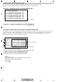
STANDBY/ON
HDD
ORDER NO.
DVD
PULL-OPEN
OPEN/CLOSE
REC ONE TOUCH COPY
RRV2963
DV IN/OUT
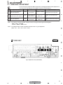
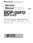
DVR-520H-S
DVD RECORDER
DVR-520H-S
DVR-65H-S
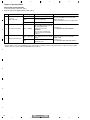
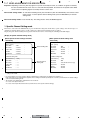
THIS MANUAL IS APPLICABLE TO THE FOLLOWING MODEL(S) AND TYPE(S).
Model
Type
Power Requirement
Region No.
Serial No.
Please confirm 3rd & 4th
alphabetical letters.
DVR-520H-S
KU/CA
AC120V
1
DVR-520H-S
KUXU/CA
AC120V
1
&&PG######$$
DVR-65H-S
KCXU
AC120V
1
&&PG######$$
÷
When servicing this model, some service procedures may reset the settings that customer
set (*) to the factory default settings. Make sure to explain this to the customer.
(*) : Initial Setup (Clock Setting, Remote Control Set, Channel settings, Video Out settings,
Audio In settings, Audio Out settings, Language settings)
Refer to the chapter 13 of the Operating Instructions for more details.
An HDD (Hard Disc Drive) is mounted in this product.
The HDD is a precision instrument very vulnerable to shock and electrostatic charges.
Please read "7.4 Cautions on Handling the HDD" in this manual and exercise sufficient caution
when handling the HDD itself, as well as the product with the HDD built in.
When an HDD becomes defective and inoperable, restoration of the user's data recorded on
the HDD, or copying of the user's recorded data to other media (such as a new HDD) is totally
impossible. Before servicing, OBTAIN THE USER'S PRIOR CONSENT to that effect.
The user must be made aware that all recorded data are deleted if the HDD is intialized.
For details, refer to "Important symbols for good services" .
PIONEER CORPORATION
4-1, Meguro 1-chome, Meguro-ku, Tokyo 153-8654, Japan
PIONEER ELECTRONICS (USA) INC. P.O. Box 1760, Long Beach, CA 90801-1760, U.S.A.
PIONEER EUROPE NV Haven 1087, Keetberglaan 1, 9120 Melsele, Belgium
PIONEER ELECTRONICS ASIACENTRE PTE. LTD. 253 Alexandra Road, #04-01, Singapore 159936
PIONEER CORPORATION 2004
T-ZZV MAY 2004 printed in Japan
1
2
3
4
SAFETY INFORMATION
A
This service manual is intended for qualified service technicians; it is not meant for the casual
do-it-yourselfer. Qualified technicians have the necessary test equipment and tools, and have been
trained to properly and safely repair complex products such as those covered by this manual.
Improperly performed repairs can adversely affect the safety and reliability of the product and may
void the warranty. If you are not qualified to perform the repair of this product properly and safely, you
should not risk trying to do so and refer the repair to a qualified service technician.
B
WARNING
This product contains lead in solder and certain electrical parts contain chemicals which are known to the state of California to
cause cancer, birth defects or other reproductive harm.
Health & Safety Code Section 25249.6 – Proposition 65
NOTICE
(FOR CANADIAN MODEL ONLY)
Fuse symbols
(fast operating fuse) and/or
(slow operating fuse) on PCB indicate that replacement
parts must be of identical designation.
REMARQUE
(POUR MODÈLE CANADIEN SEULEMENT)
C
Les symboles de fusible
(fusible de type rapide) et/ou
(fusible de type lent) sur CCI indiquent que
les pièces de remplacement doivent avoir la même désignation.
(FOR USA MODEL ONLY)
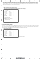
1. SAFETY PRECAUTIONS
The following check should be performed for the
continued protection of the customer and service
technician.
LEAKAGE CURRENT CHECK
Measure leakage current to a known earth ground
(water pipe, conduit, etc.) by connecting a leakage
current tester such as Simpson Model 229-2 or
equivalent between the earth ground and all exposed
metal parts of the appliance (input/output terminals,
screwheads, metal overlays, control shaft, etc.). Plug
the AC line cord of the appliance directly into a 120V
AC 60 Hz outlet and turn the AC power switch on. Any
current measured must not exceed 0.5 mA.
D
Device
under
test
E
Reading should
not be above
0.5 mA
Leakage
current
tester
Test all
exposed metal
surfaces
Also test with
plug reversed
(Using AC adapter
plug as required)
Earth
ground
ANY MEASUREMENTS NOT WITHIN THE
LIMITS OUTLINED ABOVE ARE INDICATIVE
OF A POTENTIAL SHOCK HAZARD AND
MUST BE CORRECTED BEFORE RETURNING THE APPLIANCE TO THE CUSTOMER.
2. PRODUCT SAFETY NOTICE
Many electrical and mechanical parts in the appliance
have special safety related character istics. These are
often not evident from visual inspection nor the
protection afforded by them necessarily can be obtained
by using replacement components rated for voltage,
wattage, etc. Replacement parts which have these
special safety characteristics are identified in this
Service Manual.
Electrical components having such features are
identified by marking with a
on the schematics and
on the parts list in this Service Manual.
The use of a substitute replacement component which
does not have the same safety characteristics as the
PIONEER recommended replacement one, shown in the
parts list in this Service Manual, may create shock, fire,
or other hazards.
Product Safety is continuously under review and new
instructions are issued from time to time. For the latest
information, always consult the current PIONEER
Service Manual. A subscription to, or additional copies
of, PIONEER Service Manual may be obtained at a
nominal charge from PIONEER.
AC Leakage Test
F
2
DVR-520H-S
1
2
3
4
5
6
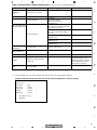
IMPORTANT
THIS PIONEER APPARATUS CONTAINS
LASER OF CLASS 1.
SERVICING OPERATION OF THE APPARATUS
SHOULD BE DONE BY A SPECIALLY
INSTRUCTED PERSON.
7
WARNING!
DEVICE INCLUDES LASER DIODE WHICH
EMITS INVISIBLE INFRARED RADIATION
WHICH IS DANGEROUS TO EYES. THERE IS
A WARNING SIGN ACCORDING TO PICTURE
1 INSIDE THE DEVICE CLOSE TO THE LASER
DIODE.
LASER DIODE CHARACTERISTICS
MAXIMUM OUTPUT POWER : 70 mw
WAVELENGTH : 658 nm
8
A
LASER
Picture 1
Warning sign for
laser radiation
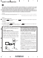
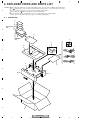
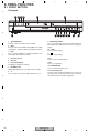
LABEL CHECK
B
STA
ND
BY
/ON
HD
D
PU
LLOP
EN
DV
D
Î
C
OP
EN/
CLO
SE
RE
C
ON
E TO
UC
H CO
PY
DRW2194
DV
IN/O
UT
Additional Laser Caution
1. The ON/OFF(ON:low level,OFF:high level) status of the
CLAMP signals for detecting the loading state are detected
by the drive CPUs, and the design prevents laser diode
oscillation when the CLAMP signal turns OFF.
In normal operation, if no disc is clamped, the laser diode
oscillation is disabled.
However, the interlock does not always operate in the test
mode.
D
2. When the cover is opened, close viewing of the objective
lens with the naked eye will cause exposure to a Class 3A
laser beam.
E
F
3
DVR-520H-S
5
6
7
8
1
2
3
4
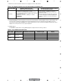
[ Important symbols for good services ]
In this manual, the symbols shown-below indicate that adjustments, settings or cleaning should be made securely.
When you find the procedures bearing any of the symbols, be sure to fulfill them:
A
1. Product safety
You should conform to the regulations governing the product (safety, radio and noise, and other regulations), and
should keep the safety during servicing by following the safety instructions described in this manual.
2. Adjustments
To keep the original performances of the product, optimum adjustments or specification confirmation is indispensable.
In accordance with the procedures or instructions described in this manual, adjustments should be performed.
3. Cleaning
For optical pickups, tape-deck heads, lenses and mirrors used in projection monitors, and other parts requiring cleaning,
proper cleaning should be performed to restore their performances.
B
4. Shipping mode and shipping screws
To protect the product from damages or failures that may be caused during transit, the shipping mode should be set or
the shipping screws should be installed before shipping out in accordance with this manual, if necessary.
5. Lubricants, glues, and replacement parts
Appropriately applying grease or glue can maintain the product performances. But improper lubrication or applying
glue may lead to failures or troubles in the product. By following the instructions in this manual, be sure to apply the
prescribed grease or glue to proper portions by the appropriate amount.For replacement parts or tools, the prescribed
ones should be used.
C
D
E
F
4
DVR-520H-S
1
2
3
4
5
6
7
8
CONTENTS
SAFETY INFORMATION......................................................................................................................................2
1. SPECIFICATIONS .............................................................................................................................................6
2. EXPLODED VIEWS AND PARTS LIST.............................................................................................................8
2.1 PACKING ....................................................................................................................................................8
2.2 EXTERIOR ...............................................................................................................................................10
2.3 FRONT PANEL .........................................................................................................................................13
3. BLOCK DIAGRAM AND SCHEMATIC DIAGRAM ..........................................................................................16
3.1.1 OVERALL BLOCK DIAGRAM ...............................................................................................................16
3.1.2 TUNB and JCKB ASSY BLOCK DIAGRAM ..........................................................................................18
3.1.3 MAIN ASSY BLOCK DIAGRAM ............................................................................................................20
3.1.4 POWER BLOCK DIAGRAM ..................................................................................................................22
3.2 OVERALL WIRING DIAGRAM .................................................................................................................24
3.3 TUNB ASSY..............................................................................................................................................26
3.4 JCKB ASSY(1/2).......................................................................................................................................28
3.5 JCKB(2/2), ATWB and ATHB ASSYS .......................................................................................................30
3.6 MAIN ASSY(1/5).......................................................................................................................................32
3.7 MAIN ASSY(2/5).......................................................................................................................................34
3.8 MAIN ASSY(3/5).......................................................................................................................................36
3.9 MAIN ASSY(4/5).......................................................................................................................................38
3.10 MAIN ASSY(5/5).....................................................................................................................................40
3.11 FLKY, KIRB, FRJB and DVJB ASSYS ....................................................................................................42
3.12 POWER SUPPLY UNIT ..........................................................................................................................44
3.13 WAVE FORMS........................................................................................................................................46
4. PCB CONNECTION DIAGRAM ......................................................................................................................49
4.1 TUNB ASSY..............................................................................................................................................50
4.2 JCKB, ATWB and ATHB ASSYS ..............................................................................................................52
4.3 MAIN ASSY ..............................................................................................................................................56
4.4 FLKY, KIRB, FRJB and DVJB ASSYS ......................................................................................................60
4.5 POWER SUPPLY UNIT ............................................................................................................................64
5. PCB PARTS LIST ............................................................................................................................................65
6. ADJUSTMENT ................................................................................................................................................69
6.1 TUNB ASSY ADJUSTMENT ....................................................................................................................69
6.2 MAIN ASSY ADJUSTMENT .....................................................................................................................70
7. GENERAL INFORMATION .............................................................................................................................71
7.1 DIAGNOSIS..............................................................................................................................................71
7.1.1 CPRM ID NUMBER AND DATA SETTING ............................................................................................72
7.1.2 MODEL SETTING .................................................................................................................................76
7.1.3 DOWNLOAD METHOD .........................................................................................................................77
7.1.4 SERVICE MODE ...................................................................................................................................79
7.1.5 DV DEBUG MODE ................................................................................................................................91
7.1.6 ERROR RATE MEASUREMENT...........................................................................................................94
7.1.7 VIDEO ADJUSTMENT FOR SPECIFIC AREA......................................................................................96
7.1.8 AGING MODE .....................................................................................................................................100
7.1.9 SETUP SEQUENCE............................................................................................................................102
7.1.10 DISASSEMBLY..................................................................................................................................103
7.2 IC ............................................................................................................................................................108
7.3 OUTLINE OF THE PRODUCT ...............................................................................................................135
7.4 CAUTIONS ON HANDLING THE HDD...................................................................................................138
7.5 DISC/CONTENT FORMAT .....................................................................................................................140
7.6 CLEANING .............................................................................................................................................141
8. PANEL FACILITIES .......................................................................................................................................142
A
B
C
D
E
F
5
DVR-520H-S
5
6
7
8
1
2
3
4
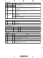
1. SPECIFICATIONS
A
B
General
Timer
System . . . . . . . . . . . . . . . . . HDD, DVD-Video, DVD-R/RW,
Video-CD, CD,
CD-R/RW (WMA, MP3, JPEG, CD-DA)
Power requirements. . . . . . . . . . . . . . . . . . . . .120 V, 60 Hz
Power consumption
DVR-65H . . . . . . . . . . . . . . . . . . . . . . . . . . . . . . . . . 50 W
DVR-520H . . . . . . . . . . . . . . . . . . . . . . . . . . . . . . . . . 48 W
Power consumption in standby mode
0.48 W
(Front panel display: off)
Weight . . . . . . . . . . . . . . . . . . . . . . . . . .10 lb. 2 oz. / 4.6 kg
Dimensions . . . . . . . . . . . . . 420 (W) x 59 (H) x 339 (D) mm
Operating temperature . . . . . . . . . . . . . . . . +5∞Cto +35∞C
Operating humidity . . . . . . . . . . . . . . . . . . . . . . . 5% to 85%
(no condensation)
TV format . . . . . . . . . . . . . . . . . . . . . . . . . . . . . . . . . . NTSC
Programs . . . . . . . . . . . . . . . . . . . . . . 1 month/32 programs
Clock. . . . . . . . . . . . . . .Quartz lock (12-hour digital display)
Power off memory . . . . Approx. 5 years (after manufacture)
Recording
Recording format . . . . . . . . . . . . . . . DVD Video Recording
DVD-VIDEO
Recordable discs
DVD-RW (DVD Re-recordable disc)
DVD-R (DVD Recordable disc)
Video recording format
Sampling frequency . . . . . . . . . . . . . . . . . . . . . . . . 13.5MHz
Compression format . . . . . . . . . . . . . . . . . . . . . . . . . MPEG
Audio recording format
Sampling frequency . . . . . . . . . . . . . . . . . . . . . . . . . 48kHz
Compression format. . . . . . . . . Dolby Digital or Linear PCM
(uncompressed)
Recording time
C
HDD
Fine (FINE). . . . . . . . . . . . . . . . . . . . . . . . Approx. 17 hours
Standard Play (SP). . . . . . . . . . . . . . . . . . Approx. 34 hours
Long Play (LP) . . . . . . . . . . . . . . . . . . . . . Approx. 68 hours
Extended Play (EP) . . . . . . . . . . . . . . . . Approx. 102 hours
Manual Mode (MN) . . . . . . . . . . . . . Approx. 17-102 hours
DVD-R/DVD-RW
Fine (FINE). . . . . . . . . . . . . . . . . . . . . . . . . . Approx. 1 hour
Standard Play (SP) . . . . . . . . . . . . . . . . . . Approx. 2 hours
Long Play (LP) . . . . . . . . . . . . . . . . . . . . . . Approx. 4 hours
Extended Play (EP). . . . . . . . . . . . . . . . . . . Approx. 6 hours
Manual Mode (MN) . . . . . . . . . . . . . . . . Approx. 1-6 hours
D
Tuner
Receivable channels
VHF. . . . . . . . . . . . . . . . . . . . . . . . . . . . . . . . . . . . . . 2-13ch
UHF . . . . . . . . . . . . . . . . . . . . . . . . . . . . . . . . . . . . 14-69ch
CATV. . . . . . . . . . . . . . . . . . . . . . . . . . . . . . . . . C1-C125ch
Input/Output
VHF/UHF antenna input/output terminal . . . . VHF/UHF set
75 Ω (F-shape connector)
Video input . . . . . . . . . . . . . Input 1 (rear), 3 (rear), 2 (front)
Input level. . . . . . . . . . . . . . . . . . . . . . . . . . . . 1 Vp-p (75 Ω)
Jacks . . . . . . . . . . . . . . . . . . . . . . . . . . . . . . . . . . RCA jack
Video output. . . . . . . . . . . . . . . . . . . . . . . . . . . . . Output
.
1,2
Output level. . . . . . . . . . . . . . . . . . . . . . . . . . .1 Vp-p (75 Ω)
Jacks . . . . . . . . . . . . . . . . . . . . . . . . . . . . . . . . . .RCA jack
S-Video input . . . . . . . . . . . . . . . . .Input 1, 3 (rear), 2 (front)
Y (luminance) - Input level . . . . . . . . . . . . . .1 Vp-p (75 Ω)
C (color) - Input level . . . . . . . . . . . . . . . . 286 mVp-p (75 Ω)
Jacks . . . . . . . . . . . . . . . . . . . . . . . . . . . . . . 4 pin mini DIN
S-Video output . . . . . . . . . . . . . . . . . . . . . . . . . . . Output 1,2
Y (luminance) - Output level . . . . . . . . . . . . . 1. Vp-p (75 Ω)
C (color) - Output level . . . . . . . . . . . . . . 286 mVp-p (75 Ω)
Jacks . . . . . . . . . . . . . . . . . . . . . . . . . . . . . . .4. pin mini DIN
Component video output
Output level . . . . . . . . . . . . . . . . . . . . . . Y: 1.0 Vp-p (75Ω)
PB, PR: 0.7 Vp-p (75Ω)
Jacks . . . . . . . . . . . . . . . . . . . . . . . . . . . . . . . . . RCA jacks
Audio input . . . . . . . . . . . . . . . Input 1, 3 (rear), 2 (front) L/R
Input level
During audio input . . . . . . . . . . . . . . . . . . . . . . . . . . 2V rms
(Input impedance: more than 22 k Ω)
Jacks . . . . . . . . . . . . . . . . . . . . . . . . . . . . . . . . . RCA jacks
Audio output . . . . . . . . . . . . . . . . . . . . . . . . . Output 1,2 L/R
During audio output . . . . . . . . . . . . . . . . . . . . . . . . . 2V rms
(Output impedance: less than 1.5 k Ω)
Jacks . . . . . . . . . . . . . . . . . . . . . . . . . . . . . . . . . RCA jacks
Control input . . . . . . . . . . . . . . . . . . . . . . . . . . . . . .Mini jack
DV input/output (DVR-520H only). . . . . . . . . . . . . . . . 4 pin
(i.LINK/IEEE 1394 standard)
Supplied accessories
Remote control. . . . . . . . . . . . . . . . . . . . . . . . . . . . . . . . . .1
Dry cell batteries (AA/R6P) . . . . . . . . . . . . . . . . . . . . . . . . 2
Audio / Video cable (red/white/yellow) . . . . . . . . . . . . . . . .1
RF antenna cable . . . . . . . . . . . . . . . . . . . . . . . . . . . . . . . . 1
Power cable . . . . . . . . . . . . . . . . . . . . . . . . . . . . . . . . . . . . 1
Operating Instructions . . . . . . . . . . . . . . . . . . . . . . . . . . . .1
Warranty card . . . . . . . . . . . . . . . . . . . . . . . . . . . . . . . . . . .1
Note: The specifications and design of this product are subject
to change without notice, due to improvement.
E
F
6
DVR-520H-S
1
2
3
4
5
6
7
8
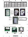
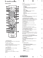
Accessories
• Remote control ×1
(VXX2932)
ST ANDBY/ON ONE TOUCH
COPY
A
OPEN/CLOSE
0
HDD
AUDIO
• RF antenna cable ×1
(VDE1025)
DVD
SUBTITLE
ANGLE
ABC
DEF
GHI
JKL
MNO
PQRS
TUV
WXYZ
VCR Plus+
PLAY MODE
CHANNEL
CLEAR
+
• Power cable ×1
(ADG7021 : DVR-520H-S/KU/CA)
(ADG7075 : DVR-520H-S/KUXU/CA
DVR-65H-S/KCXU)
INPUT
SELECT
CLEAR
DISC NAVIGATOR
PLAY LIST
OP MENU
MENU
ENTER
HOME
MENU
RETURN
REV SCAN
PAUSE
PREV
STOP OK
CASE
SELECTION
REC
•
PLAY
DISC
HISTORY
BACK
NEX T
STOP REC
FWD SCAN
CM
B
SKIP
STEP/SLOW
e
E
REC MODE TIMER REC
NAVI
MARK
CHP
MARK
TV CONTROL
EASY
TIMER
• Audio / Video cable(L=1.5m) ×1
(red/white/yellow)
(XDE3049 : DVR-520H-S/KU/CA)
(VDE1077 : DVR-520H-S/KUXU/CA
DVR-65H-S/KCXU)
DISPLAY
INPUT
CHANNEL VOLUME
SELECT
DVD RECORDER
• Dry cell batteries ×2
(AA/R6P)
Red
White
C
Yellow
D
E
F
7
DVR-520H-S
5
6
7
8
1
2
3
4
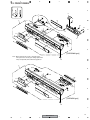
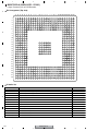
2. EXPLODED VIEWS AND PARTS LIST
NOTES:
A
Parts marked by "NSP" are generally unavailable because they are not in our Master Spare Parts List.
The
mark found on some component parts indicates the importance of the safety factor of the part.
Therefore, when replacing, be sure to use parts of identical designation.
Screws adjacent to mark on product are used for disassembly.
For the applying amount of lubricants or glue, follow the instructions in this manual.
(In the case of no amount instructions, apply as you think it appropriate.)
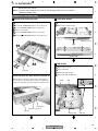
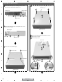
2.1 PACKING
12
9
10
DVR-520H-S 11
Only
7
B
13
8
DVR-65H
Only
6
4
15
2
5
C
3
14
1
13
D
16
17
E
F
18
8
DVR-520H-S
1
2
3
4
5
6
7
8
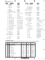
PACKING parts List
Mark No.
>
1
2
3
4
5
NSP 6
7
8
Description
Part No.
Mark No.
Description
HDD Caution 8L B
HDD Caution 8L
Card
Warranty Card
Polyethylene Bag
VRR1046
VRR1047
See Contrast table (2)
See Contrast table (2)
VHL1051
Mirror Sheet
IM Holder
Front Pad
Rear Pad
Packing Case
VHL1006
See Contrast table (2)
See Contrast table (2)
See Contrast table (2)
See Contrast table (2)
Power Cable
Audio / Video Cable
RF Antenna Cable
Remote Control
Battery Cover
See Contrast table (2)
See Contrast table (2)
VDE1025
VXX2932
AZN7933
NSP 9
NSP 10
NSP 11
NSP 12
13
Dry Cell Battery (R6P, AA)
Operating Instructions
(English)
Operating Instructions
(French)
See Contrast table (2)
See Contrast table (2)
14
15
16
17
18
See Contrast table (2)
Part No.
A
B
(2) CONTRAST TABLE
DVR-520H-S/KU/CA, KUXU/CA and DVR-65H/KCXU are constructed the same except for the following :
Mark No.
>
NSP
1
2
6
7
Symbol and Description
Power Cable
Audio / Video Cable
Dry Cell Battery (R6P, AA)
Operating Instructions
(English)
DVR-520H-S
/KU/CA
DVR-520H-S
/KUXU/CA
DVR-65H-S
/KCXU
ADG7021
XDE3049
VEM1031
VRB1338
ADG7075
VDE1077
VEM1030
VRB1338
ADG7075
VDE1077
VEM1030
VRB1343
C
NSP
NSP
8 Operating Instructions
(French)
11 Card
12 Warranty Card
15 IM Holder
Not used
Not used
VRC1210
VRY1132
ARY7045
VHC1116
VRY1132
ARY7045
VHC1115
Not used
ARY7007
VHC1115
16 Front Pad
17 Rear Pad
18 Packing Case
VHA1368
VHA1369
VHG2545
VHA1364
VHA1365
VHG2530
VHA1364
VHA1365
VHG2549
D
E
F
9
DVR-520H-S
5
6
7
8
1
2
3
4
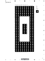
2.2 EXTERIOR
A
CONTACT SIDE
NON-CONTACT
SIDE
52
64
55
64
62
64
40
31 64
64
B
37
45
24
13
22
64
20
10
53
64
K
G
A
21
12
H
6
Lithium Battery
(CR2032)
G
53
60
64
36 J
53
7
B
C
F
64
H
64
64
C
35
14
23
41
62
48
A
I
J 64
38
1
64
42
53
38
64
60
38
C
9
64
K
39
65
D
64
65
E
O
B
A
59
64
63
I
64
D
54
25
2
63
61
8
11
64
58
63 61
43
61
34
19
F
33
46
I
32
36
F
E
30
47
64
4
53
50
38
56
B
H
J
64 27 29
28
57
L
(65H type)
51
(520H type) 49
64
O 15
5
C
12
64
64
50
44
3
DVR-520H-S
1
2
E
17
L
64
Refer to
"2.3 FRONT PANEL SECTION".
10
D
16
64
18
F
26
G
3
4
5
6
7
8
EXTERIOR parts List
Mark No.
>
Description
Mark No.
Part No.
1
2
3
4
5
TUNB Assy
JCKB Assy
MAIN Assy
FRJB Assy
DVJB Assy
VWV2010
VWV2023
VWV2025
VWV2004
VWV2006
6
7
8
9
10
ATWB Assy
ATHB Assy
POWER SUPPLY Unit
DRIVE Assy R7 (for Service)
HDD
VWV2009
VWV2011
VWR1380
VXX2942
See Contrast table (2)
11
12
13
14
15
DC Fan Motor
Ferrite Core
Ferrite Core
Connector Assy (13P)
Flexible Cable (8P)
VXM1114
ATX1048
See Contrast table (2)
PF13PP-D47
See Contrast table (2)
16
17
18
19
20
Flexible Cable (24P)
Flexible Cable (32P)
Flexible Cable (7P)
Flexible Cable (13P)
Flexible Cable (40P)
See Contrast table (2)
See Contrast table (2)
See Contrast table (2)
See Contrast table (2)
See Contrast table (2)
21
22
23
24
NSP 25
Shield Flexible Cable (40P)
Housing Assy (4P)
Housing Assy (2P)
Housing Assy (4P)
P. Plate Holder
See Contrast table (2)
See Contrast table (2)
See Contrast table (2)
See Contrast table (2)
PNY-405
26
27
28
NSP 29
30
Rubber Foot
Radiation Sheet
Rubber Spacer
PC Support
Heatsink Cushion
VEB1349
VEB1360
VEB1370
VEC1749
VEC2363
31
32
NSP 33
Gasket Sheet
Spacer
Clamp
VEC2394
VEC2413
VEC2418
Description
Part No.
34
35
FFC Protector
Gasket 20 x 8T
VEC2436
VEC2437
36
37
38
NSP 39
NSP 40
Gasket 75 x 7T
Gasket Sheet 2
Aluminum Tape
HDD Stay
Bonnet Angle
VEC2439
VEC2440
VEF1056
VNE2334
VNE2335
NSP 41
NSP 42
NSP 43
NSP 44
45
Writer Stay L
Writer Stay R
PCB Base
Heatsink
SYPS Cover
VNE2336
VNE2337
VNE2339
VNH1070
VNK5426
46
NSP 47
NSP 48
49
50
Fan Duct
Base Chassis Assy
Binder (BK-1)
HDD Badge
Tray Sheet
VNK5427
VXA2682
ZCA-BK1
See Contrast table (2)
See Contrast table (2)
51
52
NSP 53
54
55
Tray Panel
Bonnet Label
Tape
Rear Panel
Bonnet Case S
See Contrast table (2)
VRW2104
ZTA-156A-19
See Contrast table (2)
VXX2925
56
57
58
59
60
Tray Panel Base
Tray Panel Lens
Screw
Screw
Screw
See Contrast table (2)
See Contrast table (2)
BPZ30P250FTC
PBZ30P080FTC
AMZ30P060FTC
61
62
63
64
65
Screw
Screw
Screw
Screw
#6-32 Screw
BBZ30P040FTC
BCZ40P060FNI
BPZ30P080FTC
BBZ30P060FTC
DBA1125
A
B
C
D
(2) CONTRAST TABLE
DVR-520H-S/KU/CA, KUXU/CA and DVR-65H/KCXU are constructed the same except for the following :
Mark No.
Symbol and Description
DVR-520H-S
/KU/CA
DVR-520H-S
/KUXU/CA
DVR-65H-S
/KCXU
10
10
13
15
16
HDD 80G 4R080L0 SV
HDD 160G 4R160L0 SV
Ferrite Core
Flexible Cable (8P)
Flexible Cable (24P)
VXF1010
Not used
VTH1051
VDA2011
VDA2012
VXF1010
Not used
VTH1050
VDA1997
VDA1998
Not used
VXF1028
VTH1050
VDA1997
VDA1998
17
18
19
20
21
Flexible Cable (32P)
Flexible Cable (7P)
Flexible Cable (13P)
Flexible Cable (40P)
Shield Flexible Cable (40P)
VDA2013
VDA2014
VDA2015
VDA2034
VDA2033
VDA1999
VDA2000
VDA2001
VDA2032
VDA2031
VDA1999
VDA2000
VDA2001
VDA2032
VDA2031
VKP2330
VKP2332
VKP2327
VKP2315
VKP2327
VKP2315
22 Housing Assy (4P)
23 Housing Assy (2P)
E
F
11
DVR-520H-S
5
6
7
8
1
3
4
DVR-520H-S
/KU/CA
DVR-520H-S
/KUXU/CA
DVR-65H-S
/KCXU
24 Housing Assy (4P)
49 HDD Badge
50 Tray Sheet B
VKP2348
VAM1141
VEC2409
VKP2335
VAM1141
VEC2409
VKP2335
Not used
Not used
50
51
54
56
57
Not used
VNK5421
VNA2704
Not used
Not used
Not used
VNK5421
VNA2704
Not used
Not used
VEC2448
Not used
VNA2737
VNK5432
VNK5592
Mark No.
A
2
Symbol and Description
Tray Sheet
Tray Panel
Rear Panel
Tray Panel Base
Tray Panel Lens
B
C
D
E
F
12
DVR-520H-S
1
2
3
4
5
6
7
8
CONTACT SIDE
NON-CONTACT
SIDE
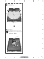
2.3 FRONT PANEL
A
3
24
2
24
5
19
E
16
9(2/2)
24
24
12
D
7
24
24
B
4
11
17
(Note)
13
10
6
8
20
1
21
9(1/2)
14
C
15
[DVR-520H type]
Note : When replacing the jack door, first fully open it.
If the jack door is not fully open during replacement,
it may unexpectedly fall out after being replaced.
18
5
16
9(2/2)
D
12
22
7
24
25
11
23
17
(Note)
13
8
20
10 22
22
6
9(1/2)
21
E
14
15
[DVR-65H type]
18
F
13
DVR-520H-S
5
6
7
8
1
2
3
4
FRONT PANEL parts List
Mark No.
Mark No.
Part No.
1
2
3
4
5
FLKY Assy
KIRB Assy
Flexible Cable (19P)
Flexible Cable (7P)
Front Panel Assy
VWG2489
VWG2493
See Contrast table (2)
See Contrast table (2)
See Contrast table (2)
6
7
NSP 8
NSP 9
NSP 10
Pioneer Name Plate
Door Spring
Mirror Sheet
Main Key
REC Ring
See Contrast table (2)
VBK1151
VHL1082
See Contrast table (2)
VNK5425
NSP 11
NSP 12
NSP 13
Sub Panel
Power Key
IR Window
See Contrast table (2)
VNK5480
See Contrast table (2)
A
B
Description
Description
Part No.
NSP 14
NSP 15
DV Cover
FL Lens
VNK5451
See Contrast table (2)
NSP 16
17
18
19
20
Front Panel
Jack Door
Rubber Foot
Drive Sheet
Panel Sheet
See Contrast table (2)
VNK5494
VEB1349
VEC2345
See Contrast table (2)
NSP 21
NSP 22
23
24
25
Copy Ring
Cap
FL Filter
Screw
Sheet S
VNK5523
See Contrast table (2)
See Contrast table (2)
BPZ30P080FTC
See Contrast table (2)
(2) CONTRAST TABLE
DVR-520H-S/KU/CA, KUXU/CA and DVR-65H/KCXU are constructed the same except for the following :
Mark No.
Symbol and Description
DVR-520H-S
/KU/CA
DVR-520H-S
/KUXU/CA
DVR-65H-S
/KCXU
3
4
5
6
9
Flexible Cable (19P)
Flexible Cable (7P)
Front Panel Assy
Pioneer Name Plate
Main Key
VDA2016
VDA2019
VXA2645
VAM1146
VNK5420
VDA2002
VDA2005
VXA2645
VAM1146
VNK5420
VDA2002
VDA2005
VXA2649
VAM1147
VNK5436
NSP
NSP
NSP
NSP
11
13
15
16
20
Sub Panel
IR Window
FL Lens
Front Panel
Panel Sheet
VNK5483
VNK5423
VNK5422
VNK5441
VEC2446
VNK5483
VNK5423
VNK5422
VNK5441
VEC2446
VNK5526
Not used
VNK5593
VNK5527
Not used
NSP
22 Cap
23 FL Filter
25 Sheet S
Not used
Not used
Not used
Not used
Not used
Not used
VNK5437
VEC2421
VEC2426
C
NSP
D
E
F
14
DVR-520H-S
1
2
3
4
5
6
7
8
A
B
C
D
E
F
15
DVR-520H-S
5
6
7
8
1
2
3
4
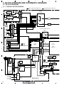
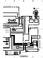
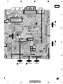
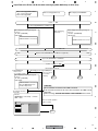
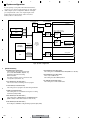
3. BLOCK DIAGRAM AND SCHEMATIC DIAGRAM
3.1 BLOCK DIAGRAM
3.1.1 OVERALL BLOCK DIAGRAM
A
: Playback system signal route
: Recording system signal route
U301 VXF1022
TV FRONT-END
ANT
RF IN
RF AOUT VOUT
19
OUT 16
A
TUNB
ASSY
17
3
MPX
Decoder
(19P)
(19P)
UVV
2V
UVL
L
LPF
OUT 21
7 MPX Audio
IN
UVV
CN401
CN301
IC451 CXA2020M
Video Selector
Video Driver
IC701
LA73033(1/2)
7
7
UVL
15
3V
CN451
CN402
(13P)
(13P)
13
77
2Y
F
75
3C
CN1301 CN705
7
1C
(15P)
6 CIN2 8
LPF
79
1Y
B
V/Y
V/Y
27
3Y
ATT WIDEBAND SPECTRAL
(15P)
19
17
1V
5
2C
C
25
C
LPF
3
FRJB
ASSY
JA1301
4
Y
YIN2
10
Audio Selector with Electirc ATT
IC601
LC75342M
Y/C
C
JA1302
LIN4
VIDEO
8
L
11
6
13
R
C
VIN2
12
LIN2
14
2
INPUT1 JA601
VIDEO
LIN2
LIN1
LIN3
VIN1
VIN3
Y
CN4501
Y/C
(40P)
C
L
YIN1
R
YIN3
Y/C
HDD
IC1001
M65673WG
JCKB ASSY(1/3)
CIN1
Y
[ATA]
B 1/3
INPUT3
VIDEO
1 Chip
Sysytem Codec
CIN3
C
D
L
5
12
INPUT3
[ATAPI]
1
LIN1
L
LIN3
R
DVD-VR
DVD-Video
8
IC202
SDRAM
16Mbit
CN101
(45P)
Pickup
4
2
E
A
B
C
D
S4
S3
S2
S1
PICKUP
ASSY
(40P)
(40P)
IC1103
DSP
201
Writer
CPU
C
48
MAIN ASSY
33
Flash
64Mbit
IC1102
34
35
38
PB DVD/CD
37
40
7-10
13-16
ASSY
B 2/3 JCKB
(2/3)
76
M
STEPPIONG
MOTOR
M
IC101
UPC3330GC
2
CN703 (2P)
2
(12P)
CN201
CD Digital
IC501
BD7907FS
DRIVE ASSY
DVR-520H-S
2
3
4
13
(21P)
(21P)
CN501
16
1
CD Digital
13
39
CN502
CN3001
(1/2)
CN702
(1/2)
RF IC
(2P)
LOADING
MOTOR
CPU SDRAM
128Mbit
IC1101
36
6CH
Driver
F
SRAM
4Mbit
IC1401 ATA SDRAM
256Mbit ×2
IC1421
IC301
M30700FKLGP
3
LD
DRIVE
CN401 CN4401
IC201
UPD63630GM
5
SPDL
MOTOR
DVD-VR
DVD-Video
5
6
7
8
A
• R ch is same as L ch.
J
DVJB ASSY
TPB
XTPA
TPA
JA1401
XTPB
DV TERMINAL
1
2
3
4
1,3 2
6
7
CN5102 1,3 2
CN701(1/2)
(32P)
SEL.V/Y
9
IC202
PEG034A
IC204
BR24L32F-W
Tuner
U-com
EEPROM
9
SEL.C
7
IC203
RS5C372A
Real
Time
Clock
IC5204
DV SDRAM
16Mbit
(7P)
6
XTPB
TPB
XTPA
(7P)
TPA
CN1401
B
7
7
38 39 37 36
IC5202
UPD72893BGD-LML
IEEE1394
Link IC
IC5101
UPD72852AGB-8EU
IEEE1394
Physical IC
Control
Data
L
SEL.L
5
5
C
CN2001
(32P)
IC3101
AK5357VT
Master Clock Freerun
• MPEG2 PS Encode
• AC-3/Linear PCM
Audio Encode
• 2ch ATA/ATAPI Interface
• MPEG2 PS Decode
T26
• AC-3/MPEG1/Linear
V27
PCM Audio Decode
9 Audio
10
A/D 2
12 48KHz
20Bit
B 3/3 JCKB ASSY(3/3)
Sampling Rate IC3301
SM5950AM
Converter
C IN
CVBS IN
D
Y(G)
Y(G)
Cb
F5
Cb
D2
IC1301
ENC
SDRAM
128Mbit
Cr
Cr
JA702
VIDEO
VOUT
CN2001
(2/2)
(32P)
Cr/R
DEC
SDRAM
128Mbit
IC1201
Cb/B
Y/G
Y
C
CN701
(2/2)
21
21
23
23
25
25
29
29
27
27
Cr OUT
Cb OUT
Y(G) OUT
Y OUT
C OUT
51
60
53
56
45
58
43
63
41
65
IC3201
PCM1742KE
1-3
YOUT
IC701
LA73033(2/2)
(32P)
2
3
1
17
17
Y
C
VIDEO
LOUT
Y
C
R
JA651
1
OPTICAL
AC-3/PCM
DIGITAL
AUDIO
OUT
Tuner U-com
IC1001 PT6315
FLKY ASSY
KIRB ASSY
CN201
(19P)
FL Driver
FL
V1001
F
Key
SW
CN1001
(19P)
17
DVR-520H-S
5
LINE
OUT 2
L
(21P) (21P)
D
E
E
R
COUT
L OUT
IC3251-1/2 CN3001(2/2) CN702(2/2)
UPC4570G2
SPDIF
1
LINE
OUT 1
L
Cb
68 V
Audio 7
D/A Conv.
Y
C
Y(G)
Cr
COMPONENT
VIDEO OUT
JA701
AG24
AF23
AD21
AG25
AE24
6
7
8
1
2
3
4
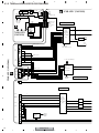
3.1.2 TUNB and JCKB ASSY BLOCK DIAGRAM
U301
STID
SUID
1
2
19
18
3
17
4
5
13
16
15
7
17
18
3
1
1
13
4
10
5
7
9
9
7
5
MUTE
A
CN451
IC451
MPX Audio
Decoder
CXA2064M
Wideband Separation
TUNB ASSY
(VWV2010)
B
AGC
SCL
SDA
AFT
Audio
SCL AFT
SDA AGC
<u-com>
ATT
TUON
U/V
V/U Tuner FrontEnd
VXF 1022-
CN401
CN301
Q306
+6V
SW.
+5V
Ripple Filter
B
AGC
SCL
SDA
AFT
TUON<u-com>
MUTE <u-com>
STID
<u-com>
SUID
UV_L <IC601>
UV_R
JCKB ASSY (VWV2028)
Video Input Circuit
CN402
+32V
Reg.
A
V/Y
27
U/V
IC701
LA73033
Video Selector 25
&
Video Driver
(1/2)
Q451
15kHz LPF
C
Q514
Sync-Sepa
36
S
JA601
SYNC
SYNC
<u-com>
SDET1 <u-com>
C
SCL
SDA
Y
YVSEL
SWSTBY
<u-com>
V
IN1
(Rear)
SYNCAFT
<u-com>
L
R
C
S
SDET3 <u-com>
C
UV_L/R <from TUNB ASSY>
L
R
Y
JA1302
V
IN2
(Front)
R
L
12
8
2
6
IC601
Audio Selector
with
Electric A.T.T
SDET2 <u-com>
5
L
26 R
LC75342M
10
4
8
12
10
6
2
4
CN705
JA1301
S
C
CN1301
D
V
IN3
(Rear)
F
FRJB ASSY (VWV2004)
Y
EVOLCLK
EVOLDATA <u-com>
EVOLCE
Audio Input Circuit
JA651
Optical
OUT
Output Circuit
JA701
Component
OUT
E
Y
60
Cb
56
Cr
58
IC701
LA73033
Video Selector
&
Video Driver
63
(2/2)
Y
JA702
C
65
V
68
OUT1
51
LPF
53
LPF
45
LPF
41
43
Y
C
Muting
Comp
(Discrete)
LAMUTE
RAMUTE
<MAIN>
OUT2
L
F
R
18
DVR-520H-S
1
2
3
4
5
6
7
8
V1001
IC1001
FL Driver
PT6315
FLCK, FLDATA, FLSTB
<CN401 Pin7>
D
EVOLCLK
<IC601> EVOLDATA
EVOLCE
FLKY ASSY
IC202
(VWG2489)
SDET1
<JA1301,
SDET2
JA601>
SDET3
SYNCAFT
<IC701>
Tuner/FL
Control U-com
S1001-S1009
S1201-S1203
KEY1, KEY2, KEY3
E
Front Keys
PEG034A-K
KIRB
ASSY
IC1201
SYNC
IR Detector
CN201
SCL
<IC701> SDA
SWSTBY
(VWG2490)
CN1001
<Q514>
A
FL Display
B
JA201
<CN401 Pin19>
<IC451>
SELIR
AGC
SR In
STID,SAPID
<IC451>
Q104
MUTE
FAN
Driver
<CN401 Pin15> TUON
IC204
SCLEEP
PCMOUT
SDAEEP
ASCK
SST to M
SSM to TSIS
HST to M
HSM to TSYS
XRESET
2
CN703
BT201
Battery
BR24L32F-W
XINTRA
SCL
SDA
< from DRIVE >
SPDIF
EEPROM
FAN
IC203
Real-Time
Clock
RS5C372A
Other Devices
1
C
X201
XIN, XOUT Ceramic
Resonator
IC201
PCMOUT
XRESETIN Reset IC
PST3265
13
16
17
18
RAMUTE
525P
LAMUTE
22
23
24
SELR
CN702
< from/to MAIN >
U-com I/F
3
D
4
SELL
5
6
SELC
7
SELV/Y
8
9
10
11
12
13
14
15
16
L
R
17
18
19
E
20
Cr/R
21
22
Cb/B
23
24
Y/G
C
25
26
27
Y
28
29
30
31
32
CN701
< to/from MAIN >
F
19
DVR-520H-S
5
6
7
8
1
2
3
4
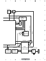
3.1.3 MAIN ASSY BLOCK DIAGRAM
C MAIN ASSY
A
(VWV2025)
To JCKB ASSY
CN2001
AUDIO LR OUT
IC3251
IC3101
AK5357VT
A/D
AUDIO LR IN
IC3201
PCM1742KE
DAC
Q2101-Q2105
VIDEO Y,C,Yp,Cb,Cr OUT
VIDEO Y,C IN
IC3403
IC2301
AGC,ACC
ADCCLKO
B
D.OUT
To JCKB ASSY
C
CN3001
CD D.OUT
TO TUNER u-COM
ECLK0
IC1301
IC1001
ENC
SDRAM
M65673WG
1 Chip System Codec
MT48LC4M32B2TG-7
DCLK0
IC1201
DEC
SDRAM
• MPEG2 PS Encode
• AC-3/Linear PCM Audio Encode
• 2ch ATA/ATAPI Interface
• MPEG2 PS Decode
• AC-3/MPEG1/Linear PCM Audio Decode
IC1401
ATA BUS
CN4401
To Writer
ATA SDRAM
D
K4S561632E-TC75
W986416DH-6
To H.D.D
SERIAL
IC1421
ATA SDRAM
E
K4S561632D-TC75
CN4501
ARCLK0
IC1102
FLASH
CN1901
VYW2176
IC1103
Backup
SRAM
CY62148VLL-70ZI
F
20
DVR-520H-S
1
2
3
4
5
6
7
8
A
VSS1195
X4102
VCXO
ADMCLKI
Input Mster
clock
IC4101
27M
B
33/36M
IC3402
SM8707KV
PLL IC
36M
AMCLK2
33M
VMCLKI
27M
IC4205
DVVPWM
AMCLK1
C
DVPLLCK(ADMCLKI)
IC3301
SRC
SRC**O
SM5950AM
24M
SRC**I
TC7WHU04FU
Play Mster clock
IC4206
D
DVVCLKO
IC5341
HCLK0
E
VCLKI
IC5202
HOST BUS
MCLK
IC1101
CPU SDRAM
LINK/DV CODEC
IC5204
DV SDRAM
K4S281632E-TC75
UPD72852AGB-8EU
SCLK
IC5101
Phy
K4S161622D-TC80
CN5102
UPD72893BGD-LML
DV
F
21
DVR-520H-S
5
6
7
8
1
2
3
4
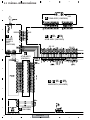
3.1.4 POWER BLOCK DIAGRAM
A
C MAIN ASSY
IC4004
5V REG.
V+5A
5
1
5
1
1
V+6V
2
V+6V
SW+2.5V
IC4007 V+3V
3.3V REG.
4
SW+4V
5
6
SW+4V
V+2R5V
4
V+4V
7
SW+4V
3
V+2R5V
CN4001
(8P)
SW+6V
B
IC4008 V+PRA
1.2V REG.
IC4006
5V REG.
V+5D
IC4002 V+3D
3.3V REG.
8
1
IC5002 V+2R5
2.5V REG.
3
7
1
V+3D
V+4V
V+12A
Q4000
V+4V
A TUNB ASSY
V+13V
C
FLDC –
FLDC +
3
V1001
FL TUBE
NC
14
V+5E
V+5E
18
V+5VI
V+13SW
V+5VO
CN701
(32P) 32
3
CN702
(24P) 21 23
V+5VO
V+6E
V+9
CN402
(13P)
CN3001
(24P) 21 23
19
V+13SW
1
2
D
CN2005
(19P)
V–28V
13 11
CN2001
(32P) 32
V+9
CN1001
(19P)
IC1001
FL Driver VEE 30
CN451
(13P) 11
V+37E
D FLKY ASSY
9
V+37E
CN401
(19P)
7
V+6E
CN301
(19P)
V+5RP
V+5VO
V+9
V+5VI
V+6E V+37E
18
V+5VO
17
Q103
6
2
V+6SW
V+5VI
Q101
CN202
(8P)
SW+2.5V
4
SW+4V
6
SW+4V
7
SW+4V
8
V+6E
I
E
V+6SW
IC102
3.3V REG.
1
CN201
(13P)
3
5
FLDC (–)
4
7
9
11
13
CN101
AC IN
F1
EV+37V
EV+6V
SW+13V
SW+6V
IC101
V+5E V+5M
5V REG.
3
1
5
V+37E
4
V+6E V+13SW V+6SW
1
1
11
Q104
SW+5V
V+13SW
13
CN105
(2P)
SW+12V
IC103
9V REG.
V+13SW
9
DRIVE ASSY
R7
LIVE 1
1
4
V+9
3
B JCKB ASSY
1
DC FAN
MOTOR
CN204
(4P)
NEUTRAL 2
3
V+6E
7
CN203
(4P)
4
F
FL–28V
6
V+6E
CN104
(13P)
FLDC (+)
V+3_3E
V+13FAN
2
POWER SUPPLY UNIT
SW+6V
Q102
SW+12V
SW+5V
HDD
22
DVR-520H-S
1
2
3
4
5
6
7
8
A
B
C
D
E
F
23
DVR-520H-S
5
6
7
8
1
2
3
4
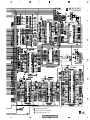
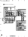
3.2 OVERALL WIRING DIAGRAM
A
A TUNB ASSY (VWV2010)
ADG7075
B
B B 1/2 - B 2/2
I
POWER
SUPPLY
UNIT
(VWR1380)
JCKB ASSY (VWV2023)
C
H
ATHB ASSY
(VWV2011)
D
C C 1/5 - C 5/5
MAIN ASSY (VWV2025)
E
F
J
DVJB ASSY
(VWV2006)
24
DVR-520H-S
1
2
3
4
5
6
7
8
÷ When ordering service parts, be sure to refer to "EXPLODED VIEWS and PARTS LIST" or
"PCB PARTS LIST".
÷ The > mark found on some component parts indicates the importance of the safety factor
of the part. Therefore, when replacing, be sure to use parts of identical designation.
÷
: The power supply is shown with the marked box.
A
UPPER: LINE 1
UNDER: LINE 3
B
VKB1150
C
ASSY
G ATWB
(VWV2009)
D
DRIVE ASSY
(R7)
(VXX2942)
ASSY
D FLKY
(VWG2489)
F
FRJB ASSY
(VWV2004)
E
VNF1129-
E
F
KIRB ASSY
(VWG2493)
25
DVR-520H-S
5
6
7
8
1
2
3
4
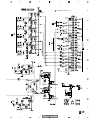
3.3 TUNB ASSY
A
(T)
(T)
A TUNB ASSY (VWV2010)
B
(T)
(T)
(T)
C
(T)
(T)
(T)
D
(T)
E
F
A
26
DVR-520H-S
1
2
3
4
5
6
7
8
A
(T)
(T)
: Video Signal Route (TUNER)
: Audio Signal Route (TUNER)
: Audio Signal Route (L ch)
B
C
(T)
(T)
B 2/2
CN401
(T)
D
B 2/2
CN402
E
F
A
27
DVR-520H-S
5
6
7
8
1
2
3
4
3.4 JCKB ASSY(1/2)
A
CN201
B 1/2 JCKB ASSY (VWV2023)
I
B
B 2/2
C
(Y) (C)
(Y)
B 2/2
B 2/2
(C)
B 2/2
D
1
E
: Video Signal Route
(Y)
(C)
: Video Signal Route (Y)
B 2/2
: Video Signal Route (C)
: Audio Signal Route (L ch)
F
B 1/2
28
DVR-520H-S
1
2
3
4
5
6
7
8
A
D
CN1001
B
B 2/2
C
PEG034B
TUFL u-com
D
E
EEPROM
F
B 2/2
B 1/2
29
DVR-520H-S
5
6
7
8
1
2
3
4
3.5 JCKB(2/2), ATWB and ATHB ASSYS
A
CN11
to DRIVE ASSY R7
to HDD C 4/5
ATHB
CN4401
ASSY(VWV2011) CN12 CN13
CN14
(Y)
G
H
(C)
(Cb)
ATWB
ASSY
(VWV2009)
C 4/5 CN4501
B
(T)
(Cr)
(D)
A
: Video Signal Route
: Video Signal Route (TUNER)
: Video Signal Route (Y)
: Video Signal Route (C)
: Video Signal Route (Cb)
: Video Signal Route (Cr)
: Audio Signal Route (L ch)
: Audio Signal Route (DIGITAL)
CN301
2
C
A
CN451
D
B 1/2
E
F
CN1301
B 1/2
F
(Y)
(C)
B 1/2
B 2/2 G H
30
DVR-520H-S
1
2
3
4
(T)
5
6
7
8
C 3/5 CN3001
A
From
DRIVE ASSY (R7R)
C 2/5
CN2001
5
13
12
15
6
(D)
B 1/2
11
(D)
(D)
(D)
(D)
14
B
(T)
8
(Cb)
(Cb)
(Y)
16
(Cr)
(Y)
17
(Cr)
18
9
C
(Y)
(C)
7
3
(Y)
4
(Y)
D
10
(Y)
(C)
(C)
(Y)
(Y)
Video Selector
&
Video Driver
(Y)
(C)
E
B 2/2
F
JCKB ASSY
(VWV2023)
B 2/2
31
DVR-520H-S
5
6
7
8
1
2
3
4
3.6 MAIN ASSY(1/5)
A
C 5/5
C 4/5
C 2/5,4/5
C 2/5
B
C 2/5
C 2/5
C
M65673WG-A
D
E
(D)
(AT)
(D)
C 2/5,4/5
C 1/5
32
C 4/5
F
C 3/5 C 5/5
C 3/5
DVR-520H-S
1
2
3
4
5
6
7
8
ASSY
C 1/5 MAIN
(VWV2025)
A
FLASH ROM
VYW2179
B
C
IC1104
TC7SZ126FU-TLB
1
5 VCC
2
R1104
R1105
10k (S)
100 (S)
4
GND
3
Backup SRAM
D
C 2/5
E
(AT)
(D)
F
: ATA Data Signal Route
: Audio Signal Route (DIGITAL)
: Audio Signal Route (L ch)
C 1/5
33
DVR-520H-S
5
6
7
8
1
2
3
4
3
4
3.7 MAIN ASSY(2/5)
A
C 2/5 MAIN ASSY (VWV2025)
B
C
D
C 1/5
C 1/5
E
C 1/5
C 1/5
C 1/5
F
C 2/5
34
DVR-520H-S
1
2
5
6
7
8
A
: Audio Signal Route (L ch)
7
C 3/5
17
4
B
16
15
C 1/5
B 2/2 CN701
3
C 3/5
5
9
C
10
6
8
13
12
11
C 1/5
D
C 3/5
E
C 1/5
F
C 2/5
35
DVR-520H-S
5
6
7
8
1
2
3
4
3.8 MAIN ASSY(3/5)
A
C 2/5
C 2/5
(D)
(D)
VKN1814
C 4/5
B
C 2/5
C 4/5
(D)
14
C
(D)
C 4/5
(D)
D
B 2/2
CN702
C 1/5
(D)
E
C 1/5
18
C 4/5
F
C 3/5
36
DVR-520H-S
1
2
3
4
5
6
7
8
A
C 1/5
C 3/5 MAIN ASSY (VWV2025)
(D)
: Audio Signal Route (DIGITAL)
: Audio Signal Route (L ch)
B
C 2/5
C
C 2/5
D
E
C 2/5
C 1/5
AK5357VT-TBB
F
C 3/5
37
DVR-520H-S
5
6
7
8
1
2
3
4
3.9 MAIN ASSY(4/5)
A
MM1603DP
I
CN202
C 3/5
C 3/5
B
C 4/5 MAIN ASSY (VWV2025)
C
D
C 5/5
C 1/5, 2/5
C 5/5
C 1/5
1
E
C 3/5
2
C 1/5, 2/5
C 1/5
F
C 4/5
38
DVR-520H-S
1
2
3
4
5
6
7
(AT)
8
A
: ATA Data Signal Route
C 1/5
(AT)
To DRIVE ASSY (R7)
ATAPI BUS
B
C
To HDD
D
E
F
C 4/5
39
DVR-520H-S
5
6
7
8
1
2
3
4
3
4
3.10 MAIN ASSY(5/5)
A
C 5/5 MAIN ASSY (VWV2025)
C 1/5
B
C
D
IC5101
UPD72852AGB-8EU-A
J
E
IC5101
CN1401
F
C 5/5
40
DVR-520H-S
1
2
5
6
7
8
A
C 1/5
C 4/5
B
C 1/5
C
IC5202
UPD72893BGD-LML
D
C 4/5
E
C 1/5
C 1/5
F
C 5/5
IC5204 K4S161622D-TC80
41
DVR-520H-S
5
6
7
8
1
2
3
4
3
4
3.11 FLKY, KIRB, FRJB and DVJB ASSYS
D FLKY ASSY (VWG2489)
A
1.0
B
C
B 1/2 CN201
D
E
F
D
42
DVR-520H-S
1
2
5
6
7
(Y)
: Video Signal Route
: Video Signal Route (Y)
E
(C)
8
: Video Signal Route (C)
: Audio Signal Route (L ch)
A
KIRB ASSY (VWG2493)
SWITCHES
S1201 : STANDBY/ON
S1202 : DISC HISTORY
S1203 : DISC NAVIGATOR
100
B
SWITCHES
S1001 : 0 OPEN/CLOSE
S1002 : & (REC/STOP)
S1004 : 7 (STOP)
S1005 : ¶ REC
S1006 : ONE TOUCH DUBBING
S1007 : S1008 : +
S1009 : 3 (PLAY)
F
FRJB ASSY
(VWV2004)
C
(Y)
(C)
INPUT 2
(C)
(Y)
D
B 2/2
CN705
E
C 5/5
CN5102
F
J
DVJB ASSY
(VWV2006)
D E F J
43
DVR-520H-S
5
6
7
8
1
2
3
4
3.12 POWER SUPPLY UNIT
A
I
POWER SUPPLY UNIT (VWR1380)
B
Not used
Not used
Not used
AC IN
C
Not used
D
Not used
Not used
Not used
E
Not used
F
I
44
DVR-520H-S
1
2
3
4
5
6
7
8
A
Note : No individual parts replacement for repair is accepted by Model Supplier due to the safety reasons.
Replace whole ASSY.
to R7
DRIVE ASSY
to HDD
B
C
Not used
Not used
Not used
Not used
C 4/5 CN4001
B 1/2 CN104
D
Not used
E
Not used
F
I
45
DVR-520H-S
5
6
7
8
1
2
3
4
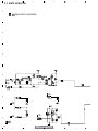
3.13 WAVE FORMS
Note : The encircled numbers denote measuring point in the schematic diagram.
A
B
1
JCKB ASSY
IC601-pin 11 (L4)
(Function : Tuner 2 ch)
V: 1V/div. H: 200µsec/div.
6
CN701-pin 27 (CMtoT)
(Function : DVD play)
V: 500mV/div. H: 10µsec/div.
10
JA702-pin 4 (COUT)
(Function : DVD play)
V: 500mV/div. H: 10µsec/div.
14
CN701-pin 23 (CBBMtoT)
(Function : DVD play)
V: 500mV/div. H: 10µsec/div.
GND
GND
GND
GND
B
(Not terminated)
2
CN401-pin 3 (UVIN)
(Function : Tuner 2 ch)
V: 500mV/div. H: 10µsec/div.
7
IC701-pin 69 (VOUT)
(Function : DVD play)
V: 500mV/div. H: 10µsec/div.
15
CN701-pin 21 (CRRMtoT)
(Function : DVD play)
V: 500mV/div. H: 10µsec/div.
GND
GND
IC701-pin 27 (YSWO)
(Function : Line 1 Video in)
V: 500mV/div. H: 10µsec/div.
(75Ω terminated)
GND
GND
3
8
IC701-pin 65 (COUT)
(Function : DVD play)
V: 500mV/div. H: 10µsec/div.
11
CN701-pin 5 (ALTtoM)
(Function : DVD play)
V: 1V/div. H: 200µsec/div.
16
IC701-pin 60 (PYRSCOUT)
(Function : DVD play)
V: 500mV/div. H: 10µsec/div.
17
IC701-pin 58 (CRGOUT)
(Function : DVD play)
V: 500mV/div. H: 10µsec/div.
18
IC701-pin 56 (CBBOUT)
(Function : DVD play)
V: 500mV/div. H: 10µsec/div.
C
GND
GND
GND
4
IC701-pin 25 (CSWO)
(Function : Line 1 Video in)
V: 500mV/div. H: 10µsec/div.
9
IC701-pin 63 (YOUT)
(Function : DVD play)
V: 500mV/div. H: 10µsec/div.
GND
12
CN701-pin 17 (ALMtoT)
(Function : DVD play)
V: 2V/div. H: 200µsec/div.
D
GND
GND
GND
GND
5
CN701-pin 29 (YVMtoT)
(Function : DVD play)
V: 500mV/div. H: 10µsec/div.
13
CN701-pin 25 (YGMtoT)
(Function : DVD play)
V: 500mV/div. H: 10µsec/div.
GND
GND
E
GND
F
46
DVR-520H-S
1
2
3
4
5
C
6
7
8
MAIN ASSY
Measurement condition ;
No.3 to No.8, No.10 to No.13
No.15 ,No.16
No.9, No.14
No.17
1
X4102 - pin 4 (ADMCLKI)
V: 1V/div. H: 20nsec/div.
(Function : P.ON)
A
: 75% Color-bar, A1 disc 2-20
: 75% Color-bar
: 1kHz, 2Vrms, A1 disc 2-1
: 1kHz, 2Vrms
6
Q2105 - B (Cr)
V: 500mV/div. H: 10µsec/div.
(Function : PLAY)
11
CN2001-pin 29 (Y Out)
V: 500mV/div. H: 10µsec/div.
(Function : PLAY)
16
CN2001-pin 7 (SEL C)
V: 500mV/div. H: 10µsec/div.
(Function : L1)
GND
GND
2
R4205 (VMCLK)
V: 1V/div. H: 20nsec/div.
(Function : P. ON)
7
Q2101 - B (Y)
V: 500mV/div. H: 10µsec/div.
(Function : PLAY)
8
CN2001-pin 23 (Cb Out)
V: 500mV/div. H: 10µsec/div.
(Function : PLAY)
GND
12
CN2001-pin 27 (C Out)
V: 500mV/div. H: 10µsec/div.
(Function : PLAY)
13
CN2001-pin 25 (Y Out)
V: 500mV/div. H: 10µsec/div.
(Function : PLAY)
B
GND
17
CN2001-pin 5 (SEL L)
V: 500mV/div. H: 200µsec/div.
(Function : L1)
18
IC3402-pin 7 (27MCLK)
V: 1V/div. H: 20nsec/div.
(Function : P.ON)
GND
GND
3
Q2103 - B (Y)
V: 500mV/div. H: 10µsec/div.
(Function : PLAY)
GND
GND
C
GND
GND
4
Q2102 - B (C)
V: 500mV/div. H: 10µsec/div.
(Function : PLAY)
GND
9
CN2001-pin 17 (Lch Out)
V: 2V/div. H: 200µsec/div.
(Function : PLAY)
GND
14
CN3001-pin 13 (PCMAIN)
V: 1V/div. H: 400nsec/div.
(Function : PLAY)
D
GND
GND
5
Q2104 - B (Cb)
V: 500mV/div. H: 10µsec/div.
(Function : PLAY)
GND
10
CN2001-pin 21 (Cr Out)
V: 500mV/div. H: 10µsec/div.
(Function : PLAY)
15
CN2001-pin 9 (SEL Y/V)
V: 500mV/div. H: 10µsec/div.
(Function : L1)
E
GND
GND
GND
F
47
DVR-520H-S
5
6
7
8
1
2
1
2
3
4
3
4
A
B
C
D
E
F
48
DVR-520H-S
5
6
7
8
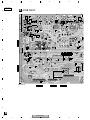
4. PCB CONNECTION DIAGRAM
A
NOTE FOR PCB DIAGRAMS :
1. Part numbers in PCB diagrams match those in the schematic
diagrams.
2. A comparison between the main parts of PCB and schematic
diagrams is shown below.
Symbol In PCB
Diagrams
Symbol In Schematic
Diagrams
B C E B C E
Part Name
3. The parts mounted on this PCB include all necessary parts for
several destinations.
For further information for respective destinations, be sure to
check with the schematic diagram.
4. View point of PCB diagrams.
Connector
Capacitor
Transistor
B C E
B
C
E B
C
SIDE A
E
Transistor
with resistor
B C E
D
G S D
B
G S
Field effect
transistor
D G S
P.C.Board
Chip Part
SIDE B
Resistor array
3-terminal
regulator
C
D
E
F
49
DVR-520H-S
5
6
7
8
5
1
C301
L303
R301
C302
D301
1
C313
Q302
C304
Q302
NP
G-Link
L306
CN301
C451
VR452
VR451
TUNB
SEPA
SEPA
ADJAST
ADJAST
SPECTRUM WIDE
C456
ICT FC
C465
C471
19
19
C462
VNP1963-A
R307
R306
R318
C326
C327
U301
C306
C319
R326
V+9
PC
C453
GND
VR453
C468
V+9
INPUT
LAVEL
ADJAST
1 1
C467
C461
Q451
R468
C473
CN451
CN451
KN300
C B2 E2
E B C2
13
13
R467
R466
C305
C329
C318
C316
R328
R453
R454
4
GND
Q306
VWV
CN301
NP
3
2
LF
R317
R316
JA301
C328 or R325
R
PYKC F4X
Q304
4
3
2
1
C309
D302
Q451
C474
R471
C472
B CN402
DVR-520H-S
50
C458
R463
C460
E
R315
Q304
R324
R312
B CN401
D
Q301
Q301
C
Q306
B
4
3
2
1
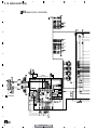
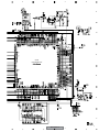
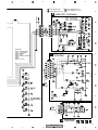
4.1 TUNB ASSY
A
SIDE A
SIDE A
A TUNB ASSY
V+5TU
C303
C459
R455
(VNP1963-A)
F
A
A
5
6
7
8
DVR-520H-S
51
A
A
F
(VNP1963-A)
UV_RIN(R4)
13
UV_LIN
(L4)
UV_RIN
(R4)
V+9
SD/STID
R472
R464
UV_LIN(L4)
R478
R473
MIONTA
R470
R476
1
C477
C475
R474
C476
R475
R480
R477
E
R456
C470
GND
C464
C463
R465
C454
R458
R451
R459
R461
D
R452
C455
C457
R479
UVA_IN
C469
C466
R460
IC451
28
30
30
28
R469
R457
CN451
SU/SAPID
FOMOI
MUTE
IC452
( 28p
)
15
16
15 16
15
14
14
15
1
1
1
1
IC452
IC451
C452
GND
C478
R481
JUST
VIDEO
AFT
MUTE
V+37E
AFT
UVIN
LF
V+6E
TUON
VWV2010
NC(SIFtoONTA)
19
R462
G-Link
UVIN
R305
CN301
AUDIO
R323
SCL
AGC
1
VWV2016
R304
SDA
C
SIF
GND
V+6E
IF
C315
R327 or L301
G-Link
BT(+33V)
C312
BP(+5V)
V+
V+6E
VWV2034
R322
C325
Q305
R314
Q305
5T
U
MB(+5V)
C311
Q307 C317
L302
B
L305
C321
SDA
SCL
C308
R310
C320
L304
ADRS
C307
R321
C324
Q307
R302 C310
R320
C323
C322
R303
AGC
Q303
C314
R313
Q303
R309
R308
R319
A TUNB ASSY
A
SIDE B
SIDE B
5
6
7
8
1
2
3
4
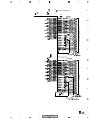
4.2 JCKB, ATWB and ATHB ASSYS
SIDE A
B JCKB ASSY
A
14
2
10
L171
R321
AFT
C174
C137
R172
R275
C219
R303
R304
R205
R302
R264
R277
8
1
1
7
7
E
R289
R288
V+5E
10
CN705
CN201
CN705
D
D CN1001
CN11
1
C123
LF
40 40
11
ATHB
CN12
1
1
40
40
VWV
VWV2011
(VNP1961-A)
R
(HDD)
KN801
CMKD-P3X
CN12
E
to HDD
G ATWB ASSY
CMKD-P3X
R
VWV
40 40
11
CONTACT BOTTOM SIDE
ATWB
1
1
CN13
CN14
40
C CN4401
CN13
F
40
VWV2036
VWV2009
(WRITER)
LF
(VNP1961-A)
CN14
B G H
to ASSY
52
DVR-520H-S
1
2
3
4
KEY2
DVD
FLDATA
C121
1
CN703
CN11
CONTACT BOTTOM SIDE
FLPON
GND
CN201
F CN1301
C CN4501
B
10
CONTACT 1 1
SIDE
IC103
IC401
IC206
KEY1
H ATHB ASSY
GND
Q404
C B2
8
HDD
1
14
14
GND
C239
C247
V+5M
4
11
IC204
L101
CONTACT
SIDE
C103
C107
13
GND
SDET2
GND
Y
GND
C
GND
V
GND
R
GND
L
GND
D103
Q406
Q771
Q405
Q407
13
IC206
R283
IR
5
C141
C211
C240
C106
W
6S SW
V+ 13
V+
Q101
R299
R268
R269
C236
VWV
C214
5
R290
8
R276
Q202
R262
C230 R300 R231
R256
D202
59
R209
C248
R265
C222
C233
R218
R273
R282
R233
1
IC204
C206
58 R217
R272
C
NP
R301
SDA
SCL
58
30
C231
L201
R200
R236
X202
C209
C228
L204
R259
L202
R257
R271
30
C220
R243
R240
1
5
R201
C202
C201
C203
R454
L203
R258
V+5M
Q201
C208
R213
R216
R214 R204
R215
59
Q514
Q202
R254
R261
R447
R448
R292
R212
R210
R293 C210
29
C204
C205
1
X204
9 9
IC201
Q104
C135
R111
11
CN202
IC202
TH
AN
CH
OF
DE
HE
25
8888
29
IC501
L102
CONTACT
SIDE
AGC
116
X201
5M
V+
IC201
Q702
Q201
Q712
Q703
Q104
C218
116
87
R234
IC202
R270
1
+
+
C229 R308
R255
87
R250
GND
R287
V+13
SW
FLCLK
Q171
B
W
R174 Q172
R173
C173
1
IC701
R179
R176 C176
Q173
X203
R175
C175 R185
R178 C177
R183 R320
R184
CN105
10
C716
MODIFED TEXT
1
R180
-
BT201
BT202
-
Q711
Q173
Q172
JA601
IC651
R651 1
R653
C652
5
Q708
4
3
9
VNP1961-A
JCKB
11
NP
IC651
8
18
NC
4
6
15
R230
R229
C251
R206
R202
R203
R294
R207
C252
R221
Q171
3
12
9
JA201
C651
2
7
13
JA651
5
1
8
FLSTB
5
1
7
5
6
7
8
SIDE A
A
14
4
C749
41
41
R721
C703
1919
C752
C736
20
C722
6 R565
R724
R564
R736
R737
L508
R563
R562
C503
C_TtoM
SCL
AFT
TUON
GND
V+6E
GND
V+37E
GND
SIF
GND
JUST
/LM
LDASH
GND
UVIN
GND
G-LINK
Y_TtoM
4
L506
1
3
C539
C543
1
1
C118
C117
1
R426
L403
L404
L402
R425
C429
R418
13
CN402
13
22
22
12
12
11
11
R423
R427
R438
11
C423
C430
Q404
C435
C437 R437
34
44
C416
C425
C414
RfromM
MUTE
MIONTA
FOMOI
SD/STID
SD/SAP
GND
L
GND
R
GND
V+9
GND
NC
D
LfromM
Y
X401
C
NC
Y
C
Y2
Cb
Cr
RfromM
LfromM
NC
CSYNC
NC
YtoM
CtoM
LtoM
RtoM
AGCCTL
Y2
CN702
C407
C428
Q407
C439
C410
V+9
R784
V+13SW
V+5VI
XRST
525P
MRST
PCMOUT
HSMtoT
SSMtoT
R701
SSTtoM
HSTtoM
ASCK
SPDIF
Cb
FC
11
IC401
C432
R785
ICT
Cr
23 R429
33
C441
R440
C440
R439
R414
C418
C426
V+5VO
LF
V+13SW
V+5VI
R421
V+13SW
WORD SURFACE IS
UPPER SIDE
C
Q405
R415
44
C123
C415
C424
C133
CN104
C121
1
R431
C417
C401
C402
C404
13
13
IC103
R434 C438
C549
PC
YtoM
CtoM
LtoM
RtoM
R770
R772
R782
R103
R420
R419
R413
R436
R435
R424
Q406
C434
C427
R428
R430
C436
V+
5V
O
V+
5V
I
SW+13V
GND
SW+6V
GND
FLDC+
GND
EV+37V
GND
EV+6V
FLDCFL-28V
P_ON
FLON
C128
CN403
R783
Q771
R773
FLDC+
FL-28V
1
CN701
CONTACT
SIDE
GND
GND
GNDA
32
V+5VO
LMUTE RMUTE P_CONT
GND
GND
GND
BUP
GND
GND
24
GND
GND
CONTACT
SIDE
GND
KEY2
KEY1
DVD
60
60
C731
C732
R555 R554 R553
C608
C609
C614
C616
C126
V+9
GND
FLDC-
HDD
IR
NC
FLSTB
FLDATA
C125
R277
R290
R276
FLPON
Q101
V+6E
R102
34
GND
R774
1 2
19 19
SDA
C115
24
1 1
1
AGC
C507
CN402
10
1
R780
C604
R613
C619
R804
C612
R302
R301
R264
GND
R287
V+13
SW
FLCLK
7
7
B
A CN451
R288
V+5E
C2
C501
R771
1
IC206
B
C717
C715
Q712
C718
R711
Q703
4
3
8
VWV2029
VWV2032
VWV2035
CN401
R714
Q702
C502
IC501
6
1
01
VWV2015
VWV2019
VWV2022
VWV2023
VWV2027
VWV2028
C B2 E2
R556
Q514
C542
Y
L701
Y
R548
R781
C712
C713
40
40
C714
C748
C727
C751
VWV
E
GND
20
C735
CVBS
C603
8
Cr
R502
R509
L503
21
21
R612
C620
C707
C708
C710
C711
D712
C733
C734
C602
C704
C705
R755
C744
Q711
NP
R753
NP
C615
C611
C618
C607
D710
R726
R614
C621
IC701
32
C716
R749
R748
C740
C719
R805
80
C728
C709
61
A CN301
C739
80
C729
C730
D714
Q201
L505
R725
CN401
R304
CMKD-P3X
C610
C601
D704
C750
C726
C723
1
V+5M
D705
D706
C724
C725
C738
Cb
L504
R
THIS PRODUCT CONTAINS LEAD IN SOLDER
AND CERTAIN ELECTRICAL PARTS CONTAIN
CHEMICALS WHITCH ARE KNOWN TO THE STATE
OF CALIFORNIA TO CAUSE CANCER,BIRTH
DEFECTS OR OTHER REPRODUCTIVE HARM.
HEALTH & SAFETY CODE SECTION
25249.6 - PROPOSITION 65
R808
V+5VO
1
R745
CN704
33
Q708
C706
1
JA701
WARNING
14
14
2
3
10
JA702
R230
R229
C251
R206
R202
R203
R294
R207
C252
R221
Q171
2
61
R180
1
18
R812
15
L405
12
23
4
3
R712
8
9
1
1
9
8
13
C141
6
5
2
1
5
1
7
KN802
(VNP1961-A)
CN104
CN702
CN701
E
H CN201
C CN3001
CN2001
F
B
53
DVR-520H-S
5
6
7
8
1
2
SIDE B
3
4
B JCKB ASSY
R744
Q507
R718
R717
R306
R620
R307
1
R757
Q103
V+6E
5
IC101
R208
C124
C403
C132
V+5VI
C212
V+13SW
GND
FLDC-
19
R801
R407
R411
C
R
C433
C
C120
GND
B2
E2
C431
C122
V+13SW
C2
XRESET
CN401
C760
GNDA
GND
(VNP1961-A)
R817
32
V+5VO
GND
24
CN701
CN702
CN104
E
F
B
54
DVR-520H-S
2
3
4
V+9
D105
B
0
1
2
3
4
5
6
7
8
9
1
B E
0
1
2
3
4
5
6
7
8
9
R702
NC
Y
C
Y2
Cb
Cr
RfromM
LfromM
NC
CSYNC
NC
YtoM
CtoM
LtoM
RtoM
AGCCTL
1
V+13SW
E
VWV2 0
1
2
3
4
5
6
7
8
9
1
NC
GND
V+13SW
BUP
V+5VI
GND
XRST
LMUTE
525P
RMUTE
MRST
GND
PCMOUT
GND
HSMtoT
P_CONT
SSMtoT
GND
SSTtoM
GND
HSTtoM
GND
ASCK
GND
SPDIF
V+9
DVD
FLDC+
FL-28V
R810
L
4
FL-28V
C131
R433
V+9
C101
C127
V+6SW
C134
C130
Q401
R759
R105
P_ON
FLON
C405
FLDCFL-28V
FLDC+
GND
EV+37V
GND
EV+6V
GND
SW+13V
GND
SW+6V
R403
C1
C747
C108
V+6E
A
B
C
0 1 2 3 4 5 6 7 8 9
1
0
L401
13
CN402
R604
VWV
R609
V+37E
SD/SAP
GND
R740
R728
R747
R735
R442
R410
LF
1
R611
R601
C613
R777
R779
C116
R104
15
15
0
R807
FOMOI
GND
Q706
C605
D716
R549
R546
Q512
R540
R412
R811
R409 R417
C413
C421
D
Q102
1
1
0 1 2 3
R544
Q513
R545
C409
R445
Q403
R446
C411
C408
R541
R542
C534
C535
C533 R543
L507
C536
C537
R547
C532
D401
G-LINK
GND
C412
C420 C419 C422
R406
SD/STID
GND
16
C119
R561
Q516
R552
R443
R404
R405
C406
1
MUTE
R441
16
R608
R603
R538
R560
VWV2035
IC601
30
30
R719
C
R727
D717
C538
Y
C544
Q515
C545
C541 R551
C546
L509
C547
Q402
MIONTA
V+5VO
R558
R557
C540
R452
R716
R501
C129
R408
R416
C548
R550
R559
R444
1
G-LINK
C
R402
R401
TUON
GND
V+6E
GND
V+37E
GND
SIF
GND
JUST
/LM
LDASH
GND
UVIN
GND
R621
R723
SDA
AFT
R809
C721
C720
R722
Q701
19
SCL
C742
D709
R729
C737
VWV2027
VWV2028
VWV2029
VWV2032
D713
R720
C702
R520
R704
R706
R523 R705
R707
R730
D708
R806
C514
C745
R778
C66
R742
Q707
R760
C743
R738
C519
R521
D711
Q705
R733
C746
R739
R761
R741
R750
Q709
D707
Q704
R731
C762
Q510
C518
C517
C516
R519
R518
AGC
R536
R708
C753
R709
C754
R710
C755
Q505
Q506
R517
C515
R522
Y
R732
C531
Cr
B
C530
C529
C528
R534
R533
R531
R532
C526 R535
C768
R754
R752
VWV2015
VWV2019
VWV2022
VWV2023
D702
D703
R746 C766
Q710
R528
R751
C756
C525
R527
C527
R530
Q509
R776
R775
C741
R743
C774
D701
R525
C520
C772
C770
C771
C765
R734
C764
C769
R524
C773
R756
C757
R715
Q508
C524
C523
C758
C763
5
C522
R526
R529
R818
C761
C767
R713
C521
Cb
4
A
5
6
7
8
SIDE B
A
R655
R605
R606
R617
73
Q507
C216
C772
C217
R652
Q203
R226
B
R112
R263
R267
R278
IC601
1 R107
C138
C226
Q701
D102
R295
4
8
5
Q408
Q409
D101
Q105
5
R453
R108
Q410
1
R106
4
C242
C246
R450
R280
C243 IC203
R253
1
XRESET_IN
C253
R449
R279
9
SYNCAFT
R296
C225
Q105
IC203
C139
R113
8
L103
R109
C140
R110
Q410
Q515 Q102 Q411
Q516 Q408
C245
FANPWM
Q409
C
C104
3
3
1
4
6
13
1
1
D718
D719
1
GND
GND
GND
GND
GND
GND
GND
C227
D104
Q402 Q512
4
6
IC102
IC102
Q513 Q103
C105
Y
7
L
IC101 Q403
C
V
4
5
5
7
IC101
R208
R
C101
V+6SW
R101
C108
V+6E
4
D720
R759
R757
D601
C249
R227
R451
C102
1
R222
Q411
C234
R758
IC205 Q710 Q707
Q509 Q510
Q206 Q203
Q709 Q706
Q704
Q204
Q506 Q705 Q205
Q505
1
D203
R281
R297
R246
R237
R307
D607
Q508
C136
Q205
R247
L205
R219
Q204
C221
R245 R242
C224
V+5M
D201
D604
C250
R286
R235
R241
R223
L206
L208
R225
C207
DLCE
Q206
C653
C254
R251
R803
R305
L207
R224
C223
R306
V+6E
D605
JUST R252
R211
R260
R244
VWV
R608
R603
R239
C232
P_CONT
4
4
R248
R249
R291
R802
11
R266
R228
R441
AGC
R232
R298
55
R285
C172
88
R274
717
C241
R182
V+5M
C171
C617
IC205
R238
VWV2035
R602
C606
R177
R442
R615
D602
C244
L284
R284
R171
R727
D603
R729
C737
27
28
29
32
D606
C654
R607 R186
C655
C658 R181
R618
C659
R742
C656
R610
C657
C660
R619
R740
R728
C741
C769
C661
R616
R654 R220
C215
C770
SDET2
V+13SW
C120
GND
V+5E
GND
GND
FLPON
V+13SW
FLDATA
FLCLK
FLSTB
NC
KEY1
IR
KEY2
HDD
DVD
GND
FLDC+
FLDCFL-28V
R
C212
V+13SW
CN201
C213
1
CN705
Q401
H ATHB ASSY
1
C122
D
C701
V+9
R
D
CMKD-P3X
R703
(HDD)
LF
1
40
(VNP1961-A)
CN12
E
G ATWB ASSY
CMKD-P3X
R
(WRITER)
LF
1
40
F
CN14
(VNP1961-A)
B G H
55
DVR-520H-S
5
6
7
8
1
2
3
4
4.3 MAIN ASSY
C5124
L5502
C5127
C5103
C5214
C5122
R5121
C5120
2
8
C1050
2
8
1
7
2
1
R1003
8
L1001
C1042
L1005
C1059
L1006
R1008
C1038
R1004
L1003
C1036
R1005 C1035
R1074
C1053
C1058
C1030
L1004
C1056
C1029
2 C4211
3
X4201
IC3101
16
1
4
L4202
C3255
D3103
R4204
9
R4201
C4202
8
IC4205
5
C4210
D4202
4
C4208
D4201
C4203
R4210
C4201
1
F4201
R4205
L4201
C4209
R3108
R3107
R3106
R3105
R3104
C1024
C1026
TP1029
TP1028
TP1027
7 1
7 R5274 1 R5273
R5132
R5131
TP5106
C1060
L1007
R1009
C1041
C1037
C1055
C3107
4
R2015
R2026
R2014
TP2017
TP2025
TP2013
TP2023
R2013
R2012
TP2012
TP2016
R2011
R3271
TP2011
R3270
TP2008
TP2009
DVR-520H-S
TP2014 TP2024
Q2241
TP2022
TP2006
TP2005
R2047
C2243
TP2003
TP2018
R2025
R2040
C3251
TP2007
TP2020
R
R
R
R
R
R2254
R2253
R2255
C2405
8
IC2302
5
1
4
R2404
R2405
R2411
R2406
3
R5123
C5119
C5118
C1003
C1004
C1034
R1006
Q2102
R2107
Q2103
TP1032
R4202
C4206
C2210
R4209
C4207
C
2
C5123
R5124
R5112
R5113
C1509
C1028 C1002
C1510
C1001
C1016
R1011 TP1051
C1027 C1508
C1014
VR1001
R1090
TP1060
VR1002
Q2104
R2109
C2105
C2103 R2103
Q2101
C2104
8
IC2211
5
4
R4207 R4208
TP1012
VC4201
F
56
TP1013
TP4202
7
C2406
TP2506
TP2505
TP2504
TP2503
TP2502
IC4206
TP2021
C2308
Q2403
R2407
7 C2311
1
R2409
1
3
C2302
C2305
C2407
8
R4211
R4206 R4212
R2308
R2408
TP2501
TP48
8
R2502
TP49
TP50
2
8 R2306
5
C1049
R2227
R5222
7 1
71
R1031
C2241
1
IC2302
IC4003 IC4005
IC3001
Q2403 Q2402
Q2001
C1047
C1006
C1039
TP1030
R1045
TP2004 R2027
R1905
IC2301
1
R1066 C1051
C1048
5
1
1
Q2402
4
C1025
L1009
R2112
R2113
R2102
C2220
C2223
R2334
R2332 R2208
C2332
1
R2214
R1043
R1048
R4213
4
C2334
7
CN1901
IC2301
Q2241
Q3201 Q3202
R2305
3
R2331
IC2331
4
6
C2333
R2333
R1904
R1903
R1902
R1901
C2206
8 2
82
2
R1080
Q2204
C1045
C1052
R5223
TP1024
R2209
C1057
TP1033
C2221
R2204
C2201
Q2203
TP1026
TP1031
C2205
TP4302
IC2211
C2102
R2205
TP4301 TP4303
IC4206
IC4205
IC3101
IC4004
IC2331
R2239
R5285
C1044
C1005
C2101
R2221
R4304
IC4008
Q2203
IC3403
IC3402
C1021
TP2001 R2412
TP2019
TP2002
R2203
2
2 8
R4303
C1012
Q2222
C2208
2 8
R4302
C1019
C1022
C2331
8
C1018
R2111
R5289
R5290
R1034
C1013
TP15
D
R1012
C1011
C2202
1
R2207
1 7
R2206
1 7
Q2202
7
R5127
C5113
C1023
C2222
R2210
Q2201
Q2202
R2304
R2307
R5130
64
C1017
C2209
C2204
Q2201
Q2222
R2301
Q2301
R2202 R2201
CN4301
C2106
Q2311
R2312
C2301
7
C2306
1
TP1002
R2106
R2105
R2233
R2235
8
Q2302
Q2312
R2313
IC5204
IC3301
R2252
R2302
TP4307
R4307
R4306
7 1
1
C2246
48
C1031
R1021 R1022
TP1050
R1024
TP1041
R2116 R2114
R2314
TP14
Q2301
Q2103
R2266
R2311
R2303
2
8
2
R4305
R2115
C2265
TP4306
TP4305
TP4304
Q2101
Q2102
Q2302
Q2312
C5126
IC5101
49
C1032
R1023
Q2105
C2319
C2317
TP1067
L1008
R4108
TP28
L1102
Q2105
Q2104
Q2311
R4110
IC4101
VR2105
C4103
R4101
R4106
C5111
R5104
R1071
R4104
R4107
C1104
R5105
C1054
VR2104
R4103
3
C4104
2
8
C4102
R4102
IC4101
C4105
5
4
X4102
1
R5106
R5128
R5129
16
TP2015
D1111
R4105 R1111 C1114
IC5202
R4109 C4107
R1052
C5105
17
33
C5125
C4106
1
Q1102
4
Q1102
R5107
C5104
R5126
32
R5103
C5110
C1061
X5101
R5125
7
C5138
B
1
C5121
R5115
R5117
R5110
C5137
IC5101
R5109
R5108
C5136
L5106
C5112
IC4007
L5105
L5102
L5501
C4034
L5104
L5101
E
C4033
C5132
L5103
C5101
C4032
7
C5102
CN5102
1
IC4007
C
F5101
TP4015
R5265
CN1401
CN5102
J
D4002
R5114
R5116
R5120
R5122
C MAIN ASSY
SIDE A
A
5
6
7
8
SIDE A
This PCB is six layer structure.
A
R5247
TP32
R5231
R5233
TP5201 R5216
2
2
8
R4507
1
2
CN4501
8
7 1
C5321
1
2
8
8 R4538 2
R4541
1
7
TP4001
TP4010
R4017
CN4001
CN4001
1
C4029
8
R4020
R4018
TP4009
I CN202
R4014
F4003
C4023
R4009
C4024
R2017
E
TP4005
R2019
TP4002
Q2001
C4021
TP41
TP40
TP3012
TP42
TP3002
R4008
D
TP3003 TP3001 TP3014
TP3004
CN4401
2
8
2
8
1
C5206
TP5204
R3407
C3406
C4005
TP4012
TP3005
TP3006
R4004
CN4501
R5241
C5208
R5244
R5239
R4534
C4027
C4004
IC4005
C4010
F4001
C4018
C4006
R3202
TP4011
Q3202
R4015
TP4201
R3203 R3204
TP3007
1
TP3008
TP3010
TP3009
R4537
CN11
D4501
R4010
3
1
IC4003
TP3403
TP3402
4
R3205
10
C3004
IC3001
TP3013
TP3401
C3407
F3403
R3410
F3402
F3102
R3103
D3104
C4028
R3411
R3408
C3105
1
D3102
11
8
IC4004
Q3201
20
C3001
TP3011
IC4008
D4001
1
C4014
C3102
D3002
R4530
C3402
C4013
C3002
R3002
TP2017
TP2025
R2014
R2015
R2026
TP2015
TP2013
4
5
D3001
R4019
IC3402
TP4008
R3001
R3025
R3024
R3023
R3022
R3003
C3251
TP2014 TP2024
D3101
D3103
R3104
C3255
1
C3106
9
16
IC3403
R4531
H
C5221
R5297
5
R3409
C3101
8
IC3101
9
16
1
02
F3401
C3301
R3102
R5298
C3405
R3405
C3403
R3406
C3408
C3404
L3301
C3108
R2013
R5243
C5224
C3303
R4001
R3309
8
R3108
R3107
R3106
R3105
L5508
C5229
R3403
C5231
1
24
C1040
C1058
2 C4211
R4510
C3302
R3313
R3305
C3107
TP2023
R5245
R5242
IC3301
R1008
TP1013
TP1012
R4509
R3310
R3307
R3311
R3312
R3306
R4501 R4503
7
L1006
IC5204
1039
TP2016
R5246
R1031
1049
07
R4504
C5223
C4020
C4031
C1059
1047
C5230
R5294
12
R1066 C1051
C1006
R5293
C5222
C
C4401
R3304
13
C1005
7
R4435
7
052
1048
1
CN13
R4432
1 7
TP3303
R3303
7
G
R4428
R4429
R5313
R5314
C5205
R5255
1
1044
1045
2 8
1 7
7
R5250
C5329
7 1
2 8
8
2
R5240
R5261
R5296
1
8
R5258
C5211
8 2
R5259
R5248
2
C1057
7
52
C5218
104
C5213
2
8
53
C5225
2
8
1
7
1
7
R1003
R5283
R5295
C1060
L1007
L1001
C1042
R5230
CN4401
1
R5227
R5228
2
R5225
B
8
C5228
105
R5284
R5285
7
R5224
2
C5227
R5229
R5281
R5282
R5290
1
R5237
R5238
R5278
R5279
R5280
7 R4406 1 7 R4405 1
8
2
8
2
C5226
R5288
R5289
7
2
8
R5275
2
2 8
1
8
7
IC5202
C5217
R5276
R5286
R5277
R5287
C1050
C5123
R5124
R5127
R5132
R5131
TP5106
R5130
7 1
7 R5274 1 R5273
1
R5234
R5235
R5236
8 2
8 2
7 1
1
7 R5220 1 7 R5218 1
C5215
R5272
4
R5217
8
C5126
C5125
R5215
TP5202
L5507
16
R5232
R5214
R4407
R5128
R5129
R4408
C5216
7
R4436
1
C5103
C5127
7
C5104
126
TP38
TP31
C5207
R4508
2
8
2 8
2
8
R5219
2
8
2 8
2
8
208
L5504
R5221
1
8
1 7
7 1
7
156 157
1
C5209
1 7
C5212
C5204
C5214
R5263
R5262
R5260
R5257
R5256
R5253
R5254
R5249
7
C5210
R5251
R5252
L5502
C5124
22
F
(VNP1960-C)
C
57
DVR-520H-S
5
6
7
8
1
2
3
4
C MAIN ASSY
SIDE B
A
TP1
2
8
R1305
1
C5203
IC1103
IC1104
7
2
8
1
7
C1309
R1306
C1310
C1302
TP2
L5503
TP8
C1313
TP3
43
L1301
IC1301
L1402
7
7
5
C1311
C1312
1
1
28
R1032
54
TP1016
7
1
7
1
2
7
17
1 R1410 16
C3205
C3006
B CN702
DVR-520H-S
3
R3014
C
R3019
CN3001
4
C32
R32
R3252
R3013
CN3001
TP10
R3258
R3261
R3260
R3257
1
TP11
F
IC3251
C3252
R3012
R3010
R1053
R3269
R3011
R3009
R1055
R3262
R3263
R3268
TP4007
8
7
R3017 R3015
24
R3016
C4003
IC3002
TP4006
C3003
C4017
C4016
F4002
R4016
C4030
C3
C3257
R3267
14
1
C4009
R3201
C3208
C3254 R3251
TP3251
C3253
C3258
R4011
R4013
C3207
R3254 R3255
R3266
C4008
R4005
R4012
C4011
R4006
R3265
C3201
TP10
TP1
TP1014
9
8
C3202
C4026
R3253
GND
IC4002
1 7
7
IC3201
C4002
TP3253
7 1
8 2 1
C3203
C1401
C4012
C5008
F3201
C3204
2
28
2 8 2 8
R1408 R1409 R1411
C1409
27
8
5
L1401
C4037
R5264
R1402
C1402
C4007
8
R1407
IC1401
1 C1408
C1407
IC5002
4
TP5004
8
7
R4525
1
C5007
2
C1405
R1406
7
R5322
5
1
2
C5005
8
7
R4519
2
1
C5006
R1033
TP101
8
R1405
1
R1404
7
2
IC5322
8
8
R5209
8
C5323
L5321
4
7
R4518
1
TP5003
R5329
1
C1406
1
8 2
R5328
7
R4528 R4527 R4533 R4532 R4535 R4536
C5328
R5330
2
R5324
C5324
C5327
8
7 1
3
C1404
R5326
R5325
C5326
C5325
R5327
1
D5322
8
R5323
7 1
R4505
C5322
D5321
TP12
2
7
C1429
C5306
1
R4502 8 2 R4506 2 R4512
2
4
4
IC5321
TP4013
1
1
TP1017
TP4014
58
8
R1065
27
C1403
5
R5321
TP4004
TP13
7
2
R5342
R5343
8
7
R4423
8 2
7 1
C5307
IC3251
IC3002
1
R1309
R1412
R4529
C4015
8
L5301
2
1
C5343
R5301
C4022
IC2501
2
8
Q4000
E
8
1
2
R1426
R5341
C5309
C1427
R1310
2
C1428
IC1421
2
1
C5310
7
2 8
1
IC5341
R1425
7
8
C5342
9
8
1
R1423
2
1
16
44
C1426
C1425
R5310
C5301
7
8
IC5301
2 8
R5307
C5308
Q4000
IC4002
IC1201
C1301
R1424
C5311
3
4
R5304
R4404
8
54
1
C1424
R5312
R4427
C4001
TP4003
R4401
2 8 2
7
C4501
C1423
C5341
R5309 L5505
R5308
R4417
TP4502
TP4501
TP4506
TP4504
TP4503
TP4505
TP4508
TP4507
TP4509
TP4510
TP4511
TP4513
TP4512
TP4515
TP4517
TP4516
TP4518
TP4514
TP4519
TP4520
TP4521
TP4522
TP4523
TP4524
TP4526
TP4525
TP4527
TP4528
TP4529
TP4530
IC3201
1
IC4006
IC5002
IC1101
D
R5305
R4416
5
IC5322
IC1401
R5311
R5306
C4019
3
IC5321
IC1001
7
R4440
C4025
IC4006
C1421
C1422
R4410
TP4418
TP4414
TP4419
TP4420
TP4421
TP4422
TP4423
TP4424
TP4426
TP4425
TP4427
TP4429
TP4428
D4401
TP4430
1
C
R4403 R4426
IC1421
IC1102
R4425 R4431 R4430 R4433 R4434
IC5341
7 1
IC5301
1
B
R4402
TP4402 TP4401
TP4406
TP4404
TP4403
TP4405
TP4408
TP4407
TP4409
TP4410
TP4411
TP4413
TP4415TP4412
TP4417
TP4416
TP2010
C3005
L2
32
5
6
7
8
SIDE B
This PCB is six layer structure.
A
TP5103
R5144
B
R1120
R1107 R1106
R1110
R1118
R1108
R1113
R1112
R1109
C1062
C1511
R1025
7 1 2 8 TP1058 TP1040
TP1052
TP1056
TP1059
TP1054
TP1055
TP1057
TP1053
TP1037
R1072 R1026
7
2
7
8
IC1102
1
R1076
2
1
8
7
R1077
1
C
1
1
8
2
1
R5264
R1093
R1092 R1119 R1054
7
7
TP1001
R1056
R1058
TP1004
R1059
28
TP1005
TP1008R1060
R1063
TP1007
TP1006 R1062
TP1042
R1061
TP1009
R1064
IC1001
C1113
C1105
7
7
TP101
2R10688 2 R10698
1 7
R1033
27
IC1101
7
C1109
2
8
2
R1114
8
7
8 R1051
1
C2506
C2502
12
44
E
TP1902
TP1904
11
TP1905
C2504
TP1906 TP1907
C2507
1
TP17
TP18
R2505
CN2501
ZF5
D2501
7
TP1901
C1901
1
R2506
CN2001
1
2
TP1903
IC2501
TP2507
1
R2503
8
TP2508
32
1
2
8
2
7
8
R1115
7
2
7
R2501
C2501
8
1
22
L2501
R1205
7
C1201
1
C1208
7
C1206
C1204
L2101
C1203
R3014
TP2010
C3005
R1203
C1101
23
33
27
C1209
R3260
R3257
1
C3256
TP3252
R3256
L1101
C2505
8
C2503
R3258
R3261
R1207
IC3251
R3264
R3259
C1103
1 R10447 R1042 7 34
1
C2508
IC1201
R3268
1
L1201
C3206
51
TP3251
C3253
2
1
C3208
TP1035 TP1036
7
9
C3207
8 2
2
D
1 C1102
54
TP1023 TP1039 TP1018
2
28
TP1019 TP1022
R1046
R1206
TP1038 TP1061
TP1062
R1070
R1081 8
TP1065
TP1066
R1208
2
R1202
C1202
C1205
R1075
C3205
R1053
8
C1207
R1055
R3262
R3263
2
R1204
7
R1116
1 R1410 16
7 1
2
8
1 R1049 7
54
1
1
8
7
2
1
1 7
R1117
17
C1106
C1107
7
C1111
R1105
R1121
C1110
1
TP23
TP22
R1002
TP100
TP5205
L1002
TP5206
TP5207
TP5208
TP5209
C1010
TP5210
R1057
TP5211
TP1003
R1035
TP1020
TP1017
1
TP21
2
C1008
5
5
TP24
2 1
TP1046
TP1048
R1078
TP1047
1
R1079
C1007
R1050
TP1015 2 8 TP1011 7
TP1010
7
TP1014 1
8
TP27
8
7 TP1049
TP1043
1
TP1034
C1009
07
R1017
R1015
R1073
2 8
TP1044 8
12
6
R5143
1
7 1 7
TP1045
R1016
C1512
C1501
C1502
C1503
8
TP1063
7
C1504
1
C1505
NIN15
R1307
2
TP1064
7
8
C1506
1
R1308
2
C1306
8
C1308
2
R1302
R1312
R1311
C1311
7
R1309
7
1
C1312
1
8
C1507
7
R1310
1
R5141
R1091
32
17
2
3
TP26
4 5
86
44
R1104
R1103
C1108
IC1104
R5142
IC1103
IC1301
C5108
TP25
43
1
C5116
1
C5109
16
TP5104
7
C5107 TP5105
8
1
C5117
7
2
C5115
TP5102
C5106
TP5101
C5114
C5131
1
R1303
C5135
7
8
C5134
C5133
1
7
R1304
2
C1303
8
C1304
2
C1305
1
R1305
C1307
8
C1309
2
C1310
C1302
R1306
TP16
TP19
CN2001
F
(VNP1960-C)
C
B CN701
59
DVR-520H-S
5
6
7
8
1
2
3
4
4.4 FLKY, KIRB, FRJB and DVJB ASSYS
SIDE A
A
KIRB ASSY
1
7
1
7 CONTACT SIDE
CN1201
R
ACP-BS
LED
(HDD)
S1202
D1201
C1203
LED
(DVD)
S1203
GND
GND
W1201
S1201
IR
W1207
IR
LED_HDD
W1200
V+5FL
W1205
V+13SW
GND
W1204
W1202
CN1201
IC1201
KIRB ASSY
VWG
W1203
W1206
VWG2490
VWG2493
L1201
B
1
E
D1203
IC1201
POWER
DVD(H)
DISC NAVI(S)
HDD(H)
DISC HISTRY(S)
(VNP1962-C)
C
D FLKY ASSY
GND
W1026
VDD
GND
W1025
W1017
GND
W1015
W1016
FLDC+
FLSTB
W1014
FL-28V
W1013
FLDC-
LED_HDD
STOP
VWG2489
VWG2508
PLAY
V+5FL
PC
S1005
W1004
S1002
S1009
S1004
C1012
C1010
V+5FL
ACP-BS
S1001
OPEN/CLOSE
REC
REC STOP
VWG
(VNP1962-C)
CN1001
B CN201
F
D E
60
DVR-520H-S
1
2
33
33
27 27
9 9
W1003
KEY2
W1010
LED_DVD
W1011
W1002
KEY1
W1009
1
1
W1001 GND
W1000
W1007
IR
L1001
V+13SW
1
CONTACT SIDE
7
1
W1012
VDD
W1008
C1005
19
7
CN1002
CN1002
19
1
E
1
D
V1001
CONTACT UPPER SIDE
CN1001
3
4
S1006
ONE TO
DUBBI
MODE
REC MODE
5
6
7
8
SIDE A
A
F
FRJB ASSY
B CN705
CN1301
B
FRJB ASSY
W1302
W1301
C
1
13
1
13
L
W1303
JA1301
ACP-BS
R
JA1302
6
4
2
7
CN1301
7
3
5
2
3
1
5
6
Video
W1300
S_DET
4
1
Lch
Rch
S-Video
VWV2004
VWV
KN1301
(VNP1962-C)
C
GND
W1023
W1024 VDD
GND
W1022
CN1401
GND
W1006
GND
W1005
S1008
CN1401
R
REC MODE (S)
DVJB ASSY
1
(-)
CONTACT SIDE
1
7
(+)
ACP-BS
JA1401
VWV2006
VWV
GND
W1020 FLDC+
VDD
ONE TOUCH
DUBBING
MODE (H)
C CN5102
FC J
2
W1018
S1007
S1006
49 49
DVJB ASSY
3
C
J
7
41 41
33
3
D
4
FLPON
VDD
1
W1027
W1021
W1019
FLKY ASSY
E
(VNP1962-C)
F
D F J
61
DVR-520H-S
5
6
7
8
1
2
3
4
SIDE B
A
F
FRJB ASSY
R1302
L
C1309
R1311
R1308
C1306
C1303
D1304
D1303
R1502
R1501
R1304
B
R1504
C
R1301
R1303
C1302
C1301
D1301
D1302
R
R1503
13
SIDE
S-Video
LF
L R
V C
C1304
Lch
R1306
R1305
R1310
R1309
C1308
R1307
Rch
1CONTACT
C1305
R1312
Video
Y
S_DET
(VNP1962-C)
CN1301
C
R1401
(+)
VDD
ACP-BS
TPA
TPB
XTPA
(VNP1962-C)
F
D F J
62
DVR-520H-S
2
3
4
R1010
R1016
R1012
(-)
R
E
1
FLDC+
C
XTPB
LF
GND
41
GND
49
GND
Q1009
C1500
C1001
C1502
CN1401
GND
TPA
R1402
XTPA
1
Q1007
R1500
R1029
Q1007
Q1001
Q1009
GND
XTPB
7 TPB
LF
C1018
C1017
DVJB ASSY
FLPON
Q1002
Q1008
Q1008
Q1001
IC1001
C1014
J
VDD
D
VDD
R1009
R1008
R1033
R1032
R1030
R1031
B
Q1002
GND
GND
D FLKY ASSY
REC MODE (S)
5
REC
D
REC STOP
6
PLAY
7
R1034
STOP
OPEN/CLOSE
1
R
7
19
C1013
KEY1_2
1
C
V+13SW
LED_DVD
CN1201
IR
V+13SW
LED_DVD
R1213
1
VWG****
GND
LED_HDD
7
CN1002
KEY1_2
POWER
V+5FL
ACP-BS
VDD
V+13SW
7
1
R1005
B
GND
V+5FL
LED_HDD
IR
FLDATA
FLPON
C1021
GND
GND
R1208
IR
FLCLK
GND
V+5FL
V+5E
FLSTB
LED_DVD
C1007
C1002 V+13SW
KEY1
KEY2
VWG2490
VWG2493
R1035
9
KEY1
R1209
C1205
R1210
LED_HDD
27
IR
FLKY ASSY
KEY2
HDD(H)
DISC HISTRY(S)
R1201
GND
D1202
Q1201
C1202
R1211
(HDD)
LED
IR
FLDC+
C1201
GND
GND
R1207
R1206
C1206
FLDCGND
LED_HDD
DVD(H)
DISC NAVI(S)
FL-28V
FLSTB
R1214
R1203
R1202
D1204
Q1202
R1204
R1205
6
GND
VWG2489
VWG2508
VWG****
LED_DVD
GND
R1013
R1014
VDD
GND
C1011
A
FL-28V
34
GND
Q1202
R1212
(DVD)
LED
FLDC+
34
KIRB ASSY
R1001
C1003
R1006
33
IR
C1204
C1020
C1004
R1002
33
44
44
C1019
R1011
R1015
C1207
V+5FL
23
C1006
E
R1017
33
C1009 23
VDD
C1018
C1017
Q1201
R1007
V+5FL
22
ONE TOUCH
DUBBING
MODE (H)
22
01
R1010
10
R1016
R1012
GND
FLDC+
Q1008
1
12 IC
(-)
12
41
1
N
11 11
R1500
R1029
Q1007
5
8
SIDE B
A
KIRB ASSY
B
LF
(VNP1962-C)
C
CN1001
A
D
E
E
(VNP1962-C)
F
D E
DVR-520H-S
8
63
1
2
3
4
4.5 POWER SUPPLY UNIT
I
SIDE A
A
SIDE A
POWER SUPPLY UNIT
B
C
CN202
C CN4001
CN204
to HDD
CN203
D
to
R7 DRIVE ASSY
B CN104
CN201
E
F
I
I
64
DVR-520H-S
1
2
3
4
5
6
7
8
5. PCB PARTS LIST
NOTES:
Parts marked by "NSP" are generally unavailable because they are not in our Master Spare Parts List.
The mark found on some component parts indicates the importance of the safety factor of the part.
Therefore, when replacing, be sure to use parts of identical designation.
When ordering resistors, first convert resistance values into code form as shown in the following examples.
Ex.1 When there are 2 effective digits (any digit apart from 0), such as 560 ohm and 47k ohm (tolerance is shown by J=5%,
and K=10%).
560 Ω
56 x 10 1
RD1/4PU 5 6 1 J
561
47k Ω
RD1/4PU 4 7 3 J
47 x 10 3
473
0.5 Ω
RN2H R 5 0 K
R50
1Ω
RS1P 1 R 0 K
1R0
Ex.2 When there are 3 effective digits (such as in high precision metal film resistors).
5.62k Ω
562 x 10 1
5621
RN1/4PC 5 6 2 1 F
Mark No.
Description
Part No.
NSP 1..FLKB ASSY
2..FLKY ASSY
2..KIRB ASSY
2..FRJB ASSY
2..DVJB ASSY
VWM2258
VWG2489
VWG2493
VWV2004
VWV2006
NSP 1..JACB ASSY
2..ATWB ASSY
2..ATHB ASSY
2..JCKB ASSY
VWM2265
VWV2009
VWV2011
VWV2023
Mark No.
Description
C455, C463, C464, C466, C468
C477 (4.4uF)
C471 (10/50V)
C465 (3.3/50V)
A
Part No.
B
VCG1039
VCG1039
VCH1224
VCH1225
RESISTORS
>
1..TUNB ASSY
1..MAIN ASSY
1..POWER SUPPLY UNIT
Mark No.
Description
VWV2010
VWV2025
VWR1380
RS1/10S0R0J
RS1/16S6802F
VCP1123
VCP1154
RS1/16S###J
OTHERS
C
CN451 13P SOCKET
CN301 19P SOCKET
U301 TV TUNER PACK
AKP7070
AKP7073
VXF1022
Part No.
A TUNB ASSY
B JCKB ASSY
SEMICONDUCTORS
IC451
Q303
Q301
Q304, Q451
Q302
CXA2064M
2SA1576A
2SC4081
HN1C01FU
RN4903
Q306
D301
D302
UMF21N
1SS355
UDZS33B
SEMICONDUCTORS
IC204
IC701
IC601
IC501
> IC101
BR24L32F-W
LA73033M
LC75342M
MM1504XN
MM1565AF
> IC103
NJM78M09FA
PEG034B
PQ1K333M2ZP
PST3245
RS5C372A
IC202
> IC102
IC201
IC203
COILS AND FILTERS
L302 INDUCTOR
L304, L305 CHIP BEADS
L303 RADIAL INDUCTOR
R327
R465
VR453 (2.2k)
VR451, VR452 (4.7k)
Other Resistors
CTF1399
VTL1081
VTL1165
CAPACITORS
C460, C474
C301, C303, C451, C467
C319
C453
C305
CCSRCH681J50
CEAT100M50
CEAT101M10
CEAT101M16
CEAT102M6R3
C462
C459, C473
C469, C470
C475
C311
CEAT4R7M50
CKSRYB103K50
CKSRYB105K10
CKSRYB123K50
CKSRYB222K50
C452
C458, C472
C457
C476
C313, C454, C461
CKSRYB272K50
CKSRYB472K50
CKSRYB473K25
CKSRYB562K50
CKSRYF104Z25
IC206
IC205
Q506, Q508, Q510, Q701
Q104
Q102, Q103
TC74HCT7007AF
TC7WU04FU
2SA1576A
2SB1238X
2SC2411K
Q105, Q172, Q205, Q702
Q204
Q202, Q203, Q707, Q710
Q206, Q712
Q514
2SC4081
2SD2114K
DTA124EUA
DTC124EUA
HN1B04FU
Q708, Q711
Q201
Q703, Q706, Q709
Q101
D102
HN1C03FU
RN1901
RN4903
UMF21N
1SR154-400
D203
D201, D716, D717
D601, D602, D604, D605
D718-D720
1SS352
1SS355
DF3A5.6FU
DF3A5.6FU
6
E
F
65
DVR-520H-S
5
D
7
8
1
Mark No.
2
Description
Part No.
D103, D202
RB501V-40
D607
UDZS5.1B
3
Mark No.
4
Description
Part No.
R173
R519, R526, R534
R602, R605, R606, R615-R617
RS1/16S3901F
RS1/16S5600F
RS1/16S75R0F
R704, R715, R717, R718
R728-R730, R740, R743, R747
R757-R759
Other Resistors
RS1/16S75R0F
RS1/16S75R0F
RS1/16S75R0F
RS1/16S###J
A
COILS AND FILTERS
L503-L505
L701
L103
L102
L201-L208, L284 CHIP BEADS
LAU100J
LAU2R2J
LCYA100J2520
LTA102J
VTL1081
OTHERS
CAPACITORS
B
C
D
E
C211, C220, C225, C226, C543
C619-C621
C245
C516, C522, C528, C720, C721
C140
CCSRCH101J50
CCSRCH101J50
CCSRCH120J50
CCSRCH150J50
CCSRCH221J50
C249, C250, C517, C523, C529
C542
C221, C232, C233
C177
C702
CCSRCH270J50
CCSRCH331J50
CCSRCH470J50
CCSRCH561J50
CCSRCH680J50
C215
C174, C601-C603, C607-C611
C614-C616, C618
C103, C107, C117, C118
C125, C126, C128, C141, C214
CCSRCH681J50
CEAT100M50
CEAT100M50
CEAT101M10
CEAT101M10
C507, C652, C717, C727
C121, C123, C133, C604, C612
C748, C751
C704, C716, C719
C539
CEAT101M10
CEAT101M16
CEAT101M6R3
CEAT102M6R3
CEAT220M25
C738
C739
C740, C744
C135
C705, C706
CEAT221M16
CEAT221M6R3
CEAT470M16
CEAT471M16
CEAT471M6R3
C137
C102
C129, C224, C606, C617, C747
C222, C223, C707, C708
C711-C713, C718, C723-C725
CEJQ101M16
CKSQYB225K10
CKSRYB103K50
CKSRYB104K16
CKSRYB104K16
C728-C730, C732-C735, C737
C741
C502
C241
C104-C106, C115, C116
CKSRYB104K16
CKSRYB104K16
CKSRYB105K10
CKSRYF103Z50
CKSRYF104Z25
C119, C120, C122, C124, C127
C130-C132, C134, C136, C139
C173, C175, C202-C204
C216, C217, C228, C234
C239, C240, C244, C246, C501
CKSRYF104Z25
CKSRYF104Z25
CKSRYF104Z25
CKSRYF104Z25
CKSRYF104Z25
C519, C525, C531, C605, C613
C653, C709, C710, C714, C715
C726, C731, C736, C749, C750
C752, C760
C101, C209, C210, C212, C213
CKSRYF104Z25
CKSRYF104Z25
CKSRYF104Z25
CKSRYF104Z25
CKSRYF105Z10
C218, C219, C227, C231, C236
CKSRYF105Z10
X201 (10MHz)
X203 (4.433619MHz)
X202 (32kHz)
CN202 9P FFC CONNECTOR
CN705 13P FFC CONNECTOR
ASS7034
VSS1176
VSS1197
52045-0945
52045-1345
CN201 19P FFC CONNECTOR
CN402 13P PLUG
CN401 19P PLUG
CN104 CONNECTOR 13P
CN105, CN703 CONNECTOR 2P
52045-1945
AKP7059
AKP7062
B13B-PH-K
B2B-PH-K
JA651 OPT.LINK OUT 8MB/S
JA201 JACK
BT201 LITHIUM BATTERY
(CR2032)
JA701 3P PIN JACK
JA601 JACK
JFJ1001
RKN1004
VEM1033
JA702 JACK
CN702 CONNECTOR
CN701 32P FFC CONNECTOR
KN801, KN802
WRAPPING TERMINAL
VKB1184
VKN1200
VKN1263
VNF1084
VKB1150
VKB1183
C MAIN ASSY
SEMICONDUCTORS
IC3101
IC2301
IC1103
IC5204
IC1101
AK5357VT
BA7655AF
CY62148VLL-70ZI
K4S161622D-TC80
K4S281632E-TC75
IC1401, IC1421
IC1001
IC5002
> IC4007
IC1301
K4S561632E-TC75
M65673WG-A
MM1562FF
MM1603DP
MT48LC4M32B2TG-7
> IC4004, IC4006
NJM2872F05
NJU7013F
PCM1742KE
PQ015YZ01ZP
PQ070XZ02ZP
IC4206, IC5301, IC5321
IC3201
> IC4008
> IC4002
F
IC4003
IC4005
IC3301
IC3402
IC4101
PST3428U
PST3809U
SM5950AM
SM8707KV
SN74AHC2G53HDCT
IC3001
IC3002
IC5341
IC1104
IC3403, IC4205, IC5322
TC74LCX541FT
TC74VHC14FT
TC74VHC157FT
TC7SZ126FU
TC7WHU04FU
IC3251
IC5101
UPC4570G2
UPD72852AGB-8EU-A
RESISTORS
R208
R178
RS1/10S0R0J
RS1/16S1501F
66
DVR-520H-S
1
2
3
4
5
Mark No.
6
Description
Part No.
IC5202
IC1102
IC1201
UPD72893BGD-LML
VYW2176
W986416DH-6
Q2101-Q2105, Q2201, Q2203, Q2301
Q2312
Q4000
Q2202, Q2222
Q2302, Q2311
2SA1576A
2SA1576A
2SC2411K
2SC4081
DTC114EUA
Q2402, Q2403
Q3201, Q3202
Q1102
Q2001
D3001, D3002, D3101-D3104
HN1B04FU
RN1903
RN4982
UMF21N
1SS355
D5321
D5322
D4201
D1111
HVC359
HVC362
MA2ZV05
RB521S-30
COILS AND FILTERS
F3102, F3401-F3403, F4201, F5101
L1001-L1009, L1101, L1102, L1301
L1401, L1402, L3301, L5501-L5505
L5507, L5508 EMI FILTER
L5301, L5321
DTF1069
DTL1106
DTL1106
DTL1106
LCYA100J2520
L4202
F3201
L2101
L4201
L5103-L5106
LCYA1R2J2520
VTF1096
VTL1067
VTL1079
VTL1082
CAPACITORS
C5311, C5329
C3253, C3258
C5105
C5325, C5327
C3207
CCSRCH100D50
CCSRCH101J50
CCSRCH271J50
CCSRCH330J50
CCSRCH331J50
C4208
C5131-C5138
C5326
C3254, C3257
C5121, C5122
CCSRCH390J50
CCSRCH4R0C50
CCSRCH5R0C50
CCSRCH681J50
CCSRCH8R0D50
C2208, C2317, C4034, C5322
CEVW100M16
C3251, C3255, C4001, C4002, C4004 CEVW101M16
C4029, C4037
CEVW101M16
C2101, C2221, C2405, C3201, C3204CEVW101M6R3
C3206
CEVW101M6R3
C2301
C1054, C1061, C3301, C4022
C3106
C5321
C2308, C3102, C3107, C4003, C5341
CEVW220M6R3
CEVW221M4
CEVW2R2M50
CEVW470M16
CEVW470M6R3
C5301
C1031, C1032, C1503-C1506
C2204, C4206, C5309
C1901, C4014, C4019, C4033
C1004, C1012, C1014, C1029, C1034
CEVW4R7M35
CKSQYB104K16
CKSQYB105K10
CKSQYB225K10
CKSRYB102K50
C1040, C1044, C1049, C1051
C1110, C1111, C1207, C1208, C1307
C1311, C1313, C1407, C1408
C1427, C1428, C3303, C3408
C1003, C1027, C1037, C1052, C1109
CKSRYB102K50
CKSRYB102K50
CKSRYB102K50
CKSRYB102K50
CKSRYB103K50
7
Mark No.
8
Description
C1206, C1305, C1308, C1310, C1406
C1425, C2305, C3003, C3004, C4018
C4020, C4207, C5214, C5222, C5224
C1508-C1510, C2311, C4104, C5306
C4103
Part No.
CKSRYB103K50
CKSRYB103K50
CKSRYB103K50
CKSRYB104K16
CKSRYB223K50
C5328
CKSRYB473K25
C2202
CKSRYB563K16
C1002, C1005, C1007-C1010, C1016CKSRYF104Z25
C1018, C1019, C1021-C1023
CKSRYF104Z25
C1025, C1026, C1028, C1030, C1035 CKSRYF104Z25
C1038, C1041, C1042, C1047, C1102
C1105, C1106, C1108, C1114, C1202
C1204, C1302, C1304, C1312, C1402
C1404, C1422, C1424, C2102-C2106
C2201, C2206, C2222, C2223, C2306
CKSRYF104Z25
CKSRYF104Z25
CKSRYF104Z25
CKSRYF104Z25
CKSRYF104Z25
C2319, C2406, C2407, C3006, C3101
C3105, C3108, C3202, C3203, C3205
C3252, C3256, C3302, C4006-C4008
C4010, C4012, C4013, C4017, C4021
C4024-C4026, C4032, C4202, C4203
CKSRYF104Z25
CKSRYF104Z25
CKSRYF104Z25
CKSRYF104Z25
CKSRYF104Z25
C4209, C5113, C5118, C5120
C5125-C5127, C5204, C5215, C5218
C5225-C5228, C5230, C5308, C5310
C5323, C5342, C5343
C1001, C1006, C1048, C1103, C1107
CKSRYF104Z25
CKSRYF104Z25
CKSRYF104Z25
CKSRYF104Z25
CKSRYF105Z10
C1203, C1205, C1209, C1303, C1306
C1309, C1403, C1405, C1409, C1423
C1426, C1429, C3001, C3404-C3407
C4027, C4030, C4105, C4107, C4201
C4401, C4501, C5110
CKSRYF105Z10
CKSRYF105Z10
CKSRYF105Z10
CKSRYF105Z10
CKSRYF105Z10
C4028 (4.7/6.3V)
C3402, C3403, C4015 (10/10V)
C1060 (150/4V)
VC4201 (10pF)
DCH1200
VCG1045
VCH1246
VCM1012
6
B
C
RESISTORS
R1025, R1026, R1042-R1046
R1048-R1051, R1054, R1068, R1069
R1072, R1073, R5218-R5221
R5229, R5230, R5247, R5249-R5252
R5255, R5258, R5259, R5273-R5275
RAB4CQ103J
RAB4CQ103J
RAB4CQ103J
RAB4CQ103J
RAB4CQ103J
R5289, R5290
R1408-R1411
R4401, R4404, R4410, R4416, R4417
R4423, R4502, R4506, R4512
R4518, R4519, R4525
RAB4CQ103J
RAB4CQ220J
RAB4CQ223J
RAB4CQ223J
RAB4CQ223J
R1114-R1117, R4405-R4408, R4436
R4507-R4510, R4538
R1303-R1310, R1404-R1407
R1423-R1426
R1203-R1206
RAB4CQ330J
RAB4CQ330J
RAB4CQ560J
RAB4CQ560J
RAB4CQ680J
R5103
R5108
R1207, R1502, R1507, R2017, R3002
R3102, R3201, R3252, R4001, R4006
R4009, R4014, R4016, R4108, R4109
RN1/16SE5101D
RN1/16SE9101D
RS1/10S0R0J
RS1/10S0R0J
RS1/10S0R0J
R5209, R5322
R4019
R5321
R1501
R4020
RS1/10S0R0J
RS1/10S1001D
RS1/10S101J
RS1/10S2202F
RS1/10S5600D
D
E
F
67
DVR-520H-S
5
A
7
8
1
Mark No.
A
2
Description
Part No.
R4013
R3254, R3266
R4012
R3253, R3265
R4011
RS1/16S1001F
RS1/16S1002F
RS1/16S1200F
RS1/16S1201F
RS1/16S1501F
R1021, R1023
R3251, R3269
R2105, R2106, R2111, R2112, R2115
R4018
R5104-R5107
RS1/16S2201F
RS1/16S2202F
RS1/16S3300F
RS1/16S3600D
RS1/16S56R0D
Other Resistors
RS1/16S###J
3
Mark No.
RESISTORS
C
Description
R1210
R1206, R1207
R1204
Other Resistors
IC1201 REMOTE RECEIVER UNIT
CN1201 CONNECTOR
VKN1411
VKN1811
VKN1812
VKN1813
VKN1814
CN2001 32P FFC CONNECTOR
KN3 EARTH METAL FITTING
X4201 (27.000MHz)
X5101 (24.576MHz)
X4102 VCXO(27MHz)
VKN1815
VNF1109
VSS1146
VSS1184
VSS1195
R1501, R1502
Other Resistors
RS1/10S0R0J
RS1/16S###J
OTHERS
CN1301 13P FFC CONNECTOR
JA1301 YC CONNECTOR(VERTI)
JA1302 3P JACK(VERTICAL)
KN301 WRAPPING TERMINAL
52492-1320
VKB1190
VKB1206
VNF1084
G ATWB ASSY
OTHERS
CN14 40P ATA CONNECTOR
CN13 40P FFC CONECTOR
PT6315
COILS AND FILTERS
VKN1816
VKN1879
H ATHB ASSY
LAU220J
OTHERS
SWITCHES AND RELAYS
S1001, S1002, S1004-S1009
CCSRCH471J50
RESISTORS
SEMICONDUCTORS
L1001
RPM7140-H9
VKN1183
CAPACITORS
D FLKY ASSY
IC1001
RS1/10S0R0J
RS1/10S182J
RS1/10S271J
RS1/16S###J
F FRJB ASSY
C1308, C1309
CN5102 7P FFC CONNECTOR
CN4401, CN4501 40P FFC CONNECTOR
CN1901 7P FFC CONNECTOR
CN4001 8P FFC CONNECTOR
CN3001 24P FFC CONNECTOR
Part No.
OTHERS
OTHERS
B
4
CN12 40P ATA CONNECTOR
CN11 40P FFC CONNECTOR
VSG1024
VKN1816
VKN1879
CAPACITORS
D
C1012
C1010
C1001-C1004, C1020
C1006, C1009, C1013
C1011
CEJQ101M6R3
CEJQ220M35
CKSRYB103K50
CKSRYF104Z25
CKSRYF105Z10
I POWER SUPPLY UNIT
POWER SUPPLY UNIT has no service part.
J DVJB ASSY
RESISTORS
Other Resistors
RS1/16S###J
RESISTORS
Other Resistors
OTHERS
CN1001 19P FFC CONNECTOR
V1001 FL TUBE
CN1002 CONNECTOR
2 FL HOLDER
E
9607S-19F
VAW1081
VKN1183
VNF1129
RS1/16S###J
OTHERS
JA1401 DV TERMINAL
CN1401 CONNECTOR
VKB1207
VKN1183
E KIRB ASSY
SEMICONDUCTORS
Q1201, Q1202
D1203
D1201
DTC124EUA
SLR-343BBT
SLR-343DC
SWITCHES AND RELAYS
S1201-S1203
F
VSG1024
CAPACITORS
C1201, C1202, C1204
CKSRYF104Z25
1
2
68
DVR-520H-S
3
4
5
6
7
8
6. ADJUSTMENT
6.1 TUNB ASSY ADJUSTMENT
* It is not necessary to adjust the ASSY normaly when exchanging the ASSY. But the adjustment is
necessary when exchanging the Tuner Module and IC451 stereo decoder IC.
Adjustment Name
Adj. Point Measurement Point Adjustment Value
Adjustment State
No.
A
Input a signal of Mono 1kHz/100% modulation
to terrestrial tuner input. /through output.
1
Stereo Decoder ATT adjustment
(Input system adjustment)
VR453
Audio ouput (L)
(Rear panel)
2
Stereo Decoder Wideband
adjustment (Input system adjustment)
VR451
Audio ouputs (L/R)
(Rear panel)
Input a signal of Stereo 300Hz/30% modulation
Best point of separation
(NR-ON/L ch only) to terrestrial tuner input.
≥30dB Note 1
Note 2
3
Stereo Decoder Spectral adjustment
(Input system adjustment).
VR452
Audio ouputs (L/R)
(Rear panel)
Best point of separation Input a signal of Stereo 3kHz/30% modulation
(NR-ON) to terrestrial wave input. /through output
≥25dB Note 1
Note 2
370mVrms ± 18.5mV
B
Note 1 : The values for channel separation is defined as those having passed through the following filters :
100Hz – 10kHz : +0/–0.5dB
15.75kHz – 100kHz : -40dB or more
Note 2 : The adjustment No.2 and No.3 should be repeated 2 times for good adjustment.
(Steps : No.1 → No.2 →No.3 →No.2 →No.3)
C
SIDE A
TUNB ASSY
VNP1963-A
TUNB
VR452
C453
G-Link
U301
VR453
C451
VR451
C467
V+9
KN300
C462
SEPA
R328
LF
VWV
L303
D
C B2 E2
C458
R463
C460
GND
C461
Q451
E B C2
C456
19
19
C465
ICT FC
1 1
D301
CN451
R467
R466
R307
R306
CN301
C474
R471
C472
C471
NP
L306
C326
C327
V+9
Q304
C303
R326
1
VR453
R318
R324
R312
V+5TU
R301
C304
Q302
C468
13
13
C459
R455
PYKC F4X
C318
PC
R453
R454
R
GND
Q306
C313
Q301
R317
R316
JA301
C328 or R325
C302
C309
D302
2
C301
C319
1
4
C316
3
R315
5
C306
C305
C329
SEPA
ADJAST
ADJAST
VR452
VR451
SPECTRUM WIDE
NP
INPUT
LAVEL
ADJAST
R468
C473
A
Fig.1 Adjustment Points (TUNB ASSY)
E
F
69
DVR-520H-S
5
6
7
8
1
2
3
4
6.2 MAIN ASSY ADJUSTMENT
* It is not necessary to adjust the ASSY normaly when exchanging the ASSY, but confirm the data.
Adj. Point Measurement Point
Master clock free-running adjustment
(Clock system adjustment)
2
8
1
7
2
8
1
R4507
2
1 7
7
R4508
2
2
1
8 R4538 2
R4017
1
3
CN4001
C4029
R4018
8
R4020
C4024
TP4005
C4023
R4014
C3406
F4001
C4018
C4006
R2017
R2019
TP4002
Q2001
C4021
TP41
TP3012
TP42
TP3002
R4004
R4008
TP4009
TP3003 TP3001 TP3014
TP3004
TP3006
TP3005
C4010
R4015
R4009
F3102
R3205
TP4012
IC4005
R4541
TP4001
TP4010
C4027
C4005
C4004
Q3202
8
7
1
7
R3403
R3407
C4028
C3407
F3403
R3410
R3408
R3202
R4534
D4501
R4010
3
TP4011
TP3007
TP3008
1
TP3010
TP3009
TP3401
C3405
C3403
R3405
R3406
R3411
F3401
C3301
10
C3004
IC3001
11
TP3402
R3203 R3204
Q3201
20
TP3013
TP3011
IC4008
TP4201
IC4004
1
C3102
IC4003
TP3403
IC3402 Pin8
F3402
C4013
C3002
R4019
D4001
8
4
5
D3002
R4530
R4537
C3402
C4014
TP4008
D3001
1
R4001
1
C3408
C3404
8
C3101
C3106
9
16
IC3402
4
R4531
C5221
R5297
5
IC3403
C3105
1
D3104
D3102
D3101
L5508
R5298
DVR-520H-S
2
CN4501
7 1
C5321
IC3301
8
C5205
12
R4509
F
1
C4020
R4501 R4503
8
R5240
C5329
R4504
C5223
E
70
CN4401
8
2
8
2
R5219
8
2
R5221
8
1
7
R4407
7 1
R4408
2
7 R4406 1 7 R4405 1
8
2
8
2
8 2
8 2
7 1
1
2
2 8
8
L5507
C5206
R4436
156 157
1
1 7
7
TP5204
R5244
R5239
C5208
R5241
R5243
R5245
R5242
R5246
R5248
R4435
C4401
C5211
R5294
C5229
C5224
1
R3001
C3001
TP2017
TP2025
R2015
R2026
R2014
TP2014 TP2024
R2013
TP2023
R2012
R5293
C5222
C5230
C5231
R3409
R3103
16
R3104
D3103
R3025
R3024
R3023
R3022
R3003
C3251
TP2013
TP2016
C5213
R5295
R5261
TP3303
13
R1008
C1040
IC3101
R3105
1
4
R4204
C4210
R3271
R2011
7
C3303
L3301
9
R3108
R3107
L4202
TP2012
TP2011
7
2
8
C5218
8
R5296
C5225
2
8
2
52
C1050
1
1
R1003
L1006
C1058
C1053
3
R4201
X4201
R4210
C4202
C4201
F4201
1
8
IC4205
R3270
TP2008
R2047
1
C3302
C3108
C3255
TP2009
TP2006
TP2005
TP2004 R2027
7
8
R2254
Q2241
R2253
R2255
R5250
R5255
1
R4432
R4510
R3309
R3102
R3106
C2405
TP2003
TP2021
Q2402
TP2022
8
2
7
2 8
R3304
R3313
R3305
C3107
5
D4202
4
7 1
24
R1074
TP1013
TP1012
VC4201
C4208
D4201
1
8
R5258
R5259
R3311
R3312
R3306
2 C4211
TP1029
R5275
2
1
R5273
7
2 8
1
8
7
7 R5274 1
R5132
R5131
TP5106
C1060
L1007
L1001
C1042
C1038
C1036
C1059
R1004
L1003
R1005 C1035
L1004
R4205
L4201
C4209
C4203
8 2
R3307
TP2007
C2243
TP2001 R2412
TP2019
TP2002
R2405
TP2018
R2025
R2040
C5209
7 R5220 1 7 R5218 1
C5120
R1009
C1041
C1037
L1005
C1055
C1030
C1029
C1056
C1026
C1024
TP1028
R4209
C2406
TP2020
C5210
R5121
R5123
C5119
C5118
C1003
C1510
C1004
C1034
R1006
Q2102
Q2103
TP1027
TP1032
R4202
C4206
8
4
R2404
R2411
C5123
R5124
R5112
R5113
C1509
C1028 C1002
C1014
R1090
C1016
C1025
C1001
TP1060
VR1001
VR1002
R1011 TP1051
Q2104
R2109
C1027 C1508
L1009
R2112
R2102
Q2101
C2103 R2103
C2104
C1013
R1080
C2220
C2223
8
R4207 R4208
C4207
5
IC2302
1
TP2505
TP2503
TP2504
TP2502
5
4
104
2
C2241
R2406
TP2506
R2407
Q2403
7 C2311
R2409
1
R2306
8
R2502
C2407
R2408
TP2501
2
C2305
8
IC4206
C2302
1
5
1
3
105
53
IC5204
TP4202
7
R5283
R4428
R4429
R5313
R5314
R3310
VC4201
TP1030
8
R1045
R5230
R1031
C1049
R2227
R5224
R5225
R5281
R5282
R3303
C1006
R5236
R5227
R5228
R5229
R1066 C1051
C1039
R5222
7 1
71
R2308
C2308
IC2301
C1047
R5234
R5235
C5228
R5278
R5279
R5280
C1045
R5217
R5238
C1044
C1048
R5215
C5227
R5284
R5285
5
1
4
1
R1043
R5289
R5223
R4211
R4206 R4212
C2210
R2214
R1905
TP48
C2105
Q2105
R2113
C2106
C2102
C2221
C2331
R2334
C2332
4
1
R4213
3
R2331
R2332 R2208
R2305
1
4
IC2331
C2334
7
6
C2333
R2333
R1904
R1901
C2206
8 2
82
R5232
R5214
R5237
R5286
R5277
R5287
R5288
TP38
TP31
TP5201 R5216
C5226
R5276
C1052
C1021
R1048
IC5202
C5217
C1057
TP1033
2
TP32
C5207
R5231
R5233
C5215
R5290
C1005
TP1024
R2209
Q2204
R1903
R1902
R5265
C2208
Q2203
TP50
C1012
TP1026
TP1031
R2204
C2201
D
C1019
R2239
C2205
TP4302
CN1901
R2301
R2221
R2205
TP4301 TP4303
TP49
R1012
C1011
C2202
R2203
R4304
R5127
C5113
C1022
IC2211
2
R2207
1
2 8
R5130
64
R1034
C2101
L5504
R5272
1
C1018
Q2222
2
TP5202
C5126
C1023
R2206
1 7
2 8
R2304
C2222
R2210
Q2202
1 7
R4303
R2302
R2303
Q2301
R2307
1
2 8
IC5101
C1017
R2111
1 7
8
C5216
TP1002
C2209
C2204
TP15
C2306
7
2
R5128
R5129
16
48
R2106
R2105
1
2 8
1
C5103
C5127
17
49
R2107
8
C4104
Q2311
R2312
7
Q2201
R4302
R2252
Q2302
C2301
CN4301
C5111
R5104
R2233
R2235
TP4307
TP4306
TP4305
TP4304
R2313
8
R2202 R2201
8
C2246
Q2312
R4306
7 1
7
R2266
R2311
R2314
R4307
TP14
1
R2115
C2265
2
8
R4110
IC4101
5
4
C4103
R4101
TP28
C2319
C2317
R4305
R5105
C1031
C1032 R1021 R1022
TP1050
R1023
TP1041
R2116 R2114 R1024
VR2105
L1102
2
R5106
R1071
R4104
R4106
C5105
C5110
C1054
VR2104
R4103
R4107
TP1067
L1008
C4102
3
C1104
R4108
C4105
R4102
X4102
4
C4106
1
R4109 C4107
R1052
R5126
C5125
R4105 R1111 C1114
Q1102
R5125
33
TP2015
D1111
C1061
R5107
R5247
1 7
8
C5104
7
C5138
X5101
32
R5103
R5249
7
208
7
C5137
C5204
C5214
L5502
C5212
C5124
C5122
F4003
R5108
C5136
L5106
R5115
R5117
R5110
IC4007
L5105
C5112
L5104
L5101
L5102
L5501
C5102
C4033
C5132
L5103
R5109
7
C5101
C4032
C4034
1
R5251
R5252
C5121
R5263
R5262
R5260
R5257
R5256
R5253
R5254
F5101
TP4015
2
No signal input
SIDE A
D4002
C
27.000000MHZ
± 130Hz
MAIN ASSY
CN5102
1
Adjustment State
C4031
C
B
Adjustment Value
MAIN ASSY
IC3402 Pin8 (XTO)
(SM8707KV)
VC4201
R3002
1
Adjustment Name
R5114
R5116
R5120
R5122
No.
A
4
TP40
5
6
7
8
7. GENERAL INFORMATION
7.1 DIAGNOSIS
Service Diagnosis List
A
7.1.1 CPRM ID NUMBER AND DATA SETTING
The Setting is necessary
• " CPRM ERR" is displayed on the FL display immediately after the power is turned on or in Stop mode.
• When the MAIN ASSY , DRIVE ASSY or the FLASH ROM is exchanged.
7.1.2 MODEL SETTING
7.1.3 DOWNLOAD METHOD
The Setting is necessary
• When the MAIN ASSY is replaced.
• When the JCKB ASSY is replaced.
• When the MAIN ASSY and JCKB ASSY is replaced.
B
7.1.4 SERVICE MODE
[First Screeen] (Version information, etc)
[Sub Screen 1] (Result of error-rate measurement : Video mode/VR mode)
[Sub Screen 2] (HDD information)
[Second Screen] (ATA/ATAPI debug screen)
[Sub Screen 3] (writer maintenance information of ATA/ATAPI DEBUG OSD)
[Sub Screen 4] (ATA/ATAPI DEBUG OSD_LD degradation judgement)
[Fourth Screen] (VR-recording error log)
[Sub Screen 4] (Error log for VR recording)
C
[Fifth Screen] (Error log for VR playback)
[Sub Screen 2] (Error log for VR playback)
7.1.5 DV DEBUG MODE
[Third Screeen] (DV debug information)
7.1.6 ERROR RATE MEASUREMENT
Only Video mode measurement
7.1.7 VIDEO ADJUSTMENT FOR SPECIFIC AREA
Purposes:
Depending on the area, jitter may appear in a picture received by the tuner, as conditions of signals received by
the tuner are different from area to area. To correct this kind of problem, the function of the System Codec AVIO
control section for adjusting signals received by the tuner can be used.
D
7.1.8 AGING MODE
E
F
71
DVR-520H-S
5
6
7
8
1
2
3
4
7.1.1 CPRM ID NUMBER AND DATA SETTING
Entering the ID Number and ID Data for DVD Recorder
A
For the DVD recorder,it is necessary with the recoding/playback of DVD–RW disc to set an individual number (ID number) and ID data to
each recorder. If the number and data are not set correctly with the following procedure, operations in the future may not be guaranteed.
You will find the ID number to be set on the ID label on the rear panel.
Important: If no ID label is found on the rear panel, write down the specified ID number by checking it according to "How to
confirm the ID number" shown below.
The Input is Necessary When:
• " CPRM ERR" is displayed on the FL display immediately after the power is turned on or in Stop mode.
• When the MAIN ASSY , DRIVE ASSY or the HDD is exchanged.
B
JIGS AND MEASURING INSTRUMENTS
Service Remote Control
Unit (GGF1381)
DVD Recorder Data Disc
(GGV1179) (*) Refer to P138.
C
D
E
F
72
DVR-520H-S
1
2
3
4
5
6
7
8
Input Flow of the ID No. and ID data when exchanging HDD, MAIN Assy or Drive Assy
A
• When exchanging HDD or MAIN
Assy, or both exchanged
• When exchanging HDD
When exchanging Drive Assy
Power →
When displayed "CPRM ERR"
ON
Also exchanging DRIVE Assy simultaneously
When displayed following message at
Power on
FL Tube : [HDD ERR]
CRT display :
When displayed following message at
Power on
FL Tube : [CPRM ERR]
CRT display :
Only exchanging
Drive Assy
HDD information is not correct.
B
CPRM information is not correct.
Confirmation of the CPRM ID No.
Deletion of the CPRM ID No.(when ID No. is registered.)
C
Input of the CPRM ID No. and ID data
Power →
OFF →
ON
Normal operation mode
New HDD/when
there is error
on recorded contents
Exchanging to the original HDD(when
there is no error on
the recorded
When displayed following message at
contents.)
End
Power on
FL Tube : [HDD ERR]
CRT display :
HDD information is not correct.
Execute HDD Initialize from
the Disc Setup menu.
[CAUTION]
All recorded data are deleted if the HDD is intialized.
Take care that restoration of the user's data recorded on the HDD is totally
impossible.
Before servicing, OBTAIN THE USER'S PRIOR CONSENT to that effect.
*Use Remote Control of
the model
Execute
HOME MENU → Disc Setup → Intialize
HDD → Start
E
*Goes to normal operation
with no caution
Disc Setup
Basic
Initialize
Finalize
Initialize HDD
D
End
Initialize
Start
End
F
73
DVR-520H-S
5
6
7
8
1
2
3
4
How to Input the ID Number and ID Data
A
Note:
Be sure to enter the ID number in Stop mode.
Use the service remote control (GGF1381) for operations. Only opening/closing of the tray are performed from the player.
The ID data disc is swept out automatically after the recorder has read the data from it.
1 To enter the input mode, press ESC + STEREO sequentially in
a status with no ID number set, such as after FLASH-ROM
downloading.
5 While the data are being read, the message shown in the figure
at left is displayed on the screen.
(The FL display indicates "LOAD ID.")
[Recorder's ID Data Setting]
2 As number input is enabled when the unit enters the input
mode, input the 9-digit ID number.
(The entered number is also displayed on the FL display.)
B
2
[Recorder's ID Number Setting]
ID Number ?
>--------5
<CLEAR> Exit
Loading The ID Data Disc !
Input ID Number !
6 When the ID data have been read, the data are written to the
FLASH-ROM.
(The FL display indicates "WRITE ID.")
C
3 After inputting the number, press SEARCH to register the ID
number.
[Recorder's ID Data Setting]
[Recorder's ID Number Setting]
ID Number ?
> 0 0 0 0 0 0 0 0 1 OK ?
3
6
<PLAY>
Compare Mode
<SEARCH> Enter
Wait Rom Writing !
Input ID Number !
D
4 When the ID number has been registered, the unit enters the ID
data input mode. (The FL display indicates "INSERT ID.")
In this condition, place the ID data disc on the tray and close the
tray using the CLOSE key "7/0" on the player.
7 When the ID data have been written to the FLASH-ROM, the
message "Rom Write OK" is displayed on the screen.
(The FL display indicates "ID DATA OK.")
8 After confirming this message, press CLEAR to exit the input
mode.
[Recorder's ID Data Setting]
[Recorder's ID Data Setting]
E
<CLEAR> Exit
4
7
Rom Write OK !
8
<CLEAR> Exit
Insert The ID Data Disc !
F
74
DVR-520H-S
1
2
3
4
5
6
7
8
How to Confirm the ID Number
1 Press ESC + STEREO sequentially with an ID number already
set, and the unit enters the ID number confirmation mode.
A
2 The set ID number is displayed on the screen (and on the FL
display), permitting you to confirm it.
3 To exit this mode, press CLEAR .
2
3
[Recorder's ID Number Setting]
ID Number ?
[ 0 0 0 0 0 0 0 0 1]
Compare
>*********
<CLEAR> Exit
B
Input ID Number !
How to Clear the ID Number
1 Press ESC + STEREO sequentially with an ID number already
set, and the unit enters the ID number confirmation mode.
2 Input the same number as the ID number you have set.
2
[Recorder's ID Number Setting]
ID Number ?
[ 0 0 0 0 0 0 0 0 1]
Compare
>*********
<CLEAR> Exit
<STEREO> ID Data Setting Mode
Input ID Number !
3 After inputting the number, press STOP .
Only when the entered number matches the set ID number, the
ID number is cleared and the unit exits this mode.
If the numbers do not match, you must return to step 2.
( STOP is not accepted until 9 digits are entered.)
C
[Recorder's ID Number Setting]
ID Number ?
[ 0 0 0 0 0 0 0 0 1]
Compare
> 0 0 0 0 0 0 0 0 1 OK ?
3
<PLAY> Enter
<STOP> Memory Clear
<STEREO> ID Data Setting Mode
Input ID Number !
D
E
F
75
DVR-520H-S
5
6
7
8
1
2
3
4
7.1.2 MODEL SETTING
A
• The Setup is Necessary When :
a) When the MAIN Assy is replaced
b) When the JCKB Assy is replaced
c) When the MAIN Assy and JCKB Assy are replaced
Note : Make sure of setting the correct number.
• How to Setup the Model
1) After power on, the following screen is displayed on TV monitor.
Press " 22 " by using the remote control unit for service(GGF1381).
[ Recorder 's Model Setting]
Input the number by using the remote for Service.
> -Input No.
[
22
[
23
B
Model
: DVR-520H-S
: DVR-65H-S
]
]
2) After 1), the following screen is displayed on TV monitor.
Press " 011 " by using the remote control unit for service.
[ Recorder 's Type Setting]
Input the number by using the remote for Service.
> ---
(Type -- , Region No. -)
Input No.
[
01
C
:
Type
KU/CA
<US>
]
The setting complete when OSD is disappeared.
3) Unplug the power cable.
4) Reset the recorder to all its factory settings.
1. Make sure that the recorder is on.
2. Press and hold [STOP] and press [STANDBY/ON] key on the front panel.
The recorder turns off with all settings reset.
5) Enter the Service Mode and then confirm the Model Name " DVR-520H/KU/CA ".
1. Make sure that the recorder is on.
2. Press [ESC] then [DISP] keys by using the remote control unit for Service.
D
DVR-520H/KU/CA
VERSION : 0.60
SYSCON : RELEASE_45
Rev
:1.3685 $
TUFLCON : 1.22 MASK
DRIVE : DVD-RW DVR-107X
1.10K
CKT0000353WL
HDD
DEVICE
REGION
C
FLASH
E
:
:
:
:
:
OK
OK
OK
OK
ST380012ACE
PRISM-PLUS
1
∗∗∗∗∗∗∗∗∗
64M
80
Notes :
1) After the setting complete, you can NOT CLEAR the seting data.
Make sure the pressing number.
2) " NG " is appeared on TV when unsuitable number is pressed.
In such a case, please unplug the power cable and plug it again. Then restart the model setting.
F
76
DVR-520H-S
1
2
3
4
5
6
7
8
7.1.3 DOWNLOAD METHOD
• The Download is Necessary When :
a) After model setting
b) When "NG" is displayed at First screen (version information, etc)
A
[Notes]
Be sure NOT to turn off the unit during downloading.
If the unit is turned off during downloading, the SYSCON, TUFLCON, and DRIVE programs may not be properly rewritten, in
which case the unit may not be able to initialize itself normally when turned on again. If that happens, repair the unit, as
described below, then perform downloading again:
• In a case where the power to the unit was shut off during rewriting of the SYSCON program:
The SYSCON program will not function properly if the power to the unit is forcibly shut off while the message "DOWNLOAD1" is displayed on the FL display during downloading. If downloading of the programs from the disc or through serial
communication becomes impossible, replace the FLASH ROM.
• In a case where the power to the unit was shut off during rewriting of the DRIVE program:
The DRIVE program will not function properly if the power to the unit is forcibly shut off while the message "DOWNLOAD-2" is
displayed on the FL display during downloading. If downloading of the programs from the disc or through serial
communication becomes impossible, replace the DRIVE ASSY.
• In a case where the power to the unit was shut off during rewriting of the TUFLCON program (only for the flash-type
TUFLCON microcomputers):
The TUFLCON program will not function properly if the power to the unit is forcibly shut off while the message "DOWNLOAD3" is displayed on the FL display during downloading. If downloading of the programs from the disc or through serial
communication becomes impossible, replace the TUFLCON microcomputer.
1. DISC DOWNLOAD METHOD
B
C
• How to Download
This is disc download method to save the initial setting data and user setting data.
However, the following data is deleted after downloading by this method.
* Disc history data
* REC mode
* Last channel (Before turn unit off)
1) Open a disc tray in the " DVD " function.
2) Put the download disc on the tray.
3) Press and hold a " STOP " button for playback,
then press a " DISC NAVIGATOR " button on a front panel.
- The disc tray closes automatically and the disc is loaded.
- The disc tray opens automatically after loading.
4) Take out the Download Disc.
- " DISC DWLD " is displayed on FL and download is started.
- The display on FL changes to " DOWNLOAD-1 "
- The display on FL changes to " DOWNLOAD-2 "
- The display on FL changes to " DOWNLOAD-3 " (*)
- After download is completed, the power turns off, and turns on and a disc tray closes automatically.
* It takes for about 5 minutes until download is completed.
5) Press and hold a " ESC ", then press " DISP " on a test mode remote control unit for the release version confirmation.
6) Confirm a firmware release version.
7) Press " ESC " on a test mode remote control unit in order to exit the test mode.
D
E
(*) : " DOWNLOAD-3" is displayed only when the TuFL u-com is FLASH type.
F
77
DVR-520H-S
5
6
7
8
1
2
3
4
2. Serial DOWNLOAD METHOD
A
[Notes]
This method is secondary way when the disc loading is impossible.
• JIGS
* PC with serial port
* RS232C straight cable
* RS232C I/F jig (GGF1348)
* 7P FFC (VDA1681)
* Download program (UFU.exe)
* Firmware
B
• Connection
PC ⇔ RS232C cable ⇔ RS232C I/F ⇔ 7P FFC ⇔ DVD Recorder
• How to Download
1) Connect the 232C I/F JIGS above way.
2) Turn on the PC and start the " UFU.exe ".
.
3) Select the Firmware file. ("sz0" file)
4) Turn the DVD recorder on and start the download program.
" Target Device is connected" is appeared on the screen.
.
5) Select the Communication Speed (Baud Rate)
a) Base Speed
38,400
b) Data Send Speed
115,200
6) START
* Even if you click "START" button,
sometimes "Communication Error" may come out one to twice, and download may fail.
In this case, please click "START" again.
* Other factors can be considerd if download fails 3 times or more.
* And it takes about an hour for updating the firmware.
C
D
E
F
78
DVR-520H-S
1
2
3
4
5
6
7
8
7.1.4 SERVICE MODE
For service operations, use the GGF1381 remote control unit for service.
The Service-mode screens consist of nine mode screens, which are classified into such rough categories as recording system and VR
playback system, and their subscreens.
A
• How to enter Service mode : Press the ESC then DISP keys in turn while no GUI is displayed. The first screen (version
information, etc.) shown below is displayed.
• How to exit Service mode : Press the ESC key.
• How to advance to the next Service-mode screen
: While the first screen is displayed, press directly one of the keys 1-9. For service, use the
keys 2, 4 or 5, as shown below.
• How to advance to a subscreen within the same Service-mode screen
: Press the DIG/ANA key. Pressing the DIG/ANA key repeatedly will change the subscreens
within the same Service-mode screen cyclically.
The Service-mode screens to be used for service are as follows:
B
1 = First screen: Version information, etc.
2 = Second screen: ATA/ATAPI debug screen (Writer data)
4 = Fourth screen: Error log for the VR recording system
5 = Fifth screen: Error log for the VR playback system
Note: After entering one of the Service-mode screens, if you wish to shift to another Service-mode screen, exit Service mode first,
then reenter Service mode and select your desired Service-mode screen.
Description of Each Service-mode screen
1. First screen (version information, etc.)
1
2
3
4
5
6
7
8
9
10
DVR-520H/KU/CA
VERSION : 0.60
SYSCON : RELEASE_45
Rev
:1.3685 $
TUFLCON : 1.22 MASK
DRIVE : DVD-RW DVR-107X
1.10K
CKT0000353WL
HDD
DEVICE
REGION
C
FLASH
:
:
:
:
:
ST380012ACE
PRISM-PLUS
1
∗∗∗∗∗∗∗∗∗
64M
OK : OK (proper combination)
NG+ : Version of the tuner microcomputer too advanced
(*1)
NG– : Version of the tuner microcomputer too old
OK
NG
OK
OK
OK
OK
C
: OK (proper drive)
: NG (improper drive) (*2)
OK : OK (proper combination)
NG+ : Version of the drive too advanced
(*3)
NG– : Version of the drive too old
80
OK
NG
: Serial No. of the drive already registered
: Serial No. of the drive not registered (*4)
(*1–*4 : Refer to two pages after.)
1 Model name/destination
2 Version of the recorder software
3 Revision No. of the system-control computer software
(Edition administration No. [from top to bottom, common
software, firmware, application software])
4 Version No. of the tuner microcomputer, Mask or
Flash
Result of the combination ckeck with system u-com
D
5 Information on the built-in drive
(Model name, version No., model type, serial No.)
6 Data of the built-in HDD, capacity of the HDD
7 Version No. of PRISM
8 Region No.
9 CPRM data (CPRM key No.)
0 FLASH ROM information
While the first screen shown above is displayed, press the DIG/ANA key to enter the subscreen shown below.
Note: Each time the DIG/ANA key is pressed, the display changes between the first screen and its subscreen.
E
• Details on HDD data are described below:
HDD
:
WDC10234564 # 80
Capacity of the HDD (unit: Gbytes)
HDD identification error indication
Name of manufacturer, part No. by manufacturer
If any abnormality exists in HDD connection, the indications shown in Table 1 below are displayed.
F
79
DVR-520H-S
5
6
7
8
1
2
3
4
Table 1: HDD data indications according to various HDD connection statuses
Example of HDD data
to be displayed
HDD identification conditions
A
B
Remarks
Failure in physical identification of HDD
(no connection, defective HDD, interface error)
Blank space
Physical identification of HDD possible, but not identified
WDC 10234564 # 80
"#" is displayed as HDD identification error
Physical identification of HDD possible, HDD identified,
but failure in logical formatting
WDC 10234564 ! 80
"!" is displayed as HDD identification error
Physical identification of HDD possible, HDD identified,
and correct logical formatting (HDD correctly identified)
WDC 10234564 80
While the first screen shown above is displayed, press the DIG/ANA key to enter the subscreen shown below.
Note: Each time the DIG/ANA key is pressed, the display changes between the first screen and its subscreen.
• Subscreen 1: Result of error-rate measurement
ERR RATE
C
Note: Be sure to start playback after displaying this subscreen
to calculate the error rate.
: x.xe-x/
During playback in VR mode, the average error rate of the past 10 VOBUs is displayed, and during playback in DVD-Video or
Video mode, the average error rate of the past 256 sectors is displayed. During playback in VR mode, the rotation rate of the
drive (/: normal speed, no display = double speed) is also displayed.
• Subscreen 2: HDD information
HDD Info
Life Time: 87599h 09m 05s
D
Cumulative HDD-on time
• How the data on cumulative HDD-on time are processed in memory
Storage place: Backup SRAM, Flash ROM
Timing of referring to the data on cumulative HDD-on time: When the power is turned on, the backup SRAM is referred to
regarding the data on cumulative HDD-on time, and the data are stored in the RAM. If referring to the backup SRAM fails, the flash
ROM is referred to.
Timing of updating the data on cumulative HDD-on time: While the HDD is on, the data on cumulative HDD-on time in the RAM
is updated every 3 seconds, and every time updating is executed the data are stored in the backup SRAM. When the power is turned off,
the data are stored in the flash ROM.
How to clear the data on cumulative HDD-on time
Backup SRAM: When the HDD Identification Setting is performed, the data on cumulative HDD-on time are automatically cleared.
The HDD Identification Setting is automatically performed when the CPRM setting is performed on the CPRM setting screen (to
display the CPRM setting screen, press the ESC then the STEREO keys).
Notes: The data on cumulative HDD-on time are not cleared when resetting to factory-preset values is performed.
The data on cumulative HDD-on time are not cleared when the system-control computer software is downloaded.
Flash ROM: The data on cumulative HDD-on time cannot be cleared (they are not cleared even if resetting to factory-preset values is
performed or if the system-control computer software is downloaded).
Note: The data on cumulative HDD-on time in the flash ROM can be cleared if you clear the data in the backup SRAM following the
above-mentioned procedures then turn off the power of the unit, because the data in the backup SRAM are stored in the flash
ROM when the power is turned off.
E
F
80
DVR-520H-S
1
2
3
4
5
6
7
8
• When "NG" is displayed at First screen (version information, etc)
(*1) NG+ : Version of the tuner microcomputer too advanced
NG- : Version of the tuner microcomputer too old
A
1. When TUFL µ-com is MASK type
NG+ : Download the firmware.
NG- : Replace the TUFL µ-com or JCKB ASSY.
2. When TuFL µ-com is FLASH type
NG+ : Download the firmware.
NG- : Download the firmware.
(*2) NG : NG (improper drive)
Replace the correct Drive Assy.
B
(*3) NG+ : Version of the drive too advanced
NG- : Version of the drive too old
NG+ : Download the firmware.
NG- : Download the firmware.
(*4) NG : Serial No. of the drive not registered
Check the part No. and replace the correct Drive Assy.
C
D
E
F
81
DVR-520H-S
5
6
7
8
1
2
3
4
2. Second screen (ATA/ATAPI debug screen)
Subscreen 1 of the second screen is displayed when the ESC, DISP, then "2" keys are pressed, in that order.
Note: Each time the DIG/ANA key is pressed, the display changes cyclically among subscreens 1 to 4.
A
• Subscreen 1: Command log (ALL) of ATA/ATAPI DEBUG OSD
A T A / A T A P I History - ALL
32 010000000000A000
OK
32 2A00000DEBB000063000
OK
32 2A00000DF1E000063000
OK
32 2A00000DF81000063000
OK
32 2A00000DFE4000062000
OK
32 2A00000E046000063000
OK
32 2A00000E0A9000063000
OK
32 2A00000E10C000063000
OK
>32 2A00000E16F00006200023A00
(Not for Service)
B
• Subscreen 2: Command log (ERROR) of ATA/ATAPI DEBUG OSD
(Not for Service)
• Subscreen 3: Writer mentenance information of ATA/ATAPI DEBUG OSD
C
The cumulative power-on time and error log that are administered by the writer are displayed. Such information is obtained when the power
is turned on. Thereafter, each time the SEARCH key on the remote control unit for service is pressed while subscreen 3 is displayed, the
updating command is sent, and the data on the subscreen are updated. Care must be taken when updating this subscreen, because an
undesired command is inserted if it is executed while recording, etc.
1
2
3
4
5
ATA/ATAPI
Power ON
0102:56
DVD
R0053:48
W0022:16
CD
R0034:04
W0000:00
D
1
2
3
4
5
Writer MaintenanceInfo
00 00 00 0000 00000000
01 00 00 0000 00000000
02 00 00 0000 00000000
03 00 00 0000 00000000
04 00 00 0000 00000000
05 00 00 0000 00000000
06 00 00 0000 00000000
07 00 00 0000 00000000
0 0- 0 0
Error log for the Writer
(Not for Service)
Power-on time/cumulative power-on time
Duration of emission of the laser diode (LD) for DVD-R/DVD while reading
Duration of emission of the LD for DVD-W/DVD while writing
Duration of emission of the LD for CD-R/CD while reading
Duration of emission of the LD for CD-W/CD while writing
(Reference)
MTTF time of each LD (as the guideline of life span of each LD)
R7R Drive Assy (Read + Write total time)
DVD : 4700h
CD : 11000h
E
F
82
DVR-520H-S
1
2
3
4
5
6
7
8
• Subscreen 4: ATA/ATAPI DEBUG OSD_LD degradation judgment
The degrees of degradation of the LD (laser diode) for the writer (LDs for CD and DVD separately), temperature, and RF level are
displayed. To update the data on the subscreen, press the SEARCH key on the remote control unit for service while subscreen 4 is
displayed. See Table 1 below for a description of each item and the conditions for updating data.
A
A T A / A T A P I - LD Degrade
CD
DVD
TMP
ADJ
RF
TLT
1
2
3
4
5
6
:0070
:0068
:00A3
: 0 0 67
:3D70
:FFD5
104%
96%
4 1 °C
2 6 °C
OK
OK
B
Table 1: Description of each item and conditions for updating data
No.
Item
Conditions for updating by
pressing the SEARCH key
Description
Remarks
1
CD
Degradation judgment of LD for CD. Regarded as NG when the value
No disc inserted in the disc tray
is 120% or higher (same standard as for the PC drive)
∗1
2
DVD
Degradation judgment of LD for DVD. Regarded as NG when the
value is 120% or higher (same standard as for the PC drive)
No disc inserted in the disc tray
∗1
3
TMP
Current temperature inside the Writer
No disc inserted in the disc tray
∗1
4
ADJ
Temperature (approx. 25°C) inside the Writer during adjustment
No disc inserted in the disc tray
∗1
5
RF
RF level (16-bit data, proportional calculation performed using the
actual RF level value with 2.5 V = 0xFFFF as the maximum value,
displayed in 4-digit hexadecimal)
During playback of disc medium
∗2
6
TLT
Writer adjustment data for straight (non-HDD) model
(FFFF is diplayed when the writer is not adjusted.)
No condition
C
∗1 : For correct judgment, after leaving the unit at a normal temperature (25°C typ.) for some time, judgment must be performed immediately
after the unit is turned on with no disc loaded.
∗2 : Use this item only for confirmation before and after lens cleaning, as the lens becomes dirty with dust.
D
E
F
83
DVR-520H-S
5
6
7
8
1
2
3
4
3. Fouth screen (VR-recording-related error log)
Subscreen 1 of the fourth screen is displayed when the ESC, DISP, then "4" keys are pressed, in that order.
Note: Each time the DIG/ANA key is pressed, the display changes cyclically among subscreens 1 to 11.
A
• Subscreen 1:
RunFnc : ---- Ecl : **** Rate : **
-------------------------------------------------------------------------------------------------------------------------------
(Not for Service)
B
• Subscreens 2 and 3:
These subscreens are not for service use.
• Subscreen 4: Error log for VR recording
1
Recording Error History Display
01–06–01 20:05:30 No SysHdr IN
01–06–02 00:22:10 Write Error
C
1 Recording-related error log for the last 18 errors, divided
into 2 screens
(generation time [year-month-day, hour:minute:second],
error data in simplified description)
D
Notes:
• For details on error messages, see Table 2 "Description of VR-recording-related errors".
• The two error-log screens can be switched by pressing the SPEED+ or SPEED- key.
• Subscreens 5 to 11:
These subscreens are not for service use.
E
F
84
DVR-520H-S
1
2
3
4
5
6
7
8
4. Fifth screen (Error log for VR playback)
Subscreen 1 of the fifth screen is displayed when the ESC, DISP, then "5" keys are pressed, in that order.
Note: Each time the DIG/ANA key is pressed, the display changes cyclically among subscreens 1 to 4.
A
• Subscreen 1:
G : 001–01 00h00m00s00# –. – e – – 00 . 00M
Tgt : STOP Now : STOP Spd : 0
Man : STOP Sub : 0 VBF : 000 ABF : 00
TrMd : STOP TrSt : 0 TNo : Ver : 00
RvMd : STOP RvSt : 0 DNo : Aer : 00
CcSt : STOP
ld : 00000000
Stc : 00000000 Tpp-Av1 : +-0 V-A : +-0
MPEG2 720x480 A0 AC-3 2ch 0256k
NT ASP : 43 CGMS : 0 APS : 0 Src : 0
END : 00h00m00s00
Cell : 000
B
• Subscreen 2: Error log for VR playback
1
2
G : 01–01 00m00s# –. – e – – 00000000
h m s Message
h m s Err
G001 : 000000 Tr : N u l l b l k
L002 : 001230 Tr : S c h L a t e
L002 : 004103 Tp : V o b D i f +
L002 : 004104 Tp : V o b D o f –
C
1 Data on location of the display
Original(G)/play list (L), title No., chapter No. (X:XX-XX),
time of the display (min, sec, frame [XXmXXsXX]), busy
mark of the virtual mechanical-control computer (#),
error rate of the transfer data (X.XeXX), playback logical
address (ID [XXXXXXXX])
2 Error message log
Original(G)/play list (L), title No., time of generation (min,
sec [XXX:XXXX]), playback-related error log for the last
13 errors (XX:XXXXXXX)
Notes:
• For details on error messages, see Table 1 "Description of VR-playback-related errors".
• If a VR-playback-related error is generated, a problem in data reading from the disc may be suspected.
(The possibility of a problem on the drive side is high.)
D
• Subscreens 3 and 4:
These subscreens are not for service use.
E
F
85
DVR-520H-S
5
6
7
8
1
2
3
4
A
Table 1: Description of VR-playback-related errors
Error Message
Tr : NullBlk
B
C
D
Description
Transfer task: NULL at the top block
(Detecting NG stream made at the DVR-1000 series and starting protection process.)
Tr : ReadErr
Transfer task: ATA read error
Tr : SchLate
Transfer task: ATA search late
Tr : SemTOvr
Transfer task: Timeout for gaining semaphore (no synchronization with the display)
Tr : NaviErr
Transfer task: Inconsistency between NAVI (navigator) of management data and actual NAVI
Tr : OrderEr
Transfer task: Inconsistent order
Mn : Av1Hang
Main task: Detects hang-up of AV decoder and starts recovery
ERR_RCV!
TPP task: Detects hang-up of AV decoder and starts recovery
Tp : VobDif+
TPP task: The decoder STC advances by 1 VOBU hour.
Tp : VobDif-
TPP task: The STC of the management information advances
Tp : midNULL
TPP task: The management information pointer designated was NULL.
Tp : ScanNg
TPP task: Failure to set the TPP memory when scanning was canceled.
Tp : RStepEr
TPP task: Although the reverse step had failed, the operation was forcibly terminated because the top cell was located.
Tp : tppErr
TPP task: Inconsistency occurred.
Rv : 1stTOvr
Reverse playback task: Timeout for waiting for interruption to the top VOBU immediately after starting decoding
Rv : OpnTOvr
Reverse playback task: Timeout for waiting for B-picture of the open GOP immediately after starting decoding
Rv : OplTOvr
Reverse playback task: Timeout for waiting for I-picture of the open GOP immediately after starting decoding
Rv : LnkTOvr
Reverse playback task: Timeout for waiting for link
Rv : LnkFail
Reverse playback task: Starts compensation by detecting link failure
Rv : R2FTOvr
Reverse playback task: Starts retrial after detecting timeout from reverse pause to forward pause
Rv : TopVbEr
Reverse playback task: Forced termination because of a possible error of the top data during reverse normal playback
Rv : OrderEr
Reverse playback task: Inconsistent order
Av : B/CTOvr
AV1: Buffer-clear timeout
Av : StrmOvr
AV1: Timeout for waiting for stream ready
Av : TpmTOvr
AV1: Timeout for TP mode change
Av : SpmTOvr
AV1: Timeout for a step command
CC_OS_ERR
Closed caption task: OS error
Abbreviations:
STC = System Time Clock
VOBU = Video Object Unit
GOP = Group Of Picture
B-picture = Bidirectionally predictive-picture
I-picture = Intra-picture
P-picture = Predictive-picture
TP mode change = AV1 term (Trick Play mode change)
E
F
86
DVR-520H-S
1
2
3
4
5
6
7
8
Table 2: Description of VR-recording-related errors
Error related to MPEG Encoder
Error Message
Description
Stream NG
Inappropriate input stream data
Stm Start NG
Failure to start encoding (reasons not clear)
A
AVEnc Hang
Inappropriate MPEG encoder
No SysHdr IN
System packet is not input periodically
Strm Start NG
Timeout waiting for system packet input at the beginning
IN Encode *
Changes cannot be made in the process of encoding
EncModul Hang
Encoder routine is hung up.
Error related to Drive system
Error Message
B
Description
BUF Overflow
Overflow of the Stream Buffer
Drive Hang
The Drive is hung up.
Write Err
The Drive failed to write and could not be recovered.
Read Err
Reading failed, ECC failed, etc.
Drv Hard Err
Abnormality in the drive hardware or firmware
Mech No Res
No response from the mechanical-control computer
Drv Timeout
Timeout waiting for drive operation
NWA Exhaust
NWA surpassed and impossible to use
MKB Invalid
MKB reading error
Drv Err
General error of the drive
Fail Repair
Repair failed
ReadOnly DISC *
Because some data are invalid, data cannot be written
May Be V mode
AlthoughTMP_VMGI is not written, it may be Video Mode disc.
Rzn Rsv NG
Reserve RZone failed
Rzn Cls NG
Close RZone failed
Rzn Rpr NG
Repair RZone failed
Bdr Opn NG
Open Border failed
C
Bdr Cls NG
Close Border failed
Format NG
Format failed
OPC NG
OPC failed
PCA Full
PCA has been used up.
RMA Full
RMA has been used up.
VTSI_B Wr Err
Video Mode VTSI BUP Write Error
VTSI Wr Err
Video Mode VTSI Write Error
TMP-VMG WrErr
Video Mode TMP VMGI Write Error
CLS Rzon Fail
Video Mode Close Rzone failure
D
E
Error related to Dubbing
Error Message
Description
Mem get NG
Video Mode Copy Memory has not ensured.
V Rsv RzoneNG
Video Mode Copy Reserve Rzone failed
VCHDD Info NG
Obtaining Video Mode Copy HDD Cell information failed
VC Pck Anl NG
Analizing Video Mode Copy Pack failed
VC VOBU SizeE
Video Mode Copy VOBU Size NG
Tracon Trn NG
Video Mode Copy Tracon tranfer has not been completed.
F
87
DVR-520H-S
5
6
7
8
1
2
3
4
Error related to Dubbing (continued)
Error Message
A
B
Description
Strm TransfNG
Video Mode Copy Stream Transfer NG
VC FlushC NG
Video Mode Copy Flush Cache NG
VC Transf Stp
Video Mode Copy Transfer Stop
VC CopyCancel
Video Mode Copy Copy Cancel
VC Idling NG
Video Mode Copy idling NG
VC TSO BLK NG
Video Mode Copy TSO Block transfer has not been completed.
VC Cell Max
Maximum number for Video Mode copy Cells exceeded
VC HDD Inf NG
No information on Video Mode Copy HDD
VC HDD C Err
Inappropriate Video Mode Copy HDD content
V2H SRC Prot
VR →HDD copy prohibitted material
V2H Aud Ch NG
VR →HDD Audio Channel NG
V2H Aud Stm N
VR →HDD Audio Stream number NG
V2H Aud Md NG
VR →HDD Audio Mode NG
V2H V Reso NG
VR →HDD Video resolution NG
V2H Unknown
VR →HDD other NG
H2D CP SomeNG
VR →HDD copy and other NG
Other Errors
Error Message
C
D
E
Description
DRAM NG
Abnormality in access to the Work DRAM
SRAM NG
Abnormality in access to the backup work SRAM
CPRM IC NG
Inappropriate CPRM IC
Drive Destroy
The drive has crashed.
MKB REVOKED
Error in gaining data
WM Cracked
WM Cracked
VBR-SRAM NG
Abnormality in VBR SRAM
BK BATT Down
Backup RAM data has been erased.
BK FSYS Dirty
Backup RAM data has not been wrtten on the File Sys.
VOBU Info NG
Inappropriate VOBU information
Ourob Strm NG
Inappropriate stream data to the Ouroboros input
WaterMark Det
Watermark detected
No Video
No video input (not locked)
Disc Full
No further data can be written because the disc is full.
No More Info *
No more space in the internal work-management area
No Permission *
No permission to write to the disc
Limit Over *
Standard maximum limit exceeded
Rec Pause *
No operation permitted during recording pause
Invalid Param *
Invalid parameter
Protect Src *
Source to be recorded is copy-protected.
Now Busy *
In the process of the emergency processing
Invalid Disc *
The disc cannot be recognized.
Invalid UDF *
Invalid UDF content
Invalid VMG *
Invalid VMG content
Invalid TMVMG
Invalid TMP_VMGI content
Unmatch Stamp *
Impossible to modify because of nonmatching time stamp
Virgin DISC
Virgin Disc
F
88
DVR-520H-S
1
2
3
4
5
6
7
8
Other Errors (continued)
Error Message
Description
SW Vpb mode *
Switching to video playback routine is required.
SW Vrec mode *
Switching to video recording routine is required.
NV Pck MK Err
Error in creating NaviPack
NV Pck DMA Er
Inappropriate NaviPack DMA
Cell Close NG
Cell Close NG
Relocation Do
VR-recording data was relocated
Something *
undetermined error
Status NG *
Abnormality in change of statuses
Irr Action *
Incorrect action
Abort *
Cancellation
BusReset Done
Bus Reset has been excecuted.
Repair Excec
Repairing has been executed.
Format Excec
Formatting has been executed.
BUG
Some bugs
PARAM NO ACCP
Recording parameter is not matched.
DRAM CLR Err
Video Mode DRAM (Stream Buffer) Clear failure
V Categ ID NG
Inappropriate Category ID
V Cate Inf NG
Inappropriate Category information
V Ext TY NG
Type NG
V Ext MAX Ovr
Count Max exceeded
V ExtToo Big
The extension file is too large.
Over Heat
Abnormal temperatute
A
B
C
Error related to HDD
Error Message
Description
HDD unauthor
Inconsistent HDD serial No.
HDD Destroy
HDD is not recognized on the bus.
TT Rec Over
Title recording time full
HDDReset Done
HDD Reset executed
Task No Activ
Task has not been activated.
HDD Buff High
High-level process executed for the HDD Buffer
HDD Trans Err
DMA error in HDD copy transfer
D
HDD Zero WR
MBR readout generated
HDD Initialize
HDD initialized
HDD MBR NG
Inconsistent MBR data
HDD SIG NG
Inconsistent HDD Management Data Magic
HDD INFO BAD
Incorrect HDD Management Data
HDD IRRG POFF
Abnormal power off
HDD SMART NG
Inappropriate HDD SMART
E
No Error
Error Message
Non Err *
Description
Normal
Notes;
• Any error message marked with ∗ is displayed "RecErr : ---------"
on the Subscreen 1 of the fourth screen.
• In a case of an error in the drive system, scratches or dirt on a disc,
or a problem of the drive itself (dirty pickup) may be suspected.
Abbreviations:
ECC = 4 byte Code for Error Correction
UDF = Universal Disc Format
PCA = Power Calibration Area
OPC = Optical Power Control
NWA = Next Writable Address
VMG = Video Manager
RMA = Recording Management Area
MKB = Media Key Block
TMP_VMGI = Temporary Video Manager
Information
Border = from Lead-in to Lead-out
F
89
DVR-520H-S
5
6
7
8
1
2
3
4
Table 3: List of Key Codes
A
How to enter each check mode
Test mode remote control unit : [A8**]
Remote control unit supplied with the DVR : [AB**]
No.
1
2
B
Check Item
EE system
(same as preview)
Error-rate measurement
Key Input
Remarks
Turns on/off EE mode cyclically
[PLAY]
Starts the EE system in EE mode
(main-unit setting rate)
[STOP]
Stops the EE system in EE mode
[ESC] → [SIDEB]
V-mode recording:
After recording for 10 seconds, the
unit starts playback while
For details, see
displaying the error rate.
" 7.1.4 ERROR RATE MEASUREMENT ".
DVD-Video:
The error rate is automatically
measured, then the result will be
displayed.
[ESC] → [CHP/TIM]
3
Operation / purpose
[ESC] → [A.MON]
Settings for specific areas
[ESC]
Make sure that CGMS = 11 becomes when
CGMS = 10 is input.
EE mode: Simulation mode for recording status
Enters Adjustment mode for AVIO Settings are made for the selected input
settings
(TUNER, LINE).
Determines the settings, then exits For details, see
" 7.1.5 SETTINGS FOR SPECIFIC AREAS ".
Adjustment mode
How the ESC code is processed
• When the ESC code is received, ESCAPE mode is entered, but in combination with the code(s) that follow(s), a specific meaning is added.
• If ESC codes are received continuously, ESCAPE mode is retained.
C
D
E
F
90
DVR-520H-S
1
2
3
4
5
6
7
8
7.1.5 DV DEBUG MODE
Press the ESC, DISP, then "3" keys, in that order.
1
(DV/1394) Init:OK AV:01 DV:01
2
3
4
5
6
7
8
9
10
11
12
13
14
[Recoder] GUID:00E036000160001 IRM
iPCR:C03F0000 oPCR:0000007A
[DV]
GUID:0080880303480E96
VN:VICTOR MN:GR-D50K
TM:C3 TS:75 CT:32 WP:01 PS:FF OS:00
CA:A000002020 CV:FF MD:VTR
[DVdecoder:Yes]
TC:00h20m35s02f RD:02/02/05 RT:10h34m50s
ASPECT:4:3
CGMS:000000 APSTB:00 DEC:525-60
SF:32kHz QU:12bit AMODE:4) Stereo
[DVencode:No]
TC:--h--m--s--f RD:--/--/--/-- RT:--h--m--s
ASPECT:-------- CGMS:-- APSTB:--
No.
1
Item
INT4:02
A
Boldface alphanumerics
: Fixed indications
Nonboldface alphanumerics : Variable indications
Description
B
Remarks
Init
Whether the initialization of uPD72893B
(1394LINK & DVcodec IC) has been completed
(OK) or not (NG)
AV
Number of AV devices on the local bus
DV
Number of DV devices on the local bus
INT4
Number of executing INT4(PIO) interrupt
processing routines until a POWER ON
notification arrives from uPD72893B (normally, 02)
In a case of NG, communication with uPD72893B may have
failed.
If the number does not become 01 even if a DV device is
connected, identification of that device fails.
C
In a case of ROOT (IRM), IRM is displayed at the rightmost of
the GUID indication
2
GUID
GUID set in ConfigROM of the unit
3
iPCR
oPCR
iPCR value of the unit
oPCR value of the unit
4
GUID
GUID set in ConfigROM of the connected DV
device
Data are displayed only if one DV device is identified. If the
connected DV device is ROOT (IRM), IRM is displayed at the
rightmost of the GUID indication
VN
Vendor name set in ConfigROM of the connected
DV device
Data are displayed only if one DV device is identified.
(Depending on the device, the vendor name may not be set in
ConfigROM.)
MN
Model name set in ConfigROM of the connected
DV device
Data are displayed only if one DV device is identified.
(Depending on the device, the vendor name may not be set in
ConfigROM.)
TM
Transport Mode data obtained from the DV device
TS
Transport State data obtained from the DV device
CT
Cassette Type data obtained from the DV device
WP
Copy-protection data obtained from the DV device
PS
Power-state data obtained from the DV device
OS
Output signal mode data obtained from the DV
device
CA
Connect AV data obtained from the DV device
CV
Camera/VTR data obtained from the DV device
MD
DV device mode
Camera or VTR is displayed only if one DV device is identified.
[DVdecode:XXX]
Whether Yes (in the process of requesting DV
input) or No is indicated in XXX
Normally, Yes is indicated only when CH is set to DV
5
6
7
8
D
Data are displayed only if one DV device is identified.
E
Data are displayed only if one DV device is identified.
F
91
DVR-520H-S
5
6
7
8
1
No.
A
Item
3
Description
Remarks
=
~
!
C
Stream time-code data are obtained when playback in
the forward direction is performed. Otherwise, time-code
data are obtained through an AV/C command.
Time-code data of the DVdecode Stream, or
response data of the Time Code command
RD
RT
ASPECT
Rec Date of DVdecode Stream
Rec Time of DVdecode Stream
Aspect Ratio of DVdecode Stream
CGMS
CGMS of DVdecode Stream (from left to right,
Recording of DV input cannot be performed unless the
CGMS data of bits 5-4: Audio ch2, bits 3-2:
value of CGMS is 00.
Audio ch1, and bits 1-0: Video)
APSTB
APS trigger bit of DVdecode stream
DEC
With/without DVdecode stream input
With input: Signal type (525-60, 625-50, 1125-60, 125050, or Invalid) is indicated, Without input: "No" is
indicated.
SF
Sampling Frequency of DVdecode Stream
If SF is 44 kHz, it is considered that 44.1-kHz audio is
input, and sound is muted on the unit.
QU
AMODE
QUANTIZATION of DVdecode Stream
AUDIO MODE of DVdecode Stream
[DVencode:XXX]
Whether Yes (in the process of requesting DV Normally, Yes is indicated only with HDD or DVD
playback
output) or No is indicated in XXX
TC
RD
RT
ASPECT
TIME CODE of DVencode stream
REC DATE of DVencode stream
REC TIME of DVencode stream
Aspect Ratio of DVencode stream
CGMS
CGMS of DVencode stream (common to
video, audio ch1 and audio ch2)
APSTB
APS trigger bit of DVencode stream
B
-
4
TC
9
0
2
Normally, sources other than CGMS=00 are not output.
D
E
F
92
DVR-520H-S
1
2
3
4
5
6
Possible causes
Defective DV terminals, improper connection of the
DV-terminal board, defective IC, defective cables, an
IEEE 1394 device other than the DV device connected
Defective IC, defective soldering, defective power supply,
etc.
Defective DV terminals, improper connection of the
DV-terminal board, defective IC, defective source device
Note: As to a model having the Input Line System
setting, if the setting and the actual input signal
system do not match, no picture appears.
Recording cannot be performed for a copy-protected
source.
An audio signal with 44.1-kHz sampling frequency is
muted.
Defective IC, defective soldering, defective power supply,
etc.
Check of DV decoding when the recorder channel is set to DV:
Yes: The recorder is in the process of a DV input operation
No: The recorder is not executing a DV input operation
Check DEC:
525-60: An NTSC DV signal is input from the DV device.
625-50: A PAL DV signal is input from the DV device.
No:
No DV signal is input from the DV device.
Check CGMS:
00:
A copy-permitted source is being input.
Other than 00: A copy-protected source is being input.
Check SF:
32 khz: An audio signal with 32-kHz sampling frequency is being input.
48 khz: An audio signal with 48-kHz sampling frequency is being input.
44 khz: An audio signal with 44.1-kHz sampling frequency is being input.
Check DVencode during DVD/HDD playback:
Yes: The recorder is in the process of a DV output operation
No: The recorder is not executing a DV output operation
(No is also displayed during playback of copy-prohibited sources or
simultaneous-recording/playback.)
7
9
9
0
-
Check the init indication:
OK: Initialization of DV-related LSIs (IC5101, IC5202) appropriately completed
Defective IC, defective soldering, defective power supply,
NG: Communication failure between DV-related LSIs (IC5101, IC5202) and
etc.
HOST microcomputer (IC1001). Initialization of DV-related LSIs (IC5101,
IC5202) has not been completed properly.
Items to be Checked, and Conditions
Check the number of DV devices when one DV device is connected to the
recorder:
01:
The connected DV device is correctly identified.
Other than 01: The connected DV device is not correctly identified.
1
Location in the
Debug Screen
6
No picture nor sound for DV
output
No sound for DV input
DV input recording impossible
No picture nor sound for DV
input
No operation for either DV
input or output
Symptoms
Simple Diagnosis
5
7
7
8
A
B
C
D
E
F
DVR-520H-S
8
93
1
2
3
4
7.1.6 ERROR RATE MEASUREMENT
A
How to enter Error-Rate Measurement mode
Press the ESC key then the SIDE-B key of the remote control unit for service to enter Error-Rate Measurement mode. During playback of
DVD-VIDEO, Error-Rate Measurement mode can also be entered by pressing the ESC key then the PLAY key.
How to exit Error-Rate Measurement mode
Press the ESC key. The error-rate display disappears, and Error-Rate Measurement mode is exited.
Note: The error rate cannot be measured in VR mode or during CD playback.
B
Functions
1 Video-mode recording (recording medium)
In this mode, DVD recording is automatically performed for 10 seconds, the recorded DVD title is played back while the error rate is
being measured, then as soon as playback of the recorded DVD title is finished, playback stops.*1 After error-rate measurement is
finished, the average error rate will be displayed on the FL display and OSD. Only in a case in which the calculation of the average error
rate fails, the tray will open.
2 DVD-VIDEO (playback medium)
Only during playback, when the ESC key then the SIDE-B key (or the ESC key then the PLAY key) are pressed, the error rate is
calculated and displayed on the FL display and OSD.(∗2) Only in a case in which the calculation of the average error rate fails, the tray
will open.
Changes of display
Table 1: Video mode (recording medium)
D
Display
Operation
C
FL Display
OSD (On Screen Display)
"ERROR RATE" is displayed on the FL display for an instant.
ERROR
RATE
DVD recording starts.
ERROR
RATE
DVD recording is performed for 10 seconds.
x x x x x
The recorded DVD title is played back while the error rate is being measured,
then as soon as playback is finished it stops.
ER
x . x E - x
ERR RATE : x.xE-x -
After error-rate measurement is finished (∗1), the average error rate, the
measurement-finish mark (∗), and the OK/NG-judgment result (∗3) will be
displayed on the FL display and OSD.
(If the tray opens as a result of NG judgment, the display on the FL display
and OSD will be retained.)
ER
x . x E - x
ERR RATE : x.xE-x * OK
Table 2: DVD-Video (playback medium)
Display
Operation
E
FL Display
OSD (On Screen Display)
Only during playback, when the corresponding keys are pressed, the error rate
is calculated and displayed on the FL display and OSD. (∗2)
ER
x . x E - x
ERR RATE : x.xE-x -
After error-rate measurement is finished (∗1), the average error rate, the
measurement-finish mark (∗), and the OK/NG-judgment result (∗3) will be
displayed on the FL display and OSD.
(If the tray opens as a result of NG judgment, the display on the FL display and
OSD will be retained.)
ER
x . x E - x
ERR RATE : x.xE-x - OK
F
94
DVR-520H-S
1
2
3
4
5
6
7
8
∗1 : Whether error-rate measurement is finished or not is judged, as shown in Table 3 below.
Table 3: On judgment whether error-rate measurement is finished or not
Judgment whether error-rate
measurement is finished or not
Recording Mode
After playback of a certain amount (∗) of data
Measurement of the 16 ECC blocks is performed 16 times,
then the grand sum is used for calculation of the error rate.
The capacity is as follows:
16 ECC blocks × 16 sectors × 2048 bytes × 16 times
= 8388608 bytes
= 67108864 bits
Video mode
A
Recording/playback duration required
for error-rate measurement
The time required for completion of error-rate
measurement varies, depending on the input video
signal to be recorded.
(The more the motion in the input video signal to be
recorded is animated, the shorter the playback time
required for completion of error-rate measurement
becomes.)
∗2 : During DVD-VIDEO error-rate measurement, even after error-rate measurement is finished, playback continues, and the display of the
error rate results is retained. In this playback mode, if Error-Rate Measurement mode is exited by pressing the ESC key, then it is
reentered by pressing the ESC and SIDE-B keys (or ESC and PLAY keys), the error rate will not be updated, and the previous value is
displayed. To reset the previous error rate, stop disc playback.
B
∗3 : OK/NG judgment
In DVD/VIDEO and Video Mode recording, OK/NG judgment is displayed under the following conditions:
Table 4: List of OK/NG threshold values
Disc Type
Recording Mode
Finalized or not finalized
8.0 × 10
DVD-RW
Video mode
Video mode
Display
–4
OK / NG
Finalized
1.0 × 10 – 3
OK / NG
Not finalized
1.0 × 10 – 3
OK / NG
Finalized
1.0 × 10 – 3
OK / NG
Not finalized
1.0 × 10 – 3
OK / NG
DVD-VIDEO
DVD-R
Reference Value
C
D
E
F
95
DVR-520H-S
5
6
7
8
1
2
3
4
7.1.7 VIDEO ADJUSTMENT FOR SPECIFIC AREA
A
Purposes: Depending on the area, jitter may appear in a picture received by the tuner, as conditions of signals received by
the tuner are different from area to area. To correct this kind of problem, the function of the System Codec AVIO
control section for adjusting signals received by the tuner can be used.
How to enter setting modes: To enter General Setting mode, press the ESC key then the CHP/TIM key of the remote control
unit for service. To enter Specific Channel Setting mode, press the DIG/ANA key in General
Setting mode.
How to exit setting modes: Press the ESC key. The setting mode is exited, the OSD disappears.
1. Specific Channel Setting mode
B
This mode is entered when the DIG/ANA key is pressed in General Setting mode. In this mode, specific settings can be made for up to 12
channels. For channels that do not have specific settings, the settings of General Setting mode are applied.
Display in Specific Channel Setting mode (A picture from the tuner can be viewed using the semitransparent OSD display.)
[Display in Specific Channel Setting mode]
[When specific channel settings have NOT
been made]
AVIO Specific Area Mode Ver *.**
Input - [ tuner ]
Sync AGC
: ON
Threshold
: Normal
V-Sync Det
: Normal
Std Det
: Normal
HD Err Det
: Normal
C
*
*
*
*
*
[When specific channel settings have
been made]
AVIO Specific Area Mode Ver *.**
Input - [ tuner ]
Sync AGC
: ON
Threshold
: Normal
V-Sync Det
: Normal
Std Det
: Normal
HD Err Det
: Normal
General Setting data
Individual setting state
Input Channel - [
1CH]
Sync AGC
: --Threshold
: -----V-Sync Det
: -----Std Det
: -----HD Err Det
: ------
*
*
*
*
*
Individual setting state
Input Channel - [
1CH]
Sync AGC
: ON
Threshold
: Auto Threshold Level---[3]
V-Sync Det
: Normal
Std Det
: Normal
HD Err Det
: Normal
Specific Channel
Setting data
D
∗ : setting is the default.
• If a channel that does not have specific settings is displayed, the setting figures are displayed as hyphens (--).
If the setting figures are not displayed as hyphens, those settings have been specifically set even if they are identical to the default settings
or those of General Setting mode.
• The channels to be displayed in "Input Channel" are as follows:
• In a case of line input: L1-L3, DV
• In a case of tuner input: Received channel (a channel to be set in specific channel settings)
E
F
96
DVR-520H-S
1
2
3
4
5
6
7
8
Table 1: Key operations in Specific Channel Setting mode
(effective only during recording/playback stop)
Key
Operation
Setting (∗: Default)
Remarks
DIG/ANA
Switches cyclically between General
Setting mode and Specific Channel
Setting mode.
–
–
INPUT SELECT,
CHANNEL +/–
(∗R)
Switches inputs or channels.
–
–
[SIDE A], [SIDE B]
Sets Sync AGC.
[Rev ×3], [×3 Fwd]
Sets Threshold level.
A
ON (∗) / OFF
(∗) Normal
Auto Threshold Level
Manual Threshold Level
Pedestal Level
According to the setting of Threshold,
the values can be changed within the
range mentioned below.
[Rev CHAPTER SKIP] Sets Threshold level.
[CHAPTER SKIP Fwd]
–
–
• Normal:
The value is fixed, with no display of
the value.
–
• Auto Threshold Level:
0-8 (Default: 0)
–
• Manual Threshold Level:
0-8 (Default: 0)
• Pedestal Level:
0-8 (Default: 0)
–
–
[Rev SCAN],
[SCAN Fwd]
Sets V-Sync Det.
Normal (∗) / Short / Long
–
[Rev STILL STEP],
[STILL STEP Fwd]
Sets Std Det.
Normal (∗) / Non STD
–
Normal (∗) / Fast / Stop
–
[SPEED +], [SPEED -] HD Err Det
PLAY
All channels assigned to have specific
settings are canceled, and the
specific settings are reset to their
default values.
CLEAR
Initializes the setting of Specific
Channel Setting mode.
B
–
C
–
Settings of General Setting mode
are not affected.
–
Pressing the key resets the settings
of Specific Channel Setting mode
for that channel to the initial values.
Settings of General Setting mode
are not affected.
PAUSE
The specific-setting data for the
currently selected channel are reset
to their default values.
(But the assignment of a channel
having specific settings is not
canceled.)
–
ESC
Exits AVIO setting for specific areas,
clearing the OSD.
–
D
Settings of General Setting mode
are not affected (retained).
–
∗R: Refers to keys on the remote control unit supplied with this unit. The keys without "R" refer to the remote control unit for service.
E
F
97
DVR-520H-S
5
6
7
8
1
2
3
4
• Screen display when Specific Channel settings are made on 12 (maximum) channels: In such a case. If a channel which does not have
specific settings is selected, the individual setting state for that channel is not displayed, as shown in the figure below, and the settings
cannot be modified. In such a case, if you wish to make Specific Channel Settings for the currently selected channel, you must clear the
Specific Channel Settings for one or more channels beforehand.
A
[With 12 channels having specific settings,
when the currently selected channel does not have specific settings]
B
AVIO Specific Area Mode
Input - [ TUNER ]
Sync AGC
: ON
*
Threshold
V-Sync Det
Std Det
HD Err Det
*
*
*
*
:
:
:
:
Normal
Normal
Normal
Normal
Individual setting state
Sorry !
You can store only 12 channels
for Specific Area mode.
C
2. General Setting mode
This mode can be entered only during recording/playback stop. In this mode, each item and its current settings are displayed on the OSD.
The currently selected input mode (TUNER or LINE) is displayed. If L1, L2, L3 or DV is selected for input, general settings for the line
input can be made, and if TUNER is selected, general settings for the tuner input can be made.
[General Setting mode] (∗2)
AVIO Specific Area Mode
Input - [ tuner ]
Sync AGC
: ON
Threshold
: Normal
V-Sync Det
: Normal
Std Det
: Normal
HD Err Det
: Normal
D
∗
*
*
*
∗
∗ : setting is the default.
E
F
98
DVR-520H-S
1
2
3
4
5
6
7
8
Table 2: Key operations in General Setting mode (effective only during recording/playback stop)
Key
Operation
INPUT SELECT,
CHANNEL +/–
(∗R)
Switches inputs or channels.
[SIDE A], [SIDE B]
Sets Sync AGC.
Setting (∗: Default)
Remarks
–
–
ON (∗) / OFF
(∗) Normal
Auto Threshold Level
Manual Threshold Level
Pedestal Level
According to the setting of Threshold,
the values can be changed within the
range mentioned below.
[Rev ×3], [×3 Fwd]
Sets Threshold level.
[Rev CHAPTER SKIP]
[CHAPTER SKIP Fwd]
Sets Threshold level.
A
–
–
–
• Normal:
The value is fixed, with no display of
the value.
–
• Auto Threshold Level:
0-8 (Default: 0)
–
• Manual Threshold Level:
0-8 (Default: 0)
• Pedestal Level:
0-8 (Default: 0)
B
–
–
[Rev SCAN],
[SCAN Fwd]
Sets V-Sync Det.
Normal (∗) /Short/Long
–
[Rev STILL STEP],
[STILL STEP Fwd]
Sets Std Det.
Normal (∗) /Non STD
–
C
Normal (∗) /Fast/Stop
[SPEED +], [SPEED -] HD Err Det
CLEAR
Initializes the setting of General
Setting mode.
–
ESC
Exits AVIO setting for specific areas,
clearing the OSD.
–
Pressing the key resets all settings
of General Setting mode to the
initial values. Settings of Specific
Channel Setting mode are not
affected (they are retained).
–
∗R: Refers to keys on the remote control unit supplied with this unit. The keys without "R" refer to the remote control unit for service.
∗1 : In General Setting mode, if the channel displayed has specific settings, the following will be displayed.
D
[Display in General Setting mode when the channel currently displayed has specific settings]
AVIO Specific Area Mode Ver*.**
Input - [tuner ]
Sync AGC
: ON
Threshold
: Normal
V-Sync Det
: Normal
Std Det
: Normal
HD Err Det
: Normal
*
*
*
*
*
E
This channel is set up
individually.
F
99
DVR-520H-S
5
6
7
8
1
2
3
4
7.1.8 AGING MODE
A
Notes:
Commands from the remote control unit are accepted during Aging mode.
If Aging mode is quit using the ESC key, indications on the FL display will return to normal display.
Cancel timer settings before entering Aging mode.
Set the recording rate beforehand. It cannot be changed during Aging mode.
* Be aware that all recorded data are deleted when the aging for the DVD-RW and HDD is executed.
Table 1: Aging for the DVD-RW and DVD-R
To enter
Aging mode
B
To quit
Aging mode
C
Aging for the DVD-RW
Aging for the DVD-R
Press the DVD key to switch to DVD. Install a recordable
DVD-RW disc. After disc detection, press the ESC key then
the REP.B key on the remote control unit for servicing to enter
Aging mode.
Press the DVD key to switch to DVD. Install a recordable
DVD-R disc. After disc detection, press the ESC key then the
REP.B key on the remote control unit for servicing to enter
Aging mode.
Press the ESC key on the remote control unit for servicing to
quit Aging mode and return to Normal mode. This also results
in the following:
• If during recording: Recording is stopped.
• If during playback: Playback is paused.
• If during initialization: The unit stops after initialization is
finished.
• If the tray is being opened/closed: The unit stops after the
tray is opened/closed.
Press the ESC key on the remote control unit for servicing to
quit Aging mode and return to Normal mode. This also results
in the following:
• If during recording: Recording is stopped.
• If during playback: Playback is paused.
During Aging mode, the following operations are repeated in
the order shown below.
1 The tray opens.
2 The tray closes.
3 Initialization
4 Recording for 60 minutes
5 Playback for 45 minutes
During Aging mode, the following operations are repeated in
the order shown below.
1 The tray opens.
2 The tray closes.
3 Recording for 1 minute
4 Recording pause for 6 minutes
5 Recording stops.
6 Playback for 1 minute
7 Playback pause for 6 minutes
8 Playback stops.
Note:
A continuous test of the above operations is possible for
approximately 23 hours.
3 Initialization is performed according to the setting specified After 2 the tray closes, disc detection is performed, and if 99
in "DVD-RW automatic initialization" (accessed by selecting
titles have already been registered, the unit stops there. The
"Unit Setting" then "Option").
number of loops is retained and indicated on the FL display.
An error indication is retained as an OSD.
Function
D
During Aging, the number of loops is indicated on the FL
display, as shown below.
[AGING 0001]
During Aging, the number of loops is indicated on the FL
display, as shown below.
[AGING 0001]
If an error is generated, the aging operation stops.
Note:
Indications on the FL display are retained, and this
information is also retained as an OSD.
If an error is generated, the aging operation stops.
Note:
Indications on the FL display are retained, and this
information is also retained as an OSD.
Note:
Recording time depends on the recording rate set. For
example, if the recording rate is MN32, only up to 60 titles can
be registered. Check the setting for recording rate before
performing aging.
E
F
100
DVR-520H-S
1
2
3
4
5
6
7
8
Table 2: Aging for the HDD
A
Aging for the HDD
To enter
Aging mode
Press the HDD key to switch to HDD. Press the ESC key then
the REP.B key on the remote control unit for servicing to enter
Aging mode.
To quit
Aging mode
Press the ESC key on the remote control unit for servicing to
quit Aging mode and return to Normal mode. This also results
in the following:
• If during recording: Recording is stopped.
• If during playback: Playback is paused.
• If during erasure of all memory data from the HDD, the unit
stops after all memory data have been erased.
During Aging mode, the following operations are repeated in
the order shown below.
1 Erasure of all the memory data from the HDD
2 Recording for 60 minutes
3 Playback for 60 minutes
Function
B
During Aging, the number of loops is indicated on the FL
display, as shown below.
[AGING 0001]
If an error is generated, the aging operation stops.
Note:
Indications on the FL display are retained, and this
information is also retained as an OSD.
C
D
E
F
101
DVR-520H-S
5
6
7
8
1
2
3
4
7.1.9 SETUP SEQUENCE
System Codec IC (Inital Program Loader)
Tuner/FL U-com
DVD-R/RW Drive
Connect power cord.
A
System microcomputer starts up.
Drive microcomputer starts up.
Tuner/FL microcomputer starts up.
LSI Check
Initialization of peripheral-circuit
register, RAM, etc.
LSI NG displayed
on FL display
OK
"POWER ON" displayed
on FL display
FLASH Check
NG
OK
Clock indication on FL display
B
Firmware stored in Flash memory
is developed in SD-RAM expanding
the compressed data.
Power ON ?
Initialization of peripheral-circuit
register, RAM, etc.
NG
No
Downloading through
RS232C required.
"MONITOR" displayed
on FL display
Has command arrived?
Yes
ATA/ATAPI command processing
No
Jumping to developed firmware
Yes
System Codec IC (Firmware)
Power ON, cancellation of reset
"POWER ON" displayed
on FL display
Initialization of peripheral-circuit
register, RAM, etc.
Starting communication
with Tuner/FL microcomputer
C
Obtaining LD
temperature data from drive.
Is temperature below
59°C?
NG
Waiting
for communication to be
established
Is ID check of drive OK?
OK
Key-input and channel data
transmitted to the system-control
computer, and responding to
instructions from it,
indication displayed on FL
display and channel switching
performed
D
Request for power off of
system-control computer made to
Tuner/FL microcomputer
No
System-control computer is turned off
(entering standby) following request
from Tuner/FL microcomputer
No
(∗1)
Yes
"CPRM ERR" displayed on FL display
Is starting/ID check of
HDD OK?
No
(∗1)
Yes
"HDD ERR" displayed on FL display
Is disc in?
No
Yes
Is disc valid?
∗1: If both the drive ID check and
starting/ID check of HDD failed,
"CPRM ERR" is first displayed
on FL display.
No
Yes
E
Repair required?
No
Yes
Repair process
Playback requested?
Tray Open
No
Yes
Playback
Stop
F
102
DVR-520H-S
1
2
3
4
5
6
7
8
7.1.10 DISASSEMBLY
Note 1 : Even if the unit shown in the photos and illustrations in this manual may differ from your product, the procedures
described here are common.
Note 2 : For performing the diagnosis shown below, the following jig cable for service is required:
• GGD1370 (Flexible cable)
A
Diagnosis of the MAIN Assy
1 Bonnet Case S and Tray panel
1
2
3
4
5
6
2 Front panel section
Remove the bonnet case S by removing the eight screws.
Press the
STANDBY/ON button to turn on the power.
1
2
Unhook the four hooks.
Remove the front panel section.
Press the 0 OPEN/CLOSE button to open the tray.
Remove the tray panel.
Press the
1
1
Press the 0 OPEN/CLOSE button to close the tray.
B
STANDBY/ON button to turn off the power.
Front panel section
2
2 6
1
1
C
Bottom view
4
3
3 5
3 HDD Section
Tray
5
Tray panel
How to open the tray when the power cannot be on
1
2
3
4
Remove the four screws.
Remove the binder.
Remove the aluminum tape.
Remove the HDD with HDD stay.
When the player cannot eject disc tray due to power failure or
any other reasons, open the jack door, and use a long thin pole
and push the emergency eject hole under the tray panel to eject.
Binder
D
1
HDD
Front side
2
1
1
4
E
1
3
Long thin pole
Emergency eject hole
Jack door
Aluminum tape
HDD stay
F
103
DVR-520H-S
5
6
7
8
1
2
3
4 DRIVE Assy R7 (DVD-R/RW WRITER)
1
2
3
4
A
4
5 MAIN Assy
1
2
3
Remove the some jumper wires from the clamp.
Remove the binder.
Remove the some jumper wires from the SYPS cover.
Remove the four screws.
Disconnect the flexible cable.
Stand the MAIN Assy.
Remove the six screws.
DVJB Assy
1
4
4
4
4
1
4
4
2
CN5102
B
2
1
1
Binder Clamp
3
MAIN Assy.
1
3
C
Note : This photograph may show a different model.
However, the method for disassembly is the same.
DRIVE Assy R7
SYPS cover
5
6
7
D
Disconnect the connector.
Remove the three tapes.
Remove the DRIVE Assy R7.
JCKB Assy
6
Tape
5
CN703
7
E
6
Tape
6
Tape
DRIVE Assy R7
F
104
DVR-520H-S
1
2
3
4
5
6
7
8
6 Diagnosis
1
2
3
Connect the jig cable.
Insert the insulation sheet between the MAIN Assy and base chassis.
A
Arrange the unit as shown in the photo below.
Caution :
Main IC (IC1001) on the MAIN Assy generate heat to arround 80 degrees.
Be careful when works.
B
I
POWER SUPPLY Unit
Front panel section
1
Jig cable (GGD1370)
B
F
JCKB Assy
FRJB Assy
A
TUNB Assy
C
1
1
2
C
IC1001
H
J
Insulation sheet
MAIN Assy
D
DVJB Assy
ATHB Assy
DRIVE Assy R7
HDD
E
Diagnosis
F
105
DVR-520H-S
5
6
7
8
1
2
3
4
Cleaning the pickup lens
1
A
4
Remove the writer stay L by removing the three screws
with the bonnet angle and the SYPS cover.
Remove the bottom cover by removing the four screws.
Bottom cover
4
4
SYPS cover
Bonnet angle
1
1
1
4
Front side
4
4
Writer stay L
B
2
Remove the writer stay R by removing the three screws
with the bonnet angle.
Bottom view
Bonnet angle
C
2
2
Front side
5
6
7
2
Writer stay R
Remove the front bezel by unhooking the two hooks.
Remove the one screw.
Remove the top cover.
Top cover
6
3
D
Remove the four aluminum tapes.
3
3
Aluminum tape
Aluminum tape
7
3
Aluminum tape
3
Aluminum tape
E
Front bezel
5
5
5
Hook
Hook
Bottom view
F
106
DVR-520H-S
1
2
3
4
5
8
9
6
7
8
Remove the four screws.
A
Remove the clamper section.
8
8
9
8
8
B
Clamper section
C
10
Clean the pickup lens.
Before shipping out the product, be sure to clean the
following positions by using the prescribed cleaning tools :
Cleaning liquid
Cleaning paper
: GEM1004
: GED-008
D
Pickup lens
E
F
107
DVR-520H-S
5
6
7
8
1
2
3
4
7.2 IC
• The information shown in the list is basic information and may not correspond exactly to that shown in the schematic diagrams.
List of IC
A
PEG034B, RS5C372A, LC75342M, LA73033M, AK5357VT, PST3428U, PST3809U, M65672WG-C,
UPD72852AGB-8EU, UPD72893AGD-LML
PEG034B (JCKB ASSY : IC202)
• TUFL Microcomputer
Pin Function
No.
B
C
D
E
F
Pin Name
Signal Name
I/O
Function
Active
1
P95/ANEX0/CLK4
FLCLK
O
FL Driver communication line CLK
−
2
P94/DA1/TB4in
SYNC
I
C-Sync of input video
↑
3
P93/DA0/TB3in
AVLINKIN
I
Input line of NexTViewLink
−
4
P92/TB2in/Sout3
IR
I
Pulse input of remote control
−
5
P91/TB1in/Sin3
J_CLOCK
I
6
P90/TB0in/CLK3
SYNCAFT
I
C-Sync of input video
↑
7
BYTE
BYTE
I
8
CNVss
PGM
I
Communication line
9
P87/XCin
NC
(O)
−
10
P86/XCout
NC
(O)
−
11
-RESET
XRESETIN
I
12
Xout
XOUT
I
13
Vss
GND
−
14
Xin
XIN
I
15
Vcc
VCC
−
16
P85/-NMI
NMI
I
17
P84/-INT2
NC
I
18
P83/-INT1
SLICEONFB
I
Feedback from SLICEON pin
19
P82/-INT0
XINTRA
I
Alarm/interval interruption
20
P81/TA4in
LED HDD
O
for HDD Model
H
21
P80/TA4out
LED DVD
O
for HDD Model
↑↓
22
P77/TA3in
NC
23
P76/TA3out
FANPWM
O
FAN power control
24
P75/TA2in
JOGB
I
Phase VOL input
25
P74/TA2out
NC
26
P73/-CTS2/-RTS2/TA1in
IICRST
27
P72/CLK2/TA1out
AVLINKOUT
28
P71/RxD2/SCL/TA0in/TB5in SCL
I/O
I2C communication (clock)
−
29
P70/TxD2/SDA/TA0out
SDA
I/O
I2C communication (data)
−
30
Vss2
GND
−
31
LP2
LP2
O
32
LP3
LP3
O
33
LP4
LP4
O
34
Vdd2
VDD2
−
35
M2
M2
I
36
M1
M1
I
37
P11/SLICEON
SLICEON
O
Slicer operating signal
38
P67/TxD1
TXD
O
Communication line for firmware download/monitor
−
39
P66/RxD1
RXD
I
Communication line for firmware download/monitor
−
40
P65/CLK1
SCLK
(O)
Communication line for firmware download/monitor
−
u-Con Reset
↓
↑?
↓
−
(O)
H
↑↓
−
(O)
O
O
108
Mode switch
H?
DVR-520H-S
1
2
3
4
5
No.
Pin Name
6
Signal Name
7
I/O
8
Function
Active
41
P64/-CTS1/-RTS1/CLKS1
BUSY
O
Communication line for firmware download/monitor
−
42
P63/TxD0
SSTTOM
O
SYS controller communication line (Tuner → Main)
−
43
P62/RxD0
SSMTOT
I
SYS controller communication line (Main → Tuner)
−
44
P61/CLK0
SCK
I
SYS controller communication line (clock)
↑
45
P60/-CTS0/-RTS0
HSTTOM
O
Tuner → SYS handshake
L
46
P57/-RDY/CLKout
DLCONT
O
Voltage supply SW of FLASH-ROM writing
L
47
P56/ALE
WRT
O
Write signal
H
48
P55/-HOLD
SDAEEP
I/O
SDA line for EEPROM
−
49
P54/-HLDA
SCLEEP
O
SCL line for EEPROM
−
50
P53/BCLK
VOLCE
O
Communication line CE
H
51
P52/-RD
VOLDATA
O
Communication line DATA
−
52
P51/-WRH/-BHE
VOLCLK
O
Communication line CLK
−
53
P50/-WRL/-WR
DLCE
I
Signal for serial I/O mode selection
−
54
P47/-CS3
S1
O
55
P46/-CS2
LET
O
Letterbox signal add
H
56
P45/-CS1
SQU
O
Squeeze signal add
−
57
P44/-CS0
BLANK
I
58
P43/A19
XTHROU
O
59
P42/A18
NC
(O)
−
60
P41/A17
NC
(O)
−
61
P40/A16
SWVION
O
Independent source SW for video I/O output circuit
H
62
P37/A15
SWSTBY
O
Standby mode of video input selector
H
63
P36/A14
NC
(O)
64
P35/A13
NC
(I)
65
P34/A12
SCTHRU
O
66
P33/A11
NC
(I)
67
P32/A10
SDET3
I
S terminal detection of Video input 3
L
S terminal detection of Video input 2
L
68
P31/A9
SDET2
I
69
Vcc
VCC
−
70
P30/A8
SDET1
I
71
Vss
GND
−
72
P27/A7
NC
(O)
−
73
P26/A6
NC
(O)
−
74
P25/A5
NC
(O)
−
75
P24/A4
NC
(O)
−
76
P23/A3
P_SAVEBS
O
77
P22/A2
FOMO
O
−
78
P21/A1
M1ONTA
O
−
79
P20/A0
P_CONT
80
P17/D15/-INT5
NC
O
A
B
C
D
S terminal detection of Video input 1
L
System Power ON
E
H
−
(O)
F
109
DVR-520H-S
5
6
7
8
1
No.
A
B
C
D
Pin Name
2
Signal Name
3
I/O
4
Function
Active
SYS → Tuner handshake
↓
O
MUTE control
H
I
SAP detection
H
I
Stereo detection (STID)
H
XRESET
O
System Reset output
L
LDASH
O
Tuner power
H
81
P16/D14/-INT4
HSMTOT
I
82
P15/D13/-INT3
DCTRI
I
83
P14/D12
MUTE
84
P13/D11
SU/SAPID
85
P12/D10
ST/STID
86
P11/D9
87
P10/D8
88
P07/D7
STBYQ
O
89
P06/D6
LM/
O
90
P05/D5
I/BG
O
91
P04/D4
XP_SAVE
O
92
P03/D3
TUON
O
93
P02/D2
YCSW
O
94
P01/D1
RSTCTL
O
Reset signal mask from the system controller
L
95
P00/D0
FLPON
O
FL Driver Power ON
H
96
P107/AN7/-KI3
MODEL1
97
P106/AN6/-KI2
98
P105/AN5/-KI1
99
P104/AN4/-KI0
A/D IN Input for destination judgment
−
MODEL2
A/D IN Input for destination judgment
−
AGC
A/D IN Field intensity detection
−
FUNC
A/D IN
100 P103/AN3
KEY2
A/D IN Main unit key input
−
101 P102/AN2
KEY1
A/D IN Main unit key input
−
102 P101/AN1
NC
103 Avss
GND
104 P100/AN0
AFT
105 VREF
VREF
−
106 AVcc
AVCC
−
107 P97/-ADTRG/Sin4
FLSTB
O
108 Vdd1
VDD1
−
109 SYNCIN
SYNCTEXT
I
Video input for sync. sep.
110 SVREF
SLICE
I
Slice level input
111 Vss1
GND
−
112 Vdd3
VDD3
−
113 CVIN1
CVIN1
I
114 Vss3
GND
−
115 FSCIN
FSCIN
I
Fsc input
116 P96/ANEX1/Sout4
FLDATA
O
Communication line data of FL driver
−
−
−
A/D IN AFT voltage input
Communication line strobe of FL driver
L
Video input for teletext
−
E
F
110
DVR-520H-S
1
2
3
4
5
6
7
8
RS5C372A (JCKB ASSY : IC203)
• Real Time Clock IC
Block Diagram
A
32kHz Output
Control
Comparator_A
Alarm_A Register
(WEEK, MIN, HOUR)
Comparator_B
Alarm_B Register
(WEEK, MIN, HOUR)
8 VDD
Time Counter
(SEC, MIN, HOUR, WEEK, DAY, MONTH, YEAR)
4 VSS
Address
Decoder
2 SCL
OSCIN 7
OSC
Driver
Correction
DIV
OSCOUT 6
OSC
Detect
Address
Resister
I/O
Control
/INTRA 5
Interrupt Control
Shift Resister
B
3 SDA
/INTRB 1
Pin Function
No.
Pin Name
I/O
Function
C
1
/INTRB
O
Interruption output B
The output of 32.768kHz (in 32768Hz crystal use), cycled interrupt for CPU, or output alarm interrupt
(ALARM_B). This pin output 32.768kHz when activated power from 0V.
Nch open drain output.
2
SCL
I
Shift clock input
Synchronize with this clock, and input and output data from a SDA terminal.
Exceed VDD, and can input to 6V.
3
SDA
I/O
4
VSS
−
Ground pin
Serial input and output
Synchronize with SCL, and input and output writing data or readout data.
Exceed VDD, and can input to 6V. Nch open drain output in the output.
D
5
/INTRA
O
Interruption output A
Cycled interrupt for CPU, or output alarm interruption (ALARM_A, ALARM_B).
This pin becomes an OFF state when activated power from 0V. N ch open drain output.
6
OSCOUT
O
Oscillation circuit output
7
OSCIN
I
Oscillation circuit input
8
VDD
−
Positive supply input
Connect a crystal resonator of 32.768kHz or 32.000kHz between OSCIN and
OSCOUT, and constitute oscillation circuit.
(component parts of oscillation circuit except crystal resonator have it built-in.)
E
F
111
DVR-520H-S
5
6
7
8
1
2
3
4
LC75342M (JCKB ASSY : IC601)
• Electric Volume IC
A
LSELO
LIN
LTRE
LBASS1
LBASS2
LOUT
Block Diagram
10
9
8
7
8
5
L4 11
L3 12
L2 13
4 TEST
L1 14
B
LVref
Control
Circuit
3 VSS
2 CE
NC 15
Logic
Circuit
NC 16
CCB
Interface
1 DI
30 CL
R1 17
Control
Circuit
29 VDD
RVref
28 Vref
R2 18
27 NC
R3 19
25
26
ROUT
RTRE
24
RBASS2
23
RBASS1
22
RIN
C
21
RSELO
R4 20
Pin Function
No.
1
D
E
Pin Name
DI
Function
No.
Serial data input for control
Chip enable pin
Data are written in the internal latch by a timing
of "H" → "L", and each analog switch works.
Data transfer is enabled by "H" level.
Pin Name
16
NC
17
R1
Function
Not connected
2
CE
3
VSS
Ground pin
18
R2
4
TEST
Pin for electronic volume test
Set to VSS electric potential.
19
R3
5
LOUT
Volume and equalizer output pin
20
R4
6
LBASS2
RSELO
Input selector output pin
7
LBASS1
Capacitor and resistor connection pins for bus
bandpass filter
21
22
RIN
Volume and equalizer input pin
8
LTRE
23
RTRE
Capacitor connection pin for treble bandpass
filter
Capacitor connection pin for treble bandpass
filter
Input signal pin
9
LIN
Volume and equalizer input pin
24
RBASS1
10
LSELO
Input selector output pin
25
RBASS2
Capacitor and resistor connection pins for bus
bandpass filter
11
L4
26
ROUT
Volume and equalizer output pin
12
L3
27
NC
Not connected
13
L2
28
Vref
0.5XVDD voltage generation block
14
L1
29
VDD
Power supply pin
15
NC
30
CL
Clock input pin for control
Input signal pins
Not connected
F
112
DVR-520H-S
1
2
3
4
5
6
7
8
LA73033M (JCKB ASSY : IC701)
• Video selector and Video driver
A
Block Diagram
B
C
D
E
F
113
DVR-520H-S
5
6
7
8
1
2
3
4
AK5357VT (MAIN ASSY : IC3101)
• 96kHz 24 bit ∆∑ ADC
Pin Arrangement (Top view)
A
Block Diagram
VA
6
B
AINR
1
16
CKS0
AINL
2
15
CKS2
CKS1
3
14
DIF
VCOM
4
13
PDN
AGND
5
12
SCLK
VA
6
11
MCLK
VD
7
10
LRCK
DGNS
8
9
SDTO
AGND
5
VD
7
DGND
8
MCLK
11
Clock
Divider
AINL 2
∆∑
Modulator
Decimation
Filter
10 LRCK
AINR 1
∆∑
Modulator
Decimation
Filter
12 SCLK
VCOM 4
Voltage
Reference
Serial I/O
Interface
15
3
16
13
14
CKS2
CKS1
CKS0
PDN
DIF
Pin Function
No.
C
D
Pin Name
I/O
Function
1
AINR
I
R ch analog input
2
AINL
I
L ch analog input
3
CKS1
I
Mode select 1
4
VCOM
O
Common voltage output, bias voltage of VA/2 and ADC input
5
AGND
−
Analog ground
6
VA
−
Analog power supply, 2.7V to 5.5V
7
VD
−
Digital power supply, 2.7 to 5.5V (fs = 4k to 48kHz), 3.0 to 5.5V (fs = 48k to 96kHz)
8
DGND
−
Digital ground
9
SDTO
O
Audio serial data output, outputs "L" in the power down mode.
10
LRCK
I/O
Channel clock I/O, outputs "L" by master mode in the power down mode.
11
MCLK
I
12
SCLK
I/O
13
PDN
I
Power down mode
Master clock input
Audio serial data clock, outputs "L" by master mode in the power down mode.
"H": power up, "L": power down
14
DIF
I
Audio interface format, "H" : 24 bit I2S compatibility, "L" : 24 bit MSB justify
15
CKS2
I
Mode select 2
16
CKS0
I
Mode select 0
E
F
114
DVR-520H-S
1
2
3
4
9 SDTO
5
6
7
8
PST3428U (MAIN ASSY : IC4003)
• Reset IC
A
Pin Arrangement (Top view)
Block Diagram
VOUT
1
4
VSS
VDD
2
3
NC
VDD 2
1 VOUT
Vref
VSS 4
B
Pin Function
No.
Pin Name
Function
1
VOUT
Reset signal output
2
VDD
Power supply / voltage detection
3
NC
Not connected
4
VSS
VSS
C
PST3809U (MAIN ASSY : IC4005)
• Reset IC
Pin Arrangement (Top view)
Block Diagram
OUT
1
4
GND
VDD
2
3
NC
D
VDD 2
1 OUT
Vref
GND 4
E
Pin Function
No.
Pin Name
Function
1
OUT
Reset signal output
2
VDD
Power supply / voltage detection
3
NC
Not connected
4
GND
Ground
F
115
DVR-520H-S
5
6
7
8
1
2
3
4
M65673WG-A (MAIN ASSY : IC1001)
• Signal Processing IC for DVD Recorder
Pin Arrangement (Top view)
A
A B C D E
F G H
J
K
L M N P R T U V W Y AA AB AC AD AE AF AG AH
1
2
3
4
5
6
7
B
8
9
10
11
12
13
14
15
16
17
C
18
19
20
21
22
23
24
25
26
27
D
28
I/O buffer list
Buffer Name
E
Main Function
PDIDGZ
Input buffer (5V tolerant)
PDUDGZ
Input buffer (5V tolerant), pull-up
PDDDGZ
Input buffer (5V tolerant), pull-down
PDO04CDG
Output buffer, 4mA
PDO08CDG
Output buffer, 8mA
PDO0204DGZ
Output buffer, 2/4mA
Remarks
PDO0406DSGZ
Output buffer, 4/6mA
For SDRAM IF
PDO0406DSGZ×2
Output buffer, 8/12mA
For SDRAM IF
PDT0204DGZ
3 state output buffer, 2/4mA
PDB04DGZ
Bidirectional buffer, 4mA
PDB08DGZ
Bidirectional buffer, 8mA
PDB0204DGZ
Bidirectional buffer, 2/4mA
PDB0406DSGZ
Bidirectional buffer, 4/6mA
For SDRAM IF
F
116
DVR-520H-S
1
2
3
4
28
27
26
25
24
23
22
21
20
19
18
17
16
15
14
13
12
11
10
9
8
7
6
5
4
3
2
1
5
C
D
AT1CS[1]
6
ARDQM[1]
ARADRS[12] ARADRS[13] ARADRS[14]
ARDATA[8]
ARCLKO
7
ARADRS[2]
ARADRS[3]
ARADRS[6]
ARADRS[4]
SRCDATAI
B
ARADRS[8]
ARADRS[7]
ARADRS[5]
VDD
A
C
DVLRCK
SRCBCKO
SRCLRCKI
ARADRS[1]
ARADRS[11] ARADRS[9]
ARCS[0]
VDD2
VDD
GND
ARDATA[0]
ARDATA[2]
ARDATA[5]
ARDATA[7]
D
DVADATA
SPDIFO
SRCLRCKO
SRCBCKI
ADATAI
DVDADT[7]
ADATAO
F
DVBCK
BCKI
LRCKI
E
ACMOD[1]
SPDIFI
SRCDATAO
ARADRS[0] ARADRS[10]
VDD
GND
DVAMCLKI
VDD3
VDD
PLL1AVDD
ARCAS
VDD3
VDD
ARCS[1]
VDD
GND
AT2ADR[1]
G
H
DVDADT[0]
DVDADT[1]
DVDADT[3]
BCKO
GND
VDD
EADRS[7]
EADRS[6]
EADRS[10]
EBS[1]
EBS[0]
G
H
DVDADT[2] DVDAADR[1]
DVDADT[6]
DVDADT[5]
LRCKO
ACMOD[0]
VDD3
VDD3
EADRS[5]
EADRS[4]
EADRS[2]
EADRS[1]
EADRS[0]
J
K
VDD3
VDD3
ECLKO
ECLKEN
ECAS
EWE
EDQM
GND
GND
GND
GND
GND
GND
GND
GND
GND
GND
GND
J
SCICS[0]
SCICS[1]
DVDAACK
DVDAREQ
K
SCICLK[0]
SCICLK[1]
VDD
SCIDATA[1]
DDATA[14]
DDATA[15]
DDATA[2]
DDATA[1]
M
SPICS
SPIDATAI
SPICLK
DDATA[0]
L
SPIDATAO
GND
GND
GND
VDD
VDD
VDD3
EDATA[12]
EDATA[10]
EDATA[2]
N
DDATA[4]
DDATA[3]
DDATA[13]
DDATA[12]
DDATA[11]
VDD3
EDATA[14]
EDATA[13]
EDATA[5]
EDATA[11]
EDATA[1]
EDATA[9]
EDATA[4]
EDATA[7]
N
EDATA[0]
EDATA[8]
M
EDATA[3]
L
EDATA[6]
DVDADT[4] DVDAADR[0] SCIDATA[0]
VDD
GND
EADRS[9]
EADRS[8]
EADRS[11]
ECS
ERAS
P
P
DDATA[5]
DDATA[6]
DDATA[10]
DDATA[9]
DDATA[8]
VDD
GND
GND
GND
GND
GND
GND
VDD
EDATA[15]
DVDDAD8
DVSSAD8
AVSSAD8
AVDDAD8
R
R
DDATA[7]
DDQM[0]
DWE
DDQM[1]
DCLKO
GND
GND
GND
GND
GND
GND
GND
GND
AVSSAD8
AVDDAD8
CRIN
GIN
BG8
T
T
DCAS
DRAS
DCS
DADRS[11]
DADRS[9]
VDD3
GND
GND
GND
GND
GND
GND
VDD2
DVDDAD10
AVSSAD8
CIN
VRT8
VRB8
COUT
WM1DTI[5] REC656O[0]
GND
INT[7]
DADRS[6]
DADRS[5]
DADRS[1]
DADRS[0]
V
DADRS[8]
DADRS[7]
DADRS[10]
DBS[1]
DBS[0]
U
W
DADRS[3]
DADRS[2]
DADRS[4]
INT[6]
Y
INT[5]
INT[4]
INT[3]
INT[2]
AA
INT[0]
SCLK[1]
SCLK[0]
CTS[1]
AB
CTS[3]
RTS[3]
CTS[0]
RX[3]
TX[3]
RX[0]
AD
RTS[1]
AC
HDREQ[0]
TX[1]
RX[1]
RX[2]
HDACK[0]
TX[2]
RTS[2]
VDD
HCS[5]
AVSS2DA10
DVREQ
AVDD1DA10
TMS
PLLRST
REC656I[6]
REC656I[1]
PLL2AVSS
PLLON
TRST
REC656I[7]
REC656I[2]
DVVIDEO[7]
: 3.3V Power supply
: Ground
GND
AH
NC
HCS[1]
HADRS[30]
HADRS[14]
HDATA[14]
HDATA[13]
HDATA[10]
HDATA[9]
HCLKO
HCLKEN
HADRS[21]
HADRS[22]
HADRS[26]
: 1.2V Power supply
AG
NC
HCS[4]
HCS[2]
HADRS[13]
HDATA[15]
HDATA[12]
HDATA11]
HDATA[8]
DQMWS[1]
HRAS
HADRS[20]
HADRS[23]
HADRS[25]
VDD
AF
HDREQ[1]
HOE
HCS[3]
HCS[0]
HADRS[12]
HDATA[0]
HDATA[3]
HDATA[4]
DQMWS[0]
HCAS
HADRS[17]
HADRS[18]
HADRS[24]
TESTMOD[5] TESTMOD[4] TESTMOD[3]
TESTMOD[0] TESTMOD[1] TESTMOD[2]
TDO
DVVCLKO
REC656I[4]
DVVCLKI
VDD3
AE
TX[0]
HDACK[1]
HADRS[11]
HDATA[1]
HDATA[2]
HDATA[5]
HDWE
HDCS[0]
HADRS[16]
HWAIT
VDD
RTS[0]
HDATA[6]
GND
CTS[2]
HDATA[7]
VDD3
INT[1]
HDCS[1]
VDD
HADRS[19]
HADRS[9]
HADRS[15]
GND
GND
HADRS[29]
HADRS[10]
HADRS[27]
VDD3
GND
VDD
CSYNC
VDD
HADRS[28]
VDD
VDD3
VIPWM
TESTMOD[6]
VDD
TDI
PXCLK
GND
PLL2AVDD
DVVIDEO[5] REC656I[0]
ADMCLKI
TCK
GOUT
DVVIDEO[2]
VDD
VDD3
VDD
DVACK
ROUT
YOUT
REC656O[2] AVDD2DA10
REC656O[1] REC656O[3]
VDD
AH
REC656O[7] DVVIDEO[3] DVVIDEO[4]
BOUT
IREF[1]
REC656O[5]
ACCCTL
PEDCTL
AG
HKEYPLS
AVSS1DA10 REC656O[6] DVVIDEO[0] DVVIDEO[1]
GND
GND
AF
WM1DTI[3]
IREF[0]
GND
VDD3
REC656I[5]
VDD3
VDD3
GND
GND
GND
GND
VDD
VDD
R656CLKI
VDD3
VDD2
REC656O[4] AVDD1DA10
AGCCTL
WM1DTI[6]
WM1DTI[0]
VDD
WM1DTI[7]
WM1DTI[2]
WM2DTO[3] WM1DTO[0] WM1DTO[5]
DVVIDEO[6] REC656I[3]
GND
VDD
WM1DTI[4]
WM2DTQ[4] WM2DTO[6] WM1DTO[1] WM1DTO[6]
WM2DTO[0] WM2DTO[7] WM1DTO[2]
SYNC
STREAM
AE
WM1DTI[1]
AD
WM1DTO[4]
VDD
AC
AB
WMCLKO
AA
WM2DTO[1] WM2DTO[4] WM1DTO[3] WM2DTC[1]
TSRW
NBC10
VBGR10
Y
PACKETEN WM2DTO[2]
VDD
TSCLK
VRTD10
W
AVDDAD10
VDD3
VRT10
AVSSAD10
VRB10
CVBSIN
DVSSAD10
VRBD10
V
VRM10
U
AVDDAD8
28
27
26
25
24
23
22
21
20
19
18
17
16
15
14
13
12
11
10
9
8
7
6
5
4
3
2
1
6
ARRAS
ARDQM[0]
ARWE
ARDATA[9]
ARDATA[1]
ARDATA[10]
AMCLK2
DVAMCLKO
ARDATA[6]
AMCLK1
DACCLKO
VDD
VMCLK
ARDATA[11] ARDATA[12] ARDATA[13]
ADCCLKO
PLL1AVSS
PLL3AVDD
TRACE
AT2ADR[0]
AT2DIOR
AT2DATA[0]
ARDATA[3]
PLL3AVSS
PCO
DBI
AT2CS[1]
AT2IORDY
AT2RESET
ARDATA[4]
VDD
RESET
ARDATA[14] ARDATA[15]
AT2CS[0]
AT2MODE
VDD3
AT2DMACK
AT2INTRQ
AT2ADR[2]
GND
AT2DATA[3]
AT2DMARQ
AT2DIOW
VDD
AT2DATA[5]
VDD3
AT2DATA[4]
AT2DATA[9]
AT2DATA[2]
AT2DATA[1]
AT2DATA[8] AT2DATA[10] AT2DATA[15]
AT2DATA[7]
AT2DATA[6]
VDD
GND
AT1IORDY
AT1DMARQ
AT1ADR[0]
AT2DATA[11] AT2DATA[12] AT1DATA[13] AT2DATA[14] AT1ADR[2]
GND
VDD3
AT1DATA4]
AT1CS[0]
AT1RESET
EDATA[3]
AT1DATA[9]
AT1INTRQ
AT1DATA[3]
AT1DATA[0]
AT1DMACK
AT1DIOW
AT1ADR[1]
AT1DIOR
AT1DATA[5] AT1DATA[10] AT1DATA[14]
AT1DATA[1]
EDATA[31]
AT1DATA[2]
EDATA[30]
EDATA28]
EDATA[27]
EDATA[29]
EDATA[26]
EDATA[17]
EDATA[19]
AT1DATA[6] AT1DATA[14]
F
EDATA[16]
E
EDATA[18]
AT1DATA[7]
EDATA[21]
EDATA[20]
EDATA[25]
EDATA[22]
AT1DATA[8] AT1DATA[13] AT1DATA[15]
EDATA[24]
AT1DATA[12]
B
EDATA[23]
A
VDD
5
7
8
Pin Name list
A
B
C
D
E
F
DVR-520H-S
8
117
1
2
3
4
Pin Function
No.
A
B
C
D
E
BALL
Address
Pin Name
I/O
Function
No.
BALL
Address
Pin Name
I/O
Function
1
VDD3
VDD3
−
3.3V I/O power supply
56
V26
VRT10
−
TOP side reference voltage
2
GND
GND
−
Ground
57
V28
VRM10
−
Common voltage
3
VDD
VDD
−
1.2V LOGIC power supply
58
U25
VRB10
−
Bottom side reference voltage
4
AH28
VDD
−
1.2V LOGIC power supply
59
U26
VRBD10
5
AF26
ACCCTL
O
60
U27
DVSSAD10
−
ADC part digital ground
6
AF27
PEDCTL
O
VIDEO-Analog, Output buffer
61
T24
DVDDAD10
−
ADC part digital power supply (3.3V)
7
AG28
HKEYPLS
O
VIDEO-Analog, Output buffer
62
GND
GND
−
Ground
8
GND
GND
−
Ground
63
VDD
VDD
−
1.2V LOGIC power supply
I/O
Analog test bus (for debugging)
9
AE26
WM1DTI[7]
I/O
WM/VWM, Bidirectional buffer
64
U28
AVDDAD8
−
10
AD25
WM1DTI[6]
I/O
WM/VWM, Bidirectional buffer
65
T25
AVSSAD8
−
11
AC24
WM1DTI[5]
I/O
WM/VWM, Bidirectional buffer
66
T26
CIN
I
VIDEO-Analog
12
AE27
WM1DTI[4]
I/O
WM/VWM, Bidirectional buffer
67
T27
VRT8
−
VIDEO-Analog
13
AF28
WM1DTI[3]
I/O
WM/VWM, Bidirectional buffer
68
T28
VRB8
−
VIDEO-Analog
14
AD26
WM1DTI[2]
I/O
WM/VWM, Bidirectional buffer
69
R25
AVDDAD8
−
15
AE28
WM1DTI[1]
I/O
WM/VWM, Bidirectional buffer
70
R24
AVSSAD8
−
16
AC25
WM1DTI[0]
I/O
WM/VWM, Bidirectional buffer
71
R26
CRIN
I
VIDEO-Analog
17
AB24
WM1DTO[7]
I/O
WM/VWM, Bidirectional buffer
72
R28
BG8
−
VIDEO-Analog
18
VDD
VDD
1.2V LOGIC power supply
73
P28
AVDDAD8
−
−
−
−
19
GND
GND
Ground
74
P27
AVSSAD8
20
AD27
WM1DTO[6]
I/O
WM/VWM, Bidirectional buffer
75
R27
GIN
I
21
AC26
WM1DTO[5]
I/O
WM/VWM, Bidirectional buffer
76
P26
DVSSAD8
−
22
AD28
WM1DTO[4]
I/O
WM/VWM, Bidirectional buffer
77
P25
DVDDAD8
−
23
AA24
WM1DTO[3]
I/O
WM/VWM, Bidirectional buffer
78
GND
GND
24
AB25
WM1DTO[2]
I/O
WM/VWM, Bidirectional buffer
79
P24
EDATA[15]
−
80
VDD3
VDD3
81
N28
EDATA[0]
−
25
VDD
VDD
AC27
WM1DTO[1]
27
GND
GND
−
Ground
82
N27
EDATA[1]
I/O
SDRAM ENC, Bidirectional buffer
28
AC28
WMCLKO
O
WM/VWM, Output buffer
83
N26
EDATA[2]
I/O
SDRAM ENC, Bidirectional buffer
−
1.2V LOGIC power supply
Ground
SDRAM ENC, Bidirectional buffer
26
I/O
WM/VWM, Bidirectional buffer
−
I/O
VIDEO-Analog
29
VDD3
VDD3
3.3V I/O power supply
84
VDD
VDD
30
AB26
WM1DTO[0]
I/O
WM/VWM, Bidirectional buffer
85
N25
EDATA[13]
31
AA25
WM2DTO[7]
O
WM/VWM, Output buffer
86
GND
GND
32
AB27
WM2DTO[6]
O
WM/VWM, Output buffer
87
M28
EDATA[3]
I/O
−
I/O
−
I/O
−
3.3V I/O power supply
SDRAM ENC, Bidirectional buffer
1.2V LOGIC power supply
SDRAM ENC, Bidirectional buffer
Ground
SDRAM ENC, Bidirectional buffer
33
AB28
VDD
−
1.2V LOGIC power supply
88
GND
GND
34
Y24
WM2DTO[5]
O
WM/VWM, Output buffer
89
N24
EDATA[14]
I/O
SDRAM ENC, Bidirectional buffer
35
AA27
WM2DTO[4]
O
WM/VWM, Output buffer
90
M27
EDATA[4]
I/O
SDRAM ENC, Bidirectional buffer
36
AA26
WM2DTO[3]
O
WM/VWM, Output buffer
91
M26
EDATA[5]
I/O
SDRAM ENC, Bidirectional buffer
37
AA28
WM2DTO[2]
O
WM/VWM, Output buffer
92
VDD3
VDD3
38
W24
WM2DTO[1]
O
WM/VWM, Output buffer
93
M25
EDATA[11]
39
GND
GND
−
Ground
94
L28
EDATA[6]
I/O
SDRAM ENC, Bidirectional buffer
40
Y25
WM2DTO[0]
O
WM/VWM, Output buffer
95
L27
EDATA[7]
I/O
SDRAM ENC, Bidirectional buffer
−
I/O
−
Ground
3.3V I/O power supply
SDRAM ENC, Bidirectional buffer
41
GND
GND
−
Ground
96
VDD
VDD
42
Y26
SYNC
I/O
TS OUT, Bidirectional buffer
97
M24
EDATA[12]
43
Y27
STREAM
I/O
TS OUT,Bidirectional buffer
98
GND
GND
44
Y28
PACKETEN
I/O
TS OUT,Bidirectional buffer
99
L26
EDATA[8]
45
VDD3
VDD3
−
3.3V IO power supply
100 GND
GND
46
W25
TSRW
O
TS OUT,Output buffer
101 L25
EDATA[9]
I/O
SDRAM ENC, Bidirectional buffer
47
GND
GND
−
Ground
102 K28
EDQM
O
SDRAM ENC, Output buffer
48
V24
TSCLK
O
TS OUT,Output buffer
103 K27
EWE
O
SDRAM ENC, Output buffer
49
VDD3
VDD3
−
3.3V I/O power supply
104 VDD3
VDD3
−
3.3V I/O power supply
50
W26
NBC10
−
Bias current adjustment terminal
105 K26
ECAS
O
SDRAM ENC, Output buffer
51
W27
VBGR10
I/O
Analog test bus (for debugging)
106 L24
EDATA[10]
I/O
SDRAM ENC, Bidirectional buffer
52
W28
AVDDAD10
−
ADC part analog power supply (3.3V)
107 K25
ECLKEN
O
Output buffer, 4/6mA
53
V25
AVSSAD10
−
ADC part analog Ground
108 VDD
VDD
−
1.2V LOGIC power supply
54
V27
CVBSIN
I
Analog Input
109 J28
ERAS
O
SDRAM ENC, Output buffer
55
U24
VRTD10
−
Input common bias
110 GND
GND
−
Ground
I/O
−
I/O
−
1.2V LOGIC power supply
SDRAM ENC, Bidirectional buffer
Ground
SDRAM ENC, Bidirectional buffer
Ground
F
118
DVR-520H-S
1
2
3
4
5
No.
BALL
Address
6
Pin Name
I/O
7
Function
No.
BALL
Address
Pin Name
8
I/O
−
Function
111 J27
ECS
O
SDRAM ENC, Output buffer
166 VDD3
VDD3
112 GND
GND
−
Ground
167 C25
AT1DATA[11]
I/O
ATAPI-DVD, Bidirectional buffer
113 J26
EADRS[11]
O
SDRAM ENC, Output buffer
168 D24
AT1DATA[10]
I/O
ATAPI-DVD, Bidirectional buffer
114 J25
EADRS[8]
O
SDRAM ENC, Output buffer
169 E23
AT1DATA[9]
I/O
ATAPI-DVD, Bidirectional buffer
115 GND
GND
−
Ground
170 GND
GND
116 K24
ECLKO
O
SDRAM ENC, Output buffer
171 A26
AT1DATA[8]
117 VDD3
VDD3
−
3.3V I/O power supply
172 A25
AT1DATA[7]
I/O
ATAPI-DVD, Bidirectional buffer
118 H28
EBS[0]
O
SDRAM ENC, Output buffer
173 B25
AT1DATA[6]
I/O
ATAPI-DVD, Bidirectional buffer
119 H27
EBS[1]
O
SDRAM ENC, Output buffer
174 GND
GND
120 H26
EADRS[10]
O
SDRAM ENC, Output buffer
175 C24
AT1DATA[5]
121 VDD
VDD
−
1.2V LOGIC power supply
176 VDD3
VDD3
122 G28
EADRS[0]
O
SDRAM ENC, Output buffer
177 E22
AT1DATA[4]
123 GND
GND
−
Ground
178 VDD
VDD
124 J24
EADRS[9]
O
SDRAM ENC, Output buffer
179 D23
AT1DATA[3]
I/O
125 GND
GND
−
Ground
180 A24
AT1DATA[2]
I/O
ATAPI-DVD, Bidirectional buffer
126 G27
EADRS[1]
O
SDRAM ENC, Output buffer
181 B24
AT1DATA[1]
I/O
ATAPI-DVD, Bidirectional buffer
127 H25
EADRS[6]
O
SDRAM ENC, Output buffer
182 GND
GND
128 G26
EADRS[2]
O
SDRAM ENC, Output buffer
183 C23
AT1DATA[0]
I/O
129 VDD3
VDD3
3.3V I/O power supply
184 D22
AT1RESET
O
Output buffer,8mA
130 F27
EDATA[17]
I/O
SDRAM ENC, Bidirectional buffer
185 E21
AT1DMARQ
I
ATAPI-DVD, Input buffer
131 F28
EDATA[16]
I/O
SDRAM ENC, Bidirectional buffer
186 GND
GND
−
Ground
132 H24
EADRS[7]
O
SDRAM ENC, Output buffer
187 B23
AT1DMACK
O
ATAPI-DVD, Output buffer
133 VDD
VDD
−
1.2V LOGIC power supply
188 VDD3
VDD3
−
3.3V I/O power supply
134 G25
EADRS[4]
O
SDRAM ENC, Output buffer
189 A23
AT1DIOW
O
ATAPI-DVD, Output buffer
135 GND
GND
−
Ground
190 VDD
VDD
−
1.2V LOGIC power supply
136 F26
EDATA[30]
SDRAM ENC, Bidirectional buffer
191 C22
AT1DIOR
O
ATAPI-DVD, Output buffer
137 GND
GND
Ground
192 D21
AT1IORDY
I
ATAPI-DVD, Input buffer
138 E27
EDATA[19]
I/O
SDRAM ENC, Bidirectional buffer
193 B22
AT1INTRQ
I
ATAPI-DVD, Input buffer
139 E28
EDATA[18]
I/O
SDRAM ENC, Bidirectional buffer
194 GND
GND
−
Ground
140 F25
EDATA[31]
I/O
SDRAM ENC, Bidirectional buffer
195 E20
AT1ADR[2]
O
ATAPI-DVD, Output buffer
141 VDD3
VDD3
142 E26
EDATA[29]
143 G24
144 D28
145 VDD
VDD
146 D27
EDATA[21]
147 GND
GND
148 C28
EDATA[22]
149 GND
GND
−
Ground
204 D20
AT2DATA[14]
I/O
ATAPI-HDD, Bidirectional buffer
150 F24
EADRS[3]
O
SDRAM ENC, Output buffer
205 C20
AT2DATA[13]
I/O
ATAPI-HDD, Bidirectional buffer
151 E25
EDATA[28]
I/O
SDRAM ENC, Bidirectional buffer
206 GND
GND
152 D26
EDATA[26]
I/O
SDRAM ENC, Bidirectional buffer
207 B20
AT2DATA[12]
153 VDD3
VDD3
3.3V I/O power supply
208 A20
AT2DATA[11]
I/O
ATAPI-HDD, Bidirectional buffer
154 B28
EDATA[23]
I/O
SDRAM ENC, Bidirectional buffer
209 D19
AT2DATA[10]
I/O
ATAPI-HDD, Bidirectional buffer
155 C27
EDATA[25]
I/O
SDRAM ENC, Bidirectional buffer
210 GND
GND
156 B27
EDATA24]
I/O
SDRAM ENC, Bidirectional buffer
211 E18
AT2DATA[9]
157 VDD
VDD
1.2V LOGIC power supply
212 VDD3
VDD3
158 D25
EDATA[27]
SDRAM ENC, Bidirectional buffer
213 C19
AT2DATA[8]
159 GND
GND
Ground
214 VDD
VDD
160 C26
AT1DATA[15]
I/O
ATAPI-DVD, Bidirectional buffer
215 B19
AT2DATA[7]
I/O
ATAPI-HDD, Bidirectional buffer
161 E24
AT1DATA[14]
I/O
ATAPI-DVD, Bidirectional buffer
216 A19
AT2DATA[6]
I/O
ATAPI-HDD, Bidirectional buffer
162 GND
GND
−
Ground
217 D18
AT2DATA[5]
I/O
ATAPI-HDD, Bidirectional buffer
163 A28
VDD
−
1.2V LOGIC power supply
218 GND
GND
164 B26
AT1DATA[13]
I/O
ATAPI-DVD, Bidirectional buffer
219 C18
AT2DATA[4]
I/O
ATAPI-HDD, Bidirectional buffer
165 A27
AT1DATA[12]
I/O
ATAPI-DVD, Bidirectional buffer
220 E17
AT2DATA[3]
I/O
ATAPI-HDD, Bidirectional buffer
−
I/O
−
−
−
I/O
−
I/O
−
I/O
−
−
3.3V I/O power supply
Ground
ATAPI-DVD, Bidirectional buffer
Ground
ATAPI-DVD, Bidirectional buffer
3.3V I/O power supply
ATAPI-DVD, Bidirectional buffer
ATAPI-DVD, Bidirectional buffer
Ground
ATAPI-DVD, Bidirectional buffer
3.3V I/O power supply
196 A22
AT1ADR[1]
O
ATAPI-DVD, Output buffer
SDRAM ENC, Bidirectional buffer
197 C21
AT1ADR[0]
O
ATAPI-DVD, Output buffer
EADRS[5]
O
SDRAM ENC, Output buffer
198 GND
GND
−
Ground
EDATA[20]
I/O
SDRAM ENC, Bidirectional buffer
199 B21
AT1CS[1]
O
ATAPI-DVD, Output buffer
−
−
I/O
−
−
I/O
−
1.2V LOGIC power supply
200 VDD3
VDD3
−
3.3V I/O power supply
SDRAM ENC, Bidirectional buffer
201 A21
AT1CS[0]
O
ATAPI-DVD, Output buffer
Ground
202 VDD
VDD
SDRAM ENC, Bidirectional buffer
203 E19
AT2DATA[15]
−
I/O
−
I/O
−
I/O
−
I/O
−
−
B
1.2V LOGIC power supply
I/O
I/O
A
C
D
1.2V LOGIC power supply
ATAPI-HDD, Bidirectional buffer
Ground
ATAPI-HDD, Bidirectional buffer
Ground
ATAPI-HDD, idirectional buffer
E
3.3V I/O power supply
ATAPI-HDD, Bidirectional buffer
1.2V LOGIC power supply
Ground
F
119
DVR-520H-S
5
6
7
8
1
No.
A
B
C
D
E
BALL
Address
2
Pin Name
I/O
3
Function
No.
BALL
Address
4
Pin Name
I/O
Function
ATAPI-HDD, Bidirectional buffer
276 VDD3
VDD3
−
3.3V I/O power supply
Ground
277 C11
AMCLK2
I
CLOCK, Input buffer
ATAPI-HDD, Bidirectional buffer
278 GND
GND
3.3V I/O power supply
279 D11
ARDATA[1]
ATAPI-HDD, Bidirectional buffer
280 VDD3
VDD3
1.2V LOGIC power supply
281 A10
ARDATA[14]
ATAPI-HDD, Bidirectional buffer
282 VDD
VDD
I
ATAPI-HDD, Input buffer
283 B10
ARDATA[15]
I/O
SDRAM-ATAPI , Bidirectional buffer
SDRAM-ATAPI , Bidirectional buffer
221 B18
AT2DATA[2]
222 GND
GND
I/O
223 A18
AT2DATA[1]
224 VDD3
VDD3
225 D17
AT2DATA[0]
226 VDD
VDD
227 C17
AT2RESET
I/O
228 B17
AT2DMARQ
−
I/O
−
I/O
−
−
I/O
−
I/O
−
Ground
SDRAM-ATAPI , Bidirectional buffer
3.3V I/O power supply
SDRAM-ATAPI , Bidirectional buffer
1.2V LOGIC power supply
229 E16
AT2DMACK
O
ATAPI-HDD, Output buffer
284 E11
ARDATA[0]
I/O
230 GND
GND
−
Ground
285 C10
ARDATA[4]
I/O
231 A17
AT2DIOW
O
ATAPI-HDD, Output buffer
286 GND
GND
232 D16
AT2DIOR
O
ATAPI-HDD, Output buffer
287 D10
ARDATA[3]
I/O
SDRAM-ATAPI , Bidirectional buffer
233 C16
AT2IORDY
I
ATAPI-HDD, Input buffer
288 A9
ARDATA[11]
I/O
SDRAM-ATAPI , Bidirectional buffer
234 GND
GND
−
Ground
289 B9
ARDATA[12]
I/O
235 B16
AT2INTRQ
I
ATAPI-HDD, Input buffer
290 GND
GND
236 VDD3
VDD3
237 A16
AT2ADR[2]
238 VDD
VDD
239 E15
AT2ADR[1]
240 GND
GND
241 D15
AT2ADR[0]
242 VDD
VDD
243 C15
−
I/O
−
I/O
−
−
−
SDRAM-ATAPI , Bidirectional buffer
Ground
SDRAM-ATAPI , Bidirectional buffer
Ground
3.3V I/O power supply
291 C9
ARDATA[13]
I/O
SDRAM-ATAPI , Bidirectional buffer
ATAPI-HDD, Bidirectional buffer
292 E10
ARDATA[2]
I/O
SDRAM-ATAPI , Bidirectional buffer
1.2V LOGIC power supply
293 D9
ARDATA[6]
I/O
ATAPI-HDD, Bidirectional buffer
294 VDD3
VDD3
−
SDRAM-ATAPI , Bidirectional buffer
3.3V I/O power supply
Ground
295 A8
ARDATA[10]
I/O
SDRAM-ATAPI , Bidirectional buffer
ATAPI-HDD, Bidirectional buffer
296 B8
ARDATA[9]
I/O
SDRAM-ATAPI , Bidirectional buffer
−
1.2V LOGIC power supply
297 C8
ARWE
O
AT2CS[1]
O
ATAPI-HDD, Output buffer
298 VDD
VDD
−
244 GND
GND
−
Ground
299 A7
ARDATA[8]
I/O
SDRAM-ATAPI , Bidirectional buffer
245 B15
AT2CS[0]
O
ATAPI-HDD, Output buffer
300 E9
ARDATA[5]
I/O
SDRAM-ATAPI , Bidirectional buffer
246 VDD
VDD
−
1.2V LOGIC power supply
301 D8
ARDQM[0]
O
247 A15
AT2MODE
I
ATAPI-HDD, Input buffer
302 GND
GND
−
Ground
248 GND
GND
−
Ground
303 B7
ARDQM[1]
O
SDRAM-ATAPI , Output buffer
249 GND
GND
−
Ground
304 C7
ARCS[0]
O
SDRAM-ATAPI , Output buffer
250 A14
RESET
I
Input buffer (5V tolerant)
305 VDD3
VDD3
−
3.3V I/O power supply
251 VDD3
VDD3
−
3.3V I/O power supply
306 A6
ARCLKO
O
SDRAM-ATAPI , Output buffer
252 B14
VDD
−
1.2V LOGIC power supply
307 GND
GND
−
Ground
253 C14
DBI
I
TEST, Input buffer
308 B6
ARADRS[12]
O
SDRAM-ATAPI , Output buffer
254 GND
GND
−
Ground
309 E8
ARDATA[7]
I/O
255 D14
TRACE
I
TEST, Input buffer
310 D7
ARRAS
O
256 E14
VDD
−
1.2V LOGIC power supply
311 VDD3
VDD3
−
3.3V I/O power supply
257 A13
PCO
O
CLOCK, 3 state output buffer
312 A5
ARADRS[11]
O
SDRAM-ATAPI , Output buffer
258 GND
GND
−
Ground
313 C6
ARADRS[13]
O
SDRAM-ATAPI , Output buffer
259 B13
PLL3AVSS
−
314 B5
ARADRS[9]
O
SDRAM-ATAPI , Output buffer
260 C13
PLL3AVDD
−
315 VDD
VDD
−
1.2V LOGIC power supply
261 D13
VMCLK
I
316 E7
ARCAS
O
SDRAM-ATAPI , Output buffer
262 E13
PLL1AVDD
−
317 D6
ARADRS[14]
O
SDRAM-ATAPI , Output buffer
263 A12
PLL1AVSS
−
318 C5
ARADRS[1]
O
SDRAM-ATAPI , Output buffer
264 VDD3
VDD3
−
3.3V I/O power supply
319 GND
GND
−
Ground
265 B12
ADCCLKO
O
CLOCK, Output buffer
320 B4
ARADRS[3]
O
SDRAM-ATAPI , Output buffer
266 GND
GND
−
Ground
321 A4
ARADRS[8]
O
SDRAM-ATAPI , Output buffer
267 C12
VDD
−
1.2V LOGIC power supply
322 A3
ARADRS[7]
O
SDRAM-ATAPI , Output buffer
268 VDD3
VDD3
−
3.3V I/O power supply
323 GND
GND
−
Ground
269 D12
DVAMCLKO
O
CLOCK, Output buffer
324 E6
ARCS[1]
O
SDRAM-ATAPI , Output buffer
I/O
CLOCK, Input buffer
SDRAM-ATAPI , Output buffer
1.2V LOGIC power supply
SDRAM-ATAPI , Output buffer
SDRAM-ATAPI , Bidirectional buffer
SDRAM-ATAPI , Output buffer
270 GND
GND
−
Ground
325 D5
ARADRS[0]
O
SDRAM-ATAPI , Output buffer
271 A11
DACCLKO
O
CLOCK, Output buffer
326 C4
ARADRS[2]
O
SDRAM-ATAPI , Output buffer
272 VDD3
VDD3
−
3.3V I/O power supply
327 VDD3
VDD3
−
3.3V I/O power supply
273 E12
DVAMCLKI
I
AUDIO CLOCK, Input buffer
328 A2
ARADRS[5]
O
SDRAM-ATAPI , Output buffer
274 GND
GND
−
Ground
329 B3
ARADRS[6]
O
SDRAM-ATAPI , Output buffer
275 B11
AMCLK1
I
CLOCK, Input buffer
330 B2
ARADRS[4]
O
SDRAM-ATAPI , Output buffer
F
120
DVR-520H-S
1
2
3
4
5
No.
BALL
Address
6
Pin Name
I/O
7
Function
No.
BALL
Address
Pin Name
8
I/O
Function
331 GND
GND
−
Ground
386 VDD
VDD
−
1.2V LOGIC power supply
332 E5
ARADRS[10]
O
SDRAM-ATAPI, Output buffer
387 GND
GND
−
Ground
333 D4
SRCBCKI
I
AUDIO, Input buffer
388 L3
SPIDATAI
334 VDD3
VDD3
−
3.3V I/O power supply
389 VDD
VDD
335 C3
SRCLRCKI
I
AUDIO, Input buffer
390 M5
SPIDATAO
336 B1
SRCDATAI
I
AUDIO, Input buffer
391 GND
GND
337 A1
VDD
−
1.2V LOGIC power supply
392 L2
SPICLK
338 GND
GND
−
Ground
393 GND
GND
339 C2
SRCBCKO
O
AUDIO, Output buffer
394 L1
DDATA[0]
340 VDD
VDD
−
1.2V LOGIC power supply
395 VDD3
VDD3
341 D3
SRCLRCKO
O
AUDIO, Output buffer
396 M4
DDATA[14]
I/O
SDRAM-DEC, Bidirectional buffer
342 E4
SRCDATAO
O
AUDIO, Output buffer
397 M3
DDATA[15]
I/O
SDRAM-DEC, Bidirectional buffer
343 F5
SPDIFI
I
AUDIO, Input buffer
398 M2
DDATA[2]
I/O
SDRAM-DEC, Bidirectional buffer
344 D2
SPDIFO
O
AUDIO, Output buffer
399 VDD
VDD
345 C1
DVLRCK
I/O
AUDIO, Bidirectional buffer
400 N5
DDATA[11]
346 E3
DVBCK
I/O
AUDIO, Bidirectional buffer
401 GND
GND
347 D1
DVADATA
I/O
AUDIO, Bidirectional buffer
402 M1
DDATA[1]
348 F4
ACMOD[1]
I
AUDIO, Input buffer
403 GND
GND
349 G5
ACMOD[0]
I
AUDIO, Input buffer
404 N4
DDATA[12]
I/O
SDRAM-DEC, Bidirectional buffer
350 E1
LRCKI
I
AUDIO, Input buffer
405 N3
DDATA[13]
I/O
SDRAM-DEC, Bidirectional buffer
351 E2
BCKI
I
AUDIO, Input buffer
406 N2
DDATA[3]
I/O
SDRAM-DEC, Bidirectional buffer
352 GND
GND
−
Ground
407 VDD3
VDD3
353 F3
ADATAI
I
AUDIO, Input buffer
408 N1
DDATA[4]
I/O
354 GND
GND
−
Ground
409 P5
DDATA[8]
I/O
SDRAM-DEC, Bidirectional buffer
355 G4
LRCKO
O
AUDIO, Output buffer
410 P4
DDATA[9]
I/O
SDRAM-DEC, Bidirectional buffer
356 VDD
VDD
−
1.2V LOGIC power supply
411 VDD
VDD
357 H5
BCKO
O
AUDIO, Output buffer
412 P3
DDATA[10]
358 F1
ADATAO
O
DVD-AUDIO, Output buffer
413 GND
GND
359 F2
DVDADT[7]
O
DVD-AUDIO, Output buffer
414 P2
DDATA[6]
360 G2
DVDADT[6]
O
DVD-AUDIO, Output buffer
415 GND
GND
361 G3
DVDADT[5]
O
DVD-AUDIO, Output buffer
416 P1
DDATA[5]
I/O
SDRAM-DEC, Bidirectional buffer
362 J5
DVDADT[4]
O
DVD-AUDIO, Output buffer
417 R1
DDATA[7]
I/O
SDRAM-DEC, Bidirectional buffer
363 H4
DVDADT[3]
O
DVD-AUDIO, Output buffer
418 R2
DDQM[0]
O
SDRAM-DEC, Output buffer
364 G1
DVDADT[2]
O
DVD-AUDIO, Output buffer
419 VDD3
VDD3
−
3.3V I/O power supply
365 H3
DVDADT[1]
O
DVD-AUDIO, Output buffer
420 R3
DWE
O
SDRAM-DEC, Output buffer
366 H2
DVDADT[0]
O
DVD-AUDIO, Output buffer
421 VDD
VDD
−
1.2V LOGIC power supply
367 H1
DVDAADR[1]
O
DVD-AUDIO, Output buffer
422 R4
DDQM[1]
O
SDRAM-DEC, Output buffer
368 K5
DVDAADR[0]
O
DVD-AUDIO, Output buffer
423 GND
GND
−
Ground
369 J4
DVDAREQ
I/O
DVD-AUDIO, Bidirectional buffer
424 R5
DCLKO
O
SDRAM-DEC, Output buffer
3.3V I/O power supply
I/O
HOST, Bidirectional buffer
−
1.2V LOGIC power supply
I/O
HOST, Bidirectional buffer
−
I/O
−
I/O
−
−
I/O
−
I/O
−
−
−
I/O
−
I/O
−
Ground
HOST, Bidirectional buffer
Ground
SDRAM-DEC, Bidirectional buffer
3.3V I/O power supply
1.2V LOGIC power supply
Ground
SDRAM-DEC, Bidirectional buffer
Ground
3.3V I/O power supply
SDRAM-DEC, Bidirectional buffer
1.2V LOGIC power supply
Ground
SDRAM-DEC, Bidirectional buffer
Ground
GND
−
Ground
425 VDD3
VDD3
−
DVDAACK
O
DVD-AUDIO, Output buffer
426 VDD
VDD
−
1.2V LOGIC power supply
372 VDD
VDD
−
1.2V LOGIC power supply
427 T1
DCAS
O
SDRAM-DEC, Output buffer
373 J2
SCICS[1]
I/O
HOST, Bidirectional buffer
428 GND
GND
−
Ground
374 VDD3
VDD3
3.3V I/O power supply
429 T2
DRAS
−
SDRAM-DEC, Output buffer
375 J1
SCICS[0]
I/O
HOST, Bidirectional buffer
430 GND
GND
−
Ground
376 VDD
VDD
−
1.2V LOGIC power supply
431 T3
DCS
O
SDRAM-DEC, Output buffer
377 K4
SCIDATA[1]
I/O
HOST, Bidirectional buffer
432 T4
DADRS[11]
O
SDRAM-DEC, Output buffer
378 GND
GND
SDRAM-DEC, Output buffer
379 L5
SCIDATA[0]
380 K3
VDD
381 K2
SCICLK[1]
382 GND
GND
383 K1
SCICLK[0]
384 GND
GND
385 L4
SPICS
Ground
433 U1
DBS[0]
O
I/O
HOST, Bidirectional buffer
434 VDD3
VDD3
−
3.3V I/O power supply
−
1.2V LOGIC power supply
435 T5
DADRS[9]
O
SDRAM-DEC, Output buffer
I/O
HOST, Bidirectional buffer
436 U2
DBS[1]
O
SDRAM-DEC, Output buffer
Ground
437 U3
DADRS[10]
O
SDRAM-DEC, Output buffer
HOST, Bidirectional buffer
438 VDD
VDD
−
1.2V LOGIC power supply
Ground
439 U4
DADRS[7]
O
SDRAM-DEC, Output buffer
HOST, Bidirectional buffer
440 GND
GND
−
Ground
−
I/O
−
I/O
C
SDRAM-DEC, Bidirectional buffer
370 GND
−
B
SDRAM-DEC, Bidirectional buffer
371 J3
−
A
D
E
F
121
DVR-520H-S
5
6
7
8
1
No.
A
B
C
D
E
BALL
Address
2
Pin Name
I/O
3
Function
No.
BALL
Address
4
Pin Name
I/O
Function
441 V1
DADRS[0]
O
SDRAM-DEC, Output buffer
496 VDD
VDD
−
1.2V LOGIC power supply
442 GND
GND
−
Ground
497 AD4
HDACK[0]
O
Output buffer, 4mA
443 V2
DADRS[1]
O
SDRAM-DEC, Output buffer
498 AF1
HDREQ[1]
I
HOST, Input buffer
444 VDD
VDD
−
1.2V LOGIC power supply
499 AE3
HDREQ[0]
I
HOST, Input buffer
445 U5
DADRS[8]
O
SDRAM-DEC, Output buffer
500 AC5
HWAIT
I
HOST, Input buffer
446 GND
GND
−
Ground
501 AF2
HOE
O
HOST, Output buffer
447 V3
DADRS[5]
O
SDRAM-DEC, Output buffer
502 VDD3
VDD3
−
3.3V I/O power supply
448 VDD3
VDD3
−
3.3V I/O power supply
503 GND
GND
−
Ground
449 V4
DADRS[6]
O
SDRAM-DEC, Output buffer
504 AE4
VDD
−
1.2V LOGIC power supply
450 W1
DADRS[3]
O
SDRAM-DEC, Output buffer
505 AD5
HCS[5]
O
HOST, Output buffer
451 W2
DADRS[2]
O
SDRAM-DEC, Output buffer
506 AG2
HCS[4]
O
HOST, Output buffer
452 VDD
VDD
−
1.2V LOGIC power supply
507 AF3
HCS[3]
O
HOST, Output buffer
453 W3
DADRS[4]
O
SDRAM-DEC, Output buffer
508 AG3
HCS[2]
O
HOST, Output buffer
454 GND
GND
−
Ground
509 AH2
HCS[1]
O
HOST, Output buffer
455 GND
GND
−
Ground
510 GND
GND
−
Ground
456 GND
GND
−
Ground
511 AF4
HCS[0]
O
HOST, Output buffer
457 V5
INT[7]
I/O
HOST, Bidirectional buffer
512 VDD
VDD
458 VDD
VDD
−
1.2V LOGIC power supply
513 AD6
HADRS[10]
459 W4
INT[6]
I/O
HOST, Bidirectional buffer
514 GND
GND
460 Y1
INT[5]
I/O
HOST, Bidirectional buffer
515 AE5
HADRS[11]
I/O
HOST, Bidirectional buffer
461 Y2
INT[4]
I/O
HOST, Bidirectional buffer
516 AG4
HADRS[13]
I/O
HOST, Bidirectional buffer
462 VDD3
VDD3
−
3.3V I/O power supply
517 AH3
HADRS[30]
I/O
HOST, Bidirectional buffer
463 Y3
INT[3]
I/O
HOST, Bidirectional buffer
518 VDD3
VDD3
464 GND
GND
−
Ground
519 AF5
HADRS[12]
465 Y4
INT[2]
I/O
HOST, Bidirectional buffer
520 GND
GND
466 VDD
VDD
−
1.2V LOGIC power supply
521 AH4
HADRS[14]
I/O
HOST, Bidirectional buffer
−
1.2V LOGIC power supply
I/O
HOST, Bidirectional buffer
−
−
I/O
−
Ground
3.3V I/O power supply
HOST, Bidirectional buffer
Ground
467 W5
INT[1]
I/O
HOST, Bidirectional buffer
522 AE6
HDATA[1]
I/O
HOST, Bidirectional buffer
468 AA1
INT[0]
I/O
HOST, Bidirectional buffer
523 AD7
HADRS[9]
I/O
HOST, Bidirectional buffer
469 AA2
SCLK[1]
I/O
HOST, Bidirectional buffer
524 VDD3
VDD3
470 AA3
SCLK[0]
I/O
HOST, Bidirectional buffer
525 AG5
HDATA[15]
471 AB1
CTS[3]
I/O
HOST, Bidirectional buffer
526 GND
GND
472 GND
GND
Ground
527 AH5
HDATA[14]
473 Y5
CTS[2]
HOST, Bidirectional buffer
528 GND
GND
474 GND
GND
Ground
529 AF6
HDATA[0]
I/O
HOST, Bidirectional buffer
475 AA4
CTS[1]
I/O
HOST, Bidirectional buffer
530 AD8
HDATA[6]
I/O
HOST, Bidirectional buffer
476 VDD
VDD
−
1.2V LOGIC power supply
531 AE7
HDATA[2]
I/O
HOST, Bidirectional buffer
477 AB3
CTS[0]
I/O
HOST, Bidirectional buffer
532 VDD3
VDD3
478 AB2
RTS[3]
I/O
HOST, Bidirectional buffer
533 AG6
HDATA[12]
479 AC2
RTS[2]
I/O
HOST, Bidirectional buffer
534 VDD
VDD
−
1.2V LOGIC power supply
480 AC1
RTS[1]
I/O
HOST, Bidirectional buffer
535 AH6
HDATA[13]
I/O
HOST, Bidirectional buffer
481 AA5
RTS[0]
I/O
482 VDD3
VDD3
−
483 AB4
RX[3]
I/O
484 GND
GND
−
485 AC3
RX[2]
486 VDD
VDD
487 AD2
488 AD1
−
I/O
−
−
I/O
−
I/O
−
−
I/O
3.3V I/O power supply
HOST, Bidirectional buffer
Ground
HOST, Bidirectional buffer
Ground
3.3V I/O power supply
HOST, Bidirectional buffer
HOST, Bidirectional buffer
536 AG7
HDATA[11]
I/O
HOST, Bidirectional buffer
3.3V I/O power supply
537 AF7
HDATA[3]
I/O
HOST, Bidirectional buffer
HOST, Bidirectional buffer
538 GND
GND
Ground
539 AE8
HDATA[5]
I/O
HOST, Bidirectional buffer
540 GND
GND
−
1.2V LOGIC power supply
541 AD9
HDATA[7]
RX[1]
I/O
HOST, Bidirectional buffer
542 AF8
HDATA[4]
I/O
HOST, Bidirectional buffer
RX[0]
I/O
HOST, Bidirectional buffer
543 AH7
HDATA[10]
I/O
HOST, Bidirectional buffer
489 AB5
TX[3]
I/O
HOST, Bidirectional buffer
544 VDD3
VDD3
490 AC4
TX[2]
I/O
HOST, Bidirectional buffer
545 AG8
HDATA[8]
491 AD3
TX[1]
I/O
HOST, Bidirectional buffer
546 VDD
VDD
−
1.2V LOGIC power supply
492 GND
GND
−
Ground
547 AH8
HDATA[9]
I/O
HOST, Bidirectional buffer
493 AE1
TX[0]
I/O
HOST, Bidirectional buffer
548 AE9
HDWE
O
HOST, Output buffer
494 GND
GND
−
Ground
549 AF9
DQMWS[0]
O
HOST, Output buffer
495 AE2
HDACK[1]
O
HOST, Output buffer
550 GND
GND
−
Ground
−
I/O
−
I/O
−
I/O
Ground
HOST, Bidirectional buffer
Ground
HOST, Bidirectional buffer
3.3V I/O power supply
HOST, Bidirectional buffer
F
122
DVR-520H-S
1
2
3
4
5
No.
BALL
Address
6
Pin Name
I/O
Function
7
No.
BALL
Address
Pin Name
8
I/O
Function
551 AD10
HDCS[1]
O
HOST, Output buffer
606 AG16
TMS
I
TEST, nput buffer
552 GND
GND
−
Ground
607 GND
GND
−
Ground
553 AG9
DQMWS[1]
O
HOST, Output buffer
608 AF16
TDO
O
TEST, Output buffer
554 VDD3
VDD3
−
3.3V I/O power supply
609 VDD
VDD
−
555 AH9
HCLKO
O
HOST, Output buffer
610 AE16
TDI
I
1.2V LOGIC power supply
TEST, Input buffer
556 GND
GND
−
Ground
611 VDD3
VDD3
−
557 AE10
HDCS[0]
O
HOST, Output buffer
612 AH17
TRST
I
558 VDD3
VDD3
559 AD11
HADRS[15]
560 VDD
VDD
561 AF10
HCAS
562 AG10
HRAS
O
HOST, Output buffer
617 GND
GND
−
Ground
563 AH10
HCLKEN
O
HOST, Output buffer
618 AF17
DVVCLKO
O
CLOCK, Output buffer
564 GND
GND
565 AE11
HADRS[16]
566 GND
GND
Ground
567 AF11
HADRS[17]
I/O
HOST, Bidirectional buffer
568 AD12
HADRS[27]
I/O
HOST, Bidirectional buffer
569 AG11
HADRS[20]
I/O
HOST, Bidirectional buffer
570 VDD3
VDD3
571 AH11
HADRS[21]
572 VDD
VDD
−
1.2V LOGIC power supply
627 AF18
573 AE12
HADRS[19]
I/O
HOST, Bidirectional buffer
628 AE18
574 AF12
HADRS[18]
I/O
HOST, Bidirectional buffer
629 AH19
575 AG12
HADRS[23]
I/O
HOST, Bidirectional buffer
630 AG19
576 GND
GND
577 AD13
HADRS[28]
578 VDD
VDD
579 AH12
HADRS[22]
580 GND
GND
581 AE13
HADRS[29]
582 VDD
VDD
583 AF13
HADRS[24]
584 VDD3
VDD3
585 AG13
HADRS[25]
586 GND
GND
587 AH13
HADRS[26]
588 GND
GND
−
589 GND
GND
−
Ground
644 AF21
DVVIDEO[3]
I/O
VIDEO-Digital, Bidirectional buffer
590 AD14
TESTMOD[6]
I
TEST, Input buffer
645 AD20
DVVIDEO[2]
I/O
VIDEO-Digital, Bidirectional buffer
591 AE14
VDD
−
1.2V LOGIC power supply
646 AH22
DVVIDEO[1]
I/O
VIDEO-Digital, Bidirectional buffer
592 AF14
TESTMOD[5]
I
TEST, Input buffer
647 AG22
DVVIDEO[0]
I/O
VIDEO-Digital, Bidirectional buffer
593 GND
GND
−
Ground
648 AE21
REC656O[7]
O
VIDEO-Digital, Output buffer
594 AG14
TESTMOD[4]
I
TEST, Input buffer
649 AF22
REC656O[6]
O
VIDEO-Digital, Output buffer
595 VDD
VDD
−
1.2V LOGIC power supply
650 VDD
VDD
−
1.2V LOGIC power supply
596 AH14
TESTMOD[3]
I
TEST, Input buffer
651 AH23
DVREQ
I
VIDEO-Digital, Input buffer
597 GND
GND
−
Ground
652 GND
GND
−
Ground
598 AH15
TESTMOD[2]
I
TEST, Input buffer
653 AG23
DVACK
O
VIDEO-Digital, Output buffer
599 VDD
VDD
−
1.2V LOGIC power supply
654 GND
GND
−
Ground
600 AG15
TESTMOD[1]
I
TEST, Input buffer
655 AE22
AVSS1DA10
−
601 GND
GND
−
Ground
656 AD21
GOUT
O
602 AF15
TESTMOD[0]
I
TEST, Input buffer
657 AH24
AVDD1DA10
−
603 AE15
CSYNC
I
CLOCK, Input buffer
658 AF23
BOUT
O
604 AD15
VIPWM
O
CLOCK, Output buffer
659 AE23
AVDD1DA10
−
605 AH16
PLLON
I
TEST, Input buffer
660 AG24
ROUT
O
−
A
3.3V I/O power supply
TEST, Input buffer
3.3V I/O power supply
613 GND
GND
−
HOST, Bidirectional buffer
614 AD16
TCK
I
−
1.2V LOGIC power supply
615 VDD3
VDD3
−
3.3V I/O power supply
O
HOST, Output buffer
616 AG17
PLLRST
I
CLOCK, Input buffer
I/O
−
I/O
−
−
I/O
−
I/O
Ground
TEST, Input buffer
Groud
619 VDD3
VDD3
−
3.3V I/O power supply
HOST, Bidirectional buffer
620 AE17
PXCLK
O
CLOCK, Output buffer
621 GND
GND
−
Ground
622 AH18
REC656I[7]
I
VIDEO-Digital, Input buffer
623 VDD
VDD
−
1.2V LOGIC power supply
624 AG18
REC656I[6]
I
VIDEO-Digital, Input buffer
3.3V I/O power supply
625 GND
GND
−
Ground
HOST, Bidirectional buffer
626 AD17
REC656I[5]
I
VIDEO-Digital, Input buffer
REC656I[4]
I
VIDEO-Digital, Input buffer
REC656I[3]
I
VIDEO-Digital, Input buffer
REC656I[2]
I
VIDEO-Digital, Input buffer
REC656I[1]
I
VIDEO-Digital, Input buffer
Ground
631 AF19
REC656I[0]
I
HOST, Bidirectional buffer
632 AH20
DVVIDEO[7]
I/O
B
C
VIDEO-Digital, Input buffer
VIDEO-Digital, Bidirectional buffer
−
1.2V LOGIC power supply
633 AD18
DVVIDEO[6]
I/O
VIDEO-Digital, Bidirectional buffer
I/O
HOST, Bidirectional buffer
634 AE19
DVVIDEO[5]
I/O
VIDEO-Digital, Bidirectional buffer
−
I/O
Ground
635 VDD3
VDD3
−
3.3V I/O power supply
HOST, Bidirectional buffer
636 AG20
DVVCLKI
I
CLOCK, Input buffer
−
1.2V LOGIC power supply
637 AF20
PLL2AVDD
−
I/O
HOST, Bidirectional buffer
638 AH21
PLL2AVSS
−
3.3V I/O power supply
639 AD19
R656CLKI
I
HOST, Bidirectional buffer
640 GND
GND
−
Ground
Ground
641 AE20
ADMCLKI
I
CLOCKl, Input buffer
HOST, Bidirectional buffer
642 VDD3
VDD3
Ground
643 AG21
DVVIDEO[4]
−
I/O
−
I/O
−
I/O
CLOCK, Input buffer
D
3.3V I/O power supply
VIDEO-Digital, Bidirectional buffer
E
VIDEO-Analog
VIDEO-Analog
VIDEO-Analog
F
123
DVR-520H-S
5
6
7
8
1
No.
A
BALL
Address
2
Pin Name
I/O
3
Function
No.
BALL
Address
4
Pin Name
I/O
Function
661 AD22
IREF[0]
−
VIDEO-Analog
669 AD23
REC656O[4]
O
662 AF24
IREF[1]
−
VIDEO-Analog
670 AH27
REC656O[3]
O
VIDEO-Digital, Output buffer
663 AG25
YOUT
O
VIDEO-Analog
671 AG26
REC656O[2]
O
VIDEO-Digital, Output buffer
664 AH25
AVSS2DA10
−
672 AG27
REC656O[1]
O
VIDEO-Digital, Output buffer
665 AE24
COUT
O
VIDEO-Analog
673 GND
GND
−
Ground
666 AH26
AVDD2DA10
−
674 AD24
REC656O[0]
O
VIDEO-Digital, Output buffer
667 GND
GND
−
Ground
675 AE25
AGCCTL
O
VIDEO-Analog
668 AF25
REC656O[5]
O
VIDEO-Digital, Output buffer
VIDEO-Digital, Output buffer
B
Others
BALL
Address
C
D
Pin Name
BALL
Address
Pin Name
BALL
Address
Pin Name
BALL
Address
Pin Name
AA23
GND
P12
GND
AC11
VDD
AB23
VDD3
AA6
GND
P13
GND
AC14
VDD
AB6
VDD3
AC12
GND
P14
GND
AC6
VDD
AC10
VDD3
AC17
GND
P15
GND
AC8
VDD
AC13
VDD3
AC20
GND
P16
GND
L6
VDD
AC16
VDD3
AC9
GND
P17
GND
AC11
VDD
AC19
VDD3
F11
GND
R12
GND
AC14
VDD
AC22
VDD3
F14
GND
R13
GND
AC6
VDD
AC7
VDD3
F17
GND
R14
GND
AC8
VDD
F10
VDD3
F20
GND
R15
GND
L6
VDD
F13
VDD3
F23
GND
R16
GND
P6
VDD
F16
VDD3
F8
GND
R17
GND
U6
VDD
F19
VDD3
H6
GND
R23
GND
Y6
VDD
F22
VDD3
J23
GND
R6
GND
F12
VDD
F7
VDD3
M12
GND
T12
GND
F6
VDD
G23
VDD3
M13
GND
T13
GND
F9
VDD
G6
VDD3
M14
GND
T14
GND
J6
VDD
K23
VDD3
M15
GND
T15
GND
AC15
VDD
K6
VDD3
M16
GND
T16
GND
AC18
VDD
N23
VDD3
M17
GND
T17
GND
AC21
VDD
N6
VDD3
M23
GND
U12
GND
AC23
VDD
T23
VDD3
M6
GND
U13
GND
F15
VDD
T6
VDD3
N12
GND
U14
GND
F18
VDD
W23
VDD3
N13
GND
U15
GND
F21
VDD
W6
VDD3
N14
GND
U16
GND
H23
VDD
N15
GND
U17
GND
L23
VDD
N16
GND
V23
GND
P23
VDD
N17
GND
V6
GND
U23
VDD
Y23
VDD
E
F
124
DVR-520H-S
1
2
3
4
5
6
7
8
UPD72852AGB-8EU (MAIN ASSY : IC5101)
• IEEE1394 Physical IC
Pin Arrangement
DGND
LREQ
FNSel
SPD/BDB
DVDD
LPS
LKON
DGND
DVDD
RESETB
AVDD
AGND
AGND
IC (AL)
DIRECT
AGND
64
63
62
61
60
59
58
57
56
55
54
53
52
51
50
49
A
DGND
1
48
TpBias1
SCLK
2
47
AVDD
IC (DL)
3
46
TpA1p
DVDD
4
45
TpA1n
CTL0
5
44
TpB1p
CTL1
6
43
TpB1n
DGND
7
42
AGND
D0
8
41
TpBias0
D1
27
28
29
30
31
32
PC2
IC (AL)
CMC
AVDD
CPS
AGND
PC1
33
26
16
PC0
RI1
DGND
25
34
AVDD
15
24
AGND
D5
AGND
35
23
14
XI
TpB0n
D4
22
36
XO
13
21
TpB0p
DGND
DGND
37
20
12
DVDD
TpA0n
D3
19
38
SUS/RES
11
18
TpA0p
D2
17
AVDD
39
D7
40
10
D6
9
DVDD
B
C
Block Diagram
CMC 30
39 TpA0p
PC0 26
38 TpA0n
PC1 27
PC2 28
SUS/RES 19
Cable
Port 0
37 TpB0p
36 TpB0n
LREQ 63
D
LPS 59
DIRECT 50
Arbitration
and
Control State
Machine
Logic
SCLK 2
LKON 58
CTL0 5
CTL1 6
D0 8
D1 9
46 TpA1p
45 TpA1n
Link
Interface
I/O
Cable
Port 1
44 TpB1p
D2 11
43 TpB1n
D3 12
D4 14
D5 15
E
D6 17
D7 18
RESETB 55
CPS 32
Cable
Power
Status
Receive Data
Decoder
and
Retimer
Voltage
and
Current
Generator
Transmit Data
Encoder
Crystal Oscillator
PLL System
and
Transmit Clock
Generator
41 TpBias0
48 TpBias1
34 RI1
23 XI
22 XO
F
125
DVR-520H-S
5
6
7
8
1
2
3
4
Pin Function
• Cable Interface Pins
No.
A
B
Pin Name
I/O
Function
39
TpA0p
I/O
Port 0 twisted pair cable A positive phase I/O
38
TpA0n
I/O
Port 0 twisted pair cable A negative phase I/O
37
TpB0p
I/O
Port 0 twisted pair cable B positive phase I/O
36
TpB0n
I/O
Port 0 twisted pair cable B negative phase I/O
46
TpA1p
I/O
Port 1 twisted pair cable A positive phase I/O
45
TpA1n
I/O
Port 1 twisted pair cable A negative phase I/O
44
TpB1p
I/O
Port 1 twisted pair cable B positive phase I/O
43
TpB1n
I/O
Port 1 twisted pair cable B negative phase I/O
19
SUS/RES
32
CPS
I
Suspend/Resume function select
1 : Suspend/Resume on (IEEE1394a-2000 compliant)
0 : Suspend/Resume off (P1394a draft 1.3 compliant)
I
Cable power status
Connect to the cable through a 390 kΩ resistor and to the GND through a 100 kΩ resistor.
0 : Cable power fail
1 : Cable power on
• Link Interface Pins
No.
C
D
Pin Name
I/O
Function
8
D0
I/O
Data input/output (bit 0)
9
D1
I/O
Data input/output (bit 1)
11
D2
I/O
Data input/output (bit 2)
12
D3
I/O
Data input/output (bit 3)
14
D4
I/O
Data input/output (bit 4)
15
D5
I/O
Data input/output (bit 5)
17
D6
I/O
Data input/output (bit 6)
18
D7
I/O
Data input/output (bit 7)
5
CTL0
I/O
Link interface control (bit 0)
6
CTL1
I/O
63
LREQ
I
Link request input
2
SCLK
O
Link control output clock
LPS 1 : 49.152 MHz output
LPS 0 : Clamp to 0 (The clock signal will be output within 25 µsec after change to "0")
59
LPS
I
Link power status input
0 : Link power off
1 : Link power on (PHY/Link direct connection)
58
LKON
O
Link-on signal output
Link-on signal is 6.1444 MHz clock output.
50
DIRECT
I
PHY/Link isolation barrier control input
0 : Isolation barrier
1 : PHY/Link direct connection
E
Link interface control (bit 1)
F
126
DVR-520H-S
1
2
3
4
5
6
7
8
• Control Pins
No.
Pin Name
I/O
Function
26
PC0
I
27
PC1
I
28
PC2
I
30
CMC
I
Configuration manager capable setting
This pin status will be loaded to Contender bit which allocated to PHY register 4H.
0 : Non contender
1 : Contender
I
Power on reset input
Connect to GND through a 0.1 µF capacitor.
0 : Reset
1 : Normal
55
RESETB
Power class set input
This pin status will be loaded to Pwr_class bit which allocated to PHY register 4H.
IEEE1394a-2000 chapter [4.3.4.1]
A
Speed select (UPD72852GB)
I
0 : MAX. S200
FNSel = 0
1 : MAX. S400
61
B
SPD/BDB
BIAS Detected output (Logical Inverse)
O
0 : BIAS is coming from some port.
FNSel = 1
1 : BIAS is not coming from any port.
• IC
No.
Pin Name
29, 51 IC (AL)
3
IC (DL)
I/O
Function
−
Internally Connected (Low Clamped)
Connected to GND.
−
Internally Connected (Low Clamped)
Connected to GND.
C
• Power Supply Pins
No.
Pin Name
I/O
Function
AVDD
−
Analog power
24, 33, 35, 42, 49, 52, 53
AGND
−
Analog GND
4, 10, 20, 56, 60
DVDD
−
Digital VDD
1, 7, 13, 16, 21, 57, 64
DGND
−
Digital GND
25, 31, 40, 47, 54
• Other Pins
No.
D
Pin Name
I/O
Function
41
TpBias0
O
Port 0 twisted pair output
48
TpBias1
O
Port 1 twisted pair output
34
RI1
−
Resistor connection pin 1 for reference current generator
Please connect to GND pin through the 9.1 kΩ resistor.
23
XI
−
Crystal oscillator connection XI
22
XO
−
Crystal oscillator connection XO
62
FNSel
I
Function Select
0 : #61 acts as SPD (UPD72852GB compliant)
1 : #61 acts as BDB
E
F
127
DVR-520H-S
5
6
7
8
1
2
3
4
UPD72893BGD-LML (MAIN ASSY : IC5202)
• IEEE1394 Link IC
Pin Arrangement
208
207
206
205
204
203
202
201
200
199
198
197
196
195
194
193
192
191
190
189
188
187
186
185
184
183
182
181
180
179
178
177
176
175
174
173
172
171
170
169
168
167
166
165
164
163
162
161
160
159
158
157
IFIROME
IC (L)
IC (L)
IC (L)
IC (PL)
IC (L)
HS_CLK
PLLDGND
PLLAGND
PLLAVDD
PLLDVDD
IC (L)
D15
2.5GND
D14
D13
D12
D11
D10
D9
3.3GND
3.3VDD
D8
D7
D6
D5
D4
D3
D2
D1
D0
WRZ
RDZ
A17
A16
3.3GND
A15
A14
2.5VDD
A13
A12
A11
3.3VDD
A10
A9
A8
A7
A6
A5
A4
A3
A2
A
B
C
1
2
3
4
5
6
7
8
9
10
11
12
13
14
15
16
17
18
19
20
21
22
23
24
25
26
27
28
29
30
31
32
33
34
35
36
37
38
39
40
41
42
43
44
45
46
47
48
49
50
51
52
156
155
154
153
152
151
150
149
148
147
146
145
144
143
142
141
140
139
138
137
136
135
134
133
132
131
130
129
128
127
126
125
124
123
122
121
120
119
118
117
116
115
114
113
112
111
110
109
108
107
106
105
VPWM
MD0
MD1
3.3GND
MD2
MD3
MD4
MD5
MD6
MD7
3.3VDD
MD8
MD9
MD10
2.5VDD
3.3GND
MD11
MD12
MD13
MD14
MD15
MWE
MCAS
MRAS
MCLK
3.3VDD
MA0
MA1
MA2
3.3GND
MA3
MA4
MA5
MA6
MA7
MA8
MA9
MA10
2.5GND
MA11
ALRCK
ABCK
3.3VDD
PCM1
PCM2
AEMP1
3.3GND
IC (O)
AMCLKO
APWM
AMCLK44
AMCLK48
53
54
55
56
57
58
59
60
61
62
63
64
65
66
67
68
69
70
71
72
73
74
75
76
77
78
79
80
81
82
83
84
85
86
87
88
89
90
91
92
93
94
95
96
97
98
99
100
101
102
103
104
D
RESETB
PHY_D7
PHY_D6
PHY_D5
3.3VDD
PHY_D4
PHY_D3
PHY_D2
3.3GND
PHY_D1
PHY_D0
CTL1
CTL0
2.5VDD
SCLK
LREQ
LPS
LINKON
STREAM10
STREAM11
STREAM12
STREAM13
STREAM14
STREAM15
STREAM16
STREAM17
PACKETEN1
TSERROR1
TSRW1
SYNC1
3.3VDD
TSSUB1
PACKETEN2/VSYNC
TSERROR2/HSYNC
3.3GND
TSRW2/FLD
SYNC2
TSSUB2
2.5GND
STREAM20/VD0
STREAM21/VD1
STREAM22/VD2
STREAM23/VD3
STREAM24/VD4
STREAM25/VD5
STREAM26/VD6
STREAM27/VD7
AFS1
AFS2
VCLKI
VCLKO
3.3VDD
E
F
128
DVR-520H-S
1
2
3
4
A1
BR_MON
IC (PL)
DV_INT
IC (PL)
SCS
RXD
TXD
3.3GND
SCK
SI
SO
2.5GND
P_D15
P_D14
P_D13
3.3VDD
P_D12
P_D11
P_D10
P_D9
P_D8
P_D7
P_D6
P_D5
3.3GND
P_D4
P_D3
P_D2
3.3VDD
P_D1
P_D0
INT
IOCHRDY
IC (O)
IC (H)
IOR
RWZ
2.5VDD
CS
AD10
AD9
AD8
AD7
AD6
AD5
AD4
AD3
AD2
AD1
PSSEL1
PSSEL0
5
6
7
8
Block Diagram
A
High-speed
Internal ROM
192 kbytes
16-bit Timer
Unit D
<TMD>
CPU Core
RXD 150
High-speed
Internal ROM
60 kbytes
Host
Interface
<UART>
SCS 151
SCK 147
SO 145
175, 174, 172, 171,
169-167, 165-156
EEPROM
Interface
<CSI>
196, 194-189,
186-178
Memory
Controller
SI 146
A [17 : 0]
External
Flash ROM
Interface
TXD 149
D [15 : 0]
176 RDZ
177 WRZ
B
77 MCLK
76 MRAS
INTC
SDRAM
Interface
75 MCAS
74 MWE
92, 90-83,
81-79
MA [11 : 0]
73-69, 66-64,
62-57, 55, 54
RESETB 1
HS_CLK 202
System
Control
MD [15 : 0]
104 AMCLK48
103 AMCLK44
DV Codec Core
101 AMCLKO
96 PCM1
97 PCM2
Audio
Interface
102 APWM
C
98 AEMP1
93 ALRCK
D
33 PACKETEN2 / VSYNC
Selector
Host
Inteface
IEEE1394 Link Core
37 SYNC2
34 TSERROR2 / HSYNC
P_D [15 : 0] 143-141, 139-132,
130-128, 126, 125
38 TSSUB2
Selector
26-19
INT 124
STREAM1 [7 : 0]
29 TSRW1
PSSEL [1 : 0] 106, 105
27 PACKETEN1
30 SYNC1
28 TSERROR1
Test
Block
LPS 17
E
LINKON 18
SCLK 15
LREQ 16
CTL [1 : 0] 12, 13
32 TSSUB1
2-4, 6-8,
10, 11
IFIROME 208
PHY_D [7 : 0]
Parallel Interface
116-107
STREAM2 [7 : 0] / VD [7 : 0]
36 TSRW2 / FLD
IOR 120
AD [10 : 1]
53 VPWM
47-40
CS 117
RWZ 119
IOCHRDY 123
51 VCLKO
FLD
HSYNC
50 VCLKI
VSYNC
VD [7 : 0]
TSSUB
SYNC
PACKETEN
94 ABCK
TSRW
STREAM [7 : 0]
Stream
Interface
F
129
DVR-520H-S
5
6
7
8
1
2
3
4
Pin Function
(1) Link relation
No.
Pin Name
I/O
A
B
Active
18
LINKON
I
Link-on signal input
Clock input
When LPS is active, input 0.
−
17
LPS
O
Link power status output
Link power OFF : 0
Link power ON : 2.7 MHz pulse output (20 dividing of host clock 54 MHz)
−
16
LREQ
O
Link request output
−
15
SCLK
I
Clock input for Link control
LPS is active : 49.152 MHz input
LPS = 0 0 : fixed
−
I/O
PHY/Link control signal input/output
−
I/O
Data input/output between PHY-Link
−
12, 13
CTL [1 : 0]
2-4, 6-8, 10,11 PHY_D [7 : 0]
26-19
−
STREAM1 [7 : 0]
I/O
ISO data bus of stream interface 1
27
PACKETEN1
I/O
Packet enable signal input/output of stream interface 1
H/L
28
TSERROR1
I/O
Packet error signal input/output of stream interface 1
H/L
29
TSRW1
I/O
Data read/write enable signal input/output of stream interface 1
30
SYNC1
I/O
Frame synchronous signal input/output of stream interface 1
H/L
32
TSSUB1
I/O
Not used Connect to VDD or GND through a resistor.
H/L
STREAM2 [7 : 0]
I/O
ISO data bus of stream interface 2
33
PACKETEN2
I/O
Packet enable signal input/output of stream interface 2
H/L
34
TSERROR2
I/O
Packet error signal input/output of stream interface 2
H/L
36
TSRW2
I/O
Data read/write enable signal input/output of stream interface 2
37
SYNC2
I/O
Frame synchronous signal input/output of stream interface 2
38
TSSUB2
O
Not used
47-40
C
Function
−
−
−
H/L
−
Set to open.
(2) Video interface pins
No.
Pin Name
Function
Active
50
VCLKI
I
Video clock input (27 MHz)
−
51
VCLKO
O
Video clock output (27 MHz)
−
VD [7 : 0]
I/O
Video data signal
−
33
VSYNC
I/O
Video vertical sync. signal
L
34
HSYNC
I/O
Video horizontal sync. signal
L
36
FLD
I/O
Field index signal
−
53
VPWM
O
PWM signal for video PLL
−
47-40
D
I/O
E
F
130
DVR-520H-S
1
2
3
4
5
6
7
8
(3) Audio interface pins
No.
Pin Name
I/O
Function
Active
104
AMCLK48
I
Audio master clock input for sampling frequency 48 kHz
−
103
AMCLK44
I
Audio master clock input for sampling frequency 44 kHz
−
101
AMCLKO
O
Audio master clock output
−
I/O
Audio PCM serial data
At 2ch : System 1 (data of audio block 1)
At 4ch : System 1
The above is default setting value. Input/output data of PCM 1 and PCM 2 is replaced
by Channel swap setting of an AUDIO_FUNC register.
−
I/O
Audio PCM serial data
At 2ch : Mute
At 4ch : System 2 (data of audio block 2)
The above is default setting value. Input/output data of PCM 1 and PCM 2 is replaced
by Channel swap setting of an AUDIO_FUNC register.
Note: Cannot use it in DV decode.
−
O
PCM1 emphasis ON/OFF in PCM 1 output
H
−
96
97
98
PCM1
PCM2
AEMP1
B
93
ALRCK
I/O
Audio LR clock
L ch : High
R ch : Low
94
ABCK
I/O
Audio bit clock
−
O
Audio sampling frequency
AFS2 AFS1
44.1 kHz
0
1
48 kHz
0
0
32 kHz
1
0
−
PWM signal for audio PLL
−
49, 48
102
AFS [2 : 1]
APWM
O
A
C
(4) SDRAM interface pins
No.
Pin Name
I/O
Function
Active
77
MCLK
O
CLK pin connection of SDRAM
−
76
MRAS
O
RAS pin connection of SDRAM
−
75
MCAS
O
CAS pin connection of SDRAM
−
74
MWE
O
WE pin connection of SDRAM
−
MA [ 11 : 0]
O
Address pin connection of SDRAM
−
73-69, 66-64,
MD [ 15 : 0]
62-57, 55, 54
I/O
Data pin connection of SDRAM
Note: Process of pull-up or pull down is necessary.
So connect it to SDRAM directly.
−
92, 90-83,
81-79
D
E
F
131
DVR-520H-S
5
6
7
8
1
2
3
4
(5) Host interface pins
(a) Parallel interface pins
No.
A
B
Pin Name
I/O
Function
Active
117
CS
I
Chip select input of parallel interface
L
119
RWZ
I
Read and write control input of parallel interface
ISA type bus, SH-1 bus: Write strobe
68000 bus : Read/write selection signal
L
120
IOR
I
IO read control input of parallel interface
ISA type bus, SH-1 bus : Read strobe
68000 bus : Data strobe (DS)
L
123
IOCHRDY
O
Ready output of parallel interface
L
116-107
AD [ 10 : 1]
I
Address input of parallel interface
−
Data input/output of parallel interface
−
143-141, 139-132,
130-128, 126, 125 P_D [15 : 0]
I/O
(b) Serial interface pins
No.
Pin Name
I/O
Function
Active
149
TXD
I/O
Serial transmission data output of unsynchronous serial interface (UART)
−
150
RXD
I/O
Serial transmission data input of unsynchronous serial interface (UART)
−
(c) Others
No.
Pin Name
124
INT
I/O
O
C
106, 105
PSSEL [1 : 0]
I
Function
Active
Interrupt output to the outside
H
Parallel/serial interface selection
Input signal to select the outside interface which of parallel interface or serial interface.
PSSEL [1 : 0]
Select
00
Serial interface (UART)
01
Parallel interface (ISA type bus)
10
Parallel interface (68000 bus)
11
Parallel interface (SH-1 bus)
D
E
F
132
DVR-520H-S
1
2
3
4
−
5
6
7
8
(6) External ROM connection pins
(a) Flash ROM interface pins
No.
Pin Name
196, 194-189,
D [15 : 0]
186-178
175, 174, 172,
171, 169-167, A [17 : 1]
165-156
I/O
Function
Active
A
I/O
External ROM data bus
Data bus in the external ROM access.
Process of pull-up or pull down is necessary.
−
O
External ROM address bus
Address bus in the external ROM access.
Can addressing the 256k byte space.
−
176
RDZ
O
ROM read
Strobe signal which shows a read cycle for external ROM.
It becomes the inactive in the idle state.
L
177
WRZ
O
ROM write
Strobe signal which shows a write cycle for external ROM.
L
B
(b) EEPROM interface pins
No.
Pin Name
I/O
Function
Active
145
SO
I/O
Serial transmit data output of clock-synchronous system serial interface (CSI)
−
146
SI
I/O
Serial receive data input of clock-synchronous system serial interface (CSI)
−
147
SCK
I/O
Clock output of clock-synchronous system serial interface (CSI)
−
151
SCS
I/O
Chip select output of clock-synchronous system serial interface (CSI)
−
C
(7) Clock and reset pins
No.
1
202
Pin Name
RESETB
HS_CLK
I/O
Function
Active
I
Reset
RESETB input is asynchronous input. When a signal of fixed low-level width is input
without relation to an operation clock, take precedence of all operation, and reset the
system. Note: RESETB is low-active.
L
I
Host clock
Clock input pin which is supplied to CPU core and built-in peripheral I/O.
Please input 27 MHz clock. Perform 2 multiply with internal PLL by 27 MHz clock, 54
MHz clock is supplied to CPU core and internal peripheral I/O.
−
D
E
F
133
DVR-520H-S
5
6
7
8
1
2
3
4
(8) Power supply and ground pins
No.
A
Pin Name
5, 31, 52, 63,
78, 95, 127, 3.3VDD
140, 166, 187
14, 67,
118, 170
2.5VDD
39, 91,
144, 195
2.5GND
9, 35, 56, 68,
82, 99, 131, 3.3GND
148, 173, 188
B
C
I/O
Function
Active
−
3.3V power supply
3.3V positive power supply pins. Power supply for 3.3V interface I/O.
−
−
2.5V power supply
2.5V positive power supply pins. Power supply for internal each block.
−
−
−
Ground pins
Connect all GND pins to the common ground.
−
199
PLLAVDD
−
Analog power supply for multiply circuit
Analog positive power supply pin for PLL. Supply 2.5V.
−
200
PLLAGND
−
Analog ground for multiply circuit
Analog ground for PLL
−
198
PLLDVDD
−
Digital power supply for multiply circuit
Digital positive power supply pin for PLL. Supply 2.5V.
−
201
PLLDGND
−
Digital ground for multiply circuit
Digital ground for PLL
−
121
IC (H)
−
Internally connected pin
Connect to VDD directly.
−
197, 203,
205-207
IC (L)
−
Internally connected pin
Connect to ground directly.
−
−
Internally connected pin
Connect to ground through a resistor.
−
−
Internally connected pin
Set to open.
−
152, 154, 204 IC (PL)
100, 122
IC (O)
(9) Others
No.
Pin Name
153
DV_INT
I/O
Function
Active
I/O
Interrupt pin to the outside for the DV status read out.
H
Shows the bus reset occurred. There is some delay after real bus reset occurred
because of set by the built-in firmware.
H
ROM operation selection input
Set to 1 normally.
−
D
155
BR_MON
I/O
208
IFIROME
I
E
F
134
DVR-520H-S
1
2
3
4
5
6
7
8
7.3 OUTLINE OF THE PRODUCT
Main newly developed technologies
1. Pickup
4. DV-signal-processing LSI
The pickup supports quadruple-speed recording for the DVDR/RW.
A liquid-crystal tilt servo system is adopted for the pickup.
The DV-signal-processing LSI consists of the following two
chips:
• UPD72852AGB-8EU (MAIN Assy: IC5101)
A 400-Mbps two-port PHY LSI in compliance with the
IEEE1394a-2000 standards
2. Recording-signal-processing LSI
• UPD3330GC (DRIVE Assy: IC101)
The recording-signal-processing module of conventional models
consists of two chips, but this has been integrated into a
single newly developed recording-signal-processing LSI, enabling
stable performance and cost reduction.
3. AV-signal-processing LSI
• M65673WG (MAIN Assy: IC1001)
The AV-signal-processing module of conventional models
consists
of eleven chips, but this has been integrated into a single
newly developed AV-signal-processing LSI, enabling large-scale
cost reduction while maintaining the conventional functions. In
the new LSI, all the basic functions necessary for a DVD
recorder have been integrated. Like conventional models, this
model is designed to support multitasking. The main functions
are as follows:
• 3-D Y/C separation
• Video decoding
• Frame TBC
• MPEG video encoding
• Dolby Digital Consumer Encoding
• ATA/ATAPI I/F (2 ch)
• Main CPU (32-bit RISC, 54 MHz)
• Graphics engine (OSD, scaling, mixing)
• MPEG video decoding
• Audio decoding (AC-3, MPEG)
• Video encoding
• Progressive conversion
C MAIN
• Audio I/F
• 3-D DNR for playback
A
• UPD72893BGD-LML (MAIN Assy: IC5202)
An EEE1394 link controller LSI having DV (digital video)
encoding/decoding functions. Encoding/decoding of digital video
signals in compliance with the SD specifications (NTSC/PAL) of
the DV standard is supported. The 32-bit RISC CPU is built in
for controlling the IEEE1394 bus and sending/receiving AV/C
commands.
B
C
SIDE B
ASSY
D
IC5101
(Side A)
IC5202
(Side A)
IC1001
(SIDE B)
E
F
Fig.1 MAIN Assy
135
DVR-520H-S
5
6
7
8
1
2
3
4
System configuration
A
In each signal-processing LSI of the main function blocks,
various processes have been integrated into one chip, which
enables simpler system configuration. With the AV-signalprocessing LSI at the center, video inputs/outputs, audio
inputs/outputs, DV inputs/outputs, writer and various
memory cells are connected to it.
UPD72893BGD-LML
UPD72852AGB-8EU
IC5202
1394 Link /
DV Codec
IC3301
SRC
IC1102
Flash
B
1394 (DV)
IC5101
1394 Phy
Video : IC701 LA73033
Audio : IC601 LC75342M
IC1103
SRAM
IC3101
Audio A/D
IC202
Tuner / FL
Control
CPU
IC1001
AV Signal
Processing
LSI
Playback
Drive Assy
(DVD-R/RW)
Tuner / Line
Select
AK5357VT
IC1101, IC1201, IC1301
IC1401 SDRAM
Record
FL
CVBS/YC/YCbCr
C
IC3201
Audio D/A
Playback
HDD
Analog Audio
PCM1742KE
Record
DIF
Fig2. System configuration
D
[Memorized Data]
• EEPROM (IC204 JCKB ASSY)
The information about Tuner is backed up.
(Pre-set CH, AFT ON/OFF, Skip CH, etc)
Information about timed recording
Other information
(The state of Volume, remote control mode and
last positions (Line/Tuner, etc)
• ATA SDRAM (IC1401 MAIN ASSY)
The working area of ATA/OSD2/Audio TBC (OSD2 is for all GUI.)
• ATA SDRAM (IC1421 MAIN ASSY)
This is only for HDD model.
The working area about HDD operation.
• DV SDRAM (IC5204 MAIN ASSY)
The working area of Link and DV Codec
• CPU SDRAM (IC1101 MAIN ASSY)
The execution area and working area of a program
• FLASH ROM (IC1102 MAIN ASSY)
The storing area of a program code and setting information
E
• SRAM (IC1103 MAIN ASSY)
The working area for record and the storing area of setting
information (backup RAM)
• DEC SDRAM (IC1201 MAIN ASSY)
The working area of MPEG playback and OSD/Thumbnail
(OSD is mainly for Disc Menu creation in Video mode)
• ENC SDRAM (IC1301 MAIN ASSY)
The working area of MPEG recording and analog input and output (AVIO)
F
136
DVR-520H-S
1
2
3
4
5
6
7
8
New functions and specifications
5. Improved Still Picture menu in Video mode
In this model, the following new functions and specifications
have been included in addition to those of conventional models:
1. Improved multitasking functions
As both the HDD and DVD drive are mounted in this model, like
conventional models, the unit is designed to support various
multitasking. Furthermore, this model supports DVD multitasking
(only in VR mode), which was impossible with conventional
models.
a Pursuit playback
Playback of the title being recorded by the DVD drive in VR
mode or the HDD is supported.
b Simultaneous recording/playback 1
Playback of a title other than that being recorded by the DVD
drive in VR mode or the HDD is also supported.
c Simultaneous recording/playback 2
DVD playback during HDD recording is supported.
d Simultaneous recording/playback 3
HDD playback during DVD recording is supported.
The disc NAVI function, which enables displaying a list of
recorded titles with still pictures, is enabled in Video mode
with this model. Selection from among nine title menus is also
supported.
6. Adoption of MPEG2 SIF
In MN1-6 modes, MPEG2 SIF has been adopted, instead of the
MPEG1 SIF of conventional models. This enables higher-quality
recording for longer hours.
7. Improved editing functions
8. Various-format playback
f Playback during high-speed dubbing
Playback of an HDD title during high-speed dubbing from the
HDD to a DVD is supported.
9. Other functions and specifications
High-speed dubbing and normal-speed dubbing are supported, as
with conventional models. A one-touch dubbing function that
enables automatic selection between these dubbing functions is
also provided. In this model, high-speed dubbing from a DVD (in
VR mode) to the HDD is also an added capability.
3. Disc backup
The function of creating a backup disc for a disc recorded in
Video mode is added. The data of the original DVD are
transferred to the HDD, then retransferred to the DVD drive, and
because no reencoding is required during data transmission
between the drives, a backup disc with no degradation of video
and audio signals can be created.
B
For DVD, the original/play-list editing in DVD-VR mode
available with conventional models is provided.
For HDD editing, play-list-editing functions almost the same as
for the DVD-VR, such as title combination, separation, and
partial erasure, are enabled for the HDD with this model. With
conventional models, these edit functions are available only for
the dubbing list. The automatic-chapter-mark-insertion function
in response to a change in audio type (stereo, monaural,
bilingual) makes commercial-cutting editing easier.
e Recording during high-speed dubbing
HDD recording during high-speed dubbing from the HDD to a
DVD is supported.
2. Improved dubbing functions
A
C
Playback of WMA, MP3, and JPEG formats is supported.
The following main functions and specifications adopted with
conventional models are also provided with this model:
• 192-kHz, 24-bit DAC
• 48-kHz, 20-bit ADC
• Digital 3-D Y/C separation circuit
• Digital frame TBC
• 3-D DNR
• DV (iLink) input/output
• Playback with commercials skipped
• CD/video-CD playback
• Picture creation
• Recording with 3/4-D1 and 2/3-D1 resolutions
• Recording mode with 32-step MNs
• LPCM recording
• High-resolution GUI
• Progressive output
D
E
4. Advanced disc NAVI
In the conventional disc NAVI function, recorded titles are
displayed with still pictures as a list. In the advanced disc
NAVI function, the title selected with the cursor is displayed
as an animated picture with sound.
F
137
DVR-520H-S
5
6
7
8
1
2
3
4
7.4 CAUTIONS ON HANDLING THE HDD
(1) Cautions on Handling the HDD
A
• The HDD is very sensitive to shocks and vibrations. Care must be taken especially during operation (when the power is on).
• The HDD is very sensitive to electrostatic charges.
• Rapid change in temperature or humidity may cause deterioration of the HDD.
Note: After receiving damage caused by any above-mentioned factors, the HDD may operate normally for dozens or some hundreds of
hours but then suddenly crash. If you are certain you have damaged a new repair part (HDD) while making repairs, do not use the
part.
The HDD is about 10 times as sensitive to shock
during operation than during nonoperation.
Reference: Main specifications on damage to the HDD
B
Shock G
(acceleration)
Temperature
change
Moisture change
During operation
During nonoperation
<approx. 20 G
<approx. 200 G
Reference: Estimate value of falling distance vs. shock (G)
when the HDD is dropped without protection
Falling
distance
< 20°C/hour
< 20%/hour
Landing Granite
surface surface
Concrete Synthetic-resin- Antistatic
coated table
floor
sponge
0.5 inch / 12.7 mm
387
217
200
1.0 inch / 25.4 mm
595
457
310
26
37
2.0 inch / 50.8 mm
1133
600
680
70
4.0 inch / 101.6 mm
1795
1040
1050
267
(2) Cautions on handling the product on which the HDD is mounted or the HDD as a repair part, and
examples of dangerous handling
[Cautions on handling the product on which the HDD is mounted]
• While the unit is turned on, the HDD is always in operation. Be sure NOT to impart shock to the unit.
C
÷ Examples of dangerous handling: while the power is on
• Bumping on the bonnet
• Dropping an object, such as a small screwdriver or remote control unit, onto the bonnet, or bumping an object against the cabinet
• Moving the unit by dragging
• Stacking another product on the unit
Note: Be sure NOT to impart shock, such as bumping or hitting a screwdriver against the HDD, during diagnosis with the bonnet open.
÷ Examples of dangerous handling: while the power is off
• Imparting strong shock, although the HDD is more resistant to shock when the power is off
• Dropping the unit from a height of several centimeters, or after lifting one side of the unit up, then letting the unit drop.
D
• Do NOT move the unit immediately after the power is turned off. Wait at least 30 seconds after the indication on the FL display changed
from POWER OFF to the clock indication before moving the unit.
If the AC power cord is accidentally disconnected before turning the unit off, wait at least for one minute before moving it. In this case,
damage to the HDD caused by sudden shutoff may be small, because the emergency relief mechanism is activated. However, if sudden
shutoff occurrs during recording or playback, recorded data may be damaged. Be sure to check operations.
[Cautions on handling the HDD as a repair part]
1. Handle the HDD in a safe environment:
• Handle the HDD over an antistatic pad that can also absorb shock.
• Wear wrist bands to prevent electrostatic charges generated in your body from affecting the HDD.
E
2. The following must be observed when handling the HDD:
• Handle one HDD at a time. Do NOT hold several HDDs at the same time.
• Grip the HDD on both sides so that you do not touch its terminals or circuit boards.
• Do NOT stack one HDD onto another HDD (even if the HDDs are protected in antistatic bags).
• Do NOT bump the HDDs against one another.
• Do NOT bump any tool, such as a screwdriver, or other hard object against the HDD.
• When a repair part (HDD) is transported and there is a large temperature difference between outdoors and indoors, to the indoor, leave
it in its package for about a half day to gradually cool or warm the HDD to room temperature before unpacking it.
[Notes on packing for shipment]
• When returning a defective HDD for analysis, handle with care as if it were a good product. Otherwise, the results of analysis may not be
correct.
• When packing, use the antistatic bag and packing materials in which the repair part for service was delivered. Attach a copy of the slip for
service or a memo stating symptoms in as much detail as possible.
F
138
DVR-520H-S
1
2
3
4
5
6
7
8
Outline and part No. of the HDDs
*Pioneer's part No. is not stamped.
Maxtor
Western Digital
Seagate
Model
Name
Capacity
DVR-520H-S
80GB
VXF1010
4R080L0-
VXF1043
WD800BB
-xxHEAx
VXF1036
ST38001&ACE-
DVR-65H-S
160GB
VXF1028
4R160L0-
VXF1055
WD1600BB
-xxFTAx
VXF1040
ST316002&ACE-
Pioneer's
Manufacture's
Part No.
Part No.
(for service)
Pioneer's
Pioneer's
Manufacture's
Manufacture's
Part No.
Part No.
Part
No.
Part No.
(for service)
(for service)
A
• When replacing the HDD, carefully check the capacity and manufacturer's part No. on the part label to avoid replacing with a similar but
inappropriate product. You can also check the model No. of the mounted HDD on the Service mode screen.
• Do NOT use repair parts, such as commercially available HDDs, other than those designated above, as their functions, performance or
reliability cannot be guaranteed.
Western Digital (80GB)
Maxtor
Western Digital (160GB)
B
Capacity
Manufacturer's
part No.
Date of
Manufacturer
C
Seagate
Note : The body of HDD 80GB and 160GB/250GB types
of Western Digital are different.
Capacity
How to read the information of Seagate HDD
Manufacturer's
part No.
Ex. Date Code 0435x
04 year (from July)
manufactured on 35th week
Date of
Manufacturer
D
Fig.1 Location of the data on capacity and part No. of the HDD
Confirmation of the jumper pin location of the HDD
Maxtor
Western Digital
Seagate
E
Jumper pin
Setting : Cable Select(CS)
Jumper pin
Jumper pin
F
Setting : Cable Select(CS)
Setting : Cable Select(CS)
139
DVR-520H-S
5
6
7
8
1
2
3
4
7.5 DISC/CONTENT FORMAT
supported; specifically, Pro, Lossless, Voice and VBR)
Disc / content format playback
compatibility
• DRM (Digital Rights Management) file playback: No
(see also DRM in the Glossaryon page 97)
A
• File extensions: .mp3, .wma (these must be used for
the recorder to recognize MP3 and WMA files – do
not use for other file types)
General disc compatibility
This recorder is compatible with a wide range of disc
types (media) and formats. Playable discs will generally
feature one of the following logos on the disc and/or disc
packaging. Note however that some disc types, such as
recordable CD and DVD, may be in an unplayable
format—see below for further compatibility information.
• File structure: Up to 99 folders / 999 files (if these
limits are exceeded, only files and folders up to these
limits are playable)
WMA (Windows Media Audio) compatibility
DVD-Video
DVD-R
DVD-RW
B
Audio CD Video CD
CD-R
CD-RW
The Windows Media® logo printed on the box indicates
that this recorder can playback Windows Media Audio
content.
Fujicolor CD
• Also compatible with KODAK Picture CD
•
is a trademark of DVD Format/Logo Licensing
Corporation.
C
•
is a trademark of Fuji Photo Film Co. Ltd.
WMA is an acronym for Windows Media Audio and refers
to an audio compression technology developed by
Microsoft Corporation. WMA content can be encoded by
using Windows Media® Player version 7, 7.1, Windows
Media® Player for Windows® XP, or Windows Media®
Player 9 Series.
Microsoft, Windows Media, and the Windows logo are
trademarks, or registered trademarks of Microsoft
Corporation in the United States and/or other countries.
DVD-R/RW compatibility
This recorder will play and record DVD-R/RW discs.
Compatible media:
JPEG file compatibility
• DVD-RW Ver. 1.1, Ver. 1.1 / 2x and Ver. 1.2
• DVD-R Ver. 2.0 and Ver. 2.0 / 4x / 8x
Recording formats:
• Compatible formats: Baseline JPEG and EXIF 2.2*
still image files
* File format used by digital still cameras
• Sampling ratio: 4:4:4, 4:4:2, 4:2:0
• Horizontal resolution: 160 – 5120 pixels
• DVD-R: DVD-Video format (Video mode)
• DVD-RW: Video Recording (VR) format and DVDVideo format (Video mode)
D
• Vertical resolution: 120 – 3840 pixels
• Progressive JPEG compatible: No
• File extensions: .jpg, jpeg, jif, jfif (must be used for the
recorder to recognize JPEG files – do not use for other
file types)
CD-R/RW compatibility
This recorder cannot record CD-R or CD-RW discs.
• Compatible formats: CD-Audio, Video CD, ISO 9660
CD-ROM* containing MP3, WMA or JPEG files
* ISO 9660 Level 1 or 2 compliant. CD physical format:
Mode1, Mode2 XA Form1. Romeo and Joliet file
systems are both compatible with this recorder.
• Multi-session playback: Yes (except CD-Audio and
Video CD)
• Unfinalized disc playback: CD-Audio only
E
Compressed audio compatibility
• Compatible media: CD-ROM, CD-R, CD-RW
• Compatible formats: MPEG-1 Audio Layer 3 (MP3),
Windows Media Audio (WMA)
• Sampling rates: 44.1 or 48kHz
• Bit-rates: Any (128Kbps or higher recommended)
• VBR (variable bit rate) MP3 playback: Yes
• File structure: The recorder can load up to 99 folders
/ 999 files at one time (if there are more files/folders
that this on the disc then more can be reloaded)
PC-created disc compatibility
Discs recorded using a personal computer may not be
playable in this unit due to the setting of the application
software used to create the disc. In these particular
instances, check with the software publisher for more
detailed information.
Discs recorded in packet write mode (UDF format) are
not compatible with this recorder.
Check the DVD-R/RW or CD-R/RW software disc boxes
for additional compatibility information.
• VBR WMA playback: No
• WMA encoder compatibility: Windows Media Codec
8 (files encoded using Windows Media Codec 9 may be
playable but some parts of the specification are not
F
140
DVR-520H-S
1
2
3
4
5
6
7
8
7.6 CLEANING
A
Before shipping out the product, be sure to clean the following positions by using the prescribed cleaning tools:
Position to be cleaned
Cleaning tools
Pickup lenses
Cleaning liquid : GEM1004
Cleaning paper : GED-008
Position to be cleaned
Cleaning tools
Fans
Cleaning paper : GED-008
B
C
D
E
F
141
DVR-520H-S
5
6
7
8
1
2
3
4
8. PANEL FACILITIES
8.1 FRONT SECTION
Front panel
A
1
STANDBY/ON
2
3 4
HDD
DVD
5
6
PULL-OPEN
OPEN/CLOSE
REC ONE TOUCH COPY
DV IN/OUT
B
15
14 13 12 11 10 9
1
STANDBY/ON
Press to switch the recorder on/into standby.
2 HDD
Press to switch to the hard disk drive (HDD) for recording
and playback. The button lights when HDD is selected.
3 DVD
Press to switch to DVD for recording and playback. The
button lights when DVD is selected.
C
4
IR remote sensor
5
Disc tray
8
7
9 ONE TOUCH COPY
Press to start One Touch Copy of the currently playing
title to DVD or the HDD. See also theNote on copying on
page 9.
•
10
REC
Press to start recording.
11
Press to stop recording.
12 3
Press to start or restart playback.
13 7
Press to stop playback.
6 Front panel display
See Display on page 22 for details.
7 DV IN/OUT jack
Digital input/output jack for use with a DV camcorder.
8 +/–
Use to change TV channels, skip chapters/tracks, etc.
D
14 0 OPEN/CLOSE
Press to open/close the disc tray.
15 Front panel inputs
Pull the cover down where indicated to access the front
panel input jacks. Especially convenient for connecting
camcorders and other portable equipment.
E
F
142
DVR-520H-S
1
2
3
4
5
6
7
8
8.2 REAR PART
Rear panel connections
A
1
2
3
4
7
OUTPUT 1
R
OUT
L
R
INPUT 1/
AUTO START
REC
L
IN
AC IN
VHF / UHF
Y
PB
PR
COMPONENT VIDEO OUT
AUDIO
VIDEO
OUTPUT 2
AUDIO
S-VIDEO
VIDEO
INPUT 3
S-VIDEO
IN
OPTICAL
CONTROL DIGITAL OUT
B
5 6
1 VHF/UHF IN/OUT
Connect your TV antenna to the VHF/UHF IN jack. The
signal is passed through to the VHF/UHF OUT jack for
connection to your TV.
Front panel connections
STANDBY/ON
HDD
DVD
E C
PULL-OPEN
2 COMPONENT VIDEO OUT
A high-quality video output for connecting to a TV or
monitor with a component video input.
3 Audio/video outputs 1 and 2
Two sets of audio/video outputs (stereo analog audio;
S-video and standard (composite) video jack) that you can
use to connect TVs or monitors.
OPEN/CLOSE
REC
DV IN/OUT
O UCH COPY
ONE TOUCH COPY
DV IN/OUT
S-VIDEO
VIDEO
On the left side of the front panel a flip-down cover hides
a second audio/video input, consisting of an S-video and
standard (composite) video jack, and stereo analog audio
jacks.
C
On the right side is the DV input/output i.LINK connector.
This is for connection to a DV camcorder.
4 Audio/video inputs 1 and 3
Two sets of audio/video inputs (stereo analog audio;
S-video and standard (composite) video jack) that you can
use to connect to satellite receivers, TVs, VCR or other
source component for recording.
5 CONTROL IN
Use to control this recorder from the remote sensor of
another Pioneer component with a CONTROL OUT
terminal and bearing the Pioneer
mark. Connect the
CONTROL OUT of the other component to the
CONTROL IN of this recorder using a mini-plug cord.
D
6 OPTICAL DIGITAL OUT
A digital audio output for connecting to an AV amp/
receiver, Dolby Digital/DTS decoder or other equipment
with optical digital input.
7 AC IN
Connect to a power outlet using the supplied power cable
after making all other connections.
E
F
143
DVR-520H-S
5
6
7
8
1
2
3
4
8.3 DISPLAY
Display
A
1 2
3
4
5
6
7 8 9
10
11 12
13
B
15 16
14
1 + / =
Arrows indicate the copy direction between the HDD
(
) and DVD (
).
2 3 PLAY /
REC indicators
Lights during playback / recording; blinks when playback
/ recording is paused.
•
C
D
3
33
The‘ 3 ’and ‘ 3 ’ indicators light to indicate that the HDD
or DVD is selected for recording/playback.
Lights when a timer recording has been set.
(Indicator blinks if the timer has been set to DVD but
there isnít a recordable disc loaded, or the timer has
been set to HDD but the HDD is not recordable.)
AUTO
Lights when Auto Start Recording has been set, and
during Auto Start Recording.
13 Recording quality indicators
4 PL
Lights when a VR mode disc is loaded and the recorder is
in Play List mode.
FINE
Lights when the recording mode is set to FINE (best
quality).
5 PM
Lights to indicate PM (after midday) for the clock display.
SP
Lights when the recording mode is set to SP
(standard play).
6 23
Shows the remote control mode (if nothing is displayed,
the remote control mode is 1).
7 REM
Lights when the character display is showing the
remaining available recording time.
8
Lights when the component video output is set to
progressive scan.
9 V
Lights when an unfinalized Video mode disc is loaded.
E
12
10 R / RW
Indicates the type of recordable DVD loaded: DVD-R or
DVD-RW.
11 CH
Channel indicator for the built-in TV tuner.
LP
Lights when the recording mode is set to LP (long
play).
EP
Lights when the recording mode is set to EP
(extended play).
MN
Lights when the recording mode is set to MN
(manual recording level) mode.
14 Character display
15 Channel recording indicators
Indicates which channels are recorded when Dual
Mono is selected.
SAP
Lights when the currently selected TV channel has a
Second Audio Program channel.
16 OVER
Lights when the analog audio input level is too high.
F
144
DVR-520H-S
1
2
3
4
5
6
7
8
8.4 REMOTE CONTROL
Remote control
6 DVD
Press to select the DVD for recording or playback.
7
1
3
5
7
2
ST ANDBY/ON ONE TOUCH
COPY
HDD
AUDIO
ANGLE
ABC
DEF
GHI
JKL
MNO
PQRS
TUV
WXYZ
INPUT
SELECT
CHANNEL
CLEAR
+
12
10
9 Alphanumeric buttons and CLEAR
Use the number buttons for track/chapter/title selection;
channel selection, and so on. The same buttons can also
be used to enter names for titles, discs and so on.
14
OP MENU
MENU
15
ENTER
HOME
MENU
Use CLEAR to clear an entry and start again.
RETURN
FWD SCAN
10 INPUT SELECT
Press to change the input to use for recording.
CM SKIP
11 CHANNEL +/–
Press to change the channel of the built-in TV tuner.
17
16
REV SCAN
PAUSE
PREV
STOP OK
CASE
SELECTION
REC
•
PLAY
DISC
HISTORY
BACK
NEX T
STOP REC
E
REC MODE TIMER REC
NAVI
MARK
CHP
MARK
TV CONTROL
13 DISC NAVIGATOR / TOP MENU
Press to display the Disc Navigator screen, or the top
menu if a DVD-Video disc is loaded.
EASY
TIMER
DISPLAY
INPUT
CHANNEL VOLUME
SELECT
C
12 VCR Plus+
Press, then use the number buttons to enter a
PlusCode® programming number for timer recording.
STEP/SLOW
e
B
8 PLAY MODE
Press to display the Play Mode menu (for features such
as search, repeat and program play).
11
PLAY LIST
13
22
ANGLE
Switches camera angles on discs with multi-angle
scenes.
CLEAR
DISC NAVIGATOR
20
SUBTITLE
Displays/changes the subtitles included in
multilingual DVD-Video discs.
PLAY MODE
8
VCR Plus+
19
4
6
DVD
SUBTITLE
9
18
AUDIO
Changes the audio language or channel. (When the
recorder is stopped, press to change the tuner
audio.)
OPEN/CLOSE
0
A
DVD playback functions
21
14 PLAY LIST / MENU
Press to switch between Original and Play List content on
VR mode discs, or display the disc menu if a DVD-Video
disc is loaded.
D
15 »/«/|/\ (cursor buttons) and ENTER
Used to navigate all on-screen displays. Press ENTER to
select the currently highlighted option.
DVD RECORDER
16 HOME MENU
Press to display the Home Menu, from which you can
navigate all the functions of the recorder.
1 ONE TOUCH COPY
Press to start One Touch Copy of the currently playing
title to DVD or the HDD.
17 RETURN
Press to go back one level in the on-screen menu or
display.
E
18 Playback controls
2 Remote control indicator
Lights when setting up the remote control for use with a
TV and when setting the remote control mode
¡ REV SCAN / FWD SCAN ¡
Press to start reverse or forward scanning. Press
again to change the speed.
3 PLAY
Press to start playback.
3
STANDBY/ON
Press to switch the recorder on/into standby.
8 PAUSE
Press to pause playback or recording.
4 0 OPEN/CLOSE
Press to open/close the disc tray.
7 STOP
Press to stop playback.
5 HDD
Press to select the hard disk (HDD) for recording or
playback.
F
145
DVR-520H-S
5
6
7
8
1
2
3
4
3
4
CM SKIP(commercial skip)
Press repeatedly to skip progressively forward on the
disc.
4 PREV / NEXT ¢
Press to skip to the previous or next title/chapter/
track/folder; or to display the previous or next menu
page.
A
e STEP/SLOW E
During playback, press to start slow-motion
playback; while paused, press to show the previous
or next video frame.
19 Recording controls
•
REC
Press to start recording. Press repeatedly to set the
recording time in blocks of 30 mins.
B
STOP REC
Press to stop recording.
REC MODE
Press repeatedly to change the recording mode
(picture quality).
TIMER REC
Press to set a timer recording from the standard
Timer Recording screen.
EASY TIMER
Press to set a timer recording from the Easy Timer
Recording screen.
C
20 DISC HISTORY
Press to display summary information (disc name,
recording time left, etc.) from the last 30 recordable
discs loaded.
NAVI MARK
Press to select a thumbnail picture for the current
title for use in the Disc Navigator screen.
CHP MARK
Press to insert a chapter marker when playing/
recording a VR mode DVD-RW disc.
D
21 DISPLAY
Displays/changes the on-screen information displays.
22 TV CONTROL
After setting up, use these controls to control your TV.
E
F
146
DVR-520H-S
1
2
5
6
7
8
A
B
C
D
E
F
147
DVR-520H-S
5
6
7
8
1
2
3
4
7 Jigs list
A
Name
Service Remote Control Unit
DVD Test Disc (DVD-Video)
DVD Recorder Data Disc
Flexible Cable (40P)
Jig No.
GGF1381
GGV1025
GGV1179 (*)
GGD1370
Remarks
adjustment, diagnosis
Check of DVD-Video
diagnosis (ID data setting)
diagnosis of Drive Assy
(*) : GGV1134 is now released, however GGV1179 will be released in JUNE/2004.
Until GGV1179 is released, use GGV1134 data disc.
B
C
D
E
F
148
DVR-520H-S
1
2
3
4