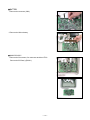
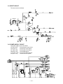
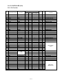
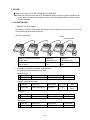
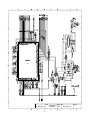
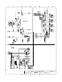
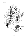
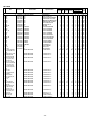
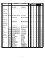
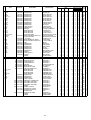
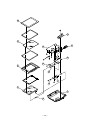
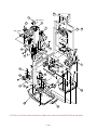
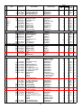
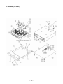
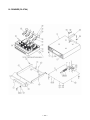
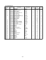
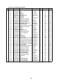
1
SERVICE MANUAL
(without price)
ELECTRONIC CASH REGISTER
TE-7000S/8000F/8500F
(EX-468/568/569)
FEB. 2003
TE-7000S
TE-8000F
INDEX
TE-8500F
Ver.3 : Aug. 2009
CONTENTS
TE-7000S/8000F/8500F
PAGE
1. SPECIFICATIONS........................................................................................ 1
2. CONNECTOR LOCATIONS ........................................................................ 4
3. MACHINE INITIALIZATION ......................................................................... 5
4. DISASSEMBLY ............................................................................................ 9
5. CIRCUIT EXPLANATION .......................................................................... 17
6. OPTION INSTALLATION........................................................................... 34
7. IN LINE ....................................................................................................... 36
8. ON LINE ..................................................................................................... 39
9. DIAGNOSTIC OPERATION ....................................................................... 41
10. ERROR CODE LIST................................................................................... 65
11. IC DATA ..................................................................................................... 70
12. PCB LAYOUT ............................................................................................ 76
13. CIRCUIT DIAGRAMS ................................................................................. 80
14. PARTS LIST ............................................................................................. 103
To prevent malfunctions caused by the weak batteries, charge the memory
protection batteries for over 12-hours before installation or after a long-time
vacation (over 30 days).
• Before installation, initialize the terminal and leave it turn on over 12-hours.
• After a long-time vacation, initialize the terminal and restore the program data if
the terminal is in malfunction, and leave it turn on over 12-hours.
• Over 48-hours charging makes the batteries fully charged.
1. SPECIFICATIONS
1-1. Electrical specifications
•Power consumption
In operation
stand-by
•Memory protection
Back-up battery
•Clock & Calendar
120 V
Max. 0.9 A
Max. 0.15 A
220 V
0.6 A
0.15 A
230 V
0.6 A
0.15 A
240 V
0.6 A
0.15 A
Recharge time
VL3032/SGB (Vanadium lithium battery)
Back-up period
30 days (25 °C)
Battery life Replace the battery every 5 years.
48 hours (full charge)
Accuracy
Auto calendar
Within ± 30 sec. per month (25 °C)
Effective until 2099 A.D.
1-2. Environmental specifications
• Operating temperature
0 °C ~ 40 °C
• Operating humidity
10 % ~ 85 %
• Storage temperature
-20 °C ~ 65 °C
• Storage humidity
10 % ~ 85 %
• Vibration strength
1.5 G (The machine must be in the carton box)
1-3. Main components
• CPU
Name
Number of control bit
Internal RAM
HD6417706AF133
32 bit
16 KBytes
• DRAM
Name
Capacity
MD56V62160E-10TAB0
64 Mbits (8 MBytes)
• Flash ROM
Name
Capacity
MBM24DL324BE90PFTN
4 MBytes
• I/O controller
Name
uPD784215AGC-XXX-8EU
• Gate array
Name
uPD65945GJ-P16-JEU
• LCD controller
Name
S1D13705F00A100
• ARCNET controller
Name
COM20019ILJP
• Switching power supply
Name
SPS-468
• LCD unit
Name
KCG057QV1DB-G00
• Inverter unit
Name
PS2-70052-001
• Themal printer
Name
Paper cut
Paper supply method
M-T203A-001(receipt)
M-T203-001(journal)
Impression heat line dot
Total dot number : 432 dots/dot line
Dot pitch : Length 8 dots/mm
Wide 8 dots/mm
Auto-paper cut
Drop-in paper loading
Type
Size
Roll diam
Thickness
Heat-sensitive paper
57.5±0.5mm
φ 83 or less
75±3µm
Print method
Head specification
• Roll paper
—1—
1-4. Duration of Life
• Printer head
50 Km (anti-abrasion)
• Printer mecanical
6,000,000 hours
• Printer cutter
600,000 hours
• LCD
36,000 hours
• Backlight
36,000 hours
1-5. Drawer List
Type
Drawer Name
Specification
M
DL-2783
D-19BC-B84M-9*
M
DL-2784
D-19BC-B84SM-9*
M
DL-2424
D-19BC-B55SM-9*
M
DL-2524
D-19BC-B64SM-9*
L
DL-3616
D-11BH-B65SS-9*
L
DL-3617
D-11BH-B65S-9*
Note : Country code
B : Other countries
D : England
—2—
TE-7000S/TE-8000F
B
D
G
C
X
X
X
X
X
X
X
G : Germany
C : U.S.A./Canada
TE-8500F
D
C
X
X
X
X
1-6. Option List
DEVICE NAME
• Clerk key kit
• Sheet holder kit
MODEL
CLK-K22
SH-KIT10
• Multi drawer kit
• Remote display
• Option pole
• Remote display cable
• PC cable
• Waterproof cover
• Waterproof cover
• Waterproof cover
• Slip printer
MDL-11
QT-2163D
QT-2061S
QT-2162S
PRL-CB-2
WT-77
WT-78/79
WT-62
SP-1300
• Slip printer cable
• Remote printer
• Remote printer
• Printer cable
• Printer cable
• Slip printer/ AC adaptor
• Power unit for External Printer
• Power cord for power unit
• Handy scnner
• Handy scnner
PRT-CB-8C
UP-250
UP-350
PRT-CB-8A
PRT-CB-8B
AD31U or E
PS-180
AC-170
HHS-15
HS1250
Connect to Com2, 3 or 4
Note : The SP-1300 can be connected
one unit only.
Length 1.5m
Connect to Com2, 3 or 4
Connect to Com2, 3 or 4
Length 3m
Length 5m
U: 100V/ E: 200V
EPSON MODEL
EPSON MODEL
Com2 port only
Com2 port only
• Laser scanner
Quic Scan 6000
Com2 port only
• CF Memory Card
• Modem
SDCFB-xx-505
56k External Faxmodem
“US Robotics”
56k External Voice
Faxmodem “US Robotics”
ELSA MICROLINK
TL-Pro (ISDN)
P-5880T
CVK-S2/L2/LLL2/FS2
• Modem
• ISDN TA
• Roll paper
• Conversion kit
NOTE
Dallas button for six people + a probe
A total of one sheet for No.3 &4
(including two sheets in solids)
Number of additional units = 3
Com3 port only
For Remote display
Length 5m
Com1 port only
WT-78: for stroke / WT-79 : for touch
Common
Common
Common
Common
Common
TE-7000S only
TE-8000F only
TE-8500F only
Common
Common
Common
Common
Common
Common
Common
Common
Common
Common
TE-7000S/
TE-8500F
TE-7000S/
TE-8500F
Common
Common
Common
Only in Germany
CAUTION
Danger of explosion if battery is incorrectly replaced.
Replace only with the same or equivalent type
recommended by the manufacturer.
Dispose of used batteries according
to the manufacture’s instructions.
VORSICHT !
Explosionsgefahr bei unsachgemäßem Austausch der
Batterie.
Ersatz nur durch denselben oder einen vom
Hersteller empfohlenen gleichwertigen Typ.
Entsorgung gebrauchter Batterien nach
Angaben des Herstellers.
ADVARSEL !
Lithiumbatteri - Eksplosionsfare ved fejlagtig hándtering.
Udskiftning má kun ske med batteri
af samme fabrikat og type.
Levér det brugte batteri tilbage til leverandØren.
—3—
Applicable
Common
TE-8000F only
Common
Common
TE-7000S/
TE-8000F
2. CONNECTOR LOCATIONS
COM1 Port
COM2 Port
COM3 Port
INLINE1 (ARCNET)
COM4 Port
INLINE2 (CAT5) OUT
INLINE2 (CAT5) IN
TERMINATOR FOR INLINE2
Ground Chassis
—4—
3. Machine Initialization
3-1.How to initialize the terminal
Preparation:
1. All peripheral devices and terminals of this cluster should be
turned off.
2. Connect all of the peripheral devices (such as printer,
display etc.) to terminal.
3. Connect all terminals by in-line.
Operation:
Date
00-00-00
Time
12:34 00
ID Character
MC #01
Date
Check System
Master
Time
Check cluster
ID
0
ID Character
R/J/Order Check
printer1System
UP-350
R/J/Order Check
printer2cluster ID UP-350
Slip PrinterR/J/Order Printer1 SP-1300
OK?
R/J/Order Printer2
Slip Printer
OK?
YES
01-10-10
12:34 00
MC #01
Master
0
UP-350
UP-350
SP-1300
YES
Date
Time
ID Character
Check System
Check cluster ID
R/J/Order Printer1
R/J/Order Printer2
Slip Printer
01-10-10
12:34 00
MC #01
Master
0
UP-350
UP-350
SP-1300
OK?
YES
Date
Time
ID Character
Check System
Check cluster ID
R/J/Order Printer1
R/J/Order Printer2
Slip Printer
01-10-10
12:34 00
MC #01
Master
0
UP-350
UP-350
SP-1300
OK?
YES
4. Turn on all peripheral devices of a terminal.
5. Turn on this terminal with pressing the Journal feed key and
release the key after the “Copyright” window is shown.
6. After releasing the key, enter “20000” (U.S.)/ “10000” (other
area: English), “40000” (other area: German), “50000” (other
area: French), “60000” (other area: Spanish) and press the
<ST> key.
7. Enter the current date (YY/MM/DD order) and time and press
the <YES> key.
8. In ID character field, the auto-defined ID No. is shown.
We recommend that you should not change the value.
9. In this field, you can select “1. Master/2. Backup Master/3.
Satellite/4. Selfmaster.”
Please select one of these options and press the <YES> key.
—5—
Date
Time
ID Character
Check System
Check cluster ID
R/J/Order Printer1
R/J/Order Printer2
Slip Printer
01-10-10
12:34 00
MC #01
Master
0
UP-350
UP-350
SP-1300
OK?
YES
Date
Time
ID Character
Check System
Check cluster ID
R/J/Order Printer1
R/J/Order Printer2
Slip Printer
01-10-10
12:34 00
MC #01
Master
0
UP-350
UP-350
SP-1300
OK?
YES
Date
Time
ID Character
Check System
Check cluster ID
R/J/Order Printer1
R/J/Order Printer2
Slip Printer
01-10-10
12:34 00
MC #01
Master
0
UP-350
UP-350
SP-1300
OK?
YES
Date
Time
ID Character
Check System
Check cluster ID
R/J/Order Printer1
R/J/Order Printer2
Slip Printer
01-10-10
12:34 00
MC #01
Master
0
UP-350
UP-350
SP-1300
OK?
YES
INIT
10-10-01 12:34
AUTO PGM
1. No Restore / Receive
2. PGM Restore (CF Card)
3. PGM Receive (Inline)
000001
10.
In this field, by pressing <YES> the check cluster No, should
be set, if your check tracking system are divided in some
clusters.
(Enter cluster No. “1”~ “9”, if you use check cluster system.)
11.
In these fields, by pressing <YES> you can select, “1. No/2.
UP-350/3. UP-250” for R/J/Order printer.
Please select one of these options and press the <YES> key.
12.
In this field, by pressing <YES> you can select, “1. No/2. SP1300” for slip printer.
Please select one of these options and press the <YES> key.
13.
Please confirm all of the field and if they are all right, press the
<YES> key to proceed the next step.
14.
If you want to download program data from other terminal or
CF card, select the appropriate menu and press the <YES>
key and proceed the next step.
If you don’t need to download any program data, just select “1.
No Restore/Receive” and press the <YES> key.
If you have another machine to initialize, return to step 4.
—6—
Restore from CF card.
INIT
10-10-01 12:34
000001
15.
Insert the CF card into the slot and select the appropriate file
and press the <YES> key.
Please select one of these options and press the <YES> key.
16.
After the confirmation window is show, press the <YES> key
to proceed restoring.
After completion of downloading, return to step 4 to initialize
other terminals.
Data Restore
1. PLUPGM1 .004
2. PLUPGM2 .004
3. STORE-AA.090
4. STORE-BB.090
STORE-AA.090
Are you sure to restore?
Program receive from other terminal.
INIT
10-10-01 12:34
Receive Data
All PGM
PGM Receive from
MC #05
OK?
In this field, by pressing <YES> you can select the receiving
contents as “1. All Data (including totalizer)/2. All PGM
(program only).”
16.
In this field, by pressing <YES> you should enter the source
ID number of the data and press the <YES> key.
17.
Please confirm all of the fields and if they are all right, press
the <YES> key to proceed downloading.
After completion of downloading, return to step 4 to initialize
other terminals.
000001
YES
INIT
10-10-01 12:34
Receive Data
All PGM
PGM Receive from
MC #05
OK?
15.
YES
INIT
10-10-01 12:34
Receive Data
All PGM
PGM Receive from
MC #05
OK?
000001
YES
000001
—7—
How to initialize the terminal (add/replace one terminal)
Preparation:
1. All peripheral devices and terminals of this cluster should be
turned off.
2. Connect all of the peripheral devices (such as printer, display
etc.) to this terminal.
3. Connect the added/replaced terminal to inline.
Operation:
Follow the steps shown on the page 1 to 3.
How to flag clear the terminal (or INIT2)
Preparation:
1. All peripheral devices and this terminal should be turned off.
2. Check the connection of all peripheral devices (such as printer,
display etc.) of this terminal.
3. Check the connection of this terminal to inline.
Operation:
4. Turn on all peripheral devices of this terminal.
5. Turn on this terminal with pressing the “Receipt feed” key and
release the key after the “Copyright” window is shown.
6. After releasing the key, press the <ST> key.
INIT
1. Flag Clear
2. Init 2
0.00
7. Select “1. Flag Clear” and press the <YES> key.
The flag clear operation is finished.
Note:
Performing “Init 2” requires password “8888888888” and <YES>.
—8—
4. DISASSEMBLY
■ UPPER COVER
1. Remove the key sheet. (TE-8000F only)
2. Remove the printer cover.
3. Remove the three screws.
Remove the upper case by sliding it forward.
—9—
4. Remove five connectors. (CN17, CN18, CN19, CN21, CN22)
Remove the screws and the earth cable.
CN18
CN19
CN17
CN21
CN22
Mode key cover
■ LCD ASS’Y
1. Remove the three screws.
Remove the mode key cover.
2. Remove the hinge cover.
3. Remove the three screws and two FPCs.
Remove the display case.
Display case
— 10 —
4.
1 Remove the screw and the earth cable.
1
2 Remove the two screws.
3 Remove the LCD ass’y.
3
2
5. Remove the two screws.
6. Remove LCD rear case.
NOTE: Be careful of the hooks when removing the LCD rear case.
Hooks
7. Remove the slide knob.
— 11 —
8. Remove the five screws, four connectors and FPC.
Remove the inverter and PCB ass’y.
9. Remove the six screws.
10.Remove the LCD chassis.
11.Remove the LCD unit.
— 12 —
■ MODE KEY
1. Remove the two screws.
Remove the mode key.
2. Remove the two connectors and two FPCs.
TE-8000F only
3. Remove the four screws and the earth cable.
4. Remove the contact rubber and PCB ass’y (E468-E6).
■ KEY BOARD ASS’Y
1. Remove the seven screws.
— 13 —
Remove the key board ass’y.
Remove the eighteen screws.
2. Remove the two screws.
Remove the PCB ass’y (E568-E42).
(TE-8000F only)
Remove two chassis.
Remove the FPC (E ), spacer (E ), and sheet.
— 14 —
■ BATTERY
1. Remove the connector (CN6).
2. Remove the lithium battery.
■ MAIN PCB ASS’Y
1. Remove the five screws, five connectors and three FPCs.
Remove the PCB ass’y (E468-1).
— 15 —
■ PRINTER
1. Remove the six screws.
Remove the printer block.
■ POWER SUPPLY
1. Remove the five screws.
Remove the four screws.
Remove the power supply.
— 16 —
— 17 —
CFL INVERTOR unit
PS2-70052-001
Power Supply for CFL
contrast on board
E468-E2-CL
CFL
KCG057QV1DB-G00
QVGA LCD UNIT
Auto Cutter
Journal
M-T203-001
Receipt
M-T203A-001
Thermal PRN UNIT
MD56V62160E-10TAB0
Option
DRAWER X 4
Standard
SDRAM
E468-E6
OPTION
TACT SW on board
MDL-11
CPU
Battery
VL3032/SGB
E468-1
HD6417706F133
FROM
MBM29DL324BE90PFTN
REAR LED
E468-E2-2
SPS-468
SW
POWER SUPPLY UNIT
iButton
DS1982-F5
(TE-8000F only)
switching power
E-STAMP I/F
(FCN-225J040-G/O)
CF card I/F
(62451-022L)
iButton Probe
DS9093
Menu Sheet SW
E568-E42
KEY_SHEET : FPC
Modular Plug
E468-ARC
Modular Plug
COM4
COM3
E468-CNB1
COM2
SIGNAL ONLY
QT-2163D
OPTIONAL Hand Held Scanner
HHS-15
MODEM or PC
Optional UNIT
OPTIONAL UNIT TBL.
PORT
OPTION
COM1
MODEM / PC
COM2 HHS-15/SP-1300 / UP-350 / UP-250
COM3 QT-2163D/SP-1300 / UP-350 / UP-250
COM4 SP-1300 / UP-350 / UP-250
CASIO STP cable
CASIO STP cable
CAT.5 UTP cable
NONE
+5V
+5V
NONE
POWER SUPPLY
CASIO ECR
CASIO ECR
CASIO ECR
CASIO ECR
Optional Printer
SP-1300/UP-250/
UP-350
OPTIONAL REMOTE
CUSTOMER DISP. SYSTEM
CAT.5 UTP cable
SIGNAL ONLY
+5V Supply
+5V Supply
PS204-A : U.S.A., Canada, etc
M2511 : Europe, etc
MP5004 : Great Britin
M3203 : Austlaria
POWER CORD
TE-7000S: E468-E4 (STROKE)
TE-8000F: E568-E4 (HYBLID)
TE-8500F: E569-E4 (FULL FLAT)
COM1
5. CIRCUIT EXPLANATION
5-1. BLOCK DIAGRAM
5-2. LSI BLOCK DIAGRAM
SERIAL
RS232C
FROM
IC19
CPU BUS
Backup
SDRAM
IC18
CPU (SH3)
IC33
buffer
1.9V + 3.3V
CF-CARD
PR
Backup Vrtc only
3.3V or 5V
SERIAL
buffer
3.3V
PCMCIA
5V
LCD
CONTROLLER
IC13
PR
I/O
CONTROLLER
IC21
LCD
E-STAMP
buffer
5V
GA
IC10
ARC-NET
232C
Note: 3.3V unless otherwise specified
232C
232C
— 18 —
5V
5-3. RESET CIRCUIT
The reset circuit is as follows.
Reset IC
5-4. POWER SUPPLY CIRCUIT
The power supply circuit is as follows.
VP (DC 25.2V):
For the printer control circuit.
VCC (DC 5V):
For the logic circuit power.
V3.3 (DC 3.3V):
For the logic circuit power.
Vbat (DC 3.3V):
For the RAM power.
V1.9V (DC 1.9V): For the CPU internal power.
Vrtc (DC 1.9V):
For the CPU RTC power.
— 19 —
5-5. DRAWER I/F CIRCUIT
The drawer open circuit is as follows.
— 20 —
The motor control IC for journal.
The signal selector IC for printing.
The motor control IC for receipt.
5-6. PRINTER CONTROL CIRCUIT
The printer control circuit is as follows.
— 21 —
5
6
7
8
9
10
D28/ PTB [4]
D27/ PTB [3]
D26/ PTB [2]
VSS Q
D25/ PTB [1]
14
15
16
D22/ PTA [6]
D21/ PTA [5]
D20/ PTA [4]
VSS
D19/ PTA [3]
VCC
25
26
27
28
29
30
31
32
33
34
35
36
37
38
39
40
41
42
43
44
VSS Q
D15
VCC Q
D14
D13
D12
D11
D10
D9
D8
D7
D6
VSS Q
D5
VCC Q
D4
D3
D2
D1
D0
D17/ PTA [1]
D16/ PTA [0]
22
23
24
D18/ PTA [2]
17
18
19
20
21
13
VCC Q
D24/ PTB [0]
D23/ PTA [7]
11
12
4
VSS - RTC
D31/ PTB [7]
D30/ PTB [6]
D29/ PTB [5]
IRQ4/PTH [4]
VSSQ
1
2
3
CTS2/IRQ5/SCPT [5]
VCC - RTC
XTAL2
EXTAL2
VCC - PLL1
ASEMD0
ASEBRKAK/ PTF [6]
TDO/ PTF [5]
TRST/PTG [3]
TMS/ PTG [2]
VCC
TCK/ PTG [1]
VSS
TDI/ PTG [0 ]
AUDSYNC/ PTF [3]
123
120
117
116
115
114
1.9V VCC
1.9V GND
3.3V VCC
3.3V GND
— 22 —
DRAK1/ PTE [3]
DRAK0/ PTE [2]
DACK1/ PTE [1]
DACK0/ PTE [0]
WAIT
108
107
106
105
CAUU/PTD [3]
CASL/PTD [2]
RASU/PTD [1]
RASL/PTD [0]
VCC Q
CE2B/PTD [7]
VSS Q
CE2A/PTD [6]
CS6/CE1B/PTC [7]
CS5/CE1A/PTC [6]
CS4/PTC [5]
96
93
90
89
92
91
95
94
98
97
99
IOIS16/PTD [5]
CKE/PTD [4]
BREQ
BACK
AUDATA [2]/ PTF [2]
AUDATA [1]/ PTF [1]
AUDATA [0]/ PTF [0]
111
110
109
104
103
102
101
100
AUDATA [3]/ PTF [3]
113
112
119
118
122
121
125
124
127
126
MD1
VCC - PLL2
CAP2
VSS - PLL2
VSS - PLL1
CAP1
VSS
EXTAL
XTAL
129
128
131
130
132
5-7. CPU (IC33)
5-7-1. Pin Assignment
STATUS0/PTE [4]
STATUS1/PTE [5]
TCLK/PTE [6]
133
134
135
88
87
86
CS3/PTC [4]
CS2/PTC [3]
VCCQ
IRQOUT/PTE [7]
VSSQ
136
137
138
139
140
141
85
84
CKIO
VCCQ
TxD0/SCPT [0]
SCK0/SCPT [1]
83
82
81
80
CS0
VSSQ
RD/WR
WE3/DQMUU/ICIOWR/PTC [2]
WE2/DQMUL/ICIORD/PTC [1]
WE1/DQMLU/WE
TxD2/SCPT [2]
SCK2/SCPT [3]
RTS2/SCPT [4]
142
143
144
79
78
77
WE0/DQMLL
RD
BS/PTC [0]
RxD0/SCPT [0]
RxD2/SCPT [2]
145
146
147
76
75
A25
A24
A23
VSS
RESETM
VCC
IRQ0/LRL0/PTH [0]
IRQ1/LRL1/PTH [1]
IRQ2/LRL2/PTH [2]
148
149
150
151
152
73
72
71
70
69
68
VCC
A22
VSS
A21
A20
IRQ3/LRL3/PTH [3]
154
155
156
67
A18
A17
A16
NMI
VCCQ
AUDCK/PTG [4]
157
64
63
62
A15
DREQ0/PTH [5]
160
161
162
163
164
61
DREQ1/PTH [6]
ADTRG/PTG [5]
MD0
MD2
60
59
58
57
VSSQ
A13
A12
A11
A10
RESETP
165
56
A9
CA
MD3
MD4
166
167
55
54
53
A8
A7
MD5
AVSS
AN [0 ]/PTJ [0]
169
170
52
51
50
A5
VCCQ
AN [1 ]/PTJ [1]
49
AN [2 ]/DA [1 ]/PTJ [2]
AN [3 ]/DA [2 ]/PTJ [3]
172
173
174
48
47
VSSQ
A3
A2
AVCC
AVSS
175
176
46
45
A1
A0
74
153
66
65
158
159
168
171
INDEX MARK
A19
VCCQ
A14
A6
A4
5-7-2. Block Diagram
MMU
UBC
CCN
AUD
Peripheral bus 1
L bus
I bus 1
TLB
CPU
CACHE
SCI
TMU
RTC
BRIDGE
BSC
SCIF
DMAC
CPG/WDT
CMT
Peripheral bus 2
INTC
I bus 2
H-UDI
ADC
DAC
I/O port
External bus
interface
Legend:
ADC:
AUD:
BSC:
CACHE:
CCN:
CMT:
CPG/WDT:
CPU:
DAC:
A/D converter
Advanced user debugger
Bus state controller
Cache memory
Cache memory controller
Compare match timer
Clock pulse generator/watchdog timer
Central processing unit
D/A converter
DMAC:
H-UDI:
INTC:
MMU:
RTC:
SCI:
SCIF:
TLB:
TMU:
UBC:
Direct memory access controller
Hitachi user-debugging interface
Interrupt controller
Memory management unit
Realtime clock
Serial communication interface (with smart card interface)
Serial communication interface (with FIFO)
Address translation buffer
Timer unit
User break controller
— 23 —
5-7-3. Pin Function
PIN NO.
1
2
3
4
5
6
7
8
9
10
11
12
13
14
15
16
17
18
19
20
21
22
23
24
25
26
27
28
29
30
31
32
33
34
35
36
37
38
39
40
41
42
43
44
45
46
47
48
49
50
51
52
53
54
55
56
57
58
59
PIN NAME
VCC-RTC
XTAL2
EXTAL2
Vcc-RTC
D31/PTB[7]
D30/PTB[6]
D29/PTB[5]
D28/PTB[4]
D27/PTB[3]
D26/PTB[2]
VssQ
D25/PTB[1]
VccQ
D24/PTB[0]
D23/PTA[7]
D22/PTA[6]
D21/PTA[5]
D20/PTA[4]
Vss
D19/PTA[3]
Vcc
D18/PTA[2]
D17/PTA[1]
D16/PTA[0]
VssQ
D15
VccQ
D14
D13
D12
D11
D10
D9
D8
D7
D6
VssQ
D5
VccQ
D4
D3
D2
D1
D0
A0
A1
A2
A3
VssQ
A4
VccQ
A5
A6
A7
A8
A9
A10
A11
A12
I/O
O
IN
IO
IO
IO
IO
IO
IO
IO
IO
IO
IO
IO
IO
IO
IO
IO
IO
IO
IO
IO
IO
IO
IO
IO
IO
IO
IO
IO
IO
IO
IO
IO
IO
O
O
O
O
O
O
O
O
O
O
O
O
O
DESCRIPTION
RTC power supply (1.9 V)
On-chip RTC crystal oscillator pin
On-chip RTC crystal oscillator pin
RTC power supply (0 V)
Data bus / input/output port B
Data bus / input/output port B
Data bus / input/output port B
Data bus / input/output port B
Data bus / input/output port B
Data bus / input/output port B
Input/output power supply (0 V)
Data bus / input/output port B
Input/output power supply (3.3 V)
Data bus / input/output port B
Data bus / input/output port A
Data bus / input/output port A
Data bus / input/output port A
Data bus / input/output port A
Internal power supply (0 V)
Data bus / input/output port A
Internal power supply (1.9 V)
Data bus / input/output port A
Data bus / input/output port A
Data bus / input/output port A
Input/output power supply (0 V)
Data bus
Input/output power supply (3.3 V)
Data bus
Data bus
Data bus
Data bus
Data bus
Data bus
Data bus
Data bus
Data bus
Input/output power supply (0 V)
Data bus
Input/output power supply (3.3 V)
Data bus
Data bus
Data bus
Data bus
Data bus
Address bus
Address bus
Address bus
Address bus
Input/output power supply (0 V)
Address bus
Input/output power supply (3.3 V)
Address bus
Address bus
Address bus
Address bus
Address bus
Address bus
Address bus
Address bus
— 24 —
PIN NO.
60
61
62
63
64
65
66
67
68
69
70
71
72
73
74
75
76
77
78
79
80
PIN NAME
A13
VssQ
A14
VccQ
A15
A16
A17
A18
A19
A20
A21
Vss
A22
Vcc
A23
A24
A25
BS/PTC[0]
RD
WE0/DQMLL
WE1/DQMLU/WE
81
WE2/DQMUL/ICIORD/PTC[1]
82
WE3/DQMUU/ICIOWR/PTC[2]
83
84
85
86
87
88
89
90
91
92
93
94
95
96
97
98
99
100
101
102
103
104
105
106
107
108
109
110
111
112
113
114
115
116
117
RD/WR
VssQ
CS0
VccQ
CS2/PTC[3]
CS3/PTC[4]
CS4/PTC[5]
CS5/CE1A/PTC[6]
CS6/CE1B/PTC[7]
CE2A/PTD[6]
VssQ
CE2B/PTD[7]
VccQ
RASL/PTD[0]
RASU/PTD[1]
CASL/PTD[2]
CASU/PTD[3]
CKE/PTD[4]
IOIS16/PTD[5]
BACK
BREQ
WAIT
DACK0/PTE[0]
DACK1/PTE[1]
DRAK0/PTE[2]
DRAK1/PTE[3]
AUDATA[0]/PTF[0]
AUDATA[1]/PTF[1]
AUDATA[2]/PTF[2]
AUDATA[3]/PTF[3]
AUDSYNC/PTF[4]
TDI/PTG[0]
Vss
TCK/PTG[1]
Vcc
I/O
O
O
O
O
O
O
O
O
O
O
O
O
O
O/IO
O
O
O
DESCRIPTION
Address bus
Input/output power supply (0 V)
Address bus
Input/output power supply (3.3 V)
Address bus
Address bus
Address bus
Address bus
Address bus
Address bus
Address bus
Internal power supply (0 V)
Address bus
Internal power supply (1.9 V)
Address bus
Address bus
Address bus
Bus cycle start signal/input/output port C
Read strobe
D7-D0 select signal / DQM (SDRAM)
D15-D8 select signal / DQM (SDRAM)/write strobe (PCMCIA)
D23-D16 select signal / DQM (SDRAM) / PCMCIA input/output
O/O/O/IO
read/input/output port C
D31-D24 select signal / DQM (SDRAM) / PCMCIA input/output
O/O/O/IO
write/input/output port C
O
Read/write
Input/output power supply (0 V)
O
Chip select
Input/output power supply (3.3 V)
O/IO
Chip select 2 / input/output port C
O/IO
Chip select 3 / input/output port C
O/IO
Chip select 4 / input/output port C
O/O/IO Chip select 5 / CE1 (area 5 PCMCIA)/input/output port C
O/O/IO Chip select 6 / CE1 (area 6 PCMCIA)/input/output port C
O/IO
Area 5 PCMCIA CE2 / input/output port D
Input/output power supply (0 V)
O/IO
Area 6 PCMCIA CE2 / input/output port D
Input/output power supply (3.3 V)
O/IO
Lower 32 Mbytes address RAS (SDRAM) / input/output port D
O/IO
Upper 32 Mbytes address RAS (SDRAM) / input/output port D
O/IO
Lower 32 Mbytes address CAS (SDRAM) / input/output port D
O/IO
Upper 32 Mbytes address CAS (SDRAM) / input/output port D
O/IO
CK enable (SDRAM) / input/output port D
I/IO
IOIS16 (PCMCIA) / input port D
O
Bus acknowledge
IN
Bus request
IN
Hardware wait request
O/IO
DMA acknowledge 0 / input/output port E
O/IO
DMA acknowledge 1 / input/output port E
O/IO
DMA request acknowledge / input/output port E
O/IO
DMA request acknowledge / input/output port E
IO
AUD data / input/output port F
IO
AUD data / input/output port F
IO
AUD data / input/output port F
IO
AUD data / input/output port F
O/IO
AUD synchronous / input/output port F
IN
Data input (H-UDI) / input port G
Internal power supply (0 V)
IN
Clock (H-UDI) / input port G
Internal power supply (1.9 V)
— 25 —
PIN NO.
118
119
120
121
122
123
124
125
126
127
128
129
130
131
132
133
134
135
136
137
138
139
140
141
142
143
144
145
146
147
148
149
150
151
152
153
154
155
156
157
158
159
160
161
162
163
164
165
166
167
168
169
170
171
172
173
174
175
176
PIN NAME
TMS/PTG[2]
TRST/PTG[3]
TDO/PTF[5]
ASEBRKAK/PTF[6]
ASEMDO
Vcc-PLL1
CAP1
Vss-PLL1
Vss-PLL2
CAP2
Vcc-PLL2
MD1
Vss
XTAL
EXTAL
STATUS0/PTE[4]
STATUS1/PTE[5]
TCLK/PTE[6]
IRQOUT/PTE[7]
VssQ
CKIO
VccQ
TxD0/SCPT[0]
SCK0/SCPT[1]
TxD2/SCPT[2]
SCK2/SCPT[3]
RTS2/SCPT[4]
RxD0/SCPT[0]
RxD2/SCPT[2]
CTS2/IRQ5/SCPT[5]
Vss
RESETM
Vcc
IRQ0/IRL0/PTH[0]
IRQ1/IRL1/PTH[1]
IRQ2/IRL2/PTH[2]
IRQ3/IRL3/PTH[3]
IRQ4/PTH[4]
VssQ
NMI
VccQ
AUDCK/PTG[4]
DREQ0/PTH[5]
DREQ1/PTH[6]
ADTRG/PTG[5]
MD0
MD2
RESETP
CA
MD3
MD4
MD5
AVss
AN[0]/PTJ[0]
AN[1]/PTJ[1]
AN[2]/DA[1]/PTJ[2]
AN[3]/DA[0]/PTJ[3]
AVcc
AVss
I/O
IN
IN
O/IO
O/IO
IN
IN
O
IN
O/IO
O/IO
IO
O/IO
IO
O
IO
O
IO
O/IO
IN
IN
IO
IN
I/I/IO
I/I/IO
I/I/IO
I/I/IO
I/IO
IN
IN
I/IO
I/IO
IN
IN
IN
IN
IN
IN
IN
IN
IN
I/IO
I/O/I
I/O/I
-
DESCRIPTION
Mode select (H-UDI) / input port G
Reset (H-UDI) / input port G
Data output (H-UDI) / input/output port F
ASE break acknowledge (H-UDI) / input/output port F
ASE mode (H-UDI)
PLL1 power supply (1.9 V)
PLL1 external capacitance pin
PLL1 power supply (0 V)
PLL2 power supply (0 V)
PLL2 external capacitance pin
PLL2 power supply (1.9 V)
Clock mode setting
Internal power supply (0 V)
Clock oscillator pin
External clock / crystal oscillator pin
Processor status / input/output port E
Processor status / input/output port E
TMU or RTC clock input/output / input/output port E
Interrupt request notification / input/output port E
Input/output power supply (0 V)
System clock input/output
Input/output power supply (3.3 V)
SCI transmit data 0 / SC port
SCI clock 0 / SC port
SCIF transmit data 2 / SC port
SCIF clock 2 / SC port
SCIF transmit request 2 / SC port
SCI receive data 0 / SC port
SCIF receive data 2 / SC port
SCIF transmit clear / external interruption request / SC port
Internal power supply (0 V)
Manual reset request
Internal power supply (1.9 V)
External interrupt request / input/output port H
External interrupt request / input/output port H
External interrupt request / input/output port H
External interrupt request / input/output port H
External interrupt request / input/output port H
Input/output power supply (0 V)
Nonmaskable interrupt request
Input/output power supply (3.3 V)
AUD clock / input port G
DMA request / input/output port H
DMA request / input/output port H
Analog trigger / input port G
Clock mode setting
Clock mode setting
Power-on reset request
Chip activate / hardware standby request
Area 0 bus width setting
Area 0 bus width setting
Endian setting
Analog power supply (0 V)
A/D converter input / input port J
A/D converter input / input port J
A/D converter input / D/A converter output / input port J
A/D converter input / D/A converter output / input port J
Analog power supply (3.3 V)
Analog power supply (0 V)
— 26 —
5-8. I/O CONTROLLER (IC21)
5-8-1. Pin Function
I/O
Port
Convertible terminal
P00
P01
P02
P03
P04
P05
P06
P10
P11
P12
P13
P14
P15
P16
P17
P20
P21
P22
P23
P24
P25
P26
P27
P30
P31
P32
P33
P34
P35
P36
P37
P40
P41
P42
P43
P44
P45
P46
P47
P50
P51
P52
P53
P54
P55
P56
P57
INTP0
INTP1
INTP2
INTP3
INTP4
INTP5
INTP6
ANI0
ANI1
ANI2
ANI3
ANI4
ANI5
ANI6
ANI7
RxD1
TxD1
ASCK1
PCL
BUZ
SI0
SO0
SCK0
TO0
TO1
TO2
TI1
TI2
TIO0
TIO1
AD0
AD1
AD2
AD3
AD4
AD5
AD6
AD7
A8
A9
A10
A11
A12
A13
A14
A15
Function
HCTS
R Head up
J Head up
DKIN
R no paper
J no paper
HDSR
VP search
Thermister H
Thermister J
DSTS0
DSTS1
PrinterTBLSel
DSTS2
DSTS3
HRXD
HTXD
HCLK
HDTR
HRTS
KEY TYPE0
Printer SO
Printer SCK
KC 0
KC 1
KC 2
KC 3
KC 4
KC 5
KC 6
KC 7
LED
Control
DKOUT
CUTTER RESET
VP ON
R STEP MOTOR
J STEP MOTOR
KI0
KI1
KI2
KI3
KI4
KI5
KI6
KI7
Initial
Normal
Power Failure
I
I
I
I
I
I
I
I
I
I
I
I
I
I
I
I
I
I
I
I
I
I
I
I
I
I
I
I
I
I
I
I
I
I
I
I
I
I
I
I
I
I
I
I
I
I
I
I
I
I
I
I
I
I
I
I
I
I
I
I
I
I
I
O
I
O
O
I
O
O
O
O
O
O
O
O
O
O
O
O
O
O
I
O
O
O
I
I
I
I
I
I
I
I
I
I
I
I
I
I
I
I
I
I
I
I
I
I
I
I
I
I
I
I
I
I
I
I
I
I
I
I
I
I
I
I
I
I
I
I
I
I
I
I
I
I
I
I
I
I
I
— 27 —
Circuit
Logic
U
U
U
U
U
U
U
-
U
U
U
U
U
U
U
U
U
U
U
U
U
U
U
U
U
U
U
U
U
U
U
U
U
U
U
U
U
U
U
U
U
U
U
U
U
AN
AN
AN
+
+
+
+
+
-
Commnet
CTS from HOST
Input DALLAS KEY
DSR from HOST
DRAWER STS0
DRAWER STS1
Printer TBL select switch
DRAWER STS2
DRAWER STS3
RxD from HOST
TxD from HOST
CLK (4Mhz) from HOST
DTR to HOST
RTS to HOST
KEYboard TYPE 0
SO to printer
CLK to printer
KEY common
output
LED Latch 0
LED Latch 1
LED Latch 2
DALLAS KEY output
Cutter RESET
Printer VP ON
STEP MOTOR IO
STEP MOTOR IO
KEY input
(MODE input)
I/O
Port
P60
P61
P62
P63
P64
P65
P66
P67
P70
P71
P72
P80
P81
P82
P83
P84
P85
P86
P87
P90
P91
P92
P93
P94
P95
P100
P101
P102
P103
P120
P121
P122
P123
P124
P125
P126
P127
P130
P131
Convertible terminal
A16
A17
A18
A19
RD
WR
WAIT
ASTB
RxD2
TxD2
ASCK2
A0
A1
A2
A3
A4
A5
A6
A7
Function
KI14
KI15
SW KEY IN
MODE COM
DW 0
DW 1
DW 2
DW 3
KEY TYPE 1
R SELECT
J SELECT
LED
Control
N-ch
Open
Drain
TI5/TO5
TI6/TO6
TI7/TO7
TI8/TO8
RTP0
RTP1
RTP2
RTP3
RTP4
RTP5
RTP6
RTP7
ANO0
ANO1
KC0
KC1
KC2
KI8
KI9
KI10
KI11
KI12
KI13
BUZZER
KC8
KC9
KC10
R STEP MOTOR
R STEP MOTOR
J STEP MOTOR
J STEP MOTOR
STB0
STB1
STB2
LATCH
PrinterBusy
PrinterBuffReady
Initial
Normal
Power Failure
I
I
I
I
I
I
I
I
I
I
I
I
I
I
I
I
I
I
I
I
I
I
I
I
I
I
I
I
I
I
I
I
I
I
I
I
I
I
I
I
I
I
O
O
O
O
O
I
O
O
O
O
O
O
O
O
O
O
I
I
I
I
I
I
O
O
O
O
O
O
O
O
O
O
O
O
O
O
I
I
I
I
I
I
I
I
I
I
I
I
I
I
I
I
I
I
I
I
I
I
I
I
I
I
I
I
I
I
I
I
I
I
I
I
I
I
I
SWITCH KI
MS0
MS1
MS2
Circuit
Logic
Commnet
U
U
U
U
KEY input
(MODE input)
SWITCH common input
MODE KEY common output
U
U
U
U
U
U
+
+
+
+
+
+
-
U
U
U
U
U
U
U
U
U
U
U
U
U
+
-
U
U
U
KEY input
(MODE input)
BUZZER
KI0
KI1
KI2
KI3
KI4
KI5
KI6
KI7
— 28 —
KEYboard TYPE 1
Printer R SEL
Printer J SEL
SA0/SA1/DG0
SB0/SB1/DG1
SC0/SC1/DG2
SD0/SD1/DG3
SE0/SE1/DG4
SF0/SF1/SCLK0
SG0/SG1/SCLK1
SDP0/SDP1/STR
KEY common
output
STEP MOTOR FHASE0
STEP MOTOR FHASE1
STEP MOTOR FHASE0
STEP MOTOR FHASE1
STB0
STB1
STB2
Printer LATCH
Printer Busy to HOST
PrinterBuffReady to HOST
MODE COM
PGM
RF
REG1
REG2
X
Z
X2/Z2
OFF
5-9. G/A (IC10)
5-9-1. Pin Function
PIN NO PIN NAME I / O
1
2
3
4
5
6
7
8
9
10
11
12
13
14
15
16
17
18
19
20
21
22
23
24
25
26
27
28
29
30
31
32
33
34
35
36
37
38
39
40
41
42
43
44
45
46
47
48
49
50
51
52
53
54
55
56
57
58
59
60
61
62
63
64
65
66
67
68
69
70
71
72
VDD
GD0
GD1
GD2
GD3
GD4
TVDD
TGND
GD5
GD6
GD7
GD8
GD9
TGND
GD10
GD11
GD12
GD13
GD14
TVDD
TGND
GD15
GA0
GA1
GA2
GA3
TGND
D0
D1
D2
TVDD
TGND
D3
D4
D5
VDD
GND
GND
D6
D7
D8
TGND
D9
D10
D11
TVDD
TGND
D12
D13
D14
TGND
D15
INTC2
INTC1
GCS1
GCS2
GRD
GWE
PCIN
PCMG
CFCE1A
CIN
CFG
CFCE2A
ANDO1
ANDO2
BFO1
BFO2
BFO3
BFO4
GND
GND
VDD
I/O
I/O
I/O
I/O
I/O
VDD
GND
I/O
I/O
I/O
I/O
I/O
GND
I/O
I/O
I/O
I/O
I/O
VDD
GND
I/O
O
O
O
O
GND
I/O
I/O
I/O
VDD
GND
I/O
I/O
I/O
VDD
GND
GND
I/O
I/O
I/O
GND
I/O
I/O
I/O
VDD
GND
I/O
I/O
I/O
GND
I/O
O
O
O
O
O
O
O
O
O
O
O
O
O
O
O
O
O
O
GND
GND
DESCRIPTIN
PIN NO PIN NAME I / O
VDD
ARC DATA (D0)
ARC DATA (D1)
ARC DATA (D2)
ARC DATA (D3)
ARC DATA (D4)
VDD
GND
ARC DATA (D5)
ARC DATA (D6)
ARC DATA (D7)
VDD
VDD
GND
VDD
VDD
VDD
VDD
VDD
VDD
GND
VDD
ARC ADDRESS (A0)
ARC ADDRESS (A1)
ARC ADDRESS (A2)
Not used
GND
DATA (D0)
DATA (D1)
DATA (D2)
VDD
GND
DATA (D3)
DATA (D4)
DATA (D5)
VDD
GND
GND
DATA (D6)
DATA (D7)
VDD
GND
VDD
VDD
VDD
VDD
GND
VDD
VDD
VDD
GND
VDD
INT for ARC
INT for UART
Chip Select for ARC
EST-CS
Read signal for ARC
Write signal for ARC
PCMCIA IN/OUT signal
Enable for PCMCIA
Chip Enable1 for CF CARD
CF CARD IN/OUT signal
Enable for CF CARD
Chip Enable2 for CF CARD
WAIT signal
DSR
CI
CD
RXD
CTS
GND
GND
— 29 —
73
74
75
76
77
78
79
80
81
82
83
84
85
86
87
88
89
90
91
92
93
94
95
96
97
98
99
100
101
102
103
104
105
106
107
108
109
110
111
112
113
114
115
116
117
118
119
120
121
122
123
124
125
126
127
128
129
130
131
132
133
134
135
136
137
138
139
140
141
142
143
144
VDD
CLKOUT
CLKIN
GND
CS
A0
A1
A2
A3
A23
A20
A21
A22
RD
WE
INT6
INT7
TVDD
RESET
RD_WE
TESTB
U1_CTSB
U1_DSRB
U1_SIN
U1_DTRB
U1_RTSB
U1_SOUT
U2_CTSB
U2_DSRB
U2_SIN
U2_DTRB
U2_RTSB
U2_SOUT
U3_CTSB
U3_DSRB
VDD
GND
GND
U3_SIN
U3_DTRB
U3_RTSB
U3_SOUT
U4_CTSB
U4_DSRB
U4_SIN
U4_DTRB
U4_RTSB
U4_SOUT
U5_CTSB
U5_DSRB
U5_SIN
U5_DTRB
U5_RTSB
U5_SOUT
TVDD
PCMIN
CE1B
CE2B
CFIN
CE1A
CFCE
CE2A
BFI1
BFI2
BFI3
BFI4
ANDI1
ANDI2
ANDI3
ANDI4
GND
GND
VDD
O
I
I
I
I
I
I
I
I
I
I
I
I
I
I
I
VDD
I
I
I
I
I
I
O
O
O
I
I
I
O
O
O
I
I
VDD
GND
GND
I
O
O
O
I
I
I
O
O
O
I
I
I
O
O
O
VDD
I
I
I
I
I
I
I
I
I
I
I
I
I
I
I
GND
GND
DESCRIPTIN
VDD
CLOCK 8MHz
CLOCK 8MHz
GND
Chip Select 5
ADDRESS (A1)
ADDRESS (A2)
ADDRESS (A3)
GND
ADDRESS (A23)
ADDRESS (A20)
ADDRESS (A21)
ADDRESS (A22)
IO READ
IO WRITE
INT for ARC
Int for PCMCIA
VDD
RESET
READ/WRITE signal
VDD
CST2
DSR2
RXD2
DTR2
RTS2
TXD2
CTS3
DSR3
RXD3
DTR3
RTS3
TXD3
CTS4
DSR4
VDD
GND
GND
RXD4
DTR4
RTS4
TXD4
VDD
VDD
VDD
NOT USED
NOT USED
NOT USED
VDD
VDD
VDD
NOT USED
NOT USED
NOT USED
VDD
PCMCD1
CE1
CE2
CFCD1
CE1
ADDRESS (A23)
CE2
CI1
CD1
RXD1
CTS1
WAIT for CF CARD
WAIT for PCMCIA
DSR1
DSR1
GND
GND
5-10. LCD CONTROLLER (IC13)
5-10-1. Pin Assignment
60 59 58 57 56 55 54 53 52 51 50 49 48 47 46 45 44 43 42 41
63
64
65
66
67
68
69
70
71
72
73
74
75
76
77
78
79
AB8
VSS
FPFRAME
FP LINE
FP DAT0
AB7
AB6
AB5
FP DAT1
AB4
AB3
FP DAT2
AB2
FP DAT4
AB1
AB0
FP DAT5
FP DAT6
FP DAT7
FP DAT3
S1D137 05
BCLK
VSS
RD#
IO VDD
FP SHIFT
VSS
FP DAT8
FP DAT9
WE 0 #
WE 1 #
FP DAT10
FP DAT11
RE SET#
CS #
BS#
GP IO0
RD /WR#
VSS
CORE VDD
40
39
38
37
36
35
34
33
32
31
30
29
28
27
26
25
24
23
22
21
VS S
DB 0
DB 1
DB 2
DB 3
DB 4
DB 5
DB 6
DB 7
DB 8
IO VDD
DB 9
DB 10
DB 11
DB 12
DB 13
DB 14
DB 15
WA I T #
CORE V DD
80
COREVDD
CORE VDD
DRDY
LCDPWR
TESTEN
AB 16
CNF3
62
CNF2
CNF1
CNF0
VSS
CLK I
IO VDD
AB 15
AB 14
AB 13
AB 12
AB 11
AB 10
AB 9
VSS
61
1 2 3 4 5 6 7 8 9 10 11 12 13 14 15 16 17 18 19 20
5-10-2. Block Diagram
16-bit FPM/EDO-DRAM
Memory
Controller
Register
CPU
R/W
LCD
Display
FIFO
Host
I/F
LockUp
Tables
I/F
DAC
Cursor
FIFO
Power Save
CRTC
Clocks
— 30 —
LCD
CRT
5-10-3. Pin Function
■ KEY
I
O
IO
P
C
CS
COx
=
=
=
=
=
=
=
Input
Output
Bi-Directional (Input/Output)
Power pin
CMOS level input
CMOS level Schmitt input
CMOS output driver, x denotes driver type (see I OL /I OH in Table 6-4: “Output Specifications,” on
page 25)
TSx = Tri-state CMOS output driver, x denotes driver type (see I OL /I OH in Table 6-4: “Output Specifications,”
on page 25)
CNx = CMOS low-noise output driver, x denotes driver type (see I OL /I OH in Table 6-4: “Output
Specifications,” on page 25)
TEST = CMOS level test input with pull down resistor
■ HOST INTERFACE
Pin Names Type
AB0
AB[16:1]
DB[15:0]
WE0#
I
I
IO
I
Pin#
70
45, 53, 54,
55, 56, 57,
58, 59, 62,
63, 64, 65,
66, 67, 68,
69
Cell
CS
Input
C
Input
3, 4, 5, 6, 7,
8, 9, 11, 12, C/TS2
13, 14, 15,
16, 17, 18,
19
77
RESET#
State
CS
Hi-Z
Input
Description
This pin has multiple functions.
• For SH-3/SH-4 mode, this pin inputs system address bit 0 (A0).
• For MC68K #1, this pin inputs the lower data strobe (LDS#).
• For MC68K #2, this pin inputs system address bit 0 (A0).
• For Generic #1, this pin inputs system address bit 0 (A0).
• For Generic #2, this pin inputs system address bit 0 (A0).
These pins input the system address bits 16 through 1 (A[16:1]).
These pins have multiple functions.
• For SH-3/SH-4 mode, these pins are connected to [D15:0].
• For MC68K #1, these pins are connected to D[15:0].
• For MC68K #2, these pins are connected to D[31:16] for a
32-bit device (e.g. MC68030) or D[15:0] for a 16-bit device
(e.g. MC68340).
• For Generic #1, these pins are connected to D[15:0].
• For Generic #2, these pins are connected to D[15:0].
This pin has multiple functions.
• For SH-3/SH-4 mode, this pin inputs the write enable signal for
the lower data byte (WE0#).
• For MC68K #1, this pin must be tied to IO V DD
• For MC68K #2, this pin inputs the bus size bit 0 (SIZ0).
• For Generic #1, this pin inputs the write enable signal for the
lower data byte (WE0#).
• For Generic #2, this pin inputs the write enable signal (WE#).
— 31 —
Pin Names Type
Pin#
Cell
RESET#
State
Description
This pin has multiple functions.
• For SH-3/SH-4 mode, this pin inputs the write enable signal for
the upper data byte (WE1#).
• For MC68K #1, this pin inputs the upper data strobe (UDS#).
• For MC68K #2, this pin inputs the data strobe (DS#).
• For Generic #1, this pin inputs the write enable signal for the
upper data byte (WE1#).
• For Generic #2, this pin inputs the byte enable signal for the
high data byte (BHE#).
WE1#
I
78
CS
Input
CS#
I
74
C
Input
This pin inputs the chip select signal.
BCLK
I
71
C
Input
This pin inputs the system bus clock.
BS#
RD/WR#
RD#
I
I
I
75
79
76
CS
CS
CS
Input
Input
Input
WAIT#
O
2
TS2
Hi-Z
RESET#
I
73
CS
0
This pin has multiple functions.
• For SH-3/SH-4 mode, this pin inputs the bus start signal (BS#).
• For MC68K #1, this pin inputs the address strobe (AS#).
• For MC68K #2, this pin inputs the address strobe (AS#).
• For Generic #1, this pin must be tied to V SS.
• For Generic #2, this pin must be tied to IO V DD.
This pin has multiple functions.
• For SH-3/SH-4 mode, this pin inputs the RD/WR# signal.
The S1D13705 needs this signal for early decode of the bus cycle.
• For MC68K #1, this pin inputs the R/W# signal.
• For MC68K #2, this pin inputs the R/W# signal.
• For Generic #1, this pin inputs the read command for the upper
data byte (RD1#).
• For Generic #2, this pin must be tied to IO V DD.
This pin has multiple functions.
• For SH-3/SH-4 mode, this pin inputs the read signal (RD#).
• For MC68K #1, this pin must be tied to IO V DD .
• For MC68K #2, this pin inputs the bus size bit 1 (SIZ1).
• For Generic #1, this pin inputs the read command for the lower
data byte (RD0#).
• For Generic #2, this pin inputs the read command (RD#).
This pin has multiple functions.
• For SH-3 mode, this pin outputs the wait request signal (WAIT#).
• For SH-4 mode, this pin outputs the device ready signal (RDY#).
• For MC68K #1, this pin outputs the data transfer
acknowledge signal (DTACK#).
• For MC68K #2, this pin outputs the data transfer and size
acknowledge bit 1 (DSACK1#).
• For Generic #1, this pin outputs the wait signal (WAIT#).
• For Generic #2, this pin outputs the wait signal (WAIT#).
Active low input to set all internal registers to the default state and
to force all signals to their inactive states.
— 32 —
■ LCD INTERFACE
Pin Names Type
FPDAT[7:0]
FPDAT
[10:8]
O
O,
IO
Pin#
Cell
RESET#
State
30, 31, 32,
33, 34, 35,
36, 37
CN3
0
24, 25, 26
CN3
Input
Description
Panel Data
These pins have multiple functions.
• Panel Data bits [10:8] for TFT/D-TFD panels.
• General Purpose Input/Output pins GPIO[3:1].
These pins should be connected to IO V DD when unused.
This pin has multiple functions.
• Panel Data bit 11 for TFT/D-TFD panels.
• General Purpose Input/Output pin GPIO4.
• Inverse Video select pin.
This pin should be connected to IO V DD when unused.
FPDAT11
O,
IO
23
CN3
Input
FPFRAME
O
39
CN3
0
Frame Pulse
FPLINE
O
38
CN3
0
Line Pulse
FPSHIFT
O
28
CN3
0
Shift Clock
LCDPWR
O
43
CO1
0
Active high LCD Power Control
DRDY
O
42
CN3
0
This pin has multiple functions.
• TFT/D-TFD Display Enable (DRDY).
• LCD Backplane Bias (MOD).
• Second Shift Clock (FPSHIFT2).
■ CLOCK INPUT
Pin Names Type
CLKI
Pin#
DRIVER
51
C
I
Description
Input Clock
■ MISCELLANEOUS
Pin Names Type
Pin#
Cell
CNF[3:0]
I
46, 47,
48, 49
C
GPIO0
IO,
I
22
CS/
TS1
TESTEN
I
44
RESET#
State
Description
These inputs are used to configure the S1D13705 - see Table
As set by 5-1: “Summary of Power On/Reset Options,” on page 22.
hardware Must be connected directly to IO VDD or VSS.
Input
This pin has multiple functions - see REG[03h] bit 2.
• General Purpose Input/Output pin.
• Hardware Power Save.
TEST pulled low Test Enable input. This input must be connected to VSS.
■ POWER SUPPLY
Pin Names Type
Pin#
DRIVER
Description
COREVDD
P
1, 21, 41,
61
P
Core VDD
IOVDD
P
10, 29, 52
P
IO VDD
VSS
P
20, 27, 40,
50, 60, 72,
80
P
Common VSS
— 33 —
6. OPTION INSTALLATION
6-1. Dallas Key (Clerk key kit CLK-K22)
1.
2.
3.
4.
Remove the upper cover as shown in steps 1 to 3 of page 9.
Fix the Dallas Cable Assy to the Dallas cover.
Fix the Dallas cover to the lower case by screw.
Let the Dallas cable through the unit and connect it to the MAIN PCB (CN25).
Note : Wind the cable through the Ferrite core two and a half times.
5. Fix the Ferrite core to the chassis by insulock tie.
6. Fix the UPPER COVER.
Ferrite core
Insulock tie
Screw
Dallas cover
CN25
Dallas Cable Assy
Das 02 Sub Assy
iButton probe (DS9092)
Dallas key Assy
DS1982-F5
DS9093N
N
Code No.
Parts Name
N
1010 4433 COVER/DALLAS E468
RJE500428-1
1
1008 6507
1007 3068
1007 3671
1007 9263
1007 3701
1007 3665
E441328*1
E441319-1
TR-20-10-10
RJE500025*1
DS1982-F5
DS9093N
1
1
1
1
1
1
DALLAS CABLE ASSY
DAS-02 CABLE SUB ASSY
CORE/FERRITE
DALLAS KEY ASSY/6PCS
iBUTTON/CLERK
iBUTTON MOUNT PROD/CLERK
Specification Q'ty
— 34 —
Price
Code
CD
AB
AD
DA
BF
AO
Note
This part is attached in the carton box of
TE-7000S/8000F/8500F.
Clerk key kit (CLK-K22)
Wire with connector( t = 40mm )
Clerk key kit (CLK-K22)
Clerk key kit (CLK-K22)
6-2. REMOTE DISPLAY
6-3. HANDY SCNNER
6-4. REMOTE PRINTER / SLIP PRINTER
Connect the following peripherals to the COM ports respectively.
REMOTE DISPLAY : COM3
HANDY SCANNER : COM2
REMOTE PRINTER/ : COM2, 3, 4
SLIP PRINTER
COM4 Port
COM3 Port
COM2 Port
COM1 Port
6-5. DRAWER
6-5-1. CONNECTOR THE DRAWER
1. Connector drawer connector (three color lead on drawer)
to the cash register.
2. Connector frame drawer connector (green lead on drawer)
to the cash register.
2
6-5-2. CONNECTOR THE DRAWER
1. Screw in 2 fixing screws bottom side of the register.
2. Stick rubber plate on the eash corner of the bottm side of
the register.
3. Mount the cash register on the top of the drawer, ensuring
that the feet on the bottom of the cash register go into the
holes on the drawer
— 35 —
2
1
1
2
2
7. IN LINE
■ There are two types for IN LINE; CATEGORY5A and ARCNET.
Note: When the cluster has more than 8 TE-7000S/8000F/8500F terminals, all printer should be local
printer. When the cluster has less than or equal to 8 TE-7000S/8000F/8500F terminals, remote
printer is allowable.
7-1. ARCNET(INLINE1)
1 ARCNET connection diagram
The maximum ARCNET cable length and the maximum connection unit will be varied by the in-line
communication speed as shown below list.
[ARCNET cable wiring]
In-line
Total Length : A
R/J
R/J
R/J
R/J
R/J
ARCNET communication speed
(Baud rate)
Maximum
connection unit
Maximum
cable length A (m)
312.5 K bps
156.25 K bps
20
32
430
890
2 In line cable, Connector, Terminater and Earth plate
The following parts are packaged in the ECR.
ARCNET cable
N
Code No.
1904 4023
Parts name
In-line cable
Specification
IPEV-SLA0.5x1P
Price code
AN
ARCNET connector(ECR side)
N
Code No.
Parts name
Specification
Price code
3540 3924
In-line connector kit
XLP-KIT-2
Parts name
Resistor
Specification
RD14J101T26
Price code
Parts name
Plate/Earth
Specification
E440398-1
Price code
AB
AK
Note
Connector×1
cap×2
Terminater
N
N
Code No.
10054255
Earth plate
Code No.
62477372
— 36 —
3 ARCNET Cable connection diagram
Signal
SD
Pin
1
RD
2
Terminater
100 ohms
FG
FG plate
(In-line connector)
Signal
SD
Pin
1
Signal
SD
Pin
1
RD
2
RD
2
Terminater
100 ohms
FG
FG plate
(In-line connector)
FG
FG plate
(In-line connector)
[Connection end of ECR]
Earth plate
Red
Red
In-line cable
Wrap bent shield wire
Black
with Copper tape
Shield wire
In-line connector
Black
Terminator (100 ohms)
[Connection between ECR and ECR]
Earth plate
Red
Red
In-line cable
In-line connector
Wrap bent shield wire
with Copper tape Shield wire Black
Black
NOTE:
1) The earth plate should be fixed to the ground chassis.
2) When using the ARCNET, slide the switch at the bottom of ECR to RS485.
7-2. CATEGORY5 (INLINE2)
1 Restrictions
• Maximum number of units that can be connected is 32.
• HUB and rooter cannot be connected.
• With ARCNET simultaneous use impossible.
• Minimum cable length between units is 5 meters.
2 APPLICATION
• Auto PGM
• Sales Data Collection
• Shared Check Tracking
• Shared Printer
• IPL
— 37 —
Maximun total length of the cable
4 units : 450m
8 units : 420m
32 units : 230m
3 BLOCK DIAGRAM
CAT5 UTP Cable
CAT5 UTP Cable
RS232C
OUT
(Min 5m) IN
OUT
(Min 5m) IN
PC
4 Connection
INLINE2 (CAT5) OUT
INLINE2 (CAT5) IN
Terminator Switch
Turn on the switch of the units of
both first and the last ends.
White/Orange
Orange
White/Green
Blue
White/Blue
Green
White/Brown
Brown
1
2
3
4
5
6
7
8
1
2
3
4
5
6
7
8
White/Orange
Orange
White/Green
Blue
White/Blue
Green
White/Brown
Brown
8, 7, 6, .....2, 1
LAN CABLE
5 LAN cable specifications
CAT5 UTP Cable (TIA/EIA 568)
0.5mm x 4P Not shielded wire Twist pair cable
NOTE:
1) The power of all units which share the network must be turned on.
If even one of them is OFF, normal communication cannot be done.
If any of the units has a failure and its power is turned off, remove the unit from the network.
2) Communication speed of the categoly 5 is fixed 312.5kbps.
3) When using CAT5, slide the switch at the bottom of ECR to CAT5 side.
— 38 —
8. ON LINE
Only the RS-232C Com1 port can be connected with a modem or perssonal computer.
Note: When the cluster has more than 8 register terminals, all printer should be local printer. When the cluster
has less than or equal to 8 register terminals, remote printer is allowable.
8-1. Direct connection to PC
1 Connection layout
RS-232C
PC
KP/M
Slip
CHK/BM
CHK/M
Slip
KP/BM
Slip
R/J
Using Com1 port
2 PC Cable wiring
TE-7000S/8000F/8500F (Com1)
Pin No.
3
2
7
8
1
4
6
9
5
PC
Signal name
SD/TXD
RD/RXD
RS/RTS
CS/CTS
CD/DCD
ER/DTR
DR/DSR
CI/RI
GND
— 39 —
Pin No.
Pin No.
(DSUB9)
3
2
7
8
1
4
6
5
(DSUB25)
2
3
4
5
8
20
6
22
7
Signal name
SD
RD
RS
CS
CD
ER
DR
CI
GND
8-2. MODEM system
1 Connection layout
on-line
PC
MAX : 15 m
Register-1
Register-2
R/J
Register-3
Register-32
R/J
R/J
R/J
Use Com1 port
2 PC Cable wiring
TE-7000S/8000F/8500F (Com1)
Pin No.
3
2
7
8
1
4
6
9
5
MODEM (DSUB25)
Signal name
SD/TXD
RD/RXD
RS/RTS
CS/CTS
CD/DCD
ER/DTR
DR/DSR
CI/RI
GND
Pin No.
2
3
4
5
8
20
6
22
7
Signal name
SD
RD
RS
CS
CD
ER
DR
CI
GND
8-3. PRINTER Connection
■ Three printers can be connected to TE-7000S/8000F/8500F.
Com2 ~ Com4 are used for ports.
1 Connection layout
Maimum connection number : Max. 3 printer
Note:The slip printer can be connected one unit only.
Register
R/J
— 40 —
R/J
Slip
9. DIAGNOSTIC OPERATION
9-1. To start the diagnostic operation
1. Power off.
2. While holding down the "Jounal feed" button, turn the power on.
3. Release the button when the main display on.
Note: Releace the botton when "INT" appears at the left bottom of the LCD.
Normal performance cannot be ensured if the botton was released before "INT" appears.
4. Input "99990000" and press [SUB TOTAL].
5. Diagnostic program is executed.
[LCD]
LCD COLOR
ARC RS485
CF INSERT
RCT/PAPER HEAD CUT
KEY FF+STRK
E-STAMP
NON
JNR/PAPER HEAD
Diag Ver : XXXXXX XXXX
DALLAS 12345678abcdef
DRW 1CLOSE 2CLOSE
MENU SHEET 1
3CLOSE 4CLOSE
0000
1234
Note: No display or print is done because there is no independent version for DIAG for the product.
9-2. Notes for the DIAG
• All test results are printed by the built-in printer receipt.
• Make sure to test HHS-15 by connecting to COM2.
• Make sure to test REMOTE DISP by connecting COM3.
• When you want to do the test infinitely, follow the direction for each test and input numbers other than 0.
Inputting numbers 1~9 as the command for the number of times for carrying out the test in the operation
of each page makes the number infinite.
Note that you can only choose one time or infinite times.
9-3. Note the following when performing the ARCNET test
1 When testing with ARCNET cable
Slide the switch of the cable to the RS485.
Make sure that a terminal resistance is fixed with the cable. (If not, the cable has to be processed.)
Note that the terminal resistance switch does not have any meaning for RS485.
2 When testing with CAT5 cable
Slide the switch of the cable to the CAT5.
Make sure to turn the terminal resistance switch ON.
9-4. Procedure and display for the operator judgment test
• In the operator judgment test, determine the test result either by OK key or NG key after "Please Hit
Key OK -> 1 NG ->9" appears.
OK key : number 1
NG key : number 9
— 41 —
9-5. Status display
[Function]
The status of the device which holds the status information is displayed.
The displayed device and the status are as follows.
Device
Status information
(displayed information)
Device
Status information
(displayed information)
Dalllas key
Dallas key No.
ARCNET
Port status
Drawer
Open or close
Printer (receipt)
Head up (normal or abnormal)
MENU sheet Sheet number
Lack of paper (with or without paper)
E-Stamp
Cutter (normal or abnorrmal)
Inserted or removed
LCD
Color/ black and white
Key type
Keyboard type information
CF card
Inserted or removed
Printer (Journal)
Head up (normal or abnormal)
Lack of paper (with or without paper)
[LCD]
The status display when all of the following status is normal is as follows; LCD type (color), Key type
(FULL FLAT + STROKE), ARCNET PORT (RS 485), CF-CARD (inserted), E-stamp (not inserted)
and Printer status.
1
2
3
4
1234567890123456789012345678901234567890
01
02
03
04
05
06
07
08
09
10
11
12
13
14
15
LCD COLOR
ARC RS485
CF INSERT
RCT/PAPER HEAD CUT
KEY
FF+STRK
E-STAMP
NON
JNR/PAPER HEAD
Always displays the status information.
When the test is performed, the status at
the end of the test is displayed after the test.
Diag Ver : ✱✱✱✱✱✱ ✱✱✱✱
DALLAS 12345678abcdef
MENU SHEET1
DRW 1CLOSE 2CLOSE 3CLOSE 4CLOSE
0000
Counter display
1234
Numbers: the size of the characters is 1.5 time. (maximum 10 digits)
The numbers are displayed in the REAR DISP also.
* The key type (“KEY FF + STRK” in the above figure ) is the one which is connected when the power
is turned on.
When displaying a different key type, turn the power off once, and replace the keyboard. The display
won’t change even if the keyboard is replaced while the power is on.
* The displayed information of the printer status is as follows;
RCT: receipt information
JNR: journal information
When an error is detected in each information, the error information is displayed in black characters
and the background is displayed in white (reversed). When the status returns to normal, the characters
turn white and the background turns white (same as in other information).
1 HEAD (head up information)
2 PAPER(lack of paper)
3 CUT (cutter information for the receipt only)
— 42 —
9-6. Check item
The following test can be checked in the diagnostic test.
No
Device to be checked
Operation
1
Batch test 1
2
2
Batch test 2
3
3
4
5
RAM WRITE/READ test
RAM READ ONLY test
FLASH CHECK SUM
6
FLASH CLEAR &
WRITE/READ test (no BACK UP)
7 CF-CARD WRITE/READ test
8 CF-CARD READ ONLY test
9 CF-CARD CLEAR test
10 CF-CARD CLEAR WRITE/READ test
11 LCD display test
12 LCD backlight OFF test
13 REAR DISPLAY test
14 REMOTE DISPLAY test
15 External printer print test
16 Internal printer print test
17 Internal printer graphic print test
18 Internal printer dot rate test
19 Internal printer print density test
20 RS232C PORT test
21 RS232C PORT batch test
22 ARCNET test
23 ARCNET batch tes
24 Time setting
25 Time display
26 Drawer open test
27 Buzzer test
28 KEY dipsplay
29 OBR test
Note
Test Device : RAM, Flash, Printer,
Date, Time, Buzzer, Drawer
Test Device : LCD, Back light,
Rear Display
Page
44
45
n011
n111
n512
46
46
47
n612
47
pn013
pn113
pn213
pn313
n021
121
n122
na23
x1x2x3n03d
cn03d
48
48
49
49
50
51
51
52
53
54
55
56
57
57
58
59
60
61
61
61
62
63
64
P1P1P1P2P2P2n13d
pn33d
x0235
xN04d
40
rllmmx0a51
150/250
x1x2x3x4x5x60a70
70
xn091
n092
94
95
— 43 —
9-7. Operation of each test
[ 1 ] Batch test 1
[Function]
RAM test, FLASH test, test print, time setting, buzzer test and drawer open test are performed
continuously.
[Operation]
Refer to the page for the details of the following tests.
Operation :
2
SUBTOTAL
The following tests are performed automatically.
(1) RAM test : WRITE/READ all block test
(2) FLASH : CHECK SUM TEST (checks only code area)
(3) Test print
(4) Times setting : Set the following data.
Arranged data : 2001 December 31, 23:59’30
(5) Buzzer : Ring the one shot buzzer.
No print or display in this test
(6) Drawer open : Opens only drawer 1.
Waits for the key input of OK or NG by the operator after the drawer opens.
OK key : number 1 NG key : number 9
(7) Receipt issuance
[LCD]
*When all the tests ends normally
BATC H
RAM WR
FLASH CHK SUM
DATE
TIME
Please Hit Key
DRW 1
END
2
OK
OK
01/12/31
23:29-30
OK-> 1 NG-> 9
OK
2
Waits for the key of OK or NG in the drawer test.
Displays the result upon the input of either key.
[Print]
*When normally printed
BATC H
2
RAM WR
OK
FLASH CHK SUM OK
BBBBBBBBBBBBBBBBBBBBBBBBBBBBBBB
DATE
Print Test
01/12/31
TIME
23:59-30
DRW 1
OK
END
2
* In case of error (** indicates the address of the error.)
• RAM WRITE test error
RAM WR
NG ✱✱✱✱✱✱✱✱✱✱✱✱
• Operator judgment test
(Below is displayed and printed when NG key is input after the applicable test.)
DRW 1
NG
— 44 —
[ 2 ] Batch test 2
[Function]
LCD display test, backlight test and REAR DISP tests are performed continuously.
[Operation]
Refer to the page for the details of the following tests.
Operation :
3
SUBTOTAL
The following tests are performed automatically.
(1) LCD test : LCD test is performed. By determining whether it is color or black and white, the
applicable test is performed.
Waits for the key input of OK or NG by the operator after the test finishes.
OK key : number 1 NG key : number 9 (Same as the backlight and REAR DISP tests)
(2) Backlight OFF test :
Turns off the backlight.
Waits for the key input of OK or NG by the operator after the backlight is turned off.
* Since the backlight is turned off, “Please hit key…” cannot be seen.
(3) REAR DISP test : This is a test for all the displays of REAR DISP.
Waits for the key input of OK or NG by the operator after the test finishes.
(4) Receipt issuance
[LCD]
*When all the tests ends normally
BATC H
Please Hit Key
LCD
Please Hit Key
BACK LIGHT
Please Hit Key
REAR DISP
END
3
OK-> 1
OK
OK-> 1
OK
OK-> 1
OK
3
NG-> 9
Waits for the key of OK or NG in the LCD test.
NG-> 9
Waits for the key of OK or NG in the backlight.
(* when this is displayed, the backlight is turned off.)
Waits for the key of OK or NG in the REAR DISP.
NG-> 9
[Print]
*When normally printed
BATC H
3
LCD
OK
BACK LIGHT
OK
REAR DISP
OK
END
3
* Operator judgment test
(Below is printed when NG key is input after the applicable test.)
• when NG is input after LCD test
LCD
NG
— 45 —
[ 3 ] RAM WRITE/READ test
[Function]
WRITE/READ test for RAM is performed.
A counter is displayed for RAM test as follows.
[Operation]
Operation :
n
0
1
1
SUBTOTAL
n: 0 = one time check (can be omitted)
not 0 = continuous check (To stop the test, press “Esc” key)
[LCD]
RAM
n011
RAM WR
OK
END
n011
Displays the address of the error in case the test ended
with an error.
[PRINT]
RAM
n011
RAM WR
OK
END
n011
Prints the address of the error in case the test ended with
an error.
[ 4 ] RAM READ ONLY test
[Function]
READ ONLY test for RAM is performed
Note that WRITE test (n011) must be performed right before this test.
[Operation]
Operation :
n
1
1
1
SUBTOTAL
n: 0 = one time check (can be omitted)
not 0 = continuous check (To stop the test, press “Esc” key)
[LCD]
RAM
n111
RAM RD
OK
END
n111
Displays the address of the error in case the test ended
with an error.
[PRINT]
RAM
n111
RAM RD
OK
END
n111
Prints the address of the error in case the test ended with
an error.
— 46 —
[ 5 ] FLASH CHECK SUM
[Function]
CHECK SUM test for FLASH ROM is performed.
The area which can be checked is only the code area.
The area range depends on the code capacity.
[Operation]
Operation :
n
5
1
2
SUBTOTAL
n: 0 = One time check (can be omitted)
not 0 = Continuous check (To stop the test, press “Esc” key)
[LCD]
FLASH
n512
FLASH CLR
OK
END
n512
Displays only OK or NG, displays no address
[PRINT]
FLASH
n512
FLASH CLR
OK
END
n512
Displays only OK or NG, displays no address
[ 6 ] FLASH CLEAR & WRITE/READ test (no BACK UP)
[Function]
The CLEAR & WRITE/READ test for FLASH MEMORY is performed.
After deleting the memory by CLEAR, WRITE/READ test is performed.
NOTE: IPL becomes necessary again after the test since this test cannot make a backup copy of
the program.
The program is also deleted if the memory inside the FLASH is deleted by the CLEAR test.
[Operation]
Operation :
n
6
1
2
SUBTOTAL
n: 0 = One time check (can be omitted)
not 0 = Continuous check (To stop the test, press “Esc” key)
[LCD] * The counter is displayed which indicates that the FLASH test is in progress.
FLASH
n612
FLASH WR ERASE PGM OK
END
NG and the address are displayed if WRITE cannot be
done normally.
n612
[PRINT]
FLASH
n612
FLASH WR ERASE PGM OK
END
NG and the address are printed if WRITE cannot be done
normally.
n612
— 47 —
[ 7 ] CF-CARD WRITE/READ test
[Function]
This test will check the write/read test (connection test) for CF-CARD.
Perform the CF-CARD clear test, before start of this test.
Note that this test does not ensure the data inside the CF-CARD as well as its performance.
[Operation]
Operation :
p
n
0
1
3
SUBTOTAL
p : designates PCMCIA SLOT
0 = CF 1 = PCMCIA
n: 0 = One time check (can be omitted)
not 0 = Continuous check (To stop the test, press “Esc” key)
[LCD]
CF-CARD
pn013
CF WR
OK
END
pn013
NG and the address are displayed if WRITE cannot be
done normally.
[PRINT]
CF-CARD
pn013
CF WR
OK
END
pn013
NG and the address are printed if WRITE cannot be done
normally.
[ 8 ] CF-CARD READ ONLY test
[Function]
This test will check the read only test for CF-CARD.
Perform the CF-CARD write test, before start of this test.
Note that this test does not ensure the data inside the CF-CARD as well as its performance.
[Operation]
Operation :
p
n
1
1
3
SUBTOTAL
p: designates PCMCIA SLOT
0 = CF 1 = PCMCIA
n: 0 = One time check (can be omitted)
not 0 = Continuous check (To stop the test, press “Esc” key)
[LCD]
CF-CARD
pn113
CF RD
OK
END
pn113
NG and the address are displayed if READ cannot be done
normally.
[PRINT]
CF-CARD
pn113
CF RD
OK
END
pn113
NG and the address are printed if READ cannot be done
normally.
— 48 —
[ 9 ] CF-CARD CLEAR test
[Function]
This test will check the clear test for CF-CARD.
Note that this test does not ensure the data inside the CF-CARD as well as its performance.
[Operation]
Operation :
p
n
2
1
3
SUBTOTAL
p: designates PCMCIA SLOT
0 = CF 1 = PCMCIA
n: 0 = One time check (can be omitted)
not 0 = Continuous check (To stop the test, press “Esc” key)
[LCD]
CF-CARD
pn213
CF CLR
OK
END
pn213
NG and the address are displayed if CLEAR cannot be
done normally.
[PRINT]
CF-CARD
pn213
CF CLR
OK
END
pn213
NG and the address are printed if CLEAR cannot be done
normally.
[ 10 ] CF-CARD CLEAR WRITE/READ test
[Function]
The CLEAR & WRITE/READ test for CF-CARD is performed.
After deleting the memory by CLEAR, WRITE/READ test (connection test) is performed.
Note that this test does not ensure the data inside the CF-CARD as well as its performance.
[Operation]
Operation :
p
n
3
1
3
SUBTOTAL
p: designates PCMCIA SLOT
0 = CF 1 = PCMCIA
n: 0 = One time check (can be omitted)
not 0 = Continuous check (To stop the test, press “Esc” key)
[LCD]
CF-CARD
pn313
CF CLR&WR
OK
END
pn313
NG and the address are displayed if WRITE cannot be
done normally.
[PRINT]
CF-CARD
pn313
CF CLR&WR
OK
END
pn313
NG and the address are printed if WRITE cannot be done
normally.
— 49 —
[ 11 ] LCD display test
[Function]
This test will check the LCD.
The test ends by the judgment of the operator either by OK or NG only when the one time check is
selected.
[Operation]
The test does not end unless inputting OK or NG key when the one time check is selected.
Operation :
n
0
2
1
SUBTOTAL
n: 0 = One time check (can be omitted)
not 0 = Continuous check ( To stop the test, press “Esc” key )
* When the one time check is selected, the following keys can be used.
OK : 1 NG : 9
[LCD]
1 Color LCD test
Black
(RGB all OFF)
White
(RGB all ON)
Red
(only R ON)
Green
(only G ON)
Blue
(only B ON)
The test is performed in the above order.
Returns to normal display upon the end of the test, and waits for the input of either “OK” or “NG” key
by the operator (when the one time check is selected).
To stop the test, press “Esc” key.
2 Display of the start, result and end of the test
[PRINT]
LCD
n021
LCD
OK
END
n021
When “OK” key is pressed. NG is displayed
when “NG” key is pressed.
LCD
n021
LCD
OK
END
n021
When “OK” key is pressed. NG is printed
when “NG” key is pressed.
— 50 —
[ 12 ] LCD backlight OFF test
[Function]
This test will check the LCD backlight.
The test ends by the judgment of the operator either by OK or NG only.
[Operation]
The test does not end unless inputting OK or NG key.
Operation :
1
2
1
SUBTOTAL
OK : 1
NG : 9
[LCD]
BACK LIGHT
121
BACK LIGHT
OK
END
121
When “OK” key is pressed. NG is displayed when “NG” key
is pressed.
[PRINT]
BACK LIGHT
121
BACK LIGHT
OK
END
121
When “OK” key is pressed. NG is printed when “NG” key
is pressed.
[ 13 ] REAR DISPLAY test
[Function]
This test will check the rear display.
The display is all lit. When the continuous check is selected, 7 segment and the transaction blinks.
The test ends by the judgment of the operator either by OK or NG only when the one time check is
selected.
[Operation]
The test does not end unless inputting OK or NG key when the one time check is selected.
Operation :
n
1
2
2
SUBTOTAL
n: 0 = One time check (can be omitted)
not 0 = Continuous check ( To stop the test, press “Esc” key )
* When the one time check is selected, the following keys can be used.
OK : 1 NG : 9
[LCD]
* When the one time check is selected
REAR DISP
n122
REAR DISP
OK
END
n122
When “OK” key is pressed. NG is displayed when “NG” key
is pressed.
[REAR DISP display]
When the continuous check is selected, REAR DISP blinks. To clear the REAR DISP, press “Esc” key.
When the one time check is selected, REAR DISP remains.
Example
All lit (7 segment + transaction)
— 51 —
[Print]
* When the one time check is selected
When “OK” key is pressed. NG is printed when “NG” key is pressed.
REAR DISP
n122
REAR DISP
OK
END
n122
When “OK” key is pressed. NG is printed when “NG” key
is pressed.
[ 14 ] REMOTE DISPLAY test
[Function]
This test will check the remote display.
Remote display cable connects to COM3.
The test ends by the judgment of the operator either by OK or NG only when the one time check is
selected.
[Operation]
The test does not end unless inputting OK or NG key when the one time check is selected.
Operation :
n
a
2
3
SUBTOTAL
n: 0 = One time check (can be omitted)
not 0 = Continuous check ( To stop the test, press “Esc” key )
a: 0 = displays the test characters
1 = displays all dots
The test keeps the display continuously when the continuous check is selected.
* When the one time check is selected, the following keys can be used.
OK : 1 NG : 9
[LCD]
* When the one time check is selected
REMOTE DISP
na23
REMOTE DISP
OK
END
na23
When “OK” key is pressed. NG is displayed when “NG” key
is pressed.
[REAR DISP display]
When the continuous check is selected, VFD scrolls. To clear the VFD, press “Esc” key.
When the one time check is selected, VFD remains.
* Test characters
1 2 3 4 5 6 7 8 9 0 ABCDEFGHIJ
KLMNOPQRSTUVWXYZabcd
[Print]
* When the one time check is selected
REMOTE DISP
na23
REMOTE DISP
OK
END
na23
When “OK” key is pressed. NG is printed when “NG” key
is pressed.
— 52 —
[ 15 ] External printer print test
[Function]
This test will check the print test for the RS232C I/F printer.
Connect the printer to the COM which is to be tested.
[Operation]
Operation :
x1 x2 x3
n
0
3
d
SUBTOTAL
X1:Print test pattern
0 = A pattern, 1 = B pattern
X2:Port selection
1 = COM1, 2 = COM2, 3 = COM3, 4 = COM4
X3:Baud rate selection
1 = 4800 bps, 2 = 9600 bps, 3 = 19.2 kbps
n: 0 = One time check (Can be omitted)
not 0 = Continuous check (To stop the test, press “Esc” key)
d: Printer type selection
1 = RJ, 2 = SLIP
Note that some printers cannot use certain baud rates. Refer to the list below.
When changing the baud rate, make sure to change the setting for the printer also.
19.2 Kbps 9600 bps 4800 bps
SLIP PRINTER (SP1300)
✕
Ο
Ο
RJ PRINTER (UP250/350)
Ο
Ο
Ο
[LCD]
* When the RJ printer is selected
PRT
xxxn03d
END
xxxn03d
* In case of error
When a printer is not connected
NON PRINTER ERR
[Print]
Printing pattern is the following 2types.
The number of lines : 40 lines for RJ and 35 lines for SLIP.
BBBBBBBBBBBBBBBBBBBBBBBBBBBBB
A pattern
B pattern
— 53 —
[ 16 ] Internal printer print test
[Function]
This test will check the characters in the receipt/journal of the internal printer.
[Operation]
Operation :
c
n
0
3
d
SUBTOTAL
c: 0 = prints character’ B’
1 = prints all characters
n: 0 = One time check (Can be omitted)
not 0 = Continuous check (To stop the test, press “Esc” key)
d: 3 = prints only receipt
4 = prints only journal
5 = prints both receipt/journal (prints alternately)
[LCD]
PRT
cn03d
END
cn03d
[Print]
1. prints character’ B’
BBBBBBBBBBBBBBBBBBBBBBBBBBBBB
2. prints all characters
Refer to the figure in the next page for the characters to be printed.
The printing order is in the order of the character code. The characters from 0x20(SP) to 0xFA(•)
are printed.
A space is printed for a code without the printing character.
A character which cannot be printed is a character within the range of the code 0x00 to 0x1F and
0xFB to 0xFF.
— 54 —
[ 17 ] Internal printer graphic print test
[Function]
This test will check the graphic patterns in the receipt/journal of the internal printer.
[Operation]
Operation :
P1 P1 P1 P2 P2 P2
n
1
3
d
SUBTOTAL
P1:0 = Graphic patter 1 (change 8 bit into a decimal number and input it)
P2:0 = Graphic patter 2 (change 8 bit into a decimal number and input it)
n: 0 = One time check (Can be omitted)
not 0 = Continuous check (To stop the test, press “Esc” key)
d: 3 = prints only receipt
4 = prints only journal
5 = prints both receipt/journal (prints alternately)
The graphic patterns and the print images are as follows;
Graphic pattern 1
Graphic pattern 2
Graphic pattern 1
Graphic pattern 2
:
: repeat (for 28 Dot line )
* Print patterns and commands
1 Receipt, 25% pattern, continuous
0
8
5
0
0
0
Print pattern image
1
1
3
3
SUBTOTAL
The display unit of the print pattern image in the right is as follows;
Horizontal: dot
Vertical: do line
2 Receipt, 50% pattern, continuous
0
8
5
1
7
0
Print pattern image
1
1
3
3
SUBTOTAL
The display unit of the print pattern image in the right is as follows;
Horizontal: dot
Vertical: do line
3 Receipt, 100% pattern, continuous
2
5
5
2
5
5
Print pattern image
1
1
3
3
SUBTOTAL
The display unit of the print pattern image in the right is as follows;
Horizontal : dot
Vertical : do line
[LCD]
PRT
P1P1P1P2P2P2na3d
END
P1P1P1P2P2P2na3d
[Print] Refer to “Print patterns and commands”.
— 55 —
[ 18 ] Internal printer dot rate test
[Function]
This test will check the printing of the receipt/journal according to the following specifications.
The printing specification is reflected in 1/2 line and the only specified number of dot lines are printed
in all dots from the 1 dot line.
Note that 1/2 line is printed two times because the printing unit is one line.
[Operation]
Operation :
p
n
3
3
d
SUBTOTAL
p: 0 = 3 dot line
1 = 5 dot line
2 = 7 dot line
n: 0 = One time check (Can be omitted)
not 0 = Continuous check (To stop the test, press “Esc” key)
d: 3 = prints only receipt
4 = prints only journal
5 = prints both receipt/journal (prints alternately)
[LCD]
PRT
pn33d
END
pn33d
[Print]
1 3 dot lines
The first 3 dot lines in the 1/2 line ( 14 dot lines) out of one line are printed in all dots.
3 dot lines (printed in all dots)
Printing image of 1/2 line
11 dot lines (no printing)
(14 dot lines)
printing image of 1 line
(28 dot lines)
3 dot lines (printed in all dots)
Printing image of 1/2 line
(14 dot lines)
11 dot lines (no printing)
2 5 dot lines
The first 5 dot lines in the 1/2 line ( 14 dot lines) out of one line are printed in all dots.
5 dot lines (printed in all dots)
Printing image of 1/2 line
9 dot lines (no printing)
(14 dot lines)
printing image of 1 line
(28 dot lines)
5 dot lines (printed in all dots)
Printing image of 1/2 line
(14 dot lines)
9 dot lines (no printing)
3 7 dot lines
The first 7 dot lines in the 1/2 line ( 14 dot lines) out of one line are printed in all dots.
7 dot lines (printed in all dots)
Printing image of 1/2 line
7 dot lines (no printing)
(14 dot lines)
printing image of 1 line
(28 dot lines)
Printing image of 1/2 line
7 dot lines (printed in all dots)
(14 dot lines)
7 dot lines (no printing)
— 56 —
[ 19 ] Internal printer print density test
[Function]
This will set the print density of the internal printer.
This setting is kept until the power is off. The setting will return to the default once the power is turned
off.
[Operation]
Operation :
x
0
2
3
5
SUBTOTAL
x: 0 = 1.0 time (default)
1 = 1.1 time
2 = 0.9 time
[LCD]
No display
[Print]
No print
[ 20 ] RS232C PORT test
[Function]
This is the RS232C test.
The loop back test for RS232C port is performed by making the connection shown in the figure.
Refer to [ 21 ] RS232C PORT batch test the figure for RS232C port connection.
[Operation]
Operation :
x
N
0
4
d
SUBTOTAL
x: Baud rate selection
0=2400 bps, 1=4800 bps, 2=9600 bps, 3=19.2 kbps, 7=115 kbps (COM 1 only)
n: 0 = One time check (can be omitted)
not 0 = Continuous check (To stop the test, press “Esc” key )
d: Port selection
1=COM1, 2=COM2, 3=COM3, 4=COM4
[LCD]
* COM 1 test (when input 4 1 #2 )
COM1
RTS1=1 --> CTS1=1
DTR1=1 --> DSR1=1
DTR1=1 --> CD1=1
DTR1=1 --> CI1=1
RTS1=0 --> CTS1=0
DTR1=0 --> DSR1=0
DTR1=0 --> CD1=0
DTR1=0 --> CI1=0
TxD
--> RxD
END
41
OK
OK
OK
OK
OK
OK
OK
OK
OK
41
Displays only COM 1
Displays only COM 1
Displays only COM 1
Displays only COM 1
[Print]
COM1
RTS1=1 --> CTS1=1
DTR1=1 --> DSR1=1
DTR1=1 --> CD1=1
DTR1=1 --> CI1=1
RTS1=0 --> CTS1=0
DTR1=0 --> DSR1=0
DTR1=0 --> CD1=0
DTR1=0 --> CI1=0
TxD
--> RxD
END
41
OK
OK
OK
OK
OK
OK
OK
OK
OK
41
Displays only COM 1
Displays only COM 1
Displays only COM 1
Displays only COM 1
— 57 —
[ 21 ] RS232C PORT batch test
[Function]
This is the RS232C port batch test.
The loop back test for RS232C port is performed by making the connection shown in the figure.
When performing this test, fix loop back connectors to all COM ports.
[Operation]
Operation :
4
0
SUBTOTAL
Baud rate: COM1: 115 kbps, COM 2 – 4 : 9600 bps
Check time: one time
[LCD]
Displays the following.
[Print]
COM1
RTS1=1 --> CTS1=1
DTR1=1 --> DSR1=1
DTR1=1 --> CD1=1
DTR1=1 --> CI1=1
RTS1=0 --> CTS1=0
DTR1=0 --> DSR1=0
DTR1=0 --> CD1=0
DTR1=0 --> CI1=0
TxD
--> RxD
RTS2=1 --> CTS2=1
DTR2=1 --> DSR2=1
RTS2=0 --> CTS2=0
DTR2=0 --> DSR2=0
TxD
--> RxD
40
OK
OK
OK
OK
OK
OK
OK
OK
OK
OK
OK
OK
OK
OK
COM 1 test result
COM 2 test result
COM3 and COM4 are printed the same way as COM2.
END
40
COM1
Figure : RS232C port connection
COM2~COM4
TxD
TxD
RxD
RxD
CTS
CTS
RTS
RTS
DTR
DTR
DSR
DSR
CD
CI
outputs "1" "0" from the output terminal and checks the input terminal.
— 58 —
[ 22 ] ARCNET test
[Function]
This test will check the counter-communication of ARCNET.
Always make the receive ECR in the wait mode first and then send data from the send ECR.
Continue the test while the communication is done normally.
The counter of the number of receive/send packets to LCD is displayed after the communication
normally starts. It is continuously displayed while the communication is done normally.
* send/receive data
SID DID LEN
DATA 00h~FFh, 00h~FBh
508 byte
LRC
1. Normal mode
When the receive ECR (a=2 below) receives the data normally, the test checks the received data,
reverse the received data (FBh – 01h, 00h, FFh – 00h), and sends back the data to the send ECR
(a= 1). The send ECR checks the reversed data. (The same repeats hereinafter)
* Retry
Receive ECR: Ignores the error until the number of error reaches consecutivel r times. Returns to
the wait mode afterwards.
Send ECR: Sends data one second after the receive ECR does not respond, and retries until r times.
Sends an error and ends afterwards.
2. Simultaneous mode
Checks only the received data when the receive ECR (a=4) receives the data normally.
The send ECR (a=3) waits for one second and start sending data again. (The same repeats
hereinafter)
[Operation]
* Make sure to check the ID upon setting the ID. When changing the ID, turn the power on again.
r
l
l
m
m
x
0
a
5
1
SUBTOTAL
r: the number of retries (1 – 9 times)
Then number of retries will be 5 when 0 or no input.
Note that the retry will be invalid in the simultaneous mode.
ll: ID number of the other ECR
mm: Own ID number
x: Baud rate selection
0=156 kbps, 1=312 kbps
a: Mode selection
1=Send mode, 2=Reception mode, 3=Send mode (Simultaneous)
4=Reception mode (Simultaneous)
The test continues unless an error occurs.
To stop the test, press “Esc” key.
[LCD]
ARCNET
rllmmx0a51
END
rllmmx0a51
* Error display
| ARCNET RETRY OVER
| ARCNET BLK ERR
| ARCNET DATA ERR
| ARCNET LENG ERR
| ARCNET TIMEOUT
| ARCNET OPEN ERR
| Selected retry number was exceeded.
| Received does not correspond to the sent Block No.
| Received data does not correspond to the sent data.
| Received data length does not correspond to the sent data length.
| Time out error when starting the ECR or between blocks.
| ARCNET initialization failed.
— 59 —
[Print]
ARCNET
rllmmx0a51
END
rllmmx0a51
* Error print
| ARCNET RETRY OVER
| ARCNET BLK ERR
| ARCNET DATA ERR
| ARCNET LENG ERR
| ARCNET TIMEOUT
| ARCNET OPEN ERR
| Selected retry number was exceeded.
| Received does not correspond to the sent Block No.
| Received data does not correspond to the sent data.
| Received data length does not correspond to the sent data length.
| Time out error when starting the ECR or between blocks.
| ARCNET initialization failed.
[ 23 ] ARCNET batch test
[Function]
This test will perform the ARCNET counter communication with the fixed set value.
Connect the two ECRs and perform the counter communication test.
The number of retries will be displayed in the upper right corner of the LCD.
[Operation]
* Send ECR
Operation :
1
5
0
SUBTOTAL
Fixed set value
ID of the other ECR: 01, Own ID: 02
Mode selection: send mode
Baud rate: 312 kbps
The number of retries = 5
* Receive ECR
Operation :
2
5
0
SUBTOTAL
Fixed set value
ID of the other ECR: 02, Own ID : 01
Mode selection: receive mode
Baud rate: 312 kbps
The number of retries = 5
[LCD]
* Send ECR
ARCNET
150
END
150
* Receive ECR
ARCNET
250
END
250
[Print]
Refer to [ 22 ] ARCNET test for the error print.
— 60 —
[ 24 ] Time setting
[ 25 ] Time display
[Function]
This sets the time and date.
When setting the time, the time and date will be displayed without inputting the fixed value.
[Operation]
* Date and time setting
Operation : x1 x2 x3 x4 x5 x6
0
a
7
0
SUBTOTAL
a: 0: time setting x1/x2: time, x3/x4: minutes, x5/x6: second
1: time setting x1/x2: year, x3/x4: month, x5/x6: day
The test will be done one time.
* Date and time display
Operation :
7
0
SUBTOTAL
To stop the operation, press “Esc” key. Date and time will be continuously displayed until “Esc”
is pressed.
[LCD]
When inputting (70#2)
DATE/TIME
70
DATE/TIME
YY/MM/DD HH:MM-SS
END
70
The left figure is for date and time display only. When
setting the time and date, each data will be displayed.
[Print]
DATE/TIME
70
DATE/TIME
YY/MM/DD HH:MM-SS
END
70
Each data will be printed only when setting the date and
time.
[ 26 ] Drawer open test
[Function]
This test will check the drawer open function.
The test ends by the judgment of the operator either by OK or NG only when the one time check is
selected.
[Operation]
Operation :
x
n
0
9
1
SUBTOTAL
x: 0 = All drawers open (can be omitted)
1 = Drawer 1 open
(The input numbers, for example, 2 and 3, correspond to the drawer numbers. Up to drawer
4 can be tested.)
n: 0 = One time check (can be omitted)
not 0 = Continuous check (To stop the test, press “Esc” key)
* When the continuous check is selected, the drawer opens every 2 seconds.
* The following “OK” or “NG” key can be used in case of one time check.
”OK” = 1
”NG” = 9
— 61 —
[LCD]
* When all drawers open one time
DRW
xn091
DRW ALL
OK
END
xn091
When “OK” key is pressed. NG is displayed when “NG” key
is pressed.
* The status signal is displayed in the status display position of the LCD.
In case of the continuous check and “all drawers open”, the status is displayed after all
drawers have opened.
[Print]
DRW
xn091
DRW ALL
OK
END
xn091
When “OK” key is pressed. NG is printed when “NG” key
is pressed.
[ 27 ] Buzzer test
[Function]
This test will check the buzzer function.
Ring the one-shot buzzer.
[Operation]
Operation :
n
0
9
2
SUBTOTAL
n: 0 = One time check (can be omitted)
not 0 = Continuous check (To stop the test, press “Esc” key )
[LCD]
BUZZ
n092
END
n092
[Print]
BUZZ
n092
END
n092
— 62 —
[ 28 ] KEY dipsplay
[Function]
The key codes for all keys except “Esc” key which are pressed down are displayed.
The key codes are located as shown in the following figure.
Note that “RF” and “JF” do not respond when pressed down during this test.
[Operation]
Operation :
9
4
SUBTOTAL
To stop the test, press “Esc” key.
[LCD]
KEY
94
KEY#mmm
END
94
[Print]
No printing is done in this test.
[Location of the key code]
TE-7000S
90
95
91
96
92
97
93
98
94
99
RF
87
86
85
84
83
JF
82
81
80
79
78
77
76
75
74
73
72
10
71
7
4
1
0
70
69
8
5
2
11
68
67
9
6
3
12
66
65
64
63
62
61
60
59
58
57
56
55
54
53
52
51
50
49
48
47
46
45
44
43
42
41
40
39
38
37
36
35
34
33
32
31
30
29
28
27
26
25
24
23
22
21
14
13
ESC
17
16
15
20
19
51
50
49
48
47
46
45
44
43
60
59
58
57
56
55
54
53
52
69
68
67
66
65
64
63
62
61
78
77
76
75
74
73
72
71
70
87
86
85
84
83
82
81
80
79
96
95
94
93
92
91
90
89
88
105
104
103
102
101
100
99
98
97
114
113
112
111
110
109
108
107
106
123
122
121
120
119
118
117
116
115
132
131
130
129
128
127
126
125
124
103
102
101
100
99
98
97
96
95
112
111
110
109
108
107
106
105
104
121
120
119
118
117
116
115
114
113
130
129
128
127
126
125
124
123
122
148
147
146
145
144
143
142
141
140
42
41
40
39
10
7
4
1
0
38
37
36
35
34
8
5
2
11
33
32
31
30
29
9
6
3
12
28
27
26
25
24
23
22
ESC
20
19
18
17
16
15
14
13
TE-8000F
152 153 154 155
157 158 159 160
156
161
RF
42
41
40
10
7
4
1
0
30
29
28
27
26
25
24
14
13
ESC
20
19
18
17
16
15
23
22
152 153 154 155
157 158 159 160
156
161
RF
50
49
48
47
46
45
44
43
85
84
83
82
81
80
79
78
77
JF
39
38
37
36
8
5
2
11
35
34
33
32
31
9
6
3
12
TE-8500F
JF
58
57
56
55
54
53
52
51
67
66
65
64
63
62
61
60
59
76
75
74
73
72
71
70
69
68
94
93
92
91
90
89
88
87
86
— 63 —
141
140
139
138
137
136
135
134
133
150
149
148
147
146
145
144
143
142
[ 29 ] OBR test
[Function]
This is a scanner test. The test enters the wait mode for the scanner input, and waits only for scanner.
The test determines the result between OK and NG by comparing the fixed data and the read data.
Make sure to connect OBR (HHS-15) to COM 2.
* The fixed barcode is as follows.
[Operation]
Operation :
9
5
SUBTOTAL
To stop the test, press “Esc” key.
[LCD]
Waiting
OK if the read data is correct.
Displays the barcode when the data is incorrect.
[Print]
— 64 —
10. ERROR CODE LIST
10-1. When an error occurs
Errors are indicated by an error codes. When this happens, you can usually find out what the problem
is as illustrated below.
Press C and check the appropriate section of this manual for the operation you want to perform.
Prompt message
Operator mistake.
E001 Wrong Mode.
E003 Wrong operator.
E005
E011
E012
E014
E015
E016
Insufficient memory.
Close the drawer.
Journal paper end.
Receipt paper end.
Check R/J printer.
Change back to REG mode.
E017
E018
E019
E020
E023
Enter Check/TBL number.
Enter Table number.
Enter Number of covers.
Enter Seat number.
Stock running short.
E024 No stock is available.
Meaning
Operation error
Check tracking (Open mode error)
Action
Perform proper operation.
Return the mode to its original
setting.
Input correct check number or
Error clerk/Error clerk in check
tracking
assign the proper clerk.
Memory allocation over
Reallocate memory.
Drawer compulsory
Close cash drawer.
Journal paper end
Replace journal paper.
Receipt paper end
Replace receipt paper.
Internal R/J printer error
Check the intermal R/J printer.
Prohibit plural operation in
Switch to another mode and then
RF/REG– mode
back to the RF/REG– mode again.
Check number compulsory
Input a check number.
Table number compulsory
Input a table number.
Cover compulsory
Enter the number of customers.
Seat number compulsory
Input a seat number.
Alarm when any item drops below Perform stock maintenance.
its programmed minimum stock
quantity during registration.
Error when actual stock value for Perform stock maintenance.
a registration items is a negative
value.
Stay down compulsory
Enter condiment item(s).
E026 Condiment Stay down
Compulsory ERR.
Enter condiment Item(s).
E028 Not found PLU or C/D is mismatch. Scanning PLU is not found or
OBR code is mismatched.
E029 No registration is possible while
Attempted registration whilstpartial
you are in the tender operation.
tender operation is being done.
E031 Press ST key before Finalization. ST compulsory
E033 Enter tendered amount.
Amount tender compulsory
E035 Change amount exceeds the limit. Change amount exceeds the limit.
Contents of the drawer exceed t h e
E036 Remove money from the drawer.
programmed limit —Sentinel
function.
E037 Digit or Amount Limitation Over.
H.D.L., H.A.L.O error
E038 Perform Money Declaration
Money declaration compulsory
E040 Issue Guest Receipt.
Guest receipt compulsory
E041 Print Validation.
Validation compulsory
E044 Print Cheque.
Check print compulsory
E045 Print Check-Endorsement.
Check endorsement compulsory
E046 REG Buffer Full. Please Finalize
or NB.
E047 Print bill.
E048 Insert Slip Paper and retry.
E049 CHECK memory full
Registration buffer full
PLU code is not found or re-enter
the PLU code.
Finalize the transaction.
Press ST key.
Enter tendered amount.
Enter amount tendered again.
Perform pickup operation.
Enter correct unit price/amount.
Perform money declaration.
Issue a guest receipt.
Perform validation operation.
Perform check print operation.
Perform check endorsement
operation.
Finalize the transaction.
Allocate sufficient buffer.
Perform slip printing operation.
Insert new slip paper.
Slip compulsory
Alarm when no paper is
inserted in the Slip.
Check tracking index full/near end Finalize and close the check
number currently used.
— 65 —
Prompt message
E050 Detail memory Full.
E051 CHK/TBL No. is occupied.
E052 CHK/TBL No. is busy.
E053 CHK/TBL No. is not opened.
E054 Out of CHK/TBL No. Range
E056 Store range full.
E057 No item exists in detail.
E058 Enter post entry item.
E059 Press Eat-in or Take-out key.
**********
E060 Printer offline.
**********
E061 Printer error
**********
E061 Printer error
YES :Retry to print
NO :Backup to R/J printer
ESC :Discard data
**********
E062 Printer paper end
**********
E062 Printer paper end
YES :Retry to print
NO :Backup to R/J printer
ESC :Discard data
E064 Printer buffer full
YES :Retry to print
NO :Backup to R/J printer
ESC :Discard data
**********
E070 Terminal out of action.
Cannot print.
**********
E071 Target terminal printer
BF full.
YES :Retry to print
NO :Backup to R/J printer
ESC :Discard data
**********
E072 Target printer terminal is busy.
**********
E073 Your receipt/order may not be
issued.
YES :Retry to print
NO :Backup to R/J printer
ESC :Discard data
Action
Meaning
Check tracking memory full/near end Finalize and close the check
number currently used.
Attempt is made to use the <NEW Finalize and close the check that
CHECK> key to open a new check is currently under thenumber that
using a number that is already used you want to use or use a differrent
for an existing check tracking check number.
memory.
Attempt to use the same check Use another check number or
number whilst the specified number close the check at that terminal.
is being used in the other terminal.
Use the correct check number
Check number not found
(if you want to reopen a check
that already exists in the check
tracking memory) or use <NEW
CHECK> to open a new check.
Check number range over
Enter correct number.
All check number are occupied in Recall the stored data.
range.
Round repeat cannot be found in
detail.
Post entry item exists in detail.
Enter Post entry item.
Press eat-in or take-out key.
Press Eat-in or Takeout key.
Printer offline. “****” means ECR Printer offline
logical ID and priter number.
Printer downed. “****” means ECR The contents are printed on
logical ID and printer number.
the backup printer.
Printer downed. “****” means
Follow the prompt message.
ECR logical ID and printer number.
Paper near-end/end “****” means
The contents are printed on the
ECR logical ID and printer number. backup printer.
Paper near-end/end “****” means Follow the prompt message.
ECR logical ID and printer number.
Print buffer full at sender side
Follow the prompt message.
Down at target ECR which has
printer “****” means ECR logical
ID and printer number.
Printer buffer full at target ECR
Follow the prompt message.
which has printer “****” means
ECR logical ID and printer number.
Busy at target ECR which printer
“****” means ECR logical ID and
printer number.
Time out at ECR which has has
printer “****” means ECR logical
ID and printer number.
— 66 —
Follow the prompt message.
Prompt message
E075 Negative Balance.
Cannot be finalized.
E080 Electronic Journal Full
Please clear E-Journal.
E082 ***** Illegal Data *****
E083 Cannot create E-Journal.
Check Flash memory.
**********
E105 Check/TBL Tracking Master
down. Please call Manager.
YES :Retry for connection.
NO :Remove it from system.
**********
E106 Check/TBL Tracking Backup
master down. Please call Manager.
YES :Retry for connection.
NO :Remove it from system.
**********
E107 Both Master&Backup master
down. CHK/TBL tracking or Clerk
interrupt is not available.
**********
E108 CHK/TBL Master is removed
from system.
**********
E109 CHK/TBL Backup master is
removed from system.
E110 CHK data mismatch between
Master and Backup master.
E130 Middle of Pick up or Loan Press
Cancel Key.
E131 Middle of <Bill Copy> Press
Cancel key.
E133 Middle of <Media Change>
Press Cancel key.
E134 Middle of Clerk Transfer
Press ESC key.
E136 Middle of <Separate Check>
Press ESC key.
E139 Not allowed to be negative by
Minus/Coupon key.
E140 Wrong menu.
E141 Press <TRAY TOTAL> twice
before finalization.
E145 Arrangement syntax error.
E150 Incorrect value entry.
E151 Incorrect key Pressed.
E152 PGM File or Memory number
does not Exist.
E164 Empoloyee No. is not Found
in the Employee File.
E165 Employee No. is not Clocking-in
E166 Employee No. is Occupied
E167 Incorrect JOB code
E168 Your Operation is out of
Schedule. Please Call Manager.
Meaning
Attempted finalization when
balance is less than zero.
Electronic journal full
Illegal Electronic journal data
Electronic journal file cannot be
created.
CHK master down
“****” means ECR logical ID.
CHK BM down
“****” means ECR logical ID.
Action
Register item(s) until the balance
becomes positive amount.
Reset the electronic journal
memory.
Check flash memory.
Follow the prompt message.
Follow the prompt message.
CHK M/BM down
“****” means ECR logical ID.
Master down then take it off from
system “****” means ECR logical
ID.
Backup master down then take it
off from system “****” means
ECR logical ID.
Data mismatch has occurred.
During picking up
Follow the promot message.
During bill copy
Follow the prompt message.
During media chang
Folow the prompt message.
During clerk transfer
Follow the prompt message.
During separate check
Follow the prompt message.
Credit balance error
Enter proper minus/coupon
amount.
Set correct sheet holder.
This sheet holder is prohibited by
program.
<TRAY TOTAL> key is not
pressed twice before finalization.
Arrangement syntax error
Incorrect entry for PGM
Linking is incorrect.
No such file, no such record
Employee No. is not set in the
Employee File.
Employee has not done
CLOCK-IN operation yet.
Employee who has done
CLOCK-IN operation attempts to
operate CLOCK-IN again.
Employee attempts to operate
CLOCK-IN with incorrect JOB
code.
Employees operate CLOCK-OUT
in not allowance time.
— 67 —
Follow the prompt message.
Program the arrangement again.
Enter proper value again.
Enter proper key again.
Enter file/record number again.
Enter employee number again.
Perform CLOCK-IN operation.
Enter the proper employee
number again.
Enter proper job code.
Follow the prompt message.
Prompt message
Meaning
E169 Work Hours Exceeded.
Overtime work.
Please Call Manager.
E170 No Shift Reminds in the Schedule. There is no available shift left.
You cannot Clock-in.
Employee attempts to operate
E171 Please Break-out and Retry.
CLOCK-OUT whilst he/she is in a
break time.
Break hours are exceeded.
E172 Break Hours Exceeded.
Please Call Manager.
E173 This employee is at work now.
Employee is at work without break.
E174 This employee is taking a break
Employee who has not done
now.
BREAK-OUT operation attempts
to operate BREAK-IN.
E175 Please Clock-in/Break-out
Sign on after you clock-in or
before you sign on. or Please
break out.
Call Manager.
E176 You cannot Clock-in.
Employee Report.
Please reset Employee Report.
Time & Attendance Data
E177 Time&Attendance Data
communication error.
Communication Error.
Please Call Manager.
E180 IDC FILE (1) memory full.
IDC FILE (1) memory is full of
Please clear IDC data.
items.
E181 IDC FILE (2) memory full.
IDC FILE (2) memory is full of
Please clear IDC data.
items.
E182 IDC FILE (3) memory full.
IDC FILE (3) memory is full of
Please clear IDC data.
items.
E200 Insert CF card.
CF card is not inserted to the slot.
E201 Format error.
CF card data or formats illegal.
E203 Insufficient memory.
Insufficient memory is remained
in CF card.
File name duplication error
E205 The file already exists.
Do you want to replace?
YES :Replace the file.
NO :Input new name.
— 68 —
Action
Follow the prompt message.
Follow the prompt message.
Follow the prompt message.
Follow the prompt message.
Follow the prompt message.
Follow the prompt message.
Follow the prompt message.
Follow the prompt message.
Follow the prompt message.
Insert CF card.
Check the CF card.
Format or use a new CF card.
Follow the prompt message.
10-2. OS Fatal Error
When a fatal error occurs in the OS operation, normal operation cannot be done afterwards.
Please carry out the following to stop the ECR operation.
When this error occurs, contact Casio Techno to inform of Error NO and Error code.
OS Fatal Error!!
Error No.1
Error Code -13
10-3. CPU Exceptional Error
Exceptional transaction is one of the CPU (SH series) function.
When the exceptional transaction except reset and general interruption (referred as “general exception” ) occurs,
the operation cannot be guaranteed afterwards. Please carry out the following to top the ECR operation.
This error may be caused by the following reasons.
• CPU defect
• software defect
• abnormal charge of the RAM backup battery
CPU Exceptional Error !
error no. 180
error point ffffd47e
access adrs 0
— 69 —
11. IC DATA
1. BA10393F-E2 (IC7, 39)
OUT1 1
–IN1 2
1ch
–
+IN1 3
8
VCC
7
OUT2
6
–IN2
5
+IN2
+
2ch
+
–
VEE 4
22
21
20
nPULSE2
RXIN
23
VSS
nRESET
24
nTXEN
nINTR
nCS
2. COM20019ILJP (IC11)
XTAL2
28
16
XTAL1
A0/nMUX
1
15
VDD
A1
2
14
VSS
A2/ALE
3
13
N/C
AD0
4
12
D7
6
7
8
9
10
19
18
nPULSE1
11
D6
5
D5
VDD
D4
17
D3
27
VSS
nRD/nDS
AD2
25
26
AD1
nWR/DIR
A0/nMUX
A1
A2/ALE
ADDRESS
DECORDING
CIRCUITRY
2K✕8
RAM
ADDITIONAL
REGISTERS
AD0-AD2,
D3-D7
nINTR
nRESET
STATUS/
COMMAND
REGISTER
nPULSE1
MICROSEQUENCER
AND
WORKING
REGISTERS
TX/RX
LOGIC
nPULSE2
nTXEN
RXIN
RESET
LOGIC
XTAL1
OSCILLATOR
XTAL2
nRD/nWR
nWR/DIR
nCS
BUS
ARBITRATION
CIRCUITRY
RECONFIGURATION
TIMER
— 70 —
NODE ID
LOGIC
3. HIN211CA-T (IC1, 2, 3)
HIN211E (SOIC, SSOP)
TOP VIEW
T3OUT
1
28 T4OUT
T1OUT
2
27 R3IN
T2OUT
3
26 R3OUT
R2IN
4
25 SD
R2OUT
5
24 EN
T2IN
6
23 R4IN
T1IN
7
22 R4OUT
R1OUT
8
21 T4IN
R1IN
9
20 T3IN
GND 10
19 R5OUT
VCC 11
18 R5IN
C1+ 12
17 V–
V+ 13
16 C2–
C1– 14
15 C2+
4. L6219DS (IC35, 36)
OUT1A
OUT2A
SENSE2
COMP, INPUT2
OUT2B
GND
GND
I02
I12
PHASE2
VREF2
RC2
1
2
3
4
5
6
7
8
9
10
11
12
BLOCK DIAGRAM
24
23
22
21
20
19
18
17
16
15
14
13
Vs (LOAD SUPPLY)
SENSE1
COMP, INPUT1
OUT1B
I01
GND
GND
I11
PHASE1
VREF1
RC1
Vss (LOGIC SUPPLY)
PIN FUNCTIONS
PLCC
(*)
PDIP &
SO
Name
Function
1;2
1;2
OUTPUT A
See pins 5;21.
4;42
3;23
SENSE
RESISTOR
Connection to Lower Emitters of Output Stage for Insertion of Current Sense
Resistor.
5;41
4;22
COMPARATOR
INPUT
Input connected to the comparators. The voltage across the sense resistor is
feedback to this input throught the low pass filter RC CC. The higher power
transistors are disabled when the sense voltage exceeds the reference voltage of
the selected comparator. When this occurs the current decays for a time set by RT
CT (toff = 1.1 RT CT). See fig.1.
8;38
5;21
OUTPUT B
Output Connection. The output stage is a “H” bridge formed by four transistors and
four diodes sultable for switching applications.
6;7;17
6;19
GROUND
See pins 7;18.
29;39;
40
7;18
GROUND
Ground Connection. With pins 6 and 19 also conducts heat from die to printed
circuit copper.
16;37
8;20
INPUT 0
See INPUT 1 (pins 9;17).
19;30
9;17
INPUT 1
These pins and pins 8;20 (INPUT 0) are logic inputs which select the outputs of the
comparators to set the current level. Current also depends on the sensing resistor
and reference voltage. See Functional Description.
20;27
10;16
PHASE
This TTL-compatible logic Inputs sets the direction of current flow through the load.
A high level causes current to flow from OUTPUT A (source) to OUTPUT B (sink).
A schmitt trigger on this input provides good noise immunity and a delay circuit
prevents output stage short circuits during switching.
21;26
11;15
REFERENCE
VOLTAGE
22;25
12;14
RC
24
13
VSS-LOGIC
SUPPLY
44
24
VS-LOAD SUPPLY
A voltage applied to this pin sets the reference voltage of the comparators, this
determining the output current (also thus depending on Rs and the two inputs
INPUT 0 and INPUT 1).
A parallel RC network connected to this pin sets the OFF time of the higher power
transistors. The pulse generator is a monostable triggered by the output of the
comparators (toff = 1.1 RT CT).
Supply Voltage Input for Logic Circuitry.
Supply Voltage Input for the Output Stages.
— 71 —
5. M51957BFP-T1 (IC17)
POWER
NC 1
8
NC
INPUT 2
NC 3
7
6
POWER
OUTPUT
GND 4
5
DELAY VALUE
5uA
INPUT
25uA
OUTPUT
+
1.25V
DELAY VALUE
GND
6. M51957BFP-T1 (IC19)
15
14
13
A12
A11
A10
A9
A8
A19
A20
WE
RESET
N.C.
WP/ACC
RY/BY
A18
A17
A7
A6
A5
A4
A3
A2
A1
1
2
3
4
5
6
7
8
9
10
11
12
13
14
15
16
17
18
19
20
21
22
23
24
48
47
46
45
44
43
42
41
40
39
38
37
36
35
34
33
32
31
30
29
28
27
26
25
A16
BYTE
VSS
DQ15/A
DQ7
DQ14
DQ6
DQ13
DQ5
DQ12
DQ4
VCC
DQ11
DQ3
DQ10
DQ2
DQ9
DQ1
DQ8
DQ0
OE
VSS
CE
A0
Function
PIN NAME
Function
PIN NAME
A1, A0 ~ A20
ADDRESS INPUT
RY/BY
RADY/BUSY
DQ0 ~ DQ15
DATA
BYTE
8 bit/16 bit
CHIP ENABLE
OE
OUTPUT ENABLE
VSS
GND
WRITE ENABLE
VCC
POWER SUPPLY
RESET
N.C.
NOT USED
WE
RESET
WP/ACC
WRITE PROTECT/
ACCELERATOR
CE
7. MD56V62160E-10TAB0 (IC18)
PIN NAME
Function
PIN NAME
Function
CLK
SYSTEM CLOCK
UDQM, LDQM
IO DATA MASK
CS
CHIP SELECT
DQi
I/O DATA
CKE
CLOCK ENABLE
Vcc
POWER SUPPLY
A0~A11
INPUT ADDRESS
Vss
GND
A12, A13
INPUT ADDRESS SELECT
VccQ
OUTPUT POWER SUPPLY
RAS
ROW ADDRESS STROBE
VssQ
OUTPUT GND
CAS
COLUMN ADDRESS STROBE
NC
NOT USED
WE
WRITE ENABLE
— 72 —
8. SN74AHC1G08DVKR (IC37)
5
VCC
2
IN A
GND
14 VCC
1A 1
1
IN B
9. SN74AHCT08PWR (IC20)
4
3
OUT Y
10. SN74LV00APWR (IC16)
1A 1
1B
2
13 4B
1Y
3
12 4A
2A 4
11 4Y
2B
5
10 3B
2Y
6
9 3A
GND 7
8 3Y
11. SN74LV07APWR (IC32)
14 VCC
1A 1
14 VCC
1B
2
13 4B
1Y
2
13 6A
1Y
3
12 4A
2A
3
12 6Y
11 4Y
2Y 4
10 3B
3A
5
3Y
6
9 4A
GND 7
8 4Y
A
2A 4
B
Y
2B
5
2Y
6
9 3A
GND 7
8 3Y
12. SN74LV08APWR (IC31, 34)
1A 1
A
Y
11 5A
10 5Y
13. SN74LV10APWR (IC15)
14 VCC
1A 1
14 VCC
1B
2
1B
2
13 4B
2A
3
1Y
3
12 4A
2B 4
2A 4
11 4Y
2B
5
10 3B
2Y
6
9 3A
GND 7
8 3Y
12 1Y
A
B
C
Y
11 3C
2C 5
10 3B
6
9 3A
GND 7
8 3Y
2Y
— 73 —
13 1C
14. SN74LV14APWR (IC8)
(TOP VIEW)
1A
1Y
2A
2Y
3A
3Y
GND
1
14
2
13
3
12
4
11
5
10
6
9
7
8
1A
VCC
6A
6Y
5A
5Y
4A
4Y
2A
3A
4A
5A
6A
1
2
3
4
5
6
9
8
11
10
13
12
A
Y
FUNCTION TABLE
(each inverter)
INPUT
A
OUTPUT
Y
H
L
L
H
15. SN74LV244APWR (IC9)/ SN74LVC244APWR (IC27, 28)
1G 1
20 VCC
1A1 2
19 2G
2Y4 3
18 1Y1
1A2 4
17 2A4
2Y3 5
16 1Y2
1A3 6
15 2A3
2Y2 7
14 1Y3
1A4 8
13 2A2
2Y1 9
12 1Y4
GND 10
11 2A1
16. SN74LVC245APWR (IC29, 30)
Inputs
T/R
1
20
Vcc
A0
2
19
A1
3
18
OE
T/R
L
Bus B Data to Bus A
B0
L
H
Bus A Data to Bus B
H
X
Z
A2
4
17
B1
A3
5
16
B2
A4
6
15
B3
A5
7
14
B4
A6
8
13
B5
A7
9
12
B6
10
11
B7
GND
Output Y
OE
L
H : High
L : Low
X : Don’t care
Z : High impedance
— 74 —
1Y
2Y
3Y
4Y
5Y
6Y
17. SN74LVU04APWR (IC22)
1A
18. SN751178NSR (IC14)
1Y
2
13
2A
3
12 6Y
2Y
1B
1A
1R
1DE
2R
2A
2B
GND
14 VCC
1
6A
11 5A
4
3A
5
10 5Y
3Y
6
9
4A
GND
7
8
4Y
1
16
2
15
3
14
4
13
5
12
6
11
7
10
8
9
VCC
1D
1Y
1Z
2DE
2Z
2Y
2D
ENABLE
DE
H
H
H
L
L
H
L
H
X
L
Z
Z
OUTPUT
R
VID . 0.2 V
±0.2 V < VID < 0.2 V
H
VID 3 ±0.2 V
L
VDD
VOUT
EXT
1
2
VSS VIN
Current
Limit
3
NCOUT
CE
Voltage
Reference
VSS
20. XC6365A363MR (IC4)
VOUT
CE
4
(FB)
5
Phase
Compensation
VOUT
Error Amp
1
2
EXT/ VDD
VDD
PWM
Controler
3
Buffer,
Drive
GND
CE
Vref whth
Soft Start,
CE
PWM/PFM
Controler
— 75 —
Z
DIFFERENTIAL INPUTS
A±B
19. XC62EP1902MR (IC5)
EXT
4
Y
H = high level,
L = low level,
X = irrelevant,
Z = high impedance (off)
H = high level,
L = low level,
? = indeterminate
CE/CE
5
OUTPUTS
INPUT
D
Ramp Wave
Generatpr,
OSC
EXT/
GND
?
12. PCB LAYOUT
MAIN PCB (E468-1 PCB)
(TOP VIEW)
— 76 —
MAIN PCB (E468-1 PCB)
(BOTTOM VIEW)
— 77 —
TACT SW PCB (E468-E6 PCB)
(TOP VIEW)
(BOTTOM VIEW)
— 78 —
CONNECTOR PCB (E468-CNB1 PCB)
(TOP VIEW)
(BOTTOM VIEW)
ARCNET PCB (E468-ARC PCB)
(TOP VIEW)
(BOTTOM VIEW)
LCD PCB (E468-E2-CL PCB)
(TOP VIEW)
(BOTTOM VIEW)
MENU SW PCB (E568-E42 PCB) TE-8000F only
(TOP VIEW)
(BOTTOM VIEW)
— 79 —
13. CIRCUIT DIAGRAM
MODEL : TE-7000S/8000F/8500F
(EX-468/568/569)
CONTENTS
1. OPTION BLOCK DIAGRAM .................................................................................................... 81
2. MAIN PCB CIRCUIT ................................................................................................................
2-1. MAIN PCB CIRCUIT (1/11) ..........................................................................................
2-2. MAIN PCB CIRCUIT (2/11) ..........................................................................................
2-3. MAIN PCB CIRCUIT (3/11) ..........................................................................................
2-4. MAIN PCB CIRCUIT (4/11) ..........................................................................................
2-5. MAIN PCB CIRCUIT (5/11) ..........................................................................................
2-6. MAIN PCB CIRCUIT (6/11) ..........................................................................................
2-7. MAIN PCB CIRCUIT (7/11) ..........................................................................................
2-8. MAIN PCB CIRCUIT (8/11) ..........................................................................................
2-9. MAIN PCB CIRCUIT (9/11) ..........................................................................................
2-10. MAIN PCB CIRCUIT (10/11) ........................................................................................
2-11. MAIN PCB CIRCUIT (11/11) ........................................................................................
82
82
83
84
85
86
87
88
89
90
91
92
3. KEYBOARD PCB CIRCUIT .....................................................................................................
3-1. TE-7000S (EX-468) ......................................................................................................
3-2. TE-8000F (EX-568) ......................................................................................................
3-2. TE-8500F (EX-569) ......................................................................................................
93
93
94
95
4. TACT SW PCB CIRCUIT .........................................................................................................
2-1. TACT SW (1/3) .............................................................................................................
2-2. TACT SW (2/3) .............................................................................................................
2-3. TACT SW (3/3) .............................................................................................................
96
96
97
98
5. CONNECTOR PCB CIRCUIT .................................................................................................. 99
6. ARCNET PCB CIRCUIT .......................................................................................................... 100
7. LCD PCB CIRCUIT .................................................................................................................. 101
8. MENU SW PCB CIRCUIT ....................................................................................................... 102
— 80 —
Optional UNIT
Thermal PRN UNIT
REAR LED
E468-E2-2
Receipt
Journal
M-T203A-001
M-T203-001
TE-7000S: E468-E4 (STROKE)
TE-8000F: E568-E4 (HYBLID)
TE-8500F: E569-E4 (FULL FLAT)
Auto Cutter
SIGNAL ONLY
COM1
MODEM or PC
+5V Supply
HHS-15
COM2
E468-E6
OPTIONAL Hand Held Scanner
KEY_SHEET : FPC
E468-CNB1
TACT SW on board
+5V Supply
E568-E42
DS9093
DS1982-F5
iButton Probe
iButton
OPTION
QVGA LCD UNIT
QT-2163D
COM3
Menu Sheet SW
OPTIONAL REMOTE
CUSTOMER DISP. SYSTEM
COM4
Optional Printer
SP-1300/UP-250/
UP-350
SIGNAL ONLY
KCG057QV1DB-G00
MBM29DL324BE90PFTN
E468-ARC
Modular Plug
FROM
CFL
MD56V62160E-10TAB0
CASIO ECR
Modular Plug
E-STAMP I/F
(FCN-225J040-G/O)
CPU
CASIO ECR
CAT.5 UTP cable
CF card I/F
(62451-022L)
HD6417706F133
SDRAM
CAT.5 UTP cable
CASIO STP cable
CASIO ECR
E468-E2-CL
CASIO STP cable
contrast on board
Standard
Option
OPTIONAL UNIT TBL.
PORT
OPTION
COM1
MODEM / PC
COM2 HHS-15/SP-1300 / UP-350 / UP-250
COM3 QT-2163D/SP-1300 / UP-350 / UP-250
COM4 SP-1300 / UP-350 / UP-250
POWER SUPPLY UNIT
Power Supply for CFL
PS2-70052-001
SPS-468
Battery
VL3032/SGB
CFL INVERTOR unit
SW
C
X
M2511 : Europe, etc
MP5004 : Great Britin
M3203 : Austlaria
PS204-A : U.S.A., Canada, etc
TE-8000F: E568-E4 (HYBLID)
VOID
RC
PD
6
12
18
MENU ESC/
24 SHIFT SKIP
RECEIPT JOURNAL
FEED
PRICE LIST#
MEDIA
CHANGE #/NS
COVERS TABLE
TRANS
4
10
16
23 CR 1 CR 2
CHK/
22 CH TEND
PAGE
UP
3
9
15
21 CHK NB
%–
7
8
9
4
5
6
NO
PLU
—
RF CANCEL
1
2
0 00
HOME
3
•
YES
5
17
NEW/OLD
2
PAGE
DOWN
11
8
14
20
SUB TOTAL
CA
1
7
13
19
AMT
TEND
MENU
SHIFT
RC
PD
FEED
RECEIPT OPEN
RECEIPT OPEN
NONE
+5V
+5V
NONE
POWER CORD
DRAWER X 4
TE-7000S: E468-E4 (STROKE)
POWER SUPPLY
switching power
MDL-11
RECEIPT JOURNAL
FEED FEED
CASIO ECR
E468-1
NO
—
ESC/
SKIP
9
18
27
36
45
54
63
72
81
90
99
108
PAGE
UP
8
17
26
35
44
53
62
71
80
89
98
107
8
7
16
25
34
43
52
61
70
79
88
97
106
7
HOME
PAGE
DOWN
RF
%—
YES
C
X
VOID CANCEL #/NS
7
8
9
CR
CHK/
TEND
4
5
6
NEW/
OLD
CHK
NB
1
2
3
0 00 .
TE-8500F: E569-E4 (FULL FLAT)
RECEIPT JOURNAL
FEED
RECEIPT
25
34
43
52
61
70
79
88
97
106
16
24
33
42
51
60
69
78
87
96
105
15
23
32
41
50
59
68
77
86
95
104
FEED
MENU
RC
PD
SHIFT
COVERS
TABLE
TRANS
%—
—
RF
OPEN
ESC/
SKIP
PAGE
UP
NO
HOME
PAGE
DOWN
YES
6
15
24
33
42
51
60
69
78
87
96
105
6
14
22
31
40
49
58
67
76
85
94
103
5
14
23
32
41
50
59
68
77
86
95
104
5
13
21
30
39
48
57
66
75
84
93
102
C
X
4
13
22
31
40
49
58
67
76
85
94
103
4
12
20
29
38
47
56
65
74
83
92
101
7
8
9
CR
CHK/
TEND
3
12
21
30
39
48
57
66
75
84
93
102
3
11
19
28
37
46
55
64
73
82
91
100
4
5
6
NEW/
OLD
CHK
NB
VOID CANCEL #/NS
SUB
TOTAL
2
11
20
29
38
47
56
65
74
83
92
101
2
10
18
27
36
45
54
63
72
81
90
99
1
CA/AMT
TEND
1
10
19
28
37
46
55
64
73
82
91
100
1
9
17
26
35
44
53
62
71
80
89
98
0 00 .
3
CA/AMT
TEND
Model
TE-7000S/8000F/8500F
CASIO COMPUTER CO.,LTD.
Name
Drawing No.
SYSTEM BLOCK
— 81 —
2
SUB
TOTAL
For software development
CPU
Model
CASIO COMPUTER CO.,LTD.
— 82 —
TE-7000S/8000F/8500F
(EX-468/568/569)
Board No.
E468-1
Name
BLOCK DIAGRAM [ 1 / 11 ]
Drawing No.
For RAC10
SDRAM
Model
CASIO COMPUTER CO.,LTD.
— 83 —
TE-7000S/8000F/8500F
(EX-468/568/569)
Board No.
E468-1
Name
BLOCK DIAGRAM [ 2 / 11 ]
Drawing No.
For CF-CARD
Model
CASIO COMPUTER CO.,LTD.
— 84 —
TE-7000S/8000F/8500F
(EX-468/568/569)
Board No.
E468-1
Name
BLOCK DIAGRAM [ 3 / 11 ]
Drawing No.
For PCMCIA
(OPTION)
Model
CASIO COMPUTER CO.,LTD.
— 85 —
TE-7000S/8000F/8500F
(EX-468/568/569)
Board No.
E468-1
Name
BLOCK DIAGRAM [ 4 / 11 ]
Drawing No.
Not used
Model
CASIO COMPUTER CO.,LTD.
— 86 —
TE-7000S/8000F/8500F
(EX-468/568/569)
Board No.
E468-1
Name
BLOCK DIAGRAM [ 5 / 11 ]
Drawing No.
INLINE1
G/A
To E468-ARC
Model
CASIO COMPUTER CO.,LTD.
— 87 —
TE-7000S/8000F/8500F
(EX-468/568/569)
Board No.
E468-1
Name
BLOCK DIAGRAM [ 6 / 11 ]
Drawing No.
To E468-CNB1
COM4 port
Model
CASIO COMPUTER CO.,LTD.
— 88 —
TE-7000S/8000F/8500F
(EX-468/568/569)
Board No.
E468-1
Name
BLOCK DIAGRAM [ 7 / 11 ]
Drawing No.
To E468-E6
Model
CASIO COMPUTER CO.,LTD.
— 89 —
TE-7000S/8000F/8500F
(EX-468/568/569)
Board No.
E468-1
Name
BLOCK DIAGRAM [ 8 / 11 ]
Drawing No.
Model
CASIO COMPUTER CO.,LTD.
— 90 —
TE-7000S/8000F/8500F
(EX-468/568/569)
Board No.
E468-1
Name
BLOCK DIAGRAM [ 9 / 11 ]
Drawing No.
Model
CASIO COMPUTER CO.,LTD.
— 91 —
TE-7000S/8000F/8500F
(EX-468/568/569)
Board No.
E468-1
Name
BLOCK DIAGRAM [ 10 / 11 ]
Drawing No.
To E468-E6
Model
CASIO COMPUTER CO.,LTD.
— 92 —
TE-7000S/8000F/8500F
(EX-468/568/569)
Board No.
E468-1
Name
BLOCK DIAGRAM [ 11 / 11 ]
Drawing No.
— 93 —
CASIO COMPUTER CO.,LTD.
Model
TE-7000S (EX-468)
Board No.
E468-E4
KEY SHEET (STROKE)
Name
Drawing No.
— 94 —
CASIO COMPUTER CO.,LTD.
Model
TE-8000F (EX-568)
Board No.
E568-E4
KEY SHEET (HYBLID)
Name
Drawing No.
— 95 —
CASIO COMPUTER CO.,LTD.
Model
TE-8500F (EX-569)
Board No.
E569-E4
KEY SHEET (FULL FLAT)
Name
Drawing No.
— 96 —
CASIO COMPUTER CO.,LTD.
Model
TE-7000S/8000F/8500F
(EX-468/568/569)
Board No.
E468-E6
TACT SW [ 1 / 3 ]
Name
Drawing No.
— 97 —
CASIO COMPUTER CO.,LTD.
Model
TE-7000S/8000F/8500F
(EX-468/568/569)
Board No.
E468-E6
TACT SW [ 2 / 3 ]
Name
8000F only
Drawing No.
— 98 —
CASIO COMPUTER CO.,LTD.
Model
TE-7000S/8000F/8500F
(EX-468/568/569)
Board No.
E468-E6
TACT SW [ 3 / 3 ]
Name
Drawing No.
Model
CASIO COMPUTER CO .,LTD
Board No.
TE-7000S/8000F/8500F E468-CNB1
(EX-468/568/569)
— 99 —
Drawing No.
Model
CASIO COMPUTER CO .,LTD
Board No.
TE-7000S/8000F/8500F E468-ARC
(EX-468/568/569)
— 100 —
Drawing No.
Model
CASIO COMPUTER CO .,LTD
Board No.
TE-7000S/8000F/8500F E468-E2-CL
(EX-468/568/569)
— 101 —
Drawing No.
TE-8000F only
CASIO COMPUTER CO .,LTD
Model
Board No.
TE-8000F (EX-568)
E568-E42
— 102 —
Drawing No.
14. PARTS LIST
MODEL : TE-7000S/8000F/8500F
TE-8000F
TE-7000S
1.
2.
3.
4.
5.
6.
7.
8.
9.
10.
11.
12.
(EX-468/568/569)
Explode view .......................................... 104
MAIN PCB BLOCK ................................ 108
LCD BLOCK........................................... 110
CUSTOMER DISPLAY BLOCK ............. 111
BUTTON BLOCK ................................... 111
POWER SUPPLY BLOCK ..................... 112
UPPER CASE BLOCK........................... 112
LOWER CASE BLOCK .......................... 113
PRINTER BLOCK .................................. 113
CLERK SWITCH CIRCUIT .................... 114
CONNECTOR BOARD .......................... 114
ARCNET IN-LINE BOARD ..................... 114
OTHERS ................................................ 114
1.
2.
3.
4.
5.
6.
7.
8.
9.
10.
11.
12.
Explode view .......................................... 115
MAIN PCB BLOCK ................................ 119
LCD BLOCK ........................................... 121
CUSTOMER DISPLAY BLOCK ............. 122
BUTTON BLOCK ................................... 122
POWER SUPPLY BLOCK ..................... 123
UPPER CASE BLOCK........................... 123
LOWER CASE BLOCK .......................... 123
PRINTER BLOCK .................................. 124
CLERK SWITCH CIRCUIT .................... 124
CONNECTOR BOARD .......................... 125
ARCNET IN-LINE BOARD ..................... 125
OTHERS ................................................ 125
TE-8500F
1.
2.
3.
4.
5.
6.
7.
8.
9.
10.
11.
12.
Explode view .......................................... 126
MAIN PCB BLOCK ................................ 130
LCD BLOCK........................................... 132
CUSTOMER DISPLAY BLOCK ............. 133
BUTTON BLOCK ................................... 133
POWER SUPPLY BLOCK ..................... 133
UPPER CASE BLOCK........................... 133
LOWER CASE BLOCK .......................... 134
PRINTER BLOCK .................................. 134
CLERK SWITCH CIRCUIT .................... 134
CONNECTOR BOARD .......................... 135
ARCNET IN-LINE BOARD ..................... 135
OTHERS ................................................ 135
13.
14.
15.
16.
17.
18.
DRAWER (DL-2424) ....................................................................................................................... 136
DRAWER (DL-2524) ....................................................................................................................... 138
DRAWER (DL-2783) ....................................................................................................................... 140
DRAWER (DL-2784) ....................................................................................................................... 142
DRAWER (DL-3616) ....................................................................................................................... 144
DRAWER (DL-3617) ....................................................................................................................... 146
NOTES :
1. Price and specifications are subject to change withput prior notice.
2. As for spare parts order and supply, refer to the “GUIDEBOOK for Spare Parts Supply”, published
separately.
3. The numbers in item column corespond to the same numbers in drawing.
4. CASIO does not supply the spare parts without parts code.
5. Remarks
Q'ty : Quantity used per unit
RANK: A = Essential
B = Stock recommended
C = Less recommended
X = No stock recommended
— 103 —
TE-7000S
18
19
LCD Ass'y
17
20
21
56
E
B C D
64
59
65
52
AA
104
66
69 70
BB
68
53
67
61
54
105
60
A
CC
55
H
G
57
58
F
Key Board Ass'y
E
63
62
— 104 —
51
90
NOT SUPPLY
89
94
88
96
93 92
95
NOT SUPPLY
* 91
47 ~ 50
M5
101 102
M6
100
101
102
103
H G
76
98
M7
97
99
CC
100
80
M7
M2
107
AA
73
106
78
83
B
C
D
M6
86
M5
1
108
74
81
F
M4
BB
82
M1
M3
M4
77
M3
M2
M1
85
79
87
84
72
71
75
* 91 There are 2 versions of the receipt printer. Please refer to the service bulletin ECR-543 for the details.
— 105 —
25
39
26
9
8
7
6
5
4
3
2
1
.
27
00
0
24
23
41
40
22
42
44
45
43
46
— 106 —
~ 38
14
16
4
8
15
9
5
E
11
2
B
C
12
D
7
13
6
3
10
— 107 —
TE-7000S
Q'ty
N
Item
Code No.
1. MAIN PCB BLOCK
N
1 10104430
N IC33
10100136
N IC21
10111217
IC10
10073986
N IC19
10103458
N IC18
10100310
N IC13
10100311
IC11
10006024
IC35,36
21120788
N IC20
10105416
IC16
10003984
N IC32
10105417
IC31,34
10005659
IC15
10007179
IC8
21056580
IC9
10005721
N IC27,28
10105407
N IC29,30
10105408
N IC22
10105409
IC6
10074001
IC5
10074002
IC4
10074003
IC17
21120763
IC14
10074005
IC1-3
21120820
IC7,39
21120821
R1-9,51,53,86,87,
163,-166,168,170,
176
R128,130,137,138,
R84,85,99,109,
152,153,155,156
R18,24,30,34,68,
71,113,114,129,
136,142,162
R10,16,17,19-22,
25-27,43,44,89,92,
97,110,127,133,
141,146,150,151,
154,157-160,169,
182
R95,140
R67,183
R47,48,54,55,59,
60,64,65
R46,52,58,63
R12,15,23,31,35,
134,135
R112
R13
R115-126,184
R73-83,90,91,96,
108,132
R42,45,50,57,62,
94,98,111,139,
144,167,174
R49,56,61,66,72,
88,143,149,178
R103,107
R28,29,32,34
R40,100,105
R101,104
Parts Name
Specification
PCB ASSY/E468-1
LSI
LSI
LSI
LSI
LSI
LSI
LSI
IC
IC/CMOS
IC/CMOS
IC/CMOS
IC/CMOS
IC/CMOS
IC/CMOS
IC/CMOS
IC/CMOS
IC/CMOS
IC/CMOS
IC/MOS
IC/MOS
IC/MOS
IC/RESET
IC
IC
IC
RESISTOR/CHIP
RJE500408*1
HD6417706F133
UPD784215AGC8028EU
UPD65945GJ-P16-JEU
MBM29DL324BE90TNAA
MD56V62160E-10TAB0
S1D13705F00A100
COM20019ILJP
L6219DS
SN74AHCT08PWR
SN74LV00APWR
SN74LV07APWR
SN74LV08APWR
SN74LV10APWR
SN74LV14APWR
SN74LV244APWR
SN74LVC244APWR
SN74LVC245APWR
SN74LVU04APWR
XC6201P192MR
XC62EP1902MR
XC6365A363MR
M51957BFP-T1
SN751178NSR
HIN211CA-T
BA10393F-E2
RC1608-000-T
RESISTOR/CHIP
RESISTOR/CHIP
USA/
Other Countries Price R
Plug Type
Code
Europe UK Canad Australia
Europe UK USA
a
1
1
1
1
1
1
1
1
2
1
1
1
2
1
1
1
2
2
1
1
1
1
1
1
3
2
20
1
1
1
1
1
1
1
1
2
1
1
1
2
1
1
1
2
2
1
1
1
1
1
1
3
2
20
1
1
1
1
1
1
1
1
2
1
1
1
2
1
1
1
2
2
1
1
1
1
1
1
3
2
20
1
1
1
1
1
1
1
1
2
1
1
1
2
1
1
1
2
2
1
1
1
1
1
1
3
2
20
RC1608-100-J-T
RC1608-101-J-T
4
8
4
8
4
8
4
8
RESISTOR/CHIP
RC1608-102-J-T
12
12
12
RESISTOR/CHIP
RC1608-103-J-T
29
29
RESISTOR/CHIP
RESISTOR/CHIP
RESISTOR/CHIP
RC1608-104-J-T
RC1608-105-J-T
RC1608-123-J-T
2
2
8
RESISTOR/CHIP
RESISTOR/CHIP
RC1608-202-J-T
RC1608-203-J-T
RESISTOR/CHIP
RESISTOR/CHIP
RESISTOR/CHIP
RESISTOR/CHIP
1
1
1
1
1
1
1
1
1
1
1
1
1
1
1
1
1
1
1
1
1
1
1
1
2
2
2
1
1
1
1
1
1
1
1
1
2
2
2
1
1
1
1
1
1
1
1
1
2
2
2
2
2
2
1
1
1
1
1
1
1
1
1
1
1
1
1
1
1
1
1
1
3
3
3
2
2
2
20 20 20
4
8
A
A
A
A
A
A
A
A
A
A
A
A
A
A
A
A
A
A
A
A
A
A
A
A
A
A
X
4
8
X
X
12
12 12 12
X
29
29
29 29 29
X
2
2
8
2
2
8
2
2
8
2
2
8
2
2
8
2
2
8
X
X
X
4
7
4
7
4
7
4
7
4
7
4
7
4
7
X
X
RC1608-222-J-T
RC1608-331-J-T
RC1608-332-J-T
RC1608-470-J-T
1
1
13
16
1
1
13
16
1
1
13
16
1
1
13
16
1
1
1
1
1
1
13 13 13
16 16 16
X
X
X
X
RESISTOR/CHIP
RC1608-472-J-T
12
12
12
12
12 12 12
X
RESISTOR/CHIP
RC1608-563-J-T
9
9
9
9
9
9
9
X
RESISTOR/CHIP
RESISTOR/CHIP
RESISTOR/CHIP
RESISTOR/CHIP
RC210-271-J-T
RC633-3R6-J-T
RC1608-1002-F-T
RC1608-1003-F-T
2
4
3
2
2
4
3
2
2
4
3
2
2
4
3
2
2
4
3
2
2
4
3
2
2
4
3
2
X
X
X
X
- 108 -
4
8
EJ
CK
BN
BU
BW
BU
CF
CF
BC
AC
AB
AA
AB
AC
AC
AF
AA
AA
AD
AC
AC
AG
AJ
BG
AT
AB
Q'ty
N
N
N
N
N
N
N
N
N
N
Item
R145
R147,185
R41
R14
RM19,20
RM1,2,5,9,10,18,
29-33,44,51-53,57,
58,60,61,64,66,68,
70,75-82,90,92-94,
96,110,111
RM59,102-104
RM8,13-17,25-28,
34-38,41-43,45-48
RM23,24,39,40,7174,83-86
RM3,4,6,7,21,22,
54-56,69,87-89,91,
95,107
C50,51
C15-19,21,24-26,
48,58,84,90,99,
100,123,127,133,
134
C80,81
C13,14,49,147
C126
C1,3,4,6,20,22,27,
40,46,52,55,71-77,
82,86,91-93,95,97,
101-122,125,128132,135-146,154
C94,96,98
C124
C28,29,33,34
CM1-4
C12
C10,39,79
C11
C47
C30,35
C2,5
C9,41,45,54,67,78
C7,87
C88
D22,24,26,28
D16-19
D14,21,23,25,27
D15
D1-9,11
D10,12,13,29,30
Q12
Q4
Q6-9
Q1
Q5
Q11
Q2,3,10
L1
X6
X1
X5
X3
X2
Code No.
Parts Name
Specification
USA/
Other Countries Price R
Plug Type
Code
Europe UK Canad Australia
Europe UK USA
a
RESISTOR/CHIP
RESISTOR/CHIP
RESISTOR/CHIP
RESISTOR/CHIP
26601173 RESISTOR/CHIP NETWORK
26601156 RESISTOR/CHIP NETWORK
RC1608-3001-F-T
RC1608-4702-F-T
RC1608-5602-F-T
RC315-15R0-F-T
RAC1608-0004DJT
RAC1608-1034DJT
1
2
1
1
2
38
1
2
1
1
2
38
1
2
1
1
2
38
1
2
1
1
2
38
1
1
1
X
2
2
2
X
1
1
1
X
1
1
1
X
2
2
2 AA C
38 38 38 AA C
26601160 RESISTOR/CHIP NETWORK
27957901 RESISTOR/CHIP NETWORK
RAC1608-1044DJT
RAC1608-3304DJT
4
22
4
22
4
22
4
22
4
4
4 AA C
22 22 22 AA C
10005641 RESISTOR/CHIP NETWORK
RAC1608-4704DJT
12
12
12
12
12 12 12 AA C
26523047 RESISTOR/CHIP NETWORK
RAC1608-5634DJT
16
16
16
16
16 16 16 AA C
CAPACITOR/CHIP
CAPACITOR/CHIP
GRM1882C1H9R0DZ01D
GRM1882C1H101JA01D
2
19
2
19
2
19
2
19
2
2
2
19 19 19
X
X
CAPACITOR/CHIP
CAPACITOR/CHIP
CAPACITOR/CHIP
CAPACITOR/CHIP
GRM1882C1H150JA01D
GRM188B10J105KA01D
GRM188B11A334KA61D
GRM188B11E104KA01D
2
4
1
66
2
4
1
66
2
4
1
66
2
4
1
66
2
2
2
4
4
4
1
1
1
66 66 66
X
X
X
X
CAPACITOR/CHIP
CAPACITOR/CHIP
CAPACITOR/CHIP
CAPACITOR/CHIP MODULE
CAPACITOR/CHIP TANTALUM
CAPACITOR/CHIP TANTALUM
CAPACITOR/CHIP TANTALUM
CAPACITOR/ELECTROLYTIC
CAPACITOR/ELECTROLYTIC
CAPACITOR/ELECTROLYTIC
CAPACITOR/ELECTROLYTIC
CAPACITOR/ELECTROLYTIC
CAPACITOR/ELECTROLYTIC
DIODE/CHIP
DIODE/CHIP
DIODE/CHIP
DIODE/CHIP ZENER
DIODE/CHIP
DIODE/CHIP
TRANSISTOR
TRANSISTOR
TRANSISTOR
TRANSISTOR
TRANSISTOR
TRANSISTOR/DIGITAL
TRANSISTOR/DIGITAL
INDUCTOR
X' TAL/CHIP
CERALOCK/CHIP
CERALOCK/CHIP
CERALOCK/CHIP
CERALOCK/CHIP
GRM21BB11H104KA01L
GRM188B11E473KA01D
GRM188B11H472KA01D
CAF13CG101K50AT
SK4-0J106M-RA
SK4-1A107M-RD0
SK5-1A106M-RA
RV-16V471MH10-R
RV-35V101MG10-R
RV2-16V100MB55-R
RV2-16V101MS-R
RV2-35V100M-R
RV3-10V221MF80-R
1SR154-400TE25
1SS376TE-17
1SS400TE61
PTZTE-255.1B
RB051L-40TE25
RB521S-30TE61
2SA1729S-TD
2SA2012-TD
2SD1626-TD
FSS134-TL
XP162A12A6PR
DTC114EETL
DTC114YETL
CDRH104R220NC-T
MA406-8.25M-10P
CSTCE8M00G55-R0
CSTCE10M0G55-R0
CSTCE16M0V53-R0
CSTCW20M0X53-R0.
3
1
4
4
1
3
1
1
2
2
6
2
1
4
4
5
1
10
5
1
1
4
1
1
1
3
1
3
1
4
4
1
3
1
1
2
2
6
2
1
4
4
5
1
10
5
1
1
4
1
1
1
3
1
1
1
1
1
1
3
1
4
4
1
3
1
1
2
2
6
2
1
4
4
5
1
10
5
1
1
4
1
1
1
3
1
1
1
1
1
1
3
1
4
4
1
3
1
1
2
2
6
2
1
4
4
5
1
10
5
1
1
4
1
1
1
3
1
1
1
1
1
1
3
3
3
X
1
1
1
X
4
4
4
X
4
4
4 AA C
1
1
1 AA C
3
3
3 AE C
1
1
1 AA C
1
1
1 AC C
2
2
2 AB C
2
2
2 AA C
6
6
6 AA C
2
2
2 AA C
1
1
1 AB C
4
4
4 AB B
4
4
4 AA B
5
5
5 AA B
1
1
1 AB B
10 10 10 AC B
5
5
5 AA B
1
1
1 AC B
1
1
1 AC B
4
4
4 AC B
1
1
1 AQ B
1
1
1 AF B
1
1
1 AA B
3
3
3 AA B
1
1
1 AG B
1
1
1 AM A
1
1
1 AB A
1
1
1 AC A
1
1
1 AC A
1
1
1 AC A
28456609
77201631
28953056
28952541
10074012
28077818
28077869
28073647
28077106
28073626
23902058
30007959
10009218
23153115
28953130
23903042
10076309
10076310
10076311
10091501
10074017
25902697
22592674
10074018
10074020
10074503
10111104
10111105
10111106
- 109 -
1
1
1
1
1
Q'ty
N
N
N
N
N
N
N
N
N
N
Item
Code No.
FU2,3
CN15
CN9
CN25
CN11-14
CN22
CN5
CN17
CN18
CN3
CN20
SW1
CN4
IC37
R177
R131
R186
C23,31,36,37
C32,89
C148
X4
R36
C38
FU1
CN6
CN19
CN21
CN8
CN1,2
CN7
SP1
SW2
30008079
10074027
77401603
35019394
35021809
35021340
35018645
35017546
35019765
10105405
10105403
10004466
69302476
10005307
10047458
10094206
10108809
10073679
30007777
35005846
35017728
35802364
35018288
10105399
10073680
32402089
10073681
10105400
N
Parts Name
Specification
FUSE/CHIP
CONNECTOR
CONNECTOR
CONNECTOR
CONNECTOR
CONNECTOR
CONNECTOR
CONNECTOR
CONNECTOR
CONNECTOR
CONNECTOR
SLIDE SWITCH
CONNECTOR
IC/CMOS
RESISTOR/CHIP
RESISTOR/CHIP
RESISTOR/CHIP
CAPACITOR/CHIP
CAPACITOR/ELECTROLYTIC
CAPACITOR/CHIP
X' TAL/CHIP
RESISTOR/METAL OXIDE
CAPACITOR/ELECTROLYTIC
FUSE
CONNECTOR
CONNECTOR
CONNECTOR
CONNECTOR
CONNECTOR
CONNECTOR
BUZZER
SLIDE SWITCH
SOCKET
SCREW
430.500
AXN380130P
B2B-PH-SM3-TB
B2B-ZR-SM3-TF
B3B-PH-SM3-TB
B4B-ZR-SM3-TF
B5B-PH-SM3-TB
B5B-ZR-SM3-TF
B12B-ZR-SM3-TF
HFW25S-2STE1
62451-022L
SSSS823-B-3B
B7B-PH-SM3-TB
SN74AHC1G08DCKR
RC1608-330-J-T
RC1608-681-J-T
RC1608-1802-F-T
GRM1882C1H271JA01D
RV3-6V331MF80-R
GRM1882C1H102JA01D
C-002RX-8.3/10
ERX1SJ5R6P
RE3-50V102M-T4
230.600
53253-0210
B14B-PHDSS
B30B-PHDSS
B3P-VH
HLEM25S-1
IMSA-9202B-1-03P-T
PKM22EPT-2001
SSSU141500
IMSA-9206H-T
S-PAMA-2X6ZC
CASE/LCD-F E468
CASE/LCD-R E468
SHEET/DISPLAY
SLIDE KNOB E468
LCD UNIT
INVERTER/CFL
HINGE/HEXA TORQ
PCB ASSY/E468-E2-CL
RESISTOR/CHIP
RESISTOR/CHIP
RESISTOR/CHIP
RESISTOR/CHIP
CONNECTOR
CONNECTOR
CONNECTOR
SLIDE VOLUME
CABLE/FFC JOINER E468
LCD CABLE SUB ASSY
LCD CABLE SUB ASSY
LCD CABLE SUB ASSY
SCREW
PANEL/LCD E468
CUSION/LCD V-E468
CUSION/LCD H-E468
TIE/INSULOCK
CHASSIS/LCD E468
SCREW
SCREW
RJE500319-1
RJE500320-1
RJE500390-1
RJE500322-1
KCG057QV1DB-G00
PS2-70052-001
KH62B075L
RJE500425*1
MCR03EZHJ470
MCR03EZHJ153
MCR03EZHJ183
MCR03EZHJ000
S12B-ZR-SM3A-TF
SFV20R-1STE1
S5B-ZR-SM3A-TF
RS15T11AA000
RJE500391-1
RJE500385*1
RJE500385*2
RJE500385*3
S-PAPT-3X8ZC
RJE500444-1
RJE500371-1
RJE500373-1
T-18S
RJE500482-1
S-WBPT-3X8ZC
S-PAMA-3X6B
USA/
Other Countries Price R
Plug Type
Code
Europe UK Canad Australia
Europe UK USA
a
2
1
1
1
4
1
1
1
1
1
1
1
1
1
1
1
1
4
2
1
1
1
1
1
1
1
1
1
2
1
1
1
1
2
2
1
1
1
4
1
1
1
1
1
1
1
1
1
1
1
1
4
2
1
1
1
1
1
1
1
1
1
2
1
1
1
1
2
2
1
1
1
4
1
1
1
1
1
1
1
1
1
1
1
1
4
2
1
1
1
1
1
1
1
1
1
2
1
1
1
1
2
2
1
1
1
4
1
1
1
1
1
1
1
1
1
1
1
1
4
2
1
1
1
1
1
1
1
1
1
2
1
1
1
1
2
1
1
1
1
1
1
1
1
12
1
1
2
1
1
1
1
1
1
1
1
4
1
2
2
1
1
4
4
1
1
1
1
1
1
1
1
12
1
1
2
1
1
1
1
1
1
1
1
4
1
2
2
1
1
4
4
1
1
1
1
1
1
1
1
12
1
1
2
1
1
1
1
1
1
1
1
4
1
2
2
1
1
4
4
1
1
1
1
1
1
1
1
12
1
1
2
1
1
1
1
1
1
1
1
4
1
2
2
1
1
4
4
2
1
1
1
4
1
1
1
1
1
1
1
1
1
1
1
1
4
2
1
1
1
1
1
1
1
1
1
2
1
1
1
1
2
2
1
1
1
4
1
1
1
1
1
1
1
1
1
1
1
1
4
2
1
1
1
1
1
1
1
1
1
2
1
1
1
1
2
2
1
1
1
4
1
1
1
1
1
1
1
1
1
1
1
1
4
2
1
1
1
1
1
1
1
1
1
2
1
1
1
1
2
AD
BE
AC
AB
AC
AB
AC
AC
AD
AK
BL
AF
AF
AA
AB
AF
AA
AD
AE
AA
AB
AE
AB
AC
AA
AE
AJ
AA
A
C
C
C
C
C
C
C
C
C
C
C
C
A
X
X
X
X
C
X
A
C
C
A
C
C
C
C
C
C
C
C
C
X
2. LCD block
N
N
N
N
N
N
N
N
N
N
N
N
N
N
N
2
3
4
5
6
7
8
9
10104449
10104450
10104455
10104452
10113417
10104448
10042373
10104461
10
11
12
13
10069249
79300427
35020199
10105428
10104456
10111055
10111056
10111057
R2-9,12-15
R10
R11
R16,TH1
CN1
CN2
CN3
VR1
N
N
N
14 10114076
10114077
10114078
N
15 10114079
- 110 -
1
1
1 BD C
1
1
1 BD C
1
1
1 AS C
1
1
1 AB C
1
1
1 EA A
1
1
1 CL A
1
1
1 BT C
1
1
1 BA A
12 12 12
X
1
1
1
X
1
1
1
X
2
2
2
X
1
1
1 AD C
1
1
1 AC C
1
1
1 AC C
1
1
1 AD C
1
1
1 AE C
1
1
1 AT C
1
1
1 AK C
1
1
1 AG C
4
4
4
X
1
1
1 BT C
2
2
2 AA X
2
2
2 AA X
1
1
1
X
1
1
1 AL C
4
4
4
X
4
4
4
X
Q'ty
N
N
N
N
N
N
N
N
N
Item
Code No.
Parts Name
SCREW
SCREW
10115091 FG CABLE SUB ASSY
16 10113436 HOLDER/HINGE E468
10114087 SHEET/BLIND E468
3. Customer Display block
17 10104422 CASE/RDP E468
18 10104421 PANEL/RDP E468
19 43081401 PCB/E445A-E2-2
LED3-7
23201365 LED/7SEG
LED1,2
24088398 LED
CN2
35405193 CONNECTOR
CN1
35405194 CONNECTOR
20 10104445 CABLE/C E468
21 10114075 CABLE/D E468
10115537 CUSION/A E468
4. Button block
22 62481255 FRAME/KB E445
23 62467810 KETTOP/S
24 62467768 KETTOP/L
25 62210371 CAP/S
26 62213988 CAP/L
27 62457250 BUTTON/1
28 62457260 BUTTON/2
29 62457270 BUTTON/3
30 62457280 BUTTON/4
31 62457290 BUTTON/6
32 62457300 BUTTON/7
33 62457310 BUTTON/8
34 62457320 BUTTON/9
35 62457330 BUTTON/0
36 62457340 BUTTON/.
37 62457350 BUTTON/00
38 62457360 BUTTON/5
39 62471478 BUTTON FILLER
40 62480990 RUBBER/CONTACT
41 62473830 SPRING/COIL
SCREW
42 62473837 SPRING/COIL
43 62481750 FPC/E445
44 62481294 SHEET/COMMON
45 62481295 SPACER/E445
46 62481296 CHASSIS/KB E445
%PLATE/S
PLATE/S
5
PLATE/S
6
PLATE/S
7
PLATE/S
8
PLATE/S
9
PLATE/S
10
PLATE/S
11
PLATE/S
12
PLATE/S
13
PLATE/S
14
PLATE/S
15
PLATE/S
16
PLATE/S
17
PLATE/S
18
PLATE/S
19
PLATE/S
20
PLATE/S
21
PLATE/S
22
PLATE/S
Specification
USA/
Other Countries Price R
Plug Type
Code
Europe UK Canad Australia
Europe UK USA
a
S-PASEMA-4X5ZC
S-PASEMA-3X6ZC
RJE500484*1
RJE500441-1
RJE500443-1
1
2
1
1
1
1
2
1
1
1
1
2
1
1
1
1
2
1
1
1
1
2
1
1
1
1
2
1
1
1
1
X
2
X
1 AB C
1 AD C
1
C
RJE500324-1
RJE500323-1
E340800-1
HDSP-5621#S02
GL8EG42
HLW10R-2C7
HLW12R-2C7
E440657-12
E440657-13
RJE500539-1
1
1
1
5
2
1
1
1
1
1
1
1
1
5
2
1
1
1
1
1
1
1
1
5
2
1
1
1
1
1
1
1
1
5
2
1
1
1
1
1
1
1
1
5
2
1
1
1
1
1
1
1
1
5
2
1
1
1
1
1
1
1
1
5
2
1
1
1
1
1
AS
AT
AF
AP
AA
AB
AB
AF
AG
AA
C
B
X
B
B
C
C
C
C
X
E140249-1
E311101A-4
E210963A-4
E311103A-1
E210964-1
E311792-1
E311792-2
E311792-3
E311792-4
E311792-5
E311792-6
E311792-7
E311792-8
E311792-9
E311792-10
E311792-11
E311116-4
E311197-2
E411877A-1
E411104A-1
S-WBPT-3X8ZC
E411104A-2
E240507A-1
E340737-1
E340738-1
E340739-1
E240526-6
E240526-7
E240526-25
E240526-26
E240526-27
E240526-28
E240526-29
E240526-30
E240526-31
E240526-32
E240526-33
E240526-34
E240526-35
E240526-36
E240526-37
E240526-38
E240526-39
E240526-40
E240526-41
E240526-42
1
72
3
60
3
1
1
1
1
1
1
1
1
1
1
1
1
4
75
3
10
7
1
1
1
1
1
1
1
1
1
1
1
1
1
1
1
1
1
1
1
1
1
1
1
1
1
72
3
60
3
1
1
1
1
1
1
1
1
1
1
1
1
4
75
3
10
7
1
1
1
1
1
1
1
1
1
1
1
1
1
1
1
1
1
1
1
1
1
1
1
1
1
72
3
60
3
1
1
1
1
1
1
1
1
1
1
1
1
4
75
3
10
7
1
1
1
1
1
1
1
1
1
1
1
1
1
1
1
1
1
1
1
1
1
1
1
1
1
72
3
60
3
1
1
1
1
1
1
1
1
1
1
1
1
4
75
3
10
7
1
1
1
1
1
1
1
1
1
1
1
1
1
1
1
1
1
1
1
1
1
1
1
1
1
72
3
60
3
1
1
1
1
1
1
1
1
1
1
1
1
4
75
3
10
7
1
1
1
1
1
1
1
1
1
1
1
1
1
1
1
1
1
1
1
1
1
1
1
1
1
72
3
60
3
1
1
1
1
1
1
1
1
1
1
1
1
4
75
3
10
7
1
1
1
1
1
1
1
1
1
1
1
1
1
1
1
1
1
1
1
1
1
1
1
1
1
72
3
60
3
1
1
1
1
1
1
1
1
1
1
1
1
4
75
3
10
7
1
1
1
1
1
1
1
1
1
1
1
1
1
1
1
1
1
1
1
1
1
1
1
1
AU
AA
AD
AA
AB
AB
AB
AB
AB
AB
AB
AB
AB
AB
AB
AB
AB
AB
AA
AA
C
B
B
B
B
C
C
C
C
C
C
C
C
C
C
C
C
C
B
B
X
B
B
B
C
C
X
X
X
X
X
X
X
X
X
X
X
X
X
X
X
X
X
X
X
X
- 111 -
AA
BF
AV
AF
AK
Q'ty
N
Item
Code No.
23
24
1
2
3
4
RECEIPT FEED
JOURNAL FEED
RECEIPT
MEDIA CHANGE
#/NS
RF
C
OPEN
RC
CR1
CR2
CHK/TEND
PD
NEW/OLD CHK
NB
CANCEL
X
VOID
YES
NO
PAGE DOWN
PAGE UP
HOME
->
COVERS
TABLE TRANS
PRICE
LIST#
CH
MENU SHIFT
ESC/SKIP
PLU
SUB TOTAL
CA/AMT TEND
5. Power supply block
47 62214802
48 37010242
49 37004283
50 10023027
N
51 10104443
N
94870806
N
10017328
N
N
N
N
N
N
N
N
N
N
Parts Name
Specification
USA/
Other Countries Price R
Plug Type
Code
Europe UK Canad Australia
Europe UK USA
a
PLATE/S
PLATE/S
PLATE/S
PLATE/S
PLATE/S
PLATE/S
PLATE/S
PLATE/S
PLATE/S
PLATE/S
PLATE/S
PLATE/S
PLATE/S
PLATE/S
PLATE/S
PLATE/S
PLATE/S
PLATE/S
PLATE/S
PLATE/S
PLATE/S
PLATE/S
PLATE/S
PLATE/S
PLATE/S
PLATE/S
PLATE/S
PLATE/S
PLATE/S
PLATE/S
PLATE/S
PLATE/S
PLATE/S
PLATE/S
PLATE/S
PLATE/S
PLATE/S
PLATE/L
PLATE/L
PLATE/L
E240526-43
E240526-44
E240526-57
E240526-58
E240526-59
E240526-60
E240526-61
E240526-62
E240526-63
E240526-65
E240526-66
E240526-67
E240526-69
E240526-71
E240526-73
E240526-75
E240526-76
E240526-78
E240526-83
E240526-88
E240526-92
E240526-108
E240526-109
E240526-110
E240526-111
E240526-112
E240526-113
E240526-114
E240526-115
E240526-118
E240526-89
E240526-90
E240526-122
E240526-123
E240526-77
E240526-125
E240526-126
E240527-1
E240527-21
E240527-23
1
1
1
1
1
1
1
1
1
1
1
1
1
1
1
1
1
1
1
1
1
1
1
1
1
1
1
1
1
4
1
1
1
1
1
1
1
1
1
1
CORD/POWER
CORD/POWER
CORD/POWER
CORD/POWER
POWER SUPPLY
FUSE
FUSE
CONNECTOR
M2511
MP5004
M3203
PS204-A
SPS-468
213 3.15
213002
CE2
1
6. Upper case block
52 10104622 BUSH/RDP E468
SCREW
SCREW
10104383 SHEET/INSULATOR
53 10104384 KEYTOP/F
54 10104386 RUBBER/CONTACT
55 10115540 CHASSIS/MODE KEY
56 10104388 CASE/DISPLAY
57 10111059 KEY CABLE SUB ASSY
58 10111063 KEY CABLE SUB ASSY
59 10104390 COVER/HINGE
60 10113482 CASE/UPPER
SCREW
SCREW
RJE500339-1
S-WBPT-3X20ZC
S-WBPT-3X8ZC
RJE500396-1
RJE500397-1
RJE500398-1
RJE500481-1
RJE500406-1
RJE500388*1
RJE500388*2
RJE500429-1
RJE500442-1
S-PASEMA-3X6ZC
S-PASEMA-4X5ZC
- 112 -
1
1
1
1
1
1
1
1
1
1
1
1
1
1
1
1
1
1
1
1
1
1
1
1
1
1
1
1
1
4
1
1
1
1
1
1
1
1
1
1
1
1
1
1
1
1
1
1
1
1
1
1
1
1
1
1
1
1
1
1
1
1
1
1
1
1
1
1
1
4
1
1
1
1
1
1
1
1
1
1
1
1
1
1
1
1
1
1
1
1
1
1
1
1
1
1
1
1
1
1
1
1
1
1
1
1
1
1
1
4
1
1
1
1
1
1
1
1
1
1
1
1
1
1
1
1
1
1
1
1
1
1
1
1
1
1
1
1
1
1
1
1
1
1
1
1
1
1
1
4
1
1
1
1
1
1
1
1
1
1
1
1
1
1
1
1
1
1
1
1
1
1
1
1
1
1
1
1
1
1
1
1
1
1
1
1
1
1
1
4
1
1
1
1
1
1
1
1
1
1
1
1
1
1
1
1
1
1
1
1
1
1
1
1
1
1
1
1
2
19
1
1
1
1
1
1
1
1
1
2
3
1
2
19
1
1
1
1
1
1
1
1
1
2
3
1
2
19
1
1
1
1
1
1
1
1
1
2
3
1
1
1
1
1
2
19
1
1
1
1
1
1
1
1
1
2
3
1
1
1
1
1
1
1
1
1
1
1
1
1
1
1
1
1
1
1
1
1
1
1
1
1
1
1
1
1
1
1
1
1
1
1
1
1
4
1
1
1
1
1
1
1
1
1
1
X
X
X
X
X
X
X
X
X
X
X
X
X
X
X
X
X
X
X
X
X
X
X
X
X
X
X
X
X
X
X
X
X
X
X
X
X
X
X
X
BC
BO
AZ
1 AR
1 DN
1
1 AD
1
C
C
C
C
A
A
A
1
1
1 AC C
2
2
2
X
19 19 19
X
1
1
1 AB C
1
1
1 AE B
1
1
1 AI B
1
1
1 BL C
1
1
1 BJ C
1
1
1 BN C
1
1
1 BF C
1
1
1 AO C
1
1
1 AV C
2
2
2
X
3
3
3
X
Q'ty
N
Item
Code No.
Parts Name
Specification
Europe
UK
USA/
Canada
Australia
Other Countries
Price
Plug Type
Code
Rank
Europe
UK
SCREW
S-PAMA-3X6B
2
2
2
2
2
2
2
X
1011 4130
COVER/MODE KEY
RJE500440-2
1
1
1
1
1
1
1
C
N
1011 5091
FG CABLE SUB ASSY
RJE500484*1
1
1
1
1
1
1
1
C
N
1011 5092
FG CABLE SUB ASSY
RJE500484*2
1
1
1
1
1
1
1
C
N
1011 5541
SHEET/BLIND
RJE500514-1
1
1
1
1
1
1
1
C
61
N
USA
N
62
1011 5542
PLATE/L HOOK
RJE500521-1
1
1
1
1
1
1
1
C
N
63
1011 5543
PLATE/R HOOK
RJE500522-1
1
1
1
1
1
1
1
C
N
64
1010 4419
COVER/PRINTER
RJE500325-1
1
1
1
1
1
1
1
C
N
65
1010 4420
COVER/JOURNAL
RJE500326-1
1
1
1
1
1
1
1
C
C
N
66
1010 4349
COVER/SHEET
RJE500395-1
1
1
1
1
1
1
1
N
67
1011 5542
CYLINDER LOCK ASSY
E341056*2
1
1
1
1
1
1
1
68
6246 5000
KEY SET/PRINTER COVER
E412062*1
1
1
1
1
1
1
1
SCREW
S-BDMA-3X5NI
4
4
4
4
4
4
4
X
X
69
70
1010 4365
1010 4364
B
AG
B
SCREW
S-BDMA-4X12NI
1
1
1
1
1
1
1
SCREW
S-BDMA-4X10B
1
1
1
1
1
1
1
X
SHEET/MODE MENU
SHEET/SPACE MENU
RJE500350-2
RJE500350-1
1
1
1
1
1
1
1
B
1
1
1
1
1
1
1
B
7. LOWER CASE BLOCK
N
71
1010 4438
CASE/LOWER E468
RJE500338-1
1
1
1
1
1
1
1
C
N
72
1010 4428
MAIN CHASSIS E468
RJE500304-1
1
1
1
1
1
1
1
C
N
73
1010 4436
SUB CHASSIS E468
RJE500305-1
1
1
1
1
1
1
1
74
1005 4340
INLINE CABLE SUB ASSY
E440720*3
1
1
1
1
1
1
1
1008 5156
DRAWER CABLE SUB ASSY
E440737*1
1
1
1
1
1
1
1
N
C
AE
C
C
N
75
1010 4437
COVER/CF E468
RJE500311-1
1
1
1
1
1
1
1
C
N
76
1010 4444
CABLE/FFC JOINER BE468
E440657-11
1
1
1
1
1
1
1
C
N
77
1010 4429
CHASSIS/POWER SUPPLY
RJE500404-1
1
1
1
1
1
1
1
C
N
78
1010 4440
ARC CABLE SUB ASSY
RJE500386*1
1
1
1
1
1
1
1
C
N
79
1010 4439
COVER/POWER SWITCH
RJE500340-1
1
1
1
1
1
1
1
C
6247 2318
CABLE/FG
E310997-26
1
1
1
1
1
1
1
X
1011 4111
CHASSIS/GROUND
RJE500453-1
1
1
1
1
1
1
1
C
N
80
N
N
81
1011 4112
PLATE/CORD
RJE500448-1
1
1
1
1
1
1
1
C
N
82
1011 4113
CHASSIS/CONNECTOR
RJE500479-1
1
1
1
1
1
1
1
C
83
6221 3892
N
1011 4221
N
ROLLER/E233
E411377-1
2
2
2
2
2
2
2
SCREW
N-HXT3-4ZC
2
2
2
2
2
2
2
AA
X
B
SCREW
S-WBPT-3X8ZC
11
11
11
11
11
11
11
X
TIE/INSULOCK
T-18S
2
1
1
1
1
1
1
X
SCREW
S-PASLMA-3X5ZC
6
6
6
6
6
6
6
X
SCREW
S-PASLMA-4X5ZC
6
6
6
6
6
6
6
X
SCREW
S-PASEMA-3X6ZC
6
6
6
6
6
6
6
X
SCREW
S-PASEMA-4X5ZC
2
2
2
2
2
2
2
X
SCREW
S-WBPT-4X10ZC
4
4
4
4
4
4
4
X
CLIP
CS-4U
3
3
3
3
3
3
3
X
SCREW
S-PASLMA-4X35ZC
2
2
2
2
2
2
2
X
SCREW
S-BDMA-6X10NI
2
2
2
2
2
2
2
X
SPACER/E468
RJE500491-1
1
1
1
1
1
1
1
C
84
3000 7581
FASTEN TAB
23031-2
1
1
1
1
1
1
1
85
1011 4118
NUT/E468
RJE500451-1
2
2
2
2
2
2
2
C
X
AA
C
NUT
NO.4-40UNC(ZC)
2
2
2
2
2
2
2
SCREW
JFS-4S-B1WM
2
2
2
2
2
2
2
X
1011 5094
COM CABLE SUB ASSY
RJE500478*1
1
1
1
1
1
1
1
C
N
1011 4126
LABEL/COM A-E468
RJE500494-1
1
1
1
1
1
1
1
X
N
1011 4127
LABEL/COM B-E468
RJE500495-1
1
1
1
1
1
1
1
X
N
1011 4128
LABEL/ARC E468
RJE500496-1
1
1
1
1
1
1
1
X
86
N
87
N
N
N
1010 4345
COVER/CONNECTOR
RJE500328-1
1
1
1
1
1
1
1
C
1011 4090
COVER/SWITCH
RJE500492-1
1
1
1
1
1
1
1
C
1011 5526
RUBBER/PAD
RJE500485-1
4
4
4
4
4
4
4
C
8. PRINTER BLOCK
N
88
9487 0779
FRAME UNIT/JOURNAL
1232726
1
1
1
1
1
1
1
CX
N
89
9487 0781
BELT/PAPER TAKE-UP
1231986
1
1
1
1
1
1
1
AD
B
N
90
9487 0780
SHAFT/PAPER ROLLING
1232732
1
1
1
1
1
1
1
AQ
B
N
91
9487 0773
FRAME UNIT/RECEIPT
1232684
1
1
1
1
1
1
1
CY
C
C
* 91 There are 2 versions of the receipt printer. Please refer to the service bulletin ECR-543 for the details.
N
92
9487 0774
SCREW
1018232
1
1
1
1
1
1
1
AA
X
N
93
9487 0775
CUTTER UNIT
1236376
1
1
1
1
1
1
1
BS
A
— 113 —
Q'ty
N
N
N
N
N
N
N
N
N
N
N
N
N
N
N
N
N
N
N
N
N
N
N
Item
Code No.
94
95
96
97
98
99
100
101
94870776
94870777
94870778
10114233
10114234
10114235
10114236
10114237
Parts Name
SCREW
CUTTER/FIXED
SPRING
CHASSIS/PR L
CHASSIS/PR R
CHASSIS/PR C
CHASSIS/PR MOUNT
SHAFT/E468
SCREW
SCREW
102 10114238 E-RING
103 10113437 COVER/PR PROTECT
104 10104346 COVER/CUTTER
9. Clerk switch circuit
105 10104389 PCB ASSY/E468-E6
IC1,2,5
10005662 IC/CMOS
IC3,4,6
21120823 IC
R1,2,7
RESISTOR/CHIP
R11-13,15-21,
RESISTOR/CHIP
24-30
R3,5,8,10,22
RESISTOR/CHIP
R4,6,9,14,23
RESISTOR/CHIP
RM1-5
27753288 RESISTOR/CHIP NETWORK
C2,4,6
CAPACITOR/CHIP
C1,3,5
CAPACITOR/CHIP
C7
28073647 CAPACITOR/ELECTROLYTIC
D1-15
10009218 DIODE/CHIP
Q1-5
22501603 TRANSISTOR/CHIP
CN2
35405184 CONNECTOR
CN1
35405185 CONNECTOR
CN6
10105680 CONNECTOR
CN5
35405190 CONNECTOR
SW1-10
34121029 SWITCH/TACT
CN3
35017728 CONNECTOR
CN4
35802364 CONNECTOR
10. Connector board
106 10105423 PCB/E468-CNB1
CN1
10105422 CONNECTOR
CN2-4
30007917 CONNECTOR
11. ARCNET In-line board
107 10105420 PCB/E468-ARC
IC1
10105419 IC
R5
10074510 REGISTOR/CHIP
R3,4
10082973 REGISTOR/CHIP
C1
10073686 CAPACITOR
C2
10073688 CAPACITOR/ELECTROLYTIC
C3,4
10074512 CAPACITOR
CN2,3
35020073 CONNECTOR
SW1
10105421 SLIDE SWITCH
CN1
35016307 CONNECTOR
12. Other
108 10103367 BATTERY/LITHIUM
10029671 SCREW/DRAWER
Specification
USA/
Other Countries Price R
Plug Type
Code
Europe UK Canad Australia
Europe UK USA
a
1073844
1231681
1231999
RJE500466-1
RJE500470-1
RJE500474-1
RJE500446-1
RJE500450-1
S-PASLMA-3X5ZC
S-PAMA-3X5ZC
R-ER-3TCBL
RJE500467-1
RJE500329-1
2
1
1
1
1
1
2
2
4
6
4
1
1
2
1
1
1
1
1
2
2
4
6
4
1
1
2
1
1
1
1
1
2
2
4
6
4
1
1
2
1
1
1
1
1
2
2
4
6
4
1
1
RJE500416*1
SN74LV374APWR
BA12003BF-E2
MCR03EZHJ000
MCR03EZHJ101
1
3
3
3
17
1
3
3
3
17
1
3
3
3
17
1
3
3
3
17
1
1
1 CN B
3
3
3 AF A
3
3
3 AF A
3
3
3
X
17 17 17
X
MCR03EZHJ103
MCR03EZHJ471
MNR14E0ABJ103
GRM1882C1H101JA01D
GRM188B11E104KA01D
RV2-16V101MS-R
1SS400TE61
2SB1182TLQR
HFW10S-2STE1
HFW12S-2STE1
HFW4R-2STE1
SFW27R-5STE1
SKHHAL
B14B-PHDSS
B30B-PHDSS
5
5
5
3
3
1
15
5
1
1
1
1
10
1
1
5
5
5
3
3
1
15
5
1
1
1
1
10
1
1
5
5
5
3
3
1
15
5
1
1
1
1
10
1
1
5
5
5
3
3
1
15
5
1
1
1
1
10
1
1
5
5
5
X
5
5
5
X
5
5
5 AA C
3
3
3
X
3
3
3
X
1
1
1 AA C
15 15 15 AA B
5
5
5 AC B
1
1
1 AB C
1
1
1 AB C
1
1
1 AF C
1
1
1 AE C
10 10 10 AA B
1
1
1 AB C
1
1
1 AE C
RJE500415-1
HLW25R-2C7
ID9P33E4GX28
1
1
3
1
1
3
1
1
3
1
1
3
1
1
3
1
1
3
1 AD C
1 AE C
3 AK C
RJE500412-1
HYC2000
RD25SM10-6101J
RD25SM10-6154J
ECQ-V1H104JZW
RE3-16V470M
DEA1X3A180JC1B
TM5RJ3-88
SSSU111400
S5B-PH-K-S
1
1
1
1
1
1
2
2
1
1
1
1
1
1
1
1
2
2
1
1
1
1
1
1
1
1
2
2
1
1
1
1
1
1
1
1
2
2
1
1
1
1
1
1
1
1
2
2
1
1
1
1
1
1
1
1
2
2
1
1
1
1
1
1
1
1
2
2
1
1
VL3032/SGB
E441149-1
1
2
1
2
1
2
1
2
1
2
1
2
1 CQ A
2 AF C
- 114 -
2
1
1
1
1
1
2
2
4
6
4
1
1
2
1
1
1
1
1
2
2
4
6
4
1
1
2
1
1
1
1
1
2
2
4
6
4
1
1
AB
BK
AA
AR
AR
AR
AC
AC
X
A
B
C
C
C
C
C
X
X
AA C
AF C
AR C
AF
BV
AA
AA
AD
AA
AA
AT
AI
AA
C
A
X
X
X
C
X
C
C
C
TE-8000F
18
19
LCD Ass'y
17
20
60
21
E
B C D
70
63
68
69
56
109
AA
73 74
BB
57
68
71
A
58
65
110
64
75
CC
59
H
G
61
62
F
E
Key Board Ass'y
67
66
— 115 —
55
Assy
95
NOT SUPPLY
94
99
NOT SUPPLY
93
101
98 97
100
*96
M5
107
106
M6
51 ~ 54
105
106
107
108
103
102
104
CC
105
H G
81
M7
M6
M3
M7
85
M2
AA
78
111
83
88
B
C
D
91
M5
1
113
79
86
F
M4
BB
87
M1
M3
M4
82
112
M2
M1
90
84
92
89
77
76
80
* 96 There are 2 versions of the receipt printer. Please refer to the service bulletin ECR-543 for the details.
— 116 —
50
25
22
27 ~ 38
24
23
48
49
SH-KIT10 (Sales item)
A
47
27 ~ 38
WT-79
23
43
26
25
24
23
44
39 40
39
WT-79
42
SPRING X 2
41
45
— 117 —
46
14
16
4
8
15
9
5
E
2
11
B
C
12
D
7
13
6
3
10
— 118 —
TE-8000F
Q'ty
N
Item
Code No.
1. MAIN PCB BLOCK
N
1,(49) 10118742
N IC33
10100136
N IC21
10111217
IC10
10073986
N IC19
10103458
N IC18
10100310
N IC13
10100311
IC11
10006024
IC35,36
21120788
N IC20
10105416
IC16
10003984
N IC32
10105417
IC31,34
10005659
IC15
10007179
IC8
21056580
IC9
10005721
N IC27,28
10105407
N IC29,30
10105408
N IC22
10105409
IC6
10074001
IC5
10074002
IC4
10074003
IC17
21120763
IC14
10074005
IC1-3
21120820
IC7,39
21120821
R1-9,51,53,86,87,
163,-166,168,170,
176
R128,130,137,138,
R84,85,99,109,
152,153,155,156
R18,24,30,34,68,
71,113,114,129,
136,142,162
R10,16,17,19-22,
25-27,43,44,89,92,
97,110,127,133,
141,146,150,151,
154,157-160,169,
182
R95,140
R67,183
R47,48,54,55,59,
60,64,65
R46,52,58,63
R12,15,23,31,35,
134,135
R112
R13
R115-126,184
R73-83,90,91,96,
108,132
R42,45,50,57,62,
94,98,111,139,
144,167,174
R49,56,61,66,72,
88,143,149,178
R103,107
R28,29,32,34
R40,100,105
R101,104
Parts Name
Specification
PCB ASSY SET/E468-1 (2pcs)
LSI
LSI
LSI
LSI
LSI
LSI
LSI
IC
IC/CMOS
IC/CMOS
IC/CMOS
IC/CMOS
IC/CMOS
IC/CMOS
IC/CMOS
IC/CMOS
IC/CMOS
IC/CMOS
IC/MOS
IC/MOS
IC/MOS
IC/RESET
IC
IC
IC
RESISTOR/CHIP
RJE500408*2
HD6417706F133
UPD784215AGC8028EU
UPD65945GJ-P16-JEU
MBM29DL324BE90TNAA
MD56V62160E-10TAB0
S1D13705F00A100
COM20019ILJP
L6219DS
SN74AHCT08PWR
SN74LV00APWR
SN74LV07APWR
SN74LV08APWR
SN74LV10APWR
SN74LV14APWR
SN74LV244APWR
SN74LVC244APWR
SN74LVC245APWR
SN74LVU04APWR
XC6201P192MR
XC62EP1902MR
XC6365A363MR
M51957BFP-T1
SN751178NSR
HIN211CA-T
BA10393F-E2
RC1608-000-T
RESISTOR/CHIP
RESISTOR/CHIP
USA/
Other Countries Price R
Plug Type
Code
Europe UK Canad Australia
Europe UK USA
a
1
1
1
1
1
1
1
1
2
1
1
1
2
1
1
1
2
2
1
1
1
1
1
1
3
2
20
1
1
1
1
1
1
1
1
2
1
1
1
2
1
1
1
2
2
1
1
1
1
1
1
3
2
20
1
1
1
1
1
1
1
1
2
1
1
1
2
1
1
1
2
2
1
1
1
1
1
1
3
2
20
1
1
1
1
1
1
1
1
2
1
1
1
2
1
1
1
2
2
1
1
1
1
1
1
3
2
20
1
1
1
1
1
1
1
1
2
1
1
1
2
1
1
1
2
2
1
1
1
1
1
1
3
2
20
1
1
1
1
1
1
1
1
2
1
1
1
2
1
1
1
2
2
1
1
1
1
1
1
3
2
20
1
1
1
1
1
1
1
1
2
1
1
1
2
1
1
1
2
2
1
1
1
1
1
1
3
2
20
RC1608-100-J-T
RC1608-101-J-T
4
8
4
8
4
8
4
8
4
8
4
8
4
8
X
X
RESISTOR/CHIP
RC1608-102-J-T
12
12
12
12
12
12
12
X
RESISTOR/CHIP
RC1608-103-J-T
29
29
29
29
29
29
29
X
RESISTOR/CHIP
RESISTOR/CHIP
RESISTOR/CHIP
RC1608-104-J-T
RC1608-105-J-T
RC1608-123-J-T
2
2
8
2
2
8
2
2
8
2
2
8
2
2
8
2
2
8
2
2
8
X
X
X
RESISTOR/CHIP
RESISTOR/CHIP
RC1608-202-J-T
RC1608-203-J-T
4
7
4
7
4
7
4
7
4
7
4
7
4
7
X
X
RESISTOR/CHIP
RESISTOR/CHIP
RESISTOR/CHIP
RESISTOR/CHIP
RC1608-222-J-T
RC1608-331-J-T
RC1608-332-J-T
RC1608-470-J-T
1
1
13
16
1
1
13
16
1
1
13
16
1
1
13
16
1
1
13
16
1
1
13
16
1
1
13
16
X
X
X
X
RESISTOR/CHIP
RC1608-472-J-T
12
12
12
12
12
12
12
X
RESISTOR/CHIP
RC1608-563-J-T
9
9
9
9
9
9
9
X
RESISTOR/CHIP
RESISTOR/CHIP
RESISTOR/CHIP
RESISTOR/CHIP
RC210-271-J-T
RC633-3R6-J-T
RC1608-1002-F-T
RC1608-1003-F-T
2
4
3
2
2
4
3
2
2
4
3
2
2
4
3
2
2
4
3
2
2
4
3
2
2
4
3
2
X
X
X
X
- 119 -
EK
CK
BN
BU
BW
BU
CF
CF
BC
AC
AB
AA
AB
AC
AC
AF
AA
AA
AD
AC
AC
AG
AJ
BG
AT
AB
A
A
A
A
A
A
A
A
A
A
A
A
A
A
A
A
A
A
A
A
A
A
A
A
A
A
X
Q'ty
N
N
N
N
N
N
N
N
N
N
Item
R145
R147,185
R41
R14
RM19,20
RM1,2,5,9,10,18,
29-33,44,51-53,57,
58,60,61,64,66,68,
70,75-82,90,92-94,
96,110,111
RM59,102-104
RM8,13-17,25-28,
34-38,41-43,45-48
RM23,24,39,40,7174,83-86
RM3,4,6,7,21,22,
54-56,69,87-89,91,
95,107
C50,51
C15-19,21,24-26,
48,58,84,90,99,
100,123,127,133,
134
C80,81
C13,14,49,147
C126
C1,3,4,6,20,22,27,
40,46,52,55,71-77,
82,86,91-93,95,97,
101-122,125,128132,135-146,154
C94,96,98
C124
C28,29,33,34
CM1-4
C12
C10,39,79
C11
C47
C30,35
C2,5
C9,41,45,54,67,78
C7,87
C88
D22,24,26,28
D16-19
D14,21,23,25,27
D15
D1-9,11
D10,12,13,29,30
Q12
Q4
Q6-9
Q1
Q5
Q11
Q2,3,10
L1
X6
X1
X5
X3
X2
Code No.
Parts Name
Specification
USA/
Other Countries Price R
Plug Type
Code
Europe UK Canad Australia
Europe UK USA
a
RESISTOR/CHIP
RESISTOR/CHIP
RESISTOR/CHIP
RESISTOR/CHIP
26601173 RESISTOR/CHIP NETWORK
26601156 RESISTOR/CHIP NETWORK
RC1608-3001-F-T
RC1608-4702-F-T
RC1608-5602-F-T
RC315-15R0-F-T
RAC1608-0004DJT
RAC1608-1034DJT
1
2
1
1
2
38
1
2
1
1
2
38
1
2
1
1
2
38
1
2
1
1
2
38
1
2
1
1
2
38
1
2
1
1
2
38
1
2
1
1
2
38
AA
AA
X
X
X
X
C
C
26601160 RESISTOR/CHIP NETWORK
27957901 RESISTOR/CHIP NETWORK
RAC1608-1044DJT
RAC1608-3304DJT
4
22
4
22
4
22
4
22
4
22
4
22
4
22
AA
AA
C
C
10005641 RESISTOR/CHIP NETWORK
RAC1608-4704DJT
12
12
12
12
12
12
12
AA
C
26523047 RESISTOR/CHIP NETWORK
RAC1608-5634DJT
16
16
16
16
16
16
16
AA
C
CAPACITOR/CHIP
CAPACITOR/CHIP
GRM1882C1H9R0DZ01D
GRM1882C1H101JA01D
2
19
2
19
2
19
2
19
2
19
2
19
2
19
X
X
CAPACITOR/CHIP
CAPACITOR/CHIP
CAPACITOR/CHIP
CAPACITOR/CHIP
GRM1882C1H150JA01D
GRM188B10J105KA01D
GRM188B11A334KA61D
GRM188B11E104KA01D
2
4
1
66
2
4
1
66
2
4
1
66
2
4
1
66
2
4
1
66
2
4
1
66
2
4
1
66
X
X
X
X
CAPACITOR/CHIP
CAPACITOR/CHIP
CAPACITOR/CHIP
CAPACITOR/CHIP MODULE
CAPACITOR/CHIP TANTALUM
CAPACITOR/CHIP TANTALUM
CAPACITOR/CHIP TANTALUM
CAPACITOR/ELECTROLYTIC
CAPACITOR/ELECTROLYTIC
CAPACITOR/ELECTROLYTIC
CAPACITOR/ELECTROLYTIC
CAPACITOR/ELECTROLYTIC
CAPACITOR/ELECTROLYTIC
DIODE/CHIP
DIODE/CHIP
DIODE/CHIP
DIODE/CHIP ZENER
DIODE/CHIP
DIODE/CHIP
TRANSISTOR
TRANSISTOR
TRANSISTOR
TRANSISTOR
TRANSISTOR
TRANSISTOR/DIGITAL
TRANSISTOR/DIGITAL
INDUCTOR
X' TAL/CHIP
CERALOCK/CHIP
CERALOCK/CHIP
CERALOCK/CHIP
CERALOCK/CHIP
GRM21BB11H104KA01L
GRM188B11E473KA01D
GRM188B11H472KA01D
CAF13CG101K50AT
SK4-0J106M-RA
SK4-1A107M-RD0
SK5-1A106M-RA
RV-16V471MH10-R
RV-35V101MG10-R
RV2-16V100MB55-R
RV2-16V101MS-R
RV2-35V100M-R
RV3-10V221MF80-R
1SR154-400TE25
1SS376TE-17
1SS400TE61
PTZTE-255.1B
RB051L-40TE25
RB521S-30TE61
2SA1729S-TD
2SA2012-TD
2SD1626-TD
FSS134-TL
XP162A12A6PR
DTC114EETL
DTC114YETL
CDRH104R220NC-T
MA406-8.25M-10P
CSTCE8M00G55-R0
CSTCE10M0G55-R0
CSTCE16M0V53-R0
CSTCW20M0X53-R0.
3
1
4
4
1
3
1
1
2
2
6
2
1
4
4
5
1
10
5
1
1
4
1
1
1
3
1
3
1
4
4
1
3
1
1
2
2
6
2
1
4
4
5
1
10
5
1
1
4
1
1
1
3
1
1
1
1
1
1
3
1
4
4
1
3
1
1
2
2
6
2
1
4
4
5
1
10
5
1
1
4
1
1
1
3
1
1
1
1
1
1
3
1
4
4
1
3
1
1
2
2
6
2
1
4
4
5
1
10
5
1
1
4
1
1
1
3
1
1
1
1
1
1
3
1
4
4
1
3
1
1
2
2
6
2
1
4
4
5
1
10
5
1
1
4
1
1
1
3
1
1
1
1
1
1
3
1
4
4
1
3
1
1
2
2
6
2
1
4
4
5
1
10
5
1
1
4
1
1
1
3
1
1
1
1
1
1
3
1
4
4
1
3
1
1
2
2
6
2
1
4
4
5
1
10
5
1
1
4
1
1
1
3
1
1
1
1
1
1
X
X
X
C
C
C
C
C
C
C
C
C
C
B
B
B
B
B
B
B
B
B
B
B
B
B
B
A
A
A
A
A
28456609
77201631
28953056
28952541
10074012
28077818
28077869
28073647
28077106
28073626
23902058
30007959
10009218
23153115
28953130
23903042
10076309
10076310
10076311
10091501
10074017
25902697
22592674
10074018
10074020
10074503
10111104
10111105
10111106
- 120 -
1
1
1
1
1
AA
AA
AE
AA
AC
AB
AA
AA
AA
AB
AB
AA
AA
AB
AC
AA
AC
AC
AC
AQ
AF
AA
AA
AG
AM
AB
AC
AC
AC
Q'ty
N
N
N
N
N
N
N
N
N
N
Item
Code No.
FU2,3
CN15
CN9
CN25
CN11-14
CN22
CN5
CN17
CN18
CN3
CN20
SW1
CN4
IC37
R177
R131
R186
C23,31,36,37
C32,89
C148
X4
R36
C38
FU1
CN6
CN19
CN21
CN8
CN1,2
CN7
SP1
SW2
30008079
10074027
77401603
35019394
35021809
35021340
35018645
35017546
35019765
10105405
10105403
10004466
69302476
10005307
10047458
10094206
10108809
10073679
30007777
35005846
35017728
35802364
35018288
10105399
10073680
32402089
10073681
10105400
N
Parts Name
Specification
FUSE/CHIP
CONNECTOR
CONNECTOR
CONNECTOR
CONNECTOR
CONNECTOR
CONNECTOR
CONNECTOR
CONNECTOR
CONNECTOR
CONNECTOR
SLIDE SWITCH
CONNECTOR
IC/CMOS
RESISTOR/CHIP
RESISTOR/CHIP
RESISTOR/CHIP
CAPACITOR/CHIP
CAPACITOR/ELECTROLYTIC
CAPACITOR/CHIP
X' TAL/CHIP
RESISTOR/METAL OXIDE
CAPACITOR/ELECTROLYTIC
FUSE
CONNECTOR
CONNECTOR
CONNECTOR
CONNECTOR
CONNECTOR
CONNECTOR
BUZZER
SLIDE SWITCH
SOCKET
SCREW
430.500
AXN380130P
B2B-PH-SM3-TB
B2B-ZR-SM3-TF
B3B-PH-SM3-TB
B4B-ZR-SM3-TF
B5B-PH-SM3-TB
B5B-ZR-SM3-TF
B12B-ZR-SM3-TF
HFW25S-2STE1
62451-022L
SSSS823-B-3B
B7B-PH-SM3-TB
SN74AHC1G08DCKR
RC1608-330-J-T
RC1608-681-J-T
RC1608-1802-F-T
GRM1882C1H271JA01D
RV3-6V331MF80-R
GRM1882C1H102JA01D
C-002RX-8.3/10
ERX1SJ5R6P
RE3-50V102M-T4
230.600
53253-0210
B14B-PHDSS
B30B-PHDSS
B3P-VH
HLEM25S-1
IMSA-9202B-1-03P-T
PKM22EPT-2001
SSSU141500
IMSA-9206H-T
S-PAMA-2X6ZC
CASE/LCD-F E468
CASE/LCD-R E468
SHEET/DISPLAY
SLIDE KNOB E468
LCD UNIT
INVERTER/CFL
HINGE/HEXA TORQ
PCB ASSY/E468-E2-CL
RESISTOR/CHIP
RESISTOR/CHIP
RESISTOR/CHIP
RESISTOR/CHIP
CONNECTOR
CONNECTOR
CONNECTOR
SLIDE VOLUME
CABLE/FFC JOINER E468
LCD CABLE SUB ASSY
LCD CABLE SUB ASSY
LCD CABLE SUB ASSY
SCREW
PANEL/LCD E468
CUSION/LCD V-E468
CUSION/LCD H-E468
TIE/INSULOCK
CHASSIS/LCD E468
SCREW
SCREW
RJE500319-1
RJE500320-1
RJE500390-1
RJE500322-1
KCG057QV1DB-G00
PS2-70052-001
KH62B075L
RJE500425*1
MCR03EZHJ470
MCR03EZHJ153
MCR03EZHJ183
MCR03EZHJ000
S12B-ZR-SM3A-TF
SFV20R-1STE1
S5B-ZR-SM3A-TF
RS15T11AA000
RJE500391-1
RJE500385*1
RJE500385*2
RJE500385*3
S-PAPT-3X8ZC
RJE500444-1
RJE500371-1
RJE500373-1
T-18S
RJE500482-1
S-WBPT-3X8ZC
S-PAMA-3X6B
USA/
Other Countries Price R
Plug Type
Code
Europe UK Canad Australia
Europe UK USA
a
2
1
1
1
4
1
1
1
1
1
1
1
1
1
1
1
1
4
2
1
1
1
1
1
1
1
1
1
2
1
1
1
1
2
2
1
1
1
4
1
1
1
1
1
1
1
1
1
1
1
1
4
2
1
1
1
1
1
1
1
1
1
2
1
1
1
1
2
2
1
1
1
4
1
1
1
1
1
1
1
1
1
1
1
1
4
2
1
1
1
1
1
1
1
1
1
2
1
1
1
1
2
2
1
1
1
4
1
1
1
1
1
1
1
1
1
1
1
1
4
2
1
1
1
1
1
1
1
1
1
2
1
1
1
1
2
2
1
1
1
4
1
1
1
1
1
1
1
1
1
1
1
1
4
2
1
1
1
1
1
1
1
1
1
2
1
1
1
1
2
2
1
1
1
4
1
1
1
1
1
1
1
1
1
1
1
1
4
2
1
1
1
1
1
1
1
1
1
2
1
1
1
1
2
2
1
1
1
4
1
1
1
1
1
1
1
1
1
1
1
1
4
2
1
1
1
1
1
1
1
1
1
2
1
1
1
1
2
AD
BE
AC
AB
AC
AB
AC
AC
AD
AK
BL
AF
AF
AA
1
1
1
1
1
1
1
1
12
1
1
2
1
1
1
1
1
1
1
1
4
1
2
2
1
1
4
4
1
1
1
1
1
1
1
1
12
1
1
2
1
1
1
1
1
1
1
1
4
1
2
2
1
1
4
4
1
1
1
1
1
1
1
1
12
1
1
2
1
1
1
1
1
1
1
1
4
1
2
2
1
1
4
4
1
1
1
1
1
1
1
1
12
1
1
2
1
1
1
1
1
1
1
1
4
1
2
2
1
1
4
4
1
1
1
1
1
1
1
1
12
1
1
2
1
1
1
1
1
1
1
1
4
1
2
2
1
1
4
4
1
1
1
1
1
1
1
1
12
1
1
2
1
1
1
1
1
1
1
1
4
1
2
2
1
1
4
4
1
1
1
1
1
1
1
1
12
1
1
2
1
1
1
1
1
1
1
1
4
1
2
2
1
1
4
4
BD
BD
AS
AB
EA
CL
BT
BA
AB
AF
AA
AD
AE
AA
AB
AE
AB
AC
AA
AE
AJ
AA
A
C
C
C
C
C
C
C
C
C
C
C
C
A
X
X
X
X
C
X
A
C
C
A
C
C
C
C
C
C
C
C
C
X
2. LCD block
N
N
N
N
N
N
N
N
N
N
N
N
N
N
N
2
3
4
5
6
7
8
9
10104449
10104450
10104455
10104452
10113417
10104448
10042373
10104461
10
11
12
13
10069249
79300427
35020199
10105428
10104456
10111055
10111056
10111057
R2-9,12-15
R10
R11
R16,TH1
CN1
CN2
CN3
VR1
N
N
N
14 10114076
10114077
10114078
N
15 10114079
- 121 -
AD
AC
AC
AD
AE
AT
AK
AG
BT
AA
AA
AL
C
C
C
C
A
A
C
A
X
X
X
X
C
C
C
C
C
C
C
C
X
C
X
X
X
C
X
X
Q'ty
N
N
N
N
N
N
N
N
N
N
Item
Code No.
Parts Name
Specification
SCREW
SCREW
10115091 FG CABLE SUB ASSY
16 10113436 HOLDER/HINGE E468
10114087 SHEET/BLIND E468
3. Customer Display block
17 10104422 CASE/RDP E468
18 10104421 PANEL/RDP E468
19 43081401 PCB/E445A-E2-2
LED3-7
23201365 LED/7SEG
LED1,2
24088398 LED
CN2
35405193 CONNECTOR
CN1
35405194 CONNECTOR
20 10104445 CABLE/C E468
21 10114075 CABLE/D E468
10115537 CUSION/A E468
4. Button block
22 10104418 FRAME/KB E568
23 62467810 KETTOP/S
24 62467768 KETTOP/L
25 62210371 CAP/S
26 62213988 CAP/L
27 62457250 BUTTON/1
28 62457260 BUTTON/2
29 62457270 BUTTON/3
30 62457280 BUTTON/4
31 62457290 BUTTON/6
32 62457300 BUTTON/7
33 62457310 BUTTON/8
34 62457320 BUTTON/9
35 62457330 BUTTON/0
36 62457340 BUTTON/.
37 62457350 BUTTON/00
38 62457360 BUTTON/5
39 62480990 RUBBER/CONTACT
40 62473830 SPRING/COIL
SCREW
41 62473837 SPRING/COIL
42 62481751 FPC/E545
43 62481313 SHEET/COMMON
44 62481314 SPACER/E545
45 62481315 CHASSIS/KB E545A
46 62481316 CHASSIS/KB E545B
47 62481749 RUBBER/CONTACT
%PLATE/S
PLATE/S
RECEIPT FEED
PLATE/S
JOURNAL FEED
PLATE/S
RECEIPT
PLATE/S
#/NS
PLATE/S
RF
PLATE/S
C
PLATE/S
OPEN
PLATE/S
RC
PLATE/S
CHK/TEND
PLATE/S
PD
PLATE/S
NEW/OLD CHK
PLATE/S
CR
PLATE/S
NB
PLATE/S
CANCEL
PLATE/S
X
PLATE/S
VOID
PLATE/S
YES
PLATE/S
S-PASEMA-4X5ZC
S-PASEMA-3X6ZC
RJE500484*1
RJE500441-1
RJE500443-1
1
2
1
1
1
1
2
1
1
1
1
2
1
1
1
1
2
1
1
1
1
2
1
1
1
1
2
1
1
1
1
2
1 AB
1 AD
1
X
X
C
C
C
RJE500324-1
RJE500323-1
E340800-1
HDSP-5621#S02
GL8EG42
HLW10R-2C7
HLW12R-2C7
E440657-12
E440657-13
RJE500539-1
1
1
1
5
2
1
1
1
1
1
1
1
1
5
2
1
1
1
1
1
1
1
1
5
2
1
1
1
1
1
1
1
1
5
2
1
1
1
1
1
1
1
1
5
2
1
1
1
1
1
1
1
1
5
2
1
1
1
1
1
1 AS
1 AT
1 AF
5 AP
2 AA
1 AB
1 AB
1 AF
1 AG
1 AA
C
B
X
B
B
C
C
C
C
X
E140258-3
E311101A-4
E210963A-4
E311103A-1
E210964-1
E311792-1
E311792-2
E311792-3
E311792-4
E311792-5
E311792-6
E311792-7
E311792-8
E311792-9
E311792-10
E311792-11
E311116-4
E411877A-1
E411104A-1
S-WBPT-3X8ZC
E411104A-2
E240508A-1
E240509-1
E240510-1
E340740-1
E340741-1
E240505A-1
E240526-6
E240526-7
E240526-61
E240526-62
E240526-63
E240526-66
E240526-67
E240526-69
E240526-71
E240526-73
E240526-78
E240526-83
E240526-88
E240526-91
E240526-92
E240526-108
E240526-109
E240526-110
E240526-111
1
41
2
29
2
1
1
1
1
1
1
1
1
1
1
1
1
43
2
20
2
1
1
1
1
1
1
1
1
1
1
1
1
1
1
1
1
1
1
1
1
1
1
1
1
1
1
41
2
29
2
1
1
1
1
1
1
1
1
1
1
1
1
43
2
20
2
1
1
1
1
1
1
1
1
1
1
1
1
1
1
1
1
1
1
1
1
1
1
1
1
1
1
41
2
29
2
1
1
1
1
1
1
1
1
1
1
1
1
43
2
20
2
1
1
1
1
1
1
1
1
1
1
1
1
1
1
1
1
1
1
1
1
1
1
1
1
1
1
41
2
29
2
1
1
1
1
1
1
1
1
1
1
1
1
43
2
20
2
1
1
1
1
1
1
1
1
1
1
1
1
1
1
1
1
1
1
1
1
1
1
1
1
1
1
41
2
29
2
1
1
1
1
1
1
1
1
1
1
1
1
43
2
20
2
1
1
1
1
1
1
1
1
1
1
1
1
1
1
1
1
1
1
1
1
1
1
1
1
1
1
41
2
29
2
1
1
1
1
1
1
1
1
1
1
1
1
43
2
20
2
1
1
1
1
1
1
1
1
1
1
1
1
1
1
1
1
1
1
1
1
1
1
1
1
1
- 122 -
USA/
Other Countries Price R
Plug Type
Code
Europe UK Canad Australia
Europe UK USA
a
1
41
2
29
2
1
1
1
1
1
1
1
1
1
1
1
1
43
2
20
2
1
1
1
1
1
1
1
1
1
1
1
1
1
1
1
1
1
1
1
1
1
1
1
1
1
AG
AA
AD
AA
AB
AB
AB
AB
AB
AB
AB
AB
AB
AB
AB
AB
AB
AA
AA
AA
BI
AX
AG
AF
AH
BM
C
B
B
B
B
C
C
C
C
C
C
C
C
C
C
C
C
B
B
X
B
B
B
C
C
C
B
X
X
X
X
X
X
X
X
X
X
X
X
X
X
X
X
X
X
X
Q'ty
N
Item
Code No.
NO
PAGE DOWN
PAGE UP
HOME
->
MENU SHIFT
ESC/SKIP
SUB TOTAL
CA/AMT TEND
48 62480770
62481492
10031253
(49)
24088401
10082500
50 55001690
5. Power supply block
51 62214802
52 37010242
53 37004283
54 10023027
N
55 10104443
N
94870806
N
10017328
N
N
N
N
N
N
N
N
N
N
N
N
N
N
N
N
N
N
N
N
N
N
N
N
N
N
N
N
N
N
Parts Name
Specification
USA/
Other Countries Price R
Plug Type
Code
Europe UK Canad Australia
Europe UK USA
a
PLATE/S
E240526-112
PLATE/S
E240526-113
PLATE/S
E240526-114
PLATE/S
E240526-115
PLATE/S
E240526-118
PLATE/S
E240526-125
PLATE/S
E240526-126
PLATE/L
E240527-21
PLATE/L
E240527-23
BUTTON/DETECT
E440387A-1
FG CABLE SUB ASSY
E440751*1
PLATE/MG E579
E441153-1
PCB ASSY/E568-E42
(This PCB is included to the Main PCB/E468-1.)
CONNECTOR
HLW4R-2C7
PUSH SW
ABU811261S
MAGNET
B-MMC12
1
1
1
1
4
1
1
1
1
3
1
1
1
1
1
1
1
4
1
1
1
1
3
1
1
1
1
1
1
1
4
1
1
1
1
3
1
1
1
1
1
1
1
4
1
1
1
1
3
1
1
1
1
1
1
1
4
1
1
1
1
3
1
1
1
1
1
1
1
4
1
1
1
1
3
1
1
1
1
1
1
1
4
1
1
1
1
3
1
1
1
1
3
2
1
3
2
1
3
2
1
3
2
1
3
2
1
3
2
1 AA
3 AE
2 AN
C
C
C
CORD/POWER
CORD/POWER
CORD/POWER
CORD/POWER
POWER SUPPLY
FUSE
FUSE
CONNECTOR
1
BC
BO
AZ
1 AR
1 DN
1
1 AD
1
C
C
C
C
A
A
A
6. Upper case block
56 10104622 BUSH/RDP E468
SCREW
SCREW
10104383 SHEET/INSULATOR
57 10104384 KEYTOP/F
58 10104386 RUBBER/CONTACT
59 10115540 CHASSIS/MODE KEY
60 10104388 CASE/DISPLAY
61 10111059 KEY CABLE SUB ASSY
62 10111063 KEY CABLE SUB ASSY
63 10104390 COVER/HINGE
64 10113481 CASE/UPPER E568
SCREW
SCREW
SCREW
65 10114133 COVER/MODE KEY
65 10121163 COVER/MODE KEY
10115091 FG CABLE SUB ASSY
10115092 FG CABLE SUB ASSY
10115541 SHEET/BLIND
66 10115546 PLATE/L HOOK
67 10115548 PLATE/R HOOK
68 10114419 COVER/PRINTER
60 10104419 COVER/PRINTER
69 10114420 COVER/JOURNAL
69 10104420 COVER/JOURNAL
70 10104349 COVER/SHEET
71 10115524 CYLINDER LOCK ASSY
72 62465000 KEY SET/PRINTER COVER
SCREW
SCREW
SCREW
73 10104365 SHEET/MODE MENU
74 10104364 SHEET/SPACE MENU
75 10115544 CABLE/FFC JOINER
7. Lower case block
76 10104438 CASE/LOWER E468
77 10104428 MAIN CHASSIS E468
78 10104436 SUB CHASSIS E468
79 10054340 INLINE CABLE SUB ASSY
M2511
MP5004
M3203
PS204-A
SPS-468
213 3.15
213002
CE2
RJE500339-1
S-WBPT-3X20ZC
S-WBPT-3X8ZC
RJE500396-1
RJE500397-1
RJE500398-1
RJE500481-1
RJE500406-1
RJE500388*1
RJE500388*2
RJE500429-1
RJE500442-2
S-PASEMA-3X6ZC
S-PASEMA-4X5ZC
S-PAMA-3X6B
RJE500332-4
RJE500440-4
RJE500484*1
RJE500484*2
RJE500514-1
RJE500523-1
RJE500524-1
RJE500325-1
RJE500325-1
RJE500326-1
RJE500326-1
RJE500395-1
E341056*2
E412062*1
S-BDMA-3X5NI
S-BDMA-4X12NI
S-BDMA-4X10B
RJE500350-2
RJE500350-1
E440657-14
RJE500338-1
RJE500304-1
RJE500305-1
E440720*3
- 123 -
1
1
1
1
1
1
1
1
1
1
1
1
1
1
1
1
1
1
2
19
1
1
1
1
1
1
1
1
1
2
3
2
1
1
1
1
1
1
1
1
1
1
1
1
1
1
4
1
1
1
1
1
1
2
19
1
1
1
1
1
1
1
1
1
2
3
2
1
1
1
1
1
1
1
1
1
1
1
1
1
1
4
1
1
1
1
1
1
2
19
1
1
1
1
1
1
1
1
1
2
3
2
1
1
1
1
1
1
1
1
1
1
1
1
1
1
4
1
1
1
1
1
1
2
19
1
1
1
1
1
1
1
1
1
2
3
2
1
1
1
1
1
1
1
1
1
1
1
1
1
1
4
1
1
1
1
1
1
2
19
1
1
1
1
1
1
1
1
1
2
3
2
1
1
1
1
1
1
1
1
1
1
1
1
1
1
4
1
1
1
1
1
1
2
19
1
1
1
1
1
1
1
1
1
2
3
2
1
1
1
1
1
1
1
1
1
1
1
1
1
1
4
1
1
1
1
1
1
1
1
1
1
1
1
1
1
1
1
1
1
1
1
1
1
1
1
1
1
1
1
1
1
1
1
1
1
1
1
1
1
1
1
1
1
2
19
1
1
1
1
1
1
1
1
1
2
3
2
1
1
1
1
1
1
1
1
1
1
1
1
1
1
4
1
1
1
1
1
AA
AA
AA
AC
X
X
X
X
X
X
X
X
X
B
C
C
X
AA
AA
AB
C
X
X
C
B
B
C
C
C
C
C
C
X
X
X
C
C
C
C
C
C
C
C
C
C
C
C
B
B
X
X
X
B
B
C
1 BV
1 BK
1 BD
1 AE
C
C
C
C
AB
AE
AI
BL
BJ
BN
BF
AO
AV
BC
AB
AC
AG
AP
AS
BJ
AE
AO
AI
AG
Q'ty
N
Item
Code No.
N
Parts Name
Specification
Europe
UK
USA/
Canada
Australia
Other Countries
Price
Plug Type
Code
Europe
UK
USA
1008 5156
DRAWER CABLE SUB ASSY
E440737*1
1
1
1
1
1
1
1
Rank
C
N
80
1010 4437
COVER/CF E468
RJE500311-1
1
1
1
1
1
1
1
C
N
81
1010 4444
CABLE/FFC JOINER BE468
E440657-11
1
1
1
1
1
1
1
C
N
82
1010 4429
CHASSIS/POWER SUPPLY
RJE500404-1
1
1
1
1
1
1
1
C
N
83
1010 4440
ARC CABLE SUB ASSY
RJE500386*1
1
1
1
1
1
1
1
C
N
84
1010 4439
COVER/POWER SWITCH
RJE500340-1
1
1
1
1
1
1
1
C
6247 2318
CABLE/FG
E310997-26
1
1
1
1
1
1
1
X
1011 4111
CHASSIS/GROUND
RJE500453-1
1
1
1
1
1
1
1
C
N
85
N
N
86
1011 4112
PLATE/CORD
RJE500448-1
1
1
1
1
1
1
1
C
N
87
1011 4113
CHASSIS/CONNECTOR
RJE500479-1
1
1
1
1
1
1
1
C
88
6221 3892
ROLLER/E233
E411377-1
2
2
2
2
2
2
2
SCREW
N-HXT3-4ZC
2
2
2
2
2
2
2
X
SCREW
S-WBPT-3X8ZC
11
11
11
11
11
11
11
X
TIE/INSULOCK
T-18S
2
1
1
1
1
1
1
X
SCREW
S-PASLMA-3X5ZC
6
6
6
6
6
6
6
X
SCREW
S-PASLMA-4X5ZC
6
6
6
6
6
6
6
X
SCREW
S-PASEMA-3X6ZC
6
6
6
6
6
6
6
X
SCREW
S-PASEMA-4X5ZC
2
2
2
2
2
2
2
X
SCREW
S-WBPT-4X10ZC
4
4
4
4
4
4
4
X
CLIP
CS-4U
3
3
3
3
3
3
3
X
N
AA
B
SCREW
S-PASLMA-4X35ZC
2
2
2
2
2
2
2
X
SCREW
S-BDMA-6X10NI
2
2
2
2
2
2
2
X
1011 4221
SPACER/E468
RJE500491-1
1
1
1
1
1
1
1
89
3000 7581
FASTEN TAB
23031-2
1
1
1
1
1
1
1
90
1011 4118
NUT/E468
RJE500451-1
2
2
2
2
2
2
2
C
NUT
NO.4-40UNC(ZC)
2
2
2
2
2
2
2
X
SCREW
JFS-4S-B1WM
2
2
2
2
2
2
2
X
1011 5094
COM CABLE SUB ASSY
RJE500478*1
1
1
1
1
1
1
1
C
N
1011 4126
LABEL/COM A-E468
RJE500494-1
1
1
1
1
1
1
1
X
N
1011 4127
LABEL/COM B-E468
RJE500495-1
1
1
1
1
1
1
1
X
N
1011 4128
LABEL/ARC E468
RJE500496-1
1
1
1
1
1
1
1
X
1010 4345
COVER/CONNECTOR
RJE500328-1
1
1
1
1
1
1
1
C
N
91
N
92
N
C
AA
C
N
1011 4090
COVER/SWITCH
RJE500492-1
1
1
1
1
1
1
1
C
N
1011 5526
RUBBER/PAD
RJE500485-1
4
4
4
4
4
4
4
C
8. PRINTER BLOCK
N
93
9487 0779
FRAME UNIT/JOURNAL
1232726
1
1
1
1
1
1
1
CX
C
N
94
9487 0781
BELT/PAPER TAKE-UP
1231986
1
1
1
1
1
1
1
AD
B
N
95
9487 0780
SHAFT/PAPER ROLLING
1232732
1
1
1
1
1
1
1
AQ
B
N
96
9487 0773
FRAME UNIT/RECEIPT
1232684
1
1
1
1
1
1
1
CY
C
N
97
9487 0774
SCREW
1018232
1
1
1
1
1
1
1
AA
X
N
98
9487 0775
CUTTER UNIT
1236376
1
1
1
1
1
1
1
BS
A
* 96 There are 2 versions of the receipt printer. Please refer to the service bulletin ECR-543 for the details.
N
99
9487 0776
SCREW
1073844
2
2
2
2
2
2
2
AB
X
N
100
9487 0777
CUTTER/FIXED
1231681
1
1
1
1
1
1
1
BK
A
AA
N
101
9487 0778
SPRING
1231999
1
1
1
1
1
1
1
N
102
1011 4233
CHASSIS/PR L
RJE500466-1
1
1
1
1
1
1
1
B
C
N
103
1011 4234
CHASSIS/PR R
RJE500470-1
1
1
1
1
1
1
1
C
N
104
1011 4235
CHASSIS/PR C
RJE500474-1
1
1
1
1
1
1
1
C
N
105
1011 4236
CHASSIS/PR MOUNT
RJE500446-1
2
2
2
2
2
2
2
C
N
106
1011 4237
SHAFT/E468
RJE500450-1
2
2
2
2
2
2
2
C
SCREW
S-PASLMA-3X5ZC
4
4
4
4
4
4
4
X
SCREW
S-PAMA-3X5ZC
6
6
6
6
6
6
6
X
E-RING
R-ER-3TCBL
4
4
4
4
4
4
4
C
107
N
1011 4238
N
108
1011 3437
COVER/PR PROTECT
RJE500467-1
1
1
1
1
1
1
1
C
N
109
1010 4346
COVER/CUTTER
RJE500329-1
1
1
1
1
1
1
1
C
9. CLERK SWITCH CIRCUIT
110
N
1010 4389
PCB ASSY/E468-E6
RJE500416*1
1
1
1
1
1
1
1
IC1,2,5
1000 5662
IC/CMOS
SN74LV374APWR
3
3
3
3
3
3
3
AF
B
A
IC3,4,6
2112 0823
IC
BA12003BF-E2
3
3
3
3
3
3
3
AF
A
R1,2,7
RESISTOR/CHIP
MCR03EZHJ000
3
3
3
3
3
3
3
X
R11-13,15-21,
RESISTOR/CHIP
MCR03EZHJ101
17
17
17
17
17
17
17
X
R3,5,8,10,22
RESISTOR/CHIP
MCR03EZHJ103
5
5
5
5
5
5
5
X
R4,6,9,14,23
RESISTOR/CHIP
MCR03EZHJ471
5
5
5
5
5
5
5
X
24-30
— 124 —
Q'ty
N
N
N
N
N
N
N
N
N
N
N
Item
Code No.
RM1-5
27753288
C2,4,6
C1,3,5
C7
28073647
D1-15
10009218
Q1-5
22501603
CN2
35405184
CN1
35405185
CN6
10105680
CN5
35405190
SW1-10
34121029
CN3
35017728
CN4
35802364
10. Connector board
111 10105423
CN1
10105422
CN2-4
30007917
11. ARCNET In-line board
112 10105420
IC1
10105419
R5
10074510
R3,4
10082973
C1
10073686
C2
10073688
C3,4
10074512
CN2,3
35020073
SW1
10105421
CN1
35016307
12. Other
113 10103367
10029671
Parts Name
Specification
RESISTOR/CHIP NETWORK
CAPACITOR/CHIP
CAPACITOR/CHIP
CAPACITOR/ELECTROLYTIC
DIODE/CHIP
TRANSISTOR/CHIP
CONNECTOR
CONNECTOR
CONNECTOR
CONNECTOR
SWITCH/TACT
CONNECTOR
CONNECTOR
MNR14E0ABJ103
GRM1882C1H101JA01D
GRM188B11E104KA01D
RV2-16V101MS-R
1SS400TE61
2SB1182TLQR
HFW10S-2STE1
HFW12S-2STE1
HFW4R-2STE1
SFW27R-5STE1
SKHHAL
B14B-PHDSS
B30B-PHDSS
PCB/E468-CNB1
CONNECTOR
CONNECTOR
USA/
Other Countries Price R
Plug Type
Code
Europe UK Canad Australia
Europe UK USA
a
5
3
3
1
15
5
1
1
1
1
10
1
1
5
3
3
1
15
5
1
1
1
1
10
1
1
5
3
3
1
15
5
1
1
1
1
10
1
1
5
3
3
1
15
5
1
1
1
1
10
1
1
5
3
3
1
15
5
1
1
1
1
10
1
1
5
3
3
1
15
5
1
1
1
1
10
1
1
5 AA
3
3
1 AA
15 AA
5 AC
1 AB
1 AB
1 AF
1 AE
10 AA
1 AB
1 AE
C
X
X
C
B
B
C
C
C
C
B
C
C
RJE500415-1
HLW25R-2C7
ID9P33E4GX28
1
1
3
1
1
3
1
1
3
1
1
3
1
1
3
1
1
3
1 AD
1 AE
3 AK
C
C
C
PCB/E468-ARC
IC
REGISTOR/CHIP
REGISTOR/CHIP
CAPACITOR
CAPACITOR/ELECTROLYTIC
CAPACITOR
CONNECTOR
SLIDE SWITCH
CONNECTOR
RJE500412-1
HYC2000
RD25SM10-6101J
RD25SM10-6154J
ECQ-V1H104JZW
RE3-16V470M
DEA1X3A180JC1B
TM5RJ3-88
SSSU111400
S5B-PH-K-S
1
1
1
1
1
1
2
2
1
1
1
1
1
1
1
1
2
2
1
1
1
1
1
1
1
1
2
2
1
1
1
1
1
1
1
1
2
2
1
1
1
1
1
1
1
1
2
2
1
1
1
1
1
1
1
1
2
2
1
1
1 AF
1 BV
1 AA
1 AA
1 AD
1 AA
2 AA
2 AT
1 AI
1 AA
C
A
X
X
X
C
X
C
C
C
BATTERY/LITHIUM
SCREW/DRAWER
VL3032/SGB
E441149-1
1
2
1
2
1
2
1
2
1
2
1
2
1 CQ
2 AF
A
C
- 125 -
TE-8500F
18
19
LCD Ass'y
17
20
39
21
E
B C D
47
42
48
35
AA
87
BB
49
52 53
51
36
50
44
37
43
88
A
CC
38
H
G
40
41
F
Key Board Ass'y
E
46
45
— 126 —
34
Assy
73
NOT SUPPLY
72
77
71
79
76 75
78
NOT SUPPLY
*74
30 ~ 33
M5
85 84
M6
83
85
86
84
81
80
CC
83
M7
82
M3
M7
63
M2
AA
78
BB
61
66
68
89
M3
B
C
D
62
M6
69
M5
1
91
57
64
65
M1
M2
M1
M4
60
90
H G
59
F
M4
70
67
55
54
58
* 74 There are 2 versions of the receipt printer. Please refer to the service bulletin ECR-543 for the details.
— 127 —
WF62 (Sales item)
29
28
22
23
24
25
26
27
— 128 —
14
16
4
8
15
9
5
E
11
2
B
C
12
D
7
13
6
3
10
— 129 —
TE-8500F
N
Item
Code No.
1. MAIN PCB BLOCK
N
1 10104430
N IC33
10100136
N IC21
10111217
IC10
10073986
N IC19
10103458
N IC18
10100310
N IC13
10100311
IC11
10006024
IC35,36
21120788
N IC20
10105416
IC16
10003984
N IC32
10105417
IC31,34
10005659
IC15
10007179
IC8
21056580
IC9
10005721
N IC27,28
10105407
N IC29,30
10105408
N IC22
10105409
IC6
10074001
IC5
10074002
IC4
10074003
IC17
21120763
IC14
10074005
IC1-3
21120820
IC7,39
21120821
R1-9,51,53,86,87,
163,-166,168,170,
176
R128,130,137,138,
R84,85,99,109,
152,153,155,156
R18,24,30,34,68,
71,113,114,129,
136,142,162
R10,16,17,19-22,
25-27,43,44,89,92,
97,110,127,133,
141,146,150,151,
154,157-160,169,
182
R95,140
R67,183
R47,48,54,55,59,
60,64,65
R46,52,58,63
R12,15,23,31,35,
134,135
R112
R13
R115-126,184
R73-83,90,91,96,
108,132
R42,45,50,57,62,
94,98,111,139,
144,167,174
R49,56,61,66,72,
88,143,149,178
R103,107
R28,29,32,34
R40,100,105
R101,104
Parts Name
Specification
PCB ASSY/E468-1
LSI
LSI
LSI
LSI
LSI
LSI
LSI
IC
IC/CMOS
IC/CMOS
IC/CMOS
IC/CMOS
IC/CMOS
IC/CMOS
IC/CMOS
IC/CMOS
IC/CMOS
IC/CMOS
IC/MOS
IC/MOS
IC/MOS
IC/RESET
IC
IC
IC
RESISTOR/CHIP
RJE500408*1
HD6417706F133
UPD784215AGC8028EU
UPD65945GJ-P16-JEU
MBM29DL324BE90TNAA
MD56V62160E-10TAB0
S1D13705F00A100
COM20019ILJP
L6219DS
SN74AHCT08PWR
SN74LV00APWR
SN74LV07APWR
SN74LV08APWR
SN74LV10APWR
SN74LV14APWR
SN74LV244APWR
SN74LVC244APWR
SN74LVC245APWR
SN74LVU04APWR
XC6201P192MR
XC62EP1902MR
XC6365A363MR
M51957BFP-T1
SN751178NSR
HIN211CA-T
BA10393F-E2
RC1608-000-T
RESISTOR/CHIP
RESISTOR/CHIP
Q'ty
USA/ Price Rank
UK
Canad Code
a
1
1
1
1
1
1
1
1
2
1
1
1
2
1
1
1
2
2
1
1
1
1
1
1
3
2
20
1
1
1
1
1
1
1
1
2
1
1
1
2
1
1
1
2
2
1
1
1
1
1
1
3
2
20
RC1608-100-J-T
RC1608-101-J-T
4
8
4
8
X
X
RESISTOR/CHIP
RC1608-102-J-T
12
12
X
RESISTOR/CHIP
RC1608-103-J-T
29
29
X
RESISTOR/CHIP
RESISTOR/CHIP
RESISTOR/CHIP
RC1608-104-J-T
RC1608-105-J-T
RC1608-123-J-T
2
2
8
2
2
8
X
X
X
RESISTOR/CHIP
RESISTOR/CHIP
RC1608-202-J-T
RC1608-203-J-T
4
7
4
7
X
X
RESISTOR/CHIP
RESISTOR/CHIP
RESISTOR/CHIP
RESISTOR/CHIP
RC1608-222-J-T
RC1608-331-J-T
RC1608-332-J-T
RC1608-470-J-T
1
1
13
16
1
1
13
16
X
X
X
X
RESISTOR/CHIP
RC1608-472-J-T
12
12
X
RESISTOR/CHIP
RC1608-563-J-T
9
9
X
RESISTOR/CHIP
RESISTOR/CHIP
RESISTOR/CHIP
RESISTOR/CHIP
RC210-271-J-T
RC633-3R6-J-T
RC1608-1002-F-T
RC1608-1003-F-T
2
4
3
2
2
4
3
2
X
X
X
X
- 130 -
EJ
CK
BN
BU
BW
BU
CF
CF
BC
AC
AB
AA
AB
AC
AC
AF
AA
AA
AD
AC
AC
AG
AJ
BG
AT
AB
A
A
A
A
A
A
A
A
A
A
A
A
A
A
A
A
A
A
A
A
A
A
A
A
A
A
X
N
N
N
N
N
N
N
N
N
N
Item
R145
R147,185
R41
R14
RM19,20
RM1,2,5,9,10,18,
29-33,44,51-53,57,
58,60,61,64,66,68,
70,75-82,90,92-94,
96,110,111
RM59,102-104
RM8,13-17,25-28,
34-38,41-43,45-48
RM23,24,39,40,7174,83-86
RM3,4,6,7,21,22,
54-56,69,87-89,91,
95,107
C50,51
C15-19,21,24-26,
48,58,84,90,99,
100,123,127,133,
134
C80,81
C13,14,49,147
C126
C1,3,4,6,20,22,27,
40,46,52,55,71-77,
82,86,91-93,95,97,
101-122,125,128132,135-146,154
C94,96,98
C124
C28,29,33,34
CM1-4
C12
C10,39,79
C11
C47
C30,35
C2,5
C9,41,45,54,67,78
C7,87
C88
D22,24,26,28
D16-19
D14,21,23,25,27
D15
D1-9,11
D10,12,13,29,30
Q12
Q4
Q6-9
Q1
Q5
Q11
Q2,3,10
L1
X6
X1
X5
X3
X2
FU2,3
Code No.
Parts Name
Specification
Q'ty
USA/ Price Rank
UK
Canad Code
a
1
1
X
2
2
X
1
1
X
1
1
X
2
2 AA
C
38
38 AA
C
26601173
26601156
RESISTOR/CHIP
RESISTOR/CHIP
RESISTOR/CHIP
RESISTOR/CHIP
RESISTOR/CHIP NETWORK
RESISTOR/CHIP NETWORK
RC1608-3001-F-T
RC1608-4702-F-T
RC1608-5602-F-T
RC315-15R0-F-T
RAC1608-0004DJT
RAC1608-1034DJT
26601160
27957901
RESISTOR/CHIP NETWORK
RESISTOR/CHIP NETWORK
RAC1608-1044DJT
RAC1608-3304DJT
4
22
4
22
AA
AA
C
C
10005641
RESISTOR/CHIP NETWORK
RAC1608-4704DJT
12
12
AA
C
26523047
RESISTOR/CHIP NETWORK
RAC1608-5634DJT
16
16
AA
C
CAPACITOR/CHIP
CAPACITOR/CHIP
GRM1882C1H9R0DZ01D
GRM1882C1H101JA01D
2
19
2
19
X
X
CAPACITOR/CHIP
CAPACITOR/CHIP
CAPACITOR/CHIP
CAPACITOR/CHIP
GRM1882C1H150JA01D
GRM188B10J105KA01D
GRM188B11A334KA61D
GRM188B11E104KA01D
2
4
1
66
2
4
1
66
X
X
X
X
CAPACITOR/CHIP
CAPACITOR/CHIP
CAPACITOR/CHIP
CAPACITOR/CHIP MODULE
CAPACITOR/CHIP TANTALUM
CAPACITOR/CHIP TANTALUM
CAPACITOR/CHIP TANTALUM
CAPACITOR/ELECTROLYTIC
CAPACITOR/ELECTROLYTIC
CAPACITOR/ELECTROLYTIC
CAPACITOR/ELECTROLYTIC
CAPACITOR/ELECTROLYTIC
CAPACITOR/ELECTROLYTIC
DIODE/CHIP
DIODE/CHIP
DIODE/CHIP
DIODE/CHIP ZENER
DIODE/CHIP
DIODE/CHIP
TRANSISTOR
TRANSISTOR
TRANSISTOR
TRANSISTOR
TRANSISTOR
TRANSISTOR/DIGITAL
TRANSISTOR/DIGITAL
INDUCTOR
X' TAL/CHIP
CERALOCK/CHIP
CERALOCK/CHIP
CERALOCK/CHIP
CERALOCK/CHIP
FUSE/CHIP
GRM21BB11H104KA01L
GRM188B11E473KA01D
GRM188B11H472KA01D
CAF13CG101K50AT
SK4-0J106M-RA
SK4-1A107M-RD0
SK5-1A106M-RA
RV-16V471MH10-R
RV-35V101MG10-R
RV2-16V100MB55-R
RV2-16V101MS-R
RV2-35V100M-R
RV3-10V221MF80-R
1SR154-400TE25
1SS376TE-17
1SS400TE61
PTZTE-255.1B
RB051L-40TE25
RB521S-30TE61
2SA1729S-TD
2SA2012-TD
2SD1626-TD
FSS134-TL
XP162A12A6PR
DTC114EETL
DTC114YETL
CDRH104R220NC-T
MA406-8.25M-10P
CSTCE8M00G55-R0
CSTCE10M0G55-R0
CSTCE16M0V53-R0
CSTCW20M0X53-R0.
430.500
3
1
4
4
1
3
1
1
2
2
6
2
1
4
4
5
1
10
5
1
1
4
1
1
1
3
1
1
1
1
1
1
2
3
1
4
4
1
3
1
1
2
2
6
2
1
4
4
5
1
10
5
1
1
4
1
1
1
3
1
1
1
1
1
1
2
X
X
X
C
C
C
C
C
C
C
C
C
C
B
B
B
B
B
B
B
B
B
B
B
B
B
B
A
A
A
A
A
A
28456609
77201631
28953056
28952541
10074012
28077818
28077869
28073647
28077106
28073626
23902058
30007959
10009218
23153115
28953130
23903042
10076309
10076310
10076311
10091501
10074017
25902697
22592674
10074018
10074020
10074503
10111104
10111105
10111106
30008079
- 131 -
AA
AA
AE
AA
AC
AB
AA
AA
AA
AB
AB
AA
AA
AB
AC
AA
AC
AC
AC
AQ
AF
AA
AA
AG
AM
AB
AC
AC
AC
AD
N
N
N
N
N
N
N
N
N
N
Item
Code No.
CN15
CN9
CN25
CN11-14
CN22
CN5
CN17
CN18
CN3
CN20
SW1
CN4
IC37
R177
R131
R186
C23,31,36,37
C32,89
C148
X4
R36
C38
FU1
CN6
CN19
CN21
CN8
CN1,2
CN7
SP1
SW2
10074027
77401603
35019394
35021809
35021340
35018645
35017546
35019765
10105405
10105403
10004466
69302476
10005307
10047458
10094206
10108809
10073679
30007777
35005846
35017728
35802364
35018288
10105399
10073680
32402089
10073681
10105400
N
Parts Name
Specification
CONNECTOR
CONNECTOR
CONNECTOR
CONNECTOR
CONNECTOR
CONNECTOR
CONNECTOR
CONNECTOR
CONNECTOR
CONNECTOR
SLIDE SWITCH
CONNECTOR
IC/CMOS
RESISTOR/CHIP
RESISTOR/CHIP
RESISTOR/CHIP
CAPACITOR/CHIP
CAPACITOR/ELECTROLYTIC
CAPACITOR/CHIP
X' TAL/CHIP
RESISTOR/METAL OXIDE
CAPACITOR/ELECTROLYTIC
FUSE
CONNECTOR
CONNECTOR
CONNECTOR
CONNECTOR
CONNECTOR
CONNECTOR
BUZZER
SLIDE SWITCH
SOCKET
SCREW
AXN380130P
B2B-PH-SM3-TB
B2B-ZR-SM3-TF
B3B-PH-SM3-TB
B4B-ZR-SM3-TF
B5B-PH-SM3-TB
B5B-ZR-SM3-TF
B12B-ZR-SM3-TF
HFW25S-2STE1
62451-022L
SSSS823-B-3B
B7B-PH-SM3-TB
SN74AHC1G08DCKR
RC1608-330-J-T
RC1608-681-J-T
RC1608-1802-F-T
GRM1882C1H271JA01D
RV3-6V331MF80-R
GRM1882C1H102JA01D
C-002RX-8.3/10
ERX1SJ5R6P
RE3-50V102M-T4
230.600
53253-0210
B14B-PHDSS
B30B-PHDSS
B3P-VH
HLEM25S-1
IMSA-9202B-1-03P-T
PKM22EPT-2001
SSSU141500
IMSA-9206H-T
S-PAMA-2X6ZC
CASE/LCD-F E468
CASE/LCD-R E468
SHEET/DISPLAY
SLIDE KNOB E468
LCD UNIT
INVERTER/CFL
HINGE/HEXA TORQ
PCB ASSY/E468-E2-CL
RESISTOR/CHIP
RESISTOR/CHIP
RESISTOR/CHIP
RESISTOR/CHIP
CONNECTOR
CONNECTOR
CONNECTOR
SLIDE VOLUME
CABLE/FFC JOINER E468
LCD CABLE SUB ASSY
LCD CABLE SUB ASSY
LCD CABLE SUB ASSY
SCREW
PANEL/LCD E468
CUSION/LCD V-E468
CUSION/LCD H-E468
TIE/INSULOCK
CHASSIS/LCD E468
SCREW
SCREW
SCREW
RJE500319-1
RJE500320-1
RJE500390-1
RJE500322-1
KCG057QV1DB-G00
PS2-70052-001
KH62B075L
RJE500425*1
MCR03EZHJ470
MCR03EZHJ153
MCR03EZHJ183
MCR03EZHJ000
S12B-ZR-SM3A-TF
SFV20R-1STE1
S5B-ZR-SM3A-TF
RS15T11AA000
RJE500391-1
RJE500385*1
RJE500385*2
RJE500385*3
S-PAPT-3X8ZC
RJE500444-1
RJE500371-1
RJE500373-1
T-18S
RJE500482-1
S-WBPT-3X8ZC
S-PAMA-3X6B
S-PASEMA-4X5ZC
Q'ty
USA/ Price Rank
UK
Canad Code
a
1
1 BE
C
1
1 AC
C
1
1 AB
C
4
4 AC
C
1
1 AB
C
1
1 AC
C
1
1 AC
C
1
1 AD
C
1
1 AK
C
1
1 BL
C
1
1 AF
C
1
1 AF
C
1
1 AA
A
1
1
X
1
1
X
1
1
X
4
4
X
2
2 AB
C
1
1
X
1
1 AF
A
1
1 AA
C
1
1 AD
C
1
1 AE
A
1
1 AA
C
1
1 AB
C
1
1 AE
C
1
1 AB
C
2
2 AC
C
1
1 AA
C
1
1 AE
C
1
1 AJ
C
1
1 AA
C
2
2
X
2. LCD block
N
N
N
N
N
N
N
N
N
N
N
N
N
N
N
2
3
4
5
6
7
8
9
10104449
10104450
10104455
10104452
10113417
10104448
10042373
10104461
10
11
12
13
10069249
79300427
35020199
10105428
10104456
10111055
10111056
10111057
R2-9,12-15
R10
R11
R16,TH1
CN1
CN2
CN3
VR1
N
N
N
14
10114076
10114077
10114078
N
15
10114079
- 132 -
1
1
1
1
1
1
1
1
12
1
1
2
1
1
1
1
1
1
1
1
4
1
2
2
1
1
4
4
1
1
1
1
1
1
1
1
1
12
1
1
2
1
1
1
1
1
1
1
1
4
1
2
2
1
1
4
4
1
BD
BD
AS
AB
EA
CL
BT
BA
AD
AC
AC
AD
AE
AT
AK
AG
BT
AA
AA
AL
C
C
C
C
A
A
C
A
X
X
X
X
C
C
C
C
C
C
C
C
X
C
X
X
X
C
X
X
X
N
N
N
N
N
N
N
N
N
Item
Code No.
10115091
16 10113436
10114087
3. Customer Display block
17 10104422
18 10104421
19 43081401
LED3-7
23201365
LED1,2
24088398
CN2
35405193
CN1
35405194
20 10104445
21 10114075
10115537
4. Button block
22 62481722
23 10007163
24 62481723
25 62481724
26 62481752
27 62481726
28 62214932
29 10104343
5. Power supply block
30 62214802
31 37010242
32 37004283
33 10023027
N
34 10104443
N
94870806
N
10017328
N
N
N
N
N
N
N
N
N
N
N
6. Upper case block
35 10104622
36
37
38
39
40
41
42
43
10104383
10104384
10104386
10115540
10104388
10111059
10111063
10104390
10113482
N
N
N
N
N
N
N
N
N
N
N
N
N
44
44
45
46
47
47
48
48
49
50
51
10114135
10121165
10115091
10115092
10115541
10115542
10115543
10114419
10104419
10114420
10104420
10104349
10115524
62465000
N
N
52
53
10104365
10104364
Parts Name
Specification
SCREW
FG CABLE SUB ASSY
HOLDER/HINGE E468
SHEET/BLIND E468
S-PASEMA-3X6ZC
RJE500484*1
RJE500441-1
RJE500443-1
CASE/RDP E468
PANEL/RDP E468
PCB/E445A-E2-2
LED/7SEG
LED
CONNECTOR
CONNECTOR
CABLE/C E468
CABLE/D E468
CUSION/A E468
RJE500324-1
RJE500323-1
E340800-1
HDSP-5621#S02
GL8EG42
HLW10R-2C7
HLW12R-2C7
E440657-12
E440657-13
RJE500539-1
FRAME/KB E577
RUBBER/CONTACT
SHEET/COMMON
SPACER/E577
FPC/E577
CHASSIS/KB E577
SCREW
SHEET/NO SLIP
SHEET/MENU
E140283-1
E240587-1
E340810-1
E340811-1
E240553-1
E340812-1
3X8 ZMC-3
E311590-1
E341031-6
CORD/POWER
CORD/POWER
CORD/POWER
CORD/POWER
POWER SUPPLY
FUSE
FUSE
CONNECTOR
M2511
MP5004
M3203
PS204-A
SPS-468
213 3.15
213002
CE2
BUSH/RDP E468
SCREW
SCREW
SHEET/INSULATOR
KEYTOP/F
RUBBER/CONTACT
CHASSIS/MODE KEY
CASE/DISPLAY
KEY CABLE SUB ASSY
KEY CABLE SUB ASSY
COVER/HINGE
CASE/UPPER
SCREW
SCREW
SCREW
COVER/MODE KEY
COVER/MODE KEY
FG CABLE SUB ASSY
FG CABLE SUB ASSY
SHEET/BLIND
PLATE/L HOOK
PLATE/R HOOK
COVER/PRINTER
COVER/PRINTER
COVER/JOURNAL
COVER/JOURNAL
COVER/SHEET
CYLINDER LOCK ASSY
KEY SET/PRINTER COVER
SCREW
SCREW
SCREW
SHEET/MODE MENU
SHEET/SPACE MENU
RJE500339-1
S-WBPT-3X20ZC
S-WBPT-3X8ZC
RJE500396-1
RJE500397-1
RJE500398-1
RJE500481-1
RJE500406-1
RJE500388*1
RJE500388*2
RJE500429-1
RJE500442-1
S-PASEMA-3X6ZC
S-PASEMA-4X5ZC
S-PAMA-3X6B
RJE500332-6
RJE500440-6
RJE500484*1
RJE500484*2
RJE500514-1
RJE500521-1
RJE500522-1
RJE500325-1
RJE500325-1
RJE500326-1
RJE500326-1
RJE500395-1
E341056*2
E412062*1
S-BDMA-3X5NI
S-BDMA-4X12NI
S-BDMA-4X10B
RJE500350-2
RJE500350-1
- 133 -
Q'ty
USA/ Price Rank
UK
Canad Code
a
2
2
X
1
1 AB
C
1
1 AD
C
1
1
C
1
1
1
5
2
1
1
1
1
1
1
1
1
5
2
1
1
1
1
1
AS
AT
AF
AP
AA
AB
AB
AF
AG
AA
C
B
X
B
B
C
C
C
C
X
1
1
1
1
1
1
15
1
1
1
1
1
1
1
1
15
1
1
BB
BI
AX
AH
BJ
AT
C
B
B
C
B
C
X
C
C
1
1
1
1
1
1
1
1
1
1
1
2
19
1
1
1
1
1
1
1
1
1
2
3
2
1
1
1
1
1
1
1
1
1
1
1
1
1
1
4
1
1
1
1
1
2
19
1
1
1
1
1
1
1
1
1
2
3
2
1
1
1
1
1
1
1
1
1
1
1
1
1
1
4
1
1
1
1
AW
AL
BC
BO
AZ
AR
DN
AD
AC
AB
AE
AI
BL
BJ
BN
BF
AO
AV
BC
AB
AC
AG
AP
AR
BJ
AE
AO
AI
AG
AA
AA
C
C
C
C
A
A
A
C
X
X
C
B
B
C
C
C
C
C
C
X
X
X
C
C
C
C
C
C
C
C
C
C
C
C
B
B
X
X
X
B
B
Q'ty
N
Item
Code No.
Parts Name
Specification
UK
USA/
Canada
Price
Rank
Code
7. LOWER CASE BLOCK
N
54
1010 4438
CASE/LOWER E468
RJE500338-1
1
1
C
N
55
1010 4428
MAIN CHASSIS E468
RJE500304-1
1
1
C
N
56
1010 4436
SUB CHASSIS E468
RJE500305-1
1
1
57
1005 4340
INLINE CABLE SUB ASSY
E440720*3
1
1
1008 5156
DRAWER CABLE SUB ASSY
E440737*1
1
1
C
58
1010 4437
COVER/CF E468
RJE500311-1
1
1
C
N
N
C
AE
C
N
59
1010 4444
CABLE/FFC JOINER BE468
E440657-11
1
1
C
N
60
1010 4429
CHASSIS/POWER SUPPLY
RJE500404-1
1
1
C
N
61
1010 4440
ARC CABLE SUB ASSY
RJE500386*1
1
1
C
N
62
1010 4439
COVER/POWER SWITCH
RJE500340-1
1
1
C
6247 2318
CABLE/FG
E310997-26
1
1
X
1011 4111
CHASSIS/GROUND
RJE500453-1
1
1
C
N
63
N
N
64
1011 4112
PLATE/CORD
RJE500448-1
1
1
C
N
65
1011 4113
CHASSIS/CONNECTOR
RJE500479-1
1
1
C
66
6221 3892
ROLLER/E233
E411377-1
2
2
SCREW
N-HXT3-4ZC
2
2
X
SCREW
S-WBPT-3X8ZC
11
11
X
TIE/INSULOCK
T-18S
1
1
X
SCREW
S-PASLMA-3X5ZC
6
6
X
SCREW
S-PASLMA-4X5ZC
6
6
X
SCREW
S-PASEMA-3X6ZC
6
6
X
SCREW
S-PASEMA-4X5ZC
2
2
X
SCREW
S-WBPT-4X10ZC
4
4
X
CLIP
CS-4U
3
3
X
SCREW
S-PASLMA-4X35ZC
2
2
X
SCREW
S-BDMA-6X10NI
2
2
X
SPACER/E468
RJE500491-1
1
1
C
67
3000 7581
FASTEN TAB
23031-2
1
1
68
1011 4118
NUT/E468
RJE500451-1
2
2
C
X
69
N
B
1011 4221
N
N
AA
1011 5094
AA
C
NUT
NO.4-40UNC(ZC)
2
2
SCREW
JFS-4S-B1WM
2
2
X
COM CABLE SUB ASSY
RJE500478*1
1
1
C
N
1011 4126
LABEL/COM A-E468
RJE500494-1
1
1
X
N
1011 4127
LABEL/COM B-E468
RJE500495-1
1
1
X
1011 4128
LABEL/ARC E468
RJE500496-1
1
1
X
1010 4345
COVER/CONNECTOR
RJE500328-1
1
1
C
N
70
N
N
1011 4090
COVER/SWITCH
RJE500492-1
1
1
C
N
1011 5526
RUBBER/PAD
RJE500485-1
4
4
C
8. PRINTER BLOCK
N
71
9487 0779
FRAME UNIT/JOURNAL
1232726
1
1
CX
C
N
72
9487 0781
BELT/PAPER TAKE-UP
1231986
1
1
AD
B
N
73
9487 0780
SHAFT/PAPER ROLLING
1232732
1
1
AQ
B
N
74
9487 0773
FRAME UNIT/RECEIPT
1232684
1
1
CY
C
N
75
9487 0774
SCREW
1018232
1
1
AA
X
N
76
9487 0775
CUTTER UNIT
1236376
1
1
BS
A
* 74 There are 2 versions of the receipt printer. Please refer to the service bulletin ECR-543 for the details.
N
77
9487 0776
SCREW
1073844
2
2
AB
X
N
78
9487 0777
CUTTER/FIXED
1231681
1
1
BK
A
AA
N
79
9487 0778
SPRING
1231999
1
1
N
80
1011 4233
CHASSIS/PR L
RJE500466-1
1
1
B
C
N
81
1011 4234
CHASSIS/PR R
RJE500470-1
1
1
C
N
82
1011 4235
CHASSIS/PR C
RJE500474-1
1
1
C
N
83
1011 4236
CHASSIS/PR MOUNT
RJE500446-1
2
2
C
N
84
1011 4237
SHAFT/E468
RJE500450-1
2
2
C
SCREW
S-PASLMA-3X5ZC
4
4
X
SCREW
S-PAMA-3X5ZC
6
6
X
E-RING
R-ER-3TCBL
4
4
C
85
N
1011 4238
N
86
1011 3437
COVER/PR PROTECT
RJE500467-1
1
1
C
N
87
1010 4346
COVER/CUTTER
RJE500329-1
1
1
C
9. CLERK SWITCH CIRCUIT
88
N
1010 4389
PCB ASSY/E468-E6
RJE500416*1
1
1
IC1,2,5
1000 5662
IC/CMOS
SN74LV374APWR
3
3
AF
A
IC3,4,6
2112 0823
IC
BA12003BF-E2
3
3
AF
A
— 134 —
B
N
N
N
N
N
N
N
N
N
N
N
Item
Code No.
R1,2,7
R11-13,15-21,
24-30
R3,5,8,10,22
R4,6,9,14,23
RM1-5
27753288
C2,4,6
C1,3,5
C7
28073647
D1-15
10009218
Q1-5
22501603
CN2
35405184
CN1
35405185
CN6
10105680
CN5
35405190
SW1-10
34121029
CN3
35017728
CN4
35802364
10. Connector board
89 10105423
CN1
10105422
CN2-4
30007917
11. ARCNET In-line board
90 10105420
IC1
10105419
R5
10074510
R3,4
10082973
C1
10073686
C2
10073688
C3,4
10074512
CN2,3
35020073
SW1
10105421
CN1
35016307
12. Other
91 10103367
10029671
Parts Name
Specification
RESISTOR/CHIP
RESISTOR/CHIP
MCR03EZHJ000
MCR03EZHJ101
RESISTOR/CHIP
RESISTOR/CHIP
RESISTOR/CHIP NETWORK
CAPACITOR/CHIP
CAPACITOR/CHIP
CAPACITOR/ELECTROLYTIC
DIODE/CHIP
TRANSISTOR/CHIP
CONNECTOR
CONNECTOR
CONNECTOR
CONNECTOR
SWITCH/TACT
CONNECTOR
CONNECTOR
MCR03EZHJ103
MCR03EZHJ471
MNR14E0ABJ103
GRM1882C1H101JA01D
GRM188B11E104KA01D
RV2-16V101MS-R
1SS400TE61
2SB1182TLQR
HFW10S-2STE1
HFW12S-2STE1
HFW4R-2STE1
SFW27R-5STE1
SKHHAL
B14B-PHDSS
B30B-PHDSS
PCB/E468-CNB1
CONNECTOR
CONNECTOR
Q'ty
USA/ Price Rank
UK
Canad Code
a
3
3
X
17
17
X
5
5
5
3
3
1
15
5
1
1
1
1
10
1
1
5
5
5
3
3
1
15
5
1
1
1
1
10
1
1
AA
AA
AC
AB
AB
AF
AE
AA
AB
AE
X
X
C
X
X
C
B
B
C
C
C
C
B
C
C
RJE500415-1
HLW25R-2C7
ID9P33E4GX28
1
1
3
1
1
3
AD
AE
AK
C
C
C
PCB/E468-ARC
IC
REGISTOR/CHIP
REGISTOR/CHIP
CAPACITOR
CAPACITOR/ELECTROLYTIC
CAPACITOR
CONNECTOR
SLIDE SWITCH
CONNECTOR
RJE500412-1
HYC2000
RD25SM10-6101J
RD25SM10-6154J
ECQ-V1H104JZW
RE3-16V470M
DEA1X3A180JC1B
TM5RJ3-88
SSSU111400
S5B-PH-K-S
1
1
1
1
1
1
2
2
1
1
1
1
1
1
1
1
2
2
1
1
AF
BV
AA
AA
AD
AA
AA
AT
AI
AA
C
A
X
X
X
C
X
C
C
C
BATTERY/LITHIUM
SCREW/DLAWER
VL3032/SGB
E441149-1
1
2
1
2
CQ
AF
A
C
- 135 -
AA
13. DRAWER (DL-2424)
— 136 —
DL-2424 (M type)
N
N
N
N
N
N
N
N
Item
1
2
3
4
5
6
7
8
9
10
N
N
N
N
N
N
N
N
11
12
13
14
15
16
17
18
19
20
21
22
23
24
25
26
27
28
29
30
31
32
33
34
35
Code No.
19068961
94870790
94870791
19026842
94870792
94870793
19068964
94870794
19064040
94870802
94870803
94870804
30007231
94870795
94870796
19076265
19076264
19070141
19027084
94870797
19026987
19027093
19027098
62214900
55000976
19081325
19064150
55801452
19060684
19068968
19076277
19070234
19070118
19070234
19060691
19027112
19083378
94870798
Parts Name
Specification
CASE/MAIN
STOPPER
DRAWER SUB ASSY
FRONT PANEL
ROLLER/DERLIN
PLATE/COIN PARTITION
EARTH/BRUSH
PLATE/BOTTOM
RUBBER/STOPPER
LOCK ASSY(WITH SWITCH)
SOLENOID ASSY
LOCK SUB ASSY
SPRING/LOCK
MICRO SWITCH
CASE/BILL
CASE/COIN
PLATE/BILL PARTITION
BRACKET/BILL HOLDER
STOPPER/BILL HOLDER
HOLDER/BILL
SPRING/BILL HOLDER
SCREW
SCREW
SCREW
LOCK/CYLINDER
KEY/CYLINDER LOCK
CLIP
RIVET
RING/CS
SCREW
SPRING
RUBBER/DAMPER
SCREW
FOOT/RUBBER
SCREW
SCREW
GROMET
WIRE/FG
LABEL
- 137 -
ZD65310
ZD48117
ZD65320
ZD65321
DR-19B
ZD63953
ZD48124
ZD48130
ZD48132
ZD48160
ZD48161-A
ZD48145
ZD48142
V-103-1A5
ZD63951
ZD63952
ZV35442
ZD08545-1
ZV27040-1
ZD02041
ZD52853
M3X8
M3X6
M4X6
ZD20025
ZD20025-1
ZD20025-2
5X30
CSTW-5
M3.5X8
ZD08746
K2320
M4X16
ZD01013-A
M4X16
M3X5
B-1
ZD31660
DL-2424
Qt'y
Price
Rank
1
2
1
1
4
3
1
1
2
1
1
1
1
1
1
1
4
1
5
5
5
3
6
3
1
1
1
1
1
4
1
1
1
4
4
6
1
1
1
NOT SUPPLY
AC
BQ
BI
AH
AC
AF
BT
AC
BY
CI
BE
AC
BE
BR
BM
AN
AK
AB
AF
AC
AA
AA
AA
BD
AJ
AC
AA
AA
AA
AG
AC
AA
AB
AA
AA
AB
AL
AB
X
C
X
X
B
C
X
X
X
B
B
C
C
B
X
X
C
X
C
C
C
X
X
X
C
C
C
X
X
X
C
X
X
X
X
X
X
X
X
14. DRAWER (DL-2524)
— 138 —
DL-2524 (M type)
N
N
N
N
N
N
N
Item
1
2
3
4
5
6
7
8
9
10
N
N
N
N
N
N
N
11
12
13
14
15
16
17
18
19
20
21
22
23
24
25
26
27
28
29
30
31
32
33
34
35
Code No.
19068961
94870790
94870791
19026842
94870792
94870793
19068964
94870794
19064040
94870802
94870803
94870804
30007231
94870795
94870796
19076265
19076264
19070141
19027084
94870797
19026987
19027093
19027098
62214900
55000976
19081325
19064150
55801452
19060684
19068968
19076277
19070234
19070118
19070234
19060691
19027112
19083378
94870800
Parts Name
CASE/MAIN
STOPPER
DRAWER SUB ASSY
FRONT PANEL
ROLLER/DERLIN
PLATE/COIN PARTITION
EARTH/BRUSH
PLATE/BOTTOM
RUBBER/STOPPER
LOCK ASSY(WITH SWITCH)
SOLENOID ASSY
LOCK SUB ASSY
SPRING/LOCK
MICRO SWITCH
CASE/BILL
CASE/COIN
PLATE/BILL PARTITION
BRACKET/BILL HOLDER
STOPPER/BILL HOLDER
HOLDER/BILL
SPRING/BILL HOLDER
SCREW
SCREW
SCREW
LOCK/CYLINDER
KEY/CYLINDER LOCK
CLIP
RIVET
RING/CS
SCREW
SPRING
RUBBER/DAMPER
SCREW
FOOT/RUBBER
SCREW
SCREW
GROMET
WIRE/FG
LABEL
Specification
ZD65310
ZD48117
ZD65320
ZD65321
DR-19B
ZD63953
ZD48124
ZD48130
ZD48132
ZD48160
ZD48161-A
ZD48145
ZD48142
V-103-1A5
ZD63951
ZD63952
ZV35442
ZD08545-1
ZV27040-1
ZD02041
ZD52853
M3X8
M3X6
M4X6
ZD20025
ZD20025-1
ZD20025-2
5X30
CSTW-5
M3.5X8
ZD08746
K2320
M4X16
ZD01013-A
M4X16
M3X5
B-1
ZD31660
DL-2524
- 139 -
Qt'y
Price
Rank
1
2
1
1
4
4
1
1
2
1
1
1
1
1
1
1
3
1
4
4
4
3
5
3
1
1
1
1
1
4
1
1
1
4
4
6
1
1
1
NOT SUPPLY
AC
BQ
BI
AH
AC
AF
BT
AD
BY
CI
BE
AC
BE
BR
BM
AN
AK
AB
AF
AC
AA
AA
AA
BD
AJ
AC
AA
AA
AA
AG
AC
AA
AB
AA
AA
AB
AL
AB
X
C
X
X
B
C
X
X
X
B
B
C
C
B
X
X
C
X
C
C
C
X
X
X
C
C
C
X
X
X
C
X
X
X
X
X
X
X
X
15. DRAWER (DL-2783)
— 140 —
DL-2783 (M type)
N
N
N
N
N
N
N
N
N
N
N
N
N
Item
1
2
3
4
5
6
7
8
9
10
11
12
13
14
15
16
17
18
19
20
21
22
23
24
25
26
27
28
29
30
31
32
33
34
35
Code No.
19068961
94870790
94870791
19026842
94870792
94870793
19068964
94870794
19081296
94870805
94870803
94870804
94870795
94870796
19076265
19076264
19070141
19027084
94870797
19026987
19027093
19027098
62214900
55000976
19081325
19064150
55801452
19060684
19068968
19076277
19070234
19070118
19070234
19060691
19027112
19083378
94870799
Parts Name
Specification
CASE/MAIN
STOPPER
DRAWER SUB ASSY
FRONT PANEL
ROLLER/DERLIN
PLATE/COIN PARTITION
EARTH/BRUSH
PLATE/BOTTOM
RUBBER/STOPPER
LOCK ASSY
SOLENOID ASSY
LOCK SUB ASSY
SPRING/LOCK
CASE/BILL
CASE/COIN
PLATE/BILL PARTITION
BRACKET/BILL HOLDER
STOPPER/BILL HOLDER
HOLDER/BILL
SPRING/BILL HOLDER
SCREW
SCREW
SCREW
LOCK/CYLINDER
KEY/CYLINDER LOCK
CLIP
RIVET
RING/CS
SCREW
SPRING
RUBBER/DAMPER
SCREW
FOOT/RUBBER
SCREW
SCREW
GROMET
WIRE/FG
LABEL
ZD65310
ZD48117
ZD65320
ZD65321
DR-19B
ZD63953
ZD48124
ZD48130
ZD48132
ZD48140
ZD48141
ZD48145
ZD48142
ZD63951
ZD63952
ZV35442
ZD08545-1
ZV27040-1
ZD02041
ZD52853
M3X8
M3X6
M4X6
ZD20025
ZD20025-1
ZD20025-2
5X30
CSTW-5
M3.5X8
ZD08746
K2320
M4X16
ZD01013-A
M4X16
M3X5
B-1
ZD31660
DL-2783
- 141 -
Qt'y
Price
Rank
1
2
1
1
4
6
1
1
2
1
1
1
1
1
1
3
1
4
4
4
3
5
3
1
1
1
1
1
4
1
1
1
4
4
6
1
1
1
NOT SUPPLY
AC
BQ
BI
AH
AC
AF
BT
AC
BP
CA
BE
AC
BR
BM
AN
AK
AB
AF
AC
AA
AA
AA
BD
AJ
AC
AA
AA
AA
AG
AC
AA
AB
AA
AA
AB
AL
AB
X
C
X
X
B
C
X
X
X
B
B
C
C
X
X
C
X
C
C
C
X
X
X
C
C
C
X
X
X
C
X
X
X
X
X
X
X
X
16. DRAWER (DL-2784)
— 142 —
DL-2784 (M type)
N
N
N
N
N
N
Item
1
2
3
4
5
6
7
8
9
10
N
N
N
N
N
N
N
N
11
12
13
14
15
16
17
18
19
20
21
22
23
24
25
26
27
28
29
30
31
32
33
34
35
Code No.
19068961
94870790
94870791
19026842
94870792
94870793
19068964
94870794
19064040
94870802
94870803
94870804
30007231
94870795
94870796
19076265
19076264
19070141
19027084
94870797
19026987
19027093
19027098
62214900
55000976
19081325
19064150
55801452
19060684
19068968
19076277
19070234
19070118
19070234
19060691
19027112
19083378
94870801
Parts Name
Specification
CASE/MAIN
STOPPER
DRAWER SUB ASSY
FRONT PANEL
ROLLER/DERLIN
PLATE/COIN PARTITION
EARTH/BRUSH
PLATE/BOTTOM
RUBBER/STOPPER
LOCK ASSY(WITH SWITCH)
SOLENOID ASSY
LOCK SUB ASSY
SPRING/LOCK
MICRO SWITCH
CASE/BILL
CASE/COIN
PLATE/BILL PARTITION
BRACKET/BILL HOLDER
STOPPER/BILL HOLDER
HOLDER/BILL
SPRING/BILL HOLDER
SCREW
SCREW
SCREW
LOCK/CYLINDER
KEY/CYLINDER LOCK
CLIP
RIVET
RING/CS
SCREW
SPRING
RUBBER/DAMPER
SCREW
FOOT/RUBBER
SCREW
SCREW
GROMET
WIRE/FG
LABEL
- 143 -
ZD65310
ZD48117
ZD65320
ZD65321
DR-19B
ZD63953
ZD48124
ZD48130
ZD48132
ZD48160
ZD48161-A
ZD48145
ZD48142
V-103-1A5
ZD63951
ZD63952
ZV35442
ZD08545-1
ZV27040-1
ZD02041
ZD52853
M3X8
M3X6
M4X6
ZD20025
ZD20025-1
ZD20025-2
5X30
CSTW-5
M3.5X8
ZD08746
K2320
M4X16
ZD01013-A
M4X16
M3X5
B-1
ZD31660
DL-2784
Qt'y
Price
Rank
1
2
1
1
4
6
1
1
2
1
1
1
1
1
1
1
4
1
4
4
4
3
5
3
1
1
1
1
1
4
1
1
1
4
4
6
1
1
1
NOT SUPPLY
AC
BQ
BI
AH
AC
AF
BT
AC
BY
CI
BE
AC
BE
BR
BM
AN
AK
AB
AF
AC
AA
AA
AA
BD
AJ
AC
AA
AA
AA
AG
AC
AA
AB
AA
AA
AB
AL
AB
X
C
X
X
B
C
X
X
X
B
B
C
C
B
X
X
C
X
C
C
C
X
X
X
C
C
C
X
X
X
C
X
X
X
X
X
X
X
X
17. DRAWER (DL-3616)
— 144 —
DL-3616 (L type) USA, Canada
N
Item Code No. Parts name
Specification Q'ty Price Code RANK
2
19077272 LOCK ASSY
ZD00290-0
1
BZ
B
3
19060672 NUT
M4XP0.7
2
AA
X
4
94870383 LABEL
DL-3616
1
AL
X
5
19079613 WIRE/FG
ZD31670
1
AI
X
6
19070223 CONNECTOR
1625-03PI
1
AL
X
7
19027112 GROMET
B-1
1
AB
X
11
19027076 SPRING
ZD01370B
1
AC
C
12
19026829 RUBBER/DAMPER
K2320
1
AC
X
13
19070234 SCREW/TAPPING
M4X16
1
AA
X
15
19026842 ROLLER/DERLIN
DR-19B
4
AH
B
16
19060679 DRAWER SUB ASSY ZD58120
1
CF
X
17
19026992 LEVER/OPEN
ZD00250
1
AN
X
18
19077930 SPRING/OPEN LEVER ZD00254
1
AB
C
19
19060680 SCREW/TAPPING
M3X4
2
AA
X
20
19064150 RIVET
PAI5X30
1
AA
X
21
55801452 RING/CS
CSTW-5
1
AA
X
22
19060683 PANEL/FRONT
ZD56721
1
BH
X
23
19060684 SCREW/TAPPING
M3.5X8
2
AA
X
24
19027027 KEY/CYLINDER
ZD00226
1
BB
C
25
19077928 CLIP
ZD00226-2
1
AJ
X
26
19060685 CASE/BILL
ZD04851
1
BO
C
27
19077926 CASE/COIN
ZD04843PS
1
BN
C
28
19077925 PLATE/BILL PARTITIONZD04842
4
AH
C
29
19077924 PLATE/COIN PARTITIONZD04844
5
AD
C
30
19077923 HOLDER/PARTITION PLZD04845
5
AC
X
31
19026991 PLATE/BILL HOLDER FIZD00245
1
AK
X
32
94870385 STOPPER/BILL HOLDERZV27041-1
5
AE
X
33
62214902 HOLDER/BILL
ZD18931
5
AC
B
34
62214904 SPRING/BILL HOLDER ZD18932
5
AB
B
35
19026987 SCREW/TAPPING
M3X8
5
AA
X
36
19027093 SCREW/TAPPING
M3X6
6
AA
X
37
19077922 PLATE/BOTTOM
ZD18031
1
CB
X
38
19060689 RUBBER/DAMPER
ZD02032
2
AE
X
39
19027046 FOOT/RUBBER
K3215
4
AJ
X
40
19070234 SCREW/TAPPING
M4X16
4
AA
X
41
19060691 SCREW/TAPPING
M3X5
5
AA
X
42
19077920 CUSHION
ZD05422
1
AE
X
43
19026214 KEY
ZD00226-1
1
AU
C
44
19077943 LEVER/SWITCH
ZD00283
1
AL
C
45
19077942 SWITCH/MICRO
SS-01GL-ET 1
BF
B
49
19079615 EARTH/SPRING
ZD02162C
1
AE
C
- 145 -
18. DRAWER (DL-3617)
— 146 —
DL-3617 (L type) Saudi-Arabia
N Item Code No. Parts name
Specification
2 19077935 LOCK ASSY
ZD00280-0
3 19060672 NUT
M4XP0.7
4 94870384 LABEL
DL-3617
5 19079613 WIRE/FG
ZD31670
6 19070223 CONNECTOR
1625-03PI
7 19027112 GROMET
B-1
11 19027076 SPRING
ZD01370B
12 19026829 RUBBER/DAMPER
K2320
13 19070234 SCREW/TAPPING
M4X16
15 19026842 ROLLER/DERLIN
DR-19B
16 19060679 DRAWER SUB ASSY ZD58120
17 19026992 LEVER/OPEN
ZD00250
18 19077930 SPRING/OPEN LEVER ZD00254
19 19060680 SCREW/TAPPING
M3X4
20 19064150 RIVET
PAI5X30
21 55801452 RING/CS
CSTW-5
22 19060683 PANEL/FRONT
ZD56721
23 19060684 SCREW/TAPPING
M3.5X8
24 19027027 KEY/CYLINDER
ZD00226
25 19077928 CLIP
ZD00226-2
26 19060685 CASE/BILL
ZD04851
27 19077926 CASE/COIN
ZD04843PS
28 19077925 PLATE/BILL PARTITIONZD04842
29 19077924 PLATE/COIN PARTITIONZD04844
30 19077923 HOLDER/PARTITION PLZD04845
31 19026991 PLATE/BILL HOLDER FIZD00245
32 94870385 STOPPER/BILL HOLDERZV27041-1
33 62214902 HOLDER/BILL
ZD18931
34 62214904 SPRING/BILL HOLDER ZD18932
35 19026987 SCREW/TAPPING
M3X8
36 19027093 SCREW/TAPPING
M3X6
37 19077922 PLATE/BOTTOM
ZD18031
38 19060689 RUBBER/DAMPER
ZD02032
39 19027046 FOOT/RUBBER
K3215
40 19070234 SCREW/TAPPING
M4X16
41 19060691 SCREW/TAPPING
M3X5
42 19077920 CUSHION
ZD05422
43 19026214 KEY
ZD00226-1
49 19079615 EARTH/SPRING
ZD02162C
- 147 -
Q'ty Price Code RANK
1
BT
B
2
AA
X
1
AL
X
1
AI
X
1
AL
X
1
AB
X
1
AC
C
1
AC
X
1
AA
X
4
AH
B
1
CF
X
1
AN
X
1
AB
C
2
AA
X
1
AA
X
1
AA
X
1
BH
X
2
AA
X
1
BB
C
1
AJ
X
1
BO
C
1
BN
C
4
AH
C
5
AD
C
5
AC
X
1
AK
X
5
AE
X
5
AC
B
5
AB
B
5
AA
X
6
AA
X
1
CB
X
2
AE
X
4
AJ
X
4
AA
X
5
AA
X
1
AE
X
1
AU
C
1
AE
C
Ver.1 : • DIAGNOTIC OPERATION
Correction of Operation code (P55, P60)
• Correction of erratum (P60)
Ver.2 :: Correction
of page
111,111,112,113,122,123
112, 113, 122, 123 and and
133) 133
Ver.2
Correction
of page
Ver.3 : Aug. 2009
• Correction of the PARTS LIST (P105, 113, 116, 124, 127 and 134)
CASIO COMPUTER CO.,LTD.
Overseas Service Division
6-2, Hon-machi 1-Chome
Shibuya-ku, Tokyo 151-8543, Japan