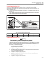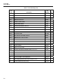
1
®
57LFC/AN
System Calibrator
Service Manual
March 2004
© 2004 Fluke Corporation, All rights reserved.
All product names are trademarks of their respective companies.
LIMITED WARRANTY AND LIMITATION OF LIABILITY
Each Fluke product is warranted to be free from defects in material and workmanship under normal use and
service. The warranty period is one year and begins on the date of shipment. Parts, product repairs, and
services are warranted for 90 days. This warranty extends only to the original buyer or end-user customer of
a Fluke authorized reseller, and does not apply to fuses, disposable batteries, or to any product which, in
Fluke's opinion, has been misused, altered, neglected, contaminated, or damaged by accident or abnormal
conditions of operation or handling. Fluke warrants that software will operate substantially in accordance
with its functional specifications for 90 days and that it has been properly recorded on non-defective media.
Fluke does not warrant that software will be error free or operate without interruption.
Fluke authorized resellers shall extend this warranty on new and unused products to end-user customers
only but have no authority to extend a greater or different warranty on behalf of Fluke. Warranty support is
available only if product is purchased through a Fluke authorized sales outlet or Buyer has paid the
applicable international price. Fluke reserves the right to invoice Buyer for importation costs of
repair/replacement parts when product purchased in one country is submitted for repair in another country.
Fluke's warranty obligation is limited, at Fluke's option, to refund of the purchase price, free of charge repair,
or replacement of a defective product which is returned to a Fluke authorized service center within the
warranty period.
To obtain warranty service, contact your nearest Fluke authorized service center to obtain return
authorization information, then send the product to that service center, with a description of the difficulty,
postage and insurance prepaid (FOB Destination). Fluke assumes no risk for damage in transit. Following
warranty repair, the product will be returned to Buyer, transportation prepaid (FOB Destination). If Fluke
determines that failure was caused by neglect, misuse, contamination, alteration, accident, or abnormal
condition of operation or handling, including overvoltage failures caused by use outside the product’s
specified rating, or normal wear and tear of mechanical components, Fluke will provide an estimate of repair
costs and obtain authorization before commencing the work. Following repair, the product will be returned to
the Buyer transportation prepaid and the Buyer will be billed for the repair and return transportation charges
(FOB Shipping Point).
THIS WARRANTY IS BUYER'S SOLE AND EXCLUSIVE REMEDY AND IS IN LIEU OF ALL OTHER
WARRANTIES, EXPRESS OR IMPLIED, INCLUDING BUT NOT LIMITED TO ANY IMPLIED WARRANTY
OF MERCHANTABILITY OR FITNESS FOR A PARTICULAR PURPOSE. FLUKE SHALL NOT BE LIABLE
FOR ANY SPECIAL, INDIRECT, INCIDENTAL, OR CONSEQUENTIAL DAMAGES OR LOSSES,
INCLUDING LOSS OF DATA, ARISING FROM ANY CAUSE OR THEORY.
Since some countries or states do not allow limitation of the term of an implied warranty, or exclusion or
limitation of incidental or consequential damages, the limitations and exclusions of this warranty may not
apply to every buyer. If any provision of this Warranty is held invalid or unenforceable by a court or other
decision-maker of competent jurisdiction, such holding will not affect the validity or enforceability of any other
provision.
Fluke Corporation
P.O. Box 9090
Everett, WA 98206-9090
U.S.A.
11/99
To register your product online, visit register.fluke.com
Fluke Europe B.V.
P.O. Box 1186
5602 BD Eindhoven
The Netherlands
Claims
Immediately upon arrival, purchaser shall check the packing container against the enclosed
packing list and shall, within thirty (30) days of arrival, give Fluke notice of shortages or any
nonconformity with the terms of the order. If purchaser fails to five notice, the delivery shall be
deemed to conform with the terms of the order.
The purchaser assumes all risk of loss or damage to instruments upon delivery by Fluke to the
carrier. If an instrument is damaged in transit, PURCHASER MUST FILE ALL CLAIMS FOR
DAMAGE WITH THE CARRIER to obtain compensation. Upon request by purchaser, Fluke will
submit an estimate of the cost to repair shipment damage.
Fluke will be happy to answer all questions to enhance the use of this instrument. Please address
your requests or correspondence to: Fluke Corporation, P.O. Box 9090, Everett, WA 98206-9090.
Interference Information
This equipment generates and uses radio frequency energy and if not installed and used in strict
accordance with the manufacturer’s instructions, may cause interference to radio and television
reception. It has been type tested and found to comply with the limits for a Class A computing
device in accordance with the specifications in Subpart J of Part 15 of FCC Rules, which are
designed to provide reasonable protection against such interference in a residential installation.
However, there is no guarantee that interference will not occur in a particular installation. If this
equipment does cause interference to radio or television reception, which can be determined by
turning the equipment off and on, the user is encouraged to try to correct the interference by one
of more of the following measures:
•
Reorient the receiving antenna
•
Relocate the equipment with respect to the receiver
•
Move the equipment away from the receiver
•
Plug the equipment into a different outlet so that the computer and receiver are on different
branch circuits
If necessary, the user should consult the dealer or an experienced radio/television technician for
additional suggestions. The user may find the following booklet prepared by the Federal
Communications Commission helpful: How to Identify and Resolve Radio-TV Interference
Problems. This booklet is available from the U.S. Government Printing Office, Washington, D.C.
20402. Stock No. 004-000-00345-4.
OPERATOR SAFETY
SUMMARY
XWWARNING
HIGH VOLTAGE
is used in the operation of this equipment
LETHAL VOLTAGE
may be present on the terminals, observe all safety precautions!
To avoid electrical shock hazard, the operator should not
electrically contact the output hi or sense hi binding posts.
During operation, lethal voltages of up to 2200 V ac or dc may
be present on these terminals.
Whenever the nature of the operation permits, keep one hand
away from equipment to reduce the hazard of current flowing
thought vital organs of the body.
Terms in this Manual
This instrument has been designed and tested in accordance with the safety standards listed in
the General Specifications, which are located in Chapter 1 of this manual. This manual contains
information and warnings which have to be followed by the user to ensure safe operation and to
retain the instrument in safe condition.
XWWARNING statements identify conditions or practices that could result in personal injury or
loss of life.
XWCAUTION statements identify conditions or practices that could result in damage to the
equipment or other property.
Symbols Marked on Equipment
X
Caution, risk of electric shock.
.
Protective ground (earth) terminal.
Q
Functional earth terminal.
W
Caution, risk of danger. Refer to the manual to maintain the safety provided by the
equipment.
XWWarning
•
Do not operate this calibrator in a position where it is difficult to operate
the power switch.
•
Do not operate this calibrator in a manner not specified in the manual or
the protection provided by the equipment may be impaired.
•
Do not operate the calibrator if it shows signs of damage or malfunction,
the protection provided by the equipment may be impaired.
•
Do not use hook-up wire on the calibrator with an insulation or current
rating of less than the calibrator output.
Power Source
The 57LFC is intended to operate from a power source that will not apply more than 246 V ac
rms between the supply conductors or between either supply conductor and ground. A protective
ground connection by way of the grounding conductor in the power cord is essential for safe
operation.
Use the Proper Fuse
To avoid fire hazard, use only the fuse specified on the line voltage selection switch label, and
which is identical in type voltage rating, and current rating.
Grounding the 57LFC
The 57LFC is Safety Class I (grounded enclosure) instruments as defined in IEC 61010 2nd
Edition. The enclosure is grounded through the grounding conductor of the power cord. To avoid
electrical shock, plug the power cord into a properly wired earth grounded receptacle before
connecting anything to any of the 57LFC terminals. A protective ground connection by way of
the grounding conductor in the power cord is essential for safe operation.
Use the Proper Power Cord
•
Use only the power cord and connector appropriate for proper operation of a 57LFC.
•
Use only a power cord that is in good condition.
•
Refer cord and connector changes to qualified service personnel.
Do Not Operate in Explosive Atmospheres
To avoid explosion, do not operate the 57LFC in an atmosphere of explosive gas.
Do Not Remove Cover
To avoid personal injury, do not remove the cover from the 57LFC. Do not operate the 57LFC
without the cover properly installed. There are no user-serviceable parts inside the 57LFC, so
there is no need for the operator to ever remove the cover.
SERVICING SAFETY
SUMMARY
FOR QUALIFIED SERVICE
PERSONNEL ONLY
Also refer to the preceding Operator Safety Summary
Do Not Service Alone
Do not perform internal service or adjustment of this product unless another person
capable of rendering first aid and resuscitation is present.
Use Care When Servicing With Power On
Dangerous voltage exist at many points inside this product. To avoid personal injury, do
not touch exposed connections and components while power is on.
Whenever the nature of the operation permits, keep one hand away from equipment to
reduce the hazard of current flowing through vital organs of the body.
Do not wear a grounded wrist strap while working on this product. A grounded wrist strap
increase the risk of current flowing through the body.
Disconnect power before removing protective panels, soldering, or replacing components.
High voltage may still be present even after disconnecting power.
FIRST AID FOR
ELECTRIC SHOCK
Free the Victim From the Live Conductor
Shut off high voltage at once and ground the circuit. If high voltage cannot be turned off
quickly, ground the circuit.
If the circuit cannot be broken or grounded, use a board, dry clothing, or other
nonconductor to free the victim.
Get Help!
Yell for help. Call an emergency number. Request medical assistance.
Never Accept Ordinary and General Tests for Death
Symptoms of electric shock may include unconsciousness, failure to breathe, absence of
pulse, pallor, and stiffness, and severe burns.
Treat the Victim
If the victim is not breathing, begin CPR or mouth-to-mouth resuscitation if you are
certified.
Table of Contents
Chapter
1
Title
Introduction and Specifications ........................................................ 1-1
Introduction........................................................................................................
Service Information ...........................................................................................
Accessories ........................................................................................................
Low Thermal EMF Test Leads......................................................................
Rack Mount Kit .............................................................................................
Shielded IEEE-488 Cables (Y8021, Y8022, and Y8023) .............................
Contacting Fluke................................................................................................
Specifications.....................................................................................................
General Specifications...................................................................................
Accuracy Specifications ................................................................................
DC Voltage Accuracy ...............................................................................
DC Current Accuracy................................................................................
Resistance Accuracy .................................................................................
AC Voltage Accuracy ...............................................................................
AC Voltage Distortion ..............................................................................
AC Current Accuracy................................................................................
AC Current Distortion...............................................................................
2
Page
1-3
1-3
1-4
1-4
1-4
1-4
1-5
1-6
1-6
1-7
1-7
1-7
1-7
1-8
1-9
1-10
1-11
Theory of Operation ........................................................................... 2-1
Introduction........................................................................................................
A1 LED PCA .....................................................................................................
A3 Motherboard PCA........................................................................................
Relay Control and Switch Matrix..................................................................
LED Control and Output Cables ...................................................................
Signal Buses ..................................................................................................
Low Volt Buffer ............................................................................................
In-guard Power Supplies ...............................................................................
Outguard Power Supplies ..............................................................................
Miscellaneous Circuits ..................................................................................
Troubleshooting Test Points..........................................................................
List of Fuses ..................................................................................................
A5 Ohms PCA ...................................................................................................
Precision Resistor Networks..........................................................................
i
2-3
2-5
2-5
2-5
2-10
2-10
2-10
2-10
2-11
2-11
2-12
2-13
2-13
2-14
57LFC/AN
Service Manual
Relay Switch Matrix and Control..................................................................
Other Control Circuits ...................................................................................
Guard Circuits ...............................................................................................
Compensation Circuits ..................................................................................
Monitor......................................................................................................
Diagnostics................................................................................................
A6 Digital Synthesis PCA .................................................................................
Precision, Dual Tracking, +/-7 V References................................................
Precision, 28bit, PWM, Dual DAC's .............................................................
DC Voltage Operation...................................................................................
DDS Waveform Generation ..........................................................................
AC Voltage Operation...................................................................................
DC Current Operation ...................................................................................
AC Current Operation ...................................................................................
Thermocouple Temperature Measurement....................................................
Iso-thermal Block Reference Junction Temperature Measurement ..............
Thermocouple Voltage Measurement: ..........................................................
Thermocouple Temperature Simulation........................................................
Analog to Digital Converter ..........................................................................
Fault Detection ..............................................................................................
Digital Control...............................................................................................
A7 Current PCA.................................................................................................
Detailed Hardware Description of DC/AC Current.......................................
Low Current Output Amplifier......................................................................
Mid-Current Output Amplifier ......................................................................
High Current Output Amplifier .....................................................................
High Current Amplifier Power Supplies (Mongo Supplies) .........................
A8 High Voltage PCA .......................................................................................
Detailed Hardware Description of the 22 V Amplifier .................................
Detailed Description of the 220 V Amplifier ................................................
Detailed Hardware Description of the High Voltage Regulator....................
Heat Sink Temperature Measurement ...........................................................
Digital Interface and Control.........................................................................
A9 Out-Guard CPU PCA...................................................................................
Real Time Clock Memory .............................................................................
IEEE-488 Interface........................................................................................
3
2-14
2-26
2-26
2-27
2-27
2-29
2-33
2-33
2-33
2-34
2-34
2-35
2-35
2-35
2-35
2-36
2-36
2-36
2-36
2-36
2-37
2-37
2-40
2-40
2-41
2-42
2-43
2-44
2-46
2-47
2-49
2-51
2-51
2-52
2-52
2-52
Calibration and Verification ............................................................... 3-1
Calibration .........................................................................................................
Procedure Architecture..................................................................................
ZERO ........................................................................................................
MAIN ........................................................................................................
DIAG.........................................................................................................
Calibration Steps ...........................................................................................
RUN ..........................................................................................................
Instruction Step (INS) ...............................................................................
Reference Step (REF) ...............................................................................
NOT ..........................................................................................................
Verification Tests...............................................................................................
Test Equipment..............................................................................................
Calibrator Configuration and Pre-check........................................................
DC Voltage Test ............................................................................................
AC Voltage Tests ..........................................................................................
AC Voltage Accuracy Test .......................................................................
ii
3-3
3-3
3-3
3-3
3-3
3-3
3-4
3-4
3-4
3-4
3-5
3-5
3-6
3-7
3-9
3-9
Contents (continued)
Frequency Accuracy Test..........................................................................
DC Current Test ............................................................................................
AC Current Test ............................................................................................
Current Output Compliance Test...................................................................
Voltage Output Compliance Test ..................................................................
Harmonic Test Levels for AC Volts..............................................................
Harmonic AC Current Test ...........................................................................
External Trigger.............................................................................................
Verification Test Check List..........................................................................
4
Maintenance........................................................................................ 4-1
Introduction........................................................................................................
Replacing the Fuse.............................................................................................
Cleaning the Air Filter .......................................................................................
Replacing PCA Modules ...................................................................................
Cleaning the Exterior .........................................................................................
5
4-3
4-3
4-4
4-6
4-7
List of Replaceable Parts ................................................................... 5-1
Introduction........................................................................................................
How to Obtain Parts...........................................................................................
Service Centers ..................................................................................................
Parts Lists...........................................................................................................
6
3-10
3-14
3-15
3-17
3-17
3-19
3-21
3-21
3-22
5-3
5-3
5-4
5-4
Schematic Diagrams .......................................................................... 6-1
iii
57LFC/AN
Service Manual
iv
List of Tables
Table
1-1.
2-1.
2-2.
2-3.
2-4.
2-5.
2-6.
2-7.
2-8.
2-9.
2-10.
2-11.
2-12.
2-13.
2-14.
2-15.
3-1.
3-2.
3-3.
3-4.
3-5.
3-6.
3-7.
3-8.
3-9.
3-10.
3-11.
3-12.
5-1.
5-2.
5-3.
5-4.
5-5.
Title
57LFC Accessories ................................................................................................
Functional Description of A3 Motherboard PCA Relays ......................................
A3 Motherboard PCA Power-up and Fault Relay States .......................................
A3 Motherboard PCA Final Relay States by Instrument State ..............................
Control Register States by Instrument State...........................................................
Functional Description of LED Signals .................................................................
A3 Motherboard PCA Test Points List ..................................................................
Functional Description of A5 Ohms PCA Relays..................................................
A5 Ohms PCA Power-up and Fault Relay States ..................................................
Final Relay States by Instrument State ..................................................................
Functional Description of Signals ..........................................................................
Compliance Voltage Thresholds ............................................................................
OTEST Register States by Instrument State ..........................................................
OCHK Register States by Instrument State ...........................................................
Diagnostic Values by Instrument State ..................................................................
Supply Values as a Function of Ranges .................................................................
Recommended Equipment for Calibration and Verification..................................
DC Volts Measurement Limits ..............................................................................
AC Volts Measurement Limits ..............................................................................
AC Frequency Values ............................................................................................
4-Wire Ohm Values ...............................................................................................
2-Wire Ohm Values ...............................................................................................
DC Current Readings .............................................................................................
AC Current Limits..................................................................................................
Current Output Compliance Limits........................................................................
Voltage Output Compliance Limits .......................................................................
Harmonic Test Values for AC Volts ......................................................................
Harmonic Test Values for AC Current ..................................................................
Final Assembly.......................................................................................................
A1 LED PCA .........................................................................................................
A3 Motherboard PCA ............................................................................................
A5 Ohms PCA........................................................................................................
A6 Digital Synthesis PCA......................................................................................
v
Page
1-4
2-6
2-7
2-8
2-9
2-10
2-12
2-17
2-20
2-21
2-26
2-28
2-30
2-30
2-32
2-47
3-6
3-8
3-10
3-11
3-12
3-13
3-14
3-16
3-17
3-18
3-20
3-21
5-5
5-9
5-10
5-18
5-23
57LFC/AN
Service Manual
5-6.
5-7.
5-8.
A7 Current PCA..................................................................................................... 5-31
A8 High Voltage PCA ........................................................................................... 5-39
A9 Out-Guard CPU PCA ....................................................................................... 5-55
vi
List of Figures
Figure
2-1.
2-2.
2-3.
2-4.
2-5.
2-6.
2-7.
3-1.
3-2.
3-3.
3-4.
3-5.
3-6.
3-7.
3-8.
3-9.
3-10.
4-1.
4-2.
4-3.
5-1.
5-2.
5-3.
5-4.
5-5.
5-6.
5-7.
5-8.
6-1.
6-2.
6-3.
6-4.
6-5.
6-6.
6-7.
Title
57LFC Block Diagram...........................................................................................
Block Diagram of the A5 Ohms PCA ....................................................................
A5 Ohms PCA High/Low Output ..........................................................................
A5 Ohms PCA High/Low Sense............................................................................
DC Current Functions ............................................................................................
AC Current Functions ............................................................................................
A8 High Voltage PCA 22 V and 220 V Amplifier ................................................
8508A Connections to the 57LFC for DC Volts Measurement .............................
8508A Connections to the 57LFC for AC Volts Measurement .............................
8508A Connections to the 57LFC for AC Frequency Measurement .....................
8508A Connections to the 57LFC for 4-Wire Ohms .............................................
8508A Connections to the 57LFC for 2-Wire Compensated Ohms.......................
8508A Connections to the 57LFC for DC Current Measurement..........................
8508A Connections to the 57LFC for AC Current Measurement..........................
8508A Connections to the 57LFC for Load Current Compliance Test..................
8508A Connections to the 57LFC for Voltage Compliance Testing .....................
Harmonic Test Setup..............................................................................................
Replacing the Fuse .................................................................................................
Accessing the Air Filter..........................................................................................
Exploded View of the Calibrator ...........................................................................
Final Assembly.......................................................................................................
A1 LED PCA .........................................................................................................
A3 Motherboard PCA ............................................................................................
A5 Ohms PCA........................................................................................................
A6 Digital Synthesis PCA......................................................................................
A7 Current PCA.....................................................................................................
A8 High Voltage PCA ...........................................................................................
A9 Out-Guard PCA................................................................................................
A1 LED PCA .........................................................................................................
A3 Motherboard PCA ............................................................................................
A5 Ohms PCA........................................................................................................
A6 Digital Synthesis PCA......................................................................................
A7 Current PCA.....................................................................................................
A8 High Voltage PCA ...........................................................................................
A9 Out-Guard CPU PCA .......................................................................................
vii
Page
2-4
2-13
2-15
2-16
2-38
2-39
2-45
3-7
3-9
3-11
3-12
3-13
3-14
3-15
3-17
3-18
3-19
4-4
4-5
4-6
5-7
5-9
5-17
5-22
5-30
5-38
5-54
5-59
6-3
6-5
6-11
6-17
6-26
6-32
6-37
57LFC/AN
Service Manual
viii
Chapter 1
Introduction and Specifications
Title
Introduction........................................................................................................
Service Information ...........................................................................................
Accessories ........................................................................................................
Low Thermal EMF Test Leads......................................................................
Rack Mount Kit .............................................................................................
Shielded IEEE-488 Cables (Y8021, Y8022, and Y8023) .............................
Contacting Fluke................................................................................................
Specifications.....................................................................................................
General Specifications...................................................................................
Accuracy Specifications ................................................................................
DC Voltage Accuracy ...............................................................................
DC Current Accuracy................................................................................
Resistance Accuracy .................................................................................
AC Voltage Accuracy ...............................................................................
AC Voltage Distortion ..............................................................................
AC Current Accuracy................................................................................
AC Current Distortion...............................................................................
Page
1-3
1-3
1-4
1-4
1-4
1-4
1-5
1-6
1-6
1-7
1-7
1-7
1-7
1-8
1-9
1-10
1-11
1-1
57LFC/AN
Service Manual
1-2
Introduction and Specifications
Introduction
1
Introduction
The Fluke Model 57LFC System Calibrator (hereafter called the Calibrator) is a precise
instrument that calibrates a wide variety of electrical measuring instruments. This
calibrator maintains a high accuracy over a wide ambient temperature range, and is able
to test instruments in harsh environments, eliminating the restriction of calibrating only in
a temperature-controlled standards laboratory. With a 57LFC, you can calibrate precision
multimeters that measure ac or dc voltage, ac or dc current, and resistance. The Calibrator
operates in a similar manner to the 57XXA series calibrators.
Specifications are provided at the end of this chapter. The Calibrator is a fullyprogrammable precision source of the following:
•
DC voltage to 220 V.
•
AC voltage to 220 V rms, with output available from 10 Hz to 100 kHz.
•
AC and DC current to 2.2 A, with AC output available from 10 Hz to 20 kHz.
•
Resistance in values from 0 Ω to 19 MΩ in 1 and 1.9x.
Features of the calibrator include the following:
•
Automatic meter error calculation obtained through using a simple remote adjust.
•
Programmable entry limits used for restricting the levels that can be remotely keyed
into the calibrator, preventing access to levels that may be harmful to equipment or
personnel.
•
Real-time clock and calendar.
•
Offset and scaling modes that simplify linearity testing of multimeters.
•
Standard IEEE-488 (GPIB) interface, complying with ANSI/IEEE Standards 488.11987 and 488.2-1987.
•
Internal self-testing and diagnostics of analog and digital functions.
•
Status LEDs on front panel to indicate standby (yellow), operate (green), high
voltage (red), and fault (red and yellow).
Service Information
Each calibrator is warranted to the original purchaser for a period of one year beginning
on the date received. The warranty is located at the front of this manual.
Service and technical advice for the calibrator is available at Fluke Service Centers. For a
complete list of Fluke Service Centers, visit www.fluke.com.
A worldwide network of Fluke service centers supports Fluke instruments and assists
customers in many ways. Most service centers have standards and calibration laboratories
certified by local national standards organizations. The following is a partial list of the
services provided by most service centers:
•
Repair and certified traceable calibration of all Fluke products.
•
Certified traceable calibration of many non-Fluke standards and calibrators.
•
Worldwide exchange of calibrator internal modules. Delivery inside the U.S.A. is
typically within 48 hours.
•
Service agreements with the flexibility to suit your needs. These can be a simple
warranty extension or an agreement that includes on-site support. Calibration service
agreements are also available in many areas.
1-3
57LFC/AN
Service Manual
•
Training programs and seminars, including laboratory metrology, system
applications, and product maintenance.
•
Application help and consulting, including system design, hardware selection,
custom software, site evaluation and installation.
•
Replacement parts inventory, including recommended spare parts and module kits.
Visit www.fluke.com for locations and phone numbers of authorized Fluke service
centers.
Accessories
Table 1-1 summarizes the accessories available for the Calibrator. Following the table is
a brief description of each accessory.
Table 1-1. 57LFC Accessories
Model
Description
5440A-7002
Low Thermal EMF Test Lead Set with Banana Plugs:
One 4 ft. cable (122 cm) and two 2 ft. (61 cm) cables.
5440A-7003
Low Thermal EMF Test Lead Set with Spade Lugs.
Two 4 ft. (122 cm) cables and One 2 ft. (61 cm) cable.
Y8021
IEEE-488 Shielded Interface Cable, 1 Meter
Y8022
IEEE-488 Shielded Interface Cable, 2 Meters
Y5537
Rack Mount Kit for 57LFC and 5500A
Low Thermal EMF Test Leads
Two types of low thermal test leads are available. These cables are designed to exhibit
low thermal emfs. The types available are:
•
Model 5440A-7002. Low Thermal Test Lead cables with banana plugs.
Set includes one 4 ft. (122 cm) cable and two 2 ft. (61 cm) cables. Each cable
includes two conductors and a shield lead.
•
Model 5440A-7003. Low Thermal Test Lead cables with spade lugs.
Set includes two 4 ft. (122 cm) cables and one 2 ft. (61 cm) cable. Each cable
includes two conductors and a shield lead. Shield lead has a banana plug connector.
Rack Mount Kit
The rack mount kit provides all the hardware necessary to mount the 57LFC. Rack mount
instructions are included with each kit.
Shielded IEEE-488 Cables (Y8021, Y8022, and Y8023)
Shielded IEEE-488 cables are available in two lengths (See Table 1-1). The cables attach
the calibrator to any other IEEE-488 device. Each cable has double 24-pin connectors at
both ends to allow stacking. Metric threaded mounting screws are provided with each
connector. Figure 4-2 in Chapter 4 shows the pinout for the IEEE-488 connector.
1-4
Introduction and Specifications
Contacting Fluke
1
Contacting Fluke
All Calibrators delivered to the Navy, contractors and subcontractors for the RTCASS
program will be repaired and calibrated at the Fluke Technical Support Center in Everett,
Washington. Contact Fluke Technical Support at 1-888-993-5853 or by sending a fax to
1-425-446-6390. The address for the Fluke Technical Support
Center address is:
Fluke Technical Support Center
1420 75th ST SW
Everett, WA 98203-6256
U. S. A.
Once full production is started the following service centers will also maintain and
calibrate the Calibrator in Europe.
FLUKE NEDERLAND B.V.
Customer Support Services
Science Park Eindhoven 5108
5692 EC Son
Netherlands
FLUKE DEUTSCHLAND GMBH
Customer Support Services
Heinrich Hertz Straße 11
D-34123 Kassel
Germany
and in Asia,
FLUKE SOUTH EAST ASIA PTE LTD.
Service Center
83 Clemenceau Avenue
#15-15/06 Ue Square
239920
Singapore
1-5
57LFC/AN
Service Manual
Specifications
The 57LFC System Calibrators are verified and calibrated at the factory prior to shipment
to ensure they meet the accuracy standards required for all certified calibration
laboratories. By calibrating to the specifications in this chapter, you can maintain the high
performance level throughout the life of your calibrator.
Specifications are valid after a warm-up period of twice the time the calibrator has been
turned off, up to a maximum of 30 minutes. For example, if the calibrator has been turned
off for five minutes, the warm-up period is ten minutes.
To ensure the validity of the specifications, a dc zeros calibration must be performed at
least every 15 days. If more than 15 days elapse without a dc zeros calibration a warning
message appears. This procedure does not require any external equipment or connections
and takes approximately 5 minutes to complete.
General Specifications
Factory set IEEE488 address ....... 4
Warm-up Time ............................... Twice the time since last warmed up, to a maximum of 30 minutes
Temperature Performance............ Operating: 0 to 50 °C
Calibration: 15 to 37.7 °C
Storage: -40 to 75 °C
Temperature Coefficient ............... Temperature Coefficient for temperatures outside tcal ±5 °C is 10% of
the 1-year spec per °C.
Relative Humidity
Operating: ................................... <95% to 43 °C (non-condensing), <40% to 50 °C.
Storage: ....................................... <95%, non-condensing
Altitude
Operating: ................................... 3,050 m (10,000 ft) maximum
Non-operating: ........................... 12,200 m (40,000 ft) maximum
Safety ............................................. Designed to comply with IEC 61010-1 2000-1; ANSI/ISA-S82.01-1994;
CAN/CSA-C22.2 No. 1010.1-92
Analog Low Isolation .................... 20 V
EMC ................................................ Designed to comply with IEC 61326-1 2000-11 (EMC) Class A Criteria
C
Line Power
Line Voltage (selectable): ........... 100 V, 120 V, 208 V, and 230 V
Line Frequency: .......................... 47 to 63 Hz
Line Voltage Variation: ................ ±7% about line voltage setting
Maximum VA: ............................. 200
Settling Time.................................. ≤ 3 to 10 seconds, similar to 5700A.
Chassis Dimensions, H x W x D ... 178 mm x 432 mm x 457 mm (7 in x 17 in x 18 in) maximum
Weight ............................................ Less than 18.15 kg (40 pounds)
Electrical/Signal Interface............. Fluke 5700A/LP equivalent signal interface, AC Mains, IEEE-488, and
RS-232 connectors, AC power switch, and Line Voltage selection all on
front panel
Cooling........................................... 1.42 cubic meters (50 cubic feet) per minute
XWCaution
Internal damage may occur if excessive external power is
applied to the binding posts while the instrument is operating in
current, voltage, or ohms. In voltage and current, exceeding
30 V may cause damage. In ohms, do not exceed the maximum
specified current.
1-6
Introduction and Specifications
Specifications
1
Accuracy Specifications
DC Voltage Accuracy
Absolute Uncertainty,
tcal ±5 °C
±(% output + V) 1 Year
Ranges
Resolution
0 mV to 220 mV
0.004%
3 µV
0.1 µV
0 V to 2.2 V
0 V to 11 V
0 V to 22 V
0 V to 220 V
0.0025%
0.0025%
0.0025%
0.004%
3 µV
30 µV
30 µV
300 µV
1 µV
10 µV
10 µV
100 µV
Maximum Burden [1]
50 Ω output impedance
50 mA
50 mA
50 mA
20 mA
[1] Remote sensing provided on all but 220 mV range.
Note: minimum output 0 V for all ranges.
DC Current Accuracy
Ranges
Absolute Uncertainty,
tcal ±5°C±
(% of output + A) 1 year
0 µA to 220 µA
0.05%
0.02 µA
0 mA to 2.2 mA
0 mA to 22 mA
0 mA to 220 mA
0 A to 2.2 A
0.05%
0.05%
0.05%
0.07%
0.05 µA
0.25 µA
2.5 µA
40 µA
Resolution
1 ηA
0.01 µA
0.1 µA
1 µA
10 µA
Maximum
Compliance
Voltage
Maximum Inductive
Load
10 V
400 µH
10 V
10 V
10 V
4V
400 µH
400 µH
400 µH
400 µH
Resistance Accuracy
Nominal Resistance
Value [1]
Absolute Uncertainty of
Characterized Value,
tcal ± 5 °C
± (Ω) 1 Year
Full Specification
Current
Maximum Peak
Current
Two-Wire Active
Compensation
Adder (ohms) [2]
0Ω
0.001 Ω
8 mA to 200 mA
220 mA
0.001
1Ω
0.001 Ω
8 mA to 100 mA
220 mA
0.001
1.9 Ω
0.002 Ω
8 mA to 100 mA
220 mA
0.001
10 Ω
0.004 Ω
8 mA to 11 mA
220 mA
0.001
19 Ω
0.008 Ω
8 mA to 11 mA
160 mA
0.001
100 Ω
0.01 Ω
8 mA to 11 mA
70 mA
0.001
190 Ω
0.02 Ω
8 mA to 11 mA
50 mA
0.001
1 kΩ
0.1 Ω
1 mA to 2 mA
22 mA
0.010
1.9 kΩ
0.2 Ω
1 mA to 1.5 mA
16 mA
0.010
10 kΩ
1Ω
0.1 mA to 0.5 mA
3 mA
0.100
19 kΩ
2Ω
0.05 mA to 0.25 mA
1.6 mA
0.200
100 kΩ
10 Ω
0.01 mA to 0.1 mA
0.3 mA
1.000
190 kΩ
20 Ω
5 µA to 50 µA
0.16 mA
2.000
1 MΩ
100 Ω
5 µA to 20 µA
30 µA
NA
1.9 MΩ
200 Ω
2.5 µA to 10 µA
16 µA
NA
10 MΩ
4 kΩ
0.5 µA to 2 µA
3 µA
NA
19 MΩ
10 kΩ
0.25 µA to 1 µA
1.6 µA
NA
[1] Discrete resistors with characterized values stored in non-volatile memory. Specifications apply to the characterized value using 4-wire connections.
[2] Active two-wire compensation may be selected for values up to 190 kΩ. Active compensation is 11 mA load and 2 V burden minimum.
1-7
57LFC/AN
Service Manual
AC Voltage Accuracy
Ranges
Frequency
10 mV to 22 mV
22 mV to 220 mV
0.22 V to 2.2 V
2.2 V to 22 V
22 V to 220 V
[2]
Absolute Uncertainty,
tcal ±5 °C
± (% output + V) 1 year
10 Hz to 45 Hz
45 Hz to 20 kHz
20 kHz to 50 kHz
50 kHz to 100 kHz
10 Hz to 45 Hz
45 Hz to 20 kHz
20 kHz to 50 kHz
50 kHz to 100 kHz
10 Hz to 45 Hz
45 Hz to 20 kHz
20 kHz to 50 kHz
50 to 100 kHz
10 Hz to 45 Hz
45 Hz to 20 kHz
0.15%
0.08%
0.25%
0.5%
0.15%
0.05%
0.25%
0.4%
0.1%
0.05%
0.1%
0.25%
0.1%
0.05%
20 µV
20 µV
20 µV
50 µV
50 µV
50 µV
50 µV
200 µV
250 µV
100 µV
320 µV
2000 µV
1 mV
1 mV
20 kHz to 50 kHz
50 kHz to 100 kHz
10 Hz to 45 Hz
45 Hz to 20 kHz
20 kHz to 50 kHz
50 kHz to 100 kHz
0.1%
0.25%
0.1%
0.05%
0.25%
0.5%
1 mV
2 mV
10 mV
10 mV
20 mV
50 mV
Resolution
Maximum
Burden [1] [2]
1 µV
50 Ω output
impedance
1 µV
50 Ω output
impedance
10 µV
50 mA
100 µV
50 mA
1 mV
20 mA
[1] Remote sensing provided on all but 22 mV and 220 mV ranges. Maximum output current is reduced by 50% above 40 °C. Maximum load capacitance
is 500 pF.
[2] V x Hz limited to 11.8e6.
Note: Frequency uncertainty is specified to be 0.01% of frequency setting.
1-8
Introduction and Specifications
Specifications
1
AC Voltage Distortion
Ranges
10 mV to 22 mV
22 mV to 220 mV
0.22 V to 2.2 V
2.2 V to 22 V
22 V to 220 V
Max Distortion and noise
10 Hz to 10 MHz Bandwidth
±(% output + V) [1]
Frequency
10 Hz to 45 Hz
45 Hz to 20 kHz
20 kHz to 50 kHz
50 kHz to 100 kHz
10 Hz to 45 Hz
45 Hz to 20 kHz
20 kHz to 50 kHz
50 kHz to 100 kHz
10 Hz to 45 Hz
45 Hz to 20 kHz
20 kHz to 50 kHz
50 kHz to 100 kHz
10 Hz to 45 Hz
45 Hz to 20 kHz
0.15%
0.035%
0.15%
0.25%
0.15%
0.035%
0.15%
0.20%
0.15%
0.035%
0.15%
0.20%
0.15%
0.035%
90 µV
90 µV
90 µV
90 µV
90 µV
90 µV
90 µV
90 µV
200 µV
200 µV
200 µV
200 µV
2 mV
2 mV
20 kHz to 50 kHz
50 kHz to 100 kHz
10 Hz to 45 Hz
45 Hz to 20 kHz
20 kHz to 50 kHz
50 kHz to 100 kHz
0.2%
0.5%
0.15%
0.05%
0.8%
1.0%
2 mV
2 mV
10 mV
10 mV
10 mV
10 mV
[1] For larger resistive loads, multiply uncertainty specifications by (actual load/maximum full load for accuracy)2.
1-9
57LFC/AN
Service Manual
AC Current Accuracy
Ranges [3]
Frequency
10 Hz to 20 Hz
20 Hz to 45 Hz
30 µA to 220 µA
45 Hz to 1 kHz
1 kHz to 5 kHz
5 kHz to 10 kHz
10 Hz to 20 Hz
20 Hz to 45 Hz
0.22 mA to 2.2 mA 45 Hz to 1 kHz
1 kHz to 5 kHz
5 kHz to 10 kHz
10 Hz to 20 Hz
20 Hz to 45 Hz
45 Hz to 1 kHz
2.2 mA to 22 mA
1 kHz to 5 kHz
5 kHz to 10 kHz
10 kHz to 20 kHz
10 Hz to 20 Hz
20 Hz to 45 Hz
45 Hz to 1 kHz
22 mA to 220 mA
1 kHz to 5 kHz
5 kHz to 10 kHz
10 kHz to 20 kHz
10 Hz to 45 Hz
0.22 A to 2.2 A
45 Hz to 1 kHz
1 kHz to 5 kHz
5 kHz to 10 kHz
Absolute Uncertainty,
tcal ±5 °C
±(% of output + A) 1 year
0.3%
0.15%
0.125%
0.4%
1.5%
0.2%
0.15%
0.1%
0.2%
0.8%
0.2%
0.1%
0.1%
0.2%
0.4%
0.8%
0.18%
0.1%
0.1%
0.3%
0.4%
0.8%
0.18%
0.1%
1%
5%
0.2 µA
0.2 µA
0.2 µA
0.3 µA
0.4 µA
0.3 µA
0.3 µA
0.3 µA
0.3 µA
0.5 µA
3 µA
3 µA
3 µA
3 µA
5 µA
5 µA
30 µA
30 µA
30 µA
50 µA
100 µA
200 µA
300 µA
300 µA
3000 µA
5000 µA
Resolution
7V
50 µH
0.1 µA
7V
50 µH
1 µA
7V
50 µH
10 µA
7V
50 µH
100 µA
4V
2.5 µH
[2] See AC Current Compliance Adder and Distortion Table for impact of compliance voltage on specification.
[3] I-guard, (as on the 5700A rear panel), required when sourcing low-level currents through a long cable.
1-10
Maximum
Inductive
Load [1]
0.01 µA
[1] 400 µH with inductive compensation ON.
Note: Frequency uncertainty is specified to be 0.01% of frequency setting.
Maximum
Compliance
Voltage (rms) [2]
Introduction and Specifications
Specifications
1
AC Current Distortion
Ranges
30 µA to 220 µA
0.22 mA to 2.2 mA
2.2 mA to 22 mA
22 mA to 220 mA
0.22 A to 2.2 A
Frequency
10 Hz to 20 Hz
20 Hz to 45 Hz
45 Hz to 1 kHz
1 kHz to 5 kHz
5 kHz to 10 kHz
10 Hz to 20 Hz
20 Hz to 45 Hz
45 Hz to 1 kHz
1 kHz to 5 kHz
5 kHz to 10 kHz
10 Hz to 20 Hz
20 Hz to 45 Hz
45 Hz to 1 kHz
1 kHz to 5 kHz
5 kHz to 10 kHz
10 kHz to 20 kHz
10 Hz to 20 Hz
20 Hz to 45 Hz
45 Hz to 1 kHz
1 kHz to 5 kHz
5 kHz to 10 kHz
10 kHz to 20 kHz
10 Hz to 45 Hz
45 Hz to 1 kHz
1 kHz to 5 kHz
5 Hz to 10 kHz
Max Distortion & Noise
10 Hz to 50 kHz BW
<0.5V Burden
±(%output + A)
Maximum Resistive
Load For Full
Accuracy Ω [1]
20 kΩ
10 kΩ
3.18 kΩ
318 Ω
18 Ω
0.15%
0.1%
0.05%
0.5%
1.0%
0.15%
0.06%
0.05%
0.5%
1.0%
0.15%
0.05%
0.07%
0.3%
0.7%
1.0%
0.15%
0.05%
0.07%
0.30%
0.70%
1.0%
0.2%
0.07%
1.0%
2.0%
0.5 µA
0.5 µA
0.5 µA
0.5 µA
0.5 µA
1.5 µA
1.5 µA
1.5 µA
1.5 µA
1.5 µA
5 µA
5 µA
5 µA
5 µA
5 µA
5 µA
50 µA
50 µA
50 µA
50 µA
50 µA
50 µA
500 µA
500 µA
500 µA
500 µA
[1] For larger resistive loads, multiply uncertainty specifications by actual load/maximum full load for accuracy.
Note: Current times Load cannot exceed the maximum compliance voltage.
1-11
57LFC/AN
Service Manual
1-12
Chapter 2
Theory of Operation
Title
Introduction........................................................................................................
A1 LED PCA .....................................................................................................
A3 Motherboard PCA........................................................................................
Relay Control and Switch Matrix..................................................................
LED Control and Output Cables ...................................................................
Signal Buses ..................................................................................................
Low Volt Buffer ............................................................................................
In-guard Power Supplies ...............................................................................
Outguard Power Supplies ..............................................................................
Miscellaneous Circuits ..................................................................................
Troubleshooting Test Points..........................................................................
List of Fuses ..................................................................................................
A5 Ohms PCA ...................................................................................................
Precision Resistor Networks..........................................................................
Relay Switch Matrix and Control..................................................................
Other Control Circuits ...................................................................................
Guard Circuits ...............................................................................................
Compensation Circuits ..................................................................................
Monitor......................................................................................................
Diagnostics................................................................................................
A6 Digital Synthesis PCA .................................................................................
Precision, Dual Tracking, +/-7 V References................................................
Precision, 28bit, PWM, Dual DAC's .............................................................
DC Voltage Operation...................................................................................
DDS Waveform Generation ..........................................................................
AC Voltage Operation...................................................................................
DC Current Operation ...................................................................................
AC Current Operation ...................................................................................
Thermocouple Temperature Measurement....................................................
Iso-thermal Block Reference Junction Temperature Measurement ..............
Thermocouple Voltage Measurement: ..........................................................
Thermocouple Temperature Simulation........................................................
Analog to Digital Converter ..........................................................................
Fault Detection ..............................................................................................
Digital Control...............................................................................................
A7 Current PCA.................................................................................................
Page
2-3
2-5
2-5
2-5
2-10
2-10
2-10
2-10
2-11
2-11
2-12
2-13
2-13
2-14
2-14
2-26
2-26
2-27
2-27
2-29
2-33
2-33
2-33
2-34
2-34
2-35
2-35
2-35
2-35
2-36
2-36
2-36
2-36
2-36
2-37
2-37
2-1
57LFC/AN
Service Manual
Detailed Hardware Description of DC/AC Current.......................................
Low Current Output Amplifier......................................................................
Mid-Current Output Amplifier ......................................................................
High Current Output Amplifier .....................................................................
High Current Amplifier Power Supplies (Mongo Supplies) .........................
A8 High Voltage PCA .......................................................................................
Detailed Hardware Description of the 22 V Amplifier .................................
Detailed Description of the 220 V Amplifier ................................................
Detailed Hardware Description of the High Voltage Regulator....................
Heat Sink Temperature Measurement ...........................................................
Digital Interface and Control.........................................................................
A9 Out-Guard CPU PCA...................................................................................
Real Time Clock Memory .............................................................................
IEEE-488 Interface........................................................................................
2-2
2-40
2-40
2-41
2-42
2-43
2-44
2-46
2-47
2-49
2-51
2-51
2-52
2-52
2-52
Theory of Operation
Introduction
2
Introduction
This Chapter is intended to provide a detailed description and analysis, where
appropriate, of the printed circuit board assemblies (PCAs) used in the 57LFC System
Calibrator. The Calibrator contains the following PCAs.
•
A1 LED PCA
•
A3 Motherboard PCA
•
A5 Ohms PCA
•
A6 Digital Synthesis PCA
•
A7 Current PCA
•
A8 High Voltage PCA
•
A9 Out-Guard CPU PCA
See Figure 2-1 for a block diagram of the 57LFC System Calibrator.
2-3
57LFC/AN
Service Manual
A9
Outguard
Controller
IEEE488
A6
Inguard
Controller
0 to ±2.2 V
AC/DC
RS232
Mains
Transformer
A6
Digital
Synthesis &
Reference
S
W
I
T
C
H
A3
Outguard
Power
±12 V
+5 V
A3
Inguard
Power
A3
Output
Switch
A5
OHMS
0 to 19 M
A7
Current
±15 V
±5 V
+6 V
0 to ±2.2 A
AC/DC
A3
High
Voltage
Power
A8
High
Voltage
±45 V
±180 V
2 to ±220 V
AC/DC
Binding
Posts
S
W
I
T
C
H
S
W
I
T
C
H
S
W
I
T
C
H
apv101f.eps
Figure 2-1. 57LFC Block Diagram
2-4
Theory of Operation
A1 LED PCA
2
A1 LED PCA
The Calibrator front panel A1 LED PCA provides the only visual indication of the
instrument operation. These LEDs provide a color-coded scheme for the instrument
status.
XWWarning
This instrument is capable of outputting lethal voltages.
Observe all safety precautions.
While the LEDs should provide years of operation, they are
subject to wear out like any other component. Never touch the
binding posts without first checking the output with a
multimeter.
The front panel A1 LED PCA is connected to and controlled by the A3 Motherboard
PCA. A cable is used to connect the A3 Motherboard PCA to the A1 LED PCA. On
power up, the yellow LED will light indicating that the instrument has moved into a
standby state. The green LED is used to indicate that the instrument is in operate and
there may be live voltages on the binding posts. The red LED is used to indicate that the
instrument may be outputting hazardous voltages greater than 30 V rms. If diagnostic
failures occur during power-up, both the yellow and red LEDs light. If all three LEDs are
lit, the instrument is broken and must be sent to a qualified technician for repair.
A3 Motherboard PCA
The following discussion covers the theory of operations for the A3 Motherboard PCA
circuits. This A3 Motherboard PCA generally carries power as well as system signal
buses to the circuit cards. The A3 Motherboard PCA can be divided into several areas: 1)
relay control and switch matrix, 2) LED control and output cables, 3) analog and digital
buses, 4) low volt buffer, 5) in-guard power supplies, 6) out-guard power supplies, 7)
miscellaneous circuits, and 8) list of fuses. Please refer to the A3 Motherboard PCA
schematics for this discussion.
XWWarning
The A3 Motherboard PCA contains lethal voltages. Only
qualified technicians should do troubleshooting.
Relay Control and Switch Matrix
The relay matrix is shown on Sheet 1 of the A3 Motherboard PCA schematic, and the
relay control is shown on Sheet 5. Some of the purposes of the relay matrix are to provide
isolation between the output binding posts and the internal circuitry during standby, and
provide isolation when running zero calibration or diagnostics. The functions of the
relays are shown in Table 2-1. The relay control circuits consist of U3, U5, U6, U8, and
U9. For U3 (74HC138), the IG_CS1 signal is generated on the A6 Digital Synthesis
PCA. U8 selects the driver latch used to set or reset the latching relays.
2-5
57LFC/AN
Service Manual
Table 2-1. Functional Description of A3 Motherboard PCA Relays
Relay
K1
Functional Description
Reset: connect LO’s to the A6 Digital Synthesis PCA; connect OUT_LO to the A6 Digital
Synthesis PCA RET_LO, and connects IN_SNS_LO to the A6 SNS_LO
Set: disconnect LO’s from the A6 Digital Synthesis PCA; disconnect the A6 Digital
Synthesis PCA RET_LO and SNS_LO from the LO input terminals
K2
Reset: select internal sensing; connect OSNS_HI to IN_SNS_HI and OSNS_LO to
IN_SNS_LO
Set: select remote sensing; connect SNS_HI to IN_SNS_HI and SNS_LO to
IN_SNS_LO
K3
Reset: connect the Digital Synthesis PCA divider; connect IN_SNS_HI to the A6 VDIV
Set: disconnect the Digital Synthesis PCA divider; disconnect IN_SNS_HI from VDIV
K4
Reset: select VMID for output; connect VMID to OUT_HI
Set: disconnect VMID from output; disconnect VMID from OUT_HI
K5
Reset: select external guard; disconnect GUARD from SCOM
Set: select internal guard; connect GUARD to SCOM
K6
Reset: select the 2 V buffer amp; connect V3BUF to VMID for output
Set: disconnect the 2 V buffer amp; disconnect V3BUF from VMID
K7
Reset: disconnect the A8 High Voltage PCA output; disconnect OUT_220V from
OUT_HI
Set: select the A8 High Voltage PCA output; connect OUT_220V to OUT_HI
K8
Reset: disconnect HIGUARD (IGUARD) from GUARD (VGUARD)
Set: connect HIGUARD to GUARD
K9
Reset: connect A6 Digital Synthesis PCA LO return; connect OUT_LO to A6_RET_LO
Set: disconnect the A6 Digital Synthesis PCA LO return, disconnect OUT_LO from
A6_RET_LO
K10
Reset: provide an internal VMID sense path, connect VMID to the A6 VDIV
Set: normal operation; disconnect VMID from VDIV
K11
Reset: provide an internal 220 V sense path; connect OUT_220V to VMID
Set: normal operation; disconnect OUT_220V from VMID
On power up, the relays are forced into a benign setting to protect circuitry and the
customer. Table 2-2 shows the state of the A3 Motherboard PCA relays after power up.
Table 2-3 shows the A3 Motherboard PCA relay states when in several states (power up
and standby). Table 2-4 shows the status of control lines for all modes of A3
Motherboard PCA operation.
2-6
Theory of Operation
A3 Motherboard PCA
2
Table 2-2. A3 Motherboard PCA Power-up and Fault Relay States
Relay
State on Power-up or after Fault
K1
Set: disconnect A6 Digital Synthesis PCA LO sense
K2
Reset: select internal sensing
K3
Set: disconnect the A6 Digital Synthesis PCA divider
K4
Set: disconnect VMID from output
K5
Reset: select external guard
K6
Undefined
K7
Reset: disconnect the A8 High Voltage PCA output
K8
Undefined
K9
Set: disconnect the A6 Digital Synthesis PCA LO return
K10
Undefined
K11
Undefined
2-7
57LFC/AN
Service Manual
Table 2-3. A3 Motherboard PCA Final Relay States by Instrument State
Relay (Virtual) Register:
Guard:
ext
Int
ext
int
Sense:
int
int
rem
rem
g=0
g=1
g=0
g=1
K11
K10
K9
K8
K7
K6
K5
K4
K3
K2
K1
d=0
d=0
d=1
d=1
4
2
1
8
4
2
1
8
4
2
1
hex
hex
hex
hex
Power Up
r
s
s
s
r
s
r
s
s
r
s
Dormant
r
s
s
s
r
s
r
s
s
r
s
External Guard (mod
mask 0010h)
x
x
x
x
x
x
r
x
x
x
x
Internal Guard
x
x
x
x
x
x
s
x
x
x
x
Internal Sense (mod mast
002h)
x
x
x
x
x
x
x
x
x
r
x
External Sense
x
x
x
x
x
x
x
x
x
s
x
22 mV A6 Output
r
s
r
s
r
s
g
r
s
r
r
Standby 22 mV A6
Output
r
s
s
s
r
s
r
s
s
r
s
220 mV A6 Output
r
s
r
s
r
s
g
r
s
r
r
Standby 220 mV A6
Output
r
s
s
s
r
s
r
s
s
r
s
Optt 3.3 V A6 Output
using LO Comp Amp
r
s
s
s
r
s
g
r
r
d
r
03a0
03b0 03a2
03a2
Opt 3.3 V A6 Output
r
s
r
s
r
s
g
r
r
d
r
0210
02b0
02b2
Standby Opt 3.3 A6
Output
r
s
s
s
r
s
r
s
s
r
s
2.2 V Buffer Out using LO
Comp Amp
r
s
s
s
r
r
g
r
r
d
r
0380
0390
0382
0392
2.2 V Buffer Output
r
s
r
s
r
r
g
r
r
d
r
0280
0290
0282
0292
r
s
s
r
r
r
s
s
r
s
s
s
r
s
g
r
r
d
r
03a0
03b0
03a2
03b2
02a0
02b0
02a2
02b2
Relay:
Instrument State\Bit
Weight:
MBRLY
Standby 2.2 V Buffer
Output
03ad
03ad
0000
0000
0010
0000
0000
02a4
02b4
0010
0002
0002
-
-
-
-
03ad
02a4
02b4
03ad
02a2
03ad
038d
22 V A8 Output using LO
Comp Amp
r
s
22 V A8 Output
r
s
r
s
r
s
g
r
r
d
r
Standby 22 V A8 Output
r
s
s
s
r
s
r
s
s
r
s
220 V A8 Output Using
LO Comp Amp
r
s
s
s
s
s
g
s
r
d
r
03e8
03f8
03ea
03fa
220 V A8 Output
r
s
r
s
s
s
g
s
r
d
r
02e8
02f8
02ea
02fa
Standby 220 V A8 Output
r
s
s
s
r
s
r
s
s
r
s
Ohms A5 Output 4-Wire
r
s
s
r
r
s
g
s
s
s
s
Standby Ohms A5 4W
r
s
s
r
r
s
r
s
s
r
s
Ohms A5 Output 2-Wire
r
s
s
r
r
s
g
s
s
r
s
Standby Ohms A5 2W
r
s
s
r
r
s
r
s
s
r
s
Ohms A5 Out 2W Comp
r
s
s
r
r
s
g
s
s
d
s
Standby A5 2W Comp
r
s
s
r
r
s
r
s
s
r
s
03ad
03ad
-
-
032f
033f
032d
032d
033d
-
-
032f
033f
032d
032d
033d
032d
Current A7 Output
r
s
s
r
r
s
g
s
s
s
s
Standby Current A7
Output
r
s
s
r
r
s
r
s
s
r
s
032f
033f
TC A10 Output
r
s
s
s
r
s
g
s
s
r
s
Standby TC A10 Output
r
s
s
s
r
s
r
s
s
r
s
03ad
Internal Measure Opt
3.3 V A6 Output
r
r
s
s
r
s
r
s
s
r
s
01ad
Internal Measure 2.2 V
Buffer Output
r
r
s
s
r
r
r
s
s
r
s
018d
Internal Measure 22 V A8
Output
r
r
s
s
r
s
r
s
s
r
s
01ad
Internal Measure 220 V
A8 Output
s
r
s
s
r
s
r
s
s
r
s
05ad
-
-
-
-
032d
03ad
03bd
Key: x = don’t care, r = reset, s = set, d = reset (0) for internal sense or set (1) for remote sense, g = reset (0) for external
guard or set (1) for internal guard
Notes:
•
An over-voltage detection or other serious problem should trip the instrument to the fault state.
•
An over-compliance or over-current detection should trip the instrument to the appropriate overload fault.
•
A hardware fault causes the instrument to enter the fault state.
2-8
Theory of Operation
A3 Motherboard PCA
2
Table 2-4. Control Register States by Instrument State
Control Register
MBSW
Signal:
-
-
Instrument State \ Bit
Weight:
8
4
Dormant
x
Fault
CKIT*
CKHVCUR*
-
WARNING*
OPERATE*
STANDBY*
2
1
8
4
2
1
hex
x
H
H
x
H
H
L
36
x
x
H
H
x
L
H
L
32
Standby
x
x
H
H
x
H
H
L
36
Output Ohms, Current,
I, or V < 30 V
x
x
H
H
x
H
L
H
35
Output V > 30 V
x
x
H
H
x
L
L
H
31
Output V < 30 V,
Monitor HVCOM
current via SMUX
x
x
H
L
x
H
L
H
25
Output V > 30 V,
Monitor HVCOM
current via SMUX
x
x
H
L
x
L
L
H
21
Output Ohms, I, or V
>30 V, Monitor Internal
Temperature via SMUX
x
x
L
H
x
H
L
H
15
Output V > 30 V,
Monitor Internal
Temperature via SMUX
x
x
L
H
x
L
L
H
11
Key: x = don’t care, H = High (Off), L = Low (On)
2-9
57LFC/AN
Service Manual
LED Control and Output Cables
Sheet 5 of the schematic shows the LED control (panel LED's connector). The LEDs are
mounted on their own daughter card with control wires cabled from the A3 Motherboard
PCA. A description of each LED is provided in Table 2-5.
Table 2-5. Functional Description of LED Signals
Signal
Functional Description
STANDBY*
Turns on the STANDBY LED when asserted Low (YELLOW)
OPERATE*
Turns on the OPERATE LED when asserted Low (GREEN)
WARNING*
Turns on the WARNING LED when asserted Low (RED)
CKHVCUR*
Turns on an analog switch to place the rectified and filtered shunt voltage generated
by the HVCOM current onto the SMUX line when asserted Low
CKIT*
Turns on a switch to connect the output of the temperature to SMUX.
Sheet 1 of the A3 Motherboard PCA schematic shows the connection and wiring for the
output cable from the A3 Motherboard PCA to the front panel binding posts. Note that
there are two guards - IGUARD and GUARD (voltage guard). These guards may be tied
together through K8 when voltage is selected. The other signal leads are OUT_HI,
SNS_HI, OUT_LO, and SNS_LO. The output high and low signals (OUT_HI and
OUT_LO) are used for the main output for volts, current, and ohms. The output sense
signals (SNS_HI and SNS_LO) are used to sense and internally adjust the output signals.
The sense terminals are not used for standard (uncompensated) two wire ohms or ac and
dc current.
Signal Buses
The system analog and digital buses are brought to the circuit cards through the A3
Motherboard PCA connectors J105-108 and J205-208. J105-J108 provides the in-guard
(IG) digital bus signal lines while J205-208 route the in-guard analog signal lines. Guard
is tied to chassis through a set of diodes and MOVs (CR57, CR58, and RV3 and CR69,
CR68, and RV1) and prevents the guard from floating more than 20 V from chassis. The
guard is tied to SCOM through CR55, CR56, RV2, and R86. Note that relay K5 on
Sheet 1 can connect the guard trace directly to SCOM.
Low Volt Buffer
The low voltage buffer circuit is shown on Sheet 4 of the A3 Motherboard PCA
schematic (along the bottom-middle of the Sheet). The V3_3 input signal to U2 comes
from the A6 Digital Synthesis PCA (A6). U2, combined with Q1,2,7 and 8, act to buffer
the V3_3 signal and isolate the output voltage from the A6 card. Q3 and Q4 limit the
output current that may be drawn.
In-guard Power Supplies
The power supplies for the analog circuits, also referred to as in-guard supplies, are
shown on Sheets 2, 3, and 4 of the A3 Motherboard PCA. On Sheet 2 of the A3
Motherboard PCA schematic, the raw transformer secondaries enter at P2. 5AC1, 5AC2,
15AC1 and 15AC2 go to Sheet 3 of the A3 Motherboard PCA schematic along with the
GUARD signal. RT7-10 protects the transformer from large current draws that might
occur if a diode bridge on Sheet 3 of the A3 Motherboard PCA schematic or other
components short.
2-10
Theory of Operation
A3 Motherboard PCA
2
The 45 ac, 180 ac, and 360 ac provide the raw voltages that will be used by the A8 High
Voltage and A5 Ohms PCAs. If secondary voltages become too large, TRIAC Q19 will
turn on the limit voltage, open the mains fuse, and prevent damage. CR62 is the full wave
rectifier for the +/-45UNR supply. The +/-45UNR are regulated to become the +/-45V
supplies. MP7 and MP8 are assemblies that contain the heat sinks and the main pairs of
drive transistors for the 45 V regulated supplies. U18 controls the regulation. Q12 with
resistor R48 and R54 and Q13 with resistors R49 and R57 limit the output currents to
~120 mA. CR28 with VR10 and VR11 and CR 26 with VR12 and VR 13 protect against
high voltages damaging the regulation circuits. Note that the HVCOM line caries the
ground return currents for the high voltage supplies back to the center tap of the
transformer.
On Sheet 3 of the A3 Motherboard PCA schematic, CR67 and CR51 rectify the 15 V ac
and 5 V ac (left side of the Sheet), respectively. The resulting +15UNR goes through
U21, a dual regulator., and becomes the guarded +15 V supply. -15UNR goes into U22
and becomes the -15 V supply. VR14 and VR15 limit short term over-voltages to 22 V or
so. The 5 ac signals are regulated to be the power for the relays (+5RLH) and the logic
(+5 V). The +/-15 V supplies are referenced to SCOM, while the +/-5 V supplies are
referenced to DCOM. Note that SCOM and DCOM grounds are kept close to each other
electrically due to the Schottky diodes, CR18 and CR19. CR29 and CR31 limit the
amount that the +/-15 V and +/-5 V power supplies can float from each other. Each
regulator in the design is protected against short-term over voltages occurring at the
regulator output with diodes CR41, CR48, CR35, CR36, and CR34. The 6 turn beads
reduce conducted noise.
Outguard Power Supplies
The connector P1 and the out-guard secondaries labeled 12GAC and 5GAC are shown on
Sheet 2 of the A3 Motherboard PCA schematic. These unregulated supplies including
+5VG_UNR, become the regulated supplies for the outguard controller card (A9) and
include +5VG and +/-12VG. These supply power the A9 Out-Guard CPU PCA through
the connector J1 (found on Sheet five). RT1, and RT3-RT5 protect the transformer from
large current draws that might occur if there is a short down stream. Each regulator in the
design (U20, U25, and U19) is protected against short-term over voltages occurring at the
regulator output with diodes CR42, CR43, and CR59. The 6 turn beads reduce conducted
noise. The regulated +/-12 V supplies also provide power to the 24 V fan located at the
front of the instrument. A second fan connector was added for a future version of the
instrument. GCOM is the reference and is tied through resistors to earth, and tied to
DCOM (the in-guard digital ground) through a 24 V bi-directional Zener, VR17.
Miscellaneous Circuits
On Sheet five of the A3 Motherboard PCA schematic, J1 connects the digital signals
from the A9 Controller card to the A3 Motherboard PCA. The serial data signals form the
communication path to the A6 Digital Synthesis PCA (which also controls the in-guard
digital bus). J6 is used for trouble shooting the circuitry in manufacturing and service
testing. Also on that Sheet is an area marked NOT INSTALLED. These circuits may be
used in a future version of the product.
Sheet 3 of the A3 Motherboard PCA schematic shows U27, a switch used to connect
signals to the SMUX bus line for monitoring the A6 Digital Synthesis PCA.
CKHVCUR* is driven by U7 pin 12 on Sheet 5 of the A3 Motherboard PCA schematic
for connecting the output of the circuit checking the HVCOM current to SMUX. CKIT*
can turn on a switch in U27 to connect the output of the temperature sensor h30 to
SMUX.
2-11
57LFC/AN
Service Manual
Troubleshooting Test Points
When a problem occurs with the instrument operation, one likely place to look is the
A3 Motherboard PCA and its power supplies. There are a number of convenient test
points to monitor the supply voltages. The test points are listed in Table 2-6.
The test points can be divided into several groups: general, function unique, out-guard,
and fault. General test points include V3BUF, +/-5UNR, +/-5V, +/-15UNR, and
+/-15V. The V3BUF monitors the buffered signal used for ac and dc output voltages
between 220 mV and 2.2 V +/-5UNR, +/-5V, +/-15UNR, and +/-15V monitor the main
supplies used in all of the in-guard board circuitry.
Power supplies unique to the A7 Current PCA are monitored by MMONGO, MMCOM,
IREF, ICOM, +/-15I_UNR, and 15I. Power supplies unique to the A8 High Voltage PCA
are +/-45UNR, +/-45V, +/-180UNR, and +/-360UNR. The A8 High Voltage PCA uses
the +/-45V, +/-180UNR and +/-360UNR to produce the high voltage outputs. The A5
Ohms PCA uses the general and +/-45Vsupplies.
Out-guard test points monitor provide access to +5VG_UNR, +5VG, GGND,
+/-12VG_UNR, and +/-12VG power signals. These power supplies are only used for the
controller card (A9) and for manufacturing test fixtures.
Besides monitoring the power supplies, several test points are used to monitor fault
conditions. Note that the FAULT* signal is a wired "O". The main fault signal is TP3. If
any fault occurs, TP3 becomes active. TP2 monitors the 15V BALANCE FAULT* signal
and provides status on the +15 V and -15 V supplies. If either supply varies from the
other by too much (indicating excessive load or failure), the fault becomes active. TP4
monitors the HVCOM signal trace. If the HVCOM signal moves more than 0.5 V from
SCOM, the fault becomes active. TP5 monitors OVER22V. This signal indicates if
SCOM differs from chassis ground by more than about 23 V. TP49 monitors 45 V
BALANCE FAULT. This fault is similar to the 15 V BALANCE FAULT and monitors
that +45 V and -45 V supplies stay within a fixed range of each other.
Table 2-6. A3 Motherboard PCA Test Points List
Number
2-12
Description
Number Description Number
Description
TP 1
V3BUF
TP21
+45 V
TP41
+MMONGO
TP 2
15V BALANCE FAULT*
TP22
-45 V
TP42
+15UNR
TP 3
FAULT*
TP23
+15 V
TP43
-15UNR
TP 4
HVCOM FAULT*
TP24
SCOM
TP44
-12VG
TP 5
CHASSIS 22V FAULT*
TP25
SCOM
TP45
-15I_UNR
TP 6
+5VG_UNR
TP26
-15 V
TP46
+12VG_UNR
TP 7
DCOM
TP27
HVCOM
TP47
-12VG_UNR
TP 8
DCOM
TP28
HVCOM
TP48
-45UNR
TP 9
-5 V
TP29
GGND
TP49
45V BALANCE FAULT*
TP10
+5RLH
TP30
+360UNR
TP11
+5 V
TP31
+180UNR
TP12
-MMONGO
TP32
-180UNR
TP13
MMCOM
TP33
-360UNR
Theory of Operation
A5 Ohms PCA
2
Table 2-6. A3 Motherboard PCA Test Points List (cont.)
Number
Description
Number Description Number
TP14
MMCOM
TP34
GGND
TP15
+IREF
TP35
-5UNR
TP16
-IREF
TP36
+15I_UNR
TP17
-15I
TP37
+5VG
TP18
ICOM
TP38
+12VG
TP19
ICOM
TP39
+5UNR
TP20
+15I
TP40
+45UNR
Description
List of Fuses
There are several fuses used on the A3 Motherboard PCA when resistive thermal
switches cannot be used. The fuses are used primarily in the high-voltage power supply
circuits. F1 and F2 are used to protect the raw +/-45 V supplies. F4 and F5 protect the +/180 V supplies, and F3 and F6 protect the +/-360 V supplies.
A5 Ohms PCA
The following discussion covers the theory of operations for the A5 Ohms PCA circuitry.
The A5 Ohms PCA sources 1x and 1.9x fixed value resistances, provides compensation,
and generates an active guard. The A5 Ohms PCA can source ohms in one of several
ways: two-wire, two-wire with compensation, and four-wire ohms. For discussion
purposes, the A5 Ohms PCA can be divided into several areas: precision thin film resistor
networks, relay switch matrix and control circuits, other control circuits, guard circuit,
two-wire compensation circuits, monitoring circuits, and diagnostic circuits. See Figure
2-1 for a block diagram of the A5 Ohms PCA. The last part of this section discusses
diagnostic capability built into the A5 Ohms PCA. See the A5 Ohms PCA schematics for
circuit details.
A3 Motherboard PCA
OUT_HI
SNS_HI
SNS_LO
OUT_LO
HIGUARD
Other Control and
Monitor Circuits
Relay
Switch
Matrix and
Switch
Control
Thin Film Resistor
Networks
Compensation
Circuits
Floating
Supply
(FCOM)
Active Guard
Circuits
Figure 2-2. Block Diagram of the A5 Ohms PCA
apv001f.eps
2-13
57LFC/AN
Service Manual
Precision Resistor Networks
Fluke proprietary hermetically sealed thin film resistors (Z1-5) are used in the A5 Ohms
PCA. While the values are not exact, the thin film resistors are made to have excellent
time and thermal stability with low temperature coefficients. The resistors are made for
4-wire operation but may be used as 2-wire devices with degraded specifications. In
four-wire mode, the resistors are connected to OUT_HI, SNS_HI, OUT_LO, and
SNS_LO. The resistors have the following nominal ohm values: 0 (short), Z1 (1, 1.9), Z2
(10, 19, 100, 190, 1.0 k, 1.9 k), Z3 (10 k, 100 k, 1 M, 10 M), Z4 (19 k, 190 k, 1.9 M,
19 M). As an example, at 19 M, the maximum peak current is 1.6 µA. The limit is
required because an active circuit used to guard the resistance value from leakage has a
maximum range of about +/-33 V. Exceeding that voltage may cause the ZGUARD
buffer to cause errors in resistance measurement. Note that the resistors have maximum
peak currents that should not be exceeded, and excessive current for extended periods of
time may damage the resistors and create a long term offset. Only one resistor is switched
onto the out high and out low signal traces at a time. The output and sense resistor traces
are directed to the output terminals through a series of relays.
Relay Switch Matrix and Control
The relay switch matrix and resistors are shown on Sheet 1 of the A5 Ohms PCA
schematic, and the switch control circuits are shown on Sheet 5 of the A5 Ohms PCA
schematic. A block diagram of the high/low and high-sense/low-sense relay routing is
shown in Figures 2-2 and 2-3. The relay matrix provides switching between the various
resistor values and the A3 Motherboard PCA, and also switches in guard circuits, 2-wire
mode compensation circuits, and other compensation circuits. These relays are latching
type and can be set or reset.
A3 Motherboard PCA connections are shown on Sheet 1 (8A-8D). K29 and K30 isolate
the ohms output and sense lines from the A3 Motherboard PCA. The HIGUARD signal is
switched through K25 and can be used to drive the shields of HI cables when the
Calibrator output is active. See the Guard Circuits section for more details.
2-14
Theory of Operation
A5 Ohms PCA
2
HiSRC
Out_Hi
K20
K29
K17
F
Comp_Out_Hi
K12
K37
K7
K13,
14,16,
& 38
K8,9,
& 10
Z
3
Z
2
K39
K15
K2
K3
K32
K18,
19,
42, &
43
Z
1
K7
K27
K4
Z
1
short
K5
K27
K11,
34, &
35
Z
2
Z
4
K41
K33
Out_Lo
K30
K31
Comp_Out_Lo
K31
K1
S
apv002.eps
Figure 2-3. A5 Ohms PCA High/Low Output
2-15
57LFC/AN
Service Manual
BUFCOMPV
SNS_HI
COMP_EXT_HI
K29
HI_CHK
K23
K17
COMP_RES_HI
K12
K26
HIGUARD
K25
K36
K13
& 38
G
U
A
R
D
Z
3
C
K
T
K8, 9,
& 10
K14
& 16
Z
3
K2
Z
2
Z
1
K32
K39
S
K3
Z
1
short
K5
K40
K18
& 19
K28
K4
K28
K6
K11,
34, &
35
K42
& 43
Z
4
Z
2
Z
4
K41
K33
SNS_LO
K30
K31
K31
RCOM1
COMP_OUT_LO
K21
COMP_RES_LO
LO_CHK
K22
apv003.eps
Figure 2-4. A5 Ohms PCA High/Low Sense
2-16
Theory of Operation
A5 Ohms PCA
2
Table 2-7 provides a functional description of the relay function for either the set or reset
condition on the A5 Ohms PCA. Table 2-8 provides information on the hardware control
map for the relays and shows the relay setting for each state. Table 2-9 shows the final
relay states by instrument state.
Table 2-7. Functional Description of A5 Ohms PCA Relays
Relay
K1
Functional Description
Reset: Connect OHMS_OUT_LO to SGND
Set: Disconnect OHMS_OUT_LO from SGND
K2
Reset: Connect 1.9 Ω Z1 resistance to OHMS_OUT_HI and OHMS_SNS_HI
Set: Disconnect 1.9 Ω Z1 resistance from HI
K3
Reset: Connect 1.9 Ω Z1 resistance to OHMS_OUT_LO and OHMS_SNS_LO
Set: Disconnect 1.9 Ω Z1 resistance from LO
K4
Reset: Connect 1 Ω Z1 resistance to OHMS_OUT_HI and OHMS_SNS_HI
Set: Disconnect 1 Ω Z1 resistance from HI
K5
Reset: Connect 1 Ω Z1 resistance to OHMS_OUT_LO and OHMS_SNS_LO
Set: Disconnect 1 Ω Z1 resistance from LO
K6
Reset: Connect 19 Ω through 190 kΩ HI sense bus to OHMS_SNS_HI
Set: Disconnect 19 Ω through 190 kΩ HI sense bus from OHMS_SNS_HI
K7
Reset: Connect 10 Ω through 100 kΩ HI source bus to OHMS_OUT_HI
Set: Connect 19 Ω through 190 kΩ HI source bus to OHMS_OUT_HI
K8
Reset: Connect 1 kΩ Z2 resistance to OHMS_SNS_HI and 10 Ω through 100 kΩ HI
source bus
Set: Disconnect 1 kΩ Z2 resistance from HI
K9
Reset: Connect 100 Ω Z2 resistance to OHMS_SNS_HI and 10 Ω through 100 kΩ
HI source bus
Set: Disconnect 100 Ω Z2 resistance from HI
K10
Reset: Connect 10 Ω Z2 resistance to OHMS_SNS_HI and 10 Ω through 100 kΩ HI
source bus
Set: Disconnect 10 Ω Z2 resistance from HI
K11
Reset: Connect 1.9 kΩ Z2 resistance to 19 Ω through 190 kΩ HI sense and source
buses
Set: Disconnect 1.9 kΩ Z2 resistance from HI
K12
Reset: Connect OHMS_OUT_HI to COMP_OUT_HI and OHMS_SNS_HI to
COMP_RES_HI
Set: Disconnect OHMS_OUT_HI from COMP_OUT_HI and OHMS_SNS_HI from
COMP_RES_HI
K13
Reset: Connect 10 MΩ Z3 resistance to HI_OHMS_HI and HI_SNS_HI
Set: Disconnect 10 MΩ Z3 resistance from HI
K14
Reset: Connect 100 kΩ Z3 resistance to OHMS_SNS_HI and 10 Ω through 100 kΩ
HI source bus
Set: Disconnect 100 kΩ Z3 resistance from HI
2-17
57LFC/AN
Service Manual
Table 2-7. Functional Description of A5 Ohms PCA Relays (cont.)
Relay
K15
Functional Description
Reset: Connect 19 Ω through 190 kΩ HI source bus to HI_OHMS_HI
Set: Disconnect 19 Ω through 190 kΩ HI source bus from HI_OHMS_HI
K16
Reset: Connect 10 kΩ Z3 resistance to OHMS_SNS_HI and 10 Ω through 100 kΩ
HI source bus
Set: Disconnect 10 kΩ Z3 resistance from HI
K17
Reset: Connect HI_SNS_HI to COMP_EXT_HI and HI_OHMS_HI to 2-wire comp
FGND
Set: Disconnect HI_OHMS_HI from FGND and connect COMP_EXT_HI to IZGRD
and not to HI_SNS_HI
K18
Reset: Connect 1.9 MΩ Z4 resistance to HI_OHMS_HI and HI_SNS_HI
Set: Disconnect 1.9 MΩ Z4 resistance from HI
K19
Reset: Connect 19 MΩ Z4 resistance to HI_OHMS_HI and HI_SNS_HI
Set: Disconnect 19 MΩ Z4 resistance from HI
K20
Reset: Connect HI_SRC to OHMS_OUT_HI
Set: Disconnect HI_SRC from HI
K21
Reset: Connect OHMS_SNS_LO to COMP_RES_LO
Set: Connect COMP_RES_LO to RCOM1 and not to OHMS_SNS_LO
K22
Reset: Connect OHMS_SNS_LO to LO_CHK
Set: Disconnect OHMS_SNS_LO from LO_CHK
K23
Reset: Connect OHMS_SNS_HI to HI_CHK
Set: Connect BUFHCOMPV to HI_CHK
K24
Reset: Short COMP_EXT_LO to COMP_OUT_LO
Set: Remove Short between COMP_EXT_LO and COMP_OUT_LO
K25
Reset: Connect A3 Motherboard PCA HIGUARD to ZGUARD drive
Set: Disconnect A3 Motherboard PCA HIGUARD from ZGUARD
K26
Reset: Connect HI_SNS_HI to input of ZGUARD amplifier
Set: Disconnect HI_SNS_HI from ZGUARD amplifier input
K27
Reset: Connect 0 Ω resistor (Short) to OHMS_OUT_HI and OHMS_OUT_LO
Set: Disconnect 0 Ω from HI and LO source
K28
Reset: Connect 0 Ω resistor (Short) to OHMS_SNS_HI and OHMS_SNS_LO
Set: Disconnect 0 Ω from HI and LO sense
K29
Reset: Connect A3 Motherboard PCA OUT_HI to HI_OHMS_HI and motherboard
SNS_HI to HI_SNS_HI
Set: Disconnect A3 Motherboard PCA OUT_HI and SNS_HI from HI_OHMS_HI and
HI_SNS_HI
2-18
Theory of Operation
A5 Ohms PCA
2
Table 2-7. Functional Description of A5 Ohms PCA Relays (cont.)
Relay
K30
Functional Description
Reset: Connect A3 Motherboard PCA OUT_LO to LO_OHMS_LO and motherboard
SNS_LO to LO_SNS_LO
Set: Disconnect A3 Motherboard PCA OUT_LO and SNS_LO from LO_OHMS_LO
and LO_SNS_LO
K31
Reset: Connect LO_SNS_LO to OHMS_SNS_LO and LO_OHMS_LO to
OHMS_OUT_LO
Set: Connect LO_SNS_LO to COMP_EXT_LO and LO_OHMS_LO to
COMP_OUT_LO
K32
Reset: Connect 10 Ω, 100 Ω, and 1 kΩ Z2 resistors to OHMS_SNS_LO and
OHMS_OUT_LO
Set: Disconnect 10 Ω, 100 Ω, and 1 kΩ Z2 resistors from LO
K33
Reset: Connect 19 Ω, 190 Ω, and 1.9 kΩ Z2 resistors to OHMS_SNS_LO and
OHMS_OUT_LO
Set: Disconnect 19 Ω, 190 Ω, and 1.9 kΩ Z2 resistors from LO
K34
Reset: Connect 19 Ω Z2 resistance to 19 Ω through 190 kΩ HI sense and source
buses
Set: Disconnect 19 Ω Z2 resistance from HI
K35
Reset: Connect 190 Ω Z2 resistance to 19 Ω through 190 kΩ HI sense and source
buses
Set: Disconnect 190 Ω Z2 resistance from HI
K36
Reset: Connect OHMS_SNS_HI to HI_SNS_HI
Set: Disconnect OHMS_SNS_HI from HI_SNS_HI
K37
Reset: Connect 10 Ω through 100 kΩ HI source bus to HI_OHMS_HI
Set: Disconnect 10 Ω through 100 kΩ HI source bus from HI_OHMS_HI
K38
Reset: Connect 1 MΩ Z3 resistance to HI_OHMS_HI and HI_SNS_HI
Set: Disconnect 1 MΩ Z3 resistance from HI
K39
Reset: Connect 10 kΩ, 100 kΩ, 1 MΩ, and 10 MΩ Z3 resistors to OHMS_SNS_LO
and OHMS_OUT_LO
Set: Disconnect 10 kΩ, 100 kΩ, 1 MΩ, and 10 MΩ Z3 resistors from LO
K40
Reset: Connect 19 Ω through 190 kΩ HI sense bus to HI_SNS_HI
Set: Disconnect 19 Ω through 190 kΩ HI sense bus from HI_SNS_HI
K41
Reset: Connect 19 kΩ, 190 kΩ, 1.9 MΩ, and 19 MΩ Z4 resistors to OHMS_SNS_LO
and OHMS_OUT_LO
Set: Disconnect 19 kΩ, 190 kΩ, 1.9 MΩ, and 19 MΩ Z4 resistors from LO
K42
Reset: Connect 19 kΩ Z4 resistance to 19 Ω through 190 kΩ HI sense and source
buses
Set: Disconnect 19 kΩ Z4 resistance from HI
K43
Reset: Connect 190 kΩ Z4 resistance to 19 Ω through 190 kΩ HI sense and source
buses
Set: Disconnect 190 kΩ Z4 resistance from HI
2-19
57LFC/AN
Service Manual
Table 2-8. A5 Ohms PCA Power-up Fault Relay States
Relay
2-20
State on Power-up or After Fault
K25
Set: Disconnects A3 Motherboard PCA HIGUARD from ZGUARD
K29
Set: Disconnects A3 Motherboard PCA OUT_HI and SNS_HI from HI_OHMS_HI
and HI_SNS_HI
K30
Set: Disconnects A3 Motherboard PCA OUT_LO and SNS_LO from LO_OHMS_LO
and LO_SNS_LO
K1 to K24
Undefined state (do not care)
K26 to K28
Undefined state (do not care)
K31 to K43
Undefined state (do not care)
s
r
r
x
x
x
x
x
x
x
x
x
x
x
x
x
x
x
x
x
Dormant
Short, 4 Wire
Short, 4 Wire, STBY
1 Ω, 4 Wire
1 Ω, 4 Wire, STBY
1.9 Ω, 4 Wire
1.9 Ω, 4 Wire, STBY
10 Ω, 4 Wire
10 Ω, 4 Wire, STBY
19 Ω, 4 Wire
19 Ω, 4 Wire, STBY
100 Ω, 4 Wire
100 Ω, 4 Wire, STBY
190 Ω, 4 Wire
190 Ω, 4 Wire, STBY
1 kΩ, 4 Wire
1 kΩ, 4 Wire, STBY
s
s
s
s
s
s
s
s
s
s
s
s
s
s
s
x
4
8
K8
,K
11
Inst. State \ Bit Weight:
-
Power Up
Relay (Virtual)
Register:
Relay:
s
s
s
s
s
s
s
s
s
s
s
s
s
s
s
s
s
s
2
K1
3,
K1
9
s
s
s
s
s
s
s
s
s
s
s
s
s
s
s
s
s
s
1
K1
4,
K4
3
s
s
r
r
s
s
r
r
s
s
s
s
s
s
s
s
s
s
8
K1
5,
K4
0
r
r
s
s
r
r
s
s
r
r
r
r
r
r
r
r
s
s
4
K3
6,
K3
7
s
s
s
s
s
s
s
s
s
s
s
s
s
s
s
s
s
s
2
K6
r
r
r
r
r
r
r
r
r
r
r
r
r
r
r
r
r
r
1
K7
s
s
s
s
s
s
s
s
s
s
s
s
s
s
s
s
s
s
8
K1
6,
K4
2
s
s
s
s
s
s
s
s
s
s
s
s
s
s
s
s
s
s
4
K1
8,
K3
8
s
s
s
s
s
s
r
r
r
r
s
s
s
s
s
s
s
s
2
K1
0,
K3
4
s
s
r
r
r
r
s
s
s
s
s
s
s
s
s
s
s
s
1
K9
,K
35
s
s
s
s
s
s
s
s
s
s
s
s
r
r
s
s
s
s
8
K4
,K
5
s
s
s
s
s
s
s
s
s
s
r
r
s
s
s
s
s
s
4
K2
,K
3
r
r
r
r
r
r
r
r
r
r
r
r
r
r
r
r
s
s
2
K2
6
s
s
s
s
s
s
s
s
s
s
s
s
s
s
r
r
s
s
1
K2
7,
K2
8
s
s
s
s
s
s
s
s
s
s
s
s
s
s
s
s
s
s
8
K4
1
ORLY
s
s
s
s
s
s
s
s
s
s
s
s
s
s
s
s
s
s
4
K3
9
s
s
r
r
s
s
r
r
s
s
s
s
s
s
s
s
s
s
2
K3
3
r
r
s
s
r
r
s
s
r
r
s
s
s
s
s
s
s
s
1
K3
2
r
r
r
r
r
r
r
r
r
r
r
r
r
r
r
r
r
r
8
K2
4
s
s
s
s
s
s
s
s
s
s
s
s
s
s
s
s
s
s
4
K2
2
s
s
s
s
s
s
s
s
s
s
s
s
s
s
s
s
s
s
2
K2
3
s
s
s
s
s
s
s
s
s
s
s
s
s
s
s
s
s
s
1
K2
0
s
s
s
s
s
s
s
s
s
s
s
s
s
s
s
s
s
s
8
K1
2
r
r
r
r
r
r
r
r
r
r
r
r
r
r
r
r
r
r
4
K3
1
s
s
s
s
s
s
s
s
s
s
s
s
s
s
s
s
s
s
2
K2
1
s
s
s
s
s
s
s
s
s
s
s
s
s
s
s
s
s
s
1
K1
7
s
r
s
r
s
r
s
r
s
r
s
r
s
r
s
r
s
s
8
K3
0
r
r
r
r
r
r
r
r
r
r
r
r
r
r
r
r
s
s
4
K1
s
r
s
r
s
r
s
r
s
r
s
r
s
r
s
r
s
s
2
K2
5
s
r
s
r
s
r
s
r
s
r
s
r
s
r
s
r
s
s
1
K2
9
7eff
f7bf
7eff
f7bf
7afc
f7b0
7afc
f7bb
7af5
f7b0
7af5
f7bb
7af9
f7b0
7af9
f7bb
7add
e7b0
7add
e7bb
76dd
d7b0
76dd
d7bb
7aed
e7b0
7aed
e7bb
76ed
d7b0
76ed
d7bb
3afd
e7b0
3afd
e7bb
Hex
Theory of Operation
A5 Ohms PCA
2
Table 2-9. Final Relay States by Instrument State
2-21
2-22
4
r
r
s
s
s
s
s
s
s
s
s
s
s
s
s
s
s
s
8
x
x
x
x
x
x
x
x
x
x
x
x
x
x
x
x
x
x
1.9 kΩ, 4 Wire, STBY
10 kΩ, 4 Wire
10 kΩ, 4 Wire, STBY
19 kΩ, 4 Wire
19 kΩ, 4 Wire, STBY
100 kΩ, 4 Wire
100 kΩ, 4 Wire, STBY
190 kΩ, 4 Wire
190 kΩ, 4 Wire, STBY
1 MΩ, 4 Wire
1 MΩ, 4 Wire, STBY
1.9 MΩ, 4 Wire
1.9 MΩ, 4 Wire, STBY
10 MΩ, 4 Wire
10 MΩ, 4 Wire, STBY
19 MΩ, 4 Wire
19 MΩ, 4 Wire, STBY
K8
,K
11
Inst. State \ Bit Weight:
-
1.9 kΩ, 4 Wire
Relay (Virtual)
Register:
Relay:
r
r
r
r
s
s
s
s
s
s
s
s
s
s
s
s
s
s
2
K1
3,
K1
9
s
s
s
s
s
s
s
s
r
r
r
r
s
s
s
s
s
s
1
K1
4,
K4
3
s
s
s
s
s
s
s
s
r
r
s
s
r
r
s
s
r
r
8
K1
5,
K4
0
s
s
s
s
s
s
s
s
s
s
r
r
s
s
r
r
s
s
4
K3
6,
K3
7
s
s
s
s
s
s
s
s
s
s
s
s
s
s
s
s
s
s
2
K6
r
r
r
r
r
r
r
r
r
r
r
r
r
r
r
r
r
r
1
K7
s
s
s
s
s
s
s
s
s
s
s
s
r
r
r
r
s
s
8
K1
6,
K4
2
s
s
s
s
r
r
r
r
s
s
s
s
s
s
s
s
s
s
4
K1
8,
K3
8
s
s
s
s
s
s
s
s
s
s
s
s
s
s
s
s
s
s
2
K1
0,
K3
4
s
s
s
s
s
s
s
s
s
s
s
s
s
s
s
s
s
s
1
K9
,K
35
s
s
s
s
s
s
s
s
s
s
s
s
s
s
s
s
s
s
8
K4
,K
5
s
s
s
s
s
s
s
s
s
s
s
s
s
s
s
s
s
s
4
K2
,K
3
r
r
r
r
r
r
r
r
r
r
r
r
r
r
r
r
r
r
2
K2
6
s
s
s
s
s
s
s
s
s
s
s
s
s
s
s
s
s
s
1
K2
7,
K2
8
r
r
s
s
r
r
s
s
r
r
s
s
r
r
s
s
s
s
8
K4
1
ORLY
s
s
r
r
s
s
r
r
s
s
r
r
s
s
r
r
s
s
4
K3
9
s
s
s
s
s
s
s
s
s
s
s
s
s
s
s
s
r
r
2
K3
3
s
s
s
s
s
s
s
s
s
s
s
s
s
s
s
s
s
s
1
K3
2
r
r
r
r
r
r
r
r
r
r
r
r
r
r
r
r
r
r
8
K2
4
s
s
s
s
s
s
s
s
s
s
s
s
s
s
s
s
s
s
4
K2
2
s
s
s
s
s
s
s
s
s
s
s
s
s
s
s
s
s
s
2
K2
3
s
s
s
s
s
s
s
s
s
s
s
s
s
s
s
s
s
s
1
K2
0
s
s
s
s
s
s
s
s
s
s
s
s
s
s
s
s
s
s
8
K1
2
r
r
r
r
r
r
r
r
r
r
r
r
r
r
r
r
r
r
4
K3
1
s
s
s
s
s
s
s
s
s
s
s
s
s
s
s
s
s
s
2
K2
1
s
s
s
s
s
s
s
s
s
s
s
s
s
s
s
s
s
s
1
K1
7
s
r
s
r
s
r
s
r
s
r
s
r
s
r
s
r
s
r
8
K3
0
r
r
r
r
r
r
r
r
r
r
r
r
r
r
r
r
r
r
4
K1
s
r
s
r
s
r
s
r
s
r
s
r
s
r
s
r
s
r
2
K2
5
s
r
s
r
s
r
s
r
s
r
s
r
s
r
s
r
s
r
1
K2
9
36fd
d7b0
36fd
d7bb
7a7d
b7b0
7a7d
b7bb
767d
77b0
767d
77bb
6afd
b7b0
6afd
b7bb
66fd
77b0
66fd
77bb
7ebd
b7b0
7ebd
b7bb
7ebd
77b0
7ebd
77bb
5efd
b7b0
5efd
b7bb
5efd
77b0
5efd
77bb
Hex
57LFC/AN
Service Manual
Table 2-9. Final Relay States by Instrument State (cont.)
s
r
r
r
r
s
s
x
x
x
x
x
x
x
x
x
x
x
x
x
x
x
x
x
x
1 Ω, 2W Comp
1 Ω, 2W Comp, STBY
1.9 Ω, 2W Comp
1.9 Ω, 2W Comp, STBY
10 Ω, 2W Comp
10 Ω, 2W Comp, STBY
19 Ω, 2W Comp
19 Ω, 2W Comp, STBY
100 Ω, 2W Comp
100 Ω, 2W Comp, STBY
190 Ω, 2W Comp
190 Ω, 2W Comp, STBY
1 kΩ, 2W Comp
1 kΩ, 2W Comp, STBY
1.9 kΩ, 2W Comp
1.9 kΩ, 2W Comp, STBY
10 kΩ, 2W Comp
10 kΩ, 2W Comp, STBY
s
s
s
s
s
s
s
s
s
s
s
s
x
4
8
K8
,K
11
Inst. State \ Bit Weight:
-
Short, W2 omp,
C STBY
Relay (Virtual)
Register:
Relay:
s
s
s
s
s
s
s
s
s
s
s
s
s
s
s
s
s
s
s
2
K1
3,
K1
9
s
s
s
s
s
s
s
s
s
s
s
s
s
s
s
s
s
s
s
1
K1
4,
K4
3
s
s
s
s
s
s
s
s
s
s
s
s
s
s
s
s
s
s
s
8
K1
5,
K4
0
s
s
s
s
s
s
s
s
s
s
s
s
s
s
s
s
s
s
s
4
K3
6,
K3
7
s
s
r
r
s
s
r
r
s
s
r
r
s
s
s
s
s
s
s
2
K6
r
r
s
s
r
r
s
s
r
r
s
s
r
r
r
r
r
r
r
1
K7
r
r
s
s
s
s
s
s
s
s
s
s
s
s
s
s
s
s
s
8
K1
6,
K4
2
s
s
s
s
s
s
s
s
s
s
s
s
s
s
s
s
s
s
s
4
K1
8,
K3
8
s
s
s
s
s
s
s
s
s
s
r
r
r
r
s
s
s
s
s
2
K1
0,
K3
4
s
s
s
s
s
s
r
r
r
r
s
s
s
s
s
s
s
s
s
1
K9
,K
35
s
s
s
s
s
s
s
s
s
s
s
s
s
s
s
s
r
r
s
8
K4
,K
5
s
s
s
s
s
s
s
s
s
s
s
s
s
s
r
r
s
s
s
4
K2
,K
3
r
r
r
r
r
r
r
r
r
r
r
r
r
r
r
r
r
r
r
2
K2
6
s
s
s
s
s
s
s
s
s
s
s
s
s
s
s
s
s
s
r
1
K2
7,
K2
8
s
s
s
s
s
s
s
s
s
s
s
s
s
s
s
s
s
s
s
8
K4
1
ORLY
r
r
s
s
s
s
s
s
s
s
s
s
s
s
s
s
s
s
s
4
K3
9
s
s
r
r
s
s
r
r
s
s
r
r
s
s
s
s
s
s
s
2
K3
3
s
s
s
s
r
r
s
s
r
r
s
s
r
r
s
s
s
s
s
1
K3
2
s
s
s
s
s
s
s
s
s
s
s
s
s
s
s
s
s
s
s
8
K2
4
s
s
s
s
s
s
s
s
s
s
s
s
s
s
s
s
s
s
s
4
K2
2
s
s
s
s
s
s
s
s
s
s
s
s
s
s
s
s
s
s
s
2
K2
3
s
s
s
s
s
s
s
s
s
s
s
s
s
s
s
s
s
s
s
1
K2
0
r
r
r
r
r
r
r
r
r
r
r
r
r
r
r
r
r
r
r
8
K1
2
s
s
s
s
s
s
s
s
s
s
s
s
s
s
s
s
s
s
s
4
K3
1
r
r
r
r
r
r
r
r
r
r
r
r
r
r
r
r
r
r
r
2
K2
1
r
r
r
r
r
r
r
r
r
r
r
r
r
r
r
r
r
r
r
1
K1
7
s
r
s
r
s
r
s
r
s
r
s
r
s
r
s
r
s
r
s
8
K3
0
r
r
r
r
r
r
r
r
r
r
r
r
r
r
r
r
r
r
r
4
K1
s
r
s
r
s
r
s
r
s
r
s
r
s
r
s
r
s
r
s
2
K2
5
s
r
s
r
s
r
s
r
s
r
s
r
s
r
s
r
s
r
s
1
K2
9
7efc
ff4b
7ef5
ff40
7ef5
ff4b
7ef9
ff40
7ef9
ff4b
7edd
ef40
7edd
ef4b
7ddd
df40
7ddd
df4b
7eed
ef40
7eed
ef4b
7ded
df40
7ded
df4b
3efd
ef40
3efd
ef4b
3dfd
df40
3dfd
df4b
7e7d
bf40
7e7d
bf4b
Hex
Theory of Operation
A5 Ohms PCA
2
Table 2-9. Final Relay States by Instrument State (cont.)
2-23
2-24
s
s
s
s
s
s
s
r
s
s
s
s
s
s
x
x
x
x
x
x
x
x
x
x
x
x
x
x
x
x
x
x
x
19 kΩ, 2W Comp, STBY
100 kΩ, 2W Comp
100 kΩ, 2W Comp, STBY
190 kΩ, 2W Comp
190 kΩ, 2W Comp, STBY
DIAG, 19 Ω, 4 Wire
DIAG, 190 Ω, 4 Wire
DIAG, 1.9 kΩ, 4 Wire
DIAG, 19 kΩ, 4 Wire
DIAG, 190 kΩ, 4 Wire
DIAG, 1 MΩ, 4 Wire
DIAG, 1.9 MΩ, 4 Wire
DIAG, 10 MΩ, 4 Wire
DIAG, 19 MΩ, 4 Wire
DIAG, Any Ω, 2/4 W,
Measure Ivref, LO, HI, or
Vcompl (use mod mask
00000700h)
DIAG, Any Ω, 2/4 W,
Connect Guard Amp and
measure Vcompl (use mod
mask 00020000h)
s
4
8
K8
,K
11
Inst. State \ Bit Weight:
-
19 kΩ, 2W Comp
Relay (Virtual)
Register:
Relay:
x
x
r
r
s
s
s
s
s
s
s
s
s
s
s
s
s
2
K1
3,
K1
9
x
x
s
s
s
s
r
s
s
s
s
r
r
r
r
s
s
1
K1
4,
K4
3
x
x
r
s
r
s
r
r
r
r
r
s
s
s
s
s
s
8
K1
5,
K4
0
x
x
s
r
s
r
s
s
s
s
s
s
s
s
s
s
s
4
K3
6,
K3
7
x
x
r
s
r
s
r
r
r
r
r
r
r
s
s
r
r
2
K6
x
x
s
r
s
r
s
s
s
s
s
s
s
r
r
s
s
1
K7
x
x
s
s
s
s
s
r
s
s
s
s
s
s
s
r
r
8
K1
6,
K4
2
x
x
s
s
r
r
s
s
s
s
s
s
s
s
s
s
s
4
K1
8,
K3
8
x
x
s
s
s
s
s
s
s
s
r
s
s
s
s
s
s
2
K1
0,
K3
4
x
x
s
s
s
s
s
s
s
r
s
s
s
s
s
s
s
1
K9
,K
35
x
x
s
s
s
s
s
s
s
s
s
s
s
s
s
s
s
8
K4
,K
5
x
x
s
s
s
s
s
s
s
s
s
s
s
s
s
s
s
4
K2
,K
3
r
x
r
r
r
r
r
r
r
r
r
r
r
r
r
r
r
2
K2
6
x
x
s
s
s
s
s
s
s
s
s
s
s
s
s
s
s
1
K2
7,
K2
8
x
x
r
s
r
s
r
r
s
s
s
r
r
s
s
r
r
8
K4
1
ORLY
x
x
s
r
s
r
s
s
s
s
s
s
s
r
r
s
s
4
K3
9
x
x
s
s
s
s
s
s
r
r
r
s
s
s
s
s
s
2
K3
3
x
x
s
s
s
s
s
s
s
s
s
s
s
s
s
s
s
1
K3
2
x
x
r
r
r
r
r
r
r
r
r
s
s
s
s
s
s
8
K2
4
x
r
r
r
r
r
r
r
r
r
r
s
s
s
s
s
s
4
K2
2
x
r
r
r
r
r
r
r
r
r
r
s
s
s
s
s
s
2
K2
3
x
r
r
r
r
r
r
r
r
r
r
s
s
s
s
s
s
1
K2
0
x
x
s
s
s
s
s
s
s
s
s
r
r
r
r
r
r
8
K1
2
x
x
r
r
r
r
r
r
r
r
r
s
s
s
s
s
s
4
K3
1
x
x
s
s
s
s
s
s
s
s
s
r
r
r
r
r
r
2
K2
1
x
x
s
s
s
s
s
s
s
s
s
r
r
r
r
r
r
1
K1
7
x
x
s
s
s
s
s
s
s
s
s
s
r
s
r
s
r
8
K3
0
x
x
r
r
r
r
r
r
r
r
r
r
r
r
r
r
r
4
K1
x
x
s
s
s
s
s
s
s
s
s
s
r
s
r
s
r
2
K2
5
x
x
s
s
s
s
s
s
s
s
s
s
r
s
r
s
r
1
K2
9
Hex
0000
0000
7d7d
7f40
7d7d
7f4b
6efd
bf40
6efd
bf4b
6dfd
7f40
6dfd
7f4b
75dd
d0bb
75ed
d0bb
35fd
d0bb
757d
70bb
65fd
70bb
7abd
b0bb
75bd
70bb
5afd
b0bb
55fd
70bb
0000
0000
57LFC/AN
Service Manual
Table 2-9. Final Relay States by Instrument State (cont.)
x
s
4
K8
,K
11
s
2
K1
3,
K1
9
s
1
K1
4,
K4
3
s
8
K1
5,
K4
0
s
4
K3
6,
K3
7
s
2
K6
r
1
K7
s
8
K1
6,
K4
2
s
4
K1
8,
K3
8
s
2
K1
0,
K3
4
s
1
K9
,K
35
s
8
K4
,K
5
s
4
K2
,K
3
s
2
K2
6
s
1
K2
7,
K2
8
s
8
K4
1
ORLY
s
4
K3
9
s
2
K3
3
s
1
K3
2
s
8
K2
4
s
4
K2
2
s
2
K2
3
s
1
K2
0
s
8
K1
2
s
4
K3
1
s
2
K2
1
s
1
K1
7
r
8
K3
0
s
4
K1
s
2
K2
5
Key: x = don’t care, r = reset, s = set
Notes
•
When sourcing a resistance, K25, K29, and K30 are reset after all other relays have been put into position.
•
When entering STBY, K25, K29, and K30 are set first.
•
Four Wire and two Wire (No Comp) use the same ORLY values. 4 Wire uses Remote Sense and 2 Wire (No Comp) uses Internal Sense, as selected by a
Motherboard relay.
•
Two wire comp works only to 190 K.
8
Inst. State \ Bit Weight:
-
LO omp,
C V ( c, dV c, a tc.)
e
Relay (Virtual)
Register:
Relay:
s
1
K2
9
7eff
fff7
Hex
Theory of Operation
A5 Ohms PCA
2
Table 2-9. Final Relay States by Instrument State (cont.)
2-25
57LFC/AN
Service Manual
Other Control Circuits
Other controls on the A5 Ohms PCA are used for selecting a number of different
parameters. Table 2-10 lists the name of the other control signals and provides a
functional description. The control signals are driven by U39 and U35 as shown on Sheet
4 of the A5 Ohms PCA schematic.
Table 2-10. Functional Description of Signals
Signal
Functional Description
ENCOMPFAULT*
Connects the divided and buffered SNS_HI compliance voltage to the circuit that
will pull down the INS-HI line if the voltage exceeds +/-33.5 V when asserted
Low.
CKEXTRA*
Not used.
CKCOMPV*
Connects the divided and buffered SNS_HI voltage to the SMUX line when
asserted Low.
CKLO*
Connects the LO_CHK output from relay K22 to the SMUX line when asserted
Low.
CKHI*
Connects the HI_CHK output from relay K23 to the SMUX line when asserted
Low.
CKIVREF*
Connects the IVREF voltage to the SMUX line when asserted Low.
INRCOM*
Connects the RCOM1 line to the IVREF ground reference buffer when asserted
Low.
INIVREF*
Connects the I_ACDC and the IFBCK lines to the IVREF control amplifier when
asserted Low.
ZIVREF*
Selects 0 V to the IVREF control amplifier when asserted low to select zero
output current. ZIVREF* should only be asserted when INIVREF* is de-asserted.
ISELHNA*
Selects the Hundreds of nano-Amp current source output when asserted Low.
ISELUA*
Selects the Micro-Amp current source output when asserted Low.
ISELTUA*
Selects the Tens of Micro-Amp current source output when asserted Low.
ISELHUA*
Selects the Hundreds of Micro-Amp current source output when asserted Low.
ISELMA*
Selects the Milli-Amp current source output when asserted Low. This is the
normal default ISEL line. Only one of the ISEL lines is normally asserted at one
time.
Guard Circuits
The U40 guard amplifier circuit drives IZGRD, ZGUARD, and also HIGUARD (see A3
Motherboard PCA pins A29 and C29) whenever the instrument is put in Operate for
ohms. IZGRD also drives the shield to T1 shown on Sheet 2 of the A5 Ohms PCA
schematics. Since HIGUARD is connected to the I-GUARD terminal, the guard amp
drives that terminal plus whatever is connected to it as well. In Standby, HIGUARD is
not driven. For volts, HIGUARD is shorted to GUARD, so that output terminal IGUARD is connected to and driven by V-GUARD. The circuitry around U40, including,
Q6, R58-61, VR3, C93, VR4, and K46 provide capacitive load compensation and
regulate the 45 V supply from the A3 Motherboard PCA to about +/-6 V referenced to
SNS.HI.
2-26
Theory of Operation
A5 Ohms PCA
2
Compensation Circuits
In addition to four-wire ohms and two-wire ohms, the user can also select to have twowire compensated ohms where amplifiers and floating supplies are used to negate most of
the effects of path loss associated with a two terminal resistance measurement instrument.
Sheet 2 contains the compensation circuits for the HI and LO paths. HI compensation
(COMP_OUT_HI) is controlled by U19 with inputs from either the internal resistance
(COMP_RES_HI) and the external HI (COMP_EXT_HI). U20 provides the drive
capability. Similarly, U17 and U41 control the low compensation output
(COMP_OUT_LO). Relay K24 shorts the low compensation current inputs when not in
use. The maximum output compensation current exceeds 100 mA. The low compensation
circuit is referenced to SCOM while the high compensation circuit is referenced to
FCOM. The 2 Wire Comp sense, either internal or remote, is selected by a A3
Motherboard PCA relay.
The floating power supply used to power the HI compensation circuit is also shown on
Sheet 2 of the A5 Ohms PCA schematic. The floating +3.75/-5 V power supply is
generated by transformer T1, full wave rectifier bridge CR4, and a number of 1000 uF
capacitors, as regulated by Q1, Q2, U24 and associated components. VR1 along with the
R23/ R20 resistor divider set the positive regulator output. VR1 along with R30, R18,
R16, and R19 set the negative regulator output.
Monitor
The embedded software continually monitors specific hardware aspects when in operate.
In ohms, monitoring protects the instrument from damage and particularly the highperformance Fluke resistor networks from damage. This is accomplished by checking the
compliance voltage against the appropriate limit on a regular basis. Short-term overloads
below the hardware trip threshold will be allowed, while longer-period over-compliance
voltages will cause the instrument to go to Standby.
Whenever sourcing a resistance:
•
ENCOMPFAULT* line will be asserted so that excessive compliance voltages
(above +-33 V) will quickly cause the hardware to trip out the instrument.
•
The compliance voltage is measured regularly using the SMUX line when in Operate.
The absolute value of the measurement is internally compared with the SMUX limit
given in Table 2-12 for the appropriate resistance output. If too many consecutive
measurements exceed the limit, meaning the compliance voltage has been too high
for over 2.5 seconds, then the software will generate an over-compliance error and
put the instrument into Standby.
2-27
57LFC/AN
Service Manual
Table 2-11. Compliance Voltage Thresholds
Max Vcompliance
V dc
Output Resistance
2-28
Max BUFHCOMPV
V dc
SMUX Limit V dc
0Ω
0
0
0.010
1.0 Ω
0.14
0.047
0.05
1.9 Ω
0.28
0.093
0.10
10 Ω
0.14
0.047
0.05
19 Ω
0.28
0.093
0.10
100 Ω
1.41
0.47
0.5
190 Ω
2.83
0.94
1.00
1.0 kΩ
2.83
0.94
1.00
1.9 kΩ
4.24
1.413
1.50
10 kΩ
14.14
4.714
5.00
19 kΩ
7.07
2.357
5.00
100 kΩ
14.14
4.714
5.00
190 kΩ
14.14
4.714
10.0
1.0 MΩ
28.28
9.427
10.0
1.9 MΩ
28.28
9.427
10.0
10 MΩ
28.28
9.427
10.0
19 MΩ
28.28
9.427
10.0
Theory of Operation
A5 Ohms PCA
2
Diagnostics
Diagnostics which may be executed as a remote command, check that the relays are
working, and that each of the resistances is close to its calibrated value. If problems are
found, an error message is printed. The error messages can be found in Appendix A of
the 57LFC/AN Operators Manual. Table 2-12 lists a few of the relay settings after a
power up.
Ohms diagnostics work as follows for each resistance in turn:
•
Sets the relays (see Table 2-8, ORLY) to the DIAG state for the resistance desired.
•
Set the OTEST register for the test current desired based on Table 2-14.
•
Set the I_ACDC DDS output voltage to be that for the proper test current shown in
the Table 2-14.
•
Set the OCHK register (see Table 2-13) to the DIAG state for measuring Ivref, and
measure the SMUX line.
•
Next, set the OCHK register to the DIAG state for measuring LO, and measure the
SMUX line. This reading should be less than the limit given in the Table 2-14. If not,
there is likely a relay or resistor problem. Save this reading for subtracting from the
following HI measurement.
•
Next, set the OCHK register to the DIAG state for measuring HI, and measure the
SMUX line. Subtract the LO reading, divide by the Ichk current, and compare the
resistance with the calibration value. The difference should a couple percent. If the
difference is too large, there’s likely a relay, resistance, or diagnostic circuit problem.
2-29
57LFC/AN
Service Manual
Table 2-12. OTEST Register States by Instrument State
Control Register:
Signal:
OTEST
ISELMA*
ISELHUA*
ISELTUA*
ISELUA*
ISELHNA*
ZIVR
EF*
INIVREF*
INRCO
M*
Instrument State \ Bit
Weight:
8
4
2
1
8
4
2
1
Hex
Dormant
L
h
h
h
h
L
h
h
7b
Any non-Ω function
L
h
h
h
h
L
h
h
7b
Any Ω, 2/4 W, Oper or
STBY or Measure
Vcompl
L
h
h
h
h
L
h
h
7b
DIAG, 1.5 to 3.3 mA
Ichk
L
h
h
h
h
h
L
L
7c
DIAG, 150 to-330 µA
Ichk
h
L
h
h
h
h
L
L
bc
DIAG, 15 to 33 µA
Ichk
h
h
L
h
h
h
L
L
dc
DIAG, 1.5 to 3.3 µA
Ichk
h
h
h
L
h
h
L
L
ec
DIAG, 150 to 330 nA
Ichk
h
h
h
h
L
h
L
L
f4
Key: x = don’t care, h = high (off, de-asserted), L = low (on, asserted)
Table 2-13. OCHK Register States by Instrument State
Control Register:
2-30
OCHK
Signal:
-
-
CKIVREF*
CKHI*
CKLO*
CKCOMPV*
CKEXTRA*
ENCOMPFAULT
*
Instrument State \ Bit
Weight:
8
4
2
1
8
4
2
1
Hex
Dormant
x
x
h
h
h
h
h
h
3f
Any non-Ω function
x
x
h
h
h
h
h
h
3f
Any Ω, 2/4 W
x
x
h
h
h
h
h
L
3e
Any Ω, 2/4 W, STBY
x
x
h
h
h
h
h
h
3f
Any Ω, 2/4 W,
Measure Vcompl
x
x
h
h
h
L
h
L
3a
DIAG, Any Ω,
Measure Ivref
x
x
L
h
h
h
h
h
1f
Theory of Operation
A5 Ohms PCA
2
Table 2-13. OCHK Register States by Instrument State (cont.)
Control Register:
OCHK
Signal:
-
-
CKIVREF*
CKHI*
CKLO*
CKCOMPV*
CKEXTRA*
ENCOMPFAULT
*
Instrument State \ Bit
Weight:
8
4
2
1
8
4
2
1
Hex
DIAG, Any Ω,
Measure LO
x
x
h
h
L
h
h
h
37
DIAG, Any Ω,
Measure HI
x
x
h
L
h
h
h
h
2f
DIAG, Any Ω,
Measure Vcompl
x
x
h
h
h
L
h
h
3b
Key: x = don’t care, h = high (off, de-asserted), L = low (on, asserted)
Notes:
•
Only one of the CKx lines can be asserted low at a time to switch a signal onto the SMUX line for
measurement
2-31
57LFC/AN
Service Manual
Table 2-14. Diagnostic Values by Instrument State
Instrument State
Ichk
IDAC
(X2)
OTES
T Reg
Ivref
LO Limit
Nominal HI
Test
Current
Vdc
Hex
SMUX
Vdc
SMUX
Vdc
SMUX Vdc
Dormant
0 mA
-
7b
-
-
-
Any non-Ω function
0 mA
-
7b
-
-
-
Any Ω, 2/4 W, Oper or STBY or
Monitor Comp or Msr Vcompl
0 mA
-
7b
-
-
-
DIAG, 0 Ω, Check Ivref, LO, or HI
3 mA
6.0
7c
3.000
0.001
<.0017
DIAG, 1 Ω, Check Ivref, LO, or HI
3 mA
6.0
7c
3.000
0.001
0.003
DIAG, 1.9 Ω, Check Ivref, LO, or HI
3 mA
6.0
7c
3.000
0.001
0.0057
DIAG, 10 Ω, Check Ivref, LO, or HI
3 mA
6.0
7c
3.000
0.001
0.030
DIAG, 19 Ω, Check Ivref, LO, or HI
3 mA
6.0
7c
3.000
0.001
0.057
DIAG, 100 Ω, Check Ivref, LO, or HI
3 mA
6.0
7c
3.000
0.001
0.300
DIAG, 190 Ω, Check Ivref, LO, or HI
3 mA
6.0
7c
3.000
0.001
0.570
DIAG, 1 kΩ, Check Ivref, LO, or HI
2 mA
4.0
7c
2.000
0.001
2.00
DIAG, 1.9 kΩ, Check Ivref, LO, or HI
2 mA
240
7c
2.000
0.001
3.80
DIAG, 10 kΩ, Check Ivref, LO, or HI
0.2 mA
4.0
bc
2.000
0.0001
2.00
DIAG, 19 kΩ, Check Ivref, LO, or HI
0.2 mA
4.0
bc
2.000
0.0001
3.80
DIAG, 100 kΩ, Check Ivref, LO, or HI
20 µA
4.0
dc
2.000
0.0001
2.00
DIAG, 190 kΩ, Check Ivref, LO, or HI
20 µA
4.0
dc
2.000
0.0001
3.80
DIAG, 1 MΩ, Check Ivref, LO, or HI
3 µA
6.0
ec
3.000
0.0001
3.00
DIAG, 1.9 MΩ, Check Ivref, LO, or HI
3 µA
6.0
ec
3.000
0.0001
5.70
DIAG, 10 MΩ, Check Ivref, LO, or HI
300 nA
6.0
f4
3.000
0.0001
3.00
DIAG, 19 MΩ, Check Ivref, LO, or HI
300 nA
6.0
f4
3.000
0.0001
5.70
Key: - = doesn’t apply
Notes:
2-32
1.
+-30 mV, +-300 mV, +-12 V full-scale can be measured on the SMUX line.
2.
0 to +/-3.3 V is the range of voltages that can be output on I_ACDC.
Theory of Operation
A6 Digital Synthesis PCA
2
A6 Digital Synthesis PCA
The A6 Digital Synthesis PCA contains the following functional blocks:
•
Precision, dual tracking, +/-7 V references
•
Two precision, 28 bit, pulse width modulated, digital to analog converters (DAC's)
•
A 500 kHz, dual channel, variable phase, arbitrary waveform generator
•
A 3.3 V, AC/DC output amplifier
•
A 33 mV/330 mV, 50 Ω output attenuator
•
A 0.33 V – 1000 V sense divider and buffer amplifier
•
Two ac/dc averaging converters
•
Two amplitude control loops, for dual channel operation
•
An 18 bit analog to digital (A/D) converter with input mux and variable gain
amplifier
•
A thermocouple based temperature sourcing and measuring circuit
•
Digital control circuitry consisting of octal latches, relay drivers, and a high speed
serial link to the main CPU.
These functional blocks, when used with the A8 High Voltage PCA, and/or A7 Current
PCA, provide single or dual channel ac/dc V/A/W, offset table and nonsinusoidal
waveforms, duty cycle, temperature measuring and sourcing, internal calibration and
diagnostics, and digital control over all the analog assemblies. A brief description of each
block is described below.
Precision, Dual Tracking, +/-7 V References
Refer to Sheet 2 of the A6 Digital Synthesis PCA schematic.
The reference circuit is based on the ref amp set used in the 8842A. Reference amplifier,
Q1, and op amp, U38, along with Z3 and Z4 generate a trimmed -7 V reference. This
reference is inverted by a flying capacitor inverter circuit consisting of U76, C60 and
C74, and buffered by U27. Each reference is also buffered by a discrete output stage; Q4
& Q5.
Precision, 28bit, PWM, Dual DAC's
Refer to Sheet 2 of the A6 Digital Synthesis PCA schematic.
Since the two precision DAC's are identical, only the voltage channel DAC will be
described. This DAC design uses pulse width modulation (PWM) to convert a digital
value to a precise analog voltage. The duty cycle is generated by programmable counter
logic contained in an FPGA, U5. The counters are 14 bit binary, operating off of the
10Mhz clock, generating a variable duty factor pulse train at a frequency of 610.3515Hz.
The duty cycle has a resolution of 1 part in 16384 (14bits).
This variable duty cycle is complemented and deskewed by a D flip flop and outputted
from the FPGA as DAC1PREF and DAC1NREF, driving the gate pins of a quad analog
switch, U45. U45 alternately connects the input of the DAC filter, Z10, to the +/-7 V
references. The output of this filter which consists of Z10, R75,R76, U28, and C76-78,
will have a voltage equal to the average value of the voltage at its input.
VDC = (D-.5)*14
and
D = N/16384 where N is the value that the timer is programmed to.
2-33
57LFC/AN
Service Manual
U52 and Z10 are used to cancel the resistance of U45, while U58 and Z2 buffer the
output and divide it by two.
To obtain an additional 14bits of resolution, another PWM channel is generated and
output at U18-12. This signal is inverted by U19A, divided by R70, R72, and R73, and
summed into the filter at C76.
DC Voltage Operation
Refer to Sheet 3 of the A6 Digital Synthesis PCA schematic.
In the 3.3 V dc range the VDAC output from Z2 is applied to the non-inverting input of
the control loop integrator, U60. The output of U60 is inverted by U87B and is buffered
by the 3.3 V output amp, U42, and switched to VMID by K8. VMID is switched to the
instrument output by the A3 Motherboard PCA relay A3-K3. This output is sensed by
NSNS_HI and switched to VDIV by A3-K2. VDIV is applied to the sense divider, Z5, by
K3. The composite sense amplifier, U57 and U21, invert the sense signal which is then
applied to the inverting input of U60. The net result is an instrument output dc voltage
that is equal to -VDAC.
The 33 V dc range operates in a similar way, except the inverting amp, U87B, is
bypassed by switch U48D and the output of U42 is amplified and inverted by the A8
High. The output of the A8 High Voltage PCA is applied to VMID and the 33 V sense
input is selected by K2.
The 330 m V dc range does not use the sense divider/amplifier, but instead receives its
feedback through analog switch U15A. U87B is bypassed in this range so there is no
inversion in this mode of operation. The output of U42 is then divided by 10 by Z8, with
the output of Z8 connected to VMID by K7.
The 330 V dc and 1000 V dc ranges are generated by rectifying a high voltage ac signal.
First the output of U25, a DDS generated 2kHz square wave, is switched to the input of
U42 by switch U48C. This square wave is amplified, stepped up, rectified and filtered by
the A8 High Voltage PCA to approximately the desired dc voltage. This dc voltage is
then connected to VDIV for connection to the instrument output and for sensing. In the
case of the 330 V range, VDIV is connected to the sense divider/amplifier by K1. In the
1000 V range, U98 is used to invert the signal on VDIV. This divided voltage is applied
to U60, which generates an error signal. This error signal is fed back to U49 (Sheet 1 of
the A6 Digital Synthesis PCA schematic) for inversion and amplification before being
applied to the multiplying reference pin of the DDS waveform generation DAC, U13.
The voltage at this pin controls the amplitude of the ac square wave, thus adjusting the dc
voltage to exactly the desired value.
DDS Waveform Generation
Refer to Sheets 1 and 8 of the A6 Digital Synthesis PCA schematic.
Direct digital synthesis was first used at Fluke in the modulation oscillator of the 6080A
synthesized signal generator. It uses a high speed waveform reconstruction DAC, digital
phase accumulator, and a waveform lookup table to generate repetitive ac signals of
arbitrary waveform. A modified and improved circuit, based on the same technique is
contained in the FPGA, U5. The DDS circuit uses a 40 phase accumulator and uses
SRAM, U1 to store the wave tables. Each memory location in the SRAM wave table
corresponds to a phase. The value of each location in the wave table is the instantaneous
amplitude value of the waveform for that particular phase. As the phase accumulator
sequences through address locations the amplitude data is routed to the 16 bit DDS
DAC's (U13, U44) where, point by point, the waveform is generated.
2-34
Theory of Operation
A6 Digital Synthesis PCA
2
The FPGA splits the addresses into two channels where the address of the secondary
channel can be offset from the first, thereby causing a phase difference between the two.
It also provides logic for writing the waveform data to the table.
The differential output current of the primary DDS DAC (U13) is converted to a voltage
of about 9.7 V p-p by R41,R47 and U4. It is then filtered to remove glitches and clock
feed thru and adjusted in amplitude by the scaling DAC, U53 & U25. This voltage can be
further adjusted by adjusting the current flowing into U13's IREFIN pin. This is done by
amplifying the control loop error voltage by an amount inversely proportional the scaling
DAC's attenuation and applying it through R11 to the U13 pin 24.
The secondary DDS channel works in a similar way.
AC Voltage Operation
Refer to Sheet 3 of the A6 Digital Synthesis PCA schematic.
The output of the primary DDS channel is routed to the 3.3 V output amplifier, U42,
through switch U48. This amplified/divided, outputted and sensed the same as for V dc
except instead of the sense amplifier output being applied to the loop integrator, it is first
converted to a dc voltage by an average responding ac/dc converter, U40, U20, Q2, Q3,
CR5, U39. This dc voltage is filtered and buffered by U84 and U3, and switched into the
loop integrator by U15. As in dc the loop integrator reference pin has the VDAC signal
on it. The difference between the VDAC and the output of the averaging converter is
integrated and applied to the DDS DAC IREFIN pin. This adjusts the output voltage of
the DDS DAC, U13, until the difference is zero.
DC Current Operation
Refer to Sheets 2 and 4 of the A6 Digital Synthesis PCA schematic.
In all the dc current ranges the IDAC output from Z1 is applied to the noninverting input
of the control loop integrator, U9. The output of U9 is switched to I_AC/DC by U33A.
This signal is converted to a high impedance current source by the transconductance
amplifier on the A7 Current PCA. This current is routed to the AUX HI output and flows
through the UUT, returning into AUX LO terminal. It then passes through a shunt on the
A7 Current PCA, converting it back into a voltage, I_FBK. I_FBK is switched to the
inverting input of U9 by U31, which integrates the difference between its two inputs,
forcing them to be equal.
AC Current Operation
In all the ac current ranges, the second DDS channel from U34 is switched to I_ACDC
by U33C. This signal is converted to a current, outputted, and fed back on I_FBK the
same way as for dc currents. In AC, I_FBK is switched to the input of U14B where it is
rectified and filtered by U14A, CR1, U84A and U3 before it is switched into the negative
input of the error integrator, U9. U9 integrates the difference between this feedback
signal and the IDAC output, generating an error signal. This error signal is amplified by
the loop compensation DAC, U47, and U90 and then routed to the reference pin of the
DDS waveform DAC, U44, adjusting the output until the difference between the inputs
of U9 is zero.
Thermocouple Temperature Measurement
Thermocouples consist of a pair of wires that are each made of different metals or alloys.
On one end of this pair, the wires are electrically connected to each other. The other end
is terminated to copper contacts fastened to an isothermal block. The voltage produced at
the iso-thermal block is a function of the thermocouple type and the temperature
2-35
57LFC/AN
Service Manual
difference between the iso-thermal block and the end of the wire pair. Thus, to measure
the temperature of a thermocouple, its voltage, and the temperature of the iso-thermal
block must be measured.
Iso-thermal Block Reference Junction Temperature Measurement
Refer to Sheet 5 of the A6 Digital Synthesis PCA schematic.
The iso-thermal block contains two copper buttons to connect to the thermocouple plug, a
precision 10 kΩ bead themistor glued between the buttons, and a 6-layer PWB. It is
constructed to maintain as low a temperature difference between the buttons and the
transistor as possible. The thermistor is biased with a programmable current sink via
TC_ISO_SRC. This current sink consists of U97, U6, R108, R126, and R127 and
provides about 10 µA, developing about 1 V across the thermistor. The voltage of the
themistor is measured by connecting TC_ISO to the A/D input with U82A.
Thermocouple Voltage Measurement:
The thermocouple voltage is multiplied by 10 on the A10 Isothermal PCA. It is then
switched into the A/D by U82. The A7A10 Isothermal PCA is assembled and tested as
part of the A7 Current PCA.
Thermocouple Temperature Simulation
All that is required to simulate a thermocouple is source a voltage that would be
generated by a thermocouple at that temperature. The reference junction is measured to
determine the temperature of the isothermal block. Then this temperature and the
requested temperature are used to determine the correct output voltage. This voltage is
generated by the 3.3 DC range, buffered by U13 and divided by 10 on the A10 Isothermal
PCA before being outputted on the thermocouple connector.
Analog to Digital Converter
Refer to Sheet 4 on the A6 Digital Synthesis PCA schematic.
All internal calibration and diagnostic measurements are buffered by a gain
programmable instrumentation amplifier, U10. The gain of this amplifier is selected by
closing U82D (X10), closing U82C (/40), or by leaving both open (X1). The output of
U10 is applied to the A/D, U30 where it is converted into a digital value to be read by the
micro-controller.
Fault Detection
Refer to Sheet 7 of the A6 Digital Synthesis PCA schematic.
In order to minimize damage caused by misuse, abuse, component malfunction, or
software errors, a fault detection circuit was incorporated into the Calibrator. It consists
of a set/reset fault latch, a power MOSFET for driving reset coils, and various fault
detecting comparators. On the A6 Digital Synthesis PCA, the only kind of faults detected
are destructive voltages present at the instrument output during voltage mode operation.
This type of fault is detected with a window comparator, U50, that monitors the output of
the sense buffer, U21. When the output of U21 exceeds +/-10 V the output of U50 goes
low, setting the fault latch, U16. The output of the fault latch sets the signal CLR_DRVR
hi, disabling all the latching relay drivers, and turns on Q6, which resets all the latching
relays connected to REL_RST*. The fault latch also signals the FPGA of a fault
condition via the IG_FAULT signal, allowing the software to respond appropriately. In
the case of the DDS assembly, a fault condition disconnects all DDS relays that are
connected to the output.
2-36
Theory of Operation
A7 Current PCA
2
The FAULT*, REL_RST*, and CLR_DRVR signals are also routed to the A3
Motherboard PCA, allowing any other assembly to detect and respond to any abnormal
conditions as needed.
Digital Control
Refer to Sheet 8 of A6 Digital Synthesis PCA schematic.
The inguard analog circuitry is controlled through an FPGA, U5. U5 contains a
1 megabit/s serial link, a serial to parallel shift register, and a state machine to provide a
microprocessor style data, address and control signals. U5 also incorporates six PWM
circuits for DAC's and a two channel DDS circuit with phase adjust and phase error
measurement. There are also some general purpose registers for control of the analog
circuitry.
A7 Current PCA
Figure 2-4 shows the operation of DC current functions. The DC input signal to the A7
Current PCA comes from the A6 Digital Synthesis PCA on the I_ACDC line. The signal
is generated by a high resolution digital-to-analog-converter (IDAC), buffered by
amplifier U58, divided by Z1, and applied to the positive input of amplifier U9.
The output of U9 is the I_ACDC signal. The negative input of U9 is connected to the
IFBK line, which is the feedback from the shunt amplifier on the A7 Current PCA. In
operation the IFBK signal must be equal to the IDAC_OUT signal. If it is not equal, the
output of U9 changes the I_ACDC signal to adjust the A7 Current PCA output to make
them equal.
The I_ACDC signal is switched by U25 to provide the I_ACDC_SW input to U18. The
output of U18 is buffered and applied to one of the three transconductance output
amplifiers. The low current amplifier provides the 220 µA and 2.2 mA ranges. The mid
current amplifier provides the 22 mA and 220 mA ranges. The high current amplifier
provides the 2.2 A range.
The output current is driven through the load connected to the OUT_HI and OUT_LO
terminals and returned through the shunt resistors. The differential shunt amp amplifies
the voltage developed across the shunt resistors and generates the IFBK feedback signal
to the A6 Digital Synthesis PCA as noted above and also to U18 amplifier. When IFBK
and I_ACDC_SW signals at the input to U18 are equal the system is in balance providing
the correct output current.
Figure 2-5 shows the operation of ac current functions. Operation of the ac current
function is similar to dc operation except the signal provided on the I_ACDC line is an ac
signal generated by the DDS and scaling DACs on the A6 Digital Synthesis PCA. The ac
feedback on the IFBK line is buffered by U14 and converted to DC by the averaging ac
converter before it is applied to U9 on the A6 Digital Synthesis PCA.
2-37
57LFC/AN
Service Manual
57LFC
DC Current
A6
R14
IFBK
U58
U31
+
C63
TP9
Z1
U9
I_ACDC
U33
IDAC
14k
+
Z1
14k
A7
Low Current Amplifier
U25
OUT_HI
U18
+
I_ACDC
R3
2GND
C117
Mid Current Amplifier
IGND
High Current Amplifier
IGND
IFBK
U25
OUT_LO
Shunt Amp
+
-
Shunt
Resitors
U48, U52,
U53, U33
SGND
IGND
2GND
Figure 2-5. DC Current Functions
2-38
apv014f.eps
Theory of Operation
A7 Current PCA
57LFC
2
AC Current
A6
U14
R14
Averaging
Converter
+
IFBK
U58
U31
+
C63
Z1
R17
R3
TP9
Current
_Error
Scaling
DAC
U47
U17
+
14k
IDAC Out
Z1
Scaling
DAC
U56
DDS
U9
IDAC
14k
U33
A7
Low Current Amplifier
OUT_HI
U18
+
I_ACDC
U25
R3
2GND
C117
Mid Current Amplifier
IGND
High Current Amplifier
IGND
IFBK
U25
OUT_LO
Shunt Amp
+
-
Shunt
Resitors
U48, U52,
U53, U33
SGND
IGND
2GND
apv015f.eps
Figure 2-6. AC Current Functions
2-39
57LFC/AN
Service Manual
Detailed Hardware Description of DC/AC Current
Current returning from the output load is sensed by current shunt R1 for the 2.2 A range,
by the 4 Ω shunt in R-net Z2 for the 220 mA range, by the 40 Ω shunt in R-net Z2; for
the 22 mA range, by the 400 Ω shunt in R-net Z2 for the 2.2 mA range, and by the four
1k resistors in series (4 k total) R19, R20, R52, R155 for 220 µA range.
Solid state switches U23, U10, and U28 select the shunt required by each range.
The SHUNT_SEL lines from the digital control circuits activate the switches for the
range required. Both the Hi and Low sides of the shunt are selected in pairs.
The shunt voltage is amplified by a differential amplifier composed of amplifiers U33,
U48, U53, U52 and associated components. R-net Z4 sets the gain of the differential amp
to 2.5. Amplifier U29 cancels any current in the RCOM1 line. U33 provides an additional
gain of 4 to the 2.2 A range shunt voltage so that a smaller value shunt could be used for
less power dissipation.
The output of the differential shunt amp is fed back to the A6 Digital Synthesis PCA on
the IFBCK line and the CAL_OS line via solid state switches U25 and U27, and to the
distortion loop error amp U18 via resistor R3.
The feedback from the differential shunt amplifier via R3 is compared to the input signal
from the A6 Digital Synthesis PCA I_ACDC_SW, by amplifier U18. Any difference is
amplified by U18, and the difference is used to drive one of the three output amplifiers,
depending on range, to the correct output level and to correct for any distortion produced
by the output amplifiers within the limits of the loop gain around the whole loop.
Switch U26 connects various feedback components to U18. The STBY* control line
from the digital control circuit turns on a switch to short U18 output to the negative input
during instrument standby to keep U18 biased to 0 output. The COMP3 control line
switches C135 around U18 to reduce the loop bandwidth in DC mode and the LCOMP
ON in the AC mode. The other control lines switch resistors in and out to tailor the
response of the loop as needed for each range.
The output U18 feeds an isolation amplifier composed of U44, U13 and associated
components. This isolation amplifier provides high impedance isolation from circuits
referenced to “S” common to circuits referenced to both “I” common and “2” common.
The “I” common and “2” common are separated from the “S” common by the shunt
resistor that is in use for each range. The output of the isolation amplifier is fed to the low
current, mid current, or high current output amplifiers via relays K10 and K1. Relays K10
and K1 also configure the “I” and “2” commons as required by the output amplifier in
use.
Low Current Output Amplifier
The output amplifier for the 220 µA and 2.2 mA ranges is composed of U32, U35, Q16,
Q19, Q 20, and associated components. This amplifier uses the “2” common for its
ground reference and has its own floating power supply referenced to the “2” common.
The power supply is composed of transformer T1, CR26, C102, C103, U50, U51 and
associated components. Amplifier U49 drives a shield in transformer T1 to reduce the
capacitance between “S” common and the “2” common. Capacitance between the two
commons appears across the current sensing shunt and degrades the frequency response
and therefore the accuracy of the instrument.
Transistor Q20, ½ of amplifier U35, CR11, R44, R148, R47, and R198 form a pull down
current source of 2 mA in the 220 µA range and 6.5 mA in the 2.2 mA range. Amplifier
U32, Q16, and R37 convert the input voltage at U32 pin 3 into a current that flows into
R43 and forms a voltage at U35 pin 5. The other input at U35 pin 6 is derived from the
resistors at the emitter of Q19 (R165, R147, and R48). Relay K12 switches R48 into the
2-40
Theory of Operation
A7 Current PCA
2
circuit for the 2.2 mA range and out for the 220 µA range. The other half of K12 switches
R47 and R198 into the circuit for the 2.2 mA range and out for the 220 µA range. When
the voltage at U35 pin 6 is equal to the voltage at pin 5 the amplifier is biased for
operation at 6.5 mA on the 2.2 mA range and 2 mA on the 220 µA range.
Transistors Q41, Q42, and resistor R7 limit the current that could be forced back into the
circuit if a voltage is applied to the output terminals of the instrument when the low
current amplifier is in use. The current will be limited to between 10 mA and 50 mA with
transient voltages up to 350 V.
Solid-state relay U34 is used to disable the amplifier when it is not being used. A high on
the LO_CURRENT_DISABLE line from the digital control circuit will turn on the relay,
shut off the bias current in the amplifier and put it in a dormant state.
The transconductance of this current amplifier is 2 mA/ V on the 2.2 mA range and
214 µA/ V on the 220 µA range.
Mid-Current Output Amplifier
The output amplifier for the 22 mA and 220 mA ranges is composed of U7, U58, U31,
Q3, Q5, Q14, Q15, MP13, MP14 and associated components. This amplifier uses the “I”
common for its ground reference.
This is a class-A push-pull output stage amplifier with 242 mA bias on the 220 mA range
and 27 mA bias on the 22 mA range.
MP13 and Q14 supply the positive output current. MP14 and Q15 supply the negative
output current. Relay K2 switches in the resistors to set the bias current. With the 1 ohm
resistors switched in to the emitters of MP13 and MP14, the bias will be set at 242 mA.
With the 10 ohm resistors switched in, the bias will be 27 mA.
Input pin 6 of U31 connects to the emitter resistors of MP13 and input pin 5 of U31
connects to R23 through R85. U31 will adjust the base voltage of Q14 and MP13 to make
the voltage at its inputs equal. Therefore, the voltage across R23 will set the bias for
positive output transistors. In similar manner, the other half of U31 will set the voltage at
the emitter of MP14 equal to the voltage across R32. The voltage across R32 will set the
bias for the negative output transistors.
With no output current, the current from the positive output transistors will flow into the
negative output transistors. To obtain a positive output, the current out of MP13 and Q14
is increased and the current through MP14 and Q15 is decreased by the same amount.
The total output current is therefore equal to two times the amount of the increase from
the positive output transistors. The current increment that was flowing in the negative
output transistors is now diverted to the output to supply ½ of the output, and the other ½
of the output comes from the increase in the positive output transistors. Negative output
currents are obtained in a similar manner. When the negative output transistors current is
increased, the positive output is decreased by the same amount.
The maximum output from the amplifier for class A operation will therefore be equal to 2
times the bias current. When either the positive transistors or the negative transistors
current is reduced to zero, the opposite side transistors will be supplying 2 times the bias
current to the output.
The differential drive for the output transistors is obtained from U7, U58, Q5, Q3 and
associated components. The positive output transistor drive voltage across R23 is
obtained from current supplied by Q5. Q5 is configured as a common base amplifier.
Current from R25 in the emitter of Q5 is passed out of the collector and into R23. Q5 is
biased by ½ of amplifier U58. R6 and R12 form a divider across the +15I supply to
2-41
57LFC/AN
Service Manual
provide +2 V at the positive input of U58. The negative input of U58 is connected to the
emitter of Q5. U58 will therefore drive the base of Q5 to keep the emitter of Q5 at +2 V.
The input to the mid current output amplifier is amplified by U7. The output of U7 is
connected to R25//R28 and R27//R84. With zero input voltage the output of U7 will be
zero. The current through R25//R28 will be 2 mA (2 V/1 K). The 2 mA through
R25//R28 will be passed through Q5 to R23 to provide a voltage of 242 mV (2
mAx121 Ω).
The voltage at emitter of MP13 tracks the voltage on R23 as explained above. With the
1 Ω resistor R53 switched in, the bias current will be 242 mA (242 mV/1 Ω). With the
10 Ω resistor, R50 switched in the bias current will be 27 mA (24 2 mV/9.1 Ω) (10 Ω in
parallel with 100 Ω = 9.1 Ω).
The negative output transistor drive operates in a similar manner. Drive voltage across
R32 is obtained from the collector of Q3. Q3 is a common base stage biased to –2 volts
by the other ½ of U58 and divider R14 and R15, which is across the –15I supply. The
input current to Q3 emitter is from R27, which in turn is connected to the output of U7.
The current through R27 will be 2 mA also, and will pass through Q3 to R32 to provide
the 242 mV for the negative output transistor drive and sets the bias in the same way as
explained above for the positive output transistor.
Solid-state relay U30 is used to disable the amplifier when it is not being used. A high on
the MID_CURRENT_DISABLE line from the digital control circuit will turn on the
relay, shut off the bias current in the amplifier and put it in a dormant state.
The transconductance of this current amplifier is 242 mA/ V on the 220 mA range and
27 mA/ V on the 22 mA range.
High Current Output Amplifier
The output amplifier for the 2.2 A range is composed of U17, U59, U37, Q9, Q4, Q10,
Q1, Q2, Q8 and associated components. This amplifier uses the “I” common for its
ground reference.
This is a class-A push-pull output stage amplifier with 1.8 A bias in the ac mode and a
class-AB push-pull output stage amplifier with 0.5 A bias in the dc mode.
The circuit topology is similar to the mid current output amplifier. The output drive
transistors, bias current determination, and differential drive are established in the same
way as the mid current output amplifier. Refer to the mid current output amplifier above
for details of the operation.
Bias current for dc operation is set at 0.5 A. Relay K22 switches resistor R79 in parallel
with R74 on the positive side, and R78 in parallel with R77 on the negative side. This
parallel combination sets up the 0.5 A bias in the output stage. With R79 and R78
switched out of the circuit, the higher resistance and therefore higher voltage across them
boost the bias in the output stage to 1.8 A for ac operation.
With 0.5 A bias in the output stage in the dc mode, either the positive output transistor or
the negative output transistor will shut off, depending on the polarity of the output
current, at about 1 A of output current. At this point, the amplifier operates class-B with
only one or the other of the output transistors in use at a time.
Solid-state relay U38 is used to disable the amplifier when it is not being used. A high on
the 2.2A_DISABLE line from the digital control circuit will turn on the relay, shut off the
bias current in the amplifier and put it in a dormant state.
The transconductance of this current amplifier is 1.83 A/ V for ac and .55 A/ V for dc
≤1 A and .45 A/ V for dc >1 A.
2-42
Theory of Operation
A7 Current PCA
2
The temperatures of MP2 and MP3 are monitored with some TMP36 temperature sensors
mounted to small circuit boards that are soldered to the tabs of the transistors. The
temperature sensors put out 10 mV/degree C and have a 500 mV offset. A voltage divider
and capacitor on the sensor circuit board reduce the +15 V supply down to around +5 V
to power the sensor. The output of the sensor goes through a RC low-pass filter and is
sent through U10 to the SMUX line where it can be periodically monitored when in the
2.2 A range. An out-of-range condition would indicate some kind of circuit failure or a
blocked or failed fan.
High Current Amplifier Power Supplies (Mongo Supplies)
The power supply for the 2.2 A high current amplifier was designed to have a magnitude
5 V higher than the output peak compliance voltage. The supply will therefore be +/-5 V
with 0 V compliance and +/-11 V with 6 V peak (4 V rms) compliance.
The circuitry used to detect the peak compliance voltage is composed of U16, U21, U20,
U19, and U47 and associated components. U16 is a unity gain buffer that monitors the
output voltage from the current PCB on the OUT_HI line through K19 and R114. The
output of U16 is switched by U47 to the input of U21. U21 is configured as a full-wave
rectifier which gives a positive rectified output for either polarity of the input signal. This
rectified output is filtered by R169, C58, and then applied to switch U47 where it is
switched to the PMUX line. PMUX is monitored by the A6 Digital Synthesis PCA,
which generates the "compliance voltage exceeded" message and places the instrument
back to standby.
The output of full-wave rectifier U21 is also applied to a track-and-hold circuit composed
of U20, C59, R170, and R193. The positive input signal from U21 is inverted and
charges C59 to a negative value of the same magnitude as the input. As the input voltage
begins to decrease U20 will turn off and leave C59 with a voltage equal to the negative of
the peak input voltage. C59 charges quickly through U20 and discharges slowly through
R193 and R170 after U20 shuts off. (U20 has an open collector output stage).
The voltage across C59 is applied to the positive input of one op-amp in U19. The
negative input is connected to Zener diode VR2 (5.1 V) that is connected between the opamp output and the negative input. VR2 is biased on by R108 and by R63, when solidstate relay U45 is on. With this circuit configuration the output of the op-amp will always
be 5.1 V lower than the voltage on the positive input. With 0 V compliance, the voltage
across C59 will be 0 and therefore the output of U19 will be -5.1 V. With 6 V compliance
the voltage across C59 will be -6 V and therefore the output of U19 will be -11.1 V. The
output of this op-amp is the –IREF that is supplied to the high current power supply on
the A3 Motherboard PCA. The other half of U19 is configured as a unity gain inverter,
and inverts the –IREF to generate the +IREF signal for the high current power supply.
At power ON, solid state relay U45 will be off and the bias current to VR2 and C57,
which is in parallel with VR2, must come from R108 (200k). The output signals +IREF
and –IREF will therefore rise slowly and in turn, the high current power supply will come
up slowly. After a delay, relay U45 will turn on and normal bias current will be provided
by R63.
The high current power supply is located on the A3 Motherboard PCA, and is composed
of U23, U24, Q14, Q17, Q9, C87, C53 and associated components. The AC input voltage
from the main power transformer is full-wave rectified by CR64 and CR60 for the
positive supply and by CR65 and CR61 for the negative supply.
When transistor Q14 is on, the positive rectified voltage will charge C87, which provides
the +MMONGO output. Q14 is controlled by U23. The inputs to U23 are the +IREF on
the + input and the full-wave + rectified AC on the negative input. If the +IREF signal is
larger than the AC input signal, the open collector output of U23 will be off and the gate
2-43
57LFC/AN
Service Manual
of Q14 will be biased on by the +15I_UNR supply through R70 and R74. Once Q14 is
on, it will remain on until C87 is charged up to a voltage equal the +IREF signal and then
Q14 will be turned off by U23. The voltage at the negative input of U23 turns on the
output and shorts the input voltage to Q14. If Q14 is off, diode CR47 (which is connected
between the negative input of U23 and the supply output) will begin to conduct when the
AC input is one diode drop greater than the supply output. If the supply output decreases
more than one diode drop from the +IREF, U23 will turn off and turn Q14 on and allow
C87 to charge for more of the AC input cycle, rather then waiting for the next cycle of
the AC input.
When transistor Q9 is on, the negative rectified voltage will charge C53, which provides
the -MMONGO output. U24 and Q17 control Q9. The inputs to U24 are the
-IREF on the + input and the full-wave - rectified ac on the negative input. If the -IREF
signal is more negative than the AC input signal, the output of U24 will be negative,
which will turn on Q17. With Q17 on the +15I supply voltage will turn on Q9. Once Q9
is on, it will remain on until C53 is charged up to a voltage equal the -IREF signal and
then Q9 will be turned off by U24/Q17. The voltage at the negative input of U24 turns
the output off, which turns off Q17 and Q9. If Q9 is off, diode CR37, which is connected
between the negative input of U24 and the negative supply output, will begin to conduct
when the AC input is one diode drop less than the negative supply output. If the negative
supply output increased more than one diode drop from the -IREF, U24/Q17 will turn on
which will turn Q9 on and allow C53 to charge for more of the AC input cycle, rather
then waiting for the next cycle of the AC input.
A8 High Voltage PCA
The function of the A8 High Voltage PCA is to amplify the 2.2 V (nominal max.) signal
from the A6 Digital Synthesis PCA to the output levels required for the 22 V and 220 V
ranges. The A11 Isothermal PCA is assembled and tested as part of the A8 High Voltage
PCA.
This is accomplished by employing separate amplifiers for each range. These amplifiers
have gains of 10 and 100 for the 22 V and 220 V ranges respectively.
The exact gain of each amplifier is not critical as overall amplitude control is maintained
by an outer amplitude control loop external to the A8 High Voltage PCA. However, this
outer loop does not correct for distortion, noise or offset, all of which must be suitably
controlled within the amplifiers. Both amplifiers are directly (dc) coupled to the output
terminals and protection against short circuit is provided by appropriate output stage
current limit circuits.
The A8 High Voltage PCA also contains a dual polarity high voltage regulator circuit
which serves to isolate the 220 V amplifier from raw dc supply voltage variations
resulting from mains fluctuations, transformer regulation and ripple. The magnitude of
the positive and negative outputs may be independently set under firmware control to
levels of 188 V or 375 V as dictated by the required amplifier output, thus allowing
amplifier output device dissipation to be reduced. The regulator also contains a current
limit and over-current shutdown feature to further protect the 220 V amplifier in the event
of an output short circuit. See Figure 2-7 a diagram of the A8 High Voltage PCA 22 V
and 220V amplifier.
2-44
VDIV
P108
RCOM1
V 3_3
K3
K3
K3
K2
K1
K4
5k
50k
500k
SG ND
R133
K4
SG ND
R138
SG ND
2k
R132
2k
R139
-
R203
+
U21
+
5k
C29
C31
U3/U11
U5/U11
R128
R204
+
-
R141
200 k
20k
A6
VDAC
U15
K2
K1
U15
220V Discrete Gain
and output stages
22V Discrete G ain
and output stages
Averaging Converter
-PA
+PA
-45
+45
VM ID
OUT_220V
K2
K1
+
U60
P108
V3_3
A8 22 V and 220 V Amplifiers
Theory of Operation
A8 High Voltage PCA
2
Figure 2-7. A8 High Voltage PCA 22 V and 220 V Amplifier
apv016f.eps
2-45
57LFC/AN
Service Manual
Detailed Hardware Description of the 22 V Amplifier
The 22 V amplifier has a gain of 10 and provides output voltages of between 2.2 V and
22 V dc or ac rms at frequencies up to 100 kHz. The amplifier is designed to
accommodate a maximum burden of 50 mA dc or ac rms and a maximum capacitive load
of 500 pF. To achieve the maximum required voltage swing under ac conditions the
output stage is operated from ±45 V supply rails, whilst the input stages are operated
from ±15 V rails. All power supplies are derived externally.
In the 22 V range relays K3 and K4 route the input signal (V3_3) and it's associated
ground (RCOM1) from connector P108 to the inverting and non-inverting inputs
respectively of an operational amplifier input stage comprising U5 and U11. The
combination of wide bandwidth amplifier U5 and chopper-stabilised amplifier U11
allows wide bandwidth and good dc performance to be achieved simultaneously.
Transistors Q59 and Q60, diodesVR23 and VR24 and resistors R233 and R234 form a
feedback voltage clamp around the op-amp to ensure the output and inverting input
always remain within their linear operating range. This is necessary to prevent
conditional large signal instability of the 22V amplifier resulting from the finite overload
recovery time of the op-amp. Dual diodes CR31 and CR32 and associated components
clamp the op-amp inverting input at approximately ±1.5V under overload conditions.
The output of U5 is fed via R144, to voltage-to-current converter stage Q56. The
transconductance of this stage is set by R210 and emitter bias current is provided by
current source Q55. Diode CR47 is included to prevent reverse base-emitter breakdown
of Q56 which would otherwise occur under overload conditions.
The output from the collector of Q56 is applied to the input of common emitter amplifier
Q36: this stage is referenced to the -45V supply rail and provides the full output voltage
swing of the amplifier. Collector bias current for Q26 is supplied by current source Q35,
thus maximising the low frequency gain of the stage.
The output from Q35 is buffered by emitter followers Q11 (biased by current source
Q8/Q10) and Q12 (biased by current source Q9/Q34) before being fed to complimentary
output emitter followers Q4 and Q5 respectively. The output stage bias current is defined
by the quiescent voltage imposed across the series/parallel combination of resistors R3 to
R10: this voltage is the sum of the base emitter voltages of Q11 and Q12 and the voltage
across dual diodes CR16 and CR17 less the base emitter voltages of Q4 and Q5 and the
voltage across CR3 and CR6. Resistors R3 to R10 are chosen to set this current at
approximately 40mA so that the output stage operates in class A under all specified load
conditions to eliminate crossover distortion.
Transistor Q3 provides limiting for positive output currents by absorbing further
increases in base current to Q4 once sufficient voltage is developed across the R3/R4
parallel combination to turn Q3 on: Q6 provides limiting for negative currents in a similar
manner by restricting the base current to Q5. Under current limit conditions, dual diodes
CR16 and CR17 prevent reverse base-emitter breakdown of Q11and Q12 respectively
whilst diodes CR4 and CR5 prevent current flow from Q11 and Q12 to the output via the
forward biased collector-base junctions of Q3 and Q6 respectively.
The overall gain of the amplifier within the specified operating bandwidth is defined by
feedback network R139, R145 and R146 and is given by the expression (R145 +
R146)/R139. Stability is ensured by dominant pole compensation provided by local
feedback around Q35 via capacitor C33. Additional open loop frequency response
shaping is provided by local feedback around U5/U11 via R141 and C31.
Fuse F1 and diodes CR14 and CR15 are included to help protect the amplifier in the
event of an external high voltage source being connected to the output terminals. During
such an occurrence the amplifier output is clamped to the ±45V supply rails by CR14
2-46
Theory of Operation
A8 High Voltage PCA
2
and/or CR15, providing short-term protection. The resulting large current flow eventually
causes F1 to rupture, thus providing protection in the longer term. To minimize
undesirable effects due to variability in fuse characteristics with operating point,
temperature and time F1 is connected within the overall feedback loop of the amplifier.
The amplifier output is routed to connector P108 via resistor R143 and relay K1. R143 is
included to help prevent output stage instability in the presence of capacitive loads.
Detailed Description of the 220 V Amplifier
The 220 V amplifier has a gain of 100 and provides output voltages of between 22 V and
220 V dc or ac rms at frequencies up to 100 kHz. The amplifier is designed to
accommodate a maximum burden of 20 mA dc or ac rms or a maximum capacitive load
of 675 pF for ambient temperatures up to 40 °C. Above this temperature, the allowable
load capacitance is reduced.
To achieve the maximum required voltage swing under ac conditions the output stage is
operated from ±375 V supply rails (±PA). These rails are regulated to provide isolation
from raw dc supply voltage variations caused by mains fluctuations, transformer
regulation and ripple. To minimize output stage power dissipation (particularly under dc
output conditions), the positive and negative PA rails can be independently switched to a
value of 188 V under firmware control when compatible with the required amplifier
output voltage. See Table 2-15 for the supply values as a function of range.
Table 2-15. Supply Values as a Function of Ranges
Calibrator Output
+PA
-PA
±22 V to ±110 V dc
+188 V
-188 V
110 V to 220 V dc
+375 V
-188 V
-110 V to -220 V dc
+188 V
-375 V
22 V to 101 V ac
+188 V
-188 V
101 V to 220 V ac
+375 V
-375 V
The amplifier input stages are operated from ±15 V rails. Regulator circuits for the high
voltage rails are located on-the A8 High Voltage PCA while the ±15 V rails are derived
externally.
In the 220 V range relays K3 and K4 route the input signal (V3_3) and it's associated
ground (RCOM1) from connector P108 to the inverting and non-inverting inputs
respectively of an operational amplifier input stage comprising U3 and U4. The
combination of wide bandwidth amplifier U3 and chopper-stabilized amplifier U4 allows
wide bandwidth and good DC performance to be achieved simultaneously. Transistors
Q31 and Q32, diodesVR22 and VR42 and resistors R129 and R130 form a feedback
voltage clamp around the op-amp to ensure the output and inverting input always remain
within their linear operating range. This is necessary to prevent conditional large signal
instability of the 220 V amplifier resulting from the finite overload recovery time of the
op-amp. Dual diode CR30 clamps the op-amp inverting input at approximately ±0.7 V
under overload conditions.
The output of U3 is fed via R131 to voltage to current converter stage Q53. The
transconductance of this stage is set by R199 and emitter bias current is provided by
current source Q54. Diode CR29 is included to prevent reverse base-emitter breakdown
of Q53 which would otherwise occur under overload conditions.
2-47
57LFC/AN
Service Manual
The output from the collector of Q53 is fed via common-gate connected high voltage Pchannel mosfet Q52 to the collector/base of Q51. Q52 is necessary to isolate the collector
of Q53, which is a low voltage small signal device, from the high voltage associated with
the -PA supply rail.
Q51 forms the input of a current mirror whose output flows into the collector of Q50. The
output/input current ratio of this mirror is defined essentially by the ratio of the values of
R198 and R118 and is approximately 4.7. The collector of Q50 is isolated from highvoltage signal excursions by common-gate configured N-channel mosfet stage Q33, and
at low frequencies the mirror output current almost entirely flows via the drain of this
device. The gate of Q33 is referenced to the -PA supply rail via VR18, and the drain of
this device provides the full output voltage swing of the amplifier. Drain bias current for
Q33 is supplied by a current source comprising Q47, Q48, CR46 and R194, thus
maximising the low frequency current-to-voltage gain of the stage: this current is set at
approximately 8 mA. Common base stage Q30 is included to recover mirror output
current which would otherwise be lost via the drain-gate capacitance of Q33 at high
frequencies. This is necessary to prevent loss of gain and to alleviate distortion caused by
variations of drain-gate capacitance with voltage.
The signal at the drain of Q33 is then fed to complimentary Darlington emitter follower
output transistors Q45/Q27 and Q46/Q44. The output stage bias current is set by the
quiescent voltage imposed across the series/parallel combination of resistors R186 to
R189: this voltage is the collector-emitter voltage of 'Vbe multiplier' transistor Q49 less
the base emitter voltages of Q27, Q44, Q45 and Q46. Resistors R186 to R189 in
conjunction with resistors R195, R196 and variable resistor R197 are chosen to allow this
current to be set at 18 mA.
High-voltage N-channel mosfet devices Q1 and Q25 isolate Q27 and Q45 from the high
potentials necessary to obtain the specified Amplifier output voltage swing. The
collector-emitter voltage of Q27 and Q45 is set at approximately 12 V by Zener diode
VR15 (which is referenced to the amplifier output) and the gate-source voltage of Q1.
Bias current for VR15 is supplied by series/parallel resistor combination R95, R96, R98
to R101, R103 and R104 which also serves to set the gate voltage of Q25 at
approximately half way between the +PA supply and amplifier output voltages: the
voltage presented across Q1 and Q25 is thus shared equally between the two devices.
C18 is included to counteract the effect of input capacitance of Q25, thus ensuring
effective voltage sharing up to the maximum operating frequency. High-voltage
P-channel mosfet devices Q2 and Q29 isolate Q44 and Q46 in a similar manner. Because
the voltage difference between the Amplifier output and the ±PA power supply rails is
supported almost entirely by Q1, Q2, Q25 and Q29, the bulk of the amplifier output stage
power dissipation is liberated in these in devices.
Transistor Q26 provides limiting for positive output currents by absorbing further
increases in gate-source voltage of Q4 once sufficient voltage is developed across the
R105 to turn Q3 on. Q6 provides limiting for negative currents in a similar manner by
restricting the gate-source voltage of Q2.
The overall gain of the amplifier within the specified operating bandwidth is defined by
feedback network R125, R127 and R132 and is given by the expression (R125 +
R127)/R132. Stability is ensured by dominant pole compensation provided by local
feedback from the emitter of Q46 to the base of Q50 via capacitor C48. Additional open
loop frequency response shaping is provided by local feedback around U3/U4 via R281
and C29.
Fuse F2 is included to provide limited protection in the event of an external high voltage
source being connected to the output terminals. This device is connected within the
overall feedback loop of the Amplifier to minimise distortion, particularly at low
frequencies, resulting from the non-linear characteristic of the device.
2-48
Theory of Operation
A8 High Voltage PCA
2
The amplifier output is routed to connector P108 via fuse F2, resistors R183 and R185,
chokes L2 and L2 and relay K1. R183, R185, L2 and L2 are included to help prevent
output stage instability in the presence of capacitive loads.
Op-Amp U15, transistors Q13 and Q61 and resistors R49, R94 and R97 comprise a
precision current mirror whose output from the collectors of Q13 and Q61 is proportional
to the current flowing from the +PA supply into the output stage. The input/output ratio
of the mirror is defined by the ratio of R49 to the parallel combination of R94 and R97
and is set at a nominal value of 110:1. Low-pass R-C network R235 and C65 restricts the
bandwidth of the signal fed to U15 and Darlington connected transistors Q14 and Q62
increase the output voltage capability of the mirror to accommodate the +PA supply. The
mirror output is sensed by resistor R58, and C67 is included to provide low-pass filtering
so that at high frequencies the resultant voltage represents the average output stage
current.
Dual FET-input operational amplifier U2, diode CR65, capacitor C92 and resistors R264
and R277 comprise a peak detector circuit that senses the voltage developed across R58
and temporarily holds its peak value. This ensures that at low frequencies the peak value
of current, which is more representative of output device dissipation than the average, is
sensed. The peak detector output is multiplexed onto the SMUX line via U10 for
subsequent A-to-D conversion.
The current from the -PA supply into the output stage is monitored in a similar manner to
that from the +PA supply.
Detailed Hardware Description of the High Voltage Regulator
The high voltage regulator circuits provides linear voltage regulation of the raw high
voltage dc supplies from the A3 Motherboard PCA to produce the ±PA supply rails
required by the 220 V amplifier output stage. The positive and negative outputs may be
set to zero or independently set to levels of 188 V or 375 V under firmware control. The
regulator has output current limit to protect both the 220 V amplifier and itself in the
event of fault and applied short-circuit conditions.
Raw unregulated dc supplies +360UNR, +180UNR, -180UNR and -360UNR (having
nominal values of +545 V, +270 V, -270 V and -545 V respectively) are presented at
connector P108.
For a required +PA output voltage of +375 V, control lines +HI/LO_V and +ON/OFF are
set low (-14 V) so that transistors Q18, Q20 and Q17 are turned off and pin 2 of analogue
switch U20 (SWA) is connected to HVCOM. The output of current source transistor Q21
(approx. 0.8mA) thus flows in resistors R241, R242, R252 and R253 and transistor Q66.
Op-amp U21 controls the gate drive to Q66 to maintain the voltage at the junction of
R241 and R242 equal to that at the output of 5 V reference U22, and the voltage at the
drain of Q66 is therefore set at 379 V due to the potential divider action of R241, R242,
R252 and R253. This voltage is applied to the gate of +PA output transistor Q22,
resulting in a nominal regulator output voltage of 375 V at the source terminal of the
device. Resistors R38, R41 to R43, R76, R78, R81 and R84 form a potential divider
chain which sets the gate (and consequently source) voltage of Q7 at approximately half
way between the voltages at the +360UNR input and the Regulator output (VR3, VR5,
VR6 and VR7 do not conduct as the sum of their breakdown voltages exceeds that
appearing at this node in normal operation and Q18 is turned off). The +PA Regulator
input/output voltage difference, and consequently output device power dissipation, is thus
shared equally between Q7 and Q22, allowing higher input voltages and output currents
than if a single output device were used. In this mode, diodes CR11 and CR12 are reverse
biased to prevent current flows from the +180UNR raw supply. Zener diodes VR9 and
2-49
57LFC/AN
Service Manual
VR10 are included to restrict the regulator output voltage if Q66 or any of it's associated
components fails.
For a required +PA output voltage of +188 V, control line +HI/LO_V is set high (+14 V)
and +ON/OFF is set low (-14 V). Transistor Q18 is thus turned on, shorting Zener diodes
VR5, VR6 and VR7 and causing diode VR3 to conduct via resistors R38 and R41 to R43.
The gate, and consequently source, of Q7 are thus held at approximately 150 V. As this is
lower in voltage than the +180UNR input supply, diode CR13 is reverse biased and all
regulator input current flows from the +180UNR supply via CR12 into the drain terminal
of Q22: the drain potential of Q22 is thus essentially equal to that of the +180UNR
supply. In this condition, pin 2 of analogue switch U20 (SWA) is left unconnected to
HVCOM and R240 is thus included in series with R241 so that the voltage at the drain of
Q66 is now controlled at 192 V. This voltage is applied to the gate of +PA output
transistor Q22, resulting in a nominal regulator output voltage of 188 V.
For a required +PA output voltage of zero, control line +ON/OFF is set high. This turns
on Q17, shorting out shorting the drain terminal of Q66 to ground and resulting in a
nominal voltage of zero at this point. It should be noted that the +PA and -PA outputs
cannot be set to zero independently as their control lines are derived from the same logic
control signal.
Current flowing from the +PA output is sensed by R88, the voltage across which is
applied to the base and emitter terminals of Q23. The collector current of Q23 is sensed
by the parallel combination of VR33 and R171, and the voltage developed is applied to
an R-C low-pass filter comprising R168 and C15. The filter output is applied to the noninverting input (pin 5) of one half of dual comparator U9, the inverting input (pin 6) of
which is normally held at approximately 3.5 V by current source CR21 and resistor R77.
Under normal operation, Q23 does not conduct and. Pin 5 of U9 therefore remains at
approximately 0 V. The comparator output (pin 7) therefore pulls low
(approximately -14 V), reverse biasing CR36 and allowing the gate voltage of Q17 to be
set in accordance with the +ON/OFF line.
When the +PA supply output current exceeds a pre-determined overload limit of
approximately 90 mA, Q23 rapidly starts to conduct and the filter output begins to rise. If
the overload condition persists for longer than approximately 75 ms, the filter output
voltage becomes sufficient to cause the comparator output to start to change state. The
positive-going comparator output voltage causes Q19 to start to conduct. This results in
positive feedback via the inverting input, thus accelerating the change in state. This
process terminates when the open-collector output of the comparator is completely
inactive. In this state the gate voltage of Q17 is pulled up to approximately 7.5 V by
R159 and Q19 is saturated. Q17 is thus turned on, shorting out the drain of Q66 and
resulting in the +PA output being reduced to zero.
Reducing +PA to zero causes the output current to fall, and consequently Q23 stops
conducting. The filter output voltage applied to the non-inverting (pin 5) comparator
input therefore starts to fall. When it reaches the level on the inverting input (the collector
saturation voltage of Q19) the comparator reverts to its original state. Q17 is again
allowed to be turned off by the low (-14 V) +ON/OFF line and the voltage at the drain of
Q66 begins to increase slowly towards its normal reference value as capacitor C13
charges.
When the regulator output voltage reaches a value sufficient to again cause the overcurrent condition the process repeats, and this cyclical operation continues until the cause
of the over-current is removed.
Resistor R90 and transistor Q24 comprise a secondary over-current detector, set at
approximately 0.5 A, whose function is to protect the Regulator against a short-circuit
applied to the +PA output. Collector current flowing in Q24 causes the voltage across
2-50
Theory of Operation
A8 High Voltage PCA
2
Zener diode VR39 to increase rapidly towards a limit of 10 V. This voltage is applied to
the non-inverting (pin 5) input of U9 without filtering so that in the event of an overload,
no intentional delay occurs before the comparator changes state and the supply shutsdown.
To provide a safer environment for fault finding of the 220 V amplifier, the high voltage
regulator outputs (±PA) my be reduced to approximately ±45 V by re-routing the drain
terminals of output transistors Q22 and Q34 to the ±45 V regulated supplies on the A3
Motherboard PCA. This is implemented by setting switch S1 to its alternative position
i.e., with the switch actuator set furthest from the connector edge of the A8 High Voltage
PCA.
The operating principles used to derive the Regulator -PA output are identical to those for
the +PA output. The -PA output voltage is set to -188 V or -375 V by low (-14 V) and
high (+14 V) states respectively of control line -HI/LO_V, and is set to zero when the ON/OFF assumes it's low (-14 V) state. Note that the +ON/OFF and -ON/OFF lines are
derived from the same control signal and therefore the +PA and -PA outputs cannot be
set to zero independently.
Heat Sink Temperature Measurement
The temperature of the heatsinks for 220 V amplifier output devices Q25, Q29, and high
voltage regulator output devices Q22 and Q42 are monitored by heatsink mounted
integrated circuit temperature sensors U25, U26, U27 and U28. The sensor output
voltages are multiplexed onto the SMUX line by U19 via U10 for subsequent A-to-D
conversion.
Digital Interface and Control
The digital interface to the A8 High Voltage PCA comprises an 8-bit data bus
(IG_DATA<7..0>), three address lines (ID_ADDR0, ID_ADDR1 and ID_ADDR2), a
board select line (IG_CSO) and a write line (IG_WR*).
When the board select line is low, U7 routes the IG_WR* signal (which is normally held
high) to the clock inputs of 4-bit relay drivers U12 and U13 or one of two 8-bit latches,
U14 and U17, as determined by the state of the three address lines. 8-bit data is clocked
into the latching inputs of U12 and U13 (which are connected to act as a single 8-bit
device), U14 or U17 in response to the IG_WR* line being taken momentarily low, data
being latched on the low to high transition.
The open-collector outputs of U12 and U13 are grouped in pairs, each pair driving the set
and reset coils of one of the four on-board latching relays. The four reset coils are also
connected together via diodes CR49 to CR53 so that all relays can be simultaneously
reset by pulling the RLY_RST* line low.
The outputs of U14 are used to control U10 and U20 directly. Outputs Q5 to Q7 are also
translated by quad comparator U8 to produce the ±14 V signals +ON/OFF, -ON/OFF,
+HI/LO_V and -HI/LO_V. This process introduces an inversion in deriving +ON/OFF
and +HI/LO_V.
Outputs Q0 to Q2 of U17 control the output routing for the heatsink temperature monitor
IC's via U19.
2-51
57LFC/AN
Service Manual
A9 Out-Guard CPU PCA
The CPU manages all of the internal remote functions including: IEEE-488 and RS-232
remote communication, calibration enable, watchdog timer, serial communication with
the FPGA on the A6 Digital Synthesis PCA. See Sheet 1 of the A9 Out-Guard CPU PCA
schematic.
The main processor (U10) is a Motorola 68306 that runs on code stored in flash memory
(See Sheet 2 of the A9 Out-Guard CPU PCA schematic). The processor directs all
internal operations in the Calibrator. It receives commands from the IEEE-488 interface.
The RS-232 interface is used in the factory for special testing.
There are two serial ports. One serial port is used for communication with a host PC. The
other port, AUX, can be used as a programmable serial output port. When the Calibrator
is used with Fluke’s hand held scope meters, the port may be used to control the scope
meter.
The CPU communicates with the A6 Digital Synthesis PCA through serial
communication lines through J1, a 20-pin cable to the A3 Motherboard PCA. All
communication with the A6 Digital Synthesis PCA is through differential transceivers
and transformers. The differential drivers reduce noise coupling between the guarded and
non-guarded CPU circuits. The transformers isolate the guarded and unguarded circuits.
The transformers are found on the A6 Digital Synthesis PCA. See Sheet 7 of the A6
Digital Synthesis PCA schematic.
There are several miscellaneous items to note on the A9 Out-Guard CPU PCA. First,
there is a watchdog timer circuit, U1. If the CPU loses communication with either the
front panel or the A6 Digital Synthesis PCA, the watchdog timer is not signaled which
allows a hard reset to the instrument. Secondly, there is the calibration enable switch.
When a 57LFC is calibrated, it is recommended that the switch be set to inactivate
calibrating the instrument until the normal calibration interval has expired. Finally, a
JTAG port is available to allow programming the flash memory through the CPU when
changes are made to the software. This can only be used by the factory.
Real Time Clock Memory
There is over 640 K bytes of static RAM on the CPU board. The RAM has a bank of
128 k x 16 and a bank of 512 k x 16. The is also 512 k x 16 flash memory in U5 and U6.
At power-up, the flash is moved into RAM. Program execution is then out of RAM. The
real time clock provides the calendar functions for the instrument. If the real-time lock
battery wears out, when power off, the instrument will lose its ability to keep track of the
calibration cycle. See Sheet 2 of the A9 Out-Guard CPU PCA schematic.
IEEE-488 Interface
The TMS9914 IEEE-488 IC is used for all remote IEEE-488 communication. There are
two buffers that provide the correct driver capability for the IEEE-488 bus. In general, the
product complies will all parts of the IEEE-488 standard. Note that U12 and U19 are not
installed. See Sheet 3 of the A9 Out-Guard CPU PCA schematic.
2-52
Chapter 3
Calibration and Verification
Title
Calibration .........................................................................................................
Procedure Architecture..................................................................................
ZERO ........................................................................................................
MAIN ........................................................................................................
DIAG.........................................................................................................
Calibration Steps ...........................................................................................
RUN ..........................................................................................................
Instruction Step (INS) ...............................................................................
Reference Step (REF) ...............................................................................
NOT ..........................................................................................................
Verification Tests...............................................................................................
Test Equipment..............................................................................................
Calibrator Configuration and Pre-check........................................................
DC Voltage Test ............................................................................................
AC Voltage Tests ..........................................................................................
AC Voltage Accuracy Test .......................................................................
Frequency Accuracy Test..........................................................................
DC Current Test ............................................................................................
AC Current Test ............................................................................................
Current Output Compliance Test...................................................................
Voltage Output Compliance Test ..................................................................
Harmonic Test Levels for AC Volts..............................................................
Harmonic AC Current Test ...........................................................................
External Trigger.............................................................................................
Verification Test Check List..........................................................................
Page
3-3
3-3
3-3
3-3
3-3
3-3
3-4
3-4
3-4
3-4
3-5
3-5
3-6
3-7
3-9
3-9
3-10
3-14
3-15
3-17
3-17
3-19
3-20
3-21
3-22
3-1
57LFC/AN
Service Manual
3-2
Calibration and Verification
Calibration
3
Calibration
Calibration of the 57LFC is accomplished using two internal calibration procedures.
The first of these is an offset or "zero" calibration and requires no external standards. The
second procedure is used to establish range gains and other constants using external
standards. The first internal procedure will be referred to as "zero" calibration and the
second will be referred to as "main" calibration for the remainder of this discussion. See
Table 3-1 for a list of the equipment required by the main calibration procedure.
The calibration procedures consist of a number of calibration steps. While the user has no
direct access to the procedures or the individual steps that comprise them, an
understanding of their structure makes it easy to write an external computer program to
utilize them. For this reason, the internal procedure architecture is described in the
following section.
Procedure Architecture
There are three parts to a calibration procedure. Every procedure has an entry point, one
or more steps, and an end point. In this section we will describe each of these and its
implications for the programmer writing a calibration application.
Note
In this section, "controller" refers to the computer controlling the
Calibrator. The term "@LFC" refers to the IEEE488 address of the
Calibrator. The examples shown are in pseudo code.
PROC <name> (Defines the procedure entry point)
The procedure name is used to define the start of a calibration procedure. There are three
(3) PROC definitions for the Calibrator: ZERO, MAIN, and DIAG. The name associated
with the PROC declaration is used in conjunction with the CAL_START command to
initiate a calibration procedure. The procedure names are defined below. Note that case is
ignored.
ZERO
ZERO (The offset or zero's calibration procedure as described above.)
print @LFC "cal_start zero"
MAIN
MAIN (The main calibration procedure as described above.)
print @LFC "cal_start main"
DIAG
DIAG (The diagnostics procedure as described in that section).
print @LFC "cal_start diag"
Calibration Steps
There are four types of calibration steps: RUN, INS, REF and NOT.
Whenever a calibration procedure is running the controller may query the Calibrator to
determine which of the four types of steps is currently being executed by the internal
calibration engine. To query the Calibrator for the calibration step type, use the
CAL_STATE? Command. As described below, the controller is expected to take
different actions depending on the internal step type. See the example below:
3-3
57LFC/AN
Service Manual
print @LFC “CAL_STATE?”
input @LFC A$
print A$
(shows RUN)
RUN
A run step requires no external intervention (input or output) it simply runs an internal
function to perform some calibration operation. Zero calibration is composed of an entry
point, followed a number of RUN steps and an END.
Instruction Step (INS)
This step causes the procedure to pause at the current step and an instruction is made
available via the CAL_INFO? command. To resume the procedure, a CAL_NEXT
command must be issued. This step is used to inform the user that some operator
intervention is required, such as an external connection to a measurement standard.
Note
The CAL_INFO? command is not mandatory.
Reference Step (REF)
A reference step, like an INS step, causes the procedure to pause and an instruction is
made available via the CAL_INFO? command. Additionally, the controller is expected to
supply a floating point number. This number is typically a reference reading from an
external DMM. As an example, the internal calibration procedure may setup the
Calibrator to source 1.9 V. Then a REF step would prompt the user to go to operate. The
controller would need to send the operate command and command an external DMM to
take a reading. The reading from the DMM would be sent to the Calibrator using a
CAL_NEXT command. The Calibrator would use that value to calculate a new
calibration constant and then would continue to the next step. See the example below:
print @LFC
input @LFC
print A$
(shows "Go
print @LFC
INPUT @DMM
print @LFC
"CAL_INFO?"
A$
to operate and measure the expected value.")
"OPER"// Go to operate
reading// get measurement from DMM
"CAL_NEXT" + reading// send DMM reading to LFC
NOT
NOT simply means that the calibration procedure in no longer running. If the controller
determines that the NOT step was returned due to a normal termination of the calibration
procedure, a CAL_STORE command MUST be issued to store the newly derived
calibration constants into non volatile memory.
Once the calibration constants are saved, it is a good idea to reset the instrument using a
*RST command
For a complete list of remote commands for calibration see Chapter 3 of the 57LFC/AN
Operators Manual.
3-4
Calibration and Verification
Verification Tests
3
During calibration, it is a good idea to check the Calibrator fault queue after each
calibration command. This will alert the user to any problems during the calibration. To
check the fault queue, send the command “ERR?” as shown below.
print @LFC "ERR?"
input @LFC A$
print A$
Verification Tests
The verification tests are used as the basis of:
•
Final product testing performed in manufacturing
•
Automated test system design
•
Product acceptance by the end user
This section describes the minimum testing necessary to verify with reasonable certainty
that the Calibrator is totally functional and will meet its published specifications over the
specified environmental conditions and for the specified calibration interval. Any
personnel using the verification tests must be familiar with the operation of the Calibrator
and the have ability to set up and operate the recommended test equipment. While the
verification tests were developed for manual testing, if the test steps listed are followed
and test uncertainty ratios are kept above 3:1, automation of the verification test will meet
the requirements of verifying the product specifications.
XWWarning
This instrument is capable of outputting lethal voltages.
Observe all safety precautions. To avoid shock, the operator
should not electrically contact the Output V or Sense binding
posts during operation. Lethal voltages of up to 230 V ac or dc
may be present.
Whenever the nature of the operation permits, keep one hand
away from the equipment to reduce the hazard of current
flowing through vital organs of the body.
The verification tests are sufficient to insure that the shipped units will meet and/or
exceed published specifications over the specified environmental conditions and
specified calibration interval. All tests limits are based on specifications measured within
23 oC +/- 3 oC (room temperature) and humidity less than 80%. Any test that fails will be
rerun immediately. If the failure repeats, it will be noted as a failure and testing will
continue with the next step if possible. Failures will be repaired and then the unit will be
retested.
Test Equipment
The equipment listed in Table 3-1 is for reference only. You can substitute any of the
equipment provided adequate measurement accuracy with a test uncertainty ratio of 4:1 if
possible. Only equipment that is calibrated and traceable according to the manufacturer
specifications may be used for performance verification testing.
3-5
57LFC/AN
Service Manual
Table 3-1. Recommended Equipment for Calibration and Verification
Recommended Equipment
Recommended Model
Purpose
Calibration and Verification
Procedure
Chapter 3 of the 57LFC/AN
Service Manual
Define procedure test points and
specifications
Test Lead Kit
Fluke 8508A-LEAD or equivalent
Cable interconnect assembly
8-1/2 digit DMM
Fluke 8508A DMM or equivalent
Measure DC Volts, DC Current,
AC Volts, AC Current, and
Resistance
Precision Calibrator
Fluke 5720A or equivalent
Characterize 8508 for ac voltage
and ac current measurements
Harmonic Distortion Analyzer
Boonton 1130 or equivalent
Measure LF harmonic distortion of
ac voltage and current
Harmonic Distortion Analyzer
Agilent ESA 4411A Spectrum
Analyzer or equivalent
Measure harmonic distortion of ac
voltage for f > 30 kHz
Test Controller
Computer with an IEEE-488
interface card or equivalent
Connect to and communicate with
the Calibrator
Frequency Measurement
Fluke 8508A or counter with
10 Hz to 100 kHz frequency range
and 25 ppm frequency uncertainty
or equivalent
Shunt Resistors (5% 1/8 watt
unless noted)
0.1 (1 W), 10, 100, and 1 k
Load Resistors (10%)
1.8 (10 W), 40 (0.1 W), 440 (2 W), Compliance testing
and 1k (5 W), and 22 k (5 W)
Resistor Divider (10% 1/4 W)
2 M/20 k
Harmonic testing for AC current
Harmonic Testing
Calibrator Configuration and Pre-check
The Calibrator must be switched on and powered for at least 30 minutes prior to
verification testing and the air filter inspected for adequate airflow. Refer to filter
inspection and cleaning procedure provided in Chapter 4 for detailed cleaning
instructions.
Verification can only be performed using a controller as the Calibrator has no front panel
controls. Furthermore the Calibrator has no internal hardware adjustments.
When powered correctly the Calibrator front interface panel STANDBY LED indicator
will illuminate (yellow). When in operate, the OPERATE LED will illuminate (green). If
the output voltage goes above 30 V, the warning LED will illuminate (red). If the unit
encounters an output fault, both the yellow and red LEDs will light. For example, if in
current mode and the load is removed, a fault condition will be indicated since the output
compliance voltage will go to a maximum value.
Self-test routines are executed at power up that test the internal controller device and
memory. Any failure at power up will be displayed with both the yellow and red LEDs
lighting. A failure message can be requested over the IEEE-488 bus as part of the
instrument status (see Chapter 3 in the 57LFC/AN Operators Manual for additional
information).
3-6
Calibration and Verification
Verification Tests
3
Confirm Cal Enable (J1) is in the disabled condition before starting the rest of the
verification procedures. If the unit passes all tests. Cover the Cal Enable switch with a
calibration label.
DC Voltage Test
The dc voltage amplitude accuracy test verifies the accuracy of dc voltage at the
Calibrator front panel output terminals. Use the specifications in Chapter 1 to determine
maximum load for testing. Connect the equipment as shown in Figure 3-1 and verify the
Calibrator is within the limits shown in Table 3-2.
FLUKE 57LFC
OPERATE
STANDBY
8508A
apv004f.eps
Figure 3-1. 8508A Connections to the 57LFC for DC Volts Measurement
3-7
57LFC/AN
Service Manual
Table 3-2. DC Volts Measurement Limits
Range
3-8
Amplitude
Reading
Upper Limit (V)
Lower Limit (V)
200.0E-3
0
2.40E-6
-2.40E-6
200.0E-3
219.0E-3
219.0075E-3
218.9925E-3
200.0E-3
-219.0E-3
-218.9925E-3
-219.0075E-3
2
0
2.40E-6
-2.40E-6
2
2.19
2.19003696
2.18996304
2
-2.19
-2.18996304
-2.19003696
20
0
24.00E-6
-24.00E-6
20
10
10.00017920
9.99982080
20
-10
-9.99982080
-10.00017920
20
21.9
21.9003696
21.8996304
20
-21.9
-21.8996304
-21.9003696
200
0
240.00E-6
-240.00E-6
200
219
219.0057984
218.9942016
200
-219
-218.9942016
-219.0057984
Calibration and Verification
Verification Tests
3
AC Voltage Tests
AC Voltage Accuracy Test
The ac voltage amplitude accuracy test verifies the accuracy of ac voltage at the
Calibrator front panel terminals. First, use the 5720A to characterize all the points in
Table 3-3. Next, connect the equipment as shown in Figure 3-2 and verify the Calibrator
is within the limits shown in Table 3-3.
FLUKE 57LFC
OPERATE
STANDBY
8508A
apv005f.eps
Figure 3-2. 8508A Connections to the 57LFC for AC Volts Measurement
3-9
57LFC/AN
Service Manual
Table 3-3. AC Volts Measurement Limits
Range
Amplitude
Frequency
Reading
Upper Limit
(V)
Lower Limit
(V)
20.0E-3
21.9E-3
10
21.93382E-3
21.86618E-3
20.0E-3
21.9E-3
45
21.92401E-3
21.87599E-3
20.0E-3
21.9E-3
20.0E+3
21.92401E-3
21.87599E-3
20.0E-3
21.9E-3
50.0E+3
21.94784E-3
21.85216E-3
20.0E-3
21.9E-3
100.0E+3
22.00208E-3
21.79792E-3
200.0E-3
219.0E-3
10
219.2422E-3
218.7578E-3
200.0E-3
219.0E-3
45
219.1021E-3
218.8979E-3
200.0E-3
219.0E-3
20.0E+3
219.1021E-3
218.8979E-3
200.0E-3
219.0E-3
50.0E+3
219.3824E-3
218.6176E-3
200.0E-3
219.0E-3
100.0E+3
219.6886E-3
218.3114E-3
2
2.19
10
2.19156160
2.18843840
2
2.19
45
2.19076480
2.18923520
2
2.19
20.0E+3
2.19076480
2.18923520
2
2.19
50.0E+3
2.19160640
2.18839360
2
2.19
100.0E+3
2.19478400
2.18521600
20
21.9
10
21.9146560
21.8853440
20
21.9
45
21.9076480
21.8923520
20
21.9
20.0E+3
21.9076480
21.8923520
20
21.9
50.0E+3
21.9146560
21.8853440
20
21.9
100.0E+3
21.9363200
21.8636800
200
219
10
219.146560
218.853440
200
219
45
219.076480
218.923520
200
219
20.0E+3
219.076480
218.923520
200
219
53.88E+3
219.363200
218.636800
200
118
100.0E+3
118.409600
117.590400
Frequency Accuracy Test
The specification for frequency is 100 ppm (0.01%). Connect the 8508A to the Calibrator
output terminals as shown in Figure 3-3. Then set the Calibrator to 2 V at the output
frequencies specified in Table 3-4. Verify that the meter reads within the limits specified
on the test record.
3-10
Calibration and Verification
Verification Tests
3
FLUKE 57LFC
OPERATE
STANDBY
8508A
Figure 3-3. 8508A Connections to the 57LFC for AC Frequency Measurement
apv006f.eps
Table 3-4. AC Frequency Values
Frequency Value
Measured Value
Lower Limit
Upper Limit
11 Hz
10.999296 Hz
11.000704 Hz
1000 Hz
999.936 Hz
1000.064 Hz
10000 Hz
99993.6 Hz
100006.4 Hz
3-11
57LFC/AN
Service Manual
FLUKE 57LFC
OPERATE
STANDBY
8508A
apv007f.eps
Figure 3-4. 8508A Connections to the 57LFC for 4-Wire Ohms
Table 3-5. 4-Wire Ohm Values
Nominal
Calibrated Value
Measured Value
Difference
Specification
0Ω
640E-6 Ω
1Ω
640E-6 Ω
1.9 Ω
1.280E-3 Ω
10 Ω
2.560E-3 Ω
19 Ω
5.120E-3 Ω
100 Ω
6.40E-3 Ω
190 Ω
12.80E-3 Ω
1.0E+ Ω3
64.0E-3 Ω
1.9E+3 Ω
128.0E-3 Ω
10.0E+3 Ω
640.0E-3 Ω
19.0E+3 Ω
1.280 Ω
100.0E+3 Ω
6.40 Ω
190.0E+3 Ω
12.80 Ω
1.0E+6 Ω
64.0 Ω
1.9E+6 Ω
128.0 Ω
10.0E+6 Ω
640.0 Ω
19.0E+6 Ω
1280.0 Ω
*Note: Calibrated ohm values are measured and stored during calibration. These values can be accessed
remotely or from the factory test report supplied with the instrument. This measurement assumes four-wire
connection. The measured value is made with a Fluke 8508A or equivalent.
3-12
Calibration and Verification
Verification Tests
3
FLUKE 57LFC
OPERATE
STANDBY
8508A
Figure 3-5. 8508A Connections to the 57LFC for 2-Wire Compensated Ohms
apv008f.eps
Table 3-6. 2-Wire Ohm Values
Nominal
Calibrated Value
Measured Value
Difference
Specification
0Ω
0.0013 Ω
1Ω
0.0013 Ω
1.9 Ω
0.0019 Ω
10 Ω
0.0032 Ω
19 Ω
0.0058 Ω
100 Ω
0.0070 Ω
190 Ω
0.0134 Ω
1.00E+03 Ω
0.0704 Ω
1.90E+03 Ω
0.1344 Ω
1.00E+04 Ω
0.7040 Ω
1.90E+04 Ω
1.4080 Ω
1.00E+05 Ω
7.0400 Ω
1.90E+05 Ω
14.0800 Ω
3-13
57LFC/AN
Service Manual
DC Current Test
The dc current amplitude accuracy test verifies the accuracy of dc current at the
Calibrator output terminals. First, use the 5720A to characterize all the points in Table
3-7. Next, connect the 8508A to the appropriate terminals on the Calibrator (as shown in
Figure 3-6) and verify the Calibrator is within the limits shown in Table 3-7. Maximum
compliance voltage is 4 V in 2.2 A range and 10 V on other ranges.
FLUKE 57LFC
OPERATE
STANDBY
8508A
apv009f.eps
Figure 3-6. 8508A Connections to the 57LFC for DC Current Measurement
Table 3-7. DC Current Readings
Range
3-14
Amplitude
Reading
Upper Limit
Lower Limit
200.0E-6
000.0E+0
16.00E-9
-16.00E-9
200.0E-6
219.0E-6
219.082880E-6
218.917120E-6
200.0E-6
-219.0E-6
-218.917120E-6
-219.082880E-6
2.0E-3
0.00E+00
40.0E-9
-40.00E-9
2.0E-3
2.19E-3
2.1907328E-3
2.1892672E-3
2.0E-3
-2.19E-3
-2.1892672E-3
-2.1907328E-3
20.0E-3
0.00E+00
200.00E-9
-200.00E-9
20.0E-3
21.90E-3
21.907168E-3
21.892832E-3
20.0E-3
-21.90E-3
-21.892832E-3
-21.907168E-3
200.0E-3
000.0E+0
2.00E-6
-2.00E-6
200.0E-3
219.0E-3
219.0717E-3
218.9283E-3
200.0E-3
-219.0E-3
-218.9283E-3
-219.0717E-3
2.0
0.00
32.00E-6
-32.00E-6
2.0
2.19
2.1910067
2.1889933
2.0
-2.19
-2.1889933
-2.1910067
Calibration and Verification
Verification Tests
3
AC Current Test
The ac current amplitude accuracy test verifies the accuracy of AC Current at the
Calibrator output terminals. First use the 5720A to characterize all the points in Table 38. Next, connect the equipment as shown in Figure 3-7 and verify the Calibrator is within
the limits shown in Table 3-8. Maximum compliance voltage is 4 V in 2.2 A range and
7 V on other ranges
FLUKE 57LFC
OPERATE
STANDBY
8508A
apv010f.eps
Figure 3-7. 8508A Connections to the 57LFC for AC Current Measurement
3-15
57LFC/AN
Service Manual
Table 3-8. AC Current Limits
Range
3-16
Amplitude
Frequency
Reading
Upper Limit
Lower Limit
200.0E-6
219.0E-6
10
219.54848E-6
218.45152E-6
200.0E-6
219.0E-6
20
219.33824E-6
218.66176E-6
200.0E-6
219.0E-6
45
219.30320E-6
218.69680E-6
200.0E-6
219.0E-6
1.0E+3
219.30320E-6
218.69680E-6
200.0E-6
219.0E-6
5.0E+3
219.75264E-6
218.24736E-6
200.0E-6
219.0E-6
10.0E+3
221.35840E-6
216.64160E-6
2.0E-3
2.19E-3
10
2.1929952E-3
2.1870048E-3
2.0E-3
2.19E-3
20
2.1922944E-3
2.1877056E-3
2.0E-3
2.19E-3
45
2.1915936E-3
2.1884064E-3
2.0E-3
2.19E-3
1.0E+3
2.1915936E-3
2.1884064E-3
2.0E-3
2.19E-3
5.0E+3
2.1929952E-3
2.1870048E-3
2.0E-3
2.19E-3
10.0E+3
2.2015328E-3
2.1784672E-3
20.0E-3
21.90E-3
10
21.929952E-3
21.870048E-3
20.0E-3
21.90E-3
20
21.915936E-3
21.884064E-3
20.0E-3
21.90E-3
45
21.915936E-3
21.884064E-3
20.0E-3
21.90E-3
1.00E+3
21.915936E-3
21.884064E-3
20.0E-3
21.90E-3
5.00E+3
21.929952E-3
21.870048E-3
20.0E-3
21.90E-3
10.00E+3
21.959264E-3
21.840736E-3
20.0E-3
21.90E-3
20.00E+3
22.015328E-3
21.784672E-3
200.0E-3
219.0E-3
10
219.27149E-3
218.72851E-3
200.0E-3
219.0E-3
20
219.15936E-3
218.84064E-3
200.0E-3
219.0E-3
45
219.15936E-3
218.84064E-3
200.0E-3
219.0E-3
1.0E+3
219.15936E-3
218.84064E-3
200.0E-3
219.0E-3
5.0E+3
219.45248E-3
218.54752E-3
200.0E-3
219.0E-3
10.0E+3
219.62464E-3
218.37536E-3
200.0E-3
219.0E-3
20.0E+3
220.24928E-3
217.75072E-3
2.0
2.19
10
2.192714880
2.187285120
2.0
2.19
20
2.192714880
2.187285120
2.0
2.19
45
2.19159360
2.18840640
2.0
2.19
1.00E+03
2.19159360
2.18840640
2.0
2.19
5.00E+03
2.2059360
2.1740640
2.0
2.19
10.0E+3
2.2632800
2.1167200
Calibration and Verification
Verification Tests
3
Current Output Compliance Test
Connect the Calibrator to the 8508A as shown in Figure 3-8. Apply the load to the 8508A
terminals. For safety reasons, please observe the power limits of the resistors used in the test. See
Table 3-9 for power limits.
• Apply the maximum dc current output (1.8 Ω load for 4 V compliance voltage) when set
to 2.19 A dc.
• Verify that the current remains at the correct limit by measuring the current as described
in the resistance accuracy test earlier in this Chapter.
FLUKE 57LFC
OPERATE
STANDBY
8508A
1.8
Figure 3-8. 8508A Connections to the 57LFC for Load Current Compliance Test
apv011f.eps
Table 3-9. Current Output Compliance Limits
Amplitude
2.19 A
Frequency
0
Shunt
Reading
1.8 Ω
Upper Limit
2.1910067
Lower Limit
2.1889933
Voltage Output Compliance Test
XWWarning
This instrument is capable of outputting lethal voltages.
Observe all safety precautions while performing this test.
Connect the Calibrator to the 8508A as shown in Figure 3-9. Apply the load to the 8508A
terminals. For safety reasons, please observe the power limits of the resistors used in the
test. Table 3-10 contains the test limits.
•
Apply the maximum load (440 Ω for 50 mA) to the dc voltage output when set to
21.9 V dc (using 8508A to measure).
•
Verify that the voltage is at the correct limit.
•
Apply the maximum load (440 Ω) to the ac voltage output when set to 100 kHz and
21.9 V rms (using 8508A to measure).
•
Verify that the voltage is at the correct limit.
•
Apply the maximum load (11 kΩ for 20 mA) to the dc voltage output when set to
219 V dc (using 8508A to measure).
•
Verify that the voltage is at the correct limit.
3-17
57LFC/AN
Service Manual
•
Apply the maximum load (11 kΩ) to the ac voltage output when set to 1 kHz and
219 V rms (using 8508A to measure).
•
Verify that the voltage is at the correct limit.
apv012f.eps
Figure 3-9. 8508A Connections to the 57LFC for Voltage Compliance Testing
Table 3-10. Voltage Output Compliance Limits
Range
3-18
Amplitude
Frequency
Reading
Upper Limit
Lower Limit
20 V
21.9
0
21.9003696 V
21.8996304 V
20 V
21.9
100.0E+3
21.9363200 V
21.8636800 V
200 V
219
0
219.005798 V
218.994201 V
200 V
219
1kHz
219.1195 V
218.8805 V
Calibration and Verification
Verification Tests
3
Harmonic Test Levels for AC Volts
The harmonic ac voltage test verifies that the output ac signal has a limited amount of
noise in the signal. For these tests, the use of the distortion analyzer or spectrum analyzer
is required. Follow the vendor's specifications for setting up those instruments. The
connection used will depend on which test instrument is used. Figure 10 shows the set up
used for a Booton 1130A and Agilent 4411A instrument. The Booton is used below
30 kHz and the Agilent is used above 30 kHz. A set of test limits is provided in
Table 3-11.
FLUKE 57LFC
OPERATE
Booton 1130A
Resistor Divider
with Optional
Switch Box
STANDBY
S1
2M/20K
Resistor
Divider
Hi Input
S2
Coax Cables
Agilent 4411A
Input
apv013f.eps
Figure 3-10. Harmonic Test Setup
3-19
57LFC/AN
Service Manual
Table 3-11. Harmonic Test Values for AC Volts
Amplitude
Frequency
Load
Reading
Maximum
Distortion
20.0E-3
10.0E+0
0.600%
20.0E-3
45.0E+0
0.485%
20.0E-3
20.0E+3
0.485%
20.0E-3
50.0E+3
0.600%
20.0E-3
100.0E+3
0.700%
200.0E-3
10.0E+0
0.195%
200.0E-3
45.0E+0
0.080%
200.0E-3
20.0E+3
0.080%
200.0E-3
50.0E+3
0.195%
200.0E-3
100.0E+3
0.245%
2.0
10.0E+0
0.160%
2.0
45.0E+0
0.045%
2.0
20.0E+3
0.045%
2.0
50.0E+3
0.160%
2.0
100.0E+3
0.210%
20.0
10.0E+0
0.160%
20.0
45.0E+0
0.045%
20.0
20.0E+3
0.045%
20.0
50.0E+3
0.210%
20.0
100.0E+3
0.510%
200.0
10.0E+0
0.155%
200.0
45.0E+0
0.055%
200.0
20.0E+3
0.055%
219.0
50.0E+3
0.805%
118.0
100.0E+3
1.008%
2
10
40 Ω
0.160%
2
100.0E+3
40 Ω
0.210%
14.2
10
400 Ω
0.164%
14.2
100.0E+3
400 Ω
0.514%
219
50.0E+3
22000 Ω
0.805%
Harmonic AC Current Test
The harmonic ac current test verifies that the output ac signal has a limited amount of
noise in the signal. A distortion analyzer is required for this test. Follow the vendor's
3-20
Calibration and Verification
Verification Tests
3
specifications for setting up those instruments. It is necessary to use a shunt resistor
across the Calibrator output. A set of test limits is provided in Table 3-12. See Figure
3-10 for a sample test setup.
Table 3-12. Harmonic Test Values for AC Current
Amplitude
Frequency
Shunt
Reading
Maximum
Distortion
219.0E-6
1.0E+3
1000 Ω
0.2783%
219.0E-6
10.0E+3
1000 Ω
1.2283%
2.19E-3
1.0E+3
100 Ω
0.1185%
2.19E-3
10.0E+3
100 Ω
1.0685%
21.9E-3
1.0E+3
10 Ω
0.0928%
21.9E-3
10.0E+3
10 Ω
0.7228%
21.9E-3
20.0E+3
10 Ω
1.0228%
219.0E-3
1.0E+3
1Ω
0.0928%
219.0E-3
10.0E+3
1Ω
0.7228%
219.0E-3
20.0E+3
1Ω
1.0228%
2.0
1.0E+3
0.1 Ω
0.0950%
2.0
10.0E+3
0.1 Ω
2.0250%
External Trigger
No external trigger mechanism is available on the Calibrator.
3-21
57LFC/AN
Service Manual
Verification Test Check List
Verification Test Procedure
Date
o
o
Temperature (23 C +/- 3 C)
Serial Number for the Calibrator Under Test
AC Mains
120 V/60 Hz
Operator
Verification Test Procedure Check List
Equipment
Calibrator Configuration and Pre-check
Unit powered for 30 minutes
None
Switch set to disable calibration
None
Yellow LED lights on Standby
None
Green LED lights on Operate
None
Red LED lights at 30 V ac
None
Red and Yellow LEDs light when load removed
during current output
0.1 Ω shunt resistor or
equivalent
Output relays disconnect terminals from
instrument during self test.
None
DC Voltage
Fluke 8508A or equivalent
AC Voltage
Frequency Accuracy
Fluke 8508A or equivalent
ACV Accuracy
Fluke 8508A or equivalent
DC Current
Fluke 8508A or equivalent
AC Current
Fluke 8508A (characterized
by a Fluke 5720) or
equivalent
Resistance
Fluke 8508A or equivalent
2-wire
4-wire
Harmonic Test Levels for AC Volts
Booton and Agilent Analyzer
with resistor divider
Harmonic Test Levels for AC Current
Booton and Agilent Analyzer
with resistor divider
External Trigger
No external trigger mechanism is available on
the Calibrator
3-22
NA
Voltage Output Compliance Test
Fluke 8508A or equivalent
with 440 W (22 V) or 11 kW
load resistor (220 V)
Current Output Compliance Test
Fluke 8508A or equivalent
with 1.8 Ω combined shunt
resistance
Test Results
(Pass/Fail)
Chapter 4
Maintenance
Title
Introduction........................................................................................................
Replacing the Fuse.............................................................................................
Cleaning the Air Filter .......................................................................................
Replacing PCA Modules ...................................................................................
Cleaning the Exterior .........................................................................................
Page
4-3
4-3
4-4
4-6
4-7
4-1
57LFC/AN
Service Manual
4-2
Maintenance
Introduction
4
Introduction
This chapter explains how to perform the maintenance tasks required to keep your
calibrator in optimal operating condition. The tasks covered in this chapter include the
following.
•
Replacing the fuse
•
Cleaning the air filter and external surfaces
•
Replacing the PCA modules
Replacing the Fuse
XWCaution
To prevent instrument damage, verify that the correct fuse is
installed for the line voltage setting.
The line power fuse is accessible on the front panel. The fuse rating label to the right of
the fuse holder shows the correct replacement fuse rating for each operating voltage. To
check or replace the fuse:
1. Disconnect line power.
2. Insert a small screwdriver in the fuse holder release slot and push upward until the
fuse compartment pops free. See Figure 4-1.
3. Slide the fuse and fuse holder out of the fuse compartment.
4. Inspect or replace the fuse.
5. Install the fuse compartment in the calibrator.
4-3
57LFC/AN
Service Manual
J5
E1
J1
CALIBRATION
MAINS SUPPLY
J5
100 V / 120 V
208 V / 230 V
STANDBY
J2
CAUTION FOR FIRE PROTECTION
032
REPLACE ONLY
WITH A 250 V FUSE
OF INDICATED RATING
SERIAL 2
TO UUT
WARNING: TO AVOID ELECTRIC SHOCK
GROUNDING CONNECTOR IN
POWER CORD MUST BE CONNECTED
J3
SERIAL 1
FROM HOST
IEEE-488
E1
OPERATE
FUSE
T2.0 A 250 V (SB)
T1 A 250 V (SB)
J4
47- 63 Hz
200 VA MAX
Figure 4-1. Replacing the Fuse
apw004f.eps
Cleaning the Air Filter
XWCaution
Damage caused by overheating may occur if the area around
the fan is restricted, the intake air is too warm, or the air filter
becomes clogged.
The air filter must be removed and cleaned at least every 30 days, or more frequently if
the calibrator is operated in a dusty environment. The air filter is accessible from the rear
panel of the Calibrator. To clean the air filter:
1. Disconnect line power.
2. Remove the filter by pulling the filter’s retainer downwards (it hinges at the bottom)
and removing the filter element.
3. Clean the filter by washing it in soapy water. Rinse and dry it thoroughly before
reinstalling.
4. Reinstall the filter.
4-4
Maintenance
Cleaning the Air Filter
4
apw010f.eps
Figure 4-2. Accessing the Air Filter
4-5
57LFC/AN
Service Manual
Replacing PCA Modules
Follow the steps below to replace PCA modules in the Calibrator. Refer to Figure 4-3 for
a disassembly illustration and the location of the PCA modules.
1. Turn the Calibrator off and disconnect line power.
2. Remove the six screws holding the top cover in place. Remove the top cover.
3. Remove the two screws holding the guard cover in place. Tilt the guard cover up and
leave vertical or remove the guard cover.
4. Remove the required module using the module extractors.
Top Cover
Guard Cover
Module
apv102f.eps
Figure 4-3. Exploded View of the Calibrator
4-6
Maintenance
Cleaning the Exterior
4
Cleaning the Exterior
To keep the calibrator looking like new, clean the case using a soft cloth slightly
dampened with either water or a non-abrasive mild cleaning solution that is not harmful
to plastics.
XWCaution
Do not use aromatic hydrocarbons or chlorinated solvents for
cleaning. They can damage the plastic materials used in the
Calibrator.
4-7
Chapter 5
List of Replaceable Parts
Title
Introduction........................................................................................................
How to Obtain Parts...........................................................................................
Service Centers ..................................................................................................
Parts Lists...........................................................................................................
Page
5-3
5-3
5-4
5-4
5-1
57LFC/AN
Service Manual
5-2
List of Replaceable Parts
Introduction
5
Introduction
This Chapter contains a list of field replaceable parts for the Calibrator. Parts are listed by
assembly. Each assembly is accompanied by an illustration showing the location of each
part and its reference designator. The parts lists give the following information:
•
•
•
•
An indication if the part is subject to damage by static discharge
Description
Fluke item number
Any special notes (i.e., factory-selected part)
The replaceable parts list is limited to removable module assemblies and ancillary
hardware such as screws nuts and structural parts that may become damaged or lost
during repair or shipping. The Calibrator is intended to be repaired to the component
level by Fluke authorized personnel only. All others are encourage to localize faults to
the module assembly and then to exchange the assembly through the Fluke Product
Exchange System.
Note
Once parts have been replaced, the Calibrator must be fully adjusted and
verified to be within manufacturer’s specification before being returned to
normal use.
XWCAUTION
The Calibrator may be damaged by static discharge if
improperly handled.
How to Obtain Parts
Listed parts may be ordered directly from Fluke Corporation and its authorized
representatives by using the part number. Parts price information is available from the
Fluke Corporation or its representatives.
To ensure prompt delivery of the correct part, include the following information when
you place an order:
•
•
•
•
•
Instrument model and serial number
Part number and revision level of the PCA containing the part
Fluke part number
Description (as given under the DESCRIPTION heading)
Quantity
Refer to Contacting Fluke earlier in this manual for more information.
5-3
57LFC/AN
Service Manual
Service Centers
All Calibrators delivered to the Navy, contractors and subcontractors for the RTCASS
program will be repaired and calibrated at the Fluke Technical Support Center in Everett,
Washington. Contact Fluke Technical Support at 1-888-993-5853 or by sending a fax to
1-425-446-6390. The address for the Fluke Technical Support Center is:
Fluke Technical Support Center
1420 75th ST SW
Everett, WA 98203-6256
U. S. A.
Once full production is started the following service centers will also maintain and
calibrate the Calibrator in Europe.
FLUKE NEDERLAND B.V.
Customer Support Services
Science Park Eindhoven 5108
5692 EC Son
Netherlands
FLUKE DEUTSCHLAND GMBH
Customer Support Services
Heinrich Hertz Straße 11
D-34123 Kassel
Germany
and in Asia,
FLUKE SOUTH EAST ASIA PTE LTD.
Service Center
83 Clemenceau Avenue
#15-15/06 Ue Square
239920
Singapore
Parts Lists
The following tables list the replaceable parts for the 57LFC System Calibrator. Parts are
listed by assembly and alphabetized by reference designator. Each assembly is
accompanied by an illustration showing the location of each part and its reference
designator.
5-4
List of Replaceable Parts
Parts Lists
5
Table 5-1. Final Assembly
Ref
Des
Description
Part
Number
Qty
A1
LED PCA
2096773
1
A3
MOTHERBOARD PCA
2048925
1
A5
OHMS PCA
2048887
1
A6
DIGITAL SYNTHESIS PCA
2116745
1
A7
CURRENT , PCA
2048916
1
A8
HIGH VOLTAGE PCA
2048868
1
A9
OUT-GUARD CPU PCA
2110808
1
F1
FUSE,.25X1.25,2A,250V,SLOW
109181
1
F2
FUSE,.25X1.25,1A,250V,SLOW
109272
1
H1
WASHER, LOW THERMAL #8
859939
12
H2
NUT, LOW THERMAL, 8-32
850334
14
H3
NUT,HEX,ELASTIC STOP,STL,10-32,.375
944350
4
H4
SCREW,6-32,.250,PAN,PHILLIPS,STEEL,ZINC-CLEAR,LOCK
152140
17
H5
WASHER,FLAT,STL,.203,.434,.031
110262
4
H6
CONNECTOR, ACC,MICRO-RIBBON,SCREW LOCK
854737
2
H7
SCREW,FHU,P,SS,6-32,.312
867234
2
H8
SCREW,FHU,P,LOCK,MAG SS,6-32,.250
320093
17
H9
NUT,HEX,BR,1/4-28
110619
1
H10
SCREW,6-32,.375,PAN,PHILLIPS,STEEL,ZINC-CLEAR,LOCK
152165
14
H11
SCREW,6-32,1.250,PAN,PHILLIPS,STEEL,ZINC-CLEAR,LOCK
159756
4
H12
SCREW,CAP,SCKT,SS,8-32,.375
295105
20
H13
2 3/4 SCREW 10-32, MODIFIED
2095974
4
H14
CONNECTOR ACCESSORY,D-SUB JACK SCREW,4-40,.250 L,W/FLAT
WASHER
1777348
4
H15
WASHER,LOCK,SPLIT,STL,.255,.491,.062
111518
4
LF1
POWER ENTRY MODULE,LINE FILTER,A/C INLET,ON/OFF SWITCH,1POLE,4A,250VAC,BULK
2065010
1
LF2
POWER ENTRY MODULE,CUSTOM FUSE DRAWER,MARKINGS 100
120 208 230, BULK
2065022
1
MP1
OUTPUT BLOCK DECAL
2100381
1
5-5
57LFC/AN
Service Manual
Table 5-1. Final Assembly (cont)
Ref
Des
5-6
Description
Part
Number
Qty
MP2
BINDING POST-RED
886382
2
MP3
BINDING POST-BLACK
886379
2
MP4
BINDING POST-PURPLE
886361
1
MP5
BINDING POST-BLUE
886366
1
MP6
GASKET, FRONT PANEL
627072
4
MP7
SHIM,TRANSFORMER
625985
1
MP8
HANDLE,INSTRUMENT, GRAY #7
886333
4
MP9
CLAMP,CABLE,.50 ID,ADHESIVE MOUNT
688629
1
MP10
FAN ASSEMBLY
2096806
1
MP11
SHOCK ABSORBER
878983
2
MP12
EXTRUSION, SIDE
2113208
2
MP13
BOTTOM FOOT, MOLDED, GRAY #7
868786
4
MP14
BINDING POST, STUD, PLATED
102707
1
MP15
BINDING HEAD, PLATED
102889
1
MP16
7 INCH CORNER
2065186
4
MP17
AIR FILTER
945287
1
MP18
TRANSFORMER
2066205
1
MP19
INSERT, PLASTIC SIDE
937276
2
MP20
GROUND STRIP,BECU FINGERS,ADHES,.32 W,12.5 L
601762
4
MP21
GROUND STRIP,CU FINGERS,.32,12.50
601770
4
MP22
FRONT PANEL DECAL
2097147
1
TM1
57LFC/AN CD ROM
2103419
1
W1
CABLE ASSEMBLY, MOTHERBOARD
2065343
1
W2
LINE CORD,NORTH AM,10A,5-15/IEC,18/3,SVT,7.5 FT
284174
1
W3
TRANSFORMER GROUND CABLE
2095956
1
List of Replaceable Parts
Parts Lists
5
H8
A6,H4,MP9
H4
A5,H4
A7,H4
A8,H4,H8
H13
H5
MP17
W3
MP6
MP7
H9
MP16
MP8
H12
MP12
H2
MP18 H4
A9
H4
MP19
A1
A3
MP1
LF1,LF2,F1
H8
MP20
MP21
H7
MP10
H11
MP14,MP15
H14
H6
H4
H22
H10
H4
H10
MP2,
H1,
H2
H4
MP3,
H1,
H2
MP4,
H1,
H2
H1,
H2
W1,H4
H8
MP13
57LFC-120
(1 of 2)
apv050f.eps
Figure 5-1. Final Assembly
5-7
57LFC/AN
Service Manual
W3
H2
MP14,H9
57LFC-120
(2 of 2)
apv051f.eps
Figure 5-1. Final Assembly (cont)
5-8
List of Replaceable Parts
Parts Lists
5
Table 5-2. A1 LED PCA
Ref
Des
Description
Part
Number
Qty
DS1
LED,RED,RIGHT ANGLE,3.0 MCD
927389
1
DS2
LED,YELLOW,HLMP-1401,2.2MCD,10MA,1.5 / 2.4V,60 DEG VIEW
ANGLE,T1 RT ANGLE,BULK
914242
1
DS3
LED,GREEN,RIGHT ANGLE,2.6 MCD
944801
1
MP1
LED, PCB
2096764
1
N/A
LED CABLE
2100054
1
N/A
CABLE ACCESSORY,CABLE ACCESS,TIE,4.00L,.10W,.75 DIA
172080
2
57LFC-4001
(1 of 1)
apv052f.eps
Figure 5-2. A1 LED PCA
5-9
57LFC/AN
Service Manual
Table 5-3. A3 Motherboard PCA
Ref
Des
Part
Number
Qty
605441
4
C2
CAPACITOR, SMR,CAP,CER,0.1UF,+-10%,50V,X7R,1206
C4-6 C8
C11-12
C17-18
C20-27
C29 C3235 C38
C41 C4546 C48-49
C51-52
C55-56
C58 C60
C62-68
C75 C7982 C88-89
C95-96
C99-100
C102-107
C116-120
C122
605292
64
C10 C57
C59
CAPACITOR, CERAMIC,100PF,+-5%,100V,C0G,0805,TAPE
601028
3
C14
CAPACITOR, SMR,CAP,CER,10PF,+-5%,50V,C0G,0805
494781
1
C28 C3031
CAPACITOR, SMR,CAP,CER,0.22UF,+-10%,25V,X7R,1206
106625
3
822403
4
C1 C3
C15 C19
Description
CAPACITOR, SMR,CAP,TA,4.7UF,+-10%,35V,6032
C36-37
CAPACITOR, R05A,CAP,AL,47UF,+-20%,50V,SOLV PROOF
C50 C108
5-10
C39 C4344 C61
C76 C98
CAPACITOR, SMR,CAP,TA,10UF,+-20%,25V,6032
927814
6
C40 C42
C77 C85
CAPACITOR, R05A,CAP,AL,100UF,+-20%,16V,SOLV PROOF
816850
4
C47 C70
CAPACITOR, CAP,AL,15000UF,+-20%,16V,25X30
803764
2
C53 C87
CAPACITOR, CAP,AL,47000UF,+-20%,16V
601259
2
C54 C71
CAPACITOR, CERAMIC,0.01UF,+-10%,50V,X7R,0805,TAPE
106146
2
C69 C78
C86
CAPACITOR, CAP,AL,2200UF,+-20%,25V,SOLV PROOF
782383
3
C72 C90
C93-94
CAPACITOR, ELECTROLYTIC,ALUMINUM,3300UF,+20%,35V,22X25,BULK
2065600
4
List of Replaceable Parts
Parts Lists
5
Table 5-3. A3 Motherboard PCA (cont)
Ref
Des
Part
Number
Qty
782532
4
C83 C101 CAPACITOR, CAP,AL,330UF,+-20%,100V,SOLV PROOF
816785
2
C84 C97
C121
CAPACITOR, SMR,CAP,CER,0.1UF,+-10%,100V,X7R,1206
804325
3
C109
CAPACITOR, R05A,CAP,POLYES,1UF,+-10%,50V
733089
1
CR1-2
DIODE,SI,125V,200MA,DO-35
802550
2
CR3 CR5
CR12
CR14
CR16-17
CR20-21
CR23
CR26
CR28-29
CR31
CR34-36
CR38-39
CR41-43
CR48
CR50
CR52-59
CR63
CR68-69
CR89
CR92
DIODE,SI,PN,S1G,400V,1A,1.8US,DO-214AC,TAPE
107573
36
CR4
CR45
DIODE,SI,PN,BAV199,70V,215MA,3US,DUAL,SERIES,SOT-23,TAPE
605805
2
CR6-11
CR13
CR15
CR37
CR40
CR44
CR47
CR79-80
CR88
DIODE,SI,DUAL,50V,250MA,SOT-23
851659
15
CR18-19
CR24-25
CR33
CR49
CR90-91
DIODE,SI,SCHOTTKY,40V,1A,DO-214AB
605821
8
C73-74
C91-92
Description
CAPACITOR, CAP,AL,47UF,+-20%,400V,SOLV PROOF
5-11
57LFC/AN
Service Manual
Table 5-3. A3 Motherboard PCA (cont)
Ref
Des
5-12
Description
Part
Number
Qty
CR22
CR27
CR60-61
CR64-65
DIODE,SI,SCHOTTKY,40V,3A,DO-204AE
604546
6
CR46
CR66-67
DIODE,SI,PN,DF01S,100V,1A,BRIDGE,4 PIN SURFACE
MOUNT,3530,TAPE
912456
3
CR51
CR62
DIODE BRIDGE,SI,200V,1.5A,SIP
296509
2
CR70-76
CR78
DIODE,SI,1KV,1A,DO-41
707075
8
CR77
DIODE BRIDGE,SI,800V,1A,SIP
341016
1
CR81-82
DIODE,SI,DUAL,70V,50MA,SOT-23
742544
2
CR83-87
DIODE,SI,SCHOTT,DUAL,30V,200MA,SOT-23
942594
5
E12-16
NUT,BROACH,STL,6-32
393785
5
F1-6
FUSE,8X8.5MM,0.2A,250V,SLOW,RADIAL
851949
6
H1-16
RIVET,AL,.089 DIA,.250 L,SEMI-TUBULAR,OVAL HEAD,DEEP HOLE
838482
16
J1
HEADER,2 ROW,2MMCTR,RT ANG,20 PIN
686725
1
J6
HEADER,2 ROW,2MMCTR,RT ANG,20 PIN
686725
1
J105-108
J205-208
CONNECTOR,DIN41612,TYPE C,64 SCKT
807818
8
K1 K3-7
K9-11
RELAY,ARMATURE,2 FORM C,5VDC,LATCH
603001
9
K2
RELAY,ARMATURE,4 FORM C,5V,LATCH
715078
1
K8
RELAY,ARMATURE,2 FORM C,5 VDC,LATCH
910773
1
L1-10
CHOKE,38.4UH,6TURN,6160A-8002,BULK
320911
10
MP1
PCB, MOTHERBOARD
2048831
1
MP15-18
CONNECTOR, ACC,DIN41612,KEY
832733
4
P1
HEADER,1 ROW,.156CTR,8 PIN
385435
1
P2
HEADER,1 ROW,.156CTR,16 PIN
831370
1
P3
CONNECTOR, MATE-N-LOK,HEADER,8 PIN
570515
1
P4
HEADER,1 ROW.100CTR,RT ANG,3 PIN,FRICTION LOCK
2083751
1
P5
HEADER,1 ROW,.100CTR,3 PIN
845334
1
P8
HEADER,1 ROW,.100CTR,4 PIN
631184
1
List of Replaceable Parts
Parts Lists
5
Table 5-3. A3 Motherboard PCA (cont)
Ref
Des
Description
Part
Number
Qty
P201
CONNECTOR,HEADER,1 ROW,.156 CTR,RT ANG,LOCKING RAMP,3
PIN,BULK
2137917
1
P202
CONNECTOR,HEADER,1 ROW,.156 CTR,RT ANG,LOCKING RAMP,5
PIN,BULK
2137921
1
Q1-2
TRANSISTOR,SI,PNP,2N3906,40V,200MA,250MHZ,625MW,AMMO
BOX,TO-92,TAPE
698233
2
Q3 Q6
Q17
TRANSISTOR,SI,PNP,MMBT3906,40V,200MA,250MHZ,225MW,SOT23,TAPE
742684
3
Q4-5
TRANSISTOR,SI,NPN,60V,350MW,SOT-23
742676
2
Q7-8
TRANSISTOR,SI,NPN,2N3904,60V,200MA,300MHZ,625MW,AMMO
BOX,TO-92,TAPE
698225
2
Q12
TRANSISTOR,SI,NPN,300V,1W,TO-92
722934
1
Q13
TRANSISTOR,SI,PNP,2N5401,160V,600MA,100MHZ,350MW,AMMO
BOX,TO-92,TAPE
698274
1
Q18
TRANSISTOR,SI,PNP,2N6520,350V,500MA,40MHZ,625MW,TO-92,TAPE
602961
1
Q19
THYRISTOR,SI,TRIAC,VBO=200V,8.0A
413013
1
R1-2 R9
R12 R1417 R26
R66-67
RESISTOR, SMR,RES,CERM,2K,+-1%,.125W,100PPM,1206
807172
11
R6
RESISTOR, SMR,RES,CERM,32.4,+-1%,0.1W,100PPM,0805
641974
1
R7 R13
R30 R60
R62 R71
R75
RESISTOR, SMR,RES,CERM,1K,+-1%,.125W,100PPM,1206
783241
7
R5 R8
RESISTOR, SMR,RES,CERM,10,+-1%,.125W,100PPM,1206
867676
2
R11 R32
R53 R58
R69 R7982 R87
R109-110
R113
RESISTOR, SMR,RES,CERM,4.99K,+-1%,.125W,100PPM,1206
604345
13
R18-19
RESISTOR, SMR,RES,CERM,1K,+-5%,1W,200PPM,2512
601176
2
R20 R27
R111
RESISTOR, CERMET,100,+-1%,0.125W,100PPM,1206,TAPE
867494
3
5-13
57LFC/AN
Service Manual
Table 5-3. A3 Motherboard PCA (cont)
Ref
Des
5-14
Part
Number
Qty
R21 R23
RESISTOR, SMR,RES,CERM,49.9K,+-1%,.125W,100PPM,1206
R28 R116
836379
4
R22
801415
1
R24 R115 RESISTOR, CERMET,150K,+-1%,0.125W,100PPM,1206,TAPE
867697
2
RESISTOR, SMR,RES,CERM,100K,+-1%,.125W,100PPM,1206
R25 R29
R33 R78
R83-85
R88 R114
769802
9
R31 R117 RESISTOR, SMR,RES,CERM,499K,+-1%,.125W,100PPM,1206
821678
2
Description
RESISTOR, SMR,RES,CERM,453,+-1%,.125W,100PPM,1206
R34 R36
R40-41
R59 R68
R70 R7374 R77
R94-95
R100
R107-108
R112
R118-119
RESISTOR, SMR,RES,CERM,10K,+-1%,.125W,100PPM,1206
769794
18
R35 R72
RESISTOR, SMR,RES,CERM,3.01K,+-1%,.125W,100PPM,1206
604329
2
R42-43
R86
R120-123
RESISTOR, SMR,RES,CERM,1,+-5%,.125W,400PPM,1206
690492
7
R44-45
R48 R57
RESISTOR, SMR,RES,CERM,4.99,+-1%,.125W,400PPM,1206
603271
4
R46-47
RESISTOR, SMR,RES,CERM,2.2M,+-5%,.125W,200PPM,1206
811778
2
R49 R54
RESISTOR, SMR,RES,CERM,100,+-5%,.125W,200PPM,1206
746297
2
R50 R52
RESISTOR, SMR,RES,CERM,200,+-1%,.125W,100PPM,1206
772798
2
R51
RESISTOR, SMR,RES,CERM,604,+-1%,.125W,100PPM,1206
644689
1
R55-56
R61
RESISTOR, SMR,RES,MF,90K,+-0.1%,0.125W,25PPM,1206
106374
3
R63
RESISTOR, METAL FILM,15K,+-0.1%,0.1W,25PPM,0805,TAPE
1274218
1
R64-65
R91-92
RESISTOR, A52R,RES,CF,560K,+-5%,0.5W
640364
4
R76
RESISTOR, A73R,RES,CERM,10K,+-5%,2W,100PPM
650405
1
List of Replaceable Parts
Parts Lists
5
Table 5-3. A3 Motherboard PCA (cont)
Ref
Des
Description
Part
Number
Qty
R89-90
RESISTOR, R05A,RES,CF,1,+-5%,0.25W
867866
2
R93
RESISTOR, A73R,RES,CERM,560,+-5%,2W,100PPM
643764
1
R124-125
RESISTOR, SMR,RES,CERM,86.6,+-1%,0.1W,100PPM,0805
106929
2
RT1 RT35 RT7-12
THERMISTOR, THERMISTOR,DISC,0.18,25C
875273
10
RT2 RT6
THERMISTOR, PTC,0.02,30V,2W,3A HOLD,6A TRIP,RADIAL,BULK
2075107
2
RV1-5
VARISTOR,22V,+-20%,1.0MA
500777
5
TP7 TP14 CONNECTOR,TERMINAL,TEST POINT,1510,TAPE
TP18
TP24
TP27
TP29
602125
6
U2
IC,OP AMP,AD744J,+-4.5 TO +-18V,2MV OFFSET,6MHZ,HI SLEW
RATE,SO8,TAPE
629992
1
U3
IC,CMOS,3-8 LINE DCDR W ENABLE,SOIC
783019
1
U4
IC,CMOS,HEX INVERTER,UNBUFFERED,SOIC
806893
1
U5-6 U8-9 IC,BIMOS,4 CHNL DRVR W/LTCH,SOIC
U28-29
929781
6
U7
IC,CMOS,OCTAL D F/F,+EDG TRG,SOIC
866798
1
U10
IC,COMPARATOR,QUAD,14 PIN,SOIC
741561
1
U11 U18
DUAL OP-AMP
1756700
2
U12 U2324
IC,COMPARATOR,DUAL,LOW PWR,SOIC
837211
3
U13
HEATSINK ASSEMBLY
2114956
1
U14
HEATSINK ASSEMBLY
2114963
1
U15 U19
HEATSINK ASSEMBLY
2114939
2
U16
HEATSINK ASSEMBLY
2114988
1
U17
HEATSINK ASSEMBLY
2114995
1
U20
HEATSINK ASSEMBLY
2114942
1
U21
HEATSINK ASSEMBLY
665562
1
U22
HEATSINK ASSEMBLY
2115019
1
U25
HEATSINK ASSEMBLY
2114921
1
5-15
57LFC/AN
Service Manual
Table 5-3. A3 Motherboard PCA (cont)
Ref
Des
5-16
Description
Part
Number
Qty
U27
IC,ANALOG SWITCH,DG444,+12 TO +-20V,85
OHMS,SPST,QUAD,NC,LOW LEAKAGE,SO16,TAPE
688457
1
U30
IC,TEMP SENSOR,LM35D,4-30V,+-2C,10MV/C,TO-92,BULK
2111629
1
U31
HEATSINK ASSEMBLY WITH 2-MJE15028 XSTRS
2065328
1
U32
HEATSINK ASSEMBLY WITH 2-MJE15029 XSTRS
2065337
1
U33-34
HEATSINK ASSEMBLY
2114974
2
VR1-2
ZENER,UNCOMP,56V,5%,2.2MA,0.4W
832568
2
VR3
,ZENER,COMP,6.4V,2%,20PPM,1MA
419036
1
VR4-5
VR16
ZENER,UNCOMP,MMBZ5245B,15V,5%,8.5MA,225MW,SOT-23,TAPE
837187
3
VR6 VR9
ZENER,UNCOMP,MMBZ5235B,6.8V,5%,20MA,225MW,SOT-23,TAPE
837195
2
VR7-8
ZENER,UNCOMP,MMBZ5251B,22V,5%,5.6MA,225MW,SOT-23,TAPE
831230
2
VR10
VR13
ZENER,UNCOMP,SMBJ12A,12V,5%,1MA,600W,TRANSIENT
SUPRESSOR,SMB,TAPE
2002382
2
VR11-12
ZENER,UNCOMP,1.5SMC47A,47V,5%,1MA,4W,TRANSIENT
SUPRESSOR,SMC,TAPE
2086534
2
VR14-15
ZENER,UNCOMP,1.5SMC20A,20V,5%,1MA,1.5KW,TRANSIENT
SUPRESSOR,SMC,TAPE
2102456
2
VR17
ZENER,UNCOMP,1SMA24CA,24V,5%,1MA,1W,TRANSIENT
SUPRESSOR,SMA,TAPE
1572981
1
List of Replaceable Parts
Parts Lists
5
57LFC-4003
apv053f.eps
Figure 5-3. A3 Motherboard PCA
5-17
57LFC/AN
Service Manual
Table 5-4. A5 Ohms PCA
Ref
Des
CAPACITOR, SMR,CAP,TA,10UF,+-20%,25V,6032
Part
Number
Qty
927814
12
CAPACITOR, SMR,CAP,CER,0.1UF,+-10%,50V,X7R,1206
C2-17
C19-21
C23-36
C38 C40
C43-45
C49 C5160 C6566 C69
C71-73
C75 C7778 C81
C84 C8687 C8992 C9899
605292
68
C22
CAPACITOR, SMR,CAP,CER,0.047UF,+-20%,50V,X7R,1206
782615
1
C37 C74
C76 C93
CAPACITOR, CERAMIC,100PF,+-5%,100V,C0G,0805,TAPE
601028
4
C41 C46
C63-64
C67-68
CAPACITOR,CAP,AL,1000UF,+-20%,16V,SOLV PROOF
837468
6
C79-80
C94-95
CAPACITOR, SMR,CAP,CER,0.1UF,+-10%,100V,X7R,1206
804325
4
C100
CAPACITOR, SMR,CAP,CER,68PF,+-2%,50V,C0G,0805
802090
1
CR1-3
CR7-8
SMR,DIODE,SI,DUAL,50V,250MA,SOT-23
851659
5
DIODE,SI,PN,DF01S,100V,1A,BRIDGE,4 PIN SURFACE
MOUNT,3530,TAPE
912456
1
CR4
CR5-6
DIODE,MBRS140 SMR,DIODE,SI,SCHOTTKY,40V,1A,DO-214AB
605821
2
CR9-10
CR13
CR16
DIODE,SI,PN,BAV199,70V,215MA,3US,DUAL,SERIES,SOT-23,TAPE
605805
4
CR11
CR15
CR17-18
DIODE,SI,PN,S1G,400V,1A,1.8US,DO-214AC,TAPE
107573
4
H1-4
RIVET,AL,.089 DIA,.344 L,SEMI-TUBULAR,OVAL HEAD
838458
4
C1 C18
C39 C42
C47-48
C82-83
C85 C88
C96-97
5-18
Description
List of Replaceable Parts
Parts Lists
5
Table 5-4. A5 Ohms PCA (cont)
Ref
Des
Description
K1 K6-7 RELAY,ARMATURE,2 FORM C,5VDC,LATCH
K15 K2023 K2526 K3637 K40
Part
Number
Qty
603001
13
K2-5 K814 K1619 K2735 K3839 K4143
RELAY,ARMATURE,4 FORM C,5V,LATCH
715078
29
K24
RELAY,ARMATURE,2 FORM C,5 VDC,LATCH
910773
1
L1-3
INDUCTOR,BEAD,95 OHMS@100MHZ,1ADC,1MOHM,3612,TAPE
867734
3
MP1
PCB, OHMS
2048822
1
MP4-5
EJECTOR, EJECTOR,PWB,NYLON
494724
2
P105
P205
CONNECTOR, DIN41612,TYPE C,RT ANG,64 PIN
807800
2
Q1
PNP,MPS6562 R05A,TRANSISTOR,SI,PNP,25V,1.5W,T0-92
698290
1
Q2
NPN R05R,TRANSISTOR,SI,NPN,25V,1.5W,SEL,TO-92
685404
1
Q3
MOSFET,P-CHANNEL, TRANSISTOR,SI,P-MOS,ENHANCEMENT,TO-72 741058
1
MOSFET,SI,N,SD210,30V,50MA,45 OHMS,300MW,DMOS,LOW
CAPACITANCE,TO-72,BULK
394122
1
Q4
TRANSISTOR,SI,PNP,2N5401,160V,600MA,100MHZ,350MW,AMMO
BOX,TO-92,TAPE
698274
1
Q5
Q6
NPN,MPSA42 R05A,TRANSISTOR,SI,NPN,300V,1W,TO-92
722934
1
R1 R4-5
R28
RESISTOR, SMR,RES,CERM,2.2M,+-5%,.125W,200PPM,1206
811778
4
R2 R14
R17 R22
R46-47
RESISTOR, CERMET,100,+-1%,0.125W,100PPM,1206,TAPE
867494
6
RESISTOR, SMR,RES,CERM,1K,+-1%,.125W,100PPM,1206
R3 R11
R15 R2526 R31
R42 R6566
783241
9
R6-9
R68-69
867676
6
RESISTOR, SMR,RES,CERM,10,+-1%,.125W,100PPM,1206
5-19
57LFC/AN
Service Manual
Table 5-4. A5 Ohms PCA (cont)
Ref
Des
Description
R10 R12- RESISTOR, SMR,RES,CERM,10K,+-1%,.125W,100PPM,1206
13 R1821 R30
R48-53
R67
5-20
Part
Number
Qty
769794
15
R16 R23
R43-45
R63
RESISTOR, SMR,RES,CERM,4.99K,+-1%,.125W,100PPM,1206
604345
6
R27
RESISTOR, SMR,RES,MF,10K,+-0.5%,.125W,10PPM,1206
687407
1
R40-41
RESISTOR, SMR,RES,CERM,2K,+-1%,.125W,100PPM,1206
807172
2
R54-55
RESISTOR, SMR,RES,CERM,24.9K,+-1%,.125W,100PPM,1206
867689
2
R56-57
R64
RESISTOR, SMR,RES,CERM,100K,+-1%,.125W,100PPM,1206
769802
3
R58-61
RESISTOR, SMR,RES,CERM,15K,+-1%,.125W,100PPM,1206
769810
4
T1
POWER TRANSFORMER,16.5V-17VCT
625977
1
TP4
TP10
CONNECTOR,TERMINAL,TEST POINT,1510,TAPE
602125
2
U1-16
BIMOS 5800, SMR,IC,BIMOS,4 CHNL DRVR W/LTCH,SOIC
929781
16
U17
CMOS 1151,IC,OP AMP,CHOPPER,DUAL,INT CAPS,8PDIP
929539
1
U18 U20
57LFC-4322,HEATSINK ASSEMBLY
2115004
2
U19
CMOS TLC2652 SMR,IC,OP AMP,CHOPPER STAB,PRECISION,SO8
642741
1
U21-23
U28 U32
IC,ANALOG SWITCH,DG444,+12 TO +-20V,85
OHMS,SPST,QUAD,NC,LOW LEAKAGE,SO16,TAPE
688457
5
U24
BIPOLAR OP284 SMR,IC,OPAMP,DUAL,PRECN,RAIL-RAIL I/O,SO8
642691
1
U25
BIFET AD823 SMR,IC,OP AMP,DUAL,RAIL-RAIL,16 MHZ,SO8
642709
1
U26-27
U31
BIPOLAR AD707K SMR,IC,OPAMP,ULOW DRIFT,LOW NOISE,SO8
887120
3
U33-34
CMOS 74HCU04 SMR,IC,CMOS,HEX INVERTER,UNBUFFERED,SOIC
806893
2
U35 U39
CMOS 74HC374 SMR,IC,CMOS,OCTAL D F/F,+EDG TRG,SOIC
866798
2
U36
BIPOLAR 339 SMR,IC,COMPARATOR,QUAD,14 PIN,SOIC
741561
1
U37-38
CMOS 74HC138 SMR,IC,CMOS,3-8 LINE DCDR W ENABLE,SOIC
783019
2
IC,OP AMP,OPA129,+-5 TO +-18V,+-2MV
OFFSET,1MHZ,DIFET,SO8,TAPE
1644333
1
U40
IC,OP AMP,AD825,+-5V TO +-15V,2MV
OFFSET,18MHZ,JFET,SO8,TAPE
2115379
1
U41
VR1
BIPOLAR 4040 SMR,IC,V REF,SHUNT,2.5 V,1%,150 PPM,SOT23
930065
1
List of Replaceable Parts
Parts Lists
5
Table 5-4. A5 Ohms PCA (cont)
Ref
Des
Description
Part
Number
Qty
VR3-4
ZENER,UNCOMP,MMBZ5233B,6V,5%,20MA,225MW,SOT-23,TAPE
837161
2
Z1
THIN FILM, HERM, RESISTANCE REF.
2063764
1
Z2
THIN FILM, HERM, RESISTANCE REF
2063675
1
Z3
THIN FILM, HERM, RESISTANCE REF.
2063701
1
Z4
THIN FILM, HERM, RESISTANCE REF.
2063735
1
Z5
R-NET, THIN FILM, ASSEMBLY
626496
1
5-21
57LFC/AN
Service Manual
57LFC-3005
apv054f.eps
Figure 5-4. A5 Ohms PCA
5-22
List of Replaceable Parts
Parts Lists
5
Table 5-5. A6 Digital Synthesis PCA
Ref
Des
Description
Part
Number
Qty
C1 C3-6 CAPACITOR, SMR,CAP,CER,0.1UF,+-10%,50V,X7R,0805
C8-16
C18-23
C26-28
C42-43
C45-46
C50 C54
C60 C70
C72-77
C79 C8184 C8695 C97101
C104105
C107109
C111116
C119126
C133134
690500
78
C2 C35
CAPACITOR, SMR,CAP,CER,10PF,+-5%,50V,C0G,0805
494781
2
C7
CAPACITOR, SMR,CAP,CER,4700PF,+-10%,50V,X7R,1206
832279
1
C17
CAPACITOR, SMR,CAP,CER,3.3PF,+-0.25PF,50V,C0G,0805
942560
1
C24 C41
CAPACITOR, SMR,CAP,CER,33PF,+-5%,50V,C0G,0805
603172
2
C25 C51
C57 C59
C62-68
C96
CAPACITOR, SMR,CAP,TA,10UF,+-20%,25V,6032
927814
12
C29 C32- CAPACITOR, SMR,CAP,CER,2200PF,+-5%,50V,C0G,0805
33
942524
3
C30-31
C36-37
CAPACITOR, CERAMIC,100PF,+-5%,100V,C0G,0805,TAPE
601028
4
C34
CAPACITOR, SMR,CAP,CER,100PF,+-1%,100V,C0G,1206
644812
1
C38-39
CAPACITOR, SMR,CAP,CER,330PF,+-5%,50V,C0G,0805
512038
2
C40
C117
CAPACITOR, SMR,CAP,CER,1000PF,+-1%,50V,C0G,1206
867668
2
C44
CAPACITOR, CERAMIC,10UF,+-20%,10V,X5R,1210,TAPE
1589417
1
5-23
57LFC/AN
Service Manual
Table 5-5. A6 Digital Synthesis PCA (cont)
Ref
Des
5-24
Description
Part
Number
Qty
C47-48
CAPACITOR, CERAMIC,560PF,+-5%,50V,C0G,0603,TAPE
1555376
2
C49
CAPACITOR, SMR,CAP,CER,0.47UF,+-10%,16V,X7R,0805
690545
1
C52-53
CAPACITOR, SMR,CAP,TA,4.7UF,+-10%,20V,3528
605433
2
C55-56
CAPACITOR, SMR,CAP,CER,1UF,+80-20%,25V,Y5V,1206
605303
2
C58
CAPACITOR, SMR,CAP,TA,33UF,+-20%,16V,6032
691151
1
C61
CAPACITOR, SMR,CAP,CER,56PF,+-5%,50V,C0G,0805
887901
1
C69 C71
C78 C80
CAPACITOR, SMR,CAP,TA,100UF,+-20%,16V,7343
803822
4
C85
CAPACITOR, ELECTROLYTIC,TANTALUM,150UF,+20%,20V,7260,TAPE
1279156
1
C131132
CAPACITOR, SMR,CAP,CER,10PF,+-10%,50V,C0G,1206
747311
2
C135
CAPACITOR, SMR,CAP,CER,0.033UF,+-10%,200V,X7R,1206
602547
1
CR1-10
CR12
CR14-15
CR21
DIODE,SI,PN,MMBD1503A,150V,200MA,DUAL,SERIES,LOW
LEAKAGE,SOT-23,TAPE
928143
14
CR11
A52R,I-REG DIODE,2MA,10%,DO-7
686714
1
CR16
CR18
CR24-25
DIODE,GF1B, SMR,DIODE,SI,100V,1A,DO-214
912451
4
CR17
CR26
DIODE,SI,PN,DF01S,100V,1A,BRIDGE,4 PIN SURFACE
MOUNT,3530,TAPE
912456
2
CR27-28
DIODE,MBRS140 SMR,DIODE,SI,SCHOTTKY,40V,1A,DO-214AB
605821
2
CR29-30
DIODE,SI,SCHOTTKY,BAT54S,30V,200MA,5NS,DUAL-SERIES,SOT23,TAPE
929745
2
E2
SURGE PROTECTOR,90V,+-20%
198507
1
H12-15
RIVET,AL,.089 DIA,.344 L,SEMI-TUBULAR,OVAL HEAD
838458
4
K1-2 K5 RELAY,ARMATURE,2 FORM C,5 VDC,LATCH
K10 K12
K14 K2022
910773
9
K13 K17
715078
2
RELAY,ARMATURE,4 FORM C,5V,LATCH
List of Replaceable Parts
Parts Lists
5
Table 5-5. A6 Digital Synthesis PCA (cont)
Ref
Des
Description
Part
Number
Qty
K18
RELAY,ARMATURE,2 FORM C,5VDC,LATCH
643178
1
K19
RELAY,ARMATURE,2 FORM A,5VDC,LATCH
642782
1
MP1
PCB, CURRENT
2048846
1
MP2
HEATSINK ASSEMBLY
2112487
1
MP3
HEATSINK ASSEMBLY
2112493
1
MP5-6
EJECTOR,PWB,NYLON
494724
2
MP13
HEAT SINK ASSEMBLY WITH MJE15029 XSTR
2062805
1
MP14
HEAT SINK ASSEMBLY WITH MJE15028 XSTR
2062797
1
P107
P207
CONNECTOR, DIN41612,TYPE C,RT ANG,64 PIN
807800
2
Q1
PNP,PWR,CENU56, TRANSISTOR,SI,PNP,80V,10W,TO-202
495689
1
742684
6
Q3-4 Q6 TRANSISTOR,SI,PNP,MMBT3906,40V,200MA,250MHZ,225MW,SOTQ12 Q14 23,TAPE
Q19
Q5 Q7
Q9 Q11
Q15-16
Q20
NPN,MMBT3904 SMR,TRANSISTOR,SI,NPN,60V,350MW,SOT-23
742676
7
Q8
NPN,PWR,CENU06, TRANSISTOR,SI,NPN,80V,10W,TO-202
535468
1
Q41-42
FET,DMOS,N-CH R05A,TRANSISTOR,SI,N-DMOS FET,DEPL,TO-92
945050
2
R1
RESISTOR, METAL FOIL,0.1,+-0.1%,1W,10PPM,RADIAL,BULK
2061053
1
R2 R13
R124
R133134
R154
RESISTOR, SMR,RES,MF,10K,+-0.1%,.125W,25PPM,1206
106366
6
R3 R1718 R21
R29 R39
R43 R57
R70-71
R85-86
R140
R145
R147
R190
R209
RESISTOR, SMR,RES,CERM,1K,+-1%,.125W,100PPM,1206
783241
17
5-25
57LFC/AN
Service Manual
Table 5-5. A6 Digital Synthesis PCA (cont)
Ref
Des
Description
RESISTOR, CERMET,100,+-1%,0.125W,100PPM,1206,TAPE
R4 R7
R16 R22
R30-31
R33 R4041 R46
R59-60
R72-73
R116
R205206
5-26
Part
Number
Qty
867494
17
R5 R12
R14 R25
R27 R45
R58 R66
R75-76
R83-84
R89-90
R106
RESISTOR, SMR,RES,CERM,2K,+-1%,.125W,100PPM,1206
807172
15
R6 R15
R64-65
RESISTOR, SMR,RES,CERM,13K,+-1%,0.1W,100PPM,0805
930164
4
R8 R108
RESISTOR, CERMET,200K,+-1%,0.125W,100PPM,1206,TAPE
783258
2
R9 R28
R156
RESISTOR, SMR,RES,CERM,2.2M,+-5%,.125W,200PPM,1206
811778
3
R10 R87
600202-536,RES RC1206 6.04K 1% 25PPM
1760171
2
R11
RESISTOR, SMR,RES,CERM,270,+-5%,.125W,200PPM,1206
746354
1
R19-20
R52
R155
RESISTOR, SMR,RES,MF,1K,+-0.1%,0.125W,10PPM,1206
929880
4
R23 R32
RESISTOR, SMR,RES,CERM,121,+-1%,.063W,100PPM,0603
689122
2
R24 R34
R61-62
RESISTOR, CERMET,0.060,+-5%,0.5W,100PPM,2010,TAPE
105999
4
List of Replaceable Parts
Parts Lists
5
Table 5-5 A6 Digital Synthesis PCA (cont)
Ref
Des
Description
Part
Number
Qty
R26 R54
R56 R69
R93
R102
R137
R143
R163166
R169172
R175176
R193
R197
R199
RESISTOR, SMR,RES,CERM,10K,+-1%,.125W,100PPM,1206
769794
21
R35-36
RESISTOR, SMR,RES,CERM,316,1%,.125W,100PPM,1206
604900
2
R37 R63
RESISTOR, SMR,RES,CERM,2.61K,+-1%,.125W,100PPM,1206
781179
2
R38 R42
R80 R95
RESISTOR, SMR,RES,CERM,698,+-1%,0.1W,100PPM,0805
641156
4
R44
R105
R148
RESISTOR, SMR,RES,CERM,511,+-1%,.125W,100PPM,1206
769869
3
R47-48
R74 R77
R198
RESISTOR, SMR,RES,CERM,110,+-1%,.125W,100PPM,1206
644473
5
R49 R53
RESISTOR, WIREWOUND,1.0,+-0.5%,1W,50PPM,2515,TAPE
1544336
2
R50-51
RESISTOR, SMR,RES,CERM,10,+-1%,.125W,100PPM,1206
867676
2
R55 R91- RESISTOR, SMR,RES,CERM,4.02K,+-1%,.125W,100PPM,1206
92 R101
R114
R118119
R211
783266
8
R67-68
RESISTOR, SMR,RES,CERM,1M,+-1%,.125W,100PPM,1206
836387
2
R78-79
RESISTOR, CERMET,47.5,+-1%,0.1W,100PPM,0805,TAPE
802006
2
R81-82
RESISTOR, SMR,RES,CERM,4.99K,+-1%,.125W,100PPM,1206
604345
2
R88
RESISTOR, SMR,RES,CERM,4.32K,+-1%,.063W,100PPM,0603
605250
1
5-27
57LFC/AN
Service Manual
Table 5-5. A6 Digital Synthesis PCA (cont)
Ref
Des
5-28
Description
Part
Number
Qty
R96-99
RESISTOR, SMR,RES,CERM,49.9K,+-1%,.125W,100PPM,1206
836379
4
R100
R103
RESISTOR, SMR,RES,CERM,4.99K,+-1%,0.1W,100PPM,0805
928767
2
R104
RESISTOR, SMR,RES,CERM,49.9,+-1%,0.1W,100PPM,0805
604923
1
R107
RESISTOR, SMR,RES,CERM,1M,+-5%,.063W,200PPM,0603
604998
1
R115
R117
R120121
RESISTOR, SMR,RES,CERM,10K,+-1%,0.1W,100PPM,0805
928791
4
R146
RESISTOR, SMR,RES,CERM,1.8K,+-5%,.125W,200PPM,1206
746453
1
R159
R173
RESISTOR, SMR,RES,CERM,6.98K,+-1%,.125W,100PPM,1206
929919
2
R186
RESISTOR, SMR,RES,CERM,301,+-1%,.125W,100PPM,1206
644598
1
R207208
RESISTOR, SMR,RES,CERM,49.9,+-1%,0.25W,100PPM,1210
929674
2
RT2
THERMISTOR, SMR,THERMISTOR,3,25,8055
642519
1
T1
POWER TRANSFORMER,16.5V-43.6VCT
627031
1
TP2-4
TP6-10
TP18-25
CONNECTOR,TERMINAL,TEST POINT,1510,TAPE
602125
16
U1
CMOS 74AC04 SMR,IC,CMOS,HEX INVERTER,SOIC
838417
1
U2
CMOS 74HC138 SMR,IC,CMOS,3-8 LINE DCDR W ENABLE,SOIC
783019
1
U3 U5
CMOS 74HC374 SMR,IC,CMOS,OCTAL D F/F,+EDG TRG,SOIC
866798
2
U4 U24
CMOS 74ACT175 SMR,IC,CMOS,QUAD D F/F,+EDG TRG,SOIC
944132
2
U6 U8-9
U11-12
U14
BIMOS 5800, SMR,IC,BIMOS,4 CHNL DRVR W/LTCH,SOIC
929781
6
U7 U13
U17 U29
U32
IC,OP AMP,AD744J,+-4.5 TO +-18V,2MV OFFSET,6MHZ,HI SLEW
RATE,SO8,TAPE
929992
5
U10 U23
U25-26
U28 U47
IC,ANALOG SWITCH,DG444,+12 TO +-20V,85
OHMS,SPST,QUAD,NC,SO16,TAPE
875232
6
U16
BIFET LF412A ,IC,OP AMP,DUAL,LO OFFST VOLT,LO-DRIFT
851704
1
U18
BIPOLAR OP27G SMR,IC,OP AMP,ULOW NOISE,LOW VOS,SO8
687282
1
U19
BIFET TL062 SMR,IC,OP AMP,DUAL,JFET,LOW POWER,SOIC
806794
1
List of Replaceable Parts
Parts Lists
5
Table 5-5. A6 Digital Synthesis PCA (cont)
Ref
Des
Description
Part
Number
Qty
U20
BIPOLAR LM393 SMR,IC,COMPARATOR,DUAL,LOW PWR,SOIC
837211
1
U21 U44
U58-59
BIFET AD823 SMR,IC,OP AMP,DUAL,RAIL-RAIL,16 MHZ,SO8
642709
4
U27
IC,ANALOG SWITCH,ADG431,5-44V,24 OHMS,SPST,NO,SO16,TAPE
689844
1
U30 U34
U38
RELAY, SMR,RELAY,SOLID STATE,1FORM A,80VDC,120MA
687217
3
U31 U37
IC,OP AMP,LT1630,2.7V TO +-15V,525UV OFFSET,15MHZ,R-R,SS,DUAL,SO8,TAPE
2075118
2
U33 U48
U52-53
IC,OP AMP,LTC1150,+-16V,10UV OFFSET,2.5MHZ,ZERODRIFT,CHOPPER,DIP8,TUBE
2051666
4
U35
BIPOLAR OP284 SMR,IC,OPAMP,DUAL,PRECN,RAIL-RAIL I/O,SO8
642691
1
U45
ISOLATOR,OPTO SMR,ISOLATOR,OPTO,LED TO TRANSISTOR,SOIC
929281
1
U49
BIFET LF356N, IC,OP AMP,JFET INPUT,8 PIN DIP
472779
1
U50
IC,VOLTAGE REGULATOR,LINEAR,LM2990,-15V,1A,LDO,TO-220,TUBE 2111724
1
U51
BIPOLAR 2940, IC,VOLT REG,LDO,+15 V,1.0 A,TO-220
602748
1
VR1 VR5 ZENER,UNCOMP,MMBZ5237B,8.2V,5%,20MA,225MW,SOT-23,TAPE
837146
2
VR2
ZENER,UNCOMP,MMBZ5231B,5.1V,5%,20MA,225MW,SOT-23,TAPE
837179
1
VR3-4
ZENER 1N5908, ZENER,TRANS SUPPRESSOR,6V
508655
2
W1 W5-7 CONNECTOR,JUMPER,COPPER,TIN,1206,SURFACE MOUNT,T/R
W14-15
W22
2061468
7
Z2
SUBSTRATE ASSY, 5500A-4R02T-H
945316
1
Z4
THIN FILM, HERM, RESISTANCE REF.
2094985
1
5-29
57LFC/AN
Service Manual
57LFC-4006
apv055f.eps
Figure 5-5. A6 Digital Synthesis PCA
5-30
List of Replaceable Parts
Parts Lists
5
Table 5-6. A7 Current PCA
Ref
Des
A7A101
Description
Part
Number
ISOTHERMAL PCA
Qty
1
C1 C3-6 CAPACITOR, SMR,CAP,CER,0.1UF,+-10%,50V,X7R,0805
C8-16
C18-23
C26-28
C42-43
C45-46
C50 C54
C60 C70
C72-77
C79
C81-84
C86-95
C97-101
C104105
C107109
C111116
C119126
C133134
690500
78
C2 C35
CAPACITOR, SMR,CAP,CER,10PF,+-5%,50V,C0G,0805
494781
2
C7
CAPACITOR, SMR,CAP,CER,4700PF,+-10%,50V,X7R,1206
832279
1
C17
CAPACITOR, SMR,CAP,CER,3.3PF,+-0.25PF,50V,C0G,0805
942560
1
C24 C41 CAPACITOR, SMR,CAP,CER,33PF,+-5%,50V,C0G,0805
603172
2
C25 C51 CAPACITOR, SMR,CAP,TA,10UF,+-20%,25V,6032
C57 C59
C62-68
C96
927814
12
C29
C3233
CAPACITOR, SMR,CAP,CER,2200PF,+-5%,50V,C0G,0805
942524
3
C3031
C3637
CAPACITOR, CERAMIC,100PF,+-5%,100V,C0G,0805,TAPE
601028
4
C34
CAPACITOR, SMR,CAP,CER,100PF,+-1%,100V,C0G,1206
644812
1
5-31
57LFC/AN
Service Manual
Table 5-6. A7 Current PCA (cont)
Ref
Des
5-32
Description
Part
Number
Qty
C38-39
CAPACITOR, SMR,CAP,CER,330PF,+-5%,50V,C0G,0805
512038
2
C40
C117
CAPACITOR, SMR,CAP,CER,1000PF,+-1%,50V,C0G,1206
867668
2
C44
CAPACITOR, CERAMIC,10UF,+-20%,10V,X5R,1210,TAPE
1589417
1
C47-48
CAPACITOR, CERAMIC,560PF,+-5%,50V,C0G,0603,TAPE
1555376
2
C49
CAPACITOR, SMR,CAP,CER,0.47UF,+-10%,16V,X7R,0805
690545
1
C52-53
CAPACITOR, SMR,CAP,TA,4.7UF,+-10%,20V,3528
605433
2
C55-56
CAPACITOR, SMR,CAP,CER,1UF,+80-20%,25V,Y5V,1206
605303
2
C58
CAPACITOR, SMR,CAP,TA,33UF,+-20%,16V,6032
691151
1
C61
CAPACITOR, SMR,CAP,CER,56PF,+-5%,50V,C0G,0805
887901
1
C69 C71 CAPACITOR, SMR,CAP,TA,100UF,+-20%,16V,7343
C78 C80
803822
4
C85
CAPACITOR, ELECTROLYTIC,TANTALUM,150UF,+-20%,20V,7260,TAPE
1279156
1
C102103
CAPACITOR, CAP,AL,470UF,+-20%,35V,SOLV PROOF
756700
2
C110
CAPACITOR, SMR,CAP,CER,3900PF,+-5%,25V,C0G,0805
690560
1
C129130
CAPACITOR, SMR,CAP,CER,0.047UF,+-20%,50V,X7R,1206
782615
2
C131132
CAPACITOR, SMR,CAP,CER,10PF,+-10%,50V,C0G,1206
747311
2
C135
CAPACITOR, SMR,CAP,CER,0.033UF,+-10%,200V,X7R,1206
602547
1
CR1-10 DIODE,SI,PN,MMBD1503A,150V,200MA,DUAL,SERIES,LOW
LEAKAGE,SOT-23,TAPE
CR12
CR1415 CR21
928143
14
CR11
DIODE,2MA,10%,DO-7
686714
1
CR16
CR18
CR2425
DIODE,SI,100V,1A,DO-214
912451
4
CR17
CR26
DIODE,SI,PN,DF01S,100V,1A,BRIDGE,4 PIN SURFACE
MOUNT,3530,TAPE
912456
2
CR2728
DIODE,SI,SCHOTTKY,40V,1A,DO-214AB
605821
2
CR2930
DIODE,SI,SCHOTTKY,BAT54S,30V,200MA,5NS,DUAL-SERIES,SOT23,TAPE
929745
2
List of Replaceable Parts
Parts Lists
5
Table 5-6. A7 Current PCA (cont)
Ref
Des
Description
Part
Number
Qty
E2
SURGE PROTECTOR,90V,+-20%
198507
1
H12-15
RIVET,AL,.089 DIA,.344 L,SEMI-TUBULAR,OVAL HEAD
838458
4
K1-2 K5 RELAY,ARMATURE,2 FORM C,5 VDC,LATCH
K10 K12
K14
K20-22
910773
9
K13 K17 RELAY,ARMATURE,4 FORM C,5V,LATCH
715078
2
K18
RELAY,ARMATURE,2 FORM C,5VDC,LATCH
643178
1
K19
RELAY,ARMATURE,2 FORM A,5VDC,LATCH
642782
1
MP1
PCB, CURRENT
2048846
1
MP2
HEATSINK ASSEMBLY
2112487
1
MP3
HEATSINK ASSEMBLY
2112493
1
MP5-6
EJECTOR,PWB,NYLON
494724
2
MP13
HEAT SINK ASSEMBLY WITH MJE15029 XSTR
2062805
1
MP14
HEAT SINK ASSEMBLY WITH MJE15028 XSTR
2062797
1
P107
P207
CONNECTOR, DIN41612,TYPE C,RT ANG,64 PIN
807800
2
Q1
TRANSISTOR,SI,PNP,80V,10W,TO-202
495689
1
742684
6
Q3-4 Q6 TRANSISTOR,SI,PNP,MMBT3906,40V,200MA,250MHZ,225MW,SOT23,TAPE
Q12
Q14
Q19
Q5 Q7
Q9 Q11
Q15-16
Q20
TRANSISTOR,SI,NPN,60V,350MW,SOT-23
742676
7
Q8
TRANSISTOR,SI,NPN,80V,10W,TO-202
535468
1
Q41-42
TRANSISTOR,SI,N-DMOS FET,DEPL,TO-92
945050
2
R1
RESISTOR, METAL FOIL,0.1,+-0.1%,1W,10PPM,RADIAL,BULK
2061053
1
R2 R13
R124
R133134
R154
RESISTOR, SMR,RES,MF,10K,+-0.1%,.125W,25PPM,1206
106366
6
5-33
57LFC/AN
Service Manual
Table 5-6. A7 Current PCA (cont)
5-34
R3 R17- RESISTOR, SMR,RES,CERM,1K,+-1%,.125W,100PPM,1206
18 R21
R29 R39
R43 R57
R70-71
R85-86
R140
R145
R147
R190
R209
783241
17
RESISTOR,CERMET,100,+-1%,0.125W,100PPM,1206,TAPE
R4 R7
R16 R22
R30-31
R33
R40-41
R46
R59-60
R72-73
R116
R205206
867494
17
R5 R12 RESISTOR, SMR,RES,CERM,2K,+-1%,.125W,100PPM,1206
R14 R25
R27 R45
R58 R66
R75-76
R83-84
R89-90
R106
807172
15
R6 R15
R64-65
930164
4
R8 R108 RESISTOR, CERMET,200K,+-1%,0.125W,100PPM,1206,TAPE
783258
2
R9 R28
R156
811778
3
R10 R87 RESISTOR, RC1206 6.04K 1% 25PPM
1760171
2
R11
746354
1
RESISTOR, SMR,RES,CERM,13K,+-1%,0.1W,100PPM,0805
RESISTOR, SMR,RES,CERM,2.2M,+-5%,.125W,200PPM,1206
RESISTOR, SMR,RES,CERM,270,+-5%,.125W,200PPM,1206
List of Replaceable Parts
Parts Lists
5
Table 5-6. A7 Current PCA (cont)
Ref
Des
Part
Number
Qty
929880
4
R23 R32 RESISTOR, SMR,RES,CERM,121,+-1%,.063W,100PPM,0603
689122
2
R24 R34 RESISTOR, CERMET,0.060,+-5%,0.5W,100PPM,2010,TAPE
R61-62
105999
4
R26 R54 RESISTOR, SMR,RES,CERM,10K,+-1%,.125W,100PPM,1206
R56 R69
R93
R102
R137
R143
R163166
R169172
R175176
R193
R197
R199
769794
21
R19-20
R52
R155
Description
RESISTOR, SMR,RES,MF,1K,+-0.1%,0.125W,10PPM,1206
R3536
RESISTOR, SMR,RES,CERM,316,1%,.125W,100PPM,1206
604900
2
R37
R63
RESISTOR, SMR,RES,CERM,2.61K,+-1%,.125W,100PPM,1206
781179
2
R38
R42
R80
R95
RESISTOR, SMR,RES,CERM,698,+-1%,0.1W,100PPM,0805
641156
4
R44
R105
R148
RESISTOR, SMR,RES,CERM,511,+-1%,.125W,100PPM,1206
769869
3
R4748
R74
R77
R198
RESISTOR, SMR,RES,CERM,110,+-1%,.125W,100PPM,1206
644473
5
R49
R53
RESISTOR, WIREWOUND,1.0,+-0.5%,1W,50PPM,2515,TAPE
1544336
2
R5051
RESISTOR, SMR,RES,CERM,10,+-1%,.125W,100PPM,1206
867676
2
5-35
57LFC/AN
Service Manual
Table 5-6. A7 Current PCA (cont)
Ref
Des
Description
Qty
R55
R91-92
R101
R114
R118119
R211
RESISTOR, SMR,RES,CERM,4.02K,+-1%,.125W,100PPM,1206
783266
8
R67-68
RESISTOR, SMR,RES,CERM,1M,+-1%,.125W,100PPM,1206
836387
2
R78-79
RESISTOR, CERMET,47.5,+-1%,0.1W,100PPM,0805,TAPE
802006
2
R81-82
RESISTOR, SMR,RES,CERM,4.99K,+-1%,.125W,100PPM,1206
604345
2
R88
RESISTOR, SMR,RES,CERM,4.32K,+-1%,.063W,100PPM,0603
605250
1
R96-99
RESISTOR, SMR,RES,CERM,49.9K,+-1%,.125W,100PPM,1206
836379
4
R100
R103
RESISTOR, SMR,RES,CERM,4.99K,+-1%,0.1W,100PPM,0805
928767
2
R104
RESISTOR, SMR,RES,CERM,49.9,+-1%,0.1W,100PPM,0805
604923
1
R107
RESISTOR, SMR,RES,CERM,1M,+-5%,.063W,200PPM,0603
604998
1
R115
R117
R120121
RESISTOR, SMR,RES,CERM,10K,+-1%,0.1W,100PPM,0805
928791
4
R146
RESISTOR, SMR,RES,CERM,1.8K,+-5%,.125W,200PPM,1206
746453
1
R159
R173
RESISTOR, SMR,RES,CERM,6.98K,+-1%,.125W,100PPM,1206
929919
2
R186
RESISTOR, SMR,RES,CERM,301,+-1%,.125W,100PPM,1206
644598
1
R207208
RESISTOR, SMR,RES,CERM,49.9,+-1%,0.25W,100PPM,1210
929674
2
T1
POWER TRANSFORMER,16.5V-43.6VCT
627031
1
CONNECTOR,TERMINAL,TEST POINT,1510,TAPE
TP2-4
TP6-10
TP18-25
602125
16
U1
SMR,IC,CMOS,HEX INVERTER,SOIC
838417
1
U2
SMR,IC,CMOS,3-8 LINE DCDR W ENABLE,SOIC
783019
1
U3 U5
CMOS 74HC374 SMR,IC,CMOS,OCTAL D F/F,+EDG TRG,SOIC
866798
2
U4 U24
SMR,IC,CMOS,QUAD D F/F,+EDG TRG,SOIC
944132
2
929781
6
U6 U8-9 IC,BIMOS,4 CHNL DRVR W/LTCH,SOIC
U11-12
U14
5-36
Part
Number
List of Replaceable Parts
Parts Lists
5
Table 5-6. A7 Current PCA (cont)
Ref
Des
Part
Number
Qty
U7 U13 IC,OP AMP,AD744J,+-4.5 TO +-18V,2MV OFFSET,6MHZ,HI SLEW
U17 U29 RATE,SO8,TAPE
U32
929992
5
U10 U23 IC,ANALOG SWITCH,DG444,+12 TO +-20V,85
U25-26 OHMS,SPST,QUAD,NC,SO16,TAPE
U28 U47
875232
6
U16
BIFET LF412A, IC,OP AMP,DUAL,LO OFFST VOLT,LO-DRIFT
851704
1
U18
BIPOLAR OP27G, SMR,IC,OP AMP,ULOW NOISE,LOW VOS,SO8
687282
1
U19
SMR,IC,OP AMP,DUAL,JFET,LOW POWER,SOIC
806794
1
U20
BIPOLAR LM393, SMR,IC,COMPARATOR,DUAL,LOW PWR,SOIC
837211
1
U21 U44 BIFET AD823, SMR,IC,OP AMP,DUAL,RAIL-RAIL,16 MHZ,SO8
U58-59
642709
4
U27
689844
1
U30 U34 RELAY,SOLID STATE,1FORM A,80VDC,120MA
U38
687217
3
U31 U37 IC,OP AMP,LT1630,2.7V TO +-15V,525UV OFFSET,15MHZ,R-R,SS,DUAL,SO8,TAPE
2075118
2
U33 U48 IC,OP AMP,LTC1150,+-16V,10UV OFFSET,2.5MHZ,ZEROU52-53 DRIFT,CHOPPER,DIP8,TUBE
2051666
4
U35
BIPOLAR OP284, SMR,IC,OPAMP,DUAL,PRECN,RAIL-RAIL I/O,SO8
642691
1
U45
ISOLATOR,OPTO,LED TO TRANSISTOR,SOIC
929281
1
U49
BIFET LF356N, IC,OP AMP,JFET INPUT,8 PIN DIP
472779
1
U50
IC,VOLTAGE REGULATOR,LINEAR,LM2990,-15V,1A,LDO,TO-220,TUBE
2111724
1
U51
BIPOLAR 2940, IC,VOLT REG,LDO,+15 V,1.0 A,TO-220
602748
1
VR1
VR5
ZENER,UNCOMP,MMBZ5237B,8.2V,5%,20MA,225MW,SOT-23,TAPE
837146
2
VR2
ZENER,UNCOMP,MMBZ5231B,5.1V,5%,20MA,225MW,SOT-23,TAPE
837179
1
VR3-4
ZENER,TRANS SUPPRESSOR,6V
508655
2
W1 W57 W1415 W22
CONNECTOR,JUMPER,COPPER,TIN,1206,SURFACE MOUNT,T/R
2061468
7
Z2
SUBSTRATE ASSEMBLY
945316
1
Z4
THIN FILM, HERM, RESISTANCE REF.
2094985
1
Description
IC,ANALOG SWITCH,ADG431,5-44V,24 OHMS,SPST,NO,SO16,TAPE
5-37
57LFC/AN
Service Manual
57LFC-4007
apv056f.eps
Figure 5-6. A7 Current PCA
5-38
List of Replaceable Parts
Parts Lists
5
Table 5-7. A8 High Voltage PCA
Ref
Des
Description
Part
Number
Qty
A10
ISOTHERMAL PCA
1
C1 C2
C8 C34
CAPACITOR, SMR,CAP,CER,0.1UF,+-10%,100V,X7R,1206
804325
4
C3 C4
C5 C11
C26
C28
C30
C32
C36
C39
C40
C53
C54
C57
C58
C60
C62
C63
C64
C66
C67
C68
C70
C71
C72
C73
C74
C76
C83
C84
C85
C86
C87
C88
C89
C90
CAPACITOR, SMR,CAP,CER,0.1UF,+-10%,50V,X7R,0805
690500
36
5-39
57LFC/AN
Service Manual
Table 5-7. A8 High Voltage PCA (cont)
Ref
Des
5-40
Description
Part
Number
Qty
C6 C7
C10
C12
C13
C37
C38
C41
CAPACITOR, CAP,AL,3.3UF,+30-20%,450V
782524
8
C9 C35
CAPACITOR, CAP,AL,10UF,+-20%,160V,SOLV PROOF
817064
2
C14
C42
C61
CAPACITOR, SMR,CAP,CER,100PF,+-5%,50V,C0G,0805
514133
3
C15
C43
C65
C69
C91
C92
CAPACITOR, FILM,POLYESTER,1.0UF,+-10%,50V,7360,TAPE
2063474
6
C16
C44
CAPACITOR, SMR,CAP,TA,100UF,+-20%,10V,7343
929877
2
C17
C25
CAPACITOR, CAP,CER,0.02UF,+-20%,500V,Z5U
407403
2
C18
C24
C45
CAPACITOR, CERAMIC,22PF,+-5%,1000V,C0G,1808,TAPE
2062822
3
C19
C46
C47
C49
CAPACITOR, FILM,POLYPHENYLENE SULFIDE,0.22UF,+20%,50V,7360,TAPE
1546405
4
C20
C23
CAPACITOR, R05R,CAP,TA,15UF,+-20%,20V
807610
2
C21
C22
CAPACITOR, SMR,CAP,POLYES,0.47UF,+-10%,50V,7360
802519
2
C27
CAPACITOR, SMR,CAP,CER,10PF,+-5%,50V,C0G,0805
494781
1
C29
CAPACITOR, SMR,CAP,CER,470PF,+-1%,50V,C0G,0805
929476
1
C31
C33
C81
C82
CAPACITOR, SMR,CAP,CER,47PF,+-5%,50V,C0G,0805
494633
4
C48
CAPACITOR, CERAMIC,10PF,+-2%,1000V,C0G,1808,TAPE
1579905
1
List of Replaceable Parts
Parts Lists
5
Table 5-7. A8 High Voltage PCA (cont)
Ref
Des
Description
Part
Number
Qty
C50
CAPACITOR, SMR,CAP,TA,1UF,+-20%,35V,3528
866970
1
C51
CAPACITOR, SMR,CAP,CER,22PF,+-1%,50V,C0G,0805
867663
1
C52
CAPACITOR, SMR,CAP,CER,0.1UF,+-10%,50V,X7R,1206
605292
1
C55
C56
C59
C75
CAPACITOR, SMR,CAP,TA,10UF,+-20%,25V,6032
927814
4
C77
C78
C79
C80
CAPACITOR,CERAMIC,0.1UF,+-10%,25V,X7R,0805,TAPE
942529
4
CR1
CR2
CR4
CR5
CR16
CR17
CR22
CR23
CR25
CR27
CR29
CR30
CR36
CR37
CR39
CR47
CR49
CR50
CR51
CR52
CR53
CR58
CR59
CR60
CR61
DIODE,SI,PN,BAV99,70V,215MA,6NS,DUAL,SERIES,SOT-23,TAPE
742320
25
CR3
CR6
CR10
CR11
CR12
CR13
CR54
CR55
CR56
CR57
DIODE,SI,PN,S1G,400V,1A,1.8US,DO-214AC,TAPE
107573
10
5-41
57LFC/AN
Service Manual
Table 5-7. A8 High Voltage PCA (cont)
Ref
Des
5-42
Description
Part
Number
Qty
CR7
CR8
CR9
CR14
CR15
CR18
CR19
CR20
CR40
CR41
CR62
CR63
DIODE,SI,PN,GF1M,1000V,1A,SMB,TAPE
2060197
12
CR21
CR38
CR46
CURRENT REGULATOR DIODE,CCLM1000,1.1MA,20%,1.7100V,SOD80,TAPE
2043974
3
CR26
CR43
CR44
CR45
DIODE,MURS120 SMR,DIODE,SI,ULTRAFAST,200V,1A,SMB
944264
4
CR31
CR32
CR65
CR66
DIODE,SI,PN,BAV199,70V,215MA,3US,DUAL,SERIES,SOT-23,TAPE
605805
4
CR35
CR48
DIODE,MBRS140 SMR,DIODE,SI,SCHOTTKY,40V,1A,DO-214AB
605821
2
CR42
CURRENT REGULATOR DIODE,CCLM2000,2MA,16%,2.3100V,SOD80,TAPE
2119594
1
F1 F2
FUSE,8X8.5MM,0.2A,250V,SLOW,RADIAL
851949
2
K1 K2
K3 K4
RELAY,ARMATURE,2 FORM C,5VDC,LATCH
603001
4
L1
CHOKE,6TURN
320911
1
L2
INDUCTOR,1.5UH,+-5%,128MHZ,SHLD
413856
1
MP1
PCB, HIGH VOLTAGE
2048854
1
MP2
MP5
HEATSINK ASSEMBLY
2070059
2
MP3
MP14
HEATSINK ASSEMBLY
2070067
2
MP4
HEATSINK ASSEMBLY
2070032
1
List of Replaceable Parts
Parts Lists
5
Table 5-7. A8 High Voltage PCA (cont)
Ref
Des
Description
Part
Number
Qty
MP6
MP9
HEATSINK ASSEMBLY
2117189
2
MP7
MP11
HEATSINK ASSEMBLY
2117192
2
MP8
HEATSINK ASSEMBLY
2070044
1
MP10
HEATSINK ASSEMBLY
2070836
1
MP12
HEATSINK ASSEMBLY
665448
1
MP13
HEATSINK ASSEMBLY
2070849
1
MP15
MP16
EJECTOR,PWB,NYLON
494724
2
P18
P28
CONNECTOR,CONN,DIN41612,TYPE C,RT ANG,64 PIN
807800
2
Q03
Q09
Q19
Q26
Q31
Q47
Q49
Q59
NPN,MMBT3904 SMR,TRANSISTOR,SI,NPN,60V,350MW,SOT-23
742676
8
Q6 Q8
Q28
Q30
Q32
Q39
Q53
Q54
Q55
Q60
TRANSISTOR,SI,PNP,MMBT3906,40V,200MA,250MHZ,225MW,SOT23,TAPE
742684
10
Q10
Q11
Q35
Q56
TRANSISTOR,SI,PNP,150V,300MW,TO-92
266619
4
Q12
Q34
Q36
TRANSISTOR,SI,NPN,2N5551,180V,600MA,100MHZ,625MW,TO92,TAPE
1791849
3
Q13
Q14
Q61
Q62
TRANSISTOR,SI,PNP,MJD350,300V,500MA,1.56W,D-PAK,TAPE
2063630
4
5-43
57LFC/AN
Service Manual
Table 5-7. A8 High Voltage PCA (cont)
Ref
Des
5-44
Description
Part
Number
Qty
Q15
Q16
Q63
Q64
TRANSISTOR,SI,NPN,MJD340,300V,500MA,1.56W,D-PAK,TAPE
2063627
4
Q17
Q18
Q20
Q41
FET,DMOS,N-CH R05A,TRANSISTOR,SI,N-DMOS,500V,TO-92
782490
4
Q21
Q37
Q38
Q40
MOSFET,P-CHN R05A,TRANSISTOR,SI,P-MOS,500V,TO-92
782508
4
Q23
Q24
TRANSISTOR,SI,PNP,2N6520,350V,500MA,40MHZ,625MW,TO-92,TAPE
602961
2
Q43
Q58
TRANSISTOR,SI,NPN,350V,625MW,TO-92
853994
2
Q45
Q50
Q51
TRANSISTOR,SI,NPN,2N3904,60V,200MA,300MHZ,625MW,AMMO
BOX,TO-92,TAPE
698225
3
Q46
TRANSISTOR,SI,PNP,12V,625MW,TO-92
831446
1
Q48
N-CHANNEL MOSFET ENHANCEMENT
1756473
1
Q66
MOSFET,SI,N,IRF820,500V,2.5A,3 OHMS,50W,TO-220,BULK
782540
1
Q67
FET,PWR,P,MTP2P50 ,TRANSISTOR,SI,P-MOS,POWER,500V,TO-220
782482
1
R1 R2
R102
R111
RESISTOR, SMR,RES,CERM,470,+-5%,.125W,200PPM,1206
740506
4
R3 R9
RESISTOR, SMR,RES,CERM,27,+-5%,.125W,200PPM,1206
807735
2
R4 R6
R8 R10
RESISTOR, CERMET,10,+-5%,0.25W,200PPM,1206,TAPE
2060987
4
R5 R7
RESISTOR, SMR,RES,CERM,22,+-5%,.125W,200PPM,1206
746230
2
List of Replaceable Parts
Parts Lists
5
Table 5-7. A8 High Voltage PCA (cont)
Ref
Des
Description
Part
Number
Qty
R11
R12
R49
R57
R129
R131
R133
R138
R144
R212
R234
RESISTOR, SMR,RES,CERM,1K,+-1%,0.1W,100PPM,0805
928713
11
R22
R23
R24
R25
R26
R27
R28
R29
R95
R96
R98
R99
R100
R101
R103
R104
R107
R108
R109
R110
R113
R114
R116
R117
RESISTOR, CERMET,68K,+-2%,0.75W,200PPM,2010,TAPE
2062916
24
5-45
57LFC/AN
Service Manual
Table 5-7. A8 High Voltage PCA (cont)
Ref
Des
5-46
Description
Part
Number
Qty
R30
R58
R134
R149
R159
R160
R164
R165
R171
R172
R203
R204
R205
R214
R244
R250
RESISTOR, SMR,RES,CERM,10K,+-1%,0.1W,100PPM,0805
928791
16
R36
R73
R74
R157
R216
R217
RESISTOR, CERMET,110,+-5%,0.75W,200PPM,2010,TAPE
2060968
6
R37
R39
R40
R85
R87
R89
R218
R220
R222
R229
R230
R231
RESISTOR, CERMET,150K,+-5%,0.25W,200PPM,1206,TAPE
2060922
12
List of Replaceable Parts
Parts Lists
5
Table 5-7. A8 High Voltage PCA (cont)
Ref
Des
Description
Part
Number
Qty
R38
R41
R42
R43
R76
R78
R81
R84
R219
R221
R223
R224
R225
R226
R227
R228
RESISTOR, CERMET,56K,+-5%,0.75W,200PPM,2010,TAPE
2060910
16
R44
R142
RESISTOR, SMR,RES,CERM,150,+-5%,.125W,200PPM,1206
746313
2
R45
R46
RESISTOR, CERMET,10K,+-5%,0.25W,200PPM,1210,TAPE
1597827
2
R48
R50
R51
R52
R53
R54
R55
R56
RESISTOR, CERMET,120K,+-1%,0.25W,100PPM,1206,TAPE
2062893
8
R61
R62
R63
R64
R150
R151
R152
R153
RESISTOR, CERMET,280K,+-5%,0.25W,200PPM,1206,TAPE
2060979
8
R65
R66
R67
R70
R71
R72
RESISTOR, CERMET,10,+-10%,1W,200PPM,2512,TAPE
2113674
6
R68
R156
R158
RESISTOR, CERMET,33.2K,+-1%,0.1W,100PPM,0805,TAPE
943345
3
5-47
57LFC/AN
Service Manual
Table 5-7. A8 High Voltage PCA (cont)
Ref
Des
5-48
Description
Part
Number
Qty
R69
R155
RESISTOR, METAL FILM,48.7K,+-0.1%,0.1W,25PPM,0805,TAPE
1544262
2
R75
R136
R137
R140
R154
R162
R207
RESISTOR, SMR,RES,CERM,100K,+-1%,0.1W,100PPM,0805
928866
7
R77
R163
RESISTOR, CERMET,3.16K,+-1%,0.1W,100PPM,0805,TAPE
943019
2
R79
R80
R82
R166
R167
R170
RESISTOR, CERMET,330K,+-5%,0.25W,200PPM,1206,TAPE
2060931
6
R83
R86
R173
R178
RESISTOR, CERMET,9.1K,+-5%,0.1W,200PPM,0805,TAPE
2060946
4
R88
R179
RESISTOR, CERMET,8.2,+-1%,0.25W,100PPM,1206,TAPE
2123526
2
R90
R232
RESISTOR, CERMET,3.3,+-1%,0.25W,100PPM,1206,TAPE
2113688
2
R91
R92
R93
R180
R181
R182
RESISTOR, CERMET,27K,+-5%,0.125W,200PPM,1206,TAPE
740530
6
R94
R97
R112
R115
RESISTOR, CERMET,18.2,+-1%,1W,100PPM,2512,TAPE
2052279
4
R118
R190
R191
RESISTOR, SMR,RES,CERM,47,+-5%,.125W,200PPM,1206
746263
3
R119
R120
R121
R122
RESISTOR, CERMET,15K,+-5%,0.75W,200PPM,2010,TAPE
2090984
4
R123
RESISTOR, SMR,RES,CERM,2.2K,+-5%,.125W,200PPM,1206
746479
1
List of Replaceable Parts
Parts Lists
5
Table 5-7. A8 High Voltage PCA (cont)
Ref
Des
Description
Part
Number
Qty
R124
RESISTOR, CERMET,3.92K,+-1%,0.125W,100PPM,0805,TAPE
1591284
1
R125
R127
RESISTOR, BULK METAL FOIL,100K,+0.1%,0.6W,0.6PPM,RADIAL,BULK
2114847
2
R126
R198
RESISTOR, CERMET,220,+-1%,0.25W,100PPM,1206,TAPE
2063572
2
R128
RESISTOR, SMR,RES,CERM,30.9K,+-1%,0.1W,100PPM,0805
928838
1
R130
R215
R233
R243
R249
RESISTOR, CERMET,4.75K,+-1%,0.1W,100PPM,0805,TAPE
2063107
5
R132
R139
R213
RESISTOR, CERMET,2K,+-1%,0.1W,100PPM,0805,TAPE
928742
3
R135
R147
R206
RESISTOR, CERMET,237,+-1%,0.1W,100PPM,0805,TAPE
801990
3
R141
RESISTOR, SMR,RES,CERM,13.3K,+-1%,0.1W,100PPM,0805
928809
1
R143
RESISTOR, SMR,RES,CERM,10,+-5%,1W,200PPM,2512
886705
1
R145
R146
RESISTOR, BULK METAL FOIL,10K,+-0.1%,0.6W,0.6PPM,RADIAL,BULK
2114858
2
R148
RESISTOR, SMR,RES,MF,1K,+-0.1%,0.1W,50PPM,0805
802469
1
R161
RESISTOR, SMR,RES,CERM,301K,+-1%,0.1W,100PPM,0805
602711
1
R168
R169
RESISTOR, SMR,RES,CERM,200K,+-1%,0.1W,100PPM,0805
928882
2
R174
R175
R176
R177
RESISTOR, SMR,RES,CERM,15K,+-1%,.125W,100PPM,1206
769810
4
R183
R185
RESISTOR, SMR,RES,CERM,100,+-1%,1W,100PPM,2512
691394
2
R184
RESISTOR, SMR,RES,CERM,332,+-1%,.125W,100PPM,1206
644614
1
R186
R187
R188
R189
RESISTOR, CERMET,100,+-1%,0.25W,100PPM,1206,TAPE
2090991
4
R192
RESISTOR, SMR,RES,CERM,1.5K,+-1%,.125W,100PPM,1206
810630
1
R193
RESISTOR, SMR,RES,CERM,432,+-1%,.125W,100PPM,1206
811885
1
5-49
57LFC/AN
Service Manual
Table 5-7 A8 High Voltage PCA (cont)
Ref
Des
5-50
Description
Part
Number
Qty
R194
RESISTOR, SMR,RES,CERM,86.6,+-1%,0.1W,100PPM,0805
106929
1
R195
RESISTOR, CERMET,3.57K,+-1%,0.1W,100PPM,0805,TAPE
943022
1
R196
RESISTOR, CERMET,750,+-1%,0.1W,100PPM,0805,TAPE
1292158
1
R197
RESISTOR, VARIABLE,CERMET,2K,+-20%,0.25W,SINGLE TURN,TOP
ADJ,4MM,TAPE
1292409
1
R199
R201
R210
RESISTOR, SMR,RES,CERM,2.43K,+-1%,0.1W,100PPM,0805
928754
3
R200
RESISTOR, SMR,RES,CERM,27.4K,+-1%,0.1W,100PPM,0805
930185
1
R202
RESISTOR, SMR,RES,CERM,18.2K,+-1%,0.1W,100PPM,0805
930177
1
R208
RESISTOR, SMR,RES,CERM,1.5K,+-1%,0.1W,100PPM,0805
688884
1
R211
R264
R265
RESISTOR, SMR,RES,CERM,3.32K,+-1%,0.1W,100PPM,0805
930099
3
R235
R236
RESISTOR, CERMET,24.3K,+-1%,0.1W,100PPM,0805,TAPE
943071
2
R240
R241
R246
R247
RESISTOR, SMR,RES,MF,10K,+-0.1%,0.1W,25PPM,0805
650389
4
R242
R248
R252
R253
R254
R255
RESISTOR, SMR,RES,CERM,249K,+-1%,.125W,100PPM,1206
821306
6
R245
R251
RESISTOR, SMR,RES,CERM,2K,+-1%,.125W,100PPM,1206
807172
2
R256
R257
R258
R259
RESISTOR, CERMET,2.21K,+-1%,0.1W,100PPM,0805,TAPE
928747
4
R260
R261
RESISTOR, CERMET,5.6,+-1%,0.25W,100PPM,1206,TAPE
2113695
2
R277
R278
RESISTOR, CERMET,10M,+-1%,0.1W,400PPM,0805,TAPE
943659
2
RT001
RT002
THERMISTOR,DISC,POS,47,+-20%,25C
604139
2
S1
WIRE,JUMPER,TEF,22AWG,WHT,.200
529776
2
List of Replaceable Parts
Parts Lists
5
Table 5-7. A8 High Voltage PCA (cont)
Ref
Des
Description
Part
Number
Qty
TP1
TP2
TP3
TP4
TP5
TP6
TP7
TP8
TP9
TP10
TP11
TP12
TP13
TP14
TP15
TP16
TP17
TP18
CONNECTOR, TERMINAL,TEST POINT,1510,TAPE
602125
18
U1 U2
BIFET LF353, SMR,IC,OP AMP,DUAL,JFET INPUT,SO8
688579
2
U3 U5
IC,OP AMP,OPA637,+-4.5V TO +-18V,250UV OFFSET,80MHZ,HISPEED,DIFET,SO8,TAPE
2091008
2
U4 U11
CMOS LTC1150, SMR,IC,OP AMP,CHOPPER,+/-15V,INT CAPS,SO8
107565
2
U6
CMOS 74HCU04, SMR,IC,CMOS,HEX INVERTER,UNBUFFERED,SOIC
806893
1
U7
CMOS 74HC138, SMR,IC,CMOS,3-8 LINE DCDR W ENABLE,SOIC
783019
1
U8
BIPOLAR 339, SMR,IC,COMPARATOR,QUAD,14 PIN,SOIC
741561
1
U9
BIPOLAR LM393, SMR,IC,COMPARATOR,DUAL,LOW PWR,SOIC
837211
1
U10
U20
IC,ANALOG SWITCH,DG413,3-44V,35
OHMS,SPST,QUAD,2NC,2NO,SO16,TAPE
1563433
2
U12
U13
BIMOS 5800, SMR,IC,BIMOS,4 CHNL DRVR W/LTCH,SOIC
929781
2
U14
U17
CMOS 74HC374 SMR,IC,CMOS,OCTAL D F/F,+EDG TRG,SOIC
866798
2
U15
U16
IC,OP AMP,OP196,3-12V,300UV OFFSET,350KHZ,R/R,S/S,SO8,TAPE
2101052
2
U19
IC,ANALOG SWITCH,DG408,+-15V,100 OHMS,8-1
MULTIPLEXER,SO16,TAPE
2101034
1
U21
U24
IC,OP AMP,AD744J,+-4.5 TO +-18V,2MV OFFSET,6MHZ,HI SLEW
RATE,SO8,TAPE
929992
2
5-51
57LFC/AN
Service Manual
Table 5-7. A8 High Voltage PCA (cont)
Ref
Des
5-52
Description
Part
Number
Qty
U22
U23
IC,VOLTAGE REFERENCE,ZRB500,5V,1%,50PPM/C,150UA,SOT23,TAPE
2101029
2
VR1
VR2
VR4
VR11
VR12
VR14
VR17
VR20
VR21
VR33
VR34
VR35
VR38
VR39
VR40
VR46
VR49
VR51
ZENER,UNCOMP,MMSZ5240B,10V,5%,20MA,500MW,SOD-123,TAPE
2060235
18
VR3
VR5
VR6
VR7
VR13
VR28
VR29
VR44
VR45
VR47
ZENER,UNCOMP,BZG03-C150,150V,8%,5MA,1.25W,SOD106,TAPE
2060212
10
VR8
VR26
VR27
VR30
ZENER,UNCOMP,MMBZ5237B,8.2V,5%,20MA,225MW,SOT-23,TAPE
837146
4
VR9
VR10
VR31
VR32
ZENER,UNCOMP,BZG03-C200,200V,6%,5MA,1.25W,SOD106,TAPE
2113707
4
VR15
VR16
VR18
ZENER,UNCOMP,MMSZ5245B,15V,5%,8.5MA,500MW,SOD-123,TAPE
2062810
3
VR19
ZENER,UNCOMP,MMSZ5226B,3.3V,5%,20MA,500MW,SOD-123,TAPE
641925
1
List of Replaceable Parts
Parts Lists
5
Table 5-7. A8 High Voltage PCA (cont)
Ref
Des
Description
Part
Number
Qty
VR22
VR23
VR24
VR25
VR41
VR42
VR43
VR48
VR50
ZENER,UNCOMP,MMBZ5231B,5.1V,5%,20MA,225MW,SOT-23,TAPE
837179
9
VR36
VR37
ZENER,UNCOMP,MMSZ5263B,56V,5%,2.2MA,500MW,SOD-123,TAPE
2060247
2
VR54
VR55
ZENER,UNCOMP,MMBZ5240B,10V,5%,20MA,225MW,SOT-23,TAPE
783704
2
VR56
VR59
ZENER 1N6456A A52R,ZENER,TRANS SUPPRESSOR,400V,5%
845003
2
VR57
VR58
ZENER,UNCOMP,1.5SMC47A,47V,5%,1MA,4W,TRANSIENT
SUPRESSOR,SMC,TAPE
2086534
2
5-53
57LFC/AN
Service Manual
57LFC-4008
apv057f.eps
Figure 5-7. A8 High Voltage PCA
5-54
List of Replaceable Parts
Parts Lists
5
Table 5-8. A9 Out-Guard CPU PCA
Ref
Des
Description
Part
Number
Qty
BT1
BATTERY,PRIMARY,LITHIUM-MNO2,3.0V,0.560AH,CR2450,COIN,PC
PINS,24X5MM,BULK
821439
1
C1-2
CAPACITOR, SMR,CAP,CER,22PF,+-10%,50V,C0G,1206
740563
2
C3-4
CAPACITOR, SMR,CAP,CER,22PF,+-10%,50V,C0G,1206
740563
2
C5
C7-8
C1112
C1516
C1821
C2526
C3132
C3638
C4244
C4749
C53
CAPACITOR, SMR,CAP,CER,0.01UF,+-10%,50V,X7R,0603
644838
25
C6
C23
C30
C39
C46
C55
C64
C66
CAPACITOR, SMR,CAP,CER,0.1UF,+-10%,25V,X7R,1206
747287
8
C9
CAPACITOR, SMR,CAP,CER,100PF,+-10%,50V,C0G,1206
740571
1
C13
CAPACITOR, SMR,CAP,TA,47UF,+-20%,16V,7343
644994
1
C17
CAPACITOR, SMR,CAP,CER,1000PF,+-10%,50V,X7R,0805
484378
1
C24
C2829
CAPACITOR, SMR,CAP,CER,0.01UF,+-10%,50V,X7R,0603
644838
3
5-55
57LFC/AN
Service Manual
Table 5-8. A9 Out-Guard PCA (cont)
Ref
Des
5-56
Description
Part
Number
Qty
C27
C45
C5052
C54
C67
CAPACITOR, SMR,CAP,TA,10UF,+-20%,25V,6032
927814
7
C3335
CAPACITOR, SMR,CAP,CER,100PF,+-10%,500V,C0G,1206
691508
3
C4041
C7273
CAPACITOR, SMR,CAP,CER,0.1UF,+-10%,25V,X7R,1206
747287
4
C5663
CAPACITOR, SMR,CAP,CER,100PF,+-10%,500V,C0G,1206
691508
8
C65
C6870
CAPACITOR, SMR,CAP,TA,10UF,+-20%,25V,6032
927814
4
C71
CAPACITOR, SMR,CAP,CER,330PF,+-5%,50V,C0G,0805
512038
1
H1-2
SCREW,6-32,.250,PAN,PHILLIPS,STEEL,ZINC-CLEAR,LOCK
152140
2
J1
CABLE,2MM,FLAT,20PIN
626066
1
J2
CONNECTOR, CONN,D-SUB,PWB,9 PIN
944256
1
J4
CONNECTOR, CONN,MICRO-RIBBON,REC,PWB,24 POS
851675
1
L1-8
INDUCTOR,BEAD,70
OHMS@100MHZ,200MADC,500MOHM,1206,TAPE
944558
8
L9-24
INDUCTOR,BEAD,70
OHMS@100MHZ,200MADC,500MOHM,1206,TAPE
944558
16
MP1-2
STANDOFF,ROUND,6-32,.220 HEIGHT,.250 OD,BRASS,SWAGE,.062
PANEL THK
261727
2
MP3-5
SPACER,SWAGE,.250 RND,BR,6-32,.250
446351
3
MP6
RUBBER,PAD,PORON,.75,.75,.125,SSA
690495
1
P3
CONNECTOR, D-SUB,PWB,9 SCKT
942581
1
R1
RESISTOR, SMR,RES,MF,10K,+-0.1%,.125W,25PPM,1206
106366
1
List of Replaceable Parts
Parts Lists
5
Table 5-8. A9 Out-Guard PCA (cont)
Ref
Des
Description
Part
Number
Qty
R2 R4
R5657
RESISTOR, SMR,RES,CERM,2K,+-5%,.125W,200PPM,1206
746461
4
R3
R55
R58
RESISTOR, SMR,RES,CERM,2K,+-5%,.125W,200PPM,1206
746461
3
R5
RESISTOR, CERMET,JUMPER,0,+0.05 MAX,0.063W,0603,TAPE
604394
1
R6
R13
RESISTOR, SMR,RES,CERM,51.1,+-1%,.125W,100PPM,1206
806422
2
R7
R11
RESISTOR, SMR,RES,CERM,499,+-1%,.125W,100PPM,1206
867833
2
R8-9
R19
R34
R37
R54
R5960
RESISTOR,SMR,RES,CERM,3K,+-5%,.125W,200PPM,1206
746511
8
R1415
RESISTOR, SMR,RES,CERM,27,+-5%,.125W,200PPM,1206
807735
2
R17
RESISTOR, SMR,RES,CERM,1K,+-5%,.125W,200PPM,1206
745992
1
R18
RESISTOR, SMR,RES,CERM,390,+-5%,.125W,200PPM,1206
740498
1
R20
RESISTOR, SMR,RES,CERM,3.6K,+-5%,.125W,200PPM,1206
746537
1
R21
RESISTOR, SMR,RES,CERM,10.7K,+-1%,0.1W,100PPM,0805
930037
1
R22
RESISTOR, SMR,RES,CERM,1K,+-5%,.125W,200PPM,1206
745992
1
S2
SWITCH,SLIDE,SPDT,LOW PROFILE
911250
1
U1
SMR,IC,CMOS,MICROPROCESSOR SUPERVISOR,SO8
929224
1
U2
SMR,IC,TTL,DUAL RS422 DRVR/RCV W/3ST,SOIC
913827
1
U3
REAL TIME CLOCK MODULE,RTC64613A,PARALLEL
I/O,W/CRYSTAL,SO24,TAPE
914036
1
U4
IC,VOLTAGE REGULATOR,LINEAR,LP2980,5V,50MA,LDO,LO
PWR,W/SHUT DOWN,SOT-23-5,TAPE
944996
1
U5
IC,MEMORY,FLASH,28F004,4MB,512KX8,5V,80NS,BOTTOM
BOOT,PROGRAMMED,U5,TSOP40,TRAY
689232
1
5-57
57LFC/AN
Service Manual
Table 5-8. A9 Out-Guard PCA (cont)
Ref
Des
5-58
Description
Part
Number
Qty
U6
IC,MEMORY,FLASH,28F004,4MB,512KX8,5V,80NS,BOTTOM
BOOT,PROGRAMMED,U6,TSOP40,TRAY
689239
1
U7
IC, LOGIC, 7SZ04, 1.8V-5.5V, INVERTER, SC70-5, TAPE
1541155
1
U8
CMOS 7SZ125 SMR,IC,CMOS,SINGLE BUFFER W/3-ST,SOT-23-5
690765
1
U9
CMOS 7SZ126 SMR,IC,CMOS,SINGLE BUFFER W/3-ST,SOT-23-5
689304
1
U10
IC,MICROPROCESSOR,68306,16
BIT,5V,16MHZ,INTEGRATED,PQFP132,TRAY
929083
1
U11
IC, LOGIC, 7SZ04, 1.8V-5.5V, INVERTER, SC70-5, TAPE
1541155
1
U14
CMOS 68C681 SM,IC,CMOS,DUAL CHANNEL UART,PLCC
866785
1
U1920
IC,INTERFACE,LT1781,DUAL RS-232 LINE DRIVER/RECEIVER,+15KV ESD,SOICW16,TAPE
2101104
2
U21
SMR,IC,NMOS,GPIB CONTROLLER,PLCC
887190
1
U24
SMR,IC,LSTTL,OCTAL GPIB XCVR,SOIC
831651
1
U25
SMR,IC,LSTTL,OCTAL GPIB XCVR,SOIC
831669
1
U3235
IC,MEMORY,SRAM,K6T1008,1MB,128KX8,5V,100NS,SO32,TAPE
914101
4
Y1
CRYSTAL,12.288MHZ,50/100PPM,20PF,PLASTIC
ENCAPSULATED,SMD,TAPE
913942
1
Y2
CRYSTAL,3.6864MHZ,100/100PPM,20PF,PLASTIC
ENCAPSULATED,SMD,TAPE
929240
1
Z1-2
RESISTOR, SMR,RES,CERM,ARRAY,4 PIN,2 RES,1K,+-5%
644861
2
List of Replaceable Parts
Parts Lists
5
57LFC-7609
(1 of 1)
apv058f.eps
Figure 5-8. A9 Out-Guard PCA
5-59
Chapter 6
Schematic Diagrams
Figure
6-1.
6-2.
6-3.
6-4.
6-5.
6-6.
6-7.
Title
Page
A1 LED PCA............................................................................................................
A3 Motherboard PCA ..............................................................................................
A5 Ohms PCA..........................................................................................................
A6 Digital Synthesis PCA........................................................................................
A7 Current PCA .......................................................................................................
A8 High Voltage PCA..............................................................................................
A9 Out-Guard CPU PCA .........................................................................................
6-3
6-5
6-11
6-17
6-26
6-32
6-37
6-1
57LFC/AN
Service Manual
6-2
Schematic Diagrams
6
57LFC-7601
(1 of 1)
Figure 6-1. A1 LED PCA
6-3
57LFC
Service Manual
+5 V
WP1
RED
WP2
WP3
WP4
WARNING*
OPERATE*
DS1
RA-LED
GREEN
YELLOW
DS3
HMPL-1503
STANDBY*
DS2
HLMP-1401
57LFC-1001
6-4
Figure 6-1. A1 LED PCA (cont)
Schematic Diagrams
6
57LFC-7603
Figure 6-2. A3 Motherboard PCA
6-5
57LFC
Service Manual
8
NOTES:
6
7
5
UNLESS OTHERWISE SPECIFIED
REFERENCE DESIGNATON
LAST
NOT USED
USED
C130 C7,9,13,16
CR92 CR30,32
E16
E9
F6
J208 J2-5,7-104,109-202
J204
K11
L10
M6
P201 P9-200
Q19
Q9-11,14-16
R125 R3,4,10,37-39
RT12
RV5
TP49
U34
U1
VR17
1. ALL RESISTORS ARE IN OHMS, ALL CAPACITORS ARE IN FARADS.
A8_VOLTAGE
D
OGUA3
DCOM
IG_DATA0
IG_DATA2
IG_DATA4
IG_DATA6
DCOM
IG_ADDR0
IG_ADDR2
DCOM
IG_CS0
DCOM
IG_RD*
DCOM
50MIL RLY_RST*
20MIL CLR_DRVR
DCOM
+5V
+5V
DCOM
DCOM
+5RLH
DCOM
OGUA2
A1
A2
A3
A4
A5
A6
A7
A8
A9
A10
A11
A12
A13
A14
A15
A16
A17
A18
A19
A20
A21
A22
A23
A24
A25
A26
A27
A28
A29
A30
A31
A32
A7_CURRENT
E7
J208
NC
C1
C2
C3
C4
C5
C6
C7
C8
C9
C10
C11
C12
C13
C14
C15
C16
C17
C18
C19
C20
C21
C22
C23
C24
C25
C26
C27
C28
C29
C30
C31
C32
A6_DDS
J207
A1
A2
A3
A4
A5
A6
A7
A8
A9
A10
A11
A12
A13
A14
A15
A16
A17
A18
A19
A20
A21
A22
A23
A24
A25
A26
A27
A28
A29
A30
A31
A32
OGUA3
5AC1
DCOM
IG_DATA1
IG_DATA3
IG_DATA5
IG_DATA7
DCOM
IG_ADDR1
IG_ADDR3
DCOM
SPARE1
DCOM
IG_DATA0
IG_DATA2
IG_DATA4
IG_DATA6
DCOM
IG_ADDR0
IG_ADDR2
DCOM
DCOM
IG_WR*
DCOM
FAULT*
IG_INT*
DCOM
DCOM
-5V
DCOM
DCOM
+5RLH
DCOM
DCOM
IG_RD*
SPARE4
DCOM
RLY_RST*
CLR_DRVR
DCOM
+5V
+5V
DCOM
DCOM
+5RLH
DCOM
OGUA2
A5_OHMS
J206
C1
C2
C3
C4
C5
C6
C7
C8
C9
C10
C11
C12
C13
C14
C15
C16
C17
C18
C19
C20
C21
C22
C23
C24
C25
C26
C27
C28
C29
C30
C31
C32
OGUA3
5AC2
SPARE2
DCOM
IG_DATA0
IG_DATA2
IG_DATA4
IG_DATA6
IG_DATA1
IG_DATA3
IG_DATA5
IG_DATA7
DCOM
IG_ADDR0
IG_ADDR2
IG_ADDR1
IG_ADDR3
DCOM
IG_CS0
IG_CS2
IG_CS4
IG_CS6
IG_CS3
DCOM
IG_RD*
SPARE4
IG_WR*
SPARE0
DCOM
RLY_RST*
CLR_DRVR
FAULT*
IG_INT*
DCOM
+5V
+5V
DCOM
-5V
J205
A1
A2
A3
A4
A5
A6
A7
A8
A9
A10
A11
A12
A13
A14
A15
A16
A17
A18
A19
A20
A21
A22
A23
A24
A25
A26
A27
A28
A29
A30
A31
A32
CLIN_A
CLIN_B
CLOUT_A
CLOUT_B
FIG_A
DCOM
DCOM
+5RLH
DCOM
OGUA2
C1
C2
C3
C4
C5
C6
C7
C8
C9
C10
C11
C12
C13
C14
C15
C16
C17
C18
C19
C20
C21
C22
C23
C24
C25
C26
C27
C28
C29
C30
C31
C32
SER_CLK_A
SER_CLK_B
TIG_A
TIG_B
FIG_B
A1
A2
A3
A4
A5
A6
A7
A8
A9
A10
A11
A12
A13
A14
A15
A16
A17
A18
A19
A20
A21
A22
A23
A24
A25
A26
A27
A28
A29
A30
A31
A32
5AC1
SPARE1
DCOM
IG_DATA1
IG_DATA3
IG_DATA5
IG_DATA7
IG_DATA0
IG_DATA2
IG_DATA4
IG_DATA6
DCOM
IG_ADDR1
IG_ADDR3
IG_ADDR0
IG_ADDR2
DCOM
IG_CS1
IG_CS3
IG_CS5
IG_CS7
IG_CS4
IG_CS6
DCOM
IG_WR*
SPARE0
IG_RD*
SPARE4
DCOM
FAULT*
IG_INT*
RLY_RST*
CLR_DRVR
DCOM
+5V
+5V
DCOM
-5V
DCOM
DCOM
+5RLH
DCOM
OGUA2
C1
C2
C3
C4
C5
C6
C7
C8
C9
C10
C11
C12
C13
C14
C15
C16
C17
C18
C19
C20
C21
C22
C23
C24
C25
C26
C27
C28
C29
C30
C31
C32
1
3
4
5AC2
SPARE2
DCOM
IG_DATA1
IG_DATA3
IG_DATA5
IG_DATA7
DCOM
IG_ADDR1
IG_ADDR3
DCOM
IG_CS5
DCOM
IG_WR*
SPARE0
DCOM
FAULT*
IG_INT*
DCOM
DCOM
-5V
DCOM
DCOM
+5RLH
DCOM
OGUA2
D
E5
NC
ISHLD
J108
C
+360UNR
+180UNR
+45V
SCOM
-45V
-180UNR
-360UNR
SCOM
+15V
SCOM
-15V
SCOM
V3_3
SCOM
RCOM1
SCOM
VMID
SCOM
SLOT
OUT_220V
J107
A1
A2
A3
A4
A5
A6
A7
A8
A9
A10
A11
A12
A13
A14
A15
A16
A17
A18
A19
A20
A21
A22
A23
A24
A25
A26
A27
A28
A29
A30
A31
A32
C1
C2
C3
C4
C5
C6
C7
C8
C9
C10
C11
C12
C13
C14
C15
C16
C17
C18
C19
C20
C21
C22
C23
C24
C25
C26
C27
C28
C29
C30
C31
C32
+360UNR
+180UNR
+45V
SCOM
-45V
-180UNR
-360UNR
+MMONGO
MMCOM
-MMONGO
+IREF
+15I
ICOM
-15I
ISHLD
SCOM
+15V
SCOM
-15V
SCOM
V3_3
SCOM
I_PHASE
IFBCK
RCOM1
PMUX
SCOM
SCOM
+15V
SCOM
-15V
SCOM
V3_3
SCOM
RCOM2
SMUX
SCOM
VMID
SCOM
SCOM
OUT_LO
SCOM
HIGUARD
SLOT
SLOT
OUT_220V
OUT_HI
J106
A1
A2
A3
A4
A5
A6
A7
A8
A9
A10
A11
A12
A13
A14
A15
A16
A17
A18
A19
A20
A21
A22
A23
A24
A25
A26
A27
A28
A29
A30
A31
A32
C1
C2
C3
C4
C5
C6
C7
C8
C9
C10
C11
C12
C13
C14
C15
C16
C17
C18
C19
C20
C21
C22
C23
C24
C25
C26
C27
C28
C29
C30
C31
C32
J105
A1
A2
A3
A4
A5
A6
A7
A8
SCOM
A9
A10
A11
SCOM
A12
V3_3
A13
SCOM
A14
TC_LO
A15
TC_COMP
TC_ISO_MEAS A16
A17
SCOM
A18
I_PHASE
A19
IFBCK
A20
RCOM1
A21
PMUX
SCOM
A22
A23
VMID
SCOM
A24
A25
A6_RET_LO A26
A6_SNS_LO A27
A28
A29
A30
SLOT A31
A32
VDIV
C1
C2
C3
C4
C5
C6
C7
C8
C9
C10
C11
C12
C13
C14
C15
C16
C17
C18
C19
C20
C21
C22
C23
C24
C25
C26
C27
C28
C29
C30
C31
C32
OGUA1
+15V
SCOM
-15V
SHORT*
+MMONGO
MMCOM
-MMONGO
-IREF
+15I
ICOM
-15I
ISHLD
SCOM
+15V
SCOM
-15V
SCOM
V3_3
SCOM
I_ACDC
RCOM2
SMUX
SCOM
SCOM
OUT_LO
SCOM
HIGUARD
SLOT
OUT_HI
OGUA1
+15V
+15V
SCOM
-15V
-15V
OTD*
SRC*
SCOM
+45V
SCOM
-45V
SCOM
V3_3
SCOM
TC_MEAS
TC_ISO_SRC
TC_SRC
SCOM
IFBCK
RCOM1
PMUX
I_ACDC
RCOM2
SMUX
SCOM
SCOM
VMID
SCOM
A6_RET_LO
A6_SNS_LO
SCOM
OUT_LO
IN_SNS_LO
SCOM
HIGUARD
SLOT
SLOT
VDIV
OUT_HI
IN_SNS_HI
A1
A2
A3
A4
A5
A6
A7
A8
A9
A10
A11
A12
A13
A14
A15
A16
A17
A18
A19
A20
A21
A22
A23
A24
A25
A26
A27
A28
A29
A30
A31
A32
C1
C2
C3
C4
C5
C6
C7
C8
C9
C10
C11
C12
C13
C14
C15
C16
C17
C18
C19
C20
C21
C22
C23
C24
C25
C26
C27
C28
C29
C30
C31
C32
OGUA1
+15V
SCOM
-15V
C
SCOM
+45V
SCOM
-45V
SCOM
V3_3
SCOM
C123-130 NOT INSTALLED
SCOM
P201 IS A 3-PIN HEADER FOR PINS 1 TO 3 AND
A 5-PIN HEADER FOR PINS 5 TO 9
I_ACDC
RCOM2
SMUX
SCOM
EARTH
E16
C123
22P
SCOM
OUT_LO
IN_SNS_LO
SCOM
HIGUARD
P201
OUT_HI
3
SLOT
K8
2
2
3
3
C125
10P
C126
10P
C127 20MIL
10P
4
1000V
1000V
1000V
1808
1808
1808
DS2E1
1
GUARD 6
2
7
3
8
4
SNS_LO
9
5
C130 20MIL
10P
10
OSNS_LO
OUT_HI
V3BUF TO VMID
13
DS2E1
CR16
BI
V3BUF
8
K6
6
DS2E1
K6
9
9
S
13
DS2E1
11
GF1G
8
6
Z 220V TO VMID
K11 K11
9
K10
K10
4
13
DS2E1
R18
11
9
VDIV
VMID
11
K4
DS2E1
E6
BI
E10
E11
E8
A6_RET_LO
GUARD
E14
K2
14
DS4E
K2
3
DS4E
7
C128
10P
SNS_HI
RST
5 OSNS_HI
20MIL
CR1
FDH300A
K4
E1
9
IN_SNS_LO
RST
11
K2
13
DS4E
K2
4
DS4E
8
SNS_LO
6 OSNS_LO
CR55
CR56
GF1G
GF1G
GF1G
1
RV2
22V
20%
1MA
2
OVER22V
RV1
22V
20%
1MA
2
E15
R120
R121
R86
1
R123
1
R122
1
1
1
CR57
K5
8
6
E3
OUT_HI
DS2E1
E4
GF1G
3A8
BI
6
GF1G
1
RV3
22V
20%
1MA
2
11
S
8
6
NOT INSTALLED
J203
1
2
3
4
SRC*
5
TC_ISO_MEAS 6
OTD*
7
SCOM
8
9
SHORT*
10
11
12
TC_ISO_SRC 13
14
15
16
TC_SRC
17
+5V
18
TC_MEAS
19
20
OUT_LO
K9
DS2E1
SNS_LO TO A6
K1
8
A6_SNS_LO
1206
57LFC-1003
(1 of 5)
4
DS2E1
9
6
IN_SNS_LO
K1
13
11
DS2E1
S
8
7
6
B
SNS_LO
TC_LO
-5V
TC_COMP
13
11
100V
OUT_LO
4
4
CR58
100V
1206
GUARD
13
OUT_LO TO A6
K9
9
DS2E1
C129
10P
100V
1206
IGUARD
GUARD TO SCOM
K5
9
DS2E1
20MIL
4
DS2E1
NC
E2
RST
GUARD
8
CR68
E13
12RST
CR12
GF1G
1
IN_SNS_HI
IN_SNS_HI
GF1G
CR14
2B7
E12
10
FDH300A
6
1W 2512
13
11
GF1G
8
VMID TO OUT
13
CR69
K3
4
DS2E1
1K
9
DS2E1
DS2E1
R19
1K
1W 2512
VMID
OUT_220V 8
DS2E1
11
VDIV
Z VMID TO VDIV
S
K3
13
VMID
50MIL
GF1G
CR17
4
SENSE SELECT
CR2
4
DS2E1
20MIL
SNS_HI TO VDIV
11
4A3
6
J202
100MIL
9
OUT_HI
SNS_HI
KEY
5
HIGUARD
OUT_LO
220V TO OUT
K7
K7
OUT_220V 8
4
A
2
20MIL
9
TOROIDS
1
SNS_HI
OSNS_HI
7
8
6
J201
1
100MIL
TQ2E
OUT_HI
IN_SNS_HI
TQ2E
B
200V
805
HIGUARD TO GUARD
K8
4
OUTPUT BLOCK
SCHEMATIC
C124
22P
200V
805
5
4
3
2
Figure 6-2. A3 Motherboard PCA (cont)
6-6
A
Schematic Diagrams
8
7
6
5
6
3
4
P5
R90
+12VGF
C108
1/4W
CR43
RT5
D
47U
50V
R89
L8
1
6TURN
P4
-12VGF
1/4W
50MIL
50MIL
RT4
DB101S
1A
KEY
12GAC2
12GCOM
12GAC1
TAB
7812
0.1U
+12VG
BI
50MIL
6TURN
C78
R69
C66
2200U
4.99K
0.1U
25V
12V
5% OUT
GND
TO220HS
C61
CR33
C65
10U
MBRS140
0.1U
25V
GGND
5B2
BI
I349
M2
50MIL
TP47
5GAC2
5GCOM
5GAC1
1
2
3
TP29 TP34
C67
0.1U
P1
C2
4.7U
35V
AY
50MIL
180M
1
2
3
4
5
6
7
8
IN
C1
TP38
L6
U20
+12VG_UNR
C68
0.1U
OUTGUARD
SECONDARIES
GF1G
TP46
CR46
180M
FAN AT MAINS END
0.1U
6TURN
1
1
2
3
C107
L9
C86
R87
C95
2200U
4.99K
0.1U
25V
U25
IN
TAB
7912
TO220HS
C98
CR63
10U
GF1G
25V
C106
0.1U
AY
100MIL
100MIL
50MIL
TP44
L10
-12V
5% OUT
GND
-12VG_UNR
G
-12VG
FROM POWER XFRMR
BI
50MIL
6TURN
5B2
CR50
CR59
GF1G
RT1
GF1G
+5VG_UNR
100MIL
CR42
100MIL
180M
TP6
1N5822
C38
0.1U
IN
TAB
7805
+5VG
100MIL
6TURN
5B2
AY
C47
1N5822
100MIL
5V
5% OUT
GND
C60
R59
10.0K
15000U
16V
100MIL
BI
TP37
L7
U19
+5VG_UNR
CR27
C
5B2
GF1G
CR22
RT3
180M
BI
0.1U
1206
TO220HS
C64
C77
CR49
C63
0.1U
100U
16V
MBRS140
0.1U
I353
M1
C121
R118
R119
0.1U
100V
10.0K
10.0K
1 VR17
G
24V
5%
2 1SMA24CA
RT7
D
5AC2
100MIL
100MIL
5COM
180M
100MIL
5AC1
RT9
100MIL
BI
3C8
BI
3C8
VR6
BI
3C8
5235
6.8V
5%
100MIL
VR9
5235
6.8V
5%
TP40
VR8
5251
22V
5%
180M
VR7
R93
Q19
8A
200V
+45UNR
5251
22V
5%
RT8
15AC2
560
1W
C109
1U
BI
100MIL
R94
3D8
C84
CR52
R53
0.1U
100V
GF1G
4.99K
VR1
15COM
BI
100MIL
CR40
3D8
C57
S
15AC1
BI
100MIL
100MIL
3D8
CR76
1N4007
CR70
P2
1N4007
CR72
SP200A
1N4007
R64
560K
0.5W
C73
47U
+180UNR
SP+300
BI
C62
BI
1
F2
0.2 AMP
T5AC1
T15AC2
T15AC1
SHIELD
GUARD SHIELD
CR62
KBP04M
1.5A
BAV199
1
F4
2
SP200B
0.2 AMP
SP200B
CR77
FROM POWER XFRMR
1
SP200A
F5
1.5A
800V
KBP08M
2
0.2 AMP
1
R92
560K
0.5W
C92
47U
F1
R62
R61
100P
1.00K
90.0K
100U
16V
U18
2N6520
6
R63
5
15K
R85
-15V
VR2
R88
A
CR78
CR75
SP200B
1
SP400A
F6
2
SP400A
0.2 AMP
1N4007
CR71
1N4007
CR74
SP200A
1N4007
1N4007
C74
47U
R84
400V
100K
TP32
S
C37
47U
50V
BI
3B8
VR12
5%
47V
1.5SMC47A
VR13
TP22
0.1%
VR3
12V
5%
SMBJ12A
-45V
4.99
BI
2N5401
1N4572
6.4V
S
2%
7
CR44
1N979B
56V 5%
10K
1W
R57
R49
100
Q13
U32
MJE15029
5
BAV74
R76
100K
R65
R68
10.0K
100K
330U
100V
560K
0.5W
AD822AR
Q18
C101
47V
5%
1.5SMC47A
+15V
2
400V
S
0.1%
C85
0.2 AMP
SP200A
VR11
TP27 TP28
HVCOM
C59
7
180AC1
360AC1
50V
HVCOM
GF1G
330U
100V
BI
-15V
CR54
C83
400V
C36
47U
0.1%
200V
C91
47U
R56
90.0K
0.1U
8
R91
560K
0.5W
2
360AC2 1
180AC2 SP400B
0.2 AMP
+45V
VR10
12V
5%
SMBJ12A
0.1%
CR45
S
F3
45AC2
HVCOM
45AC1
S
TP21
4.99
90.0K
3
2
GF1G
R55
S
400V
CR28
R48
R54
100
MPSA42
2
AD822AR
U31
MJE15028
7 TO220-HSNK
S
8
U18
1
4
KEY
1N4007
T5AC2
+360UNR
SP+600
TP31
SP200B
SP400B
INGUARD
SECONDARIES
CR73
6
8
5
Q12
0.1U
TP30
U31
MJE15028
TO220-HSNK
3
BAV74
180M
1A7
BI
100P
+15V C58
4
B
GUARD
1
2
3
4
5
6
7
8
9
10
11
12
13
14
15
16
1N979B
56V
5%
RT10
100MIL
2
4
1
180M
10.0K
3
8
U32
MJE15029
1
6 TO220-HSNK
CR26
GF1G
4
R58
TP48
2 TO220-HSNK
4.99K
-45UNR
-180UNR
SP-300
TP33
BI
-360UNR
BI
C97
57LFC-1003
(2 of 5)
CR53
0.1U
SP-600
GF1G
100V
S
8
7
6
5
4
3
2
Figure 6-2. A3 Motherboard PCA (cont)
6-7
57LFC
Service Manual
8
7
6
5
3
4
CR41
GF1G
2B6
BI
TP42
U21
1B
+15UNR
IN
0.1U
D
DB101S
100V
BI
IN
15V
OUT
GND
3B
2A
DUAL_ASSY
C105
15AC2
OUT
GND
2B
C93
C75
3300U
0.1U
15V
DUAL_ASSY
1A
CR67
2B6
U21
15AC1
+15V
3A
I329 +15V
TP23
L4
+15V
DUAL_HSNK
35V
CR91
47U
50V
MBRS140
BI
100MIL
6TURN
C50
CR29
C45
GF1G
0.1U
VR14
20V
5%
1.5SMC20A
TP24 TP25
C104
0.1U
I233
BI
100MIL
I359
SCOM
M3
2B6
BI
15COM
C94
C82
3300U
0.1U
U22
IN
35V
TP43
C76
TO220HS
TAB
7915
10U
25V
CR92
C46
GF1G
0.1U
AY
S
S
TP26
L5
-15V
5% OUT
GND
-15UNR
VR15
20V
5%
1.5SMC20A
-15V
BI
100MIL
6TURN
I331
CR31
CR48
-15V
GF1G
GF1G
CR19
GF1G
U14
TP10
R50
OUT
ADJ
5AC2
CR51
C
C79
2C7
5AC1
BI
5COM
GF1G
+5UNR
IN
R52
200V
BI
0.1U
C40
CR24
C34
100U
16V
MBRS140
0.1U
BI
+5V
I333 +5V
TP11
L3
U15
0.1U
2C7
C41
200
TO220HS
CR36
TP39
KBP04M
1.5A
+5RLH
100MIL
6TURN
AY
ADJ
BI
MBRS140
L2
IN
TAB
LT1086
2C7
-15V
CR18
MBRS140
CR35
TAB
7805
+5V
100MIL
6TURN
BI
AY
200
C70
R67
15000U
2.00K
16V
5V
5% OUT
GND
C52
0.1U
R51
604
TO220HS
C49
C42
CR25
C35
0.1U
100U
16V
MBRS140
0.1U
TP7
TP8
I228
BI
100MIL
M4
I361
C69
2200U
25V
R66
C51
2.00K
0.1U
U13
IN
TP35
TO220HS
TAB
7905
C48
C39
CR23
C33
0.1U
10U
25V
GF1G
0.1U
D
TP9
AY
L1
-5V
5% OUT
GND
-5UNR
DCOM
D
-5V
25MIL
6TURN
BI
CR34
GF1G
+5V +15V
C118
SMUX
C119
BI
CKHVCUR*
HVCOM
B
R44
R43
4.99
1
R45
R42
4.99
1
100K
0.22U
FAULT*
0.1U
2
1
0.1U
+15V
S
R33
100K
3
R31
6
499K
TP4
R107
100K
BAT54A
10.0K
U11
7
R26
2.00K
C30
0.22U
0.22U
150K
AD822AR
U11
C29
R32
0.1U
4.99K
R28
R110
49.9K
S
R27
100
+5V
0.1U
5
8
6
4 LM393DT
R35
TRIP = +/- 0.65V
-15V
D
7
10.0K
A
R41
3
2
TP5
11
100K
4.99K
10
CR86
C116
-45V
CR87
10.0K
CKIT*
3 U10
13
12 LM339
BAT54A
0.1U
TP49
D
8
U12
+5V
D
4 LM393DT
9
+45V
R115
BAT54A
R36
IN
+5V
R112
10.0K
R113
1
0.1U
4
D
S
10.0K
C32
GND V-
-15V
5D4
R114
D
OVER22V
U27
ADG444
5
S
R111
100
S
+5V
3.01K
15
16
D
U12
R40
V+
D
+5V
C26
R34
VL
14
BAT54A
+5V
10.0K
12 LM339
CR85
C27
0.1U
12 13
2
GND
3
3 U10
2
4
4.99K
R21
49.9K
S
S
BI
+5V
D
1
+VS
LM35D
VO
TP2
D
5245
15V
5%
+5V +15V
U30
12 LM339
5
453
1A6
BAT54A
VR16
S
+15V
D
6
S
AD822AR
S
S
CR84
C25
0.1U
R109
4.99K
S
S
R22
0.1U
3 U10
1
7
5
C31
S
R20
100
C23
CR83
R25
+5V
+5V
R108
10.0K
+5V
4 C120
D
R24
BI
+5V
-15V
4
C28
2
U27
ADG444
S
8
R29
V+
1
5
R23
1.00K
S
3
GND V-
49.9K
+5V
C24
R30
VL
BAV74
8
2B2
IN
D
0.1U
4
5D4
12 13
0.1U
BI
TP3
CR15
D
3 U10
14
8
57LFC-1003
(3 of 5)
12 LM339
150K
R116
49.9K
C117
R117
499K
0.1U
D
D
S
S
-15V
8
7
6
5
4
3
2
Figure 6-2. A3 Motherboard PCA (cont)
6-8
Schematic Diagrams
8
7
6
5
6
3
4
P3
5
4
CR64
MMAC2
100MIL
1 RV5
22V
20%
1MA
2
D
8
+IREF
C100
0.1U
+15I_UNR
CR65
1N5822
CR61
R80
4.99K
R74
C71
0.01U
10.0K
8 U23
3
2
R79
4.99K
C99
0.1U
RFP70N3
AY
TO220HS
R71
10.0K
4 LM393DT
100K
R46
2.2M
U34
R70
1
R78
C88
0.1U
1N5822
1 RV4
22V
20%
1MA
2
IN
100MIL
1N5822
MMAC1
100MIL
6
TP15
1N5822
CR60
1.00K
TP41
RT6
+MMONGO
VR5
5245
15V 5%
BAV74
BI
100MIL
100MIL
CR47
80M
C87
4.700E-02
16V
TP14 TP13
TMMCOM
MMCOM
100MIL
M6
I142
100MIL
C53
4.700E-02
16V
+15I_UNR
CR37
8 U23
7
5
C80
0.1U
6
4 LM393DT
C89
0.1U
+15I
100K
0.1U
3
4 LM393DT
8 U24
7
6
R75
1.00K
R77
8 U24
1
2
BI
100MIL
80M
BAV74
R83
R82
4.99K
C81
100MIL
R81
4.99K
MMCOM
RT2
-MMONGO
+15I
BI
TP12
C54
0.01U
Q17
MMBT3906
R73
10.0K
10.0K
R72
3.01K
-15I
5
4 LM393DT
U33
RFP70N3
R60
VR4
AY
TO220HS
1.00K
R47
5245
15V
5%
2.2M
TP16
-15I
100MIL
-IREF
C
7
SHIELD
ISHLD
BI
CR21
CR39
RT11
180M
2
15ICOM
1
T15IAC2
C102
0.1U
C103
0.1U
GF1G
TAB
7815
TP20
+15I
BI
50MIL
AY
C72
15V
5% OUT
GND
C56
0.1U
3300U
35V
T15IAC1
U17
IN
50MIL
DB101S
1A
50MIL
3
GF1G
GF1G
CR20
TP36
CR66
+15I_UNR
RT12
IN
TO220HS
C44
CR90
10U
MBRS140
25V
TP18 TP19
180M
50MIL
ICOM
50MIL
50MIL
I96
BI
M5
C90
3300U
35V
TP45
U16
C55
0.1U
IN
TO220HS
TAB
7915
C43
CR89
10U
GF1G
25V
TP17
AY
-15V
5% OUT
GND
-15I_UNR
50MIL
-15I
BI
50MIL
CR38
GF1G
R11
4.99K
B
+15V
C14
10P
R14
2.00K
CR4
R9
2.00K
+15V
C15
C12
4.7U
35V
0.1U
Q8
2N3904
CR5
GF1G
BAV199
S
Q7
2N3904
MMBT3904
-15V
Q4
CR81
BAW56
+15V
C6
BI
V3_3
R8
MMBT3906
0.1U
2
R7
BAW56
Q6
7
U2
CR82
10.0
6
3
R6
MC34081
4
1.00K
C4
Q5
V3BUF
BI
1B7
10.0
32.4
CR79
MMBT3904
BAV74
0.1U
-15V
TP1
R5
V3B
S
CR80
BAV74
Q3
MMBT3906
Q2
2N3906
A
R2
2.00K
S
Q1
2N3906
R1
2.00K
C3
C5
4.7U
35V
0.1U
57LFC-1003
(4 of 5)
CR3
GF1G
-15V
8
7
6
5
4
3
2
Figure 6-2. A3 Motherboard PCA (cont)
6-9
57LFC
Service Manual
8
7
6
5
3
4
+5V
+5V
REF DES
C96
0.1U
C17
0.1U
74HC374
7
6
5
4
3
2
1
0
IN
IN
IN
IN
IN
IN
IN
IN
IG_DATA7
IG_DATA6
IG_DATA5
IG_DATA4
IG_DATA3
IG_DATA2
IG_DATA1
IG_DATA0
3
D
PANEL LED'S
2
IG_DATA<7..0>
D
P8
4
D
U7
7
6
5
4
3
2
1
0
18
17
14
13
8
7
4
3
D7
D6
D5
D4
D3
D2
D1
D0
Q7
Q6
Q5
Q4
Q3
Q2
Q1
Q0
19
16
15
12
9
6
5
2
R17
2.00K
DGND
138_HC
04
UCN5800
8
7
7
374_HC
VOLTREG3P_DUAL_HSNK
10
HSNK
P5V
16
14
13
20
HS1,HS2
1
R16
2.00K
R15
2.00K
WARNING*
OPERATE*
NOT INSTALLED
STANDBY*
CKIT*
CKHVCUR*
11
1
PARTNAME
U3
U4
U5,U6,U8,U9
U28,U29
U7
U21
OE
OUT
3A3
OUT
3B8
OUT CLIN_A
R124
+5RLH
+5V
R104
C110
49.9
0.01U
C20
4.7U
0.1U
10 MHZ
IN
R99
100
86.6
R98
OUT CLIN_B
C19
P7
COAX
49.9
C8
0.1U
D
+5V
IN
IN
IN
IG_ADDR0
IG_ADDR1
IG_ADDR2
1
2
3
IG_WR*
6
4
5
D
+5V
1
74HC138
Y7
A
Y6
B
Y5
C
Y4
Y3
Y2
G1
Y1
G2A
Y0
G2B
7
9
10
11
12
13
14
15
7
6
5
4
C122
0.1U
6
5
4
3
1
2
D
IN
IN
CLR
STB
OE
C
OUT
OUT
2
K11
1
2
K10
1
2
C10
100P
BAV74
U29
UCN5800L
SET
RST
16
15
DS2E1
SET
RST
16
15
DS2E1
SET
RST
16
15
R125
COM
74HCU04
D
U4
5
IG_CS1
IN
CLR_DRVR
BI
RLY_RST*
1
2
6
IN
OUT
IN
IN
OUT
CLR
STB
OE
IN
9
10
11
12
C112
4.7U
0.1U
DS2E1
15MIL
14
IN
6
5
4
3
C113
86.6
CLOUT_A
1
B1
R97
R102
100
CLOUT_B
3
100
15MIL
R96
15MIL
15MIL
49.9
15MIL
7
V+
2
U26
R101
R103
49.9
1.00K
U28
CR88
UCN5800L
R105 C111
6
SHDN
8
V4
B2
5
49.9 0.01U
LT1223
P6
10 MHZ
OUT
COAX
C114
C115
4.7U
0.1U
BAV74
COM
-12VG
8
R12
2.00K
3
2
1
0
+12VG
1.00K
15MIL
CR6
R106
K9
9
10
11
12
8
14
IN
U3
+5V
C21
0.1U
7
6
5
4
D
6
5
4
3
1
2
IN
OUT
IN
OUT
CLR
STB
OE
COM
1
9
10
11
12
10
K8
1
2
K7
1
K6
2
1
2
K2
J1
T_DS
U5
UCN5800L
SET
RST
5
6
TQ2E
SET
RST
16
15
DS2E1
SET
RST
16
15
SET
DS2E1
RST
16
15 DS4E
IN
SER_CLK_A
IN
SER_CLK_B
F_DS
15MIL
8
14
15MIL
15MIL
GGND
15MIL
3
2
1
0
6
5
4
3
74HCU04
U4
3
1
2
4
B
IN
IN
CLR
STB
OE
OUT
OUT
FIG_B
TIG_B
IN
9
10
11
12
OUT
15MIL
15MIL
TIG_A
FIG_A
OUT
15MIL
IN
15MIL
ENCSIG
U8
UCN5800L
COM
CR7
CR10
BAV74
BAV74
ENCRESET*
0.1U
8
14
C18
2C4
BI
+5VG
2D3
BI
+12VG
2C3
BI
-12VG
1
2
3
4
5
6
7
8
9
10
11
12
13
14
15
16
17
18
19
20
CPU
G
D
+5V
7
6
5
4
C22
0.1U
6
5
4
3
1
2
D
IN
OUT
IN
OUT
CLR
STB
OE
9
10
11
12
U6
UCN5800L
COM
1
2
SET
RST
16
15
K1
DS2E1
1
2
SET
RST
16
15
K4
DS2E1
1
K3
2
SET
RST
16
15
DS2E1
1
2
SET
RST
16
15
K5
GGND
DS2E1
15MIL
2C4
15MIL
8
14
J6
BI
+5VG_UNR
15MIL
15MIL
3
2
1
0
+5V
74HCU04
C11
0.1U
U4
1
6
5
4
3
1
2
2
OUT
IN
OUT
15MIL
ENCRESET*
UNUSED
15MIL
15MIL
U9
UCN5800L
CR8
CR13
CR11
BAV74
BAV74
BAV74
BAV74
13
9
D
74HCU04
8
R13
1.00K
R95
7
T_DS
F_DS
G
10
D
57LFC-1003
(5 of 5)
D
8
ENCSIG
10.0K
U4
11
A
U4
12
R100
10.0K
74HCU04
U4
CR9
8
COM
+5VG
15MIL
74HCU04
CLR
STB
OE
14
D
IN
9
10
11
12
6
5
4
3
2
Figure 6-2. A3 Motherboard PCA (cont)
6-10
20
19
18
17
16
15
14
13
12
11
10
9
8
7
6
5
4
3
2
1
ENCODER
Schematic Diagrams
6
57LFC-7605
Figure 6-3. A5 Ohms PCA
6-11
57LFC
Service Manual
8
6
7
NOTES:
K17
13
UNLESS OTHERWISE SPECIFIED
DS4E
1. ALL RESISTANCES ARE IN OHMS.
2. ALL CAPACITANCES ARE IN FARADS.
3. ALL RELAYS ARE SHOWN IN THE RESET POSITION.
9
11
6RST
12
D
8
K29
4
6RST
P105
A31
C31
DS4E
RST
DS4E
2D7
BI
BI
2C7
DS4E
DS2E1
K20
BI
DS2E1
6
3B6
BI
BUFHCOMPV
3B5
BI
DS2E1
K23
11
HI_CHK
4
3C2
9
13
5
K23
8
HI_SRC
4
RST
DS4E
K20
6
7
K12
3
5
COMP_RES_HI
8
K12
14
12
RST
2D4
DS4E
RST
7
BI
D
9
13
11
DS2E1
HI_OHMS_HI
11
DS4E
6RST
COMP_EXT_HI
COMP_OUT_HI
K12
4
10
K17
14
DS4E
9
K29
13
OUT_HI
K17
3
11
8
F
DS4E
10
9
RST
DS4E
K17
4
1
3
4
K12
13
RST
8
RST
5
HI_SNS_HI
7
5RST
SNS_HI
DS4E
OHMS_OUT_HI
10
K29
14
OHMS_SNS_HI
RST
12
DS4E
K26
8
9
K26
K13
3
13
DS4E
4
6 11
DS2E1
K25
12RST
K25
9
4
6 11
K2
14
DS4E
7
R47
RST
5
100
K3
14
DS4E
C95
7
0.1U
R43
S
1
DS4E
5RST
4.99K
3
RST
4
9
K3
13
DS4E
5
K3
3
K3
4
DS4E
DS4E
RST
11
6
11RST
12
9
RST
DS4E
1.90
10
DS4E
8
K2
4
2
6
K38
4
DS4E
8
RST
6
K38
3
K18
4
DS4E
DS4E
K19
14
DS4E
DS4E
7
5RST
100P
3
DS4E
K14
3
K36
DS4E
8
4
10
6
RST
12
7
VNC
5
5RST
4
CR13
K27
14
CR9
C79 BAV199
DS4E
0.1U
VR3
100V
6V
5%
5233
7
S
5RST
R59
15.0K
Q5
K27
4
2N5401
DS4E
9
CR11
GF1G
11RST
C94
0.1U
-45V
100V
K19
3
DS4E
10
RST
12
11
11
DS4E
12
K4
4
7
DS4E
1.00
10
10
RST
8
K5
3
DS4E
9
10
RST
6
9
12RST
K39
4
8
DS4E
RST
6
DS4E
9
7
10
RST
5RST
12
K27
3
6
11RST
K27
13
K28
4
DS4E
12RST
12
9
8
10
RST
DS4E
RST
K8
3
DS4E
10
K28
14
DS4E
K28
3
DS4E
K9
3
8
DS4E
RST
6
DS4E
10
12RST
S
6RST
K30
13
DS4E
5
6
K14
14
K14
13
DS4E
DS4E
K37
9
RST11
13
11
DS2E1
DS2E1
K15
9
13
8
4
DS2E1
11
DS4E
10
RST
12
K15
9
4
6
DS2E1
6
K40
8
K43
3
DS4E
10
RST
12
7
8
RST
RST
5
6
K43
14
K43
13
DS4E
DS4E
4
K43
4
6
DS4E
K40
9
RST
11
DS2E1
8
7
RST
6RST
5
K16
14
K16
13
DS4E
DS4E
8
8
RST
1
4
5
6
6
K16
4
DS2E1
DS4E
K7
DS2E1
RST11
DS4E
9
10
11
12RST
7
8
RST
6RST
5
K42
14
K42
13
DS4E
DS4E
3
Z3
7
RST
5
7
K39
13
K39
14
DS4E
DS4E
8
7
RST
6RST
5
K8
14
K8
13
DS4E
DS4E
11
K6
4
K42
3
6
13
9
C
9
13
DS2E1
6
8
4
K39
3
K41
3
DS4E
DS4E
10
10
RST12
12RST
K8
4
K11
4
DS4E
DS4E
9
9
RST11
11RST
K9
4
K35
3
7
RST
5
4
5
8
K42
4
DS4E
9
K6
DS2E1
9
13
DS2E1
11
RST
11
Z4
8
1
2
K41
14
6RST
K41
13
DS4E
DS4E
7
8
RST
5RST
6
K11
13
K11
14
DS4E
DS4E
8
7
RST
6RST
5
K9
14
K9
13
DS4E
DS4E
DS4E
DS4E
10
9
RST
12RST
11
7
8
RST5
6RST
K35
14
K35
13
DS4E
DS4E
RST
12
K30
3
K32
4
DS4E
DS4E
10
9
RST
11RST
12
K30
4
K41
4
DS4E
9
REFERENCE DESIGNATON
LAST
NOT USED
USED
C101
C50,61,62,70
CR18
CR12,14
E1
K43
L3
P205
P1-104,106-204
Q6
R69
R24,29,32-39,62
T1
TP12
U41
U29,30
VR4
VR2
Z5
RST11
K11
3
DS4E
10
RST12
K35
4
DS4E
9
RST
11
B
DS4E
RST
11
K31
14
DS4E
K31
4
DS4E
K31
13
DS4E
7
K10
14
K10
13
DS4E
6
8
DS4E
6
K34
3
DS4E
DS4E
10
9
RST
12RST
11
7
7
K32
13
5RST
K32
14
DS4E
DS4E
K32
3
K33
3
DS4E
DS4E
10
10
RST
12RST
12
8
RST5
6RST
K34
14
DS4E
Z2
5
RST
K10
4
7
RST5
K33
14
DS4E
K34
13
12
DS4E
K34
4
DS4E
9
RST
11
Z2
8
11
6RST
K33
13
DS4E
K33
4
DS4E
9
RST11
OHMS_OUT_LO
K31
3
9
6RST
5
OHMS_SNS_LO
LO_OHMS_LO
DS4E
8
7
RST
9
10
14
13
1.90K 15
10
11
LO_SNS_LO
8
K37
K14
4
DS4E
DS4E
190
DS4E
13
DS4E
RST
K18
14
19.0
K10
3
9
DS2E1
K30
14
11
12
K18
13
K28
13
DS4E
DS2E1
K1
5RST
8
7
RST
K5
13
DS4E
K5
4
DS4E
DS4E
8
11RST
12
K16
3
4
6
7
RST
K18
3
K1
8
S
DS4E
DS4E
11RST
BAV199
DS4E
9
10
RST
K7
K4
13
RST
12
K4
3
2
SUB
8
OPA129
RST
Z1
K5
14
NC
6
100
9
10
1
V+
K38
14
5RST
6
19.0M
DS4E
R45
4.99K
U40 7
K38
13
7
8
RST
190K
S
BAV199
R46
5RST
1.90M
100V
C93
CR10
8
11RST
K19
13
19.0K
0.1U
R63
7
6
100K
K4
14
4.99K
A
RST11
5RST
6
8
4.99K
C80
OUT_LO
9
7
8
RST
R44
MPSA42
6V
5%
5233
A26
C26
9
8
13
DS2E1
Q6
SNS_LO
DS4E
K36
9
11
DS2E1
R60
8
RST
10.0K
100V
K2
3
K2
13
10
GF1G
11RST
12
100
CR15
15.0K
VR4
A27
C27
DS4E
10.0M
R61
15.0K
9
10
RST
Z1
3B8
2A7
BI
+45V
R58
DS4E
1.00M
IZGRD
15.0K
K13
13
K19
4
DS2E1
ZGUARD
B
K13
14
K13
4
DS4E
13
DS2E1
C
6RST
5
4
3
7
8
HIGUARD
10
8
7
RST
1
A29
C29
8
DS2E1
1.00K 2
A32
C32
K29
3
7
RST
RCOM1
5
10
COMP_EXT_LO
BI
2C7
RST
K21
8
BI
3B8
8
K21
DS2E1
K22
9
6
DS2E1
COMP_OUT_LO
BI
11
57LFC-1005
(1 of 5)
DS2E1
9
13
13
RST
K22
4
6
4
6
12
9
8
COMP_RES_LO
DS2E1
BI
11
LO_CHK
2C3
BI
3A4
2C7
RST
11
6
5
4
3
2
Figure 6-3. A5 Ohms PCA (cont)
6-12
A
Schematic Diagrams
8
6
7
5
1
3
4
6
2WIRE COMPENSATION CIRCUITRY
HI COMP
VBT+
VBT+
D
C23
C47
C45
0.1U
10U
0.1U
25V
D
F
COMP_EXT_HI
C22
R4
0.047U
2.2M
3
2
7
V+
5
R12
10.0K
TLC2652AC
R14
6
CLAMP
V5
4
B2
8
2
100
AY
BW
R7
U20
BUF634T
4
10.0
COMP_OUT_HI
1D4
BI
R6
TO220HS
3
BI
F
U19
10.0
1
1D5
1
B1
C21
R15
0.1U
C35
C38
F
1.00K
F
0.1U
C40
C42
0.1U
10U
25V
0.1U
R5
2.2M
F
VBTVBT1D4
BI
COMP_RES_HI
R13
C37
10.0K
100P
LO COMP
R65
1.00K
K24
C100
4
TQ2E
7
+15V
2
K24
8
9
R1
2.2M
+15V
TQ2E
10U
+15V
25V
R8
R9
R68
R69
10.0
10.0
10.0
10.0
AY
GF1G
C31
-15V
7
6
U41
AD825
C99
100
1U
50V
NOLOAD
2
R2
2
BW
CR18
C101
S
3
COMP_OUT_LO
C19
0.1U
S
1
BI
GF1G
+15V
BAV199
5
CR17
C30
0.1U
CR16
C98
0.1U
U18
BUF634T
4
TO220HS
10.0K
+15V
C96
C20
1A6
C
R10
68P
3
8
C
-15V
R67
3
0.1U
S
6
7
10.0K
U17
LTC1151C
R66
R11
5
4
BI
COMP_EXT_LO
4
1A6
COMP_RES_LO
BI
1A5
1.00K
C26
1.00K
0.1U
R3
C97
1.00K
S
0.1U
0.1U
-15V
S
-15V
S
10U
25V
S
-15V
2WIRE COMP CIRCUITRY FLOATING POWER SUPPLY
Q2
MPS6560,SEL
FLOATP
B
P205
5AC2
11
B
CR4
T1
C2
DB101S
2
R31
C68
C67
C46
1000U
1000U
1000U
1.00K
5AC1
9
10
U24
0.1U
5
5
C64
C41
C63
1000U
1000U
1000U
4
VR1
4040
2.5V
F
C48
4.99K
R22
10U
25V
100
F
7
OP284
C66
6
5520A-6503
R23
C65
8
4
A2
TP3 VBT+
+3.75V WITH RESPECT TO FCOM
TP1
R20
10.0K
C44
F
0.1U
0.1U
F
C39
F
10U
R21
25V
TP2
F
10.0K
Q1
FLOATM
-5V WITH RESPECT TO FCOM
MPS6562
R30
R16
10.0K
3B8
1C7
BI
VBT-
4.99K
IZGRD
R18
10.0K
C43
0.1U
2
8
3
4
R19
1
R17
U24
OP284
100
10.0K
F
F
A
57LFC-1005
(2 of 5)
8
7
6
5
4
3
A
2
Figure 6-3. A5 Ohms PCA (cont)
6-13
57LFC
Service Manual
8
6
7
5
1
3
4
+15V
1.00K
100K
10.0K
6
5
Z5
3
4
1MEG
1
Z5
10MEG
2
Z5
10.0K
9
10
Z5
25.0K
8
11
7
+15V
D
+5V +15V
C53
+5V +15V
C33
C34
0.1U
0.1U
+5V +15V
C28
C29
0.1U
0.1U
C24
C25
0.1U
0.1U
D
ISELGRD
ADG444
2
3
13
12
U23
16
14
VL
U22
V+
1
15
2
3
U22
14
15
ADG444
4B5
0.1U
D
S
ADG444
GND
5
S
12
U23
13
8
U21
9
P105
11
5
4B5
VL
13
ZIVREF*
IN
U28
1
0.1U
6
7
12
C59
15
7
8
U28
ADG444
6
7 SWRCOM 3
7
11
5
7
10
ADG444
4
ADG444
ADG444
4
5
5
4
4
IN
ISELUA*
4B5
IN
ISELTUA*
4B5
IN
ISELHUA*
4B5
IN
ISELMA*
Q3
4
3
2
1
TO72
C
TO72 1
5
BI
1D3
10.0K
0.5%
0.1U
4
S
10 PPM/C
12
4B5
CKIVREF*
IN
C56
R28
4
3B8
1A5
BI
6
ADG444
5
R27
AD707K
2.2M
RCOM1
U25
U27
6
2
4
5
10
4
IVREF
S
RCOM1
8
13
4B5
IN
U22
9
-15V
3
-15V
A20
4B5
1.00K
2
C54
ADG444
0.1U
RCOM2
INRCOM*
U21
HI_SRC
14
C57
-15V
12
U22
8
13
13
ISELHNA*
AD823
7 R25
4
1.00K
U28
16
+15V
0.1U
S
2
13
Q4
U26
4
5
4
5
AD707K
R26
6
3
V-
D
C55
S
ADG444
2
3
8
+15V
4B5
S
V+
GND
IN
4
C72
0.1U
12
C71
D
C20
12
+15V
0.1U
I_ACDC
13
4
+5V +15V
C19
11
ADG444
ADG444
C
U23
9
7
10
5
12
6
6
IFBCK
A19
13
S
-15V
12
12
C27
0.1U
D
-15V
13
V-
4
5
C32
0.1U
D
-15V
12
U21
V+
2
V-
4
5
4
S
-15V
INIVREF*
IN
GND
5
C36
VL
1
3
ADG444
V-
5
GND
4
C52
0.1U
S
13
16
ADG444
12
D
13
S
4
U23
V+
12
D
12
VL
1
2
4
S
13
3
D
13
8
S
U25
AD823
1
12
0.1U
13
U28
9
11
10
ADG444
0.1U
S
5
4
-15V
+15V
1D2
BI
HI_CHK
12
U17
LTC1151C
1
8
S
3
4B5
IN
CKHI*
13
U21
16
14
15
2
4
ADG444
5
4
12
13
-15V
B
4A5
2A7
1C7
BI
IN
CKCOMPV*
14
+15V
IZGRD
U32
16
R56
0.1U
7
100K
U31
5
100K
BUFHCOMPV
BI
1D4
0.1U
3
5
4
100K
SMUX
12
S
4A5
U36
IN
CKEXTRA*
2
S
13
U32
8
6
7
4
C49
0.1U
C21
C73
2
R64
P105
4
+15V
S
AD707K
6
3
R57
B
15
ADG444
C69
ADG444
12 LM339
5
4
12
13
S
-15V
S
7
U36
3
1
+15V
6
12
LM339
4A5
1A4
R52
BI
IN
CKLO*
LO_CHK
11
5
9
+5V +15V
C58
12
0.1U
VL
A
4A5
IN
ENCOMPFAULT*
1
0.1U
5
4
10.0K
10.0K
R54
R55
24.9K
24.9K
4.6225V
11
U36
P205
3
FAULT*
13
C23
10
12
LM339
57LFC-1005
(3 of 5)
HARDWARE FAULT
TRIP POINT
+/-11.51V
R50
C89
R53
10.0K
0.1U
10.0K
C51
0.1U
-15V
7
R51
LM339
10.0K
V-
D
8
R48
R49
2
GND
8
S
ADG444
3
U36
3
12
U32
V+
4
14
+15V
C60
13
D
10
ADG444
10.0K
10.3775V
U32
9
S
IZGRD
TRIP POINT
+/-34.5V
S
S
6
5
4
3
2
Figure 6-3. A5 Ohms PCA (cont)
6-14
A
Schematic Diagrams
8
6
7
5
4
6
1
3
TP6
P105
+45V
A8
C8
TP5
A10
C10
-45V
TP8
D
A2
C2
+15V
D
L2
+15V
95 OHM
A3
C3
A7
C7
A9
C9
A11
C11
A13
C83
C84
10U
0.1U
25V
TP4
E1
TOP SHIELD
SGND
C13
A17
C17
A22
C22
A24
C24
A28
C28
A4
C4
S
C82
C81
10U
0.1U
S
25V
TP7
L1
-15V
95 OHM
CR6
-15V
MBRS140
CR5
P205
A30
C30
TP11
MBRS140
+5RLH
C88
C87
10U
0.1U
25V
C
C
D
TP9
A26
A27
+5V
L3
+5V
95 OHM
C85
C86
10U
0.1U
25V
A6
C6
A11
C11
A14
C14
A19
C19
A22
C22
A25
C25
C26
A28
C28
A29
C29
A31
C31
TP10
DGND
D
+5V
C92
0.1U
+5V
D
U39
74HC374
TP12
C91
0.1U
C27
-5V
7
6
5
4
3
2
1
0
5B8
OUT
D
U38
+5V
B
74HC138
A12
C12
A13
0
1
2
0
1
2
IG_ADDR<2..0>
R41
A18 IG_CS6*
2.00K
1
2
3
A
B
C
6
4
5
G1
G2A
G2B
Y7
Y6
Y5
Y4
Y3
Y2
Y1
Y0
7
9
10
11
12
13
14
15
18
17
14
13
8
7
4
3
1
C17
IG_CS5*
OUT
OUT
OUT
OUT
OUT
OUT
OUT
OUT
OUT
3C3
3C4
3C4
3C5
3C6
3C7
3D8
3C8
B
+5V
0.1U
D
74HC374
7
6
5
4
3
2
1
0
D
OUT
ISELMA*
ISELHUA*
ISELTUA*
ISELUA*
ISELHNA*
ZIVREF*
INIVREF*
INRCOM*
OE
U35
100P
IG_WR*
19
16
15
12
9
6
5
2
C78
CR8
C20
Q7
Q6
Q5
Q4
Q3
Q2
Q1
Q0
11
C76
BAV74
D7
D6
D5
D4
D3
D2
D1
D0
5B8
5B8
18
17
14
13
8
7
4
3
D7
D6
D5
D4
D3
D2
D1
D0
Q7
Q6
Q5
Q4
Q3
Q2
Q1
Q0
19
16
15
12
9
6
5
2
CKIVREF*
CKHI*
CKLO*
CKCOMPV*
CKEXTRA*
ENCOMPFAULT*
OUT
OUT
OUT
OUT
OUT
OUT
3C6
3B4
3A4
3B4
3B4
3A8
11
OUT
1
5A8
OE
IG_DATA<7..0>
A
C10
A10
C9
A9
C8
A8
C7
A7
PULL_DOWN
7
6
5
4
3
2
1
0
BI
5A8
R42
1.00K
D
A24
CLR_DRVR
A23
RLY_RST*
8
OUT
57LFC-1005
(4 of 5)
5A8
BI
5A8
7
6
5
4
3
A
2
Figure 6-3. A5 Ohms PCA (cont)
6-15
57LFC
Service Manual
6
7
7
6
5
4
+5V
C2
0.1U
+5V
1
2
D
IN
IN
CLR
STB
OE
14
D
6
5
4
3
C75
5
OUT
OUT
9
10
11
12
7
6
5
4
1
3
4
+5RLH
C3
C1
0.1U
10U
25V
U3
UCN5800L
D
COM
8
8
1
K5
2
1
K4
2
1
K3
2
1
K2
1 K26 2
2
K28
1
2
1
K27
D
2
14
C8
0.1U
6
5
4
3
1
2
D
IN
IN
CLR
STB
OE
SET
RST
16
15
DS4E
SET
RST
16
15
DS4E
SET
RST
16
15
SET
RST
16
15
DS2E1
SET
RST
16
15
0
RR4<7..0>
DS4E
1
15
0
RST
16
1
UCN5800L
SET
DS4E
2
15
3
RST
16
COM
DS4E
DS4E
UNUSED
C11
+5V
7
6
5
4
SET
4
U4
5
OUT
CLR
STB
OE
4
IN
5
1
2
12
3
2
1
0
6
U33
9
10
11
12
7
74HCU04
13
4
OUT
6
D
IN
8
6
5
4
3
3
2
1
0
7
0.1U
OUT
OUT
9
10
11
12
7
6
5
4
74HCU04
74HCU04
U34
0.1U
9
D
U34
8
3
6
1
4
+5RLH
74HCU04
+5RLH
U12
UCN5800L
1
K41
2
1
K39
2
1
K33
2
1
K32
74HCU04
U34
2
COM
C7
C18
0.1U
10U
5
U34
2
1
2
6
UCN5800L
IN
OUT
CLR
STB
OE
1
K12
K31
2
1
SET
RST
SET
RST
16
15
16
15
1 K21 2
2
1
K17
2
74HCU04
U34
9
10
11
12
3
2
1
0
DS4E
RR1<7..0>
SET
DS4E
16
RST
15
SET
DS2E1
RST
16
15
6
13
DS4E
U14
COM
1
2
IN
OUT
CLR
STB
OE
COM
14
D
OUT
C5
9
10
11
12
7
6
5
4
0.1U
C77
1
K30
0.1U
1 K1
2
1 K25 2
2
1
K29
2
UCN5800L
U33
0
4
1
2
RST
16
15
SET
RST
CLR
STB
OE
16
15
SET
RST
16
15
SET
RST
16
15
U34
RST
16
15
UCN5800L
SET
RST
16
15
DS2E1
1 K7
2
4A7
IN
BI
4A7
IN
4A7
BI
1 K6
OUT
IN
OUT
CLR
STB
OE
11
9
10
11
12
3
2
1
0
2
U5
UCN5800L
SET
RST
16
15
SET
RST
16
15
DS2E1
RST
16
15
IN
OUT
IN
OUT
CLR
STB
OE
COM
10
1
2
7
6
5
4
U13
UCN5800L
IN
OUT
IN
OUT
CLR
STB
OE
COM
U1
9
10
11
12
1
9
10
11
12
3
2
1
0
K42
0
15
DS2E1
B
C9
1
2
SET
RST
16
15
1
K10 2
SET
RST
16
15
DS4E
K16
2
SET
RST
16
15
1
DS4E
K18
2
SET
RST
16
15
1
K34 2
1
SET
RST
16
15
1
K38
K35
2
SET
RST
16
15
DS4E
0.1U
D
DS4E
2
1
K9
2
U8
UCN5800L
DS4E
DS4E
SET
RST
16
15
SET
RST
16
15
DS4E
DS4E
RR5<7..0>
UCN5800L
COM
CR3
CR2
CR1
BAV74
BAV74
BAV74
57LFC-1005
(5 of 5)
PULL_DOWN
RLY_RST*
6
RST
16
DS2E1
CLR_DRVR
7
SET
DS2E1
D
RR6<7..0>
COM
IG_DATA<7..0>
8
1
0
SET
0.1U
COM
RLY_STROBE<7..0>
4A6
DS2E1
1 K36 2
4
SET
1 K37 2
5
7
6
5
4
U10
IN
14
DS4E
0
DS2E1
1
2
RR0<7..0>
DS2E1
3
DS4E
4
3
2
1
0
5
OUT
9
10
11
12
6
IN
6
5
4
3
74HCU04
SET
7
OUT
14
A
3
IN
3
2
1
0
D
8
74HCU04
6
5
4
3
D
+5RLH
U2
6
5
4
3
1
2
+5V
D
5
3
2
1
0
OUT
14
0.1U
IN
7
6
5
4
0.1U
8
6
5
4
3
IN
9
10
11
12
1 K40 2
+5RLH
+5V
UCN5800L
8
14
C16
7
6
5
4
6
5
4
3
1
2
12
C12
+5V
OUT
DS4E
C13
+5RLH
4
14
3
2
1
0
COM
OUT
15
+5RLH
U7
IN
RST
16
4
5
D
SET
DS4E
0
U33
1
D
15
RR7<7..0>
COM
IN
CLR
STB
OE
RST
16
5
74HCU04
D
1
2
SET
1
CR7
6
5
4
3
6
5
4
3
DS4E
K43 2
4
3
2
1
0
100P
15
0
C74
RST
16
5
14
2.00K
0.1U
SET
DS4E
1
OUT
CLR
STB
OE
7
6
5
4
15
1
0
IN
9
10
11
12
RST
16
6
1
2
OUT
UCN5800L
SET
K14 2
2
0.1U
IN
7
6
5
4
14
6
5
4
3
U11
1 K15 2
14
C10
7
6
5
4
OUT
CLR
STB
OE
3
2
1
0
0
1
2
3
4
DS2E1
0.1U
0
+5V
R40
BAV74
15
1
7
6
5
4
3
2
1
0
8
14
7
9
10
11
12
13
14
15
D
B
16
C17
2
IG_CS5*
DS2E1
COM
3
IN
15
+5V
4
4A7
G1
G2A
G2B
16
UCN5800L
5
IN
6
4
5
DS2E1
U16
6
4A7
IG_WR*
Y7
Y6
Y5
Y4
Y3
Y2
Y1
Y0
15
7
IG_ADDR<2..0>
A
B
C
16
TQ2E
RR2<7..0>
RST
8
IN
4B7
1
2
3
6
SET
C6
74HC138
0
1
2
CLR
STB
OE
5
RST
IN
9
10
11
12
1
1
2
8
D
U37
+5V
9
OUT
3
2
1
0
SET
1
2
2
C
1
7
2
IN
9
10
11
12
RST
1
OUT
K13 2
3
U33
0.1U
OUT
SET
5
74HCU04
IN
RST
6
C90
6
5
4
3
SET
7
3
2
1
0
+5V
8
14
U33
7
IN
1
1
74HCU04
COM
6
5
4
3
K19 2
DS4E
5
1 K20 2
4
1 K23 2
1
2
1 K22 2
15
COM
6
1 K24
10
UCN5800L
RST
16
6
3
2
1
0
+5RLH
U15
SET
5
D
UCN5800L
K8 2
DS4E
6
OUT
0.1U
15
1
2
CLR
STB
OE
7
6
5
4
RST
16
2
D
IN
9
10
11
12
U9
3
1
2
OUT
D
OUT
CLR
STB
OE
7
0.1U
IN
C15
OUT
IN
14
6
5
4
3
1
2
IN
7
6
5
4
3
C4
9
10
11
12
7
UCN5800L
6
5
4
3
3
C14
7
6
5
4
SET
4
+5V
U6
7
6
5
4
8
14
+5V
K11 2
DS4E
0.1U
C
1
5
15
2
16
3
DS4E
7
15
D
D
8
16
RST
8
DS4E
SET
8
15
RST
0
16
DS4E
RR3<7..0>
SET
1
15
RST
2
16
SET
3
COM
RST
4
CLR
STB
OE
SET
5
OUT
3
2
1
0
8
1
2
10
IN
D
9
10
11
12
8
11
OUT
8
U33
3
IN
6
74HCU04
6
5
4
3
7
3
2
1
0
8
14
25V
5
4
3
2
Figure 6-3. A5 Ohms PCA (cont)
6-16
A
Schematic Diagrams
6
57LFC-7606
Figure 6-4. A6 Digital Synthesis PCA
6-17
57LFC
Service Manual
8
7
6
5
4
3
IDAC X2
IN
2C3 5C7
IN
6C5
IN
8B7
IN
8D4
2
1
+5V
C84
13
D
U18
AD768
D
8B7
1B8
7C6
8A3
IN
IN
PRI_CH<15..0>
U32
MDG444
7
C28
0
1
2
3
4
5
6
7
8
9
10
11
12
13
14
15
DDS_CLK_OUT
7
8
9
10
11
12
13
14
17
18
19
20
21
22
23
24
D0
D1
D2
D3
D4
D5
D6
D7
D8
D9
D10
D11
D12
D13
D14
D15
16
CLK
IOUTB
27
28
R47
51.1
S
3
R10
REFCOM
5
499
IREFIN
6
COMP
2
REFOUT
DCOM
VEE
15
26
1
2
X
3
4
Y
11
L1
7
4
REFADJ
U4
AD830
8
1
LADCOM
R41
51.1
C33
330P
3.6K 5%
R50
910
U53
AD7545AK 19
S
11
10
9
8
7
6
5
4
3
2
1
0
20K 5%
S
U34
C36
0.1U
74LCX16245
S
V CHANNEL D/A
5V_DAC
S
5VPR
R196
100
5V_DAC
+
C150
C151
0.1U
10U
C
11
10
9
8
7
6
S
S
C152
0.1U
S
C153
0.1U
5V_DAC
26
27
29
30
32
33
35
36
A7
A6
A5
A4
A3
A2
A1
A0
24
DIR
25
G
23
22
20
19
17
16
14
13
B7
B6
B5
B4
B3
B2
B1
B0
11
10
9
8
7
6
IN
SCALER_OUT<11..0>
8C7
IN
PRI_STROBE
8C7
IN
SEC_STROBE
8B2
8D4
8B7
0
1
2
3
4
5
6
7
8
9
10
11
12
13
14
15
1D8
7C6
8A3
IN
DDS_CLK_OUT
7
8
9
10
11
12
13
14
17
18
19
20
21
22
23
24
D0
D1
D2
D3
D4
D5
D6
D7
D8
D9
D10
D11
D12
D13
D14
D15
16
CLK
IOUTA
1
IOUTB
27
LADCOM
28
REFADJ
REFOUT
3
REFCOM
5
IREFIN
6
COMP
2
VEE
26
OUT
3D3
5%
1
C22 +15V
4.3P
Q8
S
PMBF4391
-15V
2
S
7
2
3
TP6
DDS1 OUT
6
U25
4 AD845K
-15V
8B7
IN
5D3
6D8
8B2
8A7
IN
8B2
IN
VOLTAGE ERROR OUT
15
16
7
8
9
10
11
12
13
14
DAC_CS<0>*
IG_DATA<7..0>
7
6
5
4
3
2
1
0
6
IG_ADDR<0>
CURRENT ERROR OUT
VREF1
CS
WR
3
DB7
RFB1
DB6
DB5
2
DB4
OUT1
DB3
20
DB2
OUT2
DB1
DB0
19
RFB2
DAC1/DAC2
AGND VREF2
18
IN
3C2
IN
4B2
OUT
8C7
OUT
4C3
C
+15V
8
2
3
1
R21
U35
51K 5%
4 AD823
+15V
+15V
S
8
-15V
2
6
43.2K
5
1
3
U90
4 TL062
8
R5
7
U90
4 TL062
S
-15V
S
+5V
C39
49.9K
R19
R167
10K
5%
+15V
U56
AD7545AK 19
2
6
R20
3
10K 5%
R16
R23
51.1 49.9K
R8
51.1
R3
33P
7
S
U23
4 MC34081
C37
33P -15V
S
R17
SCALER_DAC<11..0>
5%
11
10
9
8
7
6
5
4
3
2
1
0
4
5
6
7
8
9
10
11
12
13
14
15
17
16
10K
C18
0.1U
DB11 VREF
DB10
DB9
20
RFB
DB8
DB7
DB6
DB5
1
DB4
OUT
DB3
DB2
DB1
DB0
C30
200P
R143
R142
402K
402K
WR
CS
C126
2.2U
R131
2.2M
PE
5%
P<5>
+15V
S
-15V
8
6
7
5
U35
4 AD823
S
-15V
AGND
DDS2 OUT
NOTES:
UNLESS OTHERWISE SPECIFIED
B
1. RESISTORS ARE IN OHMS, 1% TOLERANCE,
CERM OR MF SURFACE-MOUNT.
2. NON-POLARIZED CAPACITORS ARE CERAMIC,
25V, 50V OR 100V SURFACE-MOUNT. POLARIZED
CAPACITORS ARE TANTALUM.
2
S
C14
0.1U
-5V
8C7
-15V
C29
0.1U
S
SEC CHANNEL SCALE DAC
S
I CHANNEL D/A
PE
D
3
U47
AD7628K 4
499
D
IN
AGND
1
10K 5%
S
P<4>
402K
R29
2.2M
C40
2.2U
S
D
4
402K
2 PRI CHANNEL SCALE DAC
G
C31
25
S
S
DIR
0.0018U
15
5
4
3
2
1
0
R25
VDD
DCOM
B7
B6
B5
B4
B3
B2
B1
B0
S
7
C103
0.1U
SEC_CH<15..0>
B
1
48
+5V
IN
A7
A6
A5
A4
A3
A2
A1
A0
5%
R35
S
74LCX16245
5V_DAC
U17
AD768
8B7
WR
CS
S
S
5
4
3
2
1
0
R166
10K
R28
R129
2.2M
17
16
COMP DACS
12
11
9
8
6
5
3
2
7.50K
C145
0.1U
200P
DB11 VREF
5%
DB10
DB9
20
DB8
RFB
DB7
DB6
DB5
1
DB4
OUT
DB3
DB2
DB1
DB0
U34
37
38
40
41
43
44
46
47
D
+5V
8C3
C143
4
5
6
7
8
9
10
11
12
13
14
15
S
S
7.50K
R114
-15V
5%
-5V
HF/LF*
IN
R141
R162
4
R22
R11
D
LF/HF*
OFF EN*
402K
-15V
C32
0.1U
S
V-
R9
681
5
S
6
150UH
S
C21
0.1U
1
2
16
15
9
10
8
7
14
0.0018U
IOUTA
V+
3
+15V
25
VDD
10KHZ_LPF*
+15V
0.1U
S
REF DES
A
PARTNAME
U1
U2
U7,U8,U11
U12
U15,U22,U24
U26,U29
U31-33,U46
U48,U82
U16
U19
U34
7C4098
EPC1_PLCC
374_HC
EPC1_DIP
MDG444
U43,U45,U96
U47
U53,U56
U54,U83,U95
U64
U65
DG444
AD7628K
AD7545A
UCN5800
14
DS8923A
00_AC
04
16245_LCX
5VPR
5V_DAC
DGND
12,34
10
10
5
P5V
P15V
SGND
11,33
18,20
20
7,8
12
5
7
14
14
7,18,31
42
12
17
18
7
7
6
13
14
3
7
4,10,15
21,28,34
39,45
5
5
3
REFERENCE DESIGNATON
LAST
NOT USED
USED
C158 C148,149
CR20 CR12
DS3
K9
K4,5
L30
M3
P206 P2-105,107-205
Q8
R204 R134,135,144-151
R155,158,171-195
S1
T2
TP15
U99
U49,63,68-70,72-81
U85,86,88,89,91-94
VR3
Y1
Z11
Z9
57LFC-1006
(1 of 8)
Figure 6-4. A6 Digital Synthesis PCA (cont)
6-18
A
Schematic Diagrams
8
7
6
5
4
3
2
6
1
+15V
Z10 9
6
10.0K
+15V
8
2B6
IN
2A5
IN
DAC1PREF
14
DAC1NREF
11
6
220_OHM
+15V
10.05K
34.8K
6
0.001U
L13
4
0.15U
PPS
NP<0>
U19
8D3
IN
P<2>
1
R72
R75
34.0K
R73
1.00M
5V
5%
U59
78L05
IN
OUT
GND
C45
0.1U
C125
0.1U
S
25V
IN
P<1>
Z11 9
U36
MC33172
10.0K
+15V
U43
ADG411
2B6
2A5
IN
DAC2PREF
14
IN
DAC2NREF
11
6
+7VREF
1
C
L14
Z11 13
220_OHM
+15V
10.05K
34.8K
C95
L15
1
3
4
0.15U
PPS
8C3
IN
8C3
IN
P<3>
13
IN
8A3
100
13
B
U46
MDG444
1
2
16
15
9
10
8
7
3
14
11
6
3
220_OHM
S
4
R45
Q5
MMBT3904
U27
LTC1050
C74
C132
2.2U PE
2D6
OUT
2C3 2D3 5D5
C75
0.001U
Z11 10
0.47U
1
PPS
PE
8
S
6
Z11 14
7
U36
MC33172
-7VREF
5
IN
2A5 2C3
4
DAC1PREF
B
S
R71
1K
0.1U S
C47
0.001U
5%
C60
2.2U
4
OUT
4B4
22.1
+7VREF
V-
R64
100
6
OUT
OUT
10.05K
+15V
10.0K
2C6
IDAC OUT
-15V
0.1U
7
L29
DAC2PREF
1D4 5C7
5
LP FILTER
22.1
2
V+
R40
C130
+15V
R56
34.0K
S
3
C97
OUT
Z1
5520A-4R10T-N
2
34.8K
MC34072
1
M2
5%
+15V
C70
0.15U
R30
100K
R139
390
Z11
-15V
S
C53
0.001U
R65
-15V
PPS
IDAC X2
3
12
0.15U
7
4
15M 5%
200 5%
+15V
R54
34.0K
R12
R7
R159
NPCLK
IN
C71
8
220_OHM 5
74HCU04
12
1.00M
PCLK
U28
L11
U58
4 LTC1151C
220_OHM
6
U19
8D3
+15V
C72
-15V
NP<1>
TP2
8
2
0.001U
V-
2B6 2D3 5D5
34.8K
4
2
IN
Z11 11
4
2
7 Z11 8
2A5 2B3
-15V
-15V
1
2
16
15
9
10
8
7
3
IN
4
3
5500A-8102
V+
-7VREF
3
U52
MC33172
8
13
C
PPS
2
1
+15V
8C3
0.47U
1
8
Z10 14
10.0K
6
3C5
10.05K
+15V
PE
1
S
OUT
C73
0.001U
Z10 10
LP FILTER
OUT
SEE POWER/
GROUND CHART
+ C127
10U
VDAC OUT
5
S
S
S
S
5C7
Z2
5520A-4R10T-N
2
7
C88
R76
34.0K
-15V
S
5VPR
8
Z10
34.8K
MC34072
OUT
3
-15V
PPS
4
C77
0.15U
U58
LTC1151C
1
15M 5%
R70
100K
+15V
4
0.15U
8
2
220_OHM 3
74HCU04
2
220_OHM
C78
U28
L10
-15V
VDAC X2
7
5
+15V
C76
IN
TP1
8
V-
8A3
D
C94
14K
D
Z10 13
2
Z10 12
3
14K
3
L12
-15V
1
2
16
15
9
10
8
7
2B6 2C3 5D5
34.8K
4
V+
IN
Z10 11
4
6
5500A-8102
13
U45
ADG411
+7VREF
5
7
14K
IN
U52
MC33172
14K
8C3
P<0>
S
S
C56
0.1U
S
PE
-15V
PRECISION INVERTER
C52
1
Z4
R6
SEL
R6, Z3 AND Q1 ARE PART OF
MATCHED SET 5520A-4501;
PART NUMBER 626678.
0.001U
1.778K
R48
R61
1K
M3
6
3
4
2
U38
LTC1150
Z4
DAC2NREF
OUT
2C6
-7VREF
3.3K
OUT
A20
RCOM1
RCOM2
C20
RCOM2
M1
C48
0.001U
MMBT3906
-15V
C82
0.1U
A
7
Q1
RFAMP-4321
C128
0.1U
2
Z4
1
S
R138
470
S
TC_LO
TP14
5%
NET_PHYSICAL_TYPE=50MIL
RET_LO
4.445K
REF AMP
S
3
S1 COMMON
-15V
SGND
S
8
RCOM1
2B3 2C3
10
Q4
270P
3.2K
8842A-4R06T-H
R1
R51
Z4
-15V
8
2D6
22.1
9
C4
Z3
8842A-4R05T-H
R2
R3
OUT
P106
CR6
BAV99
7
2
220_OHM
3
DAC1NREF
22.1
5%
L28
A
S
+15V
2
7
6
5
MECCA SENSE1
4
OUT
5B5
OUT
3B4
OUT
3A5 3A7 3D6 4A7 5D7
OUT
3B8
57LFC-1006
(2 of 8)
3
2
Figure 6-4. A6 Digital Synthesis PCA (cont)
6-19
57LFC
Service Manual
8
7
6
NET_SPACING_TYPE=1000V
Z5
1
5
+15V
13
4
C134
6
U98
6C6
4 LT1007
IN
4C5
5C7
-15V
IN
1
SMUX
2
L18
C32
A32
VDIV
8
VDIV
220_OHM
NET_SPACING_TYPE=1000V
K3
K3
4
13
5
6
9
C135
11
6
Z5
7
-15V
V+
VLF*
IN
16
+15V
R24
34.0K
7
R66
2
6
3
3
R104
34.0K
C137
0.22U
6
C138
0.22U
-15V
R55
R57
3K 5%
1.50K
S
C27
A27
SNS_LO
6D6
R79
+15V
CM COMP<2..0>
0.1%
1206
IN
SNS_LO
R31
R197
1.00K
1.02K
1206
805
0.1%
CR14
CR15
GF1B
GF1B
1
R42
1%
105
1%
R90
R198
0
75.0
1%
805
3
805
2D3
IN
7
2
S
-15V
-15V
S
VOLTAGE ERROR OUT
OUT
+15V
V-
3
4
2
805
+15V
3
-15V
K8
4
9
13
11
8
S
205K
4
5
C50
0.01U
6
FAULT*
7
R74
100K
6
OUT
34
7A7
S
U50
LM393DT
C156
603
S
0.1U
S
2
R59
6
U99
4 AD825
1.5KE11A
1
R78
205K
S
VR3
11V
5%
U50
8 LM393DT
0.1U
7
CR13
DB101S
+15V
R58
24.9K
-7.5V
C155
6
R199
COMMON MODE REDUCTION
S
500
1
Z8
S
5520A-4R09T-H
55.555
R77
24.9K
K7
9
13
11
8
2
220_OHM
6
B
16
1
2.00K
12
6C6
6C6
6C6
IN
IN
IN
LOCAL_AC_FB*
IN
V3_3
9
3
2.2U PE
14
7 AD845K
6
15
2
11
6
-15V
4
-15V
Z7
2K 5%
+15V
4
Z7
S1 COMMON
R53
2K
+15V
3
2.00K
IN
R32
130
R52
2K
5%
5%
BAV99
2A4
RET_LO
IN
4
A
-15V
R80
20K
R160
1K
5%
5%
-15V
5%
+15V
C23
MMBT3904
L5
R1
8
5
5%
R49
2K
5%
5%
C26
0.1U
11
PPS
Z7
L7
6
7
Z7
10
9
2.00K
PRI_XING_STROBE
S
OUT
8A6
Z7
8
+15V
2.00K
4A7 3D6 3A7 2A4
5D7
IN
S1 COMMON
S
6
C58
C49
0.15U
100P
4
PPS
8
6
220_OHM 5
-15V
R100 3
100
-15V
+15V
0.15U
R2
150K
U3
AD706
7
220_OHM
C61
2.00K
U51
6 LM319
S
150K
0.1U
R38
130
AC/DC AVERAGING CONVERTER
R98
1K
-15V
7
-15V
L4
S
U84
4 TL062
S
C51
57LFC-1006
(3 of 8)
220_OHM
100P
R4
150K
7
S
2
6
3
U39
C57
0.15U
4 OP07
5%
PE
RIPPLE FILTER
-15V
S
8
S
7
RET_LO
CR5
Q2
12
5
A26
C26
BAS70-04
R46
2K
4
BAT54S
-15V
TP12
U20
R82
1K
11
R101
1K 5%
CR4
V-
R43
16.5K
6
4 AD845K
+5V
+15V
6
5A7
5C7
NET_PHYSICAL_TYPE=200MIL
MMBT3906
5%
7
+15V
2
B
OUT
CR20
S
C17
0.1U
10K 5%
3
U24
MDG444
PMUX
6
Q3
2
3
R81
U44
7
LT1360
V+
4
6
2
5520A-8107
V4A7
2A4
3A5
3D6
5D7
ZCAL* 8
R154 7
2.00K
4
R63
402K
IN
6
11
8
2.00K
U40
C55
3
13
6D6
4
13
6
13
VMID
-15V
14
3C1
5B7
Z7
4
K6
50.505
+15V
U96
ADG411
V+
LV ENABLE*
5
9
13
11
8
+15V
13
KV ENABLE*
Z7
2.00K
+15V
K9
S
5
Z8
A23
C24
+15V
5000
Z7
P106
L19
VMID
4
7
1
2
16
15
9
10
8
7
1C3
+15V
S
DC_COUPLE*
C
1K 5%
ERROR INTEGRATOR
FAULT DETECTOR
IN
3A8
5B7
R60
4
POLARITY INVERTER
-15V
6C6
OUT
100P
V-
-7.5V
V3_3
C46
3
U87
4 TL062
V3_3
220_OHM
-15V
VDAC OUT
4.87K
S
MECCA SENSE1
5
22.1
A12
C12
4
4
-15V
U57
1%
IN
100K
4 LTC1050
220_OHM
-15V
4 LTC1050
11
22.1
1%
1206
2A4
6
C98
0.01U
P106
L26
R67
6
34.0K
14
R36
1.00K
0.1%
S
U60
L17
7
R200 3
1
2
16
15
9
10
8
7
2
1.00K
5C7
220_OHM 3
4
R69
2
2
V+
IN
16.5K
6
6
U48
MDG444
1
8
3
6
V-
13
V+
7
2
+7.5V
U26
MDG444 13
Z MULT*
IN
100K
+15V
L16
7
10K 5%
+15V
+7.5V
V-
1U PE
2.43K
6C6
PPS
11
SENSE
BUFFER
R62
4
U42
AD845K
7
R83
-15V
+15V
U48
MDG444
8
V-
74HCU04
8
R68
14
R107
43.2K
V+
C69
-15V
R37
3.3 VOLT AMPLIFIER
14
0.47U
6
+15V
13
4
C68
C
0
4
-15V
TP13
U48
MDG444
V+
U19
3
-15V
2
SENSE CURRENT
CANCELLATION
1
U21
4 AD845K
5%
U31
MDG444
74HCU04
4
3
9
U15
MDG444
11
13
4
V+
2
3K 5% +15V
U41
AD845K
+15V
R168
1K
U48
MDG444
V-
U19
V-
1
2
16
15
9
10
8
7
3
10
15
+15V
8
9
DDS1 OUT
16
13
5.00K
IN
V+
DCV/ACV*
14
5.00K
7
0.1U
7
1C3
IN
4
15
Z5
6C6
V-
-15V
6D6
4C5
TP11
U24
MDG444
13
CR7
MMBD1503
P106
13
3
+15V
1000V SENSE BUFFER
50.0K
V+
VLOOP DIAG*
7
0.1U
LOOP POLARITY
6
S1 COMMON 3
IN
IN
13
+15V
Z5
4
6C6
2
D
+15V
7
8
11
6C6
IN
+15V
2A4
3A5
3A7
4A7
5D7
K2
1
10P
0.1U
K2
V FB SEL<3..0>
C144
5520A-2702
NET_SPACING_TYPE=330V
K1
9
10 500K 7
4
13
9
11 C154
Z5
330V
330V
9
2
2
3
16.667K
K1
6
D
3
Z5
2
5.00M
8
4
6
5
4
3
2
Figure 6-4. A6 Digital Synthesis PCA (cont)
6-20
A
Schematic Diagrams
8
7
6
5
R121
D
4
3
2
1
+5V
D
10K 5%
+15V
R86
1K
+15V
P106
I_PHASE
A18
IPHASE
7
3
U55
LT1360
CR8
9
10
-15V
SEC_XING_STROBE
7
BAT54S
4
5%
11
R119
1K 5%
6
2
R84
20K
R161
1K
5%
5%
6
6
8C3
OUT
U51
LM319
8
-15V
S
S
R85
1K
+15V
5%
13
S
6C6
IN
V+
LOCAL FB*
R137
15
14
16.5K
V+15V
4
13
6C6
IN
5C7 3D5
IN
-15V
V+
ILOOP DIAG*
8
SMUX
7
TP7
U33
MDG444
R169
6
C
+15V
2
L30
A19
DDS2 OUT
10
C
U33
MDG444
11
4
U19
C63
11
74HCU04
10
-15V
+15V
0.47U
PPS
-15V
U31
MDG444
IN
9
3
V-
13
220_OHM
1B3
V+
DCI/ACI*
V-
4
IFBCK
IN
U31
MDG444
1
+15V
IFBCK
6C6
-15V
V+
VLF*
13
4
13
IN
+15V
1K 5%
V-
3D5 6D6
U33
MDG444
16
13
+7.5V
V+
V+
9
11
L27
R14
10
1
7
2
16.5K
V-
L9
220_OHM
2C3
-15V
IDAC OUT
IN
6
220_OHM 3
4
1K 5%
U9
4 LTC1050
L8
220_OHM
R170
2
U33
MDG444
TP9
P106
L22
I_ACDC
3
C19
I_ACDC
220_OHM
V4
-7.5V
-15V
+15V
13
U31
MDG444
V+
8
6
7
CURRENT ERROR OUT
V-
OUT
1C3
4
B
B
-15V
TP10
+15V
8
5
Z6
7
7
4
6
Z6
13
12
2.00K
4
10
+15V
2.00K
U14
AD823
Z6
5
Z6
6
2.00K
11
2.00K
C34
R13
L3
0.1U
150K
220_OHM
3
Z6
2.00K
+15V
C62
5520A-8107
-15V
+15V
8
14
0.15U
Z6
PPS
9
L6
1
3
4
U14
AD823
BAS70-04
7
2
6
3
-15V
15
Z6
2.00K
2
1
Z6
4
R15
150K
C35
0.15U
100P
4
-15V
1
L2
S
U84
4 TL062
220_OHM
C38
100P
R33
150K
S
-15V
S
U37
OP07
C59
0.15U
16
-15V
2.00K
1
C67
PPS
8
220_OHM 3
+15V
CR1
U3
AD706
2
2
2.00K
8
2
8
3
PE
S
57LFC-1006
(4 of 8)
S
5D7 3D6 3A7 3A5 2A4
IN
S1 COMMON
A
8
7
6
5
4
3
A
2
Figure 6-4. A6 Digital Synthesis PCA (cont)
6-21
57LFC
Service Manual
8
7
6
5
4
3
2
1
C66
IG_DATA<7..0>
0.1U PE
8A6
8B7
8C3
8D6
D
2B6
2C3
2D3
IN
GAIN 10*
IN
V+
16
CR16
MMBD1501
P106
SMUX
L21
R153
C21
V+
2A4
3A5
3A7
3D6
4A7
IN
S1 COMMON
6
5
2K 5%
220_OHM
7
4
CR17
1
2
16
15
9
10
8
7
IN
SMUX
U82
MDG444
R39
C65
0.0047U
R26
14
25
22
4
3
-15V
14
+15V
R44
10K
21
19
17
16
C19
0.1U
5%
1
B1
6
R136
3
1.33K
2
C131
0.0018U
4
-15V
U10
AD620B
S
18
R27
5.11K
PE
MMBD1501
C
L20
PMUX
A21
220_OHM
5A7
3B1
IN
V+
3
R152
2
2K 5%
1
CR19
2C3
1D4
IN
2D3
IN
MMBD1501
IDAC X2
0
VDAC X2
1
2
16
15
9
10
8
7
AD_CS*
IN
8D6
IG_RD*
IN
8A6 8C2
IN
8B7 8C2
IN
6D6
IG_WR*
U30
MAX135C
S
V+
GAIN 25M*
9
10
V-
S
PMUX
1
2
3
15
13
U82
MDG444
+15V
CR18
7
6
5
4
3
2
1
0
A/D CONVERTER
C64
0.1U
SNS_LO
13
14
20
+15V
11
IN
DGND
D
13
12
11
10
9
8
7
6
205K
-15V
S
CS
RD
WR
EOC
-5V
R34
6
REF
5
V4
B2
8
-15V
3C8
REFINLO
INHI
VAGND
TP3
7
V+
24
CREF+ CREFV+
OSC1
D7
OSC2
D6
D5
BUFOUT
D4
D3
INTOUT
D2
INTIN
D1
REF+
D0
TP5
11
V-
+15V
27
402K 26
PP
5.11K
V-
U29
MDG444
MMBD1501
3D5
4C5
32.8KHZ 4
15
13
28
5
Y1
R18
115K
13
6D6
23
+5V
+15V
+15V
1C5
6D8
8A7
8B2
+7VREF
IN
AD_MUX<7..0>
+15V
BI
-15V
INSTRUMENTATION AMP
R140
3
S
4
TP4
U22
MDG444
C
1.33K
14
C129
0.0018U
11
6
S
V4
-15V
-15V
DIAGNOSTICS/CAL MUX
P106
8D4
IN
8B7
IN
8B7
IN
SRC*
C6
SRC*
SHORT*
A5
SHORT*
OTD*
C5
OTD*
+15V
U13
3A8
3C1
IN
R92
3
10K 5%
2
V3_3
8 AD706
TC_SRC
1
4
B
R87
1.00M
TC_SRC
R89
-15V
B
1.00M
L25
+15V
220_OHM
8
6
R91
5
20K 5%
U6
4 AD706
7
+15V
C16
TC_COMP
A15
TC_COMP
TC_LO
A14
TC_LO
TC_HI
C14
TC_HI
A16
TC_ISO
C15
TC_ISO_SRC
S
R88
1.00M
-15V
13
V+
8B3
IN
TC_MEAS*
8
7
U82
MDG444
2A4
IN
6
L23
TC_ISO
V-
220_OHM
4
L24
TC_ISO_SRC
-15V
220_OHM
+15V
8 U6
+15V
3
13
2
AD706
1
8B3
3B1
5C7
OUT
IN
ISO_MEAS* 1
PMUX
V+
2
+15V
U82
MDG444
3
U13
AD706
4
8
5
-15V
7
6
V-
A
4
4
R108
499K
-15V
-15V
R127
499K
A
U97
4040
2.5V
57LFC-1006
(5 of 8)
R126
24.9K
TEMPERATURE SOURCING/SENSING
8
7
6
5
-15V
4
3
2
Figure 6-4. A6 Digital Synthesis PCA (cont)
6-22
Schematic Diagrams
8
D
7
1C5
5D3
8A7
8B2
BI
6
GAIN 10*
GAIN 25M*
74HC374
7
6
5
4
3
2
1
0
IN
REG_WR<2>
18
17
14
13
8
7
4
3
D7
D6
D5
D4
D3
D2
D1
D0
Q7
Q6
Q5
Q4
Q3
Q2
Q1
Q0
ZCAL*
19
16
15
12
9
6
5
2
FAULT_CLR
VLF*
2
1
0
OUT
5D6
OUT
5C3
OUT
3B2
OUT
7B5
CM COMP<2..0>
OUT
3D5 4C5
OUT
7
6
5
4
3
2
1
0
REG_WR<1>
18
17
14
13
8
7
4
3
D7
D6
D5
D4
D3
D2
D1
D0
Q7
Q6
Q5
Q4
Q3
Q2
Q1
Q0
19
16
15
12
9
6
5
2
3
2
1
0
DCV/ACV*
U83
3C7
LOOP POLARITY
OUT
3D4
Z MULT*
OUT
3C7
OUT
3B8
OE
18
17
14
13
8
7
4
3
D7
D6
D5
D4
D3
D2
D1
D0
OUT
3B8
OUT
3B8
OUT
3B8
OUT
4C5
DCI/ACI*
OUT
4C3
ILOOP DIAG*
OUT
4C5
VLOOP DIAG*
OUT
3D5
U11
7
6
5
4
3
2
1
0
REG_WR<0>
Q7
Q6
Q5
Q4
Q3
Q2
Q1
Q0
74HC374
DC_COUPLE*
19
16
15
12
9
6
5
2
KV ENABLE*
LOCAL_AC_FB*
LOCAL FB*
1
OE
C9
0.1U
C92
0.1U
C93
0.1U
C102
0.1U
U95
U54
U7
U11
U8
+7.5V
U45
U33
U50
+ C42
10U
25V
S
C15
0.1U
+
C43
10U
C3
0.1U
C6
0.1U
25V
U10
-15V
C7
0.1U
C8
0.1U
C24
0.1U
C20
0.1U
C1
0.1U
U25
U35
U90
C81
0.1U
C13
0.1U
U36
U58
C27
0.1U
C44
0.1U
U38
C110
0.1U
C25
0.1U
U46
C112
0.1U
C115
0.1U
U39
C114
0.1U
C119
0.1U
C116
0.1U
C111
0.1U
U37
U21
U41
C120
0.1U
C121
0.1U
U40
C122
0.1U
C117
0.1U
U14
C16
0.1U
C12
0.1U
U28
681
C123
7.5V
0.1U
5%
C118
0.1U
C108
0.1U
U42
R156
C113
7.5V
0.1U
5%
R157
U87
681
VR2
5236
VR1
5236
C124
0.1U
C101
0.1U
VR2
VR1
C146
0.1U
C147
0.1U
U60
-7.5V
C
10KHZ_LPF*
11
C5
0.1U
D
A17
C17
A22
C22
A24
C23
A4
C4
3D4
3D3
LV ENABLE*
1
OUT
OUT
11
C
IN
1
+15V
C2
A2
OE
V FB SEL<3..0>
C2
0.1U
25V
A3
C3
A9
C9
74HC374
8D6
2
D
+ C41
10U
U7
IN
3
+5V
P106
11
1
8A3
4
IG_DATA<7..0>
U8
8A7
5
6
1D4
OUT
R112
DS1
2K 5%
RED
D
R163
1K
5%
D
2
1
2
1
K9
U83
U64
B
8A6
IN
RELAY_WR<1>
11
3
2
1
0
74ACT14
10
6
5
4
3
1
2
IN
OUT
IN
OUT
CLR
STB
OE
COM
14
8
UCN5800L
9
10
11
12
2
1
K6
2
1
2
K8
1
K7
2
1
K3
2
1
K2
K1
RST
SET
RST
SET
RST
SET
RST
SET
RST
SET
RST
SET
RST
SET
15
16
15
16
15
16
15
16
15
16
15
16
15
16
B
U54
U64
8D6
IN
RELAY_WR<0>
3
7
6
5
4
74ACT14
4
6
5
4
3
1
2
IN
OUT
IN
OUT
CLR
STB
OE
COM
14
8
UCN5800L
9
10
11
12
U95
3
2
1
0
7B7
IN
CLR_DRVR
6
5
4
3
1
2
IN
OUT
IN
OUT
CLR
STB
OE
COM
14
8
UCN5800L
9
10
11
12
CR3
CR2
BAV74
BAV74
R164
1K
5%
A
P206
D
C30
A30
C29
A29
+5RLH
57LFC-1006
(6 of 8)
+ C54
10U
25V
7A7
IN
RLY_RST*
A
D
8
7
6
5
4
3
2
Figure 6-4. A6 Digital Synthesis PCA (cont)
6-23
57LFC
Service Manual
8
7
6
5
4
3
2
1
+15V
R118
150K
R111
10K
5%
+15V
R109
D
8
R113
499
CR11
BAT54A
+15V
7
5
4
-15V
PE-65728T
4
A2
C100
13
CLIN_A
5
7
R94
0.01U
A1
SPARES
U66
LM358
D
T1
P206
CLIN_B
D
2
U65
6
51.1
3
12
+15V
DS8923A
8
9
U61
4 LT1360
+
-
10
DDS_SYNC_IN
U65
OUT
2
3
D
R99
U66
4 LM358
PE-65728T
A4
1
A3
CLOUT_A
C109
R102
0.01U
499
16
2
8A6
IN
DDS_CLK_OUT
IN
1B8
1D8
8A3
16
DS8923A
+
1
15
-
EXT_CLK
OUT
8D4
U65
DS8923A
+
2
D
-
1
D
3
C
7
D
-15V
R204
T1
22.1
PE-65728T 805
C133
PE-65728T
C2
8
U19
R103
10
UXC
8D6
IN
R97
51.1
9
74HCU04
6
5
499
0.01U
SER_CLK_B
12
4
U87
4 TL062
S
11
7
8
T2
C1
13
4
+15V
5
D
6
SER_CLK_A
14
U65
R96
51.1
15
D
-
-15V
DDS_SYNC_OUT
301
T1
+
2
1
-15V
D
DS8923A
8
8B7
5
D
CLOUT_B
D
6
100K
C140
0.01U
7
10
8
9
C
S
D
D
6
R202
T2
PE-65728T
A5
FIG_A
1
22.1
805
C136
R106
16
C5
FIG_B
2
TX
8A7
IN
51.1
330P
15
+15V
D
6
C4
TIG_B
R203
T2
22.1
PE-65728T
805
4
C3
9
U62
LT1360 7 0.1U
D
13
5
V+
C157
U64
2
3
51.1
12
C139
6
R95
TIG_A
13
+15V
4
D
13
U64
74ACT14
12
1
74ACT14
2
R201
OUT
V-
8A7
8D4
4
805
R117
-15V
0.1U
D
-15V
499
D
+15V
13
R110
V+
20K 5%
B
16
15
CLR_DRVR
OUT
6A8
IN
8A6
IN
6D6
OUT
8A3
FAULT_CLR
A24
74AC00
IG_FAULT*
1
B
V4
-15V
+5V
U16
U24
MDG444
14
S
WD_RESET*
P206
CLR_DRVR
U24
MDG444
11
S
RX
22.1
330P
C158
10
3
2
U16
74AC00
+15V
4
6
5
+5V
TP15
R132
10K
5%
R115
2K
U16
U16
5%
9
U64
74AC00
8
FAULT*
C23
10
FAULT*
R120
5
74ACT14
6
12
Q6
IRFR120
U64
74AC00
11
9
74ACT14
8
13
S
R105
+5V
Q7
MMBT3904
10K 5%
10K 5%
C142
0.1U
IN
D
+ C105 + C106 +
10U
10U
D
25V
3B4
25V
C107
10U
25V
C79
0.1U
U16
D
C91
0.1U
U64
D
RLY_RST*
A
RLY_RST*
8
OUT
6A6
57LFC-1006
(7 of 8)
A23
7
6
5
4
3
2
Figure 6-4. A6 Digital Synthesis PCA (cont)
6-24
A
Schematic Diagrams
8
7
6
5
4
3
2
6
U12
OUT
2
DCLK CASC
6
1
+5V
+5V
C83
0.1U
R133
R125
1K
R128
1K
5%
5%
5%
5%
D
U2
P1
EPC1-PROG
DCLK
1
2
3
4
5
6
7
8
9
10
D
4
DCLK CASC
9
8
CS
OE
DATA
OUT
7C6
OUT
5D3
OUT
6C8
OUT
12
2
6B8
OUT
AD_MUX<7..0>
OFF EN*
UXC
SCALER_OUT<11..0>
REG_WR<0>
EXT_CLK
RELAY_WR<0>
DDS_CLK_IN
RX
DATA0
EPC1
1D4
OUT
SRC*
AD_CS*
0
R124
1K
DAC_CS<1>
5D8 8B7
8A6 8C3
4
6
R123
1K
499
0
FOR U2
PRI_CHANGED
OUT
5B5
OUT
8B2 8B7 1C8
IN
7C5
IN
8A3
IN
7B5
8A7
8A6 8C7
IN
CONF_DONE 4
8B7 8D7
IN
NSTATUS
CS
OE
3
DATA
6
1
+5V
+5V
+5V
C141
0.1U
C85
0.1U
FOR U12
R122
2K
D
C86
0.1U
C87
0.1U
OUT
NSTATUS
8B3 8B7
OUT
8B7
8D3
DS2
R165
1K
3
OUT CONF_DONE
OUT
8
4
SEC_STROBE
5%
2
C10
0.1U
D
C11
0.1U
1
17
OUT PRI_STROBE
P<4>
1D3
OUT
1C8
D
D
RAM_OE*
RAM_WR*
8C3
IN
IN
1B3
OUT
9
5
6
P<5>
7
8
8C3
5D8 8D6 8C3 8A6
AD_MUX<7..0>
OUT
1
8C2 5D3
OUT
IG_WR*
5B5
OUT
SHORT*
5B5
OUT
1D4
1C5
B
OUT
9
OTD*
LF/HF*
OUT
7
3
DAC_CS<0>*
4
5
1
OUT IG_ADDR<2>
8B2
0
8
8
SCALER_OUT<11..0>
7D5
IN
8D7 8B3
IN
OUT
1B8
OUT
1C5 8B2 6D8 5D3
6
NCONFIG
NSTATUS
IN
PRI_CH<15..0>
8D3 8D7
1D8
9
10
DDS_SYNC_IN
D
SEC_CH<15..0>
BI
2
1
15
1
12
6
5
15
14
U5
EPF10K30RC240
IG_DATA<7..0>
6D8
OUT
7C6
OUT
IN
2B8
8B8
4D5
+5V
IN
IG_CS<7..0>*
BUS_CS<7..0>
P206
D
12
11
12
RAM_OE*
2
16
5D8
8A6
8B7
8D6
AD_MUX<7..0> OUT
REG_OUT<15..8>
P<0>
OUT 2D6
6
2
7
NP<1>
OUT
2C6
OUT
2B6
OUT
2C6
OUT
1D4
TC_MEAS*
OUT
5B6
ISO_MEAS*
OUT
5A6
P<3>
5
P<1>
13
HF/LF*
5D3
8A6
IN
5D3
8B7
IN
IG_RD*
RD
IG_WR*
WR
A20
C20
1C5
8B7
IN
IG_ADDR<2..0>
AOUT<2..0>
0
1
5
4
+5V
A26
A27
6
C27
7
7
-5V
5
11
6
5
4
3
1
SCALER_OUT<11..0>
NCONFIG
OUT
1C8
8B7
8D4
1C5
5D3
6D8
8A7
8D7 8B7
OUT
BI
DGND
TP8
IG_FAULT*
IN
OUT
7B5
2B8
5%
7B5
7D6
GND
OUT
OUT
0
1
13
RELAY_WR<1>
DDS_SYNC_OUT
0
6B8
7
WD_RESET* OUT
CR9
+5V
U67
7
BAT54A
13
R93
2K
5%
0
R130
2K
6
7B5
8D4
4
RESET
S1
IN
3
MR
RX
11
8
5
2
6
WDO
PFO
IG_CS<7..0>*
D
NP<0>
3
A
WDI
D
15
4
1
PFI
5
4
3
5D8 8D6 8C3 8B7
RESET*
OUT
AD_MUX<7..0>
D
D
CONF_DONE
IN
8C7
8D3
5D3 8C2
OUT
BAT54A
3A6
7
IG_RD*
OUT
8C2
OUT
2D6
REG_WR<1>
OUT
6C8
DDS_CLK_IN
OUT
8D4
DDS_CLK_OUT
C80
0.1U
SH
14 10.0MHZ
1.5PPM
VCC
OUT 8
T-1100
GND
SH
SH1
7
INT_CLK
57LFC-1006
(8 of 8)
SH2
A
D
OUT
1B8
1D8
7C6
INT_CLK
CR10
8
A6
C6
A11
C11
A14
C14
A19
C19
A22
C22
A25
C25
C26
A28
C28
A31
C31
IG_DATA<7..0>
DB7-DB0
D
+5V
B
+5V
8
VCC
C10
A10
C9
A9
C8
A8
C7
A7
7
6
5
4
3
2
1
0
4
2
14
+5V
A13
C12
A12
2
1
0
10
NPCLK
10
U71
MAX705
C
8C8
OUT
+5V
2
C18
A18
C17
A17
C16
A16
C15
A15
7
6
5
4
3
2
1
0
REG_WR<2>
TX
2D6
8A3
8C2
180
179
178
177
176
175
174
173
172
171
170
169
168
167
166
165
164
163
162
161
160
159
158
157
156
155
154
153
152
151
150
149
148
147
146
145
144
143
142
141
140
139
138
137
136
135
134
133
132
131
130
129
128
127
126
125
124
123
122
121
0
14
OUT
TCK
CONF_DONE
CEO
TDO
VCCINT
I/O6
I/O7
I/O8
I/O9
GNDINT
CLKUSR
I/O12
I/O13
I/O14
I/O15
VCCINT
I/O17
I/O18
I/O19
I/O20
I/O21
GNDINT
RDY/BSY
I/O24
I/O25
INIT_DONE
VCCINT
I/O28
I/O29
I/O30
I/O31
GNDINT
I/O33
I/O34
I/O35
I/O36
VCCINT
I/O38
I/O39
I/O40
I/O41
GNDINT
I/O43
I/O44
I/O45
I/O46
VCCINT
I/O48
I/O49
I/O50
I/O51
GNDINT
I/O53
I/O54
I/O55
I/O56
VCCINT
TMS
TRST
STATUS
DATA0
DCLK
CE
TDI
GNDINT
I/O175
I/O174
I/O173
I/O172
I/O171
VCCINT
I/O169
I/O168
I/O167
I/O166
GNDINT
I/O164
I/O163
I/O162
I/O161
VCCINT
I/O159
I/O158
I/O157
I/O156
GNDINT
I/O154
I/O153
I/O152
I/O151
VCCINT
I/O149
I/O148
I/O147
I/O146
GNDINT
I/O144
I/O143
I/O142
I/O141
VCCINT
I/O139
I/O138
I/O137
I/O136
GNDINT
I/O134
I/O133
I/O132
I/O131
VCCINT
I/O129
I/O128
I/O127
I/O126
GNDINT
MSEL0
MSEL1
VCCINT
CONFIG
61
62
63
64
65
66
67
68
69
70
71
72
73
74
75
76
77
78
79
80
81
82
83
84
85
86
87
88
89
90
91
92
93
94
95
96
97
98
99
100
101
102
103
104
105
106
107
108
109
110
111
112
113
114
115
116
117
118
119
120
1C8 8D4 8B2
2
9
+5V
7
1C8
D
D
CS
CS
WS
I/O237
RS
I/O235
I/O234
I/O233
GNDINT
I/O231
I/O230
I/O229
I/O228
I/O227
I/O226
I/O225
VCCINT
I/O223
I/O222
I/O221
I/O220
I/O219
I/O218
I/O217
GNDINT
I/O215
I/O214
DEV_OE
DED-IN
DED-CLK
DED-IN
DEV_CLR
I/O208
I/O207
I/O206
VCCINT
I/O204
I/O203
I/O202
I/O201
I/O200
I/O199
I/O198
GNDINT
I/O196
I/O195
I/O194
I/O193
I/O192
I/O191
DATA7
VCCINT
DATA6
I/O187
DATA5
DATA4
I/O184
DATA3
DATA2
DATA1
1
2
3
4
5
6
7
8
9
10
11
12
13
14
15
16
17
18
19
20
21
22
23
24
25
26
27
28
29
30
31
32
33
34
35
36
37
38
39
40
41
42
43
44
45
46
47
48
49
50
51
52
53
54
55
56
57
58
59
60
12
13
+5V
SEC_XING_STROBE
240
239
238
237
236
235
234
233
232
231
230
229
228
227
226
225
224
223
222
221
220
219
218
217
216
215
214
213
212
211
210
209
208
207
206
205
204
203
202
201
200
199
198
197
196
195
194
193
192
191
190
189
188
187
186
185
184
183
182
181
3
8A6
8C7
8D3
+5V
9
7
11
WE
CE
OE
UB
LB
18
10
2
11
14
6
10
4
3
15
9
12
13
7
5
1
0
8
11
17
6
41
40
39
7
8
9
10
13
14
15
16
29
30
31
32
35
36
37
38
IO0
IO1
IO2
IO3
IO4
IO5
IO6
IO7
IO8
IO9
IO10
IO11
IO12
IO13
IO14
IO15
2
C
A0
A1
A2
A3
A4
A5
A6
A7
A8
A9
A10
A11
A12
A13
A14
A15
A16
A17
WTDATA<15..0>
P<2>
OUT
PCLK OUT
RAM_WR* OUT
+5V
I/O61
I/O62
I/O63
I/O64
I/O65
I/O66
I/O67
I/O68
GNDINT
I/O70
I/O71
I/O72
I/O73
I/O74
I/O75
I/O76
VCCINT
I/O78
I/O79
I/O80
I/O81
I/O82
I/O83
I/O84
GNDINT
I/O86
I/O87
I/O88
VCCINT
DED-IN
DED-CLK
DED-IN
GNDINT
I/O94
I/O95
VCCINT
I/O97
I/O98
I/O99
I/O100
I/O101
I/O102
I/O103
GNDINT
I/O105
I/O106
I/O107
I/O108
I/O109
I/O110
I/O111
VCCINT
I/O113
I/O114
I/O115
I/O116
I/O117
I/O118
I/O119
I/O120
1
2
3
4
5
18
19
20
21
22
23
24
25
26
27
42
43
44
0
3
14
6
WTADDR<18..0>
15
5
6
13
17
16
2
11
14
12
9
18
10
1
3
7
8
4
C104
0.1U
IG_CS<7..0>*
RED
U1
7C4098
C99
0.1U
RX_ERR*
1
3
R116
2K 5%
OUT
10
15
D
C96
0.1U
D
RED
+5V
C90
0.1U
BYPASSES FOR U5
DS3
CONF_DONE
NCONFIG
C89
0.1U
5%
PRI_XING_STROBE
IN
6
5
4
3
2
Figure 6-4. A6 Digital Synthesis PCA (cont)
6-25
57LFC
Service Manual
57LFC-7607
Figure 6-5. A7 Current PCA
6-26
Schematic Diagrams
8
6
7
5
3
4
6
1
+15I
100P
2.00K
CR1
R21
5
1.00K
+15I
7
3
+15V
10.0K
S
2
IN
4C6>
COMP3
IN
4C6>
4
COMP4
13
IN
1A6< 4C6>
IN
1A6< 4C6>
IN
1A6< 4C6>
IN
U48
LT1150
VIKING-4R05T-H
7
5
6
2K
6
5K
C132
8
TP1
+5
+15V
10P
+15V 4C6>
IFBCK
TP2
IFBCK
IN STBY
A20
4D6>
CAL_OS*
IN
U25
DG444
VL
U52
LT1150
VDD
2
3
6
7 ISUP
V+ - 2
CKOUT
1
8
3
14
V- +
4 CKIN
5
11
S
SGND
100
U53
5K
2K
LT1150
8
U27
6
8
10
11
+15V
IN
IN
1
7 ISUP
V+ - 2
3
V- +
4 CKIN
5
6
A
-15V
D
IN
2.2A_ENABLE*
A22
1B6< 4C6>
2
8
VIKING-4R05T-H
Z4
1
PMUX
4
V- 4 CKIN
C17
5
3.3P
-15V
2
1B6< 4C6>
4D5> 3B6<
R107
1M
1
2
16
15
9
10
8
7
MP2_TEMP
MP3_TEMP
1C6< 4C6>
4
R19
3
1.00K
R20
2
R28
3
SMUX
OUT
14
11
1.00K
R52
1.00K
R155
6
1.00K
Q41
10 9
6
5
+15I2
U32
MC34081
6
1
Z2
Z2
Z2
400
40
4.0
1
+5V
SHUNT
SENSE
LO
W1
2
C34
AQV225
IN SHUNT_SEL2
IN SHUNT_SEL3
B
6.98K
-15I2
2
2
R143
7
8
3
2
4
3
R37
3
U35
OP284
1
R46
Q20
MMBT3904
100
2
CR14
MMBD1503
2
6.04K
IGND
IGND
-15I2
+15V
1
2
16
15
9
10
8
7
1000P
4
CR10
1
IN SHUNT_SEL0
IN SHUNT_SEL1
C40
2
R159
100P
3D8<>
6
10.0K +15I2
11 12
IGND
JUMPER
LOCURR_OUT
BI
S
5
Q16
MMBT3904
R87
2
100
DN2535N3
1
R33
100
2.61K
-15V
R7
MMBD1503
2
R1
.1
0.1%
S
U34
2.2M
4
Q42
DN2535N3
K12
C39
-15I2
7
8
330P
9
R146
R47
1.8K
110
TP5
U28
DG444
BOARD
SHIELD
3
2
14
R198
R148
2
511
MP7
2MA
R44
110
6.64MA
511
11
6
-15I2
S
V-
2_2A GUARD
5
8K
GND VSS
24K
3
CKOUT
16
1B6< 4C6>
1
7 ISUP
V+ + 3
LO_CURR_ENABLE
4
LT1150
15
14
BI
DG444
U10
V+
U33
ADG431
IN
3C8<>
HI_CURR_RTN
-15V
9
-15V
4D5>
V+
CKOUT
Z4
VIKING-4R05T-H
MMBD1503
4
JUMPER
+15V
S
10
R4
1
SHUNT_SEL4
IN
CR15
Q19
MMBT3906
C105
R10
6.04K
6
V-
8
6
V-
4D6>
K12
0.1U
-15V
W7
2
3
3
-15V
7
6
4
4C6>
12 13
V+
1
2
16
15
9
10
8
7
IN
SGND
MP2_TEMP_MON*
2B2>
MP3_TEMP_MON*
2B1>
1
9
13
+15V
IN
110
2
-15I2
13
I_ACDC
V- +
4 CKIN
5
R48
4
3
2.00K
7
U35
OP284
5
11
+15V
-15V
C131
4C6>
C20
GM=214UA/V, 2MA/V
3C8<>
14
SHUNT
SENSE
HI
1
7 ISUP
V+ - 2
10P
4D5>
IN
SHUNT_SEL0
6
3C8<>
V-
Z4
2.2A_ENABLE
SHUNT_SEL1
2
3
+15V
CKOUT
B
SHUNT_SEL2
9
4
U23
DG444
1
2
16
15
9
10
8
7
R147
1.00K
1.00K
C38
330P R45
+15I2
LOCURR_RTN
BI
MID_CURR_RTN
3
BI
8
R165
10.0K
R145
K5
7
V+
SHUNT_SEL3
1A6< 4C6>
13
10.0K
-15V
A21 RCOM1
2C8<>
+15V
4C6>
4
R176
3
C
+15I2
4
7
P107
2
10.0
1
R43
+15V
R173
6
6.98K
U29
MC34081
R51
R49
R41
1.00K
10.0K
RCOM1
TP3
8
BI
R175
R3
2
100
-15V
1.00K
IGND
4
-15I
4D6>
IN
3
8
V-
IN
COMP2
316
1.00K
MMBT3906
S
HICURRENT_AMP_IN
STBY*
Q6
121
IGND
-15I2
K2
R39
R32
13.0K
2
R35
4
6
R15 -15I
2
10.0K
0.0022U
8
0.0047U 11
0.033U
3
3
R154
HEATSINK
C33
4
C135
14
2
9
4
-15I
2.0MA
C7
8
MP14
MJE15028
CR11
1
2
16
15
9
10
8
7
9
4
5
Q15
MMBT3904
R88
S
V+
3
-15I2
7
Q3
7
U26
DG444
C
-15V
K1
R22
7
100
U58
AD823 MMBT3906
2.00K 6
IGND
7
8
CR2
MMBD1503
4.32K
13
+15V
-15I2
+15I2
U44
R164 5
AD823
R133
7
10.0K 6
10.0K
S
R186
301
4
0.0022U
100P
+15I
K10
4
270
5237
5% 8.2V
C31
10P
R14
8
5237
5% 8.2V
S
R11
R124 3
10.0K 2
4
CR12
R82
C29 1000P
S
VR5
4.99K
S
4.99K
VR1
TP7
0.0039U
R102 +15I
10.0K
U31
LT1630
3
R31
1
2
100
1.00K
C2
4D5>
IN
C110
R17
10.0K
4
C25
R2
+15I2
U13
MC34081
6
MID_CURR_ENABLE
AQV225
1.00K
4
10U
-15V
C117
2
MID_CURRENT_OUT
BI 3D8<>
GM=27MA/V,242MA/V
R27 4
10.0K
+15I2
U44
AD823
3
1
2
10.0K
7
100
U31
LT1630
R26
10.0K
-15I
+5V
U30
R25
R86
1.00K
R81
+15V
4
R163
R18
2
R156
2.2M
2
8
U18
OP27G
6
R84
-15I
R13
7
3
8
7
I_ACDC_SW
HEATSINK
Q14
MMBT3906
1
R134
D
MP13
MJE15029
5
IGND
ERROR_OUT
TP6
10U
9
0.0022U
6
4
C51
8
R36
R30
2
ISOLATION BARRIER
IDAC_SW
TP4
R83
U7
MC34081
6
2.00K
6
IGND
DISTORTION LOOP ERROR AMPLIFIER
+15I
MMBD1503
2.00K
-15I
R53
1
7
316
C32
8
C30
4
R12
K2
1.00K
R85
100
R29
4
8
2
10.0
100
Q5
MMBT3904
R16
U58
AD823
1
3
D
R50
R40
+15I
13.0K
1.00K
ALL RESISTANCES ARE IN OHMS.
Q7
MMBT3904
121
R6
2.00K
1.
(5B4)
R23
OTHERWISE SPECIFIED.
2.00K
NOTES:UNLESS
RCOM1
A
-15V
57LFC-1007
(1 of 5)
RCOM1
DIFFERENTIAL SHUNT AMPLIFIER
8
7
6
5
4
3
2
Figure 6-5. A7 Current PCA (cont)
6-27
57LFC
Service Manual
GM=7.9A/V AC,2.38A/V DC<1A,1.19A/V DC>1A
W15
2
1 +MONGO
BI
5A6<>
JUMPER
C52
4.7U
Q11
R74
R79
R61
47.5
0.060
0.5W
110
MMBT3904
K22
IGND
4
R34
3
2
0.060
0.5W
R55
CR16
GF1B
4.02K
R59
100
CR4
3
MMBD1503
C47
+15I
MP2
MJE15029
1
8
560P
2
6
+15I
R91
4.02K
4
R68
1.00M
R65
8
U59
AD823
1
3
R72
2
100
R66
0.1U
Q9
MMBT3904
C36
4
2.00K
HEATSINK
Q1
CENU56
1.00K
C19
-15I
+15I
13.0K
R140
7
U37
LT1630
5
100P
CR3
MMBD1503
-15I
R71
IGND
1.00K
+15I
R89
2.00K
7
U17
MC34081
6
3
R137
R75
10.0K
2.00K
2
4
2.2A_OUT
IGND
R69
10.0K
R90
2.00K
C35 10.0K
R76
6
1
2.00K
5
R95
IN
2
4
698
10P
R70
2.2A_ENABLE
AQV225
0.47U
R54
CR5
100P
+15I
R58
6
5
-15I
7
U59
AD823
R73
R207
R208
49.9
49.9
T1
+VS
Q4
MMBT3906
100
C134
MP2
LM35
C11
+15I
-15I
R67
R92
3
1.00M
4.02K
2
U37
LT1630
1
R57
2
1
MMBD1503
R60
560P
MP3_TEMP
T2
OUT
VO
LM35
GND
T3
1B6<
R106
2.00K
S
3 HEATSINK
100
R118
CR18
TEMPERATURE SENSING CIRCUITRY
GF1B
7
R24
8
9
Q12
MP3
0.1U
MP3
MJE15028
4.02K
MMBT3906
R5
2.00K
1B6<
Q8
CENU06
CR7
C48
OUT
C133
0.1U
1.00K
-15I
K22
GND
T3
IGND
T1
+VS
MP2_TEMP
T2
VO
0.1U
8
R64
13.0K
10.0K
MMBD1503
4
2.00K
+15V
C49
1.00K
C37
IGND
3D8<>
U38
8
BI
4
1C4<>
BI
+5V
-15I
R56
HICURRENT_AMP_IN
0.060
0.5W
R77
110
R78
47.5
R62
C53
0.060
0.5W
4.7U
IGND
W14
2
1 -MONGO
BI
5A6<>
JUMPER
57LFC-1007
(2 of 5)
6-28
Figure 6-5. A7 Current PCA (cont)
Schematic Diagrams
6
OUT_HI
TP8
P107
BI
BI
MID_CURRENT_OUT
DEF
DIP16
5VDC
5
2C4<>
2.2A_OUT
C41
K19
5RST
8
1B1<>
BI
LOCURR_OUT
9
4
10
3
12RST
2
1C4<>
BI
MID_CURR_RTN
9
11RST
1C4<>
BI
LOCURR_RTN
8
6RST
RST
K17
14
DS4E
RST
K13
14
DS4E
C24
S
33P
K13
13
DS4E
K18
5
R101
3
3
4.02K
2
4
K13
4
DS4E
R114
5
4.02K
6
LF412A
U16
1
OUT_HI
5
C32
A32
C31
A31
10
12
S
+15V
8
K14
7
33P
K13
3
DS4E
HIGUARD C29
A29
U16
LF412A
R116
7
100
K21
IGUARD
7
8
9
4
3
4
7
8
1D2<>
7
K17
3
DS4E
2
TQ2E
-15V
TX2A
K18
8
9
E2
10
90V
CR25
GF1B
GF1B
R104
49.9
9
K17
13
DS4E
RST
K17
4
DS4E
RST
OUT_LO
C27
A27
C26
A26
RCOM2
C21
SMUX
C22
11
8
6
1N5908
6V
10%
CR17
DB101S
VR3
1N5908
6V
10%
12
R99
CR24
VR4
49.9K 49.9K
R98
TX2A
K19
R209
TP9
1.00K
9
OUT_LO
1B4<>
HI_CURR_RTN
BI
+15V
13
R9
V+
4C6>
IN
LOW_CURRENTS_MONITOR*
1A7< 4D5>
4C6>
COMPLIANCE_VOLTAGE
IN
1
2
16
2.2A_ENABLE*
IN
15
COMPLIANCE_MONITOR* 9
10
8
+5V
7
R115
2.2M
U47
DG444
3
9
K20
8
7
2
3
4
TQ2E
14
PMUX
11
BI
6
V-
TP12
RT2
4
10.0K
RECTIFIER
TP10
33U
R172
10.0K
+15V
+15V
2
1
SOFT_START*
IN
R105
S
511
10.0K
5
3
4
U21
AD823
S
4D4>
U21
AD823
7
R197
8
10.0K
R171
10.0K
8
R166
RECTIFIER
3.00
25%
6
S
4
R169
10.0K
C58
-15V
S
C57
PEAK
TP11
10U
VR2
U45
5231
5% 5.1V
+15I
8
D
R97
1
JUMPER
U19
TL062
49.9K
C55
JUMPER
S
10U
U20
8
R93
10.0K
6
7
49.9K
C56
1U
A11
C11
IGND
4
S
U19
TL062
S
-15V
57LFC-1007
(3 of 5)
+15V
7
5
-15I IGND
R100
4.99K
IGND
I_SHLD
5
LM393DT
6
R96
1
JUMPER
C59
+15I
IGND
1
2
10.0K
8
-IREF
W6
2
200K
10.0K
-IREF
R108
3
3
R103
4.99K
8
U20
4
LM393DT
1
10.0K
C7
TLP124
2
-15I
1U
I_SHLD
W22
R170
+15V
R117
2
PEAK R193
10.0K
R120
+IREF
3 2.61K
4
A7
4
2
4
P107
1
1
+IREF
W5
+15I
R63
2
S
-15V
S
Figure 6-5. A7 Current PCA (cont)
6-29
57LFC
Service Manual
74ACT175
4
1D
5
2D
12
3D
13
4D
1
9
CLR
CLK
1Q
1QN
2Q
2QN
3Q
3QN
4Q
4QN
2
3
7
6
10
11
15
14
STBY*
STBY
SHUNT_SEL4
OUT
1C6<
OUT
1B8<
OUT
1B6<
+5V
U24
220MA_COMP*
7
6
5
4
3
2
1
0
OUT
74ACT175
U1
74AC04
11
10
4
1D
5
2D
12
3D
13
4D
1
9
CLR
CLK
1Q
1QN
2Q
2QN
3Q
3QN
4Q
4QN
2
3
7
6
10
11
15
14
U4
R38
698
R42
698
R80
R121
10.0K
2.2A_ENABLE
OUT
1B7<
2.2A_ENABLE*
OUT
1A7< 3B6<
MID_CURR_ENABLE OUT
1D3<
LO_CURR_ENABLE OUT
1B3<
+5V
C44
10U
R8
D7
D6
D5
D4
D3
D2
D1
D0
Q7
Q6
Q5
Q4
Q3
Q2
Q1
Q0
11
1
19
16
15
12
9
6
5
2
COMPLIANCE_MONITOR*
MP3_TEMP_MON*
MP2_TEMP_MON*
CAL_OS*
OUT
3B6<
OUT
OUT
OUT
OUT
3B6<
1B6<
1B6<
1A8<
CR9
+5RLH
D
1
10
2
74HC374
1
K22
K13
OE
D7
D6
D5
D4
D3
D2
D1
D0
11
1
3B8<
OUT
MMBD1503
Q7
Q6
Q5
Q4
Q3
Q2
Q1
Q0
19
16
15
12
9
6
5
2
SHUNT_SEL3
SHUNT_SEL2
SHUNT_SEL1
SHUNT_SEL0
COMP4
COMP3
COMP2
OUT
OUT
OUT
OUT
OUT
OUT
OUT
1A6<
1A6<
1A6<
1A6<
1C6<
1C6<
1C6<
7
6
5
4
1C6<
1B6<
1B6<
1B6<
6
5
4
3
1
2
74HC374
IN
OUT
IN
OUT
CLR
STB
OE
COM
14
18
17
14
13
8
7
4
3
SOFT_START*
200K
LOW_CURRENTS_MONITOR*
U3
7
6
5
4
3
2
1
0
12
74AC04
OE
3
2
1
0
U1
9
6
5
4
3
1
2
8
7
6
5
4
6
5
4
3
1
2
UCN5800L
IN
OUT
IN
OUT
CLR
STB
OE
U1
5
1
2
6
74AC04
RST
SET
5 TQ2E
15
16 DS4E
+5RLH
1
10
9
10
11
12
10
1
RST
SET
RST
SET
RST
SET
6
5 TQ2E
6
5 TQ2E
6
5 TQ2E
+5RLH
COM
10
8
OUT
IN
OUT
1
10
1
K10
9
10
11
12
1
10
K14
K1
RST
SET
RST
SET
RST
SET
6
5 TQ2E
6
5 TQ2E
6
5 TQ2E
2
1
U8
UCN5800L
COM
8
IN
OUT
IN
OUT
CLR
STB
OE
K12
UCN5800L
IN
CLR
STB
OE
1
10
K5
U14
+5RLH
14
3
2
1
0
SET
6
U6
+5RLH
6
5
4
3
RST
K2
14
74AC04
9
10
11
12
8
18
17
14
13
8
7
4
3
U1
13
698
U5
7
6
5
4
3
2
1
0
U1
74AC04
1
2
5VDC
DIP16
DEF
K19
9
10
11
12
RST
SET
U9
15
16
UCN5800L
COM
+5RLH
7
6
5
4
3
2
1
0
6
5
4
3
1
2
C20
IG_WR*
1
2
3
A
B
C
6
4
5
G1
G2A
G2B
7
9
10
11
12
13
14
15
Y7
Y6
Y5
Y4
Y3
Y2
Y1
Y0
IG_CS3*
R119
C61
4.02K
CR21
IN
OUT
CLR
STB
OE
9
10
11
12
2
1
U1
3
4
6
5
4
3
1
2
RST
SET
RST
SET
6
5 TQ2E
15
16 DS4E
U11
UCN5800L
+5RLH
8
IN
OUT
IN
OUT
CLR
STB
OE
K17
COM
12
3
2
1
0
74AC04
C16
OUT
14
IG_ADDR0
IG_ADDR1
IG_ADDR2
IN
14
74HC138
+5V
1
10
+5RLH
K21
7
6
5
4
U2
A12
C12
A13
8
14
IG_DATA<7..0>
C10
A10
C9
A9
C8
A8
C7
A7
1
9
10
11
12
U12
UCN5800L
10
1
K18
K20
RST
SET
RST
SET
7
6 TX2A
6
5 TQ2E
CR6
CR8
MMBD1503
MMBD1503
COM
8
P207
+5RLH
56P
PULLDOWN
MMBD1503
D
57LFC-1007
(4 of 5)
R190
1.00K
A24
CLR_DRVR
A23
RLY_RST*
D
DIGITAL CIRCUITRY
Figure 6-5. A7 Current PCA (cont)
6-30
Schematic Diagrams
TP15
6
+15V
P107
A13
C13
C65
C73
C76
C81
C84
C87
C90
C93
C60
C23
C15
C10
10U
0.1U
0.1U
0.1U
0.1U
0.1U
0.1U
0.1U
0.1U
0.1U
0.1U
0.1U
C122
C124
0.1U
0.1U
C120
C113
0.1U
0.1U
C100
0.1U
SGND
TP23
A14
C14
S
C67
C74
C77
C54
C88
C91
C94
C98
C5
C9
C82
C121
C123
C119
C101
10U
0.1U
0.1U
0.1U
0.1U
0.1U
0.1U
0.1U
0.1U
0.1U
0.1U
0.1U
0.1U
0.1U
0.1U
C114
0.1U
TP16
A15
C15
-15V
TP17
+5V
P207
A26
A27
C62
C70
C75
C79
C83
C86
C89
C92
C95
C97
C99
C42
C45
C46
C50
C104
C1
C21
C43
C109
10U
0.1U
0.1U
0.1U
0.1U
0.1U
0.1U
0.1U
0.1U
0.1U
0.1U
0.1U
0.1U
0.1U
0.1U
0.1U
0.1U
0.1U
0.1U
0.1U
A6
C6
A11
C11
A14
C14
A19
C19
A22
C22
A25
C25
C26
A28
C28
A31
C31
C27
C2
A2
CR27
CR28
MBRS140
MBRS140
DGND
TP22
D
TP13
U51
1
C129
D
C64
C72
10U
0.1U
R205
0.047U
100
C102
CR26
DB101S
T1
11
2
35V
9
10
C96
CR29
C108
C111
C115
C26
C126
10U
BAT54S
0.1U
0.1U
0.1U
0.1U
0.1U
TP18
GND2
35V
C130
2
100
U49
LF356
6
7
+5V
10U
3
U50
4 N/C
TAB
IN
LM2290
-15V
NULL
3
OUT
GND
-15I2
C85
150U
CR30
BAT54S
C107
C112
C116
C20
C125
0.1U
0.1U
0.1U
0.1U
0.1U
1
2
S
4
D
-15I2
TP24
2
470U
R206
0.047U
C63
C103
TP14
5520A-6502
A29
C29
+15I2
TP25
+15I2
5
+5RLH
A30
C30
4 N/C
TAB
2940
15V
3%
3
OUT
GND
2
470U
4
-5V
5AC2
5AC1
IN
2
R211 -5V
4.02K
R199
I_ACDC_SW
BI
1B8
+15I
TP20
10.0K
P107
+15I
A8
C8
C68
C4
C6
C8
C12
C13
C27
10U
0.1U
0.1U
0.1U
0.1U
0.1U
0.1U
IGND
TP19
A9
C9
IGND
C66
C3
C14
C16
C18
C22
C28
10U
0.1U
0.1U
0.1U
0.1U
0.1U
0.1U
-15I
TP21
A10
C10
-15I
P107
A1
A2
C1
C2
+MONGO
C69
C78
100U
100U
16V
16V
BI
2D3<>
A3
A4
C3
C4
A5
A6
C5
C6
C71
C80
100U
100U
16V
57LFC-1007
(5 of 5)
IGND
16V
-MONGO
BI
2A3<>
Figure 6-5. A7 Current PCA (cont)
6-31
57LFC
Service Manual
57LFC-7608
Figure 6-6. A8 High Voltage PCA
6-32
Schematic Diagrams
8
6
7
5
3
4
UNLESS OTHERWISE SPECIFIED
ALL RESISTANCES ARE IN OHMS.
ALL CAPACITANCES ARE IN FARADS.
ALL RELAYS ARE SHOWN IN THE RESET POSITION.
1.
2.
3.
D
+15V
R140
100K
+15V
CR32
GF1M
CR14
27
R3
GF1G
CR3
R4
22
R6
10
R5
BAV99
10
150
R44
R45
10K
1
2
R143 13
10
8 VMID
C24
A24
9 4
6
11
R206
C2
SGND
SGND
C12
A12
C14
A14
C16
A16
C18
A18
C23
A23
C25
A25
R142
Q9
MMBT3904
R147
237
237
SGND
0.1U
-45V
R9
27
10
R146
R145
10K
10K
GF1M
Q34
CR15
SGND
Q36
2N5551
2N5551
R207
10.0K
-15V
150
V- LTC1150
CR5
BAV99
R10
CR17
6
3
22VREF
R204
2N5401
5231
5% 5.1V
10.0K
1K
VR25
R149
5231
5% 5.1V
NOLOAD=TRUE
2N5401
U11
CR6
V+
4
B
P108
K1
F1
0.2 AMP
GF1G
2
BAV99
2A8
47P
BI
SGND
R46
11
Q6
10K
RCOM1 13
MMBT3906
SGND
Q56
100K
A21
220VREF
13
11
MVOUT
2N5551
7
9
TP5
K1
Q12
C33
K4
9
MMBT3904
R7
SGND
+15V
K3
VR43
R209
1.00K
BAV99
C
Q3
22
-15V
CR47
Q11
2N5401
BAV99
R8
NC
8
V4
R211
SGND
6
CR4
CR16
D
[Q4]
MP4
TIP31C
HEATSINK
10
0.1U
SGND
B2
5
C58
R205
3
7
V+
Q10
SGND
3.32K
2
2K
R210
R139
22VIN
Q8
MMBT3906
SGND
2.43K
6
Q55
MMBT3906
1.00K
6
4
1
B1
2B8
0.1U
BI
C57
220VIN
10.0K
V3_3
8
4
R138
C17
A17
8
1.00K
K3
OPA637AU
R144
K4
P108
R208
+15V
U5
C32
13.3K
1.50K
SGND
-15V
Q35
2N5401
SGND
47P
R141
0.1U
-15V
C31
R234
+15V
R148
0.1U
1.00K
R137
C
C1
4.7K
Q60
MMBT3906
100K
+45V
5.1V
5%
5231
R233
SGND
5.1V
5%
5231
BAV199
VR24
MMBT3904
Q59
VR23
BAV199
CR31
1
REFERENCE DESIGNATON
LAST
NOT USED
USED
C92
CR66
CR24,28,33,34,64
E9
F2
K4
L2
M1
MP14
MP1
P208
P1-107,109-207
Q67
Q1,2,4,5,7,22,25
Q27,29,33,42,44,52
Q57
R278
R13-21,31-35,47,59
R60,105,106,262
R263,266-276
RT2
S1
TP18
U28
VR59
NOTES:
6
[Q5]
MP4
TIP32C
HEATSINK
B
TP7
+45V
SGND
C4
A4
C6
A6
C35
10U
160V
C9
SGND
C13
A13
C15
A15
TP8
10U
160V
-45V
+15V
TP9
TP10
C56
10U
-15V 25V
E1
C55
C8
C34
0.1U
0.1U
10U
25V
57LFC-1008
(1 of 4)
SGND
SGND
A
8
7
6
5
4
3
A
2
Figure 6-6. A8 High Voltage PCA (cont)
6-33
57LFC
Service Manual
3
CR62
SP+400
+PA
GF1M
CR7
R51
120K
R52
120K
13
13
12
5
SGND
5
V-
LF353
4
SMUX IN
SGND
R12
1.00K
R53
HVCOM
120K
R54
C22
K2
SP-200
K2
OUT_220V
SP+400
6
11
5%
L2
R56
8
4
SP+400
SP+400
120K
R29
68K
68K
R28
SP-200
SP-400
SP+400
SP-400
C69
1U
VR51
C6
C25 HVCOM
3.3U
0.02U
450V
500V
-PA
CR63
SP-400
IN
100
R185
MJD340
MMSZ5240B
5% 10V
Q16
SP-400
100
L1
0.1U
R183
C70
1.00K
NC SP-400
V8
4
B2
5
MJD340
6TURN
Q64
6
R57
2
OP196GS
7
V+
9
13
1.5UH
R55
R27
68K
68K
R26
GF1M
120K
P108
SP-200
SGND
TP13
HVOUT
SP+400
3A1
SP-400
SGND
GF1M
R127
R125
57LFC-1008
(2 of 4)
SP+200
100K
4
4
13
5
R265
120K
2
F2
1
SP-400
BAV99
CR59
R112
4
10.0M
7
Q63
MJD340
U16
1
B1
3
24.3K
18.2
U1
V+
-15V
-15V
SP-200
[Q29]
SP-400
V-
0.1U
SP-200
CR41
R110
68K
68K
R114
12
R277
10.0M
100
100
68K
R108
68K
R107
6
-15V
8
6
SP-300
R236
18.2
0.1U
U10
ADG413
V+
+15V
3.32K
LF353
Q15
MJD340
MTP2P50E
TO220HS
R115
C26
5
120K
R48
R50
120K
R22
R24
GF1M
MURS120
CR43
100
R186
5.6
R261
CR2
BAV99
15K
R120
MMBT3906
VL
8
0.47U
SP-400
10P
DGND
-15V SGND
VA_I_NEG*
IN
4
MP7
5231
5.1V 5%
47
R118
220
R198
MMSZ5226
5% 3.3V
C27
BAV199
1
C22
MTP2P50E
TO220HS
R111
VR50
Q50
2N3904
SP-400
U1
V+
V-
[Q2]
MMSZ5240BT1
10V 5%
SP-400
+15V
0.1U
0.1U
CR66
3
VR17
68K
Q51
2N3904
SP-400
1U
SGND
8 0.1U
Q28
470
R2
VR19
Q30
C91
C3
0.1U
R30
10.0K
2
BAV99
R117
R136
MMSZ5240BT1
237
2.2K
+15V
-15V
470
10V
5%
SP-400
R135
SP-400
220
VR21
-15V
100K
-15V
MP12
TIP32
22P
68K
SP-400
3
R123
R109
2
R126
1U
C68
CR27
68K
BFC60
1
V- LTC1150
4
15K
R122
MP8
15K
2
U4
3
15K
R119
2.43K
R199
MP13
MTP2P50E
C92
-15V
SGND
TP18
0.22U
HVB
MURS120
C24
R113
10.0K
220VREF
V+
6
10.0K
BI
R203
1C7
2
SP-300
3
0.1U
+5V
C53
GND
C47
MP3
68K
+15V
7
CR44
MMSZ5240BT1
10V 5%
R116
R124
0.1U
R134
15U
SP-200
10P
SGND
1
C54
SGND
SGND
C48
3.32K
C4
R121
SGND
1.00K MMBT3906
VR18
-15V
Q53
C67
R58
10.0K
0.22U
SGND
LF353
4C11
V-
332
C23
VR2
R131
6
NC
V8
4
B2
5
VR20
7
V+
MMSZ5240BT1
5% 10V
3
3.92K
2
2K
0.1U
R132
C28
220VIN
R133
BI
1.00K
1C7
SGND
5231
5% 5.1V
VR41
R201
2.43K
OPA637AU
5
4
C46
U2
V+
7
R264
V-
CR42
2MA
PN3640
HVCOM
6
BAV199
SGND
7
MMBT3906
BAV99
1
B1
47
U2
1
432
MMSZ5245BT1
5% 15V
+15V
U3
MMBT3906
Q54
CR29
R200
SGND
SGND
Q46
R193
27.4K
-15V
470P
C29
30.9K
0.1U
0.1U
R128
C52
8
V+
3
V-
-15V
80.1U
CR65
R184
R191
R202
VR42
5231
5231
5.1V 5% 5.1V 5%
18.2K
R130
C30
R129
Q32
MMBT3906
VR22
4.7K
1.00K
Q31
MMBT3904
C5
LF353
R278
HVCOM
+15V
11
GND
+15V
U10
ADG413
V+
10
HVCOM
2
MURS120
VR16
750
R196
+15V
C49
0.22U
R187
VR15
22P
35V
VA_I_POS*
IN
4A4
CR45
22P
15U
100
R189
1U
C45
MURS120
C20
R188
C51
CR26
MMSZ5245BT1
15V 5%
C50
MMSZ5245BT1
5%
15V
0.22U
R192
2K
Q49
MMBT3904
1.50K
R195
3.57K
47
CW
R197
R190
C19
4A4
+15V
MP10
TIP31C
2N3904
VL
9
Q62
MJD350
+15V
0.47U
CR18
1.1MA Q45
CR46
Q47
MMBT3904
5.6
R260
S
MMBT3904
C21
+5V +15V
SP+200
CR1
BAV99
86.6
MJD350
Q14
SGND
SP+200
Q26
MMSZ5240BT1
10V 5%
Q48
68K
R25
IRF820
TO220HS
VR1
V-
-15V
SGND
SP+300
SP+200
GF1M
MP2
3
2
1.00K
[Q1]
CR40
68K
R104
68K
R103
MMSZ5240BT1
10V 5%
R1
470
V+
1
0.1U
GND
SP+200
VR14
+15V
VL
C66
SP+400
BAV99
22P
+5V
U10
ADG413
R11
CR25
C18
0.02U
500V
HVCOM
SP+200
R23
68K
R100
68K
R101
470
3.3U
450V
MJD350
68K
MP6
IRF820
TO220HS
C17
MJD350
Q61
68K
[Q25]
Q13
SP+400
68K
R98
68K
R99
68K
7 OP196GS
V+
6
NC SP+400
V8
4
B2
5
2
3
R102
U15
1
B1
SP+400
24.3K
VN0605T
VR49
SP+400
MMSZ5240B
5% 10V
R49
R97
18.2
R94
18.2
SP+400
R235
R194
1.00K
5231
5% 5.1V
VR48
R95
68K
R96
68K
C65
1U
LF353
3D1
IN
SP+400
C7
12
GF1M
CR58
BAV99
100K
CR30
BAV99
SGND
Figure 6-6. A8 High Voltage PCA (cont)
6-34
C32
A32
4B1
Schematic Diagrams
6
2
C16
100U
[Q7]
[Q22]
TP4
OUT
2D2
OUT
2A2
2N6520
MMSZ5263BT1
56V
5%
SP+300
R176
R87
SP+400
VR37
SP+200
R174
150K
R85
+PA
SP+400
VR56
1N6456A
400V
5%
C78
BAV99
R36
110
R156
6
4
MMBT3904
1.1MA
33.2K
VN0550
S
C14
100P
-15V
BAV99
CR36
Q19
R75
R73
S
+15V CR21
VR57
1.5SMC47A
47V
5%
Q17
7
110
VN0550
U9
LM393DT
R74
Q20
3.3U
450V
110
8
R159
+15V
10.0K
10.0K
R171
VR33
MMSZ5240BT1
5% 10V
R92
R93
27K
C13
+15V
1U
5
SP+200
+ON/OFF
IN
5237
5% 8.2V
R245
5240
10V 5%
4B4
VR26
3
CR60
R164
10.0K
C15
3.16K
C81
47P
R168
200K
R77
1
GND
27K
R91
2
VR39
R83
6
9.1K
SP+200
Q66
IRF820
MMSZ5240BT1
10V
5%
4
SP+200
0.1U
7
10.0K
R241
R240
10.0K
VR54
ZRB500
5.0V
450V
BZG03
5% 200V
VR10
C77
27K
R253
10.0K
GF1M
SP+300
249K +15V
VR
10
GF1M
R89
150K
BZG03
150V
5%
VR13
330K
330K
330K
R79
R68
33.2K
S
10
SP+400
CR20
VR12
R86
9.1K
GF1G
R82
R80
CR11
R39
150K
R37
SP+600
10
CR9
R71
SP+400
SP+400
2.00K
VR9
3.3U
HVREG_POS
R70
SP+400
56K
4.7K
U21
MC34081
3
R244
2
U22
5237
5% 8.2V
C10
280K
R84
SP+400
56K
SP+300
249K
Q18
VR8
R62
280K
SP+200
R81
SP+400
56K
R252
249K
VN0550
SP+200
SP+200
SWA
IN
SP+300
VR6
SP+300
R61
VR5
450V
BZG03
150V
5%
3.3U
BZG03
150V
5%
C12
+180UNR
A5
C5
4C1
R78
SP+400
56K
R242
SP+400
VR7
R64
A3
C3
R76
R243
280K
R63
280K
SP+400
Q21
R72
SP+400
Q23
SP+400
+HI/LO_V
IN
PMOS
SP+600
10.0
SP+400
SP+400
GF1G
4B4
SP+600
CR23
BAV99
BZG03
5% 200V
VR3
SP+600
BZG03
5% 150V
+360UNR
2N6520
Q24
SP+600
SP+600
SP+600
BZG03
150V
5%
A2
C2
SP+400
SP+200
CR10
P108
R88
SP+600
SP+400
SP+400
150K
R41
56K
VR11
SP+600
HVINT_POS
3.3
10V
5%
MMSZ5240BT1
SP+600
SP+600
R38
GF1G
CR12
VR4
R40
150K
SP+600
SP+600
56K
MMSZ5240BT1
10V 5%
56K
R43
R42
56K
SP+600
R90
+HVREG
SP+600
15.0K 15.0K
CR13
SP+600
TP2
MP9
IRF820
TO220HS
150K
IRF820
TO220HS
GF1G
TP3
MMSZ5240BT1
10V
5%
MP5
100K
BAV99 CR22
0.1U
-15V
TP6
1U
R169
R165
200K
10.0K
110
110
R157
5237
5% 8.2V
Q37
R216
U9
LM393DT
PMOS
110
C43
R158
33.2K
R217
1
3
10.0K
R172
VR34
MMSZ5240BT1
5% 10V
100K
8
2
VR27
R162
+15V
I256
HVCOM
VR58
-15V
1.5SMC47A
47V
5%
C41
3.3U
4B4
IN
450V
-ON/OFF
SP-300
SP-300
R227
R175
150K
TP17
R232
-HVREG
SP-600
VR36
SP-400
Q43
SP-400
3.3
MP11
MTP2P50E
TO220HS
MTP2P50E
TO220HS
[Q57]
[Q42]
MMSZ5263BT1
56V
5%
GF1M
R177
150K
R230
SP-400
Q58
2N6517
1N6456A
400V
5%
SP-300
MMSZ5240BT1
10V 5%
VR35
SP-600
VR38
R178
BAV99
150K
CR39
R231
SP-600
BZG03
150V
5%
330K
S
VR47
330K
VN0550
SP-600
VR59
SP-200
CR19
56K
15.0K 15.0K
SP-400
SP-400
56K
R229
SP-400
56K
Q41
CR57
C42 100P +15V
10.0K
R163
3.16K
VR40
MMSZ5240BT1
10V
5%
27K
R180
R255 -15V
27K
R173
9.1K
BZG03
5% 200V
4
BZG03
5% 200V
R251
2.00K
VR31
VR32
SP-200
SP-400
10V
5%
MMSZ5240BT1
GF1G
Q39
MMBT3906
-15V 1.1MA
27K
330K
R166
56K
CR38
SP-200
R170
GF1G
CR56
MMSZ5240BT1
10V 5%
R222
VR46
SP-600
MP14
C80
249K 249K
R223
R225
SP-400
R167
CR55
GF1G
R218
150K
R220
150K
R224
56K
SP-600
SP-200
CR61
BAV99
BAV99 CR37
4
R181
R254
SP-400
SP-600
150K
56K
R221
GF1G
SP-600
47P
5240
5% 10V
Q40
PMOS
R182
249K
R219
SP-600
SP-600
VR55
2
10.0K
SP-200
R226
SP-200
0.1U
CR54
SP-600
3
C82
SWB
IN
R248
SP-600
MTP2P50E
1
9.1K
4C1
R250
R249
R247
10.0K
100K
-HI/LO_V
IN
SP-600
TP16
7
R246
10.0K
6
2
R154
4B4
Q67
3
4.7K
BZG03
150V
5%
VR45
SP-600
0.1U
U24
MC34081
GND
SP-400
-360UNR
C79
R160
5237
5% 8.2V
R161
301K
VR30
BZG03
150V
5%
BZG03
150V
5%
VR29
ZRB500
5.0V
PMOS
BZG03
150V
5%
VR44
3.3U
450V
280K
R150
C37
+15V
VR
Q38
SP-300
56K
R151
280K
SP-300
A8
C8
M1
U23
SP-200
-180UNR
SP-400
VR28
3.3U
450V
56K
280K
A7
C7
R152
SP-200
C38
R228
SGND
280K
R153
M1
2N6517
TP1
R179
8.2
C44
R66
SP-400
10
R67
SP-400
10
CR8
R65
SP-400
10
SP-400
GF1M
-PA
SP-400
100U
HVINT_POS
S1
C1
+45V RT1
47_OHM
20%
RT2
-45V
47_OHM
20%
O1
HVINT_NEG
SP-600
C2
P1 HVREG_POS
RUN
HVREG_NEG
P2
TEST
O2
SLIDE
SP-600
57LFC-1008
(3 of 4)
Figure 6-6. A8 High Voltage PCA (cont)
6-35
57LFC
Service Manual
SPARES
TP14
P208
74HCU04
C22
A22
U6
+5RLH
1
7
6
5
4
3
2
1
0
C62
10U
0.1U
U6
1
DGND
CLR_DRVR
U7
VCC=P5V;GND=DGND
IN
OUT
IN
OUT
CLR
STB
OE
SET
RST
SET
RST
SET
RST
SET
RST
16
15
16
15
16
15
16
15
6
9
10
11
12
VCC=P5V;GND=DGND
74HCU04
U6
9
8
VCC=P5V;GND=DGND
74HCU04
U6
11
10
COM
VCC=P5V;GND=DGND
RLY_RST*
OUT
3B6
+15V
VL
V+
V+
VL
8
2
3
CR52
CR53
6
BAV99
BAV99
BAV99
BAV99
V-
5
8
CR50
GND
SGND
V+
SGND
SGND
0.1U
V+
SGND
16
10
11
V-
12
VL
13
13
U20
ADG413
9
7
COM
CR49
12
U20
ADG413
13
12
VL
1
GND
14
U20
ADG413
GND
15
14
SGND
V-
GND
V-
5
OUT
C73
U20
ADG413
SGND
4
CLR
STB
OE
9
10
11
12
5
IN
OUT
4
100P
IN
5
6
5
4
3
1
2
C61
DGND
A15
3C6
+5V
4
3
2
1
0
CR51
IG_CSO
OUT
SWB
UCN5800L
12
BAV99
A11
SWA
DGND
U13
U6
13
IG_WR*
2K
U6
74HCU04
VCC=P5V;GND=DGND
R213
VCC=P5V;GND=DGND
74HCU04
5
12
+5V
2
K2
13
6
4
5
1
2
7
9
10
11
12
13
14
15
1
2
K1
4
1
2
3
6
5
4
3
14
IG_ADDR0
IG_ADDR1
IG_ADDR2
1
2
K4
4
UCN5800L
7
6
5
4
74HC138
Y7
A
Y6
B
Y5
C
Y4
Y3
Y2
G1
Y1
G2A
Y0
G2B
1
2
K3
DGND
VDD=P5V;GND=DGND
U12
A16
C13
VCC=P5V;GND=DGND
74HCU04
3
IG_DATA<7..0>
A8
C8
A9
2
25V
8
C6
A6
C5
A5
C4
A4
C3
A3
C75
C74
SGND
0.1U
VDD=P5V;GND=DGND
SGND
-15V
SGND
+5V
A18
A19
TP15
+15V
-HI/LO_V
OUT
3B7
R215
4.7K
+5V
1.00K
R212
VCC=P5V;GND=DGND
-15V
8
+15V
9
C59
10U
25V
C64
C63
C60
C39
C36
C76
0.1U
0.1U
0.1U
0.1U
0.1U
0.1U
OUT
R259
2.21K
R258
2.21K
R257
2.21K
R256
2.21K
13
+5V
-15V
3
VSS
8
D
14
S1
S2
S3
S4
S5
S6
S7
S8
GND
DGND
EN A0 A1 A2
4
5
6
7
12
11
10
9
C87
C88
C89
C90
0.1U
0.1U
0.1U
0.1U
MP6
E3
MP7
E4
MP9
E6
MP11
E8
E2
-15V
E5
E7
E9
4
5
6
7
12
11
10
9
VDD
S1
S2
S3
S4
S5
S6
S7
S8
13
VSS
3
D
8
GND
SGND
-15V
C72
14
12
+15V
VDD
0.1U
VL
13
R238
NOLOAD
4.53K
C71
+5V
LM339
DG408DY
0.1U
SGND
3B3
U19
NOLOAD
DG408DY
SGND
-ON/OFF
+15V
+15V
U8
14
GND
3
V+
14
15
16
U10
ADG413
GND
5
13
LM339
GND
3
A2 A1 A0 EN
V-
SMUX
4
U8
11
2
VO
1
10
+15V
2
VO
2
-15V
U18
MP11
U28
16
3C7
GND
3
C86
0.1U 1 LM35D
+VS
15
OUT
5231
5% 5.1V
VR52
NOLOAD
+HI/LO_V
MP9
U27
2
301
2
LM339
+5V
C85
0.1U 1 LM35D
+VS
VO
15
OE
U8
5
GND
3
NOLOAD
MMBT3906
Q65
1
1
4
MP7
U26
VO
16
11
DGND
-15V
C84
0.1U 1 LM35D
+VS
2
3C3
2
19
16
15
12
9
6
5
2
OUT
NOLOAD 5237
5% 8.2V
Q7
Q6
Q5
Q4
Q3
Q2
Q1
Q0
R69
D7
D6
D5
D4
D3
D2
D1
D0
R214
18
17
14
13
8
7
4
3
10.0K
7
6
5
4
3
2
1
0
+ON/OFF
+15V
48.7K
12
74HC374
VR53 10.0K
LM339
1
U14
R237
U8
3
7
MP6
U25
0.1U 1 LM35D
+VS
+15V
NOLOAD
6
R155
0.1U
48.7K
C83
C40
NOLOAD
R239
C2
A2
C7
A7
C10
A10
C12
A12
C14
A14
C17
A17
C18
C20
A20
C21
A21
C23
A23
-15V
+5V
SGND
SGND
DGND
DGND
SGND
CKVATEMPS*
TP11
TP12
U17
CR35
74HC374
VA_I_POS*
OUT
2C2
VA_I_NEG*
OUT
2B2
MBRS140
CR48
MBRS140
SGND
DGND
7
6
5
4
3
2
1
0
18
17
14
13
8
7
4
3
D7
D6
D5
D4
D3
D2
D1
D0
Q7
Q6
Q5
Q4
Q3
Q2
Q1
Q0
19
16
15
12
9
6
5
2
11
1
OE
57LFC-1008
(4 of 4)
VCC=P5V;GND=DGND
Figure 6-6. A8 High Voltage PCA (cont)
6-36
OUT
2B1
Schematic Diagrams
6
57LFC-7609
(1 of 1)
Figure 6-7. A9 Out-Guard CPU PCA
6-37
57LFC
Service Manual
8
6
7
5
3
4
1
VCC
A<19..1>
16
2D8
CS<7..0>*
3A8
4
VCC
11
10
T1I
T2I
L1
14
7
T1O
T2O
70_OHM
U20
12
9
R1O
R2O
1
3
C1+
C1-
D
VCC
S2
4
5
C73
0.1UF
C2+
C2-
O
T1I
T2I
T1O
T2O
14
7
R1O
R2O
R1I
R2I
13
8
C64
A_TX
+12V
VCC
VCC
19
18
17
16
15
14
13
12
11
10
9
8
7
6
5
4
3
2
1
R5
0.0
1.
JTAG PORT
G
7
PB7/IRQ6
IACK1
IACK4
IACK7
IRQ1
IRQ4
IRQ7
D0
D1
D2
D3
D4
D5
D6
D7
D8
D9
D10
D11
D12
D13
D14
D15
BERR
DTACK
FC0
FC1
MC68306
R59
3K
3C8
+12V
U10
100P
3
VIN
S/D VOUT
2
LP2980-5
R34
3K
J1
2 Z2
1
2
1
U14
Z1
3
4
1K
68C681CJ
VCC
R9
3K
R8
3K
7
6
4
2
A4
A3
A2
A1
TXDA
TXDB
RXDA
RXDB
33
13
35
11
7
6
5
4
3
2
1
0
21
25
20
26
19
27
18
28
D7
D6
D5
D4
D3
D2
D1
D0
OP7
OP6
OP5
OP4
OP3
OP2
OP1
OP0
17
29
16
30
15
31
14
32
VCC
9
39
10
R/W
CS
DTACK
24
41
INTR
IACK
38
RESET
VCC
10.7K
3.6K
DS8923A
+
-
8
PFO
VCC
G
DTACK*
VBATT RESET
GND
UW*
0.001U
V_BAK
VCC
C17
U9
C22
1.
C24
0.01U
2
CS<2>* 2
68C681CJ
TMS9914AFN
SN75ALS160DW
SN75ALS161DW
R15
44
44
20
20
R13
51.1
2
15
R6
51.1
4
9
15
C71
NOTES:
1. PART NOT INSTALLED.
330PF
G
2B8
3A8
3A8
3A8
2C8
2B8,3A8
2B8
A
5 7SZ125
4
OE
1
3
RT_CS*
PULLED UP TO V_BAK AT THE RTC CHIP
C28
3
2B8
57LFC-1009
(1 of 2)
0.01U
E11
VCC
G
8
G
7
B
27
16
+
-
24
1
4
7SZ126
U8
NONE
3
BT1
3.0V
R17
1K
U14
U21
U24
U25
V_BAK
30,31
30,31
7,28,40
61,73,94
106,127
5
RST*
1D3
7
10
VCC
3
3C8
LW*
LTC694
8
390
GGND
6
1,12,21
23,39
23,39
1,13,22
34,46,55
67,79,88
100,112
121
22
22
10
10
G
2B4
5
14
10
TO INGUARD CPU
5
0
4
3
2
PFI
PARTNAME
DS8923A
RTC64613
E28F004BL
E28F004BL
MC68306
R14
R18
U2
U1
4
11
9
G
18
19
20
21
23
24
25
26
27
29
30
31
32
33
35
36
37
38
39
41
42
43
44
45
47
48
49
1
100PF
REF DES
U2
U3
U5
U6
U10
27
U2
OE*
VOUT
R11
499
R21
DS8923A
2
WDI
C9
14 R7
499
13
R20
TO MOTHERBOARD
16
18
1
3
-12V
36
47U
VCC
6
E4
ENCSIG
ENC_RESET*
T_DS
F_DS
G
R22
1K
CLK_3.68M
A
1K
3
4
13
+
2
42
43
3
40
5
8
IP5
IP4
IP3
IP2
IP1
IP0
C
6
12
8
U2
DS8923A
4
3
2
1
R/W*
G
SH
5
+12V
-12V
G
RESET*
R2
2K
TO AUX SERIAL PORT
REFERENCE DESIGNATON
LAST
NOT USED
USED
BT1
C10,14
C73
E11
E1-3
J4
J3
L24
MP5
MP1,2
P3
P2
R60
R10,12,16,23-33,35
R36,38-53
S2
S1
U35
U12,13,15-18,22,23
U26-31
Y2
Z2
E7
E6
VCC
Y1
V_BAK
1
5
10U
D<15..0>
VCC
6
A_RLSD
C67
1
C13
R4
2K
A_DSR
5
E5
37
G
R56
2K R3
2K
G
X2 X1/CLK
12MHZ
C1
22PF
C2
22PF
P3
7
U4
GND
0
1
2
3
4
5
6
7
8
9
10
11
12
13
14
15
8
C61
100P
G
1
IRQ<2>*
82
81
80
78
77
76
75
74
72
71
70
69
68
66
65
64
63
62
60
59
58
57
56
54
53
52
51
SH
70_OHM
R55
2K
+12V
R37
3K
TO SERIAL PORT
SH
3
100P
11
A21/CS5
A20/CS4
CS3
CS2
CS1
CS0
CAS0
CAS1
RAS0
RAS1
DRAMW
OE
LW
UW
LDS
UDS
R/W
AS
BGACK
BG
BR
EXTAL
XTAL
CLKOUT
HALT
RESET
FC2
B
TRST
TCK
TMS
TDI
TDO
AMODE
A19
A18
A17
A16
A15/DRAMA14
A14/DRAMA13
A13/DRAMA12
A12/DRAMA11
A11/DRAMA10
A10/DRAMA9
A9/DRAMA8
A8/DRAMA7
A7/DRAMA6
A6/DRAMA5
A5/DRAMA4
A4/DRAMA3
A3/DRAMA2
A2/DRAMA1
A1/DRAMA0
A23/CS7
A22/CS6
L8
A_RTS
GND
VCC
117
118
119
120
122
123
124
125
126
128
129
130
131
132
2
3
4
5
6
8
9
10
11
12
14
15
16
70_OHM
6
2
C72
0.1UF
3A8
70_OHMC57
L4
2B3
P1
8
2
3
6
7
10
4
1
5
9
C2+
C2-
VV+
D
J2
2
4
115
114
113
111
110
109
108
107
105
104
103
102
101
99
98
97
96
95
93
92
91
90
89
87
86
85
84
G
4
5
VCC
IRQ<3>*
IRQ<5>*
OP1/RTSB
OP0/RTSA
IP1/CTSB
IP0/CTSA
TXDB
RXDB
TXDA
RXDA
OP3
IP2
X2
X1
PA0
PA1
PA2
PA3
PA4
PA5
PA6
PA7
PB0/IACK2
PB1/IACK3
PB2/IACK5
PB3/IACK6
PB4/IRQ2
PB5/IRQ3
PB6/IRQ5
C
C1+
C1-
L7 100P C60
A_LTS
0.1UF
2
NC7SZ04 3
1
3
C56
70_OHM
5
5
4
4
L3
A_RCV
15
Y2
G
3.6864MHZ
U7
C4
22PF
100P
70_OHM
S_DTR
R57
2K
G
LT1781
C3
22PF
8
16
12
9
C18
7
C63
100P
5
11
U19
0.01U
C59
10
9
VCC
11
10
2
100P
15
VCC
G
VCC
L6
R58
2K
+12V
GND
P
CALSW*
70_OHM
S_CTS
0.1UF
C
L2
70_OHM
S_RTS
6
2
VV+
SH
S_RCV
LT1781
C66
100P C62
L5
13
8
R1I
R2I
10
3
C58
S_TX
6
5
4
3
2
Figure 6-7. A9 Out-Guard CPU PCA (cont)
6-38
Schematic Diagrams
18
NC7SZ04
8
9
10
11
12
13
14
15
VCC
5
2
C29
0.01U
U11
G
1
2
3
4
5
6
7
8
9
10
11
12
13
14
15
16
17
12
11
10
9
8
7
6
5
27
26
23
25
4
28
3
31
2
CE1 22
CE2 30
24
29 OE
A0
A1
A2
A3
A4
A5
U34
A6
A7
A8
M5M51008
A9
A10
A11
A12
A13
A14
A15
A16
DQ0
DQ1
DQ2
DQ3
DQ4
DQ5
DQ6
DQ7
MEMORY MAP
CS0 - BOOT ROM, CAL CONSTANTS
ROM BANK 0 OR 1
CS1 - ROM BANK 0 OR 1
CS2 - REAL TIME CLOCK
CS3 - RAM (A18=0 - BANK 0 FOR 128K PARTS)
CS3 - RAM (A18=1 - BANK 1 FOR 128K PARTS)
E28F004BL
1
2
3
4
5
6
7
8
9
10
11
12
13
14
15
16
17
18
19
CE1 22
CE2 30
24
29 OE
WE
+12V
G
16 GND
WE
8
9
10
11
12
13
14
15
13
14
15
17
18
19
20
21
G
UW*
13
14
15
17
18
19
20
21
DQ0
DQ1
DQ2
DQ3
DQ4
DQ5
DQ6
DQ7
VCC
3
A0
A1
A2
A3
A4
A5
U33
A6
A7
A8
M5M51008
A9
A10
A11
A12
A13
A14
A15
A16
16 GND
1A4
12
11
10
9
8
7
6
5
27
26
23
25
4
28
3
31
2
RAM BANK 0
128K X 8 RAM X 4
4
1
2
3
4
5
6
7
8
9
10
11
12
13
14
15
16
17
VCC 32
VCC
VCC 32
RAM BANK 1
A<19..1>
1D3
18
A0
RP
A1
A2
A3 U6
DQ0
A4
DQ1
A5
DQ2
A6
DQ3
A7
DQ4
A8
DQ5
A9
DQ6
A10
DQ7
A11
A12
A13
A14
A15
DU
A16
A17
A18
11
9
22
24
VPP
WE
CE
OE
12
11
10
9
8
7
6
5
27
26
23
25
4
28
3
31
2
VCC
VCC 32
1
2
3
4
5
6
7
8
9
10
11
12
13
14
15
16
17
A0
A1
A2
A3
A4
A5
U32
A6
A7
A8
M5M51008
A9
A10
A11
A12
A13
A14
A15
A16
13
14
15
17
18
19
20
21
DQ0
DQ1
DQ2
DQ3
DQ4
DQ5
DQ6
DQ7
1
2
3
4
5
6
7
8
9
10
11
12
13
14
15
16
17
0
1
2
3
4
5
6
7
12
11
10
9
8
7
6
5
27
26
23
25
4
28
3
31
2
25
26
27
28
32
33
34
35
CS4 - DUART FOR EXTERNAL RS-232 PORTS
CS5 - DEBUG DUART
PAGE1
IN
CS6 - UNUSED
CS7 - IEEE-488
8
9
10
11
12
13
14
15
INTERRUPT LEVEL ASSIGNMENTS
IRQ7
IRQ6
IRQ5
IRQ4
IRQ3
IRQ2
IRQ1
-
INTERNAL 10MS TIMER
UNUSED
IEEE-488 INTERFACE
EXTERNAL DUART
REAL TIME CLOCK
DEVELOPMENT DUART
WATCHDOG TIMER
12
G
REAL TIME CLOCK
VCC
A0
A1
A2
A3
A4
A5
U35
A6
A7
A8
M5M51008
A9
A10
A11
A12
A13
A14
A15
A16
DQ0
DQ1
DQ2
DQ3
DQ4
DQ5
DQ6
DQ7
0
1
2
3
4
5
6
7
13
14
15
17
18
19
20
21
CE1 22
CE2 30
24
29 OE
1D3
CS<0>*
1A4
OE*
1A4
D<15..0>
11
9
22
24
G
16 GND
WE
16 GND
WE
21
20
19
18
17
16
15
14
8
7
36
6
5
4
3
2
1
40
13
A0
RP
A1
A2
A3 U5
DQ0
A4
DQ1
A5
DQ2
A6
DQ3
A7
DQ4
A8
DQ5
A9
DQ6
A10
DQ7
A11
A12
A13
A14
A15
DU
A16
A17
A18
VPP
WE
CE
OE
10
2
25
26
27
28
32
33
34
35
0
1
2
3
4
5
6
7
1HZ
IRQ
I/O0
I/O1
I/O2
CS
I/O3
OE
I/O4
WE
I/O5
I/O6
HST/SP I/O7
C5
C36
C7
C19
C25
C31
C37
C43
C48
C8
C11
C15
0.01U
0.01U
0.01U
0.01U
0.01U
0.01U
0.01U
0.01U
0.01U
0.01U
0.01U
0.01U
9
10
11
13
14
15
16
17
1C6
0
1
2
3
4
5
6
7
IEEE-488 CONNECTOR
25
SH
16
15
14
13
4
3
2
1
L17
L9
L18
L10
L19
L11
L20
L12
11
5
10
17
9
6
8
7
L21
L13
L22
L14
L23
L15
L24
L16
U21
TMS9914AFN
1
2
3
4
5
6
7
8
12
G
42
41
39
38
37
36
35
34
3
VCC
1D3
A<3..1>
1A4
R/W*
1
2
3
LW*
CS<7>*
RESET*
1A4
CLK_3.68M
1A4
D<7..0>
7
8
9
6
5
4
21
20
DIO1
DIO2
DIO3
DIO4
DIO5
DIO6
DIO7
DIO8
ACCGR
RS0
RS1
RS2
DBIN
WE
CE
RESET
CLK
75ALS160N
CONT<7..0>
DAV
NRFD
NDAC
ATN
REN
IFC
SRQ
EOI
29
27
26
31
24
25
32
30
ACCRQ
INT
TR
CONT
TE
2
10
43
33
23
D0
D1
D2
D3
D4
D5
D6
D7
19
17
16
15
14
13
12
11
7
6
5
4
3
2
1
0
8
7
6
5
4
3
2
1
19
18
17
16
15
14
13
12
VCC
1
11
4
0
1
3
2
7
5
6
13
14
12
19
18
15
17
16
U24
D
B
2
3
4
5
6
7
8
9
BIO8
BIO7
BIO6
BIO5
BIO4
BIO3
DIO2
DIO1
70_OHM
TE
PE
U25
T
7
6
5
4
3
2
1
0
B
8
7
9
2
3
6
4
5
ATN
EOI
SRQ
REN
IFC
DAV
NDAC
NRFD
TE
DC
VCC
0.01U
IRQ<3>*
3
J4
1D3
C42
4
DIO<8..1>
1A4
VCC
A0
A1
A2
A3
G
G
1A4
RT_CS*
8
7
6
5
18
19
20
E28F004BL
CE1 22
CE2 30
24
OE
29
1
2
3
4
G
LW*
U3
RTC64613
R60
3K
1
2
3
4
5
6
7
8
9
10
11
12
13
14
15
16
17
18
19
R19
3K
0.01U
V_BAK
+12V
1A4
RESET*
10
C47
VCC
1A4
21
20
19
18
17
16
15
14
8
7
36
6
5
4
3
2
1
40
13
CS<3>*
VCC 32
1D3
6
1
11
ATN
EOI
SRQ
REN
IFC
DAV
NDAC
NRFD
70_OHM
18
19
20
21
22
23
24
SN75ALS161DW
C20
0.01U
VCC
12
R54
3K
G
C50
C51
C52
C27
C45
C26
C32
C38
C44
C49
C53
C12
C16
C21
10U
10U
10U
10U
10U
0.01U
0.01U
0.01U
0.01U
0.01U
0.01U
0.01U
0.01U
0.01U
26
1C6
IRQ<5>*
SH
G
G
+12V
R1
10.0K
VCC
E8
C54
C68
10U
10U
C39
0.1UF
C41
0.1UF
C46
0.1UF
C55
0.1UF
C40
0.1UF
C30
0.1UF
C6
0.1UF
C69
C70
10U
10U
C33
C23
0.1UF
10U
100P
500V
C35
G
MP3
E9
E10
C65
MTG HOLES OF J4 ARE
TIED TO CHASSIS GND
G
MP5 WIREPOINTS TO GND FOR MOUNTING HOLES
100P
500V
-12V
C34
MP4
100P
500V
57LFC-1009
(2 of 2)
G
Figure 6-7. A9 Out-Guard CPU PCA (cont)
6-39
57LFC
Service Manual
6-40