1
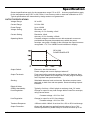
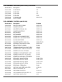
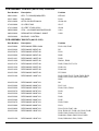
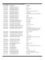
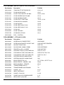
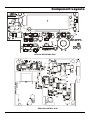
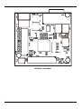
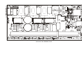
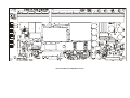
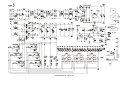
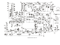
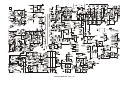
QPX1200
DC Power Supply
Service Manual
Manual Part Number 48511-1130 Issue 1
Table of Contents
Specification
2
EMC
5
Safety
6
General
7
Circuit Descriptions
9
Calibration Procedure
17
Parts List
19
Component Layouts
35
Circuit Diagrams
37
1
Specification
General specifications apply for the temperature range 5°C to 40°C. Accuracy specifications apply
for the temperature range 18°C to 28°C after 1 hour warm-up with no load and calibration at 23°C.
Typical specifications are determined by design and are not guaranteed.
OUTPUT SPECIFICATIONS
Voltage Range:
0V to 60V
Current Range:
0.01A to 50A
Power Range:
Up to 1200W
Voltage Setting:
Resolution 1mV
Accuracy: 0.1% of setting ± 2mV
Current Setting:
Resolution 10mA
Accuracy: 0.3% of setting ± 20mA
Operating Mode:
Constant voltage or constant current with automatic cross-over
provided that the power demanded stays within the power
envelope, see graph. Outside of this envelope the output becomes
unregulated. CV, CI or UNREG mode indication in display.
QPX 1200
POWER ENVELOPE
Output Switch:
Electronic, with ON indication.
Preset voltage and current displayed when off.
Output Terminals:
Front panel safety terminals accepting 6mm wire diameter, 6mm
plugs or 8mm spades at 50 Amps max, or 4mm plugs at 30 Amps
max. Duplicate rear panel terminals.
Sensing:
Switchable between local and remote. Screwless remote sense
terminals on both front and rear panels. Sense miswiring trip and
indication.
Ripple & Noise
(20MHz bandwidth):
Load Regulation:
Typically <3mVrms, <20mV pk-pk at maximum load, CV mode
Change in output for any load change within PowerFlex envelope,
using remote sense:
Constant voltage: <0.01% ± 5mV
Line Regulation:
Change in output for a 10% line change:
Constant voltage: <0.01% ± 5mV
2
Transient Response:
<250us to within 100mV of set level for a 5% to 95% load change.
Output Protection:
Output will withstand an applied forward voltage of up to 70V.
Reverse protection by diode clamp for reverse currents up to 3A.
Over-voltage Protection
(OVP):
Range 2V to 65V. Resolution 0.1V; accuracy: 0.2% ± 0.2V.
Response time typically 100µs.
Over-current Protection
(OCP):
Range 2A to 55A. Resolution 0.1A; accuracy: 0.5% ± 0.2A.
Response time typically 100ms.
Over-temperature Protection:
The output will be tripped off if a fault causes the internal
temperature to rise excessively.
Temperature Coefficient:
Typically <100ppm/°C
METER SPECIFICATIONS
Display Type:
5-digit (Volts), 4-digit (Amps), black-on-white backlit LCD.
Voltage (CI Mode and Unreg):
Resolution 1mV
Accuracy: 0.1% of reading ± 2 digits
Current (CV Mode & Unreg):
Resolution 10mA
Accuracy: 0.3% of reading ± 2 digits
V x A:
Resolution 0·1W
Accuracy: 0·5% ± 0·1W
LOGIC CONTROL INPUT and OUTPUT
LOGIC IN is a rear-panel opto-isolated input that is activated at an input current greater than
approximately 1mA. User can set LOGIC IN (via the keyboard) to enable the output, disable the
output, or be ignored when it is activated.
LOGIC OUT is an isolated rear-panel open-collector output that will sink up to 2mA when activated
(‘switch closure’); the maximum voltage that can be applied to LOGIC OUT is 30VDC. User can set
LOGIC OUT to be ‘closed’ or ‘open’ for output enabled or disabled, current limit (CI mode), power
limit (UNREG mode), or for any fault trip.
ANALOG REMOTE CONTROL and MONITORING
Non-isolated inputs and outputs to set voltage and current limit and to monitor actual output voltage
and current. These signals are referenced to the positive output and have a range of 0 to 10V or 0
to 5V (selectable via the keyboard).
Analogue Control Accuracy:
Voltage: 0.3% ± 4mV; Current: 0.5% ± 40mA
Analogue Monitor Accuracy:
Voltage: 0.3% ± 4mV; Current: 0.5% ± 40mA
KEYBOARD & ROTARY CONTROL
All functions, including the selection and set-up of the remote control interfaces, can be set from the
keyboard. The rotary Jog control can be used to adjust output voltage and current settings in a
quasi-analogue mode.
DISPLAY FEATURES
The display is a 240 x 64 pixel transflective LCD, backlit by white LEDs; contrast is softwarecontrolled and can be adjusted from the keyboard.
The default status display shows the VOLTS (5 digits) and AMPS (4 digits) in 10mm high characters,
plus the present output mode. At other times, for example during store or recall of instrument setups, the display shows up to 6 lines of information, instructions, or prompts.
3
INTERFACES
Full digital remote control facilities are available through the RS232 and USB interfaces. Setting and
readback resolutions are the same as the Output and Meter specifications respectively.
RS232:
Variable Baud rate, 19200 Baud maximum. 9-pin D-connector.
Single instrument or Addressable RS232 operation.
USB:
Standard USB 2.0 hardware connection.
Remote Command
Processing Time:
Typically <100ms between receiving the command terminator for a
step voltage change at the instrument and the output voltage
beginning to change.
GENERAL
4
AC Input:
110V – 240V AC ± 10%, 50/60Hz.
Installation Category II.
Power Consumption:
1600VA max.
Operating Range:
+5ºC to +40ºC, 20% to 80% RH.
Storage Range:
−40ºC to + 70ºC.
Environmental:
Indoor use at altitudes up to 2000m, Pollution Degree 2.
Store/Recall:
Up to 10 set-ups can be saved and recalled via the keyboard or
remote interfaces.
Safety:
Complies with EN61010-1.
EMC:
Complies with EN61326.
Size:
130mm H (3U) x 356mm W x 413mm D
Weight:
9.2kg
Options:
19-inch rack kit.
EMC
This instrument has been designed to meet the requirements of the EMC Directive 89/336/EEC.
Compliance was demonstrated by meeting the test limits of the following standards:
Emissions
EN61326 (1998) EMC product standard for Electrical Equipment for Measurement, Control and
Laboratory Use. Test limits used were:
a)
Radiated:
Class A
b)
Conducted: Class A
c)
Harmonics: EN61000-3-2 (2000) Class A; the instrument is Class A by product category.
Immunity
EN61326 (1998) EMC product standard for Electrical Equipment for Measurement, Control and
Laboratory Use.
Test methods, limits and performance achieved were:
a)
EN61000-4-2 (1995) Electrostatic Discharge : 4kV air, 4kV contact, Performance A.
b)
EN61000-4-3 (1997) Electromagnetic Field, 3V/m, 80% AM at 1kHz, Performance B.
c)
EN61000-4-11 (1994) Voltage Interrupt, 1 cycle, 100%, Performance B.
d)
EN61000-4-4 (1995) Fast Transient, 1kV peak (AC line), 0·5kV peak (DC Outputs),
Performance B.
e)
EN61000-4-5 (1995) Surge, 0·5kV (line to line), 1kV (line to ground), Performance B.
f)
EN61000-4-6 (1996) Conducted RF, 3V, 80% AM at 1kHz (AC line only; DC Output
connections <3m not tested), Performance B.
According to EN61326 the definitions of performance criteria are:
Performance criterion A: ‘During test normal performance within the specification limits.’
Performance criterion B: ‘During test, temporary degradation, or loss of function or performance
which is self-recovering’.
Performance criterion C: ‘During test, temporary degradation, or loss of function or performance
which requires operator intervention or system reset occurs.’
Where Performance B is stated it is because DC Output regulation may deviate beyond
Specification limits under the test conditions. However, the possible deviations are still small and
unlikely to be a problem in practice.
Note that if operation in a high RF field is unavoidable it is good practice to connect the PSU to the
target system using screened leads which have been passed (together) through an absorbing ferrite
sleeve fitted close to the PSU terminals.
Cautions
To ensure continued compliance with the EMC directive observe the following precautions:
a) after opening the case for any reason ensure that all signal and ground connections are remade
correctly and that case screws are correctly refitted and tightened.
b) In the event of part replacement becoming necessary, only use components of an identical type,
see the Service Manual.
5
Safety
This power supply is a Safety Class I instrument according to IEC classification and has been
designed to meet the requirements of EN61010-1 (Safety Requirements for Electrical Equipment for
Measurement, Control and Laboratory Use). It is an Installation Category II instrument intended for
operation from a normal single phase supply.
This instrument has been tested in accordance with EN61010-1 and has been supplied in a safe
condition. This instruction manual contains some information and warnings which have to be
followed by the user to ensure safe operation and to retain the instrument in a safe condition.
This instrument has been designed for indoor use in a Pollution Degree 2 environment in the
temperature range 5°C to 40°C, 20% - 80% RH (non-condensing). It may occasionally be subjected
to temperatures between +5°C and –10°C without degradation of its safety. Do not operate while
condensation is present.
Use of this instrument in a manner not specified by these instructions may impair the safety
protection provided. Do not operate the instrument outside its rated supply voltages or
environmental range.
WARNING! THIS INSTRUMENT MUST BE EARTHED
Any interruption of the mains earth conductor inside or outside the instrument will make the
instrument dangerous. Intentional interruption is prohibited. The protective action must not be
negated by the use of an extension cord without a protective conductor.
When the instrument is connected to its supply, terminals may be live and opening the covers or
removal of parts (except those to which access can be gained by hand) is likely to expose live parts.
The apparatus shall be disconnected from all voltage sources before it is opened for any
adjustment, replacement, maintenance or repair.
Capacitors inside the power supply may still be charged even if the power supply has been
disconnected from all voltage sources but will be safely discharged about 10 minutes after switching
off power.
Any adjustment, maintenance and repair of the opened instrument under voltage shall be avoided
as far as possible and, if inevitable, shall be carried out only by a skilled person who is aware of the
hazard involved.
If the instrument is clearly defective, has been subject to mechanical damage, excessive moisture
or chemical corrosion the safety protection may be impaired and the apparatus should be withdrawn
from use and returned for checking and repair.
Make sure that only fuses with the required rated current and of the specified type are used for
replacement. The use of makeshift fuses and the short-circuiting of fuse holders is prohibited.
Do not wet the instrument when cleaning it.
The following symbols are used on the instrument and in this manual:Earth (ground) terminal.
mains supply OFF.
l
mains supply ON.
alternating current (ac)
direct current (dc)
6
General
Service Handling Precautions
Service work or calibration should only be carried out by skilled engineers using high quality test
equipment. If the user is in any doubt as to his competence to carry out the work, the instrument
should be returned to the manufacturer or their agent overseas for the work to be carried out.
The tracks on the printed circuit boards are very fine and may lift if subjected to excessive heat. Use
only a miniature temperature-controlled soldering iron and remove all solder with solder wick or
suction before attempting to remove a component.
Dismantling the instrument
WARNING!
Disconnect the power supply from all voltage sources before it is opened for adjustment or repair.
Capacitors inside the supply may still be charged even if the supply has been disconnected from all
voltage sources but will be safely discharged about 10 minutes after removing power.
If any adjustment or repair of the opened supply under voltage is inevitable it shall be carried out
only be a skilled person who is aware of the hazard involved. The incoming AC supply to the unit
under test should be isolated for safety by means of a 1:1 isolation transformer of at least 1500VA.
High voltages (up to 400V) are always present in the primary-side circuits on both the PFC board
and Power board; on the Power board the primary side occupies a clearly defined area at the rear
of the board.
1.
Remove the 4 side screws to release the top cover.
2.
To gain access to the Control PCB and Keyboard, release the front panel assembly from the
chassis by removing the 2 M3 side nuts, the countersunk M3 screw securing the top bracket,
and the 4 M3 screws (with integral shakeproof washers) along the bottom edge.
3.
Keyboard: Remove the 5V supply from PJ4, the 4 connections to the mains switch, and the
3-way connections to the Control (PJ10) & Interface (PJ9) boards. The Keyboard is released
from the front panel by removing the 7 screws which secure it.
4.
Control: Remove the 10-way connector (PJ100) to the Power board, noting polarity (corner
marker to pin1); remove the flat cable connection to PJ101 and the 3-way connection to the
Keyboard (PJ105). Remove the nuts which secure the front and rear output connecting
cables from the terminals on the front panel/Control board after noting their positions. To
release the Control board remove the 3 M3 screws to the front panel plus the 3 nuts which
secure it directly to the +, −, & earth terminals. When re-assembling do not forget the brass
bus-bar between the Red output terminal and the current measurement shunt connection.
5.
PFC: Remove the 5V supply to the Keyboard (at PJ2) and the mains connections at W1,
W2, W3 &W4; when reassembling note that W1 & W4 (to the front panel switch) share a
ferrite sleeve and W2 & W3 (return from the switch) share a ferrite sleeve. Remove the 4way primary AUX connection at PJ1 ( note the position of ferrite sleeve at the Power board
end of the connection) and the HT connection at FAS5, FAS6 & W5. To release the PFC
board from the chassis remove the 9 M3 screws (with integral shakeproof washer) from the
underside of the chassis, leaving the support pillars attached to the board assembly. Ease
the board forward a little in the chassis, so that the safety earth connection to the rear panel
can be undone, and lift the board free.
7
8
6.
Power: Remove the 10-way connector (PJ5) to the Control board, noting polarity (corner
marker to pin1); remove the flat cable connection to PJ4 at the rear of the board; remove the
HT connection from the PFC board at FAS1 & FAS2; remove the 4-way primary AUX
connection from the PFC board at PJ1; remove the 3 2-way fan power connections
(PJ6,PJ7, PJ8); remove the 2 M6 barb nuts which secure the output cables to the front
panel. To release the Power board from the chassis it is first necessary to remove the 3rd,
internal, fan; push out the centres of the 2 plastic push-rivets which secure the top of the fan
to the bracket and lift out the fan with its lower bracket still attached. When re-assembling
note that the fan label faces the transformer (airflow towards the transformer). Remove the
10 M3 screws (with integral shakeproof washer) from the underside of the chassis, leaving
the support pillars attached to the board assembly, and lift the assembly forward and up.
7.
Interface: Remove the 3-way connection to the Keyboard at PJ3. The Interface board is
secured only by the RS232 screwjacks; undo these to release the board.
8.
When reassembling, take great care to ensure that all connections are exactly as before
dismantling and that no insulation creepage and clearance distances have been
compromised. Ensure that only the correct fasteners have been used otherwise earthing,
and hence EMC and safety performance, may be impaired.
Circuit Descriptions
PFC Board
Mains Input, Filtering and Rectification
The AC input is via PJ3, a pcb mounted IEC plug, and fuse FS1.
X-capacitors C1, C4, C7, C10 & C68, together with the Y-capacitors C5, C6, C11 & C12, common
mode inductors L1, L2 & L3 and differential inductors L4 & L8 comprise an input filter which ensures
that the supply meets both conducted emission and conducted immunity EMC requirements.
VD1 clips mains spikes for component protection, while R1 discharges the X-capacitors after
removal of the mains supply.
Pcb mounted fuse FS1 limits damage on boost-stage or forward converter failure. The front panel
mains switch is connected via connectors W1, W2, W3 and W4.
The bridge rectifier comprised of D1, D2, D3 and D4 has C13 and C14 connected across it to
bypass noise signals and to snub reverse recovery transients in the bridge rectifier.
C15, C16 further decouple the input filter and rectifier from the boost converter.
R2 limits the initial inrush current into the boost stage output capacitors C19 and C20 and is bypassed by relay PL1 once the boost converter starts.
Auxiliary Supplies
Primary Side
The primary auxiliary supplies are generated by IC5. This is a 7 pin TO220 style device which
incorporates the control circuitry and power switch to implement an off line flyback power supply.
It derives its power from the boosted HT rail.
R93 sets the power switch peak current to 0.4A. D20, R55 and C47 clamp the drain voltage of the
power switch at a safe level. The low voltage output of transformer T9 is peak rectified by D21 and
C49 . The output voltage is regulated to 24V by zener diode D22 and feedback to the control pin is
via opto coupler IC15. The 24V rail powers the fans.
IC6 generates an 18V rail for the PFC control IC4.
IC7 generates a 15V rail for the power pcb primary control circuit.
Secondary Side
A 5V supply for the front panel keyboard is generated by IC9. This is an 8 pin SMD style device
which incorporates the control circuitry and power switch to implement an off line flyback power
supply.
It derives its power from the AUX_HT line, which is generated by D36, D37 and C81, C37. This rail
is decoupled from the HT boost rail. When the mains supply is switched off, this AUX_HT rail falls
quickly and the front panel display vanishes very rapidly.
Start-up Control Circuit
D23 and R58 provide a 5.1V reference voltage to the negative inputs of all 4 op-amps of IC8.
When the mains is switched on, potential divider R59, R59B, R60, R60B and R61 feeds the
attenuated full wave rectified mains voltage to the positive input of IC8-A.
The bulk storage capacitors C19, C20 are being charged via inrush current limiting resistor R2.
When the mains voltage exceeds approximately 80Vrms, the output of IC8A begins to produce
pulses, which charge C21 via D24. When the mains voltage reaches approximately 87Vrms, the
voltage on C21 exceeds the reference voltage on IC8-B negative input and the output of IC8-B goes
high, charging C55,C56 via R67.
9
After a delay of about 0.4s, the voltage on C55, C56 exceeds the reference voltage on IC8-C
negative input and the output of IC8-C goes high, turning on Q8 via D29 and R74 thus energising
RL1 which bypasses the current inrush resistor R2.
The output of IC8-C also charges C58 via R70 thus producing a short delay before the output of
IC8-D goes high and turns on Q9 which in turn switches Q10 and Q11 off. When Q11 goes off, the
SS signal is no longer clamped to 0V and allows the PFC control IC4 to start up.
When the mains voltage is switched off, C21 is no longer supplied with top-up pulses and is
discharged by R64. IC 8-B output goes low and quickly discharges C55, C56 via D25. IC8-C output
then goes low and immediately turns off Q9 via D28. This causes Q11 to come on, clamping the SS
signal to 0V and stopping the PFC control IC4.
IC8-B output going low, discharges C58 via R71 and D26, thus providing a short delay before IC8-D
output goes low and switches off the bypass relay driver Q8.
The above timing sequences ensure that the inrush relay RL1 contacts only switch under zero load
conditions.
Primary Boost stage Control circuit
The primary boost stage control is by means of IC4.
This contains all the processing circuitry to shape the current taken by the power supply from the
mains supply to be sinusoidal and in phase with the voltage.
For a detailed description refer to the ST ‘Power Factor Corrector Applications Manual‘.
When the mains is switched on, the +18V supply to IC4/pin19 is established and IC4 becomes
active after a short delay when the SS signal is released by the start-up control circuit. During this
short delay the bulk storage capacitors C19, C20 are charged via the inrush-limiting resistor R2.
IC4 starts up and supplies drive pulses to the gate ICs IC1, IC2, IC3, which drive the gates of the
boost MOSFETs Q1, Q2, Q3, Q4, Q5, Q6.
C44 is connected to the soft start pin of IC4 and provides a soft start.
R34, R34b, R35, R35b, R37, C35, C35b, C36, C36b form a two stage RC filter to feed a voltage
proportional to the mains voltage to IC4/pin 7 which, after an internal 1/V2 transformation, is fed to
the internal multiplier. For a universal mains input, the voltage at this pin will vary between 1.5V and
5.5V.
R38+R38a and R39+R39a supply a current derived from the full wave rectified mains voltage to
IC4/pin 4 to be used by the internal multiplier.
Also fed to the internal multiplier is the output of the voltage error amplifier of IC4/pin 13. The input
to the error amplifier at pin 14 is from potential divider R41, R41b, R42, R42b, R62, R63 and VR1.
This potential divider monitors the voltage on the boost stage output capacitors C19, C20 and this is
compared to an accurate internal reference voltage. Thus a steady voltage of about 395V, as set by
VR1, is maintained across C19, C20.
Another potential divider R44, R44b, R45, R45b, R46 monitors the voltage across C19, C20 and
feeds into pin 3 of IC4 which is the over-voltage shutdown. C80 slows the signal going into the
over-voltage pin to prevent the over-voltage circuit from activating during transient load changes.
Pin 8 is the output of the multiplier and is the programming current for the internal current error
amplifier. This signal is taken to the mains supply side of the current sense resistor R52 via R48.
The other input of the current error amplifier is taken to the other side of R52 via R50. The current
error amplifier thus compares the signal across the current sense resistor R52 with the
programming current and adjusts the PWM drive to the boost MOSFETs accordingly.
R49 and C42 with R50 form the compensation network around the current error amplifier.
10
Boost Stage
Three boost inductors L5, L6, L7 are each driven by a pair of MOSFETs Q3+Q6, Q2+Q5, Q1+Q4
respectively to raise the incoming, full wave rectified, sinusoidal mains voltage to a value some 30V
higher than the peak of the maximum rms input voltage. This is achieved by storing energy in the
boost inductors when the MOSFETs are conducting and transferring it to C19, C20 via boost diodes
D5, D6, D33 when the MOSFETs are turned off.
When the MOSFETs turn on, the boost diodes D5, D6, D33 are still conducting current. To prevent
large switch on losses, delay inductors L9, L10, L11 are placed in series with the MOSFETs. This
ensures that the current in the boost diodes is reduced at a gradual rate and the reverse recovery
time is minimised at the same time as the drain voltage of the MOSFETs is allowed to fall rapidly.
The energy stored in L9, L10, L11 is transferred to C18, C61, C62 via D19, D7, D8 and dissipated in
R23, R6, R9.
Snubber networks C22, R15, R19, C23, R16, R21, C24, R18, R22 reduce switch-off losses in the
MOSFETs.
The main boost heatsink is protected against excessive temperature by PTC2, IC12 and associated
components; once triggered it is necessary to turn the mains power off and on again to restart.
Power Board
Forward Converter
The 400V HT supply from the PFC board is connected to the Power board via FAS1 and FAS2 and
decoupled by C2.
C1 and C3 with their respective bleed resistors R149 and R150 form the voltage divider to feed the
converter transformer T1 of the half bridge forward converter.
The half bridge configured power MOSFETs Q28 and Q29 are connected to the converter
transformer T1 via the current transformer CT1 and ZVS inductor L2 and operate at a fixed duty
cycle of about 42% at a switching frequency of 73kHz. See the gate drive waveform in
Photograph1.
C4 and C12 work with L2 to facilitate zero voltage switching for Q28 and Q29.
R11, C16 and FB3 damp high frequency ringing across T1 primary. See photograph 02.
The gate drive pulses for Q28 and Q29 are generated by oscillator IC2-B/IC2-C feeding into IC3-A
to produce complimentary square waves at IC3-A pins 1 and 2.
The leading edges of these anti-phase square waves are slowed by R39/C37 and R42/C38 and
buffered by IC2-A,E,D,F to produce anti-phase pulse trains of the correct duty cycle to drive the gate
drive transformer T3 via Q13, Q15, Q17, Q18 and C35. The supply to the gate transformer drivers is
decoupled by C17, C28, C29, C30. The gates of Q28 and Q29 receive their anti-phase drive from
the secondaries of T3 via R52 and R73 and respective anti parallel diodes D1 and D2.
The output of the current transformer CT1 is full wave rectified by D16, D17, D22, D23 and loaded
with burden resistor R26. The voltage developed across R26 is utilised by two different circuits.
The first is to turn on Q11 via zener diode D27 when the current in the primary power switches
exceeds a certain value determined by R157 and R158. Q11 collector charges C26 negatively via
R21. When the voltage across C26 exceeds a threshold set by zener diode D10, latch Q9, Q14
turns on and pulls signal SDWN down to the P0V rail via D20. This in turn causes the power factor
correction circuit to shut down – requiring the removal of the mains supply in order to restart. This
would only happen under repeated short-circuiting of the output. Q9, Q14 latch can also be
activated by the signal OPTO1 via R102 – as would be the case when the voltage on the secondary
exceeds a value set by zener diode D5. The primary heatsink is protected against excessive
temperature by PTC TH3 which turns on Q16 and this in turn activates latch Q9, Q14.
The voltage developed across R26 is also utilised to regulate the fan speed. As the secondary
loading increases, the voltage across R26 is peak detected by D50 and C31 and sets a demand
11
voltage level at the positive input of op-amp IC14-A, the output of which turns on fan drive transistor
Q38. The fan current is monitored by R120, R121 and amplified by IC14-B to provide negative
feedback to the negative input of IC14-A.
Secondary Side
The main secondary winding is centre tapped and terminates on pins 19/20, 15/16 with the centre
tap on 17/18.
Snubber networks R7, C13 and C14, R18 across each half reduce high frequency ringing.
D47 and C80 generate a negative rail which bleeds a negative current from the output via resistors
R131 and R132.
The voltage on the secondary winding is rectified by D47 & D11, L-C filtered by L1, C5, C7, C8, C11
with flywheel diodes D6 & D7, and fed to a linear output stage comprised of MOSFETs Q3, Q4, Q5,
Q6. To minimise power dissipation in the linear output stage, the voltage across the MOSFETs is
monitored by error amplifier IC7-A (Sheet 2) which maintains the voltage across the linear output
MOSFETs to below 1V by adjusting the ‘Control’ signal to the synchronous post regulator MOSFETs
drive circuit (Sheet 3).
The synchronous post regulator MOSFETs Q2 and Q8 regulate the voltage across the linear output
MOSFETs by initially blocking the pulse from the secondary winding and only conducting after a
delay determined by the ‘Control’ signal.
Referring to Sheet 3, the drive to the post regulator MOSFETs is generated by two identical circuits
operating in anti-phase.
An auxiliary centre tapped winding on the converter transformer T1 terminated on pins 21, 22, 23,
and 24 generates the V+SEC and –8VSEC rails for the secondary control circuitry and also the
reference pulses AAA and BBB for the post regulator control circuit.
This description refers to the upper channel on sheet 3.
The reference pulse AAA is buffered and squared by AND gate IC10-B. The output of the AND gate
charges and discharges capacitor C58 via R66. The discharge time is shorter due to R69 and D41
conducting. The resultant triangular waveform is shown in photograph 03.
The long tail pair (LTP) comparator Q22 & Q23 switches when the triangle waveform at Q23 base
exceeds the reference voltage on Q22 base. The ‘Control’ voltage from IC7-A is fed to the base of
Q21 via R75 and VR3. The pulse width of the two sides is balanced by adjusting VR3.
Q21 emitter sets a pedestal level from which the charging of C58 begins.
The higher this pedestal level, the quicker C58 charges to the reference level on Q22 base and the
LTP comparator switches. This in turn switches Q20 which delivers a pulse to AND gate IC10-D
where it is gated with the AAA reference signal, the trailing edge of which has been slightly delayed
by R71 and C59.
The output of the AND gate IC10-D drives a MIC4428 driver IC, the antiphase outputs of which drive
the gate of the synchronous post regulator MOSFET Q2 via gate drive transformer T4.
Photograph 04 shows the triangular signal at the base of Q23 together with the pulse at IC10-D
pin 9. The reference voltage at the base of Q22 is coincident with the X-axis in the centre of the
oscilloscope screen.
To avoid uncontrolled post regulator conduction, Q32 and associated components ensure that the
‘Control’ signal is clamped to 0V during initial power-up.
The constant power limit is realised using analogue multiplier IC6.
The output voltage and output current are monitored by IC5-A and IC5-B respectively and the
resultant signals fed to the Y and X inputs of the analogue multiplier. The output of the multiplier is
of the form (X*Y)/10 +Z.
Z is a third input and is used to modify the power limit to give a lower power limit at high output
current. The correction signal is generated by IC15-B.
12
The signal across the current sense resistors R12, R13, R14 and R15 is fed into pin5 of IC15-B.
With the output current set to 20A, the signal at pin 5 is nulled by the current in R91/VR4 from the
negative voltage generated by zener D49. The null point setting is aided by comparator IC15-A
which drives two LEDs, the null being achieved when both LEDs are off .
Having nulled the voltage generated by the 20A output current in the current sense resistors, the
increasing current generates a voltage at the output of IC15B and this is fed to the Z input of the
analogue multiplier. The required level of correction is set by VR5.
The supply rails for the front panel control circuit are generated from an auxiliary winding on the
converter transformer T1 terminated on pins 13 and 14.
A V+ rail of approximately 10V is generated by D33, D34 and filter L4, C40.
A +15V rail is generated by D35, C43, R51 and D36.
A -8V rail Is generated by D38, C44, R55 and D37.
Photograph 1
Photograph 2
13
Photograph 3
Photograph 4
Control Board
The control board contains an ARM7 processor, IC111, programmed via JTAG header PJ103. The
three processors communicate via a shared bus but in this case it is isolated via opto-couplers
IC109 and IC110.
The board needs several power supplies and, with the exception on the ‘-8V’ and ‘+15V’ rails, these
are all derived from the ‘V+’ rail generated on the Power board and connected to the Control via
PJ100. IC117 generates a 5-volt rail, which is used to generate 3.3V via IC112, and finally IC113
generates a 1.95V supply for the processor core. In addition IC107d provides a power-fail signal
that ensures that data is saved at each power-off.
Regulation
The output current is sensed via shunt R143 and the signal amplified via IC116. This is fed into the
A/D converter IC102 and also into IC115c where it is compared against the demand to regulate the
current. Similarly IC115a and IC115d regulate the output voltage with the two loops having a diode
‘OR’ connection to give a clean crossover between constant voltage and constant power modes.
Unregulated mode is detected separately on the Power board. IC107a and IC107b provide signals
to the processor so that it knows what mode the power supply is in.
14
Demand Setting
The voltage and current demands, together with OVP limit and the pseudo-analogue outputs are
generated by a digital to analogue converter IC105 together with analogue switch IC106 and a
series of sample and hold circuits. For each of the 5 channels the setting consists of a both a
setting of a DAC reference and a value setting. Consider the voltage demand as an example. First
the processor sets the analogue switch IC104a directly across IC103 and sets IC106 to connect to
IC108a. Writing a suitable value to the DAC sets the reference for the next conversion. The
processor now opens the switch to the input of IC108a so that the setting is held. Next, switch
IC104 is switched so that R119 and R120 in circuit. This gives the correct reference for the demand
to be set. Now the processor writes the correct demand to the DAC and once it has had time to
settle, the output is switched via IC106 through to IC108b where the demand is held on C113. This
whole process is repeated in a similar way for each of the 5 channels. Note that the voltage
demand channel ‘Volts Set’ and the current demand ‘Amps Set’ have additional filtering to prevent
large over/undershoots when the demand is changed.
Measurement
The system accurately measures the output voltage and current and also external demand signals
for pseudo-analogue control. This is achieved via IC402, an analogue to digital converter. IC101a
provides a clean, buffered reference. This chip communicates with the processor via an SPI bus.
OVP
IC107c provides over-voltage protection. It compares the OVP limit, set by IC108d, with the output
voltage. When the output voltage becomes excessive it latches, pulling the voltage demand to zero
via Q111 and Q112. The processor can reset the latch via Q113.
Remote Sense
RL100 selects between remote and local sensing controlled by the processor via Q109. Q106 and
Q107 sense excessive drop down the sense cables, indicating a sense fault to the processor via
Q105, if appropriate.
Logic in and Logic Out
The system has input and output logic signals which communicate with the processor via buffer
transistors Q100 and Q101.
Keyboard
The keyboard processor IC2 acts as the system master initiating all communications within the unit;
it is programmed in-circuit using the standard JTAG port accessed at PJ3. PJ9 and PJ10 provide
the connections to the other boards in the system; Q2 and IC5 enable the processor to pull down
the data line, allowing it to go high only if none of the processors in the system want to pull it low.
The firmware operates a master-slave system to ensure there are no data clashes.
The board is supplied with 5V from the PFC board via PJ4. This is used to generate a local 3.3V
supply (IC4) and 1.95V supply (IC3). IC7a, together with Q1 and associated components, provide a
current source for the display LED backlight. IC7b and associated components provides a crude
under-voltage detect to ensure the processor starts and shuts down cleanly. IC6 is a simple latch
for the LEDS and the keyboard is scanned directly by the processor: this is a quiet scan that only
scans when keys buttons are pressed or released not when the keys are left open or held down.
The diodes D1 to D4 allow the processor to use some pins for two purposes (key-scan and LED).
The display is a 240x64 pixel LCD mounted directly on the keyboard PCB and connected via PJ6.
The display contains its own voltage multiplier to generate the required bias levels; the switched
capacitors and decoupling are provided directly on the pins of the display connector.
15
Interface Board
The interface board allows the unit to communicate externally via USB or RS232. IC5 is an ARM7
processor which is programmed in-circuit using the standard JTAG port accessed at PJ5.
IC3 and IC6 generate the required supply rails. PJ3 provides an RS232 connection; IC1 and IC2
provide the necessary level shifting and inversion to convert the UART’s 5V ‘mark’ and 0V ‘space’ to
RS232’s –5V mark and +5V space. They also allow for data to pass through from one unit to
another for TTi’s Addressable RS232 Chain (ARC). USB is controlled directly by the processor; Q1
switches R22 to provide a soft connect/disconnect feature.
PJ3 provides a shared connection between the boards in the system; Q2 and IC4 allow the
processor to pull down the data line (pin) allowing it to go high only if none of the processors in the
system want to pull low. The firmware operates a master-slave system to ensure there are no data
clashes.
16
Calibration Procedure
The QPX1200 calibration menu can be found under extra functions “#99”. The output calibrations
are dependent on the measurement being in calibration so it is recommended that each of the
calibrations be done in the order they appear on the menu.
Equipment Required
Voltmeter capable of reading up to 65 Volts with 1mV accuracy and up to 15V with 100µV accuracy,
a Current measurement system capable of measuring 60 Amps with 10mA accuracy, and resistance
less than 100mΩ (e.g. a 4-terminal shunt).
Procedure
01: Vout measurement calibration
Ensure that there is no load connected to the unit and connect the voltmeter directly across the front
panel output terminals. Select option 1 from the Calibration menu (Vout measurement) and press
OK. The unit now gives an output of about 1 Volt; measure it, enter the actual voltage (to the
nearest mV) and press OK. After a few seconds the output changes to about 50 Volts; measure and
enter this to the nearest mV, press OK. After a few seconds the display changes to the Calibration
menu again; output voltage measurement is now calibrated.
02: Vout setting calibration
Ensure there is no load connected to the unit. Select option 2 from the Calibration menu (Vout
setting) and press OK. The unit self-calibrates; during this time the output voltage will be switching
between different levels. After a few seconds the display changes to the Calibration menu again;
output voltage setting is now calibrated.
03: Iout measurement calibration
Connect the current measurement system directly across the front panel terminals. Select option 3
from the Calibration menu (Iout measurement) and press OK. The unit now gives an output of
about 1 Amp; measure it accurately, enter the actual current to the nearest mA, and press OK. After
a few seconds the output changes to about 50 Amps; measure and enter this to the nearest mA and
press OK. After a few seconds the display changes to the Calibration menu; output current
measurement is now calibrated.
04: Iout setting calibration
Connect the current measurement system directly across the front panel terminals or alternatively
connect a direct short-circuit. Select option 4 from the Calibration menu (Iout setting). The unit selfcalibrates; during this time the output current will be switching between different levels. After a few
seconds the display changes to the Calibration menu; output current setting is now calibrated.
05: Vmon measurement calibration
On the rear panel terminals short ‘Vmonitor’ to ‘Vcontrol’. Ensure that there is no load connected to
the unit and connect the voltmeter from ‘Vmonitor’ to ‘Common’. Select option 5 from the
Calibration menu (Vmon measurement) and press OK. The unit now gives an output of about 1
Volt; measure the voltage at ‘Vmonitor’ and enter the output voltage this represents (e.g. 6 times the
voltage measured for the 0V to 10V range) to the nearest mV and press OK. After a few seconds
the output changes to about 50 Volts; measure and enter the voltage represented by the voltage at
‘Vmonitor’ to the nearest mV and press OK. After a few seconds the display changes to the
Calibration menu; output voltage control is now calibrated.
06: Vmon setting calibration
On the rear panel terminals short ‘Vmonitor’ to ‘Vcontrol’. Ensure there is no load connected.
Select option 6 from the calibration menu (Vmon setting) and press OK. The unit self-calibrates;
during this time the output voltage will be switching between different levels. After a few seconds
the display changes to the Calibration menu; output voltage monitor is now calibrated.
17
07: Imon measurement calibration
On the rear panel terminals short ‘Imonitor’ to ‘Icontrol’. Ensure that there is no load connected to
the unit and connect the voltmeter from ‘Imonitor’ to ‘Common’. Select option 7 from the Calibration
menu (Imon measurement) and press OK. The unit now gives an output of about 1 Amp; measure
the voltage at ‘Imonitor’ and enter the output current this represents (e.g. 5 times the current
measured for the 0V to 10V range) to the nearest mA and press OK. After a few seconds the output
changes to about 50 Amps; measure and enter the current represented by the voltage at ‘Imonitor’
to the nearest mA and press OK. After a few seconds the display changes to the calibration menu
output voltage control is now calibrated.
08: Imon setting calibration
On the rear panel terminals short ‘Imonitor’ to ‘Icontrol’. Connect the current measurement system
directly across the front panel terminals or alternatively connect a direct short-circuit. Select option
8 from the calibration menu (Imon setting) and press OK. The unit self calibrates; during this time
the output current will be switching between different levels. After a few seconds the display
changes to the Calibration menu; output current monitor is now calibrated.
18
Parts List
PCB ASSEMBLY - POWER - (44115-3060)
Part Number
Description
Position
20205-0800
STUD M6 x 20 HFHB M6-20-X
OUTPUT CONNECTION
20234-0023
SCREW M4 x 8 PNHDPZ ZPST
HEATSINKS
20234-0100
SCREW M3 x 6PNHDPZ C/W EXT SH/P
PCB SUPPORT SPACERS
20613-0007
SIL-PAD TO220 PLAIN
FOR TH1
20613-0026
SIL-PAD 900S 100MM X 25MM
FOR HEATSINKS
20661-0225
SPACER Hex M3 x 12 NPBR
PCB SUPPORT
20670-0135
CLIP GP02 FOR PCB MTG H/SINKS
20670-0310
HEATSINK PCB MTG 38MM PLAIN
SK3
20670-0340
HEATSINK TO220 CLIPON 29DEG/W
SK4
20670-0364
CLIP MAX01H FOR TO220+MAX H/S
FOR TH1, TH3
20670-0365
CLIP MAX03H FOR TO247+MAX H/S
FOR Q2-6, Q8, Q28, Q29, D3, D6-7, D11
20670-0550
HEATSINK MAX505 90MM PLAIN
SK1
20670-0560
HEATSINK MAX505 210MM PLAIN
SK2
22040-0940
BEAD (DOUBLE) - FERRITE
FB1-7
22109-0130
TRANSFORMER GATE DRIVE
T3
22109-0280
TRANSFORMR CURRENT SENSE
CT1
22109-0370
TRANSFORMER HF POWER
T1
22109-0400
TRANSF GATE DRIVE QPX POSTREG
T4-5
22154-0160
CHOKE 1mH AXIAL 1.3 OHMS
L3-4
22154-0770
CHOKE - OUTPUT -QPX
L1
22154-0780
CHOKE - 3uH - ZVS
L2
22455-0040
TAB 4.8MAX 0.8MM STR PCB MTG
FAS1-2
22467-0130
TERMINAL BLOCK 2W R/A
TB1-6
22482-0020
BEAD, CERAMIC 11-54-3557-0
FOR R12-15
22573-0086
HEADER 16W 2x8 LATCHING
PJ4
22573-0210
HEADER 10 WAY STRAIGHT .156P
PJ5
22573-0224
HEADER 4 WAY STR F/LOCK .156P
PJ1 (FIT PIN 1 TO PIN 1)
22573-0247
HEADER 2 WAY STR .1P F/LOCK
PJ6-8
22575-0038
HEADER 6 WAY STR SIL
TP4, TP5
23185-0000
RES ZERO OHM
R155, R156
23202-0100
RES 10R0F W60 MF 50PPM
R37, R41, R52, R73
23202-0270
RES 27R0F W60 MF 50PPM
R45
23202-1100
RES 100RF W60 MF 50PPM
R2, R4-6, R49
23202-2330
RES 3K30F W60 MF 50PPM
R33-34
23202-5680
RES 6M80F W60 MF 50PPM
R27-28
19
PCB ASSEMBLY - POWER - (44115-3060) /continued...
Part Number
Description
Position
23210-0330
RES 33R0J 2W MF 250PPM
R26
23210-1100
RES 100RJ 2W MF 250PPM
R140
23210-1220
RES 220RJ 2W MF 250PPM
R51, R141
23210-2470
RES 4K70J 2W MF 250PPM
R127
23210-3470
RES 47K0J 2W MF 250PPM
R131-132, R149-150
23215-2100
RES 1K00B W25 MF 15PPM
R72, R85
23222-0022
RES 2R20J W33 MF FUSIBLE NRF25
R88
23222-0220
RES 22R0J W33 MF FUSIBLE NRF25
R56, R138-139
23222-0220
RES 22R0J W33 MF FUSIBLE NRF25
R50
23222-1220
RES 220RJ W33 MF FUSIBLE NFR25
R10, R17
23274-0042
RES 47RJ 2W5 WW
R7, R11, R18
23274-0043
RES 0R015J 2W5 WW
R12-15
23274-0320
RES 220RJ 4W WW
R55
23275-0010
RES 47R0J 3W MO
R8
23385-2100
RES PS/H 1K0 CF 6MM
VR3
23385-3100
RES PS/H 10K CF 6MM
VR1-2, VR5
23385-3470
RES PS/H 47K CF 6MM
VR4
23388-0010
THERMISTOR PTC TAG 90 DEG
TH1 ,TH3
23424-0469
CAP 220PK 1KV CER P5
C16
23424-0471
CAP 4N7K 1KV CER P7.5/P10
C4, C6, C12
23424-0472
CAP 2N2K 1KV CER P5/P7.5
C13-14
23428-0470
CAP 47PG 100V CER NPO P2.5
C59, C66
23557-0506
CAP 10U 63V ELEC P2
C25
23557-0667
CAP 220U 25V ELEC RE2 P3.5
C40
23557-0673
CAP 22U 35V ELEC RE2 P2
C10, C15, C20, C43-44, C53, C87
23557-0820
CAP 10U 50V ELEC LOW ESR P2
C17
23557-0827
CAP 470U 100V LOW ESR P7.5
C5, C7-8, C11 ,C18
23620-0236
CAP 1N0K 100V P/E P5
C27
23620-0252
CAP 2N2K 63V P/E P5
C37-38, C58, C64, C76-77
23620-0264
CAP 100NK400VP/E 368 SER P15
C80
23620-0267
CAP 100NK 100V P/E P5
C21, C26, C91-92
23620-0268
CAP 220NK400VP/E 468 SER P15
C22, C102
23684-0021
CAP 2U2K 400V P/P P27.5
C1-3
23685-0013
CAP 330NK 160V/250V P/P P15
C35
25021-0910
DIO BAV21
D1-2, D13, D15, D19, D29, D31, D35,
D38, D55
20
PCB ASSEMBLY - POWER - (44115-3060) /continued...
Part Number
Description
Position
23210-0330
RES 33R0J 2W MF 250PPM
R26
25031-0100
DIO BAX12A
D16-17, D22-23
25031-0150
DIO UF4006
D47
25031-0250
DIO STTH6003CW
D3, D6-7, D11
25130-0207
DIO ZEN 15V W4
D25-26, D36
25130-0231
DIO ZEN 8V2 W4
D37, D56
25130-0915
DIO ZEN 75V W4
D5
25349-3500
TRAN PNP MJE350
Q37
25384-9001
TRAN PNP ZTX751
Q15, Q18
25388-0211
TRAN NPN ZTX651
Q13, Q17
25601-0490
TRAN MOSFET N CHAN 50V/60V
Q38
25601-0710
TRAN MOSFET NCHAN HUF75652G3
Q3-6
25601-0750
TRAN MOSFET N CHAN STW45NM50
Q28-29
25601-0800
TRAN MOSFET NCHAN IRFP90N20DPF
Q2, Q8
27001-0060
OPTO-COUPLER SFH615A-3
IC1, IC17-18
27160-0013
IC V/REG 7815
IC9
PCB ASSEMBLY SM POWER (44115-3061)
Part Number
Description
Position
22469-1000
TEST POINT SMT
TP6,TP8-9,TP11-15
23105-0000
RES SM0805 ZERO OHM
R97
23105-0010
RES SM0805 1R00F W1
R100
23105-0022
RES SM0805 2R20F W1
R120-121
23105-0033
RES SM0805 3R30F W1
R3, R24
23105-0100
RES SM0805 10R0F W1
R29, R144-145
23105-0220
RES SM0805 22R0F W1
R128, R130, R142-143
23105-0240
RES SM0805 24R0F W1
R158
23105-0750
RES SM0805 75R0F W1
R157
23105-1100
RES SM0805 100RF W1
R40, R43
23105-1470
RES SM0805 470RF W1
R25, R65, R76, R102, R125, R153-154
23105-2100
RES SM0805 1K00F W1
R20, R30-32, R39, R42, R64, R69-70,
R74-75, R80, R83, R90, R92, R117-118
23105-2180
RES SM0805 1K80F W1
R16, R99
23105-2220
RES SM0805 2K20F W1
R63, R107
23105-2300
RES SM0805 3K00F W1
R36
23105-2330
RES SM0805 3K30F W1
R44, R84, R86, R98, R147
23105-2470
RES SM0805 4K70F W1
R67-68, R77, R79, R81, R129
21
PCB ASSEMBLY SM POWER (44115-3061) /continued...
Part Number
Description
Position
23105-2510
RES SM0805 5K10F W1
R66, R78
23105-3100
RES SM0805 10K0F W1
R9, R22, R53, R58, R61, R71, R82, R87,
R89, R94, R96, R104-106, R109,
R112-115, R124, R126, R146
23105-3200
RES SM0805 20K0F W1
R137
23105-3220
RES SM0805 22K0F W1
R35, R46-47, R95, R108, R122
23105-3330
RES SM0805 33K0F W1
R21
23105-3390
RES SM0805 39K0F W1
R91
23105-3470
RES SM0805 47K0F W1
R57, R60, R123
23105-3620
RES SM0805 62K0F W1
R119
23105-4100
RES SM0805 100KF W1
R62, R110
23105-4220
RES SM0805 220KF W1
R19, R48, R54
23105-4470
RES SM0805 470KF W1
R111, R116
23105-4750
RES SM0805 750KF W1
R38, R101
23105-5100
RES SM0805 1M00F W1
R93
23461-0015
CAP SM0805 10NK 50V CER X7R
C47-48, C65, C79
23461-0020
CAP SM0805 100N50V CER Y5V
C19, C34
23461-0030
CAP SM0805 220NK 16V CER X7R
C94-95
23461-0050
CAP SM0805 22NJ 50V CER X7R
C85
23461-0300
CAP SM0805 100NK 25V CER X7R
C24, C28-33, C36, C42, C45, C49-52,
C54-55, C57, C61-63, C67-70, C72, C75,
C88-90, C96
23559-5220
CAP SM 22U 35V AL ELEC
C86,C93
23595-0100
CAP SM-B 4U7M 16V TANT
C39
25021-0050
DIO SM BAV99 SWITCHING
D9, D14, D18, D20, D28, D30, D32,
D39-44, D46, D50-52
25061-0300
LED SM - RED 3.2 X 2.8MM
LED1-2
25132-0200
DIO SM ZEN 6V2 W35
D27
25132-0270
DIO SM ZEN 7V5 W35
D45
25132-0310
DIO SM ZEN 5V6 W35
D4, D8, D12, D24, D49
25132-0320
DIO SM ZEN 3V3 W35
D10
25334-1010
TRAN SM PNP MMBT2907A
Q20, Q24
25340-1000
TRAN SM PNP BC859C
Q9, Q16, Q31, Q34-35
25377-1000
TRAN SM NPN BC849C
Q11-12, Q14, Q21, Q25, Q30, Q32, Q36
25381-1000
TRAN SM NPN SMBT3904
Q22-23, Q26-27
27106-1110
IC SM LM358M DUAL OP AMP
IC5, IC8, IC14-15
27106-1210
IC SM LMC662CM
IC7
22
PCB ASSEMBLY SM POWER (44115-3061) /continued...
Part Number
Description
Position
27151-1030
IC SM AD633
IC6
27227-0130
IC SM 4013
IC3
27227-0690
IC SM 4069
IC2
27227-0810
IC SM 4081
IC10
27253-0140
IC SM MIC4428
IC11, IC13
35555-4690
PCB - POWER
PCB ASSEMBLY CONTROL (44115-3180)
Part Number
Description
Position
10300-0324
PAD P/E S/AD 6 X 3MM
FOR XTAL
20030-0263
WASHER M3 ZPST
FOR R143
20037-0401
SOLDER TAG PLAIN - M4
FOR R143
20038-9501
WASHER M3 SPRING
FOR R143
20210-0101
NUT M3 ZPST
FOR R143
20210-0110
NUT M4 BARB
FOR R143
20234-0023
SCREW M4 X 8 PNHDPZ ZPST
FOR R143
20234-0024
SCREW M3 X 16 PNHDPZ ZPST
FOR R143
20613-0016
SIL-PAD RECTIFIER
FOR R143
20661-0873
SPACER TOWER 4.8OD X 6L
FOR LED100
20670-0580
HEATSINK TO220 AAVID 7025B
FOR R143
22240-0070
RELAY TYPE 47 (12VDC)
RL100
22467-0120
TERMINAL BLOCK 2W LIGHT GREY
SK100
22573-0048
HEADER 3WAY STR SIL STD/GOLD
TP100
22573-0086
HEADER 16W 2x8 LATCHING
PJ101
22573-0210
HEADER 10 WAY STRAIGHT .156P
PJ100
22573-0248
HEADER 3 WAY STR .1P F/LOCK
PJ105
22575-0065
HEADER 20 WAY 2X10 STR SKELN
PJ103
23202-2100
RES 1K00F W60 MF 50PPM
R136, R138
23215-2383
RES 3K83B W25 MF 15PPM
R155, R219
23215-3909
RES 90K9B W25 MF 15PPM
R156, R160
23215-4680
RES 680KB W25 MF 15PPM
R103-104
23296-0060
RES 0R002 4 TERM PBV
R143
23557-0731
CAP 100U 100V ELEC LOW ESR
C120-121
23557-0841
CAP 47U 35V ELEC P2
C2
23620-0249
CAP 330NK 63V P/E P5
C112-117
23620-0268
CAP 220NK400VP/E 468 SER P15
C118-119
23662-0207
CAP 470PK 100V P/C P5
C30
23
PCB ASSEMBLY CONTROL (44115-3180) /continued...
Part Number
Description
Position
25061-0201
LED - T1 ROUND(3MM) RED
LED100
25117-0020
DIO 1N5401
D110
27001-0050
OPTO-COUPLER 6N136
IC109-110
27160-0009
IC V/REG 7805
IC117
27161-0060
IC V/REF LT1009 2.50V
IC100
28500-0800
XTAL - 4.9152MHZ-MICROPROCSR
X101
28502-0020
RESONATOR CERAMIC 12MHZ
X100
35358-0600
BUS BAR - CONTROL
PCB ASSEMBLY SM CNTL (44115-3181)
Part Number
Description
Position
23105-0000
RES SM0805 ZERO OHM
R121-122, R185
23105-0220
RES SM0805 22R0F W1
R5
23105-0470
RES SM0805 47R0F W1
R112
23105-0560
RES SM0805 56R0F W1
R225
23105-1100
RES SM0805 100RF W1
R193
23105-1220
RES SM0805 220RF W1
R40-41, R220
23105-1270
RES SM0805 270RF W1
R105, R108, R173-174
23105-1330
RES SM0805 330RF W1
R126-131
23105-1430
RES SM0805 430RF W1
R144-145
23105-1560
RES SM0805 560RF W1
R7, R208
23105-2100
RES SM0805 1K00F W1
R123, R125, R137, R139, R150, R152,
R166, R175, R187-190, R196, R202,
R207
23105-2120
RES SM0805 1K20F W1
R6
23105-2200
RES SM0805 2K00F W1
R117-118
23105-2220
RES SM0805 2K20F W1
R124, R151, R204
23105-2270
RES SM0805 2K70F W1
R133
23105-2330
RES SM0805 3K30F W1
R111
23105-2360
RES SM0805 3K60F W1
R100
23105-2390
RES SM0805 3K90F W1
R135
23105-2470
RES SM0805 4K70F W1
R154, R168
23105-2680
RES SM0805 6K80F W1
R113
23105-2820
RES SM0805 8K20F W1
R114, R132, R147-148
23105-3100
RES SM0805 10K0F W1
R1-4, R106-107, R109-110, R142, R149,
R159, R162, R169-172, R176-183,
R198-201, R203, R205, R215, R222
23105-3150
RES SM0805 15K0F W1
R134, R209-210, R211, R218
24
PCB ASSEMBLY SM CNTL (44115-3181) /continued...
Part Number
Description
Position
23105-3200
RES SM0805 20K0F W1
R119
23105-3220
RES SM0805 22K0F W1
R163, R165
23105-3270
RES SM0805 27K0F W1
R217
23105-3470
RES SM0805 47K0F W1
R140-141, R191, R206, R212
23105-3680
RES SM0805 68K0F W1
R194, R197
23105-4100
RES SM0805 100KF W1
R120, R153, R164, R167, R192, R221
23105-4330
RES SM0805 330KF W1
R224
23105-4470
RES SM0805 470KF W1
R158
23105-4560
RES SM0805 560KF W1
R213-214, R223
23105-6100
RES SM0805 10M0F W1
R146, R195
23107-3270
RES SM0805 27K0B W1 25PPM
R101-102
23407-0100
CAP SM0805 10P CER NPO
C107-108
23407-0220
CAP SM0805 22P CER NPO
C146-147
23407-0470
CAP SM0805 47P CER NPO
C109, C123, C130
23411-1104
CAP SM1206 100NK 100V CER X7R
C3-7
23461-0015
CAP SM0805 10NK 50V CER X7R
C31, C165
23461-0020
CAP SM0805 100N50V CER Y5V
C1, C100-102, C104-106, C111, C132,
C134, C137, C139, C141-143, C145,
C148, C150-C162, C166, C176
23461-0030
CAP SM0805 220NK 16V CER X7R
C28, C168-169
23461-0040
CAP SM0805 1N0K 50V CER X7R
C164
23461-0070
CAP SM0805 4N7J 50V CER X7R
C124
23461-0300
CAP SM0805 100NK 25V CER X7R
C170, C172
23559-4101
CAP SM 100U 25V AL ELEC
C133, C135-136, C138, C140, C144,
C149, C167
23559-5100
CAP SM 10U 35V AL ELEC
C103, C110
23595-0010
CAP SM-A 1U0M 16V TANT
C163
23662-0108
CAP 2N2K 100V P/C P5
C30
25021-0050
DIO SM BAV99 SWITCHING
D103, D116-117
25021-0070
DIO SM BAS116
D105
25021-1010
DIO SM BAS21
D100-102, D106-107, D111, D113-114
25031-1030
DIO SM ZHCS500
D1-2
25132-0100
DIO ZEN 3V9 W5
D104
25132-0320
DIO SM ZEN 3V3 W35
D3, D112
25340-1000
TRAN SM PNP BC859C
Q100-101, Q103, Q105
25377-1000
TRAN SM NPN BC849C
Q102, Q104, Q109-111, Q114-115
25391-0010
TRAN SM NPN BF820
Q106-107
25
PCB ASSEMBLY SM CNTL (44115-3181) /continued...
Part Number
Description
Position
25603-0220
TRAN SM FET N FDV303N 25V
Q112-113
27103-1010
IC SM LM339A QUAD
IC107
27106-0644
IC SM TL074CD BI-FET OP-AMP
IC103, IC108
27106-1110
IC SM LM358M DUAL OP AMP
IC114
27106-1160
IC SM LM324M OP AMP
IC115
27106-1350
IC SM OPA277 PREC AMP
TIC101, IC116
27153-1160
IC SM ADS1241 8x24ADC
IC102
27153-1190
IC SM DAC8551
IC105
27160-1010
IC SM V/REG LM1117 ADJ
IC113
27160-1030
IC SM V/REG LM1117-3V3
IC112
27227-0510
IC SM 4051
IC106
27236-0530
IC SM 74HC4053
IC104
27250-2190
IC SM MCU LPC2102
IC111
35555-4960
PCB – CONTROL
PCB ASSEMBLY – PFC (44115-3100)
Part Number
Description
Position
20234-0023
SCREW M4 X 8 PNHDPZ ZPST
HEATSINKS
20234-0100
SCREW M3x6PNHDPZ C/W EXT SH/P
PCB SUPPORT SPACERS
20613-0007
SIL-PAD TO220 PLAIN
FOR TH2
20613-0026
SIL-PAD 900S 100MM X 25MM
FOR HEATSINKS
20661-0225
SPACER Hex M3 x 12 NPBR
PCB SUPPORT
20670-0340
HEATSINK TO220 CLIPON 29DEG/W
FOR IC7 & IC5
20670-0364
CLIP MAX01H FOR TO220+MAX H/S
FOR D5, D6, D33, TH2
20670-0365
CLIP MAX03H FOR TO247+MAX H/S
FOR D1-4, Q1-6
20670-0550
HEATSINK MAX505 90MM PLAIN
SK1
20670-0560
HEATSINK MAX505 210MM PLAIN
SK2
22040-0901
BEAD FERRITE FX1115
FIT TO PIN 1 OF FET Q1-6
22040-0920
BEAD FERRITE - LEADED - B/R
FB4-9
22040-0940
BEAD (DOUBLE) – FERRITE
FB1-3
22109-0350
TRANSFORMER AUX 5V
T1
22109-0380
TRANSFORMER AUX PRIMARY
T9
22154-0210
CHOKE - 2uH
L9-11
22154-0240
INDUCTOR BOOST
L5-7
22154-0740
CHOKE 17.5uH/12A
L4, L8
22154-0790
CHOKE 2mH/15A COMMON MODE
L1-3
22240-0210
RELAY SPST (24V) G8P
RL1
26
PCB ASSEMBLY – PFC (44115-3100) /continued...
Part Number
Description
Position
22312-0250
FUSE CLIP 0.25in. PCB MTG
FS1
22315-0255
FUSE 15A HRC 1.25 X 0.25
FOR FS1
22455-0030
TAB 0.25in. STR PCB MTG
W1-5
22455-0040
TAB 4.8MAX 0.8MM STR PCB MTG
FAS5-6
22482-0020
BEAD, CERAMIC 11-54-3557-0
FOR R2, R52
22520-0190
AC RECEP 10/15 AMP R/A SOLDER UL
PJ3
22573-0070
HEADER 4WAY STR SIL STD
PJ4
22573-0222
HEADER 2 WAY STR F/LOCK .156P
PJ2
22573-0224
HEADER 4 WAY STR F/LOCK .156P
PJ1
23185-0000
RES ZERO OHM
R92
23207-4100
RES 100KJ 1W MF 250PPM
R28, R55
23207-4220
RES 220KJ 1W MF 250PPM
R25-26
23210-4150
RES 150KJ 2W MF 250PPM
R1
23222-0470
RES 47R0J W33 MF FUSIBLE NFR25
R89
23222-1220
RES 220RJ W33 MF FUSIBLE NFR25
R86
23271-0019
RES 0R01J 2W MR
R52
23274-0220
RES 100RJ 7W WW (STAND-OFF)
R2
23274-0250
RES 1K0J 4W WW
R6, R9, R23
23275-0010
RES 47R0J 3W MO
R4, R12-13, R15-16, R18-19, R21-22
23385-3100
RES PS/H 10K CF 6MM
VR1
23386-0010
VARISTOR V275LA20A
VD1
23388-0010
THERMISTOR PTC TAG 90 DEG
TH2
23424-0459
CAP 4N7 250V AC CER Y
C5-6, C11-14
23424-0469
CAP 220PK 1KV CER P5
C17, C22-24, C63-64
23424-0472
CAP 2N2K 1KV CER P5/P7.5
C47, C54
23424-0476
CAP 4N7M 250V CER Y1/X1 P10
C69
23557-0506
CAP 10U 63V ELEC P2
C66
23557-0615
CAP 470U 16V RE3 P3.5
C59
23557-0665
CAP 2U2 50V ELEC RE2 P2
C21
23557-0666
CAP 47U 63V ELEC RE2 P3.5
C49
23557-0673
CAP 22U 35V ELEC RE2 P2
C44, C67
23557-0831
CAP 10U 400V ELEC P5
C81
23557-0841
CAP 47U 35V ELEC P2
C34
23557-0950
CAP 470U 400V ELEC S/I P10
C19-20
23620-0236
CAP 1N0K 100V P/E P5
C42-43
23620-0264
CAP 100NK400VP/E 368 SER P15
C37, C46
27
PCB ASSEMBLY – PFC (44115-3100) /continued...
Part Number
Description
Position
23620-0267
CAP 100NK 100V P/E P5
C35, C35B
23620-0268
CAP 220NK400VP/E 468 SER P15
C70
23684-0016
CAP 220NM 250VAC X2 P22.5 UL
C68
23684-0023
CAP 2U2M 275VAC X2 P/P UL
C1, C4, C7, C10, C15-16
23685-0013
CAP 330NK 160V/250V P/P P15
C18, C61-62
25031-0150
DIO UF4006
D20
25031-0200
DIO BYC10-600
D5-8, D19, D33
25115-0910
DIO 1N4007 B/R
D9
25117-0040
DIO 40EPS08
D1-4
25601-0740
TRAN MOSFT NCHAN IRFPS37N50A
Q1-6
27001-0060
OPTO-COUPLER SFH615A-3
IC10, IC13, IC15
27156-0030
IC TOP244Y
IC5
27160-0013
IC V/REG 7815
IC7
27160-0032
IC V/REG 7818
IC6
31547-0750
SCREEN PFC CHOKE
FOR L5-L7
PCB ASSEMBLY SM – PFC (44115-3101)
Part Number
Description
Position
22469-1000
TEST POINT SMT
TP1
23105-0000
RES SM0805 ZERO OHM
LK2
23105-0068
RES SM0805 6R80F W1
R94
23105-0100
RES SM0805 10R0F W1
R90
23105-0330
RES SM0805 33R0F W1
R5, R8, R11, R14, R17, R20
23105-0470
RES SM0805 47R0F W1
R27
23105-1220
RES SM0805 220RF W1
R3, R57, R95-96
23105-2100
RES SM0805 1K00F W1
R47, R56, R78
23105-2220
RES SM0805 2K20F W1
R71, R80, R82
23105-2330
RES SM0805 3K30F W1
R24, R43, R48, R50, R79, R91
23105-2470
RES SM0805 4K70F W1
R54, R58, R62-63, R74, R76-77
23105-3100
RES SM0805 10K0F W1
R31-33, R49, R64-65, R68, R72, R81, R85
23105-3220
RES SM0805 22K0F W1
R46, R75
23105-3270
RES SM0805 27K0F W1
R93
23105-3330
RES SM0805 33K0F W1
R37
23105-3360
RES SM0805 36K0F W1
R51
23105-3470
RES SM0805 47K0F W1
R61
23105-4100
RES SM0805 100KF W1
R99-104
28
PCB ASSEMBLY SM – PFC (44115-3101) /continued...
Part Number
Description
Position
23105-4180
RES SM0805 180KF W1
R59-60, R59B, R60B
23105-4220
RES SM0805 220KF W1
R40-42, R70, R41B, R42B
23105-4330
RES SM0805 330KF W1
R34-35, R38-39, R34B, R35B, R38B, R39B
23105-4360
RES SM0805 360KF W1
R36
23105-4430
RES SM0805 430KF W1
R45, R44B, R45B
23105-4470
RES SM0805 470KF W1
R29, R30, R29B, R30B
23105-4510
RES SM0805 510KF W1
R44
23105-4750
RES SM0805 750KF W1
R10
23105-5100
RES SM0805 1M00F W1
R66-67, R69, R73
23406-2474
CAP SM0805 470NK 16V CER X7R
C55-56
23407-0471
CAP SM0805 470P CER NPO
C41
23411-0104
CAP SM1206 100NK 50V CER X7R
C36, C36B
23461-0015
CAP SM0805 10NK 50V CER X7R
C65
23461-0200
CAP SM0805 2N2J 50V CER X7R
C40
23461-0300
CAP SM0805 100NK 25V CER X7R
C25-33, C38-39, C45, C48, C50-53,
C57-58, C60, C71-79
23559-3470
CAP SM 47U 16V AL ELEC
C82
23559-5100
CAP SM 10U 35V AL ELEC
C80
25021-0050
DIO SM BAV99 SWITCHING
D11, D18, D24-32, D34
25115-1010
DIO SM US1J 1A 600V 75ns
D10, D21
25115-1010
DIO SM US1J 1A 600V 75ns
D36, D37
25132-0230
DIO SM ZEN 5V1 W35
D23
25132-0310
DIO SM ZEN 5V6 W35
D35
25132-0330
DIO SM ZEN 24V W35
D22
25132-0340
DIO SM ZEN 12V W35
D38
25377-1000
TRAN SM NPN BC849C
Q8-11, Q13
27106-1110
IC SM LM358M DUAL OP AMP
IC12
27106-1160
IC SM LM324M OP AMP
IC8
27156-0180
IC SM TNY267G
IC9
27160-1070
IC SM TL431
IC11
27168-1030
IC SM L4981AD
IC4
27253-0150
IC SM MIC4427
IC1-3
35555-4600
PCB - PFC
29
PCB ASSEMBLY KEYBOARD (44115-3110)
Part Number
Description
Position
20661-0282
SPACER Rnd 3.7 ID x 3.2 L Nyl
LCD FIXING
20661-0872
SPACER TOWER RND 4.8ODx8L
FOR LED1-5
22224-0020
ENCODER ROT 24 POSITION
SW1
22226-0101
KEYSWITCH - ALPS SKHHBW
K1-20
22573-0048
HEADER 3WAY STR SIL STD/GOLD
TP1-3
22573-0222
HEADER 2 WAY STR F/LOCK .156P
PJ4
22573-0247
HEADER 2 WAY STR .1P F/LOCK
PJ7
22573-0248
HEADER 3 WAY STR .1P F/LOCK
PJ9-10
22575-0065
HEADER 20 WAY 2X10 STR SKELN
PJ3
22575-0550
SKT 22W 1.0 FPC VERT
PJ6
23377-4100
RES PS/H 100K CF 10MM
VR1
25061-0201
LED - T1 ROUND(3mm) RED
LED1-5
26100-0240
LCD 240 X 64 GRAPHICS BACKLIT
LCD1
26100-0241
HOLDER FOR 26100-0240
28151-0010
BUZZER - 41.T70P015H
BUZZ1
28502-0020
RESONATOR CERAMIC 12MHZ
X1
PCB ASSEMBLY SM KEYBOARD (44115-3111)
Part Number
Description
Position
23105-0000
RES SM0805 ZERO OHM
R4, R19, R21
23105-0047
RES SM0805 4R70F W1
R44
23105-0100
RES SM0805 10R0F W1
R32
23105-0560
RES SM0805 56R0F W1
R40
23105-1100
RES SM0805 100RF W1
R23
23105-1150
RES SM0805 150RF W1
R50-54
23105-2100
RES SM0805 1K00F W1
R1, R5-6, R9, R17, R22, R43, R45
23105-2220
RES SM0805 2K20F W1
R55
23105-3100
RES SM0805 10K0F W1
R24-31, R33-39, R41-42
23105-3150
RES SM0805 15K0F W1
R7
23105-3220
RES SM0805 22K0F W1
R2, R46
23105-3470
RES SM0805 47K0F W1
R10
23105-4100
RES SM0805 100KF W1
R8, R11-12
23105-4300
RES SM0805 300KF W1
R15
23105-4470
RES SM0805 470KF W1
R14
23105-5100
RES SM0805 1M00F W1
R13
23407-0220
CAP SM0805 22P CER NPO
C13-14
30
PCB ASSEMBLY SM KEYBOARD (44115-3111) /continued...
Part Number
Description
Position
23411-0475
CAP SM1206 4U7K 16V CER X7R
C1-3, C11-12
23461-0020
CAP SM0805 100NZ 50V CER Y5V
C16-17, C20-25
23461-0334
CAP SM0805 330NK 25V CER X7R
C6-10
23559-2221
CAP SM 220U 10V AL ELEC
C18-19
23559-4101
CAP SM 100U 25V AL ELEC
C4, C26-27
23595-0010
CAP SM-A 1U0M 16V TANT
C5, C15
25021-1010
DIO SM BAS21
D5
25031-1030
DIO SM ZHCS500
D1-4
25377-1000
TRAN SM NPN BC849C
Q2
25381-1020
TRAN SM NPN FZT651 60V 3A
Q1
27106-1110
IC SM LM358M DUAL OP AMP
IC7
27160-1010
IC SM V/REG LM1117 ADJ
IC3
27160-1030
IC SM V/REG LM1117-3V3
IC4
27161-2030
IC SM V/REF ZRC250 2.5V 2%
IC1
27239-0140
IC SM 74HC14
IC5
27239-5740
IC SM 74HC574
IC6
27250-2230
IC SM MCU LPC2103
IC2
35555-4760
PCB – KEYBOARD
PCB ASSEMBLY R/TERMINAL (44115-3190)
Part Number
Description
Position
23557-0731
CAP 100U 100V ELEC LOW ESR
C1
23620-0267
CAP 100NK 100V P/E P5
C2
23620-0268
CAP 220NK400VP/E 468 SER P15
C3
35555-4980
PCB REAR TERMINAL
PCB ASSEMBLY INTERFACE (44115-3150)
Part Number
Description
Position
22573-0248
HEADER 3 WAY STR .1P F/LOCK
PJ3
22574-0450
SKT 9W R/A D-TYPE (CLIP IN)
PJ2
22574-0495
SKT - USB TYPE B - PCB MTG
PJ1
22575-0065
HEADER 20 WAY 2X10 STR SKELN
PJ4-5
35358-0580
EARTHING SPRING USB
SP1
31
PCB ASSEMBLY SM INTRFACE (44115-3151)
Part Number
Description
Position
23105-0330
RES SM0805 33R0F W1
R3-4
23105-2100
RES SM0805 1K00F W1
R15, R19, R21
23105-2150
RES SM0805 1K50F W1
R22
23105-2220
RES SM0805 2K20F W1
R20
23105-3100
RES SM0805 10K0F W1
R1, R5-7, R10-14, R16-18, R25
23105-3470
RES SM0805 47K0F W1
R8-9
23105-4100
RES SM0805 100KF W1
R2, R23
23407-0180
CAP SM0805 18P CER NPO
C3, C11
23461-0020
CAP SM0805 100NZ 50V CER Y5V
C2, C9-10, C14
23461-0500
CAP SM0805 4U7 6V3 CER X5R
C4-6, C15
23559-2221
CAP SM 220U 10V AL ELEC
C12-13
23595-0010
CAP SM-A 1U0M 16V TANT
C1
25021-1010
DIO SM BAS21
D1
25061-0304
LED SM0805 RED
LED1
25377-1000
TRAN SM NPN BC849C
Q2
27160-1030
IC SM V/REG LM1117-3V3
IC3
27162-1060
IC SM TPS60401
IC6
27239-0140
IC SM 74HC14
IC4
27250-2210
IC SM MCU LPC2148
IC5
27253-0050
IC SM 14C88
IC2
27253-0060
IC SM 14C89
IC1
23407-0220
CAP SM0805 22P CER NPO
C7-8
25340-1000
TRAN SM PNP BC859C
Q1
23411-0475
CAP SM1206 4U7K 16V CER X7R
C16
23105-0000
RES SM0805 ZERO OHM
R24
28500-2040
XTAL SM 12MHZ 30/50PPM 16PF
XTL1
35555-4880
PCB - INTERFACE
MECHANICAL PARTS
Part Number
Description
Position
10232-0306
SLEEVE 50 X 25MML BLACK
FOR POWER OUTPUT WIRES
10232-0360
TUBING PVC CLEAR 9.5ID
10233-0106
TUBING H/S 9.5MM BORE CLEAR
10366-0610
TAPE ALUMINIUM FOIL
20500-0010
FAN GUARD 80MM
20620-0010
CLIP - ENCODER KNOB
20662-0570
FOOT SELF ADHESIVE GREY
32
FRONT FEET
MECHANICAL PARTS /continued...
Part Number
Description
Position
20662-9101
INSTRUMENT FOOT
BACK FEET
22040-0030
FERRITE SLEEVE APPX 8/16/14L
SAFETY EARTH
PFC TO POWER AUX
MAINS TO FRONT PANEL (2)
PFC TO KEYBOARD
POWER TO CONTROL AUX
22040-0090
FERRITE SLEEVE 31x19IDx16L
POWER TO FRONT TERMINALS
FRONT TO REAR TERMINALS
22219-0140
SWITCH ROCKER DPDT 16A 250V
22454-0060
RECEPT RED FEMALE 4.8x0.8MM
22491-0270
MAINS LD 2MST IEC SKT/EURO PL
22491-0280
MAINS LD 2M ST IEC/UK PLUG 13A
22571-0741
PIN ANTI-ROTATION (TP/44&244L)
22571-1030
TERMINAL TP60 BLACK/BLACK 25MM
F/PANEL, R/PANEL
22571-1040
TERMINAL TP60 RED/BLACK 25MM
F/PANEL, R/PANEL
22571-1100
TERMINAL PSU SAFTY GREY/GREY
F/PANEL
22575-0077
SKT 2 WAY IDT .1P
FOR INTERNAL FAN
22575-0078
SKT 3 WAY IDT .1P
PJ5 CNTL TO PJ9 KEYBOARD
PJ10 KEYBOARD TO I/F
22575-0202
SKT 2W .156 20AWG Yellow IDT
PJ4 ON KEYBOARD
22575-0204
SKT 4W .156 20AWG Yellow IDT
PFC TO POWER
22575-0210
SKT 10W.156 20AWG Yellow IDT
PJ5 POWER, PJ10 CNTL
28522-0030
FAN 80MM 24VDC 3000RPM
REAR PANEL (2), INTERNAL.
31512-1000
BRACKET WIRE SUPPORT
31512-1020
BRACKET FAN SUPPORT
31711-0190
BEZEL
33143-0290
FOOT - TILT - HOUSING
33143-0300
FOOT - TILT - SUPPORT
33331-8850
FRONT PANEL
33331-8860
REAR PANEL
33331-8870
OVERLAY FRONT PANEL
33537-1130
CASE LOWER
33537-1140
CASE UPPER
37113-2090
KEYCAP 8 x 4.5MM LIGHT GREY F/R
37151-0430
KNOB ENCODER LIGHT GREY F/R
43171-2600
CONN ASSEMBLY 16WPWR/CNTL
48511-1030
INSTRUCTION MANUAL
48511-1040CD
CD INSTRUCTION/DRIVERS
POWER TO PFC WIRES
FOR INTERNAL FAN
33
FIXINGS & FASTNERS
Part Number
Description
Position
20010-0254
RIVET SNAP-LOCK 4.1D X 5.5T
INTERNAL FAN FIXING
20010-0255
RIVET SNAP-LOCK 4.1Dx7.5T
FAN MOUNTING REAR PANEL
20010-0257
RIVET SNAPLOCK 3.6Dx2.2-3.1T
R.PANEL/CHASSIS
20030-0271
WASHER M4x12x1 ZPST
EARTH TERMINAL, EARTH
20037-0301
WASHER M3 SHK/PROOF I/T ZPST
CHASSIS/FRONT PANEL
20037-0304
WASHER M4 SHK/PROOF I/T ZPST
FRONT FEET
REAR SAFETY EARTH
REAR TERMINAL PCB FIXING
20037-0305
WASHER 5/16in.SHK/PRF I/T ZPST
FOR FRONT PANEL EARTH
20038-9502
WASHER M4 SPRING
REAR TERMINAL PCB FIXING
20063-0010
SCREW No.6 x 3/8 NIB HDPZ ST/AB
CASE
20065-0070
SCREW M2.5 x 6 PLAS PNHDPZ
BEZEL FIXING
20210-0101
NUT M3 ZPST
CHASSIS/FRONT PANEL
20210-0110
NUT M4 BARB
SAFETY EARTH
20210-0111
NUT M4 SERRATED FLANGE
EARTH TERMINAL
20210-0130
NUT M6 BARB ZPST
POWER PCB OUTPUT
20213-0040
CAPTIVE NUT SPIRE No.6
CASE UPPER/CHASSIS
REAR PANEL
20234-0016
SCREW M4 x 16 PNHDPZ ZPST
BACK FEET
20234-0023
SCREW M4 x 8 PNHDPZ ZPST
REAR TERMINAL PCB FIXING
20234-0028
SCREW M4 x 10 PNHDPZ ZPST
FRONT FEET
20234-0100
SCREW M3 x 6PNHDPZ C/W EXT
SH/PROOF
KEYBOARD/CONTROL PCB
POWER PCB/CHASSIS
PFC PCB/CHASSIS
WIRE SUPPORT BRACKET
CHASSIS/REAR PANEL
CHASSIS/FRONT PANEL
20236-0010
SCREW M4 x 12 TAMPERPROOF
SAFETY EARTH
22443-0002
GROMMET - 3109A
WIRE SUPPORT BRACKET
22571-1101
WASHER ALUMINIUM EARTH TERMINAL
FOR FRONT PANEL EARTH
34
Component Layouts
QPX1200 KEYBOARD PCB
QPX1200 CONTROL PCB
35
INTERFACE ASSEMBLY
36
QPX1200 PFC PCB COMPONENT LAYOUT
QPX1200 POWER PCB COMPONENT LAYOUT
Circuit Diagrams
37
QPX1200 PFC PCB – Sheet 1 of 2
QPX1200 PFC PCB – Sheet 2 of 2
QPX1200 POWER PCB – Sheet 1 of 3
QPX1200 POWER PCB – Sheet 2 of 3
QPX1200 POWER PCB – Sheet 3 of 3
QPX1200 CONTROL PCB
QPX1200 KEYBOARD PCB
QPX1200 INTERFACE PCB
Thurlby Thandar Instruments Ltd
Glebe Road, Huntingdon, Cambridgeshire PE29 7DR, England
Telephone: +44 (0)1480 412451 Fax: +44 (0)1480 450409
e mail: [email protected]
International website: www.tti-test.com
UK website: www.tti.co.uk