1
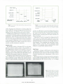
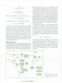
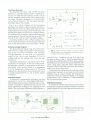
SEPTEMBER 1976 HEWLETTiPA' © Copr. 1949-1998 Hewlett-Packard Co. An Easier-to-Use Variable-Persistence/ Storage Oscilloscope with Brighter, Sharper Traces Revising the control arrangement and operating modes of a variable persistence oscilloscope results in a more "friendly" instrument that also has improved display characteristics. by Van Harrison VARIABLE PERSISTENCE-STORAGE oscillo scopes enable a user to view and measure oc casional signal transients that escape detection with conventional oscilloscopes. Now with improved writing rates, variable persistence/storage scopes have become fast enough to permit their general use in the high-speed transient analysis that often accom panies digital design and troubleshooting, especially for finding "glitches" that occur randomly (Fig. 1). The variable persistence/storage scope also retains waveforms traced at very slow sweep speeds, allow ing the user to see the entire waveform rather than a moving dot (Fig. 2). With persistence adjusted to overlap traces, these instruments can integrate fast signals that occur at too low a repetition rate for nor mal viewing, making the signals brightly visible for examination (Fig. 3). In fact, this integrating technique makes it possible to view signal transitions that are much faster than the basic writing rate of the oscilloscope. In view of all these advantages, in addition to the ability to do everything that conventional scopes can do, the question arises: why aren't variable persistence/storage scopes used more often? Part of the answer may be cost. They do cost more. But more than that may be the duller, fuzzier trace, the esoteric controls — these intimidate the casual user — and the tediousness of setting up the instrument for storage. Then too there has been the fear of burning the storage surface of an expensive-to-replace CRT. A new variable persistence/storage scope (Fig. 4) has been designed to make this type of instrument more acceptable to the average user by eliminating most of these problems. A new arrangement of the controls with LED indicators to show what state the instrument is in takes some of the mystery out of instrument operation. Auto store and auto erase modes of operation simplify instrument use. Im provements in the CRT result in a brighter trace that is more sharply focused, with trace quality as good as or better than that of some comparably-performing con ventional oscilloscopes (Fig. 5). Protection circuits reduce the likelihood of burning the storage surface while simplifying beam intensity and focus adjust ments. Basically, the new oscilloscope, Model 1741A, is identical to and can be used like the Model 1740A, described in the HP Journal, December 1975, with the added advantages of variable persistence and storage. Both scopes are dual-channel, delaying sweep oscil loscopes with dc-to-100-MHz response, 5-mV/div Cover: A shock-test machine slams down to test an instrument's ruggedness, an accelerometer responds to the resulting G forces, and a variable-persistence/ storage oscilloscope cap tures the single accel erometer pulse so its magni tude can be measured. This is one of the applica tions for which this type of oscilloscope is uniquely suited. The HP Model 1741 A variablepersistence /storage scope, shown here is de scribed in the article beginning on this page. In this Issue An Easier-to-Use Variable-Persis tence/Storage Oscilloscope with Brighter, Sharper Traces, by Van H a r r i s o n p a g e An Automatic Wide-Range Digital LCR Meter, by Satoru Hashimoto and T o s h i o T a m a m u r a p a g e Printed in U S A 2 9 ©Hewlett-Packard Company. 1976 © Copr. 1949-1998 Hewlett-Packard Co. Fig. 1. By overlapping several successive traces, variable per sistence oscilloscopes can dis close the existence of intermittent glitches that escape detection by other means. The glitch that oc casionally follows the third pulse in this pulse train is not visible on a conventional oscilloscope dis play (left) but becomes visible on a variable persistence oscillo scope (right). minimum deflection factor (1 mV/div with magnifier on), selectable input impedance (50Ãà or 1 Mfl//20pF), and a third trace for viewing the triggering waveform. To these basic performance characteristics, the Model 1741 A adds variable persistence and storage with a writing rate of >100 cm//AS in both variable persis tence and storage modes of operation, fast enough to capture a single transient pulse less than 20 ns wide and taller than 1 graticule division. these controls. As shown by the timing diagram of Fig. 6, in the AUTO ERASE mode a sweep trigger unblanks the CRT beam and starts the horizontal sweep circuit, writing a trace. At the end of the sweep, the CRT beam is blanked and control is handed to the storage circuits, which inhibit further sweep triggering while display ing the stored trace. The trace remains on view for a time (t2) between Fig. 2. Slow-moving waveform (10 ms/div) shows up as a moving dot on a conventional oscillo scope (left) but the waveform is easily seen on a variable-per sistence/storage oscilloscope (right). CRT persistence can be adjusted so the waveform is retained just until a new trace is written. Auto Erase 1 and 10 seconds, selectable by the VIEW control. At the end of the view time, the instrument switches to the ERASE mode, wiping out the trace. After 300 ms, control is handed back to the sweep circuits which then await another trigger. The AUTO ERASE circuit allows two sweeps between erasures when the in- The new oscilloscope has an AUTO ERASE mode that, by automating the erase/write/view cycle, facilitates the setting of the CRT controls for optimum bright ness and focus. This mode permits the operator to quickly evaluate the effect of any changes made to Fig. 3. Fast waveform transitions occurring at a low repetition are barely visible on a conventional oscilloscope (left) but become brightly visible when several repetitions are integrated by a variable persistence oscillo scope (right). Sweep time here is 50 ns/div and the repetition rate is 50 s weeps Is. 3 © Copr. 1949-1998 Hewlett-Packard Co. f Fig. 4. New Model 1741A Os cilloscope has variable persis tence and storage modes of operation in addition to having all the other attributes of a highquality, laboratory grade, 100-MHz Oscilloscope. Storage controls, with LED indicators to show what state the instrument is in, are grouped conveniently to the left of the CRT. strument is in the alternate sweep mode, and three sweeps if the TRIGGER VIEW mode is added. Dual- or triple-channel displays are thus possible in the AUTO ERASE mode. Besides permitting the operator to adjust the CRT beam controls quickly for optimum settings before making a transient measurement, the AUTO ERASE mode is also useful as a repetitive single-shot mode for examining the voltage levels and transition times of random binary sequences, for examining highfrequency signals contaminated with time jitter or low-frequency noise, or for examining the charac teristics of other types of signals that are obscured in normal oscilloscope operation when successive traces are not identical (Fig. 7). circuit waits in the armed state. As soon as a trigger occurs, the instrument switches automatically to the WRITE mode and the sweep starts. When the sweep terminates, the instrument switches to the STORE mode and retains the written trace up to 30 minutes for examination. Front-panel LED indicators show what state the instrument is in, clearly indicating when the scope is triggered and when it switches to Auto Store One limitation in the application of storage scopes has been the length of time that the CRT can wait in a state prepared to capture a transient when looking for powerline transients, power supply transients, or any other transients or noise that occur at unpredictable times. This wait time, usually about 30 seconds, was the time it took for the CRT screen to fade positive (become illuminated all over), washing out any trace that might subsequently be written. The AUTO STORE mode of the Model 1741 A extends this wait time to several hours. As shown by the timing diagram of Fig. 8, the instrument remains in the ERASE mode (time tj) while the sweep trigger Fig. 5. Exceptionally fine traces are obtained on the Model 1741 A in variable persistence and storage modes of opera tion. The two waveforms traced here while the instrument was in the variable persistence mode are separated hori zontally by only 1.7 mm (sweep time is 5 ns/div). © Copr. 1949-1998 Hewlett-Packard Co. Fig. 6. In AUTO ERASE mode, trace writing, viewing, and erase occur repetitively. Fig. 8. In AUTO STORE mode, oscilloscope waits in the ERASE mode until the sweep triggers. At the conclusion of the sweep, the instrument switches to the STORE mode to retain the trace. STORE. Pressing the STORE/DISPLAY button makes the trace visible for viewing. Storage time in the DISPLAY mode, however, is reduced to 10 to 30 seconds de pending on the setting of the BRIGHTNESS control. To keep front-panel clutter at a minimum, the AUTO ERASE and AUTO STORE modes are selected by the same pushbutton, LED indicators showing which mode is selected (see Fig. 4]. Depressing this button selects the AUTO STORE mode if the SINGLE SWEEP pushbutton is also pressed. Otherwise, the AUTO ERASE mode is selected. Releasing the button returns the scope to normal variable persistence operation. current, is sufficient to cause the voltage drop across Rl to turn on transistor Ql , Q2 restrains the voltage at the wiper of the INTENSITY control from going any further negative, keeping the CRT beam current at or below this level. Capacitors Cl and C2 average the voltage across Rl so the very low average of fast single-shot or low-duty cycle signals does not restrict the beam current, per mitting maximum writing rate and bright display of these signals. The averaging also provides an auto matic intensity correction when changing sweep speeds as, for example, when switching from main sweep to a much faster delayed sweep. Intensity Limit The storage surface of storage CRTs can be dam aged by excessive beam current. The possibility of this happening is reduced in the Model 1741A even though the beam current can be set high enough to achieve a 100 cm//^is single-shot writing rate. An intensity-limit circuit monitors the CRT beam current and limits the average current to a safe level. A diagram of the intensity-limit circuit is shown in Fig. 9. Resistor Rl is in series with the cathode-ray gun accelerator anode. When the anode current, which is approximately proportional to total beam Auto Focus Normally, a change in CRT beam current requires a readjustment of the FOCUS control. AUTO FOCUS allows the intensity-limit system to alter the beam current without requiring any adjustment of the FOCUS control. The change in focus voltage required by a change in beam current is diagrammed in Fig. 10. This curve is approximated by the circuit of Fig. 11. A voltage Fig. 7. Signals that do not repeat identically are difficult to analyze on a conventional scope (left), but can be presented in a repeti tive single-shot mode (right) when the Model 1741 A is operating in the AUTO ERASE mode. 5 © Copr. 1949-1998 Hewlett-Packard Co. A Brighter, More Sharply Focused Variable Persistence/Storage Cathode-Ray Tube Oscilloscope being taken as a starting point for the design. The major design goal for the new tube was to increase full-area writing rate. Within limits, writing rate can be improved by increasing the accelerating potential In the electron gun. The consequent Increase in the electron beam energy results in a higher secondary emission ratio of the storage surface, and hence in a faster writing rate. To meet design goals within a reasonable development time, it was decided to retain the successful manufacturing techniques developed for the storage elements in the Model 184A CRT and concentrate design efforts on obtaining higher electron beam energy from the electron gun. Unfortunately, deflection sensitivity is adversely affected by higher beam energy so the major effort was concerned with optimizing this trade-off. To begin with, some loss In deflection sensitivity could be tolerated because the Model 1741A's deflection amplifiers are capable of higher drive voltages than those of the Model 184A. Nevertheless, the tube length was increased by 34 mm with the extra length being applied to the deflection-plate-tophosphor-surface distance to increase deflection sensitivity. With the new tube dimensions, the flood guns are further from the screen, improving flood-gun display uniformity. To further improve uniformity, the flood gun grid leads were brought out separately on neck pins to enable balancing of the flood gun outputs. The deflection plates themselves were redesigned using cal culator programs that clearly showed the various trade-offs between operating voltages, deflection plate dimensions, fre quency response, and the other parameters that affect perfor mance. From this a deflection plate shape was derived that allowed the closest possible spacing for maximum sensitivity without intercepting the beam. The electron gun was reproportioned to realize greater beam current while optimizing spot size, using curves published by Hilary Moss.1 This resulted in a shorter anode that intercepts fewer electrons, leaving more beam current. The shortened anode also permitted a further increase in the deflection-plateto-phosphor spacing. All of these steps increased deflection sensitivity to the point that the cathode potential could be increased 855 volts to -2295 V. The result was a substantial increase in beam current and, consequently, in writing rate (> 1 00 cm/¿¿s). Cut-off voltage is -100V, allowing a large drive voltage with high beam current in the single-shot mode (the intensity-limit circuit holds the drive to lower levels in repetitive operation). Variable persistence/storage CRTs, originally developed for radar applications, retain oscilloscope traces on a storage mesh located precisely 0.08 inch behind the phosphor surface. The mesh Is a fine metallic screen coated with a dielectric (magnesium fluoride). When a trace Is to be stored, the storage surface Is brought to -10V. Electrons in the CRT beam strike the surface with suffi cient energy to dislodge several electrons for each electron In the beam, raising the potential of the storage surface where the beam strikes. The dislodged electrons are swept up by the positively charged collector mesh nearby (see drawing). CRT beam electrons that pass through the storage mesh strike the phosphor surface, generating a trace that shows where writing occurs. After completion of the sweep, the stored trace is made visible by flood-gun electrons. The low-velocity electrons from the flood guns are repelled by negatively charged areas of the storage surface and gathered by the collector mesh, but where the storage surface has been charged by the electron beam, the electrons approach close enough to the mesh to be pulled through by the high accelerat ing potential of the phosphor surface (5.2 kV), striking the phos phor with sufficient energy to produce a visible trace. To erase the stored trace, the storage mesh Is raised to the same potential as the collector electrode (+156 V) for 50 ms. The entire storage surface then becomes uniformly charged, obliterating the trace. The storage surface Is then returned to — 10 V for the next write cycle. Variable persistence is obtained by shortening the erase cycle so only partial erasure occurs. The erase cycle repeats at a 1 -kHz rate so the trace slowly fades from view. By varying the width of the erase cycles, the rate of fade can be controlled Storage Mesh Flood Guns Phosphor Viewing Screen Electron Gun within a range of 100 ms to 1 minute. During the view phase, the few inevitable gas molecules in the CRT become ionized. These collect on the storage mesh, slowly bringing the non-written areas of the storage mesh up to the potential of the written area, washing out the trace. This limits storage time in the view mode to about 30 seconds. Increasing the viewed brightness accelerates this process so there is a trade-off between trace brightness and storage time in the DIS PLAY mode. Acknowledgments Many people contributed to the design of the new CRT. Johan Sverdup and Chuck Gustafson provided continuing encour agement and guidance. Special thanks are due Roy Wheeler, Dave Granteer, and Jim Haley for valuable technical advice and programming assistance. Much help was also provided by John Hawton, Paul Carnahan, Frank Balint, and Hank Ragsdale. -RobertG. Wick/iff Jr. Taking a CRT One Step Further Reference The design of the CRT for the Model 1741 A Oscilloscope is based on this same scheme, the CRT used in the Model 184A 1 H. Moss, "Narrow Angle Electron Guns. ' Academic Press, New York and London. 6 © Copr. 1949-1998 Hewlett-Packard Co. M,, Ã- 2 I Auto-Focus Voltage Optimum Focus Voltage I -1 CRT Intensity Fig. 10. Graph of the optimum focus voltage as a function of CRT intensity (solid line). The dotted line is the curve gen erated by the auto focus circuit (Fig. 1 1). - 1 5 V - 1 5 V -15V Fig. 9. Intensity-limit circuit responds to the average current in the electron-gun anode and limits the excursions of the CRT unblanking pulse accordingly. proportional to intensity is taken from the INTENSITY control (R2 of Fig. 9) and buffered by Q4 (Fig. 11). The turn-on threshold of transistor Q5 is set by poten tiometer R6, and this threshold becomes the break point for the curve of Fig. 10. Above the break point the slope of the focus-voltage-vs-intensity-setting curve is determined by the ratio of R7 to R4 -I- R5. The focus-voltage-vs-intensity-setting curve is thus ap proximated closely enough that manual adjustment gains only marginal improvement, if any at all. Model 1741A has a BRIGHTNESS control in addition to the INTENSITY control. The INTENSITY control ad justs CRT beam current whereas the BRIGHTNESS con trol, by determining the steady-state voltage of the storage mesh, affects display intensity when viewing a stored trace. With the BRIGHTNESS control at its most negative position, the storage surface repels most flood-gun electrons, allowing only a few to be at tracted by the phosphor voltage through the mesh where the trace is written. At its most positive level, many electrons pass through where the trace is writ ten, giving a bright trace, but the display also fades positive more quickly. The BRIGHTNESS control per mits the operator to find the best balance between trace brightness and viewing time. It replaces the MAX WRITE switch of earlier HP variable persistence/ storage scopes which gave only two levels of control for this function. Added Conveniences Other features contribute to ease of operation. For instance, when the instrument is in the SINGLE SWEEP mode, pushing the manual ERASE button not only erases the trace but it also resets the sweep, eliminat ing the bother of pushing two different buttons to reset the instrument for a single-shot measurement. + 15V R7 Focus Voltage Intensity -15V Limit Circuit -15V -2.3kV © Copr. 1949-1998 Hewlett-Packard Co. Fig. 11. The auto focus circuit modifies the voltage applied to the FOCUS control in response to the INTENSITY control setting. sees something he wishes to retain without losing part of the complete sweep. Van Harrison Van Harrison spent two years with the U.S. Navy in Ethiopia before attending the University of Florida, where he obtained BSEE and MSEE degrees. Upon graduation (1972) he joined HP, contribut ing to the Model 1740A 100-MHz Oscilloscope before assuming i if — «- project leadership of the Model 1 741 A. A native of Ormond Beach, Florida, Van is married and has two children. He also designs hifi equipment, does some wood working, skis, and golfs. Conventional Operation The manner of operating the CRT has been changed for conventional non-storage display. Formerly, dur ing normal oscilloscope operation the voltage on the storage mesh was made negative (-30 V) to repel flood gun electrons and prevent them from illuminat ing anything written on the storage surface. This also happened to reduce the intensity of the electron beam. In the new oscilloscope, the flood gun grids turn off the electron flow in the conventional mode. At the same time, the storage mesh is raised to the potential of the collector mesh ( + 156 V] so no secondary emission occurs and traces are not stored. Lii) Switching to either the AUTO ERASE or AUTO STORE mode automatically sets the instrument for maximum persistence. Switching to the AUTO ERASE mode also switches the trigger mode to NORM so the trigger cir cuit is not left in the AUTO mode, which could trigger the scope randomly. A hold-off circuit is wired into the STORE function so that when the STORE button is pressed during a sweep, the instrument does not go into the STORE mode until the current sweep completes. This ar rangement is particularly desirable for slow sweeps when operating in the AUTO ERASE mode as it permits the operator to push the STORE button whenever he Acknowledgments I would like to thank Stan Lang and Johan Sverdup for constant support, encouragement and many useful ideas during the project, Al Best for his leadership and support during the latter stages of the project, Joe Millard and Eldon Cornish for flexible vertical and horizontal designs that allowed for new control ideas, Jim Carner for the mechanical design, Dick Stone and Herman Hinton for their customer-oriented in puts, and Chuck Gustafson for his many hours of help in understanding the subtleties of storage CRTs-ii" ABRIDGED SPECIFICATIONS HP Model 1741A Oscilloscope Vertical Display Modes A v» B Operation TIME BASE ACCURACY Channel A. channel B channels A and B displayed alternately on successive sweeps |ALT) <x by switching between channels at 250 kHz fale with Dlanking Out ing switching ICHOP). channel A plus channel 6 (algebraic addition): and trigger Sweep Tlme/Drv Temp Range ±3% ±4% ±2% ±3% ±3% ±4% Vertical Amplifiers (2) Bandwidth and Rise Time at all deflection (actors Irom 0*C to -SS'C BANDWIDTH: (3 dB down Irom 6 div reference signal) DC-COUPLED dc to 100 MHz m both 5011 and 1 Mil input modes AC-COUPLED approx 10 Hz 1o 100 MHz 1 Hz with 10 ' divider probes RISE TIME: t j 5 ns measured from 10% to 90% points of a 6 div input step DEFLECTION FACTOR RANGES 5 mV'drv to 20 V'div m 1 . 2. 5 sequence VERNIER continuously variable between all ranges, extends maximum deflec tion factor to at least SO V.'div POLARITY: channel B may be inverted front panel pushbutton INPUT RC (selectable) AC OR DC 1 Mil±2% shunted Dy approx 20 pF 50 OHM 500 ±3% A + B OPERATION AMPLIFIER bandwidth and deflection (actors are unchanged channel B may be inverted for A - B operation DIFFERENTIAL (A-B) COMMON MODE CMRR is at least 20 dB from dc to 20 MHz Common mode signal amplitude equivalent to 8 divisions with one verner ad|usted tor optimum rejection VERTICAL MAGNIFICATION (XS) BANDWIDTH (3 dB down from 8 div reference signal! DC-COUPLED dc to approx 30 MHz AC-COUPLED approx 10 Hz to 30 MHz RISE TIME s 12 ns (measured from 10% to 90% points of B div input step! DEFLECTION FACTOR increases sensitivity of 5 and 10 mV'drv settings by factor ot 5 for maximum sensitivity of 1 mV drv on channels A and 8 TRIGGER SOURCE: Selectable from channel A. channel 8. composite or hne frequency TRIGGER VIEW: Displays internal or external trigger signal In Alternate or Chop mode channel A channel B and trigger signals are displayed In channel A or B mode. Tngger View overrides that channel Internal trigger signal amplitude approximates vertical signal amplitude External trigger signal deflection factor •s approx 100 mV drv or 1 V drv in EXT - 10 Tnggenng point is approx center Horizontal Display Modes Main, mam intensified mixed delayed mag X10 and A vs B T1MC BASE RANGES MAIN 50 nsdiv to 2 s.drv (24 rangesi m 1. 2. 5 sequence DELAYED 50 ns-drv to 20 ms.*v (18 rangesi m 1. 2. 5 sequence MAIN SWEEP VERNIER: continuously -arable between an ranges exiends slowest sweep to at least 5 s. drv MAGNIFIER (X10) expands a* sweeps by a factor of 'C exiends fastest sweep 10 S n&drv 'Add 1 ". for 50 rr 0*Cto +15"C -35'Cto-55'C i ranges CALIBRATED SWEEP DELAY DELAY TIME RANGE 0 5 t( 10 X Main Time.Div s rtmgs of 100 re to 2 s (minimum delay ISO ns) DIFFERENTIAL TIME MEASUREMENT ACCURACY Mein Time B.« Setting •Accuracy ( + 1FCIO +3S°C) 100 nsfdivto20 msidiv 50 ms div to 2 s div ±(05% ±0.1% of full scale) ±(1% + 0 1% of full scale) 'Add 1% lor temperatures tro .[• 1 S°C and - 3: Triggering MAIN SWEEP NORMAL sweep is triggered by internal or external signal. AUTOMATIC bright baseline displayed m absence ot input signal Above SINGLE sweep occurs once with same triggering as Normal Reset pushbutton arms sweep and lights indicator Single sweep is also initiated with Erase pushbutton, sweep is armed after erase cycle DELAYED SWEEP (SWEEP AFTER DELAY) AUTO delayed sweep automatically starts at end of delay TRIG delayed sweep is armed and triggerabie at end of delay period INTERNAL. Oc to 25 MHz on signals causing 0 3 divisions or more vertical deflec tion, increasing to 1 division ol vertical deflection at 100 MHz in all display modes S signal level is increased by 2 when in Oop mode arx) by S wfien X5 vertical magnrfier is used) Tnggenng on Une frequency is also selectable EXTERNAL: dc to 50 MHz on signals of 50 mV p-p or more increasing lo 1 00 mV p-p at IX MHz (required signal level is increased by 2 when in Chop model EXTERNAL INPUT RC: appro' 1 MCI shunted by approx 20 pF LEVEL ANO SLOPE INTERNAL at any pant on powtrve or negative Slope of »splayed waveform EXTERNAL continuously variable from -1 V to -1 V on either slope Of trigger signal -tOVlo -tOVm divide by 10 mode (-) COUPLING: AC DC LF REJ or HF REJ AC attenuates signals below approx 20 Hz LF REJECT (MAIN SWEEP) attenuates signals below approx 4 KHz HF REJECT (MAIN SWEEP) attenuates signals above approx 4 kHz TRIGGER MOLDOFF .Mam Sweep) increases sweep hokJofl time in al ranges CALIBRATED MIXED TIME BASE: Dual time Dase m wtvch main time base drrves first portion of sweep and delayed time base completes sweep at (aster delayed sweep 8 © Copr. 1949-1998 Hewlett-Packard Co. BANDWIDTH CHANNEL A (Y-AXIS) same as channel A CHANNEL B (X-AXIS) dc to 5 MHz DEFLECTION FACTOR: 5 mV div to 20 V-Div (12 calibrated positions) in 1, 2, 5 sequence PHASE DIFFERENCE BETWEEN CHANNELS: 3 Oc to 100 KHl Cathode-Ray Tube and Controls TYPE: Hewlett-Packard. 127 cm (5 in) rectangular CRT. post accelerator. approx 7 5 kV accelerating potential, ahjrmnzed P31 phosphor GRATICULE: 8 • 10 div (1 div = 065 cm) internal, non-parallax graticule Graticule illumination is achieved with Persistence contra set to minimum OPERATING MOOES: «rite, store, display, auto-store, auto-erase, and con ventional i rear panel pushbutton) PERSISTENCE VARIABLE approx 100 ms 10 1 mm CONVENTIONAL natural persistence of P31 phosphor (approi 40 *is) STORAGE WRITING SPEED: -'00 crn^s d 18 d>v ^s) over center 7 • 9 div (with viewing hood) STORAGE TIME DISPLAY MODE at least 10 s at 22"C. STORE MODE at leasi 30 s at 22°C BRIGHTNESS: appro* 170 cd m* (50 ft) ERASE TIME: approx 300 ms 2-AXIS INPUT (INTENSITY MODULATION) ~4 V. *50-ns width pulse blanks trace of any intensity usabtetosiOMHzfot normahntenstty Input R, 1 kn ±10%. General AMPLITUDE CALIBRATOR (D'C to -55 d OUTPUT VOLTAGE 1 V p-p - 1 % into 3 1 Mil; 0 1 V p-p RISE TIME «0.1 MS FREQUENCY approx 1 4 kHl POWER: 100. 120. 220. 240 Vac ±10%. 48 to 440 Hz. 100 VA max WEIGHT: net 13 8 kg (30 5 b) OPERATING ENVIRONMENT TEMPERATURE ffC to -55'C HUMIDITY to 9S% relative num«drty at -4ffC ALTITUDE 10 4600 m (15.000 ft) VIBRATION vibrated in three planes for 15 mm each with 0 254 mm (0 010 in) excursion 10 to 55 Hz DIMENSIONS: 335 mm W - 197 mm H • 492 mm D (13 2 • 7 8 * 19.4m) ACCESSORIES FURNISHED: Mué bght tiler RFI finer and contrast screen, view ing hood front-panel cover power cord vinyt accessory storage pouch. Opera tor s Guide Service Manual, two 10 1 divider probes PRICE IN U.S.A.: Model 1741A Oscilloscope $3960 MANUFACTURING DIVISION: COLORADO SPRINGS DIVISION 1900 Garden of the Gods Road Colorado Springs Colorado 80907 An Automatic Wide-Range Digital LCR Meter Easy operation, a wide measurement range, two measurement frequencies, high reliability, optional HP-IB c o m Q u*//-!//!>•./ snl·l!.' w cost 1 1 iar\e it suitauic /ors vv/us range of component and impedance measurements. by Satoru Hashimoto and Toshio Tamamura ANEW DIGITAL LCR meter, Model 4261A (Fig. 1), is designed to provide the wide range and ac curacy of a universal impedance bridge without the bridge's disadvantages of manual balancing and meter-reading ambiguity. The new LCR meter is fully automatic, displaying the value and dissipation fac tor of an unknown inductor or capacitor or the value of an unknown resistor on its SVz-digit display a frac tion of a second after the unknown is connected to its terminals. Selection of the measurement equiva lent circuit is made automatically according to the value of the unknown component. The new LCR meter typically can take four or more readings per second at a 1-kHz measurement fre quency and one or more at 120 Hz with basic accur acies of 0.2% for capacitance, inductance, resistance, and dissipation factor. The unknown terminals are configured in a five-terminal arrangement that is ca pable of four, three, and two-terminal connections suitable, respectively, for low-impedance, highimpedance, and ordinary measurements. The unit measures capacitance from 0.1 pF to 1900 /¿F at 1 kHz and from 1 pF to 19.00 mFat 120 Hz, inductance from 0.1 /¿H to 190.0 H at 1 kHz and from 1 /*H to 1900 H at 120 Hz, resistance from 1 mil to 19.00 Mil at 1 kHz or 120 Hz, and dissipation factor of capacitors or induc tors from 0.001 to 1.900. For measurements in semi conductors, two test voltages, 50 mV and IV rms, are available for making capacitance measurements in the parallel equivalent circuit mode. An internal dc bias source provides switch-selectable 1.5V, 2.2V, and 6V. External bias from 0V to 30V can be supplied 426IA LCR METEB I 13. 8 S IB S S TEST SH3 LEVEL TRIGGER Fig. 1. Model 4261 A LCR Meter makes fully automatic measure ments of inductance, capacitance, resistance, and dissipation factor at 120 Hz or 1 kHz. It provides a choice of two test signal levels, three internal dc bias voltages, and two, three, or four-terminal measurement connections. HP Interface Bus (IEEE 488-1975) compatibility is optional. © Copr. 1949-1998 Hewlett-Packard Co. to a rear-panel connector. An offset adjustment for canceling stray capacitance between the unknown terminals is provided; a capacitance offset signal, available at a rear-panel BNC connector, provides an offset range of 0 to 100 pF when fed into the lowcurrent terminal through a variable capacitor. A low-power design keeps total power consump tion below 25 watts, helping to assure reliability. For automated testing or data gathering under computer or calculator control, an option provides an interface to the HP-IB (HP Interface Bus), HP's implementation of IEEE Standard 488-1975. mode is selected. In the series mode, the 4261A se lects a source resistance at least ten times the value of the DUT impedance to achieve a constant current drive. When the parallel equivalent circuit mode is chosen, a source resistance less than one-tenth that of the DUT impedance is selected to drive the DUT at a constant voltage. The source resistor (R0) helps to limit current flow into the current detecting amplifier when its ter minals are shorted, and to suppress differential or integral noise when a capacitor or inductor is con nected. For a Cp-D measurement in the parallel equivalent circuit mode, How It Works The 4261A measures L,C,R, and dissipation factor by determining the impedance or admittance of the unknown device under test (DUT). In the current-tovoltage converter section (Fig. 2), the measuring signal is applied to the DUT and an operational amp lifier is used as a current detection amplifier. The cur rent through the DUT is almost equal to that flowing in the range resistor RR. Voltages et and e2 are ob tained by detecting the voltages produced across the DUT and range resistor RR, respectively, using differ ential amplifiers A2 and A3. e: and e2 are transferred to the measurement section, where their vector ratio is detected by a phase detector and a dual-slope analog-to-digital converter. When a device is measured with the 4261 A, either a series equivalent circuit mode or a parallel equivalent circuit mode is automatically selected. When the DUT impedance is relatively low the series mode is selected and when it is relatively high the parallel (Gp + jwCp)RR e2 = (Gp + j«Cp)R0 where &> = 27rf, and f = test frequency. When e2 is the reference signal, the ratio of 6j and e2 is: ei/ez = - (Gp + j RR which is proportional to the unknown admittance. Lp-D is determined in the same manner: e,/ez = - (1/Rp + l/jwLp) RR For a measurement in the LS-D series circuit mode, the equations for el and e2 are: Differential Amplifier To Measurement Section Current Detector Amplifier Guard 10 © Copr. 1949-1998 Hewlett-Packard Co. Fig. 2. Current-to-voltage conver ter section applies the test signal to the unknown and develops two voltages, e, and e2, whose ratio is proportional to the unknown im pedance or admittance. Selection of series or parallel equivalent cir cuit for the unknown is made automatically. the vector ratio of e^ and e2. A block diagram and timing chart for this section are shown in Figs. 3 and 4. The instrument goes through a seven-step se quence to take a measurement. In step 1, an autozero is performed. Sa connects the input of the phase de tector to ground and S2 is closed. Thus with no input (Sa is shorting the input to ground), the integrator loop is adjusted for zero input and the adjustment vol tage is stored on C2. This cancels any phase detector leakage current error as well as compensating for any dc offset voltage throughout the loop. During step 2, an auto phase adjustment is performed; this will be described later. Steps 1 and 2 are performed just be fore ratio detection. Assume that a capacitor is being measured in the parallel circuit mode (Cp). e2 is the reference signal, as previously described, and is applied to the fourphase generator. Step 3 is the integrator charging period Tj. Sj is on, and switch SD is connected to 6j. 6j is then phase detected by a signal whose phase is shifted 90° from e2, as determined by control logic in the ROM. The integrator charge (Qcp) stored dur ing T! is: + e2 = Rs R + Rs When B! is the reference signal, the ratio of e2le1 is 62/ej = - (Rs+jwLs)/RR The equation for a CS-D measurement becomes BZ/BJ = - (Rs+l/ju)Cs)/RR In all cases, the vector ratio multiplied or divided by RR produces the DUT impedance or admittance. The 4261A has five range resistors (from 10Ã1 to 100 kO) having tolerances of 0.05%. It is possible to ignore the residual resistance of the range switch, which adds to RR and might contribute to the error, since the current and potential terminals of the range resistors are separated. Detecting the voltage differentially minimizes the error contributed by the residual resistance of the lead connections to the DUT, and similarly, the residual voltage of the cur rent detecting amplifier. Qcpl = -Ku>CpRRTie2. where K is the product of the efficiency of the phase detector and the integrating constant. Step 4 is the integrator discharge cycle. SD is connected to e2, which is phase detected by a signal in phase with e2. The integrator begins to discharge and continues discharging until its output crosses the zero-volt point. If the discharge time is Tcp, the charge dis sipated is: Measurement Section This section consists of a four-phase generator for phase detection, a sectional average integrator (SAI) that smooths the signal from the phase detector, a dual-slope analog-to-digital converter, and logic cir cuitry. The output is a digital quantity proportional to Integrator ROM Centered Logic Fig. 3. Measurement section develops and displays a digital representation of the vector ratio of e, and e2. 11 © Copr. 1949-1998 Hewlett-Packard Co. 7 %* ^ A * ? °V% '<<X Qdl - -KGpRRT2e2 in step 6, and Qd2 = KwCpRRTde2 in step 7. If the charging time is n'2 times the period of the clock frequency, the following equation is similarly es tablished: n 2 n j — K wCp RR e2 = n', = n' wC, = n'! D Thus n'2 is a measure of the dissipation factor. CS-D Measurement The CS-D measurement employs an unusual tech nique. e1 is the reference signal for the series equiva lent circuit mode. In step 3, SD is connected to e^ and phase detected by a signal in phase with e^ In other words, BJ is phase detected by er The integrator is charged for a period equal to n3 times the reciprocal of the test frequency f. The charge stored on the inte grator during this time is: Qcsi = Ke^a/f. Fig. 4. 7fte measurement sequence consists of seven steps including autozem and auto-phase-adjust steps. The dualslope analog-to-digital conversion method is used, except that in the CS-D measurement the slopes occur in reverse order. Step 4 is the discharge cycle. SD is connected to e2, which is phase detected by a signal whose phase is shifted from e: by 270°. The integrator discharges until its output crosses the zero-volt point. If the dis charge time is n4/fc, the charge dissipated is: QCD2 = KT(c p e 2 ' From steps 3 and 4, Q c s 2 = - K wCsRR fc Q c p i = - Q cp2 Then, because Tcp ¿cs2> T-, is rij times the period of the test frequency f, and Tcp is counted as n2 by the clock frequency fc: n4 = 277fcn3CsRR. n2 = 277-fcRRnjCp. Hence from n4, Cs is directly obtained. This technique is the widely used dual-slope method except that the slopes occur in reverse order. Usually, the integrator discharge slope is constant, but here the slope decreases as the C count increases. At full scale, the discharge slope is one-tenth that of the charging slope. This results in a good signal-tonoise ratio and precise resolution, and makes it possible for the new meter to use only five range resistors for its eight-range measurement capability. The clock frequency is selected so that Cp is directly obtained. Next, step 6 immediately initiates the D measure ment. Switch SD is connected to 6j and the phase of the detector signal is controlled at 0°. The phasedetected dc voltage is integrated and discharged in steps 6 and 7 ' , with the phase of the detector signal changed from 0° to 270° in step 7. If the discharge time is Td, 12 © Copr. 1949-1998 Hewlett-Packard Co. Four-Phase Generator The precision 90° phase shift needed for phase detection is normally derived from a standard ca pacitor, but when the test frequency is low, such as 120 Hz, standard capacitors are very expensive and very large. The 4261A measures L, C, R, and D with out a standard capacitor. The four-phase generator technique makes this possible. Fig. 5 is a circuit diagram of the four-phase generator. The reference signal is shaped and fed to a phase detector (point A) whose other input is the 0° output signal, thus forming a phase-locked loop. The filtered phase detector output tunes a voltage control led oscillator that produces a signal at four times the input frequency. Two J-K flip flops driven by the VCO provide 0°, 90°, 180° and 270° four-phase outputs. A potential problem of this method is phase noise, which causes fluctuations in counting the discharge time. In the 4261A phase noise is less than -70 dB. Example: Sectional Average Integrator The phase-detected signal of Fig. 3 has to be trans lated into a dc voltage very quickly for precise opera tion of the dual-slope technique. The sectional average integrator1, or SAI, (Fig. 6) is especially useful at the 120 Hz test frequency. If C¡Rf is suitably selected the settling time is one test sig nal period. During the first period T, the input current is in tegrated by the integrator. At the end of this period, the integrator output El is proportional to the dc in put current. After the first period, Ea is transferred to Cj by momentarily closing switch Sh- Thus the output Eg is a step function whose steady-state value is exactly proportional to IDC. Fig. 6 shows typical waveforms. Fig. 6. Sectional average integrator converts the phasedetected signal to a dc voltage within one test signal period, as shown by the typical waveforms. shown in Fig. 7. Amplifiers A4 and A5 in Fig. 7 are the same as those in Fig. 3. Since the amplifiers are not ideal, they shift the phase of the ea and e2 signals. The difference between the two phase shifts (0er) will cause a large error, especially when measuring the dissipation factor of low-loss capacitors. For accuracy, tanker must be less than 0.001. Automatic phase adjustment is done in step 2 of the measurement sequence. S A is closed and a first-order feedback loop is created through the integrator to reduce 0er. When the loop has settled, a dc voltage proportional to 0er is stored in C3 and maintained for the measurement period. Auto Phase Adjust A phase error compensation technique was first employed in the 4271A 1 MHz Digital LCR Meter.2 That method used two phase detectors and two inte grators. To produce a quality low-cost unit, an auto phase adjustment technique was adopted for the 4261A. The auto phase adjustment block diagram is ROM-Centered Design To control its various measurement modes and to manage the complex decoding necessary to provide simple operation with wide-range measurements, the Fig. 5. Four-phase generator develops precision phase shifts and eliminates the need for a standard capacitor. 13 © Copr. 1949-1998 Hewlett-Packard Co. The user need only set two slide switches. Two tests are provided. One tests the logic systems and the other mainly checks the analog circuits. Slide switches located on the sequence control board are set to the appropriate positions to put the 4261A into its self-test mode. Minimizing Errors The five-terminal connection configuration minimizes the measurement error caused by residual impedance of the test leads. It is especially useful for the measurement of low impedances (below 1Ã1). However, some care is required in making the test lead connections when measuring capacitors from 100 to 1000 /L/.F at 1 kHz. Here, an error is caused by the mutual inductance of the Hp, He cable or the Lp, Lc cable. If the mutual inductance of each cable is M/2 henries, then: Asin(cjt+0er) Fig. 7. Circuit diagram for auto phase adjustment. Closing SA creates a first-order feedback loop that stores on capaci tor C3 a voltage proportional to the differential phase shift of amplifiers A4 and A5. 4261A uses a ROM-centered design. It has two 4K-bit ROMs, one for sequence control and the other a de coder. With this design, it was easy to add the selftest functions. The ROMs are n-channel MOS ROMs manufactured by HP. C measured = - Cx To minimize this error, it is necessary to use short test leads or to twist the Hp and Lp cables together. Similarly in high-impedance measurements, it is possible to minimize the stray capacitance between the high and low terminals by shielding with the GUARD terminal. Compensation for high-impedance measurement errors can also be made by using an off set voltage equal to the voltage across the DUT but opposite in polarity; this is done with the 4261A in the connection configuration shown in Fig. 8. The variable capacitor is adjusted for a zero display. Full Autoranging The 4261A has two autoranging modes. One is a fixed measurement circuit mode in which the opera tor selects either the series or the parallel equivalent circuit, and the other is full autoranging including circuit mode changing. Measurement circuit mode changes are done by switching Sc in Fig. 3. In the full autoranging mode, the instrument selects an appropriate range from the eight available ranges according to the value of the component being tested. In this mode, the function switch need only be set to L, C, or R to make the measurement. Accessories Several accessories are available for the 4261A. The 16061A Test Fixture is a direct-connection type for Self-Test The 4261A has self-test functions that enable it to check most performance areas. No additional equip ment or circuitry is required for making the self-check. Fig. 8. To cancel stray capacitance between the unknown terminals, a capacitance offset signal, available at a rearpanel connector, provides a capacitance offset of 0 to 100 pF when fed into the low-current terminal through a variable capacitor. The capacitor is adjusted for a zero display with no unknown connected. Fig. 9. Model 16061 A Test Fixture for general-purpose use. 14 © Copr. 1949-1998 Hewlett-Packard Co. Kazu Shibata and Yoshio Satoh, who handled the industrial design. Hitoshi Noguchi provided many useful suggestions for the project. Akira Yamaguchi designed part of the logic section in the early stages of the project. \ References 1. T. Sugiyama and K. Yamaguchi, "Pulsewidth Modu lation DC Potentiometer," IEEE Transactions, Vol. IM-19, No. 4, November 1970. 2. K. Maeda, "An Automatic Precision, 1-MHz Digital LCR Meter," Hewlett-Packard Journal, March 1974. Fig. 10. Model 16062A Test Leads for low-impedance devices. general-purpose use. The 16061 A Test Fixture (Fig. 9) has inserts for both parallel and axial lead components. The 16062A Test Leads (Fig. 10) are for comparatively low-impedance DUTs (four-terminal connections). The 16063A Test Leads (Fig. 11) are for comparatively high-impedance DUTs (three-terminal connections). Satoru Hashimoto Satoru Hashimoto received his BSEE from Tokyo Metropolitan University in 1971, and soon after wards joined Yokogawa-HewlettPackard. He worked on the design of the logic section of the 4271 A 1-MHz Digital LCR Meter, then joined the 4261A Digital LCR Meter project. He developed the counter and the sequence con trol section circuitry for the 4261 A. In his spare time Satoru enjoys mountain climbing and photography. Acknowledgments The authors wish to express appreciation to the many people who participated in the development of the Model 4261A. The team members included Kohichi Maeda, who directed the project, Hiroshi Sakayori, who designed the process amplifier sec tion, Kenzo Ishiguro, who designed the display and decoder section, Seiji Mochizuki, who did the power supply design, Toshio Manabe and Yoshimasa Shibata, who contributed to the mechanical design, and Toshio Tamamura Toshio Tamamura received his BSEE degree in 1971 from the University of Electro-Communica tions in Tokyo. He has been with Yokogawa-Hewlett-Packard as a development engineer since that time. He was a principal contribu tor to the design of the 4271 A 1-MHz Digital LCR Meter and the 4261 A Digital LCR Meter; he developed the analog section cir cuitry for the 4261 A. He's mar ried and the father of a small son. In his spare time Toshio likes to play tennis. Fig. 11. Model 16063A Test Leads for high-impedance devices. 15 © Copr. 1949-1998 Hewlett-Packard Co. Hewlett-Packard Company, 1501 Page Mill Road, Palo Alto, California 94304 HEWLETT-PACKARDJOTHNAL Bulk Rate U.S. Postage Paid Hewlett-Packard Company SEPTEMBER 1976 Volume 28 • Number Technical Information from the Laboratories of Hewlett-Packard Company Hewlett-Packard S.A.. CH-1217 Meynn 2 Geneva, Switzerland Yokogawa-Hewlett-Packard Ltd., Shibuya-Ku Tokyo 151 Japan Editorial Director a Howard L. Roberts Managing Editor a Richard P. Dolan Art Director, Photographer a Arvid A. Danielson Illustrator a Sue M. Perez Administrative Services. Typography a Anne S. LoPresti European Production Manager • Michel Foglia /*""* |_| please address peels off). P C*\ F A |~^ ü*) D P Q Q - To Chan9e your address <* d6'616 y°ur naâ„¢ fr°m ou' mailing list please send us your old address label (it peels off). V-y I I f\ Palo N California L. ^J I f\ LJ \—) C. O O . Send changes to Hewlett-Packard Journal. 1 501 Page Mill Road. Palo Alto. California 94304 U.S.A. Allow 60 days. © Copr. 1949-1998 Hewlett-Packard Co.