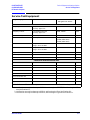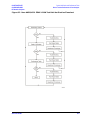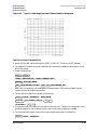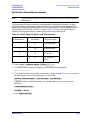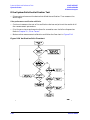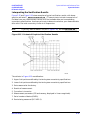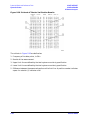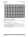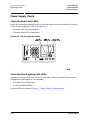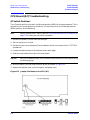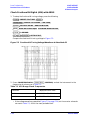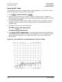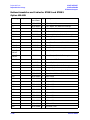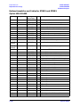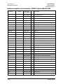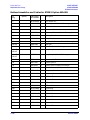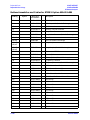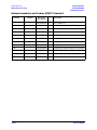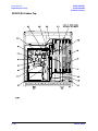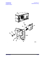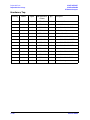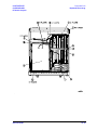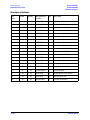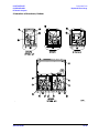
1
Service Guide
Agilent Technologies
8719ET/20ET/22ET
8719ES/20ES/22ES
Network Analyzers
Part Number 08720-90397
Printed in USA
June 2002
Supersedes February 2001
© Copyright 1999 − 2002 Agilent Technologies, Inc.
Notice
The information contained in this document is subject to change without notice.
Agilent Technologies makes no warranty of any kind with regard to this material,
including but not limited to, the implied warranties of merchantability and fitness for a
particular purpose. Agilent Technologies shall not be liable for errors contained herein or
for incidental or consequential damages in connection with the furnishing, performance, or
use of this material.
Warranty Information
THE MATERIAL CONTAINED IN THIS DOCUMENT IS PROVIDED "AS IS," AND IS
SUBJECT TO BEING CHANGED, WITHOUT NOTICE, IN FUTURE EDITIONS.
FURTHER, TO THE MAXIMUM EXTENT PERMITTED BY APPLICABLE LAW,
AGILENT DISCLAIMS ALL WARRANTIES, EITHER EXPRESS OR IMPLIED WITH
REGARD TO THIS MANUAL AND ANY INFORMATION CONTAINED HEREIN,
INCLUDING BUT NOT LIMITED TO THE IMPLIED WARRANTIES OF
MERCHANTABILITY AND FITNESS FOR A PARTICULAR PURPOSE. AGILENT
SHALL NOT BE LIABLE FOR ERRORS OR FOR INCIDENTAL OR CONSEQUENTIAL
DAMAGES IN CONNECTION WITH THE FURNISHING, USE, OR PERFORMANCE
OF THIS DOCUMENT OR ANY INFORMATION CONTAINED HEREIN. SHOULD
AGILENT AND THE USER HAVE A SEPARATE WRITTEN AGREEMENT WITH
WARRANTY TERMS COVERING THE MATERIAL IN THIS DOCUMENT THAT
CONFLICT WITH THESE TERMS, THE WARRANTY TERMS IN THE SEPARATE
AGREEMENT WILL CONTROL.
Certification
Agilent Technologies Company certifies that this product met its published specifications
at the time of shipment from the factory. Agilent Technologies further certifies that its
calibration measurements are traceable to the United States National Institute of
Standards and Technology, to the extent allowed by the Institute’s calibration facility, and
to the calibration facilities of other International Standards Organization members.
Regulatory Information
The regulatory information is located in Chapter 15 , “Safety and Regulatory Information.”
ii
Assistance
Product maintenance agreements and other customer assistance agreements are available
for Agilent Technologies products. For any assistance, contact your nearest Agilent
Technologies sales or service office. See Table 15-1 on page 15-3 for the nearest office.
Safety Notes
The following safety notes are used throughout this manual. Familiarize yourself with
each of the notes and its meaning before operating this instrument. All pertinent safety
notes for using this product are located in Chapter 15 , “Safety and Regulatory
Information.”
WARNING
Warning denotes a hazard. It calls attention to a procedure which, if
not correctly performed or adhered to, could result in injury or loss
of life. Do not proceed beyond a warning note until the indicated
conditions are fully understood and met.
CAUTION
Caution denotes a hazard. It calls attention to a procedure that, if not
correctly performed or adhered to, would result in damage to or destruction of
the instrument. Do not proceed beyond a caution sign until the indicated
conditions are fully understood and met.
How to Use This Guide
This guide uses the following conventions:
Front-Panel Key
This represents a key physically located on the
instrument.
SOFTKEY
This represents a “softkey,” a key whose label is
determined by the instrument’s firmware.
Screen Text
This represents text displayed on the instrument’s screen.
iii
Documentation Map
The Installation and Quick Start Guide provides procedures for
installing, configuring, and verifying the operation of the analyzer. It
also will help you familiarize yourself with the basic operation of the
analyzer.
The User’s Guide shows how to make measurements, explains
commonly-used features, and tells you how to get the most
performance from your analyzer.
The Reference Guide provides reference information, such as
specifications, menu maps, and key definitions.
The Programmer’s Guide provides general GPIB programming
information, a command reference, and example programs. The
Programmer’s Guide contains a CD-ROM with example programs.
The CD-ROM provides the Installation and Quick Start Guide, the
User’s Guide, the Reference Guide, and the Programmer’s Guide in
PDF format for viewing or printing from a PC.
The Service Guide provides information on calibrating,
troubleshooting, and servicing your analyzer. The Service Guide is not
part of a standard shipment and is available only as Option 0BW, or
by ordering part number 08720-90397. A CD-ROM with the Service
Guide in PDF format is included for viewing or printing from a PC.
iv
Contents
1. Service Equipment and Analyzer Options
Information in This Chapter . . . . . . . . . . . . . . . . . . . . . . . . . . . . . . . . . . . . . . . . . . . . . . . . . . .1-2
Service Test Equipment . . . . . . . . . . . . . . . . . . . . . . . . . . . . . . . . . . . . . . . . . . . . . . . . . . . . . . .1-3
Principles of Microwave Connector Care . . . . . . . . . . . . . . . . . . . . . . . . . . . . . . . . . . . . . . . . .1-6
Analyzer Options . . . . . . . . . . . . . . . . . . . . . . . . . . . . . . . . . . . . . . . . . . . . . . . . . . . . . . . . . . . .1-7
Option 1D5, High Stability Frequency Reference . . . . . . . . . . . . . . . . . . . . . . . . . . . . . . . .1-7
Option 004, Step Attenuator (ET Models) . . . . . . . . . . . . . . . . . . . . . . . . . . . . . . . . . . . . . . .1-7
Option 007, Mechanical Transfer Switch (ES Models) . . . . . . . . . . . . . . . . . . . . . . . . . . . .1-7
Option 010, Time Domain. . . . . . . . . . . . . . . . . . . . . . . . . . . . . . . . . . . . . . . . . . . . . . . . . . . .1-7
Option 012, Direct Access Receiver Configuration (ES Models) . . . . . . . . . . . . . . . . . . . . .1-7
Option 085, High Power System (ES Models) . . . . . . . . . . . . . . . . . . . . . . . . . . . . . . . . . . . .1-8
Option 089, Frequency Offset Mode (ES Models) . . . . . . . . . . . . . . . . . . . . . . . . . . . . . . . . .1-8
Option 400, Four-Sampler Test Set (ES Models). . . . . . . . . . . . . . . . . . . . . . . . . . . . . . . . . .1-8
Option 1CP, Rack Mount Flange Kit With Handles . . . . . . . . . . . . . . . . . . . . . . . . . . . . . . .1-8
Option 1CM, Rack Mount Flange Kit Without Handles . . . . . . . . . . . . . . . . . . . . . . . . . . .1-8
Service and Support Options . . . . . . . . . . . . . . . . . . . . . . . . . . . . . . . . . . . . . . . . . . . . . . . . . .1-9
Option W01 . . . . . . . . . . . . . . . . . . . . . . . . . . . . . . . . . . . . . . . . . . . . . . . . . . . . . . . . . . . . . . .1-9
Option W31 . . . . . . . . . . . . . . . . . . . . . . . . . . . . . . . . . . . . . . . . . . . . . . . . . . . . . . . . . . . . . . .1-9
Option W50 . . . . . . . . . . . . . . . . . . . . . . . . . . . . . . . . . . . . . . . . . . . . . . . . . . . . . . . . . . . . . . .1-9
Option W51 . . . . . . . . . . . . . . . . . . . . . . . . . . . . . . . . . . . . . . . . . . . . . . . . . . . . . . . . . . . . . . .1-9
Option W32 . . . . . . . . . . . . . . . . . . . . . . . . . . . . . . . . . . . . . . . . . . . . . . . . . . . . . . . . . . . . . . .1-9
Option W52 . . . . . . . . . . . . . . . . . . . . . . . . . . . . . . . . . . . . . . . . . . . . . . . . . . . . . . . . . . . . . . .1-9
Option W34 . . . . . . . . . . . . . . . . . . . . . . . . . . . . . . . . . . . . . . . . . . . . . . . . . . . . . . . . . . . . . . .1-9
Option W54 . . . . . . . . . . . . . . . . . . . . . . . . . . . . . . . . . . . . . . . . . . . . . . . . . . . . . . . . . . . . . .1-10
2. System Verification and Performance Tests
Sections in This Chapter . . . . . . . . . . . . . . . . . . . . . . . . . . . . . . . . . . . . . . . . . . . . . . . . . . . . . .2-2
How to Test the Performance of Your Analyzer . . . . . . . . . . . . . . . . . . . . . . . . . . . . . . . . . . . .2-3
ANSI/NCSL Z540–1–1994 Verification . . . . . . . . . . . . . . . . . . . . . . . . . . . . . . . . . . . . . . . . .2-3
Non-ANSI/NCSL Z540–1–1994 Verification . . . . . . . . . . . . . . . . . . . . . . . . . . . . . . . . . . . . .2-3
Instrument Verification Cycle . . . . . . . . . . . . . . . . . . . . . . . . . . . . . . . . . . . . . . . . . . . . . . . .2-4
Preliminary Tests . . . . . . . . . . . . . . . . . . . . . . . . . . . . . . . . . . . . . . . . . . . . . . . . . . . . . . . . . . .2-6
Required Equipment and Tools . . . . . . . . . . . . . . . . . . . . . . . . . . . . . . . . . . . . . . . . . . . . . . .2-6
Check the Temperature and Humidity . . . . . . . . . . . . . . . . . . . . . . . . . . . . . . . . . . . . . . . . .2-6
Clean and Gauge All Connectors . . . . . . . . . . . . . . . . . . . . . . . . . . . . . . . . . . . . . . . . . . . . .2-7
Perform the Internal Test . . . . . . . . . . . . . . . . . . . . . . . . . . . . . . . . . . . . . . . . . . . . . . . . . . .2-7
Procedure to Perform Operator’s Check. . . . . . . . . . . . . . . . . . . . . . . . . . . . . . . . . . . . . . . . .2-8
Check the Test Port Cables . . . . . . . . . . . . . . . . . . . . . . . . . . . . . . . . . . . . . . . . . . . . . . . . . .2-9
System Verification . . . . . . . . . . . . . . . . . . . . . . . . . . . . . . . . . . . . . . . . . . . . . . . . . . . . . . . . .2-15
General Information . . . . . . . . . . . . . . . . . . . . . . . . . . . . . . . . . . . . . . . . . . . . . . . . . . . . . . .2-16
Equipment Initialization . . . . . . . . . . . . . . . . . . . . . . . . . . . . . . . . . . . . . . . . . . . . . . . . . . .2-20
Measurement Calibration . . . . . . . . . . . . . . . . . . . . . . . . . . . . . . . . . . . . . . . . . . . . . . . . . .2-22
Verification Device Measurements . . . . . . . . . . . . . . . . . . . . . . . . . . . . . . . . . . . . . . . . . . .2-25
Performing the Verification Tests. . . . . . . . . . . . . . . . . . . . . . . . . . . . . . . . . . . . . . . . . . . . .2-26
If the System Fails the Verification Test . . . . . . . . . . . . . . . . . . . . . . . . . . . . . . . . . . . . . .2-30
Interpreting the Verification Results . . . . . . . . . . . . . . . . . . . . . . . . . . . . . . . . . . . . . . . . .2-31
Performance Tests . . . . . . . . . . . . . . . . . . . . . . . . . . . . . . . . . . . . . . . . . . . . . . . . . . . . . . . . . .2-33
Frequency Accuracy Performance Test . . . . . . . . . . . . . . . . . . . . . . . . . . . . . . . . . . . . . . . .2-34
Level Accuracy Performance Test . . . . . . . . . . . . . . . . . . . . . . . . . . . . . . . . . . . . . . . . . . . .2-36
Contents-v
Contents
Source Linearity Performance Test . . . . . . . . . . . . . . . . . . . . . . . . . . . . . . . . . . . . . . . . . . 2-38
Dynamic Range Performance Test . . . . . . . . . . . . . . . . . . . . . . . . . . . . . . . . . . . . . . . . . . . 2-42
Performance Test Record . . . . . . . . . . . . . . . . . . . . . . . . . . . . . . . . . . . . . . . . . . . . . . . . . . . . 2-46
3. Adjustments and Correction Constants
Information on This Chapter . . . . . . . . . . . . . . . . . . . . . . . . . . . . . . . . . . . . . . . . . . . . . . . . . . 3-2
A7 Switch Positions . . . . . . . . . . . . . . . . . . . . . . . . . . . . . . . . . . . . . . . . . . . . . . . . . . . . . . . . . 3-4
Source Pretune Correction Constants (Test 43) . . . . . . . . . . . . . . . . . . . . . . . . . . . . . . . . . . . 3-6
Analog Bus Correction Constants (Test 44) . . . . . . . . . . . . . . . . . . . . . . . . . . . . . . . . . . . . . . 3-8
IF Step Correction Constants (Test 47) . . . . . . . . . . . . . . . . . . . . . . . . . . . . . . . . . . . . . . . . . . 3-9
ADC Offset Correction Constants (Test 48) . . . . . . . . . . . . . . . . . . . . . . . . . . . . . . . . . . . . . 3-10
Serial Number Correction Constants (Test 49) . . . . . . . . . . . . . . . . . . . . . . . . . . . . . . . . . . . 3-11
Protected Option Numbers Correction Constants (Test 50) . . . . . . . . . . . . . . . . . . . . . . . . . 3-13
Unprotected Hardware Option Correction Constants . . . . . . . . . . . . . . . . . . . . . . . . . . . . . 3-15
Output Power Adjustments . . . . . . . . . . . . . . . . . . . . . . . . . . . . . . . . . . . . . . . . . . . . . . . . . . 3-17
Preparing the Instrument . . . . . . . . . . . . . . . . . . . . . . . . . . . . . . . . . . . . . . . . . . . . . . . . . . 3-17
Setting the Main Power DAC to Preset Values. . . . . . . . . . . . . . . . . . . . . . . . . . . . . . . . . . 3-18
Setting the Potentiometers to the Minimum Levels. . . . . . . . . . . . . . . . . . . . . . . . . . . . . 3-19
Adjusting the Mid Band Power . . . . . . . . . . . . . . . . . . . . . . . . . . . . . . . . . . . . . . . . . . . . . . 3-20
Adjusting the Low Band Power . . . . . . . . . . . . . . . . . . . . . . . . . . . . . . . . . . . . . . . . . . . . . 3-21
Adjusting the High Band Power (8722ET/ES) . . . . . . . . . . . . . . . . . . . . . . . . . . . . . . . . . . 3-21
Fine Tuning the Flatness . . . . . . . . . . . . . . . . . . . . . . . . . . . . . . . . . . . . . . . . . . . . . . . . . . 3-22
Power Linearity Adjustment . . . . . . . . . . . . . . . . . . . . . . . . . . . . . . . . . . . . . . . . . . . . . . . . . 3-24
Preparatory Steps . . . . . . . . . . . . . . . . . . . . . . . . . . . . . . . . . . . . . . . . . . . . . . . . . . . . . . . . 3-24
Blanking Adjustment (Test 54) . . . . . . . . . . . . . . . . . . . . . . . . . . . . . . . . . . . . . . . . . . . . . . . 3-30
Preparing the Instrument . . . . . . . . . . . . . . . . . . . . . . . . . . . . . . . . . . . . . . . . . . . . . . . . . . 3-30
Initialize EEPROMs (Test 53) . . . . . . . . . . . . . . . . . . . . . . . . . . . . . . . . . . . . . . . . . . . . . . . . 3-32
EEPROM Backup Disk Procedure . . . . . . . . . . . . . . . . . . . . . . . . . . . . . . . . . . . . . . . . . . . . . 3-33
Correction Constants Retrieval Procedure . . . . . . . . . . . . . . . . . . . . . . . . . . . . . . . . . . . . . . 3-35
Loading Firmware . . . . . . . . . . . . . . . . . . . . . . . . . . . . . . . . . . . . . . . . . . . . . . . . . . . . . . . . . 3-36
Loading Firmware into an Existing CPU . . . . . . . . . . . . . . . . . . . . . . . . . . . . . . . . . . . . . 3-36
In Case of Difficulty . . . . . . . . . . . . . . . . . . . . . . . . . . . . . . . . . . . . . . . . . . . . . . . . . . . . . . 3-36
Loading Firmware into a New CPU . . . . . . . . . . . . . . . . . . . . . . . . . . . . . . . . . . . . . . . . . . 3-37
Reference Assembly VCO Tune Adjustment . . . . . . . . . . . . . . . . . . . . . . . . . . . . . . . . . . . . . 3-39
Frequency Accuracy Adjustment . . . . . . . . . . . . . . . . . . . . . . . . . . . . . . . . . . . . . . . . . . . . . . 3-41
In Case of Difficulty . . . . . . . . . . . . . . . . . . . . . . . . . . . . . . . . . . . . . . . . . . . . . . . . . . . . . . 3-43
API Spur Avoidance and 100 kHz FM Sideband Adjustment . . . . . . . . . . . . . . . . . . . . . . . 3-44
FM Sideband Adjustment (100 kHz Spurs) . . . . . . . . . . . . . . . . . . . . . . . . . . . . . . . . . . . . 3-44
API Adjust . . . . . . . . . . . . . . . . . . . . . . . . . . . . . . . . . . . . . . . . . . . . . . . . . . . . . . . . . . . . . . 3-46
Raw Offset Correction Constants . . . . . . . . . . . . . . . . . . . . . . . . . . . . . . . . . . . . . . . . . . . . . . 3-48
Raw Offset for the R Channel (ET/ES Models). . . . . . . . . . . . . . . . . . . . . . . . . . . . . . . . . . 3-49
Raw Offset for the A and B Channels (ES Models) . . . . . . . . . . . . . . . . . . . . . . . . . . . . . . 3-51
Raw Offsets for the A and B Channels (ET Models) . . . . . . . . . . . . . . . . . . . . . . . . . . . . . 3-54
Sampler Calibration Correction Constants (Test 51) . . . . . . . . . . . . . . . . . . . . . . . . . . . . . . 3-58
4. Start Troubleshooting Here
Information on This Chapter . . . . . . . . . . . . . . . . . . . . . . . . . . . . . . . . . . . . . . . . . . . . . . . . . . 4-2
Assembly Replacement Sequence . . . . . . . . . . . . . . . . . . . . . . . . . . . . . . . . . . . . . . . . . . . . . . 4-3
Contents-vi
Contents
Having Your Analyzer Serviced . . . . . . . . . . . . . . . . . . . . . . . . . . . . . . . . . . . . . . . . . . . . . . . .4-4
Step 1. Initial Observations . . . . . . . . . . . . . . . . . . . . . . . . . . . . . . . . . . . . . . . . . . . . . . . . . . .4-5
Initiate the Analyzer Self-Test . . . . . . . . . . . . . . . . . . . . . . . . . . . . . . . . . . . . . . . . . . . . . . .4-5
Step 2. Operator’s Check . . . . . . . . . . . . . . . . . . . . . . . . . . . . . . . . . . . . . . . . . . . . . . . . . . . . . .4-7
Description . . . . . . . . . . . . . . . . . . . . . . . . . . . . . . . . . . . . . . . . . . . . . . . . . . . . . . . . . . . . . . .4-7
Procedure to Perform Operator’s Check. . . . . . . . . . . . . . . . . . . . . . . . . . . . . . . . . . . . . . . . .4-8
In Case of Difficulty . . . . . . . . . . . . . . . . . . . . . . . . . . . . . . . . . . . . . . . . . . . . . . . . . . . . . . . .4-9
Step 3. GPIB Systems Check . . . . . . . . . . . . . . . . . . . . . . . . . . . . . . . . . . . . . . . . . . . . . . . . .4-10
If Using a Plotter or Printer . . . . . . . . . . . . . . . . . . . . . . . . . . . . . . . . . . . . . . . . . . . . . . . .4-11
If Using an External Disk Drive . . . . . . . . . . . . . . . . . . . . . . . . . . . . . . . . . . . . . . . . . . . . .4-11
Troubleshooting Systems with Multiple Peripherals . . . . . . . . . . . . . . . . . . . . . . . . . . . . .4-12
Troubleshooting Systems with Controllers . . . . . . . . . . . . . . . . . . . . . . . . . . . . . . . . . . . .4-12
Step 4. Faulty Group Isolation . . . . . . . . . . . . . . . . . . . . . . . . . . . . . . . . . . . . . . . . . . . . . . . .4-13
Power Supply Check. . . . . . . . . . . . . . . . . . . . . . . . . . . . . . . . . . . . . . . . . . . . . . . . . . . . . . . . .4-14
Check the Rear Panel LEDs . . . . . . . . . . . . . . . . . . . . . . . . . . . . . . . . . . . . . . . . . . . . . . . .4-14
Check the Post Regulator (A8) LEDs . . . . . . . . . . . . . . . . . . . . . . . . . . . . . . . . . . . . . . . . .4-14
Digital Control Check. . . . . . . . . . . . . . . . . . . . . . . . . . . . . . . . . . . . . . . . . . . . . . . . . . . . . . . .4-15
Observe the Power Up Sequence . . . . . . . . . . . . . . . . . . . . . . . . . . . . . . . . . . . . . . . . . . . . .4-15
Verify Internal Tests Passed . . . . . . . . . . . . . . . . . . . . . . . . . . . . . . . . . . . . . . . . . . . . . . . .4-16
Source Check . . . . . . . . . . . . . . . . . . . . . . . . . . . . . . . . . . . . . . . . . . . . . . . . . . . . . . . . . . . . . .4-17
Phase Lock Error Messages . . . . . . . . . . . . . . . . . . . . . . . . . . . . . . . . . . . . . . . . . . . . . . . . .4-17
Check Source Output Power . . . . . . . . . . . . . . . . . . . . . . . . . . . . . . . . . . . . . . . . . . . . . . . .4-18
No Oscilloscope or Power Meter? Try the ABUS . . . . . . . . . . . . . . . . . . . . . . . . . . . . . . . .4-20
Receiver Check . . . . . . . . . . . . . . . . . . . . . . . . . . . . . . . . . . . . . . . . . . . . . . . . . . . . . . . . . . . . .4-21
Checking the R Channel Output (ET and ES Models) . . . . . . . . . . . . . . . . . . . . . . . . . . . .4-22
Checking the A Channel Output (ES Models) . . . . . . . . . . . . . . . . . . . . . . . . . . . . . . . . . . .4-23
Checking the B Channel Output (ET and ES Models) . . . . . . . . . . . . . . . . . . . . . . . . . . . .4-24
Switch Repeatability Check (ES Models) . . . . . . . . . . . . . . . . . . . . . . . . . . . . . . . . . . . . . . . .4-25
Accessories Check. . . . . . . . . . . . . . . . . . . . . . . . . . . . . . . . . . . . . . . . . . . . . . . . . . . . . . . . . . .4-26
Overall Instrument Block Diagrams . . . . . . . . . . . . . . . . . . . . . . . . . . . . . . . . . . . . . . . . . . . .4-27
8719ES and 8720ES Standard, Option 007, 012, 085, 089, 1D5 . . . . . . . . . . . . . . . . . . . .4-27
8719ES and 8720ES Option 400, 012, 085, 1D5 . . . . . . . . . . . . . . . . . . . . . . . . . . . . . . . . .4-28
8722ES Standard, Option 007, 012, 085, 089, 1D5 . . . . . . . . . . . . . . . . . . . . . . . . . . . . . . .4-29
8722ES Option 400, 012, 089, 1D5. . . . . . . . . . . . . . . . . . . . . . . . . . . . . . . . . . . . . . . . . . . .4-30
8719ET and 8720ET Standard, Option 004 . . . . . . . . . . . . . . . . . . . . . . . . . . . . . . . . . . . .4-31
8722ET Standard, Option 004 . . . . . . . . . . . . . . . . . . . . . . . . . . . . . . . . . . . . . . . . . . . . . . .4-32
5. Power Supply Troubleshooting
Information on This Chapter . . . . . . . . . . . . . . . . . . . . . . . . . . . . . . . . . . . . . . . . . . . . . . . . . . .5-2
Power Supply Troubleshooting Flowchart . . . . . . . . . . . . . . . . . . . . . . . . . . . . . . . . . . . . . . . .5-3
Assembly Replacement Sequence . . . . . . . . . . . . . . . . . . . . . . . . . . . . . . . . . . . . . . . . . . . . . . .5-4
Simplified Block Diagram of Power Supply Group . . . . . . . . . . . . . . . . . . . . . . . . . . . . . . . . .5-5
Start Here . . . . . . . . . . . . . . . . . . . . . . . . . . . . . . . . . . . . . . . . . . . . . . . . . . . . . . . . . . . . . . . . .5-6
Check the Green LED and Red LED on the Preregulator (A15) . . . . . . . . . . . . . . . . . . . . .5-6
Check the Green LEDs on the Post Regulator (A8) . . . . . . . . . . . . . . . . . . . . . . . . . . . . . . .5-6
Measure the Post Regulator (A8) Voltages . . . . . . . . . . . . . . . . . . . . . . . . . . . . . . . . . . . . . .5-7
If the Green LED of the Preregulator (A15) Is Off or Blinking . . . . . . . . . . . . . . . . . . . . . . .5-8
Check the Line Voltage, Selector Switch, and Fuse . . . . . . . . . . . . . . . . . . . . . . . . . . . . . . .5-8
If the Red LED of the Preregulator (A15) Is On . . . . . . . . . . . . . . . . . . . . . . . . . . . . . . . . . . .5-9
Contents-vii
Contents
Check the Post Regulator (A8) . . . . . . . . . . . . . . . . . . . . . . . . . . . . . . . . . . . . . . . . . . . . . . . 5-9
Verify the Preregulator (A15) . . . . . . . . . . . . . . . . . . . . . . . . . . . . . . . . . . . . . . . . . . . . . . . 5-10
Check for a Faulty Assembly . . . . . . . . . . . . . . . . . . . . . . . . . . . . . . . . . . . . . . . . . . . . . . . 5-11
Check the Operating Temperature . . . . . . . . . . . . . . . . . . . . . . . . . . . . . . . . . . . . . . . . . . . 5-12
Inspect the Motherboard . . . . . . . . . . . . . . . . . . . . . . . . . . . . . . . . . . . . . . . . . . . . . . . . . . . 5-12
If the Green LEDs of the Post Regulator (A8) Are Not All ON . . . . . . . . . . . . . . . . . . . . . . 5-13
Maintain A15W1 Cable Connection . . . . . . . . . . . . . . . . . . . . . . . . . . . . . . . . . . . . . . . . . . 5-13
Check the Post Regulator (A8) Fuses and Voltages . . . . . . . . . . . . . . . . . . . . . . . . . . . . . . 5-13
Remove the Assemblies . . . . . . . . . . . . . . . . . . . . . . . . . . . . . . . . . . . . . . . . . . . . . . . . . . . . 5-14
Briefly Disable the Shutdown Circuitry . . . . . . . . . . . . . . . . . . . . . . . . . . . . . . . . . . . . . . 5-15
Inspect the Motherboard . . . . . . . . . . . . . . . . . . . . . . . . . . . . . . . . . . . . . . . . . . . . . . . . . . . 5-16
Error Messages . . . . . . . . . . . . . . . . . . . . . . . . . . . . . . . . . . . . . . . . . . . . . . . . . . . . . . . . . . . . 5-17
Check the Fuses and Isolate A8 . . . . . . . . . . . . . . . . . . . . . . . . . . . . . . . . . . . . . . . . . . . . . 5-17
Fan Troubleshooting . . . . . . . . . . . . . . . . . . . . . . . . . . . . . . . . . . . . . . . . . . . . . . . . . . . . . . . . 5-18
Fan Speeds . . . . . . . . . . . . . . . . . . . . . . . . . . . . . . . . . . . . . . . . . . . . . . . . . . . . . . . . . . . . . . 5-18
Check the Fan Voltages . . . . . . . . . . . . . . . . . . . . . . . . . . . . . . . . . . . . . . . . . . . . . . . . . . . . 5-18
Short A8TP3 to Ground . . . . . . . . . . . . . . . . . . . . . . . . . . . . . . . . . . . . . . . . . . . . . . . . . . . 5-18
Intermittent Problems . . . . . . . . . . . . . . . . . . . . . . . . . . . . . . . . . . . . . . . . . . . . . . . . . . . . . . 5-19
Power Supply Block Diagram . . . . . . . . . . . . . . . . . . . . . . . . . . . . . . . . . . . . . . . . . . . . . . . . . 5-21
6. Digital Control Troubleshooting
Information on This Chapter . . . . . . . . . . . . . . . . . . . . . . . . . . . . . . . . . . . . . . . . . . . . . . . . . . 6-2
Assembly Replacement Sequence . . . . . . . . . . . . . . . . . . . . . . . . . . . . . . . . . . . . . . . . . . . . . . 6-3
CPU Board (A7) Troubleshooting . . . . . . . . . . . . . . . . . . . . . . . . . . . . . . . . . . . . . . . . . . . . . . 6-4
A7 Switch Positions . . . . . . . . . . . . . . . . . . . . . . . . . . . . . . . . . . . . . . . . . . . . . . . . . . . . . . . . 6-4
Checking the CPU (A7) Red LED Patterns . . . . . . . . . . . . . . . . . . . . . . . . . . . . . . . . . . . . . 6-5
Display Troubleshooting (A18,A19) . . . . . . . . . . . . . . . . . . . . . . . . . . . . . . . . . . . . . . . . . . . . . 6-7
Evaluating Your Display . . . . . . . . . . . . . . . . . . . . . . . . . . . . . . . . . . . . . . . . . . . . . . . . . . . . 6-7
Red, Green, or Blue Pixels Specifications . . . . . . . . . . . . . . . . . . . . . . . . . . . . . . . . . . . . . . 6-7
Dark Pixels Specifications . . . . . . . . . . . . . . . . . . . . . . . . . . . . . . . . . . . . . . . . . . . . . . . . . . 6-8
Newtons Rings . . . . . . . . . . . . . . . . . . . . . . . . . . . . . . . . . . . . . . . . . . . . . . . . . . . . . . . . . . . . 6-8
Troubleshooting the GSP (A19) and the Display (A18) . . . . . . . . . . . . . . . . . . . . . . . . . . . . . 6-9
Measure the Supply Voltages Applied to the GSP (A19) . . . . . . . . . . . . . . . . . . . . . . . . . . . 6-9
Run Display Test 55 . . . . . . . . . . . . . . . . . . . . . . . . . . . . . . . . . . . . . . . . . . . . . . . . . . . . . . 6-10
Inspect Ribbon Cable Repeat Display Test 55 . . . . . . . . . . . . . . . . . . . . . . . . . . . . . . . . . . 6-10
Perform Walking One Pattern . . . . . . . . . . . . . . . . . . . . . . . . . . . . . . . . . . . . . . . . . . . . . . 6-10
Run Display Tests 59-61 . . . . . . . . . . . . . . . . . . . . . . . . . . . . . . . . . . . . . . . . . . . . . . . . . . . 6-12
Front Panel Troubleshooting (A1/A2) . . . . . . . . . . . . . . . . . . . . . . . . . . . . . . . . . . . . . . . . . . . 6-13
Check Front Panel LEDs After Preset . . . . . . . . . . . . . . . . . . . . . . . . . . . . . . . . . . . . . . . . 6-13
Identify the Stuck Key . . . . . . . . . . . . . . . . . . . . . . . . . . . . . . . . . . . . . . . . . . . . . . . . . . . . 6-14
Inspect Cables . . . . . . . . . . . . . . . . . . . . . . . . . . . . . . . . . . . . . . . . . . . . . . . . . . . . . . . . . . . 6-16
Test Using a Controller . . . . . . . . . . . . . . . . . . . . . . . . . . . . . . . . . . . . . . . . . . . . . . . . . . . . 6-16
Run the Internal Diagnostic Tests . . . . . . . . . . . . . . . . . . . . . . . . . . . . . . . . . . . . . . . . . . . . . 6-17
If the Fault Is Intermittent . . . . . . . . . . . . . . . . . . . . . . . . . . . . . . . . . . . . . . . . . . . . . . . . . . 6-19
Repeat Test Function . . . . . . . . . . . . . . . . . . . . . . . . . . . . . . . . . . . . . . . . . . . . . . . . . . . . . 6-19
GPIB Failures . . . . . . . . . . . . . . . . . . . . . . . . . . . . . . . . . . . . . . . . . . . . . . . . . . . . . . . . . . . . . 6-19
Digital Control Block Diagram . . . . . . . . . . . . . . . . . . . . . . . . . . . . . . . . . . . . . . . . . . . . . . . . 6-21
Contents-viii
Contents
7. Source Troubleshooting
Information on This Chapter . . . . . . . . . . . . . . . . . . . . . . . . . . . . . . . . . . . . . . . . . . . . . . . . . . .7-2
Source Troubleshooting Flowchart . . . . . . . . . . . . . . . . . . . . . . . . . . . . . . . . . . . . . . . . . . . . . .7-3
Assembly Replacement Sequence . . . . . . . . . . . . . . . . . . . . . . . . . . . . . . . . . . . . . . . . . . . . . . .7-4
Start Troubleshooting Here . . . . . . . . . . . . . . . . . . . . . . . . . . . . . . . . . . . . . . . . . . . . . . . . . . . .7-5
Power Not within Specifications . . . . . . . . . . . . . . . . . . . . . . . . . . . . . . . . . . . . . . . . . . . . . .7-6
Phase Lock Error Message Displayed . . . . . . . . . . . . . . . . . . . . . . . . . . . . . . . . . . . . . . . . . .7-6
Broadband Phase Lock Problems . . . . . . . . . . . . . . . . . . . . . . . . . . . . . . . . . . . . . . . . . . . . . . .7-8
Swap IF Output Cables to Check R Sampler Assembly (A64) . . . . . . . . . . . . . . . . . . . . . . .7-9
Check Open Loop Power . . . . . . . . . . . . . . . . . . . . . . . . . . . . . . . . . . . . . . . . . . . . . . . . . . . .7-11
Check Reference Board (A12) . . . . . . . . . . . . . . . . . . . . . . . . . . . . . . . . . . . . . . . . . . . . . . . .7-13
Check Fractional-N Digital (A14) with ABUS . . . . . . . . . . . . . . . . . . . . . . . . . . . . . . . . . .7-14
Check the Fractional-N Analog (A13) and Fractional-N Digital (A14) with a Spectrum
Analyzer. . . . . . . . . . . . . . . . . . . . . . . . . . . . . . . . . . . . . . . . . . . . . . . . . . . . . . . . . . . . . . . . .7-15
Check the VCO (A14) Range with Oscilloscope . . . . . . . . . . . . . . . . . . . . . . . . . . . . . . . . .7-16
Substituting Tuning Voltages to Check the VCO . . . . . . . . . . . . . . . . . . . . . . . . . . . . . . . .7-16
Divide-by-N (A14) Circuit Check . . . . . . . . . . . . . . . . . . . . . . . . . . . . . . . . . . . . . . . . . . . . .7-17
A14-to-A13 Digital Control Signals Check . . . . . . . . . . . . . . . . . . . . . . . . . . . . . . . . . . . . .7-17
Pulse Generator (A52) Check with Oscilloscope . . . . . . . . . . . . . . . . . . . . . . . . . . . . . . . .7-19
Pulse Generator (A52) Check with Spectrum Analyzer . . . . . . . . . . . . . . . . . . . . . . . . . . .7-20
Band-Related Problems . . . . . . . . . . . . . . . . . . . . . . . . . . . . . . . . . . . . . . . . . . . . . . . . . . . . .7-22
Broadband Power Problems. . . . . . . . . . . . . . . . . . . . . . . . . . . . . . . . . . . . . . . . . . . . . . . . . . .7-26
ALC/Signal Separation Check . . . . . . . . . . . . . . . . . . . . . . . . . . . . . . . . . . . . . . . . . . . . . . .7-26
Step Attenuator (A69) Check . . . . . . . . . . . . . . . . . . . . . . . . . . . . . . . . . . . . . . . . . . . . . . .7-27
8. Receiver Troubleshooting
Information on This Chapter . . . . . . . . . . . . . . . . . . . . . . . . . . . . . . . . . . . . . . . . . . . . . . . . . . .8-2
Assembly Replacement Sequence . . . . . . . . . . . . . . . . . . . . . . . . . . . . . . . . . . . . . . . . . . . . . . .8-2
All Signal Paths Look Abnormal . . . . . . . . . . . . . . . . . . . . . . . . . . . . . . . . . . . . . . . . . . . . . . .8-3
2nd LO Check . . . . . . . . . . . . . . . . . . . . . . . . . . . . . . . . . . . . . . . . . . . . . . . . . . . . . . . . . . . . .8-3
4 MHz Check . . . . . . . . . . . . . . . . . . . . . . . . . . . . . . . . . . . . . . . . . . . . . . . . . . . . . . . . . . . . .8-3
At Least One Signal Path Looks Normal . . . . . . . . . . . . . . . . . . . . . . . . . . . . . . . . . . . . . . . . .8-4
Directional Coupler Check . . . . . . . . . . . . . . . . . . . . . . . . . . . . . . . . . . . . . . . . . . . . . . . . . . .8-7
A and B Sampler Check by Substitution . . . . . . . . . . . . . . . . . . . . . . . . . . . . . . . . . . . . . . . .8-8
Sampler Voltage Check . . . . . . . . . . . . . . . . . . . . . . . . . . . . . . . . . . . . . . . . . . . . . . . . . . . . .8-9
2nd Converter Check . . . . . . . . . . . . . . . . . . . . . . . . . . . . . . . . . . . . . . . . . . . . . . . . . . . . . . .8-9
9. Accessories Troubleshooting
Information on This Chapter . . . . . . . . . . . . . . . . . . . . . . . . . . . . . . . . . . . . . . . . . . . . . . . . . . .9-2
Inspect and Gauge Connectors . . . . . . . . . . . . . . . . . . . . . . . . . . . . . . . . . . . . . . . . . . . . . . . . .9-3
Inspect the Error Terms . . . . . . . . . . . . . . . . . . . . . . . . . . . . . . . . . . . . . . . . . . . . . . . . . . . . . .9-4
Isolate the Fault in the RF Path . . . . . . . . . . . . . . . . . . . . . . . . . . . . . . . . . . . . . . . . . . . . . .9-5
Verify the RF Cable . . . . . . . . . . . . . . . . . . . . . . . . . . . . . . . . . . . . . . . . . . . . . . . . . . . . . . . .9-6
Verify Shorts and Opens by Substitution . . . . . . . . . . . . . . . . . . . . . . . . . . . . . . . . . . . . . . .9-7
10. Service Key Menus and Error Messages
Information on This Chapter . . . . . . . . . . . . . . . . . . . . . . . . . . . . . . . . . . . . . . . . . . . . . . . . . .10-2
Error Messages . . . . . . . . . . . . . . . . . . . . . . . . . . . . . . . . . . . . . . . . . . . . . . . . . . . . . . . . . . . .10-3
Contents-ix
Contents
Service Menus - Internal Diagnostics . . . . . . . . . . . . . . . . . . . . . . . . . . . . . . . . . . . . . . . . . . 10-3
Tests Menu . . . . . . . . . . . . . . . . . . . . . . . . . . . . . . . . . . . . . . . . . . . . . . . . . . . . . . . . . . . . . . 10-5
Test Options Menu . . . . . . . . . . . . . . . . . . . . . . . . . . . . . . . . . . . . . . . . . . . . . . . . . . . . . . . 10-6
Self Diagnose Softkey . . . . . . . . . . . . . . . . . . . . . . . . . . . . . . . . . . . . . . . . . . . . . . . . . . . . . 10-8
Test Descriptions . . . . . . . . . . . . . . . . . . . . . . . . . . . . . . . . . . . . . . . . . . . . . . . . . . . . . . . . . 10-8
Service Menu - Service Features . . . . . . . . . . . . . . . . . . . . . . . . . . . . . . . . . . . . . . . . . . . . . 10-15
Service Modes Menu . . . . . . . . . . . . . . . . . . . . . . . . . . . . . . . . . . . . . . . . . . . . . . . . . . . . . 10-17
Service Modes More Menu . . . . . . . . . . . . . . . . . . . . . . . . . . . . . . . . . . . . . . . . . . . . . . . . 10-19
Analog Bus on OFF . . . . . . . . . . . . . . . . . . . . . . . . . . . . . . . . . . . . . . . . . . . . . . . . . . . . . . . . 10-20
Description of the Analog Bus (ANAB) . . . . . . . . . . . . . . . . . . . . . . . . . . . . . . . . . . . . . . . 10-20
The Main ADC . . . . . . . . . . . . . . . . . . . . . . . . . . . . . . . . . . . . . . . . . . . . . . . . . . . . . . . . . . 10-20
The Frequency Counter . . . . . . . . . . . . . . . . . . . . . . . . . . . . . . . . . . . . . . . . . . . . . . . . . . 10-20
Analog In Menu . . . . . . . . . . . . . . . . . . . . . . . . . . . . . . . . . . . . . . . . . . . . . . . . . . . . . . . . . 10-21
Analog Bus Nodes . . . . . . . . . . . . . . . . . . . . . . . . . . . . . . . . . . . . . . . . . . . . . . . . . . . . . . . 10-22
PEEK/POKE Menu . . . . . . . . . . . . . . . . . . . . . . . . . . . . . . . . . . . . . . . . . . . . . . . . . . . . . . . . 10-29
Firmware Revision Softkey . . . . . . . . . . . . . . . . . . . . . . . . . . . . . . . . . . . . . . . . . . . . . . . . . 10-30
GPIB Service Mnemonic Definitions . . . . . . . . . . . . . . . . . . . . . . . . . . . . . . . . . . . . . . . . . . 10-31
Invoking Tests Remotely . . . . . . . . . . . . . . . . . . . . . . . . . . . . . . . . . . . . . . . . . . . . . . . . . . 10-31
Analog Bus Codes . . . . . . . . . . . . . . . . . . . . . . . . . . . . . . . . . . . . . . . . . . . . . . . . . . . . . . . 10-32
Service Related Error Messages in Alphabetical Order . . . . . . . . . . . . . . . . . . . . . . . . . . . 10-33
11. Error Terms
Information on This Chapter . . . . . . . . . . . . . . . . . . . . . . . . . . . . . . . . . . . . . . . . . . . . . . . . . 11-2
Error Terms Can Also Serve a Diagnostic Purpose . . . . . . . . . . . . . . . . . . . . . . . . . . . . . . . 11-3
Measurement Calibration Procedure . . . . . . . . . . . . . . . . . . . . . . . . . . . . . . . . . . . . . . . . . . 11-4
Error Term Inspection . . . . . . . . . . . . . . . . . . . . . . . . . . . . . . . . . . . . . . . . . . . . . . . . . . . . . . 11-5
If Error Terms Seem Worse than Typical Values . . . . . . . . . . . . . . . . . . . . . . . . . . . . . . . 11-7
Uncorrected Performance . . . . . . . . . . . . . . . . . . . . . . . . . . . . . . . . . . . . . . . . . . . . . . . . . . 11-8
Error Term Descriptions . . . . . . . . . . . . . . . . . . . . . . . . . . . . . . . . . . . . . . . . . . . . . . . . . . . 11-10
Directivity (EDF and EDR) . . . . . . . . . . . . . . . . . . . . . . . . . . . . . . . . . . . . . . . . . . . . . . . . 11-11
Source Match (ESF and ESR) . . . . . . . . . . . . . . . . . . . . . . . . . . . . . . . . . . . . . . . . . . . . . . 11-12
Reflection Tracking (ERF and ERR) . . . . . . . . . . . . . . . . . . . . . . . . . . . . . . . . . . . . . . . . 11-13
Isolation (Crosstalk, EXF and EXR) . . . . . . . . . . . . . . . . . . . . . . . . . . . . . . . . . . . . . . . . 11-14
Load Match (ELF and ELR) . . . . . . . . . . . . . . . . . . . . . . . . . . . . . . . . . . . . . . . . . . . . . . . 11-15
Transmission Tracking (ETF and ETR) . . . . . . . . . . . . . . . . . . . . . . . . . . . . . . . . . . . . . . 11-16
12. Theory of Operation
Information on This Chapter . . . . . . . . . . . . . . . . . . . . . . . . . . . . . . . . . . . . . . . . . . . . . . . . . 12-2
System Operation . . . . . . . . . . . . . . . . . . . . . . . . . . . . . . . . . . . . . . . . . . . . . . . . . . . . . . . . . . 12-3
Functional Groups of the Analyzer . . . . . . . . . . . . . . . . . . . . . . . . . . . . . . . . . . . . . . . . . . . . 12-5
Power Supply Theory . . . . . . . . . . . . . . . . . . . . . . . . . . . . . . . . . . . . . . . . . . . . . . . . . . . . . . . 12-6
A15 Preregulator . . . . . . . . . . . . . . . . . . . . . . . . . . . . . . . . . . . . . . . . . . . . . . . . . . . . . . . . . 12-6
A8 Post Regulator . . . . . . . . . . . . . . . . . . . . . . . . . . . . . . . . . . . . . . . . . . . . . . . . . . . . . . . . 12-7
Voltage Indications: the Green LEDs . . . . . . . . . . . . . . . . . . . . . . . . . . . . . . . . . . . . . . . . . 12-8
Digital Control Theory . . . . . . . . . . . . . . . . . . . . . . . . . . . . . . . . . . . . . . . . . . . . . . . . . . . . . . 12-9
A1 Front Panel . . . . . . . . . . . . . . . . . . . . . . . . . . . . . . . . . . . . . . . . . . . . . . . . . . . . . . . . . . . 12-9
A2 Front Panel Processor . . . . . . . . . . . . . . . . . . . . . . . . . . . . . . . . . . . . . . . . . . . . . . . . . . 12-9
A7 CPU/A10 Digital IF . . . . . . . . . . . . . . . . . . . . . . . . . . . . . . . . . . . . . . . . . . . . . . . . . . . . 12-9
Contents-x
Contents
A18 Display . . . . . . . . . . . . . . . . . . . . . . . . . . . . . . . . . . . . . . . . . . . . . . . . . . . . . . . . . . . .12-10
A19 Graphics System Processor (GSP) . . . . . . . . . . . . . . . . . . . . . . . . . . . . . . . . . . . . . . .12-11
A20 Inverter . . . . . . . . . . . . . . . . . . . . . . . . . . . . . . . . . . . . . . . . . . . . . . . . . . . . . . . . . . . .12-11
A16 Rear Panel . . . . . . . . . . . . . . . . . . . . . . . . . . . . . . . . . . . . . . . . . . . . . . . . . . . . . . . . . .12-11
Source Group Theory . . . . . . . . . . . . . . . . . . . . . . . . . . . . . . . . . . . . . . . . . . . . . . . . . . . . . .12-13
Source Pretune . . . . . . . . . . . . . . . . . . . . . . . . . . . . . . . . . . . . . . . . . . . . . . . . . . . . . . . . . .12-14
A14/A13 Fractional-N Synthesizer . . . . . . . . . . . . . . . . . . . . . . . . . . . . . . . . . . . . . . . . . .12-14
A52 Pulse Generator: the Harmonic Comb . . . . . . . . . . . . . . . . . . . . . . . . . . . . . . . . . . .12-14
A64 R Sampler: Down-Converting the Signals . . . . . . . . . . . . . . . . . . . . . . . . . . . . . . . .12-14
A11 Phase Lock: Comparing Phase and Frequency . . . . . . . . . . . . . . . . . . . . . . . . . . . . .12-15
Tuning the YIG Oscillator . . . . . . . . . . . . . . . . . . . . . . . . . . . . . . . . . . . . . . . . . . . . . . . . .12-15
Phase Locked Sweep . . . . . . . . . . . . . . . . . . . . . . . . . . . . . . . . . . . . . . . . . . . . . . . . . . . . .12-15
A12 Reference: The Crystal Reference Frequencies . . . . . . . . . . . . . . . . . . . . . . . . . . . .12-16
Source Block: The YIG Oscillator Signals . . . . . . . . . . . . . . . . . . . . . . . . . . . . . . . . . . . .12-16
ALC: Automatic Leveling Control . . . . . . . . . . . . . . . . . . . . . . . . . . . . . . . . . . . . . . . . . . .12-18
Signal Separation: ES Models Only . . . . . . . . . . . . . . . . . . . . . . . . . . . . . . . . . . . . . . . . . . .12-19
A58 M/A/D/S Modulator, Amplifier, Detector, Splitter . . . . . . . . . . . . . . . . . . . . . . . . . . .12-19
A58 M/A/D and A74 Switch Splitter (Option 400 Only) . . . . . . . . . . . . . . . . . . . . . . . . . .12-20
A69 Step Attenuator . . . . . . . . . . . . . . . . . . . . . . . . . . . . . . . . . . . . . . . . . . . . . . . . . . . . .12-20
A74 Transfer Switch . . . . . . . . . . . . . . . . . . . . . . . . . . . . . . . . . . . . . . . . . . . . . . . . . . . . .12-21
A56 Lower Front Panel Assembly . . . . . . . . . . . . . . . . . . . . . . . . . . . . . . . . . . . . . . . . . . .12-21
A60 and A61 DC Bias Tees . . . . . . . . . . . . . . . . . . . . . . . . . . . . . . . . . . . . . . . . . . . . . . . .12-21
A62 and A63 Directional Couplers . . . . . . . . . . . . . . . . . . . . . . . . . . . . . . . . . . . . . . . . . .12-21
Signal Separation: ET Models Only . . . . . . . . . . . . . . . . . . . . . . . . . . . . . . . . . . . . . . . . . . .12-22
A58 M/A/D/S Modulator, Amplifier, Detector, Splitter . . . . . . . . . . . . . . . . . . . . . . . . . . .12-22
A69 Step Attenuator (All ET Option 004 Models). . . . . . . . . . . . . . . . . . . . . . . . . . . . . . .12-23
A23 DC Block (8719ET Option 004 and 8720ET Option 004 Only) . . . . . . . . . . . . . . . . .12-23
A62 Directional Couplers . . . . . . . . . . . . . . . . . . . . . . . . . . . . . . . . . . . . . . . . . . . . . . . . . .12-23
Receiver Theory . . . . . . . . . . . . . . . . . . . . . . . . . . . . . . . . . . . . . . . . . . . . . . . . . . . . . . . . . . .12-24
Samplers and Second Converters . . . . . . . . . . . . . . . . . . . . . . . . . . . . . . . . . . . . . . . . . . .12-24
A10 Digital IF . . . . . . . . . . . . . . . . . . . . . . . . . . . . . . . . . . . . . . . . . . . . . . . . . . . . . . . . . . .12-25
13. Replaceable Parts
Information on This Chapter . . . . . . . . . . . . . . . . . . . . . . . . . . . . . . . . . . . . . . . . . . . . . . . . . .13-2
Assembly Replacement Sequence . . . . . . . . . . . . . . . . . . . . . . . . . . . . . . . . . . . . . . . . . . . . . .13-3
Rebuilt-Exchange Assemblies . . . . . . . . . . . . . . . . . . . . . . . . . . . . . . . . . . . . . . . . . . . . . . . . .13-4
Ordering Information . . . . . . . . . . . . . . . . . . . . . . . . . . . . . . . . . . . . . . . . . . . . . . . . . . . . . . .13-4
Replaceable Part Listings . . . . . . . . . . . . . . . . . . . . . . . . . . . . . . . . . . . . . . . . . . . . . . . . . . . .13-6
Top Assemblies . . . . . . . . . . . . . . . . . . . . . . . . . . . . . . . . . . . . . . . . . . . . . . . . . . . . . . . . . . .13-8
Bottom Assemblies and Cables . . . . . . . . . . . . . . . . . . . . . . . . . . . . . . . . . . . . . . . . . . . . .13-12
Front RF Assemblies. . . . . . . . . . . . . . . . . . . . . . . . . . . . . . . . . . . . . . . . . . . . . . . . . . . . . .13-64
Top Cables . . . . . . . . . . . . . . . . . . . . . . . . . . . . . . . . . . . . . . . . . . . . . . . . . . . . . . . . . . . . . .13-66
Rear Cables, All Models . . . . . . . . . . . . . . . . . . . . . . . . . . . . . . . . . . . . . . . . . . . . . . . . . . .13-69
Front Cables, All Models . . . . . . . . . . . . . . . . . . . . . . . . . . . . . . . . . . . . . . . . . . . . . . . . . .13-70
Front Panel Assembly, Inside . . . . . . . . . . . . . . . . . . . . . . . . . . . . . . . . . . . . . . . . . . . . . .13-72
Rear Panel Assembly . . . . . . . . . . . . . . . . . . . . . . . . . . . . . . . . . . . . . . . . . . . . . . . . . . . . .13-74
Rear Panel Assembly, Option 1D5 . . . . . . . . . . . . . . . . . . . . . . . . . . . . . . . . . . . . . . . . . . .13-76
Hardware, Top . . . . . . . . . . . . . . . . . . . . . . . . . . . . . . . . . . . . . . . . . . . . . . . . . . . . . . . . . .13-78
Hardware, Bottom . . . . . . . . . . . . . . . . . . . . . . . . . . . . . . . . . . . . . . . . . . . . . . . . . . . . . . .13-80
Contents-xi
Contents
Hardware, Front . . . . . . . . . . . . . . . . . . . . . . . . . . . . . . . . . . . . . . . . . . . . . . . . . . . . . . . . 13-82
Hardware, Preregulator . . . . . . . . . . . . . . . . . . . . . . . . . . . . . . . . . . . . . . . . . . . . . . . . . . 13-83
Chassis Parts, Outside . . . . . . . . . . . . . . . . . . . . . . . . . . . . . . . . . . . . . . . . . . . . . . . . . . . 13-84
Chassis Parts, Inside . . . . . . . . . . . . . . . . . . . . . . . . . . . . . . . . . . . . . . . . . . . . . . . . . . . . . 13-86
Miscellaneous Part Numbers. . . . . . . . . . . . . . . . . . . . . . . . . . . . . . . . . . . . . . . . . . . . . . . 13-87
14. Assembly Replacement and Post-Repair Procedures
Information on This Chapter . . . . . . . . . . . . . . . . . . . . . . . . . . . . . . . . . . . . . . . . . . . . . . . . . 14-2
Assembly Replacement Sequence . . . . . . . . . . . . . . . . . . . . . . . . . . . . . . . . . . . . . . . . . . . . . 14-3
Procedures in This Chapter . . . . . . . . . . . . . . . . . . . . . . . . . . . . . . . . . . . . . . . . . . . . . . . . 14-4
Replacing the Line Fuse . . . . . . . . . . . . . . . . . . . . . . . . . . . . . . . . . . . . . . . . . . . . . . . . . . . . . 14-5
Removing the Covers . . . . . . . . . . . . . . . . . . . . . . . . . . . . . . . . . . . . . . . . . . . . . . . . . . . . . . . 14-6
Removing the top cover . . . . . . . . . . . . . . . . . . . . . . . . . . . . . . . . . . . . . . . . . . . . . . . . . . . . 14-6
Removing the side covers . . . . . . . . . . . . . . . . . . . . . . . . . . . . . . . . . . . . . . . . . . . . . . . . . . 14-6
Removing the bottom cover . . . . . . . . . . . . . . . . . . . . . . . . . . . . . . . . . . . . . . . . . . . . . . . . . 14-6
Removing the Front Panel Assembly . . . . . . . . . . . . . . . . . . . . . . . . . . . . . . . . . . . . . . . . . . 14-8
Removing the Front Panel Interface and Keypad Assemblies . . . . . . . . . . . . . . . . . . . . . . 14-10
Removing the Display Lamp and Assembly . . . . . . . . . . . . . . . . . . . . . . . . . . . . . . . . . . . . 14-12
Removing the Rear Panel Assembly . . . . . . . . . . . . . . . . . . . . . . . . . . . . . . . . . . . . . . . . . . 14-14
Removing the Rear Panel Interface Board Assembly . . . . . . . . . . . . . . . . . . . . . . . . . . . . . 14-16
Removing the Source Assemblies . . . . . . . . . . . . . . . . . . . . . . . . . . . . . . . . . . . . . . . . . . . . 14-18
Removing the A7 CPU Board Assembly . . . . . . . . . . . . . . . . . . . . . . . . . . . . . . . . . . . . . . . 14-20
Removing the A7BT1 Battery . . . . . . . . . . . . . . . . . . . . . . . . . . . . . . . . . . . . . . . . . . . . . . . 14-22
Removing the A15 Preregulator Assembly . . . . . . . . . . . . . . . . . . . . . . . . . . . . . . . . . . . . . 14-24
Removing the A19 Graphics Processor Assembly . . . . . . . . . . . . . . . . . . . . . . . . . . . . . . . . 14-26
Removing the A3 Disk Drive Assembly . . . . . . . . . . . . . . . . . . . . . . . . . . . . . . . . . . . . . . . . 14-28
Removing the A62, A63 Test Port Couplers and LED Board Assemblies . . . . . . . . . . . . . 14-30
Removing the A26 High Stability Frequency Reference (Option 1D5) Assembly . . . . . . 14-32
Removing the B1 Fan Assembly . . . . . . . . . . . . . . . . . . . . . . . . . . . . . . . . . . . . . . . . . . . . . 14-34
Post-Repair Procedures . . . . . . . . . . . . . . . . . . . . . . . . . . . . . . . . . . . . . . . . . . . . . . . . . . . . 14-35
15. Safety and Regulatory Information
General Information . . . . . . . . . . . . . . . . . . . . . . . . . . . . . . . . . . . . . . . . . . . . . . . . . . . . . . . . 15-2
Maintenance . . . . . . . . . . . . . . . . . . . . . . . . . . . . . . . . . . . . . . . . . . . . . . . . . . . . . . . . . . . . . 15-2
Assistance . . . . . . . . . . . . . . . . . . . . . . . . . . . . . . . . . . . . . . . . . . . . . . . . . . . . . . . . . . . . . . 15-3
Shipment for Service . . . . . . . . . . . . . . . . . . . . . . . . . . . . . . . . . . . . . . . . . . . . . . . . . . . . . . 15-3
Safety Symbols . . . . . . . . . . . . . . . . . . . . . . . . . . . . . . . . . . . . . . . . . . . . . . . . . . . . . . . . . . . . 15-4
Instrument Markings . . . . . . . . . . . . . . . . . . . . . . . . . . . . . . . . . . . . . . . . . . . . . . . . . . . . . . . 15-5
Lithium Battery Disposal . . . . . . . . . . . . . . . . . . . . . . . . . . . . . . . . . . . . . . . . . . . . . . . . . . 15-5
Safety Considerations . . . . . . . . . . . . . . . . . . . . . . . . . . . . . . . . . . . . . . . . . . . . . . . . . . . . . . . 15-6
Safety Earth Ground . . . . . . . . . . . . . . . . . . . . . . . . . . . . . . . . . . . . . . . . . . . . . . . . . . . . . . 15-6
Before Applying Power . . . . . . . . . . . . . . . . . . . . . . . . . . . . . . . . . . . . . . . . . . . . . . . . . . . . 15-6
Servicing . . . . . . . . . . . . . . . . . . . . . . . . . . . . . . . . . . . . . . . . . . . . . . . . . . . . . . . . . . . . . . . 15-7
General . . . . . . . . . . . . . . . . . . . . . . . . . . . . . . . . . . . . . . . . . . . . . . . . . . . . . . . . . . . . . . . . . 15-8
Compliance with German FTZ Emissions Requirements . . . . . . . . . . . . . . . . . . . . . . . . . 15-9
Compliance with German Noise Requirements . . . . . . . . . . . . . . . . . . . . . . . . . . . . . . . . . 15-9
Contents-xii
1 Service Equipment and Analyzer
Options
1- 1
Service Equipment and Analyzer Options
Information in This Chapter
8719ET/20ET/22ET
8719ES/20ES/22ES
RF Network Analyzers
Information in This Chapter
This chapter contains information on the required equipment used to test and repair the
network analyzer. A list of analyzer options and service support options is included at the
end of the chapter.
Sections in This Chapter
•
Service Test Equipment on page 1-3
•
Principles of Microwave Connector Care on page 1-6
•
Analyzer Options on page 1-7
•
Service and Support Options on page 1-9
1-2
Service Guide
8719ET/20ET/22ET
8719ES/20ES/22ES
RF Network Analyzers
Service Equipment and Analyzer Options
Service Test Equipment
Service Test Equipment
Required Equipment
Critical Specifications
Recommended Model or
HP/Agilent Part Number
Use
Test Instruments
Frequency Counter
Freq: 0.050 to 20 GHz
Accuracy: 3ppm max
5350B, 53150A
P,A,T
Frequency Counter
Freq: 0.050 to 26.5 GHz
Accuracy: 3ppm max
5351B, 53151A
P,A,T
Spectrum Analyzer
Max Freq: 1.8 GHz RBW: 300 Hz
8591E
A,T
Power Meter
Accuracy: ±0.02 dB
436A, 437B, 438A
E4418A (EPM-441A)
E4419A (EPM-442A)
P,A,T
Power Sensor
Freq: 0.050 to 20.05 GHz
Range: –30 to +20 dBm
8485A
P,A,T
Power Sensor
Freq: 0.050 to 40 GHz
Range: –30 to +20 dBm
8487A
P,A,T
Digital Voltmeter
Resolution: 10 mV
Any
T
Oscilloscope
Bandwidth: 100 MHz
Any
T
Printer
Raster graphics capability
Any
P
Calibration and Verification Kits
2.4 mm Calibration Kit
No substitute
85056A
P,A,T
2.4 mm Verification Kit
No substitute
85057B
P
3.5 mm Calibration Kit
No substitute
85052B
P,A,T
3.5 mm Verification Kit1
No substitute
85053B
P
7 mm Calibration Kit
No substitute
85050B
P,T
7 mm Verification Kit2
No substitute
85051B
P
Type-N Calibration Kit
No substitute
85054B
P,T
Type-N Verification Kit3
No substitute
85055A
P
A - Adjustments
T - Troubleshooting
P - Performance Tests
1. Verification can only be done up to 26.5 GHz on the Agilent 8722ET/ES while using the 3.5
mm Verification Kit.
2. Verification can only be done up to 18 GHz, while using the 7mm Verification Kit.
3. Verification can only be done up to 18 GHz, while using the Type-N Verification Kit.
Service Guide
1- 3
Service Equipment and Analyzer Options
Service Test Equipment
Required Equipment
8719ET/20ET/22ET
8719ES/20ES/22ES
RF Network Analyzers
Critical Specifications
Recommended Model or
HP/Agilent Part Number
Use
Adapters and Loads
RF Load
3.5 mm(f), 50 ohm
00902-60004
(Part of 85052B)
P
RF Load
2.4 mm(f), 50 ohm
00901-60004
(Part of 85056A)
P
RF Short
3.5 mm (f)
85052-60007
(Part of 85052B)
P
RF Short
2.4mm (f)
85056-60021
(Part of 85056A)
P
RF Open
3.5 mm(f)
85052-60009
(Part of 85052B)
A
RF Open
2.4 mm(f)
85056-60023
(Part of 85056A)
A
RF Adapter
3.5 mm(f) to 3.5 mm(f)
85052-60012
(Part of 85052B)
P,A
RF Adapter
2.4 mm(f) to 2.4 mm(f)
85056-60006
(Part of 85056A)
P,A
RF Power Splitter
3.5 mm
11667B
T
RF Power Splitter
2.4 mm
11667C
T
RF Fixed Attenuator
3.5 mm
8493C Opt. 010
A
RF Fixed Attenuator
2.4 mm
8490D Opt. 010
A
RF Adapter
2.4 mm (f) to Type-N (f)
11903B
A
RF Adapter
3.5 mm (f) to Type-N (f)
1250-1745 (2 total)
A
Cables
RF Cable
BNC 50 ohm, 24 inch
8120-2582
A
RF Cable
Type-N (m) connectors, 50W,
24-inch
11500C (2 total)
P,A
RF Cable Set
3.5 mm connectors
85131F
P,A,T
RF Cable Set
7 mm connectors to 3.5 mm
85132F
P
RF Cable Set
2.4 mm connectors
85133F
P,A,T
Extension Cables
SMB (f) to BNC (m) (4 ft. length)
8120–5048
T
Extension Cables
SMB (m) to SMB (f)
8120–5040
A,T
Coax Cable
BNC (m) to BNC (m), 50W
10503A
A
GPIB Cables
1 meter length
10833A
A
A - Adjustments
T - Troubleshooting
P - Performance Tests
1-4
Service Guide
8719ET/20ET/22ET
8719ES/20ES/22ES
RF Network Analyzers
Required Equipment
Service Equipment and Analyzer Options
Service Test Equipment
Critical Specifications
Recommended Model or
HP/Agilent Part Number
Use
Tools and Static Safety Parts
Non-Metallic Adjust Tool
8830-0024
A
08722-60018
P,A,T
Anti-Static Wrist Strap
9300-1367
A,T
Anti-Static Wrist Strap Cord
9300-0980
A,T
Static Control Table Mat and
Earth Ground Wire
9300-0797
A,T
one 3.5-inch formatted 1.44 MB
N/A
A
A - Adjustments
T - Troubleshooting
Tool Kit
Floppy Disk
P - Performance Tests
Service Guide
No substitute
1- 5
Service Equipment and Analyzer Options
Principles of Microwave Connector Care
8719ET/20ET/22ET
8719ES/20ES/22ES
RF Network Analyzers
Principles of Microwave Connector Care
Proper connector care and connection technique are critical for accurate and repeatable
measurements.
Refer to the calibration kit documentation for connector care information. Prior to making
connections to the network analyzer, carefully review the information about inspecting,
cleaning, and gauging connectors.
Practicing good connector care and connection technique extends the life of these devices.
In addition, you obtain the most accurate measurements.
For additional connector care instruction, contact your nearest Agilent Technologies sales
or service office about course numbers HP/Agilent 85050A+24A and HP/Agilent
85050A+24D.
See the following table for quick reference tips about connector care.
Table 1-1 Connector Care Quick Reference
Handling and Storage
Do
Keep connectors clean
Do Not
Extend sleeve or connector nut
Touch mating-plane surfaces
Set connectors contact-end down
Use plastic end-caps during storage
Visual Inspection
Do
Inspect all connectors carefully
Do Not
Use a damaged connector - ever
Look for metal particles, scratches, and dents
Connector Cleaning
Do
Try compressed air first
Do Not
Use isopropyl alcohol
Use any abrasives
Get liquid into plastic support beads
Clean connector threads
Gauging Connectors
Do
Clean and zero the gauge before use
Do Not
Use an out-of-spec connector
Use the correct gauge type
Use correct end of calibration block
Gauge all connectors before first use
Making Connections
Do
1-6
Align connectors carefully
Do Not
Apply bending force to connection
Make preliminary connection lightly
Over tighten preliminary connection
Turn only the connector nut
Twist or screw any connection
Use a torque wrench for final connect
Tighten past torque wrench “break” point
Service Guide
8719ET/20ET/22ET
8719ES/20ES/22ES
RF Network Analyzers
Service Equipment and Analyzer Options
Analyzer Options
Analyzer Options
Option 1D5, High Stability Frequency Reference
Option 1D5 offers ±0.05 ppm temperature stability from 0 to 55 °C (referenced to 25 °C).
Option 004, Step Attenuator (ET Models)
This option adds a 55 dB step attenuator into the RF output path.
Option 007, Mechanical Transfer Switch (ES Models)
This option replaces the solid state transfer switch with a mechanical transfer switch,
providing the analyzer with greater power handling capability. Because the mechanical
transfer switch has less loss than the solid state transfer switch, the output power of an
Option 007 analyzer is 5 dB higher.
Option 010, Time Domain
This option allows the analyzer to display the time domain response of a network by
computing the inverse Fourier transform of the frequency domain response. The analyzer
shows the response of a test device as a function of time or distance. Displaying the
reflection coefficient of a network versus time determines the magnitude and location of
each discontinuity. Displaying the transmission coefficient of a network versus time
determines the characteristics of individual transmission paths. Time domain operation
retains all accuracy inherent with the active error correction.
Option 012, Direct Access Receiver Configuration (ES Models)
This option provides front panel access to the A and B samplers. This allows direct access
to the sampler inputs for improved sensitivity in applications such as antenna tests, or for
the insertion of attenuators between the couplers and samplers. Direct access to the
B (A) sampler provides increased dynamic range in the forward (reverse) direction.
Service Guide
1- 7
Service Equipment and Analyzer Options
Analyzer Options
8719ET/20ET/22ET
8719ES/20ES/22ES
RF Network Analyzers
Option 085, High Power System (ES Models)
This option is designed to permit the measurement of high power devices. With an
external power amplifier, this configuration will allow up to 20 Watts (+43 dBm) of output
at the test ports. The maximum test port input power is 1 Watt (+30 dBm) CW, but
jumpers on the front panel allow the insertion of high power attenuators or isolators. This
allows test device output levels up to the power limits of the inserted components.
Additionally, there is an external reference input that allows the external amplifier’s
frequency response and drift to be ratioed out, and there are internally controlled step
attenuators between the couplers and samplers to prevent overload. A network analyzer
with this option can be configured to operate as a normal instrument (with slightly
degraded output power level and accuracy) or as an instrument capable of making single
connection multiple measurements. Bias tees are not part of the signal separation
circuitry of the Option 085. Because of high output power, Option 085 is only available
with a mechanical transfer switch similar to Option 007. Option 085 also includes direct
access to the receiver (Option 012).
Option 089, Frequency Offset Mode (ES Models)
This option adds the ability to offset the source and receiver frequencies for frequency
translation measurements. This provides the analyzer with mixer measurement capability.
It also provides a graphical setup that allows easy configuration of your frequency
translation measurement.
Option 400, Four-Sampler Test Set (ES Models)
This option reconfigures the analyzer’s test set to ratio out the characteristics of the test
port transfer switch, and to include a second reference channel that allows full accuracy
with a TRL measurement calibration.
NOTE
The 8722ES option 400 is optimized to operate with a test port cable length of
one meter. It may be necessary to set up the 8722ES Option 400 in the step
sweep mode if you are operating the analyzer with test port cables or
fixturing with an electronic length greater than one meter.
Option 1CP, Rack Mount Flange Kit With Handles
Option 1CP is a rack mount kit containing a pair of flanges, with handles, and the
necessary hardware to mount the analyzer in an equipment rack with 482.6 mm
(19 inches) horizontal spacing.
Option 1CM, Rack Mount Flange Kit Without Handles
Option 1CM is a rack mount kit containing a pair of flanges, without handles, and the
necessary hardware to mount the analyzer in an equipment rack with 482.6 mm
(19 inches) horizontal spacing.
1-8
Service Guide
8719ET/20ET/22ET
8719ES/20ES/22ES
RF Network Analyzers
Service Equipment and Analyzer Options
Service and Support Options
Service and Support Options
The analyzer’s standard warranty is a three-year return to Agilent service warranty.
The following service and support options are available at the time you purchase an
Agilent 8719ET/ES, Agilent 8720ET/ES, or an Agilent 8722ET/ES network analyzer.
Option W01
This option converts the standard three-year return to Agilent Technologies service
warranty to a one-year on-site service warranty. This option may not be available in all
areas.
Option W31
This option converts the standard three-year return to Agilent Technologies service
warranty to a three-year on-site service warranty. This option may not be available in all
areas.
Option W50
This option adds two years to the standard three-year return to Agilent Technologies
warranty for a total of a five-year return to Agilent Technologies service warranty.
Option W51
This option converts the standard three-year return to Agilent Technologies service
warranty to a five-year on-site service warranty. This option may not be available in all
areas.
Option W32
This option provides yearly return to Agilent Technologies for a commercial calibration for
a period of three years. The calibration provided is traceable to national standards.
Option W52
This option provides yearly return to Agilent Technologies for a commercial calibration for
a period of five years. The calibration provided is traceable to national standards.
Option W34
This option provides yearly return to Agilent Technologies for a Standards Compliant
Calibration for a period of three years. This type of calibration meets the ANSI/NCSL
Z540–1–1994 standard.
Service Guide
1- 9
Service Equipment and Analyzer Options
Service and Support Options
8719ET/20ET/22ET
8719ES/20ES/22ES
RF Network Analyzers
Option W54
This option provides yearly return to Agilent Technologies for a Standards Compliant
Calibration for a period of five years. This type of calibration meets the ANSI/NCSL
Z540–1–1994 standard.
NOTE
1-10
If the previous service and support options were not purchased along with the
analyzer, there are many other repair and calibration options available from
Agilent Technologies’ support organization. These options cover a range of
on-site services and agreements with varying response times as well as
return to Agilent Technologies agreements and per-incident pricing. Contact
the nearest Agilent Technologies sales or service office for details. Refer to
Chapter 15 , “Safety and Regulatory Information.”
Service Guide
2 System Verification and
Performance Tests
2- 1
System Verification and Performance Tests
Sections in This Chapter
8719ET/20ET/22ET
8719ES/20ES/22ES
RF Network Analyzers
Sections in This Chapter
This chapter consists of five sections.
How to Test the Performance of Your Analyzer
•
ANSI/NCSL Z540–1–1994 Verification‚ on page 2-3
•
Non-ANSI/NCSL Z540–1–1994 Verification‚ on page 2-3
•
Instrument Verification Cycle, on page 2-4
•
ANSI/NCSL Z540–1–1994 Test Path Verification Flowchart, on page 2-4
•
Non–ANSI/NCSL Z540–1–1994 Test Path Verification Flowchart, on page 2-5
Preliminary Tests
•
Check the Temperature and Humidity, on page 2-6
•
Clean and Gauge All Connectors, on page 2-7
•
Perform the Internal Test, on page 2-7
•
Procedure to Perform Operator’s Check, on page 2-8
•
Check the Test Port Cables, on page 2-9
System Verification
•
Equipment Initialization, on page 2-20
•
Measurement Calibration, on page 2-22
•
Verification Device Measurements, on page 2-25
•
Interpreting the Verification Results, on page 2-31
Performance Tests
•
Frequency Accuracy Performance Test, on page 2-34
•
Level Accuracy Performance Test, on page 2-36
•
Source Linearity Performance Test, on page 2-38
•
Dynamic Range Performance Test, on page 2-42
Performance Test Records
•
2-2
Performance Test Record, on page 2-46
Service Guide
8719ET/20ET/22ET
8719ES/20ES/22ES
RF Network Analyzers
System Verification and Performance Tests
How to Test the Performance of Your Analyzer
How to Test the Performance of Your Analyzer
There are two different ways to verify the performance of your analyzer. One method meets
ANSI/NCSL Z540–1–1994 standards, and the other method does not. To determine which
type of verification you wish to perform, refer to the following descriptions and flow charts.
ANSI/NCSL Z540–1–1994 Verification
This type of verification consists of conducting the preliminary checks, system verification,
and the performance tests without stopping to troubleshoot. Exceptions will only be made
in case of catastrophic failure or cable connector damage. In order to obtain data of how the
analyzer was performing at the time of verification, these tests must be done even if you
are aware that the analyzer will not pass. Obtaining the data (system verification printout
and performance test record) at this point is necessary so that you will understand that
your measurements may not have been accurate. You must wait until after the
ANSI/NCSL Z540–1–1994 verification is complete before troubleshooting and repairing
any problems. After troubleshooting, consult Table 14-1 on page 14-35 to find the
necessary adjustment procedures. Then repeat the system verification and performance
tests, generating a new set of data.
Non-ANSI/NCSL Z540–1–1994 Verification
This type of verification consists of conducting the preliminary checks, system verification,
and performance tests, but stopping at any point if the analyzer fails a test. You will
troubleshoot and repair the first problem encountered without continuing to other tests.
After troubleshooting, consult Table 14-1 on page 14-35 to find the necessary adjustment
procedures. Then repeat the system verification and performance tests. As the analyzer
passes the system verification and all the tests, you will print out the system verification
results and fill in the performance test record.
Service Guide
2- 3
System Verification and Performance Tests
How to Test the Performance of Your Analyzer
8719ET/20ET/22ET
8719ES/20ES/22ES
RF Network Analyzers
Instrument Verification Cycle
The performance of the network analyzer should be verified at least once per year. The
following flowcharts illustrate the test path for both types of verifications.
Figure 2-1 ANSI/NCSL Z540–1–1994 Test Path Verification Flowchart
2-4
Service Guide
8719ET/20ET/22ET
8719ES/20ES/22ES
RF Network Analyzers
System Verification and Performance Tests
How to Test the Performance of Your Analyzer
Figure 2-2 Non–ANSI/NCSL Z540–1–1994 Test Path Verification Flowchart
Service Guide
2- 5
System Verification and Performance Tests
Preliminary Tests
8719ET/20ET/22ET
8719ES/20ES/22ES
RF Network Analyzers
Preliminary Tests
CAUTION
Use an antistatic work surface and wrist strap to lessen the chance of
electrostatic discharge.
Required Equipment and Tools
Equipment Description
8719/20
8722
Calibration Kit
85052B
85056A
RF Cable Set
85131F
85133F
Verification Kit
85053B
85057B
Check the Temperature and Humidity
1. Measure the temperature and humidity of the environment and record the values in
Table 2-14, “Performance Test Record for All Models,” on page 2-46. The performance is
specified at an ambient temperature of +23 ±3 °C. Therefore, the environmental
temperature must remain in the range of +20 °C to +26 °C. Once the measurement
calibration has been done, the ambient temperature must be held to range of ± 1 °C.
2. Open the calibration and verification kits and place all the devices on top of the foam so
they will reach room temperature. The temperature of the devices is important because
device dimensions and therefore the electrical characteristics change with temperature.
3. Switch on the power to the analyzer.
NOTE
2-6
To achieve the maximum system stability, allow the analyzer to warm up for
at least 30 minutes.
Service Guide
8719ET/20ET/22ET
8719ES/20ES/22ES
RF Network Analyzers
System Verification and Performance Tests
Preliminary Tests
Clean and Gauge All Connectors
CAUTION
To prevent damage to the calibration kit and verification kit devices always
replace or repair any damaged connectors before proceeding with these tests.
NOTE
Always use adapters when verifying a system with SMA connectors.
1. Visually inspect all the connectors for any burrs, gold flakes, or places where the gold is
worn.
2. Clean all the connectors with alcohol and foam-tipped swabs. Dry the connectors with a
dry foam-tipped swab.
3. Visually inspect the calibration block and the end of the connector gauge before any
measurements are made.
4. Gauge all devices, cables, and test port connectors. Refer to the calibration kit manuals
for the correct use of gauges.
Perform the Internal Test
This quick, automated internal test may save time by indicating an instrument fault
before doing the performance tests. The tests performed are described in
Chapter 10 , “Service Key Menus and Error Messages.”
NOTE
To achieve the maximum system stability, allow the analyzer to warm up for
at least 30 minutes.
To run the analyzer internal test, press the following:
Preset
System
PRESET: FACTORY
SERVICE MENU
INTERNAL TESTS
Preset
TESTS
EXECUTE TEST
A PASS message will appear on the display if the instrument passes this test.
Service Guide
2- 7
System Verification and Performance Tests
Preliminary Tests
8719ET/20ET/22ET
8719ES/20ES/22ES
RF Network Analyzers
Procedure to Perform Operator’s Check
PORT 1 or REFLECTION port Check
1. Connect a short to PORT 1 (REFLECTION port on ET models).
2. Press the following:
Preset
System
Preset
PRESET: FACTORY
SERVICE MENU
EXECUTE TEST
TESTS EXTERNAL TESTS
CONTINUE
• If the message PRESS[CONTINUE] appears on the display during the test, that
particular attenuator setting check has failed. Press CONTINUE to check the
other attenuator settings.
• If the message FAIL appears on the analyzer display, the analyzer has failed the
PORT 1 operation check. Refer to the flow charts on page 2-4 and page 2-5.
• If the message DONE appears on the analyzer display, the analyzer has passed the
PORT 1 operation check.
PORT 2 Check (ES Models)
3. Connect the short to PORT 2.
4. Press the following:
Preset
System
22
x1
PRESET: FACTORY
SERVICE MENU
EXECUTE TEST
Preset
TESTS
CONTINUE
• If the message PRESS[CONTINUE] appears on the display during the test, that
particular attenuator setting check has failed. Press CONTINUE to check the
other attenuator settings.
• If the message FAIL appears on the analyzer display, the analyzer has failed the
PORT 2 operation check. Refer to the flow charts on page 2-4 and page 2-5.
• If the message DONE appears on the analyzer display, the analyzer has passed the
PORT 2 operation check.
Transmission Port Check (ET Models)
5. Connect an RF cable from the REFLECTION port to the TRANSMISSION port.
6. Press the following:
Preset
System
22
2-8
x1
PRESET: FACTORY
SERVICE MENU
EXECUTE TEST
Preset
TESTS
CONTINUE
Service Guide
8719ET/20ET/22ET
8719ES/20ES/22ES
RF Network Analyzers
System Verification and Performance Tests
Preliminary Tests
• If the message PRESS[CONTINUE] appears on the display during the test, that
particular attenuator setting check has failed. Press CONTINUE to check the
other attenuator settings.
• If the message FAIL appears on the analyzer display, the analyzer has failed the
TRANSMISSION port operation check. Refer to the flow charts on page 2-4 and
page 2-5.
• If the message DONE appears on the analyzer display, the analyzer has passed the
TRANSMISSION port operation check.
Check the Test Port Cables
A bad cable can cause a failure in the verification test. The following tests are not required,
but are recommended to verify the performance of the test port cable.
•
Cable Return Loss, on page 2-9
•
Cable Insertion Loss, on page 2-11
•
Cable Magnitude and Phase Stability, on page 2-12
NOTE
The illustrations depicting the analyzer display were made using an Agilent
8722ES model. Other analyzer displays may appear different, depending on
model and options.
Cable Return Loss
1. Press Preset
PRESET: FACTORY
Preset .
2. Perform a one-port calibration on PORT 1 (REFLECTION port on ET models). For
detailed calibration procedures, refer to the “Calibrating for Increased Measurement
Accuracy” chapter in the analyzer user’s guide.
3. Connect the test port cable to PORT 1 (REFLECTION port on ET models). Connect a
broadband load to the other end of the cable. Tighten to the specified torque for the
connector type.
4. To measure return loss, press the following:
ES models: Meas
Refl: FWD S11 (A/R)
ET models: Meas
REFLECTION
5. Press Marker Search SEARCH: MAX to find the worst-case return loss. Refer to the
cable manual to see if it meets the return loss specification. If not, the cable should be
either repaired or replaced. For an example of a typical return loss measurement,
see Figure 2-3.
Service Guide
2- 9
System Verification and Performance Tests
Preliminary Tests
8719ET/20ET/22ET
8719ES/20ES/22ES
RF Network Analyzers
Figure 2-3 Typical Return Loss Measurement of Test Port Cables
2-10
Service Guide
8719ET/20ET/22ET
8719ES/20ES/22ES
RF Network Analyzers
System Verification and Performance Tests
Preliminary Tests
Cable Insertion Loss
1. Keep the test port cable connected to PORT 1 (REFLECTION port on ET models).
2. Connect an RF short to the other end of the cable.
3. Press Marker Search SEARCH: MIN to find the worst-case insertion loss. The
displayed response is twice the actual loss. Divide the response by two and refer to the
cable manual to see if it meets the insertion loss specification. If the insertion loss
specification is not met, the cable should be either repaired or replaced. For an example
of a typical insertion loss measurement, see Figure 2-4.
Figure 2-4 Typical Insertion Loss Measurements of Cables
Service Guide
2- 11
System Verification and Performance Tests
Preliminary Tests
8719ET/20ET/22ET
8719ES/20ES/22ES
RF Network Analyzers
Cable Magnitude and Phase Stability
1. Connect the cable to PORT 1 (REFLECTION port on ET models), then connect a short
to end of the cable.
2. To measure magnitude and phase stability, press the following:
Display
DUAL | QUAD SETUP
Chan 1
Meas
Avg
Refl: FWD S11 (A/R)
AVERAGING FACTOR
Chan 2
Avg
Meas
64
x1
DUAL CHANNEL ON
64
Refl: FWD S11 (A/R)
Format
x1
LOG MAG
AVERAGING ON
Format
PHASE
AVERAGING ON
3. Hold the test cable in a straight line, to provide a good reference.
4. Press Sweep Setup MEASURE RESTART and wait for the analyzer to average the
measurement 64 times, by observing the counter on the left side of the display.
5. Press the following:
Chan 1
Display
DATA → MEMORY
DATA/MEM
Chan 2
Display
DATA → MEMORY
DATA/MEM
6. Make a gradual 90° bend in the middle of the cable and restart the measurement
averaging by pressing Avg AVERAGING RESTART .
7. To change the scale of the displayed traces, press the following:
Chan 1
Scale Ref
SCALE/DIV
Chan 2
Scale Ref
SCALE/DIV
8. To mark the end of the cable’s specified range, place a marker on the highest specified
frequency of the cable. Press Marker , enter the specified frequency, and press G/n .
9. Place a marker on the largest deflection that goes above and below the reference line
and is within the specified frequency range. For a typical response of cable magnitude
and phase stability, see Figure 2-5.
In this S11 measurement, the displayed trace results from energy being propagated
down the cable and reflected back from the short. Therefore, the measured deflection
value must be divided in half to reach the correct value. If the cable does not meet the
specifications in the cable manual, it should be either repaired or replaced.
2-12
Service Guide
8719ET/20ET/22ET
8719ES/20ES/22ES
RF Network Analyzers
System Verification and Performance Tests
Preliminary Tests
Figure 2-5 Typical Cable Magnitude and Phase Stability Response
Cable Connector Repeatability
1. Keep the test port cable connected to PORT 1 (REFLECTION port on ET models).
2. To measure the cable connector repeatability, connect a broadband termination to the
end of the cable.
3. Press the following:
Chan 1
Display
DUAL | QUAD SETUP
Display
Avg
DUAL CHANNEL OFF
DISPLAY: DATA
AVERAGING FACTOR
128
AVERAGING ON
x1
Wait until the analyzer has averaged the measurement 128 times by observing the
counter on the left side of the display.
4. To normalize the data trace press the following:
Display
Scale Ref
DATA → MEMORY
DATA−MEM
REFERENCE VALUE
SCALE/DIV
20
−50
x1
x1
5. Disconnect and then reconnect the cable to the test port. Tighten the connection to the
specified torque for the connector type. Look at the trace for spikes or modes.
6. To re-normalize the data trace of the reconnected cable press the following:
Display
Service Guide
DATA → MEMORY
2- 13
System Verification and Performance Tests
Preliminary Tests
8719ET/20ET/22ET
8719ES/20ES/22ES
RF Network Analyzers
7. Repeat steps 4 and 5 at least three times to look for modes. (Modes appear when a
harmonic of the source fundamental frequency is able to propagate through the cable or
connector). It is helpful to be able to plot the trace each time to compare several
connections. If any mode appears each time the cable is connected and reconnected,
measurement integrity will be affected. The cable connector or cable should be repaired
or replaced. For a typical response of cable connector repeatability, see Figure 2-6.
NOTE
The connector repeatability measurement should be done at the test port as
well as at the end of the test port cable.
Check PORT 2 for ES Models
8. Perform a one-port calibration on PORT 2. For detailed calibration procedures, refer to
“Calibrating for Increased Measurement Accuracy” in the analyzer user’s guide.
9. Repeat Steps 1 through 7 for PORT 2.
Figure 2-6 Typical Cable Connector Repeatability Response
2-14
Service Guide
8719ET/20ET/22ET
8719ES/20ES/22ES
RF Network Analyzers
System Verification and Performance Tests
System Verification
System Verification
System verification is used to verify system-level error-corrected uncertainty limits for
network analyzer measurements. The verification procedure is automated and is contained
in the firmware of the analyzer.
The system verification section consists of five parts:
1. General Information, on page 2-16
2. Equipment Initialization, on page 2-20
3. Measurement Calibration, on page 2-22
4. Verification Device Measurements, on page 2-25
5. Interpreting the Verification Results, on page 2-31
The device data provided with the verification kit has a traceable path to a national
standard. The difference between the supplied traceable data and the measured data must
fall within the total uncertainty limits at all frequencies for the system verification to pass.
The total measurement uncertainty limits for the system verification are the sum of the
factory measurement uncertainties for the verification devices and the uncertainties
associated with the system being verified. You can determine your system measurement
uncertainty limits by referring to the analyzer reference guide.
IMPORTANT
When a network analyzer system passes these tests, it does not guarantee
that the analyzer meets all of the performance specifications. However, it does
show that the system being verified measures the same devices with the same
results as a factory system which has had all its specifications verified and its
total measurement uncertainty minimized.
Service Guide
2- 15
System Verification and Performance Tests
System Verification
8719ET/20ET/22ET
8719ES/20ES/22ES
RF Network Analyzers
General Information
Verification Kit
The kit consists of the following:
• 20 dB and 40 dB attenuator
• 25 Ω mismatch airline
• 50 Ω airline
• A 3.5 inch disk containing the factory measured verification data and uncertainty limits
for each device in the kit
Measurement Uncertainty
Measurement uncertainty is defined as the sum of the residual systematic (repeatable)
and random (non-repeatable) errors in the measurement system after calibration. The
systematic errors are directivity, source match, load match, reflection and transmission
frequency tracking, and isolation (crosstalk). Random errors include errors due to noise,
drift, connector repeatability, and test cable stability. A complete description of system
errors and how they affect measurements is provided in the analyzer reference guide.
Any measurement result is the vector sum of the actual test device response plus all error
terms. The precise effect of each error term depends on its magnitude and phase
relationship to the actual test device response. When the phase of an error response is not
known, phase is assumed to be worst-case (−180 to +180°). Random errors such as noise
and connector repeatability are generally combined in a root-sum-of-the-squares (RSS)
manner.
Measurement Traceability
To establish a measurement traceability path to a national standard for a network
analyzer system, the overall system performance is verified through the measurement of
devices that have a traceable path. This is accomplished by measuring the devices in an
Agilent verification kit.
The measurement of the devices in the verification kit has a traceable path because the
factory system that measured the devices is calibrated and verified by measuring
standards that have a traceable path to the National Institute of Standards and
Technology (NIST) (see Figure 2-7). This chain of measurements defines how the
verification process brings traceability to the network analyzer system.
2-16
Service Guide
8719ET/20ET/22ET
8719ES/20ES/22ES
RF Network Analyzers
System Verification and Performance Tests
System Verification
Figure 2-7 (NIST) Traceability Path for Calibration and Verification Standard
What the System Verification Verifies
The system verification procedure verifies the minimum network analyzer system. A
minimum analyzer system includes the following:
• Network Analyzer
• Calibration Kit
• Test Port Cables
NOTE
Additional equipment or accessories used with the above system are not
verified by system verification.
Service Guide
2- 17
System Verification and Performance Tests
System Verification
8719ET/20ET/22ET
8719ES/20ES/22ES
RF Network Analyzers
Required Equipment and Accessories
The following equipment and accessories are required to verify the network analyzer
system. (For information on compatible printers, refer to the user’s guide).
• HP Printer
• Centronics or GPIB Interface Cable
• Verification Kit
• Calibration Kit
• RF Cable Set
Analyzer warmup time: 30 minutes
Table 2-1 8719ET/ES and 8720ET/ES Supported System Configurations
Description
3.5 mm
7 mm
Type-N
Calibration Kit
85052B/C/D
85050B/C/D
85054B/D
Verification Kit
85053B
85051B
85055A
Cables
85131C/D/E/F
85132C/D/E/F
85131C/D/E/F 3.5 mm85130C
(3.5 mm to Type-N adaptor set)
Table 2-2 8722ET/ES Supported System Configurations
Description
2.4 mm
3.5 mm
Calibration Kit
85056A/D
85052B/C/D
Verification Kit
85057B
85053B
Cables
85133C/D/E/F
85131C/D/E/F
2-18
Service Guide
8719ET/20ET/22ET
8719ES/20ES/22ES
RF Network Analyzers
System Verification and Performance Tests
System Verification
Cable Substitution
The test port cables specified for the network analyzer system have been characterized for
connector repeatability, magnitude and phase stability with flexing, return loss, insertion
loss, and aging rate. Since test port cable performance is a significant contributor to the
system performance, cables of lower performance will increase the uncertainty of your
measurement. Refer to the plots in the cable tests (earlier in this chapter) that show the
performance of good cables. It is highly recommended that the test port cables to be
regularly tested.
If the system verification is performed with non-HP/Agilent cables and fails, but is then
repeated with HP/Agilent cables and passes, the non-HP/Agilent cables are at fault. It must
be documented in the comments area of the performance verification printout that
non-HP/Agilent cables were used in the system. The effects of the non-specified cables
cannot be taken into account in the system verification procedure.
See supported system configurations in Table 2-1 and Table 2-2 on page 2-18.
Calibration Kit Substitution
The accuracy of the network analyzer system is dependent on how well the standards are
defined in your calibration kit.
The measurement uncertainties for the system assume a calibration with an HP/Agilent
calibration kit. Calibrations made with user defined or modified calibration kits are not
subject to the system specifications, although a procedure similar to the standard
verification procedure may be used.
See supported system configurations in Table 2-1 and Table 2-2 on page 2-18.
Service Guide
2- 19
System Verification and Performance Tests
System Verification
8719ET/20ET/22ET
8719ES/20ES/22ES
RF Network Analyzers
Equipment Initialization
1. Connect a printer to the analyzer and cables to PORT 1 and PORT 2 (REFLECTION
port and TRANSMISSION port on ET models), as shown in Figure 2-8. Let the analyzer
warm up for at least 30 minutes. One cable should have a male connector and the other
a female connector.
Figure 2-8 System Verification Test Setup
2. While the equipment is warming up, review the “Principles of Microwave Connector
Care,” on page 1-6. Good connection technique with clean, undamaged connectors is
critical for accurate measurement results.
3. Insert the verification kit disk into the analyzer disk drive.
4. Press the following:
Preset
PRESET: FACTORY
Save/Recall
SELECT DISK
Preset
INTERNAL DISK
5. If you want a printout of the verification data in tabular form, as shown on page 2-32,
press the following:
System
SERVICE MENU
TEST OPTIONS
RECORD ON
If graphics (plots) of the display and a list are desired on the printout, as shown on
page 2-31 and page 2-32, press the following:
DUMP GRAPHICS ON
NOTE
If you switch on the record function at this point, you cannot switch it off later
during the verification procedure.
6. Position the paper in the printer so that printing starts at the top of the page.
2-20
Service Guide
8719ET/20ET/22ET
8719ES/20ES/22ES
RF Network Analyzers
System Verification and Performance Tests
System Verification
7. If you have difficulty with the printer, check the following:
• If the interface on your printer is GPIB, verify that the printer address is set to 701
(or change the setting in the analyzer to match the printer).
• If the interface on your printer is serial or parallel, be sure that you selected the
printer port and the printer type correctly (refer to the user’s guide for more
information on how to perform these tasks).
8. Press Cal
CAL KIT
SELECT CAL KIT and select the type of calibration kit used.
9. Press the following:
SERVICE MENU
System
TESTS SYS VER TESTS
EXECUTE TEST
10.The analyzer displays Sys Ver Init DONE when the initialization procedure is
complete.
CAUTION
At this point, do not preset the analyzer or recall another instrument state.
You must use the instrument state from this procedure for the next
procedure.
Service Guide
2- 21
System Verification and Performance Tests
System Verification
8719ET/20ET/22ET
8719ES/20ES/22ES
RF Network Analyzers
Measurement Calibration
1. Continue with cables connected to PORT 1 and PORT 2 (REFLECTION port and
TRANSMISSION port on ET models) (see Figure 2-9).
Figure 2-9 Connections for Measurement Calibration Standards
2. Press the following:
ES models: Cal
CALIBRATE MENU FULL 2-PORT
REFLECTION
CALIBRATE MENU ENHANCED RESPONSE
TRAN/REFL ENH. RESP. REFLECTION
ET models: Cal
Port 1 Calibration
3. Connect the open that is supplied in the calibration kit to cable 1.
4. Press FORWARD:OPEN .
5. When the analyzer finishes measuring the standard, connect the short that is supplied
in the calibration kit to cable 1.
6. Press FORWARD:SHORT .
7. When the analyzer finishes measuring the standard, connect the 50Ω termination that
is supplied in the calibration kit to cable 1.
8. Press FORWARD:LOADS .
2-22
Service Guide
8719ET/20ET/22ET
8719ES/20ES/22ES
RF Network Analyzers
NOTE
System Verification and Performance Tests
System Verification
For broadband measurements, use either a broadband load or a combination
of lowband (or broadband) and sliding loads. Use the same loads used during
normal calibrations.
9. Press either BROADBAND or SLIDING , depending on which device is used. If you
select SLIDING , you must also measure a lowband load to complete the loads
calibration.
10.When the measurement is complete, press DONE:LOADS. Leave the load connected to
cable 1.
ES Models
11.If you are calibrating an ES analyzer, go to “Port 2 Calibration (ES Models),” on
page 2-23.
ET Models
12.If you are calibrating an ET analyzer, press STANDARDS DONE .
13.The analyzer briefly displays COMPUTING CAL COEFFICIENTS.
14.Connect a load to the TRANSMISSION port and press ISOLATION FWD ISOL’N .
After the isolation calibration completes, go to “Thru Calibration,” on page 2-24.
Port 2 Calibration (ES Models)
15.When the analyzer finishes measuring the standard, connect the open that is supplied
in the calibration kit to cable 2.
16.Press REVERSE:OPEN .
17.When the analyzer finishes measuring the standard, connect the short that is supplied
in the calibration kit to cable 2.
18.Press REVERSE:SHORT .
19.When the analyzer finishes measuring the standard, connect the 50Ω termination to
cable 2.
20.Press REVERSE:LOADS .
21.Press either BROADBAND or SLIDING , depending on which device is used. If you
select SLIDING , you must also measure a lowband load to complete the loads
calibration.
22.When the measurement is complete, press DONE:LOADS
Leave the load connected to cable 2.
STANDARDS DONE .
23.The analyzer briefly displays COMPUTING CAL COEFFICIENTS.
24.Press ISOLATION
DO BOTH FWD + REV .
25.After the isolation calibration completes, go to “Thru Calibration,” on page 2-24.
Service Guide
2- 23
System Verification and Performance Tests
System Verification
8719ET/20ET/22ET
8719ES/20ES/22ES
RF Network Analyzers
Thru Calibration
26.Connect the two test port return cables together to form a “thru” configuration, as
shown in Figure 2-10.
Figure 2-10 Thru Connections
27.Press the following:
ES models: TRANSMISSION
DO BOTH FWD + REV
ET models: TRANSMISSION
DO BOTH FWD THRUS
28. After the sweep press the following:
ES models: STANDARDS DONE
DONE 2-PORT CAL
ET models: STANDARDS DONE
DONE FWD ENH. RESP.
29.To save the calibration into the analyzer internal memory, press the following:
Save/Recall
SELECT DISK
INTERNAL MEMORY
Rotate the knob to select Register 1 (REG1) on the display. Then press:
RETURN
IMPORTANT
SAVE STATE
Step 29 is crucial to the correct recall of the calibration during subsequent
measurements. The calibration MUST be stored in Register 1 (REG1) of
INTERNAL MEMORY to be properly recalled.
30.When the analyzer finishes saving the instrument state, press SELECT DISK
INTERNAL DISK .
31.After the calibration is complete go to “Verification Device Measurements,” on
page 2-25.
2-24
Service Guide
8719ET/20ET/22ET
8719ES/20ES/22ES
RF Network Analyzers
System Verification and Performance Tests
System Verification
Verification Device Measurements
Measurement calibration must be complete before the verification tests are
performed.
NOTE
The following verification procedure is automated by the analyzer firmware. For each
verification device, the analyzer reads a file from the verification disk and sequentially
measures the magnitude and phase for all four S-parameters on the ES models and two
S-parameters (S11 and S21) on the ET models. Table 2-3 lists the verification device
number, the corresponding test number and the verification device type.
Table 2-3 Verification Kit Device and Test Numbers
Verification Device
Test Number
Device Description
1
27
20 dB attenuator
2
28
40 dB attenuator
3
29
50Ω airline
4
30
25Ω mismatch
airline
1. Press System
SERVICE MENU
TESTS
27
x1 .
2. In the active entry area on the display, the following will be displayed:
TEST 27 Ver Dev 1
3. If the record function was already switched as in step 5 on page 2-20, or if a printout is
not desired, go to step 4. Otherwise press the following:
System
SERVICE MENU
TEST OPTIONS
RECORD ON
If graphics (plots) of the display and a list are desired on the printout, press the
following:
DUMP GRAPHICS ON
RETURN
TESTS
4. Press EXECUTE TEST .
Service Guide
2- 25
System Verification and Performance Tests
System Verification
8719ET/20ET/22ET
8719ES/20ES/22ES
RF Network Analyzers
Performing the Verification Tests
1. When prompted, insert the 20 dB attenuator (Ver Dev 1) as shown in Figure 2-11.
Figure 2-11 Verification Device Connections
2. To start the tests, press CONTINUE .
3. If the record function is off (printout is not required), the program will pause after each
S-parameter measurement and you will need to press CONTINUE after each
measurement.
NOTE
For ES models, there are eight measurements (magnitude and phase for each
of the four S-parameters for each verification device).
For ET models, there are four measurements (magnitude and phase for each
forward S-parameter for each verification device).
2-26
Service Guide
8719ET/20ET/22ET
8719ES/20ES/22ES
RF Network Analyzers
NOTE
System Verification and Performance Tests
System Verification
Although the performance for all four S-parameters on ES models are
measured, only the uncertainties associated with the items indicated in Table
2-4 will be used for the system verification. The other characteristics are less
important for verifying system performance and they will not appear on the
printout. If a measurement fails, note which device and S-parameter failed,
and continue on with the remaining tests.
Table 2-4 Supported System Configurations for all ES Models
Verification Device
S11/S22
Magnitude
20 dB attenuator
S11/S22
Phase
S21/S12
Magnitude
S21/S12
Phase
x
x
x
40 dB attenuator
x
x
x
Airline
x
x
x
x
Stepped impedance
airline
x
x
x
x
On the ET models, two S-parameters are measured (S11 and S21). See
Table 2-5 for the uncertainties that are used for system verification.
Table 2-5 Supported System Configurations for all ET Models
Verification Device
S11
Magnitude
20 dB attenuator
S21
Magnitude
S21 Phase
x
x
x
40 dB attenuator
x
x
x
Airline
x
x
x
x
Stepped impedance
airline
x
x
x
x
NOTE
S11 Phase
Measured data is displayed as DATA.
Factory data is displayed as MEMORY.
4. When all measurements are complete, the TESTS softkey menu will appear.
Disconnect the verification device.
5. Enter Test 28 (using step keys, entry keys, or front panel knob). Repeat steps 1 through
4 in this section with the 40 dB attenuator (Ver Dev 2).
6. Enter Test 29 (using step keys, entry keys, or front panel knob). Repeat steps 1 through
4 in this section with the 50Ω airline (Ver Dev 3). For an example of how to perform
proper airline connections, refer to Figure 2-12 and Figure 2-13.
Service Guide
2- 27
System Verification and Performance Tests
System Verification
CAUTION
8719ET/20ET/22ET
8719ES/20ES/22ES
RF Network Analyzers
Be very careful not to drop the airline’s center or outer conductor. Irreparable
damage will result if these devices are dropped.
During this procedure, you will be touching the exposed center conductor of
the test port with the center conductor of the airline. Ground yourself to
prevent electrostatic discharge (ESD).
Figure 2-12 Aligning the Center Conductor
Figure 2-13 Torquing the Connection
7. Enter Test 30 (using step keys, entry keys, or front panel knob). Repeat steps 1 through
4 of this section with the 25Ω mismatch airline (Ver Dev 4). Refer to Figure 2-12 and
Figure 2-13.
8. When DUMP GRAPHICS is active, the printout of the measurements shows both a
plot of the measurement and a list of the measured frequencies with corresponding
data. The plot includes the measured data trace, factory supplied data trace and
uncertainty limits. The listing includes measured data and uncertainty limits. If there
is a failure at any frequency, an asterisk will be displayed next to the measured data
and the out-of-specification measured data on the plot will be blanked out.
2-28
Service Guide
8719ET/20ET/22ET
8719ES/20ES/22ES
RF Network Analyzers
System Verification and Performance Tests
System Verification
In Case of Difficulty
NOTE
Inspect all connections. DO NOT disconnect the cables from the analyzer test
ports. This will invalidate the calibration that you have done earlier.
• Repeat “Verification Device Measurements,” on page 2-25. Be sure to make good
connections for each verification device measurement.
• If the analyzer still fails the test, check the measurement calibration as follows:
1. Press Preset
PRESET: FACTORY
Preset .
2. Recall the calibration by pressing Save/Recall
INTERNAL MEMORY RETURN .
SELECT DISK
3. Use the front panel knob to highlight the calibration you want to recall and press
RECALL STATE .
4. Connect the short to cable 1.
5. Press Meas
Refl: FWD S11 (A/R)
CONTINUOUS .
6. Press SCALE/REF
SCALE/DIV
Sweep Setup
.05
TRIGGER MENU
x1 .
ES Models (Check PORT 2)
7. Check that the trace response is 0.00 ± 0.05 dB.
8. Disconnect the short and connect it cable 2.
9. Press Meas
Refl: REV S22(B/R) .
10.Check that the trace response is 0.00 ± 0.05 dB.
11.If any of the trace responses are out of the specified limits, repeat “Measurement
Calibration,” on page 2-22 and “Verification Device Measurements,” on page 2-25.
12.Refer to Chapter 4, “Start Troubleshooting Here” for more troubleshooting
information.
Service Guide
2- 29
System Verification and Performance Tests
System Verification
8719ET/20ET/22ET
8719ES/20ES/22ES
RF Network Analyzers
If the System Fails the Verification Test
• Disconnect and reconnect the device that failed the verification. Then measure the
device again.
If the performance verification still fails:
• Continue to measure the rest of the verification devices and printout the results of all
four measurement parameters.
• Print the error terms and examine them for anomalies near the failure frequencies.
Refer to Chapter 11 , “Error Terms.”
• Make another measurement calibration and follow the flow chart in Figure 2-14.
Figure 2-14 Verification Fails Flowchart
2-30
Service Guide
8719ET/20ET/22ET
8719ES/20ES/22ES
RF Network Analyzers
System Verification and Performance Tests
System Verification
Interpreting the Verification Results
Figure 2-15 and Figure 2-16 show examples of typical verification results, with dump
graphics activated ( DUMP GRAPHICS ON ).These printouts include a comparison of
the data from your measurement results with the traceable data and corresponding
uncertainty specifications. Use these printouts to determine whether your measured data
falls within the total uncertainty limits at all frequencies.
NOTE
If you only want a tabular list (as in Figure 2-16), activate RECORD ON .
Figure 2-15 Printout of Graphical Verification Results
The callouts in Figure 2-15 are defined as:
1. Upper limit points as defined by the total system uncertainty specifications.
2. Lower limit points as defined by the total system uncertainty specifications.
3. Data measured at the factory.
4. Results of measurement.
5. Correction is turned on.
6. Measurement parameter (S11 and memory, displayed in linear magnitude).
7. Serial number of device (01610).
8. Device being measured (SYS VER 1).
Service Guide
2- 31
System Verification and Performance Tests
System Verification
8719ET/20ET/22ET
8719ES/20ES/22ES
RF Network Analyzers
Figure 2-16 Printout of Tabular Verification Results
The callouts in Figure 2-16 are defined as:
1. Frequency of the data points, in GHz.
2. Results of the measurement.
3. Upper limit line as defined by the total system uncertainty specification.
4. Lower limit line as defined by the total system uncertainty specification.
5. Difference between the measured results and the limit line. A positive number indicates
a pass. An asterisk (*) indicates a fail.
2-32
Service Guide
8719ET/20ET/22ET
8719ES/20ES/22ES
RF Network Analyzers
System Verification and Performance Tests
Performance Tests
Performance Tests
The performance tests verify that the analyzer meets its published specifications. Data
from these tests should be recorded on the “Performance Test Record,” beginning on
page 2-46.
This section includes the following performance tests:
•
Frequency Accuracy Performance Test, on page 2-34.
•
Level Accuracy Performance Test, on page 2-36.
•
Source Linearity Performance Test, on page 2-38.
•
Dynamic Range Performance Test, on page 2-42.
Service Guide
2- 33
System Verification and Performance Tests
Performance Tests
8719ET/20ET/22ET
8719ES/20ES/22ES
RF Network Analyzers
Frequency Accuracy Performance Test
This test checks the frequency accuracy of the analyzer at or near its maximum frequency.
Table 2-6 Required Equipment
Equipment Description
8719ET/ES
8720ET/ES
8722ET/ES
Frequency Counter
53150A or 5350B
53151A or 5351B
RF Cable Set
85131F
85133F
Analyzer warmup time: 30 minutes.
NOTE
On the frequency counter, set the resolution to 1kHz or less.
1. Connect the equipment as shown in Figure 2-17 and press the following:
Preset
PRESET: FACTORY
Sweep Setup
Preset
CW FREQ
Figure 2-17 Frequency Range and Accuracy Test Setup
2. Select the analyzer CW frequency:
• Agilent 8719ET/ES, press 13.5
G/n
• Agilent 8720ET/ES, press 20
G/n
• Agilent 8722ET/ES, press 26
G/n
3. Record the frequency counter reading for each frequency point in the results section on
the “Frequency Accuracy” performance test record at the end of this chapter.
2-34
Service Guide
8719ET/20ET/22ET
8719ES/20ES/22ES
RF Network Analyzers
System Verification and Performance Tests
Performance Tests
If the Analyzer Fails This Test
• If the frequency measured is close to the specification limits (either in or out of
specification), check the time base accuracy of the counter used.
• If the analyzer fails by a significant margin, the master time base probably needs
adjustment. In this case, refer to the “Frequency Accuracy Adjustment” procedure in
Chapter 3 , “Adjustments and Correction Constants.”
• See Chapter 7 , “Source Troubleshooting,” for related troubleshooting information.
Service Guide
2- 35
System Verification and Performance Tests
Performance Tests
8719ET/20ET/22ET
8719ES/20ES/22ES
RF Network Analyzers
Level Accuracy Performance Test
This test checks the maximum variation in output power across the frequency range of the
analyzer.
Table 2-7 Required Equipment
8719ET/ES
8720ET/ES
Equipment Description
8722ET/ES
HP/Agilent Power Meter
436A, 437B,438A E4418A (EPM-441A) or
E4419A (EPM-442A)
HP/Agilent Power Sensor
8485A
8487A
Adapter 3.5-mm (f) to 3.5-mm (f)
P/N 85052-60012
(part of 85052B)
N/A
Adapter 2.4-mm (f) to 2.4-mm (f)
N/A
P/N 85056-60006
(part of 85056A)
Analyzer warmup time: 30 minutes.
1. Zero and calibrate the power meter.
2. Set the calibration factor on the power meter to the average value of the power sensor
between 50 MHz and 20 GHz (40 GHz for 8722ET/ES).
For example, if the power sensor calibration factor is 100% at 50 MHz and 92% at
20 GHz (40 GHz for 8722ET/ES), set the calibration factor to 96%.
3. Connect the equipment as shown in Figure 2-18.
Figure 2-18 Power Test Setup
2-36
Service Guide
8719ET/20ET/22ET
8719ES/20ES/22ES
RF Network Analyzers
System Verification and Performance Tests
Performance Tests
4. On the analyzer, press the following:
Preset
PRESET: FACTORY
Sweep Setup
POWER
Preset
PWR RANGE MAN
POWER RANGES
RANGE 0
5. Enter the power value listed in Table 2-8 and then press x1 .
Table 2-8 Power Values for Flatness Test
Analyzer Model Type
Test Power Setting
8719ES and 8720ES
0 dBm
8719ET and 8720ET
8719ES Option 007
5 dBm
8720ES Option 007
−10 dBm
8722ES
8722ET
−5 dBm
8722ES Option 007
6. To set a 300 second sweep, press Sweep Setup
SWEEP TIME
7. To initiate a single sweep, press Sweep Setup
TRIGGER MENU
300
x1 .
SINGLE .
8. During the sweep, notice the minimum and maximum power level readings, and record
these in the “Min.” and “Max.” columns on the “Level Accuracy” performance test
record.
The analyzer remains at each frequency point for 1.5 seconds to allow the power meter
sufficient time to settle.
If the Analyzer Fails This Test
1. Ensure that the power meter and power sensor are operating to specification.
2. Inspect the connectors for damage. Poor match at these connections can generate power
reflections and cause the analyzer to appear to be out of limits.
3. Marginal failures (especially at the high or low end) may be due to the power sensor
calibration factor approximation method. A calibration factor approximation of ±4%, as
in the above example, induces an error of about 0.15 dB. To eliminate the calibration
factor approximation as the cause of failure, do the following:
a. Press Sweep Setup
CW FREQ
and rotate the knob to the frequency in question.
b. Set the calibration factor on the power meter to the value indicated by the power
sensor.
c. The corrected power level reading should be between the limits shown in the “Level
Accuracy” performance test record.
4. The source relies on the power adjustments for proper performance, refer to Chapter 3 ,
“Adjustments and Correction Constants.” If failures still occur, after you have made the
power adjustments, refer to Chapter 7 , “Source Troubleshooting.”
Service Guide
2- 37
System Verification and Performance Tests
Performance Tests
8719ET/20ET/22ET
8719ES/20ES/22ES
RF Network Analyzers
Source Linearity Performance Test
This test checks the Source Power Linearity.
Table 2-9 Required Equipment
Equipment Description
8719ET/ES and 8720ET/ES
8722ET/ES
50Ω RF Load
P/N 00902-60004
(Part of the 85052B)
P/N 00901-60004
(Part of the 85056A)
1. Connect a 50Ω load to PORT 1 (REFLECTION port on ET models).
2. Press Preset
Preset .
PRESET: FACTORY
3. To measure R channel, press the following:
Meas
INPUT PORTS
Marker Fctn
R
MARKER MODE MENU
MARKERS: DISCRETE
4. To set the IF bandwidth to 10 Hz, press the following:
Avg
IF BW
Sweep Setup
10
x1
POWER
PWR RANGE MAN
POWER RANGES
RANGE 0
Table 2-10 Power Value Settings for Testing Linearity
Power Settings
8719ES
8720ES
8719ET, 8720ET,
8719ES Option 007,
8720ES Option 007
8722ES
8722ET,
8722ES Option 007
−5 dBm
0 dBm
−10 dBm
−5 dBm
P1 (PRef − 5 dB)
−10 dBm
−5 dBm
−15 dBm
−10 dBm
P2 (PRef − 10 dB)
−15 dBm
−10 dBm
−20 dBm
−15 dBm
P3 (PRef + 5 dB)
0 dBm
+5 dBm
−5 dBm
0 dBm
P4 (PRef + 10 dB)
+5 dBm
+10 dBm
NA
NA
PRef
2-38
Service Guide
8719ET/20ET/22ET
8719ES/20ES/22ES
RF Network Analyzers
System Verification and Performance Tests
Performance Tests
8719ET/ES and 8720ET/ES Models
1. Refer to Table 2-10 and set the analyzer to the power value that is listed in the PRef row
for the particular analyzer under test. After you enter the value, press x1 .
2. Wait for the analyzer to complete a full sweep.
3. Press Display
DATA → MEMORY
4. Press Marker
0
x1 .
∆ MODE MENU
DATA/MEM .
FIXED MKR POSITION
FIXED MKR VALUE
Recording P1 Data
5. Press Sweep Setup
POWER .
6. Enter the power value that is listed in the P1 row of Table 2-10 for the particular
analyzer under test. After you enter the value, press x1 .
7. Wait for the analyzer to complete a full sweep.
8. Press Marker Search
SEARCH: MAX
.
9. Read the marker value from the analyzer display and add 5 dB. Record the calculated
value in the “P1 Max.” column of the “Source Linearity” performance test record.
10.Press SEARCH: MIN .
11.Read the marker value from the analyzer display and add 5 dB. Record the calculated
value in the “P1 Min.” column of the “Source Linearity” performance test record.
Recording P2 Data
12.Repeat steps 5 through 11, except in step 6 enter the power value in the P2 row and in
step 11 read the marker and add 10 dB to arrive at the calculated value. Record the
calculated value in the “P2 Max.” and “P2 Min.” columns of the “Source Linearity”
performance test record.
Recording P3 Data
13.Repeat steps 5 through 11, except in step 6 enter the power value in the P3 row and in
step 11 read the marker and subtract 5 dB to arrive at the calculated value. Record the
calculated value in the “P3 Max.” and “P3 Min.” columns of the “Source Linearity”
performance test record.
Recording P4 Data
14.Repeat steps 5 through 11, except in step 6 enter the power value in the P4 row and in
step 11 read the marker and subtract 10 dB to arrive at the calculated value. Record the
calculated value in the “P4 Max.” and “P4 Min.” columns of the “Source Linearity”
performance test record.
Service Guide
2- 39
System Verification and Performance Tests
Performance Tests
8719ET/20ET/22ET
8719ES/20ES/22ES
RF Network Analyzers
8722ET/ES Models
1. Press Stop
20
G/n .
2. Press Sweep Setup
POWER .
3. Refer to Table 2-10 and set the analyzer to the power value that is listed in the PRef row
for the particular analyzer under test. After you enter the value, press x1 .
4. Wait for analyzer to complete one full sweep.
5. Press Display
DATA → MEMORY
6. Press Marker
0
x1 .
∆ MODE MENU
DATA/MEM .
FIXED MKR POSITION
FIXED MKR VALUE
Recording P1 Data
7. Press Sweep Setup
POWER .
8. Enter the power value that is listed in the P1 row of Table 2-10 for the particular
analyzer under test. After you enter the value, press x1 .
9. Wait for analyzer to complete one full sweep.
10.Press Marker Search
SEARCH: MAX
.
11.Read the marker value from the analyzer display and add 5 dB. Record the calculated
value in the 8722ET/ES (0.05 − 20 GHz) “P1 Max.” column of the “Source Linearity”
performance test record.
12.Press SEARCH: MIN .
13.Read the marker value from the analyzer display and add 5 dB. Record the calculated
value in the 8722ET/ES (0.05 − 20 GHz) “P1 Min.” column of the “Source Linearity”
performance test record.
Recording P1 Data for the 20 GHz to 40 GHz Band
14.To record data for P1 data in the 20 GHz to 40 GHz band, press Start
15.Press Stop
40
G/n
20
G/n .
.
16.Repeat steps 2 through 13 of the section, except record the values in the 8722ET/ES
(20 − 40 GHz) “P1 Max.” and “P1 Min.” columns of the “Source Linearity” performance
test record.
2-40
Service Guide
8719ET/20ET/22ET
8719ES/20ES/22ES
RF Network Analyzers
System Verification and Performance Tests
Performance Tests
Recording P2 Data
17.To record data for P2 data in the 50 MHz to 40 GHz band, press Start
50
.
M/µ
18.Repeat steps 2 through 7 of this section of the procedure.
19.Enter the power value that is listed in the P2 row of Table 2-10 for the particular
analyzer under test. After you enter the value, press x1 .
20.Wait for the analyzer to complete one full sweep.
21.Press Marker Search
SEARCH: MAX
.
22.Read the marker value from the analyzer display and add 10 dB. Record the calculated
value in the 8722ET/ES (0.05 − 40 GHz) “P2 Max.” column of the “Source Linearity”
performance test record.
23.Press SEARCH: MIN .
24.Read the marker value from the analyzer display and add 10 dB. Record the calculated
value in the 8722ET/ES (0.05 − 40 GHz) “P2 Min.” column of the “Source Linearity”
performance test record.
Recording P3 Data
25.To record data for P3 data in the 50 MHz to 20 GHz band, press Start
26.Press Stop
20
50
.
M/µ
G/n .
27.Repeat steps 2 through 7 of this section of the procedure.
28.Enter the power value that is listed in the P3 row of Table 2-10 for the particular
analyzer under test. After you enter the value, press x1 .
29.Wait for analyzer to complete one full sweep.
30.Press Marker Search
SEARCH: MAX
.
31.Read the marker value from the analyzer display and subtract 5 dB. Record the
calculated value in the 8722ET/ES (0.05 − 20 GHz) “P3 Max.” column of the “Source
Linearity” performance test record.
32.Press SEARCH: MIN .
33.Read the marker value from the analyzer display and subtract 5 dB. Record the
calculated value in the “P3 Min.” column of the “Source Linearity” performance test
record.
If the Analyzer Fails This Test
• The source relies on the power linearity adjustment for correct performance. Refer to
Chapter 3 , “Adjustments and Correction Constants,” and perform the “Power Linearity
Adjustment” procedure. Then repeat this test.
• If the analyzer repeatedly fails this test, refer to Chapter 7 , “Source Troubleshooting.”
Service Guide
2- 41
System Verification and Performance Tests
Performance Tests
8719ET/20ET/22ET
8719ES/20ES/22ES
RF Network Analyzers
Dynamic Range Performance Test
This test checks the dynamic range of the analyzer.
Table 2-11 Required Equipment
Equipment Description
8719ET/ES and 8720ET/ES
8722ET/ES
HP/Agilent Calibration Kit
85052B
85056A
HP/Agilent RF Cable Set
85131F
85133F
Analyzer warmup time: 30 minutes.
Entering Frequency Points
1. Press Preset
PRESET: FACTORY
Preset .
2. To enter the values for the first frequency segment and power value, press the
following:
Sweep Setup
SWEEP TYPE MENU
Start
50
Stop
50.000101
ADD
M/µ
M/µ
NUMBER of POINTS
MORE
EDIT LIST
11
x1
LIST POWER ON
DONE
SEGMENT POWER
Enter the power level from Table 2-12 and press x1
Return
DONE .
Table 2-12 Power Levels for the Frequency Segment Values
Model
Power
dBm
ES Models
8719ES and 8720ES
5
8719ES and 8720ES Option 007
10
8722ES
8722ES Option 007
(50MHz to 20 GHz)
−5
(20.0 GHz to 40.05 GHz)
−10
(50MHz to 20 GHz)
0
(20.0 GHz to 40.05 GHz)
−5
ET Models
8719ET and 8720ET
8722ET
5
(50MHz to 20 GHz)
(20.0 GHz to 40.05 GHz)
2-42
0
−5
Service Guide
8719ET/20ET/22ET
8719ES/20ES/22ES
RF Network Analyzers
System Verification and Performance Tests
Performance Tests
3. Repeat step 2 (beginning with ADD ) to enter the values for the remaining frequency
segments and power levels of your analyzer. Refer to Table 2-13 for the frequency
segment values.
Table 2-13 Frequency Segment Values
Segment
Start
Frequency
Stop
Frequency
Number
of Points
All Models
1
50 MHz
50.000101 MHz
11
All Models
2
839.999899 MHz
840 MHz
11
All Models
3
0.84 GHz
8 GHz
201
8719ET/ES
4
8 GHz
13.51 GHz
101
8720ET/ES
4
8 GHz
20.05 GHz
151
8722ET/ES
4
8 GHz
20 GHz
151
8722ET/ES
5
20 GHz
40.05 GHz
201
4. When all of the frequency segments have been entered, press the following:
DONE
LIST FREQ
ALL SEGS SWEEP
Test Setup
5. To set up the PORT 1 measurement (REFLECTION measurement on ET Models), press
the following:
For ES Models:
Trans: FWD S21 (B/R)
Meas
LIN MAG
Format
Avg
IF BW
Scale Ref
10
2
x1
x1
For ET Models:
TRANSMISSN
Meas
Format
Avg
LIN MAG
IF BW
Scale Ref
Service Guide
10
2
x1
x1
2- 43
System Verification and Performance Tests
Performance Tests
8719ET/20ET/22ET
8719ES/20ES/22ES
RF Network Analyzers
Calibration
6. Connect a thru (RF cable) between PORT 1 and PORT 2 on ES models (REFLECTION
and TRANSMISSION on ET models).
7. To start the measurement calibration, press the following:
Cal
CALIBRATE MENU RESPONSE &ISOL’N
RESPONSE
THRU
8. Remove the thru and connect 50Ω terminations to PORT 1 and PORT 2 on ES models
(REFLECTION port and TRANSMISSION port on ET models).
9. To continue the measurement calibration, press the following:
Avg
AVERAGING FACTOR
Cal
RESUME CAL SEQUENCE ISOL’N STD
NOTE
8
x1
AVERAGING ON
This measurement takes several minutes
10.When the analyzer beeps or the message, PRESS ‘DONE’ IF FINISHED WITH STD(s),
appears on the display, press the following:
DONE:RESP ISOL’N CAL
Measurement and Data Collection
11.Press Sweep Setup
TRIGGER MENU
SINGLE .
12.When the single sweep has been taken, press the following:
AUTOSCALE
Scale Ref
Marker Fctn
Marker
MARKER 1
Marker Fctn
Marker
MARKER MODE MENU
50
M/µ
MARKER 2
MARKER MODE MENU
∆ MODE MENU
MARKERS: DISCRETE
50.000101
M/µ
MKR STATS ON
∆ REF=1
13.Read the mean value and standard deviation from the analyzer display. Calculate the
dynamic range, using the following equation.
20 × log [(3 × Standard Deviation) + Mean Value]
Record the calculated value in the “S21 / Transmission” column of the “Dynamic Range”
performance test record for your analyzer.
14.Repeat steps 12 and 13 (beginning with Marker MARKER 1 ), placing marker 1 and
marker 2 at the start and stop of the remaining frequency ranges that are listed in
Table 2-13.
2-44
Service Guide
8719ET/20ET/22ET
8719ES/20ES/22ES
RF Network Analyzers
System Verification and Performance Tests
Performance Tests
If the Analyzer Fails This Test
• First suspect the connections, the calibration standards and the cable. Visually inspect
all of the connectors and repeat the test.
• In case of repeat failure, gauge the connectors, refer to the “Principles of Microwave
Connector Care,” on page 1-6.
• Recheck the output power of the source.
• Refer to the Chapter 4 , “Start Troubleshooting Here,” for additional help.
Service Guide
2- 45
System Verification and Performance Tests
Performance Test Record
8719ET/20ET/22ET
8719ES/20ES/22ES
RF Network Analyzers
Performance Test Record
The complete system performance verification record includes the printout from the total
system uncertainty test, these test records, and a certificate of calibration.
Use the following pages to record the results of the performance tests. You may wish to
photocopy these pages and keep them as master copies.
Table 2-14 Performance Test Record for All Models
Test Facility_____________________________________
Report Number___________________________________
___________________________________________________
Date_____________________________________________
___________________________________________________
Date of Last System Calibration____________________
___________________________________________________ __________________________________________________
Tested by_______________________________________
Analyzer
Model______________________
Customer________________________________________
Calibration Kit
S/N______________________
Verification Kit
Model___________________
Verification Kit
Test Port Cables________________________
S/N_________________________
Measurement Calibration
Calibration Kit ________________________________ Technique________________________________________
Serial Number ______________
Ambient temperature °C___________________________
Relative Humidity ________________________________
Ambient temperature at measurement
Ambient temperature at performance
verification _____________________________________°C
calibration_________________________________°C
Test Equipment Used
Model Number
Trace Number
Cal Due Date
1. Frequency Counter
________________
________________
_________________________
2. Power Meter
________________
________________
_________________________
3. Power Sensor
________________
________________
_________________________
4. Spectrum Analyzer
________________
________________
_________________________
Special Notes: This system verification applies to total measurement uncertainty and frequency accuracy
specifications. ______________________________________________________________________________________
_____________________________________________________________________________________________________
______________________________________________________________________________________________________
2-46
Service Guide
8719ET/20ET/22ET
8719ES/20ES/22ES
RF Network Analyzers
System Verification and Performance Tests
Performance Test Record
Frequency Accuracy
Frequency Point
Minimum
Specifications
Results
Maximum
Specifications
Measurement
Uncertaintya
13.5 (8719ET/ES)
13.499865 GHz ________________
13.500135 GHz
±2.35 kHz
20.0 (8720ET/ES)
19.999800 GHz ________________
20.000200 GHz
±3.00 kHz
26.0 (8722ET/ES)
25.999740 GHz ________________
26.000260 GHz
±3.60 kHz
a
The measurement uncertainty is based on equipment specified in “Service Test Equipment,” on
page 1-3.
Level Accuracy
Model Type
Minimum
PORT 1 or REFLECTION
Min.
8719ES
8720ES
−2.0 dBm
Maximum
Measurement
Uncertaintya
Max.
______________ ______________
+2.0 dBm
±0.30 dB
±0.30 dB
8719ET
8720ET
8719ES (Opt. 007)
8720ES (Opt. 007)
+3.0 dBm
______________ ______________
+7.0 dBm
8722ES
−13.0 dBm ______________ ______________
−7.0 dBm
8722ET
8722ES (Opt. 007)
−8.0 dBm
−2.0 dBm
______________ ______________
±0.35 dB
±0.30 dB
a
The measurement uncertainty is based on equipment specified in “Service Test Equipment,” on
page 1-3.
Service Guide
2- 47
System Verification and Performance Tests
Performance Test Record
8719ET/20ET/22ET
8719ES/20ES/22ES
RF Network Analyzers
Source Linearity
Power Level and Model Type
Minimum
Specification
Results
Maximum
Specification
Measurement
Uncertainty
Min.
Max.
−0.35 dB
_______
_______
0.35 dB
±0.03 dB
−0.35 dB
_______
_______
0.35 dB
±0.03 dB
−0.60 dB
_______
_______
0.60 dB
±0.03 dB
−0.60 dB
_______
_______
0.60 dB
±0.04 dB
−0.60 dB
_______
_______
0.60 dB
±0.04 dB
−0.35 dB
_______
_______
0.35 dB
±0.03 dB
−0.35 dB
_______
_______
0.35 dB
±0.03 dB
−1.0 dB
_______
_______
1.0 dB
±0.04 dB
P1
8719ET/ES, 8720ET/ES
8719ES Opt. 007,
8720ES Opt. 007
8722ET/ES, 8722ES Opt. 007
Freq. range (0.05 − 20 GHz)
8722ET/ES, 8722ES Opt. 007
Freq. range (20 − 40 GHz)
P2
8719ET/ES, 8720ET/ES
8719ES Opt. 007,
8720ES Opt. 007
8722ET/ES, 8722ES Opt. 007
Freq. range (0.05 − 40 GHz)
P3
8719ET/ES, 8720ET/ES
8719ES Opt. 007,
8720ES Opt. 007
8722ET/ES, 8722ES Opt. 007
Freq. range (0.05 − 20 GHz)
P4
8719ET/ES, 8720ET/ES
8719ES Opt. 007,
8720ES Opt. 007
2-48
Service Guide
8719ET/20ET/22ET
8719ES/20ES/22ES
RF Network Analyzers
Power Settings
System Verification and Performance Tests
Performance Test Record
8719ES
8720ES
8719ET, 8720ET
8719ES Option 007
8720ES Option 007
8722ES
8722ET
8722ES Option 007
−5 dBm
0 dBm
−10 dBm
−5 dBm
P1 (PRef − 5 dB)
−10 dBm
−5 dBm
−15 dBm
−10 dBm
P2 (PRef − 10 dB)
−15 dBm
−10 dBm
−20 dBm
−15 dBm
P3 (PRef + 5 dB)
0 dBm
+5 dBm
−5 dBm
0 dBm
P4 (PRef + 10 dB)
+5 dBm
+10 dBm
NA
NA
PRef
Service Guide
2- 49
System Verification and Performance Tests
Performance Test Record
8719ET/20ET/22ET
8719ES/20ES/22ES
RF Network Analyzers
Dynamic Range
Model Type and Frequency Range
Specification
Results
Measurement
Uncertainty
Not Option 007
Option 007
S21 /
Transmission
50 MHz to 840 MHz
102 dB
N/A
____________
±0.29 dB
840 MHz to 20.05 GHz
104 dB
N/A
____________
±0.29 dB
50 MHz to 840 MHz
77 dB
82
____________
±0.29 dB
840 MHz to 20.05 GHz
100 dB
105
____________
±0.29 dB
50 MHz to 840 MHz
98 dB
N/A
____________
±0.29 dB
840 MHz to 8 GHz
102 dB
N/A
____________
±0.29 dB
8 GHz to 20 GHz
100 dB
N/A
____________
±0.29 dB
20 GHz to 40.05 GHz
89 dB
N/A
____________
±0.29 dB
50 MHz to 840 MHz
67 dB
72 dB
____________
±0.29 dB
840 MHz to 8 GHz
93 dB
98 dB
____________
±0.29 dB
8 GHz to 20 GHz
91 dB
96 dB
____________
±0.29 dB
20 GHz to 40.05 GHz
80 dBa
85 dBa
____________
±0.29 dB
8719ET and 8720ET
8719ES and 8720ES
8722ET
8722ES
a
For Option 085 or Option 012, subtract 3 dB.
2-50
Service Guide
3 Adjustments and Correction Constants
3- 1
Adjustments and Correction Constants
Information on This Chapter
8719ET/20ET/22ET
8719ES/20ES/22ES
RF Network Analyzers
Information on This Chapter
The accuracy of the analyzer is achieved and maintained through mechanical adjustments,
electrical adjustments, and correction constants (CCs). The correction constants are
empirically derived data that are stored in memory and then recalled to refine the
instrument’s measurements and to determine its proper operation.
Anytime the CPU (A7) assembly is replaced, all of the correction constants must be
regenerated and stored to the new CPU assembly board. Agilent Technologies recommends
that you store the correction constant data to 3.5 inch disk as a backup. The procedure for
storing correction constant data to 3.5 inch disk can be found in “EEPROM Backup Disk
Procedure” on page 3-33.
Additionally, there are adjustments and correction constants that must be performed
following the replacement of an assembly. Refer to Table 14-1 on page 14-35 of
Chapter 14 , “Assembly Replacement and Post-Repair Procedures,” in order to determine
which adjustments and correction constants procedures to perform.
3-2
Service Guide
8719ET/20ET/22ET
8719ES/20ES/22ES
RF Network Analyzers
Adjustments and Correction Constants
Information on This Chapter
This chapter contains the following adjustment procedures:
• "A7 Switch Positions," on page 3-4
• "Source Pretune Correction Constants (Test 43)," on page 3-6
• "Analog Bus Correction Constants (Test 44)," on page 3-8
• "IF Step Correction Constants (Test 47)," on page 3-9
• "ADC Offset Correction Constants (Test 48)," on page 3-10
• "Serial Number Correction Constants (Test 49)," on page 3-11
• "Protected Option Numbers Correction Constants (Test 50)," on page 3-13
• "Unprotected Hardware Option Correction Constants," on page 3-15
• "Output Power Adjustments," on page 3-17
• "Power Linearity Adjustment," on page 3-24
• "Blanking Adjustment (Test 54)," on page 3-30
• "Initialize EEPROMs (Test 53)," on page 3-32
• "EEPROM Backup Disk Procedure," on page 3-33
• "Correction Constants Retrieval Procedure," on page 3-35
• "Loading Firmware," on page 3-36
• "Reference Assembly VCO Tune Adjustment," on page 3-39
• "Frequency Accuracy Adjustment," on page 3-41
• "API Spur Avoidance and 100 kHz FM Sideband Adjustment," on page 3-44
• "Raw Offset Correction Constants," on page 3-48
• "Sampler Calibration Correction Constants (Test 51)," on page 3-58
Service Guide
3- 3
Adjustments and Correction Constants
A7 Switch Positions
8719ET/20ET/22ET
8719ES/20ES/22ES
RF Network Analyzers
A7 Switch Positions
The A7 switch allows you to set up your analyzer to alter correction constants (CCs).
NOTE
Before moving the A7 switch, perform “EEPROM Backup Disk Procedure,” on
page 3-33 to save your correction constants.
Required Equipment and Tools
To move the switch position, use a non-metallic adjust tool, HP/Agilent part number
8830-0024.
1. Remove the power cord from the analyzer.
2. Set the analyzer on its side.
3. Remove the two corner standoffs from the bottom of the instrument with the T-10 TORX
screwdriver.
4. Loosen the captive screw on the bottom cover's back edge, with the T-15 TORX
screwdriver.
5. Slide the cover toward the rear of the instrument.
CAUTION
Use proper ESD procedures when performing the following steps.
6. Move the A7 switch, as shown in Figure 3-1.
• Move the A7 Switch to the ALT position before you run any of the correction constant
adjustment routines. This is the position for altering the analyzer's correction
constants.
• Move the A7 Switch to the NRM position after you have run correction constant
adjustment routines. This is the position for normal operation.
7. Reconnect the power cord and switch on the instrument.
3-4
Service Guide
8719ET/20ET/22ET
8719ES/20ES/22ES
RF Network Analyzers
Adjustments and Correction Constants
A7 Switch Positions
Figure 3-1 Switch Positions for A7 CPU Assembly
Service Guide
3- 5
Adjustments and Correction Constants
Source Pretune Correction Constants (Test 43)
8719ET/20ET/22ET
8719ES/20ES/22ES
RF Network Analyzers
Source Pretune Correction Constants (Test 43)
This procedure generates pretune values for correct phase-locked loop operation.
Required Equipment
Equipment Description
8719ET/ES
8720ET/ES
8722ET/ES
HP/Agilent Frequency counter
53150A
5350B
53151A
5351B
HP/Agilent RF cable
85131F
85133F
Analyzer warmup time: 30 minutes.
1. Make sure the A7 Switch is in the alter position (ALT).
2. Connect the equipment as shown in Figure 3-2 and then press the following:
Preset
System
PRESET: FACTORY
SERVICE MENU
ADJUSTMENT TESTS
Preset
TESTS
EXECUTE TEST
YES
Figure 3-2 Source Pretune Correction Constants Setup
3. When the prompt, Set source to 2.345 GHz, then continue appears, use the front
panel knob to adjust the frequency of the analyzer source to within 5 MHz of 2.345 GHz.
Press CONTINUE when the frequency is set.
4. For the 8722ET/ES, when the prompt Set source to 19.550 GHz appears on the
display, the continue prompt appears next. Use the front panel knob to adjust the
frequency of the analyzer source to within 5 MHz of 19.550 GHz. Press CONTINUE
when the frequency is set.
3-6
Service Guide
8719ET/20ET/22ET
8719ES/20ES/22ES
RF Network Analyzers
Adjustments and Correction Constants
Source Pretune Correction Constants (Test 43)
5. When Pretune Adj DONE is displayed, press Preset .
6. If no more correction constant routines are going to be performed, return the A7 Switch
to the NRM position and perform the “EEPROM Backup Disk Procedure” on page 3-33.
In Case of Difficulty
If any error messages appear, refer to Chapter 7 , “Source Troubleshooting,” or contact the
nearest Agilent Technologies sales or service office.
Service Guide
3- 7
Adjustments and Correction Constants
Analog Bus Correction Constants (Test 44)
8719ET/20ET/22ET
8719ES/20ES/22ES
RF Network Analyzers
Analog Bus Correction Constants (Test 44)
This procedure calibrates the analog bus by using three reference voltages (ground,
+0.37 volts and +2.5 volts), then stores the calibration data as correction constants in
EEPROMs.
Analyzer warmup time: 30 minutes.
1. Make sure the A7 Switch is in the alter position (ALT).
2. Press the following:
Preset
System
44
x1
PRESET: FACTORY
SERVICE MENU
EXECUTE TEST
Preset
TESTS
YES
3. Observe the analyzer for the results of the adjustment routine:
• If the analyzer displays ABUS Cor DONE, you have completed this procedure.
• If the analyzer displays ABUS Cor FAIL, repeat the test.
4. If no more correction constant routines are going to be performed, return the A7 Switch
to the NRM position and perform the “EEPROM Backup Disk Procedure” on page 3-33.
In Case of Difficulty
• Refer to Chapter 6 , “Digital Control Troubleshooting,” or contact the nearest Agilent
Technologies sales or service office.
3-8
Service Guide
8719ET/20ET/22ET
8719ES/20ES/22ES
RF Network Analyzers
Adjustments and Correction Constants
IF Step Correction Constants (Test 47)
IF Step Correction Constants (Test 47)
These correction constants compensate for IF amplifier linearity difference between gain
stages.
Required Equipment and Tools
Equipment Description
8719ET/ES 8720ET/ES
8722ET/ES
HP/Agilent RF cable
85131F
85133F
HP/Agilent RF open
part number
85052-60009
part number
85052-60023
HP/Agilent RF fixed attenuator
8493C
Option 010,006,020
8490D
Option 010,006,020
Analyzer warmup time: 30 minutes.
1. Make sure the A7 Switch is in the alter position (ALT).
2. Press the following:
Preset
PRESET: FACTORY
System
47
x1
SERVICE MENU
EXECUTE TEST
Preset
TESTS
YES
CONTINUE
Follow the instructions on the display.
3. Observe the analyzer for the results of the adjustment routine:
If the message IF Step Cor DONE is displayed, you have completed this procedure.
4. If no more correction constant routines are going to be performed, return the A7 Switch
to the NRM position and perform the “EEPROM Backup Disk Procedure,” on page 3-33.
In Case of Difficulty
• If the message CAUTION:TROUBLE! CHECK SETUP AND START OVER is displayed, check
that the RF cable is connected from PORT 1 to PORT 2 (REFLECTION port and
TRANSMISSION port on the ET models). Then repeat this adjustment routine.
• If the analyzer continues to fail the adjustment routine, refer to Chapter 6 , “Digital
Control Troubleshooting,” or contact the nearest Agilent Technologies sales or service
office.
Service Guide
3- 9
Adjustments and Correction Constants
ADC Offset Correction Constants (Test 48)
8719ET/20ET/22ET
8719ES/20ES/22ES
RF Network Analyzers
ADC Offset Correction Constants (Test 48)
These correction constants improve the dynamic accuracy by shifting small signals to the
most linear part of the ADC quantizing curve.
Analyzer warmup time: 30 minutes.
1. Make sure the A7 Switch is in the alter position (ALT).
2. Press the following:
Preset
System
48
NOTE
x1
PRESET: FACTORY
SERVICE MENU
EXECUTE TEST
Preset
TESTS
YES
Test 48 takes about three minutes.
3. Observe the analyzer for the results of the adjustment routine:
• If the analyzer displays ADC Ofs Cor DONE, you have completed this procedure.
• If the analyzer displays ADC Ofs Cor FAIL, repeat the test.
4. If no more correction constant routines are going to be performed, return the A7 Switch
to the NRM position and perform the “EEPROM Backup Disk Procedure,” on page 3-33.
In Case of Difficulty
• If the analyzer displays ADC Ofs Cor FAIL after repeating the test, refer to Chapter 6 ,
“Digital Control Troubleshooting,” or contact the nearest Agilent Technologies sales or
service office.
3-10
Service Guide
8719ET/20ET/22ET
8719ES/20ES/22ES
RF Network Analyzers
Adjustments and Correction Constants
Serial Number Correction Constants (Test 49)
Serial Number Correction Constants (Test 49)
This procedure stores the analyzer serial number in the A7 CPU assembly EEPROMs.
Perform this procedure only if the A7 CPU assembly has been replaced.
CAUTION
Analyzer warmup time: None.
1. Make sure the A7 Switch is in the alter position (ALT).
2. Record the ten character serial number that is on the analyzer rear panel identification
label.
NOTE
The serial number may also be entered using the optional external keyboard.
Plug the keyboard into the “DIN KYBD” connector on the rear panel and
press Preset .
3. To erase the HP/Agilent logo, press the following:
Preset
PRESET: FACTORY
MORE
Display
TITLE
Preset
ERASE TITLE
4. Enter the serial number by rotating the front panel knob to position the arrow below
each character of the instrument serial number, and then pressing SELECT LETTER
to enter each character. Enter a total of ten characters: two letters and eight digits.
Press ←
if you make a mistake.
5. Press DONE when you have finished entering the title. Double check that the correct
serial number appears in the title area. If you made a mistake at this point, return to
step 3.
CAUTION
You cannot correct mistakes after you perform step 6, unless you contact the
nearest Agilent Technologies sales or service center, for a clear serial number
keyword. Then you must perform “Protected Option Numbers Correction
Constants (Test 50)” and repeat this procedure.
6. Press System
SERVICE MENU
TESTS
49
x1
EXECUTE TEST
YES .
7. Observe the analyzer for the results of the routine:
If the analyzer displays the message Serial Cor DONE, you have completed this
procedure.
8. If no more correction constant routines are going to be performed, return the A7 Switch
to the NRM position and perform the “EEPROM Backup Disk Procedure,” on page 3-33.
Service Guide
3- 11
Adjustments and Correction Constants
Serial Number Correction Constants (Test 49)
8719ET/20ET/22ET
8719ES/20ES/22ES
RF Network Analyzers
In Case of Difficulty
• If the analyzer does not display DONE, then the serial number that you entered in steps
3 and 4 did not match the required format or a serial number was already stored. Check
the serial number recognized by the analyzer:
1. Press the following:
Preset
System
PRESET: FACTORY
SERVICE MENU
Preset
FIRMWARE REVISION
2. Look for the serial number displayed on the analyzer screen.
3. Rerun this adjustment test if the serial number is not displayed.
• If the analyzer continues to fail this adjustment routine, contact the nearest Agilent
Technologies sales or service office.
3-12
Service Guide
8719ET/20ET/22ET
8719ES/20ES/22ES
RF Network Analyzers
Adjustments and Correction Constants
Protected Option Numbers Correction Constants (Test 50)
Protected Option Numbers Correction Constants (Test 50)
This procedure stores the instrument’s protected option(s) information in A7 CPU
assembly EEPROMs.
You can also use this procedure to remove the serial number. You will need a unique
keyword from Agilent Technologies. Refer to step 6 in “Serial Number Correction
Constants (Test 49),” on page 3-11.
CAUTION
Perform this procedure only if the A7 CPU assembly has been replaced and
the “Serial Number Correction Constants (Test 49)” procedure has been
performed.
Analyzer warmup time: None
1. Remove the instrument bottom cover and record the keyword label(s) that are located
on the exposed sheet metal next to the CPU assembly (A7). Note that the individual
keyword for each option is installed in the instrument.
NOTE
If the instrument does not have a label, then contact the nearest Agilent
Technologies sales or service office. Be sure to include the full serial number
of the instrument.
2. Make sure the A7 Switch is in the alter position (ALT).
NOTE
The serial number may also be entered using the optional external keyboard.
Plug the keyboard into the “DIN KYBD” connector on the rear panel and
press Preset .
3. To erase the HP/Agilent logo, press the following:
Preset
PRESET: FACTORY
MORE
Display
CAUTION
TITLE
Preset
ERASE TITLE
Do not confuse “I” with “1” (one) or “O” with “0” (zero).
4. Enter the keyword by rotating the front panel knob to position the arrow below each
character of the keyword, and then pressing SELECT LETTER to enter each letter.
Press ←
if you made a mistake.
5. Press DONE when you have finished entering the keyword.
Service Guide
3- 13
Adjustments and Correction Constants
Protected Option Numbers Correction Constants (Test 50)
8719ET/20ET/22ET
8719ES/20ES/22ES
RF Network Analyzers
6. Press the following:
System
50
x1
SERVICE MENU
EXECUTE TEST
TESTS
YES
7. Observe the analyzer for the results of the adjustment routine:
• If the analyzer displays Option Cor DONE, you have completed this procedure.
8. If no more correction constant routines are going to be performed, return the A7 Switch
to the NRM position and perform the “EEPROM Backup Disk Procedure,” on page 3-33.
In Case of Difficulty
• If the analyzer displays Option Cor FAIL, check the keyword used in step 4 and make
sure it is correct. Pay special attention to the letters “I” or “O”, the numbers “1” or “0”.
Repeat this entire adjustment test.
• If the analyzer continues to fail the adjustment routine, refer to Chapter 6 , “Digital
Control Troubleshooting,” or contact the nearest Agilent Technologies sales or service
office.
3-14
Service Guide
8719ET/20ET/22ET
8719ES/20ES/22ES
RF Network Analyzers
Adjustments and Correction Constants
Unprotected Hardware Option Correction Constants
Unprotected Hardware Option Correction Constants
This procedure stores the instrument’s unprotected option(s) information in A7 CPU
assembly EEPROMs.
Analyzer warmup time: None.
1. Make sure the A7 Switch is in the alter position (ALT).
2. Record the installed options that are printed on the rear panel of the analyzer.
3. Press System
SERVICE MENU
PEEK/POKE
PEEK/POKE ADDRESS .
4. For the address of each unprotected hardware option, refer to Table 3-1. Enter the
address for the specific installed hardware option that needs to be enabled or disabled.
Follow the address entry by pressing x1 .
• Pressing POKE
−1
x1
after an address entry enables the option.
• Pressing POKE
0
x1
after an address entry disables the option.
Table 3-1 PEEK/POKE Addresses Unprotected Hardware Options
Hardware Option
PEEK/POKE Address
1D5
1619001529
004
1619001531
8722ET/ES
1619001533
085
1619001534
007
1619001535
089
1619001536
400
1619001537
012
1619001538
5. Repeat steps 3 and 4 for all of the unprotected options that you want to enable or
disable.
6. After you have entered all of the instrument's hardware options, press the following:
Preset
PRESET: FACTORY
System
SERVICE MENU
Preset
FIRMWARE REVISION
7. View the analyzer display for the listed options.
8. If no more correction constant routines are going to be performed, return the A7 Switch
to the NRM position and perform the “EEPROM Backup Disk Procedure,” on page 3-33.
Service Guide
3- 15
Adjustments and Correction Constants
Unprotected Hardware Option Correction Constants
8719ET/20ET/22ET
8719ES/20ES/22ES
RF Network Analyzers
In Case of Difficulty
• If any of the installed options are missing from the list, return to step 2 and reenter the
missing option(s).
• If the analyzer continues to fail, contact the nearest Agilent Technologies sales or
service office.
3-16
Service Guide
8719ET/20ET/22ET
8719ES/20ES/22ES
RF Network Analyzers
Adjustments and Correction Constants
Output Power Adjustments
Output Power Adjustments
This procedure instructs you how to set the output power of your network analyzer across
the frequency bands by adjusting potentiometers on the source interface board (A59).
Required Equipment and Tools
8719ET/ES
8720ET/ES
Equipment Description
8722ET/ES
HP/Agilent Power Meter
436A, 437B, 438A, E4418A (EPM-441A) or
E4419A (EPM-442A)
HP/Agilent Power Sensor
8485A
8487A
Adapter 3.5-mm (f) to 3.5-mm (f)
part number
85052-60012
(part of 85052B)
N/A
Adapter 2.4-mm (f) to 2.4-mm (f)
N/A
part number
85056-60006
(part of 85056A)
RF Cable
85131F
85133F
GPIB Cable
10833A
Non-Metallic Adjustment Tool
8830-0024
Antistatic Wrist Strap
9300-1367
Antistatic Wrist Strap Cord
9300-0980
Static-control Table Mat and Earth
Ground Wire
9300-0797
Analyzer warmup time: 30 minutes.
Preparing the Instrument
1. Make sure the A7 Switch is in the alter position (ALT).
2. Zero and calibrate the power meter.
3. With the analyzer turned off, remove the top two corner standoffs and the top cover.
4. Locate the metal source assembly cover that is on the top-left, front-side of the
instrument.
Service Guide
3- 17
Adjustments and Correction Constants
Output Power Adjustments
8719ET/20ET/22ET
8719ES/20ES/22ES
RF Network Analyzers
5. Unplug the flexible SMB cables coming out of the source assembly cover.
NOTE
The 8719ET/ES and the 8720ET/ES have two SMB cables. The 8722ET/ES
have four SMB cables. All cables are clearly marked for easy re-assembly.
6. Remove the 3 screws on source assembly cover and lift it off the frame.
7. Reattach the SMB cables to the proper connectors.
8. Turn the analyzer on. If it does not phase lock, check the cable connections.
Setting the Main Power DAC to Preset Values.
For each PEEK/POKE location listed in Table 3-2, do the following:
1. Press the following:
Preset
System
PRESET: FACTORY
SERVICE MENU
Preset
PEEK/POKE
2. Press PEEK POKE ADDRESS , enter the peek/poke address from Table 3-2, and
press x1 .
3. Press POKE , enter the poke value from Table 3-2, and press x1 .
4. Repeat steps 2 and 3 for the remaining peek/poke addresses.
Table 3-2 Main Power DAC Peek/Poke Location Table
DAC
Peek/Poke
Address
Poke Value for the
8719ET/ES
8720ET/ES
Poke Value for the
8722ET/ES
Low power
1619001442
1
1
Low power
1619001443
0
200
Mid power
1619001444
3
5
Mid power
1619001445
49
172
High Power
1619001446
10
10
High Power
1619001447
12
12
NOTE
3-18
Your analyzer may display the message CAUTION TEST PORT OVERLOAD,
REDUCE POWER. Ignore this message and continue with the procedure.
Service Guide
8719ET/20ET/22ET
8719ES/20ES/22ES
RF Network Analyzers
Adjustments and Correction Constants
Output Power Adjustments
Setting the Potentiometers to the Minimum Levels.
1. Locate the Source Interface board (A59). For locations of the potentiometers,
see Figure 3-3.
2. Set the low band power potentiometer (A59 R4) at the center of its range.
3. Set the offset potentiometers (A59 R70, R71, R80) to their full counter-clockwise
position.
The end stops, on 10-turn potentiometers, are indicated by a clicking sound.
4. Set the slope potentiometers (A59 R86, R87, R88) to their full clockwise position.
Figure 3-3 Location of Output Power Adjustment Potentiometers
Service Guide
3- 19
Adjustments and Correction Constants
Output Power Adjustments
8719ET/20ET/22ET
8719ES/20ES/22ES
RF Network Analyzers
Adjusting the Mid Band Power
1. Connect the equipment as shown in Figure 3-4.
Figure 3-4 Setup for Output Power Adjustments
Table 3-3 Output Power Adjustment Values
Model/Option
Power A
(dBm)
Power B
(dBm)
8719ES and 8720ES
−3
0
8719ET and 8720ET
8719ES Option 007
8720ES Option 007
+2
+5
8722ES
−13
−10
8722ET
8722ES Option 007
−8
−5
2. Press the following:
Preset
Sweep Setup
POWER
PWR RANGE MAN
POWER RANGES
RANGE 0
Enter the value from the “Power A” column in Table 3-3. Press x1 .
3-20
Service Guide
8719ET/20ET/22ET
8719ES/20ES/22ES
RF Network Analyzers
Adjustments and Correction Constants
Output Power Adjustments
3. Press Sweep Setup
CW FREQ
2.56
G/n .
4. To switch the power DAC on, press the following:
SERVICE MENU
System
SRC ADJUST MENU
1000
SERVICE MODES
POWER DAC[ON]
x1
5. Adjust the mid band power offset resistor (A59 R71) for a power meter reading that is
equal to the value (±0.1 dB) listed under “Power A” in Table 3-3.
6. Press Sweep Setup
CW FREQ
20
G/n .
7. Adjust the mid band power slope resistor (A59 R88) for a power meter reading that is
equal to the value (±0.1 dB) listed under “Power A” in Table 3-3.
8. The adjustments in step 5 and step 7 interact with each other, so repeat both
adjustments until both are in specification.
Adjusting the Low Band Power
1. Press 50
M/µ .
2. Adjust the low band power offset resistor (A59 R70) for a power meter reading that is
equal to the value (±0.1 dB), from the “Power A” column in Table 3-3.
3. Press 2.3
G/n .
4. Adjust the low band power slope resistor (A59 R86) for a power meter reading that is
equal to the value (±0.1 dB), from the “Power A” column in Table 3-3.
Adjusting the High Band Power (8722ET/ES)
1. Press 20.1
G/n .
2. Adjust the high band power offset resistor (A59 R80) for a power meter reading that is
equal to the value (±0.1 dB), from the “Power A” column in Table 3-3.
3. Press 40
G/n .
4. Adjust the high band power slope resistor (A59 R87) for a power meter reading that is
equal to the value (±0.1 dB), from the “Power A” column in Table 3-3.
Service Guide
3- 21
Adjustments and Correction Constants
Output Power Adjustments
8719ET/20ET/22ET
8719ES/20ES/22ES
RF Network Analyzers
Fine Tuning the Flatness
1. Press Preset .
2. Press POWER
PWR RANGE MAN
POWER RANGES
RANGE 0 .
3. Enter the value from the “Power B” column, in Table 3-3, for the particular analyzer
that you are adjusting.
4. Press the following:
Sweep Setup
SWEEP TYPE MENU
STEP SWEEP ON
Sweep Setup
NUMBER of POINTS
101
Avg
Meas
IF BW
300
x1
INPUT PORTS
Scale Ref
5. Press Local
.5
x1
R
x1
SYSTEM CONTROLLER
6. Press NUMBER of READINGS
7. Press ONE SWEEP
2
Cal
PWRMTR CAL .
x1 .
TAKE CAL SWEEP .
Wait for the analyzer to finish the power meter calibration.
8. Connect an RF cable between PORT 1 and PORT 2 (REFLECTION and
TRANSMISSION ports on the ET models).
9. Press Save/Recall SAVE STATE FILE UTILITIES RENAME FILE ERASE TITLE
rename file “PWRCAL” by rotating the front panel knob to position the arrow under the
desired letter and press SELECT LETTER . When the file is renamed, press DONE .
10.Press Cal
CALIBRATE MENU
RECEIVER CAL
Meas
INPUT PORTS
B .
11.Enter the power value in “Power B” column of Table 3-3 and then press
TAKE RCVR CAL SWEEP .
12.Switch off the power meter calibration by pressing the following:
Cal
PWRMTR CAL [ONE SWEEP] PWRMTR CAL OFF
The analyzer's trace now represents power flatness.
13.Adjust the slope and offset of all the bands for a flatness of:
• ±1.5 dB in the 0.05 GHz to 20 GHz range
• ±2.5 dB in the 20 GHz to 40 GHz range
3-22
Service Guide
8719ET/20ET/22ET
8719ES/20ES/22ES
RF Network Analyzers
Adjustments and Correction Constants
Output Power Adjustments
In Case of Difficulty
• With the power meter connected to PORT 1 (REFLECTION port on the ET models),
check for available power and modulator functionality by adjusting the power DAC
from 0 to 4095.
The power should vary from −20 dB to +4 dB from the maximum specified power in
most cases. (At some of the frequencies you may not be able to tune above maximum
power.)
• If your analyzer is not operating correctly, as indicated from the results of the previous
step, refer to Chapter 7 , “Source Troubleshooting,” or contact the nearest Agilent
Technologies sales or service office.
Service Guide
3- 23
Adjustments and Correction Constants
Power Linearity Adjustment
8719ET/20ET/22ET
8719ES/20ES/22ES
RF Network Analyzers
Power Linearity Adjustment
IMPORTANT
“Power Linearity Adjustment” is a continuation of “Output Power
Adjustments” on page 3-17. “Output Power Adjustments” must be performed
first. The receiver calibration from “Output Power Adjustments” must be kept
on before starting this test.
Preparatory Steps
1. If you haven't already done so, perform the procedure "Output Power Adjustments," on
page 3-17.
2. Connect a cable between PORT 1 and PORT 2 (REFLECTION port and
TRANSMISSION port on the ET models).
3. Press Power and enter the power value listed as “P3” in Table 3-4. Press x1 .
Table 3-4 Power Linearity Adjustment Values
Power
Settings
8719ES,
8720ES
8719ET, 8720ET
8719ES Option 007
8720ES Option 007
8722ES
8722ET
8722ES Option 007
P1 1
5 dBm
10 dBm
−5 dBm
0 dBm
P2
−5 dBm
0 dBm
−10 dBm
−5 dBm
P3
−15 dBm
−10 dBm
−20 dBm
−15 dBm
1. P1 only applies to 20 GHz for the 8722ET/ES.
REFERENCE VALUE . Enter the power value listed as
4. Press Scale Ref
.5
x1
“P3” in Table 3-4, then press x1 . After the “P3” value is entered, press Marker Fctn
MARKER MODE MENU MKR STATS ON . The marker stats will appear on the
display.
The displayed trace should be centered on the reference (±0.5 dB).
• If the trace is not centered on the reference, continue with the next step.
• If the trace is centered on the reference, go to “Adjusting the Power Linearity” on
page 3-25.
3-24
Service Guide
8719ET/20ET/22ET
8719ES/20ES/22ES
RF Network Analyzers
Adjustments and Correction Constants
Power Linearity Adjustment
5. To switch on the power DAC, press System
SRC ADJUST MENU PWR DAC ON .
SERVICE MENU
• For the 8719ET/ES or 8720ET/ES, press 258
• For the 8722ET/ES, press 459
SERVICE MODES
x1 .
x1 .
6. Adjust the front panel knob until the mean value is equal to “P2”. Record the “MAIN
POWER DAC” number.
(Example: Power DAC# = 461)
7. To switch off the power DAC, press PWR DAC OFF .
8. Press Save/Recall
SAVE STATE .
9. Divide the previously recorded DAC number by 256.
(Example: 461/256)
10.To store the quotient, press the following:
System
SERVICE MENU
PEEK/POKE
PEEK/POKE ADDRESS
1619001442
x1
POKE
Enter the quotient and then press x1 .
(Example quotient = 1)
11.To store the remainder by press the following:
PEEK/POKE ADDRESS
x1
1619001443
POKE
Enter the remainder and then press x1 .
(Example remainder = 205)
12.Press Preset .
13.Press Save/Recall
RECALL STATE . Verify that the mean is equal to the “P2” value.
Adjusting the Power Linearity
1. Press Power and enter the power level that is listed as “P3” in Table 3-4.
Press x1
Cal
CALIBRATE MENU
RECEIVER CAL
TAKE RCVR CAL SWEEP .
2. Press Power and enter the power level that is listed as “P2” in Table 3-4,
then press x1 .
Service Guide
3- 25
Adjustments and Correction Constants
Power Linearity Adjustment
8719ET/20ET/22ET
8719ES/20ES/22ES
RF Network Analyzers
3. Press Scale Ref REFERENCE VALUE and enter the value listed as “P2” in Table 3-4,
and then press x1 .
The displayed trace should be centered on the reference (±0.5 dB).
• If the trace is not centered on the reference, continue with the next step.
• If the trace is centered on the reference, go to “Entering the Power Levels.”
4. To switch on the power DAC, press the following:
System
SERVICE MENU
SRC ADJUST MENU
SERVICE MODES
PWR DAC ON
2580
x1
5. Adjust the front panel knob until the mean value is P2. Record the “MAIN POWER
DAC” number.
6. To switch off the power DAC, press PWR DAC OFF .
7. Press Save/Recall
SAVE STATE .
8. Divide the previously recorded DAC number by 256.
9. To store the quotient, press the following:
System
SERVICE MENU
PEEK/POKE ADDRESS
PEEK/POKE
1619001444
x1
POKE
Enter the quotient and then press x1 .
10.To store the remainder, press the following:
PEEK/POKE ADDRESS
1619001445
x1
POKE
Enter the remainder and then press x1 .
11.Press Preset .
12.Press Save/Recall
RECALL STATE and verify the mean value is equal to “P2.”
Entering the Power Levels
13.Enter the Power levels.
For 8719ET/ES and 8720ET/ES Models:
Press Power and enter the power level that is listed as “P2” in Table 3-4.
Press x1
3-26
Cal
CALIBRATE MENU
RECEIVER CAL
TAKE RCVR CAL SWEEP .
Service Guide
8719ET/20ET/22ET
8719ES/20ES/22ES
RF Network Analyzers
Adjustments and Correction Constants
Power Linearity Adjustment
For 8722ET/ES Models:
Press Stop
20
G/n .
Press Power and enter the power level that is listed as “P2” in Table 3-4.
Press x1
Cal
CALIBRATE MENU
RECEIVER CAL
TAKE RCVR CAL SWEEP .
14.Press Power and enter the power level that is listed as “P2” in Table 3-4,
then press x1 .
15.Press Scale Ref REFERENCE VALUE and enter the value listed as “P2” in Table 3-4
and then press x1 .
The displayed trace should be centered on the reference (±0.5 dB).
• If the trace is not centered on the reference, continue with the next step.
• If the trace is centered on the reference, go to “Low Band Adjustment” on page 3-28.
16.To switch on the power DAC, press the following:
System
SERVICE MENU
SRC ADJUST MENU
SERVICE MODES
PWR DAC ON
2580
x1
17.Adjust the front panel knob until the mean value is P1. Record the “MAIN POWER
DAC” number.
18.To switch off the power DAC, press PWR DAC OFF .
19.Press Save/Recall
SAVE STATE .
20.Divide the previously recorded DAC number by 256.
21.To store the quotient, press the following:
System
SERVICE MENU
PEEK/POKE ADDRESS
PEEK/POKE
1619001446
x1
POKE
Enter the quotient and then press x1 .
22.To store the remainder, press the following:
PEEK/POKE ADDRESS
1619001447
x1
POKE
Enter the remainder and then press x1 .
23.Press Preset .
24.Press Save/Recall
Service Guide
RECALL STATE and verify the mean value is equal to “P1.”
3- 27
Adjustments and Correction Constants
Power Linearity Adjustment
8719ET/20ET/22ET
8719ES/20ES/22ES
RF Network Analyzers
Low Band Adjustment
1. Connect the equipment as shown in Figure 3-5.
Figure 3-5 Setup for Power Adjustments
Table 3-5 Low Band Adjustment Values
Model
Power A
Power B
Power C
8719ES and 8720ES
− 3 dBm
10 dBm
7 dBm
8719ET and 8720ET
2 dBm
15 dBm
12 dBm
8722ES
− 13 dBm
− 5 dBm
− 8 dBm
8722ET
− 8 dBm
0 dBm
− 3 dBm
8719ES Option 007
8720ES Option 007
8722ES Option 007
2. Press the following:
PRESET FACTORY
Preset
System
Preset
SERVICE MENU
SERVICE MODES
SRC ADJUST MENU
Stop
2.54
Meas
INPUT PORTS
ALC OFF
G/n
R
Power , enter the power level from “Power A” in Table 3-5, then press x1
Cal
3-28
PWR MTR CAL
ONE SWEEP
TAKE CAL SWEEP
Service Guide
8719ET/20ET/22ET
8719ES/20ES/22ES
RF Network Analyzers
Adjustments and Correction Constants
Power Linearity Adjustment
3. Connect the cable to PORT 2 (TRANSMISSION Port on ET models) and press the
following:
Cal
Meas
CALIBRATE MENU
INPUT PORTS
RECEIVER CAL
B
4. Press Power , and enter the power level from “Power B” in Table 3-5, then press x1 .
5. Adjust A59R4 until the minimum value of the trace on the display equals “Power C” in
Table 3-5. For the location of A59R4, see Figure 3-3 on page 3-19.
6. If no more correction constant routines are going to be performed, return the A7 switch
to the NRM position and perform the “EEPROM Backup Disk Procedure,” on page 3-33.
In Case of Difficulty
• If the analyzer fails the “Power Linearity Performance Test” do the following:
— If the analyzer fails the performance test for the power levels listed as P2, P3, repeat
the "Power Linearity Adjustment," on page 3-24
— If the analyzer fails the performance test for the power level listed as P2, repeat the
"Output Power Adjustments," on page 3-17 and the "Power Linearity Adjustment,"
on page 3-24.
• If the analyzer is still not passing the “Power Linearity Performance Test,” check for
available power and modulator functionality by adjusting the power DAC from 0 to
4095 (refer to the “Output Power Adjustments” procedure).
The power should vary from −20 dB to +4 dB from the maximum specified power in
most cases. (At some of the frequencies you may not be able to tune above maximum
power.)
— If the analyzer is operating correctly, as indicated from the results of the previous
step, repeat the “Output Power Adjustments” procedure.
— If the analyzer is not operating correctly, as indicated from the results of the previous
step, refer to Chapter 7 , “Source Troubleshooting,” or contact the nearest Agilent
Technologies sales or service office.
Service Guide
3- 29
Adjustments and Correction Constants
Blanking Adjustment (Test 54)
8719ET/20ET/22ET
8719ES/20ES/22ES
RF Network Analyzers
Blanking Adjustment (Test 54)
This adjustment sets the output power level during retrace. If incorrectly adjusted, the
first data points in a sweep may not be stable.
Required Equipment and Tools
Equipment Description
8719ET/ES
8720ET/ES
8722ET/ES
Power Meter
436A, 437B, 438A, E4418A (EPM-441A) or
E4419A (EPM-442A)
Power Sensor
8485A
8487A
Adapter 3.5-mm (f) to 3.5-mm (f)
part number 85052-60012
(part of 85052B)
N/A
Adapter 2.4-mm (f) to 2.4-mm (f)
N/A
part number 85056-60006
(part of 85056A)
Non-Metallic Adjustment Tool
part number 8830-0024
Analyzer warmup time: 30 minutes.
Power meter warmup time: 30 minutes.
Preparing the Instrument
1. With the analyzer turned off, remove the top two corner standoffs and the top cover.
2. Locate the metal source assembly cover that is on the top-left, front-side of the
instrument.
3. Unplug the flexible SMB cables coming out of the source assembly cover.
NOTE
The 8719ET/ES and the 8720ET/ES have 2 SMB cables. The 8722ET/ES have
4 SMB cables. All cables are clearly marked for easy re-assembly.
4. Remove the 3 screws on source assembly cover and lift it off the frame.
5. Reattach the SMB cables to the proper connectors.
6. Turn the analyzer on. If it does not phase lock, check the cable connections.
7. Zero and calibrate the power meter and connect the power sensor to PORT 1
(REFLECTION port on the ET models).
8. Press Preset
9. Press System
FACTORY: PRESET
SERVICE MENU
Preset
TESTS
Sweep Setup
54
x1
CW FREQ
50.5
M/µ
.
EXECUTE TEST .
10.For the location of the blanking adjustment, refer to Figure 3-6. Adjust it to obtain the
value indicated on the analyzer display.
3-30
Service Guide
8719ET/20ET/22ET
8719ES/20ES/22ES
RF Network Analyzers
Adjustments and Correction Constants
Blanking Adjustment (Test 54)
11.When the adjustment is complete, press CONTINUE .
Figure 3-6 Location of Blanking Adjustment
In Case of Difficulty
If you are unable to perform this adjustment, refer to Chapter 7 , “Source
Troubleshooting,” or contact the nearest Agilent Technologies sales or service office.
Service Guide
3- 31
Adjustments and Correction Constants
Initialize EEPROMs (Test 53)
8719ET/20ET/22ET
8719ES/20ES/22ES
RF Network Analyzers
Initialize EEPROMs (Test 53)
This internal service test performs the following functions:
• destroys all correction constants and all unprotected options
• initializes certain EEPROM address locations to zeroes
• replaces the display intensity correction constants with default values
This routine will not alter the serial number or protected option number
correction constants (Tests 49 and 50, respectively).
NOTE
a. Press the following:
Preset
FACTORY: PRESET
System
SERVICE MENU
TESTS
53
Preset
x1
EXECUTE TEST
YES
12. Restore the analyzer’s correction constants by referring to the “Correction Constants
Retrieval Procedure” on page 3-35.
13. If you don't have the correction constants backed up on a disk, run all the internal
service routines in the following order:
a. Unprotected Hardware Option Correction Constants, on page 3-15
b. Analog Bus Correction Constants (Test 44), on page 3-8
c. Source Pretune Correction Constants (Test 43), on page 3-6
d. ADC Offset Correction Constants (Test 48), on page 3-10
e. IF Step Correction Constants (Test 47), on page 3-9
f.
Raw Offset Correction Constants, on page 3-48
g. Sampler Calibration Correction Constants (Test 51), on page 3-58
3-32
Service Guide
8719ET/20ET/22ET
8719ES/20ES/22ES
RF Network Analyzers
Adjustments and Correction Constants
EEPROM Backup Disk Procedure
EEPROM Backup Disk Procedure
The correction constants that are unique to your instrument are stored in EEPROM on the
CPU (A7) assembly. By creating an EEPROM backup disk, you will have a copy of all the
correction constant data for that analyzer, should you need to replace the CPU (A7)
assembly in the future.
Required Equipment and Tools
Equipment Description
8719ET/ES
8720ET/ES
3.5-inch Floppy Disk
8722ET/ES
One formatted 1.44 MB disk
1. Insert a 3.5-inch disk into the analyzer disk drive.
2. If the disk is not formatted, follow these steps:
a. Press the following:
FACTORY: PRESET
Preset
Save/Recall
FILE UTILITIES
Preset
FORMAT DISK
b. Select the format type:
• To format a LIF disk, select FORMAT:LIF .
• To format a DOS disk, select FORMAT:DOS .
c. Press FORMAT INT DISK and answer YES at the query.
3. Press the following:
System
SERVICE MENU
MORE
STORE EEPR ON
Save/Recall
RETURN
SELECT DISK
SERVICE MODES
INTERNAL DISK
SAVE STATE
NOTE
The analyzer creates a default file “FILE00”. The filename appears in the
upper-left corner of the display. The file type “ISTATE(E)” indicates that the
file is an instrument state with EEPROM backup.
NOTE
If you are using a external keyboard to enter data, you must press Preset
after plugging it in the DIN keyboard connector on the rear panel.
Service Guide
3- 33
Adjustments and Correction Constants
EEPROM Backup Disk Procedure
8719ET/20ET/22ET
8719ES/20ES/22ES
RF Network Analyzers
4. Press FILE UTILITIES RENAME FILE ERASE TITLE . Use the front panel knob
and the SELECT LETTER softkey (or an external keyboard) to rename the file
“FILE00” TO “N12345” where 12345 represents the last 5 digits of the instrument's
serial number. (The first character in the filename must be a letter). When you are
finished renaming the file, press DONE .
5. Write the following information on the disk label:
• analyzer serial number
• date backup was made
• “EEPROM Backup Disk”
In Case of Difficulty
• Insert another disk in to the analyzer disk drive and press Save/Recall .
• The analyzer should display a catalog of the disk contents. If the catalog does not
appear, refer to Chapter 6 , “Digital Control Troubleshooting,” or contact the nearest
Agilent Technologies sales or service office.
3-34
Service Guide
8719ET/20ET/22ET
8719ES/20ES/22ES
RF Network Analyzers
Adjustments and Correction Constants
Correction Constants Retrieval Procedure
Correction Constants Retrieval Procedure
By using the current EEPROM backup disk, you can download the correction constants
into your network analyzer.
Required Equipment and Tools
You will need your analyzer’s current EEPROM backup disk.
Analyzer warmup time: None required.
1. Make sure the A7 Switch is in the alter position (ALT).
2. Insert the your current analyzer’s “EEPROM backup disk” into the analyzers disk
drive.
3. Press Save/Recall SELECT DISK INTERNAL DISK . Use the front panel knob to
highlight the file “N12345” where N12345 represents the file name of the EEPROM
backup disk for the analyzer. On the factory shipped EEPROM backup disk, the
filename is FILE1.
4. Press RETURN RECALL STATE to download the correction constants data into the
analyzer’s EEPROMs.
5. Perform the procedure, “Unprotected Hardware Option Correction Constants” on
page 3-15.
6. Press Preset FACTORY: PRESET Preset and verify that good data was transferred
by performing a simple measurement.
7. If no more correction constant routines are going to be performed, return the A7 switch
back to its normal position (NRM).
In Case of Difficulty
• Insert another disk in to the analyzer disk drive and press Save/Recall .
• The analyzer should display a catalog of the disk contents. If the catalog does not
appear, refer to Chapter 6 , “Digital Control Troubleshooting,” or contact the nearest
Agilent Technologies sales or service office.
Service Guide
3- 35
Adjustments and Correction Constants
Loading Firmware
8719ET/20ET/22ET
8719ES/20ES/22ES
RF Network Analyzers
Loading Firmware
The following procedures will load firmware for new or existing CPU boards.
Required Equipment and Tools
• Firmware disk for your network analyzer.
Analyzer warmup time: None required.
Loading Firmware into an Existing CPU
Use this procedure for upgrading firmware in an operational instrument whose CPU board
has not been changed.
1. Turn off the network analyzer.
2. Insert the firmware disk into the instrument's disk drive.
3. Turn the instrument on. The firmware will be loaded automatically during power-on.
The front panel LEDs should step through a sequence as firmware is loaded. The
display will be blank during this time.
At the end of a successful loading, the LEDs for Channel 1 and PORT 1 (REFLECTION
port on ET models) will remain on and the display will indicate the version of firmware
that was loaded.
In Case of Difficulty
If the firmware did not load successfully, LED patterns on the front panel can help you
isolate the problem.
• If the following LED pattern is present, the firmware disk is not for use with your
instrument model. Check that the firmware disk matches your analyzer model.
LED Pattern
Chan 1
Chan 2
✸
✸
Chan 3
Chan 4
R
L
T
S
• If any of the LED patterns in the table on page 3-37 are present, the firmware disk may
be defective.
3-36
Service Guide
8719ET/20ET/22ET
8719ES/20ES/22ES
RF Network Analyzers
Adjustments and Correction Constants
Loading Firmware
LED Pattern
Chan 1
Chan 2
Chan 3
Chan 4
R
L
T
S
✸
✸
✸
✸
✸
✸
✸
✸
✸
✸
✸
✸
✸
✸
✸
✸
✸
✸
✸
✸
✸
✸
✸
✸
✸
✸
✸
✸
✸
• If any other LED pattern is present, the CPU board is defective.
Loading Firmware into a New CPU
When the CPU board has been replaced in the analyzer, use this procedure to load the
firmware.
1. Turn off the network analyzer.
2. Insert the firmware disk into the instrument's disk drive.
3. Turn the instrument on. The firmware will be loaded automatically during power-on.
The front panel LEDs should step through a sequence as firmware is loaded. The
display will be blank during this time.
At the end of a successful loading, the LEDs for Channel 1 and PORT 1 (REFLECTION
port on ET models does NOT have an LED) will remain on and the display will indicate
the version of firmware that was loaded.
Service Guide
3- 37
Adjustments and Correction Constants
Loading Firmware
8719ET/20ET/22ET
8719ES/20ES/22ES
RF Network Analyzers
In Case of Difficulty
If the firmware did not load successfully, LED patterns on the front panel can help you
isolate the problem.
• If the following LED pattern is present, an acceptable firmware filename was not found
on the disk. (The required format for a firmware file name is 8720ET_07._60 or
8720ES_07._60). Check that the firmware disk matches your network analyzer model.
LED Pattern
Chan 1
Chan 2
Chan 3
Chan 4
R
L
T
S
✸
• If any of the following LED patterns are present, the firmware disk may be defective.
LED Pattern
Chan 1
Chan 2
Chan 3
Chan 4
R
L
T
S
✸
✸
✸
✸
✸
✸
✸
✸
✸
✸
✸
✸
✸
✸
✸
✸
✸
✸
✸
✸
✸
✸
✸
✸
✸
✸
✸
✸
✸
• If any other LED pattern is present, the CPU board is defective.
NOTE
If firmware did not load, a red LED on the CPU board will be flashing.
If the following LED pattern is present on the CPU board, suspect the disk drive or
associated cabling:
✸
✸
✸
✸
✸
(front of instrument ⇓)
3-38
Service Guide
8719ET/20ET/22ET
8719ES/20ES/22ES
RF Network Analyzers
Adjustments and Correction Constants
Reference Assembly VCO Tune Adjustment
Reference Assembly VCO Tune Adjustment
This adjustment centers the reference assembly voltage controlled oscillator (VCO) in its
tuning range.
Required Equipment and Tools
Equipment Description
All Models
Extender board, large
part number 08720-60151
(Part of tool kit part number 08722-60018)
SMB (m) to SMB (f) Extension Cables
part number 8120–5040
Non-Metallic Adjustment Tool
part number 8830-0024
Analyzer warmup time: 30 minutes.
1. Switch off the analyzer.
2. Remove the upper corner standoffs and the instrument top cover. In order to access the
VCO TUNE adjustment screw on the Reference (A12) assembly, install the Reference
assembly onto the extender board. Use SMB extension cables as required (the EXT REF
cable need not be reconnected now). The Reference (A12) assembly is the PC board with
the red tabs.
3. Press the following:
Preset
FACTORY: PRESET
Sweep Setup
2
x1
Meas
CW FREQ
Preset
SWEEP TIME [AUTO]
SERVICE MENU
System
ANALOG BUS ON
ANALOG IN Aux Input
ANALOG BUS
15
x1
to display VCO Tune.
4. Press MARKER and Scale Ref
Service Guide
SCALE / DIV
.5
x1 .
3- 39
Adjustments and Correction Constants
Reference Assembly VCO Tune Adjustment
8719ET/20ET/22ET
8719ES/20ES/22ES
RF Network Analyzers
Figure 3-7 VCO Tune Adjustment Location
5. Adjust VCO TUNE with a non-metallic adjustment tool to 0.0 V ±500 mV (within one
division of the reference line).
The adjustment is sensitive, and if out of adjustment may display an irregular
waveform. If so, slowly tune through the entire adjustment range to obtain a flat trace,
then carefully tune for 0.0 V. Once the adjustment is done, it should be rechecked with
the reference board reinstalled in the instrument, and at operating temperature.
In Case of Difficulty
If VCO TUNE cannot be adjusted as specified, and the instrument passes the Analog Bus
Correction Constants (Test 44) adjustment, the Reference (A12) assembly must be replaced
or contact the nearest Agilent Technologies sales or service office.
3-40
Service Guide
8719ET/20ET/22ET
8719ES/20ES/22ES
RF Network Analyzers
Adjustments and Correction Constants
Frequency Accuracy Adjustment
Frequency Accuracy Adjustment
This adjustment sets the voltage controlled crystal oscillator (VCXO) frequency to
maintain the instrument’s frequency accuracy.
Required Equipment and Tools
Equipment Description
8719ET/ES
8720ET/ES
8722ET/ES
Frequency Counter
53150A or 5350B
53151A or 5351B
RF cable
85131F
85133F
Non-metallic Adjustment Tool
part number 8830-0024
Antistatic Wrist Strap
part number 9300-1367
Antistatic Wrist Strap Cord
part number 9300-0980
Static-control Table Mat and Earth
Ground Wire
part number 9300-0797
Network Analyzer warmup time: 30 minutes.
1. Remove the upper corner standoffs and analyzer top cover.
2. Connect the equipment as shown in Figure 3-8.
IMPORTANT
Make sure that the frequency counter and network analyzer references are
not connected.
Figure 3-8 Frequency Accuracy Adjustment Setup
Service Guide
3- 41
Adjustments and Correction Constants
Frequency Accuracy Adjustment
NOTE
8719ET/20ET/22ET
8719ES/20ES/22ES
RF Network Analyzers
For Option 1D5 Instruments Only: Remove the rear panel BNC to BNC
jumper that is connected between the “EXT REF” and the “10 MHz Precision
Reference,” as shown in Figure 3-10.
3. Press Preset
frequency:
FACTORY: PRESET
• For the 8719ET/ES, press 13.5
• For the 8720ET/ES, press
Preset
Sweep Setup
CW FREQ and select the
G/n .
20
G/n .
• For the 8722ET/ES, press 26
G/n .
4. No adjustment is required when the frequency counter measurement results are within
specification:
• ±135 kHz for 8719ET/ES
• ±200 kHz for 8720ET/ES
• ±260 kHz for 8722ET/ES
Otherwise, locate the Reference (A12) assembly (red extractors) and adjust the VCXO
ADJ (see Figure 3-9) for a frequency measurement within specifications.
Figure 3-9 Location of the VCXO ADJ Adjustment
3-42
Service Guide
8719ET/20ET/22ET
8719ES/20ES/22ES
RF Network Analyzers
NOTE
Adjustments and Correction Constants
Frequency Accuracy Adjustment
To increase the accuracy of this adjustment, steps 5 and 6 are recommended.
5. Replace the instrument covers and wait 15 minutes to allow the analyzer to reach its
precise operating temperature.
6. Recheck the CW frequency and adjust if necessary.
Instruments with Option 1D5 Only
7. Reconnect the BNC to BNC jumper between the “EXT REF” and the “10 MHz Precision
Reference” as shown in Figure 3-10.
Figure 3-10 High Stability Frequency Adjustment Location
8. Insert a narrow screwdriver and adjust the high-stability frequency reference
potentiometer for a CW frequency measurement within specification.
In Case of Difficulty
• If you cannot adjust the CW frequency within specification, replace the Reference (A12)
assembly or contact the nearest Agilent Technologies sales or service office.
Service Guide
3- 43
Adjustments and Correction Constants
API Spur Avoidance and 100 kHz FM Sideband Adjustment
8719ET/20ET/22ET
8719ES/20ES/22ES
RF Network Analyzers
API Spur Avoidance and 100 kHz FM Sideband Adjustment
This adjustment minimizes the spurs caused by the API (analog phase interpolator, on the
fractional-N assembly) circuits. It also improves the sideband characteristics.
Required Equipment and Tools
Equipment Description
8719ET/ES 8720ET/ES
Spectrum Analyzer
8722ET/ES
8591E Opt. 130
RF cable 50 ohm,Type N, 24 inch
11500C
RF cable 50 ohm, 24 inch BNC type
part number 8120-2582
Non-metallic Adjustment Tool
part number 8830-0024
Adapter 2.4-mm (f) to Type-N (f)
N/A
11903B
Adapter 3.5 mm (f) to Type-N (f)
part number 1250-1745
N/A
Antistatic Wrist Strap
part number 9300-1367
Antistatic Wrist Strap Cord
part number 9300-0980
Static-control Table Mat and Earth
Ground Wire
part number 9300-0797
Network Analyzer warmup time: 30 minutes.
Spectrum Analyzer warmup time: 30 minutes.
FM Sideband Adjustment (100 kHz Spurs)
1. The object of this test is to make the spur levels for all 3 frequencies equal. Connect the
equipment as in Figure 3-11.
3-44
Service Guide
8719ET/20ET/22ET
8719ES/20ES/22ES
RF Network Analyzers
Adjustments and Correction Constants
API Spur Avoidance and 100 kHz FM Sideband Adjustment
Figure 3-11 Test Setup for Sideband Adjustment
2. Set the spectrum analyzer measurement parameters to the values in Table 3-6:
Table 3-6 Spectrum Analyzer Setup Values
Parameter
Value
Reference Level
0 dBm
Scale
10 dB/division
Attenuator (ATTN)
10 dB
Video Bandwidth (VBW)
1 kHz
Resolution Bandwidth (RBW)
300 Hz
Span
100 Hz
3. On the spectrum analyzer, press FREQ Center FREQ and enter the
spectrum analyzer frequency from # 1 from Table 3-7, press MHZ .
Table 3-7 Frequency Inputs
Frequency
Network Analyzer Frequency
Spectrum Analyzer
Frequency
#1
386 MHZ
385.899997 MHZ
#2
530 MHZ
529.899997 MHZ
#3
698 MHZ
697.899997 MHZ
Service Guide
3- 45
Adjustments and Correction Constants
API Spur Avoidance and 100 kHz FM Sideband Adjustment
8719ET/20ET/22ET
8719ES/20ES/22ES
RF Network Analyzers
4. On the network analyzer, press Preset FACTORY: PRESET Preset Sweep Setup
CW FREQ and enter the network analyzer frequency #1 from Table 3-7, then press
M/µ .
5. Refer to Figure 3-12, and adjust the 100 kHz (A13R77) for a null (minimum amplitude)
on the spectrum analyzer. The minimum signal may drop down into the noise floor.
Figure 3-12 Location of API and 100 kHz Adjustments
6. Repeat steps 4 through 6 for frequencies # 2 and # 3 from Table 3-7, using the same
adjustment (A13R77).
API Adjust
1. On the spectrum analyzer, set the Video Resolution Bandwidth (VBW) to 10 Hz and the
Resolution Bandwidth to 30 Hz.
2. On the spectrum analyzer, set the center frequency for 910.063 MHz.
3. On the network analyzer, press CW FREQ
910.060
M/µ
.
4. Adjust the API1 (A13R35) for a null (minimum amplitude) on the spectrum analyzer.
5. On the spectrum analyzer, set the center frequency for 910.009 MHz.
6. On the network analyzer, press CW FREQ
910.006
M/µ
.
7. Adjust the API2 (A13R43) for a null (minimum amplitude) on the spectrum analyzer.
8. On the spectrum analyzer, set the center frequency for 910.0036 MHz.
9. On the network analyzer, press CW FREQ
3-46
910.0006
M/µ
.
Service Guide
8719ET/20ET/22ET
8719ES/20ES/22ES
RF Network Analyzers
Adjustments and Correction Constants
API Spur Avoidance and 100 kHz FM Sideband Adjustment
10.Adjust the API3 (A13R45) for a null (minimum amplitude) on the spectrum analyzer.
11.On the spectrum analyzer, set the center frequency for 910.00306 MHz.
12.On the network analyzer, press CW FREQ
910.00006
M/µ .
13.Adjust the API4 (R47) for a null (minimum amplitude) on the spectrum analyzer.
In Case of Difficulty
• If this adjustment cannot be performed satisfactorily, repeat the entire procedure.
• If the analyzer repeatedly fails this adjustment, replace the A13 board assembly or
contact the nearest Agilent Technologies sales or service office.
Service Guide
3- 47
Adjustments and Correction Constants
Raw Offset Correction Constants
8719ET/20ET/22ET
8719ES/20ES/22ES
RF Network Analyzers
Raw Offset Correction Constants
This procedure sets the raw offsets for the A,B, and R channels, in preparation for
performing the “Sampler Calibration Correction Constants (Test 51),” on page 3-58.
Required Equipment and Tools
Equipment Description
8719ET/ES
8720ET/ES
8722ET/ES
Power Meter
436A, 437B, 438A, E4418A (EPM-441A) or
E4419A (EPM-442A)
Power Sensor
8485A
8487A
Adapter 3.5-mm (f) to 3.5-mm (f)
part number
85052-60012
(part of 85052B)
N/A
Adapter 2.4-mm (f) to 2.4-mm (f)
N/A
part number
85056-60006
(part of 85056A)
RF Cable Set
85131F
85133F
RF Open
part number
85052-60009
(part of 85052B)
part number
85056-60023
(part of 85056A)
Analyzer and power meter warmup time: 30 minutes.
1. Make sure the A7 Switch is in the alter position (ALT).
2. Zero and calibrate the power meter.
3. Connect the equipment as shown in Figure 3-13.
3-48
Service Guide
8719ET/20ET/22ET
8719ES/20ES/22ES
RF Network Analyzers
Adjustments and Correction Constants
Raw Offset Correction Constants
Figure 3-13 Setup for the R Channel (ET/ES Models)
Raw Offset for the R Channel (ET/ES Models)
1. Press the following:
Preset
FACTORY PRESET
SERVICE MENU
System
Stop
10
Meas
INPUT PORTS
Preset
SERVICE MODES
MORE
SAMPLER COR OFF
G/n
Marker Search
R
SEARCH: MAX
Note the maximum frequency and write it down.
2. Press Sweep Setup
Press G/n
CW FREQ , and enter the maximum frequency point from step 1.
Marker Search
SEARCH: MAX .
Note the maximum marker reading (MMR) and write it down.
3. Enter the power sensor calibration factor for the maximum frequency point into the
power meter.
NOTE
Refer to the power sensor manual for instructions on how to enter a
calibration factor into the power meter. If the exact frequency is not listed on
the power sensor, use a value that is between the two nearest points.
Service Guide
3- 49
Adjustments and Correction Constants
Raw Offset Correction Constants
8719ET/20ET/22ET
8719ES/20ES/22ES
RF Network Analyzers
4. The objective is to set the maximum marker reading (MMR) to 4 dB higher than the
power meter reading. Perform the following mathematical operation.
a. Calculate the difference (∆) between the power meter reading (PMR) and the
maximum marker reading (MMR) and then add 4.
∆ = (PMR + 4) − MMR
The ∆ can be a positive or negative value.
NOTE
5. If the magnitude of ∆ is less than 0.15 dB, then the offset for the R channel is correctly
set. For ES models, go to “Raw Offset for the A and B Channels (ES Models)” on
page 3-51. For ET Models, go to “Raw Offsets for the A and B Channels (ET Models)” on
page 3-54. If the magnitude is greater than 0.15 dB, continue to the next step.
6. Press the following:
System
SERVICE MENU
PEEK POKE
PEEK/POKE ADDRESS
1619001376
x1
PEEK
Note the PEEK value displayed under the PEEK label.
7. Calculate the new value by adding the PEEK value to ∆ multiplied by 4.
new value = current value + (∆ X 4)
Round the new value to the nearest integer.
NOTE
8. Press Poke
and enter the new value, press x1 .
9. To get the analyzer to use the new poke value, press Preset .
10.Press the following:
INPUT PORTS
Meas
Sweep Setup
System
x1
R
CW FREQ and enter the frequency from step 1.
SERVICE MENU
MARKER SEARCH
SERVICE MODES
MORE
SAMPLER COR OFF
SEARCH:MAX
The maximum marker reading is MMR.
3-50
Service Guide
8719ET/20ET/22ET
8719ES/20ES/22ES
RF Network Analyzers
Adjustments and Correction Constants
Raw Offset Correction Constants
11.Recalculate ∆ by taking the power meter reading (PMR), adding 4 and then subtracting
the maximum marker reading (MMR).
∆ = (PMR + 4) − (MMR)
If the magnitude of ∆ is less than 0.15 dB, then the offset for the R channel is correctly
set. For ES models, go to “Raw Offset for the A and B Channels (ES Models)” on
page 3-51. For ET Models, go to “Raw Offsets for the A and B Channels (ET Models)” on
page 3-54. If the magnitude is greater than 0.15 dB, repeat steps 1 through 11 until the
R channel raw offset correction constant is achieved.
Raw Offset for the A and B Channels (ES Models)
1. Connect the equipment as shown in Figure 3-14.
Figure 3-14 Setup for the A and B Channels (ES Models)
2. Press the following:
Preset
Meas
INPUT PORTS
A
TESTPORT 2
Stop
10
System
G/n
SERVICE MENU
Marker Search
SERVICE MODES
MORE
SAMPLER COR OFF
SEARCH: MAX
Note the frequency and write it down.
3. Press Sweep Setup
CW FREQ , and enter the maximum frequency point from step 2.
Press G/n
Marker Search
(MMR) and write it down.
SEARCH: MAX . Note the maximum marker reading
Press Power . Note the displayed test port power (TPP) and write it down.
Service Guide
3- 51
Adjustments and Correction Constants
Raw Offset Correction Constants
8719ET/20ET/22ET
8719ES/20ES/22ES
RF Network Analyzers
4. The objective is to set the maximum marker reading (MMR) to 4 dB higher than the
test port power. Perform the following mathematical operation.
a. Calculate the difference (∆) between the test port power (TPP) and the maximum
marker reading (MMR) and then add 4.
∆ = (TPP + 4) − MMR
The ∆ can be a positive or negative value.
NOTE
5. If the magnitude of ∆ is less than 0.15 dB, then the offset for the A channel is correctly
set. Go to “Raw Offset for the B Channel (ES Models)” on page 3-53. If the magnitude is
greater than 0.15 dB, continue to the next step.
6. Press the following:
System
SERVICE MENU
PEEK POKE
PEEK/POKE ADDRESS
1619001372
x1
PEEK
Note the PEEK value displayed under the PEEK label.
7. Calculate the new value by adding the PEEK value to ∆ multiplied by 4.
new value = current value + (∆ X 4)
Round the new value to the nearest integer.
NOTE
8. Press Poke
and enter the new value into the poke address; press x1 .
9. To get the analyzer to use the new poke value, press Preset .
10.Press the following:
INPUT PORTS
Meas
Sweep Setup
System
x1
A
CW FREQ and enter the frequency from step 2.
SERVICE MENU
MARKER SEARCH
SERVICE MODES
MORE
SAMPLER COR OFF
SEARCH:MAX
The maximum marker reading is MMR.
11.Recalculate ∆ by taking the test port power (TPP), adding 4 and then subtracting the
maximum marker reading (MMR).
∆ = (TPP + 4) − (MMR)
If the magnitude of ∆ is less than 0.15 dB, then the offset for the A channel is correctly
set. Go to “Raw Offset for the B Channel (ES Models)” on page 3-53. If the magnitude is
greater than 0.15 dB, repeat steps 2 through 11 until the A channel raw offset
correction constant is achieved.
3-52
Service Guide
8719ET/20ET/22ET
8719ES/20ES/22ES
RF Network Analyzers
Adjustments and Correction Constants
Raw Offset Correction Constants
Raw Offset for the B Channel (ES Models)
12.Press the following:
Preset
Meas
INPUT PORTS
B
TESTPORT 1
Stop
10
G/n
SERVICE MENU
System
Marker Search
SERVICE MODES
MORE
SAMPLER COR OFF
SEARCH: MAX
Note the frequency and write it down.
13.Press Sweep Setup
step 12.
CW FREQ , and enter the maximum frequency point from
Press G/n
Marker Search
(MMR) and write it down.
SEARCH: MAX . Note the maximum marker reading
Press Power . Note the displayed test port power (TPP) and write it down.
14.The objective is to set the maximum marker reading (MMR) to 4 dB higher than the
power meter reading. Perform the following mathematical operation.
a. Calculate the difference (∆) between the test port power meter reading (TPP) and the
maximum marker reading (MMR) and then add 4.
∆ = (TPP + 4) − MMR
NOTE
The ∆ can be a positive or negative value.
15.If the magnitude of ∆ is less than 0.15 dB, then the offset for the B channel is correctly
set. Go to “Sampler Calibration Correction Constants (Test 51)” on page 3-58. If the
magnitude is greater than 0.15 dB, continue to the next step.
16.Press the following:
SERVICE MENU
System
PEEK POKE
PEEK/POKE ADDRESS
1619001374
x1
PEEK
Note the PEEK value displayed under the PEEK label.
17.Calculate the new value by adding the PEEK value to ∆ multiplied by 4.
new value = current value + (∆ X 4)
NOTE
Round the new value to the nearest integer.
Service Guide
3- 53
Adjustments and Correction Constants
Raw Offset Correction Constants
18.Press Poke
8719ET/20ET/22ET
8719ES/20ES/22ES
RF Network Analyzers
and enter the new value into the poke address; press x1 .
19.To get the analyzer to use the new poke value, press Preset .
20.Press the following:
INPUT PORTS
Meas
CW FREQ and enter the frequency from step 12.
Sweep Setup
System
x1
B
SERVICE MENU
MARKER SEARCH
SERVICE MODES
MORE
SAMPLER COR OFF
SEARCH:MAX
The maximum marker reading is MMR.
21.Recalculate ∆ by taking the test port power (TPP), adding 4 and then subtracting the
maximum marker reading (MMR).
∆ = (TPP + 4) − (MMR)
If the magnitude of ∆ is less than 0.15 dB, then the offset for the B channel is correctly
set. Go to “Sampler Calibration Correction Constants (Test 51)” on page 3-58. If the
magnitude is greater than 0.15 dB, repeat steps 12 through 21 until the B channel raw
offset correction constant is achieved.
Raw Offsets for the A and B Channels (ET Models)
1. Connect an open to the REFLECTION port.
2. Press the following:
Preset
Meas
INPUT PORTS
Stop
10
System
A
G/n
SERVICE MENU
Marker Search
SERVICE MODES
MORE
SAMPLER COR OFF
SEARCH: MAX
Note the maximum frequency and write it down.
3. Press Sweep Setup
CW FREQ , and enter the maximum frequency point from step 2.
Press G/n
Marker Search
(MMR) and write it down.
SEARCH: MAX . Note the maximum marker reading
Press Power . Note the displayed test port power (TPP) and write it down.
3-54
Service Guide
8719ET/20ET/22ET
8719ES/20ES/22ES
RF Network Analyzers
Adjustments and Correction Constants
Raw Offset Correction Constants
4. The objective is to set the maximum marker reading (MMR) to 4 dB higher than the
power meter reading. Perform the following mathematical operation.
a. Calculate the difference (∆) between the test port power meter reading (TPP) and the
maximum marker reading (MMR) and then add 4.
∆ = (TPP + 4) − MMR
The ∆ can be a positive or negative value.
NOTE
5. If the magnitude of ∆ is less than 0.15 dB, then the offset for the A channel is correctly
set. Go to “Raw Offset for the B Channel (ET Models)” on page 3-56. If the magnitude is
greater than 0.15 dB, continue to the next step.
6. Press the following:
SERVICE MENU
System
PEEK POKE
PEEK/POKE ADDRESS
1619001372
x1
PEEK
Note the PEEK value displayed under the PEEK label.
7. Calculate the new value by adding the PEEK value to ∆ multiplied by 4.
new value = current value + (∆ X 4)
Round the new value to the nearest integer.
NOTE
8. Press Poke
and enter the new value into the poke address; press x1 .
9. To get the analyzer to use the new poke value, press Preset .
10.Press the following:
INPUT PORTS
Meas
Sweep Setup
System
x1
A
CW FREQ and enter the frequency from step 2.
SERVICE MENU
MARKER SEARCH
SERVICE MODES
MORE
SAMPLER COR OFF
SEARCH:MAX
The maximum marker reading is MMR.
11.Recalculate ∆ by taking the test port power (TPP), adding 4 and then subtracting the
maximum marker reading (MMR).
∆ = (TPP + 4) − (MMR)
If the magnitude of ∆ is less than 0.15 dB, then the offset for the A channel is correctly
set. Go to “Raw Offset for the B Channel (ET Models)” on page 3-56. If the magnitude is
greater than 0.15 dB, repeat steps 1 through 11 until the A channel raw offset
correction constant is achieved.
Service Guide
3- 55
Adjustments and Correction Constants
Raw Offset Correction Constants
8719ET/20ET/22ET
8719ES/20ES/22ES
RF Network Analyzers
Raw Offset for the B Channel (ET Models)
12.Connect the equipment as shown in Figure 3-15.
Figure 3-15 Setup for Calculating the Raw Offset for the B Channel (ET Models)
13.Press the following:
Preset
Meas
INPUT PORTS
Stop
10
System
B
G/n
SERVICE MENU
Marker Search
SERVICE MODES
MORE
SAMPLER COR OFF
SEARCH: MAX
Note the frequency and write it down.
14.Press Sweep Setup
step 13.
CW FREQ , and enter the maximum frequency point from
Press G/n
Marker Search
(MMR) and write it down.
SEARCH: MAX . Note the maximum marker reading
Press Power . Note the displayed test port power (TPP).
15.The objective is to set the maximum marker reading (MMR) to 4 dB higher than the
power meter reading. Perform the following mathematical operation.
a. Calculate the difference (∆) between the test port power meter reading (TPP) and the
maximum marker reading (MMR) and then add 4.
∆ = (TPP + 4) − MMR
NOTE
The ∆ can be a positive or negative value.
16.If the magnitude of ∆ is less than 0.15 dB, then the offset for the B channel is correctly
set. Go to “Sampler Calibration Correction Constants (Test 51)” on page 3-58. If the
magnitude is greater than 0.15 dB, continue to the next step.
3-56
Service Guide
8719ET/20ET/22ET
8719ES/20ES/22ES
RF Network Analyzers
Adjustments and Correction Constants
Raw Offset Correction Constants
17.Press the following:
SERVICE MENU
System
PEEK POKE
PEEK/POKE ADDRESS
1619001374
x1
PEEK
Note the PEEK value displayed under the PEEK label.
18.Calculate the new value by adding the PEEK value to ∆ multiplied by 4.
new value = current value + (∆ X 4)
Round the new value to the nearest integer.
NOTE
19.Press Poke
and enter the new value into the poke address; press x1 .
20.To get the analyzer to use the new poke value, press Preset .
21.Press the following:
INPUT PORTS
Meas
Sweep Setup
System
x1
B
CW FREQ and enter the frequency from step 13.
SERVICE MENU
MARKER SEARCH
SERVICE MODES
MORE
SAMPLER COR OFF
SEARCH:MAX
The maximum marker reading is MMR.
22.Recalculate ∆ by taking the test port power (TPP), adding 4 and then subtracting the
maximum marker reading (MMR).
∆ = (TPP + 4) − (MMR)
If the magnitude of ∆ is less than 0.15 dB, then the offset for the A channel is correctly
set. Go to “Sampler Calibration Correction Constants (Test 51)” on page 3-58. If the
magnitude is greater than 0.15 dB, repeat steps 12 through 22 until the B channel raw
offset correction constant is achieved.
In Case of Difficulty
• Ensure that the power meter and power sensor are operating to specification.
• If you are unable to perform this adjustment, refer to Chapter 8 , “Receiver
Troubleshooting,” or contact the nearest Agilent Technologies sales or service office.
Service Guide
3- 57
Adjustments and Correction Constants
Sampler Calibration Correction Constants (Test 51)
8719ET/20ET/22ET
8719ES/20ES/22ES
RF Network Analyzers
Sampler Calibration Correction Constants (Test 51)
Required Equipment and Tools
Equipment Description
8719ET/ES
8720ET/ES
8722ET/ES
Power Meter1
436A, 437B, 438A, E4418A (EPM-441A) or
E4419A (EPM-442A)
Power Sensor
8485A
8487A
Adapter 3.5-mm (f) to 3.5-mm (f)
part number
85052-60012
(Part of 85052B)
N/A
Adapter 2.4-mm (f) to 2.4-mm (f)
N/A
part number
85056-60006
(Part of 85056A)
HP/Agilent RF Cable Set
85131F
85133F
RF Open
part number
85052-60009
(Part of 85052B)
part number
85056-60023
(Part of 85056A)
1. The EPM-441A and EPM-442A, with versions prior to A 2.02.00 firmware, cannot be
controlled by the analyzer. These versions do not have the 438A command set
firmware. These models may be upgraded at an Agilent Technologies service center.
Analyzer and power meter warmup time: 30 minutes.
IMPORTANT
Perform “Raw Offset Correction Constants,” on page 3-48 before performing
this test.
1. Make sure the A7 Switch is in the alter position (ALT).
2. Press Preset
PRESET FACTORY
Preset .
3. Connect the equipment as in Figure 3-16.
3-58
Service Guide
8719ET/20ET/22ET
8719ES/20ES/22ES
RF Network Analyzers
Adjustments and Correction Constants
Sampler Calibration Correction Constants (Test 51)
Figure 3-16 Setup for Sampler Calibration
Power Meter Setup
4. Zero and calibrate the power meter.
5. To set up the power meter address, press Local
ADDRESS: P MTR GPIB on the analyzer.
NOTE
SET ADDRESSES
The default power meter GPIB address is 13. Make sure this address is the
same as the power meter’s GPIB address. Otherwise, use the analyzer’s front
panel keypad to enter the correct GPIB address or change the address in the
power meter.
6. Press POWER MTR:[POWER METER TYPE] until the correct power meter model
number appears in the brackets.
NOTE
If you are using an HP/Agilent E4418A or a HP/Agilent E4419A, select
[438A/437] power meter type from the analyzer menu. On the power meter
softkey menu press:
437B on the E4418A
438A on the E4419A
7. Press Cal
PWRMTR CAL .
8. Press LOSS/SENSR LISTS CAL FACTOR SENSOR A . Refer to the back of the power
sensor to locate the different calibration factor values along with their corresponding
frequencies.
Service Guide
3- 59
Adjustments and Correction Constants
Sampler Calibration Correction Constants (Test 51)
NOTE
8719ET/20ET/22ET
8719ES/20ES/22ES
RF Network Analyzers
The analyzer’s calibration factor sensor table can hold a maximum of 12
calibration factor data points.
The following softkeys are included in the sensor calibration factor entries menu:
SEGMENT
press to select a point where you can use the front panel knob or entry
keys to enter a value.
EDIT
press to edit or change a previously entered value.
DELETE
press to delete a point from the sensor calibration factor table.
ADD
press this key to add a point into the sensor calibration factor table.
CLEAR LIST
press this key to erase the entire sensor calibration factor table.
DONE
press this key when done entering points to the sensor calibration
factor table.
9. As an example, the following are the keystrokes for entering the first two calibration
factor data points for the HP/Agilent 8485A power sensor (assuming CF% = 99.5 at
50 MHz and CF% = 98.4 at 20 GHz):
a. From the sensor calibration factor entries menu, press ADD .
b. Press FREQUENCY 50
M/µ . If you make an entry error, press ←
re-enter the correct value again.
c. Press CAL FACTOR
99.5
and
x1 .
d. Press DONE to terminate the first calibration factor data point entry.
e. To enter the second calibration factor data point, press ADD .
f. Press FREQUENCY
20
g. Press CAL FACTOR
98.4
G/n .
x1 .
h. To terminate the second calibration factor data point entry, press DONE .
i. Press SEGMENT and use the front panel knob to scroll through the sensor
calibration factors table. Check to be sure all values are entered correctly. If you see
an error, use the front panel knob to point to the data point you want to modify and
press EDIT .
10.Enter the power sensor calibration factors and press DONE .
11.Press the following:
System
SERVICE MENU
SERVICE MODES
MORE
SAMPLER COR OFF
3-60
Service Guide
8719ET/20ET/22ET
8719ES/20ES/22ES
RF Network Analyzers
Adjustments and Correction Constants
Sampler Calibration Correction Constants (Test 51)
Performing the Sampler Calibration
12.Press the following:
System
51
x1
SERVICE MENU
EXECUTE TEST
TESTS
YES
13.Follow the instructions on the analyzer display.
14.Observe the analyzer display for the results of the test.
• If the analyzer displays SAMPLER COR -DONE-, the test has passed, go to step 5.
• If the analyzer displays SAMPLER COR -FAIL-, repeat the test.
15.Move the A7 switch back to its normal position (NRM) if you are finished working on
the instrument.
16.Perform the “EEPROM Backup Disk Procedure,” on page 3-33.
In Case of Difficulty
• Ensure that the power meter and power sensor are operating to specification.
• If you are unable to perform this adjustment, refer to Chapter 8 , “Receiver
Troubleshooting,” or contact the nearest Agilent Technologies sales or service office.
Service Guide
3- 61
Adjustments and Correction Constants
Sampler Calibration Correction Constants (Test 51)
3-62
8719ET/20ET/22ET
8719ES/20ES/22ES
RF Network Analyzers
Service Guide
4 Start Troubleshooting Here
4- 1
Start Troubleshooting Here
Information on This Chapter
8719ET/20ET/22ET
8719ES/20ES/22ES
RF Network Analyzers
Information on This Chapter
The information in this chapter helps you:
• Identify the portion of the analyzer that is at fault.
• Locate the specific troubleshooting procedures to identify the assembly or peripheral at
fault.
To identify the portion of the analyzer at fault, follow these procedures in this order:
Step 1. Initial Observations‚ on page 4-5
Step 2. Operator’s Check‚ on page 4-7
Step 3. GPIB Systems Check‚ on page 4-10
Step 4. Faulty Group Isolation‚ on page 4-13
4-2
Service Guide
8719ET/20ET/22ET
8719ES/20ES/22ES
RF Network Analyzers
Start Troubleshooting Here
Assembly Replacement Sequence
Assembly Replacement Sequence
The following steps show the sequence to replace an assembly in the network analyzer.
Step 1. Identify the faulty group. Begin with this chapter and follow up with the
appropriate troubleshooting chapter that identifies the faulty assembly.
Step 2. Order a replacement assembly. Refer to Chapter 13 , “Replaceable Parts.”
Step 3. Replace the faulty assembly and determine what adjustments are necessary.
Refer to Chapter 14 , “Assembly Replacement and Post-Repair Procedures.”
Step 4. Perform the necessary adjustments. Refer to Chapter 3 , “Adjustments and
Correction Constants.”
Step 5. Perform the necessary performance tests. Refer to Chapter 2 , “System
Verification and Performance Tests.”
Service Guide
4- 3
Start Troubleshooting Here
Having Your Analyzer Serviced
8719ET/20ET/22ET
8719ES/20ES/22ES
RF Network Analyzers
Having Your Analyzer Serviced
The analyzer has a three year return to Agilent Technologies warranty. If the analyzer
should fail any of the following tests, do the following:
1. Call the local Agilent Technologies sales or service office. See Chapter 15 , “Safety and
Regulatory Information” to identify your nearest office. When you call the sales and
service office, have the following information prepared:
• the model number of your analyzer
• the serial number of your analyzer
• the firmware revision of your analyzer
• a description of the problem including any failed tests or error messages
2. Agilent Technologies will issue a Return Material Authorization (RMA) number and the
address where the analyzer should be shipped.
3. Ship the analyzer, using the original or comparable anti-static packaging materials.
4-4
Service Guide
8719ET/20ET/22ET
8719ES/20ES/22ES
RF Network Analyzers
Start Troubleshooting Here
Step 1. Initial Observations
Step 1. Initial Observations
Initiate the Analyzer Self-Test
1. Disconnect all devices and peripherals from the analyzer.
2. Switch on the analyzer and press Preset
PRESET: FACTORY
Preset .
3. Watch for the indications shown in Figure 4-1 to determine if the analyzer is operating
correctly.
NOTE
On ET models, there is no TRANSMISSION LED on the front panel.
Figure 4-1 Preset Sequence for ET and ES Models
Service Guide
4- 5
Start Troubleshooting Here
Step 1. Initial Observations
8719ET/20ET/22ET
8719ES/20ES/22ES
RF Network Analyzers
If the Self-Test Failed
1. Check the AC line power to the analyzer.
2. Check the fuse (rating listed on rear panel, spare inside holder).
3. Check the line voltage setting (use small screwdriver to change).
4. If the problem persists, refer to “Step 4. Faulty Group Isolation” on page 4-13.
4-6
Service Guide
8719ET/20ET/22ET
8719ES/20ES/22ES
RF Network Analyzers
Start Troubleshooting Here
Step 2. Operator’s Check
Step 2. Operator’s Check
Description
The operator’s check consists of two softkey initiated tests: Op Ck Port 1 (Test 21) and
Op Ck Port 2 (Test 22).
On the ES models, a short is connected to PORT 1 and PORT 2 to reflect all the source
energy back into the analyzer for an S11 and S22 measurement. To achieve full reflection
for ET models, a short is connected to the REFLECTION port. An RF cable is connected
between the REFLECTION and TRANSMISSION ports for Op Ck Port 2.
On ES models, the first part of Op Ck Port 1 checks the repeatability of the transfer
switch. An S11 measurement is stored in memory and the switch is toggled to PORT 2 and
then back to PORT 1 where another S11 measurement is made. The difference between
the memory trace and the second trace is switch repeatability.
The remaining parts of both tests exercise the internal attenuator in 5 dB steps over a
55 dB range. For ET models, without Option 004, a single measurement is made.
The resulting measurements must fall within a limit testing window to pass the test. The
window size is based on both source and receiver specifications.
The operator’s check determines that:
1. The source is phase-locked across the entire frequency range.
2. All three samplers are functioning properly.
3. The transfer switch is operational (ES models only).
4. The attenuator steps 5 dB at a time (ES and ET Option 004 models only).
5. A rough check of the receiver’s linearity.
Table 4-1 Required Accessories
Type of Device
HP/Agilent Part Number
Short 3.5 mm (f)
(8719ET/ES and 8720ET/ES)
85052-60007 (part of calibration kit 85052B)
Short 2.4 mm (f)
(8722ET/ES)
85056-60021 (part of calibration kit 85056A)
Cable 3.5 mm
(8719ET and 8720ET)
85131F
Cable 2.4 mm (f)
(8722ET)
85133F
Service Guide
4- 7
Start Troubleshooting Here
Step 2. Operator’s Check
8719ET/20ET/22ET
8719ES/20ES/22ES
RF Network Analyzers
Procedure to Perform Operator’s Check
Analyzer warmup time: 30 minutes
PORT 1 or REFLECTION port check
1. Connect a short to PORT 1 (REFLECTION port on ET models).
2. Press the following:
Preset
System
Preset
PRESET: FACTORY
SERVICE MENU
EXECUTE TEST
TESTS EXTERNAL TESTS
CONTINUE
• If the message PRESS[CONTINUE] appears on the display during the test, that
particular attenuator setting check has failed. Press CONTINUE to check the
other attenuator settings.
• If the message FAIL appears on the analyzer display, the analyzer has failed the
PORT 1 operation check. Refer to the flow charts on page 2-4 and page 2-5.
• If the message DONE appears on the analyzer display, the analyzer has passed the
PORT 1 operation check.
PORT 2 Check (ES Models)
3. Connect the short to PORT 2.
4. Press the following:
Preset
System
22
x1
PRESET: FACTORY
SERVICE MENU
EXECUTE TEST
Preset
TESTS
CONTINUE
• If the message PRESS[CONTINUE] appears on the display during the test, that
particular attenuator setting check has failed. Press CONTINUE to check the
other attenuator settings.
• If the message FAIL appears on the analyzer display, the analyzer has failed the
PORT 2 operation check. Refer to the flow charts on page 2-4 and page 2-5.
• If the message DONE appears on the analyzer display, the analyzer has passed the
PORT 2 operation check.
4-8
Service Guide
8719ET/20ET/22ET
8719ES/20ES/22ES
RF Network Analyzers
Start Troubleshooting Here
Step 2. Operator’s Check
Transmission Port Check (ET Models)
5. Connect an RF cable from the REFLECTION port to the TRANSMISSION port.
6. Press the following:
Preset
PRESET: FACTORY
System
22
x1
SERVICE MENU
EXECUTE TEST
Preset
TESTS
CONTINUE
• If the message PRESS[CONTINUE] appears on the display during the test, that
particular attenuator setting check has failed. Press CONTINUE to check the
other attenuator settings.
• If the message FAIL appears on the analyzer display, the analyzer has failed the
TRANSMISSION port operation check. Refer to the flow charts on page 2-4 and
page 2-5.
• If the message DONE appears on the analyzer display, the analyzer has passed the
TRANSMISSION port operation check.
In Case of Difficulty
1. Make sure that the connection is tight. Repeat the test.
2. Visually inspect the connector interfaces and clean if necessary (see “Principles of
Microwave Connector Care” on page 1-6).
3. Verify that the short meets published specifications.
4. Substitute another short, and repeat the test.
5. Finally, refer to the detailed tests located in this section, or fault isolation procedures
located in the troubleshooting sections.
Service Guide
4- 9
Start Troubleshooting Here
Step 3. GPIB Systems Check
8719ET/20ET/22ET
8719ES/20ES/22ES
RF Network Analyzers
Step 3. GPIB Systems Check
Check the analyzer’s GPIB functions with a known working passive peripheral (such as a
plotter, printer, or disk drive).
1. Connect the peripheral to the analyzer using a known good GPIB cable.
2. Press Local
peripheral.
SYSTEM CONTROLLER to enable the analyzer to control the
3. Then press SET ADDRESSES and the appropriate softkeys to verify that the device
addresses will be recognized by the analyzer. The factory default addresses are:
Table 4-2 Factory Set GPIB Addresses
Device
GPIB Address
All Analyzers
16
Plotter port
5
Printer port
1
Disk (external)
0
Controller
21
Power meter
13
NOTE
You may use other addresses with two provisions:
• Each device must have its own address.
• The address set on each device must match the one recognized by the
analyzer (and displayed).
Peripheral addresses are often set with a rear panel switch. Refer to the
manual of the peripheral to read or change its address.
4-10
Service Guide
8719ET/20ET/22ET
8719ES/20ES/22ES
RF Network Analyzers
Start Troubleshooting Here
Step 3. GPIB Systems Check
If Using a Plotter or Printer
1. Ensure that the plotter or printer is set up correctly:
• Power is on.
• Pens and paper loaded.
• Pinch wheels are down.
• Some plotters need to have P1 and P2 positions set.
2. Press Copy and then PLOT or PRINT MONOCHROME .
• If the result is a copy of the analyzer display, the printing/plotting features are
functional in the analyzer. Continue with “Troubleshooting Systems with Multiple
Peripherals” and “Troubleshooting Systems with Controllers” on page 4-12, or go to
“Step 4. Faulty Group Isolation” on page 4-13.
• If the result is not a copy of the analyzer display, refer to Chapter 6 , “Digital Control
Troubleshooting.”
If Using an External Disk Drive
1. Select the external disk drive. Press Save/Recall
SELECT DISK
2. Verify that the address is set correctly. Press Local
ADDRESS:DISK .
EXTERNAL DISK .
SET ADDRESSES
3. Ensure that the disk drive is set up correctly:
• Power is on.
• An initialized disk in the correct drive.
• Correct disk unit number and volume number. (Press Local to access the softkeys
that display the numbers; default is 0 for both.)
• With hard disk (Winchester) drives, make sure the configuration switch is properly
set (see drive manual).
4. Press Start
1
G/n
PRESET: FACTORY
Save/Recall
Preset
SAVE STATE . Then press Preset
SAVE/RECALL
RECALL STATE .
• If the resultant trace starts at 1 GHz, the GPIB system is functional in the analyzer.
Continue with “Troubleshooting Systems with Multiple Peripherals” and
“Troubleshooting Systems with Controllers” on page 4-12, or go to “Step 4. Faulty
Group Isolation” on page 4-13.
• If the resultant trace does not start at 1 GHz, suspect the GPIB function of the
analyzer. Refer to Chapter 6 , “Digital Control Troubleshooting.”
Service Guide
4- 11
Start Troubleshooting Here
Step 3. GPIB Systems Check
8719ET/20ET/22ET
8719ES/20ES/22ES
RF Network Analyzers
Troubleshooting Systems with Multiple Peripherals
Connect any other system peripherals (but not a controller) to the analyzer one at a time
and check their functionality. Any problems observed are in the peripherals, cables, or are
address problems (see previous section).
Troubleshooting Systems with Controllers
Passing the preceding checks indicates that the analyzer’s peripheral functions are
normal. Therefore, if the analyzer has not been operating properly with an external
controller, check the following:
• The GPIB interface hardware is incorrectly installed or not operational. (See the
“Operating Concepts” chapter in the user’s guide.)
• The programming syntax is incorrect. (Refer to your programmer’s guide.)
If the analyzer appears to be operating unexpectedly but has not completely failed, go to
“Step 4. Faulty Group Isolation” on page 4-13.
4-12
Service Guide
8719ET/20ET/22ET
8719ES/20ES/22ES
RF Network Analyzers
Start Troubleshooting Here
Step 4. Faulty Group Isolation
Step 4. Faulty Group Isolation
The five functional groups are:
• Power Supplies
• Digital Control
• Source
• Receiver
• Accessories
Descriptions of these groups are provided in Chapter 12 , “Theory of Operation.”
IMPORTANT
The checks in the following pages must be performed in the order presented.
If one of the procedures fails, it is an indication that the problem is in the
functional group checked. Go to the troubleshooting information for the
indicated group to isolate the problem to the defective assembly.
Figure 4-2 Troubleshooting Organization
Service Guide
4- 13
Start Troubleshooting Here
Power Supply Check
8719ET/20ET/22ET
8719ES/20ES/22ES
RF Network Analyzers
Power Supply Check
Check the Rear Panel LEDs
Switch on the analyzer and look directly at the rear panel. Notice the condition of the two
LEDs on the preregulator (A15). (See Figure 4-3.)
• The upper (red) LED should be off.
• The lower (green) LED should be on.
Figure 4-3 A15 Preregulator LEDs
Check the Post Regulator (A8) LEDs
Remove the analyzer's top cover. Switch on the power. Inspect the green LEDs along the
top edge of the post-regulator (A8) assembly.
• All 9 green LEDs should be on.
• The fan should be audible.
In case of difficulty, refer to Chapter 5 , “Power Supply Troubleshooting.”
4-14
Service Guide
8719ET/20ET/22ET
8719ES/20ES/22ES
RF Network Analyzers
Start Troubleshooting Here
Digital Control Check
Digital Control Check
Observe the Power Up Sequence
Switch the analyzer power off, then on. The following should take place within a few
seconds:
• On the front panel observe the following:
1. All ten ES model and eight ET model amber LEDs illuminate.
2. On the ES models, the TRANS REV and REFL REV LEDS near PORT 2 illuminate.
3. The amber LEDs go off after a few seconds, except the Chan 1 LED. At the same
moment, the TRANS REV and REFL REV LEDS near PORT 2 goes off.
NOTE
On ET models, there is no TRANSMISSION LED on the front panel.
• The display should come up bright and focused.
• Five red LEDs on the A9 CPU board should illuminate and then turn off. They can be
observed through a small opening in the rear panel.
Figure 4-4 Front-Panel Power Up Sequence for ET and ES Models
Service Guide
4- 15
Start Troubleshooting Here
Digital Control Check
8719ET/20ET/22ET
8719ES/20ES/22ES
RF Network Analyzers
Verify Internal Tests Passed
1. Press the following:
Preset
System
PRESET: FACTORY
SERVICE MENU
INTERNAL TESTS
Preset
TESTS
EXECUTE TEST
The display should indicate:
TEST
0 ALL INT
PASS
• If your display shows the above message, go to step 2. Otherwise, continue with this
step.
• If phase lock error messages are present, this test may stop without passing or
failing. In this case, continue with “Source Check” on page 4-17.
• If you have unexpected results, or if the analyzer indicates a specific test failure,
refer to Chapter 5 , “Power Supply Troubleshooting.” The analyzer reports the first
failure detected.
• If the analyzer indicates failure but does not identify the test, press
to search
for the failed test. Then refer to Chapter 6 , “Digital Control Troubleshooting.”
Likewise, if the response to front panel or GPIB commands is unexpected,
troubleshoot the digital control group.
2. Press 19
x1
EXECUTE TEST to perform the Analog Bus test.
• If this test fails, refer to Chapter 6 , “Digital Control Troubleshooting.”
• If this test passes, continue with “Source Check” on page 4-17.
4-16
Service Guide
8719ET/20ET/22ET
8719ES/20ES/22ES
RF Network Analyzers
Start Troubleshooting Here
Source Check
Source Check
Phase Lock Error Messages
The following list contains all phase lock error messages and their descriptions.
• NO IF FOUND: CHECK R INPUT LEVEL
The first IF was not detected during the pretune stage of phase lock.
• NO PHASE LOCK: CHECK R INPUT LEVEL
The first IF was detected at the pretune stage but phase lock could not be acquired
thereafter.
• PHASE LOCK LOST
Phase lock was acquired but then lost.
• PHASE LOCK CAL FAILED
An internal phase lock calibration routine is automatically executed at power-on, when
pretune values drift, or when phase lock problems are detected. A problem aborted a
calibration attempt.
• POSSIBLE FALSE LOCK
The analyzer is achieving phase lock but possibly on the wrong harmonic comb tooth.
• SWEEP TIME TOO FAST
The fractional-N and the digital IF circuits have lost synchronization.
The error messages listed above usually indicate a source failure or improper instrument
configuration.
For ES Models, Check the R Channel
As a preliminary step, ensure that all option jumper cables are properly connected. To
ensure that the R channel input is receiving at least −35 dBm power, perform the following
steps:
1. Perform steps 1 and 2 of “Source Pretune Correction Constants (Test 43)” on page 3-6.
Make note of the DAC number that is displayed and then abort the procedure.
2. Press the following:
System
SERVICE MENU
SRC ADJUST MENU
SERVICE MODES
DACNUM HIGH BAND
3. Enter the DAC number determined from step 1 and press x1 .
4. Disconnect the front panel R CHANNEL jumper.
5. Zero and calibrate a power meter. Connect the power sensor to R CHANNEL OUT.
6. The power meter should read greater than −35 dBm.
Service Guide
4- 17
Start Troubleshooting Here
Source Check
8719ET/20ET/22ET
8719ES/20ES/22ES
RF Network Analyzers
Check Source Output Power
1. Zero and calibrate the power meter. Set the calibration factor to the 1 GHz value. (See
the power meter manual for instructions on setting the calibration factor.)
2. Connect the equipment as shown in Figure 4-5.
Figure 4-5 Equipment Setup for Source Power Check
3. Press Preset
instrument.
PRESET: FACTORY
Preset
on the analyzer to initialize the
Checking the Source Output Power for the 8719ET/ES and 8720ET/ES
1. To check power at 1 GHz, for the 8719ET/ES and 8720ET/ES, press the following:
Power
0 ( 5
CW FREQ
1
on ET models and the ES Option 007 models) x1
Return
G/n
The power should be within ±2 dBm of the set value.
8719ET/ES Frequency Point Checks
2. To check power at 2, 5, 10, and 13.5 GHz, press
and set the power meter to the
corresponding calibration factor for that frequency. Repeat until the 13.5 GHz frequency
is completed.
The power should be within ±2 dBm of the set value for each frequency point.
8720ET/ES Frequency Point Checks
3. To check power at 2, 5, 10, and 20 GHz, press
and set the power meter to the
corresponding calibration factor for that frequency. Repeat until the 20.0 GHz frequency
is completed.
4-18
Service Guide
8719ET/20ET/22ET
8719ES/20ES/22ES
RF Network Analyzers
Start Troubleshooting Here
Source Check
The power should be within ±2 dBm of the set value for each frequency point.
Checking the Power for PORT 2 (ES Models)
4. Press Meas Refl: REV S22 (B/R) and connect the power sensor to PORT 2. Repeat
steps 1 through 3 for PORT 2. If the power is not within specification at either port, go
to Chapter 7 , “Source Troubleshooting.”
Checking the Source Output Power for the 8722ET/ES
1. To check power at 1 GHz, for the 8722ET/ES, press the following:
Power
CW FREQ
−10
( -5
1
G/n
on ET models and the ES Option 007 models) x1
Return
The power should be within ±3 dBm of the set value.
2. To check power at 2, 5, 10, 20, and 40 GHz, press
and set the power meter to the
corresponding calibration factor for that frequency. Repeat until the 40.0 GHz frequency
is completed.
The power should be within ±3 dBm of the set value for each frequency point.
Checking the Power for PORT 2 (ES Models)
3. Press Meas Refl: REV S22 (B/R) and connect the power sensor to PORT 2. Repeat
steps 1 and 2 for PORT 2. If the power is not within specification at either port, continue
troubleshooting by going to Chapter 7 , “Source Troubleshooting.”
Service Guide
4- 19
Start Troubleshooting Here
Source Check
8719ET/20ET/22ET
8719ES/20ES/22ES
RF Network Analyzers
No Oscilloscope or Power Meter? Try the ABUS
Monitor ABUS node 9.
Press the following:
Preset
PRESET: FACTORY
SERVICE MENU
System
Meas
ANALOG BUS ON
ANALOG IN Aux Input
Scale Ref
Preset
9
x1
AUTOSCALE
The display should resemble the Figure 4-6. If any of the above procedures provide
unexpected results, or if error messages are present, refer to Chapter 7 , “Source
Troubleshooting.”
Figure 4-6 0.25 V/GHz Waveform at Abus Node 9
4-20
Service Guide
8719ET/20ET/22ET
8719ES/20ES/22ES
RF Network Analyzers
Start Troubleshooting Here
Receiver Check
Receiver Check
Check the frequency response for the R, A, and B channels of the analyzer. If any input
shows unexpected results, go to Chapter 8 , “Receiver Troubleshooting.”
Table 4-3 Frequency Response (Characteristic)
Model Type
ES
Channel
Frequency Band
Frequency Response
(Characteristic)
0.05 − 20.05 GHz
±1.5 dB
20.05 − 32.00 GHz
±2.5 dB
32.00 − 40.05 GHz
+2.5 dB, −6.0 dB
0.05 −.500 GHz
+2.5 dB, −28 dB
0.5 − 20.05 GHz
±2.5 dB
20.05 − 32.00 GHz
±3.0 dB
32.00 − 40.05 GHz
+3.0 dB, −6.0 dB
0.05 − 20.05 GHz
±1.5 dB
20.05 − 32.00 GHz
±2.5 dB
32.00 − 40.05 GHz
+2.5 dB, −6.0 dB
0.05 − 20.05 GHz
±2.5 dB
20.05 − 32.00 GHz
±3.0 dB
32.00 − 40.05 GHz
+3.0 dB, −6.0 dB
R
A and B
ET
R
B
Service Guide
4- 21
Start Troubleshooting Here
Receiver Check
8719ET/20ET/22ET
8719ES/20ES/22ES
RF Network Analyzers
Checking the R Channel Output (ET and ES Models)
1. Connect the equipment as shown in Figure 4-5.
Figure 4-7 Setup for the R Channel Receiver Check (ES and ET Models)
2. Zero and calibrate the power meter. Set the calibration factor to the 1 GHz value. (See
the power meter manual for instructions on setting the calibration factor.)
3. Press the following:
Preset
PRESET: FACTORY
Preset
4. Press the following:
Meas
INPUTPORTS
Sweep Setup
R
CW FREQ
Marker
5. Calculate the difference between the power meter reading and the marker reading on
the analyzer display. This power difference is the frequency response of the R channel.
6. Repeat steps 4 and 5 at the frequency points where a problem is suspected or check
different frequency points across the band (set the calibration factor on the power meter
for each frequency measured). For the characteristic values of the frequency response,
see Table 4-3 on page 4-21.
4-22
Service Guide
8719ET/20ET/22ET
8719ES/20ES/22ES
RF Network Analyzers
Start Troubleshooting Here
Receiver Check
Checking the A Channel Output (ES Models)
7. Connect the equipment as shown in Figure 4-8.
Figure 4-8 Setup for the A Channel Receiver Check (ET and ES Models)
8. Zero and calibrate the power meter.
9. Press the following:
Meas
INPUTPORTS
A TESTPORT 2
10.Press the following:
Sweep Setup
CW FREQ
Marker
11.Calculate the difference between the power meter reading and the marker reading on
the analyzer display. This power difference is the frequency response of the A channel.
12.Repeat steps 10 and 11 at the frequency points where a problem is suspected or check
different frequency points across the band (set the calibration factor on the power meter
for each frequency measured). For the characteristic values of the frequency response,
see Table 4-3 on page 4-21.
Service Guide
4- 23
Start Troubleshooting Here
Receiver Check
8719ET/20ET/22ET
8719ES/20ES/22ES
RF Network Analyzers
Checking the B Channel Output (ET and ES Models)
13.Connect the equipment as shown in Figure 4-9.
Figure 4-9 Setup for the B Channel Receiver Check (ES Models)
14.Zero and calibrate the power meter.
15.Press the following:
Meas
INPUTPORTS
B TESTPORT 1
16.Press the following:
Sweep Setup
CW FREQ
Marker
17.Calculate the difference between the power meter reading and the marker reading on
the analyzer display. This power difference is the frequency response of the B channel.
18.Repeat steps 16 and 17 at the frequency points where a problem is suspected or check
different frequency points across the band (set the calibration factor on the power meter
for each frequency measured). For the characteristic values of the frequency response,
see Table 4-3 on page 4-21.
In Case of Difficulty
• Make sure the power meter and power sensor are operating correctly.
• Enter the exact power meter calibration factor for the frequencies that are failing. Refer
to the power meter user’s guide.
• Measure the RF power splitter tracking and the cable loss. Account for these losses in
the frequency response calculations.
4-24
Service Guide
8719ET/20ET/22ET
8719ES/20ES/22ES
RF Network Analyzers
Start Troubleshooting Here
Switch Repeatability Check (ES Models)
Switch Repeatability Check (ES Models)
Calibration does not compensate for the repeatability of the transfer switch in
instruments. As a result, the switch can be a source of error. To check the switch, use the
following procedure:
1. To set the analyzer bandwidth to 100 Hz and to take 16 averages, press the following:
Preset
Avg
PRESET: FACTORY
IF BW
100
Preset
x1
AVERAGING FACTOR
16
x1
AVERAGING ON
2. To access the response calibration menu, press Cal
RESPONSE .
CALIBRATE MENU
3. Connect a short to PORT 1 and press SHORT .
4. To display data/memory and scale the trace, press Display
DATA/MEM Scale Ref
.05
x1 .
DATA→ MEM
5. Press Meas and then repeatedly (6 to 12 times) press Refl: REV S22 (B/R)
Refl: FWD S11 (A/R) to switch the transfer switch back and forth. Return to the S11
measurement condition. After 16 averages, the trace should look similar to Figure 4-10.
Figure 4-10 Typical Switch Repeatability Trace
6. Press Meas
Refl: REV S22 (B/R) .
7. Connect a short to PORT 2 and repeat steps 2, 4 and 5.
Service Guide
4- 25
Start Troubleshooting Here
Accessories Check
8719ET/20ET/22ET
8719ES/20ES/22ES
RF Network Analyzers
Accessories Check
If the analyzer has passed all of the above checks but is still making incorrect
measurements, suspect the system accessories. Accessories such as RF or interconnect
cables, calibration or verification kit devices, and adapters can all induce system problems.
Reconfigure the system as it is normally used and reconfirm the problem. Continue with
Chapter 9 , “Accessories Troubleshooting.”
4-26
Service Guide
8719ES/8720ES OVERALL BLOCK DIAGRAM FOR STANDARD, OPT 007, 012, 085, 089, 1D5
SOURCE
W23
CW 1 GHz
TEST PORT POWER -5 dBm
OPEN ON TEST PORT
10 MHz SINEWAVE 0.1V p-p
SMB TEE: A4, A5 OR A6
10 MHz
10 MHz ADJ
A14 FRACTIONAL-N (DIGITAL)
API s
SOURCE CONTROL SWITCHES FROM A9
N
LSWP
CONTROL
AND
BIAS
TO A10
INPUTS
OSCILLATORS
COUNTER
v
A52 PULSE
GENERATOR
OFFSET
SLOPE
W31
A58 M/A/D
TP20
IFB 4 kHz
TP16
FM YIG2
IFR 4 kHz
A68
ATTN
FM YIG1
F=40 MHz
+0.25/GHz
v (9)
v(12) IF DET
MAIN YIG2
W82
A55 YIG1
A29
J3
10
1st IF 10 MHz
v(8)
SWPERR
W2
1 MHz
PL REF
W7
W3
VCXO
40 MHz
V(18)
A17
S12
S22
W18
J3
REV
PLL OUT TO
PHASE LOCK BD.
v(4)
A10 GND
TO A64J2
J7
FWD
W2
A5 2nd CONVERTER
J2
TRL
CAL
A66 B SAMPLER
F=30 MHz
J3
S21
S22
J2
S
W23
SRC TUNE
SET DAC # HIGH & MIDBAND
3200-4095 READ > 0 dBm
SET DAC # LOWBAND
3750-4095 READ > -5 dBm
0.05-2.55 GHz
LOWBAND
OPT 007 CHANGES A74
TO A MECHANICAL TRANSFER
SWITCH
SRC TUNE
SET DAC # TO 4000
FOR HIGH, MID, & LOWBAND
J2 READS > -5 dBm
J3 READ > -19 dBm
3.8 GHz
SIGNAL SEPARATION: STANDARD, OPT 007, 012
OPT 012
OUT
A62 DIRECTIONAL
COUPLER
PORT 1
A74 SOLID STATE
TRANSFER SWITCH
4
A69 STEP
ATTN
39.984 MHz
W32
0-55dB
J3
W28
STANDARD
W25
A61 BIAS TEE
J3
PORT 1
OPT 012
W29
OUT
A60 BIAS TEE
A8 POST-REGULATOR
+5VD
SWITCHING
POWER
SUPPLY
AND
REGULATOR
REGULATORS
FAN POWER
+8V
MICROCIRCUIT POWER
-8V
INSTRUMENT POWER
-18V
TO A10
EXT TRIG
EXT AM
A56 LOWER
FRONT
PANEL
DIGITAL BUS
A2 FRONT PANEL INTERFACE
A21
KEYBOARD
TO A17
TO A12
EXT REF
AUX INPUT
RPG
W26
W27
S11/S21
NORMAL= ON
9 GREEN LEDS
NORMAL= ON, STEADY
RED LED
SIGNAL SEPARATION: OPT 085
A62 DIRECTIONAL
COUPLER
TO A17
SWITCH
RS-232
INTERCONNECT
PARALLEL
INTERCONNECT
GPIB
INTERCONNECT
W99
STEP
ATTENUATORS
CONTROL
AND
BIAS
DIN KYBD PORT
INTERFACE
RS-232 PORT
INTERFACE
PARALLEL PORT
INTERFACE
+5 VD
FROM A17
MOTHERBOARD
GPIB PORT
INTERFACE
A18 DISPLAY
A22 DISPLAY
INTERFACE
DIGITAL
INTERFACE
TRANSFER SWITCH
A3 DISK
DRIVE
EEPROM
LOWER FT. PANEL
BIAS TO BIAS TEE'S
DIGITAL SIGNAL
PROCESSOR
IN
J2
J1
W32
TFT
LIQUID
CRYSTAL
DISPLAY
(LCD)
0-55dB
W58
A56 LOWER
FRONT
PANEL
W52
W59
J3
W69
W52
0-55dB
W65
PORT 1
W63
J3
A63 DIRECTIONAL
COUPLER
W60
OUT
B
A71 STEP
ATTN
IN
J2
S11/S21
TO A51
SWITCH
S12/S22
COUPLER
TO A66J2
W14
W62
W52
PORT 2
XXX
LIGHT
TO A65J2
W17
J1
W61
IN
J1
W52
W68
0-55dB
W66
J3
PORT 2
MEMORY
FLASH
RAM
RAM
VGA
INTERCONNECT
MAIN RAM
ADC
REG
OUT
COUPLER
W52
A70 STEP
ATTN
A
J2
W82
ROM
VIDEO
PALETTE
VGA
INTERFACE
MAIN CPU
sb5106e
FROM
A58J2
A19 GSP
A7 CPU
A74 MECHANICAL
TRANSFER SWITCH
A69 STEP
ATTN
OUT
J2
PORT 1
DIN KYBD
INTERCONNECT
STANDARD
PORT 2
FRONT
PANEL
PROCESSOR
W83
NORMAL= OFF
A51 TEST SET
INTERFACE
J3
PORT 2
FROM A9
MEAS RESTART
W15
W52
W22
J1
TEST SEQ
GREEN LED
W14
S12/S22
TO A17
LIMIT TEST
IN
B
J2
TO A51
This indicates Analog Bus node location.
f = Frequency Node
v = Voltage Node
A1 FRONT PANEL
TEST SET-I/0
INTERFACE
EXT BIAS
+18V
MEASURE
RESTART
A16 REAR PANEL
TEST SET-I/0
INTERFACE
+25V
LINE
POWER
A63 DIRECTIONAL
COUPLER
LEGEND
POWER
W16
W52
W30
J1
J2
J1
IN
A
W17
J2
f(16) 2nd LO 9.996 MHz
A15W1
IN
W20
v(15) VCO TUNE
A15 PREREGULATOR
W52
A24
SWITCH
W36
J1
W49
W11
100 kHz TO A13
f(14) 100kHz
VCO
W51
J2
S
W34
J4
A57
FIXED
OSC
W8
VCXO ADJ
J3
J1
SRC TUNE
SET DAC # LOWBAND
» 4000 READ > 8 dBm
16 kHz
A72 BUFFER
AMP
F=30 MHz
A17
J2
W48
4 MHz TO A10
VCXO
TUNE 40 MHz
W40
OUT
A23
SWITCH
W33
J1
J8
A53
MIXER/
AMP
10 MHz
1 MHz
W50
W21
A64 R1 SAMPLER
S11
S21
W42
f(17) PL REF
v(13)
EXT REF
S
W54
A6 2nd CONVERTER
W6
PRETUNE
DAC
AMBER LED
"PULL DOWN"
A12 REFERENCE
J1
v(2)
+2.5V
J2
J3
J1
TRL
CAL
2.55-20 GHz
W81
RED LED
"UNLOCK"
v(1)
+0.37V
R
CHANNEL
IN
F=30 MHz
W1
MAIN YIG1
PRETUNE
W47
J3
A20
S11
S12
J6
B OUT
ADC
A65 A SAMPLER
SAMPLER
BIAS
IFA 4 kHz
R OUT
A11 PHASE LOCK
f(11) IF
TP18
A OUT
W52
A9 SOURCE CONTROL BOARD
J5
INSTRUMENT
NODES
DIODE
BLANKING ADJ
A4 2nd CONVERTER
AUX IN
ANALOG
BUS
SAMPLE
RATE IS
16 kHz
LSWP (FROM A14)
SOURCE
CONTROL
SWITCHES TO
A59
AUX
INPUT
v(3)
4 MHz FROM A12
COUNT
GATE
(23)
STEP
RECOVERY
LOW BAND ADJ
JUMPER (ONLY USED WITH OPTION 1D5)
TIMING
CONTROL
LO MED HI
W88
EXT
REF IN
API ADJ
1/2
ALC
EXT
AM
A10 DIGITAL IF
60 TO 240 MHz
LOWBAND
M/A/D/S
PLL FROM
SOURCE
CONTROL
BOARD
100 kHZ
FROM A12
A72
BUFFER
AMP
EXT TRIG
MOTHERBOARD
4
W38
R
CHANNEL
OUT
VCO
A59 SOURCE INTERFACE
TO A58J3
RECEIVER
W9
A13 FRACTIONAL-N (ANALOG)
10 MHz
PRECISION
REFERENCE
R1 LOOP: OPT 085, 089
R1 LOOP:
STANDARD
A26 HIGH STABILITY
FREQUENCY REFERENCE
(OPTION 1D5)
CONTROL/REFRESH
TO A9
TO A10
TO A51
TO A12
TO A11
TO A14
CAUTION
1.5KV AC START UP
680V AC STEADY STATE
A20
INVERTER ASSY
8719ES/8720ES OVERALL BLOCK DIAGRAM FOR STANDARD, OPT 007, 012, 085, 089, 1D5
8719ES/8720ES OVERALL BLOCK DIAGRAM FOR OPT 400, 012, 089, 1D5
SOURCE
A26 HIGH STABILITY
FREQUENCY REFERENCE
(OPTION 1D5)
RECEIVER
W9
CW 1 GHz
TEST PORT POWER -5 dBm
OPEN ON TEST PORT
10 MHz SINEWAVE 0.1V p-p
SMB TEE: A4, A5 OR A6
A13 FRACTIONAL-N (ANALOG)
10 MHz
10 MHz ADJ
A14 FRACTIONAL-N (DIGITAL)
EXT TRIG
API s
VCO
4
SOURCE CONTROL SWITCHES FROM A9
N
LSWP
CONTROL
AND
BIAS
TO A10
100 kHZ
FROM A12
API ADJ
TIMING
CONTROL
60 TO 240 MHz
LOWBAND
INPUTS
OSCILLATORS
COUNTER
A52 PULSE
GENERATOR
M/A/D/S
OFFSET
EXT
AM
SLOPE
W31
A58 M/A/D
TP20
IFB 4 kHz
TP16
R OUT
A11 PHASE LOCK
IFR 4 kHz
FM YIG2
A68
ATTN
FM YIG1
JUMPER (ONLY USED WITH OPTION 1D5)
F=40 MHz
10 MHz
PRECISION
REFERENCE
PLL FROM
SOURCE
CONTROL
BOARD
+0.25/GHz
v (9)
v(12) IF DET
f(11) IF
MAIN YIG2
W82
A55 YIG1
A29
1st IF 10 MHz
v(8)
SWPERR
1 MHz
PL REF
A12 REFERENCE
EXT
REF IN
VCXO
40 MHz
V(18)
VCXO
TUNE 40 MHz
W40
S12
S22
J1
A73 BUFFER
AMP
J3
W77
J1
FWD
W2
J2
S
W35
J7
PLL OUT TO
PHASE LOCK BD.
v(4)
A10 GND
A5 2nd CONNVERTER
TRL
CAL
A66 B SAMPLER
F=30 MHz
J4
S21
S22
W49
J3
J2
S
W23
J1
SRC TUNE
SET DAC # HIGH & MIDBAND
3200-4095 READ > 0 dBm
SET DAC # LOWBAND
3750-4095 READ > -5 dBm
0.05-2.55 GHz
LOWBAND
SRC TUNE
SET DAC # LOWBAND
» 4000 READ > 8 dBm
W11
4 MHz TO A10
16 kHz
A57
FIXED
OSC
W8
SIGNAL SEPARATION: OPT 400, 012
3.8 GHz
J2
A74 SWITCH
SPLITTER
4
W39
J3
W32
POWER
A8 POST-REGULATOR
A16 REAR PANEL
TEST SET-I/0
INTERFACE
+25V
REGULATORS
FAN POWER
+8V
MICROCIRCUIT POWER
-8V
INSTRUMENT POWER
-18V
TO A17
TO A12
EXT REF
AUX INPUT
A2 FRONT PANEL INTERFACE
A21
KEYBOARD
TO A10
EXT TRIG
EXT AM
A56 LOWER
FRONT
PANEL
DIGITAL BUS
This indicates Analog Bus node location.
f = Frequency Node
v = Voltage Node
A1 FRONT PANEL
TEST SET-I/0
INTERFACE
EXT BIAS
+18V
RPG
W16
W52
W30
W38
NON-OPT 012
PORT 1
OUT
A60 BIAS TEE
A63 DIRECTIONAL
COUPLER
W37
0-55dB
J3
W25
A61 BIAS TEE
A71 STEP
ATTN
J5
W40
MEASURE
RESTART
IN
A
W17
J2
A70 STEP
ATTN
0-55dB
W41
LEGEND
A62 DIRECTIONAL
COUPLER
J1
J4
J1
+5VD
OPT 012
OUT
PORT 1
39.984 MHz
SWITCHING
POWER
SUPPLY
AND
REGULATOR
J2
S
W34
J3
f(16) 2nd LO 9.996 MHz
LINE
POWER
J3
F=30 MHz
W42
100 kHz TO A13
f(14) 100kHz
A15W1
J2
A67 R2 SAMPLER
v(15) VCO TUNE
A15 PREREGULATOR
F=30 MHz
A17
J8
A53
MIXER/
AMP
VCXO ADJ
VCO
A64 R1 SAMPLER
S11
S21
W48
W3
PRETUNE
DAC
10 MHz
1 MHz
J1
W6
f(17) PL REF
v(13)
EXT REF
A6 2nd CONVERTER
2.55-20 GHz
AMBER LED
"PULL DOWN"
J2
S
TRL
CAL
A17
J2
W7
W81
RED LED
"UNLOCK"
v(2)
+2.5V
J3
J1
W1
MAIN YIG1
PRETUNE
v(1)
+0.37V
J3
10
W2
A20
F=30 MHz
J1
J6
B OUT
ADC
S11
S12
W47
IFA 4 kHz
DIODE
BLANKING ADJ
LOW BAND ADJ
TP18
A OUT
A65 A SAMPLER
SAMPLER
BIAS
W21
INSTRUMENT
NODES
1/2
SAMPLE
RATE IS
16 kHz
STEP
RECOVERY
LO MED HI
A9 SOURCE CONTROL BOARD
J5
AUX IN
ANALOG
BUS
W88
ALC
A4 2nd CONVERTER
AUX
INPUT
v(3)
4 MHz FROM A12
COUNT
v GATE
(23)
LSWP (FROM A14)
SOURCE
CONTROL
SWITCHES TO
A59
MOTHERBOARD
A59 SOURCE INTERFACE
A10 DIGITAL IF
W14
J2
W26
OPT 012
B
IN
W15
W52
S11/S21
TO A51
W22
PORT 2
J3
J1
NON-OPT 012
PORT 2
S12/S22
FRONT
PANEL
PROCESSOR
W83
TO A17
TEST SEQ
FROM A9
LIMIT TEST
GREEN LED
MEAS RESTART
9 GREEN LEDS
RED LED
R1 LOOP: OPT 400, 089
TO A17
NON-OPT 089
NORMAL= ON, STEADY
NORMAL= ON
IN
OUT
DIN KYBD
INTERCONNECT
A51 TEST SET
INTERFACE
CONTROL
AND
BIAS
RS-232
INTERCONNECT
PARALLEL
INTERCONNECT
GPIB
INTERCONNECT
W99
DIN KYBD PORT
INTERFACE
RS-232 PORT
INTERFACE
PARALLEL PORT
INTERFACE
+5 VD
FROM A17
GPIB PORT
INTERFACE
DIGITAL
INTERFACE
A3 DISK
DRIVE
EEPROM
LOWER FT. PANEL
BIAS TO BIAS TEE'S
TO A74J3
FLASH
RAM
W82
RAM
TO A22
RED LED
NORMAL= FLASHING
CONTROL/REFRESH
VGA
INTERCONNECT
IN
OUT
TO A64J2
W56
XXX
LIGHT
W54
CAUTION
1.5KV AC START UP
680V AC STEADY STATE
W52
A23
SWITCH
A72 BUFFER
AMP
MEMORY
MAIN RAM
ADC
REG
OPT 089
TFT
LIQUID
CRYSTAL
DISPLAY
(LCD)
J2
DIGITAL SIGNAL
PROCESSOR
ROM
VIDEO
PALETTE
VGA
INTERFACE
MAIN CPU
W36
A18 DISPLAY
A22 DISPLAY
INTERFACE
TRANSFER SWITCH
W33
W52
W55
A19 GSP
A7 CPU
STEP
ATTENUATORS
sb5107e
A72 BUFFER
AMP
NORMAL= OFF
W50
W18
A24
SWITCH
W57
W53
A20
INVERTER ASSY
TO A9
TO A10
TO A51
TO A12
TO A11
TO A14
8719ES/8720ES OVERALL BLOCK DIAGRAM FOR OPT 400, 012, 089, 1D5
8722ES OVERALL BLOCK DIAGRAM FOR STANDARD, OPT 007, 012, 085, 089, 1D5
R1 LOOP:
STANDARD
SOURCE
A26 HIGH STABILITY
FREQUENCY REFERENCE
(OPTION 1D5)
CW 1 GHz
TEST PORT POWER -5 dBm
OPEN ON TEST PORT
10 MHz SINEWAVE 0.1V p-p
SMB TEE: A4, A5 OR A6
A13 FRACTIONAL-N (ANALOG)
10 MHz
10 MHz ADJ
A14 FRACTIONAL-N (DIGITAL)
EXT TRIG
API s
SOURCE
CONTROL
SWITCHES TO
A59
N
LSWP
CONTROL
AND
BIAS
TO A10
A10 DIGITAL IF
100 kHZ
FROM A12
API ADJ
TIMING
CONTROL
60 TO 240 MHz
LOWBAND
COUNTER
v
COUNT
GATE
(23)
A52 PULSE
GENERATOR
M/A/D/S
W88
SAMPLE
RATE IS
16 kHz
STEP
RECOVERY
LO MED HI
OFFSET
EXT
AM
SLOPE
W31
A58 M/A/D
A11 PHASE LOCK
FM YIG2
20-40 GHz
JUMPER (ONLY USED WITH OPTION 1D5)
10 MHz
PRECISION
REFERENCE
PLL FROM
SOURCE
CONTROL
BOARD
+0.25/GHz
v (9)
W2
v(12) IF DET
f(11) IF
IFR 4 kHz
W43
A25
v(8)
SWPERR
1 MHz
PL REF
RED LED
"UNLOCK"
A12 REFERENCE
VCXO
40 MHz
V(18)
VCXO
TUNE 40 MHz
W40
A6 2nd CONVERTER
v(2)
+2.5V
W7
W3
OUT
A72 BUFFER
AMP
F=30 MHz
J2
S12
S22
J3
W36
W18
J3
PLL OUT TO
PHASE LOCK BD.
v(4)
A10 GND
REV
J7
TO A64
J2
TRL
CAL
J2
A66 B SAMPLER
F=30 MHz
J4
S21
S22
W49
J3
J2
S
W23
J1
SRC TUNE
SET DAC # HIGH & MIDBAND
3200-4095 READ > 0 dBm
SET DAC # LOWBAND
3750-4095 READ > -5 dBm
0.05-2.55 GHz
LOWBAND
W11
OPT 007 CHANGES A74
TO A MECHANICAL TRANSFER
SWITCH
4 MHz TO A10
A57
FIXED
OSC
W8
SRC TUNE
SET DAC # TO 4000
FOR HIGH, MID, & LOWBAND
J2 READS > -5 dBm
J3 READ > -19 dBm
3.8 GHz
OPT 012
SIGNAL SEPARATION: STANDARD, OPT 007, 012
OUT
A62 DIRECTIONAL
COUPLER
PORT 1
f(16) 2nd LO 9.996 MHz
A74 SOLID STATE
TRANSFER SWITCH
A69 STEP
ATTN
4
39.984 MHz
0-55dB
W32
W28
A8 POST-REGULATOR
+5VD
TEST SET-I/0
INTERFACE
+25V
LINE
POWER
SWITCHING
POWER
SUPPLY
AND
REGULATOR
+18V
A16 REAR PANEL
FAN POWER
+8V
MICROCIRCUIT POWER
-8V
INSTRUMENT POWER
-18V
TO A17
TO A12
EXT REF
AUX INPUT
A21
KEYBOARD
TO A10
EXT TRIG
EXT AM
DIGITAL BUS
A2 FRONT PANEL PROCESSOR
OPT 012
W26
W27
A63 DIRECTIONAL
*
COUPLER
TO A51
W22
PORT 2
NORMAL= ON
RED LED
9 GREEN LEDS
NORMAL= ON, STEADY
FRONT
PANEL
PROCESSOR
W83
SIGNAL SEPARATION: OPT 085
A62 DIRECTIONAL
COUPLER
FROM A9
MEAS RESTART
PARALLEL
INTERCONNECT
A69 STEP
ATTN
GPIB
INTERCONNECT
W99
DIN KYBD PORT
INTERFACE
RS-232 PORT
INTERFACE
PARALLEL PORT
INTERFACE
+5 VD
FROM A17
MOTHERBOARD
GPIB PORT
INTERFACE
A3 DISK
DRIVE
EEPROM
A22 DISPLAY
INTERFACE
ROM
TO A65J2
J1
J3
W69
W52
0-55dB
W65
PORT 1
W63
W52
J2
J1
W32
0-55dB
W58
W52
J3
W59
TFT
LIQUID
CRYSTAL
DISPLAY
(LCD)
A63 DIRECTIONAL
COUPLER
A56 LOWER
FRONT
PANEL
B
A71 STEP
ATTN
IN
J2
S11/S21
TO A51
SWITCH
COUPLER
TO A66J2
W14
W62
W52
PORT 2
XXX
LIGHT
OUT
J1
J3
W52
W68
0-55dB
W66
PORT 2
S12/S22
MEMORY
J2
ROM
RAM
W82
RAM
VGA
INTERCONNECT
MAIN RAM
ADC
REG
VIDEO
PALETTE
VGA
INTERFACE
MAIN CPU
DIGITAL SIGNAL
PROCESSOR
IN
IN
COUPLER
W17
W61
A
A70 STEP
ATTN
J2
W60
TRANSFER SWITCH
BIAS TO BIAS TEE'S
sb58e
A18 DISPLAY
DIGITAL
INTERFACE
LOWER FT. PANEL
OUT
FROM
A58J2
A19 GSP
A7 CPU
STEP
ATTENUATORS
CONTROL
AND
BIAS
RS-232
INTERCONNECT
SWITCH
A74 MECHANICAL
TRANSFER
SWITCH
NORMAL= OFF
A51 TEST SET
INTERFACE
OUT
TO A17
PORT 1
DIN KYBD
INTERCONNECT
STANDARD
PORT 2
S12/S22
TEST SEQ
GREEN LED
J3
J1
TO A17
LIMIT TEST
W15
W52
W14
J2
IN
B
S11/S21
This indicates Analog Bus node location.
f = Frequency Node
v = Voltage Node
A1 FRONT PANEL
TEST SET-I/0
INTERFACE
EXT BIAS
REGULATORS
RPG
A56 LOWER
FRONT
PANEL
STANDARD
OUT
LEGEND
MEASURE
RESTART
PORT 1
J3
W29
W16
W25
A61 BIAS TEE
A60 BIAS TEE
POWER
W52
W30
J3
J1
J2
J1
IN
A
W17
J2
A15W1
IN
W20
FWD
W2
W42
SRC TUNE
SET DAC # LOWBAND
» 4000 READ > 8 dBm
10 MHz
1 MHz
W5
W52
W51
A24
SWITCH
v(15) VCO TUNE
A15 PREREGULATOR
W54
J1
W6
100 kHz TO A13
f(14) 100kHz
VCO
A23
SWITCH
A75 ATTN
J2
S
W34
J8
A53
MIXER/
AMP
VCXO ADJ
W50
A64 R1 SAMPLER
A5 2nd CONNVERTER
2.55-20 GHz
PRETUNE
DAC
16 kHz
S
J1
S11
S21
W48
W1
f(17) PL REF
v(13)
EXT REF
J3
W80
W81
AMBER LED
"PULL DOWN"
v(1)
+0.37V
J3
J2
J3
TRL
CAL
A17
J3
A20
A29
W33
J1
MAIN YIG1
PRETUNE
A55 YIG1
MAIN YIG2
10
1st IF 10 MHz
EXT
REF IN
W82
TP16
R OUT
FM YIG1
F=40 MHz
TP20
F=30 MHz
J1
J6
IFB 4 kHz
W79
W47
IFA 4 kHz
B OUT
ADC
S11
S12
A72
BUFFER
AMP
A65 A SAMPLER
SAMPLER
BIAS
W21
INSTRUMENT
NODES
TP18
A OUT
DIODE
A54 YIG2
BLANKING ADJ
LOW BAND ADJ
W38
A75
ATTN
R CHANNEL
IN
A9 SOURCE CONTROL BOARD
J5
AUX IN
ANALOG
BUS
1/2
ALC
A4 2nd CONVERTER
AUX
INPUT
v(3)
4 MHz FROM A12
INPUTS
OSCILLATORS
LSWP (FROM A14)
MOTHERBOARD
4
TO A58
J3
W52
VCO
SOURCE CONTROL SWITCHES FROM A9
R CHANNEL
OUT
RECEIVER
W9
A59 SOURCE INTERFACE
R1 LOOP: OPT 085, 089
W23
CONTROL/REFRESH
TO A9
TO A10
TO A51
TO A12
TO A11
TO A14
CAUTION
1.5KV AC START UP
680V AC STEADY STATE
A20
INVERTER ASSY
8722ES OVERALL BLOCK DIAGRAM FOR STANDARD, OPT 007, 012, 085, 089, 1D5
8722ES OVERALL BLOCK DIAGRAM FOR OPT 400, 012, 089, 1D5
SOURCE
A26 HIGH STABILITY
FREQUENCY REFERENCE
(OPTION 1D5)
RECEIVER
W9
CW 1 GHz
TEST PORT POWER -5 dBm
OPEN ON TEST PORT
10 MHz SINEWAVE 0.1V p-p
SMB TEE: A4, A5 OR A6
A13 FRACTIONAL-N (ANALOG)
10 MHz
10 MHz ADJ
A14 FRACTIONAL-N (DIGITAL)
EXT TRIG
API s
VCO
4
SOURCE CONTROL SWITCHES FROM A9
LSWP
CONTROL
AND
BIAS
100 kHZ
FROM A12
N
TO A10
API ADJ
TIMING
CONTROL
60 TO 240 MHz
LOWBAND
INPUTS
OSCILLATORS
COUNTER
A52 PULSE
GENERATOR
M/A/D/S
INSTRUMENT
NODES
ALC
OFFSET
EXT
AM
SAMPLE
RATE IS
16 kHz
STEP
RECOVERY
LO MED HI
SLOPE
W31
A58 M/A/D
A11 PHASE LOCK
JUMPER (ONLY USED WITH OPTION 1D5)
10 MHz
PRECISION
REFERENCE
PLL FROM
SOURCE
CONTROL
BOARD
W2
+0.25/GHz
v (9)
v(12) IF DET
f(11) IF
A20
W82
v(1)
+0.37V
RED LED
"UNLOCK"
A12 REFERENCE
VCXO
40 MHz
V(18)
VCXO
TUNE 40 MHz
J3
J3
J7
PLL OUT TO
PHASE LOCK BD.
v(4)
A10 GND
W35
A5 2nd CONNVERTER
J2
J2
S
W77
J1
FWD
W2
J1
TRL
CAL
A66 B SAMPLER
F=30 MHz
J4
S21
S22
W49
J3
J2
S
W23
J1
0.05-2.55 GHz
LOWBAND
SRC TUNE
SET DAC # HIGH & MIDBAND
3200-4095 READ > 0 dBm
SET DAC # LOWBAND
3750-4095 READ > -5 dBm
W11
4 MHz TO A10
16 kHz
W8
A57
FIXED
OSC
100 kHz TO A13
f(14) 100kHz
SIGNAL SEPARATION: OPT 400, 012
OPT 012
3.8 GHz
OUT
VCXO ADJ
A62 DIRECTIONAL
COUPLER
PORT 1
v(15) VCO TUNE
J2
W39
A74 SWITCH
SPLITTER
f(16) 2nd LO 9.996 MHz
VCO
4
PORT 1
0-55dB
J5
A8 POST-REGULATOR
A15W1
+5VD
TEST SET-I/0
INTERFACE
+25V
LINE
POWER
SWITCHING
POWER
SUPPLY
AND
REGULATOR
A16 REAR PANEL
REGULATORS
FAN POWER
+8V
MICROCIRCUIT POWER
-8V
INSTRUMENT POWER
-18V
A2 FRONT PANEL PROCESSOR
A21
KEYBOARD
TO A17
TO A12
EXT REF
AUX INPUT
This indicates Analog Bus node location.
f = Frequency Node
v = Voltage Node
EXT AM
A63 DIRECTIONAL
COUPLER
S11/S21
W14
W26
B
IN
W15
W52
0-55dB
W22
TO A51
NON-OPT 012
PORT 2
PORT 2
S12/S22
FRONT
PANEL
PROCESSOR
W83
TO A10
EXT TRIG
A56 LOWER
FRONT
PANEL
DIGITAL BUS
A1 FRONT PANEL
TEST SET-I/0
INTERFACE
EXT BIAS
+18V
RPG
OPT 012
OUT
A60 BIAS TEE
W37
W40
MEASURE
RESTART
W25
A61 BIAS TEE
A71 STEP
ATTN
W41
LEGEND
POWER
W38
NON-OPT 012
J4
W32
W16
W52
W17
W30
J3
J1
IN
A
A70 STEP
ATTN
39.984 MHz
A15 PREREGULATOR
A76 ATTN
A73 BUFFER
AMP
F=30 MHz
W42
SRC TUNE
SET DAC # LOWBAND
» 4000 READ > 8 dBm
10 MHz
1 MHz
J2
S
J1
W6
A53
MIXER/
AMP
J3
W34
J8
f(17) PL REF
v(13)
EXT REF
S12
S22
2.55-20 GHz
PRETUNE
DAC
AMBER LED
"PULL DOWN"
F=30 MHz
A17
A67 R2 SAMPLER
W3
W7
W81
v(2)
+2.5V
J1
J2
W48
J2
S
A64 R1 SAMPLER
S11
S21
J3
J3
W1
MAIN YIG1
PRETUNE
v(8)
SWPERR
1 MHz
PL REF
W40
A29
MAIN YIG2
10
1st IF 10 MHz
EXT
REF IN
W80
IFR 4 kHz
A25
W43
20-40 GHz
A55 YIG1
F=40 MHz
TP16
R OUT
FM YIG2
FM YIG1
TP20
IFB 4 kHz
W79
A6 2nd CONVERTER
J3
W21
TRL
CAL
A17
F=30 MHz
J1
J6
B OUT
ADC
S11
S12
W47
IFA 4 kHz
DIODE
A54 YIG2
BLANKING ADJ
LOW BAND ADJ
TP18
A OUT
A65 A SAMPLER
SAMPLER
BIAS
J5
AUX IN
ANALOG
BUS
1/2
W88
A4 2nd CONVERTER
AUX
INPUT
v(3)
4 MHz FROM A12
COUNT
v GATE
(23)
LSWP (FROM A14)
A9 SOURCE CONTROL BOARD
SOURCE
CONTROL
SWITCHES TO
A59
MOTHERBOARD
A59 SOURCE INTERFACE
A10 DIGITAL IF
TO A17
TEST SEQ
FROM A9
LIMIT TEST
GREEN LED
MEAS RESTART
9 GREEN LEDS
RED LED
R1 LOOP: OPT 400, 089
TO A17
NON-OPT 089
NORMAL= ON, STEADY
NORMAL= ON
NORMAL= OFF
A72 BUFFER
AMP
A75 ATTN
IN
OUT
DIN KYBD
INTERCONNECT
A51 TEST SET
INTERFACE
PARALLEL
INTERCONNECT
GPIB
INTERCONNECT
W99
W55
DIN KYBD PORT
INTERFACE
RS-232 PORT
INTERFACE
PARALLEL PORT
INTERFACE
+5 VD
FROM A17
GPIB PORT
INTERFACE
A22 DISPLAY
INTERFACE
DIGITAL
INTERFACE
TRANSFER SWITCH
A3 DISK
DRIVE
EEPROM
LOWER FT. PANEL
BIAS TO BIAS TEE'S
J2
DIGITAL SIGNAL
PROCESSOR
ROM
FLASH
RAM
W82
RAM
MAIN RAM
TO A22
ADC
REG
RED LED
NORMAL= FLASHING
VIDEO
PALETTE
VGA
INTERFACE
MAIN CPU
sb510e
A18 DISPLAY
A19 GSP
A7 CPU
STEP
ATTENUATORS
CONTROL
AND
BIAS
RS-232
INTERCONNECT
VGA
INTERCONNECT
W55
TFT
LIQUID
CRYSTAL
DISPLAY
(LCD)
W52
W36
W33
TO A74J3
A75 ATTN
IN
OUT
TO A64J2
W54
A72 BUFFER
AMP
XXX
LIGHT
MEMORY
CAUTION
1.5KV AC START UP
680V AC STEADY STATE
A20
INVERTER ASSY
W52
A23
SWITCH
W50
W18
A24
SWITCH
W51
W53
OPT 089
CONTROL/REFRESH
TO A9
TO A10
TO A51
TO A12
TO A11
TO A14
8722ES OVERALL BLOCK DIAGRAM FOR OPT 400, 012, 089, 1D5
8719ET/8720ET OVERALL BLOCK DIAGRAM FOR STANDARD, OPT 004
SOURCE
W72
A26 HIGH STABILITY
FREQUENCY REFERENCE
(OPTION 1D5)
RECEIVER
W9
CW 1 GHz
TEST PORT POWER -5 dBm
OPEN ON TEST PORT
10 MHz SINEWAVE 0.1V p-p
SMB TEE: A4, A5 OR A6
A13 FRACTIONAL-N (ANALOG)
10 MHz
10 MHz ADJ
A14 FRACTIONAL-N (DIGITAL)
A59 SOURCE INTERFACE
4
SOURCE CONTROL SWITCHES FROM A9
API s
LSWP
CONTROL
AND
BIAS
A9 SOURCE CONTROL BOARD
A10 DIGITAL IF
100 kHZ
FROM A12
N
TO A10
API ADJ
TIMING
CONTROL
60 TO 240 MHz
LOWBAND
INPUTS
OSCILLATORS
COUNTER
A52 PULSE
GENERATOR
M/A/D/S
W88
OFFSET
EXT
AM
SAMPLE
RATE IS
16 kHz
STEP
RECOVERY
LO MED HI
SLOPE
W31
INSTRUMENT
NODES
BLANKING ADJ
LOW BAND ADJ
TP18
A OUT
TP20
B OUT
ADC
IFB 4 kHz
TP16
R OUT
A11 PHASE LOCK
IFR 4 kHz
FM YIG2
A68 6 dB
ATTN
FM YIG1
JUMPER (ONLY USED WITH OPTION 1D5)
F=40 MHz
10 MHz
PRECISION
REFERENCE
PLL FROM
SOURCE
CONTROL
BOARD
f(11) IF
+0.25/GHz
v (9)
v(12) IF DET
W82
A55 YIG1
v(8)
SWPERR
W1
1 MHz
PL REF
RED LED
"UNLOCK"
VCXO
V(18)
VCXO
TUNE 40 MHz
W40
J1
A64 R1 SAMPLER
S11
S21
F=30 MHz
A17
J3
v(2)
+2.5V
J1
REV
PLL OUT TO
PHASE LOCK BD.
v(4)
A10 GND
FWD
W46
A5 2nd CONVERTER
TRL
CAL
A66 B SAMPLER
F=30 MHz
J3
W6
W42
SRC TUNE
SET DAC # LOWBAND
» 4000 READ > 8 dBm
J2
S
W34
S12
S22
W48
J2
S
W21
TRL
CAL
A6 2nd CONVERTER
F=30 MHz
J3
J2
A53
MIXER/
AMP
40 MHz
W47
A17
W3
PRETUNE
DAC
10 MHz
1 MHz
S11
S12
A65 A SAMPLER
J1
2.55-20 GHz
f(17) PL REF
v(13)
EXT REF
J3
W7
W81
AMBER LED
"PULL DOWN"
A12 REFERENCE
MAIN YIG1
PRETUNE
v(1)
+0.37V
A20
A29
10
1st IF 10 MHz
W2
EXT
REF IN
MAIN YIG2
J3
SAMPLER
BIAS
IFA 4 kHz
DIODE
A58 M/A/D/S
A4 2nd CONVERTER
AUX IN
ANALOG
BUS
1/2
ALC
LSWP (FROM A14)
SOURCE
CONTROL
SWITCHES TO
A59
AUX
INPUT
v(3)
4 MHz FROM A12
COUNT
v GATE
(23)
W74
MOTHERBOARD
FN VCOTUNE VCO
v(21)
EXT TRIG
S21
S22
W49
J2
S
W23
J1
0.05-2.55 GHz
LOWBAND
SRC TUNE
SET DAC # HIGH & MIDBAND
3200-4095 READ > 0 dBm
SET DAC # LOWBAND
3750-4095 READ > -5 dBm
W11
4 MHz TO A10
W8
16 kHz
100 kHz TO A13
f(14) 100kHz
A57
FIXED
OSC
3.8 GHz
SRC TUNE
SET DAC # TO 4000
FOR HIGH, MID, & LOWBAND
J2 READS > -5 dBm
J3 READ > -19 dBm
VCXO ADJ
SIGNAL SEPARATION
v(15) VCO TUNE
A62 DIRECTIONAL
COUPLER
f(16) 2nd LO 9.996 MHz
VCO
4
W30
STANDARD
39.984 MHz
REFLECTION
W76
LEGEND
POWER
A15 PREREGULATOR
A8 POST-REGULATOR
A15W1
+5VD
SWITCHING
POWER
SUPPLY
AND
REGULATOR
A16 REAR PANEL
TEST SET-I/0
INTERFACE
+25V
LINE
POWER
REGULATORS
FAN POWER
+8V
MICROCIRCUIT POWER
-8V
INSTRUMENT POWER
-18V
TO A17
TO A12
EXT REF
AUX INPUT
EXT AM
A69 STEP ATTN
A28 DC BLOCK
W78
DIGITAL BUS
A2 FRONT PANEL PROCESSOR
W90
W32
This indicates Analog Bus node location.
f = Frequency Node
v = Voltage Node
A21
KEYBOARD
TO A10
EXT TRIG
RPG
A1 FRONT PANEL
TEST SET-I/0
INTERFACE
EXT BIAS
+18V
MEASURE
RESTART
A27 ATTN
TRANSMISSION
OPTION 004
FRONT
PANEL
PROCESSOR
W83
TO A17
TEST SEQ
FROM A9
LIMIT TEST
GREEN LED
NORMAL= ON
9 GREEN LEDS
NORMAL= ON, STEADY
RED LED
MEAS RESTART
TO A17
NORMAL= OFF
DIN KYBD
INTERCONNECT
A51 TEST SET
INTERFACE
PARALLEL
INTERCONNECT
GPIB
INTERCONNECT
W99
DIN KYBD PORT
INTERFACE
RS-232 PORT
INTERFACE
PARALLEL PORT
INTERFACE
+5 VD
FROM A17
MOTHERBOARD
GPIB PORT
INTERFACE
A22 DISPLAY
INTERFACE
DIGITAL
INTERFACE
TRANSFER SWITCH
A3 DISK
DRIVE
EEPROM
LOWER FT. PANEL
BIAS TO BIAS TEE'S
DIGITAL SIGNAL
PROCESSOR
ROM
FLASH
RAM
RAM
VGA
INTERCONNECT
RED LED
NORMAL= FLASHING
CONTROL/REFRESH
TFT
LIQUID
CRYSTAL
DISPLAY
(LCD)
XXX
LIGHT
MEMORY
W82
MAIN RAM
ADC
REG
VIDEO
PALETTE
VGA
INTERFACE
MAIN CPU
sb511e
A18 DISPLAY
A19 GSP
A7 CPU
STEP
ATTENUATORS
CONTROL
AND
BIAS
RS-232
INTERCONNECT
CAUTION
1.5KV AC START UP
680V AC STEADY STATE
A20
INVERTER ASSY
TO A9
TO A10
TO A51
TO A12
TO A11
TO A14
8719ET/8720ET OVERALL BLOCK DIAGRAM FOR STANDARD, OPT 004
8722ET OVERALL BLOCK DIAGRAM FOR STANDARD, OPT 004
SOURCE
A26 HIGH STABILITY
FREQUENCY REFERENCE
(OPTION 1D5)
W72
RECEIVER
W9
A13 FRACTIONAL-N (ANALOG)
CW 1 GHz
TEST PORT POWER -5 dBm
OPEN ON TEST PORT
10 MHz SINEWAVE 0.1V p-p
SMB TEE: A4, A5 OR A6
10 MHz
10 MHz ADJ
A14 FRACTIONAL-N (DIGITAL)
EXT TRIG
API s
VCO
4
SOURCE CONTROL SWITCHES FROM A9
LSWP
CONTROL
AND
BIAS
100 kHZ
FROM A12
N
TO A10
API ADJ
TIMING
CONTROL
60 TO 240 MHz
LOWBAND
INPUTS
OSCILLATORS
COUNTER
A52 PULSE
GENERATOR
M/A/D/S
ALC
OFFSET
EXT
AM
SAMPLE
RATE IS
16 kHz
STEP
RECOVERY
LO MED HI
SLOPE
W31
BLANKING ADJ
LOW BAND ADJ
A58 M/A/D/S
IFB 4 kHz
JUMPER (ONLY USED WITH OPTION 1D5)
10 MHz
PRECISION
REFERENCE
+0.25/GHz
v (9)
v(12) IF DET
f(11) IF
1 MHz
PL REF
RED LED
"UNLOCK"
VCXO
TUNE 40 MHz
F=30 MHz
A17
J3
S12
S22
W48
J1
v(1)
+0.37V
v(2)
+2.5V
PLL OUT TO
PHASE LOCK BD.
v(4)
A10 GND
FWD
W46
A5 2nd CONVERTER
TRL
CAL
A66 B SAMPLER
F=30 MHz
J3
S21
S22
W49
W42
0.05-2.55 GHz
LOWBAND
J2
S
W34
W6
SRC TUNE
SET DAC # LOWBAND
» 4000 READ > 8 dBm
40 MHz
V(18)
J1
J2
A53
MIXER/
AMP
W74
A64 R1 SAMPLER
S11
S21
A17
W3
PRETUNE
DAC
10 MHz
1 MHz
VCXO
A6 2nd CONVERTER
J1
2.55-20 GHz
f(17) PL REF
v(13)
EXT REF
W40
W7
W81
AMBER LED
"PULL DOWN"
A12 REFERENCE
W1
MAIN YIG1
PRETUNE
W5
J3
W82
v(8)
SWPERR
J3
A20
A29
J2
S
REV
J3
A55 YIG1
J3
TRL
CAL
A25
W80
MAIN YIG2
10
1st IF 10 MHz
W2
EXT
REF IN
IFR 4 kHz
20-40 GHz
F=40 MHz
PLL FROM
SOURCE
CONTROL
BOARD
TP16
R OUT
W43
FM YIG2
FM YIG1
TP20
A65 A SAMPLER
F=30 MHz
S11
S12
IFA 4 kHz
B OUT
ADC
W79
A11 PHASE LOCK
A OUT
SAMPLER
BIAS
W21
INSTRUMENT
NODES
TP18
DIODE
A54 YIG2
A9 SOURCE CONTROL BOARD
W47
AUX IN
ANALOG
BUS
1/2
W88
A4 2nd CONVERTER
SOURCE
CONTROL
SWITCHES TO
A59
AUX
INPUT
v(3)
4 MHz FROM A12
COUNT
v GATE
(23)
LSWP (FROM A14)
MOTHERBOARD
A59 SOURCE INTERFACE
A10 DIGITAL IF
J2
S
W23
J1
SRC TUNE
SET DAC # HIGH & MIDBAND
3200-4095 READ > 0 dBm
SET DAC # LOWBAND
3750-4095 READ > -5 dBm
W11
4 MHz TO A10
W8
16 kHz
100 kHz TO A13
f(14) 100kHz
A57
FIXED
OSC
SRC TUNE
SET DAC # TO 4000
FOR HIGH, MID, & LOWBAND
J2 READS > -5 dBm
J3 READ > -19 dBm
3.8 GHz
VCXO ADJ
SIGNAL SEPARATION: STANDARD AND OPT 004
v(15) VCO TUNE
A62 DIRECTIONAL
COUPLER
f(16) 2nd LO 9.996 MHz
VCO
4
W30
STANDARD
39.984 MHz
REFLECTION
W76
POWER
LEGEND
A15 PREREGULATOR
A8 POST-REGULATOR
A15W1
+5VD
LINE
POWER
A16 REAR PANEL
TEST SET-I/0
INTERFACE
+25V
SWITCHING
POWER
SUPPLY
AND
REGULATOR
+18V
REGULATORS
FAN POWER
MICROCIRCUIT POWER
-8V
INSTRUMENT POWER
-18V
EXT REF
AUX INPUT
EXT AM
DIGITAL BUS
A2 FRONT PANEL PROCESSOR
A27 ATTN
W91
W32
TRANSMISSION
This indicates Analog Bus node location.
f = Frequency Node
v = Voltage Node
OPTION 004
FRONT
PANEL
PROCESSOR
W83
TO A10
EXT TRIG
W78
A21
KEYBOARD
TO A17
TO A12
A69 STEP ATTN
RPG
A1 FRONT PANEL
TEST SET-I/0
INTERFACE
EXT BIAS
+8V
MEASURE
RESTART
TO A17
TEST SEQ
FROM A9
LIMIT TEST
GREEN LED
NORMAL= ON
9 GREEN LEDS
NORMAL= ON, STEADY
RED LED
MEAS RESTART
TO A17
NORMAL= OFF
DIN KYBD
INTERCONNECT
A51 TEST SET
INTERFACE
PARALLEL
INTERCONNECT
GPIB
INTERCONNECT
W99
A18 DISPLAY
A19 GSP
A7 CPU
STEP
ATTENUATORS
CONTROL
AND
BIAS
RS-232
INTERCONNECT
DIN KYBD PORT
INTERFACE
RS-232 PORT
INTERFACE
PARALLEL PORT
INTERFACE
+5 VD
FROM A17
GPIB PORT
INTERFACE
A22 DISPLAY
INTERFACE
DIGITAL
INTERFACE
TRANSFER SWITCH
A3 DISK
DRIVE
EEPROM
LOWER FT. PANEL
BIAS TO BIAS TEE'S
VGA
INTERFACE
MAIN CPU
DIGITAL SIGNAL
PROCESSOR
ROM
FLASH
VIDEO
PALETTE
TFT
LIQUID
CRYSTAL
DISPLAY
(LCD)
XXX
LIGHT
MEMORY
RAM
W82
RAM
VGA
INTERCONNECT
MAIN RAM
CAUTION
1.5KV AC START UP
680V AC STEADY STATE
A20
INVERTER ASSY
TO A22
ADC
REG
sb512e
RED LED
NORMAL= FLASHING
CONTROL/REFRESH
TO A9
TO A10
TO A51
TO A12
TO A11
TO A14
8722ET OVERALL BLOCK DIAGRAM FOR STANDARD, OPT 004
5 Power Supply Troubleshooting
5- 1
Power Supply Troubleshooting
Information on This Chapter
8719ET/20ET/22ET
8719ES/20ES/22ES
RF Network Analyzers
Information on This Chapter
Use this procedure only if you have read Chapter 4 , “Start Troubleshooting Here.” Follow
the procedures in the order given, unless:
• An error message appears on the display; refer to “Error Messages” on page 5-17.
• The fan is not working; refer to “Fan Troubleshooting” on page 5-18.
The power supply group assemblies consist of the following:
• Post regulator (A8)
• Preregulator (A15)
5-2
Service Guide
8719ET/20ET/22ET
8719ES/20ES/22ES
RF Network Analyzers
Power Supply Troubleshooting
Power Supply Troubleshooting Flowchart
Power Supply Troubleshooting Flowchart
Service Guide
5- 3
Power Supply Troubleshooting
Assembly Replacement Sequence
8719ET/20ET/22ET
8719ES/20ES/22ES
RF Network Analyzers
Assembly Replacement Sequence
The following steps show the sequence to replace an assembly in the network analyzer.
Step 1. Identify the faulty group. Begin with Chapter 4 , “Start Troubleshooting Here.”
Follow up with the appropriate troubleshooting chapter that identifies the faulty
assembly.
Step 2. Order a replacement assembly. Refer to Chapter 13 , “Replaceable Parts.”
Step 3. Replace the faulty assembly and determine what adjustments are necessary.
Refer to Chapter 14 , “Assembly Replacement and Post-Repair Procedures.”
Step 4. Perform the necessary adjustments. Refer to Chapter 3 , “Adjustments and
Correction Constants.”
Step 5. Perform the necessary performance tests. Refer to Chapter 2 , “System
Verification and Performance Tests.”
5-4
Service Guide
8719ET/20ET/22ET
8719ES/20ES/22ES
RF Network Analyzers
Power Supply Troubleshooting
Simplified Block Diagram of Power Supply Group
Simplified Block Diagram of Power Supply Group
Figure 5-1 shows the power supply group in simplified block diagram form. Refer to the
detailed block diagram of the power supply located at the end of this chapter to see voltage
lines and specific connector pin numbers.
Figure 5-1 Power Supply Group Simplified Block Diagram
Service Guide
5- 5
Power Supply Troubleshooting
Start Here
8719ET/20ET/22ET
8719ES/20ES/22ES
RF Network Analyzers
Start Here
Check the Green LED and Red LED on the Preregulator (A15)
Switch on the analyzer and look at the rear panel of the analyzer. Check the two power
supply diagnostic LEDs on the preregulator (A15) casting by looking through the holes
located to the left of the line voltage selector switch (see Figure 5-2).
During normal operation, the bottom (green) LED is on and the top (red) LED is off. If
these LEDs are normal, then A15 is 95% verified. Proceed to the next section “Check the
Green LEDs on the Post Regulator (A8).”
• If the green LED is not on steadily, refer to “If the Green LED of the Preregulator (A15)
Is Off or Blinking” on page 5-8.
• If the red LED is on or flashing, refer to “If the Red LED of the Preregulator (A15) Is
On” on page 5-9.
Figure 5-2 Location of the Pregulator (A15) Diagnostic LEDs
Check the Green LEDs on the Post Regulator (A8)
Remove the top cover of the analyzer and locate the post regulator (A8); use the location
diagram under the top cover if necessary. Check to see if the green LEDs on the top edge of
A8 are all on. There are nine green LEDs (one is not visible without removing the PC board
stabilizer).
• If all of the green LEDs on the top edge of A8 are on, there is a 95% confidence level that
the power supply is verified. To confirm the last 5% uncertainty of the power supply,
continue to the next section “Measure the Post Regulator (A8) Voltages.”
• If any LED on A8 is off or flashing, refer to “If the Green LEDs of the Post Regulator
(A8) Are Not All ON” on page 5-13.
5-6
Service Guide
8719ET/20ET/22ET
8719ES/20ES/22ES
RF Network Analyzers
Power Supply Troubleshooting
Start Here
Measure the Post Regulator (A8) Voltages
Measure the DC voltages on the test points of A8 with a voltmeter. Refer to Figure 5-3 for
test point locations, and Table 5-1 for supply voltages and limits.
Figure 5-3 Post Regulator (A8) Test Point Locations
Table 5-1 Post Regulator (A8) Test Point Voltages
TP
Supply
Range
1
+65 V (Not Used)
+64.6 to +65.4
2
AGND
n/a
3
+5 VD
+4.9 to +5.3
4
SDIS
n/a
5
−15 V
−14.4 to −15.6
6
−12.6 PP (Not Used)
−12.1 to −12.8
7
+15 V
+14.5 to +15.5
8
+5 VU
+5.05 to +5.35
9
−5.2 V
−5.0 to −5.4
10
+22V
+21.3 to +22.7
11
+6 V
+5.8 to +6.2
Service Guide
5- 7
Power Supply Troubleshooting
If the Green LED of the Preregulator (A15) Is Off or Blinking
8719ET/20ET/22ET
8719ES/20ES/22ES
RF Network Analyzers
If the Green LED of the Preregulator (A15) Is Off or
Blinking
If the green LED is not on steadily, the line voltage is not enough to power the analyzer.
Check the Line Voltage, Selector Switch, and Fuse
Check the main power line cord, line fuse, line selector switch setting, and actual line
voltage to see that they are all correct. Figure 5-4 shows how to remove the line fuse, using
a small flat-blade screwdriver to pry out the fuse holder. Figure 5-2 shows the location of
the line voltage selector switch. Use a small flat-blade screwdriver to select the correct
switch position.
NOTE
Refer to “Hardware, Preregulator” on page 13-83 for the correct line fuse
description and part number.
If the A15 green LED is still not on steadily, replace A15.
Figure 5-4 Removing the Line Fuse
5-8
Service Guide
8719ET/20ET/22ET
8719ES/20ES/22ES
RF Network Analyzers
Power Supply Troubleshooting
If the Red LED of the Preregulator (A15) Is On
If the Red LED of the Preregulator (A15) Is On
If the red LED is on or flashing, the power supply is shutting down. Use the following
procedures to determine which assembly is causing the problem.
Check the Post Regulator (A8)
1. Switch off the analyzer.
2. Disconnect the cable (A15W1) from A8. (See Figure 5-5.)
3. Switch on the analyzer and observe the red LED on A15.
• If the red LED goes out, the problem is probably A8. To first verify that the inputs to
A8 are correct, continue to “Verify the Preregulator (A15)” on page 5-10.
• If the red LED is still on, the problem is probably A15, or one of the assemblies
obtaining power from it. Go to “Check for a Faulty Assembly” on page 5-11.
Figure 5-5 Power Supply Cable Locations
Service Guide
5- 9
Power Supply Troubleshooting
If the Red LED of the Preregulator (A15) Is On
8719ET/20ET/22ET
8719ES/20ES/22ES
RF Network Analyzers
Verify the Preregulator (A15)
Verify that the preregulator (A15) is supplying the correct voltages to the post regulator
(A8). Use a voltmeter with a small probe to measure the output voltages of A15W1’s plug.
Refer to Table 5-2 and Figure 5-6.
• If the voltages are not within tolerance, replace A15.
• If the voltages are within tolerance, A15 is verified. Go to “Check for a Faulty Assembly”
on page 5-11.
Table 5-2 Output Voltages
Pin
A15W1P1
(Disconnected)
Voltages
A8J2
(Connected)
Voltages
A15
Preregulator
Mnemonic
1
N/C
N/C
N/C
2
+100 to +125
+100 to +125
(not used)
3,4
+22.4 to +33.6
+17.0 to +18.4
+18 V
5,6
−22.4 to −33.6
−17.0 to −18.4
−18 V
7
N/C
+7.4 to +8.0
N/C
8
+9.4 to +14
+7.4 to +8.0
+8 V
9,10
−9.4 to −14
−6.7 to −7.3
−8 V
11
+32 to +48
+24.6 to +26.6
+25 V
12
N/C
+24.6 to +26.6
N/C
NOTE: The +5 VD supply must be loaded by one or more assemblies at
all times, or the other voltages will not be correct. It connects to the
motherboard connector A17J3 Pin 4.
5-10
Service Guide
8719ET/20ET/22ET
8719ES/20ES/22ES
RF Network Analyzers
Power Supply Troubleshooting
If the Red LED of the Preregulator (A15) Is On
Figure 5-6 A15W1 Plug Detail
Check for a Faulty Assembly
This procedure checks for a faulty assembly that might be shutting down the
preregulator (A15) via one of the following lines (refer to Figure 5-1).
• A15W1 connecting to the post regulator (A8)
• the +5VCPU line through the motherboard
• the +5VDIG line through the motherboard
Do the following:
1. Switch off the analyzer.
2. Ensure that A15W1 is reconnected to A8 (refer to Figure 5-5).
NOTE
Always switch off the analyzer before removing or disconnecting assemblies.
To identify specific cables and assemblies that are not shown in this chapter,
refer to Chapter 13 , “Replaceable Parts.”
When extensive disassembly is required, refer to Chapter 14 , “Assembly
Replacement and Post-Repair Procedures.”
Service Guide
5- 11
Power Supply Troubleshooting
If the Red LED of the Preregulator (A15) Is On
8719ET/20ET/22ET
8719ES/20ES/22ES
RF Network Analyzers
3. Remove or disconnect the assemblies listed in Table 5-3 one at a time and in the order
shown. The assemblies are sorted from most to least accessible. Table 5-3 also lists any
associated assemblies that receive power from the assembly that is being removed.
After each assembly is removed or disconnected, switch on the analyzer and observe the
red LED on the preregulator (A15).
• If the red LED goes out, then the particular assembly removed (or the one receiving
power from it) is faulty.
• If the red LED is still on after you have checked all of the assemblies listed in Table 5-3,
continue with the next section “Check the Operating Temperature.”
Table 5-3 Recommended Order for Removal/Disconnection for Troubleshooting
the Preregulator (A15) Assembly
Assembly to Remove
Removal or
Disconnection
Method
Other Assemblies that
Receive Power from the
Removed Assembly
1. Frac N Digital (A14)
Remove from
Card Cage
None
2. Test Set Interface (A51)
Disconnect W89
Transfer Switch (S4)
LED Front Panel (A56)
3. CPU (A7)
Disconnect W91
from A7
Disk Drive (A3)
4. Display Interface (A22)
Disconnect W37
Display (A18)
5. Front Panel Interface (A2)
Disconnect W83
from A2
Front Panel Keyboard (A1)
Check the Operating Temperature
The temperature sensing circuitry inside the preregulator (A15) may be shutting down the
supply. Make sure the temperature of the open air operating environment does not exceed
55 °C (131 °F), and that the analyzer fan is operating.
• If the fan does not seem to be operating correctly, go to “Fan Troubleshooting” on page
5-18.
• If there does not appear to be a temperature problem, it is likely that A15 is faulty.
Inspect the Motherboard
If the red LED is still on after replacement or repair of the preregulator (A15), switch off
the analyzer and inspect the motherboard for solder bridges, and other noticeable defects.
Use an ohmmeter to check for shorts. The +5VD, +5VCPU, or +5VDSENSE lines may be
bad. Refer to the block diagram at the end of this chapter and troubleshoot these suspected
power supply lines on the motherboard (A17).
5-12
Service Guide
8719ET/20ET/22ET
8719ES/20ES/22ES
RF Network Analyzers
Power Supply Troubleshooting
If the Green LEDs of the Post Regulator (A8) Are Not All ON
If the Green LEDs of the Post Regulator (A8) Are Not All
ON
The green LEDs along the top edge of the post regulator (A8) are normally on.
Flashing LEDs on A8 indicate that the shutdown circuitry on it is protecting power
supplies from overcurrent conditions by repeatedly shutting them down. This may be
caused by supply loading on A8 or on any other assembly in the analyzer.
Maintain A15W1 Cable Connection
1. Switch off the analyzer.
2. Remove A8 from its motherboard connector, but keep the A15W1 cable connected to it.
3. Short A8TP2 (AGND) (see Figure 5-3) to chassis ground with a clip lead.
4. Switch on the analyzer and observe the green LEDs on the A8.
• If any green LEDs other than +5VD are still off or flashing, continue with the next
section “Check the Post Regulator (A8) Fuses and Voltages.”
• If all LEDs are now steadily lit except for the +5VD LED, the preregulator (A15) and
post regulator (A8) are working properly and the trouble is excessive loading
somewhere after the motherboard connections at A8. Go to “Remove the Assemblies”
on page 5-14.
Check the Post Regulator (A8) Fuses and Voltages
Check the fuses along the top edge of the Post Regulator (A8). If any A8 fuse has burned
out, replace it. If it burns out again when power is applied to the analyzer, A8 or A15 is
faulty. Determine which assembly has failed as follows.
1. Remove the A15W1 cable at A8. (See Figure 5-5.)
2. Measure the voltages at A15W1P1 (see Figure 5-6) with a voltmeter having a small
probe.
3. Compare the measured voltages with those in Table 5-2.
• If the voltages are within tolerance, replace A8.
• If the voltages are not within tolerance, replace A15.
If the green LEDs are now on, the preregulator (A15) and post regulator (A8) are working
properly and the trouble is excessive loading somewhere after the motherboard
connections at A8. Continue with the next section “Remove the Assemblies.”
Service Guide
5- 13
Power Supply Troubleshooting
If the Green LEDs of the Post Regulator (A8) Are Not All ON
8719ET/20ET/22ET
8719ES/20ES/22ES
RF Network Analyzers
Remove the Assemblies
1. Switch off the analyzer.
2. Install A8. Remove the jumper from A8TP2 (AGND) to chassis ground.
3. Remove or disconnect all the assemblies listed below (see Figure 5-5 on page 5-9).
Always switch off the analyzer before removing or disconnecting an assembly.
Digital IF (A10)
Phase lock (A11)
Reference (A12)
Fractional-N analog (A13)
Fractional-N digital (A14)
GSP Interface (A22) (disconnect A17W2)
4. Switch on the analyzer and observe the green LEDs on A8.
• If any of the green LEDs are off or flashing, it is not likely that any of the assemblies
listed above are causing the problem. Go to “Briefly Disable the Shutdown Circuitry”
on page 5-15.
• If all green LEDs are now on, one or more of the above assemblies may be faulty.
Continue with the next step.
5. Switch off the analyzer.
6. Reconnect cable A17W2.
7. Switch on the analyzer and observe the LEDs.
• If the LEDs are off or blinking, replace the A19 GSP assembly.
• If the LEDs are still on, continue with the next step.
8. Switch off the analyzer.
9. Reinstall each assembly one at a time. Switch on the analyzer after each assembly is
installed. The assembly that causes the green LEDs to go off or flash could be faulty.
NOTE
5-14
It is possible, however, that this condition is caused by the A8 post regulator
not supplying enough current. To check this, reinstall the assemblies in a
different order to change the loading. If the same assembly appears to be
faulty, replace that assembly. If a different assembly appears faulty, A8 is
most likely faulty (unless both of the other assemblies are faulty).
Service Guide
8719ET/20ET/22ET
8719ES/20ES/22ES
RF Network Analyzers
Power Supply Troubleshooting
If the Green LEDs of the Post Regulator (A8) Are Not All ON
Briefly Disable the Shutdown Circuitry
In this step, you shutdown and disable the protective circuitry for a short time, forcing on
the supplies (including shorted supplies) with a 100% duty cycle.
CAUTION
Damage to components or to circuit traces may occur if A8TP4 (SDIS) is
shorted to chassis ground for more than a few seconds while supplies are
shorted.
1. Connect A8TP4 (SDIS) to chassis ground with a jumper wire.
2. Switch on the analyzer and note the test points of any LEDs that are off. Immediately
remove the jumper wire.
3. Refer to the block diagram at the end of this chapter and do the following:
• Note the mnemonics of any additional signals that may connect to any A8 test point
that showed a fault in the previous step.
• Cross reference all assemblies that use the power supplies whose A8 LEDs went out
when A8TP4 (SDIS) was connected to chassis ground.
• Make a list of these assemblies.
• Delete the following assemblies from your list as they have already been verified
earlier in this section.
Digital IF (A10)
Phase lock (A11)
Reference (A12)
Fractional-N analog (A13)
Fractional-N digital (A14)
Display (A18)
Display Interface (A22)
4. Switch off the analyzer.
NOTE
Always switch off the analyzer before removing or disconnecting assemblies.
To identify specific cables and assemblies that are not shown in this chapter,
refer to Chapter 13 , “Replaceable Parts.”
When extensive disassembly is required, refer to Chapter 14 , “Assembly
Replacement and Post-Repair Procedures.”
Service Guide
5- 15
Power Supply Troubleshooting
If the Green LEDs of the Post Regulator (A8) Are Not All ON
8719ET/20ET/22ET
8719ES/20ES/22ES
RF Network Analyzers
5. Of those assemblies that are left on the list, remove or disconnect them from the
analyzer one at a time. Table 5-4 on page 5-16 shows the best order in which to remove
them, sorting them from most to least accessible. Table 5-4 also lists any associated
assemblies that are supplied by the assembly that is being removed. After each
assembly is removed or disconnected, switch on the analyzer and observe the LEDs.
• If all the LEDs light, the assembly removed (or one receiving power from it) is faulty.
• If the LEDs are still not on steadily, continue with the next section “Inspect the
Motherboard.”
Table 5-4 Recommended Order for Removal/Disconnection for Troubleshooting
the A8 Board
Assembly to Remove
Removal or Disconnection
Method
Other Assemblies That
Receive Power from the
Removed Assembly
1. CPU Board (A7)
Disconnect W87
None
2. R Sampler (A4)
Unplug from A17 and
Remove
None
3. A Sampler (A5)
Unplug from A17 and
Remove
None
4. B Sampler (A6)
Unplug from A17 and
Remove
None
5. Source Control (A9)
Disconnect W91
None
6. Front Panel Interface (A2)
Disconnect W84
Front Panel Keyboard (A1)
7. Test Set Interface (A51)
Disconnect W89
Transfer Switch (S4)
LED Front Panel (A56)
Inspect the Motherboard
Inspect the motherboard (A17) for solder bridges and shorted traces. In particular, inspect
the traces that carry the supplies whose LEDs faulted when A8TP4 (SDIS) was grounded
earlier.
5-16
Service Guide
8719ET/20ET/22ET
8719ES/20ES/22ES
RF Network Analyzers
Power Supply Troubleshooting
Error Messages
Error Messages
Three error messages are associated with the power supplies functional group. They are
shown here.
• POWER SUPPLY SHUT DOWN!
One or more supplies on the A8 post regulator assembly is shut down due to one of the
following conditions: overcurrent, overvoltage, or undervoltage. Refer to “If the Green
LEDs of the Post Regulator (A8) Are Not All ON” on page 5-13.
• POWER SUPPLY HOT!
The temperature sensors on the post regulator (A8) assembly detect an
overtemperature condition. The regulated power supplies on A8 have been shut down.
Check the temperature of the operating environment; it should not be greater than
+55 °C (131 °F). The fan should be operating and there should be at least 15 cm (6 in)
spacing behind and all around the analyzer to allow for proper ventilation.
Check the Fuses and Isolate A8
Check the fuses associated with each of these supplies near the A8 test points. If these
fuses keep burning out, a short exists. Try isolating A8 by removing it from the
motherboard connector, but keeping the cable A15W1 connected to A8J2. Connect a
jumper wire from A8TP2 to chassis ground. If either the +15 V or −12.6 V fuse blows, or the
associated green LEDs do not light, replace A8.
If the +15 V and −12.6 V green LEDs light, troubleshoot for a short between the
motherboard connector pins XA8P2 pins 6 and 36 (−12.6 V) and the front panel probe
power connectors. Also check between motherboard connector pins XA8P2 pins 4 and 34
(+15 V) and the front-panel probe power connectors.
Service Guide
5- 17
Power Supply Troubleshooting
Fan Troubleshooting
8719ET/20ET/22ET
8719ES/20ES/22ES
RF Network Analyzers
Fan Troubleshooting
Fan Speeds
The fan speed varies depending upon temperature. It is normal for the fan to be at high
speed when the analyzer is just switched on, and then change to low speed when the
analyzer is cooled.
Check the Fan Voltages
If the fan is dead, refer to the A8 post regulator block diagram at the end of this chapter.
The fan is driven by the +18 V and −18 V supplies coming from the A15 preregulator.
Neither of these supplies is fused.
The −18 V supply is regulated on A8 in the fan drive block, and remains constant at
approximately −14 volts. It connects to the A17 motherboard via pin 32 of the A8P1
connector.
The +18 V supply is regulated on A8 but changes the voltage to the fan, depending on
air-flow and temperature information. Its voltage ranges from approximately −1.0 volts to
+14.7 volts, and connects to the A17 motherboard via pin 31 of the A8P1 connector.
Measure the voltages of these supplies while using an extender board to allow access to the
PC board connector, A8P1.
Short A8TP3 to Ground
If there is no voltage at A8P1 pins 31 and 32, switch off the analyzer. Remove A8 from its
motherboard connector (or extender board) but keep the cable A15W1 connected to A8 (see
Figure 5-5). Connect a jumper wire between A8TP3 and chassis ground. Switch on the
analyzer.
• If all the green LEDs on the top edge of A8 light (except +5VD), replace the fan.
• If other green LEDs on A8 do not light, refer to “If the Green LEDs of the Post Regulator
(A8) Are Not All ON” on page 5-13.
5-18
Service Guide
8719ET/20ET/22ET
8719ES/20ES/22ES
RF Network Analyzers
Power Supply Troubleshooting
Intermittent Problems
Intermittent Problems
PRESET states that appear spontaneously (without pressing Preset
PRESET: FACTORY
Preset ) typically signal a power supply or A7 CPU problem.
Since the A7 CPU assembly is the easiest to substitute, do so. If the problem ceases,
replace the A7. If the problem continues, replace the A15 preregulator assembly.
Service Guide
5- 19
Power Supply Troubleshooting
Intermittent Problems
8719ET/20ET/22ET
8719ES/20ES/22ES
RF Network Analyzers
This page intentionally left blank.
5-20
Service Guide
POWER SUPPLY BLOCK DIAGRAM
8719/20/22ET/ES
A15 PRE
REGULATOR
A8 POST-REGULATOR BLOCK DIAGRAM
TP10
GNDSENSE
+5VDSENSE
A15W1P2
RECTIFIER
2
5
4
6
10
9
1
3
90
93
3
3
0
0
1
1
+10V BIAS
CONTROL
CIRCUIT
LINE POWER
SWITCH
A8 POST
REGULATOR
A17 MOTHERBOARD
A15 PREREGULATOR BLOCK DIAGRAM
A17J3
GNDDSENSE
+5VDSENSE
+5VD
+5VCPU
GNDA
GNDA
RET CPU
GNDD
P/O
A15W1
A8J2
11,12
FILTER
REG
3,4
FILTER
REG
A8P1
A17XA8J
+5VCPU
18,19
48,49
TP7
+18V
RET CPU
22,23
52,53
0
RECTIFIER
+15V
+15V p-p
+15VSRC
+
TO
FAN
DRIVE
0
RECTIFIER
+22V
+25V
TP11
+6V
REG
LINE
A8J2
A15W1P1
+25V
11
94
NEUTRAL
NC
GROUND
120V
120V
TP8
FILTER
TP2
AGND
TP9
OVER
CURRENT
SENSE
+10V BIAS
+5VU
+5VA
REG
RECTIFIER
220V
+10V BIAS SUPPLY
+7.5V
7,8
120V
220V
220V
+8V
12
+18V
-
+
SHUTDOWN
CIRCUITRY
92
3
92
4
97
5
97
6
9,10
FILTER
-18V
5,6
FILTER
TP5
RECTIFIER
NC
-
+
7
96
8
SHUTDOWN SIGNALS:
95
10
l
l
l
l
95
9
EXCESSIVE CURRENT
OVER VOLTAGE (LINE)
UNDER VOLTAGE (LINE)
AMBIENT TEMPERATURE INSIDE
PREREGULATOR CASTING > 85°C
3 or 2
RECTIFIER
NC
-5.2V
REG
-18V
LSHDN
TEMPERATURE SENSE
GREEN LED
(NORMALLY ON)
-8V
A17
MOTHERBOARD
+8V
-8V
A17J2
+5VD
3
TP6
TO
FAN
DRIVE
-12.6V p-p
REG
TO STATUS
A8P1
18,19
48,49
+5VDSP
TP3
+5VD
1
2
5
6
2
1
-15V
REG
FILTER
22,23
52,53
TP4
SDIS
SHUTDOWN
A17
MOTHERBOARD
+5V
SHUTDOWN CAUSES:
SHUTDOWN
RED LED
(NORMALLY OFF)
A15W1P2
LSHDN
6
sb530e
12.5V p-p
W37
A17J3
A8P1
A17XA8J1
LSSHDN
3
A22
DISPLAY
INTERFACE
l
l
l
l
EXCESSIVE CURRENT
OVER VOLTAGE
UNDER VOLTAGE
OVER TEMP
SHUTDOWN DISABLE: SDIS-AGND
OVER TEMP
AIRFLOW
TEMP
+18V
-18V
FAN
DRIVE
STATUS
TO A9
CPU
TO
FAN
POWER SUPPLY BLOCK DIAGRAM
8719/20/22ET/ES
6 Digital Control Troubleshooting
6- 1
Digital Control Troubleshooting
Information on This Chapter
8719ET/20ET/22ET
8719ES/20ES/22ES
RF Network Analyzers
Information on This Chapter
Use this procedure only if you have read Chapter 4 , “Start Troubleshooting Here.”
The digital control group assemblies consist of the following:
• Front panel keyboard (A1)
• Front panel processor (A2)
• CPU board (A7)
• Source control board (A9)
• Digital IF board (A10)
• Rear panel (A16)
• Display (A18)
• GSP (Graphical System Processor) (A19)
• Test Set interface (A51)
Begin with “CPU Board (A7) Troubleshooting” on page 6-4, then proceed to the assembly
that you suspect has a problem. If you suspect a GPIB problem, refer to “GPIB Failures” on
page 6-19.
6-2
Service Guide
8719ET/20ET/22ET
8719ES/20ES/22ES
RF Network Analyzers
Digital Control Troubleshooting
Assembly Replacement Sequence
Assembly Replacement Sequence
The following steps show the sequence to replace an assembly in the network analyzer.
Step 1. Identify the faulty group. Begin with Chapter 4 , “Start Troubleshooting Here.”
Follow up with the appropriate troubleshooting chapter that identifies the faulty
assembly.
Step 2. Order a replacement assembly. Refer to Chapter 13 , “Replaceable Parts.”
Step 3. Replace the faulty assembly and determine what adjustments are necessary.
Refer to Chapter 14 , “Assembly Replacement and Post-Repair Procedures.”
Step 4. Perform the necessary adjustments. Refer to Chapter 3 , “Adjustments and
Correction Constants.”
Step 5. Perform the necessary performance tests. Refer to Chapter 2 , “System
Verification and Performance Tests.”
Service Guide
6- 3
Digital Control Troubleshooting
CPU Board (A7) Troubleshooting
8719ET/20ET/22ET
8719ES/20ES/22ES
RF Network Analyzers
CPU Board (A7) Troubleshooting
A7 Switch Positions
The A7 switch position must be in the Normal position (NRM) for these procedures. This is
the position for normal operating conditions. To move the switch to the Normal position
(NRM) position, do the following:
NOTE
Before moving the A7 switch, perform “EEPROM Backup Disk Procedure” on
page 3-33 to save your correction constants.
1. Remove the power line cord from the analyzer.
2. Set the analyzer on its side.
3. Remove the two corner bumpers from the bottom of the instrument with a T-15 TORX
screwdriver.
4. Loosen the captive screw on the bottom cover's back edge.
5. Slide the cover toward the rear of the instrument.
CAUTION
Be sure to observe proper ESD procedures and precautions when performing
the following step.
6. Move the switch to the Normal position (NRM) as shown in Figure 6-1.
7. Replace the bottom cover, corner bumpers, and power cord.
Figure 6-1 Jumper Positions on the CPU (A7)
6-4
Service Guide
8719ET/20ET/22ET
8719ES/20ES/22ES
RF Network Analyzers
Digital Control Troubleshooting
CPU Board (A7) Troubleshooting
Checking the CPU (A7) Red LED Patterns
The CPU board (A7) has five (of eight) red LEDs that can be viewed through a small
opening in the rear panel of the analyzer (see Figure 6-2).
NOTE
Four of the eight LEDs are easily viewed. The fifth LED can be viewed by
looking into the opening at a left angle.
1. Cycle the power while observing the five red LEDs.
Cycle the power on the analyzer and observe the five red LEDs. After an initial pattern,
the five LEDs on the CPU board (A7) should remain off.
• If the LEDs remained off, then proceed to the assembly that you suspect has a
problem.
• If the LEDs did not remain off, switch off the power and remove the bottom cover for
further troubleshooting.
Figure 6-2 CPU LED Window on Rear Panel
2. Cycle the power while observing all eight red LEDs.
With the analyzer positioned bottom up, cycle the power and observe the eight red
LEDs while looking from the front of the instrument.
NOTE
Service Guide
If firmware did not load, a red LED on the CPU board will be flashing.
Refer to “Loading Firmware” on page 3-36.
6- 5
Digital Control Troubleshooting
CPU Board (A7) Troubleshooting
8719ET/20ET/22ET
8719ES/20ES/22ES
RF Network Analyzers
3. Evaluate results.
• If either of the following LED patterns remain, go to “Display Troubleshooting
(A18,A19)” on page 6-7. (✸ = LED is on).
✸
✸
✸
0
✸
✸
0
✸
✸
✸
✸
0
✸
✸
✸
0
(front of instrument ⇓)
• If any other LED patterns remain, replace the CPU board (A7) after verifying the
power supply.
6-6
Service Guide
8719ET/20ET/22ET
8719ES/20ES/22ES
RF Network Analyzers
Digital Control Troubleshooting
Display Troubleshooting (A18,A19)
Display Troubleshooting (A18,A19)
This section contains the following information:
• Evaluating your display
• Troubleshooting the GSP (A19) and the Display (A18)
Evaluating Your Display
There are four criteria against which your display is measured:
• Background Lamp Intensity
• Green, Red or Blue Dots
• Black Dots
• Newtons Rings
Evaluate the display as follows:
• If either the GSP (A19), CPU board (A7) or Backlight Inverter (A20) assemblies are
replaced, perform a visual inspection of the display.
• If it appears that there is a problem with the display, refer to the troubleshooting
information for the assembly replaced.
Red, Green, or Blue Pixels Specifications
Red, green, or blue “stuck on” pixels may appear against a black background. To test for
these dots, press the following:
System
SERVICE MENU
TESTS
66
x1
EXECUTE TEST
CONTINUE
In a properly working display, the following will not occur:
— complete rows or columns of stuck pixels
— more than 5 stuck pixels (not to exceed a maximum of 2 red or blue, and 3 green)
— 2 or more consecutive stuck pixels
— stuck pixels less than 6.5 mm apart
Service Guide
6- 7
Digital Control Troubleshooting
Display Troubleshooting (A18,A19)
8719ET/20ET/22ET
8719ES/20ES/22ES
RF Network Analyzers
Dark Pixels Specifications
Dark “stuck on” pixels may appear against a white background. To test for these dots,
press the following:
System
SERVICE MENU
TESTS
62
x1
EXECUTE TEST
CONTINUE
In a properly working display, the following will not occur:
— more than 12 stuck pixels (not to exceed a maximum of 7 red, green, or blue)
— more than one occurrence of 2 consecutive stuck pixels
— stuck pixels less than 6.5 mm apart
Newtons Rings
To check for the patterns known as Newtons Rings, change the display to white by pressing
the following keys:
System
SERVICE MENU
TESTS
62
x1
EXECUTE TEST
CONTINUE
Figure 6-3 illustrates acceptable and non-acceptable examples of Newtons Rings.
Figure 6-3 Newtons Rings
6-8
Service Guide
8719ET/20ET/22ET
8719ES/20ES/22ES
RF Network Analyzers
Digital Control Troubleshooting
Troubleshooting the GSP (A19) and the Display (A18)
Troubleshooting the GSP (A19) and the Display (A18)
Measure the Supply Voltages Applied to the GSP (A19)
Measure the power supply voltages at the GSP (A19) assembly that come from the
motherboard (A17) assembly. Unplug the wire harness (J3) from the back of the GSP
interface. Check pins 2 and 3 for +5.16 ±0.1 V (see Figure 6-4).
If the voltages are incorrect, refer to Chapter 5 , “Power Supply Troubleshooting.”
Figure 6-4
Service Guide
GSP (A19) Voltages
6- 9
Digital Control Troubleshooting
Troubleshooting the GSP (A19) and the Display (A18)
8719ET/20ET/22ET
8719ES/20ES/22ES
RF Network Analyzers
Run Display Test 55
1. Press the following:
Preset
System
PRESET: FACTORY
SERVICE MENU
EXECUTE TEST
Preset
TESTS
DISPLAY TESTS
CONTINUE
• If the analyzer passes the test, it will display 55 DISP/CPU COM PASS. Press Preset
PRESET: FACTORY Preset and go to “Run Display Tests 59-61” on page 6-12.
• If the analyzer fails the test, the display will appear blank and the front panel LEDs
will stay on. Continue with the next check.
Inspect Ribbon Cable Repeat Display Test 55
Inspect the ribbon cable (W20) that connects the CPU board (A7) to the GSP (A19) for a
loose connection. Repeat “Run Display Test 55.” If the analyzer fails the test, a walking one
pattern will be continuously transferred from the CPU, through the cable, to the GSP.
Immediately go to the next check.
Perform Walking One Pattern
Use an oscilloscope and a probe to verify that a walking one pattern is transferring from
the CPU board (A7). The walking one pattern similar to the one shown in Figure 6-6 and is
found on pins 3 through 10, and 13 through 20. (See Figure 6-5.)
• If the signal is present at the A7 connector of the ribbon cable, verify that it is present
at the other end of the cable.
• If the signal is not present, replace the cable.
6-10
Service Guide
8719ET/20ET/22ET
8719ES/20ES/22ES
RF Network Analyzers
Digital Control Troubleshooting
Troubleshooting the GSP (A19) and the Display (A18)
Figure 6-5 Pin Locations on the GSP (A19)
Figure 6-6 CPU (A7) Walking One Pattern
Service Guide
6- 11
Digital Control Troubleshooting
Troubleshooting the GSP (A19) and the Display (A18)
8719ET/20ET/22ET
8719ES/20ES/22ES
RF Network Analyzers
Run Display Tests 59-61
1. Press the following:
Preset
PRESET: FACTORY
SERVICE MENU
System
TESTS
Preset
DISPLAY TESTS
EXECUTE TEST
59
x1
CONTINUE
2. If the analyzer passes the test, the Test number, description and PASS is
displayed.
3. Press
where 59
and perform display tests 59 through 61 (substitute the next test number
was used). Watch for the analyzer display and front panel LEDs to flash.
• If the analyzer fails any of the tests (59 through 61), replace the A19 assembly.
• If all of the following is true, replace the A18 display assembly.
— CPU passes the LED test.
— GSP passes all of the internal display tests (59 through 61).
— Power supply checks out.
6-12
Service Guide
8719ET/20ET/22ET
8719ES/20ES/22ES
RF Network Analyzers
Digital Control Troubleshooting
Front Panel Troubleshooting (A1/A2)
Front Panel Troubleshooting (A1/A2)
Check Front Panel LEDs After Preset
1. Press Preset on the analyzer.
2. Observe that all front panel LEDs turn on and, within five seconds after releasing
Preset , all but the CHAN and TRANS FWD and REFL FWD LEDs turn off.
• If all the front panel LEDs either stay on or off, there is a control problem between
the CPU board (A7) and the front panel set (A1/A2). See “Inspect Cables” on
page 6-16.
• If you suspect that one or more LEDs are burned out, then replace the keypad
assembly (A1).
NOTE
TRANS FWD and REFL FWD LEDs, and TRANS REV and REFL REV LEDs
problems may be caused by the malfunction of the LED board or the transfer
switch
• If, at the end of the turn on sequence, the channel 1 LED is not on and all GPIB
status LEDs are not off, continue with “Identify the Stuck Key” on page 6-14.
Service Guide
6- 13
Digital Control Troubleshooting
Front Panel Troubleshooting (A1/A2)
8719ET/20ET/22ET
8719ES/20ES/22ES
RF Network Analyzers
Identify the Stuck Key
Match the front panel LED pattern with the patterns in Table 6-1. The LED pattern
identifies the stuck key. Free the stuck key or replace the front panel part causing the
problem. (The Chan 3 and Chan 4 LEDs are not used. ✸ = LED is on. The footswitch is an
accessory that can be set up through a rear panel port.)
Table 6-1 Front-Panel Key Codes
Decimal
Number
LED Pattern
Chan 1
Chan 2
R
L
Key
T
S
0
G/n
✸
1
6-14
2
✸
3
✸
4
✸
5
✸
6
✸
✸
7
✸
✸
9
M/µ
✸
6
k/m
✸
8
✸
9
✸
10
✸
✸
11
✸
✸
12
✸
✸
13
✸
✸
14
✸
✸
✸
15
✸
✸
✸
3
x1
✸
−
8
✸
7
5
✸
4
2
✸
16
✸
17
✸
18
✸
✸
19
✸
✸
20
✸
✸
21
✸
✸
1
.
✸
0
Footswitch
✸
←
✸
Local
System
✸
Seq
Service Guide
8719ET/20ET/22ET
8719ES/20ES/22ES
RF Network Analyzers
Digital Control Troubleshooting
Front Panel Troubleshooting (A1/A2)
Table 6-1 Front-Panel Key Codes (Continued)
Decimal
Number
LED Pattern
Chan 1
Chan 2
R
Key
L
T
22
✸
✸
✸
23
✸
✸
✸
24
✸
✸
25
✸
✸
26
✸
✸
✸
27
✸
✸
✸
28
✸
✸
✸
29
✸
✸
✸
30
✸
✸
✸
31
Save/Recall
✸
Copy
✸
Entry Off
Scale Ref
✸
Cal
Marker Fctn
✸
✸
Power
Sweep Setup
Not Used
32
✸
33
✸
34
✸
✸
35
✸
✸
36
✸
✸
37
✸
✸
38
✸
✸
39
Chan 2
✸
Chan 4
Format
✸
Avg
Marker Search
✸
✸
Stop
Span
Not used
40
✸
✸
41
✸
✸
42
✸
✸
✸
43
✸
✸
✸
44
✸
✸
✸
45
✸
✸
✸
46
✸
✸
✸
✸
47
✸
✸
✸
✸
Service Guide
S
Chan 1
✸
Chan 3
Meas
✸
Display
Marker
✸
Start
Center
✸
Return
6- 15
Digital Control Troubleshooting
Front Panel Troubleshooting (A1/A2)
8719ET/20ET/22ET
8719ES/20ES/22ES
RF Network Analyzers
Table 6-1 Front-Panel Key Codes (Continued)
Decimal
Number
LED Pattern
R
L
Key
Chan 1
Chan 2
T
48
✸
✸
49
✸
✸
50
✸
✸
✸
51
✸
✸
✸
52
✸
✸
✸
53
✸
✸
✸
54
✸
✸
✸
✸
55
✸
✸
✸
✸
S
softkey 1
✸
softkey 2
softkey 3
✸
softkey 4
softkey 5
✸
softkey 6
softkey 7
✸
softkey 8
Inspect Cables
Remove the front panel assembly and visually inspect the ribbon cable that connects the
front panel to the motherboard. Also, inspect the interconnecting ribbon cable between the
front panel keyboard (A1) and the front panel processor (A2). Make sure the cables are
properly connected. Replace any bad cables.
Test Using a Controller
If a controller is available, write a simple command to the analyzer. If the analyzer
successfully executes the command, the problem is either the front panel processor (A2) or
the ribbon cable (W17) that connects the front panel processor (A2) to the motherboard
(A17).
6-16
Service Guide
8719ET/20ET/22ET
8719ES/20ES/22ES
RF Network Analyzers
Digital Control Troubleshooting
Run the Internal Diagnostic Tests
Run the Internal Diagnostic Tests
The analyzer incorporates 20 internal diagnostic tests. Most tests can be run as part of one
or both major test sequences: all internal (test 0) and preset (test 1).
1. To perform all internal tests, press the following:
System
SERVICE MENU
TESTS
INTERNAL TESTS
EXECUTE TEST
2. Then press
to see the results of the preset test. If either sequence fails, press the
key to find the first occurrence of a FAIL message for tests 2 through 20. If a test
does fail RETURN SELF DIAGNOSE . This routine will list the boards that are the
most probable cause of failure. See Table 6-2 for further troubleshooting information.
Service Guide
6- 17
Digital Control Troubleshooting
Run the Internal Diagnostic Tests
8719ET/20ET/22ET
8719ES/20ES/22ES
RF Network Analyzers
Table 6-2 Internal Diagnostic Test with Commentary
Failed Test
Seq.*
Probable Failed
0 All Int
M
1 Preset
M
2 ROM
P,AI
3 CMOS RAM
4 Main DRAM
5 DSP Wr/Rd
6 DSP RAM
7 DSP ALU
8 DSP Intrpt
P,AI
P,AI
P,AI
P,AI
P,AI
P,AI
CPU board (A7)
CPU board (A7)
CPU board (A7)
CPU board (A7)
CPU board (A7)
CPU board (A7) or
Digital IF (A10)
9 DIF Control
P,AI
10 DIF
Counter
P,AI
11 DSP
Control
12 Fr Pan
Wr/Rd
P,AI
CPU board (A7) or
Digital IF (A10)
Digital IF (A10) or
CPU board (A7) or
Reference (A12)
Digital IF (A10) or
CPU board (A7)
Front Panel interface (A2) or
Front Panel keyboard (A1)
or CPU board (A7)
CPU board (A7)
M
13 GPIB
(CPU Board)
14 Post-reg
AI
15 Frac-N Cont
16 Sweep Trig
P,AI
P,AI
17 ADC Lin
18 ADC Ofs
19 ABUS Test
20 FN Count
M
M
M
AI
P,AI
See Chapter 4 , “Start
Troubleshooting Here.”
See Chapter 4 , “Start
Troubleshooting Here.”
CPU board (A7)
Preregulator (A15) or
Post regulator (A8) or
Destination assembly
Fractional-N digital (A14)
Fractional-N digital (A14) or
Digital IF (A10)
Digital IF (A10)
Digital IF (A10)
Digital IF (A10)
Fractional-N digital (A14) or
Fractional -N analog (A13)
or Digital IF (A10)
Assemblies†: Comments and
Troubleshooting Hints
Executes tests 3-11, 13-16,20.
Executes tests 2-11, 14-16. Runs at
power-on or preset.
Repeats on fail; refer to “CPU
Board (A7) Troubleshooting” on
page 6-4
Replace A7.
Repeats on fail; replace A7.
Replace A7.
Replace A7.
Replace A7.
Remove A10, rerun test. If fail,
replace CPU board (A7). If pass,
replace A10.
Most likely A7 assembly.
Check analog bus node 17 for 1
MHz. If correct, A12 is verified;
suspect A10.
Most likely A10.
Run test 23. If fail, replace A2. If
pass, problem is on bus between A7
and A2 or on A7 assembly.
Check A7J2 pin 48 for 4 MHz clock
signal. If signal is bad, replace A7.
See Chapter 5 , “Power Supply
Troubleshooting.”
Replace A14.
Most likely A14
Replace A10.
Replace A10.
Replace A10.
Most likely A14 or A13, as previous
tests check A10. See Chapter 7 ,
“Source Troubleshooting.”
* P = part of Preset sequence; AI =part of ALL INTERNAL sequence; M= Manual.
† in decreasing order of probability.
6-18
Service Guide
8719ET/20ET/22ET
8719ES/20ES/22ES
RF Network Analyzers
Digital Control Troubleshooting
If the Fault Is Intermittent
If the Fault Is Intermittent
Repeat Test Function
If the failure is intermittent, do the following:
1. To switch on the repeat function, press the following:
System
SERVICE MENU
TEST OPTIONS
REPEAT ON
2. Then press the following:
RETURN
TESTS
3. Select the test desired and press the following:
EXECUTE TEST
4. Press Preset to stop the function. The test repeat function is explained in Chapter 10 ,
“Service Key Menus and Error Messages.”
GPIB Failures
If you have performed “Step 3. GPIB Systems Check” on page 4-10 and you are certain that
there is a GPIB problem in the analyzer, replace the CPU board (A7).
Service Guide
6- 19
Digital Control Troubleshooting
GPIB Failures
8719ET/20ET/22ET
8719ES/20ES/22ES
RF Network Analyzers
This page intentionally left blank.
6-20
Service Guide
DIGITAL CONTROL GROUP BLOCK DIAGRAM
8719/20/22ET/ES
EXT TRIG
A10 DIGITAL IF
TIMING
CONTROL
AUX
INPUT
v(3)
4 MHz FROM A12
TEST SET - I/0
INTERFACE
TO A17
TO A12
EXT REF
AUX INPUT
FRONT
PANEL
PROCESSOR
TO A10
EXT TRIG
TP20
A OUT
TP18
B OUT
ADC
IFB 4 kHz
TO A17
TP16
R OUT
IFR 4 kHz
TEST SEQ
FROM A9
LIMIT TEST
MEAS RESTART
TO A17
RS-232
INTERCONNECT
v(1)
+0.37 V
PARALLEL
INTERCONNECT
RS-232 PORT
INTERFACE
PARALLEL PORT
INTERFACE
+5 VD
FROM A17
MOTHERBOARD
GPIB PORT
INTERFACE
A22 DISPLAY
INTERFACE
DIGITAL
INTERFACE
A3 DISK
DRIVE
EEPROM
FLASH
VGA
INTERCONNECT
RAM
RAM
sb529e
RED LED
NORMAL= FLASHING
CONTROL/REFRESH
TFT
LIQUID
CRYSTAL
DISPLAY
(LCD)
XXX
LIGHT
MEMORY
CAUTION
1.5KV AC START UP
680V AC STEADY STATE
A20
INVERTER ASSY
MAIN RAM
ADC
REG
VIDEO
PALETTE
VGA
INTERFACE
MAIN CPU
DIGITAL SIGNAL
PROCESSOR
v(4)
A10 GND
A18 DISPLAY
A19 GSP
MINI-DIN KYBD PORT
INTERFACE
v(2)
+2.5 V
GPIB
INTERCONNECT
A7 CPU
ROM
A17
IFA 4 kHz
KEYBOARD
EXT AM
MINI-DIN KYBD
INTERCONNECT
INSTRUMENT
NODES
1/2
SAMPLE
RATE IS
16 kHz
LEDS
AUX IN
ANALOG
BUS
A2 FRONT PANEL PROCESSOR
A1 FRONT PANEL
TEST SET - I/0
INTERFACE
EXT BIAS
RPG
MOTHERBOARD
MEASURE
RESTART
A16 REAR PANEL
LSWP (FROM A14)
TO A9
TO A10
TO A11
TO A12
TO A14
TO A51
DIGITAL CONTROL GROUP BLOCK DIAGRAM
8719/20/22ET/ES
7 Source Troubleshooting
7- 1
Source Troubleshooting
Information on This Chapter
8719ET/20ET/22ET
8719ES/20ES/22ES
RF Network Analyzers
Information on This Chapter
Use this procedure only if you have read Chapter 4 , “Start Troubleshooting Here.”
This chapter is divided into two sections to address the following types of problems:
• Incorrect power levels
• Phase lock error
Begin with the flowchart, “Source Troubleshooting Flowchart” on page 7-3.
7-2
Service Guide
8719ET/20ET/22ET
8719ES/20ES/22ES
RF Network Analyzers
Source Troubleshooting
Source Troubleshooting Flowchart
Source Troubleshooting Flowchart
Service Guide
7- 3
Source Troubleshooting
Assembly Replacement Sequence
8719ET/20ET/22ET
8719ES/20ES/22ES
RF Network Analyzers
Assembly Replacement Sequence
The following steps show the sequence to replace an assembly in the network analyzer.
Step 1. Identify the faulty group. Begin with Chapter 4 , “Start Troubleshooting Here.”
Follow up with the appropriate troubleshooting chapter that identifies the faulty
assembly.
Step 2. Order a replacement assembly. Refer to Chapter 13 , “Replaceable Parts.”
Step 3. Replace the faulty assembly and determine what adjustments are necessary.
Refer to Chapter 14 , “Assembly Replacement and Post-Repair Procedures.”
Step 4. Perform the necessary adjustments. Refer to Chapter 3 , “Adjustments and
Correction Constants.”
Step 5. Perform the necessary performance tests. Refer to Chapter 2 , “System
Verification and Performance Tests.”
7-4
Service Guide
8719ET/20ET/22ET
8719ES/20ES/22ES
RF Network Analyzers
Source Troubleshooting
Start Troubleshooting Here
Start Troubleshooting Here
1. Make sure all of the assemblies are firmly seated.
2. Verify that the analog bus is working by pressing the following:
SERVICE MENU
System
TESTS
19
x1
EXECUTE TEST
• If the analyzer fails the test, return to “Step 4. Faulty Group Isolation” on page 4-13.
• If the test passes, continue with this section.
3. Make sure that input R has a signal of at least −35 dBm (about 0.01 Vp-p into 50 ohms)
at all times to maintain phase lock. To make this measurement, perform the following
steps:
a. Perform steps 1 and 2 of “Source Pretune Correction Constants (Test 43)” on
page 3-6. Make note of the DAC number that is displayed and then abort the
procedure.
b. Press the following:
System SERVICE MENU
DAC NUM HIGH BAND
SERVICE MODES
SRC ADJUST MENU
c. Enter the DAC number determined from step 3a and press x1 .
d. Zero and calibrate a power meter.
e. For ET analyzers:
On ET models, there are two ways to measure the R-channel sampler assembly
power.
1. Remove the bottom cover and disconnect the semirigid cable (W74) to the
RF INPUT (J2) of the R-channel sampler. Connect a 2.4 mm (f) barrel, flexible
cable, and the power sensor to W74.
CAUTION
Be careful not to damage the center pins of the semirigid cable. Some flexing
of the cable will have to be done to attach the power sensor. Do not over bend
the cable.
2. Remove the front panel and disconnect the junction between the cables W72 and
W74. Connect the power sensor to W72.
• If the power level is at least −35 dBm, proceed to “Phase Lock Error Message
Displayed” on page 7-6.
• If the power level is lower, proceed to “Power Not within Specifications” on
page 7-6.
Service Guide
7- 5
Source Troubleshooting
Start Troubleshooting Here
8719ET/20ET/22ET
8719ES/20ES/22ES
RF Network Analyzers
For ES Models:
Disconnect the front panel R CHANNEL jumper.
For ES Option 089 analyzers, press the following:
NOTE
System
INSTR. MODE
EXT R CHAN
Connect the power meter to R CHANNEL OUT and measure the power out.
• If the power level is at least −35 dBm, proceed to “Phase Lock Error Message
Displayed” on page 7-6.
• If the power level is lower, proceed to“Power Not within Specifications” on
page 7-6.
Power Not within Specifications
Perform these power adjustments from Chapter 3 , “Adjustments and Correction
Constants”:
1. “Output Power Adjustments” on page 3-17
2. “Power Linearity Adjustment” on page 3-24
3. “Blanking Adjustment (Test 54)” on page 3-30
• If power holes exist, use the block diagram (located at the end of Chapter 4 , “Start
Troubleshooting Here”) and the location diagrams (in Chapter 13 , “Replaceable Parts”)
to check the cables and connections in the RF path.
• If power levels are not ±2 dB of the setting (8719ET/ES and 8720ET/ES) or ±3 dB of
setting (8722ET/ES) in only one or two bands, go to “Band-Related Problems” on
page 7-22.
• If power levels are incorrect in all bands, go to “Broadband Power Problems” on
page 7-26.
Phase Lock Error Message Displayed
1. To view the 0.25V/GHz signal to the YIG oscillator, press the following:
Preset
PRESET: FACTORY
SERVICE MENU
System
Meas
ANALOG BUS ON
ANALOG IN Aux Input
Scale Ref
Preset
9
x1
AUTO SCALE
Notice that for each band, the waveform should start and stop exactly as shown in
Figure 7-1, with only one ramp in each band. A problem in one band should not affect
the appearance of the waveform in other bands.
7-6
Service Guide
8719ET/20ET/22ET
8719ES/20ES/22ES
RF Network Analyzers
Source Troubleshooting
Start Troubleshooting Here
Figure 7-1 0.25 V/GHz Waveform at Abus Node 9
• If the waveform appears normal in one but not all frequency bands, go to “Band-Related
Problems” on page 7-22.
• If the waveform appears abnormal in all frequency bands, refer to “Broadband Phase
Lock Problems” on page 7-8.
Service Guide
7- 7
Source Troubleshooting
Broadband Phase Lock Problems
8719ET/20ET/22ET
8719ES/20ES/22ES
RF Network Analyzers
Broadband Phase Lock Problems
Phase lock problems can be caused by incorrect pretune correction constants.
1. To fix this potential problem, perform “Source Pretune Correction Constants (Test 43)”
on page 3-6 from Chapter 3 , “Adjustments and Correction Constants.”
2. Then press Preset
persists.
PRESET: FACTORY
Preset to see if the phase lock problem
3. If the phase lock problem persists, perform the “Reference Assembly VCO Tune
Adjustment” on page 3-39. If this fixes the problem, perform the following adjustments
from Chapter 3 .
a. “Output Power Adjustments” on page 3-17
b. “Power Linearity Adjustment” on page 3-24
c. “Raw Offset Correction Constants” on page 3-48
d. “Sampler Calibration Correction Constants (Test 51)” on page 3-58
If the phase lock problem persists, continue with step 4.
4. The phase lock problem could be caused by a fault in one of these source assemblies:
A12 reference
A13 fractional-N analog
A14 fractional-N digital
A23,A24 R channel switches
(Options 085,089)
A67 R2 sampler assembly
(Option 400 only)
A72 R channel buffer amp
A25 source switch (8722ET/ES)
A51 test set interface
A52 pulse generator
A5,A6 source switches
A9 source control board
A11 phase lock
A54 YIG 2 (8722ET/ES only)
A55 YIG 1
A59 source interface board
A58 M/A/D/S
A64 R sampler assembly
A76 attenuator
A68 6 dB Attenuator
(8719ET/ES and 8720ET/ES)
S5 R channel switches (Options 085,089)
A73 R2 channel butter amp
(Option 400 only)
A73 R2 channel buffer amp
(Option 400 only)
A74 transfer switch (Option 400)
Continue to “Swap IF Output Cables to Check R Sampler Assembly (A64)” on page 7-9.
7-8
Service Guide
8719ET/20ET/22ET
8719ES/20ES/22ES
RF Network Analyzers
Source Troubleshooting
Broadband Phase Lock Problems
Swap IF Output Cables to Check R Sampler Assembly (A64)
1. Replace the IF OUTPUT cable of A66J3 (B sampler assembly) with the IF OUTPUT
cable removed from A64J3 (R sampler assembly).
NOTE
For ES option 400 models with R2 phase lock problems, replace the
IF OUTPUT cable at A66J3 (B sampler assembly) with the IF OUTPUT cable
from A67J3 (R2 sampler assembly).
2. Press Meas
Refl: REV S22 (B/R) (ignore the trace).
3. If the phase lock problem persists, the R sampler assembly was not the problem.
Continue with “Check Open Loop Power” on page 7-11 or “8722ET/ES Models” on
page 7-12.
4. If the phase lock error message disappears, either the control voltage, bias voltage, RF
signal or the R sampler assembly itself is faulty.
5. Swap back the IF OUTPUT cables and check for approximately 0.04V on the green
sampler control wire of A64J3 (R sampler assembly).
• If the control voltage is good, continue to step 6.
• If the control voltage is bad, check for 0.04 V at J18 (R1) on the motherboard (A17),
which is the pin located farthest to the rear.
— If the voltage at J18 is good and bad at the sampler assembly, then either the
cable between the motherboard and sampler assembly is bad or the connectors
associated with the cable is defective.
— If the voltage at J18 is bad, then the problem points to the source control board
(A9). Replace A9.
6. Check the +15 V and −15 V bias voltages at the sampler assembly.
• If the bias voltages are good, continue to step 7.
• If the bias voltages are bad, check for the +15 V and −15 V supply voltages at J18 on
the motherboard (A17). The +15 V pin is second from the rear and the −15 V pin is
third from the rear.
— If the voltage at J18 is good and bad at the sampler assembly, then either the
cable between the motherboard and sampler assembly is bad or the connectors
associated with the cable is defective.
— If the voltage is bad at J18, then check the +15V (TP7) and −15 V (TP5) at the post
regulator (A8). If the post regulator voltages are good, then replace the
motherboard (A17).
Service Guide
7- 9
Source Troubleshooting
Broadband Phase Lock Problems
NOTE
8719ET/20ET/22ET
8719ES/20ES/22ES
RF Network Analyzers
If 2.4 mm flexible cables and 2.4 mm power sensors are not available for the
8722ET/ES, use 3.5 mm to 2.4 mm adapters (HP/Agilent 11901D 2.4 mm (f) to
3.5 mm (m) and HP/Agilent 11901B 2.4 (f) mm to 3.5 mm (f)) to interface with
your 3.5 mm equipment.
7. If the control and bias voltages are good, use a power meter and the flexible cable from
the tool kit to troubleshoot the RF signal path. To prepare to troubleshoot, enter the
service mode by pressing the following:
System
SERVICE MENU
SRC ADJUST MENU
NOTE
SERVICE MODES
DAC NUM HIGH BAND
4000
x1
For ES Option 089 analyzers, press the following:
System
INSTR. MODE
EXT R CHAN
8. To measure RF signal of the R-channel, do the following:
For ES analyzers:
Disconnect the front panel R-channel jumper.
Connect the power sensor to the R CHANNEL OUT port and look for the following
power levels:
• For the 8719ES and 8720ES, the power should be at least −18 dBm.
• For the 8722ES, the power should be at least −27 dBm.
For ET analyzers:
On ET models, there are two ways to measure the R-channel sampler assembly power.
a. Remove the bottom cover and disconnect the semirigid cable (W74) to the
RF INPUT (J2) of the R-channel sampler. Connect a 2.4 mm (f) barrel, flexible cable,
and the power sensor to W74.
CAUTION
Be careful not to damage the center pins of the semirigid cable. Some flexing
of the cable will have to be done to attach the power sensor. Do not over bend
the cable.
b. Remove the front panel and disconnect the junction between the cables W72 and
W74. Connect the power sensor to W72.
• For the 8719ET and 8720ET, the power should be at least −18 dBm.
• For the 8722ET, the power should be at least −27 dBm.
9. If the power level is correct, replace the R sampler assembly (A64). If the power level is
not correct, replace the M/A/D/S (A58).
7-10
Service Guide
8719ET/20ET/22ET
8719ES/20ES/22ES
RF Network Analyzers
Source Troubleshooting
Broadband Phase Lock Problems
Check Open Loop Power
The open loop power procedure is divided into one for 8719ET/ES and 8720ET/ES models
and one for 8722ET/ES models.
8719ET/ES and 8720ET/ES Models
1. Set up the ES and ET models as following:
For ES analyzers:
Disconnect the front panel R-channel jumper.
Connect the power meter to the R CHANNEL OUT port.
NOTE
For ES Option 089 analyzers, press the following:
System
INSTR. MODE
EXT R CHAN
For ET analyzers:
On ET models, there are two ways to measure the R-channel sampler assembly power.
a. Remove the bottom cover and disconnect the semirigid cable (W74) to the
RF INPUT (J2) of the R-channel sampler. Connect a 2.4 mm (f) barrel, flexible cable,
and the power sensor to W74.
CAUTION
Be careful not to damage the center pins of the semirigid cable. Some flexing
of the cable will have to be done to attach the power sensor. Do not over bend
the cable.
b. Remove the front panel and disconnect the junction between the cables W72 and
W74. Connect the power sensor to W72.
2. To measure the low band power, press the following:
System
SERVICE MENU
SRC ADJUST MENU
SERVICE MODES
DAC NUM LOW BAND
4000
x1
The power should be at least −23 dBm.
3. To measure high band power, press DAC NUM HIGH BAND
4000
x1 .
The power should be at least −18 dBm.
4. You may have to change the DAC number slightly to achieve a good power reading. If
power is correct, proceed with “Check Reference Board (A12)” on page 7-13.
5. If the high band power level is lower than −18 dBm, check A55 YIG 1 power at A5J3.
6. Connect a power meter to A5J3 and measure the power while varying the DAC NUM
HIGH BAND values from about 3200 to 4095.
• If the power at A5J3 is greater than 0 dBm, replace the M/A/D/S (A58).
• If the power is less than 0 dBm, check YIG 1 output power at the A53 end of W6.
Service Guide
7- 11
Source Troubleshooting
Broadband Phase Lock Problems
8719ET/20ET/22ET
8719ES/20ES/22ES
RF Network Analyzers
7. Power greater than 10 dBm indicates there is proper power coming out of the YIG at
about 4.5 GHz. If the analyzer is not phase locking at this frequency in normal
operation, the problem is with the RF cabling, A5 (source switch) or A6 (source switch).
8. If no power is present, check the lowband YIG bias voltages on pin 3 (+15V) and
pin 2 (+22V) of the J1 connector. Pin 3 is located on the left and pin 2 is located in the
middle of the J1 connector. If the voltages are correct, replace the YIG.
8722ET/ES Models
1. Set up the ES and ET models as following:
For ES analyzers:
Disconnect the front panel R-channel jumper.
Connect the power meter to the R CHANNEL OUT port.
NOTE
For ES Option 089 analyzers, press the following:
System
INSTR. MODE
EXT R CHAN
For ET analyzers:
On ET models, there are two ways to measure the R-channel sampler assembly power.
a. Remove the bottom cover and disconnect the semirigid cable (W74) to the
RF INPUT (J2) of the R-channel sampler. Connect a 2.4 mm (f) barrel, flexible cable,
and the power sensor to W74.
CAUTION
Be careful not to damage the center pins of the semirigid cable. Some flexing
of the cable will have to be done to attach the power sensor. Do not over bend
the cable.
b. Remove the front panel and disconnect the junction between the cables W72 and
W74. Connect the power sensor to W72.
2. To measure the low band power, press the following:
System
SERVICE MENU
SRC ADJUST MENU
SERVICE MODES
DAC NUM LOW BAND
4000
x1
The power should be at least −32 dBm.
3. To measure mid band power, press DAC NUM MID BAND
4000
x1 .
The power should be at least −32 dBm.
4. To measure high band power, press DAC NUM HIGH BAND
4000
x1 .
The power should be at least −27 dBm.
5. You may have to change the DAC number slightly to achieve a good power reading. If
power is correct, proceed with “Check Reference Board (A12)” on page 7-13.
7-12
Service Guide
8719ET/20ET/22ET
8719ES/20ES/22ES
RF Network Analyzers
Source Troubleshooting
Broadband Phase Lock Problems
6. If the power level is not correct, connect a power meter to the source switch (A25J3) and
check the power of the YIG oscillator.
• High band power should be greater than +3 dBm for DAC numbers from 2400 to
4095.
• Mid band power should be greater than +5 dBm for DAC numbers from 3300 to 4095.
• Low band power should be greater than −2 dBm for DAC numbers from 3700 to
4095.
7. Low power in high or mid band indicates a problem with the associated YIG or switches.
Trace back along the signal path to find where the power is lost. Low power in the low
band only is a problem with the low band assemblies A53 or A57, the A5 (source switch)
or A6 source switches, or the RF cables. Activate the signal path under test by selecting
the proper DAC NUM XXX BAND .
8. If no power is present, check both YIG bias voltages on pin 3 (+15V) and pin 2 (+22V) of
the J1 connector. Pin 3 is located on the left and pin 2 is located in the middle of the J1
connector. If the voltages are correct, replace the appropriate YIG.
Check Reference Board (A12)
1. To check the 100 kHz signal from A12, press the following:
PRESET: FACTORY
Preset
SERVICE MENU
System
Meas
Preset
ANALOG BUS ON
ANALOG IN Aux Input
ANALOG BUS
14
x1
COUNTER: ON
2. The analyzer should display ANALOG BUS INPUT 14 100kHz cnt:.100 MHz.
3. Press 17
x1 to check the 1 MHz signal.
The analyzer should display 17 PL Ref cnt: 1.000 MHz.
4. If either counter reading is incorrect, the A12 reference assembly is probably faulty and
should be replaced. However, it is also possible that there is a faulty counter, A14
fractional-N digital, or A10 digital IF assembly. Replace A12 if problem persists.
Service Guide
7- 13
Source Troubleshooting
Broadband Phase Lock Problems
8719ET/20ET/22ET
8719ES/20ES/22ES
RF Network Analyzers
Check Fractional-N Digital (A14) with ABUS
1. To setup the fractional-N tuning voltage, press the following:
PRESET: FACTORY
Preset
Sweep Setup
Format
x1
LOG FREQ
ANALOG BUS ON
ANALOG IN Aux Input
Meas
21
SWEEP TYPE MENU
SERVICE MENU
System
Preset
COUNTER: ANALOG BUS
LOG MAG
Scale Ref
AUTO SCALE
Compare the fractional-N tuning voltage to Figure 7-2.
Figure 7-2 Fractional-N Tuning Voltage Waveform at Abus Node 21
2. Press COUNTER:FRAC N Sweep Setup
frequencies of column one in Table 7-1.
CW FREQ and set the instrument to the
Table 7-1 VCO Range Check Frequencies
Front Panel
Displayed Counter Value
50 MHz
119.988 to 120.012 MHz
109.999 MHz
239.975 to 240.024 MHz
• If the voltage waveform resembles Figure 7-2 on page 7-14, but the counter values do
not match Table 7-1, A14 is the most probable fault.
7-14
Service Guide
8719ET/20ET/22ET
8719ES/20ES/22ES
RF Network Analyzers
Source Troubleshooting
Broadband Phase Lock Problems
• If the voltage waveform and the counter values are bad, continue with “Substituting
Tuning Voltages to Check the VCO” on page 7-16.
• If the instrument passes both checks, the probability is greater than 90% that A13
and A14 are functional: go to “Pulse Generator (A52) Check with Oscilloscope” on
page 7-19, “Pulse Generator (A52) Check with Spectrum Analyzer” on page 7-20, or
“Check the VCO (A14) Range with Oscilloscope” on page 7-16 to confirm.
Check the Fractional-N Analog (A13) and Fractional-N Digital (A14)
with a Spectrum Analyzer
1. Press the following:
Preset
PRESET: FACTORY
System
SERVICE MENU
Preset
SERVICE MODES
FRACN TUNE ON
2. Set the parameters on the spectrum analyzer:
• start frequency = 50 MHz
• stop frequency = 250 MHz
• bandwidth = 300 kHz
3. Remove the instrument bottom cover and disconnect the A52J1 cable from the A52
Pulse Generator.
4. Connect the spectrum analyzer to the output of A14 via the A52J1 cable.
5. Slowly turn the network analyzer front panel knob to tune the signal across the entire
frequency range.
You should see a signal that is about 0 dBm at 120 MHz and below. You should see the
signal drop approximately 2.5 dB above 120 MHz.
6. Look for sidebands on the signal.
The signal should appear very clean without any sidebands present, however, you will
observe source harmonics.
• If any sidebands do appear on the signal, there could be a faulty A13 fractional-N
analog assembly.
• If you see pieces of the signal dropping out (possibly in steps) when you are tuning
the signal across the frequency range, there could be a faulty A14 fractional-N
digital assembly.
• If a clean signal appears across the entire frequency range, you can assume that the
A13 (fractional-N analog) and the A14 (fractional-N digital) assemblies are working
correctly.
Service Guide
7- 15
Source Troubleshooting
Broadband Phase Lock Problems
8719ET/20ET/22ET
8719ES/20ES/22ES
RF Network Analyzers
Check the VCO (A14) Range with Oscilloscope
1. Connect an oscilloscope to A14TP1 (labeled VCO/2, yellow tabs- rear multi pin
connector).
2. Press the following:
Preset
System
PRESET: FACTORY
SERVICE MENU
Preset
SERVICE MODES
FRACN TUNE ON
3. Vary the fractional-N VCO frequency with the front panel knob.
4. If the waveforms do not resemble Figure 7-3 at the frequencies indicated, replace A14.
(The amplitude of the waveforms will vary from 3V to 10V p-p.)
Figure 7-3 VCO/2 Waveforms at A14TP1
Substituting Tuning Voltages to Check the VCO
The tuning voltage range of the VCO is approximately +1 to +14 volts. This procedure
substitutes power supplies for the normal voltages from A13 to check the frequency range
of the A14 VCO.
1. Turn off the analyzer.
2. Remove the A13 assembly (orange tabs).
3. Put the A14 assembly on an extender board. It is not necessary to connect the cables
while the A14 is on the extender board.
7-16
Service Guide
8719ET/20ET/22ET
8719ES/20ES/22ES
RF Network Analyzers
Source Troubleshooting
Broadband Phase Lock Problems
4. Turn on the analyzer.
5. To set the internal counter to the frac-N node, press the following:
SERVICE MENU
System
Meas
ANALOG BUS ON
ANALOG IN Aux Input
COUNTER: FRAC-N
6. In turn, jumper each of the three supply voltages to A14TP14 and observe the frequency
as shown in Table 7-2. A variation of ±10% is expected. The counter frequency needs to
be extremely out of specification to constitute a failure.
Table 7-2 VCO Exercise Matrix
Supply Test
Point
Voltage
Mnemonic
A14 Test Point
Counter
Frequency
A8TP7
+15V
A14TP14
≅ 240 MHz
A8TP8
+5VU
A14TP14
≅ 155 MHz
A8TP2
AGND
A14TP14
≅ 105 MHz
7. If the frequency changes are not correct, replace A14.
8. If the frequency changes are correct, continue with “Divide-by-N (A14) Circuit Check”
next.
Divide-by-N (A14) Circuit Check
NOTE
The A13 assembly should still be out of the instrument and the A14 assembly
on an extender board.
1. Jumper A14TP14 to the +5VU supply.
2. Connect an oscilloscope to A14J3 (labeled VCO/N OUT).
3. Press System
SERVICE MENU
SERVICE MODES
FRACN TUNE ON .
4. Vary the fractional-N frequency from 120 MHz to 242 MHz.
• If the period of the signal does not vary from 7.5 µsec to 15.5 µsec, replace A14. A
variation of ±10% is expected. The counter frequency needs to be extremely out of
specification to constitute a failure.
• If the period does vary as prescribed, remove the jumper and reinsert A14. Always
turn off the analyzer before removing or replacing any assembly.
A14-to-A13 Digital Control Signals Check
1. Place A13 on the extender board and reconnect all of the flexible cables (the one to
A14J1 is optional).
2. The A14 assembly generates a TTL cycle start (CST) signal every 10 microseconds
when the VCO is oscillating.
Service Guide
7- 17
Source Troubleshooting
Broadband Phase Lock Problems
8719ET/20ET/22ET
8719ES/20ES/22ES
RF Network Analyzers
3. Connect an oscilloscope to A14TP3 (CST). (Suggested vertical scale: 2.0V/div.)
4. Press Sweep Setup TRIGGER MENU
triggering on these waveforms easier.
HOLD to stop the sweep. This will make
5. If there is no signal, replace A14.
6. Use the CST signal as an external trigger for the oscilloscope and observe the signals
listed in Figure 7-4. Since these TTL signals are generated by A14 to control A13, check
them at A13 first.
The signals should look similar to the waveforms in Figure 7-4.
Table 7-3 A14-to-A13 Digital Control Signal Locations
Mnemonic
A13 Location
A14 Location
CST
none
TP3
L FNHOLD
P2-2
P2-2
FNBIAS
P2-5
P2-5
API1
P2-32
P2-32
API2
P2-3
P2-3
API3
P2-34
P2-34
API4
P2-4
P2-4
API5
P2-35
P2-35
FNLATCH
P1-28
P1-58
Figure 7-4 A14 TTL Signals at A14TP3
• If these signals are bad, replace A14. If the signals are bad, replace A13.
7-18
Service Guide
8719ET/20ET/22ET
8719ES/20ES/22ES
RF Network Analyzers
Source Troubleshooting
Broadband Phase Lock Problems
Pulse Generator (A52) Check with Oscilloscope
1. Monitor the 1st IF signal at the output of A65 A sampler assembly: disconnect the SMB
cable from A65 and connect an oscilloscope to the sampler assembly IF output. Connect
a frequency counter to PORT 1. Then perform these steps:
a. To set the fractional-N VCO to 180 MHz, press the following:
PRESET: FACTORY
Preset
System
SERVICE MENU
FRACN TUNE ON
180
Preset
SERVICE MODES
M/µ
Press SRC ADJUST MENU DAC NUM LOW BAND and rotate the front panel knob to
change the DAC number to about 4013. Readjust the DAC number as required to measure
an output frequency of about 0.91 GHz.
NOTE
The frequency counter may have to be removed from PORT 1 to provide
enough of a reflection to see signal on the scope.
2. Now the oscilloscope should display the IF signal as a sine wave of about 10 MHz. The
actual frequency can be expressed as this equation:
Oscilloscope frequency = (counter frequency) − (180 MHz) × (harmonic)
3. Repeat steps 1b and 2 using the information in the second through fourth rows of Table
7-4. Substitute DAC NUM LOW BAND with the appropriate band.
Table 7-4 First IF Settings
DAC Number Band
Approximate
DAC Number
Displayed
Approximate
Source
Frequency On
Counter
Harmonic
Oscilloscope
Frequency
Low
4013
0.910 GHz
5
10 MHz
Mid (8722ET/ES Only)
3541
3.610 GHz
26
10 MHz
High
4004
4.690 GHz
26
10 MHz
High (8722ET/ES Only)
2529
20.17 GHz
112
10 MHz
• If the IF signals are correct, replace the A11.
• If the IF signals are incorrect, check the pulse generator bias voltages at the
motherboard (A17J19).
— pin 4 = −5.2 V
— pin 3 = +15 V
— pin 2 = −15 V
— pin 1= GND
If the voltages are correct, replace the A52 pulse generator.
Service Guide
7- 19
Source Troubleshooting
Broadband Phase Lock Problems
8719ET/20ET/22ET
8719ES/20ES/22ES
RF Network Analyzers
Pulse Generator (A52) Check with Spectrum Analyzer
1. Connect the spectrum analyzer to the network analyzer A65, A sampler assembly (J3)
IF output.
2. Set the parameters on the spectrum analyzer:
• center frequency = 10 MHz
• span = 10 MHz
• marker = 10 MHz
3. On the network analyzer, to set the fractional-N VCO to 180 MHz, press the following:
Preset
System
PRESET: FACTORY
SERVICE MENU
FRACN TUNE ON
180
SRC ADJUST MENU
Preset
SERVICE MODES
M/µ
DAC NUM LOW BAND
4000
x1
4. Slowly turn the network analyzer front panel knob until the spectrum analyzer
measures an output frequency of about 10 MHz.
• If the 10 MHz signal appeared, disregard the rest of this step and continue with the
next step.
• If the 10 MHz signal didn't appear, connect the R sampler assembly IF OUTPUT (J3)
to the spectrum analyzer input.
— If the 10 MHz signal appears on the R sampler assembly but not on the A sampler
assembly, the A sampler assembly is faulty.
— If the 10 MHz signal didn't appear at either the A sampler assembly or the
R sampler assembly, connect the network analyzer's PORT 1 to the spectrum
analyzer input.
• Set the parameters on the spectrum analyzer:
— center frequency = 0.7 GHz
— span = 200 MHz
You should see a signal near the center frequency.
• If a signal is present, the A52 pulse generator is the most probable fault.
5. Reconnect the spectrum analyzer to the A sampler assembly (J3).
6. On the spectrum analyzer, set these parameters:
• center frequency = 10 MHz
• span = 10 MHz
• marker = 10 MHz
7-20
Service Guide
8719ET/20ET/22ET
8719ES/20ES/22ES
RF Network Analyzers
Source Troubleshooting
Broadband Phase Lock Problems
7. Press DAC NUM HIGH BAND 4000
x1 on the network analyzer, and slowly turn
the front panel knob to get a signal of about 10 MHz displayed on the spectrum
analyzer.
8. Reconnect the network analyzer’s PORT 1 to spectrum analyzer input.
9. On the spectrum analyzer, set these parameters:
8719ET/ES and 8720ET/ES models:
• center frequency = 4.45 GHz
• span = 200 MHz
8722ET/ES models:
• center frequency = 23.4 GHz
• span = 200 MHz
You should see a signal near the center frequency.
• If the signals appeared for both the low band and high band, you can assume that all
the assemblies are working correctly, with the exception of the A11 phase-lock
assembly.
• If the high band signal didn't appear, there could be a faulty A68 attenuator,
A25 switch (8722ET/ES only), A5 (source switch), A6 (source switch), or the
associated cables.
• If the low band signal didn't appear, there could be a faulty A57 fixed oscillator, A53
mixer/amp, A25 switch (8722ET/ES only), A5 (source switch), A6 (source switch), or
the associated cables.
• If neither low band or high band signal appears, there could be a faulty A54 YIG
oscillator (8722ET/ES only), A55 YIG oscillator, A11 phase-lock, A58 M/A/D/S, or the
associated cables.
Service Guide
7- 21
Source Troubleshooting
Band-Related Problems
8719ET/20ET/22ET
8719ES/20ES/22ES
RF Network Analyzers
Band-Related Problems
Table 7-5 lists assemblies potentially responsible for band-related problems.
Table 7-5 Assemblies Potentially Responsible for Band-Related Problems
Low Band
Mid Band
(8722ET/ES Only)
High Band
A57
A55
A59
A53
A5 (source switch)
A5 (source switch)
A5 (source switch)
A6 (source switch)
A6 (source switch)
A6 (source switch)
A59
A25 switch (8722ET/ES)
A59
NOTE
A54 (8722ET/ES)
Problems in RF components, crimped RF cables, and improper connections
which generally cause power holes in an RF signal may cause symptoms that
indicate a band-related problem.
Start by measuring power at A5J3 (source switch) (A25J3 switch, 8722ET/ES only). If the
power here is good, then all of the band related components are verified. To check other
components, continue troubleshooting with “Broadband Power Problems” on page 7-26.
Keep the following points in mind.
• Remove the instrument covers.
• Cables having improper connections can be the problem in all cases.
• Use the flexible RF cable from the tool kit to measure power at otherwise inaccessible
connections.
• Before replacing suspect assemblies, check bias voltages on A54 (YIG oscillator),
A55 (YIG oscillator), and A57 (cavity oscillator).
— A54 and A55: +22 V middle pin, +15 V left pin on J1.
— A57: +20 V left pin, −10 V right pin.
Low Band Problems:
1. Calibrate and zero a power meter and connect it to A5J3 on ET models (A25J3 for
8722ET/ES).
2. To measure power at J3, press the following:
System
SERVICE MENU
SRC ADJUST MENU
7-22
SERVICE MODES
DAC NUM LOW BAND
4000
x1
Service Guide
8719ET/20ET/22ET
8719ES/20ES/22ES
RF Network Analyzers
Source Troubleshooting
Band-Related Problems
• If greater than −5 dBm for DAC numbers from 50 MHz (DAC # ≅3650) to about
1.1 GHz (DAC # ≅4095), troubleshoot the cabling and components from A5J3 (A25J3
for 8722ET/ES) to the R sampler assembly A64J2 (refer to the overall block diagram
at the end of Chapter 4 ).
• If less than −5 dBm at A5J3 (A25J3 for Agilent 8722ET/ES), the problem is in the
A53 mixer/amp, A57 fixed oscillator, A5 (source switch), or A6 (source switch) or A25
on 8722ET/ES models.
3. Measure power at the A53 end of cable (W6).
• If power is greater than +8 dBm, A6 (source switch) and A55 (low band YIG) are
good.
• If power is less than +8 dBm, continue with step 4.
4. Measure power at the A6 end of cable (W7).
• If power is greater than +8.5 dBm, A6 (source switch) is good. Replace A55 (YIG).
5. Measure power on the A5 (source switch) end of (W42).
• If the power is greater than −5 dBm, replace A5 (source switch).
• If the power is less than −5 dBm, the problem is the A53 mixer amp or the A57 fixed
oscillator. Replace the A53 first and if the problem persists, replace the A57.
Mid Band Problems: (8722ET/ES Only)
1. Press the following:
System
SERVICE MENU
SRC ADJUST MENU
SERVICE MODES
DAC NUM MID BAND
4000
x1
(SRC tune in the mid band is capable of tuning the instrument from about 2.4 to
5 GHz). Loss of lock in mid band only may likely be due to a bad cable or connection.
2. The following components may be at fault. Refer to the overall block diagram at the end
of Chapter 4 for information.
A5 (source switch)
A6 (source switch)
A58 M/A/D/S
A55 YIG 1
A25 (switch)
3. Since the analyzer phase locked in lowband, all of the phase lock circuitry is working.
Look for low power as a cause of phase lock errors.
4. Check power at A25J3.
• If the power at A25J3 is less than −1 dBm, check the insertion loss of A5 (source
switch), A6 (source switch), A25 and the associated cables.
• If the power at A5J3 is greater than −1 dBm, the problem is probably above 5 GHz.
Proceed with the next steps.
Service Guide
7- 23
Source Troubleshooting
Band-Related Problems
8719ET/20ET/22ET
8719ES/20ES/22ES
RF Network Analyzers
5. Check all RF cabling and connections.
• If any of the cables or connectors are bad, have them repaired or replaced.
• If the cables and connectors are good, replace the A55 YIG 1. If mid band problems
still persist, then replace the A58 M/A/D/S.
High Band Problems: (8719ET/ES and 8720ET/ES Only)
1. Press the following:
System
SERVICE MENU
SRC ADJUST MENU
SERVICE MODES
DAC NUM HIGH BAND
4000
x1
(SRC tune in the high band is capable of tuning the instrument from about 2.4 to
5 GHz). Loss of lock in high band only may likely be due to a bad cable or connection.
2. The following components may be at fault. Refer to the overall block diagram at the end
of Chapter 4 for information.
A5 (source switch)
A6 (source switch)
A58 M/A/D/S
A55 YIG 1
3. Since the analyzer phase locked in lowband, all of the phase lock circuitry is working
Look for low power as a cause of phase lock errors.
4. Check power at A5J3.
• If the power at A5J3 is less than 0 dBm, check the insertion loss of A5 (source
switch), A6 (source switch), and the associated cabling.
• If the power at A5J3 is greater than 0 dBm, the problem is probably above 5 GHz.
Proceed with the next steps.
5. Check all RF cabling and connections.
• If any of the cables or connectors are bad, have them repaired or replaced.
• If the cables and connectors are good, replace the A55 YIG 1. If high band problems
still persist, then replace the A58 M/A/D/S.
High Band Problems: (8722ET/ES Only)
1. Press the following:
System
SERVICE MENU
SRC ADJUST Menu
SERVICE MODES
DAC NUM HIGH BAND
4000
x1
(SRC tune in the high band is capable of tuning the instrument from about
19.5 to 24 GHz.) Loss of lock in high band only may likely be due to a bad cable or
connection.
7-24
Service Guide
8719ET/20ET/22ET
8719ES/20ES/22ES
RF Network Analyzers
Source Troubleshooting
Band-Related Problems
2. The following components may be at fault. Refer to the overall block diagram at the end
of Chapter 4 for information.
A25 (switch)
A6 (source switch)
A58 M/A/D/S
A54 YIG 2
3. Since the analyzer phase locked in low and/or mid band, all of the phase lock circuitry is
working, so look for low power as a cause of phase lock errors.
4. Check power at the output of A25 switch at J3.
• If the power is less than +5 dBm, check the insertion loss of A25 switch and the
associated cabling.
• If the power out of the A25 switch is greater than +5 dBm, the problem is probably
above 24 GHz. Proceed with the next steps.
5. Check all RF cabling and connections.
• If any of the cables or connectors are bad, have them repaired or replaced.
• If the cables and connectors are good, replace the A54 YIG 2. If high band problems
still persist, then replace the A58 M/A/D/S.
Service Guide
7- 25
Source Troubleshooting
Broadband Power Problems
8719ET/20ET/22ET
8719ES/20ES/22ES
RF Network Analyzers
Broadband Power Problems
This section assumes that a power problem exists across the full frequency range, and that
no error message is displayed. On ES models, the problem may affect PORT 1, PORT 2, or
both. On ET models, the problem may affect the REFLECTION port. Suspect assemblies
include:
A69 step attenuator
A59 source interface board
A5 (source switch)
A74 transfer switch
A58 M/A/D/S
A61 bias tee
A62 directional coupler
A60 bias tee
A6 (source switch)
A55 YIG1
A63 directional coupler
A25 switch (8722ET/ES Only)
A54 YIG2 (8722ET/ES Only)
A74 switch splitter (Option 400 Only)
ALC/Signal Separation Check
1. Press Sweep Setup
CW FREQ
3
G/n
.
2. For ES Models:
Choose which port to begin troubleshooting by pressing the following:
Meas
Refl: FWD S11 (A/R)
for PORT1 or Refl: FWD S22 (B/R) for PORT 2
For ET Models:
Troubleshoot the REFLECTION port by pressing the following:
Meas
REFLECTION
1. To disable the ALC eliminate modulator control, press System SERVICE MENU
SERVICE MODES SRC ADJUST MENU ALC OFF . Use a power meter to measure
the power at the faulty port.
2. For 8719ET/ES and 8720ET/ES
If you measure at least +5 dBm (+10 dBm on ET models and ES Option 007 models)
at the port, replace the A59 source interface board assembly.
For ES Models Only
• If you measure less than +5 dBm (+10 dBm on Option 007 models) at the port, press
Meas and Refl: REV S22 (B/R) or Refl: FWD S11 (A/R) and measure power at
the other port.
• If you measure less than +5 dBm (+10 dBm on Option 007 models) at the other port,
continue with “Step Attenuator (A69) Check” next.
• If you measure at least +5 dBm (+10 dBm on Option 007models) at the other port,
either the directional coupler or the bias tee or the transfer switch (A25) is faulty.
The power loss through each of these components should be negligible.
7-26
Service Guide
8719ET/20ET/22ET
8719ES/20ES/22ES
RF Network Analyzers
Source Troubleshooting
Broadband Power Problems
For 8722ET/ES
• If you measure at least −8 dBm (−3 dBm on ET models and ES Option 007 models) at
the port, replace the A59 source interface board assembly.
For ES Models Only
• If you measure less than −8 dBm (−3 dBm on Option 007 models) at the port, press
Meas and Refl: REV S22 (B/R) or Refl: FWD S11 (A/R) and measure power at
the other port.
• If you measure less than −8 dBm (−3 dBm on Option 007 models) at the other port,
continue with “Step Attenuator (A69) Check” next.
• If you measure at least −8 dBm (−3 dBm on Option 007 models) at the other port,
either the directional coupler or the bias tee or the transfer switch (A25) is faulty.
The power loss through each of these components should be negligible.
Step Attenuator (A69) Check
1. Measure the input and output power of the step attenuator; the loss should be
negligible if the attenuator is set to 0 dB.
2. If the 5 dB attenuation steps seem inconsistent, perform the “Step 2. Operator’s Check”
on page 4-7.
Service Guide
7- 27
Source Troubleshooting
Broadband Power Problems
7-28
8719ET/20ET/22ET
8719ES/20ES/22ES
RF Network Analyzers
Service Guide
8 Receiver Troubleshooting
8- 1
Receiver Troubleshooting
Information on This Chapter
8719ET/20ET/22ET
8719ES/20ES/22ES
RF Network Analyzers
Information on This Chapter
Use this procedure only if you have read Chapter 4 , “Start Troubleshooting Here.” Follow
the procedures in the order given, unless instructed otherwise.
This section can be used to determine which receiver assembly of the instrument is faulty.
The two receiver assemblies that affect all three signal paths are the digital IF (A10) and
reference assemblies (A12). The receiver assemblies that are associated with specific
signal paths are listed in Table 8-1.
Table 8-1 Receiver Assemblies and Associated Paths
Signal Path
Port
Directional
Coupler
Sampler
Assembly
2nd
Converter
R or R1
internal
NA
A64
A6
R2 (Option 400)
internal
NA
A67
A6
A
1
A62
A65
A4
B
2
A63
A66
A5
Assembly Replacement Sequence
The following steps show the sequence to replace an assembly in the network analyzer.
Step 1. Identify the faulty group. Begin with Chapter 4 , “Start Troubleshooting Here.”
Follow up with the appropriate troubleshooting chapter that identifies the faulty
assembly.
Step 2. Order a replacement assembly. Refer to Chapter 13 , “Replaceable Parts.”
Step 3. Replace the faulty assembly and determine what adjustments are necessary.
Refer to Chapter 14 , “Assembly Replacement and Post-Repair Procedures.”
Step 4. Perform the necessary adjustments. Refer to Chapter 3 , “Adjustments and
Correction Constants.”
Step 5. Perform the necessary performance tests. Refer to Chapter 2 , “System
Verification and Performance Tests.”
8-2
Service Guide
8719ET/20ET/22ET
8719ES/20ES/22ES
RF Network Analyzers
Receiver Troubleshooting
All Signal Paths Look Abnormal
All Signal Paths Look Abnormal
For the receiver to operate properly, the digital IF (A10) and 2nd converter assemblies
must receive signals from the reference assembly (A12). Those signals are the 2nd LO and
the 4 MHz signal.
2nd LO Check
To check the 2nd LO signal with the analog bus counter, press the following:
Preset
System
Meas
PRESET: FACTORY
SERVICE MENU
Preset
ANALOG BUS ON
ANALOG IN Aux Input
COUNTER: ANALOG BUS
16
x1
• If the counter reads 9.996 MHz, continue with “4 MHz Check.”
• If the counter does not read 9.996 MHz, perform the “Reference Assembly VCO Tune
Adjustment” on page 3-39.
— If the adjustment is successful and the problem is cured, for verification perform the
“Frequency Accuracy Performance Test” on page 2-34.
— If the adjustment is unsuccessful or the problem persists, replace the A12 assembly.
(A12 is indicated by red tabs.)
4 MHz Check
1. Switch off the analyzer.
2. Remove the Digital IF (A10) board (indicated by black tabs) and install it onto the
extender board (HP/Agilent part number 08753-60155, part of the 08722-60018 tool
kit).
3. Use an oscilloscope to observe the 4 MHz signal at A10P2 pin 6 which is labeled on the
extender board.
• If the 4 MHz sine wave signal is present at A10P2 pin 6, replace A10.
• If the 4 MHz sine wave signal is not present at A10P2 pin 6, check signal at A12P2
pin 36 by connecting a SMB(f) to SMB(f) cable and a SMB(m) barrel adaptor to
extend the “FN REF” cable front SMB connector. The “Ext Ref” cable (rear SMB
connector) does not have to be connected for this test. (A12 is indicated by red tabs.)
— If the 4 MHz signal is not present at A12P2 pin 36, replace A12.
— If the 4 MHz signal is present at A12 (but not A10), check the motherboard trace.
Service Guide
8- 3
Receiver Troubleshooting
At Least One Signal Path Looks Normal
8719ET/20ET/22ET
8719ES/20ES/22ES
RF Network Analyzers
At Least One Signal Path Looks Normal
One normal signal path indicates that at least one sampler, one 2nd converter, A12, and
much of A10 are functional. Therefore, substitution is a convenient troubleshooting
approach. If two signal paths are abnormal, repeat the steps of this section for each
suspect signal path.
1. To see the traces of signal path A or R, connect a short to PORT 1 on ES models
(REFLECTION port on ET models).
Press the following:
Preset
Meas
PRESET: FACTORY
INPUT PORTS
Preset
R , or A
System
SERVICE MENU
MORE
SAMPLR COR OFF
SERVICE MODES
2. To see the traces of signal path B or R2 (if the instrument is an ES model Option 400),
connect a short to PORT 2 on ES models. On ET models, connect an RF cable to the
REFLECTION and TRANSMISSION ports. Then press the following:
Preset
Meas
(B
PRESET: FACTORY
INPUT PORTS
Preset
R or
TESTPORT 2 on ES models) ( B on ET models)
System
SERVICE MENU
MORE
SAMPLR COR OFF
SERVICE MODES
3. For examples of the normal signal traces, refer to Figure 8-1 on page 8-6. For signal
trace nominal power levels, refer to Table 8-2 on page 8-5.
NOTE
The illustrations depicting the analyzer display were made using an 8722ES
model with nominal test port power. Other analyzer displays may appear
different, depending on model and options.
• Even if the R signal path trace is abnormal, the R sampler is nonetheless good (or
there would be a phase lock problem). Go directly to “2nd Converter Check” on
page 8-9.
• If the A or B signal path is very low and the R signal path is normal, go to “A and B
Sampler Check by Substitution” on page 8-8.
• If the A or B signal path appears slightly low, the problem is possibly a faulty
directional coupler or, more probably, a lossy sampler. To isolate the fault, continue
with “Directional Coupler Check” on page 8-7.
8-4
Service Guide
8719ET/20ET/22ET
8719ES/20ES/22ES
RF Network Analyzers
Receiver Troubleshooting
At Least One Signal Path Looks Normal
Table 8-2 Nominal Power Levels
Analyzer Model Type
Nominal Power Level
8719ES and 8720ES
+5 dBm
8719ET and 8720ET
8719ES Option 007 and 8720ES Option 007
+10 dBm
8722ES
−10 dBm
8722ET and 8722ES Option 007
−5 dBm
Service Guide
8- 5
Receiver Troubleshooting
At Least One Signal Path Looks Normal
8719ET/20ET/22ET
8719ES/20ES/22ES
RF Network Analyzers
Figure 8-1 Typical R, R2, A, and B Traces
8-6
Service Guide
8719ET/20ET/22ET
8719ES/20ES/22ES
RF Network Analyzers
Receiver Troubleshooting
At Least One Signal Path Looks Normal
Directional Coupler Check
1. For the 8719ET/ES and 8720ET/ES, set the output power to −10 dBm by pressing
Power
−10
x1 .
2. For the 8722ET/ES, set the output power to −15 dBm by pressing Power
−15
x1 .
For ES Models, set up the following
3. Connect an RF flexible cable from the output of the transfer switch (A74) directly to the
2.4 mm RF INPUT (J2) of the suspect sampler. Use 3.5 mm to 2.4 mm adapters where
necessary. This connection bypasses the step attenuator, bias tee, and the coupler.
IMPORTANT
To disconnect the semirigid cable of the A74 transfer switch, it may be
necessary to disconnect additional semirigid cables and loosen the transfer
switch. Be careful not to damage the center pin when disconnecting the cable.
For ET Models, set up the following
4. For standard ET models, connect an RF flexible cable from the cable (W76) that
connects the M/A/D/S (A58) to the directional coupler (A62) to the 2.4 mm RF INPUT
(J2) of the suspect sampler. (Make the connection at the coupler end of the cable).
For ET Option 004 models, connect an RF flexible cable from the cable(W32) that
connects the M/A/D/S (A58) to the step attenuator (A69) to the 2.4 mm RF INPUT (J2)
of the suspect sampler. (Make the connection at the attenuator end of the cable.)
Checking the Operation of the Sampler
5. To measure the signal at the A sampler, on ET models press Meas INPUT PORTS
A (on ES models press TESTPORT 1 or TESTPORT 2 depending on which side of
the transfer switch is being tested).
To measure the signal at the B channel, on ET models press Meas INPUT PORTS
B (on ES models press TESTPORT 1 or TESTPORT 2 depending on which side of
the transfer switch is being tested).
Compare the responses to the examples in Figure 8-1 on page 8-6 and the nominal
power levels in Table 8-2 on page 8-5. Expect the nominal power level to be a little
higher due to the reduced loss created by the bypassed components.
• If the trace is similar (with the exception of the coupler roll-off below 500 MHz) to
Figure 8-1 on page 8-6, the sampler is good. Therefore, the coupler, step attenuator,
or bias tee is lossy. Test the path by substituting the components one at a time and
comparing the response to Figure 8-1 on page 8-6, or measure the insertion loss
directly. Minor power variations are probably due to the flexible cable and are of no
concern.
• If the trace is abnormally low, the coupler is good and the sampler is at fault.
Troubleshoot the associated sampler by referring to “Sampler Voltage Check” on
page 8-9.
Service Guide
8- 7
Receiver Troubleshooting
At Least One Signal Path Looks Normal
8719ET/20ET/22ET
8719ES/20ES/22ES
RF Network Analyzers
A and B Sampler Check by Substitution
1. For the 8719ET/ES and 8720ET/ES, set the output power to −10 dBm by pressing
Power
−10
x1 .
2. For the 8722ET/ES, set the output power to −15 dBm by pressing Power
−15
x1 .
For ES Models, set up the following
3. Connect an RF flexible cable from the output of the transfer switch (A74) directly to the
2.4 mm RF INPUT (J2) of the suspect sampler. Use 3.5 mm to 2.4 mm adapters where
necessary. This connection bypasses the step attenuator, bias tee, and the coupler.
IMPORTANT
To disconnect the semirigid cable of the A74 transfer switch, it may be
necessary to disconnect additional semirigid cables and loosen the transfer
switch. Be careful not to damage the center pin when disconnecting the cable.
For ET Models, set up the following
4. For standard ET models, connect an RF flexible cable from the cable (W76) that
connects the MADS (A58) to the directional coupler (A62) to the 2.4 mm RF INPUT (J2)
of the suspect sampler. (Make the connection at the coupler end of the cable.)
For ET Option 004 models, connect an RF flexible cable from the cable that connects the
MADS (A58) to the step attenuator (A69) to the 2.4 mm RF INPUT (J2) of the suspect
sampler. (Make the connection at the attenuator end of the cable.)
5. Connect the IF output cable for the R sampler, to the IF Output of the suspect sampler.
Checking the Operation of the Sampler
6. Press Preset PRESET: FACTORY
locks. Disregard the trace.
Preset
and see whether the instrument phase
• If the instrument phase locks and no error message is displayed, the sampler under
test is normal. Go to “2nd Converter Check” on page 8-9.
• If the instrument displays the PHASE LOCK CAL FAIL error message, either the
sampler or its control and bias voltages are faulty. Continue with “Sampler Voltage
Check.”
8-8
Service Guide
8719ET/20ET/22ET
8719ES/20ES/22ES
RF Network Analyzers
Receiver Troubleshooting
At Least One Signal Path Looks Normal
Sampler Voltage Check
NOTE
The BIAS CONTROL line is not used.
1. Measure the SAMPLER CONTROL voltage (green wire) at the suspect sampler. The
voltage should be about +0.04 V when the sampler is on.
• If the sampler control voltage is wrong, replace A51, the interface assembly. (Do NOT
replace the sampler: the problem is in the control signals.)
• If the sampler control voltage is correct, proceed to the next step.
2. Check the +15 V and −15 V supply voltages.
• If the supply voltages are within 5% of nominal, replace the sampler.
• If the supply voltages are incorrect, then check the +15V (TP7) and −15 V (TP5) at
the post regulator (A8). If the post regulator voltages are good, then replace the
motherboard (A17). If the voltages are incorrect change the post regulator.
2nd Converter Check
NOTE
Repair signal path R before troubleshooting signal path A or B.
Faulty R Signal Path:
1. If R is the bad signal path, substitute A6 (R 2nd converter) with a 2nd converter from a
working signal path.
2. Press Meas
Figure 8-1.
INPUT PORTS
R and compare the trace to the signal path R trace of
• If the trace appears normal, replace the faulty 2nd converter.
• If the trace appears abnormal, replace A10.
Faulty A or B Signal Path:
1. If A is the bad signal path, remove A6 (the working R signal path 2nd converter) and
install A4 (the suspect A signal path 2nd converter) in its place.
2. If B is the bad signal path, substitute A6 with A5.
3. Press Meas
Figure 8-1.
INPUT PORTS
R and compare the trace to the signal path R trace of
• If the trace appears normal, the substitute 2nd converter is good. Replace A10.
• If the trace appears abnormal, the substitute 2nd converter is faulty. Replace A4 or
A5.
Service Guide
8- 9
Receiver Troubleshooting
At Least One Signal Path Looks Normal
8-10
8719ET/20ET/22ET
8719ES/20ES/22ES
RF Network Analyzers
Service Guide
9 Accessories Troubleshooting
9- 1
Accessories Troubleshooting
Information on This Chapter
8719ET/20ET/22ET
8719ES/20ES/22ES
RF Network Analyzers
Information on This Chapter
Use this procedure only if you have read Chapter 4 , “Start Troubleshooting Here.” Follow
the procedures in the order given, unless instructed otherwise.
Measurement failures can be divided into two categories:
• Failures which don't affect the normal functioning of the analyzer but cause incorrect
measurement data.
• Failures which impede the normal functioning of the analyzer or prohibit the use of a
feature.
This chapter addresses the first category of failures which are usually caused by the
following:
• operator errors
• faulty calibration devices or connectors
• bad cables or adapters
• improper calibration techniques
• RF cabling problems within the analyzer
These failures are checked using the following procedures:
• “Inspect and Gauge Connectors” on page 9-3
• “Inspect the Error Terms” on page 9-4
9-2
Service Guide
8719ET/20ET/22ET
8719ES/20ES/22ES
RF Network Analyzers
Accessories Troubleshooting
Inspect and Gauge Connectors
Inspect and Gauge Connectors
1. Check for damage to the mating contacts of the test port center conductors and loose
connector bulkheads. If the center pin depth is incorrect, replace the entire connector
assembly. (See Chapter 14 , “Assembly Replacement and Post-Repair Procedures.”)
2. Inspect the calibration kit devices for bent or broken center conductors and other
physical damage. Refer to the calibration kit operating and service manual for
information on gauging and inspecting the device connectors.
If any calibration device is obviously damaged or out of mechanical tolerance, replace
the device.
Service Guide
9- 3
Accessories Troubleshooting
Inspect the Error Terms
8719ET/20ET/22ET
8719ES/20ES/22ES
RF Network Analyzers
Inspect the Error Terms
Error terms are a measure of a “system”: a network analyzer, calibration kit, and any
cables used. As required, refer to Chapter 11 , “Error Terms,” for the following:
• The specific measurement calibration procedure used to generate the error terms.
• The routines required to extract error terms from the instrument.
• Typical error term data.
Use Table 9-1 to cross-reference error term data to system faults.
Table 9-1 Components Related to Specific Error Terms
Component
Directivity
Source
Match
Reflection
Tracking
Isolation
(Crosstalk)
Load
Match
Transmission
Tracking
Calibration Kit
load
X
open/short
X
X
X
X
X
X
X
X
X
bias tee
X
X
X
X
X
transfer switch
X
X
X
X
X
step attenuator
X
X
X
X
Analyzer
coupler
X
sampler
X
A10 digital IF
test port
connectors
X*
X
X
X
External cables
X
X
X
X
X
X
X
* This component is likely to contribute to crosstalk at 4 GHz.
If you detect problems using error term analysis, use the following approach to isolate the
fault:
1. Check the cable by examining the load match and transmission tracking terms. If those
terms are incorrect, go to “Verify the RF Cable” on page 9-6.
2. Verify the calibration kit devices:
• Loads: If the directivity error term looks good, the load and the test port are good.
On ES models, if directivity looks bad, connect the same load on the other test port
and measure its directivity. If the second port looks bad, as if the problem had shifted
with the load, replace the load. If the second port looks good, as if the load had not
been the problem, troubleshoot the first port.
9-4
Service Guide
8719ET/20ET/22ET
8719ES/20ES/22ES
RF Network Analyzers
Accessories Troubleshooting
Inspect the Error Terms
On ET models, if directivity looks bad, substitute a known good load to the
REFLECTION port. If the directivity is still bad, troubleshoot the REFLECTION
port. If the directivity is good, the load is bad.
• Shorts and opens: If the source match and reflection tracking terms look good, the
shorts and the opens are good. If these terms look bad while the rest of the terms
look good, proceed to “Verify Shorts and Opens by Substitution” on page 9-7.
Isolate the Fault in the RF Path
Since the calibration devices have been verified, the problem exists in the test port
connector, the coupler, or elsewhere in the internal RF path. Table 9-1 shows which
assemblies affect each error term. If more than one error term is bad, note which
assemblies are common to each of the bad terms. These are the suspects.
The method of fault isolation that must be used is assembly substitution.
Assembly Substitution Fault Isolation
IMPORTANT
Before trying this, be sure to inspect the front-panel test-port connector for
obvious damage. Tighten all semi-rigid cable connectors inside the
instrument with a calibrated torque wrench.
At this point, the error term problem has been isolated to a specific port and you should
have a list of suspected assemblies.
1. On ES models, swap identical assemblies between the PORT 1 and PORT 2 signal paths
and then regenerate the error terms.
NOTE
On ET models where a duplicate assembly is not present, the analyzer will
have to be sent in to your local Agilent Technologies service center. Refer to
Chapter 13 , “Replaceable Parts,” for instructions for returning an analyzer.
2. If the problem moves from one port to another, you have found the offending assembly.
Service Guide
9- 5
Accessories Troubleshooting
Inspect the Error Terms
8719ET/20ET/22ET
8719ES/20ES/22ES
RF Network Analyzers
Verify the RF Cable
The load match error term is a good indicator of cable problems. You can further verify a
faulty cable by measuring the reflection of the cable.
1. Press Preset
PRESET: FACTORY
Preset .
2. Perform a one-port calibration on PORT 1 (REFLECTION port on ET models). For
detailed calibration procedures, refer to the “Optimizing Measurement Results” chapter
in the analyzer user’s guide.
3. Connect the test port cable to PORT 1 (REFLECTION port on ET models). Connect a
broadband load to the other end of the cable. Tighten to the specified torque for the
connector type.
4. To measure return loss, press the following:
ES models: Meas
Refl: FWD S11 (A/R)
ET models: Meas
REFLECTION
5. Press Marker Search SEARCH: MAX to find the worst-case return loss. Refer to the
cable manual to see if it meets the return loss specification. If not, the cable should be
either repaired or replaced. For an example of a typical return loss measurement,
see Figure 9-1.
Figure 9-1 Typical Return Loss Measurement of Test Port Cables
9-6
Service Guide
8719ET/20ET/22ET
8719ES/20ES/22ES
RF Network Analyzers
Accessories Troubleshooting
Inspect the Error Terms
Verify Shorts and Opens by Substitution
Substitute a known good short and open of the same connector type and sex as the short
and open in question. If the devices are not from one of the standard calibration kits, refer
to your analyzer user’s guide for information on how to use the MODIFY CAL KIT
function. Set aside the short and open that are causing the problem.
1. Perform an S11 one-port calibration on ES models (REFLECTION one-port calibration
on ET models) using the known good short and open. Then press Format
SMITH CHART to view the devices in Smith chart format.
2. Connect the known good short to PORT 1 (REFLECTION port on ET models). Press
Scale Ref ELECTRICAL DELAY and turn the front panel knob to enter enough
electrical delay so that the trace appears as a dot at the left side of the circle, as in
Figure 9-2.
Replace the good short with the questionable short. If the questionable short is good,
the trace should appear very similar to the known good short.
3. Connect the known good open to PORT 1 (REFLECTION port on ET models). Press
Scale Ref ELECTRICAL DELAY and turn the front panel knob to enter enough
electrical delay so that the trace appears as a dot at the right side of the circle, as in
Figure 9-3 on page 9-8.
Replace the good open with the questionable open. If the questionable open is good, the
trace should appear very similar to the known good open.
Figure 9-2 Typical Smith Chart Trace of a Good Short
Service Guide
9- 7
Accessories Troubleshooting
Inspect the Error Terms
8719ET/20ET/22ET
8719ES/20ES/22ES
RF Network Analyzers
Figure 9-3 Typical Smith Chart Traces of a Good Open
9-8
Service Guide
10 Service Key Menus and Error
Messages
10- 1
Service Key Menus and Error Messages
Information on This Chapter
8719ET/20ET/22ET
8719ES/20ES/22ES
RF Network Analyzers
Information on This Chapter
The service menus aid you in performing the following service functions:
• test
• verify
• adjust
• control
• troubleshoot
The menus are divided into two groups that are described in the following sections:
• “Service Menus - Internal Diagnostics” on page 10-3
This consists of the first three keys on the menu (Tests, Test Options, and SELF-DIAG).
• “Service Menu - Service Features” on page 10-15
This consists of the next four keys on the menu (Service Modes, Analog Bus on off,
PEEK/POKE, and Firmware Revision).
When applicable, the GPIB mnemonic is written in parentheses following the key. See
“GPIB Service Mnemonic Definitions” on page 10-31.
NOTE
Throughout this service guide, these conventions are used:
•
Hardkey
are labeled front panel keys.
•
SOFTKEYS are display defined keys (in the menus).
• (GPIB COMMANDS) when applicable, follow the keystrokes in
parentheses.
10-2
Service Guide
8719ET/20ET/22ET
8719ES/20ES/22ES
RF Network Analyzers
Service Key Menus and Error Messages
Error Messages
Error Messages
The displayed error messages that pertain to service functions are defined in “Service
Related Error Messages in Alphabetical Order” on page 10-33 to help you:
• Understand the message.
• Solve the problem.
Service Menus - Internal Diagnostics
The internal diagnostics menus are shown in Figure 10-1, “Internal Diagnostics Menu
Map,” and described in the following sections. The internal diagnostic menus are accessed
by pressing System SERVICE MENU and then one of the following softkeys.
•
TESTS
•
TEST OPTIONS
•
SELF-DIAGNOSE
Service Guide
10- 3
Service Key Menus and Error Messages
Service Menus - Internal Diagnostics
8719ET/20ET/22ET
8719ES/20ES/22ES
RF Network Analyzers
Figure 10-1 Internal Diagnostics Menu Map
10-4
Service Guide
8719ET/20ET/22ET
8719ES/20ES/22ES
RF Network Analyzers
Service Key Menus and Error Messages
Service Menus - Internal Diagnostics
Tests Menu
To access this menu, press System
TESTS (TEST [D])
NOTE
TESTS .
SERVICE MENU
accesses a menu that allows you to select or execute the
service tests. The default is set to internal test 1.
Descriptions of tests in each of the categories are given in “Test Descriptions”
on page 10-8.
The tests are divided by function into the following categories:
Test Category
Range of Tests
Internal Tests
(0–20)
External Tests
(21–25)
System Verification Tests
(26–42)
Adjustment Tests
(43–54)
Display Tests
(55–61)
Test Patterns
(62–76)
To access the (default) test in each category, press the test category softkey. To access the
other tests, use the numeric keypad, step keys, or front panel knob. The test number,
name, and status abbreviation will be displayed in the active entry area of the display.
Table 10-1 shows the test status terms that appear on the display, its definition, and the
equivalent GPIB code. The GPIB command to output the test status of the most recently
executed test is OUTPTESS. For more information, refer to “GPIB Service Mnemonic
Definitions” on page 10-31.
Table 10-1 Test Status Terms
Test Status Terms
Definition
GPIB Code
PASS
PASS
0
FAIL
FAIL
1
-IP-
IN PROGRESS
2
(NA)
NOT AVAILABLE
3
-ND-
NOT DONE
4
DONE
5
DONE
Service Guide
10- 5
Service Key Menus and Error Messages
Service Menus - Internal Diagnostics
EXECUTE TEST (EXET)
8719ET/20ET/22ET
8719ES/20ES/22ES
RF Network Analyzers
runs the selected test and may display these softkeys:
•
CONTINUE (TESR1) continues the selected test.
•
YES (TESR2) alters correction constants during adjustment tests.
•
NEXT (TESR4) displays the next choice.
•
SELECT (TESR6) chooses the option indicated.
•
ABORT (TESR8) terminates the test and returns to the tests menu.
INTERNAL TESTS
evaluates the analyzer's internal operation. These tests
are completely internal and do not require external
connections or user interaction.
EXTERNAL TESTS
evaluate the analyzer's external operation. These
additional tests require some user interaction (such as
keystrokes).
SYS VER TESTS
verifies the analyzer system operation by examining the
contents of the measurement calibration arrays. The
procedure is in Chapter 2 , “System Verification and
Performance Tests.” Information about the calibration
arrays is provided in Chapter 11 , “Error Terms.”
ADJUSTMENT TESTS
generates and stores the correction constants. For more
information, refer to Chapter 3 , “Adjustments and
Correction Constants.”
Test Options Menu
To access this menu, press System
SERVICE MENU
TEST OPTIONS .
TEST OPTIONS
accesses softkeys that affect the way tests (routines) run,
or supply necessary additional data.
CONTINUE TEST (TESR1)
resumes the test from where it was stopped.
REPEAT on OFF (TO2)
toggles the repeat function on and off. When the function
is ON, the selected test will run 10,000 times unless you
press any key to stop it. The analyzer shows the current
number of passes and fails.
RECORD on OFF (TO1)
toggles the record function on and off. When the function is
ON, certain test results are sent to a printer via GPIB.
This is especially useful for correction constants. The
instrument must be in system controller mode or pass
control mode to print. Refer to the “Printing, Plotting, and
Saving Measurement Results” chapter in the analyzer’s
user’s guide.
10-6
Service Guide
8719ET/20ET/22ET
8719ES/20ES/22ES
RF Network Analyzers
Service Key Menus and Error Messages
Service Menus - Internal Diagnostics
LIMITS[NORM/SPCL]
selects either normal (NORM) or Special (SPCL) (tighter)
limits for the Operator’s Check. The SPCL limits are
useful for a guard band.
POWER LOSS (POWLLIST)
accesses the following Edit List menu to allow
modification of the external power loss data table.
LOSS/SENSR LISTS
accesses the power loss/sensor lists menu:
•
USE SENSOR A/B selects the A or B power sensor calibration factor
list for use in power meter calibration measurements.
•
CAL FACTOR SENSOR A (CALFSENA) accesses the Edit List menu
to allow modification of the calibration data table for power sensor A.
•
CAL FACTOR SENSOR B (CALFSENB) accesses the Edit List menu
to allow modification of the calibration data table for power sensor B.
•
POWER LOSS (POWLLIST) accesses the Edit List menu to allow
modification of the external power loss data table that corrects
coupled-arm power loss when a directional coupler samples the RF
output.
DUMP GRAPH
generates printed graphs of verification results when
activated during a system verification.
Edit List Menu
To access this menu, press System SERVICE MENU TEST OPTIONS
LOSS/SENSR LISTS and then press one of the following: CAL FACTOR SENSOR A or
CAL FACTOR SENSOR B or POWER LOSS .
SEGMENT
selects a segment (frequency point) to be edited, deleted
from, or added to the current data table. Works with the
entry controls.
EDIT (SEDI[D])
allows modification of frequency, cal factor and loss values
previously entered in the current data table.
DELETE (SDEL)
deletes frequency, cal factor and loss values previously
entered in the current data table.
ADD (SADD)
adds new frequency, cal factor and loss values to the
current data table up to a maximum of 12 segments
(frequency points, PTS).
CLEAR LIST (CLEL)
deletes the entire current data table (or list) when YES is
pressed. Press NO to avoid deletion.
DONE (EDITDONE)
returns to the previous menu.
Service Guide
10- 7
Service Key Menus and Error Messages
Service Menus - Internal Diagnostics
8719ET/20ET/22ET
8719ES/20ES/22ES
RF Network Analyzers
Self Diagnose Softkey
You can access the self diagnosis function by pressing System SERVICE MENU
SELF DIAGNOSE . This function examines, in order, the pass/fail status of all internal
tests and displays NO FAILURE FOUND if no tests have failed.
If a failure is detected, the routine displays the assembly or assemblies most probably
faulty and assigns a failure probability factor to each assembly.
Test Descriptions
The analyzer has up to 80 routines that test, verify, and adjust the instrument. This
section describes those tests.
Internal Tests
This group of tests runs without external connections or operator interaction. All return a
PASS or FAIL condition. All of these tests run on power-up and preset except as noted.
0
ALL INT − Runs only when selected. It consists of internal tests 3-11,
13-16, and 20. Use the front panel knob to scroll through the tests and see
which failed. If all pass, the test displays a PASS status. Each test in the
subset retains its own test status.
1
PRESET − Runs the following subset of internal tests: first, the
ROM/RAM tests 2, 3, and 4; then tests 5 through 11, 14, 15, and 16. If any
of these tests fail, this test returns a FAIL status. Use the front panel knob
to scroll through the tests and see which failed. If all pass, this test
displays a PASS status. Each test in the subset retains its own test status.
This same subset is available over GPIB as “TST?”. It is not performed
upon remote preset.
2
ROM − Part of the ROM/RAM tests and cannot be run separately. For
more information, refer to Chapter 6 , “Digital Control Troubleshooting.”
3
SRAM RAM − Verifies the A7 CPU SRAM (long-term) memory with a
non-destructive write/read pattern. A destructive version that writes over
stored data at power on can be enabled by changing the 4th switch position
of the A7 CPU switch as shown in Figure 10-2.
10-8
Service Guide
8719ET/20ET/22ET
8719ES/20ES/22ES
RF Network Analyzers
Service Key Menus and Error Messages
Service Menus - Internal Diagnostics
Figure 10-2 Switch Positions on the A7 CPU Board
4
Main DRAM − Verifies the A7 CPU main memory (DRAM) with a
non-destructive write/read test pattern. A destructive version of this test is
run during power-on.
For additional information, see “Internal Tests” on page 10-8 and
Chapter 6 , “Digital Control Troubleshooting.”
5
DSP Wr/Rd − Verifies the ability of the main processor and the DSP
(digital signal processor), both on the A7 CPU assembly, to communicate
with each other through DRAM. This also verifies that programs can be
loaded to the DSP, and that most of the main RAM access circuits operate
correctly.
6
DSP RAM − Verifies the A7 CPU RAM associated with the digital signal
processor by using a write/read pattern.
7
DSP ALU − Verifies the A7 CPU high-speed math processing portions of
the digital signal processor.
8
DSP Intrpt − Tests the ability of the A7 CPU digital signal processor to
respond to interrupts from the A10 digital IF ADC.
9
DIF Control − Tests the ability of the A7 CPU main processor to
write/read to the control latches on the A10 digital IF.
10
DIF Counter − Tests the ability of the A7 CPU main processor to
write/read to the triple divider on the A10 CPU. It tests the A7 CPU data
buffers and A10 digital IF, the 4 MHz clock from the A12 reference.
Service Guide
10- 9
Service Key Menus and Error Messages
Service Menus - Internal Diagnostics
8719ET/20ET/22ET
8719ES/20ES/22ES
RF Network Analyzers
11
DSP Control − Tests the ability of the A7 CPU digital signal processor to
write to the control latches on the A10 digital IF. Feedback is verified by
the main processor. It primarily tests the A10 digital IF, but failures may
be caused by the A7 CPU.
12
Fr Pan Wr/Rd − Tests the ability of the A7 CPU main processor to
write/read to the front panel processor. It tests the A2 front panel interface
and processors A7 CPU data buffering and address decoding. (See also
tests 23 and 24 on page 10-11) This runs only when selected.
13
GPIB − Tests the ability of the A7 CPU main processor to write/read to the
rear panel control elements. It tests the GPIB chip on the A7 CPU board
and A7 CPU data buffering and address decoding. (It does not test the
GPIB interface; for GPIB interface checking, see the your user’s guide).
This runs only when selected or with ALL INTERNAL.
14
Post Reg − Polls the status register of the A8 post-regulator, and flags
these conditions: heat sink too hot, inadequate air flow, or post-regulated
supply shutdown.
15
Frac N Cont − Tests the ability of the A7 CPU main processor to
write/read to the control element on the A14 fractional-N (digital)
assembly. The control element must be functioning, and the fractional-N
VCO must be oscillating (although not necessarily phase-locked) to pass.
16
Sweep Trig − Tests the sweep trigger (L SWP) line from the A14
fractional-N to the A10 digital IF. The receiver with the sweep
synchronizes L SWP.
17
ADC Lin − Tests the linearity of the A10 digital IF ADC using the built-in
ramp generator. The test generates a histogram of the ADC linearity,
where each data point represents the relative “width” of a particular ADC
code. Ideally, all codes have the same width; different widths correspond to
non-linearizes.
18
ADC Ofs − This runs only when selected. It tests the ability of the offset
DAC, on the A10 digital IF, to apply a bias offset to the IF signals before
the ADC input. This runs only when selected.
19
ABUS Test − Tests analog bus accuracy, by measuring several analog bus
reference voltages (all nodes from the A10 digital IF). This runs only when
selected.
20
FN Count − Uses the internal counter to count the A14 fractional-N VCO
frequency (120 to 240 MHz) and the divided fractional-N frequency
(100 kHz). It requires the 100 kHz signal from A12 and the counter gate
signal from A10 to pass.
10-10
Service Guide
8719ET/20ET/22ET
8719ES/20ES/22ES
RF Network Analyzers
Service Key Menus and Error Messages
Service Menus - Internal Diagnostics
External Tests
These tests require either external equipment and connections or operator interaction of
some kind to run. Tests 30 and 60 are comprehensive front panel checks, more complete
than test 12, that checks the front panel keys and knob entry.
21
Op Ck Port 1− Part of “Step 2. Operator’s Check” on page 4-7. The
procedure requires the external connection of a short to PORT 1.
22
Op Ck Port 2 − Same as 21, but tests PORT 2.
23
Fr Pan Seq − Tests the front panel knob entry and all A1 front panel keys,
as well as the front panel microprocessor on the A2 assembly. It prompts
the user to rotate the front panel knob, then press each key in an ordered
sequence. It continues to the next prompt only if the current prompt is
correctly satisfied.
24
Fr Pan Diag − Similar to 23 above, but your rotate the front panel knob or
presses the keys in any order. This test displays the command the
instrument received.
25
ADC Hist − Factory use only.
System Verification Tests
These tests apply mainly to system-level, error-corrected verification and troubleshooting.
Tests 26 to 30 are associated with the system verification procedure, documented in
Chapter 2 , “System Verification and Performance Tests.” Tests 31 to 42 facilitate
examining the calibration coefficient arrays (error terms) resulting from a measurement
calibration; refer to Chapter 11 , “Error Terms.”
26
Sys Ver Init − Recalls the initialization state for system verification from
an analyzer verification disk, in preparation for a measurement
calibration. It must be done before service internal tests 27, 28, 29 or 30
are performed.
27
Ver Dev 1− Recalls verification limits from disk for verification device #1
in all applicable S-parameter measurements. It performs pass/fail limit
testing of the current measurement.
28
Ver Dev 2 − Same as 28 above for device #2.
29
Ver Dev 3 − Same as 28 above for device #3.
30
Ver Dev 4 − Same as 28 above for device #4.
31-42
Cal Coef 1-12 − Copies error term data from a measurement calibration
array to display memory. A measurement calibration must be complete
and active. The definition of calibration arrays depends on the current
calibration type. After execution, the memory is automatically displayed.
For details, refer to Chapter 11 , “Error Terms.”
Service Guide
10- 11
Service Key Menus and Error Messages
Service Menus - Internal Diagnostics
8719ET/20ET/22ET
8719ES/20ES/22ES
RF Network Analyzers
Adjustment Tests
These tests are used in the procedures located in Chapter 3 , “Adjustments and Correction
Constants,” except as noted.
43
Pretune Adj − Generates source pretune values for proper phase-locked
loop operation. Run test 44 first.
44
ABUS Cor − Measures three fixed voltages on the ABUS, and generates
new correction constants for ABUS amplitude accuracy in both high
resolution and low resolution modes. Use this test before running test 43,
above.
45
NOT USED.
46
Disp 2 Ex − Not used in “Adjustments.” Writes the “secondary test
pattern” to the display for adjustments. Press Preset to exit this routine.
47
IF Step Cor − Measures the gain of the IF amplifiers (A and B only)
located on the A10 digital IF, to determine the correction constants for
absolute amplitude accuracy. It provides smooth dynamic accuracy and
absolute amplitude accuracy in the −30 dBm input power region.
48
ADC Ofs Cor − Measures the A10 Digital IF ADC linearity
characteristics, using an internal ramp generator, and stores values for the
optimal operating region. During measurement, IF signals are centered in
the optimal region to improve low-level dynamic accuracy.
49
Serial Cor − Stores the serial number (input in the Display Title menu) in
EEPROM. This routine will not overwrite an existing serial number.
50
Option Cor − Stores the option keyword (required for Option 007, 010 or
any combination).
51
Sampler Cor − Generates sampler correction constants to correct the
frequency response.
52
Power Adj − Measures power linearity at the test port. It also generates
correction constants to improve power linearity.
53
Init EEPROM − Initializes certain EEPROM addresses to zeros and
resets the display intensity correction constants to the default values. Also,
the test will not alter the serial number and correction constants for
Option 007 or 010.
54
Blanking Adj − Allows adjustment of the output power level during
retrace.
10-12
Service Guide
8719ET/20ET/22ET
8719ES/20ES/22ES
RF Network Analyzers
Service Key Menus and Error Messages
Service Menus - Internal Diagnostics
Display Tests
These tests do not return a PASS/FAIL condition. All six amber front panel LEDs will turn
off if the analyzer passes. The display will be blank; press Preset to exit the test. If any of
the six LEDs remain on, the analyzer has failed.
55
Disp/cpu com − Checks to confirm that the CPU can communicate with
the A19 GSP board. The CPU writes all zeros, all ones, and then a walking
one pattern to the GSP and reads them back. If the test fails, the CPU
repeats the walking 1 pattern until Preset is pressed.
56
DRAM cell − Tests the DRAM on GSP (A19) by writing a test pattern to
the DRAM and then verifying that it can be read back.
57
Main VRAM − Tests the VRAM by writing all zeros to one location in each
bank and then writing all ones to one location in each bank. Finally a
walking one pattern is written to one location in each bank.
58
VRAM bank − Tests all the cells in each of the 4 VRAM banks.
59
VRAM/video − Verifies that the GSP is able to successfully perform both
write and read shift register transfers. It also checks the video signals
LHSYNC, LVSYNC, and LBLANK to verify that they are active and
toggling.
60
RGB outputs − Confirms that the analog video signals are correct and it
verifies their functionality.
61
Inten DAC − Verifies that the intensity DAC can be set both low and high.
Test Patterns
Test patterns are used in the factory for adjustments, diagnostics, and troubleshooting, but
most are not used for field service. Test patterns are executed by entering the test number
(62 through 76), then pressing EXECUTE TEST CONTINUE . The test pattern will be
displayed and the softkey labels blanked. To increment to the next pattern, press softkey 1;
to go back to a previous pattern, press softkey 2. To exit the test pattern and return the
softkey labels, press softkey 8 (bottom softkey). The following is a description of the test
patterns.
62
Test Pat 1 − Displays an all white screen for verifying the light output of
the A18 display and checks for color purity.
63-65
Test Pat 2-4 − Displays a red, green, and blue pattern for verifying the
color purity of the display and also the ability to independently control
each color.
66
Test Pat 5 − Displays an all black screen. This is used to check for stuck
pixels.
Service Guide
10- 13
Service Key Menus and Error Messages
Service Menus - Internal Diagnostics
8719ET/20ET/22ET
8719ES/20ES/22ES
RF Network Analyzers
67
Test Pat 6 − Displays a 16-step gray scale for verifying that the A19 GSP
board can produce 16 different amplitudes of color (in this case, white).
The output comes from the RAM on the GSP board; it is then split. The
signal goes through a video DAC and then to an external monitor or
through some buffer amplifiers and then to the internal LCD display. If the
external display looks good but the internal display is bad, then the
problem may be with the display or the cable connecting it to the GSP
board. This pattern is also very useful when using an oscilloscope for
troubleshooting. The staircase pattern it produces will quickly show
missing or stuck data bits.
68
Test Pat 7 − Displays the following seven colors: Red, Yellow, Green, Cyan,
Blue, Magenta and White.
69
Test Pat 8 − This pattern is intended for use with an external display. The
pattern displays a color rainbow pattern for showing the ability of the A19
GSP board to display 15 colors plus white. The numbers written below
each bar indicate the tint number used to produce that bar (0 &100=pure
red, 33=pure green, 67=pure blue).
70
Test Pat 9 − Displays colors Red, Green, and Blue at four different
intensity levels. You should see 16 color bands across the screen. Starting
at the left side of the display the pattern is: Black four bands of Red (each
band increasing in intensity) Black four bands of Green (each band
increasing in intensity) Black four bands of Blue (each band increasing in
intensity) and Black. If any one of the four bits for each color is missing the
display will not look as described.
71
Test Pat 10 − Displays a character set for showing all the different types
and sizes of characters available. Three sets of characters are drawn in
each of the three character sizes. 125 characters of each size are displayed.
72
Test Pat 11 − Displays a bandwidth pattern for verifying the bandwidth of
the EXTERNAL display. It consists of multiple alternating white and
black vertical stripes. Each stripe should be clearly visible. A limited
bandwidth would smear these lines together. This is used to test the
quality of the external monitor.
73
Test Pat 12 − Displays a repeating gray scale for troubleshooting, using an
oscilloscope. It is similar to the 16 step gray-scale but is repeated 32 times
across the screen. Each of the 3 outputs of the video palette will then show
32 ramps (instead of one staircase) between each horizontal sync pulse.
This pattern is used to troubleshoot the pixel processing circuit of the A19
GSP board.
74
Test Pat 13 − Displays a convergence pattern for measuring the accuracy
of the color convergence of the external monitor.
75-76
Test Pat 14-15 − Displays crosshatch and inverse crosshatch patterns for
testing color convergence, linearization alignment. This is useful when
aligning the LCD display in the bezel.
10-14
Service Guide
8719ET/20ET/22ET
8719ES/20ES/22ES
RF Network Analyzers
Service Key Menus and Error Messages
Service Menu - Service Features
Service Menu - Service Features
The service feature menus are shown in Figure 10-3 on page 10-16 and are described in the
“Service Modes Menu” on page 10-17. The internal diagnostic menus are accessed by
pressing System SERVICE MENU and then one of the following softkeys:
•
SERVICE MODES
•
ANALOG BUS on OFF
•
PEEK/POKE
•
FIRMWARE REVISION
Service Guide
10- 15
Service Key Menus and Error Messages
Service Menu - Service Features
8719ET/20ET/22ET
8719ES/20ES/22ES
RF Network Analyzers
Figure 10-3 Service Feature Menu Map
10-16
Service Guide
8719ET/20ET/22ET
8719ES/20ES/22ES
RF Network Analyzers
Service Key Menus and Error Messages
Service Menu - Service Features
Service Modes Menu
To access this menu, press System
SERVICE MENU
SERVICE MODES .
allows you to control and monitor various circuits for
troubleshooting.
SERVICE MODES
FRACN TUNE on OFF (SM1) tests the A13 and A14 fractional-N circuits. It allows you
to directly control and monitor the output frequency of the
fractional-N synthesizer (60 MHz to 240 MHz).
Set the instrument to CW sweep mode and then set
FRACN TUNE ON. Change frequencies with the front
panel keys or knob. The output of the A14 assembly can be
checked at A14J1 HI OUT (in high band) or A14J2 LO
OUT (in low band) with an oscilloscope, a frequency
counter, or a spectrum analyzer. Signal jumps and changes
in shape at 20 MHz and 30 MHz when tuning up in
frequency, and at 29.2 MHz and 15 MHz when tuning
down, are due to switching of the digital divider. This
mode can be used with the SRC TUNE mode as described
in Chapter 7 , “Source Troubleshooting.”
SRC ADJUST MENU
NOTE
accesses the functions that allow you to adjust the source:
If the instrument displays the PHASE LOCK CAL FAILED message, use the
DAC NUM XXX BAND keys of the Source Adjustment Menu. The
relationship between DAC numbers and frequency varies between
instruments. The DAC numbers, provided in the description, and frequencies
are guidelines only.
•
SOURCE TUNE OFF (SM2D) disables the source frequency tune
modes.
•
DAC NUM XXX BAND tests the pretune functions of the phase lock
and source assemblies. These keys allow entry of digital data directly
into the DAC on the A11 phase lock assembly. When in this mode:
— Instrument does not attempt to phase lock.
— Residual FM increases.
•
DAC NUM LOW BAND (SM2L) allows you to enter DAC numbers in
the range of 3650 through 4095 to generate test port output frequencies
from 50 MHz to 1.1 GHz.
•
DAC NUM MID BAND (SM2M) (8722ET/ES only) allows you to enter
DAC numbers in the range of 2900 through 4095 to generate test port
output frequencies from 2.3 GHz to 4.9 GHz.
Service Guide
10- 17
Service Key Menus and Error Messages
Service Menu - Service Features
8719ET/20ET/22ET
8719ES/20ES/22ES
RF Network Analyzers
•
DAC NUM HIGH BAND (SM2H) (8719ET/ES and 8720ET/ES) allows
you to enter DAC numbers in the range of 2900 through 4095 to
generate test port output frequencies from 2.3 GHz to 4.9 GHz.
•
DAC NUM HIGH BAND (SM2H) (8722ET/ES) allows you to enter
DAC numbers in the range of 2020 through 4095 to generate test port
output frequencies from 18.2 GHz to 23.2 GHz.
•
PWR DAC ON off This controls the amplitude of the reference
oscillator.This DAC is located on the A59 source interface board.
•
ALC ON off toggles the automatic leveling control (ALC) on and off.
PLL AUTO ON off (SM4)
automatically attempts to determine new pretune values
when the instrument encounters phase lock problems (for
example, “harmonic skip”). With PLL AUTO OFF , the
frequencies and voltages do not change, as when they are
attempting to determine new pretune values, so
troubleshooting the phase-locked loop circuits is more
convenient. This function may also be turned off to avoid
pretune calibration errors in applications where there is a
limited frequency response in the R (reference) channel.
For example, in a high power test application, using band
limited filters for R channel phase locking.
PLL DIAG on OFF (SM5)
displays a phase lock sequence at the beginning of each
band. This sequence normally occurs very rapidly, making
it difficult to troubleshoot phase lock problems. Switching
this mode ON slows the process down, allowing you to
inspect the steps of the phase lock sequence (pretune,
acquire, and track) by pausing at each step. The steps are
indicated on the display, along with the channel (C1 or C2)
and band number (B1 through B13).
This mode can be used with PLL PAUSE to halt the
process at any step. It can also be used with the analog bus
counter.
PLL PAUSE
is used only with PLL DIAG mode. CONT indicates that
it will continuously cycle through all steps of the phase
lock sequence. PAUSE holds it at any step of interest.
This mode is useful for troubleshooting phase-locked loop
problems.
MORE
accesses the Service Modes More menu.
10-18
Service Guide
8719ET/20ET/22ET
8719ES/20ES/22ES
RF Network Analyzers
Service Key Menus and Error Messages
Service Menu - Service Features
Service Modes More Menu
To access this menu, press System
SERVICE MENU
SERVICE MODES
MORE .
SAMPLR COR ON off
is used to turn the sampler correction on and off. In the off
mode, the actual frequency response of the receiver is
displayed. In the on mode, the corrections are applied to
the frequency response.
IF GAIN AUTO
is used for normal operating conditions and works in
conjunction with IF GAIN ON and OFF. The A10 assembly
includes a switchable attenuator section and an amplifier
that amplifies low-level 4 kHz IF signals (for A and B
inputs only). This mode allows the A10 IF section to
automatically determine if the attenuator should be
switched in or out. The switch occurs when the A or B
input signal is approximately −30 dBm.
IF GAIN ON
locks out the A10 IF attenuator sections for checking the
A10 IF gain amplifier circuits, regardless of the amplitude
of the A or B IF signal. Turning this ON switches out both
the A and B attenuation circuits; they cannot be switched
independently. Be aware that input signal levels above
−30 dBm at the sampler input will saturate the ADC and
cause measurement errors.
IF GAIN OFF
switches in both of the A10 IF attenuators for checking the
A10 IF gain amplifier circuits. Small input signals will
appear noisy, and raise the apparent noise floor of the
instrument.
STORE EEPR on OFF
allows you to store the correction constants that reside in
non-volatile memory (EEPROM) onto a disk. Correction
constants improve instrument performance by
compensating for specific operating variations due to
hardware limitations (refer to Chapter 3 , “Adjustments
and Correction Constants.”) Having this information on
disk is useful as a backup, in case the constants are lost
(due to a CPU board failure). Without a disk backup, the
correction constants can be regenerated manually,
although the procedures will take longer.
Service Guide
10- 19
Service Key Menus and Error Messages
Analog Bus on OFF
8719ET/20ET/22ET
8719ES/20ES/22ES
RF Network Analyzers
Analog Bus on OFF
To access the analog bus, press System
SERVICE MENU .
Description of the Analog Bus (ANAB)
The analog bus is a single multiplexed line that networks 23 nodes within the instrument.
It can be controlled from the front panel, or through GPIB, to make voltage and frequency
measurements just like a voltmeter, oscilloscope, or frequency counter. The next few
paragraphs provide general information about the structure and operation of the analog
bus. For a description of each individual node, see “Analog Bus Nodes” on page 10-22. To
see where the nodes are located in the instrument, refer to the “Overall Block Diagram,” in
Chapter 4 , “Start Troubleshooting Here.”
The analog bus consists of a source section and a receiver section. The source can be the
following:
• any one of the 23 nodes described in “Analog Bus Nodes” on page 10-22
• the A14 fractional-N VCO
• the A14 fractional-N VCO divided down to 100 kHz
The receiver portion can be the following:
• the main ADC
• or the frequency counter on the fractional-N VCO (A14) board
When analog bus traces are displayed, frequency is the x-axis. For a linear x-axis in time,
switch to CW time mode (or sweep a single band).
The Main ADC
The main ADC is located on the A10 digital IF assembly and makes voltage measurements
in two ranges. See “ RESOLUTION " under “Analog In Menu” on page 10-21.
The Frequency Counter
The frequency counter is located on the A14 assembly and can count one of three sources:
• selected analog bus node
• A14 fractional-N VCO (FRAC N)
• A14 fractional-N VCO divided down to 100 kHz (DIV FRAC N) (frequency range is
100 kHz to 16 MHz)
The counts are triggered by the phase lock cycle: one at each pretune, acquire, and track
for each bandswitch. The counter works in swept modes or in CW mode. It can be used in
conjunction with SERVICE MODES for troubleshooting phase lock and source problems.
To read the counter over GPIB, use the command OUTPCNTR.
10-20
Service Guide
8719ET/20ET/22ET
8719ES/20ES/22ES
RF Network Analyzers
Service Key Menus and Error Messages
Analog Bus on OFF
Notes
• The display and marker units (U) correspond to volts.
• About 0.750 MHz is a typical counter reading with no ac signal present.
• Anything occurring during bandswitches is not visible.
• Fast-moving waveforms may be sensitive to sweep time.
• The analog bus input impedance is about 50K ohms.
• Waveforms up to approximately 200 Hz can be reproduced.
Analog In Menu
Select this menu to monitor voltage and frequency nodes, using the analog bus and
internal counter.
To switch on the analog bus and access the Analog In menu, press:
System
SERVICE MENU
ANALOG BUS ON off
Meas
ANALOG IN Aux Input
The RESOLUTION [LOW] key toggles between low and high resolution.
Table 10-2 Descriptions of Jumper Positions
Resolution
Maximum Signal
Minimum Signal
LOW
+0.5 V
−0.5 V
HIGH
+10 V
−10 V
AUX OUT on OFF
CAUTION
To prevent damage to the analyzer, first connect the equipment to the rear
panel AUX INPUT, and before turning the function ON.
COUNTER: OFF
NOTE
allows you to monitor the analog bus nodes (except nodes
1, 2, 3, 4, 9, 10, 12) with external equipment (oscilloscope,
voltmeter, etc.). To do this, connect the equipment to the
AUX INPUT BNC connector on the rear panel and press
AUX OUT on OFF until ON selected.
switches the internal counter off and removes the counter
from the display. The counter can be switched on with one
of the next three keys. (Using the counter slows the
sweep.) The counter bandwidth is 16 MHz unless
otherwise noted for a specific node.
OUTPCNTR is the GPIB command to output the counter's frequency data.
ANALOG BUS
Service Guide
switches the counter to monitor the analog bus.
10- 21
Service Key Menus and Error Messages
Analog Bus on OFF
8719ET/20ET/22ET
8719ES/20ES/22ES
RF Network Analyzers
FRAC N
switches the counter to monitor the A14 fractional-N VCO
frequency at the node shown on the “Overall Block
Diagram,” in Chapter 4 , “Start Troubleshooting Here.”
DIV FRACN
switches the counter to monitor the A14 fractional-N VCO
frequency after it has been divided down to 100 kHz for
phase locking the VCO.
Analog Bus Nodes
The following paragraphs describe the 23 analog bus nodes. They are listed in numerical
order and are grouped by assembly. For node locations, refer to the “Overall Block
Diagram,” in Chapter 4 .
Press System
SERVICE MENU ANALOG BUS ON Meas
ANALOG IN AUX INPUT , and then use the front panel keys or knob to select an analog
bus node. Terminate the entry by pressing x1 .
A10 Digital IF
1. +0.37V (+0.37V reference)
Check for a flat line at approximately +0.37V. This is used as the voltage reference in
the Analog Bus Correction Constants adjustment for calibrating out the analog bus
high/low resolution gain and offset errors. The absolute voltage level is not critical, but
it should be the same in high and low resolution.
2. +2.50V (+2.50V reference)
Check for a flat line at approximately +2.5V. This voltage is used in the Analog Bus
Correction Constants adjustment as a reference for calibrating the analog bus low
resolution circuitry.
3. Aux Input (Rear panel input)
This selects the rear panel AUX INPUT to drive the analog bus for making voltage and
frequency measurements. It can be used to look at test points within the instrument on
the display (using the display as an oscilloscope). Connect the test point of interest to
the AUX INPUT BNC connector on the rear panel. This feature can be useful if an
oscilloscope is not available. Also, it can be used for testing voltage-controlled devices by
connecting the driving voltage of the DUT to the AUX IN connector. You can look at the
driving voltage on one display channel while displaying the DUT S-parameter response
on the other display channel.
With AUX OUT turned ON, you can examine analog bus nodes with external
equipment (see AUX OUT on OFF in “Analog In Menu” on page 10-21). See the
“Overall Block Diagram,” in Chapter 4 . For GPIB considerations, refer to “GPIB
Service Mnemonic Definitions” on page 10-31.
4. A10 Gnd (Ground reference)
This is used in “Analog Bus Correction Constants (Test 44)” on page 3-8 as a reference
for calibrating the analog bus low and high resolution circuitry.
10-22
Service Guide
8719ET/20ET/22ET
8719ES/20ES/22ES
RF Network Analyzers
Service Key Menus and Error Messages
Analog Bus on OFF
A11 Phase Lock
5. A11 Gnd (Ground reference)
6. A11 Gnd (Ground reference)
7. A11 Gnd (Ground reference)
8. Swp Err (Phase error voltage)
This node measures the voltage at the output of the phase comparator on the A11 phase
lock assembly. This error voltage corresponds to the difference in frequency between the
divided IF and the 1 MHz reference frequency from the A12 assembly. See Figure 10-4
for a typical display.
Figure 10-4 Node 8: Swp Err, Phase Error Voltage
Service Guide
10- 23
Service Key Menus and Error Messages
Analog Bus on OFF
8719ET/20ET/22ET
8719ES/20ES/22ES
RF Network Analyzers
9. 0.25V/GHz (Source oscillator tuning voltage)
This node displays the tuning voltage ramp used to tune the source oscillators. You
should see a voltage ramp like the one shown in Figure 10-5. If this waveform is correct,
you can be confident that the A11 phase lock assembly, the source assemblies, the
A13/A14 fractional-N assemblies, and the A52 pulse generator are working properly
and the instrument is phase locked. If you see anything else, refer to Chapter 7 ,
“Source Troubleshooting.”
Figure 10-5 Node 9: 0.25V/GHz, Source Tuning Voltage
10.A11 Gnd (Ground reference)
10-24
Service Guide
8719ET/20ET/22ET
8719ES/20ES/22ES
RF Network Analyzers
Service Key Menus and Error Messages
Analog Bus on OFF
11.IF (IF used for phase lock)
Counter ON: analog bus Reading: 10 MHz
This node displays the IF frequency (see Figure 10-6) as it enters the A11 phase lock
assembly via the A7 ALC assembly. This signal comes from the R sampler output and is
used to phase lock the source.
Figure 10-6 Location of Internal Counter Reading on Display
Service Guide
10- 25
Service Key Menus and Error Messages
Analog Bus on OFF
8719ET/20ET/22ET
8719ES/20ES/22ES
RF Network Analyzers
12.IF Det (IF on A11 phase lock after 40 MHz filter)
This node detects the IF as a voltage at the output of the 40 MHz filter on the A11 phase
lock assembly. The trace should be a flat line at about −1.7 V as shown in Figure 10-7.
Figure 10-7 Node 12: Typical IF Detector Voltage Trace
A12 Reference
13.Ext Ref (Rear panel external reference input)
This node is used to detect an external reference voltage. If an external reference
(timebase) is used, the voltage level should be about −0.6 V. If an external reference is
not used, the voltage level should be about −0.87 V.
14.100 kHz (100 kHz reference frequency)
Counter ON: analog bus
Reading: 0.100 MHz
This node counts the A12 100 kHz reference signal that is used on A13 (the fractional-N
analog assembly) as a reference frequency for the phase detector.
15.VCO Tune (A12 VCO tuning voltage)
This node displays the tuning voltage for the A12 VCO. It is used in the reference
assembly VCO tune adjustment.
10-26
Service Guide
8719ET/20ET/22ET
8719ES/20ES/22ES
RF Network Analyzers
Service Key Menus and Error Messages
Analog Bus on OFF
16.2nd LO (2nd converter reference)
Counter ON: analog bus
Reading: 9.996 MHz
This node counts the 2nd LO used by the 2nd converter assemblies to produce the 2nd
IF of 4 kHz.
17.PL Ref (Phase lock reference)
Counter ON: analog bus
Reading: 1 MHz
This node counts the reference signal used by the phase comparator circuit on the A11
phase lock assembly.
18.VCXO Tune (40 MHz VCXO tuning voltage)
This node displays the voltage used to fine tune the A12 reference VCXO to 40 MHz.
You should see a flat line at some voltage level (the actual voltage level varies between
instruments). Anything other than a flat line indicates that the VCXO is tuning to
different frequencies. Refer to the “Frequency Accuracy Adjustment” on page 3-41.
19.A12 Gnd (Ground reference)
20.A12 Gnd (Ground reference)
Service Guide
10- 27
Service Key Menus and Error Messages
Analog Bus on OFF
8719ET/20ET/22ET
8719ES/20ES/22ES
RF Network Analyzers
A14 Fractional-N (Digital)
21.FN VCO Tun (A14 FN VCO tuning voltage)
This node displays the A14 FN VCO tuning voltage. This voltage comes from the A13
fractional-N (analog) assembly and is the return path for the fractional-N phase-locked
loop. If the A13 and A14 assemblies are functioning properly and the VCO is phase
locked, the trace should look like the trace shown in Figure 10-8 when in Log Freq.
sweep mode. Any other waveform indicates that the FN VCO is not phase locked. The
vertical lines in the trace indicate the band crossings. (The counter can also be enabled
to count the VCO frequency. Use CW mode.)
Figure 10-8 Node 21: FN VCO Tun, FN VCO Tuning Voltage
22.A14 Gnd (Ground reference)
23.Count Gate (Analog bus counter gate)
This node checks the analog bus counter gate signal. You should see a flat line at +5V.
The counter gate activity occurs during bandswitches, and therefore is not visible on the
analog bus. To view the bandswitch activity, look at this node on an oscilloscope, using
AUX OUT ON (refer to AUX OUT on OFF under the “Analog Bus Menu” heading).
10-28
Service Guide
8719ET/20ET/22ET
8719ES/20ES/22ES
RF Network Analyzers
Service Key Menus and Error Messages
PEEK/POKE Menu
PEEK/POKE Menu
To access this menu, press SYSTEM
PEEK/POKE
CAUTION
SERVICE MENU
PEEK/POKE .
Allows you to edit the content of one or more memory
addresses. The keys are described below.
The PEEK/POKE capability is intended for service use only.
PEEK/POKE ADDRESS
(PEEL[D])
accesses any memory address and shows it in the active
entry area of the display. Use the front panel knob, entry
keys, or step keys to enter the memory address of interest.
PEEK (PEEK)
Displays the data at the accessed memory address.
POKE (POKE[D])
allows you to change the data at the memory address
accessed by the PEEK/POKE ADDRESS softkey. Use the
front panel knob, entry keys, or step keys to change the
data. The A7CC jumper must be in the “ALT” position in
order to poke.
RESET MEMORY
Resets or clears the memory where instrument states are
stored. To do this, press RESET MEMORY Preset .
Service Guide
10- 29
Service Key Menus and Error Messages
Firmware Revision Softkey
8719ET/20ET/22ET
8719ES/20ES/22ES
RF Network Analyzers
Firmware Revision Softkey
Press SYSTEM SERVICE MENU FIRMWARE REVISION to display the current
firmware revision information. The number and implementation date appear in the active
entry area of the display as shown in Figure 10-9. The analyzer’s serial number and
installed options are also displayed. Another way to display the firmware revision
information is to cycle the line power.
Figure 10-9 Location of Firmware Revision Information on Display
10-30
Service Guide
8719ET/20ET/22ET
8719ES/20ES/22ES
RF Network Analyzers
Service Key Menus and Error Messages
GPIB Service Mnemonic Definitions
GPIB Service Mnemonic Definitions
All service routine keystrokes can be made through GPIB in one of the following
approaches:
• sending equivalent remote GPIB commands (Mnemonics have been documented
previously with the corresponding keystroke.)
• invoking the System Menu (MENUSYST) and using the analyzer mnemonic (SOFTn),
where “n” represents the softkey number. (Softkeys are numbered 1 to 8 from top to
bottom.)
An GPIB overview is provided in the “Operating Concepts” chapter in the analyzer user’s
guide. GPIB programming information is also provided in the programmer’s guide.
Invoking Tests Remotely
Many tests require a response to the displayed prompts. Since bit 1 of the Event Status
Register B is set (bit 1 = service routine waiting) any time a service routine prompts the
user for an expected response, you can send an appropriate response using one of the
following techniques:
• Read event status register B to reset the bit.
• Enable bit 1 to interrupt (ESNB[D]). See “Error Reporting” of the analyzer
programmer’s guide.
• Respond to the prompt with a TESRn command (see “Tests Menu” on page 10-5).
Symbol Conventions
[]
An optional operand
D
A numerical operand
<>
A necessary appendage
|
An either/or choice in appendages
Service Guide
10- 31
Service Key Menus and Error Messages
GPIB Service Mnemonic Definitions
8719ET/20ET/22ET
8719ES/20ES/22ES
RF Network Analyzers
Analog Bus Codes
ANAI[D]
Measures and displays the analog input. The preset state
input to the analog bus is the rear panel AUX IN. The other
22 nodes may be selected with D only if the ABUS is
enabled (ANABon).
OUTPCNTR
Outputs the counter’s frequency data.
OUTPERRO
Reads any prompt message sent to the error queue by a
service routine.
OUTPTESS
Outputs the integer status of the test most recently
executed. Status codes are those listed under “TST?”.
TST?
Executes the power-on self test (internal test 1) and outputs
an integer test status. Status codes are as follows:
0 = pass
1 = fail
2 = in progress
3 = not available
4 = not done
5 = done
10-32
Service Guide
8719ET/20ET/22ET
8719ES/20ES/22ES
RF Network Analyzers
Service Key Menus and Error Messages
Service Related Error Messages in Alphabetical Order
Service Related Error Messages in Alphabetical Order
This section contains an alphabetical list of the error messages that pertain to servicing
the analyzer. The information in the list includes explanations of the displayed messages
and suggestions to help solve the problem.
NOTE
The error messages that pertain to measurement applications are included in
the analyzer’s reference guide.
ADDITIONAL STANDARDS NEEDED
Error Number
68
Error correction for the selected calibration class cannot be computed until you
have measured all the necessary standards.
ADDRESSED TO TALK WITH NOTHING TO SAY
Error Number
31
You have sent a read command to the analyzer (such as ENTER 716) without
first requesting data with an appropriate output command (such as
OUTPDATA). The analyzer has no data in the output queue to satisfy the
request.
ANALOG BUS DISABLED IN 6KHZ IF BW
Error Number
212
IF BW[6000] , the analog bus is disabled and not
When you press Avg
available for use in troubleshooting. For a description of the analog bus, see
“Analog Bus on OFF” on page 10-20.
ANALOG INPUT OVERLOAD
Error Number
60
The power level of the analog input is too high. Reduce the power level of the
analog input source.
BATTERY FAILED. STATE MEMORY CLEARED
Error Number
183
The battery protection of the non-volatile CMOS memory has failed. The CMOS
memory has been cleared. Refer to Chapter 14 , “Assembly Replacement and
Post-Repair Procedures,” for battery replacement instructions. See the “Preset
State and Memory Allocation,” chapter in the analyzer’s reference guide for
more information about the CMOS memory.
BATTERY LOW! STORE SAVE REGS TO DISK
Error Number
184
Service Guide
The battery protection of the non-volatile CMOS memory is in danger of failing.
If this occurs, all of the instrument state registers stored in CMOS memory will
be lost. Save these states to a disk and refer to Chapter 14 , “Assembly
Replacement and Post-Repair Procedures,” for battery replacement instructions.
See the “Preset State and Memory Allocation,” chapter in the analyzer’s
reference guide for more information about the CMOS memory.
10- 33
Service Key Menus and Error Messages
Service Related Error Messages in Alphabetical Order
8719ET/20ET/22ET
8719ES/20ES/22ES
RF Network Analyzers
BLOCK INPUT ERROR
Error Number
34
The analyzer did not receive a complete data transmission. This is usually
caused by an interruption of the bus transaction. Clear by pressing the Local
key or aborting the I/O process at the controller.
BLOCK INPUT LENGTH ERROR
Error Number
35
The length of the header received by the analyzer did not agree with the size of
the internal array block. Refer to the analyzer’s programmers guide for
instructions on using analyzer input commands.
CALIBRATION ABORTED
Error Number
74
You have changed the active channel during a calibration so the calibration in
progress was terminated. Make sure the appropriate channel is active and
restart the calibration.
CALIBRATION REQUIRED
Error Number
63
A calibration set could not be found that matched the current stimulus state or
measurement parameter. You will have to perform a new calibration.
CANNOT READ/WRITE 1 FILE SYSTEM
Error Number
203
The disk is being accessed by the analyzer and is found to contain an 1
(hierarchical file system) or files nested within subdirectories. The analyzer does
not support 1. Replace the disk medium with a LIF or DOS formatted disk that
does not contain files nested within subdirectories.
CAUTION: POWER OUT MAY BE UNLEVELED
Error Number
179
There is either a hardware failure in the source or you have attempted to set the
power level too high. The analyzer allows the output power to be set higher or
lower than the specified available power range. However, these output powers
may be un-leveled or unavailable. Check to see if the power level you set is
within specifications. If it is, refer to Chapter 7 , “Source Troubleshooting.”
CORRECTION CONSTANTS NOT STORED
Error Number
3
A store operation to the EEPROM was not successful. You must change the
position of the jumper on the A7 CPU assembly. Refer to “A7 Switch Positions”
on page 3-4.
CORRECTION TURNED OFF
Error Number
66
10-34
Critical parameters in your current instrument state do not match the
parameters for the calibration set, therefore correction has been turned off. The
critical instrument state parameters are sweep type, start frequency, frequency
span, and number of points.
Service Guide
8719ET/20ET/22ET
8719ES/20ES/22ES
RF Network Analyzers
Service Key Menus and Error Messages
Service Related Error Messages in Alphabetical Order
CURRENT PARAMETER NOT IN CAL SET
Error Number
64
Correction is not valid for your selected measurement parameter. Either change
the measurement parameters or perform a new calibration.
DEADLOCK
Error Number
111
A fatal firmware error occurred before instrument preset completed. Call your
nearest Agilent Technologies sales or service office.
DEVICE: not on, not connect, wrong addrs
Error Number
119
The device at the selected address cannot be accessed by the analyzer. Verify
that the device is switched on, and check the GPIB connection between the
analyzer and the device. Ensure that the device address recognized by the
analyzer matches the GPIB address set on the device itself.
DISK HARDWARE PROBLEM
Error Number
39
The disk drive is not responding correctly. If using an external disk drive, refer
to the disk drive operating manual.
DISK MESSAGE LENGTH ERROR
Error Number
190
The analyzer and the external disk drive aren’t communicating properly. Check
the GPIB connection and then try substituting another disk drive to isolate the
problem instrument.
DISK: not on, not connected, wrong addrs
Error Number
38
The disk cannot be accessed by the analyzer. Verify power to the disk drive, and
check the GPIB connection between the analyzer and the disk drive. Ensure
that the disk drive address recognized by the analyzer matches the GPIB
address set on the disk drive itself.
DISK READ/WRITE ERROR
Error Number
189
There may be a problem with your disk. Try a new floppy disk. If a new floppy
disk does not eliminate the error, suspect hardware problems.
FILE NOT COMPATIBLE WITH INSTRUMENT
Information
Message
You cannot recall user graphics that had been saved on an earlier model of
analyzer with a monochrome display.
ILLEGAL UNIT OR VOLUME NUMBER
Error Number
46
Service Guide
The disk unit or volume number set in the analyzer is not valid. Refer to the
disk drive operating manual.
10- 35
Service Key Menus and Error Messages
Service Related Error Messages in Alphabetical Order
8719ET/20ET/22ET
8719ES/20ES/22ES
RF Network Analyzers
INITIALIZATION FAILED
Error Number
47
The disk initialization failed, probably because the disk is damaged.
INSUFFICIENT MEMORY, PWR MTR CAL OFF
Error Number
154
There is not enough memory space for the power meter calibration array.
Increase the available memory by clearing one or more save/recall registers, or
by reducing the number of points.
NO CALIBRATION CURRENTLY IN PROGRESS
Error Number
69
The RESUME CAL SEQUENCE softkey is not valid unless a calibration is
already in progress. Start a new calibration.
NO FAIL FOUND
Service Error
Number 114
The self-diagnose function of the instrument operates on an internal test failure.
At this time, no failure has been detected.
NO FILE(S) FOUND ON DISK
Error Number
45
No files of the type created by an analyzer store operation were found on the
disk. If you requested a specific file title, that file was not found on the disk.
NO IF FOUND: CHECK R INPUT LEVEL
Error Number
5
The first IF signal was not detected during pretune. Check the front panel R
channel jumper. If there is no visible problem with the jumper, refer to Chapter
7 , “Source Troubleshooting.”
NO SPACE FOR NEW CAL.CLEAR REGISTERS
Error Number
70
You cannot store a calibration set due to insufficient memory. You can free more
memory by clearing a saved instrument state from an internal register (which
may also delete an associated calibration set, if all the instrument states using
the calibration kit have been deleted). You can store the saved instrument state
and calibration set to a disk before clearing them. After deleting the instrument
states, press Preset to run the memory packer.
NOT ALLOWED DURING POWER METER CAL
Error Number
198
10-36
When the analyzer is performing a power meter calibration, the GPIB bus is
unavailable for other functions such as printing or plotting.
Service Guide
8719ET/20ET/22ET
8719ES/20ES/22ES
RF Network Analyzers
Service Key Menus and Error Messages
Service Related Error Messages in Alphabetical Order
NOT ENOUGH SPACE ON DISK FOR STORE
Error Number
44
The store operation will overflow the available disk space. Insert a new disk or
purge files to create free disk space.
OVERLOAD ON INPUT A, POWER REDUCED
Error Number
58
You have exceeded approximately +14 dBm at one of the test ports. The RF
output power is automatically reduced to −85 dBm. The annotation P⇓ appears
in the left margin of the display to indicate that the power trip function has been
activated. When this occurs, reset the power to a lower level, then toggle the
SOURCE PWR on OFF softkey to switch on the power again.
OVERLOAD ON INPUT B, POWER REDUCED
Error Number
59
You have exceeded approximately +14 dBm at one of the test ports. The RF
output power is automatically reduced to −85 dBm. The annotation P⇓ appears
in the left margin of the display to indicate that the power trip function has been
activated. When this occurs, reset the power to a lower level, then toggle the
SOURCE PWR on OFF softkey to switch on the power again.
PARALLEL PORT NOT AVAILABLE FOR COPY
Error Number
167
You have defined the parallel port as general purpose I/O (GPIO) for sequencing.
The definition was made under the Local key menus. To access the parallel
port for copy, set the selection to PARALLEL [COPY] .
PARALLEL PORT NOT AVAILABLE FOR GPIO
Error Number
165
You have defined the parallel port as COPY for sequencing in the GPIB menu.
To access the parallel port for general purpose I/O (GPIO), set the selection to
PARALLEL [GPIO] .
PHASE LOCK CAL FAILED
Error Number
4
An internal phase lock calibration routine is automatically executed at
power-on, preset, and any time a loss of phase lock is detected. This message
indicates that phase lock calibration was initiated and the first IF detected, but
a problem prevented the calibration from completing successfully. Perform the
“Source Pretune Correction Constants (Test 43)” on page 3-6. This message may
appear if you connect a mixer between the RF output and R input before turning
on frequency offset mode. Ignore it: it will go away when you turn on frequency
offset. This message may also appear if you turn on frequency offset mode before
you define the offset.
PHASE LOCK FAILURE
Error Number
7
Service Guide
The first IF signal was detected at pretune, but phase lock could not be acquired.
Refer to Chapter 7 , “Source Troubleshooting.”
10- 37
Service Key Menus and Error Messages
Service Related Error Messages in Alphabetical Order
8719ET/20ET/22ET
8719ES/20ES/22ES
RF Network Analyzers
PHASE LOCK LOST
Error Number
8
Phase lock was acquired but then lost. Refer to Chapter 7 , “Source
Troubleshooting.”
POSSIBLE FALSE LOCK
Error Number
6
Phase lock has been achieved, but the source may be phase locked to the wrong
harmonic of the synthesizer. Perform the “Source Pretune Correction Constants
(Test 43)” on page 3-6.
POWER METER INVALID
Error Number
116
The power meter indicates an out-of-range condition. Check the test setup.
POWER METER NOT SETTLED
Error Number
118
Sequential power meter readings are not consistent. Verify that the equipment
is set up correctly. If so, preset the instrument and restart the operation.
POWER SUPPLY HOT!
Error Number
21
The temperature sensors on the A8 post-regulator assembly have detected an
over-temperature condition. The power supplies regulated on the post-regulator
have been shut down. Refer to Chapter 5 , “Power Supply Troubleshooting.”
POWER SUPPLY SHUT DOWN!
Error Number
22
One or more supplies on the A8 post-regulator assembly have been shut down
due to an over-current, over-voltage, or under-voltage condition. Refer to
Chapter 5 , “Power Supply Troubleshooting.”
PRINTER: error
Error Number
175
The parallel port printer is malfunctioning. The analyzer cannot complete the
copy function.
PRINTER: not handshaking
Error Number
177
The printer at the parallel port is not responding.
PRINTER: not on, not connected, wrong addrs
Error Number
24
10-38
The printer does not respond to control. Verify power to the printer, and check
the GPIB connection between the analyzer and the printer. Ensure that the
printer address recognized by the analyzer matches the GPIB address set on the
printer itself.
Service Guide
8719ET/20ET/22ET
8719ES/20ES/22ES
RF Network Analyzers
Service Key Menus and Error Messages
Service Related Error Messages in Alphabetical Order
PWR MTR: NOT ON/CONNECTED OR WRONG ADDR
Error Number
117
The power meter cannot be accessed by the analyzer. Verify that the power
meter address and model number set in the analyzer match the address and
model number of the actual power meter.
SAVE FAILED.INSUFFICIENT MEMORY
Error Number
151
You cannot store an instrument state in an internal register due to insufficient
memory. Increase the available memory by clearing one or more save/recall
registers and pressing Preset , or by storing files to a disk.
SELF TEST #n FAILED
Service Error
Number 112
Internal test #n has failed. Several internal test routines are executed at
instrument preset. The analyzer reports the first failure detected. Refer to the
internal tests and the self-diagnose feature descriptions earlier in this chapter.
SOURCE POWER TURNED OFF, RESET UNDER POWER MENU
Information
Message
You have exceeded the maximum power level at one of the inputs and power has
been automatically reduced. The annotation P⇓ indicates that power trip has
been activated. When this occurs, reset the power and then press Power
SOURCE PWR on OFF to switch on the power. This message follows error
numbers 57, 58, and 59.
SWEEP MODE CHANGED TO CW TIME SWEEP
Error Number
187
If you select external source auto or manual instrument mode and you do not
also select CW mode, the analyzer is automatically switched to CW.
SWEEP TIME TOO FAST
Error Number
12
The fractional-N and digital IF circuits have lost synchronization. Refer to the
Chapter 6 , “Digital Control Troubleshooting.”
TEST ABORTED
Error Number
113
You have prematurely stopped a service test.
TEST PORT OVERLOAD, REDUCE POWER
Error Number
57
Service Guide
You have exceeded approximately +14 dBm at one of the test ports (or 0 dBm at
the A or B sampler, Option 012 only). When this occurs, reduce the power to a
lower level.
10- 39
Service Key Menus and Error Messages
Service Related Error Messages in Alphabetical Order
8719ET/20ET/22ET
8719ES/20ES/22ES
RF Network Analyzers
TROUBLE!CHECK SET-UP AND START OVER
Service Error
Number 115
Your equipment setup for the adjustment procedure in progress is not correct.
Refer to Chapter 3 , “Adjustments and Correction Constants.” Start the
procedure again.
WRONG DISK FORMAT, INITIALIZE DISK
Error Number
77
10-40
You have attempted to store, load, or read file titles, but your disk format does
not conform to the Logical Interchange Format (LIF) or DOS format. You must
initialize the disk before reading or writing to it.
Service Guide
11 Error Terms
11- 1
Error Terms
Information on This Chapter
8719ET/20ET/22ET
8719ES/20ES/22ES
RF Network Analyzers
Information on This Chapter
The analyzer generates and stores factors in internal arrays when a measurement
error-correction (measurement calibration) is performed. These factors are known by the
following names:
• error terms
• E-terms
• measurement calibration coefficients
The analyzer creates error terms by measuring well-defined calibration devices over the
frequency range of interest and comparing the measured data with the ideal model for the
devices. The differences represent systematic (repeatable) errors of the analyzer system.
The resulting calibration coefficients are good representations of the uncorrected
performances. For details on the various levels of error-correction, refer to the “Optimizing
Measurement Results” chapter of the analyzer user’s guide. For details on the theory of
error-correction, refer to the “Operating Concepts” chapter of the analyzer user’s guide.
11-2
Service Guide
8719ET/20ET/22ET
8719ES/20ES/22ES
RF Network Analyzers
Error Terms
Error Terms Can Also Serve a Diagnostic Purpose
Error Terms Can Also Serve a Diagnostic Purpose
Specific parts of the analyzer and its accessories directly contribute to the magnitude and
shape of the error terms. Since we know this correlation and we know what typical error
terms look like, we can examine error terms to monitor system performance (preventive
maintenance) or to identify faulty components in the system (troubleshooting).
• Preventive Maintenance: A stable, repeatable system should generate repeatable
error terms over long time intervals, for example, six months. If you print or plot the
error terms, you can periodically compare current error terms with the record. A sudden
shift in error terms reflects a sudden shift in systematic errors, and may indicate the
need for troubleshooting. A long-term trend often reflects drift, connector and cable
wear, or gradual degradation, indicating the need for further investigation and
preventive maintenance. Yet, the system may still conform to specifications. The cure is
often as simple as cleaning and gaging connectors or inspecting cables.
• Troubleshooting: If a subtle failure or mild performance problem is suspected, the
magnitude of the error terms should be compared against values generated previously
with the same instrument and calibration kit. This comparison will produce the most
precise view of the problem.
However, if previously generated values are not available, compare the current values
to the typical values listed in Table 11-3 and Table 11-4, and shown graphically on the
plots in “Error Term Descriptions” on page 11-10. If the magnitude exceeds its limit,
inspect the corresponding system component. If the condition causes system verification
to fail, replace the component.
Consider the following while troubleshooting:
✓ All parts of the system, including cables and calibration devices, can contribute to
systematic errors and impact the error terms.
✓ Connectors must be clean, gaged, and within specification for error term analysis to
be meaningful.
✓ Avoid unnecessary bending and flexing of the cables following measurement
calibration, minimizing cable instability errors.
✓ Use good connection technique during measurement and calibration. The connector
interface must be repeatable. For information on connection technique and on
cleaning and gauging connectors, refer to “Principles of Microwave Connector Care”
on page 1-6.
✓ Use error term analysis to troubleshoot minor, subtle performance problems. Refer to
Chapter 4 , “Start Troubleshooting Here,” if a blatant failure or gross measurement
error is evident.
✓ It is often worthwhile to perform the procedure twice (using two distinct
measurement calibrations) to establish the degree of repeatability. If the results do
not seem repeatable, check all connectors and cables.
Service Guide
11- 3
Error Terms
Measurement Calibration Procedure
8719ET/20ET/22ET
8719ES/20ES/22ES
RF Network Analyzers
Measurement Calibration Procedure
1. Refer to “Measurement Calibration” on page 2-22 and perform the full 2-port
calibration on ES models or the enhanced response cal on ET models with the following
modifications:
2. Connect a testport cable with a female connector to PORT 2 (TRANSMISSION port on
ET models). Use the female standards (open, short, load) on PORT 1 (REFLECTION
Port on ET models) and the male standards (open, short, load) on the cable.
3. For the isolation measurement, select from the following two options:
• If you will be measuring devices with a dynamic range less than 90 dB, press:
OMIT ISOLATION
ISOLATION DONE
• If you will be measuring devices with a dynamic range greater than 90 dB, follow
these steps:
a. Leave the cables connected and connect impedance-matched loads to the test
ports (or reference test ports).
NOTE
If you will be measuring highly reflective devices, such as filters, use the test
device, connected to the reference plane and terminated with a load, for the
isolation standard on PORT 1 (REFLECTION port on ET models). Connect a
load to PORT 2 (TRANSMISSION port on ET models).
b. Press Avg
AVERAGING ON
c. Press Avg
IF BW
10
x1
AVERAGING FACTOR
8
x1 .
to change the IF bandwidth to 10 Hz.
d. Press the following:
Cal
RESUME CAL SEQUENCE
ISOLATION
ES models: DO BOTH FWD + REV
ET models: FWD ISOL’N
e. Return the averaging and bandwidth to the original state of the measurement,
and press the following:
Cal
RESUME CAL SEQUENCE
ES models: DONE | 2-PORT CAL
ET models: DONE FWD ISOL’ ENH RESP
11-4
Service Guide
8719ET/20ET/22ET
8719ES/20ES/22ES
RF Network Analyzers
Error Terms
Error Term Inspection
Error Term Inspection
Table 11-1 (ES models) and Table 11-2 (ET models) list the calibration coefficients along
with their corresponding test numbers. Refer to the appropriate table when performing
this procedure.
Table 11-1 Calibration Coefficient Terms and Tests for ES Models
Calibration
Coefficient
Calibration Type
Test Number
Response
Response and
Isolation*
1-port
2-port
ER or ET
EX (ED)
ED
EDF
31
ET (E R)
ES
ESF
32
ER
ERF
33
4
EXF
34
5
ELF
35
6
ETF
36
7
EDR
37
8
ESR
38
9
ERR
39
10
EXR
40
11
ELR
41
12
ETR
42
1
2
3
NOTES:
Meaning of first subscript: D=directivity; S=source match; R=reflection tracking;
X=crosstalk; L=load match; T=transmission tracking.
Meaning of second subscript: F=forward; R=reverse.
* Response and Isolation cal yields: EX or ET if a transmission parameter (S21, S12) or E D or
ER if a reflection parameter (S11, S22)
Service Guide
11- 5
Error Terms
Error Term Inspection
8719ET/20ET/22ET
8719ES/20ES/22ES
RF Network Analyzers
Table 11-2 Calibration Coefficient Terms and Tests for ET Models
Calibration
Coefficient
Calibration Type
Test Number
Response
Response and
Isolation*
1-port
Enhanced
Response
ER or ET
EX(ED)
ED
EDF
31
ET (ER)
ES
ESF
32
ER
ERF
33
4
EXF
34
5
ELF
35
6
ETF
36
7
Not Used
37
8
Not Used
38
9
Not Used
39
10
Not Used
40
11
Not Used
41
12
Not Used
42
1
2
3
NOTES:
Meaning of first subscript: D=directivity; S=source match; R=reflection tracking;
X=crosstalk; L=load match; T=transmission tracking.
Meaning of second subscript: F=forward
* Response and Isolation cal yields: EX or E T if a transmission parameter (S 21, S12) or ED or
ER if a reflection parameter (S11, S22)
NOTE
If the correction is not active, press Cal
1. Press System
SERVICE MENU
TESTS
31
CORRECTION ON .
x1
EXECUTE TEST .
The analyzer copies the first calibration measurement trace for the selected error term
into memory and then displays it. Table 11-1 (ES models) and Table 11-2 (ET models)
list the test numbers.
2. Press Scale Ref and adjust the scale and reference to study the error term trace.
3. Press Marker and use the front panel knob to determine the error term magnitude.
11-6
Service Guide
8719ET/20ET/22ET
8719ES/20ES/22ES
RF Network Analyzers
Error Terms
Error Term Inspection
4. Compare the displayed measurement trace to the trace shown in “Error Term
Descriptions” on page 11-10 and to previously measured data. If data is not available
from previous measurements, refer to the typical uncorrected performance
specifications listed in Table 11-3 and Table 11-4.
5. Print or plot the measurement results:
a. Connect a printer or plotter to the analyzer.
b. Press Local SYSTEM CONTROLLER SET ADDRESSES and select the
appropriate peripheral to verify that the GPIB address is set correctly on the
analyzer.
c. Press Save/Recall and then choose either PRINT or PLOT .
d. Press Display
later.
NOTE
MORE
TITLE and title each data trace so that you can identify it
For detailed information on creating hardcopies, refer to the “Printing,
Plotting, and Saving Measurement Results” chapter in the analyzer user’s
guide.
6. Repeat steps 1 through 5 for each test number that corresponds to a calibration
coefficient (see Table 11-1 and Table 11-2).
If Error Terms Seem Worse than Typical Values
1. To verify that the system still conforms to specifications, perform a system verification,
refer to Chapter 2 , “System Verification and Performance Tests.”
2. If system verification fails, refer to Chapter 4 , “Start Troubleshooting Here.”
Service Guide
11- 7
Error Terms
Error Term Inspection
8719ET/20ET/22ET
8719ES/20ES/22ES
RF Network Analyzers
Uncorrected Performance
The following tables show typical performance without error-correction. RF cables are not
used except as noted. Related error terms should be within these values.
Table 11-3 8719ET/ES and 8720ET/ES Uncorrected Port Performance
Parameter and Option
Frequency Range
0.05 to 0.5 GHz
0.5 to 2 GHz
2 to 8 GHz
8 to 20 GHz
Directivity (ES and ET models) 1
24 dB
27 dB
21 dB
16 dB
Source Match (ES Standard) 1
12 dB
12 dB
10 dB
8 dB
Source Match (ET Standard) 1
16 dB
20 dB
14 dB
11 dB
Source Match (ES Option 400) 1
20 dB
20 dB
11 dB
10 dB
Source Match (ES Option 007) 1
16 dB
20 dB
14 dB
11 dB
Source Match (ES Option 085) 1
16 dB
18 dB
14 dB
8 dB
Load Match (ES Standard) 1
22 dB
20 dB
12 dB
10 dB
Load Match (ET Standard) 1
22 dB
22 dB
22 dB
17 dB
Load Match (ES Option 400) 1
20 dB
17 dB
12 dB
10 dB
Load Match (ES Option 007) 1
26 dB
24 dB
15 dB
12 dB
Load Match (ES Option 085) 1
26 dB
24 dB
15 dB
10 dB
Reflection Tracking
(ES and ET models) 2
±3 dB
±3 dB
±3 dB
±3 dB
Transmission Tracking
(ES2 and ET1 models)
±3 dB
±3 dB
±3 dB
±3 dB
Crosstalk (ES models) 3
75 dB4
95 dB
91 dB
86 dB
Crosstalk (ET models) 3
101 dB
101 dB
101 dB
93 dB
1. Does not include the effect of the cable set on the test ports.
2. Excludes roll-off below 500 MHz, which is typically −18 dB at 100 MHz, and −25 dB at
50 MHz.
3. Measurement Conditions: normalized to a thru, measured with two shorts, 10Hz IF
bandwidth, averaging factor of 8, alternate mode, source power set to the lesser of maximum
power out or the maximum receiver power.
4. Limited by noise floor.
11-8
Service Guide
8719ET/20ET/22ET
8719ES/20ES/22ES
RF Network Analyzers
Error Terms
Error Term Inspection
Table 11-4 8722ET/ES Uncorrected Port Characteristics
Parameter and Option
Frequency Range
0.05 to 0.5 GHz
.5 to 2 Ghz
2 to 8 GHz
8 to 20 GHz
20 to 40 GHz
23 dB
23 dB
21 dB
16 dB
15 dB
Source Match
(ES Standard, Option 400) 1
17 dB
17 dB
12 dB
11 dB
7 dB
Source Match (ET Models) 1
16 dB
20 dB
14 dB
11 dB
10 dB
Source Match
(ES Option 007, Option 085) 1
17 dB
17 dB
15 dB
11 dB
8 dB
Load Match
(ES Standard, Option 400) 1
18 dB
18 dB
15 dB
12 dB
10 dB
Load Match
(ES Option 007, Option 085) 1
21 dB
21 dB
17 dB
13 dB
10 dB
Load Match (ET Models) 1
22 dB
20 dB
20 dB
20 dB
15 dB
Reflection Tracking
(ES Models) 2
±3 dB
±3 dB
±3 dB
±3 dB
±6 dB
Reflection Tracking
(ET models) 2
±3 dB
±3 dB
±3 dB
±3 dB
±4 dB
Transmission Tracking
±3 dB
±3 dB
±3 dB
±3 dB
±6 dB
Transmission Tracking
(ET Models) 1
±3 dB
±3 dB
±3 dB
±3 dB
±3 dB
Crosstalk (ES Models) 3
60 dB 4
85 dB
85 dB
82 dB
72 dB
Crosstalk (ET Models) 3
95 dB
95 dB
95 dB
88 dB
82 dB
Directivity
(ES and ET models) 1
(ES Models) 2
1. Does not include the effect of the cable set on the test ports.
2. Excludes roll-off below 500 MHz, which is typically −18 dB at 100 MHz, and −25 dB at
50 MHz.
3. Measurement Conditions: normalized to a thru, measured with two shorts, 10 Hz IF
bandwidth, averaging factor of 8, alternate mode, source power set to the lesser of maximum
power out or the maximum receiver power.
4. Limited by noise floor.
Service Guide
11- 9
Error Terms
Error Term Descriptions
8719ET/20ET/22ET
8719ES/20ES/22ES
RF Network Analyzers
Error Term Descriptions
The error term descriptions in this section include the following information:
• significance of each error term
• typical results following a full 2-port error-correction
• guidelines to interpret each error term
The same description applies to both the forward (F) and reverse (R) terms. The plots
shown with each are typical of a working system following a full 2-port calibration as
performed in “Measurement Calibration Procedure” on page 11-4.
NOTE
The illustrations depicting the analyzer display were made using an 8722ES
model. Other analyzer displays may appear different, depending on model
and options.
It may be helpful to define some of the terms used in the error term descriptions that
follow:
• R signal path: refers to the reference signal path. It includes the A58 M/A/D/S, A64 R
sampler, and associated semirigid coax cables.
• A input path: refers to the port 1 input path and includes the A58 M/A/D/S, A69 step
attenuator, A74 transfer switch, A61 bias tee, A62 directional coupler, A65 A sampler,
and associated semirigid coax cables.
• B input path: refers to the port 2 input path and includes the A58 M/A/D/S, A69 step
attenuator, A74 transfer switch, A60 bias tee, A63 directional coupler, A66 B sampler,
and associated semirigid coax cables.
11-10
Service Guide
8719ET/20ET/22ET
8719ES/20ES/22ES
RF Network Analyzers
Error Terms
Error Term Descriptions
Directivity (EDF and EDR)
These are the uncorrected forward and reverse directivity error terms of the system. The
directivity error of the test port is determined by measuring the S11 and S22 reflection of
the calibration kit load. The load has a much better return loss specification than does the
uncorrected test port, therefore any power detected from this measurement is assumed to
be due to directivity error.
Significant System Components. The load used in the calibration is the most important
component. The test port connector, the cable, and the coupler also greatly affect the
measured directivity error.
Affected Measurements. The measurements most affected by directivity errors are
measurements of low reflection devices.
Figure 11-1 Typical EDF/EDR without Cables
Service Guide
11- 11
Error Terms
Error Term Descriptions
8719ET/20ET/22ET
8719ES/20ES/22ES
RF Network Analyzers
Source Match (ESF and ESR)
Description
These are the forward and reverse uncorrected source match terms of the driven port.
They are obtained by measuring the reflection (S11, S22) of an open and then a short
connected directly to the ports. Source match is a measure of the match between the
coupler and test set connector, as well as the match between all components from the
source to the output port.
Significant System Components. The open and short calibration devices are important,
as are the coupler and test port connectors. The power splitter, bias tees, step attenuator,
and transfer switch may also contribute to source match errors.
Affected Measurements. The measurements most affected by source match errors are
reflection and transmission measurements of highly reflective DUTs.
Figure 11-2 Typical ESF/ESR without Cables
11-12
Service Guide
8719ET/20ET/22ET
8719ES/20ES/22ES
RF Network Analyzers
Error Terms
Error Term Descriptions
Reflection Tracking (ERF and ERR)
Reflection tracking is the difference between the frequency response of the reference path
(R path) and the frequency response of the reflection test path (A or B input path). These
error terms are characterized by measuring the reflection (S11, S22) of the open and the
short during the measurement calibration. Note that coupler response is included in this
error term. Typically, this appears as a roll-off below 500 MHz, which is typically −18 dB at
100 MHz, and −25 dB at 50 MHz.
Significant System Components. The open and short calibration devices have an effect
on reflection tracking. But large variations in this error term may indicate a problem in
one of the signal paths. Suspect the R signal path if the problem appears in both ERF and
ERR. Troubleshoot the A or B input paths first if only one reflection tracking term is
affected.
Affected Measurements. All reflection measurements (high or low return loss) are
affected by the reflection tracking errors.
Figure 11-3 Typical ERF/ERR
Service Guide
11- 13
Error Terms
Error Term Descriptions
8719ET/20ET/22ET
8719ES/20ES/22ES
RF Network Analyzers
Isolation (Crosstalk, EXF and EXR)
These are the uncorrected forward and reverse isolation error terms that represent
leakage between the test ports and the signal paths. The isolation error terms are
characterized by measuring transmission (S21, S12) with loads attached to both ports
during the measurement calibration. Since these terms are low in magnitude, they are
usually noisy (not very repeatable).
Significant System Components. Loose cable connections or leakage between
components in the lower box are the most likely cause of isolation problems. The transfer
switch, bias tees, couplers, and samplers are the most susceptible components.
Affected Measurements. Isolation errors affect transmission measurements, primarily
where the measured signal level is very low. An example is a transmission measurement
where the insertion loss of the DUT is large.
Figure 11-4 Typical EXF/EXR with 3 kHz Bandwidth
11-14
Service Guide
8719ET/20ET/22ET
8719ES/20ES/22ES
RF Network Analyzers
Error Terms
Error Term Descriptions
Load Match (ELF and ELR)
Load match is a measure of the impedance match of the test port that terminates the
output of a 2-port device. The match of test port cables is included. Load match error terms
are characterized by measuring the S11 and S22 responses of a “thru” configuration during
the calibration procedure.
Significant System Components. Large variations in the forward or reverse load match
error terms may indicate a bad “thru” cable or a poor connection of the cable to the test
port.
Affected Measurements. The measurements most affected by load match errors are all
transmission measurements, and reflection measurements of a low insertion loss two-port
device, such as an airline.
Figure 11-5 Typical ELF/ELR
Service Guide
11- 15
Error Terms
Error Term Descriptions
8719ET/20ET/22ET
8719ES/20ES/22ES
RF Network Analyzers
Transmission Tracking (ETF and ETR)
Transmission tracking is the difference between the frequency response of the reference
path (including R input) and the frequency response of the transmission test path
(including A or B input) while measuring transmission. The response of the test port cables
is included. These terms are characterized by measuring the transmission (S21, S12) of the
“thru” configuration during the measurement calibration. Note that coupler response is
included in this error term. Typically, this appears as a roll-off below 500 MHz, which is
typically −18 dB at 100 MHz, and −25 dB at 50 MHz
Significant System Components. Large variations in this error term probably indicate
a problem in the reference signal path (if both ETF and ETR are bad) or in the A or B input
path. The “thru” cable also has an effect on transmission tracking.
Affected Measurements. All transmission measurements are affected by transmission
tracking errors.
Figure 11-6 Typical ETF/ETR
11-16
Service Guide
12 Theory of Operation
12- 1
Theory of Operation
Information on This Chapter
8719ET/20ET/22ET
8719ES/20ES/22ES
RF Network Analyzers
Information on This Chapter
This chapter provides a general description of the system, and operating theory of the
network analyzer functional groups. Operation is explained to the assembly level only:
component-level circuit theory is not provided. Simplified block diagrams illustrate the
operation of each functional group. Overall block diagrams are located at the end of
Chapter 4 , “Start Troubleshooting Here.”
12-2
Service Guide
8719ET/20ET/22ET
8719ES/20ES/22ES
RF Network Analyzers
Theory of Operation
System Operation
System Operation
The 8719ET/ES, 8720ET/ES, and 8722ET/ES microwave network analyzers integrate a
synthesized source, signal separation devices, a three or four channel receiver for
measurement of test device characteristics, and a large-screen display. Figure 12-1 is a
simplified block diagram of the network analyzer system.
Figure 12-1 Simplified System Block Diagram
The built-in synthesized source of the analyzer generates a swept or continuous wave (CW)
signal in the following ranges:
8719ET/ES
8720ET/ES
8722ET/ES
50 MHz to 13.51 GHz
50 MHz to 20.05 GHz
50 MHz to 40.05 GHz
The source output power is leveled by an internal ALC (automatic leveling control) circuit.
The output maximum power levels at the front panel are listed in Table 12-1 on page 12-4.
A portion of the source signal is routed to the R sampler receiver, and fed back to the
source for phase lock.
Service Guide
12- 3
Theory of Operation
System Operation
8719ET/20ET/22ET
8719ES/20ES/22ES
RF Network Analyzers
Table 12-1 Maximum Leveled Power
Model Type
Power
dBm
ES Models
8719ES and 8720ES
+5
8719ES Option 007 and 8720ES Option 007
+10
8722ES
(50 MHz to 20 GHz)
(20.0 GHz to 40.05 GHz)
8722ES Option 007
(50 MHz to 20 GHz)
(20.0 GHz to 40.05 GHz)
−5
−10
0
−5
ET Models
8719ET and 8720ET
8722ET
+10
(50 MHz to 20 GHz)
(20.0 GHz to 40.05 GHz)
0
−5
The signal separation devices separate the source signal into a reference path and a test
path. They provide attenuation for the source signal, RF path switching to allow forward
and reverse measurements, and external connections for the device under test (DUT). The
signal transmitted through or reflected from the DUT goes to the receiver for comparison
with the reference signal.
The receiver converts the source signal to a 4 kHz intermediate frequency (IF) for signal
processing, retaining both magnitude and phase characteristics. The IF is converted to
digital signals, which are processed into magnitude and phase information. The processed
and formatted data is finally routed to the display and to the GPIB for remote operation.
In addition to the analyzer, the system includes cables for interconnections and calibration
standards for accuracy enhancement.
12-4
Service Guide
8719ET/20ET/22ET
8719ES/20ES/22ES
RF Network Analyzers
Theory of Operation
Functional Groups of the Analyzer
Functional Groups of the Analyzer
The operation of the analyzer is most logically described in five functional groups. Each
group consists of several major assemblies, and performs a distinct function in the
instrument. Some assemblies are related to more than one group, and all the groups are to
some extent interrelated and affect each other’s performance.
Power Supply. The power supply functional group provides power for the other
assemblies in the instrument.
Digital Control. The digital control group provides control to all assemblies in the
network analyzer. The graphics signal processor (GSP) provides an interface between the
CPU and the display.
Source. The source group supplies a phase-locked and leveled microwave signal to the
device under test.
Signal Separation. The signal separation group performs the function of an S-parameter
test set, dividing the source signal into a reference path and a test path, and providing
connections to the device under test.
Receiver. The receiver group measures and processes the input signals for display.
The following pages describe the operation of the assemblies within each of the functional
groups.
Service Guide
12- 5
Theory of Operation
Power Supply Theory
8719ET/20ET/22ET
8719ES/20ES/22ES
RF Network Analyzers
Power Supply Theory
The power supply functional group consists of the A15 preregulator and the A8 post
regulator. These two assemblies comprise a switching power supply that provides
regulated dc voltages to power all assemblies in the analyzer. The A15 preregulator is
enclosed in a casting at the rear of the instrument behind the display. It is connected to the
A8 post regulator by a wire bus A15W1. Figure 12-2 is a simplified block diagram of the
power supply group.
Figure 12-2 Power Supply Functional Group, Simplified Block Diagram
A15 Preregulator
The A15 preregulator steps down and rectifies the line voltage. It provides a fully
regulated +5 V digital supply, and several preregulated voltages that go to the A8 post
regulator assembly for additional regulation.
The A15 preregulator assembly includes the line power module, a 60 kHz switching
preregulator, and overvoltage protection for the +5 V digital supply. It provides LEDs,
visible from the rear of the instrument, to indicate either normal or shutdown status.
12-6
Service Guide
8719ET/20ET/22ET
8719ES/20ES/22ES
RF Network Analyzers
Theory of Operation
Power Supply Theory
Line Power Module
The line power module includes the line power switch, voltage selector switch, and main
fuse. The line power switch is activated from the front panel. The voltage selector switch,
accessible at the rear panel, adapts the analyzer to local line voltages of approximately
115 V or 230 V (with 350 VA maximum). The main fuse, which prevents the input side of
the preregulator from drawing too much line current, is also accessible at the rear panel.
Refer to the analyzer installation and quick start guide for line voltage tolerances and
other power considerations.
Preregulated Voltages
The switching preregulator converts the line voltage to several dc voltages. The regulated
+5 V digital supply goes directly to the motherboard. The following partially regulated
voltages are routed through A15W1 to the A8 post regulator for final regulation:
+25 V
+18 V
−18 V
+8 V
−8 V
Regulated +5 V Digital Supply
The +5 VD supply is regulated by the control circuitry in the A15 preregulator. It goes
directly to the motherboard, and from there to all assemblies requiring a low noise digital
supply. A +5 V sense line returns from the motherboard to the A15 preregulator. The +5 V
CPU is derived from the +5 VD in the A8 post regulator and goes directly to the A19
graphics system processor.
In order for the preregulator to function, the +5 V digital supply must be loaded by one or
more assemblies, and the +5 V sense line must be working. If not, the other preregulated
voltages will not be correct.
Shutdown Indications: the Green LED and Red LED
The green LED is on during normal operation. The green LED is off when line power is not
connected, not switched on, or set too low, or if the line fuse has blown.
The red LED, which is off during normal operation, lights to indicate a fault in the +5 V
supply. This may be an over/under line voltage, over line current, or overtemperature
condition. For troubleshooting information, refer to Chapter 5 , “Power Supply
Troubleshooting.”
A8 Post Regulator
The A8 post regulator filters and regulates the dc voltages received from the A15
preregulator. It provides fusing and shutdown circuitry for individual voltage supplies. It
distributes regulated constant voltages to individual assemblies throughout the
instrument. It includes the overtemperature shutdown circuit, the variable fan speed
circuit, and the air flow detector. Nine green LEDs provide status indications for the
individual voltage supplies.
Refer to the Power Supply Block Diagram located at the end of Chapter 5 , “Power Supply
Troubleshooting” to see the voltages provided by the A8 post regulator.
Service Guide
12- 7
Theory of Operation
Power Supply Theory
8719ET/20ET/22ET
8719ES/20ES/22ES
RF Network Analyzers
Voltage Indications: the Green LEDs
The nine green LEDs along the top edge of the A8 assembly are on in normal operation, to
indicate the correct voltage is present in each supply. If they are off or flashing, a problem
is indicated. For troubleshooting information, refer to Chapter 5 , “Power Supply
Troubleshooting.”
Shutdown Circuit
The shutdown circuit is triggered by overcurrent, overvoltage, undervoltage, or
overtemperature. It protects the instrument by causing the regulated voltage supplies to
be shut down. It also sends status messages to the A7 CPU to trigger warning messages on
the analyzer display. The voltages that are not shut down are the +5VD and +5VCPU
digital supplies from the preregulator, the fan supplies, and the display supplies. The
shutdown circuit can be disabled momentarily for troubleshooting purposes by using a
jumper to connect the SDIS line (A8TP4) to ground.
Variable Fan Circuit and Air Flow Detector
The fan power is derived directly from the +18 V and −18 V supplies from the A15
preregulator. The fan is not fused, so that it will continue to provide airflow and cooling
when the instrument is otherwise disabled. If overheating occurs, the main instrument
supplies are shut down and the fan runs at full speed. An overtemperature status message
is sent to the A7 CPU to initiate a warning message on the analyzer display. The fan also
runs at full speed if the air flow detector senses a low output of air from the fan. (Full
speed is normal at initial power on.)
Display Power
The A8 assembly supplies +5VCPU to the A22 GSP interface board. The +5VCPU is routed
to the A19 GSP where it is regulated to +3.3 V and sent to the display. The A19 GSP also
controls and supplies power to the A20 backlight inverter. The voltages generated by the
inverter are then routed to the display. Display power is not connected to the protective
shutdown circuitry so that the A18 display assemblies can operate during troubleshooting
when other supplies do not work.
NOTE
12-8
If blanking pulses from the A19 GSP are not present, then +3.3 V will
not be sent to the display.
Service Guide
8719ET/20ET/22ET
8719ES/20ES/22ES
RF Network Analyzers
Theory of Operation
Digital Control Theory
Digital Control Theory
The digital control functional group consists of the following assemblies:
• A1 Front Panel
• A2 Front Panel Processor
• A7 CPU
• A10 Digital IF
• A16 Rear Panel
• A18 Display
• A19 GSP
• A20 Inverter
These assemblies combine to provide digital control for the entire analyzer. They provide
math processing functions, as well as communications between the analyzer and an
external controller or peripherals. A block diagram of the digital control functional group is
located at the end of Chapter 6 , “Digital Control Troubleshooting.”
A1 Front Panel
The A1 front panel assembly provides user interface with the analyzer. It includes the
keyboard for local user inputs, and the front panel LEDs that indicate instrument status.
The front panel knob is not electrically connected to the front panel, but provides user
inputs directly to the front panel processor.
A2 Front Panel Processor
The A2 front panel processor detects and decodes user inputs from the front panel and the
RPG, and transmits them to the CPU. It has the capability to interrupt the CPU to provide
information updates. It controls the front panel LEDs that provide status information.
A7 CPU/A10 Digital IF
The A7 CPU assembly contains the main central processing unit (CPU), the digital signal
processor, memory storage, and interconnect port interfaces. The main CPU is the master
controller for the analyzer, including the other dedicated microprocessors. The memory
includes EEPROM, DRAM, flash ROM, SRAM, and boot ROM.
Data from the receiver is serially clocked into the A7 CPU assembly from the A10 digital
IF. The data taking sequence is triggered either from the A14 fractional-N assembly,
externally from the rear panel, or by firmware on the A7 CPU assembly.
Service Guide
12- 9
Theory of Operation
Digital Control Theory
8719ET/20ET/22ET
8719ES/20ES/22ES
RF Network Analyzers
Main CPU
The main CPU is a 32-bit microprocessor that maintains digital control over the entire
instrument through the instrument bus. The main CPU receives external control
information from the front panel or GPIB, and performs processing and formatting
operations on the raw data in the main RAM. It controls the digital signal processor (DSP),
the front panel processor, the display processor, and the interconnect port interfaces. In
addition, when the analyzer is in the system controller mode, the main CPU controls
peripheral devices through the peripheral port interfaces.
The main CPU has a dedicated flash ROM that contains the operating system for
instrument control. Front panel settings are stored in SRAM, with a battery providing at
least 5 years of backup storage when external power is off.
Main RAM
The main random access memory (RAM) is shared memory for the CPU and the digital
signal processor. It stores the raw data received from the digital signal processor, while
additional calculations are performed on it by the CPU. The CPU reads the resulting
formatted data from the main RAM and converts it to GSP commands. It writes these
commands to the GSP for output to the analyzer display.
EEPROM
Electrically-erasable programmable read only memory (EEPROM) contains factory set
correction constants unique to each instrument. These constants correct for hardware
variations to maintain the highest measurement accuracy. The correction constants can be
updated by executing the routines in Chapter 3 , “Adjustments and Correction Constants.”
Digital Signal Processor (DSP)
The digital signal processor (DSP) receives the digitized data from the A10 digital IF. It
computes discrete Fourier transforms to extract the complex phase and magnitude data
from the 4 kHz IF signal. The resulting raw data is written into the main RAM.
A18 Display
The A18 display is an 8.4 inch LCD with associated drive circuitry. It receives a +3.3 V
power supply from the A19 GSP, along with the voltage generated from the A20 backlight
inverter. It receives the following signals from the A19 GSP:
• digital TTL horizontal sync
• digital TTL vertical sync
• blanking
• data clock
• digital TTL red video
• digital TTL green video
• digital TTL blue video
12-10
Service Guide
8719ET/20ET/22ET
8719ES/20ES/22ES
RF Network Analyzers
Theory of Operation
Digital Control Theory
A19 Graphics System Processor (GSP)
The A19 graphics system processor provides an interface between the A7 CPU and the A18
display. The CPU (A7) converts the formatted data to GSP commands and writes it to the
GSP. The GSP processes the data to obtain the necessary video signals and sends the
signals to the A18 display. It also produces VGA compatible RGB output signals which are
sent to the A22 GSP interface and then routed to the A16 rear panel. The assembly
receives one power supply voltage from the A22 GSP interface: +5VCPU, which is used for
processing and supplying power to the A20 backlight inverter and the A18 display.
A20 Inverter
The A20 backlight inverter assembly supplies the ac voltage for the backlight tube in the
A18 display assembly. This assembly takes the +5.16Vdc from the A1 mother board and
converts it to approximately 680 Vac. There are two control lines:
• Digital ON/OFF
• Analog Brightness
— 100% intensity is 0 V
— 50% intensity is 4.5 V
A16 Rear Panel
The A16 rear panel includes the following interfaces:
• TEST SET I/O INTERCONNECT. This provides control signals and power to operate
duplexer test adapters.
• EXT REF. This allows for a frequency reference signal input that can phase lock the
analyzer to an external frequency standard for increased frequency accuracy.
The analyzer automatically enables the external frequency reference feature when a
signal is connected to this input. When the signal is removed, the analyzer
automatically switches back to its internal frequency reference.
• 10 MHZ PRECISION REFERENCE. (Option 1D5) This output is connected to the
EXT REF (described above) to improve the frequency accuracy of the analyzer.
• AUX INPUT. This allows for a dc or ac voltage input from an external signal source,
such as a detector or function generator, which you can then measure, using the
S-parameter menu. (You can also use this connector as an analog output in service
routines.)
• EXT AM. This allows for an external analog signal input that is applied to the ALC
circuitry of the analyzer's source. This input analog signal amplitude modulates the RF
output signal.
• EXT TRIG. This allows connection of an external negative-going TTL-compatible
signal that will trigger a measurement sweep. The trigger can be set to external
through softkey functions.
Service Guide
12- 11
Theory of Operation
Digital Control Theory
8719ET/20ET/22ET
8719ES/20ES/22ES
RF Network Analyzers
• TEST SEQ. This outputs a TTL signal that can be programmed in a test sequence to be
high or low, or pulse (10 µ seconds) high or low at the end of a sweep for a robotic part
handler interface.
• LIMIT TEST. This outputs a TTL signal of the limit test results as follows:
— Pass: TTL high
— Fail: TTL low
• VGA OUTPUT. This provides a video output of the analyzer display that is capable of
being viewed on VGA monitor.
12-12
Service Guide
8719ET/20ET/22ET
8719ES/20ES/22ES
RF Network Analyzers
Theory of Operation
Source Group Theory
Source Group Theory
The source functional group produces a stable output signal by phase locking a YIG
oscillator to a synthesized voltage controlled oscillator (VCO). The full frequency range of
the source is generated in subsweeps by harmonic mixing.
The output at the front panel ports is a swept or a CW signal. Maximum leveled output
powers are listed in Table 12-1 on page 12-4. Figure 12-3 illustrates the operation of the
source functional group.
Figure 12-3 Source Functional Group, Simplified Block Diagram
The subsweep sequence takes place in the following steps. The following list describes the
details of this process, and provides additional information on the assemblies in the source
group.
1. The source is pretuned low. The source signal (SOURCE OUT) is fed to the R sampler.
2. A signal (VCO OUT) is generated by the VCO in the fractional-N synthesizer.
3. A comb of harmonics (1st LO) is produced in the pulse generator.
4. A synthesizer harmonic (1st LO) and the source signal (SOURCE OUT) are mixed in
the sampler. A difference frequency (1st IF) is generated.
5. The 1st IF signal from the R sampler is fed back and compared to a reference. A tune
current is generated.
6. The tune current is used to set the frequency of the source (YIG Oscillator).
Service Guide
12- 13
Theory of Operation
Source Group Theory
8719ET/20ET/22ET
8719ES/20ES/22ES
RF Network Analyzers
7. Phase lock is acquired and a synthesized subsweep is generated. The source tracks the
synthesizer.
Source Pretune
The pretune DAC (digital-to-analog converter) in the A11 phase lock assembly sets the
source YIG oscillator frequency to approximately 2.4 GHz. This signal (SOURCE OUT) is
input to the R sampler assembly.
A14/A13 Fractional-N Synthesizer
The A14/A13 fractional-N assemblies comprise the synthesizer. The source feedback circuit
phase locks the YIG oscillator to the synthesizer output signal as explained in “A11
Phase Lock: Comparing Phase and Frequency” on page 12-15.
The VCO in the A14 fractional-N (digital) assembly generates a swept or CW signal in the
range of 60 to 240 MHz, such that a harmonic is 10 MHz above the desired source
frequency. This is divided down and phase locked (in the A13 assembly) to a 100 kHz signal
FN REF from the A12 reference. A programmable divider is set to some number, N, such
that the integer part of the expression FVCO/N is equal to 100 kHz. To achieve frequencies
between integer multiples of the reference, the divider is programmed to divide by N part
of the time and by N+1 part of the time. The ratio of the divisions yields an average equal
to the desired fractional frequency. API (analog phase interpolator) current sources in the
A13 assembly correct for phase errors caused by the changing of the “divide by number.”
The resulting synthesized signal goes to the pulse generator.
A52 Pulse Generator: the Harmonic Comb
The signal from the synthesizer drives a step recovery diode (SRD) in the A52 pulse
generator assembly. The SRD generates a comb of harmonic multiples (1st LO) of the VCO
frequency, which goes to the samplers. One of the harmonics is 10 MHz above the desired
start frequency.
A64 R Sampler: Down-Converting the Signals
The A64 assembly is part of the receiver functional group. It is also included here because
it is an integral part of the source phase locking scheme. In the R sampler, the 1st LO
signal from the pulse generator is mixed with the SOURCE OUT signal from the source.
The difference is the intermediate frequency (IF), which is nominally 10 MHz. For phase
locking, part of this IF signal is routed back to the A11 phase lock assembly. (Additional
information on the sampler assemblies is provided in “Receiver Theory” on page 12-24.)
12-14
Service Guide
8719ET/20ET/22ET
8719ES/20ES/22ES
RF Network Analyzers
Theory of Operation
Source Group Theory
A11 Phase Lock: Comparing Phase and Frequency
The 10 MHz 1st IF signal from the A64 sampler is fed back to the A11 phase lock assembly.
The IF signal is amplified, limited, and filtered to produce a 10 MHz square wave by the
A11 phase lock assembly. The 10 MHz squarewave is then divided down to 1 MHz, and
applied to a phase/frequency detector that compares it to a crystal controlled 1 MHz signal
(PL REF) from the A12 reference assembly (see “A12 Reference: The Crystal Reference
Frequencies” on page 12-16). Any phase or frequency difference between these two signals
produces a proportional dc voltage.
Tuning the YIG Oscillator
The output of the phase/frequency detector is filtered to remove any 1 MHz feedthrough,
and is fed to an integrator. The output of the integrator is converted to a tune current. This
brings the appropriate YIG oscillator closer to the desired frequency, which in turn reduces
the phase/frequency detector output voltage. When the voltage is reduced to zero, and the
divided-down 1st IF frequency is equal to the 1 MHz reference frequency PL REF, phase
lock is achieved.
Phase Locked Sweep
When the source is phase locked to the synthesizer at the start frequency, the synthesizer
starts to sweep. The phase-locked loop forces the source to track the synthesizer,
maintaining a constant 10 MHz 1st IF signal.
The full sweep is generated in a series of subsweeps, by phase locking the source signal to
the harmonic multiples of the synthesizer. At the transitions between subsweeps, phase
lock is broken, the source is held at this frequency. Table 12-2 lists the subsweep
frequencies from the synthesizer and the source.
Service Guide
12- 15
Theory of Operation
Source Group Theory
8719ET/20ET/22ET
8719ES/20ES/22ES
RF Network Analyzers
Table 12-2 Subsweep Frequencies
Band
Synthesizer
(MHz)
Harmonic
Number (N)
Source (MHz)
Frequency
Low
60 to 120
1
50 - 110
120 to 240
1
110 - 230
120 to 240
2
230 - 470
160 to 236
3
470 - 698
141.6 to 236
5
698 - 1170
147.5 to 236
8
1170 - 1878
157.3 to 213.3
12
1878 - 2550
128 to 236
20
2550 - 4710
131.1 to 220/6
36
4710 - 8256
142.5 to 234
58
8256 - 13562
159.7 to 235.4
85
13562 - 20000
178.7 to 223.3
112
20000 - 25000
148.9 to 238.2
168
25000 - 40000
High Mid (8722ET/ES)
High (8722ET/ES)
A12 Reference: The Crystal Reference Frequencies
This assembly provides stable reference frequencies to the rest of the instrument by
dividing down the output of a 40 MHz VCXO (voltage-controlled crystal oscillator). One of
the divided-down signals is the 100 kHz FN REF for phase locking the synthesizer signal
in A13. Another is the 1 MHz main phase-locked loop reference signal PL REF that goes to
the phase comparator in A11. (The 2nd LO signal and the timing signal for the A10 digital
IF assembly are explained in “Signal Separation: ES Models Only” on page 12-19.) The
EXT REF rear panel input provides the option of using an external reference with a
frequency of 1, 2, 5, or 10 MHz, instead of the internal 40 MHz VCXO.
Source Block: The YIG Oscillator Signals
The source block includes two YIG oscillators and a 3.8 GHz fixed oscillator. The outputs of
these oscillators produce the source signal. In phase-locked operation, this signal tracks
the stable output of the synthesizer. Figure 12-4 illustrates the assemblies in the source
block.
12-16
Service Guide
8719ET/20ET/22ET
8719ES/20ES/22ES
RF Network Analyzers
Theory of Operation
Source Group Theory
Figure 12-4 Simplified Diagram of the Source Block Diagram
The YIG oscillator has a main coil and an FM coil. These are analogous to the woofer and
the tweeter in a stereo speaker: the woofer reproduces low frequencies and the tweeter
reproduces high frequencies. Similarly in the YIG oscillator, the main coil allows large,
slow changes in frequency but cannot respond to high frequency deviations, which are sent
to the faster-acting FM coils.
The tune current from the A11 phase lock assembly splits into two paths. One path is
lowpass filtered, removing high frequency components, and goes to the YIG main coil; the
other path is highpass filtered, removing low frequency components, and goes to the YIG
FM coils. The filters are matched in stop-band response, such that one picks up where the
other leaves off.
Table 12-3 Frequency Bands for All Models
Band
Low for all models
High for 8719ET/ES models
Frequency Range
50 MHz to 2.55 GHz
2.55 GHz to 13.05 GHz
High for 8720ET/ES models
Mid for the 8722ET/ES models
High for the 8722ET/ES models
2.55 GHz to 20.05 GHz
20.05 GHz to 40.05 GHz
In the low band (for all models), the 3.85 to 6.35 GHz output of YIG1 and the fixed 3.8 GHz
output of the A57 fixed oscillator are mixed in the A53 mixer/amplifier assembly. In this
band, A5 and A6 switch A53 into the circuit.
The high band of the 8719ET/ES and 8720ET/ES (mid band of 8722ET/ES) uses the full
band output of YIG1.
Service Guide
12- 17
Theory of Operation
Source Group Theory
8719ET/20ET/22ET
8719ES/20ES/22ES
RF Network Analyzers
The high band of the 8722ET/ES uses the output of YIG2.
In the A58 M/A/D/S microcircuit, the YIG oscillator signal is modulated by the ALC OUT
signal (explained in “ALC: Automatic Leveling Control”) to provide power control and
leveling.
ALC: Automatic Leveling Control
A portion of the source output is detected in the M/A/D/S and sent back to the source
interface board ALC circuit. This circuit generates a control signal which is sent to the
modulator in the M/A/D/S to control the power. The tune voltage from the main coil drive is
used to change the source amplitude as a function of frequency, thus compensating the
source for losses in the transfer switch, bias tees, and couplers.
12-18
Service Guide
8719ET/20ET/22ET
8719ES/20ES/22ES
RF Network Analyzers
Theory of Operation
Signal Separation: ES Models Only
Signal Separation: ES Models Only
Figure 12-5 Signal Separation Simplified Block Diagram
A58 M/A/D/S Modulator, Amplifier, Detector, Splitter
The M/A/D/S microcircuit accomplishes four separate functions:
• The modulator controls the output power proportionally to the signal produced by the
ALC circuit on the source interface board.
• The amplifier provides up to +30 dB of amplification. For maximum PORT 1 and PORT
2 output power levels, refer to Table 12-1 on page 12-4.
• The detector outputs a voltage that is proportional to the RF power out of the amplifier.
This voltage is used by the ALC circuit on the source interface board.
• The power source divides the source signal into two parts. One signal is routed directly
to the A64 R sampler and the other is sent through the A69 step attenuator, A74
transfer switch, A60/A61 bias tees, A62/A63 directional couplers and to the test ports
(PORT 1 /PORT 2).
The M/A/D/S microcircuit is controlled by the ALC circuitry on the source interface board.
The CPU provides fine control of the test port power for applications such as power sweep.
Service Guide
12- 19
Theory of Operation
Signal Separation: ES Models Only
8719ET/20ET/22ET
8719ES/20ES/22ES
RF Network Analyzers
A58 M/A/D and A74 Switch Splitter (Option 400 Only)
The M/A/D (Modulator/Amplifier/Detector) microcircuit accomplishes three functions:
The modulator controls the output power proportionally to the signal produced by the ALC
circuit on the source interface board.
The amplifier can provide +30 dB of amplification. For maximum PORT 1 and PORT 2
output power levels, refer to Table 12-1 on page 12-4.
The detector outputs a voltage that is proportional to the RF power out of the amplifier.
The voltage is used by the ALC circuit on the source interface board.
The switch splitter (A74) divides three inputs:
• a path routed directly to A64 (R1 sampler)
• a path routed directly to the A67 (R2 sampler)
• a path switched to the appropriate output port (through A70/71 step attenuators,
A60/61 bias tees, and A62/63 directional couplers)
Figure 12-6 Option 400 Signal Separation Simplified Block Diagram
A69 Step Attenuator
The step attenuator provides coarse power control for the source signal. It is an
electro-mechanical attenuator, controlled by the A7 CPU, that provides 0 to 55 dB of
attenuation in 5 dB steps. It adjusts the power level to the device under test (DUT) without
changing the level of the incident power in the reference path.
12-20
Service Guide
8719ET/20ET/22ET
8719ES/20ES/22ES
RF Network Analyzers
Theory of Operation
Signal Separation: ES Models Only
A74 Transfer Switch
The output of the step attenuator is fed into the A74 transfer switch. This is a solid-state
switch. It switches between the PORT 1 and PORT 2 measurement paths, automatically
enabling alternate forward and reverse measurements. In addition, A74 provides an
internal termination for the measurement port that is inactive.
A56 Lower Front Panel Assembly
LEDs on the lower front panel indicate the status of the transfer switch.
A60 and A61 DC Bias Tees
The dc bias tees provide a means of biasing active devices with an external dc voltage
connected to the rear panel DC BIAS CONNECT ports. The dc voltage is applied directly
to the center conductor of the test port connectors. A blocking capacitor ensures that the
bias current goes only to the device under test, and not back into the source. Likewise, an
inductor in the bias path prevents RF from being imposed on the external dc supply.
A62 and A63 Directional Couplers
The test signal goes into the through-line arm of the couplers, and from there to the test
ports and the device under test (DUT). The coupled arm of the couplers carries the signal
reflected from or transmitted through the device under test to the receiver for
measurement. The coupling coefficient of the directional couplers is nominally 14 dB
from 840 MHz to 40.05 GHz and 40 dB at 50 MHz.
Service Guide
12- 21
Theory of Operation
Signal Separation: ET Models Only
8719ET/20ET/22ET
8719ES/20ES/22ES
RF Network Analyzers
Signal Separation: ET Models Only
Figure 12-7 Signal Separation Simplified Block Diagram
A58 M/A/D/S Modulator, Amplifier, Detector, Splitter
The M/A/D/S microcircuit accomplishes four separate functions:
The modulator controls the output power proportionally to the signal produced by the ALC
circuit on the source interface board.
The amplifier provides up to +30 dB of amplification. For the maximum reflection output
power levels refer to Table 12-1 on page 12-4.
The detector outputs a voltage that is proportional to the RF power out of the amplifier.
This voltage is used by the ALC circuit on the source interface board.
The source divides the source signal into two parts. One signal is routed directly to the A64
R sampler and the other is sent through the A69 step attenuator (ET Option 004 models
only), A23 dc block (8719ET Option 004 and 8720ET Option 004 only), A62 directional
coupler, and out to the REFLECTION port. The TRANSMISSION port is routed through
the A21 fixed attenuator pad and then to the A66 B sampler.
The M/A/D/S microcircuit is controlled by the ALC circuitry on the source interface board.
The CPU provides fine control of the test port power for applications such as power sweep.
12-22
Service Guide
8719ET/20ET/22ET
8719ES/20ES/22ES
RF Network Analyzers
Theory of Operation
Signal Separation: ET Models Only
A69 Step Attenuator (All ET Option 004 Models)
The step attenuator provides coarse power control for the source signal. It is an
electro-mechanical attenuator, controlled by the A7 CPU, that provides 0 to 55 dB of
attenuation in 5 dB steps. It adjusts the power level to the device under test (DUT) without
changing the level of the incident power in the reference path.
A23 DC Block (8719ET Option 004 and 8720ET Option 004 Only)
The dc block prevents a dc voltage from entering the analyzer by way of a device under test
(DUT).
A62 Directional Couplers
The test signal goes into the through-line arm of the coupler, and from there to the
REFLECTION port and the device under test (DUT). The coupled arm of the coupler
carries the signal reflected from the DUT to the receiver for measurement. The coupling
coefficient of the directional couplers is nominally 14 dB (840 MHz to 40.05 GHz) and
(40 dB at 50 MHz
Service Guide
12- 23
Theory of Operation
Receiver Theory
8719ET/20ET/22ET
8719ES/20ES/22ES
RF Network Analyzers
Receiver Theory
The receiver measures and processes the input signals into digital information for display.
Figure 12-8 is a simplified block diagram of the receiver functional group. The A12
reference assembly, which is part of the source group, is also included in the illustration to
show how the 2nd LO signal is derived.
Figure 12-8 Receiver Functional Group Simplified Block Diagram
Samplers and Second Converters
Each input signal goes to a sampler and then to the second converter assembly (R, A, and
B) that down-converts the signal to a fixed 4 kHz 2nd IF.
The 1st LO signal is a comb of harmonics of the synthesizer signal, produced by a step
recovery diode in the A52 pulse generator. Refer to “Source Group Theory” on page 12-13
for details.
A64/A65/A66 (A67 Option 400) Samplers. The signal from the source is mixed with the
1st LO harmonics in the samplers. One of the harmonic signals is 10 MHz above the
desired frequency. The mixing products are filtered, leaving only the difference between
that harmonic and the source frequency. This fixed 10 MHz signal (1st IF) is calculated as
follows:
FIF = N x FVCO − FS (where N is the harmonic number)
12-24
Service Guide
8719ET/20ET/22ET
8719ES/20ES/22ES
RF Network Analyzers
Theory of Operation
Receiver Theory
Part of the 1st IF signal from the R sampler is fed back to the A11 phase lock assembly to
complete the source phase-locked loop. The 1st IF from all three samplers goes to the
corresponding second converters. The A67 sampler is only used in option 400 instruments
and is only functional during measurements with a TRL calibration.
2nd LO Signal. The stable 2nd LO signal is produced in the A12 reference assembly by
phase locking and mixing a 39.984 MHz VCO with the 40 MHz VCXO to derive a
difference of 16 kHz. This is compared to a 16 kHz reference produced by dividing 40 MHz
by 2500. The phase-locked output of the 39.984 MHz oscillator is divided by 4 to provide
the 9.996 MHz 2nd LO signal.
A4/A5/A6 Second Converters. The 1st IF and the 2nd LO are mixed in the second
converter. The resulting difference frequency is a constant 4 kHz 2nd IF signal that retains
the amplitude and phase characteristics of the measured signal. The 2nd IF signals from
all three second converter assemblies are input to the A10 digital IF assembly.
A10 Digital IF
In this assembly, the 2nd IF signals from the A and B second converters go through a gain
stage. Signals less than −30 dB on these two signal paths are amplified by 24 dB to ensure
that they can be detected by the ADC (analog-to-digital converter). For troubleshooting
purposes, the gain can be forced on or off by using the service menus (refer to Chapter 8 ,
“Receiver Troubleshooting”). The R path signal is fixed at a level high enough to maintain
phase lock, and therefore requires no amplification.
All three signals are sampled at a 16 kHz rate set by a divided-down 4 MHz clock pulse
from the A12 reference assembly. The signals are sequentially multiplexed into the ADC,
where they are converted to digital form. The ADC conversions are triggered by timing
signals from the CPU or the synthesizer, or an external signal at the rear panel EXT TRIG
connector. The digitized data is serially clocked into the A7 CPU assembly to be processed
into magnitude and phase data.
The processed and formatted data is finally routed to the display, and to the GPIB for
remote operation. Refer to “Digital Control Theory” on page 12-9 and to the “Operating
Concepts” chapter of the user’s guide for more information on signal processing.
An additional input to the A10 assembly is the analog bus (ABUS), a built-in service tool
for testing analog circuits within the instrument. This is a single multiplexed line that
networks analog nodes throughout the instrument, or monitors an external input at the
rear panel AUX INPUT connector. It is controlled by the CPU, and used like an oscilloscope
or frequency counter to make internal voltage and frequency measurements.
Service Guide
12- 25
Theory of Operation
Receiver Theory
12-26
8719ET/20ET/22ET
8719ES/20ES/22ES
RF Network Analyzers
Service Guide
13 Replaceable Parts
13- 1
Replaceable Parts
Information on This Chapter
8719ET/20ET/22ET
8719ES/20ES/22ES
RF Network Analyzers
Information on This Chapter
This chapter contains information for ordering replacement parts for the 8719ET/ES,
8720ET/ES, and 8722ET/ES network analyzers. Replaceable parts include the following:
• major assemblies
• cables
• hardware
13-2
Service Guide
8719ET/20ET/22ET
8719ES/20ES/22ES
RF Network Analyzers
Replaceable Parts
Assembly Replacement Sequence
Assembly Replacement Sequence
The following steps show the sequence to replace an assembly in the network analyzer.
Step 1. Identify the faulty group. Begin with Chapter 4 , “Start Troubleshooting Here.”
Follow up with the appropriate troubleshooting chapter that identifies the faulty
assembly.
Step 2. Order a replacement assembly. Refer to this chapter.
Step 3. Replace the faulty assembly and determine what adjustments are necessary.
Refer to Chapter 14 , “Assembly Replacement and Post-Repair Procedures.”
Step 4. Perform the necessary adjustments. Refer to Chapter 3 , “Adjustments and
Correction Constants.”
Step 5. Perform the necessary performance tests. Refer to Chapter 2 , “System
Verification and Performance Tests.”
Service Guide
13- 3
Replaceable Parts
Rebuilt-Exchange Assemblies
8719ET/20ET/22ET
8719ES/20ES/22ES
RF Network Analyzers
Rebuilt-Exchange Assemblies
Under the rebuilt-exchange assembly program, certain factory-repaired and tested
modules (assemblies) are available on a trade-in basis. These assemblies are offered for
lower cost than a new assembly, but meet all factory specifications required of a new
assembly.
The defective assembly must be returned for credit under the terms of the
rebuilt-exchange assembly program. Any spare assembly stock desired should be ordered
using the new assembly part number. Figure 13-1 illustrates the module exchange
procedure.
Ordering Information
To order a part listed in the replaceable parts lists, quote the Agilent Technologies part
number, indicate the quantity required, and address the order to the nearest Agilent
Technologies office. The sales or service offices table is located in Chapter 15 , “Safety and
Regulatory Information.”
To order a part that is not listed in the replaceable parts lists, include the instrument
model number, complete instrument serial number, the description and function of the
part, and the number of parts required. Address the order to the nearest Agilent
Technologies office.
13-4
Service Guide
8719ET/20ET/22ET
8719ES/20ES/22ES
RF Network Analyzers
Replaceable Parts
Ordering Information
Figure 13-1 Module Exchange Procedure
Service Guide
13- 5
Replaceable Parts
Replaceable Part Listings
8719ET/20ET/22ET
8719ES/20ES/22ES
RF Network Analyzers
Replaceable Part Listings
The following section lists the replacement part numbers and descriptions for the
8719ET/ES, 8720ET/ES, and 8722ET/ES network analyzer. Illustrations with reference
designators are provided after the tables with the exception of “Front Cables, All Models.”
For the cables front, refer the block diagrams at the end of Chapter 4 , “Start
Troubleshooting Here.”
•
Top Assemblies (on page 13-8)
•
Bottom Assemblies and Cables (on page 13-12)
— 8719ES and 8720ES Standard and Option 007 (on page 13-13)
— 8719ES and 8720ES Options 012, 012+007 (on page 13-15)
— 8719ES and 8720ES Options 089, 089+007 (on page 13-17)
— 8719ES and 8720ES Options 089+012, 089+012+007 (on page 13-19)
— 8719ES and 8720ES Options 085, 085+089 (on page 13-21)
— 8719ES and 8720ES Option 400 (on page 13-23)
— 8719ES and 8720ES Option 400+012 (on page 13-25)
— 8719ES and 8720ES Option 400+089 (on page 13-27)
— 8719ES and 8720ES Option 400+012+089 (on page 13-29)
— 8722ES Standard (on page 13-31)
— 8722ES Option 007 (on page 13-33)
— 8722ES Option 012 (on page 13-35)
— 8722ES Option 007+012 (on page 13-37)
— 8722ES Option 089 (on page 13-39)
— 8722ES Option 089+007 (on page 13-41)
— 8722ES Option 089+012 (on page 13-43)
— 8722ES Option 089+007+012 (on page 13-45)
— 8722ES Option 085, 085+089 (on page 13-47)
— 8722ES Option 400 (on page 13-49)
— 8722ES Option 400+012 (on page 13-51)
— 8722ES Option 400+089 (on page 13-53)
— 8722ES Option 400+012+089 (on page 13-55)
13-6
Service Guide
8719ET/20ET/22ET
8719ES/20ES/22ES
RF Network Analyzers
Replaceable Parts
Replaceable Part Listings
— 8719ET and 8720ET Standard (on page 13-57)
— 8719ET and 8720ET Option 004 (on page 13-59)
— 8722ET Standard (on page 13-61)
— 8722ET Option 004 (on page 13-63)
•
Front RF Assemblies (on page 13-64)
•
Top Cables (on page 13-66)
•
Rear Cables, All Models (on page 13-69)
•
Front Cables, All Models (on page 13-70)
•
Front Panel Assembly, Inside (on page 13-72)
•
Rear Panel Assembly (on page 13-74)
•
Rear Panel Assembly, Option 1D5 (on page 13-76)
•
Hardware, Top (on page 13-78)
•
Hardware, Bottom (on page 13-80)
•
Hardware, Front (on page 13-82)
•
Hardware, Preregulator (on page 13-83)
•
Chassis Parts, Outside (on page 13-84)
•
Chassis Parts, Inside (on page 13-86)
•
Miscellaneous Part Numbers (on page 13-87)
— Service Tools
— Documentation
— ES Upgrade Kits
— ET Upgrade Kits
— Protective Caps for Connectors
— Fuses used on the A8 Post Regulator
— GPIB Cables
— Touch-up Paint
— ESD Supplies
— Keyboard Overlay and Rack Mount Parts
Service Guide
13- 7
Replaceable Parts
Replaceable Part Listings
8719ET/20ET/22ET
8719ES/20ES/22ES
RF Network Analyzers
Top Assemblies
Reference
Designator
Models
Options
HP/Agilent
Part Number
Qty.
Description
A3
All
All
08720-60190
1
Disk Drive Replacement
Kit
A4, A5, A6
All
All
08720-60156
1
Assy-Second Converter
A8 1
All
All
08722-60099
1
Bd Assy-Post Regulator
A8 1
All
All
08722-69099
1
Bd Assy-Post Regulator
(Rebuilt-Exchange)
A9
All
All
08720-60129
1
Bd Assy-Source Control
A10
All
All
08753-60958
1
Bd Assy-Digital IF
A11
All
All
08720-60181
1
Bd Assy-Phase Lock
A12
All
All
08720-60252
1
Bd Assy-Reference
A12
All
All
08720-69252
1
Bd Assy-Reference
(Rebuilt-Exchange)
A13
All
All
08720-60258
1
Bd Assy-Frac N Analog
A13
All
All
08720-69258
1
Bd Assy-Frac N Analog
(Rebuilt-Exchange)
A14
All
All
08720-60179
1
Bd Assy-Frac N Digital
A14
All
All
08720-69179
1
Bd Assy-Frac N Digital
(Rebuilt-Exchange)
A15
All
All
08753-60098
1
Assy-PreRegulator
A15
All
All
08753-69098
1
Assy-PreRegulator
(Rebuilt-Exchange)
A53
All
All
5086-7583
1
Assy-Low Band
A53
All
All
5086-6583
1
Assy-Low Band
(Rebuilt-Exchange)
A54
8722ET/ES
All
08722-60032
1
Assy-YIG Oscillator
20 GHz To 40 GHz
A55
8722ET/ES,
8720ET/ES
All
08720-60082
1
Assy-YIG Oscillator
2.4 GHz To 20 GHz
A55
8719ET/ES
All
08719-60009
1
Assy-YIG Oscillator
2.4 GHz To 13.5 GHz
A56
All ES Models
All
1
LED Board
A57
All
All
1
Assy-Fixed Oscillator
13-8
08720-60182
08720-60073
Service Guide
8719ET/20ET/22ET
8719ES/20ES/22ES
RF Network Analyzers
Reference
Designator
Replaceable Parts
Replaceable Part Listings
Models
Options
HP/Agilent
Part Number
Qty.
Description
A58
8719ET/ES,
8720ET/ES
Standard
5086-7519
1
Assy-M/A/D/S
A58
8719ET/ES,
8720ET/ES
Standard
5086-6519
1
Assy-M/A/D/S
(Rebuilt-Exchange)
A58
8719ES,
8720ES
400
5086-7974
1
Assy-M/A/D2
A58
8719ES,
8720ES
400
5086-6974
1
Assy-M/A/D/2
(Rebuilt-Exchange)
A58
8722ET/ES
Standard
5086-7615
1
Assy-Super M/A/D/S
A58
8722ET/ES
Standard
5086-6615
1
Assy-Super M/A/D/S
(Rebuilt-Exchange)
A58
8722ES
400
5086-7980
1
Assy-M/A/D/2
A58
8722ES
400
5086-6980
1
Assy-M/A/D/2
(Rebuilt-Exchange)
A59
All
All
08720-60322
1
Bd Assy-Source Interface
A68
8719ET/ES,
8720ET/ES
All
0955-0462
1
Attenuator 6 dB
P1
All
All
1826-0423
1
IC-Voltage Regulator
A25
8722ET/ES
All
5086-7589
1
Assy-Switch 40 Ghz
A20,A29
All
All
08415-60057
1
Assy-Microwave Switch
1. For fuse part numbers on the A8 Post Regulator, refer to “Miscellaneous Part Numbers” on
page 13-87.
Service Guide
13- 9
Replaceable Parts
Replaceable Part Listings
8719ET/20ET/22ET
8719ES/20ES/22ES
RF Network Analyzers
8719ET/ES and 8720ET/ES Major Assemblies, Top
13-10
Service Guide
8719ET/20ET/22ET
8719ES/20ES/22ES
RF Network Analyzers
Replaceable Parts
Replaceable Part Listings
8722ET/ES Major Assemblies, Top
Service Guide
13- 11
Replaceable Parts
Replaceable Part Listings
8719ET/20ET/22ET
8719ES/20ES/22ES
RF Network Analyzers
Bottom Assemblies and Cables
8719ES and 8720ES Standard and Option 007
Ref. Desig.
HP/Agilent
Part Number
Qty
Description
A7
08720-60253
1
CPU Repair Kit
A7
08720-69253
1
CPU Repair Kit (Rebuilt-Exchange)
A17
08720-60264
1
Motherboard
A51
08720-60274
1
Bd Assy-Test Set Interface
A52
5086-7456
1
Assy-Pulse Generator
A52
5086-6456
1
Assy-Pulse Generator (Rebuilt-Exchange)
A60,A61
5086-7458
2
Bias Tee
A60,A61
5086-6458
2
Bias Tee (Rebuilt-Exchange)
A64,A65,A66
5086-7614
3
Assy-Sampler
A64,A65,A66
5086-6614
3
Assy-Sampler (Rebuilt-Exchange)
A69
33321-60050
1
Attenuator 0-55 dB
5086-7642
1
Transfer Switch
5086-6642
1
Transfer Switch (Rebuilt-Exchange)
08720-60006
1
Transfer Switch
A98
08720-60121
1
Frequency Converter
A98
08720-69121
1
Frequency Converter (Rebuilt-Exchange)
W22
08720-20033
1
A63 to A66
A74
Options
STD
A74
A74
007
W25
STD
08720-20249
1
A61 to A62
W25
007
08720-20259
1
A61 to A62
W26
08720-20025
1
A60 to A63
W27
08720-20011
1
A74 to A60
W28
08720-20248
1
A74 to A61
W29
08720-20009
1
A69 to A74
W30
08720-20026
1
A62 to A65
W32
08720-20021
1
A58 to A69
W36
08720-20312
1
A72 to A64
W52
08720-20098
1
External Link
13-12
Service Guide
8719ET/20ET/22ET
8719ES/20ES/22ES
RF Network Analyzers
Replaceable Parts
Replaceable Part Listings
8719ES and 8720ES Standard and Option 007
Service Guide
13- 13
Replaceable Parts
Replaceable Part Listings
8719ET/20ET/22ET
8719ES/20ES/22ES
RF Network Analyzers
Bottom Assemblies and Cables for 8719ES and 8720ES
Options 012, 012+007
HP/Agilent
Part Number
Qty
Description
A7
08720-60253
1
CPU Repair Kit
A7
08720-69253
1
CPU Repair Kit (Rebuilt-Exchange)
A17
08720-60264
1
Motherboard
A51
08720-60274
1
Bd Assy-Test Set Interface
A52
5086-7456
1
Assy-Pulse Generator
A52
5086-6456
1
Assy-Pulse Generator (Rebuilt-Exchange)
A60,A61
5086-7458
2
Bias Tee
A60,A61
5086-6458
2
Bias Tee (Rebuilt-Exchange)
A64,A65,A66
5086-7614
3
Assy-Sampler
A64,A65,A66
5086-6614
3
Assy-Sampler (Rebuilt-Exchange)
33321-60050
1
Attenuator 0-55 dB
Ref. Desig.
Options
A69
A74
012+007
08720-60006
1
Transfer Switch
A74
012
5086-7642
1
Transfer Switch
A74
012
5086-6642
1
Transfer Switch (Rebuilt-Exchange)
A98
08720-60121
1
Frequency Converter
A98
08720-69121
1
Frequency Converter (Rebuilt-Exchange)
W14
08720-20154
1
A63 to Front Panel B-Out
W15
08720-20058
1
Front Panel B-In to A66
W16
08720-20104
1
Front Panel A-In to A65
W17
08720-20164
1
A62 to Front Panel A-Out
W25
012+007
08720-20249
1
A61 to A62
W25
012
08720-20259
1
A61 to A62
W26
08720-20025
1
A60 to A63
W27
08720-20011
1
A74 to A60
W28
08720-20248
1
A74 to A61
W29
08720-20009
1
A69 to A74
W32
08720-20021
1
A58 to A69
W36
08720-20312
1
A72 to A64
W52
08720-20098
3
External Link
13-14
Service Guide
8719ET/20ET/22ET
8719ES/20ES/22ES
RF Network Analyzers
Replaceable Parts
Replaceable Part Listings
8719ES and 8720ES Options 012, 012+007
Service Guide
13- 15
Replaceable Parts
Replaceable Part Listings
8719ET/20ET/22ET
8719ES/20ES/22ES
RF Network Analyzers
Bottom Assemblies and Cables for 8719ES and 8720ES
Options 089, 089+007
HP/Agilent
Part Number
Qty
A7
08720-60253
1
CPU Repair Kit
A7
08720-69253
1
CPU Repair Kit (Rebuilt-Exchange)
A17
08720-60264
1
Motherboard
A23,A24
5086-7589
2
R-channel Switches
A23,A24
5086-6589
2
R-channel Switches (Rebuilt-Exchange)
A51
08720-60274
1
Bd Assy-Test Set Interface
A52
5086-7456
1
Assy-Pulse Generator
A52
5086-6456
1
Assy-Pulse Generator (Rebuilt-Exchange)
A60,A61
5086-7458
2
Bias Tee
A60,A61
5086-6458
2
Bias Tee (Rebuilt-Exchange)
A64,A65,A66
5086-7614
3
Assy-Sampler
A64,A65,A66
5086-6614
3
Assy-Sampler (Rebuilt-Exchange)
33321-60050
1
Attenuator 0-55 dB
Ref. Desig.
Options
A69
Description
A74
089
5086-7642
1
Transfer Switch
A74
089
5086-6642
1
Transfer Switch (Rebuilt-Exchange)
A74
089+007
08720-60006
1
Transfer Switch
A98
08720-60121
1
Frequency Converter
A98
08720-69121
1
Frequency Converter (Rebuilt-Exchange)
W18
08720-20105
1
Front Panel R-In to A2
W20
08720-20281
1
A24 to A64
W22
08720-20033
1
A63 to A66
W25
089+007
08720-20249
1
A61 to A62
W25
089
08720-20259
1
A61 to A62
W26
08720-20025
1
A60 to A63
W27
08720-20011
1
A74 to A60
W28
08720-20248
1
A74 to A61
W29
08720-20009
1
A69 to A74
W30
08720-20026
1
A62 to A65
W32
08720-20021
1
A58 to A69
W50
08720-20314
1
A72 to A23
13-16
Service Guide
8719ET/20ET/22ET
8719ES/20ES/22ES
RF Network Analyzers
Replaceable Parts
Replaceable Part Listings
HP/Agilent
Part Number
Qty
Description
W51
08720-20279
1
A23 to A24
W52
08720-20098
1
External Link
W54
08720-20282
1
A23 to Front Panel R-Channel Out
Ref. Desig.
Options
8719ES and 8720ES Options 089, 089+007
Service Guide
13- 17
Replaceable Parts
Replaceable Part Listings
8719ET/20ET/22ET
8719ES/20ES/22ES
RF Network Analyzers
Bottom Assemblies and Cables for 8719ES and 8720ES
Options 089+012, 089+012+007
HP/Agilent
Part Number
Qty
A7
08720-60253
1
CPU Repair Kit
A7
08720-69253
1
CPU Repair Kit (Rebuilt-Exchange)
A17
08720-60264
1
Motherboard
A23,A24
5086-7589
2
R-channel Switches
A23,A24
5086-6589
2
R-channel Switches (Rebuilt-Exchange)
A51
08720-60274
1
Bd Assy-Test Set Interface
A52
5086-7456
1
Assy-Pulse Generator
A52
5086-6456
1
Assy-Pulse Generator (Rebuilt-Exchange)
A60,A61
5086-7458
2
Bias Tee
A60,A61
5086-6458
2
Bias Tee (Rebuilt-Exchange)
A64,A65,A66
5086-7614
3
Assy-Sampler
A64,A65,A66
5086-6614
3
Assy-Sampler (Rebuilt-Exchange)
33321-60050
1
Attenuator 0-55 dB
Ref. Desig.
Options
A69
Description
A74
089+012
5086-7642
1
Transfer Switch
A74
089+012
5086-6642
1
Transfer Switch (Rebuilt-Exchange)
A74
089+012+007
08720-60006
1
Transfer Switch
A98
08720-60121
1
Frequency Converter
A98
08720-69121
1
Frequency Converter (Rebuilt-Exchange)
W14
08720-20154
1
A63 to Front Panel B-Out
W15
08720-20058
1
Front Panel B-In to A66
W16
08720-20104
1
Front Panel A-In to A65
W17
08720-20164
1
A62 to Front Panel A-Out
W18
08720-20105
1
Front Panel R-In to A246
W20
08720-20281
1
A24 to A64
W25
089+012+007
08720-20249
1
A61 to A62
W25
089+012
08720-20259
1
A61 to A62
W26
08720-20025
1
A60 to A63
W27
08720-20011
1
A74 to A60
W28
08720-20248
1
A74 to A61
W29
08720-20009
1
A69 to A74
13-18
Service Guide
8719ET/20ET/22ET
8719ES/20ES/22ES
RF Network Analyzers
Replaceable Parts
Replaceable Part Listings
HP/Agilent
Part Number
Qty
Description
W32
08720-20021
1
A58 to A69
W50
08720-20314
1
A72 to A23
W51
08720-20279
1
A23 to A24
W52
08720-20098
3
External Link
W54
08720-20282
1
A23 to Front Panel R-Channel Out
Ref. Desig.
Options
8719ES and 8720ES Options 089+012, 089+012+007
Service Guide
13- 19
Replaceable Parts
Replaceable Part Listings
8719ET/20ET/22ET
8719ES/20ES/22ES
RF Network Analyzers
Bottom Assemblies and Cables for 8719ES and 8720ES
Options 085, 085+089
HP/Agilent
Part Number
Qty
Description
A7
08720-60253
1
CPU Repair Kit
A7
08720-69253
1
CPU Repair Kit (Rebuilt-Exchange)
A17
08720-60264
1
Motherboard
A23,A24
5086-7589
1
R-channel Switches
A23,A24
5086-6589
2
R-channel Switches (Rebuilt-Exchange)
A51
08720-60274
1
Bd Assy-Test Set Interface
A52
5086-7456
1
Assy-Pulse Generator
A52
5086-6456
1
Assy-Pulse Generator (Rebuilt-Exchange)
A64,A65,A66
5086-7614
3
Assy-Sampler
A64,A65,A66
5086-6614
3
Assy-Sampler (Rebuilt-Exchange)
A69,A70,A71
33326-60006
3
Attenuator 0-55 dB
A74
33311J
1
Transfer Switch
A98
08720-60121
1
Frequency Converter
A98
08720-69121
1
Frequency Converter (Rebuilt-Exchange)
W14
08720-20154
1
A63 to Front Panel B-Out
W17
08720-20164
1
A62 to Front Panel A-Out
W20
08720-20281
1
A24 to A64
W32
08720-20146
1
A58 to A69
W50
08720-20314
1
A72 to A23
W51
08720-20279
1
A23 to A24
W52
08720-20098
6
External Link
W54
08720-20282
1
A23 to Front Panel R-Channel Out
W58
08720-20135
1
A69 to Rear Panel Source Out
W59
08720-20144
1
Rear Panel Source to A74
W60
08720-20161
1
A74 to Front Panel A-Switch
W61
08720-20159
1
A74 to Front Panel B-Switch
W65
08720-20158
1
A70 to A65
W66
08720-20157
1
A71 to A76
W68
08720-20165
1
Front Panel B-In to A71
W69
08720-20166
1
Front Panel A-In to A70
Ref. Desig.
13-20
Options
Service Guide
8719ET/20ET/22ET
8719ES/20ES/22ES
RF Network Analyzers
Replaceable Parts
Replaceable Part Listings
8719ES and 8720ES Options 085, 085+089
Service Guide
13- 21
Replaceable Parts
Replaceable Part Listings
8719ET/20ET/22ET
8719ES/20ES/22ES
RF Network Analyzers
Bottom Assemblies and Cables for 8719ES and 8720ES Option 400
HP/Agilent
Part Number
Qty
Description
A7
08720-60253
1
CPU Repair Kit
A7
08720-69253
1
CPU Repair Kit (Rebuilt-Exchange)
A17
08720-60264
1
Motherboard
08720-60275
1
Bd Assy-Test Set Interface
A52
5086-7456
1
Assy-Pulse Generator
A52
5086-6456
1
Assy-Pulse Generator (Rebuilt-Exchange)
A60,A61
5086-7458
2
Bias Tee
A60,A61
5086-6458
2
Bias Tee (Rebuilt-Exchange)
A64,A65,
A66,A67
5086-7614
4
Assy-Sampler
A64,A65,
A66,A67
5086-6614
4
Assy-Sampler (Rebuilt-Exchange)
A70,A71
33326-60006
2
Attenuator 0-55 dB
A74
5086-7975
1
Switch Splitter
A74
5086-6975
1
Switch Splitter (Rebuilt-Exchange)
A99
08720-60124
1
Frequency Converter
A99
08720-69124
1
Frequency Converter (Rebuilt-Exchange)
W22
08720-20033
1
A63 to A66
W25
08720-20259
1
A61 to A62
W26
08720-20025
1
A60 to A63
W30
08720-20026
1
A62 to A65
W32
08720-20173
1
A58 to A69
W36
08720-20312
1
A72 to A64
W37
08720-20136
1
A71 to A60
W38
08720-20145
1
A70 to A61
W39
08720-20169
1
A74 to A70
W40
08720-20168
1
A74 to A71
W41
08720-20316
1
A74 to A73
W52
08720-20098
1
External Link
W55
08720-20172
1
A74 to Rear Panel Source Out
W77
08720-20315
1
A73 to A67
Ref.
Desig.
A51
13-22
Options
400
Service Guide
8719ET/20ET/22ET
8719ES/20ES/22ES
RF Network Analyzers
Replaceable Parts
Replaceable Part Listings
8719ES and 8720ES Option 400
Service Guide
13- 23
Replaceable Parts
Replaceable Part Listings
8719ET/20ET/22ET
8719ES/20ES/22ES
RF Network Analyzers
Bottom Assemblies and Cables for 8719ES and 8720ES
Option 400+012
HP/Agilent
Part Number
Qty
Description
A7
08720-60253
1
CPU Repair Kit
A7
08720-69253
1
CPU Repair Kit (Rebuilt-Exchange)
A17
08720-60264
1
Motherboard
08720-60275
1
Bd Assy-Test Set Interface
A52
5086-7456
1
Assy-Pulse Generator
A52
5086-6456
1
Assy-Pulse Generator (Rebuilt-Exchange)
A60,A61
5086-7458
2
Bias Tee
A60,A61
5086-6458
2
Bias Tee (Rebuilt-Exchange)
A64,A65,A66,
A67
5086-7614
4
Assy-Sampler
A64,A65,A66,
A67
5086-6614
4
Assy-Sampler (Rebuilt-Exchange)
A70,A71
33326-60006
2
Attenuator 0-55 dB
A74
5086-7975
1
Switch Splitter
A74
5086-6975
1
Switch Splitter (Rebuilt-Exchange)
A99
08720-60124
1
Frequency Converter
A99
08720-69124
1
Frequency Converter (Rebuilt-Exchange)
W15
08720-20058
1
Front Panel B-In to A66
W16
08720-20104
1
Front Panel A-In to A65
W25
08720-20259
1
A61 to A62
W26
08720-20025
1
A60 to A63
W32
08720-20173
1
A58 to A69
W36
08720-20312
1
A72 to A64
W37
08720-20136
1
A71 to A60
W38
08720-20145
1
A70 to A61
W39
08720-20169
1
A74 to A70
W40
08720-20168
1
A74 to A71
W41
08720-20316
1
A74 to A73
W52
08720-20098
1
External Links
W55
08720-20172
1
A74 to Front Panel R-Channel OUT
W77
08720-20315
1
A73 to A67
Ref. Desig.
A51
13-24
Options
400
Service Guide
8719ET/20ET/22ET
8719ES/20ES/22ES
RF Network Analyzers
Replaceable Parts
Replaceable Part Listings
8719ES and 8720ES Option 400+012
Service Guide
13- 25
Replaceable Parts
Replaceable Part Listings
8719ET/20ET/22ET
8719ES/20ES/22ES
RF Network Analyzers
Bottom Assemblies and Cables for 8719ES and 8720ES
Option 400+089
HP/Agilent
Part Number
Qty
Description
A7
08720-60253
1
CPU Repair Kit
A7
08720-69253
1
CPU Repair Kit (Rebuilt-Exchange)
A17
08720-60264
1
Motherboard
A23, A24
5086-7589
2
R-Channel Switch
A23,A24
5086-6589
2
R-channel Switches (Rebuilt-Exchange)
08720-60275
1
Bd Assy-Test Set Interface
A52
5086-7456
1
Assy-Pulse Generator
A52
5086-6456
1
Assy-Pulse Generator (Rebuilt-Exchange)
A60,A61
5086-7458
2
Bias Tee
A60,A61
5086-6458
2
Bias Tee (Rebuilt-Exchange)
A64,A65,
A66,A67
5086-7614
4
Assy-Sampler
A64,A65,
A66,A67
5086-6614
4
Assy-Sampler (Rebuilt-Exchange)
A70,A71
33326-60006
2
Attenuator 0-55 dB
A74
5086-7975
1
Switch Splitter
A74
5086-6975
1
Switch Splitter (Rebuilt-Exchange)
A99
08720-60124
1
Frequency Converter
A99
08720-69124
1
Frequency Converter (Rebuilt-Exchange)
W18
08720-20105
1
Front Panel R-Channel IN to A24
W22
08720-20033
1
A63 to A66
W25
08720-20259
1
A61 to A62
W26
08720-20025
1
A60 to A63
W30
08720-20026
1
A62 to A65
W32
08720-20173
1
A58 to A69
W37
08720-20136
1
A71 to A60
W38
08720-20145
1
A70 to A61
W39
08720-20169
1
A74 to A70
W40
08720-20168
1
A74 to A71
W41
08720-20316
1
A74 to A73
W50
08720-20314
1
A72 to A23
W52
08720-20098
1
External Links
Ref. Desig.
A51
13-26
Options
400
Service Guide
8719ET/20ET/22ET
8719ES/20ES/22ES
RF Network Analyzers
Replaceable Parts
Replaceable Part Listings
HP/Agilent
Part Number
Qty
Description
W53
08720-20281
1
A24 to A64
W54
08720-20282
1
A23 to Front Panel R-Channel Out
W56
08720-20317
1
A74 to A72
W57
08720-20279
1
A23 to A24
W77
08720-20315
1
A73 to A67
Ref. Desig.
Options
8719ES and 8720ES Option 400+089
Service Guide
13- 27
Replaceable Parts
Replaceable Part Listings
8719ET/20ET/22ET
8719ES/20ES/22ES
RF Network Analyzers
Bottom Assemblies and Cables for 8719ES and 8720ES
Option 400+012+089
HP/Agilent
Part Number
Qty
Description
A7
08720-60253
1
CPU Repair Kit
A7
08720-69253
1
CPU Repair Kit (Rebuilt-Exchange)
A17
08720-60264
1
Motherboard
A23,A24
5086-7589
2
R-channel Switches
A23,A24
5086-6589
2
R-channel Switches (Rebuilt-Exchange)
08720-60275
1
Bd Assy-Test Set Interface
A52
5086-7456
1
Assy-Pulse Generator
A52
5086-6456
1
Assy-Pulse Generator (Rebuilt-Exchange)
A60,A61
5086-7458
2
Bias Tee
A60,A61
5086-6458
2
Bias Tee (Rebuilt-Exchange)
A64,A65,
A66,A67
5086-7614
4
Assy-Sampler
A64,A65,
A66,A67
5086-6614
4
Assy-Sampler (Rebuilt-Exchange)
A70,A71
33326-60006
2
Attenuator 0-55 dB
A74
5086-7975
1
Switch Splitter
A74
5086-6975
1
Switch Splitter (Rebuilt-Exchange)
A99
08720-60124
1
Frequency Converter
A99
08720-69124
1
Frequency Converter (Rebuilt-Exchange)
W14
08720-20154
1
A63 to Front Panel B-Out
W15
08720-20058
1
Front Panel B-In to A66
W16
08720-20104
1
Front Panel A-In to A65
W17
08720-20164
1
A62 to Front Panel A-Out
W18
08720-20105
1
Front Panel R-In to A246
W25
08720-20259
1
A61 to A62
W26
08720-20025
1
A60 to A63
W32
08720-20173
1
A58 to A69
W38
08720-20145
1
A70 to A61
W39
08720-20169
1
A74 to A70
W40
08720-20168
1
A74 to A71
W41
08720-20316
1
A74 to A73
W50
08720-20314
1
A72 to A23
W52
08720-20098
3
External Link
W53
08720-20281
1
A24 to A64
W54
08720-20282
1
A23 to Front Panel R-Channel Out
W56
08720-20317
1
A74 to A72
Ref. Desig.
A51
13-28
Options
400
Service Guide
8719ET/20ET/22ET
8719ES/20ES/22ES
RF Network Analyzers
Replaceable Parts
Replaceable Part Listings
HP/Agilent
Part Number
Qty
Description
W57
08720-20279
1
A23 to A24
W77
08720-20315
1
A73 to A67
Ref. Desig.
Options
8719ES and 8720ES Option 400+012+089
Service Guide
13- 29
Replaceable Parts
Replaceable Part Listings
8719ET/20ET/22ET
8719ES/20ES/22ES
RF Network Analyzers
Bottom Assemblies and Cables for 8722ES Standard
HP/Agilent
Part Number
Qty
Description
A7
08720-60253
1
CPU Repair Kit
A7
08720-69253
1
CPU Repair Kit (Rebuilt-Exchange)
A17
08720-60264
1
Motherboard
A51
08720-60274
1
Bd Assy-Test Set Interface
A52
5086-7456
1
Assy-Pulse Generator
A52
5086-6456
1
Assy-Pulse Generator (Rebuilt-Exchange)
A60,A61
5086-7484
2
Bias Tee
A60,A61
5086-6484
2
Bias Tee (Rebuilt-Exchange)
A64,A65,A66
5086-7614
3
Assy-Sampler
A64,A65,A66
5086-6614
3
Assy-Sampler (Rebuilt-Exchange)
A69
33326-60006
1
Attenuator 0-55 dB
A74
85331-60033
1
Transfer Switch
A98
08720-60121
1
Frequency Converter
A98
08720-69121
1
Frequency Converter (Rebuilt-Exchange)
W22
08720-20033
1
A63 to A66
W25
08722-20056
1
A61 to A62
W26
08722-20057
1
A60 to A63
W27
08722-20074
1
A74 to A60
W28
08722-20073
1
A74 to A61
W29
08722-20072
1
A69 to A74
W30
08720-20026
1
A62 to A65
W32
08722-20069
1
A58 to A69
W36
08720-20041
1
A72 to A64
W52
08722-20024
1
External Link
Ref. Desig.
13-30
Options
Service Guide
8719ET/20ET/22ET
8719ES/20ES/22ES
RF Network Analyzers
Replaceable Parts
Replaceable Part Listings
8722ES Standard
Service Guide
13- 31
Replaceable Parts
Replaceable Part Listings
8719ET/20ET/22ET
8719ES/20ES/22ES
RF Network Analyzers
Bottom Assemblies and Cables for 8722ES Option 007
HP/Agilent
Part Number
Qty
Description
A7
08720-60253
1
CPU Repair Kit
A7
08720-69253
1
CPU Repair Kit (Rebuilt-Exchange)
A17
08720-60264
1
Motherboard
A51
08720-60274
1
Bd Assy-Test Set Interface
A52
5086-7456
1
Assy-Pulse Generator
A52
5086-6456
1
Assy-Pulse Generator (Rebuilt-Exchange)
A60,A61
5086-7484
2
Bias Tee
A60,A61
5086-6484
2
Bias Tee (Rebuilt-Exchange)
A64,A65,A66
5086-7614
3
Assy-Sampler
A64,A65,A66
5086-6614
3
Assy-Sampler (Rebuilt-Exchange)
A69
33326-60006
1
Attenuator 0-55 dB
A741
08722-60098
1
Transfer Switch
A98
08720-60121
1
Frequency Converter
A98
08720-69121
1
Frequency Converter (Rebuilt-Exchange)
W22
08720-20033
1
A63 to A66
W25
08722-20056
1
A61 to A62
W26
08722-20057
1
A60 to A63
W27
08722-20078
1
A74 to A60
W28
08722-20077
1
A74 to A61
W29
08722-20076
1
A69 to A74
W30
08720-20026
1
A62 to A65
W32
08722-20069
1
A58 to A69
W36
08720-20041
1
A72 to A64
W52
08722-20024
1
External Link
Ref. Desig.
Options
1. The A74 switch has 2 interconnect cables that are not shown. Part number is 08722-20010.
13-32
Service Guide
8719ET/20ET/22ET
8719ES/20ES/22ES
RF Network Analyzers
Replaceable Parts
Replaceable Part Listings
8722ES Option 007
Service Guide
13- 33
Replaceable Parts
Replaceable Part Listings
8719ET/20ET/22ET
8719ES/20ES/22ES
RF Network Analyzers
Bottom Assemblies and Cables for 8722ES Option 012
HP/Agilent
Part Number
Qty
A7
08720-60253
1
CPU Repair Kit
A7
08720-69253
1
CPU Repair Kit
(Rebuilt-Exchange-Exchange)
A17
08720-60264
1
Motherboard
A51
08720-60274
1
Bd Assy-Test Set Interface
A52
5086-7456
1
Assy-Pulse Generator
A52
5086-6456
1
Assy-Pulse Generator (Rebuilt-Exchange)
A60,A61
5086-7484
2
Bias Tee
A60,A61
5086-6484
2
Bias Tee (Rebuilt-Exchange)
A64,A65,A66
5086-7614
3
Assy-Sampler
A64,A65,A66
5086-6614
3
Assy-Sampler (Rebuilt-Exchange)
A69
33326-60006
1
Attenuator 0-55 dB
A74
85331-60033
1
Transfer Switch
A98
08720-60121
1
Frequency Converter
A98
08720-69121
1
Frequency Converter (Rebuilt-Exchange)
W14
08722-20102
1
A63 to Front Panel B-Out
W15
08722-20079
1
Front Panel B-In to A66
W16
08722-20081
1
Front Panel A-In to A65
W17
08722-20102
1
A62 to Front Panel A-Out
W25
08722-20056
1
A61 to A62
W26
08722-20057
1
A60 to A63
W27
08722-20074
1
A74 to A60
W28
08722-20073
1
A74 to A61
W29
08722-20072
1
A69 to A74
W32
08722-20069
1
A58 to A69
W36
08720-20041
1
A72 to A64
W52
08722-20024
3
External Link
Ref. Desig.
13-34
Options
Description
Service Guide
8719ET/20ET/22ET
8719ES/20ES/22ES
RF Network Analyzers
Replaceable Parts
Replaceable Part Listings
8722ES Option 012
Service Guide
13- 35
Replaceable Parts
Replaceable Part Listings
8719ET/20ET/22ET
8719ES/20ES/22ES
RF Network Analyzers
Bottom Assemblies and Cables for 8722ES Options 007+012
HP/Agilent
Part Number
Qty
Description
A7
08720-60253
1
CPU Repair Kit
A7
08720-69253
1
CPU Repair Kit (Rebuilt-Exchange)
A17
08720-60264
1
Motherboard
A51
08720-60274
1
Bd Assy-Test Set Interface
A52
5086-7456
1
Assy-Pulse Generator
A52
5086-6456
1
Assy-Pulse Generator (Rebuilt-Exchange)
A60,A61
5086-7484
2
Bias Tee
A60,A61
5086-6484
2
Bias Tee (Rebuilt-Exchange)
A64,A65,A66
5086-7614
3
Assy-Sampler
A64,A65,A66
5086-6614
3
Assy-Sampler (Rebuilt-Exchange)
A69
33326-60006
1
Attenuator 0-55 dB
A741
08722-60098
1
Transfer Switch
A98
08720-60121
1
Frequency Converter
A98
08720-69121
W14
08722-20102
1
A63 to Front Panel B-Out
W15
08722-20079
1
Front Panel B-In to A66
W16
08722-20081
1
Front Panel A-In to A65
W17
08722-20102
1
A62 to Front Panel A-Out
W25
08722-20056
1
A61 to A62
W26
08722-20057
1
A60 to A63
W27
08722-20078
1
A74 to A60
W28
08722-20077
1
A74 to A61
W29
08722-20076
1
A69 to A74
W32
08722-20069
1
A58 to A69
W36
08720-20041
1
A72 to A64
W52
08722-20024
3
External Link
Ref. Desig.
Options
Frequency Converter (Rebuilt-Exchange))
1. The A74 switch has 2 interconnect cables that are not shown. Part number is 08722-20010.
13-36
Service Guide
8719ET/20ET/22ET
8719ES/20ES/22ES
RF Network Analyzers
Replaceable Parts
Replaceable Part Listings
8722ES Option 007+012
Service Guide
13- 37
Replaceable Parts
Replaceable Part Listings
8719ET/20ET/22ET
8719ES/20ES/22ES
RF Network Analyzers
Bottom Assemblies and Cables for 8722ES Option 089
HP/Agilent
Part Number
Qty
Description
A7
08720-60253
1
CPU Repair Kit
A7
08720-69253
1
CPU Repair Kit (Rebuilt-Exchange)
A17
08720-60264
1
Motherboard
A23,A24
5086-7589
2
R-channel Switches
A23,A24
5086-6589
2
R-channel Switches (Rebuilt-Exchange)
A51
08720-60274
1
Bd Assy-Test Set Interface
A52
5086-7456
1
Assy-Pulse Generator
A52
5086-6456
1
Assy-Pulse Generator (Rebuilt-Exchange)
A60,A61
5086-7484
2
Bias Tee
A60,A61
5086-6484
2
Bias Tee (Rebuilt-Exchange)
A64,A65,A66
5086-7614
3
Assy-Sampler
A64,A65,A66
5086-6614
3
Assy-Sampler (Rebuilt-Exchange)
A69
33326-60006
1
Attenuator 0-55 dB
A74
85331-60033
1
Transfer Switch
A98
08720-60121
1
Frequency Converter
A98
08720-69121
W18
08722-20058
1
Front Panel R-Channel IN to A24
W20
08720-20281
1
A24 to A64
W22
08720-20033
1
A63 to A66
W25
08722-20056
1
A61 to A62
W26
08722-20057
1
A60 to A63
W27
08722-20078
1
A74 to A60
W28
08722-20077
1
A74 to A61
W29
08722-20076
1
A69 to A74
W30
08720-20026
1
A62 to A65
W32
08722-20069
1
A58 to A69
W50
08720-20278
1
A72 to A23
W51
08720-20279
1
A23 to A24
W52
08722-20024
1
External Link
W54
08722-20132
1
A23 to Front Panel R-Channel OUT
Ref. Desig.
13-38
Options
Frequency Converter (Rebuilt-Exchange)
Service Guide
8719ET/20ET/22ET
8719ES/20ES/22ES
RF Network Analyzers
Replaceable Parts
Replaceable Part Listings
8722ES Option 089
Service Guide
13- 39
Replaceable Parts
Replaceable Part Listings
8719ET/20ET/22ET
8719ES/20ES/22ES
RF Network Analyzers
Bottom Assemblies and Cables for 8722ES Option 089+007
HP/Agilent
Part Number
Qty
Description
A7
08720-60253
1
CPU Repair Kit
A7
08720-69253
1
CPU Repair Kit (Rebuilt-Exchange)
A17
08720-60264
1
Motherboard
A23, A24
5086-7589
2
R-Channel Switch
A23,A24
5086-6589
2
R-channel Switches (Rebuilt-Exchange)
A51
08720-60274
1
Bd Assy-Test Set Interface
A52
5086-7456
1
Assy-Pulse Generator
A52
5086-6456
1
Assy-Pulse Generator (Rebuilt-Exchange)
A60,A61
5086-7484
2
Bias Tee
A60,A61
5086-6484
2
Bias Tee (Rebuilt-Exchange)
A64,A65,A66
5086-7614
3
Assy-Sampler
A64,A65,A66
5086-6614
3
Assy-Sampler (Rebuilt-Exchange)
A69
33326-60006
1
Attenuator 0-55 dB
A741
08722-60098
1
Transfer Switch
A98
08720-60121
1
Frequency Converter
A98
08720-69121
1
Frequency Converter (Rebuilt-Exchange)
W18
08722-20058
1
Front Panel R-Channel IN to A24
W20
08720-20281
1
A24 to A64
W22
08720-20033
1
A63 to A66
W25
08722-20056
1
A61 to A62
W26
08722-20057
1
A60 to A63
W27
08722-20078
1
A74 to A60
W28
08722-20277
1
A74 to A61
W29
08722-20076
1
A69 to A74
W30
08720-20026
1
A62 to A65
W32
08722-20069
1
A58 to A69
W50
08720-20278
1
A72 to A23
W51
08720-20279
1
A23 to A24
W52
08722-20024
1
External Link
W54
08722-20132
1
A23 to Front Panel R-Channel OUT
Ref. Desig.
Options
1. The A74 switch has 2 interconnect cables that are not shown. Part number is 08722-20010.
13-40
Service Guide
8719ET/20ET/22ET
8719ES/20ES/22ES
RF Network Analyzers
Replaceable Parts
Replaceable Part Listings
8722ES Option 089+007
Service Guide
13- 41
Replaceable Parts
Replaceable Part Listings
8719ET/20ET/22ET
8719ES/20ES/22ES
RF Network Analyzers
Bottom Assemblies and Cables for 8722ES Option 089+012
HP/Agilent
Part Number
Qty
Description
A7
08720-60253
1
CPU Repair Kit
A7
08720-69253
1
CPU Repair Kit (Rebuilt-Exchange)
A17
08720-60264
1
Motherboard
A23, A24
5086-7589
2
R-Channel Switch
A23,A24
5086-6589
2
R-channel Switches (Rebuilt-Exchange)
A51
08720-60274
1
Bd Assy-Test Set Interface
A52
5086-7456
1
Assy-Pulse Generator
A52
5086-6456
1
Assy-Pulse Generator (Rebuilt-Exchange)
A60,A61
5086-7484
2
Bias Tee
A60,A61
5086-6484
2
Bias Tee (Rebuilt-Exchange)
A64,A65,A66
5086-7614
3
Assy-Sampler
A64,A65,A66
5086-6614
3
Assy-Sampler (Rebuilt-Exchange)
A69
33326-60006
1
Attenuator 0-55 dB
A74
85331-60033
1
Transfer Switch
A98
08720-60121
1
Frequency Converter
A98
08720-69121
1
Frequency Converter (Rebuilt-Exchange)
W14
08722-20102
1
A63 to Front Panel B-Out
W15
08722-20079
1
Front Panel B-In to A66
W16
08722-20081
1
Front Panel A-In to A65
W17
08722-20102
1
A62 to Front Panel A-Out
W18
08722-20058
1
Front Panel R-Channel to A24
W20
08720-20281
1
A24 to A64
W25
08722-20056
1
A61 to A62
W26
08722-20057
1
A60 to A63
W27
08722-20074
1
A74 to A60
W28
08722-20073
1
A74 to A61
W29
08722-20072
1
A69 to A74
W32
08722-20069
1
A58 to A69
W38
08722-20130
1
A58 to A75
W50
08720-20278
1
A72 to A23
W51
08720-20279
1
A23 to A24
W52
08722-20024
3
External Link
Ref. Desig.
13-42
Options
Service Guide
8719ET/20ET/22ET
8719ES/20ES/22ES
RF Network Analyzers
Ref. Desig.
Replaceable Parts
Replaceable Part Listings
Options
W54
HP/Agilent
Part Number
Qty
Description
08722-20132
1
A23 to Front Panel R-Channel OUT
8722ES Option 089+012
Service Guide
13- 43
Replaceable Parts
Replaceable Part Listings
8719ET/20ET/22ET
8719ES/20ES/22ES
RF Network Analyzers
Bottom Assemblies and Cables for 8722ES Option 089+007+012
HP/Agilent
Part Number
Qty
Description
A7
08720-60253
1
CPU Repair Kit
A7
08720-69253
1
CPU Repair Kit (Rebuilt-Exchange)
A17
08720-60264
1
Motherboard
A23,A24
5086-7589
2
R-channel Switches
A23,A24
5086-6589
2
R-channel Switches (Rebuilt-Exchange)
A51
08720-60274
1
Bd Assy-Test Set Interface
A52
5086-7456
1
Assy-Pulse Generator
A52
5086-6456
1
Assy-Pulse Generator (Rebuilt-Exchange)
A60,A61
5086-7484
2
Bias Tee
A60,A61
5086-6484
2
Bias Tee (Rebuilt-Exchange)
A64,A65,A66
5086-7614
3
Assy-Sampler
A64,A65,A66
5086-6614
3
Assy-Sampler (Rebuilt-Exchange)
A69
33326-60006
1
Attenuator 0-55 dB
A741
08722-60098
1
Transfer Switch
A98
08720-60121
1
Frequency Converter
A98
08720-69121
1
Frequency Converter (Rebuilt-Exchange))
W14
08722-20102
1
A63 to Front Panel B-Out
W15
08722-20079
1
Front Panel B-In to A66
W16
08722-20081
1
Front Panel A-In to A65
W17
08722-20102
1
A62 to Front Panel A-Out
W18
08722-20058
1
Front Panel R-Channel IN to A24
W20
08720-20281
1
A24 to A64
W25
08722-20056
1
A61 to A62
W26
08722-20057
1
A60 to A63
W27
08722-20078
1
A74 to A60
W28
08722-20077
1
A74 to A61
W29
08722-20076
1
A69 to A74
W32
08722-20069
1
A58 to A69
W50
08720-20278
1
A72 to A23
W51
08720-20279
1
A23 to A24
Ref. Desig.
13-44
Options
Service Guide
8719ET/20ET/22ET
8719ES/20ES/22ES
RF Network Analyzers
Replaceable Parts
Replaceable Part Listings
HP/Agilent
Part Number
Qty
Description
W52
08722-20024
3
External Link
W54
08722-20132
1
A23 to Front Panel R-Channel OUT
Ref. Desig.
Options
1. The A74 switch has 2 interconnect cables that are not shown. Part number is
08722-20010.
8722ES Option 089+007+012
Service Guide
13- 45
Replaceable Parts
Replaceable Part Listings
8719ET/20ET/22ET
8719ES/20ES/22ES
RF Network Analyzers
Bottom Assemblies and Cables for 8722ES Option 085, 085+089
HP/Agilent
Part Number
Qty
Description
A7
08720-60253
1
CPU Repair Kit
A7
08720-69253
1
CPU Repair Kit (Rebuilt-Exchange)
A17
08720-60264
1
Motherboard
A23,A24
5086-7589
2
R-channel Switches
A23,A24
5086-6589
2
R-channel Switches (Rebuilt-Exchange)
A51
08720-60274
1
Bd Assy-Test Set Interface
A52
5086-7456
1
Assy-Pulse Generator
A52
5086-6456
1
Assy-Pulse Generator (Rebuilt-Exchange)
A64,A65,A66
5086-7614
3
Assy-Sampler
A64,A65,A66
5086-6614
3
Assy-Sampler (Rebuilt-Exchange)
A69,A70,A71
33326-60006
3
Attenuator 0-55 dB
A741
08722-60098
1
Transfer Switch
A98
08720-60121
1
Frequency Converter
A98
08720-69121
1
Frequency Converter (Rebuilt-Exchange)
W14
08722-20102
1
A63 to Front Panel B-Out
W17
08722-20102
1
A62 to Front Panel A-Out
W18
08722-20058
1
Front Panel R-Channel IN to A24
W20
08720-20281
1
A24 to A64
W32
08722-20086
1
A58 to A69
W50
08720-20278
1
A72 to A23
W51
08720-20279
1
A23 to A24
W52
08722-20024
6
External Link
W54
08722-20132
1
A23 to Front Panel R-Channel Out
W58
08722-20085
1
A69 to Rear Panel Source Out
W59
08722-20084
1
Rear Panel Source to A74
W60
08722-20098
1
A74 to Front Panel A-Switch
W61
08722-20097
1
A74 to Front Panel B-Switch
W65
08720-20158
1
A70 to A65
W66
08720-20157
1
A71 to A76
W68
08722-20099
1
Front Panel B-In to A71
W69
08722-20101
1
Front Panel A-In to A70
Ref. Desig.
Options
1. The A74 switch has 2 interconnect cables that are not shown. Part number is 08722-20010.
13-46
Service Guide
8719ET/20ET/22ET
8719ES/20ES/22ES
RF Network Analyzers
Replaceable Parts
Replaceable Part Listings
8722ES Option 085, 085+089
Service Guide
13- 47
Replaceable Parts
Replaceable Part Listings
8719ET/20ET/22ET
8719ES/20ES/22ES
RF Network Analyzers
Bottom Assemblies and Cables for 8722ES Option 400
HP/Agilent
Part Number
Qty
Description
A7
08720-60253
1
CPU Repair Kit
A7
08720-69253
1
CPU Repair Kit (Rebuilt-Exchange)
A17
08720-60264
1
Motherboard
A51
08720-60274
1
Bd Assy-Test Set Interface
A52
5086-7456
1
Assy-Pulse Generator
A52
5086-6456
1
Assy-Pulse Generator (Rebuilt-Exchange)
A60,A61
5086-7484
2
Bias Tee
A60,A61
5086-6484
2
Bias Tee (Rebuilt-Exchange)
A64,A65,
A66,A67
5086-7614
4
Assy-Sampler
A64,A65,
A66,A67
5086-7614
3
Assy-Sampler
A70,A71
33326-60006
2
Attenuator 0-55 dB
A74
5087-7002
1
Switch Splitter
A74
5087-6002
1
Switch Splitter (Rebuilt-Exchange)
A99
08720-60124
1
Frequency Converter
A99
08720-69124
W22
08720-20033
1
A63 to A66
W25
08722-20056
1
A61 to A62
W26
08722-20057
1
A60 to A63
W30
08720-20026
1
A62 to A65
W32
08722-20054
1
A58 to A74
W36
08720-20041
1
A72 to A64
W37
08722-20059
1
A71 to A60
W38
08722-20061
1
A70 to A61
W39
08722-20063
1
A74 to A70
W40
08722-20062
1
A74 to A71
W41
08722-20936
1
A74 to A76
W52
08722-20024
1
External Link
W55
08722-20065
1
A74 to Front Panel R-Channel OUT
W77
08720-20103
1
A73 to A67
Ref. Desig.
13-48
Options
Frequency Converter (Rebuilt-Exchange)
Service Guide
8719ET/20ET/22ET
8719ES/20ES/22ES
RF Network Analyzers
Replaceable Parts
Replaceable Part Listings
8722ES Option 400
Service Guide
13- 49
Replaceable Parts
Replaceable Part Listings
8719ET/20ET/22ET
8719ES/20ES/22ES
RF Network Analyzers
Bottom Assemblies and Cables for 8722ES Option 400+012
HP/Agilent
Part Number
Qty
Description
A7
08720-60253
1
CPU Repair Kit
A7
08720-69253
1
CPU Repair Kit (Rebuilt-Exchange)
A17
08720-60264
1
Motherboard
A51
08720-60274
1
Bd Assy-Test Set Interface
A52
5086-7456
1
Assy-Pulse Generator
A52
5086-6456
1
Assy-Pulse Generator (Rebuilt-Exchange)
A60,A61
5086-7484
2
Bias Tee
A60,A61
5086-6484
2
Bias Tee (Rebuilt-Exchange)
A64,A65,
A66,A67
5086-7614
4
Assy-Sampler
A64,A65,
A66,A67
5086-6614
4
Assy-Sampler (Rebuilt-Exchange)
A70,A71
33326-60006
2
Attenuator 0-55 dB
A74
5087-7002
1
Switch Splitter
A74
5087-6002
1
Switch Splitter (Rebuilt-Exchange)
A99
08720-60124
1
Frequency Converter
A99
08720-69124
W14
08722-20102
1
A63 to Front Panel B-Out
W15
08722-20079
1
Front Panel B-In to A66
W16
08722-20081
1
Front Panel A-In to A65
W17
08722-20102
1
A62 to Front Panel A-Out
W25
08722-20056
1
A61 to A62
W26
08722-20057
1
A60 to A63
W32
08722-20054
1
A58 to A74
W36
08720-20041
1
A72 to A64
W37
08722-20059
1
A71 to A60
W38
08722-20061
1
A70 to A61
W39
08722-20063
1
A74 to A70
W40
08722-20062
1
A74 to A71
W41
08722-20936
1
A74 to A76
W52
08722-20024
3
External Link
Ref. Desig.
13-50
Options
Frequency Converter (Rebuilt-Exchange)
Service Guide
8719ET/20ET/22ET
8719ES/20ES/22ES
RF Network Analyzers
Replaceable Parts
Replaceable Part Listings
HP/Agilent
Part Number
Qty
Description
W55
08722-20065
1
A74 to Front Panel R-Channel OUT
W77
08720-20103
1
A73 to A67
Ref. Desig.
Options
8722ES Option 400+012
Service Guide
13- 51
Replaceable Parts
Replaceable Part Listings
8719ET/20ET/22ET
8719ES/20ES/22ES
RF Network Analyzers
Bottom Assemblies and Cables for 8722ES Option 400+089
HP/Agilent
Part Number
Qty
Description
A7
08720-60253
1
CPU Repair Kit
A7
08720-69253
1
CPU Repair Kit (Rebuilt-Exchange)
A17
08720-60264
1
Motherboard
A23,A24
5086-7589
2
R-channel Switches
A23,A24
5086-6589
2
R-channel Switches (Rebuilt-Exchange)
A51
08720-60274
1
Bd Assy-Test Set Interface
A52
5086-7456
1
Assy-Pulse Generator
A52
5086-6456
1
Assy-Pulse Generator (Rebuilt-Exchange)
A60,A61
5086-7484
2
Bias Tee
A60,A61
5086-6484
2
Bias Tee (Rebuilt-Exchange)
A64,A65,
A66,A67
5086-7614
4
Assy-Sampler
A64,A65,
A66,A67
5086-6614
4
Assy-Sampler (Rebuilt-Exchange)
A70,A71
33326-60006
2
Attenuator 0-55 dB
A74
5087-7002
1
Switch Splitter
A74
5087-6002
1
Switch Splitter (Rebuilt-Exchange)
A75
08490D#003
1
Fixed Attenuator (3 dB)
A99
08720-60124
1
Frequency Converter
A99
08720-69124
W25
08722-20056
1
A61 to A62
W26
08722-20057
1
A60 to A63
W32
08722-20054
1
A58 to A74
W37
08722-20059
1
A71 to A60
W38
08722-20061
1
A70 to A61
W39
08722-20063
1
A74 to A70
W40
08722-20062
1
A74 to A71
W41
08722-20936
1
A74 to A76
W51
08720-20279
1
A23 to A24
W52
08722-20024
1
External Link
W56
08722-20135
1
A74 to A75
Ref.
Desig.
13-52
Options
Frequency Converter (Rebuilt-Exchange)
Service Guide
8719ET/20ET/22ET
8719ES/20ES/22ES
RF Network Analyzers
Ref.
Desig.
Options
W77
Replaceable Parts
Replaceable Part Listings
HP/Agilent
Part Number
Qty
Description
08720-20103
1
A73 to A67
8722ES Option 400+089
Service Guide
13- 53
Replaceable Parts
Replaceable Part Listings
8719ET/20ET/22ET
8719ES/20ES/22ES
RF Network Analyzers
Bottom Assemblies and Cables for 8722ES Option 400+012+089
HP/Agilent
Part Number
Qty
Description
A7
08720-60253
1
CPU Repair Kit
A7
08720-69253
1
CPU Repair Kit (Rebuilt-Exchange)
A17
08720-60264
1
Motherboard
A51
08720-60274
1
Bd Assy-Test Set Interface
A52
5086-7456
1
Assy-Pulse Generator
A52
5086-6456
1
Assy-Pulse Generator (Rebuilt-Exchange)
A60,A61
5086-7484
2
Bias Tee
A60,A61
5086-6484
2
Bias Tee (Rebuilt-Exchange)
A64,A65,
A66,A67
5086-7614
4
Assy-Sampler
A64,A65,
A66,A67
5086-6614
4
Assy-Sampler (Rebuilt-Exchange)
A70,A71
33321-60006
2
Attenuator 0-55 dB
A74
5087-7002
1
Switch Splitter
A74
5087-6002
1
Switch Splitter (Rebuilt-Exchange)
A99
08720-60124
1
Frequency Converter
A99
08720-69124
1
Frequency Converter (Rebuilt-Exchange)
W14
08722-20102
1
A63 to Front Panel B-Out
W15
08722-20079
1
Front Panel B-In to A66
W16
08722-20081
1
Front Panel A-In to A65
W17
08722-20102
1
A62 to Front Panel A-Out
W18
08722-20058
1
Front Panel R-Channel IN to A24
W25
08722-20056
1
A61 to A62
W26
08722-20057
1
A60 to A63
W32
08722-20054
1
A58 to A74
W37
08722-20059
1
A71 to A60
W38
08722-20061
1
A70 to A61
W39
08722-20063
1
A74 to A70
W40
08722-20062
1
A74 to A71
W41
08722-20936
1
A74 to A76
W50
08720-20278
1
A72 to A23
W51
08720-20279
1
A23 to A24
W52
08722-20024
3
External Link
Ref. Desig.
13-54
Options
Service Guide
8719ET/20ET/22ET
8719ES/20ES/22ES
RF Network Analyzers
Replaceable Parts
Replaceable Part Listings
HP/Agilent
Part Number
Qty
Description
W53
08720-20281
1
A24 to A61
W54
08722-20132
1
A23 to Front Panel R-Channel Out
W56
08722-20135
1
A74 to A75
W77
08720-20103
1
A73 to A67
Ref. Desig.
Options
8722ES Option 400+012+089
Service Guide
13- 55
Replaceable Parts
Replaceable Part Listings
8719ET/20ET/22ET
8719ES/20ES/22ES
RF Network Analyzers
Bottom Assemblies and Cables 8719ET and 8720ET Standard
HP/Agilent
Part Number
Qty
Description
A7
08720-60253
1
CPU Repair Kit
A7
08720-69253
1
CPU Repair Kit (Rebuilt-Exchange)
A17
08720-60264
1
Motherboard
A28
11742A
1
Blocking Capacitor
A52
5086-7456
1
Assy-Pulse Generator
A52
5086-6456
1
Assy-Pulse Generator (Rebuilt-Exchange)
A64,A65,A66
5086-7614
3
Assy-Sampler
A64,A65,A66
5086-6614
3
Assy-Sampler (Rebuilt-Exchange)
A98
08720-60121
1
Frequency Converter
A98
08720-69121
1
Frequency Converter (Rebuilt-Exchange)
W30
08720-20026
1
A62 to A65
W74
08720-20266
1
W72 to A64
W78
08720-20254
1
A21 to A66
Ref. Desig.
13-56
Options
Service Guide
8719ET/20ET/22ET
8719ES/20ES/22ES
RF Network Analyzers
Replaceable Parts
Replaceable Part Listings
8719ET and 8720ET Standard
Service Guide
13- 57
Replaceable Parts
Replaceable Part Listings
8719ET/20ET/22ET
8719ES/20ES/22ES
RF Network Analyzers
Bottom Assemblies and Cables 8719ET and 8720ET Option 004
HP/Agilent
Part Number
Qty
Description
A7
08720-60253
1
CPU Repair Kit
A7
08720-69253
1
CPU Repair Kit (Rebuilt-Exchange)
A17
08720-60264
1
Motherboard
A28
11742A
1
Blocking Capacitor
A51
08720-60274
1
Bd Assy-Test Set Interface
A52
5086-7456
1
Assy-Pulse Generator
A52
5086-6456
1
Assy-Pulse Generator (Rebuilt-Exchange)
A64,A65,A66
5086-7614
3
Assy-Sampler
A64,A65,A66
5086-6614
3
Assy-Sampler (Rebuilt-Exchange)
A69
33321-60050
1
Attenuator 0-55 dB
A98
08720-60121
1
Frequency Converter
A98
08720-69121
1
Frequency Converter (Rebuilt-Exchange)
W30
08720-20026
1
A62 to A65
W32
08720-20021
1
A58 to A69
W74
08720-20266
1
W72 to A64
W78
08720-20255
1
A21 to A66
W90
08720-20256
1
A28 to A62
Ref. Desig.
13-58
Options
Service Guide
8719ET/20ET/22ET
8719ES/20ES/22ES
RF Network Analyzers
Replaceable Parts
Replaceable Part Listings
8719ET and 8720ET Option 004
Service Guide
13- 59
Replaceable Parts
Replaceable Part Listings
8719ET/20ET/22ET
8719ES/20ES/22ES
RF Network Analyzers
Bottom Assemblies and Cables, 8722ET Standard
HP/Agilent
Part Number
Qty
Description
A7
08720-60253
1
CPU Repair Kit
A7
08720-69253
1
CPU Repair Kit (Rebuilt-Exchange)
A17
08720-60264
1
Motherboard
A52
5086-7456
1
Assy-Pulse Generator
A52
5086-6456
1
Assy-Pulse Generator (Rebuilt-Exchange)
A64,A65,A66,
5086-7614
3
Assy-Sampler
A64,A65,A66
5086-6614
3
Assy-Sampler (Rebuilt-Exchange)
A98
08720-60121
1
Frequency Converter
A98
08720-69121
1
Frequency Converter (Rebuilt-Exchange)
W30
08720-20026
1
A62 to A65
W74
08720-20266
1
W72 to A64
W78
08722-20125
1
A21 to A66
Ref. Desig.
13-60
Options
Service Guide
8719ET/20ET/22ET
8719ES/20ES/22ES
RF Network Analyzers
Replaceable Parts
Replaceable Part Listings
8722ET Standard
Service Guide
13- 61
Replaceable Parts
Replaceable Part Listings
8719ET/20ET/22ET
8719ES/20ES/22ES
RF Network Analyzers
Bottom Assemblies and Cables 8722ET Option 004
HP/Agilent
Part Number
Qty
Description
A7
08720-60253
1
CPU Repair Kit
A7
08720-69253
1
CPU Repair Kit (Rebuilt-Exchange)
A17
08720-60264
1
Motherboard
A51
08720-60274
1
Bd Assy-Test Set Interface
A52
5086-7456
1
Assy-Pulse Generator
A52
5086-6456
1
Assy-Pulse Generator (Rebuilt-Exchange)
A64,A65,A66,
5086-7614
3
Assy-Sampler
A64,A65,A66
5086-6614
3
Assy-Sampler (Rebuilt-Exchange)
A69
33326-60006
2
Attenuator 0-55 dB
A98
08720-60121
1
Frequency Converter
A98
08720-69121
1
Frequency Converter (Rebuilt-Exchange)
W30
08720-20026
1
A62 to A65
W32
08722-20069
1
A58 to A69
W74
08720-20266
1
W72 to A64
W78
08722-20124
1
A21 to A66
W91
08722-20125
1
A69 to A62
Ref. Desig.
13-62
Options
Service Guide
8719ET/20ET/22ET
8719ES/20ES/22ES
RF Network Analyzers
Replaceable Parts
Replaceable Part Listings
8722ET Option 004
Service Guide
13- 63
Replaceable Parts
Replaceable Part Listings
8719ET/20ET/22ET
8719ES/20ES/22ES
RF Network Analyzers
Front RF Assemblies
Ref.
Desig.
Agilent Models
Options
1
8719ET
8720ET
All
5064-3949
1
Test Port Connector
1
8722ET
All
5064-3950
1
Test Port Connector
A19
All
All
08720-60261
1
GSP Board
A22
All
All
08720-60152
1
Display Interface Board
A27
8719ET/ES
8720ET/ES
All
8493C Opt. 010
1
Attenuator
A27
8722ET/ES
All
8490C Opt. 010
1
Attenuator
A56
All ES Models
All
08720-60182
1
LED Board
A62
8719ET/ES
8720ET/ES
All
5086-7968
1
RF Coupler
A62
8719ET/ES
8720ET/ES
All
5086-6968
1
RF Coupler
(Rebuilt-Exchange)
A62
8722ET/ES
All
5086-7518
1
RF Coupler
A62
8722ET/ES
All
5086-6518
1
RF Coupler
(Rebuilt-Exchange)
A63
8719ES
8720ES
All
5086-7968
1
RF Coupler
A63
8719ES
8720ES
All
5086-6968
1
RF Coupler
(Rebuilt-Exchange)
A63
8722ES
All
5086-7518
1
RF Coupler
A63
8722ES
All
5086-6518
1
RF Coupler
(Rebuilt-Exchange)
A72
All ES Models
All
5087-7115
1
R Channel Buffer
Amplifier
A72
All ES Models
All
5087-6115
1
R Channel Buffer Amp.
(Rebuilt-Exchange)
A73
All ES Models
400
5087-7115
1
R Channel Buffer
Amplifier
A73
All ES Models
400
5087-6115
1
R Channel Buffer Amp.
(Rebuilt-Exchange)
A75
8722ES
Non Opt. 400
Non Opt. 089
Non Opt. 085
8490D OPT 006
1
Attenuator 6 dB
A75
8722ES
089
085
8490D OPT 003
1
Attenuator 3 dB
A75
8722ES
400
8490D OPT 010
1
Attenuator 10 dB
A76
8722ES
400
8490D OPT 010
1
Attenuator 10 dB
W99
All
All
8120-6890
1
Ribbon Cable
13-64
HP/Agilent Part
Number
Qty
Description
Service Guide
8719ET/20ET/22ET
8719ES/20ES/22ES
RF Network Analyzers
Replaceable Parts
Replaceable Part Listings
Front Assembly, ET Models
Front Assembly, 8719ES and 8720ES
Front Assembly, 8722ES
Service Guide
13- 65
Replaceable Parts
Replaceable Part Listings
8719ET/20ET/22ET
8719ES/20ES/22ES
RF Network Analyzers
Top Cables
Agilent Models
Options.
Type 1
HP/Agilent
Part Number
Qty
Description
W1
8719ET/ES
8720ET/ES
All
SR
08720-20064
1
A68 To A20
W1
8722ET/ES
All
SR
08720-20014
1
A29 To A20
W2
All
All
F
08720-60141
1
A9J7 To A11J1
W3
8719ET/ES
8720ET/ES
All
SR
08720-20062
1
A20 To A58
W3
8722ET/ES
All
SR
08722-20017
1
A20 To A25
W5
8722ET/ES
All
SR
08720-20266
1
A25 To A58
W6
All
All
SR
08720-20068
1
A29 To A53
W7
All
All
SR
08720-20063
1
A55 To A29
W8
All
All
F
08415-60040
1
A12 To A13
W9
All
All
F
08415-60041
1
A14 To A13
W11
All
All
SR
08720-20065
1
A57 To A53
W31
All
All
F
08415-60035
1
A52 To A14
W42
All
All
SR
08720-20061
1
A53 To A20
W43
8722ET/ES
All
SR
08722-20016
1
A54 To A25
W47
All
All
F
08720-60132
1
A9J5 To A4
W48
All
All
F
08720-60134
1
A9J6 To A6
W49
All
All
F
08720-60133
1
A9J8 To A5
W79
8722ET/ES
All
F
08514-60033
1
A11J3 To A54J2
W80
8722ET/ES
All
F
08720-60131
1
A17J15 To A54
W81
All
All
F
08720-60144
1
A17J15 To A55
W82
All
All
F
08415-60031
1
A55 To A11
Ref.
Desig.
1. F is Flexible Coax Cable
SR is Semirigid Coax Cable
13-66
Service Guide
8719ET/20ET/22ET
8719ES/20ES/22ES
RF Network Analyzers
Replaceable Parts
Replaceable Part Listings
8719ET/ES and 8720ET/ES Cables, Top
Service Guide
13- 67
Replaceable Parts
Replaceable Part Listings
8719ET/20ET/22ET
8719ES/20ES/22ES
RF Network Analyzers
8722ET/ES Cables, Top
13-68
Service Guide
8719ET/20ET/22ET
8719ES/20ES/22ES
RF Network Analyzers
Replaceable Parts
Replaceable Part Listings
Rear Cables, All Models
Ref.
Desig.
Agilent Models
Options
Type1
HP/Agilent Part
Number
Qty
W58
8719ES
8720ES
085
SR
08720-20135
1
A69 To Rear Panel
Source Out
W58
8722ES
085
SR
08722-20085
1
A69 To Rear Panel
Source Out
W59
8719ES
8720ES
085
SR
08720-20144
1
Rear Panel Source
In To A74
W59
8722ES
085
SR
08722-20084
1
Rear Panel Source
In To A74
W82
All
All
14W
8120-6876
1
VGA Out To
A22J2
W85
All
All
3W
8120-6859
1
A16 To A17
W86
All
All
2W
8120-6382
1
A7 To A17
W87
All
All
50W
8120-6379
1
A7 To A17
Description
1. nW is an abbreviation for Wire Bundle (n is the number of wires in the bundle)
Rear Panel All Models
Service Guide
13- 69
Replaceable Parts
Replaceable Part Listings
8719ET/20ET/22ET
8719ES/20ES/22ES
RF Network Analyzers
Front Cables, All Models
Ref.
Desig.
Agilent Models
W18
8719ES
8720ES
W18
Type
HP/ Part
Number
Qty
Description
085,089
SR
08720-20105
1
Front Panel
R- Channel In to A24
8722ES
085,089
SR
08722-20058
1
Front Panel
R-Channel In to A24
W20
8719ES
8720ES
8722ES
085,089
SR
08720-20281
1
A24 to A64
W23
8719ES
Standard
007,012
SR
08720-20047
1
A58 to Front Panel
R Channel Out
W23
8722ES
Standard
007,012
SR
08722-20071
1
A58 to Front Panel R
Channel Out
W30
8719ET
8720ET
8722ET
All
SR
08720-20026
1
A62 to A65
W32
8719ET
8720ET
004
SR
08720-20021
1
A58 to A69
W32
8722ET
004
SR
08722-20069
1
A58 to A69
W33
8719ES
8720ES
Standard
007,012,400
SR
08720-20311
1
Front Panel R
Channel In To A72
W33
8722ES
Standard
007,012,400
SR
08722-20075
1
Front Panel R
Channel In To A75
W36
8719ES
8720ES
Standard
007,012,400
SR
08720-20312
1
A72 To A64
W36
8722ES
Standard
007,012,400
SR
08720-20041
1
A72 To A64
W38
8719ES
8720ES
085,089
SR
08720-20313
1
A58 to A72
W38
8722ES
085,089
SR
08722-20130
1
A58 to A75
W41
8719ES
8720ES
400
SR
08720-20316
1
A74 to A73
W41
8722ES
400
SR
08722-20936
1
A74 to A76
W50
8719ES
8720ES
8722ES
085,089
SR
1
A72 to A23
W53
8719ES
8720ES
400+089
SR
1
A24 to A64
13-70
Options
08720-20314
08720-20281
Service Guide
8719ET/20ET/22ET
8719ES/20ES/22ES
RF Network Analyzers
Ref.
Desig.
Agilent Models
W54
8719ES
8720ES
W54
Replaceable Parts
Replaceable Part Listings
Type
HP/ Part
Number
Qty
Description
085,089
SR
08720-20282
1
A23 to Front Panel
R- Channel Out
8722ES
085,089
SR
08722-20132
1
A23 to Front Panel
R- Channel Out
W55
8719ES
8720ES
400
SR
08720-20172
1
A74 to Front Panel
R- Channel Out
W55
8722ES
400
SR
08722-20065
1
A74 to Front Panel
R- Channel Out
W56
8719ES
8720ES
400+089
SR
08720-20317
1
A74 to A72
W56
8722ES
400,089
SR
08722-20135
1
A74 to A72
W72
8719ET
8720ET
All
SR
08720-20253
1
A58 to W74
W72
8722ET
All
SR
08722-20123
1
A58 to W74
W74
8719ET
8720ET
8722ET
All
SR
08720-20266
1
W72 to A64
W76
8719ET
8720ET
Std.
SR
08720-20254
1
A58 to A62
W76
8722ET
Standard
SR
08722-20122
1
A58 to A62
W77
8719ES
8720ES
400
SR
08720-20315
1
A73 to A67
W78
8719ET
8720ET
All
SR
08720-20255
1
A21 to A66
W78
8722ET
All
SR
08722-20124
1
A21 to A66
W90
8719ET
8720ET
004
SR
08720-20256
1
A23 to A62
W91
8722ET
004
SR
08722-20125
1
A69 to A62
Service Guide
Options
13- 71
Replaceable Parts
Replaceable Part Listings
8719ET/20ET/22ET
8719ES/20ES/22ES
RF Network Analyzers
Front Panel Assembly, Inside
Ref.
Desig.
Models
Options
HP/Agilent Part
Number
Qty
Description
1
All
All
08753-00150
1
Display Hold Down
2
All
All
2090-0386
1
Display Lamp
3
All
All
08720-0094
4
Display Glass Clips
4
All
All
1000-0995
1
Display Glass
5
All
All
08720-00096
2
Gasket
6
All
All
2190-0067
1
Washer Lk .256
2950-0006
1
Nut Hex 1/4-32
1510-0038
1
Ground Post
7
All ES
STD,089
08720-60305
1
Front Panel Frame
(without nameplate)
7
All ES
012
08720-60306
1
Front Panel Frame
(without nameplate)
7
All ES
085
08720-60307
1
Front Panel Frame
(without nameplate)
7
All ES
012 + 085
08720-60308
1
Front Panel Frame
(without nameplate)
8
All
All
E4400-40003
1
RPG Knob (Front Round Knob)
9
All
All
1990-1864
1
RPG (Includes Cable And
Hardware)
10
All
All
08720-40016
1
Flubber Keypad
11
All
All
0515-0430
9
Screw Sm 3.0 6 Cwpntx
12
All
All
0515-0665
4
Screw Smm 3.0 14 Cwpntx
13
All
All
0515-0372
3
Screw Smm 3.0 8 Cwpntx
14
All
All
1400-1439
2
Cable-Clips Inverter Cable
15
All
All
08753-20948
1
Cover for Inverter
16
All
All
8120-8842
1
Ribbon Cable (5R) A2 to A20
17
All
All
08720-60074
1
Ribbon Cable (50R) A2 to A17
18
All
All
1
Ribbon Cable (50R) A2 to GSP
19
All
All
8120-8409
1
Ribbon Cable (31R) A2 to A18
20
All
All
8120-8439
1
Ribbon Cable (31R) A2 to A1
21
8719ES
All
08719-80038
1
Nameplate, 8719ES
21
8719ET
All
08719-80035
1
Nameplate, 8719ET
13-72
Service Guide
8719ET/20ET/22ET
8719ES/20ES/22ES
RF Network Analyzers
Ref.
Desig.
Models
Replaceable Parts
Replaceable Part Listings
Options
HP/Agilent Part
Number
Qty
Description
21
8720ES
All
08720-80099
1
Nameplate, 8720ES
21
8720ET
All
08720-80098
1
Nameplate, 8720ET
21
8722ES
All
08722-80027
1
Nameplate, 8722ES
21
8722ET
All
08722-80026
1
Nameplate, 8722ET
22
All ET
All
08720-80106
1
Front Panel Overlay
23
All ET
All
08720-80102
1
Test Set Overlay
A1
All
All
08720-60267
1
Bd Assy-keyboard
A18
All
All
2090-0361
1
Assy-color LCD
A2
All
All
08720-60260
1
Bd Assy-Front Panel Interface
A20
All
All
0950-3379
1
Assy-Inverter
Front Panel Assembly, Inside
Service Guide
13- 73
Replaceable Parts
Replaceable Part Listings
8719ET/20ET/22ET
8719ES/20ES/22ES
RF Network Analyzers
Rear Panel Assembly
Models
Options
HP/Agilent Part
Number
Qty
1
All
All
8120-6407
1
W85-A17 to A16
2
All
All
85047-60005
2
Assy-fuse
3
ET
Models
All
08753-60255
1
Bd Assy-rear Panel Interface (A16)
3
ES
Models
All
08720-60138
1
Bd Assy-rear Panel Interface (A16)
4
All
All
08753-60026
1
Assy-external Reference Cable
5
All
All
08415-60036
1
Assy-fan
6
All
All
1251-2942
4
Fastener Conn RP Lock
7
All
All
2190-0034
2
Washer Lk.194ID10
7
All
All
0380-0644
2
Nut Stdf .327L 6-32
8
All
All
1251-2942
4
Fastener Conn RP Lock
9
All
All
0515-2040
4
Screw SMM 3.5 16 PCFLTX
10
All
All
0515-0372
10
Screw SMM 3.0 8 CWPNTX
11
All
All
08720-00071
1
Rear Panel
12
All
All
3160-0281
1
Fan Guard
15
All
All
2190-0102
1
washer LK.472ID
15
All
All
2950-0035
8
Nut Hex 15/32-32
16
All
All
0400-0271
8
Grommet SN.5-515ID
17
All
All
2110-0047
2
Fuse
17
All
All
1400-0112
2
Fuse Cap
Ref.
Desig.
13-74
Description
Service Guide
8719ET/20ET/22ET
8719ES/20ES/22ES
RF Network Analyzers
Replaceable Parts
Replaceable Part Listings
Rear Panel Assembly
Service Guide
13- 75
Replaceable Parts
Replaceable Part Listings
8719ET/20ET/22ET
8719ES/20ES/22ES
RF Network Analyzers
Rear Panel Assembly, Option 1D5
Ref.
Desig.
Models
Option
HP/Agilent
Part Number
Qty
1
All ES
1D5
1250-1859
1
Adapter-coax
2
All ES
1D5
0515-0374
1
Screw-Machine M3.0×10 CW-PN-TX
3
All ES
1D5
3050-1546
1
Washer-Flat .505ID NY
4
All ES
1D5
2190-0068
1
Washer-Lock .505ID
5
All ES
1D5
0590-1310
1
Nut-Specialty 1/2-28
6
All ES
1D5
0515-0430
1
Screw-Machine M3.0×6 CW-PN-TX
7
All ES
1D5
08753-00078
1
Bracket-OSC BD
A26
All ES
1D5
08753-60158
1
Bd Assy-High Stability Freq Ref
W88
All ES
1D5
8120-6458
1
RP Interface (A16J3) to
High-Stability Freq Ref (A26J1)
13-76
Description
Service Guide
8719ET/20ET/22ET
8719ES/20ES/22ES
RF Network Analyzers
Service Guide
Replaceable Parts
Replaceable Part Listings
13- 77
Replaceable Parts
Replaceable Part Listings
8719ET/20ET/22ET
8719ES/20ES/22ES
RF Network Analyzers
Hardware, Top
Ref. Desig.
Models
Option
HP/Agilent Part
Number
Qty
1
All
All
08720-40004
3
Locator Hold Downs
2
All
All
08720-00066
1
Can Hold Down
3
All
All
0515-2035
1
Screw SMM 3.0 16 PCFLTX
4
All
All
08753-20062
1
PC Stabilizer Cap
5
All
All
08720-40011
1
PC Board Stabilizer
6
All
All
0515-2086
16
Screw SMM 4.0 7 PCFLTX
7
All
All
0515-0458
4
Screw SMM 3.5 10 CWPNTX
8
All
All
0515-0431
2
Screw SMM 3.5 6 CWPNTX
9
All
All
0515-0430
3
Screw SMM 3.0 6 CWPNTX
10
All
All
08720-00023
1
Source Hold Down
11
All
All
0515-0377
2
Screw SMM 3.5 10 CWPNTX
12
All
All
08720-00038
1
Source Cover
13
All
All
0515-1400
3
Screw SMM 3.5 8 PCFLTX
14
All
All
08720-20185
1
Source Casting
13-78
Description
Service Guide
8719ET/20ET/22ET
8719ES/20ES/22ES
RF Network Analyzers
Service Guide
Replaceable Parts
Replaceable Part Listings
13- 79
Replaceable Parts
Replaceable Part Listings
8719ET/20ET/22ET
8719ES/20ES/22ES
RF Network Analyzers
Hardware, Bottom
Ref.
Desig.
Models
Options
HP/Agilent Part
Number
Qty
Description
1
All
All
0515-0430
1
Screw Smm 3.0 6 Cwpntx
2
All
All
0515-0458
4
Screw Smm 3.5 8 Cwpntx
3
All
All
0515-0430
2
Screw Smm 3.0 6 Pcfltx
4
All
All
0515-2086
6
Screw Smm 4.0 7 Pcfltx
5
All
All
0515-1400
4
Screw Smm 3.5 8 Pcfltx
6
All
All
0515-0433
4
Screw Smm 4.0 8 Cwpntx
6
All
All
3050-0001
4
Washer Fl .172id 8
7
All
All
0515-0375
4
Screw Smm 3.0 6 Cwpntx
8
All
All
0515-0430
4
Screw Smm 3.0 6 Cwpntx
9
All
All
0515-1400
1
Screw Smm 3.5 8 Pcfltx
10
All
All
2200-0105
2
Screw Sm 440 .312 Pcfltx
11
All
All
0515-0375
4
Screw Smm 3.0 16 Cwpntx
12
All
All
0515-0375
2
Screw Smm 3.0 16 Cwpntx
13
All
All
0515-0666
2
Screw Smm 3.0 18 Cwpntx
14
All
All
0515-0665
3
Screw Smm 3.0 14 Cwpntx
15
All
All
0515-0430
2
Screw Smm 3.0 6 Cwpntx
16
All
All
08722-00016
2
Switch Bracket
17
All
All
0515-2194
1
Screw Smm 3.0 50 Cwpntx
18
All
All
0535-0031
1
Nut Hex Smm 3.0
19
All
All
08720-00113
1
Bracket, Attenuator
13-80
Service Guide
8719ET/20ET/22ET
8719ES/20ES/22ES
RF Network Analyzers
Replaceable Parts
Replaceable Part Listings
Illustration of Hardware, Bottom
Service Guide
13- 81
Replaceable Parts
Replaceable Part Listings
8719ET/20ET/22ET
8719ES/20ES/22ES
RF Network Analyzers
Hardware, Front
Ref.
Desig.
Agilent Models
Option
HP/Agilent
Part Number
Qty
Description
1
All
All
0515-0382
3
Screw SMM 4.0 12 CWPNTX
2
All
All
08753-00152
1
Disk Drive Bracket
2
All
All
0505-1934
4
Screw SMM 2.5 6 CWPNTX
3
All
All
08720-00077
1
Actuator Switch Arm
3
All
All
08753-40015
1
AC Line Button
4
All
All
0515-0430
2
Screw SMM 3.0 6 CWPNTX
5
All
All
0515-2086
6
Screw SMM 4.0 7 PCFLTX
6
All
All
0515-1400
1
Screw Smm 3.5 8 Pcfltx
7
All
All
08720-00093
1
Cable Mounting Bracket
8
All
All
5022-1087
2
Nut-Flange
9
8719ET
8720ET
All
5064-3949
1
Test Port Connector
Replacement Kit
9
8722ET
All
5064-3950
1
Test Port Connector
Replacement Kit
10
All
All
0515-0430
3
Screw SMM 3.0 6
Illustration Hardware, Front
13-82
Service Guide
8719ET/20ET/22ET
8719ES/20ES/22ES
RF Network Analyzers
Replaceable Parts
Replaceable Part Listings
Hardware, Preregulator
Ref.
Desig.
Models
Options
HP/Agilent Part
Number
Qty
Description
1
All
All
2110-1059
1
FUSE, T 5A 125V, UL LISTED/CSA CERTIFIED
TO 248 STANDARD (for 115V operations)
1
All
All
2110-1036
1
FUSE, T 4A H 250V, BUILT TO IEC127-2/5
STANDARD (for 230V operations)
2
All
All
08753-00065
1
Bracket-Preregulator
3
All
All
0515-1400
2
Screw-Machine M3.5×8 CW-FL-TX
A15
All
All
08753-60098
1
Preregulator-Assy
A15
All
All
08753-69098
1
Preregulator-Assy (Rebuilt-Exchange)
Illustration of Hardware, Preregulator
Service Guide
13- 83
Replaceable Parts
Replaceable Part Listings
8719ET/20ET/22ET
8719ES/20ES/22ES
RF Network Analyzers
Chassis Parts, Outside
Ref.
Desig.
Models
Options
HP/Agilent
Part Number
Qty
Description
1
All
All
5041-9176
2
Trim Strip
2
All
All
08720-00078
1
Cover-Top
3
All
All
5041-9188
4
Rear Standoff
4
All
All
0515-2318
4
Screw SMM 3.5 8 PCPNTX
5
All
All
5041-9187
2
Rear Cap-Side Strap
6
All
All
0515-1384
4
Screw SMM 5.0 10 PCFLTX
7
All
All
08720-00081
2
Side Strap
8
All
All
08720-00080
2
Cover-Side
9
All
All
5041-9186
2
Front Cap-Side Strap
10
All
All
08720-00079
2
Cover-Bottom
11
All
All
1460-1345
2
Foot Elevator
12
All
All
5041-9167
4
Foot
13-84
Service Guide
8719ET/20ET/22ET
8719ES/20ES/22ES
RF Network Analyzers
Replaceable Parts
Replaceable Part Listings
Illustration of Chassis Parts, Outside
Service Guide
13- 85
Replaceable Parts
Replaceable Part Listings
8719ET/20ET/22ET
8719ES/20ES/22ES
RF Network Analyzers
Chassis Parts, Inside
Ref.
Desig.
Models
Options
HP/Agilent Part
Number
Qty
Description
1
All
All
5022-1190
1
Front Panel Frame
2
All
All
0515-0375
1
Screw SMM 3.0 16 CWPNTX
3
All
All
08720-00076
1
Memory Deck
4
All
All
0515-0458
4
Screw SMM 3.5 8 CWPNTX
5
All
All
5021-5808
1
Rear Frame
6
All
All
0515-2086
16
Screw SMM 4.0 7 PCFLTX
7
All
All
08720-20131
4
Side Struts
8
All
All
08720-60116
1
Assy-Chassis
9
All
All
0950-2782
1
Disk Drive
A17
All
All
08720-60264
1
BD Assy-Motherboard
Illustration of Chassis Parts, Inside
13-86
Service Guide
8719ET/20ET/22ET
8719ES/20ES/22ES
RF Network Analyzers
Replaceable Parts
Replaceable Part Listings
Miscellaneous Part Numbers
Description
HP/Agilent
Part Number
Service Tools
TOOL KIT for All Models -- includes the following:
08722-60018
Adapter 2.4-mm (F) APC 3.5 (F)
11901B
Adapter 2.4-mm (F) APC 3.5 (M)
11901D
Extender Board Assembly-for 2nd Converters
08415-60019
Extender Board Assembly
08753-60155
Source Control Extender Board Assembly
08720-60151
Adapter-SMB (M) TO SMB (M)
1250-0669
Adapter-SMB (M) TO BNC (F)
1250-1237
Adapter-SMA (F) TO SMA (F)
1250-1158
Adapter-SMA (M) TO SMA (M)
1250-1159
SMB Tee
1250-1391
Fuse .5A 125 V
2110-0046
Fuse 1A 125 V
2110-0047
Fuse 2A 125 V
2110-0425
Fuse 4A 125 V
2110-0476
Fuse 3.15A 250 V
2110-0655
Cable Assembly-Extender RF
5061-1022
Cable Assembly-SMA Flex
8120-4396
Wrench-Open Ended 5.5
8710-1770
Bag-antistatic 12.0 X 15.0D
9222-1132
Cable Second Converter/IF
8120-5040
Documentation
Agilent Technologies 8719ET/ES, 8720ET/ES, 8722ET/ES Manual Set on
CD-ROM -- includes all manuals listed in the manual set
08720-90418
8719ET/ES, 8720ET/ES, 8722ET/ES Manual Set -- includes the following
manuals:
08720-90390
Installation and Quick Start Guide
08720-90391
User’s Guide
08720-90392
Reference Guide
08720-90393
Programmer’s Guide
08753-90475
8719ET/ES, 8720ET/ES, 8722ET/ES Service Guide -- includes the following:
8719ET/ES, 8720ET/ES, 8722ET/ES Service Guide on CD-ROM
Service Guide
08720-90397
08720-90419
13- 87
Replaceable Parts
Replaceable Part Listings
8719ET/20ET/22ET
8719ES/20ES/22ES
RF Network Analyzers
Description
HP/Agilent
Part Number
ES Upgrade Kits1
Mechanical Transfer Switch Upgrade Kit
Option 007
Time Domain Capability Upgrade Kit
Option 010
Direct Sampler Access Upgrade Kit
Option 012
High-Power S-parameter Test Set Upgrade Kit
Option 085
Frequency Offset Mode Upgrade Kit
Option 089
Firmware Upgrade Kit
Option 099
High-Stability Frequency Reference Upgrade Kit
Option 1D5
Fourth Sampler And TRL Calibration Firmware Upgrade Kit
Option 400
ET Upgrade Kits2
Source Attenuator Upgrade Kit
Option 004
Time Domain Capability Upgrade Kit
Option 010
Firmware Upgrade Kit
Option 099
High-Stability Frequency Reference Upgrade Kit
Option 1D5
Protective Caps for Connectors
Female GPIB Connector
1252-5007
Female Parallel Port
1252-4690
RS-232 Connector
1252-4697
Female 3.5 mm Test Ports
1401-0245
Fuses used on the A8 Post Regulator
Fuse 2A 125 V Non-Time Delay 0.25×0.27
2110-0425
Fuse 0.75A 125 V Non-Time Delay 0.25×0.27
2110-0424
Fuse 4A 125 V Non-Time Delay 0.25×0.27
2110-0476
Fuse 1A 125 V Non-Time Delay 0.25×0.27
2110-0047
Fuse 0.5A 125 V Non-Time Delay 0.25×0.27
2110-0046
For Line Fuse part numbers, refer to “Hardware, Preregulator” on page 13-83.
1. Order the model number (8719ESU, 8720ESU, 8722ESU) plus the upgrade option
designation.
2. Order the model number (8719ETU, 8720ETU, 8722ETU) plus the upgrade option
designation.
13-88
Service Guide
8719ET/20ET/22ET
8719ES/20ES/22ES
RF Network Analyzers
Replaceable Parts
Replaceable Part Listings
Description
HP/Agilent
Part Number
GPIB Cables
GPIB Cable, 1M (3.3 FT)
10833A
GPIB Cable, 2M (6.6 FT)
10833B
GPIB Cable, 4M (13.2 FT)
10833C
GPIB Cable, 0.5M (1.6 FT)
10833D
Touch-up Paint
Dove Gray for use on frame around front panel and painted portion of
handles
6010-1146
French Gray for use on side, top, and bottom covers
6010-1147
Parchment White for use on rack mount flanges, rack support flanges, and
front panels
6010-1148
ESD Supplies
Adjustable Antistatic Wrist Strap
9300-1367
5 Ft. Grounding Cord for wrist strap
9300-0980
2 × 4 Ft. Antistatic Table Mat With 15 Ft. Ground Wire
9300-0797
Antistatic Heel Strap for use on conductive floors
9300-1126
Keyboard Overlay and Rack Mount Parts
Keyboard Overlay for external keyboard
08753-80131
System Rack Kit, Also Order The Following:
85043D
Filler Panel-7 Inch
40104A
Rack Mount Flange Kit, for instruments with handles
5063-9223
Rack Mount Flange Kit, includes instrument handles
5063-9236
Rack Mount Flange Kit, instrument handles not included
5063-9216
Front Handle
5063-9229
Service Guide
13- 89
Replaceable Parts
Replaceable Part Listings
13-90
8719ET/20ET/22ET
8719ES/20ES/22ES
RF Network Analyzers
Service Guide
14 Assembly Replacement and
Post-Repair Procedures
14- 1
Assembly Replacement and Post-Repair Procedures
Information on This Chapter
8719ET/20ET/22ET
8719ES/20ES/22ES
RF Network Analyzers
Information on This Chapter
This chapter contains procedures for removing and replacing the major assemblies of the
Agilent 8719ET/ES, Agilent 8720ET/ES, and Agilent 8722ET/ES network analyzers. A
table showing the corresponding post-repair procedures for each replaced assembly is
located in “Post-Repair Procedures” on page 14-35.
14-2
Service Guide
8719ET/20ET/22ET
8719ES/20ES/22ES
RF Network Analyzers
Assembly Replacement and Post-Repair Procedures
Assembly Replacement Sequence
Assembly Replacement Sequence
The following steps show the sequence to replace an assembly in the network analyzer.
Step 1. Identify the faulty group. Begin with Chapter 4 , “Start Troubleshooting Here.”
Follow up with the appropriate troubleshooting chapter that identifies the faulty
assembly.
Step 2. Order a replacement assembly. Refer to Chapter 13 , “Replaceable Parts.”
Step 3. Replace the faulty assembly and determine what adjustments are necessary.
Refer to this chapter.
Step 4. Perform the necessary adjustments. Refer to Chapter 3 , “Adjustments and
Correction Constants.”
Step 5. Perform the necessary performance tests. Refer to Chapter 2 , “System
Verification and Performance Tests.”
WARNING
These servicing instructions are for use by qualified personnel only.
To avoid electrical shock, do not perform any servicing unless you
are qualified to do so.
WARNING
The opening of covers or removal of parts is likely to expose
dangerous voltages. Disconnect the instrument from all voltage
sources while it is being opened.
WARNING
The power cord is connected to internal capacitors that may remain
live for 10 seconds after disconnecting the plug from its power
supply.
CAUTION
Many of the assemblies in this instrument are very susceptible to damage
from ESD (electrostatic discharge). Perform the following procedures only at
a static-safe workstation and wear a grounding strap.
Service Guide
14- 3
Assembly Replacement and Post-Repair Procedures
Assembly Replacement Sequence
8719ET/20ET/22ET
8719ES/20ES/22ES
RF Network Analyzers
Procedures in This Chapter
The following sections describe the assembly replacement procedures for the 8719ET/ES,
8720ET/ES, and 8722ET/ES assemblies:
•
Replacing the Line Fuse‚ on page 14-5
•
Removing the Covers‚ on page 14-6
•
Removing the Front Panel Assembly‚ on page 14-8
•
Removing the Front Panel Interface and Keypad Assemblies‚ on page 14-10
•
Removing the Display Lamp and Assembly‚ on page 14-12
•
Removing the Rear Panel Assembly‚ on page 14-14
•
Removing the Rear Panel Interface Board Assembly‚ on page 14-16
•
Removing the Source Assemblies‚ on page 14-18
— M/A/D/S (A58)
— YIG 1 (A54)
— YIG 2 (A55)
— Cavity Oscillator (A57)
•
Removing the A7 CPU Board Assembly‚ on page 14-20
•
Removing the A7BT1 Battery‚ on page 14-22
•
Removing the A15 Preregulator Assembly‚ on page 14-24
•
Removing the A19 Graphics Processor Assembly‚ on page 14-26
•
Removing the A3 Disk Drive Assembly‚ on page 14-28
•
Removing the A62, A63 Test Port Couplers and LED Board Assemblies‚ on page 14-30
•
Removing the A26 High Stability Frequency Reference (Option 1D5) Assembly‚ on
page 14-32
•
Removing the B1 Fan Assembly‚ on page 14-34
NOTE
14-4
After replacing the assemblies, perform the corresponding adjustment and
verification tests located in “Post-Repair Procedures” on page 14-35.
Service Guide
8719ET/20ET/22ET
8719ES/20ES/22ES
RF Network Analyzers
Assembly Replacement and Post-Repair Procedures
Replacing the Line Fuse
Replacing the Line Fuse
Tools Required
• small slot screwdriver
Removal
WARNING
For continued protection against fire hazard, replace line fuse only
with same type and rating (115 V operation: T 5A 125V UL/CSA; 230V
operation: T 4A H 250V IEC). The use of other fuses or materials is
prohibited.
1. Disconnect the power cord.
2. Use a small slot screwdriver to pry open the fuse holder.
3. Replace the failed fuse with one of the correct rating for the line voltage. See
“Hardware, Preregulator” on page 13-83 to find the part number.
Replacement
1. Replace the fuse holder.
Service Guide
14- 5
Assembly Replacement and Post-Repair Procedures
Removing the Covers
8719ET/20ET/22ET
8719ES/20ES/22ES
RF Network Analyzers
Removing the Covers
Tools Required
• T-10 TORX screwdriver
• T-15 TORX screwdriver
• T-20 TORX screwdriver
Removing the top cover
1. Remove both upper rear feet (item 1) by loosening the attaching screws (item 2).
2. Loosen the top cover screw (item 3).
3. Slide cover off.
Removing the side covers
1. Remove the top cover.
2. Remove the lower rear foot (item 4) that corresponds to the side cover you want to
remove by loosening the attaching screw (item 5).
3. Remove the handle assembly (item 6) by loosening the attaching screws (item 7).
4. Slide cover off.
Removing the bottom cover
1. Remove both lower rear feet (item 4) by loosening the attaching screws (item 5).
2. Loosen the bottom cover screw (item 8).
3. Slide cover off.
14-6
Service Guide
8719ET/20ET/22ET
8719ES/20ES/22ES
RF Network Analyzers
Service Guide
Assembly Replacement and Post-Repair Procedures
Removing the Covers
14- 7
Assembly Replacement and Post-Repair Procedures
Removing the Front Panel Assembly
8719ET/20ET/22ET
8719ES/20ES/22ES
RF Network Analyzers
Removing the Front Panel Assembly
Tools Required
• T-10 TORX screwdriver
• T-15 TORX screwdriver
• small slot screwdriver
• ESD (electrostatic discharge) grounding wrist strap
• 5/16-inch open-end torque wrench (set to 10 in-lb)
Removal
1. Disconnect the power cord.
2. Remove the front bottom feet (item 1).
3. Remove all the RF cables that are attached to the front panel (item 2).
NOTE
Options may differ from figure and have more than one RF cable on the front
panel.
4. Remove the Line button (item 3).
5. Remove the trim strips (item 4) from the top edge of the front frame by prying under the
strip with a small slot screwdriver.
6. Remove the 7 screws (item 5) from the top and bottom edges of the frame.
a. Remove all 4 flathead screws from the top and the 3 flathead screws from the
bottom.
NOTE
The 3 bottom screws are on both ends and in the middle. They look like the
screws from the top. Do not remove the other 6 screws from the bottom.
7. Slide the front panel over the test port connectors.
8. Disconnect the ribbon cables (item 6) and (item 7). The front panel is now free from the
instrument.
Replacement
1. Reverse the order of the removal procedure.
NOTE
14-8
When reconnecting semirigid cables, torque the to 10 in-lb.
Service Guide
8719ET/20ET/22ET
8719ES/20ES/22ES
RF Network Analyzers
Service Guide
Assembly Replacement and Post-Repair Procedures
Removing the Front Panel Assembly
14- 9
Assembly Replacement and Post-Repair Procedures
Removing the Front Panel Interface and Keypad Assemblies
8719ET/20ET/22ET
8719ES/20ES/22ES
RF Network Analyzers
Removing the Front Panel Interface and Keypad
Assemblies
Tools Required
• T-10 TORX screwdriver
• T-15 TORX screwdriver
• small slot screwdriver
• ESD (electrostatic discharge) grounding wrist strap
• 5/16-inch open-end torque wrench (set to 10 in-lb)
Removal
1. Remove the front panel assembly from the analyzer, refer to “Removing the Front Panel
Assembly” on page 14-8.
2. Remove the 4 ribbon cables (item 1 through 4) from the front panel interface board.
3. Remove the 4 screws (item 5), that attach the interface board.
NOTE
If the front panel interface board is to be replaced, install the new board at
this point and reverse steps 1 through 3 to complete the process.
4. Remove the 7 screws (item 6) from the A1 keypad board.
5. Remove the 3 screws (item 7) from the display cover.
6. Lift the display assembly slightly and slide out the A1 keypad board.
Replacement
1. Reverse the order of the removal procedure.
14-10
Service Guide
8719ET/20ET/22ET
8719ES/20ES/22ES
RF Network Analyzers
Service Guide
Assembly Replacement and Post-Repair Procedures
Removing the Front Panel Interface and Keypad Assemblies
14- 11
Assembly Replacement and Post-Repair Procedures
Removing the Display Lamp and Assembly
8719ET/20ET/22ET
8719ES/20ES/22ES
RF Network Analyzers
Removing the Display Lamp and Assembly
Tools Required
• T-10 TORX screwdriver
• T-15 TORX screwdriver
• small slot screwdriver
• ESD (electrostatic discharge) grounding wrist strap
• 5/16-inch open-end torque wrench (set to 10 in-lb)
Removal
1. Remove the front panel assembly (A1), refer to “Removing the Front Panel Assembly”
on page 14-8.
2. Remove the 2 ribbon cables between:
•
(Item 1) the inverter assembly (A20) and the front panel interface board (A2)
•
(Item 2) the inverter assembly (A20) and the display assembly (A18)
3. Remove the 3 screws (item 3) that attach the display cover to the front panel.
4. Lift the display from the front panel and remove the 2 screws (item 4) from the outside
of the display.
5. Pull the lamp (item 5) out with a curving side motion, as shown.
Replacement
1. Reverse the order of the removal procedure.
14-12
Service Guide
8719ET/20ET/22ET
8719ES/20ES/22ES
RF Network Analyzers
Service Guide
Assembly Replacement and Post-Repair Procedures
Removing the Display Lamp and Assembly
14- 13
Assembly Replacement and Post-Repair Procedures
Removing the Rear Panel Assembly
8719ET/20ET/22ET
8719ES/20ES/22ES
RF Network Analyzers
Removing the Rear Panel Assembly
Tools Required
• T-10 TORX screwdriver
• T-15 TORX screwdriver
• ESD (electrostatic discharge) grounding wrist strap
Removal
1. Disconnect the power cord and remove the top (item 1) and bottom covers, refer to
“Removing the Covers” on page 14-6.
2. Remove the 4 rear standoffs (item 2).
3. If the analyzer has Option 1D5, remove the BNC jumper from the high stability
frequency reference (item 3).
4. If the analyzer has Option 085, remove the RF cable (item 4) and the connectors'
attaching hardware (item 5).
5. Remove the hardware (item 6) that attaches the RS-232 connector to the rear panel.
6. Remove the 4 screws (item 7) that attach the interface bracket to the rear panel.
7. Remove the 6 screws (item 8 and item 9) that attach the preregulator to the rear panel.
8. Remove the 8 screws (item 10) from the rear frame: 4 from the top edge and 4 from the
bottom edge.
9. Remove the screw from the pc board stabilizer and remove the stabilizer.
10.Lift the reference board (A12) from its motherboard connector and disconnect the
flexible RF cable (item 11).
11.Pull the rear panel away from the frame. Disconnect the ribbon cable (item 12) from the
motherboard connector, pressing down and out on the connector locks. Disconnect the
wiring harness (item 13) from the motherboard.
Replacement
1. Reverse the order of the removal procedure.
14-14
Service Guide
8719ET/20ET/22ET
8719ES/20ES/22ES
RF Network Analyzers
Service Guide
Assembly Replacement and Post-Repair Procedures
Removing the Rear Panel Assembly
14- 15
Assembly Replacement and Post-Repair Procedures
Removing the Rear Panel Interface Board Assembly
8719ET/20ET/22ET
8719ES/20ES/22ES
RF Network Analyzers
Removing the Rear Panel Interface Board Assembly
Tools Required
• T-10 TORX screwdriver
• T-15 TORX screwdriver
• ESD (electrostatic discharge) grounding wrist strap
Removal
1. Disconnect the power cord and remove the top and bottom covers; refer to “Removing
the Covers” on page 14-6.
2. If the analyzer has Option 1D5, remove the high-stability frequency reference jumper
(item 1).
3. Remove the hardware that attaches the 9 BNC connectors to the rear panel (item 2).
4. Remove the hardware that attaches the test set I/O interconnect to the rear panel
(item 3).
5. Remove the rear panel from the analyzer (refer to “Removing the Rear Panel Assembly”
on page 14-14).
6. If the analyzer has option 1D5, disconnect the cable (item 4) from the rear panel
interface board.
7. Disconnect the ribbon cable (item 5) from the rear panel interface board.
8. Disconnect the wiring for the 3 BNC connectors and remove the attaching hardware
(item 6).
9. Remove the MEAS RESTART connector from the interface board, approaching it from
the outside of the rear panel assembly (item 7).
Replacement
1. Reverse the order of the removal procedure.
14-16
Service Guide
8719ET/20ET/22ET
8719ES/20ES/22ES
RF Network Analyzers
Service Guide
Assembly Replacement and Post-Repair Procedures
Removing the Rear Panel Interface Board Assembly
14- 17
Assembly Replacement and Post-Repair Procedures
Removing the Source Assemblies
8719ET/20ET/22ET
8719ES/20ES/22ES
RF Network Analyzers
Removing the Source Assemblies
Tools Required
• T-15 TORX screwdriver
• 5/16-inch open-end torque wrench (set to 10 in-lb)
• ESD (electrostatic discharge) grounding wrist strap
Start Removal
1. Disconnect the power cord and remove the top cover; refer to “Removing the Covers” on
page 14-6.
2. Remove the front panel (refer to “Removing the Rear Panel Assembly” on page 14-14).
3. Remove the source module cover.
A58 M/A/D/S Removal
4. Disconnect the cables (item 1) and (item 2 for all but Option 400) from the M/A/D/S.
5. Remove the 4 screws (item 3) from each corner of the assembly.
Oscillator Removal
6. Remove the 3 screws (item 4) that attach the source module to the analyzer.
7. Disconnect the cables (item 1) and (item 2 for all but Option 400) from the M/A/D/S.
8. Remove the 4 screws (item 5) and (item 6) from the source module bracket. Remove the
bracket.
9. Lift the source module out of the analyzer.
10.Remove a screw (item 7) from the back of the oscillator.
11.Disconnect attaching RF cables.
A59 Source Interface Board Removal
12.Remove the 3 screws (item 4) that attach the source module to the analyzer.
13.Disconnect the cables (item 2) and (item 3 for all but Option 400) from the M/A/D/S.
14.Remove the 4 screws (item 4) and (item 5) from the source module bracket. Remove the
bracket.
15.Lift the source module out of the analyzer.
16.Remove 3 screws to detach the bottom source module cover.
17.Remove 4 screws that attach the source control board to the source module frame.
18.Place one hand on the top of the A59 board, with your thumb near the A58 M/A/D/S, to
push the board. Place your other hand on the bottom side of the A59, with your thumb
and index finger put through the drilled holes, to pull the board.
14-18
Service Guide
8719ET/20ET/22ET
8719ES/20ES/22ES
RF Network Analyzers
Assembly Replacement and Post-Repair Procedures
Removing the Source Assemblies
Replacement
1. Reverse the order of the removal procedure.
NOTE
When replacing the A59 source interface board, push the board evenly on all
the microcircuit pins.
Check all the pin sockets from the back of the A59 board to ensure that all of
the pins are inserted. For the 8722ET/ES models, you may need an eye glass
to inspect the shallow pins of the S1 high band switch.
When replacing the source module into the analyzer, push the cables aside
before seating the module.
Service Guide
14- 19
Assembly Replacement and Post-Repair Procedures
Removing the A7 CPU Board Assembly
8719ET/20ET/22ET
8719ES/20ES/22ES
RF Network Analyzers
Removing the A7 CPU Board Assembly
Tools Required
• T-10 TORX screwdriver
• ESD (electrostatic discharge) grounding wrist strap
Removal
1. Disconnect the power cord.
2. Remove the 4 bottom feet and bottom cover; refer to “Removing the Covers” on
page 14-6.
3. Remove the 4 screws (item 1) on the rear panel.
4. Turn the analyzer over and remove the screw (item 2) that secures the CPU board to
the deck.
5. Disconnect the ribbon cable (item 3).
6. Disconnect the ribbon cable (item 4) from the CPU board.
7. Slide the board towards the front of the instrument so that it disconnects from the 3
standoffs (item 5).
8. Disconnect the ribbon attached at the rear of the CPU board.
9. Lift the board off of the standoffs.
Replacement
1. Reverse the order of the removal procedure.
14-20
Service Guide
8719ET/20ET/22ET
8719ES/20ES/22ES
RF Network Analyzers
Service Guide
Assembly Replacement and Post-Repair Procedures
Removing the A7 CPU Board Assembly
14- 21
Assembly Replacement and Post-Repair Procedures
Removing the A7BT1 Battery
8719ET/20ET/22ET
8719ES/20ES/22ES
RF Network Analyzers
Removing the A7BT1 Battery
Tools Required
• T-10 TORX screwdriver
• ESD (electrostatic discharge) grounding wrist strap
• soldering iron with associated soldering tools
Removal
1. Remove the A7 CPU board; refer to “Removing the A7 CPU Board Assembly” on
page 14-20.
2. Unsolder and remove A7BT1 from the A7 CPU board.
WARNING
Battery A7BT1 contains lithium. The battery may explode if it is
incorrectly replaced. Do not incinerate or puncture this battery.
Either dispose of the discharged battery, according to
manufacturer’s instructions, or collect as small chemical waste.
Replacement
1. Make sure the new battery is inserted into the A7 board with the correct polarity.
2. Solder the battery into place.
3. Replace the A7 CPU board; refer to “Removing the A7 CPU Board Assembly” on
page 14-20.
14-22
Service Guide
8719ET/20ET/22ET
8719ES/20ES/22ES
RF Network Analyzers
Service Guide
Assembly Replacement and Post-Repair Procedures
Removing the A7BT1 Battery
14- 23
Assembly Replacement and Post-Repair Procedures
Removing the A15 Preregulator Assembly
8719ET/20ET/22ET
8719ES/20ES/22ES
RF Network Analyzers
Removing the A15 Preregulator Assembly
Tools Required
• T-10 TORX screwdriver
• T-15 TORX screwdriver
• ESD (electrostatic discharge) grounding wrist strap
Removal
1. Remove the rear panel; refer to “Removing the Rear Panel Assembly” on page 14-14.
2. Disconnect the wire bundles (item 1) (item 2) from the analyzer.
3. Remove the preregulator (A15) from the frame.
Replacement
1. Reverse the order of the removal procedure.
NOTE
• When reinstalling the preregulator (A15), make sure the 3 grommets on
the wiring bundles are seated in the slots on the back side of the
preregulator and also in the slot in the card cage wall.
• After reinstalling the preregulator (A15), be sure to set the line voltage
selector to the appropriate setting, 115 V or 230 V.
14-24
Service Guide
8719ET/20ET/22ET
8719ES/20ES/22ES
RF Network Analyzers
Service Guide
Assembly Replacement and Post-Repair Procedures
Removing the A15 Preregulator Assembly
14- 25
Assembly Replacement and Post-Repair Procedures
Removing the A19 Graphics Processor Assembly
8719ET/20ET/22ET
8719ES/20ES/22ES
RF Network Analyzers
Removing the A19 Graphics Processor Assembly
Tools Required
• T-10 TORX screwdriver
• T-15 TORX screwdriver
• ESD (electrostatic discharge) grounding wrist strap
Removal
1. Disconnect the power cord and remove the front panel; refer to “Removing the Front
Panel Assembly” on page 14-8.
2. Disconnect the 2 ribbon cables (item 1) and (item 2).
3. Remove the 2 screws (item 3) that attach the GSP to the front of the analyzer.
4. Pull the GSP (A19) board (item 4) out of the analyzer.
Replacement
1. Reverse the order of the removal procedure.
14-26
Service Guide
8719ET/20ET/22ET
8719ES/20ES/22ES
RF Network Analyzers
Service Guide
Assembly Replacement and Post-Repair Procedures
Removing the A19 Graphics Processor Assembly
14- 27
Assembly Replacement and Post-Repair Procedures
Removing the A3 Disk Drive Assembly
8719ET/20ET/22ET
8719ES/20ES/22ES
RF Network Analyzers
Removing the A3 Disk Drive Assembly
Tools Required
• T-8 TORX screwdriver
• T-10 TORX screwdriver
• T-15 TORX screwdriver
• small slot screwdriver
• ESD (electrostatic discharge) grounding wrist strap
Removal
1. Disconnect the power cord and remove the bottom and left side covers, refer to
“Removing the Covers” on page 14-6.
2. Remove the front panel; refer to “Removing the Front Panel Assembly” on page 14-8.
3. Turn the instrument upside-down and disconnect the ribbon cable (item 1) from the
CPU board.
4. Remove the 4 screws (item 2) that secure the disk drive bracket to the side of the frame.
5. Slide the disk drive out of the instrument.
6. Remove the 4 screws (item 3) that secure the disk drive to the bracket.
Replacement
1. Reverse the order of the removal procedure.
14-28
Service Guide
8719ET/20ET/22ET
8719ES/20ES/22ES
RF Network Analyzers
Service Guide
Assembly Replacement and Post-Repair Procedures
Removing the A3 Disk Drive Assembly
14- 29
Assembly Replacement and Post-Repair Procedures
Removing the A62, A63 Test Port Couplers and LED Board Assemblies
8719ET/20ET/22ET
8719ES/20ES/22ES
RF Network Analyzers
Removing the A62, A63 Test Port Couplers and LED Board
Assemblies
Tools Required
• T-10 TORX screwdriver
• T-15 TORX screwdriver
• small slot screwdriver
• ESD (electrostatic discharge) grounding wrist strap
• 5/16-inch open-end torque wrench (set to 10 in-lb)
Removal
1. Remove the bottom cover; refer to “Removing the Covers” on page 14-6.
2. Remove the front panel; refer to “Removing the Front Panel Assembly” on page 14-8.
3. Reaching the connections from the bottom of the analyzer, disconnect the 4 RF cables
attached to the couplers: 2 from the back of the couplers and 2 from between the
couplers.
4. Remove the 6 screws (item 1) from the bottom edge of the front panel frame.
5. Remove the screw (item 2) from the right side of the coupler bracket.
6. Remove the coupler nuts (item 3).
LED Board Removal
7. Remove the 3 screws (item 4) that attach the LED board to the coupler bracket.
Replacement
1. Reverse the order of the procedure.
NOTE
14-30
When reconnecting semirigid cables, torque the connections to 10 in-lb.
Service Guide
8719ET/20ET/22ET
8719ES/20ES/22ES
RF Network Analyzers
Service Guide
Assembly Replacement and Post-Repair Procedures
Removing the A62, A63 Test Port Couplers and LED Board Assemblies
14- 31
Assembly Replacement and Post-Repair Procedures
Removing the A26 High Stability Frequency Reference (Option 1D5) Assembly
8719ET/20ET/22ET
8719ES/20ES/22ES
RF Network Analyzers
Removing the A26 High Stability Frequency Reference
(Option 1D5) Assembly
Tools Required
• T-10 TORX screwdriver
• T-15 TORX screwdriver
• 9/16-inch hex-nut driver
• ESD (electrostatic discharge) grounding wrist strap
Removal
1. Remove the rear panel; refer to “Removing the Rear Panel Assembly” on page 14-14.
2. Disconnect W30 from the high stability frequency reference board (A26).
3. Remove the BNC connector nut and washer from the "10 MHz PRECISION
REFERENCE" connector (item 1) on the rear panel.
4. Remove the screw (item 4) that attaches the 1D5 assembly to the rear panel.
5. Remove the screw (item 2) that secures the high stability frequency reference board
(A26) to the bracket.
6. Slide the board out of the bracket. Be careful not to lose the plastic spacer washer
(item 3) that is on the BNC connector as the board is being removed.
Replacement
1. Reverse the order of the removal procedure.
NOTE
14-32
Before reinserting the high stability frequency reference board (A26) into the
bracket, be sure the plastic spacer washer (item 3) is on the BNC connector.
Service Guide
8719ET/20ET/22ET
8719ES/20ES/22ES
RF Network Analyzers
Service Guide
Assembly Replacement and Post-Repair Procedures
Removing the A26 High Stability Frequency Reference (Option 1D5) Assembly
14- 33
Assembly Replacement and Post-Repair Procedures
Removing the B1 Fan Assembly
8719ET/20ET/22ET
8719ES/20ES/22ES
RF Network Analyzers
Removing the B1 Fan Assembly
Tools Required
• 2.5-mm hex-key driver
• T-10 TORX screwdriver
• T-15 TORX screwdriver
• ESD (electrostatic discharge) grounding wrist strap
Removal
1. Remove the rear panel; refer to “Removing the Rear Panel Assembly” on page 14-14.
2. Remove the 4 screws (item 1) that secure the fan and fan cover to the rear panel.
Replacement
1. Reverse the order of the removal procedure.
NOTE
14-34
The fan should be installed so that the direction of the air flow is away from
the instrument. There is an arrow on the fan chassis indicating the air flow
direction.
Service Guide
8719ET/20ET/22ET
8719ES/20ES/22ES
RF Network Analyzers
Assembly Replacement and Post-Repair Procedures
Post-Repair Procedures
Post-Repair Procedures
After the replacement of an assembly, you must perform the service procedures listed in
Table 14-1.
NOTE
Perform the procedures in the order that they are listed in the table.
Table 14-1 Related Service Procedures
Replaced Assembly
Adjustments / Correction
Constants (CC)
Verification
A1 Front Panel Keyboard
None
Internal Test 0
Internal Test 12
Internal Test 23
A2 Front Panel Processor
None
Internal Test 0
Internal Test 12
Internal Test 23
A4/A5/A6 Second
Converter
Raw Offset CC
Sampler Calibration CC (Test 51)
Frequency Accuracy Performance Test
Dynamic Range Performance Test
A52 Pulse Generator
Raw Offset CC
Sampler Calibration CC (Test 51)
Frequency Accuracy Performance Test
Dynamic Range Performance Test
A8 Post Regulator
None
Internal Test 0
Check A8 test point voltages
A7 CPU a
A7 Switch Positions
Load Firmware
CC Retrieval
Serial Number CC (Test 49)
Option Number CC (Test 50)
Analog Bus CC (Test 44)
Source Pretune CC (Test 43)
IF Step CC (Test 47)
Raw Offset CC
Sampler Calibration CC (Test 51)
EEPROM Backup Disk
Frequency Accuracy Performance Test
Level Accuracy Performance Test
Source Linearity Performance Test
Dynamic Range Performance Test
A9 Source Control
Raw Offset CC
Sampler Calibration CC (Test 51)
Frequency Accuracy Performance Test
Dynamic Range Performance Test
A10 Digital IF
A7 Switch Positions
Analog Bus CC (Test 44)
IF Amplifier CC (Test 47)
Dynamic Range Performance Test
Internal Test 17
Internal Test 18
Internal Test 19
a. If you have an EEPROM backup disk available, you only need to perform the first three tests
listed.
Service Guide
14- 35
Assembly Replacement and Post-Repair Procedures
Post-Repair Procedures
8719ET/20ET/22ET
8719ES/20ES/22ES
RF Network Analyzers
Replaced Assembly
Adjustments / Correction
Constants (CC)
Verification
A11 Phase Lock
A7 Switch Positions
Analog Bus CC (Test 44)
Source Pretune (Tests 43)
Frequency Accuracy Performance Test
A12 Reference
Reference Assembly VCO Tune
Frequency Accuracy Performance Test
A13 Fractional-N
(Analog)
A7 Switch Positions
Analog Bus CC (Test 44)
Fractional-N Spur Avoidance and
F M Sideband Adjustment
Internal Test 20
Frequency Accuracy Performance Test
A14 Fractional-N
(Digital)
A7 Switch Positions
Analog Bus CC (Test 44)
Internal Test 20
Frequency Accuracy Performance Test
A15 Preregulator
None
Internal Test 0
A16 Rear Panel Interface
None
No test available
A17 Motherboard
None
Internal Test 0
A18 Display
None
Internal Tests 62–76
A19 Graphics System
Processor
None
Internal Tests 55−76
A51 Test Set Interface
None
Op Ck Port1 (Test 21)
Op Ck Port2 (Test 22)
A53 Low Band Assembly
Output Power Adjustments
Power Linearity Adjustments
Frequency Accuracy Performance Test
Level Accuracy Performance Test
Source Linearity Performance Test
A54 YIG2 20–40 GHz
(8722ET/ES)
Source Pretune CC (Test 43)
Output Power Adjustments
Power Linearity Adjustments
Frequency Accuracy Performance Test
Level Accuracy Performance Test
Source Linearity Performance Test
A55 YIG1 2.4-20 GHz
Source Pretune CC (Test 43)
Output Power Adjustments
Power Linearity Adjustments
Frequency Accuracy Performance Test
Level Accuracy Performance Test
Source Linearity Performance Test
A56 LED Board
None
Observe LEDs when switching from
S11 to S22
A57 Fixed Oscillator
Output Power Adjustments
Power Linearity Adjustments
Frequency Accuracy Performance Test
Level Accuracy Performance Test
Source Linearity Performance Test
A58 M/A/D/S
Output Power Adjustments
Power Linearity Adjustments
Level Accuracy Performance Test
Source Linearity Performance Test
A59 Source Interface
Output Power Adjustments
Power Linearity Adjustments
Level Accuracy Performance Test
Source Linearity Performance Test
A60/61 DC Bias Tees
Output Power Adjustments
Power Linearity Adjustments
Level Accuracy Performance
Source Linearity Performance Test
14-36
Service Guide
8719ET/20ET/22ET
8719ES/20ES/22ES
RF Network Analyzers
Assembly Replacement and Post-Repair Procedures
Post-Repair Procedures
Replaced Assembly
Adjustments / Correction
Constants (CC)
Verification
A62/A63 (Directional
Couplers)
Output Power Adjustments
Power Linearity Adjustments
Level Accuracy Performance Test
Source Linearity Performance Test
A64 R1 Sampler
Raw Offset CC
Sampler Cal CC
Frequency Accuracy Performance Test
Dynamic Range Performance Test
A64 R2 Sampler
(Option 400)
Raw Offset CC
Sampler Cal CC
Frequency Accuracy Performance Test
Dynamic Range Performance Test
A65 A Sampler
Raw Offset CC
Sampler Cal CC
Frequency Accuracy Performance Test
Dynamic Range Performance Test
A66 B Sampler
Raw Offset CC
Sampler Cal CC
Frequency Accuracy Performance Test
Dynamic Range Performance Test
A69
(55 dB Step Attenuator)
Raw Offset CC
Sampler Cal CC
Frequency Accuracy Performance Test
A70 ( Step Attenuator)
Output Power Adjustments
Power Linearity Adjustments
Level Accuracy Performance Test
Source Linearity Performance Test
A71 ( Step Attenuator)
Output Power Adjustments
Power Linearity Adjustments
Level Accuracy Performance Test
Source Linearity Performance Test
S1 Switch
(8722ES)
Output Power Adjustments
Power Linearity Adjustments
Level Accuracy Performance Test
Source Linearity Performance Test
S2/S3 Switches
Output Power Adjustments
Power Linearity Adjustments
Level Accuracy Performance Test
Source Linearity Performance Test
S4 Transfer Switch
Output Power Adjustments
Power Linearity Adjustments
Level Accuracy Performance Test
Source Linearity Performance Test
Service Guide
14- 37
Assembly Replacement and Post-Repair Procedures
Post-Repair Procedures
14-38
8719ET/20ET/22ET
8719ES/20ES/22ES
RF Network Analyzers
Service Guide
15 Safety and Regulatory Information
15- 1
Safety and Regulatory Information
General Information
8719ET/20ET/22ET
8719ES/20ES/22ES
RF Network Analyzers
General Information
Maintenance
Clean the cabinet, using a dry or damp cloth only.
WARNING
15-2
To prevent electrical shock, disconnect the analyzer from mains
before cleaning. Use a dry cloth or one slightly dampened with water
to clean the external case parts. Do not attempt to clean internally.
Service Guide
8719ET/20ET/22ET
8719ES/20ES/22ES
RF Network Analyzers
Safety and Regulatory Information
General Information
Assistance
Product maintenance agreements and other customer assistance agreements are available
for Agilent Technologies products.
For any assistance, contact your nearest Agilent Technologies Sales and Service Office.
Shipment for Service
If you are sending the instrument to Agilent Technologies for service, ship the analyzer to
the nearest Agilent service center for repair, including a description of any failed test and
any error message. Ship the analyzer using the original or comparable antistatic
packaging materials.
Table 15-1 Agilent Technologies Sales and Service Offices
Online assistance: www.agilent.com/find/assist
United States
(tel) 1 800 452 4844
Latin America
(tel) (305) 269 7500
(fax) (305) 269 7599
Canada
(tel) 1 877 894 4414
(fax) (905) 282-6495
Europe
(tel) (+31) 20 547 2323
(fax) (+31) 20 547 2390
Australia
(tel) 1 800 629 485
(fax) (+61) 3 9210 5947
New Zealand
(tel) 0 800 738 378
(fax) (+64) 4 495 8950
Japan
(tel) (+81) 426 56 7832
(fax) (+81) 426 56 7840
Singapore
(tel) 1 800 375 8100
(fax) (65) 836 0252
Malaysia
(tel) 1 800 828 848
(fax) 1 800 801 664
India
(tel) 1 600 11 2929
(fax) 000 800 650 1101
Hong Kong
(tel) 800 930 871
(fax) (852) 2506 9233
Taiwan
(tel) 0800 047 866
(fax) (886) 2 25456723
Philippines
(tel) (632) 8426802
(tel) (PLDT subscriber only)
1 800 16510170
(fax) (632) 8426809
(fax) (PLDT subscriber only)
1 800 16510288
Thailand
(tel) (outside Bangkok)
(088) 226 008
(tel) (within Bangkok)
(662) 661 3999
(fax) (66) 1 661 3714
People’s Republic of China
(tel) (preferred)
800 810 0189
(tel) (alternate)
10800 650 0021
(fax) 10800 650 0121
Service Guide
15- 3
Safety and Regulatory Information
Safety Symbols
8719ET/20ET/22ET
8719ES/20ES/22ES
RF Network Analyzers
Safety Symbols
The following safety symbols are used throughout this manual. Familiarize yourself with
each of the symbols and its meaning before operating this instrument.
CAUTION
Caution denotes a hazard. It calls attention to a procedure that, if not
correctly performed or adhered to, would result in damage to or destruction of
the instrument. Do not proceed beyond a caution note until the indicated
conditions are fully understood and met.
WARNING
Warning denotes a hazard. It calls attention to a procedure which, if
not correctly performed or adhered to, could result in injury or loss
of life. Do not proceed beyond a warning note until the indicated
conditions are fully understood and met.
15-4
Service Guide
8719ET/20ET/22ET
8719ES/20ES/22ES
RF Network Analyzers
Safety and Regulatory Information
Instrument Markings
Instrument Markings
The instruction documentation symbol. The product is marked with
this symbol when it is necessary for the user to refer to the
instructions in the documentation.
The CE mark is a registered trademark of the European Community.
(If accompanied by a year, it is when the design was proven.)
The CSA mark is a registered trademark of the Canadian Standards
Association.
This is a symbol of an Industrial Scientific and Medical Group 1 Class
A product.
ICES / NMB-001
This is a marking to indicate product compliance with the Canadian
Interference-Causing Equipment Standard (ICES-001).
The C-Tick mark is a registered trademark of the Australian
Spectrum Management Agency.
Lithium Battery Disposal
If the battery on the CPU board (A7) becomes ready for disposal. Dispose of it to your
country’s requirements. If required, you may return the battery to the nearest Agilent
Technologies sales or service office for disposal. For replacement of the battery, refer to
“Removing the A7BT1 Battery” on page 14-22.
Service Guide
15- 5
Safety and Regulatory Information
Safety Considerations
8719ET/20ET/22ET
8719ES/20ES/22ES
RF Network Analyzers
Safety Considerations
NOTE
This instrument has been designed and tested in accordance with IEC
Publication 1010, Safety Requirements for Electronics Measuring Apparatus,
and has been supplied in a safe condition. This instruction documentation
contains information and warnings which must be followed by the user to
ensure safe operation and to maintain the instrument in a safe condition.
Safety Earth Ground
WARNING
This is a Safety Class I product (provided with a protective earthing
ground incorporated in the power cord). The mains plug shall only
be inserted in a socket outlet provided with a protective earth
contact. Any interruption of the protective conductor, inside or
outside the instrument, is likely to make the instrument dangerous.
Intentional interruption is prohibited.
WARNING
Always use the three-prong AC power cord supplied with this
product. Failure to ensure adequate earth grounding by not using
this cord may cause product damage.
Before Applying Power
CAUTION
The front panel LINE switch disconnects the mains circuits from the mains
supply after the EMC filters and before other parts of the instrument.
CAUTION
Make sure that the analyzer line voltage selector switch is set to the voltage
of the power supply and the correct fuse is installed.
CAUTION
If this product is to be energized via an autotransformer make sure the
common terminal is connected to the neutral (grounded side of the mains
supply).
15-6
Service Guide
8719ET/20ET/22ET
8719ES/20ES/22ES
RF Network Analyzers
Safety and Regulatory Information
Safety Considerations
Servicing
WARNING
No operator serviceable parts inside. Refer servicing to qualified
personnel. To prevent electrical shock, do not remove covers.
WARNING
These servicing instructions are for use by qualified personnel only.
To avoid electrical shock, do not perform any servicing unless you
are qualified to do so.
WARNING
The opening of covers or removal of parts is likely to expose
dangerous voltages. Disconnect the instrument from all voltage
sources while it is being opened.
WARNING
Adjustments described in this document may be performed with
power supplied to the product while protective covers are removed.
Energy available at many points may, if contacted, result in personal
injury.
WARNING
Danger of explosion if battery is incorrectly replaced. Replace only
with the same or equivalent type recommended. Discard used
batteries according to manufacturer’s instructions.
WARNING
The power cord is connected to internal capacitors that may remain
live for 5 seconds after disconnecting the plug from its power supply.
WARNING
For continued protection against fire hazard, replace line fuse only
with same type and rating (115 V operation: T 5A 125V UL/CSA; 230V
operation: T 4A H 250V IEC). The use of other fuses or materials is
prohibited.
Service Guide
15- 7
Safety and Regulatory Information
Safety Considerations
8719ET/20ET/22ET
8719ES/20ES/22ES
RF Network Analyzers
General
WARNING
To prevent electrical shock, disconnect the analyzer from mains
before cleaning. Use a dry cloth or one slightly dampened with water
to clean the external case parts. Do not attempt to clean internally.
WARNING
If this product is not used as specified, the protection provided by
the equipment could be impaired. This product must be used in a
normal condition (in which all means for protection are intact) only.
CAUTION
This product is designed for use in Installation Category II and Pollution
Degree 2 per IEC 1010 and 664 respectively.
CAUTION
VENTILATION REQUIREMENTS: When installing the product in a cabinet,
the convection into and out of the product must not be restricted. The ambient
temperature (outside the cabinet) must be less than the maximum operating
temperature of the product by 4° C for every 100 watts dissipated in the
cabinet. If the total power dissipated in the cabinet is greater that 800 watts,
then forced convection must be used.
WARNING
Install the instrument according to the enclosure protection
provided. This instrument does not protect against the ingress of
water. This instrument protects against finger access to hazardous
parts within the enclosure.
15-8
Service Guide
8719ET/20ET/22ET
8719ES/20ES/22ES
RF Network Analyzers
Safety and Regulatory Information
Safety Considerations
Compliance with German FTZ Emissions Requirements
This network analyzer complies with German FTZ 526/527 Radiated Emissions and
Conducted Emission requirements.
Compliance with German Noise Requirements
This is to declare that this instrument is in conformance with the German Regulation on
Noise Declaration for Machines (Laermangabe nach der Maschinenlaermrerordung −3.
GSGV Deutschland).
Acoustic Noise Emission/Geraeuschemission
Service Guide
LpA<70 dB
Lpa<70 dB
Operator Position
am Arbeitsplatz
Normal Operation
normaler Betrieb
per ISO 7779
nach DIN 45635 t. 19
15- 9
Safety and Regulatory Information
Safety Considerations
15-10
8719ET/20ET/22ET
8719ES/20ES/22ES
RF Network Analyzers
Service Guide
Index
Numerics
1 MHz signal 7-13
10 dB pads, recommended part
numbers 1-4
100kHz signal 7-13
2.4 mm recommended part
numbers
cables 1-4
RF adapters 1-4
RF loads 1-4
RF open 1-4
2nd Converter Check 8-9
2nd LO check 8-3
3.5 mm recommended part
numbers
cables 1-4
RF adapters 1-4
RF loads 1-4
RF opens 1-4
4 MHz check 8-3
A
A channel output check 4-23
A7 switch positions 6-4
accessories troubleshooting 9-2
accuracy of frequency adjustment
3-41
adapters, recommended part
numbers 1-4
ADC analog bus location 10-20
ADC offset correction constants
adjustment 3-10
ADDITIONAL STANDARDS
NEEDED 10-33
ADDRESSED TO TALK WITH
NOTHING TO SAY 10-33
adjustment
A7 CC jumper positions 3-4
ADC offset correction constants
(test 48) 3-10
analog bus correction constants
(test 44) 3-8
fractional-N spur avoidance and
FM sideband 3-44
frequency accuracy 3-41
IF amplifier correction
constants (test 47) 3-9
initialize EEPROMs (test 53)
3-32
option numbers correction
constants (test 50) 3-13
serial number correction
constants (test 49) 3-11
source pretune correction
constants (test 43) 3-6
test descriptions 10-12
adjustments, service equipment
1-3, 1-4
ALC
automatic leveling control
description of 12-18
ALC/Signal Separation Check
7-26
ALT and NRM jumper position
adjustment 3-4
ALTER and NORMAL jumper
position adjustment 3-4
amplifier
(IF) adjustment 3-9
description (ES models) 12-19
analog bus
codes 10-32
correction constants adjustment
3-8
description of 10-20
frequency counter location(A14)
10-20
main ADC location 10-20
ANALOG BUS DISABLED IN
6KHZ IF BW 10-33
analog bus nodes
A10 digital IF 10-22
A11 phase lock 10-23
A12 reference 10-26
A14 fractional-N (digital) 10-28
description of 10-22
analog in menu 10-21
ANALOG INPUT OVERLOAD
10-33
analyzer options 1-2
descriptions 1-7
analyzer, shipping for service 4-4
ANSI/NCSL Z540–1–1994
test path verification flowchart
2-4
verification description 2-3
ANSI/NCSL Z540–1–1994,non
test path verification flowchart
2-5
assemblies
bottom part numbers for
8719/20ES
option 400 13-22
options 012, 012+007 13-14
options 085, 085+089 13-20
options 089+012,
089+012+007 13-18
options 089, 089+007 13-16
options 400+012 13-24
options 400+012+089 13-28
options 400+089 13-26
standard and option 007 13-12
bottom part numbers for
8719/20ET
option 004 13-58
standard 13-56
bottom part numbers for
8722ES
option 007 13-32
option 012 13-34
option 089 13-38
option 400 13-48
options 007+012 13-36
options 085, 085+089 13-46
options 089+007 13-40
options 089+007+012 13-44
options 089+012 13-42
options 400+012 13-50
options 400+012+089 13-54
options 400+089 13-52
standard 13-30
bottom part numbers for
8722ET
option 004 13-62
standard 13-60
cables top 13-66
front panel inside 13-72
front part numbers 13-64
part numbers for top 13-8
rear cables 13-69
rear panel 13-74
assembly
removal
CPU board 14-20
disk drive 14-28
display lamp 14-12
fan 14-34
front panel 14-8
front panel interface 14-10
GSP (A19) 14-26
high stability frequency
reference (option 1D5)
14-32
keypad 14-10
LED board 14-30
preregulator board (A15)
14-24
rear panel 14-14
rear panel interface 14-16
source board 14-18
test port coupler 14-30
replacement 14-2
replacement sequence 7-4
attenuator
(A69) check 7-27
recommended part numbers 1-4
B
B channel output check 4-24
Index-1
Index
background lamp intensity 6-7,
7-7, 7-14
backup EEPROM disk 3-33
band problems
high 7-24
mid 7-22
band-related problems 7-22
BATTERY FAILED. STATE
MEMORY CLEARED 10-33
BATTERY LOW! STORE SAVE
REGS TO DISK 10-33
battery, removal of A7 14-22
bias voltages
sampler assembly 7-9
blanking adjustment 3-30
block diagram
network analyzer system 12-3
signal separation option 400
12-20
simplified power supply 5-5,
12-6
simplified source flow 12-17
simplified source group 12-13
BLOCK INPUT ERROR 10-34
BLOCK INPUT LENGTH
ERROR 10-34
BNC cables, recommended part
numbers 1-4
broadband phase lock problems
7-8
broadband power problems 7-26
C
cable connector repeatability
how to perform 2-13
typical response 2-14
cables
check for performance 2-9
recommended part numbers 1-4
calibration
how to do 2-22
measurement test setup 2-22
port 1 2-22
port 2 2-23
thru 2-24
CALIBRATION ABORTED 10-34
calibration kits
recommended models 1-3
CALIBRATION REQUIRED
10-34
CANNOT READ/WRITE 1 FILE
SYSTEM 10-34
CAUTION
POWER OUT MAY BE
UNLEVELED 10-34
CC procedures
ADC offset (test 48) 3-10
Index-2
analog bus (test 44) 3-8
IF amplifier (test 47) 3-9
initialize EEPROMs (test 53)
3-32
option numbers (test 50) 3-13
serial number (test 49) 3-11
source pretune (test 43) 3-6
CC terms and tests
ES models 11-5
ET models 11-6
check
2nd converter 8-9
2nd LO 8-3
A channel output 4-23
A14 to A13 digital control
signals 7-17
ALC/signal separation 7-26
B channel output 4-24
control voltage on sampler
assembly 7-9
CPU red LED patterns 6-5
digital control 4-15
directional coupler 8-7
divide-by-N (A14) circuit 7-17
fan voltages 5-18
fractional-N analog (A13)
fractional-N digital (A14) with
spectrum analyzer 7-15
fractional-N digital (A14) 7-14
line voltage, selector switch, fuse
5-8
open loop power 19 and 20
models 7-11
open loop power 22 models 7-12
operating temperature 5-12
operator’s 4-7
PORT 1 4-8
PORT 2 4-8
post regulator (A8) fuses and
voltages 5-13
post regulator LED’s 4-14
post regulator(A8) 5-9
post regulator(A8) green LED
5-6
power supply 4-14
preregulator (A15) LED (green
and red) 5-6
pulse generator (A52) with
oscilloscope 7-19
R channel output 4-22
R sampler assembly(A64) 7-9
R2 sampler assembly Option
400 7-9
rear panel LED’s 4-14
receiver 4-21
reference board (A12) 7-13
REFLECTION port 4-8
sampler voltage 8-9
source 4-17
source output power 4-18
step attenuator (A69) 7-27
switch repeatability 4-25
TRANSMISSION port 4-9
VCO (A14) with oscilloscope
7-16
connector care 1-6
connector repeatability
cable 2-13
control voltage
sampler assembly 7-9
controllers
troubleshooting with 4-12
correction constants
ADC offset (test 48) 3-10
analog bus (test 44) 3-8
IF amplifier (test 47) 3-9
initialize EEPROMs (test 53)
3-32
option numbers (test 50) 3-13
serial number (test 49) 3-11
source pretune (test 43) 3-6
CORRECTION CONSTANTS
NOT STORED 10-34
CORRECTION TURNED OFF
10-34
covers removal of 14-6
CPU (A7) board
rear panel LED window 6-5
removal 14-20
troubleshooting 6-4
walking one pattern 6-11
CPU main
description of 12-10
CPU/A10 digital IF
description of 12-9
crimped RF cables 7-22
crosstalk description 11-14
crosstalk uncorr port performance
11-8
CURRENT PARAMETER NOT
IN CAL SET 10-35
D
dark pixels specifications 6-8
DC bias tees
description of 12-21
DEADLOCK 10-35
detector description (ES models)
12-19
DEVICE
not on, not connect, wrong addrs
10-35
digital control 12-5
check 4-15
Index
signal locations 7-18
signals A14 to A13 7-17
theory 12-9
digital signal processor (DSP)
description of 12-10
digital supply
description of 12-7
directional coupler check 8-7
directional couplers
description 12-21
directivity (EDF and EDR)
description 11-11
directivity (ES and ET models)
11-8
DISK
not on, not connected, wrong
addrs 10-35
disk drive removal 14-28
DISK HARDWARE PROBLEM
10-35
DISK MESSAGE LENGTH
ERROR 10-35
DISK READ/WRITE ERROR
10-35
display
black dots 6-7, 7-7, 7-14
four steps for evaluating 6-7,
7-7, 7-14
power supply voltages to
GSP(A19) 6-9
troubleshooting 6-7, 7-7 , 7-14
display (A18)
troubleshooting with GSP(A19)
6-9
display lamp and assembly
removal 14-12
display test descriptions 10-13
display troubleshooting (A18,A19)
6-7, 7-7 , 7-14
divide-by-N (A14) circuit check
7-17
documentation 13-87
dynamic range performance test
2-42
dynamic range test record 2-50
E
EDF and EDR description 11-11
EEPROM
description of 12-10
ELF and ELR description 11-15
equipment
EEPROM backup disk
procedure 3-33
fractional-N spur avoidance and
FM sideband adjustment
3-44
frequency accuracy adjustment
3-41
IF amplifier correction
constants adjustment 3-9
service 1-2
ERF and ERR description 11-13
error messages 10-3
ADDITIONAL STANDARDS
NEEDED 10-33
ADDRESSED TO TALK WITH
NOTHING TO SAY 10-33
ANALOG BUS DISABLED IN
6KHZ IF BW 10-33
ANALOG INPUT OVERLOAD
10-33
BATTERY FAILED. STATE
MEMORY CLEARED 10-33
BATTERY LOW! STORE SAVE
REGS TO DISK 10-33
BLOCK INPUT ERROR 10-34
BLOCK INPUT LENGTH
ERROR 10-34
CALIBRATION ABORTED
10-34
CALIBRATION REQUIRED
10-34
CANNOT READ/WRITE 1 FILE
SYSTEM 10-34
CAUTION
POWER OUT MAY BE
UNLEVELED 10-34
CORRECTION CONSTANTS
NOT STORED 10-34
CORRECTION TURNED OFF
10-34
CURRENT PARAMETER NOT
IN CAL SET 10-35
DEADLOCK 10-35
DEVICE
not on, not connect, wrong
addrs 10-35
DISK
not on, not connected, wrong
addrs 10-35
DISK HARDWARE PROBLEM
10-35
DISK MESSAGE LENGTH
ERROR 10-35
DISK READ/WRITE ERROR
10-35
FILE NOT COMPATIBLE
WITH INSTRUMENT
10-35
ILLEGAL UNIT OR VOLUME
NUMBER 10-35
INITIALIZATION FAILED
10-36
INSUFFICIENT MEMORY,
PWR MTR CAL OFF 10-36
NO CALIBRATION
CURRENTLY IN
PROGRESS 10-36
NO FAIL FOUND 10-36
NO FILE(S) FOUND ON DISK
10-36
NO IF FOUND
CHECK R INPUT LEVEL
10-36
NO SPACE FOR NEW
CAL.CLEAR REGISTERS
10-36
NOT ALLOWED DURING
POWER METER CAL 10-36
NOT ENOUGH SPACE ON
DISK FOR STORE 10-37
OVERLOAD ON INPUT A,
POWER REDUCED 10-37
OVERLOAD ON INPUT B,
POWER REDUCED 10-37
PARALLEL PORT NOT
AVAILABLE FOR COPY
10-37
PARALLEL PORT NOT
AVAILABLE FOR GPIO
10-37
PHASE LOCK CAL FAILED
10-37
PHASE LOCK FAILURE 10-37
PHASE LOCK LOST 10-38
POSSIBLE FALSE LOCK 10-38
POWER METER INVALID
10-38
POWER METER NOT
SETTLED 10-38
POWER SUPPLY HOT! 10-38
POWER SUPPLY SHUT
DOWN! 10-38
PRINTER
error 10-38
not handshaking 10-38
not on, not connected, wrong
addrs 10-38
PWR MTR
NOT ON/CONNECTED OR
WRONG ADDR 10-39
SAVE FAILED.INSUFFICIENT
MEMORY 10-39
SELF TEST #n FAILED 10-39
SOURCE POWER TURNED
OFF, RESET UNDER
POWER MENU 10-39
SWEEP MODE CHANGED TO
CW TIME SWEEP 10-39
SWEEP TIME TOO FAST 10-39
Index-3
Index
TEST ABORTED 10-39
TEST PORT OVERLOAD,
REDUCE POWER 10-39
TROUBLE!CHECK SET-UP
AND START OVER 10-40
WRONG DISK FORMAT,
INITIALIZE DISK 10-40
error messages description 10-33
error numbers
definitions 10-33
error terms
components related to 9-4
description 11-10
inspecting 9-4
inspection 11-5
types 11-2
verifying 11-4
ES models 7-9
signal separations 12-19
ESF and ESR description 11-12
E-terms 11-2
ETF and ETR description 11-16
EXF and EXR description 11-14
external test descriptions 10-11
F
fan removal 14-34
fan troubleshooting 5-18
FILE NOT COMPATIBLE WITH
INSTRUMENT 10-35
firmware revision softkey
on display 10-30
FM sideband and spur avoidance
adjustment 3-44
fractional-N Digital (A14) checks
with ABUS 7-14
fractional-N spur avoidance and
FM sideband adjustment 3-44
fractional-N synthesizer
description of 12-14
fractional-N tuning voltage
waveform at Abus Node 21
7-14
frequency accuracy
adjustment 3-41
performance tests 2-34
test record 2-47
frequency counter analog bus
location(A14) 10-20
front panel
description 12-9
LED pattern after Preset 6-13
front panel assembly removal
14-8
front panel interface removal
14-10
Index-4
front panel troubleshooting
(A1/A2) 6-13
functional group fault isolation
4-13
functional group types 4-13
functional groups
description 12-5
fuse check 5-8
G
GPIB
plotter and printer check 4-11
GPIB addresses
factory set 4-10
GPIB service mnemonic
definitions 10-31
GPIB systems check 4-10
graphics system processor (GSP)
description of 12-11
green, red or blue dots 6-7, 7-7,
7-14
GSP (A19)
applied voltages 6-9
pin locations 6-11
removal 14-26
troubleshooting 6-9
H
high band problems 7-24
how to
adjust
ADC offset correction
constants 3-10
analog bus correction
constants 3-8
fractional-N spur avoidance
and FM sideband 3-44
frequency accuracy 3-41
IF amplifier correction
constants 3-9
option numbers correction
constants 3-13
serial number correction
constants 3-11
source pretune correction
constants 3-6
backup the EEPROM disk 3-33
initialize EEPROMs 3-32
position the A7 CC jumper 3-4
I
IF amplifier correction constants
adjustment 3-9
ILLEGAL UNIT OR VOLUME
NUMBER 10-35
improper connections 7-22
INITIALIZATION FAILED 10-36
initialize EEPROMs 3-32
insertion loss
how to do 2-11
typical response 2-11
instrument markings 15-5
INSUFFICIENT MEMORY, PWR
MTR CAL OFF 10-36
internal diagnostic test
running 6-17
table of tests 6-18
internal diagnostics
menu map 10-4
internal test descriptions 10-8
internal test, performing 2-7
isolation description 11-14
J
jumper position adjustment 3-4
jumper positions on the CPU (A7)
6-4
K
keypad assemblies removal 14-10
keys, identifying stuck 6-14
L
LED board removal 14-30
level accuracy
performance test 2-36
test record 2-47
line fuse
check 5-8
replacing of 14-5
line power module
description 12-7
line voltage check 5-8
load match
description 11-15
uncorrected port performance
11-8
loads, recommended part
numbers 1-4
loads, verifying 9-4
low band problems 7-22
M
M/A/D/S, description (ES models)
12-19
magnitude and phase stability
how to for cables 2-12
maintenance 15-2
maximum leveled power, table of
all network analyzer 12-4
measurement calibration
coefficients 11-2
Index
test setup 2-22
measurement traceability
description 2-16
measurement uncertainty
description 2-16
measuring the signal 7-5, 7-6
menu
analog in description men 10-21
internal diagnostics 10-3
PEEK and POKE 10-29
service key 10-2
service modes more 10-19
test 10-5
test options 10-6
menus, service modes 10-17
microwave connector care 1-6
mid band problems 7-23
N
network analyzer, block diagram
12-3
newtons rings 6-7, 7-7, 7-14
NIST traceability path for
calibration and verification
standard 2-17
NO CALIBRATION
CURRENTLY IN PROGRESS
10-36
NO FAIL FOUND 10-36
NO FILE(S) FOUND ON DISK
10-36
NO IF FOUND
CHECK R INPUT LEVEL 10-36
NO SPACE FOR NEW
CAL.CLEAR REGISTERS
10-36
non–ANSI/NCSL Z540–1–1994
verification
description 2-3
non–ANSI/NCSL Z540–1–1994
verification description 2-3
NORMAL and ALTER jumper
position adjustment 3-4
NOT ALLOWED DURING
POWER METER CAL 10-36
NOT ENOUGH SPACE ON DISK
FOR STORE 10-37
NRM and ALT jumper position
adjustment 3-4
N-type cables, recommended part
numbers 1-4
number (option) adjustment 3-13
number (serial) adjustment 3-11
O
offset (ADC) adjustment 3-10
open loop power
measuring on 19 and 20 models
7-11
measuring on 22 models 7-12
opens, verifying 9-5
operating temperature
checking 5-12
operation verification
post-repair 14-35
operator’s check 4-7
how to perform 2-8
option 004, step attenuator
description 1-7
option 007, mechanical transfer
switch description 1-7
option 010, time domain
description 1-7
option 012, direct access receiver
configuration description 1-7
option 085, high power system
description 1-8
option 089, frequency offset mode
description 1-8
option 1CM, rack mount flange kit
without handles description
1-8
option 1CP, rack mount flange kit
with handles description 1-8
option 1D5, removing the A26
high stability frequency
reference 14-32
option 400 signal separation
block diagram simplified 12-20
option 400, four-sampler test set
description 1-8
option numbers correction
constants adjustment 3-13
output power, source check 4-18
OVERLOAD ON INPUT A,
POWER REDUCED 10-37
OVERLOAD ON INPUT B,
POWER REDUCED 10-37
P
pads, 10 dB, recommended part
numbers 1-4
PARALLEL PORT NOT
AVAILABLE FOR COPY
10-37
PARALLEL PORT NOT
AVAILABLE FOR GPIO
10-37
part numbers
8719/20ES bottom 13-12
option 400 13-22
options 012, 012+007 13-14
options 085, 085+089 13-20
options 089+012,
089+012+007 13-18
options 089, 089+007 13-16
options 400+012 13-24
options 400+012+089 13-28
options 400+089 13-26
8719/20ET bottom
option 004 13-58
standard 13-56
8722ES bottom
option 007 13-32
option 012 13-34
option 089 13-38
option 400 13-48
options 007+012 13-36
options 085, 085+089 13-46
options 089+007 13-40
options 089+007+012 13-44
options 089+012 13-42
options 400+012 13-50
options 400+012+089 13-54
options 400+089 13-52
standard 13-30
8722ET bottom
option 004 13-62
standard 13-60
cables top 13-66
front cables 13-70
front panel assembly 13-72
hardware bottom 13-80
hardware preregulator 13-83
hardware top 13-78
rear cables 13-69
rear panel 13-74
RF assemblies in front 13-64
service tools 13-87
top assemblies 13-8
PEEK/POKE Menu 10-29
performance test
dynamic range 2-42
frequency accuracy 2-34
level accuracy 2-36
record 2-46
source linearity 2-38
performance tests 2-1, 2-33
post-repair 14-35
service equipment to use 1-3,
1-4
phase lock
broadband problems 7-8
comparing phase and frequency
description of 12-15
error message displayed 7-6
error messages 4-17
measuring signal power on R
channel 7-5
Index-5
Index
PHASE LOCK CAL FAILED
10-37
PHASE LOCK FAILURE 10-37
PHASE LOCK LOST 10-38
phase lock problem
common faulty assemblies 7-8
phase locked sweep
description of 12-15
pin locations, GSP (A19) 6-11
pixels specifications
dark 6-8
red green or blue 6-7
plotter or printer GPIB check 4-11
PORT 1 check 4-8
PORT 2 Check 4-8
POSSIBLE FALSE LOCK 10-38
post regulator (A8)
checking fuses and voltages 5-13
checking operation of 5-9
description 12-7
green LED check 5-6
green LED’s not all on 5-13
LED check 4-14
measuring the voltages 5-7
post-repair procedures 14-2,
14-35
table of 14-35
power adjustments 3-17
power holes 7-22
POWER METER INVALID 10-38
POWER METER NOT SETTLED
10-38
power splitter, recommended part
numbers 1-4
power supply 12-5, 12-6
check 4-14
troubleshooting 5-2
troubleshooting flowchart 5-3
POWER SUPPLY HOT! 10-38
POWER SUPPLY SHUT DOWN!
10-38
preregulated voltages 12-7
preregulator (A15)
check green and LED 5-6
description 12-6
is green LED blinking? 5-8
is red LED on? 5-9
removal 14-24
verifying operation of 5-10
preset sequence for ET and ES
models 4-5
PRINTER
error 10-38
not handshaking 10-38
not on, not connected, wrong
addrs 10-38
procedures
Index-6
A7 CC jumper positions 3-4
ADC offset correction constants
(test 48) 3-10
analog bus correction constant
(test 44) 3-8
EEPROM backup disk 3-33
fractional-N spur avoidance and
FM sideband adjustment
3-44
Frequency Accuracy
Adjustment 3-41
IF amplifier correction
constants (test 47) 3-9
initialize EEPROMs (test 53)
3-32
option numbers correction
constant (test 50) 3-13
serial number correction
constant (test 49) 3-11
Source Pretune Correction
Constants (Test 43) 3-6
pulse generator (A52)
check oscilloscope 7-19
check spectrum analyzer 7-20
harmonic comb description
12-14
PWR MTR
NOT ON/CONNECTED OR
WRONG ADDR 10-39
R
R channel output check 4-22
R Sampler Assembly (A64)
swapping IF cables to
troubleshoot phaselock
problems 7-9
R, R2, A, and B sampler assembly
traces 8-6
R2 Sampler Assembly (Option
400)
swapping IF cables to
troubleshoot phaselock
problems 7-9
RAM main
description of 12-10
R-channel sampler
ES models 7-6
ET models 7-5
rear panel
assembly removal 14-14
CPU LED pattern 6-5
description of 12-11
interface board removal 14-16
LED check 4-14
receiver 12-5
2nd LO check 8-3
4 MHz check 8-3
assemblies and associated paths
8-2
check 4-21
directional coupler check 8-7
troubleshooting 8-2
reference assembly VCO tune
adjustment 3-39
reference board (A12)
checking 7-13
reference, crystal reference
frequencies description 12-16
REFLECTION port check 4-8
reflection tracking
(ERF and ERR) description
11-13
uncorrected port performance
11-8
removing
high stability freq. ref. assembly
14-32
LED board 14-30
line fuse 5-8
test port couplers 14-30
the ABT1 battery 14-22
the covers 14-6
the CPU board 14-20
the disk drive assembly (A3)
14-28
the display lamp and assembly
14-12
the fan assembly 14-34
the front panel 14-8
the front panel interface and
keyboard assemblies 14-10
the GSP board 14-26
the preregulator board 14-24
the rear panel assembly 14-14
the rear panel interface board
14-16
the source assembly 14-18
replacing, the line fuse 14-5
return loss
test port cable check 2-9
typical display of test port cables
2-10
RF adapters
recommended Agilent part
numbers 1-4
RF components
problems with 7-22
RF path
isolating fault in 9-5
RF signal of the R-channel
measuring of on ES models 7-10
measuring of on ET models 7-10
Index
S
sampler
A and B check by substitution
8-8
assembly, control bias voltages
7-9
control voltage check 7-9
signal down-conversion
description 12-14
voltage check 8-9
sampler check 8-7
SAVE FAILED.INSUFFICIENT
MEMORY 10-39
selector switch check 5-8
self diagnose softkey 10-8
SELF TEST #n FAILED 10-39
self-test
how to initiate 4-5
serial number correction
constants adjustment 3-11
service equipment 1-2
service feature menu map 10-16
service key menus 10-2
internal diagnostics 10-3
service features 10-15
service modes menu 10-17
service modes more menu 10-19
service test equipment 1-3
service, how to get analyzer 4-4
setup
fractional-N spur avoidance and
FM sideband adjustment
3-45
frequency accuracy adjustment
3-41
shipment for service 15-3
shorts, RF, recommended part
numbers 1-4
shorts, verifying 9-5
shutdown circuitry
disable of 5-15
signal separation 12-5
ES model theory 12-19
ES simplified block diagram
12-19
ET Models 12-22
Smith chart traces 9-7
source 12-5
band-related problems 7-22
broadband power problems 7-26
check 4-17
group theory 12-13
phaselock troubleshooting 7-9
step attenuator (A69) check 7-27
troubleshooting 7-2
troubleshooting flowchart 7-3
what to do if power is incorrect
at R channel 7-6
where to start troubleshooting
7-5
source linearity
performance test 2-38
test record 2-48
source match
(ESF and ESR) description
11-12
uncorrected performance 11-8
SOURCE POWER TURNED OFF,
RESET UNDER POWER
MENU 10-39
source pretune
correction constants adjustment
3-6
description 12-14
splitter
description (ES models) 12-19
recommended part numbers 1-4
spur avoidance and FM sideband
adjustment 3-44
step attenuator (A69)
check 7-27
description 12-20
steps to take if R power incorrect
7-6
stuck key table, LED patterns
6-14
subsweep frequencies
table of all models 12-16
supported system configurations
2-18
swapping IF cables 7-9
SWEEP MODE CHANGED TO
CW TIME SWEEP 10-39
SWEEP TIME TOO FAST 10-39
switch positions, A7 CPU board
6-4
switch repeatability check 4-25
system operation 12-3
theory 12-3
system verification 2-1, 2-15
equipment initialization 2-20
equipment needed 2-18
post-repair 14-35
test setup 2-20
tests 10-11
what it verifies 2-17
T
temperature and humidity
check 2-6
terminations, recommended part
numbers 1-4
TEST ABORTED 10-39
test equipment
required types 1-3, 1-4
service 1-3, 1-4
table of 1-3
test options menu 10-6
test pattern descriptions 10-13
test port coupler removal 14-30
TEST PORT OVERLOAD,
REDUCE POWER 10-39
test record, performance test 2-46
test setup
frequency accuracy 2-34
measurement calibration 2-22
power meter 2-36
system verification 2-20
test status terms 10-5
tests
adjustment description of 10-12
display description of 10-13
external descriptions 10-11
internal description of 10-8
menu 10-5
options menu 10-6
performance 2-33
system verification 10-11
test pattern description 10-13
theory 12-6
digital control 12-9
power supply 12-6
source group 12-13
system operation 12-3
transfer switch description 12-21
transmission port check 4-9
transmission tracking
description 11-16
uncorrected port performance
11-8
TROUBLE!CHECK SET-UP AND
START OVER 10-40
troubleshooting
accessories 9-2
band-related problems 7-22
broadband phaselock problems
7-8
broadband power problems 7-26
CPU (A7) board 6-4
display (A18,A19) 6-7
fan 5-18
front panel (A1/A2) 6-13
GSP (A19) and the Display(A18)
6-9
organization 4-13
phaselock by swapping IF cables
7-9
power supply flowchart 5-3
receiver signal paths 8-3
Index-7
Index
service equipment to use 1-3,
1-4
source 7-6
source flowchart 7-3
using controllers to system
troubleshoot 4-12
U
uncorrected performance 11-8
V
VCO
tuning range 7-16
VCO (A14)
substituting tuning voltages
7-16
VCO range check frequencies 7-14
VCO tune adjustment 3-39
VCO/2 Waveforms at A14TP1
7-16
verification
ANSI/NCSL Z540-1-1994
description 2-3
device measurements 2-25
non-ANSI/NCSL Z540-1-1994
description 2-3
post-repair procedures 14-35
results, interpreting 2-31
system 2-15
tests, performing 2-26
verification kit
contents 2-16
device and test numbers 2-25
recommended models 1-3
verifying shorts and opens by
substitution 9-7
W
walking one pattern
how to perform 6-10
WRONG DISK FORMAT,
INITIALIZE DISK 10-40
Y
YIG oscillator
bias voltages 7-13
depiction of 0.25 V/GHz
Waveform at Abus Node 9
7-7, 7-14
signal flow 12-16
tuning description 12-15
viewing the 0.25V/GHz signal
7-6
Index-8