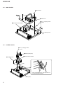
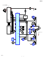
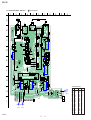
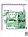
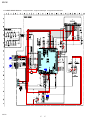
1
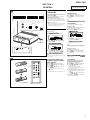
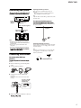
SERVICE MANUAL
XDR-F1HD
US Model
Ver. 1.0 2008.01
HD Radio Broadcasting was approved by the Federal
Communications Commission in October 2002 as the system for digital
AM and FM broadcasting in the U.S.
HD Radio technology features include:
– Static-free, clear radio reception.
– FM Multicasting – the ability to broadcast multiple program streams over
a single FM frequency.
– A variety of “data services,” including text-based
information – artist name, song title, etc. scrolled across your
receiver display.
– Digital broadcasts in the same frequencies as analog
broadcasts; listeners do not need to learn a new station
number and today’s stations remain at their current place on the dial.
HD Radio technology is developed and licensed by iBiquity Digital Corporation and supported by the leaders of the
broadcasting, consumer electronics and automotive industries.
HD RadioTM Technology Manufactured Under License From iBiquity Digital Corp. U.S. and Foreign Patents. HD RadioTM and the HD Radio logo are
proprietary trademarks of iBiquity Digital Corp.
SPECIFICATIONS
Time display
Frequency range
Audio output
Antenna terminal
Power requirements
Dimensions
Mass
Supplied accessories
12-hour system
FM: 87.5 – 108 MHz
AM: 530 – 1,710 kHz
Output level 0.7 Vrms at 47 kΩ
Recommended load impedance over 10 kΩ
75 Ω antenna terminal for FM
Antenna terminal for AM
120 V AC, 60 Hz
Approx. 180 × 60 × 160 mm (w/h/d)
(7 1/8 × 2 3/8 × 6 3/8 inches) not incl. projecting
parts and controls
Approx. 1.1 kg (2 lb 6.8 oz)
Remote commander (1)
FM dipole antenna (1)
AM loop antenna (1)
Design and specifications are subject to change
without notice.
FM/AM DIGITAL TUNER
9-887-972-01
Sony Corporation
2008A04-1
© 2008.01
Audio Business Group
Published by Sony Techno Create Corporation
XDR-F1HD
SAFETY CHECK-OUT
After correcting the original service problem, perform the following safety check before releasing the set to the customer:
Check the antenna terminals, metal trim, “metallized” knobs,
screws, and all other exposed metal parts for AC leakage.
Check leakage as described below.
LEAKAGE TEST
The AC leakage from any exposed metal part to earth ground and
from all exposed metal parts to any exposed metal part having a
return to chassis, must not exceed 0.5 mA (500 microamperes.).
Leakage current can be measured by any one of three methods.
1. A commercial leakage tester, such as the Simpson 229 or RCA
WT-540A. Follow the manufacturers’ instructions to use these
instruments.
2. A battery-operated AC milliammeter. The Data Precision 245
digital multimeter is suitable for this job.
3. Measuring the voltage drop across a resistor by means of a
VOM or battery-operated AC voltmeter. The “limit” indication
is 0.75 V, so analog meters must have an accurate low-voltage
scale. The Simpson 250 and Sanwa SH-63Trd are examples
of a passive VOM that is suitable. Nearly all battery operated
digital multimeters that have a 2 V AC range are suitable. (See
Fig. A)
To Exposed Metal
Parts on Set
Notes on chip component replacement
• Never reuse a disconnected chip component.
• Notice that the minus side of a tantalum capacitor may be damaged by heat.
UNLEADED SOLDER
Boards requiring use of unleaded solder are printed with the leadfree mark (LF) indicating the solder contains no lead.
(Caution: Some printed circuit boards may not come printed with
the lead free mark due to their particular size)
: LEAD FREE MARK
Unleaded solder has the following characteristics.
• Unleaded solder melts at a temperature about 40 °C higher
than ordinary solder.
Ordinary soldering irons can be used but the iron tip has to be
applied to the solder joint for a slightly longer time.
Soldering irons using a temperature regulator should be set to
about 350 °C.
Caution: The printed pattern (copper foil) may peel away if the
heated tip is applied for too long, so be careful!
• Strong viscosity
Unleaded solder is more viscous (sticky, less prone to flow)
than ordinary solder so use caution not to let solder bridges
occur such as on IC pins, etc.
• Usable with ordinary solder
It is best to use only unleaded solder but unleaded solder may
also be added to ordinary solder.
TABLE OF CONTENTS
0.15 μF
1.5 kΩ
AC
voltmeter
(0.75 V)
Earth Ground
Fig. A.
Using an AC voltmeter to check AC leakage.
1.
GENERAL ..................................................................
2.
DISASSEMBLY
2-1.
2-2.
2-3.
2-4.
2-5.
Cabinet Upper Assy .......................................................
KEY Board......................................................................
MICON Board Assy........................................................
MAIN Board ...................................................................
POWER Board ................................................................
3.
DIAGRAMS
3-1.
3-2.
3-3.
3-4.
3-5.
3-6.
Block Diagram ................................................................
Printed Wiring Board –Main Section–............................
Printed Wiring Board –Power Section– ..........................
Schematic Diagram –Main/Power Section– ...................
Printed Wiring Board –Micon Section–..........................
Schematic Diagram –Micon Section– ............................
4.
EXPLODED VIEWS
3
6
7
7
8
8
11
12
13
14
15
16
4-1. Cabinet Upper Section .................................................... 20
4-2. Cabinet Lower Section.................................................... 21
4-3. MICON Board Section ................................................... 22
5.
SAFETY-RELATED COMPONET WARNING!
COMPONENTS IDENTIFIED BY MARK 0 OR DOTTED LINE
WITH MARK 0 ON THE SCHEMATIC DIAGRAMS AND IN
THE PARTS LIST ARE CRITICAL TO SAFE OPERATION.
REPLACE THESE COMPONENTS WITH SONY PARTS
WHOSE PART NUMBERS APPEAR AS SHOWN IN THIS
MANUAL OR IN SUPPLEMENTS PUBLISHED BY SONY.
2
ELECTRICAL PARTS LIST .............................. 23
XDR-F1HD
SECTION 1
GENERAL
A
DISPLAY
BAND
SCAN
HD SCAN
MENU
TUNE
TUNE
PRESET
ENTER
PRESET
Preparing the remote
commander
Playing the radio
Installing the batteries into the remote commander (See Fig. B)
1 Press ?/1 to turn on the radio.
2 Press BAND to select the band AM or FM.
3 Press TUNE + or – to tune in to a desired
Insert two size AAA (R03) batteries (not supplied).
–Manual tuning
When to replace the batteries
SELECT
L
This section is extracted
from instruction manual.
ANTENNA
AM
FM
RESET
Note
Notes
• Do not charge dry batteries.
• When you are not going to use the remote commander
for a long time, remove the batteries to avoid any
damage caused by leakage and corrosion.
–Preset tuning
R
AUDIO OUT
?/1
frequency.
With normal use, the batteries should last for about
six months. When the remote commander no longer
operates the unit, replace all the batteries with new ones.
Setting the clock
of the remote commander.
You can preset 20 stations each for AM and FM.
Presetting a station
1 Follow steps 1 to 3 in “Manual tuning” to tune
the frequency you wish to preset.
2 Press and hold ENTER for a few seconds.
1 Plug in the unit.
FM
2 Press MENU to show the menu display.
3 Press PRESET + or – to select the preset
number, then press ENTER.
3 Press SELECT M or m to select “TIME SET,”
AC power cord
then press ENTER.
number.
To preset another station, repeat these steps.
Note
If you try to store another station in the same preset
number, the previously stored station will be replaced.
AM
FM
SLEEP
4 Press SELECT M or m until current hour
appears in the display, then press ENTER.
5 Repeat step 4 to set the minute.
Note
If you do not set the menu within 65 seconds, the setting
mode is canceled.
B
SLEEP
To change the display to the
daylight saving time (summer
time) indication
1
2
3
1 Press MENU to show the menu display.
2 Press SELECT M or m to select “DST,” then
4
5
6
3 Press SELECT M or m to select “ON,” then
7
8
0
HD SCAN
TUNE/
SELECT
9
ENTER
PRESET
press ENTER.
press ENTER.
“ ” appears and the time indication changes to
summer time.
To deactivate the DST function, select “OFF” in step 3.
Tuning in to a station
1 Press ?/1 to turn on the radio.
2 Press BAND to select the band AM or FM.
3 Press PRESET + or – to select the desired
preset number.
Tip
of the remote commander. Press ENTER
number is selected.
–Scan tuning
In HD scan, HD Radio stations are scanned.
1 Press ?/1 to turn on the radio.
2 Press BAND to select the band AM or FM.
3 Press SCAN or HD SCAN on the unit or
remote commander.
Scanning of the selected band starts.
When a station is received, scanning pauses for 3
seconds and then continues.
4 When the unit tunes in to the desired station,
do any of the following operations to stop
scanning.
– Press ENTER on the unit or remote commander.
– Press SCAN or HD SCAN.
SCAN
BAND
5 If necessary, press TUNE + or – to tune in to
the station more precisely.
MENU
Size AAA (R03)
×2
BRIGHT
DISPLAY
The number 5 and the PRESET +
buttons have a tactile dot.
3
XDR-F1HD
Changing the display
mode and settings
When an HD Radio station is received
FM
Setting the sleep timer
You can enjoy falling asleep to the radio using the builta preset duration.
To change the display mode
1 Press SLEEP on the remote commander.
Press DISPLAY.
x
“SLEEP” and the digits for the sleep timer duration
appear.
When an analog radio station is received
FM
SLEEP
FM
FM
x
x
2 Press SLEEP repeatedly to select the desired
FM
FM
A
B
C
D
E
Field strength level indicator
Preset number*
Band
Frequency
Current time
* When you tune in a station by selecting a preset
number.
When an analog FM broadcast that supports RBDS
(Radio Broadcast Data System) is received
FM
x
FM
If you press SLEEP
unit is turned on.
sleep timer setting.
Each press changes the setting time as follows:
60
45
30
15
OFF
A HD indicator
HD indicator Reception status
Stays lit
Strong HD signal, digital reception*
Flashes
Weak HD signal, analog reception
Not displayed No HD signal, analog reception
*
then stays lit.
B
C
D
E
F
G
H
I
J
K
Field strength level indicator
Preset number*
Call sign
Band
Song title/artist name
Channel number (FM only)
Appears when HD Radio broadcasts multiple
program.
Press TUNE + or – to select a sub channel.
Frequency
Current time
Station name
Text information
* When you tune in a station by selecting a preset
number
when the duration time is set.
is passed.
To change the sleep timer setting
You can press SLEEP repeatedly to select the desired
activated.
To deactivate the sleep timer
Press ?/1
elapsed, or press SLEEP repeatedly to set the sleep timer
to “SLEEP OFF” in step 2.
Note
remote commander.
Resetting the unit
Press this button with a pointed object if the radio fails
Note
x
have preset, etc., will revert to the factory preset.
broadcast or the station.
FM
To change the display settings
(BRIGHTNESS/CONTRAST)
A
B
C
D
Field strength level indicator
Preset number*
Band
Station name
Name of station currently tuned in.
E Frequency
F Current time
G Text information
Text information transmitted from station.
* When you tune in a station by selecting a preset
number.
Note
1 Press MENU to show the menu display.
2 Press SELECT M or m to select
3
“BRIGHTNESS” or “CONTRAST,” then press
ENTER.
Press SELECT M or m to select the setting or to
adjust the level, then press ENTER.
BRIGHTNESS:
“HIGH,” “MIDDLE” or “LOW.”
CONTRAST:
11 levels.
Note
If you do not set the menu within 10 seconds, the setting
broadcast or the station.
Tip
You can adjust “BRIGHTNESS” directly by pressing
BRIGHT on the remote commander.
4
Using the remote
commander
Buttons shared on both the remote commander and the
unit control the same functions.
HD SCAN button
stations are received for 3 seconds in order of frequency.
SCAN button
stations are received for 3 seconds in order of frequency.
BRIGHT button
To adjust the brightness of the display.
XDR-F1HD
Connecting the system
component before making the connections.
L
Find a place and an orientation that provide good
reception.
• Do not place the AM loop antenna near the unit or
other AV equipment, as noise may result.
Tip
Adjust the direction of the AM loop antenna for best AM
broadcast sound.
ANTENNA
AM
Adjusting the AM loop antenna
FM
RESET
R
AUDIO OUT
AUDIO OUT
(Stereo pin plug)
(Red) (R)
AUDIO OUT
(Stereo pin plug)
(White) (L)
To connect the FM antenna
Connect an antenna that provides good reception to the
FM antenna terminal.
Audio cable (Not supplied)
FM dipole antenna
(supplied)
Audio input
(White) (L)
Audio input
(Red) (R)
Notes
• Install this system so that the power cord can be
unplugged from the wall socket immediately in the
event of trouble.
• If noise occurs, separate the unit from other
components.
• Noise may occur during AM reception if the unit
Adjusting the FM dipole antenna
Be sure to fully extend the FM dipole antenna. Attach the
antenna in the shape of a T to a high position on a wall
away from this unit.
Tip
If you have poor FM reception, use a 75 Ω coaxial cable
(not supplied) to connect the unit to an outdoor FM
antenna as shown below.
Connecting the antenna
To connect the AM loop
antenna
ANTENNA
AM
FM
Outdoor FM antenna
to receive AM signals. Do not dismantle or roll up the
antenna.
1
2
3
Remove only the loop part from the plastic
stand.
Set up the AM loop antenna.
Connect the cords to the AM antenna
terminals.
Cord (A) or cord (B) can be connected to either
terminal.
Insert the cord while
pushing down the
terminal clamp.
A
4
B
Only insert up
to here.
Make sure the AM loop antenna is connected
5
XDR-F1HD
SECTION 2
DISASSEMBLY
Note: This set can be disassemble according to the following sequence.
SET
2-1.
CABINET UPPER ASSY
(Page 6)
2-2.
KEY BOARD
(Page 7)
2-3.
MICON BOARD ASSY
(Page 7)
2-4.
MAIN BOARD
(Page 8)
2-5.
POWER BOARD
(Page 8)
Note: Follow the disassembly procedure in the numerical order given.
2-1.
CABINET UPPER ASSY
cabinet upper assy
two claws
two (+) P tapping screws
(B 2.6)
three (+) P tapping screws
(B 2.6)
6
XDR-F1HD
2-2.
KEY BOARD
Remove the three solders.
three screws
KEY board
red
2-3.
MICON BOARD ASSY
two screws
red
red
Remove the eleven solders.
MICON board assy
7
XDR-F1HD
2-4.
MAIN BOARD
three screws
MAIN board
two (+) P tapping screws
(B 2.6)
Remove the three solders.
(+) BV tapping screws
(B 3)
2-5.
POWER BOARD
two (+) P tapping screws
(B 2.6)
retainer plate (trans)
Remove the two solders.
POWER board
white
black
When assembling the set, route the power cord
as shown below and install it.
cabinet (lower)
8
XDR-F1HD
MEMO
9
XDR-F1HD
SECTION 3
DIAGRAMS
THIS NOTE IS COMMON FOR PRINTED WIRING BOARDS AND SCHEMATIC DIAGRAMS.
(In addition to this, the necessary note is printed in each block.)
For Printed Wiring Boards.
For Schematic Diagrams.
Note:
• X : Parts extracted from the component side.
•
: Pattern from the side which enables seeing.
Note:
• All capacitors are in μF unless otherwise noted. (p: pF)
50 WV or less are not indicated except for electrolytics
and tantalums.
• All resistors are in Ω and 1/4 W or less unless otherwise
specified.
•
% : indicates tolerance.
•
f : internal component.
• C : panel designation.
Note: The components identified by mark 0 or dotted
line with mark 0 are critical for safety.
Replace only with part number specified.
• A : B+ Line.
• Voltages and waveforms are dc with respect to ground
under no-signal (detuned) conditions.
no mark : FM1
• Voltages are taken with VOM (Input impedance 10 MΩ).
Voltage variations may be noted due to normal production
tolerances.
• Waveforms are taken with a oscilloscope.
Voltage variations may be noted due to normal production
tolerances.
• Circled numbers refer to waveforms.
• Signal path.
F
: FM
f
: AM
• Waveforms
– MICON Board –
IC401 RB (XCOUT)
2.5 Vp-p
32 kHz
1 V/DIV, 10 μsec/DIV
IC401 RE (XOUT)
5.53 MHz
1 V/DIV, 0.1 μsec/DIV
10
3.2 Vp-p
XDR-F1HD
3-1.
BLOCK DIAGRAM
DSP TUNER UNIT
TU1
FM
AUDIO_R 26
1 FM ANT
R-CH
AM
L
-2
R-CH
CN1
ANTENNA
-1
AUDIO
PRE AMP
Q202,203
AUDIO_L 27
CN2
2 AM ANT
CN3
AUDIO OUT
R
AUDIO
MUTE
Q201,204
E2P_SDA 8
E2P_SCL 7
SDA 14
SYSTEM CONTROL
IC401
SCL 13
RESET 12
R-CH
AUDIO_MUTE 83
BLEND 23
55
D0 I
I 61
D7 •
63
19 DTUNER_RDS
RDS 25
LIQUID CRYSTAL
DISPLAY PANEL
LCD401
3 +8.5V REG 1
IC902
8.5V
2
A0 49
RDB 51
29 DTUNER_SCL
88 DTUNER_RESET
WRB 50
CSB 47
RESET
Q402,405
RST 48
16 17 18 19 20 21 22
X401
32kHz
POWER
CONTROL
Q903,904
RST
SD_IBOC_OUT_Q
SD_IBOC_OUT_I
BCK_IBOC_OUT
WS_IBOC_OUT
I2S_DATA
I2S_BCK
I2S_WS
30 DTUNER_SDA
10 XCIN
POWER
CONTROL
Q909,910
D913
11 XCOUT
2
9 10 11 15 16 17
IF_I2S_Q1
IF_I2S_I1
IF_I2S_BCLK
IF_I2S_WS
AUDIO_I2S_DATA
AUDIO_I2S_BCLK
AUDIO_I2S_WS
8
X402
5.53MHz
13 XOUT
LIGHT1 45
KEY
NETWORK
S801–811
I2C_SCL 12
LED+B
D401
(LCD BACK LIGHT R)
94 KEY1
95 KEY2
3 +4.7V REG 1
IC907
10.5V
2 +3.3V REG 1
IC901
5.2V
D912,914
LCD BACK
LIGHT CONTROL
Q404
D402
(LCD BACK LIGHT L)
VDD1.8V
3 +1.8V REG 1
IC904
~ AC IN
D915
POWER
CONTROL
Q406
MICON3.3V
BLEND 18
KEY3.3V
CVDD1.8V
3
+1.8V REG
1
IC906
• R-CH is omitted due to same as L-CH.
• Signal path
: FM
: AM
POWER
CONTROL
Q905,906
RESET 12
S1
RESET
REMOTE CONTROL
SIGNAL RECEIVER 1
IC403
LED+B
VOLTAGE
DETECT
Q401
3 RMT
F901
POWER
CONTROL
Q901,902
DTUNER_POWER 89
IDM MODULE
IDM1
RECT
D701-704
4
KEY OFF 97
RESET 3
D905
MICON3.3V
15 XIN
LIGHT2 44
I2C_SDA 13
LCD BACK
LIGHT CONTROL
Q403
T901
POWER
TRANSFORMER
2
MICON3.3V
RESET
IC402
VDD3.3V DIG
VDD3.3V ANA
1
1
3
+3.3V REG
4
IC903
VDD3.3V VDD
POWER
CONTROL
Q907,908
18 VDET
2
BVDD3.3V
XDR-F1HD
11
11
3
+3.3V REG
1
IC905
XDR-F1HD
3-2.
PRINTED WIRING BOARD – MAIN Section –
2
1
•
3
: Uses unleaded solder.
4
5
6
CN3
AUDIO OUT
A
7
8
9
10
11
ANTENNA
-1
L
CN2
FM
CN1
AM
-2
R
S1
RESET
2
FB301
1
TU1
B
C9
JW6
C5
JW8
JW9
IC902
C6
R926
C12
R4
IC904
2
5
1
C916
1
D912
IC907
D914
R930
E B
Q909
C
R933
R934
R931
C924
C925
D911
5
C
Q910
B E
• Semiconductor Location
W701
3
C918
1
RED
WHT
BLU
YEL
BLK
RED
WHT
BLU
YEL
BLK
BRN
1-875-767-
I
B
RED
11
(11)
MAIN BOARD
A
MICON BOARD MICON BOARD
W2
W1
(Page 15)
Ref. No.
BLU
WHT
C917
1
R913
R914 R915
R916
JW1
6
W1
2
C18
D913
JW26
W2
IC906
R912
C926
C16
SL901
1
C921
IC905
3
JW21
E B
E B Q908
C
Q907
C R929 R927
R928
R910
JW20
C919
R909
1
D910
JW18
5
JW25
JW3
C17
R908
R907
R905
C15
R906
D915
G
20
JW11
1
FB6
FB5
FB4
FB3
FB1
R5
FB2
IDM1
JW22
JW4
1
3
27
JW17
C20
C
Q906
B E
R924
R925
R935
D909
C19
JW16
C914
C
Q905
B E
R936
4
D908
3
C
Q903
B E
R922
R921
JW5 C915
R923
C
Q904
B E
C7
IC903 2 1
JW15
R101
D906
F
D907
C8
R6
R937
R902
JW7
R114
R110
H
R8
R9
R10
R11
C202
C911
R1
R3
C2
C11
E
R203 R204
1
1
5
C
Q201 R211
C
B
E R208
Q204
B E
JW29
R209
R213 R214
C
Q203
JW12
R212 B E R206
R205
JW13
C
Q202
B E
JW14
C201 R210 R7 R201
C22
C910
IC901
4
C10
C302
R103 R104
R920
R202
R919
R904 R903
C1
R2
R108
C
Q103 R109
B E
C102
C
R106
Q102
B E R105
C21
D
C101
E B
Q901
C
JW10
R302
C
Q101
B E
E B
Q104
C
C928
R918
R917
C
E B
Q902
C
C301
R102
JW28
FB201
FB101
R113
C912
1
(Page 15)
XDR-F1HD
12
12
C
POWER
BOARD
W701
(Page 13)
Location
D906
D907
D908
D909
D910
D911
D912
D913
D914
D915
F-2
C-8
E-7
E-7
G-4
G-5
H-7
G-7
H-6
G-2
IC901
IC902
IC903
IC904
IC905
IC906
IC907
D-2
C-7
E-7
F-7
G-3
G-5
G-7
Ref. No.
Q101
Q102
Q103
Q104
Q201
Q202
Q203
Q204
Q901
Q902
Q903
Q904
Q905
Q906
Q907
Q908
Q909
Q910
Location
C-4
D-4
C-4
C-4
D-4
E-4
E-4
D-4
D-1
C-1
D-8
D-7
E-7
E-7
G-3
G-4
G-7
H-7
XDR-F1HD
3-3.
PRINTED WIRING BOARD – POWER Section – •
1
2
3
4
: Uses unleaded solder.
5
6
7
8
9
10
11
12
13
14
(Page 12)
A
MAIN BOARD
W701
C
C
C908
D ~ AC IN
*
1
W701
C905
PS901
WHT
3
RED
BLU
T901
POWER TRANSFORMER
C909
POWER BOARD
REPLACEABLE:
* NOT
BUILT IN TRANSFORMER.
WHT
B
C906
D901
C901
C902
C903
D903
C904
D902
F
D905
C907
BLK
D904
E
JW901
G
F901
11
H
1-875-766-
(11)
• Semiconductor
Location
Ref. No.
D901
D902
D903
D904
D905
XDR-F1HD
13
13
Location
F-14
F-13
E-12
E-11
F-11
XDR-F1HD
3-4.
SCHEMATIC DIAGRAM – MAIN / POWER Section –
• See page 17 for IC Block Diagrams.
IC B/D
IC902
R210
R904
C912
R104
R937
R110
R902
C101
R204
C201
Q903
R903
R103
C102
R212
R203
R109
C302
R302
R923
Q102
Q103
Q202
CN3
FB101
Q203
R922
R105
R921
Q904
R106
R205
R114
C301
R206
R108
R214
Q101
FB201
R209
R211
Q201
R113
C202
R213
FB301
R208
TP903
Q104
R202
D905
PS901
CN1
Q204
C908
R102
C909
C907
F901
CN2
D901
Q905
C901
TP901
R926
T901
D907
D908
IC903
R936
D902
R925
C902
Q906
C915
C914
C10
C9
D903
R924
TP904
C903
C8
IC901
R935
C906
W701
R2
C904
W701
D906
C1
IC904
C2
R3
D904
C917
R1
TU1
TP905
C5
D915
Q901
C905
D909
C6
C7
R919
C916
C928
R8
TP902
C918
C911
R918
C910
R9
R917
Q902
R10
R920
R11
C21
C11
C12
R101
R6
R201
R7
C22
IC B/D
IC905
R4
C19
C20
C15
R909
C919
IC B/D
Q907
R908
C16
IC907
R907
R906
R5
TP1
R929
R927
R916
Q908
TP2
IDM1
R928
R905
C924
TP3
D910
W1
Q909
R915
TP4
D912
R914
D914
R910
R933
R912
R913
R934
FB1
R930
(Page 16)
R931
FB2
W2
C925 C926
Q910
FB3
FB4
IC906
FB5
D913
FB6
C17
C18
D911
(Page 16)
C921
S1
XDR-F1HD
14
14
SL901
XDR-F1HD
PRINTED WIRING BOARD – MICON Section –
3
: Uses unleaded solder.
4
5
6
7
A
3
13
14
100
1
R402
C402
C403
X401
X402
R476
R479
R438
R437
R436
R435
R434
W2
6
BRN
BLK
JW401
JW406
R412
R417
IC402 R406
2
1
3
4
JW404
RED
BLK
D401
5
LCD BACK
LIGHT R
JW405
YEL
BLU
3
R807
G
MAIN
BOARD
W1
(Page 12)
WHT
RED
1
W1
R404
11
(11)
BAND
SCAN
HD SCAN
S802
S803
S808
MENU
SELECT
.
TUNE 㸫
TUNE 㸩
ENTER
S810
S804
S805
PRESET
㸫
PRESET
㸩
S806
S811
BLU
W702
R806
1
WHT
RED
DISPLAY
S807
A
BLU
WHT
RED
N
F
(Page 12)
WHT
1-875-768-
E
B
MAIN
BOARD
W2
BLU
1
R432
E B
Q401
C
C410
R470
R415
C405
R408
R430
E B
Q403
C
JW402
R410
JW403
30
R411 JW407
R477
R418
R478
31
R431
E B
Q404
C
YEL
R414
R413
81
R469
R429
R460
C417
R426
R453
R454
C416
R421
R420
R419
C409 R416
W702
E B
Q402
C
R409
R403
1
C
Q406
B E
R401
IC401
80
C434
C429
C430
R483
R472
C431
R466
R467
R468
E B
Q405
C
50
R457
C432
JW409
JW410
JW411
JW412
JW413
R803
R804
D
R458
R474
S801
12
R424
R423
R455
R482
R471
C433
R456
R473
S801
JW414
R801
R802
R433
D402
LCD BACK
LIGHT L
C401
SL402
C
11
R422
R450
JW408
SL401
51
R427
R425
R449
R448
R447
R446
R445
R444
R443
R442
R441
R428
C420
R462
C422
C421
R465 R494
R495
C418
R480
R481
IC403
C427
C426
R459 C425
C424
C428
1 2 3
R461
1
R464
IC403
10
29
R475
R463
B
9
LCD401
LIQUID CRYSTAL DISPLAY PANEL
MICON BOARD
C435
8
R407
2
1
•
C423
3-5.
R805
R809
R808
S809
R810 R811
R813
R814
R815 R816
R812
R817
11
1-875-769-
(11)
KEY BOARD
H
• Semiconductor
Location
Ref. No.
XDR-F1HD
15
15
Location
D401
D402
C-13
C-3
IC401
IC402
IC403
C-9
D-11
B-2
Q401
Q402
Q403
Q404
Q405
Q406
D-10
B-11
B-12
B-12
B-10
D-7
XDR-F1HD
3-6.
SCHEMATIC DIAGRAM – MICON Section – • See page 10 for waveforms. • See page 17 for IC Block Diagrams.
• See page 18 for IC Pin Function Description.
LCD401
R805
S802
R802 R801
R453
R454
C423
C417
R481
Q402
R427
R466
R426
R425
W1
TP417
TP409
R477
R424
TP416
R423
TP420
C430
TP415
C431
TP419
(Page 14)
W2
R467
TP407
R468
R483
R432
R482
TP424
R422
R471
TP423
TP422
TP418
TP421
C432
R469
C433
R470
R474
(Page 14)
R473
C434
R421
R420
R419
R418
Q406
R475
X402
X401
C401
TP425
R404
C402
C403
R479
R406
R416
R417
R476
R415
IC B/D
Q401
R412
C409
R413
C410
R414
XDR-F1HD
16
16
IC402
R410
R411
C405
R403
R409
R402
IC403
R408
R407
TP401
R401
C435
R429
IC401
R472
R478
TP408
R433
D402
D401
TP406
R434
R435
R436
R437
TP405
TP404
R430
R438
TP403
TP402
C427
C428
SL401
R428
C429
R495
SL402
R459
Q405
R441
TP804
R462
C425
TP410
C420
R444
S807
TP412
TP803
TP411
R806
TP414
R807
TP413
R808
R455
S808
R809
R458
S809
R814
R457
S810
R815
R456
S811
R816
R480
C426
C416
C424
TP802
S801
R817
C422
R450
R443
S803
R804 R803
R442
S804
W702
R445
S805
C418
R464
W702
S806
R463
TP801
R448
R810
R447
R811
R446
R812
R449
R813
C421
R461
R460
R431
Q403
Q404
R465
R494
XDR-F1HD
• IC Block Diagrams
IC902 NJM2387ADL3(TE2) (MAIN BOARD)
IC905 NJM2387ADL3(TE2) (MAIN BOARD)
IC907 NJM2387ADL3(TE2) (MAIN BOARD)
CURRENT
LIMIT
OVERVOLTAGE
PROTECTION
THERMAL
PROTECTION
BANDGAP
REFERENCE
1
2
3
4
5
VIN
CONTROL
VOUT
VADJ
GND
VSS
NC
IC402 XC61CN2702NR (MICON BOARD)
4
3
1
2
VOUT
VIN
VREF
17
XDR-F1HD
・IC Pin Function Description
MICON BOARD IC401 M3062LFGPFP (SYSTEM CONTROL)
Pin No.
Pin Name
I/O
1
P9_6/NC
O
2
P9_5/NC
O
Fixed at L level (Not used)
3
P9_4/RMT
I
Remote commander signal input
4
P9_3/NC
O
Fixed at L level (Not used)
5
P9_2/NC
O
Fixed at L level (Not used)
6
P9_1/NC
O
Fixed at L level (Not used)
7
P9_0/NC
O
Fixed at L level (Not used)
18
Description
Fixed at L level (Not used)
8
BYTE
I
Not used. (Connect to VSS)
9
CNVSS
I
Not used. (Fixed at L level)
10
XCIN
I
System sub clock signal input (32 kHz)
11
XCOUT
O
System sub clock signal output (32 kHz)
12
RESET
I
Micon reset input (L: Micon reset)
13
XOUT
O
System main clock signal output (5.53 MHz)
14
VSS
—
Ground
15
XIN
I
16
VCC1
—
17
NMI
I
System main clock signal input (5.53 MHz)
Power supply pin (+3.3 V)
NMI interruption signal input (Fixed at H level)
18
INT2/VDET
I
Power failure detection signal input (H: backup mode)
19
INT1/DTUNER_RDS
I
RDS data interruption signal input
20
INT0/NC
O
Fixed at L level (Not used)
21
P8_1/NC
O
Fixed at L level (Not used)
22
P8_0/NC
O
Fixed at L level (Not used)
23
P7_7/NC
O
Fixed at L level (Not used)
24
P7_6/NC
O
Fixed at L level (Not used)
25
P7_5/NC
O
Fixed at L level (Not used)
26
P7_4/NC
O
Fixed at L level (Not used)
27
P7_3/NC
O
Fixed at L level (Not used)
28
P7_2/NC
O
Fixed at L level (Not used)
29
RXD2/DTUNER_SCL
—
Communication pin for digital tuner.
30
TXD2/DTUNER_SDA
—
Communication pin for digital tuner.
31
P6_7/SDA
O
Flash write pin (Normally: output port)
32
P6_6/SCL1
O
Flash write pin (Normally: output port)
33
P6_5/CLK1
O
Flash write pin (Normally: output port)
34
P6_4/CTS0
O
Flash write pin (Normally: output port)
35
P6_3/NC
O
Fixed at L level (Not used)
36
P6_2/NC
O
Fixed at L level (Not used)
37
P6_1/NC
O
Fixed at L level (Not used)
38
P6_0/NC
O
Fixed at L level (Not used)
39
P5_7/NC
O
Flash write pin (Normally: output port)
40
P5_6/NC
O
Fixed at L level (Not used)
41
P5_5/EPM
O
Flash write pin (Normally: output port)
42
P5_4/NC
O
Fixed at L level (Not used)
43
P5_3/NC
O
Fixed at L level (Not used)
44
P5_2/LIGHT2
O
LCD back light control signal output
45
P5_1/LIGHT1
O
LCD back light control signal output
46
P5_0/CE
O
Flash write pin (Normally: output port)
47
P4_7/CSB
O
LCD driver control signal output
48
P4_6/RST
O
LCD driver reset signal output (H: driver reset)
49
P4_5/A0
O
LCD driver control signal output
50
P4_4/WRB
O
LCD driver control signal output
51
P4_3/RDB
O
LCD driver control signal output
52
P4_2/NC
O
Fixed at L level (Not used)
53
P4_1/NC
O
Fixed at L level (Not used)
54
P4_0/NC
O
Fixed at L level (Not used)
XDR-F1HD
Pin No.
Pin Name
I/O
55
P3_7/D0
O
LCD data output
Description
56
P3_6/D1
O
LCD data output
57
P3_5/D2
O
LCD data output
58
P3_4/D3
O
LCD data output
59
P3_3/D4
O
LCD data output
60
P3_2/D5
O
LCD data output
61
P3_1/D6
O
LCD data output
62
VCC2
—
Power supply pin (+3.3 V)
63
P3_0/D7
O
LCD data output
64
VSS
—
Ground
65
P2_7/AN2_7/
SHIMUKE2
I
Destination select signal input (Fixed at L level)
66
P2_6/AN2_6/
SHIMUKE1
I
Destination select signal input (Fixed at L level)
67
P2_5/AN2_5/NC
O
Fixed at L level (Not used)
68
P2_4/AN2_4/NC
O
Fixed at L level (Not used)
69
P2_3/AN2_3/NC
O
Fixed at L level (Not used)
70
P2_2/AN2_2/NC
O
Fixed at L level (Not used)
71
P2_1/AN2_1/ENC2_
DATA
O
Flash write pin (Normally: output port)
72
P2_0/AN2_0/ENC1_
DATA
O
Flash write pin (Normally: output port)
73
P1_7/INT5/ENC1_
CLK
O
Flash write pin (Normally: output port)
74
P1_6/INT4/ENC2_
CLK
O
Flash write pin (Normally: output port)
75
P1_5/INT3/KEY_IN
O
Fixed at L level (Not used)
76
P1_4/NC
O
Fixed at L level (Not used)
77
P1_3/KEY_LED
O
Fixed at L level (Not used)
78
P1_2/NC
O
Fixed at L level (Not used)
79
P1_1/E2PROM_SCL
O
Fixed at L level (Not used)
80
P1_0/E2PROM_SDA
O
Fixed at L level (Not used)
81
P0_7/AN0_7/NC
O
Fixed at L level (Not used)
82
P0_6/AN0_6/NC
O
Fixed at L level (Not used)
83
P0_5/AN0_5/AUDIO_MUTE
O
Audio mute detection signal output (H: mute ON)
84
P0_4/AN0_4/NC
O
Fixed at L level (Not used)
85
P0_3/AN0_3/NC
O
Fixed at L level (Not used)
86
P0_2/AN0_2/NC
O
Fixed at L level (Not used)
87
P0_1/AN0_1/NC
O
Fixed at L level (Not used)
88
P0_0/AN0_0/DTUNER_RESET
O
DSP tuner/DSP reset signal output (L: reset)
89
P10_7/AN7/DTUNER_POWER
O
DSP tuner power control signal output (L: radio function)
90
P10_6/AN6/NC
O
Fixed at L level (Not used)
91
P10_5/AN5/NC
O
Fixed at L level (Not used)
92
P10_4/AN4/NC
O
Fixed at L level (Not used)
93
P10_3/AN3/NC
O
Fixed at L level (Not used)
94
P10_2/AN2/KEY1
I
A/D converter analog signal input
95
P10_1/AN1/KEY2
I
A/D converter analog signal input
96
AVSS
—
97
P10_0/KEY OFF
O
A/D key and remote control receiver power control signal output. (L: normally, H: backup)
98
VREF
—
Reference voltage input for A/D converter. (+3.3 V)
99
AVCC
—
Power supply pin for A/D converter. (+3.3 V)
100
P9_7/NC
O
Fixed at L level (Not used)
Ground for A/D converter.
19
XDR-F1HD
SECTION 4
EXPLODED VIEWS
Note:
• -XX and -X mean standardized parts, so
they may have some difference from the
original one.
• Items marked “*” are not stocked since
they are seldom required for routine service.
Some delay should be anticipated when
ordering these items.
4-1.
• The mechanical parts with no reference
number in the exploded views are not supplied.
• Color Indication of Appearance Parts Example:
KNOB, BALANCE (WHITE) . . . (RED)
R
R
Parts Color Cabinet’s Color
• Accessories are given in the last of the
electrical parts list.
The components identified by mark 0
or dotted line with mark 0 are critical for
safety.
Replace only with part number specified.
CABINET UPPER SECTION
4
3
1
2
1
cabinet lower section
5
5
Ref. No.
1
2
3
20
Part No.
Description
3-254-070-01
3-284-318-01
3-284-315-01
SCREW
PLATE, ORNAMENTAL
BUTTON (PWR)
Remark
Ref. No.
4
5
Part No.
Description
X-2190-218-1
3-254-151-01
CABINET (UPPER) SUB ASSY
SCREW (B2.6), (+) P TAPPING
Remark
XDR-F1HD
4-2.
CABINET LOWER SECTION
61
TU1
59
60
56
62
58
IDM1
53
not supplied
53
55
65
53
66
54
57
65
T901
64
F901
56
MICON board section
63
53
51
51
Ref. No.
Remark
52
Part No.
Description
Part No.
Description
51
52
53
54
55
2-667-344-01
3-284-314-01
3-254-070-01
A-1444-726-A
A-1444-733-A
FOOT, RUBBER
CABINET (LOWER)
SCREW
KEY BOARD, COMPLETE
POWER BOARD, COMPLETE
Ref. No.
61
62
63
0 64
65
A-1444-721-A
3-284-320-01
3-254-143-11
1-833-786-11
2-631-557-01
MAIN BOARD, COMPLETE
HOLDER (JACK)
SCREW (B3), (+) BV TAPPING
POWER-SUPPLY CORD
CUSHION (SW)
Remark
56
57
58
59
60
3-254-151-01
3-197-151-11
3-197-151-01
3-198-659-01
3-198-658-01
SCREW (B2.6), (+) P TAPPING
CASE (LID), SHIELD
CASE (LID), SHIELD
COVER (DSP01, B)
COVER (DSP01, A)
66
0 F901
IDM1
0 T901
TU1
2-582-365-01
1-533-451-12
A-1256-714-A
1-445-383-11
A-1256-754-A
CUSHION (BUTTON)
FUSE, GLASS TUBE (DIA. 5) (3.15A/125V)
IDM MODULE (TUX-HD01)
TRANSFORMER, POWER
DSP TUNER UNIT (TUX-DSP01)
21
XDR-F1HD
4-3.
MICON BOARD SECTION
106
105
D402
104
LCD401
D401
102
101
Ref. No.
101
102
103
104
105
22
Part No.
Description
3-398-195-01
3-286-881-01
3-284-322-01
3-286-880-01
3-284-319-01
SHEET (LCD), INSULATING
ILLUMINATOR
PLATE, LIGHT GUIDE
REFLECTOR
HOLDER (LCD)
103
not supplied
Remark
Ref. No.
106
D401
D402
LCD401
Part No.
Description
X-2190-219-1
6-502-332-01
6-502-332-01
1-802-620-11
MICON BOARD, COMPLETE
LED SDPW31H1C0000 (LCD BACK LIGHT R)
LED SDPW31H1C0000 (LCD BACK LIGHT L)
DISPLAY PANEL, LIQUID CRYSTAL
Remark
XDR-F1HD
SECTION 5
ELECTRICAL PARTS LIST
Note:
• Due to standardization, replacements in
the parts list may be different from the
parts specified in the diagrams or the components used on the set.
• -XX and -X mean standardized parts, so
they may have some difference from the
original one.
• Items marked “*” are not stocked since
they are seldom required for routine service.
Some delay should be anticipated when
ordering these items.
• CAPACITORS
uF: μF
• COILS
uH: μH
Ref. No.
• RESISTORS
All resistors are in ohms.
METAL: Metal-film resistor.
METAL OXIDE: Metal oxide-film resistor.
F: nonflammable
• SEMICONDUCTORS
In each case, u: μ, for example:
uA. . : μA. . , uPA. . , μPA. . ,
uPB. . : μPB. . , uPC. . , μPC. . ,
uPD. . : μPD. .
Part No.
Description
A-1444-726-A
KEY BOARD, COMPLETE
********************
Remark
< RESISTOR >
R805
R806
R807
R808
R809
1-216-829-11
1-216-821-11
1-216-829-11
1-216-829-11
1-216-825-11
METAL CHIP
METAL CHIP
METAL CHIP
METAL CHIP
METAL CHIP
4.7K
1K
4.7K
4.7K
2.2K
5%
5%
5%
5%
5%
1/10W
1/10W
1/10W
1/10W
1/10W
R810
R811
R812
R813
R814
1-216-833-11
1-216-829-11
1-216-837-11
1-216-841-11
1-216-829-11
METAL CHIP
METAL CHIP
METAL CHIP
METAL CHIP
METAL CHIP
10K
4.7K
22K
47K
4.7K
5%
5%
5%
5%
5%
1/10W
1/10W
1/10W
1/10W
1/10W
R815
R816
R817
1-216-833-11
1-216-829-11
1-216-837-11
METAL CHIP
METAL CHIP
METAL CHIP
10K
4.7K
22K
5%
5%
5%
1/10W
1/10W
1/10W
< SWITCH >
S802
S803
S804
S805
S806
1-798-044-11
1-798-044-11
1-798-044-11
1-798-044-11
1-798-044-11
SWITCH, TACTILE (BAND)
SWITCH, TACTILE (SCAN)
SWITCH, TACTILE (TUNE+/SELECT M)
SWITCH, TACTILE (ENTER)
SWITCH, TACTILE (PRESET –)
S807
1-798-044-11 SWITCH, TACTILE (DISPLAY)
S808
1-798-044-11 SWITCH, TACTILE (HD SCAN)
S809
1-798-044-11 SWITCH, TACTILE (MENU)
S810
1-798-044-11 SWITCH, TACTILE (TUNE–/SELECT m)
S811
1-798-044-11 SWITCH, TACTILE (PRESET +)
*************************************************************
A-1444-721-A
MAIN BOARD, COMPLETE
*********************
3-197-151-01
3-197-151-11
3-198-658-01
3-198-659-01
3-254-070-01
CASE (LID), SHIELD
CASE (LID), SHIELD
COVER (DSP01, A)
COVER (DSP01, B)
SCREW
3-254-151-01
3-284-320-01
SCREW (B2.6), (+) P TAPPING
HOLDER (JACK)
1-162-970-11
1-162-970-11
1-162-970-11
1-126-935-11
CERAMIC CHIP
CERAMIC CHIP
CERAMIC CHIP
ELECT
When indicating parts by reference number, please include the board.
The components identified by mark 0
or dotted line with mark 0 are critical for
safety.
Replace only with part number specified.
Part No.
Description
C7
C8
C9
C10
C11
1-126-964-11
1-162-970-11
1-162-970-11
1-126-935-11
1-162-966-11
ELECT
CERAMIC CHIP
CERAMIC CHIP
ELECT
CERAMIC CHIP
10uF
0.01uF
0.01uF
470uF
0.0022uF
20%
10%
10%
20%
10%
50V
25V
25V
16V
50V
C12
C15
C16
C17
C18
1-162-966-11
1-162-970-11
1-126-947-11
1-162-970-11
1-126-935-11
CERAMIC CHIP
CERAMIC CHIP
ELECT
CERAMIC CHIP
ELECT
0.0022uF
0.01uF
47uF
0.01uF
470uF
10%
10%
20%
10%
20%
50V
25V
35V
25V
16V
C19
C20
C21
C22
C101
1-165-908-11
1-165-908-11
1-162-966-11
1-162-966-11
1-165-908-11
CERAMIC CHIP
CERAMIC CHIP
CERAMIC CHIP
CERAMIC CHIP
CERAMIC CHIP
1uF
1uF
0.0022uF
0.0022uF
1uF
10%
10%
10%
10%
10%
10V
10V
50V
50V
10V
C102
C201
C202
C301
C302
1-100-742-11
1-165-908-11
1-100-742-11
1-126-947-11
1-126-935-11
CERAMIC CHIP
CERAMIC CHIP
CERAMIC CHIP
ELECT
ELECT
2.2uF
1uF
2.2uF
47uF
470uF
20%
10%
20%
20%
20%
10V
10V
10V
35V
16V
C910
C911
C912
C914
C915
1-165-908-11
1-126-935-11
1-115-340-11
1-165-908-11
1-125-891-11
CERAMIC CHIP
ELECT
CERAMIC CHIP
CERAMIC CHIP
CERAMIC CHIP
1uF
470uF
0.22uF
1uF
0.47uF
10%
20%
10%
10%
10%
10V
16V
25V
10V
10V
C916
C917
C918
C919
C921
1-125-891-11
1-126-927-11
1-126-942-61
1-165-908-11
1-125-891-11
CERAMIC CHIP
ELECT
ELECT
CERAMIC CHIP
CERAMIC CHIP
0.47uF
2200uF
1000uF
1uF
0.47uF
10%
20%
20%
10%
10%
10V
10V
25V
10V
10V
C924
C925
C926
C928
1-115-340-11
1-128-551-11
1-126-918-11
1-162-927-11
CERAMIC CHIP
ELECT
ELECT
CERAMIC CHIP
0.22uF
22uF
4700uF
100PF
10%
20%
20%
5%
25V
63V
6.3V
50V
CN1
Remark
1-780-519-11
TERMINAL BOARD (ANTENNA 2P)
(ANTENNA AM)
< CONNECTOR >
CN2
0.01uF
0.01uF
0.01uF
470uF
MAIN
< TERMINAL BOARD >
< CAPACITOR >
C1
C2
C5
C6
Ref. No.
KEY
10%
10%
10%
20%
25V
25V
25V
16V
1-815-513-22
CONNECTOR, COAXIAL (F TYPE) (ANTENNA FM)
< JACK >
CN3
1-793-987-11
JACK, PIN 2P (AUDIO OUT)
23
XDR-F1HD
MAIN
Ref. No.
Part No.
Description
Remark
< DIODE >
D906
D907
D908
D909
D910
8-719-991-33
8-719-991-33
8-719-991-33
8-719-991-33
8-719-991-33
DIODE
DIODE
DIODE
DIODE
DIODE
1SS133T-77
1SS133T-77
1SS133T-77
1SS133T-77
1SS133T-77
D911
D912
D913
D914
D915
8-719-991-33
8-719-991-33
8-719-991-33
8-719-991-33
8-719-046-47
DIODE
DIODE
DIODE
DIODE
DIODE
1SS133T-77
1SS133T-77
1SS133T-77
1SS133T-77
1N5401TM
< FERRITE BEAD >
FB1
FB2
FB3
FB4
FB5
1-216-864-11
1-216-864-11
1-414-227-11
1-414-227-11
1-414-227-11
SHORT CHIP
0
SHORT CHIP
0
INDUCTOR, FERRITE BEAD
INDUCTOR, FERRITE BEAD
INDUCTOR, FERRITE BEAD
FB6
FB101
FB201
FB301
1-414-227-11
1-414-227-11
1-414-227-11
1-414-227-11
INDUCTOR, FERRITE BEAD
INDUCTOR, FERRITE BEAD
INDUCTOR, FERRITE BEAD
INDUCTOR, FERRITE BEAD
< IC >
IC901
IC902
IC903
IC904
IC905
6-712-237-01
6-709-213-01
6-710-536-01
6-712-238-01
6-709-213-01
IC
IC
IC
IC
IC
NJM2396F33
NJM2387ADL3(TE2)
NJM2878F4-33(TE2)
NJM2845DL1-18
NJM2387ADL3(TE2)
IC906
IC907
6-712-238-01
6-709-213-01
IC NJM2845DL1-18
IC NJM2387ADL3(TE2)
< IDM MODULE >
IDM1
A-1256-714-A
IDM MODULE (TUX-HD01)
< TRANSISTOR >
Q101
Q102
Q103
Q104
Q201
6-551-392-01
8-729-620-07
8-729-620-07
6-551-696-01
6-551-392-01
TRANSISTOR
TRANSISTOR
TRANSISTOR
TRANSISTOR
TRANSISTOR
RT6N140C-TP-1
2SC3052EF-T1-LEF
2SC3052EF-T1-LEF
ISA1235AC1TP-1EF
RT6N140C-TP-1
Q202
Q203
Q204
Q901
Q902
8-729-620-07
8-729-620-07
6-551-696-01
6-551-696-01
8-729-620-07
TRANSISTOR
TRANSISTOR
TRANSISTOR
TRANSISTOR
TRANSISTOR
2SC3052EF-T1-LEF
2SC3052EF-T1-LEF
ISA1235AC1TP-1EF
ISA1235AC1TP-1EF
2SC3052EF-T1-LEF
Q903
Q904
Q905
Q906
Q907
6-551-696-01
8-729-620-07
6-551-696-01
8-729-620-07
6-551-696-01
TRANSISTOR
TRANSISTOR
TRANSISTOR
TRANSISTOR
TRANSISTOR
ISA1235AC1TP-1EF
2SC3052EF-T1-LEF
ISA1235AC1TP-1EF
2SC3052EF-T1-LEF
ISA1235AC1TP-1EF
Q908
Q909
Q910
8-729-620-07
6-551-696-01
8-729-620-07
TRANSISTOR 2SC3052EF-T1-LEF
TRANSISTOR ISA1235AC1TP-1EF
TRANSISTOR 2SC3052EF-T1-LEF
< RESISTOR >
R1
R2
R3
R4
24
1-216-825-11
1-216-825-11
1-216-821-11
1-216-821-11
METAL CHIP
METAL CHIP
METAL CHIP
METAL CHIP
2.2K
2.2K
1K
1K
5%
5%
5%
5%
1/10W
1/10W
1/10W
1/10W
Ref. No.
Part No.
Description
R5
R6
R7
R8
R9
1-216-821-11
1-216-821-11
1-216-821-11
1-216-864-11
1-216-864-11
METAL CHIP
METAL CHIP
METAL CHIP
SHORT CHIP
SHORT CHIP
1K
1K
1K
0
0
Remark
R10
R11
R101
R102
R103
1-216-864-11
1-216-864-11
1-216-817-11
1-216-864-11
1-216-853-11
SHORT CHIP
SHORT CHIP
METAL CHIP
SHORT CHIP
METAL CHIP
R104
R105
R106
R108
R109
1-216-825-11
1-216-821-11
1-216-825-11
1-216-853-11
1-216-825-11
R110
R113
R114
R201
R202
5%
5%
5%
1/10W
1/10W
1/10W
0
0
470
0
470K
5%
1/10W
5%
1/10W
METAL CHIP
METAL CHIP
METAL CHIP
METAL CHIP
METAL CHIP
2.2K
1K
2.2K
470K
2.2K
5%
5%
5%
5%
5%
1/10W
1/10W
1/10W
1/10W
1/10W
1-216-829-11
1-216-853-11
1-216-845-11
1-216-817-11
1-216-864-11
METAL CHIP
METAL CHIP
METAL CHIP
METAL CHIP
SHORT CHIP
4.7K
470K
100K
470
0
5%
5%
5%
5%
1/10W
1/10W
1/10W
1/10W
R203
R204
R205
R206
R208
1-216-853-11
1-216-825-11
1-216-821-11
1-216-825-11
1-216-853-11
METAL CHIP
METAL CHIP
METAL CHIP
METAL CHIP
METAL CHIP
470K
2.2K
1K
2.2K
470K
5%
5%
5%
5%
5%
1/10W
1/10W
1/10W
1/10W
1/10W
R209
R210
R211
R212
R213
1-216-825-11
1-216-829-11
1-216-864-11
1-216-864-11
1-216-853-11
METAL CHIP
METAL CHIP
SHORT CHIP
SHORT CHIP
METAL CHIP
2.2K
4.7K
0
0
470K
5%
5%
1/10W
1/10W
5%
1/10W
R214
R302
R902
R903
R904
1-216-845-11
1-216-805-11
1-218-847-11
1-218-863-11
1-218-847-11
METAL CHIP
METAL CHIP
METAL CHIP
METAL CHIP
METAL CHIP
100K
47
1K
4.7K
1K
5%
5%
0.5%
0.5%
0.5%
1/10W
1/10W
1/10W
1/10W
1/10W
R905
R906
R907
R908
R909
1-211-985-11
1-218-823-11
1-218-839-11
1-218-847-11
1-218-847-11
METAL CHIP
METAL CHIP
METAL CHIP
METAL CHIP
METAL CHIP
47
100
470
1K
1K
0.5%
0.5%
0.5%
0.5%
0.5%
1/10W
1/10W
1/10W
1/10W
1/10W
R910
R912
R913
R914
R915
1-216-829-11
1-218-839-11
1-218-847-11
1-218-831-11
1-218-855-11
METAL CHIP
METAL CHIP
METAL CHIP
METAL CHIP
METAL CHIP
4.7K
470
1K
220
2.2K
5%
0.5%
0.5%
0.5%
0.5%
1/10W
1/10W
1/10W
1/10W
1/10W
R916
R917
R918
R919
R920
1-218-847-11
1-216-853-11
1-216-841-11
1-216-845-11
1-216-841-11
METAL CHIP
METAL CHIP
METAL CHIP
METAL CHIP
METAL CHIP
1K
470K
47K
100K
47K
0.5%
5%
5%
5%
5%
1/10W
1/10W
1/10W
1/10W
1/10W
R921
R922
R923
R924
R925
1-216-841-11
1-216-853-11
1-216-841-11
1-216-841-11
1-216-853-11
METAL CHIP
METAL CHIP
METAL CHIP
METAL CHIP
METAL CHIP
47K
470K
47K
47K
470K
5%
5%
5%
5%
5%
1/10W
1/10W
1/10W
1/10W
1/10W
R926
R927
R928
R929
R930
1-216-841-11
1-216-841-11
1-216-853-11
1-216-841-11
1-216-833-11
METAL CHIP
METAL CHIP
METAL CHIP
METAL CHIP
METAL CHIP
47K
47K
470K
47K
10K
5%
5%
5%
5%
5%
1/10W
1/10W
1/10W
1/10W
1/10W
XDR-F1HD
MAIN
Ref. No.
Remark
Part No.
Description
Part No.
Description
R931
R933
R934
R935
R936
1-216-841-11
1-216-853-11
1-216-841-11
1-216-864-11
1-216-864-11
METAL CHIP
METAL CHIP
METAL CHIP
SHORT CHIP
SHORT CHIP
47K
470K
47K
0
0
5%
5%
5%
1/10W
1/10W
1/10W
R403
R404
R406
R407
R408
1-216-849-11
1-216-821-11
1-216-797-11
1-216-833-11
1-216-821-11
METAL CHIP
METAL CHIP
METAL CHIP
METAL CHIP
METAL CHIP
220K
1K
10
10K
1K
5%
5%
5%
5%
5%
1/10W
1/10W
1/10W
1/10W
1/10W
R937
1-218-863-11
METAL CHIP
4.7K
0.5%
1/10W
R409
R410
R411
R412
R413
1-216-821-11
1-216-809-11
1-216-809-11
1-216-825-11
1-216-817-11
METAL CHIP
METAL CHIP
METAL CHIP
METAL CHIP
METAL CHIP
1K
100
100
2.2K
470
5%
5%
5%
5%
5%
1/10W
1/10W
1/10W
1/10W
1/10W
R414
R415
R416
R417
R418
1-216-825-11
1-216-845-11
1-216-833-11
1-216-853-11
1-216-821-11
METAL CHIP
METAL CHIP
METAL CHIP
METAL CHIP
METAL CHIP
2.2K
100K
10K
470K
1K
5%
5%
5%
5%
5%
1/10W
1/10W
1/10W
1/10W
1/10W
R419
R420
R421
R422
R423
1-216-821-11
1-216-821-11
1-216-821-11
1-216-821-11
1-216-821-11
METAL CHIP
METAL CHIP
METAL CHIP
METAL CHIP
METAL CHIP
1K
1K
1K
1K
1K
5%
5%
5%
5%
5%
1/10W
1/10W
1/10W
1/10W
1/10W
R424
R425
R426
R427
R428
1-216-821-11
1-216-821-11
1-216-821-11
1-216-821-11
1-216-821-11
METAL CHIP
METAL CHIP
METAL CHIP
METAL CHIP
METAL CHIP
1K
1K
1K
1K
1K
5%
5%
5%
5%
5%
1/10W
1/10W
1/10W
1/10W
1/10W
R429
R430
R431
R432
R433
1-216-841-11
1-216-833-11
1-216-833-11
1-216-797-11
1-216-797-11
METAL CHIP
METAL CHIP
METAL CHIP
METAL CHIP
METAL CHIP
47K
10K
10K
10
10
5%
5%
5%
5%
5%
1/10W
1/10W
1/10W
1/10W
1/10W
R434
R435
R436
R437
R438
1-216-813-11
1-216-817-11
1-216-805-11
1-216-813-11
1-216-821-11
METAL CHIP
METAL CHIP
METAL CHIP
METAL CHIP
METAL CHIP
220
470
47
220
1K
5%
5%
5%
5%
5%
1/10W
1/10W
1/10W
1/10W
1/10W
R441
R442
R443
R444
R445
1-216-821-11
1-216-821-11
1-216-821-11
1-216-821-11
1-216-821-11
METAL CHIP
METAL CHIP
METAL CHIP
METAL CHIP
METAL CHIP
1K
1K
1K
1K
1K
5%
5%
5%
5%
5%
1/10W
1/10W
1/10W
1/10W
1/10W
R446
R447
R448
R449
R450
1-216-821-11
1-216-821-11
1-216-821-11
1-216-821-11
1-216-797-11
METAL CHIP
METAL CHIP
METAL CHIP
METAL CHIP
METAL CHIP
1K
1K
1K
1K
10
5%
5%
5%
5%
5%
1/10W
1/10W
1/10W
1/10W
1/10W
< TRANSISTOR >
R453
R454
R455
R456
R457
1-216-853-11
1-216-853-11
1-216-821-11
1-216-821-11
1-216-821-11
METAL CHIP
METAL CHIP
METAL CHIP
METAL CHIP
METAL CHIP
470K
470K
1K
1K
1K
5%
5%
5%
5%
5%
1/10W
1/10W
1/10W
1/10W
1/10W
< SWITCH >
S1
1-554-088-00
SWITCH, KEYBOARD (RESET)
< TUNER UNIT >
TU1
A-1256-754-A DSP TUNER UNIT (TUX-DSP01)
*************************************************************
X-2190-219-1
MICON BOARD, COMPLETE
**********************
< CAPACITOR >
C401
C402
C403
C405
C409
1-162-927-11
1-162-919-11
1-162-919-11
1-115-156-11
1-162-970-11
CERAMIC CHIP
CERAMIC CHIP
CERAMIC CHIP
CERAMIC CHIP
CERAMIC CHIP
100PF
22PF
22PF
1uF
0.01uF
5%
5%
5%
C410
C416
C417
C418
C420
1-107-826-11
1-115-156-11
1-162-970-11
1-115-156-11
1-164-346-11
CERAMIC CHIP
CERAMIC CHIP
CERAMIC CHIP
CERAMIC CHIP
CERAMIC CHIP
0.1uF
1uF
0.01uF
1uF
1uF
10%
C421
C422
C423
C424
C425
1-164-346-11
1-164-346-11
1-164-346-11
1-115-156-11
1-115-156-11
CERAMIC CHIP
CERAMIC CHIP
CERAMIC CHIP
CERAMIC CHIP
CERAMIC CHIP
1uF
1uF
1uF
1uF
1uF
16V
16V
16V
10V
10V
C426
C427
C428
C429
C430
1-115-156-11
1-115-156-11
1-164-346-11
1-162-927-11
1-162-927-11
CERAMIC CHIP
CERAMIC CHIP
CERAMIC CHIP
CERAMIC CHIP
CERAMIC CHIP
1uF
1uF
1uF
100PF
100PF
5%
5%
10V
10V
16V
50V
50V
C431
C432
C433
C434
C435
1-162-927-11
1-162-964-11
1-162-964-11
1-107-826-11
1-162-970-11
CERAMIC CHIP
CERAMIC CHIP
CERAMIC CHIP
CERAMIC CHIP
CERAMIC CHIP
100PF
0.001uF
0.001uF
0.1uF
0.01uF
5%
10%
10%
10%
10%
50V
50V
50V
16V
25V
10%
10%
50V
50V
50V
10V
25V
16V
10V
25V
10V
16V
< IC >
IC401
IC402
IC403
(Not supplied)
6-702-148-01
6-600-349-21
IC M3062LFGPFP
IC XC61CN2702NR
IC NJL23H400A (IR)
Ref. No.
MICON
Remark
Q401
Q402
Q403
Q404
Q405
8-729-620-07
6-551-696-01
8-729-620-07
8-729-620-07
8-729-027-44
TRANSISTOR
TRANSISTOR
TRANSISTOR
TRANSISTOR
TRANSISTOR
2SC3052EF-T1-LEF
ISA1235AC1TP-1EF
2SC3052EF-T1-LEF
2SC3052EF-T1-LEF
DTC114TKA-T146
R458
R459
R460
R461
R462
1-216-821-11
1-216-864-11
1-216-845-11
1-216-833-11
1-216-853-11
METAL CHIP
SHORT CHIP
METAL CHIP
METAL CHIP
METAL CHIP
1K
0
100K
10K
470K
5%
1/10W
5%
5%
5%
1/10W
1/10W
1/10W
Q406
6-551-696-01
TRANSISTOR ISA1235AC1TP-1EF
R463
R464
R465
R466
R467
1-216-857-11
1-218-903-11
1-218-895-11
1-216-821-11
1-216-821-11
METAL CHIP
METAL CHIP
METAL CHIP
METAL CHIP
METAL CHIP
1M
220K
100K
1K
1K
5%
0.5%
0.5%
5%
5%
1/10W
1/10W
1/10W
1/10W
1/10W
< RESISTOR >
R401
R402
1-216-821-11
1-216-833-11
METAL CHIP
METAL CHIP
1K
10K
5%
5%
1/10W
1/10W
25
XDR-F1HD
MICON
Ref. No.
POWER
Part No.
Description
R468
R469
R470
R471
R472
1-216-821-11
1-216-821-11
1-216-821-11
1-216-841-11
1-216-841-11
METAL CHIP
METAL CHIP
METAL CHIP
METAL CHIP
METAL CHIP
1K
1K
1K
47K
47K
5%
5%
5%
5%
5%
1/10W
1/10W
1/10W
1/10W
1/10W
Remark
R473
R474
R475
R476
R477
1-216-837-11
1-216-797-11
1-216-797-11
1-216-864-11
1-216-864-11
METAL CHIP
METAL CHIP
METAL CHIP
SHORT CHIP
SHORT CHIP
22K
10
10
0
0
5%
5%
5%
1/10W
1/10W
1/10W
R478
R479
R480
R481
R482
1-216-864-11
1-216-864-11
1-216-864-11
1-216-864-11
1-216-845-11
SHORT CHIP
SHORT CHIP
SHORT CHIP
SHORT CHIP
METAL CHIP
0
0
0
0
100K
5%
1/10W
R483
R494
R495
R801
R802
1-216-845-11
1-216-837-11
1-216-853-11
1-216-821-11
1-216-829-11
METAL CHIP
METAL CHIP
METAL CHIP
METAL CHIP
METAL CHIP
100K
22K
470K
1K
4.7K
5%
5%
5%
5%
5%
1/10W
1/10W
1/10W
1/10W
1/10W
R803
R804
1-216-825-11
1-216-829-11
METAL CHIP
METAL CHIP
2.2K
4.7K
5%
5%
1/10W
1/10W
1-798-044-11
< VIBRATOR >
X401
1-813-202-11 VIBRATOR, CRYSTAL (32kHz)
X402
1-813-988-21 VIBRATOR, CERAMIC (5.53MHz)
*************************************************************
POWER BOARD, COMPLETE
***********************
1-533-233-31
HOLDER, FUSE
< CAPACITOR >
C901
C902
C903
C904
C905
1-162-970-11
1-162-970-11
1-162-970-11
1-162-970-11
1-107-880-11
CERAMIC CHIP
CERAMIC CHIP
CERAMIC CHIP
CERAMIC CHIP
ELECT
0.01uF
0.01uF
0.01uF
0.01uF
4700uF
10%
10%
10%
10%
20%
25V
25V
25V
25V
10V
C906
C907
C908
C909
1-162-970-11
1-162-970-11
1-107-890-11
1-162-970-11
CERAMIC CHIP
CERAMIC CHIP
ELECT
CERAMIC CHIP
0.01uF
0.01uF
2200uF
0.01uF
10%
10%
20%
10%
25V
25V
25V
25V
< DIODE >
D901
D902
D903
D904
D905
8-719-046-47
8-719-046-47
8-719-046-47
8-719-046-47
6-501-582-01
DIODE
DIODE
DIODE
DIODE
DIODE
1N5401TM
1N5401TM
1N5401TM
1N5401TM
1N4002-B5
< IC LINK >
0 PS901
1-533-590-42 LINK, IC (1A)
*************************************************************
26
Description
Remark
MISCELLANEOUS
**************
0 64
D401
D402
0 F901
LCD401
1-833-786-11
6-502-332-01
6-502-332-01
1-533-451-12
1-802-620-11
POWER-SUPPLY CORD
LED SDPW31H1C0000 (LCD BACK LIGHT R)
LED SDPW31H1C0000 (LCD BACK LIGHT L)
FUSE, GLASS TUBE (DIA. 5) (3.15A/125V)
DISPLAY PANEL, LIQUID CRYSTAL
ACCESSORIES
************
SWITCH, TACTILE (?/1)
A-1444-733-A
Part No.
0 T901
1-445-383-11 TRANSFORMER, POWER
*************************************************************
< SWITCH >
S801
Ref. No.
1-754-102-31
1-754-537-11
3-267-151-01
3-292-622-11
A-1483-895-A
ANTENNA, LOOP (AM)
ANTENNA, DIPOLE (FM)
LID, BATTERY (for RMT-CF1A)
MANUAL, INSTRUCTION (ENGLISH)
REMOTE COMMANDER (RMT-CF1A)
XDR-F1HD
MEMO
27
XDR-F1HD
REVISION HISTORY
Checking the version allows you to jump to the revised page.
Also, clicking the version at the top of the revised page allows you to jump to the next revised page.
Ver.
Date
1.0
2008.01
Description of Revision
New