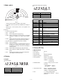
1
SERVICE MANUAL
ELECTRONIC
CASH REGISTER
MODEL ER-A440
SRV Key
PRINTER
: LKGIM7113RCZZ
: DP-730
("U" & "A" version)
CAUTION
EXTREME CAUTION MUST BE TAKEN WHEN SERVICING THIS MACHINE. EVEN
THOUGH THE MODE SWITCH IS IN THE OFF POSITION, VOLTAGE IS STILL SUPPLIED
TO THE ENTIRE MACHINE.
WHEN WORKING ON THIS MACHINE MAKE SURE THAT THE POWER CORD IS
REMOVED FROM THE WALL OUTLET.
CONTENTS
CHAPTER 1. SPECIFICATIONS . . . . . . . . . . . . . . . . . . . . . . . . . . . . . . . . . . 1-1
CHAPTER 2. OPTIONS . . . . . . . . . . . . . . . . . . . . . . . . . . . . . . . . . . . . . . . . . 2-1
CHAPTER 3. SERVICE (SRV) MODE . . . . . . . . . . . . . . . . . . . . . . . . . . . . . . 3-1
CHAPTER 4. HARDWARE DESCRIPTION . . . . . . . . . . . . . . . . . . . . . . . . . . 4-1
CHAPTER 5. TEST FUNCTION . . . . . . . . . . . . . . . . . . . . . . . . . . . . . . . . . . . 5-1
CHAPTER 6. DOWN LOAD FUNCTION . . . . . . . . . . . . . . . . . . . . . . . . . . . . 6-1
CHAPTER 7. SERVICE PRECAUTION . . . . . . . . . . . . . . . . . . . . . . . . . . . . . 7-1
CHAPTER 8. CIRCUIT DIAGRAM & PWB LAYOUT . . . . . . . . . . . . . . . . . . . 8-1
PARTS GUIDE
Parts marked with " " is important for maintaining the safety of the set. Be sure to replace these parts with specified ones
for maintaining the safety and performance of the set.
SHARP CORPORATION
This document has been published to be used
for after sales service only.
The contents are subject to change without notice.
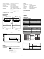
CHAPTER 1. SPECIFICATIONS
1. Appearance/Rating
1) Rating
Power source
AC 120 V ±10% 50/60Hz
Power consumption
Standby: 11.5 W
Maximum: 40 W (max.)
Operating temperature
0°C~40°C (32°F~104°F)
Operating humidity
10%~90% (RH)
Physical dimensions,
including the drawer
420(W) ✕ 427(D) ✕ 292(H)mm
16.5(W) ✕ 16.8(D) ✕ 11.5(H)in.
Weight
28.7 lbs (13 kg)
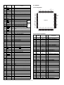
2. Keyboard
1) Standard keyboard layout
CASH
CL
7
8
9
NS
@/
FOR
4
5
6
RA
RFND
1
2
3
%1 %2 PO
VOID
0
00
RECEIOT JOURNAL
WYPL2
PCPT PRINT
#
WYPL2
#
AUTO AUTO TAX1 TAX2
1
2 SHIFT SHIFT
PLU/SUB
WYPL2
WYPL2
TAX
FS
SHIFT
CONV
FS
TEND
CHK
CH
5
10
15
20
4
9
14
19
3
8
13
18
2
7
12
MDSE SBTL
17 SBTL
1
6
11
16
CA/AT
Fig. 2-1
2) Key top name
Standard Key Top
KEY TOP
0 to 9,00
•
CL
@/FOR
1 to 20
↑R
↑J
RCPT
#
AUTO 1, 2
CASH #
NS
% 1, 2
PO 1, 2
RA
VOID
PLU/SUB
SBTL
CH
CA/AT
TAX1 SHIFT
TAX2 SHIFT
TAX
KEY TOP
PRINT
RFND
CONV
CHK
MDSE SBTL
FS SHIFT
FS TEND
DESCRIPTION
Numeric keys
Decimal point key
Clear key
Multiplication/split-pricing key
Department 1 to 20 keys
Receipt Paper Feed key
Journal Paper Feed key
Receipt print & on/off key
Non-Add Code key
Automatically Entry key 1, 2
Cashier code entry key
No Sales key
Discount key
% key 1, 2
Paid Out key
Received on Account key
Void key
PLU/Subdept code entry key
Subtotal key
Charge key
Cash/amount tendered
TAX1 shift key
TAX2 shift key
Tax key
DESCRIPTION
Validation print key
Refund key
Currency conversion key
Check key
Merchandise subtotal key
Food stamp shift key
Food stamp tendered key
Optional Key Top
KEY TOP
% 3, 4
2, 3, 4
AUTO 3 ∼ 10
CA 2
CH 2 ∼ 5
CR 3, 4
21 to 50
TAX3 SHIFT
TAX4 SHIFT
RA2
PO2
CONV2 ∼ 4
CHK2
RFND SALE
BIRTH
1 to 68
1–1
DESCRIPTION
% key 3, 4
Discount key 2, 3, 4
Automatically entry key 3 ∼ 10
Cash total 2 key
Charge key 2 ∼ 5
Credit key 3, 4
Department 21 to 50 key
TAX3 shift key
TAX4 shift key
Received on account key 2
Paid out key 2
Currency conversion key 2 ∼ 4
Check key 2
Refund sales key
Birthday key
Direct price lookup/Subdepartment keys
Customer display (Pop-up display)
3. Mode switch
SRV
MA
Fig. 4-2
SM
7 segment display (LED)
OP
REG
OP,X/Z
OFF
MGR
X1/Z1
PGM1
X2/Z2
PGM2
No. of positions
7
Color of display
Yellow Green
Character size
14.2 (H) ✕ 8.0 (W) mm
Display contents
(SRV)
(SRV')
Amount
Minus sign
Error
PGM Mode
VOID Mode
CA/AT
CHK, CR
Fig. 3-1
* The key can be removed in the REG or OFF position.
* In the SRV’ mode, key inputs are prohibited and no display is
made.
* With the key in the off position power is not supplied to the
main PWB.
Display
Position
1-8
4-10
10
10
10
10
[Functions]
•
•
•
•
SUB TOTAL/
short tender
Change
Function for each key position
SRV’:
System reset
SRV:
Service mode (Service programming)
Department
PLU
Repeat
Decimal point
Receipt OFF
Cashier No.
VP
compulsory
Sentinel
PGM2: Allows programming of an item that is not changed
frequently, in addition to the PGM1 mode programming.
• PGM1: Allows programming of items frequently changed (e.g.
department, PLU pricing, and discount rate setting).
• OP, X/Z: Allows X or Z operation by servers or cashiers.
• REG: Allows registrations.
• MGR: Allows the operations, by authorized person such as a
manager (e.g. correction after transaction finished or
cancellation of entry limits), which are not permitted to
ordinary cashiers.
10
9-10
5-10
8
3-1
9
2-3
10
10
–: Floating
E
P
u
F: Lights up when a registration is
finalized by depressing CA/AT, CHK,
CR key
o
C: Light up whenever the change due
amount appears in the display.
No zero-suppressed
No zero-suppressed
Endless count, starting from 2.
TAB
(–)
–xx–: free code
U: Light up when the validation printing is
compulsory
Light up the decimal point
5. Printer (DP-730)
• X1/Z1: Allows reading and resetting of a day’s sales total.
• X2/Z2: Allows reading or resetting sales totals in a specified
1) Specifications
• Part number:
• No. of stations:
• Printing system:
• Direction of printing:
• Printing capacity:
period.
• OFF:
10
Description
Switching off the display to prevent key board entries.
(The setting turn off the AC power.)
4. Display
DP-730
2
Mechanical serial dot
Bidirectional
Receipt – 24 characters
Journal – 24 characters
1) Layout
Validation – 55 characters
(one line only)
Operator display
• Character size:
1.36 (W) ✕ 2.75 (H) mm at 7 ✕ 7 dots
Print pitch:
Column distance 1.59 mm
Row distance
5.08 mm
Fig. 4-1
• Total number of dots:
7 segment display (LED)
No. of positions
10
Color of display
Yellow Green
Character size
14.2 (H) ✕ 8.0 (W) mm
• Font:
Receipt – 108 dots/216 positions
Journal – 108 dots/216 positions
Validation – 248 dots/495 positions
7 ✕ 7 dots (including half dot)
Space between characters – 1 dot (2
positions)
1–2
•
•
•
•
Distance between dots:
0.353 mm (H) ✕ 0.353 mm (W)
Journal near end sensor:
Service route option
Print speed:
Approx. 3.0 lines/sec.
Paper feed speed:
Receipt – Approx. 30 lines/sec.
4) Inking
• Ink supply system:
• Form:
• Specification:
• Ribbon life:
• Print color:
Journal – Approx. 30 lines/sec.
• Reliability:
MCBF – 4 million lines (excluding the
print head)
Head life – 50 million characters
(at 4 dots/1 character/
1 pin)
• Validation form sensor:
Ink ribbon
Cartridge/Endless ribbon
Material – Nylon
Approx. 6 million characters
Purple (single color)
5) Logo stamp: None
6) Cutter
• Method: Manual
Not setup
2) Printing area
Receipt/journal
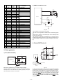
6. Drawer
1) Specification
87.08
(1) Drawer box and drawer
3.56
37.87
3.56
3.56
3.56
37.87
Model name
Size
Color
Material
Bell
Release lever
Drawer open sensor
4.2
44.5± 0.5
44.5± 0.5
SK-423
420 (W) ✕ 427 (L: included lock key)
✕ 112 (H: included rubber leg)
GRAY 368
Metal
—
Standard equipment; Situated at the bottom
Standard equipment
2) Money case
RECEIPT
Separation from the drawer
Separation of the coin compartments from the money
case
Bill separator
Number of compartments
JOURNAL
Unit : mm
Fig. 5-1
Validation form
For "U" version
Allowed
Disallowed
For "A" version
Allowed
Disallowed
—
5B/5C
YES
4B/8C
For "U" Version
For "A" Version
Bill compartments
Bill separator
70
87.08 (PRINT AREA)
Coin compartments
22
20
5B/8C
5B/5C
130 ~ 210
3) Lock
Unit : mm
Fig. 5-2
Location of the lock
Front
Method of locking
and unlocking
Locking:
Insert the drawer lock key into
the lock and turn it 90 degrees
counterclockwise.
Unlocking:
Insert the drawer lock key into
the lock and turn it 90 degrees
clockwise.
3) Paper
• Paper roll dimensions: 44.5±0.5mm in width, 83mm in diameter
• Paper quality:
Journal
Bond paper (paper thickness: 0.06 to
0.09mm, paper weight: 52.3 to 64g/m2)
Key No.
Validation form
Thickness: 0.07 to 0.14mm
Size: 130mm or more (W) ✕
70mm or more (H)
1–3
SK1-1
CHAPTER 2. OPTIONS
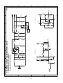
1. System configuration
(NOTE1)
This symbol shows
NEW MODEL
ER-A440
LOCAL PURCHASE
MASTER MACHINE
COMPUTER
ER-01/02FD
COMMERCIAL
PRODUCT
ER-04DW
3.5 inch FDD
CABLE
REMOTE DRAWER
Fig. 1-1
2–1
ER-03RA
OPTION RAM
2. Options
No.
NAME
MODEL
DESCRIPTION
1
EXPANSION RAM CHIP
ER-03RA
512K bytes RAM CHIP
2
REMOTE DRAWER
ER-04DW
3
PRESETS LOADER
ER-01FD/02FD
FD unit
4
KEY TOP KIT
ER-11KT7
1 × 1 KYE TOP UNIT
ER-12KT7
1 × 2 KYE TOP UNIT
ER-22KT7
2 × 2 KYE TOP UNIT
ER-11DK7G
1 × 1 DUMMY KYE KIT
ER-51DK7G
5 × 1 DUMMY KYE KIT
5
COIN CASE
ER-55CC2
for "U" version
6
COIN CASE
ER-48CC2
for "A" version
3. Service options
No.
NAME
PARTS CODE
PRICE
RANK
DESCRIPTION
1
SERVICE KEY
2
MODE KEY GRIP COVER
AL
OP key only
3
DRIP-PROOF KEYBOARD COVER
BE
Include the switch cover
4
JOURNAL NEAR END SENSOR
BB
5
TEXT PRESET KEYBOARD COVER
BH
AF
4. Service tools
No.
NAME
PARTS CODE
PRICE
RANK
1
RS-232 LOOP BACK CONNECTOR
BU
2
KEY TOP REMOVER
BB
DESCRIPTION
5. Supplies
No.
NAME
PARTS CODE
PRICE
RANK
1
ROLL PAPER
AR
2
INK LIBBON
AZ
6. Options
For installation of the options, refer to the Installation Manual which is issued separately.
2–2
DESCRIPTION
5 roll/pack
[key setup procedure]
CHAPTER 3. SRV. RESET AND
MASTER RESET
*2
MRS-2
executed
0
Key position set
Free key
0
1. SRV. reset (Program Loop Reset)
*1
Free key setup
complete.
Disable
Used to return the machine back to its operational state after a lockup has occurred.
NOTES:
1: When the 0 key is pressed, the key of the key number on display
is disabled.
2: Push the key on the position to be assigned. With this, the key of
the key number on display is assigned to that key position.
Procedure
• Method 1
1) Unplug the AC cord from the wall outlet.
2) Set the mode switch to (SRV′) position.
3) Plug in the AC cord to the wall outlet.
4) Turn to (SRV) position from (SRV′) position.
• Method 2
Key number
Key name
Key number
1
Numeric key "0"
10
Numeric key "9"
Key name
2
Numeric key "1"
11
Numeric key "00"
3
Numeric key "2"
12
Numeric key "000"
1) Set the mode switch to PGM2 position.
4
Numeric key "3"
13
Decimal point key
2) Turn off the AC switch.
5
Numeric key "4"
14
CL key
3) While holding down JOURNAL FEED key and RECEIPT FEED
key, Turn on the AC switch.
6
Numeric key "5"
15
@/FOR key
7
Numeric key "6"
16
SBTL key
Note: When disassembling and reassembling always power up using method 1 only. Method 2 will not reset the CKDC8.
8
Numeric key "7"
17
CA/AT key
9
Numeric key "8"
Note: SRV programming job#926-B must be set to "4" to allow PGM
program loop reset.
2. Master reset (All memory clear)
There are two possible methods to perform a master reset.
• MRS-1
Used to clear all memory contents and return machine back to its
initial settings and return keyboard back to default keyboard layout.
Procedure
1) Unplug the AC cord from the wall outlet.
2) Set the MODE switch to the (SRV′) position.
3) Plug in the AC cord to the wall outlet.
4) While holding down JOURNAL FEED key, turn to (SRV) position
from (SRV′) position.
• MRS-2
Used to clear all memory and keyboard contents.
This reset returns all programming back to defaults. The keyboard
must be entered by hand.
This reset is used if an application needs different keyboard layout
other than that supplied by a normal MRS-1.
Procedure
1) Unplug the AC cord from the wall outlet.
2) Set the MODE switch to the (SRV′) position.
3) Plug in the AC cord to the wall outlet.
4) While holding down JOURNAL FEED key and RECEIPT FEED
key, turn to (SRV) position from (SRV′) position.
5) Key position assignment:
After the execution of MRS-2, only the RECEIPT FEED and
JOURNAL FEED keys can remain effective on key assignment.
Any key can be assigned on any key position on the main keyboard.
3–1
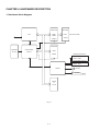
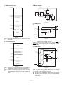
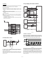
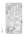
CHAPTER 4. HARDWARE DESCRIPTION
1. Hard ware block diagram
STANDARD
OPTIONAL
RAM1
RAM2
RAM
CPU
DRAWER
32KBx2
ER-03RA:512KB
512KB
STANDARD
PRINTER
GATE ARRAY
DP-730
MPCA7
ROM
256KB
OPERATER DISPLAY
1 LINE
7SEG 10DIG
CUSTOMER DISPLAY
1 LINE
7SEG 7DIG
CKDC8
SWITCH
KEY BOARD
RS232
I/F
1 ports
Fig. 1-1
4–1
2. Description of main LSI’s
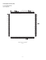
2-1. CPU (HD6415108-10)
112
111
110
109
108
107
106
105
104
103
102
101
100
99
98
97
96
95
94
93
92
91
90
89
88
87
86
85
STBY
MD2
MD1
MD0
VCC
RFSH
LWR
HWR
RD
AS
E
X
VSS
XTAL
EXTAL
VSS
TXD2
RXD2
TXD1
RXD1
SCK2
UASKC
IRQ1
IRQ0
VCC
AVCC
AN3
AN2
1) Pin configuration
84
83
82
81
80
78
78
77
76
75
74
73
72
71
70
69
68
67
66
65
64
63
62
61
60
59
58
57
29
30
31
32
33
34
35
36
37
38
39
40
41
42
43
44
45
46
47
48
49
50
51
52
53
54
55
56
1
2
3
4
5
6
7
8
9
10
11
12
13
14
15
16
17
18
19
20
21
22
23
24
25
26
27
28
A8
A9
A10
A11
A12
A13
A14
A15
VSS
A16
A17
A18
A19
A20
A21
A22
A23
VSS
WAIT
BACK
BREQ
P33
P34
P35
P36
P37
VCC
P40
RES
NMI
VSS
P10
P11
P12
P13
P14
P15
P16
P17
D0
D1
D2
D3
D4
D5
D6
D7
VSS
A0
A1
A2
A3
A4
A5
A6
A7
HD6415108-10 pin configuration
Fig. 2-1
4–2
AN1
AN0
AVSS
VSS
P67
P66
P65
P64
P63
P62
P61
P60
P57/STOP
P56
P55
P54
P53
P52
P51
P50
VSS
P47
P46
P45
P44
P43
P42
P41
P10
P11
P12
P13
P14
P15
P16
P17
D7
D6
D5
D4
D3
D2
D1
D0
2) Block diagram
P27/A23
Data bus
P26/A22
Port 1
Port 2
P25/A21
P24/A20
P23/A19
P22/A18
P21/A17
Watch
dog timer
E
MD2
MD1
H8/500 CPU
A15
A14
A13
A12
A11
A10
A9
A8
A7
A6
A5
A4
A3
A2
A1
A0
Address bus
Clock
oscillator
X
Address bus
XTAL
Data bus (Lower)
EXTAL
Data bus (Upper)
P20/A16
DTC
MD0
RES
STBY
NMI
Interruption controller
AS
P37
RD
P36
HWR
P35
16bit free running
timer x 2ch
Refresh controller
RFSH
Port 3
LWR
P34
P33
BREQ
Wait state
controller
8bit timer
A/D convertor
Serial
communication
interface x 2ch
VCC
BACK
WAIT
VCC
P47
VCC
VSS
P45
Port 4
VSS
FTI2
VSS
VSS
FTI1
P43
VSS
P42
VSS
P41/TMCI
VSS
P40
VSS
AVCC
Fig. 2-2
4–3
P50
P51
P52
P53
P54
P56
FMRS
Port 5
STOP/P57
P67
P66
RS/P65
RR/P64
CD/P63
CS/P62
DR/P61
ER/P60
AN0
Port 6
AN1
P73
IRQ0
IRQ1
Port 7
IRQ2
SCK2
TXD1
RXD1
RXD2
TXD2
Port 8
AN2
AVSS
3) Pin description
PIN
No.
SYMBOL
SIGNAL
NAME
IN/
OUT
IN
1
2
IN
PIN
No.
FUNCTION
RESET INPUT from CKDC WUTH
BUFFER
SYMBOL
SIGNAL
NAME
IN/
OUT
FUNCTION
58
P42
/TOF
IN
Slip TOF signal (Nu) pull-up
59
P43
/BOF
IN
Slip BOF signal (Nu) pull-up
IN
Printer (Dp-730) Reset signal from
MPCA
IN
Near END signal jounal
IN
CKDC interface shift enable signal
(NU) GND
IN
Near END signal receipt
NON-MASKABLE INTERRUPT INPUT
FOR SSP INTERRUPT INPUT
60
GND
61
3
VSS
VSS
4
P10
ERC
OUT
EVENT READ CANCEL (to CKDC)
5
P11
LDRQ
OUT
LOAD REQUEST (to CKDC)
6
P12
/SHEN
IN
SHIFT ENABLE (from CKDC)
63
P47
/NER
7
P13
/FRES
OUT
FISCAL MEMORY RESET (NU)
64
VSS
VSS
8
P14
BUSY
IN
FISCAL MEMORY BUSY (NU) Pull-up
65
P50
TRG1
OUT
Dot pulse adjust signal
9
IN
FISCAL MEMORY READY (NU)
Pull-up
66
P51
/PSTOP
OUT
Nu
67
P52
/CKDCR2
OUT
10
IN
POP-UP DISPLAY SENSOR (NU)
Pull-up
68
P53
OPDS
IN
GND Nu
69
P54
FVPON
70
P55
FMRS
P45
/NEJ
62
GND
IN
OUT
Nu
Nu (GND)
Nu
11
P17
12
D0
D0
I/O
DATA BUS 0
13
D1
D1
I/O
DATA BUS 1
14
D2
D2
I/O
DATA BUS 2
15
D3
D3
I/O
DATA BUS 3
16
D4
D4
I/O
17
D5
D5
I/O
18
D6
D6
19
D7
D7
20
VSS
VSS
GND
77
OUT
RR signal for RS232 (Ready to
Receive) (Nu)
21
A0
A0
OUT
ADDRESS BUS 0
78
OUT
RS signal for RS232 (Request to Send)
22
A1
A1
OUT
ADDRESS BUS 1
79
IN
23
A2
A2
OUT
ADDRESS BUS 2
80
IN
24
A3
A3
OUT
ADDRESS BUS 3
81
VSS
VSS
25
A4
A4
OUT
ADDRESS BUS 4
82
AVSS
AVSS
IN
GND
26
A5
A5
OUT
ADDRESS BUS 5
83
P70
VPJ
IN
Validation sensor journal (NU) GND
27
A6
A6
OUT
ADDRESS BUS 6
84
P71
VPR
IN
Validation sensor receipt (NU) GND
28
A7
A7
OUT
ADDRESS BUS 7
85
P72
VPTEST
IN
+24V test input
29
A8
A8
OUT
ADDRESS BUS 8
86
P73
IN
Validation sense signal (Nu) GND
30
A9
A9
OUT
ADDRESS BUS 9
87
AVCC
AVCC
IN
+5V
31
A10
A10
OUT
ADDRESS BUS 10
88
VCC
VCC
32
A11
A11
OUT
ADDRESS BUS 11
89
P80
/iRQ0
IN
Interrupt signal 0 from MPCA
33
A12
A12
OUT
ADDRESS BUS 12
34
A13
A13
OUT
ADDRESS BUS 13
35
A14
A14
OUT
ADDRESS BUS 14
91
P82
/iRQ2
IN
36
A15
A15
OUT
ADDRESS BUS 15
92
P83
SCK2
OUT
37
VSS
VSS
GND
93
P84
RXD
IN
38
A16
A16
OUT
ADDRESS BUS 16
94
P85
TXD
OUT
39
A17
A17
OUT
ADDRESS BUS 17
40
A18
A18
OUT
ADDRESS BUS 18
41
A19
A19
OUT
ADDRESS BUS 19
42
A20
A20
OUT
ADDRESS BUS 20
43
A21
A21
OUT
ADDRESS BUS 21
44
A22
A22
OUT
ADDRESS BUS 22
45
A23
A23
OUT
46
VSS
VSS
47
/WAIT
/WAIT
49
/BREQ
/BREQ
50
P33
51
P34
P56
/SLIPLMP
OUT
Nu
72
P57
/STOP
OUT
Nu
73
OUT
ER signal for RS232 (Equipment
Ready)
DATA BUS 4
74
IN
DR signal for RS232 (Data set Ready)
DATA BUS 5
75
IN
CS signal for RS232 (Clear to Send)
I/O
DATA BUS 6
76
IN
I/O
DATA BUS 7
ADDRESS BUS 23
IN
Wait signal from MPCA
IN
Bus control request (Nu) pull-up
DOPS
IN
Drawer open sencer signal
/DR0
OUT
OUT
Drawer open drive signal
P35
/DR1
53
P36
NU
IN
(Nu) GND
54
P37
NU
IN
(Nu) GND
55
VCC
VCC
56
P40
/IFV
+5V
IN
Slip printer enable (Nu) pull-up
IN
Printer (Dp-730) timing signal from
MPCA
4–4
Printer (Dp-730) Home position pulse
+5V
Interrupt signal from OPTION PWB
Interrupt signal (Nu) pull-up
CKDC & FMC i/F sync shift clock
RS232C RECEIVE DATA
RS232C SEND DATA
IN
CKDC, Fiscal memory unit I/F shift
input data
96
OUT
CKDC, Fiscal memory unit I/F shift
output data
97
VSS
VSS
98
EXTAL
EXTAL
IN
X-TAL (14.7456MHz)
99
XTAL
XTAL
IN
X-TAL (14.7456MHz)
100 VSS
VSS
101 φ
φ
GND
GND
OUT
System clock (7.3728MHz)
OUT
E clock (NU)
103 /AS
/AS
OUT
Address strobe
104 /RD
/RD
OUT
Read
105 /HWR
/WR
106 /LWR
Option drawer 1 drive signal
CI signal for RS232 (Calling Indicator)
95
102 E
Bus control request acknowl edge (Nu)
CD signal for RS232 (Carrier Detect)
GND
IN
90
GND
52
57
Nu (GND)
71
OUT
48
IN
OUT
Write
OUT
Nu
107 /RFSH
/RFSH
108 VCC
VCC
OUT
Refresh cycle (NU)
109 MD0
MD0
IN
+5V (MODE 3)
110 MD1
MD1
IN
+5V (MODE 3)
111 MD2
MD2
IN
GND (MODE 3)
112 /STBY
/STBY
IN
+5V (Nu)
+5V
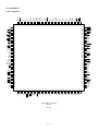
2-2. G.A (MPCA7)
160
159
158
157
156
155
154
153
152
151
150
149
148
147
146
145
144
143
142
141
140
139
138
137
136
135
134
133
132
131
130
129
128
127
126
125
124
123
122
121
NU
DOTEN
TWAIT
NU
NU
NU
NU
NU
STH2
SCK2
HTS2
SLMTR
SLMTS
SLMTD
RJMTR
RAS3
NU
GND
VCC
ASKRX
NU
NU
NU
RJMTD
RJMTS
DT5
DT6
DT7
GND
DT1
DT2
DT3
DT4
RJTMG
RJRST
RAS1
RAS2
ROS2
ROS1
OPTCS
1) Pin configuration
120
119
118
117
116
115
114
113
112
111
110
109
108
107
106
105
104
103
102
101
100
99
98
97
96
95
94
93
92
91
90
89
88
87
86
85
84
83
82
81
41
42
43
44
45
46
47
48
49
50
51
52
53
54
55
56
57
58
59
60
61
62
63
64
65
66
67
68
69
70
71
72
73
74
75
76
77
78
79
80
1
2
3
4
5
6
7
8
9
10
11
12
13
14
15
16
17
18
19
20
21
22
23
24
25
26
27
28
29
30
31
32
33
34
35
36
37
38
39
40
D3
GND
D4
D5
D6
D7
SSPRQ
RESET
INT2
INT3
RXDI
TXDI
SCKI
IRQ0
A0
A1
A2
A3
A4
A5
GND
VCC
A6
A7
A8
A9
A10
A11
A12
A13
A14
A15
A16
A17
A18
A19
A20
A21
A22
NU
RF
JF
PCUT
FCUT
VF
STAMP
SLF
SLRS
SLMTD
RES
TRG
TRG
POFF
INT1
HTS1
SCK1
STH1
NU
NU
VCC
GND
NU
VRESC
SLTMG
SLRST
AS
RD
WR
PHAI
SDT7
SDT6
SDT5
GND
SDT4
SDT3
SDT2
SDT1
D0
D1
D2
GATE ARRAY (LZ9AH39)
MPCA7
Fig. 2-3
4–5
EXINT0
EXINT1
EXINT2
EXINT3
WRO
RDO
RA15
RA16
GND
RA17
RA18
EXWAIT
WAIT
NU
MCR1
NU
DAX1
RCKX
IRRX
GND
VCC
UATX
UARX
UASCK
IRTX
RCO
NU
NU
NU
NU
MA15
TEST
MD0
MD1
IPLON
INT4
PRST
PTMG
TRGI
A23
2) Block diagram
A23~A0
IRLON
ROS1
ROS2
RAS1
RAS2
Address decode
External CS
Internal CS
RASEL
Image
control
SSPRQ
SSP comparison register
BAR.
RAS3
OPTCS
IRTX
IRRX
RCI
ASKRX
I/R Control
D0~D7
Buffer
AS
CHS
serial select
RD
TXDI
SCKI
RXDI
HTS1
SCK1
STH1
HTS2
SCK2
STH2
Multiplexer
WR
RDO
WRO
Φ
Read/write
control
Φ
RESET
INT4
RES
Divider
VRESC
INT1
INT2
POFF
WAIT
EXWAIT
INT3
INTO
control
MD0
MD1
EXINT0
EXINT1
WAIT
control
EXINT2
EXINT3
CAPS
select
IRQ0
Print mode PMD
TEST
MTD
MTD
RJRST
SLRST
*PRST
RJTMG
RJMTR
Motor
drive
Print gate
SLMTS
SLTMG
Print pulse control
PTMG
SLMTR
Printer control port
SLMTD
SLF
SLRS
VF
RF
JF
FCUT
4–6
PCUT
Fig. 2-4
STAMP
TRGI
SDT1~7
DT1~9
TRG
DOTEN
TRG
* Output selection with CAPS.
PRST/PTMG.
SLMTD
3) Pin description
Pin
No.
Signal
name
In/
Out
Pin
No.
Function
Signal
name
In/
Out
Function
1
RF
Out
Receipt side paper feed solenoid
50
INT3
In
2
JF
Out
Journal side paper feed solenoid
51
RXD2
Out
8 bit serial port output to CPU
Interrupt signal (Nu)
8 bit serial port input from CPU
3
PCUT
Out
Printer partial cut signal (NU)
52
TXD2
In
4
FCUT
Out
Printer auto cut signal (NU)
53
SCK2
In
5
VF
Out
Multi line validation paper feed (NU)
54
IRQ0
Out
6
STAMP
Out
Printer stamp signal (NU)
55
A0
In
Address bus 0
7
SLFS
Out
Slip printer paper feed singnal (NU)
56
A1
In
Address bus 1
8
SLRS
Out
Slip printer release signal (NU)
57
A2
In
Address bus 2
9
SLMTD
Out
Slip printer motor drive signal (NU)
58
A3
In
Address bus 3
10
RES
Out
Peripheral output reset
59
A4
In
Address bus 4
11
TRG
Out
Dot head trigger signal (NU)
60
A5
In
Address bus 5
12
TRG
Out
Dot head trigger signal
61
GND
—
GND
13
POFF
In
Power off signal input
62
VCC
—
+5V
14
INT1
In
(NU)
63
A6
In
Address bus 6
15
HTS1
Out
8 bit serial port output (for CKDC8)
64
A7
In
Address bus 7
16
SCK1
Out
Serial port shift clock output (for CKDC8)
65
A8
In
Address bus 8
17
STH1
In
8 bit serial port input (for CKDC8)
66
A9
In
Address bus 9
18
RAS VZ
—
Chip select (NU)
67
A10
In
Address bus 10
Serial port shift clock input from CPU.
Interrupt request to CPU
—
Nu
68
A11
In
Address bus 11
20
VCC
—
+5V
69
A12
In
Address bus 12
21
GND
—
GND
70
A13
In
Address bus 13
22
INTMCR
—
Interrupt (NU)
71
A14
In
Address bus 14
Out
Turns active when reset and power
down is met
72
A15
In
Address bus 15
73
A16
In
Address bus 16
19
23
—
VRESC
24
SLTMG
In
Slip printer timing signal (NU)
74
A17
In
Address bus 17
25
SLRST
In
Slip printer reset signal (NU)
75
A18
In
Address bus 18
26
AS
In
Address strobe
76
A19
In
Address bus 19
27
RD
In
Read strobe
77
A20
In
Address bus 20
28
WR
In
Write strobe
78
A21
In
Address bus 21
29
φ
In
(φ) System clock (7.3728 MHz)
79
A22
In
Address bus 22
30
SDT7
Out
Slip printer printhead drive signal (dot7)
(NU)
80
LCDC
—
LCD CS (NU)
81
A23
In
Address bus 23
31
SDT6
Out
Slip printer printhead drive signal (dot6)
(NU)
82
TRGI
In
Dot pulse control/drive signal
PTMG
Out
Printer timing signal
SDT5
Out
Slip printer printhead drive signal (dot5)
(NU)
83
32
84
PRST
Out
Printer reset signal
33
GND
—
GND
85
RDY
In
Ready from FMC unit
IPLON
In
To option connector (NU)
Out
Slip printer printhead drive signal (dot4)
(NU)
86
87
MD1
In
Mode select input (+5V)
Out
Slip printer printhead drive signal (dot3)
(NU)
88
MD0
In
Mode select input (GND)
89
TEST
In
+5V
Slip printer printhead drive signal (dot2)
(NU)
90
MA15
—
Image address 15 (NU)
91
MA18
—
Nu
Slip printer printhead drive signal (dot1)
(NU)
92
MA19
—
Nu
93
RCVRDY1
—
Nu
94
RCVRDY2
—
Nu
95
RC0
—
Remote control encord signal for CPU
96
IRTX
—
I/R output for LED (NU)
34
35
36
37
SDT4
SDT3
SDT2
SDT1
Out
Out
38
D0
I/O
Data bus 0
39
D1
I/O
Data bus 1
40
D2
I/O
Data bus 2
41
D3
I/O
Data bus 3
42
GND
—
GND
43
D4
I/O
Data bus 4
44
D5
I/O
Data bus 5
45
D6
I/O
Data bus 6
46
D7
I/O
Data bus 7
47
SPRQ
Out
48
RESET
In
49
SHEN
In
SSP interrupt request to CPU
MPCA reset
Shift enable from CKDC8
4–7
97
UASCK
—
I/R serial data shift clock (NU)
98
UARX
—
I/R serial data for CPU (NU)
99
UATX
—
I/R serial data from CPU (NU)
100
VCC
—
+5V
101
GND
—
GND
102
IRRX
—
I/R input from I/R unit (NU)
103
RCI
—
I/R input from I/R unit (NU)
104
DAX1
—
System clock (7.3728MHz)
In/
Out
—
Nu
106
MCR1
—
Nu
107
MCR2
—
Nu
108
WAIT
Out
Wait request signal
109
EXWAIT
110
RA18
Out
111
RA17
Out
Nu
112
GND
—
GND
113
RA16
Out
Nu
114
RA15
Out
Nu
115
RDO
Out
Expansion RD signal
Out
1) Pin configulation
NU
NU
G10
G9
G8
G7
G6
G5
G4
G3
G2
G1
BUZ
/POFF
NU
ST8
DAX2
64
63
62
61
60
59
58
57
56
55
54
53
52
51
50
49
105
In
2-3. CKDC8
Function
External wait control input signal
DP
SA
SB
SC
SD
SE
SF
SG
GND
VDD
KR4
KR10
KR11
NU
HTS
STH
Nu
116
WRO
117
EXINT3
In
Expansion interruption signal 3
Expansion WR signal
Option
118
EXINT2
In
Expansion interruption signal 2
119
EXINT1
In
Expansion interruption signal 1
120
EXINT0
In
Expansion interruption signal 0
121
OPTCS
Out
Chip select base signal for expansion
option
Option
1
2
3
4
5
6
7
8
9
10
11
12
13
14
15
16
48
47
46
45
44
43
42
41
40
39
38
37
36
35
34
33
CKDC8
ST7
ST6
/RESETS
/SHEN
ERC
LDRQ
GND
GND
/RES0
VDD
GND
KR7
17
18
19
20
21
22
23
24
25
26
27
28
29
30
31
32
Signal
name
/SCK
ST0
ST1
ST2
ST3
ST4
ST5
VDD
GND
NU
KR0
KR1
KR2
KR3
KR5
KR6
Pin
No.
122
ROS1
Out
ROM 1 chip select signal
123
ROS2
Out
ROM 2 chip select signal (NU)
124
RAS2
Out
RAM 2 chip select signal
125
RAS1
Out
RAM 1 ship select signal
126
RJRST
In
Printer reset signal
127
RJTMG
In
Printer timing signal
Pin
No.
SYMBOL
SIGNAL
NAME
128
DT4
Out
Printer dot signal 4
1
DP
DP
OUT DISPLAY SEGMENT Dp
A
SA
OUT DISPLAY SEGMENT a
2) Pin assignment (CKDC8)
IN/
OUT
FUNCTION
129
DT3
Out
Printer dot signal 3
2
130
DT2
Out
Printer dot signal 2
3
B
SB
OUT DISPLAY SEGMENT b
131
DT1
Out
Printer dot signal 1
4
C
SC
OUT DISPLAY SEGMENT c
132
GND
—
GND
5
D
SD
OUT DISPLAY SEGMENT d
133
DT7
Out
Printer dot signal 7
6
E
SE
OUT DISPLAY SEGMENT e
134
DT6
Out
Printer dot signal 6
7
F
SF
OUT DISPLAY SEGMENT f
Printer dot signal 5
8
G
SG
OUT DISPLAY SEGMENT g
Printer motor drive signal
9
VSS0
GND
GND
VDD0
VDD
VDD
135
136
DT5
Out
MTD
Out
137
MTD
Out
Printer motor drive signal
10
138
DOT9
Out
Printer dot signal 9 (NU)
11
KR4
KR4
IN
KEY RETURN 4
139
DOT8
Out
Printer dot signal 8 (NU)
12
KR10
KR10
IN
140
SYNC
—
Nu (+5V)
KEY RETURN (feed clerk
MRS sw)
141
ASKRX
—
I/R input from I/R unit (NU)
13
KR11
KR11
IN
KEY RETURN (MODE sw)
14
KR8
NU
IN
GND
15
HTS
HTS
IN
16
STH
STH
OUT
17
/SCK
/SCK
18
ST0
ST0
OUT KEY STROBE 0
19
ST1
ST1
OUT KEY STROBE 1
20
ST2
ST2
OUT KEY STROBE 2
21
ST3
ST3
OUT KEY STROBE 3
22
ST4
ST4
OUT KEY STROBE 4
OUT KEY STROBE 5
142
VCC
—
+5V
143
GND
—
GND
144
145
—
RAS3
—
Nu
Out
146
RJMTR
In
Printer motor lock detection signal (NU)
147
SLMTD
In
Nu
148
149
SLMTS
SLMTR
In
In
Nu
GND
150
HTS2
Out
Serial output to FMC unit (NU)
151
SCK2
Out
Serial clock to FMC unit (NU)
152
153
STH2
—
In
—
Serial input to FMC unit (NU) pull-up
Nu
154
—
—
Nu
155
—
—
Nu
156
157
—
—
—
—
Nu
Nu
158
LCDWT
—
Nu
159
DOTEN
Out
Dot drive enable signal
160
RASP
—
Nu
4–8
IN
SHIFT CLOCK
23
ST5
ST5
24
VDD1
VDD
25
AXSS
GND
GND
26
KR9
NU
GND
27
KR0
KR0
IN
KEY RETURN 0
28
KR1
KR1
IN
KEY RETURN 1
29
KR2
KR2
IN
KEY RETURN 2
30
KR3
KR3
IN
KEY RETURN 3
31
KR5
KR5
IN
KEY RETURN 5
32
KR6
KR6
IN
KEY RETURN 6
VDD
Pin
No.
SYMBOL
SIGNAL
NAME
IN/
OUT
33
KR7
KR7
IN
34
AVRF
GND
35
AVDD
VDD
36
/RESET
/RES0
37
XT2
38
XT1
39
IC
40
X2
41
X1
42
VSS1
GND
43
LDRQ
LDRQ
IN
LORD REQUEST
44
ERC
ERC
IN
EVENT READ CANCEL
45
SHEN
/SHEN
46
/RES1
/RESETS
47
ST6
ST6
OUT KEY STROBE 6
48
ST7
ST7
OUT KEY STROBE 7
49
ST8
ST8
OUT KEY STROBE 8
OUT KEY STROBE 9
2) CKDC8 oscillation circuit
FUNCTION
KEY RETURN 7
X3
4.19MHz
X2
IN
40
1
2
32.768 KHz
3
X1
GND
41
CKDC 8
4.19 M Hz
XT2
X2
32.768KHz
XT1
OUT SHIFT ENABLE
38
ST9
NU
51
/POFF
/POFF
52
BUZ
BUZ
53
T0
G1
OUT DISPLAY DIGIT 1
54
T1
G2
OUT DISPLAY DIGIT 2
55
T2
G3
OUT DISPLAY DIGIT 3
56
T3
G4
OUT DISPLAY DIGIT 4
57
T4
G5
OUT DISPLAY DIGIT 5
58
T5
G6
OUT DISPLAY DIGIT 6
59
T6
G7
OUT DISPLAY DIGIT 7
60
T7
G8
OUT DISPLAY DIGIT 8
61
T8
G9
OUT DISPLAY DIGIT 9
62
T9
G10
OUT DISPLAY DIGIT 10
63
T10
NU
OUT DISPLAY DIGIT 11
64
ID
NU
OUT DISPLAY SEGMENT
IN
C105
33P
C106
18P
OUT SYSTEM TO RESET
50
R164
330K
37
HD404728A91FS
Fig. 3-2
POWER OFF
OUT BUZZER
Two oscillators are connected to the CKDC8.
The main clock X3 generates 4.19MHz which is used during power
on.
When power is turned off, the CKDC8 goes into the standby mode
and the main clock stops.
The sub-clock X2 generates 32.768KHz which is primarily used to
update the internal RTC (real time clock). During the standby mode, it
keeps oscillating to update the clock and monitoring the power recovery.
4. Reset (POFF) circuit
+24V
+5V
D7
1SS133
R12
8.2KG
3. Clock generator
R11
2.7K
R9
2.7K
R10
1) CPU (HD64151010FX)
R13
15KG
13
CPU
IRQ0
99
14.7456MHz
54
+
2
C208
1µ 50V
INT0
XTAL
3
+
MPCA7
X1
56K
8
R14
9.1KG
ZD2
MTZ5.1A
-
B
1
/POFF
IC3A
4 KIA393F
C3
1000P
48
POFF
(HD64151010FX)
EXTAL
98
89
IRQ0
101
CPU
1
RESET (FROM CKDC 8)
72
PHAI
STOP (TO CKDC 8)
Fig. 3-1
Fig. 4-1
Basic clock is supplied from a 14.7456MHz ceramic oscillator.
The CPU contains an oscillation circuit from which the basic clock is
internally driven. If the CPU was not operating properly, the signal
does not appear on this line in most cases.
In order to prevent memory loss at a time of power off and power
supply failure of the ECR, the power supply condition is monitored at
all times. When a power failure is met, the CPU suspends the execution of the current program and immediately executes the power-off
program to save the data in the CPU registers in the external S-RAM
with the signal STOP forced low to prepare for the power-off situation.
The signal STOP is supplied to the CKDC8 as signal RESET to reset
the devices.
4–9
This circuit monitors +24V supply voltage.
0 page memory map
The voltage at the (–) pin of the comparator IC3A is always maintained to 5.1V by means of the zener diode ZD2, while +24V supply
voltage is divided through the resistors R12, R13, and R14, and is
applied to the (+) pin. When normal +24V is in supply, 6.8V is supplied to the (+) pin, therefore, signal POFF is at a high level. When
+24V supply voltage decreases due to a power off or any other
reason, the voltage at the (+) pin also decreases. When +24V supply
voltage drops, the voltage at the (+) pin drops below +5.1V, which
causes POFF to go low, thus predicting the power-off situation.
000000H
004000H
ROM image area
32KB
VDD
RAS3
14
4
6
5
VDD
CKDC8
14
9
RESETS
IC10B
74HC00S
14
1
8
3
10
/RESET
2
RAM image area
slightly smaller than32KB
IC10A
74HC00S
IC10C
74HC00S
R123
10K
008000H
/(RAS3./RESET)
VDD
C86
1000P
C88
1000P
C87
1000P
00F800H
STOP
The STOP signal from the CPU is converted into the RESETS signal
by the CKDC6.
00FFFFH
The RESETS signal from the CKDC8 is converted into the RESET
signal at the gate backed-up by the VRAM power, performing the
system reset.
RAM image area
00FE80H
NOT USE
Internal I/O area
00FF80H
1BFFFFH
1FFFFFH
5. Memory control
RAM area
00FFFFH
External I/O area
(0 page)
Fig. 5-2
• ROM image area: Image is formed in ROM area address
1) Memory map
C00000H to C07FFFH. This area is identical to IPL ROM area
which will beseparately developed.
All range memory map
000000H
1C0000H
Internal I/O
External I/O
Memory image area
• RAM image area: Image is formed in RAM area address 1F0000H
(*1)
(*2)
(*3)
to 1F7E7FH. ( Note)
Note: Image can be formed in lower 32KB of RAS2.
ROM area memory map
C00000H
RAM area
(10M byte)
ROS1
(256K Byte)
C00000H
C40000H
ROM area
(3M byte)
FFFFFFH
ROS2
(Not used)
Expansion I/O area (1M byte)
CA0000H
Fig. 5-1
( 1)
“Internal I/O” means the registers in the H8/510.
( 2)
“External I/O” means the base system I/O area to be addressed in page 0.
( 3)
"Memory image area" means the lower 32KB of ROM area
which is projected to 000000H ~ 007FFFH for allowing reset
start and other vector addressing, or the lower 32KB of RAM
area which is projected to 008000H ~ 00FE7FH for allowing 0
page addressing of work RAM area.
( 4)
D00000H
ROS3
NOT USE
EFFFFFH
“Expansion I/O” means expansion I/O device area which isaddressed to area other than page 0.
Fig. 5-3
4 – 10
RAM area memory map
2) Block diagram
100000H
Data bus
ROS1
ROM1
NOT USE
CPU
MPCA7
1C0000H
RAS1 (Not use)
Address bus
1F0000H
RAS2 64K Byte
RAS2
(STANDARD)
(OPTION)
RAM1
RAM
RAS3
RAM2
200000H
RAS3
512K Byte
Fig. 5-6
(OPTION)
ROM control
280000H
C80000H~CFFFFFH
ROS2
(MAX 2MB)
C00000H~C7FFFFH
Address
400000H
ROS1
Address
decorder
A23~A14
000000H~007FFFH
NOT USE
(IPLON)
BFFFFFH
Fig. 5-4
MPCA7
Note: RAS2 signal is formed as OR in the image area of 0 page.
(lower32KB).
Fig. 5-7
IPLON:
I/O area memory map
IPL board detection signal incorporated in the option slot.
Note used in the ER-A445P. (Not used)
Access is performed with two ROM chip select signals ROS1 and
ROS2, which decode 512KB address area respectively to accessmax. 4MB ROM.
00FF80H
(*1)
MPCCS
RAM control
00FFA0H
200000H~3FFFFFH
NOT USE
RAS3
1C0000H~1DFFFFH
MCR1 (NOT USE)
Address
MCR2 (NOT USE)
A23~A14
RAS1
00FFC0H
Address
decorder
(*2)
OPCCS1
008000H~
00F7FFH
*1
00FFD0H
(*2)
RAS2
OPCCS2
1E0000H~1FFFFFH
00FFE0H
NOT USE
00FFE8H
NOT USE
DOI
D
S8F
CK
Q
00FFF0H
Control register
NOT USE
00FFFFH
R
RESET
MPCA7
Fig. 5-5
Note 1: MPCCS signal is the base signal for MPCA7 internal registerdecoding, and does not exist as an internal signal.
Fig. 5-8
Access is performed with two RAM chip select signals, RAS2 and
RAS3. The control register in MPCA7 allows selection of pageimage
memory area. (RAS1 is selected for initializing.)
Note 2: OPCCS1 and OPCCS2 signals are decoded in the OPC
(optionperipheral controller) using the base signal OPTCS
for optiondecoding. They does not exist as external signals.
: For 0 page image area, selection between RAS2 and RAS3 can
bemade with the control register. The 0 page control registerperforms initializing at the timing of no stack processimmediately
after resetting.
4 – 11
As the address detection system, the brake address register comparison system is employed though the mapping system was employed
in the conventional monitor RAM. The address registerlocated in
MPCA is always compared with the system address bus to monitor
and generate NMI signal at a synchronized timing and togo to NMI
exception process.
In the exception process routine service routine, the entry address is
checked to go to SSP sub routine.
Entry to the break address register (BAR) is performed through address FFFF00H or later decoded in MPCA7.
6. SSP circuit
1) Block diagram
This is the circuit employed to do the Special Service Preset(SSP).
(Block diagram)
SSPRQ
NMI
A0~23
2) SSP register
The break address register (BAR) is accessed through direct address
of FFFF00H~FFFFFFH. Entry number is 32 entry.
D0~D7
CPU
FFFF00
H
MPCA7
Fig. 6-1
(MPCA7 block diagram)
Comparator
O
BAR 0
1
2
2
3
3
4
BAR0
5
SSPRQ
(NMI)
N
0
1
4
Coincide
D0~
D7
BAR N
7
BAR1
6
Coincide
7
REGCS
SPE
(Enable register)
Decode
BAR2
A23~
A0
Control signal
ROMCS
Fig. 6-2
Fig. 6-3
Each BAR is composed of 4 byte address. Bit composition is as
follows:
A19 A18 A17 A16 A15
A8
A7
A2
EN
1
2
3
4
Upper bits
Intermediate bits
Lower bits
Enable register
EN (bit7) = 1 Enable
= 0 Inhibit
Don't care for "-----."
< BAR composition >
Fig. 6-4
is the enable register. The entry registers of the break address are
assigned to , , and . Each bit of address corresponds to each
bit position, writing to , , and
is performed without shifting. The
corresponding area is 1MB space of ROS1 and ROS2.
4 – 12
3) SSP register access method
Access to SSP break address register is performed through the temporary register as shown below:
A19 A18 A17 A16 A15
A8
A7
A2
EN
Temporary
Temporary
4
WR
1
2
3
WR
Fig. 6-5
Information on which brake register the SSP brake is detected in is
read as binary data by reading address FFFFFFH (*1).
Used in an expanded register.
Normally is a reserve bit. Whenreading, fixed to 0.
If there are 32 break registers, binary expression is made with the
above 5 bits, and 0th is “00000B” and 31st is “11111B.”
When detected simultaneously by two or more break registers,
onewith the smaller BAR number is read as binary data.
The brake signals (NMI) and the above detection data (CMP0~4)
areheld until the above detection data are read. So read should bemade in the NMI sub routine. (Clear by FFFFFFH read.)
Enable flags can be accessed individually.
can be accessed individually, writing to
Though enable register
brake address registers
and
is performed at the same time as
writing to brake address register
through the temporary register.
Therefore, set
and
to temporary, then write into
at last.
Since the temporary register is commonly used by BAR sets, thefollowing register setting is performed after completion ofsetting of each
break address register.
SSP control method
Access to the enable register and the brake address register is only
possible when writing to them from the CPU.
bit 7
6
5
0
0
0
4
3
2
1
1: FFFFFFH is not fulldecoded. (FFFF00H~FFFFFFH). Therefore,unnecessary read access in parentheses should not be
performed.
0
CMP4 CMP3 CMP2 CMP1 CMP0 (FFFFFFH)
7. PRINTER control circuit
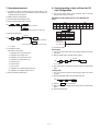
1) Block diagram
3) Printer motor drive circuit
Address bus
CPU
Main PWB side
Data
bus
Printer side
+24V
M
RECEIVER
C227
MPCA7
PRINTER
(DP-730)
MPCA7
DRIVER
Speed limiter
circuit
MTD
COM
MTD
Fig. 7-1
2) General description of the printer controller
2.2K
R128
DP
R127
Q7
C92
The DP-730 is used as the R/J printer. The printer mechanical timing
control is made by the CPU through MPCA7.
DP
Normal 555µs (516~590µs)
When the MTD is high, the motor rotates.
When the MTD is low, the motor stops.
4 – 13
<Motor lock protection>
Relation ship among RP/HP/DP
When an abnormal load is applied to the mechanism, the DP (Dot
Pulse) frequency is checked to prevent against the motor burn-out,
the timing belt shift, and gear damage. If the following condition is
made, the CPU stops the motor rotation.
RP
ON
OFF
1.5ms or above
OFF
When starting the motor: When the cycle from starting to the
100th pulse of DP is 16ms. (The one pulse cycle of DP is normally
555us.)
HP
During constant rotation of the motor: When one pulse of DP is
1100us or more.
DP
+5V
GND
The first HP after turning
OFF/ON RP.
+5V
ON
GND
20 cycles of DP (TYP.11.1ms)
50µs above
50µs above
OFF
+5V
ON
#1 #2 #3 #4
555µs(TYP.)(516~590µS)
GND
Print area
* The waveforms are those indicated with arrow in Fig.3-3.
4) Printer sensor circuit
+5V
5) Dot solenoid drive circuit
+5V
R206
R207
HP
C93
CPU
HP
Q6
R126
+5V
R131
R132
RJTMG
C91
R129
DP
R145
R146
VRESC
Q8
Q9
R130
+5V
+5V
DOT1
~DOT4
R133
RJRST
+24V
+5V
+5V
R1134
R149
R152
DOT1~DOT4
RP
IC15
C228
R153
R155
+5V
DOT5~DOT7
DOT5
~DOT7
VPS
IC16
VPJS(NU)
MPCA7
MPCA7
The DOT1 ∼ DOT7 (the dot solenoid drive signals from the MPCA7)
are pulled up by the VRESE and converted into LOW by the driver IC.
A +24V voltage is applied to the solenoid. This operates the dot wire.
NOT USED
The printer supplies the RP (Reset Pulse) signal, the HP (Home
Position) signal, and the DP (Dot Pulse) signal) to control printing
timing and conduction timing of solenoids. It also supplies the VPJ
signal to detect the presence of validation paper. These sensor are
photo interrupters.
6) Paper feed circuit
+5V
+24V
RP (RJRST) signal
This signal is outputted once for every reciprocating motion of the
print head. It indicates the reference position of the HP signal.
R145
VRESC
F2
R146
Q9
The rear edge of RP (OFF -- ON) is used as the signal.
IC16
R156
HP signal
The pulse signal is outputted from the slit in the disk installed to
the DC motor shaft. It is used as the reference signal for starting
counting of the DP signal. It is generated once for twenty DP
signals. The rear edge of the HP signal (ON -- OFF) immediately
after generation of the RP signal is used as the signal.
PFJ0
PFJ0
IC18
R161
DP (RJTMG) signal
The pulse signal is outputted from the slit in the disk installed to
the DC motor shaft. It is used as the control signal for the print
solenoid and the paper feed solenoid.
PFR0
PFR0
Q11
MPCA7
The front edge of the output signal (ON -- OFF) is used as the
signal.
The PFJ0 (the journal paper fed signal from the MPCA7) and the
PFR0 (the receipt paper feed signal) are pulled up by the VRESE and
converted into LOW level. A +24V voltage is applied to the solenoid.
This operates the paper feed solenoid.
VPJS (VPJ) signal
The presence of a validation card is detected by interruption of the
photo interrupter LED light by the validation card.
4 – 14
7) Caution
9. Key, display, time buzzer controls
CAUTION
If fuse F2 should be blown, the dot head solenoid may be shorted. Be
sure to check the head impedance and driver breakdown.
MPCA7
When fuse F2 is blown:
HTS
STH
SCK
RESET
HTS1
STH1
SCK1
RESET
INT2
POFF
Remove F2, and perform the service resetting. The set the mode
switch to a position other than SRV and SRV’ and turn off the
power.
Install fuse F2 (1A) and turn on the power.
If the fuse blows with the above operation, driver 4AC16 may be
shorted.
Turn off the power.
CPU
Disconnect the printer cable from the printer. Measure impedance
between the printer body connector pin 5 and the following pins:
1, 3, 9, 11, 13, 21, 25
The impdenace must be 10.5Ω ± 10%.
If impedance is outside the above range, the dot solenoid is bad.
Replace the dot head unit.
LDRQ
ERC
SHEN
P11
P10
P12
RES
DOT1~DOT7
1
3
9
11
13
21
25
DOT3
DOT7
DOT5
DOT2
DOT1
DOT4
DOT6
POFF
VDD
RES0
RES0
VCOM
VCOM
VCOM
VCOM
LDRQ
ECR
SHEN
P-OFF
+24V
5
7
17
23
HTS
STH
SCK
RES1
RESET
ST0~ST7
KR0~KR7
KR10,KR11
Key board
ST0~ST7
KR0~7,KR10,KR11
Driver
G1~G10
a~g,DP
T0~T9
a~g,DP
Driver
Display
2
B
VCC
BUZZER
CKDC 8
Fig. 9-1
1) Power on sequence
During service interruption, the CKDC8 senses POF within 500msec.
When service interruption is cancelled by turning on the power, the
CKDC8 cancels resetting of the CPU in the command mode. After
initializing each port, the CPU reads the start condition (1 byte).
8. Drawer drive circuit
VRESC +24V
51
DR0
52
DR1
POF
+24V
DRAW0
IC18
DRAW1
RES1
Drawer
solenoid
SHEN
CPU
TD62308F
50
R42
47K
C97
1000P
LDRQ
R143 4.7K
DOSP
1
R144
1K
2
Start condition
Next command
Fig. 9-2
After sampling POF High, the CKDC5 performs mode scan and key
scan at , then cancels resetting of the CPU. After being cancelled,
the CPU initializes each port at
and reads the start condition.
Fig. 8-1
The drawer is directly supported by the CPU. No action starts when
the power supply is not steady as the output stage of the driver is
pulled VP by VRESC signal.
After being cancelled, the CPU reads the start condition without fail to
set the sift mode. If, however, the first starting is made in other than
SRV mode after the CKDC8 resets the CPU without request from the
CPU, the CKDC8 sets the start condition supposing that starting is
made in SRV mode.
Drawer open and close is sensed with the microswitch provided in the
drawer whose signal is level converted with R74 and R73 and directly
read by the CPU.
4 – 15
2) Power off sequence
4) DISPLAY CONTROL
When the CPU senses a service interruption, it performs necessary
procedures for CPU stop. Then the CPU outputs a reset request to
the CKDC5.
LED-display
(for operator)
G1-G10
SA-SG,DP
Reset request
SHEN
CKDC5
DON'T CARE
LED-display
(for custmer)
Driver
SCK
Fig. 9-6
CKDC8 directly drives the LED display unit.
LDRQ
TL
20µsec or more
TH
10. Power supply circuit
20µsec or more
RES1
TL+TH <
= 140µsec
Power
trans.
Fig. 9-3
F1
+
~
When the CPU senses a service interruption or an error, it performs
necessary procedure for CPU stop and issues reset request.
Switching
regulator
+24V
~
F2
CPU procedures necessary for reset request
+5V
All CPU interrupts are made DI.
SCK is driven to low.
Battery
circuit
Keep LDRQ at LOW level for 20usec or more and drive it HIGH.
VDD
DC-DC
Converter
circuit
Loop
to
. During looping, access should not be made to
external memory.
It should be within 140usec from rising of one LDRQ to rising of
another.
When, however, the CKDC8 senses a service interruption at POF, it
stops displaying. Service interruption procedure is performed after
receiving reset request from the CPU. If reset request is not sent from
the CPU within 100msec the service interruption procedure is started
after 110 ±10msec to go into the stand-by mode.
Fig. 10-1
POF
RES1
110±10msec
Fig. 9-4
3) Key and switch scanning
356.25µsec
ST0
38µsec
ST9
KR0~KR7
KR10,KR11
Fig. 9-5
As the strobe signal, 8 bits of ST0 - 8 are used.
KR0 - KR7 are used as the key return signal. KR10 is used as the
return signal of the paper feed key, cashier key and MRS switch.
KR11 is used as the return signal of the mode switch.
4 – 16
+24V:
Printer, solenoid power
+5V:
VCC (Logic power)
VDD:
Battery charge, Battery back-uped power, CKDC-8 and
RAM Back-up power
4. Test contents
CHAPTER 5. TEST FUNCTION
[1] Display & Buzzer test
1. General
1) Key operation
1) This diagnostic program has been developed for diagnosing machine functions in the field. The program is contained within the
ER-A440.
The diagnostic program is stored in the external ROM which will
be executed by the CPU (H8/510) which requires the following
diagnostic operations:
100
CA/AT
2) Functional description
Display the following message on the front and the rear display
boards.
a) Proper power supply voltages are mandatory for logic circuits
(+5V, VDD, POFF, +12.5V, +24V).
1. 2. 3. 4. 5. 6. 7. 8. 9. 0.
b) CPU input/output pins, CPU internal logic, CKDC8, MPCA7,
system bus and common ROM/RAM must be working properly.
A decimal point shifts from lower number of digit by one digit (per
200m sec.).
Next, display the following segments (for approx. 1 sec.).
2. Operational procedure
To start the diagnostic program, you must enter the following command.
3-digit test item number → key in the SRV mode.
8. 8. 8. 8. 8. 8. 8. 8. 8. 8.
The key assignment must be properly set and the ROM and RAM
must be operating properly to go into this mode. This is necessary
because the control jumps to the program area in the SRV mode. A
master reset must be performed before operating the ECR for the first
time. After any option is installed, a program reset is required. When
the master reset or program reset is performed, be sure to check the
printout on the journal paper.
Master reset:
Journal print:
Repeat the above two kinds of displays.
Sound a buzzer continuously during test.
3) Check items
a) The display must be correctly shown at each position.
b) The luminosity of displays must be uniform and even at each
position.
Turn power on in the SRV’ mode and change it
to the SRV mode with the JF key pressed.
c) Abnormal buzzer sound is not allowed.
4) Test termination
MASTER RESET ***
Press any key. The test terminates with the test and message printed
Program reset: Turn power on in the SRV’ mode and change it
to the SRV mode.
Journal print:
PRG. RESET ***
100
3. Test command list
[2] Key code & Cashier key test
With the SRV mode and the following test code entry, the test start.
CODE
100
101
102
104
105
106
108
109
110
111
120
130
150
200
500
1) Key operation
DESCRIPTION
Display & Buzzer test
Key code & Cashier key test
R/J printer test
Keyboard test
Mode switch test
Printer sensor test
Calendar osckllator test
SSP test
Drawer open sensor test (For standard drawer)
Drawer open sensor test (For remote drawer)
Standard RAM test
Standard ROM test
Printer dot pulse width adjustment
Option RAM test
RS-232 loop back test
101
CA/AT
2) Functional description
Key code, MRS switch state and Cashier code are displayed.
Key code
(Not used)
(Not used)
5–1
3) Check items
3) Check items
a) Key code
a) The head of printing position must be exactly aligned for "RECEIPT" and "JOURNAL".
HARDWARE CODE" of the following keys will be displayed ever
time the keys are pressed.
"---" indicates that a key is struck twice and also that input data is
not accepted.
b) Printed characters must be free of stain and blur.
4) Test termination
This check is terminated automatically.
[KEY POSITION CODE]
<ALL KEY>
[4] Keyboard test
65
68
67
58
77
78
66
55
56
57
48
38
47
37
R
J
63
62
61
52
51
60
40
45
35
46
74
43
33
42
32
41
31
50
30
76
75
36
28
27
14
23
24
22
72
21
71
20
70
15
05
16
17
18
04
13
03
12
02
11
01
10
00
26
25
06
07
08
1) Key operation
XXXX 104
CA/AT
XXXX: Sumcheck data
Standard keyboard layout sumcheck data
ER-A440
<ER-A440 STANDARD KEY BOARD LAYOUT>
2266
2) Functional description
68
67
58
77
78
66
55
56
57
48
38
R
J
63
62
61
52
51
40
45
35
46
47
37
74
43
33
42
32
41
31
30
76
75
36
28
27
14
23
24
22
72
21
71
70
15
05
16
17
18
04
13
03
12
02
11
01
00
26
25
06
Keyboard test is performed with the sumcheck data of key code.
For sumcheck data, data are inputted to the upper upper four digits
befor the diagnostics code.
The data are compared with the added data which are added until the
final key (TL) is pressed. if the data agree with the added data, the
end print is made. If not, the error print is made.
The su check data is obtained by totalizing all key hardware codes
except for the (TL) key and converting the total into a decimal figure.
08
[ALL KEY LAYOUT]
4) Test termination
Change the mode switch position other than SRV position to terminate the test.
R
The test terminates with the test and message printed
101
J
3F 3E 3D 34
33
41
44
43
3A 4D 4E
42
37
38
39
3C 28
2D 23
30
26
2E 2F 25
4A 2B 21
2A 20
29
1F 32
1E 4C 4B 24
1C 1B
0E 17
16
15
47
46
0F 05
10
11
12
0A 00
1A 19
06
07
08
04
18
0D 03
48
0C 02
0B 01
14
[STANDARD KEYBOARD LAYOUT]
SUMCHECK DATA = 4A + 0E + 04 + 2B + 17 + ⋅ ⋅ ⋅ ⋅ ⋅ ⋅ ⋅ ⋅ = 2266
[3] R/J printer test
44
43
3A 4D 4E
42
37
38
39
33
28
2D 23
1) Key operation
102
CA/AT
R
2) Functional description
Display the following message.
3F 3E 3D 34
2A 20
29
1F
1E 4C 4B 24
1C 1B
16
15
47
46
0F 05
10
11
0B 01
00
1A 19
06
18
0D 03
48
0C 02
1 0 4
<JOURNAL>
ZZZZZZZZZZZZZZZZZZZZZZZZ
ZZZZZZZZZZZZZZZZZZZZZZZZ
ZZZZZZZZZZZZZZZZZZZZZZZZ
ZZZZZZZZZZZZZZZZZZZZZZZZ
ZZZZZZZZZZZZZZZZZZZZZZZZ
ZZZZZZZZZZZZZZZZZZZZZZZZ
3 lines of Z(24 characters)
are printed
3 lines of Z(24 characters)
are printed
Key code
5–2
26
0E 17
Display the following message on the front display.
Print the following characters.
30
2E 2F 25
A4 2B 21
04
1 2 3 4 5 6 7 8 9 0
<RECEIPT>
J
12
08
3) Check items
2) Functional description
a) Check of the display in the test and the content of end print.
State of the paper near end sensor is sensed and displayed.
4) Test termination
1 0 6
This check is terminated automatically.
X-X
The test terminates with the test and message printed
JOURNAL side
Normal end
RECEIPT side
104
3) Check items
Error
X, Y
E-----
104
Description
C
Paper near end sensor not detected. (Paper is existed)
O
Paper near end sensor detected. (Paper is not existed)
"C" is always display when no sensor is used.
[5] Mode switch test
4) Test termination
1) Key operation
Press any key. The test terminates with the test and message printed
105
CA/AT
106
2) Functional description
Display the following message on the front display.
[7] Calendar oscillator test
1 0 5
1) Key operation
X
108
2) Functional description
When the Mode Switch is switched over in the following order, a
numerical value corresponding to each position of mode switch is
displayed at X.
Mode:
x :
SRV
PGM2
PGM1
OFF
OP X/Z
0
1
2
9
3
SRV
X2/Z2
X1/Z1
MGR
REG
0
7
6
5
4
CA/AT
This program is used to test the calendar oscillator function.
Display:
"✻✻ – ✻✻" shows the current time.
"–" is blinking. (500ms ON and OFF)
3) Check items
3) Check items
a) Check of the display in the test and the content of end print.
Time elapsed after master reset must be displayed.
4) Test termination
4) Test termination
The test terminates with the test and message printed
Press any key. The terminates with the test and message printed
Normal end
108
105
Error
E-----
[8] SSP test
105
1)Key operation
109
[6] Printar sensor test
1) Key operation
106
CA/AT
2) Functional description
If an SSP is programmed, its contents are automatically chacked and
the result is printed.
CA/AT
Display:
1 0 9
5–3
3) Check items
3) Check items
Check printing of the termination message.
X
Description
4) Test termination
O
Drawer open sensor detected. (Drawer opend)
This check is terminated automatically.
C
Drawer open sensor not detected. (Drawer closed)
The test terminates with the test and message printed
a) Check opening of the specified drawer.
b) Check the display indication when the drawer is open and closed.
Normal end
4) Test termination
109
Press any key. The test terminates with the test and message printed
Error
111
E-----
109
SSP table full
F-----
[11] Standard RAM test
109
1) Key operation
120
In this SSP check, set the data for check in the empty area of SSP
entry REG and erase the data for check after completion of check.
Therefore SSP setting before check is not cleard.
If therefore there is no SSP entry REG remainedfor SSP check,
F-print is performed to terminate the program without check.
CA/AT
2) Functional description
Perform the following check for the standard RAM 128 KByte SRAM.
The memory contents should not be changed before and after the
check.
[9] Drawer open sensor test (For standard test)
Perform the following processes for memory address to be checked
(1E0000H~1F0000H).
1) Key operation
PASS1: Save memory data.
110
CA/AT
PASS2: Write data "0000H."
PASS3: Read and compare data "0000H," write data "5555H."
2) Functional description
PASS4: Read and compare data "5555H," write data "AAAAH."
State of the drawer open sensor is sensed and displayed.
PASS5: Read and compare data "AAAAH."
1 1 0
PASS6: Restore the memory data.
X
If a compare error occurs in the check sequence PASS1-PASS6, an
error print is made. If no error occurs through all address, the check
ends normally.
3) Check items
X
The following address check is performed further.
Description
O
Drawer open sensor detected. (Drawer opend)
C
Drawer open sensor not detected. (Drawer closed)
Check point address =
a) Check opening of the specified drawer.
b) Check the display indication when the drawer is open and closed.
4) Test termination
Press any key. The test terminates with the test and message printed
1E0000H, 1E0001H
1E0002H, 1E0004H
1E0008H, 1E0010H
1E0020H, 1E0040H
1E0080H, 1E0100H
1E0200H, 1E0400H
1E0800H, 1E1000H
1E2000H, 1E4000H
1E8000H, 1F0000H
7-SEGMENT DISPLAY:
1 2 0
110
3) Check the following items:
Check the termination printout.
4) Test termination
[10] Drawer open sensor test (For remote drawer)
The test terminates after printing the termination printout.
1) Key operation
111
Termination printout:
CA/AT
Normal termination
Abnormal termination
Ex – – – – –
120
120
2) Functional description
State of the drawer open sensor is sensed and displayed.
1 1 1
X = 01: Data check error
02: Address check error
Note: When an error occurs, the error print is performed and the
check is terminated. The error occurrence address is shown in
.
hexadecimal at positions shown with
X
5–4
2) Functional description
[12] Standard ROM test
Adujustment width of TPW at the test point TP1.
The pulse width of TPWW canw bwe adjusted using the 200K pot
VR1.
1) Key operation
130
CA/AT
2) Functional description
Sum check of the standard ROM (C00000H - C7FFFFH) is performed. If the lower two digits of SUM is 10H, it is normal.
7-SEGMENT DISPLAY:
1 3 0
3) Check the following items:
Check the printout after the test.
TP VR1
4) Test termination
GND
The test automatically terminates with termination message.
Normal termination print
Error termination print
130
ROM1
27020
E––––
ROM1
27020
130
Note: "
" means the ROM version number.
The underlined section (10 bytes) of code table is provided in
the ROM as a standard and the table content is always
printed.
The table position is the upper 10 digits of the ROM address.
The check sum correction address is the last address -0FH.
MAIN PWB
[13] Printer dot pulse width adjustment
1) Key operation
150
TPW=370±3(µs)
CA/AT
3) Check items
a) The pulse width of TPW must be adjusted to that at the above test
point TP1.
4) Test termination
Do the program reset.
[14] Option RAM test
1) Key operation
200
CA/AT
JOB
#NO.
RAM NO.
Memory to be
checked
Address area to be
checked
200
Option RAM
ER-03RA
200000H ∼ 27FFFFH
2) Content
The following check are performed for the optional RAM.
The following process is performed for memory addresses to be
checked.
PASS1: memory data save
PASS2: Data "0000H" write
PASS3: Data "0000H" read and comparison, data "5555H" write
PASS4: Data "5555H" read and comparison, data "AAAAH" write
PASS5: Data "AAAAH" read and comparison
PASS6: Memory data restore
5–5
Display:
If a compare error is found in the check sequence from PASS1 to
PASS6, error print (error code E1) is performed. If there is no error
found to the end of the last address, the operation is completed
normally.
Then the following address check is performed. " " shows a valid
address, and "✕" shows an invalid address.
In case of an error, error code E2 is printed.
Check Address
200000H
200001H
200002H
200004H
200008H
200010H
200020H
200040H
200080H
200100H
200200H
200400H
200800H
201000H
202000H
204000H
208000H
210000H
220000H
240000H
260000H
5 0 0
4) Test termination
JOB#201(ER-03RA)
This check is terminated automatically.
The test terminates with the test and message printed
Normal end
RS TEST
Error
RS TEST
2 0 0
3) Check the following items.
Check the termination print.
4) Test termination
The test terminates after printing the termination printout.
Termination print
E01---
200
(data check error)
E02---
200
(address check error)
200
(normal end)
: Error address
[15] RS-232 loop back test
Connect the loop back connector(UKOG-6705RCZZ) to RS232 connector.
1) Key operation
CA/AT
2) Functional description
Control signal check
OUT PUT
/ER
/RS
OFF
OFF
OFF
ON
ON
OFF
ON
ON
INPUT
/DR
OFF
OFF
ON
ON
/CI
OFF
OFF
ON
ON
/CD
OFF
ON
OFF
ON
/CS
OFF
ON
OFF
ON
Data communication check
Perform 256-byte branch loop back test between SD and RD.
DATA: $00 - $FF
NG
ER XX
XX: Error code
7-SEGMENT DISPLAY:
500
OK
BAUD RATE: 9600 BPS
5–6
E1
ER-DR error
E2
ER-CI error
E3
RS-CD error
E4
RS-CS error
E5
SD-RD error (DATA error)
E6
SD-RD error (DATA error/Flaming error)
3. Location of connector pins
CHAPTER 6. DOWN LOAD
FUNCTION
ECR-ECR cable
9PIN D-SUB
9PIN D-SUB
ECR
ECR
1. General
RAM data can be transmitted in the following two methods.
SD
3
3
SD
RD
2
2
RD
RTS
7
7
RTS
DCD
1
1
DCD
DTR
4
4
DTR
DSR
6
6
DSR
CTS
8
8
CTS
SG
5
5
SG
Save the data before servicing as follows:
ECR ←→ ECR
• Cable: 9 pin D-SUB – 9 pin D-SUB
ECR
ECR
Fig. 1-1
ECR ←→ ER-02FD
• Cable: 9 pin D-SUB – 25 pin D-SUB
ECR
ER-02FD
Fig. 1-2
2. SIO interface specification
1) Operation:
Simplex
2) Line configuration:
Direct connect
3) Data rate:
19200, 9600, 4800, 2400, 1200, 600,
300BPS (Selected by SRV JOB#903-A)
4) Sync mode:
Asynchronous
5) Checking:
Vertical parity (odd)
6) Code:
7 bits (ASCII)
7) Bit sequence:
LSB first
8) Line level:
RS232 level
SD : TRANSMITTED DATA
RD : RECEIVED DATA
DTR: DATA TERMINAL READY
DSR: DATA SET READY
RTS: REQUEST TO SEND
DCD: DATA CARRIER DETECTOR
CTS: CLEAR TO SEND
Fig. 3-1
9) Data forma:
LSB
b1
MSB
b2
b3
b4
b5
b6
b7
P
Parity
bit
Start bit
Stop
bit
FIg. 2-1
6–1
ECR-ER-02FD cable
5. Data format
25PIN D-SUB
9PIN D-SUB
ER-02FD
ECR
SD
3
2
A single byte image of the RAM data to be transmitted is divided into
a high order 4 bits and low order 4 bits and converted into ASCII
code. Then, the image of the memory is sent in the following format:
SD
1
RD
2
3
2
3
4
Data (128bytes)
RD
Memory top address: 0000H ∼ FFFFH
Top address of the memory to be transmitted in ASCII number.
RTS
4
7
RTS
Page:1F ∼ 27,00
Page of the memory to be transmitted in ASCII number.
DCD
8
1
DCD
DTR
20
4
DTR
Sum check
End code: Hex
0D
NOTE:
• In order that contents of RAM memory may not over-ride pages for
DSR
6
6
DSR
CTS
5
8
CTS
SG
7
5
SG
FG
1
FRAME GROUND is connected
to the shield of the cable.
this job, RAM image is sent in unit of 64 bytes from the address
0000. In other words, 128 bytes are sent at one time on the
transmit data format.
RAM DATA FORMAT
Exhibit:
BD
7E
83
FC
03
B6
42 44 37 45 38 33 46 43 30 33 42 36
Code table
HEX
0
1
2
3
4
5
6
7
SD : TRANSMITTED DATA
RD : RECEIVED DATA
DTR: DATA TERMINAL READY
DSR: DATA SET READY
RTS: REQUEST TO SEND
DCD: DATA CARRIER DETECTOR
CTS: CLEAR TO SEND
FG : FRAME GROUND
ASCII
30
31
32
33
34
35
36
37
Character
0
1
2
3
4
5
6
7
HEX
8
9
A
B
C
D
E
F
Fig. 3-2
6. END record
4. Application specification
The following service (SRV) modes are available for the serial data
transfer of the ECR
30 30 30 30
1) Data transmit (Source side)
2
3
4
1
All data
996
X
X
CA/AT
(Baud rate setting: #903-A)
End message:
Fixed to 30303030.
End massage:
Fixed to 4646.
SBTL
Sum check
(Auto baud rate setting: ECR to ECR only)
X: 0=SSP DATA
End code:
2) Data receive (Target)
998
X
CA/AT
(Baud rate setting: #903-A)
SBTL
(Auto baud rate setting: ECR to ECR only)
6–2
CR (0D)
ASCII
38
39
41
42
43
44
45
46
Character
8
9
A
B
C
D
E
F
7. Operational method
8. Saving/Loading of data to/From the FD
unit Configuration
1) To prepare an ECR to receive data from another ECR or the
ER-02FD, the memory size of the receiving unit must the same as
or greater than the sending unit.
1) Turn off the power switch of the ER-02FD, and set the DIP
switches of the FD unit as follows:
2) Master reset the receiving ECR.
ER-02FD (The ER-01FD functions of the ER-02FD are
used.)
3) Connect loader cable between ECRs.
4) Set the receiving ECR ready to receive.
X
998
DS-1
1
2
3
4
5
6
7
8
OFF ON OFF ON OFF OFF OFF ON
CA/AT
(Baud rate setting: #903-A)
SBTL
(Auto baud rate setting: ECR to ECR only)
Data rate
4
6
OFF OFF
ON OFF
OFF ON
ON
ON
5) Start the sending ECR.
All data
X
X
996
CA/AT
DS-2
2
3
4
ON OFF OFF
1
X
Rate [bps]
19200
9600
4800
2400
(Baud rate setting: #903-A)
Disk format
CCP/M: OFF
PC-DOS: ON
SBTL
(Auto baud rate setting: ECR to ECR only)
X: 0 = SSP
2) Connect the cable.
6) Transmission status.
Saving data
Description of error status
1: Application error (Command error)
1) Turn on the power switch and insert a floppy disk which has been
formatted.
2: Application error (Parity error)
2) Start the SEND JOB on the ECR side as follows:
3: Application error (Check sum error)
All data
4: Application error (Data size error)
996
5: Hard ware error
6: Power off error
X
X
CA/AT
X: 0 = SSP
7: Time out error
11: Application error (Transmit data size error)
3) Data transmission is started and the green lamp on the ER-02FD
blinks.
12: Application error (Block sequence error)
Loading data
7) Service reset the receiving ECR.
1) Turn on the power switch and insert the floppy disk which stores
the data.
2) Start the RECEIVE JOB on the ECR side as follows:
998
X
CA/AT
3) Press the SEND key on the FD unit.
4) Data transmission is started and the Green lamp on the ER-02FD
blinks.
5) Service reset the ECR.
6–3
CHAPTER 7. SERVICE PRECAUTION
1. Error code table
When the following error codes are displayed, press the key and take a proper action according to the table below.
Error
code
Error status
Action
E01
Registration error
Make a correct key entry.
E02
Misoperation error
Make a correct key entry.
E03
Undefined code is entered.
Enter a correct code, or declare it by the programming.
E04
Paper empty
Replace a journal paper roll with a new one.
E05
Secret code error
Enter a correct secret code.
E07
Memory is full.
Expand the file within a capacity of memory.
E11
Compulsory depression of the i key for direct finalization
Press the i key and continue the operation.
E12
Compulsory tendering
Make a tendering operation.
E26
File type error
Create files correctly.
E27
Power-off
E31
Compulsory non-add code entry
E32
No entry of your cashier code
Make a cashier code entry.
E33
The current cashier code should not be changed.
Change a cashier after finalizing the transaction.
Enter a non-add code.
E34
Overflow limitation error
Make a registration within a limit of entry.
E35
The open price entry is inhibited.
Make a preset price entry.
E36
The preset price entry is inhibited.
Make an open price entry.
E37
The direct finalization is inhibited.
Make a tendering operation.
E39
Power-off during validation printing
Print a validation again.
E67
Registration buffer is full.
E76
The drawer is still opened.
E86
Communication error
E87
Data format error
E88
Time-out error
E94
Age verification error
Close the drawer.
The dept./PLU is protected by the age limitation.
2. Conditions for soldering circuit parts
To solder the following parts manually, follow the conditions described below.
PARTS NAME
LOCATION
CONDITIONS FOR SOLDERING
Front LED
(HDSP5621)
PARTS CODE
Front LED PWB: FND1-5
315°C/2 sec.
Pop-up LED
(HDSP-F501#S02)
Pop-up LED PWB: FND1-10
315°C/2 sec.
7–1
8–1
A
B
C
D
7
6
5
3-8D
8
TRG
1
2
CN1
FROM PS PWB
PS CN
GND
+24V
7
Q3
KRC106S
VR1
200K
R18
130KF
10000P
C4
1SS353
D5
+24V +5V
100U/50V
FUSE
F1
2
1
+24V
4
6
3
5
C2
220P
IC2
KA34063A
2
Q2
C4153
HEAT SINK
ZD3
UDZ4.3B
6
6
4
8
KIA393F
IC3B
7
62K
2K
5
R16
R5
10
R17
+24V
<DOT PULSE ADJ>
D6
E102
C1
0.1uF
50V
1
1. MAIN PWB CIRCUIT DIAGRAM
POWER SUPPLY(MAIN PWB)
5
TP
R15
3.3K
+5V
D2
SFPL-52
220uH
L2
CHAPTER 8. CIRCUIT DIAGRAM & PWB LAYOUT
8
PE
3-4D
R7
1KF
R6
3.6KF
4
4
C205
1000uF
16V
2
1
C208
1u/50V
VBT
BTCN
CN2
ZD1
PTZ6.2A
D4
D3
3
R12
8.2KG
R216
150
R8
180
1SR154-400
1SR154-400
3
R14
9.1KG
R13
15KG
2
3
ZD2
UDZ5.1B
R11
2.7K
+24V
2
4
8
VDD
+5V
VCH
1
56K
R10
1SS353
D7
+5V
C207
330uF/16V
IC3A
KIA393F
<P-OFF CIRCUIT>
C120
0.1uF/50V
BT1
BATTERY
C206
330uF/16V
2
C3
1000P
R9
2.7K
1
/P0FF
3-8C
1/10
1
A
B
C
D
8–2
A
B
C
D
A[0..23]
8
<NOTE>
3-8B
3-8C
D[0..7]
C45
C46
C47
A16
A17
A18
A19
A20
A21
A22
A23
A0
A1
A2
A3
A4
A5
A6
A7
A8
A9
A10
A11
A12
A13
A14
A15
+5V
C5~C12
330PX8
D0
D1
D2
D3
D4
D5
D6
D7
+5V
330P
10K
+5V
1000P
R79
R80
R81
C48
C49
C50
R82
R83
R84
100
C29~C36
330PX8
RA2(R27~R34)
10K
1 2 3 4 5 6 7 8 9
RA1(R19~R26)
10K
1 2 3 4 5 6 7 8 9
CPU(HD6415108)
8
7
7
+5V
C21~C28
330PX8
R43~R50
10K X8
7-4A
7-7A
7-7A
3-4B
DOPS
/DR0
/DR1
/WAIT
+5V
6
C13~C20
330PX8
R35~R42
10K X8
6
R51
10K
+5V
C37
100P
4-4C
4-4C
8-2B
8-4B
8-4B
8-8B
5-6A
3-8B
33
33
33
33
33
33
33
33
5
+5V
R52
R53
R54
R55
R56
R57
R58
R59
ERC
LDRQ
/SHEN
/FRES
BUSY
/RDY
PDS
/RESET
NMI
5
R165
4.7K
+5V
+5V
1
2
3
4
5
6
7
8
9
10
11
12
13
14
15
16
17
18
19
20
21
22
23
24
25
26
27
28
29
30
31
32
33
34
35
36
37
38
39
40
41
42
43
44
45
46
47
48
49
50
51
52
53
54
55
56
C52
0.1u
IC4
C53
0.1u
OS
C209
100u10V
STBY
MD2
MD1
MD0
VCC
RFSH
LWR
HWR
RD
AS
E
PHAI
VSS
XTAL
EXTAL
VSS
TXD2
RXD2
TXD1
RXD1
SCK2
SCK1
IRQ1
IRQ0
VCC
AVCC
VPPS
VPTEST
VPR
VPJ
AVSS
VSS
HP P67
RCO P66
P65
P64
P63
P62
P61
P60
STOP P57
P56
FMRS
P54
P53
P52
P51
TRGI
VSS
OPBS
SHEN
NEJ
P44
P43
P42
P41
4
CPU(HD6415108)
/RES
NMI
VSS
D0
D1
D2
D3
D4
D5
D6
D7
D8
D9
D10
D11
D12
D13
D14
D15
VSS
A0
A1
A2
A3
A4
A5
A6
A7
A8
A9
A10
A11
A12
A13
A14
A15
VSS
A16
A17
A18
A19
A20
A21
A22
A23
VSS
WAIT
BACK
BREQ
DOPS
P34
P35
P36(DR3)
P37(DR4)
VCC
P40
C51
0.1u
4
112
111
110
109
108
107
106
105
104
103
102
101
100
99
98
97
96
95
94
93
92
91
90
89
88
87
86
85
84
83
82
81
80
79
78
77
76
75
74
73
72
71
70
69
68
67
66
65
64
63
62
61
60
59
58
57
C210
47u16V
+5V
1
3
3
2
R64
C38
330p
R60
10K
+5V
R63
+5V
33
R75
33
R77
2
3-4A
7-1B
3-4A
/NEJ
/PTMG
7-1A
3-4A
/CDS
/CSS
/DRS
/ERS
/RI
/RSS
R68
R74
10K
1.2KF
R71
1K
+5V
+5V
R67 10KF
R70
1K
C41
330P
R76
10K
+5V
+5V
2
/PRST
/NER
TRGI
R69
4.7K
+5V
+5V
R66
C39
330p
R61
10K
R65
47
C42
330P
C43
330P
R78
10K
+5V
FIL1
100P
R205
+5V
33
R73
X1
14.7456MHz
+5V
4.7KX4
VPJ
7-4B
C232
OS 33u10V
3
/IRQ1
/IRQ0
+5V
C40
330P
R62
10K
+24V
1
7-4D
/STOP
HP
6-2C
3-8B
10-8C
10-8C
3-8B
3-7D
3-7D
R72
10K
+5V
3-8B
C44
150P
TXD2
RXD2
TXD
RXD
SCK2
/AS
3-8C
/RD
/WR
8-7B
PHAI
2/10
1
3-8C
A
B
C
D
8–3
A
B
C
D
/AS
/RD
/WR
PHAI
2-1D
2-1D
2-1D
2-1C
+5V
HTS
/SCK
STH
C73
0.1u
2-8C
8
2-5C
5-6A
8-8B
2-1C
2-1C
2-1C
2-1C
A[0..23]
2-8D
D[0..7]
/POFF
8-4B
8-7A
8-4B
C54
0.01u
PFR0
PFJ0
/STAMP0
/RES
TRG
1-1A
7-8A
7-7C
7-7A
6-2C
1-5A
7
R85
10K
C211
10u50V
NMI
/RESET
/SHEN
RXD2
TXD2
SCK2
/IRQ0
C55
330P
C72
0.1u
R86
10K
+5V
+5V
C56
330P
A23
A6
A7
A8
A9
A10
A11
A12
A13
A14
A15
A16
A17
A18
A19
A20
A21
A22
A0
A1
A2
A3
A4
A5
D4
D5
D6
D7
D0
D1
D2
D3
R87
10K
+5V
C57
330P
R88
10K
+5V
C58
330P
+5V
R90
10K
+5V
R92
10K
+5V
7-6C
VRESC
R91
10K
/ACUTO
/VPF0
C59
330P
7
R89
10K
+5V
7-8B
7-8B
GATE ARRAY(MPCA7)
8
+5V
6
1
2
3
4
5
6
7
8
9
10
11
12
13
14
15
16
17
18
19
20
21
22
23
24
25
26
27
28
29
30
31
32
33
34
35
36
37
38
39
40
41
42
43
44
45
46
47
48
49
50
51
52
53
54
55
56
57
58
59
60
61
62
63
64
65
66
67
68
69
70
71
72
73
74
75
76
77
78
79
80
6
RF
JF
PCUT
FCUT
VF
STAMP
SLF
SLRS
SLMTD
RES
TRG
TRG
INT0
INT1
HTS1
SCK1
STH1
RASVZ
N.U
VCC
VSS
INTMCR
VRESC
SLTMG
SLRST
AS
RD
WR
PHAI
SDT7
SDT6
SDT5
VSS
SDT4
SDT3
SDT2
SDT1
D0
D1
D2
D3
VSS
D4
D5
D6
D7
SSPRQ
RESET
INT2
INT3
RXDI
TXDI
SCK1
IRQ0
A0
A1
A2
A3
A4
A5
VSS
VCC
A6
A7
A8
A9
A10
A11
A12
A13
A14
A15
A16
A17
A18
A19
A20
A21
A22
LCDC
G.A(MPCA7)
IC5
5
5
RASP
DOTEN
TWAIT
N.U
N.U
N.U
N.U
N.U
STH2
SCK2
HTS2
SLMTR
SLMTS
SLMTD
RJMTR
RAS3
NU
VSS
VCC
ASKRX
SYNC
DOT8
DOT9
RJMTD
RJMTS
DOT5
DOT6
D0T7
VSS
DOT1
DOT2
DOT3
DOT4
RJTMG
RJRST
RAS1
RAS2
ROS2
ROS1
OPTCS
EXINT0
EXINT1
EXINT2
EXINT3
WR0
RD0
RA15
RA16
VSS
RA17
RA18
EXWAIT
WAIT
MCR2
MCR1
DAX2
DAX1
RCRX
IRRX
VSS
VCC
UATX
UARX
UASCK
IRTX
RCO
RCVRDY2
RCVRDY1
MA19
MA18
MA15
TEST
MD0
MD1
IPLON
INT4
PRST
PTMG
TRGI
A23
160
159
158
157
156
155
154
153
152
151
150
149
148
147
146
145
144
143
142
141
140
139
138
137
136
135
134
133
132
131
130
129
128
127
126
125
124
123
122
121
120
119
118
117
116
115
114
113
112
111
110
109
108
107
106
105
104
103
102
101
100
99
98
97
96
95
94
93
92
91
90
89
88
87
86
85
84
83
82
81
+5V
4
/WAIT
R93
10K
+5V
2-2A
2-2A
2-2B
5-8B
R96
10K
R97
10K
+5V
C60
330P
3
3
4-4C
C61
330P
R99
10K
+5V
C70
1000P
R109
R98
10K
+5V
100
/RDY
7-7C
7-7B
7-7B
7-4B
7-4C
C69
1000P
+5V
DOT1
DOT2
DOT3
DOT4
R94
10K
1-4A
R110
DOT8
DOT9
MTD
/MTD
DOT5
DOT6
DOT7
PE
+5V
+5V
/PRST
/PTMG
TRGI
MA15
R95
10K
2-6B
R107
10K
+5V
4
C62
330P
C63
330P
2
R106
10K
+5V
C68
330P
R105
10K
+5V
C67
330P
R104
10K
+5V
C66
330P
R103
10K
+5V
C65
330P
R102
10K
+5V
100
C64
330P
R101
10K
+5V
C71
1000P
R108
R100
10K
+5V
100
2
1
/WR0
/RD0
/TRQ1
/ROS1
/OPTCS
/EXINT0
6-2C
6-2C
5-7C
6-2C
6-2C
7-6D/B
RJTMG(DP)
RJRST(RP)
RAS1
5-3D
RAS2
5-5A
5-8B
4-4C
4-4C
4-4C
R217
10K
+5V
C230
330P
R116
10K
+5V
RAS3
FRD
FSCK
FSD
3/10
1
A
B
C
D
8–4
A
B
C
D
7
6
8
C212
0.33U/50V
+24
1
3
7
+5V
VR2
5K
R115
3.9K
R111
68
2
IC6
KIA7812
10K
R117
Q5
A1036
R112
820
6
C74
0.1u/50V
Q36
KRC106S
C213
10u/50V
1.2K
R113
FMC CONTROL CIRCUIT (NOT USED)
8
R114
3.3K
Q4
KTA1664
JP1
5
5
Not moun ted
4
/FRES
2-5C
FSD
3-1D
FRD
3-1D
3-1D
FSCK
2-5C
BUSY
/RDY
3-3A 2-5C
4
R118
56K
+5V
R119
56K
+5V
3
R120
56K
+5V
3
R121
56K
+5V
VCH
1
2
3
4
5
6
7
8
9
10
11
CN3
FMC CN
GND
VPP
VCH
FRES
FSD
FRD
FSCK
BUSY
RDY
VCON
VPF
2
2
1
4/10
1
A
B
C
D
8–5
A
B
C
D
8
13
12
1
4
VDD
IC10D
74HC00S
MA15
R123
10K
+5V
8-8B
/RESETS
3-1C
2-1D
2-1D
9
IC10C
74HC00S
11
1
4
8
2
1
IC10A
74HC00S
7
C86
1000P
1
4
3
13
14
15
D0
D1
D2
16
1
2
3
4
5
6
7
8
9
10
11
12
A16
A15
A12
A7
A6
A5
A4
A3
A2
A1
A0
RAS3
VDD
3-2C
7
RESET
C75
0.1u
7PIN:GND
C85
100P
R122
10K
VDD
+5V
C88
1000P
10
/RD
/WR
/ROS1
C214
47u/16V
D[0..7]
A[0..18]
3-1C
2-8C
4-7D
3-8C
2-8C
MEMORY
8
2M
/RESET
6
6-4B
6
2-5D
3-8B
/(RAS3./RESET)
3-1C
RAS2
5
/RESET
D0
D1
D2
14
11
12
13
1
2
3
4
5
6
7
8
IC11
D7
D6
D5
D4
D3
OE
A10
CS
VCC
/WE
A13
A8
A9
A11
VCC
Y0
Y1
Y2
Y3
Y4
Y5
Y6
74HC138
A
B
C
G2A
G2B
G1
Y7
GND
IC13
RAM(256K)
GND
D0
D1
D2
A14
A12
A7
A6
A5
A4
A3
A2
A1
A0
C216
10U/16V
1
2
3
4
5
6
7
8
9
10
D7
D6
D5
D4
D3
OE
A10
CS
VCC
A15
CS2
WE
A13
A8
A9
A11
1M SRAM
GND
D0
D1
D2
N.C
A16
A14
A12
A7
A6
A5
A4
A3
A2
A1
A0
IC8
C79
100P
C215
10U/16V
A14
A12
A7
A6
A5
A4
A3
A2
A1
A0
13
14
15
D0
D1
D2
16
1
2
3
4
5
6
7
8
9
10
11
12
A16
A14
A12
A7
A6
A5
A4
A3
A2
A1
A0
3-2C
RAS2
C77
0.1uF
IC10B
74HC00S
1
4
VDD
D7
D6
D5
D4
D3
21
20
19
18
17
+5V
A10
A18
A17
A14
A13
A8
A9
A11
24
23
22
32
31
30
29
28
27
26
25
+5V
5
C76
0.1uF
D7
D6
D5
D4
D3
OE
A10
CE
VCC
A18/PGM
A17
A14
A13
A8
A9
A11
4M
32P DIP
C87
1000P
5
4
GND
D0
D1
D2
VPP
A16
A15
A12
A7
A6
A5
A4
A3
A2
A1
A0
IC7
ROM1
6
D7
D6
D5
D4
D3
A10
A13
A8
A9
A11
VDD
VDD
D7
D6
D5
D4
D3
A10
A13
A8
A9
A11
VDD
VDD
4
16
15
14
13
12
11
10
9
19
18
17
16
15
22
21
20
28
27
26
25
24
23
21
20
19
18
17
24
23
22
32
31
30
29
28
27
26
25
4
C83
100P
R124
0 OHM
0 OHM
R125
A15
3
3
D0
D1
D2
A14
A12
A7
A6
A5
A4
A3
A2
A1
A0
D0
D1
D2
A16
A14
A12
A7
A6
A5
A4
A3
A2
A1
A0
3-1C
14
11
12
13
1
2
3
4
5
6
7
8
9
10
16
13
14
15
1
2
3
4
5
6
7
8
9
10
11
12
RAS1
IC9
C78
0.1uF
A14
A12
A7
A6
A5
A4
A3
A2
A1
A0
D7
D6
D5
D4
D3
OE
A10
CS
VCC
/WE
A13
A8
A9
A11
RAM(256K)
GND
IC12
RESET
C217
10/16V
D0
D1
D2
D7
D6
D5
D4
D3
OE
A10
CS
VCC
A15
CS2
WE
A13
A8
A9
A11
1M SRAM
GND
D0
D1
D2
N.C
A16
A14
A12
A7
A6
A5
A4
A3
A2
A1
A0
C80
100P
2
19
18
17
16
15
22
21
20
28
27
26
25
24
23
21
20
19
18
17
24
23
22
32
31
30
29
28
27
26
25
2
D7
D6
D5
D4
D3
A10
A13
A8
A9
A11
VDD
C82
100p
VDD
D7
D6
D5
D4
D3
A10
A13
A8
A9
A11
VDD
C84
100P
1
5/10
1
A
B
C
D
8–6
A
B
C
D
7
8
D[0..7]
A[0..18]
7
OPTION MEMORY (OPT CN)
8
13
14
15
D0
D1
D2
16
1
2
3
4
5
6
7
8
9
10
11
12
A18
A16
A14
A12
A7
A6
A5
A4
A3
A2
A1
A0
6
6
DIP
C218
10uF/16V
C89
0.1uF
GND
D0
D1
D2
N.C
A16
A14
A12
A7
A6
A5
A4
A3
A2
A1
A0
IC14
RAM
VDD
D7
D6
D5
D4
D3
OE
A10
CS
VCC
A15
CS2
WE
A13
A8
A9
A11
21
20
19
18
17
24
23
22
32
31
30
29
28
27
26
25
5
D7
D6
D5
D4
D3
/RD
A10
A15
A17
/WR
A13
A8
A9
A11
VDD
5
C90
100P
2-1D
2-1D
4
/(RAS3./RESET)
/RD
/WR
4
5-6B
3
3
2
2
1
2
3
4
5
6
7
8
9
10
11
12
13
14
15
16
17
18
19
20
21
22
23
24
25
26
27
28
29
30
31
32
33
34
NOT MOUNTED
EFT CN
CN4
1
6/10
1
A
B
C
D
8–7
A
B
C
D
7
R161
3-8D
PFR0
8
R160
R159
3-7D
/VPF0
3-7D
/ACUT0
Q11
C2412K
Q12
C2412K
R147
22K
+24V
DOT8
DOT9
DOT5
DOT6
DOT7
PFJ0
DOT1
DOT2
DOT3
DOT4
3-8D
2-6A
2-6A
/DR0
/DR1
/STAMP0
Q13
C2412K
R148
22K
+24V
3-3C
3-3C
3-3C
3-3C
3-3C
3-8D
3-3C
3-3C
3-3C
3-3C
COM
1K
COM
7
Q9
A1036
R157
R158
R153
R154
R155
R156
R149
R150
R151
R152
+5V
PRINTER & SENSER
8
R145
5.6K
/DOT8
/DOT9
/AUTO
/VPF
/DOT5
/DOT6
/DOT7
/PFJ0
/DOT1
/DOT2
/DOT3
/DOT4
1
8
3
6
14
11
4
5
TD62308F
IC18
16
9
2
7
10
15
12
13
Not moun ted
IC17
IC16
IC15
1K
R146
6
3-7C
3-1C
+24V
/STAMP
/PFR0
/DRAW0
/DRAW1
VRESC
6
MTD
MTD
CN7
C91
1000P
5
DR CN
1
DS
2
/DRAW1
3
+24V
CN6
DR CN
Q8
+24V
5.6K
R134
R131
2.7K
+5V
C122
0.1U
C121
0.1U
C98
0.1U/50V
+5V
C2412K
C228
M103
5.6K
R132
1
DS
2
/DRAW0
3
+24V
3-3C
3-1C
RJRST(RP)
RJTMG(DP)
5
C229
103
R133
10K
4
2-6A
DOPS
2-3C
/MTD
10K
BD14
3-3C
R130
3.3K
2-1B
R129
4
VPJ
22K
R127
5.6K
R207
5.6K
R136
C92
M0.22UF
C93
1000P
R144
1K
47K
R142
C96
0 OHM
27K
R128
2.2K
COM
HP
3
C97
1000P
4.7K
R143
DS
R126
3.3K
R137
3.3K
Q7
C2412K
NOT USED
Q10
C2412K
+5V
R206
2.7K
R135
10K
+5V
Q6
C2412K
3
2
NER CN
NES1 2
1
GND
CN9
NEJ CN
NES0 2
1
GND
CN8
2
1
2
3
4
5
6
7
8
9
10
11
12
13
14
15
16
17
18
19
20
21
22
23
24
25
26
27
28
29
30
R213
10k
R210
10K
PR CN
CN5
R211
0ohm
+5V
1K
R214
0ohm
+5V
1K
R140
1K
R141
+5V
C231
100PF
C227
M0.1U
M(+)
R139
R138
1K
+5V
FUSE
F2
D8
2-2A
NEJ
1SR154-400
1
0ohm
R215
C95
1000P
0ohm
2-2A
NER
C94
1000P
R212
+24V
7/10
1
A
B
C
D
8–8
A
B
C
D
7
/SHEN
2-5C
3-8B
8
C101
0.1U
VDD
DP
SA
SB
SC
BD10
D9
10U/16V
C220
1SS353
VDD
R162
10K
SD
C221
SE
10U/16V
SF
SG
KR4
9-8B
/SCK
3-8C
C100
2200P
C219
33u/10V
OS
/RESETS
5-8A
/RES0
G1
G2
G3
G4
G5
G6
G7
G8
G9
G10
9-8B KR5
9-8B KR6
9-8B KR7
/POFF
C99
330P
9-8C
1-1A
VDD
7
BD9
36
53
54
55
56
57
58
59
60
61
62
63
45
46
24
34
35
9
25
VDD
6
BD1
6
4 6
1
1 1
2 4 1 2 3 4 0 5 6 7 8 1 7
/
KS
RC
F G4 K
BKKK
URRR
Z 3 2 1
3 3 3 5 3 3 3 4 4 5 3 2 2
3 2 1 1 7 8 9 0 1 2 0 9 8
R169
1M
X2
32.768KHZ
330K
R168
KKK/ XXI XX
RRRPT T C2 1
7 6 5 O2 1
F
/RESET
T0
T1
T2
T3
T4
T5
T6
IC19
T7
T8
T9
CKDC8
T10
SHEN
/RES1
VDD1
AVRF
AVDD
VSS0
AVSS
V
V
S
D
SI D
D
1 DPABC0 DE
BD8
DISPLAY DRIVER(CKDC8)
8
X3
2
C102
330P
27
26
14
50
49
48
47
23
22
21
20
19
18
13
12
44
43
15
16
BD7
4.19MHz
KR0
KR9
KR8
ST9
ST8
ST7
ST6
ST5
ST4
ST3
ST2
ST1
ST0
KR11
KR10
ERC
LDRQ
HTS
STH
3
1
C106
18p
C105
33p
BD6
330P
C103
BD4
G[1..10]
C104
330P
5
R171
12K
G10'
G9
SA..DP
R209
10K
9-8C
9-8C
2.2K
R166
G9'
G8
Q27
4
DP
DP'
Q35
KRC106S
2-5C
ERC
2-5C
LDRQ
HTS 3-8C
STH
3-8C
R174
12K
G7'
G6
D10
1SS353
Q29
Q30
FRONT CN
CN10
G6'
G5
R185
220
Q19
A1663
R175
12K
3
IC20
7
1
0
3
F'
SF
C108
KID65003P
SG
C107
1000P
G'
6
1
1
TO FRONT LED PWB
CN10-B
CN10-A
R184
220
Q18
A1663
BZ1
BUZZER
Q28
9-8D
Q14
C2412K
2
1
+5V
G8'
G7
R183
220
R173
12K
Q17
A1663
4
ST[0..9]
R167
12K
220
R182
R172
12K
Q16
A1663
9-8B
9-8B
9-8B
Q26
KR11
KR10
KR3
KR2
KR1
R181
220
Q15
A1663
R208
10K
9-8B
Q25
R164 330
BD3
BD2
KR0
R180
220
R170
12K
BD5
G10
KRC106SX10
VCH
5
R176
12K
E'
NU
5
1
2
Q31
SE
C109
G5'
G4
R186
220
Q20
A1663
R177
12K
CN11
Q32
SD
C110
D'
4
1
3
R178
12K
2
C'
3
1
4
PDS
SC
C111
G3'
G2
R188
220
Q22
A1663
TO POP UP LED PWB
POP CN(15P)
G4'
G3
R187
220
Q21
A1663
2
G2'
G1
JP2
Q34
G1'
SB
C112
B'
2
1
5
SA
C113
A'
1
1
6
G7'
Q24
A1663
NORMAL:G7'/FISCAL:PDS
PDS
Q33
R189
220
R179
12K
Q23
A1663
1
1000PX7
C114
A'..DP'
G7'
G[1'..10']
8/10
1
A
B
C
D
8–9
A
B
C
D
7
8-5C
8-8C
8-7A
8-4B
8-8B
8-4B
8-4B
8
KR[0..7]
KR11
/RES0
KR10
ST[0..9]
7
R199
KEY I/F(MAIN PWB)
8
47K
ST4
ST5
ST6
ST7
8
9
10
11
MODE SW CN
ST3
7
KR11
ST1
4
6
ST0
3
ST2
/RES0
2
5
GND
6
(NU)
V0
1
(NU)
P-ON
CN12
6
KR10
ST6
ST3
ST2
ST1
ST0
D25
D24
D23
D22
5
1SS353
D28
1SS353X4
5
1
2
3
4
5
SW1
MRS SW
ON
OFF
CL4
CL3
CL2
CL1
KR10
CLERK CN
Not used
CL4
CL3
CL2
CL1
CN13
4
4
ST8
ST7
ST6
ST5
ST4
ST3
ST2
ST1
ST0
ST5
ST4
3
1SS353X11
D21
D20
D19
D18
D17
D16
D15
D14
D13
D
D12
D11
3
CN15
C234~C242
330PX9
47KX9
K
R
0
1
U?
R190~R198
KEY CN
11
10
9
8
7
6
5
4
3
2
1
CN14
K
R
1
2
2
K
R
2
3
2
K
R
3
4
K
R
4
5
KEY74
K
R
5
6
KEYBOARD
K
R
6
7
K
R
7
8
K
R
1
0
9
1
KEY CN
9/10
1
A
B
C
D
8 – 10
A
B
C
D
TXD
2-1C
/DRS
/CSS
2-2B
2-2B
8
/RI
2-2B
FL
/CDS
2-2B
RXD
/ERS
2-2B
2-1C
/RSS
2-2B
RS232C
8
7
7
FB
C
FB
6
6
0.1U
C226
0.1U
C225
24
19
22
26
5
8
21
20
6
7
16
15
14
12
/EN
R5OUT
R4OUT
R3OUT
R2OUT
R1OUT
T4IN
T3IN
T2IN
T1IN
C2-
C2+
C1-
C1+
0.1U
C222
1
0
V
C
C
1
1
+5V
V-
V+
IC21
5
25
18
23
27
4
9
28
1
3
2
17
13
MAX211
/SHDN
R5IN
R4IN
R3IN
R2IN
R1IN
T4OUT
T3OUT
T2OUT
T1OUT
5
C224
0.1U
C223
0.1U
4
C115
4
C116
C117
C118
3
R200
100X5
R204
R203
R202
R201
1000PX5
C119
3
FL8
FL7
FL6
FL5
FL4
FL3
FL2
FL1
2
2
RS CN
CN16
/RS
D-SUB 9Pin
1
/CD
2
RD
3
SD
4
/ER
5
GND
6
/DR
7
/RS
8
/CS
9
/CS
/DR
/CI
/CD
RD
SD
/ER
1
+5V
10/10
1
/CI
A
B
C
D
8 – 11
(1) SIDE A
2. MAIN PWB LAYOUT
8 – 12
(2) SIDE B
8 – 13
8
7
F'
6
R5
27
E'
R4
27
G5'
D'
FND2
5
R3
27
G4'
C'
R2
27
G3'
B'
FND1
4
G2'
R1
27
A'
G1'
3
3
A'..DP'
G1'..G8'
2
2
POP CN(NORMAL)
CN1
1
1/1
1
C
D
A
G'
R6
27
FND3
G6'
4
A
DP'
R7
27
G7'
<POP UP LED PWB>
5
B
R8
27
FND4
G8'
6
B
C
D
7
3. FRONT PWB/POP UP PWB
8
4. FRONT DISPLAY PWB
8 – 14
8 – 15
A
B
C
D
8
7
R12
27
27
7
G'
FND4
R10
DP'
5. POP-UP PWB
8
27
R14
F'
DIG7'
27
6
R16
FND3
6
E'
DIG6'
27
R18
D'
DIG5'
5
27
C'
DIG4'
R20
FND2
5
27
R22
DIG3'
B'
4
FND1
4
27
R24
DIG2'
A'
DIG1'
3
3
POP UP CN
CN1
2
2
1
1/1
1
A
B
C
D
6. POP-UP DISPLAY PWB
8 – 16
8 – 17
7
6
3
CP301
2
4
BD1
1
5
4700UF/50V
C2
CAR BT CN
CN17
R1
18K
4
C3
22UF/50v
4
5
4
2
IC1
LM2574HVN
7
6,8PIN:NC
3
1
Q1
KTD998
3
R2
10
HEAT SINK
3
D2
PS156R
L1
180uH
2
R4
1.2KF
2
R3
22KF
C4
2200uF/50V
+24V
GND
1
TO MAIN PWB
1
2
+24V
1/1
1
C
D
A
8
C1
M0.033u
F1
1
2
Not used
5
A
PS CN
1
2
CN1
3.15A 125V
T2.5AL 250V
6
B
POWER UNIT
7
B
C
D
7. PS PWB
8
8. PS PWB
8 – 18
COPYRIGHT
1998 BY SHARP CORPORATION
All rights reserved.
Printed in Japan.
No part of this publication may be reproduced,
stored in a retrieval system, or transmitted,
in any form or by any means,
electronic, mechanical, photocopying, recording, or otherwise,
without prior written permission of the publisher.
SHARP CORPORATION
Information Systems Group
Quality & Reliability Control Center
Yamatokoriyama, Nara 639-1103, Japan
1998 March Printed in Japan