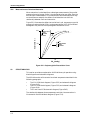
1
SERVICE MANUAL
NPB-40
Handheld Pulse Oximeter
Caution: Federal law (U.S.) restricts this device to sale by or on the order of a physician.
To contact Nellcor Puritan Bennett’s representative: In the United States, call 1-800-635-5267 or
925-463-4000; outside of the United States, call your local Nellcor Puritan Bennett representative.
© 2001 Nellcor Puritan Bennett, Inc. All rights reserved.
012 3
036048D-0601
Nellcor Puritan Bennett Inc.
4280 Hacienda Drive
Pleasanton, CA 94588 USA
Telephone Toll Free 1.800.NELLCOR
Tyco Healthcare UK LTD
Fareham Road
Gosport
PO13 0AS
U.K.
Tel: +44.1329.224000
To obtain information about a warranty, if any, for this product, contact Nellcor
Puritan Bennett Technical Services Department, or your local Nellcor Puritan
Bennett representative.
Notice: Purchase of this instrument confers no express or implied license under any
Nellcor Puritan Bennett patent to use the instrument with any sensor that is not
manufactured or licensed by Nellcor Puritan Bennett.
Oxisensor II is a trademark of Nellcor Puritan Bennett, Inc.
Covered by one or more of the following U.S. Patents and foreign equivalents:
4,621,643; 4,653,498; 4,700,708; 4,770,179; 4,869,254; 4,928,692; 4,934,372; 5,078,136;
5,351,685; 5,368,026; and Re. 35,122.
TABLE OF CONTENTS
List of Figures
List of Tables
Section 1: Introduction.................................................................................
1.1 Manual Overview............................................................................
1.2 Equipment Description ...................................................................
Section 2: Routine Maintenance ................................................................
2.1 Maintenance Overview ...................................................................
2.2 Battery Maintenance ......................................................................
2.2.1 Battery Replacement .........................................................
2.2.2 Battery Disposal ................................................................
2.3 Cleaning ............................................................................................
Section 3: Performance Verification ..........................................................
3.1 Performance Verification ...................................................................
Section 4: Troubleshooting .........................................................................
4.1 Introduction.....................................................................................
4.2 Who Should Perform Repairs.........................................................
4.3 Repair Level Supported..................................................................
4.4 How to Use This Section ................................................................
4.5 Obtaining Replacement Parts ........................................................
4.6 Troubleshooting Guide ...................................................................
Section 5: Disassembly Guide ....................................................................
5.1 Introduction.....................................................................................
5.2 System Disassembly and Reassembly ..........................................
Section 6: Spare Parts..................................................................................
6.1 Introduction.....................................................................................
Section 7: Packing for Shipment.................................................................
7.1 General Instructions........................................................................
7.2 Packing NPB-40 in Original Carton ................................................
7.3 Packing in a Different Carton .........................................................
Section 8: Specifications .............................................................................
8.1 Performance ...................................................................................
8.2 Electrical .........................................................................................
8.3 Environmental.................................................................................
8.4 Physical .........................................................................................
Technical Supplement..................................................................................
S1 Introduction.....................................................................................
S2 Pulse Oximetry Principles of Operation ..........................................
S2.1
Overview ...........................................................................
S2.2
Functional Versus Fractional Saturation............................
S2.3
Measured versus Calculated Saturation............................
S3 Circuit Analysis ...............................................................................
S3.1
Overall Unit Block Diagram Analysis .................................
S3.2
CPU PCB Theory of Operation..........................................
S3.3
LCD PCB Theory of Operation ..........................................
S4 Schematic Diagrams ......................................................................
1-1
1-1
1-1
2-1
2-1
2-1
2-1
2-2
2-2
3-1
3-1
4-1
4-1
4-1
4-1
4-1
4-1
4-2
5-1
5-1
5-1
6-1
6-1
7-1
7-1
7-1
7-1
8-1
8-1
8-2
8-2
8-3
S-1
S-1
S-1
S-1
S-1
S-2
S-2
S-3
S-5
S-11
S-17
iii
Table of Contents
LIST OF FIGURES
1-1
1-2
2-1
3-1
3-2
3-3
3-4
4-1
5-1
5-2
5-3
5-4
6-1
7-1
S2-1
S3-1
S3-2
S3-3
S4-1
S4-2
S4-3
S4-4
S4-5
NPB-40 Handheld Pulse Oximeter ................................................
NPB-40 Front Panel.......................................................................
NPB-40 Battery Installation ...........................................................
NPB-40 Self-Test Front Panel Display ..........................................
Printer Interface Setup...................................................................
Typical Average Data Print Out .....................................................
Typical Data Print Out ...................................................................
Typical Error Code Display ............................................................
Opening the NPB-40 Case ............................................................
Top Case Removal ........................................................................
Unlocking CPU PCB Connector J3 ...............................................
Separating LCD PCB from CPU PCB............................................
NPB-40 Expanded View ................................................................
Repacking the NPB-40 ..................................................................
Oxyhemoglobin Dissociation Curve ..............................................
NPB-40 Block Diagram .................................................................
CPU PCB Block Diagram ..............................................................
LCD PCB Block Diagram...............................................................
CPU PCB Parts Locator Diagram..................................................
LCD PCB Parts Locator Diagram ..................................................
CPU PCB Schematic Diagram ......................................................
LCD PCB Schematic Diagram.......................................................
Front Panel Keypad Schematic Diagram ......................................
1-1
1-2
2-2
3-1
3-3
3-4
3-5
4-2
5-2
5-2
5-3
5-3
6-2
7-2
S-2
S-4
S-6
S-12
FO-1
FO-2
FO-3
FO-4
FO-5
4-1
4-2
Troubleshooting Guide ..................................................................
NPB-40 Error Codes .....................................................................
4-2
4-5
LIST OF TABLES
iv
SECTION 1: INTRODUCTION
1.1
1.2
1.1
Manual Overview
Equipment Description
MANUAL OVERVIEW
This manual contains information for servicing the NPB-40 handheld pulse
oximeter. Only qualified service personnel should service this product. Before
servicing the NPB-40, read the operator’s manual carefully for a thorough
understanding of how to operate the NPB-40.
1.2
EQUIPMENT DESCRIPTION
The Nellcor Puritan Bennett NPB-40 handheld pulse oximeter is used for
noninvasive spot-check measurement of functional oxygen saturation of
arterial hemoglobin (SpO2 ) and pulse rate (measured by the SpO2 sensor).
The NPB-40 is for attended monitoring only, and must be used in the
continuous presence of a qualified healthcare provider. The NPB-40 can be
used on adult, pediatric, and neonatal patients. It can be used in mobile
environments when protected from excessive moisture such as direct rainfall.
The NPB-40 is powered by four “AA” cell alkaline batteries. An external
Hewlett-Packard HP82240B printer can be used with the NPB-40 to printout
readings stored in the NPB-40 memory. This printer is available from Nellcor
Puritan Bennett. The NPB-40 handheld pulse oximeter is illustrated in
Figure 1-1.
Figure 1-1: NPB-40 Handheld Pulse Oximeter
The NPB-40 is operated using a four-key keypad and an LCD display on the
front panel as shown in Figure 1-2. Refer to the NPB-40 operator’s manual
for complete operating instructions.
1-1
Section 1: Introduction
1
13
2
12
11
10
3
4
9
6
8
7
5
1
2
3
4
5
6
7
8
9
10
11
12
13
Pulse Amplitude indicator
Pulse Rate display
Pulse Search display
Low Battery indicator
Sensor disconnect indicator
Power On/Off key
Display Light/Beep On/Off key
Store Data/Print key
Shift key
Store Data icon
Shift icon
Print icon
SpO2% display
Figure 1-2: NPB-40 Front Panel
1-2
SECTION 2: ROUTINE MAINTENANCE
2.1
2.2
2.3
2.1
Maintenance Overview
Battery Maintenance
Cleaning
MAINTENANCE OVERVIEW
The NPB-40 requires no routine service or calibration. The performance
verification tests in Section 3, Performance Verification, may be used
following repairs or during routine maintenance (if required by your local
institution).
2.2
BATTERY MAINTENANCE
Warning: The NPB-40 uses four “AA” cell alkaline batteries for
operation. If batteries are not replaced when recommended or are
not disposed of properly, serious personal injury or damage to the
NPB-40 could result.
Caution: When inserting the positive end of each battery, exercise
caution to not damage the small coiled spring contact.
Nellcor Puritan Bennett recommends that you comply with the following
guidelines for battery replacement and battery disposal as a minimum.
2.2.1
Battery Replacement
Caution: The NPB-40 could be damaged by batteries that are left
unused in the unit and begin to leak. Never store the NPB-40 with
the batteries installed for a prolonged period of time.
NPB-40 batteries should be replaced whenever a low battery indication is
observed on the unit. Remove the batteries if you will be storing the NPB-40
for longer than one month. Refer Figure 2-1 for replacing the batteries.
Note:
For easier battery installation, insert the negative end of the battery
first when installing each battery.
2-1
Section 2: Routine Maintenance
Figure 2-1: NPB-40 Battery Installation
2.2.2
Battery Disposal
When NPB-40 batteries have been replaced, dispose of the old batteries.
Always follow local ordinances when disposing of the NPB-40 batteries.
Warning: Never dispose of NPB-40 batteries by burning. The
batteries could explode in fire and cause serious personal injury.
2.3
CLEANING
Caution: Do not immerse the NPB-40 or accessories in liquid or use
caustic or abrasive cleaners.
To clean the NPB-40, dampen a soft cloth with a commercial nonabrasive
cleaner and wipe the unit with the cloth.
2-2
SECTION 3: PERFORMANCE VERIFICATION
3.1
3.1
Performance Verification
PERFORMANCE VERIFICATION
The performance of the NPB-40 can be verified using the following procedure.
Before performing this procedure, the NPB-40 must have fresh batteries
installed. If any of the required observations cannot be obtained, do not
return the NPB-40 to service before referring to Section 4, Troubleshooting.
You will need an SRC-2 pulse oximeter tester to perform this procedure. If
the performance of the printing function will be verified, you will need an
HP82240B printer.
The NPB-40 is to be turned off and any sensors disconnected before
performing this procedure.
1.
Press the On/Off key on the front panel keypad.
2.
The NPB-40 will perform a self-test. Verify that all display segments
are lit during the self-test as shown in Figure 3-1. Also verify that a low
pitched audio tone is heard at the end of the self test. Also verify that
you then hear a high, a low, and a high pitch error tone indicating that
a sensor is not connected. Verify that dashes are shown on the display
and the SENSOR DISCONNECT indicator is flashing.
Figure 3-1: NPB-40 Self-Test Front Panel Display
3.
Wait for 20 to 40 seconds. Verify that two triple beeps are heard. Verify
that the NPB-40 then shuts itself off.
4.
Connect an SRC-2 pulse oximeter tester to the NPB-40 sensor
connector.
Note:
If the SRC-2 is connected directly to the NPB-40 sensor
connector, its controls will be facing the opposite direction of
the NPB-40 controls. Connecting the SRC-2 through a sensor
extension cable, such as the Nellcor Puritan Bennett model EC4 or EC-8, will make it easier to perform this procedure.
3-1
Section 3: Performance Verification
Set the SRC-2 controls as follows:
RATE
LIGHT
MODULATION
LOCAL/REMOTE/RCAL
112
HIGH 1
HIGH
LOCAL
5.
Press the On/Off key on the NPB-40 front panel keypad.
6.
When the self-test is complete, verify that the PULSE SEARCH
indicator illuminates momentarily and verify that the NPB-40 is
displaying a pulse rate of 112 (±3 bpm), that the pulse amplitude
indicator is displaying properly, that the SpO 2% indicator is displaying
81 (±2 %), that a pulse beep can be heard, and that the PULSE
SEARCH indicator is off.
7.
Set the following SRC-2 controls as indicated:
RATE
LIGHT
MODULATION
38
HIGH 2
LOW
Wait 30 seconds and verify that the NPB-40 is displaying a pulse rate of
38 (±3 bpm), that the pulse amplitude indicator is displaying properly,
that the SpO 2% indicator is displaying 81 (±2 %), that a pulse beep can
be heard, and that the PULSE SEARCH indicator is off.
8.
Set the following SRC-2 controls as indicated:
RATE
LIGHT
201
LOW
Wait 30 seconds and verify that the NPB-40 is displaying a pulse rate of
201 (±3 bpm), that the pulse amplitude indicator is displaying properly,
that the SpO 2% indicator is displaying 81 (±2 %), that a pulse beep can
be heard, and that the PULSE SEARCH indicator is off.
9.
Set the following SRC-2 control as indicated:
MODULATION
HIGH
Wait 30 seconds and verify that the NPB-40 is displaying a pulse rate of
201 (±3 bpm), that the pulse amplitude indicator is displaying properly,
that the SpO 2% indicator is displaying 81 (±2 %), that a pulse beep can
be heard, and that the PULSE SEARCH indicator is off.
3-2
10.
Press the Shift key followed by the Display Light/Beep On/Off key.
Verify that the SHIFT indicator illuminates when the Shift key is
pressed then verify that the pulse beep stops and the SHIFT indicator
extinguishes when the Display Light/Beep On/Off key is pressed.
11.
Press the Shift key followed by the Display Light/Beep On/Off key and
verify that the pulse beep can be heard again at a low level.
Section 3: Performance Verification
12.
Press the Shift key followed by the Display Light/Beep On/Off key and
verify that the pulse beep can again be heard again at a higher level.
13.
Press and release the Display Light/Beep On/Off key on the front panel
keypad and verify that the LCD backlight comes on, remains on and the
LCD is adequately illuminated.
14.
Press the Display Light/Beep On/Off key on the front panel keypad and
verify that the LCD backlight is off.
15.
Set the following SRC-2 control as indicated:
LOCAL/REMOTE/RCAL
REMOTE
16.
On the NPB-40, verify that the PULSE SEARCH indicator illuminates
after a few seconds and that the number “0” is displayed in the SpO 2%
and pulse rate displays.
17.
Set the following SRC-2 control as indicated:
LOCAL/REMOTE/RCAL
18.
LOCAL
On the NPB-40, verify that the PULSE SEARCH indicator illuminates
momentarily and verify that the NPB-40 is displaying a pulse rate of
201 (±3 bpm), that the pulse amplitude indicator is displaying properly,
that the SpO 2% indicator is displaying 79 to 83, that a pulse beep can
be heard, and that the PULSE SEARCH indicator is off.
Note:
If an HP82240B printer is not available, skip steps 19 through
27 and proceed to step 28.
19.
Refer to the printer operator’s manual as needed. Verify that paper is
properly installed in the printer and turn the printer on.
20.
Align the NPB-40 with the printer as shown in Figure 3-2.
0°– 5°
0°– 5°
1"– 2" (2.5 – 5.1 cm.)
Figure 3-2: Printer Interface Setup
3-3
Section 3: Performance Verification
21.
On the NPB-40, press the Shift key followed by the Store Data/Print
key on the front panel keypad.
Note:
22.
In the following steps, printed SpO2% values will be 79 to 83
and pulse rate values will be 201, ±3 bpm. Figures 3-3 and 3-4
are examples of typical print outs. The NPB-40 will not display
pulse or SpO2% values while printing.
Verify that the PRINT icon is illuminated on the NPB-40 display, that
the printer begins printing and that the printer prints out a summary
report similar to that shown in Figure 3-3.
Figure 3-3: Typical Average Data Print Out
3-4
23.
With the SRC-2 connected to the NPB-40 and still set up as in step 18,
press only the Store Data/Print key on the front panel keypad and
verify that the LCD display indicates “1-Id” and the STORE DATA icon
illuminates.
24.
Press only the Store Data/Print key on the front panel keypad and
verify that the LCD display indicates “2-Id” and the STORE DATA icon
illuminates.
25.
Press only the Store Data/Print key on the front panel keypad and
verify that the LCD display indicates “3-Id” and the STORE DATA icon
illuminates.
26.
Align the NPB-40 with the printer as shown in Figure 3-2 and press the
Shift key on the NPB-40 front panel keypad, followed by the Store
Data/Print key.
27.
Verify that the PRINT icon is illuminated on the NPB-40 display, that
the printer begins printing and that the printer prints out data similar
to that shown in Figure 3-4. As data stored in steps 24, 25, and 26 is
printed out, the NPB-40 display will indicate “1-Id”, “2-Id”, and “3-Id”,
respectively.
Section 3: Performance Verification
Figure 3-4: Typical Data Print Out
28.
Press the On/Off key on the front panel keypad.
29.
Verify that the NPB-40 shuts off.
3-5
(This page intentionally left blank)
SECTION 4: TROUBLESHOOTING
4.1
4.2
4.3
4.4
4.5
4.6
4.1
Introduction
Who Should Perform Repairs
Repair Level Supported
How to Use This Section
Obtaining Replacement Parts
Troubleshooting Guide
INTRODUCTION
This section provides information for troubleshooting the NPB-40 and helping
you to isolate a failure to the front panel keypad, the CPU PCB, or the LCD
PCB. A troubleshooting guide is provided in Paragraph 4.6, “Troubleshooting
Guide” that lists possible difficulties, along with probable causes, and
recommended actions to correct each difficulty. The Technical Supplement at
the end of this manual provides information on how the components of the
NPB-40 function.
4.2
WHO SHOULD PERFORM REPAIRS
Only qualified service personnel should remove and replace components of
the NPB-40. Repairs to the NPB-40 are limited to the repair level identified
in Paragraph 4.3, “Repair Level Supported.” If your facility does not have
qualified service personnel, contact the Nellcor Puritan Bennett Technical
Services Department or your local Nellcor Puritan Bennett representative.
4.3
REPAIR LEVEL SUPPORTED
Besides the batteries, the NPB-40 has five replaceable components, the case
top with the front panel keypad, the case bottom, the CPU PCB, the LCD
PCB, and the battery compartment door.
4.4
HOW TO USE THIS SECTION
Failures of the case bottom, the battery compartment door, and the case top,
not including the front panel keypad, are determined by visually inspecting
these components for cracks or deformations and for mechanical failures such
as the screw holes stripping out in the case top. The case top and the front
panel keypad are replaced together. Use the troubleshooting guide provided
in Paragraph 4.6, “Troubleshooting Guide” to isolate failure to the front panel
keypad, the CPU PCB, or the LCD PCB. Once a failure has been isolated,
refer to Section 5, Disassembly Guide for instructions for removing and
replacing a component of the NPB-40.
4.5
OBTAINING REPLACEMENT PARTS
Nellcor Puritan Bennett Technical Services Department provides technical
assistance information and replacement parts. To obtain replacement parts,
contact the Nellcor Puritan Bennett Technical Services Department or your
local Nellcor Puritan Bennett representative. Refer to parts by the part
names and part numbers listed in Section 6, Spare Parts.
4-1
Section 4: Troubleshooting
4.6
TROUBLESHOOTING GUIDE
If you encounter a problem that cannot be resolved through a visual
inspection, refer to Table 4-1 which provides a list of symptoms, probable
causes, and recommended actions to take to correct the problem. It is
recommended that corrective actions be performed in the order presented.
For a symptom that is not listed in Table 4-1, contact the Nellcor Puritan
Bennett Technical Services Department or your local Nellcor Puritan Bennett
representative.
If an error code is shown on the front panel LCD display, as shown in Figure
4-1, turn the NPB-40 off and back on again. If the error code still persists,
refer to Table 4-2 for the indicated failure and corrective action.
Figure 4-1: Typical Error Code Display
Once you have performed the recommended action, reassemble the NPB-40,
refer to Section 3, Performance Verification, and conduct a performance
verification before returning the NPB-40 to service. If the symptom persists,
continue troubleshooting.
Table 4-1: Troubleshooting Guide
Symptom
The unit does not
turn on when the
On/Off key is
pressed.
(Continued on next
page)
4-2
Probable Cause
The batteries are
missing.
Corrective Action
Open the battery compartment
and if batteries are missing,
install new batteries.
The batteries are
installed incorrectly
or are backwards.
Open the battery compartment
and if batteries are not installed
correctly, remove and reinstall
the batteries.
Install new batteries.
The batteries are at
or near a voltage too
low for the NPB-40 to
operate.
Section 4: Troubleshooting
Table 4-1: Troubleshooting Guide (Continued)
Symptom
The unit does not
turn on when the
On/Off key is
pressed.
(continued)
Probable Cause
The sensor is
defective.
Corrective Action
Replace the sensor.
The front panel
keypad is defective.
Open the NPB-40, disconnect
the case top from J3 on the CPU
PCB and connect an ohmmeter
between the flex circuit
conductor for J3, pin 5 and the
conductor for J3, pin 3. Observe
a short when the On/Off key is
pressed and an open when not
pressed. If incorrect, replace
case top. If all keys function
correctly, replace CPU PCB.
Caution: Unlock J3 before
attempting to remove flex
circuit conductor.
Inspect the flex circuit between
the front panel and the CPU
PCB and reconnect if loose.
Inspect the CPU PCB
components and circuit board
for cracking, burning, or
damage, and replace the CPU
PCB if any are found. If any
failed components are observed,
replace CPU PCB.
Replace the CPU PCB with a
known good PCB.
Open the NPB-40, disconnect
the case top from J3 on the CPU
PCB and connect an ohmmeter
lead to the flex circuit conductor
for J3, pin 3. Refer to the front
panel schematic diagram and
individually connect the other
ohmmeter lead to each
conductor for the other keys.
Observe a short when the key is
pressed and an open when not
pressed. If incorrect, replace
case top. If correct, replace the
CPU PCB.
Caution: Unlock J3 before
attempting to remove flex
circuit conductor.
Inspect the flex circuit between
the front panel and the CPU
PCB and reconnect if loose.
Inspect the CPU PCB
components and circuit board
for cracking, burning, or damage
and replace the CPU PCB if any
are found.
Flex circuit between
front panel and CPU
PCB is disconnected.
A CPU PCB
component has
failed.
One or more keys
on the front panel
keypad does not
work.
The front panel
keypad is defective.
Flex circuit between
front panel and CPU
PCB is disconnected.
A CPU PCB
component has
failed.
(Continued on next
page)
4-3
Section 4: Troubleshooting
Table 4-1: Troubleshooting Guide (Continued)
Symptom
One or more keys
on the front panel
keypad does not
work. (Continued)
One or more
display segments
does not work.
Probable Cause
CPU PCB has failed.
Corrective Action
Replace the CPU PCB with a
known good PCB.
An LCD PCB
component has
failed.
Inspect the LCD PCB
components and circuit board
for cracking, burning, or damage
and replace the LCD PCB if any
are found.
Inspect the flex circuit between
the LCD and the LCD PCB has
come loose and replace the LCD
PCB if loose.
Replace the LCD PCB with a
known good PCB.
Turn the beeper back on.
Flex circuit between
LCD and LCD PCB
has come loose.
Beeper does not
beep for pulse
indication or no
sound can be heard
from the beeper.
Pulse rate or SpO2
value is not
displayed and the
unit is on.
The beeper has been
turned off or its
volume is turned
down too low to hear.
The holes for the
beeper on the back of
the NPB-40 are
blocked.
The external output
port on the CPU PCB
has failed.
The beeper on the
LCD PCB has failed
The SpO2 sensor is
not connected
properly.
The SpO2 sensor has
failed.
A component on the
LCD PCB has failed.
A component on the
CPU PCB has failed.
LCD backlight does The Display Light
not come on when
key on the front
the Display Light
panel keypad is
key is pressed.
defective.
The backlight LEDs
on the LCD PCB
have failed.
The unit shuts off
The batteries are at
when the LCD
or near a voltage too
backlight is turned low for the NPB-40 to
on.
operate.
4-4
Clear the holes for the beeper on
the back of the NPB-40.
Replace the CPU PCB with a
known good PCB.
Replace the LCD PCB with a
known good PCB.
Connect the SpO2 sensor to the
NPB-40.
Replace the SpO2 sensor with a
known good SpO2 sensor.
Replace the LCD PCB with a
known good PCB.
Replace the CPU PCB with a
known good PCB.
See “One or more keys on the
front panel keypad does not
work,” above.
Replace the LCD PCB with a
known good PCB.
Install new batteries.
Section 4: Troubleshooting
Table 4-1: Troubleshooting Guide (Continued)
Symptom
Printer will not
print.
Probable Cause
The printer is turned
off.
The Store Data key
on the front panel
keypad is defective.
Corrective Action
Turn on the printer.
The printer batteries
are at or near a
voltage too low for it
to operate.
The NPB-40 and
printer are not
properly aligned.
A component on the
LCD PCB has failed.
A component on the
CPU PCB has failed.
The printer is
defective.
Install new batteries in the
printer.
See One or more keys on the
front panel keypad does not
work, above.
Refer to the operator’s manual
for instructions for aligning the
NPB-40 with the printer.
Replace the LCD PCB with a
known good PCB.
Replace the CPU PCB with a
known good PCB.
Attempt to print using another
known good NPB-40. If the
printer still does not print,
troubleshoot the printer
Table 4-2: NPB-40 Error Codes
Error Code
100EEE
150EEE
151EEE
152EEE
153EEE
154EEE
155EEE
Failure Indicated
Failure in the
microprocessor
analog-to-digital
converter on the CPU
PCB.
Failure of the
microprocessor on
the CPU PCB.
Failure of the RAM
on the CPU PCB.
Failure of the ROM
on the CPU PCB.
Failure in the
microprocessor I/O
ports on the CPU
PCB.
Failure of the
watchdog circuit on
the CPU PCB.
Failure of the
memory on the CPU
PCB when storing an
event or when
printing.
Corrective Action
1. Replace the sensor.
2. Replace the CPU PCB with a
known good PCB.
Replace the CPU PCB with a
known good PCB.
Replace the CPU PCB with a
known good PCB.
Replace the CPU PCB with a
known good PCB.
Replace the CPU PCB with a
known good PCB.
Replace the CPU PCB with a
known good PCB.
Replace the CPU PCB with a
known good PCB.
4-5
(This page intentionally left blank)
SECTION 5: DISASSEMBLY GUIDE
5.1
5.2
5.1
Introduction
System Disassembly and Reassembly
INTRODUCTION
The NPB-40 can be disassembled into five assemblies:
•
•
•
•
•
Note:
Case top/front panel keypad
Case bottom
CPU PCB
LCD PCB
Battery compartment door
Some spare parts you receive will have a business reply card
attached. When you receive these spare parts, please fill out and
return the business reply card.
The only tool you will need to disassemble or reassemble the NPB-40 is a
Number 1 (medium) Phillips-head screwdriver.
Caution: Observe ESD (electrostatic discharge) precautions when
disassembling and reassembling the NPB-40 and when handling any
of the components of the NPB-40.
5.2
SYSTEM DISASSEMBLY AND REASSEMBLY
Use the following procedure to disassemble the NPB-40. Reassemble the
monitor in reverse order and, if the unit is to be returned to service, install
batteries when reassembly is complete and replace the battery compartment
door. Nellcor Puritan Bennett recommends that you follow this disassembly
procedure in the order presented.
Note:
Before you begin to disassemble the NPB-40, remove the battery
compartment door and remove the batteries.
1.
Place the NPB-40 on a nonabrasive surface so that the back of the unit
is up and the bottom of the unit is closest to you.
2.
Remove the four screws holding the case together as indicated in Figure
5-1.
Note:
The two screws at the top of the NPB-40 are longer than those
at the bottom. When reassembling the unit, be sure to install
the longer screws at the top and the shorter screws at the
bottom.
Caution: When reassembling the NPB-40, hand tighten the screws
that hold the NPB-40 case together to a maximum of 4 inch-pounds.
Over tightening could cause the screws to strip out the screw-holes
in the top case, rendering it unusable.
5-1
Section 5: Disassembly Guide
Remove screws
Remove screws
Figure 5-1: Opening the NPB-40 Case
3.
While holding the case together, turn the NPB-40 over with the front
panel up and the bottom of the unit closest to you.
4.
Separate the case top from the bottom case on the right side of the unit
and rotate the case top to the left as shown in Figure 5-2.
J3
Figure 5-2: Top Case Removal
5-2
Section 5: Disassembly Guide
Caution: Failure to unlock connector J3 on the CPU PCB before
attempting to remove the front panel flex circuit could damage the
flex circuit.
5.
Unlock connector J3 on the CPU PCB as shown in Figure 5-3 and pull
the front panel keypad flex circuit out of J3.
Note:
When reassembling the NPB-40, be sure to lock J3 after you
insert the front panel keypad flex circuit. See Figure 5-3.
Unlock
J3 Lock
Lock
CPU PCB
Figure 5-3: Unlocking CPU PCB Connector J3
Note:
The battery connectors (spring assemblies) at the bottom of the
CPU PCB are held in slots in the battery compartment. In the
next step, observe how these connectors are engaged in these
slots when you remove the CPU PCB with the LCD PCB and
make sure the battery connectors are inserted back in these
slots when you reassemble the NPB-40.
6.
Lift the CPU PCB and the LCD PCB together and remove them from
the case bottom.
7.
To separate the CPU PCB and the LCD PCB, grasp the CPU PCB in
one hand and the LCD PCB in the other. Rotate the ends of the two
PCBs as shown in figure 5-4 until the two assemblies separate at the
connectors J1 and J2.
J1
LCD PCB
CPU PCB
J2
Figure 5-4: Separating LCD PCB from CPU PCB
Note:
When reassembling the NPB-40, be sure to align all 20 pins of
both J1 and J2 on the CPU PCB with all 20 sockets of J1 and
J2 on the LCD PCB before pressing the two PCBs together.
5-3
(This page intentionally left blank)
SECTION 6: SPARE PARTS
6.1
6.1
Introduction
INTRODUCTION
Spare parts, along with corresponding Nellcor Puritan Bennett part numbers,
are shown below. Figure 6-1 shows the replaceable NPB-40 monitor
components with numbered callouts that correspond to item numbers in
parentheses in the spare parts list below.
In December, 1997, the external plastic parts of the NPB-40 were modified.
Plastic parts made after that date are incompatible with parts made before
that time.
To determine which part number to order, look at the back of the instrument.
To the right of center, just above the battery compartment door, there will be
either 3 holes or three slots for the speaker. If your instrument has three
slots, use part numbers from the “After 12/97” column. If the instrument has
three holes, use part numbers from the “Before 12/97” column.
Item
(1)
(2)
(3)
(4)
(5)
Case Top/Keypad
CPU PCB
LCD PCB
Case Bottom
Battery Compartment Door
Part Numbers
(Before 12/97)
045691
034311
034835
035097
033880
Part Numbers
(After 12/97)
048863
034311
034835
035397
034975
6-1
Section 6: Spare Parts
1
2
3
4
5
Figure 6-1: NPB-40 Expanded View
6-2
SECTION 7: PACKING FOR SHIPMENT
7.1
7.2
7.3
7.1
General Instructions
Packing NPB-40 in Original Carton
Packing in a Different Carton
GENERAL INSTRUCTIONS
To ship an NPB-40 handheld pulse oximeter or one of its components for any
reason, follow the instructions in this section.
Pack the NPB-40 or component carefully. Failure to follow the instructions in
this section may result in loss or damage not covered by any applicable
Nellcor Puritan Bennett warranty. If available, use the original carton and
packing materials and follow the instructions in “Packing in Original
Carton.” If the original shipping carton and material are not available, use
other suitable shipping materials and container and follow the instructions in
“Packing in a Different Carton.”
Prior to shipping the NPB-40 or component, contact Nellcor Puritan Bennett
Technical Services Department or your local Nellcor Puritan Bennett
representative for a Returned Goods authorization (RGA) number. Mark the
shipping carton and any shipping forms with the RGA number.
Caution: Observe ESD (electrostatic discharge) precautions when
packing any NPB-40 components.
7.2
PACKING NPB-40 IN ORIGINAL CARTON
If the original carton and packing materials are available, repack the NPB-40
as shown in Figure 7-1. Add packing material in the bottom of the carton as
needed so the NPB-40 will not be able to move during shipment.
7.3
PACKING IN A DIFFERENT CARTON
If the original carton and packing material are not available when shipping
an NPB-40 or one of its components:
1.
Place the NPB-40 or component in a plastic bag.
2.
Locate a corrugated cardboard shipping carton with at least 200 pounds
per square inch (psi) bursting strength.
3.
Fill the bottom of the carton with at least 2 inches of packing material.
4.
Place the bagged NPB-40 or component on the layer of packing material
and fill the box completely with packing material such that there is at
least 2 inches of packing material around all sides of the item.
5.
Seal the carton with packing tape.
6.
Label carton with shipping address, return address, and RGA number.
7-1
Section 7: Packing for Shipment
Figure 7-1: Repacking the NPB-40
7-2
SECTION 8: SPECIFICATIONS
8.1
8.2
8.3
8.4
8.1
Performance
Electrical
Environmental
Physical
PERFORMANCE
Measurement Range
SpO 2
0–100%
Pulse Rate
20–250 beats per minute (bpm)
Accuracy
SpO 2
Adults
70–100%
0–69%
± 2 digits
unspecified
Neonates
70–100%
0–69%
± 2 digits
unspecified
Note:
Accuracies are expressed as plus or minus “X” digits (oxygen
saturation percentage points) between saturations of 70-100%. This
variation equals plus or minus one standard deviation (1SD), which
encompasses 68% of the population. All accuracy specifications are
based on testing the subject monitor on healthy adult volunteers in
induced hypoxia studies across the specified range. Adult accuracy is
determined with Oxisensor® II D-25 sensors. Neonatal accuracy is
determined with Oxisensor II N-25 sensors. In addition, the neonatal
accuracy specification is adjusted to take into account the theoretical
effect of fetal hemoglobin in neonatal blood on oximetry
measurements.
Pulse Rate
20–250 bpm
Note:
± 3 bpm
Accuracy is expressed as plus or minus 3 bpm across the display
range. This variation equals plus or minus one standard deviation
(1SD), which encompasses 68% of the population.
8-1
Section 8: Specifications
8.2
ELECTRICAL
Instrument
Power Requirements
6V, supplied by battery-power only
Patient Isolation
No electrical connection to patient (inherently insulated)
Battery
Type
Four 1.5V alkaline “AA” size batteries
Battery Capacity
Typically 19 hours with four new disposable alkaline batteries.
Note:
8.3
Not all brands of off-the-shelf alkaline batteries provide the same
battery life.
ENVIRONMENTAL
Operating Temperature
Instrument
0 to 55°C
Sensor
Within physiologic range for specified accuracy
Transport/Storage Temperature (boxed)
-40 to 70°C, 15-95% RH
Humidity
Operating
15-95% noncondensing
Storage (unboxed)
15-95% noncondensing over a temperature range of -20° C to 60° C
Altitude
Operating
-1280 ft. to 12,000 ft (-390 m to 3,658 m) [650 to 1060 hPa]
Storage
-2330 ft. to 15,000 ft. (-457 m to 4,573 m) [572 to 1100 hPa]
8-2
Section 8: Specifications
8.4
PHYSICAL
Weight (with batteries installed)
0.3 kg (11 oz.)
Size
15.75 cm high x 7.5 cm wide x 3.8 cm deep
(6.2 in. high x 2.95 in. wide x 1.5 in. deep)
Equipment Classification (IEC 601-1 / CSA 601.1 / UL 2601-1)
Type of Protection
Internally Powered
Degree of Protection
Type BF
Enclosure Degree Protection Class
IPX1
Mode of Operation
Continuous
8-3
(This page intentionally left blank)
TECHNICAL SUPPLEMENT
S1
S2
S3
S4
S1
Introduction
Pulse Oximetry Principles of Operation
Circuit Analysis
Schematic Diagrams
INTRODUCTION
This Technical Supplement provides a description of the principles of pulse
oximetry, a block diagram level theory of operation discussion, and a
schematic level theory of operation discussion. Part locator diagrams and
schematic diagrams are located at the end of this section as fold-out
drawings. These diagrams can be folded out for review while reading the
theory of operation.
S2
PULSE OXIMETRY PRINCIPLES OF OPERATION
S2.1
Overview
The NPB-40 is based on the principles of spectrophotometry and optical
plethysmography. Optical plethysmography uses light absorption technology
to reproduce waveforms produced by pulsatile blood. The changes that occur
in the absorption of light due to vascular bed changes are reproduced by the
pulse oximeter as plethysmographic wave forms.
Spectrophotometry uses various wavelengths of light to qualitatively measure
light absorption through given substances. Many times each second, the
NPB-40 passes red and infrared light into the sensor site and determines
absorption. The measurements that are taken during the arterial pulse,
reflect absorption by arterial blood, nonpulsatile blood, and tissue. The
measurements that are obtained between arterial pulses reflect absorption by
nonpulsatile blood and tissue.
By correcting "during pulse" absorption for "between pulse" absorption, the
NPB-40 determines red and infrared absorption by pulsatile arterial blood.
Because oxyhemoglobin and deoxyhemoglobin differ in red and infrared
absorption, this corrected measurement can be used to determine the percent
of oxyhemoglobin in arterial blood: SpO 2 is the ratio of corrected absorption
at each wavelength.
S2.2
Functional Versus Fractional Saturation
The NPB-40 measures functional saturation, that is, oxygenated hemoglobin
expressed as a percentage of the hemoglobin that is capable of transporting
oxygen. It does not detect significant levels of dyshemoglobins. In contrast,
some instruments such as the IL282 Co-oximeter measure fractional
saturation, that is, oxygenated hemoglobin expressed as a percentage of all
measured hemoglobin, including dyshemoglobins.
Consequently, before comparing NPB-40 measurements with those obtained
by an instrument that measures fractional saturation, measurements must
be converted as follows:
functional fractional
100
saturation = saturation x 100-(% carboxyhemoglobin +%methemoglobin)
S-1
Technical Supplement
S2.3
Measured versus Calculated Saturation
When saturation is calculated from a blood gas measurement of the partial
pressure of arterial oxygen (PaO2 ), the calculated value may differ from the
NPB-40 SpO2 measurement. This is because the calculated saturation may
not have been corrected for the effects of variables that can shift the
relationship between PaO 2 and saturation.
Figure S2-1 illustrates the effect that variations in pH, temperature, partial
pressure of carbon dioxide (PCO 2), and concentrations of 2,3-DPG and fetal
hemoglobin may have on the oxyhemoglobin dissociation curve.
Saturation (%)
100
pH
Temperature
PCO2
2,3-DPG
Fetal Hb
pH
Temperature
PCO2
2,3-DPG
50
0
50
100
PO2 (mmHg)
Figure S2-1: Oxyhemoglobin Dissociation Curve
S3
CIRCUIT ANALYSIS
This section provides an explanation of NPB-40 theory of operation using
block diagrams and schematic diagrams.
The NPB-40 consists of three main functional components described in the
following paragraphs:
•
•
•
The CPU PCB block diagram (Figure S3-2) and schematic diagram
(Figure S4-3).
The LCD PCB block diagram (Figure S3-3) and schematic diagram
(Figure S4-4).
The Front Panel PCB schematic diagram (Figure S4-5).
The relationship between these components and their interconnection is
illustrated in the NPB-40 block diagram (Figure S3-1).
S-2
Technical Supplement
The following is a list of terms and definitions used in the following
paragraphs.
Analog to Digital (A/D) converter. The CPU has a 10-bit A/D converter on
board. Up to eight different analog inputs can be provided to the A/D for
measurement.
Central Processing Unit (CPU). An Intel 80C196KC 16-bit
microprocessor. The CPU sends and receives control signals to the SpO2
analog section, display, and printer infrared LED.
High Speed Outputs (HSO). The 6 HSO lines control most of the timing of
the LED signal pulse and the demodulation of the received signal.
Input and Output (I/O). Digital lines that are used by the CPU to read in
data and output data.
Light Emitting Diodes (LEDs). Two LEDs are used in Nellcor Puritan
Bennett oximetry sensors. Light is transmitted through body tissue and
received by a photodetector circuit that converts it to photocurrent. The two
wavelengths, which are used for calculation of pulse rate and oxygen
saturation in blood, are transmitted at the following frequencies:
•
•
infrared (IR) light at ≈ 915 microns
red light at ≈ 660 microns
Pulse Width Modulation (PWM). The three 8-bit PWM outputs can be
software controlled; their duty cycle can be changed from 0 TO 99.6 percent of
the total pulse duration. PWM frequency is the crystal frequency of the CPU
(10 MHz) divided by 1024. The PWMs control the gains within the analog
circuit.
RCal. Sensor RCal value is a resistance value specific to an individual
sensor. This value is used by the software during oxygen saturation
computations to maximize accuracy.
S3.1
Overall Unit Block Diagram Analysis
Exclusive of batteries covers, keys, and external connectors, the NPB-40
consists of three main functional components: the front panel keyboard, the
CPU PCB, and the LCD PCB as follows.
•
CPU PCB — contains the CPU; power supply circuitry; support
memory circuits; sensor circuits for battery voltage; a serial data port;
LCD backlight control; pulsatile beeper drive circuits; and some display
control circuits.
•
LCD PCB — contains the SpO2 analog circuitry and interface to the
external sensor; the power conditioning circuitry; the LCD display and
display driver circuits; the interface circuitry for the printer (which is
not used unless a printer is present); the LCD backlight; and audio
output hardware.
•
Front Panel Keyboard — contains four membrane switches and a
line common to all four switches. This assembly connects to the CPU
PCB by a flex circuit.
Refer to Figure S3-1 for this NPB-40 block diagram. The CPU PCB and the
LCD PCB are each described in more detail in later paragraphs.
S-3
Technical Supplement
The NPB-40 is powered by four AA-size replaceable alkaline batteries. A dc
voltage in the range of 3.6 to 6 Vdc is provided over the life of these batteries.
When the voltage from these batteries drops to a level too low to operate the
NPB-40, the unit will shut itself off. At that time, the batteries must be
replaced.
The front panel keypad contains four keys that provide discrete signals that
are monitored by the microprocessor on the CPU PCB. Refer to Figure S4-5
for a schematic diagram of the front panel keypad.
CPU PCB
3.6-6 Vdc
Batteries
On/off key
Power
control
and PCB
power
Battery
voltage
sense
Power
down
Front
panel
keypad
LCD PCB
Raw power
Sensor
analog
signal
and
control
Power
condition
and PCB
power
Analog
sensor
circuits
Function
keys
CPU
Printer
signal
External
serial
interface
Printer
IR LED
drive
LCD
enable
LCD
data
LCD
External
output
control
External
output
port
Beeper
signal
Backlight
control
Beeper
LCD
backlight
Figure S3-1: NPB-40 Block Diagram
S-4
Patient
sensor
input
Technical Supplement
Power from the batteries is controlled and filtered by the power control and
PCB power circuits on the CPU PCB. When the On/Off key is pressed on the
front panel keypad and the unit is turned off, the power control circuits will
turn on the unit. If the unit is on when the On/Off key is pressed, the unit
will be turned off. The PCB power circuits provide filtered power for the
circuits on the CPU PCB and raw power is passed to the LCD PCB where it is
conditioned for the circuits there.
A patient sensor connected to the NPB-40 contains a resistance that is a
calibration reference for the sensor. The analog sensor circuits on the LCD
PCB then measure the signal from a photodiode in the sensor that is different
based on the light absorption characteristics of each patient. That signal is
processed by the analog sensor circuits and measured by the CPU. The LED
drive signals are then adjusted by the CPU to obtain an optimum signal from
the photodiode.
The CPU provides a drive signal for an IR LED on the LCD PCB. When this
IR LED is aligned with a receiving photodiode on an external printer, patient
data stored in the NPB-40 can be printed.
An external output port on the CPU PCB is controlled by the CPU and sends
drive signals to the beeper and LCD backlight and display data to the LCD.
An external serial data interface, used during testing in manufacturing only,
is also controlled by the CPU. This interface is only accessible with a special
test fixture.
S3.2
CPU PCB Theory of Operation
Refer to Figure S3-2 for the CPU PCB block diagram and to Figure S4-3 for
the CPU PCB schematic diagram in the following description. The CPU PCB
hardware and related circuitry, which is illustrated in the following block
diagram, includes the following subsystems:
•
CPU — A 16-bit microprocessor that includes: a serial port, watchdog
timer, A/D converter with an 8-input analog multiplexer, 3-pulse width
modulators, and a high speed I/O subsystem.
•
System memory — External to the CPU and consists of an 8K x 8
static RAM and a 64K x 16 EPROM.
•
Display control — The CPU provides drive and control signals for the
LCD driver and display on the LCD PCB.
•
Audio output drive— Drives a piezoelectric ceramic beeper on the
LCD PCB for audio output.
•
Printer drive— The CPU provides a printer drive signal that is
applied to an IR LED on the LCD PCB.
•
Power supply/Power control circuitry — The NPB-40 receives
power from 4 "AA" cell batteries. The power control circuitry
discontinues power to the unit when the batteries are no longer
reliable.
S-5
Technical Supplement
From
batteries
To LCD PCB
Battery power
3.6-6 Vdc
Raw
+10 Vdc
Battery power
feedback
From front
panel keypad
Power
switch
circuit
On/off
key
Power
shut off
control
Power
supply
circuit
Raw
-5 Vdc
Power on
VCC (+5 Vdc)
To CPU PCB circuits
Battery
voltage
sense
RD/WR
Shift
key
ADDR
0-12
RAM
AD 0-7
Display light/
beep on/off
key
RAM
enable
Store data/
print
key
WR
ADDR
9-15
EPROM enable
Address
decoding
ADDR
1-15
AD 0-15
Address
latch
WD
RST
VCC
monitor
and
watchdog
reset
circuit
Microprocessor
ALE
RD
AD 0-15
AD 0-7
External
output
enable
To/from LCD PCB
Beeper drive
External
output
port
LCD light enable
LCD CLK,
DATA, CE
LCD enable
Printer LED signal
10MHz
clock
circuit
EPROM
Analog sensor voltage reference
Beeper
LCD
backlight
LCD
driver
Printer
interface
V ref
Analog sensor signal
Analog circuit control signal
Figure S3-2: CPU PCB Block Diagram
S-6
Sensor
circuits
Technical Supplement
S3.2.1 CPU
The Intel 80C196KC CPU is a 16-bit microprocessor with built-in peripherals
including: a serial port, watchdog timer, A/D converter with an 8-input
analog multiplexer, three pulse width modulators, two 16-bit counter/timers,
up to 48 I/O lines, and a high speed I/O subsystem.
The CPU is capable of running up to 16 MHz, but it is run at 10 MHz for
decreased power consumption. All unused inputs are tied to either Vcc or
ground through resistors—this prevents unused inputs floating to any
voltage and causing excess power drain. The READY input pin is tied high,
thereby disabling wait-state generation; all bus accesses are zero wait-state.
The EA pin is tied low to enable addressing of the external EPROM.
When the power supply is first switched on by the power control circuit, the
watchdog reset circuit holds the CPU RESET pin low for at least 20 ms, then
allows the internal pull-up resistor to bring it high; this assures a good CPU
reset.
An internal watchdog timer is enabled and runs continuously. The watchdog
timer provides a means of recovering from a software upset caused by ESD,
EMI, etc.. If the software does not clear the timer at least every 64K
state-times (13.1 ms), the CPU will drive RESET low, resetting the entire
unit. The reset output by the CPU is only 16 state-times long (3.2 µs).
The CPU has the ability to dynamically switch the data bus width—based on
the BUSWIDTH input pin. A low on BUSWIDTH tells the CPU to access
memory only 8 bits at a time. When accessing the static RAM, BUSWIDTH is
low, automatically reading the 8-bit wide RAM. Since BUSWIDTH is
connected to the active low RAM enable line (RAMEN-L), all other memory
and mapped I/O are read or written 16 bits at a time.
Eight analog inputs are measured by the CPU. Input from the SpO2 analog
section on the LCD PCB includes AC and DC signals for the oximeter sensor
red and infrared channels, and the sensor calibration resistor RSENS. The
battery voltage and reference voltage from the LCD PCB are also measured.
The CPU is configured as follows:
•
Decoded AD0 and BHE generate separate WR write strobes for the low
and high bytes of a word. The signal WR (pin WRL) is the low-byte
write strobe.
•
A standard address latch enable (ALE) is generated and used.
•
HSO4 and HSO5 are configured as outputs. The HSO is used to
generate stable timing control signals to the SpO2 analog section,
display, and printer driver.
•
External control pins: P2.2, P2.3, and P2.4 are configured to monitor
front panel keyboard keys Store Data/Print, Display Light/Beep On/Off,
and Shift keys, respectively.
•
Pins HSI0 is configured for interrupt input. The CPU receives one
external interrupt (signal PHOTOI).
S-7
Technical Supplement
•
P2.0 and P2.1 are configured as a standard asynchronous serial
transmitter and receiver for a factory serial interface.
•
P2.5, P1.3, and P1.4 are configured as pulse width modulator outputs.
They are used with outputs from P1.6 and P2.6 to control gains within
the SpO 2 analog section.
S3.2.1.1 Address Demultiplexing
U10 and U11 are transparent latches that latch the address portion of the AD
bus data on the falling edge of ALE; the outputs are always enabled. The
outputs of U10 and U11 are always the address portion of the AD bus.
S3.2.1.2 Address Decoding
The CPU has a 64-Kbyte address range of 0-FFFF. RAM, EPROM, and I/O
ports share this space. The address decoding circuit splits up this space and
output enable lines to the RAM, EPROM, and external output ports.
When address lines A13, A14, A15 are all high, the output of U7C goes low,
enabling the RAM and generates the active low enable signal RAMEN-L.
This occurs for the 8K address range of E000-FFFF.
U8 is used to generate the output port active low enable signal EXOUTEN-L.
When address lines A15, A14, A11, and A10 are high, and A13 is low, U8
becomes enabled. With U8 enabled, the Y3 output is set low. The output to go
low is selected by pins A, B, and C. They form a 3-bit binary number with pin
C being the most significant bit. So when address line A12 is high, WR active
(low) and RD inactive (high), a binary 3 is produced on pins A, B, and C,
forcing output Y3 (EXOUTEN-L) low. This enables the output port for
writing. Note that in this condition, A15, A14, A12, A11, and A10 are high
and A13 is low.
The output port uses the address space of DE00-DFFF. When data is written
to that address, the output port enable signal EXOUTEN-L is activated.
Because the CPU is configured to use a 16-bit bus, except for RAM, any even
address in the DE00-DFFF range could be used for external port access. In
other words, reading or writing address DF00, DE02, DE04, etc., will all
produce the same results.
U7A generates the EPROMs active low enable signal, ROMEN-L. The active
low signals RAMEN-L and EXOUTEN-L are basically used as EPROM
disable signals. When RAMEN-L or EXOUTEN-L or the Y3 output of U8 are
low, the output of U7A, ROMEN-L, is forced high, disabling the ROM.
Therefore, the EPROM is disabled for the range DE00-FFFF and enabled for
the address range of 0-DFFF.
S3.2.2 CPU Memory
The memory system external to the CPU consists of an 8 K x 8 static RAM
(U12) and a 64 K x 16 EPROM (U5). The EPROM is 16 bits wide to enhance
CPU performance. Because RAM is infrequently accessed, it is only 8 bits
wide. U12 is a standard 8K x 8 static RAM.
S-8
Technical Supplement
The program that the CPU runs is stored in U5. U5 is a 16-bit wide output,
one-time programmable (OTP) EPROM. During 16-bit wide bus accesses, the
CPU uses address line A0 for low/high byte selection, and is not used as a
normal address line. The CPU can only address 64K x 8 bytes or 32K x 16
bytes. Pin A15 of U5 is tied low, always selecting the lower half of the
EPROM. Signal ROMEN-L is then used to enable the EPROM for the proper
memory area.
The output port external to the CPU consists of an octal D latch, U9. The
output of U9 is always enabled. The output bits of U9 control the beeper
output, the LCD backlight, and the LCD display drive signals.
S3.2.3 Standard User Controls
The standard user controls consist of four momentary push-button switches
on the front panel keypad. These keys are metal dome membrane contact
switches.
The front panel switches Store Data/Print, Display Light/Beep On/Off, and
Shift are connected to the microprocessor, U4, input lines P2.2, P2.3, and
P2.4 and are normally pulled to the high state by R10, R8, and R18.
Whenever one of these keys is pressed, the U4 input line is pulled low. The
switch contacts are debounced in software.
The fourth front panel switch, On/Off, is connected to the power switch
described Power Supply/Power Control Circuitry.
S3.2.4 Power Supply/Power Control Circuitry
The power supply and power control circuitry consists of the following
primary elements.
•
Batteries — Four 1.5 V alkaline "AA" size batteries provide 3.6-6 Vdc
power.
•
Power entry circuit — Components protect the NPB-40 from damage
if batteries are inserted incorrectly and provide reverse current limiting
and over-voltage or spike protection. In addition, a self-resetting fuse
protects the power supply from excessive current draw. The power
supply is also protected against electrostatic discharge and
electromagnetic interference.
•
Power switch circuitry — This circuit controls power applied to the
power supply circuits. Power control circuitry is connected to the
batteries. It senses any press of the front panel keypad On/Off key and
switches the power supply circuit on or off. A control signal to this
circuit from the CPU will also shut off the NPB-40 when battery voltage
drops to an unusable level.
•
Power supply circuits —consist of a power generation circuit that
provides +10Vdc, +5Vdc, and -5Vdc.
S-9
Technical Supplement
S3.2.4.1 Power Entry Circuitry
Self-resetting fuse R22 protects the NPB-40 and will open when current in
excess of 0.75 Amps is drawn by the unit. R22 will close when the condition
causing excessive current has been eliminated. CR7 provides reverse current
protection and limits negative voltages (batteries reversed) to safe levels. In
either of these conditions, CR7 will conduct and cause fuse R22 to open. CR5
protects against large voltage transients caused by ESD, EMI, etc. and will
pass these undesirable transients to ground.
S3.2.4.2 Power Supply Feedback Circuitry
The power supply feedback circuit consists of Q1 and its associated
components. When batteries are installed and the NPB-40 is turned off, the
battery voltage (VBAT) is applied through resistor R2 at the collector of Q1
providing a logic 1 level voltage to the D input of flip-flop U1B in the power
switch circuit. When the NPB-40 is turned off, VCC is at 0 volts and Q1 is
turned off. When the NPB-40 is turned on (See “Power Switch Circuitry”), the
VCC potential is applied to the base of Q1, which turns it on. The voltage at
the D input of U1B then drops to a low voltage to provide a logic 0.
S3.2.4.3 Power Switch Circuitry
The power control circuit consists of U1B and its associated components. U1B
is a D flip/flop with asynchronous preset and clear; only the clear is used.
Battery voltage is applied to U1B whenever batteries are installed. The NPB40 is turned on and off by pressing the On/Off key on the front panel keypad.
The BTN PWR line is normally pulled up to the battery voltage by R3. When
battery voltage is at an acceptable level and the On/Off key on the front panel
keypad is pressed, the BTN PWR line is grounded and the resultant highgoing pulse from U2A toggles the CLK input of U1B and the high D input
logic level is transferred to the Q output. The logic state of the D input is
controlled by the power supply feedback circuitry (See “Power Supply
Feedback Circuitry”). When the NPB-40 is off the D input of U1B is high.
Pressing the front panel On/Off key sets the Q output and the PWR ON
signal high. This enables the power supply circuits, which then generate the
operating voltages for the NPB-40. The Q-not output of U1B is applied to U4
analog to digital converter input P0.6 through a battery voltage sensing
circuit consisting of U2B, R14, R17, and C14. When the battery voltage drops
below 3.6 Vdc, as measured by U4, the PWR DOWN line at U4 output HSO3
goes high and turns on Q2, which clears flip-flop U1B and the PWR ON
signal at the Q output goes low and turns off the power supply circuits.
When the NPB-40 is turned on, the D input of U1B is low (See “Power Supply
Feedback Circuitry”). When On/Off key on the front panel keypad is pressed,
the BTN PWR line is grounded and the resultant high going pulse from U2A
toggles the CLK input of U1B and the low D input logic level is transferred to
the Q output. This sets the Q output and the PWR ON signal low, which
turns off the power supply circuits.
S-10
Technical Supplement
S3.2.4.4 Power Supply Circuits
When the PWR ON signal at the S/S input of U3 is high, U3 generates a
square wave signal that drives the primary winding of transformer T1. The
three secondary windings of T1 are rectified and filtered to provide
RAW+10V, VCC (+5Vdc), and RAW-5V. The VCC signal is resistor divided by
R9 and R12 for a feedback voltage that U3 must see to continue operating.
VCC is used on the CPU and the LCD PCBs for operating circuit power.
RAW+10V and RAW-5V are supplied to the LCD PCB for backlight power
and for power conditioning for the SpO 2 analog circuits.
S3.2.5 Serial Interface
The serial interface is only used for factory test purposes, and is not at the
RS-232 level, neither is it electrically isolated and, therefore, cannot be used
outside of the factory. The serial data port J5 is a TTL level serial interface.
RXD and TXD are configured as a standard asynchronous serial transmitter
and receiver at 19.2 Kbaud with 1 stop bit, 8 data bits, and no parity. The
serial interface can operate in full duplex mode. If no external serial data
device is connected, R19 pulls the RXD input high which prevents the input
from floating when it is not being used.
S3.2.6 Printer Control
Microprocessor U4 provides a drive signal (IR OUT) at HSO5 that controls an
infrared LED on the LCD PCB which is used to interface with an external
printer.
S3.2.7 External VCC Monitor and Watchdog Timer
The external VCC monitor and watchdog timer circuit consists of U6 and
associated components. U6 provides two functions. If the VCC input voltage
drops below 4.0 Vdc, U6 will drive the RST-L line low, which resets
microprocessor, U4. U6 also periodically receives the WD RST pulse output
from U4. If U6 does not receive the WD RST signal at least every 500 ms, it
will drive the RST-L line low, which resets U4.
S3.3
LCD PCB Theory of Operation
Refer to Figure S3-3 for the LCD PCB block diagram and to Figure S4-4 for
the LCD PCB schematic diagram in the following description. This subsection
describes the SpO 2 analog hardware. The analog circuitry has high signal
sensitivity and reduced susceptibility to noise. Its design allows for a wide range
of input signal levels and a broad range of pulsatile modulation. The SpO 2 analog
circuitry consists of four subsections:
•
Sensor output/LED control —The CPU controls the gain of both
LEDs so that signals received at the input amplifier are within an
acceptable dynamic range. Signal channel gain may also need to be
increased. The CPU uses Pulse Width Modulation (PWM) lines to
control LED current level or to amplify the signal channel.
•
Input conditioning —Sensor output current is converted to voltage. A
demodulation circuit minimizes the effects of other light sources and
stray frequency inputs. Because the IR and RED signals are at different
current levels, the two LED signals are demultiplexed and separately
amplified, so they can be compared with each other. Two circuits handle
the demultiplexing by alternately selecting LED signals using switches.
S-11
Technical Supplement
Filters then remove noise and smooth the signals before sending them
to the amplifiers.
S-12
•
Signal gain —The separated LED signals are amplified so that their
current levels are within the A/D converter's acceptable range. The
signals are filtered to improve the signal-to-noise ratio, and clamped to
a reference voltage.
•
AC ranging —DC offset is eliminated from each LED signal. An
analog switch sets the mean signal value to the mean of the A/D
converter range, and the AC modulation is superimposed on that DC
level. Then, each AC signal is amplified and filtered to eliminate
residual effects of the PWM modulations. Finally, these two signals are
input to the CPU A/D converter.
Technical Supplement
The relationship between these subsections is shown in the LCD PCB block
diagram, Figure S3-3.
To/from CPU PCB
Raw +10 Vdc
Raw -5 Vdc
+10Vdc
Power
conditioning
-5 Vdc
Printer
IR LED
V ref
Printer
LED signal
LCD clock
LCD
driver
LCD data
LCD
LCD enable
LCD light enable
LCD
backlight
Beeper drive
Analog sensor
signal
Analog circuit
control signals
Red
channel
Beeper
IR
channel
Sensor
D-connector
LED
drive
To/from patient sensor
LED drive
RSENS
Photodiode
Figure S3-3: LCD PCB Block Diagram
S3.3.1 Sensor Output/LED Control
The SpO2 analog circuitry provides control of the red and IR LEDs such that
the received signals are within the dynamic range of the input amplifier.
Because excessive current to the LEDs will induce changes in their spectral
output, it is sometimes necessary to increase the received signal channel
gain. To that point, the CPU controls both the current to the LEDs and the
amplification in the signal channel.
S-13
Technical Supplement
At initialization of transmission, the LEDs' intensity level is based on
previous running conditions, and the transmission intensity is adjusted until
the received signals match the range of the A/D converter. If the LEDs reach
maximum output without the necessary signal strength, the PWMs will
increase the channel gain. The PWM lines will select either a change in the
LED current or signal gain, but will not do both simultaneously.
The LED drive circuit switches between red and IR transmission and disables
both for a time between transmissions in order to provide a no-transmission
reference. To prevent excessive heat build-up and prolong battery life, each
LED is on for only a small portion of the duty cycle. Also, the frequency of
switching is well above that of motion artifact and not a harmonic of known
AC transmissions. The LED switching frequency is 1.485 kHz. The IR
transmission alone, and the red transmission alone, will each be on for about
one-fifth of the duty cycle; this cycle is controlled by the HSOs of the CPU.
The IR and red LEDs are separately controlled with their drive currents
multiplexed over two shared wires. Current to the IR LED is in the range of
4.3-50.0 mA; and, current to the red LED is in the range of 4.3 to 50 mA.
Currents are limited to less than 100 mA for two reasons: (1) slight excess
current can potentially change the emission characteristics of the LEDs, and
(2) large excess current could create excessive heat at the sensor site.
The IR/red LED transmission signal (HSO1 of the CPU) is fed into the select
inputs of the triple single-pole-double-throw (SPDT) analog multiplexing
switch U7, causing either the IR or the red LED transmission to be enabled.
PWM1, which is filtered by the network of R45, R35, C41, and C42, is input
to the LED drive circuit switch U7 and controls the magnitude of the IR LED
current supply.
PWM2, which is filtered by the network of R29, R39, C35, and C23, is also
input to U7 and controls the red LED current magnitude.
Two NPN transistors (Q8 and Q10) act as current sources for the IR and red
LED outputs. Two PNP transistors (Q9 and Q11) act as switches between the
IR and red LED output lines. Transistor Q12 acts as an LED drive current
limiter; it clamps the output of the current regulator circuit to the required
level. If any resistor in the LED drive circuit fails, current to the LED will
still be limited to a safe level.
The RSENS line senses the RCal value and enables the CPU to make the
proper calculations based on the type of sensor being used.
S3.3.2 Input Conditioning
Input to the SpO 2 analog circuit is the current output of the sensor
photodiode. In order to condition the signal current, it is necessary to convert
the current to voltage.
A differential synchronous demodulation circuit is used to reduce the effects
of other light sources and stray frequency inputs to the system. Because the
IR and red signals are absorbed differently by body tissue, their received
signal intensities are at different levels. Therefore, the IR and red signals
must be demodulated and then amplified separately in order to compare
them to each other. Demultiplexing is accomplished by means of two circuits
that alternately select the IR and red signal. Selection of the circuits is
controlled by two switches that are coordinated with the IR and red
transmissions. A filter with a large time constant follows to smooth the signal
and remove noise before amplification.
S-14
Technical Supplement
Before the current from the photodetector is converted to voltage, any high
frequency noise is filtered by C9 and R21. The op-amp U5A is used in parallel
with the current-to-voltage converter U5B to cancel any DC voltage,
effectively AC coupling the output of U5B. The average value of the SpO2
analog reference voltage (VREF) of U5B, 5 V, is measured at test point 6.
U3B, a single-pole-single-throw (SPST) analog switch, is controlled by the
same line that controls the on/off pulsing of the LEDs. When either of the
LEDs are on (the line is low and the switch is closed) U4B is used as a
noninverting amplifier. When the LEDs are both off, U4B is used an
inverting amplifier. The signal at the output of amplifier U4B is then
demultiplexed.
The CPU HSO lines SAMPRED and SAMPIR, which are both active low,
control SPST analog switches in U3A and U3C respectively. Switch U3A is
closed to sample the red signal; switch U3C is closed to sample the IR signal.
The sampling rate for both switches is 10 kHz. Switching is coordinated with
the LED transmission so that the IR and red signals are each sampled twice
per cycle; that is, once when the LED is off (signal inverted), and once when
the LED is on (signal not inverted). The filtering circuit that follows has a
long time constant, thereby acting as an averaging circuit.
If the instantaneous average photocurrent (DC offset) is excessive and U5B
cannot bring it to VREF, the PHOTOI line to the CPU (HSI0) is activated.
This action is an indication of excess ambient light into the photosensor, or
the occurrence of excess noise in the input circuit. It also serves as a warning
to the instrument that the sensor signal may be contaminated and causes the
software to send an error message.
S3.3.3 Signal Gain
The separated IR and red signals are amplified so that their DC values are
within the range of the A/D converter. Because the received IR and red
signals are typically at different current levels, the signal gain circuits
provide independent amplification for each signal as needed. The gain in
these circuits is adjusted by means of the PWM lines.
After the IR and red signals are amplified, they are filtered to improve the
signal-to-noise ratio and clamped to a reference voltage to prevent the
combined AC and DC signal from exceeding an acceptable input voltage from
the A/D converter.
S3.3.3.1 Variable Gain Circuits
The two variable gain circuits are functionally equivalent. The gain of each
circuit is contingent upon the signal’s received level and is controlled to bring
each signal to approximately 3.5 V. Each circuit uses an amplifier and one
switch in the triple SPDT analog multiplexing unit U9.
The gain in each of the circuits is accomplished by means of a feedback loop,
which includes one of the SPDT switches in U9. The PWMs control whether
the feedback loop is connected to ground or to the amplifier output. The
feedback is then averaged by C17/R27 (red), and C20/R26 (IR). The higher the
value of PWM2, the greater the IR gain; the higher the value of PWM1, the
greater the red gain.
S-15
Technical Supplement
S3.3.3.2 Filtering Circuits
These circuits consist of two cascaded second-order filters with a break
frequency of 10 Hz. Diodes (CR1/CR2 for the red channel, CR4/CR3 for the IR
channel) connected to VREF and ground at the positive inputs of the second
amplifiers, maintain the voltage output within the range of the A/D
converter.
S3.3.4 AC Ranging
In order to achieve a specified level of oxygen saturation measurement and to
still use a standard-type combined CPU and A/D converter, the DC offset is
subtracted from each signal. Because the DC portion of the signal can be on
the order of one thousand times the AC modulation, 16 bits of A/D conversion
would otherwise be required to accurately compare the IR and red
modulations between the combined AC and DC signals. The DC offsets are
subtracted by using an analog switch to set the mean signal value to the
mean of the range of the A/D converter whenever necessary. The AC
modulation is then superimposed upon that DC level. This is also known as
AC ranging.
Each AC signal is subsequently amplified such that its peak-to-peak values
span one-fifth of the range of the A/D converter. The amplified AC signals are
then filtered to remove the residual effects of the PWM modulations and,
finally, are input to the CPU. The combined AC and DC signals for both IR
and red signals are separately input to the A/D converter.
S3.3.4.1 Offset Subtraction Circuits
Voltage dividers R53 and R49 (red), and R61 and R63 (IR), which are located
between VREF and ground, establish a baseline voltage of 2.75 V at the input
of the unity gain amplifiers U12C (red) and U12D (IR).
Whenever SPST analog switches U11A and U11D are closed by HSO0 (active
low), the DC portions of the IR and red signals create a charge, which is
stored on C54 and C46, respectively. These capacitors hold this charge even
after the switches are opened and the resulting voltage is subtracted from the
combined signal — leaving only the AC modulation output. This AC signal is
superimposed on the baseline voltage output by U12C and U12D. The IRDC
and REDDC are then filtered and input to the microprocessor on the CPU
PCB.
S3.3.4.2 AC Variable Gain Control Circuits
The AC modulations are amplified by U12A (red) and U12B (IR) and
superimposed on the baseline voltages present at the output of U12D (IR) and
U12C (red). The amplification is handled by means of the SPDT analog
multiplexing switch U13 within the feedback loop, which increases gain as
PWM0 is increased. The IRAC and REDAC are then filtered and input to the
microprocessor on the CPU PCB.
S3.3.5 Audio Output
LS1, a piezo ceramic sounder, is the audio output device. Due to its low drive
current of 2 mA maximum, no drive circuitry is needed and is driven directly
from the external output port. It is differentially driven with 2 square waves
180 degrees out of phase. The drive frequency is approximately 1480 Hz or
740 Hz and is generated by the CPU. LS1 is differentially driven to obtain
maximum audible volume.
S-16
Technical Supplement
S3.3.6 Display Control Circuitry
The LCD CE, LCD CLK, and LCD DATA from external output port U9 and
LCD EN from the microprocessor on the CPU PCB are connected to the LCD
drive IC, U1. U1, in turn, drives the individual segments of the LCD. The
microprocessor drives LCD CE and LCD EN high, connected to the U1 CE
and INH inputs, respectively. At that time, data on the LCD DATA line is
clocked into U1 by the LCD CLK line. U1 then decodes the data input and
turns the proper segments on or off on the LCD. The INH inhibit input of U1
is held low by resistor R9 until the line is driven high by the LCD EN signal
from microprocessor on the CPU PCB. This assures that the display is
blanked until it is under microprocessor control. Should the microprocessor
be reset, the LCD EN line goes to a floating state, R9 then pulls the INH
input to U1 low, and the display is blanked.
S3.3.7 Power Conditioning Circuitry
Unfiltered positive (RAW+10V) and negative (RAW-5V) voltages from the
CPU PCB are applied to the power conditioning circuit. RAW+10V is filtered
by a circuit consisting of R6, C1, and C2 to provide a clean and stable +10 V
dc operating voltage for LCD PCB SpO 2 analog and other circuits. Likewise,
RAW-5V is filtered by a circuit consisting of R11, C8, and C10 to provide a
clean and stable -5 V dc operating voltage for the LCD PCB circuits. A
filtered +5Vdc (VCC) from the CPU PCB is also used as VCC by circuits on
the LCD PCB.
S3.3.8 Analog Reference Voltage
RAW +10V from the CPU PCB is applied to a filter consisting of R7 and C6 to
create VIN that is used by voltage converter U2 to create VREF. U2 provides
an accurate, regulated voltage that is used as the reference voltage for the
A/D inside the microprocessor U4 on the CPU PCB. Filtering is provided by
C7, C9, and R12. The voltage output VREF is + 5 Vdc.
S3.3.9 LCD Backlighting
RAW+10V from the CPU PCB is used as power for the LCD backlight. The
LCD backlight consists of LEDs DS1 through DS6. Resistors R3 and R4
provide current limiting for the LEDs. Transistor Q2 is turned on when the
LCD LIGHT signal from external output port U9 on the CPU PCB goes high
which, in turn, illuminates the backlight LEDs.
S3.3.10 Printer Drive Circuit
The printer drive circuit consists of R1, R2, Q1, and DS7. The IR OUT signal
from microprocessor U4 on the CPU PCB controls transistor Q1 which, in
turn, controls infrared LED DS7. DS7 is used to provide a data signal that is
transmitted to an external printer with an infrared receiver.
S-17
Technical Supplement
S4
SCHEMATIC DIAGRAMS
The following part locator diagrams and schematic diagrams are included in
this section:
Figure
S-18
Description
Figure S4-1
CPU PCB Parts Locator Diagram
Figure S4-2
LCD PCB Parts Locator Diagram
Figure S4-3
CPU PCB Schematic Diagram
Figure S4-4
LCD PCB Schematic Diagram
Figure S4-5
Front Panel Keypad Schematic
Diagram
TOP SIDE
BOTTOM SIDE
Figure S4-1
CPU PCB Part LocatorDiagram
034311
FOS S5-1
TOP SIDE
BOTTOM SIDE
Figure S4-2
LCD PCB Parts Locator Diagram
034315
FOS S5-3
POWER ENTRY
BT2
ADDRESS DECODING
POWER SUPPLY CIRCUIT
1
R22
0.75A
SELF RESETTING FUSE
2
3
TP53
VBAT
VBAT
U8
1
2
3
1
1
BAT+
BT1
TP2
CR5
SMCJ10C
3
PWR_ON 4
1N914S
3
1
2
BAT-
C2
330P
U3
1
2
2
CR7
MBRS330T3
1
+
6
CR6
C11
0.1U
7
5
VC
VIN
S/S
VSW 8
GNDS
GND
FB
NFB
+
2
T1
LPE-4841
C1
0.1U
C23
47U
10V
7343
2
6
7
3
2
R4
49.9
5
NEAR T1 PIN 2
2
LT1373CS8
C28
1000P
5%
C16
10U
16V
6032
R13
4.99K
4
C8
22U
20V
7343
TP41
U7C
9
10
11
E000 - FFFF
RAMEN-L
8
74HC10S
TP40
U7B
+
1
2
1
DE00 - DFFF
EXOUTEN-L
74HC138 - SMT
C7
47U
10V
7343
CR4
VBAT
TP51
15
14
13
12
11
10
9
7
Y0
Y1
Y2
Y3
Y4
Y5
Y6
Y7
G1
G2A
G2B
ADDR9
ADDR10
ADDR11
ADDR12
ADDR13
ADDR15
ADDR14
VCC
8
Power Supply Feedback
A
B
C
6
4
5
1
MBRS130 +
HIGH
CURRENT
SEPARATE VIAS
TO GROUND PLANE
FOR PINS 6 & 7
+
CR2
PLACE C23 AND C1
3
1
MBRS130
VSW
VFB
WR-L
RAW+10V
CR3
C4
47U
10V
7343
U7A
3
4
5
RAW-5V
6
1
2
13
0000 - DFFF
74HC10S
VCC
VCC
ROMEN-L
12
74HC10S
VCC
ROM_DIS-L
R9
11.5K
VCC
MBRS130
R12
36.5K
TP39
C35
1000P
5%
R2
150K
C24
0.1U
TP1
R5
150K
R20
10.0K
C20
0.1U
TP4
PWR_FB
VCC
CR1
1
1
3
1N914S
VCC
3
Q1
2N3904S
2
C5
0.1U
VBAT
VBAT
VBAT
10
1
C18
0.1U
+
C12
47U
10V
7343
U2A
14 74HC14S
2
12
7
13
C6
0.1U
VBAT
14
VCC
9 PWR_ON
Q
PRE
CLK
8
Q
7
GND
CLR
3
U2B
14 74HC14S
4
SW_VBAT
37
13
12
7
74HC74S
R14
15.8K
TP7
BAT_VOLT
REDDC
REDAC
IRDC
IRAC
RSENS
BAT_VOLT
6
5
7
4
11
10
8
9
LEDDIS
IR/RED
RWD_RST
PWM1
PWM2
19
20
21
22
23
30
31
32
TP5
C14
0.1U
R24
221
VCC
POWER SWITCH CIRCUIT
WD_RST
U6
VCC
VBAT
TP52
BTN_PWR
MAN_RST
1
2
3
R1
150K
R18
10.0K
R10
10.0K
4
R8
10.0K
VCC 8
PBRST
TD
TOL
ST
~RST
GND
RST
R6
10.0K
TP38
IRLED/AV
7
6
5
43
16
3
2
64
24
25
RST-L
N/C
RAMEN-L
PHOTOI
LTC1232
TP3
1
2
3
4
5
BTN_SHIFT
BTN_2
R11
150K
3
C3
0.1U
BTN_1
1
Q2
2N3904S
TXD
RXD
BTN_2
BTN_1
BTN_SHIFT
PWM0
REDLED/AV
ZERO-L
PWR_DOWN
2
18
17
15
44
42
39
33
38
60
AD0
AD1 59
58
AD2
57
AD3
56
AD4
55
AD5
AD6 54
53
AD7
52
AD8
51
AD9
50
AD10
AD11 49
48
AD12
47
AD13
46
AD14
45
AD15
ALE/ ADV 62
PWR
VPP
VREF
ANGND
ACH0/P0.0
ACH1/P0.1
ACH2/P0.2
ACH3/P0.3
ACH4/P0.4
ACH5/P0.5
ACH6/P0.6
ACH7/P0.7
P1.0
P1.1
P1.2
P1.3/PWM1
P1.4/PWM2
BREQ
P1.5/
HLDA
P1.6/
P1.7/
HOLD
READY
RESET
NMI
EA
BUSWIDTH
HSI0
HSI1
61
RD
40
WRL/WR
41
63
RAD0
RAD1
RAD2
RAD3
RAD4
RAD5
RAD6
RAD7
RAD8
RAD9
RAD10
RAD11
RAD12
RAD13
RAD14
RAD15
8
9
7
10
11
6
12
5
13
4
14
3
15
2
16
1
8
9
7
10
11
6
5
12
4
13
3
14
15
2
16
1
RP1 120
R25
RRD-L
R26
RWR-L
AD0
AD1
AD2
AD3
AD4
AD5
AD6
AD7
AD8
AD9
AD10
AD11
AD12
AD13
AD14
AD15
ALE
CLKOUT
P2.0/TXD
P2.1/RXD
P2.2/EXTINT
P2.3/T2CLK
P2.4/T2RST
P2.5/PWM0
P2.6/TWUP-DN
P2.7/T2CAPT
XTAL1
XTAL2
28
29
34
35
26
27
65
C22
0.1U
RD-L
WR-L
2
3
4
5
6
7
8
9
AD8
AD9
AD10
AD11
AD12
AD13
AD14
AD15
ALE
1Q
2Q
3Q
4Q
5Q
6Q
7Q
8Q
C34
1000P
5%
C19
0.1U
ADDR8
ADDR9
ADDR10
ADDR11
ADDR12
ADDR13
ADDR14
ADDR15
19
18
17
16
15
14
13
12
C
OC
74HC573S
VCC
Y2
+
10MHZ
HC49S
U12
Y2 IS USED ONLY IF
Y1 IS NOT AVAILABLE
Y1
4
VCC
ATP-SM
VCC
C10
22P
C9
22P
TP56
R23
10.0K
ADDR7
ADDR6
ADDR5
ADDR4
ADDR3
ADDR2
ADDR1
ADDR0
ADDR8
ADDR9
ADDR10
ADDR11
ADDR12
BIGRAM
C32
1000P
5%
VCC
TEST POINTS
1D
2D
3D
4D
5D
6D
7D
8D
11
1
TP13
1
VCC
VCC
U11
121
121
10MHZ
C17
0.1U
VCC
C
OC
74HC573S
R15
121
14
GND1
36
GND2
68
GND3
C29
0.1U
C30
1000P
5%
ADDR0
ADDR1
ADDR2
ADDR3
ADDR4
ADDR5
ADDR6
ADDR7
19
18
17
16
15
14
13
12
67
66
80C196KC
MEMBRANE SWITCH CONNECTOR
1Q
2Q
3Q
4Q
5Q
6Q
7Q
8Q
R21
10.0K
SAMPRED
OFF/ON
SAMPIR
PWR_DOWN
LCD_EN
IR_OUT
CLK_OUT
1D
2D
3D
4D
5D
6D
7D
8D
ALE
11
ADDR_TRI 1
TP54
WRH/BHE
INST
HSO0
HSO1
HSO2
HSO3
HSI2/HSO4
HSI3/HSO5
2
3
4
5
6
7
8
9
AD0
AD1
AD2
AD3
AD4
AD5
AD6
AD7
RP2
120
U4
1
D
11
VREF
R17
47.5K
J3
U10
U1B
R3
10.0K
R7
82.5K
C31
1000P
5%
C33
0.1U
10
9
8
7
6
5
4
3
25
24
21
23
2
26
1
A0
PWR
A1
A2
A3
A4
A5
O0
A6
O1
A7
O2
A8
O3
O4
A9
O5
A10
O6
A11
O7
A12
CE2/A13
NC/A14
27
WR-L
RD-L
22
RAMEN-L20
28
11
12
13
15
16
17
18
19
C27
47U
10V
7343
C36
1000P
5%
C25
0.1U
ADDR0
ADDR1
ADDR2
ADDR3
ADDR4
ADDR5
ADDR6
ADDR7
ADDR8
ADDR9
ADDR10
ADDR11
ADDR12
ADDR13
ADDR14
ADDR15
TP30
TP43
TP31
TP44
TP32
TP45
TP33
TP46
TP34
TP47
TP35
TP48
TP36
TP49
TP37
TP50
ALE
RD-L
WR-L
TP6
TP8
TP42
AD0
AD1
AD2
AD3
AD4
AD5
AD6
AD7
AD0
AD1
AD2
AD3
AD4
AD5
AD6
AD7
AD8
AD9
AD10
AD11
AD12
AD13
AD14
AD15
TP9
TP11
TP10
TP14
TP15
TP17
TP20
TP19
TP18
TP16
TP12
TP22
TP21
TP25
TP24
TP29
SCOPE PROBE GROUND
TP55
USE J2 PINS FOR TEST POINTS OF VCC, RAW+10V, RAW-5V
WE
OE
CE
GND 14
5565S
PLACE BY U4 PIN 14
STATIC RAM
PLACE BY U4 PIN 36
SERIAL INTERFACE
VCC
Note: Populate U12 with 8Kx8 (143101) or 32Kx8 (143102).
R19
10.0K
J5
1
2
3
4
5
VCC
TXD
RXD
C13
0.1U
ADDR1
ADDR2
ADDR3
ADDR4
ADDR5
ADDR6
ADDR7
ADDR8
ADDR9
ADDR10
ADDR11
ADDR12
ADDR13
ADDR14
ADDR15
NOTES:
1. ALL CAPACITORS ARE 10% 50V 1206 PACKAGE
UNLESS OTHERWISE NOTED.
2. ALL RESISTORS ARE 1% 1/8W 1206 PACKAGE
UNLESS OTHERWISE NOTED.
VCC
TP27
R16
10.0K
ROMEN-L
RD-L
BIGROM
J4
0
24
25
26
27
28
29
30
31
32
35
36
37
38
39
40
41
42
U5
A0
A1
A2
A3
A4
A5
A6
A7
A8
A9
A10
A11
A12
A13
A14
A15
N.C.
3
22
43
2
CE
OE
PGM
VPP
VBAT
3
1
5
CLK
CLR
6
Q
7
GND
74HC74S
TP23 TP26
FACTORY TEST
POGO DATA CONTACTS
AD0
AD1
AD2
AD3
AD4
AD5
AD6
AD7
AD8
AD9
AD10
AD11
AD12
AD13
AD14
AD15
21
20
19
18
17
16
15
14
11
10
9
8
7
6
5
4
LCD BOARD INTERFACE
VREF
U2C
14 74HC14S
6
VBAT
VBAT
J2
IRDC
RSENS
RAW-5V
PWM0
7
9
U2E
14 74HC14S
10
13
U2F
14 74HC14S
12
7
7
7
2
4
6
8
10
12
14
16
18
20
REDAC
IRAC
RAW+10V
LEDDIS
L1
BLM31B06
VBAT
U2D
14 74HC14S
8
11
VCC
1
3
5
7
9
11
13
15
17
19
REDDC
34
GND1
12
GND2
To populate U5 with 256Kx16 (143011,171259), populate J4.
14
VCC
5
Q
D
C26
47U
10V
7343
Note: To populate U5 with 64Kx16 (143003) or 128Kx16 (143010)
parts, do not populate location J4
VBAT
2
+
EPROM
U1A
PRE
D0
D1
D2
D3
D4
D5
D6
D7
D8
D9
D10
D11
D12
D13
D14
D15
44
27C1024
UNUSED GATES
4
PWR
CLINICAL SERIAL
DATA CONNECTOR
SAMPRED
PHOTOI
FSAMPRED
LCD_LIGHT
L5
FPWM2
SAMPIR
EXTERNAL OUTPUT PORT
U9
AD0
AD1
AD2
AD3
AD4
AD5
AD6
AD7
2
3
4
5
6
7
8
9
EXOUTEN-L 11
1
1D
2D
3D
4D
5D
6D
7D
8D
1Q
2Q
3Q
4Q
5Q
6Q
7Q
8Q
CLK
19
18
17
16
15
14
13
12
BEEP_1
BEEP_2
LCD_CE
LCD_CLK
LCD_DATA
LCD_LIGHT
FSAMPIR
L2
BLM31B06
IR/RED
LCD_EN
LCD_CE
LCD_DATA
REDLED/AV
PWM1
FPWM1
L3
BLM31B06
PWM2
BLM31B06
J1
1
3
5
7
9
11
13
15
17
19
2
4
6
8
10
12
14
16
18
20
IR_OUT
L4
FIRLED/AV
IRLED/AV
BLM31B06
BEEP_2
BEEP_1
LCD_CLK
ZERO-L
FOFF/ON
OFF/ON
L6
BLM31B06
VCC
OC
74HC574S
C21
0.1U
Figure S4-3
CPU PCB Schematic Diagram
034310
FOS S5-5
VREF
U14A
74HC00S
14
1
3
2
LCD DRIVER
C64
0.01U
VCC
7
56
C3
47U
10V
VREF
+
COM1
COM2
SEG1
SEG2
SEG3
SEG4
SEG5
SEG6
SEG7
SEG8
SEG9
SEG10
SEG11
SEG12
SEG13
SEG14
SEG15
SEG16
SEG17
SEG18
SEG19
SEG20
SEG21
SEG22
SEG23
SEG24
SEG25
SEG26
SEG27
SEG28
SEG29
SEG30
SEG31
SEG32
SEG33
SEG34
SEG35
SEG36
SEG37
SEG38
SEG39
SEG40
SEG41
SEG42
SEG43
SEG44
SEG45
SEG46
SEG47
SEG48
SEG49
SEG50
SEG51
SEG52
SEG53
VDD
58
C5
0.01U
7343
VLCD
59
U14B
74HC00S
14
VSS
C4
680P
0805
4
6
5
55
PWM2
OSC
7
AD822 BYPASS
R8
51.1K
+10V
OFF/ON
60
LCD_CE
CE
SAMPIR
C11
0.01U
61
LCD_CLK
SAMPRED
SCL
VCC
R13
88.7K_0.1%
4
VREF
7
+10V
8
U4B
AD822
+
R14
51.1K
-
8
5
+
-
4
6
11
10
9
Y
Z
Y0
Y1
VEE
Z0
Z1
VSS
2
2
-
8
3
+
-
4
+10V
GNDV-
+10V
5
C21
0.47U
25V
3216
U3A
DG201S
4
13
V+
8
C14
22U
20V
U3B
DG201S
7343
12
+
11
4
VREF
5
-5V
13
15
C20
1000P
V+
5
U11D
DG201S
IR CHANNEL
TP22
VREF
C23
220P
6
5
75
R23
3.32K
-5V
7
2
3
-
4
R58
100K
+10V
2
-
3
+
4
8
+
+10V
U8
LF441S
+
4
C38
0.12U
-
-5V
VREF
CR3
1N914S
-5V
TP21
-
5
+
-5V
8
U5A
AD822
U11A
5
DG201S
VCC
C18
0.047U
-
4
R22
511K
Z5U
C22
0.047U
SENSOR INPUT
3
Q9
MPSA56S
VREF
U7
6
11
10
9
3
12
13
R66
2.74K
2
R30
10.0K
2
1
1
Q11
5
3
MPSA56S
Q10
MPSA06S
RSENS
3
C25
100P
C34
100P
XO
X1
VCC
X
Y
Z
Y0
Y1
VEE
Z0
Z1
VSS
16
1
C33
4.7P
14
6
15
5
-
1
4
2
U6B
LT1013S
-
4
R70
3.32K
12
C62
0.01U
TP19
R2
182
DS3
AA1101W
DS6
AA1101W
DS5
AA1101W
DS2
AA1101W
DS1
AA1101W
DS4
AA1101W
3
TP13
C35
0.1U
8
C26
0.022U
R45
100K
VCC
+10V
VCC
VCC
R35
20.0K
C43
0.01U
VCC
V+
9
DG201S BYPASS
+
8
C48
22U
20V
7
11
V- GND
4
5
U11C
DG201S
C53
0.01U
6
V- GND
4
5
3
1
LCD_LIGHT
U11B
DG201S
-5V
PIEZO
BEEP_1
7343
Q2
2N3904S
LS1
AT-17
2
R5
4.75K
-5V
-5V
1
BEEP_2
IR/RED
C60
Q1
2N3904S
2
R1
10.0K
13
V+
10
C41
0.1U
+10V
13
TP14
R39
20.0K
C42
0.022U
2
1
IR_OUT
R43
182K
22P
CPU INTERFACE
R36
10.0
TP17
R47
R48
10.0K
10.0K
3
1
OFF/ON
VCC VREF
R71
100K
3
1
Q7
2N3904S
CR5
3
TP15
1N914S
1
CR6
J2
LEDDIS
2
1N914S
REDDC
VREF
IRDC
TP12
R31
15.8K
+
8
PWM0
6
+
7
-
1
3
5
7
9
11
13
15
17
19
2
4
6
8
10
12
14
16
18
20
REDAC
IRAC
RAW+10V
LEDDIS
PHOTOI
AGND and DGND for board set are
connected together on CPU board
2
DB9 RIB
RIGHT SIDE
RSENS
RAW-5V
VCC
R28
40.2K
1
BOSS HOLES
LEFT SIDE
LTE-302
TP4
TP9
13
C36
0.1U
Z5U
DS7
R3
604
PWM1
11
+10V
R73
100K
7
R72
100K
H3
VCC
R4
604
U14D
14
74HC00S
11
-
TO CASE EMI PAINT
H2
IR PRINTER LINK
VREF
R32
182K
R29
100K
R40
22.1K
H1
+
RAW+10V
VREF
R51
6.04K_0.1%
2
LCD BACKLIGHT
REDLED/AV
+
3
+
Q8
MPSA06S
1
10
7
2N3906S
3
3
2
BLM31B06
20V
Z5U
1
Q3
2N3904S
Q12
VCC
INH
A
B
C
CD4053S
11
2
C10
22U
U14C
14
74HC00S
2
VCC
TP16
Q4
2N3904S
7
R46
10.0K
10
R63
15.0K
LED DRIVE
1
-5V
CONNECT CGND
TO AGND WITH
SEPARATE TRACE
TO J2.2
5
9
4
8
3
7
2
6
1
C63
0.01U
R37
2.74K
2
VREF
3
1
R67
34.8K
+
3
+ 4
4
2
C28
0.01U
C7
22U
20V
8
U12D
TP26 LMC6044S
-5V
R41
10.0K
C40
0.1U
+
3
+5.7V
GNDV-
VCC
2
TP25 +5.7V
R10
10.0K
RAW-5V
R62
100K
2
+3
Z5U
7343
V+
3
1
TP28
C9
0.1U
7343
TP5 -5V
VREF
C55
1000P
R61
12.1K
13
1
IR/RED
VREF
GND3 6
7
GND4
9
U10B
LF444CM
-5V
+10V
GND1
GND2
+
R11
49.9
C8
0.1U
7
VOUT
7343
C56
0.1U
11
-
11
C37
0.068U
R19
280K
-
+10V
C2
22U
20V
Z5U
R65
3.32K
-
4
18P
TP7
R20
182K
6
VREF
7
+
R12
1.0
1
VIN
78L05D
C1
0.1U
3216
+
5
+ 4
4
2
3
RAW+10V
IRAC
U12B
LMC6044S
+
6
1
R42
100K
VREF
5
R6
49.9
8
VSS
C57
0.47U
25V
+5.7V
C54
0.015U
1825
+10V
TP24
VREF
U2
8
VEE 7
Z0
Z1
R68
3.32K
POWER ENTRY
+
TP3 +10V
C52
0.01U
CR4
1N914S
N40LCD
7343
4
Z
Y0
Y1
C6
22U
20V
15
Y
IRDC
R59
3.32K
GNDV-
C12
C58
0.01U
SEG52
SEG51
SEG50
SEG49
SEG48
SEG47
SEG46
SEG45
SEG44
SEG43
SEG42
SEG41
SEG40
SEG39
SEG38
SEG37
SEG36
SEG35
SEG34
SEG33
SEG32
SEG31
SEG30
SEG29
SEG28
SEG27
SEG26
SEG25
SEG24
SEG23
SEG22
SEG21
SEG20
SEG19
SEG18
SEG17
SEG16
SEG15
SEG14
SEG13
SEG12
SEG11
SEG10
SEG9
SEG8
SEG7
SEG6
SEG5
SEG4
SEG3
SEG2
SEG1
VIN
RAW+10V
14
X
1
11
15
14
XO
X1
2
1
SEG1
SEG2
SEG3
SEG4
SEG5
SEG6
SEG7
SEG8
SEG9
SEG10
SEG11
SEG12
SEG13
SEG14
SEG15
SEG16
SEG17
SEG18
SEG19
SEG20
SEG21
SEG22
SEG23
SEG24
SEG25
SEG26
SEG27
SEG28
SEG29
SEG30
SEG31
SEG32
SEG33
SEG34
SEG35
SEG36
SEG37
SEG38
SEG39
SEG40
SEG41
SEG42
SEG43
SEG44
SEG45
SEG46
SEG47
SEG48
SEG49
SEG50
SEG51
SEG52
LCDCOM
NJU6432B
VCC 16
CD4053S
+
3216
V+
16
R16
1.00M
12
13
14
11
5
3
C50
0.068U
6
INH
A
B
C
-
3
13
-5V
C27
100P
-
6
11
10
9
R52
100K
418
C15
0.47U
25V
U3D
DG201S
R21
3.32K
L1
+
+ 4
13
R49
15.0K
+10V
1
3
GNDV-
U3C
DG201S
TP29
5
TP18
12
4
J3
1
2
3
4
5
6
7
8
9
10
11
12
13
14
15
16
17
18
19
20
21
22
23
24
25
26
27
28
29
30
31
32
33
34
35
36
37
38
39
40
41
42
43
44
45
46
47
48
49
50
51
52
53
54
LCDCOM
1
2
3
4
5
6
7
8
9
10
11
12
13
14
15
16
17
18
19
20
21
22
23
25
26
27
28
29
30
31
32
33
34
35
36
37
38
39
40
41
42
43
44
45
46
47
48
49
50
51
52
53
54
R7
182
U13
R55
34.8K
U10A
LF444CM
+
2N3906S
11
+10V
U5B
AD822
2
PWM0
REDLED/AV
VCC
U12C
TP23 LMC6044S
-5V
Q6
10
C61
0.01U
+5.7V
GNDV-
R56
100K
C59
0.01U
R54
100K
V+
16
+
4
13
P1
DB9FB
C47
1000P
R53
12.1K
R64
3.32K
9
R25
3.32K
11
-
+10V
TP8
SEG12
VCC
8
11
U10D
LF444CM
CR1
1N914S
C51
0.12U
-
TP11
LCDCOM
R60
3.32K
-
14
-5V
9
14
-
TP1
+10V
-5V
C19
390P
-
C44
0.1U
3216
+
+ 4
GNDV-
-5V
VREF
+
13
-5V
VREF
6
TP27
C32
0.068U
1
-5V
7
8
+
C31
0.068U
3
+
R34
100K
4
-
U12A
LMC6044S
10
1
R24
3.32K
3
DG201S BYPASS
9
10
U4A
AD822
+
TP2
V+
1
+10V
3
13
R33
100K
1
C46
0.015U
1825
+10V
CR2
1N914S
+
2N3906S
REDAC
+
C45
0.47U
25V
+5.7V
R44
100K
+10V
U10C
LF444CM
Q5
R27
82.5K
+10V
TP6
R38
100K
VREF
C16
220P
2
NC
R50
3.32K
C49
0.01U
VREF
C17
1000P
R26
82.5K
R57
3.32K
C39
0.12U
INH
24
TP20
C30
0.12U
5
3
VCC
-5V
R17
88.7K_0.1%
RED CHANNEL
CD4053S
-5V
R9
51.1K
REDDC
Z5U
7
R18
1.00M
ZERO-L
2
1
57
LCD_EN
IRLED/AV
C29
VREF 0.1U
12
XO
X1 13
3
6
INH
A
B
C
1
R15
2.00K
X
1
-5V
15
VCC
DN
64
63
IR
14
C24
0.01U
TP10
3
16
C13
0.01U
62
LCD_DATA
U9
LCD FLEXTAIL
U1
U6A
LT1013S
J1
RSENS
NOTES:
1. ALL CAPACITORS ARE 10% 50V 1206 PACKAGE
UNLESS OTHERWISE NOTED.
SAMPRED
PHOTOI
SAMPIR
IR/RED
LCD_EN
LCD_CE
LCD_DATA
REDLED/AV
PWM1
1
3
5
7
9
11
13
15
17
19
2
4
6
8
10
12
14
16
18
20
LCD_LIGHT
PWM2
IR_OUT
IRLED/AV
BEEP_2
BEEP_1
LCD_CLK
ZERO-L
OFF/ON
2. ALL RESISTORS ARE 1% 1/8W 1206 PACKAGE
UNLESS OTHERWISE NOTED.
Figure S4-4
LCD PCB Schematic Diagram
034314
FOS S5-7
1
2
3
To
CPU PCB
J3
4
5
Figure S4-5
Keypad Schematic Diagram
FOS S5-9