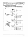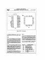
1
PROYECTO TERMINAL
GRABADOR
DE
EPROMs
AUT~NOMO
REALIZADO POR:
JOSÉ IGNACIO FLORES TAPIA.
NÉSTOR SANCHEZ GÓMEZ.
CON ASESORíA DE:
MIGUEL ANGEL RUíZ SANCHEZ
El proyecto presente se dividió para su análisis y diseño en tres bloques principales,
que son:
1. HARDWARE
2. SOFTWARE
3. MANUAL DE USUARlO
Para el bloque de H A R D W A R E tenemos:
Análisis: E n esta etapa se analizan los requerimientos delsistema grabador, y en base
a estos se proponen varias soluciones y alternativas.
Diseño: Aquí se realiza un bosquejo en el cual se proporciona una descripción de los
diferentes circuitos utilizados de acuerdo a los requerimientos de la etapa anterior. S e
parte de la configuraciónde los pines de las EPROMs, después se analizan los
circuitos de control para cada uno de los pines, acontinuación se describen los
componentes para la
interfaz
con los anteriores,
por
y
último se analiza el
microcontrolador usado y los periféricos que son memoria externa RAM y ROM, así
como los latch, buffers,y decodificadores para el control de los periféricos.
Implementación: E n esta parte se proporciona una lista de los principales circuitos
integrados que se requerirán para el grabador con una descripción y una justificación
de porque se usaron.Además del diagramafinalsimbólicoy
un diagrama con la
distribución física.
Para el bloque de SOFTWARE tenemos:
Análisis: Para llevar acabo esta etapa se toma en cuenta el bloque anterior, en el cual
se analizan las necesidadesy las posibles formas de cubrirlas.
Diseño: S e proyectan soluciones (en diagramas de flujo) en base a las diferentes
funciones que será capaz de desarrollarel sistema grabador.
Implementación: Aquí se proporciona una relación de los códigos fuentes para dar
solución a cada una de las funciones del grabador.
E n el bloque del MANUAL DE USUARIO se proporciona una guíapaso a paso de cómo
debe ser operado el grabador por el usuario.
PAGINA 2
PROYECTO TERMINAL
GRABADOR DE EPROMS AUT~NOMO
CONTENIDO
JUSTIFICACI~N
4
OBJETIVO
5
CARACTERíSTICAS
5
INTRODUCCI~N
6
ANALISIS Y DISEÑO DE HARDWARE
7
IMPLEMENTACIÓN DE HARDWARE
13
ANÁLISIS Y DISEÑO DE SOFTWARE
18
IMPLEMENTACIÓN DE SOFTWARE
25
RESULTADOS
36
MANUAL DE USUARIO
38
lnterfaz de usuario
38
Funcionamiento
38
BIBLIOGRAFíA
41
Justificación y hojas técnicas de los C.1.s
ANEXO 1
Listados de programas de prueba
ANEXO 2
Descripción
ANEXO 2
Códigos
ANEXO 2
PÁGINA 3
TERMINAL
PROYECTO
GRABADOR DE EPROMS AUTÓNOMO
Justificación.
En el presente proyecto se realizará eldiseño de un sistema grabador de EPROMs
autónomo de una PC.Estoesque
pueda grabar de EPROM a EPROM sin que se
tenga que hacer uso de una PC, además de que también se podrá usar para grabar de
una PC a una EPROM a través de un RS232 que es una interfaz por el puerto serial.
Enungrabador convencional se pueden realizar varias operaciones, entre lasmas
elementales están:
CARGAR: El programador acepta un archivo en código HEX, y lo carga en su buffer de
memoria.
DESPLEGAR: Se despliega el contenido del buffer de memoria del programador en la
pantalla de la PC.
COPIAR: Se lee el contenido de la EPROM y se almacena en el buffer de memoria del
programador.
PROGRAMAR: Se almacena el contenido del buffer de memoria del programador en el
arreglo de memoria de la EPROM.
COMPARAR:Se compara el contenido de la EPROM con el contenido del buffer de
memoria del programador.
VERIFICAR: Se examina el contenido de la EPROM y se determina si esta ha sido
borrada.
TIPO:
Se
selecciona el tipo de EPROM que será insertada
en
el
socket del
programador.
EDITAR: Se puede alterar el contenido del buffer de memoria del programador.
GRABAR: Comprende los procesos de COPIAR y PROGRAMAR,
Cada que se requiere realizar alguna de estas operaciones, por fuerza es necesario
hacer uso de una computadora, en la cual este instalado el software y el hardware del
grabador, pero ¿quepasa
si necesitamos únicamente realizarvarias
copias del
contenido de una misma EPROM?, o si queremos comparar el contenido de una
EPROM con el contenido de la otra. En estos casos usar una PC únicamente para este
propósito es un desperdicio, podemos entonces pensar en el diseño de un grabador de
EPROMs que sea autónomo de una PC y que nos sirva para estos propósitos, con la
se requierarealizaralguna
operación
ventaja de queen cualquier momentoque
adicional a estas podemos conectar el grabador a una PC cualquiera y vía puerto serial
llevar acabo nuestros propósitos.
PAGINA 4
TERMINAL
PROYECTO
GRABADOR DE EPROMS AUT~NOMO
Objetivo.
Diseñar e implementar un grabador de EPROMs autónomo (Que copie de EPROM a
EPROM, además de PC a EPROM).
Características:
El grabador tiene capacidad para grabar EPROMs de hasta 64Kb, que es mucho
mas de las necesidades cotidianas en un laboratorio de Sistemas Digitales, esto
es, grabará EPROMs de la forma 27XXX,que va desde la 2716 (2Kb) hasta la
27512 (64Kb).
Se pueden hacer copias múltiples de una sola EPROM, es decir, el contenido de
la EPROM fuente se vacía en la RAM del sistema y después el contenido de la
RAM se puede vaciar el contenido en las N EPROMs destino que se deseen.
Pararealizar lo anterior se contará con un solo socket, y elprogramairá
pidiendoal
usuario la EPROM fuente y la EPROM destino cuando sean
requeridas
El sistema grabador funcionara tanto en forma autónoma (para realizar copias),
comoes forma dependiente (interfazarse con un PC a través de un puerto
serial).
PAGINA
5
GRABADOR
TERMINAL
PROYECTO
AUTóNOMO
DE EPROMs
INTRODUCCI~N.
En los sistemasdigitalescapaces
de trabajar independientemente (tales como una
PC), existe un lugar donde se encuentran localizadas las instrucciones que permitirán
que dicho sistema realice las funciones para las cuales fue diseñado, dicho lugar es
una memoria.
Debido a que seria muy costoso mantener el sistema siemprefuncionandocon
su
programa en una memoria RAM (Random Access Memories), ya que
estas pierden su
información al dejar de existir un voltaje de alimentación surgen memorias que permiten
mantener información aun sin que exista alguna señal de alimentación, dichas memorias
son llamadas EPROM(Erasable Programmable Read Only Memories).
Estas memorias,como yase comento,mantienen datos en ellas aun sin voltaje de
alimentación presente permitiendo apagar el sistema cuando no se esté utilizando; en
contraste con lo anterior, la forma en la cual se les introduce la información es diferente
se
que en una RAM convencional. Para grabar información en una memoria EPROM
hace necesario un sistema especial que nosayude a realizar esta tarea llamado
GRABADOR o también PROGRAMADOR.
Para grabar las memorias EPROM se hace necesario mandarle no solo direcciones y
datos, sino también otras señales de control, tales como ChipEnable (CE), Output
Enable (OE) yProgramming Pulse Voltage (Vpp) siendo este último un voltaje alto
(normalmente 25 V o 21 V o 12.5 V según el tipo de EPROM) comparado con lógica
lTL(OVy5v).
LosgrabadoresdeEPROM
mas conocidos, son aquellos quedependendeuna
computadora (funciones del microprocesador, memoria R A M , etc), pero en el presente
proyecto se intentara el diseño de un grabador autónomo.
PAGINA 6
GRABADOR DE EPROMS AUTÓNOMO
TERMINAL
PROYECTO
ANALISIS Y DISEÑO DEL HARDWARE.
Dado que lo que se necesita es diseñar un grabador de EPROMs, lo primero que se
debe de analizar es la configuración de los pines para cada una de estas memorias. En
base a un análisis de las terminales que presentan los diferentes modelos de EPROMs,
con los cuales se podrá trabajar, que van desde la 2716 hasta la 27512,se observó
que existen 7 terminales que difieren, tal como se observa en la siguiente tabla:
27256
27512
Al5
Al2
A7
A6
VPP
A12
VPP
A12
A7
A6
A7
A6
A5
A5
A4
A4
A3
A2
AI
A3
A2
AI
A5
A4
A3
A2
AI
A0
O0
A0
O0
A0
O0
02
02
o1
02
GND
GND
GND
o1
o1
271 6
271282764
VPP
A7
A6
A7
A6
A5
A5
A5
A4
A4
A4
A3
A2
AI
A3
A2
AI
A3
A0
O0
A0
O0
o1
o2
GND GND
02
28
27
26 vcc
25 A8
24 A9
1
Al2
A7
A6
o1
2732
2
3
4
5
6
23
m
A2
22 OE
21
AI
M CE
A0
O0
19
18
17
16
15
o1
11
12
13
GND 14
-
02
!
~
07
06
05
04
03
-
2764
271 28
vcc
vcc
vcc
PGM
PGM
27256
vcc
vcc
Al4
Al4
Al3
A8
A9
&
l
N.C. Al3
A13
A8
A9
A8
A9
A8
A9
A8
A9
&l
All
OWPP
OE
&l
OE
OE
CE
CE
CE
CE
07
06
05
04
03
07
06
05
04
03
07
06
05
04
03
07
06
m
2751 2
05
04
03
0W P P
m
CE
07
06
05
04
03
Como puede observarse, algunos modelos son de 28 pines y otros de 24. Analizando
la figura se obtiene la siguiente relación de voltajes en la que podemos observar de
acuerdoaltipo de EPROM que voltaje necesita paracada uno de los pinesen los
cuales se aplica algún voltaje.
NOTA: En la columna del #PIN se observan expresiones para dos números diferentes
de pines, esto es porque los pines son diferentes dependiendo si son EPROMs de 24 o
de 28 pines. Los números entre paréntesis delasdemás columnas se refieren a los
diferentes voltajes que se necesitan en esos pines.
De la relación anterior se observa que para los pines 20 y 27, no existe un problema
complicado para las diferentes señales según el tipo de EPROM, en comparación con
los pines restantes. Para estos últimos fue necesario diseñar un circuito que pudiera
PAGINA
7
Ms
DEGRABADOR
TERMINAL
PROYECTO
ser controlado directamente por el programa, para proporcionar la señal necesaria, por
lo cual se desarrollo el circuito de la figura 1 (en base a el circuito de la figura 2 en el
y de
voltaje),
que
utilizan
cual se observan las consideraciones de
corriente
reguladores de voltaje LM317 entre otros elementos.
+12v
4
PIN 28 DELSOCKET
221 u
%EM1
. 7407
,,
5
2N2222
4
8
212907
470G
PESA
PIN 1 DEL SOCKET
15L1
221 11
'e;"
PIN 22 DEL SOCKET
o2x1
PC04
PAGINA
S
DE EPROMs AUTóNOMO
GRABADOR
TERMINAL
PROYECTO
FIGURA 2. CIRCUITO BASE PARA CONTROLARPINES DEL SOCKET
~
~
~~~
~~
~
"_
~
T"
OV, 5V, 12.5V, 21V, 25V
HABILITA 5V
HABILITA 12.5v
HABILITA 21V
HABILITA 25V
HABILITA OV
Vout=Vref(l+(Rlx/RZ))+ladjRlx
Vout=1.25 (l+(Rlx/22l))+(.OOOO5*Rlx)
-1.4
Los pines 20 y 27 utilizan un circuito cornbinacional mas sencillo que puede observarse
en el circuito de la figura 3.
FIGURA 3. CIRCUITO COMBINACIONAL PARA CONTROL DEPINES 20 Y 27.
d PAS-B
PIN 27 D E L S O C K E T
..................
O PAO-B
PIN 20 D E L S O C K E T O
De esta formapara activar algún voltaje del circuito de control de voltajes, basta
mandar un cero lógico y para activarcerovolts se precisa de un uno lógico, lo cual
hace posible su control desde el programa principal.
Para llevar acabo dicho control se precisa de un circuito que organice todo el
funcionamiento, es aquí donde se hace necesario el uso de un microcontrolador, entre
los circuitos considerados están: 8031, 8051, 8032, 8052,todos ellos de Intel. Una de
la características para decidir entre ellos fueron los requerimientos de memoria ROM
TERMINAL
PROYECTO
GRABADOR DE EPROMS AUT~NOMO
interna, externa o ambas que se tienen en el proyecto, además del costo y la existencia
de ellos en el mercado..
Como la programación se realizará en lenguaje ensamblador, no se necesita de ningún
interprete dentro del micro, además de que algunas funciones extras que se presentan
en los micros 8051, 8032 y 8052, como son las interrupciones, no serán usados en el
presente proyecto.
Tomando en cuentauna breve investigación demercado,se obtuvo como resultado
que el microcontrolador 8031 es mas barato que el 8051 casi en una tercera parte, y
que el 8052 esun micro que esta discontinuado, porlocualseresuelveutilizarel
microcontrolador 8031 para el grabador.
El microcontrolador se encargará de proporcionar las “señales” para leer la EPROM
fuente, grabar la EPROM destino, etc. Para llevar acabo esta entrega de “señales” de
precisa de algunos pasos intermedlos, como lo es almacenar los datos fuentes en la
memoria RAM del sistema, además de realizar el direccionamiento de los datos (poner
los datos en las localidades de memoria correctas).
Entre los posibles circuitos auxiliares a utilizar , seencuentran algunos buffers, unas
PPIs
(Programmable
Periferical Interfaz), las cuales serán
las
encargadas
de
proporcionar los mensajesadecuados al socket, y para la interfaz con el usuario se
precisarádecircuitería,
como
son
decodificadores, displaysde
7 segmentos, y
circuiteríacombinacional y secuencia1 para control y manipulación del grabador. Un
diagrama inicial de lo que será el grabador de EPROMs se observa en la figura4.
Parael grabador se tiene proyectado usar una EPROM que sea la encargada de
almacenar el software propio del grabador, debido a esto no se hace necesario que el
microcontrolador a usar posea memoria ROM interna.
Para la parte de la interfaz con el usuario sepropone elusode
un displayde 7
segmentos (será el que desplegara mayor información del estado de los procesos que
se realicen en el grabador), un par de leds que indicaran cuandose puede remover
una EPROM del socket y cuando no, ademásde un tercero que indicara si se esta
trabajando en mododependiente o enmodo dependiente, y un parde botones. El
primer botón (PBZ)se
usará para navegaren
todos los menús ysubmenús.
El
segundo botón (PBI) será para iniciar el proceso seleccionado por PB2.
El circuito propuesto paraesta parte se muestra en la figura 5.
Cabe señalar que para la interfaz de usuario se podría haber usado un número mayor
de displays y mas botones, o inclusive un LCD y un teclado controlados por un 8279,
enesteproyecto no se realizo de esa manera, pero queda abiertopara posteriores
modificaciones, además de que podría servir muy bien para efectos de un sistema de
desarrollo del microcontrolador 803’: realizando las modificaciones pertinentes.
PAGINA
10
AUTÓNOMO
DE EPROMs
GRABADOR
TERMINAL
PROYECTO
Con lo que se ha descrito hasta este momento el grabador de EPROMs funcionará de
forma autónoma, perosi se quiere usar de forma dependiente, es decir, como un
grabador convencional, debemos de considerar algunos aspectos extras, como son:
¿Cómo se implementará la comunicación entre el grabador y la PC?,
¿Cómo debe de ser el programa que controle al grabador? y
‘Cómo será el programa que controle a la PC?.
Para responder a estas preguntas de debe de analizar, conqueescon
lo que se
cuenta en cuanto a hardware y en cuanto a software, y ver si con esto essuficiente o si
necesitamos implementar algo mas.
Evidentemente para solucionar el problema de comunicación entre la PC y el grabador,
dadas las características del microcontrolador que cuenta con las salidas adecuadas
para este fin (TXDy RXD),se puede usar un RS232,que es una interfaz serial,. Lo que
se debe de hacer entonces es implementar el hardware necesario, en la figura 6 se
muestran las conexiones para este propósito.
FIGURA 4. DIAGRAMA INICIAL DEL GRABADOR
PÁGINA 11
GRABADOR DE EPROMS AUTÓNOMO
PROYECTO TERMINAL
FIGURA 5. CIRCUITO PROPUESTO PARA INTERFAZ CON EL USUARIO
PA4-B *
CLK
4.7KG
PA5-Be
DATOS
74co
LED 1 naranja
dependhndep
Modo
PC5-B.
PA6-B
I
LED 3 verde
(remover)
I
I
330Q
V.
LED 3 rojo
(Noremover)
330Q
PA7-B.
I
V.
PBI (ENTER)
PB2 (Selector)
PC7-
FIGURA 6. lnterfaz serial RS232
TXD.
RXW
...........................
...................................... :.:.:.
..........
DBQ
PAGINA
12
GRABADOR DE EPROMS AUT~NOMO
TERMINAL
PROYECTO
IMPLEMENTACI~NDEL HARDWARE.
Después de todoeste análisis, ya se puede decidir que componentes se utilizaránpara
llevar acabo el proyecto. En la figura 7 se presenta la distribución física de estos en el
grabador de EPROMs, en la figura 8 hay una lista de todos los circuitos y componentes
usados y en elANEXO 1 se proporciona una breve justificación para cada uno, además
de las hojas técnicas de los C.I. (Circuitos Integrados) mas importantes.
A continuación se presentan los diagramas correspondientes a los bloques de la figura
4, que son los circuitos con los cuales se implemento el grabador.
FIGURA 7 DISTRIBUCIÓN FíSICA DE LOS COMPONENTES.
GRABADOR DE EPROMs AUTóNOMO
PROYECTO TERMINAL
LISTA DE LOS COMPONENTES USADOS
IC-NÚMERO
ICE
IC2
IC3
IC4
IC5
IC6
IC7
IC8
IC9
IC1o
IC1 1
IC12
IC13
IC14
IC15
IC16
IC1 7
IC1 8
IC19
NúMERO ID
8031
8255-A
8255-B
62256
6264
2764
74LS373
74LS245-A
74LS245-B
74LS138
74LS04
74LS08
7407
7407
74LSOO
MUA78S40
1488
1489
74LS51
IC20
DI
LMI
LM2-LM6
T I -T5
T6-TI O
R4.7
74LS164
MAN7409
LM337
LM3 1 7
2N2222
2N2902
4.7 K
RX:X
CAPX.X
POT1
LEDX
TMRI
BOB1
Varios
Varios
20K
led
11.0592mhz
150 microH
DESCRIPCI~N
Microcontrolador de 8 bits
Interfaz periférica programable
lnterfaz periférica programable
RAM de 32kbx 8bits
RAM de 8Kb x 8bits
EPROM de 8Kb x 8bits
Latch 8 bits
Buffer bidireccional de 8 bits
Buffer bidireccional de 8 bits
Decodificador de 3 a 8
Compuertas lógicas NOT
Compuertas lógicas AND
Buffers para DC mayor a TTL
Buffers para DC mayor a TTL
Compuertas lógicas NAND
Convertidor de DC a DC
Convertidor de TTL a RS232
Convertidor de RS232 a TTL
Compuerta AND-OR-NEGADA con dos
compuertas de dos y tres entradas.
Registro de entrada serie/salida paralela
Display de 7 segmentos
Regulador deVoltaje
Regulador deVoltaje
Transistores
Transistores
Resistencias de 4.7K para efectosde PULLOP
Resistencias varias
Capacitores varios
Potenciómetro de precisión de 20K
Leds
Cristal para velocidad del KIT
Bobina de Miller
PÁGINA 14
PROYECTO TERMINAL
GRABADOR DE EPROMS AUT~NOMO
FIGURA 9. BLOQUE PARA EL MICROCONTROLADOR, LOS BUFFERS,
EL LATCH Y EL DECODIFICADOR.
PÁGINA 15
GRABADOR DE EPROMS AUT~NOMO
TERMINAL
PROYECTO
FIGURA I O . CONEXIONES PARA LA RAM,LA EPROM Y LAS PPIs
-
RESET
1
PPI-E
1
PPI-A
ROM
I
PROYECTO TERMINAL
GRABADOR DE EPROMs AUTóNOMO
FIGURA 11. SOCKET DEL GRABADOR
NOTA: Los pines marcados con ‘‘0 “ son los pines que van a estar controlados por los
circuitos de las figuras 1 y 3.
PROYECTO TERMINAL
ANALISIS
GRABADOR DE EPROMS AUT~NOMO
Y DISEÑO DEL SOFTWARE.
Para obtener un buen diseño del software, tenemos que analizar varias COSaS primero,
como son:
1.- Forma en la que se va a utilizar el grabador (Dependiente o Independiente)
2.- Determinar las funciones que tendrá el grabador, en base a
el modo de trabajo
elegido.
En el caso de que sea de modo autónomo, se podrán realizar las operaciones
de GRABAR y COMPARAR.
En el caso de que sea en modo dependiente, se podrán realizar las operaciones
de CARGAR DE PC A BUFFER, CARGAR DE BUFFER A PC, COPIAR BUFFER
A EPROM, COPIAR EPROM A BUFFER, COMPARAR EPROM CON BUFFER,
VERIFICAR SI EPROM BORRADA y SELECCIONAR TIPO, las cuales ya han
sido descritas anteriormente.
3.- lmplementar cada una de las funciones en base al modo de trabajo elegido.
Antes de la implantación del software, se diseñaron algunos diagramas deflujo
principales, que nos marcan la forma en la que tienen que funcionar los programas.
Enel diagrama de flujo 1 se muestra lo que sería el menú principal,con el cual
podemos elegir el modo de trabajo. Notamos claramente lo que se menciono acerca de
las funciones de los botones PBI y PB2, donde PB2 nos sirve para desplazarnos en
los menús y PBI para aceptar la opción escogida por PB2. AI inicio se espera a que se
pulse
PB2
para
iniciar,
después se desplaza a modo “Independiente
y
modo
“d”ependiente en forma alternada mientras se este presionando PB2. Si estando en “d”
se presiona PBI entonces nos iremos al menú del modo dependiente y si estamos en
T y se presiona PBI nos iremos al menú del modo independiente.
En el diagrama de flujo 2, observamos el menú del modode trabajo independiente,
GRABAR
DE EPROM
AEPROM
, de
donde solo se tienen las opciones de
COMPARAR EL CONTENIDO DE LA EPROM CON EL CONTENIDO DEL BUFFER y
la opción de salir que se maneja con una c minúscula.
El menú para modo de trabajo dependiente se muestra en el diagrama de flujo 3, en
este modo setienen algunas otras opciones ademásde las quepermite el modo
independiente. En este modo ya no se hace uso de los botones para manipular el flujo
de la información, ahora se manipula el programa por medio de señales (números) que
le manda un programa que estará corriendo en la PC (ITFC.EXE) a la que esté
conectado el grabador por medio del puerto serie, entonces el programa está
monitoreando el puerto serial y ejecutará la opción de acuerdo al caracter leído.
El diagrama de flujo 4 explica la rutina de GRABAR en modo independiente.
~.
~
PÁGINA 1s
GRABADOR DE EPROMS AUT~NOMO
PROYECTO TERMINAL
-
DIAGRAMA DE FLUJO I. MENÚ PRINCIPAL
I
“HOLA”
7
SI
DESPLEGAR
“I”
DESPLEGAR
o+
1
“d”
PB2?
I
MENU MODO
DEPENDIENTE
I
p’
INDEPEND.
I
PAGINA
19
GRABADOR DE EPROMS AUT~NOMO
PROYECTO TERMINAL
DIAGRAMA DE FLUJO 2. MENÚ EN MODO INDEPENDIENTE
desplegar
"O"
desplegar
'I o 99
desplegar
"C"
+
-
I"'
GRABAR
COMPARAR
DIAGRAMA DE FLUJO 3. MENÚ EN MODO DEPENDIENTE
seleccionar el
tipo de E P R O M
con la cual se
va a trabajar
y espera
caracter por
puerto
serial
+
GRABADOR DE EPROMS AUT~NOMO
TERMINAL
PROYECTO
DIAGRAMA DE FLUJO 4. RUTINA PARA GRABAR EN MODO
INDEPENDIENTE
1
Poner tipo en
W ’y
desplegar
pedir EPROM
destino
+
sig. tipo
P
5l
4
habilitar
hardware
-+
@tipo
pedir EPROM
fuente
“Fll
borrada?
I SI
escribir
en EPROM
desplegar
sig. tipo
almacenar
0
I
7,
leer datos
al buffer
I
PÁGINA 21
PROYECTO TERMINAL
G R ~ A D O DE
R EPROMS AUTÓNOMO
"
Las rutinas de grabado para cada uno de los tipos de EPROMs permitidos en este
grabador, se obtuvieron de algunos diagramas de flujo propuestos en el manual de
INTEL de MEMORY, en el diagrama de flujo 5 se muestra un algoritmo de grabación
QUICK PULSE, el cual funciona de la siguiente manera:
Seleccionar dirección para grabar, poner voltajes de programación, poner datos
a grabarse, inicializar una variable en O, se da un pulso de programación de 100
microsegundos.
Se incrementa la variable, se lee el dato grabado en la EPROM, se verifica que
se haya grabado correctamente, si es así, se monitorea si es la última dirección
una
y en casopositivo se ponen todos los voltajes en 5 voltsyserealiza
comparación completa.
En caso de que no se haya grabado correctamente se checa si la variable es
igual a 25, si es igual a 25 se verifica el byte, si es correcto se checa si es la
última dirección y se procede de la forma anterior, si no es correcto, se manda
un mensaje de error.
Cuando la variable es menor que 25 se vuelve a dar un pulso de programación
de 100 microsegundos y se procede de la misma manera.
En el diagrama de flujo 6 se muestra un algoritmo de programación INTELIGENTE. La
forma de operar de este algoritmo es similar al QUIK-PULSE, excepto por que manda
un pulso extra de duración 3 veces el valor de la variable tratando de asegurar que la
grabación sea correcta y para disminuir el tiempo de grabación.
Para cada tipode EPROM las direcciones de fin variar? de acuerdo a la capacidad y los
voltajes de programación también.
Se recomienda el uso del algoritmo de programación QUICK-PULSE paraaquellos
tipos de EPROMs que usen voltajes de 21V y de 25V.y del algoritmo INTELIGENTE
para los tipos que usen voltajes de 12.5V.
"_
-
PAGINA
22
GRABADOR DE EPROMS AUT~NOMO
PROYECTO TERMINAL
DIAGRAMA DE FLUJO 5. Algoritmo de programación QUICK-PULSE
+PASS
c R .\BADOR DE EPROMS AUT~NOMO
PROYECTO
TERMINAL
DIAGRAMA DE FLUJO 6. Algoritmo de programación INTELIGENTE
f
t
YES
PROYECTO TERMINAL
-
G K.L\BADORDE EPROMS AUT~NOMO
IMPLEMENTACIÓN DEL SOFTWARE.
A continuación se presenta el código fuente del programa principal implementado
únicamente para EPROMs 2764A.En el ANEXO 2 se incluyen listados de programas
que fueron usados para probar el sistema por partes.
;LISTA DE ETIQUETAS
#INCLUDE EQUS.TXT
LIST
LIST
PCTRL2
PCTRLI
PA2
PA1
PB2
PB1
PC2
PC1
DIRBUFF
TIPO
TIP0.3
STATO.0
STAT0 1
ADRO
ADRl
START0
START1
END0
END1
TEMP1
FILLK
FILLKW
CHKSUM
NBYTES
RTYPE
TEMP2
VBYTE
X
XCERO
XUN O
XDOS
XTRES
XCUATRO
XCINCO
XSElS
XSIETE
XOCHO
XNUEVE
XA
XB
XCMAY
XCMIN
XD
XE
XF
XG
XH
XI
XL
xs
xu
XY
XlNT
.EQU
.EQU
.EQU
.EQU
.EQU
EQU
EQU
EQU
EQU
.EQU
EQU
.EQU
.EQU
.EQU
.EQU
.EQU
.EQU
.EQU
.EQU
.EQU
.EQU
.EQU
EQU
EQU
EQU
.EQU
.EQU
EQU
.EQU
EQU
.EQU
.EQU
EQU
.EQU
.EQU
.EQU
EQU
.EQU
.EQU
EQU
EQU
EQU
.EQU
EQU
.EQU
.EQU
EQU
EQU
EQU
6003H
4C@3H
6000h
4000H
6001H
4001h
6002H
,PALABRAS DE DIRECCiON DE ACCESO PARA
.CONFIGURAR LAS PPIs
,PALABRAS DEDIREt-;:JN PARA ACCESAR A
,LOS PUERTOS DE 3 L ; A PPI
>PI-A
,SE LISARA'1' PARA
Y '? PARA LA PPI-B
, J
4002H
8MX)H
29H
30H
OOH
01H
31H
32H
33H
34k
35H
36H
37H
38H
39H
3AH
3BH
3CH
3DH
3EH
3FH
ODFH
086H
OBBH
OAFH
VARIABLES USADAL E1.l EL PROGRAMA
OE6H
OEDH
OFDH
087h
OFFH
OEFH
077h
07Ch
059H
03CH
03EH
079H
071H
06FH
076h
050H
058H
.EQU
OGDH
.EQU
EQU
EQU
05EH
06EH
OB3H
-
"
-
PÁGINA 25
C K XB ADOR
EPROMs
AUTóNOMO
DE
PROYECTO TERMINAL
0063 Moo
MOV
DPTR,#PCTRL'
0064 Xx309o6003 INICIO
MOV
MODOS
PARA
A,#88H
0085 M03 7488
MOVX @ D P i R . k
0066 2005 FO
"~
,CONFIGURACIOI.I DE LA PPI-B
Di :t'ERACION
VER HOJAS 7 k:!I I C A S
CONFIGURAC ;;1 DE LA PPI-A
O067 20069o4003
DPTR
#PCTRLl
MOV
A,#80H
MOV
O068 2009 74 80
m69 2008 FO
@DPTR.AMOVX
ACALL PWRDWN
0070 2ooC 31 A7
.**~***,~*
0071 200E
REGRESO
ACALL
HOLA
0072 200E 71 29
MOV A,#XINT
,DESPLIEGA
SIGNL L)E- INTERROGACION
0073 2010 74 B3
0074 201271 BE
IMPRIME
ACALL
MON-PB2
ACALL
CHECK-PBS
,MONITOREA
PbL PARA
SELECCIONAR
0075 201471 66
0076 2016 B440CJNE
FB
A,#049H,MON_PBZ
MODO
,EL
DE 1 KABAJO
0077 20198000
MOD-INDP
SJMP
.**Lt*t~******,***~***********~.*~***r.~..*...*~*.~******~~*..***.*.~....
0078 201B
MOD-INDP
MOV
A,#XI
.MOI\IITOREA PBI
PAitA
LOMENZAR
CON
0079 201B 7450
ACALL
IMPRIME
MODO
INDEPElhO:ti~lTE,
O PB2 PARA
o080 201D 71 BE
66
71
CHKI
ACALL
CHECK-PBS
CAMBIAR
MODC
A LjC?ENDIENTE
0081 201F
0082 2021 844002
CJNE A,#040H,CHK2
0083 202401 2B
AJMP MOD-DEP
CJNE
A,#080H CHKI
0084 2026 8480 F6 CHK2
0085 2029 o1 98
MENU-IND
AJMP
.........................................................
0086 M2B
MOD-DEP
MOV
A,#XD
,MONITOREA
PB1
f'fiF?i?. COMENZAR
CON
m 8 7 202B743E
O088 202D 71 BE
ACALL
IMPRIME
MODO
DEPENDI:.: 1-E O PB2 PARA
CHECK1
ACALL
CHECK-PBS
CAMBIAR
A MOL
' IDEPENDIENTE
0089 202F 71 66
CJNE A,#040H CHECK2
o090 2031 844002
0091 203401 1B
MOD-INDP
AJMP
CJNE
A,#080H
CHECK1
0092 2036 8480 F6 CHECK2
0093
38
203901
MENU-DEP
AJMP
0094 203B
.*
0095 2038
MENU-DEP
MOV A,#XE
O096 203B 7479
ACALL
IMPRIME
0097 2030 71 BE
MOV A , W H
.PROGRAMA
PUERTO
SEK:E H i MODO 1
0098 203F 74 50
0099 2041 F598
SCON,A
MOV
o100 2043
o1 o1 2043 74 F4
MOV A,#OF4H
CARGA VALOR DE BAUDRATE
o102 2045 F5 8D
TH1.A
MOV
o1a3 2047
74
o1o4 2047
M
MOV A,#MH
,PROGRAMA
TIMER
1 EN M J L J ~2:
o1o5 2049 F5 89
TMOD,A
MOV
o1o6 2048
O107 2048 7440
MOV A . W H
ARRANCA TIMER 1
88 F5
TCON,A
MOV
o1o8 204D
o1a3 204F
o1 10 204F
o111 204F
0112 204F
;RUTINA DE
MENU
EN
MODO
DEPENDIENTE
O1 13 204F 906002 WRRS MOV
DPTR,#PC2
0114 2052 74 OF
MOV
A,#OFH
O1 15 2054 FO
@DPTR.A
MOVX
0116 2055 CO EO
PUSH A
o1 17 2057
71
58
ACALL
RECIBE
O118 M59 8401 O 4
CJNE A,#01
,ESF2
o119 205C DO EO
POP A
o120 205E01 6B
AJMP
MEM-PROG
o121 2060840204 ESF2CJNE A,#O2,ESSAL
POP
A
o122 2063 DO EO
o123 206501
AJMP
7D
PROG-MEM
O124 2067 DO EO
ESSALPOPA
-01
AJMP MOD-DEP
o125 28
.****
O126 2068
O127 2068
; MANDA 80 BYTESDELCONTENIDODELBUFFERDE
LA K A h l DEL KIT A PC
o128 2068 71 58
MEM-PROG
ACALL
RECIBE
,RECIBE
BYTE
Al O CIE DPTR
o129 206D F5 83
MOV DPHA
o130 206F7158
WRDL
ACALL
RECIBE
KECIBE
BYTE
BAL<,
.:E .JPTR
O131 2071 F582
DPL,D
MOV
O132 2073
79
o1
33 2073 80
MOV R1.#80H
o134 2075
t l l * f * * f * f * * t t * * * * * * * * * * t l t t * t - ~ * * . ~ . . . . .
8-
1**L********~.****************.~*~~~~**.~*~.*~~~*******~**.****...~..
. t t t . * t * t * t * * f f * * * t t * * ~ ~ ~ * * " . ~ ~ ~ ~ * * . * ~ * . ~ * . . ~ * * . . ~ ~ ~ * ~ * * ~ * ~ ~ ~ * * ~ * ~ . . . . .
l****f***~tf.*.****t*****f.*****~~~..*~*.~*~t*f***.*****.**~~t.t-I...
PROYECTO
TERM
IN AL
-
..~
.
GK.4BADOR
EPROMs
DE
~~~~
~
LOOPE
O135 2075 EO MOVXA,@DPTR
ACALL TRANS
O136 207671 4A
DPTR
SIGUIENTE
INC DATC
O1372078 A3
DJNZ R1 ,LOOPE
O138 2079 D9 FA
AJMP MENU-DEP
O139 207B O1 38
O140 M 7 D
*.* ttt****tt*...,..~*"~*..******.~***~~~***.~*..****~.~..~**~***.*~..-..
0141
207D
, RECIBE EL CONTENIDO DE UN PROGRAMA DE LA PC A L 6J;FER DEL KIT
O142
207D
PROG-MEMACALLRECIBE,RECIBE
ELTOTAL DE 6 V E S DE CODIGO
O143 M 7 D 7 1 58
MOV
R3,A
O144 207FFB
ACALLRECIBER3CONTIENEBYTEALTO
O145 208071 58
MOV
R2,A
,R? CONTIENE
BYTE
BAJO
O146 2082 FA
o147 2083
O148 2083 71 S3
LOOPCAP
ACALL
RECIBE
RECIBE
2 BYTES DE ÜiRtL:clON
012085 F5 83
DPH,A
MOV
O150 208771 58
RECIBE
ACALL
0151 2089 F582
MOV DPL,A
0152 2088 71 58
ACALL
RECIBE
FiEClBE
DATO
O153 208D FO
@DPTR,A
MOVX
O154 208EIA
DEC R2
O155
CJNE
208F
F1
FF
RZ,#OFFH,LOOPCAP
BA
O156 M 9 2 1 B
DEC R3
0157 2093 BB FF ED
CJNE R3.#OFFH,LOOPCAP
O158 209601 38
MENU-DEP
AJMP
NRRS
o159 2098
.
O160 2098
0161 2098
;RUTINA DE MENU
EN
MODO
INDEPENDIENTE
O162 209851 MENU-IND
ED
ACALL
CONF-ESCR
O163 M 9 A 31 A7
ACALL PWRDWN
209C O164
746F
A,#XGMOV
=E71 O185
BE
IMPRIME
ACALL
71 20AO
O166 LED?
ACALLF6
O167 M A 2 31 A7
PWRDV'JN
ACALL
O168 20A471 66
CHEYK-PBS
ACALL
O169 M A 6 B 4 4 0 1 A
ItdICIO-GRAB
A.#O<)H
CJNE
O1 70 20A9 74 59
A.#XCMAY
MOV
O1717120AB
BE
IMPRIME
ACALL
71 20AD
O172
F6
LEC2
ACALL
O1 73 M A F 31 A7
ACALL PWRDWN
O174 2081 71 66
CHECK-PBS
ACALL
O175 2083844012
INICIO-COMP
A.#040H
CJNE
O176 2086 74 3C
MOV A #XCMIN
O177 2088 71 BE
IMPRIME
ACALL
O178 208A 71 F6
LEDL
ACALL
20BC
O179
31 A7
PWKCVVIN
ACALL
0180 20BE 71 66
CHECK-PBS
ACALL
0181 20CO B4 40 OA
CJNE
A,#CJOH
SAL-IND
,checa C O I I pb2
0182 20C3
0183 M C 3
0184 20C3 8480D2
INICIO-GRAB
CJNE
A,tO30H,MENU-IND
O185 20C6 O1 D2
GRABAR-IND
AJMP
0186 M C 88 4 8 0 CD INICIO-COMP
CJNE
A #080HMENU_IND
COMPR-IND
AJMP
0187 M C B 21 25
O188 M C D8 4 8 0 C8
SAL-IND
CJNE A , m O H MENU-IND
O189 20DOO1 1B
MOD-INDP
AJMP
O190 20D2
O191 20D27529 FF
GRABAR-IND
MOV
TIPII)
#OFFH
0192 M D 5 0 5 2 9
PROX-TIPO
TIPO
INC
O193 20D7 E5 29
A,TIFL?
MOV
O194
ACALLAB
20D9 71
GE;"iC
71 20DB
O195
ACALLF6
LEC..
O196 71
20DD
66
CHCC.I_
ACALL
PBS
0197 20DF 8 4 40 07
CJNE A M14CH START ,PB2
O198 M E 2 E 5 2 9
MOV ATIFC
O199 20E4 B4 O8
CJNE
A.#D",t-.
EE
PROX-TIPO
O200 20E701 0 2
GRAHiiR-JND
AJMP
O201 20E9
O202 M E 9
O203 20E9 8 4 8 0 E9 START
CJNE
A,#08Cti
PROX-TIPO
;PB1
OM4 M E C 31 28
ACALL I N l r _ t i l i k F INICIALIZAR
EL
Bu: -t;i DE LA RAM
EN OOH
O205 20EE 7471
FUENTE
MOV
A,#XF
O206 20F071 BE
ACALL IMPC?IIV1E
f*******~.t~...fttlttlttt********tttl~....~.**~*******.**~******~.i..~..
AUTóNOMO
PROYECTO TERMINAL
( ;K . A B
"_
ADOR
DE
EPROMs
AUTóNOMO
0207 20F2 71 F6
LEC.'
ACALL
O208 20F431 A7
PW"3'uIYbd
ACALL
O209 20F6 71 66
CHE-:I(_PBS
ACALL
0210 20F88804
F3
CJNE A.#WOh FUENTE
,PB1
LEU
ACALL
0211 20FB 71 E3
ACALL
0212 81
20FD 71
DEi4:'IX
0213 20FF
31
48
ACALL
CCMC
,CARGAR
CONTF
EL
PIID0 DEEPROM
LA EN
LA RAM
0214 2101 743E
DESTINO
MOV
A,#XE
0215
71 2103
BE
IMPRIME
ACALL
312105
0216
A7
ACALL PWRDWN
0217 2107 71 66
ACALL
CHECK-PBS
0218 21098480OC
A,#O?O+,SALIR-DEST
CJNE
0219 E3
210C71
ACALL LEL i
0220 210E51 16
ACALL PCM3 PROGRAMAR
EPROR,'
LA
.;3N EL CONTENIDO DERAM
LA
21 O221E5 10
29
MOV A.TIPS
O222
GE-TSC
ACALL
21
AB
12 71
ACALL
O223 812114 71
DELa\~X
0224
21 2116
O1
DESTINO
AJMP
O225 2118743C
SALIR-DEST
MOV
A,#XCMIN
0226 211A71 BE
ACALL IMPP:IME
0227 31
211C
A7
ACALL PW'T'CWN
O228
66 211E71
ACALL CHEIK-PBS
O229 21208480DE
CJNE DESTINO
A,#EO+
O230 212301 9s
ME1AJMP
-i~~II\lL:
o231
2125
INICIALIZAR BUFFEF ,.,ah CEROS Y CARGAR EPIL I I A RAM *************
0232 2125
O233 212531 28
COMPR-IND
ACALL
INIC_?'I!FF
O234 212731 48
CCM:
ACALL
O 2 3 5 212901 98
MENLJ
AJMP
.!NE
O236 2128
INlClALlZA EL BUFFEX 3 F L KIT EN W H *****t*t****r~''r********
0237 2128
O238 2128
O 2 3 2128 C083
INIC-BUFF
PUSH
DPH
0240
2D 21 CO 82
PUSH DPL
0241
2F 21
EO CO
PUSH A
0242 2131 903000
#3000H
DPTH
MOV
0243 21347400
PONCERO
MOV
A,#03b
0244 2136 FO
@DPTR
MOVX
A
0245 2137 74 FE
A,#OFEH
MOV
CJNE A,DpL F'KOX-CERO
0246 2139 8 5 82 OC
0247 213C
MOV
74 3F
A,WFH
0248
21 07
83
B5
3E
CJNE A,DPH PROX-CERO
0249
41 21 DO EO
POP A
O250 2143 DO82
POP DPL
21O251
45 DO 83
POP DPF
0252 2147 22
RET
o m 2148
O254 2148A3
PROX-CERO
DPTR
INC
O255 214921 34
POIIC.F.RO
AJMP
o256 2148
.********.** COPIA DATOS DE Lt._ P R O M ALBUFER *tff*~*f'.'t~'*f~*********
0257 2148
o258 2148
;LEEELCONTENIDO DE UN RA:~!G,CDE LAEPROM ESPECií I':ADO POR EL USUARIO
o259 2148
;YESPUESTOEN LAMEMORIP J F L BUFFERUSANDOLA
MtJFAA DlRECClON
0260 2148
o261 2148
DPTR,#PCTUL!
.MOV
CCMD
o262 2148
A.#89H
.MOV
0263 2148
@DPTR,A
,MOVX
O264
74 214831
ACALL PWRLP
O26571214D 00
_..ECT
CONF
ACALL
0266 214F900000 CCMDI
MOV
DPTR
AXXDH
M 6 7 2152
O268 215231
C6
CREAD
ACALL
RDPROM
02El 21
EO54 CO
PUSH A
0270 21
83
56 E5
MOV A,DFki
0271 2158 4430
ORL
A,=, . : r m B
M72 215A
83 F5
MOV DPh ' <
0273 EO
21% DO
POP A
0274 215E FO
MOVX @L)L T L P,
0275 74
215F
FF
MOV A,#OFl'I
027661 21 85 82 O 6
CJNE A.0;' .IrEXT
0277 74
2164 3F
MOV A #:-;L.
0278
21
66 05 83 O1
CJNE A 0;+-I LIvEXT
.*****f.***.
***..tt*****
"
~~
PAGINA 28
c,I?.\BADOR DE EPROMS AUT~NOMO
PROYECTO TERMINAL
RET
0279 2169 22
0280 21 6A
o281 216A A3
EXT
CN
INC
DPTR
MOV A,DF-I
0282 216B E5 83
O283 216D 54 CF
ANL A . # l ! ' C ~ l l I B
6F 21 F5 83
MOV DPH
0284
71
21
52
AJMP CRMI'
O285
0286 2173 22
RET
POWER
.....***********~**~~~~.~*.....1
0287 2174
.esteprocedimentolnicializa los ' ~ ~ l ' d , t . :que
,
se mandanalsocket - 1 ,
O288 2174
,5 volts
O289 2174
MOV
DPTR
::PA:
O290 2174906000 PWRUP
o291 2177 74 80
MOV A,& -MOVX @ D ' l 3 A
o292 2179 FO
MOV DPT '< ifPB1
O2937A21 90 40 O1
MOV A,#l '4
O294 217D 7417
7F
O295 21 FO
MOVX @ D F ' l ' i A
DPTF
MOV
dPB2
O296 2180 90 60 O1
A683 74
MOV A#.KAI+
0297 21
O298 2185 FO
MOVX @CF H A
O293 2186 90 60 02
MOV DPT" %PC2
A#OE.MOV
o300 2189 74 OE
MOVX @DP: Y , A
0301 218B FO
P1
MOV
FF
W L t
0302 218C 7590
030331218F 92
ACALL DL I '%
a304 2191 22
RET
RETARDO ['F
millsegundos ***********'"*+***
a#)5 2192
32
78
MOV
R3,#32+
a306 2192DLYW
0307 219431 93
ACALL
DL-DELAY
1
DJNZ
DB FC
i'. X
a308 2196R3
0309 2198 22
RET
o31o 2199
I**tttt*tt**.
retardo d e , mil,seg , , ~/,,
o31 1 2199
o312 2199 7400
DELAY1
A,#O
MOV
o313 2198 D5 EO FD
DL1
DJNZ A.DL1
DJNZ A,DL2
o314 219E D5 EO FD DL2
o315 21A1 22
RET
o316 21A2
RETARDO Lt- 3 riilcrosegundos ************l'''*ff****
o31 7 21A2
DLYM
MOV R3,##OAt5
o318 21A2 78 OA
DLYMI
DJNZ
R3,DL'.!
o319 21A4 DB FE
o320 21A6 22
RET
o321 21A7
POWER Dc,LJ!\l .*.******t******l*t**tt*tlt***'r..****t
o322 21A7
o323 21A7
, a q u semandanvoltajesde O volts ? S I comodatos y direccionestanrblen O
o324 21A790 40 00 PWRDWN'
MOV DPTFi
#PA1
MOV A.#0:'i+
o325 21AA 74 00
MOVX @L:r'
A
o326 21AC FO
0327 21AD 90 60 02
MOV
DP?
3 :QC2
0328 21BO 74 OE
MOV A.#(1F
o329 2182 FO
MOVX @ L b
;
iA
a330 2183 90 60 O1
MOV DP: - XPB2
74B6 A6
MOV a M:;.,.
O331 21
a332 21B8 FO
MOVX @C'F"
;? k
0333 21B9 90 40 O1
MOV DPT: ::PBI
MOV A #I:,:,. , i
0334 21BC 74 A8
o335 21BE FO
MOVX QLI
RA
DPTL MOV
0336 21BF906000
!:PA?
74C2 MOV
4E
A #4C ' 4
O337 21
o338 21C4 FO
MOVX @ r I I '" :' A
0339 21c5 22
RET
0340 21C6
RUTINA
PARA LtL +ROM
*
L
.
*
0341 21C6
,ESTARUTINALEEEL
CONTE'I i'ii 3E UNALOCALIDAD.
0342 21C6
;EL'DPTR'CONTIENE LA L O C A , I : . A U A SER LEIDA
a343 21C6
i EN EL
ACC
;EL RESULTADO
ES
REGRESA
o344 21C6
a345 21C6
MOV
ADKl ,
o346 21C6 85 8332 RDPROM
i
0347 21C982
85 MOV
31
ADRG I:'
o348 21cc
0349
21 21CC
CE
RDG4
AJMP
a350 21CE
+ +
21
.~.*****.*.~.~ff*ftft
. . . I . . . *
.*****.*~**,*f*ltll**ff
8
3
~.**tf*f***.*t.*..*l***it*t**L..
.**ftl..*l*f**.*llf.*tt
.~~f.********ft*tl~tf**
,
**.***************.e
I*f.*fl..*I**
>L
...l.
f
cx ~ B A D O RDE EPROMS AUT~NOMO
TERMINAL
PROYECTO
0351
a352
a353
a354
a355
a356
a357
0368
0359
O360
O361
a362
o363
a364
0385
0366
a367
0368
m
0370
O371
0372
0373
0374
0375
0376
0377
0378
0379
a380
0381
m 2
a383
0384
o385
0386
m 7
0388
0389
0390
a391
a392
0393
a394
0395
0396
0397
0398
0399
o400
0401
0402
0403
O404
O405
O406
0407
O408
0409
o41o
o411
o412
O413
O414
O41 5
O416
O417
O418
o419
o420
o421
o422
MOVA.ADR1
21CE E5 32
RD64
SETB A.5
21 DOD 2 E5
JB A.3,Al 1
21D2 20 E3 OA
21D5
MOV DPTR.#FB
21D5904001 A11L64
SETB A.3
21D8 D2 E3
ANL A,#001
? iB
21 DA54 3F
MOVX @DP ' A
21DC FO
AJMP RDk ' i
21DD 21 E7
21DF
MOV DPTR # F ' f
21DF904001
AllH64
CLR A.3
21E2 C2 E3
ANL A , # 0 0 1 ' ' ' l i B
21E4 54 3F
MOVX@DF
fi
21E6 FO
21 E7
21E7 90 40 00 RDNX64
MOVDPTR #I '
MOV A.ADK:
21 EAE5 31
MOVX @DF' I - i
21EC FO
MOVDPTR ill ; 2
21ED906002
MOVA.#OE.
21FO 74 OE
MOVX @DP. F c
21F2 FO
MOV DPTR r;'3L
21F3 90 60 O1
MOV A,#16r,
21F6 74 26
MOVX@DF I ii.
21 F8FO
21F9906000
MOVDPTP :f A?
MOV A,#KiL
21FC 74 83
MOVX@DP 1. A
21FE FO
21FF904002
MOVDPTE ::: 2
m 2 3 1 A2
ACALL DLYI':
MOVXA.@L:"-R
2204 EO
2205 COEO
PUSH A
MOV OPTS :P 4 2
m7936000
22OA 74 81
MOV A.#61"
ZZOCFO
MOVX@DF F: 4
m D DOEO
POP A
MOV DPP. : I
m F 85 3283
2212 85 31 82
MOV DPL a
2215 22
RET
2216
2216
I...**********..***
ESCRIBE DATC :; >EL BUFFER A LA EPROM "****'***********
2216
2216
;PROGRAMA
EL
SOCKET
SEG! 1 4 EPROM
221651 PCMD
ED
ACALL CON F.^; ;R
2218 31 74
ACALL PLV " ;'
221A75 33 00 PCMDI
MOV STAR' .COH
221D 753400
#03H
MOV ST;*
2220 85 33 82
MOV DP!- A K T O
2223 85 34 83
MOV DPt
+RT1
2226
222651 PAGAIN
ED
ACALL
CONF
-iR
2228 71 13
ACALL T G F :
222A EO
MOVX A,C: r . TR
2228 71 1E
ACALL
TDFE
222D 51 59
ACALL Whir' -?OM
222F 20 O1OD
STAT!'
"ERR
JB
2232 74 FF
MOV A,#(! "
2234 B5 82 1E
CJNE A D i >',IEXT
2237 74 OF
MOV A N I
2239 8 5 8 3 19
CJNE A;¡
JEXT
223C 31 A7
ACALL l''v'u, ~ v N
223E 22
RET
223F
223F 74 76
PERR
MOV A,#XH
224171 BE
ACALL Irdb; IL'F
2243 71 81
ACALL DE'
2245 71 81
ACALL DE..
.'
2247 74 86
MOV A # Y . J ' .,
224971 BE
ACALLIMP'.:
. ¡E
2248 71 81
ACALL DEI '! X
2
2
471 81
ACALL DE
':I-.
"
~
5
t - i
~
'
I
PÁGINA 30
GR BADO OR DE EPROMS AUT~NOMO
PROYECTO TERMJNAL
0423 224F 71 66
ACALL C n t . "ES
0424 2251 8E488 0
CJNE A , N X
;'ERR
0425 225422
RET
0426 2256
2255A3
PNEXT
0427
INC DPTR
0428 2233 41 26
AJMP
PAk; ':,
0429 225822
RET
04302259
*t*.***r...*r***.
RUTINA PARA ES(: 3 - R
. EPROM
0431 2259
0432 2259
;ESTA
RUTINA
ESCRIBE
EL L C I '
'IIDODEL
BUFFER A UNA JCALIDAD
04332259
;EL'DPTR' CONTIENE LA LOCAL
u A SER ESCRITA
04342259
;EL VALOR A ESCRIBIRSE ESTA
, EL ACC
04352259
O436 -8583
32
WRPROM
MOV
ADRl
J
0437 225C8285 MOV
31
ADRO 1:'
O438 2 2 5 F F 5 3 9
MOV FILLKV,
0439 2261
O440 2261 41 63
AJMP W R B 4
0441 2263
EPROM _,.,\.,
0442 2263
MOVDPTR,#F
O443 2263906000 WR64A
MOV A,#06:
O444 2266 7481
MOVX @ D F
.
O445 2268 FO
MOV DPTF: ;i ' :L'
o446 226996001
MOV A . # 2 D . ~
0447 226C 74 2D
MOVX @DPO448 226E FO
MOV
DPTH
'_I
O449 2 2 6 F 9 0 6 0 0 2
MOV A,WCt
o450 2272 7 4 0 E
MOVX @DF'".
0451 2274 FO
MOVA.#AI:!
0452 2275 7 4 3 2
SETB A 5
O453 2277D2E5
JB A3.WJ"'
.
O454 2 2 7 9 M E3OA
o455 227c
MOVDPTK iiF
O456 2 2 7 C 9 0 4 0 0W
1 llLGA
SETB A ?
0457 227F D 2 E 3
ANL A . m ' : '18
0458 2281 5 4 3 F
MOVX@D! .
C459 2283FO
AJMP w m - .,
0460 2284418E
0461 2286
MOVDPTK #F '
04622286904001W11
H6A
CLR A 3
O463 2289 C2 E3
ANL A , W : j \ i 1B
O464 2288 5 4 3 F
MOVX @DF. -,
0485 228D FO
O466 228E
MOV DPTH # t : '
0467228E
904000 WNX64A
MOV A
O468 2291 E 5 3 1
MOVX@!Ut .
O469 2293FO
MOVDPTP 0470 2294 90 40 0 2
ACALL DL';.
0471 229731A2
ACALL DL'(:
0472 2299 31A2
ACALL D i
0473229831A2
0474 229D 31A2
ACALL D i ' l _'
MOV X , K
0475 229F 7 5 3 F 0 0
MOV A,FILLI<L',
0476
22A2
E539
AGN64
047722A4 FO
MOVX@Dt'
MOVDPTR i' .\?
0478 2 2 A 5 9 0 6 0 0 0
MOV A # 8 5 '
0479 22A8 74 85
MOVX @ D i '
0480 22AAFO
PUSH A
O481 22AB COEO
0482 22AD 31A2
ACALL DL\
ACALL DL 1'
0483 22AF 31A2
ACALL D i i..'
0484228131A2
O485 228331A2
ACALL DL .'.
04862285DO EO
POP A
0487 2287053F
INC X
O488 2289
O489 2289 E 5 3 F
NOV64A
MOVA,X
PUSH A
0490 22BB CO EO
MOVDPÍ-F ; 42
0491 2 2 B D 9 0 6 0 0 0
MOV A , & ' . <
049222C0 7481
0493 22C2FO
i
MOVX@!I+
0494 22C3 90 40 0 2
MOV DPTh .:
I
~
.***t.********
8.
.
~
f
.
f
l
*
*
.
.
.
.
.
t
*
f
*
*
*
*
*
.
,
...*l.
ff.******************"*~**....*
-
S ,
.
A
j j
+
1
-
'~
"
PÁGINA 31
PROYECTO TERMINAL
POPA
CJNE A , # X
0495 22C6 DOEO
0496 2208 04 20 D7
o497 22C B
04%
G K ABADOR
EPROMs
DE
-~
..<;Id64
MOVA.X
?L'
MOV DPT"
MOV A , # 8 5 ~
MOVX@DF
4
MOV DPT!.' . 42
MOV A,%"
MOVX@Dr' '
CLR STAT:
"
MOV
DPP
MOV
DPL
il
RET
AJMP PGMEk
22CB E5
3F
OVER64
0499 2 2 C D 9 0 6 0 0 0
OM30 22DO 74 85
0501 22D2 FO
r '
0502 2 2 D 3 9 0 6 0 0 0
0503 22D6 74 81
0504 22D8 FO
O505 22D9 C2 O1
0506 22DB 85 32 83
0507 22DE 85 31 82
0508 22E1 22
E4
PERR6A
0509 22E241
o51o 22E4
RUTINA DEERE( , k;h PROGRAMAClON *******r'''''**********.i
o511 22E4
22E4
D
2
O1
PGMERR
SETB STATC.
o512
í'
32 85
DPL
MOV
o5138322E6
MOV DPL
L ,
o514 22E9 85 31 82
RET
o515 22EC 22
o516 Z E D
.***"**.*.*f.*
CONFIG PPI-A ;
ESCR,TURA It**********.**+.*-********
o517 22ED
o518 22ED
,en espeaal puerto C de
la PPI-..
CONF-ESCR
PUSH A
o519 Z E D COEO
22EF
PUSH
CO 83
o5M DPH
PUSH DPL
o521 22F1 C 0 8 2
:TRL1
MOV DF'T?
o522 2 2 F 3 9 0 4 0 0 3
MOV A,#6:'o5238022F6 74
MOVX@DF
.1
o524 22F8 FO
DP! POP
o525 22F9 DO 8 2
22FB
POP
DO 83
o526DPH
POP A
o527 22FD DO EO
RET
o528 22FF 22
-
.****,***.*.I**
t
~~
,;
o529
m
m
.******t..**..*
CONFIG
;
.* ****************f......
e***
0530 2300
,en
especlal
puerto
C de
la PPI-?
0531
CONF-LECT
PUSH P
0532 m C 0 EO
PUSH
CO 83
DF'b
05J3 2302
PUSH DPL
o534 2304 CO 8 2
MOV DPTn i:F TRLI
0535 2 3 0 6 9 0 4 0 0 3
MOV A,#SC'"
o536892309 74
M O V X @ U i :' c
0537 2308 FO
POP
DO 82
DPL
o538 230C
230E
POP
DO 83
o539DPri
231O DO
POP A
0540 EO
22 O541 2312
RET
0542 2313
.***
TRANSFORMA E ; : . :,E EpROMA RAM Lltlt.****.*..I**********t
cm3 2313
o544 2313
,paraefectosdegrabaraparttr
ilt. 1 (*,.aildad3000h
EOCO
TDPB
PUSH
A
o545 2313
MOV A DPL
0546 2315 E5 83
ORL A , # K :IXX)B
0547 23174430
MOV 830548
F5 2319
DPh
EO B DO
A POP
a549 231
22 0550 231 D
0551 231 E
E 9AM A EPROM LI**.t**.**,1..r*l**tt*tttt
.****.*
TRANSFORM+, L
0552 231 E
0563 231 E
;paragrabarapartlrde
la d l r e c r l d
K!k de la EPROM destino
CO
TDPE
PUSH
A
0564 231 EEO
MOV 83a555
E5 2320
A at
0556 2322 F
54 C
ANL A d 1 '
1 i!B
830557
F5 2324
MOV DL'&. .
POP A
0558 2326 DO EO
RET
0559 2328 22
0560 2329
O561 2329
.**~*****..,..********~
lMPRllv,t
-,y
r**l*****************t**~**~.r.r*
O562 2329
HOLA
MOV
A.#76lo563 2329 74 76
t
ACALL lb::-.
o564 2328 71 BE
232D 71
ACALL L i z ( . '
0565 81
81 232F 71
ACALL De:-'
0566
,,
t...**.*+**
RET
AA.....*
I
8
AUTóNOMO
G.~
I ) ABADOR DE EPROMS AUT~NOMO
PROYECTO TERMINAL
0567 MOV
2331 745F
C E 3 233371BE
C569 81
2335 71
A.&i
ACALL IMP - 'E
ACALL DE,
'/
ACALL DEL(- .';
MOV A.#!!jt
ACALL IMP;- 'E
ACALL DEL. ''
ACALL DELMOV At-t!7.
ACALL IMF . 'E
ACALLUE: 1 <
ACALL DEL-\ X
RET
0570 2337 71 81
0571 2339 7 4 5 8
0572 2338 71 BE
0573 233D 71 81
0574 233F 71 81
0575 77
2341 74
0576 2343 71 BE
0577 2345 71 81
0578 2347 71 81
a579 234s 22
.**
0580 234A
0581 234A F 5 9 9
TRANS
MOV
SBUF.A
0582 234C
EO CO
PUSH A
0583 234E 71 95
ACALL DISPLAY
0584A 2350DOEO
POP
0585 23523099 FD WTB JNB SCON 1 W ' t !
0586 2 3 5 5 C 2 9 3
CLR SCON 1
0587 235722
RET
4
7
1....***************.*****""***~.
.*.*...****.****.t****tt*****.......1
05882358
* * ~ttl~ttt,*~*tttt****~~,~**..,.....ii
O589 2358 3998 FDRECIBE
0590 2358 C 2 9 8
O591 235D €599
0592 235F COEO
0583 71
2361
95
0584 2363DO EO
o595 236522
TRANSMITE
BYTE
DlRECC!.JNADO
ET
~.*..*******f~******.fffft*****t*
JNB SCON O . R E i i
CLR SCON O
A,SBUF
MOV
PUSH
A
ACALL DISPLAY
POP A
R
0586
2366
0587 2366
0598 2366
0599 2366
o600
0601
0602
O603
0604
0605
0606
0607
0608
0609
237E 1
0610
061
0612
0613
0614
.
.lt~***....*.**f*.****~.~*~******..1.
~
,RECIBEECO DE TERMINAL
..r.r***********t*************+t***
;monltorea los botones de control . .' ' í PB2) y no regresa hasta qLle no
;se haya preslonado uno de los :
2366 C 0 8 3
CHECK-PES:
PUSH !IF1+
PUSH UPI2368 C 0 8 2
236A936002
MOV DP-F dPC2
236D 7 4 0 0
CHECA
MOV A,#UOt.
MOVX A @?! '"TK
236F EO
ANL A MlC .II
237054CO
237230E605
JNB A+.> ~ P B S
JNB k 7 I!-PBS
2375 30 E7 02
AJMP U t i ! ' A ,
2378 61 6D
237A 71 81
FIN-PBS
ACALL DECA / I _
237C DO 8 2
POP [:F.
POP
DO 83
GPr
2380 22
RET
2381
.***l't*t**.lrr****tI*tl**lr.trrt........r.+r.~~ttt.t***********~****~****
2381
8'
0615 2 3 8 1
0616 2381 7 9 6 0
DELAYX
MOV R I , # W P
0617
2383D901
DELAY0
DJNZ
R1 DEi.4YI1
0618 2385 22
RET
0619 2386
06M 2386 7 8 0 0
DELAY3
MOV
RO,WJk:
0621 2388D8
FE
RETA1
DJNZ
RO,REl~b
DJNZ RO.KE-1i.2
0622 2 3 8 A D 8 F E
RETA2
DJNZ RO.RE?i^ 3
0623 238C 0 8
FE
RETA3
0624 2 3 8 E D 8 F E
RETA4
DJNZ
RO.Rt"
A4
O625 m 0 8RETA5
FEDJNZ
RO,RET35
AJMP D E G (0
0626 2392 G I 83
0627 m 4 2 2
RET
.RETARDO
06282395
.It****r*+tl+.tr*.*.*~****..*..~~......+.....+*t**tl+rr*****r******tt+tt*r
0629 2x35
06302x35
; ESCRIBE EN EL DISPLAY EL \ X ' I T E N l D O DELACUMULADOH EN DOSDlGlTOS HEXA
O631 23% C 0 8 2
DISPLAY
PUSH
DPL
E':CRlBE EN EL DISPLAY EL CONTENIDO
DEL
0632 2397 CO83
PUSH
DPH
b C !MULADORDlGlTOS
EN HEY4DECIMALES.
O633 2XBCOEO
PUSH
A
0634 2333 54OF
ANL A W F H
0635 239D 71 AB
ACALL GE F7SL'
ESCRIBE EL BYTE BAJO
O636 239F D O E 0
POP A
0637 SWAP
23A1 C4
A
O638 23A254OF
ANL A.#OFh
~
PÁGINA 33
I N AL
PROYECTO
TERM
"
~
0639 23A471 AB
O640
0641
0642
o643
o644
o645
o646
0647
0648
m49
O650
0851
0852
0853
0854
0666
o656
ACALL GET7SC:
ZAG
DPH
POP
DO 83
23A8
DPL
POP
DO 82
B A A 22
.~**.rr*.*+r-*
23AB
23A B,REGRESA
23AB
23AB C082
GETiSC
23AD PUSH
DPH
CO 83
B A F CO FO
2381 90 2 4 0 9
2384 93
2385 71 BE
2387 DO FO
2389
DPH
POP
DO 83
23BB
DPL
POP
DO 82
23BD 22
238E
0857 23BE
o658 238E
0859 238E
0660 23B E
O661 23sE
0662 23BE CO 8 2
o663 23CO CO 83
o664 23c2 co EO
~~
SE ESCRIBE EL BYTE ALTO
RET
t**t***."**.~*.*....~."....r.+tl*t*****t*****Ilttt****.*~.
EL CODIGODE
y SECVENTOSDEL ACUMULADOR
PUSH DPL
PUSH B
MOV DPTR,#TAB~LA
MOVC A.@A+DP'R
ACALL IMPRIME
POP B
GARGA DATO DE 7 SEGMENTOS
RET
.***rr*t.+.+r*****.**..**.******.....,+...*.r..*******t.****tttll***********.
;mandaal dlsplay el contenldo del acmulador cargadoantes de llamar
.a esteurocedlmiento,normallllente ;on alguncodigoestablecidoen
id
;etiquetas
IMPRIME
0665 23c49060OO
o666 23C7 78 08
0667 2369 F 5 FO
o668 23CB 54 80
0669 23CO 03
0670 23CE 03
0671 23CF 44 10
0672 23D1 FO
0673 23D25 4 EF
G R ~. B A D O R
DE EPROMS AUT~NOMO
-
ETQ-I
0674 23D3 FO
PUSH
DPL
PUSH UPH
PUSH A
MOV D W R . d P A 2
MOV
ROME
MOV B A
ANL P W U H
RR
i
:
RR
A
ORL A # ' O b
MOVX @DPT;i A
ANL A#OEFF
[email protected]
A
MOV A ti
RL
A
DJNZ RI! ET .4
MOV A # K +
POP k
POP DF'b
POP Dr7t~
RET
0675 23D5 E5 FO
0676 23D7
0677 23D8 D8 EF
0678 23DA 74 00
0679 23DC DOEO
0680 23DE DO 83
0681 23EO DO 82
0682 B E 2 22
r***********"***.,.,.***lri..tlr.tr+.********tt*******tt+tt**"*".~.
0683 B E 3
0684 23E3
;rutina que permite encender al Icd ' ':ed rolo)
0685 23E3 CO EO
LED1
PUSH A
0686 23E5
PUSH
CO 82
DPL
3 E - i CO 83
3PH
0687 2PUSH
MOV r)F' -R w 4 2
0688 23FJWGOOO
o689 23EC 73 80
MOV ,-,%O'I
0690 B E E FO
MOVX @DF -,? A
3 E F DO 83
DFb
0691 2POP
0692 23F' DO 8 2
POP ::PI
o693 23F3 DO EO
POP k
m 4 23F5 22
RET
*~tt**+*rr*."tt*~LIl***~*~....*~~....r.....r**~**~**t.****tt*ltt*t*****t**
06% 23F6
;rutma
para
encender
led 1 (leií lerci.
06% B C 1 EOCO
LED2
PUSH
A
m 7 23FCj
0698 23F5 CO 82
PUSH DPL
06?23 23FA
PUSH
CO 83
SPH
0700 23FC90GOOO
MGV UPTR.tPA2
MOV P #30H
0701 2 3 F F 74 40
MOVX (QDP;~Y A
0702 2401 FO
4 2 DO 83
dFti
0703 2PCP
POP r J r ' ,
0704 2 4 - 1 DO 82
POP A
0705 2 4 i DO EO
RE i
0706 24x-22
.Irr*.r.r...+rrr*~~~.t~~*'t+rl.l*r....r.l.....r******..~."****~**..****.*~
0707 2 4 0 ,
,TABLAS
DATOS
DE
0708 24m
0709 2403
.gfedcba
071O 240cjDF
TABLA
BYTE
1 1 0 1 1 ~ 1 ' 1 8 l)
n
.**.~....
..
"
-.___.
PAGINA 34
PROYECTO TERMI N .AL
"
"
..
GR.ABADOR DE EPROMS AUT~NOMO
lr%XX?
i 38
:
BYTE
0711 240A 86
1011'~0~'1B
2
BYTE
0712 2406 BB
10101111B 3
BYTE
0713 240CAF
111OC:llJ3 4
BYTE
0714 240D EG
11107 i C l B 5
.BYTE
0715 240E ED
lllll~'OIB 6
BYTE
0716 240F FD
o717 241o a7
.BYTE 1oooO111B 7
24110718
FF
BYTE
111111~1B 8
2412
0719
EF
.BYTE 111011!1B 9
2413
0720
77
.BYTE 0111Gl i 1B A
241
0721
4 7C
BYTE
O111 11CK)B B
0722 2415 53
.BYTE 0107'~K~lB 2
24160723
3E
BYTE
03111''::R
U
0724 241 7 79
BYTE
OIlI!X!lEI t
0725 2418 71
BYTE
O111MXllB F
0726
2419
0727
2419
0728 241A
ORG
$+I
,OBLIGA A L El.SAMBLADOR A GENERAR
0729 241ACOM
RUN
WORD INICIC:
"OR SEPARADO
UNA
LINEA
DE CODIGO
0730 241C
END
;PARA LA C I R E C .:ON DE ARRANQUE.
O731 241C
0732 241C
O733 241C
t a m : Number of errors = O
".
PÁGINA 35
TERMINAL
PROYECTO
GRABADOR DE EPROMS AUT~NOMO
RESULTADOS
En relación a los avances obtenidos en el presente proyecto podemos establecer que:
Es posible "simular" la lectura y escritura alsocket, es decir, se pueden enviar señales
para datos, direcciones y control de voltajes tanto para leer
como para escribir de la
EPROM. Sedice"simular" por el hecho de que no se hanlogradorealizar dichas
funciones en forma efectiva cuando
se coloca una EPROM en el socket, únicamentese
han verificado con una punta lógica y multímetro.
un
Para los voltajes de controlse sigue la siguiente técnica:
Si se quiere tener un voltajeX en el pin Y del socket, se debe enviar un O lógico
a la línea correspondiente al voltaje X del pin Y y 1's en las demás líneas de
voltajes. Esta técnica es válidaen los pines 1, 22, 23, 26y 28.
Por ejemplo si queremos que en el pin 22 se obtengan voltajes de 21 Volts y de
O Volts respectivamente tendremos las siguientes asignaciones:
a) PCO-B = 1, PCI-B = 1, PC2-B = O, PC3-B = 1, PA1-B = O.
b) PCO-B = X,PCI-B = X, PC2-B = X, PC3-B = X, PA1-B = 1.
donde la X significa cualquier valor(1 o O).
Para los pines20 y 27 funciona de la siguientemanera:
El PB6-B para el pin27 y el PB6-B para el pin20 tienen la función de selectores,
(PN-B, si
es decir, estas líneas establecen si la salida cambia respecto a una
PB6-B esta en 1) uotra (PB6-A, si PB6-B estaen O) línea de control (estos
27 del socket, paraelpin 20 funcionade la misma
valoressonparaelpin
forma), el valor obtenidoen la salida será la entrada seleccionada invertida.
Por ejemplo si queremos que en el pin 27 se obtenga primero un 1 y después un
O proporcionados porPA2-B tendremos las siguientes asignaciones:
a) PB6-B = 1, PB6-A = X, PA2-B = O.
b) PB6-B = 1, PB6-A = X, PA2-B = 1.
donde la X significa cualquier valor(1 o O).
Las PPIs (8255) estánprogramadassegúnlas
siguiente manera:
hojas técnicas(ver
anexo I ) , de la
PPI-A se programa con todos los puertos de salida en la fase de escritura de la
EPROM en el socket, y se programa con los puertos A y B de salida y el puerto
C de entrada en la fase de lectura de la EPROM en el socket, esto es por que el
puerto C de la PPI-A maneja los datos.
PAGINA
36
PROYECTO TERMINAL
GRABADOR
AUTóNOMO
DE EPROMs
PPI-B se programa con los puertos A,B y la parte alta del puertoC como salidas
ylapartebajadelpuerto
C comoentrada,durantetodoeldesarrollodel
programa, el hecho de que la parte baja del puerto C (PCO-PC3) se programe
como entrada es por que son las líneas que controlan los botones (PBI y PB2) y
estos proporcionan siempreuna entrada al sistema.
El sistema ya cuenta con elprototipodetodoel
programa en el cual ya están
establecidos todos los mensajes necesarios para la comunicación con el usuario, tanto
enformaindependiente(medianteel
display, los leds y el reconocimiento de los
botones PBI y PB2), como en forma
dependiente
(mediante
el display
y
la
comunicación serial). Como consecuencia de esto ya existe completa comunicación
entre el sistema y cualquier computadora a través del puerto serie y mediante rutinas
mostradas en el anexo 2.
Dentro de estas rutinas existen algunas para leer el contenidode memoria de cualquier
partedel sistema, rutinas para escribir en cualquierparte de lamemoria RAM del
sistema, rutinaspara verificar los distintos voltajes en los pines de control, etc.
AI existir un prototipo del programa principal únicamente restaría hacer un llamado a la
rutina correspondiente en el lugar indicado implementando la función llamadaen algún
otro lugar del programa.
S e lograron mandar las señales de control, datos y direcciones tantopara lectura como
para escritura al socket pero al momento de insertar laE P R O M no funcionaban, por lo
cual, se sugiere verificarla sincronización adecuada de dichas señales, así como
verificar los tiempos y la implementaciónde los algoritmos de programación.
Debido a los constantes problemas de hardware (chips quemados, en particular PPIs)
se aconseja revisar la implementación de la fuente de
5 V. colocándola fuera de la
tarjeta para evitar conflictos en la transferencia de información ó en los voltajes de
alimentación porexceso de temperatura.
Cabe señalar que para la interfaz de usuario se podría haber usado un número mayor
de displays y mas botones, o inclusive un LCD y un teclado controlados por un 8279,
en este proyecto no se realizó de esa manera, pero queda abierto para posteriores
modificaciones, además de que podría servir muy bien para efectos de un sistema de
desarrollo
del
microcontrolador
8031 realizando las modificaciones
pertinentes
(programas para la PC, programas para el sistema y algún hardware adicional).
El hecho de que solo se use un socket, se debe a la intención de ahorrar espacio y
tiempo ya que todo lo que se lograría con 2 sockets es posible realizarlo con uno solo,
aunque para mayor comodidad del usuario sería mejor implementar un segundo socket,
pero esto queda para mejoras posteriores.
PÁGINA 37
PROYECTO TERMlh .AL
”
GR -< H ADOR DE EPROMS AUT~NOMO
MANUAL DE USUARIO.
lnterfaz con el usuario
En este bloque se localizan los push bottons 1 y 2, así corno el display y los leds, de
acuerdo al circuito de la figura 5:
El led 1 se ha colocado en consideración a que existiera ¡a conexión al puerto serial de
una PC (Computadora Personal). para indicar en cual de los dos modos se está
operando; modo local: CopiadeEPROM a EPROM sin necesidad de una PC, Modo
Remoto: Copia deun archivo en código maquinaen una PC a EPROM vía el puerto
serial de la PC.
Los otros dos leds Contrapuestos indicarán al usuario ei momento en que se están
aplicando los voltajes necesarios a la EPROM para evrtarque está sea removida en
ese momento, el led rojo indicara que se esta leyendo o escribiendo a la EPROM y el
led verde indicara el momento en el que se puede quitar G poner la EPROM..
El PB2 (Push Botton 2) y el PBI servirán como teclado para que el usuario realice la
selección deltipo de EPROM, asícomo el proceso de programación. El PB2 servirá
como selector en los menús y submenús yel PBI corno unaseñalpara aceptar la
opción elegida por PB2 (ENTER).
El display indicará en cada momento al usuario las diferentes etapas que conforman el
proceso de grabar EPROMs. desde seleccionar el modode trabajo (Dependiente o
Independiente). Si se esta en modo independiente, selecclonar el tipo de EPROM con
la quese vaa trabajar, y el estado en el queseencuentre
elproceso de copia.
(Selección, lectura, programación, verificación, errores, etc ) .
FUNCIONAMIENTO:
Enbase a la explicación de los bloques principales, a continuación sebosqueja
funcionamiento:
el
AI encender el grabador enviara u n mensaje de inicio (“HOLA”)
al usuario y pondrá en
el display un signo de interrogación ( :). Esperaraque se presione PB2, y estará en
modoINDEPENDIENTE (despliega “I”). AI presionar nuevamente PB2 se ira a modo
DEPENDIENTE (despliega “d”).
Estará oscilando en ese menú mientras no se presione P B I . Si se desea trabajar en
presionar P B I Cuando este la “I” en el display de 7
modoINDEPENDIENTEsedebe
segmentos, en ese momento se entrará al menú del modo INDEPENDIENTE. Si lo que
se desea es trabajar en modo DEPENDIENTE, se tendra clue presionar PBI cuando la
“d” este en eldisplay y se entrara almenú del modoDEPENDIENTE. El proceso
anterior se describe en el diagrama de flujo 1 que muestra además las acciones que se
realizan vía software.
C K ~ !ADOR
j
DE EPROMS AUT~NOMO
PROYECTO TERMINAL
El menú del modo INDEPENDIENTE se describe a continuación:
“G” ---a Indica grabar de EPROM a EPROM.
“C” ----> Indica compar-arel ccntenido de la EPROh‘ con el buffer del grabador.
“c” ----> Es una señal generalizada que indicara s b / t r al menú anterior en
todos los menus y submenús.
Para realizar cualquiera de las acciones anteriores se debe de seleccionar con el PB2
y después arrancar el proceso con el PBI. Este proceso lo observamos en el diagrama
de flujo 2.
Cada una de las opciones del modo INDEPENDIENTE nos lleva a una rutina. La rutina
para GRABAR se muestra en el diagrama de flujo 4.
A continuación de detalla el proceso de GRABAR.
AI iniciar el proceso de programación. el usuario deberá establecer el tipo de EPROM
con la que va a trabajar, esto se realiza en base a una tabla de equivalencia la cual se
selecciona con el PB2, esta tabla inicia con el tipo O, y va aumentando hasta agotarla y
vuelve a iniciar en forma cíclica, la tabla es la siguiente:
# selección
O
1
2
3
4
.~
EPROM vpp
2716
2732
2732A
2764
2764A
25 V
25 V
21 V
21 v
12.5 -V
#-&lección
-~
5
6
7
8
Después de elegir el tipo de EPROM. se presiona el Pi; para iniciar el proceso, en
este punto se pedirá que se cargue ¡a EPROM fuente rvediante la aparición de una
señal en el display (“F”); a continuación se vuelve a presionar el P B I y el grabador
leerá datos de la EPROM fuente, segiln el tamaño de la EPROM, durante este proceso
estará encendido el led rojo.
~
Una vez llenoel buffer, aparecerá otra señal en el dlsiJlay (“d”) indicandoque se
salir
cargue la EPROM destino existiendo la posibilidad tic, elegir la opciónde
presionando PB2 para elegir “c” y después PB1 para salic Si se elige “d” y ya se cargo
la EPROM destino se presiona nuevamente el PBI, el grdbador procederá a cargarla
con la información del buffer. mientras vuelve a encender el led rojo.
Si existiera un error, el display mostrara alternadamente urla “H” y un número 1 el cual
indicara que existe un error. se deberá presionar el PBI para reiniciar el proceso.
Si no existió ningún error, el grabador checará si la EPHOM ha sido copiada en su
así el grabador
totalidad (solo para EPROMs 27512 que son de64V.t1), ysies
regresara al iniciodel proceso mostrando el tipo de E?ROM seleccionado, de lo
PROYECTO TERMIN AL
.~
C H \ I3.4DOR DE EPROMs
AUTóNOMO
contrario se pediráal usuario que inserte la EPROM /Lente nuevamente y todo el
proceso anterior se repetirá hasta copiar completamente z i contenido de la EPROM.
El hecho de que solo se use un socket, se debe a la intención de ahorrar espacio y
tiempo ya que todo lo que se lograría con 2 sockets es po-ible realizarlo con uno solo,
aunque para mayor comodidad del usuario seria mejor imprementar un segundo socket,
pero esto queda para mejoras posteriores.
Si se eligióenel
menú principal la opción detrabajar en modo dependiente, se
mostrara una “E” que indica “E”spera L:n caracter del puer?,. serial. En este momento se
deberá correr el programa “ITFC.EXE” para inrtefazar la 1):’ con el grabador.
Este programa muestra un menú con las opciones de:
ARCHIVO:
Abrir
Guardar como
Cargar al buffer
EPROM:
Programar
Verificar copia
Cargar a buffer
Imprimir
BUFFER:
Editar
Imprimir
AYUDA
Acerca de
Manual
*
*
*
La opciónAbrir, del menú ARCHIVO abre un archivo c o : ~información en HEX, y lo
alista para Cargarlo al buffer del grabador.
La opción Editar del menú BUFFER carga a la RAM de la PC 80 bytes de código HEX
a partir de una dirección especificada por el usuario y los despliega en la pantalla.
Las opciones marcadas con * son las que están impl’mentadas
ITFC.PAS.
enel
programa
TERMIN.L\L
PROYECTO
GL
~
"
,
ADOR DE EPROMS AUTÓNOMO
BIBLIOGRAFíA.
Intel.
MICROCONTROLLER HANDBOOK. Familia ?JICS-51,
Capítulo 7.- ArchitectureMCS-51
Capitulo 8.- MCS-51 Programmer's Guide anu Instruction Set.
Capitulo 9.- Data Sheets.
Capitulo 10.- MCS-51 Aplication Notes.
MEMORY.
Intel
Capitulo 3.- Dinamic and Static RAMS(Rancmn Access Memories)
51256 (pag. 3-80), 5164 (pag. 3-37).
Capitulo 4.- EPROMs (Erasable Programmable Read Only Memories)
2716 (pag. 4-I), 2732 (pag. 4-5j. 2764 (pag. 4.18),
27128 (pag. 4-42), 27256 (pag 463), 27512 (pag.4-111)
Algoritmo de programación QulS--Pulse (pag. 4-397)
Intel.
DISPOSITIVOS PERIFÉRICOS.
PPI (Programmable Peripherical Interface) t ; L d ; 5 . Pags 3-100 a 3-119.
SGS
DATABOOK, LOW POWER SCHOTTKY T i l . ICs
C.I. : 74373, 74245, 74138, 7400, 7404, 7408 7407. 74LS151
William G. Houghton MASTERING DIGITAL DEVICE CONTROL.
Capitulo 1 .- The Intel 8051 Family.
Capitulo 2.- External Program Memory Expansion
Capitulo 3.- External Data Memory Expansio::
Capitulo 4.- Expanding 110
Capitulo 8.- Adding An RS-232 Port
0
Motorola. SEMICONDUCTOR TECHNICAL DATA.
MUA78S40 pag. 3-330
LM317
3-21
pag.
LM337
pag. 3-43
Intronics,inc.
INTRODUCING TO EPROM PROGRHMER.
Pag. 1 - 11.
PROYECTO
TERMINAL
GI! EPROMS
%ADOR DE
A.
-
ANEXO I
JUSTIFICACI~N
Y
HOJAS TÉCNICAS
DE
CIRCUITOS INTEGRADOS
AUTóNOMO
PROYECTO TERMINAL
c;!,
I
~DOR
DE EPROMS AUT~NOMO
803 1:
microcontrolador de 8 bits.
4 puertos de 8 bits cada uno.
0
Memoria RAM interna de 128 x 8 bits.
0
2 timers de 16 bits.
0
Interrupciones.
0
Tecnología HMOS.
El uso de este chip se basa en la existencia y pre: ! o que de el se obtuvo en el
mercado. asícomo
de contar con las
terminale..;
necesariaspara
manejar
informaciónde 8 bits, y direcciones de 16 bits. !iLleson características del
grabador.
0
0
74245:
Buffer bidireccional octal de tres estados.
Terminal para habilitar salidas.
0
Control para transmisión y recepción.
0
Canal bidireccional de 8 bits.
0
Estado de alta impedancia.
Este circuito, debido a sus 8 bits y a sus tres estaao, permite el intercambio de
información, en este caso del microcontrolador con e ¡ resto del grabador.
0
0
74373:
Latch octal con salida en tercer estado.
0
Control de entradas al latch.
0
Control de salidas del latch.
0
Canal de 8 bits para datos de entrada
0
Canal de 8 bits para datos de salida (en tercer cs4.3do).
Para este circuito se toma en cuenta su capacidat1 .jara el manejo de 8 bits y su
estado de alta impedancia.
0
74138:
Decoficicador y demultiplexor de tres a ocho.
0
Tres entradas de control para direcciones.
0
Tres entradas de habilitación
0
Ocho salidas posibles.
El uso de este circuito se basaen las necesidades de poder controlar hasta
ocho dispositivos con solo tres líneas para habilitarlos.
0
8255:
0
0
0
0
0
0
0
Interface periféricapfogramable.
3 buses de 8 bits.
Control de lectura.
Control de Escritura.
Control de selección
Buses con estado de alta impedancia
Línea de reset.
PROYECTO
TERMINAL
GI? 4 -3 ~ D O RDE EPROMS AUT~NOMO
2 líneas de selección de bus.
Este circuito integrado nos permite realizar la commicación entre la parte que
maneja el usuario, y el socket del grabador con el mcrocontrolador.
O
2764:
Capacidad para 8Kb x 8bits
O
CHMOS compatible con microprocesadores y microcontroladores.
O
Latch de direcciones integrados.
O
Tamaño universal de 28 pines con dos líneas de control.
0
Bajo consumo de potencia (1O 0 microA máximo;
0
Características de inmunidad al ruido.
0
Alta velocidad de respuesta.
Esta memoria tipo EPROM tiene las características necesarias para adaptarla a
nuestro sistema y almacenara el programa prlncipal (BIOS) del sistema
grabador..
0
6264:
Capacidad para 8Kb x 8bits
0
Operación estática.
O
Tiempos iguales de acceso para lectura y escritura.
O
5 volts de alimentación.
0
Compatiblecon TTL.
O
Datos comunes de entrada y salida.
Esta memoria tipo RAM tiene la usamos únicamente con propósitos de desarrollo del
sistema, es decir, sirve comoalmacén temporal del programa principalpara realizar
pruebas. ya terminado el sistema no será necesario su uso.
O
62256:
Capacidad para 32Kb x 8bits
Operación estática.
0
Tiempos iguales de acceso para lectura y escritura.
O
5 volts de alimentación.
0
Compatiblecon TTL.
0
Datos comunes de entrada y salida.
Esta memoria tipo RAM tiene la finalidad de servir como h : f e r del sistema grabador, es
decir, será donde se almacenen los datos del programa 2 L;:abarse en la EPROM.
0
0
LM337:
Corriente de salida mayor a I .5 A.
Salida ajustable entre -1.2Vy -37V.
0
Protección térmica interna.
0 Corriente constante con la temperatura.
0
Operación flotante para aplicaciones de alto v o ~ a : e .
Este regulador de voltaje lo usamos para proporcionar a ¡ ( , S transistores que controlan
los voltajes un voltaje de -1.4V.
0
0
PROYECTO TERMLNAL
GR 3 ~ D O R
DE EPROMS AUT~NOMO
LM317:
Corriente de salida mayor a 1.5 A.
O
Salida ajustable entre -1.2V y -37V.
O
Protección térmica interna.
O
Corriente constante con la temperatura.
O
Operación flotante para aplicaciones de alto vol:a,e.
Estereguladorde
voltaje lo usamos para proporcionar a los pinesdelsocket
voltajes de programaclón adecuados controlados por los transistores.
O
los
MUA78S40:
O
Corriente de salida de 1.5 A sin transistor de salida.
0
Salida ajustable entre 1.5V y 40V.
O
Línea de 80dB y protección de carga.
o Soporta desde 2.5V hasta 40V de entrada.
0
Altaganancia.
Este cor;vertidor de DC a DC lo usamos para generar los 30 volts que necesitan en la
entrada de los reguladores LM317.
Además de los circuttos integrados mencionados anteriormente, se utilizaran algunas
compuertas lógicas tales como inversores, NAND, OR. etc. cuya elección dependerá
del uso inmediato que se proyecte. así como algunos otros componentes de acuerdo a
la hoja de especificaciones para el buen funcionamiento ct ¡os circuitos.
MCS@-51
8-BIT CONTROL-ORIENTED MICROCOMPUTERS
803118051
8031 AH/8051 AH
8032AH/8052AH
8751 HI8751 H-1218751
H88
m
m
m
m
m
m Boolean Processor
m Blt-Addressable RAM
Hlgh Pertormance HMOS Procesa
Internal TlmerdEvent Counters
2-Level Interrupt Priorlty Structure
32 I/O Llnes (Four &Bit Ports)
64K Program Memory Space
m Programmable Full DuplexSerlal Channel
m 111 Instructions (64 Slngle-Cycle)
m 64K Data Memory Space
m Security Feature Protects EPROM Parts Against Software Plmcy
The MCSe-51 products are optimized for control applications. Byte-processingand numerical operations on
small data structures are facilitated by a variety of fast addressing modes for accessing the internal RAM. The
instruction set provides a convenient menu of &bit arithmetic instructions, including multiply and divide
in
stnrctions. Extensive on-chip support is provided for one-bit variables as a separate data type, allowing direct
bit manipulation and testing in control and logic systems that require Boolean processing.
i
I n t m d Momory
D . V h
8052AH
8051AH
8051
8032AH
8031AH
8031
8751H
8751H-12
8751H-88
Program
8K x B R O M
4K x 8 R O M
4K x 8 ROM
none
none
none
4K x 8 EPROM128
4K x 8 EPROM
4K x 8 EPROM
D.tr
256 x 8RAM
128 x 8 RAM
128 x 8 RAM
x 8RAM
128 x 8 RAM
128 x 8 RAM
x 8 RAM
128 x 8 RAM
128 x 8 RAM
256
Timers/
Evmt Counters
3
2
2
3
2
2
2
2
2
x 16-Bit
x 16-Bit
x 16-Bit
x 16-Bit
X 16-Bit
x 16-Bit
X 16-Bit
x 16-Bit
x 16-Bit
Interrupts
6
5
5
6
5
5
5
5
5
The 8751H is an EPROM version of the 8051AH; that is, the onchip Program Memory can be electrically
programmed. and can be erased by exposure to ultraviolet light. It is fully compatible with its predecessor, the
8751-8, b u t inoorporates two new features: a Program Memory Security bit that can be used to protect the
EPROM against unauthorizedr e a d d , and a programmable baudrate modification bit (SMOD). SMOD is not
The 8751H-88 also only operates up to 8 MHz.
present in the 8751H-12 or the 8751H-88.
803118051
8031AH18051AH
8032AHl8052AH
8751
HI8751
H-1218751
H-88
PRELC%NlNA,RY
Figure 1. MCS*-51 Block Diagram
PIN DESCRIPTIONS
vcc
vss
Port O also receives the code bytes during programming of the EPROM parts, and outputs the code bytes
during programverification of the ROM and EPROM
parts. External pullups are required during program
verification.
Circuit ground.
Port 1
Port o
Port 1 is an &bit bidirectional 110 port with internal
pullups. The Port 1 output buffers can sinkhource4
LS TTL inputs. Port 1 pins that have 1s written to
them are pulled high by the internal pullups, and in
that state can be used as inputs. As inputs, Port 1
pins that are externally being pulled low wil source
current (IIL, on the data sheet) because of the internal
pullups.
Supply voltage.
Port O is an 8-bit open drain bidirectional I/O port. As
an output port each pin can sink 8 LS TTL inputs.
Port O pins that have 1s written to them float, and in
that state can be used as high-impedanceinputs.
Port O is also the multiplexed low-order address and
data bus during accesses to external Program and
Data Memory. In this application it usesstrong internal pullups when emitting Is, and can source and
sink 8 LS TTL inputs.
Port 1 also receives the lowsrder address bytes during programmingof the EPROM parts andduring
program verification of the ROM and EPROM parts.
8031/8051 8031 AW8051AH
H-1218751
H-88
8032AH18052AH e 8751 HI8751
P,RELDR,NEFllARV
7
ws2'w32ONLV
T2EX
m.0 ADO
P1.l
Pad
Pln
Flgure 2. MCSX-51 Connections
In the 8032AH and 8052AH,
Port 1 pins P1.0 and
P I .1 also serve the T2 and T2EX functions, respectively.
Port 2
Port 2 is an &bit bidirectional 110 port with internal
pullups. The Port 2 output buffers can sinWsource 4
LS TTL inputs. Port 2 pins that have 1s written to
them are pulled high by the internal pullups, and in
that stale can be used as inputs. As inputs, Port 2
pins that are externally being pulled low will source
current (IIL, on the data sheet) because of the internal
pullups.
Port 2 emits the high-order address byte during
fetches from external Program Memory and during
accesses to external Data Memory that use 16-bit
addresses (MOVX @DPTR). In thisapplication it
uses strong internal pullups when emitting 1s. During
accesses to external Dala Memory thatuse &bit addresses (MOVX @Ri), Port 2 emits the contents of
the P2 Special Function Register.
Port 2 also receives thehigh-order address bits during programming of theEPROM parts and during
program verification of the ROM and EPROM parts.
I
Port 3
Port 3 is an 8-bit bidirectional I/O port with internal
pullups. The Port 3 output buffers can sinWsource 4
LS TTL inputs. Port 3 pins that have 1s written to
them are pulled hgh by the internal pullups. and in
that state can be used as inputs. As inputs, Port 3
pins that are externally being pulled low will source
current (IIL, on thedata sheet) because of the pullups.
Port 3 also serves the functions of various special
features of the MCS-51 Family, as listed below:
Port Pln
P3.0
P3.1
P3.2
P3.3
P3.4
P3.5
P3.6
P3.7
A R m l h FUnction
RXD (serial input port)
TXD (serial output port)
¡hi73 (external interrupt O )
(external interrupt 1)
TO (Timer O external input)
T1 (Timer 1 external input)
(external data memory write
strobe)
86 (external data memory read
strobe)
J
8255A/82558-5
PROGRAMMABLE PERIPHERAL INTERFACE
m MCS-85TM Compatible 8255A-5
m Direct Bit Set/Reset Capability Eadng
m Completely TTL Compatible
m Fully Compatible with Intel
m Reduces System Package Count
m Improved DC Driving Capability
m Available In EXPRESS
24 Programmable I/o Pins
m
Microprocessor Families
Improved Timing Characteristlcs
Control Appiicatlon Interface
-Standard Temperature Range
-Extended Temperature Range
m 40 Pin DIP Package or 44 Lead PLCC
(See Intel Packagmg: Order Number 231369)
The Intel 8255A is a general purpose programmable 110devlce designed for use with Intel microprocessors. It
has 24 I10 plns whlch may be lndivldually programmed in 2 groups of 112 and used in 3 major modes
operatlon. In the first mode (MODE O), each group of 12 I10 pins may be programmed in Sets of 4 to be inpa
or output. In MODE I , the second mode, each group may be programmed to have 8 lines ofinput or output.01
the remarnlng 4 pins, 3 are used for handshaking and interrupt control signals. The third mode of operation
(MODE 2) IS a bidirectional bus mode whlch uses 8 lines for a bidirectlonal bus, and 5 lines, borrowing one
from the other group, for handshaking.
1
231308-2
Figure 2. Pin
Configuration
3-100
1
8255A FUNCTIONAL DESCRIPTION
CPU Address and Control busses and in turn, issues
commands to both of the Control Groups.
Ga"al
T ~ 8255A
Q
is a programmable peripheral interface
(?PI) device designed for use In Intel mtcrocomputer
systems. Its function IS that of a general purposeI/O
component to interface peripheral equipment to the
mcrocomputer system bus. The functional configuration of the 8255A is programmed by the system
software so that normally no external logic is necessary to interface peripheral devices or structures.
Data Bus Buffer
This 3-state bidirectional &bit buffer is used to interlaCG the 8255A to thesystem data bus.Data is
ransmitted or received by the bufferupon execution
of input or output instructions by the CPU. Control
words and status information arealso transferred
through the data bus buffer.
(
m
Read. A "low" on this input pin enables the 8255A
to send the data or statusinformation to the CPU on
the data bus. In essence, it allows the CPU to "read
from" the 8255A.
(
m
Wrlte. A "low" on this input pin enables the CPU to
write data or control words into the 8255A.
(A0 and AI)
AeadIWrite and Control Logic
The function of this block is to manageall of the
internal and externaltransfers of both Data and
Control or Status words. It accepts inputs from the
i
(S)
Chlp Select. A "low" on this input pin enables the
communication between the 8255A and the CPU.
I
Port Select O and Port Select 1. These input signals, in conjunction with the RD and WR inputs, controltheselectionof
one of the three ports or the
control word registers. They arenormally connected
to the least stgnificant bits of the address bus (4
and A,).
I
Each of the Control blocks (Group A and G r o u p q
accepts “commands” from the ReadlWrite
Logic,receives “control words” from the inteny
data bus and issues the propercommands to its m
sociated ports.
8255A BASIC OPERATION
IiJXTk I WR I
Cow
I Input Operation
Control Group A-Port
Control Group B-Port
Output Operatlon
A and Port C upper (C7-CI)
8 and Port C lower (C3-Q
The Control Word Register can Only be written ¡m.
No Read operation of the Control Word Register b
allowed.
Ports A, 8, and C
X
I ,A I
1
’
X
i
X
X
O
1
1
/
X
I
1
Tho 8255A contains three &bit ports (A, 8,and c].
All can be configured in a wide variety of f u n c t i a
characteristics by tho systemsoftware but each ha
its own special features or “personality” to further
enhance the power and flexibility of the 8255A.
I Dlsable Functlon
1 Data Bus -+ 3-State
1
O
Illegal Condition
1
O
Data Bus
”*
3-State
Port A. One &bit data output latch/buffer and om
&bit data input latch.
(RESET)
Reset. A “high” on this Input clears the control reglster and all ports (A, B, C) are set to the input mode.
Group A and GroupB Controls
The functronalconfiguration of each port is programmed by the systems software. In essence, the
CPU “outputs” a control word to the8255A. The
control word contalns Information such as “mode”,
“bit set“, “bit reset“, etc., that Initializesthe functional configuration of the 8255A.
Port B. One &bit data inputloutput latch/buffor and
one &bit data Input buffer.
Port C. One &bit data output Iatchlbuffer and one
&bit data input buffer (no latch for input). This port
can be divided into two 4-bit ports under the rnodr
control. Each 4-brt port contains a 4-bit latch and tt
can be used for the control signal outputs and status
signal Inputs In conjunction wrth ports A and B.
3-102
I
I
o
".d
I
I
I
2313OE-4
Figure 4.6225A Block Dlagram Showlng Group A and Group B Control Functlons
Pln Conflguratlon
.*a
I
1
.
Pin Names
D7-DO
RESET
Data Bus (Bi-Directional)
Reset Input
cs
m
Chip Select
WR
Write Input
Read Input
AO. Al
Port Address
PA7-PA0
Port A (BIT)
PB7-PBO
Port B (BIT)
PC7- PC0
Port c (BIT)
vcc
+ 5 Volts
GND
o Volts
8255A OPERATIONAL DESCRIPTION
Mode Selection
There are lhree basic modes of operation that can
be selected by the system software:
3-103
Mode &Basic
r
Input/Output
Modt '"Strobed
Input/Output
5-r-L
Mode 2- 31-DirectionalBus
L
L
When the reset input goes "hlgh" all ports will be set
to the Input mode ((.e., all 24 lines will be In the high
IS removedthe
impedancestate).Afterthereset
8255A can remam In the Input mode wlth no addiof
tional inl!ialization required. During the execution
the system program any of lhe other modes may be
selectedusing a singleoutputinstruction.Thisallows a srngle 8255A to service a varlety of perlpheral
devices with a simple software maintenance routine.
The modes for Port A and Port B can be separately
defined, while Port C IS divided into two portlons as
required by the Port A and Port B definitlons. All of
theoutputregisters,includingthestatus
flip-flops,
will be reset whenever the mode IS changed. Modes
may be combined so that thelr functional definition
can be "tailored" to almostany I 1 0 structure. For
instance; Group B can be programmed in Mode O to
monitor simple swltch closmgs or dlsplay computationalresults, Group A could be programmed in
Mode 1 to monitor a keyboard or t a m reader on an
interrupt-drlven basis.
Flgure 6. Mode Deflnltlon Format
1
1
The mode deftnitions and possible mode c o m
tions may seem confusmg at first but after a cursay
review of the complete device operation a simpk,
loglcal I/O approach will surface. The design of thr
8255A has taken into account things such as dli.
clent PC board layout, csntrol signal definition vs #:
layout and complete functional flexibility to supper(
almost any peripheral device with no external logic.
Suchdeslgn represents themaximumuse
of
avallable pins.
Single Bit Set/Reset Feature
237300-6
Figure 5. Basic Mode Definitions andBus
Interface
Any of the elght bits of Port C can be Set or Reset
uslng a smgleOUTput instruction. T h ~ sfeature reduces software requlrements in Control-based apple
catlons.
3-1 04
This function allows the Programmer to disallow or
allow a specificI/O device to interrupt the CPU without affectrng any other devtce tn the interrupt structure.
INTE flip-flop definition:
(BIT-SET)-INTE
(BIT-RESET)-INTE
m
is set-Interrupt
enable
is RESET-Interrupt disable
NOTE:
All Mask flip-flops are automaticallyresetduring
mode selection and deviceReset.
B l T S E T I R L S f l FLAG
-
o rcr~vr
231308-8
"
Figure 7. Bit Set/Reset Format
When Port C is being used as status/control for Port
A or B.these bitscan be setor reset by ustng the Bit
Set/Reset operation lust as if they were data output
ports.
interrupt Control Functions
When the 8255A is programmed to operate In mode
1 or mode 2, control signals are provided
that can be
used as interrupt request inputs to the CPU. The Interrupt request signals, generated from port C,can
be lnhlblted or enabledbysettingorresettingthe
assoctated INTE flip-flop, using thebltset/reset
lunctton of port C.
Operating Modes
MODE O (Easlc InpuVOutput). This functional configurationprovidessimpleinput
and outputoperations for each of the three ports. No "handshaking"
is required, data is simply written to or read from a
specifled port.
Mode O Basic Functional Definitions:
Two &bit ports and two 4-bit ports.
Any port can be input or output.
Outputs are latched.
Inputs are not latched.
16 different lnput/Output configurations are possible in this Mode.
231308-9
3-105
MODE O PORT DEFINITION
I
I
j
1
1
o
I
-
I
O
O
O
O
o
O
1
j
O
O
1
O
1
o
O
O
I o
\
1
I
8
A
1
1
1
1
1
I
1
I
1
1
1
o
1
1
1
I
1
I
1
1
~
1
1
¡-
1
¡
1
1
1
1
i
l
/
l
j
1
O
O
1
O
O
O
1
I
1
1
1
1
1
I
O
I
I
O
1
O
1
O
I
I
~
I
OUTPUT
O
OUTPUT
OUTPUT
OUTPUT
1
OUTPUT
INPUT
OUTPUT
2
INPUT
OUTPUT
OUTPUT
1
I
OUTPUT
!
INPUT
I
INPUT
-
OUTPUT
OUTPUT
OUTPUT
I
1
1
INPUT
O
,
INPUT
”
c
”
”
1
1
1
O
l
/
1
~
1
1
1
Group B
OUTPUT
1
O
j
Group A
OUTPUT
INPUT
INPUT
INPUT
INPUT
OUTPUT
1
,
I
1
1
1
INPUT
INPUT
OUTPUT
OUTPUT
1
I
1
~
1
3
4
5
6
7
8
9
’1
I
1
I
1
1
OUTPUT
I
10
I
INPUT
1
12
I
1
I
1
INPUT
3-1O 6
lNPUT
1
¡
14
INPUT
1
15
iNPUT
13
I
1
1
INPUT
OUTPUT
OUTPUT
INPUT
INPUT
OUTPUT
OUTPUT
INPUT
OUTPUT
OUTPUT
INPUT
INPUT
OUTPUT
I
I
I
I
I
1
I
1
1
1
INPUT
OUTPUT
INPUT
I
1
1
OUTPUT
INPUT
OUTPUT
INPUT
1
OUTPUT
1
OUTPUT
INPUT
1I
OUTPUT
INPUT
IAODECONFIGURATIONS
CONTnOL WORD CO
231308-13
07%
231308-14
-
3-107
,'*
-
PA,-P*,
D,-Do
"
231308-17
1
0
0
I
1
0
0
O ) Do "
231308-19
.
"
1
0
0
0
1
0
1
1
O,
3-1O9
Do
--
1
0
D,.Do
---
I
231300-23
1
W N T R O L WORD 815
D1-O0
t_
I
~
~~~~
~~~
Operating Modes
Input Control Signal Deflnition
MODE 1 (Strobed Input/Output). Thisfunctional
configuration provides a means for transferring I10
data to or from a specified port In conjunction with
strobes or “handshakmg” signals. In mode 1 , pori A
and port B use the lines on port C to generate or
accept these “handshaking” slgnals.
(Strobe Input). A “low” onthis input loads
data into the input latch.
Mode 1 Basic Functional Definitions:
* Two Groups (Group A and Group 6)
Each group contains one 8-blt data port and one
4-bit control/data port.
The %bit data port can bo either input or output.
Both inputs and outpu:s are latched.
The 4-bit port is used for control and status of the
&bit data port.
been loaded into the input latch; in essence, an acknowledgement. IBF is set by STB input being low
and is reset by the rising edge of the RD input.
IBF (Input Buffer Full F/F)
A “high” on this output indicates that the data has
INTR (Interrupt Request)
A “high” on this output can be used to interrupt the
CPU whenaninputdevice
is requestingservice.
INTRissetbythe
is a “one”, IBF is a “one”
and INTE is a “one”. It is reset by the falling edge of
RD. Thisprocedureallows
an inputdevice lo requestservice from the CPU bysimplystrobing its
data into the port.
¡nu
8K X
5164WL
8-BIT CMOS STATIC RAM
5164s-10
5164s-12
Unitr
Address Access Time ( t u )
1O0
120
ns
Chip SelectAccess Time (tACS)
1O0
120
ns
Output Enable Access Time ( b ~ )
55
60
ns
Operatlon
m Statlc
No Clock/Retresh Required
m Equal Access and Cycle Times
Slmplifles System Design
m Slngle + 5V Supply
-
-
Mode
mDown
Power
m l T L ComDatlble
m Common Data Input and Output
m High Reliability 28-Pin 600 Mil PDlP
Package
~
The 51645 is a 8192-word by &bit CMOS static RAM fabricated using CMOS Silicon Gate process.
(m,,
The 51648 is placed in a standby or reduced power consumptron mode by asserting either CS input
CS2) false. When in standby mode, the device is deselected and the outputs are in a high impedance state,
independent of the m input. When device is deselected,standby current is reduced to 100 'pA (max). The
device will remain in standby mode until both pins are asserted true again. The device has a data retention
mode that guarantees that date will remain valid at minimum VCC of 2.0V.
Pin Connectlonr
Block Dlagram
hiwnory Arroy
*I 2
240570-2
Pln Namer
240570 - 1
ChiD Select One
I
Chip Select Two
Write Enable
"cc
GND
I
I
Power
Ground
I
w
5164S/L
m,.
earliest transitiion of
high WE or low CSp. Out
Enable (OE)IS used for precise control of the out-
Device Operation
WE
cs,
=1
m
Mode
I/O
Powor
H
X
Standby
High Z
Standby
L
X
X
X
X
X
Standby
High
Standby
L
H
H
L
Read
DOUT
Active
L
H
H
H
Read
High Z
Active
/
ABSOLUTE MAXIMUM RATINGS
Voltage on Any Pin
Relative to Ground (VIN,VOUT)
'Notice: Stresses above those listed under 'Mbso-
lute Maximum Ratings" maycause pefmanent damage to the device.
This
is a stress ratihg only and
functionaloperation of the device st these w any
. . . . . - 0 . W to 7 v
RECOMMENDED OPERATING CONDITIONS
Voltage referenced to VSS. TA = 0% to 70%
Symbol
VCC
I
VS~
Supply Voltage
I
Ground
Typ
Mln
Parameter
4.5
I
O
VIH
Input High Voltage
2.2
VIL
Input Low Voltage
-0.3
I
Mom
1.
During transitions, Ihe Inputs may undershoot to
CAPACITANCE
sVmm
TA = 25°C. f
=
Max
5.0
I
O
I
1 -
I
o
I
Vcc + 0.3
5.5
-
- 3.5V
0.8
Unltr
v
v
v
V
for periods less than 20 n<
1.0MHz
Parameter
Mln
Max
Unltr
CIN 1
Input Capacltance (VIN = OV)
-
6
PF
%UT
Output Capacitance (VO~JT= OV)
-
8
PF
Nom
This parameter is sampled and not 1 0 0 % tested
l
-
inw
32K X
~~
~
~~
~~
51256S/L
8-BIT CMOS STATIC RAM
~
Address Access Time(tm)
1O 0
120
ns
Chip Select Access Time( t A G )
1O 0
120
ns
50
60
ns
Output Enable AccessTime
(b~)
m Static Operatlon
-No Clock/Refresh Required
D Equal Access and Cycle Tlmes
-Simpllfles System Deslgn
m Single
+ 5V Supply
mDown
Power
Mode
m TTL Compatible
m Common Data Input and Output
m High Rellabillty 28-Pin 600 M11 POlP
Package
The 51256s is a 32766-wordby &bit CMOS static RAM fabricated using CMOS Silicon Gate process.
When the Chip Select is brought high, the device assumes a standby mode in which the standby current is
reduced to 100 p A (max). The device hasa dala retention mode that guarantees that data will remain valid at
minimum Vrr. of 2.0V.
Pln Connection.
Functlonal BlockDlrgram
"cc
4-4
DECODER
1024 x 256
MEMORY ARRAY
M
GNO
-~
240572-2
240572- 1
m
I
1
L GND I
Chip Select
Wrie Enable
OutDut Enable
Ground
I
51256S/L
Device Operation
Table 1. Mode Selectlon Truth Table
(a)
The 512568 has two control inputs: Chlp Select
and Write Enable
C S 2 the power control pin
used for device operation.WE is the data control pin
used to gate data at the I10 pins. Out Enable(OE) is
used for precisecontrol of the outputs.
(m).
ABSOLUTE MAXIMUM RATINGS
'Nolice: Stresses above those listed under "Absolute Maximum Ratings" may cause pennanent damage to the device. This is a stress rating only and
functional operation of the device at these or any
other conditions above those
indkatbd in the operaIional sections of this
specifkationis notimplid. Exposure to absolute maximum ratihg conditions
for
extended periods mayaffect devicereldbility.
Voltage on Any Pin
. . . . . -0.34 to 7V
Relative to Ground (VIN, VOUT)
Storage Temperature (TSTG) . . . . - 55°C to + 150°C
Power Dissipation(PD) . . . . . . . . . . . . . . . . . . . . . 1 .OW
DC Continuous Output Current(los).. . . . . . . .50 rnA
RECOMMENDED OPERATING CONDITIONS
Voltage referenced to VSS. TA
0°C to 70°C
Symbol
Mln
Supply Voltage
vcc
4.5
Ground
vss
O
Input High Voltage
VIH
2.2
Vcc + 0.5
V
Input Low Voltage
VIL
- 0.3
0.8
V
Parameter
NOTE
VIL (Min) =
Unlt
Typ
Max
5.0
5.5
V
0
O
V
1
- 3.0V for 20 ns pulse
CAPACITANCE TA =
I
25°C. f
=
1.0MHz
Max
Unit
ClNl
Input Capacitance (VIM = OV)
8
PF
CGUT
Output Capacitance (VOUT = OV)
10
PF
symbol
I
=
NOTE
This parameter
Parameter
IS
sampled and not 100% tasted
Min
¡nu
2716
16K (2Kx 8) UV ERASABLE PROM
m Pin Compatible to Intel “Unlversal Site”
Fast Acceso Time
-2716-1: 350 ns Max
EPROMs
2716-2 390 ns Max
-2716:
450 ns Max
SimpleProgramming Requirements
Single Location Programmlng
-Programs with One 50 ms Pulse
-
m Single + 5V Power Supply
m Low Power Disslpatlon
-Active Power: 525 mW Max
-Standby Power: 132 mW Max
m Inputs and Outputs TTL Compatible
Durlng Read and Program
m CompletelyStatic
The Intel 2716 is a 16.384-bit ultraviolet erasable and electrically programmable read-only memory(EPROM).
The 2716 operates from a single 5-volt power supply, has a static standby mode, and features fast singleaddress programming.It makes destgning with EPROMs fast, easy and economical.
The 2716, with its single 5-volt supply and with an access timeup to 350 ns, is ideal for use with highperformance + 5V microprocessors such as Intel’s 8085 and 8086. Selected 2716-5s and 2716-6s are also
available for slower speed applications. The 2716 also has a static standby mode which reduces power
consumption without increasing access time. The maximum active power dissipation is 525 mW while the
maximum standby power dissipation is only 132 mW, a 75% savings.
The 2716 uses a simple and fast methbd for programming-a slngle TTL-level pulse. There
is no need for high
voltage pulsing because all programming controls are handled by
TTL signals. Programmingof any location at
any tim-ither
individually, sequentially orat random IS possible wlth the 2716‘s single-address programmmg. Total programming time for all 16,384bits is only 1O0 seconds.
vcc
GNO
VPP
--
DATA OUTPUTS
‘0
O--r
E-”
CE
PROGRAM
OE AND
-
-
- ‘7
4
OUTPUT
BUFFERS
Y GATING
AO-Alo
E
m
00-07
CELL MATRIX
2
,
Figure l.Block Dlagram
210310-1
Pln Names
Addresses
Chip Enable
Output Enable
Outputs
2716
2716
~-"---L
I
I
210310-2
~
~
.
NOTE:
Intel "Universal Site" compatible EPROM confqurations are shown in the blocks adjacent to the 2716 pins.
Flgun 2. Cordlp Pln Conflgwatlon
EXPRESS EPROM PROOUCT FAMILY
EXTENDED TEMPERATURE
(EXPRESS) EPROMs
The Intel EXPRESSEPROMfamilyisa
series of
electrically programmable readonly memorieswhich
have received additional processing to enhance
product characteristics. EXPRESS
processing
is
available for several densities of EPROM, allowing
the choice of appropriate memory size to match system applications.EXPRESSEPROM products are
available with 168 f 8 hour, 125'C dynamic burn-in
using Intel's standard bias configuration. This process exceeds or meets most industry specrfications
of burn-in. The standard EXPRESS EPROM operating temperature range is0% to 7VC. Extended operating temperature range ( - 40% to 85%) EXPRESS products are
available.
Like
all
Intel
EPROMs, the EXPRESS EPROM familyis inspected
to 0.1 K electrical AQL. This may allow the user to
reduce or eliminate incoming inspection testing.
+
PRODUCT DEFlNlTONS
Typ.(Operatlng TomporahmlBurn-ln125% (hr)
O
1
168 *e
44
0% to + 70%
- 4rc to + 85'C
EXPRESS OPTIONS
2716 Versions
Plckaglng Optlonr
I
wood Vorrknr
-1
STD
I
Cudip
Q
Q, I
J
2716
I
DEVICE OPERATION
a)the lowest possible memorypowerdissipation,
and
b) complete assurance thatoutput bus contention
w~llnot occur.
The six modes of operation of the 2716 are listed tn
Table l. It should be notedthat inputs for all modes
are l T L levels. The power supplies required are a
5V VCC and a Vpp. The Vpp power supply must be To use these two control lines most efficiently,
at 25V duringthethreeprogrammmg
modes, and
(pin 18) shouldbe decoded and used as the primary
must be at 5V in the other three modes.
(pin 205 should
devlce selecting function, while
be made a common connection
to all devices in the
line fromthe sysarray and connectedto the
Read Mode
temcontrol bus. This assures that all deselected
memory devices are in their low-power standby
The 2716 has two control functions, both of whtch
modes andthat the outputpins areactive only when
must be logically satisfied in order to obtaln data at
data IS desired from a particular memory device.
is the power control
the outputs. Chip Enable (E)
and should be used for device selection. OutputEnable
is the output control and should be used
Programming
to gate data from the output
pins, Independent of
device selection. Assuming that addresses are staInitially. and after each erasure. all bits of the 2716
ble, address access time (tACC)is equal to the delay
are in the “1” state. Data is introduced by Selectively
from CE to output (tCE). Data is available at the outprogramming “O’s” into the desired bit locations. Alputs ~(-JE after the falling edge of OE. assuming that
though only “0‘s” will be programmed, both “1’s”
has been low and addresses have been stable
and “O’s” can be presented in the data word. The
for at least tACC-tOE.
only way to change a “O” to a “1” is by ultraviolet
light erasure.
m
+
m
m
(m)
m
Standby Mode
The 2716 has a standby mode which reduces the
maximumactivepowerdissipationby75’10,from
525 mW to 132 mW. The2716 is placedinthe
standby mode by applying a TTL-high signal to the
input. When in standby mode, the outputs are in
ina high impedance state, independent of the
put.
m
m
Output OR-Tieing
Because 2716s are usually used in larger memory
arrays, Intel has provided a 2-line control function
that accommodates this use of multiplememory
connections.The two-linecontrolfunctionallows
for:
The 2716 is In the programmin mode when the Vpp
power supply is at25V and &is at VIH. The data to
be programmed is applied 8 bits in parallel to the
data output pins. The levels requiredfor the address
and data Inputs areTTL.
When the address and data are siable. a 50 m
active-high, TTL program pulse is applied to the
input. A pulse must be applied
at each address location to be programmed. You can program any location at any t i m n i t h e r individually, sequentially, or
at random.The programpulse has a maximum width
of 55 ms. The 2716 must notbe programmedwith a
DC signal applied to the E input.
Table 1. Mode Sclcctlon
NOTE:
1. X can be VIL or VIH.
E
2716
ERASURE CHARACTERISTICS
Programming ofmultiple 2716s in parallel with the
same data can be easily accomplished due to the
simplicity of the programming requirements. Like inputs of the paralleled 2716s may be connected together when they are programmed with the
same
data. A lowlevel TTL pulse appliedtotheinput
programs the paralleled 2716s.
The erasure characteristics of the 2716 are such
that erasure begins to occur upon exposure to light
with wavelengthsshorterthanaproximately
4000
Angstroms (A). It should be noted that sunlight and
certain typesof fluorescent lamps have wavelengths
in the 3000-4000A range. Data showthat constant
exposure toroom-levelfluorescentlightingcould
erase thetypical 2716 inapproximately 3 years,
while it would take approximately 1 week to cause
erasure whenexposed to direct sunlight.If the 2716
is to be exposed to these typesof lighting conditions
for extended periodsof time. opaque labels should
be placed over the window to prevent unintentional
erasure.
Program Inhibit
Programmingof multiple 2716s in parallel with differfor
ent data is also easily accomplished. Except
all like inputs (including
of the parallel 2716s
may be common. A TTL-level program pulse applied
to a 2716's
input wiEVpp at 25V will program
that 2716. A low-level CE inputinhibitstheother
2716 from being programmed.
m)
m,
The recommended erasure procedure for the 2716
is exposure to shortwave ultraviolet light which
has a
wavelength of 2537 Angstroms (A). The integrated
dose (¡.e., UV intensity X exposure time) for erasure
should be a minimum of 15 Ws/cm? The erasure
time with this dosage is approximately 15 to 20 minutes using anultraviolet lamp with a 12000 p W / c d
power rating. The 2716 should be placed within 1
inch of the lamp tubes during erasure.
Verify
A verify should be performed on the programmed
bits todeterminethattheywerecorrectlyprogrammed. Theverify may be performed with Vpp at
25V. Except during programming and program verify, Vpp must be at 5V.
ADDRESS =FIRST LOCATION
Vpp = 25.0V
.)
fPROGRAM ONE 50mr PULSE
>
1
PASSED
210310-3
Flgure 3. Standard Programmlng Flowchart
¡nu
2732A
32K (4K x 8) UV-ERASABLEPROMS
M 200
na
(2732A-2)
Maxlmum
Access
Wme
HMOS*-ETechnology
M Compatlble with High-speed
Mlcrocontrolleraand Mlcroprocesaorr
Zero-Automatic
State
WAIT
Programmlng
m Two Llne Control
m 10% VCC Tolorance Avallablb
...
...
m
Low Current
Requlrement
- 100 mA
Actlvb
- 35 mA Standby
m Intellgent
IdentlflerTu
Mode
Operrtlon
m Indu8try Standard Plnout
...
JEOEC
Approved 24 Pln Ceramlc Package
( S . . Pacluglog Spot. 0rd.r c 231360)
The Intel 2732A is a 5V-only, 32,768-bit ultraviolet erasable (cerdlp) Electrically Programmable
Read-only
Memory (EPROM). The standard 2732A access time is 250 ns with speed selection (2732A-2) available at
200 ne. The access time is compatible with high performance microprocessors such as the 8 MHz iAPX 186. In
these systems,the 2732A allows the microprocessor to operate without the addition of WAIT states.
(m)
(m)
An important 2732A feature is Output Enable
which is separate from the ChipEnable
control. The
control eliminates bus contention in microprocessor systems. The
is used by the 2732A to place it in a
= VI,) which reduces power consumption without increasing access time. The standby
standby mode
mode reduces the current requirement by 65%; the maximum active current is reduced from 100 mA to a
standby current of 35 mA.
m
(m
'HMOS is a patented process of Intel Corporation.
Pln N8m.r
Flgun 1. Block Dlagram
280081 -1
-
n256
7C2M
!71W
!X121
2732A
4"--"---o
290081-2
Intel "Universal Site" compatible EPROM configurations areshown in the blocks adjacent to the 2732A pins.
Figure 2. Ccrdip Pin Configuration
J
w
2732A
EXPRESS EPROM PRODUCT FAMILY
EXTENDED TEMPERATURE
(EXPRESS) EPROMs
The Intel EXPRESSEPROMfamily is a series of
electrically programmable read only memorieswhich
have received additional processing to enhance
product characteristics. EXPRESS processingis
available for several densities of EPROM, allowing
the choice of appropriate memory size to match systemapplications.EXPRESSEPROM
products are
hour, 125'C dynamic burn-in
available with 168
using Intel's standard bias configuration. This process exceeds or meets most industry specifications
of burn-in. The standard EXPRESS EPROM operating temperature rangeis 0% to 70%. Extended operating temperature range (-40'C to 85%) EXPRESS products
are
available. Like all Intel
EPROMs. the EXPRESS EPROM familyis inspected
to 0.1 YO electrical AQL. This may allow the user to
reduce or eliminate incoming inspection testing.
*€l
+
READ OPERATION
PRODUCT DEFINITONS
Type Operatln Temperature Burn-In
(PC to + 70%
- 40% to
+ 85'C
125.C (hr]
168 f8
EXPRESS OPTIONS
2732A Versions
Packaging Optlona
Cerdlp
Veralona
Spoed
I
- 25
D.C. CHARACTERISTICS
Electrical Parameters of EXPRESSEPROM products are identical to standard EPROMparameters
except for:
I=,(')
V a Active
Current (mA)
Current at High
ITemperature (mA)I
I
NOTE
l. Maximumcurrent value is with outputs 00to O7 unloaded.
W
mE/vpp =
+5V. R = 1 K n . V m =
I
w
2732A
every eight devices. The bulk capacitor should be
located near where the power supply is connected
to the array. The purpose of the bulk capacitor is to
overcome the voltage droopcaused by the inductive
effects of PC board traces.
Programming of multiple 2732As in parallel with the
same data can be easily accomplished due to the
simplicity of the programming requirements. Like inputs of the paralleled 2732As may be connected together when they are programmed
with the same
data. A low level TTL pulse applied to the
input
programs the paralleled 2732As.
r"c3
I -
plied to the
input. A program pulse must be applied at each address location to be programmed
(see Figure 3). Any location can be programmed at
any time-either individually, sequentially, or at random. The program pulsehas amaximum width of 55
ms. The EPROM must not be programmed with a
DC signal applied to the
input.
vcc 1S.0V
vpp = 2 1.ov
PROCRAU ONE 5Oma PULSE
Program Inhibit
<
vq: Iv,, = 5.ov
Programming of multiple EPROMs in parallel with
diierent data is easily accomplished by using the
input inhibits
Program Inhibit mode. A high level
the other EPROMs from being pr rammed. Except
for
all like inputs (including $;q/Vpp) of the parallel EPROMsmay be common. A l T L low level
pulse applied to the
input with m / V p p at 21V
will program that selected device.
m
J
F l
Program Verify
PASSED
290001-0
Flgure 3. Standard Prognmmlng Flowchart
PROGRAMMING MODES
CAUTION: Exmeding 22V on m/Vpp ~ l H l p . n r nent&&rng. t
m *wco.
Initially, and after each erasure (cerdip EPROMs). all
bits of the EPROM are in the "1 " state. Data isintroduced by selectively programming "Os" into the bit
locations. Although only "Os" will be programmed,
both "1 S" and "Os" can be present in the data word.
The only way to change a "O" to a "1" in cerdip
EPROMs is by ultraviolet light erasure.
The device is in the programming mode when the
bE/Vpp input is at 21V. It is required that a 0.1 pF
capacitor be placed across i x / V p p and ground to
suppressspuriousvoltage
transients whichmay
damage the device. The data to be programmed is
applied 8 bits in parallel to the data output pins. The
levels required for the address and data inputs are
TTL.
When the address and data are
stable, a 20 ms
(50 ms typical) active low, TTL program pulseis ap-
A verify(Read) should be performed on the programmed bits to determine that they have beencorrectly programmed. The verify is performed with
m / V p p and
at VIL. Data should be verified toV
after the falling edge of
m
E.
intellgent ldentifierm Mode
The inteligent Identifier Mode allows the reading out
of a binary code froman EPROMthat will identify its
manufacturer and type. f h i mode is intended for
use by programming equipment for the purpose of
automatically matching the device
to
be programmed with its correspondingprogramming algorithm. This mode isfunctional in the 25'C f 5'C ambient temperature range that is required when programming the device.
To activate this mode, the programming equipment
must force 11.5V to 1 2 S V on address line A9 of the
EPROM.Two
identifier bytes may then be sequenced from the device outputs by toggling a&
dress line A0 from VIL to VW. All other address lines
Identifier
must be held at VIL during the int&ent
Mode.
Byte O (A0 = Vl1) represents the manufacturer code
and byte 1 (A0 = Vln) the device identifier code.
These two identifier bytes are given in Table l .
inw
276419
64Ü (8K x 8)
UV ERASABLE PROMS
m Inteligent ldentlflerm Mode
m Fast Access Time-HMOS' ¡I E
- 180 ns Cerdip D2764A-1
...
Industry Standard Pinout
JEDEC
Approved . .28 Lead Package
.
m Moisture Resistant
m Two-line Control
(See Packagng Spec,Order +231369)
The Intel 2764A is a 5V only, 65,536-bit electrically programmable read-only memory(EPROM). The 2764A is
fabricated with Intel's HMOSII-E technology which significantly reduces die size and greatly improves
the
device's performance, power consumption, reliability and producibility.
The 2764A provides access times to 180 ns (2764A-1). This is compatible with
high-performancemicroprocessors, such as Intel's 8 MHz iAPX 186 allowing full speed operation without the addition of WAIT states. The
2764A is also directly compatible with the 12 MHz 8051 family.
Two-linecontrol andJEDEC-approved.28
pinpackagingare
standard features of Intel higherdensity
EPROMs. This assures easy microprocessorinterfacing and minimum design efforts when upgrading, adding,
or choosing between non-volatile memory alternatives.
'HMOS is a patented process of Intel Corporation.
vcc
ano
-
OAlA OUfPUTS
00-07
I
I
Flgure 1. Block Dkgram
230864- 1
w
2764A
Pln Names
7
OutDut
Enable
.
I
outputs
Program
No Connect
00-07
m
N.C.
2764A
230864-2
NOTE:
Intel "Universal Site"-Compatible EPROM pin configurations are shown in the blocks a d m t to the 2784A pina.
Flgurr 2. Cordlp Pln Contlguratlon
w
2764A
TheIntel EXPRESS EPROM family is a series of
electrically programmable read only memories which
havereceived additional processing to enhance
productcharacteristics.
E X P R E S S processing is
available for several densities of EPROM, allowing
the choice of appropriate memorysize to match systemapplications. EXPRESS EPROM products are
available with 168 k 8 hour, 125'C dynamic burn-in
using Intel's standard bias configuration. This process exceeds or meets most industry specifications
of burn-in. The standard EXPRESS EPROMoperating temperature range is 0% to 70°C. Extended operating temperature range ( - 40'C to + 85.C) EXPRESS products
are
available.
Like
all
Intel
EPROMs, the EXPRESS EPROMfamily is inspected
!o 0.1% electrical AQL. This may allow the user to
reduce or eliminate incoming inspection testing.
EXPRESS EPROM PRODUCT FAMILY
EXPRESS OPTIONS
PRODUCT DEFINITIONS
2764A VERSIONS
EXTENDED TEMPERATURE
(EXPRESS) EPROMs
Typo
O
T
Operrtlng Temperrturo
(Tcto + 70%
L
- 4VC to + 65'C
- 40%
IO
+ 65'C
1
Prckrglng Optlono
Burn-ln 125'C (hr)
1 6 6 f6
None
S p e d Vorrlonr
Cordlp
Q. T. L
I
-20
166 f6
READ OPERATION
D.C. CHARACTERISTICS
Electrical parametersof EXPRESS EPROMproducts are identical
to standard EPROM parameters exceptfor:
Symbol
Parameter
TD2764A
Min
Te8t
COnditlOn8
LD2764A
Max
ISB
Vcc Standby Current (mA)
40
Ice,("
Vcc Active Current(mA)
1 O0
VCC Active Current
at High Temperature (mA)
75
NOTE
l. The maximum current value IS with outputs 00to O7 unloaded.
Burn-in mas and Thing Diagrams
=
VlH,
=
m = E = VIL
m = m = VIL
Vpp = VE,
VIL
T~,-,,h"t = 85%
2764A
(-)
1
FAILED
int,ligent ProgrammingTM Algorithm
The inteligent Programming Algorithm.a standard in
the industry for the past few years, is required for all
of Intel's 12SV CERDIP EPROMs. Plastic EPROMs
may also be programmed using this method. A flowchart of the inbligent ProgrammingAlgortthm is
shown in Figure 3.
The inbligent ProgrammingAlgorithm utilizes two
different pulse types: initial and overprogram.The
duration of the initial
pulse(s) is one millisecond, which will then be followed by a longeroverpro-
m
gram pulseof length 3X msec. X is an iteration counter and is equal to the number of the initialone millisecond pulses applied to a particular location, before a correct verify occurs. Up to 25 one-rnillisecond pulses per
byte are provided for before the overprogram pulse is applied.
The entln roquencs of program pulres and byte
vsrlficatlonr Ir performod at VCC = 6.OV and
Vpp = 1 2 9 . When the int&ent Programming cycle has been completed, all bytes should be compared to the original data with VE = Vpp = 5.0V.
¡nu
27C64/87C64
64K (8K x 8) CHMOS PRODUCTION AND
UV ERASABLE PROMS
m High Performance Speeds
m CHMOS Mlcrocontroller and
Mlcroprocessor Compatible
67C644ntegrated Address Latch
Unlversal 28 Pln Memory Slte, 2-llne
Control
m Low Power Consumption
100 pA Maxlmum Standby Current
m Nolse lmmunlty Features
10% VCC Tolerance
-Maximum Latch-up lmmunlty
Through EPI Processing
-
-*
-150 ns Maximum Access Time
m New Quick-Pulse ProgrammingTu
Algorithm (1 second programming)
m Avallable In 28-Pln Cerdlp and Pla8tlc
DIP Package and 32-LeadPLCC
Packape.
Intel's 27C64 and 87C64 CHMOS EPROMs are 64K bit 5V only memories organized
as 8192 words of 8 bits.
They employ advanced CHMOS'II-E circuitv for systems requiring low power, high performance speeds, and
immunity to noise. The 87C64 has been optimized for multiplexed bus microcontroller and microprocessor
compatibility while the 27C64 has a non-multiplexed addressing interface and is plug compatible with the
standard Intel 2764A (HMOS 11-E).
DIP,Plastic DIP,and Plastic Leaded Chip Carrier (PLCC)
The 27064 and 87C64 are otfered in both a ceramic
Packages. Cerdip packages provide flexibility in prototyping andR8D environments, whereas plasticDIP and
PLCC EPROMsprovide optimumcost effectiveness in production environments. A new Ouick-Pulse ProgrammingTM Algorithm is employed which can speed up programming by as much as one hundred limes.
The 87C64 incorporates an address latch on the address pins to minimize chip count in multiplexed
bus
systems. Designers can eliminate an external address latch by tieing address and dala pins of the 8 7 W
directy to the processor's multiplexed addressldata pins. On the falling edge of the ALE input (ALE/=),
address information at the address inputs ( A o - A ~ ~of
) the 87064 is latched internally.The address inputs are
then ignoreda s data informationis passed on the same bus.
The highest degreeof protection against latch-up is achieved through Intel's uniqueEPI processing. Prevention of latch-up is provided for stresses up to 100 mA on address and data pins from - 1V lo VCC + 1V.
'HMOS and CHMOS are patented processes of Intel Corporation.
Shaded Areas
'.
representthe 87064 v e f m
Flgure 1. Block Diagram
290000-1
280000-2
NO=
Intel "Universal Site" Compatible EPROM Pin Configurations are shown in the adjacent blocks to 27064 Pins.
Shaded Areas .
r e p e t e n t l b 0 7 W version
'
Figure 2. Pin Contiguratlon
32 PIN PLCC
0.450" X 0.550'
( 1 1.430 X 13.970)
(MILLIMETERS)
TOP VIEW
Figure 3. PLCC(N) Lead Configuration
280000-1 1
Extended Temperature (Express)
EPROMs
EXPRESS EPROM Product Family
TheIntel E X P R E S S EPROM family is a series of
electrically programmable read only memories which
havereceivedadditional
processing to enhance
productcharacteristics.
E X P R E S S processing is
'available for several densities of EPROM, allowing
the.choiceof appropriate memorysize to match system applications.
I
E X P R E S S E P R O Mproducts are available with 168
f 8 hour, 125% dynamic burn-in using Intel's standard bias configuration. This process exceeds or
meets most industry specifications of burn-in. The
standard EXPRESS EPROM operating temperature
range is O'C to 70'C. Extended operating temperature range (- 40% to + 85%) E X P R E S S products
are also available. Like all Intel EPROMs. the EXP R E S S E P R O Mfamily is inspected to 0.1% electrical AQL. This mayallow the user to reduce or eliminate incoming inspection testing.
I
PRODUCT DEFINITIONS
Type
Operating
TemDerature PCI
a l
T
Oto +70
I
I
Burn-In 125°C (hr)
168 f 8
I
-40t0+85
I
NONE
EXPRESS Options
27C64/07C64 Vcrdona
Speed
PLCC
Cerdlp
Venlona
I
-20
I
T,L.Q
I
T
I
I
READ OPERATION
D.C. CHARACTERISTICS
Electrical Parame
:of
EXPRESS EPROMproducts are identical to standard EPROM parameters except for:
27C64
87C64
Parameter
Symbol
Mln
VE
ISB
Iccl(l)
Standby Current (mA)
0.1
€€
=
lTL
1.0
E
= VIH,
V c c Active Current (mA)
TTL
20,30
VCC Active Current at
TTL
20, 30
NOTE
1. see notes 4 and 6 of Read Operation D.C.Characteristics.
I
+5V
=
v a ,m
CMOS
High Temperature
Vpp
Test Condltlons
Max
+ 5V
R = 1 KII
GNO = OV
m =+sv
290000-13
Vcc = t 5 V
= 33.3 K H z
Burn-In Birr and Tlmlng Dlrprama
= VIL
= VIL
m = m = VIL
=
= VIL
VPP = V a , Tambmt = 85'C
4
f ADORESS =FIRST
LOCATION
3
7s
1
Vtt = 6.25V
PROGRAM ONE 100 u s PULSE
INCREMENT X
J<-“
A
Vcc
E Vpp
= 5.0V
29oooO- t 2
~~
Figure 5. Quick-Pulse ProgramrningTv Algorithm
Quick-Pulse Programmingm Algorithm
Intel’s 27C64 and 87C64 EPROMs can now be programmed using the Quick-Pulse Programming Algorithm, developed by Intel to substantially reduce the
throughput time in the production environment.This
algorithm allows these devicesto be programmed in
under one second, almost a hundred fold improvement over previous algorithms. Actual programming
time is a function of the PROM programmer being
used.
The Quick-Pulse Programming Algorithmuses initial
pulses of 1O 0 microseconds followed by a byte veri-
ficationtodeterminewhenthe
address byte has
been successfully programmed. Up to 25 100 ps
pulses per byte are provided beforea failure is recognized. A flowchart of the Quick-Pulse Programming Algorithm is shown in Figure 5.
For the Quick Pulse Programming Algorithm, the
entire sequence of programmingpulses and byte verifications is performedat VCC = 6.25V and Vpp at
12.75V.Whenprogramming
of the EPROM has
been completed, all bytes should be compared to
the original data with VCC = Vpp = 5.0V.
27 128A
128K (16K x 8) PRODUCTION AND UV ERASABLE PROMS
m Fast 150 nsec Access Time
HMOS' 11-E Technology
m New Quick-Pulse Programmlngm
m Intellgetit ldentltlerm Mode
m f 10% VCC Tolerance Available
m Availablein28-Pin Cerdip andPlastic
m Low Power
Maxlmum Active
-40100mAmAMaximum
Standby
-Automated
Algorithm
Used on Plastlc DIP
-intellgent
ProgrammingTM Algorithm
Compatible
ProgrammingOperations
Packages
(.See
Psckagmg Spec. Order r231369)
The Intel27128A is a 5V only, 131,072-htultraviolet erasable and electrically programmable read-only memory (EPROM). The 27128A is' fabricated with Intel's HMOSII-E technology which significantly reduces die size
and greatly improves the device's performance, reliability and manufacturability.
The 27128A is currently available in two different package types. CERDIP packages provide flexibility in
prototyping and RBD environments where reprogrammabilityis required. Plastic DIP EPROMs provide optimum cost effectiveness in production environments.
Intel's new Quick-Pulse Programming Algorithm enables these Plastic
EPROMs to be programmed within two
seconds. Programming equipmentthat takes advantage of this innovation willelectronically identify t h e
EPROM with the help of the int&ent Identifier and rapidly program it using a superior programming method.
The inQigent Programming Algorithm may be utilized in the
absence of such equipment and is used to
program CERDIP devices.
The 27128A is available in fast
access times including150 ns (271 28A-1). This
ensures compatibility with highperformance microprocessors,such as Intel's 8 MHz 80186 allowing full speed operation without the addition
of WAIT states. The27128A is also directly compatible with the 12 MHz 8051 family.
'HMOS is a patented process of Intel Corporation.
vcc
GND
VPP
m
-
"c
a--
OUTPUT ENABLE -'
CHIP ENABLE
AND
"--c
PROG LOOK
DECODER
AO-Ao
ADDRESS
INPUTS
X
DECODER
tttttttt
OUTPUT BUFFERS
4
Y-GATINQ
:
131,072-BIT
CELL MATRIX
230849-1
Figure 1. Block Diagram
27120A
Pin Names
,
-._.
N.C.
. ..- - . ....
I NO INTERNAL CONNECT
27120A
P27126A
27321,
230849-2
NOTE: Inld "Univwul SIa'%omp.UOb EPROM Pln CaWiguationr u a Shorm in Ru Blodrr AdmcmI lo the 27128A Pins
Flgure 2. Cordip(D)/Phrtlc(P) DIP Pln Conflguratlonr
w
27128A
available with 168 f8 hour, 125’C dynamic burnusing Intel’s standard bias configuration. Thls prl
cess exceeds or meets most industry specificatior
of burn-in. The standard EXPRESS EPROM OWB
The Intel EXPRESS EPROM family is a series of
electrically programmable read only memories which ing temperature range is 0% to 70%. Exte1 ...:d01
erating temperature range (-40% to
85%) E:
havereceivedaddltlonal
processing to enhance
PRESS products
are
available.
Like all Int
productcharacteristics.
EXPRESS processing is
EPROMs, t h e EXPRESS EPROMfamily is inspecte
available for several densities of EPROM, allowing
to 0.1% electrical AQL. This may allow the user
the chdce of appropriate memory sizeto match sysreduce or eliminate Incoming inspection testing.
tem applkrtions. EXPRESSEPROM products are
EXTENDED TEMPERATURE
(EXPRESS) EPROMS
+
EXPRESS EPROM PRODUCT FAMILY
EXPRESS OPTIONS
PRODUCT DEFINITIONS
Typo Oporatkrg Tomporrturo 6um-In 125% (M)
27120A Ver8lonr
,-
o
T
L
0% to
.
+ 70%
+ 85.C
-40% to
-40% to f85.C
166 f 8
I
None
168 f 8
READ OPERATION
D.C. CHARACTERISTICS
Electrical Parameters of Express EPROM Producta are identical to standard EPROM parameters exceptfo
I
Pmm0t.r
TD27128h LD27128A
Mln
I
MU
Bum-in 81.a and nmlng Diagrama
I
T0.1 COndltkM
+
ADORESS = FIRST LOCATION
PROGRAM ONE I W r s PULSE
4
INCREMENT X
1
I, $
<-y+,
f*ILDD
vcc = vpp = 5.ov
FIgure 4. Oulck-Pulso Programmlngn Algorithm
Quick-Pulse Programmingm Algorithm
(For Plastic EPROMs)
Intel's Plastic EPROMs can now be programmed using the Quick-Pulse Programming Algorithm, developed by Intel to substantially reduce the throughput
time in the production programmingenvironment.
This algorithm allows Plastic devicesto be programmed In under two seconds, almost a hundred
fold improvement over previous algorithms. Actual
programming time is a function of the PROM programmer being used.
The Quick-Pulse Programming Algorithm uses initial
pulses of 100 microseconds followedby a byte verification todetermine when the address byte has
been successfullyprogrammed. Up to 25 100 pr
pulses per byte are provided before a failure ir rec
ognized. A flow chart of the Quick-Pube Program
ming Algorithm is shown in F i e 4.
For the Quick-Pulse ProgrammingAlgorithm,the en
tire sequence of pfogrammlng pulses and byte vM,
cations is performed at Vcc = 6.25V and Vpp 8
12.75V. Whenprogramming of the EPROM ha
been completed, all bytes should be compared 1
the original data with V m = Vpp = 5.0V.
In addition to the Quick-PulseProgramming Algo
rithm, Plastic EPROMs are also compatible with In
tel's int&ent Programming Algorithm.
27C128
128K (16K x 8) CHMOS PRODUCTION AND
UV ERASABLE PROMS
m CHMOS Microcontroller and
m
m Low Power Consumption
m Quick-PulseProgrammingTMAlgorithm
Microprocessor Compatible
- 100 pA Maxlmum Standby Current
High Performance
150 ns Access Time
-
Allows Rapid, Automated Programming
m Maxlmum Latch-Up Immunity Through
€PI Processing
1V Input Protectlon
14V Vpp Protection
-- *
-2 Second Throughput
Available In 28-Pln Cerdlp and 32-Lead
PLCC Packages
(See Packaging Spec. Order r231360)
Intel's 27C128 CHMOS EPROM is a 128K bit 5V-only memory, organized as 16,384 words of 8 bits each. The
27C128 is idealfor systems requiringlow power, high performance. and noise Immunity due
to its CHMOS'II-E
processing, and it is pin compatiblewith the standard Intel271 28A.
The 27C128 is offered in Ceramic DIP and Plastic Leaded Chip Carrier (PLCC) Packages. Cerdip packages
provide flexibility in prototyping and R 8 D environments while the PLCC package is most cost effective in
production environments. The Quick-Pulse ProgrammingTM Algorithm improves programming ' s p e e d by as
much as one hundred times over older algorithms. further reducingcosts for system manufacturers.
Intel's untque EPI processing providesexcellent latch-up immunity. Prevention of latch-up is guaranteed for
stresses up to 1O 0 mA on address and data pins from - 1V to Vcc + 1V and for Vpp voltage overshootup to
14V.
'HMOS and CHMOS are patented processes of Intel Corporation.
vcc
ON0
m
ENABLE
CHIP
OUTPUT BUFFERS
PAOQ LOQlC
Y
YGAtlNQ
OECOOER
&-A13
AODAESS
INPUTS
X
:
131,072.811
CELL MATRIX
Figuro 1. Block Dlagram
290127-1
w
27C128
Pln Name8
CHIP ENABLE
OUTPUTENABLE
PROGRAM
No I n t m l Connect
Don't Uw
27C128
NOTE
290127-2
Intel "Universal Site"-CornpatiMe EPROM Pin Configurations are Shown inthe Blocks Adjacent to the 27C128 Pins.
Flgure 2. Cerdip(D) Pln Conflguratlona
Flaure 3. PLCC(N1Lead Confloumtlon
-
w
27C128
READ MODE
The 27C128 has two control functions, both
of which
to obtain dataat the
must be logically active in order
is the power control and
outputs. Chip Enable
should be used for device selection. Output Enable
IS the output control
and should be used to
gate data from the output pins, independent of device selection. Assuming that addresses are stable,
the address access time ( t A E ) is equal to the delay
to output (t&. Data is available at the outfrom
uts after the dele of ~ O from
E
the falling edge of
assuming t h a t k has been low and addresses
have been stable for at least tACC.bE.
(m)
(m)
m
k
STANDBY MODE
EPROMs can be placed in standby mode which reduces the maximum currentof the device by applyWhen in standing a TTL-high signalto the input.
by mode, the outputs arein a high impedance state,
independent
of
the
input.
Two Llne Output Control
tothe system designer-the standby current level,
theactivecurrentlevel,
and thetransientcurrent
peaks thatare produced by thefalling and rising
edges of Chip Enable. The magnitude
of these transient and inductive current peaks is dependent on
the output capacitive and inductive loading of the
device. The associated transient voltagepeaks can
be suppressed by complying with Intel’s Two-Line
Control, and by properly selected decoupling capacitors. I t IS recommended that a 0.1 pF ceramic capacltor be used on every device between VE and
GND. This should be a high frequency capacitor
for
lowinherentinductance and should be placed as
close to the device as possible. In addition, a 4.7 pF
bulk electrolytic capacitor should be used between
VCC and GNO for every eight devices. The bulk capacitor should be located near where the power
sup
ply is connected to the array. The purpose of the
bulkcapacitor is to overcome the voltagedroop
caused by the inductive effect of PC board-traces.
PROGRAMMING MODES
Caution: Exceeding 14V on Vpp will permanent&
damage the device.
Because EPROMs are usually used in larger memoryarrays,Intel has provided 2 control lines which
accommodate this mumple memory connection. The
two control lines allow lor:
a)thelowest possible memorypowerdissipation,
and
b) complete assurance that output bus contention
w i l l not occur.
Initially.andafter
each erasure, all bits of the
EPROM are in the “1” state. Data is introduced by
selectively programming “Os” into the desired bit locations.Althoughonly
“Os” will be programmed,
both “1s” and “Os” can be present in
the data word.
The only way to change a“O” to a “1” is by ultraviolet light erasure.
To use these two control lines most efficiently. E
should be decoded and used as the primary device
selectingfunction,while
shouldbemadeacommon connection to all devices in the array and conline from the system control
nected to the
bus. This assures that all deselected memory devices are in their low
power standby mode
and that the
output pins are active only when
data is desired from
a particular memory device.
m
m
SYSTEM CONSIDERATIONS
The power switching characteristicsof EPROMs require careful decoupling of the devices. The supply
current, Icc, has three segments that are of interest
The device is in the programmingmode whenVpp is
raised tosrogramming voltage (See Table 2) and
and PGM areboth at TTL low and
= VIH.
The datato be programmed is applied 8 bits in parallel to the data output
pins. The levels required for the
address and data inputs areTTL.
Program Inhibit
Programming of multiple EPROMs inparallel with
differentdata is easily accomplished by using the
Program Inhibit mode.A high-level
or
input
inhibits the other devices from being pro rammed.
of the
Except for S ,all like inputs (including
parallel EPROMs ma be common. A l T L low-level
input with Vpp at its propulse applied to the
gramming voltage and
= VIL will program the
selected device.
E m
dk)
h
dm
w
27C 128
F
START
ADDRESS =FIRST LOCATKIN
4
= 6.25V
Vpp = 12.75V
Va
PROGRAM ONE l o o p s PULSC
*
X =25?
PASSED
290127-0
Figura 5. Oulck-Pulse ProgrammingTu Algorithm
Quick-Pulse Programminga Algorithm
Intel's 27C128 EPROM is programmedusing the
Quick-Pulse Programming Algorithm, developed by
Intel to substantially reduce the throughput time in
the production environment. This algorithm allows
the device to beprogrammed in under two seconds,
almost a hundred fold improvement over previous
algorithms. Actual programming time is a function of
!he PROM programmer being used.
-ne Quick-Pulse Programming Algorithm uses initial
pulses of 100 microseconds followedby a byte ven-
fication to determine when the address byte has
been successfullyprogrammed.Up to 25 100 ps
pulses per byte are provided before afailure is recognized. A flowchart of the Quick-PulseProgramming Algorithm is shown in Figure 5.
For the Quick Pulse Programming Algorithm,the entire sequence of programming pulsesand byte v e f i
cations is performed at Vcc = 6.25V and Vpp at
12.75V. Whenprogramming of the EPROMhas
been completed, all bytes should be compared to
the original data with VE = Vpp = 5.0V.
27256
256K (32K x 8) PRODUCTION AND UVERASABLE PROMS
m New Quick-Pulse ProgrammingTM
Algorithm for Plastic P27256
4 Second Programming
intellgent ProgrammingTM Algorithm
Compatible
-
m Fast Access Time
m Plastic Production P27256 is
Compatible with Auto-Insertion
Equipment
. .
Moisture Resistant
m Industry Standard Pinout . . . JEDEC
. ..
Approved
28 Lead Cerdip and
Plastic Package
170 n s D27256-1
-200 n r P27256-2
( S e e Packaglng Spec. Order r231369)
m intellgent IdentlfierTM Mode
The Intel 27256 is a 5V only, 262,144-bit Ultraviolet Erasable (Cerdip)/plastic production
(P27256) electricall
programmable read-only memory (EPROM). Organized as 32K words by 8 bits, individual bytes can be ac
such as th
cessed in less than 170 ns (27256-1). Thisis compatible with high performance microprocessors,
Intel iAPX 186, allowing full speed operation without the additionOf performance-degrading WAIT states. Thl
27256 is also directly compatible with Intel's 8051 family of microcontrollers.
The Plastic P27256 is ideal for high volume production environments where code flexibility is crucial. Plasti
packaging is also well-suited to auto-insertion equipment in cost-effective automated
assembly lines. Intel'
new Quick-Pulse Programming Algorithm enables the P27256 to be programmed within four seconds (plu
programmer overhead). Programming equipment which takes advantage ofthis innovation will electronicall
identify the EPROM with the help of the inkligent Identifier and rapidly program it using a superior program
ming method. The inteligent Programming Algorithm maybe utilized in the absence of such equipment.
The 27256 enables implementation of new, advanced systems with firmware-intensive architectures. Thl
combination of the27256's high-density, cost-effectiveEPROM storage, and newadvanced microprocessor
having megabit addressing capability provides designers with opportunities to engineer user-fnendly.
h ~ l
reliability, high-performancesystems.
The 27256's large storage capability of 32 K-byte; enables it to function as a high-density software carriel
Entire operatingsystems, diagnostics,high-level language programs and specialized application software
ca
reside in a 27256 EPROM directly on a system's memory bus. This permits immediatemicroprocessor acces
and execution of software and elminates the need for time-consuming diskaccesses and downloads.
Two-linecontrol and JEDEC-approved. 28-pin packaging arestandardfeaturesofallIntelhigh-densit
EPROMs. This assures easy microprocessor interfacing and minimum design efforts when upgrading, adding
or choosing between nonvolatile memory alternatives.
The 27256 is manufactured using Intel's advancedHMOS'II-E technology,
'HMOS is a patented process of Intel Corporation.
vcc
am
-
0411
ouwun
00-0,
a
280087- 1
Flgure 1. Block Diagram
27256
Pin Names
Chip Enable
00-07
N.C.
outputs
No Connect
27256
P27256
NOTE:
lntel"Universal Site"-CompatibleEPROM pin configurations are shown in the blocks adjacent to the P27256 pins.
Figura 2. Cerdip/PIartlc DIP Pin Conflguratlon
I
w
27256
The Intel EXPRESS EPROM family is a series of
electrically programmableread only memories which
havereceivedaddltional
processing to enhance
EXPRESS processing is
productcharacteristics.
available for several densities of EPROM, allowing
the choice of appropriate memorysize to match s y s
temappllcations. EXPRESS EPROM products are
available with 168 f 8 hour, 125% dynamic burn-in
using Intel's standard bias configuration. This process exceeds or meets most industry specifications
of burn-in. The standard EXPRESS EPROM operating temperature range is O'C to 70%. Extended o p
erating temperature range (-40% to + 85%) EXPRESS products
are
available.
Like
all
Intel
EPROMs, the EXPRESS EPROM family is inspected
to 0.1% electrical AQL. This may allow the user to
reduce or eliminate incoming inspection testing.
EXPRESS EPROM PRODUCT FAMILY
EXPRESS OPTIONS
PRODUCT OEFlNiflONS
27256 VERSIONS
EXTENDED TEMPERATURE
(EXPRESS) EPROMs
Type
Q
T
L
I
1
Operating
~emperature
O'C to 70'C
-40% to f 85'C
-4O'Cto + 8 S C
+
I
I
Burn-in
12WC (hr)
168 k 8
None
168 f8
I
Prckaglng Optlonr
Speed
Cordlp
Vmrmlans
Q, T, L
-20
-
1
READ OPERATION
D.C. CHARACTERISTICS
Electrical parameters ofEXPRESS EPROM products are identical lo standard EPROM parameters except for:
Symbol
ISB
Ice(')
TO27256
LD27256
Parameter
Mln
Vcc Standby Current (mA)
Vcc Active Cunent(mA)
Max
50
125
NOTE
l. The maximum current value is with outputs 00to 07 unloaded.
Burn-In Bbs and fimlng Diagrams
Test Condklons
E
= VI&
bE
=
E
-bE
= VIL
VIL
27256
e l
cc
=
Vpp = 5.W
Flgure 4. Intellgent ProgrammingTv Flowchart
inteligant ProgrammingTM Algorithm
The inbligent ProgrammingAlgorithmhas been a
standard in the industry for the past fewyears. A
flowchart of the inbligent Programming Algorithm is
shown in Figure 4.
The inteligent Programming Algorithm utilizes two
different pulse types: initial and overprogram. The
duration of the initial E pulse(s) is one millisecond,
which will then be followedby a longeroverprogram
pulse of length 3X msec. X is an iteration counter
and is equalto the number of the initialone millisecond pulses applied to a particular location, before a
correct ver* occurs. Up to 25 one-millisecond pulses per byte are provided for before the overprogram
pulse is applied.
The entiresequence of programpulur and byte
verlflcatlonr Ir performed at V c c = 6.0V and
Vpp = 12.W. When the inbligent Programming cycle has been completed, all bytes should be compared to the original data with Vcc = Vpp = 5.0V.
¡nu
27512
512K (64K x 8 ) PRODUCTION AND
UV ERASABLE PROM
m Software
Carrier
Capablllty
m 170 ns Maxlmum Access Tlme
m Two-Llne Control
m
m
intellgent ldentlfler~Mode
-Automated Programmlng
Opsratlona
l T L Compatible
m Low Power
125 mA mar. Actlve
-40 mA max. Standby
Intellgent Prograrnmlngm Algorlthrn
(Sea
in
packagmg spec orda
csrdlp
# 231 369)
The Intel27512 is a 5V-only, 524,288-bit ultraviolet
Erasable andElectrically ProgrammableRead Only Memory (EPROM) organized as 64K words by8 bits. Thisensures compatibility with high-performance microprocessors, such as the Intel 8 MHz iAPX 286, allowing full speed operation without the addition of performance-de
grading WAIT states. The27512 is also directly compatible with Intel’s 8051 family of microcontrollers.
The 27512 enables implementation of new, advanced systems with firmware intensive architectures. The
combination of the 27512’s highdensity, cost-effective EPROM storage, andnew advanced microprocessors
having megabyte addressing capability provides designers with opportunities to engineer user-friendly,
high-re
liability, high-performance systems.
The 27512’s large storage capability of 64 K-bytes enables it to functlon as a high-density software carrier.
Entire operating systems, diagnostics, high-level language programs and specialized application software can
reside in a 27512 EPROM directly on a system’s memorybus. This permits immediate microprocessoraccess
and execution of software and eliminates the need for time-consuming disk accesses and downloads.
Two-linecontrol andJEDEC-approved. 28-pinpackagingarestandardfeatures
ofallIntel
highdensity
EPROMs. This assures easymicroprocessor interfacing and minimumdesign efforts when upgrading, adding.
or choosing betweennonvolatile memory alternatives.
The 27512 is manufactured using Intel’s advancedHMOs *It-€ technology.
‘HMOS is a patented process of Intel Corporation.
Figure 1. Block Dlagram
231088-1
w
27512
Pin Names
b-A15
Addresses
€€
Chg Enable
iS€EIVpp
Oulpvts EnablelVpp
00-01
outplcs
O.U.
Don't Use
27512
231088-2
Figure 2. Pin Conflguratlonr
EXTENDED TEMPERATURE
(EXPRESS) EPROMs
EXPRESS EPROM PRODUCT FAMILV
The Intel EXPRESSEPROMfamilyis
a series of
electrically programmable readonly memories which
have received additional processing to enhance
product characteristics. EXPRESS processing is
available for several densities of EPROM, allowing
the choice of appropriate memory size lo match system applications. EXPRESSEPROM products are
available with 168 f 8 hours, 125% dynamic burn-in
using Intel's standard bias configuration. This process exceeds or meets most industry specifications
of burn-in. The standard EXPRESS EPROM operating temperature range is0°C to 70'C. Extended operating temperature range ( - 40.C to + 85T) EXPRESS products
are
available.
Like
all
Intel
P q O M s , the EXPRESS EPROM family is inspected
tu J. 1*lo
electrical AQL. This may allow the user to
reduce or eliminate incoming inspection testing.
Type Operating Temperature] Bum-in
125% (hr)
Q f
o'c to + 70%
168 + 8
PRODUCT DEFINITIONS
I
I
EXPRESS OPTIONS
27512 VERSIONS
Speed Verdonr
-STD. -25, -30
-3
Q, T,
L
L
275 12
READ OPERATION
D.C. CHARACTERISTICS
Electrical parametersof EXPRESS EPROMproducts are identical to standardEPROM parameters except for:
TD27512
Test
LD27512
Parameter
Symbol
Condltlonr
Mln
Max
VCC Standby Current(mA)
= VlH. m / V w = VIL
50
’SB
m / v p p = E = VIL
VCC Active Current (mA)
150
ICCl(”
aE/vpp = €€ = VIL
VCGActive Current at
125
High Temperature(mA)
TAmbient = 05°C
NOTE
1. The rnaxlmurn current value
.I
c
IS
with outputs 00 to O7 unloaded.
9
.
vssc
Al 5
14
+5V A = 1 K f 1
V s = GND E = GND
Vw)
I
+5V
231088-3
Binary S e Q u e n c e from
Burn-In Bias and Tlmlng Diagram8
lo A15
231088-4
27512
r
”
Figure 5. Lnbllgent Programmingm Flowchart
inteligent ProgrammingTM Algorithm
The inkligent ProgrammingAlgorithmprograms
Intel EPROMs using an efficient and reliable method
particularlysuitedtotheproductionprogramming
environment. Typical programming time for individual devices are on the order of six minutes. Actual
programming times may vary due to differences in
programming equipment. Programming reliability is
also ensured as the incremental program marginof
each byte is continuallymonitoredtodetermine
when it has been successfully programmed. Aflow:hart of the tnteligentProgrammingAlgorithm
is
shown in Figure 4.
The inkligent Programming Algorithm utilizes two
different pulse types:initial and overprogram. The
durationoftheinitialpulse@)
is one millisecond,
which will then be followed bya longer overprogram
pulse of length 3X msec. X is an iteration counter
and is equal to the number
of the initial one millisecond pulses applied to a particular location, beforea
correct verlfyoccurs. Up to 25 one-millisecond pulses per byte are provided
for before the overprogram
~ progrrm
pulse is applied. 7?te entire s e q w of
pulse8 and byto veriflcallbnr is perfomad 8t
VCC = 6,OK When the inteligent Programming cycle has been completed, all bytes should be compared to the original data with VCC = 5.0V.
T54LSOOK74LSOO
QUAD 2-INPUT NAND GATE
"cc
GNO
GUARANTEED OPERATING RANGES
PART NUMBERS
TEMPERATURE
MIN
T54LSOOX
45
v
50V
T74LSOOX
4 75 V
5ov
OC CHARACTERISTICS OVER OPERATING TEMPERATURE RANGE (unless otherwise specllled)
SYMBOL
LIMITS
PARAMETER
'
MIN
I
Wp
MAX
UNITS
rEsT CONOITIONSI
N ~I I I ~
I
OUlpUt
VOL
LOW Voh.ge
'In
Input HIGH Current
Input IIL
LOW Current
.'os
Oulput Short Clrcud
Currcnr (Nole31
54.74
74
O 25
O4
V
035
05
V
1 O
20
OI
-
pV
Ac c =
MAX.VIp, = 2 7 V
mA
Vcc = MAX. VIN 10 V
-0 36 Vcc mA
- 20
- 100
k C c = MIN. IoL = 4 O mA. VIN - 2 O V
VCC-MIN.IOL-B0mA.VlN-20V
mA
= MAX. VIN = 0.4 V
VCc = y*X. V w ~= O V
*-
'#>
....
T54LS04/T74LS04
-
I
"
HEX INVERTER
RANGES
OPERATING GUARANTEED
"
PART NUMBERS
SUPPLY VOLTAGE
TYP
MIN
v
T54LS04X
45
T74LSMX
4 75 v
TEMPERATURE
MAX
50V
v
-55OC
525v
5 0 VV C I O
55
IO
125'C
t70.c
D C CHARACTERISTICS OVER OPERATING TEMPERATURE RANGE unless olherw!s_e specllied)
LIMITS
U
-TNS
INOIC 1 1
,yp
-
MIX-_
2 0
Guaranteed
Volnp*
Input HIGH
~
O?
VIL
"
"
-- -. ".
-066
~
.-.
_
_
-
"
Guaran1s.d lnpul LOW VOlIDQ.
oa
"
.______
VCC = MIN. IIp,
-I 5
- 18 mA
.
"
34
Output HIGH Voltage
27
34
VC-
= MIN.
1 0 ~ -4M)#A. VIN VIL
F
AC CHARACTERISTICS: 14 --25OC
.
"
"
(See Page 273 for Waveforms)
.
~-
""
-.
QUAD 2-INPUT AND GATE
"CC
GUARANTEED OPERATING RANGES
-
. .
SUPPLY VOLlAGE
PART NUMBERS
MIN
'
MU
N P
TEMPERATURE
T54LSO8X
45
v
5ov
SS
v
-55.C to 126%
T74LSOBX
4 76 V
5ov
5.28 v
0-cto + l O * C .
x
P.ck80.
IVW;
D for CeIWnic DID. 8
for PIarllc Dep Se, PackagonO Inlormalmn Se~nonlor packages a w l a b l e on this vloduct
DC CHARACTERISTICS OVER OPFlRATlNG TEMPERATURE RANGE ( u n l e s s olherwtse s p e c d i d )
SYMBOL
PARAMETER
'
LIMITS
Typ
MIN
MAX
VIH
IWUI HIGH V o l t e ~ e
VIL
Input LOW VOll.0.
VCO
Input ClimD Diode VOIl.lp
(In
Input HIGH Current
IIL
IWUI
'0s
ourput Shon ClICUil
Current ( ~ o c3e1
~CCH
SUDD& Current HIGH
24
48
ICCL
Supptr CurrentLOW
44
88
UNITS
2.0
S4
74
TEST CONDITIONS INWe 1)
~'
V
Gumentad Input HIGH V o h w
V
G u e r a n l d Input LOW V011.ge
V c c - M l N . 1 , ~ -~1 8 m A
-
-085
-1 S
V
IO
20
o1
PA
mA
-0 38
mA
-1 O0
mA
VCc = M U . V o u ~ O V
mA
Vcc -MAX. 1nputsOp.n
mA
VCC"AX.V~N=OV
~~
I
LOW Current
- 20
AC CHARACTERISTICS: TA = 25OC (See Page 273 for
..
.
VCC=MAX.V,N- 2 7 V
vc, = MAX. vy( = I O V
.-
VcC
Waveforms1
"
"_
2
MAX. VIN = O 4 V
-
DUAL 2-WIDE 2-INPUT/J.INPUT AND-OR-INVERT GATE
QUARANTEED OPERATING RANGES
PART NUMBERS
TMLSSlX
45
I
T74LS5 1x
I
MIN
v
SUPPLY VOLTAGE
PIP
I
I
5ov
I
475V
TEMPERATURE
MAX
50V
55
v
525V
- 554c to
I
'
I25T
O.Cto+lO'C
DC CHARACTERISTICS OVER OPERATINO T E M P E R A T L ) _ R E - R A N O E ~olherwlse rpec~lted)
SVMBOL
PARAMETER
VIM
Input HIGH Voltage
VIL
Input LOW Voll.pe
'0s
Current ( ~ o t3e1
t u e r a n t a d lnpul HIGH Volug.
07
Gurfrnted I n o u t LOW
o
74
10
I
I
20
O1
-O 36
- 20
- Io0
I
I
#A
mA
.
TEST CONMTIONS(Nole 11
V
54
Input LOW Current
Outpul Short Circuol
UNITS
MLJ(
20
I
IIL
1 7
LIMITS
MIN
NP
I
Vohuje
V
VCC=MAX.VIN-I~V
I Vrr-MAx.V,U-lOV
-
-
MAX. VIN 0.4 V
mA
Vcc
mA
VCC = M A Y . vou,
-
ov
AC CHARACTERISTICS: TA = 25OC (See Page 273 for Waveforms)
1
i
T54LS138R74LS138
1-OF-8 DECODER/DEMULTIPLEXER
-
OEscatPrtoN T h l Lsm&st T L ¿ C S I J ~ ~ ; ~ “ ! ~ ,(t,i
BIS
WI,
P mea !,aid
0ecoderlOl:nulriplrxrr. This drwicr I$ I W I I ty~(prl
~
for high Ppood b!p%Icrmcmery
chip s o l a c t addrnr decodinp. Thr multiple input snabI(( a!l9W gllrellel bxpansion 10
6 I.of.24 decoder usmg just t h r n LS138 devices or to a 1.of.32 decoder using four
LSl3Es end one inverter. The LS138 ir febricalrd with rhe Schottky barrter diode
prwemfor high wead and ir complalely compatible with all S G S - A T E S T T L
I
farnilits.
DEMULTIPLEXINGCAPABILITV
MULTIPLE INPUT ENABLE FOR EASY EXPANSION
TYPICAL POWER DISSIPATION OF 32 mW
ACTIVE LOW MUTUALLY EXCLUSIVE OUTPUTS
INPUT CLAMP DIODES LIMIT HIGH SPEED TERMINATION EFFECTS
F U L L Y T T L A N D CMOS COMPATIBLE
LOADING
(Note al
PIN NAMES
_A0 :A2
€1. €2
Address Inputs
Enable (Actwe LOW1
E3
60
Enable (Actwe HIGH)Input
Act~veLOW Outputs INote bl
- G7
Inwu
0.5 U L
0.5 U.L.
0.25 U L
0.25 U.L.
CONNECTION DIAGRAM
DIP (TOP VIEW1
T54LS164/T74LS164
SERIAL-IN PARALLEL-OUT SHIFT REGISTER
D E S C R I P T I O N - The T54LS164/T74LS164 ir a high speed 8-811 Serial-In
Parallel-Out Shift Register. Serial data is enter&through
a2-lnpulANO
gata
synchronous with the LOW IO HIGH transition of Ihe clock. The devlce features an
asynchronous Master Resetwhich
clears the register Istting all outputs LOW
Independent of the clock. It ulilizer the Schottky diode clamped process to achieve
high speeds and is fully compatible with all S G S A T E S TTC products.
LOGIC SYMBOL
TYPICAL SHIFT FREOUENCV OF 35 MHz
ASYNCHRONOUS MASTER RESET
GATED SERIAL DATA INPUT
e FULLV SYNCHRONOUS DATA TRANSFERS
INPUT C L A M P DIODES LIMIT HIGH S P E E D T E R M I N A T I O N E F F E C T S
FULLV TTL AND CMOS COMPATIBLE
LOADING
INotc J¡
PIN NAMES
A. 0
o 5 U.L.
Olla Inputs
Clock (Actwe HIGH Gomg
CP
0.25 U . L .
O 25 U . L .
0.5 U . L .
Edge1 Input
B
00
CONNECTION DIAGRAM
DIP (TOP VlEWl
0.5 U.L.
Master Reset (Actwe LOW1
Input
-07
Outputs (Note bl
hnrts
a
b
I TTL Un31 Load I U L 1 * 40 YA HIGHII 6 m4 LOW.
The Outpul LOW draw factor
2 5 U.L to, M d M a r y 154) md 5 U.L
Temorrature R a n w
____
"
LOGIC DIAGRAM
"
"
~
-
101
C0mmrrco.l
-
1741
."
~"
"
4,
T54LS373n74LS373
OCTAL TRANSPARENT LATCH
WITH3-STATEOUTPUTS
-
DESCRIPTION The T54LSTr74LS373 Consosrs of eoqht latches wllh 3-state outputs
for bus organized system applications. The fllp-flops
appeartransparent to the data
Idata changes asynchronously) when Latch Enable (LE) I S HIGH When LE IS LOW, the
data thatfleets the set-up tlmes 1s latched. Data appears on the bus when the Outpur
Enable íO€) I S LOW.When O € I S HIGH the buroutpurs I S In the htgh Impedance state.
L O O K SVMOOL
ElQHT U T C H E S IN A BINOLE PACKAQL
ron Bus INTERFACINQ
HVbTERESlb ON LATCH ENABLE
INPUT c u M P DIODES LIMIT HIGH SPEED TERMINATION EFFECTS
FULLY CMOS AND m COUPATABLE
J-STATL OUTPUTS
ABSOLVTE MAXIMUMRATINGS (above whlch the useful lde may be Impanred)
Storage Temperature
Temperalure (Ambient) Under elas
Pm Potenhal to Ground Pm
Input Vohags (dc)
'inpu~Current (dc)
Voltage Appbd lo ov(puts (Oulpu( HIGH)
Ou~putCurrent idc) (Outpul LOW)
ycc
' E ~ W~npu
votap.
- 65'C
+15v
10 + 150'C
-- 55°C 'o + 125'C
3.5 V 10 + 7.0 V
U5VlO
25 mA to +5.0 mA
vcc
--
GNO
Rn
20
PmIO
CONNECTION DIACRAY
DIP ITOP VIEW1
-05VlO +lOV
+50
mA
m n or ~nprnCurmu Mn adncmnl lo POI*CIVH ~ W Y U
PIN NAMES
LOADING (Note a )
HIGH
DO -
LE
m
?
O
00- 07
Data Inputs
Enable
Latch
(Actwe HIGH)
Input
Outpul
Enable
(Actwe L O W )
Input
Oulpuls (Note b)
o 5 U.L.
OSUL
0.25 U.L
05 UL
0.25 U.L
65 (25) U L
15 (7.5) U L
P
L
-1
r'
NUTOROLA
SEMICONDUCTOR
TECHNICAL DATA
."
1
iI
4 7 W O
I
UNIVERSAL
SWITCHING REGULATOR
SUBSYSTEM
UNIVERSAL SWITCHING REGULATOR SUBSYSTEM
SILICON MONOLITHIC
INTEGRATED CIRCUIT
"
!
I
"A
1
i
PIN CONNECTIONS
I
ILL-
J
I / j
MOTOROLA LINEAR INTERFACE GEVICES
3-390
i
MOTOROLA LINEAR4NTERFACE DEVICES
1-.-t91
\
pA78S40
FIGURE 6
- STEP-UPCONVERTER
,
J
?
-I
1
I
MOTOROLA
SEMlCONDUCTOR
TECHNICAL DATA
M137
LM237
"37
I
i
THREE-TERMINAL
ADJUSTABLE NEGATIVE
VOLTAGE REGULATORS
THREE-TERMINAL ADJUSTABLE
OUTPUT NEGATIVE VOLTAGE REGULATORS
The LM137/2371337 are adjustable 3-terminal n8gaeve voltage
regulators capable of supplying in excess of 1.5 A over an output
voltage range of 1.2 V to -37 V. These voltage regulators are
exceptionally e8.y to use and require only two external resistors
to set the output voltage. Further, tney employ internal current
limiting, thermal shutdown and safe area compansrtton. making
them errentially blow-out proof.
The LM137 series sorva a wide variety of applicatiorts including
local. o n - u r d regulation. This device can also be used to make
a programmable output ngulator; or, by connecting a fixed resistor batween the adjÜSlm8nt and output. the LM137 series can
be used as a precision Current regulator.
SILICON MONOLITHIC
INTEGHATED CIRCUIT
-
I
L
Output Currcnt in Excess of 1 .S Amper. in K and T Suffix
Packages
o Output Curronl inExcess of 0.5 Ampere In H Suffix Packago
o Output Adjustabla Between
1.2 V and -37 V
0 Internal Therms! Overload Protection
o Internal Short-Circuit-Current Limiting.Constant with
Temperatura
0 Output Transistor Safe-Area Compensation
o Floating Operation tor High Voltago Applicalions
O Standard 3-LeadTransistor Packsgm
0 Eliminatea Stocking Many Fixed Voltages
O
-
T sumx
PLASTIC PACKAGE
CASE 221A
PIN l.AUJUST
I
1
1. Vi"
3. V0"I
STANDARD APPLICATION
n sumx
METAL PACKAGE
CASE 74
Ieorrmm V h W l
IS INFLIT
PIN 1. AIWJST
'l. OUTP'JT
3. I
m
"out
I
MOTOROLA LINEAR/INTERFACE DEVICES
3.43
MOTOROLA
SEMICONDUCTOR
TECHNICAL DATA
z
-
LM117
LM217
LM317
1
1
THREE-TERMINAL
ADJUSTABLE POSITIVE
VOLTAGE REGULATORS
THREE-TERMINALADJUSTABLE
OUTPUT POSITIVE VOLTAGE REGULATORS
SILICON MONOLITHIC
INTEGRATED CIRCUIT
3-termma1 posltwe voltage
The LM117,217 317 are adjustable
regulators capable of supplymg In excess 01 1.5 A ovef an output
voltage range of 1.2 V to 37 V. These voltage regulators are ex.
ceptiooal;y easy to u5e and require only two eaernal resislors 10
set the output voltage. Further, they employ internal currenl Ilm,ting.thermalshutdown
and safeareac3mpensatoon.
makw
them essentially blow-out pioof.
The LMll7 series serve a wnde vareety of appllcalions lncludlng
IOCSI. oncard regulation This devlcr can also be used to make
a programmable output regulator, or by connecting a Itxed reststor between the adjustment and output, the L H 1 1 7 serles can be
used as a precoslooi current regulator.
e Output Current in Excess of 1.5 Ampere In K and T Suffix
Packages
e Ouiput Current in Excess of 0.5 Ampere In ti Sufflx Packaye
e Output Adjustable between t ? V and 37 V
e Internal Thermal Overload Prctectuon
Inle-nai Short-Ckrcu#t CurrentLimitmg Constant wlth
Temperature
e Output Transstor Safe-Area Cornpensallon
Floattng Operation lor tilgh Voltrge Aoohcations
5tar.da,d 3-lead Transistor Packages
El#mti:..:esStocklng Many Ftxed Voltages
"
;
A
K SUFFIX
METAL PACKAGE
CASt 1
STANDARD APPLICATION
O
0
USE
IS OUTPUT
Pl". I ..*a 3 .I.(lrlc.ll"
.
,
C
I.
:o,.*
.I.I,VIC.(
1
".
,.01.,d
C.".
Sannecll"
1 SUFFIX
PLASTIC PACKAGE
CASE 221A
PIN 1 ADJUST
2 VOUl
3. V,"
1
_.
'
1
,
2
"
7
"-t
I
----
MOTOROLA L1NEAR:INTERFLCE DEVICES
3-21
ORDERING lNMRMAllON
1
PROYECTO TERMINAL
~
-
~
~
_
_
_
DE
"_____ C~KABADOR
.
ANEXO 2
LISTADOS
DE
PROGRAMAS
DE
PRUEBA
EPROMS AUT~NOMO
PROYECTO TERMINAL.
GRABADOR DE EPROMS AUT~NOMO
Debido a la necesidad de estar desarrollando innumerables pruebas para evaluar el
funcionamiento de cada etapa del sistema grabador, se precisa una forma ágily segura
para tal efecto; una forma segura pero poco ágil es el uso de memorias EPROM para
realizar las pruebas, ya que se requiere tener un grabador y un borrador de EPROM
así como de un cierto tiempo para que las memorias se borren lo cual entorpecería el
avance del proyecto.
Tomando encuenta io anterior, asícomo la proyección quese daal grabador para
poder trabajar mediante el puerto serie de la PC, se realizaron programas con tal fin y
adaptando nuestro sistema para aceptar memorias EEPROM (Electrically Erasable and
Reprogrammable Only Memories) en lugar de las EPROM para agilizar las pruebas, se
desarrollaron los programas "CARGADOR.ASM" Y "CARGAD.PAS".
El programa CARGADOR.ASMsegrabo en una EEPROM y este contiene el código
necesario para cargar un programaquele
llega de! puerto serial enviado porel
programa CARGAD.PAS a la RAM del grabador y después ejecutarlo. Esto es lo que
hizo mas ágiles las pruebas.
En base al hecho de que se debiera tener intercomunicación del sistema con la PC vía
puerto serie, se implemento un programa que mostrara dicha intercomunicación, el cual
recibe un caracter de! teclado de la PC, lo transmite al grabador y este lo regresa para
por.
nombre
volver a aparecer en la pantalla dos veces. dicho programalleva
"ECOP.ASM".
Una vez aprobada la intercomunicación, se desarrollan programas para probar y poner
a punto la interfaz con el usuario en modo de trabajo independiente (botones y display),
surgiendo así el programa "CHKPBS.ASM", permitiendo también el monitoreo de las
líneas de datos y direcciones manejando palabras que permitieran examinar el cambio
dos palabras
de valor lógico (de O a 1 y viceversa) por lo cual semanejaron
complementarias "AA" y "55", asícomo los voltajes de programación que sevana
manejar, creando el archivo "CHKVTJS.ASM".
Ya teniendo control de todo lo anterior se implementaun programa queademásde
integrarlo, presenta la mterfaz con el Gsuario. así como ;os mensajes necesarios para ir
llevando al usuario al buen uso de su programador (los cuales secomentan en el
manualde usuario) y mostrandoun "esqueleto" del programa final, este, enfocado al
tipo de EPROM 2764A. surge el programa "GRAB64ASM" queseve precedido por
igual que los arriba
todos los anteriores y otros muchos progranlas de sruebaal
mencionados.
Para el modo de trabajo dependiente se desarrollo i.in programa que permitiera el
manejo de las opciones del grabador en este modo, y haciendo uso de algunos de los
programas desarrollados en el modo independiente (taies como el cargad.pas, etc) se
implementa el programa "ITFC .PAS".
PROYECTO TERMINAL
..
.
!
RABADOR DE EPROMS AUT~NOMO
"
~
Los códigos fuentes ya compilados y funcionando, se pr2sentan a continuación:
.m******
0001 O 0 0 0
este programa permite cargar' un proi;r'ama e11la direccion
;estatiiecldo COII el primer .ORG y lo mmienm .j ejecutar en la direccion
0002 oooc
;proplrc.sta en ei segundo .ORG
0003 0009
0004 O000
#INCLUDE EQUS.TXT
0108+ O000
.LIST
0005 O000
. LIST
0006 O000
ORG OOOOh
0007 O000
0008 0000 21 O 0
AJMPINICIO
O009 OOG2
O010
O100
O011 O1O0 74 50
0012 O102 F5 98
0013 0101
0014 01G4 74 F4
MOV A,#OF4H
:CARGA
VALOi-i
DE
BAUDRATE
0015 O106 F5 8D
MOVTH1
A
0016 O108
0017 0108 74 20
MOVA,#20H:PROGRAMA
TI;%.lER1ENMODO
2
0018 OIGA F5 89
MOV TMGD,A
O019 OlOC
O020 O1['C 74 40
MOV
A,#40H
:ARRANCA
TlME!R 1
O021 OlOt F5 88
MOV TC0Y.A
0022 o1 1(>
REZNB
ACALLRECIBE:RECIBE
0023 O1 10 31 2C
t :_ TOTALDEBYTESDECODIGO
0024 O1 72 FB
MOV
R3.A
0025 O1 i'; 31 2C
ACALL
RECIBE
R3 CONTIEhL
BYTE
ALTO;
0026 O 1 I FA
MOV
R2.A
;R2
(CONTIENE E') 'E BAJO;
0027 O1 i ' )
0028 O1 I ij
0029 0116 31 2C
L@(JPCAP ACALL
RECIBE
.RECIBE
BYTES
2
DE
DlRECClON
0030 O1 lb F5 83
MOVDPH
A
0031 O 1 l , ~31
, 2C
ACALL RECiBE
0032 O1 ' F582
MOV D P L A
0033 O1 1:.
0034 011E 31 2C
ACALL
RECIBE
.RECIBE
DA' .i
0035 012Ci
0036 012C FO
MOVX @DPTR,A
0037 O12
0038 012; 1A
DEC R2
CJNE
R2.#OFFH,LOOPCAP
0039 OIL:; EA FF F1
0040 01::: 16
DEC R3
0041 0121:~ BB FF ED
CJNE
R3
#OFFH.LOOPCAP
0042 O129
0043 0 1 2 ~
02~20 O 0
LJMP
2000H
0044 012(;
0045 01: ':30
98 FD RECIBE
JNB
SCON.O
RECiBE
0046 01; 1 C2 98
CLR SCON O
0047 O1
E5 99
MOb A,SEJF
0048 O1 22
RET
0049 O13.1
0050 O1 ?,!l;
. ORG $+
:OBLIGA
1
AL ENSAM3LADOR
GENERAR
A
RUN
.vmrd INICIO
;FOR SEPARAL 3 UNA
LINEA DE
CODIGO
0051 011J:. O 0 O1
END
PARA LA DlRECClON
ARRANQUE.
>E
0052 01:
tasm: NUI:;WI.of errors = O
'
'
PROYECT( ) TERMINAL
(
~-
"BADOR
.
"
DE EPROMS AUT~NOMO
{ESTE PF\JGRAMAES ELENCARGADCDE
MANDMF.INFOF- MACIONUTILIZANDOELPUERTO
SERIE 1 L E LA PC; TRABdJA EN CONJUNTO COW EL (;ARGAC'lR.ASM}
PROGRAM LEEOBJ;
USES CRT DOS;
VAR NL,Tb PC,CB,BE,EC NB,I,J:INTEGEP.
NOMBF-!E-ARCH,LINEA TBS,PCS.CBS:STRINGjSO].
F,FE:TE:.IT;
{
P
,*********m++****
*
*
*
}
FUNCTION H E M (N:INTEGER):STRING:
VARLINESTRING[16];
BEGIN
L
******************A
I*********
*******A*****
LINE:='O1:13456789ABCDEF':
HEXA:=L"\IE[HI(N) DIV If<+ I]+LINE[HI(N) 'AOD 161 1]+
LINE[LO(i\.i DIV 16+1]+LIUE[LO(NI MOD 16+1];
END;
A * " {
********** ESTE
PROCEDIMIENTO
M,+NDA
LA
Ih!:'ORMACION
CONTENIDA EN
EL
REGISTRcj 'AL' POREL PUERTO SERIE HACIENDC USO Dt: LAINTERRUPCION 14 DEL DOS
A
1
r*m******~*~**********m****~******n**********~**********x*****~.**+
PROCEDi IRE ESCRIBE ('Y,.BYTE):
var
Reg : Re:;ksters;
begin
with Reg (10
begin
DX:=O;
AH:=$OI
AL:=X;
INTR($I.I REG);
end;
end;
{-*****
ESTEPROCEDIMIENTOESTABLECE LA CONFIGJRACIONDELPUERTO PARAQUE
TRABAJE A LA VELOClDkD DE 'BAUD RATE' ADECUADA EN EASE AL CRISTAL
QUE MANEJA EL
SISTEMA ***********m*********++x+*+**********m*****~**
PROCEDURE INITPORT:
var
Reg : Re :tsters;
begin
with Reg 10
begin
DX:=O:
AH:=O:
AL:=$OP :
INTR($"l I REG);
end;
end;
BEGIN {PROGRAMA PR'NCIPAL).
CLRSCR
BE:=O:
NL:=O;
INITPORT
WRITELN
WRITE (';<SMBRE DEL r.ICHIVO 3BJET3:');
READLh 'GOMBRE-ARC'. I )
NOMBRE^ I\RCH:=NOME;?E-ARCH+'.OBJ':
WRITELP,
1
RABADOR
DE EPROMS AUT~NOMO
.
PROYECTO TERMINAL
ASSIGN 'r NOMBRE-AP'JH);
RESET (f.
TB:=-3;
NLlz-2;
WHILE NOT EOF(F) DO
BEGIN
READLNt F LINEA);
VAL('$'+!\OPY (LINEA,2 . : j NB,EC):
TB:=TB+ d B .
INC(NL)
END;
TBS:=HExA(TB);
ESCRIBE ;HI(TB));
ESCRIBE ! LO(TB));
RESET(F
FOR J:=' O
'
NL DO
BEG1N
READLNIELINEA);
VAL('$+LoPY(LINEA,2,2),NB,EC).
VAL('$+COPY(LINEA,4.4,.PC,I);
FOR l.= 1 TO NB DO
BEG1N
CBS:=C. PY(LINEA,8+1*2.2):
VAL('$+CBS,CB,EC);
PCS:=HEXA(PC);
GOTOX Í 1.6);
WRlTEi~u('ESCRIBIENOJ$,CBS.'
escribei ;¡(PC)):
A $,PCS):
ESCRltji,iO(PC));
ESCRIBt(LO(CB));
INC(BE)
INC(PC 1
END;
END;
READLN!'
LINEA);
GOTOXr i 8);
WRITELN 'DIRECCION DE ARRANQUE: $',COPY (LINEA,12,2)i..OPY(LINEA,10,2));
CLOSE(F :
GOTOX\ : 11);
WRITELI,"SE ESCRIBIERON $,HEXA(BE),' BYTES .'),
END.
!RABADOR DE EPROMS AUT~NOMO
._I_.
-___
;este / ) I :jyrama I egresa el caracter que se intrci,;uce desde el teclado de la
;PC dc..de un elnuladot- de terminal configurac.) para tt-ansmitir por el
PROYEC'Y! TERMINAL
I
"
o001 OO(.i>
0002 OOC?'..
;puef") serie 1
0003 0
0
!
:
1
#INCLUDE C:EQUS.TXT
0004 00L '
0162+ 0011 1
. LIST
0005 00i:i;
LIST
0006 OOOS
ORG 2000h
0007 200:)
INlClO
MOV
A.#50H
;PROGRAM/:
PUERTO
SERIE
EN MODO I
0008 201Jk 74 50
MOV SCON,A
O009 2 0 ~ :F5
' 98
O010 20' ' ,
MOb A,#OF4H
;CARGA VALC:? DE
BAUDRATE
0011 20Ct.; 74 F4
MOV
TH1.A
0012 200t) F5 8D
0013 2 0 ~,"
0014 20(: 74 20
MOV A,#20H;PROGRAMAT,?,AER
1 EN MODO 2
0015 20; F5 89
MOV TM@D,A
0016 20t
MOV A.#4clH
:ARRANCA TIMER 1
0017 20i. ~,74 40
0018 2 0 ( : t F5 88
MOV TCOU,A
0019 2C' C298
CLR sc0r.Jo
0020 20
0021 2 0 ' 11 24
RECNB
ACALL RECIBE
RECIBE
E r'TE
0022 2 0 , :
F5 99
0023 20
MOVSBUF.A
JNB SCON. 1. W B H
:TR.tNSMITE ECO
0024 2C 30 99 FD VLTBH
0025 20
C 2 99
CLR SCON 1
0026 20 ' ' , F5MOV
99
SBUF.A
0027 20
30 99
FD
WBHI
JNB SCON.l .VVTBHI
:TKANSMITE ECO
0028 20: C 2 99
CLR SCON 1
0029 2 0 L . 80 EE
SJMP RECrdB
0030 20: :
0031 20; i
0032 211, ; 30 98 F D RECIBE
JNB SCON.O.RECIBE
0033 2CL CCLR
2 98
SCON O
0034 2G: E5 99
MOL' A,SBIJF
0035 20: 22
RET
0036 20:
0037 20: 1
ORG $ + I
;OBLIGA AL ENSAW SLADOR A GENERAR
0038 20: , : O 0 20
RUN
.\,smI-dIN1 310
.POR
SEPARA20 UNA LINEA
DE
CODIGO
0039 20; !
.END
PARA LA DlRECClOh JE ARRANQUE.
tasm: N u ' : ) e t - of errors = O
~
I.
1
j!
PROYEC'
;
TERMINAL
.___
.
~~-~.
I
.KABADORDE EPROMS AUTÓNOMO
O001 OOOU ;ESTE PROGRAMA PERMITE LLER LOS 2BS DE ¡..AINTERFAZ CON EL USUARIO
0002 00013 ;AS1 COMO DESPLEGARDATOSENEL DISPLAY
0003 OGUO
#INCLUDE C:EQUS.TXT
0162+ OO! 1
0
.LIST
0005 0 0 :! ~
. LIST
.ORG 20~1~1 0007
2030H
O009 2000 90 60 03
INICIO:
MOV
DPTR.
#PCTRL2
O010 2052 74 88
MOV A.#88H
1 001 2Oil.i FO
MOdX I@DPTR,A
0012 2GC1.; 90
MCV
03
40
DPTR,
#PCTRLI
0013 2C ' 74 80
MO'd A.#30H
0014 2 0 , 5 FO
f@3PTR,A
MOVX
0017 2 0 W 74 REGRESO
DF
MOV A,#XCERO
0018 200E
2C1 1
ACALL IMPRIME
0020 2 C : 1 90 60 ET6
02
MOV
DPTR,#PC2
MO'\JX
A.;,@DPTR
0021 20 1 EO
ANL
A.#OCOH
0022 20 i 54 co
CJNE A,#080H,ET5
0023 20 i ;1 B4 80 04
0024
20
'I :J 74MOV
86
A.#XUNO
0025 2013 11 2 C
ACALL iMPRlME
0026 2 0 1 ' )
0027 2C! ' , 90 60 02 ET5
MOL
DPTR.#PC2
MG'dX A.@DPTR
0028 2GL EO
0029 2C. 54 CO
ANL
A.#OCOH
o030 2 ~ : a4 40 EA
CJhE A,#040H
ET6
0031 2 0 2 ~k.#XDOS
74
iMGV
BB
0032 20;.: I 1 2C
ACkLL
iMPRlME
0033 202.4
0034 202 1 O1 10
AJMP ETG
MO'J
DPTR,#PA2
0038 202 : 90 60 O 0 IMPRIME:
0039
MGV
RO,#08
0040
VOV
21,A
004 1
ANL
A
#&OH
0042
RE
A
0043
RR
A
0044
ORL
A #:OH
0045
MGVX al3PTR.A
0046
ANL. A.#OEFH
0047
MGVX .@DPTR,A
0048
MG'v' R . F I
0049
RL
A
0050
DJNZ KO,ETQ4
0051
RE7
0052
0053
PvlOVX @DPTR,A
0054
RE
0055
0056 202.1.;
ORG $- I
OBLIGA AL ENSAMbLADOR A GENERAR
0057 2G4.1 O0 20
RUN
WORD
INICIO
;POR
SEPARADO
UNA LINEA DE CODIGO
END
LA
PARA
DlRECClON DE ARRANQUE.
0058 2C41:
0059 20.11)
0060 2041,
tasm: N L I I I: ) P I of errors = C;
I.:
I
PROYE('T1 1 TERMINAL
o001
0003 O O W
0162+ 001 0
#INCLUDE C:EQUS.TXT
.LIST
. LIST
OOC,
OOG! !
ZOC;!!
.ORG
2004.'
20(J!.' 90 60 03
20C88
~:
74
20C FO
20Lh 9040 03
2000 7480
2000H
MOV
DPTH,
#PCTRL2
MGV k , # 8 8 H
MGVX @DPTR,CMOV DPTR, #PCTRLI
A.#80H
MOV
MOVX @DPTR,A
INICIO:
2005 FO
2OCC
201 .;
20C , 74 REGRESO
DF
MCV
A.3XCERO
2OCL
48 11
ACALL IMPRIME
201iJ
MOV
DPTR #PC2
201 .I 90 60 02 ET6
201 > EO
A,@DPTR
MOVX
20.1,: 54 co
ANL
A.#OCOH
20 B4 80 12
CJNE A.#080H
ET5
207 74 86
MC'v' A.#XUNO
20'18 11 48
ACALL IMPRIME
20: ;7 74 AA
MO'v'
A.#OAAH
20 ' 90 40 O 0
MOV
DPTR,#PAI
202.: 11 5D
ACHLL DATO
20: i 74 17
MO'\J
A.#017H
2,X 90 40 O 1
MCv' DPTR.#PE Í
20Z9 11 5D
AC-LL
DATO
8 :
. j
~
2023
20; 3 90 60 02
20,5 EO
ETS:
2 O F 54 CO
DC
201;,1 74 BB
205G 1148
20:..j74 55
L'3: -4 90 40 O 0
:':.X 3 11 5D
;'3:-:z 74 O 0
29,'; 1 90 40 O 1
2044 11 5D
204._i
1'3,¡(301 I O
MOV
DPTR #PC2
MGL'X A.@DPTF
ANL
A,#OCOH
CJNE A.#040H,ET6
MOL'
A.#XDOS
ACrLL IMPRIME
MC .j A.#i755H
MO':J DPTR,#PAI
AC;IiL
DATO
MC.1 A.#OOH
MCV
DP-R,#PB
1
AC.ALL DATO
AJMP
ET6
L 5.: 3
L".'
3
1-
3
201:Y 9060 O 0
0050 200B 78 08
0051 2 0 4 3 F9
0052 25A E 54 80
0053 ;O
' :3 03
0054 ;O! I 03
0055 2Ot 21 44 O
t
:KABADOR
- DE EPROMS AUT~NOMO
"ROGHAMA QL'E M A k 3 A LAS PAL/:.!. RAS DE CONTROL A LOS
PUERTOS DE LAS PPIs
;PARA MONITOREA8
LOS
VOLTAJES NE ZESARIOS
PARA
PROGRAMACION
0035 20:-40
1 84
0036
0037
0038
0039
0040
O041
0042
0043
0044
0045
0046
0047
0048
0049
"
.
~
.m***
OOCr
0002 OOUd
DE EPROM
0004
0005
0006
0007
0008
0009
0010
0011
0012
0013
0014
0015
0016
0017
0018
O019
0020
0021
O022
0023
0024
0025
0026
0027
0028
0029
0030
0031
0032
0033
0034
"
"
IMPRIME
MO\.
ETQ4
DPTR,#PA2
RO,#08
i4OV
R1,A
AN, A.#e IH
MC;
RR
RR
A
A
O R L ~ A.#ÍCIH
PROYE( '1 i)TERhlINAL
~.
0056 2 3 1 ' 4 FO
0057 2:): 5 54 EF
0058 2057 FO
0059 20155 E9
O060 2059 23
0061 205A D8 F1
0062 ?O!.C 22
0063 2 0 i D
0064 2OC111)
FO
0065 20t.E 22
0066 20':F
0067 20r?3
0068 2& 4O 0 20
~-
"_
~
~
MGVX
AN;
"___
-
"
c . -:ABADOR
DE EPROMs AUTóNOMO
_
GJPTR.A
A.#,:,EFH
MO,;X
,Qi:jPTR.t..
MOV
kEl
RL
A
DJNZ RO ETQ4
RE'
DATO
RUN
0069 29112
0070 20t-J2
0071 2062
tasm: N I I Iber
: of errors = O
MOVX
RE - i
@DP1-R.A
ORG $+ 1
OBLIGA AL
ENSAME-ADOR
A
GENERAR
VVORC INICIO
; P O R SEPARADO UNA LINEA
DE
END
F'ARA LC DlRECClON CE ARRANQUE.
CODIGO
PROYE('T0
- TERMINAL
/" EL NOMBRE DEESTE
INTERFAZAR LA PC
CON
DEPENDIENTE*/
PROGRAM GRABA;
I
__-
i?AEiAIlOR DE EPROMs AUTóNOMO
~~
PROGRAM; ES ITFC.PAS QUE ES EL QUE SE ENCARGA DE
EL GRABADOR CUANDO SE ESTA TRABAJANDO
EN
MODO
USES CRT,DOS;
CONST
V I 2 = 12.5V';
v21 = 21.0V':
V25 = '25.0V';
DIRES= '8000;
TOPE =65500;
var AR-1KSTS:STRING:
LINEA STRING:
DIRE:STRING[4];
NNOMAR,NOMAR:STRlNG[l3]
VDEF,rdV,TPE:STRING[7];
T,S.SIFIS.RES:CHAR:
OP-CC D,C:BYTE;
SEG 1hD:INTEGER;
NL,TB ?C,CB,BE,EC,NB.I,J:INTEGER
UB,N.E COL,REN,DIRINTEGER
TBS Pc;S,CBS.STRING[80];
F,FE TEXT;
CONT3UF:ARRAY[I. TOPE] O F WOF 3 ;>
{m********.****++****m**************~~~*******ct******************x*****
}
FUNCTION HEXAB (N:BYTE)'STR!NG:
VAR L I N t .STRING[16]:
BEGIN
LINE:='OI23456789ABCDEF'.
HEXAB = LINE[ N DIV 16+1]+LINE[ N Moil 16+1].
END:
(m********~***********cm**~*~*******~~********.*******************x**
}
FUNCTISN HEXA (N:INTEGER):S [RING:
VAR Lll'jE -STRING[16]
BEG1N
LINE:='OI 23456789ABCDEF'
HEXA:=LINE[HI(N) DIV 16+1]+LINE(HI(N)MOD 16+1]+
LINE[LO(N) DIV I ~ + I ] + L I N E [ L O ( NMOD
I
'6+1];
END:
{f*******Lrr.***************t*-1.*********-*******-.***********************
FUNCTIJ'd HEXAW (N:W(IRD):SIRING
VAR LINE :STRING[16]
BEG1 N
LINE:='Ol L3456789ABCDEF'
HEXAVL' - HEXAB(HI(N))+1iEXAEi_O(N)',:
END:
{cm******,.***********-**i~*********.~******r?**xc********************
FUNCTION BUSCA(OP-C3DE:BY rE):INTEGER;
VAR I.INTEGER;
OP-S"C. iNG[2]:
1
1
.::ABAL)OR DE EPROMS AUT~NOMO
PROYE('': 1 TERblINAL
~
~
_
_
I
~
"~
BEG1N
I:=O;
OP.=HE>,AB(OP_CODE)
REPEAT
INC(I);
UNTIL (C.IPY(AR-INSTS[ I]. 1,2) x LIP)OR (1>242)
BUSCA 4 .
END:
{*m*****.-.**********xK*+*,*,********~.~*****t*,***********x************
}
PROCEDiLjRE ESCRIBE (,< BYTE)
var
Reg : R ~ ~ ~ l s t e r - s ;
begin
with Rei) do
begin
DX:=O
AH:=$O
AL:=X
INTR(SI,I,REG).
end;
end:
{CCI*******,*****m***xK*+**c~*******************~***********************
PROCEDLJRE LEE (VAR X BYTE)
var
Reg Ri'.iistet-s;
begin
1
'
with Rell .lo
begin
DX:=O
AH:=$[:;
INTR($ ¡,$,REG):
X:=AL
end:
end:
{m*****~~*.*****+*****H++*+***********~i********i~**C********************
}
PROCEEORE INITPORT
var
Reg Registers;
begi11
with Rei] JO
begin
DX:=O
AH:=O
AL.=$8S
INTR($ '*1,REG);
end:
end
{******A.
A.
*********x
X,Y =PGS,CION
6s = INDICADOR
********AA*-
PROCEDIMIENTO IMPRIME
PLC =POSICION DE LETRA CAMBIADA TT :TAMAÑO DEL TEXTO
LC = LETRA CAMBIADA *********************,~*m*******
m******~~.~***xm****m*************i~********c************************,
1'
PROCELLRE IMPRIME(X.Y.INTE.;ER;TEXTO:STRING
TT,PLC f 5:INTEGER;LC:CHAR);
BEG1N
TEXTCCLOR(0);
TEXTBkSKGROUND(2):
GOTOX' (X,Y);
WRITE' ! EXTO);
GOTOX :(PLC,Y),
TEXTCCLOR(4);
WRITE(1.C);
GOTOX'. (TT,Y);
IF BS.--- O THEN WRITELN.
TEXTCGiOR(7);
TEXTB,+,CKGROUND(O):
END;
{rn******~***m*-*f*****f***************~~.*********************************,
I
FUNCTI .)N
LEE-BYTE(DI%.WORD):BYTE,
VAR
0P-CC)d:BYTE;
BEG1N
ESCRIBE(3);
ESCRIBE(HI(D1R));
ESCRIEPF(LO(DIR));
LEE(GF -COD);
LEE-B? I-E:=OP-COD
END:
T * * * * * * *.*-*
PROCEDlMlENTO MENUE
*t******************i**f**~*
INDIC = .NDICA SI YA SE ACTIVC LA OPCION O NO, Y CUAL DE ELLAS
1
+**H+*
m******~.**~m******m****~********~~********,.*********************
PROCELURE MENUE(INDIC.lNTESERj
BEGIN
HIGHVIDEO;
WINDOW (1,2,80,2);
TEXTBtaCKGROUND(0):
TEXTC, lLOR(2).
IF INDI: .-I THEN
TEXTC(ACKGROUND(2)
ELSE
TEXTEIACKGROUND(OI
WRITE,'?I');
TEXTC,IiOR(7),
')
WRITE,'KCHIVO
TEXTBP,CKGROUND(O)
CLREOL.
IF INDIC=2 THEN
TEXTHMCKGROUND(~I
ELSE
TEXTtJt\CKGROUND(O'
TEXTC 3LOR(2):
WRITEi'E');
TEXTCgiOR(7);
'1.
WRITE''F'R0M
TEXTB:ICKGROUND(O).
CLREOL
IF INDI
;. 3 THEN
TEXT!I/\CKGROUND(2;
ELSE
TEXTtittCKGROUND(0)
PRO\'E( T O TERMINAL
"
.~__.
~~~
___
iJXABADOR DE EPROMs AUTÓNOMO
~
TEXTCi.liOR(2);
WRITEt,'B');
TEXTCOLOR(7):
'1
WRITEt'UFFER
TEXTBbjCKGROUND(0).
CLREOIF INDIC=4 THEN
BEG1N
TEXTBACKGROUND(2).
WRITE'A');
END
ELSE
BEG1N
TEXTBACKGROUND(G)
WRITE( A');
END
TEXTC(ILOR(~);
WRITE ? ');
TEXTCOLOR(7);
WRITE('UDA
TEXTBACKGROUND(0):
CLREOL
END
I);
***+
{M*
k
PROCE:C)IMIEN"(CjES-AtDO
****x***
MAIUEJk, -A "BARRA DE ESTADC: '
*m*****,*~***+********mr************n********************************
PROCEWRE ESTADO:
BEG1N
WINDOW (1,25,80,25);
GOTO~Y(1,l);
WRiTEI'/\RCHIVO:');
CLREOL
GOTOXY(10,l);
WRITEiPdOMAR):
GOTOX\ (25,l);
WRITE,": IPO DE EPROL,: ' ) .
CLREO,
GOTOX'r (39,l);
WRlTErTPE);
G0TOA.Y (50,l);
WRITE "\!OLTAJECLREC',_
GOTO) k 1,60,1);
WRITElNV);
GOTOXY(69,l):
WRITEs"3ALIR
END;
I);
<-+I);
********************~~*-*
*********************+.***-
1
PROYE( 'io
TERMINAL
-
~-
-~
.x I
__-
***** PROCEDIvIENTO ;::ARG/\,
{M*****,
A *
"
*************A*
MANDA AL BUFFER EL A7CHIVC' SELECCIONADO
LABADOR
__-
********'L.****-*
**h*n******l*r'**m******rm**
m********..*++m******m****+******************+**********************
PROCE9URE CARGA;
BEGIN
CLRSC*>
BE:=O
NL.=O,
INITPORT;
ASSIGPI (F,NOMAR);
RESET : F);
TB:z-3
NL x-2
WHILE NOT EOF(F) DO
BEGIN
READL.N(F,LINEA);
VAL('$'+SOPY (LINEA,2.2),NB.EC).
TB:=TE-:+NB;
INC(N:~
END;
TBS:=hEXA(TB).
ESCRIHE (HI(TB)):
ESCRli [I (LO(TB));
RESET,/');
FOR J =- 1 TO NL DO
BEG1N
READ! '..i(F,LINEA);
VAL('$ I '2OPY(LINEA,2.2,.NB.EC
VAL('$ rZOPY(LINEA,4.4) PC,I),
WINDCJW (20,8.70,15);
TEXT': ..)LOR(O):
TEXTEI' CKGROUND(2),
FOR !
TO NB DO
BEGlh
CBS -LOPY(LINEA,8+1*2.2).
VAL('$ 1-CBS,CB.EC);
PCS =-IEXA(PC):
GOT: C Y ( 1 , l ) ;
W R l ~ i . : . N ( ' E S C R I B I E N ~ O$'.CBS.' A $',PCS)
escrltJr ,il(PC))
ESCR,,?E(LO(PC));
ESCR !IE(LO(CB));
INC(B:
INC(P
END
END.
VAL('$",-OPY(LINEA,12 ..I).CB.EC') {MANDA DPH}
ESCRli., (CB);
CLOSt- 1 ;
GOTC),, ,I ,5);
WRITE. d('SE ESCRIBIE90N $' FiEXA(BE),' BYTES ')
I
DE EPROMS AUT~NOMO
END:
{m*****.*.************
PROCEDlMlENTO
MANE<!..ELMENUDE
ARCHIVO
ARCH1
f******************r***
NOMAR=TIENEEL
NOM3REDELARCHIVO
rm***~....*****************************+********~*********************
1
PROCF IRE ARCHI;
BEGlh
MENUE ' ) ;
WINDC ~ ' d 1,3,20.7);
(
IMPRlh.~t(l,l,'ABRIR
' 15 1 3,'A')
IMPRIIIcL1,2,'GUARDAR COMO
15. ',O,'G');
1,3,'CARGAR A BUFFEF-' ' 15.1.0,'C'):
IMPRlb
DlRS - ;.ADKEY;
CLRSC .\
W I N D i .:'i(2,4,33,5);
CASE ! ' ;?S OF
'A'.'a
GIN
lPRIME(1,l,'NOMBRE DEL ARCHIVO: * OBJ
I lTOXY(28,l);
F =READKEY;
T:iXTCOLOR(O):
T . IXTBACKGROCIND(2).
lTOXY(21,l);
REOL,
r iADLN (NN0MI.R).
y >MAR:=NNOMkR + ' OEJ'
S I G N (F,NOMAR).
F .!SET (F);
C OSE(F);
1
'
~
' ,
r
I;
--~
'G','g' 3 SIN
, PRIME( 1 , l ,'GI:-IRDAR COMO ' OBJ
C .lTOXY(28,1);
1 .READKEY;
rXTCOLOR(0):
y iXTBACKGROUND(2);
1 3TOXY( 15,l);
.REOL:
i- EADLN (NNOMAil)
'It3MAR:=NNOMDR+ ' OB.;'
{
?EWRITE(NOMAR,I.}
I
L
'C'.'c'
,
)
1
GIN
,JNDOW(34,14.35 16).
L_RSCR,
EXTCOLOR(0):
iIXTBACKGROIJIUD(2)
3TOXY(2,2);
RITE('S/N');
=READKEY;
CXTCOLOR(7).
,.
I
'.30.22 1 ,'
'IXTBACKGROUND(0):
.RSCR:
T='S' THEN
ZARGA:
3
'
30,28 1 ' ) :
I);
PROYE( O TERLIINAL
_ _ _ _ ~
~___
1
i.: .MADOR
DE EPROMS AUT~NOMO
ELSE
ERF( R;
END:
TEXTC -OR(7):
TEXTB. ,KGROUND(O):
CLRSC'
END:
~
{m*****
. I***********
PROi;EDIMIENTO VOLTAJES
********************
MANEJ:, _A OPCION DE VOLTALES DE PROGRAMACION
VDEF
-~<ESENTAELVCLTAJE P'OR DEFAULT
NV = VOLTAJE DE PROGRAMACION
1
,*****************************,**********************************
*m****$*
PROCEZ JRE VOLTAJES
BEGIN
WINDC \/ (25,10.65,14):
TEXTC -OR(O),
TEXTEt 3KGROUND(2);
IND:=O
GOTO> '( 1 , l ) :
WRITE1 U('V0LTAJE DE PROGKAMACION PROPUESTO: '.VDEF.'
GOTO: (1.2):
WRITE d('
'),
GOTO (1,3),
WRITE NUEVOVOLTAJE. ' J .
\]('S/NWRITE,
'1
GOTC',
(16,3):
RES:=L :ADKEY:
CASE
.S OF
' S ' , S':Í?: ;IN
.1 REOL.
': JTOXY ( 1, I );
REOL;
i PRlME(2.1,'(1)12.5V ' i2,3.0,'1'):
'*: :'RIME(15,1,'(2)21 OV
12.16,0'2');
,; ?RIME(28,1,'(3)25 O V ' '029.1 '3');
?TOXY(16,3);
, - .READKEY;
. S E S OF
'.NV:=V12;
.NV-=V21;
NV.=V25;
'T dD.
{FIN DEL LYSE
DE
S}
;
. RSCR:
E' 3 ,
{FIN DEL EkGIN}
'N' 'n' I'. J =VDEF
ELSE
ERix ,R.
END:
{FIN DEL CASE}
END:
I
L.
~
{m*****..
-*************f****1-*******..*******C***f*********************'
PROCE IRE CONF;
BEG1N
WINDC \ ' (23.4.4318);
TEXTC. i OR(0).
TEXTB.':.KGROUND(2):
IMPRlMiT (1.2,' (O) 2716
IMPRIIL''i (1,3,'(1) 2732
'
'
12.3,O '0'1.
12.3.C 1'):
}
I):
PROl'EI
OTEK\IINAL
',
~~~
(
"
"
IMPRIME (1,4,' (2)2732A 'J2.3 i;'2').
12.3.0 3 ' ) .
IMPRIME (1,5.' (3) 2764
IMPRIIVE (1,6.' (4)2764A ' 12,3 0.'4'):
IMPRIME (1,7.' ( 5 ) 27128 ' . 12.3.0 '5'):
IMPRlMi' (1,8,' (6) 27128, ' . 1 2 . 3C ' 6 ' ) :
IMPRIME (1.9.'( 7 ) 27256 ' 12.3.0 7'):
IMPRIM'k~1.10.'
( , 8 )27512
12.3 '3');
T:=REA [')KEY:
CLRSCL
IND.=O
CASE ! I F
'0':BELIN
T'Jf:='2716':
V :.?F:=V25
U E =2047.
'
"
S $3';
ES::RIBE(O).
EN C!
'1':BEC;IN
T,'C,='2732'
L 1 EF:=V25
CI ? =4095.
3';
E ;3RIBE( 1 j .
Eku:
'Z''BE:,IN
T :' . -' 2732A':
3EF:=V21
1
'Z
u
b:f =4096.
S - 2';
E S.:RIBE(2).
E hr
'3':BE: IN
T~JE:='2764'.
V 3EF:=V21
U L =8191:
v "2'. .
E <",RIBE(3).
EP I'
'4' B I ( IN
7- 2 T.
_ . 2764A':
V. CF:=V12
ij5 =8191.
=I
S
:
'1';
E SzRIBE(4):
EP ':
'5 Bt: IN
T -'i.='27123';
V._EF:=V21
U? =I6383
S :'21;
E : 3RIBE(5):
En:
'6' BE
N
T : i ='27128A':
V3fF:=V12.
CIF = 16383. 1':
, . m
I
:-~
.MADOR DE EPROMS AUT~NOMO
PRO\'E('."O
TERLIINAL
__
.
"
C I<4 B A ;)OR
~~
~
DE EPROMs AUTóNOMO
ESZRIBE(6):
ENL
'7':BEC;IN
TPE:='27256';
\/CtF:=V12:
L = 32767:
S '1';
E:3SRIBE(7);
EKC.
'8'.BtC;lN
T'~'E:='27512';
VL EF:=V12:
U t = 6550.
I
S : '1';
E: CRIBE(8);
Eh;:
ELSE
ERRC,:
{Fth END,
IF IND=( THEN
VOLT) JES:
CASE S OF
'IVES :RIBE(O):
'2' E.;:RIBE(I):
'3' E:;:RIBE(2):
END:
{FIN
DEL
CASE
TEXTC . LOR(7)
TEXTE'-CKGROUND(0):
CLRS(
DEL CASE}
DE S j
END
PROCECURE VERIF;
BEG1N
GOTOX'/( 1.4):
WRITLL-N('SISIRVE LA IERIFICACION').
DELA) ( 1000)CLRSCtl:
END
{m*~**~.,********************1~**~*****~~************************~-******,
PROCF: URE CARG;
1
BEG1N
GOTC) Y ( 1.4).
WRITE _N('SI SIRVE LA CARGA';.
DELA': t 1000)
CLKS,: 3 :
END
1
{m*+.*~..~********,***********~~..*s*,*~*.~~~****~****
PROCEGURE IMPR;
BEG1N
GOTO> Y ( 1,4),
WRITE N('SI SIRVE LA I M P R E S I ~ N ' ) ;
DE LA ' 1000)
CLRS,, ?
END
PRO\'E(' "O TERbllNAL
".
y * * * * * , ,***x*****************
"
EPROMs
DE
t?ABADOR
...
.
___
********A*******+**************************,
PR0CE;;URE EPR;
BEG1N
MENUEl2);
WlNDC:V(18.3,44,18);
16.1,C,'P');
IMPRIb' i( 1,I,'PROGRAN.\R
IMFRlK !(1,2 'VERIFICAF COPIA 16,1.0,'V');
IMPHIM.I(I,S.'CARGARC BUFFER '.16.1,0,'C');
IMPRIM:Z(l,4.'IMPRIMIR
le, 1 0,'l').
DIRS.=cEADKEY,
CASE ,¡?S OF
'P'!'P' E" SIN
C! ISCR.
CGUF:
EN:I
'v','V' BF- ;IN
'
C : .ZSCR.
V: ?IF;
:fh
'c','C E : ;IN
C1 RSCR.
C.-\3G:
EN,:
I t
i , I BE:; N
C 'ZSCR,
I R . R;
Elu.
ELSE
BEGlPl
ER 3 R ;
.'L:-;
;CR:
EK3
{FIN DEL CASE}
END.
END
1 1
********************-**********1*********************-************
CARG- J F :
BEG;N
lNITPf 3 T .
ESCR:':E(l):
VAL('S DIRE,DIR,EC):
DlPE
'iEXAW(DIR);
ESCR
E(HI(DIR));
ESCF,
E(LO(DIR));
FOR R::N :=O TO UB DC
BEG1P ,
LEE :).
,.:0'.-BUF[REN+I]:=(C) }
{ Et,D
ENC
(-*****.,********************~~*********.***********~************~******\
1
1
PRGCE
BEGN
WINO
TE ..T
TE ,\T:
'URE EDT:
N(19.4.60.21).
)LOK(O)
..CKGROUND(2).
AUTóNOMO
PRO\'E( 7
0 TERMINAL
.
'
"
~~
GOTC r Y ( 1 1 ) ;
WF:IT: .N ('DIRECCION.
G a l - C P Y (12.1);
READ! Y(DIRE);
LOWL ]EO.
INITP~ i T ;
ES::R - E( 1j .
Vk.~i'P
* DIRE.DIR,EC):
DIkE 'iEXAW(DIR);
ESCR'F\E(HI(DIR));
ESKR F.E(LO(DIR));
F O F~!'N:=O TO 1 DO
BEGlh
LC.)'& v I D E 0
GOTC XY (1 .REN+2):
W 3 I T E(HEXAW(DIR),'
hi(;h\'lDEO;
I ,
"~
Li<.AE3AL)OR
EPROMsDE
.
~
AUTóNOMO
PRO\'Ec.TO TERMINAL
..
"
"
I
,.I
:il.M%AL)OR
DE EPROMs AUTóNOMO
.__
~~
~
DI R =Dl R+80;
STR(DIR,DIRE).:
TEXTCOLOR(71
TEXTBACKGRC:UND(O)
CLRSCR;
END:
. I i:nPR;
I
ELSE
EPKC j
EN U
CLRSCF,.
ENC
,,*****************"***********************************~~******
{M*,&%.
?
PRC'::t JREACQ;
BEGIrd
TEXTCOLOR(O),
TE,UT€;/-,CKGROUND(2):
WIND -;W(20 10.70.16);
GC?? C = Y ( l . l ) ;
WKiTi
GRABADOR CE EPRÜMS PARA ELPROYECTO TERMINAL 2
I);
GGT Cj ' Y ( 1.2);
GOTC>,Y(1.3);
WFNi '
OCTC'BRE DE 1996
GC.1 : ~'(1.4);
WKI~T"
GC -1 i f t 1 . 5 ) ;
WRiTt , '
DERECHOS
RESERVADOS
DELA 1500):
ENC
'i;
'1.
\
'):
',
,************************************f***************f*****X*******
{M**.P
PRO::E i i R E MAN;
BEGIN
GC-FC Y(1.4);
w m ! ~ , . . ~SIRVE
( # s EL MANUC
DEL.^' 1000).
CLRS;.
ENC
1
~
I
{m*~~~,..*******r*******************************************~~**********
PRCI(:E T,URE AYUD;
BEG:,\I
ME!.:(. 4 )
WlPi,.;f
d(52.3,75,6);
IMFK;; r \ l . 1 'ACERCA DE ' 13 ;,O,'A'):
IMPKlh:^I(1.2,'MANUAL
' 13.1 0 'M');
DIRS - EADKEY;
CLP:;:
CAL:[- qis '3F
:Q
'a
'n,
!>
ELLir
ER;:,
(!AN
--,
END
TE>^, C :,LOk(7);
TE;
5
.,KGROUND(O);
}
:'O
PRO\ ti
"
TERMINAL
"
(
.~
K.i\BADORDE EPROMs AUTóNOMO
~~
CLRS:
ENE
{*X**....
r***********************r***-******************************~~*****,
PR03tL;URE INITPC;
BEG1N
ESCK13E(6);
END
f
{m*,***
,,*****************flrCI***l****~*********************f******1C******
PROCE3URE INIT;
BEG1'\I
TE>\'
c ' I LOR(7):
TEA ' ~ L ZKGROUND(0);
CLt-,:~;:F-:
ME:v~-N:
O).
ES7 .\L,(,J
END,
~
}